SSM2044
User Manual: SSM2044
Open the PDF directly: View PDF  .
.
Page Count: 3
SolidStcte SSM
MigroTechnologry
Ior Music 2044
4-POLE
VOLTAGE
CONTROLLED
FILTER
DESCRIPTION
The SSM2044 is
a low cost
4-pole
voltage
controlled
f
ilter
whose
design
has
been optimized
for use
as an
electronic
music lowpass
filter.
On-chip
voltage
control of resonance
allows
direct and
easy
interfacing with programmers
and controllers. A novel filtering
technique"
provides
extended
control range,
low noise
and high
control rejection for "pop"-free
performance.
The
filter
can
also
be used
as
a low distortion
sinewave oscillator. No external ladder network is required making
the device a real
cost and
space
saver in
polyphonic
applications.
FEATURES
r Low Cost
I High
Control Rejection
(40db
typical
tor
1000 to 1 sweep)
r t 1BV
to
t5V Supplies
I Minimum
External
Parts
Count
*Patent applied for.
I Current
Output
r 90db Signal-to-Noise
r 10,000 to 1
Minimum
Sweep
Range
r On-Chip
Resonance
Control
r Differential Signal Inputs
r Stable
Resonance
Over
Frequency
Sweep
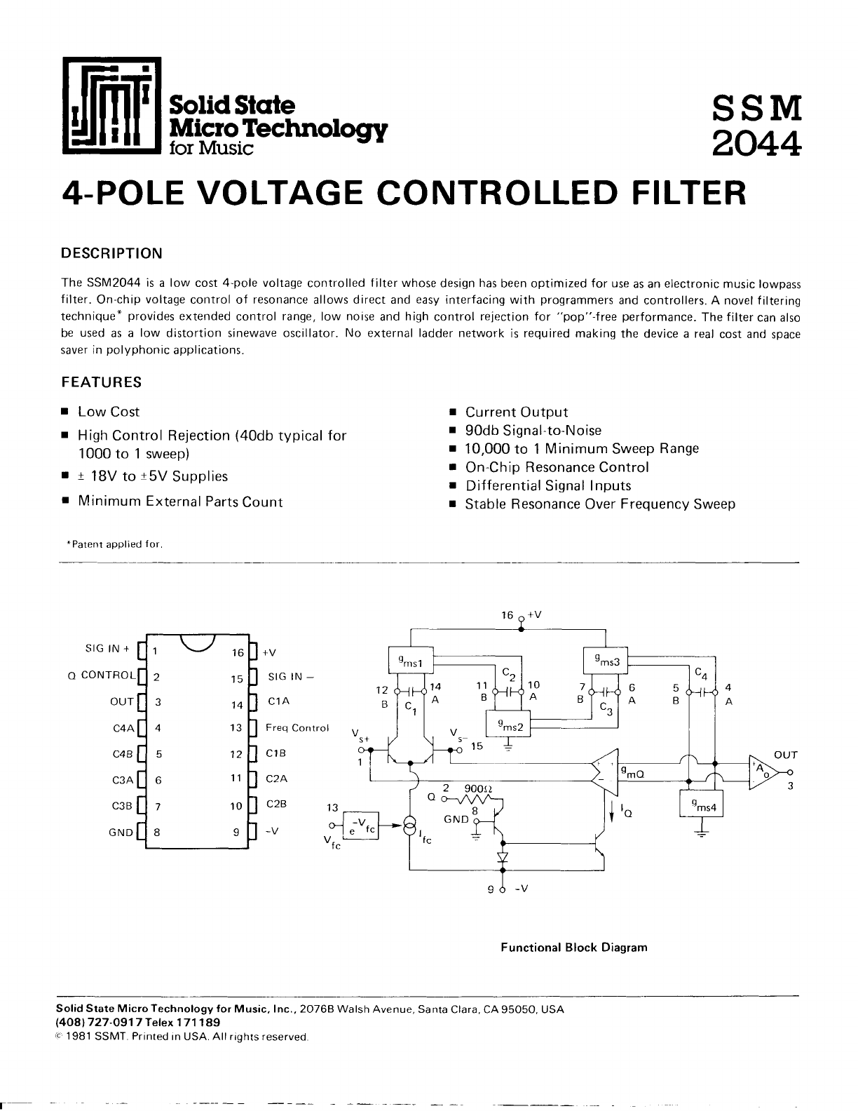
1 \-/ 16
2ts
3lq
4 't3
512
6 11
710
89
SIG
IN
+
O CONTROL
OUT
C4A
c48
C3A
c3B
GND
SIG
IN
-
c1A
Freq
Control
ClB
c2B
Functional Block Diagram
Solid State Micro
Technology
for
Music, Inc.,
2076B
Walsh
Avenue, Santa
Clara, CA 95O5O, USA
(408l.727-0917 Telex
1 71 1 89
.c
1981
SSMT.
Printed
in USA.
All
rights reserved.
SPECIFICATIONS
@ V, =
115
and
TA =
25'C
STORAGE
TEMPERATURE
-55"C
to
+125"C
OPERATING TEMPERATURE
0"C to
+70"C
PARAMETER MIN TYP MAX UNITS CONDITIONS
Positive
Supply
Range
Negative
Supply
Range
Positive
Supply
Current
Negative
Supply
Current
+5
-6
1.0
4.5
1.4
6.2
+18
-18
2.0
8.0
mA
mA
VFC
=
GND
VFC
- GND
Frequency Control
Range
Frequency Control
Feedthrough
Output Offset lO/lO
tu*
Frequency
Control Offset f/fnom
10,000:1
0.6
50,000:'l
-40db
0.05
1
-30db
o.2
1.5
V ,
=V =GND
sf s-
-90mV
<V-^ < +90mV
V V =V-^ GND
si s- t-
(-
Untrimmed
O
Control
Input lmpedance
O Current
at
Oscillation
O Control
Feedthrough
O
Control
Feedthrough
Max Available Control Current
Freq.
Control Input Range
Max
Output Signal
Currcnt
l0
Mu*
Signal to Noise
675
4AO
900
425
-30d
b
1200
450
-20d
b
-60db
s)
1tA
voc >
0.7v
-90mV(Vf.{+90mV
Untrimmed
Trimmed
1.25
120
t 300
17
r 400
90dt-.
2"2
+iB0
t 520
mA
pA
*FINAL
SPECIFICATIONS
MAY I]E SUB.IECT
TO CHANGE.
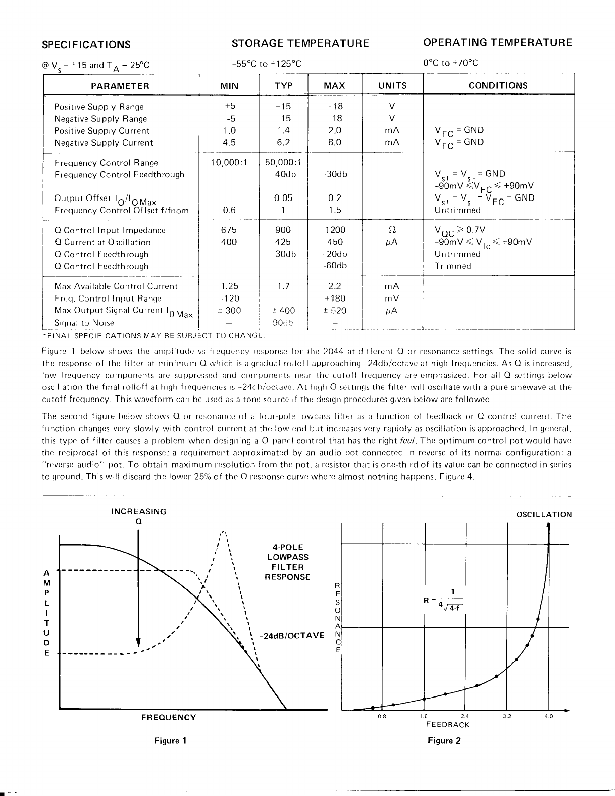
Figure
1 below shows the anrplitucle vs
frequuncy
response
tor rhe
2044
at
ciifferent O or resorranco
sottings- The solicl curve is
the response of the filter at rninirnurn 0 whrcl-r is a
qrariLrirl
roilofl approaci'r.rg
-24dttloctave
at high
frequencies.
As O is
increased,
low frequency
cornponents aril supplosserl and corrponents noar thc cutof{ frcquency
are
cnrphasized.
For all O settingls
below
oscillation the
firral rolloff
at
hiqh
trcquenc;ics
is
-24dlrloctavc.
At high O
soitings
the
filter will
oscillate with a
pure
sinewave at
the
cutoff frequency.
This waveform can be userl
as
a
tone source
if the riesigrr
procedures
given
below are
followed.
The second
figure
below shows
O or rosonancc
o{ a four polr:
lowlrass
filtu as a function
of feedback
or O control current-
Tl're
f
unction changcs
very
slowly with corrtrol currL-nt at tht: low
r:rrrl
but
incr cases vcry rapidly
as oscillation is approached.
In
qeneral,
this
type
of f
ilter causes
a problem
when desiqning
a
O panel
control
that
has the right feel
.f he
optimum
control
pot
wolrld have
the reciprocal
of this response; a requirement approximatr-'cl by an auclio
pot connected in reverse of its normal configuratiorr: a
"reverse
audio"
pot.
To obtain maxirnum resolution
fronr
the
pot,
a resistor that is one-third of its value can be connected in
series
to qround.
This will discard the lower 25o/o of the
O respons€r curve where almost nothing happens.
Figure
4.
INCREASING
o
A
M
P
L
I
T
U
D
E
FREOUENCY
Figure 1
FEEDBACK
Figure
2
OSCILLATION
4.POLE
LOWPASS
FILTER
RESPONSE
-24d8lOCTAVE
SIG
rN-
2ooo { roox
I \--'l 16
215
3214
4013
_4
j tz
4
6 11
71Q
89
O CONTROL
Q CONTROL
REJECTION
ADJ
(OPTIONAL)
50K
+V+-------------- ----------i
t
I
I
470K
0.017,rf
001/,f
100Ks
1%
j;i TL082
CONTROL
SUM[,4ER
'TEL
LABS TYPE
O81.
TC. r
3600
ppmi'C
ALL COI\4PONENTS
59,.
UNLESS NOTET).
(OPTIONAL.
SEE
BELOW)
F
igu re 3-Typical Connection
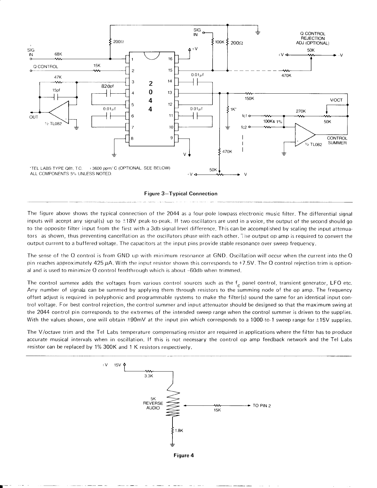
The figure
above
shows the typical connection
of the 2044
as a four-pole
lowpass electronic music filter.
The differential
signal
inputs will accept any signal(s) up to t18V peak
to-peak.
lf two oscillators are used in
a
voice,
the output of the
second should
go
to the opposite
filter input from the first with a 3db
signal
level rlifference. This
can be accomplished by scaling the input
attenua-
tors as shown, thus
preventing
cancellation as the
oscillators
phase
with each
other.
l ire
output op
amp
is required
to convert the
output current to a buffered voltage. The
capacitors at
the input
pins
provide
stable
resonance
over
sweep
frequency.
The sense
of the
O control is
frorn GND up with minimum resonance
at GND.
Oscillation
willoccur when
the current into
the
O
pin reaches
approximately 425 1tA.
With the input !'esistor
shown this corresponds
to +7.5V.
The O control rejection trim is option-
al and
is used
to
minimize O
control
fecdthrough
which is about
-60db
when trimmed.
The control summer adds the voltages from various control sources such as the f^ panel
control, transient
generator,
LFO etc.
Any number of signals can
be
summed
by applying
them through resistors to the iumming node
of the op amp.
The frequency
offset adlust is required in polyphonic
and programmable
systems
to make the filter(s)
sound the same
for an
identical
input con-
trol voltage.
For best
control
rejection,
the control summer and input attenuator should be designed so that the
maximum
swing
at
the 2O44
control
pin corresponds to the extremes
of the intended sweep range when the control
summer
is driven to the
supplies.
With the values
shown, one
will
obtain
t90mV at
the input
pin
which
corresponds to a 1000-to-1
sweep range
for
115V
supplies.
The V/octave
trim and the Tel Labs temperature compensating resistor
are
required in
applications
where the
f
ilter has
to produce
accurate
musical
intervals when in oscillation.
lf this is not necessary the control op amp feedback
network and the Tel Labs
resistor
can
be
replaced
by 1o/o 300K and 1 K resistors
respectively.
1V 15V
Figure
4
0.01
! f
15K
l-
TO PIN
2
