STM32F405/415, STM32F407/417, STM32F427/437 And STM32F429/439 Advanced Arm® Based 32 Bit MCUs Reference Manual STM32 ARM Trang 875 1749
User Manual:
Open the PDF directly: View PDF ![]() .
.
Page Count: 875 [warning: Documents this large are best viewed by clicking the View PDF Link!]

RM0090 Rev 18 875/1749
RM0090 Serial peripheral interface (SPI)
925
28.2.2 I2S features
•Full duplex communication
•Half-duplex communication (only transmitter or receiver)
•Master or slave operations
•8-bit programmable linear prescaler to reach accurate audio sample frequencies (from
8 kHz to 192 kHz)
•Data format may be 16-bit, 24-bit or 32-bit
•Packet frame is fixed to 16-bit (16-bit data frame) or 32-bit (16-bit, 24-bit, 32-bit data
frame) by audio channel
•Programmable clock polarity (steady state)
•Underrun flag in slave transmission mode, overrun flag in reception mode (master and
slave), and Frame Error flag in reception and transmission mode (slave only)
•16-bit register for transmission and reception with one data register for both channel
sides
•Supported I2S protocols:
–I
2S Phillps standard
– MSB-justified standard (left-justified)
– LSB-justified standard (right-justified)
– PCM standard (with short and long frame synchronization on 16-bit channel frame
or 16-bit data frame extended to 32-bit channel frame)
•Data direction is always MSB first
•DMA capability for transmission and reception (16-bit wide)
•Master clock may be output to drive an external audio component. Ratio is fixed at
256 × FS (where FS is the audio sampling frequency)
•Both I2S (I2S2 and I2S3) have a dedicated PLL (PLLI2S) to generate an even more
accurate clock.
•I2S (I2S2 and I2S3) clock can be derived from an external clock mapped on the
I2S_CKIN pin.
Serial peripheral interface (SPI) RM0090
876/1749 RM0090 Rev 18
28.3 SPI functional description
28.3.1 General description
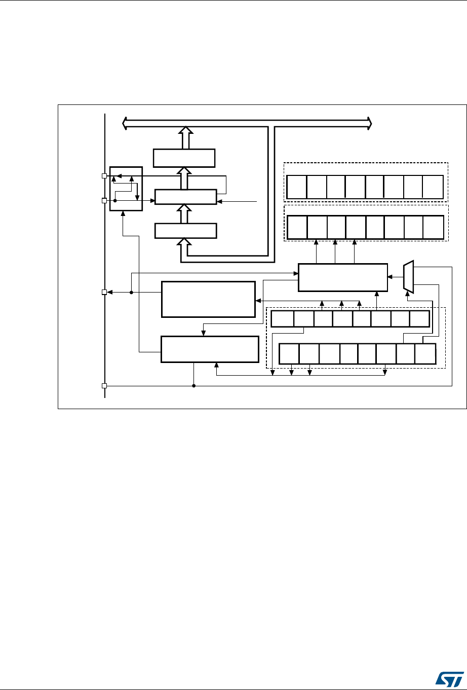
The block diagram of the SPI is shown in Figure 246.
Figure 246. SPI block diagram
Usually, the SPI is connected to external devices through four pins:
•MISO: Master In / Slave Out data. This pin can be used to transmit data in slave mode
and receive data in master mode.
•MOSI: Master Out / Slave In data. This pin can be used to transmit data in master
mode and receive data in slave mode.
•SCK: Serial Clock output for SPI masters and input for SPI slaves.
•NSS: Slave select. This is an optional pin to select a slave device. This pin acts as a
‘chip select’ to let the SPI master communicate with slaves individually and to avoid
contention on the data lines. Slave NSS inputs can be driven by standard IO ports on
the master device. The NSS pin may also be used as an output if enabled (SSOE bit)
and driven low if the SPI is in master configuration. In this manner, all NSS pins from
devices connected to the Master NSS pin see a low level and become slaves when
they are configured in NSS hardware mode. When configured in master mode with
NSS configured as an input (MSTR=1 and SSOE=0) and if NSS is pulled low, the SPI
enters the master mode fault state: the MSTR bit is automatically cleared and the
device is configured in slave mode (refer to Section 28.3.10).
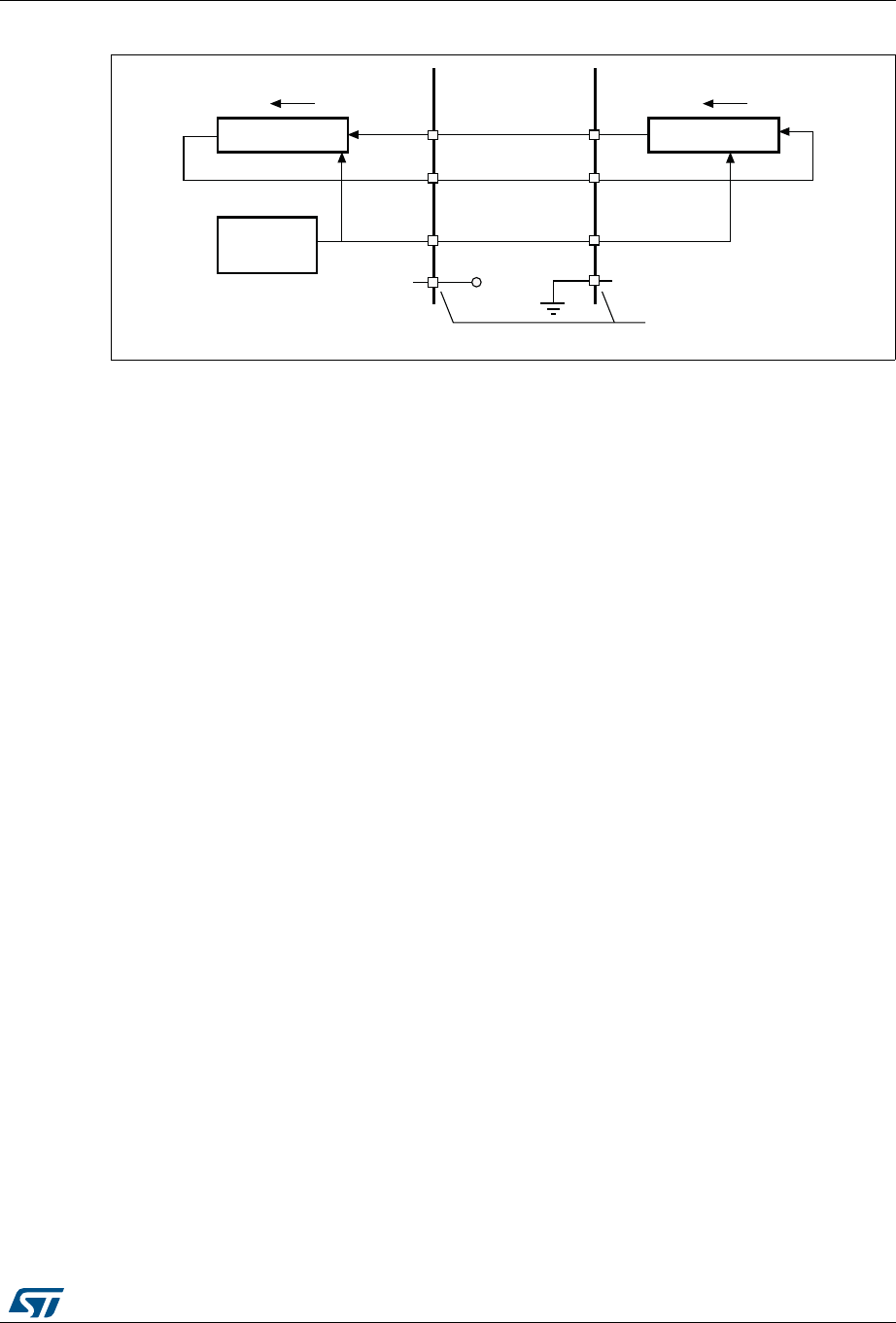
A basic example of interconnections between a single master and a single slave is
illustrated in Figure 247.
MS51604V1
MOSI
MISO
Baud rate generator
SCK
Master control logic
Communication control
SPE BR2 BR1 BR0 MSTR CPOL CPHA
BR[2:0]
RXNE
IE
LSB
FIRST
BIDI
MODE
BIDI
OE
BSY OVR MOD
FRXNETXE
ERR
IE
TXE
IE
00
DFF
0 SSOE
CRCEN
0
RX
ONLY
CRC
Next
CRC
ERR
0
1
NSS
SPI_CR1
SPI_CR2
SPI_SR
TXDM
AEN
RXDM
AEN
Address and data bus
Read
Rx buffer
Shift register
LSB first
Tx buffer
Write
SSM SSI
RM0090 Rev 18 877/1749
RM0090 Serial peripheral interface (SPI)
925
Figure 247. Single master/ single slave application
1. Here, the NSS pin is configured as an input.
The MOSI pins are connected together and the MISO pins are connected together. In this
way data is transferred serially between master and slave (most significant bit first).
The communication is always initiated by the master. When the master device transmits
data to a slave device via the MOSI pin, the slave device responds via the MISO pin. This
implies full-duplex communication with both data out and data in synchronized with the
same clock signal (which is provided by the master device via the SCK pin).
Slave select (NSS) pin management
Hardware or software slave select management can be set using the SSM bit in the
SPI_CR1 register.
•Software NSS management (SSM = 1)
The slave select information is driven internally by the value of the SSI bit in the
SPI_CR1 register. The external NSS pin remains free for other application uses.
•Hardware NSS management (SSM = 0)
Two configurations are possible depending on the NSS output configuration (SSOE bit
in register SPI_CR2).
– NSS output enabled (SSM = 0, SSOE = 1)
This configuration is used only when the device operates in master mode. The
NSS signal is driven low when the master starts the communication and is kept
low until the SPI is disabled.
– NSS output disabled (SSM = 0, SSOE = 0)
This configuration allows multimaster capability for devices operating in master
mode. For devices set as slave, the NSS pin acts as a classical NSS input: the
slave is selected when NSS is low and deselected when NSS high.
8-bit shift register
SPI clock
generator
8-bit shift register
MISO
MOSI MOSI
MISO
SCK SCK
SlaveMaster
NSS(1) NSS(1)
VDD
MSBit LSBit MSBit LSBit
Not used if NSS is managed
by software
ai14745

Serial peripheral interface (SPI) RM0090
878/1749 RM0090 Rev 18
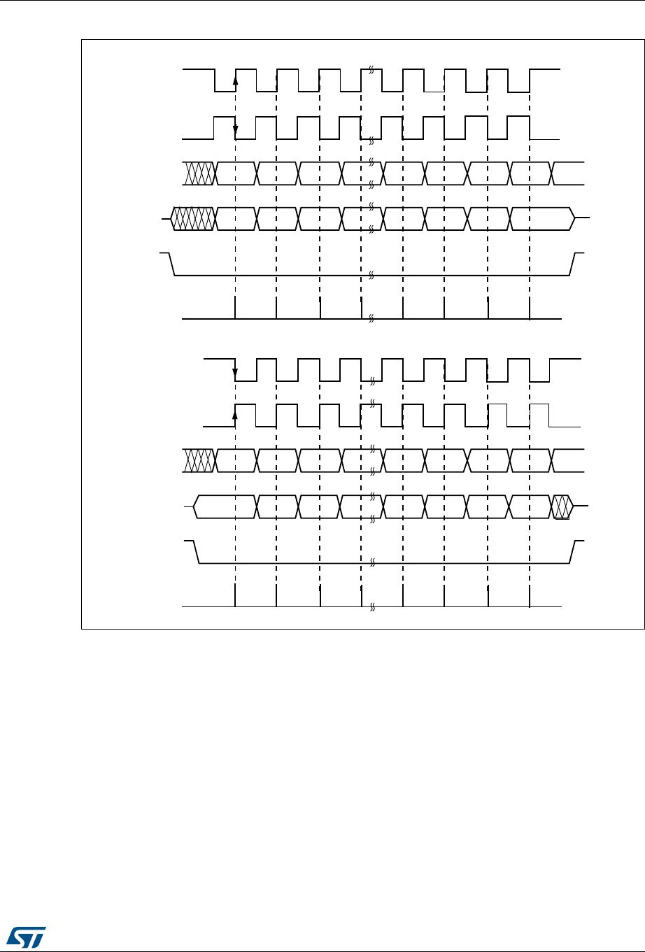
Clock phase and clock polarity
Four possible timing relationships may be chosen by software, using the CPOL and CPHA
bits in the SPI_CR1 register. The CPOL (clock polarity) bit controls the steady state value of
the clock when no data is being transferred. This bit affects both master and slave modes. If
CPOL is reset, the SCK pin has a low-level idle state. If CPOL is set, the SCK pin has a
high-level idle state.
If the CPHA (clock phase) bit is set, the second edge on the SCK pin (falling edge if the
CPOL bit is reset, rising edge if the CPOL bit is set) is the MSBit capture strobe. Data are
latched on the occurrence of the second clock transition. If the CPHA bit is reset, the first
edge on the SCK pin (falling edge if CPOL bit is set, rising edge if CPOL bit is reset) is the
MSBit capture strobe. Data are latched on the occurrence of the first clock transition.
The combination of the CPOL (clock polarity) and CPHA (clock phase) bits selects the data
capture clock edge.
Figure 248, shows an SPI transfer with the four combinations of the CPHA and CPOL bits.
The diagram may be interpreted as a master or slave timing diagram where the SCK pin,
the MISO pin, the MOSI pin are directly connected between the master and the slave
device.
Note: Prior to changing the CPOL/CPHA bits the SPI must be disabled by resetting the SPE bit.
Master and slave must be programmed with the same timing mode.
The idle state of SCK must correspond to the polarity selected in the SPI_CR1 register (by
pulling up SCK if CPOL=1 or pulling down SCK if CPOL=0).
The Data Frame Format (8- or 16-bit) is selected through the DFF bit in SPI_CR1 register,
and determines the data length during transmission/reception.
RM0090 Rev 18 879/1749
RM0090 Serial peripheral interface (SPI)
925
Figure 248. Data clock timing diagram
1. These timings are shown with the LSBFIRST bit reset in the SPI_CR1 register.
Data frame format
Data can be shifted out either MSB-first or LSB-first depending on the value of the
LSBFIRST bit in the SPI_CR1 Register.
Each data frame is 8 or 16 bits long depending on the size of the data programmed using
the DFF bit in the SPI_CR1 register. The selected data frame format is applicable for
transmission and/or reception.
CPOL = 1
CPOL = 0
MSBit LSBit
MSBit LSBit
MISO
MOSI
NSS
(to slave)
Capture strobe
CPHA =1
CPOL = 1
CPOL = 0
MSBit LSBit
MSBit LSBit
MISO
MOSI
NSS
(to slave)
Capture strobe
CPHA =0
ai17154d

Serial peripheral interface (SPI) RM0090
880/1749 RM0090 Rev 18
28.3.2 Configuring the SPI in slave mode
In the slave configuration, the serial clock is received on the SCK pin from the master
device. The value set in the BR[2:0] bits in the SPI_CR1 register, does not affect the data
transfer rate.
Note: It is recommended to enable the SPI slave before the master sends the clock. If not,
undesired data transmission might occur. The data register of the slave needs to be ready
before the first edge of the communication clock or before the end of the ongoing
communication. It is mandatory to have the polarity of the communication clock set to the
steady state value before the slave and the master are enabled.
Follow the procedure below to configure the SPI in slave mode:
Procedure
1. Set the DFF bit to define 8- or 16-bit data frame format
2. Select the CPOL and CPHA bits to define one of the four relationships between the
data transfer and the serial clock (see Figure 248). For correct data transfer, the CPOL
and CPHA bits must be configured in the same way in the slave device and the master
device. This step is not required when the TI mode is selected through the FRF bit in
the SPI_CR2 register.
3. The frame format (MSB-first or LSB-first depending on the value of the LSBFIRST bit in
the SPI_CR1 register) must be the same as the master device. This step is not
required when TI mode is selected.
4. In Hardware mode (refer to Slave select (NSS) pin management), the NSS pin must be
connected to a low level signal during the complete byte transmit sequence. In NSS
software mode, set the SSM bit and clear the SSI bit in the SPI_CR1 register. This step
is not required when TI mode is selected.
5. Set the FRF bit in the SPI_CR2 register to select the TI mode protocol for serial
communications.
6. Clear the MSTR bit and set the SPE bit (both in the SPI_CR1 register) to assign the
pins to alternate functions.
In this configuration the MOSI pin is a data input and the MISO pin is a data output.
Transmit sequence
The data byte is parallel-loaded into the Tx buffer during a write cycle.
The transmit sequence begins when the slave device receives the clock signal and the most
significant bit of the data on its MOSI pin. The remaining bits (the 7 bits in 8-bit data frame
format, and the 15 bits in 16-bit data frame format) are loaded into the shift-register. The
TXE flag in the SPI_SR register is set on the transfer of data from the Tx Buffer to the shift
register and an interrupt is generated if the TXEIE bit in the SPI_CR2 register is set.
Receive sequence
For the receiver, when data transfer is complete:
•The Data in shift register is transferred to Rx Buffer and the RXNE flag (SPI_SR
register) is set
•An Interrupt is generated if the RXNEIE bit is set in the SPI_CR2 register.
RM0090 Rev 18 881/1749
RM0090 Serial peripheral interface (SPI)
925
After the last sampling clock edge the RXNE bit is set, a copy of the data byte received in
the shift register is moved to the Rx buffer. When the SPI_DR register is read, the SPI
peripheral returns this buffered value.
Clearing of the RXNE bit is performed by reading the SPI_DR register.
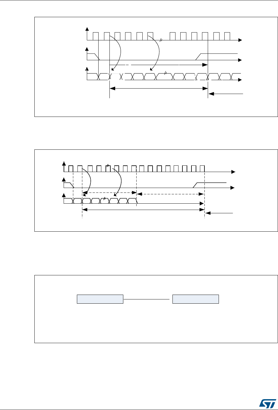
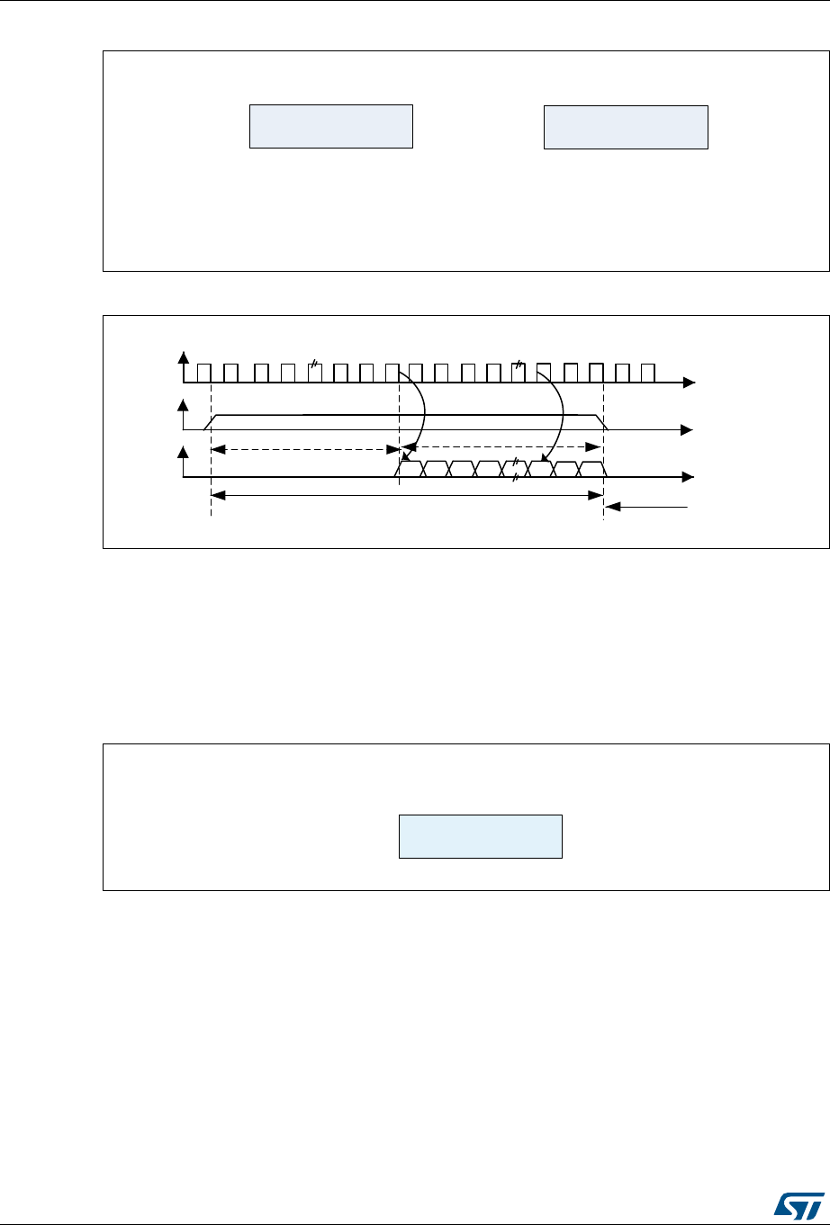
SPI TI protocol in slave mode
In slave mode, the SPI interface is compatible with the TI protocol. The FRF bit of the
SPI_CR2 register can be used to configure the slave SPI serial communications to be
compliant with this protocol.
The clock polarity and phase are forced to conform to the TI protocol requirements whatever
the values set in the SPI_CR1 register. NSS management is also specific to the TI protocol
which makes the configuration of NSS management through the SPI_CR1 and SPI_CR2
registers (such as SSM, SSI, SSOE) transparent for the user.
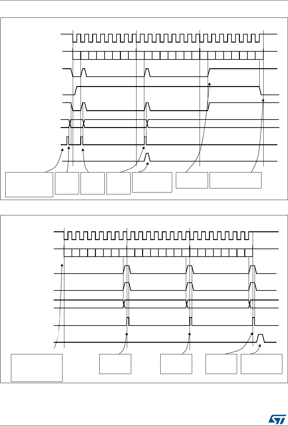
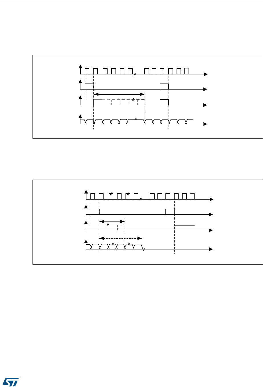
In Slave mode (Figure 249: TI mode - Slave mode, single transfer and Figure 250: TI mode
- Slave mode, continuous transfer), the SPI baud rate prescaler is used to control the
moment when the MISO pin state changes to HI-Z. Any baud rate can be used thus allowing
to determine this moment with optimal flexibility. However, the baud rate is generally set to
the external master clock baud rate. The time for the MISO signal to become HI-Z (trelease)
depends on internal resynchronizations and on the baud rate value set in through BR[2:0] of
SPI_CR1 register. It is given by the formula:
Note: This feature is not available for Motorola SPI communications (FRF bit set to 0).
To detect TI frame errors in Slave transmitter only mode by using the Error interrupt (ERRIE
= 1), the SPI must be configured in 2-line unidirectional mode by setting BIDIMODE and
BIDIOE to 1 in the SPI_CR1 register. When BIDIMODE is set to 0, OVR is set to 1 because
the data register is never read and error interrupt are always generated, while when
BIDIMODE is set to 1, data are not received and OVR is never set.
Figure 249. TI mode - Slave mode, single transfer
tbaud_rate
2
---------------------------- 4t
pclk
×+trelease
tbaud_rate
2
---------------------------- 6t
pclk
×+<<
ai18434
MSBIN
MOSI
input
NSS
input
SCK
input
trigger
edge
sampling
edge
trigger
edge
sampling
edge
trigger
edge
sampling
edge
DONTCARE LSBIN DONTCARE
MISO
output 1 or 0 MSBOUT LSBOUT
tRelease
Serial peripheral interface (SPI) RM0090
882/1749 RM0090 Rev 18
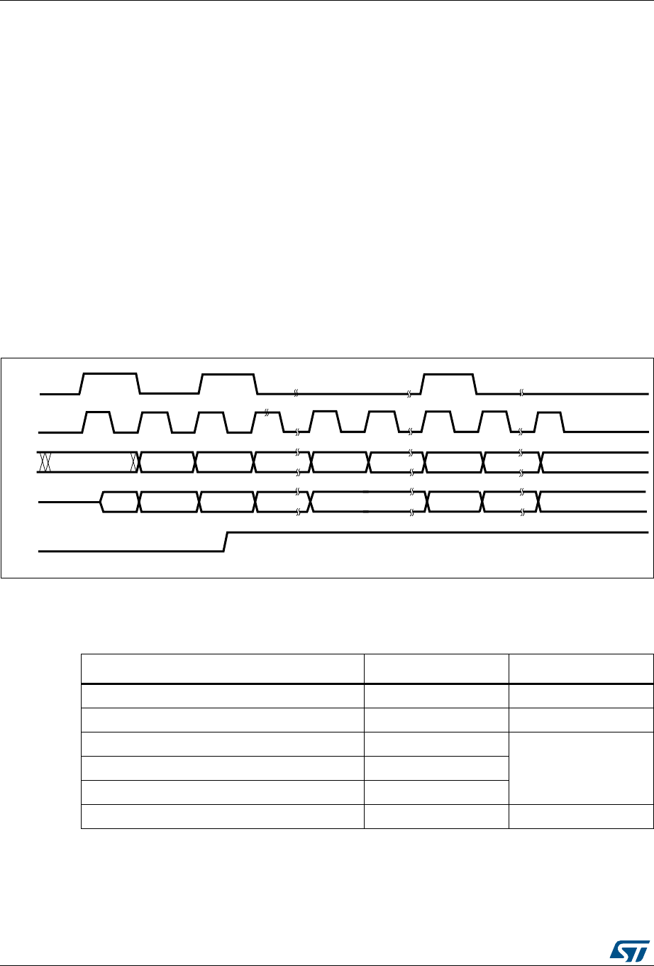
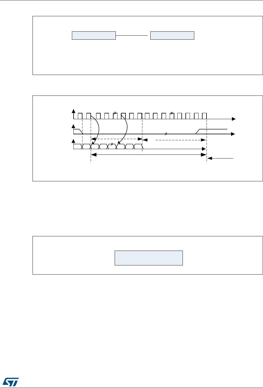
Figure 250. TI mode - Slave mode, continuous transfer
28.3.3 Configuring the SPI in master mode
In the master configuration, the serial clock is generated on the SCK pin.
Procedure
1. Select the BR[2:0] bits to define the serial clock baud rate (see SPI_CR1 register).
2. Select the CPOL and CPHA bits to define one of the four relationships between the
data transfer and the serial clock (see Figure 248). This step is not required when the
TI mode is selected.
3. Set the DFF bit to define 8- or 16-bit data frame format
4. Configure the LSBFIRST bit in the SPI_CR1 register to define the frame format. This
step is not required when the TI mode is selected.
5. If the NSS pin is required in input mode, in hardware mode, connect the NSS pin to a
high-level signal during the complete byte transmit sequence. In NSS software mode,
set the SSM and SSI bits in the SPI_CR1 register. If the NSS pin is required in output
mode, the SSOE bit only should be set. This step is not required when the TI mode is
selected.
6. Set the FRF bit in SPI_CR2 to select the TI protocol for serial communications.
7. The MSTR and SPE bits must be set (they remain set only if the NSS pin is connected
to a high-level signal).
In this configuration the MOSI pin is a data output and the MISO pin is a data input.
Transmit sequence
The transmit sequence begins when a byte is written in the Tx Buffer.
The data byte is parallel-loaded into the shift register (from the internal bus) during the first
bit transmission and then shifted out serially to the MOSI pin MSB first or LSB first
depending on the LSBFIRST bit in the SPI_CR1 register. The TXE flag is set on the transfer
of data from the Tx Buffer to the shift register and an interrupt is generated if the TXEIE bit in
the SPI_CR2 register is set.
ai18435
MSBIN
MOSI
input
NSS
input
SCK
input
trigger sampling trigger sampling trigger sampling
DONTCARE LSBIN DONTCARE
MISO
output 1 or 0 MSBOUT LSBOUT
MSBIN LSBIN
MSBOUT LSBOUT
FRAME 1 FRAME 2
RM0090 Rev 18 883/1749
RM0090 Serial peripheral interface (SPI)
925
Receive sequence
For the receiver, when data transfer is complete:
•The data in the shift register is transferred to the RX Buffer and the RXNE flag is set
•An interrupt is generated if the RXNEIE bit is set in the SPI_CR2 register
At the last sampling clock edge the RXNE bit is set, a copy of the data byte received in the
shift register is moved to the Rx buffer. When the SPI_DR register is read, the SPI
peripheral returns this buffered value.
Clearing the RXNE bit is performed by reading the SPI_DR register.
A continuous transmit stream can be maintained if the next data to be transmitted is put in
the Tx buffer once the transmission is started. Note that TXE flag should be ‘1 before any
attempt to write the Tx buffer is made.
Note: When a master is communicating with SPI slaves which need to be de-selected between
transmissions, the NSS pin must be configured as GPIO or another GPIO must be used and
toggled by software.
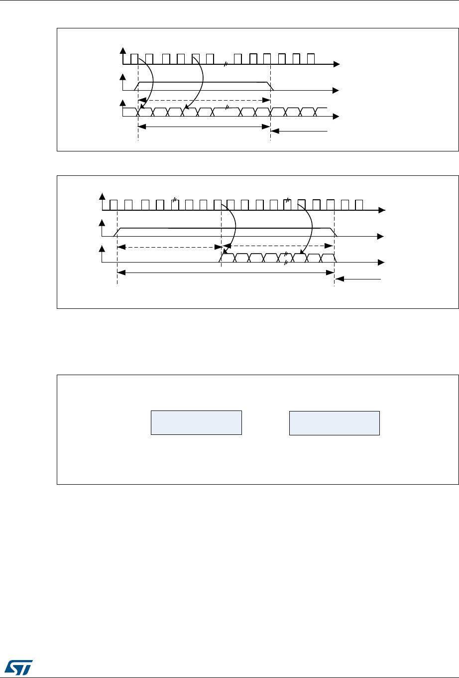
SPI TI protocol in master mode
In master mode, the SPI interface is compatible with the TI protocol. The FRF bit of the
SPI_CR2 register can be used to configure the master SPI serial communications to be
compliant with this protocol.
The clock polarity and phase are forced to conform to the TI protocol requirements whatever
the values set in the SPI_CR1 register. NSS management is also specific to the TI protocol
which makes the configuration of NSS management through the SPI_CR1 and SPI_CR2
registers (SSM, SSI, SSOE) transparent for the user.
Figure 251: TI mode - master mode, single transfer and Figure 252: TI mode - master mode,
continuous transfer) show the SPI master communication waveforms when the TI mode is
selected in master mode.
Figure 251. TI mode - master mode, single transfer
ai18436
MSBIN
MOSI
input
NSS
output
SCK
output
trigger
edge
sampling
edge
trigger
edge
sampling
edge
trigger
edge
sampling
edge
DONTCARE LSBIN DONTCARE
MISO
output 1 or 0 MSBOUT LSBOUT
Serial peripheral interface (SPI) RM0090
884/1749 RM0090 Rev 18
Figure 252. TI mode - master mode, continuous transfer
28.3.4 Configuring the SPI for half-duplex communication
The SPI is capable of operating in half-duplex mode in 2 configurations.
•1 clock and 1 bidirectional data wire
•1 clock and 1 data wire (receive-only or transmit-only)
1 clock and 1 bidirectional data wire (BIDIMODE = 1)
This mode is enabled by setting the BIDIMODE bit in the SPI_CR1 register. In this mode
SCK is used for the clock and MOSI in master or MISO in slave mode is used for data
communication. The transfer direction (Input/Output) is selected by the BIDIOE bit in the
SPI_CR1 register. When this bit is 1, the data line is output otherwise it is input.
1 clock and 1 unidirectional data wire (BIDIMODE = 0)
In this mode, the application can use the SPI either in transmit-only mode or in receive-only
mode.
•Transmit-only mode is similar to full-duplex mode (BIDIMODE=0, RXONLY=0): the
data are transmitted on the transmit pin (MOSI in master mode or MISO in slave mode)
and the receive pin (MISO in master mode or MOSI in slave mode) can be used as a
general-purpose IO. In this case, the application just needs to ignore the Rx buffer (if
the data register is read, it does not contain the received value).
•In receive-only mode, the application can disable the SPI output function by setting the
RXONLY bit in the SPI_CR1 register. In this case, it frees the transmit IO pin (MOSI in
master mode or MISO in slave mode), so it can be used for other purposes.
To start the communication in receive-only mode, configure and enable the SPI:
•In master mode, the communication starts immediately and stops when the SPE bit is
cleared and the current reception stops. There is no need to read the BSY flag in this
mode. It is always set when an SPI communication is ongoing.
•In slave mode, the SPI continues to receive as long as the NSS is pulled down (or the
SSI bit is cleared in NSS software mode) and the SCK is running.
ai18437
MSBOUT
MOSI
output
NSS
output
SCK
output
trigger sampling trigger sampling trigger sampling
DONTCARE LSBOUT
DONTCARE
MISO
intput 1 or 0 MSBIN LSBIN
MSBOUT LSBOUT
MSBIN LSBIN
FRAME 1 FRAME 2

RM0090 Rev 18 885/1749
RM0090 Serial peripheral interface (SPI)
925
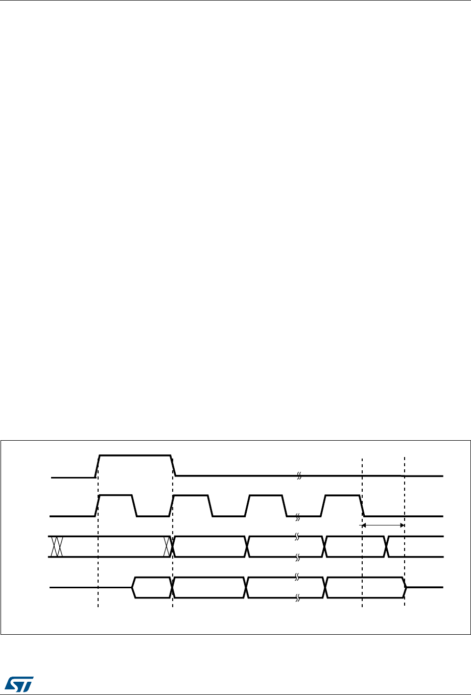
28.3.5 Data transmission and reception procedures
Rx and Tx buffers
In reception, data are received and then stored into an internal Rx buffer while In
transmission, data are first stored into an internal Tx buffer before being transmitted.
A read access of the SPI_DR register returns the Rx buffered value whereas a write access
to the SPI_DR stores the written data into the Tx buffer.
Start sequence in master mode
•In full-duplex (BIDIMODE=0 and RXONLY=0)
– The sequence begins when data are written into the SPI_DR register (Tx buffer).
– The data are then parallel loaded from the Tx buffer into the 8-bit shift register
during the first bit transmission and then shifted out serially to the MOSI pin.
– At the same time, the received data on the MISO pin is shifted in serially to the 8-
bit shift register and then parallel loaded into the SPI_DR register (Rx buffer).
•In unidirectional receive-only mode (BIDIMODE=0 and RXONLY=1)
– The sequence begins as soon as SPE=1
– Only the receiver is activated and the received data on the MISO pin are shifted in
serially to the 8-bit shift register and then parallel loaded into the SPI_DR register
(Rx buffer).
•In bidirectional mode, when transmitting (BIDIMODE=1 and BIDIOE=1)
– The sequence begins when data are written into the SPI_DR register (Tx buffer).
– The data are then parallel loaded from the Tx buffer into the 8-bit shift register
during the first bit transmission and then shifted out serially to the MOSI pin.
– No data are received.
•In bidirectional mode, when receiving (BIDIMODE=1 and BIDIOE=0)
– The sequence begins as soon as SPE=1 and BIDIOE=0.
– The received data on the MOSI pin are shifted in serially to the 8-bit shift register
and then parallel loaded into the SPI_DR register (Rx buffer).
– The transmitter is not activated and no data are shifted out serially to the MOSI
pin.
Start sequence in slave mode
•In full-duplex mode (BIDIMODE=0 and RXONLY=0)
– The sequence begins when the slave device receives the clock signal and the first
bit of the data on its MOSI pin. The 7 remaining bits are loaded into the shift
register.
– At the same time, the data are parallel loaded from the Tx buffer into the 8-bit shift
register during the first bit transmission, and then shifted out serially to the MISO

Serial peripheral interface (SPI) RM0090
886/1749 RM0090 Rev 18
pin. The software must have written the data to be sent before the SPI master
device initiates the transfer.
•In unidirectional receive-only mode (BIDIMODE=0 and RXONLY=1)
– The sequence begins when the slave device receives the clock signal and the first
bit of the data on its MOSI pin. The 7 remaining bits are loaded into the shift
register.
– The transmitter is not activated and no data are shifted out serially to the MISO
pin.
•In bidirectional mode, when transmitting (BIDIMODE=1 and BIDIOE=1)
– The sequence begins when the slave device receives the clock signal and the first
bit in the Tx buffer is transmitted on the MISO pin.
– The data are then parallel loaded from the Tx buffer into the 8-bit shift register
during the first bit transmission and then shifted out serially to the MISO pin. The
software must have written the data to be sent before the SPI master device
initiates the transfer.
– No data are received.
•In bidirectional mode, when receiving (BIDIMODE=1 and BIDIOE=0)
– The sequence begins when the slave device receives the clock signal and the first
bit of the data on its MISO pin.
– The received data on the MISO pin are shifted in serially to the 8-bit shift register
and then parallel loaded into the SPI_DR register (Rx buffer).
– The transmitter is not activated and no data are shifted out serially to the MISO
pin.
Handling data transmission and reception
The TXE flag (Tx buffer empty) is set when the data are transferred from the Tx buffer to the
shift register. It indicates that the internal Tx buffer is ready to be loaded with the next data.
An interrupt can be generated if the TXEIE bit in the SPI_CR2 register is set. Clearing the
TXE bit is performed by writing to the SPI_DR register.
Note: The software must ensure that the TXE flag is set to 1 before attempting to write to the Tx
buffer. Otherwise, it overwrites the data previously written to the Tx buffer.
The RXNE flag (Rx buffer not empty) is set on the last sampling clock edge, when the data
are transferred from the shift register to the Rx buffer. It indicates that data are ready to be
read from the SPI_DR register. An interrupt can be generated if the RXNEIE bit in the
SPI_CR2 register is set. Clearing the RXNE bit is performed by reading the SPI_DR
register.
For some configurations, the BSY flag can be used during the last data transfer to wait until
the completion of the transfer.
Full-duplex transmit and receive procedure in master or slave mode (BIDIMODE=0 and
RXONLY=0)
The software has to follow this procedure to transmit and receive data (see Figure 253 and
Figure 254):
RM0090 Rev 18 887/1749
RM0090 Serial peripheral interface (SPI)
925
1. Enable the SPI by setting the SPE bit to 1.
2. Write the first data item to be transmitted into the SPI_DR register (this clears the TXE
flag).
3. Wait until TXE=1 and write the second data item to be transmitted. Then wait until
RXNE=1 and read the SPI_DR to get the first received data item (this clears the RXNE
bit). Repeat this operation for each data item to be transmitted/received until the n–1
received data.
4. Wait until RXNE=1 and read the last received data.
5. Wait until TXE=1 and then wait until BSY=0 before disabling the SPI.
This procedure can also be implemented using dedicated interrupt subroutines launched at
each rising edges of the RXNE or TXE flag.
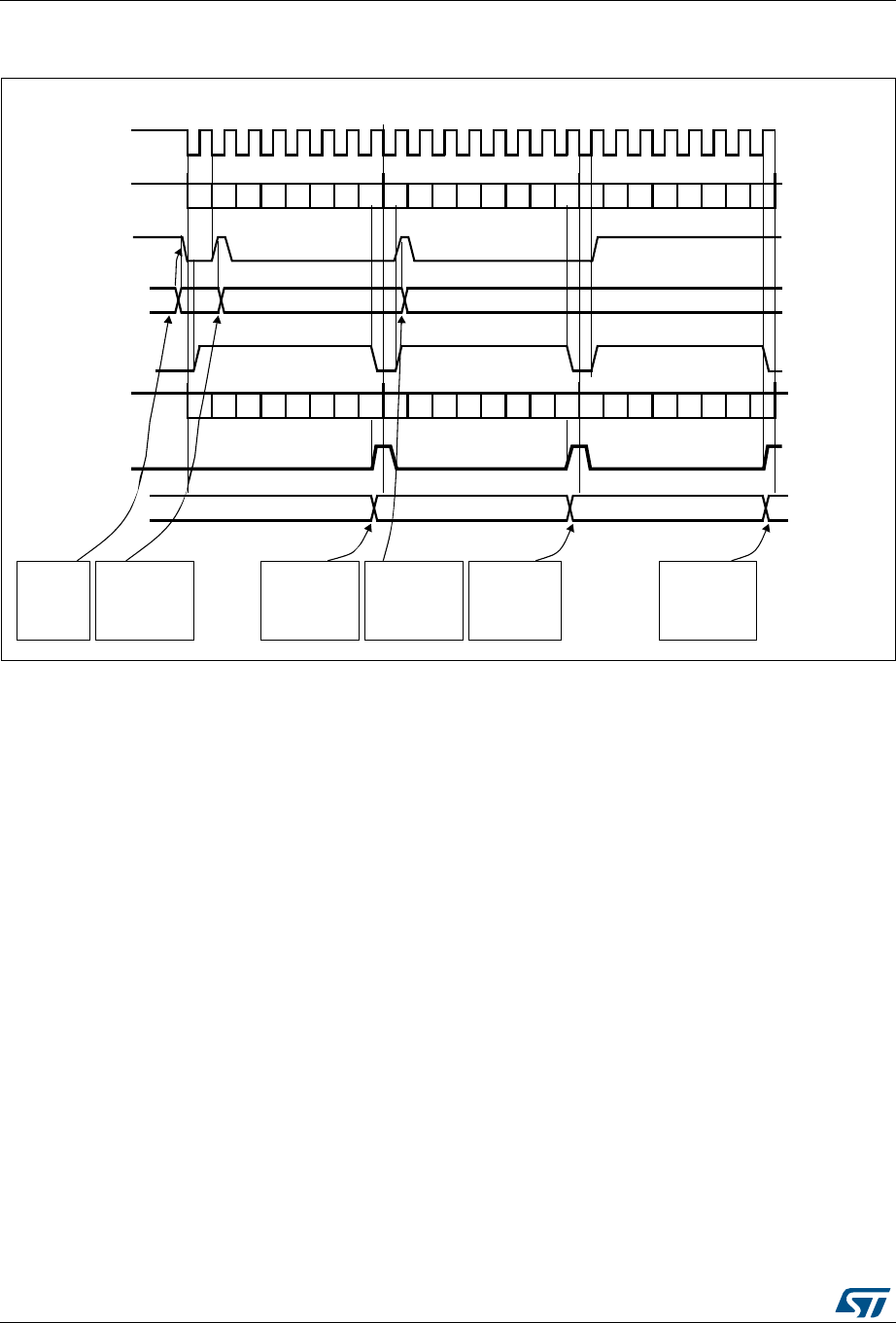
Figure 253. TXE/RXNE/BSY behavior in Master / full-duplex mode (BIDIMODE=0 and
RXONLY=0) in case of continuous transfers
MISO/MOSI (in)
Tx buffer
DATA 1 = 0xA1
TXE flag
0xF2
BSY flag
0xF3
software
writes 0xF1
into SPI_DR
software waits
until TXE=1 and
writes 0xF2 into
SPI_DR
software waits
until RXNE=1
and reads 0xA1
from SPI_DR
set by hardware
cleared by software
set by hardware
cleared by software set by hardware
set by hardware
SCK
DATA 2 = 0xA2 DATA 3 = 0xA3
reset by hardware
Example in Master mode with CPOL=1, CPHA=1
0xF1
RXNE flag
(write SPI_DR)
Rx buffer
set by hardware
MISO/MOSI (out)
DATA1 = 0xF1 DATA2 = 0xF2 DATA3 = 0xF3
(read SPI_DR)
0xA1 0xA2 0xA3
software waits
until TXE=1 and
writes 0xF3 into
SPI_DR
software waits
until RXNE=1
and reads 0xA2
from SPI_ DR
software waits
until RXNE=1
and reads 0xA3
from SPI_DR
b0 b1 b2 b3 b4 b5 b6 b7 b0 b1 b2 b3 b4 b5 b6 b7 b0 b1 b2 b3 b4 b5 b6 b7
b0 b1 b2 b3 b4 b5 b6 b7 b0 b1 b2 b3 b4 b5 b6 b7 b0 b1 b2 b3 b4 b5 b6 b7
cleared by software
ai17343
Serial peripheral interface (SPI) RM0090
888/1749 RM0090 Rev 18
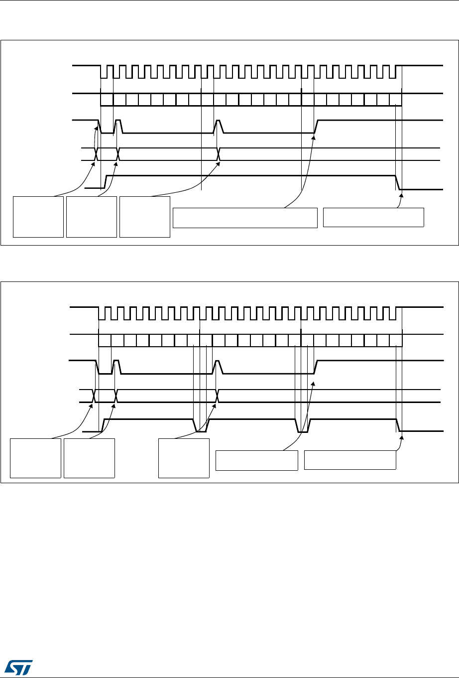
Figure 254. TXE/RXNE/BSY behavior in Slave / full-duplex mode (BIDIMODE=0,
RXONLY=0) in case of continuous transfers
Transmit-only procedure (BIDIMODE=0 RXONLY=0)
In this mode, the procedure can be reduced as described below and the BSY bit can be
used to wait until the completion of the transmission (see Figure 255 and Figure 256).
1. Enable the SPI by setting the SPE bit to 1.
2. Write the first data item to send into the SPI_DR register (this clears the TXE bit).
3. Wait until TXE=1 and write the next data item to be transmitted. Repeat this step for
each data item to be transmitted.
4. After writing the last data item into the SPI_DR register, wait until TXE=1, then wait until
BSY=0, this indicates that the transmission of the last data is complete.
This procedure can be also implemented using dedicated interrupt subroutines launched at
each rising edge of the TXE flag.
Note: During discontinuous communications, there is a 2 APB clock period delay between the
write operation to SPI_DR and the BSY bit setting. As a consequence, in transmit-only
mode, it is mandatory to wait first until TXE is set and then until BSY is cleared after writing
the last data.
After transmitting two data items in transmit-only mode, the OVR flag is set in the SPI_SR
register since the received data are never read.
0xF1
set by cleared by software
MISO/MOSI (in)
Tx buffer
DATA 1 = 0xA1
TXE flag
0xF2
BSY flag
0xF3
software
writes 0xF1
into SPI_DR
software waits
until TXE=1 and
writes 0xF2 into
SPI_DR
software waits
until RXNE=1
and reads 0xA1
from SPI_DR
set by hardware
cleared by software
set by hardware
cleared by software set by hardware
SCK
DATA 2 = 0xA2 DATA 3 = 0xA3
reset by hardware
Example in Slave mode with CPOL=1, CPHA=1
RXNE flag
(write to SPI_DR)
Rx buffer
set by hardware
MISO/MOSI (out)
DATA 1 = 0xF1 DATA 2 = 0xF2 DATA 3 = 0xF3
(read from SPI_DR)
0xA1 0xA2 0xA3
software waits
until TXE=1 and
writes 0xF3 into
SPI_DR
software waits
until RXNE=1
and reads 0xA2
from SPI_ DR
software waits
until RXNE=1
and reads 0xA3
from SPI_DR
b0 b1 b2 b3 b4 b5 b6 b7 b0 b1 b2 b3 b4 b5 b6 b7 b0 b1 b2 b3 b4 b5 b6 b7
b0 b1 b2 b3 b4 b5 b6 b7 b0 b1 b2 b3 b4 b5 b6 b7 b0 b1 b2 b3 b4 b5 b6 b7
cleared by software
ai17344
RM0090 Rev 18 889/1749
RM0090 Serial peripheral interface (SPI)
925
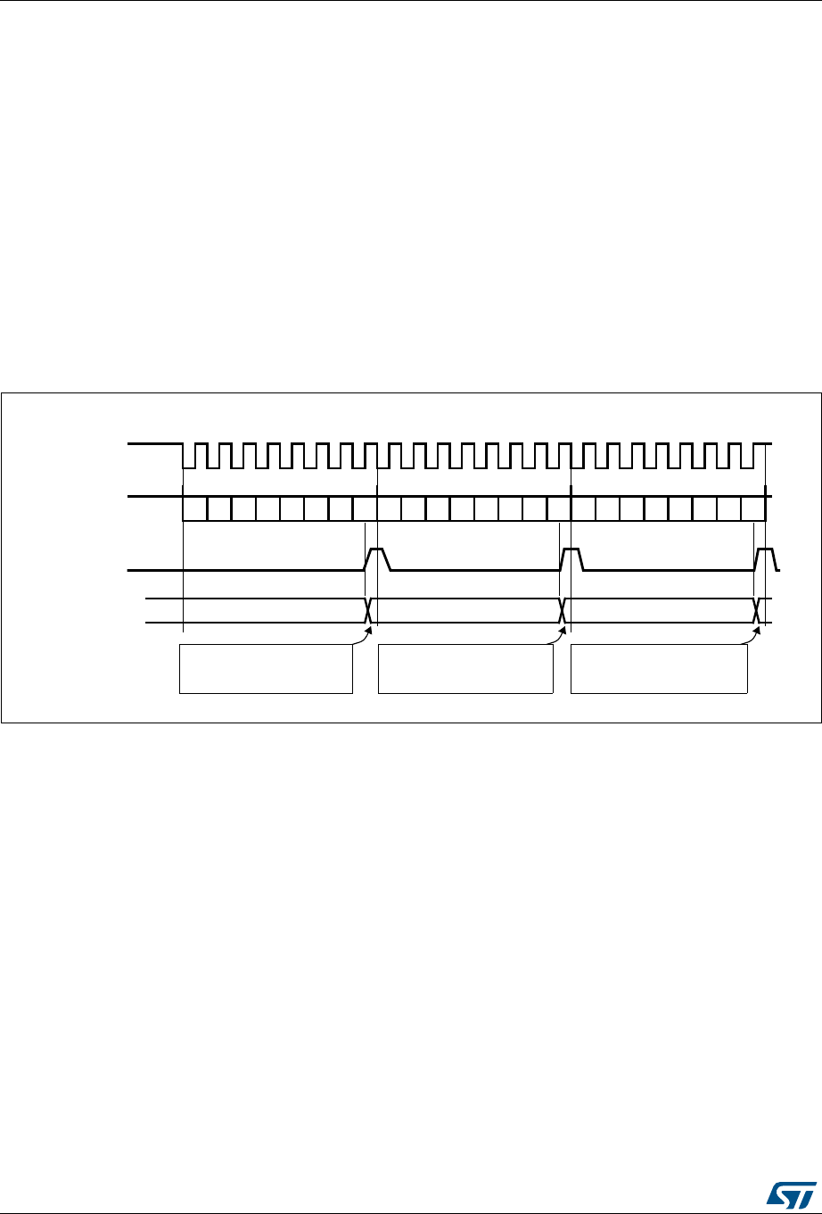
Figure 255. TXE/BSY behavior in Master transmit-only mode (BIDIMODE=0 and RXONLY=0)
in case of continuous transfers
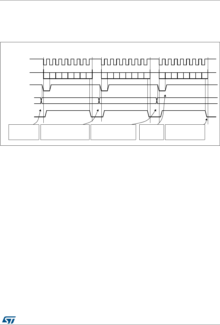
Figure 256. TXE/BSY in Slave transmit-only mode (BIDIMODE=0 and RXONLY=0) in case of
continuous transfers
Bidirectional transmit procedure (BIDIMODE=1 and BIDIOE=1)
In this mode, the procedure is similar to the procedure in Transmit-only mode except that
the BIDIMODE and BIDIOE bits both have to be set in the SPI_CR2 register before enabling
the SPI.
Unidirectional receive-only procedure (BIDIMODE=0 and RXONLY=1)
In this mode, the procedure can be reduced as described below (see Figure 257):
0xF1
Tx buffer
TXE flag
0xF2
BSY flag
0xF3
software writes
0xF1 into
SPI_DR
software waits
until TXE=1 and
writes 0xF2 into
SPI_DR
set by hardware
cleared by software
set by hardware
cleared by software set by hardware
set by hardware
SCK
reset by hardware
Example in Master mode with CPOL=1, CPHA=1
(write to SPI_DR)
MISO/MOSI (out)
DATA 1 = 0xF1 DATA 2 = 0xF2 DATA 3 = 0xF3
software waits
until TXE=1 and
writes 0xF3 into
SPI_DR
software waits until BSY=0software waits until TXE=1
b0 b1 b2 b3 b4 b5 b6 b7 b0 b1 b2 b3 b4 b5 b6 b7 b0 b1 b2 b3 b4 b5 b6 b7
ai17345
0xF1
Tx buffer
TXE flag
0xF2
BSY flag
0xF3
software writes
0xF1 into
SPI_DR
software waits
until TXE=1 and
writes 0xF2 into
SPI_DR
set by hardware
cleared by software
set by hardware
cleared by software set by hardware
set by hardware
SCK
reset by hardware
Example in slave mode with CPOL=1, CPHA=1
(write to SPI_DR)
MISO/MOSI (out)
DATA 1 = 0xF1 DATA 2 = 0xF2 DATA 3 = 0xF3
software waits
until TXE=1 and
writes 0xF3 into
SPI_DR
software waits until BSY=0software waits until TXE=1
b0 b1 b2 b3 b4 b5 b6 b7 b0 b1 b2 b3 b4 b5 b6 b7 b0 b1 b2 b3 b4 b5 b6 b7
ai17346
Serial peripheral interface (SPI) RM0090
890/1749 RM0090 Rev 18
1. Set the RXONLY bit in the SPI_CR1 register.
2. Enable the SPI by setting the SPE bit to 1:
a) In master mode, this immediately activates the generation of the SCK clock, and
data are serially received until the SPI is disabled (SPE=0).
b) In slave mode, data are received when the SPI master device drives NSS low and
generates the SCK clock.
3. Wait until RXNE=1 and read the SPI_DR register to get the received data (this clears
the RXNE bit). Repeat this operation for each data item to be received.
This procedure can also be implemented using dedicated interrupt subroutines launched at
each rising edge of the RXNE flag.
Note: If it is required to disable the SPI after the last transfer, follow the recommendation
described in Section 28.3.8.
Figure 257. RXNE behavior in receive-only mode (BIDIRMODE=0 and RXONLY=1)
in case of continuous transfers
Bidirectional receive procedure (BIDIMODE=1 and BIDIOE=0)
In this mode, the procedure is similar to the Receive-only mode procedure except that the
BIDIMODE bit has to be set and the BIDIOE bit cleared in the SPI_CR2 register before
enabling the SPI.
Continuous and discontinuous transfers
When transmitting data in master mode, if the software is fast enough to detect each rising
edge of TXE (or TXE interrupt) and to immediately write to the SPI_DR register before the
ongoing data transfer is complete, the communication is said to be continuous. In this case,
there is no discontinuity in the generation of the SPI clock between each data item and the
BSY bit is never cleared between each data transfer.
On the contrary, if the software is not fast enough, this can lead to some discontinuities in
the communication. In this case, the BSY bit is cleared between each data transmission
(see Figure 258).
In Master receive-only mode (RXONLY=1), the communication is always continuous and
the BSY flag is always read at 1.
MISO/MOSI (in)
DATA 1 = 0xA1
software waits until RXNE=1
and reads 0xA1 from SPI_DR
SCK
DATA 2 = 0xA2 DATA 3 = 0xA3
Example with CPOL=1, CPHA=1, RXONLY=1
RXNE flag
Rx buffer
set by hardware
(read from SPI_DR) 0xA1 0xA2 0xA3
software waits until RXNE=1
and reads 0xA2 from SPI_DR
software waits until RXNE=1
and reads 0xA3 from SPI_DR
b0 b1 b2 b3 b4 b5 b6 b7 b0 b1 b2 b3 b4 b5 b6 b7 b0 b1 b2 b3 b4 b5 b6 b7
cleared by software
ai17347
RM0090 Rev 18 891/1749
RM0090 Serial peripheral interface (SPI)
925
In slave mode, the continuity of the communication is decided by the SPI master device. In
any case, even if the communication is continuous, the BSY flag goes low between each
transfer for a minimum duration of one SPI clock cycle (see Figure 256).
Figure 258. TXE/BSY behavior when transmitting (BIDIRMODE=0 and RXONLY=0)
in case of discontinuous transfers
28.3.6 CRC calculation
A CRC calculator has been implemented for communication reliability. Separate CRC
calculators are implemented for transmitted data and received data. The CRC is calculated
using a programmable polynomial serially on each bit. It is calculated on the sampling clock
edge defined by the CPHA and CPOL bits in the SPI_CR1 register.
Note: This SPI offers two kinds of CRC calculation standard which depend directly on the data
frame format selected for the transmission and/or reception: 8-bit data (CR8) and 16-bit data
(CRC16).
CRC calculation is enabled by setting the CRCEN bit in the SPI_CR1 register. This action
resets the CRC registers (SPI_RXCRCR and SPI_TXCRCR). In full duplex or transmitter
only mode, when the transfers are managed by the software (CPU mode), it is necessary to
write the bit CRCNEXT immediately after the last data to be transferred is written to the
SPI_DR. At the end of this last data transfer, the SPI_TXCRCR value is transmitted.
In receive only mode and when the transfers are managed by software (CPU mode), it is
necessary to write the CRCNEXT bit after the second last data has been received. The CRC
is received just after the last data reception and the CRC check is then performed.
At the end of data and CRC transfers, the CRCERR flag in the SPI_SR register is set if
corruption occurs during the transfer.
If data are present in the TX buffer, the CRC value is transmitted only after the transmission
of the data byte. During CRC transmission, the CRC calculator is switched off and the
register value remains unchanged.
SPI communication using the CRC is possible through the following procedure:
MOSI (out)
Tx buffer
DATA 1 = 0xF1
TXE flag
0xF1
BSY flag
0xF2
software writes 0xF1
into SPI_DR
software waits until TXE=1 but is
late to write 0xF2 into SPI_DR
software waits until TXE=1 but
is late to write 0xF3 into
SPI_DR
SCK
3Fx0 = 3 ATAD2Fx0 = 2 ATAD
Example with CPOL=1, CPHA=1
0xF3
software waits
until TXE=1
software waits until BSY=0
(write to SPI_DR)
b0 b1 b2 b3 b4 b5 b6 b7 b0 b1 b2 b3 b4 b5 b6 b7 b0 b1 b2 b3 b4 b5 b6 b7
ai17348

Serial peripheral interface (SPI) RM0090
892/1749 RM0090 Rev 18
1. Program the CPOL, CPHA, LSBFirst, BR, SSM, SSI and MSTR values.
2. Program the polynomial in the SPI_CRCPR register.
3. Enable the CRC calculation by setting the CRCEN bit in the SPI_CR1 register. This
also clears the SPI_RXCRCR and SPI_TXCRCR registers.
4. Enable the SPI by setting the SPE bit in the SPI_CR1 register.
5. Start the communication and sustain the communication until all but one byte or half-
word have been transmitted or received.
– In full duplex or transmitter-only mode, when the transfers are managed by
software, when writing the last byte or half word to the Tx buffer, set the
CRCNEXT bit in the SPI_CR1 register to indicate that the CRC will be transmitted
after the transmission of the last byte.
– In receiver only mode, set the bit CRCNEXT just after the reception of the second
to last data to prepare the SPI to enter in CRC Phase at the end of the reception of
the last data. CRC calculation is frozen during the CRC transfer.
6. After the transfer of the last byte or half word, the SPI enters the CRC transfer and
check phase. In full duplex mode or receiver-only mode, the received CRC is
compared to the SPI_RXCRCR value. If the value does not match, the CRCERR flag in
SPI_SR is set and an interrupt can be generated when the ERRIE bit in the SPI_CR2
register is set.
Note: When the SPI is in slave mode, be careful to enable CRC calculation only when the clock is
stable, that is, when the clock is in the steady state. If not, a wrong CRC calculation may be
done. In fact, the CRC is sensitive to the SCK slave input clock as soon as CRCEN is set,
and this, whatever the value of the SPE bit.
With high bitrate frequencies, be careful when transmitting the CRC. As the number of used
CPU cycles has to be as low as possible in the CRC transfer phase, it is forbidden to call
software functions in the CRC transmission sequence to avoid errors in the last data and
CRC reception. In fact, CRCNEXT bit has to be written before the end of the
transmission/reception of the last data.
For high bit rate frequencies, it is advised to use the DMA mode to avoid the degradation of
the SPI speed performance due to CPU accesses impacting the SPI bandwidth.
When the devices are configured as slaves and the NSS hardware mode is used, the NSS
pin needs to be kept low between the data phase and the CRC phase.
When the SPI is configured in slave mode with the CRC feature enabled, CRC calculation
takes place even if a high level is applied on the NSS pin. This may happen for example in
case of a multislave environment where the communication master addresses slaves
alternately.
Between a slave deselection (high level on NSS) and a new slave selection (low level on
NSS), the CRC value should be cleared on both master and slave sides in order to
resynchronize the master and slave for their respective CRC calculation.
To clear the CRC, follow the procedure below:
1. Disable SPI (SPE = 0)
2. Clear the CRCEN bit
3. Set the CRCEN bit
4. Enable the SPI (SPE = 1)

RM0090 Rev 18 893/1749
RM0090 Serial peripheral interface (SPI)
925
28.3.7 Status flags
Four status flags are provided for the application to completely monitor the state of the SPI
bus.
Tx buffer empty flag (TXE)
When it is set, this flag indicates that the Tx buffer is empty and the next data to be
transmitted can be loaded into the buffer. The TXE flag is cleared when writing to the
SPI_DR register.
Rx buffer not empty (RXNE)
When set, this flag indicates that there are valid received data in the Rx buffer. It is cleared
when SPI_DR is read.
BUSY flag
This BSY flag is set and cleared by hardware (writing to this flag has no effect). The BSY
flag indicates the state of the communication layer of the SPI.
When BSY is set, it indicates that the SPI is busy communicating. There is one exception in
master mode / bidirectional receive mode (MSTR=1 and BDM=1 and BDOE=0) where the
BSY flag is kept low during reception.
The BSY flag is useful to detect the end of a transfer if the software wants to disable the SPI
and enter Halt mode (or disable the peripheral clock). This avoids corrupting the last
transfer. For this, the procedure described below must be strictly respected.
The BSY flag is also useful to avoid write collisions in a multimaster system.
The BSY flag is set when a transfer starts, with the exception of master mode / bidirectional
receive mode (MSTR=1 and BDM=1 and BDOE=0).
It is cleared:
•when a transfer is finished (except in master mode if the communication is continuous)
•when the SPI is disabled
•when a master mode fault occurs (MODF=1)
When communication is not continuous, the BSY flag is low between each communication.
When communication is continuous:
•in master mode, the BSY flag is kept high during all the transfers
•in slave mode, the BSY flag goes low for one SPI clock cycle between each transfer
Note: Do not use the BSY flag to handle each data transmission or reception. It is better to use the
TXE and RXNE flags instead.

Serial peripheral interface (SPI) RM0090
894/1749 RM0090 Rev 18
28.3.8 Disabling the SPI
When a transfer is terminated, the application can stop the communication by disabling the
SPI peripheral. This is done by clearing the SPE bit.
For some configurations, disabling the SPI and entering the Halt mode while a transfer is
ongoing can cause the current transfer to be corrupted and/or the BSY flag might become
unreliable.
To avoid any of those effects, it is recommended to respect the following procedure when
disabling the SPI:
In master or slave full-duplex mode (BIDIMODE=0, RXONLY=0)
1. Wait until RXNE=1 to receive the last data
2. Wait until TXE=1
3. Then wait until BSY=0
4. Disable the SPI (SPE=0) and, eventually, enter the Halt mode (or disable the peripheral
clock)
In master or slave unidirectional transmit-only mode (BIDIMODE=0,
RXONLY=0) or bidirectional transmit mode (BIDIMODE=1, BIDIOE=1)
After the last data is written into the SPI_DR register:
1. Wait until TXE=1
2. Then wait until BSY=0
3. Disable the SPI (SPE=0) and, eventually, enter the Halt mode (or disable the peripheral
clock)
In master unidirectional receive-only mode (MSTR=1, BIDIMODE=0,
RXONLY=1) or bidirectional receive mode (MSTR=1, BIDIMODE=1, BIDIOE=0)
This case must be managed in a particular way to ensure that the SPI does not initiate a
new transfer. The sequence below is valid only for SPI Motorola configuration (FRF bit set to
0):
1. Wait for the second to last occurrence of RXNE=1 (n–1)
2. Then wait for one SPI clock cycle (using a software loop) before disabling the SPI
(SPE=0)
3. Then wait for the last RXNE=1 before entering the Halt mode (or disabling the
peripheral clock)
When the SPI is configured in TI mode (Bit FRF set to 1), the following procedure has to be
respected to avoid generating an undesired pulse on NSS when the SPI is disabled:
1. Wait for the second to last occurrence of RXNE = 1 (n-1).
2. Disable the SPI (SPE = 0) in the following window frame using a software loop:
– After at least one SPI clock cycle,
– Before the beginning of the LSB data transfer.
Note: In master bidirectional receive mode (MSTR=1 and BDM=1 and BDOE=0), the BSY flag is
kept low during transfers.

RM0090 Rev 18 895/1749
RM0090 Serial peripheral interface (SPI)
925
In slave receive-only mode (MSTR=0, BIDIMODE=0, RXONLY=1) or
bidirectional receive mode (MSTR=0, BIDIMODE=1, BIDOE=0)
1. You can disable the SPI (write SPE=1) at any time: the current transfer will complete
before the SPI is effectively disabled
2. Then, if you want to enter the Halt mode, you must first wait until BSY = 0 before
entering the Halt mode (or disabling the peripheral clock).
28.3.9 SPI communication using DMA (direct memory addressing)
To operate at its maximum speed, the SPI needs to be fed with the data for transmission
and the data received on the Rx buffer should be read to avoid overrun. To facilitate the
transfers, the SPI features a DMA capability implementing a simple request/acknowledge
protocol.
A DMA access is requested when the enable bit in the SPI_CR2 register is enabled.
Separate requests must be issued to the Tx and Rx buffers (see Figure 259 and
Figure 260):
•In transmission, a DMA request is issued each time TXE is set to 1. The DMA then
writes to the SPI_DR register (this clears the TXE flag).
•In reception, a DMA request is issued each time RXNE is set to 1. The DMA then reads
the SPI_DR register (this clears the RXNE flag).
When the SPI is used only to transmit data, it is possible to enable only the SPI Tx DMA
channel. In this case, the OVR flag is set because the data received are not read.
When the SPI is used only to receive data, it is possible to enable only the SPI Rx DMA
channel.
In transmission mode, when the DMA has written all the data to be transmitted (flag TCIF is
set in the DMA_ISR register), the BSY flag can be monitored to ensure that the SPI
communication is complete. This is required to avoid corrupting the last transmission before
disabling the SPI or entering the Stop mode. The software must first wait until TXE=1 and
then until BSY=0.
Note: During discontinuous communications, there is a 2 APB clock period delay between the
write operation to SPI_DR and the BSY bit setting. As a consequence, it is mandatory to
wait first until TXE=1 and then until BSY=0 after writing the last data.
Serial peripheral interface (SPI) RM0090
896/1749 RM0090 Rev 18
Figure 259. Transmission using DMA
Figure 260. Reception using DMA
0xF1
Tx buffer
TXE flag
0xF2
BSY flag
0xF3
set by hardware
clear by DMA write
set by hardware
cleared by DMA write set by hardware
set by hardware
SCK
reset
Example with CPOL=1, CPHA=1
(write to SPI_DR)
MISO/MOSI (out)
DATA 1 = 0xF1 DATA 2 = 0xF2 DATA 3 = 0xF3
software configures the
DMA SPI Tx channel
to send 3 data items
and enables the SPI
DMA writes to SPI_DR
DMA request ignored by the DMA because
DMA TCIF flag set by hardware clear by software
DMA writes
DATA1 into
SPI_DR
by hardware
DMA writes
DATA2 into
SPI_DR
DMA writes
DATA3 into
SPI_DR
software waits until BSY=0
(DMA transfer complete)
DMA transfer is
complete (TCIF=1 in
DMA_ISR)
software waits
until TXE=1
DMA transfer is complete
b0 b1 b2 b3 b4 b5 b6 b7 b0 b1 b2 b3 b4 b5 b6 b7 b0 b1 b2 b3 b4 b5 b6 b7
ai17349
MISO/MOSI (in)
DATA 1 = 0xA1
software configures the
DMA SPI Rx channel
to receive 3 data items
and enables the SPI
SCK
DATA 2 = 0xA2 DATA 3 = 0xA3
Example with CPOL=1, CPHA=1
RXNE flag
Rx buffer
set by hardware
(read from SPI_DR) 0xA1 0xA2 0xA3
DMA request
DMA reads
DATA3 from
SPI_DR
flag DMA TCIF
set by hardware clear
by software
DMA read from SPI_DR
The DMA transfer is
complete (TCIF=1 in
DMA_ISR)
DMA reads
DATA2 from
SPI_DR
DMA reads
DATA1 from
SPI_DR
(DMA transfer complete)
b0 b1 b2 b3 b4 b5 b6 b7 b0 b1 b2 b3 b4 b5 b6 b7 b0 b1 b2 b3 b4 b5 b6 b7
clear by DMA read
ai17350

RM0090 Rev 18 897/1749
RM0090 Serial peripheral interface (SPI)
925
DMA capability with CRC
When SPI communication is enabled with CRC communication and DMA mode, the
transmission and reception of the CRC at the end of communication are automatic that is
without using the bit CRCNEXT. After the CRC reception, the CRC must be read in the
SPI_DR register to clear the RXNE flag.
At the end of data and CRC transfers, the CRCERR flag in SPI_SR is set if corruption
occurs during the transfer.
28.3.10 Error flags
Master mode fault (MODF)
Master mode fault occurs when the master device has its NSS pin pulled low (in NSS
hardware mode) or SSI bit low (in NSS software mode), this automatically sets the MODF
bit. Master mode fault affects the SPI peripheral in the following ways:
•The MODF bit is set and an SPI interrupt is generated if the ERRIE bit is set.
•The SPE bit is cleared. This blocks all output from the device and disables the SPI
interface.
•The MSTR bit is cleared, thus forcing the device into slave mode.
Use the following software sequence to clear the MODF bit:
1. Make a read or write access to the SPI_SR register while the MODF bit is set.
2. Then write to the SPI_CR1 register.
To avoid any multiple slave conflicts in a system comprising several MCUs, the NSS pin
must be pulled high during the MODF bit clearing sequence. The SPE and MSTR bits can
be restored to their original state after this clearing sequence.
As a security, hardware does not allow the setting of the SPE and MSTR bits while the
MODF bit is set.
In a slave device the MODF bit cannot be set. However, in a multimaster configuration, the
device can be in slave mode with this MODF bit set. In this case, the MODF bit indicates
that there might have been a multimaster conflict for system control. An interrupt routine can
be used to recover cleanly from this state by performing a reset or returning to a default
state.
Overrun condition
An overrun condition occurs when the master device has sent data bytes and the slave
device has not cleared the RXNE bit resulting from the previous data byte transmitted.
When an overrun condition occurs:
•the OVR bit is set and an interrupt is generated if the ERRIE bit is set.
In this case, the receiver buffer contents will not be updated with the newly received data
from the master device. A read from the SPI_DR register returns this byte. All other
subsequently transmitted bytes are lost.
Clearing the OVR bit is done by a read from the SPI_DR register followed by a read access
to the SPI_SR register.
Serial peripheral interface (SPI) RM0090
898/1749 RM0090 Rev 18
CRC error
This flag is used to verify the validity of the value received when the CRCEN bit in the
SPI_CR1 register is set. The CRCERR flag in the SPI_SR register is set if the value
received in the shift register does not match the receiver SPI_RXCRCR value.
TI mode frame format error
A TI mode frame format error is detected when an NSS pulse occurs during an ongoing
communication when the SPI is acting in slave mode and configured to conform to the TI
mode protocol. When this error occurs, the FRE flag is set in the SPI_SR register. The SPI
is not disabled when an error occurs, the NSS pulse is ignored, and the SPI waits for the
next NSS pulse before starting a new transfer. The data may be corrupted since the error
detection may result in the lost of two data bytes.
The FRE flag is cleared when SPI_SR register is read. If the bit ERRIE is set, an interrupt is
generated on the NSS error detection. In this case, the SPI should be disabled because
data consistency is no more guaranteed and communications should be reinitiated by the
master when the slave SPI is re-enabled.
Figure 261. TI mode frame format error detection
28.3.11 SPI interrupts
ai18438
MSBIN
MOSI
input
NSS
output
SCK
output
trigger sampling trigger sampling trigger sampling
DONTCARE
MISO
output 1 or 0 MSBOUT LSBOUT
MSBIN LSBIN
MSBOUT LSBOUT
trigger sampling trigger sampling trigger sampling trigger sampling
LSBIN DONTCARE
TIFRFE
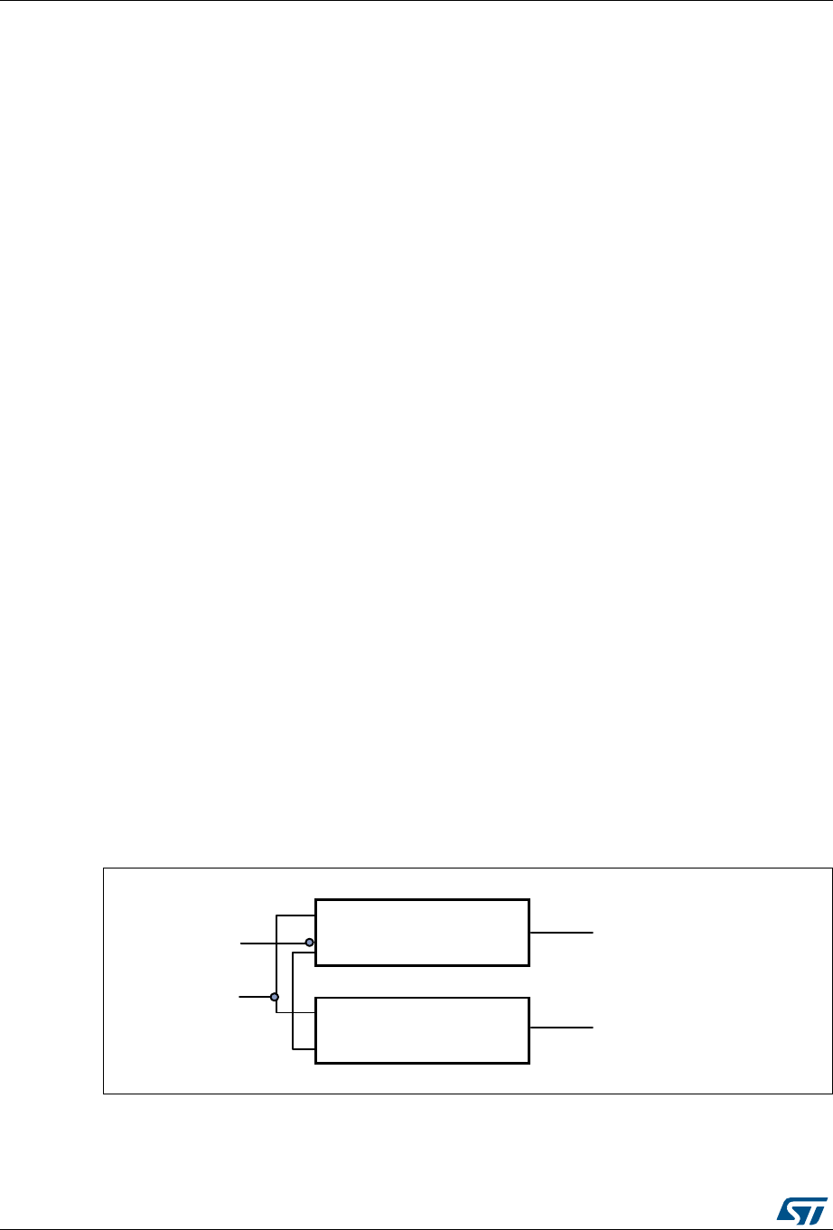
Table 126. SPI interrupt requests
Interrupt event Event flag Enable Control bit
Transmit buffer empty flag TXE TXEIE
Receive buffer not empty flag RXNE RXNEIE
Master Mode fault event MODF
ERRIEOverrun error OVR
CRC error flag CRCERR
TI frame format error FRE ERRIE
RM0090 Rev 18 899/1749
RM0090 Serial peripheral interface (SPI)
925
28.4 I2S functional description
28.4.1 I2S general description
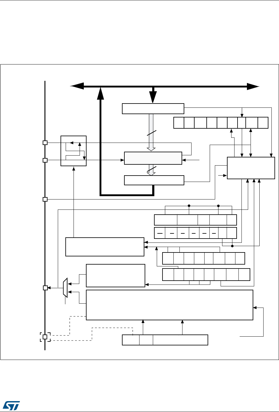
The block diagram of the I2S is shown in Figure 262.
Figure 262. I2S block diagram
1. I2S2ext_SD and I2S3ext_SD are the extended SD pins that control the I2S full duplex mode.
The SPI could function as an audio I2S interface when the I2S capability is enabled (by
setting the I2SMOD bit in the SPI_I2SCFGR register). This interface uses almost the same
pins, flags and interrupts as the SPI.
Tx buffer
Shift register
16-bit
Communication
Rx buffer
16-bit
MOSI/ SD
Master control logic
MISO/
I2S2ext_SD/
I2S3ext_SD(1)
SPI
baud rate generator
CK
I2SMOD
LSB first
LSB
First SPE BR2 BR1 BR0 MSTR CPOL CPHA
Bidi
mode
Bidi
OE
CRC
EN
CRC
Next DFF Rx
only SSM SSI
Address and data bus
control
NSS/WS
BSY OVR MODF CRC
ERR
CH
SIDE TxE RxNE
I2S clock generator
MCK
I2S_CK
I2S
MOD I2SE
CH
DATLEN LEN
CK
POL
I2SCFG I2SSTD
MCKOEODD I2SDIV[7:0]
[1:0] [1:0] [1:0]
UDR
I2SxCLK
MS19909V1
FRE
Serial peripheral interface (SPI) RM0090
900/1749 RM0090 Rev 18
The I2S shares three common pins with the SPI:
•SD: Serial Data (mapped on the MOSI pin) to transmit or receive the two time-
multiplexed data channels (in half-duplex mode only).
•WS: Word Select (mapped on the NSS pin) is the data control signal output in master
mode and input in slave mode.
•CK: Serial Clock (mapped on the SCK pin) is the serial clock output in master mode
and serial clock input in slave mode.
•I2S2ext_SD and I2S3ext_SD: additional pins (mapped on the MISO pin) to control the
I2S full duplex mode.
An additional pin could be used when a master clock output is needed for some external
audio devices:
•MCK: Master Clock (mapped separately) is used, when the I2S is configured in master
mode (and when the MCKOE bit in the SPI_I2SPR register is set), to output this
additional clock generated at a preconfigured frequency rate equal to 256 × FS, where
FS is the audio sampling frequency.
The I2S uses its own clock generator to produce the communication clock when it is set in
master mode. This clock generator is also the source of the master clock output. Two
additional registers are available in I2S mode. One is linked to the clock generator
configuration SPI_I2SPR and the other one is a generic I2S configuration register
SPI_I2SCFGR (audio standard, slave/master mode, data format, packet frame, clock
polarity, etc.).
The SPI_CR1 register and all CRC registers are not used in the I2S mode. Likewise, the
SSOE bit in the SPI_CR2 register and the MODF and CRCERR bits in the SPI_SR are not
used.
The I2S uses the same SPI register for data transfer (SPI_DR) in 16-bit wide mode.
28.4.2 I2S full duplex
To support I2S full duplex mode, two extra I2S instances called extended I2Ss (I2S2_ext,
I2S3_ext) are available in addition to I2S2 and I2S3 (see Figure 263). The first I2S full-
duplex interface is consequently based on I2S2 and I2S2_ext, and the second one on I2S3
and I2S3_ext.
Note: I2S2_ext an I2S3_ext are used only in full-duplex mode.
Figure 263. I2S full duplex block diagram
1. Where x can be 2 or 3.
MS19910V1
SPI/I2Sx
I2Sx_ext
SPIx_MOSI/I2Sx_SD(in/out)
I2S_ WS
I2Sx_SCK
I2Sx_extSD(in/out)

RM0090 Rev 18 901/1749
RM0090 Serial peripheral interface (SPI)
925
I2Sx can operate in master mode. As a result:
• Only I2Sx can output SCK and WS in half duplex mode
• Only I2Sx can deliver SCK and WS to I2S2_ext and I2S3_ext in full duplex mode.
The extended I2Ss (I2Sx_ext) can be used only in full duplex mode. The I2Sx_ext operate
always in slave mode.
Both I2Sx and I2Sx_ext can be configured as transmitters or receivers.
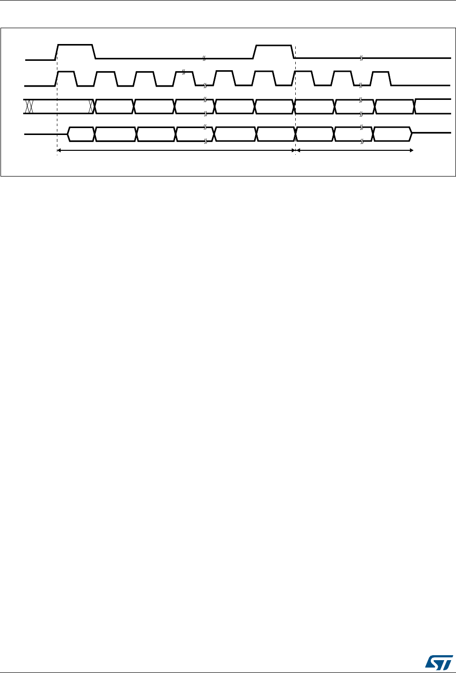
28.4.3 Supported audio protocols
The four-line bus has to handle only audio data generally time-multiplexed on two channels:
the right channel and the left channel. However there is only one 16-bit register for the
transmission and the reception. So, it is up to the software to write into the data register the
adequate value corresponding to the considered channel side, or to read the data from the
data register and to identify the corresponding channel by checking the CHSIDE bit in the
SPI_SR register. Channel Left is always sent first followed by the channel right (CHSIDE
has no meaning for the PCM protocol).
Four data and packet frames are available. Data may be sent with a format of:
•16-bit data packed in 16-bit frame
•16-bit data packed in 32-bit frame
•24-bit data packed in 32-bit frame
•32-bit data packed in 32-bit frame
When using 16-bit data extended on 32-bit packet, the first 16 bits (MSB) are the significant
bits, the 16-bit LSB is forced to 0 without any need for software action or DMA request (only
one read/write operation).
The 24-bit and 32-bit data frames need two CPU read or write operations to/from the
SPI_DR or two DMA operations if the DMA is preferred for the application. For 24-bit data
frame specifically, the 8 nonsignificant bits are extended to 32 bits with 0-bits (by hardware).
For all data formats and communication standards, the most significant bit is always sent
first (MSB first).
The I2S interface supports four audio standards, configurable using the I2SSTD[1:0] and
PCMSYNC bits in the SPI_I2SCFGR register.
I2S Philips standard
For this standard, the WS signal is used to indicate which channel is being transmitted. It is
activated one CK clock cycle before the first bit (MSB) is available.
Serial peripheral interface (SPI) RM0090
902/1749 RM0090 Rev 18
Figure 264. I2S Philips protocol waveforms (16/32-bit full accuracy, CPOL = 0)
Data are latched on the falling edge of CK (for the transmitter) and are read on the rising
edge (for the receiver). The WS signal is also latched on the falling edge of CK.
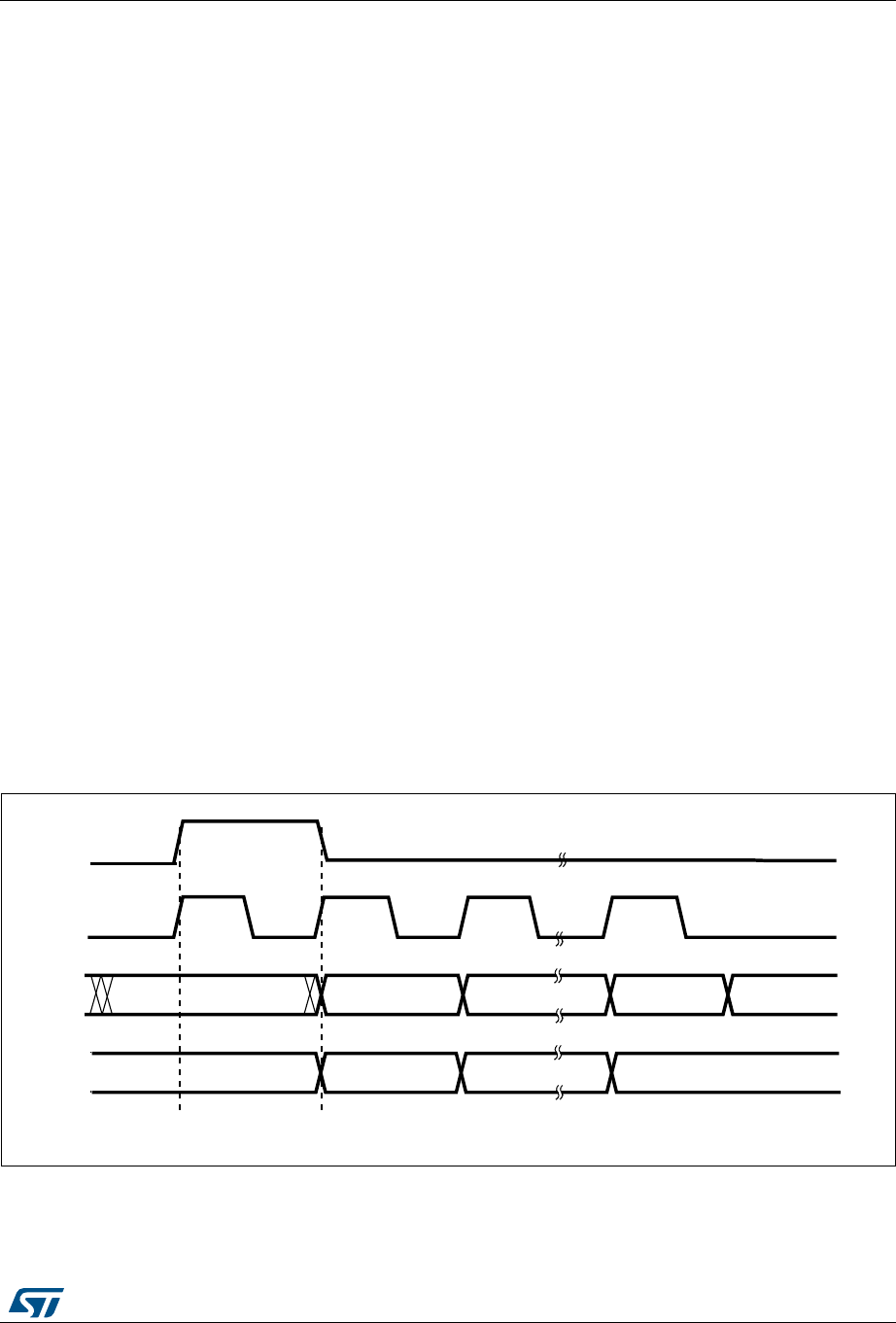
Figure 265. I2S Philips standard waveforms (24-bit frame with CPOL = 0)
This mode needs two write or read operations to/from the SPI_DR.
•In transmission mode:
if 0x8EAA33 has to be sent (24-bit):
Figure 266. Transmitting 0x8EAA33
•In reception mode:
if data 0x8EAA33 is received:
MS19591V1
CK
WS
SD
Can be 16-bit or 32-bit
MSB MSBLSB
Channel left
Channel
right
transmission reception
MS19592V1
CK
WS
SD
Transmission Reception
24-bit data
MSB LSB
Channel left 32-bit
Channel right
8-bit remaining 0 forced
MS19593V1
0x8EAA 0x33XX
First write to Data register Second write to Data register
Only the 8 MSB are sent
to compare the 24 bits
8 LSBs have no meaning
and can be anything
RM0090 Rev 18 903/1749
RM0090 Serial peripheral interface (SPI)
925
Figure 267. Receiving 0x8EAA33
Figure 268. I2S Philips standard (16-bit extended to 32-bit packet frame with
CPOL = 0)
When 16-bit data frame extended to 32-bit channel frame is selected during the I2S
configuration phase, only one access to SPI_DR is required. The 16 remaining bits are
forced by hardware to 0x0000 to extend the data to 32-bit format.
If the data to transmit or the received data are 0x76A3 (0x76A30000 extended to 32-bit), the
operation shown in Figure 269 is required.
Figure 269. Example
For transmission, each time an MSB is written to SPI_DR, the TXE flag is set and its
interrupt, if allowed, is generated to load SPI_DR with the new value to send. This takes
place even if 0x0000 have not yet been sent because it is done by hardware.
For reception, the RXNE flag is set and its interrupt, if allowed, is generated when the first
16 MSB half-word is received.
In this way, more time is provided between two write or read operations, which prevents
underrun or overrun conditions (depending on the direction of the data transfer).
MSB justified standard
For this standard, the WS signal is generated at the same time as the first data bit, which is
the MSBit.
MS19594V1
0x8EAA 0x33XX
First read to Data register Second read to Data register
Only the 8 MSB are sent
to compare the 24 bits
8 LSBs have no meaning
and can be anything
MS19599V1
CK
WS
SD
Transmission Reception
16-bit data
MSB LSB
Channel left 32-bit Channel right
16-bit remaining 0 forced
MS19595V1
0x76A3
Only one access to SPIx_DR
Serial peripheral interface (SPI) RM0090
904/1749 RM0090 Rev 18
Figure 270. MSB justified 16-bit or 32-bit full-accuracy length with CPOL = 0
Data are latched on the falling edge of CK (for transmitter) and are read on the rising edge
(for the receiver).
Figure 271. MSB justified 24-bit frame length with CPOL = 0
Figure 272. MSB justified 16-bit extended to 32-bit packet frame with CPOL = 0
LSB justified standard
This standard is similar to the MSB justified standard (no difference for the 16-bit and 32-bit
full-accuracy frame formats).
MS30100 V1
CK
WS
SD
Transmission Reception
16- or 32 bit data
MSB LSB
Channel left
Channel right
MSB
MS30101V1
CK
WS
SD
Transmission Reception
24 bit data
MSB LSB
Channel left 32-bit
Channel right
8-bit remaining
0 forced
MS30102V1
CK
WS
SD
Transmission Reception
16-bit data
MSB LSB
Channel left 32-bit
Channel right
16-bit remaining
0 forced
RM0090 Rev 18 905/1749
RM0090 Serial peripheral interface (SPI)
925
Figure 273. LSB justified 16-bit or 32-bit full-accuracy with CPOL = 0
Figure 274. LSB justified 24-bit frame length with CPOL = 0
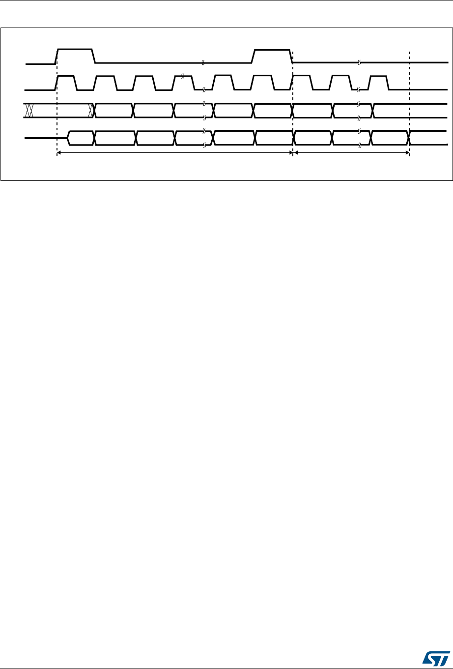
•In transmission mode:
If data 0x3478AE have to be transmitted, two write operations to the SPI_DR register
are required from software or by DMA. The operations are shown below.
Figure 275. Operations required to transmit 0x3478AE
•In reception mode:
If data 0x3478AE are received, two successive read operations from SPI_DR are
required on each RXNE event.
MS30103V1
CK
WS
SD
Transmission Reception
16- or 32-bit data
MSB LSB
Channel left
Channel right
MSB
MS30104V1
CK
WS
SD
Transmission
Reception
8-bit data
0 forced
MSB LSB
Channel left 32-bit
Channel right
24-bit remaining
0xXX34 0x78AE
First write to Data register
conditioned by TXE=1
Second write to Data register
conditioned by TXE=1
Only the 8 LSB of the
half-word are significant.
A field of 0x00 is forced
instead of the 8 MSBs.
MS19596V1
Serial peripheral interface (SPI) RM0090
906/1749 RM0090 Rev 18
Figure 276. Operations required to receive 0x3478AE
Figure 277. LSB justified 16-bit extended to 32-bit packet frame with CPOL = 0
When 16-bit data frame extended to 32-bit channel frame is selected during the I2S
configuration phase, Only one access to SPI_DR is required. The 16 remaining bits are
forced by hardware to 0x0000 to extend the data to 32-bit format. In this case it corresponds
to the half-word MSB.
If the data to transmit or the received data are 0x76A3 (0x0000 76A3 extended to 32-bit),
the operation shown in Figure 278 is required.
Figure 278. Example of LSB justified 16-bit extended to 32-bit packet frame
In transmission mode, when TXE is asserted, the application has to write the data to be
transmitted (in this case 0x76A3). The 0x000 field is transmitted first (extension on 32-bit).
TXE is asserted again as soon as the effective data (0x76A3) is sent on SD.
In reception mode, RXNE is asserted as soon as the significant half-word is received (and
not the 0x0000 field).
In this way, more time is provided between two write or read operations to prevent underrun
or overrun conditions.
0xXX34 0x78AE
First read from Data register
conditioned by RXNE=1
Second read from Data register
conditioned by RXNE=1
Only the 8 LSB of the
half-word are significant.
A field of 0x00 is forced
instead of the 8 MSBs.
MS19597V1
MS30105V1
CK
WS
SD
Transmission
Reception
16-bit data
0 forced
MSB LSB
Channel left 32-bit
Channel right
16-bit remaining
0x76A3
Only one access to the SPIx-DR register
MS19598V1
RM0090 Rev 18 907/1749
RM0090 Serial peripheral interface (SPI)
925
PCM standard
For the PCM standard, there is no need to use channel-side information. The two PCM
modes (short and long frame) are available and configurable using the PCMSYNC bit in
SPI_I2SCFGR.
Figure 279. PCM standard waveforms (16-bit)
For long frame synchronization, the WS signal assertion time is fixed 13 bits in master
mode.
For short frame synchronization, the WS synchronization signal is only one cycle long.
Figure 280. PCM standard waveforms (16-bit extended to 32-bit packet frame)
Note: For both modes (master and slave) and for both synchronizations (short and long), the
number of bits between two consecutive pieces of data (and so two synchronization signals)
needs to be specified (DATLEN and CHLEN bits in the SPI_I2SCFGR register) even in
slave mode.
28.4.4 Clock generator
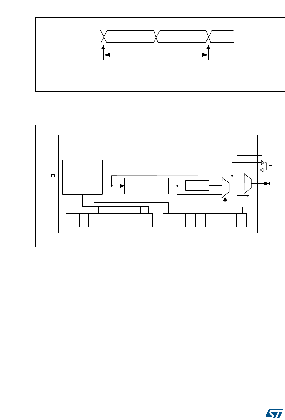
The I2S bitrate determines the dataflow on the I2S data line and the I2S clock signal
frequency.
I2S bitrate = number of bits per channel × number of channels × sampling audio frequency
For a 16-bit audio, left and right channel, the I2S bitrate is calculated as follows:
I2S bitrate = 16 × 2 × FS
It will be: I2S bitrate = 32 x 2 x FS if the packet length is 32-bit wide.
MS30106V1
CK
WS
short frame
SD
WS
long frame
13-bits
MSB LSB MSB
MS30107V1
CK
WS
short frame
SD
WS
long frame
Up to 13-bits
MSB LSB
16 bits
Serial peripheral interface (SPI) RM0090
908/1749 RM0090 Rev 18
Figure 281. Audio sampling frequency definition
When the master mode is configured, a specific action needs to be taken to properly
program the linear divider in order to communicate with the desired audio frequency.
Figure 282. I2S clock generator architecture
1. Where x could be 2 or 3.
Figure 281 presents the communication clock architecture. To achieve high-quality audio
performance, the I2SxCLK clock source can be either the PLLI2S output (through R division
factor) or an external clock (mapped to I2S_CKIN pin).
The audio sampling frequency can be 192 kHz, 96 kHz, or 48 kHz. In order to reach the
desired frequency, the linear divider needs to be programmed according to the formulas
below:
When the master clock is generated (MCKOE in the SPI_I2SPR register is set):
FS = I2SxCLK / [(16*2)*((2*I2SDIV)+ODD)*8)] when the channel frame is 16-bit wide
FS = I2SxCLK / [(32*2)*((2*I2SDIV)+ODD)*4)] when the channel frame is 32-bit wide
When the master clock is disabled (MCKOE bit cleared):
FS = I2SxCLK / [(16*2)*((2*I2SDIV)+ODD))] when the channel frame is 16-bit wide
FS = I2SxCLK / [(32*2)*((2*I2SDIV)+ODD))] when the channel frame is 32-bit wide
Table 127 provides example precision values for different clock configurations.
Note: Other configurations are possible that allow optimum clock precision.
MS30108V1
16-or 32-bit left
channel
16-or 32-bit
right channel
32- or 64-bits
sampling point sampling point
FS
FS : audio sampling frequency
MS30109V1
MCKOE ODD
8-bit linear divider
+ reshaping stage
Divider by 4 Div2
I²SDIV[7:0]
I²SMOD
CHLEN
0
1
0
1
MCKOE
CK
MCK
I²SxCLK

RM0090 Rev 18 909/1749
RM0090 Serial peripheral interface (SPI)
925
28.4.5 I2S master mode
The I2S can be configured as follows:
•In master mode for transmission or reception (half-duplex mode using I2Sx)
•In master mode transmission and reception (full duplex mode using I2Sx and
I2Sx_ext).
This means that the serial clock is generated on the CK pin as well as the Word Select
signal WS. Master clock (MCK) may be output or not, thanks to the MCKOE bit in the
SPI_I2SPR register.
Table 127. Audio frequency precision (for PLLM VCO = 1 MHz or 2 MHz)(1)
Master
clock
Target fS
(Hz)
Data
format PLLI2SN PLLI2SR I2SDIV I2SODD Real fS (Hz) Error
Disabled
8000
16-bit 192 2 187 1 8000 0.0000%
32-bit 192 3 62 1 8000 0.0000%
16000
16-bit 192 3 62 1 16000 0.0000%
32-bit 256 2 62 1 16000 0.0000%
32000
16-bit 256 2 62 1 32000 0.0000%
32-bit 256 5 12 1 32000 0.0000%
48000
16-bit 192 5 12 1 48000 0.0000%
32-bit 384 5 12 1 48000 0.0000%
96000
16-bit 384 5 12 1 96000 0.0000%
32-bit 424 3 11 1 96014.49219 0.0151%
22050
16-bit 290 3 68 1 22049.87695 0.0006%
32-bit 302 2 53 1 22050.23438 0.0011%
44100
16-bit 302 2 53 1 44100.46875 0.0011%
32-bit 429 4 19 0 44099.50781 0.0011%
192000
16-bit 424 3 11 1 192028.9844 0.0151%
32-bit 258 3 3 1 191964.2813 0.0186%
Enabled
8000 don't care 256 5 12 1 8000 0.0000%
16000 don't care 213 2 13 0 16000.60059 0.0038%
32000 don't care 213 2 6 1 32001.20117 0.0038%
48000 don't care 258 3 3 1 47991.07031 0.0186%
96000 don't care 344 2 3 1 95982.14063 0.0186%
22050 don't care 429 4 9 1 22049.75391 0.0011%
44100 don't care 271 2 6 0 44108.07422 0.0183%
1. This table gives only example values for different clock configurations. Other configurations allowing optimum clock
precision are possible.

Serial peripheral interface (SPI) RM0090
910/1749 RM0090 Rev 18
Procedure
1. Select the I2SDIV[7:0] bits in the SPI_I2SPR register to define the serial clock baud
rate to reach the proper audio sample frequency. The ODD bit in the SPI_I2SPR
register also has to be defined.
2. Select the CKPOL bit to define the steady level for the communication clock. Set the
MCKOE bit in the SPI_I2SPR register if the master clock MCK needs to be provided to
the external DAC/ADC audio component (the I2SDIV and ODD values should be
computed depending on the state of the MCK output, for more details refer to
Section 28.4.4: Clock generator).
3. Set the I2SMOD bit in SPI_I2SCFGR to activate the I2S functionalities and choose the
I2S standard through the I2SSTD[1:0] and PCMSYNC bits, the data length through the
DATLEN[1:0] bits and the number of bits per channel by configuring the CHLEN bit.
Select also the I2S master mode and direction (Transmitter or Receiver) through the
I2SCFG[1:0] bits in the SPI_I2SCFGR register.
4. If needed, select all the potential interruption sources and the DMA capabilities by
writing the SPI_CR2 register.
5. The I2SE bit in SPI_I2SCFGR register must be set.
WS and CK are configured in output mode. MCK is also an output, if the MCKOE bit in
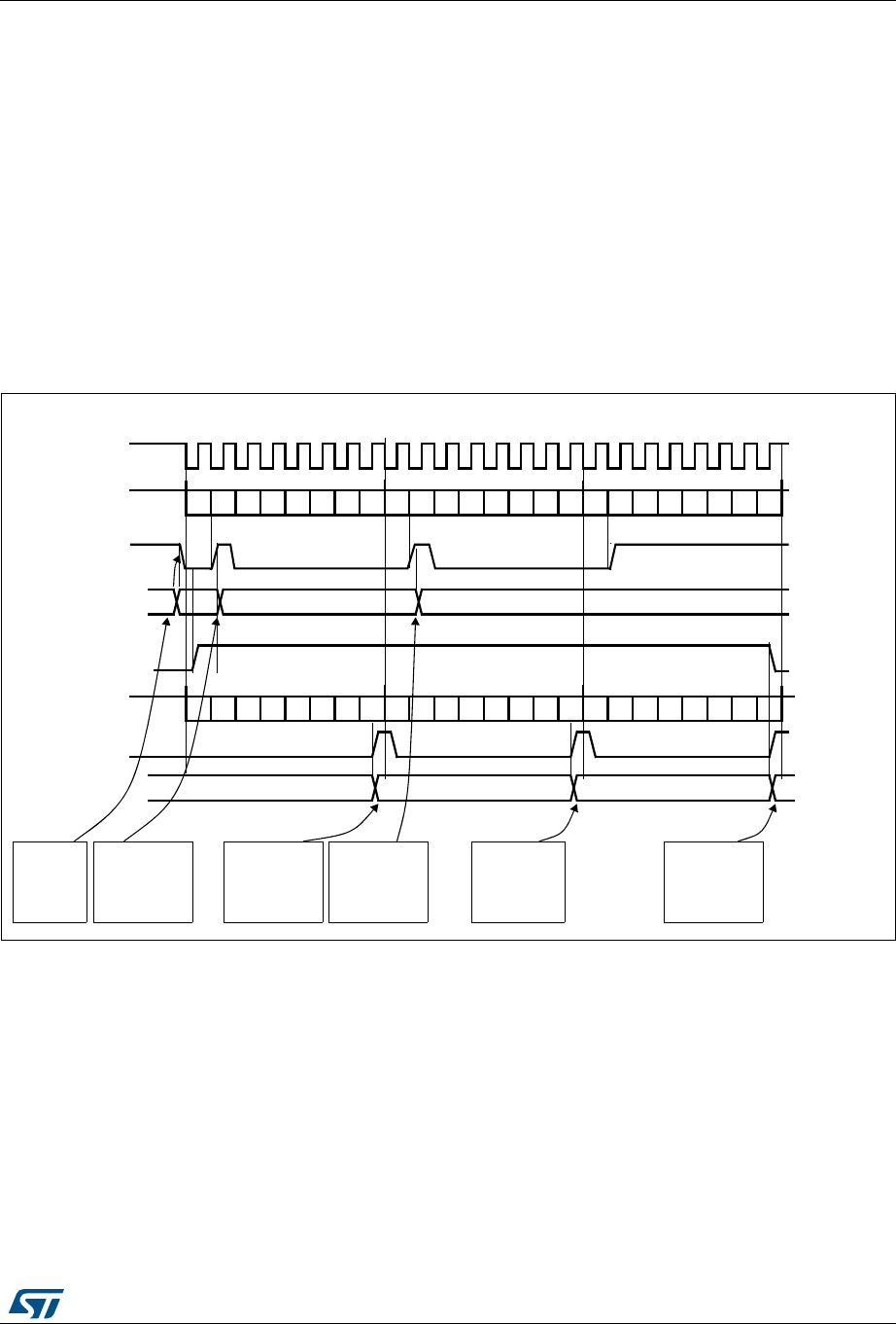
SPI_I2SPR is set.
Transmission sequence
The transmission sequence begins when a half-word is written into the Tx buffer.
Assumedly, the first data written into the Tx buffer correspond to the channel Left data.
When data are transferred from the Tx buffer to the shift register, TXE is set and data
corresponding to the channel Right have to be written into the Tx buffer. The CHSIDE flag
indicates which channel is to be transmitted. It has a meaning when the TXE flag is set
because the CHSIDE flag is updated when TXE goes high.
A full frame has to be considered as a Left channel data transmission followed by a Right
channel data transmission. It is not possible to have a partial frame where only the left
channel is sent.
The data half-word is parallel loaded into the 16-bit shift register during the first bit
transmission, and then shifted out, serially, to the MOSI/SD pin, MSB first. The TXE flag is
set after each transfer from the Tx buffer to the shift register and an interrupt is generated if
the TXEIE bit in the SPI_CR2 register is set.
For more details about the write operations depending on the I2S standard mode selected,
refer to Section 28.4.3: Supported audio protocols).
To ensure a continuous audio data transmission, it is mandatory to write the SPI_DR with
the next data to transmit before the end of the current transmission.
To switch off the I2S, by clearing I2SE, it is mandatory to wait for TXE = 1 and BSY = 0.
Reception sequence
The operating mode is the same as for the transmission mode except for the point 3 (refer to
the procedure described in Section 28.4.5: I2S master mode), where the configuration
should set the master reception mode through the I2SCFG[1:0] bits.
Whatever the data or channel length, the audio data are received by 16-bit packets. This
means that each time the Rx buffer is full, the RXNE flag is set and an interrupt is generated

RM0090 Rev 18 911/1749
RM0090 Serial peripheral interface (SPI)
925
if the RXNEIE bit is set in SPI_CR2 register. Depending on the data and channel length
configuration, the audio value received for a right or left channel may result from one or two
receptions into the Rx buffer.
Clearing the RXNE bit is performed by reading the SPI_DR register.
CHSIDE is updated after each reception. It is sensitive to the WS signal generated by the
I2S cell.
For more details about the read operations depending on the I2S standard mode selected,
refer to Section 28.4.3: Supported audio protocols.
If data are received while the previously received data have not been read yet, an overrun is
generated and the OVR flag is set. If the ERRIE bit is set in the SPI_CR2 register, an
interrupt is generated to indicate the error.
To switch off the I2S, specific actions are required to ensure that the I2S completes the
transfer cycle properly without initiating a new data transfer. The sequence depends on the
configuration of the data and channel lengths, and on the audio protocol mode selected. In
the case of:
•16-bit data length extended on 32-bit channel length (DATLEN = 00 and CHLEN = 1)
using the LSB justified mode (I2SSTD = 10)
a) Wait for the second to last RXNE = 1 (n – 1)
b) Then wait 17 I2S clock cycles (using a software loop)
c) Disable the I2S (I2SE = 0)
•16-bit data length extended on 32-bit channel length (DATLEN = 00 and CHLEN = 1) in
MSB justified, I2S or PCM modes (I2SSTD = 00, I2SSTD = 01 or I2SSTD = 11,
respectively)
a) Wait for the last RXNE
b) Then wait 1 I2S clock cycle (using a software loop)
c) Disable the I2S (I2SE = 0)
•For all other combinations of DATLEN and CHLEN, whatever the audio mode selected
through the I2SSTD bits, carry out the following sequence to switch off the I2S:
a) Wait for the second to last RXNE = 1 (n – 1)
b) Then wait one I2S clock cycle (using a software loop)
c) Disable the I2S (I2SE = 0)
Note: The BSY flag is kept low during transfers.
28.4.6 I2S slave mode
The I2S can be configured as follows:
•In slave mode for transmission or reception (half-duplex mode using I2Sx)
•In slave mode transmission and reception (full duplex mode using I2Sx and I2Sx_ext).
The operating mode is following mainly the same rules as described for the I2S master
configuration. In slave mode, there is no clock to be generated by the I2S interface. The
clock and WS signals are input from the external master connected to the I2S interface.
There is then no need, for the user, to configure the clock.
The configuration steps to follow are listed below:

Serial peripheral interface (SPI) RM0090
912/1749 RM0090 Rev 18
1. Set the I2SMOD bit in the SPI_I2SCFGR register to reach the I2S functionalities and
choose the I2S standard through the I2SSTD[1:0] bits, the data length through the
DATLEN[1:0] bits and the number of bits per channel for the frame configuring the
CHLEN bit. Select also the mode (transmission or reception) for the slave through the
I2SCFG[1:0] bits in SPI_I2SCFGR register.
2. If needed, select all the potential interrupt sources and the DMA capabilities by writing
the SPI_CR2 register.
3. The I2SE bit in SPI_I2SCFGR register must be set.
Transmission sequence
The transmission sequence begins when the external master device sends the clock and
when the NSS_WS signal requests the transfer of data. The slave has to be enabled before
the external master starts the communication. The I2S data register has to be loaded before
the master initiates the communication.
For the I2S, MSB justified and LSB justified modes, the first data item to be written into the
data register corresponds to the data for the left channel. When the communication starts,
the data are transferred from the Tx buffer to the shift register. The TXE flag is then set in
order to request the right channel data to be written into the I2S data register.
The CHSIDE flag indicates which channel is to be transmitted. Compared to the master
transmission mode, in slave mode, CHSIDE is sensitive to the WS signal coming from the
external master. This means that the slave needs to be ready to transmit the first data
before the clock is generated by the master. WS assertion corresponds to left channel
transmitted first.
Note: The I2SE has to be written at least two PCLK cycles before the first clock of the master
comes on the CK line.
The data half-word is parallel-loaded into the 16-bit shift register (from the internal bus)
during the first bit transmission, and then shifted out serially to the MOSI/SD pin MSB first.
The TXE flag is set after each transfer from the Tx buffer to the shift register and an interrupt
is generated if the TXEIE bit in the SPI_CR2 register is set.
Note that the TXE flag should be checked to be at 1 before attempting to write the Tx buffer.
For more details about the write operations depending on the I2S standard mode selected,
refer to Section 28.4.3: Supported audio protocols.
To secure a continuous audio data transmission, it is mandatory to write the SPI_DR
register with the next data to transmit before the end of the current transmission. An
underrun flag is set and an interrupt may be generated if the data are not written into the
SPI_DR register before the first clock edge of the next data communication. This indicates
to the software that the transferred data are wrong. If the ERRIE bit is set into the SPI_CR2
register, an interrupt is generated when the UDR flag in the SPI_SR register goes high. In
this case, it is mandatory to switch off the I2S and to restart a data transfer starting from the
left channel.
To switch off the I2S, by clearing the I2SE bit, it is mandatory to wait for TXE = 1 and
BSY = 0.
Reception sequence
The operating mode is the same as for the transmission mode except for the point 1 (refer to
the procedure described in Section 28.4.6: I2S slave mode), where the configuration should
set the master reception mode using the I2SCFG[1:0] bits in the SPI_I2SCFGR register.

RM0090 Rev 18 913/1749
RM0090 Serial peripheral interface (SPI)
925
Whatever the data length or the channel length, the audio data are received by 16-bit
packets. This means that each time the RX buffer is full, the RXNE flag in the SPI_SR
register is set and an interrupt is generated if the RXNEIE bit is set in the SPI_CR2 register.
Depending on the data length and channel length configuration, the audio value received for
a right or left channel may result from one or two receptions into the RX buffer.
The CHSIDE flag is updated each time data are received to be read from SPI_DR. It is
sensitive to the external WS line managed by the external master component.
Clearing the RXNE bit is performed by reading the SPI_DR register.
For more details about the read operations depending the I2S standard mode selected, refer
to Section 28.4.3: Supported audio protocols.
If data are received while the precedent received data have not yet been read, an overrun is
generated and the OVR flag is set. If the bit ERRIE is set in the SPI_CR2 register, an
interrupt is generated to indicate the error.
To switch off the I2S in reception mode, I2SE has to be cleared immediately after receiving
the last RXNE = 1.
Note: The external master components should have the capability of sending/receiving data in 16-
bit or 32-bit packets via an audio channel.
28.4.7 Status flags
Three status flags are provided for the application to fully monitor the state of the I2S bus.
Busy flag (BSY)
The BSY flag is set and cleared by hardware (writing to this flag has no effect). It indicates
the state of the communication layer of the I2S.
When BSY is set, it indicates that the I2S is busy communicating. There is one exception in
master receive mode (I2SCFG = 11) where the BSY flag is kept low during reception.
The BSY flag is useful to detect the end of a transfer if the software needs to disable the I2S.
This avoids corrupting the last transfer. For this, the procedure described below must be
strictly respected.
The BSY flag is set when a transfer starts, except when the I2S is in master receiver mode.
The BSY flag is cleared:
•when a transfer completes (except in master transmit mode, in which the
communication is supposed to be continuous)
•when the I2S is disabled
When communication is continuous:
•In master transmit mode, the BSY flag is kept high during all the transfers
•In slave mode, the BSY flag goes low for one I2S clock cycle between each transfer
Note: Do not use the BSY flag to handle each data transmission or reception. It is better to use the
TXE and RXNE flags instead.

Serial peripheral interface (SPI) RM0090
914/1749 RM0090 Rev 18
Tx buffer empty flag (TXE)
When set, this flag indicates that the Tx buffer is empty and the next data to be transmitted
can then be loaded into it. The TXE flag is reset when the Tx buffer already contains data to
be transmitted. It is also reset when the I2S is disabled (I2SE bit is reset).
RX buffer not empty (RXNE)
When set, this flag indicates that there are valid received data in the RX Buffer. It is reset
when SPI_DR register is read.
Channel Side flag (CHSIDE)
In transmission mode, this flag is refreshed when TXE goes high. It indicates the channel
side to which the data to transfer on SD has to belong. In case of an underrun error event in
slave transmission mode, this flag is not reliable and I2S needs to be switched off and
switched on before resuming the communication.
In reception mode, this flag is refreshed when data are received into SPI_DR. It indicates
from which channel side data have been received. Note that in case of error (like OVR) this
flag becomes meaningless and the I2S should be reset by disabling and then enabling it
(with configuration if it needs changing).
This flag has no meaning in the PCM standard (for both Short and Long frame modes).
When the OVR or UDR flag in the SPI_SR is set and the ERRIE bit in SPI_CR2 is also set,
an interrupt is generated. This interrupt can be cleared by reading the SPI_SR status
register (once the interrupt source has been cleared).
28.4.8 Error flags
There are three error flags for the I2S cell.
Underrun flag (UDR)
In slave transmission mode this flag is set when the first clock for data transmission appears
while the software has not yet loaded any value into SPI_DR. It is available when the
I2SMOD bit in SPI_I2SCFGR is set. An interrupt may be generated if the ERRIE bit in
SPI_CR2 is set.
The UDR bit is cleared by a read operation on the SPI_SR register.
Overrun flag (OVR)
This flag is set when data are received and the previous data have not yet been read from
SPI_DR. As a result, the incoming data are lost. An interrupt may be generated if the ERRIE
bit is set in SPI_CR2.
In this case, the receive buffer contents are not updated with the newly received data from
the transmitter device. A read operation to the SPI_DR register returns the previous
correctly received data. All other subsequently transmitted half-words are lost.
Clearing the OVR bit is done by a read operation on the SPI_DR register followed by a read
access to the SPI_SR register.
Frame error flag (FRE)
This flag can be set by hardware only if the I2S is configured in Slave mode. It is set if the
external master is changing the WS line at a moment when the slave is not expected this

RM0090 Rev 18 915/1749
RM0090 Serial peripheral interface (SPI)
925
change. If the synchronization is lost, to recover from this state and resynchronize the
external master device with the I2S slave device, follow the steps below:
1. Disable the I2S
2. Re-enable it when the correct level is detected on the WS line (WS line is high in I2S
mode, or low for MSB- or LSB-justified or PCM modes).
Desynchronization between the master and slave device may be due to noisy environment
on the SCK communication clock or on the WS frame synchronization line. An error interrupt
can be generated if the ERRIE bit is set. The desynchronization flag (FRE) is cleared by
software when the status register is read.
28.4.9 I2S interrupts
Table 128 provides the list of I2S interrupts.
28.4.10 DMA features
DMA is working in exactly the same way as for the SPI mode. There is no difference on the
I2S. Only the CRC feature is not available in I2S mode since there is no data transfer
protection system.
Table 128. I2S interrupt requests
Interrupt event Event flag Enable Control bit
Transmit buffer empty flag TXE TXEIE
Receive buffer not empty flag RXNE RXNEIE
Overrun error OVR
ERRIE
Underrun error UDR
Frame error flag FRE ERRIE

Serial peripheral interface (SPI) RM0090
916/1749 RM0090 Rev 18
28.5 SPI and I2S registers
The peripheral registers have to be accessed by half-words (16 bits) or words (32 bits).
28.5.1 SPI control register 1 (SPI_CR1) (not used in I2S mode)
Address offset: 0x00
Reset value: 0x0000
1514131211109876543210
BIDI
MODE
BIDI
OE
CRC
EN
CRC
NEXT DFF RX
ONLY SSM SSI LSB
FIRST SPE BR [2:0] MSTR CPOL CPHA
rw rw rw rw rw rw rw rw rw rw rw rw rw rw rw rw
Bit 15 BIDIMODE: Bidirectional data mode enable
0: 2-line unidirectional data mode selected
1: 1-line bidirectional data mode selected
Note: This bit is not used in I2S mode
Bit 14 BIDIOE: Output enable in bidirectional mode
This bit combined with the BIDImode bit selects the direction of transfer in bidirectional mode
0: Output disabled (receive-only mode)
1: Output enabled (transmit-only mode)
Note: This bit is not used in I2S mode.
In master mode, the MOSI pin is used while the MISO pin is used in slave mode.
Bit 13 CRCEN: Hardware CRC calculation enable
0: CRC calculation disabled
1: CRC calculation enabled
Note: This bit should be written only when SPI is disabled (SPE = ‘0’) for correct operation.
It is not used in I2S mode.
Bit 12 CRCNEXT: CRC transfer next
0: Data phase (no CRC phase)
1: Next transfer is CRC (CRC phase)
Note: When the SPI is configured in full duplex or transmitter only modes, CRCNEXT must be
written as soon as the last data is written to the SPI_DR register.
When the SPI is configured in receiver only mode, CRCNEXT must be set after the
second last data reception.
This bit should be kept cleared when the transfers are managed by DMA.
It is not used in I2S mode.
Bit 11 DFF: Data frame format
0: 8-bit data frame format is selected for transmission/reception
1: 16-bit data frame format is selected for transmission/reception
Note: This bit should be written only when SPI is disabled (SPE = ‘0’) for correct operation.
It is not used in I2S mode.

RM0090 Rev 18 917/1749
RM0090 Serial peripheral interface (SPI)
925
Bit 10 RXONLY: Receive only
This bit combined with the BIDImode bit selects the direction of transfer in 2-line
unidirectional mode. This bit is also useful in a multislave system in which this particular
slave is not accessed, the output from the accessed slave is not corrupted.
0: Full duplex (Transmit and receive)
1: Output disabled (Receive-only mode)
Note: This bit is not used in I2S mode
Bit 9 SSM: Software slave management
When the SSM bit is set, the NSS pin input is replaced with the value from the SSI bit.
0: Software slave management disabled
1: Software slave management enabled
Note: This bit is not used in I2S mode and SPI TI mode
Bit 8 SSI: Internal slave select
This bit has an effect only when the SSM bit is set. The value of this bit is forced onto the
NSS pin and the IO value of the NSS pin is ignored.
Note: This bit is not used in I2S mode and SPI TI mode
Bit 7 LSBFIRST: Frame format
0: MSB transmitted first
1: LSB transmitted first
Note: This bit should not be changed when communication is ongoing.
It is not used in I2S mode and SPI TI mode
Bit 6 SPE: SPI enable
0: Peripheral disabled
1: Peripheral enabled
Note: This bit is not used in I2S mode.
When disabling the SPI, follow the procedure described in Section 28.3.8.
Bits 5:3 BR[2:0]: Baud rate control
000: fPCLK/2
001: fPCLK/4
010: fPCLK/8
011: fPCLK/16
100: fPCLK/32
101: fPCLK/64
110: fPCLK/128
111: fPCLK/256
Note: These bits should not be changed when communication is ongoing.
They are not used in I2S mode.
Bit 2 MSTR: Master selection
0: Slave configuration
1: Master configuration
Note: This bit should not be changed when communication is ongoing.
It is not used in I2S mode.

Serial peripheral interface (SPI) RM0090
918/1749 RM0090 Rev 18
28.5.2 SPI control register 2 (SPI_CR2)
Address offset: 0x04
Reset value: 0x0000
Bit1 CPOL: Clock polarity
0: CK to 0 when idle
1: CK to 1 when idle
Note: This bit should not be changed when communication is ongoing.
It is not used in I2S mode and SPI TI mode.
Bit 0 CPHA: Clock phase
0: The first clock transition is the first data capture edge
1: The second clock transition is the first data capture edge
Note: This bit should not be changed when communication is ongoing.
It is not used in I2S mode and SPI TI mode.
15 14 13 12 11 10 9 8 7 6 5 4 3 2 1 0
Reserved TXEIE RXNEIE ERRIE FRF Res. SSOE TXDMAEN RXDMAEN
rw rw rw rw rw rw rw
Bits 15:8 Reserved, must be kept at reset value.
Bit 7 TXEIE: Tx buffer empty interrupt enable
0: TXE interrupt masked
1: TXE interrupt not masked. Used to generate an interrupt request when the TXE flag is set.
Bit 6 RXNEIE: RX buffer not empty interrupt enable
0: RXNE interrupt masked
1: RXNE interrupt not masked. Used to generate an interrupt request when the RXNE flag is
set.
Bit 5 ERRIE: Error interrupt enable
This bit controls the generation of an interrupt when an error condition occurs )(CRCERR,
OVR, MODF in SPI mode, FRE in TI mode and UDR, OVR, and FRE in I2S mode).
0: Error interrupt is masked
1: Error interrupt is enabled
Bit 4 FRF: Frame format
0: SPI Motorola mode
1 SPI TI mode
Note: This bit is not used in I2S mode.
Bit 3 Reserved. Forced to 0 by hardware.
Bit 2 SSOE: SS output enable
0: SS output is disabled in master mode and the cell can work in multimaster configuration
1: SS output is enabled in master mode and when the cell is enabled. The cell cannot work
in a multimaster environment.
Note: This bit is not used in I2S mode and SPI TI mode.

RM0090 Rev 18 919/1749
RM0090 Serial peripheral interface (SPI)
925
28.5.3 SPI status register (SPI_SR)
Address offset: 0x08
Reset value: 0x0002
Bit 1 TXDMAEN: Tx buffer DMA enable
When this bit is set, the DMA request is made whenever the TXE flag is set.
0: Tx buffer DMA disabled
1: Tx buffer DMA enabled
Bit 0 RXDMAEN: Rx buffer DMA enable
When this bit is set, the DMA request is made whenever the RXNE flag is set.
0: Rx buffer DMA disabled
1: Rx buffer DMA enabled
15 14 13 12 11 10 9 8 7 6 5 4 3 2 1 0
Reserved FRE BSY OVR MODF CRC
ERR UDR CHSIDE TXE RXNE
rrrrrc_w0r r rr
Bits 15:9 Reserved. Forced to 0 by hardware.
Bit 8 FRE: Frame format error
0: No frame format error
1: A frame format error occurred
This flag is set by hardware and cleared by software when the SPIx_SR register is read.
Note: This flag is used when the SPI operates in TI slave mode or I2S slave mode (refer to
Section 28.3.10).
Bit 7 BSY: Busy flag
0: SPI (or I2S) not busy
1: SPI (or I2S) is busy in communication or Tx buffer is not empty
This flag is set and cleared by hardware.
Note: BSY flag must be used with caution: refer to Section 28.3.7 and Section 28.3.8.
Bit 6 OVR: Overrun flag
0: No overrun occurred
1: Overrun occurred
This flag is set by hardware and reset by a software sequence. Refer to Section 28.4.8:
Error flags for the software sequence.
Bit 5 MODF: Mode fault
0: No mode fault occurred
1: Mode fault occurred
This flag is set by hardware and reset by a software sequence. Refer to Section 28.4.8:
Error flags for the software sequence.
Note: This bit is not used in I2S mode
Bit 4 CRCERR: CRC error flag
0: CRC value received matches the SPI_RXCRCR value
1: CRC value received does not match the SPI_RXCRCR value
This flag is set by hardware and cleared by software writing 0.
Note: This bit is not used in I2S mode.

Serial peripheral interface (SPI) RM0090
920/1749 RM0090 Rev 18
28.5.4 SPI data register (SPI_DR)
Address offset: 0x0C
Reset value: 0x0000
Bit 3 UDR: Underrun flag
0: No underrun occurred
1: Underrun occurred
This flag is set by hardware and reset by a software sequence. Refer to Section 28.4.8:
Error flags for the software sequence.
Note: This bit is not used in SPI mode.
Bit 2 CHSIDE: Channel side
0: Channel Left has to be transmitted or has been received
1: Channel Right has to be transmitted or has been received
Note: This bit is not used for SPI mode and is meaningless in PCM mode.
Bit 1 TXE: Transmit buffer empty
0: Tx buffer not empty
1: Tx buffer empty
Bit 0 RXNE: Receive buffer not empty
0: Rx buffer empty
1: Rx buffer not empty
1514131211109876543210
DR[15:0]
rw rw rw rw rw rw rw rw rw rw rw rw rw rw rw rw
Bits 15:0 DR[15:0]: Data register
Data received or to be transmitted.
The data register is split into 2 buffers - one for writing (Transmit Buffer) and another one for
reading (Receive buffer). A write to the data register will write into the Tx buffer and a read
from the data register will return the value held in the Rx buffer.
Note: These notes apply to SPI mode:
Depending on the data frame format selection bit (DFF in SPI_CR1 register), the data
sent or received is either 8-bit or 16-bit. This selection has to be made before enabling
the SPI to ensure correct operation.
For an 8-bit data frame, the buffers are 8-bit and only the LSB of the register
(SPI_DR[7:0]) is used for transmission/reception. When in reception mode, the MSB of
the register (SPI_DR[15:8]) is forced to 0.
For a 16-bit data frame, the buffers are 16-bit and the entire register, SPI_DR[15:0] is
used for transmission/reception.

RM0090 Rev 18 921/1749
RM0090 Serial peripheral interface (SPI)
925
28.5.5 SPI CRC polynomial register (SPI_CRCPR) (not used in I2S
mode)
Address offset: 0x10
Reset value: 0x0007
28.5.6 SPI RX CRC register (SPI_RXCRCR) (not used in I2S mode)
Address offset: 0x14
Reset value: 0x0000
1514131211109876543210
CRCPOLY[15:0]
rw rw rw rw rw rw rw rw rw rw rw rw rw rw rw rw
Bits 15:0 CRCPOLY[15:0]: CRC polynomial register
This register contains the polynomial for the CRC calculation.
The CRC polynomial (0007h) is the reset value of this register. Another polynomial can be
configured as required.
Note: These bits are not used for the I2S mode.
1514131211109876543210
RXCRC[15:0]
rrrrrrrrrrrrrrrr
Bits 15:0 RXCRC[15:0]: Rx CRC register
When CRC calculation is enabled, the RxCRC[15:0] bits contain the computed CRC value of
the subsequently received bytes. This register is reset when the CRCEN bit in SPI_CR1
register is written to 1. The CRC is calculated serially using the polynomial programmed in
the SPI_CRCPR register.
Only the 8 LSB bits are considered when the data frame format is set to be 8-bit data (DFF
bit of SPI_CR1 is cleared). CRC calculation is done based on any CRC8 standard.
The entire 16-bits of this register are considered when a 16-bit data frame format is selected
(DFF bit of the SPI_CR1 register is set). CRC calculation is done based on any CRC16
standard.
Note: A read to this register when the BSY Flag is set could return an incorrect value.
These bits are not used for I2S mode.

Serial peripheral interface (SPI) RM0090
922/1749 RM0090 Rev 18
28.5.7 SPI TX CRC register (SPI_TXCRCR) (not used in I2S mode)
Address offset: 0x18
Reset value: 0x0000
28.5.8 SPI_I2S configuration register (SPI_I2SCFGR)
Address offset: 0x1C
Reset value: 0x0000
1514131211109876543210
TXCRC[15:0]
rrrrrrrrrrrrrrrr
Bits 15:0 TXCRC[15:0]: Tx CRC register
When CRC calculation is enabled, the TxCRC[7:0] bits contain the computed CRC value of
the subsequently transmitted bytes. This register is reset when the CRCEN bit of SPI_CR1
is written to 1. The CRC is calculated serially using the polynomial programmed in the
SPI_CRCPR register.
Only the 8 LSB bits are considered when the data frame format is set to be 8-bit data (DFF
bit of SPI_CR1 is cleared). CRC calculation is done based on any CRC8 standard.
The entire 16-bits of this register are considered when a 16-bit data frame format is selected
(DFF bit of the SPI_CR1 register is set). CRC calculation is done based on any CRC16
standard.
Note: A read to this register when the BSY flag is set could return an incorrect value.
These bits are not used for I2S mode.
15 14 13 12 11 10 9 8 7 6 5 4 3 2 1 0
Reserved
I2SMOD I2SE I2SCFG PCMSY
NC Res.
I2SSTD CKPOL DATLEN CHLEN
rw rw rw rw rw rw rw rw rw rw rw
Bits 15:12 Reserved, must be kept at reset value.
Bit 11 I2SMOD: I2S mode selection
0: SPI mode is selected
1: I2S mode is selected
Note: This bit should be configured when the SPI or I2S is disabled
Bit 10 I2SE: I2S Enable
0: I2S peripheral is disabled
1: I2S peripheral is enabled
Note: This bit is not used in SPI mode.
Bits 9:8 I2SCFG: I2S configuration mode
00: Slave - transmit
01: Slave - receive
10: Master - transmit
11: Master - receive
Note: This bit should be configured when the I2S is disabled.
It is not used in SPI mode.

RM0090 Rev 18 923/1749
RM0090 Serial peripheral interface (SPI)
925
28.5.9 SPI_I2S prescaler register (SPI_I2SPR)
Address offset: 0x20
Reset value: 0000 0010 (0x0002)
Bit 7 PCMSYNC: PCM frame synchronization
0: Short frame synchronization
1: Long frame synchronization
Note: This bit has a meaning only if I2SSTD = 11 (PCM standard is used)
It is not used in SPI mode.
Bit 6 Reserved: forced at 0 by hardware
Bits 5:4 I2SSTD: I2S standard selection
00: I2S Philips standard.
01: MSB justified standard (left justified)
10: LSB justified standard (right justified)
11: PCM standard
For more details on I2S standards, refer to Section 28.4.3: Supported audio protocols. Not used
in SPI mode.
Note: For correct operation, these bits should be configured when the I2S is disabled.
Bit 3 CKPOL: Steady state clock polarity
0: I2S clock steady state is low level
1: I2S clock steady state is high level
Note: For correct operation, this bit should be configured when the I2S is disabled.
This bit is not used in SPI mode
Bits 2:1 DATLEN: Data length to be transferred
00: 16-bit data length
01: 24-bit data length
10: 32-bit data length
11: Not allowed
Note: For correct operation, these bits should be configured when the I2S is disabled.
This bit is not used in SPI mode.
Bit 0 CHLEN: Channel length (number of bits per audio channel)
0: 16-bit wide
1: 32-bit wide
The bit write operation has a meaning only if DATLEN = 00 otherwise the channel length is fixed to
32-bit by hardware whatever the value filled in. Not used in SPI mode.
Note: For correct operation, this bit should be configured when the I2S is disabled.
1514131211109 876543210
Reserved MCKOE ODD I2SDIV
rw rw rw

Serial peripheral interface (SPI) RM0090
924/1749 RM0090 Rev 18
Bits 15:10 Reserved, must be kept at reset value.
Bit 9 MCKOE: Master clock output enable
0: Master clock output is disabled
1: Master clock output is enabled
Note: This bit should be configured when the I2S is disabled. It is used only when the I2S is in master
mode.
This bit is not used in SPI mode.
Bit 8 ODD: Odd factor for the prescaler
0: real divider value is = I2SDIV *2
1: real divider value is = (I2SDIV * 2)+1
Refer to Section 28.4.4: Clock generator. Not used in SPI mode.
Note: This bit should be configured when the I2S is disabled. It is used only when the I2S is in master
mode.
Bits 7:0 I2SDIV: I2S Linear prescaler
I2SDIV [7:0] = 0 or I2SDIV [7:0] = 1 are forbidden values.
Refer to Section 28.4.4: Clock generator. Not used in SPI mode.
Note: These bits should be configured when the I2S is disabled. It is used only when the I2S is in
master mode.
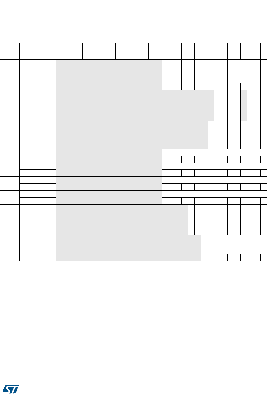
RM0090 Rev 18 925/1749
RM0090 Serial peripheral interface (SPI)
925
28.5.10 SPI register map
The table provides shows the SPI register map and reset values.
Refer to Section 2.3: Memory map for the register boundary addresses.
Table 129. SPI register map and reset values
Offset Register
31
30
29
28
27
26
25
24
23
22
21
20
19
18
17
16
15
14
13
12
11
10
9
8
7
6
5
4
3
2
1
0
0x00 SPI_CR1 Reserved
BIDIMODE
BIDIOE
CRCEN
CRCNEXT
DFF
RXONLY
SSM
SSI
LSBFIRST
SPE
BR [2:0]
MSTR
CPOL
CPHA
Reset value 0000000000000000
0x04 SPI_CR2 Reserved
TXEIE
RXNEIE
ERRIE
FRF
Reserved
SSOE
TXDMAEN
RXDMAEN
Reset value 0000 000
0x08 SPI_SR Reserved
FRE
BSY
OVR
MODF
CRCERR
UDR
CHSIDE
TXE
RXNE
Reset value 000000010
0x0C SPI_DR Reserved DR[15:0]
Reset value 0000000000000000
0x10 SPI_CRCPR Reserved CRCPOLY[15:0]
Reset value 0000000000000111
0x14 SPI_RXCRCR Reserved RxCRC[15:0]
Reset value 0000000000000000
0x18 SPI_TXCRCR Reserved TxCRC[15:0]
Reset value 0000000000000000
0x1C SPI_I2SCFGR Reserved
I2SMOD
I2SE
I2SCFG
PCMSYNC
Reserved
I2SSTD
CKPOL
DATLEN
CHLEN
Reset value 00000 000000
0x20 SPI_I2SPR Reserved
MCKOE
ODD
I2SDIV
Reset value 0000000010

Serial audio interface (SAI) RM0090
926/1749 RM0090 Rev 18
29 Serial audio interface (SAI)
This section applies to the STM32F42xxx and STM32F43xxx family.
29.1 Introduction
The SAI interface (serial audio interface) offers a wide set of audio protocols due to its
flexibility and wide range of configurations. Many stereo or mono audio applications may be
targeted. I2S standards, LSB or MSB-justified, PCM/DSP, TDM, and AC’97 protocols may
be addressed for example.
To bring this level of flexibility and configurability, the SAI contains two audio sub-blocks that
are fully independent of each other. Each audio sub-block is connected to up to 4 pins (SD,
SCK, FS, MCLK). Some of these pins can be shared if the two sub-blocks are declared as
synchronous to leave some free to be used as general purpose I/Os. The MCLK pin can be
output, or not, depending on the application, the decoder requirement and whether the
audio block is configured as the master.
The SAI can work in master or slave configuration. The audio sub-blocks can be either
receiver or transmitter and can work synchronously or not (with respect to the other one).

RM0090 Rev 18 927/1749
RM0090 Serial audio interface (SAI)
964
29.2 Main features
•Two independent audio sub-blocks which can be transmitters or receivers with their
respective FIFO.
•8-word integrated FIFOs for each audio sub-block.
•Synchronous or asynchronous mode between the audio sub-blocks.
•Master or slave configuration independent for both audio sub-blocks.
•Clock generator for each audio block to target independent audio frequency sampling
when both audio sub-blocks are configured in master mode.
•Data size configurable: 8-, 10-, 16-, 20-, 24-, 32-bit.
•Peripheral with large configurability and flexibility allowing to target as example the
following audio protocol: I2S, LSB or MSB-justified, PCM/DSP, TDM, AC’97
•Up to 16 slots available with configurable size and with the possibility to select which
ones are active in the audio frame.
•Number of bits by frame may be configurable.
•Frame synchronization active level configurable (offset, bit length, level).
•First active bit position in the slot is configurable.
•LSB first or MSB first for data transfer.
•Mute mode.
•Stereo/Mono audio frame capability.
•Communication clock strobing edge configurable (SCK).
•Error flags with associated interrupts if enabled respectively.
– Overrun and underrun detection,
– Anticipated frame synchronization signal detection in slave mode,
– Late frame synchronization signal detection in slave mode,
– Codec not ready for the AC’97 mode in reception.
•Interruption sources when enabled:
–Errors,
– FIFO requests.
•DMA interface with 2 dedicated channels to handle access to the dedicated integrated
FIFO of each SAI audio sub-block.
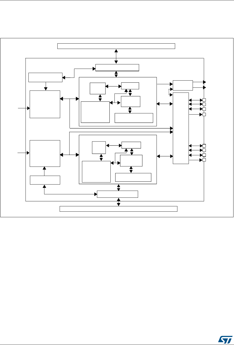
Serial audio interface (SAI) RM0090
928/1749 RM0090 Rev 18
29.3 Functional block diagram
The block diagram of the SAI is shown in Figure 283.
Figure 283. Functional block diagram
The SAI is mainly composed of two audio sub-blocks with their own clock generator. Each
audio block integrates a 32-bit shift register controlled by their own functional state machine.
Data are stored or read from the dedicated FIFO. FIFO may be accessed by the CPU, or by
DMA in order to leave the CPU free during the communication. Each audio block is
independent. They can be synchronous with each other.
An I/O line controller manages each dedicated pins for a given audio block in the SAI. If the
two blocks are synchronized, this controller reduces the number of I/Os used, freeing up an
FS pin, an SCK pin and eventually an MCLK pin, making them general purpose I/Os.
The functional state machine can be configured to address a wide range of audio protocols.
Some registers are present to set-up the desired protocols (audio frame waveform
generator).
The audio block can be a transmitter or receiver, in master or slave mode. The master mode
means the bit clock SCK and the frame synchronization signal are generated from the SAI,
whereas in slave mode, they come from another external or internal master. There is a
particular case for which the FS signal direction is not directly linked to the master or slave
MS30032V1
FIFO
FIFO
Audio block A
32-bit shift register
APB interface
APB interface
Serial Audio Interface
FIFO ctrl
FSM
Configuration
registers and
Status register
APB
APB
SAI_CK_A
synchro
ctrl out
int_sck
int_FS
FS_A
SCK_A
SD_A
MCLK_A
SAI_XCR1
Clock generator
Audio block A
FSM
(SAI)
Audio block B
FIFO ctrl
Configuration
registers and
Status register
Clock generator
Audio block B
SAI_XCR1
SAI_CK_B
I/O line Management
FS_B
SCK_B
SD_B
MCLK_B
32-bit shift register

RM0090 Rev 18 929/1749
RM0090 Serial audio interface (SAI)
964
mode definition. In AC’97 protocol, it will be an SAI output even if the SAI (link controller) is
set-up to consume the SCK clock (and so to be in Slave mode).
29.4 Main SAI modes
Each audio sub-block of the SAI can be configured to be master or slave via bit MODE[0] in
the SAI_xCR1 register of the selected audio block.
In master mode:
•The bit clock is generated by the SAI using the clock generator on pin SCK_A or
SCK_B (depending which audio block is declared as a master in the SAI).
•The dedicated pin SCK_x is considered as an output.
In slave mode:
•The slave must be enabled before the master is enabled.
•The slave audio block’s SCK clock I/O pin is considered input if it is configured in
asynchronous mode.
•If the audio block is declared synchronous with the second audio block in the SAI, its
SCK I/O pin is released to leave it free to be used as a general purpose I/O and is
connected internally to the SCK pin of the device with which it will be synchronized.
Each audio sub-block can be independently defined as a transmitter or receiver by bit
MODE[1] in the SAI_xCR1 register of the relevant audio block. The I/O pin SD will be
defined respectively as an output or an input.
It is possible to declare two master audio blocks in the same SAI with two different MCLK
and SCK clock frequencies (they have to be declared asynchronous).
Each of the audio blocks in the SAI are enabled by bit SAIxEN in the SAI_xCR1 register. As
soon as this bit is active, the transmitter or the receiver is sensitive to the activity on the
clock line, data line and synchronization line in slave mode.
In master TX mode, enabling the audio block immediately generates the bit clock for the
external slaves even if there is no data in the FIFO, However FS signal generation is
conditioned by the presence of data in the FIFO. After the FIFO receives the first data to
transmit, this data is output to external slaves. If there is no data to transmit in the FIFO, 0
values are then sent in the audio frame with an underrun flag generation.
In slave mode, the audio frame starts when the audio block is enabled and when a start of
frame is detected.
In Slave TX mode, no underrun event is possible on the first frame after the audio block is
enabled, because the mandatory operating sequence in this case is:
1. Write into the SAI_xDR (by software or by DMA).
2. Wait until the FIFO threshold (FLH) flag is different from 000b (FIFO empty).
3. Enable the audio block in slave transmitter mode.
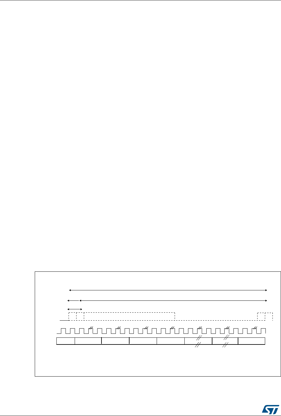
Serial audio interface (SAI) RM0090
930/1749 RM0090 Rev 18
29.5 SAI synchronization mode
Internal synchronization
An audio block can be declared synchronous with the second audio block. In this case, the
bit clock and the frame synchronization signals are shared to reduce the number of external
pins used for the communication. The audio block declared as synchronous with the other
one will see its own SCK_x, FS_x, and MCLK_x pins released to bring them back as GPIOs.
The one declared asynchronous is the one for which the I/O pins FS_x and SCK_x ad
MCLK_x (if the audio block is considered as master) are considered.
Typically, the audio block synchronous mode may be used to configure the SAI in full duplex
mode. One of the two audio blocks can be configured as master and the other as slave, or
both can be slaves; with one block declared as asynchronous (respective bit SYNCEN[1:0]
= 00 in SAI_xCR1) and the other one declared as synchronous with the other audio block
(respective bit SYNCEN[1:0] = 01 in the SAI_xCR1).
Note: APB frequency PCLK must be greater or equal to twice the bit rate clock frequency (due to
internal resynchronization stages).
29.6 Audio data size
The audio frame can target different data sizes by configuring bit DS[2:0] in the SAI_xCR1
register. The data sizes may be 8-, 10-, 16-, 20-, 24- or 32-bit. During the transfer, either the
MSB or the LSB of the data are sent first, depending on the configuration of bit LSBFIRST in
the SAI_xCR1 register.
29.7 Frame synchronization
The FS signal acts as the Frame synchronization signal in the audio frame (start of frame).
The shape of this signal is completely configurable in order to target the different audio
protocols with their own specificities concerning this Frame synchronization behavior. This
configurability is done using register SAI_xFRCR. Figure 284 gives a view of this flexibility.
Figure 284. Audio frame
Slot 0
Fs
sck
sd
Fs offset
Fs length = < 256 bits
Fs active length = < 128 bits
MS30037V1
Slot 1 Slot 2 Slot 3 Slot n
……

RM0090 Rev 18 931/1749
RM0090 Serial audio interface (SAI)
964
In AC’97 mode (bit PRTCFG[1:0] = 10 in the SAI_xCR1 register), the frame synchronization
shape is forced to be configured to target these protocols. The SAI_xFRCR register value is
ignored.
Each audio block is independent and so each requires a specific configuration.
29.7.1 Frame length
•Master mode: The audio frame length can be configured up to 256 bit clock, setting bit
FRL[7:0] in the SAI_xFRCR register. If the frame length is greater than the number of
declared slots for the frame, the remaining bits to transmit will be extended to 0 or the
SD line will be released to HI-z depending the state of bit TRIS in the SAI_xCR2
register (refer to Section 29.12.4). In reception mode, the remaining bit is ignored.
•Slave mode: The audio frame length is mainly used in order to specify to the slave the
number of bit clocks per audio frame sent by the external master. It is used mainly to
detect from the master, any anticipated or late occurrence of the Frame
synchronization signal during an on-going audio frame. An error will be generated in
such case. For more details please refer to the Section 29.13.
The number of bits in the frame is equal to FRL[7:0] + 1.
The minimum number of bits to transfer in an audio frame is 8. This is the case when the
data size is 8-bit and only one slot is defined in NBSLOT[3:0] in the SAI_xSLOTR register
(NBSLOT[3:0] = 0000 for slot 0).
In master mode:
•If bit NODIV in the SAI_xCR1 register is cleared, the frame length should be aligned to
a number equal to a power of 2, from 8 to 256. This is to ensure that an audio frame
contains an integer number of MCLK pulses per bit clock, which ensures correct
operation of the external DAC/ADC inside the decoders. If the value set in FRL[7:0]
does not respect this rule, flag WCKCFG is set when the audio block is enabled and an
interrupt is generated if bit WCKCFGIE is set in the SAI_xIM register. The SAI is
automatically disabled.
•If bit NODIV in the SAI_xCR1 register is set, the FRL[7:0] bit can take any of the values
without constraint since the input clock of the audio block should be equal to the bit
clock. There is no MCLK_x clock which can be output. MCLK_x output pad is
automatically disabled.
In slave mode, there are no constraints for the FRL[7:0] bit configuration in the SAI_xFRCR
register.
29.7.2 Frame synchronization polarity
Bit FSPOL in the SAI_xFRCR register sets the active polarity of the FS pin from which a
frame is started. The start of frame is edge sensitive.
In slave mode, the audio block waits for a valid frame to start to transmit or to receive. Start
of frame is synchronized to this signal. It is effective only if the start of frame is not detected
during an on-going communication and assimilated to an anticipated start of frame (refer to
Section 29.13).
In master mode, the frame synchronization is sent continuously each time an audio frame is
complete until the SAIxEN bit in the SAI_xCR1 register is cleared. If no data is present in the
FIFO at the end of the previous audio frame, an underrun condition will be managed as

Serial audio interface (SAI) RM0090
932/1749 RM0090 Rev 18
described in Section 29.13), but there will be no interruption in the audio communication
flow.
29.7.3 Frame synchronization active level length
Bit FSALL[6:0] in the SAI_xFRCR register configures the length of the active level of the
Frame synchronization signal. The length can be set from 1 to 128 bit clock SCK.
The active length may be half of the frame length in I2S, LSB or MSB-justified modes for
instance, or one-bit wide for PCM/DSP or TDM mode, or even 16-bit length in AC’97.
29.7.4 Frame synchronization offset
Depending on the audio protocol targeted in the application, the Frame synchronization
signal can be asserted when transmitting the last bit or the first bit of the audio frame (as for
instance, respectively, in I2S standard protocol and in MSB-justified protocol). Bit FSOFF in
the SAI_xFRCR register makes the choice.
29.7.5 FS signal role
The FS signal may have a different meaning depending on the FS function. Bit FSDEF in
the SAI_xFRCR register selects which meaning it will have. It may be either:
•0: a start of frame, like for instance the PCM/DSP, TDM, AC’97, audio protocols,
•1: a start of frame and a channel side identification within the audio frame like for the
I2S, the MSB or LSB-justified protocols.
When the FS signal is considered as a start of frame and channel side identification within
the frame, the number of declared slots must be considered to be half of the number for the
left channel and half of the number for the right channel. If the number of bit clock on half
audio frame is greater than the number of slots dedicated to a channel side, if TRIS = 0, 0 is
sent for transmission for the remaining bit clock in the SAI_xCR2 register, otherwise if TRIS
= 1, the SD line is released to HI-Z. In reception, the remaining bit clock are not considered
until the channel side changes.
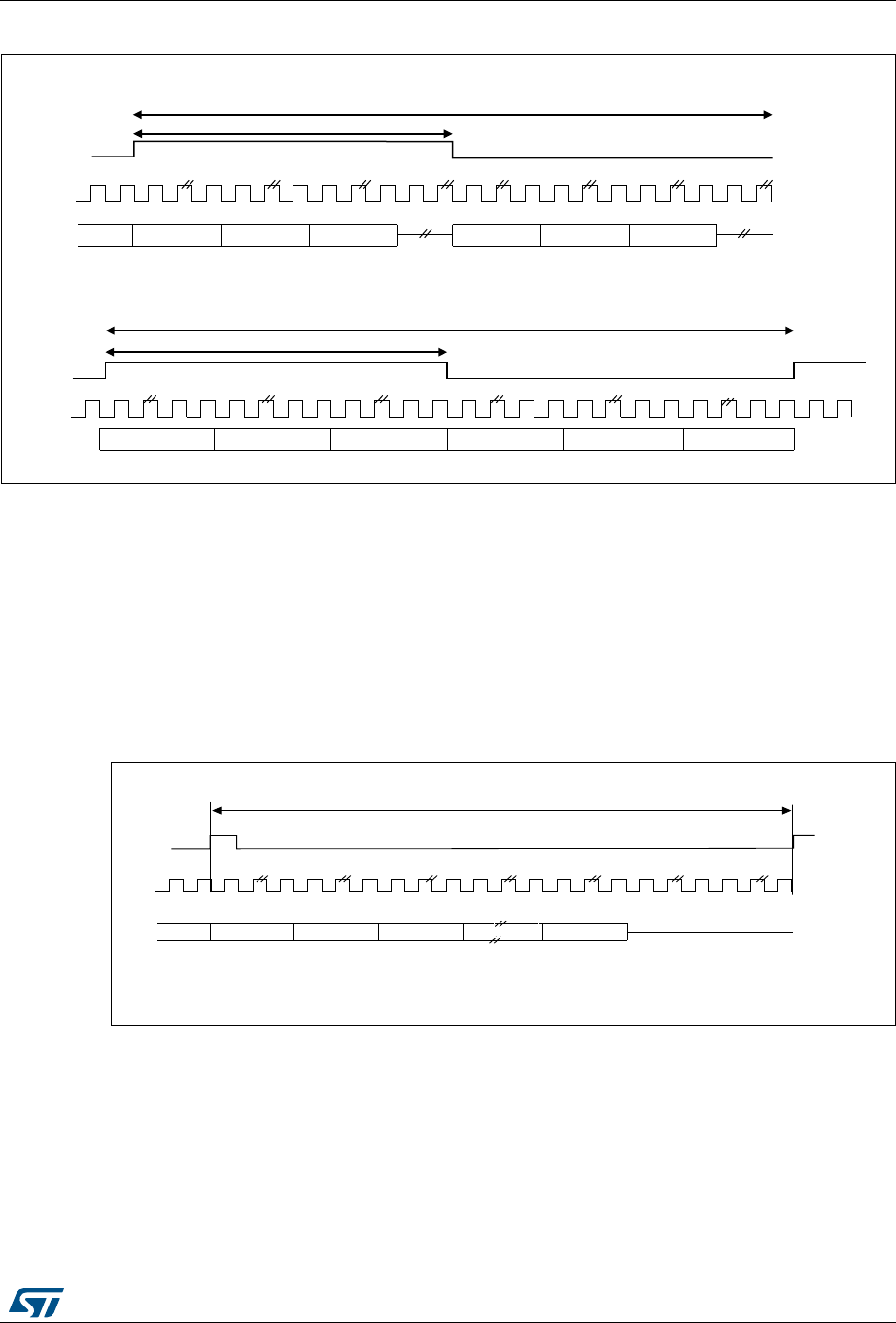
RM0090 Rev 18 933/1749
RM0090 Serial audio interface (SAI)
964
Figure 285. FS role is start of frame + channel side identification (FSDEF = TRIS = 1)
1. The frame length should be even.
If bit FSDEF in SAI_xFRCR is kept clear, so FS signal is equivalent to a start of frame, and
if the number of slots defined in bit NBSLOT[3:0] in SAI_xSLOTR multiplied by
the number of bits by slot configured in bit SLOTSZ[1:0] in SAI_xSLOTR is less than the
frame size (bit FRL[7:0] in the SAI_xFRCR register), then,
•if TRIS = 0 in the SAI_xCR2 register, the remaining bit after the last slot will be forced to
0 until the end of frame in case of transmission,
•if TRIS = 1, the line will be released to HI-Z during the transfer of these remaining bits.
In reception mode, these bits are discarded.
Figure 286. FS role is start of frame (FSDEF = 0)
29.8 Slot configuration
The slot is the basic element in the audio frame. The number of slots in the audio frame is
equal to the configured setting of bit NBSLOT[3:0] in the SAI_xSLOTR register +1.
The maximum number of slots per audio frame is fixed at 16.
For AC’97 protocol (when bit PRTCFG[1:0] = 10), the number of slots is automatically set to
target the protocol specification, and the value of NBSLOT[3:0] is ignored.
sck
slot
Audio frame
FS
Half of frame
Audio frame
FS
Half of frame
Number of slots not aligned with the audio frame
Number of slots aligned with the audio frame
MS30038V1
Slot 0
sck
slot Slot 1 Slot 2 Slot 3 Slot 5
Slot 4
Slot 0 ON Slot 1 OFF Slot 2 ON Slot 3 ON Slot 4 OFF Slot 5 ON
Audio frame
Data = 0 after slot n if TRIS = 0
SD output released (HI-Z) after slot n if TRIS = 1
MS30039V1
sck
slot Slot 0 Slot 1 Slot 2 Slot n
...
Serial audio interface (SAI) RM0090
934/1749 RM0090 Rev 18
Each slot can be defined as a valid slot, or not, by setting bit SLOTEN[15:0] in the
SAI_xSLOTR register. In an audio frame, during the transfer of a non-valid slot, 0 value will
be forced on the data line or the SD data line will be released to HI-z (refer to
Section 29.12.4) if the audio block is transmitter, or the received value from the end of this
slot will be ignored. Consequently, there will be no FIFO access and so no request to read
or write the FIFO linked to this inactive slot status.
The slot size is also configurable as shown in the Figure 287. The size of the slots is
selected by setting bit SLOTSZ[1:0] in the SAI_xSLOTR register. The size is applied
identically for each slot in an audio frame.
Figure 287. Slot size configuration with FBOFF = 0 in SAI_xSLOTR
It is possible to choose the position of the first data bit to transfer within the slots, this offset
is configured by bit FBOFF[5:0] in the SAI_xSLOTR register. 0 values will be injected in
transmitter mode from the beginning of the slot until this offset position is reached. In
reception, the bit in the offset phase is ignored. This feature targets the LSB justified
protocol (if the offset is equal to the slot size minus the data size).
Figure 288. First bit offset
MS30033V1
00..00
00..00
X..X
XX..XX
X: don’t care
Audio block is transmitter
Slot size = data size
data size
data size
data size
data size
slotx
slotx
slotx
16-bit
32-bit
Audio block is receiver
Slot size = data size
data size
data size
data size
slotx
slotx
slotx
16-bit
32-bit
data size
MS30034V1
XX .. XX
00
00..00
X: don’t care
Audio block is transmitter
Slot size = data size
data size
data size
data size
data size
slotx
slotx
slotx
16-bit
32-bit
Audio block is receiver
00
FBOFF
FBOFF = SLOT SZ -DS
XX
Slot size = data size
data size
data size
data size
data size
slotx
slotx
slotx
16-bit
32-bit
XX
FBOFF
FBOFF = SLOT SZ -DS
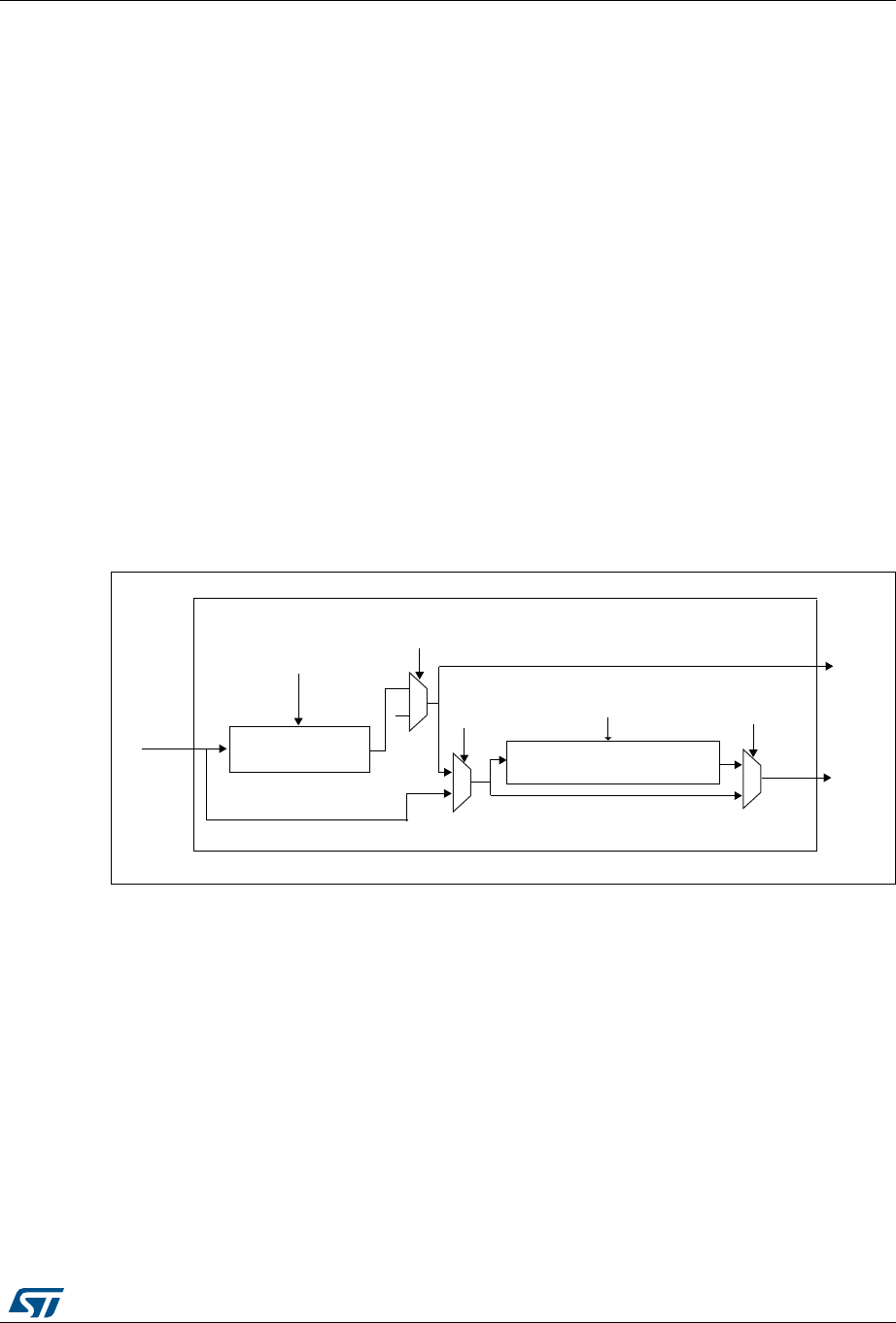
RM0090 Rev 18 935/1749
RM0090 Serial audio interface (SAI)
964
It is mandatory to respect the following conditions in order to avoid bad SAI behavior:
FBOFF ≤ (SLOTSZ - DS),
DS ≤ SLOTSZ,
NBSLOT x SLOTSZ ≤ FRL (frame length),
The number of slots should be even when bit FSDEF in the SAI_xFRCR register is set.
In AC’97 (bit PRTCFG[1:0] = 10), the slot size is automatically set as defined in
Section 29.11.
29.9 SAI clock generator
Each audio block has its own clock generator to make these two blocks completely
independent. There is no difference in terms of functionality between these two clock
generators. They are exactly the same.
When the audio block is defined as Master, the clock generator generates the
communication clock (the bit clock) and the master clock for external decoders.
When the audio block is defined as slave, the clock generator is OFF.
Figure 289 illustrates the architecture of the audio block clock generator.
Figure 289. Audio block clock generator overview
Note: If NoDiv is set to 1, the MCLK_x signal will be set at 0 level if this pin is configured as the
SAI pin in GPIO peripherals.
The clock source for the clock generator comes from the product clock controller. The
SAI_CK_x clock is equivalent to the master clock which may be divided for the external
decoders using bit MCKDIV[3:0]:
MCLK_x = SAI_CK_x / (MCKDIV[3:0] * 2), if MCKDIV[3:0] is not equal to 0000.
MCLK_x = SAI_CK_x, if MCKDIV[3:0] is equal to 0000.
MCLK_x signal is used only in TDM.
The division must be even in order to keep 50% on the Duty cycle on the MCLK output and
on the SCK_x clock. If bit MCKDIV[3:0] = 0000, division by one is applied to have MCLK_x
= SAI_CK_x.
In the SAI, the single ratio MCLK/FS = 256 is considered. Mostly, three frequency ranges
will be encountered as illustrated in the Table 130.
Master clock
divider Bit clock divider
MCKDIV[3:0]
SCK_x
MCLK_x
NODIV
0
1
0
1
NODIV
0
1
0
NODIV
SAI_CK_x
MS30040V1
FRL[7:0]

Serial audio interface (SAI) RM0090
936/1749 RM0090 Rev 18
The master clock may be generated externally on an I/O pad for external decoders if the
corresponding audio block is declared as master with bit NODIV = 0 in the SAI_xCR1
register. In slave, the value set in this last bit is ignored since the clock generator is OFF,
and the MCLK_x I/O pin is released for use as a general purpose I/O.
The bit clock is derived from the master clock. The bit clock divider sets the divider factor
between the bit clock SCK_x and the master clock MCLK_x following the formula:
SCK_x = MCLK x (FRL[7:0] +1) / 256
where:
256 is the fixed ratio between MCLK and the audio frequency sampling.
FRL[7:0] is the number of bit clock - 1 in the audio frame, configured in the SAI_xFRCR
register.
It is mandatory in master mode that (FRL[7:0] +1) should be equal to a number with a power
of 2 (refer to Section 29.7) in order to have an even integer number of MCLK_x pulses by bit
clock. The 50% duty cycle is guaranteed on the bit clock SCK_x.
The SAI_CK_x clock can be also equal to the bit clock frequency. In this case, bit NODIV in
the SAI_xCR1 register should be set and the value inside the MCKDIV divider and the bit
clock divider will be ignored. In this case, the number of bits per frame is fully configurable
without the need to be equal to a power of two.
The bit clock strobing edge on SCK can be configured by bit CKSTR in the SAI_xCR1
register.
29.10 Internal FIFOs
Each audio block in the SAI has its own FIFO. Depending if the block is defined to be a
transmitter or a receiver, the FIFO will be written or read, respectively. There is therefore
only one FIFO request linked to FREQ bit in the SAI_xSR register.
Table 130. Example of possible audio frequency sampling range
Input SAI_CK_x clock
frequency
Most usual audio frequency
sampling achievable MCKDIV[3:0]
192 kHz x 256
192 kHz MCKDIV[3:0] = 0000
96 kHz MCKDIV[3:0] = 0001
48 kHz MCKDIV[3:0] = 0010
16 kHz MCKDIV[3:0] = 0100
8 kHz MCKDIV[3:0] = 1000
44.1 kHz x 256
44.1 kHz MCKDIV[3:0] = 0000
22.05 kHz MCKDIV[3:0] = 0001
11.025 kHz MCKDIV[3:0] = 0010
SAI_CK_x = MCLK(1)
1. This may happen when the product clock controller selects an external clock source, instead of PLL clock.
MCLK MCKDIV[3:0] = 0000

RM0090 Rev 18 937/1749
RM0090 Serial audio interface (SAI)
964
An interrupt is generated if FREQIE bit is enabled in the SAI_xIM register. This depends on:
•FIFO threshold setting (FLTH bits in SAI_CR2)
•Communication direction transmitter or receiver (see Section : Interrupt generation in
transmitter mode and Section : Interrupt generation in reception mode)
Interrupt generation in transmitter mode
The interrupt generation depends on the FIFO configuration in transmitter mode:
•When the FIFO threshold bits in SAI_XCR2 register are configured as FIFO empty
(FTH[2:0] set to 000b), an interrupt is generated (FREQ bit set by hardware to 1 in
SAI_XSR register) if no data are available in SAI_xDR register (FLTH[2:0] bits in SAI_xSR
is less than 001b). This Interrupt (FREQ bit in SAI_XSR register) is cleared by hardware
when the FIFO became not empty (FLTH[2:0] bits in SAI_xSR are different from 000b) i.e
one or more data are stored in the FIFO.
•When the FIFO threshold bits in SAI_XCR2 register are configured as FIFO quarter full
(FTH[2:0] set to 001b), an interrupt is generated (FREQ bit set by hardware to 1 in
SAI_XSR register) if less than a quarter of the FIFO contains data (FLTH[2:0] bits in
SAI_xSR are less than 010b). This Interrupt (FREQ bit in SAI_XSR register) is cleared by
hardware when at least a quarter of the FIFO contains data (FLTH[2:0] bits in SAI_xSR
are higher or equal to 010b).
•When the FIFO threshold bits in SAI_XCR2 register are configured as FIFO half full
(FTH[2:0] set to 010b), an interrupt is generated (FREQ bit set by hardware to 1 in
SAI_XSR register) if less than half of the FIFO contains data (FLTH[2:0] bits in SAI_xSR
are less than 011b). This Interrupt (FREQ bit in SAI_XSR register) is cleared by hardware
when at least half of the FIFO contains data (FLTH[2:0] bits in SAI_xSR are higher or
equal to 011b).
•When the FIFO threshold bits in SAI_XCR2 register are configured as FIFO three quarter
(FTH[2:0] set to 011b), an interrupt is generated (FREQ bit is set by hardware to 1 in
SAI_XSR register) if less than three quarters of the FIFO contain data (FLTH[2:0] bits in
SAI_xSR are less than 100b). This Interrupt (FREQ bit in SAI_XSR register) is cleared by
hardware when at least three quarters of the FIFO contain data (FLTH[2:0] bits in
SAI_xSR are higher or equal to 100b).
•When the FIFO threshold bits in SAI_XCR2 register are configured as FIFO full (FTH[2:0]
set to 100b), an interrupt is generated (FREQ bit is set by hardware to 1 in SAI_XSR
register) if the FIFO is not full (FLTH[2:0] bits in SAI_xSR is less than 101b). This Interrupt
(FREQ bit in SAI_XSR register) is cleared by hardware when the FIFO is full (FLTH[2:0]
bits in SAI_xSR is equal to 101b value).
Interrupt generation in reception mode
The interrupt generation depends on the FIFO configuration in reception mode:
•When the FIFO threshold bits in SAI_XCR2 register are configured as FIFO empty
(FTH[2:0] set to 000b), an interrupt is generated (FREQ bit is set by hardware to 1 in
SAI_XSR register) if at least one data is available in SAI_xDR register(FLTH[2:0] bits in
SAI_xSR is higher or equal to 001b). This Interrupt (FREQ bit in SAI_XSR register) is
cleared by hardware when the FIFO became empty (FLTH[2:0] bits in SAI_xSR is equal
to 000b) i.e no data is stored in FIFO.
•When the FIFO threshold bits in SAI_XCR2 register are configured as FIFO quarter fully
(FTH[2:0] set to 001b), an interrupt is generated (FREQ bit is set by hardware to 1 in
SAI_XSR register) if at less one quarter of the FIFO data locations are available

Serial audio interface (SAI) RM0090
938/1749 RM0090 Rev 18
(FLTH[2:0] bits in SAI_xSR is higher or equal to 010b). This Interrupt (FREQ bit in
SAI_XSR register) is cleared by hardware when less than a quarter of the FIFO data
locations become available (FLTH[2:0] bits in SAI_xSR is less than 010b).
•When the FIFO threshold bits in SAI_XCR2 register are configured as FIFO half fully
(FTH[2:0] set to 010b value), an interrupt is generated (FREQ bit is set by hardware to 1
in SAI_XSR register) if at least half of the FIFO data locations are available (FLTH[2:0]
bits in SAI_xSR is higher or equal to 011b). This Interrupt (FREQ bit in SAI_XSR register)
is cleared by hardware when less than half of the FIFO data locations become available
(FLTH[2:0] bits in SAI_xSR is less than 011b).
•When the FIFO threshold bits in SAI_XCR2 register are configured as FIFO three quarter
full(FTH[2:0] set to 011b value), an interrupt is generated (FREQ bit is set by hardware to
1 in SAI_XSR register) if at least three quarters of the FIFO data locations are available
(FLTH[2:0] bits in SAI_xSR is higher or equal to 100b). This Interrupt (FREQ bit in
SAI_XSR register) is cleared by hardware when the FIFO has less than three quarters of
the FIFO data locations avalable(FLTH[2:0] bits in SAI_xSR is less than 100b).
•When the FIFO threshold bits in SAI_XCR2 register are configured as FIFO full(FTH[2:0]
set to 100b), an interrupt is generated (FREQ bit is set by hardware to 1 in SAI_XSR
register) if the FIFO is full (FLTH[2:0] bits in SAI_xSR is equal to 101b). This Interrupt
(FREQ bit in SAI_XSR register) is cleared by hardware when the FIFO is not full
(FLTH[2:0] bits in SAI_xSR is less than 101b).
Like interrupt generation, the SAI can use the DMA if DMAEN bit in the SAI_xCR1 register is
set. The FREQ bit assertion mechanism is the same as the interruption generation
mechanism described above for FREQIE.
Each FIFO is an 8-word FIFO. Each read or write operation from/to the FIFO targets one
word FIFO allocation whatever the access size. Each FIFO word contains one audio frame.
FIFO pointers are incremented by one word after each access to the SAI_xDR register.
Data should be right aligned when it is written in the SAI_xDR.
Data received will be right aligned in the SAI_xDR.
The FIFO pointers can be reinitialized when the SAI is disabled by setting bit FFLUSH in the
SAI_xCR2 register. If FFLUSH is set when the SAI is enabled the data present in the FIFO
will be lost automatically.
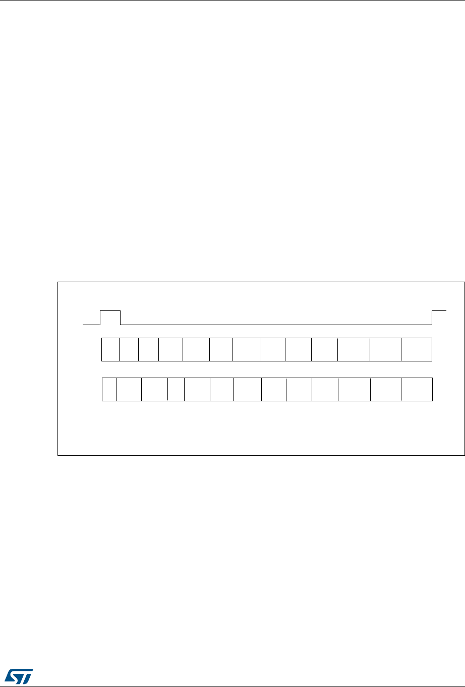
RM0090 Rev 18 939/1749
RM0090 Serial audio interface (SAI)
964
29.11 AC’97 link controller
The SAI is able to work as an AC’97 link controller. In this protocol:
•The slot number and the slot size are fixed.
•The frame synchronization signal is perfectly defined and has a fixed shape.
To select this protocol, set bit PRTCFG[1:0] in the SAI_xCR1 register to 10. When AC’97
mode is selected the data sizes that can be used are 16-bit or 20-bit only, else SAI behavior
is not guaranteed.
•Bits NBSLOT[3:0] and SLOTSZ[1:0] are consequently ignored.
•The number of slots is fixed at 13 slots. The first one is 16 bits wide and all the others
are 20 bits wide (data slots).
•Bit FBOFF[5:0] in the SAI_xSLOTR register is ignored
•The SAI_xFRCR register is ignored.
The FS signal from the block defined as asynchronous is configured automatically as an
output, since the AC’97 controller link drives the FS signal whatever the master or slave
configuration.
Figure 290 presents an AC’97 audio frame structure.
Figure 290. AC’97 audio frame
Note: In AC’97 protocol, bit 2 of the tag is reserved (always 0), so whatever the value written in the
SAI FIFO, bit 2 of the TAG is forced to 0 level.
For more details about TAG representation, please refer to the AC’97 protocol standard.
One SAI can be used to target an AC’97 point-to-point communication.
In receiver mode, the SAI acting as an AC’97 link controller will require no FIFO request and
so no data storage in the FIFO when the codec ready bit in the slot 0 is decoded low. If bit
CNRDYIE is enabled in the SAI_xIM register, flag CNRDY will be set in the SAI_xSR
register and an interrupt is generated. This flag is dedicated to the AC’97 protocol.
MS192343V1
FS
123 4 5 6 7 8 9 10 1112
SDI
SDO
Tag CMD
ADDR
CMD
DATA
LINE1
DAC
PCM
LFRONT
PCM
RFRONT
PCM
CENTER
PCM
LSURR
PCM
RSURR
PCM
LFE
LINE2
DAC
HSET
DAC
IO
CTRL
Tag STATUS
ADDR
STATUS
DATA
LINE1
ADC
PCM
LEFT
PCM
RIGHT
PCM
MIC
RSR
VD
RSR
LVD
LINE2
ADC HSET IO
STATUS
RSR
VD

Serial audio interface (SAI) RM0090
940/1749 RM0090 Rev 18
29.12 Specific features
The SAI has some specific functions which can be useful depending on the audio protocol
selected. These functions are accessible through specific bits in the SAI_xCR2 register.
29.12.1 Mute mode
Mute mode may be used when the audio block is a transmitter or receiver.
Transmitter
In transmitter mode, Mute mode can be selected at anytime. Mute mode is active for entire
audio frames. The bit MUTE in the SAI_xCR2 register requests Mute mode when it is set
during an on-going frame.
The mute mode bit is strobed only at the end of the frame. If set at this time, the mute mode
is active at the beginning of the new audio frame, for a complete frame, until the next end of
frame, it then strobes the bit to determine if the next frame will still be a mute frame.
If the number of slots set in bit NBSLOT[3:0] in the SAI_xSLOTR register is lower than or
equal to two, it is possible to specify if the value sent during the Mute mode is 0 or if it is the
last value of each slot. The selection is done via bit MUTEVAL in the SAI_xCR2 register.
If the number of slots set in bit NBSLOT[3:0] in the SAI_xSLOTR register is greater than
two, MUTEVAL bit in the SAI_xCR2 has no meaning as 0 values are sent on each bit on
each slot.
During Mute mode, the FIFO pointers are still incremented, meaning that data which was
present in the FIFO and for which the Mute mode is requested is discarded.
Receiver
In receiver mode, it is possible to detect a Mute mode sent from the external transmitter
when all the declared and valid slots of the audio frame receive 0 for a given consecutive
number of audio frames (bit MUTECNT[5:0] in the SAI_xCR2 register).
When the number of MUTE frames is detected, flag MUTEDET in the SAI_xSR register is
set and an interrupt can be generated if bit MUTEDETIE is set in the SAI_xCR2.
The mute frame counter is cleared when the audio block is disabled or when a valid slot
receives at least one data in an audio frame. The interrupt is generated just once, when the
counter reaches the specified value in bit MUTECNT[5:0]. Then the interrupt event is re-
armed when the counter is cleared.
29.12.2 MONO/STEREO function
In transmission mode, it is possible to address the Mono mode without any data pre-
processing in memory when the number of slot is equal to 2 (NBSLOT[3:0] = 0001 in the
SAI_xSLOTR). In such a case, the access to and from the FIFO will be reduced by two
since in transmission, the data for slot 0 is duplicated into data slot 1.
To select the Mono feature, set bit MONO in the SAI_xCR1 register.
In reception mode, bit MONO can be set and has a meaning only if the number of slots is
equal to 2 like for the transmission mode. When it is set, only the data of slot 0 will be stored
in the FIFO. The data belonging to slot 1 will be discarded since in this case, it is supposed
to be the same as the previous slot. If the data flux in reception is a real stereo audio flow
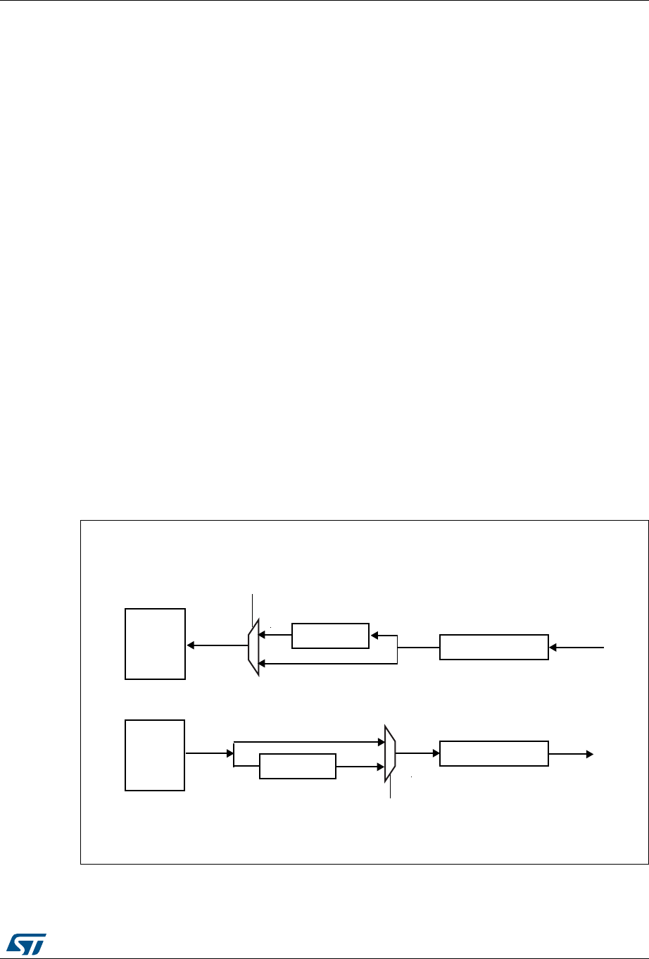
RM0090 Rev 18 941/1749
RM0090 Serial audio interface (SAI)
964
with a distinct and different left and right data, bit MONO has no meaning. The conversion
from the output stereo file to the equivalent mono file is done by software.
Note: To enable Mono mode, NBSLOT and SLOTEN must equal two and MONO bit set to 1.
29.12.3 Companding mode
Telecommunication applications may require to process the data to transmit or to receive
with a data companding algorithm.
Depending on the COMP[1:0] bit in the SAI_xCR2 register (used only when TDM mode is
selected), the software may choose to process or not the data before sending it on SD serial
output line (compression) or to expand the data after the reception on SD serial input line
(expansion) as illustrated in Figure 291,.The two companding modes supported are the µ-
Law and the A-Law log which are a part of the CCITT G.711 recommendation.
The companding standard employed in the United States and Japan is the µ-Law and allows
14 bits of dynamic range (COMP[1:0] = 10 in the SAI_xCR2 register).
The European companding standard is A-Law and allows 13 bits of dynamic range
(COMP[1:0] = 11 in the SAI_xCR2 register).
Companding standard (µ-Law or A-Law) can be computed based on 1’s complement or 2’s
complement representation depending on the CPL bit setting in the SAI_xCR2 register.
The µ-Law and A-Law formats encode data into 8-bit code elements with MSB alignment.
Companded data is always 8 bits wide. For this reason, bit DS[2:0] in the SAI_xCR1 register
will be forced to 010 when the SAI audio block is enabled (bit SAIxEN = 1 in the SAI_xCR1
register) and when the COMP[1:0] bit selects one of these two companding modes.
If no companding processing is required, COMP[1:0] bit in the SAI_xCR2 register should be
kept cleared.
Figure 291. Data companding hardware in an audio block in the SAI
Note: Not applicable when AC’97 selected.
expand
FIFO
COMP[1]
COMP[1]
32-bit shift register
SD
Receiver mode (bit MODE[0] = 1 in SAI_xCR1)
Transmitter mode (bit MODE[0] = 0 in SAI_xCR1)
MS19244V1
1
0
1
032-bit shift register
SD
compress
FIFO

Serial audio interface (SAI) RM0090
942/1749 RM0090 Rev 18
Expansion or compression mode is automatically selected by the SAI configuration.
•If the SAI audio block is configured to be a transmitter, and if the COMP[1] bit is set in
the SAI_xCR2 register, the compression mode will be applied.
•If the SAI audio block is declared as a receiver, the expansion algorithm will be applied.
29.12.4 Output data line management on an inactive slot
In transmitter mode, it is possible to choose the behavior of the SD line in output when an
inactive slot is sent on the data line (via bit TRIS in the SAI_xCR2 register when the SAI is
disabled).
•Either the SAI forces 0 on the SD output line when an inactive slot is transmitted, or
•The line is released in HI-z state at the end of the last bit of data transferred, to release
the line for other transmitters connected to this node.
It is important to note that the two transmitters do not attempt to drive the same SD output
pin simultaneously, which could result in a short circuit. In order to ensure a gap between
transmissions, if the data is lower than 32-bit, the data can be extended to 32-bit by setting
bit SLOTSZ[1:0] = 10 in the SAI_xSLOTR register. Then, the SD output pin will be tristated
at the end of the LSB of the active slot (during the padding to 0 phase to extend the data to
32-bit) if the following slot is declared inactive.
In addition, if the number of slots multiplied by the slot size is lower than the frame length,
the SD output line will be tristated when the padding to 0 is done to complete the audio
frame.
Figure 292 illustrates these behaviors.
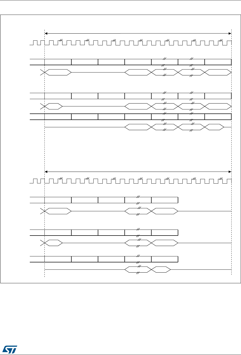
RM0090 Rev 18 943/1749
RM0090 Serial audio interface (SAI)
964
Figure 292. Tristate strategy on SD output line on an inactive slot
When the selected audio protocol uses the FS signal as a start of frame and a channel side
identification (bit FSDEF = 1 in the SAI_xFRCR register), the tristate mode is managed
according to Figure 293 (where bit TRIS in the SAI_xCR1 register = 1, and FSDEF=1, and
half frame length > number of slots/2, and NBSLOT=6).
slot
Audio frame
Bit TRIS = 1 in the SAI_xCR1 and frame length = number of slots
MS192345V1
Slot size = data size
Slot size > data size
Bit TRIS = 1 in the SAI_xCR1 and frame length > number of slots
SD (output)
sck
Slot 0 ON Slot 1 OFF Slot 2 OFF Slot 3 ON .. ON .. ON Slot n ON
Data 0 Data 1 .. .. Data m
Slot 0 ON Slot 1 OFF Slot 2 OFF Slot 3 ON .. ON .. ON Slot n ON
Data 0 Data 1 .. .. Data m
Slot 0 ON Slot 1 OFF Slot 2 OFF Slot 3 ON .. ON .. ON Slot n ON
Data 0 .. .. Data m
slot
SD (output)
slot
SD (output)
slot
Audio frame
Slot size = data size
SD (output)
sck
Slot 0 ON Slot 1 OFF Slot 2 OFF .. ON Slot n ON
Data 0 .. Data m
slot
Slot size > data size
SD (output)
Slot 0 ON Slot 1 OFF Slot 2 OFF .. ON Slot n ON
.. Data m
Data 0
slot
SD (output)
Slot 0 ON Slot 1 OFF Slot 2 OFF .. ON
.. Data m
.. ON
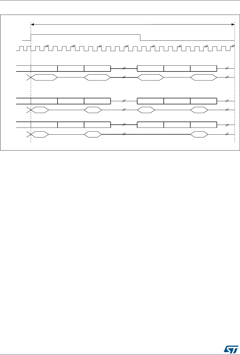
Serial audio interface (SAI) RM0090
944/1749 RM0090 Rev 18
Figure 293. Tristate on output data line in a protocol like I2S
If the TRIS bit in the SAI_xCR2 register is cleared, all the High impedance states on the SD
output line on Figure 292 and Figure 293 are replaced by a drive with a value of 0.
29.13 Error flags
The SAI embeds some error flags:
– FIFO overrun/underrun,
– Anticipated frame synchronization detection,
– Late frame synchronization detection,
– Codec not ready (AC’97 exclusively),
– Wrong clock configuration in master mode.
29.13.1 FIFO overrun/underrun (OVRUDR)
The FIFO Overrun/Underrun bit is called OVRUDR in the SAI_xSR register.
The overrun or underrun errors occupy the same bit since an audio block can be either
receiver or transmitter and each audio block in an SAI has its own SAI_xSR register.
Overrun
When the audio block is configured as receiver, an overrun condition may appear if data is
received in an audio frame when the FIFO is full and is not able to store the received data.
In this case, the received data is lost, the flag OVRUDR in the SAI_xSR register is set and
an interrupt is generated if bit OVRUDRIE is set in the SAI_xIM register. The slot number
from which the overrun occurs, is stored internally. No more data will be stored into the FIFO
until it becomes free to store new data. When the FIFO has at least one data free, the SAI
audio block receiver will store new data (from new audio frame) from the slot number which
slot
MS192346V1
Slot size = data size
Slot size > data size
SD (output)
sck
Slot 0 ON Slot 1 OFF Slot 2 ON Slot 3 ON Slot 4 OFF Slot 5 ON
Data 0 Data 1
Slot 0 ON Slot 1 OFF Slot 2 ON
Data 0
slot
SD (output)
Data 2 Data 3
Slot 3 ON Slot 4 OFF Slot 5 ON
Data 1 Data 2 Data 3
Slot 0 ON Slot 1 OFF Slot 2 ON
Data 0
slot
SD (output)
Slot 3 ON Slot 4 OFF Slot 5 ON
Data 1 Data m
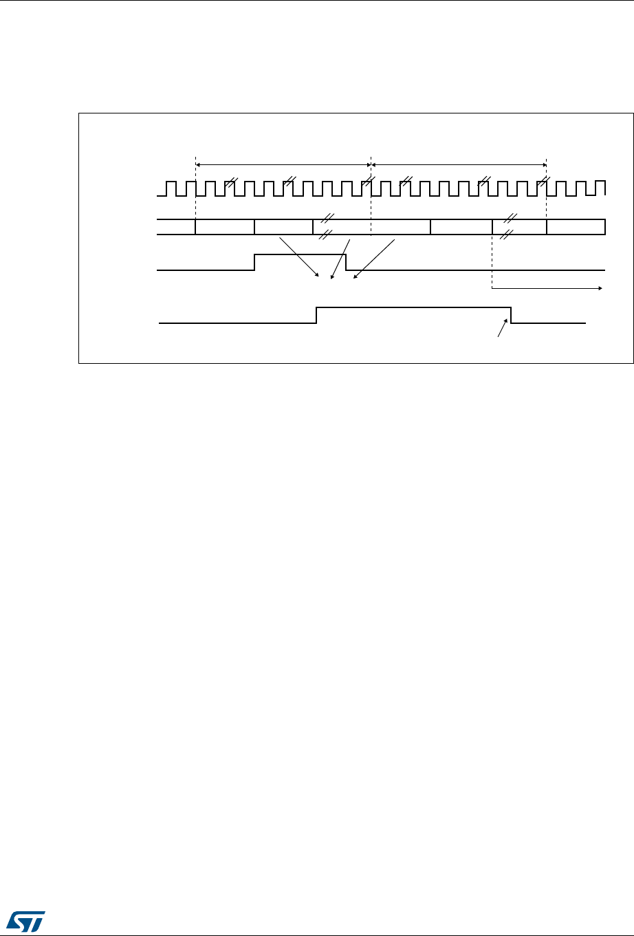
RM0090 Rev 18 945/1749
RM0090 Serial audio interface (SAI)
964
was stored internally when the overrun condition was detected, and this, to avoid data slot
de-alignment in the destination memory (refer to Figure 294).
The OVRUDR flag is cleared when bit COVRUDR is set in the SAI_xCLRFR register.
Figure 294. Overrun detection error
Underrun
An underrun may occur when the audio block in the SAI is a transmitter and the FIFO is
empty when data needs to be transmitted (the audio block configuration (Master or Slave) is
not relevant). If an underrun is detected, the software must resynchronize data and slot.
Proceed as follows:
1. Disable the SAI peripheral by resetting the SAIEN bit of the SAI_xCR1 register. Check
that the SAI has been disabled by reading back the SAIEN bit (SAIEN should be equal
to 0).
2. Flush the Tx FIFO through the FFLUS bit of the SAI_xCR2 register.
3. Re-assigned to the correct data to be transferred on the first active slot of the new
frame.
4. Re-enabling the SAI peripheral (SAIEN bit set to 1).
The underrun event sets the OVRUDR flag in the SAI_xSR register and an interrupt is
generated if the OVRUDRIE bit is set in the SAI_xIM register. To clear this flag, set the
COVRUDR bit in the SAI_xCLRFR register.
MS192348V2
sck
data Slot 0 ON
Example: FIFO overrun on Slot 1
Audio frame Audio frame
Slot n ON... ON
FIFO full
OVRUDR
Slot 1 ON Slot 1 ON Slot 0 ON Slot 1 ON
Received data discarded Data stored again in FIFO
COVRUDR = 1
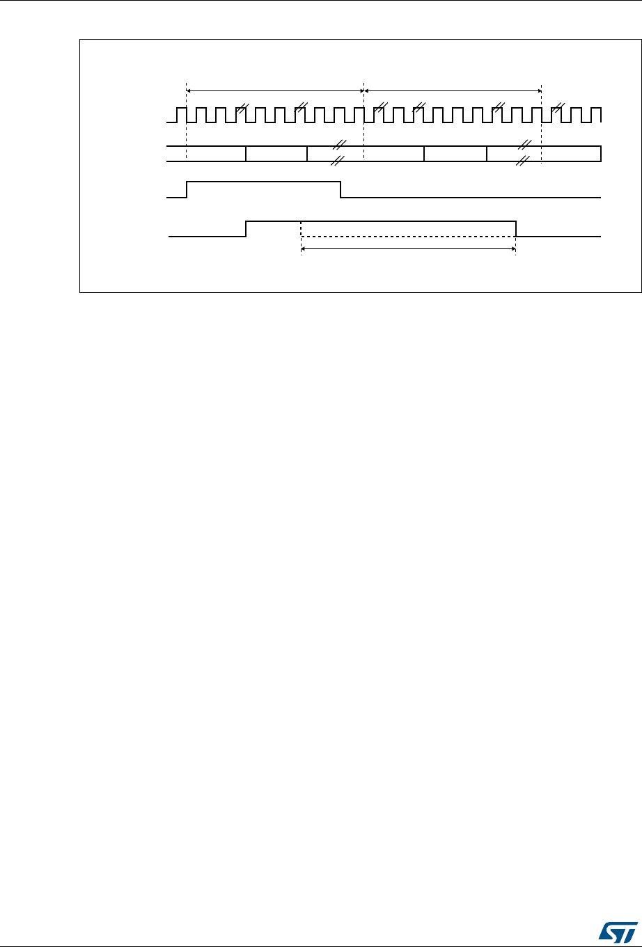
Serial audio interface (SAI) RM0090
946/1749 RM0090 Rev 18
Figure 295. FIFO underrun event
29.13.2 Anticipated frame synchronisation detection (AFSDET)
This flag AFSDET is used only in Slave mode. In master mode, it is never asserted. It
informs about the detection of a frame synchronisation (FS) earlier than expected since the
frame length, the frame polarity, the frame offset are defined and known.
Early detection sets flag AFSDET in the SAI_xSR register.
This detection has no effect on the current audio frame which is not sensitive to the
anticipated FS. This means that “parasitic” events on signal FS are flagged without any
perturbation of the current audio frame.
If bit AFSDETIE is set in the SAI_xIM register, an interrupt is generated. To clear the flag
AFSDET, bit CAFSDET in the SAI_xCLRFR register has to be set.
To resynchronize with the master after Anticipated frame detection error, four steps should
be respected:
1. SAI block should be disabled by resetting SAIEN bit in SAI_xCR1 register, to be sure
that the SAI is disabled SAIEN bit is should be equal to 0 (reading back this bit).
2. FIFO should be flushed via FFLUS bit in SAI_xCR2 register.
3. Re-enabling the SAI peripheral (SAIEN bit set to 1) then the SAI.
4. SAI block will wait for the assertion on FS to restart the synchronization with master.
Note: This flag is not asserted in AC’97 since the SAI audio block acts as a link controller and
generates the FS signal even when declared as slave.
29.13.3 Late frame synchronization detection
Flag LFSDET in the SAI_xSR register can be set only when the SAI audio block is defined
as slave. The frame length, the frame polarity and the frame offset configuration are known
in register SAI_xFRCR.
If the external master does not send the FS signal at the expecting time (generating the
signal too late), the flag LFSDET in the SAI_xSR register will be set and an interrupt is
generated if bit LFSDETIE in the SAI_xIM register is set.
The flag is cleared when bit CLFSDET is set in the SAI_xCLRFR register.
MS192347V2
sck
data Slot 0 ON MUTE
Slot size = data size
SD (output)
Example: FIFO underrun on Slot 1
Audio frame Audio frame
MUTE Slot 1 ON ... ON Slot 0 ON
OVRUND=1
MUTE
FIFO empty
OVRUND

RM0090 Rev 18 947/1749
RM0090 Serial audio interface (SAI)
964
The late frame synchronisation detection flag is set when the error is detected, SAI needs to
be resynchronized with the master (the four steps described above should be respected).
This detection and flag assertion can detect glitches on the SCK clock in a noisy
environment, detected by the state machine of the audio block. It could incorrectly shift the
SAI audio block state machine from one state in the current audio frame, thus corrupting the
frame.
There is no corruption if the external master is not managing the audio data frame transfer in
a continuous mode, which should not be the case for most application purposes. In this
case, flag LFSDET will be set.
Note: This flag is not asserted in AC’97 mode since the SAI audio block acts as a link controller
and generates the FS signal even when declared as slave.
29.13.4 Codec not ready (CNRDY AC’97)
The flag CNRDY in the SAI_xSR register is relevant only if the SAI audio block is configured
to work in AC’97 mode (bit PRTCFG[1:0] = 10 in the SAI_xCR1 register). If bit CNRDYIE is
set in the SAI_xIM register, an interrupt will be generated when the flag CNRDY is set.
It is asserted when the codec is not ready to communicate during the reception of the TAG 0
(slot0) of the AC’97 audio frame. In this case, there will be no data automatically stored into
the FIFO since the codec is not ready, until the TAG 0 indicates that the codec is ready. All
the active slots defined in the SAI_xSLOTR register will be captured when the codec is
ready.
To clear the flag, bit CCNRDY in the SAI_xCLRFR register has to be set.
29.13.5 Wrong clock configuration in master mode (with NODIV = 0)
When the audio block is master (MODE[1] = 0 in the SAI_xCR1 register) and if bit NODIV in
the SAI_xCR1 is clear, the flag WCKCFG will be set if bit FRL[7:0] in the SAI_xFRCR is not
set with a proper value when the SAIxEN bit in the SAI_xCR1 register is set, in order to
respect this following rule:
where n is in the range from 3 to 8.
If bit WCKCFGIE is set, an interrupt is generated when flag WCKCFG is set in the SAI_xSR
register. To clear the flag, set bit CWCKCFG bit in the SAI_xCLRFR register.
When bit WCKCFG is set, the audio block is automatically disabled, clearing bit SAIxEN in
the SAI_xCR1 register via hardware.
The above formula is intended to guarantee that the number of MCLK pulses by bit clock is
an even integer in the audio frame with a 50% duty cycle bit clock generation to guarantee
the good quality of the audio sounds or acquisitions.
FRL[7,0]()1+2n
=

Serial audio interface (SAI) RM0090
948/1749 RM0090 Rev 18
29.14 Interrupt sources
The SAI has 7 possible interrupt sources as illustrated by Table .
Below are the SAI configuration steps to follow when an interrupt occurs:
1. Disable SAI interrupt.
2. Configure SAI.
3. Configure SAI interrupt source.
4. Enable SAI.
29.15 Disabling the SAI
The audio block in the SAI can be disabled at any moment by clearing bit SAIxEN in the
SAI_xCR1 register. All the frames that have already started will be automatically completed
before the total extinction of the SAI. Bit SAIxEN in the SAI_xCR1 register will stay high until
the SAI is completely switched-off at the end of the current audio frame transfer.
Table 131. Interrupt sources
Interrupt
source
Interru
pt
group
Audio block mode Interrupt enable Interrupt clear
FREQ FREQ Master or Slave
Receiver or transmitter
FREQIE in
SAI_xIM register
Depend on:
- FIFO threshold setting
(FLTH bits in SAI_CR2)
- Communication direction
transmitter or receiver
for more details please refer
to Internal FIFOs section
OVRUDR ERROR Master or Slave
Receiver or transmitter
OVRUDRIE in
SAI_xIM register
COVRUDR = 1 in
SAI_xCLRFR register
AFSDET ERROR
Slave
(Not used in AC’97
mode)
AFSDETIE in
SAI_xIM register
CAFSDET = 1 in
SAI_xCLRFR register
LFSDET ERROR
Slave
(Not used in AC’97
mode)
LFSDETIE in
SAI_xIM register
CLFSDET = 1 in
SAI_xCLRFR register
CNRDY ERROR Slave
(Only in AC’97 mode)
CNRDYIE in
SAI_xIM register
CCNRDY = 1 in
SAI_xCLRFR register
MUTEDE
TMUTE Master or slave
Receiver mode only
MUTEDETIE in
SAI_xIM register
CMUTEDET = 1 in
SAI_xCLRFR register
WCKCFG ERROR
Master with NODIV = 0
in the SAI_xCR1
register
WCKCFGIE in
SAI_xIM register
CWCKCFG = 1 in
SAI_xCLRFR register

RM0090 Rev 18 949/1749
RM0090 Serial audio interface (SAI)
964
If there is an audio block in the SAI synchronous with the other one, the one which is the
master must be disabled first.
29.16 SAI DMA interface
In order to free the CPU and to optimize the bus bandwidth, each SAI audio block has an
independent DMA interface in order to read or to write into the SAI_xDR register (to hit the
internal FIFO). There is one DMA channel per audio block following basic DMA
request/acknowledge protocol.
To configure the audio block to transfer through the DMA interface, set bit DMAEN in the
SAI_xCR1 register. The DMA request is managed directly by the FIFO controller depend of
FIFO threshold level (for more details please refer to Internal FIFOs section). DMA direction
is linked to the SAI audio block configuration:
•If the audio block is a transmitter, the audio block’s FIFO controller outputs a DMA
request to load the FIFO with data written in the SAI_xDR register.
•If the audio block is a receiver, the DMA request will concern read operations from the
SAI_xDR register.
Below are the SAI configuration steps followed when DMA is used:
1. Configure SAI and FIFO Threshold level (in order to specify when the DMA request to
be launched)
2. Configure SAI DMA channel
3. Enable DMA
4. Enable SAI
Note: Before configuring the SAI block, the SAI DMA channel must be disabled.

Serial audio interface (SAI) RM0090
950/1749 RM0090 Rev 18
29.17 SAI registers
29.17.1 SAI xConfiguration register 1 (SAI_xCR1) where x is A or B
Address offset: Block A: 0x004
Address offset: Block B: 0x024
Reset value: 0x0000 0040
31 30 29 28 27 26 25 24 23 22 21 20 19 18 17 16
Reserved MCKDIV[3:0] NODIV Res. DMAEN SAIxEN
rw rw rw rw rw rw rw
15 14 13 12 11 10 9 8 7 6 5 4 3 2 1 0
Reserved
OutDri
vMONO SYNCEN[1:0] CKSTR LSBFIR
ST DS[2:0] Res. PRTCFG[1:0] MODE[1:0]
rw rw rw rw rw rw rw rw rw rw rw rw rw
Bits 31:24 Reserved, always read as 0.
Bit 23:20 MCKDIV[3:0]: Master clock divider. These bits are set and cleared by software.
0000: Divides by 1 the master clock input.
Otherwise, The Master clock frequency is calculated accordingly to the following formula:
MCLK_x = SAI_CK_x / (MCKDIV[3:0] * 2)
These bits have no meaning when the audio block is slave.
They have to be configured when the audio block is disabled.
Bit 19 NODIV: No divider. This bit is set and cleared by software.
0: Master Clock divider is enabled
1: No divider used in the clock generator (in this case Master Clock Divider bit has no effect)
Bit 18 Reserved, always read as 0.
Bit 17 DMAEN: DMA enable. This bit is set and cleared by software.
0: DMA is disabled
1: DMA is enabled
Note: In receiver mode, the bits MODE must be configured before setting bit DMAEN to avoid a DMA
request since the audio block is transmitter after reset (default setting)
Bit 16 SAIxEN: Audio block enable where x is A or B. This bit is set by software. It is cleared by hardware,
after disabling it by software (writing the bit low), the audio is completely disabled (waiting for the end
of the current frame).
0: Audio block is disabled
1: Audio block is enabled: this bit can be set only if it is at 0 during the write operation (means the
SAI is completely disabled before being re-enabled).
This bit allows to control the state of the audio block. If it is disabled somewhere in an audio frame,
the on-going transfer will be completed and the cell will be totally disabled at the end of this audio
frame transfer.
Note: When SAIx block is configured as master mode, clock must be present on the input of the SAI
before setting SAIxEN bit.
Bits 15:14 Reserved, always read as 0.
Bit 13 OUTDRIV: Output drive. This bit is set and cleared by software.
0: Audio block output driven when SAIEN is set
1: Audio block output driven immediately after the setting of this bit.
Note: This bit has to be set before enabling the audio block but after the audio block configuration.

RM0090 Rev 18 951/1749
RM0090 Serial audio interface (SAI)
964
Bit 12 MONO: Mono mode. This bit is set and cleared by software.
0: Stereo mode
1: Mono mode.
This bit has a meaning only when the number of slots is equal to 2.
When the Mono mode is selected, the data of the slot 0 data is duplicated on the slot 1 when the
audio block is a transmitter. In reception mode, the slot1 is discarded and only the data received
from the slot 0 will be stored.
Refer to Section 29.12.2 for more details.
Bits 11:10 SYNCEN[1:0]: Synchronization enable. This bit is set and cleared by software.
00: audio block is asynchronous.
01: audio block is synchronous with the other internal audio block. In this case audio block should be
configured in Slave mode
10: Reserved.
11: Not used
These bits have to be configured when the audio block is disabled.
Bit 9 CKSTR: Clock strobing edge. This bit is set and cleared by software.
0: data strobing edge is falling edge of SCK
1: data strobing edge is rising edge of SCK
This bit has to be configured when the audio block is disabled.
Bit 8 LSBFIRST: Least significant bit first. This bit is set and cleared by software.
0: data is transferred with the MSB of the data first
1: data is transferred with the LSB of the data first
This bit has to be configured when the audio block is disabled.
This bit has no meaning in AC’97 audio protocol since in AC’97 data is transferred with the MSB of
the data first.
Bits 7:5 DS[2:0]: Data size. These bits are set and cleared by software.
000: Not used
001: Not used
010: 8-bit
011: 10-bit
100: 16-bit
101: 20-bit
110: 24-bit
111: 32-bit
When the companding mode is selected (bit COMP[1:0]), these DS[1:0] are ignored since the data
size is fixed to 8-bit mode by the algorithm itself.
These bits must be configured when the audio block is disabled.
Note: When AC’97 mode is selected the data sizes that can be used are: 16-bit or 20-bit only, else
SAI behavior is not guaranteed.

Serial audio interface (SAI) RM0090
952/1749 RM0090 Rev 18
Bit 4 Reserved, always read as 0.
Bits 3:2 PRTCFG[1:0]: Protocol configuration. These bits are set and cleared by software.
00: Free protocol
01: Not used
10: AC’97 protocol
11: Not used
Free protocol selection allows to use the powerful configuration of the audio block to address a
specific audio protocol (like I2S, LSB/MSB justified, TDM, PCM/DSP...) setting most of the
configuration register bits as well as frame configuration register.
These bits have to be configured when the audio block is disabled.
Bits 1:0 MODE[1:0]: Audio block mode. These bits are set and cleared by software.
00: Master transmitter
01: Master receiver
10: Slave transmitter
11: Slave receiver
These bits have to be configured when the audio block is disabled.
Note: In Master transmitter mode the audio block will start to generate the FS and clocks

RM0090 Rev 18 953/1749
RM0090 Serial audio interface (SAI)
964
29.17.2 SAI xConfiguration register 2 (SAI_xCR2) where x is A or B
Address offset: Block A: 0x008
Address offset: Block B: 0x028
Reset value: 0x0000 0000
31 30 29 28 27 26 25 24 23 22 21 20 19 18 17 16
Reserved
15 14 13 12 11 10 9 8 7 6 5 4 3 2 1 0
COMP[1:0] CPL MUTECNT[5:0] MUTE
VAL Mute TRIS FFLUS FTH
rw rw rw rw rw rw rw rw rw rw rw rw rw rw rw rw
Bits 31:16 Reserved, always read as 0
Bits 15:14 COMP[1:0]: Companding mode. These bits are set and cleared by software.
00: No companding algorithm
01: Reserved.
10: µ-Law algorithm
11: A-Law algorithm
The µ-Law and the A-Law log are a part of the CCITT G.711 recommendation, the type of
complement that will be used depends on ComPLement bit.
The data expansion or data compression are determined by the state of bit MODE[0].
The data compression is applied if the audio block is configured as a transmitter.
The data expansion is automatically applied when the audio block is configured as a receiver.
Refer to Section 29.12.3 for more details.
Note: Companding mode is applicable only when TDM is selected.
Bit 13 CPL: Complement bit. This bit is set and cleared by software.
It defines the type of complement to be used for companding mode
0: 1’s complement representation.
1: 2’s complement representation.
Note: This bit has effect only when the companding mode is µ-Law algorithm or A-Law algorithm.
Bits 12:7 MUTECNT[5:0]: Mute counter. These bits are set and cleared by software.
These bits are used only in reception mode.
The value set in these bits is compared to the number of consecutive mute frames detected in
reception. When the number of mute frames is equal to this value, the flag MUTEDET will be set and
an interrupt will be generated if bit MUTEDETIE is set.
Refer to Section 29.12.1 for more details.

Serial audio interface (SAI) RM0090
954/1749 RM0090 Rev 18
Bit 6 MUTEVAL: Mute value. This bit is set and cleared by software.This bit has to be written before
enabling the audio block: SAIxEN.
0: Bit value 0 is sent during the MUTE mode.
1: Last values are sent during the MUTE mode.
This bit has a meaning only when the audio block is a transmitter and when the number of slots is
lower or equal to 2 and if the MUTE bit is set.
If more slots are declared, the bit value sent during the transmission in mute mode will be equal to 0,
whatever the value of this MUTEVAL bit.
if the number of slot is lower or equal to 2 and MUTEVAL = 1, the mute value transmitted for each
slot will be the ones sent during the previous frame.
Refer to Section 29.12.1 for more details.
Bit 5 MUTE: Mute. This bit is set and cleared by software.
0: No Mute mode.
1: Mute mode enabled.
This bit has a meaning only when the audio block is a transmitter. The MUTE value is linked to the
MUTEVAL value if the number of slots is lower or equal to 2, or equal to 0 if it is greater than 2.
Refer to Section 29.12.1 for more details.
Bit 4 TRIS: Tristate management on data line. This bit is set and cleared by software.
0: SD output line is still driven by the SAI when a slot is inactive.
1: SD output line is released (HI-Z) at the end of the last data bit of the last active slot if the next one
is inactive.
This bit has a meaning only if the audio block is configured to be a transmitter.
This bit should be configured when SAI is disabled.
Refer to Section 29.12.4 for more details.
Bit 3 FFLUSH: FIFO flush. This bit is set by software. It is always read low.
0: No FIFO flush.
1: FIFO flush.
Writing 1 to the bit triggers the FIFO Flush. All the internal FIFO pointers (read and write) are
cleared.
Data still present in the FIFO will be lost in such case (no more transmission or received data lost).
This bit should be configured when SAI is disabled.
Before flushing SAI, DMA stream/interruption must be disabled
Bits 2:0 FTH: FIFO threshold. This bit is set and cleared by software.
000: FIFO empty
001: ¼ FIFO
010: ½ FIFO
011: ¾ FIFO
100: FIFO full
101: Reserved
110: Reserved
111: Reserved

RM0090 Rev 18 955/1749
RM0090 Serial audio interface (SAI)
964
29.17.3 SAI xFrame configuration register (SAI_XFRCR) where x is A or B
Address offset: Block A: 0x00C
Address offset: Block B: 0x02C
Reset value: 0x0000 0007
Note: This register has no meaning in AC’97 audio protocol
31 30 29 28 27 26 25 24 23 22 21 20 19 18 17 16
Reserved FSOFF FSPOL FSDEF
rw rw r
15 14 13 12 11 10 9 8 7 6 5 4 3 2 1 0
Res. FSALL[6:0] FRL[7:0]
rw rw rw rw rw rw rw rw rw rw rw rw rw rw rw
Bits 31:19 Reserved, always read as 0.
Bit 18 FSOFF: Frame synchronization offset. This bit is set and cleared by software.
0: FS is asserted on the first bit of the slot 0.
1: FS is asserted one bit before the first bit of the slot 0.
This bit has no meaning and is not used in AC’97 audio block configuration.
This bit must be configured when the audio block is disabled.
Bit 17 FSPOL: Frame synchronization polarity. This bit is set and cleared by software
0: FS is active low (falling edge)
1: FS is active high (rising edge)
This bit is used to configure the level of the start of frame on the FS signal.
This bit has no meaning and is not used in AC’97 audio block configuration.
This bit must be configured when the audio block is disabled.
Bit 16 FSDEF: Frame synchronization definition. This bit is set and cleared by software.
0: FS signal is a start frame signal
1: FS signal is a start of frame signal + channel side identification
When the bit is set, the number of slots defined in the SAI_ASLOTR register has to be even. It
means that there will be half of this number of slots dedicated for the left channel and the other slots
for the right channel (e.g: this bit has to be set for I2S or MSB/LSB-justified protocols...)
This bit has no meaning and is not used in AC’97 audio block configuration.
This bit must be configured when the audio block is disabled.

Serial audio interface (SAI) RM0090
956/1749 RM0090 Rev 18
Bit 15 Reserved, always read as 0.
Bits 14:8 FSALL[6:0]: Frame synchronization active level length. These bits are set and cleared by software
The value set in these bits specifies the length in number of bit clock (SCK) + 1 (FSALL[6:0] + 1) of
the active level of the FS signal in the audio frame
These bits have no meaning and are not used in AC’97 audio block configuration.
These bits must be configured when the audio block is disabled.
Bits 7:0 FRL[7:0]: Frame length. These bits are set and cleared by software.
They define the length of the audio frame. More precisely, these bits define the number of SCK
clocks for each audio frame.
The number of bits in the frame is equal to FRL[7:0] + 1.
The minimum number of bits to transfer in an audio frame has to be equal to 8 or else the audio
block will have unexpected behavior. This is the case when the data size is 8-bit and only one slot 0
is defined in NBSLOT[4:0] in the SAI_ASLOTR register (NBSLOT[3:0] = 0000).
In master mode, if the master clock MCLK_x pin is declared as an output, the frame length should
be aligned to a number equal to a power of 2, from 8 to 256 in order to keep in an audio frame, an
integer number of MCLK pulses by bit clock for correct operation for external DAC/ADC inside the
decoders.
The Frame length should be even.
These bits have no meaning and are not used in AC’97 audio block configuration.

RM0090 Rev 18 957/1749
RM0090 Serial audio interface (SAI)
964
29.17.4 SAI xSlot register (SAI_xSLOTR) where x is A or B
Address offset: Block A: 0x010
Address offset: Block B: 0x030
Reset value: 0x0000 0000
Note: This register has no meaning in AC’97 audio protocol
31 30 29 28 27 26 25 24 23 22 21 20 19 18 17 16
SLOTEN[15:0]
rw rw rw rw rw rw rw rw rw rw rw rw rw rw rw rw
15 14 13 12 11 10 9 8 7 6 5 4 3 2 1 0
Reserved NBSLOT[3:0] SLOTSZ[1:0] Res FBOFF[4:0]
rw rw rw rw rw rw rw rw rw rw rw
Bits 31:16 SLOTEN[15:0]: Slot enable. These bits are set and cleared by software.
Each bit of the SLOTEN bits identify a slot position from 0 to 15 (maximum 16 slots)
0: Inactive slot.
1: Active slot.
These bits must be set when the audio block is disabled.
They are ignored in AC’97 mode.
Bits 15:12 Reserved, always read as 0.
Bits 11:8 NBSLOT[3:0]: Number of slots in an audio frame. These bits are set and cleared by software.
The value set in these bits register represents the number of slots + 1 in the audio frame (including
the number of inactive slots). The maximum number of slots is 16.
The number of slots should be even if bit FSDEF in the SAI_AFRCR register is set.
If the size is greater than the data size, the remaining bits will be forced to 0 if bit TRIS in the
SAI_xCR1 register is clear, otherwise they will be forced to 0 if the next slot is active or the SD line
will be forced to HI-Z if the next slot is inactive and bit TRIS = 1.
These bits must be set when the audio block is disabled.
They are ignored in AC’97 omode.
Bits 7:6 SLOTSZ[1:0]: Slot size
This bits is set and cleared by software.
00: The slot size is equivalent to the data size (specified in DS[3:0] in the SAI_ACR1 register).
01: 16-bit
10: 32-bit
11: Reserved
The slot size must be greater or equal to the data size. If this condition is not respected, the behavior
of the SAI will be undetermined.
These bits must be set when the audio block is disabled.
They are ignored in AC’97 mode.
Bit 1 Reserved, always read as 0.
Bits 4:0 FBOFF[4:0]: First bit offset
These bits are set and cleared by software.
The value set in these bits represents the position of the first data transfer bit in the slot. It represents
an offset value. During this offset phase 0 value are sent on the data line for transmission mode. For
reception mode, the received bit are discarded during the offset phase.
These bits must be set when the audio block is disabled.
They are ignored in AC’97 mode.

Serial audio interface (SAI) RM0090
958/1749 RM0090 Rev 18
29.17.5 SAI xInterrupt mask register (SAI_xIM) where x is A or B
Address offset: blockA: 0x014
Address offset: block B: 0x034
Reset value: 0x0000 0000
31 30 29 28 27 26 25 24 23 22 21 20 19 18 17 16
Reserved
15 14 13 12 11 10 9 8 7 6 5 4 3 2 1 0
Reserved
LFSDETI
E
AFSDET
IE
CNRDY
IE
FREQI
E
WCKC
FGIE
MUT
EDET
IE
OVRU
DRIE
rw rw rw rw rw rw rw
Bits 31:7 Reserved, always read as 0.
Bit 6 LFSDETIE: Late frame synchronization detection interrupt enable. This bit is set and cleared by
software.
0: Interrupt is disabled
1: Interrupt is enabled
When this bit is set, an interrupt will be generated if the LFSDET bit is set in the SAI_ASR register.
This bit has no meaning in AC’97 mode. It has no meaning also if the audio block is master.
Bit 5 AFSDETIE: Anticipated frame synchronization detection interrupt enable. This bit is set and cleared by
software.
0: Interrupt is disabled
1: Interrupt is enabled
When this bit is set, an interrupt will be generated if the AFSDET bit in the SAI_ASR register is set.
This bit has no meaning in AC’97 mode. It has no meaning also if the audio block is master.
Bit 4 CNRDYIE: Codec not ready interrupt enable (ac’97). This bit is set and cleared by software.
0: Interrupt is disabled
1: Interrupt is enabled
When the interrupt is enabled, the audio block will detect in the slot 0 (tag0) of the AC’97 frame if the
codec connected on this line is ready or not. If not, the flag CNRDY in the SAI_ASR register will be
set and an interruption will be generated.
This bit has a meaning only if the AC97 mode is selected (bit PRTCFG[1:0]) and the audio block is a
receiver.
Bit 3 FREQIE: FIFO request interrupt enable. This bit is set and cleared by software.
0: Interrupt is disabled
1: Interrupt is enabled
When this bit is set, an interrupt will be generated if the FREQ bit in the SAI_ASR register is set.
In receiver mode, the bit MODE must be configured before setting bit FREQIE to avoid a parasitic
interruption since the audio block is a transmitter (default setting).

RM0090 Rev 18 959/1749
RM0090 Serial audio interface (SAI)
964
Bit 2 WCKCFGIE: Wrong clock configuration interrupt enable. This bit is set and cleared by software.
0: Interrupt is disabled
1: Interrupt is enabled
This bit is considered only if the audio block is configured as master (MODE[1] = 0 in the SAI_ACR1
register) and bit NODIV = 0 in the SAI_xCR1 register.
It generates an interrupt if the flag WCKCFG in the SAI_ASR register is set.
Note: This bit is used only in TDM mode and has no meaning for other modes.
Bit 1 MUTEDETIE: Mute detection interrupt enable. This bit is set and cleared by software.
0: Interrupt is disabled
1: Interrupt is enabled
When this bit is set, an interrupt will be generated if the MUTEDET bit in the SAI_ASR register is set.
This bit has a meaning only if the audio block is configured in receiver mode.
Bit 0 OVRUDRIE: Overrun/underrun interrupt enable. This bit is set and cleared by software.
0: Interrupt is disabled
1: Interrupt is enabled
When this bit is set, an interrupt will be generated if the OVRUDR bit in the SAI_ASR register is set.

Serial audio interface (SAI) RM0090
960/1749 RM0090 Rev 18
29.17.6 SAI xStatus register (SAI_xSR) where x is A or B
Address offset: block A: 0x018
Address offset: block B: 0x038
Reset value: 0x0000 0008
31 30 29 28 27 26 25 24 23 22 21 20 19 18 17 16
Reserved FLTH
rrr
15 14 13 12 11 10 9 8 7 6 5 4 3 2 1 0
Reserved LFSDET AFSDET CNRDY FREQ WCKCFG MUTED
ET OVRUDR
rr r r r r r
Bits 31:19 Reserved, always read as 0.
Bits 18:16 FLTH: FIFO level threshold. This bit is read only. The FIFO level threshold flag is managed only by
hardware and its setting depends on SAI block configuration (transmitter or receiver mode).
If SAI block is configured as transmitter:
000: FIFO_empty
001: FIFO <= ¼ but not empty
010: ¼ < FIFO <= ½
011: ½ < FIFO <= ¾
100: ¾ < FIFO but not full
101: FIFO full
If SAI block is configured as receiver:
000: FIFO_empty
001: FIFO < ¼ but not empty
010: ¼ <= FIFO < ½
011: ½ =< FIFO < ¾
100: ¾ =< FIFO but not full
101: FIFO full
Bits 15:7 Reserved, always read as 0.
Bit 6 LFSDET: Late frame synchronization detection. This bit is read only.
0: No error.
1: Frame synchronization signal is not present at the right time.
This flag can be set only if the audio block is configured in Slave mode.
It is not used in AC’97 mode.
It may generate an interrupt if bit LFSDETIE in the SAI_xIM register is set.
This flag is cleared when the software sets bit CLFSDET in the SAI_xCLRFR register
Bit 5 AFSDET: Anticipated frame synchronization detection. This bit is read only.
0: No error.
1: Frame synchronization signal is detected earlier than expected.
This flag can be set only if the audio block is configured in Slave mode.
It is not used in AC’97.
It may generate an interrupt if bit AFSDETIE in the SAI_xIM register is set.
This flag is cleared when the software sets bit CAFSDET in the SAI_xCLRFR register

RM0090 Rev 18 961/1749
RM0090 Serial audio interface (SAI)
964
Bit 4 CNRDY: Codec not ready. This bit is read only.
0: The external AC’97 codec is ready
1: The external AC’97 codec is not ready
This bit is used only when the AC’97 audio protocol is selected in the SAI_xCR1 register and is
configured in receiver mode.
It may generate an interrupt if bit CNRDYIE in the SAI_xIM register is set.
This flag is cleared when the software sets bit CCNRDY in the SAI_xCLRFR register
Bit 3 FREQ: FIFO request. This bit is read only.
0: No FIFO request.
1: FIFO request to read or to write the SAI_xDR.
The request depends on the audio block configuration.
If configured in transmission, the FIFO request concerns a write request operation in the SAI_xDR.
If configured in reception, the FIFO request concerns a read request operation from the SAI_xDR.
This flag can generate an interrupt if bit FREQIE in the SAI_xIM register is set.
Bit 2 WCKCFG: Wrong clock configuration flag. This bit is read only.
0: The clock configuration is correct
1: The clock configuration does not respect the rule concerning the frame length specification
defined in Section 29.7 (configuration of FRL[7:0] bit in the SAI_x FRCR register)
This bit is used only when the audio block is master (MODE[1] = 0 in the SAI_xCR1 register) and
when NODIV = 0 in the SAI_xCR1 register.
It may generate an interrupt if bit WCKCFGIE in the SAI_xIM register is set.
This flag is cleared when the software sets bit CWCKCFG in the SAI_xCLRFR register
Bit 1 MUTEDET: Mute detection. This bit is read only.
0: No MUTE detection on the SD input line
1: MUTE value detected on the SD input line (0 value) for a specified number of consecutive audio
frame
This flag is set if consecutive 0 values are received in each slot of an audio frame and for a
consecutive number of audio frames (set in the MUTECNT bit in the SAI_xCR2 register).
It may generate an interrupt if bit MUTEDETIE in the SAI_xIM register is set.
This flag is cleared when the software sets bit CMUTEDET in the SAI_xCLRFR register.
Bit 0 OVRUDR: Overrun / underrun. This bit is read only.
0: No overrun/underrun error.
1: Overrun/underrun error detection.
The overrun condition can occur only when the audio block is configured in reception.
The underrun condition can occur only when the audio block is configured in transmission.
It may generate an interrupt if bit OVRUDRIE in the SAI_xIM register is set.
This flag is cleared when the software set bit COVRUDR bit in the SAI_xCLRFR register.

Serial audio interface (SAI) RM0090
962/1749 RM0090 Rev 18
29.17.7 SAI xClear flag register (SAI_xCLRFR) where X is A or B
Address offset: block A: 0x01C
Address offset: block B: 0x03C
Reset value: 0x0000 0000
31 30 29 28 27 26 25 24 23 22 21 20 19 18 17 16
Reserved
15 14 13 12 11 10 9 8 7 6 5 4 3 2 1 0
Reserved CLFSDET CAFSDE
TCCNRDY Reserved CWCKCFG CMUTE
DET
COVRUD
R
rw rw rw rw rw rw
Bits 31:7 Reserved, always read as 0.
Bit 6 CLFSDET: Clear late frame synchronization detection flag. This bit is write only.
Writing 1 in this bit clears the flag LFSDET in the SAI_xSR register.
It is not used in AC’97.
Reading this bit always returns the value 0.
Bit 5 .CAFSDET: Clear anticipated frame synchronization detection flag. This bit is write only.
Writing 1 in this bit clears the flag AFSDET in the SAI_xSR register.
It is not used in AC’97.
Reading this bit always returns the value 0.
Bit 4 CCNRDY: Clear codec not ready flag. This bit is write only.
Writing 1 in this bit clears the flag CNRDY in the SAI_xSR register.
This bit is used only when the AC’97 audio protocol is selected in the SAI_xCR1 register.
Reading this bit always returns the value 0.
Bit 3 Reserved, always read as 0.
Bit 2 CWCKCFG: Clear wrong clock configuration flag. This bit is write only.
Writing 1 in this bit clears the flag WCKCFG in the SAI_xSR register.
This bit is used only when the audio block is set as master (MODE[1] = 0 in the SAI_ACR1 register)
and bit NODIV = 0 in the SAI_xCR1 register.
Reading this bit always returns the value 0.
Bit 1 CMUTEDET: Mute detection flag. This bit is write only.
Writing 1 in this bit clears the flag MUTEDET in the SAI_xSR register.
Reading this bit always returns the value 0.
Bit 0 COVRUDR: Clear overrun / underrun. This bit is write only.
Writing 1 in this bit clears the flag OVRUDR in the SAI_xSR register.
Reading this bit always returns the value 0.
RM0090 Rev 18 963/1749
RM0090 Serial audio interface (SAI)
964
29.17.8 SAI xData register (SAI_xDR) where x is A or B
Address offset: block A: 0x020
Address offset: block B: 0x040
Reset value: 0x0000 0000
29.17.9 SAI register map
The following table summarizes the SAI registers.
31 30 29 28 27 26 25 24 23 22 21 20 19 18 17 16
DATA[31:16]
rw rw rw rw rw rw rw rw rw rw rw rw rw rw rw rw
15 14 13 12 11 10 9 8 7 6 5 4 3 2 1 0
DATA[15:0]
rw rw rw rw rw rw rw rw rw rw rw rw rw rw rw rw
Bits 31:0 DATA[31:0]: Data
A write into this register has the effect of loading the FIFO if the FIFO is not full.
A read from this register has to effect of draining-up the FIFO if the FIFO is not empty.
Table 132. SAI register map and reset values
Offset
Register
and reset
value
31
30
29
28
27
26
25
24
23
22
21
20
19
18
17
16
15
14
13
12
11
10
9
8
7
6
5
4
3
2
1
0
0x0004
or
0x0024
SAI_xCR1
Reserved
MCJDIV[3:0]
NODIV
Res.
DMAEN
SAIxEN
Reserved.
OutDri
MONO
SYNCE
N[1:0]
CKSTR
LSBFIRST
DS[2:0]
Res.
PRTCF
G[1:0]
MODE[
1:0]
Reset value 00000 00 000000010 0000
0x0008
or 0x0028
SAI_xCR2
Reserved
COMP[
1:0]
CPL
MUTECN[5:0]
MUTE VAL
MUTE
TRIS
FFLUS
FTH
Reset value 0000000000000000
0x000Cor
0x002C
SAI_xFRCR
Reserved
FSOFF
FSPOL
FSDEF
Reserved
FSALL[6:0] FRL[7:0]
Reset value 000 000000000000111
0x0010 or
0x0030
SAI_xSLOTR SLOTEN[15:0]
Reserved
NBSLOT[3:0] SLOTS
Z[1:0}
Reserved
FBOFF[4:0]
Reset value0000000000000000 000000 00000
0x0014
or 0x0034
SAI_xIM
Reserved
LFSDET
AFSDETIE
CNRDYIE
FREQIE
WCKCFG
MUTEDET
OVRUDRIE
Reset value 0000000
0x0018
or
0x0038
SAI_xSR
Reserved
FLVL[2:0]
Reserved
LFSDET
AFSDET
CNRDY
FREQ
WCKCFG
MUTEDET
OVRUDR
Reset value 000 0000100

Serial audio interface (SAI) RM0090
964/1749 RM0090 Rev 18
Refer to Section 2.3: Memory map for the register boundary addresses.
0x001C
or 0x003C
SAI_xCLRFR
Reserved
LFSDET
CAFSDET
CNRDY
Res.
WCKCFG
MUTEDET
OVRUDR
Reset value 000 000
0x0020
or 0x0040
SAI_xDR DATA[31:0]
Reset value00000000000000000000000000000000
Table 132. SAI register map and reset values (continued)
Offset
Register
and reset
value
31
30
29
28
27
26
25
24
23
22
21
20
19
18
17
16
15
14
13
12
11
10
9
8
7
6
5
4
3
2
1
0

RM0090 Rev 18 965/1749
RM0090 Universal synchronous asynchronous receiver transmitter (USART)
1018
30 Universal synchronous asynchronous receiver
transmitter (USART)
This section applies to the whole STM32F4xx family, unless otherwise specified.
30.1 USART introduction
The universal synchronous asynchronous receiver transmitter (USART) offers a flexible
means of full-duplex data exchange with external equipment requiring an industry standard
NRZ asynchronous serial data format. The USART offers a very wide range of baud rates
using a fractional baud rate generator.
It supports synchronous one-way communication and half-duplex single wire
communication. It also supports the LIN (local interconnection network), Smartcard Protocol
and IrDA (infrared data association) SIR ENDEC specifications, and modem operations
(CTS/RTS). It allows multiprocessor communication.
High speed data communication is possible by using the DMA for multibuffer configuration.
30.2 USART main features
•Full duplex, asynchronous communications
•NRZ standard format (Mark/Space)
•Configurable oversampling method by 16 or by 8 to give flexibility between speed and
clock tolerance
•Fractional baud rate generator systems
– Common programmable transmit and receive baud rate (refer to the datasheets
for the value of the baud rate at the maximum APB frequency.
•Programmable data word length (8 or 9 bits)
•Configurable stop bits - support for 1 or 2 stop bits
•LIN Master Synchronous Break send capability and LIN slave break detection
capability
– 13-bit break generation and 10/11 bit break detection when USART is hardware
configured for LIN
•Transmitter clock output for synchronous transmission
•IrDA SIR encoder decoder
– Support for 3/16 bit duration for normal mode
•Smartcard emulation capability
– The Smartcard interface supports the asynchronous protocol Smartcards as
defined in the ISO 7816-3 standards
– 0.5, 1.5 stop bits for Smartcard operation
•Single-wire half-duplex communication
•Configurable multibuffer communication using DMA (direct memory access)
– Buffering of received/transmitted bytes in reserved SRAM using centralized DMA
•Separate enable bits for transmitter and receiver

Universal synchronous asynchronous receiver transmitter (USART) RM0090
966/1749 RM0090 Rev 18
•Transfer detection flags:
– Receive buffer full
– Transmit buffer empty
– End of transmission flags
•Parity control:
– Transmits parity bit
– Checks parity of received data byte
•Four error detection flags:
– Overrun error
– Noise detection
– Frame error
– Parity error
•Ten interrupt sources with flags:
– CTS changes
– LIN break detection
– Transmit data register empty
– Transmission complete
– Receive data register full
– Idle line received
– Overrun error
– Framing error
– Noise error
– Parity error
•Multiprocessor communication - enter into mute mode if address match does not occur
•Wake up from mute mode (by idle line detection or address mark detection)
•Two receiver wakeup modes: Address bit (MSB, 9th bit), Idle line
30.3 USART functional description
The interface is externally connected to another device by three pins (see Figure 296). Any
USART bidirectional communication requires a minimum of two pins: Receive Data In (RX)
and Transmit Data Out (TX):
RX: Receive Data Input is the serial data input. Oversampling techniques are used for data
recovery by discriminating between valid incoming data and noise.
TX: Transmit Data Output. When the transmitter is disabled, the output pin returns to its I/O
port configuration. When the transmitter is enabled and nothing is to be transmitted, the TX
pin is at high level. In single-wire and smartcard modes, this I/O is used to transmit and
receive the data (at USART level, data are then received on SW_RX).

RM0090 Rev 18 967/1749
RM0090 Universal synchronous asynchronous receiver transmitter (USART)
1018
Through these pins, serial data is transmitted and received in normal USART mode as
frames comprising:
•An Idle Line prior to transmission or reception
•A start bit
•A data word (8 or 9 bits) least significant bit first
•0.5,1, 1.5, 2 Stop bits indicating that the frame is complete
•This interface uses a fractional baud rate generator - with a 12-bit mantissa and 4-bit
fraction
•A status register (USART_SR)
•Data Register (USART_DR)
•A baud rate register (USART_BRR) - 12-bit mantissa and 4-bit fraction.
•A Guardtime Register (USART_GTPR) in case of Smartcard mode.
Refer to Section 30.6: USART registers on page 1007 for the definitions of each bit.
The following pin is required to interface in synchronous mode:
•CK: Transmitter clock output. This pin outputs the transmitter data clock for
synchronous transmission corresponding to SPI master mode (no clock pulses on start
bit and stop bit, and a software option to send a clock pulse on the last data bit). In
parallel data can be received synchronously on RX. This can be used to control
peripherals that have shift registers (e.g. LCD drivers). The clock phase and polarity
are software programmable. In smartcard mode, CK can provide the clock to the
smartcard.
The following pins are required in Hardware flow control mode:
•CTS: Clear To Send blocks the data transmission at the end of the current transfer
when high
•RTS: Request to send indicates that the USART is ready to receive a data (when low).
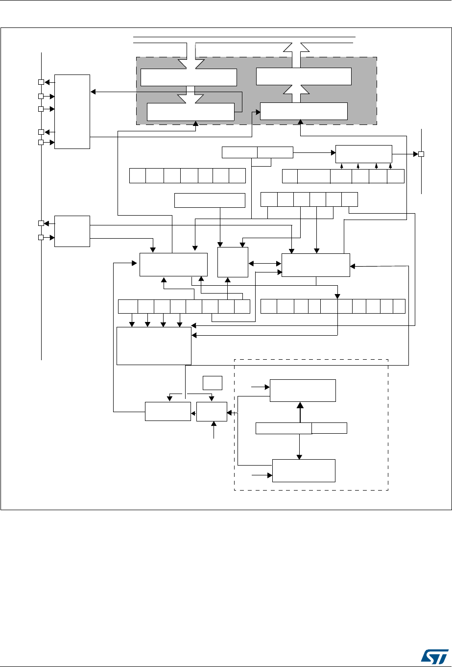
Universal synchronous asynchronous receiver transmitter (USART) RM0090
968/1749 RM0090 Rev 18
Figure 296. USART block diagram
Wakeup
unit
Receiver
control
SR
Transmit
control
TXETC RXNEIDLEORE NF FE
USART
control
interrupt
CR1
MWAKE
Receive data register (RDR)
Receive Shift Register
Read
Transmit data register (TDR)
Transmit Shift Register
Write
SW_RX
TX
(Data register) DR
Transmitter
clock
Receiver
clock
Receiver rate
Transmitter rate
f
PCLKx(x=1,2)
control
control
/
[8 x (2 - OVER8)]
Conventional baud rate generator
SBKRWURETE
IDLERXNE
TCIETXEIE
CR1
UE PCE PS
PEIE
PE
PWDATA
IRLP
SCEN IREN
DMAR
DMAT
USART Address
CR2
CR3
IrDA
SIR
ENDEC
block
LINE CKEN CPOL CPHA LBCL
SCLK control CK
CR2
GT
STOP[1:0]
NACK
DIV_Mantissa
15 0
RE
USART_BRR
/USARTDIV
TE
HD
(CPU or DMA)
(CPU or DMA)
PRDATA
Hardware
flow
controller
CTS LBD
RX
IRDA_OUT
IRDA_IN
RTS
CTS
GTPR
PSC
IE IE
DIV_Fraction
4
USARTDIV = DIV_Mantissa + (DIV_Fraction / 8 × (2 – OVER8))
SAMPLING
CR1
OVER8
DIVIDER
ai16099b
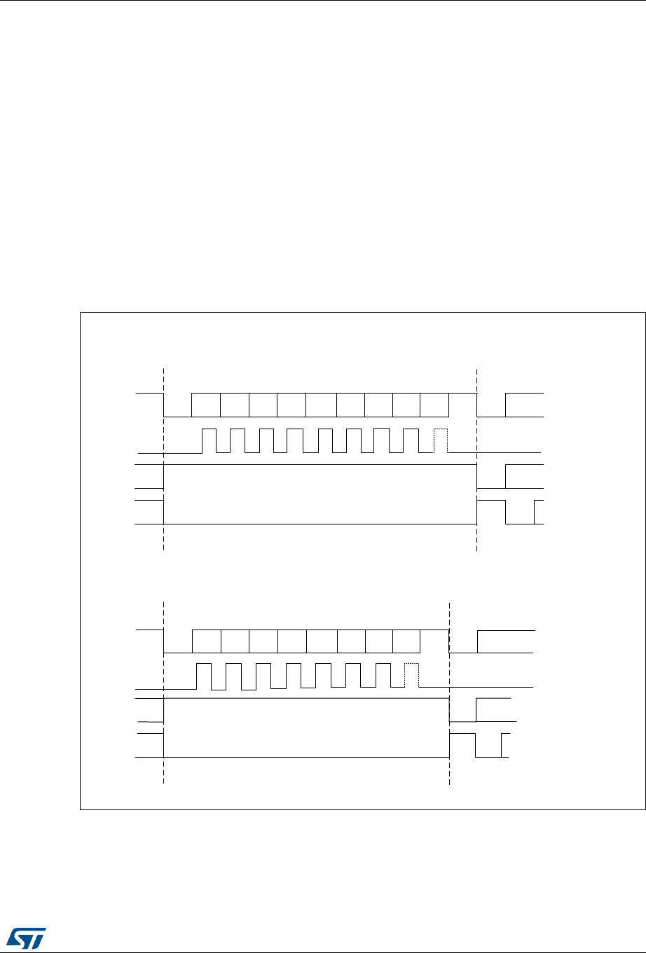
RM0090 Rev 18 969/1749
RM0090 Universal synchronous asynchronous receiver transmitter (USART)
1018
30.3.1 USART character description
Word length may be selected as being either 8 or 9 bits by programming the M bit in the
USART_CR1 register (see Figure 297).
The TX pin is in low state during the start bit. It is in high state during the stop bit.
An Idle character is interpreted as an entire frame of “1”s followed by the start bit of the
next frame which contains data (The number of “1” ‘s will include the number of stop bits).
A Break character is interpreted on receiving “0”s for a frame period. At the end of the
break frame the transmitter inserts either 1 or 2 stop bits (logic “1” bit) to acknowledge the
start bit.
Transmission and reception are driven by a common baud rate generator, the clock for each
is generated when the enable bit is set respectively for the transmitter and receiver.
The details of each block is given below.
Figure 297. Word length programming
MS19822V2
Bit0 Bit1 Bit2 Bit3 Bit4 Bit5 Bit6 Bit7 Bit8
Start
bit
Stop
bit
Next
Start
bit
Idle frame
9-bit word length (M bit is set), 1 Stop bit
Possible
Parity
bit
Break frame
Data frame Next data frame
Clock
** LBCL bit controls last data clock pulse
**
Start
bit
Start
bit
Stop
bit
Bit0 Bit1 Bit2 Bit3 Bit4 Bit5 Bit6 Bit7
Start
bit Stop
bit
Next
Start
bit
Idle frame
8-bit word length (M bit is reset), 1 Stop bit
Possible
Parity
bit
Break frame
Data frame Next data frame
Clock
** LBCL bit controls last data clock pulse
**
Start
bit
Start
bit
Stop
bit

Universal synchronous asynchronous receiver transmitter (USART) RM0090
970/1749 RM0090 Rev 18
30.3.2 Transmitter
The transmitter can send data words of either 8 or 9 bits depending on the M bit status.
When the transmit enable bit (TE) is set, the data in the transmit shift register is output on
the TX pin and the corresponding clock pulses are output on the CK pin.
Character transmission
During an USART transmission, data shifts out least significant bit first on the TX pin. In this
mode, the USART_DR register consists of a buffer (TDR) between the internal bus and the
transmit shift register (see Figure 296).
Every character is preceded by a start bit which is a logic level low for one bit period. The
character is terminated by a configurable number of stop bits.
The following stop bits are supported by USART: 0.5, 1, 1.5 and 2 stop bits.
Note: The TE bit should not be reset during transmission of data. Resetting the TE bit during the
transmission will corrupt the data on the TX pin as the baud rate counters will get frozen.
The current data being transmitted will be lost.
An idle frame will be sent after the TE bit is enabled.
Configurable stop bits
The number of stop bits to be transmitted with every character can be programmed in
Control register 2, bits 13,12.
•1 stop bit: This is the default value of number of stop bits.
•2 Stop bits: This will be supported by normal USART, single-wire and modem modes.
•0.5 stop bit: To be used when receiving data in Smartcard mode.
•1.5 stop bits: To be used when transmitting and receiving data in Smartcard mode.
An idle frame transmission will include the stop bits.
A break transmission will be 10 low bits followed by the configured number of stop bits
(when m = 0) and 11 low bits followed by the configured number of stop bits (when m = 1). It
is not possible to transmit long breaks (break of length greater than 10/11 low bits).
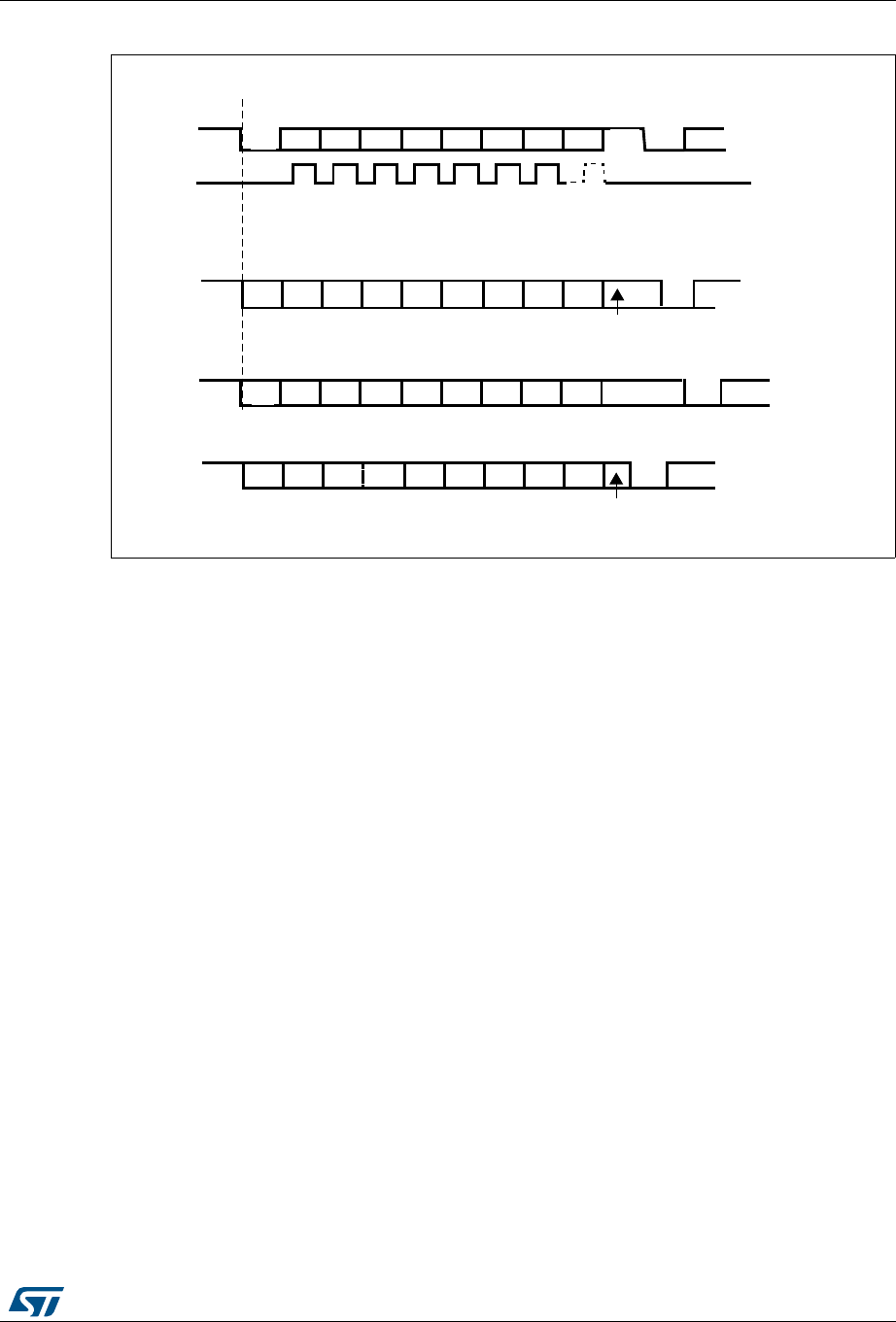
RM0090 Rev 18 971/1749
RM0090 Universal synchronous asynchronous receiver transmitter (USART)
1018
Figure 298. Configurable stop bits
Procedure:
1. Enable the USART by writing the UE bit in USART_CR1 register to 1.
2. Program the M bit in USART_CR1 to define the word length.
3. Program the number of stop bits in USART_CR2.
4. Select DMA enable (DMAT) in USART_CR3 if Multi buffer Communication is to take
place. Configure the DMA register as explained in multibuffer communication.
5. Select the desired baud rate using the USART_BRR register.
6. Set the TE bit in USART_CR1 to send an idle frame as first transmission.
7. Write the data to send in the USART_DR register (this clears the TXE bit). Repeat this
for each data to be transmitted in case of single buffer.
8. After writing the last data into the USART_DR register, wait until TC=1. This indicates
that the transmission of the last frame is complete. This is required for instance when
the USART is disabled or enters the Halt mode to avoid corrupting the last
transmission.
Single byte communication
Clearing the TXE bit is always performed by a write to the data register.
The TXE bit is set by hardware and it indicates:
•The data has been moved from TDR to the shift register and the data transmission has
started.
•The TDR register is empty.
•The next data can be written in the USART_DR register without overwriting the
previous data.
This flag generates an interrupt if the TXEIE bit is set.
MSv42088V1
Bit0 Bit1 Bit2 Bit3 Bit4 Bit5 Bit6 Bit7
Start
Bit Stop
bit
Next
start
8-bit Word length (M bit is reset) Possible
parity
bit
Data frame
Next data frame
****
** LBCL bit controls last data clock pulse
CLOCK **
Bit0 Bit1 Bit2 Bit3 Bit4 Bit5 Bit6 Bit7
Start
Bit 2 Stop Bits
Next
Start
Bit
Possible
parity
bit
Data frame
Next data frame
Next data frame
Bit0 Bit1 Bit2 Bit3 Bit4 Bit5 Bit6 Bit7
Start
Bit
Next
start
bit
Possible
Parity
Bit
Data frame
Next data frame
1 1/2 stop bits
a) 1 Stop Bit
b) 1 1/2 stop Bits
c) 2 Stop Bits
Bit0 Bit1 Bit2 Bit3 Bit4 Bit5 Bit6 Bit7
Start
Bit
1/2 Stop Bit
Next
Start
Bit
Possible
parity
bit
Data frame
d) 1/2 Stop Bit
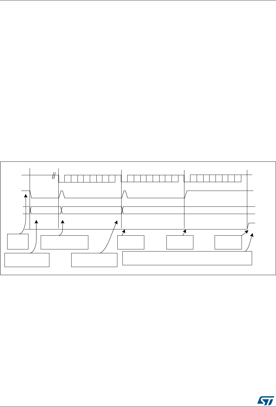
Universal synchronous asynchronous receiver transmitter (USART) RM0090
972/1749 RM0090 Rev 18
When a transmission is taking place, a write instruction to the USART_DR register stores
the data in the TDR register and which is copied in the shift register at the end of the current
transmission.
When no transmission is taking place, a write instruction to the USART_DR register places
the data directly in the shift register, the data transmission starts, and the TXE bit is
immediately set.
If a frame is transmitted (after the stop bit) and the TXE bit is set, the TC bit goes high. An
interrupt is generated if the TCIE bit is set in the USART_CR1 register.
After writing the last data into the USART_DR register, it is mandatory to wait for TC=1
before disabling the USART or causing the microcontroller to enter the low-power mode
(see Figure 299: TC/TXE behavior when transmitting).
The TC bit is cleared by the following software sequence:
1. A read from the USART_SR register
2. A write to the USART_DR register
Note: The TC bit can also be cleared by writing a ‘0 to it. This clearing sequence is recommended
only for Multibuffer communication.
Figure 299. TC/TXE behavior when transmitting
Break characters
Setting the SBK bit transmits a break character. The break frame length depends on the M
bit (see Figure 297).
If the SBK bit is set to ‘1 a break character is sent on the TX line after completing the current
character transmission. This bit is reset by hardware when the break character is completed
(during the stop bit of the break character). The USART inserts a logic 1 bit at the end of the
last break frame to guarantee the recognition of the start bit of the next frame.
Note: If the software resets the SBK bit before the commencement of break transmission, the
break character will not be transmitted. For two consecutive breaks, the SBK bit should be
set after the stop bit of the previous break.
Software wait until TC=1
Software
enables the
USART
Software waits until TXE=1
and writes F2 into DR
Idle preamble Frame 1 Frame 2 Frame 3
Set by hardware
set by hardware
cleared by software
set by hardware
cleared by software
Software waits until TXE=1
and writes F1 into DR
Software waits until TXE=1
and writes F1 into DR
TC is not set
because TXE=0
TC is not set
because TXE=1
USART_DR
TC flag
TXE flag
TX line
set
by hardware
TC is not set
because TXE=0
F1 F2 F3
MS48961V1
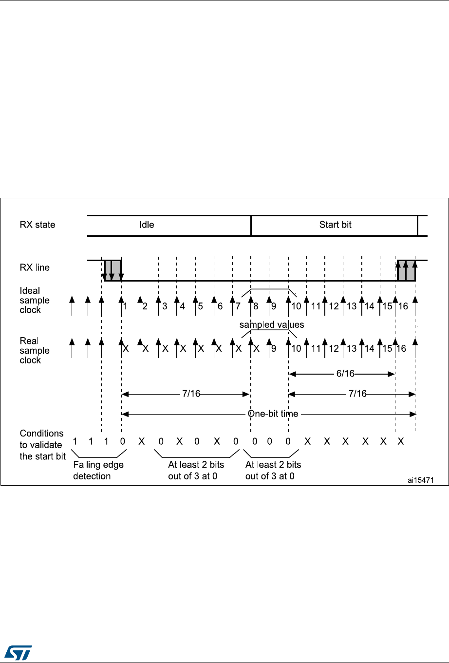
RM0090 Rev 18 973/1749
RM0090 Universal synchronous asynchronous receiver transmitter (USART)
1018
Idle characters
Setting the TE bit drives the USART to send an idle frame before the first data frame.
30.3.3 Receiver
The USART can receive data words of either 8 or 9 bits depending on the M bit in the
USART_CR1 register.
Start bit detection
The start bit detection sequence is the same when oversampling by 16 or by 8.
In the USART, the start bit is detected when a specific sequence of samples is recognized.
This sequence is: 1 1 1 0 X 0 X 0 X 0 0 0 0.
Figure 300. Start bit detection when oversampling by 16 or 8
Note: If the sequence is not complete, the start bit detection aborts and the receiver returns to the
idle state (no flag is set) where it waits for a falling edge.
The start bit is confirmed (RXNE flag set, interrupt generated if RXNEIE=1) if the 3 sampled
bits are at 0 (first sampling on the 3rd, 5th and 7th bits finds the 3 bits at 0 and second
sampling on the 8th, 9th and 10th bits also finds the 3 bits at 0).
The start bit is validated (RXNE flag set, interrupt generated if RXNEIE=1) but the NE noise
flag is set if, for both samplings, at least 2 out of the 3 sampled bits are at 0 (sampling on the

Universal synchronous asynchronous receiver transmitter (USART) RM0090
974/1749 RM0090 Rev 18
3rd, 5th and 7th bits and sampling on the 8th, 9th and 10th bits). If this condition is not met,
the start detection aborts and the receiver returns to the idle state (no flag is set).
If, for one of the samplings (sampling on the 3rd, 5th and 7th bits or sampling on the 8th, 9th
and 10th bits), 2 out of the 3 bits are found at 0, the start bit is validated but the NE noise
flag bit is set.
Character reception
During an USART reception, data shifts in least significant bit first through the RX pin. In this
mode, the USART_DR register consists of a buffer (RDR) between the internal bus and the
received shift register.
Procedure:
1. Enable the USART by writing the UE bit in USART_CR1 register to 1.
2. Program the M bit in USART_CR1 to define the word length.
3. Program the number of stop bits in USART_CR2.
4. Select DMA enable (DMAR) in USART_CR3 if multibuffer communication is to take
place. Configure the DMA register as explained in multibuffer communication. STEP 3
5. Select the desired baud rate using the baud rate register USART_BRR
6. Set the RE bit USART_CR1. This enables the receiver which begins searching for a
start bit.
When a character is received
•The RXNE bit is set. It indicates that the content of the shift register is transferred to the
RDR. In other words, data has been received and can be read (as well as its
associated error flags).
•An interrupt is generated if the RXNEIE bit is set.
•The error flags can be set if a frame error, noise or an overrun error has been detected
during reception.
•In multibuffer, RXNE is set after every byte received and is cleared by the DMA read to
the Data Register.
•In single buffer mode, clearing the RXNE bit is performed by a software read to the
USART_DR register. The RXNE flag can also be cleared by writing a zero to it. The
RXNE bit must be cleared before the end of the reception of the next character to avoid
an overrun error.
Note: The RE bit should not be reset while receiving data. If the RE bit is disabled during
reception, the reception of the current byte will be aborted.
Break character
When a break character is received, the USART handles it as a framing error.
Idle character
When an idle frame is detected, there is the same procedure as a data received character
plus an interrupt if the IDLEIE bit is set.

RM0090 Rev 18 975/1749
RM0090 Universal synchronous asynchronous receiver transmitter (USART)
1018
Overrun error
An overrun error occurs when a character is received when RXNE has not been reset. Data
can not be transferred from the shift register to the RDR register until the RXNE bit is
cleared.
The RXNE flag is set after every byte received. An overrun error occurs if RXNE flag is set
when the next data is received or the previous DMA request has not been serviced. When
an overrun error occurs:
•The ORE bit is set.
•The RDR content will not be lost. The previous data is available when a read to
USART_DR is performed.
•The shift register will be overwritten. After that point, any data received during overrun
is lost.
•An interrupt is generated if either the RXNEIE bit is set or both the EIE and DMAR bits
are set.
•The ORE bit is reset by a read to the USART_SR register followed by a USART_DR
register read operation.
Note: The ORE bit, when set, indicates that at least 1 data has been lost. There are two
possibilities:
•if RXNE=1, then the last valid data is stored in the receive register RDR and can be
read,
•if RXNE=0, then it means that the last valid data has already been read and thus there
is nothing to be read in the RDR. This case can occur when the last valid data is read in
the RDR at the same time as the new (and lost) data is received. It may also occur
when the new data is received during the reading sequence (between the USART_SR
register read access and the USART_DR read access).
Selecting the proper oversampling method
The receiver implements different user-configurable oversampling techniques (except in
synchronous mode) for data recovery by discriminating between valid incoming data and
noise.
The oversampling method can be selected by programming the OVER8 bit in the
USART_CR1 register and can be either 16 or 8 times the baud rate clock (Figure 301 and
Figure 302).
Depending on the application:
•select oversampling by 8 (OVER8=1) to achieve higher speed (up to fPCLK/8). In this
case the maximum receiver tolerance to clock deviation is reduced (refer to
Section 30.3.5: USART receiver tolerance to clock deviation on page 988)
•select oversampling by 16 (OVER8=0) to increase the tolerance of the receiver to clock
deviations. In this case, the maximum speed is limited to maximum fPCLK/16
Universal synchronous asynchronous receiver transmitter (USART) RM0090
976/1749 RM0090 Rev 18
Programming the ONEBIT bit in the USART_CR3 register selects the method used to
evaluate the logic level. There are two options:
•the majority vote of the three samples in the center of the received bit. In this case,
when the 3 samples used for the majority vote are not equal, the NF bit is set
•a single sample in the center of the received bit
Depending on the application:
– select the three samples’ majority vote method (ONEBIT=0) when operating in a
noisy environment and reject the data when a noise is detected (refer to
Figure 133) because this indicates that a glitch occurred during the sampling.
– select the single sample method (ONEBIT=1) when the line is noise-free to
increase the receiver’s tolerance to clock deviations (see Section 30.3.5: USART
receiver tolerance to clock deviation on page 988). In this case the NF bit will
never be set.
When noise is detected in a frame:
•The NF bit is set at the rising edge of the RXNE bit.
•The invalid data is transferred from the Shift register to the USART_DR register.
•No interrupt is generated in case of single byte communication. However this bit rises
at the same time as the RXNE bit which itself generates an interrupt. In case of
multibuffer communication an interrupt will be issued if the EIE bit is set in the
USART_CR3 register.
The NF bit is reset by a USART_SR register read operation followed by a USART_DR
register read operation.
Note: Oversampling by 8 is not available in the Smartcard, IrDA and LIN modes. In those modes,
the OVER8 bit is forced to ‘0 by hardware.
Figure 301. Data sampling when oversampling by 16
MSv31152V1
1 2 3 4 5 6 7 8 9 10 11 12 13 14 15 16
sampled values
6/16
7/167/16
One bit time
Sample clock
RX line
RM0090 Rev 18 977/1749
RM0090 Universal synchronous asynchronous receiver transmitter (USART)
1018
Figure 302. Data sampling when oversampling by 8
Framing error
A framing error is detected when:
The stop bit is not recognized on reception at the expected time, following either a de-
synchronization or excessive noise.
When the framing error is detected:
•The FE bit is set by hardware
•The invalid data is transferred from the Shift register to the USART_DR register.
•No interrupt is generated in case of single byte communication. However this bit rises
at the same time as the RXNE bit which itself generates an interrupt. In case of
multibuffer communication an interrupt will be issued if the EIE bit is set in the
USART_CR3 register.
The FE bit is reset by a USART_SR register read operation followed by a USART_DR
register read operation.
Table 133. Noise detection from sampled data
Sampled value NE status Received bit value
000 0 0
001 1 0
010 1 0
011 1 1
100 1 0
101 1 1
110 1 1
111 0 1
MSv31153V1
1 2 3 4 5 6 7
sampled values
2/8
3/8
3/8
One bit time
Sample
clock (x8)
RX line
8

Universal synchronous asynchronous receiver transmitter (USART) RM0090
978/1749 RM0090 Rev 18
Configurable stop bits during reception
The number of stop bits to be received can be configured through the control bits of Control
Register 2 - it can be either 1 or 2 in normal mode and 0.5 or 1.5 in Smartcard mode.
1. 0.5 stop bit (reception in Smartcard mode): No sampling is done for 0.5 stop bit. As
a consequence, no framing error and no break frame can be detected when 0.5 stop bit
is selected.
2. 1 stop bit: Sampling for 1 stop Bit is done on the 8th, 9th and 10th samples.
3. 1.5 stop bits (Smartcard mode): When transmitting in smartcard mode, the device
must check that the data is correctly sent. Thus the receiver block must be enabled (RE
=1 in the USART_CR1 register) and the stop bit is checked to test if the smartcard has
detected a parity error. In the event of a parity error, the smartcard forces the data
signal low during the sampling - NACK signal-, which is flagged as a framing error.
Then, the FE flag is set with the RXNE at the end of the 1.5 stop bit. Sampling for 1.5
stop bits is done on the 16th, 17th and 18th samples (1 baud clock period after the
beginning of the stop bit). The 1.5 stop bit can be decomposed into 2 parts: one 0.5
baud clock period during which nothing happens, followed by 1 normal stop bit period
during which sampling occurs halfway through. Refer to Section 30.3.11: Smartcard on
page 997 for more details.
4. 2 stop bits: Sampling for 2 stop bits is done on the 8th, 9th and 10th samples of the
first stop bit. If a framing error is detected during the first stop bit the framing error flag
will be set. The second stop bit is not checked for framing error. The RXNE flag will be
set at the end of the first stop bit.
30.3.4 Fractional baud rate generation
The baud rate for the receiver and transmitter (Rx and Tx) are both set to the same value as
programmed in the Mantissa and Fraction values of USARTDIV.
Equation 1: Baud rate for standard USART (SPI mode included)
Equation 2: Baud rate in Smartcard, LIN and IrDA modes
USARTDIV is an unsigned fixed point number that is coded on the USART_BRR register.
•When OVER8=0, the fractional part is coded on 4 bits and programmed by the
DIV_fraction[3:0] bits in the USART_BRR register
•When OVER8=1, the fractional part is coded on 3 bits and programmed by the
DIV_fraction[2:0] bits in the USART_BRR register, and bit DIV_fraction[3] must be kept
cleared.
Note: The baud counters are updated to the new value in the baud registers after a write operation
to USART_BRR. Hence the baud rate register value should not be changed during
communication.
Tx/Rx baud fCK
8 2 OVER8–()USARTDIV××
-------------------------------------------------------------------------------------
=
Tx/Rx baud fCK
16 USARTDIV×
----------------------------------------------
=

RM0090 Rev 18 979/1749
RM0090 Universal synchronous asynchronous receiver transmitter (USART)
1018
How to derive USARTDIV from USART_BRR register values when OVER8=0
Example 1:
If DIV_Mantissa = 0d27 and DIV_Fraction = 0d12 (USART_BRR = 0x1BC), then
Mantissa (USARTDIV) = 0d27
Fraction (USARTDIV) = 12/16 = 0d0.75
Therefore USARTDIV = 0d27.75
Example 2:
To program USARTDIV = 0d25.62
This leads to:
DIV_Fraction = 16*0d0.62 = 0d9.92
The nearest real number is 0d10 = 0xA
DIV_Mantissa = mantissa (0d25.620) = 0d25 = 0x19
Then, USART_BRR = 0x19A hence USARTDIV = 0d25.625
Example 3:
To program USARTDIV = 0d50.99
This leads to:
DIV_Fraction = 16*0d0.99 = 0d15.84
The nearest real number is 0d16 = 0x10 => overflow of DIV_frac[3:0] => carry must be
added up to the mantissa
DIV_Mantissa = mantissa (0d50.990 + carry) = 0d51 = 0x33
Then, USART_BRR = 0x330 hence USARTDIV = 0d51.000
How to derive USARTDIV from USART_BRR register values when OVER8=1
Example 1:
If DIV_Mantissa = 0x27 and DIV_Fraction[2:0]= 0d6 (USART_BRR = 0x1B6), then
Mantissa (USARTDIV) = 0d27
Fraction (USARTDIV) = 6/8 = 0d0.75
Therefore USARTDIV = 0d27.75
Example 2:
To program USARTDIV = 0d25.62
This leads to:
DIV_Fraction = 8*0d0.62 = 0d4.96
The nearest real number is 0d5 = 0x5
DIV_Mantissa = mantissa (0d25.620) = 0d25 = 0x19

Universal synchronous asynchronous receiver transmitter (USART) RM0090
980/1749 RM0090 Rev 18
Then, USART_BRR = 0x195 => USARTDIV = 0d25.625
Example 3:
To program USARTDIV = 0d50.99
This leads to:
DIV_Fraction = 8*0d0.99 = 0d7.92
The nearest real number is 0d8 = 0x8 => overflow of the DIV_frac[2:0] => carry must be
added up to the mantissa
DIV_Mantissa = mantissa (0d50.990 + carry) = 0d51 = 0x33
Then, USART_BRR = 0x0330 => USARTDIV = 0d51.000
Table 134. Error calculation for programmed baud rates at fPCLK = 8 MHz or fPCLK = 12 MHz,
oversampling by 16(1)
Oversampling by 16 (OVER8=0)
Baud rate7 fPCLK = 8 MHz fPCLK = 12 MHz
S.No Desired Actual
Value
programmed
in the baud
rate register
% Error =
(Calculated -
Desired) B.rate /
Desired B.rate
Actual
Value
programmed
in the baud
rate register
% Error
1 1.2 KBps 1.2 KBps 416.6875 0 1.2 KBps 625 0
2 2.4 KBps 2.4 KBps 208.3125 0.01 2.4 KBps 312.5 0
3 9.6 KBps 9.604 KBps 52.0625 0.04 9.6 KBps 78.125 0
4 19.2 KBps 19.185 KBps 26.0625 0.08 19.2 KBps 39.0625 0
5 38.4 KBps 38.462 KBps 13 0.16 38.339 KBps 19.5625 0.16
6 57.6 KBps 57.554 KBps 8.6875 0.08 57.692 KBps 13 0.16
7 115.2 KBps 115.942 KBps 4.3125 0.64 115.385 KBps 6.5 0.16
8 230.4 KBps 228.571 KBps 2.1875 0.79 230.769 KBps 3.25 0.16
9 460.8 KBps 470.588 KBps 1.0625 2.12 461.538 KBps 1.625 0.16
10 921.6 KBps NA NA NA NA NA NA
11 2 MBps NA NA NA NA NA NA
12 3 MBps NA NA NA NA NA NA
1. The lower the CPU clock the lower the accuracy for a particular baud rate. The upper limit of the achievable baud rate can
be fixed with these data.

RM0090 Rev 18 981/1749
RM0090 Universal synchronous asynchronous receiver transmitter (USART)
1018
Table 135. Error calculation for programmed baud rates at fPCLK = 8 MHz or fPCLK =12 MHz,
oversampling by 8(1)
Oversampling by 8 (OVER8 = 1)
Baud rate fPCLK = 8 MHz fPCLK = 12 MHz
S.No Desired Actual
Value
programmed
in the baud
rate register
% Error =
(Calculated -
Desired)
B.rate /
Desired
B.rate
Actual
Value
programmed
in the baud
rate register
% Error
1 1.2 KBps 1.2 KBps 833.375 0 1.2 KBps 1250 0
2 2.4 KBps 2.4 KBps 416.625 0.01 2.4 KBps 625 0
3 9.6 KBps 9.604 KBps 104.125 0.04 9.6 KBps 156.25 0
4 19.2 KBps 19.185 KBps 52.125 0.08 19.2 KBps 78.125 0
5 38.4 KBps 38.462 KBps 26 0.16 38.339 KBps 39.125 0.16
6 57.6 KBps 57.554 KBps 17.375 0.08 57.692 KBps 26 0.16
7 115.2 KBps 115.942 KBps 8.625 0.64 115.385 KBps 13 0.16
8 230.4 KBps 228.571 KBps 4.375 0.79 230.769 KBps 6.5 0.16
9 460.8 KBps 470.588 KBps 2.125 2.12 461.538 KBps 3.25 0.16
10 921.6 KBps 888.889 KBps 1.125 3.55 923.077 KBps 1.625 0.16
11 2 MBps NA NA NA NA NA NA
12 3 MBps NA NA NA NA NA NA
1. The lower the CPU clock the lower the accuracy for a particular baud rate. The upper limit of the achievable baud rate can
be fixed with these data.
Table 136. Error calculation for programmed baud rates at fPCLK = 16 MHz or fPCLK = 24 MHz,
oversampling by 16(1)
Oversampling by 16 (OVER8 = 0)
Baud rate fPCLK = 16 MHz fPCLK = 24 MHz
S.No Desired Actual
Value
programmed
in the baud
rate register
% Error =
(Calculated -
Desired) B.rate /
Desired B.rate
Actual
Value
programmed
in the baud
rate register
% Error
1 1.2 KBps 1.2 KBps 833.3125 0 1.2 1250 0
2 2.4 KBps 2.4 KBps 416.6875 0 2.4 625 0
3 9.6 KBps 9.598 KBps 104.1875 0.02 9.6 156.25 0
4 19.2 KBps 19.208 KBps 52.0625 0.04 19.2 78.125 0
5 38.4 KBps 38.369 KBps 26.0625 0.08 38.4 39.0625 0
6 57.6 KBps 57.554 KBps 17.375 0.08 57.554 26.0625 0.08

Universal synchronous asynchronous receiver transmitter (USART) RM0090
982/1749 RM0090 Rev 18
7 115.2 KBps 115.108 KBps 8.6875 0.08 115.385 13 0.16
8 230.4 KBps 231.884 KBps 4.3125 0.64 230.769 6.5 0.16
9 460.8 KBps 457.143 KBps 2.1875 0.79 461.538 3.25 0.16
10 921.6 KBps 941.176 KBps 1.0625 2.12 923.077 1.625 0.16
11 2 MBps NA NA NA NA NA NA
12 3 MBps NA NA NA NA NA NA
1. The lower the CPU clock the lower the accuracy for a particular baud rate. The upper limit of the achievable baud rate can
be fixed with these data.
Table 136. Error calculation for programmed baud rates at fPCLK = 16 MHz or fPCLK = 24 MHz,
oversampling by 16(1) (continued)
Oversampling by 16 (OVER8 = 0)
Baud rate fPCLK = 16 MHz fPCLK = 24 MHz
S.No Desired Actual
Value
programmed
in the baud
rate register
% Error =
(Calculated -
Desired) B.rate /
Desired B.rate
Actual
Value
programmed
in the baud
rate register
% Error
Table 137. Error calculation for programmed baud rates at fPCLK = 16 MHz or fPCLK = 24 MHz,
oversampling by 8(1)
Oversampling by 8 (OVER8=1)
Baud rate fPCLK = 16 MHz fPCLK = 24 MHz
S.No Desired Actual
Value
programmed
in the baud
rate register
% Error =
(Calculated -
Desired) B.rate /
Desired B.rate
Actual
Value
programmed
in the baud
rate register
% Error
1 1.2 KBps 1.2 KBps 1666.625 0 1.2 KBps 2500 0
2 2.4 KBps 2.4 KBps 833.375 0 2.4 KBps 1250 0
3 9.6 KBps 9.598 KBps 208.375 0.02 9.6 KBps 312.5 0
4 19.2 KBps 19.208 KBps 104.125 0.04 19.2 KBps 156.25 0
5 38.4 KBps 38.369 KBps 52.125 0.08 38.4 KBps 78.125 0
6 57.6 KBps 57.554 KBps 34.75 0.08 57.554 KBps 52.125 0.08
7 115.2 KBps 115.108 KBps 17.375 0.08 115.385 KBps 26 0.16
8 230.4 KBps 231.884 KBps 8.625 0.64 230.769 KBps 13 0.16
9 460.8 KBps 457.143 KBps 4.375 0.79 461.538 KBps 6.5 0.16
10 921.6 KBps 941.176 KBps 2.125 2.12 923.077 KBps 3.25 0.16
11 2 MBps 2000 KBps 1 0 2000 KBps 1.5 0
12 3 MBps NA NA NA 3000 KBps 1 0
1. The lower the CPU clock the lower the accuracy for a particular baud rate. The upper limit of the achievable baud rate can
be fixed with these data.

RM0090 Rev 18 983/1749
RM0090 Universal synchronous asynchronous receiver transmitter (USART)
1018
Table 138. Error calculation for programmed baud rates at fPCLK = 8 MHz or fPCLK = 16 MHz,
oversampling by 16(1)
Oversampling by 16 (OVER8=0)
Baud rate fPCLK = 8 MHz fPCLK = 16 MHz
S.No Desired Actual
Value
programme
d in the
baud rate
register
% Error =
(Calculated -
Desired)B.Rate
/Desired B.Rate
Actual
Value
programmed
in the baud
rate register
% Error
1. 2.4 KBps 2.400 KBps 208.3125 0.00% 2.400 KBps 416.6875 0.00%
2. 9.6 KBps 9.604 KBps 52.0625 0.04% 9.598 KBps 104.1875 0.02%
3. 19.2 KBps 19.185 KBps 26.0625 0.08% 19.208 KBps 52.0625 0.04%
4. 57.6 KBps 57.554 KBps 8.6875 0.08% 57.554 KBps 17.3750 0.08%
5. 115.2 KBps 115.942 KBps 4.3125 0.64% 115.108 KBps 8.6875 0.08%
6. 230.4 KBps 228.571
KBps 2.1875 0.79% 231.884 KBps 4.3125 0.64%
7. 460.8 KBps 470.588
KBps 1.0625 2.12% 457.143 KBps 2.1875 0.79%
8. 896 KBps NA NA NA 888.889 KBps 1.1250 0.79%
9. 921.6 KBps NA NA NA 941.176 KBps 1.0625 2.12%
10. 1.792 MBps NA NA NA NA NA NA
11. 1.8432 MBps NA NA NA NA NA NA
12. 3.584 MBps NA NA NA NA NA NA
13. 3.6864 MBps NA NA NA NA NA NA
14. 7.168 MBps NA NA NA NA NA NA
15. 7.3728 MBps NA NA NA NA NA NA
1. The lower the CPU clock the lower the accuracy for a particular baud rate. The upper limit of the achievable baud rate can
be fixed with these data.
Table 139. Error calculation for programmed baud rates at fPCLK = 8 MHz or fPCLK = 16 MHz,
oversampling by 8(1)
Oversampling by 8 (OVER8=1)
Baud rate fPCLK = 8 MHz fPCLK = 16 MHz
S.No Desired Actual
Value
programmed
in the baud
rate register
% Error =
(Calculated -
Desired)B.Rate
/Desired B.Rate
Actual
Value
programmed
in the baud
rate register
%
Error
1. 2.4 KBps 2.400 KBps 416.625 0.01% 2.400 KBps 833.375 0.00%
2. 9.6 KBps 9.604 KBps 104.125 0.04% 9.598 KBps 208.375 0.02%
3. 19.2 KBps 19.185 KBps 52.125 0.08% 19.208 KBps 104.125 0.04%

Universal synchronous asynchronous receiver transmitter (USART) RM0090
984/1749 RM0090 Rev 18
4. 57.6 KBps 57.557 KBps 17.375 0.08% 57.554 KBps 34.750 0.08%
5. 115.2 KBps 115.942 KBps 8.625 0.64% 115.108 KBps 17.375 0.08%
6. 230.4 KBps 228.571 KBps 4.375 0.79% 231.884 KBps 8.625 0.64%
7. 460.8 KBps 470.588 KBps 2.125 2.12% 457.143 KBps 4.375 0.79%
8. 896 KBps 888.889 KBps 1.125 0.79% 888.889 KBps 2.250 0.79%
9. 921.6 KBps 888.889 KBps 1.125 3.55% 941.176 KBps 2.125 2.12%
10. 1.792 MBps NA NA NA 1.7777 MBps 1.125 0.79%
11. 1.8432 MBps NA NA NA 1.7777 MBps 1.125 3.55%
12. 3.584 MBps NA NA NA NA NA NA
13. 3.6864 MBps NA NA NA NA NA NA
14. 7.168 MBps NA NA NA NA NA NA
15. 7.3728 MBps NA NA NA NA NA NA
1. The lower the CPU clock the lower the accuracy for a particular baud rate. The upper limit of the achievable baud rate can
be fixed with these data.
Table 139. Error calculation for programmed baud rates at fPCLK = 8 MHz or fPCLK = 16 MHz,
oversampling by 8(1) (continued)
Oversampling by 8 (OVER8=1)
Baud rate fPCLK = 8 MHz fPCLK = 16 MHz
S.No Desired Actual
Value
programmed
in the baud
rate register
% Error =
(Calculated -
Desired)B.Rate
/Desired B.Rate
Actual
Value
programmed
in the baud
rate register
%
Error
Table 140. Error calculation for programmed baud rates at fPCLK = 30 MHz or fPCLK = 60 MHz,
oversampling by 16(1)(2)
Oversampling by 16 (OVER8=0)
Baud rate fPCLK = 30 MHz fPCLK = 60 MHz
S.No Desired Actual
Value
programmed
in the baud
rate register
% Error =
(Calculated -
Desired)B.Rate
/Desired B.Rate
Actual
Value
programmed
in the baud
rate register
%
Error
1. 2.4 KBps 2.400 KBps 781.2500 0.00% 2.400 KBps 1562.5000 0.00%
2. 9.6 KBps 9.600 KBps 195.3125 0.00% 9.600 KBps 390.6250 0.00%
3. 19.2 KBps 19.194 KBps 97.6875 0.03% 19.200 KBps 195.3125 0.00%
4. 57.6 KBps 57.582KBps 32.5625 0.03% 57.582 KBps 65.1250 0.03%
5. 115.2 KBps 115.385 KBps 16.2500 0.16% 115.163 KBps 32.5625 0.03%
6. 230.4 KBps 230.769 KBps 8.1250 0.16% 230.769KBps 16.2500 0.16%
7. 460.8 KBps 461.538 KBps 4.0625 0.16% 461.538 KBps 8.1250 0.16%
8. 896 KBps 909.091 KBps 2.0625 1.46% 895.522 KBps 4.1875 0.05%

RM0090 Rev 18 985/1749
RM0090 Universal synchronous asynchronous receiver transmitter (USART)
1018
9. 921.6 KBps 909.091 KBps 2.0625 1.36% 923.077 KBps 4.0625 0.16%
10. 1.792 MBps 1.1764 MBps 1.0625 1.52% 1.8182 MBps 2.0625 1.36%
11. 1.8432
MBps 1.8750 MBps 1.0000 1.73% 1.8182 MBps 2.0625 1.52%
12. 3.584 MBps NA NA NA 3.2594 MBps 1.0625 1.52%
13. 3.6864
MBps NA NA NA 3.7500 MBps 1.0000 1.73%
14. 7.168 MBps NA NA NA NA NA NA
15. 7.3728
MBps NA NA NA NA NA NA
1. The lower the CPU clock the lower the accuracy for a particular baud rate. The upper limit of the achievable baud rate can
be fixed with these data.
2. Only USART1 and USART6 are clocked with PCLK2. Other USARTs are clocked with PCLK1. Refer to the device
datasheets for the maximum values for PCLK1 and PCLK2.
Table 140. Error calculation for programmed baud rates at fPCLK = 30 MHz or fPCLK = 60 MHz,
oversampling by 16(1)(2) (continued)
Oversampling by 16 (OVER8=0)
Baud rate fPCLK = 30 MHz fPCLK = 60 MHz
S.No Desired Actual
Value
programmed
in the baud
rate register
% Error =
(Calculated -
Desired)B.Rate
/Desired B.Rate
Actual
Value
programmed
in the baud
rate register
%
Error
Table 141. Error calculation for programmed baud rates at fPCLK = 30 MHz or fPCLK = 60 MHz,
oversampling by 8(1) (2)
Oversampling by 8 (OVER8=1)
Baud rate fPCLK = 30 MHz fPCLK =60 MHz
S.No Desired Actual
Value
programmed
in the baud
rate register
% Error =
(Calculated -
Desired)B.Rate
/Desired B.Rate
Actual
Value
programmed
in the baud
rate register
%
Error
1. 2.4 KBps 2.400 KBps 1562.5000 0.00% 2.400 KBps 3125.0000 0.00%
2. 9.6 KBps 9.600 KBps 390.6250 0.00% 9.600 KBps 781.2500 0.00%
3. 19.2 KBps 19.194 KBps 195.3750 0.03% 19.200 KBps 390.6250 0.00%
4. 57.6 KBps 57.582 KBps 65.1250 0.16% 57.582 KBps 130.2500 0.03%
5. 115.2 KBps 115.385 KBps 32.5000 0.16% 115.163 KBps 65.1250 0.03%
6. 230.4 KBps 230.769 KBps 16.2500 0.16% 230.769 KBps 32.5000 0.16%
7. 460.8 KBps 461.538 KBps 8.1250 0.16% 461.538 KBps 16.2500 0.16%
8. 896 KBps 909.091 KBps 4.1250 1.46% 895.522 KBps 8.3750 0.05%
9. 921.6 KBps 909.091 KBps 4.1250 1.36% 923.077 KBps 8.1250 0.16%
10. 1.792 MBps 1.7647 MBps 2.1250 1.52% 1.8182 MBps 4.1250 1.46%

Universal synchronous asynchronous receiver transmitter (USART) RM0090
986/1749 RM0090 Rev 18
11. 1.8432 MBps 1.8750 MBps 2.0000 1.73% 1.8182 MBps 4.1250 1.36%
12. 3.584 MBps 3.7500 MBps 1.0000 4.63% 3.5294 MBps 2.1250 1.52%
13. 3.6864 MBps 3.7500 MBps 1.0000 1.73% 3.7500 MBps 2.0000 1.73%
14. 7.168 MBps NA NA NA 7.5000 MBps 1.0000 4.63%
15. 7.3728 MBps NA NA NA 7.5000 MBps 1.0000 1.73%
1. The lower the CPU clock the lower the accuracy for a particular baud rate. The upper limit of the achievable baud rate can
be fixed with these data.
2. Only USART1 and USART6 are clocked with PCLK2. Other USARTs are clocked with PCLK1. Refer to the device
datasheets for the maximum values for PCLK1 and PCLK2.
Table 141. Error calculation for programmed baud rates at fPCLK = 30 MHz or fPCLK = 60 MHz,
oversampling by 8(1) (2) (continued)
Oversampling by 8 (OVER8=1)
Baud rate fPCLK = 30 MHz fPCLK =60 MHz
S.No Desired Actual
Value
programmed
in the baud
rate register
% Error =
(Calculated -
Desired)B.Rate
/Desired B.Rate
Actual
Value
programmed
in the baud
rate register
%
Error
Table 142. Error calculation for programmed baud rates at fPCLK = 42 MHz or fPCLK = 84 Hz,
oversampling by 16(1)(2)
Oversampling by 16 (OVER8=0)
Baud rate fPCLK = 42 MHz fPCLK = 84 MHz
S.No Desired Actual
Value
programmed
in the baud
rate register
% Error =
(Calculated -
Desired)B.Rate
/Desired B.Rate
Actual
Value
programmed
in the baud
rate register
%
Error
1. 1.2 KBps 1.2 KBps 2187.5 0 1.2 KBps NA 0
2. 2.4 KBps 2.4 KBps 1093.75 0 2.4 KBps 2187.5 0
3. 9.6 KBps 9.6 KBps 273.4375 0 9.6 KBps 546.875 0
4. 19.2 KBps 19.195 KBps 136.75 0.02 19.2 KBps 273.4375 0
5. 38.4 KBps 38.391 KBps 68.375 0.02 38.391 KBps 136.75 0.02
6. 57.6 KBps 57.613 KBps 45.5625 0.02 57.613 KBps 91.125 0.02
7. 115.2 KBps 115.068 KBps 22.8125 0.11 115.226 KBps 45.5625 0.02
8. 230.4 KBps 230.769 KBps 11.375 0.16 230.137 KBps 22.8125 0.11
9. 460.8 KBps 461.538 KBps 5.6875 0.16 461.538 KBps 11.375 0.16
10. 921.6 KBps 913.043 KBps 2.875 0.93 923.076 KBps 5.6875 0.93
11. 1.792 MBps 1.826 MBps 1.4375 1.9 1.787 MBps 2.9375 0.27
12. 1.8432 MBps 1.826 MBps 1.4375 0.93 1.826 MBps 2.875 0.93
13. 3.584 MBps N.A N.A N.A 3.652 MBps 1.4375 1.9
14. 3.6864 MBps N.A N.A N.A 3.652 MBps 1.4375 0.93

RM0090 Rev 18 987/1749
RM0090 Universal synchronous asynchronous receiver transmitter (USART)
1018
15. 7.168 MBps N.A N.A N.A N.A N.A N.A
16. 7.3728 MBps N.A N.A N.A N.A N.A N.A
17. 9 MBps N.A N.A N.A N.A N.A N.A
18. 10.5 MBps N.A N.A N.A N.A N.A N.A
1. The lower the CPU clock the lower the accuracy for a particular baud rate. The upper limit of the achievable baud rate can be
fixed with these data.
2. Only USART1 and USART6 are clocked with PCLK2. Other USARTs are clocked with PCLK1. Refer to the device
datasheets for the maximum values for PCLK1 and PCLK2.
Table 142. Error calculation for programmed baud rates at fPCLK = 42 MHz or fPCLK = 84 Hz,
oversampling by 16(1)(2) (continued)
Oversampling by 16 (OVER8=0)
Baud rate fPCLK = 42 MHz fPCLK = 84 MHz
S.No Desired Actual
Value
programmed
in the baud
rate register
% Error =
(Calculated -
Desired)B.Rate
/Desired B.Rate
Actual
Value
programmed
in the baud
rate register
%
Error
Table 143. Error calculation for programmed baud rates at fPCLK = 42 MHz or fPCLK = 84 MHz,
oversampling by 8(1)(2)
Oversampling by 8 (OVER8=1)
Baud rate fPCLK = 42 MHz fPCLK = 84 MHz
S.No Desired Actual
Value
programmed
in the baud
rate register
Value
programmed
in the baud
rate register
Actual
Value
programmed
in the baud
rate register
%
Error
1. 2.4 KBps 2.4 KBps 2187.5 0 2.4 KBps NA 0
2. 9.6 KBps 9.6 KBps 546.875 0 9.6 KBps 1093.75 0
3. 19.2 KBps 19.195 KBps 273.5 0.02 19.2 KBps 546.875 0
4. 38.4 KBps 38.391 KBps 136.75 0.02 38.391 KBps 273.5 0.02
5. 57.6 KBps 57.613 KBps 91.125 0.02 57.613 KBps 182.25 0.02
6. 115.2 KBps 115.068 KBps 45.625 0.11 115.226 KBps 91.125 0.02
7. 230.4 KBps 230.769 KBps 22.75 0.11 230.137 KBps 45.625 0.11
8. 460.8 KBps 461.538 KBps 11.375 0.16 461.538 KBps 22.75 0.16
9. 921.6 KBps 913.043 KBps 5.75 0.93 923.076 KBps 11.375 0.93
10. 1.792 MBps 1.826 MBps 2.875 1.9 1.787Mbps 5.875 0.27
11. 1.8432 MBps 1.826 MBps 2.875 0.93 1.826 MBps 5.75 0.93
12. 3.584 MBps 3.5 MBps 1.5 2.34 3.652 MBps 2.875 1.9
13. 3.6864 MBps 3.82 MBps 1.375 3.57 3.652 MBps 2.875 0.93
14. 7.168 MBps N.A N.A N.A 7 MBps 1.5 2.34
15. 7.3728 MBps N.A N.A N.A 7.636 MBps 1.375 3.57

Universal synchronous asynchronous receiver transmitter (USART) RM0090
988/1749 RM0090 Rev 18
30.3.5 USART receiver tolerance to clock deviation
The USART asynchronous receiver works correctly only if the total clock system deviation is
smaller than the USART receiver’s tolerance. The causes which contribute to the total
deviation are:
•DTRA: Deviation due to the transmitter error (which also includes the deviation of the
transmitter’s local oscillator)
•DQUANT: Error due to the baud rate quantization of the receiver
•DREC: Deviation of the receiver’s local oscillator
•DTCL: Deviation due to the transmission line (generally due to the transceivers which
can introduce an asymmetry between the low-to-high transition timing and the high-to-
low transition timing)
DTRA + DQUANT + DREC + DTCL < USART receiver’s tolerance
The USART receiver’s tolerance to properly receive data is equal to the maximum tolerated
deviation and depends on the following choices:
•10- or 11-bit character length defined by the M bit in the USART_CR1 register
•oversampling by 8 or 16 defined by the OVER8 bit in the USART_CR1 register
•use of fractional baud rate or not
•use of 1 bit or 3 bits to sample the data, depending on the value of the ONEBIT bit in
the USART_CR3 register
16. 9 MBps N.A N.A N.A 9.333 MBps 1.125 3.7
17. 10.5 MBps N.A N.A N.A 10.5 MBps 1 0
1. The lower the CPU clock the lower the accuracy for a particular baud rate. The upper limit of the achievable baud rate can
be fixed with these data.
2. Only USART1 and USART6 are clocked with PCLK2. Other USARTs are clocked with PCLK1. Refer to the device
datasheets for the maximum values for PCLK1 and PCLK2.
Table 143. Error calculation for programmed baud rates at fPCLK = 42 MHz or fPCLK = 84 MHz,
oversampling by 8(1)(2) (continued)
Oversampling by 8 (OVER8=1)
Baud rate fPCLK = 42 MHz fPCLK = 84 MHz
S.No Desired Actual
Value
programmed
in the baud
rate register
Value
programmed
in the baud
rate register
Actual
Value
programmed
in the baud
rate register
%
Error
Table 144. USART receiver’s tolerance when DIV fraction is 0
M bit
OVER8 bit = 0 OVER8 bit = 1
ONEBIT=0 ONEBIT=1 ONEBIT=0 ONEBIT=1
0 3.75% 4.375% 2.50% 3.75%
1 3.41% 3.97% 2.27% 3.41%

RM0090 Rev 18 989/1749
RM0090 Universal synchronous asynchronous receiver transmitter (USART)
1018
Note: The figures specified in Table 144 and Table 145 may slightly differ in the special case when
the received frames contain some Idle frames of exactly 10-bit times when M=0 (11-bit times
when M=1).
30.3.6 Multiprocessor communication
There is a possibility of performing multiprocessor communication with the USART (several
USARTs connected in a network). For instance one of the USARTs can be the master, its TX
output is connected to the RX input of the other USART. The others are slaves, their
respective TX outputs are logically ANDed together and connected to the RX input of the
master.
In multiprocessor configurations it is often desirable that only the intended message
recipient should actively receive the full message contents, thus reducing redundant USART
service overhead for all non addressed receivers.
The non addressed devices may be placed in mute mode by means of the muting function.
In mute mode:
•None of the reception status bits can be set.
•All the receive interrupts are inhibited.
•The RWU bit in USART_CR1 register is set to 1. RWU can be controlled automatically
by hardware or written by the software under certain conditions.
The USART can enter or exit from mute mode using one of two methods, depending on the
WAKE bit in the USART_CR1 register:
•Idle Line detection if the WAKE bit is reset,
•Address Mark detection if the WAKE bit is set.
Idle line detection (WAKE=0)
The USART enters mute mode when the RWU bit is written to 1.
It wakes up when an Idle frame is detected. Then the RWU bit is cleared by hardware but
the IDLE bit is not set in the USART_SR register. RWU can also be written to 0 by software.
An example of mute mode behavior using Idle line detection is given in Figure 303.
Table 145. USART receiver tolerance when DIV_Fraction is different from 0
M bit
OVER8 bit = 0 OVER8 bit = 1
ONEBIT=0 ONEBIT=1 ONEBIT=0 ONEBIT=1
0 3.33% 3.88% 2% 3%
1 3.03% 3.53% 1.82% 2.73%
Universal synchronous asynchronous receiver transmitter (USART) RM0090
990/1749 RM0090 Rev 18
Figure 303. Mute mode using Idle line detection
Address mark detection (WAKE=1)
In this mode, bytes are recognized as addresses if their MSB is a ‘1 else they are
considered as data. In an address byte, the address of the targeted receiver is put on the 4
LSB. This 4-bit word is compared by the receiver with its own address which is programmed
in the ADD bits in the USART_CR2 register.
The USART enters mute mode when an address character is received which does not
match its programmed address. In this case, the RWU bit is set by hardware. The RXNE
flag is not set for this address byte and no interrupt nor DMA request is issued as the
USART would have entered mute mode.
It exits from mute mode when an address character is received which matches the
programmed address. Then the RWU bit is cleared and subsequent bytes are received
normally. The RXNE bit is set for the address character since the RWU bit has been
cleared.
The RWU bit can be written to as 0 or 1 when the receiver buffer contains no data (RXNE=0
in the USART_SR register). Otherwise the write attempt is ignored.
An example of mute mode behavior using address mark detection is given in Figure 304.
Figure 304. Mute mode using address mark detection
MSv40881V1
Data 1 Data 2 IDLEData 3 Data 4 Data 6
Idle frame detectedRWU written to 1
RWU
RX
Mute mode Normal mode
RXNE RXNE
Data 5
MSv40882V1
IDLE Addr=0 Data 1 Data 2 IDLE Addr=1 Data 3 Data 4 Addr=2 Data 5
In this example, the current address of the receiver is 1
(programmed in the USART_CR2 register)
RXNE
Non-matching addressMatching address
Non-matching address
RWU written to 1
(RXNE was cleared)
RWU
RX
Mute mode Mute modeNormal mode
RXNE RXNE

RM0090 Rev 18 991/1749
RM0090 Universal synchronous asynchronous receiver transmitter (USART)
1018
30.3.7 Parity control
Parity control (generation of parity bit in transmission and parity checking in reception) can
be enabled by setting the PCE bit in the USART_CR1 register. Depending on the frame
length defined by the M bit, the possible USART frame formats are as listed in Table 146.
Even parity
The parity bit is calculated to obtain an even number of “1s” inside the frame made of the 7
or 8 LSB bits (depending on whether M is equal to 0 or 1) and the parity bit.
E.g.: data=00110101; 4 bits set => parity bit will be 0 if even parity is selected (PS bit in
USART_CR1 = 0).
Odd parity
The parity bit is calculated to obtain an odd number of “1s” inside the frame made of the 7 or
8 LSB bits (depending on whether M is equal to 0 or 1) and the parity bit.
E.g.: data=00110101; 4 bits set => parity bit will be 1 if odd parity is selected (PS bit in
USART_CR1 = 1).
Parity checking in reception
If the parity check fails, the PE flag is set in the USART_SR register and an interrupt is
generated if PEIE is set in the USART_CR1 register. The PE flag is cleared by a software
sequence (a read from the status register followed by a read or write access to the
USART_DR data register).
Note: In case of wakeup by an address mark: the MSB bit of the data is taken into account to
identify an address but not the parity bit. And the receiver does not check the parity of the
address data (PE is not set in case of a parity error).
Parity generation in transmission
If the PCE bit is set in USART_CR1, then the MSB bit of the data written in the data register
is transmitted but is changed by the parity bit (even number of “1s” if even parity is selected
(PS=0) or an odd number of “1s” if odd parity is selected (PS=1)).
Note: The software routine that manages the transmission can activate the software sequence
which clears the PE flag (a read from the status register followed by a read or write access
to the data register). When operating in half-duplex mode, depending on the software, this
can cause the PE flag to be unexpectedly cleared.
Table 146. Frame formats
M bit PCE bit USART frame(1)
1. Legends: SB: start bit, STB: stop bit, PB: parity bit.
0 0 | SB | 8 bit data | STB |
0 1 | SB | 7-bit data | PB | STB |
1 0 | SB | 9-bit data | STB |
1 1 | SB | 8-bit data PB | STB |

Universal synchronous asynchronous receiver transmitter (USART) RM0090
992/1749 RM0090 Rev 18
30.3.8 LIN (local interconnection network) mode
The LIN mode is selected by setting the LINEN bit in the USART_CR2 register. In LIN
mode, the following bits must be kept cleared:
•STOP[1:0] and CLKEN in the USART_CR2 register
•SCEN, HDSEL and IREN in the USART_CR3 register.
LIN transmission
The same procedure explained in Section 30.3.2 has to be applied for LIN Master
transmission than for normal USART transmission with the following differences:
•Clear the M bit to configure 8-bit word length.
•Set the LINEN bit to enter LIN mode. In this case, setting the SBK bit sends 13 ‘0 bits
as a break character. Then a bit of value ‘1 is sent to allow the next start detection.
LIN reception
A break detection circuit is implemented on the USART interface. The detection is totally
independent from the normal USART receiver. A break can be detected whenever it occurs,
during Idle state or during a frame.
When the receiver is enabled (RE=1 in USART_CR1), the circuit looks at the RX input for a
start signal. The method for detecting start bits is the same when searching break
characters or data. After a start bit has been detected, the circuit samples the next bits
exactly like for the data (on the 8th, 9th and 10th samples). If 10 (when the LBDL = 0 in
USART_CR2) or 11 (when LBDL=1 in USART_CR2) consecutive bits are detected as ‘0,
and are followed by a delimiter character, the LBD flag is set in USART_SR. If the LBDIE
bit=1, an interrupt is generated. Before validating the break, the delimiter is checked for as it
signifies that the RX line has returned to a high level.
If a ‘1 is sampled before the 10 or 11 have occurred, the break detection circuit cancels the
current detection and searches for a start bit again.
If the LIN mode is disabled (LINEN=0), the receiver continues working as normal USART,
without taking into account the break detection.
If the LIN mode is enabled (LINEN=1), as soon as a framing error occurs (i.e. stop bit
detected at ‘0, which will be the case for any break frame), the receiver stops until the break
detection circuit receives either a ‘1, if the break word was not complete, or a delimiter
character if a break has been detected.
The behavior of the break detector state machine and the break flag is shown on the
Figure 305: Break detection in LIN mode (11-bit break length - LBDL bit is set) on page 993.
Examples of break frames are given on Figure 306: Break detection in LIN mode vs.
Framing error detection on page 994.
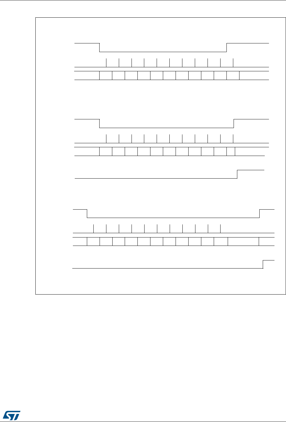
RM0090 Rev 18 993/1749
RM0090 Universal synchronous asynchronous receiver transmitter (USART)
1018
Figure 305. Break detection in LIN mode (11-bit break length - LBDL bit is set)
MSv40883V1
Idle Bit0 Bit1 Bit2 Bit3 Bit4 Bit5 Bit6 Bit7 Bit8 Bit9 Bit10 Idle
0000 000 0001
Case 1: break signal not long enough => break discarded, LBD is not set
RX line
Capture strobe
Break state
machine
Read samples
Idle Bit0 Bit1 Bit2 Bit3 Bit4 Bit5 Bit6 Bit7 Bit8 Bit9 B10 Idle
0000 000 0000
Case 2: break signal just long enough => break detected, LBD is set
RX line
Capture strobe
Break state
machine
Read samples
Break frame
Break frame
Delimiter is immediate
LBD
Idle Bit0 Bit1 Bit2 Bit3 Bit4 Bit5 Bit6 Bit7 Bit8 Bit9 Bit10 Idle
0000 000 0000
Case 3: break signal long enough => break detected, LBD is set
RX line
Capture strobe
Break state
machine
Read samples
Break frame
LBD
wait delimiter
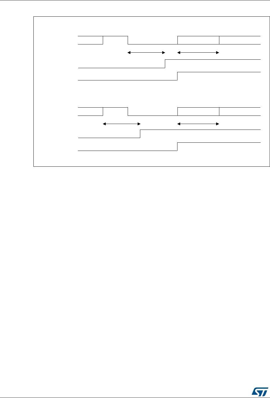
Universal synchronous asynchronous receiver transmitter (USART) RM0090
994/1749 RM0090 Rev 18
Figure 306. Break detection in LIN mode vs. Framing error detection
30.3.9 USART synchronous mode
The synchronous mode is selected by writing the CLKEN bit in the USART_CR2 register to
1. In synchronous mode, the following bits must be kept cleared:
•LINEN bit in the USART_CR2 register,
•SCEN, HDSEL and IREN bits in the USART_CR3 register.
The USART allows the user to control a bidirectional synchronous serial communications in
master mode. The CK pin is the output of the USART transmitter clock. No clock pulses are
sent to the CK pin during start bit and stop bit. Depending on the state of the LBCL bit in the
USART_CR2 register clock pulses will or will not be generated during the last valid data bit
(address mark). The CPOL bit in the USART_CR2 register allows the user to select the
clock polarity, and the CPHA bit in the USART_CR2 register allows the user to select the
phase of the external clock (see Figure 307, Figure 308 & Figure 309).
During the Idle state, preamble and send break, the external CK clock is not activated.
In synchronous mode the USART transmitter works exactly like in asynchronous mode. But
as CK is synchronized with TX (according to CPOL and CPHA), the data on TX is
synchronous.
In this mode the USART receiver works in a different manner compared to the
asynchronous mode. If RE=1, the data is sampled on CK (rising or falling edge, depending
on CPOL and CPHA), without any oversampling. A setup and a hold time must be
respected (which depends on the baud rate: 1/16 bit time).
Note: The CK pin works in conjunction with the TX pin. Thus, the clock is provided only if the
transmitter is enabled (TE=1) and a data is being transmitted (the data register USART_DR
MSv31157V1
data 1 IDLE BREAK data 2 (0x55) data 3 (header)
1 data time 1 data time
RX line
RXNE /FE
LBDF
Case 1: break occurring after an Idle
data 1 data2 BREAK data 2 (0x55) data 3 (header)
1 data time 1 data time
RX line
RXNE /FE
LBDF
Case 2: break occurring while data is being received
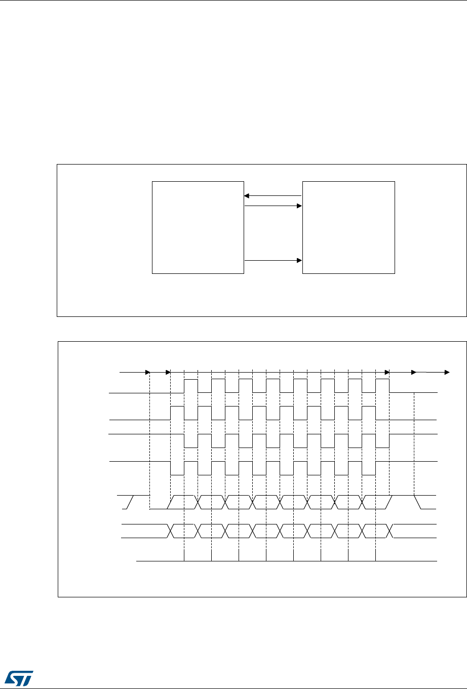
RM0090 Rev 18 995/1749
RM0090 Universal synchronous asynchronous receiver transmitter (USART)
1018
has been written). This means that it is not possible to receive a synchronous data without
transmitting data.
The LBCL, CPOL and CPHA bits have to be selected when both the transmitter and the
receiver are disabled (TE=RE=0) to ensure that the clock pulses function correctly. These
bits should not be changed while the transmitter or the receiver is enabled.
It is advised that TE and RE are set in the same instruction in order to minimize the setup
and the hold time of the receiver.
The USART supports master mode only: it cannot receive or send data related to an input
clock (CK is always an output).
Figure 307. USART example of synchronous transmission
Figure 308. USART data clock timing diagram (M=0)
MSv31158V2
USART Synchronous device
(e.g. slave SPI)
RX
TX
Data out
Data in
Clock
CK
MSv31159V1
01234567
01234567
*
*
*
*
MSB
MSB
LSB
LSB
Start
Start Stop
Idle or preceding
transmission
Idle or next
transmission
*
*LBCL bit controls last data pulse
Capture strobe
Data on RX
(from slave)
Data on TX
(from master)
Clock (CPOL=1, CPHA=1
Clock (CPOL=1, CPHA=0
Clock (CPOL=0, CPHA=1
Clock (CPOL=0, CPHA=0
Stop
M=0 (8 data bits)
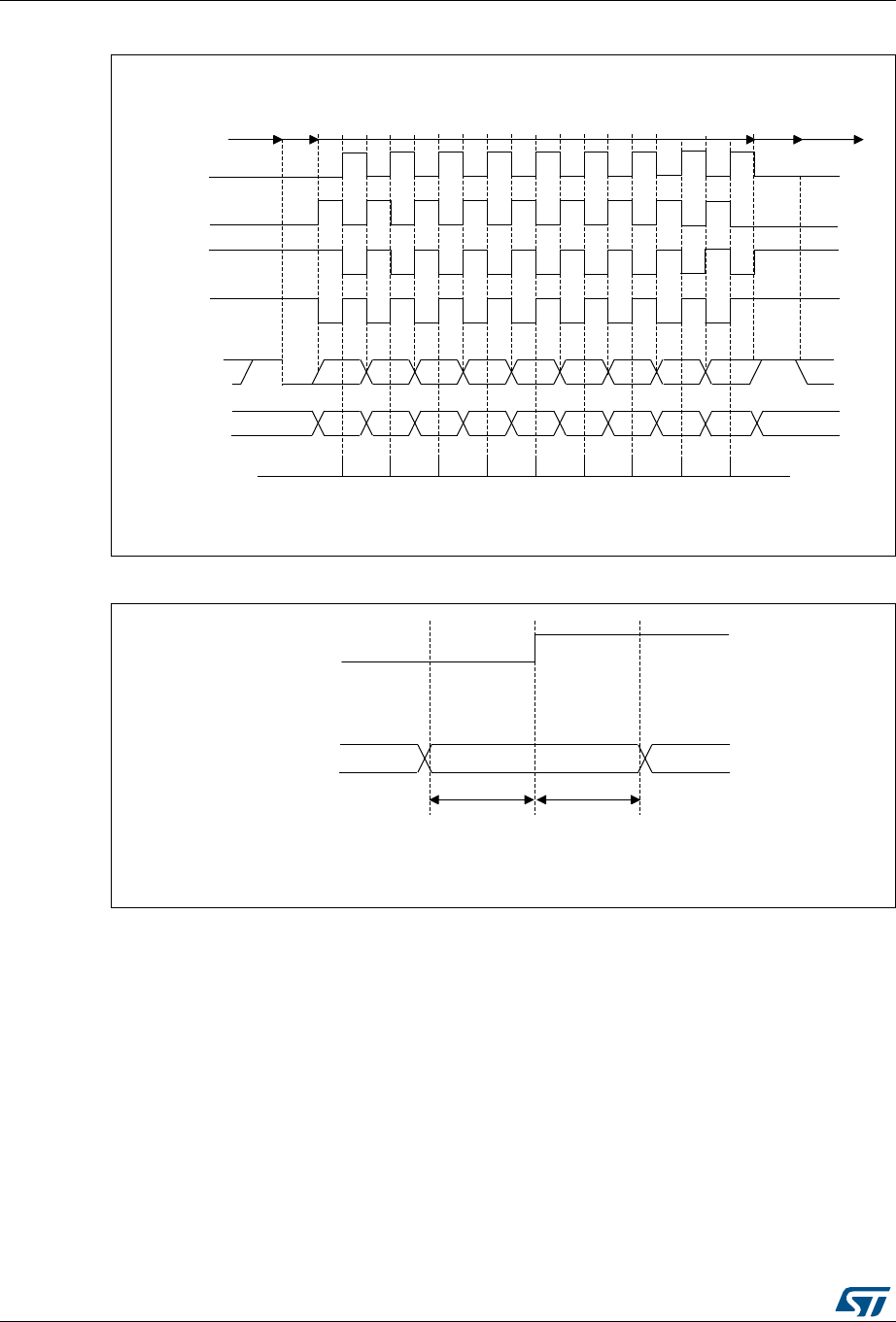
Universal synchronous asynchronous receiver transmitter (USART) RM0090
996/1749 RM0090 Rev 18
Figure 309. USART data clock timing diagram (M=1)
Figure 310. RX data setup/hold time
Note: The function of CK is different in Smartcard mode. Refer to the Smartcard mode chapter for
more details.
30.3.10 Single-wire half-duplex communication
The single-wire half-duplex mode is selected by setting the HDSEL bit in the USART_CR3
register. In this mode, the following bits must be kept cleared:
•LINEN and CLKEN bits in the USART_CR2 register,
•SCEN and IREN bits in the USART_CR3 register.
The USART can be configured to follow a single-wire half-duplex protocol where the TX and
RX lines are internally connected. The selection between half- and full-duplex
communication is made with a control bit ‘HALF DUPLEX SEL’ (HDSEL in USART_CR3).
MSv31160V1
0 1 2 3 4 5 6 8
0 1 2 3 4 5 6 8
*
*
*
*
MSB
MSB
LSB
LSBStart
Start Stop
Idle or
preceding
transmission
Idle or next
transmission
*
*LBCL bit controls last data pulse
Capture
strobe
Data on RX
(from slave)
Data on TX
(from master)
Clock (CPOL=1,
CPHA=1
Clock (CPOL=1,
CPHA=0
Clock (CPOL=0,
CPHA=1
Clock (CPOL=0,
CPHA=0
Stop
M=1 (9 data bits)
7
7
MSv31161V2
Data on RX (from slave)
CK
(capture strobe on CK rising
edge in this example)
Valid DATA bit
tSETUP tHOLD
tSETUP=tHOLD 1/16 bit time
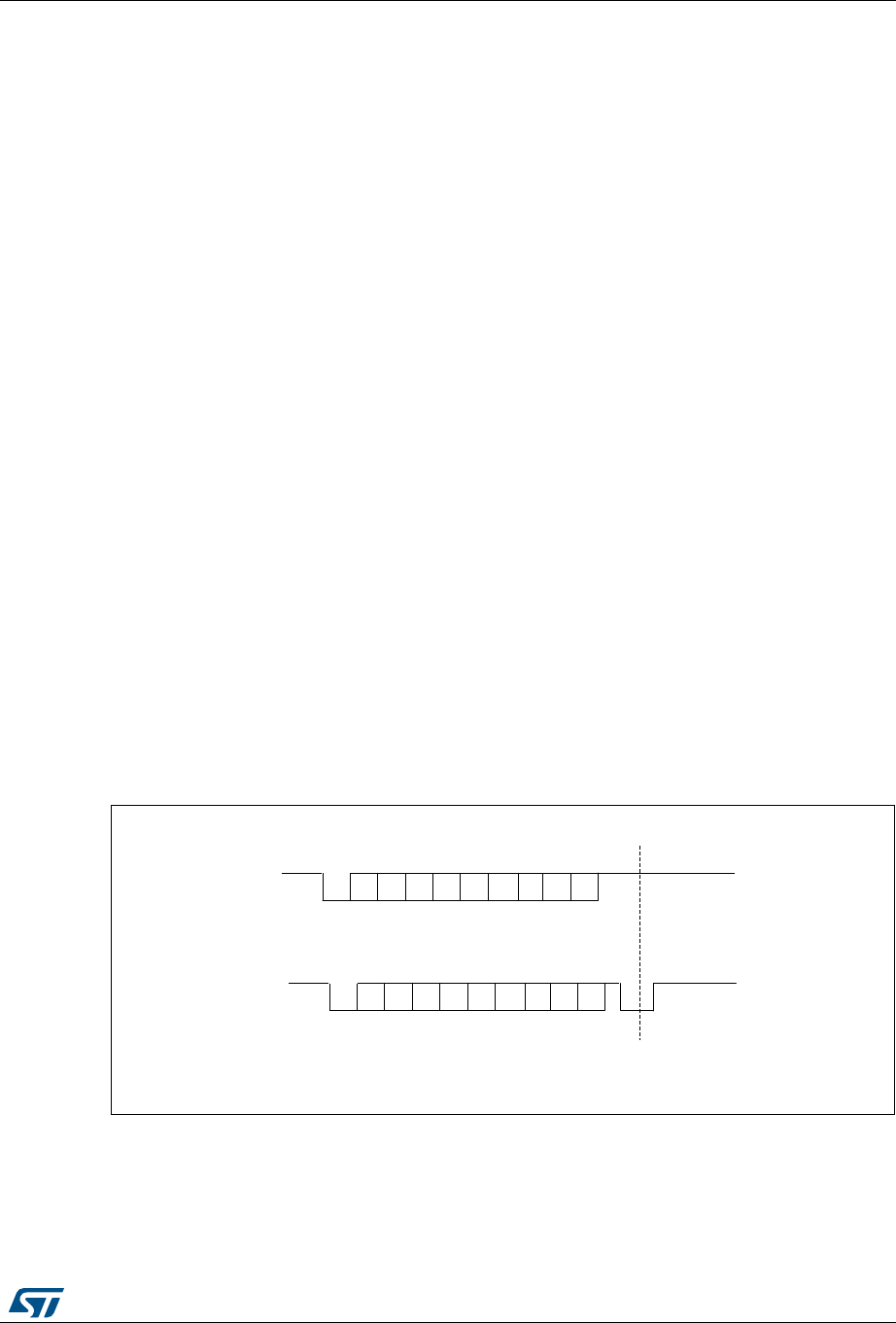
RM0090 Rev 18 997/1749
RM0090 Universal synchronous asynchronous receiver transmitter (USART)
1018
As soon as HDSEL is written to 1:
•the TX and RX lines are internally connected
•the RX pin is no longer used
•the TX pin is always released when no data is transmitted. Thus, it acts as a standard
I/O in idle or in reception. It means that the I/O must be configured so that TX is
configured as floating input (or output high open-drain) when not driven by the USART.
Apart from this, the communications are similar to what is done in normal USART mode.
The conflicts on the line must be managed by the software (by the use of a centralized
arbiter, for instance). In particular, the transmission is never blocked by hardware and
continue to occur as soon as a data is written in the data register while the TE bit is set.
30.3.11 Smartcard
The Smartcard mode is selected by setting the SCEN bit in the USART_CR3 register. In
smartcard mode, the following bits must be kept cleared:
•LINEN bit in the USART_CR2 register,
•HDSEL and IREN bits in the USART_CR3 register.
Moreover, the CLKEN bit may be set in order to provide a clock to the smartcard.
The Smartcard interface is designed to support asynchronous protocol Smartcards as
defined in the ISO 7816-3 standard. The USART should be configured as:
•8 bits plus parity: where M=1 and PCE=1 in the USART_CR1 register
•1.5 stop bits when transmitting and receiving: where STOP=11 in the USART_CR2
register.
Note: It is also possible to choose 0.5 stop bit for receiving but it is recommended to use 1.5 stop
bits for both transmitting and receiving to avoid switching between the two configurations.
Figure 311 shows examples of what can be seen on the data line with and without parity
error.
Figure 311. ISO 7816-3 asynchronous protocol
When connected to a Smartcard, the TX output of the USART drives a bidirectional line that
is also driven by the Smartcard. The TX pin must be configured as open-drain.
Smartcard is a single wire half duplex communication protocol.
•Transmission of data from the transmit shift register is guaranteed to be delayed by a
minimum of 1/2 baud clock. In normal operation a full transmit shift register will start
MSv31162V1
Without Parity error
p
76543210S
Guard time
WithParity error
p
76543210S
Guard time
Start bit
Start bit Line pulled low by receiver
during stop in case of parity error
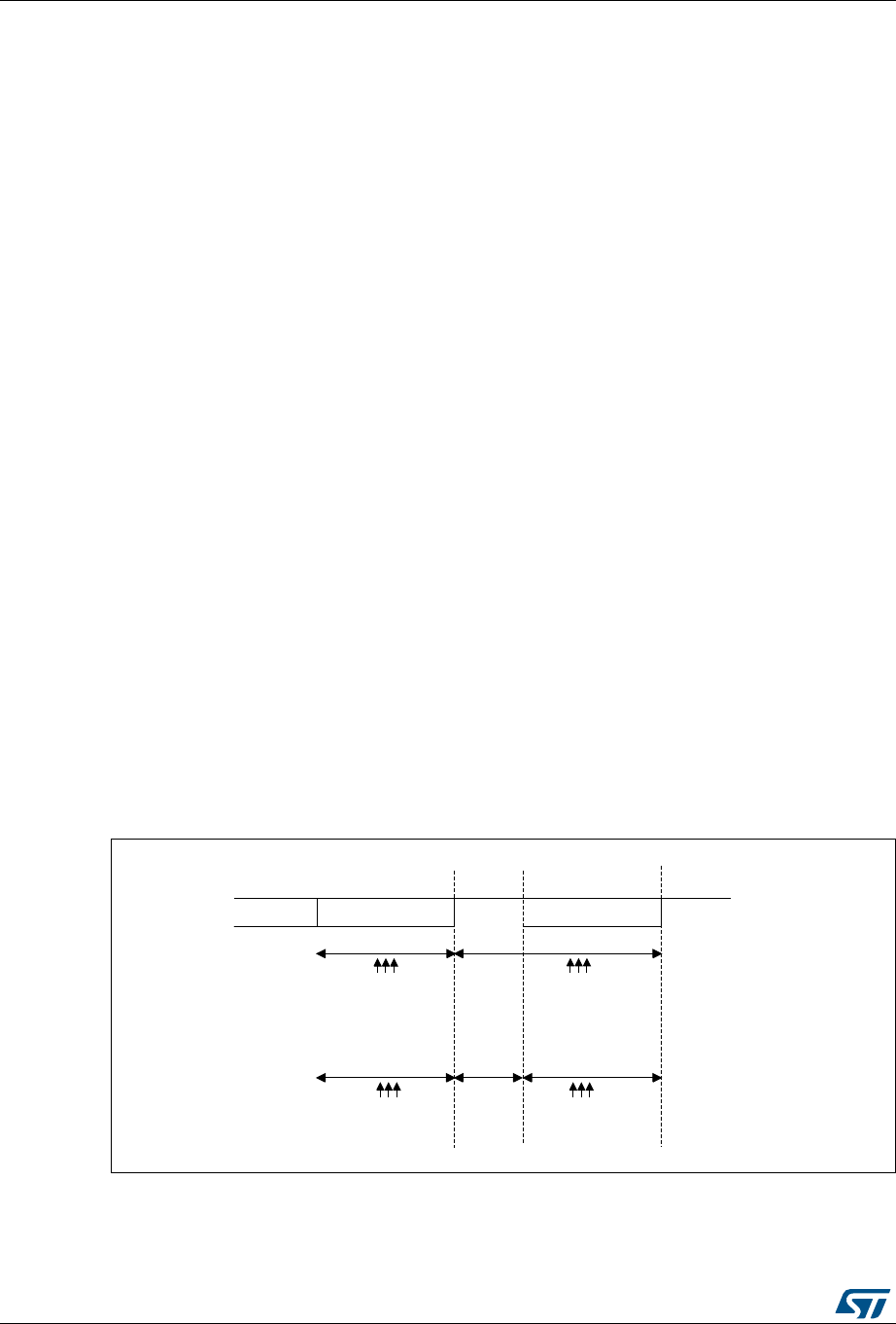
Universal synchronous asynchronous receiver transmitter (USART) RM0090
998/1749 RM0090 Rev 18
shifting on the next baud clock edge. In Smartcard mode this transmission is further
delayed by a guaranteed 1/2 baud clock.
•If a parity error is detected during reception of a frame programmed with a 0.5 or 1.5
stop bit period, the transmit line is pulled low for a baud clock period after the
completion of the receive frame. This is to indicate to the Smartcard that the data
transmitted to USART has not been correctly received. This NACK signal (pulling
transmit line low for 1 baud clock) will cause a framing error on the transmitter side
(configured with 1.5 stop bits). The application can handle re-sending of data according
to the protocol. A parity error is ‘NACK’ed by the receiver if the NACK control bit is set,
otherwise a NACK is not transmitted.
•The assertion of the TC flag can be delayed by programming the Guard Time register.
In normal operation, TC is asserted when the transmit shift register is empty and no
further transmit requests are outstanding. In Smartcard mode an empty transmit shift
register triggers the guard time counter to count up to the programmed value in the
Guard Time register. TC is forced low during this time. When the guard time counter
reaches the programmed value TC is asserted high.
•The de-assertion of TC flag is unaffected by Smartcard mode.
•If a framing error is detected on the transmitter end (due to a NACK from the receiver),
the NACK will not be detected as a start bit by the receive block of the transmitter.
According to the ISO protocol, the duration of the received NACK can be 1 or 2 baud
clock periods.
•On the receiver side, if a parity error is detected and a NACK is transmitted the receiver
will not detect the NACK as a start bit.
Note: A break character is not significant in Smartcard mode. A 0x00 data with a framing error will
be treated as data and not as a break.
No Idle frame is transmitted when toggling the TE bit. The Idle frame (as defined for the
other configurations) is not defined by the ISO protocol.
Figure 312 details how the NACK signal is sampled by the USART. In this example the
USART is transmitting a data and is configured with 1.5 stop bits. The receiver part of the
USART is enabled in order to check the integrity of the data and the NACK signal.
Figure 312. Parity error detection using the 1.5 stop bits
The USART can provide a clock to the smartcard through the CK output. In smartcard
mode, CK is not associated to the communication but is simply derived from the internal
peripheral input clock through a 5-bit prescaler. The division ratio is configured in the
MSv31163V1
Bit 7 Parity bit 1.5 Stop bit
1 bit time 1.5 bit time
0.5 bit time
Sampling at
8th, 9th, 10th
Sampling at
8th, 9th, 10th
Sampling at
8th, 9th, 10th
Sampling at
8th, 9th, 10th

RM0090 Rev 18 999/1749
RM0090 Universal synchronous asynchronous receiver transmitter (USART)
1018
prescaler register USART_GTPR. CK frequency can be programmed from fCK/2 to fCK/62,
where fCK is the peripheral input clock.
30.3.12 IrDA SIR ENDEC block
The IrDA mode is selected by setting the IREN bit in the USART_CR3 register. In IrDA
mode, the following bits must be kept cleared:
•LINEN, STOP and CLKEN bits in the USART_CR2 register,
•SCEN and HDSEL bits in the USART_CR3 register.
The IrDA SIR physical layer specifies use of a Return to Zero, Inverted (RZI) modulation
scheme that represents logic 0 as an infrared light pulse (see Figure 313).
The SIR Transmit encoder modulates the Non Return to Zero (NRZ) transmit bit stream
output from USART. The output pulse stream is transmitted to an external output driver and
infrared LED. USART supports only bit rates up to 115.2Kbps for the SIR ENDEC. In normal
mode the transmitted pulse width is specified as 3/16 of a bit period.
The SIR receive decoder demodulates the return-to-zero bit stream from the infrared
detector and outputs the received NRZ serial bit stream to USART. The decoder input is
normally HIGH (marking state) in the Idle state. The transmit encoder output has the
opposite polarity to the decoder input. A start bit is detected when the decoder input is low.
•IrDA is a half duplex communication protocol. If the Transmitter is busy (i.e. the USART
is sending data to the IrDA encoder), any data on the IrDA receive line will be ignored
by the IrDA decoder and if the Receiver is busy (USART is receiving decoded data
from the USART), data on the TX from the USART to IrDA will not be encoded by IrDA.
While receiving data, transmission should be avoided as the data to be transmitted
could be corrupted.
•A ‘0 is transmitted as a high pulse and a ‘1 is transmitted as a ‘0. The width of the pulse
is specified as 3/16th of the selected bit period in normal mode (see Figure 314).
•The SIR decoder converts the IrDA compliant receive signal into a bit stream for
USART.
•The SIR receive logic interprets a high state as a logic one and low pulses as logic
zeros.
•The transmit encoder output has the opposite polarity to the decoder input. The SIR
output is in low state when Idle.
•The IrDA specification requires the acceptance of pulses greater than 1.41 us. The
acceptable pulse width is programmable. Glitch detection logic on the receiver end
filters out pulses of width less than 2 PSC periods (PSC is the prescaler value
programmed in the IrDA low-power Baud Register, USART_GTPR). Pulses of width
less than 1 PSC period are always rejected, but those of width greater than one and
less than two periods may be accepted or rejected, those greater than 2 periods will be
accepted as a pulse. The IrDA encoder/decoder doesn’t work when PSC=0.
•The receiver can communicate with a low-power transmitter.
•In IrDA mode, the STOP bits in the USART_CR2 register must be configured to “1 stop
bit”.
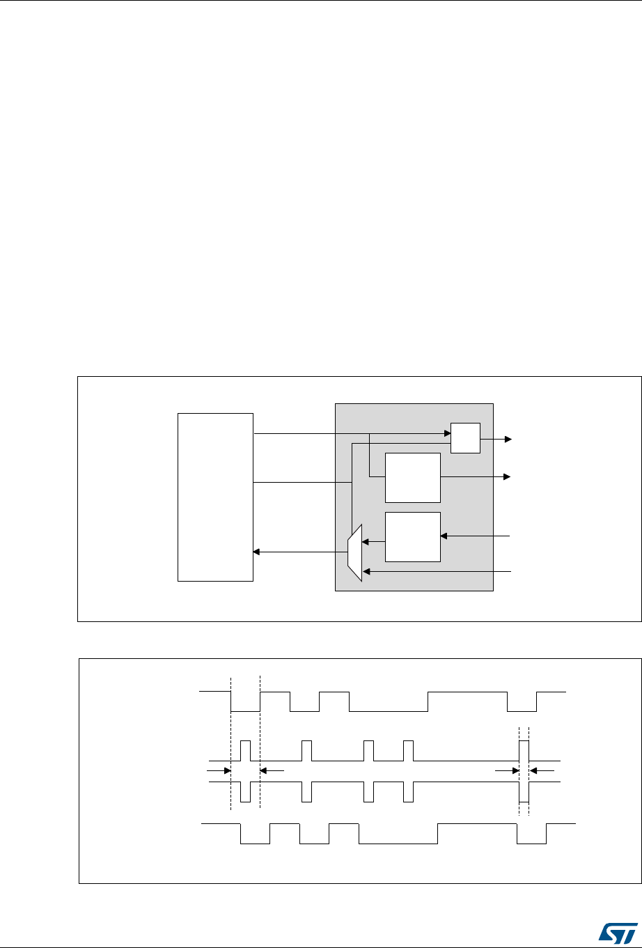
Universal synchronous asynchronous receiver transmitter (USART) RM0090
1000/1749 RM0090 Rev 18
IrDA low-power mode
Transmitter:
In low-power mode the pulse width is not maintained at 3/16 of the bit period. Instead, the
width of the pulse is 3 times the low-power baud rate which can be a minimum of 1.42 MHz.
Generally this value is 1.8432 MHz (1.42 MHz < PSC< 2.12 MHz). A low-power mode
programmable divisor divides the system clock to achieve this value.
Receiver:
Receiving in low-power mode is similar to receiving in normal mode. For glitch detection the
USART should discard pulses of duration shorter than 1/PSC. A valid low is accepted only if
its duration is greater than 2 periods of the IrDA low-power Baud clock (PSC value in
USART_GTPR).
Note: A pulse of width less than two and greater than one PSC period(s) may or may not be
rejected.
The receiver set up time should be managed by software. The IrDA physical layer
specification specifies a minimum of 10 ms delay between transmission and reception (IrDA
is a half duplex protocol).
Figure 313. IrDA SIR ENDEC- block diagram
Figure 314. IrDA data modulation (3/16) -Normal mode
SIREN
MSv31164V2
USART
OR
SIR
Transmit
Encoder
SIR
Receive
DEcoder
TX
RX
USART_RX
IrDA_IN
IrDA_OUT
USART_TX
MSv31165V1
TX
Start
bit
0101001101
Stop
bit
Bit period
IrDA_OUT
IrDA_IN
RX
3/16
0101 001101

RM0090 Rev 18 1001/1749
RM0090 Universal synchronous asynchronous receiver transmitter (USART)
1018
30.3.13 Continuous communication using DMA
The USART is capable of continuous communication using the DMA. The DMA requests for
Rx buffer and Tx buffer are generated independently.
Transmission using DMA
DMA mode can be enabled for transmission by setting DMAT bit in the USART_CR3
register. Data is loaded from a SRAM area configured using the DMA peripheral (refer to the
DMA specification) to the USART_DR register whenever the TXE bit is set. To map a DMA
channel for USART transmission, use the following procedure (x denotes the channel
number):
1. Write the USART_DR register address in the DMA control register to configure it as the
destination of the transfer. The data will be moved to this address from memory after
each TXE event.
2. Write the memory address in the DMA control register to configure it as the source of
the transfer. The data will be loaded into the USART_DR register from this memory
area after each TXE event.
3. Configure the total number of bytes to be transferred to the DMA control register.
4. Configure the channel priority in the DMA register
5. Configure DMA interrupt generation after half/ full transfer as required by the
application.
6. Clear the TC bit in the SR register by writing 0 to it.
7. Activate the channel in the DMA register.
When the number of data transfers programmed in the DMA Controller is reached, the DMA
controller generates an interrupt on the DMA channel interrupt vector.
In transmission mode, once the DMA has written all the data to be transmitted (the TCIF flag
is set in the DMA_ISR register), the TC flag can be monitored to make sure that the USART
communication is complete. This is required to avoid corrupting the last transmission before
disabling the USART or entering the Stop mode. The software must wait until TC=1. The TC
flag remains cleared during all data transfers and it is set by hardware at the last frame’s
end of transmission.
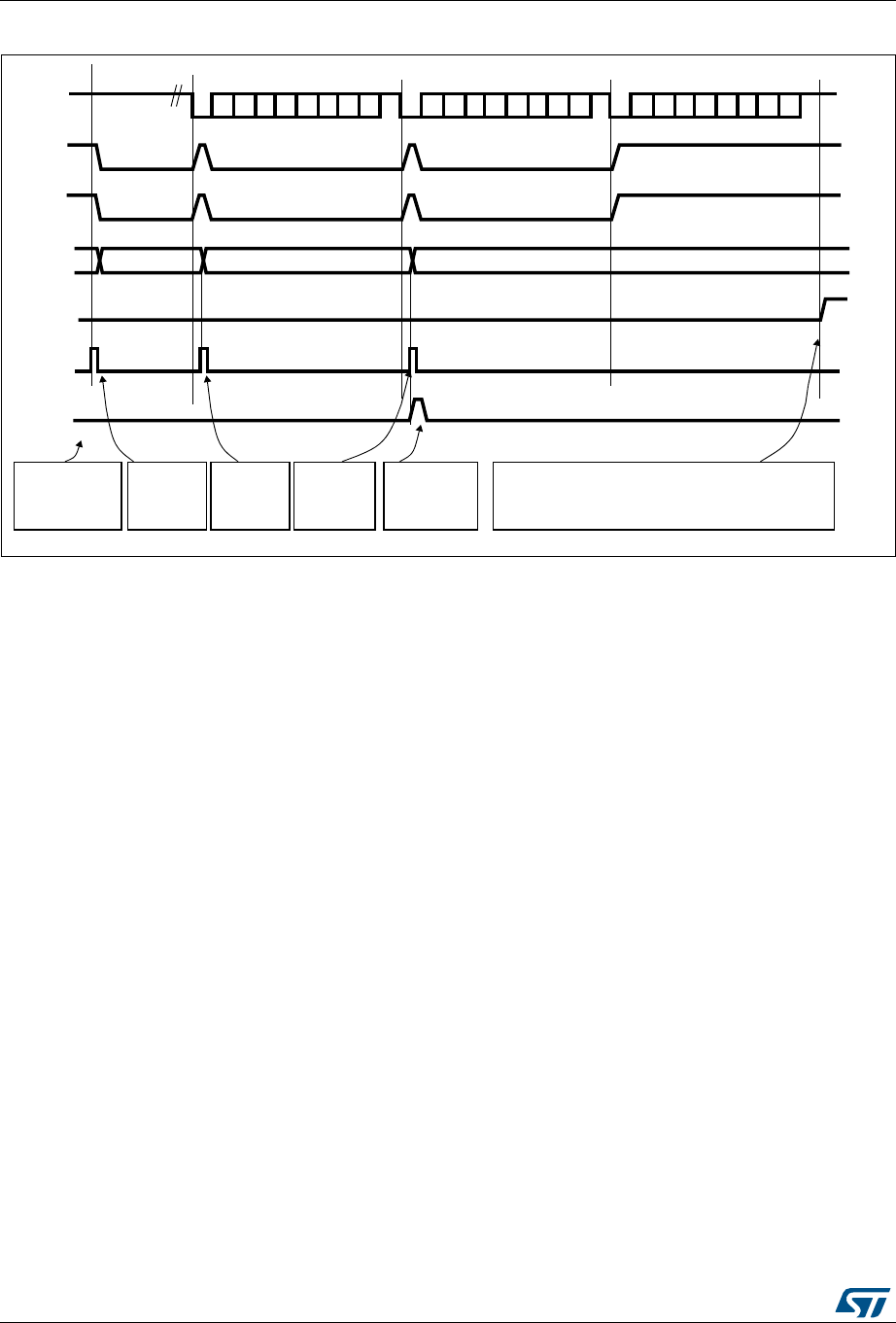
Universal synchronous asynchronous receiver transmitter (USART) RM0090
1002/1749 RM0090 Rev 18
Figure 315. Transmission using DMA
Reception using DMA
DMA mode can be enabled for reception by setting the DMAR bit in USART_CR3 register.
Data is loaded from the USART_DR register to a SRAM area configured using the DMA
peripheral (refer to the DMA specification) whenever a data byte is received. To map a DMA
channel for USART reception, use the following procedure:
1. Write the USART_DR register address in the DMA control register to configure it as the
source of the transfer. The data will be moved from this address to the memory after
each RXNE event.
2. Write the memory address in the DMA control register to configure it as the destination
of the transfer. The data will be loaded from USART_DR to this memory area after each
RXNE event.
3. Configure the total number of bytes to be transferred in the DMA control register.
4. Configure the channel priority in the DMA control register
5. Configure interrupt generation after half/ full transfer as required by the application.
6. Activate the channel in the DMA control register.
When the number of data transfers programmed in the DMA Controller is reached, the DMA
controller generates an interrupt on the DMA channel interrupt vector. The DMAR bit should
be cleared by software in the USART_CR3 register during the interrupt subroutine.
TX line
USART_DR
Frame 1
TXE flag
F2
TC flag
F3
Frame 2
software waits until TC=1
Frame 3
set by hardware
cleared by DMA read
set by hardware
cleared by DMA read set by hardware
set
Idle preamble
by hardware
F1
software configures
the DMA to send 3
data and enables the
USART
DMA request ignored by the DMA
DMA writes
flag DMA TCIF set by hardware
clear
by software
USART_DR
because DMA transfer is complete
DMA writes F1
into
USART_DR
DMA writes F2
into
USART_DR
DMA writes F3
into
USART_DR.
The DMA transfer
is complete
(TCIF=1 in
DMA_ISR)
(Transfer complete)
ai17192b
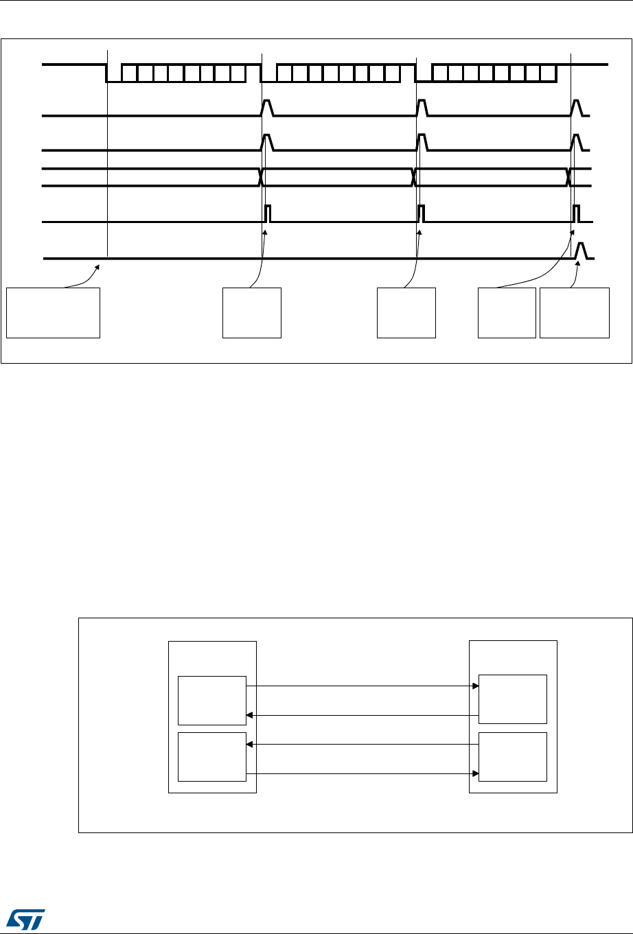
RM0090 Rev 18 1003/1749
RM0090 Universal synchronous asynchronous receiver transmitter (USART)
1018
Figure 316. Reception using DMA
Error flagging and interrupt generation in multibuffer communication
In case of multibuffer communication if any error occurs during the transaction the error flag
will be asserted after the current byte. An interrupt will be generated if the interrupt enable
flag is set. For framing error, overrun error and noise flag which are asserted with RXNE in
case of single byte reception, there will be separate error flag interrupt enable bit (EIE bit in
the USART_CR3 register), which if set will issue an interrupt after the current byte with
either of these errors.
30.3.14 Hardware flow control
It is possible to control the serial data flow between 2 devices by using the CTS input and
the RTS output. The Figure 317 shows how to connect 2 devices in this mode:
Figure 317. Hardware flow control between 2 USARTs
RTS and CTS flow control can be enabled independently by writing respectively RTSE and
CTSE bits to 1 (in the USART_CR3 register).
TX line
USART_DR
Frame 1
RXNE flag
F2 F3
Frame 2 Frame 3
set by hardware
cleared by DMA read
F1
software configures the
DMA to receive 3 data
blocks and enables
the USART
DMA request
DMA reads USART_DR
DMA TCIF flag set by hardware
cleared
by software
DMA reads F1
from
USART_DR
(Transfer complete)
DMA reads F2
from
USART_DR
DMA reads F3
from
USART_DR
The DMA transfer
is complete
(TCIF=1 in
DMA_ISR)
ai17193b
MSv31169V2
TX circuit
USART 1
TX
RX circuit
RX circuit
USART 2
TX circuit
TX
CTS
CTSRTS
RX
RTS
RX
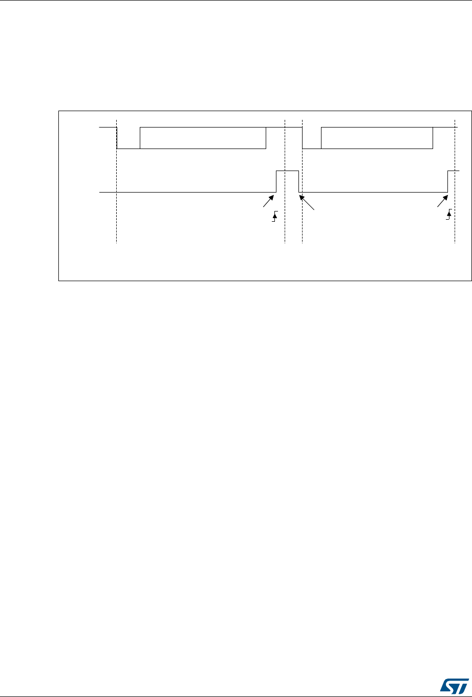
Universal synchronous asynchronous receiver transmitter (USART) RM0090
1004/1749 RM0090 Rev 18
RTS flow control
If the RTS flow control is enabled (RTSE=1), then RTS is asserted (tied low) as long as the
USART receiver is ready to receive a new data. When the receive register is full, RTS is
deasserted, indicating that the transmission is expected to stop at the end of the current
frame. Figure 318 shows an example of communication with RTS flow control enabled.
Figure 318. RTS flow control
CTS flow control
If the CTS flow control is enabled (CTSE=1), then the transmitter checks the CTS input
before transmitting the next frame. If CTS is asserted (tied low), then the next data is
transmitted (assuming that a data is to be transmitted, in other words, if TXE=0), else the
transmission does not occur. When CTS is deasserted during a transmission, the current
transmission is completed before the transmitter stops.
When CTSE=1, the CTSIF status bit is automatically set by hardware as soon as the CTS
input toggles. It indicates when the receiver becomes ready or not ready for communication.
An interrupt is generated if the CTSIE bit in the USART_CR3 register is set. The figure
below shows an example of communication with CTS flow control enabled.
MSv31168V2
Start
bit
Start
bit
Stop
bit Idle Stop
bit
RX
RTS
Data 1 read
Data 2 can now be transmitted
RXNE RXNE
Data 1 Data 2
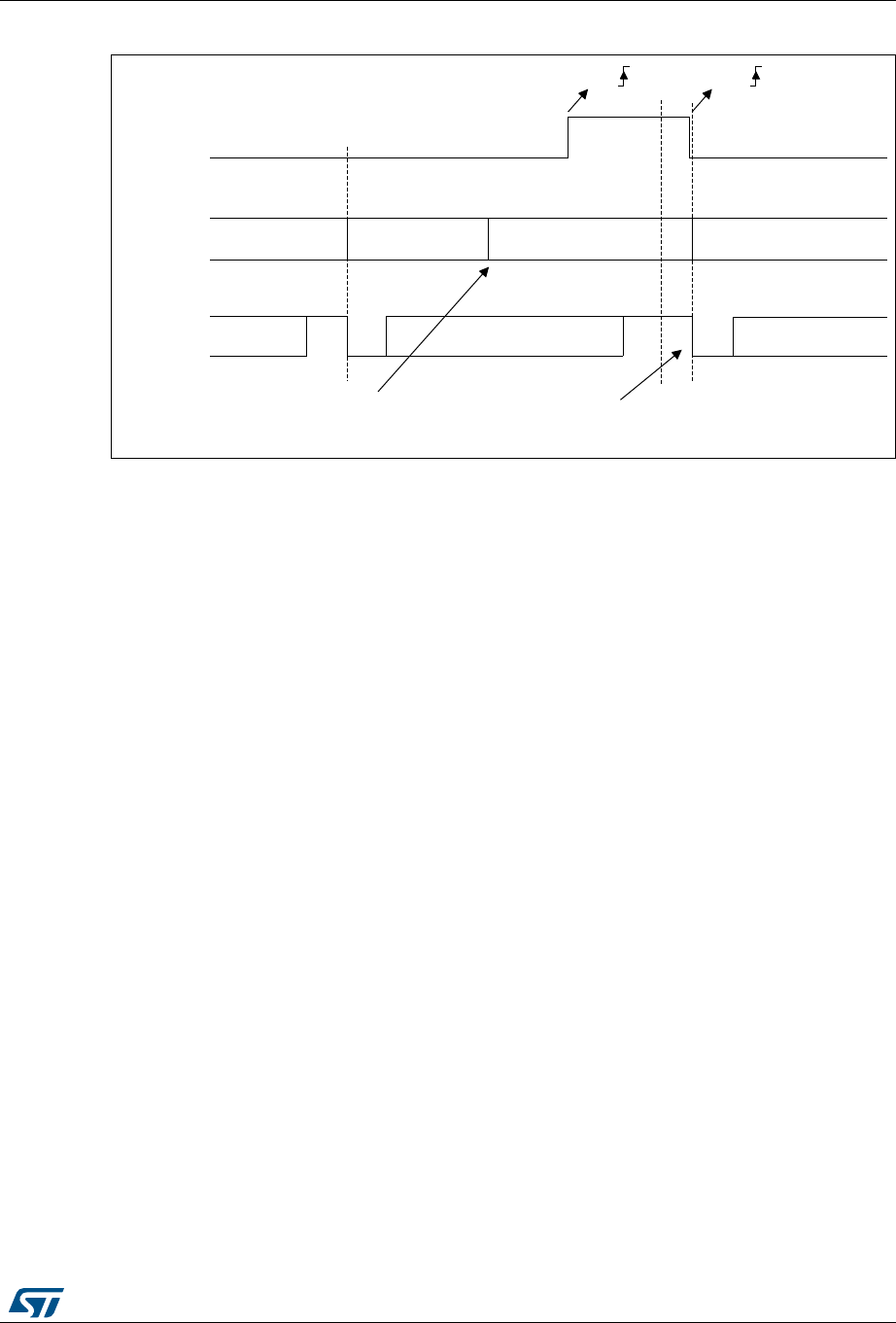
RM0090 Rev 18 1005/1749
RM0090 Universal synchronous asynchronous receiver transmitter (USART)
1018
Figure 319. CTS flow control
Note: Special behavior of break frames: when the CTS flow is enabled, the transmitter does not
check the CTS input state to send a break.
MSv31167V2
Start
bit
Stop
bit
TX
TDR
CTS
Data 1
Data 2
Stop
bit Idle Start
bit
Data 2 Data 3
Data 3
empty empty
CTS
CTS
Transmit data register
Writing data 3 in TDR Transmission of Data 3 is
delayed until CTS = 0
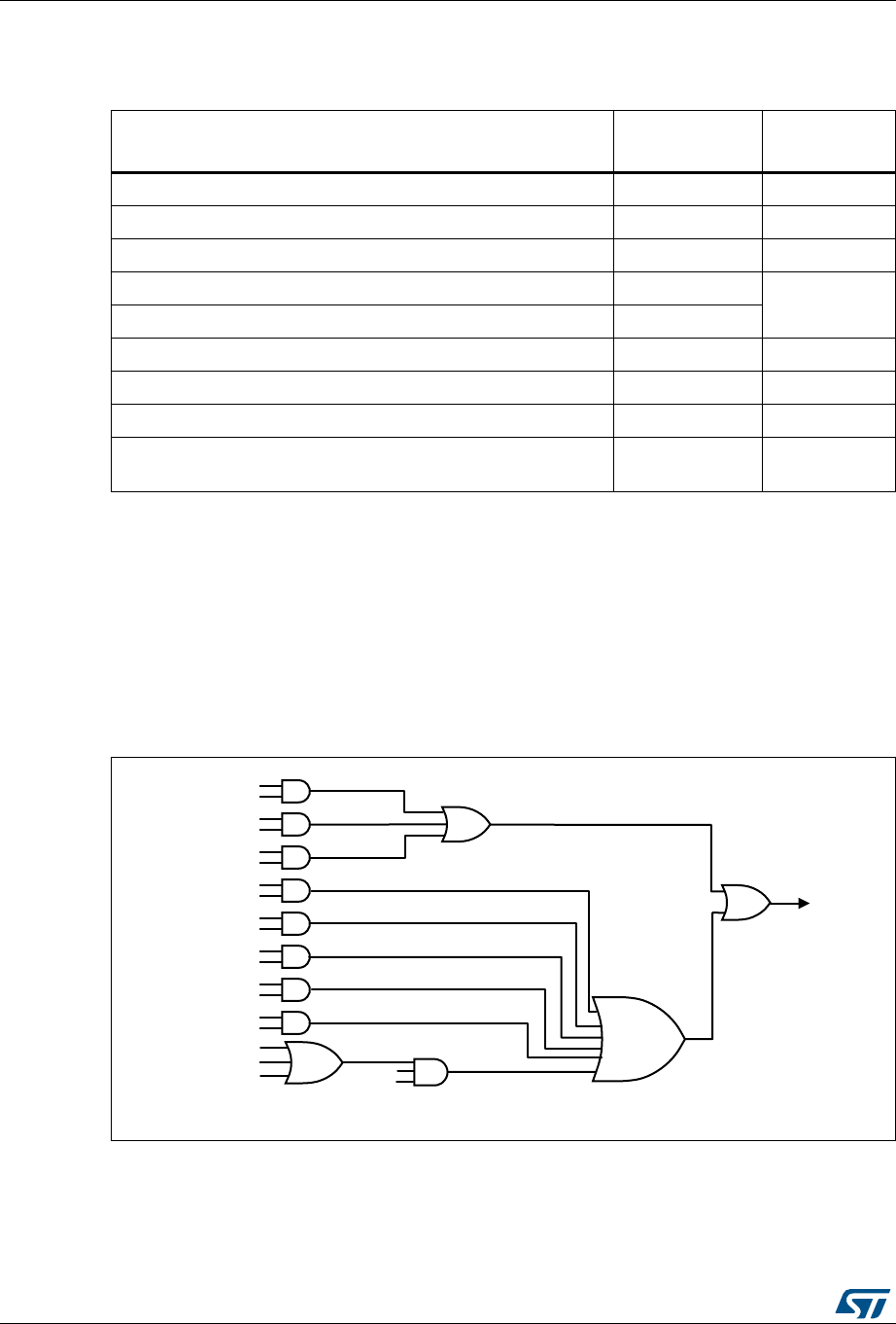
Universal synchronous asynchronous receiver transmitter (USART) RM0090
1006/1749 RM0090 Rev 18
30.4 USART interrupts
The USART interrupt events are connected to the same interrupt vector (see Figure 320).
•During transmission: Transmission Complete, Clear to Send or Transmit Data Register
empty interrupt.
•While receiving: Idle Line detection, Overrun error, Receive Data register not empty,
Parity error, LIN break detection, Noise Flag (only in multi buffer communication) and
Framing Error (only in multi buffer communication).
These events generate an interrupt if the corresponding Enable Control Bit is set.
Figure 320. USART interrupt mapping diagram
Table 147. USART interrupt requests
Interrupt event Event flag Enable control
bit
Transmit Data Register Empty TXE TXEIE
CTS flag CTS CTSIE
Transmission Complete TC TCIE
Received Data Ready to be Read RXNE
RXNEIE
Overrun Error Detected ORE
Idle Line Detected IDLE IDLEIE
Parity Error PE PEIE
Break Flag LBD LBDIE
Noise Flag, Overrun error and Framing Error in multibuffer
communication NF or ORE or FE EIE
MSv42089V1
TC
TCIE
TXE
TXEIE
CTSIF
CTSIE
IDLE
IDLEIE
RXNEIE
ORE
RXNEIE
RXNE
PE
PEIE
LBD
LBDIE
FE
NE
ORE EIE
USART
interrupt
DMAR
RM0090 Rev 18 1007/1749
RM0090 Universal synchronous asynchronous receiver transmitter (USART)
1018
30.5 USART mode configuration
30.6 USART registers
Refer to Section 1.1: List of abbreviations for registers for registers for a list of abbreviations
used in register descriptions.
The peripheral registers have to be accessed by half-words (16 bits) or words (32 bits).
30.6.1 Status register (USART_SR)
Address offset: 0x00
Reset value: 0x0000 00C0
Table 148. USART mode configuration(1)
1. X = supported; NA = not applicable.
USART modes USART
1
USART
2
USART
3UART4 UART5 USART
6
Asynchronous mode XXXXXX
Hardware flow control XXXNANAX
Multibuffer communication (DMA)XXXXXX
Multiprocessor communicationXXXXXX
Synchronous XXXNANAX
Smartcard XXXNANAX
Half-duplex (single-wire mode)XXXXXX
IrDA XXXXXX
LIN XXXXXX
31 30 29 28 27 26 25 24 23 22 21 20 19 18 17 16
Reserved
1514131211109876543210
Reserved CTS LBD TXE TC RXNE IDLE ORE NF FE PE
rc_w0rc_w0rrc_w0rc_w0rrrrr

Universal synchronous asynchronous receiver transmitter (USART) RM0090
1008/1749 RM0090 Rev 18
Bits 31:10 Reserved, must be kept at reset value
Bit 9 CTS: CTS flag
This bit is set by hardware when the CTS input toggles, if the CTSE bit is set. It is cleared by
software (by writing it to 0). An interrupt is generated if CTSIE=1 in the USART_CR3
register.
0: No change occurred on the CTS status line
1: A change occurred on the CTS status line
Note: This bit is not available for UART4 & UART5.
Bit 8 LBD: LIN break detection flag
This bit is set by hardware when the LIN break is detected. It is cleared by software (by
writing it to 0). An interrupt is generated if LBDIE = 1 in the USART_CR2 register.
0: LIN Break not detected
1: LIN break detected
Note: An interrupt is generated when LBD=1 if LBDIE=1
Bit 7 TXE: Transmit data register empty
This bit is set by hardware when the content of the TDR register has been transferred into
the shift register. An interrupt is generated if the TXEIE bit =1 in the USART_CR1 register. It
is cleared by a write to the USART_DR register.
0: Data is not transferred to the shift register
1: Data is transferred to the shift register)
Note: This bit is used during single buffer transmission.
Bit 6 TC: Transmission complete
This bit is set by hardware if the transmission of a frame containing data is complete and if
TXE is set. An interrupt is generated if TCIE=1 in the USART_CR1 register. It is cleared by
a software sequence (a read from the USART_SR register followed by a write to the
USART_DR register). The TC bit can also be cleared by writing a '0' to it. This clearing
sequence is recommended only for multibuffer communication.
0: Transmission is not complete
1: Transmission is complete
Bit 5 RXNE: Read data register not empty
This bit is set by hardware when the content of the RDR shift register has been transferred
to the USART_DR register. An interrupt is generated if RXNEIE=1 in the USART_CR1
register. It is cleared by a read to the USART_DR register. The RXNE flag can also be
cleared by writing a zero to it. This clearing sequence is recommended only for multibuffer
communication.
0: Data is not received
1: Received data is ready to be read.
Bit 4 IDLE: IDLE line detected
This bit is set by hardware when an Idle Line is detected. An interrupt is generated if the
IDLEIE=1 in the USART_CR1 register. It is cleared by a software sequence (an read to the
USART_SR register followed by a read to the USART_DR register).
0: No Idle Line is detected
1: Idle Line is detected
Note: The IDLE bit will not be set again until the RXNE bit has been set itself (i.e. a new idle
line occurs).

RM0090 Rev 18 1009/1749
RM0090 Universal synchronous asynchronous receiver transmitter (USART)
1018
Bit 3 ORE: Overrun error
This bit is set by hardware when the word currently being received in the shift register is
ready to be transferred into the RDR register while RXNE=1. An interrupt is generated if
RXNEIE=1 in the USART_CR1 register. It is cleared by a software sequence (an read to the
USART_SR register followed by a read to the USART_DR register).
0: No Overrun error
1: Overrun error is detected
Note: When this bit is set, the RDR register content will not be lost but the shift register will be
overwritten. An interrupt is generated on ORE flag in case of Multi Buffer
communication if the EIE bit is set.
Bit 2 NF: Noise detected flag
This bit is set by hardware when noise is detected on a received frame. It is cleared by a
software sequence (an read to the USART_SR register followed by a read to the
USART_DR register).
0: No noise is detected
1: Noise is detected
Note: This bit does not generate interrupt as it appears at the same time as the RXNE bit
which itself generates an interrupting interrupt is generated on NF flag in case of Multi
Buffer communication if the EIE bit is set.
Note: When the line is noise-free, the NF flag can be disabled by programming the ONEBIT
bit to 1 to increase the USART tolerance to deviations (Refer to Section 30.3.5: USART
receiver tolerance to clock deviation on page 988).
Bit 1 FE: Framing error
This bit is set by hardware when a de-synchronization, excessive noise or a break character
is detected. It is cleared by a software sequence (an read to the USART_SR register
followed by a read to the USART_DR register).
0: No Framing error is detected
1: Framing error or break character is detected
Note: This bit does not generate interrupt as it appears at the same time as the RXNE bit
which itself generates an interrupt. If the word currently being transferred causes both
frame error and overrun error, it will be transferred and only the ORE bit will be set.
An interrupt is generated on FE flag in case of Multi Buffer communication if the EIE bit
is set.
Bit 0 PE: Parity error
This bit is set by hardware when a parity error occurs in receiver mode. It is cleared by a
software sequence (a read from the status register followed by a read or write access to the
USART_DR data register). The software must wait for the RXNE flag to be set before
clearing the PE bit.
An interrupt is generated if PEIE = 1 in the USART_CR1 register.
0: No parity error
1: Parity error
Universal synchronous asynchronous receiver transmitter (USART) RM0090
1010/1749 RM0090 Rev 18
30.6.2 Data register (USART_DR)
Address offset: 0x04
Reset value: 0xXXXX XXXX
30.6.3 Baud rate register (USART_BRR)
Note: The baud counters stop counting if the TE or RE bits are disabled respectively.
Address offset: 0x08
Reset value: 0x0000 0000
30.6.4 Control register 1 (USART_CR1)
Address offset: 0x0C
Reset value: 0x0000 0000
Bits 31:9 Reserved, must be kept at reset value
Bits 8:0 DR[8:0]: Data value
Contains the Received or Transmitted data character, depending on whether it is read from
or written to.
The Data register performs a double function (read and write) since it is composed of two
registers, one for transmission (TDR) and one for reception (RDR)
The TDR register provides the parallel interface between the internal bus and the output shift
register (see Figure 1).
The RDR register provides the parallel interface between the input shift register and the
internal bus.
When transmitting with the parity enabled (PCE bit set to 1 in the USART_CR1 register), the
value written in the MSB (bit 7 or bit 8 depending on the data length) has no effect because
it is replaced by the parity.
When receiving with the parity enabled, the value read in the MSB bit is the received parity
bit.
31 30 29 28 27 26 25 24 23 22 21 20 19 18 17 16
Reserved
1514131211109876543210
DIV_Mantissa[11:0] DIV_Fraction[3:0]
rw rw rw rw rw rw rw rw rw rw rw rw rw rw rw rw
Bits 31:16 Reserved, must be kept at reset value
Bits 15:4 DIV_Mantissa[11:0]: mantissa of USARTDIV
These 12 bits define the mantissa of the USART Divider (USARTDIV)
Bits 3:0 DIV_Fraction[3:0]: fraction of USARTDIV
These 4 bits define the fraction of the USART Divider (USARTDIV). When OVER8=1, the
DIV_Fraction3 bit is not considered and must be kept cleared.
31 30 29 28 27 26 25 24 23 22 21 20 19 18 17 16
Reserved
15 14 13 12 11 10 9 8 7 6 5 4 3 2 1 0
OVER8 Reserved UE M WAKE PCE PS PEIE TXEIE TCIE RXNEIE IDLEIE TE RE RWU SBK
rw Res. rw rw rw rw rw rw rw rw rw rw rw rw rw rw

RM0090 Rev 18 1011/1749
RM0090 Universal synchronous asynchronous receiver transmitter (USART)
1018
Bits 31:16 Reserved, must be kept at reset value
Bit 15 OVER8: Oversampling mode
0: oversampling by 16
1: oversampling by 8
Note: Oversampling by 8 is not available in the Smartcard, IrDA and LIN modes: when
SCEN=1,IREN=1 or LINEN=1 then OVER8 is forced to ‘0 by hardware.
Bit 14 Reserved, must be kept at reset value
Bit 13 UE: USART enable
When this bit is cleared, the USART prescalers and outputs are stopped and the end of the
current byte transfer in order to reduce power consumption. This bit is set and cleared by
software.
0: USART prescaler and outputs disabled
1: USART enabled
Bit 12 M: Word length
This bit determines the word length. It is set or cleared by software.
0: 1 Start bit, 8 Data bits, n Stop bit
1: 1 Start bit, 9 Data bits, n Stop bit
Note: The M bit must not be modified during a data transfer (both transmission and reception)
Bit 11 WAKE: Wakeup method
This bit determines the USART wakeup method, it is set or cleared by software.
0: Idle Line
1: Address Mark
Bit 10 PCE: Parity control enable
This bit selects the hardware parity control (generation and detection). When the parity
control is enabled, the computed parity is inserted at the MSB position (9th bit if M=1; 8th bit
if M=0) and parity is checked on the received data. This bit is set and cleared by software.
Once it is set, PCE is active after the current byte (in reception and in transmission).
0: Parity control disabled
1: Parity control enabled
Bit 9 PS: Parity selection
This bit selects the odd or even parity when the parity generation/detection is enabled (PCE
bit set). It is set and cleared by software. The parity will be selected after the current byte.
0: Even parity
1: Odd parity
Bit 8 PEIE: PE interrupt enable
This bit is set and cleared by software.
0: Interrupt is inhibited
1: An USART interrupt is generated whenever PE=1 in the USART_SR register
Bit 7 TXEIE: TXE interrupt enable
This bit is set and cleared by software.
0: Interrupt is inhibited
1: An USART interrupt is generated whenever TXE=1 in the USART_SR register
Bit 6 TCIE: Transmission complete interrupt enable
This bit is set and cleared by software.
0: Interrupt is inhibited
1: An USART interrupt is generated whenever TC=1 in the USART_SR register

Universal synchronous asynchronous receiver transmitter (USART) RM0090
1012/1749 RM0090 Rev 18
Bit 5 RXNEIE: RXNE interrupt enable
This bit is set and cleared by software.
0: Interrupt is inhibited
1: An USART interrupt is generated whenever ORE=1 or RXNE=1 in the USART_SR
register
Bit 4 IDLEIE: IDLE interrupt enable
This bit is set and cleared by software.
0: Interrupt is inhibited
1: An USART interrupt is generated whenever IDLE=1 in the USART_SR register
Bit 3 TE: Transmitter enable
This bit enables the transmitter. It is set and cleared by software.
0: Transmitter is disabled
1: Transmitter is enabled
Note: During transmission, a “0” pulse on the TE bit (“0” followed by “1”) sends a preamble
(idle line) after the current word, except in smartcard mode.
When TE is set, there is a 1 bit-time delay before the transmission starts.
Bit 2 RE: Receiver enable
This bit enables the receiver. It is set and cleared by software.
0: Receiver is disabled
1: Receiver is enabled and begins searching for a start bit
Bit 1 RWU: Receiver wakeup
This bit determines if the USART is in mute mode or not. It is set and cleared by software
and can be cleared by hardware when a wakeup sequence is recognized.
0: Receiver in active mode
1: Receiver in mute mode
Note: Before selecting Mute mode (by setting the RWU bit) the USART must first receive a
data byte, otherwise it cannot function in Mute mode with wakeup by Idle line detection.
In Address Mark Detection wakeup configuration (WAKE bit=1) the RWU bit cannot be
modified by software while the RXNE bit is set.
Bit 0 SBK: Send break
This bit set is used to send break characters. It can be set and cleared by software. It should
be set by software, and will be reset by hardware during the stop bit of break.
0: No break character is transmitted
1: Break character will be transmitted

RM0090 Rev 18 1013/1749
RM0090 Universal synchronous asynchronous receiver transmitter (USART)
1018
30.6.5 Control register 2 (USART_CR2)
Address offset: 0x10
Reset value: 0x0000 0000
31 30 29 28 27 26 25 24 23 22 21 20 19 18 17 16
Reserved
1514131211109876543210
Res.
LINEN STOP[1:0] CLKEN CPOL CPHA LBCL Res. LBDIE LBDL Res. ADD[3:0]
rw rw rw rw rw rw rw rw rw rw rw rw rw rw
Bits 31:15 Reserved, must be kept at reset value
Bit 14 LINEN: LIN mode enable
This bit is set and cleared by software.
0: LIN mode disabled
1: LIN mode enabled
The LIN mode enables the capability to send LIN Synch Breaks (13 low bits) using the SBK bit in
the USART_CR1 register, and to detect LIN Sync breaks.
Bits 13:12 STOP: STOP bits
These bits are used for programming the stop bits.
00: 1 Stop bit
01: 0.5 Stop bit
10: 2 Stop bits
11: 1.5 Stop bit
Note: The 0.5 Stop bit and 1.5 Stop bit are not available for UART4 & UART5.
Bit 11 CLKEN: Clock enable
This bit allows the user to enable the CK pin.
0: CK pin disabled
1: CK pin enabled
This bit is not available for UART4 & UART5.
Bit 10 CPOL: Clock polarity
This bit allows the user to select the polarity of the clock output on the CK pin in synchronous mode.
It works in conjunction with the CPHA bit to produce the desired clock/data relationship
0: Steady low value on CK pin outside transmission window.
1: Steady high value on CK pin outside transmission window.
This bit is not available for UART4 & UART5.
Bit 9 CPHA: Clock phase
This bit allows the user to select the phase of the clock output on the CK pin in synchronous mode.
It works in conjunction with the CPOL bit to produce the desired clock/data relationship (see figures
308 to 309)
0: The first clock transition is the first data capture edge
1: The second clock transition is the first data capture edge
Note: This bit is not available for UART4 & UART5.

Universal synchronous asynchronous receiver transmitter (USART) RM0090
1014/1749 RM0090 Rev 18
Note: These 3 bits (CPOL, CPHA, LBCL) should not be written while the transmitter is enabled.
30.6.6 Control register 3 (USART_CR3)
Address offset: 0x14
Reset value: 0x0000 0000
Bit 8 LBCL: Last bit clock pulse
This bit allows the user to select whether the clock pulse associated with the last data bit
transmitted (MSB) has to be output on the CK pin in synchronous mode.
0: The clock pulse of the last data bit is not output to the CK pin
1: The clock pulse of the last data bit is output to the CK pin
Note: 1: The last bit is the 8th or 9th data bit transmitted depending on the 8 or 9 bit format selected
by the M bit in the USART_CR1 register.
2: This bit is not available for UART4 & UART5.
Bit 7 Reserved, must be kept at reset value
Bit 6 LBDIE: LIN break detection interrupt enable
Break interrupt mask (break detection using break delimiter).
0: Interrupt is inhibited
1: An interrupt is generated whenever LBD=1 in the USART_SR register
Bit 5 LBDL: lin break detection length
This bit is for selection between 11 bit or 10 bit break detection.
0: 10-bit break detection
1: 11-bit break detection
Bit 4 Reserved, must be kept at reset value
Bits 3:0 ADD[3:0]: Address of the USART node
This bit-field gives the address of the USART node.
This is used in multiprocessor communication during mute mode, for wake up with address mark
detection.
31 30 29 28 27 26 25 24 23 22 21 20 19 18 17 16
Reserved
15 14 13 12 11 10 9 8 7 6 5 4 3 2 1 0
Reserved ONEBIT CTSIE CTSE RTSE DMAT DMAR SCEN NACK HDSEL IRLP IREN EIE
rw rw rw rw rw rw rw rw rw rw rw rw
Bits 31:12 Reserved, must be kept at reset value
Bit 11 ONEBIT: One sample bit method enable
This bit allows the user to select the sample method. When the one sample bit method is
selected the noise detection flag (NF) is disabled.
0: Three sample bit method
1: One sample bit method
Note: The ONEBIT feature applies only to data bits. It does not apply to START bit.
Bit 10 CTSIE: CTS interrupt enable
0: Interrupt is inhibited
1: An interrupt is generated whenever CTS=1 in the USART_SR register
Note: This bit is not available for UART4 & UART5.

RM0090 Rev 18 1015/1749
RM0090 Universal synchronous asynchronous receiver transmitter (USART)
1018
Bit 9 CTSE: CTS enable
0: CTS hardware flow control disabled
1: CTS mode enabled, data is only transmitted when the CTS input is asserted (tied to 0). If
the CTS input is deasserted while a data is being transmitted, then the transmission is
completed before stopping. If a data is written into the data register while CTS is
deasserted, the transmission is postponed until CTS is asserted.
Note: This bit is not available for UART4 & UART5.
Bit 8 RTSE: RTS enable
0: RTS hardware flow control disabled
1: RTS interrupt enabled, data is only requested when there is space in the receive buffer.
The transmission of data is expected to cease after the current character has been
transmitted. The RTS output is asserted (tied to 0) when a data can be received.
Note: This bit is not available for UART4 & UART5.
Bit 7 DMAT: DMA enable transmitter
This bit is set/reset by software
1: DMA mode is enabled for transmission.
0: DMA mode is disabled for transmission.
Bit 6 DMAR: DMA enable receiver
This bit is set/reset by software
1: DMA mode is enabled for reception
0: DMA mode is disabled for reception
Bit 5 SCEN: Smartcard mode enable
This bit is used for enabling Smartcard mode.
0: Smartcard Mode disabled
1: Smartcard Mode enabled
Note: This bit is not available for UART4 & UART5.
Bit 4 NACK: Smartcard NACK enable
0: NACK transmission in case of parity error is disabled
1: NACK transmission during parity error is enabled
Note: This bit is not available for UART4 & UART5.
Bit 3 HDSEL: Half-duplex selection
Selection of Single-wire Half-duplex mode
0: Half duplex mode is not selected
1: Half duplex mode is selected

Universal synchronous asynchronous receiver transmitter (USART) RM0090
1016/1749 RM0090 Rev 18
Bit 2 IRLP: IrDA low-power
This bit is used for selecting between normal and low-power IrDA modes
0: Normal mode
1: Low-power mode
Bit 1 IREN: IrDA mode enable
This bit is set and cleared by software.
0: IrDA disabled
1: IrDA enabled
Bit 0 EIE: Error interrupt enable
Error Interrupt Enable Bit is required to enable interrupt generation in case of a framing
error, overrun error or noise flag (FE=1 or ORE=1 or NF=1 in the USART_SR register) in
case of Multi Buffer Communication (DMAR=1 in the USART_CR3 register).
0: Interrupt is inhibited
1: An interrupt is generated whenever DMAR=1 in the USART_CR3 register and FE=1 or
ORE=1 or NF=1 in the USART_SR register.

RM0090 Rev 18 1017/1749
RM0090 Universal synchronous asynchronous receiver transmitter (USART)
1018
30.6.7 Guard time and prescaler register (USART_GTPR)
Address offset: 0x18
Reset value: 0x0000 0000
31 30 29 28 27 26 25 24 23 22 21 20 19 18 17 16
Reserved
1514131211109876543210
GT[7:0] PSC[7:0]
rw rw rw rw rw rw rw rw rw rw rw rw rw rw rw rw
Bits 31:16 Reserved, must be kept at reset value
Bits 15:8 GT[7:0]: Guard time value
This bit-field gives the Guard time value in terms of number of baud clocks.
This is used in Smartcard mode. The Transmission Complete flag is set after this guard time
value.
Note: This bit is not available for UART4 & UART5.
Bits 7:0 PSC[7:0]: Prescaler value
–In IrDA Low-power mode:
PSC[7:0] = IrDA Low-Power Baud Rate
Used for programming the prescaler for dividing the system clock to achieve the low-power
frequency:
The source clock is divided by the value given in the register (8 significant bits):
00000000: Reserved - do not program this value
00000001: divides the source clock by 1
00000010: divides the source clock by 2
...
–In normal IrDA mode: PSC must be set to 00000001.
– In smartcard mode:
PSC[4:0]: Prescaler value
Used for programming the prescaler for dividing the system clock to provide the smartcard
clock.
The value given in the register (5 significant bits) is multiplied by 2 to give the division factor
of the source clock frequency:
00000: Reserved - do not program this value
00001: divides the source clock by 2
00010: divides the source clock by 4
00011: divides the source clock by 6
...
Note: 1: Bits [7:5] have no effect if Smartcard mode is used.
2: This bit is not available for UART4 & UART5.
Universal synchronous asynchronous receiver transmitter (USART) RM0090
1018/1749 RM0090 Rev 18
30.6.8 USART register map
The table below gives the USART register map and reset values.
Refer to Section 2.3: Memory map for the register boundary addresses.
Table 149. USART register map and reset values
Offset Register
31
30
29
28
27
26
25
24
23
22
21
20
19
18
17
16
15
14
13
12
11
10
9
8
7
6
5
4
3
2
1
0
0x00 USART_SR Reserved
CTS
LBD
TXE
TC
RXNE
IDLE
ORE
NF
FE
PE
Reset value 0011000000
0x04 USART_DR Reserved DR[8:0]
Reset value 000000000
0x08 USART_BRR Reserved DIV_Mantissa[15:4] DIV_Fraction
[3:0]
Reset value 0000000000000000
0x0C USART_CR1 Reserved
OVER8
Reserved
UE
M
WAKE
PCE
PS
PEIE
TXEIE
TCIE
RXNEIE
IDLEIE
TE
RE
RWU
SBK
Reset value 0 00000000000000
0x10 USART_CR2 Reserved
LINEN
STOP
[1:0]
CLKEN
CPOL
CPHA
LBCL
Reserved
LBDIE
LBDL
Reserved
ADD[3:0]
Reset value 0000000 00 0000
0x14 USART_CR3 Reserved
ONEBI
CTSIE
CTSE
RTSE
DMAT
DMAR
SCEN
NACK
HDSEL
IRLP
IREN
EIE
Reset value 000000000000
0x18 USART_GTPR Reserved GT[7:0] PSC[7:0]
Reset value 0000000000000000

RM0090 Rev 18 1019/1749
RM0090 Secure digital input/output interface (SDIO)
1075
31 Secure digital input/output interface (SDIO)
This section applies to the whole STM32F4xx family, unless otherwise specified.
31.1 SDIO main features
The SD/SDIO MMC card host interface (SDIO) provides an interface between the APB2
peripheral bus and MultiMediaCards (MMCs), SD memory cards, SDIO cards and CE-ATA
devices.
The MultiMediaCard system specifications are available through the MultiMediaCard
Association website at http://www.jedec.org/, published by the MMCA technical committee.
SD memory card and SD I/O card system specifications are available through the SD card
Association website at http://www.sdcard.org.
CE-ATA system specifications are available through the CE-ATA workgroup website.
The SDIO features include the following:
•Full compliance with MultiMediaCard System Specification Version 4.2. Card support
for three different databus modes: 1-bit (default), 4-bit and 8-bit
•Full compatibility with previous versions of MultiMediaCards (forward compatibility)
•Full compliance with SD Memory Card Specifications Version 2.0
•Full compliance with SD I/O Card Specification Version 2.0: card support for two
different databus modes: 1-bit (default) and 4-bit
•Full support of the CE-ATA features (full compliance with CE-ATA digital protocol
Rev1.1)
•Data transfer up to 50 MHz for the 8 bit mode
•Data and command output enable signals to control external bidirectional drivers.
Note: The SDIO does not have an SPI-compatible communication mode.
The SD memory card protocol is a superset of the MultiMediaCard protocol as defined in the
MultiMediaCard system specification V2.11. Several commands required for SD memory
devices are not supported by either SD I/O-only cards or the I/O portion of combo cards.
Some of these commands have no use in SD I/O devices, such as erase commands, and
thus are not supported in the SDIO. In addition, several commands are different between
SD memory cards and SD I/O cards and thus are not supported in the SDIO. For details
refer to SD I/O card Specification Version 1.0. CE-ATA is supported over the MMC electrical
interface using a protocol that utilizes the existing MMC access primitives. The interface
electrical and signaling definition is as defined in the MMC reference.
The MultiMediaCard/SD bus connects cards to the controller.
The current version of the SDIO supports only one SD/SDIO/MMC4.2 card at any one time
and a stack of MMC4.1 or previous.
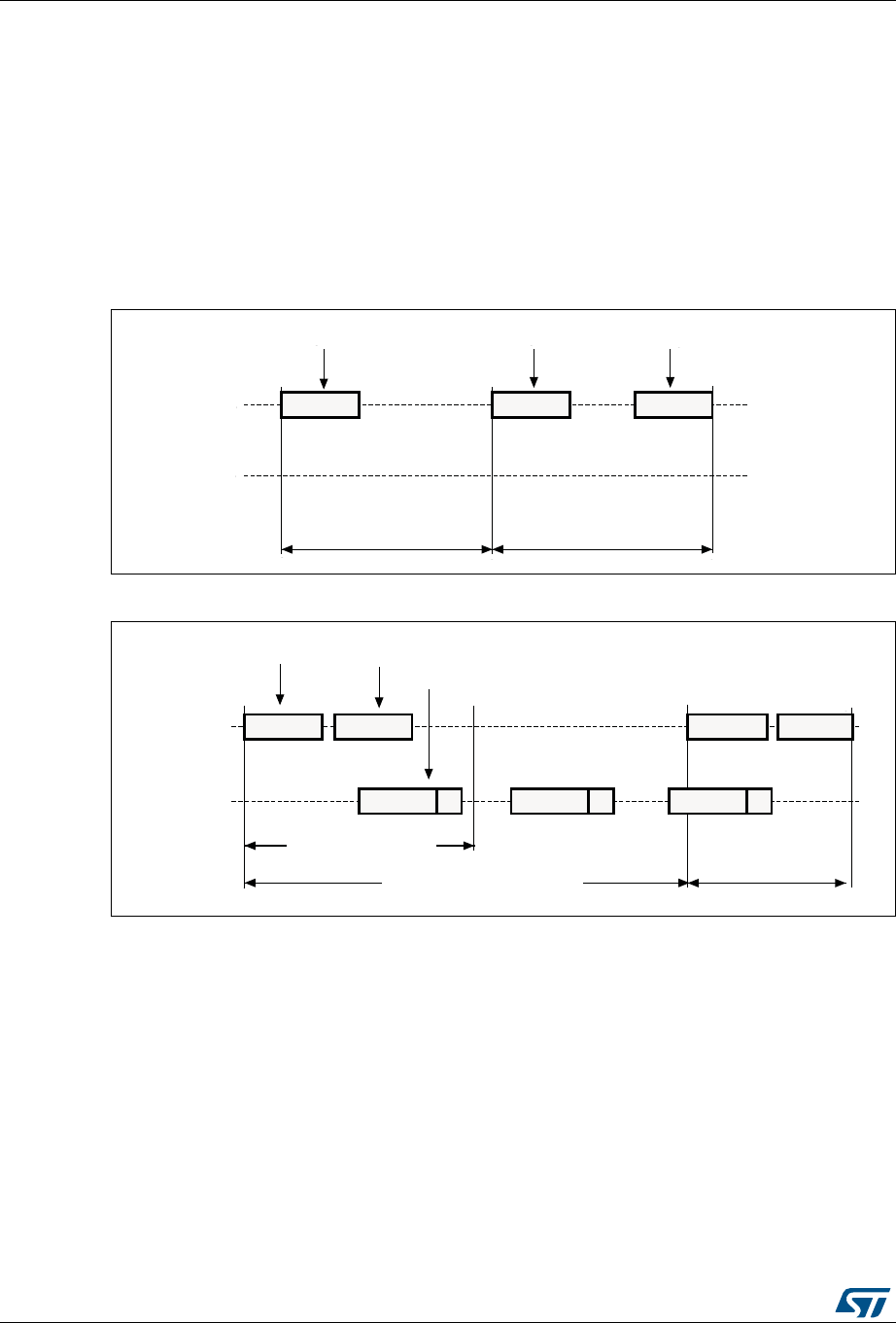
Secure digital input/output interface (SDIO) RM0090
1020/1749 RM0090 Rev 18
31.2 SDIO bus topology
Communication over the bus is based on command and data transfers.
The basic transaction on the MultiMediaCard/SD/SD I/O bus is the command/response
transaction. These types of bus transaction transfer their information directly within the
command or response structure. In addition, some operations have a data token.
Data transfers to/from SD/SDIO memory cards are done in data blocks. Data transfers
to/from MMC are done data blocks or streams. Data transfers to/from the CE-ATA Devices
are done in data blocks.
Figure 321. SDIO “no response” and “no data” operations
Figure 322. SDIO (multiple) block read operation
ai14734b
Operation (no response) Operation (no data)
SDMMC_CMD
SDMMC_D
From host to card(s) From host to card From card to host
ResponseCommand Command
ai14735b
Command Response
Data block crc Data block crc Data block crc
Block read operation
Multiple block read operation Data stop operation
From host to card From card to host
data from card to host Stop command
stops data transfer
Command Response
SDMMC_CMD
SDMMC_D
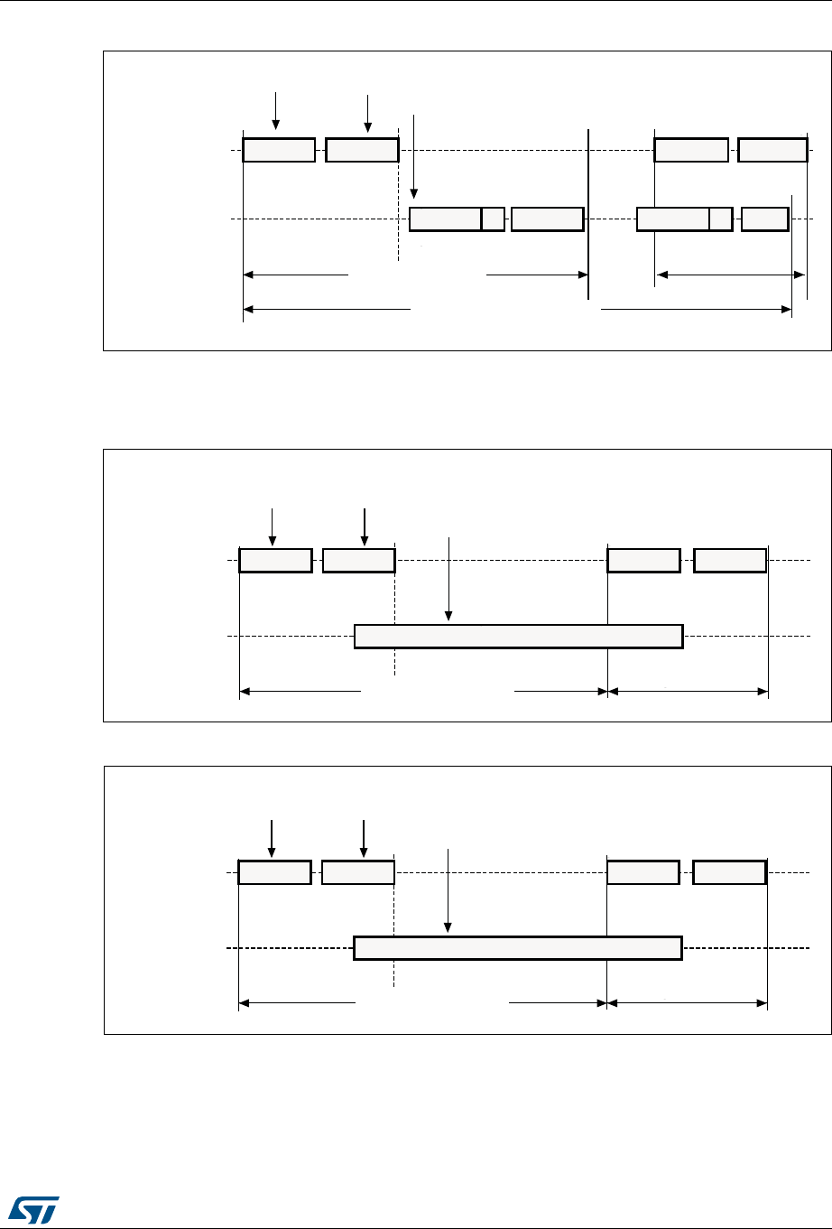
RM0090 Rev 18 1021/1749
RM0090 Secure digital input/output interface (SDIO)
1075
Figure 323. SDIO (multiple) block write operation
Note: The SDIO will not send any data as long as the Busy signal is asserted (SDIO_D0 pulled
low).
Figure 324. SDIO sequential read operation
Figure 325. SDIO sequential write operation
ai14737b
Command Response
Data block crc Data block crc
Data stop operation
From host to card From card to host
data from host to card Stop command
stops data transfer
Command Response
SDMMC_CMD
SDMMC_D Busy
Block write operation
Busy
Multiple block write operation
ai14738b
Data stop operation
From card to host Stop command
stops data transfer
Command Response Command Response
Data stream
Data transfer operation
From host to
card(s)
Data from card to host
SDMMC_CMD
SDMMC_D
ai14739b
Data stop operation
From card to host Stop command
stops data transfer
ResponseCommand ResponseCommand
Data stream
Data transfer operation
From host to
card(s)
Data from host to card
SDMMC_CMD
SDMMC_D
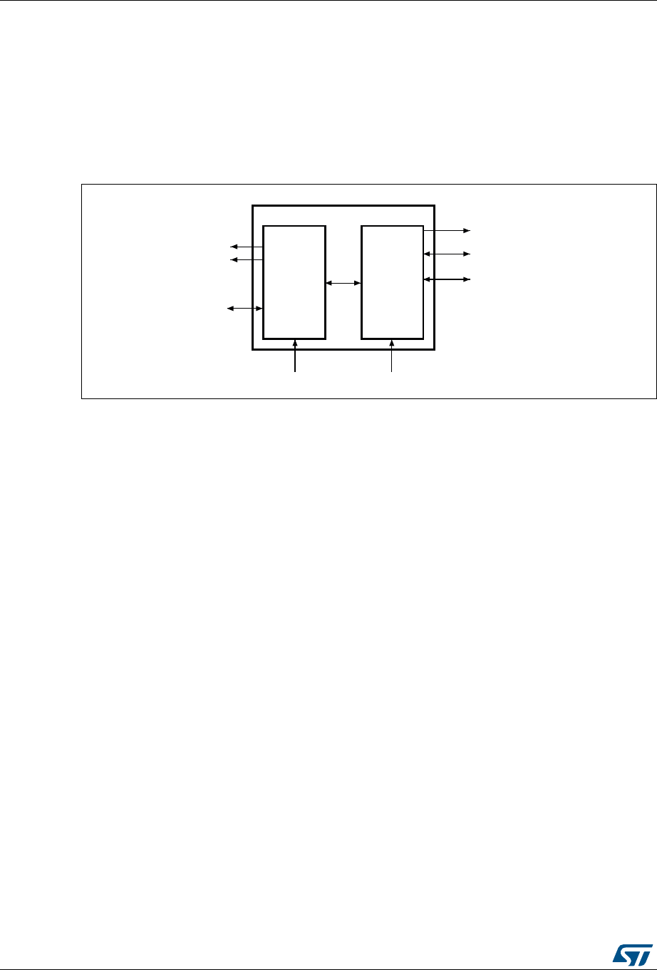
Secure digital input/output interface (SDIO) RM0090
1022/1749 RM0090 Rev 18
31.3 SDIO functional description
The SDIO consists of two parts:
•The SDIO adapter block provides all functions specific to the MMC/SD/SD I/O card
such as the clock generation unit, command and data transfer.
•The APB2 interface accesses the SDIO adapter registers, and generates interrupt and
DMA request signals.
Figure 326. SDIO block diagram
By default SDIO_D0 is used for data transfer. After initialization, the host can change the
databus width.
If a MultiMediaCard is connected to the bus, SDIO_D0, SDIO_D[3:0] or SDIO_D[7:0] can be
used for data transfer. MMC V3.31 or previous, supports only 1 bit of data so only SDIO_D0
can be used.
If an SD or SD I/O card is connected to the bus, data transfer can be configured by the host
to use SDIO_D0 or SDIO_D[3:0]. All data lines are operating in push-pull mode.
SDIO_CMD has two operational modes:
•Open-drain for initialization (only for MMCV3.31 or previous)
•Push-pull for command transfer (SD/SD I/O card MMC4.2 use push-pull drivers also for
initialization)
SDIO_CK is the clock to the card: one bit is transferred on both command and data lines
with each clock cycle.
The SDIO uses two clock signals:
•SDIO adapter clock SDIOCLK up to 50 MHz (48 MHz when in use with USB)
•APB2 bus clock (PCLK2)
PCLK2 and SDIO_CK clock frequencies must respect the following condition:
The signals shown in Table 150 are used on the MultiMediaCard/SD/SD I/O card bus.
ai15898b
APB2 bus
APB2
Interrupts and
PCLK2
SDMMC_CK
interface
DMA request
SDMMCCLK
SDMMC_D[7:0]
SDMMC_CMD
SDMMC
SDMMC
adapter
Frequenc PCLK2()38⁄Frequency SDIO_CK()×≥
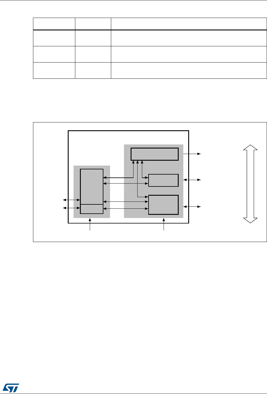
RM0090 Rev 18 1023/1749
RM0090 Secure digital input/output interface (SDIO)
1075
31.3.1 SDIO adapter
Figure 327 shows a simplified block diagram of an SDIO adapter.
Figure 327. SDIO adapter
The SDIO adapter is a multimedia/secure digital memory card bus master that provides an
interface to a multimedia card stack or to a secure digital memory card. It consists of five
subunits:
•Adapter register block
•Control unit
•Command path
•Data path
•Data FIFO
Note: The adapter registers and FIFO use the APB2 bus clock domain (PCLK2). The control unit,
command path and data path use the SDIO adapter clock domain (SDIOCLK).
Adapter register block
The adapter register block contains all system registers. This block also generates the
signals that clear the static flags in the multimedia card. The clear signals are generated
when 1 is written into the corresponding bit location in the SDIO Clear register.
Table 150. SDIO I/O definitions
Pin Direction Description
SDIO_CK Output MultiMediaCard/SD/SDIO card clock. This pin is the clock from
host to card.
SDIO_CMD Bidirectional MultiMediaCard/SD/SDIO card command. This pin is the
bidirectional command/response signal.
SDIO_D[7:0] Bidirectional MultiMediaCard/SD/SDIO card data. These pins are the
bidirectional databus.
ai15899b
To APB2
interface
Control unit
Command
path
Data path
Adapter
registers
SDMMC_CK
SDMMC_CMD
SDMMC_D[7:0]
SDMMC adapter
PCLK2 SDMMCCLK
FIFO
Card bus
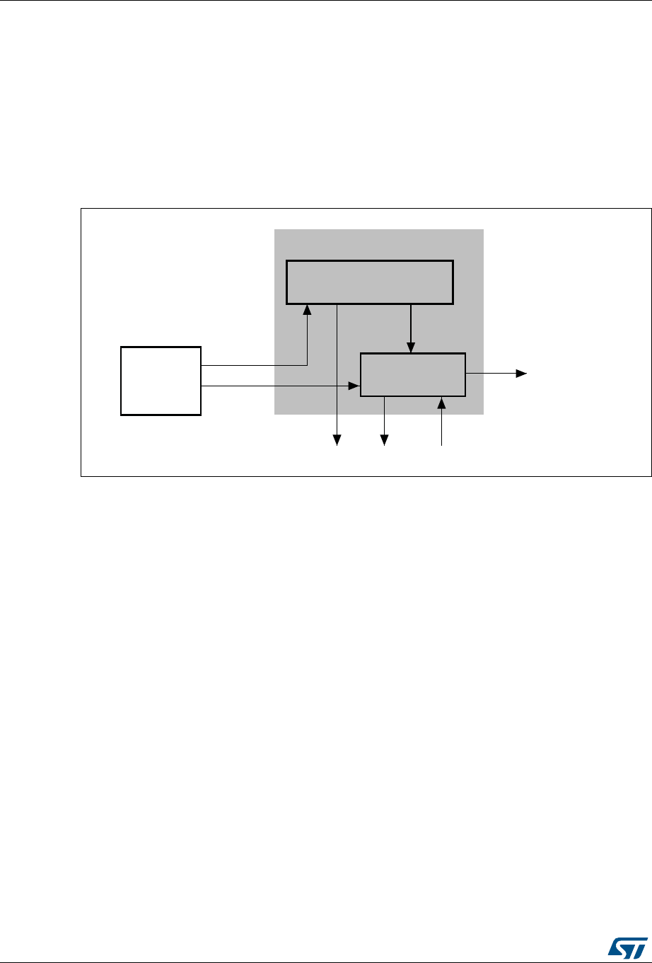
Secure digital input/output interface (SDIO) RM0090
1024/1749 RM0090 Rev 18
Control unit
The control unit contains the power management functions and the clock divider for the
memory card clock.
There are three power phases:
•power-off
•power-up
•power-on
Figure 328. Control unit
The control unit is illustrated in Figure 328. It consists of a power management subunit and
a clock management subunit.
The power management subunit disables the card bus output signals during the power-off
and power-up phases.
The clock management subunit generates and controls the SDIO_CK signal. The SDIO_CK
output can use either the clock divide or the clock bypass mode. The clock output is
inactive:
•after reset
•during the power-off or power-up phases
•if the power saving mode is enabled and the card bus is in the Idle state (eight clock
periods after both the command and data path subunits enter the Idle phase)
ai14804b
Control unit
Power management
Clock management
Adapter
registers
SDMMC_CK
To command and data path
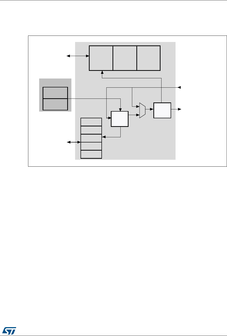
RM0090 Rev 18 1025/1749
RM0090 Secure digital input/output interface (SDIO)
1075
Command path
The command path unit sends commands to and receives responses from the cards.
Figure 329. SDIO adapter command path
•Command path state machine (CPSM)
– When the command register is written to and the enable bit is set, command
transfer starts. When the command has been sent, the command path state
machine (CPSM) sets the status flags and enters the Idle state if a response is not
required. If a response is required, it waits for the response (see Figure 330 on
page 1026). When the response is received, the received CRC code and the
internally generated code are compared, and the appropriate status flags are set.
ai15900b
Adapter registers
CMD
Status
flag
CRC
Shift
register
CMD
To control unit
SDMMC_CMDin
SDMMC_CMDout
To APB2 interface
Control
logic
Command
timer
Argument
Response
registers
Secure digital input/output interface (SDIO) RM0090
1026/1749 RM0090 Rev 18
Figure 330. Command path state machine (CPSM)
When the Wait state is entered, the command timer starts running. If the timeout is reached
before the CPSM moves to the Receive state, the timeout flag is set and the Idle state is
entered.
Note: The command timeout has a fixed value of 64 SDIO_CK clock periods.
If the interrupt bit is set in the command register, the timer is disabled and the CPSM waits
for an interrupt request from one of the cards. If a pending bit is set in the command register,
the CPSM enters the Pend state, and waits for a CmdPend signal from the data path
subunit. When CmdPend is detected, the CPSM moves to the Send state. This enables the
data counter to trigger the stop command transmission.
Note: The CPSM remains in the Idle state for at least eight SDIO_CK periods to meet the NCC and
NRC timing constraints. NCC is the minimum delay between two host commands, and NRC is
the minimum delay between the host command and the card response.
Idle
Pend
Send
Wait
Receive
Last Data
CPSM
disabled
Enabled and
command start CPSM disabled or
no response
Wait for response
Response
started
Response received or
disabled or command
CRC failed
CPSM Disabled or
command timeout
CPSM Enabled and
pending command
ai14806b
Wait_CPL
Response Received in CE-ATA
mode and no interrupt and
wait for CE-ATA Command
Completion signal enabled
Response Received in CE-ATA mode and
no interrupt and wait for CE-ATA
Command Completion signal disabled
CE-ATA Command
Completion signal
received or
CPSM disabled or
Command CRC failed
On reset
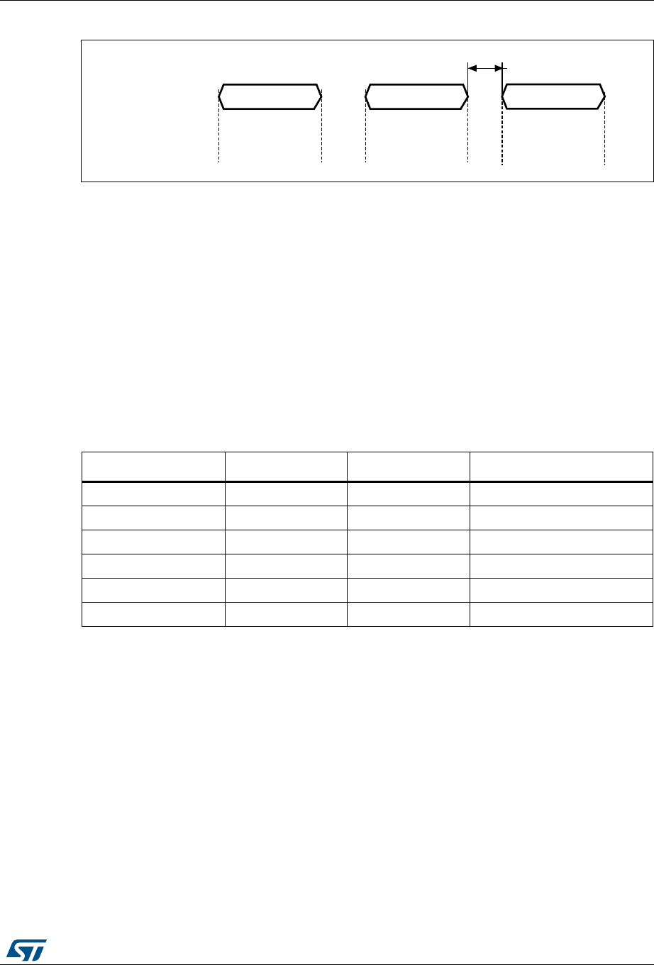
RM0090 Rev 18 1027/1749
RM0090 Secure digital input/output interface (SDIO)
1075
Figure 331. SDIO command transfer
•Command format
– Command: a command is a token that starts an operation. Command are sent
from the host either to a single card (addressed command) or to all connected
cards (broadcast command are available for MMC V3.31 or previous). Commands
are transferred serially on the CMD line. All commands have a fixed length of 48
bits. The general format for a command token for MultiMediaCards, SD-Memory
cards and SDIO-Cards is shown in Table 151. CE-ATA commands are an
extension of MMC commands V4.2, and so have the same format.
The command path operates in a half-duplex mode, so that commands and
responses can either be sent or received. If the CPSM is not in the Send state, the
SDIO_CMD output is in the Hi-Z state, as shown in Figure 331 on page 1027.
Data on SDIO_CMD are synchronous with the rising edge of SDIO_CK. Table
shows the command format.
– Response: a response is a token that is sent from an addressed card (or
synchronously from all connected cards for MMC V3.31 or previous), to the host
as an answer to a previously received command. Responses are transferred
serially on the CMD line.
The SDIO supports two response types. Both use CRC error checking:
•48 bit short response
•136 bit long response
Note: If the response does not contain a CRC (CMD1 response), the device driver must ignore the
CRC failed status.
Table 151. Command format
Bit position Width Value Description
47 1 0 Start bit
46 1 1 Transmission bit
[45:40] 6 - Command index
[39:8] 32 - Argument
[7:1] 7 - CRC7
011End bit
ai14807b
SDMMC_CK
SDMMC_CMD
Command Response Command
State Idle Send Wait Receive Idle Send
Hi-Z Controller drives Hi-Z Card drives Hi-Z Controller drives
at least 8 SDMMC_CK
cycles

Secure digital input/output interface (SDIO) RM0090
1028/1749 RM0090 Rev 18
The command register contains the command index (six bits sent to a card) and the
command type. These determine whether the command requires a response, and whether
the response is 48 or 136 bits long (see Section 31.9.4 on page 1062). The command path
implements the status flags shown in Table 154:
The CRC generator calculates the CRC checksum for all bits before the CRC code. This
includes the start bit, transmitter bit, command index, and command argument (or card
status). The CRC checksum is calculated for the first 120 bits of CID or CSD for the long
response format. Note that the start bit, transmitter bit and the six reserved bits are not used
in the CRC calculation.
The CRC checksum is a 7-bit value:
CRC[6:0] = Remainder [(M(x) * x7) / G(x)]
G(x) = x7 + x3 + 1
M(x) = (start bit) * x39 + ... + (last bit before CRC) * x0, or
M(x) = (start bit) * x119 + ... + (last bit before CRC) * x0
Table 152. Short response format
Bit position Width Value Description
47 1 0 Start bit
46 1 0 Transmission bit
[45:40] 6 - Command index
[39:8] 32 - Argument
[7:1] 7 - CRC7(or 1111111)
011End bit
Table 153. Long response format
Bit position Width Value Description
135 1 0 Start bit
134 1 0 Transmission bit
[133:128] 6 111111 Reserved
[127:1] 127 - CID or CSD (including internal CRC7)
0 1 1 End bit
Table 154. Command path status flags
Flag Description
CMDREND Set if response CRC is OK.
CCRCFAIL Set if response CRC fails.
CMDSENT Set when command (that does not require response) is sent
CTIMEOUT Response timeout.
CMDACT Command transfer in progress.
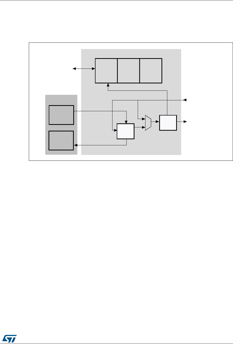
RM0090 Rev 18 1029/1749
RM0090 Secure digital input/output interface (SDIO)
1075
Data path
The data path subunit transfers data to and from cards. Figure 332 shows a block diagram
of the data path.
Figure 332. Data path
The card databus width can be programmed using the clock control register. If the 4-bit wide
bus mode is enabled, data is transferred at four bits per clock cycle over all four data signals
(SDIO_D[3:0]). If the 8-bit wide bus mode is enabled, data is transferred at eight bits per
clock cycle over all eight data signals (SDIO_D[7:0]). If the wide bus mode is not enabled,
only one bit per clock cycle is transferred over SDIO_D0.
Depending on the transfer direction (send or receive), the data path state machine (DPSM)
moves to the Wait_S or Wait_R state when it is enabled:
•Send: the DPSM moves to the Wait_S state. If there is data in the transmit FIFO, the
DPSM moves to the Send state, and the data path subunit starts sending data to a
card.
•Receive: the DPSM moves to the Wait_R state and waits for a start bit. When it
receives a start bit, the DPSM moves to the Receive state, and the data path subunit
starts receiving data from a card.
Data path state machine (DPSM)
The DPSM operates at SDIO_CK frequency. Data on the card bus signals is synchronous to
the rising edge of SDIO_CK. The DPSM has six states, as shown in Figure 333: Data path
state machine (DPSM).
ai14808b
Data path
Data FIFO
Transmit
Status
flag
CRC
Shift
register
To control unit
SDMMC_Din[7:0]
SDMMC_Dout[7:0]
Receive
Control
logic
Data
timer
Secure digital input/output interface (SDIO) RM0090
1030/1749 RM0090 Rev 18
Figure 333. Data path state machine (DPSM)
•Idle: the data path is inactive, and the SDIO_D[7:0] outputs are in Hi-Z. When the data
control register is written and the enable bit is set, the DPSM loads the data counter
with a new value and, depending on the data direction bit, moves to either the Wait_S
or the Wait_R state.
•Wait_R: if the data counter equals zero, the DPSM moves to the Idle state when the
receive FIFO is empty. If the data counter is not zero, the DPSM waits for a start bit on
SDIO_D. The DPSM moves to the Receive state if it receives a start bit before a
timeout, and loads the data block counter. If it reaches a timeout before it detects a
start bit, or a start bit error occurs, it moves to the Idle state and sets the timeout status
flag.
•Receive: serial data received from a card is packed in bytes and written to the data
FIFO. Depending on the transfer mode bit in the data control register, the data transfer
mode can be either block or stream:
– In block mode, when the data block counter reaches zero, the DPSM waits until it
receives the CRC code. If the received code matches the internally generated
Idle
Busy
Send
Wait_R
Receive
End of packet
Disabled or CRC fail
or timeout
Not busy
Disabled or
end of data
Data ready
End of packet or
end of data or
FIFO overrun
Enable and not send
Disabled or
Rx FIFO empty or timeout or
start bit error
Disabled or FIFO underrun or
end of data or CRC fail
ai1480
9b
Wait_S
Start bit
On reset
Disabled or CRC fail
Enable and send
DPSM disabled
Read Wait
DPSM enabled and
Read Wait Started
and SD I/O mode enabled
ReadWait Stop
Data received and
Read Wait Started a
nd
SD I/O mode enabl
ed

RM0090 Rev 18 1031/1749
RM0090 Secure digital input/output interface (SDIO)
1075
CRC code, the DPSM moves to the Wait_R state. If not, the CRC fail status flag is
set and the DPSM moves to the Idle state.
– In stream mode, the DPSM receives data while the data counter is not zero. When
the counter is zero, the remaining data in the shift register is written to the data
FIFO, and the DPSM moves to the Wait_R state.
If a FIFO overrun error occurs, the DPSM sets the FIFO error flag and moves to the
Idle state:
•Wait_S: the DPSM moves to the Idle state if the data counter is zero. If not, it waits until
the data FIFO empty flag is deasserted, and moves to the Send state.
Note: The DPSM remains in the Wait_S state for at least two clock periods to meet the NWR timing
requirements, where NWR is the number of clock cycles between the reception of the card
response and the start of the data transfer from the host.
•Send: the DPSM starts sending data to a card. Depending on the transfer mode bit in
the data control register, the data transfer mode can be either block or stream:
– In block mode, when the data block counter reaches zero, the DPSM sends an
internally generated CRC code and end bit, and moves to the Busy state.
– In stream mode, the DPSM sends data to a card while the enable bit is high and
the data counter is not zero. It then moves to the Idle state.
If a FIFO underrun error occurs, the DPSM sets the FIFO error flag and moves to the
Idle state.
•Busy: the DPSM waits for the CRC status flag:
– If it does not receive a positive CRC status, it moves to the Idle state and sets the
CRC fail status flag.
– If it receives a positive CRC status, it moves to the Wait_S state if SDIO_D0 is not
low (the card is not busy).
If a timeout occurs while the DPSM is in the Busy state, it sets the data timeout flag and
moves to the Idle state.
The data timer is enabled when the DPSM is in the Wait_R or Busy state, and
generates the data timeout error:
– When transmitting data, the timeout occurs if the DPSM stays in the Busy state for
longer than the programmed timeout period
– When receiving data, the timeout occurs if the end of the data is not true, and if the
DPSM stays in the Wait_R state for longer than the programmed timeout period.
•Data: data can be transferred from the card to the host or vice versa. Data is
transferred via the data lines. They are stored in a FIFO of 32 words, each word is 32
bits wide.
Table 155. Data token format
Description Start bit Data CRC16 End bit
Block Data 0 - yes 1
Stream Data 0 - no 1

Secure digital input/output interface (SDIO) RM0090
1032/1749 RM0090 Rev 18
Data FIFO
The data FIFO (first-in-first-out) subunit is a data buffer with a transmit and receive unit.
The FIFO contains a 32-bit wide, 32-word deep data buffer, and transmit and receive logic.
Because the data FIFO operates in the APB2 clock domain (PCLK2), all signals from the
subunits in the SDIO clock domain (SDIOCLK) are resynchronized.
Depending on the TXACT and RXACT flags, the FIFO can be disabled, transmit enabled, or
receive enabled. TXACT and RXACT are driven by the data path subunit and are mutually
exclusive:
– The transmit FIFO refers to the transmit logic and data buffer when TXACT is
asserted
– The receive FIFO refers to the receive logic and data buffer when RXACT is
asserted
•Transmit FIFO:
Data can be written to the transmit FIFO through the APB2 interface when the SDIO is
enabled for transmission.
The transmit FIFO is accessible via 32 sequential addresses. The transmit FIFO
contains a data output register that holds the data word pointed to by the read pointer.
When the data path subunit has loaded its shift register, it increments the read pointer
and drives new data out.
If the transmit FIFO is disabled, all status flags are deasserted. The data path subunit
asserts TXACT when it transmits data.
•Receive FIFO
When the data path subunit receives a word of data, it drives the data on the write
databus. The write pointer is incremented after the write operation completes. On the
read side, the contents of the FIFO word pointed to by the current value of the read
pointer is driven onto the read databus. If the receive FIFO is disabled, all status flags
are deasserted, and the read and write pointers are reset. The data path subunit
asserts RXACT when it receives data. Table 157 lists the receive FIFO status flags.
The receive FIFO is accessible via 32 sequential addresses.
Table 156. Transmit FIFO status flags
Flag Description
TXFIFOF Set to high when all 32 transmit FIFO words contain valid data.
TXFIFOE Set to high when the transmit FIFO does not contain valid data.
TXFIFOHE Set to high when 8 or more transmit FIFO words are empty. This flag can be used
as a DMA request.
TXDAVL Set to high when the transmit FIFO contains valid data. This flag is the inverse of
the TXFIFOE flag.
TXUNDERR Set to high when an underrun error occurs. This flag is cleared by writing to the
SDIO Clear register.

RM0090 Rev 18 1033/1749
RM0090 Secure digital input/output interface (SDIO)
1075
31.3.2 SDIO APB2 interface
The APB2 interface generates the interrupt and DMA requests, and accesses the SDIO
adapter registers and the data FIFO. It consists of a data path, register decoder, and
interrupt/DMA logic.
SDIO interrupts
The interrupt logic generates an interrupt request signal that is asserted when at least one
of the selected status flags is high. A mask register is provided to allow selection of the
conditions that will generate an interrupt. A status flag generates the interrupt request if a
corresponding mask flag is set.
SDIO/DMA interface - procedure for data transfers between the SDIO and
memory
In the example shown, the transfer is from the SDIO host controller to an MMC (512 bytes
using CMD24 (WRITE_BLOCK). The SDIO FIFO is filled by data stored in a memory using
the DMA controller.
1. Do the card identification process
2. Increase the SDIO_CK frequency
3. Select the card by sending CMD7
4. Configure the DMA2 as follows:
a) Enable DMA2 controller and clear any pending interrupts.
b) Program the DMA2_Stream3 or DMA2_Stream6 Channel4 source address
register with the memory location’s base address and DMA2_Stream3 or
Table 157. Receive FIFO status flags
Flag Description
RXFIFOF Set to high when all 32 receive FIFO words contain valid data
RXFIFOE Set to high when the receive FIFO does not contain valid data.
RXFIFOHF Set to high when 8 or more receive FIFO words contain valid data. This flag can be
used as a DMA request.
RXDAVL Set to high when the receive FIFO is not empty. This flag is the inverse of the
RXFIFOE flag.
RXOVERR Set to high when an overrun error occurs. This flag is cleared by writing to the SDIO
Clear register.

Secure digital input/output interface (SDIO) RM0090
1034/1749 RM0090 Rev 18
DMA2_Stream6 Channel4 destination address register with the SDIO_FIFO
register address.
c) Program DMA2_Stream3 or DMA2_Stream6 Channel4 control register (memory
increment, not peripheral increment, peripheral and source width is word size).
d) Program DMA2_Stream3 or DMA2_Stream6 Channel4 to select the peripheral as
flow controller (set PFCTRL bit in DMA_S3CR or DMA_S6CR configuration
register).
e) Configure the incremental burst transfer to 4 beats (at least from peripheral side)
in DMA2_Stream3 or DMA2_Stream6 Channel4.
f) Enable DMA2_Stream3 or DMA2_Stream6 Channel4
5. Send CMD24 (WRITE_BLOCK) as follows:
a) Program the SDIO data length register (SDIO data timer register should be
already programmed before the card identification process).
b) Program the SDIO argument register with the address location of the card where
data is to be transferred.
c) Program the SDIO command register: CmdIndex with 24 (WRITE_BLOCK);
WaitResp with ‘1’ (SDIO card host waits for a response); CPSMEN with ‘1’ (SDIO
card host enabled to send a command). Other fields are at their reset value.
d) Wait for SDIO_STA[6] = CMDREND interrupt, then program the SDIO data control
register: DTEN with ‘1’ (SDIO card host enabled to send data); DTDIR with ‘0’
(from controller to card); DTMODE with ‘0’ (block data transfer); DMAEN with ‘1’
(DMA enabled); DBLOCKSIZE with 0x9 (512 bytes). Other fields are don’t care.
e) Wait for SDIO_STA[10] = DBCKEND.
6. Check that no channels are still enabled by polling the DMA Enabled Channel Status
register.
31.4 Card functional description
31.4.1 Card identification mode
While in card identification mode the host resets all cards, validates the operation voltage
range, identifies cards and sets a relative card address (RCA) for each card on the bus. All
data communications in the card identification mode use the command line (CMD) only.
31.4.2 Card reset
The GO_IDLE_STATE command (CMD0) is the software reset command and it puts the
MultiMediaCard and SD memory in the Idle state. The IO_RW_DIRECT command (CMD52)
resets the SD I/O card. After power-up or CMD0, all cards output bus drivers are in the high-
impedance state and the cards are initialized with a default relative card address
(RCA=0x0001) and with a default driver stage register setting (lowest speed, highest driving
current capability).
31.4.3 Operating voltage range validation
All cards can communicate with the SDIO card host using any operating voltage within the
specification range. The supported minimum and maximum VDD values are defined in the
operation conditions register (OCR) on the card.

RM0090 Rev 18 1035/1749
RM0090 Secure digital input/output interface (SDIO)
1075
Cards that store the card identification number (CID) and card specific data (CSD) in the
payload memory are able to communicate this information only under data-transfer VDD
conditions. When the SDIO card host module and the card have incompatible VDD ranges,
the card is not able to complete the identification cycle and cannot send CSD data. For this
purpose, the special commands, SEND_OP_COND (CMD1), SD_APP_OP_COND (ACMD41
for SD Memory), and IO_SEND_OP_COND (CMD5 for SD I/O), are designed to provide a
mechanism to identify and reject cards that do not match the VDD range desired by the
SDIO card host. The SDIO card host sends the required VDD voltage window as the
operand of these commands. Cards that cannot perform data transfer in the specified range
disconnect from the bus and go to the inactive state.
By using these commands without including the voltage range as the operand, the SDIO
card host can query each card and determine the common voltage range before placing out-
of-range cards in the inactive state. This query is used when the SDIO card host is able to
select a common voltage range or when the user requires notification that cards are not
usable.
31.4.4 Card identification process
The card identification process differs for MultiMediaCards and SD cards. For
MultiMediaCard cards, the identification process starts at clock rate Fod. The SDIO_CMD
line output drivers are open-drain and allow parallel card operation during this process. The
registration process is accomplished as follows:
1. The bus is activated.
2. The SDIO card host broadcasts SEND_OP_COND (CMD1) to receive operation
conditions.
3. The response is the wired AND operation of the operation condition registers from all
cards.
4. Incompatible cards are placed in the inactive state.
5. The SDIO card host broadcasts ALL_SEND_CID (CMD2) to all active cards.
6. The active cards simultaneously send their CID numbers serially. Cards with outgoing
CID bits that do not match the bits on the command line stop transmitting and must wait
for the next identification cycle. One card successfully transmits a full CID to the SDIO
card host and enters the Identification state.
7. The SDIO card host issues SET_RELATIVE_ADDR (CMD3) to that card. This new
address is called the relative card address (RCA); it is shorter than the CID and
addresses the card. The assigned card changes to the Standby state, it does not react
to further identification cycles, and its output switches from open-drain to push-pull.
8. The SDIO card host repeats steps 5 through 7 until it receives a timeout condition.
For the SD card, the identification process starts at clock rate Fod, and the SDIO_CMD line
output drives are push-pull drivers instead of open-drain. The registration process is
accomplished as follows:

Secure digital input/output interface (SDIO) RM0090
1036/1749 RM0090 Rev 18
1. The bus is activated.
2. The SDIO card host broadcasts SD_APP_OP_COND (ACMD41).
3. The cards respond with the contents of their operation condition registers.
4. The incompatible cards are placed in the inactive state.
5. The SDIO card host broadcasts ALL_SEND_CID (CMD2) to all active cards.
6. The cards send back their unique card identification numbers (CIDs) and enter the
Identification state.
7. The SDIO card host issues SET_RELATIVE_ADDR (CMD3) to an active card with an
address. This new address is called the relative card address (RCA); it is shorter than
the CID and addresses the card. The assigned card changes to the Standby state. The
SDIO card host can reissue this command to change the RCA. The RCA of the card is
the last assigned value.
8. The SDIO card host repeats steps 5 through 7 with all active cards.
For the SD I/O card, the registration process is accomplished as follows:
1. The bus is activated.
2. The SDIO card host sends IO_SEND_OP_COND (CMD5).
3. The cards respond with the contents of their operation condition registers.
4. The incompatible cards are set to the inactive state.
5. The SDIO card host issues SET_RELATIVE_ADDR (CMD3) to an active card with an
address. This new address is called the relative card address (RCA); it is shorter than
the CID and addresses the card. The assigned card changes to the Standby state. The
SDIO card host can reissue this command to change the RCA. The RCA of the card is
the last assigned value.
31.4.5 Block write
During block write (CMD24 - 27) one or more blocks of data are transferred from the host to
the card with a CRC appended to the end of each block by the host. A card supporting block
write is always able to accept a block of data defined by WRITE_BL_LEN. If the CRC fails,
the card indicates the failure on the SDIO_D line and the transferred data are discarded and
not written, and all further transmitted blocks (in multiple block write mode) are ignored.
If the host uses partial blocks whose accumulated length is not block aligned and, block
misalignment is not allowed (CSD parameter WRITE_BLK_MISALIGN is not set), the card
will detect the block misalignment error before the beginning of the first misaligned block.
(ADDRESS_ERROR error bit is set in the status register). The write operation will also be
aborted if the host tries to write over a write-protected area. In this case, however, the card
will set the WP_VIOLATION bit.
Programming of the CID and CSD registers does not require a previous block length setting.
The transferred data is also CRC protected. If a part of the CSD or CID register is stored in
ROM, then this unchangeable part must match the corresponding part of the receive buffer.
If this match fails, then the card reports an error and does not change any register contents.
Some cards may require long and unpredictable times to write a block of data. After
receiving a block of data and completing the CRC check, the card begins writing and holds
the SDIO_D line low if its write buffer is full and unable to accept new data from a new
WRITE_BLOCK command. The host may poll the status of the card with a SEND_STATUS
command (CMD13) at any time, and the card will respond with its status. The
READY_FOR_DATA status bit indicates whether the card can accept new data or whether
the write process is still in progress. The host may deselect the card by issuing CMD7 (to

RM0090 Rev 18 1037/1749
RM0090 Secure digital input/output interface (SDIO)
1075
select a different card), which will place the card in the Disconnect state and release the
SDIO_D line(s) without interrupting the write operation. When selecting the card again, it will
reactivate busy indication by pulling SDIO_D to low if programming is still in progress and
the write buffer is unavailable.
31.4.6 Block read
In Block read mode the basic unit of data transfer is a block whose maximum size is defined
in the CSD (READ_BL_LEN). If READ_BL_PARTIAL is set, smaller blocks whose start and
end addresses are entirely contained within one physical block (as defined by
READ_BL_LEN) may also be transmitted. A CRC is appended to the end of each block,
ensuring data transfer integrity. CMD17 (READ_SINGLE_BLOCK) initiates a block read and
after completing the transfer, the card returns to the Transfer state.
CMD18 (READ_MULTIPLE_BLOCK) starts a transfer of several consecutive blocks.
The host can abort reading at any time, within a multiple block operation, regardless of its
type. Transaction abort is done by sending the stop transmission command.
If the card detects an error (for example, out of range, address misalignment or internal
error) during a multiple block read operation (both types) it stops the data transmission and
remains in the data state. The host must than abort the operation by sending the stop
transmission command. The read error is reported in the response to the stop transmission
command.
If the host sends a stop transmission command after the card transmits the last block of a
multiple block operation with a predefined number of blocks, it is responded to as an illegal
command, since the card is no longer in the data state. If the host uses partial blocks whose
accumulated length is not block-aligned and block misalignment is not allowed, the card
detects a block misalignment error condition at the beginning of the first misaligned block
(ADDRESS_ERROR error bit is set in the status register).
31.4.7 Stream access, stream write and stream read
(MultiMediaCard only)
In stream mode, data is transferred in bytes and no CRC is appended at the end of each
block.
Stream write (MultiMediaCard only)
WRITE_DAT_UNTIL_STOP (CMD20) starts the data transfer from the SDIO card host to the
card, beginning at the specified address and continuing until the SDIO card host issues a
stop command. When partial blocks are allowed (CSD parameter WRITE_BL_PARTIAL is
set), the data stream can start and stop at any address within the card address space,
otherwise it can only start and stop at block boundaries. Because the amount of data to be
transferred is not determined in advance, a CRC cannot be used. When the end of the
memory range is reached while sending data and no stop command is sent by the SD card
host, any additional transferred data are discarded.

Secure digital input/output interface (SDIO) RM0090
1038/1749 RM0090 Rev 18
The maximum clock frequency for a stream write operation is given by the following
equation fields of the card-specific data register:
•Maximumspeed = maximum write frequency
•TRANSPEED = maximum data transfer rate
•writebllen = maximum write data block length
•NSAC = data read access time 2 in CLK cycles
•TAAC = data read access time 1
•R2WFACTOR = write speed factor
If the host attempts to use a higher frequency, the card may not be able to process the data
and stop programming, set the OVERRUN error bit in the status register, and while ignoring
all further data transfer, wait (in the receive data state) for a stop command. The write
operation is also aborted if the host tries to write over a write-protected area. In this case,
however, the card sets the WP_VIOLATION bit.
Stream read (MultiMediaCard only)
READ_DAT_UNTIL_STOP (CMD11) controls a stream-oriented data transfer.
This command instructs the card to send its data, starting at a specified address, until the
SDIO card host sends STOP_TRANSMISSION (CMD12). The stop command has an
execution delay due to the serial command transmission and the data transfer stops after
the end bit of the stop command. When the end of the memory range is reached while
sending data and no stop command is sent by the SDIO card host, any subsequent data
sent are considered undefined.
The maximum clock frequency for a stream read operation is given by the following
equation and uses fields of the card specific data register.
•Maximumspeed = maximum read frequency
•TRANSPEED = maximum data transfer rate
•readbllen = maximum read data block length
•writebllen = maximum write data block length
•NSAC = data read access time 2 in CLK cycles
•TAAC = data read access time 1
•R2WFACTOR = write speed factor
If the host attempts to use a higher frequency, the card is not able to sustain data transfer. If
this happens, the card sets the UNDERRUN error bit in the status register, aborts the
transmission and waits in the data state for a stop command.
Maximumspeed MIN TRANSPEED 82
writebllen
×()NSAC–()
TAAC R2WFACTOR×
-------------------------------------------------------------------------(, )=
Maximumspeed MIN TRANSPEED 82
readbllen
×()NSAC–()
TAAC R2WFACTOR×
------------------------------------------------------------------------(, )=

RM0090 Rev 18 1039/1749
RM0090 Secure digital input/output interface (SDIO)
1075
31.4.8 Erase: group erase and sector erase
The erasable unit of the MultiMediaCard is the erase group. The erase group is measured in
write blocks, which are the basic writable units of the card. The size of the erase group is a
card-specific parameter and defined in the CSD.
The host can erase a contiguous range of Erase Groups. Starting the erase process is a
three-step sequence.
First the host defines the start address of the range using the ERASE_GROUP_START
(CMD35) command, next it defines the last address of the range using the
ERASE_GROUP_END (CMD36) command and, finally, it starts the erase process by issuing
the ERASE (CMD38) command. The address field in the erase commands is an Erase
Group address in byte units. The card ignores all LSBs below the Erase Group size,
effectively rounding the address down to the Erase Group boundary.
If an erase command is received out of sequence, the card sets the ERASE_SEQ_ERROR
bit in the status register and resets the whole sequence.
If an out-of-sequence (neither of the erase commands, except SEND_STATUS) command
received, the card sets the ERASE_RESET status bit in the status register, resets the erase
sequence and executes the last command.
If the erase range includes write protected blocks, they are left intact and only unprotected
blocks are erased. The WP_ERASE_SKIP status bit in the status register is set.
The card indicates that an erase is in progress by holding SDIO_D low. The actual erase
time may be quite long, and the host may issue CMD7 to deselect the card.
31.4.9 Wide bus selection or deselection
Wide bus (4-bit bus width) operation mode is selected or deselected using
SET_BUS_WIDTH (ACMD6). The default bus width after power-up or GO_IDLE_STATE
(CMD0) is 1 bit. SET_BUS_WIDTH (ACMD6) is only valid in a transfer state, which means
that the bus width can be changed only after a card is selected by
SELECT/DESELECT_CARD (CMD7).
31.4.10 Protection management
Three write protection methods for the cards are supported in the SDIO card host module:
1. internal card write protection (card responsibility)
2. mechanical write protection switch (SDIO card host module responsibility only)
3. password-protected card lock operation
Internal card write protection
Card data can be protected against write and erase. By setting the permanent or temporary
write-protect bits in the CSD, the entire card can be permanently write-protected by the
manufacturer or content provider. For cards that support write protection of groups of
sectors by setting the WP_GRP_ENABLE bit in the CSD, portions of the data can be
protected, and the write protection can be changed by the application. The write protection
is in units of WP_GRP_SIZE sectors as specified in the CSD. The SET_WRITE_PROT and
CLR_WRITE_PROT commands control the protection of the addressed group. The
SEND_WRITE_PROT command is similar to a single block read command. The card sends
a data block containing 32 write protection bits (representing 32 write protect groups starting

Secure digital input/output interface (SDIO) RM0090
1040/1749 RM0090 Rev 18
at the specified address) followed by 16 CRC bits. The address field in the write protect
commands is a group address in byte units.
The card ignores all LSBs below the group size.
Mechanical write protect switch
A mechanical sliding tab on the side of the card allows the user to set or clear the write
protection on a card. When the sliding tab is positioned with the window open, the card is
write-protected, and when the window is closed, the card contents can be changed. A
matched switch on the socket side indicates to the SDIO card host module that the card is
write-protected. The SDIO card host module is responsible for protecting the card. The
position of the write protect switch is unknown to the internal circuitry of the card.
Password protect
The password protection feature enables the SDIO card host module to lock and unlock a
card with a password. The password is stored in the 128-bit PWD register and its size is set
in the 8-bit PWD_LEN register. These registers are nonvolatile so that a power cycle does
not erase them. Locked cards respond to and execute certain commands. This means that
the SDIO card host module is allowed to reset, initialize, select, and query for status,
however it is not allowed to access data on the card. When the password is set (as indicated
by a nonzero value of PWD_LEN), the card is locked automatically after power-up. As with
the CSD and CID register write commands, the lock/unlock commands are available in the
transfer state only. In this state, the command does not include an address argument and
the card must be selected before using it. The card lock/unlock commands have the
structure and bus transaction types of a regular single-block write command. The
transferred data block includes all of the required information for the command (the
password setting mode, the PWD itself, and card lock/unlock). The command data block
size is defined by the SDIO card host module before it sends the card lock/unlock
command, and has the structure shown in Table 171.
The bit settings are as follows:
•ERASE: setting it forces an erase operation. All other bits must be zero, and only the
command byte is sent
•LOCK_UNLOCK: setting it locks the card. LOCK_UNLOCK can be set simultaneously
with SET_PWD, however not with CLR_PWD
•CLR_PWD: setting it clears the password data
•SET_PWD: setting it saves the password data to memory
•PWD_LEN: it defines the length of the password in bytes
•PWD: the password (new or currently used, depending on the command)
The following sections list the command sequences to set/reset a password, lock/unlock the
card, and force an erase.
Setting the password
1. Select a card (SELECT/DESELECT_CARD, CMD7), if none is already selected.
2. Define the block length (SET_BLOCKLEN, CMD16) to send, given by the 8-bit card
lock/unlock mode, the 8-bit PWD_LEN, and the number of bytes of the new password.

RM0090 Rev 18 1041/1749
RM0090 Secure digital input/output interface (SDIO)
1075
When a password replacement is done, the block size must take into account that both
the old and the new passwords are sent with the command.
3. Send LOCK/UNLOCK (CMD42) with the appropriate data block size on the data line
including the 16-bit CRC. The data block indicates the mode (SET_PWD = 1), the
length (PWD_LEN), and the password (PWD) itself. When a password replacement is
done, the length value (PWD_LEN) includes the length of both passwords, the old and
the new one, and the PWD field includes the old password (currently used) followed by
the new password.
4. When the password is matched, the new password and its size are saved into the PWD
and PWD_LEN fields, respectively. When the old password sent does not correspond
(in size and/or content) to the expected password, the LOCK_UNLOCK_FAILED error
bit is set in the card status register, and the password is not changed.
The password length field (PWD_LEN) indicates whether a password is currently set. When
this field is nonzero, there is a password set and the card locks itself after power-up. It is
possible to lock the card immediately in the current power session by setting the
LOCK_UNLOCK bit (while setting the password) or sending an additional command for card
locking.
Resetting the password
1. Select a card (SELECT/DESELECT_CARD, CMD7), if none is already selected.
2. Define the block length (SET_BLOCKLEN, CMD16) to send, given by the 8-bit card
lock/unlock mode, the 8-bit PWD_LEN, and the number of bytes in the currently used
password.
3. Send LOCK/UNLOCK (CMD42) with the appropriate data block size on the data line
including the 16-bit CRC. The data block indicates the mode (CLR_PWD = 1), the
length (PWD_LEN) and the password (PWD) itself. The LOCK_UNLOCK bit is ignored.
4. When the password is matched, the PWD field is cleared and PWD_LEN is set to 0.
When the password sent does not correspond (in size and/or content) to the expected
password, the LOCK_UNLOCK_FAILED error bit is set in the card status register, and
the password is not changed.
Locking a card
1. Select a card (SELECT/DESELECT_CARD, CMD7), if none is already selected.
2. Define the block length (SET_BLOCKLEN, CMD16) to send, given by the 8-bit card
lock/unlock mode (byte 0 in Table 171), the 8-bit PWD_LEN, and the number of bytes
of the current password.
3. Send LOCK/UNLOCK (CMD42) with the appropriate data block size on the data line
including the 16-bit CRC. The data block indicates the mode (LOCK_UNLOCK = 1), the
length (PWD_LEN), and the password (PWD) itself.
4. When the password is matched, the card is locked and the CARD_IS_LOCKED status
bit is set in the card status register. When the password sent does not correspond (in
size and/or content) to the expected password, the LOCK_UNLOCK_FAILED error bit
is set in the card status register, and the lock fails.
It is possible to set the password and to lock the card in the same sequence. In this case,
the SDIO card host module performs all the required steps for setting the password (see
Setting the password on page 1040), however it is necessary to set the LOCK_UNLOCK bit
in Step 3 when the new password command is sent.

Secure digital input/output interface (SDIO) RM0090
1042/1749 RM0090 Rev 18
When the password is previously set (PWD_LEN is not 0), the card is locked automatically
after power-on reset. An attempt to lock a locked card or to lock a card that does not have a
password fails and the LOCK_UNLOCK_FAILED error bit is set in the card status register.
Unlocking the card
1. Select a card (SELECT/DESELECT_CARD, CMD7), if none is already selected.
2. Define the block length (SET_BLOCKLEN, CMD16) to send, given by the 8-bit
cardlock/unlock mode (byte 0 in Table 171), the 8-bit PWD_LEN, and the number of
bytes of the current password.
3. Send LOCK/UNLOCK (CMD42) with the appropriate data block size on the data line
including the 16-bit CRC. The data block indicates the mode (LOCK_UNLOCK = 0), the
length (PWD_LEN), and the password (PWD) itself.
4. When the password is matched, the card is unlocked and the CARD_IS_LOCKED
status bit is cleared in the card status register. When the password sent is not correct in
size and/or content and does not correspond to the expected password, the
LOCK_UNLOCK_FAILED error bit is set in the card status register, and the card
remains locked.
The unlocking function is only valid for the current power session. When the PWD field is not
clear, the card is locked automatically on the next power-up.
An attempt to unlock an unlocked card fails and the LOCK_UNLOCK_FAILED error bit is set
in the card status register.
Forcing erase
If the user has forgotten the password (PWD content), it is possible to access the card after
clearing all the data on the card. This forced erase operation erases all card data and all
password data.
1. Select a card (SELECT/DESELECT_CARD, CMD7), if none is already selected.
2. Set the block length (SET_BLOCKLEN, CMD16) to 1 byte. Only the 8-bit card
lock/unlock byte (byte 0 in Table 171) is sent.
3. Send LOCK/UNLOCK (CMD42) with the appropriate data byte on the data line including
the 16-bit CRC. The data block indicates the mode (ERASE = 1). All other bits must be
zero.
4. When the ERASE bit is the only bit set in the data field, all card contents are erased,
including the PWD and PWD_LEN fields, and the card is no longer locked. When any
other bits are set, the LOCK_UNLOCK_FAILED error bit is set in the card status
register and the card retains all of its data, and remains locked.
An attempt to use a force erase on an unlocked card fails and the LOCK_UNLOCK_FAILED
error bit is set in the card status register.
31.4.11 Card status register
The response format R1 contains a 32-bit field named card status. This field is intended to
transmit the card status information (which may be stored in a local status register) to the
host. If not specified otherwise, the status entries are always related to the previously issued
command.
Table 158 defines the different entries of the status. The type and clear condition fields in
the table are abbreviated as follows:

RM0090 Rev 18 1043/1749
RM0090 Secure digital input/output interface (SDIO)
1075
Type:
•E: error bit
•S: status bit
•R: detected and set for the actual command response
•X: detected and set during command execution. The SDIO card host must poll the card
by issuing the status command to read these bits.
Clear condition:
•A: according to the card current state
•B: always related to the previous command. Reception of a valid command clears it
(with a delay of one command)
•C: clear by read
Table 158. Card status
Bits Identifier Type Value Description Clear
condition
31 ADDRESS_
OUT_OF_RANGE E R X ’0’= no error
’1’= error
The command address argument was out
of the allowed range for this card.
A multiple block or stream read/write
operation is (although started in a valid
address) attempting to read or write
beyond the card capacity.
C
30 ADDRESS_MISALIGN - ’0’= no error
’1’= error
The commands address argument (in
accordance with the currently set block
length) positions the first data block
misaligned to the card physical blocks.
A multiple block read/write operation
(although started with a valid
address/block-length combination) is
attempting to read or write a data block
which is not aligned with the physical
blocks of the card.
C
29 BLOCK_LEN_ERROR - ’0’= no error
’1’= error
Either the argument of a
SET_BLOCKLEN command exceeds the
maximum value allowed for the card, or
the previously defined block length is
illegal for the current command (e.g. the
host issues a write command, the current
block length is smaller than the maximum
allowed value for the card and it is not
allowed to write partial blocks)
C
28 ERASE_SEQ_ERROR - ’0’= no error
’1’= error
An error in the sequence of erase
commands occurred. C
27 ERASE_PARAM E X ’0’= no error
’1’= error
An invalid selection of erase groups for
erase occurred. C
26 WP_VIOLATION E X ’0’= no error
’1’= error
Attempt to program a write-protected
block. C

Secure digital input/output interface (SDIO) RM0090
1044/1749 RM0090 Rev 18
25 CARD_IS_LOCKED S R
‘0’ = card
unlocked
‘1’ = card locked
When set, signals that the card is locked
by the host A
24 LOCK_UNLOCK_
FAILED E X ’0’= no error
’1’= error
Set when a sequence or password error
has been detected in lock/unlock card
command
C
23 COM_CRC_ERROR E R ’0’= no error
’1’= error
The CRC check of the previous command
failed. B
22 ILLEGAL_COMMAND E R ’0’= no error
’1’= error Command not legal for the card state B
21 CARD_ECC_FAILED E X ’0’= success
’1’= failure
Card internal ECC was applied but failed
to correct the data. C
20 CC_ERROR E R ’0’= no error
’1’= error
(Undefined by the standard) A card error
occurred, which is not related to the host
command.
C
19 ERROR E X ’0’= no error
’1’= error
(Undefined by the standard) A generic
card error related to the (and detected
during) execution of the last host
command (e.g. read or write failures).
C
18 Reserved
17 Reserved
16 CID/CSD_OVERWRITE E X ’0’= no error ‘1’=
error
Can be either of the following errors:
– The CID register has already been
written and cannot be overwritten
– The read-only section of the CSD does
not match the card contents
– An attempt to reverse the copy (set as
original) or permanent WP
(unprotected) bits was made
C
15 WP_ERASE_SKIP E X ’0’= not protected
’1’= protected
Set when only partial address space
was erased due to existing write C
14 CARD_ECC_DISABLED S X ’0’= enabled
’1’= disabled
The command has been executed without
using the internal ECC. A
13 ERASE_RESET - ’0’= cleared
’1’= set
An erase sequence was cleared before
executing because an out of erase
sequence command was received
(commands other than CMD35, CMD36,
CMD38 or CMD13)
C
Table 158. Card status (continued)
Bits Identifier Type Value Description Clear
condition

RM0090 Rev 18 1045/1749
RM0090 Secure digital input/output interface (SDIO)
1075
31.4.12 SD status register
The SD status contains status bits that are related to the SD memory card proprietary
features and may be used for future application-specific usage. The size of the SD Status is
one data block of 512 bits. The contents of this register are transmitted to the SDIO card
host if ACMD13 is sent (CMD55 followed with CMD13). ACMD13 can be sent to a card in
transfer state only (card is selected).
Table 159 defines the different entries of the SD status register. The type and clear condition
fields in the table are abbreviated as follows:
Type:
•E: error bit
•S: status bit
•R: detected and set for the actual command response
•X: detected and set during command execution. The SDIO card Host must poll the card
by issuing the status command to read these bits
12:9 CURRENT_STATE S R
0 = Idle
1 = Ready
2 = Ident
3 = Stby
4 = Tran
5 = Data
6 = Rcv
7 = Prg
8 = Dis
9 = Btst
10-15 = reserved
The state of the card when receiving the
command. If the command execution
causes a state change, it will be visible to
the host in the response on the next
command. The four bits are interpreted as
a binary number between 0 and 15.
B
8 READY_FOR_DATA S R ’0’= not ready ‘1’
= ready
Corresponds to buffer empty signalling on
the bus -
7 SWITCH_ERROR E X ’0’= no error
’1’= switch error
If set, the card did not switch to the
expected mode as requested by the
SWITCH command
B
6 Reserved
5 APP_CMD S R ‘0’ = Disabled
‘1’ = Enabled
The card will expect ACMD, or an
indication that the command has been
interpreted as ACMD
C
4 Reserved for SD I/O Card
3 AKE_SEQ_ERROR E R ’0’= no error
’1’= error
Error in the sequence of the
authentication process C
2 Reserved for application specific commands
1
Reserved for manufacturer test mode
0
Table 158. Card status (continued)
Bits Identifier Type Value Description Clear
condition

Secure digital input/output interface (SDIO) RM0090
1046/1749 RM0090 Rev 18
Clear condition:
•A: according to the card current state
•B: always related to the previous command. Reception of a valid command clears it
(with a delay of one command)
•C: clear by read
Table 159. SD status
Bits Identifier Type Value Description Clear
condition
511: 510 DAT_BUS_WIDTH S R
’00’= 1 (default)
‘01’= reserved
‘10’= 4 bit width
‘11’= reserved
Shows the currently defined
databus width that was
defined by
SET_BUS_WIDTH
command
A
509 SECURED_MODE S R ’0’= Not in the mode
’1’= In Secured Mode
Card is in Secured Mode of
operation (refer to the “SD
Security Specification”).
A
508: 496 Reserved
495: 480 SD_CARD_TYPE S R
’00xxh’= SD Memory Cards as
defined in Physical Spec Ver1.01-
2.00 (’x’= don’t care). The
following cards are currently
defined:
’0000’= Regular SD RD/WR Card.
’0001’= SD ROM Card
In the future, the 8 LSBs will
be used to define different
variations of an SD memory
card (each bit will define
different SD types). The 8
MSBs will be used to define
SD Cards that do not comply
with current SD physical
layer specification.
A
479: 448 SIZE_OF_PROTE
CT ED_AREA S R Size of protected area (See
below) (See below) A
447: 440 SPEED_CLASS S R Speed Class of the card (See
below) (See below) A
439: 432 PERFORMANCE_
MOVE S R
Performance of move indicated by
1 [MB/s] step.
(See below)
(See below) A
431:428 AU_SIZE S R Size of AU
(See below) (See below) A
427:424 Reserved
423:408 ERASE_SIZE S R Number of AUs to be erased at a
time (See below) A
407:402 ERASE_TIMEOUT S R
Timeout value for erasing areas
specified by
UNIT_OF_ERASE_AU
(See below) A
401:400 ERASE_OFFSET S R Fixed offset value added to erase
time. (See below) A
399:312 Reserved
311:0 Reserved for Manufacturer

RM0090 Rev 18 1047/1749
RM0090 Secure digital input/output interface (SDIO)
1075
SIZE_OF_PROTECTED_AREA
Setting this field differs between standard- and high-capacity cards. In the case of a
standard-capacity card, the capacity of protected area is calculated as follows:
Protected area = SIZE_OF_PROTECTED_AREA_* MULT * BLOCK_LEN.
SIZE_OF_PROTECTED_AREA is specified by the unit in MULT*BLOCK_LEN.
In the case of a high-capacity card, the capacity of protected area is specified in this field:
Protected area = SIZE_OF_PROTECTED_AREA
SIZE_OF_PROTECTED_AREA is specified by the unit in bytes.
SPEED_CLASS
This 8-bit field indicates the speed class and the value can be calculated by PW/2 (where
PW is the write performance).
PERFORMANCE_MOVE
This 8-bit field indicates Pm (performance move) and the value can be set by 1 [MB/sec]
steps. If the card does not move used RUs (recording units), Pm should be considered as
infinity. Setting the field to FFh means infinity.
Table 160. Speed class code field
SPEED_CLASS Value definition
00h Class 0
01h Class 2
02h Class 4
03h Class 6
04h – FFh Reserved
Table 161. Performance move field
PERFORMANCE_MOVE Value definition
00h Not defined
01h 1 [MB/sec]
02h 02h 2 [MB/sec]
--------- ---------
FEh 254 [MB/sec]
FFh Infinity

Secure digital input/output interface (SDIO) RM0090
1048/1749 RM0090 Rev 18
AU_SIZE
This 4-bit field indicates the AU size and the value can be selected in the power of 2 base
from 16 KB.
The maximum AU size, which depends on the card capacity, is defined in Table 163. The
card can be set to any AU size between RU size and maximum AU size.
ERASE_SIZE
This 16-bit field indicates NERASE. When NERASE numbers of AUs are erased, the
timeout value is specified by ERASE_TIMEOUT (Refer to ERASE_TIMEOUT). The host
should determine the proper number of AUs to be erased in one operation so that the host
can show the progress of the erase operation. If this field is set to 0, the erase timeout
calculation is not supported.
Table 162. AU_SIZE field
AU_SIZE Value definition
00h Not defined
01h 16 KB
02h 32 KB
03h 64 KB
04h 128 KB
05h 256 KB
06h 512 KB
07h 1 MB
08h 2 MB
09h 4 MB
Ah – Fh Reserved
Table 163. Maximum AU size
Capacity 16 MB-64 MB 128 MB-256 MB 512 MB 1 GB-32 GB
Maximum AU Size 512 KB 1 MB 2 MB 4 MB
Table 164. Erase size field
ERASE_SIZE Value definition
0000h Erase timeout calculation is not supported.
0001h 1 AU
0002h 2 AU
0003h 3 AU
--------- ---------
FFFFh 65535 AU

RM0090 Rev 18 1049/1749
RM0090 Secure digital input/output interface (SDIO)
1075
ERASE_TIMEOUT
This 6-bit field indicates TERASE and the value indicates the erase timeout from offset
when multiple AUs are being erased as specified by ERASE_SIZE. The range of
ERASE_TIMEOUT can be defined as up to 63 seconds and the card manufacturer can
choose any combination of ERASE_SIZE and ERASE_TIMEOUT depending on the
implementation. Determining ERASE_TIMEOUT determines the ERASE_SIZE.
ERASE_OFFSET
This 2-bit field indicates TOFFSET and one of four values can be selected. This field is
meaningless if the ERASE_SIZE and ERASE_TIMEOUT fields are set to 0.
31.4.13 SD I/O mode
SD I/O interrupts
To allow the SD I/O card to interrupt the MultiMediaCard/SD module, an interrupt function is
available on a pin on the SD interface. Pin 8, used as SDIO_D1 when operating in the 4-bit
SD mode, signals the cards interrupt to the MultiMediaCard/SD module. The use of the
interrupt is optional for each card or function within a card. The SD I/O interrupt is level-
sensitive, which means that the interrupt line must be held active (low) until it is either
recognized and acted upon by the MultiMediaCard/SD module or deasserted due to the end
of the interrupt period. After the MultiMediaCard/SD module has serviced the interrupt, the
interrupt status bit is cleared via an I/O write to the appropriate bit in the SD I/O card’s
internal registers. The interrupt output of all SD I/O cards is active low and the application
must provide external pull-up resistors on all data lines (SDIO_D[3:0]). The
MultiMediaCard/SD module samples the level of pin 8 (SDIO_D/IRQ) into the interrupt
detector only during the interrupt period. At all other times, the MultiMediaCard/SD module
ignores this value.
Table 165. Erase timeout field
ERASE_TIMEOUT Value definition
00 Erase timeout calculation is not supported.
01 1 [sec]
02 2 [sec]
03 3 [sec]
--------- ---------
63 63 [sec]
Table 166. Erase offset field
ERASE_OFFSET Value definition
0h 0 [sec]
1h 1 [sec]
2h 2 [sec]
3h 3 [sec]

Secure digital input/output interface (SDIO) RM0090
1050/1749 RM0090 Rev 18
The interrupt period is applicable for both memory and I/O operations. The definition of the
interrupt period for operations with single blocks is different from the definition for multiple-
block data transfers.
SD I/O suspend and resume
Within a multifunction SD I/O or a card with both I/O and memory functions, there are
multiple devices (I/O and memory) that share access to the MMC/SD bus. To share access
to the MMC/SD module among multiple devices, SD I/O and combo cards optionally
implement the concept of suspend/resume. When a card supports suspend/resume, the
MMC/SD module can temporarily halt a data transfer operation to one function or memory
(suspend) to free the bus for a higher-priority transfer to a different function or memory. After
this higher-priority transfer is complete, the original transfer is resumed (restarted) where it
left off. Support of suspend/resume is optional on a per-card basis. To perform the
suspend/resume operation on the MMC/SD bus, the MMC/SD module performs the
following steps:
1. Determines the function currently using the SDIO_D [3:0] line(s)
2. Requests the lower-priority or slower transaction to suspend
3. Waits for the transaction suspension to complete
4. Begins the higher-priority transaction
5. Waits for the completion of the higher priority transaction
6. Restores the suspended transaction
SD I/O ReadWait
The optional ReadWait (RW) operation is defined only for the SD 1-bit and 4-bit modes. The
ReadWait operation allows the MMC/SD module to signal a card that it is reading multiple
registers (IO_RW_EXTENDED, CMD53) to temporarily stall the data transfer while allowing
the MMC/SD module to send commands to any function within the SD I/O device. To
determine when a card supports the ReadWait protocol, the MMC/SD module must test
capability bits in the internal card registers. The timing for ReadWait is based on the
interrupt period.
31.4.14 Commands and responses
Application-specific and general commands
The SD card host module system is designed to provide a standard interface for a variety of
applications types. In this environment, there is a need for specific customer/application
features. To implement these features, two types of generic commands are defined in the
standard: application-specific commands (ACMD) and general commands (GEN_CMD).
When the card receives the APP_CMD (CMD55) command, the card expects the next
command to be an application-specific command. ACMDs have the same structure as
regular MultiMediaCard commands and can have the same CMD number. The card
recognizes it as ACMD because it appears after APP_CMD (CMD55). When the command
immediately following the APP_CMD (CMD55) is not a defined application-specific
command, the standard command is used. For example, when the card has a definition for
SD_STATUS (ACMD13), and receives CMD13 immediately following APP_CMD (CMD55),
this is interpreted as SD_STATUS (ACMD13). However, when the card receives CMD7
immediately following APP_CMD (CMD55) and the card does not have a definition for
ACMD7, this is interpreted as the standard (SELECT/DESELECT_CARD) CMD7.

RM0090 Rev 18 1051/1749
RM0090 Secure digital input/output interface (SDIO)
1075
To use one of the manufacturer-specific ACMDs the SD card Host must perform the
following steps:
1. Send APP_CMD (CMD55)
The card responds to the MultiMediaCard/SD module, indicating that the APP_CMD bit
is set and an ACMD is now expected.
2. Send the required ACMD
The card responds to the MultiMediaCard/SD module, indicating that the APP_CMD bit
is set and that the accepted command is interpreted as an ACMD. When a nonACMD
is sent, it is handled by the card as a normal MultiMediaCard command and the
APP_CMD bit in the card status register stays clear.
When an invalid command is sent (neither ACMD nor CMD) it is handled as a standard
MultiMediaCard illegal command error.
The bus transaction for a GEN_CMD is the same as the single-block read or write
commands (WRITE_BLOCK, CMD24 or READ_SINGLE_BLOCK,CMD17). In this case, the
argument denotes the direction of the data transfer rather than the address, and the data
block has vendor-specific format and meaning.
The card must be selected (in transfer state) before sending GEN_CMD (CMD56). The data
block size is defined by SET_BLOCKLEN (CMD16). The response to GEN_CMD (CMD56)
is in R1b format.
Command types
Both application-specific and general commands are divided into the four following types:
•broadcast command (BC): sent to all cards; no responses returned.
•broadcast command with response (BCR): sent to all cards; responses received
from all cards simultaneously.
•addressed (point-to-point) command (AC): sent to the card that is selected; does
not include a data transfer on the SDIO_D line(s).
•addressed (point-to-point) data transfer command (ADTC): sent to the card that is
selected; includes a data transfer on the SDIO_D line(s).
Command formats
See Table 151 on page 1027 for command formats.
Commands for the MultiMediaCard/SD module
Table 167. Block-oriented write commands
CMD
index Type Argument Response
format Abbreviation Description
CMD23 ac
[31:16] set to 0
[15:0] number
of blocks
R1 SET_BLOCK_COUNT
Defines the number of blocks which
are going to be transferred in the
multiple-block read or write command
that follows.
CMD24 adtc [31:0] data
address R1 WRITE_BLOCK Writes a block of the size selected by
the SET_BLOCKLEN command.

Secure digital input/output interface (SDIO) RM0090
1052/1749 RM0090 Rev 18
CMD25 adtc [31:0] data
address R1 WRITE_MULTIPLE_BLOCK
Continuously writes blocks of data
until a STOP_TRANSMISSION
follows or the requested number of
blocks has been received.
CMD26 adtc [31:0] stuff bits R1 PROGRAM_CID
Programming of the card identification
register. This command must be
issued only once per card. The card
contains hardware to prevent this
operation after the first programming.
Normally this command is reserved
for manufacturer.
CMD27 adtc [31:0] stuff bits R1 PROGRAM_CSD Programming of the programmable
bits of the CSD.
Table 167. Block-oriented write commands (continued)
CMD
index Type Argument Response
format Abbreviation Description
Table 168. Block-oriented write protection commands
CMD
index Type Argument Response
format Abbreviation Description
CMD28 ac [31:0] data
address R1b SET_WRITE_PROT
If the card has write protection features,
this command sets the write protection bit
of the addressed group. The properties of
write protection are coded in the card-
specific data (WP_GRP_SIZE).
CMD29 ac [31:0] data
address R1b CLR_WRITE_PROT
If the card provides write protection
features, this command clears the write
protection bit of the addressed group.
CMD30 adtc
[31:0] write
protect data
address
R1 SEND_WRITE_PROT
If the card provides write protection
features, this command asks the card to
send the status of the write protection
bits.
CMD31 Reserved
Table 169. Erase commands
CMD
index Type Argument Response
format Abbreviation Description
CMD32
...
CMD34
Reserved. These command indexes cannot be used in order to maintain backward compatibility with older
versions of the MultiMediaCard.
CMD35 ac [31:0] data address R1 ERASE_GROUP_START
Sets the address of the first erase
group within a range to be selected
for erase.
CMD36 ac [31:0] data address R1 ERASE_GROUP_END
Sets the address of the last erase
group within a continuous range to be
selected for erase.

RM0090 Rev 18 1053/1749
RM0090 Secure digital input/output interface (SDIO)
1075
CMD37 Reserved. This command index cannot be used in order to maintain backward compatibility with older
versions of the MultiMediaCards
CMD38 ac [31:0] stuff bits R1 ERASE Erases all previously selected write
blocks.
Table 169. Erase commands (continued)
CMD
index Type Argument Response
format Abbreviation Description
Table 170. I/O mode commands
CMD
index Type Argument Response
format Abbreviation Description
CMD39 ac
[31:16] RCA
[15:15] register
write flag
[14:8] register
address
[7:0] register data
R4 FAST_IO
Used to write and read 8-bit (register) data
fields. The command addresses a card and a
register and provides the data for writing if
the write flag is set. The R4 response
contains data read from the addressed
register. This command accesses
application-dependent registers that are not
defined in the MultiMediaCard standard.
CMD40 bcr [31:0] stuff bits R5 GO_IRQ_STATE Places the system in the interrupt mode.
CMD41 Reserved
Table 171. Lock card
CMD
index Type Argument Response
format Abbreviation Description
CMD42 adtc [31:0] stuff bits R1b LOCK_UNLOCK
Sets/resets the password or locks/unlocks
the card. The size of the data block is set
by the SET_BLOCK_LEN command.
CMD43
...
CMD54
Reserved
Table 172. Application-specific commands
CMD
index Type Argument Response
format Abbreviation Description
CMD55 ac [31:16] RCA
[15:0] stuff bits R1 APP_CMD
Indicates to the card that the next command
bits is an application specific command rather
than a standard command
CMD56 adtc [31:1] stuff bits
[0]: RD/WR
Used either to transfer a data block to the card
or to get a data block from the card for general
purpose/application-specific commands. The
size of the data block shall be set by the
SET_BLOCK_LEN command.

Secure digital input/output interface (SDIO) RM0090
1054/1749 RM0090 Rev 18
31.5 Response formats
All responses are sent via the MCCMD command line SDIO_CMD. The response
transmission always starts with the left bit of the bit string corresponding to the response
code word. The code length depends on the response type.
A response always starts with a start bit (always 0), followed by the bit indicating the
direction of transmission (card = 0). A value denoted by x in the tables below indicates a
variable entry. All responses, except for the R3 response type, are protected by a CRC.
Every command code word is terminated by the end bit (always 1).
There are five types of responses. Their formats are defined as follows:
31.5.1 R1 (normal response command)
Code length = 48 bits. The 45:40 bits indicate the index of the command to be responded to,
this value being interpreted as a binary-coded number (between 0 and 63). The status of the
card is coded in 32 bits.
31.5.2 R1b
It is identical to R1 with an optional busy signal transmitted on the data line. The card may
become busy after receiving these commands based on its state prior to the command
reception.
31.5.3 R2 (CID, CSD register)
Code length = 136 bits. The contents of the CID register are sent as a response to the
CMD2 and CMD10 commands. The contents of the CSD register are sent as a response to
CMD57
...
CMD59
Reserved.
CMD60
...
CMD63
Reserved for manufacturer.
Table 172. Application-specific commands (continued)
CMD
index Type Argument Response
format Abbreviation Description
Table 173. R1 response
Bit position Width (bits Value Description
47 1 0 Start bit
46 1 0 Transmission bit
[45:40] 6 X Command index
[39:8] 32 X Card status
[7:1] 7 X CRC7
011 End bit
RM0090 Rev 18 1055/1749
RM0090 Secure digital input/output interface (SDIO)
1075
CMD9. Only the bits [127...1] of the CID and CSD are transferred, the reserved bit [0] of
these registers is replaced by the end bit of the response. The card indicates that an erase
is in progress by holding MCDAT low. The actual erase time may be quite long, and the host
may issue CMD7 to deselect the card.
31.5.4 R3 (OCR register)
Code length: 48 bits. The contents of the OCR register are sent as a response to CMD1.
The level coding is as follows: restricted voltage windows = low, card busy = low.
31.5.5 R4 (Fast I/O)
Code length: 48 bits. The argument field contains the RCA of the addressed card, the
register address to be read from or written to, and its content.
Table 174. R2 response
Bit position Width (bits Value Description
135 1 0 Start bit
134 1 0 Transmission bit
[133:128] 6 ‘111111’ Command index
[127:1] 127 X Card status
011 End bit
Table 175. R3 response
Bit position Width (bits Value Description
47 1 0 Start bit
46 1 0 Transmission bit
[45:40] 6 ‘111111’ Reserved
[39:8] 32 X OCR register
[7:1] 7 ‘1111111’ Reserved
011 End bit
Table 176. R4 response
Bit position Width (bits Value Description
47 1 0 Start bit
46 1 0 Transmission bit
[45:40] 6 ‘100111’ CMD39
[39:8] Argument field
[31:16] 16 X RCA
[15:8] 8 X register address
[7:0] 8 X read register contents

Secure digital input/output interface (SDIO) RM0090
1056/1749 RM0090 Rev 18
31.5.6 R4b
For SD I/O only: an SDIO card receiving the CMD5 will respond with a unique SDIO
response R4. The format is:
Once an SD I/O card has received a CMD5, the I/O portion of that card is enabled to
respond normally to all further commands. This I/O enable of the function within the I/O card
will remain set until a reset, power cycle or CMD52 with write to I/O reset is received by the
card. Note that an SD memory-only card may respond to a CMD5. The proper response for
a memory-only card would be Present memory = 1 and Number of I/O functions = 0. A
memory-only card built to meet the SD Memory Card specification version 1.0 would detect
the CMD5 as an illegal command and not respond. The I/O aware host will send CMD5. If
the card responds with response R4, the host determines the card’s configuration based on
the data contained within the R4 response.
31.5.7 R5 (interrupt request)
Only for MultiMediaCard. Code length: 48 bits. If the response is generated by the host, the
RCA field in the argument will be 0x0.
[7:1] 7 X CRC7
0 1 1 End bit
Table 176. R4 response (continued)
Bit position Width (bits Value Description
Table 177. R4b response
Bit position Width (bits Value Description
47 1 0 Start bit
46 1 0 Transmission bit
[45:40] 6 x Reserved
[39:8] Argument field
39 16 X Card is ready
[38:36] 3 X Number of I/O functions
35 1 X Present memory
[34:32] 3 X Stuff bits
[31:8] 24 X I/O ORC
[7:1] 7 X Reserved
0 1 1 End bit
Table 178. R5 response
Bit position Width (bits Value Description
47 1 0 Start bit
46 1 0 Transmission bit
[45:40] 6 ‘101000’ CMD40

RM0090 Rev 18 1057/1749
RM0090 Secure digital input/output interface (SDIO)
1075
31.5.8 R6
Only for SD I/O. The normal response to CMD3 by a memory device. It is shown in
Table 179.
The card [23:8] status bits are changed when CMD3 is sent to an I/O-only card. In this case,
the 16 bits of response are the SD I/O-only values:
•Bit [15] COM_CRC_ERROR
•Bit [14] ILLEGAL_COMMAND
•Bit [13] ERROR
•Bits [12:0] Reserved
31.6 SDIO I/O card-specific operations
The following features are SD I/O-specific operations:
•SDIO read wait operation by SDIO_D2 signalling
•SDIO read wait operation by stopping the clock
•SDIO suspend/resume operation (write and read suspend)
•SDIO interrupts
The SDIO supports these operations only if the SDIO_DCTRL[11] bit is set, except for read
suspend that does not need specific hardware implementation.
[39:8] Argument field
[31:16] 16 X RCA [31:16] of winning
card or of the host
[15:0] 16 X Not defined. May be used
for IRQ data
[7:1] 7 X CRC7
0 1 1 End bit
Table 178. R5 response (continued)
Bit position Width (bits Value Description
Table 179. R6 response
Bit position Width (bits) Value Description
47 1 0 Start bit
46 1 0 Transmission bit
[45:40] 6 ‘101000’ CMD40
[39:8] Argument
field
[31:16] 16 X RCA [31:16] of winning card or of the host
[15:0] 16 X Not defined. May be used for IRQ data
[7:1] 7 X CRC7
0 1 1 End bit

Secure digital input/output interface (SDIO) RM0090
1058/1749 RM0090 Rev 18
31.6.1 SDIO I/O read wait operation by SDIO_D2 signaling
It is possible to start the readwait interval before the first block is received: when the data
path is enabled (SDIO_DCTRL[0] bit set), the SDIO-specific operation is enabled
(SDIO_DCTRL[11] bit set), read wait starts (SDI0_DCTRL[10] =0 and SDI_DCTRL[8] =1)
and data direction is from card to SDIO (SDIO_DCTRL[1] = 1), the DPSM directly moves
from Idle to Readwait. In Readwait the DPSM drives SDIO_D2 to 0 after 2 SDIO_CK clock
cycles. In this state, when you set the RWSTOP bit (SDIO_DCTRL[9]), the DPSM remains
in Wait for two more SDIO_CK clock cycles to drive SDIO_D2 to 1 for one clock cycle (in
accordance with SDIO specification). The DPSM then starts waiting again until it receives
data from the card. The DPSM will not start a readwait interval while receiving a block even
if read wait start is set: the readwait interval will start after the CRC is received. The
RWSTOP bit has to be cleared to start a new read wait operation. During the readwait
interval, the SDIO can detect SDIO interrupts on SDIO_D1.
31.6.2 SDIO read wait operation by stopping SDIO_CK
If the SDIO card does not support the previous read wait method, the SDIO can perform a
read wait by stopping SDIO_CK (SDIO_DCTRL is set just like in the method presented in
Section 31.6.1, but SDIO_DCTRL[10] =1): DSPM stops the clock two SDIO_CK cycles after
the end bit of the current received block and starts the clock again after the read wait start bit
is set.
As SDIO_CK is stopped, any command can be issued to the card. During a read/wait
interval, the SDIO can detect SDIO interrupts on SDIO_D1.
31.6.3 SDIO suspend/resume operation
While sending data to the card, the SDIO can suspend the write operation. the
SDIO_CMD[11] bit is set and indicates to the CPSM that the current command is a suspend
command. The CPSM analyzes the response and when the ACK is received from the card
(suspend accepted), it acknowledges the DPSM that goes Idle after receiving the CRC
token of the current block.
The hardware does not save the number of the remaining block to be sent to complete the
suspended operation (resume).
The write operation can be suspended by software, just by disabling the DPSM
(SDIO_DCTRL[0] =0) when the ACK of the suspend command is received from the card.
The DPSM enters then the Idle state.
To suspend a read: the DPSM waits in the Wait_r state as the function to be suspended
sends a complete packet just before stopping the data transaction. The application
continues reading RxFIFO until the FIF0 is empty, and the DPSM goes Idle automatically.
31.6.4 SDIO interrupts
SDIO interrupts are detected on the SDIO_D1 line once the SDIO_DCTRL[11] bit is set.

RM0090 Rev 18 1059/1749
RM0090 Secure digital input/output interface (SDIO)
1075
31.7 CE-ATA specific operations
The following features are CE-ATA specific operations:
•sending the command completion signal disable to the CE-ATA device
•receiving the command completion signal from the CE-ATA device
•signaling the completion of the CE-ATA command to the CPU, using the status bit
and/or interrupt.
The SDIO supports these operations only for the CE-ATA CMD61 command, that is, if
SDIO_CMD[14] is set.
31.7.1 Command completion signal disable
Command completion signal disable is sent 8 bit cycles after the reception of a short
response if the ‘enable CMD completion’ bit, SDIO_CMD[12], is not set and the ‘not interrupt
Enable’ bit, SDIO_CMD[13], is set.
The CPSM enters the Pend state, loading the command shift register with the disable
sequence “00001” and, the command counter with 43. Eight cycles after, a trigger moves
the CPSM to the Send state. When the command counter reaches 48, the CPSM becomes
Idle as no response is awaited.
31.7.2 Command completion signal enable
If the ‘enable CMD completion’ bit SDIO_CMD[12] is set and the ‘not interrupt Enable’ bit
SDIO_CMD[13] is set, the CPSM waits for the command completion signal in the Waitcpl
state.
When ‘0’ is received on the CMD line, the CPSM enters the Idle state. No new command
can be sent for 7 bit cycles. Then, for the last 5 cycles (out of the 7) the CMD line is driven to
‘1’ in push-pull mode.
31.7.3 CE-ATA interrupt
The command completion is signaled to the CPU by the status bit SDIO_STA[23]. This static
bit can be cleared with the clear bit SDIO_ICR[23].
The SDIO_STA[23] status bit can generate an interrupt on each interrupt line, depending on
the mask bit SDIO_MASKx[23].
31.7.4 Aborting CMD61
If the command completion disable signal has not been sent and CMD61 needs to be
aborted, the command state machine must be disabled. It then becomes Idle, and the
CMD12 command can be sent. No command completion disable signal is sent during the
operation.

Secure digital input/output interface (SDIO) RM0090
1060/1749 RM0090 Rev 18
31.8 HW flow control
The HW flow control functionality is used to avoid FIFO underrun (TX mode) and overrun
(RX mode) errors.
The behavior is to stop SDIO_CK and freeze SDIO state machines. The data transfer is
stalled while the FIFO is unable to transmit or receive data. Only state machines clocked by
SDIOCLK are frozen, the APB2 interface is still alive. The FIFO can thus be filled or emptied
even if flow control is activated.
To enable HW flow control, the SDIO_CLKCR[14] register bit must be set to 1. After reset
Flow Control is disabled.
31.9 SDIO registers
The device communicates to the system via 32-bit-wide control registers accessible via
APB2.
The peripheral registers have to be accessed by words (32 bits).
31.9.1 SDIO power control register (SDIO_POWER)
Address offset: 0x00
Reset value: 0x0000 0000
Note: At least seven HCLK clock periods are needed between two write accesses to this register.
After a data write, data cannot be written to this register for three SDIOCLK clock periods
plus two PCLK2 clock periods.
313029282726252423222120191817161514131211109876543210
Reserved
PWRC
TRL
rw rw
Bits 31:2 Reserved, must be kept at reset value
Bits 1:0 PWRCTRL: Power supply control bits.
These bits are used to define the current functional state of the card clock:
00: Power-off: the clock to card is stopped.
01: Reserved
10: Reserved power-up
11: Power-on: the card is clocked.

RM0090 Rev 18 1061/1749
RM0090 Secure digital input/output interface (SDIO)
1075
31.9.2 SDI clock control register (SDIO_CLKCR)
Address offset: 0x04
Reset value: 0x0000 0000
The SDIO_CLKCR register controls the SDIO_CK output clock.
313029282726252423222120191817161514131211109876543210
Reserved
HWFC_EN
NEGEDGE
WID
BUS
BYPASS
PWRSAV
CLKEN
CLKDIV
rw rw rw rw rw rw rw rw rw rw rw rw rw rw rw
Bits 31:15 Reserved, must be kept at reset value
Bit 14 HWFC_EN: HW Flow Control enable
0b: HW Flow Control is disabled
1b: HW Flow Control is enabled
When HW Flow Control is enabled, the meaning of the TXFIFOE and RXFIFOF interrupt
signals, please see SDIO Status register definition in Section 31.9.11.
Bit 13 NEGEDGE:SDIO_CK dephasing selection bit
0b: SDIO_CK generated on the rising edge of the master clock SDIOCLK
1b: SDIO_CK generated on the falling edge of the master clock SDIOCLK
Bits 12:11 WIDBUS: Wide bus mode enable bit
00: Default bus mode: SDIO_D0 used
01: 4-wide bus mode: SDIO_D[3:0] used
10: 8-wide bus mode: SDIO_D[7:0] used
Bit 10 BYPASS: Clock divider bypass enable bit
0: Disable bypass: SDIOCLK is divided according to the CLKDIV value before driving the
SDIO_CK output signal.
1: Enable bypass: SDIOCLK directly drives the SDIO_CK output signal.
Bit 9 PWRSAV: Power saving configuration bit
For power saving, the SDIO_CK clock output can be disabled when the bus is idle by setting
PWRSAV:
0: SDIO_CK clock is always enabled
1: SDIO_CK is only enabled when the bus is active
Bit 8 CLKEN: Clock enable bit
0: SDIO_CK is disabled
1: SDIO_CK is enabled
Bits 7:0 CLKDIV: Clock divide factor
This field defines the divide factor between the input clock (SDIOCLK) and the output clock
(SDIO_CK): SDIO_CK frequency = SDIOCLK / [CLKDIV + 2].
Secure digital input/output interface (SDIO) RM0090
1062/1749 RM0090 Rev 18
Note: While the SD/SDIO card or MultiMediaCard is in identification mode, the SDIO_CK
frequency must be less than 400 kHz.
The clock frequency can be changed to the maximum card bus frequency when relative
card addresses are assigned to all cards.
After a data write, data cannot be written to this register for three SDIOCLK clock periods
plus two PCLK2 clock periods. SDIO_CK can also be stopped during the read wait interval
for SD I/O cards: in this case the SDIO_CLKCR register does not control SDIO_CK.
31.9.3 SDIO argument register (SDIO_ARG)
Address offset: 0x08
Reset value: 0x0000 0000
The SDIO_ARG register contains a 32-bit command argument, which is sent to a card as
part of a command message.
31.9.4 SDIO command register (SDIO_CMD)
Address offset: 0x0C
Reset value: 0x0000 0000
The SDIO_CMD register contains the command index and command type bits. The
command index is sent to a card as part of a command message. The command type bits
control the command path state machine (CPSM).
313029282726252423222120191817161514131211109876543210
CMDARG
rw rw rw rw rw rw rw rw rw rw rw rw rw rw rw rw rw rw rw rw rw rw rw rw rw rw rw rw rw rw rw rw
Bits 31:0 CMDARG: Command argument
Command argument sent to a card as part of a command message. If a command contains
an argument, it must be loaded into this register before writing a command to the command
register.
313029282726252423222120191817161514131211109876543210
Reserved
CE-ATACMD
nIEN
ENCMDcompl
SDIOSuspend
CPSMEN
WAITPEND
WAITINT
WAITRESP
CMDINDEX
rw rw rw rw rw rw rw rw rw rw rw rw rw rw rw
Bits 31:15 Reserved, must be kept at reset value
Bit 14 ATACMD: CE-ATA command
If ATACMD is set, the CPSM transfers CMD61.
Bit 13 nIEN: not Interrupt Enable
if this bit is 0, interrupts in the CE-ATA device are enabled.
Bit 12 ENCMDcompl: Enable CMD completion
If this bit is set, the command completion signal is enabled.

RM0090 Rev 18 1063/1749
RM0090 Secure digital input/output interface (SDIO)
1075
Note: After a data write, data cannot be written to this register for three SDIOCLK clock periods
plus two PCLK2 clock periods.
MultiMediaCards can send two kinds of response: short responses, 48 bits long, or long
responses,136 bits long. SD card and SD I/O card can send only short responses, the
argument can vary according to the type of response: the software will distinguish the type
of response according to the sent command. CE-ATA devices send only short responses.
31.9.5 SDIO command response register (SDIO_RESPCMD)
Address offset: 0x10
Reset value: 0x0000 0000
The SDIO_RESPCMD register contains the command index field of the last command
response received. If the command response transmission does not contain the command
index field (long or OCR response), the RESPCMD field is unknown, although it must
contain 111111b (the value of the reserved field from the response).
Bit 11 SDIOSuspend: SD I/O suspend command
If this bit is set, the command to be sent is a suspend command (to be used only with SDIO
card).
Bit 10 CPSMEN: Command path state machine (CPSM) Enable bit
If this bit is set, the CPSM is enabled.
Bit 9 WAITPEND: CPSM Waits for ends of data transfer (CmdPend internal signal).
If this bit is set, the CPSM waits for the end of data transfer before it starts sending a
command.
Bit 8 WAITINT: CPSM waits for interrupt request
If this bit is set, the CPSM disables command timeout and waits for an interrupt request.
Bits 7:6 WAITRESP: Wait for response bits
They are used to configure whether the CPSM is to wait for a response, and if yes, which
kind of response.
00: No response, expect CMDSENT flag
01: Short response, expect CMDREND or CCRCFAIL flag
10: No response, expect CMDSENT flag
11: Long response, expect CMDREND or CCRCFAIL flag
Bits 5:0 CMDINDEX: Command index
The command index is sent to the card as part of a command message.
313029282726252423222120191817161514131211109876543210
Reserved
RESPCMD
rrrrrr
Bits 31:6 Reserved, must be kept at reset value
Bits 5:0 RESPCMD: Response command index
Read-only bit field. Contains the command index of the last command response received.
Secure digital input/output interface (SDIO) RM0090
1064/1749 RM0090 Rev 18
31.9.6 SDIO response 1..4 register (SDIO_RESPx)
Address offset: (0x10 + (4 × x)); x = 1..4
Reset value: 0x0000 0000
The SDIO_RESP1/2/3/4 registers contain the status of a card, which is part of the received
response.
The Card Status size is 32 or 127 bits, depending on the response type.
The most significant bit of the card status is received first. The SDIO_RESP3 register LSB is
always 0b.
31.9.7 SDIO data timer register (SDIO_DTIMER)
Address offset: 0x24
Reset value: 0x0000 0000
The SDIO_DTIMER register contains the data timeout period, in card bus clock periods.
A counter loads the value from the SDIO_DTIMER register, and starts decrementing when
the data path state machine (DPSM) enters the Wait_R or Busy state. If the timer reaches 0
while the DPSM is in either of these states, the timeout status flag is set.
Note: A data transfer must be written to the data timer register and the data length register before
being written to the data control register.
313029282726252423222120191817161514131211109876543210
CARDSTATUSx
rrrrrrrrrrrrrrrrrrrrrrrrrrrrrrrr
Bits 31:0 CARDSTATUSx: see Table 180.
Table 180. Response type and SDIO_RESPx registers
Register Short response Long response
SDIO_RESP1 Card Status[31:0] Card Status [127:96]
SDIO_RESP2 Unused Card Status [95:64]
SDIO_RESP3 Unused Card Status [63:32]
SDIO_RESP4 Unused Card Status [31:1]0b
313029282726252423222120191817161514131211109876543210
DATATIME
rw rw rw rw rw rw rw rw rw rw rw rw rw rw rw rw rw rw rw rw rw rw rw rw rw rw rw rw rw rw rw rw
Bits 31:0 DATATIME: Data timeout period
Data timeout period expressed in card bus clock periods.

RM0090 Rev 18 1065/1749
RM0090 Secure digital input/output interface (SDIO)
1075
31.9.8 SDIO data length register (SDIO_DLEN)
Address offset: 0x28
Reset value: 0x0000 0000
The SDIO_DLEN register contains the number of data bytes to be transferred. The value is
loaded into the data counter when data transfer starts.
Note: For a block data transfer, the value in the data length register must be a multiple of the block
size (see SDIO_DCTRL). A data transfer must be written to the data timer register and the
data length register before being written to the data control register.
For an SDIO multibyte transfer the value in the data length register must be between 1 and
512.
313029282726252423222120191817161514131211109876543210
Reserved DATALENGTH
rw rw rw rw rw rw rw rw rw rw rw rw rw rw rw rw rw rw rw rw rw rw rw rw rw
Bits 31:25 Reserved, must be kept at reset value
Bits 24:0 DATALENGTH: Data length value
Number of data bytes to be transferred.

Secure digital input/output interface (SDIO) RM0090
1066/1749 RM0090 Rev 18
31.9.9 SDIO data control register (SDIO_DCTRL)
Address offset: 0x2C
Reset value: 0x0000 0000
The SDIO_DCTRL register control the data path state machine (DPSM).
313029282726252423222120191817161514131211109876543210
Reserved
SDIOEN
RWMOD
RWSTOP
RWSTART
DBLOCKSIZE
DMAEN
DTMODE
DTDIR
DTEN
rw rw rw rw rw rw rw rw rw rw rw rw
Bits 31:12 Reserved, must be kept at reset value
Bit 11 SDIOEN: SD I/O enable functions
If this bit is set, the DPSM performs an SD I/O-card-specific operation.
Bit 10 RWMOD: Read wait mode
0: Read Wait control stopping SDIO_D2
1: Read Wait control using SDIO_CK
Bit 9 RWSTOP: Read wait stop
0: Read wait in progress if RWSTART bit is set
1: Enable for read wait stop if RWSTART bit is set
Bit 8 RWSTART: Read wait start
If this bit is set, read wait operation starts.
Bits 7:4 DBLOCKSIZE: Data block size
Define the data block length when the block data transfer mode is selected:
0000: (0 decimal) lock length = 20 = 1 byte
0001: (1 decimal) lock length = 21 = 2 bytes
0010: (2 decimal) lock length = 22 = 4 bytes
0011: (3 decimal) lock length = 23 = 8 bytes
0100: (4 decimal) lock length = 24 = 16 bytes
0101: (5 decimal) lock length = 25 = 32 bytes
0110: (6 decimal) lock length = 26 = 64 bytes
0111: (7 decimal) lock length = 27 = 128 bytes
1000: (8 decimal) lock length = 28 = 256 bytes
1001: (9 decimal) lock length = 29 = 512 bytes
1010: (10 decimal) lock length = 210 = 1024 bytes
1011: (11 decimal) lock length = 211 = 2048 bytes
1100: (12 decimal) lock length = 212 = 4096 bytes
1101: (13 decimal) lock length = 213 = 8192 bytes
1110: (14 decimal) lock length = 214 = 16384 bytes
1111: (15 decimal) reserved
Bit 3 DMAEN: DMA enable bit
0: DMA disabled.
1: DMA enabled.

RM0090 Rev 18 1067/1749
RM0090 Secure digital input/output interface (SDIO)
1075
Note: After a data write, data cannot be written to this register for three SDIOCLK clock periods
plus two PCLK2 clock periods.
The meaning of the DTMODE bit changes according to the value of the SDIOEN bit. When
SDIOEN=0 and DTMODE=1, the MultiMediaCard stream mode is enabled, and when
SDIOEN=1 and DTMODE=1, the peripheral enables an SDIO multibyte transfer.
31.9.10 SDIO data counter register (SDIO_DCOUNT)
Address offset: 0x30
Reset value: 0x0000 0000
The SDIO_DCOUNT register loads the value from the data length register (see
SDIO_DLEN) when the DPSM moves from the Idle state to the Wait_R or Wait_S state. As
data is transferred, the counter decrements the value until it reaches 0. The DPSM then
moves to the Idle state and the data status end flag, DATAEND, is set.
Note: This register should be read only when the data transfer is complete.
Bit 2 DTMODE: Data transfer mode selection 1: Stream or SDIO multibyte data transfer.
0: Block data transfer
1: Stream or SDIO multibyte data transfer
Bit 1 DTDIR: Data transfer direction selection
0: From controller to card.
1: From card to controller.
Bit 0 DTEN: Data transfer enabled bit
Data transfer starts if 1b is written to the DTEN bit. Depending on the direction bit, DTDIR,
the DPSM moves to the Wait_S, Wait_R state or Readwait if RW Start is set immediately at
the beginning of the transfer. It is not necessary to clear the enable bit after the end of a data
transfer but the SDIO_DCTRL must be updated to enable a new data transfer
313029282726252423222120191817161514131211109876543210
Reserved DATACOUNT
rrrrrrrrrrrrrrrrrrrrrrrrr
Bits 31:25 Reserved, must be kept at reset value
Bits 24:0 DATACOUNT: Data count value
When this bit is read, the number of remaining data bytes to be transferred is returned. Write
has no effect.

Secure digital input/output interface (SDIO) RM0090
1068/1749 RM0090 Rev 18
31.9.11 SDIO status register (SDIO_STA)
Address offset: 0x34
Reset value: 0x0000 0000
The SDIO_STA register is a read-only register. It contains two types of flag:
•Static flags (bits [23:22,10:0]): these bits remain asserted until they are cleared by
writing to the SDIO Interrupt Clear register (see SDIO_ICR)
•Dynamic flags (bits [21:11]): these bits change state depending on the state of the
underlying logic (for example, FIFO full and empty flags are asserted and deasserted
as data while written to the FIFO)
313029282726252423222120191817161514131211109876543210
Reserved
CEATAEND
SDIOIT
RXDAVL
TXDAVL
RXFIFOE
TXFIFOE
RXFIFOF
TXFIFOF
RXFIFOHF
TXFIFOHE
RXACT
TXACT
CMDACT
DBCKEND
STBITERR
DATAEND
CMDSENT
CMDREND
RXOVERR
TXUNDERR
DTIMEOUT
CTIMEOUT
DCRCFAIL
CCRCFAIL
rrrrrrrrrrrrrrrrrrrrrrrr
Bits 31:24 Reserved, must be kept at reset value
Bit 23 CEATAEND: CE-ATA command completion signal received for CMD61
Bit 22 SDIOIT: SDIO interrupt received
Bit 21 RXDAVL: Data available in receive FIFO
Bit 20 TXDAVL: Data available in transmit FIFO
Bit 19 RXFIFOE: Receive FIFO empty
Bit 18 TXFIFOE: Transmit FIFO empty
When HW Flow Control is enabled, TXFIFOE signals becomes activated when the FIFO
contains 2 words.
Bit 17 RXFIFOF: Receive FIFO full
When HW Flow Control is enabled, RXFIFOF signals becomes activated 2 words before the
FIFO is full.
Bit 16 TXFIFOF: Transmit FIFO full
Bit 15 RXFIFOHF: Receive FIFO half full: there are at least 8 words in the FIFO
Bit 14 TXFIFOHE: Transmit FIFO half empty: at least 8 words can be written into the FIFO
Bit 13 RXACT: Data receive in progress
Bit 12 TXACT: Data transmit in progress
Bit 11 CMDACT: Command transfer in progress
Bit 10 DBCKEND: Data block sent/received (CRC check passed)
Bit 9 STBITERR: Start bit not detected on all data signals in wide bus mode
Bit 8 DATAEND: Data end (data counter, SDIDCOUNT, is zero)
Bit 7 CMDSENT: Command sent (no response required)
Bit 6 CMDREND: Command response received (CRC check passed)
Bit 5 RXOVERR: Received FIFO overrun error

RM0090 Rev 18 1069/1749
RM0090 Secure digital input/output interface (SDIO)
1075
31.9.12 SDIO interrupt clear register (SDIO_ICR)
Address offset: 0x38
Reset value: 0x0000 0000
The SDIO_ICR register is a write-only register. Writing a bit with 1b clears the corresponding
bit in the SDIO_STA Status register.
Bit 4 TXUNDERR: Transmit FIFO underrun error
Bit 3 DTIMEOUT: Data timeout
Bit 2 CTIMEOUT: Command response timeout
The Command TimeOut period has a fixed value of 64 SDIO_CK clock periods.
Bit 1 DCRCFAIL: Data block sent/received (CRC check failed)
Bit 0 CCRCFAIL: Command response received (CRC check failed)
313029282726252423222120191817161514131211109876543210
Reserved
CEATAENDC
SDIOITC
Reserved
DBCKENDC
STBITERRC
DATAENDC
CMDSENTC
CMDRENDC
RXOVERRC
TXUNDERRC
DTIMEOUTC
CTIMEOUTC
DCRCFAILC
CCRCFAILC
rw rw rw rw rw rw rw rw rw rw rw rw rw
Bits 31:24 Reserved, must be kept at reset value
Bit 23 CEATAENDC: CEATAEND flag clear bit
Set by software to clear the CEATAEND flag.
0: CEATAEND not cleared
1: CEATAEND cleared
Bit 22 SDIOITC: SDIOIT flag clear bit
Set by software to clear the SDIOIT flag.
0: SDIOIT not cleared
1: SDIOIT cleared
Bits 21:11 Reserved, must be kept at reset value
Bit 10 DBCKENDC: DBCKEND flag clear bit
Set by software to clear the DBCKEND flag.
0: DBCKEND not cleared
1: DBCKEND cleared
Bit 9 STBITERRC: STBITERR flag clear bit
Set by software to clear the STBITERR flag.
0: STBITERR not cleared
1: STBITERR cleared
Bit 8 DATAENDC: DATAEND flag clear bit
Set by software to clear the DATAEND flag.
0: DATAEND not cleared
1: DATAEND cleared

Secure digital input/output interface (SDIO) RM0090
1070/1749 RM0090 Rev 18
Bit 7 CMDSENTC: CMDSENT flag clear bit
Set by software to clear the CMDSENT flag.
0: CMDSENT not cleared
1: CMDSENT cleared
Bit 6 CMDRENDC: CMDREND flag clear bit
Set by software to clear the CMDREND flag.
0: CMDREND not cleared
1: CMDREND cleared
Bit 5 RXOVERRC: RXOVERR flag clear bit
Set by software to clear the RXOVERR flag.
0: RXOVERR not cleared
1: RXOVERR cleared
Bit 4 TXUNDERRC: TXUNDERR flag clear bit
Set by software to clear TXUNDERR flag.
0: TXUNDERR not cleared
1: TXUNDERR cleared
Bit 3 DTIMEOUTC: DTIMEOUT flag clear bit
Set by software to clear the DTIMEOUT flag.
0: DTIMEOUT not cleared
1: DTIMEOUT cleared
Bit 2 CTIMEOUTC: CTIMEOUT flag clear bit
Set by software to clear the CTIMEOUT flag.
0: CTIMEOUT not cleared
1: CTIMEOUT cleared
Bit 1 DCRCFAILC: DCRCFAIL flag clear bit
Set by software to clear the DCRCFAIL flag.
0: DCRCFAIL not cleared
1: DCRCFAIL cleared
Bit 0 CCRCFAILC: CCRCFAIL flag clear bit
Set by software to clear the CCRCFAIL flag.
0: CCRCFAIL not cleared
1: CCRCFAIL cleared

RM0090 Rev 18 1071/1749
RM0090 Secure digital input/output interface (SDIO)
1075
31.9.13 SDIO mask register (SDIO_MASK)
Address offset: 0x3C
Reset value: 0x0000 0000
The interrupt mask register determines which status flags generate an interrupt request by
setting the corresponding bit to 1b.
313029282726252423222120191817161514131211109876543210
Reserved
CEATAENDIE
SDIOITIE
RXDAVLIE
TXDAVLIE
RXFIFOEIE
TXFIFOEIE
RXFIFOFIE
TXFIFOFIE
RXFIFOHFIE
TXFIFOHEIE
RXACTIE
TXACTIE
CMDACTIE
DBCKENDIE
STBITERRIE
DATAENDIE
CMDSENTIE
CMDRENDIE
RXOVERRIE
TXUNDERRIE
DTIMEOUTIE
CTIMEOUTIE
DCRCFAILIE
CCRCFAILIE
rw rw rw rw rw rw rw rw rw rw rw rw rw rw rw rw rw rw rw rw rw rw rw rw
Bits 31:24 Reserved, must be kept at reset value
Bit 23 CEATAENDIE: CE-ATA command completion signal received interrupt enable
Set and cleared by software to enable/disable the interrupt generated when receiving the
CE-ATA command completion signal.
0: CE-ATA command completion signal received interrupt disabled
1: CE-ATA command completion signal received interrupt enabled
Bit 22 SDIOITIE: SDIO mode interrupt received interrupt enable
Set and cleared by software to enable/disable the interrupt generated when receiving the
SDIO mode interrupt.
0: SDIO Mode Interrupt Received interrupt disabled
1: SDIO Mode Interrupt Received interrupt enabled
Bit 21 RXDAVLIE: Data available in Rx FIFO interrupt enable
Set and cleared by software to enable/disable the interrupt generated by the presence of
data available in Rx FIFO.
0: Data available in Rx FIFO interrupt disabled
1: Data available in Rx FIFO interrupt enabled
Bit 20 TXDAVLIE: Data available in Tx FIFO interrupt enable
Set and cleared by software to enable/disable the interrupt generated by the presence of
data available in Tx FIFO.
0: Data available in Tx FIFO interrupt disabled
1: Data available in Tx FIFO interrupt enabled
Bit 19 RXFIFOEIE: Rx FIFO empty interrupt enable
Set and cleared by software to enable/disable interrupt caused by Rx FIFO empty.
0: Rx FIFO empty interrupt disabled
1: Rx FIFO empty interrupt enabled
Bit 18 TXFIFOEIE: Tx FIFO empty interrupt enable
Set and cleared by software to enable/disable interrupt caused by Tx FIFO empty.
0: Tx FIFO empty interrupt disabled
1: Tx FIFO empty interrupt enabled
Bit 17 RXFIFOFIE: Rx FIFO full interrupt enable
Set and cleared by software to enable/disable interrupt caused by Rx FIFO full.
0: Rx FIFO full interrupt disabled
1: Rx FIFO full interrupt enabled

Secure digital input/output interface (SDIO) RM0090
1072/1749 RM0090 Rev 18
Bit 16 TXFIFOFIE: Tx FIFO full interrupt enable
Set and cleared by software to enable/disable interrupt caused by Tx FIFO full.
0: Tx FIFO full interrupt disabled
1: Tx FIFO full interrupt enabled
Bit 15 RXFIFOHFIE: Rx FIFO half full interrupt enable
Set and cleared by software to enable/disable interrupt caused by Rx FIFO half full.
0: Rx FIFO half full interrupt disabled
1: Rx FIFO half full interrupt enabled
Bit 14 TXFIFOHEIE: Tx FIFO half empty interrupt enable
Set and cleared by software to enable/disable interrupt caused by Tx FIFO half empty.
0: Tx FIFO half empty interrupt disabled
1: Tx FIFO half empty interrupt enabled
Bit 13 RXACTIE: Data receive acting interrupt enable
Set and cleared by software to enable/disable interrupt caused by data being received (data
receive acting).
0: Data receive acting interrupt disabled
1: Data receive acting interrupt enabled
Bit 12 TXACTIE: Data transmit acting interrupt enable
Set and cleared by software to enable/disable interrupt caused by data being transferred
(data transmit acting).
0: Data transmit acting interrupt disabled
1: Data transmit acting interrupt enabled
Bit 11 CMDACTIE: Command acting interrupt enable
Set and cleared by software to enable/disable interrupt caused by a command being
transferred (command acting).
0: Command acting interrupt disabled
1: Command acting interrupt enabled
Bit 10 DBCKENDIE: Data block end interrupt enable
Set and cleared by software to enable/disable interrupt caused by data block end.
0: Data block end interrupt disabled
1: Data block end interrupt enabled
Bit 9 STBITERRIE: Start bit error interrupt enable
Set and cleared by software to enable/disable interrupt caused by start bit error.
0: Start bit error interrupt disabled
1: Start bit error interrupt enabled
Bit 8 DATAENDIE: Data end interrupt enable
Set and cleared by software to enable/disable interrupt caused by data end.
0: Data end interrupt disabled
1: Data end interrupt enabled
Bit 7 CMDSENTIE: Command sent interrupt enable
Set and cleared by software to enable/disable interrupt caused by sending command.
0: Command sent interrupt disabled
1: Command sent interrupt enabled

RM0090 Rev 18 1073/1749
RM0090 Secure digital input/output interface (SDIO)
1075
31.9.14 SDIO FIFO counter register (SDIO_FIFOCNT)
Address offset: 0x48
Reset value: 0x0000 0000
The SDIO_FIFOCNT register contains the remaining number of words to be written to or
read from the FIFO. The FIFO counter loads the value from the data length register (see
SDIO_DLEN) when the data transfer enable bit, DTEN, is set in the data control register
(SDIO_DCTRL register) and the DPSM is at the Idle state. If the data length is not word-
aligned (multiple of 4), the remaining 1 to 3 bytes are regarded as a word.
Bit 6 CMDRENDIE: Command response received interrupt enable
Set and cleared by software to enable/disable interrupt caused by receiving command
response.
0: Command response received interrupt disabled
1: command Response Received interrupt enabled
Bit 5 RXOVERRIE: Rx FIFO overrun error interrupt enable
Set and cleared by software to enable/disable interrupt caused by Rx FIFO overrun error.
0: Rx FIFO overrun error interrupt disabled
1: Rx FIFO overrun error interrupt enabled
Bit 4 TXUNDERRIE: Tx FIFO underrun error interrupt enable
Set and cleared by software to enable/disable interrupt caused by Tx FIFO underrun error.
0: Tx FIFO underrun error interrupt disabled
1: Tx FIFO underrun error interrupt enabled
Bit 3 DTIMEOUTIE: Data timeout interrupt enable
Set and cleared by software to enable/disable interrupt caused by data timeout.
0: Data timeout interrupt disabled
1: Data timeout interrupt enabled
Bit 2 CTIMEOUTIE: Command timeout interrupt enable
Set and cleared by software to enable/disable interrupt caused by command timeout.
0: Command timeout interrupt disabled
1: Command timeout interrupt enabled
Bit 1 DCRCFAILIE: Data CRC fail interrupt enable
Set and cleared by software to enable/disable interrupt caused by data CRC failure.
0: Data CRC fail interrupt disabled
1: Data CRC fail interrupt enabled
Bit 0 CCRCFAILIE: Command CRC fail interrupt enable
Set and cleared by software to enable/disable interrupt caused by command CRC failure.
0: Command CRC fail interrupt disabled
1: Command CRC fail interrupt enabled
313029282726252423222120191817161514131211109876543210
Reserved FIFOCOUNT
rrrrrrrrrrrrrrrrrrrrrrrr
Bits 31:24 Reserved, must be kept at reset value
Bits 23:0 FIFOCOUNT: Remaining number of words to be written to or read from the FIFO.
Secure digital input/output interface (SDIO) RM0090
1074/1749 RM0090 Rev 18
31.9.15 SDIO data FIFO register (SDIO_FIFO)
Address offset: 0x80
Reset value: 0x0000 0000
The receive and transmit FIFOs can be read or written as 32-bit wide registers. The FIFOs
contain 32 entries on 32 sequential addresses. This allows the CPU to use its load and store
multiple operands to read from/write to the FIFO.
31.9.16 SDIO register map
The following table summarizes the SDIO registers.
313029282726252423222120191817161514131211109876543210
FIF0Data
rw rw rw rw rw rw rw rw rw rw rw rw rw rw rw rw rw rw rw rw rw rw rw rw rw rw rw rw rw rw rw rw
bits 31:0 FIFOData: Receive and transmit FIFO data
The FIFO data occupies 32 entries of 32-bit words, from address:
SDIO base + 0x080 to SDIO base + 0xFC.
Table 181. SDIO register map
Offset Register
31
30
29
28
27
26
25
24
23
22
21
20
19
18
17
16
15
14
13
12
11
10
9
8
7
6
5
4
3
2
1
0
0x00 SDIO_POWER
Reserved
PWRCTRL
0x04 SDIO_CLKCR
Reserved
HWFC_EN
NEGEDGE
WIDBUS
BYPASS
PWRSAV
CLKEN
CLKDIV
0x08 SDIO_ARG CMDARG
0x0C SDIO_CMD
Reserved
CE-ATACMD
nIEN
ENCMDcompl
SDIOSuspend
CPSMEN
WAITPEND
WAITINT
WAITRESP
CMDINDEX
0x10 SDIO_RESPCMD Reserved RESPCMD
0x14 SDIO_RESP1 CARDSTATUS1
0x18 SDIO_RESP2 CARDSTATUS2
0x1C SDIO_RESP3 CARDSTATUS3
0x20 SDIO_RESP4 CARDSTATUS4
0x24 SDIO_DTIMER DATATIME
0x28 SDIO_DLEN Reserved DATALENGTH
0x2C SDIO_DCTRL
Reserved
SDIOEN
RWMOD
RWSTOP
RWSTART
DBLOCKSIZE
DMAEN
DTMODE
DTDIR
DTEN
0x30 SDIO_DCOUNT Reserved DATACOUNT

RM0090 Rev 18 1075/1749
RM0090 Secure digital input/output interface (SDIO)
1075
0x34 SDIO_STA
Reserved
CEATAEND
SDIOIT
RXDAVL
TXDAVL
RXFIFOE
TXFIFOE
RXFIFOF
TXFIFOF
RXFIFOHF
TXFIFOHE
RXACT
TXACT
CMDACT
DBCKEND
STBITERR
DATAEND
CMDSENT
CMDREND
RXOVERR
TXUNDERR
DTIMEOUT
CTIMEOUT
DCRCFAIL
CCRCFAIL
0x38 SDIO_ICR
Reserved
CEATAENDC
SDIOITC
Reserved
DBCKENDC
STBITERRC
DATAENDC
CMDSENTC
CMDRENDC
RXOVERRC
TXUNDERRC
DTIMEOUTC
CTIMEOUTC
DCRCFAILC
CCRCFAILC
0x3C SDIO_MASK
Reserved
CEATAENDIE
SDIOITIE
RXDAVLIE
TXDAVLIE
RXFIFOEIE
TXFIFOEIE
RXFIFOFIE
TXFIFOFIE
RXFIFOHFIE
TXFIFOHEIE
RXACTIE
TXACTIE
CMDACTIE
DBCKENDIE
STBITERRIE
DATAENDIE
CMDSENTIE
CMDRENDIE
RXOVERRIE
TXUNDERRIE
DTIMEOUTIE
CTIMEOUTIE
DCRCFAILIE
CCRCFAILIE
0x48 SDIO_FIFOCNT Reserved FIFOCOUNT
0x80 SDIO_FIFO FIF0Data
Table 181. SDIO register map (continued)
Offset Register
31
30
29
28
27
26
25
24
23
22
21
20
19
18
17
16
15
14
13
12
11
10
9
8
7
6
5
4
3
2
1
0

Controller area network (bxCAN) RM0090
1076/1749 RM0090 Rev 18
32 Controller area network (bxCAN)
This section applies to the whole STM32F4xx family, unless otherwise specified.
32.1 bxCAN introduction
The Basic Extended CAN peripheral, named bxCAN, interfaces the CAN network. It
supports the CAN protocols version 2.0A and B. It has been designed to manage a high
number of incoming messages efficiently with a minimum CPU load. It also meets the
priority requirements for transmit messages.
For safety-critical applications, the CAN controller provides all hardware functions for
supporting the CAN Time Triggered Communication option.
32.2 bxCAN main features
•Supports CAN protocol version 2.0 A, B Active
•Bit rates up to 1 Mbit/s
•Supports the Time Triggered Communication option
Transmission
•Three transmit mailboxes
•Configurable transmit priority
•Time Stamp on SOF transmission
Reception
•Two receive FIFOs with three stages
•Scalable filter banks:
– 28 filter banks shared between CAN1 and CAN2
•Identifier list feature
•Configurable FIFO overrun
•Time Stamp on SOF reception
Time-triggered communication option
•Disable automatic retransmission mode
•16-bit free running timer
•Time Stamp sent in last two data bytes
Management
•Maskable interrupts
•Software-efficient mailbox mapping at a unique address space
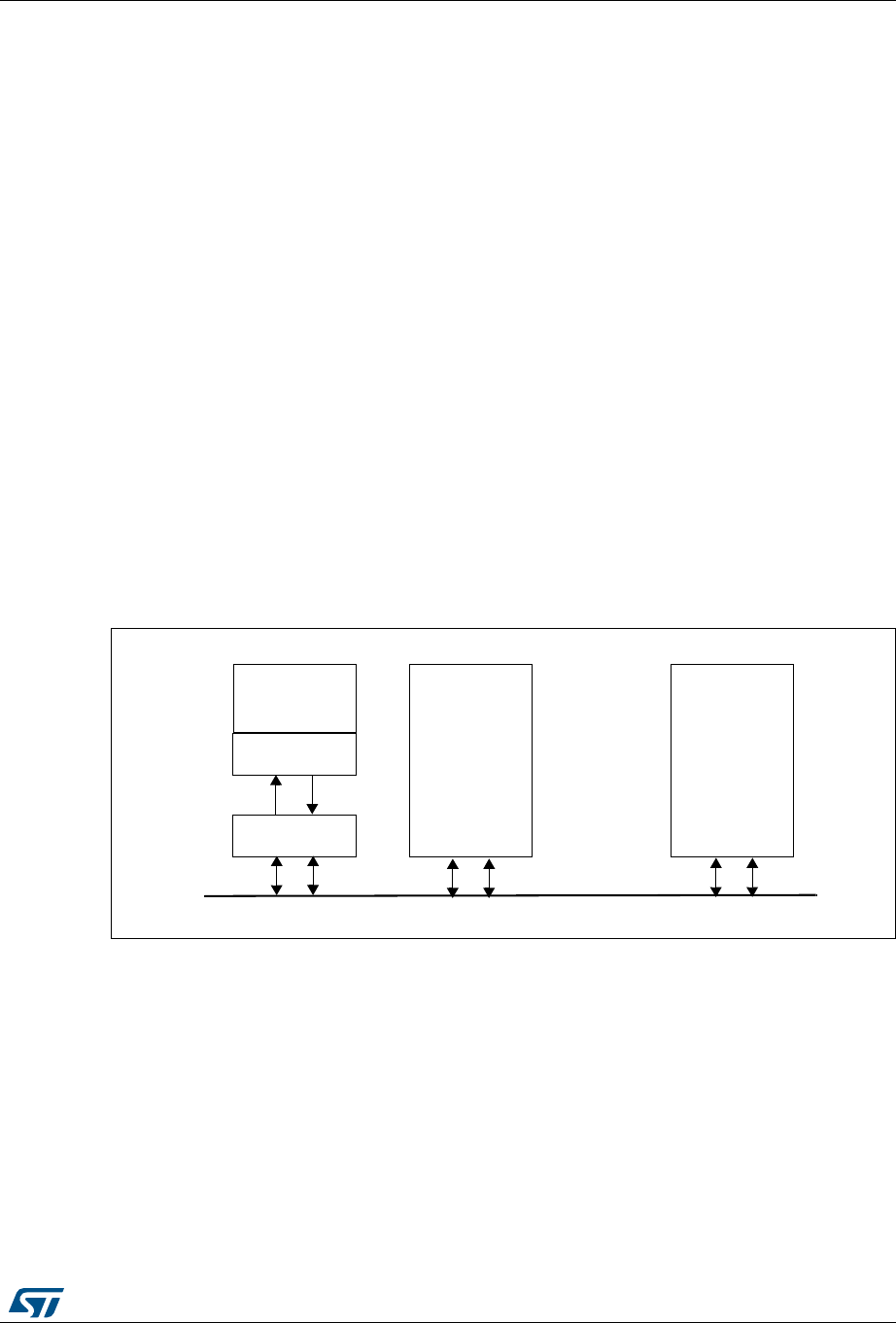
RM0090 Rev 18 1077/1749
RM0090 Controller area network (bxCAN)
1121
Dual CAN
•CAN1: Master bxCAN for managing the communication between a Slave bxCAN and
the 512-byte SRAM memory
•CAN2: Slave bxCAN, with no direct access to the SRAM memory.
•The two bxCAN cells share the 512-byte SRAM memory (see Figure 335)
32.3 bxCAN general description
In today’s CAN applications, the number of nodes in a network is increasing and often
several networks are linked together via gateways. Typically the number of messages in the
system (and thus to be handled by each node) has significantly increased. In addition to the
application messages, Network Management and Diagnostic messages have been
introduced.
•An enhanced filtering mechanism is required to handle each type of message.
Furthermore, application tasks require more CPU time, therefore real-time constraints
caused by message reception have to be reduced.
•A receive FIFO scheme allows the CPU to be dedicated to application tasks for a long
time period without losing messages.
The standard HLP (Higher Layer Protocol) based on standard CAN drivers requires an
efficient interface to the CAN controller.
Figure 334. CAN network topology
32.3.1 CAN 2.0B active core
The bxCAN module handles the transmission and the reception of CAN messages fully
autonomously. Standard identifiers (11-bit) and extended identifiers (29-bit) are fully
supported by hardware.
CAN node 1
CAN node 2
CAN node n
CAN
CAN
High Low
CAN
CAN
Rx Tx
CAN
Transceiver
CAN
Controller
MCU
CAN Bus
Application

Controller area network (bxCAN) RM0090
1078/1749 RM0090 Rev 18
32.3.2 Control, status and configuration registers
The application uses these registers to:
•Configure CAN parameters, e.g. baud rate
•Request transmissions
•Handle receptions
•Manage interrupts
•Get diagnostic information
32.3.3 Tx mailboxes
Three transmit mailboxes are provided to the software for setting up messages. The
transmission Scheduler decides which mailbox has to be transmitted first.
32.3.4 Acceptance filters
The bxCAN provides 28 scalable/configurable identifier filter banks for selecting the
incoming messages the software needs and discarding the others.
Receive FIFO
Two receive FIFOs are used by hardware to store the incoming messages. Three complete
messages can be stored in each FIFO. The FIFOs are managed completely by hardware.
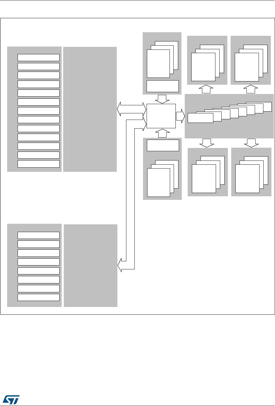
RM0090 Rev 18 1079/1749
RM0090 Controller area network (bxCAN)
1121
Figure 335. Dual CAN block diagram
32.4 bxCAN operating modes
bxCAN has three main operating modes: initialization, normal and Sleep. After a
hardware reset, bxCAN is in Sleep mode to reduce power consumption and an internal pull-
up is active on CANTX. The software requests bxCAN to enter initialization or Sleep mode
by setting the INRQ or SLEEP bits in the CAN_MCR register. Once the mode has been
entered, bxCAN confirms it by setting the INAK or SLAK bits in the CAN_MSR register and
the internal pull-up is disabled. When neither INAK nor SLAK are set, bxCAN is in normal
26
..
Accept ance Filt ers
..
3
2
1
Fi l t er 0
27
Tr an sm i ssi o n
Scheduler
Mailbox 0 1
2
Recei ve FI FO 1
Mailbox 0 1
2
Receive FIFO 0
Mailbox 0 1
2
Tx Mailboxes
Tr an sm i ssi o n
Scheduler
Mailbox 0 1
2
Receive FIFO 1
Mailbox 0 1
2
Receive FIFO 0
Mailbox 0 1
2
Tx Mailboxes
Memory
Access
Co n t r o l l er
Master Control
Master Status
Rx FI FO 0 St at u s
Rx FI FO 1 St at u s
Error Status
Bi t Ti m i ng
Interrupt Enable
Control/Status/Configuration
Tx St at us
Master Control
Master Status
Rx FI FO 0 St a t u s
Rx FI FO 1 St a t u s
Error Status
Bit Ti m i ng
Filter Mode
Filter Scale
Interrupt Enable
Control/Status/Configuration
Tx St at u s
Fi l t er FIFO As si g n
Filter Master
Filter Activation
CAN 2.0B Active Core
CAN2 (Slave)
CAN 2.0B Active Core
CAN1 (Master) with 512 bytes SRAM
Mast er retsaMretsaM
Master Filters
Sl a v e
Sl a v e Sl a v e
Slave Filters
(0 to 27)
(0 to 27)
Note: CAN 2 start filter bank number n is confi gurable by writing to
the CAN2SB[5:0] bits in the CAN_ FMR register.
ai16094b

Controller area network (bxCAN) RM0090
1080/1749 RM0090 Rev 18
mode. Before entering normal mode bxCAN always has to synchronize on the CAN bus.
To synchronize, bxCAN waits until the CAN bus is idle, this means 11 consecutive recessive
bits have been monitored on CANRX.
32.4.1 Initialization mode
The software initialization can be done while the hardware is in Initialization mode. To enter
this mode the software sets the INRQ bit in the CAN_MCR register and waits until the
hardware has confirmed the request by setting the INAK bit in the CAN_MSR register.
To leave Initialization mode, the software clears the INQR bit. bxCAN has left Initialization
mode once the INAK bit has been cleared by hardware.
While in Initialization Mode, all message transfers to and from the CAN bus are stopped and
the status of the CAN bus output CANTX is recessive (high).
Entering Initialization Mode does not change any of the configuration registers.
To initialize the CAN Controller, software has to set up the Bit Timing (CAN_BTR) and CAN
options (CAN_MCR) registers.
To initialize the registers associated with the CAN filter banks (mode, scale, FIFO
assignment, activation and filter values), software has to set the FINIT bit (CAN_FMR). Filter
initialization also can be done outside the initialization mode.
Note: When FINIT=1, CAN reception is deactivated.
The filter values also can be modified by deactivating the associated filter activation bits (in
the CAN_FA1R register).
If a filter bank is not used, it is recommended to leave it non active (leave the corresponding
FACT bit cleared).
32.4.2 Normal mode
Once the initialization is complete, the software must request the hardware to enter Normal
mode to be able to synchronize on the CAN bus and start reception and transmission.
The request to enter Normal mode is issued by clearing the INRQ bit in the CAN_MCR
register. The bxCAN enters Normal mode and is ready to take part in bus activities when it
has synchronized with the data transfer on the CAN bus. This is done by waiting for the
occurrence of a sequence of 11 consecutive recessive bits (Bus Idle state). The switch to
Normal mode is confirmed by the hardware by clearing the INAK bit in the CAN_MSR
register.
The initialization of the filter values is independent from Initialization Mode but must be done
while the filter is not active (corresponding FACTx bit cleared). The filter scale and mode
configuration must be configured before entering Normal Mode.
32.4.3 Sleep mode (low power)
To reduce power consumption, bxCAN has a low-power mode called Sleep mode. This
mode is entered on software request by setting the SLEEP bit in the CAN_MCR register. In
this mode, the bxCAN clock is stopped, however software can still access the bxCAN
mailboxes.
If software requests entry to initialization mode by setting the INRQ bit while bxCAN is in
Sleep mode, it must also clear the SLEEP bit.
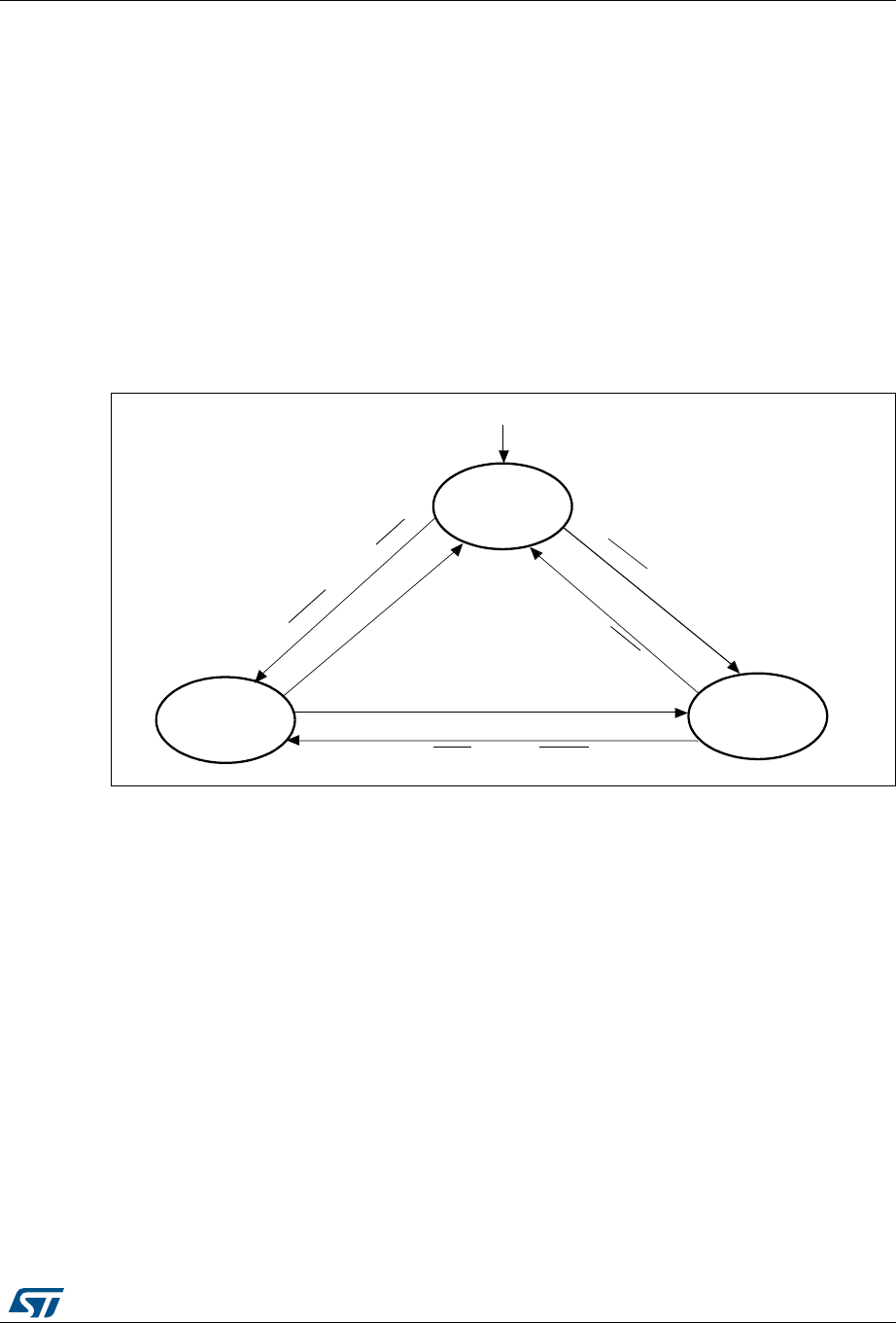
RM0090 Rev 18 1081/1749
RM0090 Controller area network (bxCAN)
1121
bxCAN can be woken up (exit Sleep mode) either by software clearing the SLEEP bit or on
detection of CAN bus activity.
On CAN bus activity detection, hardware automatically performs the wakeup sequence by
clearing the SLEEP bit if the AWUM bit in the CAN_MCR register is set. If the AWUM bit is
cleared, software has to clear the SLEEP bit when a wakeup interrupt occurs, in order to exit
from Sleep mode.
Note: If the wakeup interrupt is enabled (WKUIE bit set in CAN_IER register) a wakeup interrupt
will be generated on detection of CAN bus activity, even if the bxCAN automatically
performs the wakeup sequence.
After the SLEEP bit has been cleared, Sleep mode is exited once bxCAN has synchronized
with the CAN bus, refer to Figure 336. The Sleep mode is exited once the SLAK bit has
been cleared by hardware.
Figure 336. bxCAN operating modes
1. ACK = The wait state during which hardware confirms a request by setting the INAK or SLAK bits in the
CAN_MSR register
2. SYNC = The state during which bxCAN waits until the CAN bus is idle, meaning 11 consecutive recessive
bits have been monitored on CANRX
32.5 Test mode
Test mode can be selected by the SILM and LBKM bits in the CAN_BTR register. These bits
must be configured while bxCAN is in Initialization mode. Once test mode has been
selected, the INRQ bit in the CAN_MCR register must be reset to enter Normal mode.
32.5.1 Silent mode
The bxCAN can be put in Silent mode by setting the SILM bit in the CAN_BTR register.
In Silent mode, the bxCAN is able to receive valid data frames and valid remote frames, but
it sends only recessive bits on the CAN bus and it cannot start a transmission. If the bxCAN
has to send a dominant bit (ACK bit, overload flag, active error flag), the bit is rerouted
internally so that the CAN Core monitors this dominant bit, although the CAN bus may
Sleep
Initialization
Normal
Reset
SLAK= 1
INAK = 0
SLAK= 0
INAK = 1
SLAK= 0
INAK = 0
SLEEP . INRQ . ACK
SLEEP . INRQ . ACK
INRQ . ACK
INRQ . SYNC . SLEEP
SLEEP . ACK
SLEEP . SYNC . INRQ
ai15902
Controller area network (bxCAN) RM0090
1082/1749 RM0090 Rev 18
remain in recessive state. Silent mode can be used to analyze the traffic on a CAN bus
without affecting it by the transmission of dominant bits (Acknowledge Bits, Error Frames).
Figure 337. bxCAN in silent mode
32.5.2 Loop back mode
The bxCAN can be set in Loop Back Mode by setting the LBKM bit in the CAN_BTR
register. In Loop Back Mode, the bxCAN treats its own transmitted messages as received
messages and stores them (if they pass acceptance filtering) in a Receive mailbox.
Figure 338. bxCAN in loop back mode
This mode is provided for self-test functions. To be independent of external events, the CAN
Core ignores acknowledge errors (no dominant bit sampled in the acknowledge slot of a
data / remote frame) in Loop Back Mode. In this mode, the bxCAN performs an internal
feedback from its Tx output to its Rx input. The actual value of the CANRX input pin is
disregarded by the bxCAN. The transmitted messages can be monitored on the CANTX pin.
32.5.3 Loop back combined with silent mode
It is also possible to combine Loop Back mode and Silent mode by setting the LBKM and
SILM bits in the CAN_BTR register. This mode can be used for a “Hot Selftest”, meaning the
bxCAN can be tested like in Loop Back mode but without affecting a running CAN system
connected to the CANTX and CANRX pins. In this mode, the CANRX pin is disconnected
from the bxCAN and the CANTX pin is held recessive.
bxCAN
CANTX CANRX
Tx Rx
=1
bxCAN
CANTX CANRX
Tx Rx

RM0090 Rev 18 1083/1749
RM0090 Controller area network (bxCAN)
1121
Figure 339. bxCAN in combined mode
32.6 Debug mode
When the microcontroller enters the debug mode (Cortex®-M4 with FPU core halted), the
bxCAN continues to work normally or stops, depending on:
•the DBG_CAN1_STOP bit for CAN1 or the DBG_CAN2_STOP bit for CAN2 in the
DBG module. For more details, refer to Section 38.16.2: Debug support for timers,
watchdog, bxCAN and I2C.
•the DBF bit in CAN_MCR. For more details, refer to Section 32.9.2.
32.7 bxCAN functional description
32.7.1 Transmission handling
In order to transmit a message, the application must select one empty transmit mailbox, set
up the identifier, the data length code (DLC) and the data before requesting the transmission
by setting the corresponding TXRQ bit in the CAN_TIxR register. Once the mailbox has left
empty state, the software no longer has write access to the mailbox registers. Immediately
after the TXRQ bit has been set, the mailbox enters pending state and waits to become the
highest priority mailbox, see Transmit Priority. As soon as the mailbox has the highest
priority it will be scheduled for transmission. The transmission of the message of the
scheduled mailbox will start (enter transmit state) when the CAN bus becomes idle. Once
the mailbox has been successfully transmitted, it will become empty again. The hardware
indicates a successful transmission by setting the RQCP and TXOK bits in the CAN_TSR
register.
If the transmission fails, the cause is indicated by the ALST bit in the CAN_TSR register in
case of an Arbitration Lost, and/or the TERR bit, in case of transmission error detection.
bxCAN
CANTX CANRX
Tx Rx
=1

Controller area network (bxCAN) RM0090
1084/1749 RM0090 Rev 18
Transmit priority
Abort
A transmission request can be aborted by the user setting the ABRQ bit in the CAN_TSR
register. In pending or scheduled state, the mailbox is aborted immediately. An abort
request while the mailbox is in transmit state can have two results. If the mailbox is
transmitted successfully the mailbox becomes empty with the TXOK bit set in the
CAN_TSR register. If the transmission fails, the mailbox becomes scheduled, the
transmission is aborted and becomes empty with TXOK cleared. In all cases the mailbox
will become empty again at least at the end of the current transmission.
Nonautomatic retransmission mode
This mode has been implemented in order to fulfil the requirement of the Time Triggered
Communication option of the CAN standard. To configure the hardware in this mode the
NART bit in the CAN_MCR register must be set.
In this mode, each transmission is started only once. If the first attempt fails, due to an
arbitration loss or an error, the hardware will not automatically restart the message
transmission.
At the end of the first transmission attempt, the hardware considers the request as
completed and sets the RQCP bit in the CAN_TSR register. The result of the transmission is
indicated in the CAN_TSR register by the TXOK, ALST and TERR bits.
By identifier When more than one transmit mailbox is pending, the
transmission order is given by the identifier of the message
stored in the mailbox. The message with the lowest identifier
value has the highest priority according to the arbitration of the
CAN protocol. If the identifier values are equal, the lower mailbox
number will be scheduled first.
By transmit request order The transmit mailboxes can be configured as a transmit FIFO by
setting the TXFP bit in the CAN_MCR register. In this mode the
priority order is given by the transmit request order. This mode is
very useful for segmented transmission.
RM0090 Rev 18 1085/1749
RM0090 Controller area network (bxCAN)
1121
Figure 340. Transmit mailbox states
32.7.2 Time triggered communication mode
In this mode, the internal counter of the CAN hardware is activated and used to generate the
Time Stamp value stored in the CAN_RDTxR/CAN_TDTxR registers, respectively (for Rx
and Tx mailboxes). The internal counter is incremented each CAN bit time (refer to
Section 32.7.7). The internal counter is captured on the sample point of the Start Of Frame
bit in both reception and transmission.
32.7.3 Reception handling
For the reception of CAN messages, three mailboxes organized as a FIFO are provided. In
order to save CPU load, simplify the software and guarantee data consistency, the FIFO is
managed completely by hardware. The application accesses the messages stored in the
FIFO through the FIFO output mailbox.
Valid message
A received message is considered as valid when it has been received correctly according to
the CAN protocol (no error until the last but one bit of the EOF field) and It passed through
the identifier filtering successfully, see Section 32.7.4.
EMPTY
TXRQ=1
RQCP=X
TXOK=X
PENDING
RQCP=0
TXOK=0
SCHEDULED
RQCP=0
TXOK=0
Mailbox has
TRANSMIT
RQCP=0
TXOK=0
CAN Bus = IDLE
Transmit failed * NART
Transmit succeeded
Mailbox does not
EMPTY
RQCP=1
TXOK=0
highest priority
have highest priority
EMPTY
RQCP=1
TXOK=1
ABRQ=1
ABRQ=1
Transmit failed * NART
TME = 1
TME = 0
TME = 0
TME = 0
TME = 1
TME = 1
Controller area network (bxCAN) RM0090
1086/1749 RM0090 Rev 18
Figure 341. Receive FIFO states
FIFO management
Starting from the empty state, the first valid message received is stored in the FIFO which
becomes pending_1. The hardware signals the event setting the FMP[1:0] bits in the
CAN_RFR register to the value 01b. The message is available in the FIFO output mailbox.
The software reads out the mailbox content and releases it by setting the RFOM bit in the
CAN_RFR register. The FIFO becomes empty again. If a new valid message has been
received in the meantime, the FIFO stays in pending_1 state and the new message is
available in the output mailbox.
If the application does not release the mailbox, the next valid message will be stored in the
FIFO which enters pending_2 state (FMP[1:0] = 10b). The storage process is repeated for
the next valid message putting the FIFO into pending_3 state (FMP[1:0] = 11b). At this
point, the software must release the output mailbox by setting the RFOM bit, so that a
mailbox is free to store the next valid message. Otherwise the next valid message received
will cause a loss of message.
Refer also to Section 32.7.5
Overrun
Once the FIFO is in pending_3 state (i.e. the three mailboxes are full) the next valid
message reception will lead to an overrun and a message will be lost. The hardware
EMPTY
Valid Message
FMP=0x00
FOVR=0
PENDING_1
FMP=0x01
FOVR=0
Received
PENDING_2
FMP=0x10
FOVR=0
PENDING_3
FMP=0x11
FOVR=0
Valid Message
Received
Release
OVERRUN
FMP=0x11
FOVR=1
Mailbox
Release
Mailbox
Valid Message
Received
Valid Message
Received
Release
Mailbox
Release
Mailbox
Valid Message
Received
RFOM=1
RFOM=1
RFOM=1

RM0090 Rev 18 1087/1749
RM0090 Controller area network (bxCAN)
1121
signals the overrun condition by setting the FOVR bit in the CAN_RFR register. Which
message is lost depends on the configuration of the FIFO:
•If the FIFO lock function is disabled (RFLM bit in the CAN_MCR register cleared) the
last message stored in the FIFO will be overwritten by the new incoming message. In
this case the latest messages will be always available to the application.
•If the FIFO lock function is enabled (RFLM bit in the CAN_MCR register set) the most
recent message will be discarded and the software will have the three oldest messages
in the FIFO available.
Reception related interrupts
Once a message has been stored in the FIFO, the FMP[1:0] bits are updated and an
interrupt request is generated if the FMPIE bit in the CAN_IER register is set.
When the FIFO becomes full (i.e. a third message is stored) the FULL bit in the CAN_RFR
register is set and an interrupt is generated if the FFIE bit in the CAN_IER register is set.
On overrun condition, the FOVR bit is set and an interrupt is generated if the FOVIE bit in
the CAN_IER register is set.
32.7.4 Identifier filtering
In the CAN protocol the identifier of a message is not associated with the address of a node
but related to the content of the message. Consequently a transmitter broadcasts its
message to all receivers. On message reception a receiver node decides - depending on
the identifier value - whether the software needs the message or not. If the message is
needed, it is copied into the SRAM. If not, the message must be discarded without
intervention by the software.
To fulfill this requirement, the bxCAN Controller provides 28 configurable and scalable filter
banks (27-0) to the application. This hardware filtering saves CPU resources which would
be otherwise needed to perform filtering by software. Each filter bank x consists of two 32-bit
registers, CAN_FxR0 and CAN_FxR1.
Scalable width
To optimize and adapt the filters to the application needs, each filter bank can be scaled
independently. Depending on the filter scale a filter bank provides:
•One 32-bit filter for the STDID[10:0], EXTID[17:0], IDE and RTR bits.
•Two 16-bit filters for the STDID[10:0], RTR, IDE and EXTID[17:15] bits.
Refer to Figure 342.
Furthermore, the filters can be configured in mask mode or in identifier list mode.
Mask mode
In mask mode the identifier registers are associated with mask registers specifying which
bits of the identifier are handled as “must match” or as “don’t care”.
Identifier list mode
In identifier list mode, the mask registers are used as identifier registers. Thus instead of
defining an identifier and a mask, two identifiers are specified, doubling the number of single
identifiers. All bits of the incoming identifier must match the bits specified in the filter
registers.
Controller area network (bxCAN) RM0090
1088/1749 RM0090 Rev 18
Filter bank scale and mode configuration
The filter banks are configured by means of the corresponding CAN_FMR register. To
configure a filter bank it must be deactivated by clearing the FACT bit in the CAN_FAR
register. The filter scale is configured by means of the corresponding FSCx bit in the
CAN_FS1R register, refer to Figure 342. The identifier list or identifier mask mode for the
corresponding Mask/Identifier registers is configured by means of the FBMx bits in the
CAN_FMR register.
To filter a group of identifiers, configure the Mask/Identifier registers in mask mode.
To select single identifiers, configure the Mask/Identifier registers in identifier list mode.
Filters not used by the application should be left deactivated.
Each filter within a filter bank is numbered (called the Filter Number) from 0 to a maximum
dependent on the mode and the scale of each of the filter banks.
Concerning the filter configuration, refer to Figure 342.
Figure 342. Filter bank scale configuration - register organization
Filter match index
Once a message has been received in the FIFO it is available to the application. Typically,
application data is copied into SRAM locations. To copy the data to the right location the
One 32-Bit Filter - Identifier Mask
Two 16-Bit Filters - Identifier Mask
CAN_FxR1[31:24]
CAN_FxR2[31:24]
CAN_FxR1[15:8]
CAN_FxR1[31:24]
CAN_FxR1[7:0]
CAN_FxR1[23:16]
x = filter bank number
FSCx = 1FSCx = 0
1 These bits are located in the CAN_FS1R register
Filter Bank Scale
ID
Mask
ID
Mask
STID[10:3]
STID[2:0]
EXID[12:5]
Mapping
STID[10:3]
ID
Mask
Mapping
RTR
Two 32-Bit Filters - Identifier List
ID
ID
STID[10:3] STID[2:0] EXID[12:5]
Mapping
Four 16-Bit Filters - Identifier List
ID
ID
STID[10:3]
ID
ID
Mapping
n
n+1
n+2
n+3
n+1
Filter Bank Mode2
n
n
n+1
EXID[4:0] IDE
EXID[17:13]
EXID[17:13]
STID[2:0] RTR IDE EXID[17:15]
FBMx = 0FBMx = 1
Filter
2 These bits are located in the CAN_FM1R register
n
Num.
FBMx = 0FBMx = 1
Config. Bits1
STID[2:0] RTR IDE EXID[17:15]
0
RTREXID[4:0] IDE 0
CAN_FxR1[23:16] CAN_FxR1[15:8] CAN_FxR1[7:0]
CAN_FxR2[7:0]CAN_FxR2[15:8]CAN_FxR2[23:16]
CAN_FxR1[31:24]
CAN_FxR2[31:24]
CAN_FxR1[23:16] CAN_FxR1[15:8] CAN_FxR1[7:0]
CAN_FxR2[7:0]CAN_FxR2[15:8]CAN_FxR2[23:16]
CAN_FxR2[15:8]
CAN_FxR2[31:24]
CAN_FxR2[7:0]
CAN_FxR2[23:16]
CAN_FxR1[15:8]
CAN_FxR1[31:24]
CAN_FxR1[7:0]
CAN_FxR1[23:16]
CAN_FxR2[15:8]
CAN_FxR2[31:24]
CAN_FxR2[7:0]
CAN_FxR2[23:16]
ID=Identifier
RM0090 Rev 18 1089/1749
RM0090 Controller area network (bxCAN)
1121
application has to identify the data by means of the identifier. To avoid this, and to ease the
access to the SRAM locations, the CAN controller provides a Filter Match Index.
This index is stored in the mailbox together with the message according to the filter priority
rules. Thus each received message has its associated filter match index.
The Filter Match index can be used in two ways:
•Compare the Filter Match index with a list of expected values.
•Use the Filter Match Index as an index on an array to access the data destination
location.
For nonmasked filters, the software no longer has to compare the identifier.
If the filter is masked the software reduces the comparison to the masked bits only.
The index value of the filter number does not take into account the activation state of the
filter banks. In addition, two independent numbering schemes are used, one for each FIFO.
Refer to Figure 343 for an example.
Figure 343. Example of filter numbering
9
8
ID List (32-bit)
ID Mask (32-bit)
ID List (16-bit)
ID List (32-bit)
Deactivated
ID Mask (16-bit)
ID List (32-bit)
Filter
0
1
3
5
6
9
ID Mask (32-bit)
13
FIFO0 Filter
0
1
2
3
4
5
6
7
10
11
12
13
ID Mask (16-bit)
ID List (32-bit)
ID Mask (16-bit)
ID List (16-bit)
Deactivated
ID Mask (16-bit)
ID List (32-bit)
Filter
2
4
7
8
10
11
ID Mask (32-bit)
12
FIFO1 Filter
0
1
2
4
5
6
7
8
11
12
13
14
3
Deactivated
9
10
Num. Num.BankBank
ID = Identifier
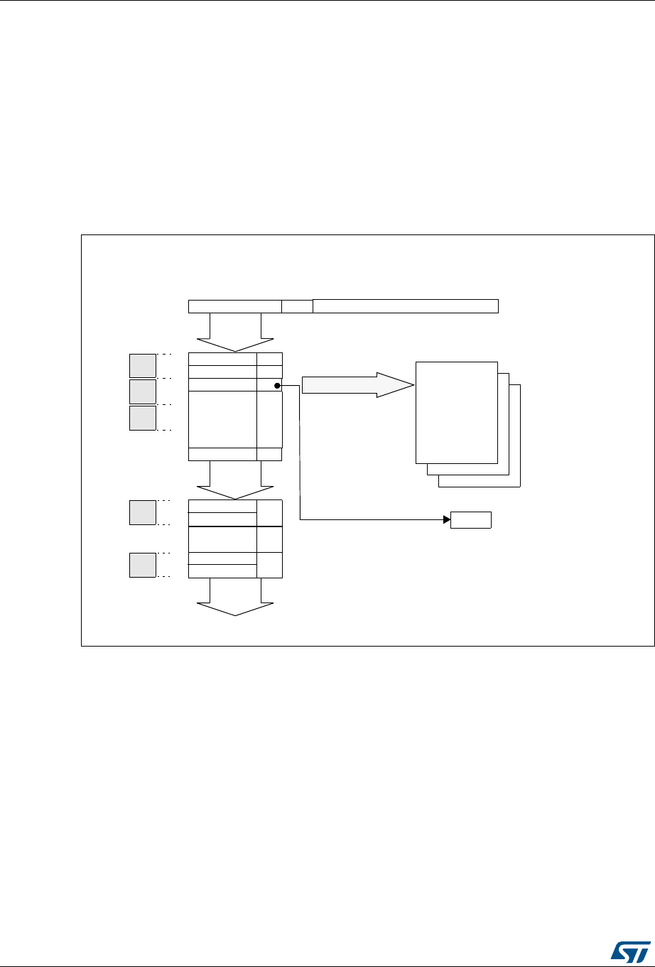
Controller area network (bxCAN) RM0090
1090/1749 RM0090 Rev 18
Filter priority rules
Depending on the filter combination it may occur that an identifier passes successfully
through several filters. In this case the filter match value stored in the receive mailbox is
chosen according to the following priority rules:
•A 32-bit filter takes priority over a 16-bit filter.
•For filters of equal scale, priority is given to the Identifier List mode over the Identifier
Mask mode
•For filters of equal scale and mode, priority is given by the filter number (the lower the
number, the higher the priority).
Figure 344. Filtering mechanism - Example
The example above shows the filtering principle of the bxCAN. On reception of a message,
the identifier is compared first with the filters configured in identifier list mode. If there is a
match, the message is stored in the associated FIFO and the index of the matching filter is
stored in the Filter Match Index. As shown in the example, the identifier matches with
Identifier #2 thus the message content and FMI 2 is stored in the FIFO.
If there is no match, the incoming identifier is then compared with the filters configured in
mask mode.
If the identifier does not match any of the identifiers configured in the filters, the message is
discarded by hardware without disturbing the software.
Identifier List
Message Discarded
Identifier & Mask
Identifier 0
Identifier 1
Identifier 4
Identifier 5
Identifier 2
Mask
Identifier 3
Mask
Identifier
Message Received
Ctrl Data
Identifier #4 Match
Message
Stored
Receive FIFO
No Match
Found
Filter number stored in the
Filter Match Index field
within the CAN_RDTxR
register
FMI
Filter bank
0
2
3
1
4
Num
Three filter banks in 32-bit Unidentified List mode,
the remaining in 32-bit Identifier Mask mode

RM0090 Rev 18 1091/1749
RM0090 Controller area network (bxCAN)
1121
32.7.5 Message storage
The interface between the software and the hardware for the CAN messages is
implemented by means of mailboxes. A mailbox contains all information related to a
message; identifier, data, control, status and time stamp information.
Transmit mailbox
The software sets up the message to be transmitted in an empty transmit mailbox. The
status of the transmission is indicated by hardware in the CAN_TSR register.
Receive mailbox
When a message has been received, it is available to the software in the FIFO output
mailbox. Once the software has handled the message (e.g. read it) the software must
release the FIFO output mailbox by means of the RFOM bit in the CAN_RFR register to
make the next incoming message available. The filter match index is stored in the MFMI
field of the CAN_RDTxR register. The 16-bit time stamp value is stored in the TIME[15:0]
field of CAN_RDTxR.
Table 182. Transmit mailbox mapping
Offset to transmit mailbox base address (bytes) Register name
0CAN_TIxR
4 CAN_TDTxR
8CAN_TDLxR
12 CAN_TDHxR
Table 183. Receive mailbox mapping
Offset to receive mailbox base address (bytes) Register name
0CAN_RIxR
4 CAN_RDTxR
8 CAN_RDLxR
12 CAN_RDHxR
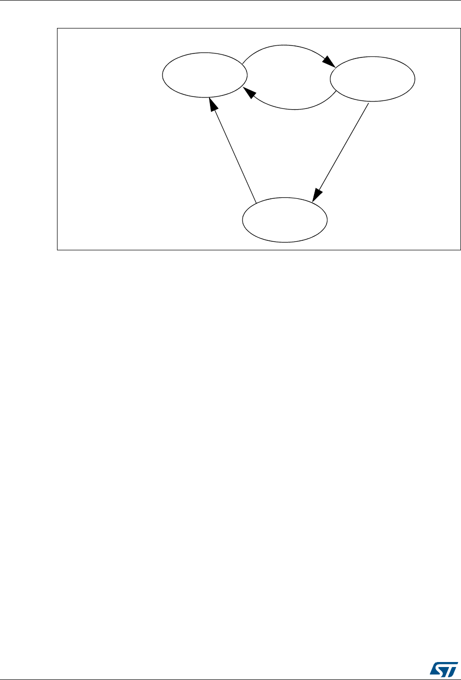

RM0090 Rev 18 1093/1749
RM0090 Controller area network (bxCAN)
1121
32.7.6 Error management
The error management as described in the CAN protocol is handled entirely by hardware
using a Transmit Error Counter (TEC value, in CAN_ESR register) and a Receive Error
Counter (REC value, in the CAN_ESR register), which get incremented or decremented
according to the error condition. For detailed information about TEC and REC management,
refer to the CAN standard.
Both of them may be read by software to determine the stability of the network.
Furthermore, the CAN hardware provides detailed information on the current error status in
CAN_ESR register. By means of the CAN_IER register (ERRIE bit, etc.), the software can
configure the interrupt generation on error detection in a very flexible way.
Bus-Off recovery
The Bus-Off state is reached when TEC is greater than 255, this state is indicated by BOFF
bit in CAN_ESR register. In Bus-Off state, the bxCAN is no longer able to transmit and
receive messages.
Depending on the ABOM bit in the CAN_MCR register bxCAN will recover from Bus-Off
(become error active again) either automatically or on software request. But in both cases
the bxCAN has to wait at least for the recovery sequence specified in the CAN standard
(128 occurrences of 11 consecutive recessive bits monitored on CANRX).
If ABOM is set, the bxCAN will start the recovering sequence automatically after it has
entered Bus-Off state.
If ABOM is cleared, the software must initiate the recovering sequence by requesting
bxCAN to enter and to leave initialization mode.
Note: In initialization mode, bxCAN does not monitor the CANRX signal, therefore it cannot
complete the recovery sequence. To recover, bxCAN must be in normal mode.
32.7.7 Bit timing
The bit timing logic monitors the serial bus-line and performs sampling and adjustment of
the sample point by synchronizing on the start-bit edge and resynchronizing on the following
edges.
Its operation may be explained simply by splitting nominal bit time into three segments as
follows:
•Synchronization segment (SYNC_SEG): a bit change is expected to occur within this
time segment. It has a fixed length of one time quantum (1 x tq).
•Bit segment 1 (BS1): defines the location of the sample point. It includes the
PROP_SEG and PHASE_SEG1 of the CAN standard. Its duration is programmable
between 1 and 16 time quanta but may be automatically lengthened to compensate for
positive phase drifts due to differences in the frequency of the various nodes of the
network.
•Bit segment 2 (BS2): defines the location of the transmit point. It represents the
PHASE_SEG2 of the CAN standard. Its duration is programmable between 1 and 8
time quanta but may also be automatically shortened to compensate for negative
phase drifts.
The resynchronization Jump Width (SJW) defines an upper bound to the amount of
lengthening or shortening of the bit segments. It is programmable between 1 and 4 time
quanta.
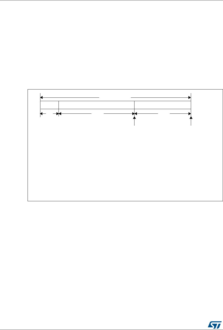
Controller area network (bxCAN) RM0090
1094/1749 RM0090 Rev 18
A valid edge is defined as the first transition in a bit time from dominant to recessive bus
level provided the controller itself does not send a recessive bit.
If a valid edge is detected in BS1 instead of SYNC_SEG, BS1 is extended by up to SJW so
that the sample point is delayed.
Conversely, if a valid edge is detected in BS2 instead of SYNC_SEG, BS2 is shortened by
up to SJW so that the transmit point is moved earlier.
As a safeguard against programming errors, the configuration of the Bit Timing Register
(CAN_BTR) is only possible while the device is in Standby mode.
Note: For a detailed description of the CAN bit timing and resynchronization mechanism, refer to
the ISO 11898 standard.
Figure 346. Bit timing
SYNC_SEG BIT SEGMENT 1 (BS1) BIT SEGMENT 2 (BS2)
NOMINAL BIT TIME
1 x tqtBS1 tBS2
SAMPLE POINT TRANSMIT POINT
NominalBitTime 1tq
×tBS1 tBS2
++=
with:
tBS1 = tq x (TS1[3:0] + 1),
tBS2 = tq x (TS2[2:0] + 1),
tq = (BRP[9:0] + 1) x tPCLK
tPCLK = time period of the APB clock,
BRP[9:0], TS1[3:0] and TS2[2:0] are defined in the CAN_BTR Register.
BaudRate 1
NominalBitTime
----------------------------------------------=
where tq refers to the Time quantum
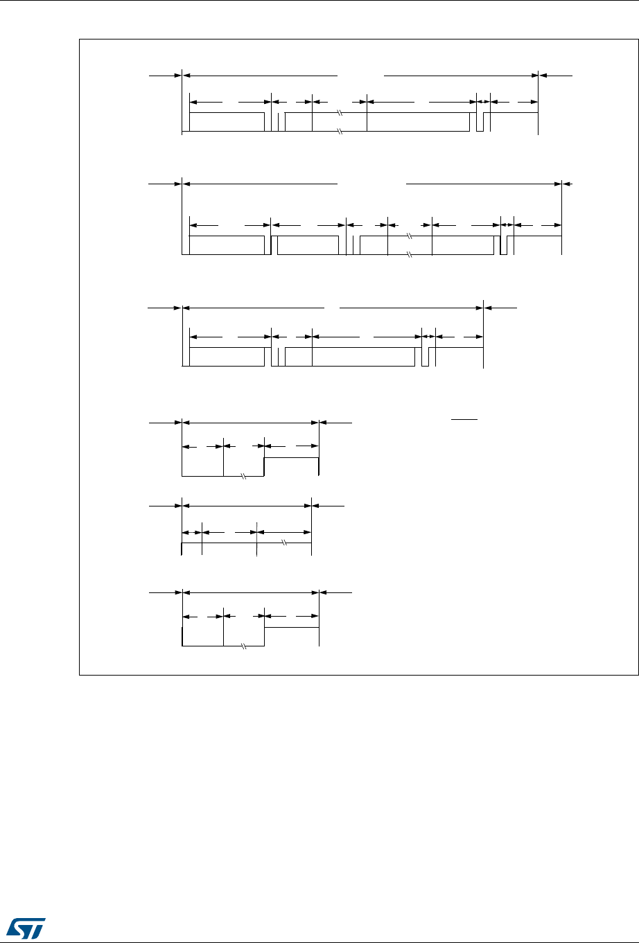
RM0090 Rev 18 1095/1749
RM0090 Controller area network (bxCAN)
1121
Figure 347. CAN frames
32.8 bxCAN interrupts
Four interrupt vectors are dedicated to bxCAN. Each interrupt source can be independently
enabled or disabled by means of the CAN Interrupt Enable Register (CAN_IER).
Data Frame or
Remote Frame
Data Field
8 * N
Ctrl Field
6
Arbitration Field
32
CRC Field
16
Ack Field
7
SOF
ID DLC CRC
Data Frame (Standard identifier)
44 + 8 * N
Arbitration Field
32
RTR
IDE
r0
SOF
ID DLC
Remote Frame
44
CRC Field
16 7
CRC
Ctrl Field
6
Overload
Overload Frame
Error
6
Error Delimiter
8
Error Frame
Flag Echo
6
Bus Idle
Inter-Frame Space
Suspend
8
Intermission
3Transmission
ACK
ACK
2
2
Inter-Frame Space
or Overload Frame
Inter-Frame Space
Inter-Frame Space
or Overload Frame
Inter-Frame Space
Inter-Frame Space
or Overload Frame Notes:
0 <= N <= 8
SOF = Start Of Frame
ID = Identifier
RTR = Remote Transmission Request
IDE = Identifier Extension Bit
r0 = Reserved Bit
DLC = Data Length Code
CRC = Cyclic Redundancy Code
Error flag: 6 dominant bits if node is error
active else 6 recessive bits.
Suspend transmission: applies to error
passive nodes only.
EOF = End of Frame
ACK = Acknowledge bit
Ctrl = Control
Data Frame or
Remote Frame
Any Frame
Inter-Frame Space
or Error Frame
End Of Frame or
Error Delimiter or
Overload Delimiter
Ack Field
EOF
RTR
IDE
r0
EOF
Data Field
8 * N
Ctrl Field
6
32
CRC Field
16
Ack Field
7
SOF
ID DLC CRC
Data Frame (Extended Identifier)
64 + 8 * N
ACK
2
Inter-Frame Space
or Overload Frame
Inter-Frame Space
SRR
IDE
EOF
RTR
r1
r0
32
6
Overload
8
6
Overload
Flag Echo Delimiter
Flag
ai15154
Arbitration Field Arbitration Field
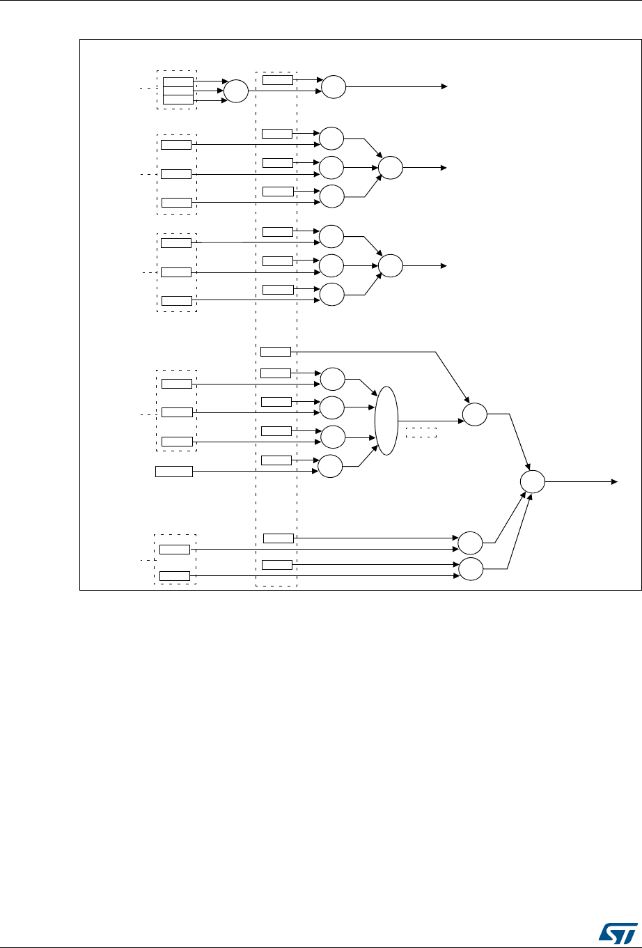
Controller area network (bxCAN) RM0090
1096/1749 RM0090 Rev 18
Figure 348. Event flags and interrupt generation
•The transmit interrupt can be generated by the following events:
– Transmit mailbox 0 becomes empty, RQCP0 bit in the CAN_TSR register set.
– Transmit mailbox 1 becomes empty, RQCP1 bit in the CAN_TSR register set.
– Transmit mailbox 2 becomes empty, RQCP2 bit in the CAN_TSR register set.
•The FIFO 0 interrupt can be generated by the following events:
– Reception of a new message, FMP0 bits in the CAN_RF0R register are not ‘00’.
– FIFO0 full condition, FULL0 bit in the CAN_RF0R register set.
– FIFO0 overrun condition, FOVR0 bit in the CAN_RF0R register set.
•The FIFO 1 interrupt can be generated by the following events:
– Reception of a new message, FMP1 bits in the CAN_RF1R register are not ‘00’.
– FIFO1 full condition, FULL1 bit in the CAN_RF1R register set.
– FIFO1 overrun condition, FOVR1 bit in the CAN_RF1R register set.
•The error and status change interrupt can be generated by the following events:
– Error condition, for more details on error conditions refer to the CAN Error Status
register (CAN_ESR).
RQCP0
RQCP1
FMP1
CAN_TSR +TMEIE
CAN_IER
TRANSMIT
&
FMPIE1
FULL1 &
FFIE1
FOVR1 &
FOVIE1
&
+
CAN_RF1R
FIFO 1
EWGF
EWGIE
EPVF
EPVIE
BOFF
BOFIE
1≤LEC≤6
LECIE
&
&
&
&
CAN_ESR +&
ERRIE
INTERRUPT
INTERRUPT
FMP0 &
FMPIE0
FULL0 &
FFIE0
FOVR0 &
FOVIE0
+
CAN_RF0R
FIFO 0
INTERRUPT
RQCP2
WKUI &
WKUIE
CAN_MSR
+
INTERRUPT
ERROR
STATUS CHANGE
ERRI
SLAKI
SLKIE &
CAN_MSR

RM0090 Rev 18 1097/1749
RM0090 Controller area network (bxCAN)
1121
– Wakeup condition, SOF monitored on the CAN Rx signal.
– Entry into Sleep mode.
32.9 CAN registers
The peripheral registers have to be accessed by words (32 bits).
32.9.1 Register access protection
Erroneous access to certain configuration registers can cause the hardware to temporarily
disturb the whole CAN network. Therefore the CAN_BTR register can be modified by
software only while the CAN hardware is in initialization mode.
Although the transmission of incorrect data will not cause problems at the CAN network
level, it can severely disturb the application. A transmit mailbox can be only modified by
software while it is in empty state, refer to Figure 340.
The filter values can be modified either deactivating the associated filter banks or by setting
the FINIT bit. Moreover, the modification of the filter configuration (scale, mode and FIFO
assignment) in CAN_FMxR, CAN_FSxR and CAN_FFAR registers can only be done when
the filter initialization mode is set (FINIT=1) in the CAN_FMR register.
32.9.2 CAN control and status registers
Refer to Section 1.1 for a list of abbreviations used in register descriptions.
CAN master control register (CAN_MCR)
Address offset: 0x00
Reset value: 0x0001 0002
31 30 29 28 27 26 25 24 23 22 21 20 19 18 17 16
Reserved DBF
rw
1514131211109876543210
RESET Reserved TTCM ABOM AWUM NART RFLM TXFP SLEEP INRQ
rs rw rw rw rw rw rw rw rw
Bits 31:17 Reserved, must be kept at reset value.
Bit 16 DBF: Debug freeze
0: CAN working during debug
1: CAN reception/transmission frozen during debug. Reception FIFOs can still be
accessed/controlled normally.
Bit 15 RESET: bxCAN software master reset
0: Normal operation.
1: Force a master reset of the bxCAN -> Sleep mode activated after reset (FMP bits and
CAN_MCR register are initialized to the reset values). This bit is automatically reset to 0.
Bits 14:8 Reserved, must be kept at reset value.

Controller area network (bxCAN) RM0090
1098/1749 RM0090 Rev 18
Bit 7 TTCM: Time triggered communication mode
0: Time Triggered Communication mode disabled.
1: Time Triggered Communication mode enabled
Note: For more information on Time Triggered Communication mode refer to Section 32.7.2.
Bit 6 ABOM: Automatic bus-off management
This bit controls the behavior of the CAN hardware on leaving the Bus-Off state.
0: The Bus-Off state is left on software request, once 128 occurrences of 11 recessive bits
have been monitored and the software has first set and cleared the INRQ bit of the
CAN_MCR register.
1: The Bus-Off state is left automatically by hardware once 128 occurrences of 11 recessive
bits have been monitored.
For detailed information on the Bus-Off state refer to Section 32.7.6.
Bit 5 AWUM: Automatic wakeup mode
This bit controls the behavior of the CAN hardware on message reception during Sleep
mode.
0: The Sleep mode is left on software request by clearing the SLEEP bit of the CAN_MCR
register.
1: The Sleep mode is left automatically by hardware on CAN message detection.
The SLEEP bit of the CAN_MCR register and the SLAK bit of the CAN_MSR register are
cleared by hardware.
Bit 4 NART: No automatic retransmission
0: The CAN hardware will automatically retransmit the message until it has been
successfully transmitted according to the CAN standard.
1: A message will be transmitted only once, independently of the transmission result
(successful, error or arbitration lost).
Bit 3 RFLM: Receive FIFO locked mode
0: Receive FIFO not locked on overrun. Once a receive FIFO is full the next incoming
message will overwrite the previous one.
1: Receive FIFO locked against overrun. Once a receive FIFO is full the next incoming
message will be discarded.
Bit 2 TXFP: Transmit FIFO priority
This bit controls the transmission order when several mailboxes are pending at the same
time.
0: Priority driven by the identifier of the message
1: Priority driven by the request order (chronologically)
Bit 1 SLEEP: Sleep mode request
This bit is set by software to request the CAN hardware to enter the Sleep mode. Sleep
mode will be entered as soon as the current CAN activity (transmission or reception of a
CAN frame) has been completed.
This bit is cleared by software to exit Sleep mode.
This bit is cleared by hardware when the AWUM bit is set and a SOF bit is detected on the
CAN Rx signal.
This bit is set after reset - CAN starts in Sleep mode.

RM0090 Rev 18 1099/1749
RM0090 Controller area network (bxCAN)
1121
CAN master status register (CAN_MSR)
Address offset: 0x04
Reset value: 0x0000 0C02
Bit 0 INRQ: Initialization request
The software clears this bit to switch the hardware into normal mode. Once 11 consecutive
recessive bits have been monitored on the Rx signal the CAN hardware is synchronized and
ready for transmission and reception. Hardware signals this event by clearing the INAK bit in
the CAN_MSR register.
Software sets this bit to request the CAN hardware to enter initialization mode. Once
software has set the INRQ bit, the CAN hardware waits until the current CAN activity
(transmission or reception) is completed before entering the initialization mode. Hardware
signals this event by setting the INAK bit in the CAN_MSR register.
31 30 29 28 27 26 25 24 23 22 21 20 19 18 17 16
Reserved
1514131211109876543210
Reserved.
RX SAMP RXM TXM
Reserved
SLAKI WKUI ERRI SLAK INAK
rrrr rc_w1rc_w1rc_w1rr
Bits 31:12 Reserved, must be kept at reset value.
Bit 11 RX: CAN Rx signal
Monitors the actual value of the CAN_RX Pin.
Bit 10 SAMP: Last sample point
The value of RX on the last sample point (current received bit value).
Bit 9 RXM: Receive mode
The CAN hardware is currently receiver.
Bit 8 TXM: Transmit mode
The CAN hardware is currently transmitter.
Bits 7:5 Reserved, must be kept at reset value.
Bit 4 SLAKI: Sleep acknowledge interrupt
When SLKIE=1, this bit is set by hardware to signal that the bxCAN has entered Sleep
Mode. When set, this bit generates a status change interrupt if the SLKIE bit in the
CAN_IER register is set.
This bit is cleared by software or by hardware, when SLAK is cleared.
Note: When SLKIE=0, no polling on SLAKI is possible. In this case the SLAK bit can be
polled.
Bit 3 WKUI: Wakeup interrupt
This bit is set by hardware to signal that a SOF bit has been detected while the CAN
hardware was in Sleep mode. Setting this bit generates a status change interrupt if the
WKUIE bit in the CAN_IER register is set.
This bit is cleared by software.
Controller area network (bxCAN) RM0090
1100/1749 RM0090 Rev 18
CAN transmit status register (CAN_TSR)
Address offset: 0x08
Reset value: 0x1C00 0000
Bit 2 ERRI: Error interrupt
This bit is set by hardware when a bit of the CAN_ESR has been set on error detection and
the corresponding interrupt in the CAN_IER is enabled. Setting this bit generates a status
change interrupt if the ERRIE bit in the CAN_IER register is set.
This bit is cleared by software.
Bit 1 SLAK: Sleep acknowledge
This bit is set by hardware and indicates to the software that the CAN hardware is now in
Sleep mode. This bit acknowledges the Sleep mode request from the software (set SLEEP
bit in CAN_MCR register).
This bit is cleared by hardware when the CAN hardware has left Sleep mode (to be
synchronized on the CAN bus). To be synchronized the hardware has to monitor a
sequence of 11 consecutive recessive bits on the CAN RX signal.
Note: The process of leaving Sleep mode is triggered when the SLEEP bit in the CAN_MCR
register is cleared. Refer to the AWUM bit of the CAN_MCR register description for
detailed information for clearing SLEEP bit
Bit 0 INAK: Initialization acknowledge
This bit is set by hardware and indicates to the software that the CAN hardware is now in
initialization mode. This bit acknowledges the initialization request from the software (set
INRQ bit in CAN_MCR register).
This bit is cleared by hardware when the CAN hardware has left the initialization mode (to
be synchronized on the CAN bus). To be synchronized the hardware has to monitor a
sequence of 11 consecutive recessive bits on the CAN RX signal.
31 30 29 28 27 26 25 24 23 22 21 20 19 18 17 16
LOW2 LOW1 LOW0 TME2 TME1 TME0 CODE[1:0] ABRQ2
Reserved
TERR2 ALST2 TXOK2 RQCP2
rrrrrrrrrs rc_w1rc_w1rc_w1rc_w1
1514131211109876543210
ABRQ1 Reserved
Res.
TERR1 ALST1 TXOK1 RQCP1 ABRQ0
Reserved
TERR0 ALST0 TXOK0 RQCP0
rs rc_w1 rc_w1 rc_w1 rc_w1 rs rc_w1 rc_w1 rc_w1 rc_w1
Bit 31 LOW2: Lowest priority flag for mailbox 2
This bit is set by hardware when more than one mailbox are pending for transmission and
mailbox 2 has the lowest priority.
Bit 30 LOW1: Lowest priority flag for mailbox 1
This bit is set by hardware when more than one mailbox are pending for transmission and
mailbox 1 has the lowest priority.
Bit 29 LOW0: Lowest priority flag for mailbox 0
This bit is set by hardware when more than one mailbox are pending for transmission and
mailbox 0 has the lowest priority.
Note: The LOW[2:0] bits are set to zero when only one mailbox is pending.
Bit 28 TME2: Transmit mailbox 2 empty
This bit is set by hardware when no transmit request is pending for mailbox 2.
Bit 27 TME1: Transmit mailbox 1 empty
This bit is set by hardware when no transmit request is pending for mailbox 1.

RM0090 Rev 18 1101/1749
RM0090 Controller area network (bxCAN)
1121
Bit 26 TME0: Transmit mailbox 0 empty
This bit is set by hardware when no transmit request is pending for mailbox 0.
Bits 25:24 CODE[1:0]: Mailbox code
In case at least one transmit mailbox is free, the code value is equal to the number of the
next transmit mailbox free.
In case all transmit mailboxes are pending, the code value is equal to the number of the
transmit mailbox with the lowest priority.
Bit 23 ABRQ2: Abort request for mailbox 2
Set by software to abort the transmission request for the corresponding mailbox.
Cleared by hardware when the mailbox becomes empty.
Setting this bit has no effect when the mailbox is not pending for transmission.
Bits 22:20 Reserved, must be kept at reset value.
Bit 19 TERR2: Transmission error of mailbox 2
This bit is set when the previous TX failed due to an error.
Bit 18 ALST2: Arbitration lost for mailbox 2
This bit is set when the previous TX failed due to an arbitration lost.
Bit 17 TXOK2: Transmission OK of mailbox 2
The hardware updates this bit after each transmission attempt.
0: The previous transmission failed
1: The previous transmission was successful
This bit is set by hardware when the transmission request on mailbox 2 has been completed
successfully. Refer to Figure 340.
Bit 16 RQCP2: Request completed mailbox2
Set by hardware when the last request (transmit or abort) has been performed.
Cleared by software writing a “1” or by hardware on transmission request (TXRQ2 set in
CAN_TMID2R register).
Clearing this bit clears all the status bits (TXOK2, ALST2 and TERR2) for Mailbox 2.
Bit 15 ABRQ1: Abort request for mailbox 1
Set by software to abort the transmission request for the corresponding mailbox.
Cleared by hardware when the mailbox becomes empty.
Setting this bit has no effect when the mailbox is not pending for transmission.
Bits 14:12 Reserved, must be kept at reset value.
Bit 11 TERR1: Transmission error of mailbox1
This bit is set when the previous TX failed due to an error.
Bit 10 ALST1: Arbitration lost for mailbox1
This bit is set when the previous TX failed due to an arbitration lost.
Bit 9 TXOK1: Transmission OK of mailbox1
The hardware updates this bit after each transmission attempt.
0: The previous transmission failed
1: The previous transmission was successful
This bit is set by hardware when the transmission request on mailbox 1 has been completed
successfully. Refer to Figure 340
Bit 8 RQCP1: Request completed mailbox1
Set by hardware when the last request (transmit or abort) has been performed.
Cleared by software writing a “1” or by hardware on transmission request (TXRQ1 set in
CAN_TI1R register).
Clearing this bit clears all the status bits (TXOK1, ALST1 and TERR1) for Mailbox 1.

Controller area network (bxCAN) RM0090
1102/1749 RM0090 Rev 18
CAN receive FIFO 0 register (CAN_RF0R)
Address offset: 0x0C
Reset value: 0x0000 0000
Bit 7 ABRQ0: Abort request for mailbox0
Set by software to abort the transmission request for the corresponding mailbox.
Cleared by hardware when the mailbox becomes empty.
Setting this bit has no effect when the mailbox is not pending for transmission.
Bits 6:4 Reserved, must be kept at reset value.
Bit 3 TERR0: Transmission error of mailbox0
This bit is set when the previous TX failed due to an error.
Bit 2 ALST0: Arbitration lost for mailbox0
This bit is set when the previous TX failed due to an arbitration lost.
Bit 1 TXOK0: Transmission OK of mailbox0
The hardware updates this bit after each transmission attempt.
0: The previous transmission failed
1: The previous transmission was successful
This bit is set by hardware when the transmission request on mailbox 1 has been completed
successfully. Refer to Figure 340
Bit 0 RQCP0: Request completed mailbox0
Set by hardware when the last request (transmit or abort) has been performed.
Cleared by software writing a “1” or by hardware on transmission request (TXRQ0 set in
CAN_TI0R register).
Clearing this bit clears all the status bits (TXOK0, ALST0 and TERR0) for Mailbox 0.
31 30 29 28 27 26 25 24 23 22 21 20 19 18 17 16
Reserved
1514131211109876 5 4 3210
Reserved RFOM0 FOVR0 FULL0 Res. FMP0[1:0]
rs rc_w1 rc_w1 r r
Bits 31:6 Reserved, must be kept at reset value.
Bit 5 RFOM0: Release FIFO 0 output mailbox
Set by software to release the output mailbox of the FIFO. The output mailbox can only be
released when at least one message is pending in the FIFO. Setting this bit when the FIFO
is empty has no effect. If at least two messages are pending in the FIFO, the software has to
release the output mailbox to access the next message.
Cleared by hardware when the output mailbox has been released.
Bit 4 FOVR0: FIFO 0 overrun
This bit is set by hardware when a new message has been received and passed the filter
while the FIFO was full.
This bit is cleared by software.
Bit 3 FULL0: FIFO 0 full
Set by hardware when three messages are stored in the FIFO.
This bit is cleared by software.
Bit 2 Reserved, must be kept at reset value.
RM0090 Rev 18 1103/1749
RM0090 Controller area network (bxCAN)
1121
CAN receive FIFO 1 register (CAN_RF1R)
Address offset: 0x10
Reset value: 0x0000 0000
CAN interrupt enable register (CAN_IER)
Address offset: 0x14
Reset value: 0x0000 0000
Bits 1:0 FMP0[1:0]: FIFO 0 message pending
These bits indicate how many messages are pending in the receive FIFO.
FMP is increased each time the hardware stores a new message in to the FIFO. FMP is
decreased each time the software releases the output mailbox by setting the RFOM0 bit.
31 30 29 28 27 26 25 24 23 22 21 20 19 18 17 16
Reserved
1514131211109876 5 43210
Reserved RFOM1 FOVR1 FULL1 Res. FMP1[1:0]
rs rc_w1 rc_w1 r r
Bits 31:6 Reserved, must be kept at reset value.
Bit 5 RFOM1: Release FIFO 1 output mailbox
Set by software to release the output mailbox of the FIFO. The output mailbox can only be
released when at least one message is pending in the FIFO. Setting this bit when the FIFO
is empty has no effect. If at least two messages are pending in the FIFO, the software has to
release the output mailbox to access the next message.
Cleared by hardware when the output mailbox has been released.
Bit 4 FOVR1: FIFO 1 overrun
This bit is set by hardware when a new message has been received and passed the filter
while the FIFO was full.
This bit is cleared by software.
Bit 3 FULL1: FIFO 1 full
Set by hardware when three messages are stored in the FIFO.
This bit is cleared by software.
Bit 2 Reserved, must be kept at reset value.
Bits 1:0 FMP1[1:0]: FIFO 1 message pending
These bits indicate how many messages are pending in the receive FIFO1.
FMP1 is increased each time the hardware stores a new message in to the FIFO1. FMP is
decreased each time the software releases the output mailbox by setting the RFOM1 bit.
31 30 29 28 27 26 25 24 23 22 21 20 19 18 17 16
Reserved
SLKIE WKUIE
rw rw
151413121110987654321 0
ERRIE Reserved
LEC
IE
BOF
IE
EPV
IE
EWG
IE Res.
FOV
IE1
FF
IE1
FMP
IE1
FOV
IE0
FF
IE0
FMP
IE0
TME
IE
rw rw rw rw rw rw rw rw rw rw rw rw

Controller area network (bxCAN) RM0090
1104/1749 RM0090 Rev 18
Bits 31:18 Reserved, must be kept at reset value.
Bit 17 SLKIE: Sleep interrupt enable
0: No interrupt when SLAKI bit is set.
1: Interrupt generated when SLAKI bit is set.
Bit 16 WKUIE: Wakeup interrupt enable
0: No interrupt when WKUI is set.
1: Interrupt generated when WKUI bit is set.
Bit 15 ERRIE: Error interrupt enable
0: No interrupt will be generated when an error condition is pending in the CAN_ESR.
1: An interrupt will be generation when an error condition is pending in the CAN_ESR.
Bits 14:12 Reserved, must be kept at reset value.
Bit 11 LECIE: Last error code interrupt enable
0: ERRI bit will not be set when the error code in LEC[2:0] is set by hardware on error
detection.
1: ERRI bit will be set when the error code in LEC[2:0] is set by hardware on error detection.
Bit 10 BOFIE: Bus-off interrupt enable
0: ERRI bit will not be set when BOFF is set.
1: ERRI bit will be set when BOFF is set.
Bit 9 EPVIE: Error passive interrupt enable
0: ERRI bit will not be set when EPVF is set.
1: ERRI bit will be set when EPVF is set.
Bit 8 EWGIE: Error warning interrupt enable
0: ERRI bit will not be set when EWGF is set.
1: ERRI bit will be set when EWGF is set.
Bit 7 Reserved, must be kept at reset value.
Bit 6 FOVIE1: FIFO overrun interrupt enable
0: No interrupt when FOVR is set.
1: Interrupt generation when FOVR is set.
Bit 5 FFIE1: FIFO full interrupt enable
0: No interrupt when FULL bit is set.
1: Interrupt generated when FULL bit is set.
Bit 4 FMPIE1: FIFO message pending interrupt enable
0: No interrupt generated when state of FMP[1:0] bits are not 00b.
1: Interrupt generated when state of FMP[1:0] bits are not 00b.
Bit 3 FOVIE0: FIFO overrun interrupt enable
0: No interrupt when FOVR bit is set.
1: Interrupt generated when FOVR bit is set.
RM0090 Rev 18 1105/1749
RM0090 Controller area network (bxCAN)
1121
CAN error status register (CAN_ESR)
Address offset: 0x18
Reset value: 0x0000 0000
Bit 2 FFIE0: FIFO full interrupt enable
0: No interrupt when FULL bit is set.
1: Interrupt generated when FULL bit is set.
Bit 1 FMPIE0: FIFO message pending interrupt enable
0: No interrupt generated when state of FMP[1:0] bits are not 00b.
1: Interrupt generated when state of FMP[1:0] bits are not 00b.
Bit 0 TMEIE: Transmit mailbox empty interrupt enable
0: No interrupt when RQCPx bit is set.
1: Interrupt generated when RQCPx bit is set.
Note: Refer to Section 32.8: bxCAN interrupts.
31 30 29 28 27 26 25 24 23 22 21 20 19 18 17 16
REC[7:0] TEC[7:0]
rrrrrrrrrrrrrrrr
1514131211109876543210
Reserved
LEC[2:0]
Res.
BOFF EPVF EWGF
rw rw rw r r r
Bits 31:24 REC[7:0]: Receive error counter
The implementing part of the fault confinement mechanism of the CAN protocol. In case of
an error during reception, this counter is incremented by 1 or by 8 depending on the error
condition as defined by the CAN standard. After every successful reception the counter is
decremented by 1 or reset to 120 if its value was higher than 128. When the counter value
exceeds 127, the CAN controller enters the error passive state.
Bits 23:16 TEC[7:0]: Least significant byte of the 9-bit transmit error counter
The implementing part of the fault confinement mechanism of the CAN protocol.
Bits 15:7 Reserved, must be kept at reset value.
Bits 6:4 LEC[2:0]: Last error code
This field is set by hardware and holds a code which indicates the error condition of the last
error detected on the CAN bus. If a message has been transferred (reception or
transmission) without error, this field will be cleared to ‘0’.
The LEC[2:0] bits can be set to value 0b111 by software. They are updated by hardware to
indicate the current communication status.
000: No Error
001: Stuff Error
010: Form Error
011: Acknowledgment Error
100: Bit recessive Error
101: Bit dominant Error
110: CRC Error
111: Set by software
Bit 3 Reserved, must be kept at reset value.

Controller area network (bxCAN) RM0090
1106/1749 RM0090 Rev 18
CAN bit timing register (CAN_BTR)
Address offset: 0x1C
Reset value: 0x0123 0000
This register can only be accessed by the software when the CAN hardware is in
initialization mode.
Bit 2 BOFF: Bus-off flag
This bit is set by hardware when it enters the bus-off state. The bus-off state is entered on
TEC overflow, greater than 255, refer to Section 32.7.6.
Bit 1 EPVF: Error passive flag
This bit is set by hardware when the Error Passive limit has been reached (Receive Error
Counter or Transmit Error Counter>127).
Bit 0 EWGF: Error warning flag
This bit is set by hardware when the warning limit has been reached
(Receive Error Counter or Transmit Error Counter≥96).
31 30 29 28 27 26 25 24 23 22 21 20 19 18 17 16
SILM LBKM Reserved SJW[1:0] Res. TS2[2:0] TS1[3:0]
rw rw rw rw rw rw rw rw rw rw rw
1514131211109876543210
Reserved BRP[9:0]
rw rw rw rw rw rw rw rw rw rw
Bit 31 SILM: Silent mode (debug)
0: Normal operation
1: Silent Mode
Bit 30 LBKM: Loop back mode (debug)
0: Loop Back Mode disabled
1: Loop Back Mode enabled
Bits 29:26 Reserved, must be kept at reset value.
Bits 25:24 SJW[1:0]: Resynchronization jump width
These bits define the maximum number of time quanta the CAN hardware is allowed to
lengthen or shorten a bit to perform the resynchronization.
tRJW = tq x (SJW[1:0] + 1)
Bit 23 Reserved, must be kept at reset value.
Bits 22:20 TS2[2:0]: Time segment 2
These bits define the number of time quanta in Time Segment 2.
tBS2 = tq x (TS2[2:0] + 1)
RM0090 Rev 18 1107/1749
RM0090 Controller area network (bxCAN)
1121
32.9.3 CAN mailbox registers
This chapter describes the registers of the transmit and receive mailboxes. Refer to
Section 32.7.5: Message storage for detailed register mapping.
Transmit and receive mailboxes have the same registers except:
•The FMI field in the CAN_RDTxR register.
•A receive mailbox is always write protected.
•A transmit mailbox is write-enabled only while empty, corresponding TME bit in the
CAN_TSR register set.
There are three TX Mailboxes and two RX Mailboxes , as shown in Figure 349. Each RX
Mailbox allows access to a 3-level depth FIFO, the access being offered only to the oldest
received message in the FIFO. Each mailbox consist of four registers.
Figure 349. RX and TX mailboxes
Bits 19:16 TS1[3:0]: Time segment 1
These bits define the number of time quanta in Time Segment 1
tBS1 = tq x (TS1[3:0] + 1)
For more information on bit timing refer to Section 32.7.7.
Bits 15:10 Reserved, must be kept at reset value.
Bits 9:0 BRP[9:0]: Baud rate prescaler
These bits define the length of a time quanta.
tq = (BRP[9:0]+1) x tPCLK
CAN_RI0R
CAN_RDT0R
CAN_RL0R
CAN_RH0R
CAN_TI0R
CAN_TDT0R
CAN_TDL0R
CAN_TDH0R
FIFO0 Three Tx Mailboxes
CAN_RI1R
CAN_RDT1R
CAN_RL1R
CAN_RH1R
FIFO1
CAN_TI1R
CAN_TDT1R
CAN_TDL1R
CAN_TDH1R
CAN_TI2R
CAN_TDT2R
CAN_TDL2R
CAN_TDH2R

Controller area network (bxCAN) RM0090
1108/1749 RM0090 Rev 18
CAN TX mailbox identifier register (CAN_TIxR) (x=0..2)
Address offsets: 0x180, 0x190, 0x1A0
Reset value: 0xXXXX XXXX (except bit 0, TXRQ = 0)
All TX registers are write protected when the mailbox is pending transmission (TMEx reset).
This register also implements the TX request control (bit 0) - reset value 0.
31 30 29 28 27 26 25 24 23 22 21 20 19 18 17 16
STID[10:0]/EXID[28:18] EXID[17:13]
rw rw rw rw rw rw rw rw rw rw rw rw rw rw rw rw
1514131211109876543210
EXID[12:0] IDE RTR TXRQ
rw rw rw rw rw rw rw rw rw rw rw rw rw rw rw rw
Bits 31:21 STID[10:0]/EXID[28:18]: Standard identifier or extended identifier
The standard identifier or the MSBs of the extended identifier (depending on the IDE bit
value).
Bits 20:3 EXID[17:0]: Extended identifier
The LSBs of the extended identifier.
Bit 2 IDE: Identifier extension
This bit defines the identifier type of message in the mailbox.
0: Standard identifier.
1: Extended identifier.
Bit 1 RTR: Remote transmission request
0: Data frame
1: Remote frame
Bit 0 TXRQ: Transmit mailbox request
Set by software to request the transmission for the corresponding mailbox.
Cleared by hardware when the mailbox becomes empty.

RM0090 Rev 18 1109/1749
RM0090 Controller area network (bxCAN)
1121
CAN mailbox data length control and time stamp register (CAN_TDTxR)
(x=0..2)
All bits of this register are write protected when the mailbox is not in empty state.
Address offsets: 0x184, 0x194, 0x1A4
Reset value: 0xXXXX XXXX
31 30 29 28 27 26 25 24 23 22 21 20 19 18 17 16
TIME[15:0]
rw rw rw rw rw rw rw rw rw rw rw rw rw rw rw rw
1514131211109876543210
Reserved TGT Reserved DLC[3:0]
rw rw rw rw rw
Bits 31:16 TIME[15:0]: Message time stamp
This field contains the 16-bit timer value captured at the SOF transmission.
Bits 15:9 Reserved, must be kept at reset value.
Bit 8 TGT: Transmit global time
This bit is active only when the hardware is in the Time Trigger Communication mode,
TTCM bit of the CAN_MCR register is set.
0: Time stamp TIME[15:0] is not sent.
1: Time stamp TIME[15:0] value is sent in the last two data bytes of the 8-byte message:
TIME[7:0] in data byte 7 and TIME[15:8] in data byte 6, replacing the data written in
CAN_TDHxR[31:16] register (DATA6[7:0] and DATA7[7:0]). DLC must be programmed as 8
in order these two bytes to be sent over the CAN bus.
Bits 7:4 Reserved, must be kept at reset value.
Bits 3:0 DLC[3:0]: Data length code
This field defines the number of data bytes a data frame contains or a remote frame request.
A message can contain from 0 to 8 data bytes, depending on the value in the DLC field.
Controller area network (bxCAN) RM0090
1110/1749 RM0090 Rev 18
CAN mailbox data low register (CAN_TDLxR) (x=0..2)
All bits of this register are write protected when the mailbox is not in empty state.
Address offsets: 0x188, 0x198, 0x1A8
Reset value: 0xXXXX XXXX
CAN mailbox data high register (CAN_TDHxR) (x=0..2)
All bits of this register are write protected when the mailbox is not in empty state.
Address offsets: 0x18C, 0x19C, 0x1AC
Reset value: 0xXXXX XXXX
31 30 29 28 27 26 25 24 23 22 21 20 19 18 17 16
DATA3[7:0] DATA2[7:0]
rw rw rw rw rw rw rw rw rw rw rw rw rw rw rw rw
1514131211109876543210
DATA1[7:0] DATA0[7:0]
rw rw rw rw rw rw rw rw rw rw rw rw rw rw rw rw
Bits 31:24 DATA3[7:0]: Data byte 3
Data byte 3 of the message.
Bits 23:16 DATA2[7:0]: Data byte 2
Data byte 2 of the message.
Bits 15:8 DATA1[7:0]: Data byte 1
Data byte 1 of the message.
Bits 7:0 DATA0[7:0]: Data byte 0
Data byte 0 of the message.
A message can contain from 0 to 8 data bytes and starts with byte 0.
31 30 29 28 27 26 25 24 23 22 21 20 19 18 17 16
DATA7[7:0] DATA6[7:0]
rw rw rw rw rw rw rw rw rw rw rw rw rw rw rw rw
1514131211109876543210
DATA5[7:0] DATA4[7:0]
rw rw rw rw rw rw rw rw rw rw rw rw rw rw rw rw
Bits 31:24 DATA7[7:0]: Data byte 7
Data byte 7 of the message.
Note: If TGT of this message and TTCM are active, DATA7 and DATA6 will be replaced by
the TIME stamp value.
Bits 23:16 DATA6[7:0]: Data byte 6
Data byte 6 of the message.
Bits 15:8 DATA5[7:0]: Data byte 5
Data byte 5 of the message.
Bits 7:0 DATA4[7:0]: Data byte 4
Data byte 4 of the message.

RM0090 Rev 18 1111/1749
RM0090 Controller area network (bxCAN)
1121
CAN receive FIFO mailbox identifier register (CAN_RIxR) (x=0..1)
Address offsets: 0x1B0, 0x1C0
Reset value: 0xXXXX XXXX
All RX registers are write protected.
31 30 29 28 27 26 25 24 23 22 21 20 19 18 17 16
STID[10:0]/EXID[28:18] EXID[17:13]
rrrrrrrrrrrrrrrr
1514131211109876543210
EXID[12:0] IDE RTR
Res.
rrrrrrrrrrrrrrr
Bits 31:21 STID[10:0]/EXID[28:18]: Standard identifier or extended identifier
The standard identifier or the MSBs of the extended identifier (depending on the IDE bit
value).
Bits 20:3 EXID[17:0]: Extended identifier
The LSBs of the extended identifier.
Bit 2 IDE: Identifier extension
This bit defines the identifier type of message in the mailbox.
0: Standard identifier.
1: Extended identifier.
Bit 1 RTR: Remote transmission request
0: Data frame
1: Remote frame
Bit 0 Reserved, must be kept at reset value.

Controller area network (bxCAN) RM0090
1112/1749 RM0090 Rev 18
CAN receive FIFO mailbox data length control and time stamp register
(CAN_RDTxR) (x=0..1)
Address offsets: 0x1B4, 0x1C4
Reset value: 0xXXXX XXXX
All RX registers are write protected.
31 30 29 28 27 26 25 24 23 22 21 20 19 18 17 16
TIME[15:0]
rrrrrrrrrrrrrrrr
1514131211109876543210
FMI[7:0] Reserved DLC[3:0]
rrrrrrrr rrrr
Bits 31:16 TIME[15:0]: Message time stamp
This field contains the 16-bit timer value captured at the SOF detection.
Bits 15:8 FMI[7:0]: Filter match index
This register contains the index of the filter the message stored in the mailbox passed
through. For more details on identifier filtering refer to Section 32.7.4
Bits 7:4 Reserved, must be kept at reset value.
Bits 3:0 DLC[3:0]: Data length code
This field defines the number of data bytes a data frame contains (0 to 8). It is 0 in the case
of a remote frame request.

RM0090 Rev 18 1113/1749
RM0090 Controller area network (bxCAN)
1121
CAN receive FIFO mailbox data low register (CAN_RDLxR) (x=0..1)
All bits of this register are write protected when the mailbox is not in empty state.
Address offsets: 0x1B8, 0x1C8
Reset value: 0xXXXX XXXX
All RX registers are write protected.
CAN receive FIFO mailbox data high register (CAN_RDHxR) (x=0..1)
Address offsets: 0x1BC, 0x1CC
Reset value: 0xXXXX XXXX
All RX registers are write protected.
31 30 29 28 27 26 25 24 23 22 21 20 19 18 17 16
DATA3[7:0] DATA2[7:0]
rrrrrrrrrrrrrrrr
1514131211109876543210
DATA1[7:0] DATA0[7:0]
rrrrrrrrrrrrrrrr
Bits 31:24 DATA3[7:0]: Data Byte 3
Data byte 3 of the message.
Bits 23:16 DATA2[7:0]: Data Byte 2
Data byte 2 of the message.
Bits 15:8 DATA1[7:0]: Data Byte 1
Data byte 1 of the message.
Bits 7:0 DATA0[7:0]: Data Byte 0
Data byte 0 of the message.
A message can contain from 0 to 8 data bytes and starts with byte 0.
31 30 29 28 27 26 25 24 23 22 21 20 19 18 17 16
DATA7[7:0] DATA6[7:0]
rrrrrrrrrrrrrrrr
1514131211109876543210
DATA5[7:0] DATA4[7:0]
rrrrrrrrrrrrrrrr
Bits 31:24 DATA7[7:0]: Data Byte 7
Data byte 3 of the message.
Bits 23:16 DATA6[7:0]: Data Byte 6
Data byte 2 of the message.
Bits 15:8 DATA5[7:0]: Data Byte 5
Data byte 1 of the message.
Bits 7:0 DATA4[7:0]: Data Byte 4
Data byte 0 of the message.

Controller area network (bxCAN) RM0090
1114/1749 RM0090 Rev 18
32.9.4 CAN filter registers
CAN filter master register (CAN_FMR)
Address offset: 0x200
Reset value: 0x2A1C 0E01
All bits of this register are set and cleared by software.
31 30 29 28 27 26 25 24 23 22 21 20 19 18 17 16
Reserved
1514131211109876543210
Reserved CAN2SB[5:0] Reserved FINIT
rw rw rw rw rw rw rw
Bits 31:14 Reserved, must be kept at reset value.
Bits 13:8 CAN2SB[5:0]: CAN2 start bank
These bits are set and cleared by software. They define the start bank for the CAN2
interface (Slave) in the range 0 to 27.
Note: When CAN2SB[5:0] = 28d, all the filters to CAN1 can be used.
When CAN2SB[5:0] is set to 0, no filters are assigned to CAN1.
Bits 7:1 Reserved, must be kept at reset value.
Bit 0 FINIT: Filter init mode
Initialization mode for filter banks
0: Active filters mode.
1: Initialization mode for the filters.
RM0090 Rev 18 1115/1749
RM0090 Controller area network (bxCAN)
1121
CAN filter mode register (CAN_FM1R)
Address offset: 0x204
Reset value: 0x0000 0000
This register can be written only when the filter initialization mode is set (FINIT=1) in the
CAN_FMR register.
Note: Refer to Figure 342.
CAN filter scale register (CAN_FS1R)
Address offset: 0x20C
Reset value: 0x0000 0000
This register can be written only when the filter initialization mode is set (FINIT=1) in the
CAN_FMR register.
Note: Refer to Figure 342.
31 30 29 28 27 26 25 24 23 22 21 20 19 18 17 16
Reserved
FBM27 FBM26 FBM25 FBM24 FBM23 FBM22 FBM21 FBM20 FBM19 FBM18 FBM17 FBM16
rw rw rw rw rw rw rw rw rw rw rw rw
1514131211109876543210
FBM15 FBM14 FBM13 FBM12 FBM11 FBM10 FBM9 FBM8 FBM7 FBM6 FBM5 FBM4 FBM3 FBM2 FBM1 FBM0
rw rw rw rw rw rw rw rw rw rw rw rw rw rw rw rw
Bits 31:28 Reserved, must be kept at reset value.
Bits 27:0 FBMx: Filter mode
Mode of the registers of Filter x.
0: Two 32-bit registers of filter bank x are in Identifier Mask mode.
1: Two 32-bit registers of filter bank x are in Identifier List mode.
31 30 29 28 27 26 25 24 23 22 21 20 19 18 17 16
Reserved FSC27 FSC26 FSC25 FSC24 FSC23 FSC22 FSC21 FSC20 FSC19 FSC18 FSC17 FSC16
rw rw rw rw rw rw rw rw rw rw rw rw
1514131211109876543210
FSC15 FSC14 FSC13 FSC12 FSC11 FSC10 FSC9 FSC8 FSC7 FSC6 FSC5 FSC4 FSC3 FSC2 FSC1 FSC0
rw rw rw rw rw rw rw rw rw rw rw rw rw rw rw rw
Bits 31:28 Reserved, must be kept at reset value.
Bits 27:0 FSCx: Filter scale configuration
These bits define the scale configuration of Filters 13-0.
0: Dual 16-bit scale configuration
1: Single 32-bit scale configuration

Controller area network (bxCAN) RM0090
1116/1749 RM0090 Rev 18
CAN filter FIFO assignment register (CAN_FFA1R)
Address offset: 0x214
Reset value: 0x0000 0000
This register can be written only when the filter initialization mode is set (FINIT=1) in the
CAN_FMR register.
CAN filter activation register (CAN_FA1R)
Address offset: 0x21C
Reset value: 0x0000 0000
31 30 29 28 27 26 25 24 23 22 21 20 19 18 17 16
Reserved
FFA27 FFA26 FFA25 FFA24 FFA23 FFA22 FFA21 FFA20 FFA19 FFA18 FFA17 FFA16
rw rw rw rw rw rw rw rw rw rw rw rw
1514131211109876543210
FFA15 FFA14 FFA13 FFA12 FFA11 FFA10 FFA9 FFA8 FFA7 FFA6 FFA5 FFA4 FFA3 FFA2 FFA1 FFA0
rw rw rw rw rw rw rw rw rw rw rw rw rw rw rw rw
Bits 31:28 Reserved, must be kept at reset value.
Bits 27:0 FFAx: Filter FIFO assignment for filter x
The message passing through this filter will be stored in the specified FIFO.
0: Filter assigned to FIFO 0
1: Filter assigned to FIFO 1
31 30 29 28 27 26 25 24 23 22 21 20 19 18 17 16
Reserved FACT27 FACT26 FACT25 FACT24 FACT23 FACT22 FACT21 FACT20 FACT19 FACT18 FACT17 FACT16
rw rw rw rw rw rw rw rw rw rw rw rw
1514131211109876543210
FACT15 FACT14 FACT13 FACT12 FACT11 FACT10 FACT9 FACT8 FACT7 FACT6 FACT5 FACT4 FACT3 FACT2 FACT1 FACT0
rw rw rw rw rw rw rw rw rw rw rw rw rw rw rw rw
Bits 31:28 Reserved, must be kept at reset value.
Bits 27:0 FACTx: Filter active
The software sets this bit to activate Filter x. To modify the Filter x registers (CAN_FxR[0:7]),
the FACTx bit must be cleared or the FINIT bit of the CAN_FMR register must be set.
0: Filter x is not active
1: Filter x is active

RM0090 Rev 18 1117/1749
RM0090 Controller area network (bxCAN)
1121
Filter bank i register x (CAN_FiRx) (i=0..27, x=1, 2)
Address offsets: 0x240..0x31C
Reset value: 0xXXXX XXXX
There are 28 filter banks, i=0 .. 27. Each filter bank i is composed of two 32-bit registers,
CAN_FiR[2:1].
This register can only be modified when the FACTx bit of the CAN_FAxR register is cleared
or when the FINIT bit of the CAN_FMR register is set.
In all configurations:
Note: Depending on the scale and mode configuration of the filter the function of each register can
differ. For the filter mapping, functions description and mask registers association, refer to
Section 32.7.4.
A Mask/Identifier register in mask mode has the same bit mapping as in identifier list
mode.
For the register mapping/addresses of the filter banks refer to Table 184.
31 30 29 28 27 26 25 24 23 22 21 20 19 18 17 16
FB31 FB30 FB29 FB28 FB27 FB26 FB25 FB24 FB23 FB22 FB21 FB20 FB19 FB18 FB17 FB16
rw rw rw rw rw rw rw rw rw rw rw rw rw rw rw rw
1514131211109876543210
FB15 FB14 FB13 FB12 FB11 FB10 FB9 FB8 FB7 FB6 FB5 FB4 FB3 FB2 FB1 FB0
rw rw rw rw rw rw rw rw rw rw rw rw rw rw rw rw
Bits 31:0 FB[31:0]: Filter bits
Identifier
Each bit of the register specifies the level of the corresponding bit of the expected identifier.
0: Dominant bit is expected
1: Recessive bit is expected
Mask
Each bit of the register specifies whether the bit of the associated identifier register must
match with the corresponding bit of the expected identifier or not.
0: Don’t care, the bit is not used for the comparison
1: Must match, the bit of the incoming identifier must have the same level has specified in
the corresponding identifier register of the filter.
Controller area network (bxCAN) RM0090
1118/1749 RM0090 Rev 18
32.9.5 bxCAN register map
Refer to Section 2.3: Memory map for the register boundary addresses. The registers from
offset 0x200 to 31C are present only in CAN1.
Table 184. bxCAN register map and reset values
Offset Register
31
30
29
28
27
26
25
24
23
22
21
20
19
18
17
16
15
14
13
12
11
10
9
8
7
6
5
4
3
2
1
0
0x000 CAN_MCR Reserved
DBF
RESET
Reserved
TTCM
ABOM
AWUM
NART
RFLM
TXFP
SLEEP
INRQ
Reset value 10 00000010
0x004 CAN_MSR Reserved
RX
SAMP
RXM
TXM
Res.
SLAKI
WKUI
ERRI
SLAK
INAK
Reset value 1100 00010
0x008 CAN_TSR
LOW[2:0]
TME[2:0]
CODE[1:0]
ABRQ2
Res.
TERR2
ALST2
TXOK2
RQCP2
ABRQ1
Res.
TERR1
ALST1
TXOK1
RQCP1
ABRQ0
Res..
TERR0
ALST0
TXOK0
RQCP0
Reset value 000111000 00000 00000 0000
0x00C CAN_RF0R Reserved
RFOM0
FOVR0
FULL0
Reserved
FMP0[1:0]
Reset value 000 00
0x010 CAN_RF1R Reserved
RFOM1
FOVR1
FULL1
Reserved
FMP1[1:0]
Reset value 000 00
0x014 CAN_IER Reserved
SLKIE
WKUIE
ERRIE
Res.
LECIE
BOFIE
EPVIE
EWGIE
Reserved
FOVIE1
FFIE1
FMPIE1
FOVIE0
FFIE0
FMPIE0
TMEIE
Reset value 000 0000 0000000
0x018 CAN_ESR REC[7:0] TEC[7:0] Reserved
LEC[2:0]
Reserved
BOFF
EPVF
EWGF
Reset value 0000000000000000 000 000
0x01C CAN_BTR
SILM
LBKM
Reserved
SJW[1:0]
Reserved
TS2[2:0] TS1[3:0] Reserved BRP[9:0]
Reset value 00 00 0100011 0000000000
0x020-
0x17F Reserved
0x180 CAN_TI0R STID[10:0]/EXID[28:18] EXID[17:0]
IDE
RTR
TXRQ
Reset value xxxxxxxxxxxxxxxxxxxxxxxxxxxxxxx0
0x184 CAN_TDT0R TIME[15:0] Reserved
TGT
Reserved DLC[3:0]
Reset value xxxxxxxxxxxxxxxx x xxxx
0x188 CAN_TDL0R DATA3[7:0] DATA2[7:0] DATA1[7:0] DATA0[7:0]
Reset value xxxxxxxxxxxxxxxxxxxxxxxxxxxxxxxx
RM0090 Rev 18 1119/1749
RM0090 Controller area network (bxCAN)
1121
0x18C CAN_TDH0R DATA7[7:0] DATA6[7:0] DATA5[7:0] DATA4[7:0]
Reset value xxxxxxxxxxxxxxxxxxxxxxxxxxxxxxxx
0x190 CAN_TI1R STID[10:0]/EXID[28:18] EXID[17:0]
IDE
RTR
TXRQ
Reset value xxxxxxxxxxxxxxxxxxxxxxxxxxxxxxx0
0x194 CAN_TDT1R TIME[15:0] Reserved
TGT
Reserved DLC[3:0]
Reset value xxxxxxxxxxxxxxxx x xxxx
0x198 CAN_TDL1R DATA3[7:0] DATA2[7:0] DATA1[7:0] DATA0[7:0]
Reset value xxxxxxxxxxxxxxxxxxxxxxxxxxxxxxxx
0x19C CAN_TDH1R DATA7[7:0] DATA6[7:0] DATA5[7:0] DATA4[7:0]
Reset value xxxxxxxxxxxxxxxxxxxxxxxxxxxxxxxx
0x1A0 CAN_TI2R STID[10:0]/EXID[28:18] EXID[17:0]
IDE
RTR
TXRQ
Reset value xxxxxxxxxxxxxxxxxxxxxxxxxxxxxxx0
0x1A4 CAN_TDT2R TIME[15:0] Reserved
TGT
Reserved DLC[3:0]
Reset value xxxxxxxxxxxxxxxx x xxxx
0x1A8 CAN_TDL2R DATA3[7:0] DATA2[7:0] DATA1[7:0] DATA0[7:0]
Reset value xxxxxxxxxxxxxxxxxxxxxxxxxxxxxxxx
0x1AC CAN_TDH2R DATA7[7:0] DATA6[7:0] DATA5[7:0] DATA4[7:0]
Reset value xxxxxxxxxxxxxxxxxxxxxxxxxxxxxxxx
0x1B0
CAN_RI0R STID[10:0]/EXID[28:18] EXID[17:0]
IDE
RTR
Reserved
Reset value xxxxxxxxxxxxxxxxxxxxxxxxxxxxxxx
0x1B4 CAN_RDT0R TIME[15:0] FMI[7:0] Reserved DLC[3:0]
Reset value xxxxxxxxxxxxxxxxxxxxxxxx xxxx
0x1B8 CAN_RDL0R DATA3[7:0] DATA2[7:0] DATA1[7:0] DATA0[7:0]
Reset value xxxxxxxxxxxxxxxxxxxxxxxxxxxxxxxx
0x1BC CAN_RDH0R DATA7[7:0] DATA6[7:0] DATA5[7:0] DATA4[7:0]
Reset value xxxxxxxxxxxxxxxxxxxxxxxxxxxxxxxx
0x1C0
CAN_RI1R STID[10:0]/EXID[28:18] EXID[17:0]
IDE
RTR
Reserved
Reset value xxxxxxxxxxxxxxxxxxxxxxxxxxxxxxx
Table 184. bxCAN register map and reset values (continued)
Offset Register
31
30
29
28
27
26
25
24
23
22
21
20
19
18
17
16
15
14
13
12
11
10
9
8
7
6
5
4
3
2
1
0
Controller area network (bxCAN) RM0090
1120/1749 RM0090 Rev 18
0x1C4 CAN_RDT1R TIME[15:0] FMI[7:0] Reserved DLC[3:0]
Reset value xxxxxxxxxxxxxxxxxxxxxxxx xxxx
0x1C8 CAN_RDL1R DATA3[7:0] DATA2[7:0] DATA1[7:0] DATA0[7:0]
Reset value xxxxxxxxxxxxxxxxxxxxxxxxxxxxxxxx
0x1CC CAN_RDH1R DATA7[7:0] DATA6[7:0] DATA5[7:0] DATA4[7:0]
Reset value xxxxxxxxxxxxxxxxxxxxxxxxxxxxxxxx
0x1D0-
0x1FF Reserved
0x200 CAN_FMR Reserved CAN2SB[5:0] Reserved
FINIT
Reset value 001110 1
0x204 CAN_FM1R Reserved FBM[27:0]
Reset value 0000000000000000000000000000
0x208 Reserved
0x20C CAN_FS1R Reserved FSC[27:0]
Reset value 0000000000000000000000000000
0x210 Reserved
0x214 CAN_FFA1R Reserved FFA[27:0]
Reset value 0000000000000000000000000000
0x218 Reserved
0x21C CAN_FA1R Reserved FACT[27:0]
Reset value 0000000000000000000000000000
0x220 Reserved
0x224-
0x23F Reserved
0x240 CAN_F0R1 FB[31:0]
Reset value xxxxxxxxxxxxxxxxxxxxxxxxxxxxxxxx
0x244 CAN_F0R2 FB[31:0]
Reset value xxxxxxxxxxxxxxxxxxxxxxxxxxxxxxxx
0x248 CAN_F1R1 FB[31:0]
Reset value xxxxxxxxxxxxxxxxxxxxxxxxxxxxxxxx
Table 184. bxCAN register map and reset values (continued)
Offset Register
31
30
29
28
27
26
25
24
23
22
21
20
19
18
17
16
15
14
13
12
11
10
9
8
7
6
5
4
3
2
1
0

RM0090 Rev 18 1121/1749
RM0090 Controller area network (bxCAN)
1121
0x24C CAN_F1R2 FB[31:0]
Reset value xxxxxxxxxxxxxxxxxxxxxxxxxxxxxxxx
.
.
.
.
.
.
.
.
.
.
.
.
0x318 CAN_F27R1 FB[31:0]
Reset value xxxxxxxxxxxxxxxxxxxxxxxxxxxxxxxx
0x31C CAN_F27R2 FB[31:0]
Reset value xxxxxxxxxxxxxxxxxxxxxxxxxxxxxxxx
Table 184. bxCAN register map and reset values (continued)
Offset Register
31
30
29
28
27
26
25
24
23
22
21
20
19
18
17
16
15
14
13
12
11
10
9
8
7
6
5
4
3
2
1
0

Ethernet (ETH): media access control (MAC) with DMA controller RM0090
1122/1749 RM0090 Rev 18
33 Ethernet (ETH): media access control (MAC) with
DMA controller
This section applies only to STM32F42xx/F43xx and STM32F407x/F417x devices.
33.1 Ethernet introduction
Portions Copyright (c) 2004, 2005 Synopsys, Inc. All rights reserved. Used with permission.
The Ethernet peripheral enables the STM32F4xx to transmit and receive data over Ethernet
in compliance with the IEEE 802.3-2002 standard.
The Ethernet provides a configurable, flexible peripheral to meet the needs of various
applications and customers. It supports two industry standard interfaces to the external
physical layer (PHY): the default media independent interface (MII) defined in the IEEE
802.3 specifications and the reduced media independent interface (RMII). It can be used in
number of applications such as switches, network interface cards, etc.
The Ethernet is compliant with the following standards:
•IEEE 802.3-2002 for Ethernet MAC
•IEEE 1588-2008 standard for precision networked clock synchronization
•AMBA 2.0 for AHB Master/Slave ports
•RMII specification from RMII consortium
33.2 Ethernet main features
The Ethernet (ETH) peripheral includes the following features, listed by category:

RM0090 Rev 18 1123/1749
RM0090 Ethernet (ETH): media access control (MAC) with DMA controller
1239
33.2.1 MAC core features
•Supports 10/100 Mbit/s data transfer rates with external PHY interfaces
•IEEE 802.3-compliant MII interface to communicate with an external Fast Ethernet
PHY
•Supports both full-duplex and half-duplex operations
– Supports CSMA/CD Protocol for half-duplex operation
– Supports IEEE 802.3x flow control for full-duplex operation
– Optional forwarding of received pause control frames to the user application in full-
duplex operation
– Back-pressure support for half-duplex operation
– Automatic transmission of zero-quanta pause frame on deassertion of flow control
input in full-duplex operation
•Preamble and start-of-frame data (SFD) insertion in Transmit, and deletion in Receive
paths
•Automatic CRC and pad generation controllable on a per-frame basis
•Options for automatic pad/CRC stripping on receive frames
•Programmable frame length to support Standard frames with sizes up to 16 KB
•Programmable interframe gap (40-96 bit times in steps of 8)
•Supports a variety of flexible address filtering modes:
– Up to four 48-bit perfect (DA) address filters with masks for each byte
– Up to three 48-bit SA address comparison check with masks for each byte
– 64-bit Hash filter (optional) for multicast and unicast (DA) addresses
– Option to pass all multicast addressed frames
– Promiscuous mode support to pass all frames without any filtering for network
monitoring
– Passes all incoming packets (as per filter) with a status report
•Separate 32-bit status returned for transmission and reception packets
•Supports IEEE 802.1Q VLAN tag detection for reception frames
•Separate transmission, reception, and control interfaces to the Application
•Supports mandatory network statistics with RMON/MIB counters (RFC2819/RFC2665)
•MDIO interface for PHY device configuration and management
•Detection of LAN wakeup frames and AMD Magic Packet™ frames
•Receive feature for checksum off-load for received IPv4 and TCP packets
encapsulated by the Ethernet frame
•Enhanced receive feature for checking IPv4 header checksum and TCP, UDP, or ICMP
checksum encapsulated in IPv4 or IPv6 datagrams
•Support Ethernet frame time stamping as described in IEEE 1588-2008. Sixty-four-bit
time stamps are given in each frame’s transmit or receive status
•Two sets of FIFOs: a 2-KB Transmit FIFO with programmable threshold capability, and
a 2-KB Receive FIFO with a configurable threshold (default of 64 bytes)
•Receive Status vectors inserted into the Receive FIFO after the EOF transfer enables
multiple-frame storage in the Receive FIFO without requiring another FIFO to store
those frames’ Receive Status
•Option to filter all error frames on reception and not forward them to the application in

Ethernet (ETH): media access control (MAC) with DMA controller RM0090
1124/1749 RM0090 Rev 18
Store-and-Forward mode
•Option to forward under-sized good frames
•Supports statistics by generating pulses for frames dropped or corrupted (due to
overflow) in the Receive FIFO
•Supports Store and Forward mechanism for transmission to the MAC core
•Automatic generation of PAUSE frame control or back pressure signal to the MAC core
based on Receive FIFO-fill (threshold configurable) level
•Handles automatic retransmission of Collision frames for transmission
•Discards frames on late collision, excessive collisions, excessive deferral and underrun
conditions
•Software control to flush Tx FIFO
•Calculates and inserts IPv4 header checksum and TCP, UDP, or ICMP checksum in
frames transmitted in Store-and-Forward mode
•Supports internal loopback on the MII for debugging
33.2.2 DMA features
•Supports all AHB burst types in the AHB Slave Interface
•Software can select the type of AHB burst (fixed or indefinite burst) in the AHB Master
interface.
•Option to select address-aligned bursts from AHB master port
•Optimization for packet-oriented DMA transfers with frame delimiters
•Byte-aligned addressing for data buffer support
•Dual-buffer (ring) or linked-list (chained) descriptor chaining
•Descriptor architecture, allowing large blocks of data transfer with minimum CPU
intervention;
•each descriptor can transfer up to 8 KB of data
•Comprehensive status reporting for normal operation and transfers with errors
•Individual programmable burst size for Transmit and Receive DMA Engines for optimal
host bus utilization
•Programmable interrupt options for different operational conditions
•Per-frame Transmit/Receive complete interrupt control
•Round-robin or fixed-priority arbitration between Receive and Transmit engines
•Start/Stop modes
•Current Tx/Rx Buffer pointer as status registers
•Current Tx/Rx Descriptor pointer as status registers
33.2.3 PTP features
•Received and transmitted frames time stamping
•Coarse and fine correction methods
•Trigger interrupt when system time becomes greater than target time
•Pulse per second output (product alternate function output)

RM0090 Rev 18 1125/1749
RM0090 Ethernet (ETH): media access control (MAC) with DMA controller
1239
33.3 Ethernet pins
Table 185 shows the MAC signals and the corresponding MII/RMII signal mapping. All MAC
signals are mapped onto AF11, some signals are mapped onto different I/O pins, and
should be configured in Alternate function mode (for more details, refer to Section 8.3.2: I/O
pin multiplexer and mapping).
Table 185. Alternate function mapping
Port
AF11
ETH
PA0-WKUP ETH_MII_CRS
PA1 ETH_MII _RX_CLK / ETH_RMII _REF_CLK
PA2 ETH _MDIO
PA3 ETH _MII_COL
PA7 ETH_MII _RX_DV / ETH_RMII _CRS_DV
PB0 ETH _MII_RXD2
PB1 ETH _MII_RXD3
PB5 ETH _PPS_OUT
PB8 ETH _MII_TXD3
PB10 ETH_ MII_RX_ER
PB11 ETH _MII_TX_EN / ETH _RMII_TX_EN
PB12 ETH _MII_TXD0 / ETH _RMII_TXD0
PB13 ETH _MII_TXD1 / ETH _RMII_TXD1
PC1 ETH _MDC
PC2 ETH _MII_TXD2
PC3 ETH _MII_TX_CLK
PC4 ETH_MII_RXD0 / ETH_RMII_RXD0
PC5 ETH _MII_RXD1/ ETH _RMII_RXD1
PE2 ETH_MII_TXD3
PG8 ETH_PPS_OUT
PG11 ETH _MII_TX_EN / ETH _RMII_TX_EN
PG13 ETH _MII_TXD0 / ETH _RMII_TXD0
PG14 ETH _MII_TXD1 / ETH _RMII_TXD1
PH2 ETH _MII_CRS
PH3 ETH _MII_COL
PH6 ETH _MII_RXD2
PH7 ETH _MII_RXD3
PI10 ETH _MII_RX_ER
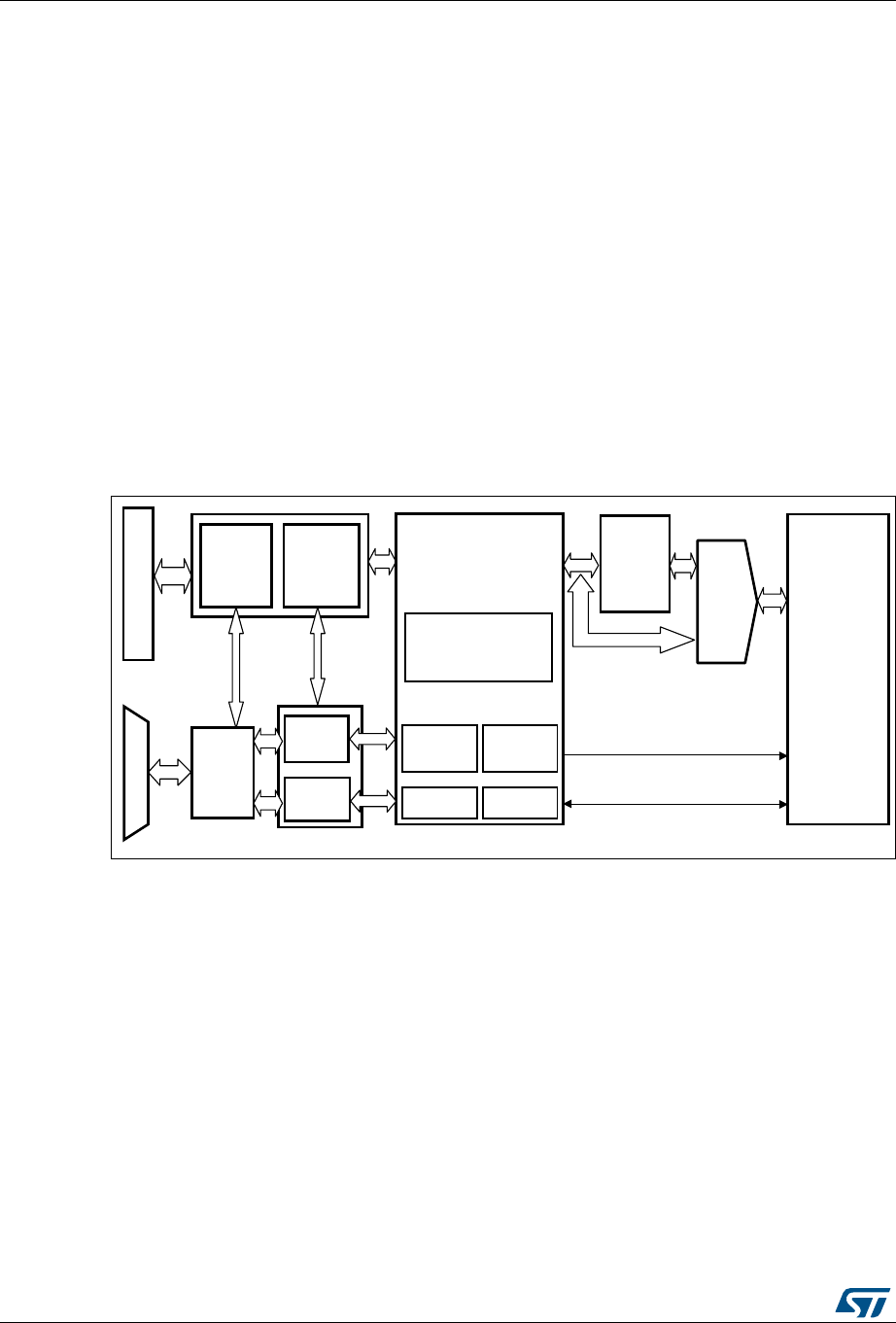
Ethernet (ETH): media access control (MAC) with DMA controller RM0090
1126/1749 RM0090 Rev 18
33.4 Ethernet functional description: SMI, MII and RMII
The Ethernet peripheral consists of a MAC 802.3 (media access control) with a dedicated
DMA controller. It supports both default media-independent interface (MII) and reduced
media-independent interface (RMII) through one selection bit (refer to SYSCFG_PMC
register).
The DMA controller interfaces with the Core and memories through the AHB Master and
Slave interfaces. The AHB Master Interface controls data transfers while the AHB Slave
interface accesses Control and Status Registers (CSR) space.
The Transmit FIFO (Tx FIFO) buffers data read from system memory by the DMA before
transmission by the MAC Core. Similarly, the Receive FIFO (Rx FIFO) stores the Ethernet
frames received from the line until they are transferred to system memory by the DMA.
The Ethernet peripheral also includes an SMI to communicate with external PHY. A set of
configuration registers permit the user to select the desired mode and features for the MAC
and the DMA controller.
Note: The AHB clock frequency must be at least 25 MHz when the Ethernet is used.
Figure 350. ETH block diagram
1. For AHB connections refer to Figure 1: System architecture for STM32F405xx/07xx and
STM32F415xx/17xx devices and Figure 2: System architecture for STM32F42xxx and STM32F43xxx
devices.
33.4.1 Station management interface: SMI
The station management interface (SMI) allows the application to access any PHY registers
through a 2-wire clock and data lines. The interface supports accessing up to 32 PHYs.
The application can select one of the 32 PHYs and one of the 32 registers within any PHY
and send control data or receive status information. Only one register in one PHY can be
addressed at any given time.
Both the MDC clock line and the MDIO data line are implemented as alternate function I/O
in the microcontroller:
•MDC: a periodic clock that provides the timing reference for the data transfer at the
maximum frequency of 2.5 MHz. The minimum high and low times for MDC must be
2 Kbyte
RX FIFO
Ethernet
DMA
Media access
control
MAC 802.3
MAC
control
registers
DMA
control &
status
registers
Operation
mode
register
Interface
Select
MII
MDC
MDIO
AHB Slave interface
RMII
ai15620c
Bus matrix
External PHY
Checksum
offload
PTP
IEEE1588
PMT MMC
2 Kbyte
TX FIFO
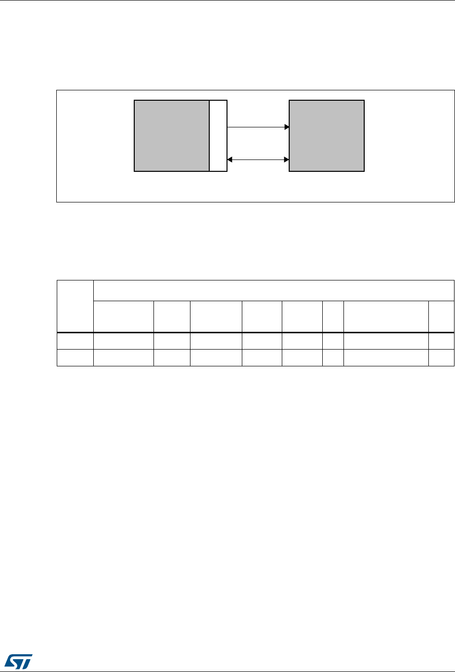
RM0090 Rev 18 1127/1749
RM0090 Ethernet (ETH): media access control (MAC) with DMA controller
1239
160 ns each, and the minimum period for MDC must be 400 ns. In idle state the SMI
management interface drives the MDC clock signal low.
•MDIO: data input/output bitstream to transfer status information to/from the PHY device
synchronously with the MDC clock signal
Figure 351. SMI interface signals
SMI frame format
The frame structure related to a read or write operation is shown in Table 13, the order of bit
transmission must be from left to right.
The management frame consists of eight fields:
•Preamble: each transaction (read or write) can be initiated with the preamble field that
corresponds to 32 contiguous logic one bits on the MDIO line with 32 corresponding
cycles on MDC. This field is used to establish synchronization with the PHY device.
•Start: the start of frame is defined by a <01> pattern to verify transitions on the line
from the default logic one state to zero and back to one.
•Operation: defines the type of transaction (read or write) in progress.
•PADDR: the PHY address is 5 bits, allowing 32 unique PHY addresses. The MSB bit of
the address is the first transmitted and received.
•RADDR: the register address is 5 bits, allowing 32 individual registers to be addressed
within the selected PHY device. The MSB bit of the address is the first transmitted and
received.
•TA: the turn-around field defines a 2-bit pattern between the RADDR and DATA fields
to avoid contention during a read transaction. For a read transaction the MAC controller
drives high-impedance on the MDIO line for the 2 bits of TA. The PHY device must
drive a high-impedance state on the first bit of TA, a zero bit on the second one.
Table 186. Management frame format
Management frame fields
Preamble
(32 bits) Start Operation PADDR RADDR TA Data (16 bits) Idle
Read 1... 1 01 10 ppppp rrrrr Z0 ddddddddddddddd Z
Write 1... 1 01 01 ppppp rrrrr 10 ddddddddddddddd Z
STM32 MCU
MDIO
MDC External
PHY
ai15621b
802.3 MAC
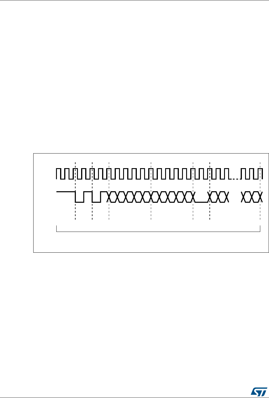
Ethernet (ETH): media access control (MAC) with DMA controller RM0090
1128/1749 RM0090 Rev 18
For a write transaction, the MAC controller drives a <10> pattern during the TA field.
The PHY device must drive a high-impedance state for the 2 bits of TA.
•Data: the data field is 16-bit. The first bit transmitted and received must be bit 15 of the
ETH_MIID register.
•Idle: the MDIO line is driven in high-impedance state. All three-state drivers must be
disabled and the PHY’s pull-up resistor keeps the line at logic one.
SMI write operation
When the application sets the MII Write and Busy bits (in Ethernet MAC MII address register
(ETH_MACMIIAR)), the SMI initiates a write operation into the PHY registers by transferring
the PHY address, the register address in PHY, and the write data (in Ethernet MAC MII data
register (ETH_MACMIIDR). The application should not change the MII Address register
contents or the MII Data register while the transaction is ongoing. Write operations to the MII
Address register or the MII Data Register during this period are ignored (the Busy bit is
high), and the transaction is completed without any error. After the Write operation has
completed, the SMI indicates this by resetting the Busy bit.
Figure 352 shows the frame format for the write operation.
Figure 352. MDIO timing and frame structure - Write cycle
SMI read operation
When the user sets the MII Busy bit in the Ethernet MAC MII address register
(ETH_MACMIIAR) with the MII Write bit at 0, the SMI initiates a read operation in the PHY
registers by transferring the PHY address and the register address in PHY. The application
should not change the MII Address register contents or the MII Data register while the
transaction is ongoing. Write operations to the MII Address register or MII Data Register
during this period are ignored (the Busy bit is high) and the transaction is completed without
any error. After the read operation has completed, the SMI resets the Busy bit and then
updates the MII Data register with the data read from the PHY.
Figure 353 shows the frame format for the read operation.
MDC
MDIO 32 1's 0 1 01A4 A3 A2 A1 A0 R4 R3 R2 R1 R0
D15 D14
D1 D0
Preamble
Start
of
frame
OP
code PHY address Register address Turn
around data
Data to PHY
ai15626
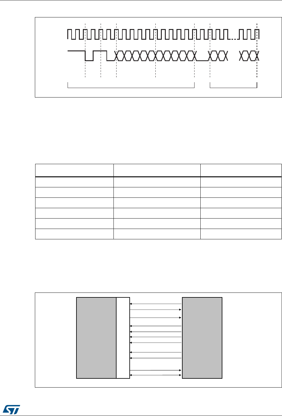
RM0090 Rev 18 1129/1749
RM0090 Ethernet (ETH): media access control (MAC) with DMA controller
1239
Figure 353. MDIO timing and frame structure - Read cycle
SMI clock selection
The MAC initiates the Management Write/Read operation. The SMI clock is a divided clock
whose source is the application clock (AHB clock). The divide factor depends on the clock
range setting in the MII Address register.
Table 187 shows how to set the clock ranges.
33.4.2 Media-independent interface: MII
The media-independent interface (MII) defines the interconnection between the MAC
sublayer and the PHY for data transfer at 10 Mbit/s and 100 Mbit/s.
Figure 354. Media independent interface signals
Table 187. Clock range
Selection HCLK clock MDC clock
000 60-100 MHz AHB clock / 42
001 100-150 MHz AHB clock / 62
010 20-35 MHz AHB clock / 16
011 35-60 MHz AHB clock / 26
100 150-180 MHz AHB clock / 102
101, 110, 111 Reserved -
MDC
MDIO 32 1's 0 1 1 0
A4 A3 A2 A1 A0 R4 R3 R2 R1 R0
D15 D14
D1 D0
Preamble Start
of
frame
OP
code PHY address Register address Turn
around data
Data to PHY
ai15627
Data from PHY
MDC
MDIO
RX_DV
CRS
COL
TX_EN
RX_CLK
RXD[3:0]
RX_ER
TX _CLK
TXD[3:0]
External
PHY
ai15622c
802.3 MAC
STM32 MCU

Ethernet (ETH): media access control (MAC) with DMA controller RM0090
1130/1749 RM0090 Rev 18
•MII_TX_CLK: continuous clock that provides the timing reference for the TX data
transfer. The nominal frequency is: 2.5 MHz at 10 Mbit/s speed; 25 MHz at 100 Mbit/s
speed.
•MII_RX_CLK: continuous clock that provides the timing reference for the RX data
transfer. The nominal frequency is: 2.5 MHz at 10 Mbit/s speed; 25 MHz at 100 Mbit/s
speed.
•MII_TX_EN: transmission enable indicates that the MAC is presenting nibbles on the
MII for transmission. It must be asserted synchronously (MII_TX_CLK) with the first
nibble of the preamble and must remain asserted while all nibbles to be transmitted are
presented to the MII.
•MII_TXD[3:0]: transmit data is a bundle of 4 data signals driven synchronously by the
MAC sublayer and qualified (valid data) on the assertion of the MII_TX_EN signal.
MII_TXD[0] is the least significant bit, MII_TXD[3] is the most significant bit. While
MII_TX_EN is deasserted the transmit data must have no effect upon the PHY.
•MII_CRS: carrier sense is asserted by the PHY when either the transmit or receive
medium is non idle. It shall be deasserted by the PHY when both the transmit and
receive media are idle. The PHY must ensure that the MII_CS signal remains asserted
throughout the duration of a collision condition. This signal is not required to transition
synchronously with respect to the TX and RX clocks. In full duplex mode the state of
this signal is don’t care for the MAC sublayer.
•MII_COL: collision detection must be asserted by the PHY upon detection of a collision
on the medium and must remain asserted while the collision condition persists. This
signal is not required to transition synchronously with respect to the TX and RX clocks.
In full duplex mode the state of this signal is don’t care for the MAC sublayer.
•MII_RXD[3:0]: reception data is a bundle of 4 data signals driven synchronously by the
PHY and qualified (valid data) on the assertion of the MII_RX_DV signal. MII_RXD[0] is
the least significant bit, MII_RXD[3] is the most significant bit. While MII_RX_EN is
deasserted and MII_RX_ER is asserted, a specific MII_RXD[3:0] value is used to
transfer specific information from the PHY (see Table 189).
•MII_RX_DV: receive data valid indicates that the PHY is presenting recovered and
decoded nibbles on the MII for reception. It must be asserted synchronously
(MII_RX_CLK) with the first recovered nibble of the frame and must remain asserted
through the final recovered nibble. It must be deasserted prior to the first clock cycle
that follows the final nibble. In order to receive the frame correctly, the MII_RX_DV
signal must encompass the frame, starting no later than the SFD field.
•MII_RX_ER: receive error must be asserted for one or more clock periods
(MII_RX_CLK) to indicate to the MAC sublayer that an error was detected somewhere
in the frame. This error condition must be qualified by MII_RX_DV assertion as
described in Table 189.
Table 188. TX interface signal encoding
MII_TX_EN MII_TXD[3:0] Description
0 0000 through 1111 Normal inter-frame
1 0000 through 1111 Normal data transmission
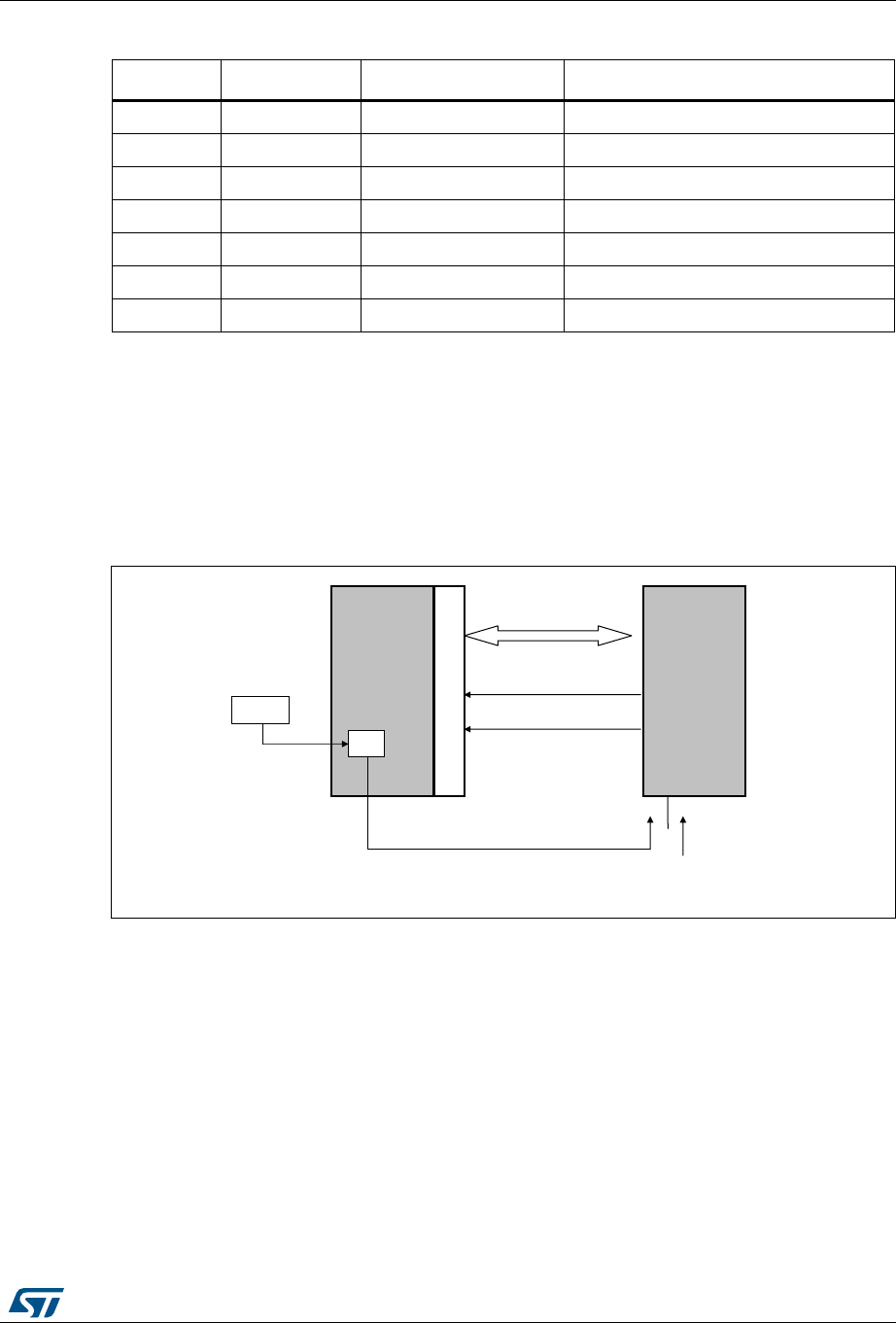
RM0090 Rev 18 1131/1749
RM0090 Ethernet (ETH): media access control (MAC) with DMA controller
1239
MII clock sources
To generate both TX_CLK and RX_CLK clock signals, the external PHY must be clocked
with an external 25 MHz as shown in Figure 355. Instead of using an external 25 MHz
quartz to provide this clock, the STM32F4xxmicrocontroller can output this signal on its
MCO pin. In this case, the PLL multiplier has to be configured so as to get the desired
frequency on the MCO pin, from the 25 MHz external quartz.
Figure 355. MII clock sources
33.4.3 Reduced media-independent interface: RMII
The reduced media-independent interface (RMII) specification reduces the pin count
between the microcontroller Ethernet peripheral and the external Ethernet in 10/100 Mbit/s.
According to the IEEE 802.3u standard, an MII contains 16 pins for data and control. The
RMII specification is dedicated to reduce the pin count to 7 pins (a 62.5% decrease in pin
count).
Table 189. RX interface signal encoding
MII_RX_DV MII_RX_ERR MII_RXD[3:0] Description
0 0 0000 through 1111 Normal inter-frame
0 1 0000 Normal inter-frame
0 1 0001 through 1101 Reserved
0 1 1110 False carrier indication
0 1 1111 Reserved
1 0 0000 through 1111 Normal data reception
1 1 0000 through 1111 Data reception with errors
STM32
MCU
MCO
25 MHz
25 MHz
TX _CLK
For 10/100 Mbit/s
RX _CLK
HSE
802.3 MAC
ai15623b
External
PHY
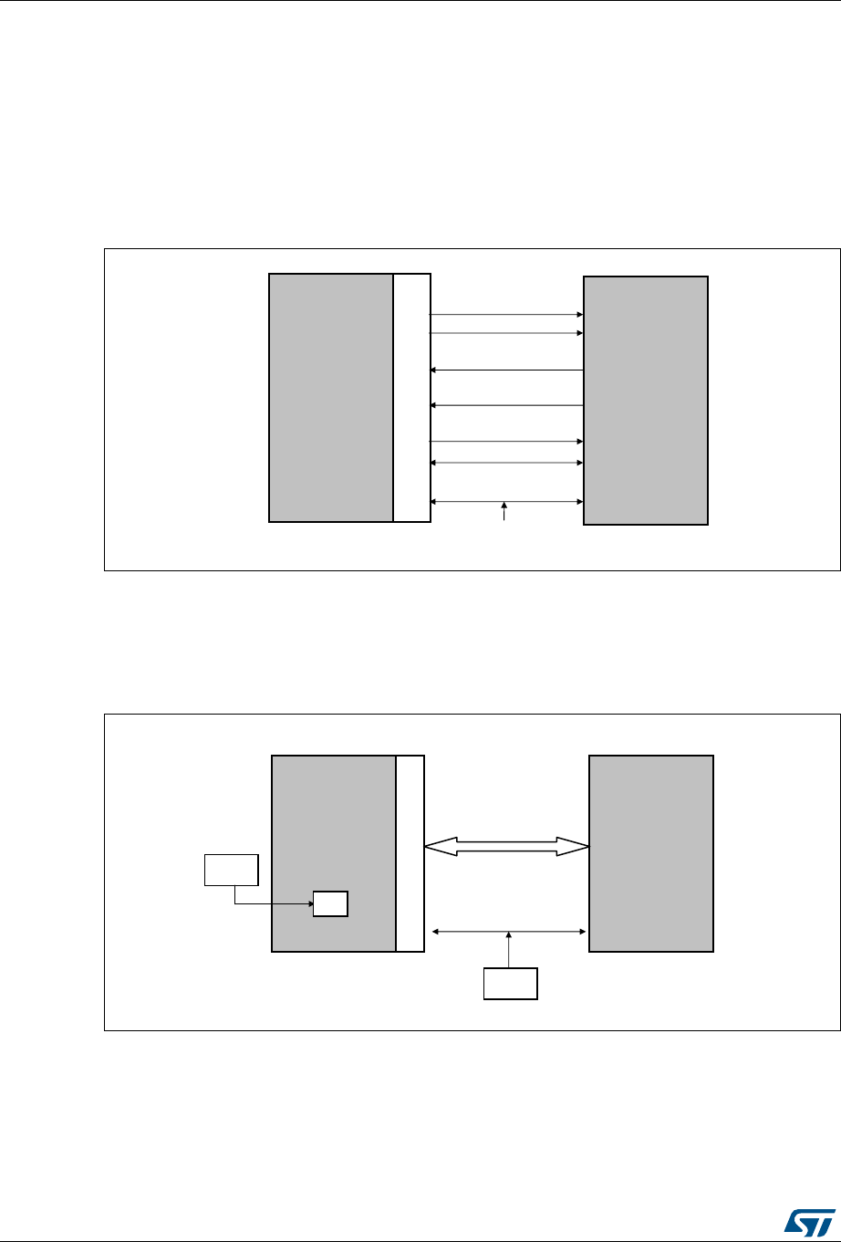
Ethernet (ETH): media access control (MAC) with DMA controller RM0090
1132/1749 RM0090 Rev 18
The RMII is instantiated between the MAC and the PHY. This helps translation of the MAC’s
MII into the RMII. The RMII block has the following characteristics:
•It supports 10-Mbit/s and 100-Mbit/s operating rates
•The clock reference must be doubled to 50 MHz
•The same clock reference must be sourced externally to both MAC and external
Ethernet PHY
•It provides independent 2-bit wide (dibit) transmit and receive data paths
Figure 356. Reduced media-independent interface signals
RMII clock sources
Either clock the PHY from an external 50 MHz clock or use a PHY with an embedded PLL to
generate the 50 MHz frequency.
Figure 357. RMII clock sources
33.4.4 MII/RMII selection
The mode, MII or RMII, is selected using the configuration bit 23, MII_RMII_SEL, in the
SYSCFG_PMC register. The application has to set the MII/RMII mode while the Ethernet
controller is under reset or before enabling the clocks.
STM32
MCU
TXD[1:0]
TX_EN
RXD[1:0]
CRS_DV
MDC
MDIO
REF_ CLK
Clock source
802.3 MAC
External
PHY
ai15624b
MS19930V1
STM32
MCU
REF_CLK
50 MHz
25 MHz
PLL
For 10/100 Mbit/s
External
PHY
802.3 MAC
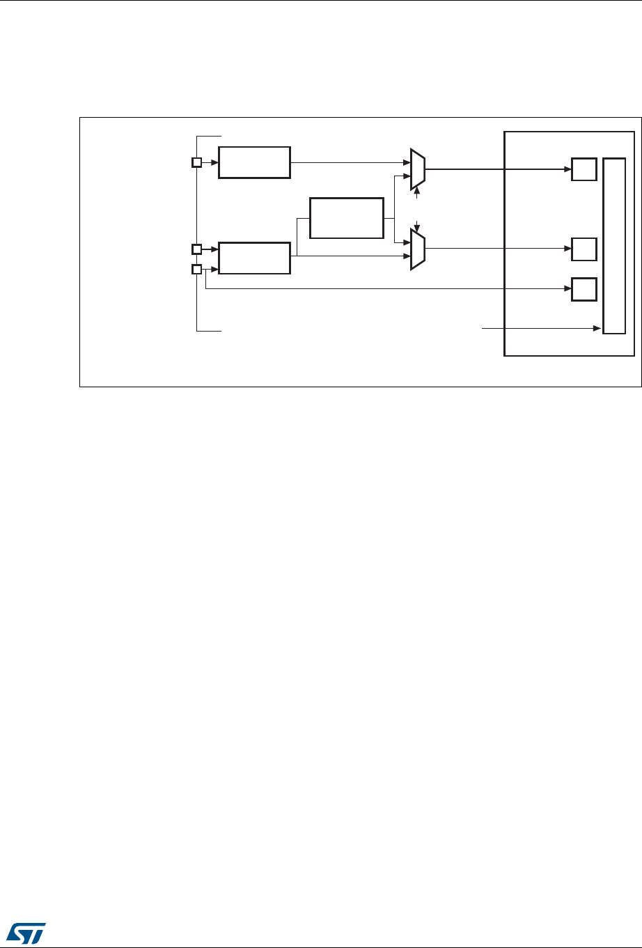
RM0090 Rev 18 1133/1749
RM0090 Ethernet (ETH): media access control (MAC) with DMA controller
1239
MII/RMII internal clock scheme
The clock scheme required to support both the MII and RMII, as well as 10 and 100 Mbit/s
operations is described in Figure 358.
Figure 358. Clock scheme
1. The MII/RMII selection is controlled through bit 23, MII_RMII_SEL, in the SYSCFG_PMC register.
To save a pin, the two input clock signals, RMII_REF_CK and MII_RX_CLK, are multiplexed
on the same GPIO pin.
33.5 Ethernet functional description: MAC 802.3
The IEEE 802.3 International Standard for local area networks (LANs) employs the
CSMA/CD (carrier sense multiple access with collision detection) as the access method.
The Ethernet peripheral consists of a MAC 802.3 (media access control) controller with
media independent interface (MII) and a dedicated DMA controller.
The MAC block implements the LAN CSMA/CD sublayer for the following families of
systems: 10 Mbit/s and 100 Mbit/s of data rates for baseband and broadband systems. Half-
and full-duplex operation modes are supported. The collision detection access method is
applied only to the half-duplex operation mode. The MAC control frame sublayer is
supported.
The MAC sublayer performs the following functions associated with a data link control
procedure:
•Data encapsulation (transmit and receive)
– Framing (frame boundary delimitation, frame synchronization)
– Addressing (handling of source and destination addresses)
– Error detection
•Media access management
– Medium allocation (collision avoidance)
– Contention resolution (collision handling)
GPIO and AF
controller
GPIO and AF
controller
MII_TX_CLK as AF
(25 MHz or 2.5 MHz)
MII_RX_CLK as AF
(25 MHz or 2.5 MHz)
Sync. divider
/2 for 100 Mb/s
/20 for 10 Mb/s
50 MHz
0
1
0
1
25 MHz or 2.5 MHz
25 MHz or 2.5 MHz
0 MII
1 RMII(1)
25 MHz
or 2.5 MHz
25 MHz
or 2.5 MHz
MACTXCLK
MACRXCLK
TX
RX
AHB
HCLK
HCLK
MAC
must be greater
than 25 MHz
ai15650
RMII
RMII_REF_CK as AF
(50 MHz)

Ethernet (ETH): media access control (MAC) with DMA controller RM0090
1134/1749 RM0090 Rev 18
Basically there are two operating modes of the MAC sublayer:
•Half-duplex mode: the stations contend for the use of the physical medium, using the
CSMA/CD algorithms.
•Full duplex mode: simultaneous transmission and reception without contention
resolution (CSMA/CD algorithm are unnecessary) when all the following conditions are
met:
– physical medium capability to support simultaneous transmission and reception
– exactly 2 stations connected to the LAN
– both stations configured for full-duplex operation
33.5.1 MAC 802.3 frame format
The MAC block implements the MAC sublayer and the optional MAC control sublayer
(10/100 Mbit/s) as specified by the IEEE 802.3-2002 standard.
Two frame formats are specified for data communication systems using the CSMA/CD
MAC:
•Basic MAC frame format
•Tagged MAC frame format (extension of the basic MAC frame format)
Figure 360 and Figure 361 describe the frame structure (untagged and tagged) that
includes the following fields:
•Preamble: 7-byte field used for synchronization purposes (PLS circuitry)
Hexadecimal value: 55-55-55-55-55-55-55
Bit pattern: 01010101 01010101 01010101 01010101 01010101 01010101 01010101
(right-to-left bit transmission)
•Start frame delimiter (SFD): 1-byte field used to indicate the start of a frame.
Hexadecimal value: D5
Bit pattern: 11010101 (right-to-left bit transmission)
•Destination and Source Address fields: 6-byte fields to indicate the destination and
source station addresses as follows (see Figure 359):
– Each address is 48 bits in length
– The first LSB bit (I/G) in the destination address field is used to indicate an
individual (I/G = 0) or a group address (I/G = 1). A group address could identify
none, one or more, or all the stations connected to the LAN. In the source address
the first bit is reserved and reset to 0.
– The second bit (U/L) distinguishes between locally (U/L = 1) or globally (U/L = 0)
administered addresses. For broadcast addresses this bit is also 1.
– Each byte of each address field must be transmitted least significant bit first.
The address designation is based on the following types:
•Individual address: this is the physical address associated with a particular station on
the network.
•Group address. A multidestination address associated with one or more stations on a
given network. There are two kinds of multicast address:
– Multicast-group address: an address associated with a group of logically related
stations.
– Broadcast address: a distinguished, predefined multicast address (all 1’s in the
destination address field) that always denotes all the stations on a given LAN.

RM0090 Rev 18 1135/1749
RM0090 Ethernet (ETH): media access control (MAC) with DMA controller
1239
Figure 359. Address field format
•QTag Prefix: 4-byte field inserted between the Source address field and the MAC Client
Length/Type field. This field is an extension of the basic frame (untagged) to obtain the
tagged MAC frame. The untagged MAC frames do not include this field. The
extensions for tagging are as follows:
– 2-byte constant Length/Type field value consistent with the Type interpretation
(greater than 0x0600) equal to the value of the 802.1Q Tag Protocol Type (0x8100
hexadecimal). This constant field is used to distinguish tagged and untagged MAC
frames.
– 2-byte field containing the Tag control information field subdivided as follows: a 3-
bit user priority, a canonical format indicator (CFI) bit and a 12-bit VLAN Identifier.
The length of the tagged MAC frame is extended by 4 bytes by the QTag Prefix.
•MAC client length/type: 2-byte field with different meaning (mutually exclusive),
depending on its value:
– If the value is less than or equal to maxValidFrame (0d1500) then this field
indicates the number of MAC client data bytes contained in the subsequent data
field of the 802.3 frame (length interpretation).
– If the value is greater than or equal to MinTypeValue (0d1536 decimal, 0x0600)
then this field indicates the nature of the MAC client protocol (Type interpretation)
related to the Ethernet frame.
Regardless of the interpretation of the length/type field, if the length of the data field is
less than the minimum required for proper operation of the protocol, a PAD field is
added after the data field but prior to the FCS (frame check sequence) field. The
length/type field is transmitted and received with the higher-order byte first.
For length/type field values in the range between maxValidLength and minTypeValue
(boundaries excluded), the behavior of the MAC sublayer is not specified: they may or
may not be passed by the MAC sublayer.
•Data and PAD fields: n-byte data field. Full data transparency is provided, it means that
any arbitrary sequence of byte values may appear in the data field. The size of the
PAD, if any, is determined by the size of the data field. Max and min length of the data
and PAD field are:
– Maximum length = 1500 bytes
– Minimum length for untagged MAC frames = 46 bytes
– Minimum length for tagged MAC frames = 42 bytes
When the data field length is less than the minimum required, the PAD field is added to
match the minimum length (42 bytes for tagged frames, 46 bytes for untagged frames).
•Frame check sequence: 4-byte field that contains the cyclic redundancy check (CRC)
value. The CRC computation is based on the following fields: source address,
destination address, QTag prefix, length/type, LLC data and PAD (that is, all fields
except the preamble, SFD). The generating polynomial is the following:
MSB LSB
Bit transmission order (right to left)
U/L I/G
46-bit address
I/G = 0 Individual address
I/G = 1 Group address
U/L = 0 Globally administered address
U/L = 1 Locally administered address
ai15628
Gx() x32 x26 x23 x22 x16 x12 x11 x10 x8x7x5x4x2x1+ + + + + + + +++++++=
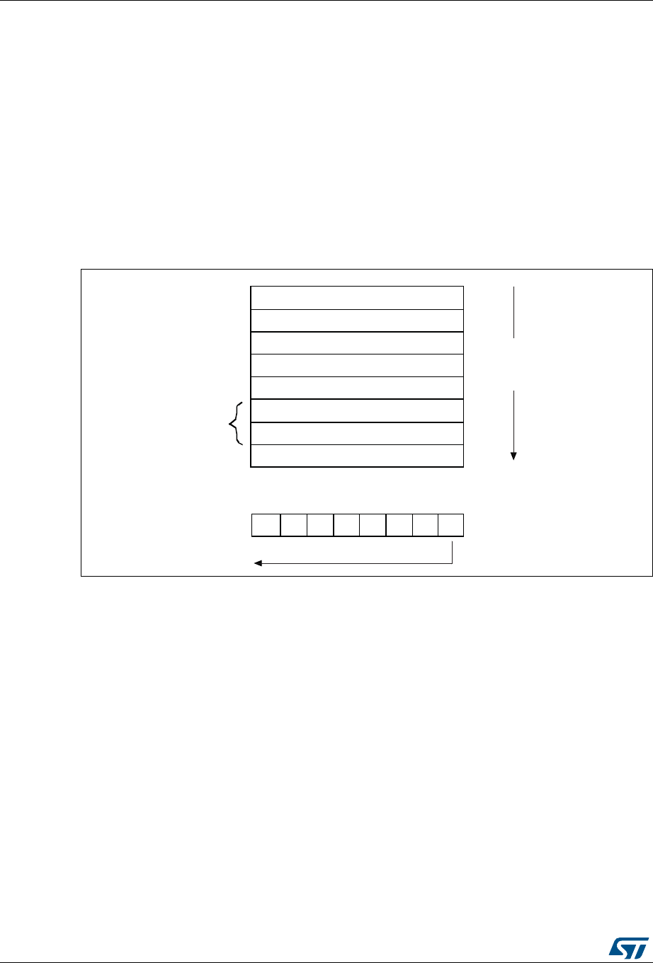
Ethernet (ETH): media access control (MAC) with DMA controller RM0090
1136/1749 RM0090 Rev 18
The CRC value of a frame is computed as follows:
•The first 2 bits of the frame are complemented
•The n-bits of the frame are the coefficients of a polynomial M(x) of degree (n – 1). The
first bit of the destination address corresponds to the xn – 1 term and the last bit of the
data field corresponds to the x0 term
•M(x) is multiplied by x32 and divided by G(x), producing a remainder R(x) of degree
≤31
•The coefficients of R(x) are considered as a 32-bit sequence
•The bit sequence is complemented and the result is the CRC
•The 32-bits of the CRC value are placed in the frame check sequence. The x32 term is
the first transmitted, the x0 term is the last one
Figure 360. MAC frame format
Preamble
SFD
Destination address
Source address
MAC client length/type
MAC client data
PAD
Frame check sequence
7 bytes
1 byte
6 bytes
6 bytes
2 bytes
46-1500 bytes
4 bytes
MSB LSB
Bit transmission order (right to left)
Bytes within
frame transmitted
top to bottom
ai15629
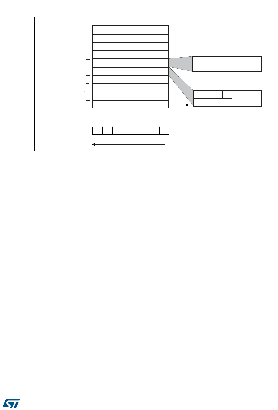
RM0090 Rev 18 1137/1749
RM0090 Ethernet (ETH): media access control (MAC) with DMA controller
1239
Figure 361. Tagged MAC frame format
Each byte of the MAC frame, except the FCS field, is transmitted low-order bit first.
An invalid MAC frame is defined by one of the following conditions:
•The frame length is inconsistent with the expected value as specified by the length/type
field. If the length/type field contains a type value, then the frame length is assumed to
be consistent with this field (no invalid frame)
•The frame length is not an integer number of bytes (extra bits)
•The CRC value computed on the incoming frame does not match the included FCS
33.5.2 MAC frame transmission
The DMA controls all transactions for the transmit path. Ethernet frames read from the
system memory are pushed into the FIFO by the DMA. The frames are then popped out and
transferred to the MAC core. When the end-of-frame is transferred, the status of the
transmission is taken from the MAC core and transferred back to the DMA. The Transmit
FIFO has a depth of 2 Kbyte. FIFO-fill level is indicated to the DMA so that it can initiate a
data fetch in required bursts from the system memory, using the AHB interface. The data
from the AHB Master interface is pushed into the FIFO.
When the SOF is detected, the MAC accepts the data and begins transmitting to the MII.
The time required to transmit the frame data to the MII after the application initiates
transmission is variable, depending on delay factors like IFG delay, time to transmit
preamble/SFD, and any back-off delays for Half-duplex mode. After the EOF is transferred
to the MAC core, the core completes normal transmission and then gives the status of
transmission back to the DMA. If a normal collision (in Half-duplex mode) occurs during
transmission, the MAC core makes the transmit status valid, then accepts and drops all
further data until the next SOF is received. The same frame should be retransmitted from
SOF on observing a Retry request (in the Status) from the MAC. The MAC issues an
underflow status if the data are not provided continuously during the transmission. During
the normal transfer of a frame, if the MAC receives an SOF without getting an EOF for the
previous frame, then the SOF is ignored and the new frame is considered as the
continuation of the previous frame.
Preamble
SFD
Destination address
Source address
Length/type = 802.1QTagType
Tag control information
MAC client length/type
MAC client data
7 bytes
1 byte
6 bytes
6 bytes
QTag Prefix
42-1500 bytes
2 bytes
MSB LSB
Bit transmission order (right to left)
bytes within
frame transmitted
top to bottom
Frame check sequence
Pad
4 bytes
4 bytes
1 0 0 0 0 0 0 0 1
VLAN identifier (VID, 12 bits)
CFIUser priority
MSB LSB
0 0 0 0 0 0 0 0 0
ai15630

Ethernet (ETH): media access control (MAC) with DMA controller RM0090
1138/1749 RM0090 Rev 18
There are two modes of operation for popping data towards the MAC core:
•In Threshold mode, as soon as the number of bytes in the FIFO crosses the configured
threshold level (or when the end-of-frame is written before the threshold is crossed),
the data is ready to be popped out and forwarded to the MAC core. The threshold level
is configured using the TTC bits of ETH_DMABMR.
•In Store-and-forward mode, only after a complete frame is stored in the FIFO, the frame
is popped towards the MAC core. If the Tx FIFO size is smaller than the Ethernet frame
to be transmitted, then the frame is popped towards the MAC core when the Tx FIFO
becomes almost full.
The application can flush the Transmit FIFO of all contents by setting the FTF
(ETH_DMAOMR register [20]) bit. This bit is self-clearing and initializes the FIFO pointers to
the default state. If the FTF bit is set during a frame transfer to the MAC core, then transfer
is stopped as the FIFO is considered to be empty. Hence an underflow event occurs at the
MAC transmitter and the corresponding Status word is forwarded to the DMA.
Automatic CRC and pad generation
When the number of bytes received from the application falls below 60 (DA+SA+LT+Data),
zeros are appended to the transmitting frame to make the data length exactly 46 bytes to
meet the minimum data field requirement of IEEE 802.3. The MAC can be programmed not
to append any padding. The cyclic redundancy check (CRC) for the frame check sequence
(FCS) field is calculated and appended to the data being transmitted. When the MAC is
programmed to not append the CRC value to the end of Ethernet frames, the computed
CRC is not transmitted. An exception to this rule is that when the MAC is programmed to
append pads for frames (DA+SA+LT+Data) less than 60 bytes, CRC will be appended at the
end of the padded frames.
The CRC generator calculates the 32-bit CRC for the FCS field of the Ethernet frame. The
encoding is defined by the following polynomial.
Transmit protocol
The MAC controls the operation of Ethernet frame transmission. It performs the following
functions to meet the IEEE 802.3/802.3z specifications. It:
•generates the preamble and SFD
•generates the jam pattern in Half-duplex mode
•controls the Jabber timeout
•controls the flow for Half-duplex mode (back pressure)
•generates the transmit frame status
•contains time stamp snapshot logic in accordance with IEEE 1588
When a new frame transmission is requested, the MAC sends out the preamble and SFD,
followed by the data. The preamble is defined as 7 bytes of 0b10101010 pattern, and the
SFD is defined as 1 byte of 0b10101011 pattern. The collision window is defined as 1 slot
time (512 bit times for 10/100 Mbit/s Ethernet). The jam pattern generation is applicable only
to Half-duplex mode, not to Full-duplex mode.
In MII mode, if a collision occurs at any time from the beginning of the frame to the end of
the CRC field, the MAC sends a 32-bit jam pattern of 0x5555 5555 on the MII to inform all
Gx() x32 x26 x23 x22 x16 x12 x11 x10 x8x7x5x4x2x1+ + + + + + + +++++++=

RM0090 Rev 18 1139/1749
RM0090 Ethernet (ETH): media access control (MAC) with DMA controller
1239
other stations that a collision has occurred. If the collision is seen during the preamble
transmission phase, the MAC completes the transmission of the preamble and SFD and
then sends the jam pattern.
A jabber timer is maintained to cut off the transmission of Ethernet frames if more than 2048
(default) bytes have to be transferred. The MAC uses the deferral mechanism for flow
control (back pressure) in Half-duplex mode. When the application requests to stop
receiving frames, the MAC sends a JAM pattern of 32 bytes whenever it senses the
reception of a frame, provided that transmit flow control is enabled. This results in a collision
and the remote station backs off. The application requests flow control by setting the BPA bit
(bit 0) in the ETH_MACFCR register. If the application requests a frame to be transmitted,
then it is scheduled and transmitted even when back pressure is activated. Note that if back
pressure is kept activated for a long time (and more than 16 consecutive collision events
occur) then the remote stations abort their transmissions due to excessive collisions. If IEEE
1588 time stamping is enabled for the transmit frame, this block takes a snapshot of the
system time when the SFD is put onto the transmit MII bus.
Transmit scheduler
The MAC is responsible for scheduling the frame transmission on the MII. It maintains the
interframe gap between two transmitted frames and follows the truncated binary exponential
backoff algorithm for Half-duplex mode. The MAC enables transmission after satisfying the
IFG and backoff delays. It maintains an idle period of the configured interframe gap (IFG bits
in the ETH_MACCR register) between any two transmitted frames. If frames to be
transmitted arrive sooner than the configured IFG time, the MII waits for the enable signal
from the MAC before starting the transmission on it. The MAC starts its IFG counter as soon
as the carrier signal of the MII goes inactive. At the end of the programmed IFG value, the
MAC enables transmission in Full-duplex mode. In Half-duplex mode and when IFG is
configured for 96 bit times, the MAC follows the rule of deference specified in Section
4.2.3.2.1 of the IEEE 802.3 specification. The MAC resets its IFG counter if a carrier is
detected during the first two-thirds (64-bit times for all IFG values) of the IFG interval. If the
carrier is detected during the final one third of the IFG interval, the MAC continues the IFG
count and enables the transmitter after the IFG interval. The MAC implements the truncated
binary exponential backoff algorithm when it operates in Half-duplex mode.
Transmit flow control
When the Transmit Flow Control Enable bit (TFE bit in ETH_MACFCR) is set, the MAC
generates Pause frames and transmits them as necessary, in Full-duplex mode. The Pause
frame is appended with the calculated CRC, and is sent. Pause frame generation can be
initiated in two ways.
A pause frame is sent either when the application sets the FCB bit in the ETH_MACFCR
register or when the receive FIFO is full (packet buffer).
•If the application has requested flow control by setting the FCB bit in ETH_MACFCR,
the MAC generates and transmits a single Pause frame. The value of the pause time in
the generated frame contains the programmed pause time value in ETH_MACFCR. To
extend the pause or end the pause prior to the time specified in the previously
transmitted Pause frame, the application must request another Pause frame
transmission after programming the Pause Time value (PT in ETH_MACFCR register)
with the appropriate value.
•If the application has requested flow control when the receive FIFO is full, the MAC
generates and transmits a Pause frame. The value of the pause time in the generated
frame is the programmed pause time value in ETH_MACFCR. If the receive FIFO

Ethernet (ETH): media access control (MAC) with DMA controller RM0090
1140/1749 RM0090 Rev 18
remains full at a configurable number of slot-times (PLT bits in ETH_MACFCR) before
this Pause time runs out, a second Pause frame is transmitted. The process is
repeated as long as the receive FIFO remains full. If this condition is no more satisfied
prior to the sampling time, the MAC transmits a Pause frame with zero pause time to
indicate to the remote end that the receive buffer is ready to receive new data frames.
Single-packet transmit operation
The general sequence of events for a transmit operation is as follows:
1. If the system has data to be transferred, the DMA controller fetches them from the
memory through the AHB Master interface and starts forwarding them to the FIFO. It
continues to receive the data until the end of frame is transferred.
2. When the threshold level is crossed or a full packet of data is received into the FIFO,
the frame data are popped and driven to the MAC core. The DMA continues to transfer
data from the FIFO until a complete packet has been transferred to the MAC. Upon
completion of the frame, the DMA controller is notified by the status coming from the
MAC.
Transmit operation—Two packets in the buffer
1. Because the DMA must update the descriptor status before releasing it to the Host,
there can be at the most two frames inside a transmit FIFO. The second frame is
fetched by the DMA and put into the FIFO only if the OSF (operate on second frame)
bit is set. If this bit is not set, the next frame is fetched from the memory only after the
MAC has completely processed the frame and the DMA has released the descriptors.
2. If the OSF bit is set, the DMA starts fetching the second frame immediately after
completing the transfer of the first frame to the FIFO. It does not wait for the status to
be updated. In the meantime, the second frame is received into the FIFO while the first
frame is being transmitted. As soon as the first frame has been transferred and the
status is received from the MAC, it is pushed to the DMA. If the DMA has already
completed sending the second packet to the FIFO, the second transmission must wait
for the status of the first packet before proceeding to the next frame.
Retransmission during collision
While a frame is being transferred to the MAC, a collision event may occur on the MAC line
interface in Half-duplex mode. The MAC would then indicate a retry attempt by giving the
status even before the end of frame is received. Then the retransmission is enabled and the
frame is popped out again from the FIFO. After more than 96 bytes have been popped
towards the MAC core, the FIFO controller frees up that space and makes it available to the
DMA to push in more data. This means that the retransmission is not possible after this
threshold is crossed or when the MAC core indicates a late collision event.
Transmit FIFO flush operation
The MAC provides a control to the software to flush the Transmit FIFO through the use of Bit
20 in the Operation mode register. The Flush operation is immediate and the Tx FIFO and
the corresponding pointers are cleared to the initial state even if the Tx FIFO is in the middle
of transferring a frame to the MAC Core. This results in an underflow event in the MAC
transmitter, and the frame transmission is aborted. The status of such a frame is marked
with both underflow and frame flush events (TDES0 bits 13 and 1). No data are coming to
the FIFO from the application (DMA) during the Flush operation. Transfer transmit status
words are transferred to the application for the number of frames that is flushed (including
partial frames). Frames that are completely flushed have the Frame flush status bit (TDES0
13) set. The Flush operation is completed when the application (DMA) has accepted all of

RM0090 Rev 18 1141/1749
RM0090 Ethernet (ETH): media access control (MAC) with DMA controller
1239
the Status words for the frames that were flushed. The Transmit FIFO Flush control register
bit is then cleared. At this point, new frames from the application (DMA) are accepted. All
data presented for transmission after a Flush operation are discarded unless they start with
an SOF marker.
Transmit status word
At the end of the Ethernet frame transfer to the MAC core and after the core has completed
the transmission of the frame, the transmit status is given to the application. The detailed
description of the Transmit Status is the same as for bits [23:0] in TDES0. If IEEE 1588 time
stamping is enabled, a specific frames’ 64-bit time stamp is returned, along with the transmit
status.
Transmit checksum offload
Communication protocols such as TCP and UDP implement checksum fields, which helps
determine the integrity of data transmitted over a network. Because the most widespread
use of Ethernet is to encapsulate TCP and UDP over IP datagrams, the Ethernet controller
has a transmit checksum offload feature that supports checksum calculation and insertion in
the transmit path, and error detection in the receive path. This section explains the operation
of the checksum offload feature for transmitted frames.
Note: The checksum for TCP, UDP or ICMP is calculated over a complete frame, then inserted
into its corresponding header field. Due to this requirement, this function is enabled only
when the Transmit FIFO is configured for Store-and-forward mode (that is, when the TSF bit
is set in the ETH_ETH_DMAOMR register). If the core is configured for Threshold (cut-
through) mode, the Transmit checksum offload is bypassed.
You must make sure the Transmit FIFO is deep enough to store a complete frame before
that frame is transferred to the MAC Core transmitter. If the FIFO depth is less than the input
Ethernet frame size, the payload (TCP/UDP/ICMP) checksum insertion function is bypassed
and only the frame’s IPv4 Header checksum is modified, even in Store-and-forward mode.
The transmit checksum offload supports two types of checksum calculation and insertion.
This checksum can be controlled for each frame by setting the CIC bits (Bits 28:27 in
TDES1, described in TDES1: Transmit descriptor Word1).
See IETF specifications RFC 791, RFC 793, RFC 768, RFC 792, RFC 2460 and RFC 4443
for IPv4, TCP, UDP, ICMP, IPv6 and ICMPv6 packet header specifications, respectively.
•IP header checksum
In IPv4 datagrams, the integrity of the header fields is indicated by the 16-bit header
checksum field (the eleventh and twelfth bytes of the IPv4 datagram). The checksum
offload detects an IPv4 datagram when the Ethernet frame’s Type field has the value
0x0800 and the IP datagram’s Version field has the value 0x4. The input frame’s
checksum field is ignored during calculation and replaced by the calculated value. IPv6
headers do not have a checksum field; thus, the checksum offload does not modify
IPv6 header fields. The result of this IP header checksum calculation is indicated by the
IP Header Error status bit in the Transmit status (Bit 16). This status bit is set whenever
the values of the Ethernet Type field and the IP header’s Version field are not
consistent, or when the Ethernet frame does not have enough data, as indicated by the

Ethernet (ETH): media access control (MAC) with DMA controller RM0090
1142/1749 RM0090 Rev 18
IP header Length field. In other words, this bit is set when an IP header error is
asserted under the following circumstances:
a) For IPv4 datagrams:
– The received Ethernet type is 0x0800, but the IP header’s Version field does not
equal 0x4
– The IPv4 Header Length field indicates a value less than 0x5 (20 bytes)
– The total frame length is less than the value given in the IPv4 Header Length field
b) For IPv6 datagrams:
– The Ethernet type is 0x86DD but the IP header Version field does not equal 0x6
– The frame ends before the IPv6 header (40 bytes) or extension header (as given
in the corresponding Header Length field in an extension header) has been
completely received. Even when the checksum offload detects such an IP header
error, it inserts an IPv4 header checksum if the Ethernet Type field indicates an
IPv4 payload.
•TCP/UDP/ICMP checksum
The TCP/UDP/ICMP checksum processes the IPv4 or IPv6 header (including
extension headers) and determines whether the encapsulated payload is TCP, UDP or
ICMP.
Note that:
a) For non-TCP, -UDP, or -ICMP/ICMPv6 payloads, this checksum is bypassed and
nothing further is modified in the frame.
b) Fragmented IP frames (IPv4 or IPv6), IP frames with security features (such as an
authentication header or encapsulated security payload), and IPv6 frames with
routing headers are bypassed and not processed by the checksum.
The checksum is calculated for the TCP, UDP, or ICMP payload and inserted into its
corresponding field in the header. It can work in the following two modes:
– In the first mode, the TCP, UDP, or ICMPv6 pseudo-header is not included in the
checksum calculation and is assumed to be present in the input frame’s checksum
field. The checksum field is included in the checksum calculation, and then
replaced by the final calculated checksum.
– In the second mode, the checksum field is ignored, the TCP, UDP, or ICMPv6
pseudo-header data are included into the checksum calculation, and the
checksum field is overwritten with the final calculated value.
Note that: for ICMP-over-IPv4 packets, the checksum field in the ICMP packet must
always be 0x0000 in both modes, because pseudo-headers are not defined for such
packets. If it does not equal 0x0000, an incorrect checksum may be inserted into the
packet.
The result of this operation is indicated by the payload checksum error status bit in the
Transmit Status vector (bit 12). The payload checksum error status bit is set when
either of the following is detected:
– the frame has been forwarded to the MAC transmitter in Store-and-forward mode
without the end of frame being written to the FIFO
– the packet ends before the number of bytes indicated by the payload length field in
the IP header is received.
When the packet is longer than the indicated payload length, the bytes are ignored as
stuff bytes, and no error is reported. When the first type of error is detected, the TCP,
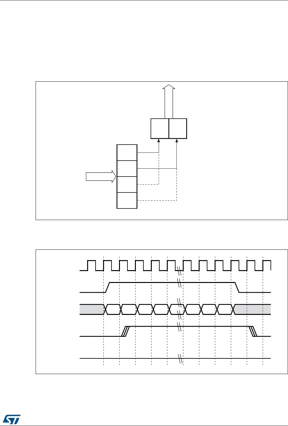
RM0090 Rev 18 1143/1749
RM0090 Ethernet (ETH): media access control (MAC) with DMA controller
1239
UDP or ICMP header is not modified. For the second error type, still, the calculated
checksum is inserted into the corresponding header field.
MII/RMII transmit bit order
Each nibble from the MII is transmitted on the RMII a dibit at a time with the order of dibit
transmission shown in Figure 362. Lower order bits (D1 and D0) are transmitted first
followed by higher order bits (D2 and D3).
Figure 362. Transmission bit order
MII/RMII transmit timing diagrams
Figure 363. Transmission with no collision
D0
D1
D2
D3
LSB
MII_TXD[3:0]
MSB
D0 D1
LSB MSB
RMII_TXD[1:0]
Bibit stream
Nibble stream
ai15632
MII_TX_CLK
MII_TX_EN
MII_TXD[3:0] PR EA MB LE
MII_CS
MII_COL
ai1563
1
Low
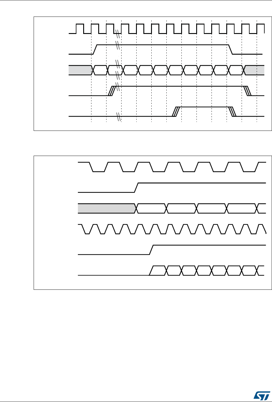
Ethernet (ETH): media access control (MAC) with DMA controller RM0090
1144/1749 RM0090 Rev 18
Figure 364. Transmission with collision
Figure 365 shows a frame transmission in MII and RMII.
Figure 365. Frame transmission in MMI and RMII modes
33.5.3 MAC frame reception
The MAC received frames are pushes into the Rx FIFO. The status (fill level) of this FIFO is
indicated to the DMA once it crosses the configured receive threshold (RTC in the
ETH_DMAOMR register) so that the DMA can initiate pre-configured burst transfers
towards the AHB interface.
In the default Cut-through mode, when 64 bytes (configured with the RTC bits in the
ETH_DMAOMR register) or a full packet of data are received into the FIFO, the data are
popped out and the DMA is notified of its availability. Once the DMA has initiated the
transfer to the AHB interface, the data transfer continues from the FIFO until a complete
MII_TX_CLK
MII_TX_EN
MII_TXD[3:0] PR EAM BLE SFD
MII_CS
MII_COL
ai15651
DA DA JAM JAM JAM JAM
MII_RX_CLK
MII_TX_EN
MII_TXD[3:0]
RMII_REF_CLK
RMII_TXD[1:0]
RMII_TX_EN
ai15652

RM0090 Rev 18 1145/1749
RM0090 Ethernet (ETH): media access control (MAC) with DMA controller
1239
packet has been transferred. Upon completion of the EOF frame transfer, the status word is
popped out and sent to the DMA controller.
In Rx FIFO Store-and-forward mode (configured by the RSF bit in the ETH_DMAOMR
register), a frame is read only after being written completely into the Receive FIFO. In this
mode, all error frames are dropped (if the core is configured to do so) such that only valid
frames are read and forwarded to the application. In Cut-through mode, some error frames
are not dropped, because the error status is received at the end of the frame, by which time
the start of that frame has already been read of the FIFO.
A receive operation is initiated when the MAC detects an SFD on the MII. The core strips the
preamble and SFD before proceeding to process the frame. The header fields are checked
for the filtering and the FCS field used to verify the CRC for the frame. The frame is dropped
in the core if it fails the address filter.
Receive protocol
The received frame preamble and SFD are stripped. Once the SFD has been detected, the
MAC starts sending the Ethernet frame data to the receive FIFO, beginning with the first
byte following the SFD (destination address). If IEEE 1588 time stamping is enabled, a
snapshot of the system time is taken when any frame's SFD is detected on the MII. Unless
the MAC filters out and drops the frame, this time stamp is passed on to the application.
If the received frame length/type field is less than 0x600 and if the MAC is programmed for
the auto CRC/pad stripping option, the MAC sends the data of the frame to RxFIFO up to
the count specified in the length/type field, then starts dropping bytes (including the FCS
field). If the Length/Type field is greater than or equal to 0x600, the MAC sends all received
Ethernet frame data to Rx FIFO, regardless of the value on the programmed auto-CRC strip
option. The MAC watchdog timer is enabled by default, that is, frames above 2048 bytes
(DA + SA + LT + Data + pad + FCS) are cut off. This feature can be disabled by
programming the watchdog disable (WD) bit in the MAC configuration register. However,
even if the watchdog timer is disabled, frames greater than 16 KB in size are cut off and a
watchdog timeout status is given.
Receive CRC: automatic CRC and pad stripping
The MAC checks for any CRC error in the receiving frame. It calculates the 32-bit CRC for
the received frame that includes the Destination address field through the FCS field. The
encoding is defined by the following polynomial.
Regardless of the auto-pad/CRC strip, the MAC receives the entire frame to compute the
CRC check for the received frame.
Receive checksum offload
Both IPv4 and IPv6 frames in the received Ethernet frames are detected and processed for
data integrity. You can enable the receive checksum offload by setting the IPCO bit in the
ETH_MACCR register. The MAC receiver identifies IPv4 or IPv6 frames by checking for
value 0x0800 or 0x86DD, respectively, in the received Ethernet frame Type field. This
identification applies to VLAN-tagged frames as well. The receive checksum offload
calculates IPv4 header checksums and checks that they match the received IPv4 header
checksums. The IP Header Error bit is set for any mismatch between the indicated payload
Gx() x32 x26 x23 x22 x16 x12 x11 x10 x8x7x5x4x2x1+ + + + + + + +++++++=

Ethernet (ETH): media access control (MAC) with DMA controller RM0090
1146/1749 RM0090 Rev 18
type (Ethernet Type field) and the IP header version, or when the received frame does not
have enough bytes, as indicated by the IPv4 header’s Length field (or when fewer than 20
bytes are available in an IPv4 or IPv6 header). The receive checksum offload also identifies
a TCP, UDP or ICMP payload in the received IP datagrams (IPv4 or IPv6) and calculates the
checksum of such payloads properly, as defined in the TCP, UDP or ICMP specifications. It
includes the TCP/UDP/ICMPv6 pseudo-header bytes for checksum calculation and checks
whether the received checksum field matches the calculated value. The result of this
operation is given as a Payload Checksum Error bit in the receive status word. This status
bit is also set if the length of the TCP, UDP or ICMP payload does not match the expected
payload length given in the IP header. As mentioned in TCP/UDP/ICMP checksum, the
receive checksum offload bypasses the payload of fragmented IP datagrams, IP datagrams
with security features, IPv6 routing headers, and payloads other than TCP, UDP or ICMP.
This information (whether the checksum is bypassed or not) is given in the receive status,
as described in the RDES0: Receive descriptor Word0 section. In this configuration, the
core does not append any payload checksum bytes to the received Ethernet frames.
As mentioned in RDES0: Receive descriptor Word0, the meaning of certain register bits
changes as shown in Table 190.
Receive frame controller
If the RA bit is reset in the MAC CSR frame filter register, the MAC performs frame filtering
based on the destination/source address (the application still needs to perform another level
of filtering if it decides not to receive any bad frames like runt, CRC error frames, etc.). On
detecting a filter-fail, the frame is dropped and not transferred to the application. When the
filtering parameters are changed dynamically, and in case of (DA-SA) filter-fail, the rest of
the frame is dropped and the Rx Status Word is immediately updated (with zero frame
Table 190. Frame statuses
Bit 18:
Ethernet frame
Bit 27: Header
checksum error
Bit 28: Payload
checksum error Frame status
000
The frame is an IEEE 802.3 frame (Length
field value is less than 0x0600).
100
IPv4/IPv6 Type frame in which no checksum
error is detected.
101
IPv4/IPv6 Type frame in which a payload
checksum error (as described for PCE) is
detected
110
IPv4/IPv6 Type frame in which IP header
checksum error (as described for IPCO HCE)
is detected.
111
IPv4/IPv6 Type frame in which both PCE and
IPCO HCE are detected.
001
IPv4/IPv6 Type frame in which there is no IP
HCE and the payload check is bypassed due
to unsupported payload.
011
Type frame which is neither IPv4 or IPv6
(checksum offload bypasses the checksum
check completely)
0 1 0 Reserved

RM0090 Rev 18 1147/1749
RM0090 Ethernet (ETH): media access control (MAC) with DMA controller
1239
length, CRC error and Runt Error bits set), indicating the filter fail. In Ethernet power down
mode, all received frames are dropped, and are not forwarded to the application.
Receive flow control
The MAC detects the receiving Pause frame and pauses the frame transmission for the
delay specified within the received Pause frame (only in Full-duplex mode). The Pause
frame detection function can be enabled or disabled with the RFCE bit in ETH_MACFCR.
Once receive flow control has been enabled, the received frame destination address begins
to be monitored for any match with the multicast address of the control frame
(0x0180 C200 0001). If a match is detected (the destination address of the received frame
matches the reserved control frame destination address), the MAC then decides whether or
not to transfer the received control frame to the application, based on the level of the PCF
bit in ETH_MACFFR.
The MAC also decodes the type, opcode, and Pause Timer fields of the receiving control
frame. If the byte count of the status indicates 64 bytes, and if there is no CRC error, the
MAC transmitter pauses the transmission of any data frame for the duration of the decoded
Pause time value, multiplied by the slot time (64 byte times for both 10/100 Mbit/s modes).
Meanwhile, if another Pause frame is detected with a zero Pause time value, the MAC
resets the Pause time and manages this new pause request.
If the received control frame matches neither the type field (0x8808), the opcode (0x00001),
nor the byte length (64 bytes), or if there is a CRC error, the MAC does not generate a
Pause.
In the case of a pause frame with a multicast destination address, the MAC filters the frame
based on the address match.
For a pause frame with a unicast destination address, the MAC filtering depends on whether
the DA matched the contents of the MAC address 0 register and whether the UPDF bit in
ETH_MACFCR is set (detecting a pause frame even with a unicast destination address).
The PCF register bits (bits [7:6] in ETH_MACFFR) control filtering for control frames in
addition to address filtering.
Receive operation multiframe handling
Since the status is available immediately following the data, the FIFO is capable of storing
any number of frames into it, as long as it is not full.
Error handling
If the Rx FIFO is full before it receives the EOF data from the MAC, an overflow is declared
and the whole frame is dropped, and the overflow counter in the (ETH_DMAMFBOCR
register) is incremented. The status indicates a partial frame due to overflow. The Rx FIFO
can filter error and undersized frames, if enabled (using the FEF and FUGF bits in
ETH_DMAOMR).
If the Receive FIFO is configured to operate in Store-and-forward mode, all error frames can
be filtered and dropped.
In Cut-through mode, if a frame's status and length are available when that frame's SOF is
read from the Rx FIFO, then the complete erroneous frame can be dropped. The DMA can
flush the error frame being read from the FIFO, by enabling the receive frame flash bit. The
data transfer to the application (DMA) is then stopped and the rest of the frame is internally
read and dropped. The next frame transfer can then be started, if available.
Ethernet (ETH): media access control (MAC) with DMA controller RM0090
1148/1749 RM0090 Rev 18
Receive status word
At the end of the Ethernet frame reception, the MAC outputs the receive status to the
application (DMA). The detailed description of the receive status is the same as for
bits[31:0] in RDES0, given in RDES0: Receive descriptor Word0.
Frame length interface
In case of switch applications, data transmission and reception between the application and
MAC happen as complete frame transfers. The application layer should be aware of the
length of the frames received from the ingress port in order to transfer the frame to the
egress port. The MAC core provides the frame length of each received frame inside the
status at the end of each frame reception.
Note: A frame length value of 0 is given for partial frames written into the Rx FIFO due to overflow.
MII/RMII receive bit order
Each nibble is transmitted to the MII from the dibit received from the RMII in the nibble
transmission order shown in Figure 366. The lower-order bits (D0 and D1) are received first,
followed by the higher-order bits (D2 and D3).
Figure 366. Receive bit order
D0
D1
D2
D3
LSB
MII_RXD[3:0]
MSB
D0 D1
LSB MSB
RMII_RXD[1:0]
Di-bit stream
Nibble stream
ai1563
3
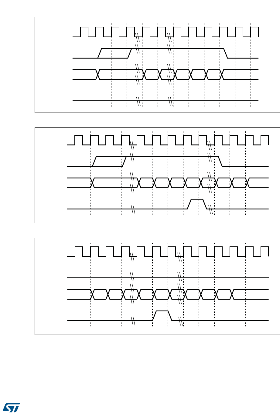
RM0090 Rev 18 1149/1749
RM0090 Ethernet (ETH): media access control (MAC) with DMA controller
1239
Figure 367. Reception with no error
Figure 368. Reception with errors
Figure 369. Reception with false carrier indication
33.5.4 MAC interrupts
Interrupts can be generated from the MAC core as a result of various events.
The ETH_MACSR register describes the events that can cause an interrupt from the MAC
core. You can prevent each event from asserting the interrupt by setting the corresponding
mask bits in the Interrupt Mask register.
MII_RX_CLK
MII_RX_DV
MII_RXD[3:0] PREAMBLE SFD
MII_RX_ERR
ai1563
4
FCS
MII_RX_CLK
MII_RX_DV
MII_RXD[3:0] PREAMBLE SFD
MII_RX_ERR
ai15635
DA DA XX XX XX
MII_RX_CLK
MII_RX_DV
MII_RXD[3:0] XX
MII_RX_ERR
ai15636
0E XX XX XX XX
XX XXXX
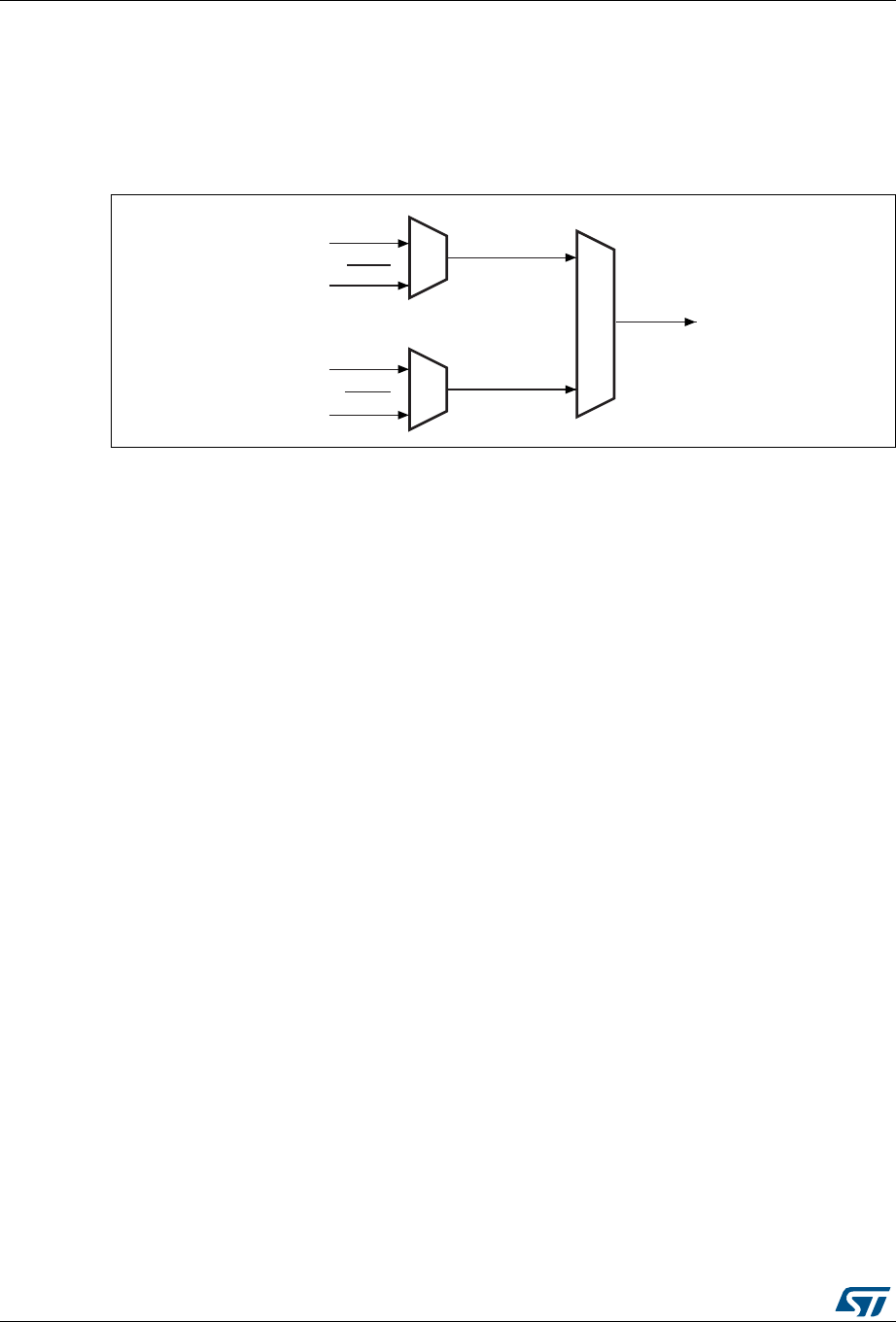
Ethernet (ETH): media access control (MAC) with DMA controller RM0090
1150/1749 RM0090 Rev 18
The interrupt register bits only indicate the block from which the event is reported. You have
to read the corresponding status registers and other registers to clear the interrupt. For
example, bit 3 of the Interrupt register, set high, indicates that the Magic packet or Wake-on-
LAN frame is received in Power-down mode. You must read the ETH_MACPMTCSR
Register to clear this interrupt event.
Figure 370. MAC core interrupt masking scheme
33.5.5 MAC filtering
Address filtering
Address filtering checks the destination and source addresses on all received frames and
the address filtering status is reported accordingly. Address checking is based on different
parameters (Frame filter register) chosen by the application. The filtered frame can also be
identified: multicast or broadcast frame.
Address filtering uses the station's physical (MAC) address and the Multicast Hash table for
address checking purposes.
Unicast destination address filter
The MAC supports up to 4 MAC addresses for unicast perfect filtering. If perfect filtering is
selected (HU bit in the Frame filter register is reset), the MAC compares all 48 bits of the
received unicast address with the programmed MAC address for any match. Default
MacAddr0 is always enabled, other addresses MacAddr1–MacAddr3 are selected with an
individual enable bit. Each byte of these other addresses (MacAddr1–MacAddr3) can be
masked during comparison with the corresponding received DA byte by setting the
corresponding Mask Byte Control bit in the register. This helps group address filtering for the
DA. In Hash filtering mode (when HU bit is set), the MAC performs imperfect filtering for
unicast addresses using a 64-bit Hash table. For hash filtering, the MAC uses the 6 upper
CRC (see note 1 below) bits of the received destination address to index the content of the
Hash table. A value of 000000 selects bit 0 in the selected register, and a value of 111111
selects bit 63 in the Hash Table register. If the corresponding bit (indicated by the 6-bit CRC)
is set to 1, the unicast frame is said to have passed the Hash filter; otherwise, the frame has
failed the Hash filter.
Note: This CRC is a 32-bit value coded by the following polynomial (for more details refer to
Section 33.5.3):
AND
AND
OR
TSTI
PMTI
Interrupt
TSTS
PMTS
PMTIM
ai15637
TSTIM
Gx() x32 x26 x23 x22 x16 x12 x11 x10 x8x7x5x4x2x1++++++++++++++=

RM0090 Rev 18 1151/1749
RM0090 Ethernet (ETH): media access control (MAC) with DMA controller
1239
Multicast destination address filter
The MAC can be programmed to pass all multicast frames by setting the PAM bit in the
Frame filter register. If the PAM bit is reset, the MAC performs the filtering for multicast
addresses based on the HM bit in the Frame filter register. In Perfect filtering mode, the
multicast address is compared with the programmed MAC destination address registers
(1–3). Group address filtering is also supported. In Hash filtering mode, the MAC performs
imperfect filtering using a 64-bit Hash table. For hash filtering, the MAC uses the 6 upper
CRC (see note 1 below) bits of the received multicast address to index the content of the
Hash table. A value of 000000 selects bit 0 in the selected register and a value of 111111
selects bit 63 in the Hash Table register. If the corresponding bit is set to 1, then the
multicast frame is said to have passed the Hash filter; otherwise, the frame has failed the
Hash filter.
Note: This CRC is a 32-bit value coded by the following polynomial (for more details refer to
Section 33.5.3):
Hash or perfect address filter
The DA filter can be configured to pass a frame when its DA matches either the Hash filter
or the Perfect filter by setting the HPF bit in the Frame filter register and setting the
corresponding HU or HM bits. This configuration applies to both unicast and multicast
frames. If the HPF bit is reset, only one of the filters (Hash or Perfect) is applied to the
received frame.
Broadcast address filter
The MAC does not filter any broadcast frames in the default mode. However, if the MAC is
programmed to reject all broadcast frames by setting the BFD bit in the Frame filter register,
any broadcast frames are dropped.
Unicast source address filter
The MAC can also perform perfect filtering based on the source address field of the
received frames. By default, the MAC compares the SA field with the values programmed in
the SA registers. The MAC address registers [1:3] can be configured to contain SA instead
of DA for comparison, by setting bit 30 in the corresponding register. Group filtering with SA
is also supported. The frames that fail the SA filter are dropped by the MAC if the SAF bit in
the Frame filter register is set. Otherwise, the result of the SA filter is given as a status bit in
the Receive Status word (see RDES0: Receive descriptor Word0).
When the SAF bit is set, the result of the SA and DA filters is AND’ed to decide whether the
frame needs to be forwarded. This means that either of the filter fail result will drop the
frame. Both filters have to pass the frame for the frame to be forwarded to the application.
Inverse filtering operation
For both destination and source address filtering, there is an option to invert the filter-match
result at the final output. These are controlled by the DAIF and SAIF bits in the Frame filter
register, respectively. The DAIF bit is applicable for both Unicast and Multicast DA frames.
The result of the unicast/multicast destination address filter is inverted in this mode.
Similarly, when the SAIF bit is set, the result of the unicast SA filter is inverted. Table 191
Gx() x32 x26 x23 x22 x16 x12 x11 x10 x8x7x5x4x2x1++++++++++++++=

Ethernet (ETH): media access control (MAC) with DMA controller RM0090
1152/1749 RM0090 Rev 18
and Table 192 summarize destination and source address filtering based on the type of
frame received.
Table 191. Destination address filtering
Frame
type PM HPF HU DAIF HM PAM DB DA filter operation
Broadcast
1XXX X XXPass
0XXX X X0Pass
0XXX X X1Fail
Unicast
1 X X X X X X Pass all frames
0 X 0 0 X X X Pass on perfect/group filter match
0 X 0 1 X X X Fail on perfect/Group filter match
0 0 1 0 X X X Pass on hash filter match
0 0 1 1 X X X Fail on hash filter match
011 0 X XX
Pass on hash or perfect/Group filter
match
0 1 1 1 X X X Fail on hash or perfect/Group filter match
Multicast
1 X X X X X X Pass all frames
X X X X X 1 X Pass all frames
0XX0 0 0 X
Pass on Perfect/Group filter match and
drop PAUSE control frames if PCF = 0x
00 X0 1 0 X
Pass on hash filter match and drop
PAUSE control frames if PCF = 0x
01 X0 1 0 X
Pass on hash or perfect/Group filter
match and drop PAUSE control frames if
PCF = 0x
0XX1 0 0 X
Fail on perfect/Group filter match and
drop PAUSE control frames if PCF = 0x
00 X1 1 0 X
Fail on hash filter match and drop PAUSE
control frames if PCF = 0x
01 X1 1 0 X
Fail on hash or perfect/Group filter match
and drop PAUSE control frames if PCF =
0x

RM0090 Rev 18 1153/1749
RM0090 Ethernet (ETH): media access control (MAC) with DMA controller
1239
33.5.6 MAC loopback mode
The MAC supports loopback of transmitted frames onto its receiver. By default, the MAC
loopback function is disabled, but this feature can be enabled by programming the
Loopback bit in the MAC ETH_MACCR register.
33.5.7 MAC management counters: MMC
The MAC management counters (MMC) maintain a set of registers for gathering statistics
on the received and transmitted frames. These include a control register for controlling the
behavior of the registers, two 32-bit registers containing generated interrupts (receive and
transmit), and two 32-bit registers containing masks for the Interrupt register (receive and
transmit). These registers are accessible from the application. Each register is 32 bits wide.
Section 33.8 describes the various counters and lists the addresses of each of the statistics
counters. This address is used for read/write accesses to the desired transmit/receive
counter.
The Receive MMC counters are updated for frames that pass address filtering. Dropped
frames statistics are not updated unless the dropped frames are runt frames of less than 6
bytes (DA bytes are not received fully).
Good transmitted and received frames
Transmitted frames are considered “good” if transmitted successfully. In other words, a
transmitted frame is good if the frame transmission is not aborted due to any of the following
errors:
+ Jabber Timeout
+ No Carrier/Loss of Carrier
+ Late Collision
+ Frame Underflow
+ Excessive Deferral
+ Excessive Collision
Table 192. Source address filtering
Frame type PM SAIF SAF SA filter operation
Unicast
1 X X Pass all frames
000Pass status on perfect/Group filter match but do not drop
frames that fail
010Fail status on perfect/group filter match but do not drop frame
001Pass on perfect/group filter match and drop frames that fail
011Fail on perfect/group filter match and drop frames that fail

Ethernet (ETH): media access control (MAC) with DMA controller RM0090
1154/1749 RM0090 Rev 18
Received frames are considered “good” if none of the following errors exists:
+ CRC error
+ Runt Frame (shorter than 64 bytes)
+ Alignment error (in 10/ 100 Mbit/s only)
+ Length error (non-Type frames only)
+ Out of Range (non-Type frames only, longer than maximum size)
+ MII_RXER Input error
The maximum frame size depends on the frame type, as follows:
+ Untagged frame maxsize = 1518
+ VLAN Frame maxsize = 1522
33.5.8 Power management: PMT
This section describes the power management (PMT) mechanisms supported by the MAC.
PMT supports the reception of network (remote) wakeup frames and Magic Packet frames.
PMT generates interrupts for wakeup frames and Magic Packets received by the MAC. The
PMT block is enabled with remote wakeup frame enable and Magic Packet enable. These
enable bits (WFE and MPE) are in the ETH_MACPMTCSR register and are programmed by
the application. When the power down mode is enabled in the PMT, then all received frames
are dropped by the MAC and they are not forwarded to the application. The MAC comes out
of the power down mode only when either a Magic Packet or a Remote wakeup frame is
received and the corresponding detection is enabled.
Remote wakeup frame filter register
There are eight wakeup frame filter registers. To write on each of them, load the wakeup
frame filter register value by value. The wanted values of the wakeup frame filter are loaded
by sequentially loading eight times the wakeup frame filter register. The read operation is
identical to the write operation. To read the eight values, you have to read eight times the
wakeup frame filter register to reach the last register. Each read/write points the wakeup
frame filter register to the next filter register.
Figure 371. Wakeup frame filter register
Filter 0 Byte Mask
Filter 1 Byte Mask
Filter 2 Byte Mask
Filter 3 Byte Mask
RSVD
Filter 3
Command
RSVD
Filter 2
Command
RSVD
Filter 1
Command
RSVD
Filter 0
Command
Filter 3 Offset Filter 2 Offset Filter 1 Offset Filter 0 Offset
Filter 1 CRC - 16 Filter 0 CRC - 16
Filter 3 CRC - 16 Filter 2 CRC - 16
Wakeup frame filter reg0
Wakeup frame filter reg1
Wakeup frame filter reg2
Wakeup frame filter reg3
Wakeup frame filter reg4
Wakeup frame filter reg5
Wakeup frame filter reg6
Wakeup frame filter reg7
ai15647

RM0090 Rev 18 1155/1749
RM0090 Ethernet (ETH): media access control (MAC) with DMA controller
1239
•Filter i Byte Mask
This register defines which bytes of the frame are examined by filter i (0, 1, 2, and 3) in
order to determine whether or not the frame is a wakeup frame. The MSB (thirty-first
bit) must be zero. Bit j [30:0] is the Byte Mask. If bit j (byte number) of the Byte Mask is
set, then Filter i Offset + j of the incoming frame is processed by the CRC block;
otherwise Filter i Offset + j is ignored.
•Filter i Command
This 4-bit command controls the filter i operation. Bit 3 specifies the address type,
defining the pattern’s destination address type. When the bit is set, the pattern applies
to only multicast frames. When the bit is reset, the pattern applies only to unicast
frames. Bit 2 and bit 1 are reserved. Bit 0 is the enable bit for filter i; if bit 0 is not set,
filter i is disabled.
•Filter i Offset
This register defines the offset (within the frame) from which the frames are examined
by filter i. This 8-bit pattern offset is the offset for the filter i first byte to be examined.
The minimum allowed is 12, which refers to the 13th byte of the frame (offset value 0
refers to the first byte of the frame).
•Filter i CRC-16
This register contains the CRC_16 value calculated from the pattern, as well as the
byte mask programmed to the wakeup filter register block.
Remote wakeup frame detection
When the MAC is in sleep mode and the remote wakeup bit is enabled in the
ETH_MACPMTCSR register, normal operation is resumed after receiving a remote wakeup
frame. The application writes all eight wakeup filter registers, by performing a sequential
write to the wakeup frame filter register address. The application enables remote wakeup by
writing a 1 to bit 2 in the ETH_MACPMTCSR register. PMT supports four programmable
filters that provide different receive frame patterns. If the incoming frame passes the
address filtering of Filter Command, and if Filter CRC-16 matches the incoming examined
pattern, then the wakeup frame is received. Filter_offset (minimum value 12, which refers to
the 13th byte of the frame) determines the offset from which the frame is to be examined.
Filter Byte Mask determines which bytes of the frame must be examined. The thirty-first bit
of Byte Mask must be set to zero. The wakeup frame is checked only for length error, FCS
error, dribble bit error, MII error, collision, and to ensure that it is not a runt frame. Even if the
wakeup frame is more than 512 bytes long, if the frame has a valid CRC value, it is
considered valid. Wakeup frame detection is updated in the ETH_MACPMTCSR register for
every remote wakeup frame received. If enabled, a PMT interrupt is generated to indicate
the reception of a remote wakeup frame.
Magic packet detection
The Magic Packet frame is based on a method that uses Advanced Micro Device’s Magic
Packet technology to power up the sleeping device on the network. The MAC receives a
specific packet of information, called a Magic Packet, addressed to the node on the network.
Only Magic Packets that are addressed to the device or a broadcast address are checked to
determine whether they meet the wakeup requirements. Magic Packets that pass address
filtering (unicast or broadcast) are checked to determine whether they meet the remote
Wake-on-LAN data format of 6 bytes of all ones followed by a MAC address appearing 16
times. The application enables Magic Packet wakeup by writing a 1 to bit 1 in the
ETH_MACPMTCSR register. The PMT block constantly monitors each frame addressed to

Ethernet (ETH): media access control (MAC) with DMA controller RM0090
1156/1749 RM0090 Rev 18
the node for a specific Magic Packet pattern. Each received frame is checked for a
0xFFFF FFFF FFFF pattern following the destination and source address field. The PMT
block then checks the frame for 16 repetitions of the MAC address without any breaks or
interruptions. In case of a break in the 16 repetitions of the address, the 0xFFFF FFFF FFFF
pattern is scanned for again in the incoming frame. The 16 repetitions can be anywhere in
the frame, but must be preceded by the synchronization stream (0xFFFF FFFF FFFF). The
device also accepts a multicast frame, as long as the 16 duplications of the MAC address
are detected. If the MAC address of a node is 0x0011 2233 4455, then the MAC scans for
the data sequence:
Destination address source address ……………….. FFFF FFFF FFFF
0011 2233 4455 0011 2233 4455 0011 2233 4455 0011 2233 4455
0011 2233 4455 0011 2233 4455 0011 2233 4455 0011 2233 4455
0011 2233 4455 0011 2233 4455 0011 2233 4455 0011 2233 4455
0011 2233 4455 0011 2233 4455 0011 2233 4455 0011 2233 4455
…CRC
Magic Packet detection is updated in the ETH_MACPMTCSR register for received Magic
Packet. If enabled, a PMT interrupt is generated to indicate the reception of a Magic Packet.
System consideration during power-down
The Ethernet PMT block is able to detect frames while the system is in the Stop mode,
provided that the EXTI line 19 is enabled.
The MAC receiver state machine should remain enabled during the power-down mode. This
means that the RE bit has to remain set in the ETH_MACCR register because it is involved
in magic packet/ wake-on-LAN frame detection. The transmit state machine should however
be turned off during the power-down mode by clearing the TE bit in the ETH_MACCR
register. Moreover, the Ethernet DMA should be disabled during the power-down mode,
because it is not necessary to copy the magic packet/wake-on-LAN frame into the SRAM.
To disable the Ethernet DMA, clear the ST bit and the SR bit (for the transmit DMA and the
receive DMA, respectively) in the ETH_DMAOMR register.
The recommended power-down and wakeup sequences are as follows:

RM0090 Rev 18 1157/1749
RM0090 Ethernet (ETH): media access control (MAC) with DMA controller
1239
1. Disable the transmit DMA and wait for any previous frame transmissions to complete.
These transmissions can be detected when the transmit interrupt ETH_DMASR
register[0] is received.
2. Disable the MAC transmitter and MAC receiver by clearing the RE and TE bits in the
ETH_MACCR configuration register.
3. Wait for the receive DMA to have emptied all the frames in the Rx FIFO.
4. Disable the receive DMA.
5. Configure and enable the EXTI line 19 to generate either an event or an interrupt.
6. If you configure the EXTI line 19 to generate an interrupt, you also have to correctly
configure the ETH_WKUP_IRQ Handler function, which should clear the pending bit of
the EXTI line 19.
7. Enable Magic packet/Wake-on-LAN frame detection by setting the MFE/ WFE bit in the
ETH_MACPMTCSR register.
8. Enable the MAC power-down mode, by setting the PD bit in the ETH_MACPMTCSR
register.
9. Enable the MAC Receiver by setting the RE bit in the ETH_MACCR register.
10. Enter the system’s Stop mode (for more details refer to Section 5.3.4):
11. On receiving a valid wakeup frame, the Ethernet peripheral exits the power-down
mode.
12. Read the ETH_MACPMTCSR to clear the power management event flag, enable the
MAC transmitter state machine, and the receive and transmit DMA.
13. Configure the system clock: enable the HSE and set the clocks.
33.5.9 Precision time protocol (IEEE1588 PTP)
The IEEE 1588 standard defines a protocol that allows precise clock synchronization in
measurement and control systems implemented with technologies such as network
communication, local computing and distributed objects. The protocol applies to systems
that communicate by local area networks supporting multicast messaging, including (but not
limited to) Ethernet. This protocol is used to synchronize heterogeneous systems that
include clocks of varying inherent precision, resolution and stability. The protocol supports
system-wide synchronization accuracy in the submicrosecond range with minimum network
and local clock computing resources. The message-based protocol, known as the precision
time protocol (PTP), is transported over UDP/IP. The system or network is classified into
Master and Slave nodes for distributing the timing/clock information. The protocol’s
technique for synchronizing a slave node to a master node by exchanging PTP messages is
described in Figure 372.
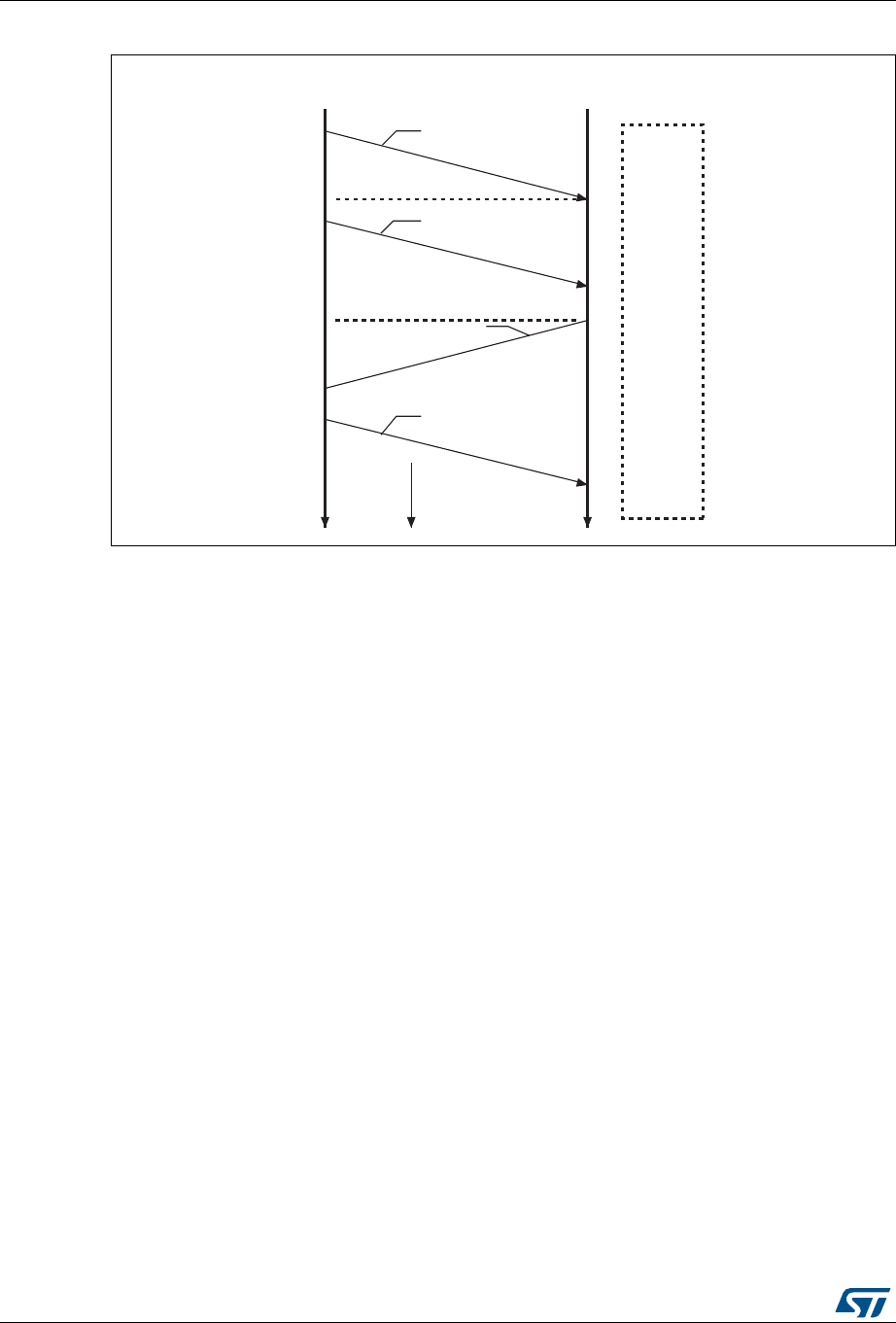
Ethernet (ETH): media access control (MAC) with DMA controller RM0090
1158/1749 RM0090 Rev 18
Figure 372. Networked time synchronization
1. The master broadcasts PTP Sync messages to all its nodes. The Sync message
contains the master’s reference time information. The time at which this message
leaves the master’s system is t1. For Ethernet ports, this time has to be captured at the
MII.
2. A slave receives the Sync message and also captures the exact time, t2, using its
timing reference.
3. The master then sends the slave a Follow_up message, which contains the t1
information for later use.
4. The slave sends the master a Delay_Req message, noting the exact time, t3, at which
this frame leaves the MII.
5. The master receives this message and captures the exact time, t4, at which it enters its
system.
6. The master sends the t4 information to the slave in the Delay_Resp message.
7. The slave uses the four values of t1, t2, t3, and t4 to synchronize its local timing
reference to the master’s timing reference.
Most of the protocol implementation occurs in the software, above the UDP layer. As
described above, however, hardware support is required to capture the exact time when
specific PTP packets enter or leave the Ethernet port at the MII. This timing information has
to be captured and returned to the software for a proper, high-accuracy implementation of
PTP.
Reference timing source
To get a snapshot of the time, the core requires a reference time in 64-bit format (split into
two 32-bit channels, with the upper 32 bits providing time in seconds, and the lower 32 bits
indicating time in nanoseconds) as defined in the IEEE 1588 specification.
The PTP reference clock input is used to internally generate the reference time (also called
the System Time) and to capture time stamps. The frequency of this reference clock must
Master clock time Slave clock time
Data at
slave clock
Sync message
Follow_up message
containing value of t1
Delay_Req message
Delay_Resp message
containing value of t4
time
t1
t2m
t3m
t4
t1, t2, t3, t4
t2
t1, t2
t3
t2
t1, t2, t3
ai15669

RM0090 Rev 18 1159/1749
RM0090 Ethernet (ETH): media access control (MAC) with DMA controller
1239
be greater than or equal to the resolution of time stamp counter. The synchronization
accuracy target between the master node and the slaves is around 100 ns.
The generation, update and modification of the System Time are described in System Time
correction methods.
The accuracy depends on the PTP reference clock input period, the characteristics of the
oscillator (drift) and the frequency of the synchronization procedure.
Due to the synchronization from the Tx and Rx clock input domain to the PTP reference
clock domain, the uncertainty on the time stamp latched value is 1 reference clock period. If
we add the uncertainty due to resolution, we will add half the period for time stamping.
Transmission of frames with the PTP feature
When a frame’s SFD is output on the MII, a time stamp is captured. Frames for which time
stamp capture is required are controllable on a per-frame basis. In other words, each
transmitted frame can be marked to indicate whether a time stamp must be captured or not
for that frame. The transmitted frames are not processed to identify PTP frames. Frame
control is exercised through the control bits in the transmit descriptor. Captured time stamps
are returned to the application in the same way as the status is provided for frames. The
time stamp is sent back along with the Transmit status of the frame, inside the
corresponding transmit descriptor, thus connecting the time stamp automatically to the
specific PTP frame. The 64-bit time stamp information is written back to the TDES2 and
TDES3 fields, with TDES2 holding the time stamp’s 32 least significant bits.
Reception of frames with the PTP feature
When the IEEE 1588 time stamping feature is enabled, the Ethernet MAC captures the time
stamp of all frames received on the MII. The MAC provides the time stamp as soon as the
frame reception is complete. Captured time stamps are returned to the application in the
same way as the frame status is provided. The time stamp is sent back along with the
Receive status of the frame, inside the corresponding receive descriptor. The 64-bit time
stamp information is written back to the RDES2 and RDES3 fields, with RDES2 holding the
time stamp’s 32 least significant bits.
System Time correction methods
The 64-bit PTP time is updated using the PTP input reference clock, HCLK. This PTP time
is used as a source to take snapshots (time stamps) of the Ethernet frames being
transmitted or received at the MII. The System Time counter can be initialized or corrected
using either the Coarse or the Fine correction method.
In the Coarse correction method, the initial value or the offset value is written to the Time
stamp update register (refer to Section 33.8.3). For initialization, the System Time counter is
written with the value in the Time stamp update registers, whereas for system time
correction, the offset value (Time stamp update register) is added to or subtracted from the
system time.
In the Fine correction method, the slave clock (reference clock) frequency drift with respect
to the master clock (as defined in IEEE 1588) is corrected over a period of time, unlike in the
Coarse correction method where it is corrected in a single clock cycle. The longer correction
time helps maintain linear time and does not introduce drastic changes (or a large jitter) in
the reference time between PTP Sync message intervals. In this method, an accumulator
sums up the contents of the Addend register as shown in Figure 373. The arithmetic carry
that the accumulator generates is used as a pulse to increment the system time counter.
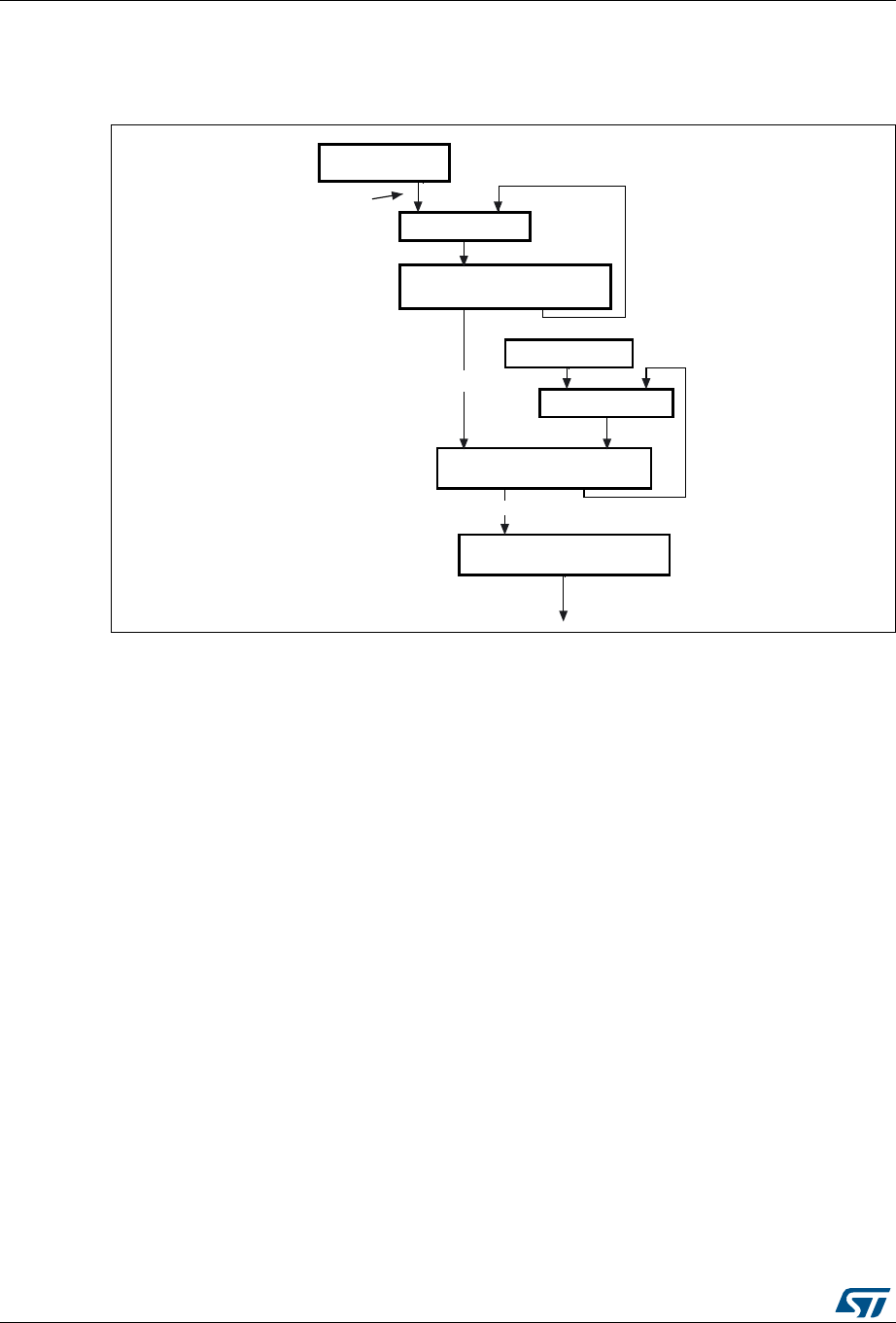
Ethernet (ETH): media access control (MAC) with DMA controller RM0090
1160/1749 RM0090 Rev 18
The accumulator and the addend are 32-bit registers. Here, the accumulator acts as a high-
precision frequency multiplier or divider. Figure 373 shows this algorithm.
Figure 373. System time update using the Fine correction method
The system time update logic requires a 50 MHz clock frequency to achieve 20 ns accuracy.
The frequency division is the ratio of the reference clock frequency to the required clock
frequency. Hence, if the reference clock (HCLK) is, let us say, 66 MHz, the ratio is calculated
as 66 MHz/50 MHz = 1.32. Hence, the default addend value to be set in the register is
232/1.32, which is equal to 0xC1F0 7C1F.
If the reference clock drifts lower, to 65 MHz for example, the ratio is 65/50 or 1.3 and the
value to set in the addend register is 232/1.30 equal to 0xC4EC 4EC4. If the clock drifts
higher, to 67 MHz for example, the addend register must be set to 0xBF0 B7672. When the
clock drift is zero, the default addend value of 0xC1F0 7C1F (232/1.32) should be
programmed.
In Figure 373, the constant value used to increment the subsecond register is 0d43. This
makes an accuracy of 20 ns in the system time (in other words, it is incremented by 20 ns
steps).
The software has to calculate the drift in frequency based on the Sync messages, and to
update the Addend register accordingly. Initially, the slave clock is set with
FreqCompensationValue0 in the Addend register. This value is as follows:
FreqCompensationValue0 = 232 / FreqDivisionRatio
If MasterToSlaveDelay is initially assumed to be the same for consecutive Sync messages,
the algorithm described below must be applied. After a few Sync cycles, frequency lock
occurs. The slave clock can then determine a precise MasterToSlaveDelay value and re-
synchronize with the master using the new value.
Addend register
+
Accumulator register
Subsecond register
+
Constant value
Second register
Increment Second register
Addend update
ai15670
Increment Subsecond
register

RM0090 Rev 18 1161/1749
RM0090 Ethernet (ETH): media access control (MAC) with DMA controller
1239
The algorithm is as follows:
•At time MasterSyncTime (n) the master sends the slave clock a Sync message. The
slave receives this message when its local clock is SlaveClockTime (n) and computes
MasterClockTime (n) as:
MasterClockTime (n) = MasterSyncTime (n) + MasterToSlaveDelay (n)
•The master clock count for current Sync cycle, MasterClockCount (n) is given by:
MasterClockCount (n) = MasterClockTime (n) – MasterClockTime (n – 1) (assuming
that MasterToSlaveDelay is the same for Sync cycles n and n – 1)
•The slave clock count for current Sync cycle, SlaveClockCount (n) is given by:
SlaveClockCount (n) = SlaveClockTime (n) – SlaveClockTime (n – 1)
•The difference between master and slave clock counts for current Sync cycle,
ClockDiffCount (n) is given by:
ClockDiffCount (n) = MasterClockCount (n) – SlaveClockCount (n)
•The frequency-scaling factor for slave clock, FreqScaleFactor (n) is given by:
FreqScaleFactor (n) = (MasterClockCount (n) + ClockDiffCount (n)) /
SlaveClockCount (n)
•The frequency compensation value for Addend register, FreqCompensationValue (n) is
given by:
FreqCompensationValue (n) = FreqScaleFactor (n) × FreqCompensationValue (n – 1)
In theory, this algorithm achieves lock in one Sync cycle; however, it may take several
cycles, due to changing network propagation delays and operating conditions.
This algorithm is self-correcting: if for any reason the slave clock is initially set to a value
from the master that is incorrect, the algorithm corrects it at the cost of more Sync cycles.
Programming steps for system time generation initialization
The time stamping feature can be enabled by setting bit 0 in the Time stamp control register
(ETH__PTPTSCR). However, it is essential to initialize the time stamp counter after this bit
is set to start time stamp operation. The proper sequence is the following:
1. Mask the Time stamp trigger interrupt by setting bit 9 in the MACIMR register.
2. Program Time stamp register bit 0 to enable time stamping.
3. Program the Subsecond increment register based on the PTP clock frequency.
4. If you are using the Fine correction method, program the Time stamp addend register
and set Time stamp control register bit 5 (addend register update).
5. Poll the Time stamp control register until bit 5 is cleared.
6. To select the Fine correction method (if required), program Time stamp control register
bit 1.
7. Program the Time stamp high update and Time stamp low update registers with the
appropriate time value.
8. Set Time stamp control register bit 2 (Time stamp init).
9. The Time stamp counter starts operation as soon as it is initialized with the value
written in the Time stamp update register.
10. Enable the MAC receiver and transmitter for proper time stamping.
Note: If time stamp operation is disabled by clearing bit 0 in the ETH_PTPTSCR register, the
above steps must be repeated to restart the time stamp operation.

Ethernet (ETH): media access control (MAC) with DMA controller RM0090
1162/1749 RM0090 Rev 18
Programming steps for system time update in the Coarse correction method
To synchronize or update the system time in one process (coarse correction method),
perform the following steps:
1. Write the offset (positive or negative) in the Time stamp update high and low registers.
2. Set bit 3 (TSSTU) in the Time stamp control register.
3. The value in the Time stamp update registers is added to or subtracted from the system
time when the TSSTU bit is cleared.
Programming steps for system time update in the Fine correction method
To synchronize or update the system time to reduce system-time jitter (fine correction
method), perform the following steps:
1. With the help of the algorithm explained in System Time correction methods, calculate
the rate by which you want to speed up or slow down the system time increments.
2. Update the time stamp.
3. Wait the time you want the new value of the Addend register to be active. You can do
this by activating the Time stamp trigger interrupt after the system time reaches the
target value.
4. Program the required target time in the Target time high and low registers. Unmask the
Time stamp interrupt by clearing bit 9 in the ETH_MACIMR register.
5. Set Time stamp control register bit 4 (TSARU).
6. When this trigger causes an interrupt, read the ETH_MACSR register.
7. Reprogram the Time stamp addend register with the old value and set ETH_TPTSCR
bit 5 again.
PTP trigger internal connection with TIM2
The MAC provides a trigger interrupt when the system time becomes greater than the target
time. Using an interrupt introduces a known latency plus an uncertainty in the command
execution time.
In order to avoid this uncertainty, a PTP trigger output signal is set high when the system
time is greater than the target time. It is internally connected to the TIM2 input trigger. With
this signal, the input capture feature, the output compare feature and the waveforms of the
timer can be used, triggered by the synchronized PTP system time. No uncertainty is
introduced since the clock of the timer (PCLK1: TIM2 APB1 clock) and PTP reference clock
(HCLK) are synchronous.
This PTP trigger signal is connected to the TIM2 ITR1 input selectable by software. The
connection is enabled through bits 11 and 10 in the TIM2 option register (TIM2_OR).
Figure 374 shows the connection.
Figure 374. PTP trigger output to TIM2 ITR1 connection
Ethernet MAC
ai1567
1
TIM2
ITR1PTP trigger
RM0090 Rev 18 1163/1749
RM0090 Ethernet (ETH): media access control (MAC) with DMA controller
1239
PTP pulse-per-second output signal
This PTP pulse output is used to check the synchronization between all nodes in the
network. To be able to test the difference between the local slave clock and the master
reference clock, both clocks were given a pulse-per-second (PPS) output signal that may be
connected to an oscilloscope if necessary. The deviation between the two signals can
therefore be measured. The pulse width of the PPS output is 125 ms.
The PPS output is enabled through a GPIO alternate function. (GPIO_AFR register).
The default frequency of the PPS output is 1 Hz. PPSFREQ[3:0] (in ETH_PTPPPSCR) can
be used to set the frequency of the PPS output to 2PPSFREQ Hz.
When set to 1 Hz, the PPS pulse width is 125 ms with binary rollover (TSSSR=0, bit 9 in
ETH_PTPTSCR) and 100 ms with digital rollover (TSSSR=1). When set to 2 Hz and higher,
the duty cycle of the PPS output is 50% with binary rollover.
With digital rollover (TSSSR=1), it is recommended not to use the PPS output with a
frequency other than 1 Hz as it would have irregular waveforms (though its average
frequency would always be correct during any one-second window).
Figure 375. PPS output
33.6 Ethernet functional description: DMA controller operation
The DMA has independent transmit and receive engines, and a CSR space. The transmit
engine transfers data from system memory into the Tx FIFO while the receive engine
transfers data from the Rx FIFO into system memory. The controller utilizes descriptors to
efficiently move data from source to destination with minimum CPU intervention. The DMA
is designed for packet-oriented data transfers such as frames in Ethernet. The controller can
be programmed to interrupt the CPU in cases such as frame transmit and receive transfer
completion, and other normal/error conditions. The DMA and the STM32F4xx communicate
through two data structures:
•Control and status registers (CSR)
•Descriptor lists and data buffers.
Control and status registers are described in detail in Section 33.8. Descriptors are
described in detail in Normal Tx DMA descriptors.
The DMA transfers the received data frames to the receive buffer in the STM32F4xx
memory, and transmits data frames from the transmit buffer in the STM32F4xx memory.
Descriptors that reside in the STM32F4xx memory act as pointers to these buffers. There
are two descriptor lists: one for reception, and one for transmission. The base address of
each list is written into DMA Registers 3 and 4, respectively. A descriptor list is forward-
linked (either implicitly or explicitly). The last descriptor may point back to the first entry to
create a ring structure. Explicit chaining of descriptors is accomplished by configuring the
second address chained in both the receive and transmit descriptors (RDES1[14] and
TDES0[20]). The descriptor lists reside in the Host’s physical memory space. Each
descriptor can point to a maximum of two buffers. This enables the use of two physically
Ethernet MAC
ai15672
PPS output
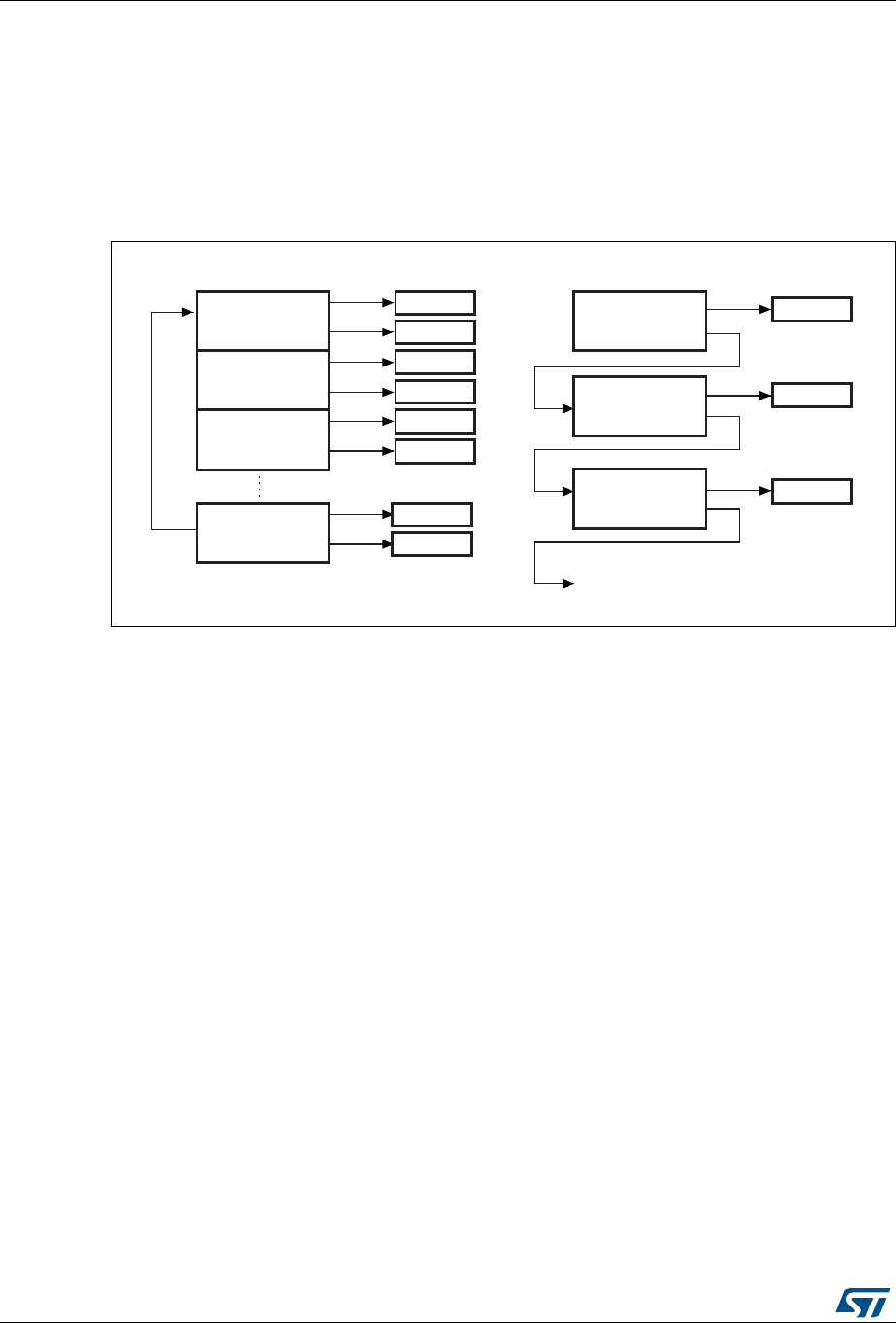
Ethernet (ETH): media access control (MAC) with DMA controller RM0090
1164/1749 RM0090 Rev 18
addressed buffers, instead of two contiguous buffers in memory. A data buffer resides in the
Host’s physical memory space, and consists of an entire frame or part of a frame, but cannot
exceed a single frame. Buffers contain only data. The buffer status is maintained in the
descriptor. Data chaining refers to frames that span multiple data buffers. However, a single
descriptor cannot span multiple frames. The DMA skips to the next frame buffer when the
end of frame is detected. Data chaining can be enabled or disabled. The descriptor ring and
chain structure is shown in Figure 376.
Figure 376. Descriptor ring and chain structure
33.6.1 Initialization of a transfer using DMA
Initialization for the MAC is as follows:
1. Write to ETH_DMABMR to set STM32F4xx bus access parameters.
2. Write to the ETH_DMAIER register to mask unnecessary interrupt causes.
3. The software driver creates the transmit and receive descriptor lists. Then it writes to
both the ETH_DMARDLAR and ETH_DMATDLAR registers, providing the DMA with
the start address of each list.
4. Write to MAC Registers 1, 2, and 3 to choose the desired filtering options.
5. Write to the MAC ETH_MACCR register to configure and enable the transmit and
receive operating modes. The PS and DM bits are set based on the auto-negotiation
result (read from the PHY).
6. Write to the ETH_DMAOMR register to set bits 13 and 1 and start transmission and
reception.
7. The transmit and receive engines enter the running state and attempt to acquire
descriptors from the respective descriptor lists. The receive and transmit engines then
begin processing receive and transmit operations. The transmit and receive processes
are independent of each other and can be started or stopped separately.
33.6.2 Host bus burst access
The DMA attempts to execute fixed-length burst transfers on the AHB master interface if
configured to do so (FB bit in ETH_DMABMR). The maximum burst length is indicated and
limited by the PBL field (ETH_DMABMR [13:8]). The receive and transmit descriptors are
Descriptor 0
ai15638
Descriptor 1
Descriptor 2
Descriptor n
Buffer 1
Buffer 2
Buffer 1
Buffer 2
Buffer 1
Buffer 2
Buffer 1
Buffer 2
Ring structure Chain structure
Descriptor 0
Descriptor 1
Descriptor 2
Buffer 1
Buffer 1
Buffer 1
Next descriptor

RM0090 Rev 18 1165/1749
RM0090 Ethernet (ETH): media access control (MAC) with DMA controller
1239
always accessed in the maximum possible burst size (limited by PBL) for the 16 bytes to be
read.
The Transmit DMA initiates a data transfer only when there is sufficient space in the
Transmit FIFO to accommodate the configured burst or the number of bytes until the end of
frame (when it is less than the configured burst length). The DMA indicates the start address
and the number of transfers required to the AHB Master Interface. When the AHB Interface
is configured for fixed-length burst, then it transfers data using the best combination of
INCR4, INCR8, INCR16 and SINGLE transactions. Otherwise (no fixed-length burst), it
transfers data using INCR (undefined length) and SINGLE transactions.
The Receive DMA initiates a data transfer only when sufficient data for the configured burst
is available in Receive FIFO or when the end of frame (when it is less than the configured
burst length) is detected in the Receive FIFO. The DMA indicates the start address and the
number of transfers required to the AHB master interface. When the AHB interface is
configured for fixed-length burst, then it transfers data using the best combination of INCR4,
INCR8, INCR16 and SINGLE transactions. If the end of frame is reached before the fixed-
burst ends on the AHB interface, then dummy transfers are performed in order to complete
the fixed-length burst. Otherwise (FB bit in ETH_DMABMR is reset), it transfers data using
INCR (undefined length) and SINGLE transactions.
When the AHB interface is configured for address-aligned beats, both DMA engines ensure
that the first burst transfer the AHB initiates is less than or equal to the size of the configured
PBL. Thus, all subsequent beats start at an address that is aligned to the configured PBL.
The DMA can only align the address for beats up to size 16 (for PBL > 16), because the
AHB interface does not support more than INCR16.
33.6.3 Host data buffer alignment
The transmit and receive data buffers do not have any restrictions on start address
alignment. In our system with 32-bit memory, the start address for the buffers can be aligned
to any of the four bytes. However, the DMA always initiates transfers with address aligned to
the bus width with dummy data for the byte lanes not required. This typically happens during
the transfer of the beginning or end of an Ethernet frame.
•Example of buffer read:
If the Transmit buffer address is 0x0000 0FF2, and 15 bytes need to be transferred,
then the DMA will read five full words from address 0x0000 0FF0, but when transferring
data to the Transmit FIFO, the extra bytes (the first two bytes) will be dropped or
ignored. Similarly, the last 3 bytes of the last transfer will also be ignored. The DMA
always ensures it transfers a full 32-bit data items to the Transmit FIFO, unless it is the
end of frame.
•Example of buffer write:
If the Receive buffer address is 0x0000 0FF2, and 16 bytes of a received frame need to
be transferred, then the DMA will write five full 32-bit data items from address
0x0000 0FF0. But the first 2 bytes of the first transfer and the last 2 bytes of the third
transfer will have dummy data.
33.6.4 Buffer size calculations
The DMA does not update the size fields in the transmit and receive descriptors. The DMA
updates only the status fields (xDES0) of the descriptors. The driver has to calculate the
sizes. The transmit DMA transfers the exact number of bytes (indicated by buffer size field in
TDES1) towards the MAC core. If a descriptor is marked as first (FS bit in TDES0 is set),

Ethernet (ETH): media access control (MAC) with DMA controller RM0090
1166/1749 RM0090 Rev 18
then the DMA marks the first transfer from the buffer as the start of frame. If a descriptor is
marked as last (LS bit in TDES0), then the DMA marks the last transfer from that data buffer
as the end of frame. The receive DMA transfers data to a buffer until the buffer is full or the
end of frame is received. If a descriptor is not marked as last (LS bit in RDES0), then the
buffer(s) that correspond to the descriptor are full and the amount of valid data in a buffer is
accurately indicated by the buffer size field minus the data buffer pointer offset when the
descriptor’s FS bit is set. The offset is zero when the data buffer pointer is aligned to the
databus width. If a descriptor is marked as last, then the buffer may not be full (as indicated
by the buffer size in RDES1). To compute the amount of valid data in this final buffer, the
driver must read the frame length (FL bits in RDES0[29:16]) and subtract the sum of the
buffer sizes of the preceding buffers in this frame. The receive DMA always transfers the
start of next frame with a new descriptor.
Note: Even when the start address of a receive buffer is not aligned to the system databus width
the system should allocate a receive buffer of a size aligned to the system bus width. For
example, if the system allocates a 1024 byte (1 KB) receive buffer starting from address
0x1000, the software can program the buffer start address in the receive descriptor to have
a 0x1002 offset. The receive DMA writes the frame to this buffer with dummy data in the first
two locations (0x1000 and 0x1001). The actual frame is written from location 0x1002. Thus,
the actual useful space in this buffer is 1022 bytes, even though the buffer size is
programmed as 1024 bytes, due to the start address offset.
33.6.5 DMA arbiter
The arbiter inside the DMA takes care of the arbitration between transmit and receive
channel accesses to the AHB master interface. Two types of arbitrations are possible:
round-robin, and fixed-priority. When round-robin arbitration is selected (DA bit in
ETH_DMABMR is reset), the arbiter allocates the databus in the ratio set by the PM bits in
ETH_DMABMR, when both transmit and receive DMAs request access simultaneously.
When the DA bit is set, the receive DMA always gets priority over the transmit DMA for data
access.
33.6.6 Error response to DMA
For any data transfer initiated by a DMA channel, if the slave replies with an error response,
that DMA stops all operations and updates the error bits and the fatal bus error bit in the
Status register (ETH_DMASR register). That DMA controller can resume operation only
after soft- or hard-resetting the peripheral and re-initializing the DMA.
33.6.7 Tx DMA configuration
TxDMA operation: default (non-OSF) mode
The transmit DMA engine in default mode proceeds as follows:
1. The user sets up the transmit descriptor (TDES0-TDES3) and sets the OWN bit
(TDES0[31]) after setting up the corresponding data buffer(s) with Ethernet frame data.
2. Once the ST bit (ETH_DMAOMR register[13]) is set, the DMA enters the Run state.
3. While in the Run state, the DMA polls the transmit descriptor list for frames requiring
transmission. After polling starts, it continues in either sequential descriptor ring order
or chained order. If the DMA detects a descriptor flagged as owned by the CPU, or if an
error condition occurs, transmission is suspended and both the Transmit Buffer

RM0090 Rev 18 1167/1749
RM0090 Ethernet (ETH): media access control (MAC) with DMA controller
1239
Unavailable (ETH_DMASR register[2]) and Normal Interrupt Summary (ETH_DMASR
register[16]) bits are set. The transmit engine proceeds to Step 9.
4. If the acquired descriptor is flagged as owned by DMA (TDES0[31] is set), the DMA
decodes the transmit data buffer address from the acquired descriptor.
5. The DMA fetches the transmit data from the STM32F4xx memory and transfers the
data.
6. If an Ethernet frame is stored over data buffers in multiple descriptors, the DMA closes
the intermediate descriptor and fetches the next descriptor. Steps 3, 4, and 5 are
repeated until the end of Ethernet frame data is transferred.
7. When frame transmission is complete, if IEEE 1588 time stamping was enabled for the
frame (as indicated in the transmit status) the time stamp value is written to the transmit
descriptor (TDES2 and TDES3) that contains the end-of-frame buffer. The status
information is then written to this transmit descriptor (TDES0). Because the OWN bit is
cleared during this step, the CPU now owns this descriptor. If time stamping was not
enabled for this frame, the DMA does not alter the contents of TDES2 and TDES3.
8. Transmit Interrupt (ETH_DMASR register [0]) is set after completing the transmission
of a frame that has Interrupt on Completion (TDES1[31]) set in its last descriptor. The
DMA engine then returns to Step 3.
9. In the Suspend state, the DMA tries to re-acquire the descriptor (and thereby returns to
Step 3) when it receives a transmit poll demand, and the Underflow Interrupt Status bit
is cleared.
Figure 377 shows the TxDMA transmission flow in default mode.
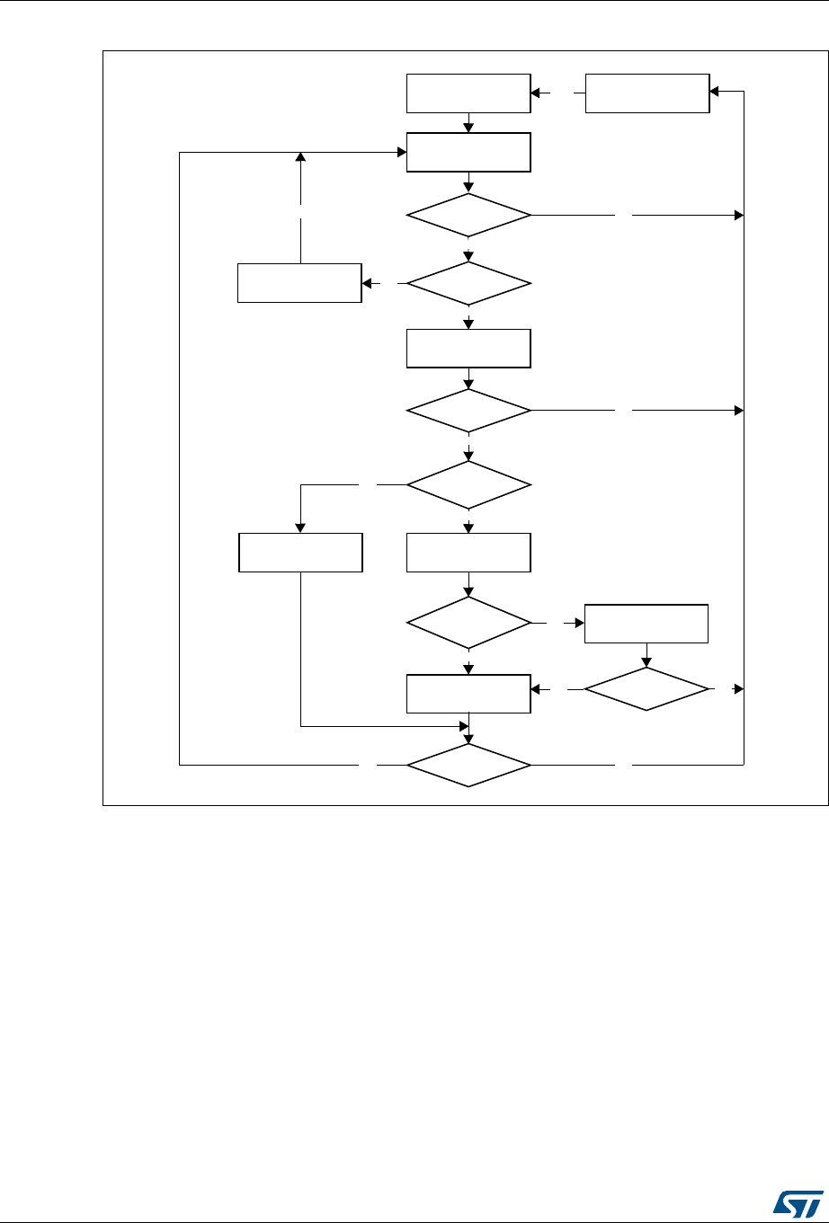
Ethernet (ETH): media access control (MAC) with DMA controller RM0090
1168/1749 RM0090 Rev 18
Figure 377. TxDMA operation in Default mode
TxDMA operation: OSF mode
While in the Run state, the transmit process can simultaneously acquire two frames without
closing the Status descriptor of the first (if the OSF bit is set in ETH_DMAOMR register[2]).
As the transmit process finishes transferring the first frame, it immediately polls the transmit
descriptor list for the second frame. If the second frame is valid, the transmit process
transfers this frame before writing the first frame’s status information. In OSF mode, the
Run-state transmit DMA operates according to the following sequence:
Start TxDMA
(Re-)fetch next
descriptor
Write status word
to TDES0
Wait for Tx status
Transfer data from
buffer(s)
(AHB)
error?
Own
bit set?
(AHB)
error?
Frame xfer
complete?
Time stamp
present?
(AHB)
error?
Write time stamp to
TDES2 and TDES3
(AHB)
error?
Stop TxDMA
TxDMA suspended
No
Yes
No
Yes
No
No
Start
Yes
Yes
Yes
Close intermediate
descriptor
No
Yes
No
Yes
No
Poll demand
ai15639

RM0090 Rev 18 1169/1749
RM0090 Ethernet (ETH): media access control (MAC) with DMA controller
1239
1. The DMA operates as described in steps 1–6 of the TxDMA (default mode).
2. Without closing the previous frame’s last descriptor, the DMA fetches the next
descriptor.
3. If the DMA owns the acquired descriptor, the DMA decodes the transmit buffer address
in this descriptor. If the DMA does not own the descriptor, the DMA goes into Suspend
mode and skips to Step 7.
4. The DMA fetches the Transmit frame from the STM32F4xx memory and transfers the
frame until the end of frame data are transferred, closing the intermediate descriptors if
this frame is split across multiple descriptors.
5. The DMA waits for the transmission status and time stamp of the previous frame. When
the status is available, the DMA writes the time stamp to TDES2 and TDES3, if such
time stamp was captured (as indicated by a status bit). The DMA then writes the status,
with a cleared OWN bit, to the corresponding TDES0, thus closing the descriptor. If
time stamping was not enabled for the previous frame, the DMA does not alter the
contents of TDES2 and TDES3.
6. If enabled, the Transmit interrupt is set, the DMA fetches the next descriptor, then
proceeds to Step 3 (when Status is normal). If the previous transmission status shows
an underflow error, the DMA goes into Suspend mode (Step 7).
7. In Suspend mode, if a pending status and time stamp are received by the DMA, it
writes the time stamp (if enabled for the current frame) to TDES2 and TDES3, then
writes the status to the corresponding TDES0. It then sets relevant interrupts and
returns to Suspend mode.
8. The DMA can exit Suspend mode and enter the Run state (go to Step 1 or Step 2
depending on pending status) only after receiving a Transmit Poll demand
(ETH_DMATPDR register).
Figure 378 shows the basic flowchart in OSF mode.
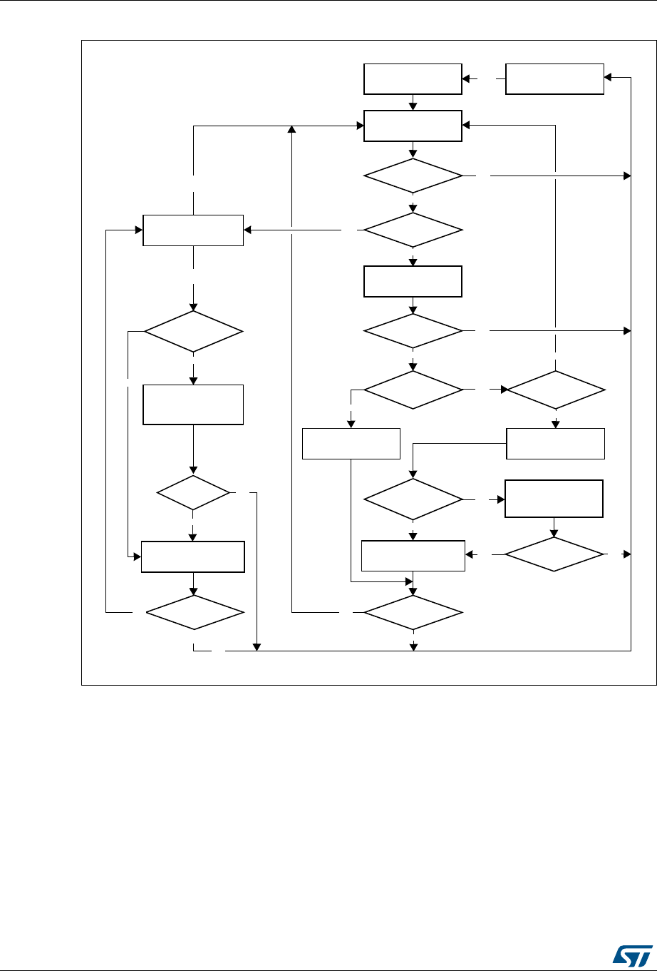
Ethernet (ETH): media access control (MAC) with DMA controller RM0090
1170/1749 RM0090 Rev 18
Figure 378. TxDMA operation in OSF mode
Transmit frame processing
The transmit DMA expects that the data buffers contain complete Ethernet frames,
excluding preamble, pad bytes, and FCS fields. The DA, SA, and Type/Len fields contain
valid data. If the transmit descriptor indicates that the MAC core must disable CRC or pad
insertion, the buffer must have complete Ethernet frames (excluding preamble), including
the CRC bytes. Frames can be data-chained and span over several buffers. Frames have to
be delimited by the first descriptor (TDES0[28]) and the last descriptor (TDES0[29]). As the
transmission starts, TDES0[28] has to be set in the first descriptor. When this occurs, the
frame data are transferred from the memory buffer to the Transmit FIFO. Concurrently, if the
last descriptor (TDES0[29]) of the current frame is cleared, the transmit process attempts to
acquire the next descriptor. The transmit process expects TDES0[28] to be cleared in this
descriptor. If TDES0[29] is cleared, it indicates an intermediary buffer. If TDES0[29] is set, it
Previous frame
status available
Start TxDMA
(Re-)fetch next
descriptor
Write status word to
prev. frame’s TDES0
Transfer data from
buffer(s)
(AHB)
error?
Own
bit set?
(AHB)
error?
Frame xfer
complete?
Time stamp
present?
(AHB)
error?
Write time stamp to
TDES2 & TDES3
for previous frame
(AHB)
error?
Stop TxDMA
No
Yes
No
Yes
No
Start
Yes
Close intermediate
descriptor
No
No
Wait for previous
frame’s Tx status
Second
frame?
Yes
Yes
No
Yes
Yes
Write time stamp to
TDES2 & TDES3
for previous frame
(AHB)
error?
(AHB)
error?
Yes
Time stamp
present?
Yes
Write status word to
prev. frame’s TDES0
TxDMA suspended
Yes
No
Yes
No
No
Poll
demand
No
No
ai1564
0

RM0090 Rev 18 1171/1749
RM0090 Ethernet (ETH): media access control (MAC) with DMA controller
1239
indicates the last buffer of the frame. After the last buffer of the frame has been transmitted,
the DMA writes back the final status information to the transmit descriptor 0 (TDES0) word
of the descriptor that has the last segment set in transmit descriptor 0 (TDES0[29]). At this
time, if Interrupt on Completion (TDES0[30]) is set, Transmit Interrupt (in ETH_DMASR
register [0]) is set, the next descriptor is fetched, and the process repeats. Actual frame
transmission begins after the Transmit FIFO has reached either a programmable transmit
threshold (ETH_DMAOMR register[16:14]), or a full frame is contained in the FIFO. There is
also an option for the Store and forward mode (ETH_DMAOMR register[21]). Descriptors
are released (OWN bit TDES0[31] is cleared) when the DMA finishes transferring the frame.
Transmit polling suspended
Transmit polling can be suspended by either of the following conditions:
•The DMA detects a descriptor owned by the CPU (TDES0[31]=0) and the Transmit
buffer unavailable flag is set (ETH_DMASR register[2]). To resume, the driver must
give descriptor ownership to the DMA and then issue a Poll Demand command.
•A frame transmission is aborted when a transmit error due to underflow is detected.
The appropriate Transmit Descriptor 0 (TDES0) bit is set. If the second condition
occurs, both the Abnormal Interrupt Summary (in ETH_DMASR register [15]) and
Transmit Underflow bits (in ETH_DMASR register[5]) are set, and the information is
written to Transmit Descriptor 0, causing the suspension. If the DMA goes into
Suspend state due to the first condition, then both the Normal Interrupt Summary
(ETH_DMASR register [16]) and Transmit Buffer Unavailable (ETH_DMASR
register[2]) bits are set. In both cases, the position in the transmit list is retained. The
retained position is that of the descriptor following the last descriptor closed by the
DMA. The driver must explicitly issue a Transmit Poll Demand command after rectifying
the suspension cause.
Normal Tx DMA descriptors
The normal transmit descriptor structure consists of four 32-bit words as shown in
Figure 379. The bit descriptions of TDES0, TDES1, TDES2 and TDES3 are given below.
Note that enhanced descriptors must be used if time stamping is activated (ETH_PTPTSCR
bit 0, TSE=1) or if IPv4 checksum offload is activated (ETH_MACCR bit 10, IPCO=1).
Figure 379. Normal transmit descriptor
TDES 3
O
W
N
Ctrl
[30:26]
Res.
24
Ctrl
[23:20]
Reserved
[19:18] Status [16:0]
Reserved
[31:29]
Buffer 2 byte count
[28:16]
Reserved
[15:13]
Buffer 1 byte count
[12:0]
Buffer 1 address [31:0] / Time stamp low [31:0]
Buffer 2 address [31:0] or Next descriptor address [31:0] / Time stamp high [31:0]
TDES 0
TDES 1
TDES 2
31 0
ai15642b
T
T
S
E
T
T
S
S

Ethernet (ETH): media access control (MAC) with DMA controller RM0090
1172/1749 RM0090 Rev 18
•TDES0: Transmit descriptor Word0
The application software has to program the control bits [30:26]+[23:20] plus the OWN
bit [31] during descriptor initialization. When the DMA updates the descriptor (or writes
it back), it resets all the control bits plus the OWN bit, and reports only the status bits.
31 30 29 28 27 26 25 24 23 22 21 20 19 18 17 16
OWN IC LS FS DC DP TTSE Res CIC TER TCH Res. TTSS IHE
rw rw rw rw rw rw rw rw rw rw rw rw rw
1514131211109 8 76543210
ES JT FF IPE LCA NC LCO EC VF CC ED UF DB
rw rw rw rw rw rw rw rw rw rw rw rw rw rw rw rw
Bit 31 OWN: Own bit
When set, this bit indicates that the descriptor is owned by the DMA. When this bit is reset, it
indicates that the descriptor is owned by the CPU. The DMA clears this bit either when it
completes the frame transmission or when the buffers allocated in the descriptor are read
completely. The ownership bit of the frame’s first descriptor must be set after all subsequent
descriptors belonging to the same frame have been set.
Bit 30 IC: Interrupt on completion
When set, this bit sets the Transmit Interrupt (Register 5[0]) after the present frame has
been transmitted.
Bit 29 LS: Last segment
When set, this bit indicates that the buffer contains the last segment of the frame.
Bit 28 FS: First segment
When set, this bit indicates that the buffer contains the first segment of a frame.
Bit 27 DC: Disable CRC
When this bit is set, the MAC does not append a cyclic redundancy check (CRC) to the end
of the transmitted frame. This is valid only when the first segment (TDES0[28]) is set.
Bit 26 DP: Disable pad
When set, the MAC does not automatically add padding to a frame shorter than 64 bytes.
When this bit is reset, the DMA automatically adds padding and CRC to a frame shorter than
64 bytes, and the CRC field is added despite the state of the DC (TDES0[27]) bit. This is
valid only when the first segment (TDES0[28]) is set.
Bit 25 TTSE: Transmit time stamp enable
When TTSE is set and when TSE is set (ETH_PTPTSCR bit 0), IEEE1588 hardware time
stamping is activated for the transmit frame described by the descriptor. This field is only valid
when the First segment control bit (TDES0[28]) is set.
Bit 24 Reserved, must be kept at reset value.
Bits 23:22 CIC: Checksum insertion control
These bits control the checksum calculation and insertion. Bit encoding is as shown below:
00: Checksum Insertion disabled
01: Only IP header checksum calculation and insertion are enabled
10: IP header checksum and payload checksum calculation and insertion are enabled, but
pseudo-header checksum is not calculated in hardware
11: IP Header checksum and payload checksum calculation and insertion are enabled, and
pseudo-header checksum is calculated in hardware.

RM0090 Rev 18 1173/1749
RM0090 Ethernet (ETH): media access control (MAC) with DMA controller
1239
Bit 21 TER: Transmit end of ring
When set, this bit indicates that the descriptor list reached its final descriptor. The DMA
returns to the base address of the list, creating a descriptor ring.
Bit 20 TCH: Second address chained
When set, this bit indicates that the second address in the descriptor is the next descriptor
address rather than the second buffer address. When TDES0[20] is set, TBS2
(TDES1[28:16]) is a “don’t care” value. TDES0[21] takes precedence over TDES0[20].
Bits 19:18 Reserved, must be kept at reset value.
Bit 17 TTSS: Transmit time stamp status
This field is used as a status bit to indicate that a time stamp was captured for the described
transmit frame. When this bit is set, TDES2 and TDES3 have a time stamp value captured for the
transmit frame. This field is only valid when the descriptor’s Last segment control bit (TDES0[29])
is set.
Note that when enhanced descriptors are enabled (EDFE=1 in ETH_DMABMR), TTSS=1
indicates that TDES6 and TDES7 have the time stamp value.
Bit 16 IHE: IP header error
When set, this bit indicates that the MAC transmitter detected an error in the IP datagram
header. The transmitter checks the header length in the IPv4 packet against the number of
header bytes received from the application and indicates an error status if there is a
mismatch. For IPv6 frames, a header error is reported if the main header length is not 40
bytes. Furthermore, the Ethernet length/type field value for an IPv4 or IPv6 frame must
match the IP header version received with the packet. For IPv4 frames, an error status is
also indicated if the Header Length field has a value less than 0x5.
Bit 15 ES: Error summary
Indicates the logical OR of the following bits:
TDES0[14]: Jabber timeout
TDES0[13]: Frame flush
TDES0[11]: Loss of carrier
TDES0[10]: No carrier
TDES0[9]: Late collision
TDES0[8]: Excessive collision
TDES0[2]:Excessive deferral
TDES0[1]: Underflow error
TDES0[16]: IP header error
TDES0[12]: IP payload error
Bit 14 JT: Jabber timeout
When set, this bit indicates the MAC transmitter has experienced a jabber timeout. This bit is
only set when the MAC configuration register’s JD bit is not set.
Bit 13 FF: Frame flushed
When set, this bit indicates that the DMA/MTL flushed the frame due to a software Flush
command given by the CPU.
Bit 12 IPE: IP payload error
When set, this bit indicates that MAC transmitter detected an error in the TCP, UDP, or ICMP
IP datagram payload. The transmitter checks the payload length received in the IPv4 or IPv6
header against the actual number of TCP, UDP or ICMP packet bytes received from the
application and issues an error status in case of a mismatch.

Ethernet (ETH): media access control (MAC) with DMA controller RM0090
1174/1749 RM0090 Rev 18
•TDES1: Transmit descriptor Word1
Bit 11 LCA: Loss of carrier
When set, this bit indicates that a loss of carrier occurred during frame transmission (that is,
the MII_CRS signal was inactive for one or more transmit clock periods during frame
transmission). This is valid only for the frames transmitted without collision when the MAC
operates in Half-duplex mode.
Bit 10 NC: No carrier
When set, this bit indicates that the Carrier Sense signal form the PHY was not asserted
during transmission.
Bit 9 LCO: Late collision
When set, this bit indicates that frame transmission was aborted due to a collision occurring
after the collision window (64 byte times, including preamble, in MII mode). This bit is not
valid if the Underflow Error bit is set.
Bit 8 EC: Excessive collision
When set, this bit indicates that the transmission was aborted after 16 successive collisions
while attempting to transmit the current frame. If the RD (Disable retry) bit in the MAC
Configuration register is set, this bit is set after the first collision, and the transmission of the
frame is aborted.
Bit 7 VF: VLAN frame
When set, this bit indicates that the transmitted frame was a VLAN-type frame.
Bits 6:3 CC: Collision count
This 4-bit counter value indicates the number of collisions occurring before the frame was
transmitted. The count is not valid when the Excessive collisions bit (TDES0[8]) is set.
Bit 2 ED: Excessive deferral
When set, this bit indicates that the transmission has ended because of excessive deferral
of over 24 288 bit times if the Deferral check (DC) bit in the MAC Control register is set high.
Bit 1 UF: Underflow error
When set, this bit indicates that the MAC aborted the frame because data arrived late from
the RAM memory. Underflow error indicates that the DMA encountered an empty transmit
buffer while transmitting the frame. The transmission process enters the Suspended state
and sets both Transmit underflow (Register 5[5]) and Transmit interrupt (Register 5[0]).
Bit 0 DB: Deferred bit
When set, this bit indicates that the MAC defers before transmission because of the
presence of the carrier. This bit is valid only in Half-duplex mode.
31 30 29 28 27 26 25 24 23 22 21 20 19 18 17 16 15 14 13 12 11 10 9 8 7 6 5 4 3 2 1 0
Reserved
TBS2
Reserved
TBS1
rw rw rw rw rw rw rw rw rw rw rw rw rw rw rw rw rw rw rw rw rw rw rw rw rw rw
31:29 Reserved, must be kept at reset value.

RM0090 Rev 18 1175/1749
RM0090 Ethernet (ETH): media access control (MAC) with DMA controller
1239
•TDES2: Transmit descriptor Word2
TDES2 contains the address pointer to the first buffer of the descriptor or it contains
time stamp data.
•TDES3: Transmit descriptor Word3
TDES3 contains the address pointer either to the second buffer of the descriptor or the
next descriptor, or it contains time stamp data.
28:16 TBS2: Transmit buffer 2 size
These bits indicate the second data buffer size in bytes. This field is not valid if TDES0[20] is
set.
15:13 Reserved, must be kept at reset value.
12:0 TBS1: Transmit buffer 1 size
These bits indicate the first data buffer byte size, in bytes. If this field is 0, the DMA ignores
this buffer and uses Buffer 2 or the next descriptor, depending on the value of TCH
(TDES0[20]).
31 30 29 28 27 26 25 24 23 22 21 20 19 18 17 16 15 14 13 12 11 10 9 8 7 6 5 4 3 2 1 0
TBAP1/TBAP/TTSL
rw
Bits 31:0 TBAP1: Transmit buffer 1 address pointer / Transmit frame time stamp low
These bits have two different functions: they indicate to the DMA the location of data in
memory, and after all data are transferred, the DMA can then use these bits to pass back time
stamp data.
TBAP: When the software makes this descriptor available to the DMA (at the moment that the
OWN bit is set to 1 in TDES0), these bits indicate the physical address of Buffer 1. There is no
limitation on the buffer address alignment. See Host data buffer alignment for further details on
buffer address alignment.
TTSL: Before it clears the OWN bit in TDES0, the DMA updates this field with the 32 least
significant bits of the time stamp captured for the corresponding transmit frame (overwriting
the value for TBAP1). This field has the time stamp only if time stamping is activated for this
frame (see TTSE, TDES0 bit 25) and if the Last segment control bit (LS) in the descriptor is
set.
31 30 29 28 27 26 25 24 23 22 21 20 19 18 17 16 15 14 13 12 11 10 9 8 7 6 5 4 3 2 1 0
TBAP2/TBAP2/TTSH
rw

Ethernet (ETH): media access control (MAC) with DMA controller RM0090
1176/1749 RM0090 Rev 18
Enhanced Tx DMA descriptors
Enhanced descriptors (enabled with EDFE=1, ETHDMABMR bit 7), must be used if time
stamping is activated (TSE=1, ETH_PTPTSCR bit 0) or if IPv4 checksum offload is
activated (IPCO=1, ETH_MACCR bit 10).
Enhanced descriptors comprise eight 32-bit words, twice the size of normal descriptors.
TDES0, TDES1, TDES2 and TDES3 have the same definitions as for normal transmit
descriptors (refer to Normal Tx DMA descriptors). TDES6 and TDES7 hold the time stamp.
TDES4, TDES5, TDES6 and TDES7 are defined below.
When the Enhanced descriptor mode is selected, the software needs to allocate 32-bytes (8
words) of memory for every descriptor. When time stamping or IPv4 checksum offload are
not being used, the enhanced descriptor format may be disabled and the software can use
normal descriptors with the default size of 16 bytes.
Bits 31:0 TBAP2: Transmit buffer 2 address pointer (Next descriptor address) / Transmit frame time
stamp high
These bits have two different functions: they indicate to the DMA the location of data in
memory, and after all data are transferred, the DMA can then use these bits to pass back
time stamp data.
TBAP2: When the software makes this descriptor available to the DMA (at the moment when
the OWN bit is set to 1 in TDES0), these bits indicate the physical address of Buffer 2 when a
descriptor ring structure is used. If the Second address chained (TDES1 [20]) bit is set, this
address contains the pointer to the physical memory where the next descriptor is present. The
buffer address pointer must be aligned to the bus width only when TDES1 [20] is set. (LSBs are
ignored internally.)
TTSH: Before it clears the OWN bit in TDES0, the DMA updates this field with the 32 most
significant bits of the time stamp captured for the corresponding transmit frame (overwriting
the value for TBAP2). This field has the time stamp only if time stamping is activated for this
frame (see TDES0 bit 25, TTSE) and if the Last segment control bit (LS) in the descriptor is
set.

RM0090 Rev 18 1177/1749
RM0090 Ethernet (ETH): media access control (MAC) with DMA controller
1239
Figure 380. Enhanced transmit descriptor
•TDES4: Transmit descriptor Word4
Reserved
•TDES5: Transmit descriptor Word5
Reserved
•TDES6: Transmit descriptor Word6
TDES 3
O
W
N
Ctrl
[30:26]
Res.
24
Ctrl
[23:20]
Reserved
[19:18] Status [16:0]
Reserved
[31:29]
Buffer 2 byte count
[28:16]
Reserved
[15:13]
Buffer 1 byte count
[12:0]
Buffer 1 address [31:0]
Buffer 2 address [31:0] or Next descriptor address [31:0]
TDES 0
TDES 1
TDES 2
31 0
ai17105b
T
T
S
E
T
T
S
S
TDES 7
TDES 4
TDES 5
TDES 6
Reserved
Reserved
Time stamp low [31:0]
Time stamp high [31:0]
31 30 29 28 27 26 25 24 23 22 21 20 19 18 17 16 15 14 13 12 11 10 9 8 7 6 5 4 3 2 1 0
TTSL
rw
Bits 31:0 TTSL: Transmit frame time stamp low
This field is updated by DMA with the 32 least significant bits of the time stamp captured
for the corresponding transmit frame. This field has the time stamp only if the Last segment
control bit (LS) in the descriptor is set.

Ethernet (ETH): media access control (MAC) with DMA controller RM0090
1178/1749 RM0090 Rev 18
•TDES7: Transmit descriptor Word7
33.6.8 Rx DMA configuration
The Receive DMA engine’s reception sequence is illustrated in Figure 381 and described
below:
1. The CPU sets up Receive descriptors (RDES0-RDES3) and sets the OWN bit
(RDES0[31]).
2. Once the SR (ETH_DMAOMR register[1]) bit is set, the DMA enters the Run state.
While in the Run state, the DMA polls the receive descriptor list, attempting to acquire
free descriptors. If the fetched descriptor is not free (is owned by the CPU), the DMA
enters the Suspend state and jumps to Step 9.
3. The DMA decodes the receive data buffer address from the acquired descriptors.
4. Incoming frames are processed and placed in the acquired descriptor’s data buffers.
5. When the buffer is full or the frame transfer is complete, the Receive engine fetches the
next descriptor.
6. If the current frame transfer is complete, the DMA proceeds to step 7. If the DMA does
not own the next fetched descriptor and the frame transfer is not complete (EOF is not
yet transferred), the DMA sets the Descriptor error bit in RDES0 (unless flushing is
disabled). The DMA closes the current descriptor (clears the OWN bit) and marks it as
intermediate by clearing the Last segment (LS) bit in the RDES1 value (marks it as last
descriptor if flushing is not disabled), then proceeds to step 8. If the DMA owns the next
descriptor but the current frame transfer is not complete, the DMA closes the current
descriptor as intermediate and returns to step 4.
7. If IEEE 1588 time stamping is enabled, the DMA writes the time stamp (if available) to
the current descriptor’s RDES2 and RDES3. It then takes the received frame’s status
and writes the status word to the current descriptor’s RDES0, with the OWN bit cleared
and the Last segment bit set.
8. The Receive engine checks the latest descriptor’s OWN bit. If the CPU owns the
descriptor (OWN bit is at 0) the Receive buffer unavailable bit (in ETH_DMASR
register[7]) is set and the DMA Receive engine enters the Suspended state (step 9). If
the DMA owns the descriptor, the engine returns to step 4 and awaits the next frame.
9. Before the Receive engine enters the Suspend state, partial frames are flushed from
the Receive FIFO (you can control flushing using bit 24 in the ETH_DMAOMR
register).
10. The Receive DMA exits the Suspend state when a Receive Poll demand is given or the
start of next frame is available from the Receive FIFO. The engine proceeds to step 2
and re-fetches the next descriptor.
31 30 29 28 27 26 25 24 23 22 21 20 19 18 17 16 15 14 13 12 11 10 9 8 7 6 5 4 3 2 1 0
TTSH
rw
Bits 31:0 TTSH: Transmit frame time stamp high
This field is updated by DMA with the 32 most significant bits of the time stamp captured for
the corresponding transmit frame. This field has the time stamp only if the Last segment control
bit (LS) in the descriptor is set.
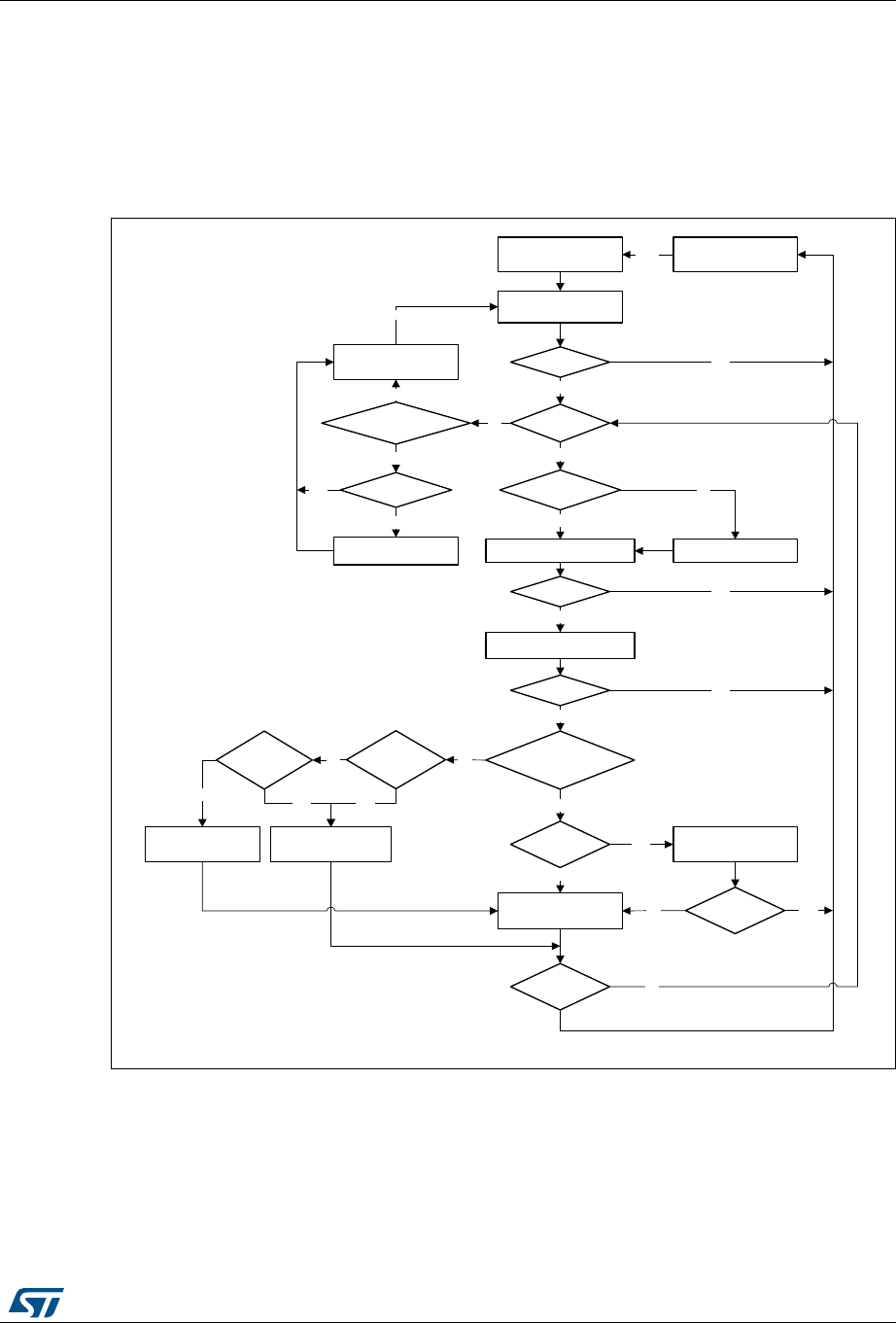
RM0090 Rev 18 1179/1749
RM0090 Ethernet (ETH): media access control (MAC) with DMA controller
1239
The DMA does not acknowledge accepting the status until it has completed the time stamp
write-back and is ready to perform status write-back to the descriptor. If software has
enabled time stamping through CSR, when a valid time stamp value is not available for the
frame (for example, because the receive FIFO was full before the time stamp could be
written to it), the DMA writes all ones to RDES2 and RDES3. Otherwise (that is, if time
stamping is not enabled), RDES2 and RDES3 remain unchanged.
Figure 381. Receive DMA operation
(Re-)Fetch next
descriptor
(AHB)
error?
No
Own bit set?
Yes
Yes
Stop RxDMAStart RxDMA Start
(AHB)
error?
No
RxDMA suspended
Yes
Frame data
available ?
Wait for frame dataWrite data to buffer(s)
Yes
Yes
Fetch next descriptor
Yes
No
Frame transfer
complete?
No
Set descriptor error
Yes
Time stamp
present?
No
Close RDES0 as last
descriptor
Write time stamp to
RDES2 & RDES3
No (AHB)
error? Yes
Close RDES0 as
intermediate descriptor
Frame transfer
complete?
No
Flush disabled?
No
Flush the
remaining frame
Yes
Yes
No
No
No
Yes
Yes
Poll demand/
new frame available
No
Yes
(AHB)
error?
(AHB)
error?
No
Own bit set
for next desc?
Flush
disabled ?
ai1564
3

Ethernet (ETH): media access control (MAC) with DMA controller RM0090
1180/1749 RM0090 Rev 18
Receive descriptor acquisition
The receive engine always attempts to acquire an extra descriptor in anticipation of an
incoming frame. Descriptor acquisition is attempted if any of the following conditions is/are
satisfied:
•The receive Start/Stop bit (ETH_DMAOMR register[1]) has been set immediately after
the DMA has been placed in the Run state.
•The data buffer of the current descriptor is full before the end of the frame currently
being transferred
•The controller has completed frame reception, but the current receive descriptor has
not yet been closed.
•The receive process has been suspended because of a CPU-owned buffer
(RDES0[31] = 0) and a new frame is received.
•A Receive poll demand has been issued.
Receive frame processing
The MAC transfers the received frames to the STM32F4xx memory only when the frame
passes the address filter and the frame size is greater than or equal to the configurable
threshold bytes set for the Receive FIFO, or when the complete frame is written to the FIFO
in Store-and-forward mode. If the frame fails the address filtering, it is dropped in the MAC
block itself (unless Receive All ETH_MACFFR [31] bit is set). Frames that are shorter than
64 bytes, because of collision or premature termination, can be purged from the Receive
FIFO. After 64 (configurable threshold) bytes have been received, the DMA block begins
transferring the frame data to the receive buffer pointed to by the current descriptor. The
DMA sets the first descriptor (RDES0[9]) after the DMA AHB Interface becomes ready to
receive a data transfer (if DMA is not fetching transmit data from the memory), to delimit the
frame. The descriptors are released when the OWN (RDES0[31]) bit is reset to 0, either as
the data buffer fills up or as the last segment of the frame is transferred to the receive buffer.
If the frame is contained in a single descriptor, both the last descriptor (RDES0[8]) and first
descriptor (RDES0[9]) bits are set. The DMA fetches the next descriptor, sets the last
descriptor (RDES0[8]) bit, and releases the RDES0 status bits in the previous frame
descriptor. Then the DMA sets the receive interrupt bit (ETH_DMASR register [6]). The
same process repeats unless the DMA encounters a descriptor flagged as being owned by
the CPU. If this occurs, the receive process sets the receive buffer unavailable bit
(ETH_DMASR register[7]) and then enters the Suspend state. The position in the receive
list is retained.
Receive process suspended
If a new receive frame arrives while the receive process is in Suspend state, the DMA re-
fetches the current descriptor in the STM32F4xx memory. If the descriptor is now owned by
the DMA, the receive process re-enters the Run state and starts frame reception. If the
descriptor is still owned by the host, by default, the DMA discards the current frame at the
top of the Rx FIFO and increments the missed frame counter. If more than one frame is
stored in the Rx FIFO, the process repeats. The discarding or flushing of the frame at the
top of the Rx FIFO can be avoided by setting the DMA Operation mode register bit 24
(DFRF). In such conditions, the receive process sets the receive buffer unavailable status
bit and returns to the Suspend state.
RM0090 Rev 18 1181/1749
RM0090 Ethernet (ETH): media access control (MAC) with DMA controller
1239
Normal Rx DMA descriptors
The normal receive descriptor structure consists of four 32-bit words (16 bytes). These are
shown in Figure 382. The bit descriptions of RDES0, RDES1, RDES2 and RDES3 are given
below.
Note that enhanced descriptors must be used if time stamping is activated (TSE=1,
ETH_PTPTSCR bit 0) or if IPv4 checksum offload is activated (IPCO=1, ETH_MACCR bit
10).
Figure 382. Normal Rx DMA descriptor structure
•RDES0: Receive descriptor Word0
RDES0 contains the received frame status, the frame length and the descriptor
ownership information.
RDES 3
O
W
NStatus [30:0]
Reserved
[30:29] Buffer 2 byte count
[28:16] CTRL
[15:14] Buffer 1 byte count
[12:0]
Buffer 1 address [31:0]
Buffer 2 address [31:0] or Next descriptor address [31:0]
RDES 0
RDES 1
RDES 2
31 0
ai1564
4
Res.
CT
RL
31 30 29 28 27 26 25 24 23 22 21 20 19 18 17 16 15 14 13 12 11 10 9 8 7 6 5 4 3 2 1 0
OWN
AFM
FL
ES
DE
SAF
LE
OE
VLAN
FS
LS
IPHCE/TSV
LCO
FT
RWT
RE
DE
CE
PCE/ESA
rw
Bit 31 OWN: Own bit
When set, this bit indicates that the descriptor is owned by the DMA of the MAC Subsystem.
When this bit is reset, it indicates that the descriptor is owned by the Host. The DMA clears this bit
either when it completes the frame reception or when the buffers that are associated with this
descriptor are full.
Bit 30 AFM: Destination address filter fail
When set, this bit indicates a frame that failed the DA filter in the MAC Core.
Bits 29:16 FL: Frame length
These bits indicate the byte length of the received frame that was transferred to host memory
(including CRC). This field is valid only when last descriptor (RDES0[8]) is set and descriptor error
(RDES0[14]) is reset.
This field is valid when last descriptor (RDES0[8]) is set. When the last descriptor and error
summary bits are not set, this field indicates the accumulated number of bytes that have been
transferred for the current frame.

Ethernet (ETH): media access control (MAC) with DMA controller RM0090
1182/1749 RM0090 Rev 18
Bit 15 ES: Error summary
Indicates the logical OR of the following bits:
RDES0[1]: CRC error
RDES0[3]: Receive error
RDES0[4]: Watchdog timeout
RDES0[6]: Late collision
RDES0[7]: Giant frame (This is not applicable when RDES0[7] indicates an IPV4 header
checksum error.)
RDES0[11]: Overflow error
RDES0[14]: Descriptor error.
This field is valid only when the last descriptor (RDES0[8]) is set.
Bit 14 DE: Descriptor error
When set, this bit indicates a frame truncation caused by a frame that does not fit within the current
descriptor buffers, and that the DMA does not own the next descriptor. The frame is truncated.
This field is valid only when the last descriptor (RDES0[8]) is set.
Bit 13 SAF: Source address filter fail
When set, this bit indicates that the SA field of frame failed the SA filter in the MAC Core.
Bit 12 LE: Length error
When set, this bit indicates that the actual length of the received frame does not match the value in
the Length/ Type field. This bit is valid only when the Frame type (RDES0[5]) bit is reset.
Bit 1
1
OE: Overflow error
When set, this bit indicates that the received frame was damaged due to buffer overflow.
Bit 10 VLAN: VLAN tag
When set, this bit indicates that the frame pointed to by this descriptor is a VLAN frame tagged
by the MAC core.
Bit 9 FS: First descriptor
When set, this bit indicates that this descriptor contains the first buffer of the frame. If the size of the
first buffer is 0, the second buffer contains the beginning of the frame. If the size of the second buffer
is also 0, the next descriptor contains the beginning of the frame.
Bit 8 LS: Last descriptor
When set, this bit indicates that the buffers pointed to by this descriptor are the last buffers of
the frame.
Bit 7 IPHCE/TSV: IPv header checksum error / time stamp valid
If IPHCE is set, it indicates an error in the IPv4 or IPv6 header. This error can be due to inconsistent
Ethernet Type field and IP header Version field values, a header checksum mismatch in IPv4, or an
Ethernet frame lacking the expected number of IP header bytes. This bit can take on special
meaning as specified in Table 193.
If enhanced descriptor format is enabled (EDFE=1, bit 7 of ETH_DMABMR), this bit takes on
the TSV function (otherwise it is IPHCE). When TSV is set, it indicates that a snapshot of the
timestamp is written in descriptor words 6 (RDES6) and 7 (RDES7). TSV is valid only when
the Last descriptor bit (RDES0[8]) is set.
Bit 6 LCO: Late collision
When set, this bit indicates that a late collision has occurred while receiving the frame in Half-
duplex mode.

RM0090 Rev 18 1183/1749
RM0090 Ethernet (ETH): media access control (MAC) with DMA controller
1239
Bits 5, 7, and 0 reflect the conditions discussed in Table 193.
Bit 5 FT: Frame type
When set, this bit indicates that the Receive frame is an Ethernet-type frame (the LT field is greater
than or equal to 0x0600). When this bit is reset, it indicates that the received frame is an
IEEE802.3 frame. This bit is not valid for Runt frames less than 14 bytes. When the normal
descriptor format is used (ETH_DMABMR EDFE=0), FT can take on special meaning as
specified in Table 193.
Bit 4 RWT: Receive watchdog timeout
When set, this bit indicates that the Receive watchdog timer has expired while receiving the
current frame and the current frame is truncated after the watchdog timeout.
Bit 3 RE: Receive error
When set, this bit indicates that the RX_ERR signal is asserted while RX_DV is asserted
during frame reception.
Bit 2 DE: Dribble bit error
When set, this bit indicates that the received frame has a non-integer multiple of bytes (odd
nibbles). This bit is valid only in MII mode.
Bit 1 CE: CRC error
When set, this bit indicates that a cyclic redundancy check (CRC) error occurred on the
received frame. This field is valid only when the last descriptor (RDES0[8]) is set.
Bit 0 PCE/ESA: Payload checksum error / extended status available
When set, it indicates that the TCP, UDP or ICMP checksum the core calculated does not
match the received encapsulated TCP, UDP or ICMP segment’s Checksum field. This bit is
also set when the received number of payload bytes does not match the value indicated in
the Length field of the encapsulated IPv4 or IPv6 datagram in the received Ethernet frame.
This bit can take on special meaning as specified in Table 193.
If the enhanced descriptor format is enabled (EDFE=1, bit 7 in ETH_DMABMR), this bit takes
on the ESA function (otherwise it is PCE). When ESA is set, it indicates that the extended
status is available in descriptor word 4 (RDES4). ESA is valid only when the last descriptor bit
(RDES0[8]) is set.
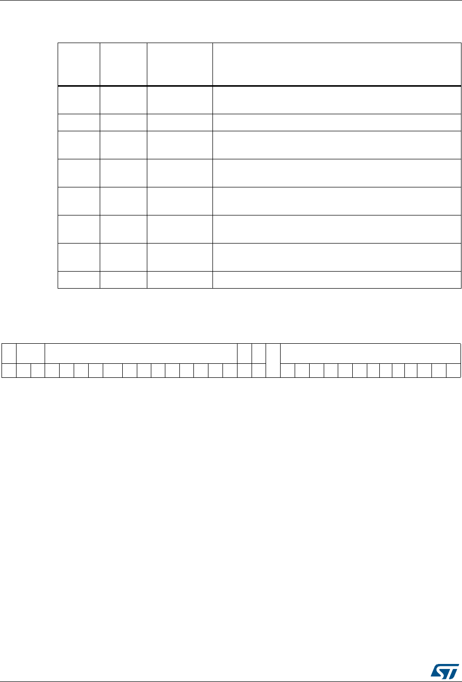
Ethernet (ETH): media access control (MAC) with DMA controller RM0090
1184/1749 RM0090 Rev 18
•RDES1: Receive descriptor Word1
Table 193. Receive descriptor 0 - encoding for bits 7, 5 and 0 (normal descriptor
format only, EDFE=0)
Bit 5:
frame
type
Bit 7: IPC
checksum
error
Bit 0: payload
checksum
error
Frame status
00 0
IEEE 802.3 Type frame (Length field value is less than
0x0600.)
1 0 0 IPv4/IPv6 Type frame, no checksum error detected
10 1
IPv4/IPv6 Type frame with a payload checksum error (as described
for PCE) detected
11 0
IPv4/IPv6 Type frame with an IP header checksum error (as
described for IPC CE) detected
11 1
IPv4/IPv6 Type frame with both IP header and payload checksum
errors detected
00 1
IPv4/IPv6 Type frame with no IP header checksum error and the
payload check bypassed, due to an unsupported payload
01 1
A Type frame that is neither IPv4 or IPv6 (the checksum offload
engine bypasses checksum completely.)
0 1 0 Reserved
31 30 29 28 27 26 25 24 23 22 21 20 19 18 17 16 15 14 13 12 11 10 9 8 7 6 5 4 3 2 1 0
DIC
RBS2 RBS2
RER
RCH
Reserved
RBS
rw rw rw rw rw rw rw rw rw rw rw rw rw rw rw rw rw rw rw rw rw rw rw rw rw rw rw rw rw rw rw
Bit 31 DIC: Disable interrupt on completion
When set, this bit prevents setting the Status register’s RS bit (CSR5[6]) for the received frame
ending in the buffer indicated by this descriptor. This, in turn, disables the assertion of the interrupt to
Host due to RS for that frame.
Bits 30:29 Reserved, must be kept at reset value.
Bits 28:16 RBS2: Receive buffer 2 size
These bits indicate the second data buffer size, in bytes. The buffer size must be a multiple of 4,
8, or 16, depending on the bus widths (32, 64 or 128, respectively), even if the value of RDES3
(buffer2 address pointer) is not aligned to bus width. If the buffer size is not an appropriate multiple
of 4, 8 or 16, the resulting behavior is undefined. This field is not valid if RDES1 [14] is set.
Bit 15 RER: Receive end of ring
When set, this bit indicates that the descriptor list reached its final descriptor. The DMA returns to the
base address of the list, creating a descriptor ring.

RM0090 Rev 18 1185/1749
RM0090 Ethernet (ETH): media access control (MAC) with DMA controller
1239
•RDES2: Receive descriptor Word2
RDES2 contains the address pointer to the first data buffer in the descriptor, or it
contains time stamp data.
Bit 14 RCH: Second address chained
When set, this bit indicates that the second address in the descriptor is the next descriptor address
rather than the second buffer address. When this bit is set, RBS2 (RDES1[28:16]) is a “don’t
care” value. RDES1[15] takes precedence over RDES1[14].
Bit 13 Reserved, must be kept at reset value.
Bits 12:0 RBS1: Receive buffer 1 size
Indicates the first data buffer size in bytes. The buffer size must be a multiple of 4, 8 or 16,
depending upon the bus widths (32, 64 or 128), even if the value of RDES2 (buffer1 address
pointer) is not aligned. When the buffer size is not a multiple of 4, 8 or 16, the resulting behavior is
undefined. If this field is 0, the DMA ignores this buffer and uses Buffer 2 or next descriptor
depending on the value of RCH (bit 14).
31 30 29 28 27 26 25 24 23 22 21 20 19 18 17 16 15 14 13 12 11 10 9 8 7 6 5 4 3 2 1 0
RBP1 / RTSL
rw rw rw rw rw rw rw rw rw rw rw rw rw rw rw rw rw rw rw rw rw rw rw rw rw rw rw rw rw rw rw rw
Bits 31:0 RBAP1 / RTSL: Receive buffer 1 address pointer / Receive frame time stamp low
These bits take on two different functions: the application uses them to indicate to the DMA
where to store the data in memory, and then after transferring all the data the DMA may use
these bits to pass back time stamp data.
RBAP1: When the software makes this descriptor available to the DMA (at the moment that
the OWN bit is set to 1 in RDES0), these bits indicate the physical address of Buffer 1. There are
no limitations on the buffer address alignment except for the following condition: the DMA uses the
configured value for its address generation when the RDES2 value is used to store the start of
frame. Note that the DMA performs a write operation with the RDES2[3/2/1:0] bits as 0 during the
transfer of the start of frame but the frame data is shifted as per the actual Buffer address pointer.
The DMA ignores RDES2[3/2/1:0] (corresponding to bus width of 128/64/32) if the address pointer
is to a buffer where the middle or last part of the frame is stored.
RTSL: Before it clears the OWN bit in RDES0, the DMA updates this field with the 32 least
significant bits of the time stamp captured for the corresponding receive frame (overwriting
the value for RBAP1). This field has the time stamp only if time stamping is activated for this
frame and if the Last segment control bit (LS) in the descriptor is set.

Ethernet (ETH): media access control (MAC) with DMA controller RM0090
1186/1749 RM0090 Rev 18
•RDES3: Receive descriptor Word3
RDES3 contains the address pointer either to the second data buffer in the descriptor
or to the next descriptor, or it contains time stamp data.
Enhanced Rx DMA descriptors format with IEEE1588 time stamp
Enhanced descriptors (enabled with EDFE=1, ETHDMABMR bit 7), must be used if time
stamping is activated (TSE=1, ETH_PTPTSCR bit 0) or if IPv4 checksum offload is
activated (IPCO=1, ETH_MACCR bit 10).
Enhanced descriptors comprise eight 32-bit words, twice the size of normal descriptors.
RDES0, RDES1, RDES2 and RDES3 have the same definitions as for normal receive
descriptors (refer to Normal Rx DMA descriptors). RDES4 contains extended status while
RDES6 and RDES7 hold the time stamp. RDES4, RDES5, RDES6 and RDES7 are defined
below.
When the Enhanced descriptor mode is selected, the software needs to allocate 32 bytes (8
words) of memory for every descriptor. When time stamping or IPv4 checksum offload are
not being used, the enhanced descriptor format may be disabled and the software can use
normal descriptors with the default size of 16 bytes.
31 30 29 28 27 26 25 24 23 22 21 20 19 18 17 16 15 14 13 12 11 10 9 8 7 6 5 4 3 2 1 0
RBP2 / RTSH
rw rw rw rw rw rw rw rw rw rw rw rw rw rw rw rw rw rw rw rw rw rw rw rw rw rw rw rw rw rw rw rw
Bits 31:0 RBAP2 / RTSH: Receive buffer 2 address pointer (next descriptor address) / Receive frame
time stamp high
These bits take on two different functions: the application uses them to indicate to the DMA
the location of where to store the data in memory, and then after transferring all the data the
DMA may use these bits to pass back time stamp data.
RBAP1: When the software makes this descriptor available to the DMA (at the moment that
the OWN bit is set to 1 in RDES0), these bits indicate the physical address of buffer 2 when a
descriptor ring structure is used. If the second address chained (RDES1 [24]) bit is set, this address
contains the pointer to the physical memory where the next descriptor is present. If RDES1 [24] is
set, the buffer (next descriptor) address pointer must be bus width-aligned (RDES3[3, 2, or
1:0] = 0, corresponding to a bus width of 128, 64 or 32. LSBs are ignored internally.)
However, when RDES1 [24] is reset, there are no limitations on the RDES3 value, except for the
following condition: the DMA uses the configured value for its buffer address generation when the
RDES3 value is used to store the start of frame. The DMA ignores RDES3[3, 2, or 1:0]
(corresponding to a bus width of 128, 64 or 32) if the address pointer is to a buffer where the
middle or last part of the frame is stored.
RTSH: Before it clears the OWN bit in RDES0, the DMA updates this field with the 32 most
significant bits of the time stamp captured for the corresponding receive frame (overwriting
the value for RBAP2). This field has the time stamp only if time stamping is activated and if
the Last segment control bit (LS) in the descriptor is set.
RM0090 Rev 18 1187/1749
RM0090 Ethernet (ETH): media access control (MAC) with DMA controller
1239
Figure 383. Enhanced receive descriptor field format with IEEE1588 time stamp
enabled
•RDES4: Receive descriptor Word4
The extended status, shown below, is valid only when there is status related to IPv4
checksum or time stamp available as indicated by bit 0 in RDES0.
RDES 3
O
W
NStatus [30:0]
Reserved
[30:29]
Buffer 2 byte count
[28:16]
CTRL
[15:14]
Buffer 1 byte count
[12:0]
Buffer 1 address [31:0]
Buffer 2 address [31:0] or Next descriptor address [31:0]
RDES 0
RDES 1
RDES 2
31 0
ai17104
Res.
CT
RL
RDES 7
RDES 4
RDES 5
RDES 6
Extended Status [31:0]
Reserved
Time stamp low [31:0]
Time stamp high [31:0]
31 30 29 28 27 26 25 24 23 22 21 20 19 18 17 16 15 14 13 12 11 10 9 8 7 6 5 4 3 2 1 0
Reserved
PV
PFT
PMT
IPV6PR
IPV4PR
IPCB
IPPE
IPHE
IPPT
rw rw rw rw rw rw rw rw rw rw rw rw rw rw
Bits 31:14 Reserved, must be kept at reset value.
Bit 13 PV: PTP version
When set, indicates that the received PTP message uses the IEEE 1588 version 2 format.
When cleared, it uses version 1 format. This is valid only if the message type is non-zero.
Bit 12 PFT: PTP frame type
When set, this bit indicates that the PTP message is sent directly over Ethernet. When this bit
is cleared and the message type is non-zero, it indicates that the PTP message is sent over
UDP-IPv4 or UDP-IPv6. The information on IPv4 or IPv6 can be obtained from bits 6 and 7.

Ethernet (ETH): media access control (MAC) with DMA controller RM0090
1188/1749 RM0090 Rev 18
•RDES5: Receive descriptor Word5
Reserved.
•RDES6: Receive descriptor Word6
The table below describes the fields that have different meaning for RDES6 when the
receive descriptor is closed and time stamping is enabled.
Bits 11:8 PMT: PTP message type
These bits are encoded to give the type of the message received.
– 0000: No PTP message received
– 0001: SYNC (all clock types)
– 0010: Follow_Up (all clock types)
– 0011: Delay_Req (all clock types)
– 0100: Delay_Resp (all clock types)
– 0101: Pdelay_Req (in peer-to-peer transparent clock) or Announce (in ordinary or boundary
clock)
– 0110: Pdelay_Resp (in peer-to-peer transparent clock) or Management (in ordinary or
boundary clock)
– 0111: Pdelay_Resp_Follow_Up (in peer-to-peer transparent clock) or Signaling (for ordinary
or boundary clock)
– 1xxx - Reserved
Bit 7 IPV6PR: IPv6 packet received
When set, this bit indicates that the received packet is an IPv6 packet.
Bit 6 IPV4PR: IPv4 packet received
When set, this bit indicates that the received packet is an IPv4 packet.
Bit 5 IPCB: IP checksum bypassed
When set, this bit indicates that the checksum offload engine is bypassed.
Bit 4 IPPE: IP payload error
When set, this bit indicates that the 16-bit IP payload checksum (that is, the TCP, UDP, or
ICMP checksum) that the core calculated does not match the corresponding checksum field
in the received segment. It is also set when the TCP, UDP, or ICMP segment length does not
match the payload length value in the IP Header field.
Bit 3 IPHE: IP header error
When set, this bit indicates either that the 16-bit IPv4 header checksum calculated by the
core does not match the received checksum bytes, or that the IP datagram version is not
consistent with the Ethernet Type value.
Bits 2:0 IPPT: IP payload type
if IPv4 checksum offload is activated (IPCO=1, ETH_MACCR bit 10), these bits
indicate the type of payload encapsulated in the IP datagram. These bits are ‘00’ if there is an IP
header error or fragmented IP.
– 000: Unknown or did not process IP payload
– 001: UDP
–010: TCP
–011: ICMP
– 1xx: Reserved

RM0090 Rev 18 1189/1749
RM0090 Ethernet (ETH): media access control (MAC) with DMA controller
1239
.
•RDES7: Receive descriptor Word7
The table below describes the fields that have a different meaning for RDES7 when the
receive descriptor is closed and time stamping is enabled.
.
33.6.9 DMA interrupts
Interrupts can be generated as a result of various events. The ETH_DMASR register
contains all the bits that might cause an interrupt. The ETH_DMAIER register contains an
enable bit for each of the events that can cause an interrupt.
There are two groups of interrupts, Normal and Abnormal, as described in the ETH_DMASR
register. Interrupts are cleared by writing a 1 to the corresponding bit position. When all the
enabled interrupts within a group are cleared, the corresponding summary bit is cleared. If
the MAC core is the cause for assertion of the interrupt, then any of the TSTS or PMTS bits
in the ETH_DMASR register is set high.
Interrupts are not queued and if the interrupt event occurs before the driver has responded
to it, no additional interrupts are generated. For example, the Receive Interrupt bit
(ETH_DMASR register [6]) indicates that one or more frames were transferred to the
STM32F4xx buffer. The driver must scan all descriptors, from the last recorded position to
the first one owned by the DMA.
An interrupt is generated only once for simultaneous, multiple events. The driver must scan
the ETH_DMASR register for the cause of the interrupt. The interrupt is not generated again
unless a new interrupting event occurs, after the driver has cleared the appropriate bit in the
ETH_DMASR register. For example, the controller generates a Receive interrupt
(ETH_DMASR register[6]) and the driver begins reading the ETH_DMASR register. Next,
receive buffer unavailable (ETH_DMASR register[7]) occurs. The driver clears the Receive
interrupt. Even then, a new interrupt is generated, due to the active or pending Receive
buffer unavailable interrupt.
31 30 29 28 27 26 25 24 23 22 21 20 19 18 17 16 15 14 13 12 11 10 9 8 7 6 5 4 3 2 1 0
RTSL
rw rw rw rw rw rw rw rw rw rw rw rw rw rw rw rw rw rw rw rw rw rw rw rw rw rw rw rw rw rw rw rw
Bits 31:0 RTSL: Receive frame time stamp low
The DMA updates this field with the 32 least significant bits of the time stamp captured for the
corresponding receive frame. The DMA updates this field only for the last descriptor of the receive
frame indicated by last descriptor status bit (RDES0[8]). When this field and the RTSH field in
RDES7 show all ones, the time stamp must be treated as corrupt.
31 30 29 28 27 26 25 24 23 22 21 20 19 18 17 16 15 14 13 12 11 10 9 8 7 6 5 4 3 2 1 0
RTSH
rw rw rw rw rw rw rw rw rw rw rw rw rw rw rw rw rw rw rw rw rw rw rw rw rw rw rw rw rw rw rw rw
Bits 31:0 RTSH: Receive frame time stamp high
The DMA updates this field with the 32 most significant bits of the time stamp captured for the
corresponding receive frame. The DMA updates this field only for the last descriptor of the receive
frame indicated by last descriptor status bit (RDES0[8]).
When this field and RDES7’s RTSL field show all ones, the time stamp must be treated as
corrupt.
Ethernet (ETH): media access control (MAC) with DMA controller RM0090
1190/1749 RM0090 Rev 18
Figure 384. Interrupt scheme
33.7 Ethernet interrupts
The Ethernet controller has two interrupt vectors: one dedicated to normal Ethernet
operations and the other, used only for the Ethernet wakeup event (with wakeup frame or
Magic Packet detection) when it is mapped on EXTI lIne19.
The first Ethernet vector is reserved for interrupts generated by the MAC and the DMA as
listed in the MAC interrupts and DMA interrupts sections.
The second vector is reserved for interrupts generated by the PMT on wakeup events. The
mapping of a wakeup event on EXTI line19 causes the STM32F4xx to exit the low-power
mode, and generates an interrupt.
When an Ethernet wakeup event mapped on EXTI Line19 occurs and the MAC PMT
interrupt is enabled and the EXTI Line19 interrupt, with detection on rising edge, is also
enabled, both interrupts are generated.
A watchdog timer (see ETH_DMARSWTR register) is given for flexible control of the RS bit
(ETH_DMASR register). When this watchdog timer is programmed with a non-zero value, it
gets activated as soon as the RxDMA completes a transfer of a received frame to system
memory without asserting the Receive Status because it is not enabled in the corresponding
Receive descriptor (RDES1[31]). When this timer runs out as per the programmed value,
the RS bit is set and the interrupt is asserted if the corresponding RIE is enabled in the
ETH_DMAIER register. This timer is disabled before it runs out, when a frame is transferred
to memory and the RS is set because it is enabled for that descriptor.
AND
AND
OR
OR
AND
NIS
NISE
AND
AIS
AISE
OR Interrupt
TS
TIE
FBES
FBEIE
AI15646
PMTI
TSTI
MMCI
AND
TBUS
TBUIE
AND
RS
RIE
AND
ERS
ERIE
AND
TPSS
TPSSIE AND
TJTS
TJTIE
AND
ROS
ROIE
AND
TUS
TUIE
AND
RBU
RBUIE AND
RPSS
RPSSIE
AND
RWTS
RWTIE
AND
ETS
ETIE

RM0090 Rev 18 1191/1749
RM0090 Ethernet (ETH): media access control (MAC) with DMA controller
1239
Note: Reading the PMT control and status register automatically clears the Wakeup Frame
Received and Magic Packet Received PMT interrupt flags. However, since the registers for
these flags are in the CLK_RX domain, there may be a significant delay before this update
is visible by the firmware. The delay is especially long when the RX clock is slow (in 10 Mbit
mode) and when the AHB bus is high-frequency.
Since interrupt requests from the PMT to the CPU are based on the same registers in the
CLK_RX domain, the CPU may spuriously call the interrupt routine a second time even after
reading PMT_CSR. Thus, it may be necessary that the firmware polls the Wakeup Frame
Received and Magic Packet Received bits and exits the interrupt service routine only when
they are found to be at ‘0’.
33.8 Ethernet register descriptions
The peripheral registers can be accessed by bytes (8-bit), half-words (16-bit) or words (32-
bits).
33.8.1 MAC register description
Ethernet MAC configuration register (ETH_MACCR)
Address offset: 0x0000
Reset value: 0x0000 8000
The MAC configuration register is the operation mode register of the MAC. It establishes
receive and transmit operating modes.
313029282726252423222120191817161514131211109876543210
Reserved
CSTF
Reserved
WD
JD
Reserved
IFG
CSD
Reserved
FES
ROD
LM
DM
IPCO
RD
Reserved
APCS
BL
DC
TE
RE
Reserved
rw rw rw rw rw rw rw rw rw rw rw rw rw rw rw rw
Bits 31:26 Reserved, must be kept at reset value.
Bit 25
CSTF: CRC stripping for Type frames
When set, the last 4 bytes (FCS) of all frames of Ether type (type field greater than
0x0600) will be stripped and dropped before forwarding the frame to the application.
Bit 24Reserved, must be kept at reset value.
Bit 23 WD: Watchdog disable
When this bit is set, the MAC disables the watchdog timer on the receiver, and can receive
frames of up to 16 384 bytes.
When this bit is reset, the MAC allows no more than 2 048 bytes of the frame being received
and cuts off any bytes received after that.
Bit 22 JD: Jabber disable
When this bit is set, the MAC disables the jabber timer on the transmitter, and can transfer
frames of up to 16 384 bytes.
When this bit is reset, the MAC cuts off the transmitter if the application sends out more than
2 048 bytes of data during transmission.
Bits 21:20 Reserved, must be kept at reset value.

Ethernet (ETH): media access control (MAC) with DMA controller RM0090
1192/1749 RM0090 Rev 18
Bits 19:17 IFG: Interframe gap
These bits control the minimum interframe gap between frames during transmission.
000: 96 bit times
001: 88 bit times
010: 80 bit times
….
111: 40 bit times
Note: In Half-duplex mode, the minimum IFG can be configured for 64 bit times (IFG = 100)
only. Lower values are not considered.
Bit 16 CSD: Carrier sense disable
When set high, this bit makes the MAC transmitter ignore the MII CRS signal during frame
transmission in Half-duplex mode. No error is generated due to Loss of Carrier or No Carrier
during such transmission.
When this bit is low, the MAC transmitter generates such errors due to Carrier Sense and
even aborts the transmissions.
Bit 15 Reserved, must be kept at reset value.
Bit 14 FES: Fast Ethernet speed
Indicates the speed in Fast Ethernet (MII) mode:
0: 10 Mbit/s
1: 100 Mbit/s
Bit 13 ROD: Receive own disable
When this bit is set, the MAC disables the reception of frames in Half-duplex mode.
When this bit is reset, the MAC receives all packets that are given by the PHY while
transmitting.
This bit is not applicable if the MAC is operating in Full-duplex mode.
Bit 12 LM: Loopback mode
When this bit is set, the MAC operates in loopback mode at the MII. The MII receive clock
input (RX_CLK) is required for the loopback to work properly, as the transmit clock is not
looped-back internally.
Bit 11 DM: Duplex mode
When this bit is set, the MAC operates in a Full-duplex mode where it can transmit and
receive simultaneously.
Bit 10 IPCO: IPv4 checksum offload
When set, this bit enables IPv4 checksum checking for received frame payloads'
TCP/UDP/ICMP headers. When this bit is reset, the checksum offload function in the
receiver is disabled and the corresponding PCE and IP HCE status bits (see Table 190) are
always cleared.
Bit 9 RD: Retry disable
When this bit is set, the MAC attempts only 1 transmission. When a collision occurs on the
MII, the MAC ignores the current frame transmission and reports a Frame Abort with
excessive collision error in the transmit frame status.
When this bit is reset, the MAC attempts retries based on the settings of BL.
Note: This bit is applicable only in the Half-duplex mode.
Bit 8 Reserved, must be kept at reset value.

RM0090 Rev 18 1193/1749
RM0090 Ethernet (ETH): media access control (MAC) with DMA controller
1239
Bit 7 APCS: Automatic pad/CRC stripping
When this bit is set, the MAC strips the Pad/FCS field on incoming frames only if the
length’s field value is less than or equal to 1 500 bytes. All received frames with length field
greater than or equal to 1 501 bytes are passed on to the application without stripping the
Pad/FCS field.
When this bit is reset, the MAC passes all incoming frames unmodified.
Bits 6:5 BL: Back-off limit
The Back-off limit determines the random integer number (r) of slot time delays (4 096 bit
times for 1000 Mbit/s and 512 bit times for 10/100 Mbit/s) the MAC waits before
rescheduling a transmission attempt during retries after a collision.
Note: This bit is applicable only to Half-duplex mode.
00: k = min (n, 10)
01: k = min (n, 8)
10: k = min (n, 4)
11: k = min (n, 1),
where n = retransmission attempt. The random integer r takes the value in the range 0 ≤ r <
2k
Bit 4 DC: Deferral check
When this bit is set, the deferral check function is enabled in the MAC. The MAC issues a
Frame Abort status, along with the excessive deferral error bit set in the transmit frame
status when the transmit state machine is deferred for more than 24 288 bit times in 10/100-
Mbit/s mode. Deferral begins when the transmitter is ready to transmit, but is prevented
because of an active CRS (carrier sense) signal on the MII. Defer time is not cumulative. If
the transmitter defers for 10 000 bit times, then transmits, collides, backs off, and then has
to defer again after completion of back-off, the deferral timer resets to 0 and restarts.
When this bit is reset, the deferral check function is disabled and the MAC defers until the
CRS signal goes inactive. This bit is applicable only in Half-duplex mode.
Bit 3 TE: Transmitter enable
When this bit is set, the transmit state machine of the MAC is enabled for transmission on
the MII. When this bit is reset, the MAC transmit state machine is disabled after the
completion of the transmission of the current frame, and does not transmit any further
frames.
Bit 2 RE: Receiver enable
When this bit is set, the receiver state machine of the MAC is enabled for receiving frames
from the MII. When this bit is reset, the MAC receive state machine is disabled after the
completion of the reception of the current frame, and will not receive any further frames from
the MII.
Bits 1:0 Reserved, must be kept at reset value.

Ethernet (ETH): media access control (MAC) with DMA controller RM0090
1194/1749 RM0090 Rev 18
Ethernet MAC frame filter register (ETH_MACFFR)
Address offset: 0x0004
Reset value: 0x0000 0000
The MAC frame filter register contains the filter controls for receiving frames. Some of the
controls from this register go to the address check block of the MAC, which performs the
first level of address filtering. The second level of filtering is performed on the incoming
frame, based on other controls such as pass bad frames and pass control frames.
313029282726252423222120191817161514131211109876543210
RA Reserved
HPF
SAF
SAIF
PCF
BFD
PAM
DAIF
HM
HU
PM
rw rw rw rw rw rw rw rw rw rw rw rw
Bit 31 RA: Receive all
When this bit is set, the MAC receiver passes all received frames on to the application,
irrespective of whether they have passed the address filter. The result of the SA/DA filtering
is updated (pass or fail) in the corresponding bits in the receive status word. When this bit is
reset, the MAC receiver passes on to the application only those frames that have passed the
SA/DA address filter.
Bits 30:11 Reserved, must be kept at reset value.
Bit 10 HPF: Hash or perfect filter
When this bit is set and if the HM or HU bit is set, the address filter passes frames that
match either the perfect filtering or the hash filtering.
When this bit is cleared and if the HU or HM bit is set, only frames that match the Hash filter
are passed.
Bit 9 SAF: Source address filter
The MAC core compares the SA field of the received frames with the values programmed in
the enabled SA registers. If the comparison matches, then the SAMatch bit in the RxStatus
word is set high. When this bit is set high and the SA filter fails, the MAC drops the frame.
When this bit is reset, the MAC core forwards the received frame to the application. It also
forwards the updated SA Match bit in RxStatus depending on the SA address comparison.
Bit 8 SAIF: Source address inverse filtering
When this bit is set, the address check block operates in inverse filtering mode for the SA
address comparison. The frames whose SA matches the SA registers are marked as failing
the SA address filter.
When this bit is reset, frames whose SA does not match the SA registers are marked as
failing the SA address filter.

RM0090 Rev 18 1195/1749
RM0090 Ethernet (ETH): media access control (MAC) with DMA controller
1239
Ethernet MAC hash table high register (ETH_MACHTHR)
Address offset: 0x0008
Reset value: 0x0000 0000
The 64-bit Hash table is used for group address filtering. For hash filtering, the contents of
the destination address in the incoming frame are passed through the CRC logic, and the
upper 6 bits in the CRC register are used to index the contents of the Hash table. This CRC
is a 32-bit value coded by the following polynomial (for more details refer to Section 33.5.3):
Bits 7:6 PCF: Pass control frames
These bits control the forwarding of all control frames (including unicast and multicast
PAUSE frames). Note that the processing of PAUSE control frames depends only on RFCE
in Flow Control Register[2].
00: MAC prevents all control frames from reaching the application
01: MAC forwards all control frames to application except Pause control frames
10: MAC forwards all control frames to application even if they fail the address filter
11: MAC forwards control frames that pass the address filter.
These bits control the forwarding of all control frames (including unicast and multicast
PAUSE frames). Note that the processing of PAUSE control frames depends only on RFCE
in Flow Control Register[2].
00 or 01: MAC prevents all control frames from reaching the application
10: MAC forwards all control frames to application even if they fail the address filter
11: MAC forwards control frames that pass the address filter.
Bit 5 BFD: Broadcast frames disable
When this bit is set, the address filters filter all incoming broadcast frames.
When this bit is reset, the address filters pass all received broadcast frames.
Bit 4 PAM: Pass all multicast
When set, this bit indicates that all received frames with a multicast destination address (first
bit in the destination address field is '1') are passed.
When reset, filtering of multicast frame depends on the HM bit.
Bit 3 DAIF: Destination address inverse filtering
When this bit is set, the address check block operates in inverse filtering mode for the DA
address comparison for both unicast and multicast frames.
When reset, normal filtering of frames is performed.
Bit 2 HM: Hash multicast
When set, MAC performs destination address filtering of received multicast frames
according to the hash table.
When reset, the MAC performs a perfect destination address filtering for multicast frames,
that is, it compares the DA field with the values programmed in DA registers.
Bit 1 HU: Hash unicast
When set, MAC performs destination address filtering of unicast frames according to the
hash table.
When reset, the MAC performs a perfect destination address filtering for unicast frames, that
is, it compares the DA field with the values programmed in DA registers.
Bit 0 PM: Promiscuous mode
When this bit is set, the address filters pass all incoming frames regardless of their
destination or source address. The SA/DA filter fails status bits in the receive status word
are always cleared when PM is set.
Gx() x32 x26 x23 x22 x16 x12 x11 x10 x8x7x5x4x2x1+ + + + + + + +++++++=
Ethernet (ETH): media access control (MAC) with DMA controller RM0090
1196/1749 RM0090 Rev 18
The most significant bit determines the register to be used (hash table high/hash table low),
and the other 5 bits determine which bit within the register. A hash value of 0b0 0000 selects
bit 0 in the selected register, and a value of 0b1 1111 selects bit 31 in the selected register.
For example, if the DA of the incoming frame is received as 0x1F52 419C B6AF (0x1F is the
first byte received on the MII interface), then the internally calculated 6-bit Hash value is
0x2C and the HTH register bit[12] is checked for filtering. If the DA of the incoming frame is
received as 0xA00A 9800 0045, then the calculated 6-bit Hash value is 0x07 and the HTL
register bit[7] is checked for filtering.
If the corresponding bit value in the register is 1, the frame is accepted. Otherwise, it is
rejected. If the PAM (pass all multicast) bit is set in the ETH_MACFFR register, then all
multicast frames are accepted regardless of the multicast hash values.
The Hash table high register contains the higher 32 bits of the multicast Hash table.
Ethernet MAC hash table low register (ETH_MACHTLR)
Address offset: 0x000C
Reset value: 0x0000 0000
The Hash table low register contains the lower 32 bits of the multi-cast Hash table.
Ethernet MAC MII address register (ETH_MACMIIAR)
Address offset: 0x0010
Reset value: 0x0000 0000
The MII address register controls the management cycles to the external PHY through the
management interface.
313029282726252423222120191817161514131211109876543210
HTH
rw rw rw rw rw rw rw rw rw rw rw rw rw rw rw rw rw rw rw rw rw rw rw rw rw rw rw rw rw rw rw rw
Bits 31:0 HTH: Hash table high
This field contains the upper 32 bits of Hash table.
313029282726252423222120191817161514131211109876543210
HTL
rw rw rw rw rw rw rw rw rw rw rw rw rw rw rw rw rw rw rw rw rw rw rw rw rw rw rw rw rw rw rw rw
Bits 31:0 HTL: Hash table low
This field contains the lower 32 bits of the Hash table.
3130292827262524232221201918171615141312111098765432 1 0
Reserved
PA MR
Reserved
CR MW MB
rw rw rw rw rw rw rw rw rw rw rw rw rw rw rc_
w1

RM0090 Rev 18 1197/1749
RM0090 Ethernet (ETH): media access control (MAC) with DMA controller
1239
Ethernet MAC MII data register (ETH_MACMIIDR)
Address offset: 0x0014
Reset value: 0x0000 0000
The MAC MII Data register stores write data to be written to the PHY register located at the
address specified in ETH_MACMIIAR. ETH_MACMIIDR also stores read data from the PHY
register located at the address specified by ETH_MACMIIAR.
Bits 31:16 Reserved, must be kept at reset value.
Bits 15:11 PA: PHY address
This field tells which of the 32 possible PHY devices are being accessed.
Bits 10:6 MR: MII register
These bits select the desired MII register in the selected PHY device.
Bit 5 Reserved, must be kept at reset value.
Bits 4:2 CR: Clock range
The CR clock range selection determines the HCLK frequency and is used to decide the
frequency of the MDC clock:
Selection HCLK MDC Clock
000 60-100 MHz HCLK/42
001 100-150 MHzHCLK/62
010 20-35 MHz HCLK/16
011 35-60 MHz HCLK/26
100 150-168 MHz HCLK/102
101, 110, 111 Reserved -
Bit 1 MW: MII write
When set, this bit tells the PHY that this will be a Write operation using the MII Data register. If
this bit is not set, this will be a Read operation, placing the data in the MII Data register.
Bit 0 MB: MII busy
This bit should read a logic 0 before writing to ETH_MACMIIAR and ETH_MACMIIDR. This
bit must also be reset to 0 during a Write to ETH_MACMIIAR. During a PHY register access,
this bit is set to 0b1 by the application to indicate that a read or write access is in progress.
ETH_MACMIIDR (MII Data) should be kept valid until this bit is cleared by the MAC during a
PHY Write operation. The ETH_MACMIIDR is invalid until this bit is cleared by the MAC
during a PHY Read operation. The ETH_MACMIIAR (MII Address) should not be written to
until this bit is cleared.
3130292827262524232221201918171615141312111098765432 1 0
Reserved
MD
rw rw rw rw rw rw rw rw rw rw rw rw rw rw rw rw
Bits 31:16 Reserved, must be kept at reset value.
Bits 15:0 MD: MII data
This contains the 16-bit data value read from the PHY after a Management Read operation,
or the 16-bit data value to be written to the PHY before a Management Write operation.

Ethernet (ETH): media access control (MAC) with DMA controller RM0090
1198/1749 RM0090 Rev 18
Ethernet MAC flow control register (ETH_MACFCR)
Address offset: 0x0018
Reset value: 0x0000 0000
The Flow control register controls the generation and reception of the control (Pause
Command) frames by the MAC. A write to a register with the Busy bit set to '1' causes the
MAC to generate a pause control frame. The fields of the control frame are selected as
specified in the 802.3x specification, and the Pause Time value from this register is used in
the Pause Time field of the control frame. The Busy bit remains set until the control frame is
transferred onto the cable. The Host must make sure that the Busy bit is cleared before
writing to the register.
31 30 29 28 27 26 25 24 23 22 21 20 19 18 17 16 15 14 13 12 11 10 9 8 7 6 5 4 3 2 1 0
PT
Reserved
ZQPD
Reserved
PLT
UPFD
RFCE
TFCE
FCB/
BPA
rw rw rw rw rw rw rw rw rw rw rw rw rw rw rw rw rw rw rw rw rw rw rc_w1
/rw
Bits 31:16 PT: Pause time
This field holds the value to be used in the Pause Time field in the transmit control frame. If
the Pause Time bits is configured to be double-synchronized to the MII clock domain, then
consecutive write operations to this register should be performed only after at least 4 clock
cycles in the destination clock domain.
Bits 15:8 Reserved, must be kept at reset value.
Bit 7 ZQPD: Zero-quanta pause disable
When set, this bit disables the automatic generation of Zero-quanta pause control frames on
the deassertion of the flow-control signal from the FIFO layer.
When this bit is reset, normal operation with automatic Zero-quanta pause control frame
generation is enabled.
Bit 6 Reserved, must be kept at reset value.
Bits 5:4 PLT: Pause low threshold
This field configures the threshold of the Pause timer at which the Pause frame is
automatically retransmitted. The threshold values should always be less than the Pause
Time configured in bits[31:16]. For example, if PT = 100H (256 slot-times), and PLT = 01,
then a second PAUSE frame is automatically transmitted if initiated at 228 (256 – 28) slot-
times after the first PAUSE frame is transmitted.
Selection Threshold
00 Pause time minus 4 slot times
01 Pause time minus 28 slot times
10 Pause time minus 144 slot times
11 Pause time minus 256 slot times
Slot time is defined as time taken to transmit 512 bits (64 bytes) on the MII interface.
Bit 3 UPFD: Unicast pause frame detect
When this bit is set, the MAC detects the Pause frames with the station’s unicast address
specified in the ETH_MACA0HR and ETH_MACA0LR registers, in addition to detecting
Pause frames with the unique multicast address.
When this bit is reset, the MAC detects only a Pause frame with the unique multicast
address specified in the 802.3x standard.

RM0090 Rev 18 1199/1749
RM0090 Ethernet (ETH): media access control (MAC) with DMA controller
1239
Ethernet MAC VLAN tag register (ETH_MACVLANTR)
Address offset: 0x001C
Reset value: 0x0000 0000
The VLAN tag register contains the IEEE 802.1Q VLAN Tag to identify the VLAN frames.
The MAC compares the 13th and 14th bytes of the receiving frame (Length/Type) with
0x8100, and the following 2 bytes are compared with the VLAN tag; if a match occurs, the
received VLAN bit in the receive frame status is set. The legal length of the frame is
increased from 1518 bytes to 1522 bytes.
Bit 2 RFCE: Receive flow control enable
When this bit is set, the MAC decodes the received Pause frame and disables its transmitter
for a specified (Pause Time) time.
When this bit is reset, the decode function of the Pause frame is disabled.
Bit 1 TFCE: Transmit flow control enable
In Full-duplex mode, when this bit is set, the MAC enables the flow control operation to
transmit Pause frames. When this bit is reset, the flow control operation in the MAC is
disabled, and the MAC does not transmit any Pause frames.
In Half-duplex mode, when this bit is set, the MAC enables the back-pressure operation.
When this bit is reset, the back pressure feature is disabled.
Bit 0 FCB/BPA: Flow control busy/back pressure activate
This bit initiates a Pause Control frame in Full-duplex mode and activates the back pressure
function in Half-duplex mode if TFCE bit is set.
In Full-duplex mode, this bit should be read as 0 before writing to the Flow control register.
To initiate a Pause control frame, the Application must set this bit to 1. During a transfer of
the Control frame, this bit continues to be set to signify that a frame transmission is in
progress. After completion of the Pause control frame transmission, the MAC resets this bit
to 0. The Flow control register should not be written to until this bit is cleared.
In Half-duplex mode, when this bit is set (and TFCE is set), back pressure is asserted by the
MAC core. During back pressure, when the MAC receives a new frame, the transmitter
starts sending a JAM pattern resulting in a collision. When the MAC is configured to Full-
duplex mode, the BPA is automatically disabled.
31 30 29 28 27 26 25 24 23 22 21 20 19 18 17 16 15 14 13 12 11 10 9 8 7 6 5 4 3 2 1 0
Reserved
VLANTC
VLANTI
rw rw rw rw rw rw rw rw rw rw rw rw rw rw rw rw rw

Ethernet (ETH): media access control (MAC) with DMA controller RM0090
1200/1749 RM0090 Rev 18
Ethernet MAC remote wakeup frame filter register (ETH_MACRWUFFR)
Address offset: 0x0028
Reset value: 0x0000 0000
This is the address through which the remote wakeup frame filter registers are written/read
by the application. The Wakeup frame filter register is actually a pointer to eight (not
transparent) such wakeup frame filter registers. Eight sequential write operations to this
address with the offset (0x0028) will write all wakeup frame filter registers. Eight sequential
read operations from this address with the offset (0x0028) will read all wakeup frame filter
registers. This register contains the higher 16 bits of the 7th MAC address. Refer to Remote
wakeup frame filter register section for additional information.
Figure 385. Ethernet MAC remote wakeup frame filter register (ETH_MACRWUFFR)
Bits 31:17 Reserved, must be kept at reset value.
Bit 16 VLANTC: 12-bit VLAN tag comparison
When this bit is set, a 12-bit VLAN identifier, rather than the complete 16-bit VLAN tag, is
used for comparison and filtering. Bits[11:0] of the VLAN tag are compared with the
corresponding field in the received VLAN-tagged frame.
When this bit is reset, all 16 bits of the received VLAN frame’s fifteenth and sixteenth bytes
are used for comparison.
Bits 15:0 VLANTI: VLAN tag identifier (for receive frames)
This contains the 802.1Q VLAN tag to identify VLAN frames, and is compared to the fifteenth
and sixteenth bytes of the frames being received for VLAN frames. Bits[15:13] are the user
priority, Bit[12] is the canonical format indicator (CFI) and bits[11:0] are the VLAN tag’s VLAN
identifier (VID) field. When the VLANTC bit is set, only the VID (bits[11:0]) is used for
comparison.
If VLANTI (VLANTI[11:0] if VLANTC is set) is all zeros, the MAC does not check the fifteenth
and sixteenth bytes for VLAN tag comparison, and declares all frames with a Type field value
of 0x8100 as VLAN frames.
Filter 0 Byte Mask
Filter 1 Byte Mask
Filter 2 Byte Mask
Filter 3 Byte Mask
RSVD
Filter 3
Command
RSVD
Filter 2
Command
RSVD
Filter 1
Command
RSVD
Filter 0
Command
Filter 3 Offset Filter 2 Offset Filter 1 Offset Filter 0 Offset
Filter 1 CRC - 16 Filter 0 CRC - 16
Filter 3 CRC - 16 Filter 2 CRC - 16
Wakeup frame filter reg0
Wakeup frame filter reg1
Wakeup frame filter reg2
Wakeup frame filter reg3
Wakeup frame filter reg4
Wakeup frame filter reg5
Wakeup frame filter reg6
Wakeup frame filter reg7
ai15648

RM0090 Rev 18 1201/1749
RM0090 Ethernet (ETH): media access control (MAC) with DMA controller
1239
Ethernet MAC PMT control and status register (ETH_MACPMTCSR)
Address offset: 0x002C
Reset value: 0x0000 0000
The ETH_MACPMTCSR programs the request wakeup events and monitors the wakeup
events.
31 30 29 28 27 26 25 24 23 22 21 20 19 18 17 16 15 14 13 12 11 10 9 8 7 6 5 4 3 2 1 0
WFFRPR
Reserved
GU
Reserved
WFR
MPR
Reserved
WFE
MPE
PD
rs Res. rw rc_r rc_r rw rw rs
Bit 31 WFFRPR: Wakeup frame filter register pointer reset
When set, it resets the Remote wakeup frame filter register pointer to 0b000. It is
automatically cleared after 1 clock cycle.
Bits 30:10 Reserved, must be kept at reset value.
Bit 9 GU: Global unicast
When set, it enables any unicast packet filtered by the MAC (DAF) address recognition to be
a wakeup frame.
Bits 8:7 Reserved, must be kept at reset value.
Bit 6 WFR: Wakeup frame received
When set, this bit indicates the power management event was generated due to reception of
a wakeup frame. This bit is cleared by a read into this register.
Bit 5 MPR: Magic packet received
When set, this bit indicates the power management event was generated by the reception of
a Magic Packet. This bit is cleared by a read into this register.
Bits 4:3 Reserved, must be kept at reset value.
Bit 2 WFE: Wakeup frame enable
When set, this bit enables the generation of a power management event due to wakeup
frame reception.
Bit 1 MPE: Magic Packet enable
When set, this bit enables the generation of a power management event due to Magic
Packet reception.
Bit 0 PD: Power down
When this bit is set, all received frames will be dropped. This bit is cleared automatically
when a magic packet or wakeup frame is received, and Power-down mode is disabled.
Frames received after this bit is cleared are forwarded to the application. This bit must only
be set when either the Magic Packet Enable or Wakeup Frame Enable bit is set high.

Ethernet (ETH): media access control (MAC) with DMA controller RM0090
1202/1749 RM0090 Rev 18
Ethernet MAC debug register (ETH_MACDBGR)
Address offset: 0x0034
Reset value: 0x0000 0000
This debug register gives the status of all the main modules of the transmit and receive data
paths and the FIFOs. An all-zero status indicates that the MAC core is in Idle state (and
FIFOs are empty) and no activity is going on in the data paths.
31 30 29 28 27 26 25 24 23 22 21 20 19 18 17 16 15 14 13 12 11 10 9 8 7 6 5 4 3 2 1 0
Reserved
TFF
TFNE
Reserved
TFWA
TFRS
MTP
MTFCS
MMTEA
Reserved
RFFL
Reserved
RFRCS
RFWRA
Reserved
MSFRWCS
MMRPEA
ro ro ro ro ro ro ro ro ro ro ro ro ro ro ro ro ro
Bits 31:26 Reserved, must be kept at reset value.
Bit 25 TFF: Tx FIFO full
When high, it indicates that the Tx FIFO is full and hence no more frames will be accepted
for transmission.
Bit 24 TFNE: Tx FIFO not empty
When high, it indicates that the TxFIFO is not empty and has some data left for
transmission.
Bit 23 Reserved, must be kept at reset value.
Bit 22 TFWA: Tx FIFO write active
When high, it indicates that the TxFIFO write controller is active and transferring data to the
TxFIFO.
Bits 21:20 TFRS: Tx FIFO read status
This indicates the state of the TxFIFO read controller:
00: Idle state
01: Read state (transferring data to the MAC transmitter)
10: Waiting for TxStatus from MAC transmitter
11: Writing the received TxStatus or flushing the TxFIFO
Bit 19 MTP: MAC transmitter in pause
When high, it indicates that the MAC transmitter is in Pause condition (in full-duplex mode
only) and hence will not schedule any frame for transmission
Bits 18:17 MTFCS: MAC transmit frame controller status
This indicates the state of the MAC transmit frame controller:
00: Idle
01: Waiting for Status of previous frame or IFG/backoff period to be over
10: Generating and transmitting a Pause control frame (in full duplex mode)
11: Transferring input frame for transmission
Bit 16 MMTEA: MAC MII transmit engine active
When high, it indicates that the MAC MII transmit engine is actively transmitting data and
that it is not in the Idle state.
Bits 15:10 Reserved, must be kept at reset value.

RM0090 Rev 18 1203/1749
RM0090 Ethernet (ETH): media access control (MAC) with DMA controller
1239
Bits 9:8 RFFL: Rx FIFO fill level
This gives the status of the Rx FIFO fill-level:
00: RxFIFO empty
01: RxFIFO fill-level below flow-control de-activate threshold
10: RxFIFO fill-level above flow-control activate threshold
11: RxFIFO full
Bit 7 Reserved, must be kept at reset value.
Bits 6:5 RFRCS: Rx FIFO read controller status
It gives the state of the Rx FIFO read controller:
00: IDLE state
01: Reading frame data
10: Reading frame status (or time-stamp)
11: Flushing the frame data and status
Bit 4 RFWRA: Rx FIFO write controller active
When high, it indicates that the Rx FIFO write controller is active and transferring a received
frame to the FIFO.
Bit 3 Reserved, must be kept at reset value.
Bits 2:1 MSFRWCS: MAC small FIFO read / write controllers status
When high, these bits indicate the respective active state of the small FIFO read and write
controllers of the MAC receive frame controller module.
Bit 0 MMRPEA: MAC MII receive protocol engine active
When high, it indicates that the MAC MII receive protocol engine is actively receiving data
and is not in the Idle state.

Ethernet (ETH): media access control (MAC) with DMA controller RM0090
1204/1749 RM0090 Rev 18
Ethernet MAC interrupt status register (ETH_MACSR)
Address offset: 0x0038
Reset value: 0x0000 0000
The ETH_MACSR register contents identify the events in the MAC that can generate an
interrupt.
15 14 13 12 11 10 9 8 7 6 5 4 3 2 1 0
Reserved
TSTS
Reserved
MMCTS MMCRS MMCS PMTS
Reserved
rc_r r r r r
Bits 15:10 Reserved, must be kept at reset value.
Bit 9 TSTS: Time stamp trigger status
This bit is set high when the system time value equals or exceeds the value specified in the
Target time high and low registers. This bit is cleared by reading the ETH_PTPTSSR
register.
Bits 8:7 Reserved, must be kept at reset value.
Bit 6 MMCTS: MMC transmit status
This bit is set high whenever an interrupt is generated in the ETH_MMCTIR Register. This bit
is cleared when all the bits in this interrupt register (ETH_MMCTIR) are cleared.
Bit 5 MMCRS: MMC receive status
This bit is set high whenever an interrupt is generated in the ETH_MMCRIR register. This bit
is cleared when all the bits in this interrupt register (ETH_MMCRIR) are cleared.
Bit 4 MMCS: MMC status
This bit is set high whenever any of bits 6:5 is set high. It is cleared only when both bits are
low.
Bit 3 PMTS: PMT status
This bit is set whenever a Magic packet or Wake-on-LAN frame is received in Power-down
mode (see bits 5 and 6 in the ETH_MACPMTCSR register Ethernet MAC PMT control and
status register (ETH_MACPMTCSR)). This bit is cleared when both bits[6:5], of this last
register, are cleared due to a read operation to the ETH_MACPMTCSR register.
Bits 2:0 Reserved, must be kept at reset value.
RM0090 Rev 18 1205/1749
RM0090 Ethernet (ETH): media access control (MAC) with DMA controller
1239
Ethernet MAC interrupt mask register (ETH_MACIMR)
Address offset: 0x003C
Reset value: 0x0000 0000
The ETH_MACIMR register bits make it possible to mask the interrupt signal due to the
corresponding event in the ETH_MACSR register.
Ethernet MAC address 0 high register (ETH_MACA0HR)
Address offset: 0x0040
Reset value: 0x8000 FFFF
The MAC address 0 high register holds the upper 16 bits of the 6-byte first MAC address of
the station. Note that the first DA byte that is received on the MII interface corresponds to
the LS Byte (bits [7:0]) of the MAC address low register. For example, if 0x1122 3344 5566
is received (0x11 is the first byte) on the MII as the destination address, then the MAC
address 0 register [47:0] is compared with 0x6655 4433 2211.
15 14 13 12 11 10 9 8 7 6 5 4 3 2 1 0
Reserved
TSTIM
Reserved
PMTIM
Reserved
rw rw
Bits 15:10 Reserved, must be kept at reset value.
Bit 9 TSTIM: Time stamp trigger interrupt mask
When set, this bit disables the time stamp interrupt generation.
Bits 8:4 Reserved, must be kept at reset value.
Bit 3 PMTIM: PMT interrupt mask
When set, this bit disables the assertion of the interrupt signal due to the setting of the PMT
Status bit in ETH_MACSR.
Bits 2:0 Reserved, must be kept at reset value.
313029282726252423222120191817161514131211109876543210
MO
Reserved
MACA0H
1rw rw rw rw rw rw rw rw rw rw rw rw rw rw rw rw
Bit 31 MO: Always 1.
Bits 30:16 Reserved, must be kept at reset value.
Bits 15:0 MACA0H: MAC address0 high [47:32]
This field contains the upper 16 bits (47:32) of the 6-byte MAC address0. This is used by the
MAC for filtering for received frames and for inserting the MAC address in the transmit flow
control (Pause) frames.
Ethernet (ETH): media access control (MAC) with DMA controller RM0090
1206/1749 RM0090 Rev 18
Ethernet MAC address 0 low register (ETH_MACA0LR)
Address offset: 0x0044
Reset value: 0xFFFF FFFF
The MAC address 0 low register holds the lower 32 bits of the 6-byte first MAC address of
the station.
Ethernet MAC address 1 high register (ETH_MACA1HR)
Address offset: 0x0048
Reset value: 0x0000 FFFF
The MAC address 1 high register holds the upper 16 bits of the 6-byte second MAC address
of the station.
313029282726252423222120191817161514131211109876543210
MACA0L
rw rw rw rw rw rw rw rw rw rw rw rw rw rw rw rw rw rw rw rw rw rw rw rw rw rw rw rw rw rw rw rw
Bits 31:0 MACA0L: MAC address0 low [31:0]
This field contains the lower 32 bits of the 6-byte MAC address0. This is used by the MAC
for filtering for received frames and for inserting the MAC address in the transmit flow control
(Pause) frames.
313029282726252423222120191817161514131211109876543210
AE SA MBC Reserved MACA1H
rw rw rw rw rw rw rw rw rw rw rw rw rw rw rw rw rw rw rw rw rw rw rw rw
Bit 31 AE: Address enable
When this bit is set, the address filters use the MAC address1 for perfect filtering. When this
bit is cleared, the address filters ignore the address for filtering.
Bit 30 SA: Source address
When this bit is set, the MAC address1[47:0] is used for comparison with the SA fields of the
received frame.
When this bit is cleared, the MAC address1[47:0] is used for comparison with the DA fields
of the received frame.
Bits 29:24 MBC: Mask byte control
These bits are mask control bits for comparison of each of the MAC address1 bytes. When
they are set high, the MAC core does not compare the corresponding byte of received
DA/SA with the contents of the MAC address1 registers. Each bit controls the masking of the
bytes as follows:
– Bit 29: ETH_MACA1HR [15:8]
– Bit 28: ETH_MACA1HR [7:0]
– Bit 27: ETH_MACA1LR [31:24]
…
– Bit 24: ETH_MACA1LR [7:0]
RM0090 Rev 18 1207/1749
RM0090 Ethernet (ETH): media access control (MAC) with DMA controller
1239
Ethernet MAC address1 low register (ETH_MACA1LR)
Address offset: 0x004C
Reset value: 0xFFFF FFFF
The MAC address 1 low register holds the lower 32 bits of the 6-byte second MAC address
of the station.
Ethernet MAC address 2 high register (ETH_MACA2HR)
Address offset: 0x0050
Reset value: 0x0000 FFFF
The MAC address 2 high register holds the upper 16 bits of the 6-byte second MAC address
of the station.
Bits 23:16 Reserved, must be kept at reset value.
Bits 15:0 MACA1H: MAC address1 high [47:32]
This field contains the upper 16 bits (47:32) of the 6-byte second MAC address.
313029282726252423222120191817161514131211109876543210
MACA1L
rw rw rw rw rw rw rw rw rw rw rw rw rw rw rw rw rw rw rw rw rw rw rw rw rw rw rw rw rw rw rw rw
Bits 31:0 MACA1L: MAC address1 low [31:0]
This field contains the lower 32 bits of the 6-byte MAC address1. The content of this field is
undefined until loaded by the application after the initialization process.
313029282726252423222120191817161514131211109876543210
AE SA MBC Reserved MACA2H
rw rw rw rw rw rw rw rw rw rw rw rw rw rw rw rw rw rw rw rw rw rw rw rw

Ethernet (ETH): media access control (MAC) with DMA controller RM0090
1208/1749 RM0090 Rev 18
Ethernet MAC address 2 low register (ETH_MACA2LR)
Address offset: 0x0054
Reset value: 0xFFFF FFFF
The MAC address 2 low register holds the lower 32 bits of the 6-byte second MAC address
of the station.
Bit 31 AE: Address enable
When this bit is set, the address filters use the MAC address2 for perfect filtering. When
reset, the address filters ignore the address for filtering.
Bit 30 SA: Source address
When this bit is set, the MAC address 2 [47:0] is used for comparison with the SA fields of
the received frame.
When this bit is reset, the MAC address 2 [47:0] is used for comparison with the DA fields of
the received frame.
Bits 29:24 MBC: Mask byte control
These bits are mask control bits for comparison of each of the MAC address2 bytes. When
set high, the MAC core does not compare the corresponding byte of received DA/SA with the
contents of the MAC address 2 registers. Each bit controls the masking of the bytes as
follows:
– Bit 29: ETH_MACA2HR [15:8]
– Bit 28: ETH_MACA2HR [7:0]
– Bit 27: ETH_MACA2LR [31:24]
…
– Bit 24: ETH_MACA2LR [7:0]
Bits 23:16 Reserved, must be kept at reset value.
Bits 15:0 MACA2H: MAC address2 high [47:32]
This field contains the upper 16 bits (47:32) of the 6-byte MAC address2.
313029282726252423222120191817161514131211109876543210
MACA2L
rw rw rw rw rw rw rw rw rw rw rw rw rw rw rw rw rw rw rw rw rw rw rw rw rw rw rw rw rw rw rw rw
Bits 31:0 MACA2L: MAC address2 low [31:0]
This field contains the lower 32 bits of the 6-byte second MAC address2. The content of this
field is undefined until loaded by the application after the initialization process.

RM0090 Rev 18 1209/1749
RM0090 Ethernet (ETH): media access control (MAC) with DMA controller
1239
Ethernet MAC address 3 high register (ETH_MACA3HR)
Address offset: 0x0058
Reset value: 0x0000 FFFF
The MAC address 3 high register holds the upper 16 bits of the 6-byte second MAC address
of the station.
Ethernet MAC address 3 low register (ETH_MACA3LR)
Address offset: 0x005C
Reset value: 0xFFFF FFFF
The MAC address 3 low register holds the lower 32 bits of the 6-byte second MAC address
of the station.
313029282726252423222120191817161514131211109876543210
AE SA MBC
Reserved
MACA3H
rw rw rw rw rw rw rw rw rw rw rw rw rw rw rw rw rw rw rw rw rw rw rw rw
Bit 31 AE: Address enable
When this bit is set, the address filters use the MAC address3 for perfect filtering. When this
bit is cleared, the address filters ignore the address for filtering.
Bit 30 SA: Source address
When this bit is set, the MAC address 3 [47:0] is used for comparison with the SA fields of the
received frame.
When this bit is cleared, the MAC address 3[47:0] is used for comparison with the DA fields
of the received frame.
Bits 29:24 MBC: Mask byte control
These bits are mask control bits for comparison of each of the MAC address3 bytes. When
these bits are set high, the MAC core does not compare the corresponding byte of received
DA/SA with the contents of the MAC address 3 registers. Each bit controls the masking of the
bytes as follows:
– Bit 29: ETH_MACA3HR [15:8]
– Bit 28: ETH_MACA3HR [7:0]
– Bit 27: ETH_MACA3LR [31:24]
…
– Bit 24: ETH_MACA3LR [7:0]
Bits 23:16 Reserved, must be kept at reset value.
Bits 15:0 MACA3H: MAC address3 high [47:32]
This field contains the upper 16 bits (47:32) of the 6-byte MAC address3.
313029282726252423222120191817161514131211109876543210
MACA3L
rw rw rw rw rw rw rw rw rw rw rw rw rw rw rw rw rw rw rw rw rw rw rw rw rw rw rw rw rw rw rw rw
Bits 31:0 MACA3L: MAC address3 low [31:0]
This field contains the lower 32 bits of the 6-byte second MAC address3. The content of this
field is undefined until loaded by the application after the initialization process.

Ethernet (ETH): media access control (MAC) with DMA controller RM0090
1210/1749 RM0090 Rev 18
33.8.2 MMC register description
Ethernet MMC control register (ETH_MMCCR)
Address offset: 0x0100
Reset value: 0x0000 0000
The Ethernet MMC Control register establishes the operating mode of the management
counters.
Ethernet MMC receive interrupt register (ETH_MMCRIR)
Address offset: 0x0104
Reset value: 0x0000 0000
The Ethernet MMC receive interrupt register maintains the interrupts generated when
receive statistic counters reach half their maximum values. (MSB of the counter is set.) It is
a 32-bit wide register. An interrupt bit is cleared when the respective MMC counter that
313029282726252423222120191817161514131211109876543210
Reserved
MCFHP
MCP
MCF
ROR
CSR
CR
rw rw rw rw rw rw
Bits 31:6 Reserved, must be kept at reset value.
Bit 5
MCFHP: MMC counter Full-Half preset
When MCFHP is low and bit4 is set, all MMC counters get preset to almost-half value. All
frame-counters get preset to 0x7FFF_FFF0 (half - 16)
When MCFHP is high and bit4 is set, all MMC counters get preset to almost-full value. All
frame-counters get preset to 0xFFFF_FFF0 (full - 16)
Bit 4
MCP: MMC counter preset
When set, all counters will be initialized or preset to almost full or almost half as per
Bit5 above. This bit will be cleared automatically after 1 clock cycle. This bit along
with bit5 is useful for debugging and testing the assertion of interrupts due to MMC
counter becoming half-full or full.
Bit 3 MCF: MMC counter freeze
When set, this bit freezes all the MMC counters to their current value. (None of the MMC
counters are updated due to any transmitted or received frame until this bit is cleared to 0. If
any MMC counter is read with the Reset on Read bit set, then that counter is also cleared in
this mode.)
Bit 2 ROR: Reset on read
When this bit is set, the MMC counters is reset to zero after read (self-clearing after reset).
The counters are cleared when the least significant byte lane (bits [7:0]) is read.
Bit 1 CSR: Counter stop rollover
When this bit is set, the counter does not roll over to zero after it reaches the maximum
value.
Bit 0 CR: Counter reset
When it is set, all counters are reset. This bit is cleared automatically after 1 clock cycle.

RM0090 Rev 18 1211/1749
RM0090 Ethernet (ETH): media access control (MAC) with DMA controller
1239
caused the interrupt is read. The least significant byte lane (bits [7:0]) of the respective
counter must be read in order to clear the interrupt bit.
Ethernet MMC transmit interrupt register (ETH_MMCTIR)
Address offset: 0x0108
Reset value: 0x0000 0000
The Ethernet MMC transmit Interrupt register maintains the interrupts generated when
transmit statistic counters reach half their maximum values. (MSB of the counter is set.) It is
a 32-bit wide register. An interrupt bit is cleared when the respective MMC counter that
caused the interrupt is read. The least significant byte lane (bits [7:0]) of the respective
counter must be read in order to clear the interrupt bit.
31 30 29 28 27 26 25 24 23 22 21 20 19 18 17 16 15 14 13 12 11 10 9 8 7 6 5 4 3 2 1 0
Reserved
RGUFS
Reserved
RFAES
RFCES
Reserved
rc_r rc_r rc_r
Bits 31:18 Reserved, must be kept at reset value.
Bit 17 RGUFS: Received Good Unicast Frames Status
This bit is set when the received, good unicast frames, counter reaches half the maximum
value.
Bits 16:7 Reserved, must be kept at reset value.
Bit 6 RFAES: Received frames alignment error status
This bit is set when the received frames, with alignment error, counter reaches half the
maximum value.
Bit 5 RFCES: Received frames CRC error status
This bit is set when the received frames, with CRC error, counter reaches half the maximum
value.
Bits 4:0 Reserved, must be kept at reset value.
313029282726252423222120191817161514131211109876543210
Reserved
TGFS
Reserved
TGFMSCS
TGFSCS
Reserved
rc_r rc_r rc_r
Bits 31:22 Reserved, must be kept at reset value.
Bit 21 TGFS: Transmitted good frames status
This bit is set when the transmitted, good frames, counter reaches half the maximum value.
Bits 20:16 Reserved, must be kept at reset value.

Ethernet (ETH): media access control (MAC) with DMA controller RM0090
1212/1749 RM0090 Rev 18
Ethernet MMC receive interrupt mask register (ETH_MMCRIMR)
Address offset: 0x010C
Reset value: 0x0000 0000
The Ethernet MMC receive interrupt mask register maintains the masks for interrupts
generated when the receive statistic counters reach half their maximum value. (MSB of the
counter is set.) It is a 32-bit wide register.
Bit 15 TGFMSCS: Transmitted good frames more single collision status
This bit is set when the transmitted, good frames after more than a single collision, counter
reaches half the maximum value.
Bit 14 TGFSCS: Transmitted good frames single collision status
This bit is set when the transmitted, good frames after a single collision, counter reaches half
the maximum value.
Bits 13:0 Reserved, must be kept at reset value.
3130292827262524232221201918171615141312111098 7 6 5 43210
Reserved
RGUFM
Reserved
RFAEM
RFCEM
Reserved
rw rw rw
Bits 31:18 Reserved, must be kept at reset value.
Bit 17 RGUFM: Received good unicast frames mask
Setting this bit masks the interrupt when the received, good unicast frames, counter
reaches half the maximum value.
Bits 16:7 Reserved, must be kept at reset value.
Bit 6 RFAEM: Received frames alignment error mask
Setting this bit masks the interrupt when the received frames, with alignment error, counter
reaches half the maximum value.
Bit 5 RFCEM: Received frame CRC error mask
Setting this bit masks the interrupt when the received frames, with CRC error, counter
reaches half the maximum value.
Bits 4:0 Reserved, must be kept at reset value.

RM0090 Rev 18 1213/1749
RM0090 Ethernet (ETH): media access control (MAC) with DMA controller
1239
Ethernet MMC transmit interrupt mask register (ETH_MMCTIMR)
Address offset: 0x0110
Reset value: 0x0000 0000
The Ethernet MMC transmit interrupt mask register maintains the masks for interrupts
generated when the transmit statistic counters reach half their maximum value. (MSB of the
counter is set). It is a 32-bit wide register.
Ethernet MMC transmitted good frames after a single collision counter
register (ETH_MMCTGFSCCR)
Address offset: 0x014C
Reset value: 0x0000 0000
This register contains the number of successfully transmitted frames after a single collision
in Half-duplex mode.
31 30 29 28 27 26 25 24 23 22 21 20 19 18 17 16 15 14 13 12 11 10 9 8 7 6 5 4 3 2 1 0
Reserved
TGFM
Reserved
TGFMSCM
TGFSCM
Reserved
rw rw rw
Bits 31:22 Reserved, must be kept at reset value.
Bit 21 TGFM: Transmitted good frames mask
Setting this bit masks the interrupt when the transmitted, good frames, counter reaches half
the maximum value.
Bits 20:16 Reserved, must be kept at reset value.
Bit 15 TGFMSCM: Transmitted good frames more single collision mask
Setting this bit masks the interrupt when the transmitted good frames after more than a
single collision counter reaches half the maximum value.
Bit 14 TGFSCM: Transmitted good frames single collision mask
Setting this bit masks the interrupt when the transmitted good frames after a single collision
counter reaches half the maximum value.
Bits 13:0 Reserved, must be kept at reset value.
313029282726252423222120191817161514131211109876543210
TGFSCC
rrrrrrrrrrrrrrrrrrrrrrrrrrrrrrrr
Bits 31:0 TGFSCC: Transmitted good frames single collision counter
Transmitted good frames after a single collision counter.
Ethernet (ETH): media access control (MAC) with DMA controller RM0090
1214/1749 RM0090 Rev 18
Ethernet MMC transmitted good frames after more than a single collision
counter register (ETH_MMCTGFMSCCR)
Address offset: 0x0150
Reset value: 0x0000 0000
This register contains the number of successfully transmitted frames after more than a
single collision in Half-duplex mode.
Ethernet MMC transmitted good frames counter register (ETH_MMCTGFCR)
Address offset: 0x0168
Reset value: 0x0000 0000
This register contains the number of good frames transmitted.
Ethernet MMC received frames with CRC error counter register
(ETH_MMCRFCECR)
Address offset: 0x0194
Reset value: 0x0000 0000
This register contains the number of frames received with CRC error.
313029282726252423222120191817161514131211109876543210
TGFMSCC
rrrrrrrrrrrrrrrrrrrrrrrrrrrrrrrr
Bits 31:0 TGFMSCC: Transmitted good frames more single collision counter
Transmitted good frames after more than a single collision counter
313029282726252423222120191817161514131211109876543210
TGFC
rrrrrrrrrrrrrrrrrrrrrrrrrrrrrrrr
Bits 31:0 TGFC: Transmitted good frames counter
313029282726252423222120191817161514131211109876543210
RFCEC
rrrrrrrrrrrrrrrrrrrrrrrrrrrrrrrr
Bits 31:0 RFCEC: Received frames CRC error counter
Received frames with CRC error counter
RM0090 Rev 18 1215/1749
RM0090 Ethernet (ETH): media access control (MAC) with DMA controller
1239
Ethernet MMC received frames with alignment error counter register
(ETH_MMCRFAECR)
Address offset: 0x0198
Reset value: 0x0000 0000
This register contains the number of frames received with alignment (dribble) error.
MMC received good unicast frames counter register (ETH_MMCRGUFCR)
Address offset: 0x01C4
Reset value: 0x0000 0000
This register contains the number of good unicast frames received.
33.8.3 IEEE 1588 time stamp registers
This section describes the registers required to support precision network clock
synchronization functions under the IEEE 1588 standard.
Ethernet PTP time stamp control register (ETH_PTPTSCR)
Address offset: 0x0700
Reset value: 0x0000 00002000
This register controls the time stamp generation and update logic.
313029282726252423222120191817161514131211109876543210
RFAEC
rrrrrrrrrrrrrrrrrrrrrrrrrrrrrrrr
Bits 31:0 RFAEC: Received frames alignment error counter
Received frames with alignment error counter
313029282726252423222120191817161514131211109876543210
RGUFC
rrrrrrrrrrrrrrrrrrrrrrrrrrrrrrrr
Bits 31:0 RGUFC: Received good unicast frames counter
313029282726252423222120191817161514131211109876543210
Reserved
TSPFFMAE
TSCNT
TSSMRME
TSSEME
TSSIPV4FE
TSSIPV6FE
TSSPTPOEFE
TSPTPPSV2E
TSSSR
TSSARFE
Reserved
TTSARU
TSITE
TSSTU
TSSTI
TSFCU
TSE
rw rw rw rw rw rw rw rw rw rw rw rw rw rw rw rw

Ethernet (ETH): media access control (MAC) with DMA controller RM0090
1216/1749 RM0090 Rev 18
Bits 31:19 Reserved, must be kept at reset value.
Bit 18 TSPFFMAE: Time stamp PTP frame filtering MAC address enable
When set, this bit uses the MAC address (except for MAC address 0) to filter the PTP frames
when PTP is sent directly over Ethernet.
Bits 17:16 TSCNT: Time stamp clock node type
The following are the available types of clock node:
00: Ordinary clock
01: Boundary clock
10: End-to-end transparent clock
11: Peer-to-peer transparent clock
Bit 15 TSSMRME: Time stamp snapshot for message relevant to master enable
When this bit is set, the snapshot is taken for messages relevant to the master node only.
When this bit is cleared the snapshot is taken for messages relevant to the slave node only.
This is valid only for the ordinary clock and boundary clock nodes.
Bit 14 TSSEME: Time stamp snapshot for event message enable
When this bit is set, the time stamp snapshot is taken for event messages only (SYNC,
Delay_Req, Pdelay_Req or Pdelay_Resp). When this bit is cleared the snapshot is taken for
all other messages except for Announce, Management and Signaling.
Bit 13 TSSIPV4FE: Time stamp snapshot for IPv4 frames enable
When this bit is set, the time stamp snapshot is taken for IPv4 frames.
Bit 12 TSSIPV6FE: Time stamp snapshot for IPv6 frames enable
When this bit is set, the time stamp snapshot is taken for IPv6 frames.
Bit 11 TSSPTPOEFE: Time stamp snapshot for PTP over ethernet frames enable
When this bit is set, the time stamp snapshot is taken for frames which have PTP messages
in Ethernet frames (PTP over Ethernet) also. By default snapshots are taken for UDP-
IPEthernet PTP packets.
Bit 10 TSPTPPSV2E: Time stamp PTP packet snooping for version2 format enable
When this bit is set, the PTP packets are snooped using the version 2 format. When the bit is
cleared, the PTP packets are snooped using the version 1 format.
Note: IEEE 1588 Version 1 and Version 2 formats as indicated in IEEE standard 1588-2008
(Revision of IEEE STD. 1588-2002).
Bit 9 TSSSR: Time stamp subsecond rollover: digital or binary rollover control
When this bit is set, the Time stamp low register rolls over when the subsecond counter
reaches the value 0x3B9A C9FF (999 999 999 in decimal), and increments the Time Stamp
(high) seconds.
When this bit is cleared, the rollover value of the subsecond register reaches 0x7FFF FFFF.
The subsecond increment has to be programmed correctly depending on the PTP’s
reference clock frequency and this bit value.
Bit 8 TSSARFE: Time stamp snapshot for all received frames enable
When this bit is set, the time stamp snapshot is enabled for all frames received by the core.
Bits 7:6 Reserved, must be kept at reset value.
Bit 5 TSARU: Time stamp addend register update
When this bit is set, the Time stamp addend register’s contents are updated to the PTP block
for fine correction. This bit is cleared when the update is complete. This register bit must be
read as zero before you can set it.

RM0090 Rev 18 1217/1749
RM0090 Ethernet (ETH): media access control (MAC) with DMA controller
1239
The table below indicates the messages for which a snapshot is taken depending on the
clock, enable master and enable snapshot for event message register settings.
Bit 4 TSITE: Time stamp interrupt trigger enable
When this bit is set, a time stamp interrupt is generated when the system time becomes
greater than the value written in the Target time register. When the Time stamp trigger
interrupt is generated, this bit is cleared.
Bit 3 TSSTU: Time stamp system time update
When this bit is set, the system time is updated (added to or subtracted from) with the value
specified in the Time stamp high update and Time stamp low update registers. Both the
TSSTU and TSSTI bits must be read as zero before you can set this bit. Once the update is
completed in hardware, this bit is cleared.
Bit 2 TSSTI: Time stamp system time initialize
When this bit is set, the system time is initialized (overwritten) with the value specified in the
Time stamp high update and Time stamp low update registers. This bit must be read as zero
before you can set it. When initialization is complete, this bit is cleared.
Bit 1 TSFCU: Time stamp fine or coarse update
When set, this bit indicates that the system time stamp is to be updated using the Fine
Update method. When cleared, it indicates the system time stamp is to be updated using the
Coarse method.
Bit 0 TSE: Time stamp enable
When this bit is set, time stamping is enabled for transmit and receive frames. When this bit
is cleared, the time stamp function is suspended and time stamps are not added for transmit
and receive frames. Because the maintained system time is suspended, you must always
initialize the time stamp feature (system time) after setting this bit high.
Table 194. Time stamp snapshot dependency on registers bits
TSCNT
(bits 17:16)
TSSMRME
(bit 15)(1)
1. N/A = not applicable.
TSSEME
(bit 14) Messages for which snapshots are taken
00 or 01 X(2)
2. X = don’t care.
0 SYNC, Follow_Up, Delay_Req, Delay_Resp
00 or 01 1 1 Delay_Req
00 or 01 0 1 SYNC
10 N/A 0 SYNC, Follow_Up, Delay_Req, Delay_Resp
10 N/A 1 SYNC, Follow_Up
11 N/A 0 SYNC, Follow_Up, Delay_Req, Delay_Resp,
Pdelay_Req, Pdelay_Resp
11 N/A 1 SYNC, Pdelay_Req, Pdelay_Resp

Ethernet (ETH): media access control (MAC) with DMA controller RM0090
1218/1749 RM0090 Rev 18
Ethernet PTP subsecond increment register (ETH_PTPSSIR)
Address offset: 0x0704
Reset value: 0x0000 0000
This register contains the 8-bit value by which the subsecond register is incremented. In
Coarse update mode (TSFCU bit in ETH_PTPTSCR), the value in this register is added to
the system time every clock cycle of HCLK. In Fine update mode, the value in this register is
added to the system time whenever the accumulator gets an overflow.
Ethernet PTP time stamp high register (ETH_PTPTSHR)
Address offset: 0x0708
Reset value: 0x0000 0000
This register contains the most significant (higher) 32 time bits. This read-only register
contains the seconds system time value. The Time stamp high register, along with Time
stamp low register, indicates the current value of the system time maintained by the MAC.
Though it is updated on a continuous basis.
313029282726252423222120191817161514131211109876543210
Reserved
STSSI
rw rw rw rw rw rw rw rw
Bits 31:8 Reserved, must be kept at reset value.
Bits 7:0 STSSI: System time subsecond increment
The value programmed in this register is added to the contents of the subsecond value of the
system time in every update.
For example, to achieve 20 ns accuracy, the value is: 20 / 0.467 = ~ 43 (or 0x2A).
313029282726252423222120191817161514131211109876543210
STS
rrrrrrrrrrrrrrrrrrrrrrrrrrrrrrrr
Bits 31:0 STS: System time second
The value in this field indicates the current value in seconds of the System Time maintained
by the core.

RM0090 Rev 18 1219/1749
RM0090 Ethernet (ETH): media access control (MAC) with DMA controller
1239
Ethernet PTP time stamp low register (ETH_PTPTSLR)
Address offset: 0x070C
Reset value: 0x0000 0000
This register contains the least significant (lower) 32 time bits. This read-only register
contains the subsecond system time value.
Ethernet PTP time stamp high update register (ETH_PTPTSHUR)
Address offset: 0x0710
Reset value: 0x0000 0000
This register contains the most significant (higher) 32 bits of the time to be written to, added
to, or subtracted from the System Time value. The Time stamp high update register, along
with the Time stamp update low register, initializes or updates the system time maintained
by the MAC. You have to write both of these registers before setting the TSSTI or TSSTU
bits in the Time stamp control register.
313029282726252423222120191817161514131211109876543210
STPNS
STSS
r rrrrrrrrrrrrrrrrrrrrrrrrrrrrrrr
Bit 31 STPNS: System time positive or negative sign
This bit indicates a positive or negative time value. When set, the bit indicates that time
representation is negative. When cleared, it indicates that time representation is positive.
Because the system time should always be positive, this bit is normally zero.
Bits 30:0 STSS: System time subseconds
The value in this field has the subsecond time representation, with 0.46 ns accuracy.
313029282726252423222120191817161514131211109876543210
TSUS
rw rw rw rw rw rw rw rw rw rw rw rw rw rw rw rw rw rw rw rw rw rw rw rw rw rw rw rw rw rw rw rw
Bits 31:0 TSUS: Time stamp update second
The value in this field indicates the time, in seconds, to be initialized or added to the system
time.

Ethernet (ETH): media access control (MAC) with DMA controller RM0090
1220/1749 RM0090 Rev 18
Ethernet PTP time stamp low update register (ETH_PTPTSLUR)
Address offset: 0x0714
Reset value: 0x0000 0000
This register contains the least significant (lower) 32 bits of the time to be written to, added
to, or subtracted from the System Time value.
Ethernet PTP time stamp addend register (ETH_PTPTSAR)
Address offset: 0x0718
Reset value: 0x0000 0000
This register is used by the software to readjust the clock frequency linearly to match the
master clock frequency. This register value is used only when the system time is configured
for Fine update mode (TSFCU bit in ETH_PTPTSCR). This register content is added to a
32-bit accumulator in every clock cycle and the system time is updated whenever the
accumulator overflows.
31 30 29 28 27 26 25 24 23 22 21 20 19 18 17 16 15 14 13 12 11 10 9 8 7 6 5 4 3 2 1 0
TSUPNS
TSUSS
rw rw rw rw rw rw rw rw rw rw rw rw rw rw rw rw rw rw rw rw rw rw rw rw rw rw rw rw rw rw rw rw
Bit 31 TSUPNS: Time stamp update positive or negative sign
This bit indicates positive or negative time value. When set, the bit indicates that time
representation is negative. When cleared, it indicates that time representation is positive.
When TSSTI is set (system time initialization) this bit should be zero. If this bit is set when
TSSTU is set, the value in the Time stamp update registers is subtracted from the system
time. Otherwise it is added to the system time.
Bits 30:0 TSUSS: Time stamp update subseconds
The value in this field indicates the subsecond time to be initialized or added to the system
time. This value has an accuracy of 0.46 ns (in other words, a value of 0x0000_0001 is
0.46 ns).
313029282726252423222120191817161514131211109876543210
TSA
rw rw rw rw rw rw rw rw rw rw rw rw rw rw rw rw rw rw rw rw rw rw rw rw rw rw rw rw rw rw rw rw
Bits 31:0 TSA: Time stamp addend
This register indicates the 32-bit time value to be added to the Accumulator register to
achieve time synchronization.

RM0090 Rev 18 1221/1749
RM0090 Ethernet (ETH): media access control (MAC) with DMA controller
1239
Ethernet PTP target time high register (ETH_PTPTTHR)
Address offset: 0x071C
Reset value: 0x0000 0000
This register contains the higher 32 bits of time to be compared with the system time for
interrupt event generation. The Target time high register, along with Target time low register,
is used to schedule an interrupt event (TSARU bit in ETH_PTPTSCR) when the system time
exceeds the value programmed in these registers.
Ethernet PTP target time low register (ETH_PTPTTLR)
Address offset: 0x0720
Reset value: 0x0000 0000
This register contains the lower 32 bits of time to be compared with the system time for
interrupt event generation.
Ethernet PTP time stamp status register (ETH_PTPTSSR)
Address offset: 0x0728
Reset value: 0x0000 0000
This register contains the time stamp status register.
313029282726252423222120191817161514131211109876543210
TTSH
rw rw rw rw rw rw rw rw rw rw rw rw rw rw rw rw rw rw rw rw rw rw rw rw rw rw rw rw rw rw rw rw
Bits 31:0 TTSH: Target time stamp high
This register stores the time in seconds. When the time stamp value matches or exceeds
both Target time stamp registers, the MAC, if enabled, generates an interrupt.
313029282726252423222120191817161514131211109876543210
TTSL
rw rw rw rw rw rw rw rw rw rw rw rw rw rw rw rw rw rw rw rw rw rw rw rw rw rw rw rw rw rw rw rw
Bits 31:0 TTSL: Target time stamp low
This register stores the time in (signed) nanoseconds. When the value of the time stamp
matches or exceeds both Target time stamp registers, the MAC, if enabled, generates an
interrupt.
313029282726252423222120191817161514131211109876543210
Reserved
TSTTR
TSSO
ro ro

Ethernet (ETH): media access control (MAC) with DMA controller RM0090
1222/1749 RM0090 Rev 18
Ethernet PTP PPS control register (ETH_PTPPPSCR)
Address offset: 0x072C
Reset value: 0x0000 0000
This register controls the frequency of the PPS output.
Bits 31:2 Reserved, must be kept at reset value.
Bit 1 TSTTR: Time stamp target time reached
When set, this bit indicates that the value of the system time is greater than or equal to the
value specified in the Target time high and low registers. This bit is cleared when the
ETH_PTPTSSR register is read.
Bit 0 TSSO: Time stamp second overflow
When set, this bit indicates that the second value of the time stamp has overflowed beyond
0xFFFF FFFF.
313029282726252423222120191817161514131211109876543210
Reserved PPSFREQ
ro ro
Bits 31:4 Reserved, must be kept at reset value.
Bits 3:0 PPSFREQ: PPS frequency selection
The PPS output frequency is set to 2PPSFREQ Hz.
0000: 1 Hz with a pulse width of 125 ms for binary rollover and, of 100 ms for digital rollover
0001: 2 Hz with 50% duty cycle for binary rollover (digital rollover not recommended)
0010: 4 Hz with 50% duty cycle for binary rollover (digital rollover not recommended)
0011: 8 Hz with 50% duty cycle for binary rollover (digital rollover not recommended)
0100: 16 Hz with 50% duty cycle for binary rollover (digital rollover not recommended)
...
1111: 32768 Hz with 50% duty cycle for binary rollover (digital rollover not recommended)
Note: If digital rollover is used (TSSSR=1, bit 9 in ETH_PTPTSCR), it is recommended not to
use the PPS output with a frequency other than 1 Hz. Otherwise, with digital rollover,
the PPS output has irregular waveforms at higher frequencies (though its average
frequency will always be correct during any one-second window).

RM0090 Rev 18 1223/1749
RM0090 Ethernet (ETH): media access control (MAC) with DMA controller
1239
33.8.4 DMA register description
This section defines the bits for each DMA register. Non-32 bit accesses are allowed as long
as the address is word-aligned.
Ethernet DMA bus mode register (ETH_DMABMR)
Address offset: 0x1000
Reset value: 0x0002 0101
The bus mode register establishes the bus operating modes for the DMA.
313029282726252423222120191817161514131211109876543210
Reserved
MB
AAB
FPM
USP
RDP
FB
PM PBL
EDFE
DSL
DA
SR
rw rw rw rw rw rw rw rw rw rw rw rw rw rw rw rw rw rw rw rw rw rw rw rw rw rs
Bits 31:27 Reserved, must be kept at reset value.
Bit 26 MB: Mixed burst
When this bit is set high and the FB bit is low, the AHB master interface starts all bursts of a
length greater than 16 with INCR (undefined burst). When this bit is cleared, it reverts to
fixed burst transfers (INCRx and SINGLE) for burst lengths of 16 and below.
Bit 25 AAB: Address-aligned beats
When this bit is set high and the FB bit equals 1, the AHB interface generates all bursts
aligned to the start address LS bits. If the FB bit equals 0, the first burst (accessing the data
buffer’s start address) is not aligned, but subsequent bursts are aligned to the address.
Bit 24 FPM: 4xPBL mode
When set high, this bit multiplies the PBL value programmed (bits [22:17] and bits [13:8])
four times. Thus the DMA transfers data in a maximum of 4, 8, 16, 32, 64 and 128 beats
depending on the PBL value.
Bit 23 USP: Use separate PBL
When set high, it configures the RxDMA to use the value configured in bits [22:17] as PBL
while the PBL value in bits [13:8] is applicable to TxDMA operations only. When this bit is
cleared, the PBL value in bits [13:8] is applicable for both DMA engines.
Bits 22:17 RDP: Rx DMA PBL
These bits indicate the maximum number of beats to be transferred in one RxDMA
transaction. This is the maximum value that is used in a single block read/write operation.
The RxDMA always attempts to burst as specified in RDP each time it starts a burst transfer
on the host bus. RDP can be programmed with permissible values of 1, 2, 4, 8, 16, and 32.
Any other value results in undefined behavior.
These bits are valid and applicable only when USP is set high.
Bit 16 FB: Fixed burst
This bit controls whether the AHB Master interface performs fixed burst transfers or not.
When set, the AHB uses only SINGLE, INCR4, INCR8 or INCR16 during start of normal
burst transfers. When reset, the AHB uses SINGLE and INCR burst transfer operations.

Ethernet (ETH): media access control (MAC) with DMA controller RM0090
1224/1749 RM0090 Rev 18
Ethernet DMA transmit poll demand register (ETH_DMATPDR)
Address offset: 0x1004
Reset value: 0x0000 0000
This register is used by the application to instruct the DMA to poll the transmit descriptor list.
The transmit poll demand register enables the Transmit DMA to check whether or not the
current descriptor is owned by DMA. The Transmit Poll Demand command is given to wake
up the TxDMA if it is in Suspend mode. The TxDMA can go into Suspend mode due to an
underflow error in a transmitted frame or due to the unavailability of descriptors owned by
Bits 15:14 PM: Rx Tx priority ratio
RxDMA requests are given priority over TxDMA requests in the following ratio:
00: 1:1
01: 2:1
10: 3:1
11: 4:1
This is valid only when the DA bit is cleared.
Bits 13:8 PBL: Programmable burst length
These bits indicate the maximum number of beats to be transferred in one DMA transaction.
This is the maximum value that is used in a single block read/write operation. The DMA
always attempts to burst as specified in PBL each time it starts a burst transfer on the host
bus. PBL can be programmed with permissible values of 1, 2, 4, 8, 16, and 32. Any other
value results in undefined behavior. When USP is set, this PBL value is applicable for
TxDMA transactions only.
The PBL values have the following limitations:
– The maximum number of beats (PBL) possible is limited by the size of the Tx FIFO and Rx
FIFO.
– The FIFO has a constraint that the maximum beat supported is half the depth of the FIFO.
– If the PBL is common for both transmit and receive DMA, the minimum Rx FIFO and Tx
FIFO depths must be considered.
– Do not program out-of-range PBL values, because the system may not behave properly.
Bit 7 EDFE: Enhanced descriptor format enable
When this bit is set, the enhanced descriptor format is enabled and the descriptor size is
increased to 32 bytes (8 words). This is required when time stamping is activated (TSE=1,
ETH_PTPTSCR bit 0) or if IPv4 checksum offload is activated (IPCO=1, ETH_MACCR bit
10).
Bits 6:2 DSL: Descriptor skip length
This bit specifies the number of words to skip between two unchained descriptors. The
address skipping starts from the end of current descriptor to the start of next descriptor.
When DSL value equals zero, the descriptor table is taken as contiguous by the DMA, in
Ring mode.
Bit 1 DA: DMA Arbitration
0: Round-robin with Rx:Tx priority given in bits [15:14]
1: Rx has priority over Tx
Bit 0 SR: Software reset
When this bit is set, the MAC DMA controller resets all MAC Subsystem internal registers
and logic. It is cleared automatically after the reset operation has completed in all of the core
clock domains. Read a 0 value in this bit before re-programming any register of the core.

RM0090 Rev 18 1225/1749
RM0090 Ethernet (ETH): media access control (MAC) with DMA controller
1239
transmit DMA. You can issue this command anytime and the TxDMA resets it once it starts
re-fetching the current descriptor from host memory.
EHERNET DMA receive poll demand register (ETH_DMARPDR)
Address offset: 0x1008
Reset value: 0x0000 0000
This register is used by the application to instruct the DMA to poll the receive descriptor list.
The Receive poll demand register enables the receive DMA to check for new descriptors.
This command is given to wake up the RxDMA from Suspend state. The RxDMA can go into
Suspend state only due to the unavailability of descriptors owned by it.
Ethernet DMA receive descriptor list address register (ETH_DMARDLAR)
Address offset: 0x100C
Reset value: 0x0000 0000
The Receive descriptor list address register points to the start of the receive descriptor list.
The descriptor lists reside in the STM32F4xx's physical memory space and must be word-
aligned. The DMA internally converts it to bus-width aligned address by making the
corresponding LS bits low. Writing to the ETH_DMARDLAR register is permitted only when
reception is stopped. When stopped, the ETH_DMARDLAR register must be written to
before the receive Start command is given.
313029282726252423222120191817161514131211109876543210
TPD
rw_wt
Bits 31:0 TPD: Transmit poll demand
When these bits are written with any value, the DMA reads the current descriptor pointed to
by the ETH_DMACHTDR register. If that descriptor is not available (owned by Host),
transmission returns to the Suspend state and ETH_DMASR register bit 2 is asserted. If the
descriptor is available, transmission resumes.
313029282726252423222120191817161514131211109876543210
RPD
rw_wt
Bits 31:0 RPD: Receive poll demand
When these bits are written with any value, the DMA reads the current descriptor pointed to
by the ETH_DMACHRDR register. If that descriptor is not available (owned by Host),
reception returns to the Suspended state and ETH_DMASR register bit 7 is not asserted. If
the descriptor is available, the Receive DMA returns to active state.
313029282726252423222120191817161514131211109876543210
SRL
rw rw rw rw rw rw rw rw rw rw rw rw rw rw rw rw rw rw rw rw rw rw rw rw rw rw rw rw rw rw rw rw

Ethernet (ETH): media access control (MAC) with DMA controller RM0090
1226/1749 RM0090 Rev 18
Ethernet DMA transmit descriptor list address register (ETH_DMATDLAR)
Address offset: 0x1010
Reset value: 0x0000 0000
The Transmit descriptor list address register points to the start of the transmit descriptor list.
The descriptor lists reside in the STM32F4xx's physical memory space and must be word-
aligned. The DMA internally converts it to bus-width-aligned address by taking the
corresponding LSB to low. Writing to the ETH_DMATDLAR register is permitted only when
transmission has stopped. Once transmission has stopped, the ETH_DMATDLAR register
can be written before the transmission Start command is given.
Ethernet DMA status register (ETH_DMASR)
Address offset: 0x1014
Reset value: 0x0000 0000
The Status register contains all the status bits that the DMA reports to the application. The
ETH_DMASR register is usually read by the software driver during an interrupt service
routine or polling. Most of the fields in this register cause the host to be interrupted. The
ETH_DMASR register bits are not cleared when read. Writing 1 to (unreserved) bits in
ETH_DMASR register[16:0] clears them and writing 0 has no effect. Each field (bits [16:0])
can be masked by masking the appropriate bit in the ETH_DMAIER register.
Bits 31:0 SRL: Start of receive list
This field contains the base address of the first descriptor in the receive descriptor list. The
LSB bits [1/2/3:0] for 32/64/128-bit bus width) are internally ignored and taken as all-zero by
the DMA. Hence these LSB bits are read only.
313029282726252423222120191817161514131211109876543210
STL
rw rw rw rw rw rw rw rw rw rw rw rw rw rw rw rw rw rw rw rw rw rw rw rw rw rw rw rw rw rw rw rw
Bits 31:0 STL: Start of transmit list
This field contains the base address of the first descriptor in the transmit descriptor list. The
LSB bits [1/2/3:0] for 32/64/128-bit bus width) are internally ignored and taken as all-zero
by the DMA. Hence these LSB bits are read-only.
313029282726252423222120191817161514131211109876543210
Reserved
TSTS
PMTS
MMCS
Reserved
EBS
TPS
RPS
NIS
AIS
ERS
FBES
Reserved
ETS
RWTS
RPSS
RBUS
RS
TUS
ROS
TJTS
TBUS
TPSS
TS
rrr rrrrrrrrr
rc-
w1
rc-
w1
rc-
w1
rc-
w1
rc-
w1
rc-
w1
rc-
w1
rc-
w1
rc-
w1
rc-
w1
rc-
w1
rc-
w1
rc-
w1
rc-
w1
rc-
w1

RM0090 Rev 18 1227/1749
RM0090 Ethernet (ETH): media access control (MAC) with DMA controller
1239
Bits 31:30 Reserved, must be kept at reset value.
Bit 29 TSTS: Time stamp trigger status
This bit indicates an interrupt event in the MAC core's Time stamp generator block. The
software must read the MAC core’s status register, clearing its source (bit 9), to reset this bit
to 0. When this bit is high an interrupt is generated if enabled.
Bit 28 PMTS: PMT status
This bit indicates an event in the MAC core’s PMT. The software must read the
corresponding registers in the MAC core to get the exact cause of interrupt and clear its
source to reset this bit to 0. The interrupt is generated when this bit is high if enabled.
Bit 27 MMCS: MMC status
This bit reflects an event in the MMC of the MAC core. The software must read the
corresponding registers in the MAC core to get the exact cause of interrupt and clear the
source of interrupt to make this bit as 0. The interrupt is generated when this bit is high if
enabled.
Bit 26 Reserved, must be kept at reset value.
Bits 25:23 EBS: Error bits status
These bits indicate the type of error that caused a bus error (error response on the AHB
interface). Valid only with the fatal bus error bit (ETH_DMASR register [13]) set. This field
does not generate an interrupt.
Bit 231 Error during data transfer by TxDMA
0 Error during data transfer by RxDMA
Bit 24 1 Error during read transfer
0 Error during write transfer
Bit 25 1 Error during descriptor access
0 Error during data buffer access
Bits 22:20 TPS: Transmit process state
These bits indicate the Transmit DMA FSM state. This field does not generate an interrupt.
000: Stopped; Reset or Stop Transmit Command issued
001: Running; Fetching transmit transfer descriptor
010: Running; Waiting for status
011: Running; Reading Data from host memory buffer and queuing it to transmit buffer (Tx
FIFO)
100, 101: Reserved for future use
110: Suspended; Transmit descriptor unavailable or transmit buffer underflow
111: Running; Closing transmit descriptor
Bits 19:17 RPS: Receive process state
These bits indicate the Receive DMA FSM state. This field does not generate an interrupt.
000: Stopped: Reset or Stop Receive Command issued
001: Running: Fetching receive transfer descriptor
010: Reserved for future use
011: Running: Waiting for receive packet
100: Suspended: Receive descriptor unavailable
101: Running: Closing receive descriptor
110: Reserved for future use
111: Running: Transferring the receive packet data from receive buffer to host memory

Ethernet (ETH): media access control (MAC) with DMA controller RM0090
1228/1749 RM0090 Rev 18
Bit 16 NIS: Normal interrupt summary
The normal interrupt summary bit value is the logical OR of the following when the
corresponding interrupt bits are enabled in the ETH_DMAIER register:
– ETH_DMASR [0]: Transmit interrupt
– ETH_DMASR [2]: Transmit buffer unavailable
– ETH_DMASR [6]: Receive interrupt
– ETH_DMASR [14]: Early receive interrupt
Only unmasked bits affect the normal interrupt summary bit.
This is a sticky bit and it must be cleared (by writing a 1 to this bit) each time a corresponding
bit that causes NIS to be set is cleared.
Bit 15 AIS: Abnormal interrupt summary
The abnormal interrupt summary bit value is the logical OR of the following when the
corresponding interrupt bits are enabled in the ETH_DMAIER register:
– ETH_DMASR [1]:Transmit process stopped
– ETH_DMASR [3]:Transmit jabber timeout
– ETH_DMASR [4]: Receive FIFO overflow
– ETH_DMASR [5]: Transmit underflow
– ETH_DMASR [7]: Receive buffer unavailable
– ETH_DMASR [8]: Receive process stopped
– ETH_DMASR [9]: Receive watchdog timeout
– ETH_DMASR [10]: Early transmit interrupt
– ETH_DMASR [13]: Fatal bus error
Only unmasked bits affect the abnormal interrupt summary bit.
This is a sticky bit and it must be cleared each time a corresponding bit that causes AIS to be
set is cleared.
Bit 14 ERS: Early receive status
This bit indicates that the DMA had filled the first data buffer of the packet. Receive Interrupt
ETH_DMASR [6] automatically clears this bit.
Bit 13 FBES: Fatal bus error status
This bit indicates that a bus error occurred, as detailed in [25:23]. When this bit is set, the
corresponding DMA engine disables all its bus accesses.
Bits 12:11 Reserved, must be kept at reset value.
Bit 10 ETS: Early transmit status
This bit indicates that the frame to be transmitted was fully transferred to the Transmit FIFO.
Bit 9 RWTS: Receive watchdog timeout status
This bit is asserted when a frame with a length greater than 2 048 bytes is received.
Bit 8 RPSS: Receive process stopped status
This bit is asserted when the receive process enters the Stopped state.
Bit 7 RBUS: Receive buffer unavailable status
This bit indicates that the next descriptor in the receive list is owned by the host and cannot
be acquired by the DMA. Receive process is suspended. To resume processing receive
descriptors, the host should change the ownership of the descriptor and issue a Receive Poll
Demand command. If no Receive Poll Demand is issued, receive process resumes when the
next recognized incoming frame is received. ETH_DMASR [7] is set only when the previous
receive descriptor was owned by the DMA.

RM0090 Rev 18 1229/1749
RM0090 Ethernet (ETH): media access control (MAC) with DMA controller
1239
Ethernet DMA operation mode register (ETH_DMAOMR)
Address offset: 0x1018
Reset value: 0x0000 0000
The operation mode register establishes the Transmit and Receive operating modes and
commands. The ETH_DMAOMR register should be the last CSR to be written as part of
DMA initialization.
Bit 6 RS: Receive status
This bit indicates the completion of the frame reception. Specific frame status information
has been posted in the descriptor. Reception remains in the Running state.
Bit 5 TUS: Transmit underflow status
This bit indicates that the transmit buffer had an underflow during frame transmission.
Transmission is suspended and an underflow error TDES0[1] is set.
Bit 4 ROS: Receive overflow status
This bit indicates that the receive buffer had an overflow during frame reception. If the partial
frame is transferred to the application, the overflow status is set in RDES0[11].
Bit 3 TJTS: Transmit jabber timeout status
This bit indicates that the transmit jabber timer expired, meaning that the transmitter had
been excessively active. The transmission process is aborted and placed in the Stopped
state. This causes the transmit jabber timeout TDES0[14] flag to be asserted.
Bit 2 TBUS: Transmit buffer unavailable status
This bit indicates that the next descriptor in the transmit list is owned by the host and cannot
be acquired by the DMA. Transmission is suspended. Bits [22:20] explain the transmit
process state transitions. To resume processing transmit descriptors, the host should change
the ownership of the bit of the descriptor and then issue a Transmit Poll Demand command.
Bit 1 TPSS: Transmit process stopped status
This bit is set when the transmission is stopped.
Bit 0 TS: Transmit status
This bit indicates that frame transmission is finished and TDES1[31] is set in the first
descriptor.
313029282726252423222120191817161514131211109876543210
Reserved
DTCEFD
RSF
DFRF
Reserved
TSF
FTF
Reserved
TTC
ST
Reserved
FEF
FUGF
Reserved
RTC
OSF
SR
Reserved
rw rw rw rw rs rw rw rw rw rw rw rw rw rw rw
Bits 31:27 Reserved, must be kept at reset value.
Bit 26 DTCEFD: Dropping of TCP/IP checksum error frames disable
When this bit is set, the core does not drop frames that only have errors detected by the
receive checksum offload engine. Such frames do not have any errors (including FCS error)
in the Ethernet frame received by the MAC but have errors in the encapsulated payload only.
When this bit is cleared, all error frames are dropped if the FEF bit is reset.

Ethernet (ETH): media access control (MAC) with DMA controller RM0090
1230/1749 RM0090 Rev 18
Bit 25 RSF: Receive store and forward
When this bit is set, a frame is read from the Rx FIFO after the complete frame has been
written to it, ignoring RTC bits. When this bit is cleared, the Rx FIFO operates in Cut-through
mode, subject to the threshold specified by the RTC bits.
Bit 24 DFRF: Disable flushing of received frames
When this bit is set, the RxDMA does not flush any frames due to the unavailability of
receive descriptors/buffers as it does normally when this bit is cleared (see Receive process
suspended).
Bits 23:22 Reserved, must be kept at reset value.
Bit 21 TSF: Transmit store and forward
When this bit is set, transmission starts when a full frame resides in the Transmit FIFO.
When this bit is set, the TTC values specified by the ETH_DMAOMR register bits [16:14] are
ignored.
When this bit is cleared, the TTC values specified by the ETH_DMAOMR register bits
[16:14] are taken into account.
This bit should be changed only when transmission is stopped.
Bit 20 FTF: Flush transmit FIFO
When this bit is set, the transmit FIFO controller logic is reset to its default values and thus
all data in the Tx FIFO are lost/flushed. This bit is cleared internally when the flushing
operation is complete. The Operation mode register should not be written to until this bit is
cleared.
Bits 19:17 Reserved, must be kept at reset value.
Bits 16:14 TTC: Transmit threshold control
These three bits control the threshold level of the Transmit FIFO. Transmission starts when
the frame size within the Transmit FIFO is larger than the threshold. In addition, full frames
with a length less than the threshold are also transmitted. These bits are used only when the
TSF bit (Bit 21) is cleared.
000: 64
001: 128
010: 192
011: 256
100: 40
101: 32
110: 24
111: 16
Bit 13 ST: Start/stop transmission
When this bit is set, transmission is placed in the Running state, and the DMA checks the
transmit list at the current position for a frame to be transmitted. Descriptor acquisition is
attempted either from the current position in the list, which is the transmit list base address
set by the ETH_DMATDLAR register, or from the position retained when transmission was
stopped previously. If the current descriptor is not owned by the DMA, transmission enters
the Suspended state and the transmit buffer unavailable bit (ETH_DMASR [2]) is set. The
Start Transmission command is effective only when transmission is stopped. If the command
is issued before setting the DMA ETH_DMATDLAR register, the DMA behavior is
unpredictable.
When this bit is cleared, the transmission process is placed in the Stopped state after
completing the transmission of the current frame. The next descriptor position in the transmit
list is saved, and becomes the current position when transmission is restarted. The Stop
Transmission command is effective only when the transmission of the current frame is
complete or when the transmission is in the Suspended state.

RM0090 Rev 18 1231/1749
RM0090 Ethernet (ETH): media access control (MAC) with DMA controller
1239
Bits 12:8 Reserved, must be kept at reset value.
Bit 7 FEF: Forward error frames
When this bit is set, all frames except runt error frames are forwarded to the DMA.
When this bit is cleared, the Rx FIFO drops frames with error status (CRC error, collision
error, giant frame, watchdog timeout, overflow). However, if the frame’s start byte (write)
pointer is already transferred to the read controller side (in Threshold mode), then the
frames are not dropped. The Rx FIFO drops the error frames if that frame's start byte is not
transferred (output) on the ARI bus.
Bit 6 FUGF: Forward undersized good frames
When this bit is set, the Rx FIFO forwards undersized frames (frames with no error and
length less than 64 bytes) including pad-bytes and CRC).
When this bit is cleared, the Rx FIFO drops all frames of less than 64 bytes, unless such a
frame has already been transferred due to lower value of receive threshold (e.g., RTC = 01).
Bit 5 Reserved, must be kept at reset value.
Bits 4:3 RTC: Receive threshold control
These two bits control the threshold level of the Receive FIFO. Transfer (request) to DMA
starts when the frame size within the Receive FIFO is larger than the threshold. In addition,
full frames with a length less than the threshold are transferred automatically.
Note: Note that value of 11 is not applicable if the configured Receive FIFO size is 128 bytes.
Note: These bits are valid only when the RSF bit is zero, and are ignored when the RSF bit is
set to 1.
00: 64
01: 32
10: 96
11: 128
Bit 2 OSF: Operate on second frame
When this bit is set, this bit instructs the DMA to process a second frame of Transmit data
even before status for first frame is obtained.
Bit 1 SR: Start/stop receive
When this bit is set, the receive process is placed in the Running state. The DMA attempts to
acquire the descriptor from the receive list and processes incoming frames. Descriptor
acquisition is attempted from the current position in the list, which is the address set by the
DMA ETH_DMARDLAR register or the position retained when the receive process was
previously stopped. If no descriptor is owned by the DMA, reception is suspended and the
receive buffer unavailable bit (ETH_DMASR [7]) is set. The Start Receive command is
effective only when reception has stopped. If the command was issued before setting the
DMA ETH_DMARDLAR register, the DMA behavior is unpredictable.
When this bit is cleared, RxDMA operation is stopped after the transfer of the current frame.
The next descriptor position in the receive list is saved and becomes the current position
when the receive process is restarted. The Stop Receive command is effective only when
the Receive process is in either the Running (waiting for receive packet) or the Suspended
state.
Bit 0 Reserved, must be kept at reset value.

Ethernet (ETH): media access control (MAC) with DMA controller RM0090
1232/1749 RM0090 Rev 18
Ethernet DMA interrupt enable register (ETH_DMAIER)
Address offset: 0x101C
Reset value: 0x0000 0000
The Interrupt enable register enables the interrupts reported by ETH_DMASR. Setting a bit
to 1 enables a corresponding interrupt. After a hardware or software reset, all interrupts are
disabled.
313029282726252423222120191817161514131211109876543210
Reserved
NISE
AISE
ERIE
FBEIE
Reserved
ETIE
RWTIE
RPSIE
RBUIE
RIE
TUIE
ROIE
TJTIE
TBUIE
TPSIE
TIE
rw rw rw rw rw rw rw rw rw rw rw rw rw rw rw
Bits 31:17 Reserved, must be kept at reset value.
Bit 16 NISE: Normal interrupt summary enable
When this bit is set, a normal interrupt is enabled. When this bit is cleared, a normal
interrupt is disabled. This bit enables the following bits:
– ETH_DMASR [0]: Transmit Interrupt
– ETH_DMASR [2]: Transmit buffer unavailable
– ETH_DMASR [6]: Receive interrupt
– ETH_DMASR [14]: Early receive interrupt
Bit 15 AISE: Abnormal interrupt summary enable
When this bit is set, an abnormal interrupt is enabled. When this bit is cleared, an abnormal
interrupt is disabled. This bit enables the following bits:
– ETH_DMASR [1]: Transmit process stopped
– ETH_DMASR [3]: Transmit jabber timeout
– ETH_DMASR [4]: Receive overflow
– ETH_DMASR [5]: Transmit underflow
– ETH_DMASR [7]: Receive buffer unavailable
– ETH_DMASR [8]: Receive process stopped
– ETH_DMASR [9]: Receive watchdog timeout
– ETH_DMASR [10]: Early transmit interrupt
– ETH_DMASR [13]: Fatal bus error
Bit 14 ERIE: Early receive interrupt enable
When this bit is set with the normal interrupt summary enable bit (ETH_DMAIER
register[16]), the early receive interrupt is enabled.
When this bit is cleared, the early receive interrupt is disabled.
Bit 13 FBEIE: Fatal bus error interrupt enable
When this bit is set with the abnormal interrupt summary enable bit (ETH_DMAIER
register[15]), the fatal bus error interrupt is enabled.
When this bit is cleared, the fatal bus error enable interrupt is disabled.
Bits 12:11 Reserved, must be kept at reset value.
Bit 10 ETIE: Early transmit interrupt enable
When this bit is set with the abnormal interrupt summary enable bit (ETH_DMAIER register
[15]), the early transmit interrupt is enabled.
When this bit is cleared, the early transmit interrupt is disabled.

RM0090 Rev 18 1233/1749
RM0090 Ethernet (ETH): media access control (MAC) with DMA controller
1239
The Ethernet interrupt is generated only when the TSTS or PMTS bits of the DMA Status
register is asserted with their corresponding interrupt are unmasked, or when the NIS/AIS
Status bit is asserted and the corresponding Interrupt Enable bits (NISE/AISE) are enabled.
Bit 9 RWTIE: receive watchdog timeout interrupt enable
When this bit is set with the abnormal interrupt summary enable bit (ETH_DMAIER
register[15]), the receive watchdog timeout interrupt is enabled.
When this bit is cleared, the receive watchdog timeout interrupt is disabled.
Bit 8 RPSIE: Receive process stopped interrupt enable
When this bit is set with the abnormal interrupt summary enable bit (ETH_DMAIER
register[15]), the receive stopped interrupt is enabled. When this bit is cleared, the receive
stopped interrupt is disabled.
Bit 7 RBUIE: Receive buffer unavailable interrupt enable
When this bit is set with the abnormal interrupt summary enable bit (ETH_DMAIER
register[15]), the receive buffer unavailable interrupt is enabled.
When this bit is cleared, the receive buffer unavailable interrupt is disabled.
Bit 6 RIE: Receive interrupt enable
When this bit is set with the normal interrupt summary enable bit (ETH_DMAIER
register[16]), the receive interrupt is enabled.
When this bit is cleared, the receive interrupt is disabled.
Bit 5 TUIE: Underflow interrupt enable
When this bit is set with the abnormal interrupt summary enable bit (ETH_DMAIER
register[15]), the transmit underflow interrupt is enabled.
When this bit is cleared, the underflow interrupt is disabled.
Bit 4 ROIE: Overflow interrupt enable
When this bit is set with the abnormal interrupt summary enable bit (ETH_DMAIER
register[15]), the receive overflow interrupt is enabled.
When this bit is cleared, the overflow interrupt is disabled.
Bit 3 TJTIE: Transmit jabber timeout interrupt enable
When this bit is set with the abnormal interrupt summary enable bit (ETH_DMAIER
register[15]), the transmit jabber timeout interrupt is enabled.
When this bit is cleared, the transmit jabber timeout interrupt is disabled.
Bit 2 TBUIE: Transmit buffer unavailable interrupt enable
When this bit is set with the normal interrupt summary enable bit (ETH_DMAIER
register[16]), the transmit buffer unavailable interrupt is enabled.
When this bit is cleared, the transmit buffer unavailable interrupt is disabled.
Bit 1 TPSIE: Transmit process stopped interrupt enable
When this bit is set with the abnormal interrupt summary enable bit (ETH_DMAIER
register[15]), the transmission stopped interrupt is enabled.
When this bit is cleared, the transmission stopped interrupt is disabled.
Bit 0 TIE: Transmit interrupt enable
When this bit is set with the normal interrupt summary enable bit (ETH_DMAIER
register[16]), the transmit interrupt is enabled.
When this bit is cleared, the transmit interrupt is disabled.

Ethernet (ETH): media access control (MAC) with DMA controller RM0090
1234/1749 RM0090 Rev 18
Ethernet DMA missed frame and buffer overflow counter register
(ETH_DMAMFBOCR)
Address offset: 0x1020
Reset value: 0x0000 0000
The DMA maintains two counters to track the number of missed frames during reception.
This register reports the current value of the counter. The counter is used for diagnostic
purposes. Bits [15:0] indicate missed frames due to the STM32F4xx buffer being
unavailable (no receive descriptor was available). Bits [27:17] indicate missed frames due to
Rx FIFO overflow conditions and runt frames (good frames of less than 64 bytes).
Ethernet DMA receive status watchdog timer register (ETH_DMARSWTR)
Address offset: 0x1024
Reset value: 0x0000 0000
This register, when written with a non-zero value, enables the watchdog timer for the receive
status (RS, ETH_DMASR[6]).
313029282726252423222120191817161514131211109876543210
Reserved
OFOC
MFA
OMFC
MFC
rc_
r
rc_
r
rc_
r
rc_
r
rc_
r
rc_
r
rc_
r
rc_
r
rc_
r
rc_
r
rc_
r
rc_
r
rc_
r
rc_
r
rc_
r
rc_
r
rc_
r
rc_
r
rc_
r
rc_
r
rc_
r
rc_
r
rc_
r
rc_
r
rc_
r
rc_
r
rc_
r
rc_
r
rc_
r
Bits 31:29 Reserved, must be kept at reset value.
Bit 28 OFOC: Overflow bit for FIFO overflow counter
Bits 27:17 MFA: Missed frames by the application
Indicates the number of frames missed by the application
Bit 16 OMFC: Overflow bit for missed frame counter
Bits 15:0 MFC: Missed frames by the controller
Indicates the number of frames missed by the Controller due to the host receive buffer being
unavailable. This counter is incremented each time the DMA discards an incoming frame.
313029282726252423222120191817161514131211109876543210
Reserved
RSWTC
rw rw rw rw rw rw rw rw
Bits 31:8 Reserved, must be kept at reset value.
Bits 7:0 RSWTC: Receive status (RS) watchdog timer count
Indicates the number of HCLK clock cycles multiplied by 256 for which the watchdog timer
is set. The watchdog timer gets triggered with the programmed value after the RxDMA
completes the transfer of a frame for which the RS status bit is not set due to the setting of
RDES1[31] in the corresponding descriptor. When the watchdog timer runs out, the RS bit
is set and the timer is stopped. The watchdog timer is reset when the RS bit is set high due
to automatic setting of RS as per RDES1[31] of any received frame.

RM0090 Rev 18 1235/1749
RM0090 Ethernet (ETH): media access control (MAC) with DMA controller
1239
Ethernet DMA current host transmit descriptor register (ETH_DMACHTDR)
Address offset: 0x1048
Reset value: 0x0000 0000
The Current host transmit descriptor register points to the start address of the current
transmit descriptor read by the DMA.
Ethernet DMA current host receive descriptor register (ETH_DMACHRDR)
Address offset: 0x104C
Reset value: 0x0000 0000
The Current host receive descriptor register points to the start address of the current receive
descriptor read by the DMA.
Ethernet DMA current host transmit buffer address register
(ETH_DMACHTBAR)
Address offset: 0x1050
Reset value: 0x0000 0000
The Current host transmit buffer address register points to the current transmit buffer
address being read by the DMA.
313029282726252423222120191817161514131211109876543210
HTDAP
rrrrrrrrrrrrrrrrrrrrrrrrrrrrrrrr
Bits 31:0 HTDAP: Host transmit descriptor address pointer
Cleared . Pointer updated by DMA during operation.
313029282726252423222120191817161514131211109876543210
HRDAP
rrrrrrrrrrrrrrrrrrrrrrrrrrrrrrrr
Bits 31:0 HRDAP: Host receive descriptor address pointer
Cleared On Reset. Pointer updated by DMA during operation.
313029282726252423222120191817161514131211109876543210
HTBAP
rrrrrrrrrrrrrrrrrrrrrrrrrrrrrrrr
Bits 31:0 HTBAP: Host transmit buffer address pointer
Cleared On Reset. Pointer updated by DMA during operation.
Ethernet (ETH): media access control (MAC) with DMA controller RM0090
1236/1749 RM0090 Rev 18
Ethernet DMA current host receive buffer address register
(ETH_DMACHRBAR)
Address offset: 0x1054
Reset value: 0x0000 0000
The current host receive buffer address register points to the current receive buffer address
being read by the DMA.
33.8.5 Ethernet register maps
Table 195 gives the ETH register map and reset values.
313029282726252423222120191817161514131211109876543210
HRBAP
rrrrrrrrrrrrrrrrrrrrrrrrrrrrrrrr
Bits 31:0 HRBAP: Host receive buffer address pointer
Cleared On Reset. Pointer updated by DMA during operation.
Table 195. Ethernet register map and reset values
Offset Register
31
30
29
28
27
26
25
24
23
22
21
20
19
18
17
16
15
14
13
12
11
10
9
8
7
6
5
4
3
2
1
0
0x00 ETH_MACCR Reserved
CSTF
eserved
WD
JD
Reserved
IFG
CSD
Reserved
FES
ROD
LM
DM
IPCO
RD
Reserved
APCS
BL
DC
TE
RE
Reserved
Reset value 0 00 0000 000000 00 0000
0x04 ETH_MACFFR
RA
Reserved
HPF
SAF
SAIF
PCF
BFD
PAM
DAIF
HM
HU
PM
Reset value 0 00000000000
0x08 ETH_MACHTHR HTH[31:0]
Reset value 00000000000000000000000000 000000
0x0C ETH_MACHTLR HTL[31:0]
Reset value 00000000000000000000000000 000000
0x10 ETH_MACMIIAR Reserved PA MR
CR
M
W
M
B
Reset value 0000000000 000000
0x14 ETH_MACMIIDR Reserved MD
Reset value 0000000000 000000
0x18 ETH_MACFCR PT Reserved
ZQPD
Reserved
PLT
UPFD
RFCE
TFCE
FCB/BPA
Reset value 0000000000000000 0 000000
0x1C
ETH_
MACVLANTR Reserved
VLANTC
VLANTI
Reset value 00000000000000000
0x28
ETH_
MACRWUFFR Frame filter reg0\Frame filter reg1\Frame filter reg2\Frame filter reg3\Frame filter reg4\...\Frame filter reg7
Reset value 0
RM0090 Rev 18 1237/1749
RM0090 Ethernet (ETH): media access control (MAC) with DMA controller
1239
0x2C ETH_
MACPMTCSR
WFFRPR
Reserved
GU
Reserved
WFR
MPR
Reserved
WFE
MPE
PD
Reset value 0 000000
0x34
ETH_
MACDBGR
Reserved
TFF
TFNEGU
Reserved
TFWA
TFRS
MTP
MTFCS
MMTEA
Reserved
RFFL
Reserved
RFRCS
RFWRA
Reserved
MSFRWCS
MMRPEA
Reset value 00 0000000 00 000 000
0x38 ETH_MACSR Reserved
TSTS
Reserved
MMCTS
MMCRS
MMCS
PMTS
Reserve
d
Reset value 00000
0x3C ETH_MACIMR Reserved
TSTIM
Reserved
PMTIM
Reserve
d
Reset value 00
0x40 ETH_MACA0HR
MO
Reserved MACA0H
Reset value 10000000000000001111111111 111111
0x44 ETH_MACA0LR MACA0L
Reset value 11111111111111111111111111 111111
0x48 ETH_MACA1HR
AE
SA
MBC[6:0] Reserved MACA1H
Reset value 00000000 1111111111 111111
0x4C ETH_MACA1LR MACA1L
Reset value 11111111111111111111111111 111111
0x50 ETH_MACA2HR
AE
SA
MBC Reserved MACA2H
Reset value 00000000 1111111111 111111
0x54 ETH_MACA2LR MACA2L
Reset value 11111111111111111111111111 111111
0x58 ETH_MACA3HR
AE
SA
MBC Reserved MACA3H
Reset value 00000000 1111111111 111111
0x5C ETH_MACA3LR MACA3L
Reset value 11111111111111111111111111 111111
0x100 ETH_MMCCR Reserved
MCFHP
MCP
MCF
ROR
CSR
CR
Reset value 000000
0x104 ETH_MMCRIR Reserved
RGUFS
Reserved
RFAES
RFCES
Reserved
Reset value 0 0 0
0x108 ETH_MMCTIR Reserved
TGFS
Reserved
TGFMSCS
TGFSCS
Reserved
Reset value 0 0 0
0x10C ETH_MMCRIMR Reserved
RGUFM
Reserved
RFAEM
RFCEM
Reserved
Reset value 0 0 0
Table 195. Ethernet register map and reset values (continued)
Offset Register
31
30
29
28
27
26
25
24
23
22
21
20
19
18
17
16
15
14
13
12
11
10
9
8
7
6
5
4
3
2
1
0
Ethernet (ETH): media access control (MAC) with DMA controller RM0090
1238/1749 RM0090 Rev 18
0x110 ETH_MMCTIMR Reserved
TGFM
Reserved
TGFMSCM
TGFSCM
Reserved
Reset value 0 0 0
0x14C
ETH_MMCTGFS
CCR TGFSCC
Reset value 00000000000000000000000000 000000
0x150
ETH_MMCTGF
MSCCR TGFMSCC
Reset value 00000000000000000000000000 000000
0x168
ETH_MMCTGF
CR TGFC
Reset value 00000000000000000000000000 000000
0x194
ETH_MMCRFC
ECR RFCEC
Reset value 00000000000000000000000000 000000
0x198
ETH_MMCRFAE
CR RFAEC
Reset value 00000000000000000000000000 000000
0x1C4
ETH_MMCRGU
FCR RGUFC
Reset value 00000000000000000000000000 000000
0x700 ETH_PTPTSCR Reserved
TSPFFMAE
TSCNT
TSSMRME
TSSEME
TSSIPV4FE
TSSIPV6FE
TSSPTPOEFE
TSPTPPSV2E
TSSSR
TSSARFE
Reserved
TTSARU
TSITE
TSSTU
TSSTI
TSFCU
TSE
Reset value 00000100000 000000
0x704 ETH_PTPSSIR Reserved STSSI
Reset value 00000000
0x708 ETH_PTPTSHR STS[31:0]
Reset value 00000000000000000000000000 000000
0x70C ETH_PTPTSLR
STPNS
STSS
Reset value 00000000000000000000000000 000000
0x710
ETH_PTPTSHU
RTSUS
Reset value 00000000000000000000000000 000000
0x714
ETH_PTPTSLU
R
TSUPNS
TSUSS
Reset value 00000000000000000000000000 000000
0x718 ETH_PTPTSAR TSA
Reset value 00000000000000000000000000 000000
0x71C ETH_PTPTTHR TTSH
Reset value 00000000000000000000000000 000000
0x720 ETH_PTPTTLR TTSL
Reset value 00000000000000000000000000 000000
Table 195. Ethernet register map and reset values (continued)
Offset Register
31
30
29
28
27
26
25
24
23
22
21
20
19
18
17
16
15
14
13
12
11
10
9
8
7
6
5
4
3
2
1
0
RM0090 Rev 18 1239/1749
RM0090 Ethernet (ETH): media access control (MAC) with DMA controller
1239
Refer to Section 2.3: Memory map for the register boundary addresses.
0x728 ETH_PTPTSSR Reserved
TSTTR
TSSO
Reset value 00
0x72C
ETH_PTPPPSC
RReserved
PPS
FREQ
Reset value 000
0x1000 ETH_DMABMR Reserved
MB
AAB
FPM
USP
RDP
FB
PM PBL
EDFE
DSL
DA
SR
Reset value 000000000100000000100 000001
0x1004 ETH_DMATPDR TPD
Reset value 00000000000000000000000000 000000
0x1008 ETH_DMARPDR RPD
Reset value 00000000000000000000000000 000000
0x100C
ETH_DMARDLA
RSRL
Reset value 00000000000000000000000000 000000
0x1010
ETH_DMATDLA
RSTL
Reset value 00000000000000000000000000 000000
0x1014 ETH_DMASR
Reserved
TSTS
PMTS
MMCS
Reserved
EBS
TPS
RPS
NIS
AIS
ERS
FBES
Reserved
ETS
RWTS
RPSS
RBUS
RS
TUS
ROS
TJTS
TBUS
TPSS
TS
Reset value 000 0000000000000 00000000000
0x1018 ETH_DMAOMR Reserved
DTCEFD
RSF
DFRF
Reserved
TSF
FTF
Reserve
d
TTC
ST
Reserved
FEF
FUGF
Reserved
RTC
OSF
SR
Reserved
Reset value 000 00 0000 00 0000
0x101C ETH_DMAIER Reserved
NISE
AISE
ERIE
FBEIE
Reserved
ETIE
RWTIE
RPSIE
RBUIE
RIE
TUIE
ROIE
TJTIE
TBUIE
TPSIE
TIE
Reset value 0000 00000000000
0x1020
ETH_DMAMFB
OCR Reserve
d
OFOC
MFA
OMFC
MFC
Reset value 00000000000000000000000000000
0x1024
ETH_
DMARSWTR Reserved RSWTC
Reset value 00000000
0x1048
ETH_
DMACHTDR HTDAP
Reset value 00000000000000000000000000 000000
0x104C
ETH_
DMACHRDR HRDAP
Reset value 00000000000000000000000000 000000
0x1050
ETH_
DMACHTBAR HTBAP
Reset value 00000000000000000000000000 000000
0x1054
ETH_
DMACHRBAR HRBAP
Reset value 00000000000000000000000000 000000
Table 195. Ethernet register map and reset values (continued)
Offset Register
31
30
29
28
27
26
25
24
23
22
21
20
19
18
17
16
15
14
13
12
11
10
9
8
7
6
5
4
3
2
1
0

USB on-the-go full-speed (OTG_FS) RM0090
1240/1749 RM0090 Rev 18
34 USB on-the-go full-speed (OTG_FS)
This section applies to the whole STM32F4xx family, unless otherwise specified.
34.1 OTG_FS introduction
Portions Copyright (c) 2004, 2005 Synopsys, Inc. All rights reserved. Used with permission.
This section presents the architecture and the programming model of the OTG_FS
controller.
The following acronyms are used throughout this section:
References are made to the following documents:
•USB On-The-Go Supplement, Revision 1.3
•Universal Serial Bus Revision 2.0 Specification
The OTG_FS is a dual-role device (DRD) controller that supports both device and host
functions and is fully compliant with the On-The-Go Supplement to the USB 2.0
Specification. It can also be configured as a host-only or device-only controller, fully
compliant with the USB 2.0 Specification. In host mode, the OTG_FS supports full-speed
(FS, 12 Mbits/s) and low-speed (LS, 1.5 Mbits/s) transfers whereas in device mode, it only
supports full-speed (FS, 12 Mbits/s) transfers. The OTG_FS supports both HNP and SRP.
The only external device required is a charge pump for VBUS in host mode.
FS Full-speed
LS Low-speed
MAC Media access controller
OTG On-the-go
PFC Packet FIFO controller
PHY Physical layer
USB Universal serial bus
UTMI USB 2.0 transceiver macrocell interface (UTMI)

RM0090 Rev 18 1241/1749
RM0090 USB on-the-go full-speed (OTG_FS)
1380
34.2 OTG_FS main features
The main features can be divided into three categories: general, host-mode and device-
mode features.
34.2.1 General features
The OTG_FS interface general features are the following:
•It is USB-IF certified to the Universal Serial Bus Specification Rev 2.0
•It includes full support (PHY) for the optional On-The-Go (OTG) protocol detailed in the
On-The-Go Supplement Rev 1.3 specification
– Integrated support for A-B Device Identification (ID line)
– Integrated support for host Negotiation Protocol (HNP) and Session Request
Protocol (SRP)
– It allows host to turn VBUS off to conserve battery power in OTG applications
– It supports OTG monitoring of VBUS levels with internal comparators
– It supports dynamic host-peripheral switch of role
•It is software-configurable to operate as:
– SRP capable USB FS Peripheral (B-device)
– SRP capable USB FS/LS host (A-device)
– USB On-The-Go Full-Speed Dual Role device
•It supports FS SOF and LS Keep-alives with
– SOF pulse PAD connectivity (OTG_FS_SOF)
– SOF pulse internal connection to timer2 (TIM2)
– Configurable framing period
– Configurable end of frame interrupt
•It includes power saving features such as system stop during USB Suspend, switch-off
of clock domains internal to the digital core, PHY and DFIFO power management
•It features a dedicated RAM of 1.25 Kbytes with advanced FIFO control:
– Configurable partitioning of RAM space into different FIFOs for flexible and
efficient use of RAM
– Each FIFO can hold multiple packets
– Dynamic memory allocation
– Configurable FIFO sizes that are not powers of 2 to allow the use of contiguous
memory locations
•It guarantees max USB bandwidth for up to one frame (1ms) without system
intervention

USB on-the-go full-speed (OTG_FS) RM0090
1242/1749 RM0090 Rev 18
34.2.2 Host-mode features
The OTG_FS interface main features and requirements in host-mode are the following:
•External charge pump for VBUS voltage generation.
•Up to 8 host channels (pipes): each channel is dynamically reconfigurable to allocate
any type of USB transfer.
•Built-in hardware scheduler holding:
– Up to 8 interrupt plus isochronous transfer requests in the periodic hardware
queue
– Up to 8 control plus bulk transfer requests in the non-periodic hardware queue
•Management of a shared RX FIFO, a periodic TX FIFO and a nonperiodic TX FIFO for
efficient usage of the USB data RAM.
34.2.3 Peripheral-mode features
The OTG_FS interface main features in peripheral-mode are the following:
•1 bidirectional control endpoint0
•3 IN endpoints (EPs) configurable to support Bulk, Interrupt or Isochronous transfers
•3 OUT endpoints configurable to support Bulk, Interrupt or Isochronous transfers
•Management of a shared Rx FIFO and a Tx-OUT FIFO for efficient usage of the USB
data RAM
•Management of up to 4 dedicated Tx-IN FIFOs (one for each active IN EP) to put less
load on the application
•Support for the soft disconnect feature.
RM0090 Rev 18 1243/1749
RM0090 USB on-the-go full-speed (OTG_FS)
1380
34.3 OTG_FS functional description
Figure 386. OTG full-speed block diagram
34.3.1 OTG pins
34.3.2 OTG full-speed core
The USB OTG FS receives the 48 MHz ±0.25% clock from the reset and clock controller
(RCC), via an external quartz. The USB clock is used for driving the 48 MHz domain at full-
speed (12 Mbit/s) and must be enabled prior to configuring the OTG FS core.
The CPU reads and writes from/to the OTG FS core registers through the AHB peripheral
bus. It is informed of USB events through the single USB OTG interrupt line described in
Section 34.15: OTG_FS interrupts.
MS19928V4
USB2.0
OTG FS
core
System clock domain USB clock
domain
OTG
FS
PHY
OTG_FS_DP
OTG_FS_DM
OTG_FS_ID
OTG_FS_VBUS
Universal serial bus
Power
and
clock
controller
Cortex® core
UTMIFS
RAM bus
1.25 Kbyte
USB data
FIFOs
USB clock at 48 MHz
USB suspend
OTG_FS_SOF
Table 196. OTG_FS input/output pins
Signal name Signal type Description
OTG_FS_DP Digital input/output USB OTG D+ line
OTG_FS_DM Digital input/output USB OTG D- line
OTG_FS_ID Digital input USB OTG ID
OTG_FS_VBUS Analog input USB OTG VBUS
OTG_FS_SOF Digital output USB OTG Start Of Frame (visibility)

USB on-the-go full-speed (OTG_FS) RM0090
1244/1749 RM0090 Rev 18
The CPU submits data over the USB by writing 32-bit words to dedicated OTG_FS locations
(push registers). The data are then automatically stored into Tx-data FIFOs configured
within the USB data RAM. There is one Tx-FIFO push register for each in-endpoint
(peripheral mode) or out-channel (host mode).
The CPU receives the data from the USB by reading 32-bit words from dedicated OTG_FS
addresses (pop registers). The data are then automatically retrieved from a shared Rx-FIFO
configured within the 1.25 KB USB data RAM. There is one Rx-FIFO pop register for each
out-endpoint or in-channel.
The USB protocol layer is driven by the serial interface engine (SIE) and serialized over the
USB by the full-/low-speed transceiver module within the on-chip physical layer (PHY).
34.3.3 Full-speed OTG PHY
The embedded full-speed OTG PHY is controlled by the OTG FS core and conveys USB
control & data signals through the full-speed subset of the UTMI+ Bus (UTMIFS). It provides
the physical support to USB connectivity.
The full-speed OTG PHY includes the following components:
•FS/LS transceiver module used by both host and device. It directly drives transmission
and reception on the single-ended USB lines.
•integrated ID pull-up resistor used to sample the ID line for A/B device identification.
•DP/DM integrated pull-up and pull-down resistors controlled by the OTG_FS core
depending on the current role of the device. As a peripheral, it enables the DP pull-up
resistor to signal full-speed peripheral connections as soon as VBUS is sensed to be at
a valid level (B-session valid). In host mode, pull-down resistors are enabled on both
DP/DM. Pull-up and pull-down resistors are dynamically switched when the device’s
role is changed via the host negotiation protocol (HNP).
•Pull-up/pull-down resistor ECN circuit. The DP pull-up consists of 2 resistors controlled
separately from the OTG_FS as per the resistor Engineering Change Notice applied to
USB Rev2.0. The dynamic trimming of the DP pull-up strength allows for better noise
rejection and Tx/Rx signal quality.
•VBUS sensing comparators with hysteresis used to detect VBUS Valid, A-B Session
Valid and session-end voltage thresholds. They are used to drive the session request
protocol (SRP), detect valid startup and end-of-session conditions, and constantly
monitor the VBUS supply during USB operations.
•VBUS pulsing method circuit used to charge/discharge VBUS through resistors during
the SRP (weak drive).
Caution: To guarantee a correct operation for the USB OTG FS peripheral, the AHB frequency should
be higher than 14.2 MHz.
RM0090 Rev 18 1245/1749
RM0090 USB on-the-go full-speed (OTG_FS)
1380
34.4 OTG dual role device (DRD)
Figure 387. OTG A-B device connection
1. External voltage regulator only needed when building a VBUS powered device
2. STMPS2141STR needed only if the application has to support a VBUS powered device. A basic power
switch can be used if 5 V are available on the application board.
34.4.1 ID line detection
The host or peripheral (the default) role is assumed depending on the ID input pin
(OTG_FS_ID). The ID line status is determined on plugging in the USB, depending on which
side of the USB cable is connected to the micro-AB receptacle.
•If the B-side of the USB cable is connected with a floating ID wire, the integrated pull-
up resistor detects a high ID level and the default Peripheral role is confirmed. In this
configuration the OTG_FS complies with the standard FSM described by section 6.8.2:
On-The-Go B-device of the On-The-Go Specification Rev1.3 supplement to the
USB2.0.
•If the A-side of the USB cable is connected with a grounded ID, the OTG_FS issues an
ID line status change interrupt (CIDSCHG bit in OTG_FS_GINTSTS) for host software
initialization, and automatically switches to the host role. In this configuration the
OTG_FS complies with the standard FSM described by section 6.8.1: On-The-Go A-
device of the On-The-Go Specification Rev1.3 supplement to the USB2.0.
34.4.2 HNP dual role device
The HNP capable bit in the Global USB configuration register (HNPCAP bit in OTG_FS_
GUSBCFG) enables the OTG_FS core to dynamically change its role from A-host to A-
peripheral and vice-versa, or from B-Peripheral to B-host and vice-versa according to the
host negotiation protocol (HNP). The current device status can be read by the combined
values of the Connector ID Status bit in the Global OTG control and status register (CIDSTS
bit in OTG_FS_GOTGCTL) and the current mode of operation bit in the global interrupt and
status register (CMOD bit in OTG_FS_GINTSTS).
The HNP program model is described in detail in Section 34.17: OTG_FS programming
model.
STM32 MCU STMPS2141STR
Current-limited
power distribution
switch (2)
VDD
VBUS
DP
VSS
PA9
PA1 2
PA1 1
USB micro-AB connector
DM
GPIO+IRQ
GPIO
EN
Overcurrent
5 V Pwr
5 V to V
DD
voltage regulator
VDD
ID
PA1 0
OSC_IN
OSC_OUT
MS19904V4

USB on-the-go full-speed (OTG_FS) RM0090
1246/1749 RM0090 Rev 18
34.4.3 SRP dual role device
The SRP capable bit in the global USB configuration register (SRPCAP bit in
OTG_FS_GUSBCFG) enables the OTG_FS core to switch off the generation of VBUS for
the A-device to save power. Note that the A-device is always in charge of driving VBUS
regardless of the host or peripheral role of the OTG_FS.
the SRP A/B-device program model is described in detail in Section 34.17: OTG_FS
programming model.
34.5 USB peripheral
This section gives the functional description of the OTG_FS in the USB peripheral mode.
The OTG_FS works as an USB peripheral in the following circumstances:
•OTG B-Peripheral
– OTG B-device default state if B-side of USB cable is plugged in
•OTG A-Peripheral
– OTG A-device state after the HNP switches the OTG_FS to its peripheral role
•B-device
– If the ID line is present, functional and connected to the B-side of the USB cable,
and the HNP-capable bit in the Global USB Configuration register (HNPCAP bit in
OTG_FS_GUSBCFG) is cleared (see On-The-Go Rev1.3 par. 6.8.3).
•Peripheral only (see Figure 388: USB peripheral-only connection)
– The force device mode bit in the Global USB configuration register (FDMOD in
OTG_FS_GUSBCFG) is set to 1, forcing the OTG_FS core to work as a USB
peripheral-only (see On-The-Go Rev1.3 par. 6.8.3). In this case, the ID line is
ignored even if present on the USB connector.
Note: To build a bus-powered device implementation in case of the B-device or peripheral-only
configuration, an external regulator has to be added that generates the VDD chip-supply
from VBUS.
The VBUS pin can be freed by disabling the VBUS sensing option. This is done by setting the
NOVBUSSENS bit in the OTG_FS_GCCFG register. In this case the VBUS is considered
internally to be always at VBUS valid level (5 V).
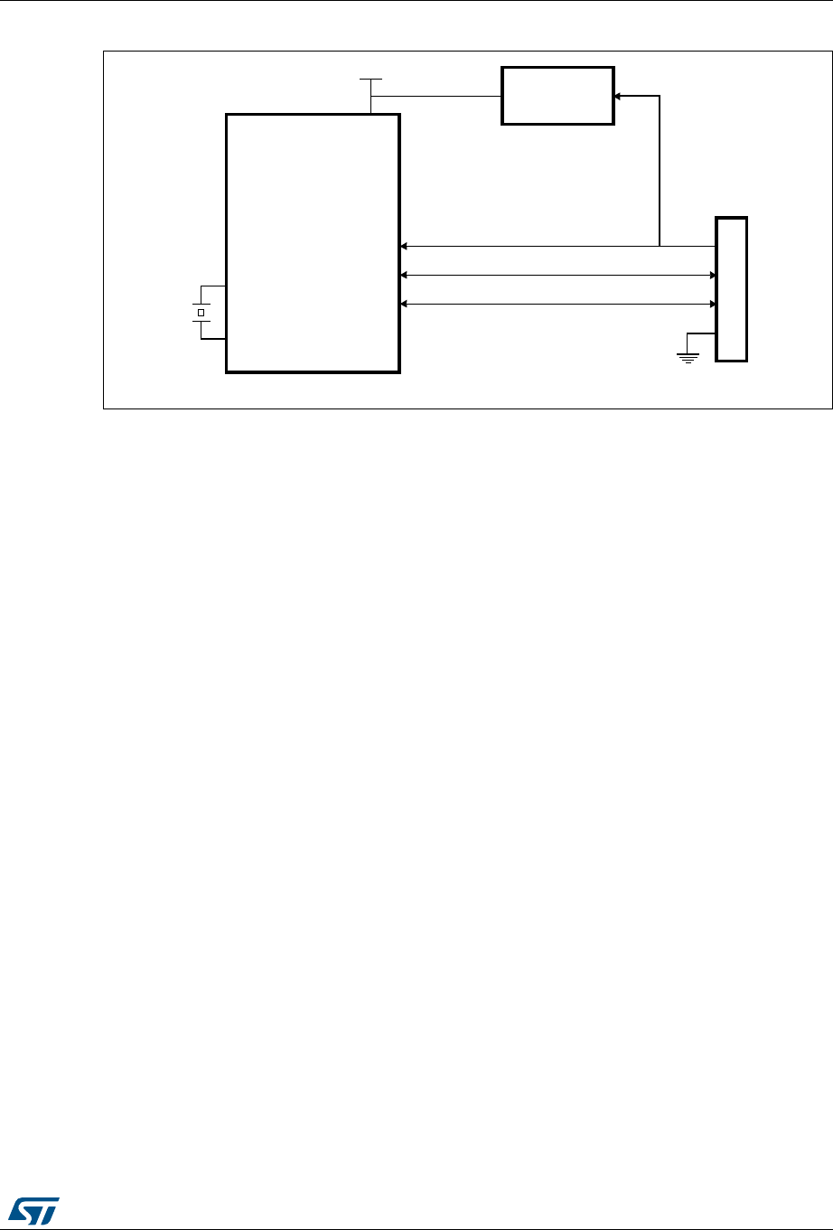
RM0090 Rev 18 1247/1749
RM0090 USB on-the-go full-speed (OTG_FS)
1380
Figure 388. USB peripheral-only connection
1. Use a regulator to build a bus-powered device.
34.5.1 SRP-capable peripheral
The SRP capable bit in the Global USB configuration register (SRPCAP bit in
OTG_FS_GUSBCFG) enables the OTG_FS to support the session request protocol (SRP).
In this way, it allows the remote A-device to save power by switching off VBUS while the USB
session is suspended.
The SRP peripheral mode program model is described in detail in the B-device session
request protocol section.
34.5.2 Peripheral states
Powered state
The VBUS input detects the B-Session valid voltage by which the USB peripheral is allowed
to enter the powered state (see USB2.0 par9.1). The OTG_FS then automatically connects
the DP pull-up resistor to signal full-speed device connection to the host and generates the
session request interrupt (SRQINT bit in OTG_FS_GINTSTS) to notify the powered state.
The VBUS input also ensures that valid VBUS levels are supplied by the host during USB
operations. If a drop in VBUS below B-session valid happens to be detected (for instance
because of a power disturbance or if the host port has been switched off), the OTG_FS
automatically disconnects and the session end detected (SEDET bit in
OTG_FS_GOTGINT) interrupt is generated to notify that the OTG_FS has exited the
powered state.
In the powered state, the OTG_FS expects to receive some reset signaling from the host.
No other USB operation is possible. When a reset signaling is received the reset detected
interrupt (USBRST in OTG_FS_GINTSTS) is generated. When the reset signaling is
complete, the enumeration done interrupt (ENUMDNE bit in OTG_FS_GINTSTS) is
generated and the OTG_FS enters the Default state.
STM32 MCU
5V to VDD
Volatge regulator
VDD
VBUS
DP
VSS
PA9
PA1 2
PA1 1
USB Std-B connector
DM
OSC_IN
OSC_OUT
MS19905V4

USB on-the-go full-speed (OTG_FS) RM0090
1248/1749 RM0090 Rev 18
Soft disconnect
The powered state can be exited by software with the soft disconnect feature. The DP pull-
up resistor is removed by setting the soft disconnect bit in the device control register (SDIS
bit in OTG_FS_DCTL), causing a device disconnect detection interrupt on the host side
even though the USB cable was not really removed from the host port.
Default state
In the Default state the OTG_FS expects to receive a SET_ADDRESS command from the
host. No other USB operation is possible. When a valid SET_ADDRESS command is
decoded on the USB, the application writes the corresponding number into the device
address field in the device configuration register (DAD bit in OTG_FS_DCFG). The
OTG_FS then enters the address state and is ready to answer host transactions at the
configured USB address.
Suspended state
The OTG_FS peripheral constantly monitors the USB activity. After counting 3 ms of USB
idleness, the early suspend interrupt (ESUSP bit in OTG_FS_GINTSTS) is issued, and
confirmed 3 ms later, if appropriate, by the suspend interrupt (USBSUSP bit in
OTG_FS_GINTSTS). The device suspend bit is then automatically set in the device status
register (SUSPSTS bit in OTG_FS_DSTS) and the OTG_FS enters the suspended state.
The suspended state may optionally be exited by the device itself. In this case the
application sets the remote wakeup signaling bit in the device control register (RWUSIG bit
in OTG_FS_DCTL) and clears it after 1 to 15 ms.
When a resume signaling is detected from the host, the resume interrupt (WKUPINT bit in
OTG_FS_GINTSTS) is generated and the device suspend bit is automatically cleared.
34.5.3 Peripheral endpoints
The OTG_FS core instantiates the following USB endpoints:
•Control endpoint 0:
– Bidirectional and handles control messages only
– Separate set of registers to handle in and out transactions
– Proper control (OTG_FS_DIEPCTL0/OTG_FS_DOEPCTL0), transfer
configuration (OTG_FS_DIEPTSIZ0/OTG_FS_DIEPTSIZ0), and status-interrupt
(OTG_FS_DIEPINTx/)OTG_FS_DOEPINT0) registers. The available set of bits
inside the control and transfer size registers slightly differs from that of other
endpoints
•3 IN endpoints
– Each of them can be configured to support the isochronous, bulk or interrupt
transfer type
– Each of them has proper control (OTG_FS_DIEPCTLx), transfer configuration
(OTG_FS_DIEPTSIZx), and status-interrupt (OTG_FS_DIEPINTx) registers
– The Device IN endpoints common interrupt mask register (OTG_FS_DIEPMSK) is
available to enable/disable a single kind of endpoint interrupt source on all of the
IN endpoints (EP0 included)
– Support for incomplete isochronous IN transfer interrupt (IISOIXFR bit in
OTG_FS_GINTSTS), asserted when there is at least one isochronous IN endpoint

RM0090 Rev 18 1249/1749
RM0090 USB on-the-go full-speed (OTG_FS)
1380
on which the transfer is not completed in the current frame. This interrupt is
asserted along with the end of periodic frame interrupt
(OTG_FS_GINTSTS/EOPF).
•3 OUT endpoints
– Each of them can be configured to support the isochronous, bulk or interrupt
transfer type
– Each of them has a proper control (OTG_FS_DOEPCTLx), transfer configuration
(OTG_FS_DOEPTSIZx) and status-interrupt (OTG_FS_DOEPINTx) register
– Device Out endpoints common interrupt mask register (OTG_FS_DOEPMSK) is
available to enable/disable a single kind of endpoint interrupt source on all of the
OUT endpoints (EP0 included)
– Support for incomplete isochronous OUT transfer interrupt (INCOMPISOOUT bit
in OTG_FS_GINTSTS), asserted when there is at least one isochronous OUT
endpoint on which the transfer is not completed in the current frame. This interrupt
is asserted along with the end of periodic frame interrupt
(OTG_FS_GINTSTS/EOPF).
Endpoint control
•The following endpoint controls are available to the application through the device
endpoint-x IN/OUT control register (DIEPCTLx/DOEPCTLx):
– Endpoint enable/disable
– Endpoint activate in current configuration
– Program USB transfer type (isochronous, bulk, interrupt)
– Program supported packet size
– Program Tx-FIFO number associated with the IN endpoint
– Program the expected or transmitted data0/data1 PID (bulk/interrupt only)
– Program the even/odd frame during which the transaction is received or
transmitted (isochronous only)
– Optionally program the NAK bit to always negative-acknowledge the host
regardless of the FIFO status
– Optionally program the STALL bit to always stall host tokens to that endpoint
– Optionally program the SNOOP mode for OUT endpoint not to check the CRC
field of received data
Endpoint transfer
The device endpoint-x transfer size registers (DIEPTSIZx/DOEPTSIZx) allow the application
to program the transfer size parameters and read the transfer status. Programming must be
done before setting the endpoint enable bit in the endpoint control register. Once the
endpoint is enabled, these fields are read-only as the OTG FS core updates them with the
current transfer status.
The following transfer parameters can be programmed:
•Transfer size in bytes
•Number of packets that constitute the overall transfer size

USB on-the-go full-speed (OTG_FS) RM0090
1250/1749 RM0090 Rev 18
Endpoint status/interrupt
The device endpoint-x interrupt registers (DIEPINTx/DOPEPINTx) indicate the status of an
endpoint with respect to USB- and AHB-related events. The application must read these
registers when the OUT endpoint interrupt bit or the IN endpoint interrupt bit in the core
interrupt register (OEPINT bit in OTG_FS_GINTSTS or IEPINT bit in OTG_FS_GINTSTS,
respectively) is set. Before the application can read these registers, it must first read the
device all endpoints interrupt (OTG_FS_DAINT) register to get the exact endpoint number
for the device endpoint-x interrupt register. The application must clear the appropriate bit in
this register to clear the corresponding bits in the DAINT and GINTSTS registers
The peripheral core provides the following status checks and interrupt generation:
•Transfer completed interrupt, indicating that data transfer was completed on both the
application (AHB) and USB sides
•Setup stage has been done (control-out only)
•Associated transmit FIFO is half or completely empty (in endpoints)
•NAK acknowledge has been transmitted to the host (isochronous-in only)
•IN token received when Tx-FIFO was empty (bulk-in/interrupt-in only)
•Out token received when endpoint was not yet enabled
•Babble error condition has been detected
•Endpoint disable by application is effective
•Endpoint NAK by application is effective (isochronous-in only)
•More than 3 back-to-back setup packets were received (control-out only)
•Timeout condition detected (control-in only)
•Isochronous out packet has been dropped, without generating an interrupt
34.6 USB host
This section gives the functional description of the OTG_FS in the USB host mode. The
OTG_FS works as a USB host in the following circumstances:
•OTG A-host
– OTG A-device default state when the A-side of the USB cable is plugged in
•OTG B-host
– OTG B-device after HNP switching to the host role
•A-device
– If the ID line is present, functional and connected to the A-side of the USB cable,
and the HNP-capable bit is cleared in the Global USB Configuration register
(HNPCAP bit in OTG_FS_GUSBCFG). Integrated pull-down resistors are
automatically set on the DP/DM lines.
•Host only (see Figure 389: USB host-only connection).
– The force host mode bit in the global USB configuration register (FHMOD bit in
OTG_FS_GUSBCFG) forces the OTG_FS core to work as a USB host-only. In this
case, the ID line is ignored even if present on the USB connector. Integrated pull-
down resistors are automatically set on the DP/DM lines.
Note: On-chip 5 V VBUS generation is not supported. For this reason, a charge pump or, if 5 V are
available on the application board, a basic power switch must be added externally to drive
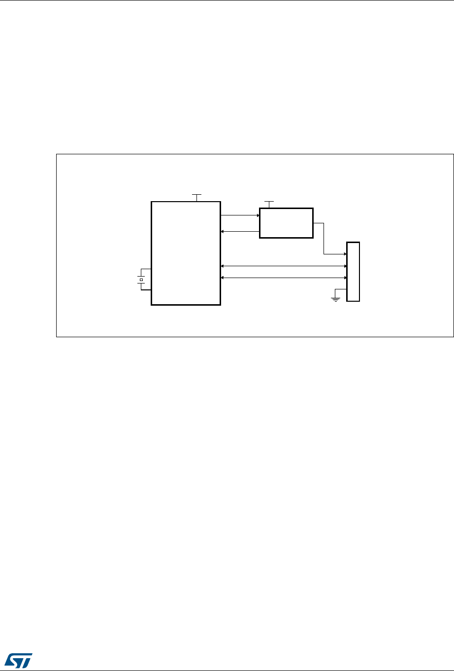
RM0090 Rev 18 1251/1749
RM0090 USB on-the-go full-speed (OTG_FS)
1380
the 5 V VBUS line. The external charge pump can be driven by any GPIO output. This is
required for the OTG A-host, A-device and host-only configurations.
The VBUS input ensures that valid VBUS levels are supplied by the charge pump during USB
operations while the charge pump overcurrent output can be input to any GPIO pin
configured to generate port interrupts. The overcurrent ISR must promptly disable the VBUS
generation.
The VBUS pin can be freed by disabling the VBUS sensing option. This is done by setting the
NOVBUSSENS bit in the OTG_FS_GCCFG register. In this case the VBUS is considered
internally to be always at VBUS valid level (5 V).
Figure 389. USB host-only connection
1. STMPS2141STR needed only if the application has to support a VBUS powered device. A basic power
switch can be used if 5 V are available on the application board.
2. VDD range is between 2 V and 3.6 V.
34.6.1 SRP-capable host
SRP support is available through the SRP capable bit in the global USB configuration
register (SRPCAP bit in OTG_FS_GUSBCFG). With the SRP feature enabled, the host can
save power by switching off the VBUS power while the USB session is suspended.
The SRP host mode program model is described in detail in the A-device session request
protocol section.
34.6.2 USB host states
Host port power
On-chip 5 V VBUS generation is not supported. For this reason, a charge pump or, if 5 V are
available on the application board, a basic power switch, must be added externally to drive
the 5 V VBUS line. The external charge pump can be driven by any GPIO output. When the
application decides to power on VBUS using the chosen GPIO, it must also set the port
power bit in the host port control and status register (PPWR bit in OTG_FS_HPRT).
MSv36915V2
STMPS2141STR
Current-limited
power distribution
switch(2)
OSC_IN
OSC_OUT
GPIO
GPIO + IRQ
EN
Overcurrent
5 V
5 V Pwr
VBUS
DM
DP
VSS
USB Std-A connector
VDD

USB on-the-go full-speed (OTG_FS) RM0090
1252/1749 RM0090 Rev 18
VBUS valid
When HNP or SRP is enabled the VBUS sensing pin (PA9) pin should be connected to
VBUS. The VBUS input ensures that valid VBUS levels are supplied by the charge pump
during USB operations. Any unforeseen VBUS voltage drop below the VBUS valid threshold
(4.25 V) leads to an OTG interrupt triggered by the session end detected bit (SEDET bit in
OTG_FS_GOTGINT). The application is then required to remove the VBUS power and clear
the port power bit.
When HNP and SRP are both disabled, the VBUS sensing pin (PA9) should not be
connected to VBUS. This pin can be can be used as GPIO.
The charge pump overcurrent flag can also be used to prevent electrical damage. Connect
the overcurrent flag output from the charge pump to any GPIO input and configure it to
generate a port interrupt on the active level. The overcurrent ISR must promptly disable the
VBUS generation and clear the port power bit.
Host detection of a peripheral connection
If SRP or HNP are enabled, even if USB peripherals or B-devices can be attached at any
time, the OTG_FS will not detect any bus connection until VBUS is no longer sensed at a
valid level (5 V). When VBUS is at a valid level and a remote B-device is attached, the
OTG_FS core issues a host port interrupt triggered by the device connected bit in the host
port control and status register (PCDET bit in OTG_FS_HPRT).
When HNP and SRP are both disabled, USB peripherals or B-device are detected as soon
as they are connected. The OTG_FS core issues a host port interrupt triggered by the
device connected bit in the host port control and status (PCDET bit in OTG_FS_HPRT).
Host detection of peripheral a disconnection
The peripheral disconnection event triggers the disconnect detected interrupt (DISCINT bit
in OTG_FS_GINTSTS).
Host enumeration
After detecting a peripheral connection the host must start the enumeration process by
sending USB reset and configuration commands to the new peripheral.
Before starting to drive a USB reset, the application waits for the OTG interrupt triggered by
the debounce done bit (DBCDNE bit in OTG_FS_GOTGINT), which indicates that the bus is
stable again after the electrical debounce caused by the attachment of a pull-up resistor on
DP (FS) or DM (LS).
The application drives a USB reset signaling (single-ended zero) over the USB by keeping
the port reset bit set in the host port control and status register (PRST bit in
OTG_FS_HPRT) for a minimum of 10 ms and a maximum of 20 ms. The application takes
care of the timing count and then of clearing the port reset bit.
Once the USB reset sequence has completed, the host port interrupt is triggered by the port
enable/disable change bit (PENCHNG bit in OTG_FS_HPRT). This informs the application
that the speed of the enumerated peripheral can be read from the port speed field in the
host port control and status register (PSPD bit in OTG_FS_HPRT) and that the host is
starting to drive SOFs (FS) or Keep alives (LS). The host is now ready to complete the
peripheral enumeration by sending peripheral configuration commands.

RM0090 Rev 18 1253/1749
RM0090 USB on-the-go full-speed (OTG_FS)
1380
Host suspend
The application decides to suspend the USB activity by setting the port suspend bit in the
host port control and status register (PSUSP bit in OTG_FS_HPRT). The OTG_FS core
stops sending SOFs and enters the suspended state.
The suspended state can be optionally exited on the remote device’s initiative (remote
wakeup). In this case the remote wakeup interrupt (WKUPINT bit in OTG_FS_GINTSTS) is
generated upon detection of a remote wakeup signaling, the port resume bit in the host port
control and status register (PRES bit in OTG_FS_HPRT) self-sets, and resume signaling is
automatically driven over the USB. The application must time the resume window and then
clear the port resume bit to exit the suspended state and restart the SOF.
If the suspended state is exited on the host initiative, the application must set the port
resume bit to start resume signaling on the host port, time the resume window and finally
clear the port resume bit.
34.6.3 Host channels
The OTG_FS core instantiates 8 host channels. Each host channel supports an USB host
transfer (USB pipe). The host is not able to support more than 8 transfer requests at the
same time. If more than 8 transfer requests are pending from the application, the host
controller driver (HCD) must re-allocate channels when they become available from
previous duty, that is, after receiving the transfer completed and channel halted interrupts.
Each host channel can be configured to support in/out and any type of periodic/nonperiodic
transaction. Each host channel makes us of proper control (HCCHARx), transfer
configuration (HCTSIZx) and status/interrupt (HCINTx) registers with associated mask
(HCINTMSKx) registers.
Host channel control
•The following host channel controls are available to the application through the host
channel-x characteristics register (HCCHARx):
– Channel enable/disable
– Program the FS/LS speed of target USB peripheral
– Program the address of target USB peripheral
– Program the endpoint number of target USB peripheral
– Program the transfer IN/OUT direction
– Program the USB transfer type (control, bulk, interrupt, isochronous)
– Program the maximum packet size (MPS)
– Program the periodic transfer to be executed during odd/even frames
Host channel transfer
The host channel transfer size registers (HCTSIZx) allow the application to program the
transfer size parameters, and read the transfer status. Programming must be done before
setting the channel enable bit in the host channel characteristics register. Once the endpoint

USB on-the-go full-speed (OTG_FS) RM0090
1254/1749 RM0090 Rev 18
is enabled the packet count field is read-only as the OTG FS core updates it according to
the current transfer status.
•The following transfer parameters can be programmed:
– transfer size in bytes
– number of packets making up the overall transfer size
– initial data PID
Host channel status/interrupt
The host channel-x interrupt register (HCINTx) indicates the status of an endpoint with
respect to USB- and AHB-related events. The application must read these register when the
host channels interrupt bit in the core interrupt register (HCINT bit in OTG_FS_GINTSTS) is
set. Before the application can read these registers, it must first read the host all channels
interrupt (HCAINT) register to get the exact channel number for the host channel-x interrupt
register. The application must clear the appropriate bit in this register to clear the
corresponding bits in the HAINT and GINTSTS registers. The mask bits for each interrupt
source of each channel are also available in the OTG_FS_HCINTMSK-x register.
•The host core provides the following status checks and interrupt generation:
– Transfer completed interrupt, indicating that the data transfer is complete on both
the application (AHB) and USB sides
– Channel has stopped due to transfer completed, USB transaction error or disable
command from the application
– Associated transmit FIFO is half or completely empty (IN endpoints)
– ACK response received
– NAK response received
– STALL response received
– USB transaction error due to CRC failure, timeout, bit stuff error, false EOP
– Babble error
– fraMe overrun
– dAta toggle error
34.6.4 Host scheduler
The host core features a built-in hardware scheduler which is able to autonomously re-order
and manage the USB transaction requests posted by the application. At the beginning of
each frame the host executes the periodic (isochronous and interrupt) transactions first,
followed by the nonperiodic (control and bulk) transactions to achieve the higher level of
priority granted to the isochronous and interrupt transfer types by the USB specification.
The host processes the USB transactions through request queues (one for periodic and one
for nonperiodic). Each request queue can hold up to 8 entries. Each entry represents a
pending transaction request from the application, and holds the IN or OUT channel number
along with other information to perform a transaction on the USB. The order in which the
requests are written to the queue determines the sequence of the transactions on the USB
interface.
At the beginning of each frame, the host processes the periodic request queue first, followed
by the nonperiodic request queue. The host issues an incomplete periodic transfer interrupt
(IPXFR bit in OTG_FS_GINTSTS) if an isochronous or interrupt transaction scheduled for
the current frame is still pending at the end of the current frame. The OTG HS core is fully
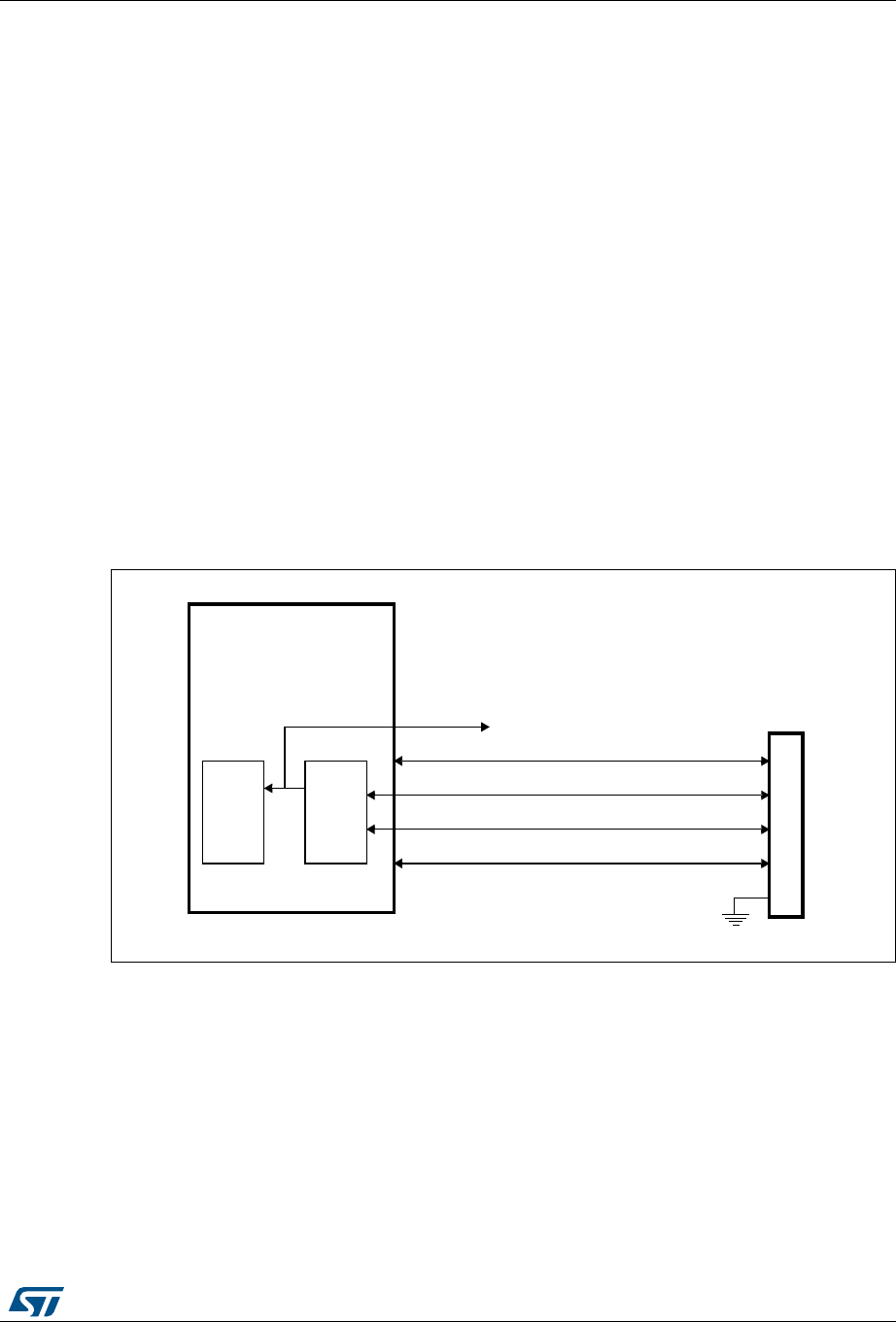
RM0090 Rev 18 1255/1749
RM0090 USB on-the-go full-speed (OTG_FS)
1380
responsible for the management of the periodic and nonperiodic request queues.The
periodic transmit FIFO and queue status register (HPTXSTS) and nonperiodic transmit
FIFO and queue status register (HNPTXSTS) are read-only registers which can be used by
the application to read the status of each request queue. They contain:
•The number of free entries currently available in the periodic (nonperiodic) request
queue (8 max)
•Free space currently available in the periodic (nonperiodic) Tx-FIFO (out-transactions)
•IN/OUT token, host channel number and other status information.
As request queues can hold a maximum of 8 entries each, the application can push to
schedule host transactions in advance with respect to the moment they physically reach the
SB for a maximum of 8 pending periodic transactions plus 8 pending nonperiodic
transactions.
To post a transaction request to the host scheduler (queue) the application must check that
there is at least 1 entry available in the periodic (nonperiodic) request queue by reading the
PTXQSAV bits in the OTG_FS_HNPTXSTS register or NPTQXSAV bits in the
OTG_FS_HNPTXSTS register.
34.7 SOF trigger
Figure 390. SOF connectivity
The OTG FS core provides means to monitor, track and configure SOF framing in the host
and peripheral, as well as an SOF pulse output connectivity feature.
Such utilities are especially useful for adaptive audio clock generation techniques, where
the audio peripheral needs to synchronize to the isochronous stream provided by the PC, or
the host needs to trim its framing rate according to the requirements of the audio peripheral.
34.7.1 Host SOFs
In host mode the number of PHY clocks occurring between the generation of two
consecutive SOF (FS) or Keep-alive (LS) tokens is programmable in the host frame interval
register (HFIR), thus providing application control over the SOF framing period. An interrupt
STM32 MCU
VBUS
D+
VSS
PA8
PA 1 2
PA 1 1
USB mic ro-AB connector
D-
IDTIM2
ITR1 SOF
pulse
SOFgen
PA9
PA 1 0
SOF pulse output, to
external audio control
MS19907V3

USB on-the-go full-speed (OTG_FS) RM0090
1256/1749 RM0090 Rev 18
is generated at any start of frame (SOF bit in OTH_FS_GINTSTS). The current frame
number and the time remaining until the next SOF are tracked in the host frame number
register (HFNUM).
An SOF pulse signal, generated at any SOF starting token and with a width of 20 HCLK
cycles, can be made available externally on the OTG_FS_SOF pin using the SOFOUTEN
bit in the global control and configuration register. The SOF pulse is also internally
connected to the input trigger of timer 2 (TIM2), so that the input capture feature, the output
compare feature and the timer can be triggered by the SOF pulse. The TIM2 connection is
enabled through the ITR1_RMP bits of TIM2_OR register.
34.7.2 Peripheral SOFs
In device mode, the start of frame interrupt is generated each time an SOF token is received
on the USB (SOF bit in OTH_FS_GINTSTS). The corresponding frame number can be read
from the device status register (FNSOF bit in OTG_FS_DSTS). An SOF pulse signal with a
width of 20 HCLK cycles is also generated and can be made available externally on the
OTG_FS_SOF pin by using the SOF output enable bit in the global control and configuration
register (SOFOUTEN bit in OTG_FS_GCCFG). The SOF pulse signal is also internally
connected to the TIM2 input trigger, so that the input capture feature, the output compare
feature and the timer can be triggered by the SOF pulse. The TIM2 connection is enabled
through the ITR1_RMP bits of the TIM2 option register (TIM2_OR).
The end of periodic frame interrupt (GINTSTS/EOPF) is used to notify the application when
80%, 85%, 90% or 95% of the time frame interval elapsed depending on the periodic frame
interval field in the device configuration register (PFIVL bit in OTG_FS_DCFG). This feature
can be used to determine if all of the isochronous traffic for that frame is complete.
34.8 OTG low-power modes
Table 197 below defines the STM32 low power modes and their compatibility with the OTG.
Table 197. Compatibility of STM32 low power modes with the OTG
Mode Description USB compatibility
Run MCU fully active Required when USB not in
suspend state.
Sleep USB suspend exit causes the device to exit Sleep mode.
Peripheral registers content is kept.
Available while USB is in
suspend state.
Stop USB suspend exit causes the device to exit Stop mode.
Peripheral registers content is kept(1).
1. Within Stop mode there are different possible settings. Some restrictions may also exist, please refer to
Section 5: Power controller (PWR) to understand which (if any) restrictions apply when using OTG.
Available while USB is in
suspend state.
Standby Powered-down. The peripheral must be reinitialized after
exiting Standby mode.
Not compatible with USB
applications.

RM0090 Rev 18 1257/1749
RM0090 USB on-the-go full-speed (OTG_FS)
1380
The power consumption of the OTG PHY is controlled by three bits in the general core
configuration register:
•PHY power down (GCCFG/PWRDWN)
It switches on/off the full-speed transceiver module of the PHY. It must be preliminarily
set to allow any USB operation.
•A-VBUS sensing enable (GCCFG/VBUSASEN)
It switches on/off the VBUS comparators associated with A-device operations. It must
be set when in A-device (USB host) mode and during HNP.
•B-VBUS sensing enable (GCCFG/VBUSASEN)
It switches on/off the VBUS comparators associated with B-device operations. It must
be set when in B-device (USB peripheral) mode and during HNP.
Power reduction techniques are available while in the USB suspended state, when the USB
session is not yet valid or the device is disconnected.
•Stop PHY clock (STPPCLK bit in OTG_FS_PCGCCTL)
When setting the stop PHY clock bit in the clock gating control register, most of the
48 MHz clock domain internal to the OTG full-speed core is switched off by clock
gating. The dynamic power consumption due to the USB clock switching activity is cut
even if the 48 MHz clock input is kept running by the application
Most of the transceiver is also disabled, and only the part in charge of detecting the
asynchronous resume or remote wakeup event is kept alive.
•Gate HCLK (GATEHCLK bit in OTG_FS_PCGCCTL)
When setting the Gate HCLK bit in the clock gating control register, most of the system
clock domain internal to the OTG_FS core is switched off by clock gating. Only the
register read and write interface is kept alive. The dynamic power consumption due to
the USB clock switching activity is cut even if the system clock is kept running by the
application for other purposes.
•USB system stop
When the OTG_FS is in the USB suspended state, the application may decide to
drastically reduce the overall power consumption by a complete shut down of all the
clock sources in the system. USB System Stop is activated by first setting the Stop
PHY clock bit and then configuring the system deep sleep mode in the power control
system module (PWR).
The OTG_FS core automatically reactivates both system and USB clocks by
asynchronous detection of remote wakeup (as an host) or resume (as a device)
signaling on the USB.
To save dynamic power, the USB data FIFO is clocked only when accessed by the OTG_FS
core.
34.9 Dynamic update of the OTG_FS_HFIR register
The USB core embeds a dynamic trimming capability of SOF framing period in host mode
allowing to synchronize an external device with the SOF frames.
When the OTG_FS_HFIR register is changed within a current SOF frame, the SOF period
correction is applied in the next frame as described in Figure 391.
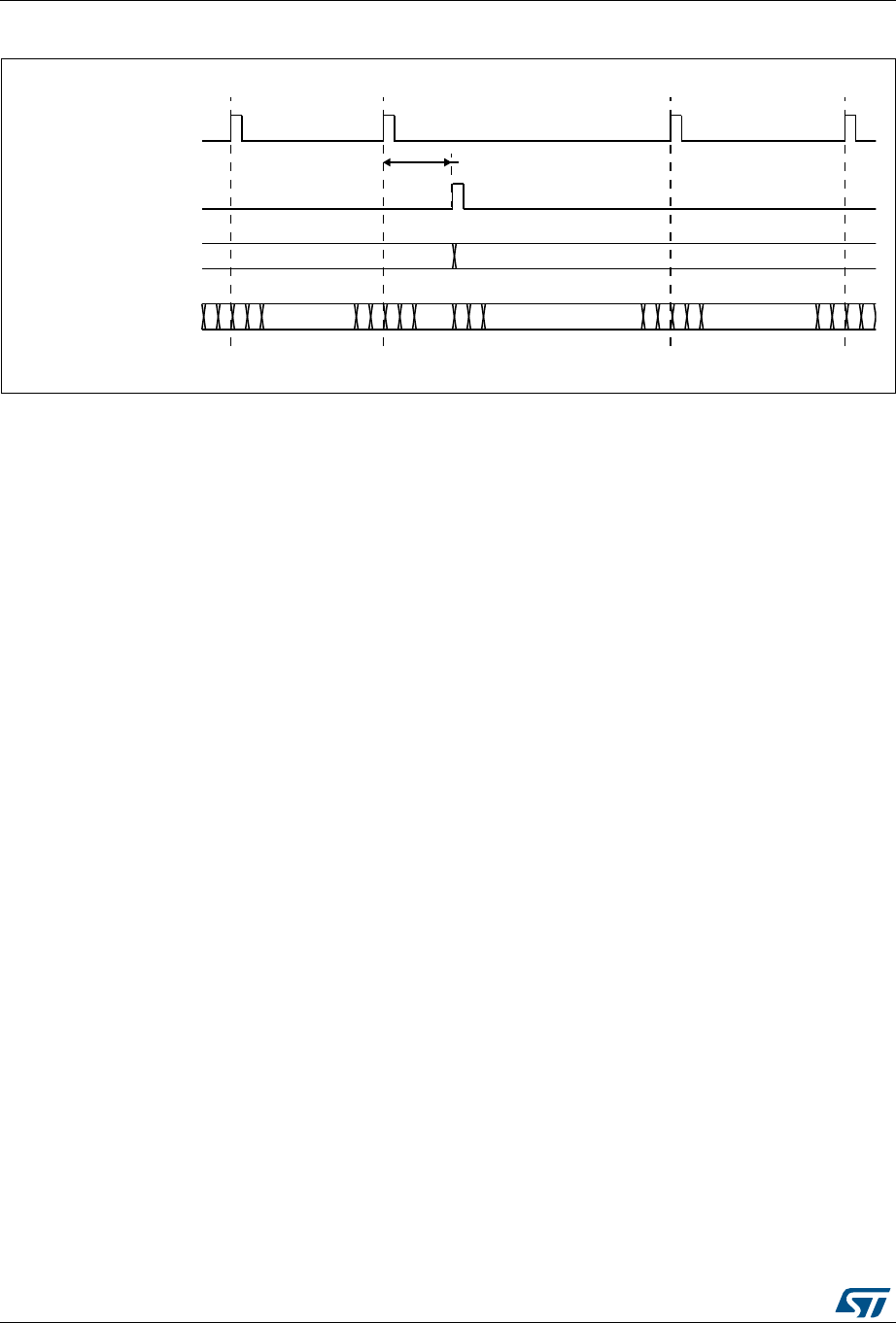
USB on-the-go full-speed (OTG_FS) RM0090
1258/1749 RM0090 Rev 18
Figure 391. Updating OTG_FS_HFIR dynamically
34.10 USB data FIFOs
The USB system features 1.25 Kbyte of dedicated RAM with a sophisticated FIFO control
mechanism. The packet FIFO controller module in the OTG_FS core organizes RAM space
into Tx-FIFOs into which the application pushes the data to be temporarily stored before the
USB transmission, and into a single Rx FIFO where the data received from the USB are
temporarily stored before retrieval (popped) by the application. The number of instructed
FIFOs and how these are organized inside the RAM depends on the device’s role. In
peripheral mode an additional Tx-FIFO is instructed for each active IN endpoint. Any FIFO
size is software configured to better meet the application requirements.
400
…………
450
Latency
SOF
reload
OTG_FS_HFIR
write
value
Frame
timer
Old OTG_FS_HIFR value
= 400 periods
OTG_FS_HIFR value
= 450 periods+HIFR write latency
New OTG_FS_HIFR value
= 450 periods
1
400
0
399
1
400
0
399
450
449
1
450
0
449
1
450
0
449
OTG_FS_HFIR
ai18
4
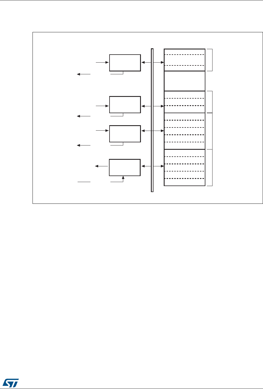
RM0090 Rev 18 1259/1749
RM0090 USB on-the-go full-speed (OTG_FS)
1380
34.11 Peripheral FIFO architecture
Figure 392. Device-mode FIFO address mapping and AHB FIFO access mapping
34.11.1 Peripheral Rx FIFO
The OTG peripheral uses a single receive FIFO that receives the data directed to all OUT
endpoints. Received packets are stacked back-to-back until free space is available in the
Rx-FIFO. The status of the received packet (which contains the OUT endpoint destination
number, the byte count, the data PID and the validity of the received data) is also stored by
the core on top of the data payload. When no more space is available, host transactions are
NACKed and an interrupt is received on the addressed endpoint. The size of the receive
FIFO is configured in the receive FIFO Size register (GRXFSIZ).
The single receive FIFO architecture makes it more efficient for the USB peripheral to fill in
the receive RAM buffer:
•All OUT endpoints share the same RAM buffer (shared FIFO)
•The OTG FS core can fill in the receive FIFO up to the limit for any host sequence of
OUT tokens
The application keeps receiving the Rx-FIFO non-empty interrupt (RXFLVL bit in
OTG_FS_GINTSTS) as long as there is at least one packet available for download. It reads
the packet information from the receive status read and pop register (GRXSTSP) and finally
pops data off the receive FIFO by reading from the endpoint-related pop address.
IN endpoint Tx FIFO #n
DFIFO push access
from AHB
Any OUT endpoint DFIFO pop
access from AHB
Dedicated Tx
FIFO #n control
(optional)
Dedicated Tx
FIFO #1 control
(optional)
Rx FIFO control
IN endpoint Tx FIFO #1
DFIFO push access
from AHB
MAC pop
MAC pop
MAC push
Single data
FIFO
Tx FIFO #n
packet
Tx FIFO #0 packet
DIEPTXF2[31:16]
DIEPTXFx[15:0]
DIEPTXF2[15:0]
DIEPTXF1[31:16]
DIEPTXF1[15:0]
GNPTXFSIZ[31:16]
ai15611
IN endpoint Tx FIFO #0
DFIFO push access
from AHB
Dedicated Tx
FIFO #0 control
(optional)
MAC pop
Tx FIFO #1 packet
Rx packets
(Rx start
address
fixed to 0)
.
.
..
.
..
.
.
GNPTXFSIZ[15:0]
GRXFSIZ[31:16]
A1 = 0
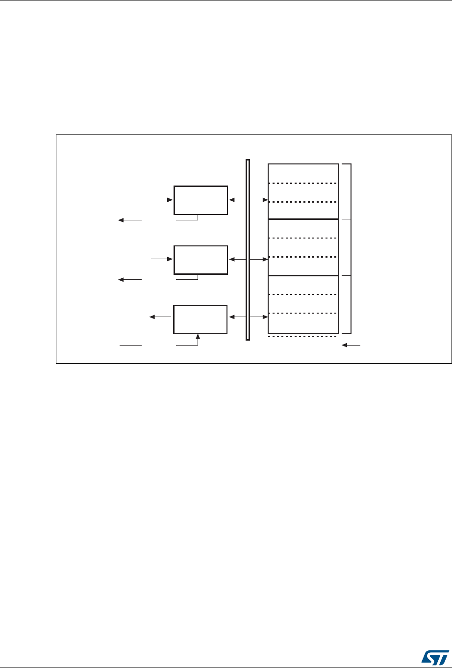
USB on-the-go full-speed (OTG_FS) RM0090
1260/1749 RM0090 Rev 18
34.11.2 Peripheral Tx FIFOs
The core has a dedicated FIFO for each IN endpoint. The application configures FIFO sizes
by writing the non periodic transmit FIFO size register (OTG_FS_TX0FSIZ) for IN endpoint0
and the device IN endpoint transmit FIFOx registers (DIEPTXFx) for IN endpoint-x.
34.12 Host FIFO architecture
Figure 393. Host-mode FIFO address mapping and AHB FIFO access mapping
34.12.1 Host Rx FIFO
The host uses one receiver FIFO for all periodic and nonperiodic transactions. The FIFO is
used as a receive buffer to hold the received data (payload of the received packet) from the
USB until it is transferred to the system memory. Packets received from any remote IN
endpoint are stacked back-to-back until free space is available. The status of each received
packet with the host channel destination, byte count, data PID and validity of the received
data are also stored into the FIFO. The size of the receive FIFO is configured in the receive
FIFO size register (GRXFSIZ).
The single receive FIFO architecture makes it highly efficient for the USB host to fill in the
receive data buffer:
•All IN configured host channels share the same RAM buffer (shared FIFO)
•The OTG FS core can fill in the receive FIFO up to the limit for any sequence of IN
tokens driven by the host software
The application receives the Rx FIFO not-empty interrupt as long as there is at least one
packet available for download. It reads the packet information from the receive status read
and pop register and finally pops the data off the receive FIFO.
Any periodic channel
DFIFO push access
from AHB
Any channel DFIFO pop
access from AHB
Periodic Tx
FIFO control
(optional)
Non-periodic
Tx FIFO control
Rx FIFO control
Any non-periodic
channel DFIFO push
access from AHB
MAC pop
MAC pop
MAC push
Single data
FIFO
Periodic Tx packets
Periodic Tx packets
Rx packets
HPTXFSIZ[31:16]
HPTXFSIZ[15:0]
NPTXFSIZ[31:16]
NPTXFSIZ[15:0]
RXFSIZ[31:16]
Rx start address
fixed to 0
A1 = 0
ai15610

RM0090 Rev 18 1261/1749
RM0090 USB on-the-go full-speed (OTG_FS)
1380
34.12.2 Host Tx FIFOs
The host uses one transmit FIFO for all non-periodic (control and bulk) OUT transactions
and one transmit FIFO for all periodic (isochronous and interrupt) OUT transactions. FIFOs
are used as transmit buffers to hold the data (payload of the transmit packet) to be
transmitted over the USB. The size of the periodic (nonperiodic) Tx FIFO is configured in the
host periodic (nonperiodic) transmit FIFO size (HPTXFSIZ/HNPTXFSIZ) register.
The two Tx FIFO implementation derives from the higher priority granted to the periodic type
of traffic over the USB frame. At the beginning of each frame, the built-in host scheduler
processes the periodic request queue first, followed by the nonperiodic request queue.
The two transmit FIFO architecture provides the USB host with separate optimization for
periodic and nonperiodic transmit data buffer management:
•All host channels configured to support periodic (nonperiodic) transactions in the OUT
direction share the same RAM buffer (shared FIFOs)
•The OTG FS core can fill in the periodic (nonperiodic) transmit FIFO up to the limit for
any sequence of OUT tokens driven by the host software
The OTG_FS core issues the periodic Tx FIFO empty interrupt (PTXFE bit in
OTG_FS_GINTSTS) as long as the periodic Tx-FIFO is half or completely empty,
depending on the value of the periodic Tx-FIFO empty level bit in the AHB configuration
register (PTXFELVL bit in OTG_FS_GAHBCFG). The application can push the transmission
data in advance as long as free space is available in both the periodic Tx FIFO and the
periodic request queue. The host periodic transmit FIFO and queue status register
(HPTXSTS) can be read to know how much space is available in both.
OTG_FS core issues the non periodic Tx FIFO empty interrupt (NPTXFE bit in
OTG_FS_GINTSTS) as long as the nonperiodic Tx FIFO is half or completely empty
depending on the non periodic Tx FIFO empty level bit in the AHB configuration register
(TXFELVL bit in OTG_FS_GAHBCFG). The application can push the transmission data as
long as free space is available in both the nonperiodic Tx FIFO and nonperiodic request
queue. The host nonperiodic transmit FIFO and queue status register (HNPTXSTS) can be
read to know how much space is available in both.
34.13 FIFO RAM allocation
34.13.1 Device mode
Receive FIFO RAM allocation: the application should allocate RAM for SETUP Packets:
10 locations must be reserved in the receive FIFO to receive SETUP packets on control
endpoint. The core does not use these locations, which are reserved for SETUP packets, to
write any other data. One location is to be allocated for Global OUT NAK. Status information
is written to the FIFO along with each received packet. Therefore, a minimum space of
(Largest Packet Size / 4) + 1 must be allocated to receive packets. If multiple isochronous
endpoints are enabled, then at least two (Largest Packet Size / 4) + 1 spaces must be
allocated to receive back-to-back packets. Typically, two (Largest Packet Size / 4) + 1
spaces are recommended so that when the previous packet is being transferred to the CPU,
the USB can receive the subsequent packet.
Along with the last packet for each endpoint, transfer complete status information is also
pushed to the FIFO. Typically, one location for each OUT endpoint is recommended.

USB on-the-go full-speed (OTG_FS) RM0090
1262/1749 RM0090 Rev 18
Transmit FIFO RAM allocation: the minimum RAM space required for each IN Endpoint
Transmit FIFO is the maximum packet size for that particular IN endpoint.
Note: More space allocated in the transmit IN Endpoint FIFO results in better performance on the
USB.
34.13.2 Host mode
Receive FIFO RAM allocation
Status information is written to the FIFO along with each received packet. Therefore, a
minimum space of (Largest Packet Size / 4) + 1 must be allocated to receive packets. If
multiple isochronous channels are enabled, then at least two (Largest Packet Size / 4) + 1
spaces must be allocated to receive back-to-back packets. Typically, two (Largest Packet
Size / 4) + 1 spaces are recommended so that when the previous packet is being
transferred to the CPU, the USB can receive the subsequent packet.
Along with the last packet in the host channel, transfer complete status information is also
pushed to the FIFO. So one location must be allocated for this.
Transmit FIFO RAM allocation
The minimum amount of RAM required for the host Non-periodic Transmit FIFO is the
largest maximum packet size among all supported non-periodic OUT channels.
Typically, two Largest Packet Sizes worth of space is recommended, so that when the
current packet is under transfer to the USB, the CPU can get the next packet.
The minimum amount of RAM required for host periodic Transmit FIFO is the largest
maximum packet size out of all the supported periodic OUT channels. If there is at least one
Isochronous OUT endpoint, then the space must be at least two times the maximum packet
size of that channel.
Note: More space allocated in the Transmit Non-periodic FIFO results in better performance on
the USB.
34.14 USB system performance
Best USB and system performance is achieved owing to the large RAM buffers, the highly
configurable FIFO sizes, the quick 32-bit FIFO access through AHB push/pop registers and,
especially, the advanced FIFO control mechanism. Indeed, this mechanism allows the
OTG_FS to fill in the available RAM space at best regardless of the current USB sequence.
With these features:
•The application gains good margins to calibrate its intervention in order to optimize the
CPU bandwidth usage:
– It can accumulate large amounts of transmission data in advance compared to
when they are effectively sent over the USB
– It benefits of a large time margin to download data from the single receive FIFO
•The USB Core is able to maintain its full operating rate, that is to provide maximum full-
speed bandwidth with a great margin of autonomy versus application intervention:
– It has a large reserve of transmission data at its disposal to autonomously manage
the sending of data over the USB

RM0090 Rev 18 1263/1749
RM0090 USB on-the-go full-speed (OTG_FS)
1380
– It has a lot of empty space available in the receive buffer to autonomously fill it in
with the data coming from the USB
As the OTG_FS core is able to fill in the 1.25 Kbyte RAM buffer very efficiently, and as
1.25 Kbyte of transmit/receive data is more than enough to cover a full speed frame, the
USB system is able to withstand the maximum full-speed data rate for up to one USB frame
(1 ms) without any CPU intervention.
34.15 OTG_FS interrupts
When the OTG_FS controller is operating in one mode, either device or host, the application
must not access registers from the other mode. If an illegal access occurs, a mode
mismatch interrupt is generated and reflected in the Core interrupt register (MMIS bit in the
OTG_FS_GINTSTS register). When the core switches from one mode to the other, the
registers in the new mode of operation must be reprogrammed as they would be after a
power-on reset.
Figure 394 shows the interrupt hierarchy.
USB on-the-go full-speed (OTG_FS) RM0090
1264/1749 RM0090 Rev 18
Figure 394. Interrupt hierarchy
1. OTG_FS_WKUP become active (high state) when resume condition occurs during L1 SLEEP or L2 SUSPEND states.
MSv36921V3
OTG_DAINTMSK
Device all endpoints interrupt mask
register
OTG_DIEPMSK/
OTG_DOEPMSK
Device IN/OUT endpoints common
interrupt mask register
OTG_HCTINTMSKx
Host channels interrupt mask registers
OTG_HAINTMSK
Host all channels interrupt mask register
31:26 25 24 23:20 19 18 17:3 2 1:0
OTG_HCTINTx
Host channels interrupt registers
OTG_HAINT
Host all channels interrupt register
OTG_HPRT
Host port control and status register
OTG_DAINT
Device all endpoints interrupt register
(15 + #EP):16
OUT endpoints
(#EP-1):0
IN endpoints
OTG_GOTGINT
OTG interrupt register
OTG_DIEPINTx/
OTG_DOEPINTx
Device IN/OUT endpoint interrupt
registers
OTG_GINTSTS
Core register interrupt
OTG_GINTMSK
Core interrupt mask register
OTG_AHBCFG
AHB configuration register
Global interrupt mask (bit 0)
OR
AND
Global interrupt
OTG_FS
Wakeup interrupt
OTG_FS_WKUP
AND
(1)
x = 0
x = #HC-1
x = 0
x = #HC-1
HCINT
HPRTINT
OEPINP
IEPINT
OTGINT
...
...

RM0090 Rev 18 1265/1749
RM0090 USB on-the-go full-speed (OTG_FS)
1380
34.16 OTG_FS control and status registers
By reading from and writing to the control and status registers (CSRs) through the AHB
slave interface, the application controls the OTG_FS controller. These registers are 32 bits
wide, and the addresses are 32-bit block aligned. The OTG_FS registers must be accessed
by words (32 bits).
CSRs are classified as follows:
•Core global registers
•Host-mode registers
•Host global registers
•Host port CSRs
•Host channel-specific registers
•Device-mode registers
•Device global registers
•Device endpoint-specific registers
•Power and clock-gating registers
•Data FIFO (DFIFO) access registers
Only the Core global, Power and clock-gating, Data FIFO access, and host port control and
status registers can be accessed in both host and device modes. When the OTG_FS
controller is operating in one mode, either device or host, the application must not access
registers from the other mode. If an illegal access occurs, a mode mismatch interrupt is
generated and reflected in the Core interrupt register (MMIS bit in the OTG_FS_GINTSTS
register). When the core switches from one mode to the other, the registers in the new mode
of operation must be reprogrammed as they would be after a power-on reset.
USB on-the-go full-speed (OTG_FS) RM0090
1266/1749 RM0090 Rev 18
34.16.1 CSR memory map
The host and device mode registers occupy different addresses. All registers are
implemented in the AHB clock domain.
Figure 395. CSR memory map
1. x = 3 in device mode and x = 7 in host mode.
Global CSR map
These registers are available in both host and device modes.
0000h
Core global CSRs (1 Kbyte)
0400h
Host mode CSRs (1 Kbyte)
0800h
Device mode CSRs (1.5 Kbyte)
0E00h
Power and clock gating CSRs (0.5 Kbyte)
1000h
Device EP 0/Host channel 0 FIFO (4 Kbyte)
2000h
Device EP1/Host channel 1 FIFO (4 Kbyte)
3000h
Device EP (x – 1)
(1)
/Host channel (x – 1)
(1)
FIFO (4 Kbyte)
Device EP x
(1)
/Host channel x
(1)
FIFO (4 Kbyte)
Reserved
DFIFO
push/pop
to this region
2 0000h
3 FFFFh
Direct access to data FIFO RAM
for debugging (128 Kbyte)
DFIFO
debug read/
write to this
region
ai15615b
Table 198. Core global control and status registers (CSRs)
Acronym Address
offset Register name
OTG_FS_GOTGCTL 0x000 OTG_FS control and status register (OTG_FS_GOTGCTL) on page 1271
OTG_FS_GOTGINT 0x004 OTG_FS interrupt register (OTG_FS_GOTGINT) on page 1272
OTG_FS_GAHBCFG 0x008 OTG_FS AHB configuration register (OTG_FS_GAHBCFG) on page 1274
OTG_FS_GUSBCFG 0x00C OTG_FS USB configuration register (OTG_FS_GUSBCFG) on page 1275
OTG_FS_GRSTCTL 0x010 OTG_FS reset register (OTG_FS_GRSTCTL) on page 1277

RM0090 Rev 18 1267/1749
RM0090 USB on-the-go full-speed (OTG_FS)
1380
Host-mode CSR map
These registers must be programmed every time the core changes to host mode.
OTG_FS_GINTSTS 0x014 OTG_FS core interrupt register (OTG_FS_GINTSTS) on page 1279
OTG_FS_GINTMSK 0x018 OTG_FS interrupt mask register (OTG_FS_GINTMSK) on page 1283
OTG_FS_GRXSTSR 0x01C OTG_FS Receive status debug read/OTG status read and pop registers
(OTG_FS_GRXSTSR/OTG_FS_GRXSTSP) on page 1286
OTG_FS_GRXSTSP 0x020
OTG_FS_GRXFSIZ 0x024 OTG_FS Receive FIFO size register (OTG_FS_GRXFSIZ) on page 1287
OTG_FS_HNPTXFSIZ/
OTG_FS_DIEPTXF0(1) 0x028
OTG_FS Host non-periodic transmit FIFO size register
(OTG_FS_HNPTXFSIZ)/Endpoint 0 Transmit FIFO size
(OTG_FS_DIEPTXF0)
OTG_FS_HNPTXSTS 0x02C OTG_FS non-periodic transmit FIFO/queue status register
(OTG_FS_HNPTXSTS) on page 1288
OTG_FS_GCCFG 0x038 OTG_FS general core configuration register (OTG_FS_GCCFG) on
page 1289
OTG_FS_CID 0x03C OTG_FS core ID register (OTG_FS_CID) on page 1290
OTG_FS_HPTXFSIZ 0x100 OTG_FS Host periodic transmit FIFO size register (OTG_FS_HPTXFSIZ) on
page 1291
OTG_FS_DIEPTXFx
0x104
0x108
0x10C
OTG_FS device IN endpoint transmit FIFO size register
(OTG_FS_DIEPTXFx) (x = 1..3, where x is the FIFO_number) on page 1291
1. The general rule is to use OTG_FS_HNPTXFSIZ for host mode and OTG_FS_DIEPTXF0 for device mode.
Table 198. Core global control and status registers (CSRs) (continued)
Acronym Address
offset Register name
Table 199. Host-mode control and status registers (CSRs)
Acronym Offset
address Register name
OTG_FS_HCFG 0x400 OTG_FS Host configuration register (OTG_FS_HCFG) on page 1292
OTG_FS_HFIR 0x404 OTG_FS Host frame interval register (OTG_FS_HFIR) on page 1292
OTG_FS_HFNUM 0x408 OTG_FS Host frame number/frame time remaining register
(OTG_FS_HFNUM) on page 1293
OTG_FS_HPTXSTS 0x410 OTG_FS_Host periodic transmit FIFO/queue status register
(OTG_FS_HPTXSTS) on page 1293
OTG_FS_HAINT 0x414 OTG_FS Host all channels interrupt register (OTG_FS_HAINT) on
page 1294
OTG_FS_HAINTMSK 0x418 OTG_FS Host all channels interrupt mask register (OTG_FS_HAINTMSK)
on page 1295

USB on-the-go full-speed (OTG_FS) RM0090
1268/1749 RM0090 Rev 18
Device-mode CSR map
These registers must be programmed every time the core changes to device mode.
OTG_FS_HPRT 0x440 OTG_FS Host port control and status register (OTG_FS_HPRT) on
page 1295
OTG_FS_HCCHARx
0x500
0x520
...
0x5E0
OTG_FS Host channel-x characteristics register (OTG_FS_HCCHARx)
(x = 0..7, where x = Channel_number) on page 1298
OTG_FS_HCINTx 0x508 OTG_FS Host channel-x interrupt register (OTG_FS_HCINTx) (x = 0..7,
where x = Channel_number) on page 1299
OTG_FS_HCINTMSKx 0x50C OTG_FS Host channel-x interrupt mask register (OTG_FS_HCINTMSKx)
(x = 0..7, where x = Channel_number) on page 1300
OTG_FS_HCTSIZx 0x510 OTG_FS Host channel-x transfer size register (OTG_FS_HCTSIZx)
(x = 0..7, where x = Channel_number) on page 1301
Table 199. Host-mode control and status registers (CSRs) (continued)
Acronym Offset
address Register name
Table 200. Device-mode control and status registers
Acronym Offset
address Register name
OTG_FS_DCFG 0x800 OTG_FS device configuration register (OTG_FS_DCFG) on page 1302
OTG_FS_DCTL 0x804 OTG_FS device control register (OTG_FS_DCTL) on page 1303
OTG_FS_DSTS 0x808 OTG_FS device status register (OTG_FS_DSTS) on page 1304
OTG_FS_DIEPMSK 0x810 OTG_FS device IN endpoint common interrupt mask register
(OTG_FS_DIEPMSK) on page 1305
OTG_FS_DOEPMSK 0x814 OTG_FS device OUT endpoint common interrupt mask register
(OTG_FS_DOEPMSK) on page 1306
OTG_FS_DAINT 0x818 OTG_FS device all endpoints interrupt register (OTG_FS_DAINT) on
page 1307
OTG_FS_DAINTMSK 0x81C OTG_FS all endpoints interrupt mask register (OTG_FS_DAINTMSK) on
page 1308
OTG_FS_DVBUSDIS 0x828 OTG_FS device VBUS discharge time register (OTG_FS_DVBUSDIS) on
page 1308
OTG_FS_DVBUSPULSE 0x82C OTG_FS device VBUS pulsing time register (OTG_FS_DVBUSPULSE)
on page 1308
OTG_FS_DIEPEMPMSK 0x834 OTG_FS device IN endpoint FIFO empty interrupt mask register:
(OTG_FS_DIEPEMPMSK) on page 1309
OTG_FS_DIEPCTL0 0x900 OTG_FS device control IN endpoint 0 control register
(OTG_FS_DIEPCTL0) on page 1309

RM0090 Rev 18 1269/1749
RM0090 USB on-the-go full-speed (OTG_FS)
1380
Data FIFO (DFIFO) access register map
These registers, available in both host and device modes, are used to read or write the FIFO
space for a specific endpoint or a channel, in a given direction. If a host channel is of type
IN, the FIFO can only be read on the channel. Similarly, if a host channel is of type OUT, the
FIFO can only be written on the channel.
OTG_FS_DIEPCTLx
0x920
0x940
0x960
OTG device endpoint x control register (OTG_FS_DIEPCTLx) (x = 1..3,
where x = Endpoint_number) on page 1311
OTG_FS_DIEPINTx 0x908 OTG_FS device endpoint-x interrupt register (OTG_FS_DIEPINTx)
(x = 0..3, where x = Endpoint_number) on page 1318
OTG_FS_DIEPTSIZ0 0x910 OTG_FS device IN endpoint 0 transfer size register
(OTG_FS_DIEPTSIZ0) on page 1320
OTG_FS_DTXFSTSx 0x918
OTG_FS device IN endpoint transmit FIFO status register
(OTG_FS_DTXFSTSx) (x = 0..3, where x = Endpoint_number) on
page 1324
OTG_FS_DIEPTSIZx
0x930
0x950
0x970
OTG_FS device OUT endpoint-x transfer size register
(OTG_FS_DOEPTSIZx) (x = 1..3, where x = Endpoint_number) on
page 1324
OTG_FS_DOEPCTL0 0xB00 OTG_FS device control OUT endpoint 0 control register
(OTG_FS_DOEPCTL0) on page 1314
OTG_FS_DOEPCTLx
0xB20
0xB40
0xB60
OTG device endpoint x control register (OTG_FS_DIEPCTLx) (x = 1..3,
where x = Endpoint_number) on page 1311
OTG_FS_DOEPINTx 0xB08 OTG_FS device endpoint-x interrupt register (OTG_FS_DOEPINTx)
(x = 0..3, where x = Endpoint_number) on page 1319
OTG_FS_DOEPTSIZ0 0xB10 OTG_FS device OUT endpoint 0 transfer size register
(OTG_FS_DOEPTSIZ0) on page 1322
OTG_FS_DOEPTSIZx
0xB30
0xB50
0xB70
OTG_FS device OUT endpoint-x transfer size register
(OTG_FS_DOEPTSIZx) (x = 1..3, where x = Endpoint_number) on
page 1324
Table 200. Device-mode control and status registers (continued)
Acronym Offset
address Register name
Table 201. Data FIFO (DFIFO) access register map
FIFO access register section Address range Access
Device IN Endpoint 0/Host OUT Channel 0: DFIFO Write Access
Device OUT Endpoint 0/Host IN Channel 0: DFIFO Read Access 0x1000–0x1FFC w
r
Device IN Endpoint 1/Host OUT Channel 1: DFIFO Write Access
Device OUT Endpoint 1/Host IN Channel 1: DFIFO Read Access 0x2000–0x2FFC w
r

USB on-the-go full-speed (OTG_FS) RM0090
1270/1749 RM0090 Rev 18
Power and clock gating CSR map
There is a single register for power and clock gating. It is available in both host and device
modes.
... ... ...
Device IN Endpoint x(1)/Host OUT Channel x(1): DFIFO Write Access
Device OUT Endpoint x(1)/Host IN Channel x(1): DFIFO Read Access 0xX000–0xXFFC w
r
1. Where x is 3 in device mode and 7 in host mode.
Table 202. Power and clock gating control and status registers
Register name Acronym Offset address: 0xE00–0xFFF
Power and clock gating control register OTG_FS_PCGCCTL 0xE00-0xE04
Reserved - 0xE05–0xFFF
Table 201. Data FIFO (DFIFO) access register map (continued)
FIFO access register section Address range Access
RM0090 Rev 18 1271/1749
RM0090 USB on-the-go full-speed (OTG_FS)
1380
34.16.2 OTG_FS global registers
These registers are available in both host and device modes, and do not need to be
reprogrammed when switching between these modes.
Bit values in the register descriptions are expressed in binary unless otherwise specified.
OTG_FS control and status register (OTG_FS_GOTGCTL)
Address offset: 0x000
Reset value: 0x0001 0000
The OTG_FS_GOTGCTL register controls the behavior and reflects the status of the OTG
function of the core.
313029282726252423222120191817161514131211109876543210
Reserved
BSVLD
ASVLD
DBCT
CIDSTS
Reserved
DHNPEN
HSHNPEN
HNPRQ
HNGSCS
Reserved
SRQ
SRQSCS
rrrr rwrwrwr rwr
Bits 31:20 Reserved, must be kept at reset value.
Bit 19 BSVLD: B-session valid
Indicates the device mode transceiver status.
0: B-session is not valid.
1: B-session is valid.
In OTG mode, you can use this bit to determine if the device is connected or disconnected.
Note: Only accessible in device mode.
Bit 18 ASVLD: A-session valid
Indicates the host mode transceiver status.
0: A-session is not valid
1: A-session is valid
Note: Only accessible in host mode.
Bit 17 DBCT: Long/short debounce time
Indicates the debounce time of a detected connection.
0: Long debounce time, used for physical connections (100 ms + 2.5 µs)
1: Short debounce time, used for soft connections (2.5 µs)
Note: Only accessible in host mode.
Bit 16 CIDSTS: Connector ID status
Indicates the connector ID status on a connect event.
0: The OTG_FS controller is in A-device mode
1: The OTG_FS controller is in B-device mode
Note: Accessible in both device and host modes.
Bits 15:12 Reserved, must be kept at reset value.

USB on-the-go full-speed (OTG_FS) RM0090
1272/1749 RM0090 Rev 18
OTG_FS interrupt register (OTG_FS_GOTGINT)
Address offset: 0x04
Reset value: 0x0000 0000
Bit 11 DHNPEN: Device HNP enabled
The application sets this bit when it successfully receives a SetFeature.SetHNPEnable
command from the connected USB host.
0: HNP is not enabled in the application
1: HNP is enabled in the application
Note: Only accessible in device mode.
Bit 10 HSHNPEN: host set HNP enable
The application sets this bit when it has successfully enabled HNP (using the
SetFeature.SetHNPEnable command) on the connected device.
0: Host Set HNP is not enabled
1: Host Set HNP is enabled
Note: Only accessible in host mode.
Bit 9 HNPRQ: HNP request
The application sets this bit to initiate an HNP request to the connected USB host. The
application can clear this bit by writing a 0 when the host negotiation success status change
bit in the OTG_FS_GOTGINT register (HNSSCHG bit in OTG_FS_GOTGINT) is set. The
core clears this bit when the HNSSCHG bit is cleared.
0: No HNP request
1: HNP request
Note: Only accessible in device mode.
Bit 8 HNGSCS: Host negotiation success
The core sets this bit when host negotiation is successful. The core clears this bit when the
HNP Request (HNPRQ) bit in this register is set.
0: Host negotiation failure
1: Host negotiation success
Note: Only accessible in device mode.
Bits 7:2 Reserved, must be kept at reset value.
Bit 1 SRQ: Session request
The application sets this bit to initiate a session request on the USB. The application can
clear this bit by writing a 0 when the host negotiation success status change bit in the
OTG_FS_GOTGINT register (HNSSCHG bit in OTG_FS_GOTGINT) is set. The core clears
this bit when the HNSSCHG bit is cleared.
If you use the USB 1.1 full-speed serial transceiver interface to initiate the session request,
the application must wait until VBUS discharges to 0.2 V, after the B-Session Valid bit in this
register (BSVLD bit in OTG_FS_GOTGCTL) is cleared.
0: No session request
1: Session request
Note: Only accessible in device mode.
Bit 0 SRQSCS: Session request success
The core sets this bit when a session request initiation is successful.
0: Session request failure
1: Session request success
Note: Only accessible in device mode.

RM0090 Rev 18 1273/1749
RM0090 USB on-the-go full-speed (OTG_FS)
1380
The application reads this register whenever there is an OTG interrupt and clears the bits in
this register to clear the OTG interrupt.
313029282726252423222120191817161514131211109876543210
Reserved
DBCDNE
ADTOCHG
HNGDET
Reserved
HNSSCHG
SRSSCHG
Reserved
SEDET
Res.
rc_
w1
rc_
w1
rc_
w1
rc_
w1
rc_
w1
rc_
w1
Bits 31:20 Reserved, must be kept at reset value.
Bit 19 DBCDNE: Debounce done
The core sets this bit when the debounce is completed after the device connect. The
application can start driving USB reset after seeing this interrupt. This bit is only valid when
the HNP Capable or SRP Capable bit is set in the OTG_FS_GUSBCFG register (HNPCAP
bit or SRPCAP bit in OTG_FS_GUSBCFG, respectively).
Note: Only accessible in host mode.
Bit 18 ADTOCHG: A-device timeout change
The core sets this bit to indicate that the A-device has timed out while waiting for the B-device
to connect.
Note: Accessible in both device and host modes.
Bit 17 HNGDET: Host negotiation detected
The core sets this bit when it detects a host negotiation request on the USB.
Note: Accessible in both device and host modes.
Bits 16:10 Reserved, must be kept at reset value.
Bit 9 HNSSCHG: Host negotiation success status change
The core sets this bit on the success or failure of a USB host negotiation request. The
application must read the host negotiation success bit of the OTG_FS_GOTGCTL register
(HNGSCS in OTG_FS_GOTGCTL) to check for success or failure.
Note: Accessible in both device and host modes.
Bits 7:3 Reserved, must be kept at reset value.
Bit 8 SRSSCHG: Session request success status change
The core sets this bit on the success or failure of a session request. The application must
read the session request success bit in the OTG_FS_GOTGCTL register (SRQSCS bit in
OTG_FS_GOTGCTL) to check for success or failure.
Note: Accessible in both device and host modes.
Bit 2 SEDET: Session end detected
The core sets this bit to indicate that the level of the voltage on VBUS is no longer valid for a
B-Peripheral session when VBUS < 0.8 V.
Bits 1:0 Reserved, must be kept at reset value.

USB on-the-go full-speed (OTG_FS) RM0090
1274/1749 RM0090 Rev 18
OTG_FS AHB configuration register (OTG_FS_GAHBCFG)
Address offset: 0x008
Reset value: 0x0000 0000
This register can be used to configure the core after power-on or a change in mode. This
register mainly contains AHB system-related configuration parameters. Do not change this
register after the initial programming. The application must program this register before
starting any transactions on either the AHB or the USB.
313029282726252423222120191817161514131211109876543210
Reserved
PTXFELVL
TXFELVL
Reserved
GINTMSK
rw rw rw
Bits 31:9 Reserved, must be kept at reset value.
Bit 8 PTXFELVL: Periodic TxFIFO empty level
Indicates when the periodic TxFIFO empty interrupt bit in the OTG_FS_GINTSTS register
(PTXFE bit in OTG_FS_GINTSTS) is triggered.
0: PTXFE (in OTG_FS_GINTSTS) interrupt indicates that the Periodic TxFIFO is half empty
1: PTXFE (in OTG_FS_GINTSTS) interrupt indicates that the Periodic TxFIFO is completely
empty
Note: Only accessible in host mode.
Bit 7 TXFELVL: TxFIFO empty level
In device mode, this bit indicates when IN endpoint Transmit FIFO empty interrupt (TXFE in
OTG_FS_DIEPINTx.) is triggered.
0: the TXFE (in OTG_FS_DIEPINTx) interrupt indicates that the IN Endpoint TxFIFO is half
empty
1: the TXFE (in OTG_FS_DIEPINTx) interrupt indicates that the IN Endpoint TxFIFO is
completely empty
In host mode, this bit indicates when the nonperiodic Tx FIFO empty interrupt (NPTXFE bit in
OTG_FS_GINTSTS) is triggered:
0: the NPTXFE (in OTG_FS_GINTSTS) interrupt indicates that the nonperiodic Tx FIFO is
half empty
1: the NPTXFE (in OTG_FS_GINTSTS) interrupt indicates that the nonperiodic Tx FIFO is
completely empty
Bits 6:1 Reserved, must be kept at reset value.
Bit 0 GINTMSK: Global interrupt mask
The application uses this bit to mask or unmask the interrupt line assertion to itself.
Irrespective of this bit’s setting, the interrupt status registers are updated by the core.
0: Mask the interrupt assertion to the application.
1: Unmask the interrupt assertion to the application.
Note: Accessible in both device and host modes.

RM0090 Rev 18 1275/1749
RM0090 USB on-the-go full-speed (OTG_FS)
1380
OTG_FS USB configuration register (OTG_FS_GUSBCFG)
Address offset: 0x00C
Reset value: 0x0000 1440
This register can be used to configure the core after power-on or a changing to host mode
or device mode. It contains USB and USB-PHY related configuration parameters. The
application must program this register before starting any transactions on either the AHB or
the USB. Do not make changes to this register after the initial programming.
31 30 29 28 27 26 25 24 23 22 21 20 19 18 17 16 15 14 13 12 11 10 9 8 7 6 5 4 3 2 1 0
CTXPKT
FDMOD
FHMOD
Reserved TRDT
HNPCA
P
SRPCAP
Res.
PHYSEL
Reserved TOCAL
rw rw rw rw rw rw r rw
Bit 31 CTXPKT: Corrupt Tx packet
This bit is for debug purposes only. Never set this bit to 1.
Note: Accessible in both device and host modes.
Bit 30 FDMOD: Force device mode
Writing a 1 to this bit forces the core to device mode irrespective of the OTG_FS_ID input
pin.
0: Normal mode
1: Force device mode
After setting the force bit, the application must wait at least 25 ms before the change takes
effect.
Note: Accessible in both device and host modes.
Bit 29 FHMOD: Force host mode
Writing a 1 to this bit forces the core to host mode irrespective of the OTG_FS_ID input pin.
0: Normal mode
1: Force host mode
After setting the force bit, the application must wait at least 25 ms before the change takes
effect.
Note: Accessible in both device and host modes.
Bits 28:14 Reserved, must be kept at reset value.
Bits 13:10 TRDT: USB turnaround time
These bits allow setting the turnaround time in PHY clocks. They must be configured
according to Table 203: TRDT values, depending on the application AHB frequency. Higher
TRDT values allow stretching the USB response time to IN tokens in order to compensate for
longer AHB read access latency to the Data FIFO.
Note: Only accessible in device mode.
Bit 9 HNPCAP: HNP-capable
The application uses this bit to control the OTG_FS controller’s HNP capabilities.
0: HNP capability is not enabled.
1: HNP capability is enabled.
Note: Accessible in both device and host modes.

USB on-the-go full-speed (OTG_FS) RM0090
1276/1749 RM0090 Rev 18
Bit 8 SRPCAP: SRP-capable
The application uses this bit to control the OTG_FS controller’s SRP capabilities. If the core
operates as a non-SRP-capable
B-device, it cannot request the connected A-device (host) to activate VBUS and start a
session.
0: SRP capability is not enabled.
1: SRP capability is enabled.
Note: Accessible in both device and host modes.
Bit 7 Reserved, must be kept at reset value.
Bit 6 PHYSEL: Full speed serial transceiver select
This bit is always 1 with read-only access.
Bits 5:3 Reserved, must be kept at reset value.
Bits 2:0 TOCAL: FS timeout calibration
The number of PHY clocks that the application programs in this field is added to the full-
speed interpacket timeout duration in the core to account for any additional delays
introduced by the PHY. This can be required, because the delay introduced by the PHY in
generating the line state condition can vary from one PHY to another.
The USB standard timeout value for full-speed operation is 16 to 18 (inclusive) bit times. The
application must program this field based on the speed of enumeration. The number of bit
times added per PHY clock is 0.25 bit times.
Table 203. TRDT values
AHB frequency range (MHz)
TRDT minimum value
Min. Max
14.2 15 0xF
15 16 0xE
16 17.2 0xD
17.2 18.5 0xC
18.5 20 0xB
20 21.8 0xA
21.8 24 0x9
24 27.5 0x8
27.5 32 0x7
32 - 0x6

RM0090 Rev 18 1277/1749
RM0090 USB on-the-go full-speed (OTG_FS)
1380
OTG_FS reset register (OTG_FS_GRSTCTL)
Address offset: 0x010
Reset value: 0x8000 0000
The application uses this register to reset various hardware features inside the core.
313029282726252423222120191817161514131211109876543210
AHBIDL
Reserved TXFNUM
TXFFLSH
RXFFLSH
Reserved
FCRST
HSRST
CSRST
rrw rs rs rs rs rs
Bit 31 AHBIDL: AHB master idle
Indicates that the AHB master state machine is in the Idle condition.
Note: Accessible in both device and host modes.
Bits 30:11 Reserved, must be kept at reset value.
Bits 10:6 TXFNUM: TxFIFO number
This is the FIFO number that must be flushed using the TxFIFO Flush bit. This field must not
be changed until the core clears the TxFIFO Flush bit.
00000:
– Non-periodic TxFIFO flush in host mode
– Tx FIFO 0 flush in device mode
00001:
– Periodic TxFIFO flush in host mode
– TXFIFO 1 flush in device mode
00010: TXFIFO 2 flush in device mode
...
00101: TXFIFO 15 flush in device mode
10000: Flush all the transmit FIFOs in device or host mode.
Note: Accessible in both device and host modes.
Bit 5 TXFFLSH: TxFIFO flush
This bit selectively flushes a single or all transmit FIFOs, but cannot do so if the core is in the
midst of a transaction.
The application must write this bit only after checking that the core is neither writing to the
TxFIFO nor reading from the TxFIFO. Verify using these registers:
Read—NAK Effective Interrupt ensures the core is not reading from the FIFO
Write—AHBIDL bit in OTG_FS_GRSTCTL ensures the core is not writing anything to the
FIFO.
Note: Accessible in both device and host modes.
Bit 4 RXFFLSH: RxFIFO flush
The application can flush the entire RxFIFO using this bit, but must first ensure that the core
is not in the middle of a transaction.
The application must only write to this bit after checking that the core is neither reading from
the RxFIFO nor writing to the RxFIFO.
The application must wait until the bit is cleared before performing any other operations. This
bit requires 8 clocks (slowest of PHY or AHB clock) to clear.
Note: Accessible in both device and host modes.
Bit 3 Reserved, must be kept at reset value.

USB on-the-go full-speed (OTG_FS) RM0090
1278/1749 RM0090 Rev 18
Bit 2 FCRST: Host frame counter reset
The application writes this bit to reset the frame number counter inside the core. When the
frame counter is reset, the subsequent SOF sent out by the core has a frame number of 0.
Note: Only accessible in host mode.
Bit 1 HSRST: HCLK soft reset
The application uses this bit to flush the control logic in the AHB Clock domain. Only AHB
Clock Domain pipelines are reset.
FIFOs are not flushed with this bit.
All state machines in the AHB clock domain are reset to the Idle state after terminating the
transactions on the AHB, following the protocol.
CSR control bits used by the AHB clock domain state machines are cleared.
To clear this interrupt, status mask bits that control the interrupt status and are generated by
the AHB clock domain state machine are cleared.
Because interrupt status bits are not cleared, the application can get the status of any core
events that occurred after it set this bit.
This is a self-clearing bit that the core clears after all necessary logic is reset in the core. This
can take several clocks, depending on the core’s current state.
Note: Accessible in both device and host modes.
Bit 0 CSRST: Core soft reset
Resets the HCLK and PCLK domains as follows:
Clears the interrupts and all the CSR register bits except for the following bits:
– RSTPDMODL bit in OTG_FS_PCGCCTL
– GAYEHCLK bit in OTG_FS_PCGCCTL
– PWRCLMP bit in OTG_FS_PCGCCTL
– STPPCLK bit in OTG_FS_PCGCCTL
– FSLSPCS bit in OTG_FS_HCFG
– DSPD bit in OTG_FS_DCFG
All module state machines (except for the AHB slave unit) are reset to the Idle state, and all
the transmit FIFOs and the receive FIFO are flushed.
Any transactions on the AHB Master are terminated as soon as possible, after completing the
last data phase of an AHB transfer. Any transactions on the USB are terminated immediately.
The application can write to this bit any time it wants to reset the core. This is a self-clearing
bit and the core clears this bit after all the necessary logic is reset in the core, which can take
several clocks, depending on the current state of the core. Once this bit has been cleared,
the software must wait at least 3 PHY clocks before accessing the PHY domain
(synchronization delay). The software must also check that bit 31 in this register is set to 1
(AHB Master is Idle) before starting any operation.
Typically, the software reset is used during software development and also when you
dynamically change the PHY selection bits in the above listed USB configuration registers.
When you change the PHY, the corresponding clock for the PHY is selected and used in the
PHY domain. Once a new clock is selected, the PHY domain has to be reset for proper
operation.
Note: Accessible in both device and host modes.

RM0090 Rev 18 1279/1749
RM0090 USB on-the-go full-speed (OTG_FS)
1380
OTG_FS core interrupt register (OTG_FS_GINTSTS)
Address offset: 0x014
Reset value: 0x0400 0020
This register interrupts the application for system-level events in the current mode (device
mode or host mode).
Some of the bits in this register are valid only in host mode, while others are valid in device
mode only. This register also indicates the current mode. To clear the interrupt status bits of
the rc_w1 type, the application must write 1 into the bit.
The FIFO status interrupts are read-only; once software reads from or writes to the FIFO
while servicing these interrupts, FIFO interrupt conditions are cleared automatically.
The application must clear the OTG_FS_GINTSTS register at initialization before
unmasking the interrupt bit to avoid any interrupts generated prior to initialization.
313029282726252423222120191817161514131211109876543210
WKUINT
SRQINT
DISCINT
CIDSCHG
Reserved
PTXFE
HCINT
HPRTINT
Reserved
IPXFR/INCOMPISOOUT
IISOIXFR
OEPINT
IEPINT
Reserved
EOPF
ISOODRP
ENUMDNE
USBRST
USBSUSP
ESUSP
Reserved
GONAKEFF
GINAKEFF
NPTXFE
RXFLVL
SOF
OTGINT
MMIS
CMOD
rc_w1 rrr Res.rc_w1rr rc_w1 rrrr
rc_w1
r
rc_w1
r
Bit 31 WKUPINT: Resume/remote wakeup detected interrupt
In device mode, this interrupt is asserted when a resume is detected on the USB. In host
mode, this interrupt is asserted when a remote wakeup is detected on the USB.
Note: Accessible in both device and host modes.
Bit 30 SRQINT: Session request/new session detected interrupt
In host mode, this interrupt is asserted when a session request is detected from the device.
In device mode, this interrupt is asserted when VBUS is in the valid range for a B-peripheral
device. Accessible in both device and host modes.
Bit 29 DISCINT: Disconnect detected interrupt
Asserted when a device disconnect is detected.
Note: Only accessible in host mode.
Bit 28 CIDSCHG: Connector ID status change
The core sets this bit when there is a change in connector ID status.
Note: Accessible in both device and host modes.
Bit 27 Reserved, must be kept at reset value.
Bit 26 PTXFE: Periodic TxFIFO empty
Asserted when the periodic transmit FIFO is either half or completely empty and there is
space for at least one entry to be written in the periodic request queue. The half or
completely empty status is determined by the periodic TxFIFO empty level bit in the
OTG_FS_GAHBCFG register (PTXFELVL bit in OTG_FS_GAHBCFG).
Note: Only accessible in host mode.

USB on-the-go full-speed (OTG_FS) RM0090
1280/1749 RM0090 Rev 18
Bit 25 HCINT: Host channels interrupt
The core sets this bit to indicate that an interrupt is pending on one of the channels of the
core (in host mode). The application must read the OTG_FS_HAINT register to determine
the exact number of the channel on which the interrupt occurred, and then read the
corresponding OTG_FS_HCINTx register to determine the exact cause of the interrupt. The
application must clear the appropriate status bit in the OTG_FS_HCINTx register to clear
this bit.
Note: Only accessible in host mode.
Bit 24 HPRTINT: Host port interrupt
The core sets this bit to indicate a change in port status of one of the OTG_FS controller
ports in host mode. The application must read the OTG_FS_HPRT register to determine the
exact event that caused this interrupt. The application must clear the appropriate status bit in
the OTG_FS_HPRT register to clear this bit.
Note: Only accessible in host mode.
Bits 23:22 Reserved, must be kept at reset value.
Bit 21 IPXFR: Incomplete periodic transfer
In host mode, the core sets this interrupt bit when there are incomplete periodic transactions
still pending, which are scheduled for the current frame.
INCOMPISOOUT: Incomplete isochronous OUT transfer
In device mode, the core sets this interrupt to indicate that there is at least one isochronous
OUT endpoint on which the transfer is not completed in the current frame. This interrupt is
asserted along with the End of periodic frame interrupt (EOPF) bit in this register.
Bit 20 IISOIXFR: Incomplete isochronous IN transfer
The core sets this interrupt to indicate that there is at least one isochronous IN endpoint on
which the transfer is not completed in the current frame. This interrupt is asserted along with
the End of periodic frame interrupt (EOPF) bit in this register.
Note: Only accessible in device mode.
Bit 19 OEPINT: OUT endpoint interrupt
The core sets this bit to indicate that an interrupt is pending on one of the OUT endpoints of
the core (in device mode). The application must read the OTG_FS_DAINT register to
determine the exact number of the OUT endpoint on which the interrupt occurred, and then
read the corresponding OTG_FS_DOEPINTx register to determine the exact cause of the
interrupt. The application must clear the appropriate status bit in the corresponding
OTG_FS_DOEPINTx register to clear this bit.
Note: Only accessible in device mode.
Bit 18 IEPINT: IN endpoint interrupt
The core sets this bit to indicate that an interrupt is pending on one of the IN endpoints of the
core (in device mode). The application must read the OTG_FS_DAINT register to determine
the exact number of the IN endpoint on which the interrupt occurred, and then read the
corresponding OTG_FS_DIEPINTx register to determine the exact cause of the interrupt.
The application must clear the appropriate status bit in the corresponding
OTG_FS_DIEPINTx register to clear this bit.
Note: Only accessible in device mode.
Bits 17:16 Reserved, must be kept at reset value.
Bit 15 EOPF: End of periodic frame interrupt
Indicates that the period specified in the periodic frame interval field of the OTG_FS_DCFG
register (PFIVL bit in OTG_FS_DCFG) has been reached in the current frame.
Note: Only accessible in device mode.

RM0090 Rev 18 1281/1749
RM0090 USB on-the-go full-speed (OTG_FS)
1380
Bit 14 ISOODRP: Isochronous OUT packet dropped interrupt
The core sets this bit when it fails to write an isochronous OUT packet into the RxFIFO
because the RxFIFO does not have enough space to accommodate a maximum size packet
for the isochronous OUT endpoint.
Note: Only accessible in device mode.
Bit 13 ENUMDNE: Enumeration done
The core sets this bit to indicate that speed enumeration is complete. The application must
read the OTG_FS_DSTS register to obtain the enumerated speed.
Note: Only accessible in device mode.
Bit 12 USBRST: USB reset
The core sets this bit to indicate that a reset is detected on the USB.
Note: Only accessible in device mode.
Bit 11 USBSUSP: USB suspend
The core sets this bit to indicate that a suspend was detected on the USB. The core enters
the Suspended state when there is no activity on the data lines for a period of 3 ms.
Note: Only accessible in device mode.
Bit 10 ESUSP: Early suspend
The core sets this bit to indicate that an Idle state has been detected on the USB for 3 ms.
Note: Only accessible in device mode.
Bits 9:8 Reserved, must be kept at reset value.
Bit 7 GONAKEFF: Global OUT NAK effective
Indicates that the Set global OUT NAK bit in the OTG_FS_DCTL register (SGONAK bit in
OTG_FS_DCTL), set by the application, has taken effect in the core. This bit can be cleared
by writing the Clear global OUT NAK bit in the OTG_FS_DCTL register (CGONAK bit in
OTG_FS_DCTL).
Note: Only accessible in device mode.
Bit 6 GINAKEFF: Global IN non-periodic NAK effective
Indicates that the Set global non-periodic IN NAK bit in the OTG_FS_DCTL register
(SGINAK bit in OTG_FS_DCTL), set by the application, has taken effect in the core. That is,
the core has sampled the Global IN NAK bit set by the application. This bit can be cleared by
clearing the Clear global non-periodic IN NAK bit in the OTG_FS_DCTL register (CGINAK
bit in OTG_FS_DCTL).
This interrupt does not necessarily mean that a NAK handshake is sent out on the USB. The
STALL bit takes precedence over the NAK bit.
Note: Only accessible in device mode.
Bit 5 NPTXFE: Non-periodic TxFIFO empty
This interrupt is asserted when the non-periodic TxFIFO is either half or completely empty,
and there is space for at least one entry to be written to the non-periodic transmit request
queue. The half or completely empty status is determined by the non-periodic TxFIFO empty
level bit in the OTG_FS_GAHBCFG register (TXFELVL bit in OTG_FS_GAHBCFG).
Note: Accessible in host mode only.
Bit 4 RXFLVL: RxFIFO non-empty
Indicates that there is at least one packet pending to be read from the RxFIFO.
Note: Accessible in both host and device modes.

USB on-the-go full-speed (OTG_FS) RM0090
1282/1749 RM0090 Rev 18
Bit 3 SOF: Start of frame
In host mode, the core sets this bit to indicate that an SOF (FS), or Keep-Alive (LS) is
transmitted on the USB. The application must write a 1 to this bit to clear the interrupt.
In device mode, in the core sets this bit to indicate that an SOF token has been received on
the USB. The application can read the Device Status register to get the current frame
number. This interrupt is seen only when the core is operating in FS.
Note: Accessible in both host and device modes.
Bit 2 OTGINT: OTG interrupt
The core sets this bit to indicate an OTG protocol event. The application must read the OTG
Interrupt Status (OTG_FS_GOTGINT) register to determine the exact event that caused this
interrupt. The application must clear the appropriate status bit in the OTG_FS_GOTGINT
register to clear this bit.
Note: Accessible in both host and device modes.
Bit 1 MMIS: Mode mismatch interrupt
The core sets this bit when the application is trying to access:
– A host mode register, when the core is operating in device mode
– A device mode register, when the core is operating in host mode
The register access is completed on the AHB with an OKAY response, but is ignored by the
core internally and does not affect the operation of the core.
Note: Accessible in both host and device modes.
Bit 0 CMOD: Current mode of operation
Indicates the current mode.
0: Device mode
1: Host mode
Note: Accessible in both host and device modes.

RM0090 Rev 18 1283/1749
RM0090 USB on-the-go full-speed (OTG_FS)
1380
OTG_FS interrupt mask register (OTG_FS_GINTMSK)
Address offset: 0x018
Reset value: 0x0000 0000
This register works with the Core interrupt register to interrupt the application. When an
interrupt bit is masked, the interrupt associated with that bit is not generated. However, the
Core Interrupt (OTG_FS_GINTSTS) register bit corresponding to that interrupt is still set.
313029282726252423222120191817161514131211109876543210
WUIM
SRQIM
DISCINT
CIDSCHGM
Reserved
PTXFEM
HCIM
PRTIM
Reserved
IPXFRM/IISOOXFRM
IISOIXFRM
OEPINT
IEPINT
Reserved
EOPFM
ISOODRPM
ENUMDNEM
USBRST
USBSUSPM
ESUSPM
Reserved
GONAKEFFM
GINAKEFFM
NPTXFEM
RXFLVLM
SOFM
OTGINT
MMISM
Reserved
rw rw rw rw rw rw rw rw rw rw rw rw rw rw rw rw rw rw rw rw rw rw rw rw
Bit 31 WUIM: Resume/remote wakeup detected interrupt mask
0: Masked interrupt
1: Unmasked interrupt
Note: Accessible in both host and device modes.
Bit 30 SRQIM: Session request/new session detected interrupt mask
0: Masked interrupt
1: Unmasked interrupt
Note: Accessible in both host and device modes.
Bit 29 DISCINT: Disconnect detected interrupt mask
0: Masked interrupt
1: Unmasked interrupt
Note: Only accessible in device mode.
Bit 28 CIDSCHGM: Connector ID status change mask
0: Masked interrupt
1: Unmasked interrupt
Note: Accessible in both host and device modes.
Bit 27 Reserved, must be kept at reset value.
Bit 26 PTXFEM: Periodic TxFIFO empty mask
0: Masked interrupt
1: Unmasked interrupt
Note: Only accessible in host mode.
Bit 25 HCIM: Host channels interrupt mask
0: Masked interrupt
1: Unmasked interrupt
Note: Only accessible in host mode.
Bit 24 PRTIM: Host port interrupt mask
0: Masked interrupt
1: Unmasked interrupt
Note: Only accessible in host mode.

USB on-the-go full-speed (OTG_FS) RM0090
1284/1749 RM0090 Rev 18
Bits 23:22 Reserved, must be kept at reset value.
Bit 21 IPXFRM: Incomplete periodic transfer mask
0: Masked interrupt
1: Unmasked interrupt
Note: Only accessible in host mode.
IISOOXFRM: Incomplete isochronous OUT transfer mask
0: Masked interrupt
1: Unmasked interrupt
Note: Only accessible in device mode.
Bit 20 IISOIXFRM: Incomplete isochronous IN transfer mask
0: Masked interrupt
1: Unmasked interrupt
Note: Only accessible in device mode.
Bit 19 OEPINT: OUT endpoints interrupt mask
0: Masked interrupt
1: Unmasked interrupt
Note: Only accessible in device mode.
Bit 18 IEPINT: IN endpoints interrupt mask
0: Masked interrupt
1: Unmasked interrupt
Note: Only accessible in device mode.
Bits 17:16 Reserved, must be kept at reset value.
Bit 15 EOPFM: End of periodic frame interrupt mask
0: Masked interrupt
1: Unmasked interrupt
Note: Only accessible in device mode.
Bit 14 ISOODRPM: Isochronous OUT packet dropped interrupt mask
0: Masked interrupt
1: Unmasked interrupt
Note: Only accessible in device mode.
Bit 13 ENUMDNEM: Enumeration done mask
0: Masked interrupt
1: Unmasked interrupt
Note: Only accessible in device mode.
Bit 12 USBRST: USB reset mask
0: Masked interrupt
1: Unmasked interrupt
Note: Only accessible in device mode.
Bit 11 USBSUSPM: USB suspend mask
0: Masked interrupt
1: Unmasked interrupt
Note: Only accessible in device mode.

RM0090 Rev 18 1285/1749
RM0090 USB on-the-go full-speed (OTG_FS)
1380
Bit 10 ESUSPM: Early suspend mask
0: Masked interrupt
1: Unmasked interrupt
Note: Only accessible in device mode.
Bits 9:8 Reserved, must be kept at reset value.
Bit 7 GONAKEFFM: Global OUT NAK effective mask
0: Masked interrupt
1: Unmasked interrupt
Note: Only accessible in device mode.
Bit 6 GINAKEFFM: Global non-periodic IN NAK effective mask
0: Masked interrupt
1: Unmasked interrupt
Note: Only accessible in device mode.
Bit 5 NPTXFEM: Non-periodic TxFIFO empty mask
0: Masked interrupt
1: Unmasked interrupt
Note: Only accessible in Host mode.
Bit 4 RXFLVLM: Receive FIFO non-empty mask
0: Masked interrupt
1: Unmasked interrupt
Note: Accessible in both device and host modes.
Bit 3 SOFM: Start of frame mask
0: Masked interrupt
1: Unmasked interrupt
Note: Accessible in both device and host modes.
Bit 2 OTGINT: OTG interrupt mask
0: Masked interrupt
1: Unmasked interrupt
Note: Accessible in both device and host modes.
Bit 1 MMISM: Mode mismatch interrupt mask
0: Masked interrupt
1: Unmasked interrupt
Note: Accessible in both device and host modes.
Bit 0 Reserved, must be kept at reset value.

USB on-the-go full-speed (OTG_FS) RM0090
1286/1749 RM0090 Rev 18
OTG_FS Receive status debug read/OTG status read and pop registers
(OTG_FS_GRXSTSR/OTG_FS_GRXSTSP)
Address offset for Read: 0x01C
Address offset for Pop: 0x020
Reset value: 0x0000 0000
A read to the Receive status debug read register returns the contents of the top of the
Receive FIFO. A read to the Receive status read and pop register additionally pops the top
data entry out of the RxFIFO.
The receive status contents must be interpreted differently in host and device modes. The
core ignores the receive status pop/read when the receive FIFO is empty and returns a
value of 0x0000 0000. The application must only pop the Receive Status FIFO when the
Receive FIFO non-empty bit of the Core interrupt register (RXFLVL bit in
OTG_FS_GINTSTS) is asserted.
Host mode
313029282726252423222120191817161514131211109876543210
Reserved PKTSTS DPID BCNT CHNUM
rr r r
Bits 31:21 Reserved, must be kept at reset value.
Bits 20:17 PKTSTS: Packet status
Indicates the status of the received packet
0010: IN data packet received
0011: IN transfer completed (triggers an interrupt)
0101: Data toggle error (triggers an interrupt)
0111: Channel halted (triggers an interrupt)
Others: Reserved
Bits 16:15 DPID: Data PID
Indicates the Data PID of the received packet
00: DATA0
10: DATA1
01: DATA2
11: MDATA
Bits 14:4 BCNT: Byte count
Indicates the byte count of the received IN data packet.
Bits 3:0 CHNUM: Channel number
Indicates the channel number to which the current received packet belongs.

RM0090 Rev 18 1287/1749
RM0090 USB on-the-go full-speed (OTG_FS)
1380
Device mode
OTG_FS Receive FIFO size register (OTG_FS_GRXFSIZ)
Address offset: 0x024
Reset value: 0x0000 0200
The application can program the RAM size that must be allocated to the RxFIFO.
313029282726252423222120191817161514131211109876543210
Reserved
FRMNUM PKTSTS DPID BCNT EPNUM
rrr r r
Bits 31:25 Reserved, must be kept at reset value.
Bits 24:21 FRMNUM: Frame number
This is the least significant 4 bits of the frame number in which the packet is received on the
USB. This field is supported only when isochronous OUT endpoints are supported.
Bits 20:17 PKTSTS: Packet status
Indicates the status of the received packet
0001: Global OUT NAK (triggers an interrupt)
0010: OUT data packet received
0011: OUT transfer completed (triggers an interrupt)
0100: SETUP transaction completed (triggers an interrupt)
0110: SETUP data packet received
Others: Reserved
Bits 16:15 DPID: Data PID
Indicates the Data PID of the received OUT data packet
00: DATA0
10: DATA1
01: DATA2
11: MDATA
Bits 14:4 BCNT: Byte count
Indicates the byte count of the received data packet.
Bits 3:0 EPNUM: Endpoint number
Indicates the endpoint number to which the current received packet belongs.
313029282726252423222120191817161514131211109876543210
Reserved
RXFD
rw
Bits 31:16 Reserved, must be kept at reset value.
Bits 15:0 RXFD: RxFIFO depth
This value is in terms of 32-bit words.
Minimum value is 16
Maximum value is 256
The power-on reset value of this register is specified as the largest Rx data FIFO depth.

USB on-the-go full-speed (OTG_FS) RM0090
1288/1749 RM0090 Rev 18
OTG_FS Host non-periodic transmit FIFO size register
(OTG_FS_HNPTXFSIZ)/Endpoint 0 Transmit FIFO size (OTG_FS_DIEPTXF0)
Address offset: 0x028
Reset value: 0x0000 0200
Host mode
Device mode
OTG_FS non-periodic transmit FIFO/queue status register
(OTG_FS_HNPTXSTS)
Address offset: 0x02C
Reset value: 0x0008 0200
Note: In Device mode, this register is not valid.
This read-only register contains the free space information for the non-periodic TxFIFO and
the non-periodic transmit request queue.
313029282726252423222120191817161514131211109876543210
NPTXFD/TX0FD NPTXFSA/TX0FSA
rw rw
Bits 31:16 NPTXFD: Non-periodic TxFIFO depth
This value is in terms of 32-bit words.
Minimum value is 16
Maximum value is 256
Bits 15:0 NPTXFSA: Non-periodic transmit RAM start address
This field contains the memory start address for non-periodic transmit FIFO RAM.
Bits 31:16 TX0FD: Endpoint 0 TxFIFO depth
This value is in terms of 32-bit words.
Minimum value is 16
Maximum value is 256
Bits 15:0 TX0FSA: Endpoint 0 transmit RAM start address
This field contains the memory start address for the endpoint 0 transmit FIFO RAM.
313029282726252423222120191817161514131211109876543210
Reserved
NPTXQTOP NPTQXSAV NPTXFSAV
rr r

RM0090 Rev 18 1289/1749
RM0090 USB on-the-go full-speed (OTG_FS)
1380
OTG_FS general core configuration register (OTG_FS_GCCFG)
Address offset: 0x038
Reset value: 0x0000 XXXX
Bit 31 Reserved, must be kept at reset value.
Bits 30:24 NPTXQTOP: Top of the non-periodic transmit request queue
Entry in the non-periodic Tx request queue that is currently being processed by the MAC.
Bits 30:27: Channel/endpoint number
Bits 26:25:
– 00: IN/OUT token
– 01: Zero-length transmit packet (device IN/host OUT)
– 11: Channel halt command
Bit 24: Terminate (last entry for selected channel/endpoint)
Bits 23:16 NPTQXSAV: Non-periodic transmit request queue space available
Indicates the amount of free space available in the non-periodic transmit request queue.
This queue holds both IN and OUT requests in host mode. Device mode has only IN
requests.
00: Non-periodic transmit request queue is full
01: 1 location available
10: 2 locations available
bxn: n locations available (0 ≤ n ≤ 8)
Others: Reserved
Bits 15:0 NPTXFSAV: Non-periodic TxFIFO space available
Indicates the amount of free space available in the non-periodic TxFIFO.
Values are in terms of 32-bit words.
00: Non-periodic TxFIFO is full
01: 1 word available
10: 2 words available
0xn: n words available (where 0 ≤ n ≤ 256)
Others: Reserved
313029282726252423222120191817161514131211109876543210
Reserved
NOVBUSSENS
SOFOUTEN
VBUSBSEN
VBUSASEN
Reserved
.PWRDWN
Reserved
rw rw rw rw rw

USB on-the-go full-speed (OTG_FS) RM0090
1290/1749 RM0090 Rev 18
OTG_FS core ID register (OTG_FS_CID)
Address offset: 0x03C
Reset value:0x0000 1200
This is a register containing the Product ID as reset value.
Bits 31:22 Reserved, must be kept at reset value.
Bit 21 NOVBUSSENS: VBUS sensing disable option
When this bit is set, VBUS is considered internally to be always at VBUS valid level (5 V). This
option removes the need for a dedicated VBUS pad, and leave this pad free to be used for
other purposes such as a shared functionality. VBUS connection can be remapped on
another general purpose input pad and monitored by software.
This option is only suitable for host-only or device-only applications.
0: VBUS sensing available by hardware
1: VBUS sensing not available by hardware.
Bit 20 SOFOUTEN: SOF output enable
0: SOF pulse not available on PAD (OTG_FS_SOF)
1: SOF pulse available on PAD (OTG_FS_SOF)
Bit 19 VBUSBSEN: Enable the VBUS sensing “B” device
0: VBUS sensing “B” disabled
1: VBUS sensing “B” enabled
Bit 18 VBUSASEN: Enable the VBUS sensing “A” device
0: VBUS sensing “A” disabled
1: VBUS sensing “A” enabled
Bit 17 Reserved, must be kept at reset value.
Bit 16 PWRDWN: Power down
Used to activate the transceiver in transmission/reception
0: Power down active
1: Power down deactivated (“Transceiver active”)
Bits 15:0 Reserved, must be kept at reset value.
313029282726252423222120191817161514131211109876543210
PRODUCT_ID
rw rw rw rw rw rw rw rw rw rw rw rw rw rw rw rw rw rw rw rw rw rw rw rw rw rw rw rw rw rw rw rw
Bits 31:0 PRODUCT_ID: Product ID field
Application-programmable ID field.

RM0090 Rev 18 1291/1749
RM0090 USB on-the-go full-speed (OTG_FS)
1380
OTG_FS Host periodic transmit FIFO size register (OTG_FS_HPTXFSIZ)
Address offset: 0x100
Reset value: 0x0200 0400
OTG_FS device IN endpoint transmit FIFO size register (OTG_FS_DIEPTXFx)
(x = 1..3, where x is the FIFO_number)
Address offset: 0x104 + 0x04 * (x -1)
Reset value: 0x0200 0200
313029282726252423222120191817161514131211109876543210
PTXFSIZ PTXSA
rrrrrrrrrrrrrrrrrrrrrrrrrrrrrrrr
Bits 31:16 PTXFD: Host periodic TxFIFO depth
This value is in terms of 32-bit words.
Minimum value is 16
Bits 15:0 PTXSA: Host periodic TxFIFO start address
The power-on reset value of this register is the sum of the largest Rx data FIFO depth and
largest non-periodic Tx data FIFO depth.
313029282726252423222120191817161514131211109876543210
INEPTXFD INEPTXSA
rrrrrrrrrrrrrrrrrrrrrrrrrrrrrrrr
Bits 31:16 INEPTXFD: IN endpoint TxFIFO depth
This value is in terms of 32-bit words.
Minimum value is 16
The power-on reset value of this register is specified as the largest IN endpoint FIFO
number depth.
Bits 15:0 INEPTXSA: IN endpoint FIFOx transmit RAM start address
This field contains the memory start address for IN endpoint transmit FIFOx. The address
must be aligned with a 32-bit memory location.

USB on-the-go full-speed (OTG_FS) RM0090
1292/1749 RM0090 Rev 18
34.16.3 Host-mode registers
Bit values in the register descriptions are expressed in binary unless otherwise specified.
Host-mode registers affect the operation of the core in the host mode. Host mode registers
must not be accessed in device mode, as the results are undefined. Host mode registers
can be categorized as follows:
OTG_FS Host configuration register (OTG_FS_HCFG)
Address offset: 0x400
Reset value: 0x0000 0000
This register configures the core after power-on. Do not make changes to this register after
initializing the host.
OTG_FS Host frame interval register (OTG_FS_HFIR)
Address offset: 0x404
Reset value: 0x0000 EA60
This register stores the frame interval information for the current speed to which the
OTG_FS controller has enumerated.
313029282726252423222120191817161514131211109876543210
Reserved
FSLSS
FSLSPCS
rrwrw
Bits 31:3 Reserved, must be kept at reset value.
Bit 2 FSLSS: FS- and LS-only support
The application uses this bit to control the core’s enumeration speed. Using this bit, the
application can make the core enumerate as an FS host, even if the connected device
supports HS traffic. Do not make changes to this field after initial programming.
1: FS/LS-only, even if the connected device can support HS (read-only)
Bits 1:0 FSLSPCS: FS/LS PHY clock select
When the core is in FS host mode
01: PHY clock is running at 48 MHz
Others: Reserved
When the core is in LS host mode
00: Reserved
01: Select 48 MHz PHY clock frequency
10: Select 6 MHz PHY clock frequency
11: Reserved
Note: The FSLSPCS must be set on a connection event according to the speed of the
connected device (after changing this bit, a software reset must be performed).
313029282726252423222120191817161514131211109876543210
Reserved
FRIVL
rw rw rw rw rw rw rw rw rw rw rw rw rw rw rw rw

RM0090 Rev 18 1293/1749
RM0090 USB on-the-go full-speed (OTG_FS)
1380
OTG_FS Host frame number/frame time remaining register (OTG_FS_HFNUM)
Address offset: 0x408
Reset value: 0x0000 3FFF
This register indicates the current frame number. It also indicates the time remaining (in
terms of the number of PHY clocks) in the current frame.
OTG_FS_Host periodic transmit FIFO/queue status register
(OTG_FS_HPTXSTS)
Address offset: 0x410
Reset value: 0x0008 0100
This read-only register contains the free space information for the periodic TxFIFO and the
periodic transmit request queue.
Bits 31:16 Reserved, must be kept at reset value.
Bits 15:0 FRIVL: Frame interval
The value that the application programs to this field specifies the interval between two
consecutive SOFs (FS) or Keep-Alive tokens (LS). This field contains the number of PHY
clocks that constitute the required frame interval. The application can write a value to this
register only after the Port enable bit of the host port control and status register (PENA bit in
OTG_FS_HPRT) has been set. If no value is programmed, the core calculates the value
based on the PHY clock specified in the FS/LS PHY Clock Select field of the host
configuration register (FSLSPCS in OTG_FS_HCFG). Do not change the value of this field
after the initial configuration.
– Frame interval = 1 ms × (FRIVL - 1)
313029282726252423222120191817161514131211109876543210
FTREM FRNUM
rrrrrrrrrrrrrrrrrrrrrrrrrrrrrrrr
Bits 31:16 FTREM: Frame time remaining
Indicates the amount of time remaining in the current frame, in terms of PHY clocks. This
field decrements on each PHY clock. When it reaches zero, this field is reloaded with the
value in the Frame interval register and a new SOF is transmitted on the USB.
Bits 15:0 FRNUM: Frame number
This field increments when a new SOF is transmitted on the USB, and is cleared to 0 when
it reaches 0x3FFF.
313029282726252423222120191817161514131211109876543210
PTXQTOP PTXQSAV PTXFSAVL
rrrrrrrrrrrrrrrrrrrrrrrrrrrrrrrr

USB on-the-go full-speed (OTG_FS) RM0090
1294/1749 RM0090 Rev 18
OTG_FS Host all channels interrupt register (OTG_FS_HAINT)
Address offset: 0x414
Reset value: 0x0000 000
When a significant event occurs on a channel, the host all channels interrupt register
interrupts the application using the host channels interrupt bit of the Core interrupt register
(HCINT bit in OTG_FS_GINTSTS). This is shown in Figure 394. There is one interrupt bit
per channel, up to a maximum of 16 bits. Bits in this register are set and cleared when the
application sets and clears bits in the corresponding host channel-x interrupt register.
Bits 31:24 PTXQTOP: Top of the periodic transmit request queue
This indicates the entry in the periodic Tx request queue that is currently being processed by
the MAC.
This register is used for debugging.
Bit 31: Odd/Even frame
– 0: send in even frame
– 1: send in odd frame
Bits 30:27: Channel/endpoint number
Bits 26:25: Type
– 00: IN/OUT
– 01: Zero-length packet
– 11: Disable channel command
Bit 24: Terminate (last entry for the selected channel/endpoint)
Bits 23:16 PTXQSAV: Periodic transmit request queue space available
Indicates the number of free locations available to be written in the periodic transmit request
queue. This queue holds both IN and OUT requests.
00: Periodic transmit request queue is full
01: 1 location available
10: 2 locations available
bxn: n locations available (0 ≤ n ≤ 8)
Others: Reserved
Bits 15:0 PTXFSAVL: Periodic transmit data FIFO space available
Indicates the number of free locations available to be written to in the periodic TxFIFO.
Values are in terms of 32-bit words
0000: Periodic TxFIFO is full
0001: 1 word available
0010: 2 words available
bxn: n words available (where 0 ≤ n ≤ PTXFD)
Others: Reserved
313029282726252423222120191817161514131211109876543210
Reserved HAINT
rrrrrrrrrrrrrrrr
Bits 31:16 Reserved, must be kept at reset value.
Bits 15:0 HAINT: Channel interrupts
One bit per channel: Bit 0 for Channel 0, bit 15 for Channel 15
RM0090 Rev 18 1295/1749
RM0090 USB on-the-go full-speed (OTG_FS)
1380
OTG_FS Host all channels interrupt mask register (OTG_FS_HAINTMSK)
Address offset: 0x418
Reset value: 0x0000 0000
The host all channel interrupt mask register works with the host all channel interrupt register
to interrupt the application when an event occurs on a channel. There is one interrupt mask
bit per channel, up to a maximum of 16 bits.
OTG_FS Host port control and status register (OTG_FS_HPRT)
Address offset: 0x440
Reset value: 0x0000 0000
This register is available only in host mode. Currently, the OTG host supports only one port.
A single register holds USB port-related information such as USB reset, enable, suspend,
resume, connect status, and test mode for each port. It is shown in Figure 394. The rc_w1
bits in this register can trigger an interrupt to the application through the host port interrupt
bit of the core interrupt register (HPRTINT bit in OTG_FS_GINTSTS). On a Port Interrupt,
the application must read this register and clear the bit that caused the interrupt. For the
rc_w1 bits, the application must write a 1 to the bit to clear the interrupt.
313029282726252423222120191817161514131211109876543210
Reserved
HAINTM
rw rw rw rw rw rw rw rw rw rw rw rw rw rw rw rw
Bits 31:16 Reserved, must be kept at reset value.
Bits 15:0 HAINTM: Channel interrupt mask
0: Masked interrupt
1: Unmasked interrupt
One bit per channel: Bit 0 for channel 0, bit 15 for channel 15
313029282726252423222120191817161514131211109876 543210
Reserved
PSPD PTCTL
PPWR
PLSTS
Reserved
PRST
PSUSP
PRES
POCCHNG
POCA
PENCHNG
PENA
PCDET
PCSTS
r r rw rw rw rw rw r r rw rs rw rc_
w1 rrc_
w1
rc_
w0
rc_
w1 r
Bits 31:19 Reserved, must be kept at reset value.
Bits 18:17 PSPD: Port speed
Indicates the speed of the device attached to this port.
01: Full speed
10: Low speed
11: Reserved

USB on-the-go full-speed (OTG_FS) RM0090
1296/1749 RM0090 Rev 18
Bits 16:13 PTCTL: Port test control
The application writes a nonzero value to this field to put the port into a Test mode, and the
corresponding pattern is signaled on the port.
0000: Test mode disabled
0001: Test_J mode
0010: Test_K mode
0011: Test_SE0_NAK mode
0100: Test_Packet mode
0101: Test_Force_Enable
Others: Reserved
Bit 12 PPWR: Port power
The application uses this field to control power to this port, and the core clears this bit on an
overcurrent condition.
0: Power off
1: Power on
Bits 11:10 PLSTS: Port line status
Indicates the current logic level USB data lines
Bit 10: Logic level of OTG_FS_DP
Bit 11: Logic level of OTG_FS_DM
Bit 9 Reserved, must be kept at reset value.
Bit 8 PRST: Port reset
When the application sets this bit, a reset sequence is started on this port. The application
must time the reset period and clear this bit after the reset sequence is complete.
0: Port not in reset
1: Port in reset
The application must leave this bit set for a minimum duration of at least 10 ms to start a
reset on the port. The application can leave it set for another 10 ms in addition to the
required minimum duration, before clearing the bit, even though there is no maximum limit
set by the USB standard.
Bit 7 PSUSP: Port suspend
The application sets this bit to put this port in Suspend mode. The core only stops sending
SOFs when this is set. To stop the PHY clock, the application must set the Port clock stop
bit, which asserts the suspend input pin of the PHY.
The read value of this bit reflects the current suspend status of the port. This bit is cleared
by the core after a remote wakeup signal is detected or the application sets the Port reset bit
or Port resume bit in this register or the Resume/remote wakeup detected interrupt bit or
Disconnect detected interrupt bit in the Core interrupt register (WKUINT or DISCINT in
OTG_FS_GINTSTS, respectively).
0: Port not in Suspend mode
1: Port in Suspend mode
Bit 6 PRES: Port resume
The application sets this bit to drive resume signaling on the port. The core continues to
drive the resume signal until the application clears this bit.
If the core detects a USB remote wakeup sequence, as indicated by the Port
resume/remote wakeup detected interrupt bit of the Core interrupt register (WKUINT bit in
OTG_FS_GINTSTS), the core starts driving resume signaling without application
intervention and clears this bit when it detects a disconnect condition. The read value of this
bit indicates whether the core is currently driving resume signaling.
0: No resume driven
1: Resume driven

RM0090 Rev 18 1297/1749
RM0090 USB on-the-go full-speed (OTG_FS)
1380
Bit 5 POCCHNG: Port overcurrent change
The core sets this bit when the status of the Port overcurrent active bit (bit 4) in this register
changes.
Bit 4 POCA: Port overcurrent active
Indicates the overcurrent condition of the port.
0: No overcurrent condition
1: Overcurrent condition
Bit 3 PENCHNG: Port enable/disable change
The core sets this bit when the status of the Port enable bit 2 in this register changes.
Bit 2 PENA: Port enable
A port is enabled only by the core after a reset sequence, and is disabled by an overcurrent
condition, a disconnect condition, or by the application clearing this bit. The application
cannot set this bit by a register write. It can only clear it to disable the port. This bit does not
trigger any interrupt to the application.
0: Port disabled
1: Port enabled
Bit 1 PCDET: Port connect detected
The core sets this bit when a device connection is detected to trigger an interrupt to the
application using the host port interrupt bit in the Core interrupt register (HPRTINT bit in
OTG_FS_GINTSTS). The application must write a 1 to this bit to clear the interrupt.
Bit 0 PCSTS: Port connect status
0: No device is attached to the port
1: A device is attached to the port

USB on-the-go full-speed (OTG_FS) RM0090
1298/1749 RM0090 Rev 18
OTG_FS Host channel-x characteristics register (OTG_FS_HCCHARx)
(x = 0..7, where x = Channel_number)
Address offset: 0x500 + 0x20 * x
Reset value: 0x0000 0000
313029282726252423222120191817161514131211109876543210
CHENA
CHDIS
ODDFRM
DAD MCNT
EPTYP
LSDEV
Reserved
EPDIR
EPNUM MPSIZ
rs rs rw rw rw rw rw rw rw rw rw rw rw rw rw rw rw rw rw rw rw rw rw rw rw rw rw rw rw rw rw
Bit 31 CHENA: Channel enable
This field is set by the application and cleared by the OTG host.
0: Channel disabled
1: Channel enabled
Bit 30 CHDIS: Channel disable
The application sets this bit to stop transmitting/receiving data on a channel, even before
the transfer for that channel is complete. The application must wait for the Channel disabled
interrupt before treating the channel as disabled.
Bit 29 ODDFRM: Odd frame
This field is set (reset) by the application to indicate that the OTG host must perform a
transfer in an odd frame. This field is applicable for only periodic (isochronous and interrupt)
transactions.
0: Even frame
1: Odd frame
Bits 28:22 DAD: Device address
This field selects the specific device serving as the data source or sink.
Bits 21:20 MCNT: Multicount
This field indicates to the host the number of transactions that must be executed per frame
for this periodic endpoint. For non-periodic transfers, this field is not used
00: Reserved. This field yields undefined results
01: 1 transaction
10: 2 transactions per frame to be issued for this endpoint
11: 3 transactions per frame to be issued for this endpoint
Note: This field must be set to at least 01.
Bits 19:18 EPTYP: Endpoint type
Indicates the transfer type selected.
00: Control
01: Isochronous
10: Bulk
11: Interrupt
Bit 17 LSDEV: Low-speed device
This field is set by the application to indicate that this channel is communicating to a low-
speed device.
Bit 16 Reserved, must be kept at reset value.
RM0090 Rev 18 1299/1749
RM0090 USB on-the-go full-speed (OTG_FS)
1380
OTG_FS Host channel-x interrupt register (OTG_FS_HCINTx) (x = 0..7, where
x = Channel_number)
Address offset: 0x508 + 0x20 * x
Reset value: 0x0000 0000
This register indicates the status of a channel with respect to USB- and AHB-related events.
It is shown in Figure 394. The application must read this register when the host channels
interrupt bit in the Core interrupt register (HCINT bit in OTG_FS_GINTSTS) is set. Before
the application can read this register, it must first read the host all channels interrupt
(OTG_FS_HAINT) register to get the exact channel number for the host channel-x interrupt
register. The application must clear the appropriate bit in this register to clear the
corresponding bits in the OTG_FS_HAINT and OTG_FS_GINTSTS registers.
Bit 15 EPDIR: Endpoint direction
Indicates whether the transaction is IN or OUT.
0: OUT
1: IN
Bits 14:11 EPNUM: Endpoint number
Indicates the endpoint number on the device serving as the data source or sink.
Bits 10:0 MPSIZ: Maximum packet size
Indicates the maximum packet size of the associated endpoint.
313029282726252423222120191817161514131211109876543210
Reserved
DTERR
FRMOR
BBERR
TXERR
Reserved
ACK
NAK
STALL
Reserved
CHH
XFRC
rc_
w1
rc_
w1
rc_
w1
rc_
w1
rc_
w1
rc_
w1
rc_
w1
rc_
w1
rc_
w1
Bits 31:11 Reserved, must be kept at reset value.
Bit 10 DTERR: Data toggle error
Bit 9 FRMOR: Frame overrun
Bit 8 BBERR: Babble error
Bit 7 TXERR: Transaction error
Indicates one of the following errors occurred on the USB.
CRC check failure
Timeout
Bit stuff error
False EOP
Bit 6 Reserved, must be kept at reset value.
Bit 5 ACK: ACK response received/transmitted interrupt
Bit 4 NAK: NAK response received interrupt
Bit 3 STALL: STALL response received interrupt

USB on-the-go full-speed (OTG_FS) RM0090
1300/1749 RM0090 Rev 18
OTG_FS Host channel-x interrupt mask register (OTG_FS_HCINTMSKx)
(x = 0..7, where x = Channel_number)
Address offset: 0x50C + 0x20 * x
Reset value: 0x0000 0000
This register reflects the mask for each channel status described in the previous section.
Bit 2 Reserved, must be kept at reset value.
Bit 1 CHH: Channel halted
Indicates the transfer completed abnormally either because of any USB transaction error or
in response to disable request by the application.
Bit 0 XFRC: Transfer completed
Transfer completed normally without any errors.
313029282726252423222120191817161514131211109876543210
Reserved
DTERRM
FRMORM
BBERRM
TXERRM
Reserved
ACKM
NAKM
STALLM
Reserved
CHHM
XFRCM
rw rw rw rw rw rw rw rw rw
Bits 31:11 Reserved, must be kept at reset value.
Bit 10 DTERRM: Data toggle error mask
0: Masked interrupt
1: Unmasked interrupt
Bit 9 FRMORM: Frame overrun mask
0: Masked interrupt
1: Unmasked interrupt
Bit 8 BBERRM: Babble error mask
0: Masked interrupt
1: Unmasked interrupt
Bit 7 TXERRM: Transaction error mask
0: Masked interrupt
1: Unmasked interrupt
Bit 6 Reserved, must be kept at reset value.
Bit 5 ACKM: ACK response received/transmitted interrupt mask
0: Masked interrupt
1: Unmasked interrupt
Bit 4 NAKM: NAK response received interrupt mask
0: Masked interrupt
1: Unmasked interrupt
Bit 3 STALLM: STALL response received interrupt mask
0: Masked interrupt
1: Unmasked interrupt

RM0090 Rev 18 1301/1749
RM0090 USB on-the-go full-speed (OTG_FS)
1380
OTG_FS Host channel-x transfer size register (OTG_FS_HCTSIZx) (x = 0..7,
where x = Channel_number)
Address offset: 0x510 + 0x20 * x
Reset value: 0x0000 0000
Bit 2 Reserved, must be kept at reset value.
Bit 1 CHHM: Channel halted mask
0: Masked interrupt
1: Unmasked interrupt
Bit 0 XFRCM: Transfer completed mask
0: Masked interrupt
1: Unmasked interrupt
313029282726252423222120191817161514131211109876543210
Reserved
DPID PKTCNT XFRSIZ
rw rw rw rw rw rw rw rw rw rw rw rw rw rw rw rw rw rw rw rw rw rw rw rw rw rw rw rw rw rw rw rw
Bit 31 Reserved, must be kept at reset value.
Bits 30:29 DPID: Data PID
The application programs this field with the type of PID to use for the initial transaction. The
host maintains this field for the rest of the transfer.
00: DATA0
01: DATA2
10: DATA1
11: MDATA (non-control)/SETUP (control)
Bits 28:19 PKTCNT: Packet count
This field is programmed by the application with the expected number of packets to be
transmitted (OUT) or received (IN).
The host decrements this count on every successful transmission or reception of an OUT/IN
packet. Once this count reaches zero, the application is interrupted to indicate normal
completion.
Bits 18:0 XFRSIZ: Transfer size
For an OUT, this field is the number of data bytes the host sends during the transfer.
For an IN, this field is the buffer size that the application has reserved for the transfer. The
application is expected to program this field as an integer multiple of the maximum packet
size for IN transactions (periodic and non-periodic).

USB on-the-go full-speed (OTG_FS) RM0090
1302/1749 RM0090 Rev 18
34.16.4 Device-mode registers
OTG_FS device configuration register (OTG_FS_DCFG)
Address offset: 0x800
Reset value: 0x0220 0000
This register configures the core in device mode after power-on or after certain control
commands or enumeration. Do not make changes to this register after initial programming.
313029282726252423222120191817161514131211109876543210
Reserved
PFIVL
DAD
Reserved
NZLSOHSK
DSPD
rw rw rw rw rw rw rw rw rw rw rw
Bits 31:13 Reserved, must be kept at reset value.
Bits 12:11 PFIVL: Periodic frame interval
Indicates the time within a frame at which the application must be notified using the end of
periodic frame interrupt. This can be used to determine if all the isochronous traffic for that
frame is complete.
00: 80% of the frame interval
01: 85% of the frame interval
10: 90% of the frame interval
11: 95% of the frame interval
Bits 10:4 DAD: Device address
The application must program this field after every SetAddress control command.
Bit 3 Reserved, must be kept at reset value.
Bit 2 NZLSOHSK: Non-zero-length status OUT handshake
The application can use this field to select the handshake the core sends on receiving a
nonzero-length data packet during the OUT transaction of a control transfer’s Status stage.
1: Send a STALL handshake on a nonzero-length status OUT transaction and do not send
the received OUT packet to the application.
0: Send the received OUT packet to the application (zero-length or nonzero-length) and
send a handshake based on the NAK and STALL bits for the endpoint in the Device
endpoint control register.
Bits 1:0 DSPD: Device speed
Indicates the speed at which the application requires the core to enumerate, or the
maximum speed the application can support. However, the actual bus speed is determined
only after the chirp sequence is completed, and is based on the speed of the USB host to
which the core is connected.
00: Reserved
01: Reserved
10: Reserved
11: Full speed (USB 1.1 transceiver clock is 48 MHz)

RM0090 Rev 18 1303/1749
RM0090 USB on-the-go full-speed (OTG_FS)
1380
OTG_FS device control register (OTG_FS_DCTL)
Address offset: 0x804
Reset value: 0x0000 0000
313029282726252423222120191817161514131211109876543210
Reserved
POPRGDNE
CGONAK
SGONAK
CGINAK
SGINAK
TCTL
GONSTS
GINSTS
SDIS
RWUSIG
rwwwwwrwrwrwr rrwrw
Bits 31:12 Reserved, must be kept at reset value.
Bit 11 POPRGDNE: Power-on programming done
The application uses this bit to indicate that register programming is completed after a
wakeup from power down mode.
Bit 10 CGONAK: Clear global OUT NAK
Writing 1 to this field clears the Global OUT NAK.
Bit 9 SGONAK: Set global OUT NAK
Writing 1 to this field sets the Global OUT NAK.
The application uses this bit to send a NAK handshake on all OUT endpoints.
The application must set the this bit only after making sure that the Global OUT NAK
effective bit in the Core interrupt register (GONAKEFF bit in OTG_FS_GINTSTS) is cleared.
Bit 8 CGINAK: Clear global IN NAK
Writing 1 to this field clears the Global IN NAK.
Bit 7 SGINAK: Set global IN NAK
Writing 1 to this field sets the Global non-periodic IN NAK. The application uses this bit to
send a NAK handshake on all non-periodic IN endpoints.
The application must set this bit only after making sure that the Global IN NAK effective bit
in the Core interrupt register (GINAKEFF bit in OTG_FS_GINTSTS) is cleared.
Bits 6:4 TCTL: Test control
000: Test mode disabled
001: Test_J mode
010: Test_K mode
011: Test_SE0_NAK mode
100: Test_Packet mode
101: Test_Force_Enable
Others: Reserved
Bit 3 GONSTS: Global OUT NAK status
0: A handshake is sent based on the FIFO Status and the NAK and STALL bit settings.
1: No data is written to the RxFIFO, irrespective of space availability. Sends a NAK
handshake on all packets, except on SETUP transactions. All isochronous OUT packets are
dropped.
USB on-the-go full-speed (OTG_FS) RM0090
1304/1749 RM0090 Rev 18
Table 204 contains the minimum duration (according to device state) for which the Soft
disconnect (SDIS) bit must be set for the USB host to detect a device disconnect. To
accommodate clock jitter, it is recommended that the application add some extra delay to
the specified minimum duration.
OTG_FS device status register (OTG_FS_DSTS)
Address offset: 0x808
Reset value: 0x0000 0010
This register indicates the status of the core with respect to USB-related events. It must be
read on interrupts from the device all interrupts (OTG_FS_DAINT) register.
Bit 2 GINSTS: Global IN NAK status
0: A handshake is sent out based on the data availability in the transmit FIFO.
1: A NAK handshake is sent out on all non-periodic IN endpoints, irrespective of the data
availability in the transmit FIFO.
Bit 1 SDIS: Soft disconnect
The application uses this bit to signal the USB OTG core to perform a soft disconnect. As
long as this bit is set, the host does not see that the device is connected, and the device
does not receive signals on the USB. The core stays in the disconnected state until the
application clears this bit.
0: Normal operation. When this bit is cleared after a soft disconnect, the core generates a
device connect event to the USB host. When the device is reconnected, the USB host
restarts device enumeration.
1: The core generates a device disconnect event to the USB host.
Bit 0 RWUSIG: Remote wakeup signaling
When the application sets this bit, the core initiates remote signaling to wake up the USB
host. The application must set this bit to instruct the core to exit the Suspend state. As
specified in the USB 2.0 specification, the application must clear this bit 1 ms to 15 ms after
setting it.
Table 204. Minimum duration for soft disconnect
Operating speed Device state Minimum duration
Full speed Suspended 1 ms + 2.5 µs
Full speed Idle 2.5 µs
Full speed Not Idle or Suspended (Performing transactions) 2.5 µs
313029282726252423222120191817161514131211109876543210
Reserved
FNSOF
Reserved
EERR
ENUMSPD
SUSPSTS
rrrrrrrrrrrrrr rrrr
Bits 31:22 Reserved, must be kept at reset value.
Bits 21:8 FNSOF: Frame number of the received SOF
Bits 7:4 Reserved, must be kept at reset value.

RM0090 Rev 18 1305/1749
RM0090 USB on-the-go full-speed (OTG_FS)
1380
OTG_FS device IN endpoint common interrupt mask register
(OTG_FS_DIEPMSK)
Address offset: 0x810
Reset value: 0x0000 0000
This register works with each of the OTG_FS_DIEPINTx registers for all endpoints to
generate an interrupt per IN endpoint. The IN endpoint interrupt for a specific status in the
OTG_FS_DIEPINTx register can be masked by writing to the corresponding bit in this
register. Status bits are masked by default.
Bit 3 EERR: Erratic error
The core sets this bit to report any erratic errors.
Due to erratic errors, the OTG_FS controller goes into Suspended state and an interrupt is
generated to the application with Early suspend bit of the OTG_FS_GINTSTS register
(ESUSP bit in OTG_FS_GINTSTS). If the early suspend is asserted due to an erratic error,
the application can only perform a soft disconnect recover.
Bits 2:1 ENUMSPD: Enumerated speed
Indicates the speed at which the OTG_FS controller has come up after speed detection
through a chirp sequence.
01: Reserved
10: Reserved
11: Full speed (PHY clock is running at 48 MHz)
Others: reserved
Bit 0 SUSPSTS: Suspend status
In device mode, this bit is set as long as a Suspend condition is detected on the USB. The
core enters the Suspended state when there is no activity on the USB data lines for a period
of 3 ms. The core comes out of the suspend:
– When there is an activity on the USB data lines
– When the application writes to the Remote wakeup signaling bit in the OTG_FS_DCTL
register (RWUSIG bit in OTG_FS_DCTL).
313029282726252423222120191817161514131211109876543210
Reserved
NAKM
Reserved
INEPNEM
INEPNMM
ITTXFEMSK
TOM
Reserved
EPDM
XFRCM
rw rw rw rw rw rw rw
Bits 31:14 Reserved, must be kept at reset value.
Bit 13 NAKM: NAK interrupt mask
0: Masked interrupt
1: Unmasked interrupt
Bits 12:7 Reserved, must be kept at reset value.
Bit 6 INEPNEM: IN endpoint NAK effective mask
0: Masked interrupt
1: Unmasked interrupt

USB on-the-go full-speed (OTG_FS) RM0090
1306/1749 RM0090 Rev 18
OTG_FS device OUT endpoint common interrupt mask register
(OTG_FS_DOEPMSK)
Address offset: 0x814
Reset value: 0x0000 0000
This register works with each of the OTG_FS_DOEPINTx registers for all endpoints to
generate an interrupt per OUT endpoint. The OUT endpoint interrupt for a specific status in
the OTG_FS_DOEPINTx register can be masked by writing into the corresponding bit in this
register. Status bits are masked by default.
Bit 5 INEPNMM: IN token received with EP mismatch mask
0: Masked interrupt
1: Unmasked interrupt
Bit 4 ITTXFEMSK: IN token received when TxFIFO empty mask
0: Masked interrupt
1: Unmasked interrupt
Bit 3 TOM: Timeout condition mask (Non-isochronous endpoints)
0: Masked interrupt
1: Unmasked interrupt
Bit 2 Reserved, must be kept at reset value.
Bit 1 EPDM: Endpoint disabled interrupt mask
0: Masked interrupt
1: Unmasked interrupt
Bit 0 XFRCM: Transfer completed interrupt mask
0: Masked interrupt
1: Unmasked interrupt
313029282726252423222120191817161514131211109876543210
Reserved
NAK
BERRM
Reserved
OUTPKTERRM
Reserved
STSPHSRXM
OTEPDM
STUPM
Reserved
EPDM
XFRCM
rw rw rw rw rw rw rw rw
Bits 31:14 Reserved, must be kept at reset value.
Bit 13 NAKMSK: NAK interrupt mask
0: Masked interrupt
1: Unmasked interrupt
Bit 12 BERRM: Babble error interrupt mask
0: Masked interrupt
1: Unmasked interrupt
Bits 11:9 Reserved, must be kept at reset value.
Bit 8 OUTPKTERRM: Out packet error mask
0: Masked interrupt
1: Unmasked interrupt

RM0090 Rev 18 1307/1749
RM0090 USB on-the-go full-speed (OTG_FS)
1380
OTG_FS device all endpoints interrupt register (OTG_FS_DAINT)
Address offset: 0x818
Reset value: 0x0000 0000
When a significant event occurs on an endpoint, a OTG_FS_DAINT register interrupts the
application using the Device OUT endpoints interrupt bit or Device IN endpoints interrupt bit
of the OTG_FS_GINTSTS register (OEPINT or IEPINT in OTG_FS_GINTSTS,
respectively). There is one interrupt bit per endpoint, up to a maximum of 16 bits for OUT
endpoints and 16 bits for IN endpoints. For a bidirectional endpoint, the corresponding IN
and OUT interrupt bits are used. Bits in this register are set and cleared when the
application sets and clears bits in the corresponding Device Endpoint-x interrupt register
(OTG_FS_DIEPINTx/OTG_FS_DOEPINTx).
Bits 7:6 Reserved, must be kept at reset value.
Bit 5 STSPHSRXM: Status phase received for control write mask
0: Masked interrupt
1: Unmasked interrupt
Bit 4 OTEPDM: OUT token received when endpoint disabled mask
Applies to control OUT endpoints only.
0: Masked interrupt
1: Unmasked interrupt
Bit 3 STUPM: SETUP phase done mask
Applies to control endpoints only.
0: Masked interrupt
1: Unmasked interrupt
Bit 2 Reserved, must be kept at reset value.
Bit 1 EPDM: Endpoint disabled interrupt mask
0: Masked interrupt
1: Unmasked interrupt
Bit 0 XFRCM: Transfer completed interrupt mask
0: Masked interrupt
1: Unmasked interrupt
313029282726252423222120191817161514131211109876543210
OEPINT IEPINT
rrrrrrrrrrrrrrrrrrrrrrrrrrrrrrrr
Bits 31:16 OEPINT: OUT endpoint interrupt bits
One bit per OUT endpoint:
Bit 16 for OUT endpoint 0, bit 19 for OUT endpoint 3.
Bits 15:0 IEPINT: IN endpoint interrupt bits
One bit per IN endpoint:
Bit 0 for IN endpoint 0, bit 3 for endpoint 3.
USB on-the-go full-speed (OTG_FS) RM0090
1308/1749 RM0090 Rev 18
OTG_FS all endpoints interrupt mask register (OTG_FS_DAINTMSK)
Address offset: 0x81C
Reset value: 0x0000 0000
The OTG_FS_DAINTMSK register works with the Device endpoint interrupt register to
interrupt the application when an event occurs on a device endpoint. However, the
OTG_FS_DAINT register bit corresponding to that interrupt is still set.
OTG_FS device VBUS discharge time register (OTG_FS_DVBUSDIS)
Address offset: 0x0828
Reset value: 0x0000 17D7
This register specifies the VBUS discharge time after VBUS pulsing during SRP.
OTG_FS device VBUS pulsing time register (OTG_FS_DVBUSPULSE)
Address offset: 0x082C
Reset value: 0x0000 05B8
This register specifies the VBUS pulsing time during SRP.
313029282726252423222120191817161514131211109876543210
OEPM IEPM
rw rw rw rw rw rw rw rw rw rw rw rw rw rw rw rw rw rw rw rw rw rw rw rw rw rw rw rw rw rw rw rw
Bits 31:16 OEPM: OUT EP interrupt mask bits
One per OUT endpoint:
Bit 16 for OUT EP 0, bit 19 for OUT EP 3
0: Masked interrupt
1: Unmasked interrupt
Bits 15:0 IEPM: IN EP interrupt mask bits
One bit per IN endpoint:
Bit 0 for IN EP 0, bit 3 for IN EP 3
0: Masked interrupt
1: Unmasked interrupt
313029282726252423222120191817161514131211109876543210
Reserved VBUSDT
rw rw rw rw rw rw rw rw rw rw rw rw rw rw rw rw
Bits 31:16 Reserved, must be kept at reset value.
Bits 15:0 VBUSDT: Device VBUS discharge time
Specifies the VBUS discharge time after VBUS pulsing during SRP. This value equals:
VBUS discharge time in PHY clocks / 1 024
Depending on your VBUS load, this value may need adjusting.
RM0090 Rev 18 1309/1749
RM0090 USB on-the-go full-speed (OTG_FS)
1380
OTG_FS device IN endpoint FIFO empty interrupt mask register:
(OTG_FS_DIEPEMPMSK)
Address offset: 0x834
Reset value: 0x0000 0000
This register is used to control the IN endpoint FIFO empty interrupt generation
(TXFE_OTG_FS_DIEPINTx).
OTG_FS device control IN endpoint 0 control register (OTG_FS_DIEPCTL0)
Address offset: 0x900
Reset value: 0x0000 0000
This section describes the OTG_FS_DIEPCTL0 register. Nonzero control endpoints use
registers for endpoints 1–3.
313029282726252423222120191817161514131211109876543210
Reserved DVBUSP
rw rw rw rw rw rw rw rw rw rw rw rw
Bits 31:12 Reserved, must be kept at reset value.
Bits 11:0 DVBUSP: Device VBUS pulsing time
Specifies the VBUS pulsing time during SRP. This value equals:
VBUS pulsing time in PHY clocks / 1 024
313029282726252423222120191817161514131211109876543210
Reserved INEPTXFEM
rw rw rw rw rw rw rw rw rw rw rw rw rw rw rw rw
Bits 31:16 Reserved, must be kept at reset value.
Bits 15:0 INEPTXFEM: IN EP Tx FIFO empty interrupt mask bits
These bits act as mask bits for OTG_FS_DIEPINTx.
TXFE interrupt one bit per IN endpoint:
Bit 0 for IN endpoint 0, bit 3 for IN endpoint 3
0: Masked interrupt
1: Unmasked interrupt
313029282726252423222120191817161514131211109876543210
EPENA
EPDIS
Reserved
SNAK
CNAK
TXFNUM
STALL
Reserved
EPTYP
NAKSTS
Reserved
USBAEP
Reserved
MPSIZ
r r w w rw rw rw rw rs r r r r rw rw

USB on-the-go full-speed (OTG_FS) RM0090
1310/1749 RM0090 Rev 18
Bit 31 EPENA: Endpoint enable
The application sets this bit to start transmitting data on the endpoint 0.
The core clears this bit before setting any of the following interrupts on this endpoint:
– Endpoint disabled
– Transfer completed
Bit 30 EPDIS: Endpoint disable
The application sets this bit to stop transmitting data on an endpoint, even before the
transfer for that endpoint is complete. The application must wait for the Endpoint disabled
interrupt before treating the endpoint as disabled. The core clears this bit before setting the
Endpoint disabled interrupt. The application must set this bit only if Endpoint enable is
already set for this endpoint.
Bits 29:28 Reserved, must be kept at reset value.
Bit 27 SNAK: Set NAK
A write to this bit sets the NAK bit for the endpoint.
Using this bit, the application can control the transmission of NAK handshakes on an
endpoint. The core can also set this bit for an endpoint after a SETUP packet is received on
that endpoint.
Bit 26 CNAK: Clear NAK
A write to this bit clears the NAK bit for the endpoint.
Bits 25:22 TXFNUM: TxFIFO number
This value is set to the FIFO number that is assigned to IN endpoint 0.
Bit 21 STALL: STALL handshake
The application can only set this bit, and the core clears it when a SETUP token is received
for this endpoint. If a NAK bit, a Global IN NAK or Global OUT NAK is set along with this bit,
the STALL bit takes priority.
Bit 20 Reserved, must be kept at reset value.
Bits 19:18 EPTYP: Endpoint type
Hardcoded to ‘00’ for control.
Bit 17 NAKSTS: NAK status
Indicates the following:
0: The core is transmitting non-NAK handshakes based on the FIFO status
1: The core is transmitting NAK handshakes on this endpoint.
When this bit is set, either by the application or core, the core stops transmitting data, even
if there are data available in the TxFIFO. Irrespective of this bit’s setting, the core always
responds to SETUP data packets with an ACK handshake.
Bit 16 Reserved, must be kept at reset value.
RM0090 Rev 18 1311/1749
RM0090 USB on-the-go full-speed (OTG_FS)
1380
OTG device endpoint x control register (OTG_FS_DIEPCTLx) (x = 1..3, where
x = Endpoint_number)
Address offset: 0x900 + 0x20 * x
Reset value: 0x0000 0000
The application uses this register to control the behavior of each logical endpoint other than
endpoint 0.
Bit 15 USBAEP: USB active endpoint
This bit is always set to 1, indicating that control endpoint 0 is always active in all
configurations and interfaces.
Bits 14:2 Reserved, must be kept at reset value.
Bits 1:0 MPSIZ: Maximum packet size
The application must program this field with the maximum packet size for the current logical
endpoint.
00: 64 bytes
01: 32 bytes
10: 16 bytes
11: 8 bytes
313029282726252423222120191817161514131211109876543210
EPENA
EPDIS
SODDFRM
SD0PID/SEVNFRM
SNAK
CNAK
TXFNUM
STALL
Reserved
EPTYP
NAKSTS
EONUM/DPID
USBAEP
Reserved MPSIZ
rsrswwwwrwrwrwrwrw rwrwr rrw rwrwrwrwrwrwrwrwrwrwrw
Bit 31 EPENA: Endpoint enable
The application sets this bit to start transmitting data on an endpoint.
The core clears this bit before setting any of the following interrupts on this endpoint:
– SETUP phase done
– Endpoint disabled
– Transfer completed
Bit 30 EPDIS: Endpoint disable
The application sets this bit to stop transmitting/receiving data on an endpoint, even before
the transfer for that endpoint is complete. The application must wait for the Endpoint
disabled interrupt before treating the endpoint as disabled. The core clears this bit before
setting the Endpoint disabled interrupt. The application must set this bit only if Endpoint
enable is already set for this endpoint.
Bit 29 SODDFRM: Set odd frame
Applies to isochronous IN and OUT endpoints only.
Writing to this field sets the Even/Odd frame (EONUM) field to odd frame.

USB on-the-go full-speed (OTG_FS) RM0090
1312/1749 RM0090 Rev 18
Bit 28 SD0PID: Set DATA0 PID
Applies to interrupt/bulk IN endpoints only.
Writing to this field sets the endpoint data PID (DPID) field in this register to DATA0.
SEVNFRM: Set even frame
Applies to isochronous IN endpoints only.
Writing to this field sets the Even/Odd frame (EONUM) field to even frame.
Bit 27 SNAK: Set NAK
A write to this bit sets the NAK bit for the endpoint.
Using this bit, the application can control the transmission of NAK handshakes on an
endpoint. The core can also set this bit for OUT endpoints on a Transfer completed interrupt,
or after a SETUP is received on the endpoint.
Bit 26 CNAK: Clear NAK
A write to this bit clears the NAK bit for the endpoint.
Bits 25:22 TXFNUM: TxFIFO number
These bits specify the FIFO number associated with this endpoint. Each active IN endpoint
must be programmed to a separate FIFO number.
This field is valid only for IN endpoints.
Bit 21 STALL: STALL handshake
Applies to non-control, non-isochronous IN endpoints only (access type is rw).
The application sets this bit to stall all tokens from the USB host to this endpoint. If a NAK
bit, Global IN NAK, or Global OUT NAK is set along with this bit, the STALL bit takes priority.
Only the application can clear this bit, never the core.
Bit 20 Reserved, must be kept at reset value.
Bits 19:18 EPTYP: Endpoint type
This is the transfer type supported by this logical endpoint.
00: Control
01: Isochronous
10: Bulk
11: Interrupt
Bit 17 NAKSTS: NAK status
It indicates the following:
0: The core is transmitting non-NAK handshakes based on the FIFO status.
1: The core is transmitting NAK handshakes on this endpoint.
When either the application or the core sets this bit:
For non-isochronous IN endpoints: The core stops transmitting any data on an IN endpoint,
even if there are data available in the TxFIFO.
For isochronous IN endpoints: The core sends out a zero-length data packet, even if there
are data available in the TxFIFO.
Irrespective of this bit’s setting, the core always responds to SETUP data packets with an
ACK handshake.

RM0090 Rev 18 1313/1749
RM0090 USB on-the-go full-speed (OTG_FS)
1380
Bit 16 EONUM: Even/odd frame
Applies to isochronous IN endpoints only.
Indicates the frame number in which the core transmits/receives isochronous data for this
endpoint. The application must program the even/odd frame number in which it intends to
transmit/receive isochronous data for this endpoint using the SEVNFRM and SODDFRM
fields in this register.
0: Even frame
1: Odd frame
DPID: Endpoint data PID
Applies to interrupt/bulk IN endpoints only.
Contains the PID of the packet to be received or transmitted on this endpoint. The
application must program the PID of the first packet to be received or transmitted on this
endpoint, after the endpoint is activated. The application uses the SD0PID register field to
program either DATA0 or DATA1 PID.
0: DATA0
1: DATA1
Bit 15 USBAEP: USB active endpoint
Indicates whether this endpoint is active in the current configuration and interface. The core
clears this bit for all endpoints (other than EP 0) after detecting a USB reset. After receiving
the SetConfiguration and SetInterface commands, the application must program endpoint
registers accordingly and set this bit.
Bits 14:11 Reserved, must be kept at reset value.
Bits 10:0 MPSIZ: Maximum packet size
The application must program this field with the maximum packet size for the current logical
endpoint. This value is in bytes.

USB on-the-go full-speed (OTG_FS) RM0090
1314/1749 RM0090 Rev 18
OTG_FS device control OUT endpoint 0 control register
(OTG_FS_DOEPCTL0)
Address offset: 0xB00
Reset value: 0x0000 8000
This section describes the OTG_FS_DOEPCTL0 register. Nonzero control endpoints use
registers for endpoints 1–3.
313029282726252423222120191817161514131211109876543210
EPENA
EPDIS
Reserved
SNAK
CNAK
Reserved
STALL
SNPM
EPTYP
NAKSTS
Reserved
USBAEP
Reserved MPSIZ
w r w w rs rw r r r r r r
Bit 31 EPENA: Endpoint enable
The application sets this bit to start transmitting data on endpoint 0.
The core clears this bit before setting any of the following interrupts on this endpoint:
– SETUP phase done
– Endpoint disabled
– Transfer completed
Bit 30 EPDIS: Endpoint disable
The application cannot disable control OUT endpoint 0.
Bits 29:28 Reserved, must be kept at reset value.
Bit 27 SNAK: Set NAK
A write to this bit sets the NAK bit for the endpoint.
Using this bit, the application can control the transmission of NAK handshakes on an
endpoint. The core can also set this bit on a Transfer completed interrupt, or after a SETUP
is received on the endpoint.
Bit 26 CNAK: Clear NAK
A write to this bit clears the NAK bit for the endpoint.
Bits 25:22 Reserved, must be kept at reset value.
Bit 21 STALL: STALL handshake
The application can only set this bit, and the core clears it, when a SETUP token is received
for this endpoint. If a NAK bit or Global OUT NAK is set along with this bit, the STALL bit
takes priority. Irrespective of this bit’s setting, the core always responds to SETUP data
packets with an ACK handshake.
Bit 20 SNPM: Snoop mode
This bit configures the endpoint to Snoop mode. In Snoop mode, the core does not check
the correctness of OUT packets before transferring them to application memory.
Bits 19:18 EPTYP: Endpoint type
Hardcoded to 2’b00 for control.

RM0090 Rev 18 1315/1749
RM0090 USB on-the-go full-speed (OTG_FS)
1380
OTG_FS device endpoint-x control register (OTG_FS_DOEPCTLx) (x = 1..3,
where x = Endpoint_number)
Address offset for OUT endpoints: 0xB00 + 0x20 * x
Reset value: 0x0000 0000
The application uses this register to control the behavior of each logical endpoint other than
endpoint 0.
Bit 17 NAKSTS: NAK status
Indicates the following:
0: The core is transmitting non-NAK handshakes based on the FIFO status.
1: The core is transmitting NAK handshakes on this endpoint.
When either the application or the core sets this bit, the core stops receiving data, even if
there is space in the RxFIFO to accommodate the incoming packet. Irrespective of this bit’s
setting, the core always responds to SETUP data packets with an ACK handshake.
Bit 16 Reserved, must be kept at reset value.
Bit 15 USBAEP: USB active endpoint
This bit is always set to 1, indicating that a control endpoint 0 is always active in all
configurations and interfaces.
Bits 14:2 Reserved, must be kept at reset value.
Bits 1:0 MPSIZ: Maximum packet size
The maximum packet size for control OUT endpoint 0 is the same as what is programmed in
control IN endpoint 0.
00: 64 bytes
01: 32 bytes
10: 16 bytes
11: 8 bytes
313029282726252423222120191817161514131211109876543210
EPENA
EPDIS
SODDFRM/SD1PID
SD0PID/SEVNFRM
SNAK
CNAK
Reserved
STALL
SNPM
EPTYP
NAKSTS
EONUM/DPID
USBAEP
Reserved
MPSIZ
rsrswwww rwrwrwrwr rrw rwrwrwrwrwrwrwrwrwrwrw
Bit 31 EPENA: Endpoint enable
Applies to IN and OUT endpoints.
The application sets this bit to start transmitting data on an endpoint.
The core clears this bit before setting any of the following interrupts on this endpoint:
– SETUP phase done
– Endpoint disabled
– Transfer completed

USB on-the-go full-speed (OTG_FS) RM0090
1316/1749 RM0090 Rev 18
Bit 30 EPDIS: Endpoint disable
The application sets this bit to stop transmitting/receiving data on an endpoint, even before
the transfer for that endpoint is complete. The application must wait for the Endpoint
disabled interrupt before treating the endpoint as disabled. The core clears this bit before
setting the Endpoint disabled interrupt. The application must set this bit only if Endpoint
enable is already set for this endpoint.
Bit 29 SD1PID: Set DATA1 PID
Applies to interrupt/bulk IN and OUT endpoints only. Writing to this field sets the endpoint
data PID (DPID) field in this register to DATA1.
SODDFRM: Set odd frame
Applies to isochronous IN and OUT endpoints only. Writing to this field sets the Even/Odd
frame (EONUM) field to odd frame.
Bit 28 SD0PID: Set DATA0 PID
Applies to interrupt/bulk OUT endpoints only.
Writing to this field sets the endpoint data PID (DPID) field in this register to DATA0.
SEVNFRM: Set even frame
Applies to isochronous OUT endpoints only.
Writing to this field sets the Even/Odd frame (EONUM) field to even frame.
Bit 27 SNAK: Set NAK
A write to this bit sets the NAK bit for the endpoint.
Using this bit, the application can control the transmission of NAK handshakes on an
endpoint. The core can also set this bit for OUT endpoints on a Transfer Completed
interrupt, or after a SETUP is received on the endpoint.
Bit 26 CNAK: Clear NAK
A write to this bit clears the NAK bit for the endpoint.
Bits 25:22 Reserved, must be kept at reset value.
Bit 21 STALL: STALL handshake
Applies to non-control, non-isochronous OUT endpoints only (access type is rw).
The application sets this bit to stall all tokens from the USB host to this endpoint. If a NAK
bit, Global IN NAK, or Global OUT NAK is set along with this bit, the STALL bit takes
priority. Only the application can clear this bit, never the core.
Bit 20 SNPM: Snoop mode
This bit configures the endpoint to Snoop mode. In Snoop mode, the core does not check
the correctness of OUT packets before transferring them to application memory.
Bits 19:18 EPTYP: Endpoint type
This is the transfer type supported by this logical endpoint.
00: Control
01: Isochronous
10: Bulk
11: Interrupt

RM0090 Rev 18 1317/1749
RM0090 USB on-the-go full-speed (OTG_FS)
1380
Bit 17 NAKSTS: NAK status
Indicates the following:
0: The core is transmitting non-NAK handshakes based on the FIFO status.
1: The core is transmitting NAK handshakes on this endpoint.
When either the application or the core sets this bit:
The core stops receiving any data on an OUT endpoint, even if there is space in the
RxFIFO to accommodate the incoming packet.
Irrespective of this bit’s setting, the core always responds to SETUP data packets with an
ACK handshake.
Bit 16 EONUM: Even/odd frame
Applies to isochronous IN and OUT endpoints only.
Indicates the frame number in which the core transmits/receives isochronous data for this
endpoint. The application must program the even/odd frame number in which it intends to
transmit/receive isochronous data for this endpoint using the SEVNFRM and SODDFRM
fields in this register.
0: Even frame
1: Odd frame
DPID: Endpoint data PID
Applies to interrupt/bulk OUT endpoints only.
Contains the PID of the packet to be received or transmitted on this endpoint. The
application must program the PID of the first packet to be received or transmitted on this
endpoint, after the endpoint is activated. The application uses the SD0PID register field to
program either DATA0 or DATA1 PID.
0: DATA0
1: DATA1
Bit 15 USBAEP: USB active endpoint
Indicates whether this endpoint is active in the current configuration and interface. The core
clears this bit for all endpoints (other than EP 0) after detecting a USB reset. After receiving
the SetConfiguration and SetInterface commands, the application must program endpoint
registers accordingly and set this bit.
Bits 14:11 Reserved, must be kept at reset value.
Bits 10:0 MPSIZ: Maximum packet size
The application must program this field with the maximum packet size for the current logical
endpoint. This value is in bytes.

USB on-the-go full-speed (OTG_FS) RM0090
1318/1749 RM0090 Rev 18
OTG_FS device endpoint-x interrupt register (OTG_FS_DIEPINTx) (x = 0..3,
where x = Endpoint_number)
Address offset: 0x908 + 0x20 * x
Reset value: 0x0000 0080
This register indicates the status of an endpoint with respect to USB- and AHB-related
events. It is shown in Figure 394. The application must read this register when the IN
endpoints interrupt bit of the Core interrupt register (IEPINT in OTG_FS_GINTSTS) is set.
Before the application can read this register, it must first read the device all endpoints
interrupt (OTG_FS_DAINT) register to get the exact endpoint number for the Device
endpoint-x interrupt register. The application must clear the appropriate bit in this register to
clear the corresponding bits in the OTG_FS_DAINT and OTG_FS_GINTSTS registers.
313029282726252423222120191817161514131211109876543210
Reserved
NAK
Reserved
PKTDRPSTS
Reserved
TXFE
INEPNE
INEPNM
ITTXFE
TOC
Reserved
EPDISD
XFRC
rc_
w1
rc_
w1 rrc_
w1
rc_
w1
rc_
w1
rc_
w1
rc_
w1
rc_
w1
Bits 31:14 Reserved, must be kept at reset value.
Bit 13 NAK: NAK input
The core generates this interrupt when a NAK is transmitted or received by the device. In
case of isochronous IN endpoints the interrupt gets generated when a zero length packet is
transmitted due to unavailability of data in the Tx FIFO.
Bit 12 Reserved, must be kept at reset value.
Bit 11 PKTDRPSTS: Packet dropped status
This bit indicates to the application that an ISOC OUT packet has been dropped. This bit
does not have an associated mask bit and does not generate an interrupt.
Bits 10:8 Reserved, must be kept at reset value.
Bit 7 TXFE: Transmit FIFO empty
This interrupt is asserted when the TxFIFO for this endpoint is either half or completely
empty. The half or completely empty status is determined by the TxFIFO Empty Level bit in
the OTG_FS_GAHBCFG register (TXFELVL bit in OTG_FS_GAHBCFG).
Bit 6 INEPNE: IN endpoint NAK effective
This bit can be cleared when the application clears the IN endpoint NAK by writing to the
CNAK bit in OTG_FS_DIEPCTLx.
This interrupt indicates that the core has sampled the NAK bit set (either by the application
or by the core). The interrupt indicates that the IN endpoint NAK bit set by the application
has taken effect in the core.
This interrupt does not guarantee that a NAK handshake is sent on the USB. A STALL bit
takes priority over a NAK bit.
Bit 5 INEPNM: IN token received with EP mismatch.
Indicates that the data in the top of the non-periodic TxFIFO belongs to an endpoint other
than the one for which the IN token was received. This interrupt is asserted on the endpoint
for which the IN token was received.

RM0090 Rev 18 1319/1749
RM0090 USB on-the-go full-speed (OTG_FS)
1380
OTG_FS device endpoint-x interrupt register (OTG_FS_DOEPINTx) (x = 0..3,
where x = Endpoint_number)
Address offset: 0xB08 + 0x20 * x
Reset value: 0x0000 0080
This register indicates the status of an endpoint with respect to USB- and AHB-related
events. It is shown in Figure 394. The application must read this register when the OUT
Endpoints Interrupt bit of the OTG_FS_GINTSTS register (OEPINT bit in
OTG_FS_GINTSTS) is set. Before the application can read this register, it must first read
the OTG_FS_DAINT register to get the exact endpoint number for the OTG_FS_DOEPINTx
register. The application must clear the appropriate bit in this register to clear the
corresponding bits in the OTG_FS_DAINT and OTG_FS_GINTSTS registers.
Bit 4 ITTXFE: IN token received when TxFIFO is empty
Applies to non-periodic IN endpoints only.
Indicates that an IN token was received when the associated TxFIFO (periodic/non-periodic)
was empty. This interrupt is asserted on the endpoint for which the IN token was received.
Bit 3 TOC: Timeout condition
Applies only to Control IN endpoints.
Indicates that the core has detected a timeout condition on the USB for the last IN token on
this endpoint.
Bit 2 Reserved, must be kept at reset value.
Bit 1 EPDISD: Endpoint disabled interrupt
This bit indicates that the endpoint is disabled per the application’s request.
Bit 0 XFRC: Transfer completed interrupt
This field indicates that the programmed transfer is complete on the AHB as well as on the
USB, for this endpoint.
313029282726252423222120191817161514131211109876543210
Reserved
NAK
BERR
Reserved
OUTPKTERR
Reserved
STSPHSRX
OTEPDIS
STUP
Reserved
EPDISD
XFRC
rc_w1
rc_w1
rc_w1
rc_w1
rc_w1
rc_w1
rc_w1
rc_w1
Bits 31:14 Reserved, must be kept at reset value.
Bit 13 NAK: NAK input
The core generates this interrupt when a NAK is transmitted or received by the device. In
case of isochronous IN endpoints the interrupt gets generated when a zero length packet is
transmitted due to unavailability of data in the Tx FIFO.
Bit 12 BERR: Babble error interrupt
The core generates this interrupt when babble is received for the endpoint.
Bits 11:9 Reserved, must be kept at reset value.

USB on-the-go full-speed (OTG_FS) RM0090
1320/1749 RM0090 Rev 18
OTG_FS device IN endpoint 0 transfer size register (OTG_FS_DIEPTSIZ0)
Address offset: 0x910
Reset value: 0x0000 0000
The application must modify this register before enabling endpoint 0. Once endpoint 0 is
enabled using the endpoint enable bit in the device control endpoint 0 control registers
(EPENA in OTG_FS_DIEPCTL0), the core modifies this register. The application can only
read this register once the core has cleared the Endpoint enable bit.
Nonzero endpoints use the registers for endpoints 1–3.
Bit 8 OUTPKTERR: OUT packet error
This interrupt is asserted when the core detects an overflow or a CRC error for an OUT
packet. This interrupt is valid only when thresholding is enabled.
Bits 7:6 Reserved, must be kept at reset value.
Bit 5 STSPHSRX: Status phase received for control write
This interrupt is generated only after the core has transferred all the data that the host has
sent during the data phase of a control write transfer, to the system memory buffer. The
interrupt indicates to the application that the host has switched from data phase to the status
phase of a control write transfer. The application can use this interrupt to ACK or STALL the
status phase, after it has decoded the data phase.
Bit 4 OTEPDIS: OUT token received when endpoint disabled
Applies only to control OUT endpoints.
Indicates that an OUT token was received when the endpoint was not yet enabled. This
interrupt is asserted on the endpoint for which the OUT token was received.
Bit 3 STUP: SETUP phase done
Applies to control OUT endpoint only.
Indicates that the SETUP phase for the control endpoint is complete and no more back-to-
back SETUP packets were received for the current control transfer. On this interrupt, the
application can decode the received SETUP data packet.
Bit 2 Reserved, must be kept at reset value.
Bit 1 EPDISD: Endpoint disabled interrupt
This bit indicates that the endpoint is disabled per the application’s request.
Bit 0 XFRC: Transfer completed interrupt
This field indicates that the programmed transfer is complete on the AHB as well as on the
USB, for this endpoint.
313029282726252423222120191817161514131211109876543210
Reserved
PKTCNT
Reserved
XFRSIZ
rw rw rw rw rw rw rw rw rw

RM0090 Rev 18 1321/1749
RM0090 USB on-the-go full-speed (OTG_FS)
1380
Bits 31:21 Reserved, must be kept at reset value.
Bits 20:19 PKTCNT: Packet count
Indicates the total number of USB packets that constitute the Transfer Size amount of data
for endpoint 0.
This field is decremented every time a packet (maximum size or short packet) is read from
the TxFIFO.
Bits 18:7 Reserved, must be kept at reset value.
Bits 6:0 XFRSIZ: Transfer size
Indicates the transfer size in bytes for endpoint 0. The core interrupts the application only
after it has exhausted the transfer size amount of data. The transfer size can be set to the
maximum packet size of the endpoint, to be interrupted at the end of each packet.
The core decrements this field every time a packet from the external memory is written to
the TxFIFO.

USB on-the-go full-speed (OTG_FS) RM0090
1322/1749 RM0090 Rev 18
OTG_FS device OUT endpoint 0 transfer size register (OTG_FS_DOEPTSIZ0)
Address offset: 0xB10
Reset value: 0x0000 0000
The application must modify this register before enabling endpoint 0. Once endpoint 0 is
enabled using the Endpoint enable bit in the OTG_FS_DOEPCTL0 registers (EPENA bit in
OTG_FS_DOEPCTL0), the core modifies this register. The application can only read this
register once the core has cleared the Endpoint enable bit.
Nonzero endpoints use the registers for endpoints 1–3.
31 30 29 28 27 26 25 24 23 22 21 20 19 18 17 16 15 14 13 12 11 10 9 8 7 6 5 4 3 2 1 0
Reserved
STUPCNT Reserved
PKTCNT
Reserved XFRSIZ
rw rw rw rw rw rw rw rw rw rw
Bit 31 Reserved, must be kept at reset value.
Bits 30:29 STUPCNT: SETUP packet count
This field specifies the number of back-to-back SETUP data packets the endpoint can
receive.
01: 1 packet
10: 2 packets
11: 3 packets
Bits 28:20 Reserved, must be kept at reset value.
Bit 19 PKTCNT: Packet count
This field is decremented to zero after a packet is written into the RxFIFO.
Bits 18:7 Reserved, must be kept at reset value.
Bits 6:0 XFRSIZ: Transfer size
Indicates the transfer size in bytes for endpoint 0. The core interrupts the application only
after it has exhausted the transfer size amount of data. The transfer size can be set to the
maximum packet size of the endpoint, to be interrupted at the end of each packet.
The core decrements this field every time a packet is read from the RxFIFO and written to
the external memory.

RM0090 Rev 18 1323/1749
RM0090 USB on-the-go full-speed (OTG_FS)
1380
OTG_FS device endpoint-x transfer size register (OTG_FS_DIEPTSIZx)
(x = 1..3, where x = Endpoint_number)
Address offset: 0x910 + 0x20 * x
Reset value: 0x0000 0000
The application must modify this register before enabling the endpoint. Once the endpoint is
enabled using the Endpoint enable bit in the OTG_FS_DIEPCTLx registers (EPENA bit in
OTG_FS_DIEPCTLx), the core modifies this register. The application can only read this
register once the core has cleared the Endpoint enable bit.
313029282726252423222120191817161514131211109876543210
Reserved PKTCNT XFRSIZ
rw rw rw rw rw rw rw rw rw rw rw rw rw rw rw rw rw rw rw rw rw rw rw rw rw rw rw rw rw
Bits 31:29 Reserved, must be kept at reset value.
Bit 28:19 PKTCNT: Packet count
Indicates the total number of USB packets that constitute the Transfer Size amount of data
for this endpoint.
This field is decremented every time a packet (maximum size or short packet) is read from
the TxFIFO.
Bits 18:0 XFRSIZ: Transfer size
This field contains the transfer size in bytes for the current endpoint. The core only interrupts
the application after it has exhausted the transfer size amount of data. The transfer size can
be set to the maximum packet size of the endpoint, to be interrupted at the end of each
packet.
The core decrements this field every time a packet from the external memory is written to the
TxFIFO.

USB on-the-go full-speed (OTG_FS) RM0090
1324/1749 RM0090 Rev 18
OTG_FS device IN endpoint transmit FIFO status register
(OTG_FS_DTXFSTSx) (x = 0..3, where x = Endpoint_number)
Address offset for IN endpoints: 0x918 + 0x20 * x
This read-only register contains the free space information for the Device IN endpoint
TxFIFO.
OTG_FS device OUT endpoint-x transfer size register (OTG_FS_DOEPTSIZx)
(x = 1..3, where x = Endpoint_number)
Address offset: 0xB10 + 0x20 * x
Reset value: 0x0000 0000
The application must modify this register before enabling the endpoint. Once the endpoint is
enabled using Endpoint Enable bit of the OTG_FS_DOEPCTLx registers (EPENA bit in
OTG_FS_DOEPCTLx), the core modifies this register. The application can only read this
register once the core has cleared the Endpoint enable bit.
313029282726252423222120191817161514131211109876543210
Reserved INEPTFSAV
rrrrrrrrrrrrrrrr
31:16 Reserved, must be kept at reset value.
15:0 INEPTFSAV: IN endpoint TxFIFO space available
Indicates the amount of free space available in the Endpoint TxFIFO.
Values are in terms of 32-bit words:
0x0: Endpoint TxFIFO is full
0x1: 1 word available
0x2: 2 words available
0xn: n words available
Others: Reserved
3130 29282726252423222120191817161514131211109876543210
Reserved
RXDPID/S
TUPCNT PKTCNT XFRSIZ
r/rw r/rw rw rw rw rw rw rw rw rw rw rw rw rw rw rw rw rw rw rw rw rw rw rw rw rw rw rw rw rw rw
Bit 31 Reserved, must be kept at reset value.
Bits 30:29 RXDPID: Received data PID
Applies to isochronous OUT endpoints only.
This is the data PID received in the last packet for this endpoint.
00: DATA0
01: DATA2
10: DATA1
11: MDATA
RM0090 Rev 18 1325/1749
RM0090 USB on-the-go full-speed (OTG_FS)
1380
34.16.5 OTG_FS power and clock gating control register
(OTG_FS_PCGCCTL)
Address offset: 0xE00
Reset value: 0x0000 0000
This register is available in host and device modes.
STUPCNT: SETUP packet count
Applies to control OUT Endpoints only.
This field specifies the number of back-to-back SETUP data packets the endpoint can
receive.
01: 1 packet
10: 2 packets
11: 3 packets
Bit 28:19 PKTCNT: Packet count
Indicates the total number of USB packets that constitute the Transfer Size amount of data
for this endpoint.
This field is decremented every time a packet (maximum size or short packet) is written to
the RxFIFO.
Bits 18:0 XFRSIZ: Transfer size
This field contains the transfer size in bytes for the current endpoint. The core only interrupts
the application after it has exhausted the transfer size amount of data. The transfer size can
be set to the maximum packet size of the endpoint, to be interrupted at the end of each
packet.
The core decrements this field every time a packet is read from the RxFIFO and written to
the external memory.
3130 29282726252423222120191817161514131211109876543210
Reserved
PHYSUSP
Reserved
GATEHCLK
STPPCLK
rw rw rw
Bit 31:5 Reserved, must be kept at reset value.
Bit 4 PHYSUSP: PHY Suspended
Indicates that the PHY has been suspended. This bit is updated once the PHY is suspended
after the application has set the STPPCLK bit (bit 0).
Bits 3:2 Reserved, must be kept at reset value.
Bit 1 GATEHCLK: Gate HCLK
The application sets this bit to gate HCLK to modules other than the AHB Slave and Master
and wakeup logic when the USB is suspended or the session is not valid. The application
clears this bit when the USB is resumed or a new session starts.
Bit 0 STPPCLK: Stop PHY clock
The application sets this bit to stop the PHY clock when the USB is suspended, the session
is not valid, or the device is disconnected. The application clears this bit when the USB is
resumed or a new session starts.
USB on-the-go full-speed (OTG_FS) RM0090
1326/1749 RM0090 Rev 18
34.16.6 OTG_FS register map
The table below gives the USB OTG register map and reset values.
Table 205. OTG_FS register map and reset values
Offset Register
31
30
29
28
27
26
25
24
23
22
21
20
19
18
17
16
15
14
13
12
11
10
9
8
7
6
5
4
3
2
1
0
0x000
OTG_FS_GOTG
CTL Reserved
BSVLD
ASVLD
DBCT
CIDSTS
Reserved
DHNPEN
HSHNPEN
HNPRQ
HNGSCS
Reserved
SRQ
SRQSCS
Reset value 0001 0000 00
0x004
OTG_FS_GOTG
INT Reserved
DBCDNE
ADTOCHG
HNGDET
Reserved
HNSSCHG
SRSSCHG
Reserved
SEDET
Res.
Reset value 000 00 0
0x008
OTG_FS_GAHB
CFG Reserved
PTXFELVL
TXFELVL
Reserved
GINTMSK
Reset value 00 0
0x00C
OTG_FS_GUSB
CFG
CTXPKT
FDMOD
FHMOD
Reserved
TRDT
HNPCA
SRPCAP
Reserved
PHYSEL
Reserved
TOCAL
Reset value 00 0 001010 0 000
0x010
OTG_FS_GRST
CTL
AHBIDL
Reserved
TXFNUM
TXFFLSH
RXFFLSH
Reserved
FCRST
HSRST
CSRST
Reset value 1 0000000 000
0x014
OTG_FS_GINTS
TS
WKUINT
SRQINT
DISCINT
CIDSCHG
Reserved
PTXFE
HCINT
HPRTINT
Reserved
IPXFR/INCOMPISOOUT
IISOIXFR
OEPINT
IEPINT
Reserved
EOPF
ISOODRP
ENUMDNE
USBRST
USBSUSP
ESUSP
Reserved
GONAKEFF
GINAKEFF
NPTXFE
RXFLVL
SOF
OTGINT
MMIS
CMOD
Reset value 00 00 100 0000 000000 00100000
0x018
OTG_FS_GINT
MSK
WUIM
SRQIM
DISCINT
CIDSCHGM
Reserved
PTXFEM
HCIM
PRTIM
Reserved
IPXFRM/IISOOXFRM
IISOIXFRM
OEPINT
IEPINT
Reserved
EOPFM
ISOODRPM
ENUMDNEM
USBRST
USBSUSPM
ESUSPM
Reserved
GONAKEFFM
GINAKEFFM
NPTXFEM
RXFLVLM
SOFM
OTGINT
MMISM
Reserved
Reset value 00 00 000 0000 000000 0000000
0x01C
OTG_FS_GRXS
TSR (host
mode) Reserved
PKTSTS DPID BCNT CHNUM
Reset value 0000 000000000000000
OTG_FS_GRXS
TSR (Device
mode) Reserved
FRMNUM PKTSTS DPID BCNT EPNUM
Reset value 0000000000000000000000000
RM0090 Rev 18 1327/1749
RM0090 USB on-the-go full-speed (OTG_FS)
1380
0x020
OTG_FS_GRXS
TSR (host
mode) Reserved
PKTSTS DPID BCNT CHNUM
Reset value 0000 000000000000000
OTG_FS_GRXS
TSPR (Device
mode) Reserved
FRMNUM PKTSTS DPID BCNT EPNUM
Reset value 0000000000000000000000000
0x024
OTG_FS_GRXF
SIZ Reserved
RXFD
Reset value 0000001000000000
0x028
OTG_FS_HNPT
XFSIZ/
OTG_FS_DIEPT
XF0
NPTXFD/TX0FD NPTXFSA/TX0FSA
Reset value 00 000000000000000000001000000000
0x02C
OTG_FS_HNPT
XSTS
Res.
NPTXQTOP NPTQXSAV NPTXFSAV
Reset value 0 000000000001000000001000000000
0x038
OTG_FS_
GCCFG Reserved
NOVBUSSENS
SOFOUTEN
VBUSBSEN
VBUSASEN
Reserved
.PWRDWN
Reserved
Reset value 0 0 0 0 0
0x03C
OTG_FS_CID PRODUCT_ID
Reset value 00 000000000000000001001000000000
0x100
OTG_FS_HPTX
FSIZ PTXFSIZ PTXSA
Reset value 00 000010000000000000010000000000
0x104
OTG_FS_DIEPT
XF1 INEPTXFD INEPTXSA
Reset value 00 000010000000000000001000000000
0x108
OTG_FS_DIEPT
XF2 INEPTXFD INEPTXSA
Reset value 00 000010000000000000010000000000
0x10C
OTG_FS_DIEPT
XF3 INEPTXFD INEPTXSA
Reset value 00 000010000000000000010000000000
0x400
OTG_FS_HCFG
Reserved
FSLSS
FSLSPCS
Reset value 000
0x404
OTG_FS_HFIR
Reserved
FRIVL
Reset value 1110101001100000
0x408
OTG_FS_HFNU
MFTREM FRNUM
Reset value 00 000000000000000011111111111111
Table 205. OTG_FS register map and reset values (continued)
Offset Register
31
30
29
28
27
26
25
24
23
22
21
20
19
18
17
16
15
14
13
12
11
10
9
8
7
6
5
4
3
2
1
0
USB on-the-go full-speed (OTG_FS) RM0090
1328/1749 RM0090 Rev 18
0x410
OTG_FS_HPTX
STS PTXQTOP PTXQSAV PTXFSAVL
Reset value 0 0 0 00 00 0YYYYYYYYYYYYYYYYYYYYYYYY
0x414
OTG_FS_HAINT
Reserved
HAINT
Reset value 0000000000000000
0x418
OTG_FS_HAINT
MSK Reserved
HAINTM
Reset value 0000000000000000
0x440
OTG_FS_HPRT
Reserved
PSPD PTCTL
PPWR
PLSTS
Reserved
PRST
PSUSP
PRES
POCCHNG
POCA
PENCHNG
PENA
PCDET
PCSTS
Reset value 000000000 000000000
0x500
OTG_FS_HCCH
AR0
CHENA
CHDIS
ODDFRM
DAD MCNT
EPTYP
LSDEV
Reserved
EPDIR
EPNUM MPSIZ
Reset value 00 0000000000000 0000000000000000
0x520
OTG_FS_HCCH
AR1
CHENA
CHDIS
ODDFRM
DAD MCNT
EPTYP
LSDEV
Reserved
EPDIR
EPNUM MPSIZ
Reset value 00 0000000000000 0000000000000000
0x540
OTG_FS_HCCH
AR2
CHENA
CHDIS
ODDFRM
DAD MCNT
EPTYP
LSDEV
Reserved
EPDIR
EPNUM MPSIZ
Reset value 00 0000000000000 0000000000000000
0x560
OTG_FS_HCCH
AR3
CHENA
CHDIS
ODDFRM
DAD MCNT
EPTYP
LSDEV
Reserved
EPDIR
EPNUM MPSIZ
Reset value 00 0000000000000 0000000000000000
0x580
OTG_FS_HCCH
AR4
CHENA
CHDIS
ODDFRM
DAD MCNT
EPTYP
LSDEV
Reserved
EPDIR
EPNUM MPSIZ
Reset value 00 0000000000000 0000000000000000
0x5A0
OTG_FS_HCCH
AR5
CHENA
CHDIS
ODDFRM
DAD MCNT
EPTYP
LSDEV
Reserved
EPDIR
EPNUM MPSIZ
Reset value 00 0000000000000 0000000000000000
0x5C0
OTG_FS_HCCH
AR6
CHENA
CHDIS
ODDFRM
DAD MCNT
EPTYP
LSDEV
Reserved
EPDIR
EPNUM MPSIZ
Reset value 00 0000000000000 0000000000000000
0x5E0
OTG_FS_HCCH
AR7
CHENA
CHDIS
ODDFRM
DAD MCNT
EPTYP
LSDEV
Reserved
EPDIR
EPNUM MPSIZ
Reset value 00 0000000000000 0000000000000000
0x508
OTG_FS_HCINT
0Reserved
DTERR
FRMOR
BBERR
TXERR
Reserved
ACK
NAK
STALL
Reserved
CHH
XFRC
Reset value 0000 000 00
Table 205. OTG_FS register map and reset values (continued)
Offset Register
31
30
29
28
27
26
25
24
23
22
21
20
19
18
17
16
15
14
13
12
11
10
9
8
7
6
5
4
3
2
1
0

RM0090 Rev 18 1329/1749
RM0090 USB on-the-go full-speed (OTG_FS)
1380
0x528
OTG_FS_HCINT
1Reserved
DTERR
FRMOR
BBERR
TXERR
Reserved
ACK
NAK
STALL
Reserved
CHH
XFRC
Reset value 0000 000 00
0x548
OTG_FS_HCINT
2Reserved
DTERR
FRMOR
BBERR
TXERR
Reserved
ACK
NAK
STALL
Reserved
CHH
XFRC
Reset value 0000 000 00
0x568
OTG_FS_HCINT
3Reserved
DTERR
FRMOR
BBERR
TXERR
Reserved
ACK
NAK
STALL
Reserved
CHH
XFRC
Reset value 0000 000 00
0x588
OTG_FS_HCINT
4Reserved
DTERR
FRMOR
BBERR
TXERR
Reserved
ACK
NAK
STALL
Reserved
CHH
XFRC
Reset value 0000 000 00
0x5A8
OTG_FS_HCINT
5Reserved
DTERR
FRMOR
BBERR
TXERR
Reserved
ACK
NAK
STALL
Reserved
CHH
XFRC
Reset value 0000 000 00
0x5C8
OTG_FS_HCINT
6Reserved
DTERR
FRMOR
BBERR
TXERR
Reserved
ACK
NAK
STALL
Reserved
CHH
XFRC
Reset value 0000 000 00
0x5E8
OTG_FS_HCINT
7Reserved
DTERR
FRMOR
BBERR
TXERR
Reserved
ACK
NAK
STALL
Reserved
CHH
XFRC
Reset value 0000 000 00
0x50C
OTG_FS_HCINT
MSK0 Reserved
DTERRM
FRMORM
BBERRM
TXERRM
Reserved
ACKM
NAKM
STALLM
Reserved
CHHM
XFRCM
Reset value 0000 000 00
0x52C
OTG_FS_HCINT
MSK1 Reserved
DTERRM
FRMORM
BBERRM
TXERRM
Reserved
ACKM
NAKM
STALLM
Reserved
CHHM
XFRCM
Reset value 0000 000 00
0x54C
OTG_FS_HCINT
MSK2 Reserved
DTERRM
FRMORM
BBERRM
TXERRM
Reserved
ACKM
NAKM
STALLM
Reserved
CHHM
XFRCM
Reset value 0000 000 00
0x56C
OTG_FS_HCINT
MSK3 Reserved
DTERRM
FRMORM
BBERRM
TXERRM
Reserved
ACKM
NAKM
STALLM
Reserved
CHHM
XFRCM
Reset value 0000 000 00
0x58C
OTG_FS_HCINT
MSK4 Reserved
DTERRM
FRMORM
BBERRM
TXERRM
Reserved
ACKM
NAKM
STALLM
Reserved
CHHM
XFRCM
Reset value 0000 000 00
Table 205. OTG_FS register map and reset values (continued)
Offset Register
31
30
29
28
27
26
25
24
23
22
21
20
19
18
17
16
15
14
13
12
11
10
9
8
7
6
5
4
3
2
1
0
USB on-the-go full-speed (OTG_FS) RM0090
1330/1749 RM0090 Rev 18
0x5AC
OTG_FS_HCINT
MSK5 Reserved
DTERRM
FRMORM
BBERRM
TXERRM
Reserved
ACKM
NAKM
STALLM
Reserved
CHHM
XFRCM
Reset value 0000 000 00
0x5CC
OTG_FS_HCINT
MSK6 Reserved
DTERRM
FRMORM
BBERRM
TXERRM
Reserved
ACKM
NAKM
STALLM
Reserved
CHHM
XFRCM
Reset value 0000 000 00
0x5EC
OTG_FS_HCINT
MSK7 Reserved
DTERRM
FRMORM
BBERRM
TXERRM
Reserved
ACKM
NAKM
STALLM
Reserved
CHHM
XFRCM
Reset value 0000 000 00
0x510
OTG_FS_HCTSI
Z0
Reserved
DPID PKTCNT XFRSIZ
Reset value 0 000000000000000000000000000000
0x530
OTG_FS_HCTSI
Z1
Reserved
DPID PKTCNT XFRSIZ
Reset value 0 000000000000000000000000000000
0x550
OTG_FS_HCTSI
Z2
Reserved
DPID PKTCNT XFRSIZ
Reset value 0 000000000000000000000000000000
0x570
OTG_FS_HCTSI
Z3
Reserved
DPID PKTCNT XFRSIZ
Reset value 0 000000000000000000000000000000
0x590
OTG_FS_HCTSI
Z4
Reserved
DPID PKTCNT XFRSIZ
Reset value 0 000000000000000000000000000000
0x5B0
OTG_FS_HCTSI
Z5
Reserved
DPID PKTCNT XFRSIZ
Reset value 0 000000000000000000000000000000
0x5D0
OTG_FS_HCTSI
Z6
Reserved
DPID PKTCNT XFRSIZ
Reset value 0 000000000000000000000000000000
0x5F0
OTG_FS_HCTSI
Z7
Reserved
DPID PKTCNT XFRSIZ
Reset value 0 000000000000000000000000000000
0x800
OTG_FS_DCFG
Reserved
PFIVL
DAD
Reserved
NZLSOHSK
DSPD
Reset value 000000000 000
0x804
OTG_FS_DCTL
Reserved
POPRGDNE
CGONAK
SGONAK
CGINAK
SGINAK
TCTL
GONSTS
GINSTS
SDIS
RWUSIG
Reset value 000000000000
Table 205. OTG_FS register map and reset values (continued)
Offset Register
31
30
29
28
27
26
25
24
23
22
21
20
19
18
17
16
15
14
13
12
11
10
9
8
7
6
5
4
3
2
1
0
RM0090 Rev 18 1331/1749
RM0090 USB on-the-go full-speed (OTG_FS)
1380
0x808
OTG_FS_DSTS
Reserved
FNSOF
Reserved
EERR
ENUMSPD
SUSPSTS
Reset value 00000000000000 0000
0x810
OTG_FS_DIEPM
SK Reserved
NAKM
Reserved
INEPNEM
INEPNMM
ITTXFEMSK
TOM
Reserved
EPDM
XFRCM
Reset value 0 0000 00
0x814
OTG_FS_DOEP
MSK Reserved
NAKMSK
BERRM
Reserved
OUTPKTERRM
Reserved
STSPHSRXM
OTEPDM
STUPM
Reserved
EPDM
XFRCM
Reset value 00 0 000 00
0x818
OTG_FS_DAINT OEPINT IEPINT
Reset value 00 000000000000000000000000000000
0x81C
OTG_FS_DAINT
MSK OEPM IEPM
Reset value 00 000000000000000000000000000000
0x828
OTG_FS_DVBU
SDIS Reserved
VBUSDT
Reset value 0001011111010111
0x82C
OTG_FS_DVBU
SPULSE Reserved
DVBUSP
Reset value 010110111000
0x834
OTG_FS_DIEPE
MPMSK Reserved
INEPTXFEM
Reset value 0000000000000000
0x900
OTG_FS_DIEPC
TL0
EPENA
EPDIS
Reserved
SNAK
CNAK
TXFNUM
STALL
Reserved
EPTY
P
NAKSTS
Reserved
USBAEP
Reserved
MPSI
Z
Reset value 00 0000000 000 1 00
0x918
TG_FS_DTXFST
S0 Reserved
INEPTFSAV
Reset value 0000001000000000
0x920
OTG_FS_DIEPC
TL1
EPENA
EPDIS
SODDFRM/SD1PID
SD0PID/SEVNFRM
SNAK
CNAK
TXFNUM
STALL
Reserved
EPTYP
NAKSTS
EONUM/DPID
USBAEP
Reserved
MPSIZ
Reset value 00 000000000 00000 00000000000
0x938
TG_FS_DTXFST
S1 Reserved
INEPTFSAV
Reset value 0000001000000000
Table 205. OTG_FS register map and reset values (continued)
Offset Register
31
30
29
28
27
26
25
24
23
22
21
20
19
18
17
16
15
14
13
12
11
10
9
8
7
6
5
4
3
2
1
0
USB on-the-go full-speed (OTG_FS) RM0090
1332/1749 RM0090 Rev 18
0x940
OTG_FS_DIEPC
TL2
EPENA
EPDIS
SODDFRM
SD0PID/SEVNFRM
SNAK
CNAK
TXFNUM
STALL
Reserved
EPTYP
NAKSTS
EONUM/DPID
USBAEP
Reserved
MPSIZ
Reset value 00 000000000 00000 00000000000
0x958
TG_FS_DTXFST
S2 Reserved
INEPTFSAV
Reset value 0000001000000000
0x960
OTG_FS_DIEPC
TL3
EPENA
EPDIS
SODDFRM
SD0PID/SEVNFRM
SNAK
CNAK
TXFNUM
STALL
Reserved
EPTYP
NAKSTS
EONUM/DPID
USBAEP
Reserved
MPSIZ
Reset value 00 000000000 00000 00000000000
0x978
TG_FS_DTXFST
S3 Reserved
INEPTFSAV
Reset value 0000001000000000
0xB00
OTG_FS_DOEP
CTL0
EPENA
EPDIS
Reserved
SNAK
CNAK
Reserved
STALL
SNPM
EPTY
P
NAKSTS
Reserved
USBAEP
Reserved
MPSI
Z
Reset value 00 00 00000 1 00
0xB20
OTG_FS_DOEP
CTL1
EPENA
EPDIS
SODDFRM
SD0PID/SEVNFRM
SNAK
CNAK
Reserved
STALL
SNPM
EPTYP
NAKSTS
EONUM/DPID
USBAEP
Reserved
MPSIZ
Reset value 00 0000 0000000 00000000000
0xB40
OTG_FS_DOEP
CTL2
EPENA
EPDIS
SODDFRM
SD0PID/SEVNFRM
SNAK
CNAK
Reserved
STALL
SNPM
EPTYP
NAKSTS
EONUM/DPID
USBAEP
Reserved
MPSIZ
Reset value 00 0000 0000000 00000000000
0xB60
OTG_FS_DOEP
CTL3
EPENA
EPDIS
SODDFRM
SD0PID/SEVNFRM
SNAK
CNAK
Reserved
STALL
SNPM
EPTYP
NAKSTS
EONUM/DPID
USBAEP
Reserved
MPSIZ
Reset value 00 0000 0000000 00000000000
0x908
OTG_FS_DIEPI
NT0 Reserved
NAK
Reserved
PKTDRPSTS
Reserved
TXFE
INEPNE
INEPNM
ITTXFE
TOC
Reserved
EPDISD
XFRC
Reset value 00 1000000
Table 205. OTG_FS register map and reset values (continued)
Offset Register
31
30
29
28
27
26
25
24
23
22
21
20
19
18
17
16
15
14
13
12
11
10
9
8
7
6
5
4
3
2
1
0

RM0090 Rev 18 1333/1749
RM0090 USB on-the-go full-speed (OTG_FS)
1380
0x928
OTG_FS_DIEPI
NT1 Reserved
NAK
Reserved
PKTDRPSTS
Reserved
TXFE
INEPNE
INEPNM
ITTXFE
TOC
Reserved
EPDISD
XFRC
Reset value 00 1000000
0x948
OTG_FS_DIEPI
NT2 Reserved
NAK
Reserved
PKTDRPSTS
Reserved
TXFE
INEPNE
INEPNM
ITTXFE
TOC
Reserved
EPDISD
XFRC
Reset value 00 1000000
0x968
OTG_FS_DIEPI
NT3 Reserved
NAK
Reserved
PKTDRPSTS
Reserved
TXFE
INEPNE
INEPNM
ITTXFE
TOC
Reserved
EPDISD
XFRC
Reset value 00 1000000
0xB08
OTG_FS_DOEPI
NT0 Reserved
NAK
BERR
Reserved
OUTPKTERR
Reserved
STSPHSRX
OTEPDIS
STUP
Reserved
EPDISD
XFRC
Reset value 00 0 000 00
0xB28
OTG_FS_DOEPI
NT1 Reserved
NAK
BERR
Reserved
OUTPKTERR
Reserved
STSPHSRX
OTEPDIS
STUP
Reserved
EPDISD
XFRC
Reset value 00 0 000 00
0xB48
OTG_FS_DOEPI
NT2 Reserved
NAK
BERR
Reserved
OUTPKTERR
Reserved
STSPHSRX
OTEPDIS
STUP
Reserved
EPDISD
XFRC
Reset value 00 0 000 00
0xB68
OTG_FS_DOEPI
NT3 Reserved
NAK
BERR
Reserved
OUTPKTERR
Reserved
STSPHSRX
OTEPDIS
STUP
Reserved
EPDISD
XFRC
Reset value 00 0 000 00
0x910
OTG_FS_DIEPT
SIZ0 Reserved
PKTC
NT Reserved
XFRSIZ
Reset value 00 0000000
0x930
OTG_FS_DIEPT
SIZ1 Reserved
PKTCNT XFRSIZ
Reset value 00000000000000000000000000000
0x950
OTG_FS_DIEPT
SIZ2 Reserved
PKTCNT XFRSIZ
Reset value 00000000000000000000000000000
0x970
OTG_FS_DIEPT
SIZ3 Reserved
PKTCNT XFRSIZ
Reset value 00000000000000000000000000000
Table 205. OTG_FS register map and reset values (continued)
Offset Register
31
30
29
28
27
26
25
24
23
22
21
20
19
18
17
16
15
14
13
12
11
10
9
8
7
6
5
4
3
2
1
0
USB on-the-go full-speed (OTG_FS) RM0090
1334/1749 RM0090 Rev 18
Refer to Section 2.3: Memory map for the register boundary addresses.
0xB10
OTG_FS_DOEP
TSIZ0
Reserved
STUP
CNT Reserved
PKTCNT
Reserved
XFRSIZ
Reset value 0 0 0 0000000
0xB30
OTG_FS_DOEP
TSIZ1
Reserved
RXDPID/
STUPCNT
PKTCNT XFRSIZ
Reset value 0 000000000000000000000000000000
0xB50
OTG_FS_DOEP
TSIZ2
Reserved
RXDPID/
STUPCNT
PKTCNT XFRSIZ
Reset value 0 000000000000000000000000000000
0xB70
OTG_FS_DOEP
TSIZ3
Reserved
RXDPID/
STUPCNT
PKTCNT XFRSIZ
Reset value 0 000000000000000000000000000000
0xE00
OTG_FS_PCGC
CTL Reserved
PHYSUSP
Reserved
GATEHCLK
STPPCLK
Reset value
Table 205. OTG_FS register map and reset values (continued)
Offset Register
31
30
29
28
27
26
25
24
23
22
21
20
19
18
17
16
15
14
13
12
11
10
9
8
7
6
5
4
3
2
1
0

RM0090 Rev 18 1335/1749
RM0090 USB on-the-go full-speed (OTG_FS)
1380
34.17 OTG_FS programming model
34.17.1 Core initialization
The application must perform the core initialization sequence. If the cable is connected
during power-up, the current mode of operation bit in the OTG_FS_GINTSTS (CMOD bit in
OTG_FS_GINTSTS) reflects the mode. The OTG_FS controller enters host mode when an
“A” plug is connected or device mode when a “B” plug is connected.
This section explains the initialization of the OTG_FS controller after power-on. The
application must follow the initialization sequence irrespective of host or device mode
operation. All core global registers are initialized according to the core’s configuration:
1. Program the following fields in the OTG_FS_GAHBCFG register:
– Global interrupt mask bit GINTMSK = 1
– RxFIFO non-empty (RXFLVL bit in OTG_FS_GINTSTS)
– Periodic TxFIFO empty level
2. Program the following fields in the OTG_FS_GUSBCFG register:
– HNP capable bit
– SRP capable bit
– FS timeout calibration field
– USB turnaround time field
3. The software must unmask the following bits in the OTG_FS_GINTMSK register:
OTG interrupt mask
Mode mismatch interrupt mask
4. The software can read the CMOD bit in OTG_FS_GINTSTS to determine whether the
OTG_FS controller is operating in host or device mode.

USB on-the-go full-speed (OTG_FS) RM0090
1336/1749 RM0090 Rev 18
34.17.2 Host initialization
To initialize the core as host, the application must perform the following steps:
1. Program the HPRTINT in the OTG_FS_GINTMSK register to unmask
2. Program the OTG_FS_HCFG register to select full-speed host
3. Program the PPWR bit in OTG_FS_HPRT to 1. This drives VBUS on the USB.
4. Wait for the PCDET interrupt in OTG_FS_HPRT0. This indicates that a device is
connecting to the port.
5. Program the PRST bit in OTG_FS_HPRT to 1. This starts the reset process.
6. Wait at least 10 ms for the reset process to complete.
7. Program the PRST bit in OTG_FS_HPRT to 0.
8. Wait for the PENCHNG interrupt in OTG_FS_HPRT.
9. Read the PSPD bit in OTG_FS_HPRT to get the enumerated speed.
10. Program the HFIR register with a value corresponding to the selected PHY clock 1
11. Program the FSLSPCS field in the OTG_FS_HCFG register following the speed of the
device detected in step 9. If FSLSPCS has been changed a port reset must be
performed.
12. Program the OTG_FS_GRXFSIZ register to select the size of the receive FIFO.
13. Program the OTG_FS_HNPTXFSIZ register to select the size and the start address of
the Non-periodic transmit FIFO for non-periodic transactions.
14. Program the OTG_FS_HPTXFSIZ register to select the size and start address of the
periodic transmit FIFO for periodic transactions.
To communicate with devices, the system software must initialize and enable at least one
channel.
34.17.3 Device initialization
The application must perform the following steps to initialize the core as a device on power-
up or after a mode change from host to device.
1. Program the following fields in the OTG_FS_DCFG register:
– Device speed
– Non-zero-length status OUT handshake
2. Program the OTG_FS_GINTMSK register to unmask the following interrupts:
– USB reset
– Enumeration done
– Early suspend
– USB suspend
–SOF
3. Program the VBUSBSEN bit in the OTG_FS_GCCFG register to enable VBUS sensing
in “B” device mode and supply the 5 volts across the pull-up resistor on the DP line.
4. Wait for the USBRST interrupt in OTG_FS_GINTSTS. It indicates that a reset has been
detected on the USB that lasts for about 10 ms on receiving this interrupt.
Wait for the ENUMDNE interrupt in OTG_FS_GINTSTS. This interrupt indicates the end of
reset on the USB. On receiving this interrupt, the application must read the OTG_FS_DSTS

RM0090 Rev 18 1337/1749
RM0090 USB on-the-go full-speed (OTG_FS)
1380
register to determine the enumeration speed and perform the steps listed in Endpoint
initialization on enumeration completion on page 1353.
At this point, the device is ready to accept SOF packets and perform control transfers on
control endpoint 0.
34.17.4 Host programming model
Channel initialization
The application must initialize one or more channels before it can communicate with
connected devices. To initialize and enable a channel, the application must perform the
following steps:
1. Program the OTG_FS_GINTMSK register to unmask the following:
2. Channel interrupt
– Non-periodic transmit FIFO empty for OUT transactions (applicable when
operating in pipelined transaction-level with the packet count field programmed
with more than one).
– Non-periodic transmit FIFO half-empty for OUT transactions (applicable when
operating in pipelined transaction-level with the packet count field programmed
with more than one).
3. Program the OTG_FS_HAINTMSK register to unmask the selected channels’
interrupts.
4. Program the OTG_FS_HCINTMSK register to unmask the transaction-related
interrupts of interest given in the host channel interrupt register.
5. Program the selected channel’s OTG_FS_HCTSIZx register with the total transfer size,
in bytes, and the expected number of packets, including short packets. The application
must program the PID field with the initial data PID (to be used on the first OUT
transaction or to be expected from the first IN transaction).
6. Program the OTG_FS_HCCHARx register of the selected channel with the device’s
endpoint characteristics, such as type, speed, direction, and so forth. (The channel can
be enabled by setting the channel enable bit to 1 only when the application is ready to
transmit or receive any packet).
Halting a channel
The application can disable any channel by programming the OTG_FS_HCCHARx register
with the CHDIS and CHENA bits set to 1. This enables the OTG_FS host to flush the posted
requests (if any) and generates a channel halted interrupt. The application must wait for the
CHH interrupt in OTG_FS_HCINTx before reallocating the channel for other transactions.
The OTG_FS host does not interrupt the transaction that has already been started on the
USB.
Before disabling a channel, the application must ensure that there is at least one free space
available in the non-periodic request queue (when disabling a non-periodic channel) or the
periodic request queue (when disabling a periodic channel). The application can simply
flush the posted requests when the Request queue is full (before disabling the channel), by
programming the OTG_FS_HCCHARx register with the CHDIS bit set to 1, and the CHENA
bit cleared to 0.
The application is expected to disable a channel on any of the following conditions:
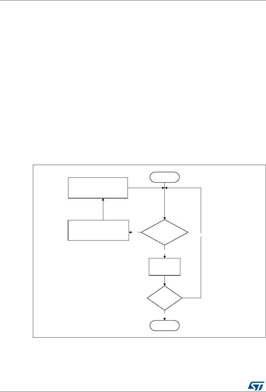
USB on-the-go full-speed (OTG_FS) RM0090
1338/1749 RM0090 Rev 18
1. When an STALL, TXERR, BBERR or DTERR interrupt in OTG_FS_HCINTx is received
for an IN or OUT channel. The application must be able to receive other interrupts
(DTERR, Nak, Data, TXERR) for the same channel before receiving the halt.
2. When a DISCINT (Disconnect Device) interrupt in OTG_FS_GINTSTS is received.
(The application is expected to disable all enabled channels).
3. When the application aborts a transfer before normal completion.
Operational model
The application must initialize a channel before communicating to the connected device.
This section explains the sequence of operation to be performed for different types of USB
transactions.
•Writing the transmit FIFO
The OTG_FS host automatically writes an entry (OUT request) to the periodic/non-
periodic request queue, along with the last word write of a packet. The application must
ensure that at least one free space is available in the periodic/non-periodic request
queue before starting to write to the transmit FIFO. The application must always write
to the transmit FIFO in words. If the packet size is non-word aligned, the application
must use padding. The OTG_FS host determines the actual packet size based on the
programmed maximum packet size and transfer size.
Figure 396. Transmit FIFO write task
•Reading the receive FIFO
MPS: Maximum packet size
Start
ai15673b
Wait for NPTXFE/PTXFE
interrupt in
OTG_FS_GINTSTS
Read GNPTXSTS/HPTXFSIZ
registers for available FIFO
and queue spaces
1 MPS or
LPS FIFO space
available?
Write 1 packet
data to
transmit FIFO
More packets
to send?
Done
No
No Ye s
Ye s
LPS: Last packet size
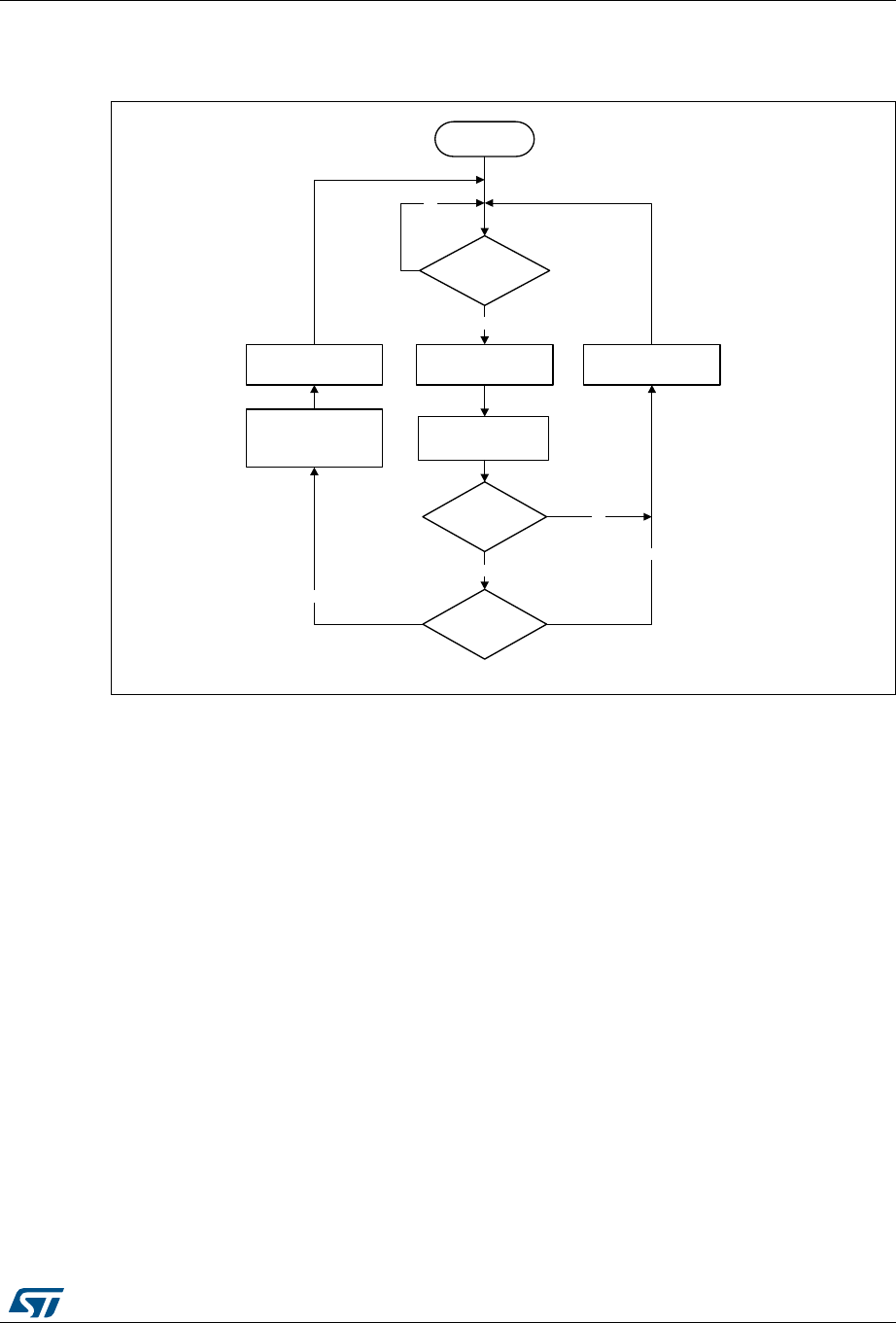
RM0090 Rev 18 1339/1749
RM0090 USB on-the-go full-speed (OTG_FS)
1380
The application must ignore all packet statuses other than IN data packet (bx0010).
Figure 397. Receive FIFO read task
•Bulk and control OUT/SETUP transactions
A typical bulk or control OUT/SETUP pipelined transaction-level operation is shown in
Figure 398. See channel 1 (ch_1). Two bulk OUT packets are transmitted. A control
SETUP transaction operates in the same way but has only one packet. The
assumptions are:
– The application is attempting to send two maximum-packet-size packets (transfer
size = 1, 024 bytes).
– The non-periodic transmit FIFO can hold two packets (128 bytes for FS).
– The non-periodic request queue depth = 4.
•Normal bulk and control OUT/SETUP operations
The sequence of operations in (channel 1) is as follows:
a) Initialize channel 1
b) Write the first packet for channel 1
c) Along with the last word write, the core writes an entry to the non-periodic request
queue
d) As soon as the non-periodic queue becomes non-empty, the core attempts to
send an OUT token in the current frame
e) Write the second (last) packet for channel 1
f) The core generates the XFRC interrupt as soon as the last transaction is
completed successfully
RXFLVL
interrupt ?
Read the received
packet from the
Receive FIFO
Read
OTG_FS_GRXSTSP
PKTSTS
0b0010?
Yes
Yes
Unmask RXFLVL
interrupt
BCNT > 0?
No
Mask RXFLVL
interrupt
Yes
Unmask RXFLVL
interrupt
No
No
Start
ai1567
4
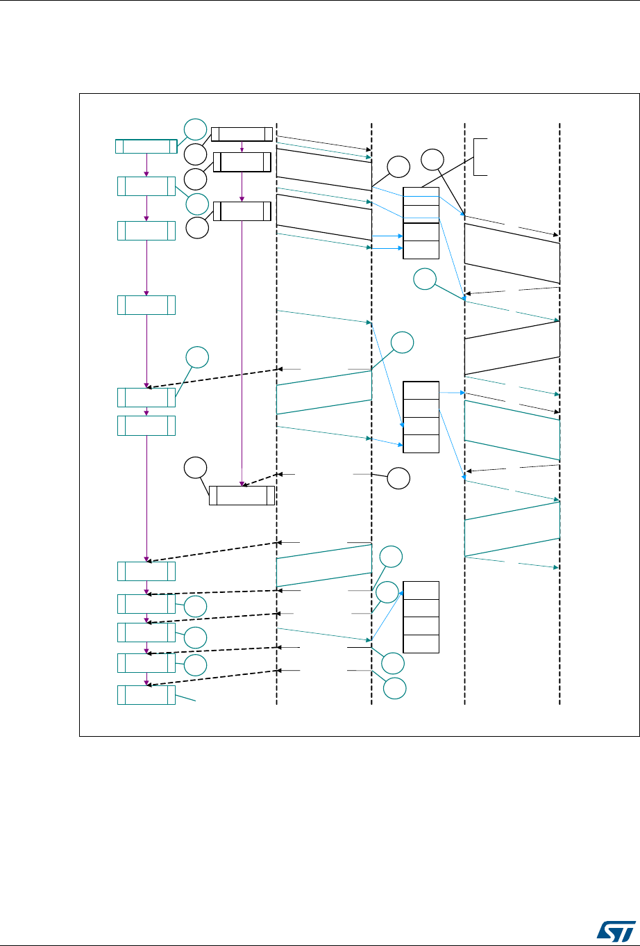
USB on-the-go full-speed (OTG_FS) RM0090
1340/1749 RM0090 Rev 18
g) In response to the XFRC interrupt, de-allocate the channel for other transfers
h) Handling non-ACK responses
Figure 398. Normal bulk/control OUT/SETUP and bulk/control IN transactions
The channel-specific interrupt service routine for bulk and control OUT/SETUP
transactions is shown in the following code samples.
•Interrupt service routine for bulk/control OUT/SETUP and bulk/control IN
transactions
a) Bulk/Control OUT/SETUP
Unmask (NAK/TXERR/STALL/XFRC)
if (XFRC)
{
ACK
HostApplication DeviceAHB USB
OUT
DATA0
MPS
1
MPS
1
MPS
w rit e_ tx _ fifo
(ch_1)
init_reg(ch_1)
set _ ch_e n
(ch_2)
init_reg(ch_2)
w rit e_ tx _ fifo
(ch_1)
set _ ch_e n
(ch_2)
ch_2
ch_2
ch_1
ch_1
De-allocate
(ch_1)
IN
ch_2
ch_2
ch_2
ch_1
ACK
OUT
set _ ch_e n
(ch_2)
Non-Periodic Request
Queue
Assume that this queue
can hold 4 entries.
4
1
6
ACK
DATA0
IN
ACK
read_rx_sts
read_rx_fifo
1
MPS
set _ ch_e n
(ch_2)
1
MPS
read_rx_stsre
ad_rx_fifo
read_rx_sts
Disable
(ch_2)
1
2
34
5
6
7
De-allocate
(ch_2)
CHH interruptr
ch_2
2
3
5
7
8
9
12
13
read_rx_sts 10
11
DATA1
MPS
DATA1
ai15675
RXFLVL interrupt
XFRC interrupt
RXFLVL interrupt
RXFLVL interrupt
RXFLVL interrupt
XFRC interrupt

RM0090 Rev 18 1341/1749
RM0090 USB on-the-go full-speed (OTG_FS)
1380
Reset Error Count
Mask ACK
De-allocate Channel
}
else if (STALL)
{
Transfer Done = 1
Unmask CHH
Disable Channel
}
else if (NAK or TXERR )
{
Rewind Buffer Pointers
Unmask CHH
Disable Channel
if (TXERR)
{
Increment Error Count
Unmask ACK
}
else
{
Reset Error Count
}
}
else if (CHH)
{
Mask CHH
if (Transfer Done or (Error_count == 3))
{
De-allocate Channel
}
else
{
Re-initialize Channel
}
}
else if (ACK)
{
Reset Error Count
Mask ACK
}
The application is expected to write the data packets into the transmit FIFO as and
when the space is available in the transmit FIFO and the Request queue. The
application can make use of the NPTXFE interrupt in OTG_FS_GINTSTS to find the
transmit FIFO space.
b) Bulk/Control IN
Unmask (TXERR/XFRC/BBERR/STALL/DTERR)
if (XFRC)
{
Reset Error Count

USB on-the-go full-speed (OTG_FS) RM0090
1342/1749 RM0090 Rev 18
Unmask CHH
Disable Channel
Reset Error Count
Mask ACK
}
else if (TXERR or BBERR or STALL)
{
Unmask CHH
Disable Channel
if (TXERR)
{
Increment Error Count
Unmask ACK
}
}
else if (CHH)
{
Mask CHH
if (Transfer Done or (Error_count == 3))
{
De-allocate Channel
}
else
{
Re-initialize Channel
}
}
else if (ACK)
{
Reset Error Count
Mask ACK
}
else if (DTERR)
{
Reset Error Count
}
The application is expected to write the requests as and when the Request queue space is
available and until the XFRC interrupt is received.
•Bulk and control IN transactions
A typical bulk or control IN pipelined transaction-level operation is shown in Figure 399.
See channel 2 (ch_2). The assumptions are:
– The application is attempting to receive two maximum-packet-size packets
(transfer size = 1 024 bytes).
– The receive FIFO can contain at least one maximum-packet-size packet and two
status words per packet (72 bytes for FS).
– The non-periodic request queue depth = 4.
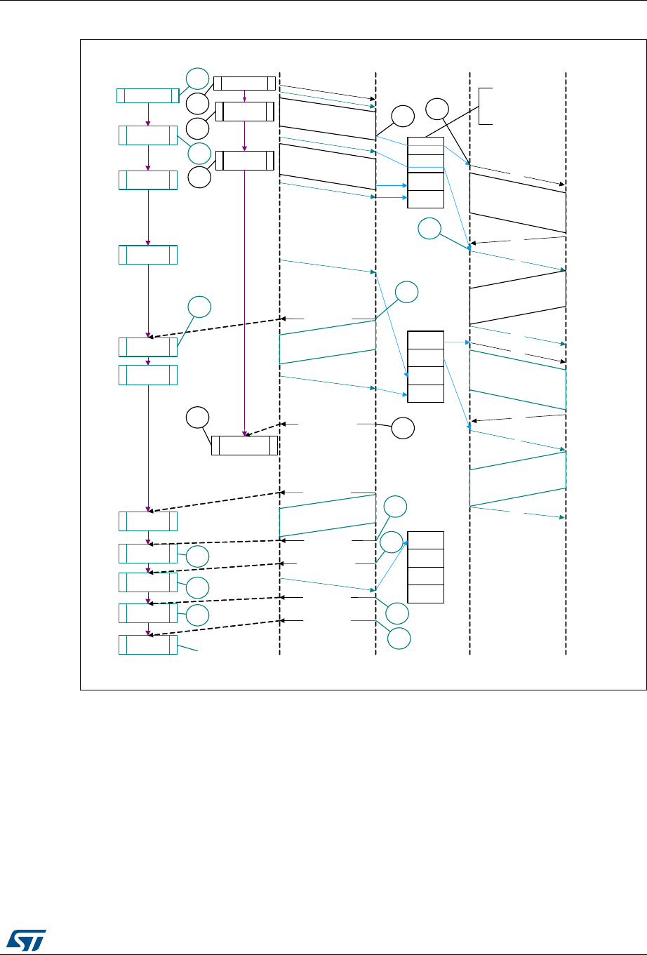
RM0090 Rev 18 1343/1749
RM0090 USB on-the-go full-speed (OTG_FS)
1380
Figure 399. Bulk/control IN transactions
The sequence of operations is as follows:
a) Initialize channel 2.
b) Set the CHENA bit in HCCHAR2 to write an IN request to the non-periodic request
queue.
c) The core attempts to send an IN token after completing the current OUT
transaction.
d) The core generates an RXFLVL interrupt as soon as the received packet is written
to the receive FIFO.
e) In response to the RXFLVL interrupt, mask the RXFLVL interrupt and read the
received packet status to determine the number of bytes received, then read the
receive FIFO accordingly. Following this, unmask the RXFLVL interrupt.
ACK
HostApplication DeviceAHB USB
OUT
DATA0
MPS
1
MPS
1
MPS
w rit e_ tx _ fifo
(ch_1)
init_reg(ch_1)
set _ ch_e n
(ch_2)
init_reg(ch_2)
w rit e_ tx _ fifo
(ch_1)
set _ ch_e n
(ch_2)
ch_2
ch_2
ch_1
ch_1
De-allocate
(ch_1)
IN
ch_2
ch_2
ch_2
ch_1
ACK
OUT
set _ ch_e n
(ch_2)
Non-Periodic Request
Queue
Assume that this queue
can hold 4 entries.
4
1
6
ACK
DATA0
IN
ACK
read_rx_sts
read_rx_fifo
1
MPS
set _ ch_e n
(ch_2)
1
MPS
read_rx_stsre
ad_rx_fifo
read_rx_sts
Disable
(ch_2)
1
2
34
5
6
7
De-allocate
(ch_2)
CHH interruptr
ch_2
2
3
5
7
8
9
12
13
read_rx_sts 10
11
DATA1
MPS
DATA1
ai15675
RXFLVL interrupt
XFRC interrupt
RXFLVL interrupt
RXFLVL interrupt
RXFLVL interrupt
XFRC interrupt

USB on-the-go full-speed (OTG_FS) RM0090
1344/1749 RM0090 Rev 18
f) The core generates the RXFLVL interrupt for the transfer completion status entry
in the receive FIFO.
g) The application must read and ignore the receive packet status when the receive
packet status is not an IN data packet (PKTSTS in GRXSTSR ≠0b0010).
h) The core generates the XFRC interrupt as soon as the receive packet status is
read.
i) In response to the XFRC interrupt, disable the channel and stop writing the
OTG_FS_HCCHAR2 register for further requests. The core writes a channel
disable request to the non-periodic request queue as soon as the
OTG_FS_HCCHAR2 register is written.
j) The core generates the RXFLVL interrupt as soon as the halt status is written to
the receive FIFO.
k) Read and ignore the receive packet status.
l) The core generates a CHH interrupt as soon as the halt status is popped from the
receive FIFO.
m) In response to the CHH interrupt, de-allocate the channel for other transfers.
n) Handling non-ACK responses
•Control transactions
Setup, Data, and Status stages of a control transfer must be performed as three
separate transfers. Setup-, Data- or Status-stage OUT transactions are performed
similarly to the bulk OUT transactions explained previously. Data- or Status-stage IN
transactions are performed similarly to the bulk IN transactions explained previously.
For all three stages, the application is expected to set the EPTYP field in
OTG_FS_HCCHAR1 to Control. During the Setup stage, the application is expected to
set the PID field in OTG_FS_HCTSIZ1 to SETUP.
•Interrupt OUT transactions
A typical interrupt OUT operation is shown in Figure 400. The assumptions are:
– The application is attempting to send one packet in every frame (up to 1 maximum
packet size), starting with the odd frame (transfer size = 1 024 bytes)
– The periodic transmit FIFO can hold one packet (1 KB)
– Periodic request queue depth = 4
The sequence of operations is as follows:
a) Initialize and enable channel 1. The application must set the ODDFRM bit in
OTG_FS_HCCHAR1.
b) Write the first packet for channel 1.
c) Along with the last word write of each packet, the OTG_FS host writes an entry to
the periodic request queue.
d) The OTG_FS host attempts to send an OUT token in the next (odd) frame.
e) The OTG_FS host generates an XFRC interrupt as soon as the last packet is
transmitted successfully.
f) In response to the XFRC interrupt, reinitialize the channel for the next transfer.
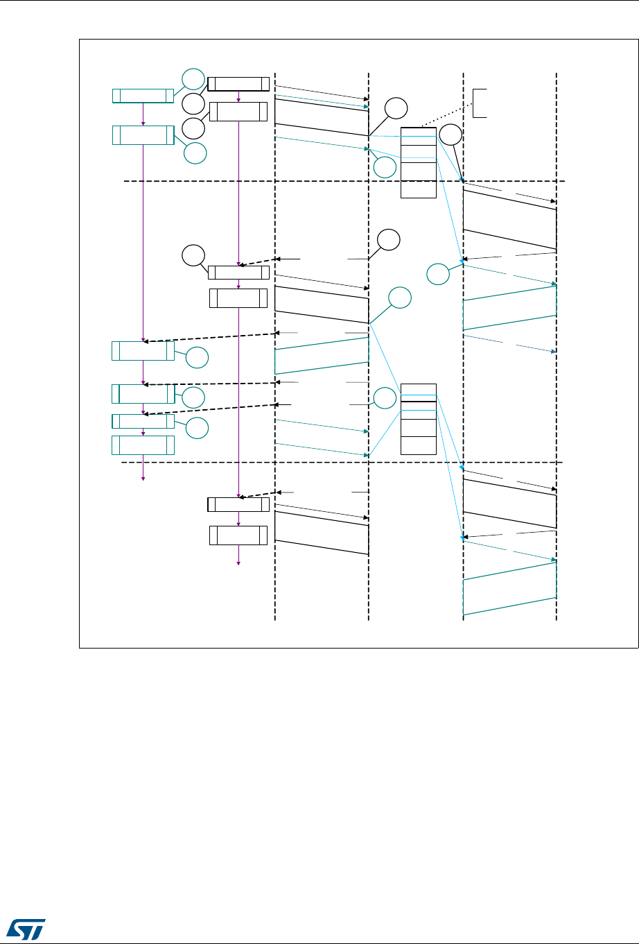
RM0090 Rev 18 1345/1749
RM0090 USB on-the-go full-speed (OTG_FS)
1380
Figure 400. Normal interrupt OUT/IN transactions
•Interrupt service routine for interrupt OUT/IN transactions
a) Interrupt OUT
Unmask (NAK/TXERR/STALL/XFRC/FRMOR)
if (XFRC)
{
Reset Error Count
Mask ACK
De-allocate Channel
}
else
if (STALL or FRMOR)
{
Mask ACK
Unmask CHH
Host
Application DeviceAHB USB
OUT
DATA0
MPS
1
MPS
1
MPS
write_tx_fifo
(ch_1)
init_reg(ch_1)
set_ch_en
(ch_2)
init_reg(ch _2)
write_tx_fifo
(ch_1)
IN
OUT
DATA1
MPS
Periodic Request Queue
Assume that this queue
can hold 4 entries.
1
5
DATA0
IN
RXFLVL interrupt
1
MPS
read_rx_sts
read_rx_fifo
read_rx_sts
1
2
3
4
6
2
3
6
78
9
Odd
(micro)
frame
Even
(micro)
frame
init_reg(ch_1)
set_ch_en
(ch_2)
init_reg(ch _2)
write_tx_fifo
(ch_1)
init_reg(ch_1)
1
MPS
DATA1
5
4
ACK
ACK
ACK
ch_1
ch_2
ch_2
ch_1
ai1567
6
RXFLVL interrupt
XFRC interrupt
XFRC interrupt
XFRC interrupt

USB on-the-go full-speed (OTG_FS) RM0090
1346/1749 RM0090 Rev 18
Disable Channel
if (STALL)
{
Transfer Done = 1
}
}
else
if (NAK or TXERR)
{
Rewind Buffer Pointers
Reset Error Count
Mask ACK
Unmask CHH
Disable Channel
}
else
if (CHH)
{
Mask CHH
if (Transfer Done or (Error_count == 3))
{
De-allocate Channel
}
else
{
Re-initialize Channel (in next b_interval - 1 Frame)
}
}
else
if (ACK)
{
Reset Error Count
Mask ACK
}
The application uses the NPTXFE interrupt in OTG_FS_GINTSTS to find the transmit
FIFO space.
b) Interrupt IN
Unmask (NAK/TXERR/XFRC/BBERR/STALL/FRMOR/DTERR)
if (XFRC)
{
Reset Error Count
Mask ACK
if (OTG_FS_HCTSIZx.PKTCNT == 0)
{
De-allocate Channel
}
else
{
Transfer Done = 1
Unmask CHH
Disable Channel

RM0090 Rev 18 1347/1749
RM0090 USB on-the-go full-speed (OTG_FS)
1380
}
}
else
if (STALL or FRMOR or NAK or DTERR or BBERR)
{
Mask ACK
Unmask CHH
Disable Channel
if (STALL or BBERR)
{
Reset Error Count
Transfer Done = 1
}
else
if (!FRMOR)
{
Reset Error Count
}
}
else
if (TXERR)
{
Increment Error Count
Unmask ACK
Unmask CHH
Disable Channel
}
else
if (CHH)
{
Mask CHH
if (Transfer Done or (Error_count == 3))
{
De-allocate Channel
}
else
Re-initialize Channel (in next b_interval - 1 /Frame)
}
}
else
if (ACK)
{
Reset Error Count
Mask ACK

USB on-the-go full-speed (OTG_FS) RM0090
1348/1749 RM0090 Rev 18
}
•Interrupt IN transactions
The assumptions are:
– The application is attempting to receive one packet (up to 1 maximum packet size)
in every frame, starting with odd (transfer size = 1 024 bytes).
– The receive FIFO can hold at least one maximum-packet-size packet and two
status words per packet (1 031 bytes).
– Periodic request queue depth = 4.
•Normal interrupt IN operation
The sequence of operations is as follows:
a) Initialize channel 2. The application must set the ODDFRM bit in
OTG_FS_HCCHAR2.
b) Set the CHENA bit in OTG_FS_HCCHAR2 to write an IN request to the periodic
request queue.
c) The OTG_FS host writes an IN request to the periodic request queue for each
OTG_FS_HCCHAR2 register write with the CHENA bit set.
d) The OTG_FS host attempts to send an IN token in the next (odd) frame.
e) As soon as the IN packet is received and written to the receive FIFO, the OTG_FS
host generates an RXFLVL interrupt.
f) In response to the RXFLVL interrupt, read the received packet status to determine
the number of bytes received, then read the receive FIFO accordingly. The
application must mask the RXFLVL interrupt before reading the receive FIFO, and
unmask after reading the entire packet.
g) The core generates the RXFLVL interrupt for the transfer completion status entry
in the receive FIFO. The application must read and ignore the receive packet
status when the receive packet status is not an IN data packet (PKTSTS in
GRXSTSR ≠0b0010).
h) The core generates an XFRC interrupt as soon as the receive packet status is
read.
i) In response to the XFRC interrupt, read the PKTCNT field in OTG_FS_HCTSIZ2.
If the PKTCNT bit in OTG_FS_HCTSIZ2 is not equal to 0, disable the channel
before re-initializing the channel for the next transfer, if any). If PKTCNT bit in

RM0090 Rev 18 1349/1749
RM0090 USB on-the-go full-speed (OTG_FS)
1380
OTG_FS_HCTSIZ2 = 0, reinitialize the channel for the next transfer. This time, the
application must reset the ODDFRM bit in OTG_FS_HCCHAR2.
•Isochronous OUT transactions
A typical isochronous OUT operation is shown in Figure 401. The assumptions are:
– The application is attempting to send one packet every frame (up to 1 maximum
packet size), starting with an odd frame. (transfer size = 1 024 bytes).
– The periodic transmit FIFO can hold one packet (1 KB).
– Periodic request queue depth = 4.
The sequence of operations is as follows:
a) Initialize and enable channel 1. The application must set the ODDFRM bit in
OTG_FS_HCCHAR1.
b) Write the first packet for channel 1.
c) Along with the last word write of each packet, the OTG_FS host writes an entry to
the periodic request queue.
d) The OTG_FS host attempts to send the OUT token in the next frame (odd).
e) The OTG_FS host generates the XFRC interrupt as soon as the last packet is
transmitted successfully.
f) In response to the XFRC interrupt, reinitialize the channel for the next transfer.
g) Handling non-ACK responses
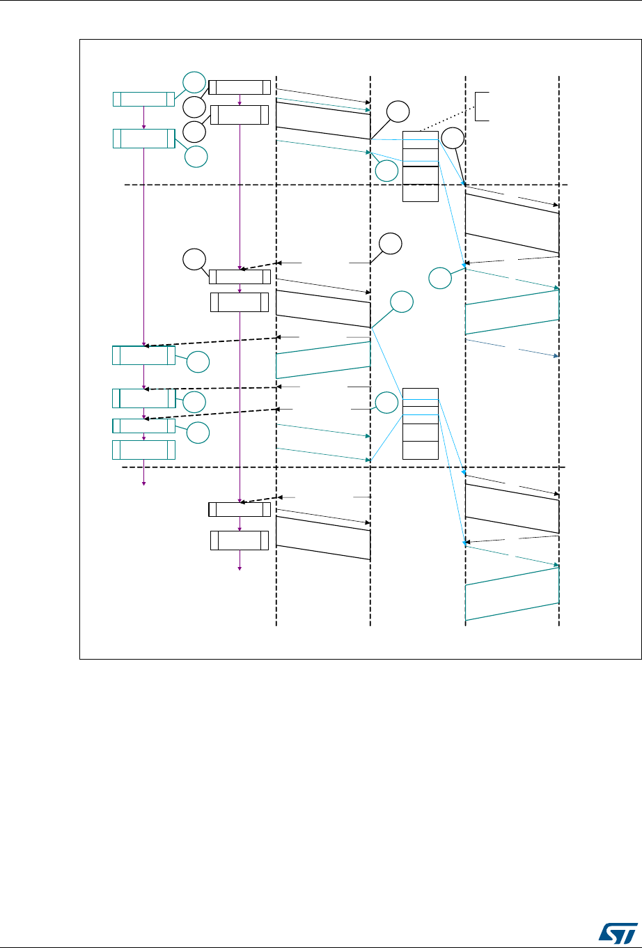
USB on-the-go full-speed (OTG_FS) RM0090
1350/1749 RM0090 Rev 18
Figure 401. Normal isochronous OUT/IN transactions
•Interrupt service routine for isochronous OUT/IN transactions
Code sample: Isochronous OUT
Unmask (FRMOR/XFRC)
if (XFRC)
{
De-allocate Channel
}
else
if (FRMOR)
{
Unmask CHH
Disable Channel
}
Host
Application DeviceAHB USB
OUT
DATA0
MPS
1
MPS
1
MPS
write_tx_fifo
(ch_1)
init_reg(ch_1)
set_ch_en
(ch_2)
init_reg(ch _2)
write_tx_fifo
(ch_1)
IN
OUT
DATA1
MPS
Periodic Request Queue
Assume that this queue
can hold 4 entries.
1
5
DATA0
IN
RXFLVL interrupt
1
MPS
read_rx_sts
read_rx_fifo
read_rx_sts
1
2
3
4
6
2
3
6
78
9
Odd
(micro)
frame
Even
(micro)
frame
init_reg(ch_1)
set_ch_en
(ch_2)
init_reg(ch _2)
write_tx_fifo
(ch_1)
init_reg(ch_1)
1
MPS
DATA1
5
4
ACK
ACK
ACK
ch_1
ch_2
ch_2
ch_1
ai1567
6
RXFLVL interrupt
XFRC interrupt
XFRC interrupt
XFRC interrupt

RM0090 Rev 18 1351/1749
RM0090 USB on-the-go full-speed (OTG_FS)
1380
else
if (CHH)
{
Mask CHH
De-allocate Channel
}
Code sample: Isochronous IN
Unmask (TXERR/XFRC/FRMOR/BBERR)
if (XFRC or FRMOR)
{
if (XFRC and (OTG_FS_HCTSIZx.PKTCNT == 0))
{
Reset Error Count
De-allocate Channel
}
else
{
Unmask CHH
Disable Channel
}
}
else
if (TXERR or BBERR)
{
Increment Error Count
Unmask CHH
Disable Channel
}
else
if (CHH)
{
Mask CHH
if (Transfer Done or (Error_count == 3))
{
De-allocate Channel
}
else
{
Re-initialize Channel
}
}

USB on-the-go full-speed (OTG_FS) RM0090
1352/1749 RM0090 Rev 18
•Isochronous IN transactions
The assumptions are:
– The application is attempting to receive one packet (up to 1 maximum packet size)
in every frame starting with the next odd frame (transfer size = 1 024 bytes).
– The receive FIFO can hold at least one maximum-packet-size packet and two
status word per packet (1 031 bytes).
– Periodic request queue depth = 4.
The sequence of operations is as follows:
a) Initialize channel 2. The application must set the ODDFRM bit in
OTG_FS_HCCHAR2.
b) Set the CHENA bit in OTG_FS_HCCHAR2 to write an IN request to the periodic
request queue.
c) The OTG_FS host writes an IN request to the periodic request queue for each
OTG_FS_HCCHAR2 register write with the CHENA bit set.
d) The OTG_FS host attempts to send an IN token in the next odd frame.
e) As soon as the IN packet is received and written to the receive FIFO, the OTG_FS
host generates an RXFLVL interrupt.
f) In response to the RXFLVL interrupt, read the received packet status to determine
the number of bytes received, then read the receive FIFO accordingly. The
application must mask the RXFLVL interrupt before reading the receive FIFO, and
unmask it after reading the entire packet.
g) The core generates an RXFLVL interrupt for the transfer completion status entry in
the receive FIFO. This time, the application must read and ignore the receive
packet status when the receive packet status is not an IN data packet (PKTSTS bit
in OTG_FS_GRXSTSR ≠0b0010).
h) The core generates an XFRC interrupt as soon as the receive packet status is
read.
i) In response to the XFRC interrupt, read the PKTCNT field in OTG_FS_HCTSIZ2.
If PKTCNT ≠0 in OTG_FS_HCTSIZ2, disable the channel before re-initializing the
channel for the next transfer, if any. If PKTCNT = 0 in OTG_FS_HCTSIZ2,
reinitialize the channel for the next transfer. This time, the application must reset
the ODDFRM bit in OTG_FS_HCCHAR2.
•Selecting the queue depth
Choose the periodic and non-periodic request queue depths carefully to match the
number of periodic/non-periodic endpoints accessed.
The non-periodic request queue depth affects the performance of non-periodic
transfers. The deeper the queue (along with sufficient FIFO size), the more often the
core is able to pipeline non-periodic transfers. If the queue size is small, the core is
able to put in new requests only when the queue space is freed up.
The core’s periodic request queue depth is critical to perform periodic transfers as
scheduled. Select the periodic queue depth, based on the number of periodic transfers
scheduled in a microframe. If the periodic request queue depth is smaller than the
periodic transfers scheduled in a microframe, a frame overrun condition occurs.
•Handling babble conditions
OTG_FS controller handles two cases of babble: packet babble and port babble.
Packet babble occurs if the device sends more data than the maximum packet size for

RM0090 Rev 18 1353/1749
RM0090 USB on-the-go full-speed (OTG_FS)
1380
the channel. Port babble occurs if the core continues to receive data from the device at
EOF2 (the end of frame 2, which is very close to SOF).
When OTG_FS controller detects a packet babble, it stops writing data into the Rx
buffer and waits for the end of packet (EOP). When it detects an EOP, it flushes already
written data in the Rx buffer and generates a Babble interrupt to the application.
When OTG_FS controller detects a port babble, it flushes the RxFIFO and disables the
port. The core then generates a Port disabled interrupt (HPRTINT in
OTG_FS_GINTSTS, PENCHNG in OTG_FS_HPRT). On receiving this interrupt, the
application must determine that this is not due to an overcurrent condition (another
cause of the Port Disabled interrupt) by checking POCA in OTG_FS_HPRT, then
perform a soft reset. The core does not send any more tokens after it has detected a
port babble condition.
34.17.5 Device programming model
Endpoint initialization on USB reset
1. Set the NAK bit for all OUT endpoints
– SNAK = 1 in OTG_FS_DOEPCTLx (for all OUT endpoints)
2. Unmask the following interrupt bits
– INEP0 = 1 in OTG_FS_DAINTMSK (control 0 IN endpoint)
– OUTEP0 = 1 in OTG_FS_DAINTMSK (control 0 OUT endpoint)
–STUP=1 in DOEPMSK
– XFRC = 1 in DOEPMSK
– XFRC = 1 in DIEPMSK
– TOC = 1 in DIEPMSK
3. Set up the Data FIFO RAM for each of the FIFOs
– Program the OTG_FS_GRXFSIZ register, to be able to receive control OUT data
and setup data. If thresholding is not enabled, at a minimum, this must be equal to
1 max packet size of control endpoint 0 + 2 words (for the status of the control
OUT data packet) + 10 words (for setup packets).
– Program the OTG_FS_TX0FSIZ register (depending on the FIFO number chosen)
to be able to transmit control IN data. At a minimum, this must be equal to 1 max
packet size of control endpoint 0.
4. Program the following fields in the endpoint-specific registers for control OUT endpoint
0 to receive a SETUP packet
– STUPCNT = 3 in OTG_FS_DOEPTSIZ0 (to receive up to 3 back-to-back SETUP
packets)
At this point, all initialization required to receive SETUP packets is done.
Endpoint initialization on enumeration completion
1. On the Enumeration Done interrupt (ENUMDNE in OTG_FS_GINTSTS), read the
OTG_FS_DSTS register to determine the enumeration speed.
2. Program the MPSIZ field in OTG_FS_DIEPCTL0 to set the maximum packet size. This
step configures control endpoint 0. The maximum packet size for a control endpoint
depends on the enumeration speed.

USB on-the-go full-speed (OTG_FS) RM0090
1354/1749 RM0090 Rev 18
At this point, the device is ready to receive SOF packets and is configured to perform control
transfers on control endpoint 0.
Endpoint initialization on SetAddress command
This section describes what the application must do when it receives a SetAddress
command in a SETUP packet.
1. Program the OTG_FS_DCFG register with the device address received in the
SetAddress command
2. Program the core to send out a status IN packet
Endpoint initialization on SetConfiguration/SetInterface command
This section describes what the application must do when it receives a SetConfiguration or
SetInterface command in a SETUP packet.
1. When a SetConfiguration command is received, the application must program the
endpoint registers to configure them with the characteristics of the valid endpoints in
the new configuration.
2. When a SetInterface command is received, the application must program the endpoint
registers of the endpoints affected by this command.
3. Some endpoints that were active in the prior configuration or alternate setting are not
valid in the new configuration or alternate setting. These invalid endpoints must be
deactivated.
4. Unmask the interrupt for each active endpoint and mask the interrupts for all inactive
endpoints in the OTG_FS_DAINTMSK register.
5. Set up the Data FIFO RAM for each FIFO.
6. After all required endpoints are configured; the application must program the core to
send a status IN packet.
At this point, the device core is configured to receive and transmit any type of data packet.
Endpoint activation
This section describes the steps required to activate a device endpoint or to configure an
existing device endpoint to a new type.
1. Program the characteristics of the required endpoint into the following fields of the
OTG_FS_DIEPCTLx register (for IN or bidirectional endpoints) or the
OTG_FS_DOEPCTLx register (for OUT or bidirectional endpoints).
– Maximum packet size
– USB active endpoint = 1
– Endpoint start data toggle (for interrupt and bulk endpoints)
– Endpoint type
– TxFIFO number
2. Once the endpoint is activated, the core starts decoding the tokens addressed to that
endpoint and sends out a valid handshake for each valid token received for the
endpoint.

RM0090 Rev 18 1355/1749
RM0090 USB on-the-go full-speed (OTG_FS)
1380
Endpoint deactivation
This section describes the steps required to deactivate an existing endpoint.
1. In the endpoint to be deactivated, clear the USB active endpoint bit in the
OTG_FS_DIEPCTLx register (for IN or bidirectional endpoints) or the
OTG_FS_DOEPCTLx register (for OUT or bidirectional endpoints).
2. Once the endpoint is deactivated, the core ignores tokens addressed to that endpoint,
which results in a timeout on the USB.
Note: The application must meet the following conditions to set up the device core to handle
traffic:
NPTXFEM and RXFLVLM in the OTG_FS_GINTMSK register must be cleared.
34.17.6 Operational model
SETUP and OUT data transfers
This section describes the internal data flow and application-level operations during data
OUT transfers and SETUP transactions.
•Packet read
This section describes how to read packets (OUT data and SETUP packets) from the
receive FIFO.
1. On catching an RXFLVL interrupt (OTG_FS_GINTSTS register), the application must
read the Receive status pop register (OTG_FS_GRXSTSP).
2. The application can mask the RXFLVL interrupt (in OTG_FS_GINTSTS) by writing to
RXFLVL = 0 (in OTG_FS_GINTMSK), until it has read the packet from the receive
FIFO.
3. If the received packet’s byte count is not 0, the byte count amount of data is popped
from the receive Data FIFO and stored in memory. If the received packet byte count is
0, no data is popped from the receive data FIFO.
4. The receive FIFO’s packet status readout indicates one of the following:
a) Global OUT NAK pattern:
PKTSTS = Global OUT NAK, BCNT = 0x000, EPNUM = Don’t Care (0x0),
DPID = Don’t Care (0b00).
These data indicate that the global OUT NAK bit has taken effect.
b) SETUP packet pattern:
PKTSTS = SETUP, BCNT = 0x008, EPNUM = Control EP Num, DPID = D0.
These data indicate that a SETUP packet for the specified endpoint is now
available for reading from the receive FIFO.
c) Setup stage done pattern:
PKTSTS = Setup Stage Done, BCNT = 0x0, EPNUM = Control EP Num,
DPID = Don’t Care (0b00).
These data indicate that the Setup stage for the specified endpoint has completed
and the Data stage has started. After this entry is popped from the receive FIFO,
the core asserts a Setup interrupt on the specified control OUT endpoint.
d) Data OUT packet pattern:
PKTSTS = DataOUT, BCNT = size of the received data OUT packet (0 ≤BCNT
≤1 024), EPNUM = EPNUM on which the packet was received, DPID = Actual
Data PID.
USB on-the-go full-speed (OTG_FS) RM0090
1356/1749 RM0090 Rev 18
e) Data transfer completed pattern:
PKTSTS = Data OUT Transfer Done, BCNT = 0x0, EPNUM = OUT EP Num
on which the data transfer is complete, DPID = Don’t Care (0b00).
These data indicate that an OUT data transfer for the specified OUT endpoint has
completed. After this entry is popped from the receive FIFO, the core asserts a
Transfer Completed interrupt on the specified OUT endpoint.
5. After the data payload is popped from the receive FIFO, the RXFLVL interrupt
(OTG_FS_GINTSTS) must be unmasked.
6. Steps 1–5 are repeated every time the application detects assertion of the interrupt line
due to RXFLVL in OTG_FS_GINTSTS. Reading an empty receive FIFO can result in
undefined core behavior.
Figure 402 provides a flowchart of the above procedure.
Figure 402. Receive FIFO packet read
•SETUP transactions
This section describes how the core handles SETUP packets and the application’s
sequence for handling SETUP transactions.
•Application requirements
1. To receive a SETUP packet, the STUPCNT field (OTG_FS_DOEPTSIZx) in a control
OUT endpoint must be programmed to a non-zero value. When the application
programs the STUPCNT field to a non-zero value, the core receives SETUP packets
and writes them to the receive FIFO, irrespective of the NAK status and EPENA bit
setting in OTG_FS_DOEPCTLx. The STUPCNT field is decremented every time the
control endpoint receives a SETUP packet. If the STUPCNT field is not programmed to
a proper value before receiving a SETUP packet, the core still receives the SETUP
packet and decrements the STUPCNT field, but the application may not be able to
word_cnt =
BCNT[11:2] +C
(BCNT[1]
| BCNT[1])
rcv_out_pkt()
rd_data = rd_reg (OTG_FS_GRXSTSP);
mem[0: word_cnt – 1] =
rd_rxfifo(rd_data.EPNUM,
word_cnt)
N
rd_data.BCNT = 0
wait until RXFLVL in OTG_FS_GINTSTSG
packet
store in
memory
Y
ai15677b

RM0090 Rev 18 1357/1749
RM0090 USB on-the-go full-speed (OTG_FS)
1380
determine the correct number of SETUP packets received in the Setup stage of a
control transfer.
– STUPCNT = 3 in OTG_FS_DOEPTSIZx
2. The application must always allocate some extra space in the Receive data FIFO, to be
able to receive up to three SETUP packets on a control endpoint.
– The space to be reserved is 10 words. Three words are required for the first
SETUP packet, 1 word is required for the Setup stage done word and 6 words are
required to store two extra SETUP packets among all control endpoints.
– 3 words per SETUP packet are required to store 8 bytes of SETUP data and 4
bytes of SETUP status (Setup packet pattern). The core reserves this space in the
receive data FIFO to write SETUP data only, and never uses this space for data
packets.
3. The application must read the 2 words of the SETUP packet from the receive FIFO.
4. The application must read and discard the Setup stage done word from the receive
FIFO.
•Internal data flow
1. When a SETUP packet is received, the core writes the received data to the receive
FIFO, without checking for available space in the receive FIFO and irrespective of the
endpoint’s NAK and STALL bit settings.
– The core internally sets the IN NAK and OUT NAK bits for the control IN/OUT
endpoints on which the SETUP packet was received.
2. For every SETUP packet received on the USB, 3 words of data are written to the
receive FIFO, and the STUPCNT field is decremented by 1.
– The first word contains control information used internally by the core
– The second word contains the first 4 bytes of the SETUP command
– The third word contains the last 4 bytes of the SETUP command
3. When the Setup stage changes to a Data IN/OUT stage, the core writes an entry
(Setup stage done word) to the receive FIFO, indicating the completion of the Setup
stage.
4. On the AHB side, SETUP packets are emptied by the application.
5. When the application pops the Setup stage done word from the receive FIFO, the core
interrupts the application with an STUP interrupt (OTG_FS_DOEPINTx), indicating it
can process the received SETUP packet.
– The core clears the endpoint enable bit for control OUT endpoints.
•Application programming sequence
1. Program the OTG_FS_DOEPTSIZx register.
– STUPCNT = 3
2. Wait for the RXFLVL interrupt (OTG_FS_GINTSTS) and empty the data packets from
the receive FIFO.
3. Assertion of the STUP interrupt (OTG_FS_DOEPINTx) marks a successful completion
of the SETUP Data Transfer.
– On this interrupt, the application must read the OTG_FS_DOEPTSIZx register to
determine the number of SETUP packets received and process the last received
SETUP packet.
USB on-the-go full-speed (OTG_FS) RM0090
1358/1749 RM0090 Rev 18
Figure 403. Processing a SETUP packet
•Handling more than three back-to-back SETUP packets
Per the USB 2.0 specification, normally, during a SETUP packet error, a host does not send
more than three back-to-back SETUP packets to the same endpoint. However, the USB 2.0
specification does not limit the number of back-to-back SETUP packets a host can send to
the same endpoint. When this condition occurs, the OTG_FS controller generates an
interrupt (B2BSTUP in OTG_FS_DOEPINTx).
•Setting the global OUT NAK
Internal data flow
1. When the application sets the Global OUT NAK (SGONAK bit in OTG_FS_DCTL), the
core stops writing data, except SETUP packets, to the receive FIFO. Irrespective of the
space availability in the receive FIFO, non-isochronous OUT tokens receive a NAK
handshake response, and the core ignores isochronous OUT data packets
2. The core writes the Global OUT NAK pattern to the receive FIFO. The application must
reserve enough receive FIFO space to write this data pattern.
3. When the application pops the Global OUT NAK pattern word from the receive FIFO,
the core sets the GONAKEFF interrupt (OTG_FS_GINTSTS).
4. Once the application detects this interrupt, it can assume that the core is in Global OUT
NAK mode. The application can clear this interrupt by clearing the SGONAK bit in
OTG_FS_DCTL.
Wait for STUP in OTG_FS_DOEPINTx
rem_supcnt =
rd_reg(DOEPTSIZx)
setup_cmd[31:0] = mem[4 – 2 * rem_supcnt]
setup_cmd[63:32] = mem[5 – 2 * rem_supcnt]
ctrl-rd/wr/2 stage
Find setup cmd type
Write
2-stage
Read
setup_np_in_pkt
Status IN phase
rcv_out_pkt
Data OUT phase
setup_np_in_pkt
Data IN phase
ai15678

RM0090 Rev 18 1359/1749
RM0090 USB on-the-go full-speed (OTG_FS)
1380
Application programming sequence
1. To stop receiving any kind of data in the receive FIFO, the application must set the
Global OUT NAK bit by programming the following field:
– SGONAK = 1 in OTG_FS_DCTL
2. Wait for the assertion of the GONAKEFF interrupt in OTG_FS_GINTSTS. When
asserted, this interrupt indicates that the core has stopped receiving any type of data
except SETUP packets.
3. The application can receive valid OUT packets after it has set SGONAK in
OTG_FS_DCTL and before the core asserts the GONAKEFF interrupt
(OTG_FS_GINTSTS).
4. The application can temporarily mask this interrupt by writing to the GINAKEFFM bit in
the OTG_FS_GINTMSK register.
– GINAKEFFM = 0 in the OTG_FS_GINTMSK register
5. Whenever the application is ready to exit the Global OUT NAK mode, it must clear the
SGONAK bit in OTG_FS_DCTL. This also clears the GONAKEFF interrupt
(OTG_FS_GINTSTS).
– OTG_FS_DCTL = 1 in CGONAK
6. If the application has masked this interrupt earlier, it must be unmasked as follows:
– GINAKEFFM = 1 in GINTMSK
•Disabling an OUT endpoint
The application must use this sequence to disable an OUT endpoint that it has enabled.
Application programming sequence
1. Before disabling any OUT endpoint, the application must enable Global OUT NAK
mode in the core.
– SGONAK = 1 in OTG_FS_DCTL
2. Wait for the GONAKEFF interrupt (OTG_FS_GINTSTS)
3. Disable the required OUT endpoint by programming the following fields:
– EPDIS = 1 in OTG_FS_DOEPCTLx
– SNAK = 1 in OTG_FS_DOEPCTLx
4. Wait for the EPDISD interrupt (OTG_FS_DOEPINTx), which indicates that the OUT
endpoint is completely disabled. When the EPDISD interrupt is asserted, the core also
clears the following bits:
– EPDIS = 0 in OTG_FS_DOEPCTLx
– EPENA = 0 in OTG_FS_DOEPCTLx
5. The application must clear the Global OUT NAK bit to start receiving data from other
non-disabled OUT endpoints.
– SGONAK = 0 in OTG_FS_DCTL
•Transfer Stop Programming for OUT endpoints
The application must use the following programing sequence to stop any transfers (because
of an interrupt from the host, typically a reset).
Sequence of operations:

USB on-the-go full-speed (OTG_FS) RM0090
1360/1749 RM0090 Rev 18
1. Enable all OUT endpoints by setting
– EPENA = 1 in all OTG_FS_DOEPCTLx registers.
2. Flush the RxFIFO as follows
– Poll OTG_FS_GRSTCTL.AHBIDL until it is 1. This indicates that AHB master is
idle.
– Perform read modify write operation on OTG_FS_GRSTCTL.RXFFLSH =1
– Poll OTG_FS_GRSTCTL.RXFFLSH until it is 0, but also using a timeout of less
than 10 milli-seconds (corresponds to minimum reset signaling duration). If 0 is
seen before the timeout, then the RxFIFO flush is successful. If at the moment the
timeout occurs, there is still a 1, (this may be due to a packet on EP0 coming from
the host) then go back (once only) to the previous step (“Perform read modify write
operation”).
3. Before disabling any OUT endpoint, the application must enable Global OUT NAK
mode in the core, according to the instructions in “Setting the global OUT NAK on
page 1358”. This ensures that data in the RxFIFO is sent to the application
successfully. Set SGONAK = 1 in OTG_FS_DCTL
4. Wait for the GONAKEFF interrupt (OTG_FS_GINTSTS)
5. Disable all active OUT endpoints by programming the following register bits:
– EPDIS = 1 in registers OTG_FS_DOEPCTLx
– SNAK = 1 in registers OTG_FS_DOEPCTLx
6. Wait for the EPDIS interrupt in OTG_FS_DOEPINTx for each OUT endpoint
programmed in the previous step. The EPDIS interrupt in OTG_FS_DOEPINTx
indicates that the corresponding OUT endpoint is completely disabled. When the
EPDIS interrupt is asserted, the following bits are cleared:
– EPENA = 0 in registers OTG_FS_DOEPCTLx
– EPDIS = 0 in registers OTG_FS_DOEPCTLx
– SNAK = 0 in registers OTG_FS_DOEPCTLx
•Generic non-isochronous OUT data transfers
This section describes a regular non-isochronous OUT data transfer (control, bulk, or
interrupt).
Application requirements
1. Before setting up an OUT transfer, the application must allocate a buffer in the memory
to accommodate all data to be received as part of the OUT transfer.
2. For OUT transfers, the transfer size field in the endpoint’s transfer size register must be
a multiple of the maximum packet size of the endpoint, adjusted to the word boundary.
– transfer size[EPNUM] = n × (MPSIZ[EPNUM] + 4 – (MPSIZ[EPNUM] mod 4))
– packet count[EPNUM] = n
–n > 0
3. On any OUT endpoint interrupt, the application must read the endpoint’s transfer size
register to calculate the size of the payload in the memory. The received payload size
can be less than the programmed transfer size.
– Payload size in memory = application programmed initial transfer size – core
updated final transfer size
– Number of USB packets in which this payload was received = application
programmed initial packet count – core updated final packet count

RM0090 Rev 18 1361/1749
RM0090 USB on-the-go full-speed (OTG_FS)
1380
Internal data flow
1. The application must set the transfer size and packet count fields in the endpoint-
specific registers, clear the NAK bit, and enable the endpoint to receive the data.
2. Once the NAK bit is cleared, the core starts receiving data and writes it to the receive
FIFO, as long as there is space in the receive FIFO. For every data packet received on
the USB, the data packet and its status are written to the receive FIFO. Every packet
(maximum packet size or short packet) written to the receive FIFO decrements the
packet count field for that endpoint by 1.
– OUT data packets received with bad data CRC are flushed from the receive FIFO
automatically.
– After sending an ACK for the packet on the USB, the core discards non-
isochronous OUT data packets that the host, which cannot detect the ACK, re-
sends. The application does not detect multiple back-to-back data OUT packets
on the same endpoint with the same data PID. In this case the packet count is not
decremented.
– If there is no space in the receive FIFO, isochronous or non-isochronous data
packets are ignored and not written to the receive FIFO. Additionally, non-
isochronous OUT tokens receive a NAK handshake reply.
– In all the above three cases, the packet count is not decremented because no data
are written to the receive FIFO.
3. When the packet count becomes 0 or when a short packet is received on the endpoint,
the NAK bit for that endpoint is set. Once the NAK bit is set, the isochronous or non-
isochronous data packets are ignored and not written to the receive FIFO, and non-
isochronous OUT tokens receive a NAK handshake reply.
4. After the data are written to the receive FIFO, the application reads the data from the
receive FIFO and writes it to external memory, one packet at a time per endpoint.
5. At the end of every packet write on the AHB to external memory, the transfer size for
the endpoint is decremented by the size of the written packet.
6. The OUT data transfer completed pattern for an OUT endpoint is written to the receive
FIFO on one of the following conditions:
– The transfer size is 0 and the packet count is 0
– The last OUT data packet written to the receive FIFO is a short packet
(0 ≤packet size < maximum packet size)
7. When either the application pops this entry (OUT data transfer completed), a transfer
completed interrupt is generated for the endpoint and the endpoint enable is cleared.
Application programming sequence

USB on-the-go full-speed (OTG_FS) RM0090
1362/1749 RM0090 Rev 18
1. Program the OTG_FS_DOEPTSIZx register for the transfer size and the corresponding
packet count.
2. Program the OTG_FS_DOEPCTLx register with the endpoint characteristics, and set
the EPENA and CNAK bits.
– EPENA = 1 in OTG_FS_DOEPCTLx
– CNAK = 1 in OTG_FS_DOEPCTLx
3. Wait for the RXFLVL interrupt (in OTG_FS_GINTSTS) and empty the data packets
from the receive FIFO.
– This step can be repeated many times, depending on the transfer size.
4. Asserting the XFRC interrupt (OTG_FS_DOEPINTx) marks a successful completion of
the non-isochronous OUT data transfer.
5. Read the OTG_FS_DOEPTSIZx register to determine the size of the received data
payload.
•Generic isochronous OUT data transfer
This section describes a regular isochronous OUT data transfer.
Application requirements
1. All the application requirements for non-isochronous OUT data transfers also apply to
isochronous OUT data transfers.
2. For isochronous OUT data transfers, the transfer size and packet count fields must
always be set to the number of maximum-packet-size packets that can be received in a
single frame and no more. Isochronous OUT data transfers cannot span more than 1
frame.
3. The application must read all isochronous OUT data packets from the receive FIFO
(data and status) before the end of the periodic frame (EOPF interrupt in
OTG_FS_GINTSTS).
4. To receive data in the following frame, an isochronous OUT endpoint must be enabled
after the EOPF (OTG_FS_GINTSTS) and before the SOF (OTG_FS_GINTSTS).
Internal data flow
1. The internal data flow for isochronous OUT endpoints is the same as that for non-
isochronous OUT endpoints, but for a few differences.
2. When an isochronous OUT endpoint is enabled by setting the Endpoint Enable and
clearing the NAK bits, the Even/Odd frame bit must also be set appropriately. The core
receives data on an isochronous OUT endpoint in a particular frame only if the
following condition is met:
– EONUM (in OTG_FS_DOEPCTLx) = SOFFN[0] (in OTG_FS_DSTS)
3. When the application completely reads an isochronous OUT data packet (data and
status) from the receive FIFO, the core updates the RXDPID field in
OTG_FS_DOEPTSIZx with the data PID of the last isochronous OUT data packet read
from the receive FIFO.

RM0090 Rev 18 1363/1749
RM0090 USB on-the-go full-speed (OTG_FS)
1380
Application programming sequence
1. Program the OTG_FS_DOEPTSIZx register for the transfer size and the corresponding
packet count
2. Program the OTG_FS_DOEPCTLx register with the endpoint characteristics and set
the Endpoint Enable, ClearNAK, and Even/Odd frame bits.
– EPENA = 1
–CNAK=1
– EONUM = (0: Even/1: Odd)
3. Wait for the RXFLVL interrupt (in OTG_FS_GINTSTS) and empty the data packets
from the receive FIFO
– This step can be repeated many times, depending on the transfer size.
4. The assertion of the XFRC interrupt (in OTG_FS_DOEPINTx) marks the completion of
the isochronous OUT data transfer. This interrupt does not necessarily mean that the
data in memory are good.
5. This interrupt cannot always be detected for isochronous OUT transfers. Instead, the
application can detect the IISOOXFRM interrupt in OTG_FS_GINTSTS.
6. Read the OTG_FS_DOEPTSIZx register to determine the size of the received transfer
and to determine the validity of the data received in the frame. The application must
treat the data received in memory as valid only if one of the following conditions is met:
– RXDPID = D0 (in OTG_FS_DOEPTSIZx) and the number of USB packets in
which this payload was received = 1
– RXDPID = D1 (in OTG_FS_DOEPTSIZx) and the number of USB packets in
which this payload was received = 2
– RXDPID = D2 (in OTG_FS_DOEPTSIZx) and the number of USB packets in
which this payload was received = 3
The number of USB packets in which this payload was received =
Application programmed initial packet count – Core updated final packet count
The application can discard invalid data packets.
•Incomplete isochronous OUT data transfers
This section describes the application programming sequence when isochronous OUT data
packets are dropped inside the core.
Internal data flow
1. For isochronous OUT endpoints, the XFRC interrupt (in OTG_FS_DOEPINTx) may not
always be asserted. If the core drops isochronous OUT data packets, the application
could fail to detect the XFRC interrupt (OTG_FS_DOEPINTx) under the following
circumstances:
– When the receive FIFO cannot accommodate the complete ISO OUT data packet,
the core drops the received ISO OUT data
– When the isochronous OUT data packet is received with CRC errors
– When the isochronous OUT token received by the core is corrupted
– When the application is very slow in reading the data from the receive FIFO
2. When the core detects an end of periodic frame before transfer completion to all
isochronous OUT endpoints, it asserts the incomplete Isochronous OUT data interrupt
(IISOOXFRM in OTG_FS_GINTSTS), indicating that an XFRC interrupt (in
OTG_FS_DOEPINTx) is not asserted on at least one of the isochronous OUT

USB on-the-go full-speed (OTG_FS) RM0090
1364/1749 RM0090 Rev 18
endpoints. At this point, the endpoint with the incomplete transfer remains enabled, but
no active transfers remain in progress on this endpoint on the USB.
Application programming sequence
1. Asserting the IISOOXFRM interrupt (OTG_FS_GINTSTS) indicates that in the current
frame, at least one isochronous OUT endpoint has an incomplete transfer.
2. If this occurs because isochronous OUT data is not completely emptied from the
endpoint, the application must ensure that the application empties all isochronous OUT
data (data and status) from the receive FIFO before proceeding.
– When all data are emptied from the receive FIFO, the application can detect the
XFRC interrupt (OTG_FS_DOEPINTx). In this case, the application must re-
enable the endpoint to receive isochronous OUT data in the next frame.
3. When it receives an IISOOXFRM interrupt (in OTG_FS_GINTSTS), the application
must read the control registers of all isochronous OUT endpoints
(OTG_FS_DOEPCTLx) to determine which endpoints had an incomplete transfer in the
current microframe. An endpoint transfer is incomplete if both the following conditions
are met:
– EONUM bit (in OTG_FS_DOEPCTLx) = SOFFN[0] (in OTG_FS_DSTS)
– EPENA = 1 (in OTG_FS_DOEPCTLx)
4. The previous step must be performed before the SOF interrupt (in OTG_FS_GINTSTS)
is detected, to ensure that the current frame number is not changed.
5. For isochronous OUT endpoints with incomplete transfers, the application must discard
the data in the memory and disable the endpoint by setting the EPDIS bit in
OTG_FS_DOEPCTLx.
6. Wait for the EPDIS interrupt (in OTG_FS_DOEPINTx) and enable the endpoint to
receive new data in the next frame.
– Because the core can take some time to disable the endpoint, the application may
not be able to receive the data in the next frame after receiving bad isochronous
data.
•Stalling a non-isochronous OUT endpoint
This section describes how the application can stall a non-isochronous endpoint.
1. Put the core in the Global OUT NAK mode.
2. Disable the required endpoint
– When disabling the endpoint, instead of setting the SNAK bit in
OTG_FS_DOEPCTL, set STALL = 1 (in OTG_FS_DOEPCTL).
The STALL bit always takes precedence over the NAK bit.
3. When the application is ready to end the STALL handshake for the endpoint, the
STALL bit (in OTG_FS_DOEPCTLx) must be cleared.
4. If the application is setting or clearing a STALL for an endpoint due to a
SetFeature.Endpoint Halt or ClearFeature.Endpoint Halt command, the STALL bit must
be set or cleared before the application sets up the Status stage transfer on the control
endpoint.
Examples
This section describes and depicts some fundamental transfer types and scenarios.
•Bulk OUT transaction
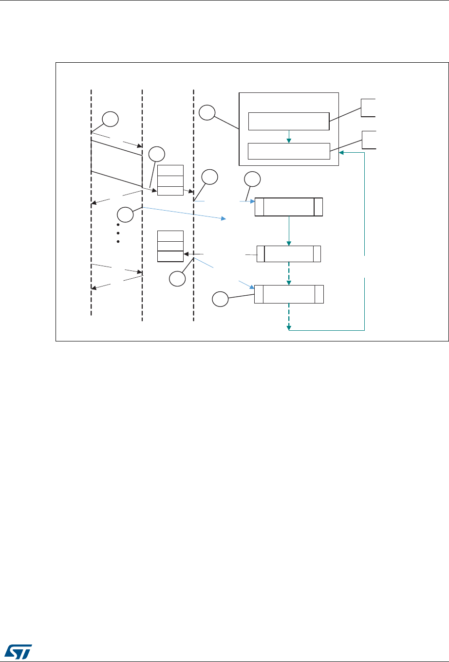
RM0090 Rev 18 1365/1749
RM0090 USB on-the-go full-speed (OTG_FS)
1380
Figure 404 depicts the reception of a single Bulk OUT Data packet from the USB to the AHB
and describes the events involved in the process.
Figure 404. Bulk OUT transaction
After a SetConfiguration/SetInterface command, the application initializes all OUT endpoints
by setting CNAK = 1 and EPENA = 1 (in OTG_FS_DOEPCTLx), and setting a suitable
XFRSIZ and PKTCNT in the OTG_FS_DOEPTSIZx register.
1. host attempts to send data (OUT token) to an endpoint.
2. When the core receives the OUT token on the USB, it stores the packet in the RxFIFO
because space is available there.
3. After writing the complete packet in the RxFIFO, the core then asserts the RXFLVL
interrupt (in OTG_FS_GINTSTS).
4. On receiving the PKTCNT number of USB packets, the core internally sets the NAK bit
for this endpoint to prevent it from receiving any more packets.
5. The application processes the interrupt and reads the data from the RxFIFO.
6. When the application has read all the data (equivalent to XFRSIZ), the core generates
an XFRC interrupt (in OTG_FS_DOEPINTx).
7. The application processes the interrupt and uses the setting of the XFRC interrupt bit
(in OTG_FS_DOEPINTx) to determine that the intended transfer is complete.
IN data transfers
•Packet write
This section describes how the application writes data packets to the endpoint FIFO when
dedicated transmit FIFOs are enabled.
1. The application can either choose the polling or the interrupt mode.
init_out_ep
Host DeviceUSB
OUT
ACK
RXFLVL intr i
wr_reg (DOEPTSIZx)
wr_reg(DOEPCTLx)
64 bytes
OUT
NAK
xact _1
Application
XFRC
intr
DOEPCTLx.NAK=1
PKTCNT 0
XFRSIZ = 0
r
idle until intr
rcv_out _pkt()
idle until intr
On new xfer
or RxFIFO
not empty
1
2
3
4
5
6
7
8
XFRSIZ = 64 bytes
PKTCNT = 1
EPENA = 1
CNAK = 1
ai15679b

USB on-the-go full-speed (OTG_FS) RM0090
1366/1749 RM0090 Rev 18
– In polling mode, the application monitors the status of the endpoint transmit data
FIFO by reading the OTG_FS_DTXFSTSx register, to determine if there is enough
space in the data FIFO.
– In interrupt mode, the application waits for the TXFE interrupt (in
OTG_FS_DIEPINTx) and then reads the OTG_FS_DTXFSTSx register, to
determine if there is enough space in the data FIFO.
– To write a single non-zero length data packet, there must be space to write the
entire packet in the data FIFO.
– To write zero length packet, the application must not look at the FIFO space.
2. Using one of the above mentioned methods, when the application determines that
there is enough space to write a transmit packet, the application must first write into the
endpoint control register, before writing the data into the data FIFO. Typically, the
application, must do a read modify write on the OTG_FS_DIEPCTLx register to avoid
modifying the contents of the register, except for setting the Endpoint Enable bit.
The application can write multiple packets for the same endpoint into the transmit FIFO, if
space is available. For periodic IN endpoints, the application must write packets only for one
microframe. It can write packets for the next periodic transaction only after getting transfer
complete for the previous transaction.
•Setting IN endpoint NAK
Internal data flow
1. When the application sets the IN NAK for a particular endpoint, the core stops
transmitting data on the endpoint, irrespective of data availability in the endpoint’s
transmit FIFO.
2. Non-isochronous IN tokens receive a NAK handshake reply
– Isochronous IN tokens receive a zero-data-length packet reply
3. The core asserts the INEPNE (IN endpoint NAK effective) interrupt in
OTG_FS_DIEPINTx in response to the SNAK bit in OTG_FS_DIEPCTLx.
4. Once this interrupt is seen by the application, the application can assume that the
endpoint is in IN NAK mode. This interrupt can be cleared by the application by setting
the CNAK bit in OTG_FS_DIEPCTLx.
Application programming sequence
1. To stop transmitting any data on a particular IN endpoint, the application must set the
IN NAK bit. To set this bit, the following field must be programmed.
– SNAK = 1 in OTG_FS_DIEPCTLx
2. Wait for assertion of the INEPNE interrupt in OTG_FS_DIEPINTx. This interrupt
indicates that the core has stopped transmitting data on the endpoint.
3. The core can transmit valid IN data on the endpoint after the application has set the
NAK bit, but before the assertion of the NAK Effective interrupt.
4. The application can mask this interrupt temporarily by writing to the INEPNEM bit in
DIEPMSK.
– INEPNEM = 0 in DIEPMSK
5. To exit Endpoint NAK mode, the application must clear the NAK status bit (NAKSTS) in
OTG_FS_DIEPCTLx. This also clears the INEPNE interrupt (in OTG_FS_DIEPINTx).
– CNAK = 1 in OTG_FS_DIEPCTLx
6. If the application masked this interrupt earlier, it must be unmasked as follows:

RM0090 Rev 18 1367/1749
RM0090 USB on-the-go full-speed (OTG_FS)
1380
– INEPNEM = 1 in DIEPMSK
•IN endpoint disable
Use the following sequence to disable a specific IN endpoint that has been previously
enabled.
Application programming sequence
1. The application must stop writing data on the AHB for the IN endpoint to be disabled.
2. The application must set the endpoint in NAK mode.
– SNAK = 1 in OTG_FS_DIEPCTLx
3. Wait for the INEPNE interrupt in OTG_FS_DIEPINTx.
4. Set the following bits in the OTG_FS_DIEPCTLx register for the endpoint that must be
disabled.
– EPDIS = 1 in OTG_FS_DIEPCTLx
– SNAK = 1 in OTG_FS_DIEPCTLx
5. Assertion of the EPDISD interrupt in OTG_FS_DIEPINTx indicates that the core has
completely disabled the specified endpoint. Along with the assertion of the interrupt, the
core also clears the following bits:
– EPENA = 0 in OTG_FS_DIEPCTLx
– EPDIS = 0 in OTG_FS_DIEPCTLx
6. The application must read the OTG_FS_DIEPTSIZx register for the periodic IN EP, to
calculate how much data on the endpoint were transmitted on the USB.
7. The application must flush the data in the Endpoint transmit FIFO, by setting the
following fields in the OTG_FS_GRSTCTL register:
– TXFNUM (in OTG_FS_GRSTCTL) = Endpoint transmit FIFO number
– TXFFLSH in (OTG_FS_GRSTCTL) = 1
The application must poll the OTG_FS_GRSTCTL register, until the TXFFLSH bit is cleared
by the core, which indicates the end of flush operation. To transmit new data on this
endpoint, the application can re-enable the endpoint at a later point.
•Transfer Stop Programming for IN endpoints
The application must use the following programing sequence to stop any transfers (because
of an interrupt from the host, typically a reset).
Sequence of operations:

USB on-the-go full-speed (OTG_FS) RM0090
1368/1749 RM0090 Rev 18
1. Disable the IN endpoint by setting:
– EPDIS = 1 in all OTG_FS_DIEPCTLx registers
2. Wait for the EPDIS interrupt in OTG_FS_DIEPINTx, which indicates that the IN
endpoint is completely disabled. When the EPDIS interrupt is asserted the following
bits are cleared:
– EPDIS = 0 in OTG_FS_DIEPCTLx
– EPENA = 0 in OTG_FS_DIEPCTLx
3. Flush the TxFIFO by programming the following bits:
– TXFFLSH = 1 in OTG_FS_GRSTCTL
– TXFNUM = “FIFO number specific to endpoint” in OTG_FS_GRSTCTL
4. The application can start polling till TXFFLSH in OTG_FS_GRSTCTL is cleared. When
this bit is cleared, it ensures that there is no data left in the Tx FIFO.
•Generic non-periodic IN data transfers
Application requirements
1. Before setting up an IN transfer, the application must ensure that all data to be
transmitted as part of the IN transfer are part of a single buffer.
2. For IN transfers, the Transfer Size field in the Endpoint Transfer Size register denotes a
payload that constitutes multiple maximum-packet-size packets and a single short
packet. This short packet is transmitted at the end of the transfer.
– To transmit a few maximum-packet-size packets and a short packet at the end of
the transfer:
Transfer size[EPNUM] = x × MPSIZ[EPNUM] + sp
If (sp > 0), then packet count[EPNUM] = x + 1.
Otherwise, packet count[EPNUM] = x
– To transmit a single zero-length data packet:
Transfer size[EPNUM] = 0
Packet count[EPNUM] = 1
– To transmit a few maximum-packet-size packets and a zero-length data packet at
the end of the transfer, the application must split the transfer into two parts. The
first sends maximum-packet-size data packets and the second sends the zero-
length data packet alone.
First transfer: transfer size[EPNUM] = x × MPSIZ[epnum]; packet count = n;
Second transfer: transfer size[EPNUM] = 0; packet count = 1;
3. Once an endpoint is enabled for data transfers, the core updates the Transfer size
register. At the end of the IN transfer, the application must read the Transfer size
register to determine how much data posted in the transmit FIFO have already been
sent on the USB.
4. Data fetched into transmit FIFO = Application-programmed initial transfer size – core-
updated final transfer size
– Data transmitted on USB = (application-programmed initial packet count – Core
updated final packet count) × MPSIZ[EPNUM]
– Data yet to be transmitted on USB = (Application-programmed initial transfer size
– data transmitted on USB)
Internal data flow

RM0090 Rev 18 1369/1749
RM0090 USB on-the-go full-speed (OTG_FS)
1380
1. The application must set the transfer size and packet count fields in the endpoint-
specific registers and enable the endpoint to transmit the data.
2. The application must also write the required data to the transmit FIFO for the endpoint.
3. Every time a packet is written into the transmit FIFO by the application, the transfer size
for that endpoint is decremented by the packet size. The data is fetched from the
memory by the application, until the transfer size for the endpoint becomes 0. After
writing the data into the FIFO, the “number of packets in FIFO” count is incremented
(this is a 3-bit count, internally maintained by the core for each IN endpoint transmit
FIFO. The maximum number of packets maintained by the core at any time in an IN
endpoint FIFO is eight). For zero-length packets, a separate flag is set for each FIFO,
without any data in the FIFO.
4. Once the data are written to the transmit FIFO, the core reads them out upon receiving
an IN token. For every non-isochronous IN data packet transmitted with an ACK
handshake, the packet count for the endpoint is decremented by one, until the packet
count is zero. The packet count is not decremented on a timeout.
5. For zero length packets (indicated by an internal zero length flag), the core sends out a
zero-length packet for the IN token and decrements the packet count field.
6. If there are no data in the FIFO for a received IN token and the packet count field for
that endpoint is zero, the core generates an “IN token received when TxFIFO is empty”
(ITTXFE) Interrupt for the endpoint, provided that the endpoint NAK bit is not set. The
core responds with a NAK handshake for non-isochronous endpoints on the USB.
7. The core internally rewinds the FIFO pointers and no timeout interrupt is generated.
8. When the transfer size is 0 and the packet count is 0, the transfer complete (XFRC)
interrupt for the endpoint is generated and the endpoint enable is cleared.
Application programming sequence
1. Program the OTG_FS_DIEPTSIZx register with the transfer size and corresponding
packet count.
2. Program the OTG_FS_DIEPCTLx register with the endpoint characteristics and set the
CNAK and EPENA (Endpoint Enable) bits.
3. When transmitting non-zero length data packet, the application must poll the
OTG_FS_DTXFSTSx register (where x is the FIFO number associated with that
endpoint) to determine whether there is enough space in the data FIFO. The
application can optionally use TXFE (in OTG_FS_DIEPINTx) before writing the data.
•Generic periodic IN data transfers
This section describes a typical periodic IN data transfer.
Application requirements
1. Application requirements 1, 2, 3, and 4 of Generic non-periodic IN data transfers also
apply to periodic IN data transfers, except for a slight modification of requirement 2.
– The application can only transmit multiples of maximum-packet-size data packets
or multiples of maximum-packet-size packets, plus a short packet at the end. To
transmit a few maximum-packet-size packets and a short packet at the end of the
transfer, the following conditions must be met:
transfer size[EPNUM] = x × MPSIZ[EPNUM] + sp
(where x is an integer ≥ 0, and 0 ≤ sp < MPSIZ[EPNUM])
If (sp > 0), packet count[EPNUM] = x + 1
Otherwise, packet count[EPNUM] = x;
MCNT[EPNUM] = packet count[EPNUM]

USB on-the-go full-speed (OTG_FS) RM0090
1370/1749 RM0090 Rev 18
– The application cannot transmit a zero-length data packet at the end of a transfer.
It can transmit a single zero-length data packet by itself. To transmit a single zero-
length data packet:
– transfer size[EPNUM] = 0
packet count[EPNUM] = 1
MCNT[EPNUM] = packet count[EPNUM]
2. The application can only schedule data transfers one frame at a time.
– (MCNT – 1) × MPSIZ ≤XFERSIZ ≤MCNT × MPSIZ
– PKTCNT = MCNT (in OTG_FS_DIEPTSIZx)
– If XFERSIZ < MCNT × MPSIZ, the last data packet of the transfer is a short
packet.
– Note that: MCNT is in OTG_FS_DIEPTSIZx, MPSIZ is in OTG_FS_DIEPCTLx,
PKTCNT is in OTG_FS_DIEPTSIZx and XFERSIZ is in OTG_FS_DIEPTSIZx
3. The complete data to be transmitted in the frame must be written into the transmit FIFO
by the application, before the IN token is received. Even when 1 word of the data to be
transmitted per frame is missing in the transmit FIFO when the IN token is received, the
core behaves as when the FIFO is empty. When the transmit FIFO is empty:
– A zero data length packet would be transmitted on the USB for isochronous IN
endpoints
– A NAK handshake would be transmitted on the USB for interrupt IN endpoints
Internal data flow
1. The application must set the transfer size and packet count fields in the endpoint-
specific registers and enable the endpoint to transmit the data.
2. The application must also write the required data to the associated transmit FIFO for
the endpoint.
3. Every time the application writes a packet to the transmit FIFO, the transfer size for that
endpoint is decremented by the packet size. The data are fetched from application
memory until the transfer size for the endpoint becomes 0.
4. When an IN token is received for a periodic endpoint, the core transmits the data in the
FIFO, if available. If the complete data payload (complete packet, in dedicated FIFO
mode) for the frame is not present in the FIFO, then the core generates an IN token
received when TxFIFO empty interrupt for the endpoint.
– A zero-length data packet is transmitted on the USB for isochronous IN endpoints
– A NAK handshake is transmitted on the USB for interrupt IN endpoints
5. The packet count for the endpoint is decremented by 1 under the following conditions:
– For isochronous endpoints, when a zero- or non-zero-length data packet is
transmitted
– For interrupt endpoints, when an ACK handshake is transmitted
– When the transfer size and packet count are both 0, the transfer completed
interrupt for the endpoint is generated and the endpoint enable is cleared.
6. At the “Periodic frame Interval” (controlled by PFIVL in OTG_FS_DCFG), when the
core finds non-empty any of the isochronous IN endpoint FIFOs scheduled for the
current frame non-empty, the core generates an IISOIXFR interrupt in
OTG_FS_GINTSTS.
Application programming sequence

RM0090 Rev 18 1371/1749
RM0090 USB on-the-go full-speed (OTG_FS)
1380
1. Program the OTG_FS_DIEPCTLx register with the endpoint characteristics and set the
CNAK and EPENA bits.
2. Write the data to be transmitted in the next frame to the transmit FIFO.
3. Asserting the ITTXFE interrupt (in OTG_FS_DIEPINTx) indicates that the application
has not yet written all data to be transmitted to the transmit FIFO.
4. If the interrupt endpoint is already enabled when this interrupt is detected, ignore the
interrupt. If it is not enabled, enable the endpoint so that the data can be transmitted on
the next IN token attempt.
5. Asserting the XFRC interrupt (in OTG_FS_DIEPINTx) with no ITTXFE interrupt in
OTG_FS_DIEPINTx indicates the successful completion of an isochronous IN transfer.
A read to the OTG_FS_DIEPTSIZx register must give transfer size = 0 and packet
count = 0, indicating all data were transmitted on the USB.
6. Asserting the XFRC interrupt (in OTG_FS_DIEPINTx), with or without the ITTXFE
interrupt (in OTG_FS_DIEPINTx), indicates the successful completion of an interrupt
IN transfer. A read to the OTG_FS_DIEPTSIZx register must give transfer size = 0 and
packet count = 0, indicating all data were transmitted on the USB.
7. Asserting the incomplete isochronous IN transfer (IISOIXFR) interrupt in
OTG_FS_GINTSTS with none of the aforementioned interrupts indicates the core did
not receive at least 1 periodic IN token in the current frame.
•Incomplete isochronous IN data transfers
This section describes what the application must do on an incomplete isochronous IN data
transfer.
Internal data flow
1. An isochronous IN transfer is treated as incomplete in one of the following conditions:
a) The core receives a corrupted isochronous IN token on at least one isochronous
IN endpoint. In this case, the application detects an incomplete isochronous IN
transfer interrupt (IISOIXFR in OTG_FS_GINTSTS).
b) The application is slow to write the complete data payload to the transmit FIFO
and an IN token is received before the complete data payload is written to the
FIFO. In this case, the application detects an IN token received when TxFIFO
empty interrupt in OTG_FS_DIEPINTx. The application can ignore this interrupt,
as it eventually results in an incomplete isochronous IN transfer interrupt
(IISOIXFR in OTG_FS_GINTSTS) at the end of periodic frame.
The core transmits a zero-length data packet on the USB in response to the
received IN token.
2. The application must stop writing the data payload to the transmit FIFO as soon as
possible.
3. The application must set the NAK bit and the disable bit for the endpoint.
4. The core disables the endpoint, clears the disable bit, and asserts the Endpoint Disable
interrupt for the endpoint.
Application programming sequence
1. The application can ignore the IN token received when TxFIFO empty interrupt in
OTG_FS_DIEPINTx on any isochronous IN endpoint, as it eventually results in an
incomplete isochronous IN transfer interrupt (in OTG_FS_GINTSTS).
2. Assertion of the incomplete isochronous IN transfer interrupt (in OTG_FS_GINTSTS)
indicates an incomplete isochronous IN transfer on at least one of the isochronous IN
endpoints.

USB on-the-go full-speed (OTG_FS) RM0090
1372/1749 RM0090 Rev 18
3. The application must read the Endpoint Control register for all isochronous IN
endpoints to detect endpoints with incomplete IN data transfers.
4. The application must stop writing data to the Periodic Transmit FIFOs associated with
these endpoints on the AHB.
5. Program the following fields in the OTG_FS_DIEPCTLx register to disable the
endpoint:
– SNAK = 1 in OTG_FS_DIEPCTLx
– EPDIS = 1 in OTG_FS_DIEPCTLx
6. The assertion of the Endpoint Disabled interrupt in OTG_FS_DIEPINTx indicates that
the core has disabled the endpoint.
– At this point, the application must flush the data in the associated transmit FIFO or
overwrite the existing data in the FIFO by enabling the endpoint for a new transfer
in the next microframe. To flush the data, the application must use the
OTG_FS_GRSTCTL register.
•Stalling non-isochronous IN endpoints
This section describes how the application can stall a non-isochronous endpoint.
Application programming sequence
1. Disable the IN endpoint to be stalled. Set the STALL bit as well.
2. EPDIS = 1 in OTG_FS_DIEPCTLx, when the endpoint is already enabled
– STALL = 1 in OTG_FS_DIEPCTLx
– The STALL bit always takes precedence over the NAK bit
3. Assertion of the Endpoint Disabled interrupt (in OTG_FS_DIEPINTx) indicates to the
application that the core has disabled the specified endpoint.
4. The application must flush the non-periodic or periodic transmit FIFO, depending on
the endpoint type. In case of a non-periodic endpoint, the application must re-enable
the other non-periodic endpoints that do not need to be stalled, to transmit data.
5. Whenever the application is ready to end the STALL handshake for the endpoint, the
STALL bit must be cleared in OTG_FS_DIEPCTLx.
6. If the application sets or clears a STALL bit for an endpoint due to a
SetFeature.Endpoint Halt command or ClearFeature.Endpoint Halt command, the
STALL bit must be set or cleared before the application sets up the Status stage
transfer on the control endpoint.
Special case: stalling the control OUT endpoint
The core must stall IN/OUT tokens if, during the data stage of a control transfer, the host
sends more IN/OUT tokens than are specified in the SETUP packet. In this case, the
application must enable the ITTXFE interrupt in OTG_FS_DIEPINTx and the OTEPDIS
interrupt in OTG_FS_DOEPINTx during the data stage of the control transfer, after the core
has transferred the amount of data specified in the SETUP packet. Then, when the
application receives this interrupt, it must set the STALL bit in the corresponding endpoint
control register, and clear this interrupt.
34.17.7 Worst case response time
When the OTG_FS controller acts as a device, there is a worst case response time for any
tokens that follow an isochronous OUT. This worst case response time depends on the AHB
clock frequency.

RM0090 Rev 18 1373/1749
RM0090 USB on-the-go full-speed (OTG_FS)
1380
The core registers are in the AHB domain, and the core does not accept another token
before updating these register values. The worst case is for any token following an
isochronous OUT, because for an isochronous transaction, there is no handshake and the
next token could come sooner. This worst case value is 7 PHY clocks when the AHB clock
is the same as the PHY clock. When the AHB clock is faster, this value is smaller.
If this worst case condition occurs, the core responds to bulk/interrupt tokens with a NAK
and drops isochronous and SETUP tokens. The host interprets this as a timeout condition
for SETUP and retries the SETUP packet. For isochronous transfers, the Incomplete
isochronous IN transfer interrupt (IISOIXFR) and Incomplete isochronous OUT transfer
interrupt (IISOOXFR) inform the application that isochronous IN/OUT packets were
dropped.
Choosing the value of TRDT in OTG_FS_GUSBCFG
The value in TRDT (OTG_FS_GUSBCFG) is the time it takes for the MAC, in terms of PHY
clocks after it has received an IN token, to get the FIFO status, and thus the first data from
the PFC block. This time involves the synchronization delay between the PHY and AHB
clocks. The worst case delay for this is when the AHB clock is the same as the PHY clock.
In this case, the delay is 5 clocks.
Once the MAC receives an IN token, this information (token received) is synchronized to the
AHB clock by the PFC (the PFC runs on the AHB clock). The PFC then reads the data from
the SPRAM and writes them into the dual clock source buffer. The MAC then reads the data
out of the source buffer (4 deep).
If the AHB is running at a higher frequency than the PHY, the application can use a smaller
value for TRDT (in OTG_FS_GUSBCFG).
Figure 405 has the following signals:
•tkn_rcvd: Token received information from MAC to PFC
•dynced_tkn_rcvd: Doubled sync tkn_rcvd, from PCLK to HCLK domain
•spr_read: Read to SPRAM
•spr_addr: Address to SPRAM
•spr_rdata: Read data from SPRAM
•srcbuf_push: Push to the source buffer
•srcbuf_rdata: Read data from the source buffer. Data seen by MAC
Refer to Table 203: TRDT values for the values of TRDT versus AHB clock frequency.
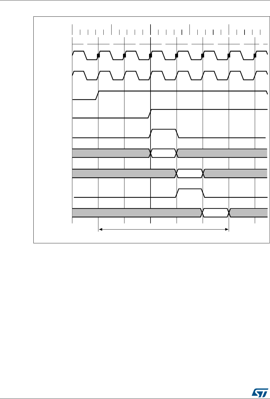
USB on-the-go full-speed (OTG_FS) RM0090
1374/1749 RM0090 Rev 18
Figure 405. TRDT max timing case
34.17.8 OTG programming model
The OTG_FS controller is an OTG device supporting HNP and SRP. When the core is
connected to an “A” plug, it is referred to as an A-device. When the core is connected to a
“B” plug it is referred to as a B-device. In host mode, the OTG_FS controller turns off VBUS
to conserve power. SRP is a method by which the B-device signals the A-device to turn on
VBUS power. A device must perform both data-line pulsing and VBUS pulsing, but a host can
detect either data-line pulsing or VBUS pulsing for SRP. HNP is a method by which the B-
device negotiates and switches to host role. In Negotiated mode after HNP, the B-device
suspends the bus and reverts to the device role.
12345678
0ns 50ns 100ns 150ns 200ns
HCLK
PCLK
tkn_rcvd
dsynced_tkn_rcvd
spr_read
spr_addr
spr_rdata
srcbuf_push
srcbuf_rdata
5 Clocks
D1
A1
D1
ai15680

RM0090 Rev 18 1375/1749
RM0090 USB on-the-go full-speed (OTG_FS)
1380
A-device session request protocol
The application must set the SRP-capable bit in the Core USB configuration register. This
enables the OTG_FS controller to detect SRP as an A-device.
Figure 406. A-device SRP
1. DRV_VBUS = VBUS drive signal to the PHY
VBUS_VALID = VBUS valid signal from PHY
A_VALID = A-peripheral VBUS level signal to PHY
D+ = Data plus line
D- = Data minus line
1. To save power, the application suspends and turns off port power when the bus is idle
by writing the port suspend and port power bits in the host port control and status
register.
2. PHY indicates port power off by deasserting the VBUS_VALID signal.
3. The device must detect SE0 for at least 2 ms to start SRP when VBUS power is off.
4. To initiate SRP, the device turns on its data line pull-up resistor for 5 to 10 ms. The
OTG_FS controller detects data-line pulsing.
5. The device drives VBUS above the A-device session valid (2.0 V minimum) for VBUS
pulsing.
The OTG_FS controller interrupts the application on detecting SRP. The Session
request detected bit is set in Global interrupt status register (SRQINT set in
OTG_FS_GINTSTS).
6. The application must service the Session request detected interrupt and turn on the
port power bit by writing the port power bit in the host port control and status register.
The PHY indicates port power-on by asserting the VBUS_VALID signal.
7. When the USB is powered, the device connects, completing the SRP process.
ai15681
DRV_VBUS
VBUS_VALID
A_VALID
D+
D-
Suspend
VBUS pulsing
Data line pulsing Connect
1
6
25
3
47
Low
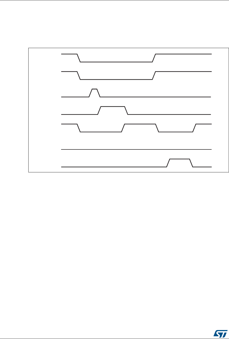
USB on-the-go full-speed (OTG_FS) RM0090
1376/1749 RM0090 Rev 18
B-device session request protocol
The application must set the SRP-capable bit in the Core USB configuration register. This
enables the OTG_FS controller to initiate SRP as a B-device. SRP is a means by which the
OTG_FS controller can request a new session from the host.
Figure 407. B-device SRP
1. VBUS_VALID = VBUS valid signal from PHY
B_VALID = B-peripheral valid session to PHY
DISCHRG_VBUS = discharge signal to PHY
SESS_END = session end signal to PHY
CHRG_VBUS = charge VBUS signal to PHY
DP = Data plus line
DM = Data minus line
1. To save power, the host suspends and turns off port power when the bus is idle.
The OTG_FS controller sets the early suspend bit in the Core interrupt register after 3
ms of bus idleness. Following this, the OTG_FS controller sets the USB suspend bit in
the Core interrupt register.
The OTG_FS controller informs the PHY to discharge VBUS.
2. The PHY indicates the session’s end to the device. This is the initial condition for SRP.
The OTG_FS controller requires 2 ms of SE0 before initiating SRP.
For a USB 1.1 full-speed serial transceiver, the application must wait until VBUS
discharges to 0.2 V after BSVLD (in OTG_FS_GOTGCTL) is deasserted. This
discharge time can be obtained from the transceiver vendor and varies from one
transceiver to another.
3. The USB OTG core informs the PHY to speed up VBUS discharge.
4. The application initiates SRP by writing the session request bit in the OTG Control and
status register. The OTG_FS controller perform data-line pulsing followed by VBUS
pulsing.
5. The host detects SRP from either the data-line or VBUS pulsing, and turns on VBUS.
The PHY indicates VBUS power-on to the device.
ai15682
VBUS_VALID
B_VALID
DISCHRG_VBUS
SESS_END
DP
DM
CHRG_VBUS
Suspend
Data line pulsing Connect
VBUS pulsing
1
6
2
3
4
58
7
Low
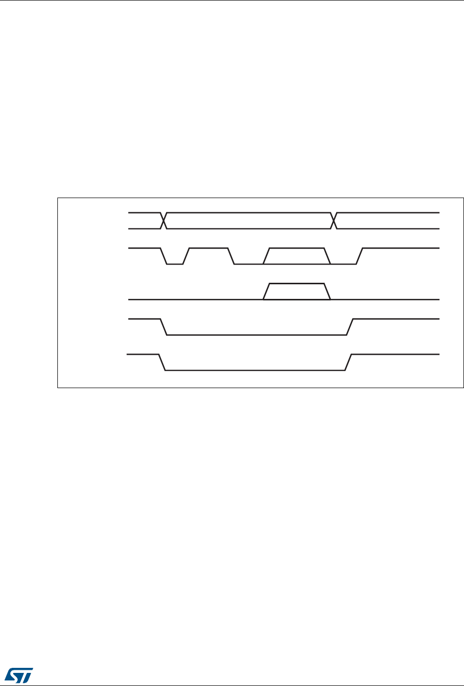
RM0090 Rev 18 1377/1749
RM0090 USB on-the-go full-speed (OTG_FS)
1380
6. The OTG_FS controller performs VBUS pulsing.
The host starts a new session by turning on VBUS, indicating SRP success. The
OTG_FS controller interrupts the application by setting the session request success
status change bit in the OTG interrupt status register. The application reads the session
request success bit in the OTG control and status register.
7. When the USB is powered, the OTG_FS controller connects, completing the SRP
process.
A-device host negotiation protocol
HNP switches the USB host role from the A-device to the B-device. The application must set
the HNP-capable bit in the Core USB configuration register to enable the OTG_FS
controller to perform HNP as an A-device.
Figure 408. A-device HNP
1. DPPULLDOWN = signal from core to PHY to enable/disable the pull-down on the DP line inside the PHY.
DMPULLDOWN = signal from core to PHY to enable/disable the pull-down on the DM line inside the PHY.
1. The OTG_FS controller sends the B-device a SetFeature b_hnp_enable descriptor to
enable HNP support. The B-device’s ACK response indicates that the B-device
supports HNP. The application must set host Set HNP Enable bit in the OTG Control
ai15683
OTG core
DP
DM
DPPULLDOWN
DMPULLDOWN
Host Device Host
1
Suspend 2
3
45
Reset
6
Traffic 7
8
Connect
Traffic

USB on-the-go full-speed (OTG_FS) RM0090
1378/1749 RM0090 Rev 18
and status register to indicate to the OTG_FS controller that the B-device supports
HNP.
2. When it has finished using the bus, the application suspends by writing the Port
suspend bit in the host port control and status register.
3. When the B-device observes a USB suspend, it disconnects, indicating the initial
condition for HNP. The B-device initiates HNP only when it must switch to the host role;
otherwise, the bus continues to be suspended.
The OTG_FS controller sets the host negotiation detected interrupt in the OTG
interrupt status register, indicating the start of HNP.
The OTG_FS controller deasserts the DM pull down and DM pull down in the PHY to
indicate a device role. The PHY enables the OTG_FS_DP pull-up resistor to indicate a
connect for B-device.
The application must read the current mode bit in the OTG Control and status register
to determine device mode operation.
4. The B-device detects the connection, issues a USB reset, and enumerates the
OTG_FS controller for data traffic.
5. The B-device continues the host role, initiating traffic, and suspends the bus when
done.
The OTG_FS controller sets the early suspend bit in the Core interrupt register after 3
ms of bus idleness. Following this, the OTG_FS controller sets the USB Suspend bit in
the Core interrupt register.
6. In Negotiated mode, the OTG_FS controller detects the suspend, disconnects, and
switches back to the host role. The OTG_FS controller asserts the DM pull down and
DM pull down in the PHY to indicate its assumption of the host role.
7. The OTG_FS controller sets the Connector ID status change interrupt in the OTG
Interrupt Status register. The application must read the connector ID status in the OTG
Control and Status register to determine the OTG_FS controller operation as an A-
device. This indicates the completion of HNP to the application. The application must
read the Current mode bit in the OTG control and status register to determine host
mode operation.
8. The B-device connects, completing the HNP process.
RM0090 Rev 18 1379/1749
RM0090 USB on-the-go full-speed (OTG_FS)
1380
B-device host negotiation protocol
HNP switches the USB host role from B-device to A-device. The application must set the
HNP-capable bit in the Core USB configuration register to enable the OTG_FS controller to
perform HNP as a B-device.
Figure 409. B-device HNP
1. DPPULLDOWN = signal from core to PHY to enable/disable the pull-down on the DP line inside the PHY.
DMPULLDOWN = signal from core to PHY to enable/disable the pull-down on the DM line inside the PHY.
1. The A-device sends the SetFeature b_hnp_enable descriptor to enable HNP support.
The OTG_FS controller’s ACK response indicates that it supports HNP. The application
must set the device HNP enable bit in the OTG Control and status register to indicate
HNP support.
The application sets the HNP request bit in the OTG Control and status register to
indicate to the OTG_FS controller to initiate HNP.
2. When it has finished using the bus, the A-device suspends by writing the Port suspend
bit in the host port control and status register.
The OTG_FS controller sets the Early suspend bit in the Core interrupt register after 3
ms of bus idleness. Following this, the OTG_FS controller sets the USB suspend bit in
the Core interrupt register.
The OTG_FS controller disconnects and the A-device detects SE0 on the bus,
indicating HNP. The OTG_FS controller asserts the DP pull down and DM pull down in
the PHY to indicate its assumption of the host role.
The A-device responds by activating its OTG_FS_DP pull-up resistor within 3 ms of
detecting SE0. The OTG_FS controller detects this as a connect.
The OTG_FS controller sets the host negotiation success status change interrupt in the
OTG Interrupt status register, indicating the HNP status. The application must read the
host negotiation success bit in the OTG Control and status register to determine host
negotiation success. The application must read the current Mode bit in the Core
interrupt register (OTG_FS_GINTSTS) to determine host mode operation.
3. The application sets the reset bit (PRST in OTG_FS_HPRT) and the OTG_FS
controller issues a USB reset and enumerates the A-device for data traffic.
ai15684
OTG core
DP
DM
DPPULLDOWN
DMPULLDOWN
HostDevice Device
1
Suspend 2
3
45
Reset
6
Traffic 7
8
Connect
Traffic

USB on-the-go full-speed (OTG_FS) RM0090
1380/1749 RM0090 Rev 18
4. The OTG_FS controller continues the host role of initiating traffic, and when done,
suspends the bus by writing the Port suspend bit in the host port control and status
register.
5. In Negotiated mode, when the A-device detects a suspend, it disconnects and switches
back to the host role. The OTG_FS controller deasserts the DP pull down and DM pull
down in the PHY to indicate the assumption of the device role.
6. The application must read the current mode bit in the Core interrupt
(OTG_FS_GINTSTS) register to determine the host mode operation.
7. The OTG_FS controller connects, completing the HNP process.

RM0090 Rev 18 1381/1749
RM0090 USB on-the-go high-speed (OTG_HS)
1543
35 USB on-the-go high-speed (OTG_HS)
This section applies to the whole STM32F4xx family, unless otherwise specified.
35.1 OTG_HS introduction
Portions Copyright (c) 2004, 2005 Synopsys, Inc. All rights reserved. Used with permission.
This section presents the architecture and the programming model of the OTG_HS
controller.
The following acronyms are used throughout the section:
References are made to the following documents:
•USB On-The-Go Supplement, Revision 1.3
•Universal Serial Bus Revision 2.0 Specification
The OTG_HS is a dual-role device (DRD) controller that supports both peripheral and host
functions and is fully compliant with the On-The-Go Supplement to the USB 2.0
Specification. It can also be configured as a host-only or peripheral-only controller, fully
compliant with the USB 2.0 Specification. In host mode, the OTG_HS supports high-speed
(HS, 480 Mbits/s), full-speed (FS, 12 Mbits/s) and low-speed (LS, 1.5 Mbits/s) transfers
whereas in peripheral mode, it only supports high-speed (HS, 480Mbits/s) and full-speed
(FS, 12 Mbits/s) transfers. The OTG_HS supports both HNP and SRP. The only external
device required is a charge pump for VBUS in OTG mode.
35.2 OTG_HS main features
The main features can be divided into three categories: general, host-mode and peripheral-
mode features.
FS full-speed
HS High-speed
LS Low-speed
USB Universal serial bus
OTG On-the-go
PHY Physical layer
MAC Media access controller
PFC Packet FIFO controller
UTMI USB Transceiver Macrocell Interface
ULPI UTMI+ Low Pin Interface

USB on-the-go high-speed (OTG_HS) RM0090
1382/1749 RM0090 Rev 18
35.2.1 General features
The OTG_HS interface main features are the following:
•It is USB-IF certified in compliance with the Universal Serial Bus Revision 2.0
Specification
•It supports 3 PHY interfaces
– An on-chip full-speed PHY
– An ULPI interface for external high-speed PHY.
•It supports the host negotiation protocol (HNP) and the session request protocol (SRP)
•It allows the host to turn VBUS off to save power in OTG applications, with no need for
external components
•It allows to monitor VBUS levels using internal comparators
•It supports dynamic host-peripheral role switching
•It is software-configurable to operate as:
– An SRP-capable USB HS/FS peripheral (B-device)
– An SRP-capable USB HS/FS/low-speed host (A-device)
– An USB OTG FS dual-role device
•It supports HS/FS SOFs as well as low-speed (LS) keep-alive tokens with:
– SOF pulse PAD output capability
– SOF pulse internal connection to timer 2 (TIM2)
– Configurable framing period
– Configurable end-of-frame interrupt
•It embeds an internal DMA with shareholding support and software selectable AHB
burst type in DMA mode
•It has power saving features such as system clock stop during USB suspend, switching
off of the digital core internal clock domains, PHY and DFIFO power management
•It features a dedicated 4-Kbyte data RAM with advanced FIFO management:
– The memory partition can be configured into different FIFOs to allow flexible and
efficient use of RAM
– Each FIFO can contain multiple packets
– Memory allocation is performed dynamically
– The FIFO size can be configured to values that are not powers of 2 to allow the
use of contiguous memory locations
•It ensures a maximum USB bandwidth of up to one frame without application
intervention

RM0090 Rev 18 1383/1749
RM0090 USB on-the-go high-speed (OTG_HS)
1543
35.2.2 Host-mode features
The OTG_HS interface features in host mode are the following:
•It requires an external charge pump to generate VBUS
•It has up to 12 host channels (pipes), each channel being dynamically reconfigurable to
support any kind of USB transfer
•It features a built-in hardware scheduler holding:
– Up to 8 interrupt plus isochronous transfer requests in the periodic hardware
queue
– Up to 8 control plus bulk transfer requests in the nonperiodic hardware queue
•It manages a shared RX FIFO, a periodic TX FIFO, and a nonperiodic TX FIFO for
efficient usage of the USB data RAM
•It features dynamic trimming capability of SOF framing period in host mode.
35.2.3 Peripheral-mode features
The OTG_HS interface main features in peripheral mode are the following:
•It has 1 bidirectional control endpoint 0
•It has 5 IN endpoints (EP) configurable to support bulk, interrupt or isochronous
transfers
•It has 5 OUT endpoints configurable to support bulk, interrupt or isochronous transfers
•It manages a shared Rx FIFO and a Tx-OUT FIFO for efficient usage of the USB data
RAM
•It manages up to 6 dedicated Tx-IN FIFOs (one for each IN-configured EP) to reduce
the application load
•It features soft disconnect capability
35.3 OTG_HS functional description
Figure 410 shows the OTG_HS interface block diagram.
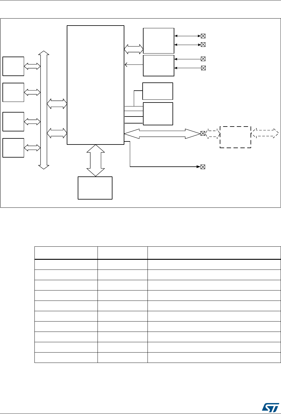
USB on-the-go high-speed (OTG_HS) RM0090
1384/1749 RM0090 Rev 18
Figure 410. USB OTG interface block diagram
1. The USB DMA cannot directly address the internal Flash memory.
35.3.1 OTG pins
35.3.2 High-speed OTG PHY
The USB OTG HS core embeds an ULPI interface to connect an external HS phy.
MSv43325V1
Data FIFO
Single-port RAM
(SPRAM)
AHB
master
interface
AHB
slave
interface
CPU
Memory
Peripheral 1
Peripheral 2
Data FIFO
RAM interface
AHB (application bus)
OTG_HS
(USB OTG HS core)
OTG_HS_DP
OTG_HS_DM
OTG_HS_ID
OTG_HS_VBUS
OTG FS PHY
transceiver
OTG_HS_SOF
ULPI interface (12 pins) ULPI PHY
(external
component)
USB2.0 (D+/D-)
ULPI_CK;
ULPI_DIR;
ULPI_STP;
ULPI_NXT;
ULPI_D0-7
NVIC
Interrupt: EP1 out
Interrupt: EP1 in
Interrupt: global
Interrupt: async wakeup
OTG detections
EXTIEXTI
serial
Table 206. OTG_HS input/output pins
Signal name Signal type Description
OTG_HS_DP Digital input/output USB OTG D+ line
OTG_HS_DM Digital input/output USB OTG D- line
OTG_HS_ID Digital input USB OTG ID
OTG_HS_VBUS Analog input USB OTG VBUS
OTG_HS_SOF Digital output USB OTG Start Of Frame (visibility)
OTG_HS_ULPI_CK Digital input USB OTG ULPI clock
OTG_HS_ULPI_DIR Digital input USB OTG ULPI data bus direction control
OTG_HS_ULPI_STP Digital output USB OTG ULPI data stream stop
OTG_HS_ULPI_NXT Digital input USB OTG ULPI next data stream request
OTG_HS_ULPI_D[0..7] Digital input/output USB OTG ULPI 8-bit bi-directional data bus

RM0090 Rev 18 1385/1749
RM0090 USB on-the-go high-speed (OTG_HS)
1543
35.3.3 Embedded Full-speed OTG PHY
The full-speed OTG PHY includes the following components:
•FS/LS transceiver module used by both host and Device. It directly drives transmission
and reception on the single-ended USB lines.
•Integrated ID pull-up resistor used to sample the ID line for A/B Device identification.
•DP/DM integrated pull-up and pull-down resistors controlled by the OTG_HS core
depending on the current role of the device. As a peripheral, it enables the DP pull-up
resistor to signal full-speed peripheral connections as soon as VBUS is sensed to be at
a valid level (B-session valid). In host mode, pull-down resistors are enabled on both
DP/DM. Pull-up and pull-down resistors are dynamically switched when the peripheral
role is changed via the host negotiation protocol (HNP).
•Pull-up/pull-down resistor ECN circuit
The DP pull-up consists of 2 resistors controlled separately from the OTG_HS as per
the resistor Engineering Change Notice applied to USB Rev2.0. The dynamic trimming
of the DP pull-up strength allows to achieve a better noise rejection and Tx/Rx signal
quality.
•VBUS sensing comparators with hysteresis used to detect VBUS_VALID, A-B Session
Valid and session-end voltage thresholds. They are used to drive the session request
protocol (SRP), detect valid startup and end-of-session conditions, and constantly
monitor the VBUS supply during USB operations.
•VBUS pulsing method circuit used to charge/discharge VBUS through resistors during
the SRP (weak drive).
Caution: To guarantee a correct operation for the USB OTG HS peripheral, the AHB frequency
should be higher than 30 MHz.
35.4 OTG dual-role device
35.4.1 ID line detection
The host or peripheral (the default) role depends on the level of the ID input line. It is
determined when the USB cable is plugged in and depends on which side of the USB cable
is connected to the micro-AB receptacle:
•If the B-side of the USB cable is connected with a floating ID wire, the integrated pull-
up resistor detects a high ID level and the default peripheral role is confirmed. In this
configuration the OTG_HS conforms to the FSM standard described in
section 6.8.2. On-The-Go B-device of the USB On-The-Go Supplement, Revision 1.3.
•If the A-side of the USB cable is connected with a grounded ID, the OTG_HS issues an
ID line status change interrupt (CIDSCHG bit in the OTG_HS_GINTSTS register) for
host software initialization, and automatically switches to host role. In this configuration
the OTG_HS conforms to the FSM standard described by section 6.8.1: On-The-Go A-
Device of the USB On-The-Go Supplement, Revision 1.3.
35.4.2 HNP dual role device
The HNP capable bit in the Global USB configuration register (HNPCAP bit in the
OTG_HS_ GUSBCFG register) configures the OTG_HS core to dynamically change from
A-host to A-device role and vice-versa, or from B-device to B-host role and vice-versa,
according to the host negotiation protocol (HNP). The current device status is defined by the

USB on-the-go high-speed (OTG_HS) RM0090
1386/1749 RM0090 Rev 18
combination of the Connector ID Status bit in the Global OTG control and status register
(CIDSTS bit in OTG_HS_GOTGCTL) and the current mode of operation bit in the global
interrupt and status register (CMOD bit in OTG_HS_GINTSTS).
The HNP programming model is described in detail in Section 35.13: OTG_HS
programming model.
35.4.3 SRP dual-role device
The SRP capable bit in the global USB configuration register (SRPCAP bit in
OTG_HS_GUSBCFG) configures the OTG_HS core to switch VBUS off for the A-device in
order to save power. The A-device is always in charge of driving VBUS regardless of the
OTG_HS role (host or peripheral). The SRP A/B-device program model is described in
detail in Section 35.13: OTG_HS programming model.
35.5 USB functional description in peripheral mode
The OTG_HS operates as an USB peripheral in the following circumstances:
•OTG B-device
OTG B-device default state if the B-side of USB cable is plugged in
•OTG A-device
OTG A-device state after the HNP switches the OTG_HS to peripheral role
•B-Device
If the ID line is present, functional and connected to the B-side of the USB cable, and
the HNP-capable bit in the Global USB Configuration register (HNPCAP bit in
OTG_HS_GUSBCFG) is cleared (see On-The-Go specification Revision 1.3 section
6.8.3).
•Peripheral only (see Figure 388: USB peripheral-only connection)
The force peripheral mode bit in the Global USB configuration register (FDMOD in
OTG_HS_GUSBCFG) is set to 1, forcing the OTG_HS core to operate in USB
peripheral-only mode (see On-The-Go specification Revision 1.3 section 6.8.3). In this
case, the ID line is ignored even if it is available on the USB connector.
Note: To build a bus-powered device architecture in the B-Device or peripheral-only configuration,
an external regulator must be added to generate the VDD supply voltage from VBUS.
35.5.1 SRP-capable peripheral
The SRP capable bit in the Global USB configuration register (SRPCAP bit in
OTG_HS_GUSBCFG) configures the OTG_HS to support the session request protocol
(SRP). As a result, it allows the remote A-device to save power by switching VBUS off when
the USB session is suspended.
The SRP peripheral mode program model is described in detail in Section : B-device
session request protocol.

RM0090 Rev 18 1387/1749
RM0090 USB on-the-go high-speed (OTG_HS)
1543
35.5.2 Peripheral states
Powered state
The VBUS input detects the B-session valid voltage used to put the USB peripheral in the
Powered state (see USB2.0 specification section 9.1). The OTG_HS then automatically
connects the DP pull-up resistor to signal full-speed device connection to the host, and
generates the session request interrupt (SRQINT bit in OTG_HS_GINTSTS) to notify the
Powered state. The VBUS input also ensures that valid VBUS levels are supplied by the host
during USB operations. If VBUS drops below the B-session valid voltage (for example
because power disturbances occurred or the host port has been switched off), the OTG_HS
automatically disconnects and the session end detected (SEDET bit in
OTG_HS_GOTGINT) interrupt is generated to notify that the OTG_HS has exited the
Powered state.
In Powered state, the OTG_HS expects a reset from the host. No other USB operations are
possible. When a reset is received, the reset detected interrupt (USBRST in
OTG_HS_GINTSTS) is generated. When the reset is complete, the enumeration done
interrupt (ENUMDNE bit in OTG_HS_GINTSTS) is generated and the OTG_HS enters the
Default state.
Soft disconnect
The Powered state can be exited by software by using the soft disconnect feature. The DP
pull-up resistor is removed by setting the Soft disconnect bit in the device control register
(SDIS bit in OTG_HS_DCTL), thus generating a device disconnect detection interrupt on
the host side even though the USB cable was not really unplugged from the host port.
Default state
In Default state the OTG_HS expects to receive a SET_ADDRESS command from the host.
No other USB operations are possible. When a valid SET_ADDRESS command is decoded
on the USB, the application writes the corresponding number into the device address field in
the device configuration register (DAD bit in OTG_HS_DCFG). The OTG_HS then enters
the address state and is ready to answer host transactions at the configured USB address.
Suspended state
The OTG_HS peripheral constantly monitors the USB activity. When the USB remains idle
for 3 ms, the early suspend interrupt (ESUSP bit in OTG_HS_GINTSTS) is issued. It is
confirmed 3 ms later, if appropriate, by generating a suspend interrupt (USBSUSP bit in
OTG_HS_GINTSTS). The device suspend bit is then automatically set in the device status
register (SUSPSTS bit in OTG_HS_DSTS) and the OTG_HS enters the Suspended state.
The device can also exit from the Suspended state by itself. In this case the application sets
the remote wakeup signaling bit in the device control register (RWUSIG bit in
OTG_HS_DCTL) and clears it after 1 to 15 ms.
When a resume signaling is detected from the host, the resume interrupt (WKUPINT bit in
OTG_HS_GINTSTS) is generated and the device suspend bit is automatically cleared.

USB on-the-go high-speed (OTG_HS) RM0090
1388/1749 RM0090 Rev 18
35.5.3 Peripheral endpoints
The OTG_HS core instantiates the following USB endpoints:
•Control endpoint 0
This endpoint is bidirectional and handles control messages only.
It has a separate set of registers to handle IN and OUT transactions, as well as
dedicated control (OTG_HS_DIEPCTL0/OTG_HS_DOEPCTL0), transfer configuration
(OTG_HS_DIEPTSIZ0/OTG_HS_DIEPTSIZ0), and status-interrupt
(OTG_HS_DIEPINTx/)OTG_HS_DOEPINT0) registers. The bits available inside the
control and transfer size registers slightly differ from other endpoints.
•5 IN endpoints
– They can be configured to support the isochronous, bulk or interrupt transfer type.
– They feature dedicated control (OTG_HS_DIEPCTLx), transfer configuration
(OTG_HS_DIEPTSIZx), and status-interrupt (OTG_HS_DIEPINTx) registers.
– The Device IN endpoints common interrupt mask register (OTG_HS_DIEPMSK)
allows to enable/disable a single endpoint interrupt source on all of the
IN endpoints (EP0 included).
– They support incomplete isochronous IN transfer interrupt (IISOIXFR bit in
OTG_HS_GINTSTS). This interrupt is asserted when there is at least one
isochronous IN endpoint for which the transfer is not completed in the current
frame. This interrupt is asserted along with the end of periodic frame interrupt
(OTG_HS_GINTSTS/EOPF).
•5 OUT endpoints
– They can be configured to support the isochronous, bulk or interrupt transfer type.
– They feature dedicated control (OTG_HS_DOEPCTLx), transfer configuration
(OTG_HS_DOEPTSIZx) and status-interrupt (OTG_HS_DOEPINTx) registers.
– The Device Out endpoints common interrupt mask register
(OTG_HS_DOEPMSK) allows to enable/disable a single endpoint interrupt source
on all OUT endpoints (EP0 included).
– They support incomplete isochronous OUT transfer interrupt (INCOMPISOOUT
bit in OTG_HS_GINTSTS). This interrupt is asserted when there is at least one
isochronous OUT endpoint on which the transfer is not completed in the current
frame. This interrupt is asserted along with the end of periodic frame interrupt
(OTG_HS_GINTSTS/EOPF).

RM0090 Rev 18 1389/1749
RM0090 USB on-the-go high-speed (OTG_HS)
1543
Endpoint controls
The following endpoint controls are available through the device endpoint-x IN/OUT control
register (DIEPCTLx/DOEPCTLx):
•Endpoint enable/disable
•Endpoint activation in current configuration
•Program the USB transfer type (isochronous, bulk, interrupt)
•Program the supported packet size
•Program the Tx-FIFO number associated with the IN endpoint
•Program the expected or transmitted data0/data1 PID (bulk/interrupt only)
•Program the even/odd frame during which the transaction is received or transmitted
(isochronous only)
•Optionally program the NAK bit to always send a negative acknowledge to the host
regardless of the FIFO status
•Optionally program the STALL bit to always stall host tokens to that endpoint
•Optionally program the Snoop mode for OUT endpoint where the received data CRC is
not checked
Endpoint transfer
The device endpoint-x transfer size registers (DIEPTSIZx/DOEPTSIZx) allow the application
to program the transfer size parameters and read the transfer status.
The programming operation must be performed before setting the endpoint enable bit in the
endpoint control register.
Once the endpoint is enabled, these fields are read-only as the OTG FS core updates them
with the current transfer status.
The following transfer parameters can be programmed:
•Transfer size in bytes
•Number of packets constituting the overall transfer size.
Endpoint status/interrupt
The device endpoint-x interrupt registers (DIEPINTx/DOPEPINTx) indicate the status of an
endpoint with respect to USB- and AHB-related events. The application must read these
registers when the OUT endpoint interrupt bit or the IN endpoint interrupt bit in the core
interrupt register (OEPINT bit in OTG_HS_GINTSTS or IEPINT bit in OTG_HS_GINTSTS,
respectively) is set. Before the application can read these registers, it must first read the
device all endpoints interrupt register (OTG_HS_DAINT) to get the exact endpoint number
for the device endpoint-x interrupt register. The application must clear the appropriate bit in
this register to clear the corresponding bits in the DAINT and GINTSTS registers.

USB on-the-go high-speed (OTG_HS) RM0090
1390/1749 RM0090 Rev 18
The peripheral core provides the following status checks and interrupt generation:
•Transfer completed interrupt, indicating that data transfer has completed on both the
application (AHB) and USB sides
•Setup stage done (control-out only)
•Associated transmit FIFO is half or completely empty (in endpoints)
•NAK acknowledge transmitted to the host (isochronous-in only)
•IN token received when Tx-FIFO was empty (bulk-in/interrupt-in only)
•OUT token received when endpoint was not yet enabled
•Babble error condition detected
•Endpoint disable by application is effective
•Endpoint NAK by application is effective (isochronous-in only)
•More than 3 back-to-back setup packets received (control-out only)
•Timeout condition detected (control-in only)
•Isochronous out packet dropped without generating an interrupt
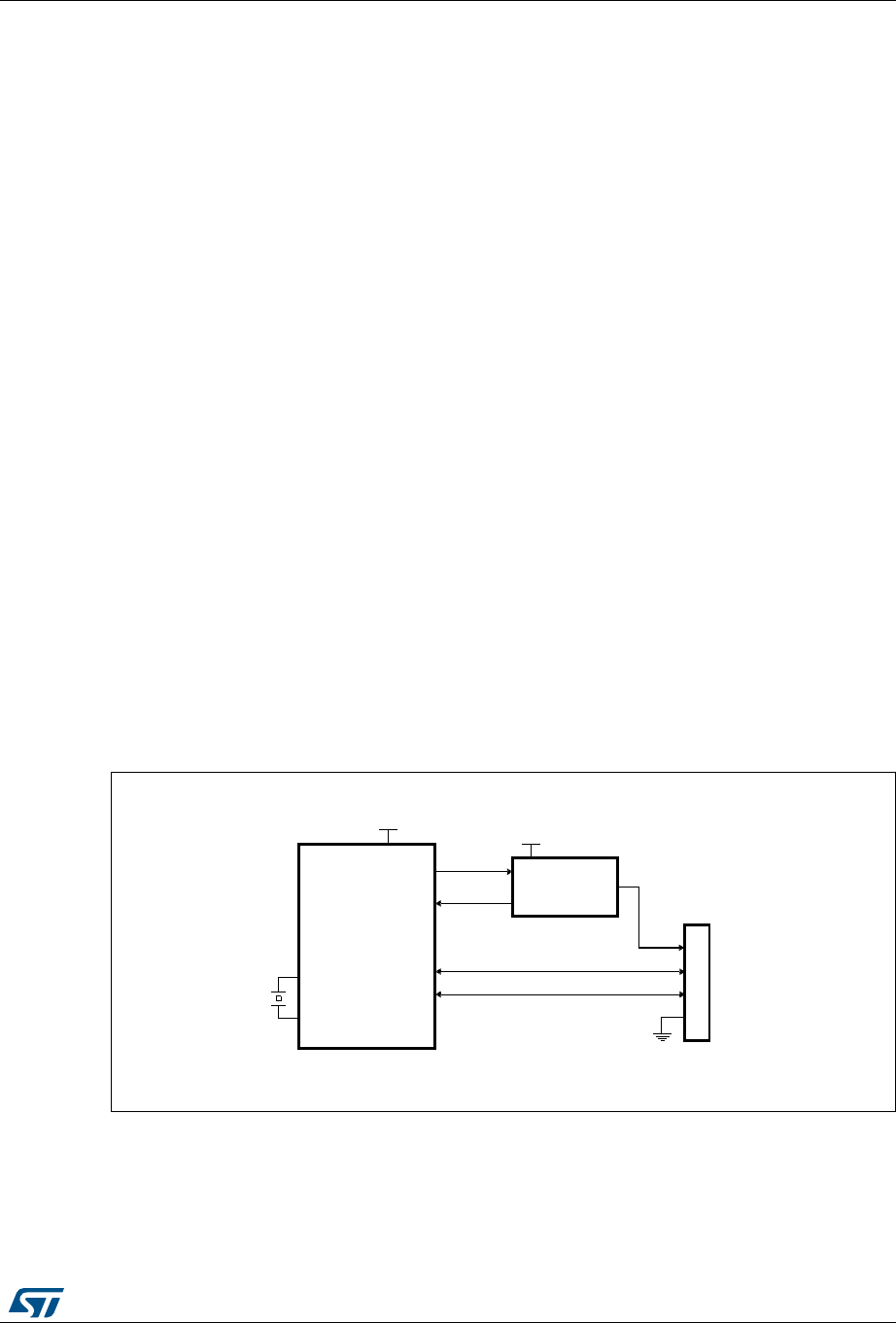
RM0090 Rev 18 1391/1749
RM0090 USB on-the-go high-speed (OTG_HS)
1543
35.6 USB functional description on host mode
This section gives the functional description of the OTG_HS in the USB host mode. The
OTG_HS works as a USB host in the following circumstances:
•OTG A-host
OTG A-device default state when the A-side of the USB cable is plugged in
•OTG B-host
OTG B-device after HNP switching to the host role
•A-device
If the ID line is present, functional and connected to the A-side of the USB cable, and
the HNP-capable bit is cleared in the Global USB Configuration register (HNPCAP bit
in OTG_HS_GUSBCFG). Integrated pull-down resistors are automatically set on the
DP/DM lines.
•Host only (Figure 389: USB host-only connection).
The force host mode bit in the global USB configuration register (FHMOD bit in
OTG_HS_GUSBCFG) forces the OTG_HS core to operate in USB host-only mode. In
this case, the ID line is ignored even if it is available on the USB connector. Integrated
pull-down resistors are automatically set on the OTG_HS_FS_DP/OTG_HS_FS_DM
lines.
Note: On-chip 5 V VBUS generation is not supported. As a result, a charge pump or a basic power
switch (if a 5 V supply is available on the application board) must be added externally to
drive the 5 V VBUS line. The external charge pump can be driven by any GPIO output. This
is required for the OTG A-host, A-device and host-only configurations.
The VBUS input ensures that valid VBUS levels are supplied by the charge pump during USB
operations while the charge pump overcurrent output can be input to any GPIO pin
configured to generate port interrupts. The overcurrent ISR must promptly disable the VBUS
generation.
Figure 411. USB host-only connection
35.6.1 SRP-capable host
SRP support is available through the SRP capable bit in the global USB configuration
register (SRPCAP bit in OTG_HS_GUSBCFG). When the SRP feature is enabled, the host
can save power by switching off the VBUS power while the USB session is suspended. The
MSv36915V2
STMPS2141STR
Current-limited
power distribution
switch(2)
OSC_IN
OSC_OUT
GPIO
GPIO + IRQ
EN
Overcurrent
5 V
5 V Pwr
VBUS
DM
DP
VSS
USB Std-A connector
VDD

USB on-the-go high-speed (OTG_HS) RM0090
1392/1749 RM0090 Rev 18
SRP host mode program model is described in detail in Section : A-device session request
protocol.
35.6.2 USB host states
Host port power
On-chip 5 V VBUS generation is not supported. As a result, a charge pump or a basic power
switch (if a 5 V supply voltage is available on the application board) must be added
externally to drive the 5 V VBUS line. The external charge pump can be driven by any GPIO
output. When the application powers on VBUS through the selected GPIO, it must also set
the port power bit in the host port control and status register (PPWR bit in OTG_HS_HPRT).
VBUS valid
When SRP or HNP is enabled the VBUS sensing pin (PB13) pin should be connected to
VBUS. The VBUS input ensures that valid VBUS levels are supplied by the charge pump
during USB operations. Any unforeseen VBUS voltage drop below the VBUS valid threshold
(4.25 V) generates an OTG interrupt triggered by the session end detected bit (SEDET bit in
OTG_HS_GOTGINT). The application must then switch the VBUS power off and clear the
port power bit.
When HNP and SRP are both disabled, the VBUS sensing pin (PB13) should not be
connected to VBUS. This pin can be can be used as GPIO.
The charge pump overcurrent flag can also be used to prevent electrical damage. Connect
the overcurrent flag output from the charge pump to any GPIO input, and configure it to
generate a port interrupt on the active level. The overcurrent ISR must promptly disable the
VBUS generation and clear the port power bit.
Detection of peripheral connection by the host
If SRP or HNP are enabled, even if USB peripherals or B-devices can be attached at any
time, the OTG_HS does not detect a bus connection until the end of the VBUS sensing
(VBUS over 4.75 V).
When VBUS is at a valid level and a remote B-device is attached, the OTG_HS core issues a
host port interrupt triggered by the device connected bit in the host port control and status
register (PCDET bit in OTG_HS_HPRT).
When HNP and SRP are both disabled, USB peripherals or B-device are detected as
soon as they are connected. The OTG_FS core issues a host port interrupt triggered by
the device connected bit in the host port control and status (PCDET bit in OTG_FS_HPRT).
Detection of peripheral disconnection by the host
The peripheral disconnection event triggers the disconnect detected interrupt (DISCINT bit
in OTG_HS_GINTSTS).
Host enumeration
After detecting a peripheral connection, the host must start the enumeration process by
issuing an USB reset and configuration commands to the new peripheral.
Before sending an USB reset, the application waits for the OTG interrupt triggered by the
debounce done bit (DBCDNE bit in OTG_HS_GOTGINT), which indicates that the bus is

RM0090 Rev 18 1393/1749
RM0090 USB on-the-go high-speed (OTG_HS)
1543
stable again after the electrical debounce caused by the attachment of a pull-up resistor on
OTG_HS_FS_DP (full speed) or OTG_HS_FS_DM (low speed).
The application issues an USB reset (single-ended zero) via the USB by keeping the port
reset bit set in the Host port control and status register (PRST bit in OTG_HS_HPRT) for a
minimum of 10 ms and a maximum of 20 ms. The application monitors the time and then
clears the port reset bit.
Once the USB reset sequence has completed, the host port interrupt is triggered by the port
enable/disable change bit (PENCHNG bit in OTG_HS_HPRT) to inform the application that
the speed of the enumerated peripheral can be read from the port speed field in the host
port control and status register (PSPD bit in OTG_HS_HPRT), and that the host is starting
to drive SOFs (full speed) or keep-alive tokens (low speed). The host is then ready to
complete the peripheral enumeration by sending peripheral configuration commands.
Host suspend
The application can decide to suspend the USB activity by setting the port suspend bit in the
host port control and status register (PSUSP bit in OTG_HS_HPRT). The OTG_HS core
stops sending SOFs and enters the Suspended state.
The Suspended state can be exited on the remote device initiative (remote wakeup). In this
case the remote wakeup interrupt (WKUPINT bit in OTG_HS_GINTSTS) is generated upon
detection of a remote wakeup event, the port resume bit in the host port control and status
register (PRES bit in OTG_HS_HPRT) is set, and a resume signaling is automatically
issued on the USB. The application must monitor the resume window duration, and then
clear the port resume bit to exit the Suspended state and restart the SOF.
If the Suspended state is exited on the host initiative, the application must set the port
resume bit to start resume signaling on the host port, monitor the resume window duration
and then clear the port resume bit.
35.6.3 Host channels
The OTG_HS core instantiates 12 host channels. Each host channel supports an USB host
transfer (USB pipe). The host is not able to support more than 8 transfer requests
simultaneously. If more than 8 transfer requests are pending from the application, the host
controller driver (HCD) must re-allocate channels when they become available, that is, after
receiving the transfer completed and channel halted interrupts.
Each host channel can be configured to support IN/OUT and any type of
periodic/nonperiodic transaction. Each host channel has dedicated control (HCCHARx),
transfer configuration (HCTSIZx) and status/interrupt (HCINTx) registers with associated
mask (HCINTMSKx) registers.

USB on-the-go high-speed (OTG_HS) RM0090
1394/1749 RM0090 Rev 18
Host channel controls
The following host channel controls are available through the host channel-x characteristics
register (HCCHARx):
•Channel enable/disable
•Program the HS/FS/LS speed of target USB peripheral
•Program the address of target USB peripheral
•Program the endpoint number of target USB peripheral
•Program the transfer IN/OUT direction
•Program the USB transfer type (control, bulk, interrupt, isochronous)
•Program the maximum packet size (MPS)
•Program the periodic transfer to be executed during odd/even frames
Host channel transfer
The host channel transfer size registers (HCTSIZx) allow the application to program the
transfer size parameters, and read the transfer status.
The programming operation must be performed before setting the channel enable bit in the
host channel characteristics register. Once the endpoint is enabled, the packet count field is
read-only as the OTG HS core updates it according to the current transfer status.
The following transfer parameters can be programmed:
•Transfer size in bytes
•Number of packets constituting the overall transfer size
•Initial data PID
Host channel status/interrupt
The host channel-x interrupt register (HCINTx) indicates the status of an endpoint with
respect to USB- and AHB-related events. The application must read these register when the
host channels interrupt bit in the core interrupt register (HCINT bit in OTG_HS_GINTSTS) is
set. Before the application can read these registers, it must first read the host all channels
interrupt (HCAINT) register to get the exact channel number for the host channel-x interrupt
register. The application must clear the appropriate bit in this register to clear the
corresponding bits in the HAINT and GINTSTS registers. The mask bits for each interrupt
source of each channel are also available in the OTG_HS_HCINTMSK-x register.

RM0090 Rev 18 1395/1749
RM0090 USB on-the-go high-speed (OTG_HS)
1543
The host core provides the following status checks and interrupt generation:
•Transfer completed interrupt, indicating that the data transfer is complete on both the
application (AHB) and USB sides
•Channel stopped due to transfer completed, USB transaction error or disable
command from the application
•Associated transmit FIFO half or completely empty (IN endpoints)
•ACK response received
•NAK response received
•STALL response received
•USB transaction error due to CRC failure, timeout, bit stuff error, false EOP
•Babble error
•Frame overrun
•Data toggle error
35.6.4 Host scheduler
The host core features a built-in hardware scheduler which is able to autonomously re-order
and manage the USB the transaction requests posted by the application. At the beginning of
each frame the host executes the periodic (isochronous and interrupt) transactions first,
followed by the nonperiodic (control and bulk) transactions to achieve the higher level of
priority granted to the isochronous and interrupt transfer types by the USB specification.
The host processes the USB transactions through request queues (one for periodic and one
for nonperiodic). Each request queue can hold up to 8 entries. Each entry represents a
pending transaction request from the application, and holds the IN or OUT channel number
along with other information to perform a transaction on the USB. The order in which the
requests are written to the queue determines the sequence of the transactions on the USB
interface.
At the beginning of each frame, the host processes the periodic request queue first, followed
by the nonperiodic request queue. The host issues an incomplete periodic transfer interrupt
(IPXFR bit in OTG_HS_GINTSTS) if an isochronous or interrupt transaction scheduled for
the current frame is still pending at the end of the current frame. The OTG HS core is fully
responsible for the management of the periodic and nonperiodic request queues.The
periodic transmit FIFO and queue status register (HPTXSTS) and nonperiodic transmit
FIFO and queue status register (HNPTXSTS) are read-only registers which can be used by
the application to read the status of each request queue. They contain:
•The number of free entries currently available in the periodic (nonperiodic) request
queue (8 max)
•Free space currently available in the periodic (nonperiodic) Tx-FIFO (out-transactions)
•IN/OUT token, host channel number and other status information.
As request queues can hold a maximum of 8 entries each, the application can push to
schedule host transactions in advance with respect to the moment they physically reach the
USB for a maximum of 8 pending periodic transactions plus 8 pending nonperiodic
transactions.
To post a transaction request to the host scheduler (queue) the application must check that
there is at least 1 entry available in the periodic (nonperiodic) request queue by reading the
PTXQSAV bits in the OTG_HS_HNPTXSTS register or NPTQXSAV bits in the
OTG_HS_HNPTXSTS register.
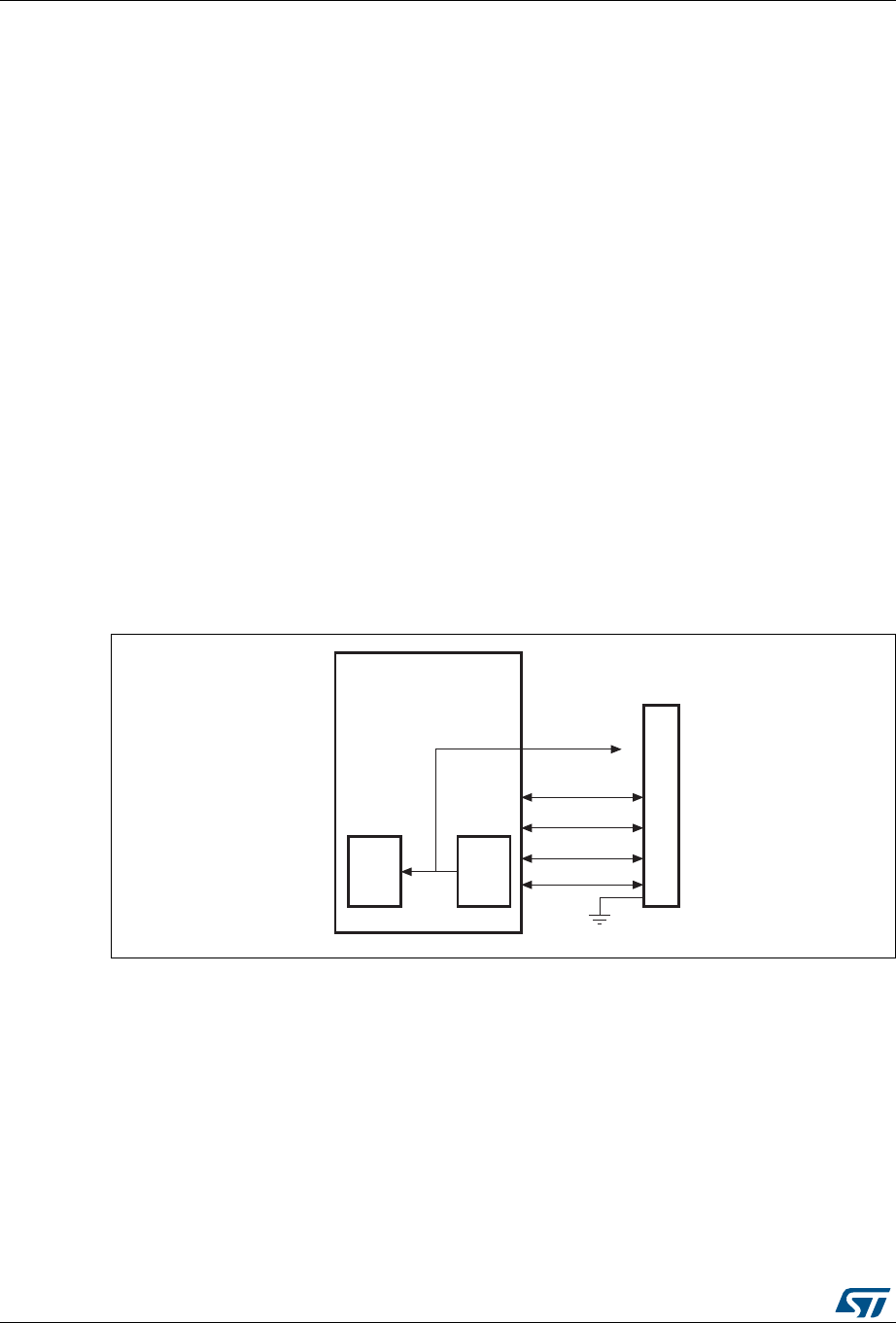
USB on-the-go high-speed (OTG_HS) RM0090
1396/1749 RM0090 Rev 18
35.7 SOF trigger
The OTG FS core allows to monitor, track and configure SOF framing in the host and
peripheral. It also features an SOF pulse output connectivity.
These capabilities are particularly useful to implement adaptive audio clock generation
techniques, where the audio peripheral needs to synchronize to the isochronous stream
provided by the PC, or the host needs trimming its framing rate according to the
requirements of the audio peripheral.
35.7.1 Host SOFs
In host mode the number of PHY clocks occurring between the generation of two
consecutive SOF (FS) or keep-alive (LS) tokens is programmable in the host frame interval
register (OTG_HS_HFIR), thus providing application control over the SOF framing period.
An interrupt is generated at any start of frame (SOF bit in OTG_HS_GINTSTS). The current
frame number and the time remaining until the next SOF are tracked in the host frame
number register (OTG_HS_HFNUM).
An SOF pulse signal is generated at any SOF starting token and with a width of 20 HCLK
cycles. It can be made available externally on the SOF pin using the SOFOUTEN bit in the
global control and configuration register. The SOF pulse is also internally connected to the
input trigger of timer 2 (TIM2), so that the input capture feature, the output compare feature
and the timer can be triggered by the SOF pulse. The TIM2 connection is enabled through
ITR1_RMP bits of TIM2_OR register.
Figure 412. SOF trigger output to TIM2 ITR1 connection
35.7.2 Peripheral SOFs
In peripheral mode, the start of frame interrupt is generated each time an SOF token is
received on the USB (SOF bit in OTG_HS_GINTSTS). The corresponding frame number
can be read from the device status register (FNSOF bit in OTG_HS_DSTS). An SOF pulse
signal with a width of 20 HCLK cycles is also generated and can be made available
externally on the SOF pin by using the SOF output enable bit in the global control and
configuration register (SOFOUTEN bit in OTG_HS_GCCFG). The SOF pulse signal is also
internally connected to the TIM2 input trigger, so that the input capture feature, the output
compare feature and the timer can be triggered by the SOF pulse (see Figure 412). The
TIM2 connection is enabled through ITR1_RMP bits of TIM2_OR register.
SOF
pulse
ITR1
TIM2
OTG_HS_Core
SOF output pulse
USB Micro-AB connector
VBUS
DP
DM
ID
ai16092

RM0090 Rev 18 1397/1749
RM0090 USB on-the-go high-speed (OTG_HS)
1543
The end of periodic frame interrupt (GINTSTS/EOPF) is used to notify the application when
80%, 85%, 90% or 95% of the time frame interval elapsed depending on the periodic frame
interval field in the device configuration register (PFIVL bit in OTG_HS_DCFG).
This feature can be used to determine if all of the isochronous traffic for that frame is
complete.
35.8 OTG_HS low-power modes
Table 207 below defines the STM32 low power modes and their compatibility with the OTG.
The following bits and procedures reduce power consumption.
The power consumption of the OTG PHY is controlled by three bits in the general core
configuration register:
•PHY power down (GCCFG/PWRDWN)
This bit switches on/off the PHY full-speed transceiver module. It must be preliminarily
set to allow any USB operation.
•A-VBUS sensing enable (GCCFG/VBUSASEN)
This bit switches on/off the VBUS comparators associated with A-device operations. It
must be set when in A-device (USB host) mode and during HNP.
•B-VBUS sensing enable (GCCFG/VBUSASEN)
This bit switches on/off the VBUS comparators associated with B-device operations. It
must be set when in B-device (USB peripheral) mode and during HNP.
Power reduction techniques are available in the USB suspended state, when the USB
session is not yet valid or the device is disconnected.
•Stop PHY clock (STPPCLK bit in OTG_HS_PCGCCTL)
– When setting the stop PHY clock bit in the clock gating control register, most of the
clock domain internal to the OTG high-speed core is switched off by clock gating.
Table 207. Compatibility of STM32 low power modes with the OTG
Mode Description USB compatibility
Run MCU fully active Required when USB not in
suspend state.
Sleep USB suspend exit causes the device to exit Sleep mode. Peripheral
registers content is kept.
Available while USB is in
suspend state.
Stop USB suspend exit causes the device to exit Stop mode. Peripheral
registers content is kept(1).
Available while USB is in
suspend state.
Standby Powered-down. The peripheral must be reinitialized after exiting
Standby mode.
Not compatible with USB
applications.
1. Within Stop mode there are different possible settings. Some restrictions may also exist, please refer to Section 5: Power
controller (PWR) to understand which (if any) restrictions apply when using OTG.
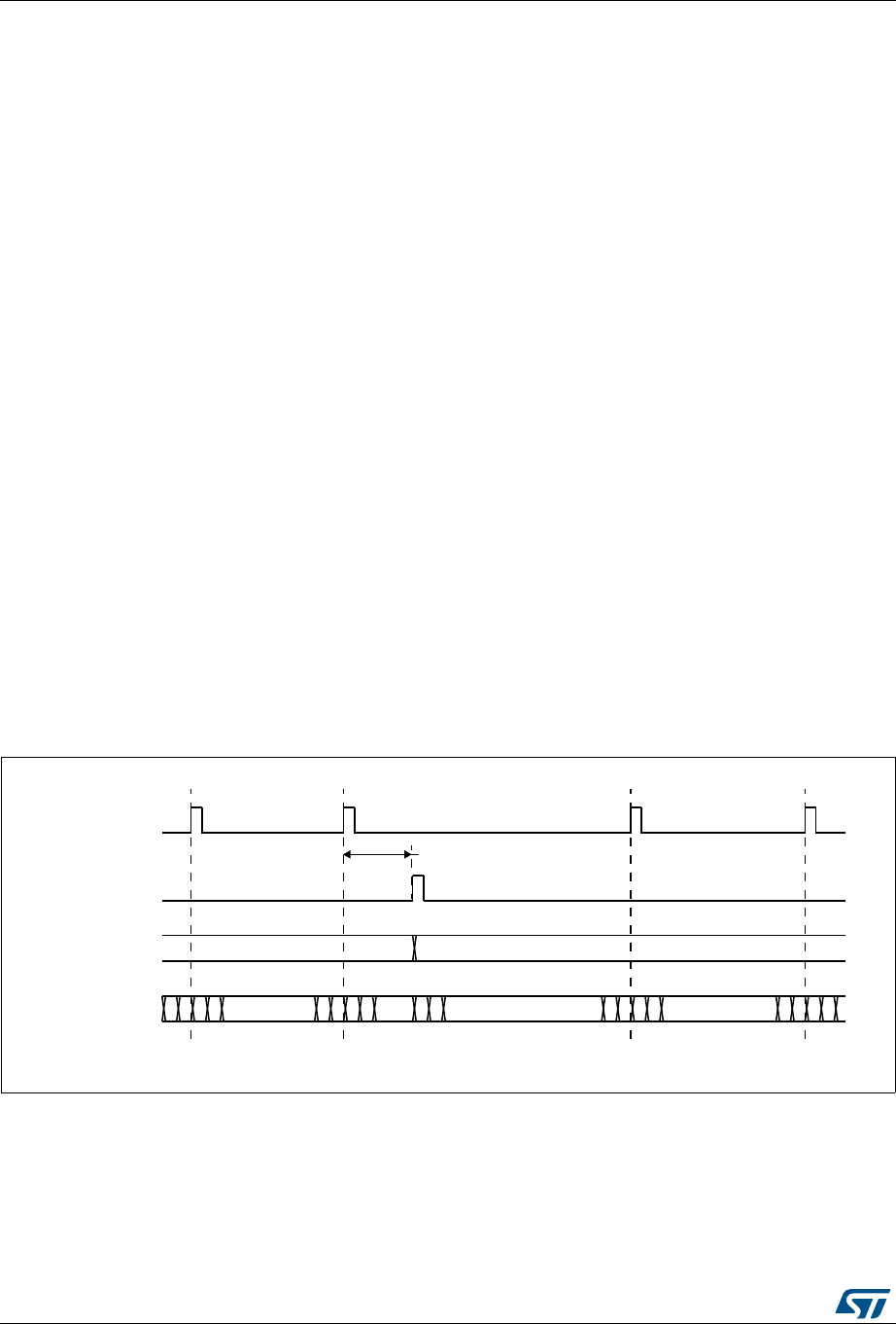
USB on-the-go high-speed (OTG_HS) RM0090
1398/1749 RM0090 Rev 18
The dynamic power consumption due to the USB clock switching activity is cut
even if the clock input is kept running by the application
– Most of the transceiver is also disabled, and only the part in charge of detecting
the asynchronous resume or remote wakeup event is kept alive.
•Gate HCLK (GATEHCLK bit in OTG_HS_PCGCCTL)
When setting the Gate HCLK bit in the clock gating control register, most of the system
clock domain internal to the OTG_HS core is switched off by clock gating. Only the
register read and write interface is kept alive. The dynamic power consumption due to
the USB clock switching activity is cut even if the system clock is kept running by the
application for other purposes.
•USB system stop
– When the OTG_HS is in USB suspended state, the application can decide to
drastically reduce the overall power consumption by shutting down all the clock
sources in the system. USB System Stop is activated by first setting the Stop PHY
clock bit and then configuring the system deep sleep mode in the powercontrol
system module (PWR).
– The OTG_HS core automatically reactivates both system and USB clocks by
asynchronous detection of remote wakeup (as an host) or resume (as a Device)
signaling on the USB.
35.9 Dynamic update of the OTG_HS_HFIR register
The USB core embeds a dynamic trimming capability of micro-SOF framing period in host
mode allowing to synchronize an external device with the micro-SOF frames.
When the OTG_HS_HFIR register is changed within a current micro-SOF frame, the SOF
period correction is applied in the next frame as described in Figure 413.
Figure 413. Updating OTG_HS_HFIR dynamically
400
……… ……
450
Latency
SOF
reload
OTG_HS_HFIR
write
value
Frame
timer
Old OTG_HS_HIFR value
= 400 periods
OTG_HS_HIFR value
= 450 periods+HIFR write latency
New OTG_HS_HIFR value
= 450 periods
1
400
0
399
1
400
0
399
450
449
1
450
0
449
1
450
0
449
OTG_HS_HFIR
ai18439b

RM0090 Rev 18 1399/1749
RM0090 USB on-the-go high-speed (OTG_HS)
1543
35.10 FIFO RAM allocation
35.10.1 Peripheral mode
Receive FIFO RAM
For Receive FIFO RAM, the application should allocate RAM for SETUP packets: 10
locations must be reserved in the receive FIFO to receive SETUP packets on control
endpoints. These locations are reserved for SETUP packets and are not used by the core to
write any other data.
One location must be allocated for Global OUT NAK. Status information are also written to
the FIFO along with each received packet. Therefore, a minimum space of (Largest Packet
Size / 4) + 1 must be allocated to receive packets. If a high-bandwidth endpoint or multiple
isochronous endpoints are enabled, at least two spaces of (Largest Packet Size / 4) + 1
must be allotted to receive back-to-back packets. Typically, two (Largest Packet Size / 4) + 1
spaces are recommended so that when the previous packet is being transferred to AHB, the
USB can receive the subsequent packet.
Along with each endpoints last packet, transfer complete status information are also pushed
to the FIFO. Typically, one location for each OUT endpoint is recommended.
Transmit FIFO RAM
For Transmit FIFO RAM, the minimum RAM space required for each IN Endpoint Transmit
FIFO is the maximum packet size for this IN endpoint.
Note: More space allocated in the transmit IN Endpoint FIFO results in a better performance on
the USB.
35.10.2 Host mode
Receive FIFO RAM
For Receive FIFO RAM allocation, Status information are written to the FIFO along with
each received packet. Therefore, a minimum space of (Largest Packet Size / 4) + 1 must be
allocated to receive packets. If a high-bandwidth channel or multiple isochronous channels
are enabled, at least two spaces of (Largest Packet Size / 4) + 1 must be allocated to
receive back-to-back packets. Typically, two (Largest Packet Size / 4) + 1 spaces are
recommended so that when the previous packet is being transferred to AHB, the USB can
receive the subsequent packet.
Along with each host channels last packet, transfer complete status information are also
pushed to the FIFO. As a consequence, one location must be allocated to store this data.
Transmit FIFO RAM
For Transmit FIFO RAM allocation, the minimum amount of RAM required for the host
nonperiodic Transmit FIFO is the largest maximum packet size for all supported nonperiodic
OUT channels. Typically, a space corresponding to two Largest Packet Size is
recommended, so that when the current packet is being transferred to the USB, the AHB
can transmit the subsequent packet.
The minimum amount of RAM required for Host periodic Transmit FIFO is the largest
maximum packet size for all supported periodic OUT channels. If there is at least one High

USB on-the-go high-speed (OTG_HS) RM0090
1400/1749 RM0090 Rev 18
Bandwidth Isochronous OUT endpoint, then the space must be at least two times the
maximum packet size for that channel.
Note: More space allocated in the Transmit nonperiodic FIFO results in better performance on the
USB.
When operating in DMA mode, the DMA address register for each host channel (HCDMAn)
is stored in the SPRAM (FIFO). One location for each channel must be reserved for this.
35.11 OTG_HS interrupts
When the OTG_HS controller is operating in one mode, either peripheral or host, the
application must not access registers from the other mode. If an illegal access occurs, a
mode mismatch interrupt is generated and reflected in the Core interrupt register (MMIS bit
in the OTG_HS_GINTSTS register). When the core switches from one mode to the other,
the registers in the new mode of operation must be reprogrammed as they would be after a
power-on reset.
Figure 414 shows the interrupt hierarchy.
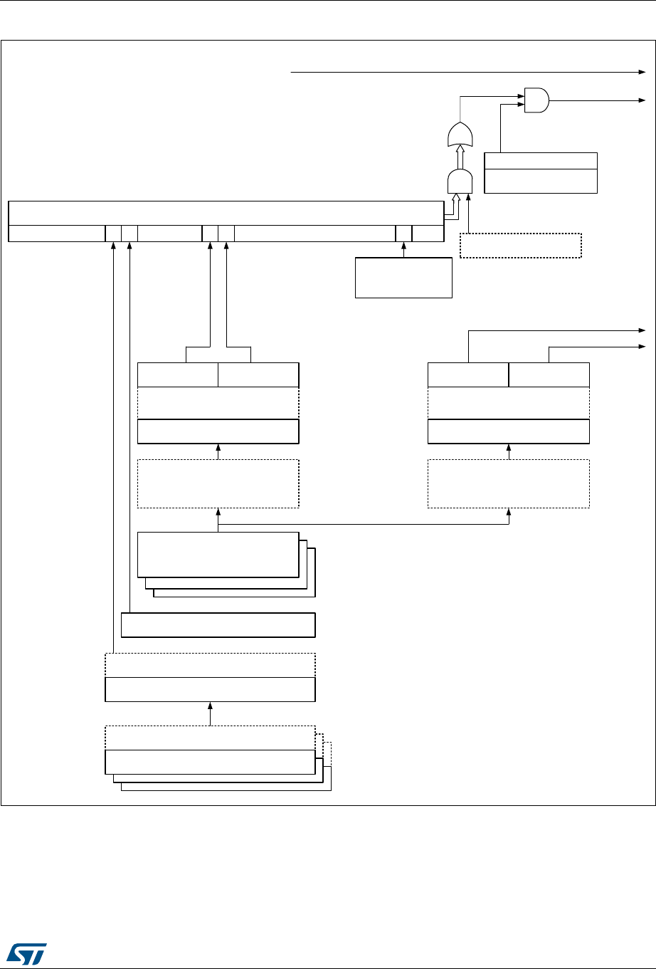
RM0090 Rev 18 1401/1749
RM0090 USB on-the-go high-speed (OTG_HS)
1543
Figure 414. Interrupt hierarchy
1. OTG_HS_WKUP becomes active (high state) when resume condition occurs during L1 SLEEP or L2 SUSPEND states.
MSv47472V2
OTG_DEACHINTMSK
Device each endpoint interrupt mask
register
OTG_DAINTMSK
Device all endpoints interrupt mask
register
OTG_DIEPMSK/
OTG_DOEPMSK
Device IN/OUT endpoints common
interrupt mask register
OTG_DIEPEACHMSK1/
OTG_DOEPEACHMSK1
Device each IN/OUT endpoint interrupt
mask registers
OTG_HCTINTMSKx
Host channels interrupt mask registers
OTG_HAINTMSK
Host all channels interrupt mask register
31:26 25 24 23:20 19 18 17:3 2 1:0
OTG_HCTINTx
Host channels interrupt registers
OTG_HAINT
Host all channels interrupt register
OTG_HPRT
Host port control and status register
OTG_DAINT
Device all endpoints interrupt register
(15 + #EP):16
OUT endpoints
(#EP-1):0
IN endpoints
OTG_GOTGINT
OTG interrupt register
OTG_DEACHINT
Device each endpoint interrupt register
17
EP1OUT
1
EP1IN
OTG_DIEPINTx/
OTG_DOEPINTx
Device IN/OUT endpoint interrupt
registers
OTG_GINTSTS
Core register interrupt
OTG_GINTMSK
Core interrupt mask register
OTG_AHBCFG
AHB configuration register
Global interrupt mask (bit 0)
OR
AND
AND
(1)
x = 0
x = #HC-1
x = 0
x = #HC-1
HCINT
HPRTINT
OEPINP
IEPINT
OTGINT
...
...
Global interrupt
OTG_HS
Wakeup interrupt
OTG_HS_WKUP
EP1_OUT interrupt OTG_HS_EP1_OUT
EP1_IN interrupt OTG_HS_EP1_IN

USB on-the-go high-speed (OTG_HS) RM0090
1402/1749 RM0090 Rev 18
35.12 OTG_HS control and status registers
By reading from and writing to the control and status registers (CSRs) through the AHB
slave interface, the application controls the OTG_HS controller. These registers are 32 bits
wide, and the addresses are 32-bit block aligned. The OTG_HS registers must be accessed
by words (32 bits). CSRs are classified as follows:
•Core global registers
•Host-mode registers
•Host global registers
•Host port CSRs
•Host channel-specific registers
•Device-mode registers
•Device global registers
•Device endpoint-specific registers
•Power and clock-gating registers
•Data FIFO (DFIFO) access registers
Only the Core global, Power and clock-gating, Data FIFO access, and host port control and
status registers can be accessed in both host and peripheral modes. When the OTG_HS
controller is operating in one mode, either peripheral or host, the application must not
access registers from the other mode. If an illegal access occurs, a mode mismatch
interrupt is generated and reflected in the Core interrupt register (MMIS bit in the
OTG_HS_GINTSTS register). When the core switches from one mode to the other, the
registers in the new mode of operation must be reprogrammed as they would be after a
power-on reset.
35.12.1 CSR memory map
The host and peripheral mode registers occupy different addresses. All registers are
implemented in the AHB clock domain.

RM0090 Rev 18 1403/1749
RM0090 USB on-the-go high-speed (OTG_HS)
1543
Figure 415. CSR memory map
1. x = 5 in peripheral mode and x = 11 in host mode.
Global CSR map
These registers are available in both host and peripheral modes.
0000h
Core global CSRs (1 Kbyte)
0400h
Host mode CSRs (1 Kbyte)
0800h
Device mode CSRs (1.5 Kbyte)
0E00h
Power and clock gating CSRs (0.5 Kbyte)
1000h
Device EP 0/Host channel 0 FIFO (4 Kbyte)
2000h
Device EP1/Host channel 1 FIFO (4 Kbyte)
3000h
Device EP (x – 1)(1)/Host channel (x – 1)(1) FIFO (4 Kbyte)
Device EP x(1)/Host channel x(1) FIFO (4 Kbyte)
Reserved
DFIFO
push/pop
to this region
2 0000h
3 FFFFh
Direct access to data FIFO RAM
for debugging (128 Kbyte)
DFIFO
debug read/
write to this
region
ai15615b
Table 208. Core global control and status registers (CSRs)
Acronym Address
offset Register name
OTG_HS_GOTGCTL 0x000 OTG_HS control and status register (OTG_HS_GOTGCTL) on page 1408
OTG_HS_GOTGINT 0x004 OTG_HS interrupt register (OTG_HS_GOTGINT) on page 1409
OTG_HS_GAHBCFG 0x008 OTG_HS AHB configuration register (OTG_HS_GAHBCFG) on page 1411
OTG_HS_GUSBCFG 0x00C OTG_HS USB configuration register (OTG_HS_GUSBCFG) on page 1412
OTG_HS_GRSTCTL 0x010 OTG_HS reset register (OTG_HS_GRSTCTL) on page 1415
OTG_HS_GINTSTS 0x014 OTG_HS core interrupt register (OTG_HS_GINTSTS) on page 1418
OTG_HS_GINTMSK 0x018 OTG_HS interrupt mask register (OTG_HS_GINTMSK) on page 1422

USB on-the-go high-speed (OTG_HS) RM0090
1404/1749 RM0090 Rev 18
Host-mode CSR map
These registers must be programmed every time the core changes to host mode.
OTG_HS_GRXSTSR 0x01C OTG_HS Receive status debug read/OTG status read and pop registers
(OTG_HS_GRXSTSR/OTG_HS_GRXSTSP) on page 1425
OTG_HS_GRXSTSP 0x020
OTG_HS_GRXFSIZ 0x024 OTG_HS Receive FIFO size register (OTG_HS_GRXFSIZ) on page 1426
OTG_HS_GNPTXFSIZ/
OTG_HS_TX0FSIZ 0x028 OTG_HS nonperiodic transmit FIFO size/Endpoint 0 transmit FIFO size
register (OTG_HS_GNPTXFSIZ/OTG_HS_TX0FSIZ) on page 1427
OTG_HS_GNPTXSTS 0x02C OTG_HS nonperiodic transmit FIFO/queue status register
(OTG_HS_GNPTXSTS) on page 1427
OTG_HS_GCCFG 0x038 OTG_HS general core configuration register (OTG_HS_GCCFG) on
page 1428
OTG_HS_CID 0x03C OTG_HS core ID register (OTG_HS_CID) on page 1429
OTG_HS_HPTXFSIZ 0x100 OTG_HS Host periodic transmit FIFO size register (OTG_HS_HPTXFSIZ)
on page 1429
OTG_HS_DIEPTXFx
0x104
0x108
...
0x114
OTG_HS device IN endpoint transmit FIFO size register
(OTG_HS_DIEPTXFx) (x = 1..5, where x is the FIFO_number) on page 1430
Table 208. Core global control and status registers (CSRs) (continued)
Acronym Address
offset Register name
Table 209. Host-mode control and status registers (CSRs)
Acronym Offset
address Register name
OTG_HS_HCFG 0x400 OTG_HS host configuration register (OTG_HS_HCFG) on page 1430
OTG_HS_HFIR 0x404 OTG_HS Host frame interval register (OTG_HS_HFIR) on page 1432
OTG_HS_HFNUM 0x408 OTG_HS host frame number/frame time remaining register
(OTG_HS_HFNUM) on page 1432
OTG_HS_HPTXSTS 0x410 OTG_HS_Host periodic transmit FIFO/queue status register
(OTG_HS_HPTXSTS) on page 1433
OTG_HS_HAINT 0x414 OTG_HS Host all channels interrupt register (OTG_HS_HAINT) on
page 1434
OTG_HS_HAINTMSK 0x418 OTG_HS host all channels interrupt mask register (OTG_HS_HAINTMSK)
on page 1434
OTG_HS_HPRT 0x440 OTG_HS host port control and status register (OTG_HS_HPRT) on
page 1435

RM0090 Rev 18 1405/1749
RM0090 USB on-the-go high-speed (OTG_HS)
1543
Device-mode CSR map
These registers must be programmed every time the core changes to peripheral mode.
OTG_HS_HCCHARx
0x500
0x520
...
0x660
OTG_HS host channel-x characteristics register (OTG_HS_HCCHARx)
(x = 0..11, where x = Channel_number) on page 1437
OTG_HS_HCSPLTx 0x504 OTG_HS host channel-x split control register (OTG_HS_HCSPLTx)
(x = 0..11, where x = Channel_number) on page 1439
OTG_HS_HCINTx 0x508 OTG_HS host channel-x interrupt register (OTG_HS_HCINTx) (x = 0..11,
where x = Channel_number) on page 1440
OTG_HS_HCINTMSKx 0x50C OTG_HS host channel-x interrupt mask register (OTG_HS_HCINTMSKx)
(x = 0..11, where x = Channel_number) on page 1441
OTG_HS_HCTSIZx 0x510 OTG_HS host channel-x transfer size register (OTG_HS_HCTSIZx)
(x = 0..11, where x = Channel_number) on page 1442
OTG_HS_HCDMAx 0x514 OTG_HS host channel-x DMA address register (OTG_HS_HCDMAx)
(x = 0..11, where x = Channel_number) on page 1443
Table 209. Host-mode control and status registers (CSRs) (continued)
Acronym Offset
address Register name
Table 210. Device-mode control and status registers
Acronym Offset
address Register name
OTG_HS_DCFG 0x800 OTG_HS device configuration register (OTG_HS_DCFG) on
page 1443
OTG_HS_DCTL 0x804 OTG_HS device control register (OTG_HS_DCTL) on page 1445
OTG_HS_DSTS 0x808 OTG_HS device status register (OTG_HS_DSTS) on page 1447
OTG_HS_DIEPMSK 0x810 OTG_HS device IN endpoint common interrupt mask register
(OTG_HS_DIEPMSK) on page 1448
OTG_HS_DOEPMSK 0x814 OTG_HS device OUT endpoint common interrupt mask register
(OTG_HS_DOEPMSK) on page 1449
OTG_HS_DAINT 0x818 OTG_HS device all endpoints interrupt register (OTG_HS_DAINT)
on page 1450
OTG_HS_DAINTMSK 0x81C OTG_HS all endpoints interrupt mask register
(OTG_HS_DAINTMSK) on page 1451
OTG_HS_DVBUSDIS 0x828 OTG_HS device VBUS discharge time register
(OTG_HS_DVBUSDIS) on page 1451
OTG_HS_DVBUSPULSE 0x82C OTG_HS device VBUS pulsing time register
(OTG_HS_DVBUSPULSE) on page 1452
OTG_HS_DTHRCTL 0x830 OTG_HS Device threshold control register (OTG_HS_DTHRCTL)
on page 1453

USB on-the-go high-speed (OTG_HS) RM0090
1406/1749 RM0090 Rev 18
OTG_HS_DIEPEMPMSK 0x834 OTG_HS device IN endpoint FIFO empty interrupt mask register:
(OTG_HS_DIEPEMPMSK) on page 1454
OTG_HS_DEACHINT 0x838 OTG_HS device each endpoint interrupt register
(OTG_HS_DEACHINT) on page 1454
OTG_HS_DEACHINTMSK 0x83C OTG_HS device each endpoint interrupt register mask
(OTG_HS_DEACHINTMSK) on page 1455
OTG_HS_DIEPEACHMSK1 0x844 OTG_HS device each in endpoint-1 interrupt register
(OTG_HS_DIEPEACHMSK1) on page 1455
OTG_HS_DOEPEACHMSK1 0x884 OTG_HS device each OUT endpoint-1 interrupt register
(OTG_HS_DOEPEACHMSK1) on page 1456
OTG_HS_DIEPCTLx
0x900
0x920
...
0x9A0
OTG device endpoint-x control register (OTG_HS_DIEPCTLx) (x =
0..5, where x = Endpoint_number) on page 1457
OTG_HS_DIEPINTx 0x908
OTG_HS device endpoint-x interrupt register
(OTG_HS_DIEPINTx) (x = 0..5, where x = Endpoint_number) on
page 1464
OTG_HS_DIEPTSIZ0 0x910 OTG_HS device IN endpoint 0 transfer size register
(OTG_HS_DIEPTSIZ0) on page 1467
OTG_HS_DIEPDMAx/
OTG_HS_DOEPDMAx 0x914/0xB14
OTG_HS device endpoint-x DMA address register
(OTG_HS_DIEPDMAx / OTG_HS_DOEPDMAx) (x = 0..5, where
x = Endpoint_number) on page 1471
OTG_HS_DTXFSTSx 0x918
OTG_HS device IN endpoint transmit FIFO status register
(OTG_HS_DTXFSTSx) (x = 0..5, where x = Endpoint_number) on
page 1470
OTG_HS_DIEPTSIZx
0x930
0x950
...
0x9B0
OTG_HS device endpoint-x transfer size register
(OTG_HS_DIEPTSIZx) (x = 1..5, where x = Endpoint_number) on
page 1469
OTG_HS_DOEPCTL0 0xB00 OTG_HS device control OUT endpoint 0 control register
(OTG_HS_DOEPCTL0) on page 1460
OTG_HS_DOEPSIZ0 0xB10 OTG_HS device OUT endpoint 0 transfer size register
(OTG_HS_DOEPTSIZ0) on page 1468
OTG_HS_DOEPCTLx
0xB20
0xB40
...
0xBA0
OTG_HS device endpoint-x control register
(OTG_HS_DOEPCTLx) (x = 1..5, where x = Endpoint_number) on
page 1461
Table 210. Device-mode control and status registers (continued)
Acronym Offset
address Register name

RM0090 Rev 18 1407/1749
RM0090 USB on-the-go high-speed (OTG_HS)
1543
Data FIFO (DFIFO) access register map
These registers, available in both host and peripheral modes, are used to read or write the
FIFO space for a specific endpoint or a channel, in a given direction. If a host channel is of
type IN, the FIFO can only be read on the channel. Similarly, if a host channel is of type
OUT, the FIFO can only be written on the channel.
Power and clock gating CSR map
There is a single register for power and clock gating. It is available in both host and
peripheral modes.
35.12.2 OTG_HS global registers
These registers are available in both host and peripheral modes, and do not need to be
reprogrammed when switching between these modes.
OTG_HS_DOEPINTx
0xB08
0xB28
...
0xBA8
OTG_HS device endpoint-x interrupt register
(OTG_HS_DOEPINTx) (x = 0..5, where x = Endpoint_number) on
page 1466
OTG_HS_DOEPTSIZx
0xB30
0xB50
...
0xBB0
OTG_HS device endpoint-x transfer size register
(OTG_HS_DOEPTSIZx) (x = 1..5, where x = Endpoint_number)
on page 1470
Table 210. Device-mode control and status registers (continued)
Acronym Offset
address Register name
Table 211. Data FIFO (DFIFO) access register map
FIFO access register section Address range Access
Device IN Endpoint 0/Host OUT Channel 0: DFIFO Write Access
Device OUT Endpoint 0/Host IN Channel 0: DFIFO Read Access 0x1000–0x1FFC w
r
Device IN Endpoint 1/Host OUT Channel 1: DFIFO Write Access
Device OUT Endpoint 1/Host IN Channel 1: DFIFO Read Access 0x2000–0x2FFC w
r
... ... ...
Device IN Endpoint x(1)/Host OUT Channel x(1): DFIFO Write Access
Device OUT Endpoint x(1)/Host IN Channel x(1): DFIFO Read Access
1. Where x is 5 in peripheral mode and 11 in host mode.
0xX000–0xXFFC w
r
Table 212. Power and clock gating control and status registers
Register name Acronym Offset address: 0xE00–0xFFF
Power and clock gating control register OTG_HS_PCGCCTL 0xE00-0xE04
Reserved - 0xE05–0xFFF

USB on-the-go high-speed (OTG_HS) RM0090
1408/1749 RM0090 Rev 18
Bit values in the register descriptions are expressed in binary unless otherwise specified.
OTG_HS control and status register (OTG_HS_GOTGCTL)
Address offset: 0x000
Reset value: 0x0001 0000
The OTG control and status register controls the behavior and reflects the status of the OTG
function of the core.
313029282726252423222120191817161514131211109876543210
Reserved
BSVLD
ASVLD
DBCT
CIDSTS
Reserved
DHNPEN
HSHNPEN
HNPRQ
HNGSCS
Reserved
SRQ
SRQSCS
rrrr rwrwrwr rwr
Bits 31:20 Reserved, must be kept at reset value.
Bit 19 BSVLD: B-session valid
Indicates the peripheral mode transceiver status.
0: B-session is not valid.
1: B-session is valid.
In OTG mode, you can use this bit to determine if the device is connected or disconnected.
Note: Only accessible in peripheral mode.
Bit 18 ASVLD: A-session valid
Indicates the host mode transceiver status.
0: A-session is not valid
1: A-session is valid
Note: Only accessible in host mode.
Bit 17 DBCT: Long/short debounce time
Indicates the debounce time of a detected connection.
0: Long debounce time, used for physical connections (100 ms + 2.5 µs)
1: Short debounce time, used for soft connections (2.5 µs)
Note: Only accessible in host mode.
Bit 16 CIDSTS: Connector ID status
Indicates the connector ID status on a connect event.
0: The OTG_HS controller is in A-device mode
1: The OTG_HS controller is in B-device mode
Note: Accessible in both peripheral and host modes.
Bits 15:12 Reserved, must be kept at reset value.
Bit 11 DHNPEN: Device HNP enabled
The application sets this bit when it successfully receives a SetFeature.SetHNPEnable
command from the connected USB host.
0: HNP is not enabled in the application
1: HNP is enabled in the application
Note: Only accessible in peripheral mode.

RM0090 Rev 18 1409/1749
RM0090 USB on-the-go high-speed (OTG_HS)
1543
OTG_HS interrupt register (OTG_HS_GOTGINT)
Address offset: 0x04
Reset value: 0x0000 0000
The application reads this register whenever there is an OTG interrupt and clears the bits in
this register to clear the OTG interrupt.
Bit 10 HSHNPEN: Host set HNP enable
The application sets this bit when it has successfully enabled HNP (using the
SetFeature.SetHNPEnable command) on the connected device.
0: Host Set HNP is not enabled
1: Host Set HNP is enabled
Note: Only accessible in host mode.
Bit 9 HNPRQ: HNP request
The application sets this bit to initiate an HNP request to the connected USB host. The
application can clear this bit by writing a 0 when the host negotiation success status change
bit in the OTG interrupt register (HNSSCHG bit in OTG_HS_GOTGINT) is set. The core
clears this bit when the HNSSCHG bit is cleared.
0: No HNP request
1: HNP request
Note: Only accessible in peripheral mode.
Bit 8 HNGSCS: Host negotiation success
The core sets this bit when host negotiation is successful. The core clears this bit when the
HNP Request (HNPRQ) bit in this register is set.
0: Host negotiation failure
1: Host negotiation success
Note: Only accessible in peripheral mode.
Bits 7:2 Reserved, must be kept at reset value.
Bit 1 SRQ: Session request
The application sets this bit to initiate a session request on the USB. The application can
clear this bit by writing a 0 when the host negotiation success status change bit in the OTG
Interrupt register (HNSSCHG bit in OTG_HS_GOTGINT) is set. The core clears this bit when
the HNSSCHG bit is cleared.
If you use the USB 1.1 full-speed serial transceiver interface to initiate the session request,
the application must wait until VBUS discharges to 0.2 V, after the B-Session Valid bit in this
register (BSVLD bit in OTG_HS_GOTGCTL) is cleared.
0: No session request
1: Session request
Note: Only accessible in peripheral mode.
Bit 0 SRQSCS: Session request success
The core sets this bit when a session request initiation is successful.
0: Session request failure
1: Session request success
Note: Only accessible in peripheral mode.

USB on-the-go high-speed (OTG_HS) RM0090
1410/1749 RM0090 Rev 18
313029282726252423222120191817161514131211109876543210
Reserved
DBCDNE
ADTOCHG
HNGDET
Reserved
HNSSCHG
SRSSCHG
Reserved
SEDET
Res.
rc_
w1
rc_
w1
rc_
w1
rc_
w1
rc_
w1
rc_
w1
Bits 31:20 Reserved, must be kept at reset value.
Bit 19 DBCDNE: Debounce done
The core sets this bit when the debounce is completed after the device connect. The
application can start driving USB reset after seeing this interrupt. This bit is only valid when
the HNP Capable or SRP Capable bit is set in the Core USB Configuration register (HNPCAP
bit or SRPCAP bit in OTG_HS_GUSBCFG, respectively).
Note: Only accessible in host mode.
Bit 18 ADTOCHG: A-device timeout change
The core sets this bit to indicate that the A-device has timed out while waiting for the B-device
to connect.
Note: Accessible in both peripheral and host modes.
Bit 17 HNGDET: Host negotiation detected
The core sets this bit when it detects a host negotiation request on the USB.
Note: Accessible in both peripheral and host modes.
Bits 16:10 Reserved, must be kept at reset value.
Bit 9 HNSSCHG: Host negotiation success status change
The core sets this bit on the success or failure of a USB host negotiation request. The
application must read the host negotiation success bit of the OTG Control and Status register
(HNGSCS in OTG_HS_GOTGCTL) to check for success or failure.
Note: Accessible in both peripheral and host modes.
Bits 7:3 Reserved, must be kept at reset value.
Bit 8 SRSSCHG: Session request success status change
The core sets this bit on the success or failure of a session request. The application must
read the session request success bit in the OTG Control and status register (SRQSCS bit in
OTG_HS_GOTGCTL) to check for success or failure.
Note: Accessible in both peripheral and host modes.
Bit 2 SEDET: Session end detected
The core sets this bit to indicate that the level of the voltage on VBUS is no longer valid for a
B-device session when VBUS < 0.8 V.
Bits 1:0 Reserved, must be kept at reset value.

RM0090 Rev 18 1411/1749
RM0090 USB on-the-go high-speed (OTG_HS)
1543
OTG_HS AHB configuration register (OTG_HS_GAHBCFG)
Address offset: 0x008
Reset value: 0x0000 0000
This register can be used to configure the core after power-on or a change in mode. This
register mainly contains AHB system-related configuration parameters. Do not change this
register after the initial programming. The application must program this register before
starting any transactions on either the AHB or the USB.
313029282726252423222120191817161514131211109876543210
Reserved
PTXFELVL
TXFELVL
Reserved
DMAEN
HBSTLEN
GINT
rw rw rw rw rw rw rw rw
Bits 31:20 Reserved, must be kept at reset value.
Bit 8 PTXFELVL: Periodic TxFIFO empty level
Indicates when the periodic TxFIFO empty interrupt bit in the Core interrupt register (PTXFE
bit in OTG_HS_GINTSTS) is triggered.
0: PTXFE (in OTG_HS_GINTSTS) interrupt indicates that the Periodic TxFIFO is half empty
1: PTXFE (in OTG_HS_GINTSTS) interrupt indicates that the Periodic TxFIFO is completely
empty
Note: Only accessible in host mode.
Bit 7 TXFELVL: TxFIFO empty level
In peripheral mode, this bit indicates when the IN endpoint Transmit FIFO empty interrupt
(TXFE in OTG_HS_DIEPINTx.) is triggered.
0: TXFE (in OTG_HS_DIEPINTx) interrupt indicates that the IN Endpoint TxFIFO is half
empty
1: TXFE (in OTG_HS_DIEPINTx) interrupt indicates that the IN Endpoint TxFIFO is
completely empty
Note: Only accessible in peripheral mode.
Bit 6 Reserved, must be kept at reset value.
Bits5 DMAEN: DMA enable
0: The core operates in slave mode
1: The core operates in DMA mode
Bits 4:1 HBSTLEN: Burst length/type
0000 Single
0001 INCR
0011 INCR4
0101 INCR8
0111 INCR16
Others: Reserved
Bit 0 GINT: Global interrupt mask
This bit is used to mask or unmask the interrupt line assertion to the application. Irrespective
of this bit setting, the interrupt status registers are updated by the core.
0: Mask the interrupt assertion to the application.
1: Unmask the interrupt assertion to the application
Note: Accessible in both peripheral and host modes.

USB on-the-go high-speed (OTG_HS) RM0090
1412/1749 RM0090 Rev 18
OTG_HS USB configuration register (OTG_HS_GUSBCFG)
Address offset: 0x00C
Reset value: 0x0000 1440
This register can be used to configure the core after power-on or a changing to host mode
or peripheral mode. It contains USB and USB-PHY related configuration parameters. The
application must program this register before starting any transactions on either the AHB or
the USB. Do not make changes to this register after the initial programming.
313029282726252423222120191817161514131211109876543210
CTXPKT
FDMOD
FHMOD
Reserved
ULPIIPD
PTCI
PCCI
TSDPS
ULPIEVBUSI
ULPIEVBUSD
ULPICSM
ULPIAR
ULPIFSLS
Reserved
PHYLPCS
Reserved
TRDT
HNPCAP
SRPCAP
Reserved
PHYSEL
Reserved
TOCAL
rw rw rw rw rw rw rw rw rw rw rw rw rw rw rw rw rw rw
Bit 31 CTXPKT: Corrupt Tx packet
This bit is for debug purposes only. Never set this bit to 1.
Note: Accessible in both peripheral and host modes.
Bit 30 FDMOD: Forced peripheral mode
Writing a 1 to this bit forces the core to peripheral mode irrespective of the OTG_HS_ID input
pin.
0: Normal mode
1: Forced peripheral mode
After setting the force bit, the application must wait at least 25 ms before the change takes
effect.
Note: Accessible in both peripheral and host modes.
Bit 29 FHMOD: Forced host mode
Writing a 1 to this bit forces the core to host mode irrespective of the OTG_HS_ID input pin.
0: Normal mode
1: Forced host mode
After setting the force bit, the application must wait at least 25 ms before the change takes
effect.
Note: Accessible in both peripheral and host modes.
Bits 28:26 Reserved, must be kept at reset value.
Bit 25 ULPIIPD: ULPI interface protect disable
This bit controls the circuitry built in the PHY to protect the ULPI interface when the link tri-
states stp and data. Any pull-up or pull-down resistors employed by this feature can be
disabled. Please refer to the ULPI specification for more details.
0: Enables the interface protection circuit
1: Disables the interface protection circuit
Bit 24 PTCI: Indicator pass through
This bit controls whether the complement output is qualified with the internal VBUS valid
comparator before being used in the VBUS state in the RX CMD. Please refer to the ULPI
specification for more details.
0: Complement Output signal is qualified with the Internal VBUS valid comparator
1: Complement Output signal is not qualified with the Internal VBUS valid comparator

RM0090 Rev 18 1413/1749
RM0090 USB on-the-go high-speed (OTG_HS)
1543
Bit 23 PCCI: Indicator complement
This bit controls the PHY to invert the ExternalVbusIndicator input signal, and generate the
complement output. Please refer to the ULPI specification for more details.
0: PHY does not invert the ExternalVbusIndicator signal
1: PHY inverts ExternalVbusIndicator signal
Bit 22 TSDPS: TermSel DLine pulsing selection
This bit selects utmi_termselect to drive the data line pulse during SRP (session request
protocol).
0: Data line pulsing using utmi_txvalid (default)
1: Data line pulsing using utmi_termsel
Bit 21 ULPIEVBUSI: ULPI external VBUS indicator
This bit indicates to the ULPI PHY to use an external VBUS overcurrent indicator.
0: PHY uses an internal VBUS valid comparator
1: PHY uses an external VBUS valid comparator
Bit 20 ULPIEVBUSD: ULPI External VBUS Drive
This bit selects between internal or external supply to drive 5 V on VBUS, in the ULPI PHY.
0: PHY drives VBUS using internal charge pump (default)
1: PHY drives VBUS using external supply.
Bit 19 ULPICSM: ULPI Clock SuspendM
This bit sets the ClockSuspendM bit in the interface control register on the ULPI PHY. This bit
applies only in the serial and carkit modes.
0: PHY powers down the internal clock during suspend
1: PHY does not power down the internal clock
Bit 18 ULPIAR: ULPI Auto-resume
This bit sets the AutoResume bit in the interface control register on the ULPI PHY.
0: PHY does not use AutoResume feature
1: PHY uses AutoResume feature
Bit 17 ULPIFSLS: ULPI FS/LS select
The application uses this bit to select the FS/LS serial interface for the ULPI PHY. This bit is
valid only when the FS serial transceiver is selected on the ULPI PHY.
0: ULPI interface
1: ULPI FS/LS serial interface
Bit 16 Reserved, must be kept at reset value.
Bit 15 PHYLPCS: PHY Low-power clock select
This bit selects either 480 MHz or 48 MHz (low-power) PHY mode. In FS and LS modes, the
PHY can usually operate on a 48 MHz clock to save power.
0: 480 MHz internal PLL clock
1: 48 MHz external clock
In 480 MHz mode, the UTMI interface operates at either 60 or 30 MHz, depending on
whether the 8- or 16-bit data width is selected. In 48 MHz mode, the UTMI interface operates
at 48 MHz in FS and LS modes.
Bit 14 Reserved, must be kept at reset value.
Bits 13:10 TRDT: USB turnaround time
These bits allows to set the turnaround time in PHY clocks. They must be configured
according to Table 213: TRDT values, depending on the application AHB frequency. Higher
TRDT values allow stretching the USB response time to IN tokens in order to compensate for
longer AHB read access latency to the Data FIFO.

USB on-the-go high-speed (OTG_HS) RM0090
1414/1749 RM0090 Rev 18
Bit 9 HNPCAP: HNP-capable
The application uses this bit to control the OTG_HS controller’s HNP capabilities.
0: HNP capability is not enabled
1: HNP capability is enabled
Note: Accessible in both peripheral and host modes.
Bit 8 SRPCAP: SRP-capable
The application uses this bit to control the OTG_HS controller’s SRP capabilities. If the core
operates as a nonSRP-capable B-device, it cannot request the connected A-device (host) to
activate VBUS and start a session.
0: SRP capability is not enabled
1: SRP capability is enabled
Note: Accessible in both peripheral and host modes.
Bit 7 Reserved, must be kept at reset value.
Bit 6 PHYSEL: USB 2.0 high-speed ULPI PHY or USB 1.1 full-speed serial transceiver select
0: USB 2.0 high-speed ULPI PHY
1: USB 1.1 full-speed serial transceiver
Bits 5:3 Reserved, must be kept at reset value.
Bits 2:0 TOCAL: FS timeout calibration
The number of PHY clocks that the application programs in this field is added to the full-
speed interpacket timeout duration in the core to account for any additional delays
introduced by the PHY. This can be required, because the delay introduced by the PHY in
generating the line state condition can vary from one PHY to another.
The USB standard timeout value for full-speed operation is 16 to 18 (inclusive) bit times. The
application must program this field based on the speed of enumeration. The number of bit
times added per PHY clock is 0.25 bit times.
Table 213. TRDT values
AHB frequency range (MHz)
TRDT minimum value
Min. Max
30 - 0x9

RM0090 Rev 18 1415/1749
RM0090 USB on-the-go high-speed (OTG_HS)
1543
OTG_HS reset register (OTG_HS_GRSTCTL)
Address offset: 0x010
Reset value: 0x8000 0000
The application uses this register to reset various hardware features inside the core.
313029282726252423222120191817161514131211109876543210
AHBIDL
DMAREQ
Reserved
TXFNUM
TXFFLSH
RXFFLSH
Reserved
FCRST
HSRST
CSRST
rr rw rs rs rs rs rs
Bit 31 AHBIDL: AHB master idle
Indicates that the AHB master state machine is in the Idle condition.
Note: Accessible in both peripheral and host modes.
Bit 30 DMAREQ: DMA request signal
This bit indicates that the DMA request is in progress. Used for debug.
Bits 29:11 Reserved, must be kept at reset value.
Bits 10:6 TXFNUM: TxFIFO number
This is the FIFO number that must be flushed using the TxFIFO Flush bit. This field must not
be changed until the core clears the TxFIFO Flush bit.
00000:
– Nonperiodic TxFIFO flush in host mode
– Tx FIFO 0 flush in peripheral mode
00001:
– Periodic TxFIFO flush in host mode
– TXFIFO 1 flush in peripheral mode
00010: TXFIFO 2 flush in peripheral mode
...
00101: TXFIFO 15 flush in peripheral mode
10000: Flush all the transmit FIFOs in peripheral or host mode.
Note: Accessible in both peripheral and host modes.
Bit 5 TXFFLSH: TxFIFO flush
This bit selectively flushes a single or all transmit FIFOs, but cannot do so if the core is in the
midst of a transaction.
The application must write this bit only after checking that the core is neither writing to the
TxFIFO nor reading from the TxFIFO. Verify using these registers:
– Read: the NAK effective interrupt ensures the core is not reading from the FIFO
– Write: the AHBIDL bit in OTG_HS_GRSTCTL ensures that the core is not writing
anything to the FIFO
Note: Accessible in both peripheral and host modes.

USB on-the-go high-speed (OTG_HS) RM0090
1416/1749 RM0090 Rev 18
Bit 4 RXFFLSH: RxFIFO flush
The application can flush the entire RxFIFO using this bit, but must first ensure that the core
is not in the middle of a transaction.
The application must only write to this bit after checking that the core is neither reading from
the RxFIFO nor writing to the RxFIFO.
The application must wait until the bit is cleared before performing any other operation. This
bit requires 8 clocks (slowest of PHY or AHB clock) to be cleared.
Note: Accessible in both peripheral and host modes.
Bit 3 Reserved, must be kept at reset value.

RM0090 Rev 18 1417/1749
RM0090 USB on-the-go high-speed (OTG_HS)
1543
Bit 2 FCRST: Host frame counter reset
The application writes this bit to reset the (micro) frame number counter inside the core.
When the (micro) frame counter is reset, the subsequent SOF sent out by the core has a
frame number of 0.
Note: Only accessible in host mode.
Bit 1 HSRST: HCLK soft reset
The application uses this bit to flush the control logic in the AHB Clock domain. Only AHB
Clock Domain pipelines are reset.
FIFOs are not flushed with this bit.
All state machines in the AHB clock domain are reset to the Idle state after terminating the
transactions on the AHB, following the protocol.
CSR control bits used by the AHB clock domain state machines are cleared.
To clear this interrupt, status mask bits that control the interrupt status and are generated by
the AHB clock domain state machine are cleared.
Because interrupt status bits are not cleared, the application can get the status of any core
events that occurred after it set this bit.
This is a self-clearing bit that the core clears after all necessary logic is reset in the core. This
can take several clocks, depending on the core’s current state.
Note: Accessible in both peripheral and host modes.
Bit 0 CSRST: Core soft reset
Resets the HCLK and PCLK domains as follows:
Clears the interrupts and all the CSR register bits except for the following bits:
– RSTPDMODL bit in OTG_HS_PCGCCTL
– GAYEHCLK bit in OTG_HS_PCGCCTL
– PWRCLMP bit in OTG_HS_PCGCCTL
– STPPCLK bit in OTG_HS_PCGCCTL
– FSLSPCS bit in OTG_HS_HCFG
– DSPD bit in OTG_HS_DCFG
All module state machines (except for the AHB slave unit) are reset to the Idle state, and all
the transmit FIFOs and the receive FIFO are flushed.
Any transactions on the AHB Master are terminated as soon as possible, after completing the
last data phase of an AHB transfer. Any transactions on the USB are terminated immediately.
The application can write to this bit any time it wants to reset the core. This is a self-clearing bit
and the core clears this bit after all the necessary logic is reset in the core, which can take
several clocks, depending on the current state of the core. Once this bit has been cleared, the
software must wait at least 3 PHY clocks before accessing the PHY domain (synchronization
delay). The software must also check that bit 31 in this register is set to 1 (AHB Master is Idle)
before starting any operation.
Typically, the software reset is used during software development and also when you
dynamically change the PHY selection bits in the above listed USB configuration registers.
When you change the PHY, the corresponding clock for the PHY is selected and used in the
PHY domain. Once a new clock is selected, the PHY domain has to be reset for proper
operation.
Note: Accessible in both peripheral and host modes.

USB on-the-go high-speed (OTG_HS) RM0090
1418/1749 RM0090 Rev 18
OTG_HS core interrupt register (OTG_HS_GINTSTS)
Address offset: 0x014
Reset value: 0x0400 0020
This register interrupts the application for system-level events in the current mode
(peripheral mode or host mode).
Some of the bits in this register are valid only in host mode, while others are valid in
peripheral mode only. This register also indicates the current mode. To clear the interrupt
status bits of the rc_w1 type, the application must write 1 into the bit.
The FIFO status interrupts are read-only; once software reads from or writes to the FIFO
while servicing these interrupts, FIFO interrupt conditions are cleared automatically.
The application must clear the OTG_HS_GINTSTS register at initialization before
unmasking the interrupt bit to avoid any interrupts generated prior to initialization.
313029282726252423222120191817161514131211109876543210
WKUINT
SRQINT
DISCINT
CIDSCHG
Reserved
PTXFE
HCINT
HPRTINT
Reserved
DATAFSUSP
IPXFR/INCOMPISOOUT
IISOIXFR
OEPINT
IEPINT
Reserved
EOPF
ISOODRP
ENUMDNE
USBRST
USBSUSP
ESUSP
Reserved
GONAKEFF
GINAKEFF
NPTXFE
RXFLVL
SOF
OTGINT
MMIS
CMOD
rc_w1 rrr rc_w1rr rc_w1 rrrr
rc_w1
r
rc_w1
r
Bit 31 WKUPINT: Resume/remote wakeup detected interrupt
In peripheral mode, this interrupt is asserted when a resume is detected on the USB. In host
mode, this interrupt is asserted when a remote wakeup is detected on the USB.
Note: Accessible in both peripheral and host modes.
Bit 30 SRQINT: Session request/new session detected interrupt
In host mode, this interrupt is asserted when a session request is detected from the device.
In peripheral mode, this interrupt is asserted when VBUS is in the valid range for a B-device
device. Accessible in both peripheral and host modes.
Bit 29 DISCINT: Disconnect detected interrupt
Asserted when a device disconnect is detected.
Note: Only accessible in host mode.
Bit 28 CIDSCHG: Connector ID status change
The core sets this bit when there is a change in connector ID status.
Note: Accessible in both peripheral and host modes.
Bit 27 Reserved, must be kept at reset value.
Bit 26 PTXFE: Periodic TxFIFO empty
Asserted when the periodic transmit FIFO is either half or completely empty and there is
space for at least one entry to be written in the periodic request queue. The half or
completely empty status is determined by the periodic TxFIFO empty level bit in the Core
AHB configuration register (PTXFELVL bit in OTG_HS_GAHBCFG).
Note: Only accessible in host mode.

RM0090 Rev 18 1419/1749
RM0090 USB on-the-go high-speed (OTG_HS)
1543
Bit 25 HCINT: Host channels interrupt
The core sets this bit to indicate that an interrupt is pending on one of the channels of the
core (in host mode). The application must read the host all channels interrupt
(OTG_HS_HAINT) register to determine the exact number of the channel on which the
interrupt occurred, and then read the corresponding host channel-x interrupt
(OTG_HS_HCINTx) register to determine the exact cause of the interrupt. The application
must clear the appropriate status bit in the OTG_HS_HCINTx register to clear this bit.
Note: Only accessible in host mode.
Bit 24 HPRTINT: Host port interrupt
The core sets this bit to indicate a change in port status of one of the OTG_HS controller
ports in host mode. The application must read the host port control and status
(OTG_HS_HPRT) register to determine the exact event that caused this interrupt. The
application must clear the appropriate status bit in the host port control and status register to
clear this bit.
Note: Only accessible in host mode.
Bits 23 Reserved, must be kept at reset value.
Bit 22 DATAFSUSP: Data fetch suspended
This interrupt is valid only in DMA mode. This interrupt indicates that the core has stopped
fetching data for IN endpoints due to the unavailability of TxFIFO space or request queue
space. This interrupt is used by the application for an endpoint mismatch algorithm. For
example, after detecting an endpoint mismatch, the application:
– Sets a global nonperiodic IN NAK handshake
– Disables IN endpoints
– Flushes the FIFO
– Determines the token sequence from the IN token sequence learning queue
– Re-enables the endpoints
– Clears the global nonperiodic IN NAK handshake If the global nonperiodic IN NAK
is cleared, the core has not yet fetched data for the IN endpoint, and the IN token is
received: the core generates an “IN token received when FIFO empty” interrupt.
The OTG then sends a NAK response to the host. To avoid this scenario, the
application can check the FetSusp interrupt in OTG_FS_GINTSTS, which ensures
that the FIFO is full before clearing a global NAK handshake. Alternatively, the
application can mask the “IN token received when FIFO empty” interrupt when
clearing a global IN NAK handshake.
Bit 21 IPXFR: Incomplete periodic transfer
In host mode, the core sets this interrupt bit when there are incomplete periodic transactions
still pending, which are scheduled for the current frame.
Note: Only accessible in host mode.
INCOMPISOOUT: Incomplete isochronous OUT transfer
In peripheral mode, the core sets this interrupt to indicate that there is at least one
isochronous OUT endpoint on which the transfer is not completed in the current frame. This
interrupt is asserted along with the End of periodic frame interrupt (EOPF) bit in this register.
Note: Only accessible in peripheral mode.
Bit 20 IISOIXFR: Incomplete isochronous IN transfer
The core sets this interrupt to indicate that there is at least one isochronous IN endpoint on
which the transfer is not completed in the current frame. This interrupt is asserted along with
the End of periodic frame interrupt (EOPF) bit in this register.
Note: Only accessible in peripheral mode.

USB on-the-go high-speed (OTG_HS) RM0090
1420/1749 RM0090 Rev 18
Bit 19 OEPINT: OUT endpoint interrupt
The core sets this bit to indicate that an interrupt is pending on one of the OUT endpoints of
the core (in peripheral mode). The application must read the device all endpoints interrupt
(OTG_HS_DAINT) register to determine the exact number of the OUT endpoint on which
the interrupt occurred, and then read the corresponding device OUT Endpoint-x Interrupt
(OTG_HS_DOEPINTx) register to determine the exact cause of the interrupt. The
application must clear the appropriate status bit in the corresponding OTG_HS_DOEPINTx
register to clear this bit.
Note: Only accessible in peripheral mode.
Bit 18 IEPINT: IN endpoint interrupt
The core sets this bit to indicate that an interrupt is pending on one of the IN endpoints of the
core (in peripheral mode). The application must read the device All Endpoints Interrupt
(OTG_HS_DAINT) register to determine the exact number of the IN endpoint on which the
interrupt occurred, and then read the corresponding device IN Endpoint-x interrupt
(OTG_HS_DIEPINTx) register to determine the exact cause of the interrupt. The application
must clear the appropriate status bit in the corresponding OTG_HS_DIEPINTx register to
clear this bit.
Note: Only accessible in peripheral mode.
Bits 17:16 Reserved, must be kept at reset value.
Bit 15 EOPF: End of periodic frame interrupt
Indicates that the period specified in the periodic frame interval field of the device
configuration register (PFIVL bit in OTG_HS_DCFG) has been reached in the current frame.
Note: Only accessible in peripheral mode.
Bit 14 ISOODRP: Isochronous OUT packet dropped interrupt
The core sets this bit when it fails to write an isochronous OUT packet into the RxFIFO
because the RxFIFO does not have enough space to accommodate a maximum size packet
for the isochronous OUT endpoint.
Note: Only accessible in peripheral mode.
Bit 13 ENUMDNE: Enumeration done
The core sets this bit to indicate that speed enumeration is complete. The application must
read the device Status (OTG_HS_DSTS) register to obtain the enumerated speed.
Note: Only accessible in peripheral mode.
Bit 12 USBRST: USB reset
The core sets this bit to indicate that a reset is detected on the USB.
Note: Only accessible in peripheral mode.
Bit 11 USBSUSP: USB suspend
The core sets this bit to indicate that a suspend was detected on the USB. The core enters
the Suspended state when there is no activity on the data lines for a period of 3 ms.
Note: Only accessible in peripheral mode.
Bit 10 ESUSP: Early suspend
The core sets this bit to indicate that an Idle state has been detected on the USB for 3 ms.
Note: Only accessible in peripheral mode.
Bits 9:8 Reserved, must be kept at reset value.

RM0090 Rev 18 1421/1749
RM0090 USB on-the-go high-speed (OTG_HS)
1543
Bit 7 GONAKEFF: Global OUT NAK effective
Indicates that the Set global OUT NAK bit in the Device control register (SGONAK bit in
OTG_HS_DCTL), set by the application, has taken effect in the core. This bit can be cleared
by writing the Clear global OUT NAK bit in the Device control register (CGONAK bit in
OTG_HS_DCTL).
Note: Only accessible in peripheral mode.
Bit 6 GINAKEFF: Global IN nonperiodic NAK effective
Indicates that the Set global nonperiodic IN NAK bit in the Device control register (SGINAK
bit in OTG_HS_DCTL), set by the application, has taken effect in the core. That is, the core
has sampled the Global IN NAK bit set by the application. This bit can be cleared by clearing
the Clear global nonperiodic IN NAK bit in the Device control register (CGINAK bit in
OTG_HS_DCTL).
This interrupt does not necessarily mean that a NAK handshake is sent out on the USB. The
STALL bit takes precedence over the NAK bit.
Note: Only accessible in peripheral mode.
Bit 5 NPTXFE: Nonperiodic TxFIFO empty
This interrupt is asserted when the nonperiodic TxFIFO is either half or completely empty,
and there is space in at least one entry to be written to the nonperiodic transmit request
queue. The half or completely empty status is determined by the nonperiodic TxFIFO empty
level bit in the OTG_HS_GAHBCFG register (TXFELVL bit in OTG_HS_GAHBCFG).
Note: Only accessible in host mode.
Bit 4 RXFLVL: RxFIFO nonempty
Indicates that there is at least one packet pending to be read from the RxFIFO.
Note: Accessible in both host and peripheral modes.
Bit 3 SOF: Start of frame
In host mode, the core sets this bit to indicate that an SOF (FS), or Keep-Alive (LS) is
transmitted on the USB. The application must write a 1 to this bit to clear the interrupt.
In peripheral mode, in the core sets this bit to indicate that an SOF token has been received
on the USB. The application can read the Device Status register to get the current frame
number. This interrupt is seen only when the core is operating in FS.
Note: Accessible in both host and peripheral modes.
Bit 2 OTGINT: OTG interrupt
The core sets this bit to indicate an OTG protocol event. The application must read the OTG
Interrupt Status (OTG_HS_GOTGINT) register to determine the exact event that caused this
interrupt. The application must clear the appropriate status bit in the OTG_HS_GOTGINT
register to clear this bit.
Note: Accessible in both host and peripheral modes.
Bit 1 MMIS: Mode mismatch interrupt
The core sets this bit when the application is trying to access:
A host mode register, when the core is operating in peripheral mode
A peripheral mode register, when the core is operating in host mode
The register access is completed on the AHB with an OKAY response, but is ignored by the
core internally and does not affect the operation of the core.
Note: Accessible in both host and peripheral modes.
Bit 0 CMOD: Current mode of operation
Indicates the current mode.
0: Peripheral mode
1: Host mode
Note: Accessible in both host and peripheral modes.

USB on-the-go high-speed (OTG_HS) RM0090
1422/1749 RM0090 Rev 18
OTG_HS interrupt mask register (OTG_HS_GINTMSK)
Address offset: 0x018
Reset value: 0x0000 0000
This register works with the Core interrupt register to interrupt the application. When an
interrupt bit is masked, the interrupt associated with that bit is not generated. However, the
Core Interrupt (OTG_HS_GINTSTS) register bit corresponding to that interrupt is still set.
313029282726252423222120191817161514131211109876543210
WUIM
SRQIM
DISCINT
CIDSCHGM
Reserved
PTXFEM
HCIM
PRTIM
Reserved
FSUSPM
IPXFRM/IISOOXFRM
IISOIXFRM
OEPINT
IEPINT
Reserved
EOPFM
ISOODRPM
ENUMDNEM
USBRST
USBSUSPM
ESUSPM
Reserved
GONAKEFFM
GINAKEFFM
NPTXFEM
RXFLVLM
SOFM
OTGINT
MMISM
Reserved
rw rw rw rw rw rw rw rw rw rw rw rw rw rw rw rw rw rw rw rw rw rw rw rw rw
Bit 31 WUIM: Resume/remote wakeup detected interrupt mask
0: Masked interrupt
1: Unmasked interrupt
Note: Accessible in both host and peripheral modes.
Bit 30 SRQIM: Session request/new session detected interrupt mask
0: Masked interrupt
1: Unmasked interrupt
Note: Accessible in both host and peripheral modes.
Bit 29 DISCINT: Disconnect detected interrupt mask
0: Masked interrupt
1: Unmasked interrupt
Note: Accessible in both host and peripheral modes.
Bit 28 CIDSCHGM: Connector ID status change mask
0: Masked interrupt
1: Unmasked interrupt
Note: Accessible in both host and peripheral modes.
Bit 27 Reserved, must be kept at reset value.
Bit 26 PTXFEM: Periodic TxFIFO empty mask
0: Masked interrupt
1: Unmasked interrupt
Note: Only accessible in host mode.
Bit 25 HCIM: Host channels interrupt mask
0: Masked interrupt
1: Unmasked interrupt
Note: Only accessible in host mode.
Bit 24 PRTIM: Host port interrupt mask
0: Masked interrupt
1: Unmasked interrupt
Note: Only accessible in host mode.
Bit 23 Reserved, must be kept at reset value.

RM0090 Rev 18 1423/1749
RM0090 USB on-the-go high-speed (OTG_HS)
1543
Bit 22 FSUSPM: Data fetch suspended mask
0: Masked interrupt
1: Unmasked interrupt
Note: Only accessible in peripheral mode.
Bit 21 IPXFRM: Incomplete periodic transfer mask
0: Masked interrupt
1: Unmasked interrupt
Note: Only accessible in host mode.
IISOOXFRM: Incomplete isochronous OUT transfer mask
0: Masked interrupt
1: Unmasked interrupt
Note: Only accessible in peripheral mode.
Bit 20 IISOIXFRM: Incomplete isochronous IN transfer mask
0: Masked interrupt
1: Unmasked interrupt
Note: Only accessible in peripheral mode.
Bit 19 OEPINT: OUT endpoints interrupt mask
0: Masked interrupt
1: Unmasked interrupt
Note: Only accessible in peripheral mode.
Bit 18 IEPINT: IN endpoints interrupt mask
0: Masked interrupt
1: Unmasked interrupt
Note: Only accessible in peripheral mode.
Bits 17:16 Reserved, must be kept at reset value.
Bit 15 EOPFM: End of periodic frame interrupt mask
0: Masked interrupt
1: Unmasked interrupt
Note: Only accessible in peripheral mode.
Bit 14 ISOODRPM: Isochronous OUT packet dropped interrupt mask
0: Masked interrupt
1: Unmasked interrupt
Note: Only accessible in peripheral mode.
Bit 13 ENUMDNEM: Enumeration done mask
0: Masked interrupt
1: Unmasked interrupt
Note: Only accessible in peripheral mode.
Bit 12 USBRST: USB reset mask
0: Masked interrupt
1: Unmasked interrupt
Note: Only accessible in peripheral mode.
Bit 11 USBSUSPM: USB suspend mask
0: Masked interrupt
1: Unmasked interrupt
Note: Only accessible in peripheral mode.

USB on-the-go high-speed (OTG_HS) RM0090
1424/1749 RM0090 Rev 18
Bit 10 ESUSPM: Early suspend mask
0: Masked interrupt
1: Unmasked interrupt
Note: Only accessible in peripheral mode.
Bits 9:8 Reserved, must be kept at reset value.
Bit 7 GONAKEFFM: Global OUT NAK effective mask
0: Masked interrupt
1: Unmasked interrupt
Note: Only accessible in peripheral mode.
Bit 6 GINAKEFFM: Global nonperiodic IN NAK effective mask
0: Masked interrupt
1: Unmasked interrupt
Note: Only accessible in peripheral mode.
Bit 5 NPTXFEM: Nonperiodic TxFIFO empty mask
0: Masked interrupt
1: Unmasked interrupt
Note: Accessible in both peripheral and host modes.
Bit 4 RXFLVLM: Receive FIFO nonempty mask
0: Masked interrupt
1: Unmasked interrupt
Note: Accessible in both peripheral and host modes.
Bit 3 SOFM: Start of frame mask
0: Masked interrupt
1: Unmasked interrupt
Note: Accessible in both peripheral and host modes.
Bit 2 OTGINT: OTG interrupt mask
0: Masked interrupt
1: Unmasked interrupt
Note: Accessible in both peripheral and host modes.
Bit 1 MMISM: Mode mismatch interrupt mask
0: Masked interrupt
1: Unmasked interrupt
Note: Accessible in both peripheral and host modes.
Bit 0 Reserved, must be kept at reset value.

RM0090 Rev 18 1425/1749
RM0090 USB on-the-go high-speed (OTG_HS)
1543
OTG_HS Receive status debug read/OTG status read and pop registers
(OTG_HS_GRXSTSR/OTG_HS_GRXSTSP)
Address offset for Read: 0x01C
Address offset for Pop: 0x020
Reset value: 0x0000 0000
A read to the Receive status debug read register returns the contents of the top of the
Receive FIFO. A read to the Receive status read and pop register additionally pops the top
data entry out of the RxFIFO.
The receive status contents must be interpreted differently in host and peripheral modes.
The core ignores the receive status pop/read when the receive FIFO is empty and returns a
value of 0x0000 0000. The application must only pop the Receive Status FIFO when the
Receive FIFO nonempty bit of the Core interrupt register (RXFLVL bit in
OTG_HS_GINTSTS) is asserted.
Host mode:
313029282726252423222120191817161514131211109876543210
Reserved
PKTSTS DPID BCNT CHNUM
rr r r
Bits 31:21 Reserved, must be kept at reset value.
Bits 20:17 PKTSTS: Packet status
Indicates the status of the received packet
0010: IN data packet received
0011: IN transfer completed (triggers an interrupt)
0101: Data toggle error (triggers an interrupt)
0111: Channel halted (triggers an interrupt)
Others: Reserved
Bits 16:15 DPID: Data PID
Indicates the Data PID of the received packet
00: DATA0
10: DATA1
01: DATA2
11: MDATA
Bits 14:4 BCNT: Byte count
Indicates the byte count of the received IN data packet.
Bits 3:0 CHNUM: Channel number
Indicates the channel number to which the current received packet belongs.

USB on-the-go high-speed (OTG_HS) RM0090
1426/1749 RM0090 Rev 18
Peripheral mode:
OTG_HS Receive FIFO size register (OTG_HS_GRXFSIZ)
Address offset: 0x024
Reset value: 0x0000 0400
The application can program the RAM size that must be allocated to the RxFIFO.
313029282726252423222120191817161514131211109876543210
Reserved FRMNUM PKTSTS DPID BCNT EPNUM
rrr r r
Bits 31:25 Reserved, must be kept at reset value.
Bits 24:21 FRMNUM: Frame number
This is the least significant 4 bits of the frame number in which the packet is received on the
USB. This field is supported only when isochronous OUT endpoints are supported.
Bits 20:17 PKTSTS: Packet status
Indicates the status of the received packet
0001: Global OUT NAK (triggers an interrupt)
0010: OUT data packet received
0011: OUT transfer completed (triggers an interrupt)
0100: SETUP transaction completed (triggers an interrupt)
0110: SETUP data packet received
Others: Reserved
Bits 16:15 DPID: Data PID
Indicates the Data PID of the received OUT data packet
00: DATA0
10: DATA1
01: DATA2
11: MDATA
Bits 14:4 BCNT: Byte count
Indicates the byte count of the received data packet.
Bits 3:0 EPNUM: Endpoint number
Indicates the endpoint number to which the current received packet belongs.
313029282726252423222120191817161514131211109876543210
Reserved
RXFD
rw
Bits 31:16 Reserved, must be kept at reset value.
Bits 15:0 RXFD: RxFIFO depth
This value is in terms of 32-bit words.
Minimum value is 16
Maximum value is 1024
The power-on reset value of this register is specified as the largest Rx data FIFO depth.

RM0090 Rev 18 1427/1749
RM0090 USB on-the-go high-speed (OTG_HS)
1543
OTG_HS nonperiodic transmit FIFO size/Endpoint 0 transmit FIFO size
register (OTG_HS_GNPTXFSIZ/OTG_HS_TX0FSIZ)
Address offset: 0x028
Reset value: 0x0000 0200
Host mode:
Peripheral mode:
OTG_HS nonperiodic transmit FIFO/queue status register
(OTG_HS_GNPTXSTS)
Address offset: 0x02C
Reset value: 0x0008 0400
Note: In peripheral mode, this register is not valid.
This read-only register contains the free space information for the nonperiodic TxFIFO and
the nonperiodic transmit request queue.
313029282726252423222120191817161514131211109876543210
NPTXFD NPTXFSA
rw rw
Bits 31:16 NPTXFD: Nonperiodic TxFIFO depth
This value is in terms of 32-bit words.
Minimum value is 16
Maximum value is 1024
Bits 15:0 NPTXFSA: Nonperiodic transmit RAM start address
This field contains the memory start address for nonperiodic transmit FIFO RAM.
313029282726252423222120191817161514131211109876543210
TX0FD TX0FSA
r/rw r/rw
Bits 31:16 T0XFD: Endpoint 0 TxFIFO depth
This value is in terms of 32-bit words.
Minimum value is 16
Maximum value is 256
Bits 15:0 TX0FSA: Endpoint 0 transmit RAM start address
This field contains the memory start address for Endpoint 0 transmit FIFO RAM.
313029282726252423222120191817161514131211109876543210
Reserved
NPTXQTOP NPTQXSAV NPTXFSAV
rr r

USB on-the-go high-speed (OTG_HS) RM0090
1428/1749 RM0090 Rev 18
OTG_HS general core configuration register (OTG_HS_GCCFG)
Address offset: 0x038
Reset value: 0x0000 XXXX
Bit 31 Reserved, must be kept at reset value.
Bits 30:24 NPTXQTOP: Top of the nonperiodic transmit request queue
Entry in the nonperiodic Tx request queue that is currently being processed by the MAC.
Bits [30:27]: Channel/endpoint number
Bits [26:25]:
– 00: IN/OUT token
– 01: Zero-length transmit packet (device IN/host OUT)
– 10: PING/CSPLIT token
– 11: Channel halt command
Bit [24]: Terminate (last entry for selected channel/endpoint)
Bits 23:16 NPTQXSAV: Nonperiodic transmit request queue space available
Indicates the amount of free space available in the nonperiodic transmit request queue.
This queue holds both IN and OUT requests in host mode. Peripheral mode has only IN
requests.
00: Nonperiodic transmit request queue is full
01: dx1 location available
10: dx2 locations available
bxn: dxn locations available (0 ≤n≤dx8)
Others: Reserved
Bits 15:0 NPTXFSAV: Nonperiodic TxFIFO space available
Indicates the amount of free space available in the nonperiodic TxFIFO.
Values are in terms of 32-bit words.
00: Nonperiodic TxFIFO is full
01: dx1 word available
10: dx2 words available
0xn: dxn words available (where 0 ≤n≤dx1024)
Others: Reserved
313029282726252423222120191817161514131211109876543210
Reserved
NOVBUSSENS
SOFOUTEN
VBUSBSEN
VBUSASEN
I2CPADEN
.PWRDWN
Reserved
rw rw rw rw rw rw

RM0090 Rev 18 1429/1749
RM0090 USB on-the-go high-speed (OTG_HS)
1543
OTG_HS core ID register (OTG_HS_CID)
Address offset: 0x03C
Reset value:0x0000 1100
This is a register containing the Product ID as reset value.
OTG_HS Host periodic transmit FIFO size register (OTG_HS_HPTXFSIZ)
Address offset: 0x100
Reset value: 0x0200 0800
Bits 31:22 Reserved, must be kept at reset value.
Bit 21 NOVBUSSENS: VBUS sensing disable option
When this bit is set, VBUS is considered internally to be always at VBUS valid level (5 V). This
option removes the need for a dedicated VBUS pad, and leave this pad free to be used for
other purposes such as a shared functionality. VBUS connection can be remapped on
another general purpose input pad and monitored by software.
This option is only suitable for host-only or device-only applications.
0: VBUS sensing available by hardware
1: VBUS sensing not available by hardware.
Bit 20 SOFOUTEN: SOF output enable
0: SOF pulse not available on PAD
1: SOF pulse available on PAD
Bit 19 VBUSBSEN: Enable the VBUS sensing “B” device
0: VBUS sensing “B” disabled
1: VBUS sensing “B” enabled
Bit 18 VBUSASEN: Enable the VBUS sensing “A” device
0: VBUS sensing “A” disabled
1: VBUS sensing “A” enabled
Bit 17 I2CPADEN: Enable I2C bus connection for the external I2C PHY interface.
0: I2C bus disabled
1: I2C bus enabled
Bit 16 PWRDWN: Power down
Used to activate the transceiver in transmission/reception
0: Power down active
1: Power down deactivated (“Transceiver active”)
Bits 15:0 Reserved, must be kept at reset value.
313029282726252423222120191817161514131211109876543210
PRODUCT_ID
rw rw rw rw rw rw rw rw rw rw rw rw rw rw rw rw rw rw rw rw rw rw rw rw rw rw rw rw rw rw rw rw
Bits 31:0 PRODUCT_ID: Product ID field
Application-programmable ID field.

USB on-the-go high-speed (OTG_HS) RM0090
1430/1749 RM0090 Rev 18
OTG_HS device IN endpoint transmit FIFO size register (OTG_HS_DIEPTXFx)
(x = 1..5, where x is the FIFO_number)
Address offset: 0x104 + 0x04 * (x - 1)
Reset value: 0x02000400
35.12.3 Host-mode registers
Bit values in the register descriptions are expressed in binary unless otherwise specified.
Host-mode registers affect the operation of the core in the host mode. Host mode registers
must not be accessed in peripheral mode, as the results are undefined. Host mode registers
can be categorized as follows:
OTG_HS host configuration register (OTG_HS_HCFG)
Address offset: 0x400
Reset value: 0x0000 0000
This register configures the core after power-on. Do not change to this register after
initializing the host.
313029282726252423222120191817161514131211109876543210
PTXFD PTXSA
rrrrrrrrrrrrrrrrrrrrrrrrrrrrrrrr
Bits 31:16 PTXFD: Host periodic TxFIFO depth
This value is in terms of 32-bit words.
Minimum value is 16
Maximum value is 512
Bits 15:0 PTXSA: Host periodic TxFIFO start address
The power-on reset value of this register is the sum of the largest Rx data FIFO depth and
largest nonperiodic Tx data FIFO depth.
313029282726252423222120191817161514131211109876543210
INEPTXFD INEPTXSA
rrrrrrrrrrrrrrrrrrrrrrrrrrrrrrrr
Bits 31:16 INEPTXFD: IN endpoint TxFIFO depth
This value is in terms of 32-bit words.
Minimum value is 16
Maximum value is 512
The power-on reset value of this register is specified as the largest IN endpoint FIFO
number depth.
Bits 15:0 INEPTXSA: IN endpoint FIFOx transmit RAM start address
This field contains the memory start address for IN endpoint transmit FIFOx. The address
must be aligned with a 32-bit memory location.

RM0090 Rev 18 1431/1749
RM0090 USB on-the-go high-speed (OTG_HS)
1543
313029282726252423222120191817161514131211109876543210
Reserved
FSLSS
FSLSPCS
rrwrw
Bits 31:3 Reserved, must be kept at reset value.
Bit 2 FSLSS: FS- and LS-only support
The application uses this bit to control the core’s enumeration speed. Using this bit, the
application can make the core enumerate as an FS host, even if the connected device
supports HS traffic. Do not make changes to this field after initial programming.
0: HS/FS/LS, based on the maximum speed supported by the connected device
1: FS/LS-only, even if the connected device can support HS (read-only)
Bits 1:0 FSLSPCS: FS/LS PHY clock select
When the core is in FS host mode:
01: PHY clock is running at 48 MHz
Others: Reserved
When the core is in LS host mode:
00: Reserved
01: PHY clock is running at 48 MHz.
10: Select 6 MHz PHY clock frequency
11: Reserved
Note: The FSLSPCS bit must be set on a connection event according to the speed of the
connected device. A software reset must be performed after changing this bit.

USB on-the-go high-speed (OTG_HS) RM0090
1432/1749 RM0090 Rev 18
OTG_HS Host frame interval register (OTG_HS_HFIR)
Address offset: 0x404
Reset value: 0x0000 EA60
This register stores the frame interval information for the current speed to which the
OTG_HS controller has enumerated.
OTG_HS host frame number/frame time remaining register
(OTG_HS_HFNUM)
Address offset: 0x408
Reset value: 0x0000 3FFF
This register indicates the current frame number. It also indicates the time remaining (in
terms of the number of PHY clocks) in the current frame.
313029282726252423222120191817161514131211109876543210
Reserved
FRIVL
rw rw rw rw rw rw rw rw rw rw rw rw rw rw rw rw
Bits 31:16 Reserved, must be kept at reset value.
Bits 15:0 FRIVL: Frame interval
The value that the application programs to this field specifies the interval between two
consecutive SOFs (FS), micro-SOFs (HS) or Keep-Alive tokens (LS). This field contains the
number of PHY clocks that constitute the required frame interval. The application can write a
value to this register only after the Port enable bit of the host port control and status register
(PENA bit in OTG_HS_HPRT) has been set. If no value is programmed, the core calculates
the value based on the PHY clock specified in the FS/LS PHY Clock Select field of the Host
configuration register (FSLSPCS in OTG_HS_HCFG):
frame duration × PHY clock frequency
– Frame interval = 1 ms × (FRIVL - 1)
Note: The FRIVL bit can be modified whenever the application needs to change the Frame
interval time.
313029282726252423222120191817161514131211109876543210
FTREM FRNUM
rrrrrrrrrrrrrrrrrrrrrrrrrrrrrrrr
Bits 31:16 FTREM: Frame time remaining
Indicates the amount of time remaining in the current frame, in terms of PHY clocks. This
field decrements on each PHY clock. When it reaches zero, this field is reloaded with the
value in the Frame interval register and a new SOF is transmitted on the USB.
Bits 15:0 FRNUM: Frame number
This field increments when a new SOF is transmitted on the USB, and is cleared to 0 when
it reaches 0x3FFF.

RM0090 Rev 18 1433/1749
RM0090 USB on-the-go high-speed (OTG_HS)
1543
OTG_HS_Host periodic transmit FIFO/queue status register
(OTG_HS_HPTXSTS)
Address offset: 0x410
Reset value: 0x0008 0100
This read-only register contains the free space information for the periodic TxFIFO and the
periodic transmit request queue.
313029282726252423222120191817161514131211109876543210
PTXQTOP PTXQSAV PTXFSAVL
rrrrrrrrrrrrrrrrrrrrrrrrrrrrrrrr
Bits 31:24 PTXQTOP: Top of the periodic transmit request queue
This indicates the entry in the periodic Tx request queue that is currently being processed by
the MAC.
This register is used for debugging.
Bit [31]: Odd/Even frame
– 0: send in even (micro) frame
– 1: send in odd (micro) frame
Bits [30:27]: Channel/endpoint number
Bits [26:25]: Type
– 00: IN/OUT
– 01: Zero-length packet
– 11: Disable channel command
Bit [24]: Terminate (last entry for the selected channel/endpoint)
Bits 23:16 PTXQSAV: Periodic transmit request queue space available
Indicates the number of free locations available to be written in the periodic transmit request
queue. This queue holds both IN and OUT requests.
00: Periodic transmit request queue is full
01: dx1 location available
10: dx2 locations available
bxn: dxn locations available (0 ≤dxn ≤PTXFD)
Others: Reserved
Bits 15:0 PTXFSAVL: Periodic transmit data FIFO space available
Indicates the number of free locations available to be written to in the periodic TxFIFO.
Values are in terms of 32-bit words
0000: Periodic TxFIFO is full
0001: dx1 word available
0010: dx2 words available
bxn: dxn words available (where 0 ≤dxn ≤dx512)
Others: Reserved
USB on-the-go high-speed (OTG_HS) RM0090
1434/1749 RM0090 Rev 18
OTG_HS Host all channels interrupt register (OTG_HS_HAINT)
Address offset: 0x414
Reset value: 0x0000 000
When a significant event occurs on a channel, the host all channels interrupt register
interrupts the application using the host channels interrupt bit of the Core interrupt register
(HCINT bit in OTG_HS_GINTSTS). This is shown in Figure 414. There is one interrupt bit
per channel, up to a maximum of 16 bits. Bits in this register are set and cleared when the
application sets and clears bits in the corresponding host channel-x interrupt register.
OTG_HS host all channels interrupt mask register (OTG_HS_HAINTMSK)
Address offset: 0x418
Reset value: 0x0000 0000
The host all channel interrupt mask register works with the host all channel interrupt register
to interrupt the application when an event occurs on a channel. There is one interrupt mask
bit per channel, up to a maximum of 16 bits.
313029282726252423222120191817161514131211109876543210
Reserved
HAINT
rrrrrrrrrrrrrrrr
Bits 31:16 Reserved, must be kept at reset value.
Bits 15:0 HAINT: Channel interrupts
One bit per channel: Bit 0 for Channel 0, bit 15 for Channel 15
313029282726252423222120191817161514131211109876543210
Reserved
HAINTM
rw rw rw rw rw rw rw rw rw rw rw rw rw rw rw rw
Bits 31:16 Reserved, must be kept at reset value.
Bits 15:0 HAINTM: Channel interrupt mask
0: Masked interrupt
1: Unmasked interrupt
One bit per channel: Bit 0 for channel 0, bit 15 for channel 15

RM0090 Rev 18 1435/1749
RM0090 USB on-the-go high-speed (OTG_HS)
1543
OTG_HS host port control and status register (OTG_HS_HPRT)
Address offset: 0x440
Reset value: 0x0000 0000
This register is available only in host mode. Currently, the OTG host supports only one port.
A single register holds USB port-related information such as USB reset, enable, suspend,
resume, connect status, and test mode for each port. It is shown in Figure 414. The rc_w1
bits in this register can trigger an interrupt to the application through the host port interrupt
bit of the core interrupt register (HPRTINT bit in OTG_HS_GINTSTS). On a Port Interrupt,
the application must read this register and clear the bit that caused the interrupt. For the
rc_w1 bits, the application must write a 1 to the bit to clear the interrupt.
313029282726252423222120191817161514131211109876 543210
Reserved
PSPD PTCTL
PPWR
PLSTS
Reserved
PRST
PSUSP
PRES
POCCHNG
POCA
PENCHNG
PENA
PCDET
PCSTS
r r rw rw rw rw rw r r rw rs rw rc_
w1 rrc_
w1
rc_
w0
rc_
w1 r
Bits 31:19 Reserved, must be kept at reset value.
Bits 18:17 PSPD: Port speed
Indicates the speed of the device attached to this port.
00: High speed
01: Full speed
10: Low speed
11: Reserved
Bits 16:13 PTCTL: Port test control
The application writes a nonzero value to this field to put the port into a Test mode, and the
corresponding pattern is signaled on the port.
0000: Test mode disabled
0001: Test_J mode
0010: Test_K mode
0011: Test_SE0_NAK mode
0100: Test_Packet mode
0101: Test_Force_Enable
Others: Reserved
Bit 12 PPWR: Port power
The application uses this field to control power to this port, and the core clears this bit on an
overcurrent condition.
0: Power off
1: Power on
Bits 11:10 PLSTS: Port line status
Indicates the current logic level USB data lines
Bit [10]: Logic level of OTG_HS_FS_DP
Bit [11]: Logic level of OTG_HS_FS_DM
Bit 9 Reserved, must be kept at reset value.

USB on-the-go high-speed (OTG_HS) RM0090
1436/1749 RM0090 Rev 18
Bit 8 PRST: Port reset
When the application sets this bit, a reset sequence is started on this port. The application
must time the reset period and clear this bit after the reset sequence is complete.
0: Port not in reset
1: Port in reset
The application must leave this bit set for a minimum duration of at least 10 ms to start a
reset on the port. The application can leave it set for another 10 ms in addition to the
required minimum duration, before clearing the bit, even though there is no maximum limit
set by the USB standard.
High speed: 50 ms
Full speed/Low speed: 10 ms
Bit 7 PSUSP: Port suspend
The application sets this bit to put this port in Suspend mode. The core only stops sending
SOFs when this is set. To stop the PHY clock, the application must set the Port clock stop
bit, which asserts the suspend input pin of the PHY.
The read value of this bit reflects the current suspend status of the port. This bit is cleared
by the core after a remote wakeup signal is detected or the application sets the Port reset bit
or Port resume bit in this register or the Resume/remote wakeup detected interrupt bit or
Disconnect detected interrupt bit in the Core interrupt register (WKUINT or DISCINT in
OTG_HS_GINTSTS, respectively).
0: Port not in Suspend mode
1: Port in Suspend mode
Bit 6 PRES: Port resume
The application sets this bit to drive resume signaling on the port. The core continues to
drive the resume signal until the application clears this bit.
If the core detects a USB remote wakeup sequence, as indicated by the Port
resume/remote wakeup detected interrupt bit of the Core interrupt register (WKUINT bit in
OTG_HS_GINTSTS), the core starts driving resume signaling without application
intervention and clears this bit when it detects a disconnect condition. The read value of this
bit indicates whether the core is currently driving resume signaling.
0: No resume driven
1: Resume driven
Bit 5 POCCHNG: Port overcurrent change
The core sets this bit when the status of the Port overcurrent active bit (bit 4) in this register
changes.
Bit 4 POCA: Port overcurrent active
Indicates the overcurrent condition of the port.
0: No overcurrent condition
1: Overcurrent condition
Bit 3 PENCHNG: Port enable/disable change
The core sets this bit when the status of the Port enable bit [2] in this register changes.
RM0090 Rev 18 1437/1749
RM0090 USB on-the-go high-speed (OTG_HS)
1543
OTG_HS host channel-x characteristics register (OTG_HS_HCCHARx)
(x = 0..11, where x = Channel_number)
Address offset: 0x500 + 0x20 * x
Reset value: 0x0000 0000
Bit 2 PENA: Port enable
A port is enabled only by the core after a reset sequence, and is disabled by an overcurrent
condition, a disconnect condition, or by the application clearing this bit. The application
cannot set this bit by a register write. It can only clear it to disable the port. This bit does not
trigger any interrupt to the application.
0: Port disabled
1: Port enabled
Bit 1 PCDET: Port connect detected
The core sets this bit when a device connection is detected to trigger an interrupt to the
application using the host port interrupt bit in the Core interrupt register (HPRTINT bit in
OTG_HS_GINTSTS). The application must write a 1 to this bit to clear the interrupt.
Bit 0 PCSTS: Port connect status
0: No device is attached to the port
1: A device is attached to the port
313029282726252423222120191817161514131211109876543210
CHENA
CHDIS
ODDFRM
DAD MC
EPTYP
LSDEV
Reserved
EPDIR
EPNUM MPSIZ
rs rs rw rw rw rw rw rw rw rw rw rw rw rw rw rw rw rw rw rw rw rw rw rw rw rw rw rw rw rw rw
Bit 31 CHENA: Channel enable
This field is set by the application and cleared by the OTG host.
0: Channel disabled
1: Channel enabled
Bit 30 CHDIS: Channel disable
The application sets this bit to stop transmitting/receiving data on a channel, even before
the transfer for that channel is complete. The application must wait for the Channel disabled
interrupt before treating the channel as disabled.
Bit 29 ODDFRM: Odd frame
This field is set (reset) by the application to indicate that the OTG host must perform a
transfer in an odd frame. This field is applicable for only periodic (isochronous and interrupt)
transactions.
0: Even (micro) frame
1: Odd (micro) frame
Bits 28:22 DAD: Device address
This field selects the specific device serving as the data source or sink.

USB on-the-go high-speed (OTG_HS) RM0090
1438/1749 RM0090 Rev 18
Bits 21:20 MC: Multi Count (MC) / Error Count (EC)
– When the split enable bit (SPLITEN) in the host channel-x split control register
(OTG_HS_HCSPLTx) is reset (0), this field indicates to the host the number of transactions
that must be executed per micro-frame for this periodic endpoint. For nonperiodic transfers,
this field specifies the number of packets to be fetched for this channel before the internal
DMA engine changes arbitration.
00: Reserved This field yields undefined results
01: 1 transaction
b10: 2 transactions to be issued for this endpoint per micro-frame
11: 3 transactions to be issued for this endpoint per micro-frame.
– When the SPLITEN bit is set (1) in OTG_HS_HCSPLTx, this field indicates the number of
immediate retries to be performed for a periodic split transaction on transaction errors. This
field must be set to at least 01.
Bits 19:18 EPTYP: Endpoint type
Indicates the transfer type selected.
00: Control
01: Isochronous
10: Bulk
11: Interrupt
Bit 17 LSDEV: Low-speed device
This field is set by the application to indicate that this channel is communicating to a low-
speed device.
Bit 16 Reserved, must be kept at reset value.
Bit 15 EPDIR: Endpoint direction
Indicates whether the transaction is IN or OUT.
0: OUT
1: IN
Bits 14:11 EPNUM: Endpoint number
Indicates the endpoint number on the device serving as the data source or sink.
Bits 10:0 MPSIZ: Maximum packet size
Indicates the maximum packet size of the associated endpoint.

RM0090 Rev 18 1439/1749
RM0090 USB on-the-go high-speed (OTG_HS)
1543
OTG_HS host channel-x split control register (OTG_HS_HCSPLTx) (x = 0..11,
where x = Channel_number)
Address offset: 0x504 + 0x20 * x
Reset value: 0x0000 0000
313029282726252423222120191817161514131211109876543210
SPLITEN
Reserved
COMPLSPLT
XACTPOS
HUBADDR
PRTADDR
rw rw rw rw rw rw rw rw rw rw rw rw rw rw rw rw rw rw
Bit 31 SPLITEN: Split enable
The application sets this bit to indicate that this channel is enabled to perform split
transactions.
Bits 30:17 Reserved, must be kept at reset value.
Bit 16 COMPLSPLT: Do complete split
The application sets this bit to request the OTG host to perform a complete split transaction.
Bits 15:14 XACTPOS: Transaction position
This field is used to determine whether to send all, first, middle, or last payloads with each
OUT transaction.
11: All. This is the entire data payload of this transaction (which is less than or equal to 188
bytes)
10: Begin. This is the first data payload of this transaction (which is larger than 188 bytes)
00: Mid. This is the middle payload of this transaction (which is larger than 188 bytes)
01: End. This is the last payload of this transaction (which is larger than 188 bytes)
Bits 13:7 HUBADDR: Hub address
This field holds the device address of the transaction translator’s hub.
Bits 6:0 PRTADDR: Port address
This field is the port number of the recipient transaction translator.

USB on-the-go high-speed (OTG_HS) RM0090
1440/1749 RM0090 Rev 18
OTG_HS host channel-x interrupt register (OTG_HS_HCINTx) (x = 0..11, where
x = Channel_number)
Address offset: 0x508 + 0x20 * x
Reset value: 0x0000 0000
This register indicates the status of a channel with respect to USB- and AHB-related events.
It is shown in Figure 414. The application must read this register when the host channels
interrupt bit in the Core interrupt register (HCINT bit in OTG_HS_GINTSTS) is set. Before
the application can read this register, it must first read the host all channels interrupt
(OTG_HS_HAINT) register to get the exact channel number for the host channel-x interrupt
register. The application must clear the appropriate bit in this register to clear the
corresponding bits in the OTG_HS_HAINT and OTG_HS_GINTSTS registers.
313029282726252423222120191817161514131211109876543210
Reserved
DTERR
FRMOR
BBERR
TXERR
NYET
ACK
NAK
STALL
AHBERR
CHH
XFRC
rc_
w1
rc_
w1
rc_
w1
rc_
w1
rc_
w1
rc_
w1
rc_
w1
rc_
w1
rc_
w1
rc_
w1
rc_
w1
Bits 31:11 Reserved, must be kept at reset value.
Bit 10 DTERR: Data toggle error
Bit 9 FRMOR: Frame overrun
Bit 8 BBERR: Babble error
Bit 7 TXERR: Transaction error
Indicates one of the following errors occurred on the USB.
CRC check failure
Timeout
Bit stuff error
False EOP
Bit 6 NYET: Response received interrupt
Bit 5 ACK: ACK response received/transmitted interrupt
Bit 4 NAK: NAK response received interrupt
Bit 3 STALL: STALL response received interrupt
Bit 2 AHBERR: AHB error
This error is generated only in Internal DMA mode when an AHB error occurs during an AHB
read/write operation. The application can read the corresponding DMA channel address
register to get the error address.
Bit 1 CHH: Channel halted
Indicates the transfer completed abnormally either because of any USB transaction error or in
response to disable request by the application.
Bit 0 XFRC: Transfer completed
Transfer completed normally without any errors.

RM0090 Rev 18 1441/1749
RM0090 USB on-the-go high-speed (OTG_HS)
1543
OTG_HS host channel-x interrupt mask register (OTG_HS_HCINTMSKx)
(x = 0..11, where x = Channel_number)
Address offset: 0x50C + 0x20 * x
Reset value: 0x0000 0000
This register reflects the mask for each channel status described in the previous section.
313029282726252423222120191817161514131211109876543210
Reserved
DTERRM
FRMORM
BBERRM
TXERRM
NYET
ACKM
NAKM
STALLM
AHBERRM
CHHM
XFRCM
rw rw rw rw rw rw rw rw rw rw rw
Bits 31:11 Reserved, must be kept at reset value.
Bit 10 DTERRM: Data toggle error mask
0: Masked interrupt
1: Unmasked interrupt
Bit 9 FRMORM: Frame overrun mask
0: Masked interrupt
1: Unmasked interrupt
Bit 8 BBERRM: Babble error mask
0: Masked interrupt
1: Unmasked interrupt
Bit 7 TXERRM: Transaction error mask
0: Masked interrupt
1: Unmasked interrupt
Bit 6 NYET: response received interrupt mask
0: Masked interrupt
1: Unmasked interrupt
Bit 5 ACKM: ACK response received/transmitted interrupt mask
0: Masked interrupt
1: Unmasked interrupt
Bit 4 NAKM: NAK response received interrupt mask
0: Masked interrupt
1: Unmasked interrupt
Bit 3 STALLM: STALL response received interrupt mask
0: Masked interrupt
1: Unmasked interrupt

USB on-the-go high-speed (OTG_HS) RM0090
1442/1749 RM0090 Rev 18
OTG_HS host channel-x transfer size register (OTG_HS_HCTSIZx) (x = 0..11,
where x = Channel_number)
Address offset: 0x510 + 0x20 * x
Reset value: 0x0000 0000
Bit 2 AHBERRM: AHB error mask
0: Masked interrupt
1: Unmasked interrupt
Bit 1 CHHM: Channel halted mask
0: Masked interrupt
1: Unmasked interrupt
Bit 0 XFRCM: Transfer completed mask
0: Masked interrupt
1: Unmasked interrupt
313029282726252423222120191817161514131211109876543210
DOPING
DPID PKTCNT XFRSIZ
rw rw rw rw rw rw rw rw rw rw rw rw rw rw rw rw rw rw rw rw rw rw rw rw rw rw rw rw rw rw rw rw
Bit 31 DOPING: Do ping
This bit is used only for OUT transfers. Setting this field to 1 directs the host to do PING
protocol.
Note: Do not set this bit for IN transfers. If this bit is set for IN transfers it disables the channel.
Bits 30:29 DPID: Data PID
The application programs this field with the type of PID to use for the initial transaction. The
host maintains this field for the rest of the transfer.
00: DATA0
01: DATA2
10: DATA1
11: MDATA (noncontrol)/SETUP (control)
Bits 28:19 PKTCNT: Packet count
This field is programmed by the application with the expected number of packets to be
transmitted (OUT) or received (IN).
The host decrements this count on every successful transmission or reception of an OUT/IN
packet. Once this count reaches zero, the application is interrupted to indicate normal
completion.
Bits 18:0 XFRSIZ: Transfer size
For an OUT, this field is the number of data bytes the host sends during the transfer.
For an IN, this field is the buffer size that the application has reserved for the transfer. The
application is expected to program this field as an integer multiple of the maximum packet
size for IN transactions (periodic and nonperiodic).

RM0090 Rev 18 1443/1749
RM0090 USB on-the-go high-speed (OTG_HS)
1543
OTG_HS host channel-x DMA address register (OTG_HS_HCDMAx) (x = 0..11,
where x = Channel_number)
Address offset: 0x514 + 0x20 * x
Reset value: 0x0000 0000
35.12.4 Device-mode registers
OTG_HS device configuration register (OTG_HS_DCFG)
Address offset: 0x800
Reset value: 0x0220 0000
This register configures the core in peripheral mode after power-on or after certain control
commands or enumeration. Do not make changes to this register after initial programming.
313029282726252423222120191817161514131211109876543210
DMAADDR
rw rw rw rw rw rw rw rw rw rw rw rw rw rw rw rw rw rw rw rw rw rw rw rw rw rw rw rw rw rw rw rw
Bits 31:0 DMAADDR: DMA address
This field holds the start address in the external memory from which the data for the endpoint
must be fetched or to which it must be stored. This register is incremented on every AHB
transaction.
313029282726252423222120191817161514131211109876543210
Reserved
PERSCHIVL
Reserved
Reserved
PFIVL
DAD
Reserved
NZLSOHSK
DSPD
rw rw rw rw rw rw rw rw rw rw rw rw rw
Bits 31:26 Reserved, must be kept at reset value.
Bits 25:24 PERSCHIVL: Periodic scheduling interval
This field specifies the amount of time the Internal DMA engine must allocate for fetching
periodic IN endpoint data. Based on the number of periodic endpoints, this value must be
specified as 25, 50 or 75% of the (micro)frame.
– When any periodic endpoints are active, the internal DMA engine allocates the
specified amount of time in fetching periodic IN endpoint data
– When no periodic endpoint is active, then the internal DMA engine services
nonperiodic endpoints, ignoring this field
– After the specified time within a (micro)frame, the DMA switches to fetching
nonperiodic endpoints
00: 25% of (micro)frame
01: 50% of (micro)frame
10: 75% of (micro)frame
11: Reserved
Bits 23:13 Reserved, must be kept at reset value.

USB on-the-go high-speed (OTG_HS) RM0090
1444/1749 RM0090 Rev 18
Bits 12:11 PFIVL: Periodic (micro)frame interval
Indicates the time within a (micro) frame at which the application must be notified using the
end of periodic (micro) frame interrupt. This can be used to determine if all the isochronous
traffic for that frame is complete.
00: 80% of the frame interval
01: 85% of the frame interval
10: 90% of the frame interval
11: 95% of the frame interval
Bits 10:4 DAD: Device address
The application must program this field after every SetAddress control command.
Bit 3 Reserved, must be kept at reset value.
Bit 2 NZLSOHSK: Nonzero-length status OUT handshake
The application can use this field to select the handshake the core sends on receiving a
nonzero-length data packet during the OUT transaction of a control transfer’s Status stage.
1: Send a STALL handshake on a nonzero-length status OUT transaction and do not send
the received OUT packet to the application.
0: Send the received OUT packet to the application (zero-length or nonzero-length) and
send a handshake based on the NAK and STALL bits for the endpoint in the device endpoint
control register.
Bits 1:0 DSPD: Device speed
Indicates the speed at which the application requires the core to enumerate, or the
maximum speed the application can support. However, the actual bus speed is determined
only after the chirp sequence is completed, and is based on the speed of the USB host to
which the core is connected.
00: High speed
01: Full speed using external ULPI PHY
10: Reserved
11: Full speed using internal embedded PHY

RM0090 Rev 18 1445/1749
RM0090 USB on-the-go high-speed (OTG_HS)
1543
OTG_HS device control register (OTG_HS_DCTL)
Address offset: 0x804
Reset value: 0x0000 0000
313029282726252423222120191817161514131211109876543210
Reserved
POPRGDNE
CGONAK
SGONAK
CGINAK
SGINAK
TCTL
GONSTS
GINSTS
SDIS
RWUSIG
rwwwwwrwrwrwr rrwrw
Bits 31:12 Reserved, must be kept at reset value.
Bit 11 POPRGDNE: Power-on programming done
The application uses this bit to indicate that register programming is completed after a
wakeup from power down mode.
Bit 10 CGONAK: Clear global OUT NAK
Writing 1 to this field clears the Global OUT NAK.
Bit 9 SGONAK: Set global OUT NAK
Writing 1 to this field sets the Global OUT NAK.
The application uses this bit to send a NAK handshake on all OUT endpoints.
The application must set the this bit only after making sure that the Global OUT NAK
effective bit in the Core interrupt register (GONAKEFF bit in OTG_HS_GINTSTS) is
cleared.
Bit 8 CGINAK: Clear global IN NAK
Writing 1 to this field clears the Global IN NAK.
Bit 7 SGINAK: Set global IN NAK
Writing 1 to this field sets the Global nonperiodic IN NAK.The application uses this bit to
send a NAK handshake on all nonperiodic IN endpoints.
The application must set this bit only after making sure that the Global IN NAK effective bit
in the Core interrupt register (GINAKEFF bit in OTG_HS_GINTSTS) is cleared.
Bits 6:4 TCTL: Test control
000: Test mode disabled
001: Test_J mode
010: Test_K mode
011: Test_SE0_NAK mode
100: Test_Packet mode
101: Test_Force_Enable
Others: Reserved
Bit 3 GONSTS: Global OUT NAK status
0: A handshake is sent based on the FIFO Status and the NAK and STALL bit settings.
1: No data is written to the RxFIFO, irrespective of space availability. Sends a NAK
handshake on all packets, except on SETUP transactions. All isochronous OUT packets are
dropped.

USB on-the-go high-speed (OTG_HS) RM0090
1446/1749 RM0090 Rev 18
Table 214 contains the minimum duration (according to device state) for which the Soft
disconnect (SDIS) bit must be set for the USB host to detect a device disconnect. To
accommodate clock jitter, it is recommended that the application add some extra delay to
the specified minimum duration.
Bit 2 GINSTS: Global IN NAK status
0: A handshake is sent out based on the data availability in the transmit FIFO.
1: A NAK handshake is sent out on all nonperiodic IN endpoints, irrespective of the data
availability in the transmit FIFO.
Bit 1 SDIS: Soft disconnect
The application uses this bit to signal the USB OTG core to perform a soft disconnect. As
long as this bit is set, the host does not see that the device is connected, and the device
does not receive signals on the USB. The core stays in the disconnected state until the
application clears this bit.
0: Normal operation. When this bit is cleared after a soft disconnect, the core generates a
device connect event to the USB host. When the device is reconnected, the USB host
restarts device enumeration.
1: The core generates a device disconnect event to the USB host.
Bit 0 RWUSIG: Remote wakeup signaling
When the application sets this bit, the core initiates remote signaling to wake up the USB
host. The application must set this bit to instruct the core to exit the Suspend state. As
specified in the USB 2.0 specification, the application must clear this bit 1 ms to 15 ms after
setting it.
Table 214. Minimum duration for soft disconnect
Operating speed Device state Minimum duration
High speed Not Idle or Suspended (Performing transactions) 125 µs
Full speed Suspended 1 ms + 2.5 µs
Full speed Idle 2.5 µs
Full speed Not Idle or Suspended (Performing transactions) 2.5 µs

RM0090 Rev 18 1447/1749
RM0090 USB on-the-go high-speed (OTG_HS)
1543
OTG_HS device status register (OTG_HS_DSTS)
Address offset: 0x808
Reset value: 0x0000 0010
This register indicates the status of the core with respect to USB-related events. It must be
read on interrupts from the device all interrupts (OTG_HS_DAINT) register.
313029282726252423222120191817161514131211109876543210
Reserved FNSOF Reserved
EERR
ENUMSPD
SUSPSTS
rrrrrrrrrrrrrr rrrr
Bits 31:22 Reserved, must be kept at reset value.
Bits 21:8 FNSOF: Frame number of the received SOF
Bits 7:4 Reserved, must be kept at reset value.
Bit 3 EERR: Erratic error
The core sets this bit to report any erratic errors.
Due to erratic errors, the OTG_HS controller goes into Suspended state and an interrupt is
generated to the application with Early suspend bit of the Core interrupt register (ESUSP bit
in OTG_HS_GINTSTS). If the early suspend is asserted due to an erratic error, the
application can only perform a soft disconnect recover.
Bits 2:1 ENUMSPD: Enumerated speed
Indicates the speed at which the OTG_HS controller has come up after speed detection
through a chirp sequence.
00: High speed
01: Reserved
10: Reserved
11: Full speed (PHY clock is running at 48 MHz)
Others: reserved
Bit 0 SUSPSTS: Suspend status
In peripheral mode, this bit is set as long as a Suspend condition is detected on the USB.
The core enters the Suspended state when there is no activity on the USB data lines for a
period of 3 ms. The core comes out of the suspend:
– When there is an activity on the USB data lines
– When the application writes to the Remote wakeup signaling bit in the Device control register
(RWUSIG bit in OTG_HS_DCTL).

USB on-the-go high-speed (OTG_HS) RM0090
1448/1749 RM0090 Rev 18
OTG_HS device IN endpoint common interrupt mask register
(OTG_HS_DIEPMSK)
Address offset: 0x810
Reset value: 0x0000 0000
This register works with each of the Device IN endpoint interrupt (OTG_HS_DIEPINTx)
registers for all endpoints to generate an interrupt per IN endpoint. The IN endpoint interrupt
for a specific status in the OTG_HS_DIEPINTx register can be masked by writing to the
corresponding bit in this register. Status bits are masked by default.
313029282726252423222120191817161514131211109876543210
Reserved
NAKM
Reserved
TXFURM
Reserved
INEPNEM
INEPNMM
ITTXFEMSK
TOM
AHBERRM
EPDM
XFRCM
rw rw rw rw rw rw rw rw rw
Bits 31:10 Reserved, must be kept at reset value.
Bit 13 NAKM: NAK interrupt mask
0: Masked interrupt
1: Unmasked interrupt
Bits 12:9 Reserved, must be kept at reset value.
Bit 8 TXFURM: FIFO underrun mask
0: Masked interrupt
1: Unmasked interrupt
Bit 7 Reserved, must be kept at reset value.
Bit 6 INEPNEM: IN endpoint NAK effective mask
0: Masked interrupt
1: Unmasked interrupt
Bit 5 INEPNMM: IN token received with EP mismatch mask
0: Masked interrupt
1: Unmasked interrupt
Bit 4 ITTXFEMSK: IN token received when TxFIFO empty mask
0: Masked interrupt
1: Unmasked interrupt
Bit 3 TOM: Timeout condition mask (nonisochronous endpoints)
0: Masked interrupt
1: Unmasked interrupt
RM0090 Rev 18 1449/1749
RM0090 USB on-the-go high-speed (OTG_HS)
1543
OTG_HS device OUT endpoint common interrupt mask register
(OTG_HS_DOEPMSK)
Address offset: 0x814
Reset value: 0x0000 0000
This register works with each of the Device OUT endpoint interrupt (OTG_HS_DOEPINTx)
registers for all endpoints to generate an interrupt per OUT endpoint. The OUT endpoint
interrupt for a specific status in the OTG_HS_DOEPINTx register can be masked by writing
into the corresponding bit in this register. Status bits are masked by default.
Bit 2 AHBERRM: AHB error mask
0: Masked interrupt
1: Unmasked interrupt
Bit 1 EPDM: Endpoint disabled interrupt mask
0: Masked interrupt
1: Unmasked interrupt
Bit 0 XFRCM: Transfer completed interrupt mask
0: Masked interrupt
1: Unmasked interrupt
313029282726252423222120191817161514131211109876543210
Reserved
NYETMSK
NAKMSK
BERRM
Reserved
OPEM
Reserved
B2BSTUP
STSPHSRXM
OTEPDM
STUPM
AHBERRM
EPDM
XFRCM
rw rw rw rw rw rw rw rw rw rw rw
Bits 31:15 Reserved, must be kept at reset value.
Bit 14 NYETMSK: NYET interrupt mask
0: Masked interrupt
1: Unmasked interrupt
Bit 13 NAKMSK: NAK interrupt mask
0: Masked interrupt
1: Unmasked interrupt
Bit 12 BERRM: Babble error interrupt mask
0: Masked interrupt
1: Unmasked interrupt
Bits 11:9 Reserved, must be kept at reset value.
Bit 8 OPEM: OUT packet error mask
0: Masked interrupt
1: Unmasked interrupt
Bit 7 Reserved, must be kept at reset value.

USB on-the-go high-speed (OTG_HS) RM0090
1450/1749 RM0090 Rev 18
OTG_HS device all endpoints interrupt register (OTG_HS_DAINT)
Address offset: 0x818
Reset value: 0x0000 0000
When a significant event occurs on an endpoint, a device all endpoints interrupt register
interrupts the application using the Device OUT endpoints interrupt bit or Device IN
endpoints interrupt bit of the Core interrupt register (OEPINT or IEPINT in
OTG_HS_GINTSTS, respectively). There is one interrupt bit per endpoint, up to a maximum
of 16 bits for OUT endpoints and 16 bits for IN endpoints. For a bidirectional endpoint, the
corresponding IN and OUT interrupt bits are used. Bits in this register are set and cleared
when the application sets and clears bits in the corresponding Device Endpoint-x interrupt
register (OTG_HS_DIEPINTx/OTG_HS_DOEPINTx).
Bit 6 B2BSTUP: Back-to-back SETUP packets received mask
Applies to control OUT endpoints only.
0: Masked interrupt
1: Unmasked interrupt
Bit 5 STSPHSRXM: Status phase received for control write mask
0: Masked interrupt
1: Unmasked interrupt
Bit 4 OTEPDM: OUT token received when endpoint disabled mask
Applies to control OUT endpoints only.
0: Masked interrupt
1: Unmasked interrupt
Bit 3 STUPM: SETUP phase done mask
Applies to control endpoints only.
0: Masked interrupt
1: Unmasked interrupt
Bit 2 AHBERRM: AHB error mask
0: Masked interrupt
1: Unmasked interrupt
Bit 1 EPDM: Endpoint disabled interrupt mask
0: Masked interrupt
1: Unmasked interrupt
Bit 0 XFRCM: Transfer completed interrupt mask
0: Masked interrupt
1: Unmasked interrupt
313029282726252423222120191817161514131211109876543210
OEPINT IEPINT
rrrrrrrrrrrrrrrrrrrrrrrrrrrrrrrr

RM0090 Rev 18 1451/1749
RM0090 USB on-the-go high-speed (OTG_HS)
1543
OTG_HS all endpoints interrupt mask register (OTG_HS_DAINTMSK)
Address offset: 0x81C
Reset value: 0x0000 0000
The device endpoint interrupt mask register works with the device endpoint interrupt register
to interrupt the application when an event occurs on a device endpoint. However, the device
all endpoints interrupt (OTG_HS_DAINT) register bit corresponding to that interrupt is still
set.
OTG_HS device VBUS discharge time register (OTG_HS_DVBUSDIS)
Address offset: 0x0828
Reset value: 0x0000 17D7
This register specifies the VBUS discharge time after VBUS pulsing during SRP.
Bits 31:16 OEPINT: OUT endpoint interrupt bits
One bit per OUT endpoint:
Bit 16 for OUT endpoint 0, bit 31 for OUT endpoint 15
Bits 15:0 IEPINT: IN endpoint interrupt bits
One bit per IN endpoint:
Bit 0 for IN endpoint 0, bit 15 for endpoint 15
313029282726252423222120191817161514131211109876543210
OEPM IEPM
rw rw rw rw rw rw rw rw rw rw rw rw rw rw rw rw rw rw rw rw rw rw rw rw rw rw rw rw rw rw rw rw
Bits 31:16 OEPM: OUT EP interrupt mask bits
One per OUT endpoint:
Bit 16 for OUT EP 0, bit 18 for OUT EP 3
0: Masked interrupt
1: Unmasked interrupt
Bits 15:0 IEPM: IN EP interrupt mask bits
One bit per IN endpoint:
Bit 0 for IN EP 0, bit 3 for IN EP 3
0: Masked interrupt
1: Unmasked interrupt
313029282726252423222120191817161514131211109876543210
Reserved
VBUSDT
rw rw rw rw rw rw rw rw rw rw rw rw rw rw rw rw
Bits 31:16 Reserved, must be kept at reset value.
Bits 15:0 VBUSDT: Device VBUS discharge time
Specifies the VBUS discharge time after VBUS pulsing during SRP. This value equals:
VBUS discharge time in PHY clocks / 1 024
Depending on your VBUS load, this value may need adjusting.

USB on-the-go high-speed (OTG_HS) RM0090
1452/1749 RM0090 Rev 18
OTG_HS device VBUS pulsing time register (OTG_HS_DVBUSPULSE)
Address offset: 0x082C
Reset value: 0x0000 05B8
This register specifies the VBUS pulsing time during SRP.
313029282726252423222120191817161514131211109876543210
Reserved
DVBUSP
rw rw rw rw rw rw rw rw rw rw rw rw
Bits 31:12 Reserved, must be kept at reset value.
Bits 11:0 DVBUSP: Device VBUS pulsing time
Specifies the VBUS pulsing time during SRP. This value equals:
VBUS pulsing time in PHY clocks / 1 024

RM0090 Rev 18 1453/1749
RM0090 USB on-the-go high-speed (OTG_HS)
1543
OTG_HS Device threshold control register (OTG_HS_DTHRCTL)
Address offset: 0x0830
Reset value: 0x0000 0000
313029282726252423222120191817161514131211109876543210
Reserved
ARPEN
Reserved
RXTHRLEN
RXTHREN
Reserved TXTHRLEN
ISOTHREN
NONISOTHREN
rw rw rw rw rw rw rw rw rw rw rw rw rw rw rw rw rw rw rw rw rw rw
Bits 31:28 Reserved, must be kept at reset value.
Bit 27 ARPEN: Arbiter parking enable
This bit controls internal DMA arbiter parking for IN endpoints. When thresholding is enabled
and this bit is set to one, then the arbiter parks on the IN endpoint for which there is a token
received on the USB. This is done to avoid getting into underrun conditions. By default
parking is enabled.
Bit 26 Reserved, must be kept at reset value.
Bits 25: 17 RXTHRLEN: Receive threshold length
This field specifies the receive thresholding size in words. This field also specifies the
amount of data received on the USB before the core can start transmitting on the AHB. The
threshold length has to be at least eight words. The recommended value for RXTHRLEN is
to be the same as the programmed AHB burst length (HBSTLEN bit in
OTG_HS_GAHBCFG).
Bit 16 RXTHREN: Receive threshold enable
When this bit is set, the core enables thresholding in the receive direction.
Bits 15: 11 Reserved, must be kept at reset value.
Bits 10:2 TXTHRLEN: Transmit threshold length
This field specifies the transmit thresholding size in words. This field specifies the amount of
data in bytes to be in the corresponding endpoint transmit FIFO, before the core can start
transmitting on the USB. The threshold length has to be at least eight words. This field
controls both isochronous and nonisochronous IN endpoint thresholds. The recommended
value for TXTHRLEN is to be the same as the programmed AHB burst length (HBSTLEN bit
in OTG_HS_GAHBCFG).
Bit 1 ISOTHREN: ISO IN endpoint threshold enable
When this bit is set, the core enables thresholding for isochronous IN endpoints.
Bit 0 NONISOTHREN: Nonisochronous IN endpoints threshold enable
When this bit is set, the core enables thresholding for nonisochronous IN endpoints.

USB on-the-go high-speed (OTG_HS) RM0090
1454/1749 RM0090 Rev 18
OTG_HS device IN endpoint FIFO empty interrupt mask register:
(OTG_HS_DIEPEMPMSK)
Address offset: 0x834
Reset value: 0x0000 0000
This register is used to control the IN endpoint FIFO empty interrupt generation
(TXFE_OTG_HS_DIEPINTx).
OTG_HS device each endpoint interrupt register (OTG_HS_DEACHINT)
Address offset: 0x0838
Reset value: 0x0000 0000
There is one interrupt bit for endpoint 1 IN and one interrupt bit for endpoint 1 OUT.
313029282726252423222120191817161514131211109876543210
Reserved INEPTXFEM
rw rw rw rw rw rw rw rw rw rw rw rw rw rw rw rw
Bits 31:16 Reserved, must be kept at reset value.
Bits 15:0 INEPTXFEM: IN EP Tx FIFO empty interrupt mask bits
These bits act as mask bits for OTG_HS_DIEPINTx.
TXFE interrupt one bit per IN endpoint:
Bit 0 for IN endpoint 0, bit 15 for IN endpoint 15
0: Masked interrupt
1: Unmasked interrupt
313029282726252423222120191817161514131211109876543210
Reserved
OEP1INT
Reserved
IEP1INT
Reserved
r r
Bits 31:18 Reserved, must be kept at reset value.
Bit 17 OEP1INT: OUT endpoint 1 interrupt bit
Bits 16:2 Reserved, must be kept at reset value.
Bit 1 IEP1INT: IN endpoint 1interrupt bit
Bit 0 Reserved, must be kept at reset value.
RM0090 Rev 18 1455/1749
RM0090 USB on-the-go high-speed (OTG_HS)
1543
OTG_HS device each endpoint interrupt register mask
(OTG_HS_DEACHINTMSK)
Address offset: 0x083C
Reset value: 0x0000 0000
There is one interrupt bit for endpoint 1 IN and one interrupt bit for endpoint 1 OUT.
OTG_HS device each in endpoint-1 interrupt register
(OTG_HS_DIEPEACHMSK1)
Address offset: 0x844
Reset value: 0x0000 0000
313029282726252423222120191817161514131211109876543210
Reserved
OEP1INTM
Reserved
IEP1INTM
Reserved
rw rw
Bits 31:18 Reserved, must be kept at reset value.
Bit 17 OEP1INTM: OUT Endpoint 1 interrupt mask bit
Bits 16:2 Reserved, must be kept at reset value.
Bit 1 IEP1INTM: IN Endpoint 1 interrupt mask bit
Bit 0 Reserved, must be kept at reset value.
313029282726252423222120191817161514131211109876543210
Reserved
NAKM
Reserved
BIM
TXFURM
Reserved
INEPNEM
INEPNMM
ITTXFEMSK
TOM
AHBERRM
EPDM
XFRCM
rw rw rw rw rw rw rw rw rw rw
Bits 31:14 Reserved, must be kept at reset value.
Bit 13 NAKM: NAK interrupt mask
0: Masked interrupt
1: unmasked interrupt
Bit 12:10 Reserved, must be kept at reset value.
Bit 9 BIM: BNA interrupt mask
0: Masked interrupt
1: Unmasked interrupt
Bit 8 TXFURM: FIFO underrun mask
0: Masked interrupt
1: Unmasked interrupt
Bit 7 Reserved, must be kept at reset value.
USB on-the-go high-speed (OTG_HS) RM0090
1456/1749 RM0090 Rev 18
OTG_HS device each OUT endpoint-1 interrupt register
(OTG_HS_DOEPEACHMSK1)
Address offset: 0x884
Reset value: 0x0000 0000
Bit 6 INEPNEM: IN endpoint NAK effective mask
0: Masked interrupt
1: Unmasked interrupt
Bit 5 INEPNMM: IN token received with EP mismatch mask
0: Masked interrupt
1: Unmasked interrupt
Bit 4 ITTXFEMSK: IN token received when TxFIFO empty mask
0: Masked interrupt
1: Unmasked interrupt
Bit 3 TOM: Timeout condition mask (nonisochronous endpoints)
0: Masked interrupt
1: Unmasked interrupt
Bit 2 AHBERRM: AHB error mask
0: Masked interrupt
1: Unmasked interrupt
Bit 1 EPDM: Endpoint disabled interrupt mask
0: Masked interrupt
1: Unmasked interrupt
Bit 0 XFRCM: Transfer completed interrupt mask
0: Masked interrupt
1: Unmasked interrupt
313029282726252423222120191817161514131211109876543210
Reserved
NYETM
NAKM
BERRM
Reserved
BIM
TXFURM
Reserved
INEPNEM
INEPNMM
ITTXFEMSK
TOM
AHBERRM
EPDM
XFRCM
rw rw rw rw rw rw rw rw rw rw rw rw
Bits 31:15 Reserved, must be kept at reset value.
Bit 14 NYETM: NYET interrupt mask
0: Masked interrupt
1: unmasked interrupt
Bit 13 NAKM: NAK interrupt mask
0: Masked interrupt
1: Unmasked interrupt
Bit 12 BERRM: Bubble error interrupt mask
0: Masked interrupt
1: Unmasked interrupt
Bit 11:10 Reserved, must be kept at reset value.

RM0090 Rev 18 1457/1749
RM0090 USB on-the-go high-speed (OTG_HS)
1543
OTG device endpoint-x control register (OTG_HS_DIEPCTLx) (x = 0..5, where
x = Endpoint_number)
Address offset: 0x900 + 0x20 * x
Reset value: 0x0000 0000
The application uses this register to control the behavior of each logical endpoint other than
endpoint 0.
Bit 9 BIM: BNA interrupt mask
0: Masked interrupt
1: Unmasked interrupt
Bit 8 OPEM: OUT packet error mask
0: Masked interrupt
1: Unmasked interrupt
Bits 7:3 Reserved, must be kept at reset value.
Bit 2 AHBERRM: AHB error mask
0: Masked interrupt
1: Unmasked interrupt
Bit 1 EPDM: Endpoint disabled interrupt mask
0: Masked interrupt
1: Unmasked interrupt
Bit 0 XFRCM: Transfer completed interrupt mask
0: Masked interrupt
1: Unmasked interrupt
313029282726252423222120191817161514131211109876543210
EPENA
EPDIS
SODDFRM
SD0PID/SEVNFRM
SNAK
CNAK
TXFNUM
Stall
Reserved
EPTYP
NAKSTS
EONUM/DPID
USBAEP
Reserved
MPSIZ
rsrswwwwrwrwrwrw
rw/
rs rw rw r r rw rw rw rw rw rw rw rw rw rw rw rw

USB on-the-go high-speed (OTG_HS) RM0090
1458/1749 RM0090 Rev 18
Bit 31 EPENA: Endpoint enable
The application sets this bit to start transmitting data on an endpoint.
The core clears this bit before setting any of the following interrupts on this endpoint:
– SETUP phase done
– Endpoint disabled
– Transfer completed
Bit 30 EPDIS: Endpoint disable
The application sets this bit to stop transmitting/receiving data on an endpoint, even before
the transfer for that endpoint is complete. The application must wait for the Endpoint
disabled interrupt before treating the endpoint as disabled. The core clears this bit before
setting the Endpoint disabled interrupt. The application must set this bit only if Endpoint
enable is already set for this endpoint.
Bit 29 SODDFRM: Set odd frame
Applies to isochronous IN and OUT endpoints only.
Writing to this field sets the Even/Odd frame (EONUM) field to odd frame.
Bit 28 SD0PID: Set DATA0 PID
Applies to interrupt/bulk IN endpoints only.
Writing to this field sets the endpoint data PID (DPID) field in this register to DATA0.
SEVNFRM: Set even frame
Applies to isochronous IN endpoints only.
Writing to this field sets the Even/Odd frame (EONUM) field to even frame.
Bit 27 SNAK: Set NAK
A write to this bit sets the NAK bit for the endpoint.
Using this bit, the application can control the transmission of NAK handshakes on an
endpoint. The core can also set this bit for OUT endpoints on a Transfer completed interrupt,
or after a SETUP is received on the endpoint.
Bit 26 CNAK: Clear NAK
A write to this bit clears the NAK bit for the endpoint.
Bits 25:22 TXFNUM: TxFIFO number
These bits specify the FIFO number associated with this endpoint. Each active IN endpoint
must be programmed to a separate FIFO number.
This field is valid only for IN endpoints.
Bit 21 STALL: STALL handshake
Applies to noncontrol, nonisochronous IN endpoints only (access type is rw).
The application sets this bit to stall all tokens from the USB host to this endpoint. If a NAK
bit, Global IN NAK, or Global OUT NAK is set along with this bit, the STALL bit takes priority.
Only the application can clear this bit, never the core.
Applies to control endpoints only (access type is rs).
The application can only set this bit, and the core clears it, when a SETUP token is received
for this endpoint. If a NAK bit, Global IN NAK, or Global OUT NAK is set along with this bit,
the STALL bit takes priority. Irrespective of this bit’s setting, the core always responds to
SETUP data packets with an ACK handshake.
Bit 20 Reserved, must be kept at reset value.

RM0090 Rev 18 1459/1749
RM0090 USB on-the-go high-speed (OTG_HS)
1543
Bits 19:18 EPTYP: Endpoint type
This is the transfer type supported by this logical endpoint.
00: Control
01: Isochronous
10: Bulk
11: Interrupt
Bit 17 NAKSTS: NAK status
It indicates the following:
0: The core is transmitting nonNAK handshakes based on the FIFO status.
1: The core is transmitting NAK handshakes on this endpoint.
When either the application or the core sets this bit:
For nonisochronous IN endpoints: The core stops transmitting any data on an IN endpoint,
even if there are data available in the TxFIFO.
For isochronous IN endpoints: The core sends out a zero-length data packet, even if there
are data available in the TxFIFO.
Irrespective of this bit’s setting, the core always responds to SETUP data packets with an ACK
handshake.
Bit 16 EONUM: Even/odd frame
Applies to isochronous IN endpoints only.
Indicates the frame number in which the core transmits/receives isochronous data for this
endpoint. The application must program the even/odd frame number in which it intends to
transmit/receive isochronous data for this endpoint using the SEVNFRM and SODDFRM
fields in this register.
0: Even frame
1: Odd frame
DPID: Endpoint data PID
Applies to interrupt/bulk IN endpoints only.
Contains the PID of the packet to be received or transmitted on this endpoint. The
application must program the PID of the first packet to be received or transmitted on this
endpoint, after the endpoint is activated. The application uses the SD0PID register field to
program either DATA0 or DATA1 PID.
0: DATA0
1: DATA1
Bit 15 USBAEP: USB active endpoint
Indicates whether this endpoint is active in the current configuration and interface. The core
clears this bit for all endpoints (other than EP 0) after detecting a USB reset. After receiving
the SetConfiguration and SetInterface commands, the application must program endpoint
registers accordingly and set this bit.
Bits 14:11 Reserved, must be kept at reset value.
Bits 10:0 MPSIZ: Maximum packet size
The application must program this field with the maximum packet size for the current logical
endpoint. This value is in bytes.

USB on-the-go high-speed (OTG_HS) RM0090
1460/1749 RM0090 Rev 18
OTG_HS device control OUT endpoint 0 control register
(OTG_HS_DOEPCTL0)
Address offset: 0xB00
Reset value: 0x0000 8000
This section describes the device control OUT endpoint 0 control register. Nonzero control
endpoints use registers for endpoints 1–15.
313029282726252423222120191817161514131211109876543210
EPENA
EPDIS
Reserved
SNAK
CNAK
Reserved
Stall
SNPM
EPTYP
NAKSTS
Reserved
USBAEP
Reserved MPSIZ
w r w w rs rw r r r r r r
Bit 31 EPENA: Endpoint enable
The application sets this bit to start transmitting data on endpoint 0.
The core clears this bit before setting any of the following interrupts on this endpoint:
– SETUP phase done
– Endpoint disabled
– Transfer completed
Bit 30 EPDIS: Endpoint disable
The application cannot disable control OUT endpoint 0.
Bits 29:28 Reserved, must be kept at reset value.
Bit 27 SNAK: Set NAK
A write to this bit sets the NAK bit for the endpoint.
Using this bit, the application can control the transmission of NAK handshakes on an
endpoint. The core can also set this bit on a Transfer completed interrupt, or after a SETUP
is received on the endpoint.
Bit 26 CNAK: Clear NAK
A write to this bit clears the NAK bit for the endpoint.
Bits 25:22 Reserved, must be kept at reset value.
Bit 21 STALL: STALL handshake
The application can only set this bit, and the core clears it, when a SETUP token is received
for this endpoint. If a NAK bit or Global OUT NAK is set along with this bit, the STALL bit
takes priority. Irrespective of this bit’s setting, the core always responds to SETUP data
packets with an ACK handshake.
Bit 20 SNPM: Snoop mode
This bit configures the endpoint to Snoop mode. In Snoop mode, the core does not check
the correctness of OUT packets before transferring them to application memory.
Bits 19:18 EPTYP: Endpoint type
Hardcoded to 2’b00 for control.

RM0090 Rev 18 1461/1749
RM0090 USB on-the-go high-speed (OTG_HS)
1543
OTG_HS device endpoint-x control register (OTG_HS_DOEPCTLx) (x = 1..5,
where x = Endpoint_number)
Address offset for OUT endpoints: 0xB00 + 0x20 * x
Reset value: 0x0000 0000
The application uses this register to control the behavior of each logical endpoint other than
endpoint 0.
Bit 17 NAKSTS: NAK status
Indicates the following:
0: The core is transmitting nonNAK handshakes based on the FIFO status.
1: The core is transmitting NAK handshakes on this endpoint.
When either the application or the core sets this bit, the core stops receiving data, even if
there is space in the RxFIFO to accommodate the incoming packet. Irrespective of this bit’s
setting, the core always responds to SETUP data packets with an ACK handshake.
Bit 16 Reserved, must be kept at reset value.
Bit 15 USBAEP: USB active endpoint
This bit is always set to 1, indicating that a control endpoint 0 is always active in all
configurations and interfaces.
Bits 14:2 Reserved, must be kept at reset value.
Bits 1:0 MPSIZ: Maximum packet size
The maximum packet size for control OUT endpoint 0 is the same as what is programmed in
control IN endpoint 0.
00: 64 bytes
01: 32 bytes
10: 16 bytes
11: 8 bytes
313029282726252423222120191817161514131211109876543210
EPENA
EPDIS
SODDFRM
SD0PID/SEVNFRM
SNAK
CNAK
Reserved
Stall
SNPM
EPTYP
NAKSTS
EONUM/DPID
USBAEP
Reserved MPSIZ
rsrswwww rwrwrwrwr rrw rwrwrwrwrwrwrwrwrwrwrw

USB on-the-go high-speed (OTG_HS) RM0090
1462/1749 RM0090 Rev 18
Bit 31 EPENA: Endpoint enable
Applies to IN and OUT endpoints.
The application sets this bit to start transmitting data on an endpoint.
The core clears this bit before setting any of the following interrupts on this endpoint:
– SETUP phase done
– Endpoint disabled
– Transfer completed
Bit 30 EPDIS: Endpoint disable
The application sets this bit to stop transmitting/receiving data on an endpoint, even before
the transfer for that endpoint is complete. The application must wait for the Endpoint
disabled interrupt before treating the endpoint as disabled. The core clears this bit before
setting the Endpoint disabled interrupt. The application must set this bit only if Endpoint
enable is already set for this endpoint.
Bit 29 SODDFRM: Set odd frame
Applies to isochronous OUT endpoints only.
Writing to this field sets the Even/Odd frame (EONUM) field to odd frame.
Bit 28 SD0PID: Set DATA0 PID
Applies to interrupt/bulk OUT endpoints only.
Writing to this field sets the endpoint data PID (DPID) field in this register to DATA0.
SEVNFRM: Set even frame
Applies to isochronous OUT endpoints only.
Writing to this field sets the Even/Odd frame (EONUM) field to even frame.
Bit 27 SNAK: Set NAK
A write to this bit sets the NAK bit for the endpoint.
Using this bit, the application can control the transmission of NAK handshakes on an
endpoint. The core can also set this bit for OUT endpoints on a Transfer Completed
interrupt, or after a SETUP is received on the endpoint.
Bit 26 CNAK: Clear NAK
A write to this bit clears the NAK bit for the endpoint.
Bits 25:22 Reserved, must be kept at reset value.
Bit 21 STALL: STALL handshake
Applies to noncontrol, nonisochronous OUT endpoints only (access type is rw).
The application sets this bit to stall all tokens from the USB host to this endpoint. If a NAK
bit, Global IN NAK, or Global OUT NAK is set along with this bit, the STALL bit takes
priority. Only the application can clear this bit, never the core.
Bit 20 SNPM: Snoop mode
This bit configures the endpoint to Snoop mode. In Snoop mode, the core does not check
the correctness of OUT packets before transferring them to application memory.
Bits 19:18 EPTYP: Endpoint type
This is the transfer type supported by this logical endpoint.
00: Control
01: Isochronous
10: Bulk
11: Interrupt

RM0090 Rev 18 1463/1749
RM0090 USB on-the-go high-speed (OTG_HS)
1543
Bit 17 NAKSTS: NAK status
Indicates the following:
0: The core is transmitting nonNAK handshakes based on the FIFO status.
1: The core is transmitting NAK handshakes on this endpoint.
When either the application or the core sets this bit:
The core stops receiving any data on an OUT endpoint, even if there is space in the
RxFIFO to accommodate the incoming packet.
Irrespective of this bit’s setting, the core always responds to SETUP data packets with an
ACK handshake.
Bit 16 EONUM: Even/odd frame
Applies to isochronous IN and OUT endpoints only.
Indicates the frame number in which the core transmits/receives isochronous data for this
endpoint. The application must program the even/odd frame number in which it intends to
transmit/receive isochronous data for this endpoint using the SEVNFRM and SODDFRM
fields in this register.
0: Even frame
1: Odd frame
DPID: Endpoint data PID
Applies to interrupt/bulk OUT endpoints only.
Contains the PID of the packet to be received or transmitted on this endpoint. The
application must program the PID of the first packet to be received or transmitted on this
endpoint, after the endpoint is activated. The application uses the SD0PID register field to
program either DATA0 or DATA1 PID.
0: DATA0
1: DATA1
Bit 15 USBAEP: USB active endpoint
Indicates whether this endpoint is active in the current configuration and interface. The core
clears this bit for all endpoints (other than EP 0) after detecting a USB reset. After receiving
the SetConfiguration and SetInterface commands, the application must program endpoint
registers accordingly and set this bit.
Bits 14:11 Reserved, must be kept at reset value.
Bits 10:0 MPSIZ: Maximum packet size
The application must program this field with the maximum packet size for the current logical
endpoint. This value is in bytes.

USB on-the-go high-speed (OTG_HS) RM0090
1464/1749 RM0090 Rev 18
OTG_HS device endpoint-x interrupt register (OTG_HS_DIEPINTx) (x = 0..5,
where x = Endpoint_number)
Address offset: 0x908 + 0x20 * x
Reset value: 0x0000 0080
This register indicates the status of an endpoint with respect to USB- and AHB-related
events. It is shown in Figure 414. The application must read this register when the IN
endpoints interrupt bit of the Core interrupt register (IEPINT in OTG_HS_GINTSTS) is set.
Before the application can read this register, it must first read the device all endpoints
interrupt (OTG_HS_DAINT) register to get the exact endpoint number for the device
endpoint-x interrupt register. The application must clear the appropriate bit in this register to
clear the corresponding bits in the OTG_HS_DAINT and OTG_HS_GINTSTS registers.
313029282726252423222120191817161514131211109876543210
Reserved
NAK
Reserved
PKTDRPSTS
Reserved
TXFIFOUDRN
TXFE
INEPNE
INEPNM
ITTXFE
TOC
AHBERR
EPDISD
XFRC
rc_
w1
rc_
w1
rc_
w1 rrc_
w1
rc_
w1
rc_
w1
rc_
w1
rc_
w1
rc_
w1
rc_
w1
Bits 31:14 Reserved, must be kept at reset value.
Bit 13 NAK: NAK interrupt
The core generates this interrupt when a NAK is transmitted or received by the device. In
case of isochronous IN endpoints the interrupt gets generated when a zero length packet is
transmitted due to unavailability of data in the Tx FIFO.
Bit 12 Reserved, must be kept at reset value.
Bit 11 PKTDRPSTS: Packet dropped status
This bit indicates to the application that an ISOC OUT packet has been dropped. This bit
does not have an associated mask bit and does not generate an interrupt.
Bits 10:9 Reserved, must be kept at reset value.
Bit 8 TXFIFOUDRN: Transmit Fifo Underrun (TxfifoUndrn) The core generates this interrupt when it
detects a transmit FIFO underrun condition for this endpoint.
Dependency: This interrupt is valid only when Thresholding is enabled
Bit 7 TXFE: Transmit FIFO empty
This interrupt is asserted when the TxFIFO for this endpoint is either half or completely
empty. The half or completely empty status is determined by the TxFIFO empty level bit in
the Core AHB configuration register (TXFELVL bit in OTG_HS_GAHBCFG).
Bit 6 INEPNE: IN endpoint NAK effective
This bit can be cleared when the application clears the IN endpoint NAK by writing to the
CNAK bit in OTG_HS_DIEPCTLx.
This interrupt indicates that the core has sampled the NAK bit set (either by the application
or by the core). The interrupt indicates that the IN endpoint NAK bit set by the application
has taken effect in the core.
This interrupt does not guarantee that a NAK handshake is sent on the USB. A STALL bit
takes priority over a NAK bit.

RM0090 Rev 18 1465/1749
RM0090 USB on-the-go high-speed (OTG_HS)
1543
Bit 5 INEPNM: IN token received with EP mismatch
Indicates that the data in the top of the non-periodic TxFIFO belongs to an endpoint other
than the one for which the IN token was received. This interrupt is asserted on the endpoint
for which the IN token was received.
Bit 4 ITTXFE: IN token received when TxFIFO is empty
Applies to nonperiodic IN endpoints only.
Indicates that an IN token was received when the associated TxFIFO (periodic/nonperiodic)
was empty. This interrupt is asserted on the endpoint for which the IN token was received.
Bit 3 TOC: Timeout condition
Applies only to Control IN endpoints.
Indicates that the core has detected a timeout condition on the USB for the last IN token on
this endpoint.
Bit 2 AHBERR: AHB error
This is generated only in internal DMA mode when there is an AHB error during an AHB
read/write. The application can read the corresponding endpoint DMA address register to
get the error address.
Bit 1 EPDISD: Endpoint disabled interrupt
This bit indicates that the endpoint is disabled per the application’s request.
Bit 0 XFRC: Transfer completed interrupt
This field indicates that the programmed transfer is complete on the AHB as well as on the
USB, for this endpoint.

USB on-the-go high-speed (OTG_HS) RM0090
1466/1749 RM0090 Rev 18
OTG_HS device endpoint-x interrupt register (OTG_HS_DOEPINTx) (x = 0..5,
where x = Endpoint_number)
Address offset: 0xB08 + 0x20 * x
Reset value: 0x0000 0080
This register indicates the status of an endpoint with respect to USB- and AHB-related
events. It is shown in Figure 414. The application must read this register when the OUT
Endpoints Interrupt bit of the Core interrupt register (OEPINT bit in OTG_HS_GINTSTS) is
set. Before the application can read this register, it must first read the device all endpoints
interrupt (OTG_HS_DAINT) register to get the exact endpoint number for the device
Endpoint-x interrupt register. The application must clear the appropriate bit in this register to
clear the corresponding bits in the OTG_HS_DAINT and OTG_HS_GINTSTS registers.
313029282726252423222120191817161514131211109876543210
Reserved
NYET
NAK
BERR
Reserved
OUTPKTERR
Reserved
B2BSTUP
Reserved
OTEPDIS
STUP
AHBERR
EPDISD
XFRC
rc_
w1
rc_
w1
rc_
w1
rc_
w1
rc_
w1
rc_
w1
rc_
w1
rc_
w1
rc_
w1
rc_
w1
Bits 31:15 Reserved, must be kept at reset value.
Bit 14 NYET: NYET interrupt
The core generates this interrupt when a NYET response is transmitted for a
nonisochronous OUT endpoint.
Bit 13 NAK: NAK input
The core generates this interrupt when a NAK is transmitted or received by the device. In
case of isochronous IN endpoints the interrupt gets generated when a zero length packet is
transmitted due to unavailability of data in the Tx FIFO.
Bit 12 BERR: Babble error interrupt
The core generates this interrupt when babble is received for the endpoint.
Bits 11:9 Reserved, must be kept at reset value.
Bit 8 OUTPKTERR: OUT packet error
This interrupt is asserted when the core detects an overflow or a CRC error for an OUT
packet. This interrupt is valid only when thresholding is enabled.
Bit 7 Reserved, must be kept at reset value.
Bit 6 B2BSTUP: Back-to-back SETUP packets received
Applies to Control OUT endpoint only.
This bit indicates that the core has received more than three back-to-back SETUP packets
for this particular endpoint.
Bit 5 Reserved, must be kept at reset value.
Bit 4 OTEPDIS: OUT token received when endpoint disabled
Applies only to control OUT endpoint.
Indicates that an OUT token was received when the endpoint was not yet enabled. This
interrupt is asserted on the endpoint for which the OUT token was received.

RM0090 Rev 18 1467/1749
RM0090 USB on-the-go high-speed (OTG_HS)
1543
OTG_HS device IN endpoint 0 transfer size register (OTG_HS_DIEPTSIZ0)
Address offset: 0x910
Reset value: 0x0000 0000
The application must modify this register before enabling endpoint 0. Once endpoint 0 is
enabled using the endpoint enable bit in the device control endpoint 0 control registers
(EPENA in OTG_HS_DIEPCTL0), the core modifies this register. The application can only
read this register once the core has cleared the Endpoint enable bit.
Nonzero endpoints use the registers for endpoints 1–15.
Bit 3 STUP: SETUP phase done
Applies to control OUT endpoints only.
Indicates that the SETUP phase for the control endpoint is complete and no more back-to-
back SETUP packets were received for the current control transfer. On this interrupt, the
application can decode the received SETUP data packet.
Bit 2 AHBERR: AHB error
This is generated only in internal DMA mode when there is an AHB error during an AHB
read/write. The application can read the corresponding endpoint DMA address register to
get the error address.
Bit 1 EPDISD: Endpoint disabled interrupt
This bit indicates that the endpoint is disabled per the application’s request.
Bit 0 XFRC: Transfer completed interrupt
This field indicates that the programmed transfer is complete on the AHB as well as on the
USB, for this endpoint.
313029282726252423222120191817161514131211109876543210
Reserved
PKTCNT
Reserved
XFRSIZ
rw rw rw rw rw rw rw rw rw
Bits 31:21 Reserved, must be kept at reset value.
Bits 20:19 PKTCNT: Packet count
Indicates the total number of USB packets that constitute the Transfer Size amount of data
for endpoint 0.
This field is decremented every time a packet (maximum size or short packet) is read from
the TxFIFO.
Bits 18:7 Reserved, must be kept at reset value.
Bits 6:0 XFRSIZ: Transfer size
Indicates the transfer size in bytes for endpoint 0. The core interrupts the application only
after it has exhausted the transfer size amount of data. The transfer size can be set to the
maximum packet size of the endpoint, to be interrupted at the end of each packet.
The core decrements this field every time a packet from the external memory is written to
the TxFIFO.

USB on-the-go high-speed (OTG_HS) RM0090
1468/1749 RM0090 Rev 18
OTG_HS device OUT endpoint 0 transfer size register (OTG_HS_DOEPTSIZ0)
Address offset: 0xB10
Reset value: 0x0000 0000
The application must modify this register before enabling endpoint 0. Once endpoint 0 is
enabled using the Endpoint enable bit in the device control endpoint 0 control registers
(EPENA bit in OTG_HS_DOEPCTL0), the core modifies this register. The application can
only read this register once the core has cleared the Endpoint enable bit.
Nonzero endpoints use the registers for endpoints 1–15.
313029282726252423222120191817161514131211109876543210
Reserved
STUPC
NT Reserved
PKTCNT
Reserved XFRSIZ
rw rw rw rw rw rw rw rw rw rw
Bit 31 Reserved, must be kept at reset value.
Bits 30:29 STUPCNT: SETUP packet count
This field specifies the number of back-to-back SETUP data packets the endpoint can
receive.
01: 1 packet
10: 2 packets
11: 3 packets
Bits 28:20 Reserved, must be kept at reset value.
Bit 19 PKTCNT: Packet count
This field is decremented to zero after a packet is written into the RxFIFO.
Bits 18:7 Reserved, must be kept at reset value.
Bits 6:0 XFRSIZ: Transfer size
Indicates the transfer size in bytes for endpoint 0. The core interrupts the application only
after it has exhausted the transfer size amount of data. The transfer size can be set to the
maximum packet size of the endpoint, to be interrupted at the end of each packet.
The core decrements this field every time a packet is read from the RxFIFO and written to
the external memory.

RM0090 Rev 18 1469/1749
RM0090 USB on-the-go high-speed (OTG_HS)
1543
OTG_HS device endpoint-x transfer size register (OTG_HS_DIEPTSIZx)
(x = 1..5, where x = Endpoint_number)
Address offset: 0x910 + 0x20 * x
Reset value: 0x0000 0000
The application must modify this register before enabling the endpoint. Once the endpoint is
enabled using the Endpoint enable bit in the device endpoint-x control registers (EPENA bit
in OTG_HS_DIEPCTLx), the core modifies this register. The application can only read this
register once the core has cleared the Endpoint enable bit.
313029282726252423222120191817161514131211109876543210
Reserved
MCNT PKTCNT XFRSIZ
rw rw rw rw rw rw rw rw rw rw rw rw rw rw rw rw rw rw rw rw rw rw rw rw rw rw rw rw rw rw rw
Bit 31 Reserved, must be kept at reset value.
Bits 30:29 MCNT: Multi count
For periodic IN endpoints, this field indicates the number of packets that must be transmitted
per frame on the USB. The core uses this field to calculate the data PID for isochronous IN
endpoints.
01: 1 packet
10: 2 packets
11: 3 packets
Bit 28:19 PKTCNT: Packet count
Indicates the total number of USB packets that constitute the Transfer Size amount of data
for this endpoint.
This field is decremented every time a packet (maximum size or short packet) is read from
the TxFIFO.
Bits 18:0 XFRSIZ: Transfer size
This field contains the transfer size in bytes for the current endpoint. The core only interrupts
the application after it has exhausted the transfer size amount of data. The transfer size can
be set to the maximum packet size of the endpoint, to be interrupted at the end of each
packet.
The core decrements this field every time a packet from the external memory is written to the
TxFIFO.

USB on-the-go high-speed (OTG_HS) RM0090
1470/1749 RM0090 Rev 18
OTG_HS device IN endpoint transmit FIFO status register
(OTG_HS_DTXFSTSx) (x = 0..5, where x = Endpoint_number)
Address offset for IN endpoints: 0x918 + 0x20 + x
This read-only register contains the free space information for the Device IN endpoint
TxFIFO.
OTG_HS device endpoint-x transfer size register (OTG_HS_DOEPTSIZx)
(x = 1..5, where x = Endpoint_number)
Address offset: 0xB10 + 0x20 * x
Reset value: 0x0000 0000
The application must modify this register before enabling the endpoint. Once the endpoint is
enabled using Endpoint Enable bit of the device endpoint-x control registers (EPENA bit in
OTG_HS_DOEPCTLx), the core modifies this register. The application can only read this
register once the core has cleared the Endpoint enable bit.
313029282726252423222120191817161514131211109876543210
Reserved INEPTFSAV
rrrrrrrrrrrrrrrr
31:16 Reserved, must be kept at reset value.
15:0 INEPTFSAV: IN endpoint TxFIFO space avail ()
Indicates the amount of free space available in the Endpoint TxFIFO.
Values are in terms of 32-bit words:
0x0: Endpoint TxFIFO is full
0x1: 1 word available
0x2: 2 words available
0xn: n words available (0 < n < 512)
Others: Reserved
3130 29282726252423222120191817161514131211109876543210
Reserved
RXDPID/S
TUPCNT PKTCNT XFRSIZ
r/rw r/rw rw rw rw rw rw rw rw rw rw rw rw rw rw rw rw rw rw rw rw rw rw rw rw rw rw rw rw rw rw

RM0090 Rev 18 1471/1749
RM0090 USB on-the-go high-speed (OTG_HS)
1543
OTG_HS device endpoint-x DMA address register (OTG_HS_DIEPDMAx /
OTG_HS_DOEPDMAx) (x = 0..5, where x = Endpoint_number)
Address offset for IN endpoints: 0x914 + 0x20 * x
Reset value: 0xXXXX XXXX
Address offset for OUT endpoints: 0xB14 + 0x20 * x
Reset value: 0xXXXX XXXX
Bit 31 Reserved, must be kept at reset value.
Bits 30:29 RXDPID: Received data PID (access type is "r")
Applies to isochronous OUT endpoints only.
This is the data PID received in the last packet for this endpoint.
00: DATA0
01: DATA2
10: DATA1
11: MDATA
STUPCNT: SETUP packet count (access type is "rw")
Applies to control OUT Endpoints only.
This field specifies the number of back-to-back SETUP data packets the endpoint can
receive.
01: 1 packet
10: 2 packets
11: 3 packets
Bit 28:19 PKTCNT: Packet count
Indicates the total number of USB packets that constitute the Transfer Size amount of data
for this endpoint.
This field is decremented every time a packet (maximum size or short packet) is written to
the RxFIFO.
Bits 18:0 XFRSIZ: Transfer size
This field contains the transfer size in bytes for the current endpoint. The core only interrupts
the application after it has exhausted the transfer size amount of data. The transfer size can
be set to the maximum packet size of the endpoint, to be interrupted at the end of each
packet.
The core decrements this field every time a packet is read from the RxFIFO and written to
the external memory.
3130 29282726252423222120191817161514131211109876543210
DMAADDR
rw rw rw rw rw rw rw rw rw rw rw rw rw rw rw rw rw rw rw rw rw rw rw rw rw rw rw rw rw rw rw rw
Bits 31:0 DMAADDR: DMA address
This bit holds the start address of the external memory for storing or fetching endpoint data.
Note: For control endpoints, this field stores control OUT data packets as well as SETUP
transaction data packets. When more than three SETUP packets are received back-to-
back, the SETUP data packet in the memory is overwritten. This register is incremented
on every AHB transaction. The application can give only a word-aligned address.
USB on-the-go high-speed (OTG_HS) RM0090
1472/1749 RM0090 Rev 18
35.12.5 OTG_HS power and clock gating control register
(OTG_HS_PCGCCTL)
Address offset: 0xE00
Reset value: 0x0000 0000
This register is available in host and peripheral modes.
35.12.6 OTG_HS register map
The table below gives the USB OTG register map and reset values.
3130 29282726252423222120191817161514131211109876543210
Reserved
PHYSUSP
Reserved
GATEHCLK
STPPCLK
rw rw rw
Bit 31:5 Reserved, must be kept at reset value.
Bit 4 PHYSUSP: PHY suspended
Indicates that the PHY has been suspended. This bit is updated once the PHY is suspended
after the application has set the STPPCLK bit (bit 0).
Bits 3:2 Reserved, must be kept at reset value.
Bit 1 GATEHCLK: Gate HCLK
The application sets this bit to gate HCLK to modules other than the AHB Slave and Master
and wakeup logic when the USB is suspended or the session is not valid. The application
clears this bit when the USB is resumed or a new session starts.
Bit 0 STPPCLK: Stop PHY clock
The application sets this bit to stop the PHY clock when the USB is suspended, the session
is not valid, or the device is disconnected. The application clears this bit when the USB is
resumed or a new session starts.
Table 215. OTG_HS register map and reset values
Offset Register
31
30
29
28
27
26
25
24
23
22
21
20
19
18
17
16
15
14
13
12
11
10
9
8
7
6
5
4
3
2
1
0
0x000
OTG_HS_GO
TGCTL Reserved
BSVLD
ASVLD
DBCT
CIDSTS
Reserved
DHNPEN
HSHNPEN
HNPRQ
HNGSCS
Reserved
SRQ
SRQSCS
Reset value 0001 0000 00
0x004
OTG_HS_GO
TGINT Reserved
DBCDNE
ADTOCHG
HNGDET
Reserved
HNSSCHG
SRSSCHG
Reserved
SEDET
Res.
Reset value 0 0 0 0 0 0
0x008
OTG_HS_GA
HBCFG Reserved
PTXFELVL
TXFELVL
Reserved
GINT
Reset value 00 0
RM0090 Rev 18 1473/1749
RM0090 USB on-the-go high-speed (OTG_HS)
1543
0x00C
OTG_HS_GU
SBCFG
CTXPKT
FDMOD
FHMOD
Reserved
ULPIIPD
PTCI
PCCI
TSDPS
ULPIEVBUSI
ULPIEVBUSD
ULPICSM
ULPIAR
ULPIFSLS
Reserved
PHYLPCS
Reserved
TRDT
HNPCAP
SRPCAP
Reserved
PHYSEL
Reserve
d
TOCAL
Reset value 000 000000000 0 010100 1 000
0x010
OTG_HS_GR
STCTL
AHBIDL
DMAREQ
Reserved TXFNUM
TXFFLSH
RXFFLSH
Reserved
FCRST
HSRST
CSRST
Reset value 1 0 00000000000
0x014
OTG_HS_GIN
TSTS
WKUINT
SRQINT
DISCINT
CIDSCHG
Reserved
PTXFE
HCINT
HPRTINT
Reserved
DATAFSUSP
IPXFR/INCOMPISOOUT
IISOIXFR
OEPINT
IEPINT
Reserved
EOPF
ISOODRP
ENUMDNE
USBRST
USBSUSP
ESUSP
Reserved
GONAKEFF
GINAKEFF
NPTXFE
RXFLVL
SOF
OTGINT
MMIS
CMOD
Reset value 0000 100 00000 000000 00100000
0x018
OTG_HS_GIN
TMSK
WUIM
SRQIM
DISCINT
CIDSCHGM
Reserved
PTXFEM
HCIM
PRTIM
Reserved
FSUSPM
IPXFRM/IISOOXFRM
IISOIXFRM
OEPINT
IEPINT
Reserved
EOPFM
ISOODRPM
ENUMDNEM
USBRST
USBSUSPM
ESUSPM
Reserved
GONAKEFFM
GINAKEFFM
NPTXFEM
RXFLVLM
SOFM
OTGINT
MMISM
Reserved
Reset value 0000 000 00000 000000 0000000
0x01C
OTG_HS_GR
XSTSR (Host
mode) Reserved PKTSTS DPID BCNT CHNUM
Reset value 0000 000000000000000
OTG_HS_GR
XSTSR
(peripheral
mode) Reserved FRMNUM PKTSTS DPID BCNT EPNUM
Reset value 0000000000000000000000000
0x020
OTG_HS_GR
XSTSP (Host
mode) Reserved PKTSTS DPID BCNT CHNUM
Reset value 0000 000000000000000
OTG_HS_GR
XSTSP
(peripheral
mode) Reserved FRMNUM PKTSTS DPID BCNT EPNUM
Reset value 0000000000000000000000000
0x024
OTG_HS_GR
XFSIZ Reserved RXFD
Reset value 0000010000000000
Table 215. OTG_HS register map and reset values (continued)
Offset Register
31
30
29
28
27
26
25
24
23
22
21
20
19
18
17
16
15
14
13
12
11
10
9
8
7
6
5
4
3
2
1
0
USB on-the-go high-speed (OTG_HS) RM0090
1474/1749 RM0090 Rev 18
0x028
OTG_HS_GN
PTXFSIZ
(Host mode)
NPTXFD NPTXFSA
Reset value 00000000000000000000001000000000
OTG_HS_GN
PTXFSIZ
(peripheral
mode)
TX0FD TX0FSA
Reset value 00000000000000000000001000000000
0x02C
OTG_HS_GN
PTXSTS
Res.
NPTXQTOP NPTQXSAV NPTXFSAV
Reset value 0000000000010000000010000000000
0x030 OTG_HS_GI2
CCTL
BSYDNE
RW
Reserved
I2CDATSE0
I2CDEVADR
Reserved
ACK
I2CEN
ADDR REGADDR RWDATA
0x038
OTG_HS_GC
CFG Reserved
NOVBUSSENS
SOFOUTEN
VBUSBSEN
VBUSASEN
.I2CPADEN
.PWRDWN
Reserved
Reset value 000000
0x03C OTG_HS_CID PRODUCT_ID
Reset value 00000000000000000001000100000000
0x100
OTG_HS_HPT
XFSIZ PTXFD PTXSA
Reset value 00000010000000000000100000000000
0x104
OTG_HS_DIE
PTXF1 INEPTXFD INEPTXSA
Reset value 00000010000000000000010000000000
0x108
OTG_HS_DIE
PTXF2 INEPTXFD INEPTXSA
Reset value 00000010000000000000010000000000
0x10C
OTG_HS_DIE
PTXF3 INEPTXFD INEPTXSA
Reset value 00000010000000000000010000000000
0x110
OTG_HS_DIE
PTXF4 INEPTXFD INEPTXSA
Reset value 00000010000000000000010000000000
0x400
OTG_HS_HCF
GReserved
FSLSS
FSLSPCS
Reset value 000
0x404
OTG_HS_HFI
RReserved FRIVL
Reset value 1110101001100000
0x408
OTG_HS_HFN
UM FTREM FRNUM
Reset value 00000000000000000011111111111111
0x410
OTG_HS_HPT
XSTS PTXQTOP PTXQSAV PTXFSAVL
Reset value 00 0 0 0 0 0 0YYYYYYYYYYYYYYYYYYYYYYYY
Table 215. OTG_HS register map and reset values (continued)
Offset Register
31
30
29
28
27
26
25
24
23
22
21
20
19
18
17
16
15
14
13
12
11
10
9
8
7
6
5
4
3
2
1
0
RM0090 Rev 18 1475/1749
RM0090 USB on-the-go high-speed (OTG_HS)
1543
0x414
OTG_HS_HAI
NT Reserved HAINT
Reset value 0000000000000000
0x418
OTG_HS_HAI
NTMSK Reserved HAINTM
Reset value 0000000000000000
0x440
OTG_HS_HPR
TReserved
PSP
DPTCTL
PPWR
PLSTS
Reserved
PRST
PSUSP
PRES
POCCHNG
POCA
PENCHNG
PENA
PCDET
PCSTS
Reset value 0000000000000000000
0x500
OTG_HS_HC
CHAR0
CHENA
CHDIS
ODDFRM
DAD MC
EPTYP
LSDEV
Reserved
EPDIR
EPNUM MPSIZ
Reset value 000000000000000 0000000000000000
0x520
OTG_HS_HC
CHAR1
CHENA
CHDIS
ODDFRM
DAD MC
EPTYP
LSDEV
Reserved
EPDIR
EPNUM MPSIZ
Reset value 000000000000000 0000000000000000
0x540
OTG_HS_HC
CHAR2
CHENA
CHDIS
ODDFRM
DAD MC
EPTYP
LSDEV
Reserved
EPDIR
EPNUM MPSIZ
Reset value 000000000000000 0000000000000000
0x560
OTG_HS_HC
CHAR3
CHENA
CHDIS
ODDFRM
DAD MC
EPTYP
LSDEV
Reserved
EPDIR
EPNUM MPSIZ
Reset value 000000000000000 0000000000000000
0x580
OTG_HS_HC
CHAR4
CHENA
CHDIS
ODDFRM
DAD MC
EPTYP
LSDEV
Reserved
EPDIR
EPNUM MPSIZ
Reset value 000000000000000 0000000000000000
0x5A0
OTG_HS_HC
CHAR5
CHENA
CHDIS
ODDFRM
DAD MC
EPTYP
LSDEV
Reserved
EPDIR
EPNUM MPSIZ
Reset value 000000000000000 0000000000000000
0x5C0
OTG_HS_HC
CHAR6
CHENA
CHDIS
ODDFRM
DAD MC
EPTYP
LSDEV
Reserved
EPDIR
EPNUM MPSIZ
Reset value 000000000000000 0000000000000000
0x5E0
OTG_HS_HC
CHAR7
CHENA
CHDIS
ODDFRM
DAD MC
EPTYP
LSDEV
Reserved
EPDIR
EPNUM MPSIZ
Reset value 000000000000000 0000000000000000
0x600
OTG_HS_HC
CHAR8
CHENA
CHDIS
ODDFRM
DAD MC
EPTYP
LSDEV
Reserved
EPDIR
EPNUM MPSIZ
Reset value 000000000000000 0000000000000000
Table 215. OTG_HS register map and reset values (continued)
Offset Register
31
30
29
28
27
26
25
24
23
22
21
20
19
18
17
16
15
14
13
12
11
10
9
8
7
6
5
4
3
2
1
0

USB on-the-go high-speed (OTG_HS) RM0090
1476/1749 RM0090 Rev 18
0x620
OTG_HS_HC
CHAR9
CHENA
CHDIS
ODDFRM
DAD MC
EPTYP
LSDEV
Reserved
EPDIR
EPNUM MPSIZ
Reset value 000000000000000 0000000000000000
0x640
OTG_HS_HC
CHAR10
CHENA
CHDIS
ODDFRM
DAD MC
EPTYP
LSDEV
Reserved
EPDIR
EPNUM MPSIZ
Reset value 000000000000000 0000000000000000
0x660
OTG_HS_HC
CHAR11
CHENA
CHDIS
ODDFRM
DAD MC
EPTYP
LSDEV
Reserved
EPDIR
EPNUM MPSIZ
Reset value 000000000000000 0000000000000000
0x504
OTG_HS_HCS
PLT0
SPLITEN
Reserved
COMPLSPLT
XACTPOS
HUBADDR PRTADDR
Reset value 0 00000000000000000
0x508
OTG_HS_HCI
NT0 Reserved
DTERR
FRMOR
BBERR
TXERR
NYET
ACK
NAK
STALL
AHBERR
CHH
XFRC
Reset value 00000000000
0x524
OTG_HS_HCS
PL1
SPLITEN
Reserved
COMPLSPLT
XACTPOS
HUBADDR PRTADDR
Reset value 0 00000000000000000
0x528
OTG_HS_HCI
NT1 Reserved
DTERR
FRMOR
BBERR
TXERR
NYET
ACK
NAK
STALL
AHBERR
CHH
XFRC
Reset value 00000000000
0x544
OTG_HS_HCS
PLT2
SPLITEN
Reserved
COMPLSPLT
XACTPOS
HUBADDR PRTADDR
Reset value 0 00000000000000000
0x548
OTG_HS_HCI
NT2 Reserved
DTERR
FRMOR
BBERR
TXERR
NYET
ACK
NAK
STALL
AHBERR
CHH
XFRC
Reset value 00000000000
0x564
OTG_HS_HCS
PLT3
SPLITEN
Reserved
COMPLSPLT
XACTPOS
HUBADDR PRTADDR
Reset value 0 00000000000000000
0x568
OTG_HS_HCI
NT3 Reserved
DTERR
FRMOR
BBERR
TXERR
NYET
ACK
NAK
STALL
AHBERR
CHH
XFRC
Reset value 00000000000
Table 215. OTG_HS register map and reset values (continued)
Offset Register
31
30
29
28
27
26
25
24
23
22
21
20
19
18
17
16
15
14
13
12
11
10
9
8
7
6
5
4
3
2
1
0

RM0090 Rev 18 1477/1749
RM0090 USB on-the-go high-speed (OTG_HS)
1543
0x584
OTG_HS_HCS
PLT4
SPLITEN
Reserved
COMPLSPLT
XACTPOS
HUBADDR PRTADDR
Reset value 0 00000000000000000
0x588
OTG_HS_HCI
NT4 Reserved
DTERR
FRMOR
BBERR
TXERR
NYET
ACK
NAK
STALL
AHBERR
CHH
XFRC
Reset value 00000000000
0x5A4
OTG_HS_HCS
PLT5
SPLITEN
Reserved
COMPLSPLT
XACTPOS
HUBADDR PRTADDR
Reset value 0 00000000000000000
0x5A8
OTG_HS_HCI
NT5 Reserved
DTERR
FRMOR
BBERR
TXERR
NYET
ACK
NAK
STALL
AHBERR
CHH
XFRC
Reset value 00000000000
0x5C4
OTG_HS_HCS
PLT6
SPLITEN
Reserved
COMPLSPLT
XACTPOS
HUBADDR PRTADDR
Reset value 0 00000000000000000
0x5C8
OTG_HS_HCI
NT6 Reserved
DTERR
FRMOR
BBERR
TXERR
NYET
ACK
NAK
STALL
AHBERR
CHH
XFRC
Reset value 00000000000
0x5E4
OTG_HS_HCS
PLT7
SPLITEN
Reserved
COMPLSPLT
XACTPOS
HUBADDR PRTADDR
Reset value 0 00000000000000000
0x5E8
OTG_HS_HCI
NT7 Reserved
DTERR
FRMOR
BBERR
TXERR
NYET
ACK
NAK
STALL
AHBERR
CHH
XFRC
Reset value 00000000000
0x604
OTG_HS_HCS
PLT8
SPLITEN
Reserved
COMPLSPLT
XACTPOS
HUBADDR PRTADDR
Reset value 0 00000000000000000
0x608
OTG_HS_HCI
NT8 Reserved
DTERR
FRMOR
BBERR
TXERR
NYET
ACK
NAK
STALL
AHBERR
CHH
XFRC
Reset value 00000000000
Table 215. OTG_HS register map and reset values (continued)
Offset Register
31
30
29
28
27
26
25
24
23
22
21
20
19
18
17
16
15
14
13
12
11
10
9
8
7
6
5
4
3
2
1
0

USB on-the-go high-speed (OTG_HS) RM0090
1478/1749 RM0090 Rev 18
0x624
OTG_HS_HCS
PLT9
SPLITEN
Reserved
COMPLSPLT
XACTPOS
HUBADDR PRTADDR
Reset value 0 00000000000000000
0x628
OTG_HS_HCI
NT9 Reserved
DTERR
FRMOR
BBERR
TXERR
NYET
ACK
NAK
STALL
AHBERR
CHH
XFRC
Reset value 00000000000
0x644
OTG_HS_HCS
PLT10
SPLITEN
Reserved
COMPLSPLT
XACTPOS
HUBADDR PRTADDR
Reset value 0 00000000000000000
0x648
OTG_HS_HCI
NT10 Reserved
DTERR
FRMOR
BBERR
TXERR
NYET
ACK
NAK
STALL
AHBERR
CHH
XFRC
Reset value 00000000000
0x664
OTG_HS_HCS
PLT11
SPLITEN
Reserved
COMPLSPLT
XACTPOS
HUBADDR PRTADDR
Reset value 0 00000000000000000
0x668
OTG_HS_HCI
NT11 Reserved
DTERR
FRMOR
BBERR
TXERR
NYET
ACK
NAK
STALL
AHBERR
CHH
XFRC
Reset value 00000000000
0x50C
OTG_HS_HCI
NTMSK0 Reserved
DTERRM
FRMORM
BBERRM
TXERRM
NYET
ACKM
NAKM
STALLM
AHBERRM
CHHM
XFRCM
Reset value 00000000000
0x52C
OTG_HS_HCI
NTMSK1 Reserved
DTERRM
FRMORM
BBERRM
TXERRM
NYET
ACKM
NAKM
STALLM
AHBERRM
CHHM
XFRCM
Reset value 00000000000
0x54C
OTG_HS_HCI
NTMSK2 Reserved
DTERRM
FRMORM
BBERRM
TXERRM
NYET
ACKM
NAKM
STALLM
AHBERRM
CHHM
XFRCM
Reset value 00000000000
0x56C
OTG_HS_HCI
NTMSK3 Reserved
DTERRM
FRMORM
BBERRM
TXERRM
NYET
ACKM
NAKM
STALLM
AHBERRM
CHHM
XFRCM
Reset value 00000000000
0x58C
OTG_HS_HCI
NTMSK4 Reserved
DTERRM
FRMORM
BBERRM
TXERRM
NYET
ACKM
NAKM
STALLM
AHBERRM
CHHM
XFRCM
Reset value 00000000000
Table 215. OTG_HS register map and reset values (continued)
Offset Register
31
30
29
28
27
26
25
24
23
22
21
20
19
18
17
16
15
14
13
12
11
10
9
8
7
6
5
4
3
2
1
0

RM0090 Rev 18 1479/1749
RM0090 USB on-the-go high-speed (OTG_HS)
1543
0x5AC
OTG_HS_HCI
NTMSK5 Reserved
DTERRM
FRMORM
BBERRM
TXERRM
NYET
ACKM
NAKM
STALLM
AHBERRM
CHHM
XFRCM
Reset value 00000000000
0x5CC
OTG_HS_HCI
NTMSK6 Reserved
DTERRM
FRMORM
BBERRM
TXERRM
NYET
ACKM
NAKM
STALLM
AHBERRM
CHHM
XFRCM
Reset value 00000000000
0x5EC
OTG_HS_HCI
NTMSK7 Reserved
DTERRM
FRMORM
BBERRM
TXERRM
NYET
ACKM
NAKM
STALLM
AHBERRM
CHHM
XFRCM
Reset value 00000000000
0x60C
OTG_HS_HCI
NTMSK8 Reserved
DTERRM
FRMORM
BBERRM
TXERRM
NYET
ACKM
NAKM
STALLM
AHBERRM
CHHM
XFRCM
Reset value 00000000000
0x62C
OTG_HS_HCI
NTMSK9 Reserved
DTERRM
FRMORM
BBERRM
TXERRM
NYET
ACKM
NAKM
STALLM
AHBERRM
CHHM
XFRCM
Reset value 00000000000
0x64C
OTG_HS_HCI
NTMSK10 Reserved
DTERRM
FRMORM
BBERRM
TXERRM
NYET
ACKM
NAKM
STALLM
AHBERRM
CHHM
XFRCM
Reset value 00000000000
0x66C
OTG_HS_HCI
NTMSK11 Reserved
DTERRM
FRMORM
BBERRM
TXERRM
NYET
ACKM
NAKM
STALLM
AHBERRM
CHHM
XFRCM
Reset value 00000000000
0x510
OTG_HS_HCT
SIZ0
DOPING
DPID PKTCNT XFRSIZ
Reset value 00000000000000000000000000000000
0x530
OTG_HS_HCT
SIZ1
DOPING
DPID PKTCNT XFRSIZ
Reset value 00000000000000000000000000000000
0x550
OTG_HS_HCT
SIZ2
DOPING
DPID PKTCNT XFRSIZ
Reset value 00000000000000000000000000000000
0x570
OTG_HS_HCT
SIZ3
DOPING
DPID PKTCNT XFRSIZ
Reset value 00000000000000000000000000000000
Table 215. OTG_HS register map and reset values (continued)
Offset Register
31
30
29
28
27
26
25
24
23
22
21
20
19
18
17
16
15
14
13
12
11
10
9
8
7
6
5
4
3
2
1
0

USB on-the-go high-speed (OTG_HS) RM0090
1480/1749 RM0090 Rev 18
0x590
OTG_HS_HCT
SIZ4
DOPING
DPID PKTCNT XFRSIZ
Reset value 00000000000000000000000000000000
0x5B0
OTG_HS_HCT
SIZ5
DOPING
DPID PKTCNT XFRSIZ
Reset value 00000000000000000000000000000000
0x5D0
OTG_HS_HCT
SIZ6
DOPING
DPID PKTCNT XFRSIZ
Reset value 00000000000000000000000000000000
0x5F0
OTG_HS_HCT
SIZ7
DOPING
DPID PKTCNT XFRSIZ
Reset value 00000000000000000000000000000000
0x610
OTG_HS_HCT
SIZ8
DOPING
DPID PKTCNT XFRSIZ
Reset value 00000000000000000000000000000000
0x630
OTG_HS_HCT
SIZ9
DOPING
DPID PKTCNT XFRSIZ
Reset value 00000000000000000000000000000000
0x650
OTG_HS_HCT
SIZ10
DOPING
DPID PKTCNT XFRSIZ
Reset value 00000000000000000000000000000000
0x670
OTG_HS_HCT
SIZ11
DOPING
DPID PKTCNT XFRSIZ
Reset value 00000000000000000000000000000000
0x514
OTG_HS_HC
DMA0 DMAADDR
Reset value 00000000000000000000000000000000
0x524
OTG_HS_HC
DMA1 DMAADDR
Reset value 00000000000000000000000000000000
0x544
OTG_HS_HC
DMA2 DMAADDR
Reset value 00000000000000000000000000000000
0x564
OTG_HS_HC
DMA3 DMAADDR
Reset value 00000000000000000000000000000000
0x584
OTG_HS_HC
DMA4 DMAADDR
Reset value 00000000000000000000000000000000
0x5A4
OTG_HS_HC
DMA5 DMAADDR
Reset value 00000000000000000000000000000000
Table 215. OTG_HS register map and reset values (continued)
Offset Register
31
30
29
28
27
26
25
24
23
22
21
20
19
18
17
16
15
14
13
12
11
10
9
8
7
6
5
4
3
2
1
0
RM0090 Rev 18 1481/1749
RM0090 USB on-the-go high-speed (OTG_HS)
1543
0x5C4
OTG_HS_HC
DMA6 DMAADDR
Reset value 00000000000000000000000000000000
0x5E4
OTG_HS_HC
DMA7 DMAADDR
Reset value 00000000000000000000000000000000
0x604
OTG_HS_HC
DMA8 DMAADDR
Reset value 00000000000000000000000000000000
0x624
OTG_HS_HC
DMA9 DMAADDR
Reset value 00000000000000000000000000000000
0x644
OTG_HS_HC
DMA10 DMAADDR
Reset value 00000000000000000000000000000000
0x664
OTG_HS_HC
DMA11 DMAADDR
Reset value 00000000000000000000000000000000
0x800
OTG_HS_
DCFG Reserved
PERSCHIVL
Reserved
Reserved
PFIVL
DAD
Reserved
NZLSOHSK
DSPD
Reset value 10 000000000 000
0x804
OTG_HS_DCT
LReserved
POPRGDNE
CGONAK
SGONAK
CGINAK
SGINAK
TCTL
GONSTS
GINSTS
SDIS
RWUSIG
Reset value 000000000000
0x808
OTG_HS_DST
SReserved FNSOF Reserved
EERR
ENUMSPD
SUSPSTS
Reset value 00000000000000 0000
0x810
OTG_HS_DIE
PMSK Reserved
NAKM
Reserved
TXFURM
Reserved
INEPNEM
INEPNMM
ITTXFEMSK
TOM
AHBERRM
EPDM
XFRCM
Reset value 0 000000000
0x814
OTG_HS_DO
EPMSK Reserved
NYETMSK
NAKMSK
BERRM
Reserved
OPEM
Reserved
B2BSTUP
STSPHSRXM
OTEPDM
STUPM
AHBERRM
EPDM
XFRCM
Reset value 000 0 0000000
0x818
OTG_HS_DAI
NT OEPINT IEPINT
Reset value 00000000000000000000000000000000
0x81C
OTG_HS_DAI
NTMSK OEPM IEPM
Reset value 00000000000000000000000000000000
0x828
OTG_HS_DVB
USDIS Reserved VBUSDT
Reset value 0001011111010111
Table 215. OTG_HS register map and reset values (continued)
Offset Register
31
30
29
28
27
26
25
24
23
22
21
20
19
18
17
16
15
14
13
12
11
10
9
8
7
6
5
4
3
2
1
0
USB on-the-go high-speed (OTG_HS) RM0090
1482/1749 RM0090 Rev 18
0x82C
OTG_HS_DVB
USPULSE Reserved DVBUSP
Reset value 010110111000
0x830
OTG_HS_DTH
RCTL Reserved
ARPEN
Reserved
RXTHRLEN
RXTHREN
Reserved TXTHRLEN
ISOTHREN
NONISOTHREN
Reset value 0 0000000000 00000000000
0x834
OTG_HS_DIE
PEMPMSK Reserved INEPTXFEM
Reset value 0000000000000000
0x838
OTG_HS_DEA
CHINT Reserved Reserved
Reserved
Reset value 0 0
0x83C
OTG_HS_DEA
CHINTMSK Reserved Reserved
Reserved
Reset value 0 0
0x844
OTG_HS_DIE
PEACHMSK1 Reserved
NAKM
Reserve
d
BIM
TXFURM
Reserved
INEPNEM
INEPNMM
ITTXFEMSK
TOM
AHBERRM
EPDM
XFRCM
Reset value 0 00 0000000
0x884
OTG_HS_DO
EPEACHMSK
1Reserved
NYETM
NAKM
BERRM
Reserved
BIM
TXFURM
Reserved
INEPNEM
INEPNMM
ITTXFEMSK
TOM
AHBERRM
EPDM
XFRCM
Reset value 000 00 0000000
0x900
OTG_HS_DIE
PCTL0
EPENA
EPDIS
SODDFRM
SD0PID/SEVNFRM
SNAK
CNAK
TXFNUM
STALL
Reserved
EPTYP
NAKSTS
EONUM/DPID
USBAEP
Reserved MPSIZ
Reset value 00000000000 00000 00000000000
0x918
TG_FS_DTXF
STS0 Reserved INEPTFSAV
Reset value 0000001000000000
0x920
OTG_HS_DIE
PCTL1
EPENA
EPDIS
SODDFRM
SD0PID/SEVNFRM
SNAK
CNAK
TXFNUM
Stall
Reserved
EPTYP
NAKSTS
EONUM/DPID
USBAEP
Reserved MPSIZ
Reset value 00000000000 00000 00000000000
0x938
TG_FS_DTXF
STS1 Reserved INEPTFSAV
Reset value 0000001000000000
Table 215. OTG_HS register map and reset values (continued)
Offset Register
31
30
29
28
27
26
25
24
23
22
21
20
19
18
17
16
15
14
13
12
11
10
9
8
7
6
5
4
3
2
1
0

RM0090 Rev 18 1483/1749
RM0090 USB on-the-go high-speed (OTG_HS)
1543
0x940
OTG_HS_DIE
PCTL2
EPENA
EPDIS
SODDFRM
SD0PID/SEVNFRM
SNAK
CNAK
TXFNUM
Stall
Reserved
EPTYP
NAKSTS
EONUM/DPID
USBAEP
Reserved MPSIZ
Reset value 00000000000 00000 00000000000
0x958
TG_FS_DTXF
STS2 Reserved INEPTFSAV
Reset value 0000001000000000
0x960
OTG_HS_DIE
PCTL3
EPENA
EPDIS
SODDFRM
SD0PID/SEVNFRM
SNAK
CNAK
TXFNUM
Stall
Reserved
EPTYP
NAKSTS
EONUM/DPID
USBAEP
Reserved MPSIZ
Reset value 00000000000 00000 00000000000
0x978
TG_FS_DTXF
STS3 Reserved INEPTFSAV
Reset value 0000001000000000
0x980
OTG_HS_DIE
PCTL4
EPENA
EPDIS
SODDFRM
SD0PID/SEVNFRM
SNAK
CNAK
TXFNUM
Stall
Reserved
EPTYP
NAKSTS
EONUM/DPID
USBAEP
Reserved MPSIZ
Reset value 00000000000 00000 00000000000
0x9A0
OTG_HS_DIE
PCTL5
EPENA
EPDIS
SODDFRM
SD0PID/SEVNFRM
SNAK
CNAK
TXFNUM
STALL
Reserved
EPTYP
NAKSTS
EONUM/DPID
USBAEP
Reserved MPSIZ
Reset value 00000000000 00000 00000000000
0x9C0
OTG_HS_DIE
PCTL6
EPENA
EPDIS
SODDFRM
SD0PID/SEVNFRM
SNAK
CNAK
TXFNUM
STALL
Reserved
EPTYP
NAKSTS
EONUM/DPID
USBAEP
Reserved MPSIZ
Reset value 00000000000 00000 00000000000
0x9E0
OTG_HS_DIE
PCTL7
EPENA
EPDIS
SODDFRM
SD0PID/SEVNFRM
SNAK
CNAK
TXFNUM
STALL
Reserved
EPTYP
NAKSTS
EONUM/DPID
USBAEP
Reserved MPSIZ
Reset value 00000000000 00000 00000000000
0xB00
OTG_HS_DO
EPCTL0
EPENA
EPDIS
Reserved
SNAK
CNAK
Reserved
STALL
SNPM
EPT
YP
NAKSTS
Reserved
USBAEP
Reserved
MPSI
Z
Reset value 0 0 0 0 0 0 0 0 0 1 0 0
Table 215. OTG_HS register map and reset values (continued)
Offset Register
31
30
29
28
27
26
25
24
23
22
21
20
19
18
17
16
15
14
13
12
11
10
9
8
7
6
5
4
3
2
1
0

USB on-the-go high-speed (OTG_HS) RM0090
1484/1749 RM0090 Rev 18
0xB20
OTG_HS_DO
EPCTL1
EPENA
EPDIS
SODDFRM
SD0PID/SEVNFRM
SNAK
CNAK
Reserved
STALL
SNPM
EPTYP
NAKSTS
EONUM/DPID
USBAEP
Reserved MPSIZ
Reset value 000000 0000000 00000000000
0xB40
OTG_HS_DO
EPCTL2
EPENA
EPDIS
SODDFRM
SD0PID/SEVNFRM
SNAK
CNAK
Reserved
Stall
SNPM
EPTYP
NAKSTS
EONUM/DPID
USBAEP
Reserved MPSIZ
Reset value 000000 0000000 00000000000
0xB60
OTG_HS_DO
EPCTL3
EPENA
EPDIS
SODDFRM
SD0PID/SEVNFRM
SNAK
CNAK
Reserved
Stall
SNPM
EPTYP
NAKSTS
EONUM/DPID
USBAEP
Reserved MPSIZ
Reset value 000000 0000000 00000000000
0x908
OTG_HS_DIE
PINT0 Reserved
NAK
Reserved
PKTDRPSTS
Reserved
TXFIFOUDRN
TXFE
INEPNE
INEPNM
ITTXFE
TOC
AHBERR
EPDISD
XFRC
Reset value 0 0 010000000
0x928
OTG_HS_DIE
PINT1 Reserved
NAK
Reserved
PKTDRPSTS
Reserved
TXFIFOUDRN
TXFE
INEPNE
INEPNM
ITTXFE
TOC
AHBERR
EPDISD
XFRC
Reset value 0 0 010000000
0x948
OTG_HS_DIE
PINT2 Reserved
NAK
BERR
PKTDRPSTS
Reserved
TXFIFOUDRN
TXFE
INEPNE
INEPNM
ITTXFE
TOC
AHBERR
EPDISD
XFRC
Reset value 0
Reserved
0 010000000
0x968
OTG_HS_DIE
PINT3 Reserved
NAK
PKTDRPSTS
Reserved
TXFIFOUDRN
TXFE
INEPNE
INEPNM
ITTXFE
TOC
AHBERR
EPDISD
XFRC
Reset value 000 010000000
0x988
OTG_HS_DIE
PINT4 Reserved
NAK
Reserved
PKTDRPSTS
Reserved
TXFIFOUDRN
TXFE
INEPNE
INEPNM
ITTXFE
TOC
AHBERR
EPDISD
XFRC
Reset value 0 0 010000000
Table 215. OTG_HS register map and reset values (continued)
Offset Register
31
30
29
28
27
26
25
24
23
22
21
20
19
18
17
16
15
14
13
12
11
10
9
8
7
6
5
4
3
2
1
0

RM0090 Rev 18 1485/1749
RM0090 USB on-the-go high-speed (OTG_HS)
1543
0x9A8
OTG_HS_DIE
PINT5 Reserved
NAK
Reserved
PKTDRPSTS
Reserved
TXFIFOUDRN
TXFE
INEPNE
INEPNM
ITTXFE
TOC
AHBERR
EPDISD
XFRC
Reset value 0 0 010000000
0x9C8
OTG_HS_DIE
PINT6 Reserved
NAK
Reserved
PKTDRPSTS
Reserved
TXFIFOUDRN
TXFE
INEPNE
INEPNM
ITTXFE
TOC
AHBERR
EPDISD
XFRC
Reset value 0 0 010000000
0x9E8
OTG_HS_DIE
PINT7 Reserved
NAK
Reserved
PKTDRPSTS
Reserved
TXFIFOUDRN
TXFE
INEPNE
INEPNM
ITTXFE
TOC
AHBERR
EPDISD
XFRC
Reset value 0 0 010000000
0xB08
OTG_HS_DO
EPINT0 Reserved
NYET
NAK
BERR
Reserved
OUTPKTERR
Reserved
B2BSTUP
Reserved
OTEPDIS
STUP
AHBERR
EPDISD
XFRC
Reset value 0 0 0 0 0 0 1 0 0 0
0xB28
OTG_HS_DO
EPINT1 Reserved
NYET
NAK
BERR
Reserved
OUTPKTERR
Reserved
B2BSTUP
Reserved
OTEPDIS
STUP
AHBERR
EPDISD
XFRC
Reset value 0 0 0 0 0 0 0 0 0 0
0xB48
OTG_HS_DO
EPINT2 Reserved
NYET
NAK
BERR
Reserved
OUTPKTERR
Reserved
B2BSTUP
Reserved
OTEPDIS
STUP
AHBERR
EPDISD
XFRC
Reset value 0 0 0 0 0 0 0 0 0 0
0xB68
OTG_HS_DO
EPINT3 Reserved
NYET
NAK
BERR
Reserved
OUTPKTERR
Reserved
B2BSTUP
Reserved
OTEPDIS
STUP
AHBERR
EPDISD
XFRC
Reset value 0 0 0 0 0 0 0 0 0 0
0xB88
OTG_HS_DO
EPINT4 Reserved
NYET
NAK
BERR
Reserved
OUTPKTERR
Reserved
B2BSTUP
Reserved
OTEPDIS
STUP
AHBERR
EPDISD
XFRC
Reset value 0 0 0 0 0 0 0 0 0 0
0xBA8
OTG_HS_DO
EPINT5 Reserved
NYET
NAK
BERR
Reserved
OUTPKTERR
Reserved
B2BSTUP
Reserved
OTEPDIS
STUP
AHBERR
EPDISD
XFRC
Reset value 0 0 0 0 0 0 0 0 0 0
Table 215. OTG_HS register map and reset values (continued)
Offset Register
31
30
29
28
27
26
25
24
23
22
21
20
19
18
17
16
15
14
13
12
11
10
9
8
7
6
5
4
3
2
1
0
USB on-the-go high-speed (OTG_HS) RM0090
1486/1749 RM0090 Rev 18
0xBC8
OTG_HS_DO
EPINT6 Reserved
NYET
NAK
BERR
Reserved
OUTPKTERR
Reserved
B2BSTUP
Reserved
OTEPDIS
STUP
AHBERR
EPDISD
XFRC
Reset value 0 0 0 0 0 0 0 0 0 0
0xBE8
OTG_HS_DO
EPINT7 Reserved
NYET
NAK
BERR
Reserved
OUTPKTERR
Reserved
B2BSTUP
Reserved
OTEPDIS
STUP
AHBERR
EPDISD
XFRC
Reset value 0 0 0 0 0 0 0 0 0 0
0x910
OTG_HS_DIE
PTSIZ0 Reserved
PKT
CNT Reserved XFRSIZ
Reset value 00 0000000
0x930
OTG_HS_DIE
PTSIZ1
Reserved
MCN
TPKTCNT XFRSIZ
Reset value 0000000000000000000000000000000
0x934
OTG_HS_DIE
PDMA1 DMAADDR
Reset value 0000000000000000000000000000000
0x93C
OTG_HS_DIE
PDMAB1 DMABADDR
Reset value 00000000000000000000000000000000
0x950
OTG_HS_DIE
PTSIZ2
Reserved
MCN
TPKTCNT XFRSIZ
Reset value 0000000000000000000000000000000
0x954
OTG_HS_DIE
PDMA2 DMAADDR
Reset value 00000000000000000000000000000000
0x95C
OTG_HS_DIE
PDMAB2 DMABADDR
Reset value 00000000000000000000000000000000
0x970
OTG_HS_DIE
PTSIZ3
Reserved
MCN
TPKTCNT XFRSIZ
Reset value 0000000000000000000000000000000
0x974
OTG_HS_DIE
PDMA3 DMAADDR
Reset value 00000000000000000000000000000000
0x97C
OTG_HS_DIE
PDMAB3 DMABADDR
Reset value 00000000000000000000000000000000
0xB10
OTG_HS_DO
EPTSIZ0
Reserved
STU
PCN
TReserved
PKTCNT
Reserved XFRSIZ
Reset value 00 0 0000000
0xB30
OTG_HS_DO
EPTSIZ1
Reserved
RXDPID/
STUPCNT
PKTCNT XFRSIZ
Reset value 0000000000000000000000000000000
0xB34
OTG_HS_DO
EPDMA1 DMAADDR
Reset value 00000000000000000000000000000000
Table 215. OTG_HS register map and reset values (continued)
Offset Register
31
30
29
28
27
26
25
24
23
22
21
20
19
18
17
16
15
14
13
12
11
10
9
8
7
6
5
4
3
2
1
0
RM0090 Rev 18 1487/1749
RM0090 USB on-the-go high-speed (OTG_HS)
1543
Refer to Section 2.3: Memory map for the register boundary addresses.
35.13 OTG_HS programming model
35.13.1 Core initialization
The application must perform the core initialization sequence. If the cable is connected
during power-up, the current mode of operation bit in the Core interrupt register (CMOD bit
in OTG_HS_GINTSTS) reflects the mode. The OTG_HS controller enters host mode when
an “A” plug is connected or peripheral mode when a “B” plug is connected.
This section explains the initialization of the OTG_HS controller after power-on. The
application must follow the initialization sequence irrespective of host or peripheral mode
operation. All core global registers are initialized according to the core’s configuration:
0xB3C
OTG_HS_DO
EPDMAB1 DMABADDR
Reset value 00000000000000000000000000000000
0xB50
OTG_HS_DO
EPTSIZ2
Reserved
RXDPID/
STUPCNT
PKTCNT XFRSIZ
Reset value 0000000000000000000000000000000
0xB54
OTG_HS_DO
EPDMA2 DMAADDR
Reset value 00000000000000000000000000000000
0xB5C
OTG_HS_DO
EPDMAB2 DMABADDR
Reset value 00000000000000000000000000000000
0xB70
OTG_HS_DO
EPTSIZ3
Reserved
RXDPID/
STUPCNT
PKTCNT XFRSIZ
Reset value 0000000000000000000000000000000
0xB74
OTG_HS_DO
EPDMA3 DMAADDR
Reset value 00000000000000000000000000000000
0xB7C
OTG_HS_DO
EPDMAB3 DMABADDR
Reset value 00000000000000000000000000000000
0xE00
OTG_HS_PC
GCCTL Reserved
PHYSUSP
Reserved
GATEHCLK
STPPCLK
Reset value
Table 215. OTG_HS register map and reset values (continued)
Offset Register
31
30
29
28
27
26
25
24
23
22
21
20
19
18
17
16
15
14
13
12
11
10
9
8
7
6
5
4
3
2
1
0

USB on-the-go high-speed (OTG_HS) RM0090
1488/1749 RM0090 Rev 18
1. Program the following fields in the Global AHB configuration (OTG_HS_GAHBCFG)
register:
–DMA mode bit
– AHB burst length field
– Global interrupt mask bit GINT = 1
– RxFIFO nonempty (RXFLVL bit in OTG_HS_GINTSTS)
– Periodic TxFIFO empty level
2. Program the following fields in OTG_HS_GUSBCFG register:
– HNP capable bit
– SRP capable bit
– FS timeout calibration field
– USB turnaround time field
3. The software must unmask the following bits in the GINTMSK register:
OTG interrupt mask
Mode mismatch interrupt mask
4. The software can read the CMOD bit in OTG_HS_GINTSTS to determine whether the
OTG_HS controller is operating in host or peripheral mode.
35.13.2 Host initialization
To initialize the core as host, the application must perform the following steps:
1. Program the HPRTINT in GINTMSK to unmask
2. Program the OTG_HS_HCFG register to select full-speed host
3. Program the PPWR bit in OTG_HS_HPRT to 1. This drives VBUS on the USB.
4. Wait for the PCDET interrupt in OTG_HS_HPRT0. This indicates that a device is
connecting to the port.
5. Program the PRST bit in OTG_HS_HPRT to 1. This starts the reset process.
6. Wait at least 10 ms for the reset process to complete.
7. Program the PRST bit in OTG_HS_HPRT to 0.
8. Wait for the PENCHNG interrupt in OTG_HS_HPRT.
9. Read the PSPD bit in OTG_HS_HPRT to get the enumerated speed.
10. Program the HFIR register with a value corresponding to the selected PHY clock 1.
11. Program the FSLSPCS field in OTG_FS_HCFG register according to the speed of the
detected device read in step 9. If FSLSPCS has been changed, reset the port.
12. Program the OTG_HS_GRXFSIZ register to select the size of the receive FIFO.
13. Program the OTG_HS_GNPTXFSIZ register to select the size and the start address of
the nonperiodic transmit FIFO for nonperiodic transactions.
14. Program the OTG_HS_HPTXFSIZ register to select the size and start address of the
periodic transmit FIFO for periodic transactions.
To communicate with devices, the system software must initialize and enable at least one
channel.

RM0090 Rev 18 1489/1749
RM0090 USB on-the-go high-speed (OTG_HS)
1543
35.13.3 Device initialization
The application must perform the following steps to initialize the core as a device on power-
up or after a mode change from host to device.
1. Program the following fields in the OTG_HS_DCFG register:
– Device speed
– Nonzero-length status OUT handshake
2. Program the OTG_HS_GINTMSK register to unmask the following interrupts:
– USB reset
– Enumeration done
– Early suspend
– USB suspend
–SOF
3. Program the VBUSBSEN bit in the OTG_HS_GCCFG register to enable VBUS sensing
in “B” peripheral mode and supply the 5 volts across the pull-up resistor on the DP line.
4. Wait for the USBRST interrupt in OTG_HS_GINTSTS. It indicates that a reset has
been detected on the USB that lasts for about 10 ms on receiving this interrupt.
Wait for the ENUMDNE interrupt in OTG_HS_GINTSTS. This interrupt indicates the end of
reset on the USB. On receiving this interrupt, the application must read the OTG_HS_DSTS
register to determine the enumeration speed and perform the steps listed in Endpoint
initialization on enumeration completion on page 1516.
At this point, the device is ready to accept SOF packets and perform control transfers on
control endpoint 0.
35.13.4 DMA mode
The OTG host uses the AHB master interface to fetch the transmit packet data (AHB to
USB) and receive the data update (USB to AHB). The AHB master uses the programmed
DMA address (HCDMAx register in host mode and DIEPDMAx/DOEPDMAx register in
peripheral mode) to access the data buffers.
35.13.5 Host programming model
Channel initialization
The application must initialize one or more channels before it can communicate with
connected devices. To initialize and enable a channel, the application must perform the
following steps:

USB on-the-go high-speed (OTG_HS) RM0090
1490/1749 RM0090 Rev 18
1. Program the GINTMSK register to unmask the following:
2. Channel interrupt
– Nonperiodic transmit FIFO empty for OUT transactions (applicable for Slave mode
that operates in pipelined transaction-level with the packet count field
programmed with more than one).
– Nonperiodic transmit FIFO half-empty for OUT transactions (applicable for Slave
mode that operates in pipelined transaction-level with the packet count field
programmed with more than one).
3. Program the OTG_HS_HAINTMSK register to unmask the selected channels’
interrupts.
4. Program the OTG_HS_HCINTMSK register to unmask the transaction-related
interrupts of interest given in the host channel interrupt register.
5. Program the selected channel’s OTG_HS_HCTSIZx register with the total transfer size,
in bytes, and the expected number of packets, including short packets. The application
must program the PID field with the initial data PID (to be used on the first OUT
transaction or to be expected from the first IN transaction).
6. Program the selected channels in the OTG_HS_HCSPLTx register(s) with the hub and
port addresses (split transactions only).
7. Program the selected channels in the HCDMAx register(s) with the buffer start address.
8. Program the OTG_HS_HCCHARx register of the selected channel with the device’s
endpoint characteristics, such as type, speed, direction, and so forth. (The channel can
be enabled by setting the channel enable bit to 1 only when the application is ready to
transmit or receive any packet).
Halting a channel
The application can disable any channel by programming the OTG_HS_HCCHARx register
with the CHDIS and CHENA bits set to 1. This enables the OTG_HS host to flush the posted
requests (if any) and generates a channel halted interrupt. The application must wait for the
CHH interrupt in OTG_HS_HCINTx before reallocating the channel for other transactions.
The OTG_HS host does not interrupt the transaction that has already been started on the
USB.
To disable a channel in DMA mode operation, the application does not need to check for
space in the request queue. The OTG_HS host checks for space to write the disable
request on the disabled channel’s turn during arbitration. Meanwhile, all posted requests are
dropped from the request queue when the CHDIS bit in HCCHARx is set to 1.
Before disabling a channel, the application must ensure that there is at least one free space
available in the nonperiodic request queue (when disabling a nonperiodic channel) or the
periodic request queue (when disabling a periodic channel). The application can simply
flush the posted requests when the Request queue is full (before disabling the channel), by
programming the OTG_HS_HCCHARx register with the CHDIS bit set to 1, and the CHENA
bit cleared to 0.
The application is expected to disable a channel on any of the following conditions:
1. When an XFRC interrupt in OTG_HS_HCINTx is received during a nonperiodic IN
transfer or high-bandwidth interrupt IN transfer (Slave mode only)
2. When an STALL, TXERR, BBERR or DTERR interrupt in OTG_HS_HCINTx is
received for an IN or OUT channel (Slave mode only). For high-bandwidth interrupt INs
in Slave mode, once the application has received a DTERR interrupt it must disable the

RM0090 Rev 18 1491/1749
RM0090 USB on-the-go high-speed (OTG_HS)
1543
channel and wait for a channel halted interrupt. The application must be able to receive
other interrupts (DTERR, NAK, Data, TXERR) for the same channel before receiving
the halt.
3. When a DISCINT (Disconnect Device) interrupt in OTG_HS_GINTSTS is received.
(The application is expected to disable all enabled channels
4. When the application aborts a transfer before normal completion.
Ping protocol
When the OTG_HS host operates in high speed, the application must initiate the ping
protocol when communicating with high-speed bulk or control (data and status stage) OUT
endpoints.
The application must initiate the ping protocol when it receives a NAK/NYET/TXERR
interrupt. When the HS_OTG host receives one of the above responses, it does not
continue any transaction for a specific endpoint, drops all posted or fetched OUT requests
(from the request queue), and flushes the corresponding data (from the transmit FIFO).
This is valid in slave mode only. In Slave mode, the application can send a ping token either
by setting the DOPING bit in HCTSIZx before enabling the channel or by just writing the
HCTSIZx register with the DOPING bit set when the channel is already enabled. This
enables the HS_OTG host to write a ping request entry to the request queue. The
application must wait for the response to the ping token (a NAK, ACK, or TXERR interrupt)
before continuing the transaction or sending another ping token. The application can
continue the data transaction only after receiving an ACK from the OUT endpoint for the
requested ping. In DMA mode operation, the application does not need to set the DOPING
bit in HCTSIZx for a NAK/NYET response in case of Bulk/Control OUT. The OTG_HS host
automatically sets the DOPING bit in HCTSIZx, and issues the ping tokens for Bulk/Control
OUT. The HS_OTG host continues sending ping tokens until it receives an ACK, and then
switches automatically to the data transaction.
Operational model
The application must initialize a channel before communicating to the connected device.
This section explains the sequence of operation to be performed for different types of USB
transactions.
•Writing the transmit FIFO
The OTG_HS host automatically writes an entry (OUT request) to the periodic/nonperiodic
request queue, along with the last word write of a packet. The application must ensure that
at least one free space is available in the periodic/nonperiodic request queue before starting
to write to the transmit FIFO. The application must always write to the transmit FIFO in
words. If the packet size is non-word-aligned, the application must use padding. The
OTG_HS host determines the actual packet size based on the programmed maximum
packet size and transfer size.
USB on-the-go high-speed (OTG_HS) RM0090
1492/1749 RM0090 Rev 18
Figure 416. Transmit FIFO write task
•Reading the receive FIFO
The application must ignore all packet statuses other than IN data packet (bx0010).
1 MPS
or LPS FIFO space
available?
Wait for
Write 1 packet
data to
Transmit FIFO
More packets
to send?
Yes
No
No
Read GNPTXSTS/
HPTXFSIZ registers for
available FIFO and
queue spaces
Yes
MPS: Maximum packet size
LPS: Last packet sizetacet
Start
Done
ai15673
TXFELVL or PTXFELVL
interrupt in
OTG_FS_GAHBCFG
RM0090 Rev 18 1493/1749
RM0090 USB on-the-go high-speed (OTG_HS)
1543
Figure 417. Receive FIFO read task
•Bulk and control OUT/SETUP transactions
A typical bulk or control OUT/SETUP pipelined transaction-level operation is shown in
Figure 418. See channel 1 (ch_1). Two bulk OUT packets are transmitted. A control
SETUP transaction operates in the same way but has only one packet. The
assumptions are:
– The application is attempting to send two maximum-packet-size packets (transfer
size = 1, 024 bytes).
– The nonperiodic transmit FIFO can hold two packets (128 bytes for FS).
– The nonperiodic request queue depth = 4.
•Normal bulk and control OUT/SETUP operations
The sequence of operations for channel 1 is as follows:
a) Initialize channel 1
b) Write the first packet for channel 1
c) Along with the last word write, the core writes an entry to the nonperiodic request
queue
d) As soon as the nonperiodic queue becomes nonempty, the core attempts to send
an OUT token in the current frame
e) Write the second (last) packet for channel 1
f) The core generates the XFRC interrupt as soon as the last transaction is
completed successfully
g) In response to the XFRC interrupt, de-allocate the channel for other transfers
h) Handling nonACK responses
RXFLVL
interrupt ?
Read the received
packet from the
Receive FIFO
Read
OTG_FS_GRXSTSP
PKTSTS
0b0010?
Yes
Yes
Unmask RXFLVL
interrupt
BCNT > 0?
No
Mask RXFLVL
interrupt
Yes
Unmask RXFLVL
interrupt
No
No
Start
ai1567
4
RM0090 Rev 18 1495/1749
RM0090 USB on-the-go high-speed (OTG_HS)
1543
Figure 419. Normal bulk/control OUT/SETUP and bulk/control IN transactions - Slave
mode
The channel-specific interrupt service routine for bulk and control OUT/SETUP
transactions in Slave mode is shown in the following code samples.
•Interrupt service routine for bulk/control OUT/SETUP and bulk/control IN
transactions
a) Bulk/Control OUT/SETUP
Unmask (NAK/TXERR/STALL/XFRC)
if (XFRC)
{
Reset Error Count

USB on-the-go high-speed (OTG_HS) RM0090
1496/1749 RM0090 Rev 18
Mask ACK
De-allocate Channel
}
else if (STALL)
{
Transfer Done = 1
Unmask CHH
Disable Channel
}
else if (NAK or TXERR )
{
Rewind Buffer Pointers
Unmask CHH
Disable Channel
if (TXERR)
{
Increment Error Count
Unmask ACK
}
else
{
Reset Error Count
}
}
else if (CHH)
{
Mask CHH
if (Transfer Done or (Error_count == 3))
{
De-allocate Channel
}
else
{
Re-initialize Channel
}
}
else if (ACK)
{
Reset Error Count
Mask ACK
}
The application is expected to write the data packets into the transmit FIFO as and
when the space is available in the transmit FIFO and the Request queue. The
application can make use of the NPTXFE interrupt in OTG_HS_GINTSTS to find the
transmit FIFO space.
b) Bulk/Control IN
Unmask (TXERR/XFRC/BBERR/STALL/DTERR)
if (XFRC)
{
Reset Error Count
Unmask CHH
Disable Channel

RM0090 Rev 18 1497/1749
RM0090 USB on-the-go high-speed (OTG_HS)
1543
Reset Error Count
Mask ACK
}
else if (TXERR or BBERR or STALL)
{
Unmask CHH
Disable Channel
if (TXERR)
{
Increment Error Count
Unmask ACK
}
}
else if (CHH)
{
Mask CHH
if (Transfer Done or (Error_count == 3))
{
De-allocate Channel
}
else
{
Re-initialize Channel
}
}
else if (ACK)
{
Reset Error Count
Mask ACK
}
else if (DTERR)
{
Reset Error Count
}
The application is expected to write the requests as and when the Request queue
space is available and until the XFRC interrupt is received.
•Bulk and control IN transactions
A typical bulk or control IN pipelined transaction-level operation is shown in Figure 420.
See channel 2 (ch_2). The assumptions are:
– The application is attempting to receive two maximum-packet-size packets
(transfer size = 1 024 bytes).
– The receive FIFO can contain at least one maximum-packet-size packet and two
status words per packet (72 bytes for FS).
– The nonperiodic request queue depth = 4.
RM0090 Rev 18 1499/1749
RM0090 USB on-the-go high-speed (OTG_HS)
1543
Figure 421. Bulk/control IN transactions - Slave mode
The sequence of operations is as follows:
a) Initialize channel 2.
b) Set the CHENA bit in HCCHAR2 to write an IN request to the nonperiodic request
queue.
c) The core attempts to send an IN token after completing the current OUT
transaction.
d) The core generates an RXFLVL interrupt as soon as the received packet is written
to the receive FIFO.
e) In response to the RXFLVL interrupt, mask the RXFLVL interrupt and read the
received packet status to determine the number of bytes received, then read the

USB on-the-go high-speed (OTG_HS) RM0090
1500/1749 RM0090 Rev 18
receive FIFO accordingly. Following this, unmask the RXFLVL interrupt.
f) The core generates the RXFLVL interrupt for the transfer completion status entry
in the receive FIFO.
g) The application must read and ignore the receive packet status when the receive
packet status is not an IN data packet (PKTSTS in GRXSTSR ≠0b0010).
h) The core generates the XFRC interrupt as soon as the receive packet status is
read.
i) In response to the XFRC interrupt, disable the channel and stop writing the
OTG_HS_HCCHAR2 register for further requests. The core writes a channel
disable request to the nonperiodic request queue as soon as the
OTG_HS_HCCHAR2 register is written.
j) The core generates the RXFLVL interrupt as soon as the halt status is written to
the receive FIFO.
k) Read and ignore the receive packet status.
l) The core generates a CHH interrupt as soon as the halt status is popped from the
receive FIFO.
m) In response to the CHH interrupt, de-allocate the channel for other transfers.
n) Handling nonACK responses
•Control transactions in slave mode
Setup, Data, and Status stages of a control transfer must be performed as three
separate transfers. Setup-, Data- or Status-stage OUT transactions are performed
similarly to the bulk OUT transactions explained previously. Data- or Status-stage IN
transactions are performed similarly to the bulk IN transactions explained previously.
For all three stages, the application is expected to set the EPTYP field in
OTG_HS_HCCHAR1 to Control. During the Setup stage, the application is expected to
set the PID field in OTG_HS_HCTSIZ1 to SETUP.
•Interrupt OUT transactions
A typical interrupt OUT operation in Slave mode is shown in Figure 422. The
assumptions are:
– The application is attempting to send one packet in every frame (up to 1 maximum
packet size), starting with the odd frame (transfer size = 1 024 bytes)
– The periodic transmit FIFO can hold one packet (1 KB)
– Periodic request queue depth = 4
The sequence of operations is as follows:
a) Initialize and enable channel 1. The application must set the ODDFRM bit in
OTG_HS_HCCHAR1.
b) Write the first packet for channel 1. For a high-bandwidth interrupt transfer, the
application must write the subsequent packets up to MCNT (maximum number of
packets to be transmitted in the next frame times) before switching to another
channel.
c) Along with the last word write of each packet, the OTG_HS host writes an entry to
the periodic request queue.
d) The OTG_HS host attempts to send an OUT token in the next (odd) frame.
e) The OTG_HS host generates an XFRC interrupt as soon as the last packet is
transmitted successfully.
f) In response to the XFRC interrupt, reinitialize the channel for the next transfer.
USB on-the-go high-speed (OTG_HS) RM0090
1502/1749 RM0090 Rev 18
Figure 423. Normal interrupt OUT/IN transactions - Slave mode
•Interrupt service routine for interrupt OUT/IN transactions
a) Interrupt OUT
Unmask (NAK/TXERR/STALL/XFRC/FRMOR)
if (XFRC)
{
Reset Error Count
Mask ACK
De-allocate Channel
}
else
if (STALL or FRMOR)
{

RM0090 Rev 18 1503/1749
RM0090 USB on-the-go high-speed (OTG_HS)
1543
Mask ACK
Unmask CHH
Disable Channel
if (STALL)
{
Transfer Done = 1
}
}
else
if (NAK or TXERR)
{
Rewind Buffer Pointers
Reset Error Count
Mask ACK
Unmask CHH
Disable Channel
}
else
if (CHH)
{
Mask CHH
if (Transfer Done or (Error_count == 3))
{
De-allocate Channel
}
else
{
Re-initialize Channel (in next b_interval - 1 Frame)
}
}
else
if (ACK)
{
Reset Error Count
Mask ACK
}
The application is expected to write the data packets into the transmit FIFO when the
space is available in the transmit FIFO and the Request queue up to the count
specified in the MCNT field before switching to another channel. The application uses
the NPTXFE interrupt in OTG_HS_GINTSTS to find the transmit FIFO space.
b) Interrupt IN
Unmask (NAK/TXERR/XFRC/BBERR/STALL/FRMOR/DTERR)
if (XFRC)
{
Reset Error Count
Mask ACK
if (OTG_HS_HCTSIZx.PKTCNT == 0)
{
De-allocate Channel
}
else
{

USB on-the-go high-speed (OTG_HS) RM0090
1504/1749 RM0090 Rev 18
Transfer Done = 1
Unmask CHH
Disable Channel
}
}
else
if (STALL or FRMOR or NAK or DTERR or BBERR)
{
Mask ACK
Unmask CHH
Disable Channel
if (STALL or BBERR)
{
Reset Error Count
Transfer Done = 1
}
else
if (!FRMOR)
{
Reset Error Count
}
}
else
if (TXERR)
{
Increment Error Count
Unmask ACK
Unmask CHH
Disable Channel
}
else
if (CHH)
{
Mask CHH
if (Transfer Done or (Error_count == 3))
{
De-allocate Channel
}
else
Re-initialize Channel (in next b_interval - 1 /Frame)
}
}
else
if (ACK)
{
Reset Error Count
Mask ACK

RM0090 Rev 18 1505/1749
RM0090 USB on-the-go high-speed (OTG_HS)
1543
}
The application is expected to write the requests for the same channel when the
Request queue space is available up to the count specified in the MCNT field before
switching to another channel (if any).
•Interrupt IN transactions
The assumptions are:
– The application is attempting to receive one packet (up to 1 maximum packet size)
in every frame, starting with odd (transfer size = 1 024 bytes).
– The receive FIFO can hold at least one maximum-packet-size packet and two
status words per packet (1 031 bytes).
– Periodic request queue depth = 4.
•Normal interrupt IN operation
The sequence of operations is as follows:
a) Initialize channel 2. The application must set the ODDFRM bit in
OTG_HS_HCCHAR2.
b) Set the CHENA bit in OTG_HS_HCCHAR2 to write an IN request to the periodic
request queue. For a high-bandwidth interrupt transfer, the application must write
the OTG_HS_HCCHAR2 register MCNT (maximum number of expected packets
in the next frame times) before switching to another channel.
c) The OTG_HS host writes an IN request to the periodic request queue for each
OTG_HS_HCCHAR2 register write with the CHENA bit set.
d) The OTG_HS host attempts to send an IN token in the next (odd) frame.
e) As soon as the IN packet is received and written to the receive FIFO, the OTG_HS
host generates an RXFLVL interrupt.
f) In response to the RXFLVL interrupt, read the received packet status to determine
the number of bytes received, then read the receive FIFO accordingly. The
application must mask the RXFLVL interrupt before reading the receive FIFO, and
unmask after reading the entire packet.
g) The core generates the RXFLVL interrupt for the transfer completion status entry
in the receive FIFO. The application must read and ignore the receive packet
status when the receive packet status is not an IN data packet (PKTSTS in
GRXSTSR ≠0b0010).
h) The core generates an XFRC interrupt as soon as the receive packet status is
read.
i) In response to the XFRC interrupt, read the PKTCNT field in OTG_HS_HCTSIZ2.
If the PKTCNT bit in OTG_HS_HCTSIZ2 is not equal to 0, disable the channel
before re-initializing the channel for the next transfer, if any). If PKTCNT bit in

USB on-the-go high-speed (OTG_HS) RM0090
1506/1749 RM0090 Rev 18
OTG_HS_HCTSIZ2 = 0, reinitialize the channel for the next transfer. This time, the
application must reset the ODDFRM bit in OTG_HS_HCCHAR2.
•Isochronous OUT transactions
A typical isochronous OUT operation in Slave mode is shown in Figure 424. The
assumptions are:
– The application is attempting to send one packet every frame (up to 1 maximum
packet size), starting with an odd frame. (transfer size = 1 024 bytes).
– The periodic transmit FIFO can hold one packet (1 KB).
– Periodic request queue depth = 4.
The sequence of operations is as follows:
a) Initialize and enable channel 1. The application must set the ODDFRM bit in
OTG_HS_HCCHAR1.
b) Write the first packet for channel 1. For a high-bandwidth isochronous transfer, the
application must write the subsequent packets up to MCNT (maximum number of
packets to be transmitted in the next frame times before switching to another
channel.
c) Along with the last word write of each packet, the OTG_HS host writes an entry to
the periodic request queue.
d) The OTG_HS host attempts to send the OUT token in the next frame (odd).
e) The OTG_HS host generates the XFRC interrupt as soon as the last packet is
transmitted successfully.
f) In response to the XFRC interrupt, reinitialize the channel for the next transfer.
g) Handling nonACK responses
USB on-the-go high-speed (OTG_HS) RM0090
1508/1749 RM0090 Rev 18
Figure 425. Normal isochronous OUT/IN transactions - Slave mode
•Interrupt service routine for isochronous OUT/IN transactions
Code sample: Isochronous OUT
Unmask (FRMOR/XFRC)
if (XFRC)
{
De-allocate Channel
}
else
if (FRMOR)
{
Unmask CHH
Disable Channel
}

RM0090 Rev 18 1509/1749
RM0090 USB on-the-go high-speed (OTG_HS)
1543
else
if (CHH)
{
Mask CHH
De-allocate Channel
}
Code sample: Isochronous IN
Unmask (TXERR/XFRC/FRMOR/BBERR)
if (XFRC or FRMOR)
{
if (XFRC and (OTG_HS_HCTSIZx.PKTCNT == 0))
{
Reset Error Count
De-allocate Channel
}
else
{
Unmask CHH
Disable Channel
}
}
else
if (TXERR or BBERR)
{
Increment Error Count
Unmask CHH
Disable Channel
}
else
if (CHH)
{
Mask CHH
if (Transfer Done or (Error_count == 3))
{
De-allocate Channel
}
else
{
Re-initialize Channel
}
}

USB on-the-go high-speed (OTG_HS) RM0090
1510/1749 RM0090 Rev 18
•Isochronous IN transactions
The assumptions are:
– The application is attempting to receive one packet (up to 1 maximum packet size)
in every frame starting with the next odd frame (transfer size = 1 024 bytes).
– The receive FIFO can hold at least one maximum-packet-size packet and two
status words per packet (1 031 bytes).
– Periodic request queue depth = 4.
The sequence of operations is as follows:
a) Initialize channel 2. The application must set the ODDFRM bit in
OTG_HS_HCCHAR2.
b) Set the CHENA bit in OTG_HS_HCCHAR2 to write an IN request to the periodic
request queue. For a high-bandwidth isochronous transfer, the application must
write the OTG_HS_HCCHAR2 register MCNT (maximum number of expected
packets in the next frame times) before switching to another channel.
c) The OTG_HS host writes an IN request to the periodic request queue for each
OTG_HS_HCCHAR2 register write with the CHENA bit set.
d) The OTG_HS host attempts to send an IN token in the next odd frame.
e) As soon as the IN packet is received and written to the receive FIFO, the OTG_HS
host generates an RXFLVL interrupt.
f) In response to the RXFLVL interrupt, read the received packet status to determine
the number of bytes received, then read the receive FIFO accordingly. The
application must mask the RXFLVL interrupt before reading the receive FIFO, and
unmask it after reading the entire packet.
g) The core generates an RXFLVL interrupt for the transfer completion status entry in
the receive FIFO. This time, the application must read and ignore the receive
packet status when the receive packet status is not an IN data packet (PKTSTS bit
in OTG_HS_GRXSTSR ≠0b0010).
h) The core generates an XFRC interrupt as soon as the receive packet status is
read.
i) In response to the XFRC interrupt, read the PKTCNT field in OTG_HS_HCTSIZ2.
If PKTCNT ≠0 in OTG_HS_HCTSIZ2, disable the channel before re-initializing
the channel for the next transfer, if any. If PKTCNT = 0 in OTG_HS_HCTSIZ2,
reinitialize the channel for the next transfer. This time, the application must reset
the ODDFRM bit in OTG_HS_HCCHAR2.
•Selecting the queue depth
Choose the periodic and nonperiodic request queue depths carefully to match the
number of periodic/nonperiodic endpoints accessed.
The nonperiodic request queue depth affects the performance of nonperiodic transfers.
The deeper the queue (along with sufficient FIFO size), the more often the core is able
to pipeline nonperiodic transfers. If the queue size is small, the core is able to put in
new requests only when the queue space is freed up.
The core’s periodic request queue depth is critical to perform periodic transfers as
scheduled. Select the periodic queue depth, based on the number of periodic transfers
scheduled in a micro-frame. In Slave mode, however, the application must also take
into account the disable entry that must be put into the queue. So, if there are two
nonhigh-bandwidth periodic endpoints, the periodic request queue depth must be at
least 4. If at least one high-bandwidth endpoint is supported, the queue depth must be

RM0090 Rev 18 1511/1749
RM0090 USB on-the-go high-speed (OTG_HS)
1543
8. If the periodic request queue depth is smaller than the periodic transfers scheduled
in a micro-frame, a frame overrun condition occurs.
•Handling babble conditions
OTG_HS controller handles two cases of babble: packet babble and port babble.
Packet babble occurs if the device sends more data than the maximum packet size for
the channel. Port babble occurs if the core continues to receive data from the device at
EOF2 (the end of frame 2, which is very close to SOF).
When OTG_HS controller detects a packet babble, it stops writing data into the Rx
buffer and waits for the end of packet (EOP). When it detects an EOP, it flushes already
written data in the Rx buffer and generates a Babble interrupt to the application.
When OTG_HS controller detects a port babble, it flushes the RxFIFO and disables the
port. The core then generates a Port disabled interrupt (HPRTINT in
OTG_HS_GINTSTS, PENCHNG in OTG_HS_HPRT). On receiving this interrupt, the
application must determine that this is not due to an overcurrent condition (another
cause of the Port Disabled interrupt) by checking POCA in OTG_HS_HPRT, then
perform a soft reset. The core does not send any more tokens after it has detected a
port babble condition.
•Bulk and control OUT/SETUP transactions in DMA mode
The sequence of operations is as follows:
a) Initialize and enable channel 1 as explained in Section : Channel initialization.
b) The HS_OTG host starts fetching the first packet as soon as the channel is
enabled. For internal DMA mode, the OTG_HS host uses the programmed DMA
address to fetch the packet.
c) After fetching the last word of the second (last) packet, the OTG_HS host masks
channel 1 internally for further arbitration.
d) The HS_OTG host generates a CHH interrupt as soon as the last packet is sent.
e) In response to the CHH interrupt, de-allocate the channel for other transfers.
•NAK and NYET handling with internal DMA
a) The OTG_HS host sends a bulk OUT transaction.
b) The device responds with NAK or NYET.
c) If the application has unmasked NAK or NYET, the core generates the
corresponding interrupt(s) to the application. The application is not required to
service these interrupts, since the core takes care of rewinding the buffer pointers
and re-initializing the Channel without application intervention.
d) The core automatically issues a ping token.
e) When the device returns an ACK, the core continues with the transfer. Optionally,
the application can utilize these interrupts, in which case the NAK or NYET
interrupt is masked by the application.
The core does not generate a separate interrupt when NAK or NYET is received by the
host functionality.
•Bulk and control IN transactions in DMA mode
The sequence of operations is as follows:
a) Initialize and enable the used channel (channel x) as explained in Section :
Channel initialization.
b) The OTG_HS host writes an IN request to the request queue as soon as the
channel receives the grant from the arbiter (arbitration is performed in a round-
robin fashion).

USB on-the-go high-speed (OTG_HS) RM0090
1512/1749 RM0090 Rev 18
c) The OTG_HS host starts writing the received data to the system memory as soon
as the last byte is received with no errors.
d) When the last packet is received, the OTG_HS host sets an internal flag to remove
any extra IN requests from the request queue.
e) The OTG_HS host flushes the extra requests.
f) The final request to disable channel x is written to the request queue. At this point,
channel 2 is internally masked for further arbitration.
g) The OTG_HS host generates the CHH interrupt as soon as the disable request
comes to the top of the queue.
h) In response to the CHH interrupt, de-allocate the channel for other transfers.
•Interrupt OUT transactions in DMA mode
a) Initialize and enable channel x as explained in Section : Channel initialization.
b) The OTG_HS host starts fetching the first packet as soon the channel is enabled
and writes the OUT request along with the last word fetch. In high-bandwidth
transfers, the HS_OTG host continues fetching the next packet (up to the value
specified in the MC field) before switching to the next channel.
c) The OTG_HS host attempts to send the OUT token at the beginning of the next
odd frame/micro-frame.
d) After successfully transmitting the packet, the OTG_HS host generates a CHH
interrupt.
e) In response to the CHH interrupt, reinitialize the channel for the next transfer.
•Interrupt IN transactions in DMA mode
The sequence of operations (channelx) is as follows:
a) Initialize and enable channel x as explained in Section : Channel initialization.
b) The OTG_HS host writes an IN request to the request queue as soon as the
channel x gets the grant from the arbiter (round-robin with fairness). In high-
bandwidth transfers, the OTG_HS host writes consecutive writes up to MC times.
c) The OTG_HS host attempts to send an IN token at the beginning of the next (odd)
frame/micro-frame.
d) As soon the packet is received and written to the receive FIFO, the OTG_HS host
generates a CHH interrupt.
e) In response to the CHH interrupt, reinitialize the channel for the next transfer.
•Isochronous OUT transactions in DMA mode
a) Initialize and enable channel x as explained in Section : Channel initialization.
b) The OTG_HS host starts fetching the first packet as soon as the channel is
enabled, and writes the OUT request along with the last word fetch. In high-
bandwidth transfers, the OTG_HS host continues fetching the next packet (up to
the value specified in the MC field) before switching to the next channel.
c) The OTG_HS host attempts to send an OUT token at the beginning of the next
(odd) frame/micro-frame.
d) After successfully transmitting the packet, the HS_OTG host generates a CHH
interrupt.
e) In response to the CHH interrupt, reinitialize the channel for the next transfer.
•Isochronous IN transactions in DMA mode
The sequence of operations ((channel x) is as follows:

RM0090 Rev 18 1513/1749
RM0090 USB on-the-go high-speed (OTG_HS)
1543
a) Initialize and enable channel x as explained in Section : Channel initialization.
b) The OTG_HS host writes an IN request to the request queue as soon as the
channel x gets the grant from the arbiter (round-robin with fairness). In high-
bandwidth transfers, the OTG_HS host performs consecutive write operations up
to MC times.
c) The OTG_HS host attempts to send an IN token at the beginning of the next (odd)
frame/micro-frame.
d) As soon the packet is received and written to the receive FIFO, the OTG_HS host
generates a CHH interrupt.
e) In response to the CHH interrupt, reinitialize the channel for the next transfer.
•Bulk and control OUT/SETUP split transactions in DMA mode
The sequence of operations in (channel x) is as follows:
a) Initialize and enable channel x for start split as explained in Section : Channel
initialization.
b) The OTG_HS host starts fetching the first packet as soon the channel is enabled
and writes the OUT request along with the last word fetch.
c) After successfully transmitting start split, the OTG_HS host generates the CHH
interrupt.
d) In response to the CHH interrupt, set the COMPLSPLT bit in HCSPLT1 to send the
complete split.
e) After successfully transmitting complete split, the OTG_HS host generates the
CHH interrupt.
f) In response to the CHH interrupt, de-allocate the channel.
•Bulk/Control IN split transactions in DMA mode
The sequence of operations (channel x) is as follows:
a) Initialize and enable channel x as explained in Section : Channel initialization.
b) The OTG_HS host writes the start split request to the nonperiodic request after
getting the grant from the arbiter. The OTG_HS host masks the channel x
internally for the arbitration after writing the request.
c) As soon as the IN token is transmitted, the OTG_HS host generates the CHH
interrupt.
d) In response to the CHH interrupt, set the COMPLSPLT bit in HCSPLT2 and re-
enable the channel to send the complete split token. This unmasks channel x for
arbitration.
e) The OTG_HS host writes the complete split request to the nonperiodic request
after receiving the grant from the arbiter.
f) The OTG_HS host starts writing the packet to the system memory after receiving
the packet successfully.
g) As soon as the received packet is written to the system memory, the OTG_HS
host generates a CHH interrupt.
h) In response to the CHH interrupt, de-allocate the channel.
•Interrupt OUT split transactions in DMA mode
The sequence of operations in (channel x) is as follows:
a) Initialize and enable channel 1 for start split as explained in Section : Channel
initialization. The application must set the ODDFRM bit in HCCHAR1.
b) The HS_OTG host starts reading the packet.

USB on-the-go high-speed (OTG_HS) RM0090
1514/1749 RM0090 Rev 18
c) The HS_OTG host attempts to send the start split transaction.
d) After successfully transmitting the start split, the OTG_HS host generates the
CHH interrupt.
e) In response to the CHH interrupt, set the COMPLSPLT bit in HCSPLT1 to send the
complete split.
f) After successfully completing the complete split transaction, the OTG_HS host
generates the CHH interrupt.
g) In response to CHH interrupt, de-allocate the channel.
•Interrupt IN split transactions in DMA mode
The sequence of operations in (channel x) is as follows:
a) Initialize and enable channel x for start split as explained in Section : Channel
initialization.
b) The OTG_HS host writes an IN request to the request queue as soon as channel
x receives the grant from the arbiter.
c) The OTG_HS host attempts to send the start split IN token at the beginning of the
next odd micro-frame.
d) The OTG_HS host generates the CHH interrupt after successfully transmitting the
start split IN token.
e) In response to the CHH interrupt, set the COMPLSPLT bit in HCSPLT2 to send the
complete split.
f) As soon as the packet is received successfully, the OTG_HS host starts writing the
data to the system memory.
g) The OTG_HS host generates the CHH interrupt after transferring the received
data to the system memory.
h) In response to the CHH interrupt, de-allocate or reinitialize the channel for the next
start split.
•Isochronous OUT split transactions in DMA mode
The sequence of operations (channel x) is as follows:
a) Initialize and enable channel x for start split (begin) as explained in Section :
Channel initialization. The application must set the ODDFRM bit in HCCHAR1.
Program the MPS field.
b) The HS_OTG host starts reading the packet.
c) After successfully transmitting the start split (begin), the HS_OTG host generates
the CHH interrupt.
d) In response to the CHH interrupt, reinitialize the registers to send the start split
(end).
e) After successfully transmitting the start split (end), the OTG_HS host generates a
CHH interrupt.
f) In response to the CHH interrupt, de-allocate the channel.
•Isochronous IN split transactions in DMA mode
The sequence of operations (channel x) is as follows:
a) Initialize and enable channel x for start split as explained in Section : Channel
initialization.
b) The OTG_HS host writes an IN request to the request queue as soon as channel
x receives the grant from the arbiter.

RM0090 Rev 18 1515/1749
RM0090 USB on-the-go high-speed (OTG_HS)
1543
c) The OTG_HS host attempts to send the start split IN token at the beginning of the
next odd micro-frame.
d) The OTG_HS host generates the CHH interrupt after successfully transmitting the
start split IN token.
e) In response to the CHH interrupt, set the COMPLSPLT bit in HCSPLT2 to send the
complete split.
f) As soon as the packet is received successfully, the OTG_HS host starts writing the
data to the system memory.
g) The OTG_HS host generates the CHH interrupt after transferring the received
data to the system memory. In response to the CHH interrupt, de-allocate the
channel or reinitialize the channel for the next start split.
35.13.6 Device programming model
Endpoint initialization on USB reset
1. Set the NAK bit for all OUT endpoints
– SNAK = 1 in OTG_HS_DOEPCTLx (for all OUT endpoints)
2. Unmask the following interrupt bits
– INEP0 = 1 in OTG_HS_DAINTMSK (control 0 IN endpoint)
– OUTEP0 = 1 in OTG_HS_DAINTMSK (control 0 OUT endpoint)
–STUP=1 in DOEPMSK
– XFRC = 1 in DOEPMSK
– XFRC = 1 in DIEPMSK
– TOC = 1 in DIEPMSK
3. Set up the Data FIFO RAM for each of the FIFOs
– Program the OTG_HS_GRXFSIZ register, to be able to receive control OUT data
and setup data. If thresholding is not enabled, at a minimum, this must be equal to
1 max packet size of control endpoint 0 + 2 words (for the status of the control
OUT data packet) + 10 words (for setup packets).
– Program the OTG_HS_TX0FSIZ register (depending on the FIFO number
chosen) to be able to transmit control IN data. At a minimum, this must be equal to
1 max packet size of control endpoint 0.
4. Program the following fields in the endpoint-specific registers for control OUT endpoint
0 to receive a SETUP packet
– STUPCNT = 3 in OTG_HS_DOEPTSIZ0 (to receive up to 3 back-to-back SETUP
packets)
5. In DMA mode, the DOEPDMA0 register should have a valid memory address to store
any SETUP packets received.
At this point, all initialization required to receive SETUP packets is done.

USB on-the-go high-speed (OTG_HS) RM0090
1516/1749 RM0090 Rev 18
Endpoint initialization on enumeration completion
1. On the Enumeration Done interrupt (ENUMDNE in OTG_HS_GINTSTS), read the
OTG_HS_DSTS register to determine the enumeration speed.
2. Program the MPSIZ field in OTG_HS_DIEPCTL0 to set the maximum packet size. This
step configures control endpoint 0. The maximum packet size for a control endpoint
depends on the enumeration speed.
3. In DMA mode, program the DOEPCTL0 register to enable control OUT endpoint 0, to
receive a SETUP packet.
– EPENA bit in DOEPCTL0 = 1
At this point, the device is ready to receive SOF packets and is configured to perform control
transfers on control endpoint 0.
Endpoint initialization on SetAddress command
This section describes what the application must do when it receives a SetAddress
command in a SETUP packet.
1. Program the OTG_HS_DCFG register with the device address received in the
SetAddress command
1. Program the core to send out a status IN packet
Endpoint initialization on SetConfiguration/SetInterface command
This section describes what the application must do when it receives a SetConfiguration or
SetInterface command in a SETUP packet.
1. When a SetConfiguration command is received, the application must program the
endpoint registers to configure them with the characteristics of the valid endpoints in
the new configuration.
2. When a SetInterface command is received, the application must program the endpoint
registers of the endpoints affected by this command.
3. Some endpoints that were active in the prior configuration or alternate setting are not
valid in the new configuration or alternate setting. These invalid endpoints must be
deactivated.
4. Unmask the interrupt for each active endpoint and mask the interrupts for all inactive
endpoints in the OTG_HS_DAINTMSK register.
5. Set up the Data FIFO RAM for each FIFO.
6. After all required endpoints are configured; the application must program the core to
send a status IN packet.
At this point, the device core is configured to receive and transmit any type of data packet.

RM0090 Rev 18 1517/1749
RM0090 USB on-the-go high-speed (OTG_HS)
1543
Endpoint activation
This section describes the steps required to activate a device endpoint or to configure an
existing device endpoint to a new type.
1. Program the characteristics of the required endpoint into the following fields of the
OTG_HS_DIEPCTLx register (for IN or bidirectional endpoints) or the
OTG_HS_DOEPCTLx register (for OUT or bidirectional endpoints).
– Maximum packet size
– USB active endpoint = 1
– Endpoint start data toggle (for interrupt and bulk endpoints)
– Endpoint type
– TxFIFO number
2. Once the endpoint is activated, the core starts decoding the tokens addressed to that
endpoint and sends out a valid handshake for each valid token received for the
endpoint.
Endpoint deactivation
This section describes the steps required to deactivate an existing endpoint.
1. In the endpoint to be deactivated, clear the USB active endpoint bit in the
OTG_HS_DIEPCTLx register (for IN or bidirectional endpoints) or the
OTG_HS_DOEPCTLx register (for OUT or bidirectional endpoints).
2. Once the endpoint is deactivated, the core ignores tokens addressed to that endpoint,
which results in a timeout on the USB.
Note: The application must meet the following conditions to set up the device core to handle
traffic:
NPTXFEM and RXFLVLM in GINTMSK must be cleared.
35.13.7 Operational model
SETUP and OUT data transfers
This section describes the internal data flow and application-level operations during data
OUT transfers and SETUP transactions.
•Packet read
This section describes how to read packets (OUT data and SETUP packets) from the
receive FIFO in Slave mode.
1. On catching an RXFLVL interrupt (OTG_HS_GINTSTS register), the application must
read the Receive status pop register (OTG_HS_GRXSTSP).
2. The application can mask the RXFLVL interrupt (in OTG_HS_GINTSTS) by writing to
RXFLVL = 0 (in GINTMSK), until it has read the packet from the receive FIFO.
3. If the received packet’s byte count is not 0, the byte count amount of data is popped
from the receive Data FIFO and stored in memory. If the received packet byte count is
0, no data is popped from the receive data FIFO.

USB on-the-go high-speed (OTG_HS) RM0090
1518/1749 RM0090 Rev 18
4. The receive FIFO packet status readout indicates one of the following:
a) Global OUT NAK pattern:
PKTSTS = Global OUT NAK, BCNT = 0x000, EPNUM = Don’t Care (0x0),
DPID = Don’t Care (0b00).
These data indicate that the global OUT NAK bit has taken effect.
b) SETUP packet pattern:
PKTSTS = SETUP, BCNT = 0x008, EPNUM = Control EP Num, DPID = D0.
These data indicate that a SETUP packet for the specified endpoint is now
available for reading from the receive FIFO.
c) Setup stage done pattern:
PKTSTS = Setup Stage Done, BCNT = 0x0, EPNUM = Control EP Num,
DPID = Don’t Care (0b00).
These data indicate that the Setup stage for the specified endpoint has completed
and the Data stage has started. After this entry is popped from the receive FIFO,
the core asserts a Setup interrupt on the specified control OUT endpoint.
d) Data OUT packet pattern:
PKTSTS = DataOUT, BCNT = size of the received data OUT packet
(0 ≤BCNT ≤1 024), EPNUM = EPNUM on which the packet was received,
DPID = Actual Data PID.
e) Data transfer completed pattern:
PKTSTS = Data OUT Transfer Done, BCNT = 0x0, EPNUM = OUT EP Num
on which the data transfer is complete, DPID = Don’t Care (0b00).
These data indicate that an OUT data transfer for the specified OUT endpoint has
completed. After this entry is popped from the receive FIFO, the core asserts a
Transfer Completed interrupt on the specified OUT endpoint.
5. After the data payload is popped from the receive FIFO, the RXFLVL interrupt
(OTG_HS_GINTSTS) must be unmasked.
6. Steps 1–5 are repeated every time the application detects assertion of the interrupt line
due to RXFLVL in OTG_HS_GINTSTS. Reading an empty receive FIFO can result in
undefined core behavior.
Figure 426 provides a flowchart of the above procedure.
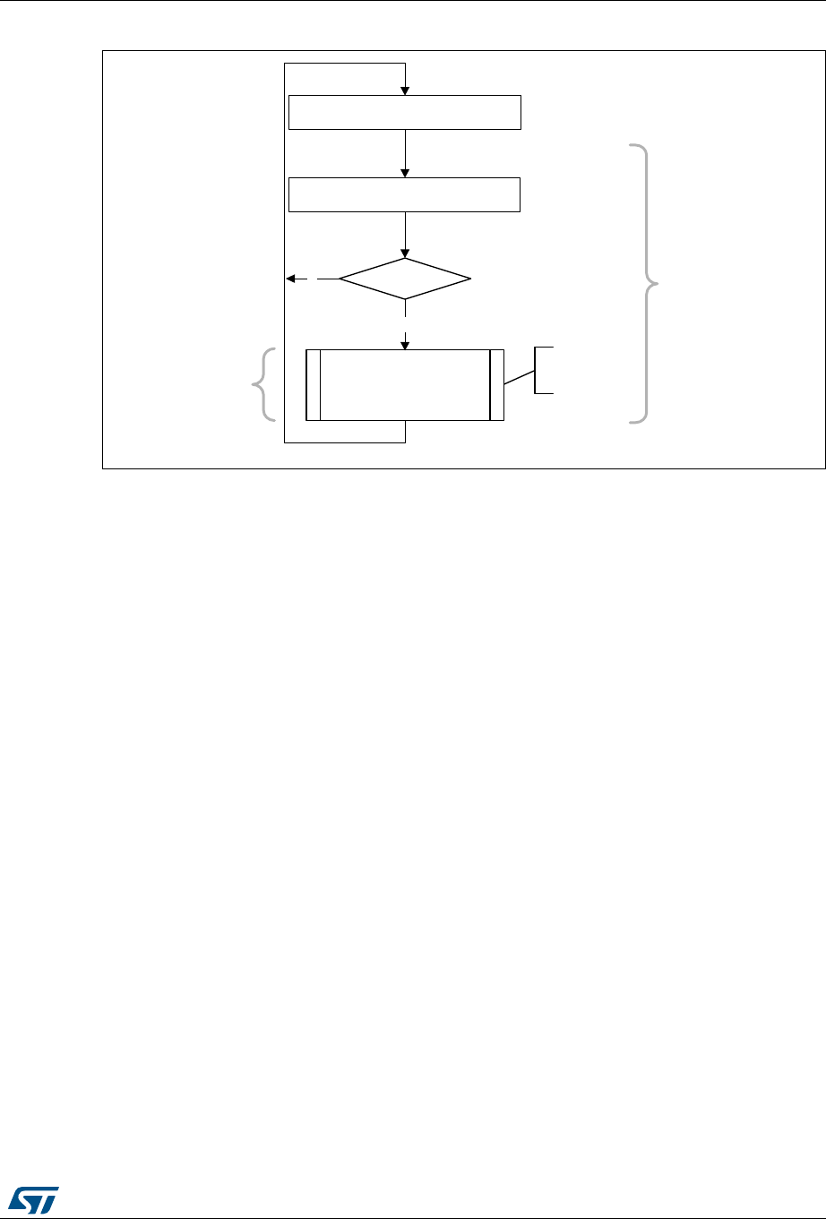
RM0090 Rev 18 1519/1749
RM0090 USB on-the-go high-speed (OTG_HS)
1543
Figure 426. Receive FIFO packet read in slave mode
•SETUP transactions
This section describes how the core handles SETUP packets and the application’s
sequence for handling SETUP transactions.
•Application requirements
1. To receive a SETUP packet, the STUPCNT field (OTG_HS_DOEPTSIZx) in a control
OUT endpoint must be programmed to a nonzero value. When the application
programs the STUPCNT field to a nonzero value, the core receives SETUP packets
and writes them to the receive FIFO, irrespective of the NAK status and EPENA bit
setting in OTG_HS_DOEPCTLx. The STUPCNT field is decremented every time the
control endpoint receives a SETUP packet. If the STUPCNT field is not programmed to
a proper value before receiving a SETUP packet, the core still receives the SETUP
packet and decrements the STUPCNT field, but the application may not be able to
determine the correct number of SETUP packets received in the Setup stage of a
control transfer.
– STUPCNT = 3 in OTG_HS_DOEPTSIZx
2. The application must always allocate some extra space in the Receive data FIFO, to be
able to receive up to three SETUP packets on a control endpoint.
– The space to be reserved is 10 words. Three words are required for the first
SETUP packet, 1 word is required for the Setup stage done word and 6 words are
required to store two extra SETUP packets among all control endpoints.
– 3 words per SETUP packet are required to store 8 bytes of SETUP data and 4
bytes of SETUP status (Setup packet pattern). The core reserves this space in the
receive data.
– FIFO to write SETUP data only, and never uses this space for data packets.
3. The application must read the 2 words of the SETUP packet from the receive FIFO.
4. The application must read and discard the Setup stage done word from the receive
FIFO.
•Internal data flow
dword_cnt =
BCNT[11:2] +C
(BCNT[1]
| BCNT[1])
rcv_out_pkt()
rd_data = rd_reg (OTG_FS_GRXSTSP);
mem[0:dword_cnt-1] =
rd_rxfifo(rd_data.EPNUM,
dword_cnt)
N
rd_data.BCNT = 0
wait until RXFLVL in OTG_FS_GINTSTSG
packet
store in
memory
Y
ai15677

USB on-the-go high-speed (OTG_HS) RM0090
1520/1749 RM0090 Rev 18
5. When a SETUP packet is received, the core writes the received data to the receive
FIFO, without checking for available space in the receive FIFO and irrespective of the
endpoint’s NAK and STALL bit settings.
– The core internally sets the IN NAK and OUT NAK bits for the control IN/OUT
endpoints on which the SETUP packet was received.
6. For every SETUP packet received on the USB, 3 words of data are written to the
receive FIFO, and the STUPCNT field is decremented by 1.
– The first word contains control information used internally by the core
– The second word contains the first 4 bytes of the SETUP command
– The third word contains the last 4 bytes of the SETUP command
7. When the Setup stage changes to a Data IN/OUT stage, the core writes an entry
(Setup stage done word) to the receive FIFO, indicating the completion of the Setup
stage.
8. On the AHB side, SETUP packets are emptied by the application.
9. When the application pops the Setup stage done word from the receive FIFO, the core
interrupts the application with an STUP interrupt (OTG_HS_DOEPINTx), indicating it
can process the received SETUP packet.
– The core clears the endpoint enable bit for control OUT endpoints.
•Application programming sequence
1. Program the OTG_HS_DOEPTSIZx register.
– STUPCNT = 3
2. Wait for the RXFLVL interrupt (OTG_HS_GINTSTS) and empty the data packets from
the receive FIFO.
3. Assertion of the STUP interrupt (OTG_HS_DOEPINTx) marks a successful completion
of the SETUP Data Transfer.
– On this interrupt, the application must read the OTG_HS_DOEPTSIZx register to
determine the number of SETUP packets received and process the last received
SETUP packet.
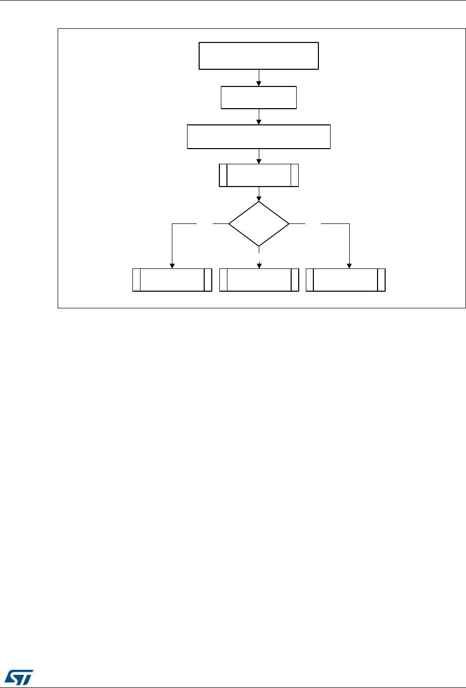
RM0090 Rev 18 1521/1749
RM0090 USB on-the-go high-speed (OTG_HS)
1543
Figure 427. Processing a SETUP packet
•Handling more than three back-to-back SETUP packets
Per the USB 2.0 specification, normally, during a SETUP packet error, a host does not send
more than three back-to-back SETUP packets to the same endpoint. However, the USB 2.0
specification does not limit the number of back-to-back SETUP packets a host can send to
the same endpoint. When this condition occurs, the OTG_HS controller generates an
interrupt (B2BSTUP in OTG_HS_DOEPINTx).
•Setting the global OUT NAK
Internal data flow:
1. When the application sets the Global OUT NAK (SGONAK bit in OTG_HS_DCTL), the
core stops writing data, except SETUP packets, to the receive FIFO. Irrespective of the
space availability in the receive FIFO, nonisochronous OUT tokens receive a NAK
handshake response, and the core ignores isochronous OUT data packets
2. The core writes the Global OUT NAK pattern to the receive FIFO. The application must
reserve enough receive FIFO space to write this data pattern.
3. When the application pops the Global OUT NAK pattern word from the receive FIFO,
the core sets the GONAKEFF interrupt (OTG_HS_GINTSTS).
4. Once the application detects this interrupt, it can assume that the core is in Global OUT
NAK mode. The application can clear this interrupt by clearing the SGONAK bit in
OTG_HS_DCTL.
Wait for STUP in OTG_FS_DOEPINTx
rem_supcnt =
rd_reg(DOEPTSIZx)
setup_cmd[31:0] = mem[4 – 2 * rem_supcnt]
setup_cmd[63:32] = mem[5 – 2 * rem_supcnt]
ctrl-rd/wr/2 stage
Find setup cmd type
Write
2-stage
Read
setup_np_in_pkt
Status IN phase
rcv_out_pkt
Data OUT phase
setup_np_in_pkt
Data IN phase
ai15678

USB on-the-go high-speed (OTG_HS) RM0090
1522/1749 RM0090 Rev 18
Application programming sequence:
1. To stop receiving any kind of data in the receive FIFO, the application must set the
Global OUT NAK bit by programming the following field:
– SGONAK = 1 in OTG_HS_DCTL
2. Wait for the assertion of the GONAKEFF interrupt in OTG_HS_GINTSTS. When
asserted, this interrupt indicates that the core has stopped receiving any type of data
except SETUP packets.
3. The application can receive valid OUT packets after it has set SGONAK in
OTG_HS_DCTL and before the core asserts the GONAKEFF interrupt
(OTG_HS_GINTSTS).
4. The application can temporarily mask this interrupt by writing to the GINAKEFFM bit in
GINTMSK.
– GINAKEFFM = 0 in GINTMSK
5. Whenever the application is ready to exit the Global OUT NAK mode, it must clear the
SGONAK bit in OTG_HS_DCTL. This also clears the GONAKEFF interrupt
(OTG_HS_GINTSTS).
– OTG_HS_DCTL = 1 in CGONAK
6. If the application has masked this interrupt earlier, it must be unmasked as follows:
– GINAKEFFM = 1 in GINTMSK
•Disabling an OUT endpoint
The application must use this sequence to disable an OUT endpoint that it has enabled.
Application programming sequence:
1. Before disabling any OUT endpoint, the application must enable Global OUT NAK
mode in the core.
– SGONAK = 1 in OTG_HS_DCTL
2. Wait for the GONAKEFF interrupt (OTG_HS_GINTSTS)
3. Disable the required OUT endpoint by programming the following fields:
– EPDIS = 1 in OTG_HS_DOEPCTLx
– SNAK = 1 in OTG_HS_DOEPCTLx
4. Wait for the EPDISD interrupt (OTG_HS_DOEPINTx), which indicates that the OUT
endpoint is completely disabled. When the EPDISD interrupt is asserted, the core also
clears the following bits:
– EPDIS = 0 in OTG_HS_DOEPCTLx
– EPENA = 0 in OTG_HS_DOEPCTLx
5. The application must clear the Global OUT NAK bit to start receiving data from other
nondisabled OUT endpoints.
– SGONAK = 0 in OTG_HS_DCTL
•Transfer Stop Programming for OUT endpoints
The application must use the following programing sequence to stop any transfers (because
of an interrupt from the host, typically a reset).
Sequence of operations:

RM0090 Rev 18 1523/1749
RM0090 USB on-the-go high-speed (OTG_HS)
1543
1. Enable all OUT endpoints by setting
– EPENA = 1 in all OTG_HS_DOEPCTLx registers.
2. Flush the RxFIFO as follows
– Poll OTG_HS_GRSTCTL.AHBIDL until it is 1. This indicates that AHB master is
idle.
– Perform read modify write operation on OTG_HS_GRSTCTL.RXFFLSH =1
– Poll OTG_HS_GRSTCTL.RXFFLSH until it is 0, but also using a timeout of less
than 10 milli-seconds (corresponds to minimum reset signaling duration). If 0 is
seen before the timeout, then the RxFIFO flush is successful. If at the moment the
timeout occurs, there is still a 1, (this may be due to a packet on EP0 coming from
the host) then go back (once only) to the previous step (“Perform read modify write
operation”).
3. Before disabling any OUT endpoint, the application must enable Global OUT NAK
mode in the core, according to the instructions in “Setting the global OUT NAK on
page 1521”. This ensures that data in the RxFIFO is sent to the application
successfully. Set SGONAK = 1 in OTG_HS_DCTL
4. Wait for the GONAKEFF interrupt (OTG_HS_GINTSTS)
5. Disable all active OUT endpoints by programming the following register bits:
– EPDIS = 1 in registers OTG_HS_DOEPCTLx
– SNAK = 1 in registers OTG_HS_DOEPCTLx
6. Wait for the EPDIS interrupt in OTG_HS_DOEPINTx for each OUT endpoint
programmed in the previous step. The EPDIS interrupt in OTG_HS_DOEPINTx
indicates that the corresponding OUT endpoint is completely disabled. When the
EPDIS interrupt is asserted, the following bits are cleared:
– EPENA = 0 in registers OTG_HS_DOEPCTLx
– EPDIS = 0 in registers OTG_HS_DOEPCTLx
– SNAK = 0 in registers OTG_HS_DOEPCTLx
•Generic non-isochronous OUT data transfers
This section describes a regular nonisochronous OUT data transfer (control, bulk, or
interrupt).
Application requirements:
1. Before setting up an OUT transfer, the application must allocate a buffer in the memory
to accommodate all data to be received as part of the OUT transfer.
2. For OUT transfers, the transfer size field in the endpoint’s transfer size register must be
a multiple of the maximum packet size of the endpoint, adjusted to the word boundary.
– transfer size[EPNUM] = n × (MPSIZ[EPNUM] + 4 – (MPSIZ[EPNUM] mod 4))
– packet count[EPNUM] = n
–n > 0
3. On any OUT endpoint interrupt, the application must read the endpoint’s transfer size
register to calculate the size of the payload in the memory. The received payload size
can be less than the programmed transfer size.
– Payload size in memory = application programmed initial transfer size – core
updated final transfer size
– Number of USB packets in which this payload was received = application
programmed initial packet count – core updated final packet count

USB on-the-go high-speed (OTG_HS) RM0090
1524/1749 RM0090 Rev 18
Internal data flow:
1. The application must set the transfer size and packet count fields in the endpoint-
specific registers, clear the NAK bit, and enable the endpoint to receive the data.
2. Once the NAK bit is cleared, the core starts receiving data and writes it to the receive
FIFO, as long as there is space in the receive FIFO. For every data packet received on
the USB, the data packet and its status are written to the receive FIFO. Every packet
(maximum packet size or short packet) written to the receive FIFO decrements the
packet count field for that endpoint by 1.
– OUT data packets received with bad data CRC are flushed from the receive FIFO
automatically.
– After sending an ACK for the packet on the USB, the core discards
nonisochronous OUT data packets that the host, which cannot detect the ACK, re-
sends. The application does not detect multiple back-to-back data OUT packets
on the same endpoint with the same data PID. In this case the packet count is not
decremented.
– If there is no space in the receive FIFO, isochronous or nonisochronous data
packets are ignored and not written to the receive FIFO. Additionally,
nonisochronous OUT tokens receive a NAK handshake reply.
– In all the above three cases, the packet count is not decremented because no data
are written to the receive FIFO.
3. When the packet count becomes 0 or when a short packet is received on the endpoint,
the NAK bit for that endpoint is set. Once the NAK bit is set, the isochronous or
nonisochronous data packets are ignored and not written to the receive FIFO, and
nonisochronous OUT tokens receive a NAK handshake reply.
4. After the data are written to the receive FIFO, the application reads the data from the
receive FIFO and writes it to external memory, one packet at a time per endpoint.
5. At the end of every packet write on the AHB to external memory, the transfer size for
the endpoint is decremented by the size of the written packet.
6. The OUT data transfer completed pattern for an OUT endpoint is written to the receive
FIFO on one of the following conditions:
– The transfer size is 0 and the packet count is 0
– The last OUT data packet written to the receive FIFO is a short packet
(0 ≤packet size < maximum packet size)
7. When either the application pops this entry (OUT data transfer completed), a transfer
completed interrupt is generated for the endpoint and the endpoint enable is cleared.
Application programming sequence:

RM0090 Rev 18 1525/1749
RM0090 USB on-the-go high-speed (OTG_HS)
1543
1. Program the OTG_HS_DOEPTSIZx register for the transfer size and the
corresponding packet count.
2. Program the OTG_HS_DOEPCTLx register with the endpoint characteristics, and set
the EPENA and CNAK bits.
– EPENA = 1 in OTG_HS_DOEPCTLx
– CNAK = 1 in OTG_HS_DOEPCTLx
3. Wait for the RXFLVL interrupt (in OTG_HS_GINTSTS) and empty the data packets
from the receive FIFO.
– This step can be repeated many times, depending on the transfer size.
4. Asserting the XFRC interrupt (OTG_HS_DOEPINTx) marks a successful completion of
the nonisochronous OUT data transfer.
5. Read the OTG_HS_DOEPTSIZx register to determine the size of the received data
payload.
•Generic isochronous OUT data transfer
This section describes a regular isochronous OUT data transfer.
Application requirements:
1. All the application requirements for nonisochronous OUT data transfers also apply to
isochronous OUT data transfers.
2. For isochronous OUT data transfers, the transfer size and packet count fields must
always be set to the number of maximum-packet-size packets that can be received in a
single frame and no more. Isochronous OUT data transfers cannot span more than 1
frame.
3. The application must read all isochronous OUT data packets from the receive FIFO
(data and status) before the end of the periodic frame (EOPF interrupt in
OTG_HS_GINTSTS).
4. To receive data in the following frame, an isochronous OUT endpoint must be enabled
after the EOPF (OTG_HS_GINTSTS) and before the SOF (OTG_HS_GINTSTS).
Internal data flow:
1. The internal data flow for isochronous OUT endpoints is the same as that for
nonisochronous OUT endpoints, but for a few differences.
2. When an isochronous OUT endpoint is enabled by setting the Endpoint Enable and
clearing the NAK bits, the Even/Odd frame bit must also be set appropriately. The core
receives data on an isochronous OUT endpoint in a particular frame only if the
following condition is met:
– EONUM (in OTG_HS_DOEPCTLx) = SOFFN[0] (in OTG_HS_DSTS)
3. When the application completely reads an isochronous OUT data packet (data and
status) from the receive FIFO, the core updates the RXDPID field in
OTG_HS_DOEPTSIZx with the data PID of the last isochronous OUT data packet read
from the receive FIFO.
Application programming sequence:

USB on-the-go high-speed (OTG_HS) RM0090
1526/1749 RM0090 Rev 18
1. Program the OTG_HS_DOEPTSIZx register for the transfer size and the
corresponding packet count
2. Program the OTG_HS_DOEPCTLx register with the endpoint characteristics and set
the Endpoint Enable, ClearNAK, and Even/Odd frame bits.
– EPENA = 1
–CNAK=1
– EONUM = (0: Even/1: Odd)
3. In Slave mode, wait for the RXFLVL interrupt (in OTG_HS_GINTSTS) and empty the
data packets from the receive FIFO
– This step can be repeated many times, depending on the transfer size.
4. The assertion of the XFRC interrupt (in OTG_HS_DOEPINTx) marks the completion of
the isochronous OUT data transfer. This interrupt does not necessarily mean that the
data in memory are good.
5. This interrupt cannot always be detected for isochronous OUT transfers. Instead, the
application can detect the IISOOXFRM interrupt in OTG_HS_GINTSTS.
6. Read the OTG_HS_DOEPTSIZx register to determine the size of the received transfer
and to determine the validity of the data received in the frame. The application must
treat the data received in memory as valid only if one of the following conditions is met:
– RXDPID = D0 (in OTG_HS_DOEPTSIZx) and the number of USB packets in
which this payload was received = 1
– RXDPID = D1 (in OTG_HS_DOEPTSIZx) and the number of USB packets in
which this payload was received = 2
– RXDPID = D2 (in OTG_HS_DOEPTSIZx) and the number of USB packets in
which this payload was received = 3
The number of USB packets in which this payload was received =
Application programmed initial packet count – Core updated final packet count
The application can discard invalid data packets.
•Incomplete isochronous OUT data transfers
This section describes the application programming sequence when isochronous OUT data
packets are dropped inside the core.
Internal data flow:
1. For isochronous OUT endpoints, the XFRC interrupt (in OTG_HS_DOEPINTx) may not
always be asserted. If the core drops isochronous OUT data packets, the application
could fail to detect the XFRC interrupt (OTG_HS_DOEPINTx) under the following
circumstances:
– When the receive FIFO cannot accommodate the complete ISO OUT data packet,
the core drops the received ISO OUT data
– When the isochronous OUT data packet is received with CRC errors
– When the isochronous OUT token received by the core is corrupted
– When the application is very slow in reading the data from the receive FIFO
2. When the core detects an end of periodic frame before transfer completion to all
isochronous OUT endpoints, it asserts the incomplete Isochronous OUT data interrupt
(IISOOXFRM in OTG_HS_GINTSTS), indicating that an XFRC interrupt (in
OTG_HS_DOEPINTx) is not asserted on at least one of the isochronous OUT
endpoints. At this point, the endpoint with the incomplete transfer remains enabled, but
no active transfers remain in progress on this endpoint on the USB.

RM0090 Rev 18 1527/1749
RM0090 USB on-the-go high-speed (OTG_HS)
1543
Application programming sequence:
1. Asserting the IISOOXFRM interrupt (OTG_HS_GINTSTS) indicates that in the current
frame, at least one isochronous OUT endpoint has an incomplete transfer.
2. If this occurs because isochronous OUT data is not completely emptied from the
endpoint, the application must ensure that the application empties all isochronous OUT
data (data and status) from the receive FIFO before proceeding.
– When all data are emptied from the receive FIFO, the application can detect the
XFRC interrupt (OTG_HS_DOEPINTx). In this case, the application must re-
enable the endpoint to receive isochronous OUT data in the next frame.
3. When it receives an IISOOXFRM interrupt (in OTG_HS_GINTSTS), the application
must read the control registers of all isochronous OUT endpoints
(OTG_HS_DOEPCTLx) to determine which endpoints had an incomplete transfer in
the current micro-frame. An endpoint transfer is incomplete if both the following
conditions are met:
– EONUM bit (in OTG_HS_DOEPCTLx) = SOFFN[0] (in OTG_HS_DSTS)
– EPENA = 1 (in OTG_HS_DOEPCTLx)
4. The previous step must be performed before the SOF interrupt (in
OTG_HS_GINTSTS) is detected, to ensure that the current frame number is not
changed.
5. For isochronous OUT endpoints with incomplete transfers, the application must discard
the data in the memory and disable the endpoint by setting the EPDIS bit in
OTG_HS_DOEPCTLx.
6. Wait for the EPDIS interrupt (in OTG_HS_DOEPINTx) and enable the endpoint to
receive new data in the next frame.
– Because the core can take some time to disable the endpoint, the application may
not be able to receive the data in the next frame after receiving bad isochronous
data.
•Stalling a nonisochronous OUT endpoint
This section describes how the application can stall a nonisochronous endpoint.
1. Put the core in the Global OUT NAK mode.
2. Disable the required endpoint
– When disabling the endpoint, instead of setting the SNAK bit in
OTG_HS_DOEPCTL, set STALL = 1 (in OTG_HS_DOEPCTL).
The STALL bit always takes precedence over the NAK bit.
3. When the application is ready to end the STALL handshake for the endpoint, the
STALL bit (in OTG_HS_DOEPCTLx) must be cleared.
4. If the application is setting or clearing a STALL for an endpoint due to a
SetFeature.Endpoint Halt or ClearFeature.Endpoint Halt command, the STALL bit must
be set or cleared before the application sets up the Status stage transfer on the control
endpoint.
Examples
This section describes and depicts some fundamental transfer types and scenarios.
•Slave mode bulk OUT transaction
Figure 428 depicts the reception of a single Bulk OUT Data packet from the USB to the AHB
and describes the events involved in the process.
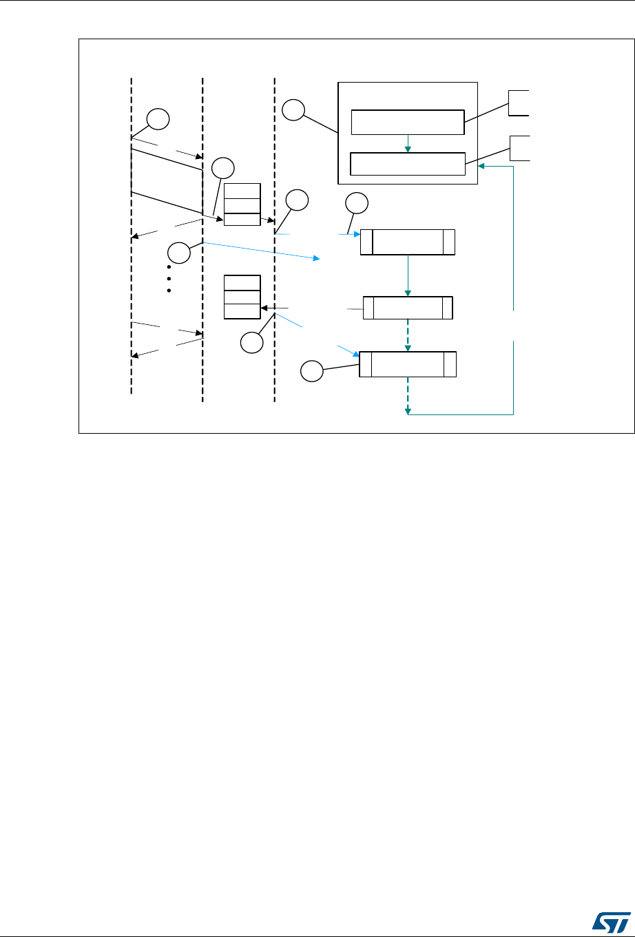
USB on-the-go high-speed (OTG_HS) RM0090
1528/1749 RM0090 Rev 18
Figure 428. Slave mode bulk OUT transaction
After a SetConfiguration/SetInterface command, the application initializes all OUT endpoints
by setting CNAK = 1 and EPENA = 1 (in OTG_HS_DOEPCTLx), and setting a suitable
XFRSIZ and PKTCNT in the OTG_HS_DOEPTSIZx register.
1. Host attempts to send data (OUT token) to an endpoint.
2. When the core receives the OUT token on the USB, it stores the packet in the RxFIFO
because space is available there.
3. After writing the complete packet in the RxFIFO, the core then asserts the RXFLVL
interrupt (in OTG_HS_GINTSTS).
4. On receiving the PKTCNT number of USB packets, the core internally sets the NAK bit
for this endpoint to prevent it from receiving any more packets.
5. The application processes the interrupt and reads the data from the RxFIFO.
6. When the application has read all the data (equivalent to XFRSIZ), the core generates
an XFRC interrupt (in OTG_HS_DOEPINTx).
7. The application processes the interrupt and uses the setting of the XFRC interrupt bit
(in OTG_HS_DOEPINTx) to determine that the intended transfer is complete.
IN data transfers
•Packet write
This section describes how the application writes data packets to the endpoint FIFO in Slave
mode when dedicated transmit FIFOs are enabled.
init_out_ep
Host DeviceUSB
OUT
ACK
RXFLVL intr i
wr_reg (DOEPTSIZx)
wr_reg(DOEPCTLx)
512 bytes
OUT
NAK
xact _1
Application
XFRC
intr
DOEPCTLx.NAK=1
PKTCNT 0
XFRSIZ = 0
r
idle until intr
rcv_out _pkt()
idle until intr
On new xfer
or RxFIFO
not empty
1
2
3
4
5
6
7
8
XFRSIZ = 512 bytes
PKTCNT = 1
EPENA = 1
CNAK = 1
ai15679

RM0090 Rev 18 1529/1749
RM0090 USB on-the-go high-speed (OTG_HS)
1543
1. The application can either choose the polling or the interrupt mode.
– In polling mode, the application monitors the status of the endpoint transmit data
FIFO by reading the OTG_HS_DTXFSTSx register, to determine if there is
enough space in the data FIFO.
– In interrupt mode, the application waits for the TXFE interrupt (in
OTG_HS_DIEPINTx) and then reads the OTG_HS_DTXFSTSx register, to
determine if there is enough space in the data FIFO.
– To write a single nonzero length data packet, there must be space to write the
entire packet in the data FIFO.
– To write zero length packet, the application must not look at the FIFO space.
2. Using one of the above mentioned methods, when the application determines that
there is enough space to write a transmit packet, the application must first write into the
endpoint control register, before writing the data into the data FIFO. Typically, the
application, must do a read modify write on the OTG_HS_DIEPCTLx register to avoid
modifying the contents of the register, except for setting the Endpoint Enable bit.
The application can write multiple packets for the same endpoint into the transmit FIFO, if
space is available. For periodic IN endpoints, the application must write packets only for one
micro-frame. It can write packets for the next periodic transaction only after getting transfer
complete for the previous transaction.
•Setting IN endpoint NAK
Internal data flow:
1. When the application sets the IN NAK for a particular endpoint, the core stops
transmitting data on the endpoint, irrespective of data availability in the endpoint’s
transmit FIFO.
2. Nonisochronous IN tokens receive a NAK handshake reply
– Isochronous IN tokens receive a zero-data-length packet reply
3. The core asserts the INEPNE (IN endpoint NAK effective) interrupt in
OTG_HS_DIEPINTx in response to the SNAK bit in OTG_HS_DIEPCTLx.
4. Once this interrupt is seen by the application, the application can assume that the
endpoint is in IN NAK mode. This interrupt can be cleared by the application by setting
the CNAK bit in OTG_HS_DIEPCTLx.
Application programming sequence:

USB on-the-go high-speed (OTG_HS) RM0090
1530/1749 RM0090 Rev 18
1. To stop transmitting any data on a particular IN endpoint, the application must set the
IN NAK bit. To set this bit, the following field must be programmed.
– SNAK = 1 in OTG_HS_DIEPCTLx
2. Wait for assertion of the INEPNE interrupt in OTG_HS_DIEPINTx. This interrupt
indicates that the core has stopped transmitting data on the endpoint.
3. The core can transmit valid IN data on the endpoint after the application has set the
NAK bit, but before the assertion of the NAK Effective interrupt.
4. The application can mask this interrupt temporarily by writing to the INEPNEM bit in
DIEPMSK.
– INEPNEM = 0 in DIEPMSK
5. To exit Endpoint NAK mode, the application must clear the NAK status bit (NAKSTS) in
OTG_HS_DIEPCTLx. This also clears the INEPNE interrupt (in OTG_HS_DIEPINTx).
– CNAK = 1 in OTG_HS_DIEPCTLx
6. If the application masked this interrupt earlier, it must be unmasked as follows:
– INEPNEM = 1 in DIEPMSK
•IN endpoint disable
Use the following sequence to disable a specific IN endpoint that has been previously
enabled.
Application programming sequence:
1. The application must stop writing data on the AHB for the IN endpoint to be disabled.
2. The application must set the endpoint in NAK mode.
– SNAK = 1 in OTG_HS_DIEPCTLx
3. Wait for the INEPNE interrupt in OTG_HS_DIEPINTx.
4. Set the following bits in the OTG_HS_DIEPCTLx register for the endpoint that must be
disabled.
– EPDIS = 1 in OTG_HS_DIEPCTLx
– SNAK = 1 in OTG_HS_DIEPCTLx
5. Assertion of the EPDISD interrupt in OTG_HS_DIEPINTx indicates that the core has
completely disabled the specified endpoint. Along with the assertion of the interrupt, the
core also clears the following bits:
– EPENA = 0 in OTG_HS_DIEPCTLx
– EPDIS = 0 in OTG_HS_DIEPCTLx
6. The application must read the OTG_HS_DIEPTSIZx register for the periodic IN EP, to
calculate how much data on the endpoint were transmitted on the USB.
7. The application must flush the data in the Endpoint transmit FIFO, by setting the
following fields in the OTG_HS_GRSTCTL register:
– TXFNUM (in OTG_HS_GRSTCTL) = Endpoint transmit FIFO number
– TXFFLSH in (OTG_HS_GRSTCTL) = 1
The application must poll the OTG_HS_GRSTCTL register, until the TXFFLSH bit is cleared
by the core, which indicates the end of flush operation. To transmit new data on this
endpoint, the application can re-enable the endpoint at a later point.
•Transfer Stop Programming for IN endpoints
The application must use the following programing sequence to stop any transfers (because
of an interrupt from the host, typically a reset).

RM0090 Rev 18 1531/1749
RM0090 USB on-the-go high-speed (OTG_HS)
1543
Sequence of operations:
1. Disable the IN endpoint by setting:
– EPDIS = 1 in all OTG_HS_DIEPCTLx registers
2. Wait for the EPDIS interrupt in OTG_HS_DIEPINTx, which indicates that the IN
endpoint is completely disabled. When the EPDIS interrupt is asserted the following
bits are cleared:
– EPDIS = 0 in OTG_HS_DIEPCTLx
– EPENA = 0 in OTG_HS_DIEPCTLx
3. Flush the TxFIFO by programming the following bits:
– TXFFLSH = 1 in OTG_HS_GRSTCTL
– TXFNUM = “FIFO number specific to endpoint” in OTG_HS_GRSTCTL
4. The application can start polling till TXFFLSH in OTG_HS_GRSTCTL is cleared. When
this bit is cleared, it ensures that there is no data left in the Tx FIFO.
•Generic nonperiodic IN data transfers
Application requirements:
1. Before setting up an IN transfer, the application must ensure that all data to be
transmitted as part of the IN transfer are part of a single buffer.
2. For IN transfers, the Transfer Size field in the Endpoint Transfer Size register denotes a
payload that constitutes multiple maximum-packet-size packets and a single short
packet. This short packet is transmitted at the end of the transfer.
– To transmit a few maximum-packet-size packets and a short packet at the end of
the transfer:
Transfer size[EPNUM] = x × MPSIZ[EPNUM] + sp
If (sp > 0), then packet count[EPNUM] = x + 1.
Otherwise, packet count[EPNUM] = x
– To transmit a single zero-length data packet:
Transfer size[EPNUM] = 0
Packet count[EPNUM] = 1
– To transmit a few maximum-packet-size packets and a zero-length data packet at
the end of the transfer, the application must split the transfer into two parts. The
first sends maximum-packet-size data packets and the second sends the zero-
length data packet alone.
First transfer: transfer size[EPNUM] = x × MPSIZ[epnum]; packet count = n;
Second transfer: transfer size[EPNUM] = 0; packet count = 1;
3. Once an endpoint is enabled for data transfers, the core updates the Transfer size
register. At the end of the IN transfer, the application must read the Transfer size
register to determine how much data posted in the transmit FIFO have already been
sent on the USB.
4. Data fetched into transmit FIFO = Application-programmed initial transfer size – core-
updated final transfer size
– Data transmitted on USB = (application-programmed initial packet count – Core
updated final packet count) × MPSIZ[EPNUM]
– Data yet to be transmitted on USB = (Application-programmed initial transfer size
– data transmitted on USB)
Internal data flow:

USB on-the-go high-speed (OTG_HS) RM0090
1532/1749 RM0090 Rev 18
1. The application must set the transfer size and packet count fields in the endpoint-
specific registers and enable the endpoint to transmit the data.
2. The application must also write the required data to the transmit FIFO for the endpoint.
3. Every time a packet is written into the transmit FIFO by the application, the transfer size
for that endpoint is decremented by the packet size. The data is fetched from the
memory by the application, until the transfer size for the endpoint becomes 0. After
writing the data into the FIFO, the “number of packets in FIFO” count is incremented
(this is a 3-bit count, internally maintained by the core for each IN endpoint transmit
FIFO. The maximum number of packets maintained by the core at any time in an IN
endpoint FIFO is eight). For zero-length packets, a separate flag is set for each FIFO,
without any data in the FIFO.
4. Once the data are written to the transmit FIFO, the core reads them out upon receiving
an IN token. For every nonisochronous IN data packet transmitted with an ACK
handshake, the packet count for the endpoint is decremented by one, until the packet
count is zero. The packet count is not decremented on a timeout.
5. For zero length packets (indicated by an internal zero length flag), the core sends out a
zero-length packet for the IN token and decrements the packet count field.
6. If there are no data in the FIFO for a received IN token and the packet count field for
that endpoint is zero, the core generates an “IN token received when TxFIFO is empty”
(ITTXFE) Interrupt for the endpoint, provided that the endpoint NAK bit is not set. The
core responds with a NAK handshake for nonisochronous endpoints on the USB.
7. The core internally rewinds the FIFO pointers and no timeout interrupt is generated.
8. When the transfer size is 0 and the packet count is 0, the transfer complete (XFRC)
interrupt for the endpoint is generated and the endpoint enable is cleared.
Application programming sequence:
1. Program the OTG_HS_DIEPTSIZx register with the transfer size and corresponding
packet count.
2. Program the OTG_HS_DIEPCTLx register with the endpoint characteristics and set the
CNAK and EPENA (Endpoint Enable) bits.
3. When transmitting nonzero length data packet, the application must poll the
OTG_HS_DTXFSTSx register (where x is the FIFO number associated with that
endpoint) to determine whether there is enough space in the data FIFO. The
application can optionally use TXFE (in OTG_HS_DIEPINTx) before writing the data.
•Generic periodic IN data transfers
This section describes a typical periodic IN data transfer.
Application requirements:
1. Application requirements 1, 2, 3, and 4 of Generic nonperiodic IN data transfers on
page 1531 also apply to periodic IN data transfers, except for a slight modification of
requirement 2.
– The application can only transmit multiples of maximum-packet-size data packets
or multiples of maximum-packet-size packets, plus a short packet at the end. To

RM0090 Rev 18 1533/1749
RM0090 USB on-the-go high-speed (OTG_HS)
1543
transmit a few maximum-packet-size packets and a short packet at the end of the
transfer, the following conditions must be met:
transfer size[EPNUM] = x × MPSIZ[EPNUM] + sp
(where x is an integer ≥0, and 0 ≤sp < MPSIZ[EPNUM])
If (sp > 0), packet count[EPNUM] = x + 1
Otherwise, packet count[EPNUM] = x;
MCNT[EPNUM] = packet count[EPNUM]
– The application cannot transmit a zero-length data packet at the end of a transfer.
It can transmit a single zero-length data packet by itself. To transmit a single zero-
length data packet:
– transfer size[EPNUM] = 0
packet count[EPNUM] = 1
MCNT[EPNUM] = packet count[EPNUM]
2. The application can only schedule data transfers one frame at a time.
– (MCNT – 1) × MPSIZ ≤XFERSIZ ≤MCNT × MPSIZ
– PKTCNT = MCNT (in OTG_HS_DIEPTSIZx)
– If XFERSIZ < MCNT × MPSIZ, the last data packet of the transfer is a short
packet.
– Note that: MCNT is in OTG_HS_DIEPTSIZx, MPSIZ is in OTG_HS_DIEPCTLx,
PKTCNT is in OTG_HS_DIEPTSIZx and XFERSIZ is in OTG_HS_DIEPTSIZx
3. The complete data to be transmitted in the frame must be written into the transmit FIFO
by the application, before the IN token is received. Even when 1 word of the data to be
transmitted per frame is missing in the transmit FIFO when the IN token is received, the
core behaves as when the FIFO is empty. When the transmit FIFO is empty:
– A zero data length packet would be transmitted on the USB for isochronous IN
endpoints
– A NAK handshake would be transmitted on the USB for interrupt IN endpoints
4. For a high-bandwidth IN endpoint with three packets in a frame, the application can
program the endpoint FIFO size to be 2 × max_pkt_size and have the third packet
loaded in after the first packet has been transmitted on the USB.
Internal data flow:
1. The application must set the transfer size and packet count fields in the endpoint-
specific registers and enable the endpoint to transmit the data.
2. The application must also write the required data to the associated transmit FIFO for
the endpoint.
3. Every time the application writes a packet to the transmit FIFO, the transfer size for that
endpoint is decremented by the packet size. The data are fetched from application
memory until the transfer size for the endpoint becomes 0.
4. When an IN token is received for a periodic endpoint, the core transmits the data in the
FIFO, if available. If the complete data payload (complete packet, in dedicated FIFO

USB on-the-go high-speed (OTG_HS) RM0090
1534/1749 RM0090 Rev 18
mode) for the frame is not present in the FIFO, then the core generates an IN token
received when TxFIFO empty interrupt for the endpoint.
– A zero-length data packet is transmitted on the USB for isochronous IN endpoints
– A NAK handshake is transmitted on the USB for interrupt IN endpoints
5. The packet count for the endpoint is decremented by 1 under the following conditions:
– For isochronous endpoints, when a zero- or nonzero-length data packet is
transmitted
– For interrupt endpoints, when an ACK handshake is transmitted
– When the transfer size and packet count are both 0, the transfer completed
interrupt for the endpoint is generated and the endpoint enable is cleared.
6. At the “Periodic frame Interval” (controlled by PFIVL in OTG_HS_DCFG), when the
core finds nonempty any of the isochronous IN endpoint FIFOs scheduled for the
current frame nonempty, the core generates an IISOIXFR interrupt in
OTG_HS_GINTSTS.
Application programming sequence:
1. Program the OTG_HS_DIEPCTLx register with the endpoint characteristics and set the
CNAK and EPENA bits.
2. Write the data to be transmitted in the next frame to the transmit FIFO.
3. Asserting the ITTXFE interrupt (in OTG_HS_DIEPINTx) indicates that the application
has not yet written all data to be transmitted to the transmit FIFO.
4. If the interrupt endpoint is already enabled when this interrupt is detected, ignore the
interrupt. If it is not enabled, enable the endpoint so that the data can be transmitted on
the next IN token attempt.
5. Asserting the XFRC interrupt (in OTG_HS_DIEPINTx) with no ITTXFE interrupt in
OTG_HS_DIEPINTx indicates the successful completion of an isochronous IN transfer.
A read to the OTG_HS_DIEPTSIZx register must give transfer size = 0 and packet
count = 0, indicating all data were transmitted on the USB.
6. Asserting the XFRC interrupt (in OTG_HS_DIEPINTx), with or without the ITTXFE
interrupt (in OTG_HS_DIEPINTx), indicates the successful completion of an interrupt
IN transfer. A read to the OTG_HS_DIEPTSIZx register must give transfer size = 0 and
packet count = 0, indicating all data were transmitted on the USB.
7. Asserting the incomplete isochronous IN transfer (IISOIXFR) interrupt in
OTG_HS_GINTSTS with none of the aforementioned interrupts indicates the core did
not receive at least 1 periodic IN token in the current frame.
•Incomplete isochronous IN data transfers
This section describes what the application must do on an incomplete isochronous IN data
transfer.
Internal data flow:
1. An isochronous IN transfer is treated as incomplete in one of the following conditions:
a) The core receives a corrupted isochronous IN token on at least one isochronous
IN endpoint. In this case, the application detects an incomplete isochronous IN
transfer interrupt (IISOIXFR in OTG_HS_GINTSTS).
b) The application is slow to write the complete data payload to the transmit FIFO
and an IN token is received before the complete data payload is written to the
FIFO. In this case, the application detects an IN token received when TxFIFO
empty interrupt in OTG_HS_DIEPINTx. The application can ignore this interrupt,

RM0090 Rev 18 1535/1749
RM0090 USB on-the-go high-speed (OTG_HS)
1543
as it eventually results in an incomplete isochronous IN transfer interrupt
(IISOIXFR in OTG_HS_GINTSTS) at the end of periodic frame.
The core transmits a zero-length data packet on the USB in response to the
received IN token.
2. The application must stop writing the data payload to the transmit FIFO as soon as
possible.
3. The application must set the NAK bit and the disable bit for the endpoint.
4. The core disables the endpoint, clears the disable bit, and asserts the Endpoint Disable
interrupt for the endpoint.
Application programming sequence
1. The application can ignore the IN token received when TxFIFO empty interrupt in
OTG_HS_DIEPINTx on any isochronous IN endpoint, as it eventually results in an
incomplete isochronous IN transfer interrupt (in OTG_HS_GINTSTS).
2. Assertion of the incomplete isochronous IN transfer interrupt (in OTG_HS_GINTSTS)
indicates an incomplete isochronous IN transfer on at least one of the isochronous IN
endpoints.
3. The application must read the Endpoint Control register for all isochronous IN
endpoints to detect endpoints with incomplete IN data transfers.
4. The application must stop writing data to the Periodic Transmit FIFOs associated with
these endpoints on the AHB.
5. Program the following fields in the OTG_HS_DIEPCTLx register to disable the
endpoint:
– SNAK = 1 in OTG_HS_DIEPCTLx
– EPDIS = 1 in OTG_HS_DIEPCTLx
6. The assertion of the Endpoint Disabled interrupt in OTG_HS_DIEPINTx indicates that
the core has disabled the endpoint.
– At this point, the application must flush the data in the associated transmit FIFO or
overwrite the existing data in the FIFO by enabling the endpoint for a new transfer
in the next micro-frame. To flush the data, the application must use the
OTG_HS_GRSTCTL register.
•Stalling nonisochronous IN endpoints
This section describes how the application can stall a nonisochronous endpoint.
Application programming sequence:

USB on-the-go high-speed (OTG_HS) RM0090
1536/1749 RM0090 Rev 18
1. Disable the IN endpoint to be stalled. Set the STALL bit as well.
2. EPDIS = 1 in OTG_HS_DIEPCTLx, when the endpoint is already enabled
– STALL = 1 in OTG_HS_DIEPCTLx
– The STALL bit always takes precedence over the NAK bit
3. Assertion of the Endpoint Disabled interrupt (in OTG_HS_DIEPINTx) indicates to the
application that the core has disabled the specified endpoint.
4. The application must flush the nonperiodic or periodic transmit FIFO, depending on the
endpoint type. In case of a nonperiodic endpoint, the application must re-enable the
other nonperiodic endpoints that do not need to be stalled, to transmit data.
5. Whenever the application is ready to end the STALL handshake for the endpoint, the
STALL bit must be cleared in OTG_HS_DIEPCTLx.
6. If the application sets or clears a STALL bit for an endpoint due to a
SetFeature.Endpoint Halt command or ClearFeature.Endpoint Halt command, the
STALL bit must be set or cleared before the application sets up the Status stage
transfer on the control endpoint.
Special case: stalling the control OUT endpoint
The core must stall IN/OUT tokens if, during the data stage of a control transfer, the host
sends more IN/OUT tokens than are specified in the SETUP packet. In this case, the
application must enable the ITTXFE interrupt in OTG_HS_DIEPINTx and the OTEPDIS
interrupt in OTG_HS_DOEPINTx during the data stage of the control transfer, after the core
has transferred the amount of data specified in the SETUP packet. Then, when the
application receives this interrupt, it must set the STALL bit in the corresponding endpoint
control register, and clear this interrupt.
35.13.8 Worst case response time
When the OTG_HS controller acts as a device, there is a worst case response time for any
tokens that follow an isochronous OUT. This worst case response time depends on the AHB
clock frequency.
The core registers are in the AHB domain, and the core does not accept another token
before updating these register values. The worst case is for any token following an
isochronous OUT, because for an isochronous transaction, there is no handshake and the
next token could come sooner. This worst case value is 7 PHY clocks when the AHB clock
is the same as the PHY clock. When the AHB clock is faster, this value is smaller.
If this worst case condition occurs, the core responds to bulk/interrupt tokens with a NAK
and drops isochronous and SETUP tokens. The host interprets this as a timeout condition
for SETUP and retries the SETUP packet. For isochronous transfers, the Incomplete
isochronous IN transfer interrupt (IISOIXFR) and Incomplete isochronous OUT transfer
interrupt (IISOOXFR) inform the application that isochronous IN/OUT packets were
dropped.
Choosing the value of TRDT in OTG_HS_GUSBCFG
The value in TRDT (OTG_HS_GUSBCFG) is the time it takes for the MAC, in terms of PHY
clocks after it has received an IN token, to get the FIFO status, and thus the first data from
the PFC block. This time involves the synchronization delay between the PHY and AHB
clocks. The worst case delay for this is when the AHB clock is the same as the PHY clock.
In this case, the delay is 5 clocks.
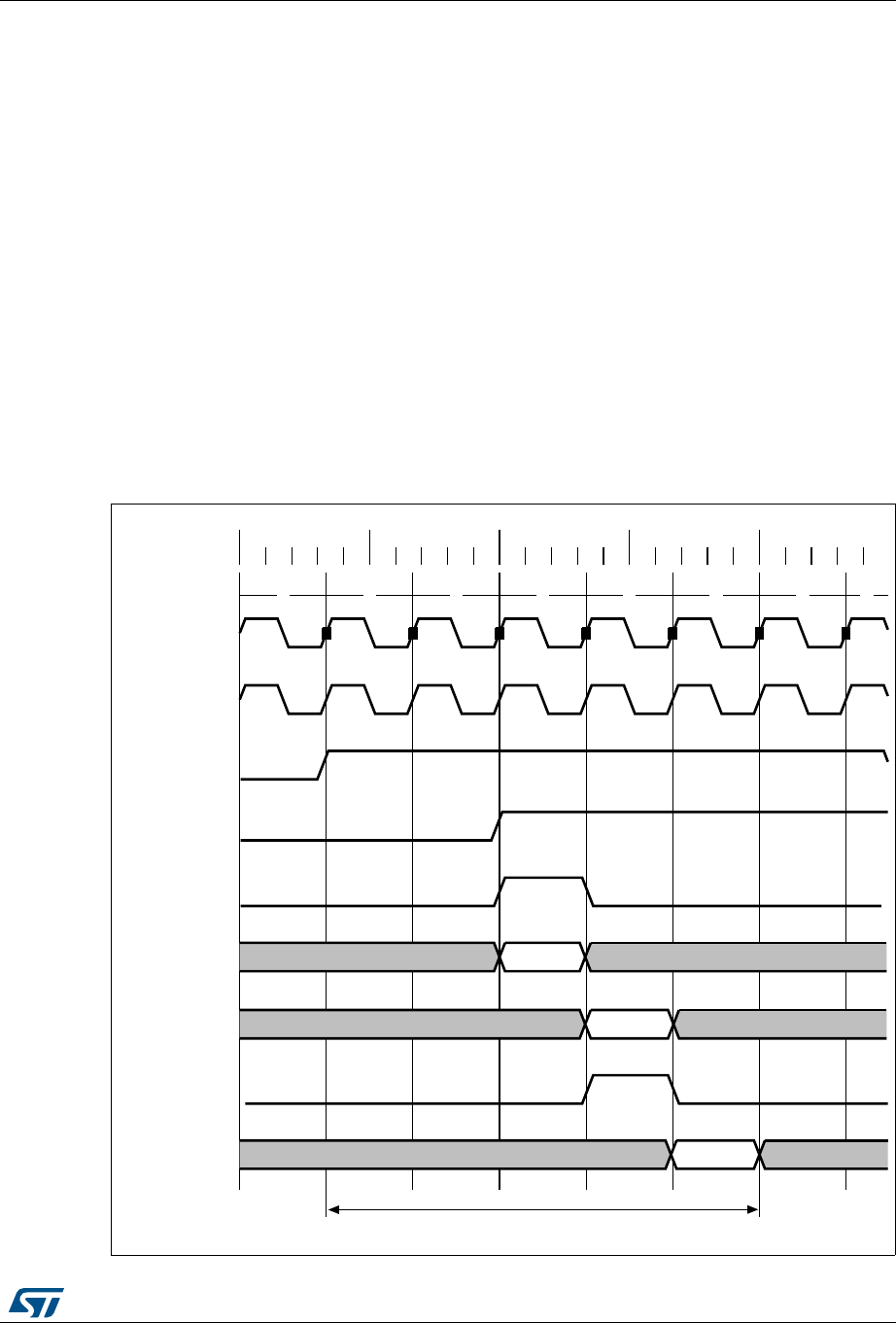
RM0090 Rev 18 1537/1749
RM0090 USB on-the-go high-speed (OTG_HS)
1543
Once the MAC receives an IN token, this information (token received) is synchronized to the
AHB clock by the PFC (the PFC runs on the AHB clock). The PFC then reads the data from
the SPRAM and writes them into the dual clock source buffer. The MAC then reads the data
out of the source buffer (4 deep).
If the AHB is running at a higher frequency than the PHY, the application can use a smaller
value for TRDT (in OTG_HS_GUSBCFG).
Figure 429 has the following signals:
•tkn_rcvd: Token received information from MAC to PFC
•dynced_tkn_rcvd: Doubled sync tkn_rcvd, from PCLK to HCLK domain
•spr_read: Read to SPRAM
•spr_addr: Address to SPRAM
•spr_rdata: Read data from SPRAM
•srcbuf_push: Push to the source buffer
•srcbuf_rdata: Read data from the source buffer. Data seen by MAC
Refer to Table 213: TRDT values for the values of TRDT versus AHB clock frequency.
Figure 429. TRDT max timing case
12345678
0ns 50ns 100ns 150ns 200ns
HCLK
PCLK
tkn_rcvd
dsynced_tkn_rcvd
spr_read
spr_addr
spr_rdata
srcbuf_push
srcbuf_rdata
5 Clocks
D1
A1
D1
ai15680
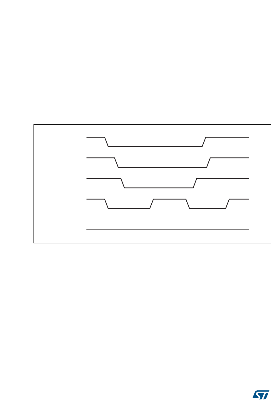
USB on-the-go high-speed (OTG_HS) RM0090
1538/1749 RM0090 Rev 18
35.13.9 OTG programming model
The OTG_HS controller is an OTG device supporting HNP and SRP. When the core is
connected to an “A” plug, it is referred to as an A-device. When the core is connected to a
“B” plug it is referred to as a B-device. In host mode, the OTG_HS controller turns off VBUS
to conserve power. SRP is a method by which the B-device signals the A-device to turn on
VBUS power. A device must perform both data-line pulsing and VBUS pulsing, but a host can
detect either data-line pulsing or VBUS pulsing for SRP. HNP is a method by which the B-
device negotiates and switches to host role. In Negotiated mode after HNP, the B-device
suspends the bus and reverts to the device role.
A-device session request protocol
The application must set the SRP-capable bit in the Core USB configuration register. This
enables the OTG_HS controller to detect SRP as an A-device.
Figure 430. A-device SRP
1. DRV_VBUS = VBUS drive signal to the PHY
VBUS_VALID = VBUS valid signal from PHY
A_VALID = A-device VBUS level signal to PHY
DP = Data plus line
DM = Data minus line
ai15681b
DRV_VBUS
VBUS_VALID
A_VALID
OTG_HS_FS_DP
OTG_HS_FS_DM
Suspend
VBUS pulsing
Data line pulsing Connect
1
6
25
3
47
Low
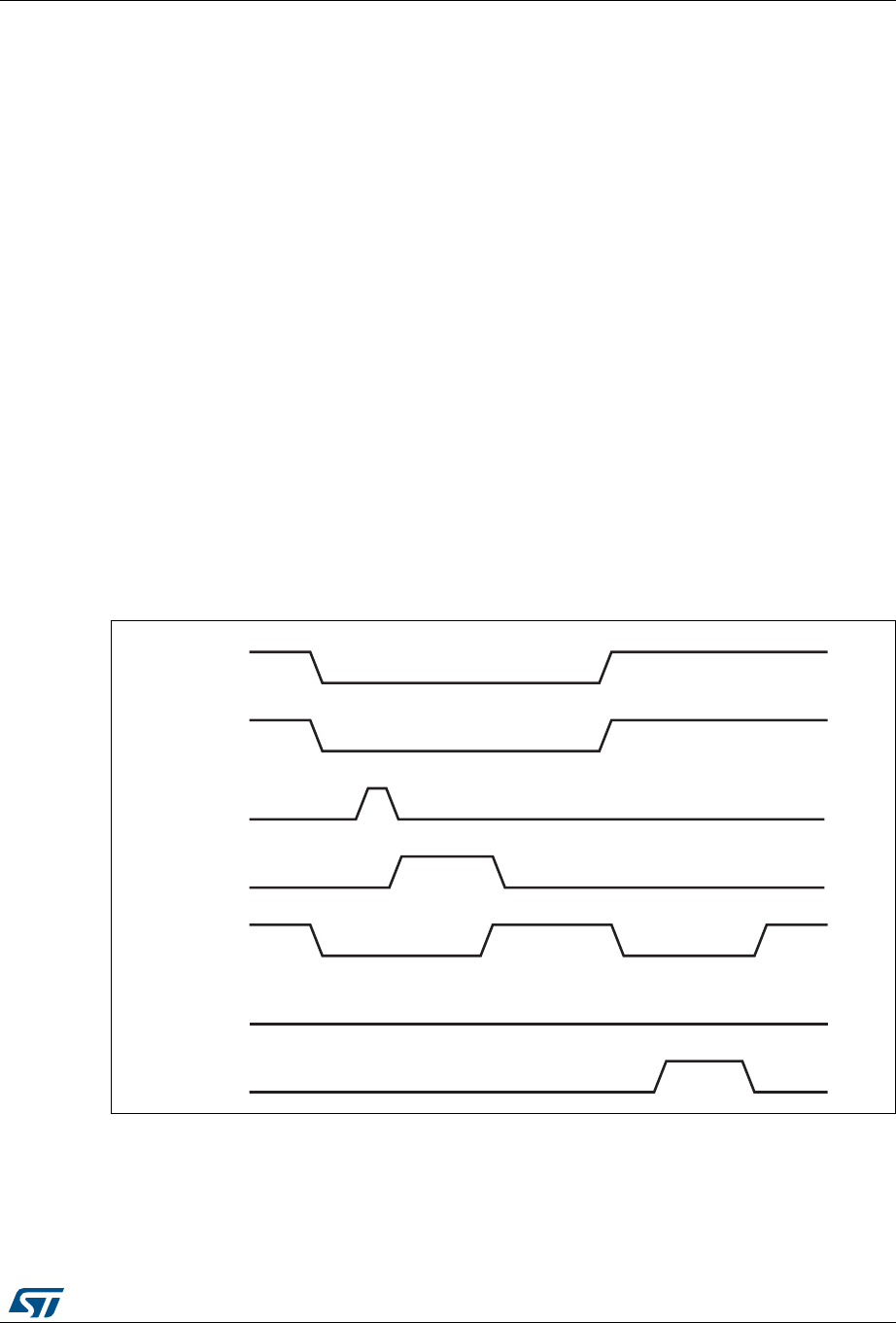
RM0090 Rev 18 1539/1749
RM0090 USB on-the-go high-speed (OTG_HS)
1543
1. To save power, the application suspends and turns off port power when the bus is idle
by writing the port suspend and port power bits in the host port control and status
register.
2. PHY indicates port power off by deasserting the VBUS_VALID signal.
3. The device must detect SE0 for at least 2 ms to start SRP when VBUS power is off.
4. To initiate SRP, the device turns on its data line pull-up resistor for 5 to 10 ms. The
OTG_HS controller detects data-line pulsing.
5. The device drives VBUS above the A-device session valid (2.0 V minimum) for VBUS
pulsing.
The OTG_HS controller interrupts the application on detecting SRP. The Session
request detected bit is set in Global interrupt status register (SRQINT set in
OTG_HS_GINTSTS).
6. The application must service the Session request detected interrupt and turn on the
port power bit by writing the port power bit in the host port control and status register.
The PHY indicates port power-on by asserting the VBUS_VALID signal.
7. When the USB is powered, the device connects, completing the SRP process.
B-device session request protocol
The application must set the SRP-capable bit in the Core USB configuration register. This
enables the OTG_HS controller to initiate SRP as a B-device. SRP is a means by which the
OTG_HS controller can request a new session from the host.
Figure 431. B-device SRP
1. VBUS_VALID = VBUS valid signal from PHY
B_VALID = B-device valid session to PHY
DISCHRG_VBUS = discharge signal to PHY
SESS_END = session end signal to PHY
CHRG_VBUS = charge VBUS signal to PHY
DP = Data plus line
DM = Data minus line
ai1568b2
VBUS_VALID
B_VALID
DISCHRG_VBUS
SESS_END
OTG_HS_FS_DP
OTG_HS_FS_DM
CHRG_VBUS
Suspend
Data line pulsing Connect
V
BUS
pulsing
1
6
2
3
4
58
7
Low
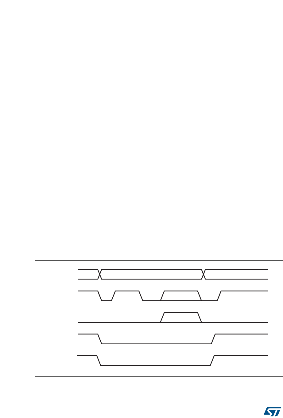
USB on-the-go high-speed (OTG_HS) RM0090
1540/1749 RM0090 Rev 18
1. To save power, the host suspends and turns off port power when the bus is idle.
The OTG_HS controller sets the early suspend bit in the Core interrupt register after 3
ms of bus idleness. Following this, the OTG_HS controller sets the USB suspend bit in
the Core interrupt register.
The OTG_HS controller informs the PHY to discharge VBUS.
2. The PHY indicates the session’s end to the device. This is the initial condition for SRP.
The OTG_HS controller requires 2 ms of SE0 before initiating SRP.
For a USB 1.1 full-speed serial transceiver, the application must wait until VBUS
discharges to 0.2 V after BSVLD (in OTG_HS_GOTGCTL) is deasserted. This
discharge time can be obtained from the transceiver vendor and varies from one
transceiver to another.
3. The USB OTG core informs the PHY to speed up VBUS discharge.
4. The application initiates SRP by writing the session request bit in the OTG Control and
status register. The OTG_HS controller perform data-line pulsing followed by VBUS
pulsing.
5. The host detects SRP from either the data-line or VBUS pulsing, and turns on VBUS.
The PHY indicates VBUS power-on to the device.
6. The OTG_HS controller performs VBUS pulsing.
The host starts a new session by turning on VBUS, indicating SRP success. The
OTG_HS controller interrupts the application by setting the session request success
status change bit in the OTG interrupt status register. The application reads the session
request success bit in the OTG control and status register.
7. When the USB is powered, the OTG_HS controller connects, completing the SRP
process.
A-device host negotiation protocol
HNP switches the USB host role from the A-device to the B-device. The application must set
the HNP-capable bit in the Core USB configuration register to enable the OTG_HS
controller to perform HNP as an A-device.
Figure 432. A-device HNP
1. DPPULLDOWN = signal from core to PHY to enable/disable the pull-down on the DP line inside the PHY.
DMPULLDOWN = signal from core to PHY to enable/disable the pull-down on the DM line inside the PHY.
ai15683b
OTG core
DP
DM
DPPULLDOWN
DMPULLDOWN
Host Device Host
1
Suspend 2
3
45
Reset
6
Traffic 7
8
Connect
Traffic

RM0090 Rev 18 1541/1749
RM0090 USB on-the-go high-speed (OTG_HS)
1543
1. The OTG_HS controller sends the B-device a SetFeature b_hnp_enable descriptor to
enable HNP support. The B-device’s ACK response indicates that the B-device
supports HNP. The application must set host Set HNP Enable bit in the OTG Control
and status register to indicate to the OTG_HS controller that the B-device supports
HNP.
2. When it has finished using the bus, the application suspends by writing the Port
suspend bit in the host port control and status register.
3. When the B-device observes a USB suspend, it disconnects, indicating the initial
condition for HNP. The B-device initiates HNP only when it must switch to the host role;
otherwise, the bus continues to be suspended.
The OTG_HS controller sets the host negotiation detected interrupt in the OTG
interrupt status register, indicating the start of HNP.
The OTG_HS controller deasserts the DM pull down and DM pull down in the PHY to
indicate a device role. The PHY enables the OTG_HS_DP pull-up resistor to indicate a
connect for B-device.
The application must read the current mode bit in the OTG Control and status register
to determine peripheral mode operation.
4. The B-device detects the connection, issues a USB reset, and enumerates the
OTG_HS controller for data traffic.
5. The B-device continues the host role, initiating traffic, and suspends the bus when
done.
The OTG_HS controller sets the early suspend bit in the Core interrupt register after 3
ms of bus idleness. Following this, the OTG_HS controller sets the USB Suspend bit in
the Core interrupt register.
6. In Negotiated mode, the OTG_HS controller detects the suspend, disconnects, and
switches back to the host role. The OTG_HS controller asserts the DM pull down and
DM pull down in the PHY to indicate its assumption of the host role.
7. The OTG_HS controller sets the Connector ID status change interrupt in the OTG
Interrupt Status register. The application must read the connector ID status in the OTG
Control and Status register to determine the OTG_HS controller operation as an A-
device. This indicates the completion of HNP to the application. The application must
read the Current mode bit in the OTG control and status register to determine host
mode operation.
8. The B-device connects, completing the HNP process.
B-device host negotiation protocol
HNP switches the USB host role from B-device to A-device. The application must set the
HNP-capable bit in the Core USB configuration register to enable the OTG_HS controller to
perform HNP as a B-device.

USB on-the-go high-speed (OTG_HS) RM0090
1542/1749 RM0090 Rev 18
Figure 433. B-device HNP
1. DPPULLDOWN = signal from core to PHY to enable/disable the pull-down on the DP line inside the PHY.
DMPULLDOWN = signal from core to PHY to enable/disable the pull-down on the DM line inside the PHY.
1. The A-device sends the SetFeature b_hnp_enable descriptor to enable HNP support.
The OTG_HS controller’s ACK response indicates that it supports HNP. The
application must set the Device HNP enable bit in the OTG Control and status register
to indicate HNP support.
The application sets the HNP request bit in the OTG Control and status register to
indicate to the OTG_HS controller to initiate HNP.
2. When it has finished using the bus, the A-device suspends by writing the Port suspend
bit in the host port control and status register.
The OTG_HS controller sets the Early suspend bit in the Core interrupt register after 3
ms of bus idleness. Following this, the OTG_HS controller sets the USB suspend bit in
the Core interrupt register.
The OTG_HS controller disconnects and the A-device detects SE0 on the bus,
indicating HNP. The OTG_HS controller asserts the DP pull down and DM pull down in
the PHY to indicate its assumption of the host role.
The A-device responds by activating its OTG_HS_DP pull-up resistor within 3 ms of
detecting SE0. The OTG_HS controller detects this as a connect.
The OTG_HS controller sets the host negotiation success status change interrupt in
the OTG Interrupt status register, indicating the HNP status. The application must read
the host negotiation success bit in the OTG Control and status register to determine
ai15684b
OTG core
DP
DM
DPPULLDOWN
DMPULLDOWN
HostDevice Device
1
Suspend 2
3
45
Reset
6
Traffic 7
8
Connect
Traffic

RM0090 Rev 18 1543/1749
RM0090 USB on-the-go high-speed (OTG_HS)
1543
host negotiation success. The application must read the current Mode bit in the Core
interrupt register (OTG_HS_GINTSTS) to determine host mode operation.
3. The application sets the reset bit (PRST in OTG_HS_HPRT) and the OTG_HS
controller issues a USB reset and enumerates the A-device for data traffic.
4. The OTG_HS controller continues the host role of initiating traffic, and when done,
suspends the bus by writing the Port suspend bit in the host port control and status
register.
5. In Negotiated mode, when the A-device detects a suspend, it disconnects and switches
back to the host role. The OTG_HS controller deasserts the DP pull down and DM pull
down in the PHY to indicate the assumption of the device role.
6. The application must read the current mode bit in the Core interrupt
(OTG_HS_GINTSTS) register to determine the host mode operation.
7. The OTG_HS controller connects, completing the HNP process.

Flexible static memory controller (FSMC) RM0090
1544/1749 RM0090 Rev 18
36 Flexible static memory controller (FSMC)
This section applies to the whole STM32F40x/41x family only.
36.1 FSMC main features
The FSMC block is able to interface with synchronous and asynchronous memories and
16-bit PC memory cards. Its main purpose is to:
•Translate the AHB transactions into the appropriate external device protocol
•Meet the access timing requirements of the external devices
All external memories share the addresses, data and control signals with the controller.
Each external device is accessed by means of a unique chip select. The FSMC performs
only one access at a time to an external device.
The FSMC has the following main features:
•Interfaces with static memory-mapped devices including:
– Static random access memory (SRAM)
– NOR Flash memory/OneNAND Flash memory
– PSRAM (4 memory banks)
•Two banks of NAND Flash with ECC hardware that checks up to 8 Kbytes of data
•16-bit PC Card compatible devices
•Supports burst mode access to synchronous devices (NOR Flash and PSRAM)
•8- or 16-bit wide databus
•Independent chip select control for each memory bank
•Independent configuration for each memory bank
•Programmable timings to support a wide range of devices, in particular:
– Programmable wait states (up to 15)
– Programmable bus turnaround cycles (up to 15)
– Programmable output enable and write enable delays (up to 15)
– Independent read and write timings and protocol, so as to support the widest
variety of memories and timings
•Write enable and byte lane select outputs for use with PSRAM and SRAM devices
•Translation of 32-bit wide AHB transactions into consecutive 16-bit or 8-bit accesses to
external 16-bit or 8-bit devices
•A Write FIFO, 2-word long (16-word long for STM32F42x and STM32F43x), each word
is 32 bits wide, only stores data and not the address. Therefore, this FIFO only buffers
AHB write burst transactions. This makes it possible to write to slow memories and free
the AHB quickly for other operations. Only one burst at a time is buffered: if a new AHB
burst or single transaction occurs while an operation is in progress, the FIFO is
drained. The FSMC will insert wait states until the current memory access is complete.
•External asynchronous wait control
The FSMC registers that define the external device type and associated characteristics are
usually set at boot time and do not change until the next reset or power-up. However, it is
possible to change the settings at any time.
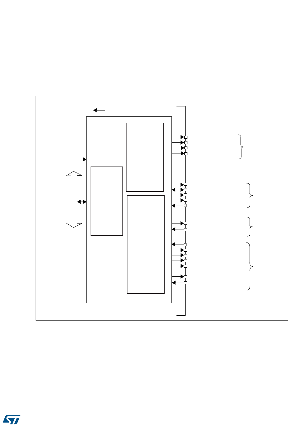
RM0090 Rev 18 1545/1749
RM0090 Flexible static memory controller (FSMC)
1601
36.2 Block diagram
The FSMC consists of four main blocks:
•The AHB interface (including the FSMC configuration registers)
•The NOR Flash/PSRAM controller
•The NAND Flash/PC Card controller
•The external device interface
The block diagram is shown in Figure 434.
Figure 434. FSMC block diagram
36.3 AHB interface
The AHB slave interface enables internal CPUs and other bus master peripherals to access
the external static memories.
AHB transactions are translated into the external device protocol. In particular, if the
selected external memory is 16 or 8 bits wide, 32-bit wide transactions on the AHB are split
into consecutive 16- or 8-bit accesses. The FSMC Chip Select (FSMC_NEx) does not
AHB bus
FSMC interrupt to NVIC
NOR/PSRAM
memory
controller
HCLK
From clock
controller
NAND/PC Card
memory
controller
signals
NAND
Shared
signals
signals
NOR/PSRAM
FSMC_NE[4:1]
FSMC_NL (or NADV)
FSMC_NWAIT
FSMC_NOE
FSMC_NWE
FSMC_NIORD
FSMC_NREG
FSMC_CD
signals
PC Card
ai15591b
FSMC_NBL[1:0]
FSMC_NCE[3:2]
FSMC_INT[3:2]
FSMC_INTR
FSMC_NCE4_1
FSMC_NCE4_2
FSMC_NIOWR
FSMC_CLK
Configuration
registers
FSMC_A[25:0]
FSMC_D[15:0]

Flexible static memory controller (FSMC) RM0090
1546/1749 RM0090 Rev 18
toggle between consecutive accesses except when performing accesses in mode D with the
extended mode enabled.
The FSMC generates an AHB error in the following conditions:
•When reading or writing to an FSMC bank which is not enabled
•When reading or writing to the NOR Flash bank while the FACCEN bit is reset in the
FSMC_BCRx register.
•When reading or writing to the PC Card banks while the input pin FSMC_CD (Card
Presence Detection) is low.
The effect of this AHB error depends on the AHB master which has attempted the R/W
access:
•If it is the Cortex®-M4 with FPU CPU, a hard fault interrupt is generated
•If is a DMA, a DMA transfer error is generated and the corresponding DMA channel is
automatically disabled.
The AHB clock (HCLK) is the reference clock for the FSMC.
36.3.1 Supported memories and transactions
General transaction rules
The requested AHB transaction data size can be 8-, 16- or 32-bit wide whereas the
accessed external device has a fixed data width. This may lead to inconsistent transfers.
Therefore, some simple transaction rules must be followed:
•AHB transaction size and memory data size are equal
There is no issue in this case.
•AHB transaction size is greater than the memory size
In this case, the FSMC splits the AHB transaction into smaller consecutive memory
accesses in order to meet the external data width.
•AHB transaction size is smaller than the memory size
Asynchronous transfers may or not be consistent depending on the type of external
device.
– Asynchronous accesses to devices that have the byte select feature (SRAM,
ROM, PSRAM).
a) FSMC allows write transactions accessing the right data through its byte lanes
NBL[1:0]
b) Read transactions are allowed. All memory bytes are read and the useless
ones are discarded. The NBL[1:0] are kept low during read transactions.
– Asynchronous accesses to devices that do not have the byte select feature (NOR
and NAND Flash 16-bit).
This situation occurs when a byte access is requested to a 16-bit wide Flash
memory. Clearly, the device cannot be accessed in byte mode (only 16-bit words
can be read from/written to the Flash memory) therefore:
a) Write transactions are not allowed
b) Read transactions are allowed. All memory bytes are read and the useless ones
are discarded. The NBL[1:0] are set to 0 during read transactions.

RM0090 Rev 18 1547/1749
RM0090 Flexible static memory controller (FSMC)
1601
Configuration registers
The FSMC can be configured using a register set. See Section 36.5.6, for a detailed
description of the NOR Flash/PSRAM control registers. See Section 36.6.8, for a detailed
description of the NAND Flash/PC Card registers.
36.4 External device address mapping
From the FSMC point of view, the external memory is divided into 4 fixed-size banks of
256 Mbytes each (Refer to Figure 435):
•Bank 1 used to address up to 4 NOR Flash or PSRAM memory devices. This bank is
split into 4 NOR/PSRAM subbanks with 4 dedicated Chip Selects, as follows:
– Bank 1 - NOR/PSRAM 1
– Bank 1 - NOR/PSRAM 2
– Bank 1 - NOR/PSRAM 3
– Bank 1 - NOR/PSRAM 4
•Banks 2 and 3 used to address NAND Flash devices (1 device per bank)
•Bank 4 used to address a PC Card device
For each bank the type of memory to be used is user-defined in the Configuration register.
Figure 435. FSMC memory banks
36.4.1 NOR/PSRAM address mapping
HADDR[27:26] bits are used to select one of the four memory banks as shown in Table 216.
Bank 1
NAND Flash
NOR / PSRAM
Supported memory typeBanks
4 × 64 MB
6000 0000h
6FF F FFF Fh
Address
7000 0000h
7FF F FFF Fh
8000 0000h
8FF F FFF Fh
9000 0000h
9FF F FFF Fh
Bank 2
4 × 64 MB
Bank 3
4 × 64 MB
Bank 4
4 × 64 MB PC Card
ai14719
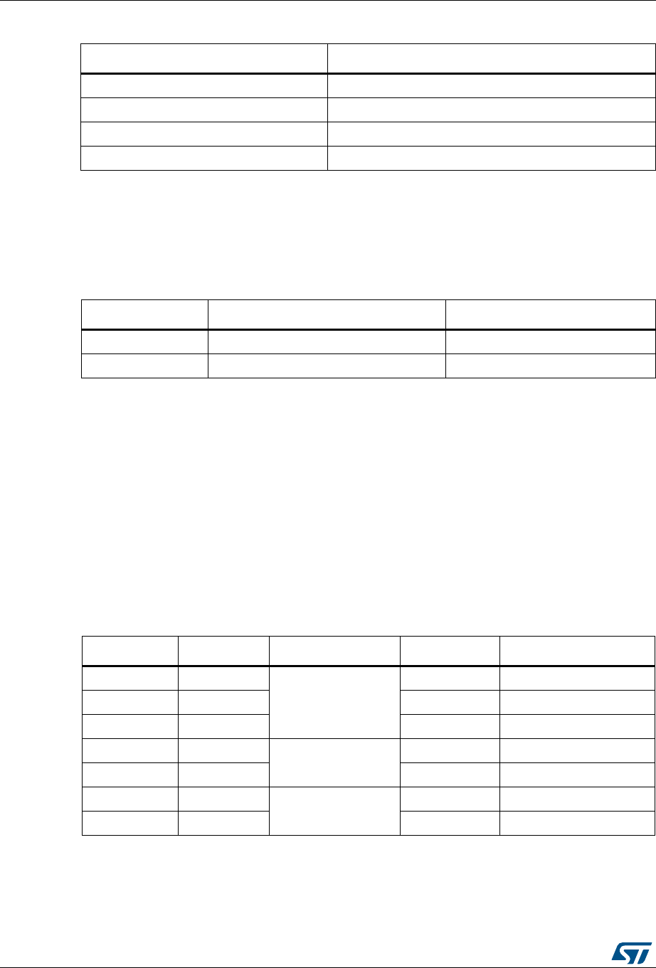
Flexible static memory controller (FSMC) RM0090
1548/1749 RM0090 Rev 18
HADDR[25:0] contain the external memory address. Since HADDR is a byte address
whereas the memory is addressed in words, the address actually issued to the memory
varies according to the memory data width, as shown in the following table.
Wrap support for NOR Flash/PSRAM
Wrap burst mode for synchronous memories is not supported. The memories must be
configured in linear burst mode of undefined length.
36.4.2 NAND/PC Card address mapping
In this case, three banks are available, each of them divided into memory spaces as
indicated in Table 218.
Table 216. NOR/PSRAM bank selection
HADDR[27:26](1)
1. HADDR are internal AHB address lines that are translated to external memory.
Selected bank
00 Bank 1 - NOR/PSRAM 1
01 Bank 1 - NOR/PSRAM 2
10 Bank 1 - NOR/PSRAM 3
11 Bank 1 - NOR/PSRAM 4
Table 217. External memory address
Memory width(1)
1. In case of a 16-bit external memory width, the FSMC will internally use HADDR[25:1] to generate the
address for external memory FSMC_A[24:0].
Whatever the external memory width (16-bit or 8-bit), FSMC_A[0] should be connected to external memory
address A[0].
Data address issued to the memory Maximum memory capacity (bits)
8-bit HADDR[25:0] 64 Mbyte x 8 = 512 Mbit
16-bit HADDR[25:1] >> 1 64 Mbyte/2 x 16 = 512 Mbit
Table 218. Memory mapping and timing registers
Start address End address FSMC Bank Memory space Timing register
0x9C00 0000 0x9FFF FFFF
Bank 4 - PC card
I/O FSMC_PIO4 (0xB0)
0x9800 0000 0x9BFF FFFF Attribute FSMC_PATT4 (0xAC)
0x9000 0000 0x93FF FFFF Common FSMC_PMEM4 (0xA8)
0x8800 0000 0x8BFF FFFF
Bank 3 - NAND Flash
Attribute FSMC_PATT3 (0x8C)
0x8000 0000 0x83FF FFFF Common FSMC_PMEM3 (0x88)
0x7800 0000 0x7BFF FFFF
Bank 2- NAND Flash
Attribute FSMC_PATT2 (0x6C)
0x7000 0000 0x73FF FFFF Common FSMC_PMEM2 (0x68)

RM0090 Rev 18 1549/1749
RM0090 Flexible static memory controller (FSMC)
1601
For NAND Flash memory, the common and attribute memory spaces are subdivided into
three sections (see in Table 219 below) located in the lower 256 Kbytes:
•Data section (first 64 Kbytes in the common/attribute memory space)
•Command section (second 64 Kbytes in the common / attribute memory space)
•Address section (next 128 Kbytes in the common / attribute memory space)
The application software uses the 3 sections to access the NAND Flash memory:
•To send a command to NAND Flash memory: the software must write the command
value to any memory location in the command section.
•To specify the NAND Flash address that must be read or written: the software
must write the address value to any memory location in the address section. Since an
address can be 4 or 5 bytes long (depending on the actual memory size), several
consecutive writes to the address section are needed to specify the full address.
•To read or write data: the software reads or writes the data value from or to any
memory location in the data section.
Since the NAND Flash memory automatically increments addresses, there is no need to
increment the address of the data section to access consecutive memory locations.
36.5 NOR Flash/PSRAM controller
The FSMC generates the appropriate signal timings to drive the following types of
memories:
•Asynchronous SRAM and ROM
–8-bit
– 16-bit
– 32-bit
•PSRAM (Cellular RAM)
– Asynchronous mode
– Burst mode for synchronous accesses
– Multiplexed or nonmultiplexed
•NOR Flash
– Asynchronous mode
– Burst mode for synchronous accesses
– Multiplexed or nonmultiplexed
The FSMC outputs a unique chip select signal NE[4:1] per bank. All the other signals
(addresses, data and control) are shared.
Table 219. NAND bank selections
Section name HADDR[17:16] Address range
Address section 1X 0x020000-0x03FFFF
Command section 01 0x010000-0x01FFFF
Data section 00 0x000000-0x0FFFF

Flexible static memory controller (FSMC) RM0090
1550/1749 RM0090 Rev 18
For synchronous accesses, the FSMC issues the clock (CLK) to the selected external
device only during the read/write transactions. This clock is a submultiple of the HCLK clock.
The size of each bank is fixed and equal to 64 Mbytes.
Each bank is configured by means of dedicated registers (see Section 36.5.6).
The programmable memory parameters include access timings (see Table 220) and support
for wait management (for PSRAM and NOR Flash accessed in burst mode).
36.5.1 External memory interface signals
Table 221, Table 222 and Table 223 list the signals that are typically used to interface NOR
Flash, SRAM and PSRAM.
Note: Prefix “N”. specifies the associated signal as active low.
NOR Flash, nonmultiplexed I/Os
Table 220. Programmable NOR/PSRAM access parameters
Parameter Function Access mode Unit Min. Max.
Address
setup
Duration of the address
setup phase Asynchronous AHB clock cycle
(HCLK) 015
Address hold Duration of the address hold
phase
Asynchronous,
muxed I/Os
AHB clock cycle
(HCLK) 115
Data setup Duration of the data setup
phase Asynchronous AHB clock cycle
(HCLK) 1256
Bus turn Duration of the bus
turnaround phase
Asynchronous and
synchronous
read/write
AHB clock cycle
(HCLK) 015
Clock divide
ratio
Number of AHB clock cycles
(HCLK) to build one memory
clock cycle (CLK)
Synchronous AHB clock cycle
(HCLK) 2 16
Data latency
Number of clock cycles to
issue to the memory before
the first data of the burst
Synchronous Memory clock
cycle (CLK) 2 17
Table 221. Nonmultiplexed I/O NOR Flash
FSMC signal name I/O Function
CLK O Clock (for synchronous access)
A[25:0] O Address bus
D[15:0] I/O Bidirectional data bus
NE[x] O Chip select, x = 1..4
NOE O Output enable
NWE O Write enable
NL(=NADV) O Latch enable (this signal is called address
valid, NADV, by some NOR Flash devices)
NWAIT I NOR Flash wait input signal to the FSMC

RM0090 Rev 18 1551/1749
RM0090 Flexible static memory controller (FSMC)
1601
NOR Flash memories are addressed in 16-bit words. The maximum capacity is 512 Mbit (26
address lines).
NOR Flash, multiplexed I/Os
NOR-Flash memories are addressed in 16-bit words. The maximum capacity is 512 Mbit
(26 address lines).
PSRAM/SRAM, nonmultiplexed I/Os
PSRAM memories are addressed in 16-bit words. The maximum capacity is 512 Mbit (26
address lines).
PSRAM, multiplexed I/Os
Table 222. Multiplexed I/O NOR Flash
FSMC signal name I/O Function
CLK O Clock (for synchronous access)
A[25:16] O Address bus
AD[15:0] I/O 16-bit multiplexed, bidirectional address/data bus
NE[x] O Chip select, x = 1..4
NOE O Output enable
NWE O Write enable
NL(=NADV) O Latch enable (this signal is called address valid, NADV, by some NOR
Flash devices)
NWAIT I NOR Flash wait input signal to the FSMC
Table 223. Nonmultiplexed I/Os PSRAM/SRAM
FSMC signal name I/O Function
CLK O Clock (only for PSRAM synchronous access)
A[25:0] O Address bus
D[15:0] I/O Data bidirectional bus
NE[x] O Chip select, x = 1..4 (called NCE by PSRAM (Cellular RAM i.e. CRAM))
NOE O Output enable
NWE O Write enable
NL(= NADV) O Address valid only for PSRAM input (memory signal name: NADV)
NWAIT I PSRAM wait input signal to the FSMC
NBL[1] O Upper byte enable (memory signal name: NUB)
NBL[0] O Lowed byte enable (memory signal name: NLB)
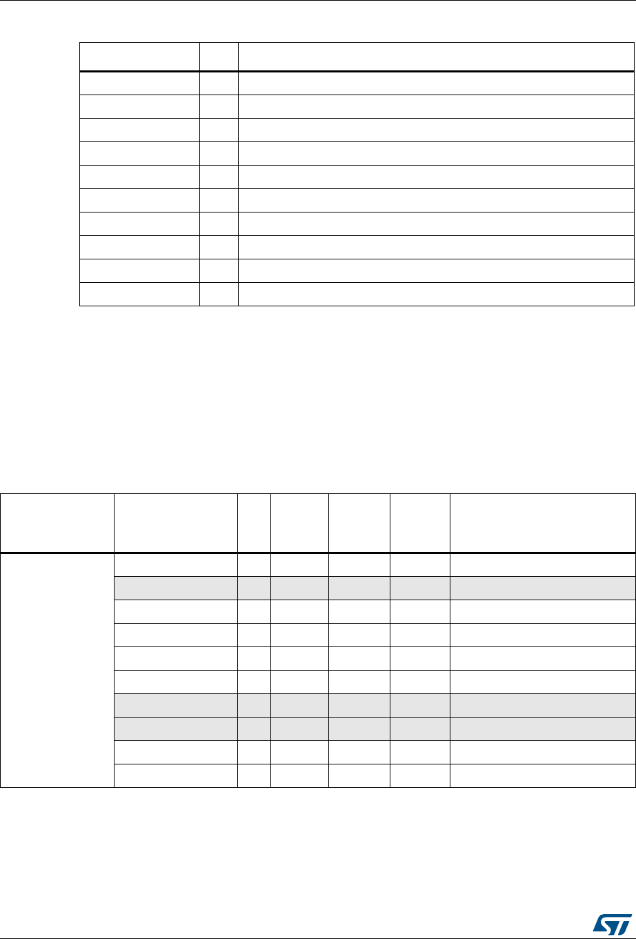
Flexible static memory controller (FSMC) RM0090
1552/1749 RM0090 Rev 18
PSRAM memories are addressed in 16-bit words. The maximum capacity is 512 Mbit (26
address lines).
36.5.2 Supported memories and transactions
Table 225 below displays an example of the supported devices, access modes and
transactions when the memory data bus is 16-bit for NOR, PSRAM and SRAM.
Transactions not allowed (or not supported) by the FSMC in this example appear in gray.
Table 224. Multiplexed I/O PSRAM
FSMC signal name I/O Function
CLK O Clock (for synchronous access)
A[25:16] O Address bus
AD[15:0] I/O 16-bit multiplexed, bidirectional address/data bus
NE[x] O Chip select, x = 1..4 (called NCE by PSRAM (Cellular RAM i.e. CRAM))
NOE O Output enable
NWE O Write enable
NL(= NADV) O Address valid PSRAM input (memory signal name: NADV)
NWAIT I PSRAM wait input signal to the FSMC
NBL[1] O Upper byte enable (memory signal name: NUB)
NBL[0] O Lowed byte enable (memory signal name: NLB)
Table 225. NOR Flash/PSRAM controller: example of supported memories and transactions
Device Mode R/W
AHB
data
size
Memory
data size
Allowed/
not
allowed
Comments
NOR Flash
(muxed I/Os and
nonmuxed I/Os)
Asynchronous R 8 16 Y -
Asynchronous W 8 16 N -
Asynchronous R 16 16 Y -
Asynchronous W 16 16 Y -
Asynchronous R 32 16 Y Split into two FSMC accesses
Asynchronous W 32 16 Y Split into two FSMC accesses
Asynchronous page R -16 N Mode is not supported
Synchronous R 8 16 N -
Synchronous R 16 16 Y -
Synchronous R 32 16 Y -

RM0090 Rev 18 1553/1749
RM0090 Flexible static memory controller (FSMC)
1601
36.5.3 General timing rules
Signals synchronization
•All controller output signals change on the rising edge of the internal clock (HCLK)
•In synchronous mode (read or write), all output signals change on the rising edge of
HCLK. Whatever the CLKDIV value, all outputs change as follows:
– NOEL/NWEL/ NEL/NADVL/ NADVH /NBLL/ Address valid outputs change on the
falling edge of FSMC_CLK clock.
– NOEH/ NWEH / NEH/ NOEH/NBLH/ Address invalid outputs change on the rising
edge of FSMC_CLK clock.
PSRAM
(multiplexed and
nonmultiplexed
I/Os)
Asynchronous R 8 16 Y -
Asynchronous W 8 16 Y Use of byte lanes NBL[1:0]
Asynchronous R 16 16 Y -
Asynchronous W 16 16 Y -
Asynchronous R 32 16 Y Split into two FSMC accesses
Asynchronous W 32 16 Y Split into two FSMC accesses
Asynchronous page R -16 N Mode is not supported
Synchronous R 8 16 N -
Synchronous R 16 16 Y -
Synchronous R 32 16 Y -
Synchronous W 8 16 Y Use of byte lanes NBL[1:0]
Synchronous W 16 / 32 16 Y -
SRAM and ROM
Asynchronous R 8 / 16 16 Y -
Asynchronous W 8 / 16 16 Y Use of byte lanes NBL[1:0]
Asynchronous R 32 16 Y Split into two FSMC accesses
Asynchronous W 32 16 Y
Split into two FSMC accesses.
Use of byte lanes NBL[1:0]
Table 225. NOR Flash/PSRAM controller: example of supported memories and transactions
Device Mode R/W
AHB
data
size
Memory
data size
Allowed/
not
allowed
Comments
Flexible static memory controller (FSMC) RM0090
1554/1749 RM0090 Rev 18
36.5.4 NOR Flash/PSRAM controller asynchronous transactions
Asynchronous static memories (NOR Flash memory, PSRAM, SRAM)
•Signals are synchronized by the internal clock HCLK. This clock is not issued to the
memory
•The FSMC always samples the data before de-asserting the NOE signals. This
guarantees that the memory data-hold timing constraint is met (chip enable high to
data transition, usually 0 ns min.)
•If the extended mode is enabled (EXTMOD bit is set in the FSMC_BCRx register), up
to four extended modes (A, B, C and D) are available. It is possible to mix A, B, C and
D modes for read and write operations. For example, read operation can be performed
in mode A and write in mode B.
•If the extended mode is disabled (EXTMOD bit is reset in the FSMC_BCRx register),
the FSMC can operate in Mode1 or Mode2 as follows:
– Mode 1 is the default mode when SRAM/PSRAM memory type is selected
(MTYP[0:1] = 0x0 or 0x01 in the FSMC_BCRx register)
– Mode 2 is the default mode when NOR memory type is selected (MTYP[0:1] =
0x10 in the FSMC_BCRx register).
Mode 1 - SRAM/PSRAM (CRAM)
The next figures show the read and write transactions for the supported modes followed by
the required configuration of FSMC _BCRx, and FSMC_BTRx/FSMC_BWTRx registers.
Figure 436. Mode1 read accesses
1. NBL[1:0] are driven low during read access.
A[25:0]
NOE
ADDSET DATAST
Memory transaction
NEx
D[15:0]
HCLK cycles HCLK cycles
NWE
NBL[1:0]
data driven
by memory
ai15557
High
RM0090 Rev 18 1555/1749
RM0090 Flexible static memory controller (FSMC)
1601
Figure 437. Mode1 write accesses
The one HCLK cycle at the end of the write transaction helps guarantee the address and
data hold time after the NWE rising edge. Due to the presence of this one HCLK cycle, the
DATAST value must be greater than zero (DATAST > 0).
Table 226. FSMC_BCRx bit fields
Bit number Bit name Value to set
31-20 Reserved 0x000
19 CBURSTRW 0x0 (no effect on asynchronous mode)
18:16 CPSIZE 0x0 (no effect on asynchronous mode)
15 ASYNCWAIT Set to 1 if the memory supports this feature. Otherwise keep at 0.
14 EXTMOD 0x0
13 WAITEN 0x0 (no effect on asynchronous mode)
12 WREN As needed
11 WAITCFG Don’t care
10 WRAPMOD 0x0
9 WAITPOL Meaningful only if bit 15 is 1
8 BURSTEN 0x0
7 Reserved 0x1
6 FACCEN Don’t care
5-4 MWID As needed
3-2 MTYP[0:1] As needed, exclude 0x2 (NOR Flash)
A[25:0]
NOE
ADDSET (DATAST + 1)
Memory transaction
NEx
D[15:0]
HCLK cycles HCLK cycles
NWE
NBL[1:0]
data driven by FSMC
ai15558
1HCLK
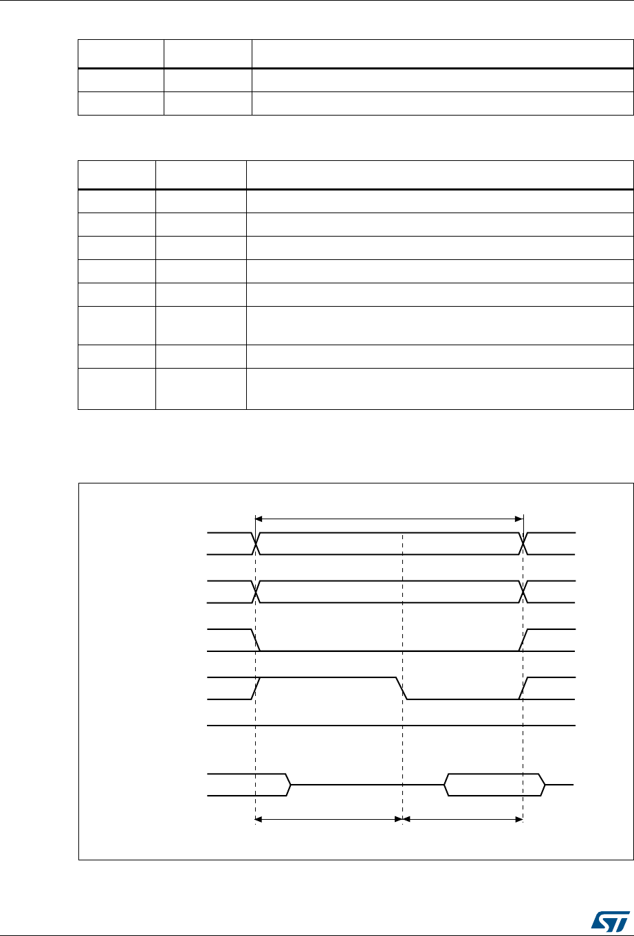
Flexible static memory controller (FSMC) RM0090
1556/1749 RM0090 Rev 18
Mode A - SRAM/PSRAM (CRAM) OE toggling
Figure 438. ModeA read accesses
1. NBL[1:0] are driven low during read access.
1 MUXE 0x0
0 MBKEN 0x1
Table 227. FSMC_BTRx bit fields
Bit number Bit name Value to set
31:30 Reserved 0x0
29-28 ACCMOD Don’t care
27-24 DATLAT Don’t care
23-20 CLKDIV Don’t care
19-16 BUSTURN Time between NEx high to NEx low (BUSTURN HCLK)
15-8 DATAST Duration of the second access phase (DATAST+1 HCLK cycles for
write accesses, DATAST HCLK cycles for read accesses).
7-4 ADDHLD Don’t care
3-0 ADDSET[3:0] Duration of the first access phase (ADDSET HCLK cycles).
Minimum value for ADDSET is 0.
Table 226. FSMC_BCRx bit fields (continued)
Bit number Bit name Value to set
A[25:0]
NOE
ADDSET DATAST
Memory transaction
NEx
D[15:0]
HCLK cycles HCLK cycles
NWE
NBL[1:0]
data driven
by memory
ai15559
High
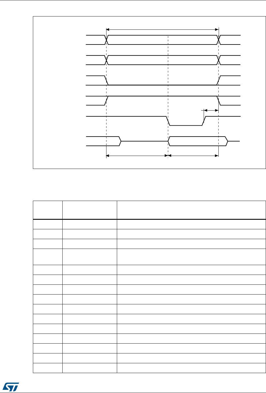
RM0090 Rev 18 1557/1749
RM0090 Flexible static memory controller (FSMC)
1601
Figure 439. ModeA write accesses
The differences compared with mode1 are the toggling of NOE and the independent read
and write timings.
Table 228. FSMC_BCRx bit fields
Bit
number Bit name Value to set
31-20 Reserved 0x000
19 CBURSTRW 0x0 (no effect on asynchronous mode)
18:16 CPSIZE 0x0 (no effect on asynchronous mode)
15 ASYNCWAIT Set to 1 if the memory supports this feature. Otherwise keep at
0.
14 EXTMOD 0x1
13 WAITEN 0x0 (no effect on asynchronous mode)
12 WREN As needed
11 WAITCFG Don’t care
10 WRAPMOD 0x0
9 WAITPOL Meaningful only if bit 15 is 1
8 BURSTEN 0x0
7 Reserved 0x1
6 FACCEN Don’t care
5-4 MWID As needed
3-2 MTYP[0:1] As needed, exclude 0x2 (NOR Flash)
A[25:0]
NOE
ADDSET (DATAST + 1)
Memory transaction
NEx
D[15:0]
HCLK cycles HCLK cycles
NWE
NBL[1:0]
data driven by FSMC
ai15560
1HCLK

Flexible static memory controller (FSMC) RM0090
1558/1749 RM0090 Rev 18
1 MUXEN 0x0
0 MBKEN 0x1
Table 229. FSMC_BTRx bit fields
Bit
number Bit name Value to set
31:30 Reserved 0x0
29-28 ACCMOD 0x0
27-24 DATLAT Don’t care
23-20 CLKDIV Don’t care
19-16 BUSTURN Time between NEx high to NEx low (BUSTURN HCLK)
15-8 DATAST Duration of the second access phase (DATAST HCLK cycles) for
read accesses.
7-4 ADDHLD Don’t care
3-0 ADDSET[3:0]
Duration of the first access phase (ADDSET HCLK cycles) for read
accesses.
Minimum value for ADDSET is 0.
Table 230. FSMC_BWTRx bit fields
Bit
number Bit name Value to set
31:30 Reserved 0x0
29-28 ACCMOD 0x0
27-24 DATLAT Don’t care
23-20 CLKDIV Don’t care
19-16 BUSTURN Time between NEx high to NEx low (BUSTURN HCLK)
15-8 DATAST Duration of the second access phase (DATAST+1 HCLK cycles for
write accesses,
7-4 ADDHLD Don’t care
3-0 ADDSET[3:0]
Duration of the first access phase (ADDSET HCLK cycles) for write
accesses.
Minimum value for ADDSET is 0.
Table 228. FSMC_BCRx bit fields (continued)
Bit
number Bit name Value to set
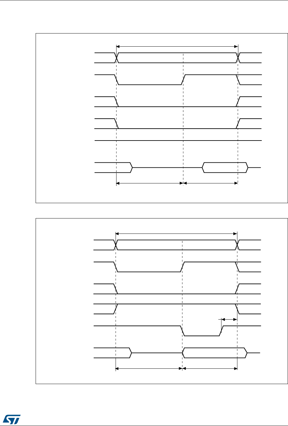
RM0090 Rev 18 1559/1749
RM0090 Flexible static memory controller (FSMC)
1601
Mode 2/B - NOR Flash
Figure 440. Mode2 and mode B read accesses
Figure 441. Mode2 write accesses
A[25:0]
NOE
ADDSET DATAST
Memory transaction
NEx
D[15:0]
HCLK cycles HCLK cycles
NWE
NADV
data driven
by memory
ai15561
High
A[25:0]
NOE
ADDSET (DATAST + 1)
Memory transaction
NEx
D[15:0]
HCLK cycles HCLK cycles
NWE
NADV
data driven by FSMC
ai15562
1HCLK
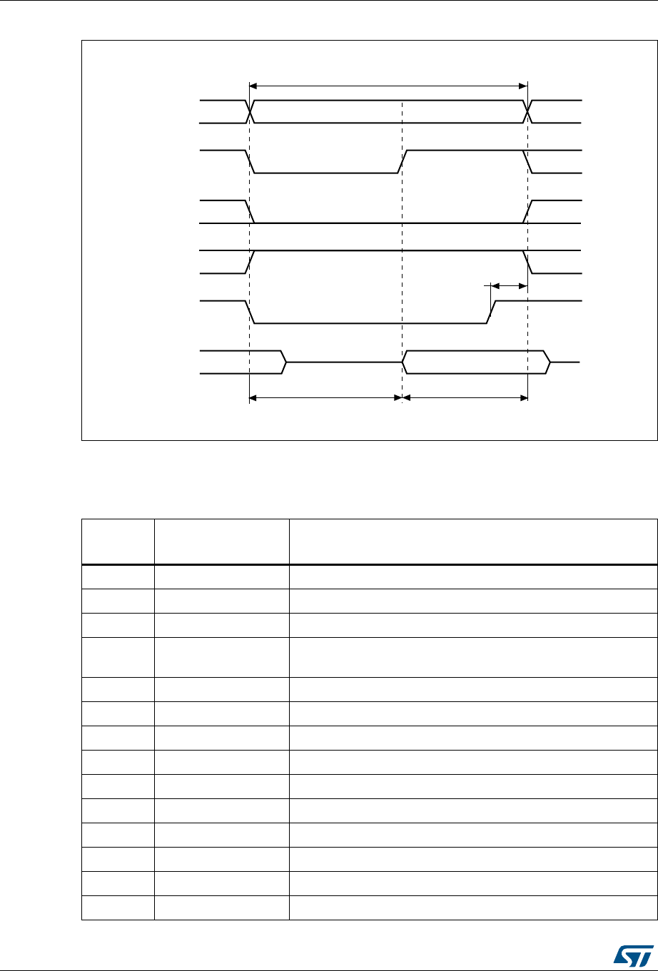
Flexible static memory controller (FSMC) RM0090
1560/1749 RM0090 Rev 18
Figure 442. Mode B write accesses
The differences with mode1 are the toggling of NWE and the independent read and write
timings when extended mode is set (Mode B).
Table 231. FSMC_BCRx bit fields
Bit
number Bit name Value to set
31-20 Reserved 0x000
19 CBURSTRW 0x0 (no effect on asynchronous mode)
18:16 Reserved 0x0 (no effect on asynchronous mode)
15 ASYNCWAIT Set to 1 if the memory supports this feature. Otherwise keep at
0.
14 EXTMOD 0x1 for mode B, 0x0 for mode 2
13 WAITEN 0x0 (no effect on asynchronous mode)
12 WREN As needed
11 WAITCFG Don’t care
10 WRAPMOD 0x0
9 WAITPOL Meaningful only if bit 15 is 1
8 BURSTEN 0x0
7 Reserved 0x1
6 FACCEN 0x1
5-4 MWID As needed
A[25:0]
NOE
ADDSET (DATAST + 1)
Memory transaction
NEx
D[15:0]
HCLK cycles HCLK cycles
NWE
NADV
data driven by FSMC
ai15563
1HCLK

RM0090 Rev 18 1561/1749
RM0090 Flexible static memory controller (FSMC)
1601
Note: The FSMC_BWTRx register is valid only if extended mode is set (mode B), otherwise all its
content is don’t care.
3-2 MTYP[0:1] 0x2 (NOR Flash memory)
1 MUXEN 0x0
0 MBKEN 0x1
Table 232. FSMC_BTRx bit fields
Bit
number Bit name Value to set
31:30 Reserved 0x0
29-28 ACCMOD 0x1
27-24 DATLAT Don’t care
23-20 CLKDIV Don’t care
19-16 BUSTURN Time between NEx high to NEx low (BUSTURN HCLK)
15-8 DATAST Duration of the second access phase (DATAST HCLK cycles) for
read accesses.
7-4 ADDHLD Don’t care
3-0 ADDSET[3:0]
Duration of the first access phase (ADDSET HCLK cycles) for read
accesses.
Minimum value for ADDSET is 0.
Table 233. FSMC_BWTRx bit fields
Bit
number Bit name Value to set
31:30 Reserved 0x0
29-28 ACCMOD 0x1
27-24 DATLAT Don’t care
23-20 CLKDIV Don’t care
19-16 BUSTURN Time between NEx high to NEx low (BUSTURN HCLK)
15-8 DATAST Duration of the second access phase (DATAST+1 HCLK cycles for
write accesses,
7-4 ADDHLD Don’t care
3-0 ADDSET[3:0]
Duration of the first access phase (ADDSET HCLK cycles) for write
accesses.
Minimum value for ADDSET is 0.
Table 231. FSMC_BCRx bit fields (continued)
Bit
number Bit name Value to set
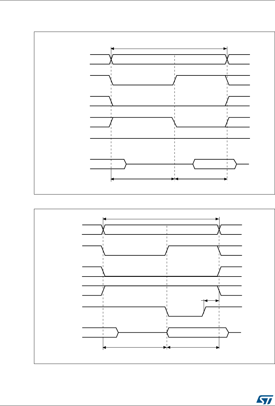
Flexible static memory controller (FSMC) RM0090
1562/1749 RM0090 Rev 18
Mode C - NOR Flash - OE toggling
Figure 443. Mode C read accesses
Figure 444. Mode C write accesses
The differences compared with mode1 are the toggling of NOE and the independent read
and write timings.
A[25:0]
NOE
ADDSET DATAST
Memory transaction
NEx
D[15:0]
HCLK cycles HCLK cycles
NWE
NADV
data driven
by memory
ai15564
High
A[25:0]
NOE
ADDSET (DATAST + 1)
Memory transaction
NEx
D[15:0]
HCLK cycles HCLK cycles
NWE
NADV
data driven by FSMC
ai15565
1HCLK

RM0090 Rev 18 1563/1749
RM0090 Flexible static memory controller (FSMC)
1601
Table 234. FSMC_BCRx bit fields
Bit No. Bit name Value to set
31-20 Reserved 0x000
19 CBURSTRW 0x0 (no effect on asynchronous mode)
18:16 CPSIZE 0x0 (no effect on asynchronous mode)
15 ASYNCWAIT Set to 1 if the memory supports this feature. Otherwise keep
at 0.
14 EXTMOD 0x1
13 WAITEN 0x0 (no effect on asynchronous mode)
12 WREN As needed
11 WAITCFG Don’t care
10 WRAPMOD 0x0
9 WAITPOL Meaningful only if bit 15 is 1
8 BURSTEN 0x0
7 Reserved 0x1
6 FACCEN 0x1
5-4 MWID As needed
3-2 MTYP[0:1] 0x2 (NOR Flash memory)
1 MUXEN 0x0
0 MBKEN 0x1
Table 235. FSMC_BTRx bit fields
Bit
number Bit name Value to set
31:30 Reserved 0x0
29-28 ACCMOD 0x2
27-24 DATLAT 0x0
23-20 CLKDIV 0x0
19-16 BUSTURN Time between NEx high to NEx low (BUSTURN HCLK)
15-8 DATAST Duration of the second access phase (DATAST HCLK cycles) for
read accesses.
7-4 ADDHLD Don’t care
3-0 ADDSET[3:0]
Duration of the first access phase (ADDSET HCLK cycles) for read
accesses.
Minimum value for ADDSET is 0.
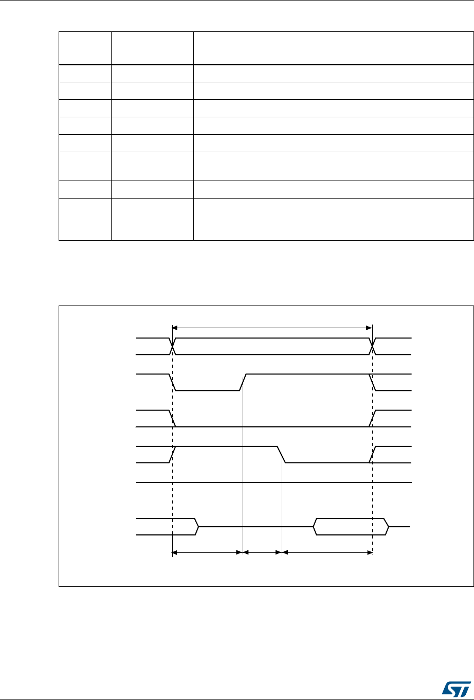
Flexible static memory controller (FSMC) RM0090
1564/1749 RM0090 Rev 18
Mode D - asynchronous access with extended address
Figure 445. Mode D read accesses
Table 236. FSMC_BWTRx bit fields
Bit
number Bit name Value to set
31:30 Reserved 0x0
29-28 ACCMOD 0x2
27-24 DATLAT Don’t care
23-20 CLKDIV Don’t care
19-16 BUSTURN Time between NEx high to NEx low (BUSTURN HCLK)
15-8 DATAST Duration of the second access phase (DATAST+1 HCLK cycles for
write accesses,
7-4 ADDHLD Don’t care
3-0 ADDSET[3:0]
Duration of the first access phase (ADDSET HCLK cycles) for write
accesses.
Minimum value for ADDSET is 0.
A[25:0]
NOE
ADDSET DATAST
Memory transaction
NEx
D[15:0]
HCLK cycles HCLK cycles
NWE
NADV
data driven
by memory
ai15566
High
ADDHLD
HCLK cycles
RM0090 Rev 18 1565/1749
RM0090 Flexible static memory controller (FSMC)
1601
Figure 446. Mode D write accesses
The differences with mode1 are the toggling of NOE that goes on toggling after NADV
changes and the independent read and write timings.
Table 237. FSMC_BCRx bit fields
Bit No. Bit name Value to set
31-20 Reserved 0x000
19 CBURSTRW 0x0 (no effect on asynchronous mode)
18:16 CPSIZE 0x0 (no effect on asynchronous mode)
15 ASYNCWAIT Set to 1 if the memory supports this feature. Otherwise keep
at 0.
14 EXTMOD 0x1
13 WAITEN 0x0 (no effect on asynchronous mode)
12 WREN As needed
11 WAITCFG Don’t care
10 WRAPMOD 0x0
9 WAITPOL Meaningful only if bit 15 is 1
8 BURSTEN 0x0
7 Reserved 0x1
6 FACCEN Set according to memory support
5-4 MWID As needed
3-2 MTYP[0:1] As needed

Flexible static memory controller (FSMC) RM0090
1566/1749 RM0090 Rev 18
1 MUXEN 0x0
0 MBKEN 0x1
Table 238. FSMC_BTRx bit fields
Bit No. Bit name Value to set
31:30 Reserved 0x0
29-28 ACCMOD 0x3
27-24 DATLAT Don’t care
23-20 CLKDIV Don’t care
19-16 BUSTURN Time between NEx high to NEx low (BUSTURN HCLK)
15-8 DATAST Duration of the second access phase (DATAST HCLK cycles) for
read accesses.
7-4 ADDHLD Duration of the middle phase of the read access (ADDHLD HCLK
cycles)
3-0 ADDSET[3:0] Duration of the first access phase (ADDSET HCLK cycles) for read
accesses. Minimum value for ADDSET is 0.
Table 239. FSMC_BWTRx bit fields
Bit No. Bit name Value to set
31:30 Reserved 0x0
29-28 ACCMOD 0x3
27-24 DATLAT 0x0
23-20 CLKDIV 0x0
19-16 BUSTURN Time between NEx high to NEx low (BUSTURN HCLK)
15-8 DATAST Duration of the second access phase (DATAST+1 HCLK cycles) for
write accesses
7-4 ADDHLD Duration of the middle phase of the write access (ADDHLD HCLK
cycles)
3-0 ADDSET[3:0] Duration of the first access phase (ADDSET+1 HCLK cycles) for
write accesses. Minimum value for ADDSET is 0.
Table 237. FSMC_BCRx bit fields (continued)
Bit No. Bit name Value to set
RM0090 Rev 18 1567/1749
RM0090 Flexible static memory controller (FSMC)
1601
Muxed mode - multiplexed asynchronous access to NOR Flash memory
Figure 447. Multiplexed read accesses
Figure 448. Multiplexed write accesses
The difference with mode D is the drive of the lower address byte(s) on the databus.
A[25:16]
NOE
ADDSET (DATAST + 1)
Memory transaction
NEx
AD[15:0]
HCLK cycles HCLK cycles
NWE
NADV
data driven by FSMC
ai15569
1HCLK
ADDHLD
HCLK cycles
Lower address

Flexible static memory controller (FSMC) RM0090
1568/1749 RM0090 Rev 18
WAIT management in asynchronous accesses
If the asynchronous memory asserts a WAIT signal to indicate that it is not yet ready to
accept or to provide data, the ASYNCWAIT bit has to be set in FSMC_BCRx register.
Table 240. FSMC_BCRx bit fields
Bit No. Bit name Value to set
31-21 Reserved 0x000
19 CBURSTRW 0x0 (no effect on asynchronous mode)
18:16 CPSIZE 0x0 (no effect on asynchronous mode)
15 ASYNCWAIT Set to 1 if the memory supports this feature. Otherwise keep at
0.
14 EXTMOD 0x0
13 WAITEN 0x0 (no effect on asynchronous mode)
12 WREN As needed
11 WAITCFG Don’t care
10 WRAPMOD 0x0
9 WAITPOL Meaningful only if bit 15 is 1
8 BURSTEN 0x0
7 Reserved 0x1
6 FACCEN 0x1
5-4 MWID As needed
3-2 MTYP[0:1] 0x2 (NOR Flash memory)
1 MUXEN 0x1
0 MBKEN 0x1
Table 241. FSMC_BTRx bit fields
Bit No. Bit name Value to set
31:30 Reserved 0x0
29-28 ACCMOD 0x0
27-24 DATLAT Don’t care
23-20 CLKDIV Don’t care
19-16 BUSTURN Time between NEx high to NEx low (BUSTURN HCLK)
15-8 DATAST Duration of the second access phase (DATAST HCLK cycles for
read accesses and DATAST+1 HCLK cycles for write accesses).
7-4 ADDHLD Duration of the middle phase of the access (ADDHLD HCLK cycles).
3-0 ADDSET[3:0] Duration of the first access phase (ADDSET HCLK cycles).
Minimum value for ADDSET is 1.

RM0090 Rev 18 1569/1749
RM0090 Flexible static memory controller (FSMC)
1601
If the WAIT signal is active (high or low depending on the WAITPOL bit), the second access
phase (Data setup phase) programmed by the DATAST bits, is extended until WAIT
becomes inactive. Unlike the data setup phase, the first access phases (Address setup and
Address hold phases), programmed by the ADDSET[3:0] and ADDHLD bits, are not WAIT
sensitive and so they are not prolonged.
The data setup phase (DATAST in the FSMC_BTRx register) must be programmed so that
WAIT can be detected 4 HCLK cycles before the end of memory transaction. The following
cases must be considered:
1. DATAST in FSMC_BTRx register) Memory asserts the WAIT signal aligned to
NOE/NWE which toggles:
2. Memory asserts the WAIT signal aligned to NEx (or NOE/NWE not toggling):
if
then
otherwise
where max_wait_assertion_time is the maximum time taken by the memory to assert
the WAIT signal once NEx/NOE/NWE is low.
Figure 449 and Figure 450 show the number of HCLK clock cycles that are added to the
memory access after WAIT is released by the asynchronous memory (independently of the
above cases).
DATAST 4 HCLK×()max_wait_assertion_time+≥
max_wait_assertion_time address_phase hold_phase+>
DATAST 4 HCLK×()max_wait_assertion_time address_phase–hold_phase–()+≥
DATAST 4 HCLK×≥
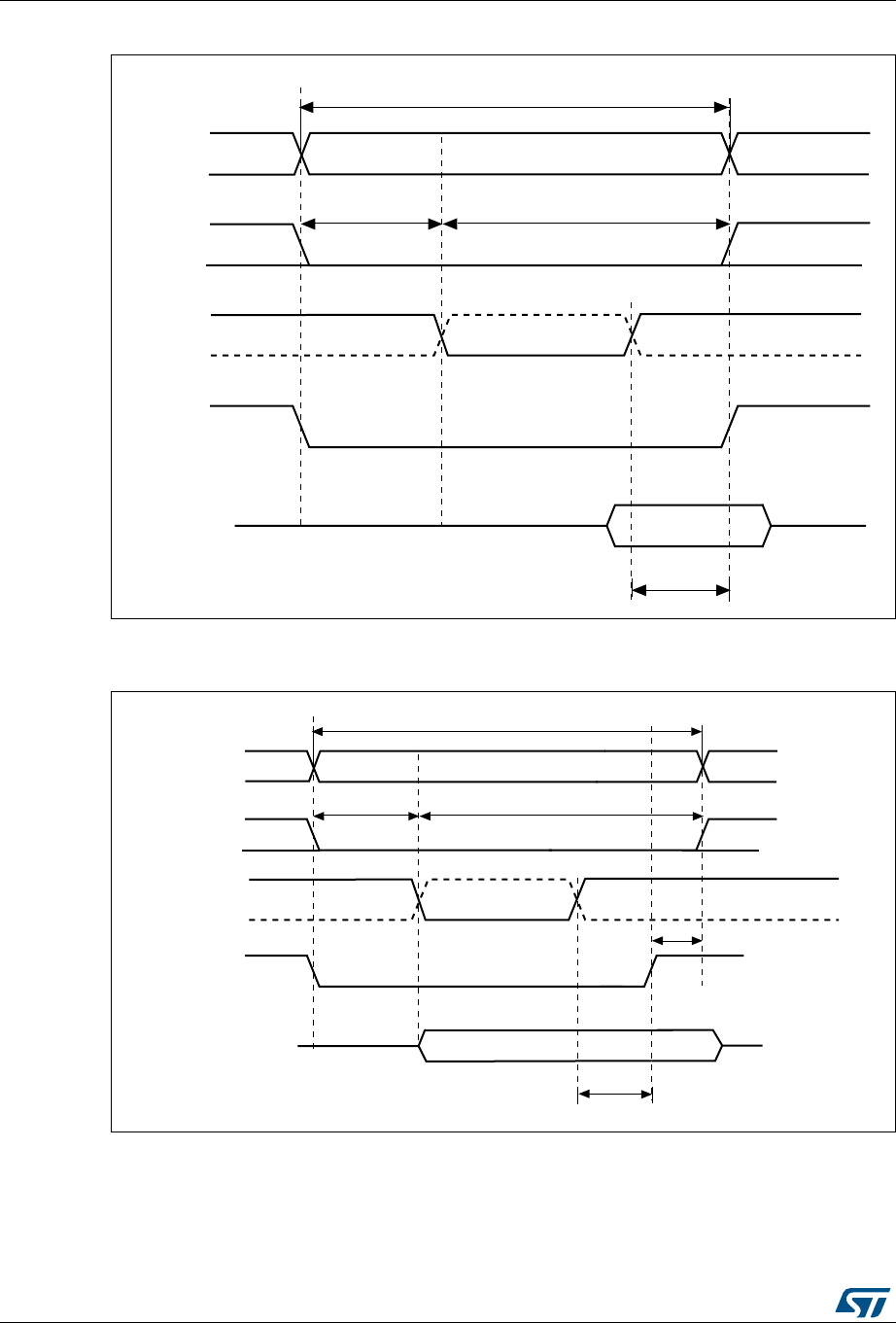
Flexible static memory controller (FSMC) RM0090
1570/1749 RM0090 Rev 18
Figure 449. Asynchronous wait during a read access
1. NWAIT polarity depends on WAITPOL bit setting in FSMC_BCRx register.
Figure 450. Asynchronous wait during a write access
1. NWAIT polarity depends on WAITPOL bit setting in FSMC_BCRx register.
A[25:0]
NOE
4HCLK
Memory transaction
NWAIT
D[15:0]
NEx
data driven
by memory
ai18471b
address phase
don’t care
data setup phase
don’t care
A[25:0]
NWE
Memory transaction
NWAIT
D[15:0]
NEx
data driven by FSMC
ai15797c
3HCLK
address phase data setup phase
1HCLK
don’t care don’t care

RM0090 Rev 18 1571/1749
RM0090 Flexible static memory controller (FSMC)
1601
36.5.5 Synchronous transactions
The memory clock, CLK, is a submultiple of HCLK according to the value of parameter
CLKDIV.
NOR Flash memories specify a minimum time from NADV assertion to CLK high. To meet
this constraint, the FSMC does not issue the clock to the memory during the first internal
clock cycle of the synchronous access (before NADV assertion). This guarantees that the
rising edge of the memory clock occurs in the middle of the NADV low pulse.
Data latency versus NOR Flash latency
The data latency is the number of cycles to wait before sampling the data. The DATLAT
value must be consistent with the latency value specified in the NOR Flash configuration
register. The FSMC does not include the clock cycle when NADV is low in the data latency
count.
Caution: Some NOR Flash memories include the NADV Low cycle in the data latency count, so the
exact relation between the NOR Flash latency and the FMSC DATLAT parameter can be
either of:
•NOR Flash latency = (DATLAT + 2) CLK clock cycles
•NOR Flash latency = (DATLAT + 3) CLK clock cycles
Some recent memories assert NWAIT during the latency phase. In such cases DATLAT can
be set to its minimum value. As a result, the FSMC samples the data and waits long enough
to evaluate if the data are valid. Thus the FSMC detects when the memory exits latency and
real data are taken.
Other memories do not assert NWAIT during latency. In this case the latency must be set
correctly for both the FSMC and the memory, otherwise invalid data are mistaken for good
data, or valid data are lost in the initial phase of the memory access.
Single-burst transfer
When the selected bank is configured in burst mode for synchronous accesses, if for
example an AHB single-burst transaction is requested on 16-bit memories, the FSMC
performs a burst transaction of length 1 (if the AHB transfer is 16-bit), or length 2 (if the AHB
transfer is 32-bit) and de-assert the chip select signal when the last data is strobed.
Clearly, such a transfer is not the most efficient in terms of cycles (compared to an
asynchronous read). Nevertheless, a random asynchronous access would first require to re-
program the memory access mode, which would altogether last longer.
Cross boundary page for Cellular RAM 1.5
Cellular RAM 1.5 does not allow burst access to cross the page boundary. The FSMC
controller allows to split automatically the burst access when the memory page size is
reached by configuring the CPSIZE bits in the FSMC_BCR1 register following the memory
page size.
Wait management
For synchronous NOR Flash memories, NWAIT is evaluated after the programmed latency
period, (DATLAT+2) CLK clock cycles.
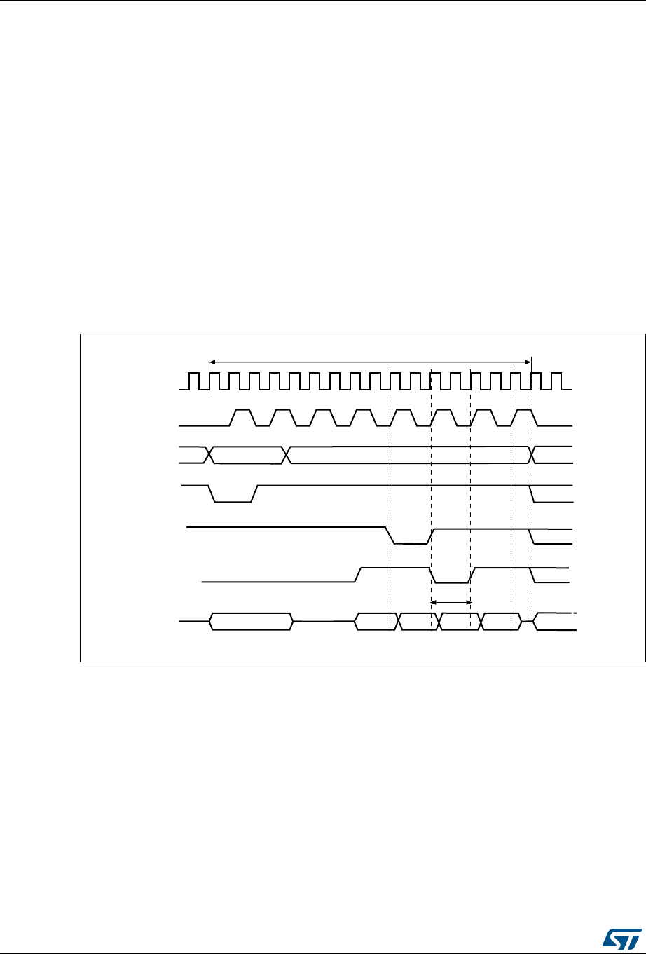
Flexible static memory controller (FSMC) RM0090
1572/1749 RM0090 Rev 18
If NWAIT is sensed active (low level when WAITPOL = 0, high level when WAITPOL = 1),
wait states are inserted until NWAIT is sensed inactive (high level when WAITPOL = 0, low
level when WAITPOL = 1).
When NWAIT is inactive, the data is considered valid either immediately (bit WAITCFG = 1)
or on the next clock edge (bit WAITCFG = 0).
During wait-state insertion via the NWAIT signal, the controller continues to send clock
pulses to the memory, keeping the chip select and output enable signals valid, and does not
consider the data valid.
There are two timing configurations for the NOR Flash NWAIT signal in burst mode:
•Flash memory asserts the NWAIT signal one data cycle before the wait state (default
after reset)
•Flash memory asserts the NWAIT signal during the wait state
These two NOR Flash wait state configurations are supported by the FSMC, individually for
each chip select, thanks to the WAITCFG bit in the FSMC_BCRx registers (x = 0..3).
Figure 451. Wait configurations
aaddr[15:0] data data
addr[25:16]
Memory transaction = burst of 4 half words
HCLK
CLK
A[25:16]
NADV
NWAIT
(WAITCFG = 1)
A/D[15:0]
inserted wait state
data
NWAIT
(WAITCFG = 0)
ai15798b
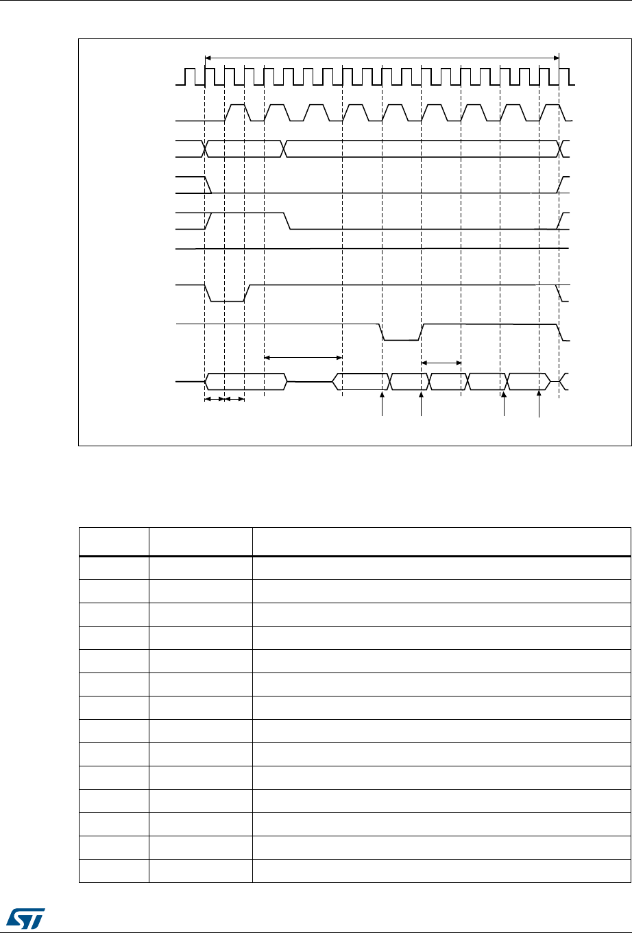
RM0090 Rev 18 1573/1749
RM0090 Flexible static memory controller (FSMC)
1601
Figure 452. Synchronous multiplexed read mode - NOR, PSRAM (CRAM)
1. Byte lane outputs BL are not shown; for NOR access, they are held high, and, for PSRAM (CRAM) access,
they are held low.
2. NWAIT polarity is set to 0.
Table 242. FSMC_BCRx bit fields
Bit No. Bit name Value to set
31-20 Reserved 0x000
19 CBURSTRW No effect on synchronous read
18-16 CPSIZE As needed (0x1 for CRAM 1.5)
15 ASCYCWAIT 0x0
14 EXTMOD 0x0
13 WAITEN Set to 1 if the memory supports this feature, otherwise keep at 0.
12 WREN no effect on synchronous read
11 WAITCFG to be set according to memory
10 WRAPMOD 0x0
9 WAITPOL to be set according to memory
8 BURSTEN 0x1
7 Reserved 0x1
6 FACCEN Set according to memory support (NOR Flash memory)
5-4 MWID As needed
Addr[15:0] data data
addr[25:16]
Memory transaction = burst of 4 half words
HCLK
CLK
A[25:16]
NEx
NOE
NWE High
NADV
NWAIT
(WAITCFG=
0)
A/D[15:0]
1 clock
cycle
1 clock
cycle
(DATLAT + 2) inserted wait state
Data strobes ai17723f
CLK cycles
data data
Data strobes

Flexible static memory controller (FSMC) RM0090
1574/1749 RM0090 Rev 18
3-2 MTYP[0:1] 0x1 or 0x2
1 MUXEN As needed
0 MBKEN 0x1
Table 243. FSMC_BTRx bit fields
Bit No. Bit name Value to set
31:30 Reserved 0x0
29:28 ACCMOD 0x0
27-24 DATLAT Data latency
23-20 CLKDIV
0x0 to get CLK = HCLK (not supported)
0x1 to get CLK = 2 × HCLK
..
19-16 BUSTURN Time between NEx high to NEx low (BUSTURN HCLK)
15-8 DATAST Don’t care
7-4 ADDHLD Don’t care
3-0 ADDSET[3:0] Don’t care
Table 242. FSMC_BCRx bit fields (continued)
Bit No. Bit name Value to set
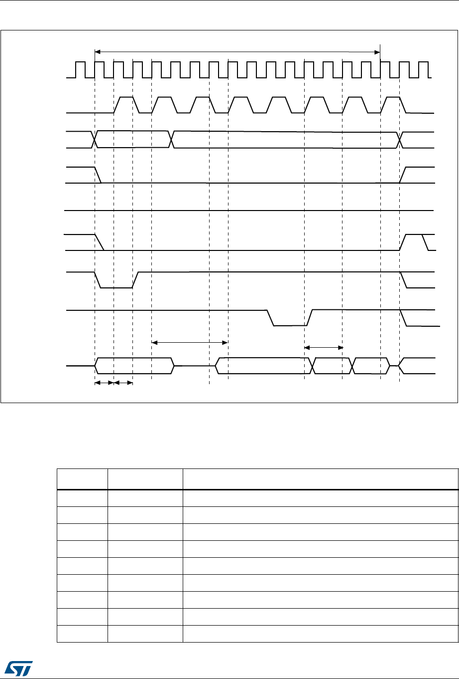
RM0090 Rev 18 1575/1749
RM0090 Flexible static memory controller (FSMC)
1601
Figure 453. Synchronous multiplexed write mode - PSRAM (CRAM)
1. Memory must issue NWAIT signal one cycle in advance, accordingly WAITCFG must be programmed to 0.
2. NWAIT polarity is set to 0.
3. Byte Lane (NBL) outputs are not shown, they are held low while NEx is active.
Addr[15:0] data
addr[25:16]
Memory transaction = burst of 2 half words
HCLK
CLK
A[25:16]
NEx
NOE
NWE
Hi-Z
NADV
NWAIT
(WAITCFG = 0)
A/D[15:0]
1 clock 1 clock
(DATLAT + 2) inserted wait state
ai14731f
CLK cycles
data
Table 244. FSMC_BCRx bit fields
Bit No. Bit name Value to set
31-20 Reserved 0x000
19 CBURSTRW 0x1
18-16 CPSIZE As needed (0x1 for CRAM 1.5)
15 ASCYCWAIT 0x0
14 EXTMOD 0x0
13 WAITEN Set to 1 if the memory supports this feature, otherwise keep at 0.
12 WREN 0x1
11 WAITCFG 0x0
10 WRAPMOD 0x0

Flexible static memory controller (FSMC) RM0090
1576/1749 RM0090 Rev 18
9 WAITPOL to be set according to memory
8 BURSTEN no effect on synchronous write
7 Reserved 0x1
6 FACCEN Set according to memory support
5-4 MWID As needed
3-2 MTYP[0:1] 0x1
1 MUXEN As needed
0 MBKEN 0x1
Table 245. FSMC_BTRx bit fields
Bit No. Bit name Value to set
31:30 Reserved 0x0
29:28 ACCMOD 0x0
27-24 DATLAT Data latency
23-20 CLKDIV 0x0 to get CLK = HCLK (not supported)
0x1 to get CLK = 2 × HCLK
19-16 BUSTURN Time between NEx high to NEx low (BUSTURN HCLK)
15-8 DATAST Don’t care
7-4 ADDHLD Don’t care
3-0 ADDSET[3:0] Don’t care
Table 244. FSMC_BCRx bit fields (continued)
Bit No. Bit name Value to set

RM0090 Rev 18 1577/1749
RM0090 Flexible static memory controller (FSMC)
1601
36.5.6 NOR/PSRAM control registers
The NOR/PSRAM control registers have to be accessed by words (32 bits).
SRAM/NOR-Flash chip-select control registers 1..4 (FSMC_BCR1..4)
Address offset: 0xA000 0000 + 8 * (x – 1), x = 1...4
Reset value: 0x0000 30DB for Bank1 and 0x0000 30D2 for Bank 2 to 4
This register contains the control information of each memory bank, used for SRAMs,
PSRAM and NOR Flash memories.
3130292827262524232221201918171615141312111098 76543210
Reserved
CBURSTRW
CPSIZE[2:0]
ASCYCWAIT
EXTMOD
WAITEN
WREN
WAITCFG
WRAPMOD
WAITPOL
BURSTEN
Reserved
FACCEN
MWID[1:0]
MTYP[1:0]
MUXEN
MBKEN
rw rw rw rw rw rw rw rw rw rw rw rw rw rw rw rw
Bits 31: 20 Reserved, must be kept at reset value.
Bit 19 CBURSTRW: Write burst enable.
For Cellular RAM (PSRAM) memories, this bit enables the synchronous burst protocol
during write operations. The enable bit for synchronous read accesses is the BURSTEN
bit in the FSMC_BCRx register.
0: Write operations are always performed in asynchronous mode
1: Write operations are performed in synchronous mode.
Bits 18: 16 CPSIZE[2:0]: CRAM page size.
These are used for Cellular RAM 1.5 which does not allow burst access to cross the
address boundaries between pages. When these bits are configured, the FSMC
controller splits automatically the burst access when the memory page size is reached
(refer to memory datasheet for page size).
000: No burst split when crossing page boundary (default after reset)
001: 128 bytes
010: 256 bytes
011: 512 bytes
100: 1024 bytes
Others: reserved.
Bit 15 ASYNCWAIT: Wait signal during asynchronous transfers
This bit enables/disables the FSMC to use the wait signal even during an asynchronous
protocol.
0: NWAIT signal is not taken into account when running an asynchronous protocol
(default after reset)
1: NWAIT signal is taken into account when running an asynchronous protocol

Flexible static memory controller (FSMC) RM0090
1578/1749 RM0090 Rev 18
Bit 14 EXTMOD: Extended mode enable.
This bit enables the FSMC to program the write timings for non-multiplexed
asynchronous accesses inside the FSMC_BWTR register, thus resulting in different
timings for read and write operations.
0: values inside FSMC_BWTR register are not taken into account (default after reset)
1: values inside FSMC_BWTR register are taken into account
Note: When the extended mode is disabled, the FSMC can operate in Mode1 or Mode2
as follows:
– Mode 1 is the default mode when the SRAM/PSRAM memory type is selected
(MTYP [0:1]=0x0 or 0x01)
– Mode 2 is the default mode when the NOR memory type is selected
(MTYP [0:1]= 0x10).
Bit 13 WAITEN: Wait enable bit.
This bit enables/disables wait-state insertion via the NWAIT signal when accessing the
Flash memory in synchronous mode.
0: NWAIT signal is disabled (its level not taken into account, no wait state inserted after
the programmed Flash latency period)
1: NWAIT signal is enabled (its level is taken into account after the programmed Flash
latency period to insert wait states if asserted) (default after reset)
Bit 12 WREN: Write enable bit.
This bit indicates whether write operations are enabled/disabled in the bank by the
FSMC:
0: Write operations are disabled in the bank by the FSMC, an AHB error is reported,
1: Write operations are enabled for the bank by the FSMC (default after reset).
Bit 11 WAITCFG: Wait timing configuration.
The NWAIT signal indicates whether the data from the memory are valid or if a wait state
must be inserted when accessing the Flash memory in synchronous mode. This
configuration bit determines if NWAIT is asserted by the memory one clock cycle before
the wait state or during the wait state:
0: NWAIT signal is active one data cycle before wait state (default after reset),
1: NWAIT signal is active during wait state (not used for PRAM).
Bit 10 WRAPMOD: Wrapped burst mode support.
Defines whether the controller will or not split an AHB burst wrap access into two linear
accesses. Valid only when accessing memories in burst mode
0: Direct wrapped burst is not enabled (default after reset),
1: Direct wrapped burst is enabled.
Note: This bit has no effect as the CPU and DMA cannot generate wrapping burst
transfers.
Bit 9 WAITPOL: Wait signal polarity bit.
Defines the polarity of the wait signal from memory. Valid only when accessing the
memory in burst mode:
0: NWAIT active low (default after reset),
1: NWAIT active high.
Bit 8 BURSTEN: Burst enable bit.
This bit enables/disables synchronous accesses during read operations. It is valid only
for synchronous memories operating in burst mode:
0: Burst mode disabled (default after reset). Read accesses are performed in
asynchronous mode.
1: Burst mode enable. Read accesses are performed in synchronous mode.

RM0090 Rev 18 1579/1749
RM0090 Flexible static memory controller (FSMC)
1601
Bit 7 Reserved, must be kept at reset value.
Bit 6 FACCEN: Flash access enable
Enables NOR Flash memory access operations.
0: Corresponding NOR Flash memory access is disabled
1: Corresponding NOR Flash memory access is enabled (default after reset)
Bits 5:4 MWID[1:0]: Memory databus width.
Defines the external memory device width, valid for all type of memories.
00: 8 bits,
01: 16 bits (default after reset),
10: reserved, do not use,
11: reserved, do not use.
Bits 3:2 MTYP[1:0]: Memory type.
Defines the type of external memory attached to the corresponding memory bank:
00: SRAM (default after reset for Bank 2...4)
01: PSRAM (CRAM)
10: NOR Flash/OneNAND Flash (default after reset for Bank 1)
11: reserved
Bit 1 MUXEN: Address/data multiplexing enable bit.
When this bit is set, the address and data values are multiplexed on the databus, valid
only with NOR and PSRAM memories:
0: Address/Data nonmultiplexed
1: Address/Data multiplexed on databus (default after reset)
Bit 0 MBKEN: Memory bank enable bit.
Enables the memory bank. After reset Bank1 is enabled, all others are disabled.
Accessing a disabled bank causes an ERROR on AHB bus.
0: Corresponding memory bank is disabled
1: Corresponding memory bank is enabled

Flexible static memory controller (FSMC) RM0090
1580/1749 RM0090 Rev 18
SRAM/NOR-Flash chip-select timing registers 1..4 (FSMC_BTR1..4)
Address offset: 0xA000 0000 + 0x04 + 8 * (x – 1), x = 1..4
Reset value: 0x0FFF FFFF
FSMC_BTRx bits are written by software to add a delay at the end of a read /write
transaction. This delay allows matching the minimum time between consecutive
transactions (tEHEL from NEx high to FSMC_NEx low) and the maximum time required by
the memory to free the data bus after a read access (tEHQZ).
This register contains the control information of each memory bank, used for SRAMs,
PSRAM and NOR Flash memories.If the EXTMOD bit is set in the FSMC_BCRx register,
then this register is partitioned for write and read access, that is, 2 registers are available:
one to configure read accesses (this register) and one to configure write accesses
(FSMC_BWTRx registers).
313029282726252423222120191817161514131211109876543210
Reserved
ACCMOD[1:0]
DATLAT[3:0]
CLKDIV[3:0]
BUSTURN[3:0]
DATAST[7:0]
ADDHLD[3:0]
ADDSET[3:0]
rw rw rw rw rw rw rw rw rw rw rw rw rw rw rw rw rw rw rw rw rw rw rw rw rw rw rw rw rw rw
Bits 31:30 Reserved, must be kept at reset value.
Bits 29:28 ACCMOD[1:0]: Access mode
Specifies the asynchronous access modes as shown in the timing diagrams. These bits are
taken into account only when the EXTMOD bit in the FSMC_BCRx register is 1.
00: access mode A
01: access mode B
10: access mode C
11: access mode D
Bits 27:24 DATLAT[3:0]: Data latency for synchronous memory (see note below bit description table)
For synchronous accesses with read/write burst mode enabled (BURSTEN / CBURSTRW bits
set), this field defines the number of memory clock cycles (+2) to issue to the memory before
reading/writing the first data. This timing parameter is not expressed in HCLK periods, but in
FSMC_CLK periods. For asynchronous accesses, this value is don't care.
0000: Data latency of 2 CLK clock cycles for first burst access
1111: Data latency of 17 CLK clock cycles for first burst access (default value after reset)
Bits 23:20 CLKDIV[3:0]: Clock divide ratio (for FSMC_CLK signal)
Defines the period of FSMC_CLK clock output signal, expressed in number of HCLK cycles:
0000: Reserved
0001: FSMC_CLK period = 2 × HCLK periods
0010: FSMC_CLK period = 3 × HCLK periods
1111: FSMC_CLK period = 16 × HCLK periods (default value after reset)
In asynchronous NOR Flash, SRAM or PSRAM accesses, this value is don’t care.

RM0090 Rev 18 1581/1749
RM0090 Flexible static memory controller (FSMC)
1601
Bits 19:16 BUSTURN[3:0]: Bus turnaround phase duration
These bits are written by software to add a delay at the end of a write-to-read (and read-to
write) transaction. The programmed bus turnaround delay is inserted between an
asynchronous read (muxed or D mode) or a write transaction and any other
asynchronous/synchronous read or write to/from a static bank (for a read operation, the bank
can be the same or a different one; for a write operation, the bank can be different except in r
muxed or D mode).
In some cases, the bus turnaround delay is fixed, whatever the programmed BUSTURN
values:
– No bus turnaround delay is inserted between two consecutive asynchronous write transfers
to the same static memory bank except in muxed and D mode.
– A bus turnaround delay of 1 FSMC clock cycle is inserted between:
– Two consecutive asynchronous read transfers to the same static memory bank
except for muxed and D modes.
– An asynchronous read to an asynchronous or synchronous write to any static bank
or dynamic bank except for muxed and D modes.
– An asynchronous (modes 1, 2, A, B or C) read and a read operation from another
static bank.
– A bus turnaround delay of 2 FSMC clock cycles is inserted between:
– Two consecutive synchronous write accesses (in burst or single mode) to the same
bank
– A synchronous write (burst or single) access and an asynchronous write or read
transfer to or from static memory bank (the bank can be the same or different in case
of a read operation).
– Two consecutive synchronous read accesses (in burst or single mode) followed by a
any synchronous/asynchronous read or write from/to another static memory bank.
– A bus turnaround delay of 3 FSMC clock cycles is inserted between:
– Two consecutive synchronous write operations (in burst or single mode) to different
static banks.
– A synchronous write access (in burst or single mode) and a synchronous read
access from the same or to a different bank.
0000: BUSTURN phase duration = 0 HCLK clock cycle added
...
1111: BUSTURN phase duration = 15 × HCLK clock cycles (default value after reset)

Flexible static memory controller (FSMC) RM0090
1582/1749 RM0090 Rev 18
Note: PSRAMs (CRAMs) have a variable latency due to internal refresh. Therefore these
memories issue the NWAIT signal during the whole latency phase to prolong the latency as
needed.
With PSRAMs (CRAMs) the DATLAT field must be set to 0, so that the FSMC exits its
latency phase soon and starts sampling NWAIT from memory, then starts to read or write
when the memory is ready.
This method can be used also with the latest generation of synchronous Flash memories
that issue the NWAIT signal, unlike older Flash memories (check the datasheet of the
specific Flash memory being used).
Bits 15:8 DATAST[7:0]: Data-phase duration
These bits are written by software to define the duration of the data phase (refer to Figure 436
to Figure 448), used in asynchronous accesses:
0000 0000: Reserved
0000 0001: DATAST phase duration = 1 × HCLK clock cycles
0000 0010: DATAST phase duration = 2 × HCLK clock cycles
...
1111 1111: DATAST phase duration = 255 × HCLK clock cycles (default value after reset)
For each memory type and access mode data-phase duration, refer to the respective figure
(Figure 436 to Figure 448).
Example: Mode1, write access, DATAST=1: Data-phase duration= DATAST+1 = 2 HCLK clock
cycles.
Note: In synchronous accesses, this value is don't care.
Bits 7:4 ADDHLD[3:0]: Address-hold phase duration
These bits are written by software to define the duration of the address hold phase (refer to
Figure 445 to Figure 448), used in mode D and multiplexed accesses:
0000: Reserved
0001: ADDHLD phase duration =1 × HCLK clock cycle
0010: ADDHLD phase duration = 2 × HCLK clock cycle
...
1111: ADDHLD phase duration = 15 × HCLK clock cycles (default value after reset)
For each access mode address-hold phase duration, refer to the respective figure (Figure 445
to Figure 448).
Note: In synchronous accesses, this value is not used, the address hold phase is always 1
memory clock period duration.
Bits 3:0 ADDSET[3:0]: Address setup phase duration
These bits are written by software to define the duration of the address setup phase (refer to
Figure 436 to Figure 448), used in SRAMs, ROMs and asynchronous NOR Flash and PSRAM
accesses:
0000: ADDSET phase duration = 0 × HCLK clock cycle
...
1111: ADDSET phase duration = 15 × HCLK clock cycles (default value after reset)
For each access mode address setup phase duration, refer to the respective figure (refer to
Figure 436 to Figure 448).
Note: In synchronous NOR Flash and PSRAM accesses, this value is don’t care.

RM0090 Rev 18 1583/1749
RM0090 Flexible static memory controller (FSMC)
1601
SRAM/NOR-Flash write timing registers 1..4 (FSMC_BWTR1..4)
Address offset: 0xA000 0000 + 0x104 + 8 * (x – 1), x = 1...4
Reset value: 0x0FFF FFFF
This register contains the control information of each memory bank, used for SRAMs,
PSRAMs and NOR Flash memories. This register is active for write asynchronous access
only when the EXTMOD bit is set in the FSMC_BCRx register.
313029282726252423222120191817161514131211109876543210
Res.
ACCM
OD[2:0] Reserved BUSTURN[3:0] DATAST[7:0] ADDHLD[3:0] ADDSET[3:0]
rw rw rw rw rw rw rw rw rw rw rw rw rw rw rw rw rw rw rw rw rw rw
Bits 31:30 Reserved, must be kept at reset value.
Bits 29:28 ACCMOD[2:0]: Access mode.
Specifies the asynchronous access modes as shown in the next timing diagrams.These bits are
taken into account only when the EXTMOD bit in the FSMC_BCRx register is 1.
00: access mode A
01: access mode B
10: access mode C
11: access mode D
Bits 27:20 Reserved, must be kept at reset value.
Bits 19:16 BUSTURN[3:0]: Bus turnaround phase duration
The programmed bus turnaround delay is inserted between a an asynchronous write transfer and
any other asynchronous/synchronous read or write transfer to/from a static bank (for a read
operation, the bank can be the same or a different one; for a write operation, the bank can be
different except in r muxed or D mode).
In some cases, the bus turnaround delay is fixed, whatever the programmed BUSTURN values:
– No bus turnaround delay is inserted between two consecutive asynchronous write transfers to the
same static memory bank except in muxed and D mode.
– A bus turnaround delay of 2 FSMC clock cycles is inserted between:
– Two consecutive synchronous write accesses (in burst or single mode) to the same bank.
– A synchronous write transfer (in burst or single mode) and an asynchronous write or read
transfer to/from static a memory bank.
– A bus turnaround delay of 3 FSMC clock cycles is inserted between:
– Two consecutive synchronous write accesses (in burst or single mode) to different static
banks.
– A synchronous write transfer (in burst or single mode) and a synchronous read from the
same or from a different bank.
0000: BUSTURN phase duration = 0 HCLK clock cycle added
...
1111: BUSTURN phase duration = 15 HCLK clock cycles added (default value after reset)

Flexible static memory controller (FSMC) RM0090
1584/1749 RM0090 Rev 18
36.6 NAND Flash/PC Card controller
The FSMC generates the appropriate signal timings to drive the following types of device:
•NAND Flash
–8-bit
– 16-bit
•16-bit PC Card compatible devices
The NAND/PC Card controller can control three external banks. Bank 2 and bank 3 support
NAND Flash devices. Bank 4 supports PC Card devices.
Each bank is configured by means of dedicated registers (Section 36.6.8). The
programmable memory parameters include access timings (shown in Table 246) and ECC
configuration.
Bits 15:8 DATAST[7:0]: Data-phase duration.
These bits are written by software to define the duration of the data phase (refer to Figure 436 to
Figure 448), used in asynchronous SRAM, PSRAM and NOR Flash memory accesses:
0000 0000: Reserved
0000 0001: DATAST phase duration = 1 × HCLK clock cycles
0000 0010: DATAST phase duration = 2 × HCLK clock cycles
...
1111 1111: DATAST phase duration = 255 × HCLK clock cycles (default value after reset)
Note: In synchronous accesses, this value is don't care.
Bits 7:4 ADDHLD[3:0]: Address-hold phase duration.
These bits are written by software to define the duration of the address hold phase (refer to
Figure 445 to Figure 448), used in asynchronous multiplexed accesses:
0000: Reserved
0001: ADDHLD phase duration = 1 × HCLK clock cycle
0010: ADDHLD phase duration = 2 × HCLK clock cycle
...
1111: ADDHLD phase duration = 15 × HCLK clock cycles (default value after reset)
Note: In synchronous NOR Flash accesses, this value is not used, the address hold phase is always
1 Flash clock period duration.
Bits 3:0 ADDSET[3:0]: Address setup phase duration.
These bits are written by software to define the duration of the address setup phase in HCLK cycles
(refer to Figure 445 to Figure 448), used in asynchronous accessed:
0000: ADDSET phase duration = 0 × HCLK clock cycle
...
1111: ADDSET phase duration = 15 × HCLK clock cycles (default value after reset)
Note: In synchronous NOR Flash and PSRAM accesses, this value is don’t care.

RM0090 Rev 18 1585/1749
RM0090 Flexible static memory controller (FSMC)
1601
36.6.1 External memory interface signals
The following tables list the signals that are typically used to interface NAND Flash and PC
Card.
Note: Prefix “N”. specifies the associated signal as active low.
8-bit NAND Flash
t
There is no theoretical capacity limitation as the FSMC can manage as many address
cycles as needed.
Table 246. Programmable NAND/PC Card access parameters
Parameter Function Access mode Unit Min. Max.
Memory setup
time
Number of clock cycles (HCLK)
to set up the address before the
command assertion
Read/Write AHB clock cycle
(HCLK) 1 255
Memory wait Minimum duration (HCLK clock
cycles) of the command assertion Read/Write AHB clock cycle
(HCLK) 2 256
Memory hold
Number of clock cycles (HCLK)
to hold the address (and the data
in case of a write access) after
the command de-assertion
Read/Write AHB clock cycle
(HCLK) 1 254
Memory
databus high-Z
Number of clock cycles (HCLK)
during which the databus is kept
in high-Z state after the start of a
write access
Write AHB clock cycle
(HCLK) 0 255
Table 247. 8-bit NAND Flash
FSMC signal name I/O Function
A[17] O NAND Flash address latch enable (ALE) signal
A[16] O NAND Flash command latch enable (CLE) signal
D[7:0] I/O 8-bit multiplexed, bidirectional address/data bus
NCE[x] O Chip select, x = 2, 3
NOE(= NRE) O Output enable (memory signal name: read enable, NRE)
NWE O Write enable
NWAIT/INT[3:2] I NAND Flash ready/busy input signal to the FSMC

Flexible static memory controller (FSMC) RM0090
1586/1749 RM0090 Rev 18
16-bit NAND Flash
There is no theoretical capacity limitation as the FSMC can manage as many address
cycles as needed.
16-bit PC Card
Table 248. 16-bit NAND Flash
FSMC signal name I/O Function
A[17] O NAND Flash address latch enable (ALE) signal
A[16] O NAND Flash command latch enable (CLE) signal
D[15:0] I/O 16-bit multiplexed, bidirectional address/data bus
NCE[x] O Chip select, x = 2, 3
NOE(= NRE) O Output enable (memory signal name: read enable, NRE)
NWE O Write enable
NWAIT/INT[3:2] I NAND Flash ready/busy input signal to the FSMC
Table 249. 16-bit PC Card
FSMC signal name I/O Function
A[10:0] O Address bus
NIORD O Output enable for I/O space
NIOWR O Write enable for I/O space
NREG O Register signal indicating if access is in Common or Attribute space
D[15:0] I/O Bidirectional databus
NCE4_1 O Chip select 1
NCE4_2 O Chip select 2 (indicates if access is 16-bit or 8-bit)
NOE O Output enable in Common and in Attribute space
NWE O Write enable in Common and in Attribute space
NWAIT I PC Card wait input signal to the FSMC (memory signal name
IORDY)
INTR I PC Card interrupt to the FSMC (only for PC Cards that can generate
an interrupt)
CD I
PC Card presence detection. Active high. If an access is performed
to the PC Card banks while CD is low, an AHB error is generated.
Refer to Section 36.3: AHB interface

RM0090 Rev 18 1587/1749
RM0090 Flexible static memory controller (FSMC)
1601
36.6.2 NAND Flash / PC Card supported memories and transactions
Table 250 below shows the supported devices, access modes and transactions.
Transactions not allowed (or not supported) by the NAND Flash / PC Card controller appear
in gray.
36.6.3 Timing diagrams for NAND and PC Card
Each PC Card/CompactFlash and NAND Flash memory bank is managed through a set of
registers:
•Control register: FSMC_PCRx
•Interrupt status register: FSMC_SRx
•ECC register: FSMC_ECCRx
•Timing register for Common memory space: FSMC_PMEMx
•Timing register for Attribute memory space: FSMC_PATTx
•Timing register for I/O space: FSMC_PIOx
Each timing configuration register contains three parameters used to define number of
HCLK cycles for the three phases of any PC Card/CompactFlash or NAND Flash access,
plus one parameter that defines the timing for starting driving the databus in the case of a
write. Figure 454 shows the timing parameter definitions for common memory accesses,
knowing that Attribute and I/O (only for PC Card) memory space access timings are similar.
Table 250. Supported memories and transactions
Device Mode R/W
AHB
data size
Memory
data size
Allowed/
not allowed Comments
NAND 8-bit
Asynchronous R 8 8 Y
Asynchronous W 8 8 Y
Asynchronous R 16 8 Y Split into 2 FSMC accesses
Asynchronous W 16 8 Y Split into 2 FSMC accesses
Asynchronous R 32 8 Y Split into 4 FSMC accesses
Asynchronous W 32 8 Y Split into 4 FSMC accesses
NAND 16-bit
Asynchronous R 8 16 Y
Asynchronous W 8 16 N
Asynchronous R 16 16 Y
Asynchronous W 16 16 Y
Asynchronous R 32 16 Y Split into 2 FSMC accesses
Asynchronous W 32 16 Y Split into 2 FSMC accesses
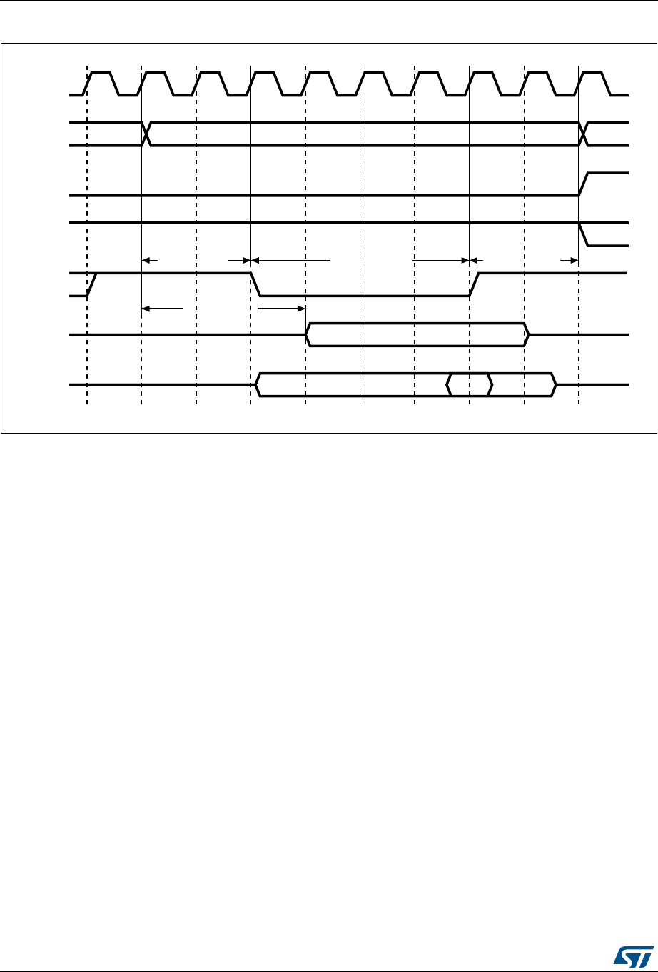
Flexible static memory controller (FSMC) RM0090
1588/1749 RM0090 Rev 18
Figure 454. NAND/PC Card controller timing for common memory access
1. NOE remains high (inactive) during write access. NWE remains high (inactive) during read access.
2. For write accesses, the hold phase delay is (MEMHOLD) x HCLK cycles, while it is (MEMHOLD + 2) x
HCLK cycles for read accesses.
36.6.4 NAND Flash operations
The command latch enable (CLE) and address latch enable (ALE) signals of the NAND
Flash device are driven by some address signals of the FSMC controller. This means that to
send a command or an address to the NAND Flash memory, the CPU has to perform a write
to a certain address in its memory space.
A typical page read operation from the NAND Flash device is as follows:
1. Program and enable the corresponding memory bank by configuring the FSMC_PCRx
and FSMC_PMEMx (and for some devices, FSMC_PATTx, see Section 36.6.5)
registers according to the characteristics of the NAND Flash (PWID bits for the databus
width of the NAND Flash, PTYP = 1, PWAITEN = 0 or 1 as needed, see Common
memory space timing register 2..4 (FSMC_PMEM2..4) for timing configuration).
2. The CPU performs a byte write in the common memory space, with data byte equal to
one Flash command byte (for example 0x00 for Samsung NAND Flash devices). The
CLE input of the NAND Flash is active during the write strobe (low pulse on NWE), thus
the written byte is interpreted as a command by the NAND Flash. Once the command
is latched by the NAND Flash device, it does not need to be written for the following
page read operations.
3. The CPU can send the start address (STARTAD) for a read operation by writing the
required bytes (for example four bytes or three for smaller capacity devices),
STARTAD[7:0], STARTAD[15:8], STARTAD[23:16] and finally STARTAD[25:24] for
64 Mb x 8 bit NAND Flash) in the common memory or attribute space. The ALE input of
the NAND Flash device is active during the write strobe (low pulse on NWE), thus the
i15570b
HCLK
A[25:0]
NCEx
NREG,
NIOW,
NIOR
NWE,
NOE
(1)
write_data
read_data
High
Valid
MEMxSET + 1
MEMxWAIT + 1
MEMxHOLD + 1
MEMxHIZ
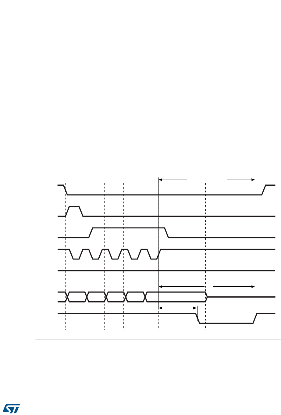
RM0090 Rev 18 1589/1749
RM0090 Flexible static memory controller (FSMC)
1601
written bytes are interpreted as the start address for read operations. Using the
attribute memory space makes it possible to use a different timing configuration of the
FSMC, which can be used to implement the prewait functionality needed by some
NAND Flash memories (see details in Section 36.6.5).
4. The controller waits for the NAND Flash to be ready (R/NB signal high) to become
active, before starting a new access (to same or another memory bank). While waiting,
the controller maintains the NCE signal active (low).
5. The CPU can then perform byte read operations in the common memory space to read
the NAND Flash page (data field + Spare field) byte by byte.
6. The next NAND Flash page can be read without any CPU command or address write
operation, in three different ways:
– by simply performing the operation described in step 5
– a new random address can be accessed by restarting the operation at step 3
– a new command can be sent to the NAND Flash device by restarting at step 2
36.6.5 NAND Flash prewait functionality
Some NAND Flash devices require that, after writing the last part of the address, the
controller wait for the R/NB signal to go low as shown in Figure 455.
Figure 455. Access to non ‘CE don’t care’ NAND-Flash
1. CPU wrote byte 0x00 at address 0x7001 0000.
2. CPU wrote byte A7-A0 at address 0x7002 0000.
3. CPU wrote byte A15-A8 at address 0x7002 0000.
4. CPU wrote byte A23-A16 at address 0x7002 0000.
5. CPU wrote byte A25-A24 at address 0x7802 0000: FSMC performs a write access using FSMC_PATT2
timing definition, where ATTHOLD ≥ 7 (providing that (7+1) × HCLK = 112 ns > tWB max). This guarantees
that NCE remains low until R/NB goes low and high again (only requested for NAND Flash memories
where NCE is not don’t care).
NCE
NOE
I/O[7:0]
R/NB
ai17733b
High
tWB
CLE
ALE
0x00 A7-A0 A15-A8 A23-A16 A25-A14
tR
NWE
(1) (2) (3) (4) (5)
NCE must stay low

Flexible static memory controller (FSMC) RM0090
1590/1749 RM0090 Rev 18
When this functionality is needed, it can be guaranteed by programming the MEMHOLD
value to meet the tWB timing. However CPU read accesses to the NAND Flash memory has
a hold delay of (MEMHOLD + 2) x HCLK cycles, while CPU write accesses have a hold
delay of (MEMHOLD) x HCLK cycles.
To overcome this timing constraint, the attribute memory space can be used by
programming its timing register with an ATTHOLD value that meets the tWB timing, and
leaving the MEMHOLD value at its minimum. Then, the CPU must use the common memory
space for all NAND Flash read and write accesses, except when writing the last address
byte to the NAND Flash device, where the CPU must write to the attribute memory space.
36.6.6 Computation of the error correction code (ECC)
in NAND Flash memory
The FSMC PC-Card controller includes two error correction code computation hardware
blocks, one per memory bank. They are used to reduce the host CPU workload when
processing the error correction code by software in the system.
These two registers are identical and associated with bank 2 and bank 3, respectively. As a
consequence, no hardware ECC computation is available for memories connected to bank
4.
The error correction code (ECC) algorithm implemented in the FSMC can perform 1-bit error
correction and 2-bit error detection per 256, 512, 1 024, 2 048, 4 096 or 8 192 bytes read
from or written to NAND Flash memory. It is based on the Hamming coding algorithm and
consists in calculating the row and column parity.
The ECC modules monitor the NAND Flash databus and read/write signals (NCE and NWE)
each time the NAND Flash memory bank is active.
The functional operations are:
•When access to NAND Flash is made to bank 2 or bank 3, the data present on the
D[15:0] bus is latched and used for ECC computation.
•When access to NAND Flash occurs at any other address, the ECC logic is idle, and
does not perform any operation. Thus, write operations for defining commands or
addresses to NAND Flash are not taken into account for ECC computation.
Once the desired number of bytes has been read from/written to the NAND Flash by the
host CPU, the FSMC_ECCR2/3 registers must be read in order to retrieve the computed
value. Once read, they should be cleared by resetting the ECCEN bit to zero. To compute a
new data block, the ECCEN bit must be set to one in the FSMC_PCR2/3 registers.
To perform an ECC computation:

RM0090 Rev 18 1591/1749
RM0090 Flexible static memory controller (FSMC)
1601
1. Enable the ECCEN bit in the FSMC_PCR2/3 register.
2. Write data to the NAND Flash memory page. While the NAND page is written, the ECC
block computes the ECC value.
3. Read the ECC value available in the FSMC_ECCR2/3 register and store it in a
variable.
4. Clear the ECCEN bit and then enable it in the FSMC_PCR2/3 register before reading
back the written data from the NAND page. While the NAND page is read, the ECC
block computes the ECC value.
5. Read the new ECC value available in the FSMC_ECCR2/3 register.
6. If the two ECC values are the same, no correction is required, otherwise there is an
ECC error and the software correction routine returns information on whether the error
can be corrected or not.
36.6.7 PC Card/CompactFlash operations
Address spaces and memory accesses
The FSMC supports Compact Flash storage or PC Cards in Memory Mode and I/O Mode
(True IDE mode is not supported).
The Compact Flash storage and PC Cards are made of 3 memory spaces:
•Common Memory Space
•Attribute Space
•I/O Memory Space
The nCE2 and nCE1 pins (FSMC_NCE4_2 and FSMC_NCE4_1 respectively) select the
card and indicate whether a byte or a word operation is being performed: nCE2 accesses
the odd byte on D15-8 and nCE1 accesses the even byte on D7-0 if A0=0 or the odd byte on
D7-0 if A0=1. The full word is accessed on D15-0 if both nCE2 and nCE1 are low.
The memory space is selected by asserting low nOE for read accesses or nWE for write
accesses, combined with the low assertion of nCE2/nCE1 and nREG.
•If pin nREG=1 during the memory access, the common memory space is selected
•If pin nREG=0 during the memory access, the attribute memory space is selected
The I/O Space is selected by asserting low nIORD for read accesses or nIOWR for write
accesses [instead of nOE/nWE for memory Space], combined with nCE2/nCE1. Note that
nREG must also be asserted low during accesses to I/O Space.
Three type of accesses are allowed for a 16-bit PC Card:
•Accesses to Common Memory Space for data storage can be either 8-bit accesses at
even addresses or 16 bit AHB accesses.
Note that 8-bit accesses at odd addresses are not supported and will not lead to the
low assertion of nCE2. A 32-bit AHB request is translated into two 16-bit memory
accesses.
•Accesses to Attribute Memory Space where the PC Card stores configuration
information are limited to 8-bit AHB accesses at even addresses.
Note that a 16-bit AHB access will be converted into a single 8-bit memory transfer:
nCE1 will be asserted low, nCE2 will be asserted high and only the even Byte on D7-
D0 will be valid. Instead a 32-bit AHB access will be converted into two 8-bit memory

Flexible static memory controller (FSMC) RM0090
1592/1749 RM0090 Rev 18
transfers at even addresses: nCE1 will be asserted low, NCE2 will be asserted high
and only the even bytes will be valid.
•Accesses to I/O Space can be performed either through AHB 8-bit or 16-bit accesses.
The FSMC Bank 4 gives access to those 3 memory spaces as described in Section 36.4.2:
NAND/PC Card address mapping and Table 218: Memory mapping and timing registers.
Wait Feature
The CompactFlash Storage or PC Card may request the FSMC to extend the length of the
access phase programmed by MEMWAITx/ATTWAITx/IOWAITx bits, asserting the nWAIT
signal after nOE/nWE or nIORD/nIOWR activation if the wait feature is enabled through the
PWAITEN bit in the FSMC_PCRx register. In order to detect the nWAIT assertion correctly,
the MEMWAITx/ATTWAITx/IOWAITx bits must be programmed as follows:
Table 251. 16-bit PC-Card signals and access type
nCE2
nCE1
nREG
nOE/nWE
nIORD /nIOWR
A10
A9
A7-1
A0
Space Access Type Allowed/not
Allowed
1 0 101XXX-XX Common
Memory
Space
Read/Write byte on D7-D0 YES
0 1 1 0 1 X X X-X X Read/Write byte on D15-D8 Not supported
0 0 1 0 1 X X X-X 0 Read/Write word on D15-D0 YES
X0 00101X-X0
Attribute
Space
Read or Write Configuration
Registers YES
X0 00100X-X0 Read or Write CIS (Card
Information Structure) YES
1 0 001XXX-X1
Attribute
Space
Invalid Read or Write (odd
address) YES
0 1 001XXX-Xx Invalid Read or Write (odd
address) YES
1 0 010XXX-X0
I/O space
Read Even Byte on D7-0 YES
1 0 0 1 0 X X X-X 1 Read Odd Byte on D7-0 YES
1 0 0 1 0 X X X-X 0 Write Even Byte on D7-0 YES
1 0 0 1 0 X X X-X 1 Write Odd Byte on D7-0 YES
0 0 0 1 0 X X X-X 0 Read Word on D15-0 YES
0 0 0 1 0 X X X-X 0 Write word on D15-0 YES
0 1 0 1 0 X X X-X X Read Odd Byte on D15-8 Not supported
0 1 0 1 0 X X X-X X Write Odd Byte on D15-8 Not supported

RM0090 Rev 18 1593/1749
RM0090 Flexible static memory controller (FSMC)
1601
xxWAITx >= 4 + max_wait_assertion_time/HCLK
Where max_wait_assertion_time is the maximum time taken by NWAIT to go low once
nOE/nWE or nIORD/nIOWR is low.
After the de-assertion of nWAIT, the FSMC extends the WAIT phase for 4 HCLK clock
cycles.
36.6.8 NAND Flash/PC Card control registers
The NAND Flash/PC Card control registers have to be accessed by words (32 bits).
PC Card/NAND Flash control registers 2..4 (FSMC_PCR2..4)
Address offset: 0xA0000000 + 0x40 + 0x20 * (x – 1), x = 2..4
Reset value: 0x0000 0018
31302928272625242322212019181716151413121110987654321 0
Reserved ECCPS[2:0] TAR[2:0] TCLR[2:0] Res.
ECCEN
PWID[1:0]
PTYP
PBKEN
PWAITEN
Reserved
rw rw rw rw rw rw rw rw rw rw rw rw rw rw rw rw rw
Bits 31:20 Reserved, must be kept at reset value.
Bits 19:17 ECCPS[2:0]: ECC page size.
Defines the page size for the extended ECC:
000: 256 bytes
001: 512 bytes
010: 1024 bytes
011: 2048 bytes
100: 4096 bytes
101: 8192 bytes
Bits 16:13 TAR[2:0]: ALE to RE delay.
Sets time from ALE low to RE low in number of AHB clock cycles (HCLK).
Time is: t_ar = (TAR + SET + 2) × THCLK where THCLK is the HCLK clock period
0000: 1 HCLK cycle (default)
1111: 16 HCLK cycles
Note: SET is MEMSET or ATTSET according to the addressed space.
Bits 12:9 TCLR[2:0]: CLE to RE delay.
Sets time from CLE low to RE low in number of AHB clock cycles (HCLK).
Time is t_clr = (TCLR + SET + 2) × THCLK where THCLK is the HCLK clock period
0000: 1 HCLK cycle (default)
1111: 16 HCLK cycles
Note: SET is MEMSET or ATTSET according to the addressed space.
Bits 8:7 Reserved, must be kept at reset value.
Bit 6 ECCEN: ECC computation logic enable bit
0: ECC logic is disabled and reset (default after reset),
1: ECC logic is enabled.

Flexible static memory controller (FSMC) RM0090
1594/1749 RM0090 Rev 18
FIFO status and interrupt register 2..4 (FSMC_SR2..4)
Address offset: 0xA000 0000 + 0x44 + 0x20 * (x-1), x = 2..4
Reset value: 0x0000 0040
This register contains information about FIFO status and interrupt. The FSMC has a FIFO
that is used when writing to memories to store up to16 words of data from the AHB.
This is used to quickly write to the AHB and free it for transactions to peripherals other than
the FSMC, while the FSMC is draining its FIFO into the memory. This register has one of its
bits that indicates the status of the FIFO, for ECC purposes.
The ECC is calculated while the data are written to the memory, so in order to read the
correct ECC the software must wait until the FIFO is empty.
Bits 5:4 PWID[1:0]: Databus width.
Defines the external memory device width.
00: 8 bits
01: 16 bits (default after reset). This value is mandatory for PC Cards.
10: reserved, do not use
11: reserved, do not use
Bit 3 PTYP: Memory type.
Defines the type of device attached to the corresponding memory bank:
0: PC Card, CompactFlash, CF+ or PCMCIA
1: NAND Flash (default after reset)
Bit 2 PBKEN: PC Card/NAND Flash memory bank enable bit.
Enables the memory bank. Accessing a disabled memory bank causes an ERROR on AHB
bus
0: Corresponding memory bank is disabled (default after reset)
1: Corresponding memory bank is enabled
Bit 1 PWAITEN: Wait feature enable bit.
Enables the Wait feature for the PC Card/NAND Flash memory bank:
0: disabled
1: enabled
Note: For a PC Card, when the wait feature is enabled, the MEMWAITx/ATTWAITx/IOWAITx
bits must be programmed to a value as follows:
xxWAITx ≥ 4 + max_wait_assertion_time/HCLK
Where max_wait_assertion_time is the maximum time taken by NWAIT to go low once
nOE/nWE or nIORD/nIOWR is low.
Bit 0 Reserved, must be kept at reset value.
313029282726252423222120191817161514131211109876543210
Reserved
FEMPT
IFEN
ILEN
IREN
IFS
ILS
IRS
r rwrwrwrwrwrw

RM0090 Rev 18 1595/1749
RM0090 Flexible static memory controller (FSMC)
1601
Common memory space timing register 2..4 (FSMC_PMEM2..4)
Address offset: Address: 0xA000 0000 + 0x48 + 0x20 * (x – 1), x = 2..4
Reset value: 0xFCFC FCFC
Each FSMC_PMEMx (x = 2..4) read/write register contains the timing information for PC
Card or NAND Flash memory bank x, used for access to the common memory space of the
16-bit PC Card/CompactFlash, or to access the NAND Flash for command, address write
access and data read/write access.
Bits 31:7 Reserved, must be kept at reset value.
Bit 6 FEMPT: FIFO empty.
Read-only bit that provides the status of the FIFO
0: FIFO not empty
1: FIFO empty
Bit 5 IFEN: Interrupt falling edge detection enable bit
0: Interrupt falling edge detection request disabled
1: Interrupt falling edge detection request enabled
Bit 4 ILEN: Interrupt high-level detection enable bit
0: Interrupt high-level detection request disabled
1: Interrupt high-level detection request enabled
Bit 3 IREN: Interrupt rising edge detection enable bit
0: Interrupt rising edge detection request disabled
1: Interrupt rising edge detection request enabled
Bit 2 IFS: Interrupt falling edge status
The flag is set by hardware and reset by software.
0: No interrupt falling edge occurred
1: Interrupt falling edge occurred
Note: This bit is set by programming it to 1 by software.
Bit 1 ILS: Interrupt high-level status
The flag is set by hardware and reset by software.
0: No Interrupt high-level occurred
1: Interrupt high-level occurred
Bit 0 IRS: Interrupt rising edge status
The flag is set by hardware and reset by software.
0: No interrupt rising edge occurred
1: Interrupt rising edge occurred
Note: This bit is set by programming it to 1 by software.
313029282726252423222120191817161514131211109876543210
MEMHIZ[7:0] MEMHOLD[7:0] MEMWAIT[7:0] MEMSET[7:0]
rw rw rw rw rw rw rw rw rw rw rw rw rw rw rw rw rw rw rw rw rw rw rw rw rw rw rw rw rw rw rw rw

Flexible static memory controller (FSMC) RM0090
1596/1749 RM0090 Rev 18
Attribute memory space timing registers 2..4 (FSMC_PATT2..4)
Address offset: 0xA000 0000 + 0x4C + 0x20 * (x – 1), x = 2..4
Reset value: 0xFCFC FCFC
Each FSMC_PATTx (x = 2..4) read/write register contains the timing information for PC
Card/CompactFlash or NAND Flash memory bank x. It is used for 8-bit accesses to the
attribute memory space of the PC Card/CompactFlash or to access the NAND Flash for the
last address write access if the timing must differ from that of previous accesses (for
Ready/Busy management, refer to Section 36.6.5: NAND Flash prewait functionality).
Bits 31:24 MEMHIZx[7:0]: Common memory x databus HiZ time
Defines the number of HCLK clock cycles during which the databus is kept in HiZ after the
start of a PC Card/NAND Flash write access to common memory space on socket x. Only
valid for write transaction:
0000 0000: 1 HCLK cycle
1111 1110: 255 HCLK cycles
1111 1111: Reserved
Bits 23:16 MEMHOLDx[7:0]: Common memory x hold time
For NAND Flash read accesses to the common memory space, these bits define the
number of (HCLK+2) clock cycles during which the address is held after the command is
deasserted (NWE, NOE).
For NAND Flash write accesses to the common memory space, these bits define the
number of HCLK clock cycles during which the data are held after the command is
deasserted (NWE, NOE).
0000 0000: Reserved
0000 0001: 1 HCLK cycle for write accesses, 3 HCLK cycles for read accesses
1111 1110: 254 HCLK cycle for write accesses, 256 HCLK cycles for read accesses
1111 1111: Reserved
Bits 15:8 MEMWAITx[7:0]: Common memory x wait time
Defines the minimum number of HCLK (+1) clock cycles to assert the command (NWE,
NOE), for PC Card/NAND Flash read or write access to common memory space on socket
x. The duration for command assertion is extended if the wait signal (NWAIT) is active (low)
at the end of the programmed value of HCLK:
0000 0000: Reserved
0000 0001: 2 HCLK cycles (+ wait cycle introduced by deasserting NWAIT)
1111 1110: 255 HCLK cycles (+ wait cycle introduced by deasserting NWAIT)
1111 1111: Reserved.
Bits 7:0 MEMSETx[7:0]: Common memory x setup time
Defines the number of HCLK () clock cycles to set up the address before the command
assertion (NWE, NOE), for PC Card/NAND Flash read or write access to common memory
space on socket x:
0000 0000: 1 HCLK cycle
1111 1110: 255 HCLK cycles
1111 1111: Reserved
313029282726252423222120191817161514131211109876543210
ATTHIZ[7:0] ATTHOLD[7:0] ATTWAIT[7:0] ATTSET[7:0]
rw rw rw rw rw rw rw rw rw rw rw rw rw rw rw rw rw rw rw rw rw rw rw rw rw rw rw rw rw rw rw rw

RM0090 Rev 18 1597/1749
RM0090 Flexible static memory controller (FSMC)
1601
I/O space timing register 4 (FSMC_PIO4)
Address offset: 0xA000 0000 + 0xB0
Reset value: 0xFCFCFCFC
The FSMC_PIO4 read/write registers contain the timing information used to gain access to
the I/O space of the 16-bit PC Card/CompactFlash.
Bits 31:24 ATTHIZ[7:0]: Attribute memory x databus HiZ time
Defines the number of HCLK clock cycles during which the databus is kept in HiZ after the
start of a PC CARD/NAND Flash write access to attribute memory space on socket x. Only
valid for write transaction:
0000 0000: 0 HCLK cycle
1111 1110: 255 HCLK cycles
1111 1111: Reserved.
Bits 23:16 ATTHOLD[7:0]: Attribute memory x hold time
For PC Card/NAND Flash read accesses to attribute memory space on socket x, these bits
define the number of HCLK clock cycles (HCLK +2) clock cycles during which the address is
held after the command is deasserted (NWE, NOE).
For PC Card/NAND Flash write accesses to attribute memory space on socket x, these bits
define the number of HCLK clock cycles during which the data are held after the command
is deasserted (NWE, NOE).
0000 0000: reserved
0000 0001: 1 HCLK cycle for write access, 3 HCLK cycles for read accesses
1111 1110: 254 HCLK cycle for write access, 256 HCLK cycles for read accesses
1111 1111: Reserved
Bits 15:8 ATTWAIT[7:0]: Attribute memory x wait time
Defines the minimum number of HCLK (+1) clock cycles to assert the command (NWE,
NOE), for PC Card/NAND Flash read or write access to attribute memory space on socket x.
The duration for command assertion is extended if the wait signal (NWAIT) is active (low) at
the end of the programmed value of HCLK:
0000 0000: Reserved
0000 0001: 2 HCLK cycles (+ wait cycle introduced by deassertion of NWAIT)
1111 1111: 255 HCLK cycles (+ wait cycle introduced by deasserting NWAIT)
1111 1111: Reserved.
Bits 7:0 ATTSET[7:0]: Attribute memory x setup time
Defines the number of HCLK (+1) clock cycles to set up address before the command
assertion (NWE, NOE), for PC CARD/NAND Flash read or write access to attribute memory
space on socket x:
0000 0000: 1 HCLK cycle
1111 1110: 255 HCLK cycles
1111 1111: Reserved.
313029282726252423222120191817161514131211109876543210
IOHIZ[7:0] IOHOLD[7:0] IOWAIT[7:0] IOSET[7:0]
rw rw rw rw rw rw rw rw rw rw rw rw rw rw rw rw rw rw rw rw rw rw rw rw rw rw rw rw rw rw rw rw

Flexible static memory controller (FSMC) RM0090
1598/1749 RM0090 Rev 18
ECC result registers 2/3 (FSMC_ECCR2/3)
Address offset: 0xA000 0000 + 0x54 + 0x20 * (x – 1), x = 2 or 3
Reset value: 0x0000 0000
These registers contain the current error correction code value computed by the ECC
computation modules of the FSMC controller (one module per NAND Flash memory bank).
When the CPU reads the data from a NAND Flash memory page at the correct address
(refer to Section 36.6.6: Computation of the error correction code (ECC) in NAND Flash
memory), the data read from or written to the NAND Flash are processed automatically by
ECC computation module. At the end of X bytes read (according to the ECCPS field in the
FSMC_PCRx registers), the CPU must read the computed ECC value from the
FSMC_ECCx registers, and then verify whether these computed parity data are the same
as the parity value recorded in the spare area, to determine whether a page is valid, and, to
correct it if applicable. The FSMC_ECCRx registers should be cleared after being read by
setting the ECCEN bit to zero. For computing a new data block, the ECCEN bit must be set
to one.
Bits 31:24 IOHIZ[7:0]: I/O x databus HiZ time
Defines the number of HCLK clock cycles during which the databus is kept in HiZ after the start
of a PC Card write access to I/O space on socket x. Only valid for write transaction:
0000 0000: 0 HCLK cycle
1111 1111: 255 HCLK cycles (default value after reset)
Bits 23:16 IOHOLD[7:0]: I/O x hold time
Defines the number of HCLK clock cycles to hold address (and data for write access) after the
command deassertion (NWE, NOE), for PC Card read or write access to I/O space on socket
x:
0000 0000: reserved
0000 0001: 1 HCLK cycle
1111 1111: 255 HCLK cycles (default value after reset)
Bits 15:8 IOWAIT[7:0]: I/O x wait time
Defines the minimum number of HCLK (+1) clock cycles to assert the command (SMNWE,
SMNOE), for PC Card read or write access to I/O space on socket x. The duration for
command assertion is extended if the wait signal (NWAIT) is active (low) at the end of the
programmed value of HCLK:
0000 0000: reserved, do not use this value
0000 0001: 2 HCLK cycles (+ wait cycle introduced by deassertion of NWAIT)
1111 1111: 256 HCLK cycles (+ wait cycle introduced by the Card deasserting NWAIT)
(default value after reset)
Bits 7:0 IOSET[7:0]: I/O x setup time
Defines the number of HCLK (+1) clock cycles to set up the address before the command
assertion (NWE, NOE), for PC Card read or write access to I/O space on socket x:
0000 0000: 1 HCLK cycle
1111 1111: 256 HCLK cycles (default value after reset)
313029282726252423222120191817161514131211109876543210
ECCx[31:0]
r

RM0090 Rev 18 1599/1749
RM0090 Flexible static memory controller (FSMC)
1601
Bits 31:0 ECCx[31:0]: ECC result
This field provides the value computed by the ECC computation logic. Tabl e 252 hereafter
describes the contents of these bit fields.
Table 252. ECC result relevant bits
ECCPS[2:0] Page size in bytes ECC bits
000 256 ECC[21:0]
001 512 ECC[23:0]
010 1024 ECC[25:0]
011 2048 ECC[27:0]
100 4096 ECC[29:0]
101 8192 ECC[31:0]

Flexible static memory controller (FSMC) RM0090
1600/1749 RM0090 Rev 18
36.6.9 FSMC register map
The following table summarizes the FSMC registers.
Table 253. FSMC register map
Offset Register
31
30
29
28
27
26
25
24
23
22
21
20
19
18
17
16
15
14
13
12
11
10
9
8
7
6
5
4
3
2
1
0
0000 FSMC_BCR1 Reserved
CBURSTRW
CPSIZE[2:0]
ASYNCWAIT
EXTMOD
WAITEN
WREN
WAITCFG
WRAPMOD
WAITPOL
BURSTEN
Reserved
FACCEN
MWID[1:0]
MTYP[0:1]
MUXEN
MBKEN
0008 FSMC_BCR2 Reserved
CBURSTRW
CPSIZE[2:0]
ASYNCWAIT
EXTMOD
WAITEN
WREN
WAITCFG
WRAPMOD
WAITPOL
BURSTEN
Reserved
FACCEN
MWID[1:0]
MTYP[0:1]
MUXEN
MBKEN
0010 FSMC_BCR3 Reserved
CBURSTRW
CPSIZE[2:0]
ASYNCWAIT
EXTMOD
WAITEN
WREN
WAITCFG
WRAPMOD
WAITPOL
BURSTEN
Reserved
FACCEN
MWID[1:0]
MTYP[0:1]
MUXEN
MBKEN
0018 FSMC_BCR4 Reserved
CBURSTRW
CPSIZE[2:0]
ASYNCWAIT
EXTMOD
WAITEN
WREN
WAITCFG
WRAPMOD
WAITPOL
BURSTEN
Reserved
FACCEN
MWID[1:0]
MTYP[0:1]
MUXEN
MBKEN
0004 FSMC_BTR1 Res.
ACCMOD[1:0]
DATLAT[3:0]
CLKDIV[3:0]
BUSTURN[3:0]
DATAST[7:0]
ADDHLD[3:0]
ADDSET[3:0]
000C FSMC_BTR2 Res.
ACCMOD[1:0]
DATLAT[3:0]
CLKDIV[3:0]
BUSTURN[3:0]
DATAST[7:0]
ADDHLD[3:0]
ADDSET[3:0]
0014 FSMC_BTR3 Res.
ACCMOD[1:0]
DATLAT[3:0]
CLKDIV[3:0]
BUSTURN[3:0]
DATAST[7:0]
ADDHLD[3:0]
ADDSET[3:0]
001C FSMC_BTR4 Res.
ACCMOD[1:0]
DATLAT[3:0]
CLKDIV[3:0]
BUSTURN[3:0]
DATAST[7:0]
ADDHLD[3:0]
ADDSET[3:0]
0104 FSMC_BWTR
1Res.
ACC
MOD
[1:0]
Res.
BUSTURN[3:0]
DATAST[7:0]
ADDHLD[3:0]
ADDSET[3:0]
010C FSMC_BWTR
2Res.
ACC
MOD
[1:0]
Res.
BUSTURN[3:0]
DATAST[7:0]
ADDHLD[3:0]
ADDSET[3:0]
RM0090 Rev 18 1601/1749
RM0090 Flexible static memory controller (FSMC)
1601
Refer to Table 1 on page 64 for the register boundary addresses.
0114 FSMC_BWTR
3Res.
ACC
MOD
[1:0]
Res.
BUSTURN[3:0]
DATAST[7:0]
ADDHLD[3:0]
ADDSET[3:0]
011C FSMC_BWTR
4Res.
ACC
MOD
[1:0]
Res.
BUSTURN[3:0]
DATAST[7:0]
ADDHLD[3:0]
ADDSET[3:0]
0xA000
0060 FSMC_PCR2 Reserved
ECCPS[2:0]
TAR[2:0]
TCLR[2:0]
Res.
ECCEN
PWID[1:0]
PTYP
PBKEN
PWAITEN
Reserved
0xA000
0080 FSMC_PCR3 Reserved
ECCPS[2:0]
TAR[2:0]
TCLR[2:0]
Res.
ECCEN
PWID[1:0]
PTYP
PBKEN
PWAITEN
Reserved
0xA000
00A0 FSMC_PCR4 Reserved
ECCPS[2:0]
TAR[2:0]
TCLR[2:0]
Res.
ECCEN
PWID[1:0]
PTYP
PBKEN
PWAITEN
Reserved
0xA000
0064 FSMC_SR2 Reserved
FEMPT
IFEN
ILEN
IREN
IFS
ILS
IRS
0xA000
0084 FSMC_SR3 Reserved
FEMPT
IFEN
ILEN
IREN
IFS
ILS
IRS
0xA000
00A4 FSMC_SR4 Reserved
FEMPT
IFEN
ILEN
IREN
IFS
ILS
IRS
0xA000
0068
FSMC_PMEM
2MEMHIZ[7:0] MEMHOLD[7:0] MEMWAIT[7:0] MEMSET[7:0]
0xA000
0088
FSMC_PMEM
3MEMHIZ[7:0] MEMHOLD[7:0] MEMWAIT[7:0] MEMSET[7:0]
0xA000
00A8
FSMC_PMEM
4MEMHIZ[7:0] MEMHOLD[7:0] MEMWAIT[7:0] MEMSET[7:0]
0xA000
006C FSMC_PATT2 ATTHIZ[7:0] ATTHOLD[7:0] ATTWAIT[7:0] ATTSET[7:0]
0xA000
008C FSMC_PATT3 ATTHIZ[7:0] ATTHOLD[7:0] ATTWAIT[7:0] ATTSET[7:0]
0xA000
00AC FSMC_PATT4 ATTHIZ[7:0] ATTHOLD[7:0] ATTWAIT[7:0] ATTSET[7:0]
0xA000
00B0 FSMC_PIO4 IOHIZ[7:0] IOHOLD[7:0] IOWAIT[7:0] IOSET[7:0]
0xA000
0074 FSMC_ECCR2 ECC[31:0]
0xA000
0094 FSMC_ECCR3 ECC[31:0]
Table 253. FSMC register map (continued)
Offset Register
31
30
29
28
27
26
25
24
23
22
21
20
19
18
17
16
15
14
13
12
11
10
9
8
7
6
5
4
3
2
1
0

Flexible memory controller (FMC) RM0090
1602/1749 RM0090 Rev 18
37 Flexible memory controller (FMC)
The Flexible memory controller (FMC) includes three memory controllers:
•The NOR/PSRAM memory controller
•The NAND/PC Card memory controller
•The Synchronous DRAM (SDRAM/Mobile LPSDR SDRAM) controller
This section applies to STM32F42xxx and STM32F43xxx only.
37.1 FMC main features
The FMC functional block makes the interface with synchronous and asynchronous static
memories, SDRAM memories, and 16-bit PC memory cards. Its main purposes are:
•to translate AHB transactions into the appropriate external device protocol
•to meet the access time requirements of the external memory devices
All external memories share the addresses, data and control signals with the controller.
Each external device is accessed by means of a unique Chip Select. The FMC performs
only one access at a time to an external device.
The main features of the FMC controller are the following:
•Interface with static-memory mapped devices including:
– Static random access memory (SRAM)
– NOR Flash memory/OneNAND Flash memory
– PSRAM (4 memory banks)
– 16-bit PC Card compatible devices
– Two banks of NAND Flash memory with ECC hardware to check up to 8 Kbytes of
data
•Interface with synchronous DRAM (SDRAM/Mobile LPSDR SDRAM) memories
•Burst mode support for faster access to synchronous devices such as NOR Flash
memory, PSRAM and SDRAM)
•Programmable continuous clock output for asynchronous and synchronous accesses
•8-,16- or 32-bit wide data bus
•Independent Chip Select control for each memory bank
•Independent configuration for each memory bank
•Write enable and byte lane select outputs for use with PSRAM, SRAM and SDRAM
devices
•External asynchronous wait control
•Write Data FIFO with 16 x33-bit depth
•Write Address FIFO with 16x30-bit depth
•Cacheable Read FIFO with 6 x32-bit depth (6 x14-bit address tag) for SDRAM
controller.

RM0090 Rev 18 1603/1749
RM0090 Flexible memory controller (FMC)
1682
The FMC embeds two Write FIFOs: a Write Data FIFO with a 16x33-bit depth and a Write
Address FIFO with a 16x30-bit depth.
•The Write Data FIFO stores the AHB data to be written to the memory (up to 32 bits)
plus one bit for the AHB transfer (burst or not sequential mode)
•The Write Address FIFO stores the AHB address (up to 28 bits) plus the AHB data size
(up to 2 bits). When operating in burst mode, only the start address is stored except
when crossing a page boundary (for PSRAM and SDRAM). In this case, the AHB burst
is broken into two FIFO entries.
At startup the FMC pins must be configured by the user application. The FMC I/O pins which
are not used by the application can be used for other purposes.
The FMC registers that define the external device type and associated characteristics are
usually set at boot time and do not change until the next reset or power-up. However, the
settings can be changed at any time.
37.2 Block diagram
The FMC consists of five main blocks:
•The AHB interface (including the FMC configuration registers)
•The NOR Flash/PSRAM/SRAM controller
•The NAND Flash/PC Card controller
•The SDRAM controller
•The external device interface
The block diagram is shown in Figure 456.
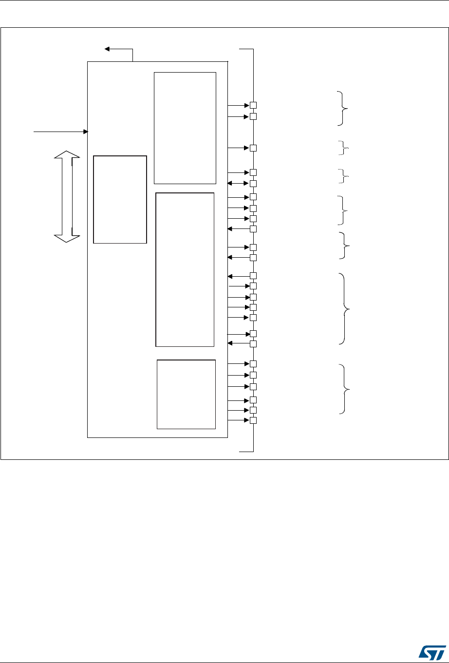
Flexible memory controller (FMC) RM0090
1604/1749 RM0090 Rev 18
Figure 456. FMC block diagram
37.3 AHB interface
The AHB slave interface allows internal CPUs and other bus master peripherals to access
the external memories.
AHB transactions are translated into the external device protocol. In particular, if the
selected external memory is 16- or 8-bit wide, 32-bit wide transactions on the AHB are split
into consecutive 16- or 8-bit accesses. The FMC Chip Select (FMC_NEx) does not toggle
between consecutive accesses except when performing accesses in mode D with the
extended mode enabled.
MS30443V5
HCLK
NAND/PC Card
memory
controller
NAND
signals
Shared
signals
NOR/PSRAM
signals
FMC_NE[4:1]
FMC_NL(or NADV)
FMC_NWAIT
FMC_D[ 31:0]
FMC_NOE
FMC_NWE
FMC_NIORD
FMC_NREG
FMC_CD
PC Card
signals
FMC_NBL[3:0]
FMC_NCE[3:2]
FMC_INT[3:2]
FMC_INTR
FMC_NCE4_1
FMC_NCE4_2
FMC_NIOWR
FMC_CLK
SDRAM
controller
FMC_SDNWE
FMC_SDCKE[1:0]
FMC_SDNE[1:0]
FMC_NRAS
FMC_NCAS
SDRAM
signals
FMC_A[25:0]
NOR/PSRAM/SRAM
Shared signals
SRAM/PSRAM/SDRAM
Shared signals
FMC_SDCLK
FMC interrupts to NVIC
From clock
controller
Configuration
registers
NOR/PSRAM
memory
controller

RM0090 Rev 18 1605/1749
RM0090 Flexible memory controller (FMC)
1682
The FMC generates an AHB error in the following conditions:
•When reading or writing to an FMC bank (Bank 1 to 4) which is not enabled.
•When reading or writing to the NOR Flash bank while the FACCEN bit is reset in the
FMC_BCRx register.
•When reading or writing to the PC Card banks while the FMC_CD input pin (Card
Presence Detection) is low.
•When writing to a write protected SDRAM bank (WP bit set in the SDRAM_SDCRx
register).
•When the SDRAM address range is violated (access to reserved address range)
The effect of an AHB error depends on the AHB master which has attempted the R/W
access:
•If the access has been attempted by the Cortex®-M4 with FPU CPU, a hard fault
interrupt is generated.
•If the access has been performed by a DMA controller, a DMA transfer error is
generated and the corresponding DMA channel is automatically disabled.
The AHB clock (HCLK) is the reference clock for the FMC.
37.3.1 Supported memories and transactions
General transaction rules
The requested AHB transaction data size can be 8-, 16- or 32-bit wide whereas the
accessed external device has a fixed data width. This may lead to inconsistent transfers.
Therefore, some simple transaction rules must be followed:
•AHB transaction size and memory data size are equal
There is no issue in this case.
•AHB transaction size is greater than the memory size:
In this case, the FMC splits the AHB transaction into smaller consecutive memory
accesses to meet the external data width. The FMC Chip Select (FMC_NEx) does not
toggle between the consecutive accesses.
•AHB transaction size is smaller than the memory size:
The transfer may or not be consistent depending on the type of external device:
– Accesses to devices that have the byte select feature (SRAM, ROM, PSRAM,
SDRAM)
In this case, the FMC allows read/write transactions and accesses the right data
through its byte lanes BL[3:0].
byte to be written are addressed by NBL[3:0].
All memory byte are read (NBL[3:0] are driven low during read transaction) and
the useless ones are discarded.
– Accesses to devices that do not have the byte select feature (16-bit NOR and
NAND Flash memories)
This situation occurs when a byte access is requested to a 16-bit wide Flash
memory. Since the device cannot be accessed in byte mode (only 16-bit words
can be read/written from/to the Flash memory), Write transactions and Read
transactions are allowed (the controller reads the entire 16-bit memory word and
uses only the required byte).

Flexible memory controller (FMC) RM0090
1606/1749 RM0090 Rev 18
Configuration registers
The FMC can be configured through a set of registers. Refer to Section 37.5.6, for a
detailed description of the NOR Flash/PSRAM controller registers. Refer to Section 37.6.8,
for a detailed description of the NAND Flash/PC Card registers and to Section 37.7.5 for a
detailed description of the SDRAM controller registers.
37.4 External device address mapping
From the FMC point of view, the external memory is divided into 6 fixed-size banks of
256 Mbyte each (see Figure 457):
•Bank 1 used to address up to 4 NOR Flash memory or PSRAM devices. This bank is
split into 4 NOR/PSRAM subbanks with 4 dedicated Chip Selects, as follows:
– Bank 1 - NOR/PSRAM 1
– Bank 1 - NOR/PSRAM 2
– Bank 1 - NOR/PSRAM 3
– Bank 1 - NOR/PSRAM 4
•Banks 2 and 3 used to address NAND Flash memory devices (1 device per bank)
•Bank 4 used to address a PC Card
•Bank 5 and 6 used to address SDRAM devices (1 device per bank).
For each bank the type of memory to be used can be configured by the user application
through the Configuration register.
RM0090 Rev 18 1607/1749
RM0090 Flexible memory controller (FMC)
1682
Figure 457. FMC memory banks
37.4.1 NOR/PSRAM address mapping
HADDR[27:26] bits are used to select one of the four memory banks as shown in Table 254.
Bank 1
4 x 64 MB
NOR/PSRAM/SRAM
Supported memory typeBank
0x6000 0000
Address
PC Card
MS30444V2
SDRAM
0x6FFF FFFF
0x7000 0000
0x7FFF FFFF
0x8000 0000
0x8FFF FFFF
0x9000 0000
0x9FFF FFFF
0xC000 0000
0xCFFF FFFF
0xD000 0000
0xDFFF FFFF
Bank 2
4 x 64 MB
Bank 3
4 x 64 MB
Bank 4
4 x 64 MB
SDRAM Bank 1
4 x 64 MB
SDRAM Bank 2
4 x 64 MB
NAND Flash memory
Table 254. NOR/PSRAM bank selection
HADDR[27:26](1)
1. HADDR are internal AHB address lines that are translated to external memory.
Selected bank
00 Bank 1 - NOR/PSRAM 1
01 Bank 1 - NOR/PSRAM 2
10 Bank 1 - NOR/PSRAM 3
11 Bank 1 - NOR/PSRAM 4
Flexible memory controller (FMC) RM0090
1608/1749 RM0090 Rev 18
The HADDR[25:0] bits contain the external memory address. Since HADDR is a byte
address whereas the memory is addressed at word level, the address actually issued to the
memory varies according to the memory data width, as shown in the following table.
Wrap support for NOR Flash/PSRAM
Wrap burst mode for synchronous memories is not supported. The memories must be
configured in linear burst mode of undefined length.
37.4.2 NAND Flash memory/PC Card address mapping
In this case, three banks are available, each of them being divided into memory areas as
indicated in Table 256.
For NAND Flash memory, the common and attribute memory spaces are subdivided into
three sections (see in Table 257 below) located in the lower 256 Kbytes:
•Data section (first 64 Kbytes in the common/attribute memory space)
•Command section (second 64 Kbytes in the common / attribute memory space)
•Address section (next 128 Kbytes in the common / attribute memory space)
Table 255. NOR/PSRAM External memory address
Memory width(1)
1. In case of a 16-bit external memory width, the FMC will internally use HADDR[25:1] to generate the
address for external memory FMC_A[24:0]. In case of a 32-bit memory width, the FMC will internally use
HADDR[25:2] to generate the external address.
Whatever the external memory width, FMC_A[0] should be connected to external memory address A[0].
Data address issued to the memory Maximum memory capacity (bits)
8-bit HADDR[25:0] 64 Mbyte x 8 = 512 Mbit
16-bit HADDR[25:1] >> 1 64 Mbyte/2 x 16 = 512 Mbit
32-bit HADDR[25:2] >> 2 64 Mbyte/4 x 32 = 512 Mbit
Table 256. NAND/PC Card memory mapping and timing registers
Start address End address FMC bank Memory space Timing register
0x9C00 0000 0x9FFF FFFF
Bank 4 - PC card
I/O FMC_PIO4 (0xB0)
0x9800 0000 0x9BFF FFFF Attribute FMC_PATT4 (0xAC)
0x9000 0000 0x93FF FFFF Common FMC_PMEM4 (0xA8)
0x8800 0000 0x8BFF FFFF
Bank 3 - NAND Flash
Attribute FMC_PATT3 (0x8C)
0x8000 0000 0x83FF FFFF Common FMC_PMEM3 (0x88)
0x7800 0000 0x7BFF FFFF
Bank 2- NAND Flash
Attribute FMC_PATT2 (0x6C)
0x7000 0000 0x73FF FFFF Common FMC_PMEM2 (0x68)

RM0090 Rev 18 1609/1749
RM0090 Flexible memory controller (FMC)
1682
The application software uses the 3 sections to access the NAND Flash memory:
•To send a command to NAND Flash memory, the software must write the command
value to any memory location in the command section.
•To specify the NAND Flash address that must be read or written, the software
must write the address value to any memory location in the address section. Since an
address can be 4 or 5 byte long (depending on the actual memory size), several
consecutive write operations to the address section are required to specify the full
address.
•To read or write data, the software reads or writes the data from/to any memory
location in the data section.
Since the NAND Flash memory automatically increments addresses, there is no need to
increment the address of the data section to access consecutive memory locations.
37.4.3 SDRAM address mapping
The HADDR[28] bit (internal AHB address line 28) is used to select one of the two memory
banks as indicated in Table 258.
The following table shows SDRAM mapping for an 13-bit row ,a 11-bit column and 4 internal
bank configurations.
Table 257. NAND bank selection
Section name HADDR[17:16] Address range
Address section 1X 0x020000-0x03FFFF
Command section 01 0x010000-0x01FFFF
Data section 00 0x000000-0x0FFFF
Table 258. SDRAM bank selection
HADDR[28] Selected bank Control register Timing register
0 SDRAM Bank1 FMC_SDCR1 FMC_SDTR1
1 SDRAM Bank2 FMC_SDCR2 FMC_SDTR2
Table 259. SDRAM address mapping
Memory width(1) Internal bank Row address Column
address(2)
Maximum
memory capacity
(Mbyte)
8-bit HADDR[25:24] HADDR[23:11] HADDR[10:0] 64 Mbyte:
4 x 8K x 2K
16-bit HADDR[26:25] HADDR[24:12] HADDR[11:1] 128 Mbyte:
4 x 8K x 2K x 2
32-bit HADDR[27:26] HADDR[25:13] HADDR[12:2] 256 Mbyte:
4 x 8K x 2K x 4

Flexible memory controller (FMC) RM0090
1610/1749 RM0090 Rev 18
The HADDR[27:0] bits are translated to external SDRAM address depending on the
SDRAM controller configuration:
•Data size:8, 16 or 32 bits
•Row size:11, 12 or 13 bits
•Column size: 8, 9, 10 or 11 bits
•Number of internal banks: two or four internal banks
Table 260 to Table shows the SDRAM address mapping versus the SDRAM controller
configuration.
)
1. When interfacing with a 16-bit memory, the FMC internally uses the HADDR[11:1] internal AHB address
lines to generate the external address. When interfacing with a 32-bit memory, the FMC internally uses
HADDR[12:2] lines to generate the external address. Whatever the memory width, FMC_A[0] has to be
connected to the external memory address A[0].
2. The AutoPrecharge is not supported. FMC_A[10] must be connected to the external memory address
A[10] but it will be always driven ‘low’.
Table 260. SDRAM address mapping with 8-bit data bus width(1)(2)
Row size
configuration
HADDR(AHB Internal Address Lines)
27 26 25 24 23 22 21 20 19 18 17 16 15 14 13 12 11 10 9 8 7 6 5 4 3 2 1 0
11-bit row size
configuration
Res. Bank
[1:0] Row[10:0] Column[7:0]
Res. Bank
[1:0] Row[10:0] Column[8:0]
Res. Bank
[1:0] Row[10:0] Column[9:0]
Res. Bank
[1:0] Row[10:0] Column[10:0]
12-bit row size
configuration
Res. Bank
[1:0] Row[11:0] Column[7:0]
Res. Bank
[1:0] Row[11:0] Column[8:0]
Res. Bank
[1:0] Row[11:0] Column[9:0]
Res. Bank
[1:0] Row[11:0] Column[10:0]
13-bit row size
configuration
Res. Bank
[1:0] Row[12:0] Column[7:0]
Res. Bank
[1:0] Row[12:0] Column[8:0]
Res. Bank
[1:0] Row[12:0] Column[9:0]
Res. Bank
[1:0] Row[12:0] Column[10:0]
1. BANK[1:0] are the Bank Address BA[1:0]. When only 2 internal banks are used, BA1 must always be set to ‘0’.
2. Access to Reserved (Res.) address range generates an AHB error.
RM0090 Rev 18 1611/1749
RM0090 Flexible memory controller (FMC)
1682
)
Table 261. SDRAM address mapping with 16-bit data bus width(1)(2)
Row size
Configuration
HADDR(AHB address Lines)
27
26
25
24
23
22
21
20
19
18
17
16
15
14
13
12
11
10
9
8
7
6
5
4
3
2
1
0
11-bit row size
configuration
Res. Bank
[1:0] Row[10:0] Column[7:0] BM0(3)
Res. Bank
[1:0] Row[10:0] Column[8:0] BM0
Res. Bank
[1:0] Row[10:0] Column[9:0] BM0
Res. Bank
[1:0] Row[10:0] Column[10:0] BM0
12-bit row size
configuration
Res. Bank
[1:0] Row[11:0] Column[7:0] BM0
Res. Bank
[1:0] Row[11:0] Column[8:0] BM0
Res. Bank
[1:0] Row[11:0] Column[9:0] BM0
Res. Bank
[1:0] Row[11:0] Column[10:0] BM0
13-bit row size
configuration
Res. Bank
[1:0] Row[12:0] Column[7:0] BM0
Res. Bank
[1:0] Row[12:0] Column[8:0] BM0
Res. Bank
[1:0] Row[12:0] Column[9:0] BM0
Re
s.
Bank
[1:0] Row[12:0] Column[10:0] BM0
1. BANK[1:0] are the Bank Address BA[1:0]. When only 2 internal banks are used, BA1 must always be set to ‘0’.
2. Access to Reserved space (Res.) generates an AHB error.
3. BM0: is the byte mask for 16-bit access.
Table 262. SDRAM address mapping with 32-bit data bus width(1)(2)
Row size
configuration
HADDR(AHB address Lines)
27
26
25
24
23
22
21
20
19
18
17
16
15
14
13
12
11
10
9
8
7
6
5
4
3
2
1
0
11-bit row size
configuration
Res. Bank
[1:0] Row[10:0] Column[7:0] BM[1:0
](3)
Res. Bank
[1:0] Row[10:0] Column[8:0] BM[1:0
Res. Bank
[1:0] Row[10:0] Column[9:0] BM[1:0
Res. Bank
[1:0] Row[10:0] Column[10:0] BM[1:0
12-bit row size
configuration
Res. Bank
[1:0] Row[11:0] Column[7:0] BM[1:0
Res. Bank
[1:0] Row[11:0] Column[8:0] BM[1:0
Res. Bank
[1:0] Row[11:0] Column[9:0] BM[1:0
Res. Bank
[1:0] Row[11:0] Column[10:0] BM[1:0

Flexible memory controller (FMC) RM0090
1612/1749 RM0090 Rev 18
37.5 NOR Flash/PSRAM controller
The FMC generates the appropriate signal timings to drive the following types of memories:
•Asynchronous SRAM and ROM
– 8 bits
– 16 bits
– 32 bits
•PSRAM (Cellular RAM)
– Asynchronous mode
– Burst mode for synchronous accesses
– Multiplexed or non-multiplexed
•NOR Flash memory
– Asynchronous mode
– Burst mode for synchronous accesses
– Multiplexed or non-multiplexed
The FMC outputs a unique Chip Select signal, NE[4:1], per bank. All the other signals
(addresses, data and control) are shared.
The FMC supports a wide range of devices through a programmable timings among which:
•Programmable wait states (up to 15)
•Programmable bus turnaround cycles (up to 15)
•Programmable output enable and write enable delays (up to 15)
•Independent read and write timings and protocol to support the widest variety of
memories and timings
•Programmable continuous clock (FMC_CLK) output.
The FMC Clock (FMC_CLK) is a submultiple of the HCLK clock. It can be delivered to the
selected external device either during synchronous accesses only or during asynchronous
13-bit row size
configuration
Res. Bank
[1:0] Row[12:0] Column[7:0] BM[1:0
Res. Bank
[1:0] Row[12:0] Column[8:0] BM[1:0
Res. Bank
[1:0] Row[12:0] Column[9:0] BM[1:0
Bank
[1:0] Row[12:0] Column[10:0] BM[1:0
1. BANK[1:0] are the Bank Address BA[1:0]. When only 2 internal banks are used, BA1 must always be set to ‘0’.
2. Access to Reserved space (Res.) generates an AHB error.
3. BM[1:0]: is the byte mask for 32-bit access.
Table 262. SDRAM address mapping with 32-bit data bus width(1)(2) (continued)
Row size
configuration
HADDR(AHB address Lines)
27
26
25
24
23
22
21
20
19
18
17
16
15
14
13
12
11
10
9
8
7
6
5
4
3
2
1
0

RM0090 Rev 18 1613/1749
RM0090 Flexible memory controller (FMC)
1682
and synchronous accesses depending on the CCKEN bit configuration in the FMC_BCR1
register:
•If the CCLKEN bit is reset, the FMC generates the clock (CLK) only during
synchronous accesses (Read/write transactions).
•If the CCLKEN bit is set, the FMC generates a continuous clock during asynchronous
and synchronous accesses. To generate the FMC_CLK continuous clock, Bank 1 must
be configured in synchronous mode (see Section 37.5.6: NOR/PSRAM controller
registers). Since the same clock is used for all synchronous memories, when a
continuous output clock is generated and synchronous accesses are performed, the
AHB data size has to be the same as the memory data width (MWID) otherwise the
FMC_CLK frequency will be changed depending on AHB data transaction (refer to
Section 37.5.5: Synchronous transactions for FMC_CLK divider ratio formula).
The size of each bank is fixed and equal to 64 Mbyte. Each bank is configured through
dedicated registers (see Section 37.5.6: NOR/PSRAM controller registers).
The programmable memory parameters include access times (see Table 263) and support
for wait management (for PSRAM and NOR Flash accessed in burst mode).
37.5.1 External memory interface signals
Table 264, Table 265 and Table 266 list the signals that are typically used to interface with
NOR Flash memory, SRAM and PSRAM.
Note: The prefix “N” identifies the signals which are active low.
Table 263. Programmable NOR/PSRAM access parameters
Parameter Function Access mode Unit Min. Max.
Address
setup
Duration of the address
setup phase Asynchronous AHB clock cycle
(HCLK) 015
Address hold Duration of the address hold
phase
Asynchronous,
muxed I/Os
AHB clock cycle
(HCLK) 115
Data setup Duration of the data setup
phase Asynchronous AHB clock cycle
(HCLK) 1256
Bust turn Duration of the bus
turnaround phase
Asynchronous and
synchronous
read/write
AHB clock cycle
(HCLK) 015
Clock divide
ratio
Number of AHB clock cycles
(HCLK) to build one memory
clock cycle (CLK)
Synchronous AHB clock cycle
(HCLK) 2 16
Data latency
Number of clock cycles to
issue to the memory before
the first data of the burst
Synchronous Memory clock
cycle (CLK) 2 17

Flexible memory controller (FMC) RM0090
1614/1749 RM0090 Rev 18
NOR Flash memory, non-multiplexed I/Os
The maximum capacity is 512 Mbits (26 address lines).
NOR Flash memory, 16-bit multiplexed I/Os
The maximum capacity is 512 Mbits.
PSRAM/SRAM, non-multiplexed I/Os
Table 264. Non-multiplexed I/O NOR Flash memory
FMC signal name I/O Function
CLK O Clock (for synchronous access)
A[25:0] O Address bus
D[31:0] I/O Bidirectional data bus
NE[x] O Chip Select, x = 1..4
NOE O Output enable
NWE O Write enable
NL(=NADV) O Latch enable (this signal is called address
valid, NADV, by some NOR Flash devices)
NWAIT I NOR Flash wait input signal to the FMC
Table 265. 16-bit multiplexed I/O NOR Flash memory
FMC signal name I/O Function
CLK O Clock (for synchronous access)
A[25:16] O Address bus
AD[15:0] I/O
16-bit multiplexed, bidirectional address/data bus (the 16-bit address
A[15:0] and data D[15:0] are multiplexed on the databus)
NE[x] O Chip Select, x = 1..4
NOE O Output enable
NWE O Write enable
NL(=NADV) O Latch enable (this signal is called address valid, NADV, by some NOR
Flash devices)
NWAIT I NOR Flash wait input signal to the FMC
Table 266. Non-multiplexed I/Os PSRAM/SRAM
FMC signal name I/O Function
CLK O Clock (only for PSRAM synchronous access)
A[25:0] O Address bus
D[31:0] I/O Data bidirectional bus

RM0090 Rev 18 1615/1749
RM0090 Flexible memory controller (FMC)
1682
The maximum capacity is 512 Mbits.
PSRAM, 16-bit multiplexed I/Os
The maximum capacity is 512 Mbits (26 address lines).
37.5.2 Supported memories and transactions
Table 268 below shows an example of the supported devices, access modes and
transactions when the memory data bus is 16-bit wide for NOR Flash memory, PSRAM and
SRAM. The transactions not allowed (or not supported) by the FMC are shown in gray in
this example.
NE[x] O Chip Select, x = 1..4 (called NCE by PSRAM (Cellular RAM i.e.
CRAM))
NOE O Output enable
NWE O Write enable
NL(= NADV) O Address valid only for PSRAM input (memory signal name: NADV)
NWAIT I PSRAM wait input signal to the FMC
NBL[3] O Byte3 Upper byte enable (memory signal name: NUB)
NBL[2] O Byte2 Lowed byte enable (memory signal name: NLB)
NBL[1] O Byte1 Upper byte enable (memory signal name: NLB)
NBL[0] O Byte0 Lower byte enable (memory signal name: NLB)
Table 267. 16-Bit multiplexed I/O PSRAM
FMC signal name I/O Function
CLK O Clock (for synchronous access)
A[25:16] O Address bus
AD[15:0] I/O
16-bit multiplexed, bidirectional address/data bus (the 16-bit address
A[15:0] and data D[15:0] are multiplexed on the databus)
NE[x] O Chip Select, x = 1..4 (called NCE by PSRAM (Cellular RAM i.e.
CRAM))
NOE O Output enable
NWE O Write enable
NL(= NADV) O Address valid PSRAM input (memory signal name: NADV)
NWAIT I PSRAM wait input signal to the FMC
NBL[1] O Upper byte enable (memory signal name: NUB)
NBL[0] O Lowed byte enable (memory signal name: NLB)
Table 266. Non-multiplexed I/Os PSRAM/SRAM (continued)
FMC signal name I/O Function

Flexible memory controller (FMC) RM0090
1616/1749 RM0090 Rev 18
Table 268. NOR Flash/PSRAM: Example of supported memories and transactions
Device Mode R/W
AHB
data
size
Memory
data size
Allowed/
not
allowed
Comments
NOR Flash
(muxed I/Os
and nonmuxed
I/Os)
Asynchronous R 8 16 Y
Asynchronous W 8 16 N
Asynchronous R 16 16 Y
Asynchronous W 16 16 Y
Asynchronous R 32 16 Y Split into 2 FMC accesses
Asynchronous W 32 16 Y Split into 2 FMC accesses
Asynchronous
page R -16 N Mode is not supported
Synchronous R 8 16 N
Synchronous R 16 16 Y
Synchronous R 32 16 Y
PSRAM
(multiplexed
I/Os and non-
multiplexed
I/Os)
Asynchronous R 8 16 Y
Asynchronous W 8 16 Y Use of byte lanes NBL[1:0]
Asynchronous R 16 16 Y
Asynchronous W 16 16 Y
Asynchronous R 32 16 Y Split into 2 FMC accesses
Asynchronous W 32 16 Y Split into 2 FMC accesses
Asynchronous
page R -16 N Mode is not supported
Synchronous R 8 16 N
Synchronous R 16 16 Y
Synchronous R 32 16 Y
Synchronous W 8 16 Y Use of byte lanes NBL[1:0]
Synchronous W 16/32 16 Y
SRAM and
ROM
Asynchronous R 8 / 16 16 Y
Asynchronous W 8 / 16 16 Y Use of byte lanes NBL[1:0]
Asynchronous R 32 16 Y Split into 2 FMC accesses
Asynchronous W 32 16 Y Split into 2 FMC accesses
Use of byte lanes NBL[1:0]

RM0090 Rev 18 1617/1749
RM0090 Flexible memory controller (FMC)
1682
37.5.3 General timing rules
Signals synchronization
•All controller output signals change on the rising edge of the internal clock (HCLK)
•In synchronous mode (read or write), all output signals change on the rising edge of
HCLK. Whatever the CLKDIV value, all outputs change as follows:
– NOEL/NWEL/ NEL/NADVL/ NADVH /NBLL/ Address valid outputs change on the
falling edge of FMC_CLK clock.
– NOEH/ NWEH / NEH/ NOEH/NBLH/ Address invalid outputs change on the rising
edge of FMC_CLK clock.
37.5.4 NOR Flash/PSRAM controller asynchronous transactions
Asynchronous static memories (NOR Flash, PSRAM, SRAM)
•Signals are synchronized by the internal clock HCLK. This clock is not issued to the
memory
•The FMC always samples the data before de-asserting the NOE signal. This
guarantees that the memory data hold timing constraint is met (minimum Chip Enable
high to data transition is usually 0 ns)
•If the extended mode is enabled (EXTMOD bit is set in the FMC_BCRx register), up to
four extended modes (A, B, C and D) are available. It is possible to mix A, B, C and D
modes for read and write operations. For example, read operation can be performed in
mode A and write in mode B.
•If the extended mode is disabled (EXTMOD bit is reset in the FMC_BCRx register), the
FMC can operate in Mode1 or Mode2 as follows:
– Mode 1 is the default mode when SRAM/PSRAM memory type is selected
(MTYP[1:0] = 0x0 or 0x01 in the FMC_BCRx register)
– Mode 2 is the default mode when NOR memory type is selected
(MTYP[1:0] = 0x10 in the FMC_BCRx register).
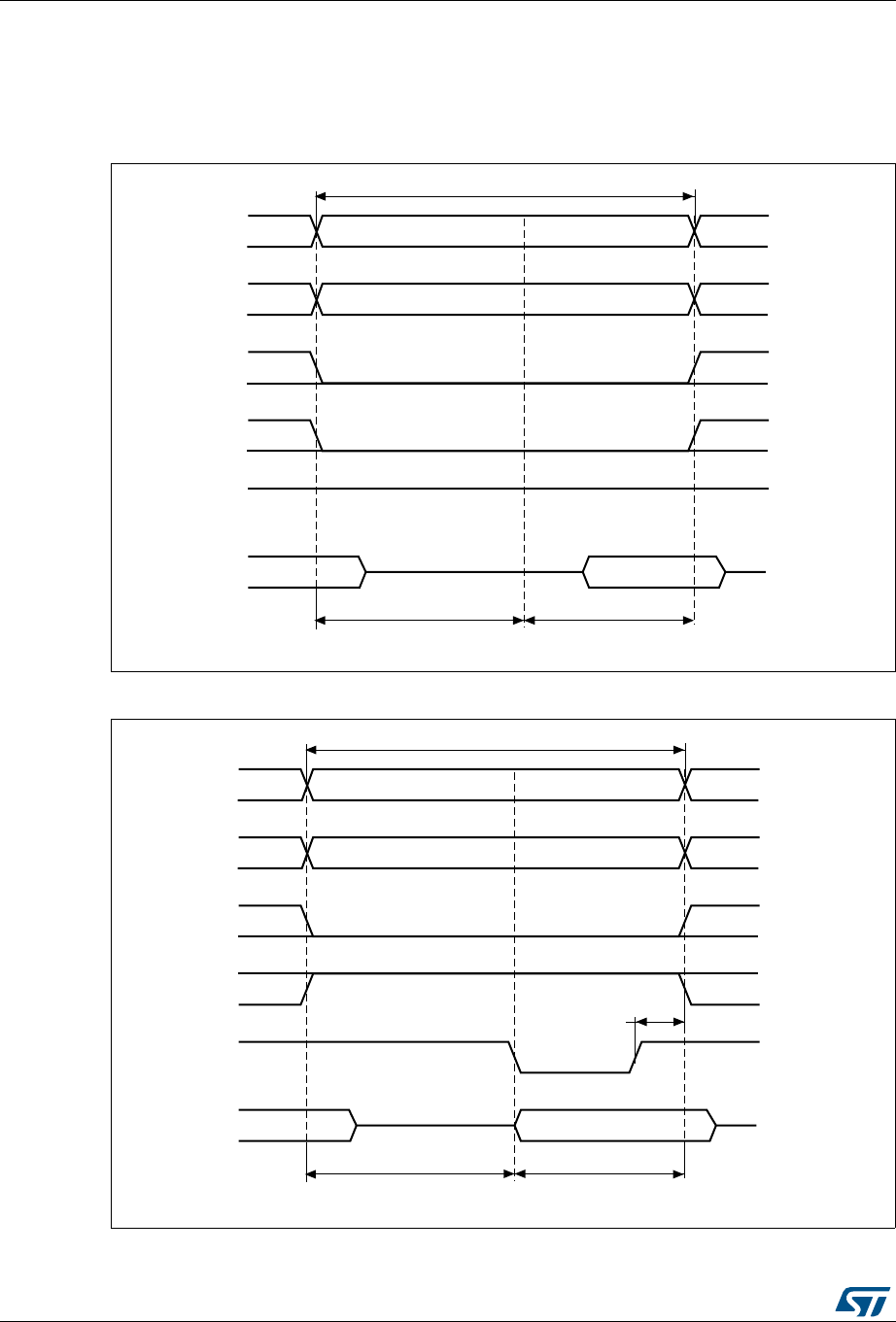
Flexible memory controller (FMC) RM0090
1618/1749 RM0090 Rev 18
Mode 1 - SRAM/PSRAM (CRAM)
The next figures show the read and write transactions for the supported modes followed by
the required configuration of FMC _BCRx, and FMC_BTRx/FMC_BWTRx registers.
Figure 458. Mode1 read access waveforms
Figure 459. Mode1 write access waveforms
A[25:0]
NOE
ADDSET DATAST
Memory transaction
NEx
D[31:0]
HCLK cycles HCLK cycles
NWE
NBL[3:0]
data driven
by memory
MS30452V1
High
A[25:0]
NOE
ADDSET (DATAST + 1)
Memory transaction
NEx
D[31:0]
HCLK cycles HCLK cycles
NWE
NBL[3:0]
data driven by FSMC
MS30453V1
1HCLK

RM0090 Rev 18 1619/1749
RM0090 Flexible memory controller (FMC)
1682
The one HCLK cycle at the end of the write transaction helps guarantee the address and
data hold time after the NWE rising edge. Due to the presence of this HCLK cycle, the
DATAST value must be greater than zero (DATAST > 0).
Table 269. FMC_BCRx bit fields
Bit
number Bit name Value to set
31-21 Reserved 0x000
20 CCLKEN As needed
19 CBURSTRW 0x0 (no effect in asynchronous mode)
18:16 CPSIZE 0x0 (no effect in asynchronous mode)
15 ASYNCWAIT Set to 1 if the memory supports this feature. Otherwise keep at
0.
14 EXTMOD 0x0
13 WAITEN 0x0 (no effect in asynchronous mode)
12 WREN As needed
11 WAITCFG Don’t care
10 WRAPMOD 0x0
9 WAITPOL Meaningful only if bit 15 is 1
8 BURSTEN 0x0
7 Reserved 0x1
6 FACCEN Don’t care
5-4 MWID As needed
3-2 MTYP[1:0] As needed, exclude 0x2 (NOR Flash memory)
1 MUXE 0x0
0 MBKEN 0x1
Table 270. FMC_BTRx bit fields
Bit
number Bit name Value to set
31:30 Reserved 0x0
29-28 ACCMOD Don’t care
27-24 DATLAT Don’t care
23-20 CLKDIV Don’t care
19-16 BUSTURN Time between NEx high to NEx low (BUSTURN HCLK)
15-8 DATAST Duration of the second access phase (DATAST+1 HCLK cycles for
write accesses, DATAST HCLK cycles for read accesses).
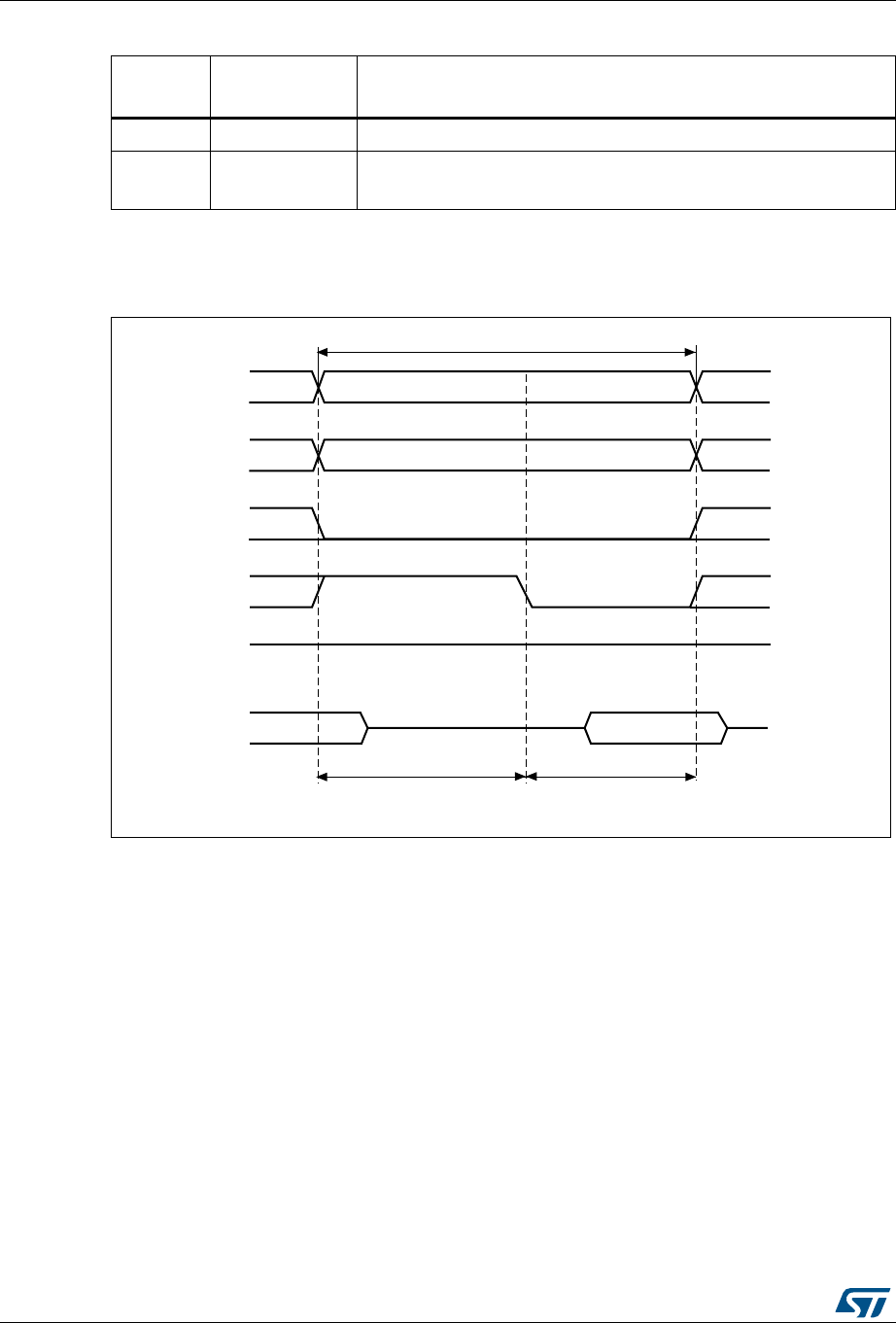
Flexible memory controller (FMC) RM0090
1620/1749 RM0090 Rev 18
Mode A - SRAM/PSRAM (CRAM) OE toggling
Figure 460. ModeA read access waveforms
1. NBL[3:0] are driven low during the read access
7-4 ADDHLD Don’t care
3-0 ADDSET Duration of the first access phase (ADDSET HCLK cycles).
Minimum value for ADDSET is 0.
Table 270. FMC_BTRx bit fields (continued)
Bit
number Bit name Value to set
A[25:0]
NOE
ADDSET DATAST
Memory transaction
NEx
D[31:0]
HCLK cycles HCLK cycles
NWE
NBL[3:0]
data driven
by memory
MS30454V1
High
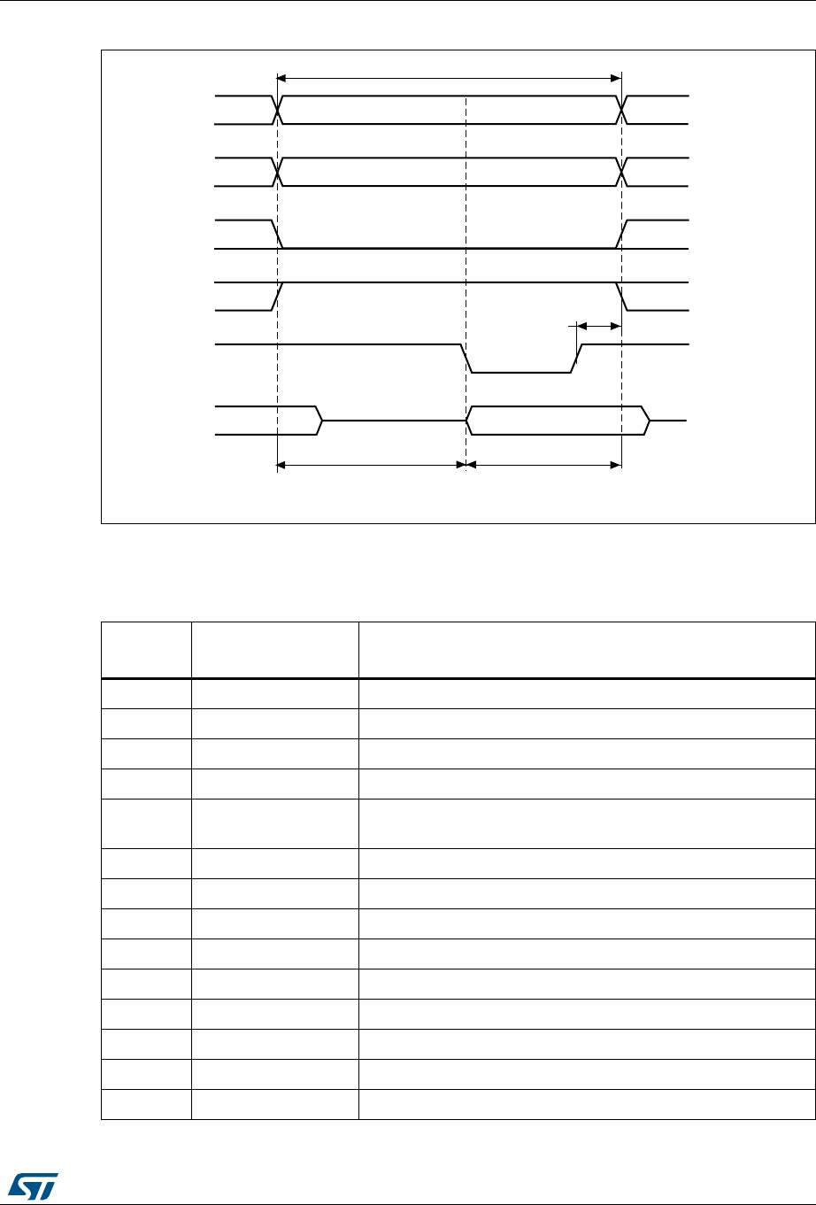
RM0090 Rev 18 1621/1749
RM0090 Flexible memory controller (FMC)
1682
Figure 461. ModeA write access waveforms
The differences compared with mode1 are the toggling of NOE and the independent read
and write timings.
Table 271. FMC_BCRx bit fields
Bit
number Bit name Value to set
31-21 Reserved 0x000
20 CCLKEN As needed
19 CBURSTRW 0x0 (no effect in asynchronous mode)
18:16 CPSIZE 0x0 (no effect in asynchronous mode)
15 ASYNCWAIT Set to 1 if the memory supports this feature. Otherwise keep at
0.
14 EXTMOD 0x1
13 WAITEN 0x0 (no effect in asynchronous mode)
12 WREN As needed
11 WAITCFG Don’t care
10 WRAPMOD 0x0
9 WAITPOL Meaningful only if bit 15 is 1
8 BURSTEN 0x0
7 Reserved 0x1
6 FACCEN Don’t care
A[25:0]
NOE
ADDSET (DATAST + 1)
Memory transaction
NEx
D[31:0]
HCLK cycles HCLK cycles
NWE
NBL[3:0]
data driven by FSMC
MS30455V1
1HCLK

Flexible memory controller (FMC) RM0090
1622/1749 RM0090 Rev 18
5-4 MWID As needed
3-2 MTYP[1:0] As needed, exclude 0x2 (NOR Flash memory)
1 MUXEN 0x0
0 MBKEN 0x1
Table 272. FMC_BTRx bit fields
Bit
number Bit name Value to set
31:30 Reserved 0x0
29-28 ACCMOD 0x0
27-24 DATLAT Don’t care
23-20 CLKDIV Don’t care
19-16 BUSTURN Time between NEx high to NEx low (BUSTURN HCLK)
15-8 DATAST Duration of the second access phase (DATAST HCLK cycles) for read
accesses.
7-4 ADDHLD Don’t care
3-0 ADDSET[3:0]
Duration of the first access phase (ADDSET HCLK cycles) for read
accesses.
Minimum value for ADDSET is 0.
Table 273. FMC_BWTRx bit fields
Bit
number Bit name Value to set
31:30 Reserved 0x0
29-28 ACCMOD 0x0
27-24 DATLAT Don’t care
23-20 CLKDIV Don’t care
19-16 BUSTURN Time between NEx high to NEx low (BUSTURN HCLK)
15-8 DATAST Duration of the second access phase (DATAST HCLK cycles) for write
accesses.
7-4 ADDHLD Don’t care
3-0 ADDSET[3:0]
Duration of the first access phase (ADDSET HCLK cycles) for write
accesses.
Minimum value for ADDSET is 0.
Table 271. FMC_BCRx bit fields (continued)
Bit
number Bit name Value to set
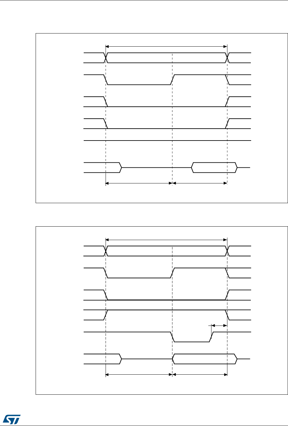
RM0090 Rev 18 1623/1749
RM0090 Flexible memory controller (FMC)
1682
Mode 2/B - NOR Flash
Figure 462. Mode2 and mode B read access waveforms
1. NBL[3:0] are driven low during the read access
Figure 463. Mode2 write access waveforms
A[25:0]
NOE
ADDSET DATAST
Memory transaction
NEx
D[31:0]
HCLK cycles HCLK cycles
NWE
NADV
data driven
by memory
MS30456V1
High
A[25:0]
NOE
ADDSET (DATAST + 1)
Memory transaction
NEx
D[31:0]
HCLK cycles HCLK cycles
NWE
NADV
data driven by FSMC
MS30457V1
1HCLK
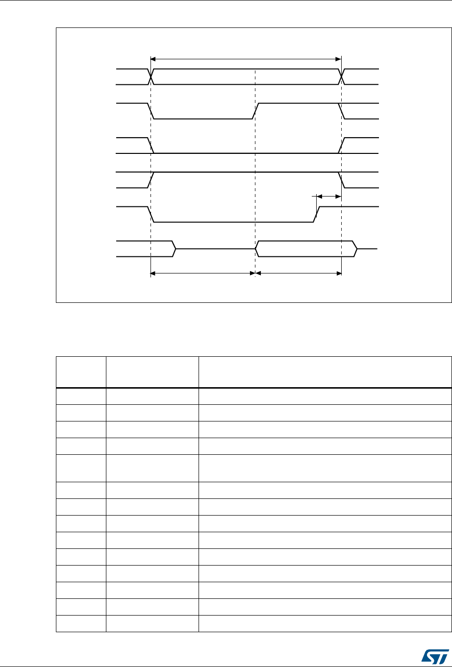
Flexible memory controller (FMC) RM0090
1624/1749 RM0090 Rev 18
Figure 464. ModeB write access waveforms
The differences with mode1 are the toggling of NWE and the independent read and write
timings when extended mode is set (Mode B).
Table 274. FMC_BCRx bit fields
Bit
number Bit name Value to set
31-21 Reserved 0x000
20 CCLKEN As needed
19 CBURSTRW 0x0 (no effect in asynchronous mode)
18:16 CPSIZE 0x0 (no effect in asynchronous mode)
15 ASYNCWAIT Set to 1 if the memory supports this feature. Otherwise keep at
0.
14 EXTMOD 0x1 for mode B, 0x0 for mode 2
13 WAITEN 0x0 (no effect in asynchronous mode)
12 WREN As needed
11 WAITCFG Don’t care
10 WRAPMOD 0x0
9 WAITPOL Meaningful only if bit 15 is 1
8 BURSTEN 0x0
7 Reserved 0x1
6 FACCEN 0x1
A[25:0]
NOE
ADDSET (DATAST + 1)
Memory transaction
NEx
D[31:0]
HCLK cycles HCLK cycles
NWE
NADV
data driven by FSMC
MS30458V1.
1HCLK

RM0090 Rev 18 1625/1749
RM0090 Flexible memory controller (FMC)
1682
Note: The FMC_BWTRx register is valid only if the extended mode is set (mode B), otherwise its
content is don’t care.
5-4 MWID As needed
3-2 MTYP[1:0] 0x2 (NOR Flash memory)
1 MUXEN 0x0
0 MBKEN 0x1
Table 275. FMC_BTRx bit fields
Bit number Bit name Value to set
31-30 Reserved 0x0
29-28 ACCMOD 0x1 if extended mode is set
27-24 DATLAT Don’t care
23-20 CLKDIV Don’t care
19-16 BUSTURN Time between NEx high to NEx low (BUSTURN HCLK)
15-8 DATAST Duration of the access second phase (DATAST HCLK cycles) for
read accesses.
7-4 ADDHLD Don’t care
3-0 ADDSET[3:0] Duration of the access first phase (ADDSET HCLK cycles) for read
accesses. Minimum value for ADDSET is 0.
Table 276. FMC_BWTRx bit fields
Bit number Bit name Value to set
31-30 Reserved 0x0
29-28 ACCMOD 0x1 if extended mode is set
27-24 DATLAT Don’t care
23-20 CLKDIV Don’t care
19-16 BUSTURN Time between NEx high to NEx low (BUSTURN HCLK)
15-8 DATAST Duration of the access second phase (DATAST HCLK cycles) for
write accesses.
7-4 ADDHLD Don’t care
3-0 ADDSET[3:0] Duration of the access first phase (ADDSET HCLK cycles) for write
accesses. Minimum value for ADDSET is 0.
Table 274. FMC_BCRx bit fields (continued)
Bit
number Bit name Value to set
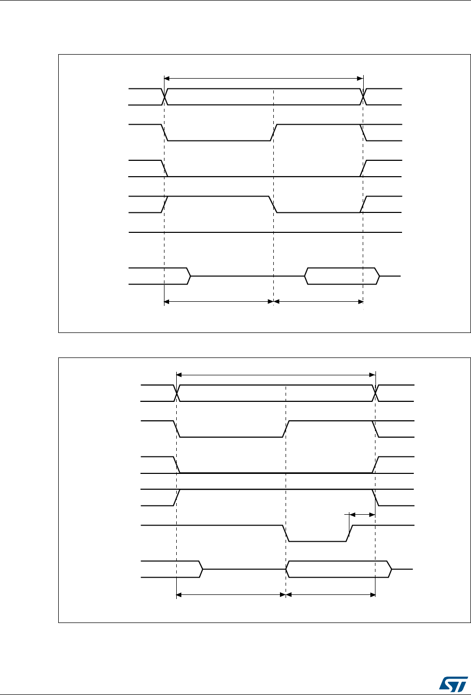
Flexible memory controller (FMC) RM0090
1626/1749 RM0090 Rev 18
Mode C - NOR Flash - OE toggling
Figure 465. ModeC read access waveforms
Figure 466. ModeC write access waveforms
The differences compared with mode1 are the toggling of NOE and the independent read
and write timings.
A[25:0]
NOE
ADDSET DATAST
Memory transaction
NEx
D[31:0]
HCLK cycles HCLK cycles
NWE
NADV
data driven
by memory
MS30459V1
High
A[25:0]
NOE
ADDSET (DATAST + 1)
Memory transaction
NEx
D[31:0]
HCLK cycles HCLK cycles
NWE
NADV
data driven by FSMC
MS30460V1
1HCLK

RM0090 Rev 18 1627/1749
RM0090 Flexible memory controller (FMC)
1682
Table 277. FMC_BCRx bit fields
Bit No. Bit name Value to set
31-21 Reserved 0x000
20 CCLKEN As needed
19 CBURSTRW 0x0 (no effect in asynchronous mode)
18:16 Reserved 0x0 (no effect in asynchronous mode)
15 ASYNCWAIT Set to 1 if the memory supports this feature. Otherwise keep at 0.
14 EXTMOD 0x1
13 WAITEN 0x0 (no effect in asynchronous mode)
12 WREN As needed
11 WAITCFG Don’t care
10 WRAPMOD 0x0
9 WAITPOL Meaningful only if bit 15 is 1
8 BURSTEN 0x0
7 Reserved 0x1
6 FACCEN 0x1
5-4 MWID As needed
3-2 MTYP[1:0] 0x02 (NOR Flash memory)
1 MUXEN 0x0
0 MBKEN 0x1
Table 278. FMC_BTRx bit fields
Bit No. Bit name Value to set
31:30 Reserved 0x0
29-28 ACCMOD 0x2
27-24 DATLAT 0x0
23-20 CLKDIV 0x0
19-16 BUSTURN Time between NEx high to NEx low (BUSTURN HCLK)
15-8 DATAST Duration of the second access phase (DATAST HCLK cycles) for
read accesses.
7-4 ADDHLD Don’t care
3-0 ADDSET[3:0] Duration of the first access phase (ADDSET HCLK cycles) for read
accesses. Minimum value for ADDSET is 0.
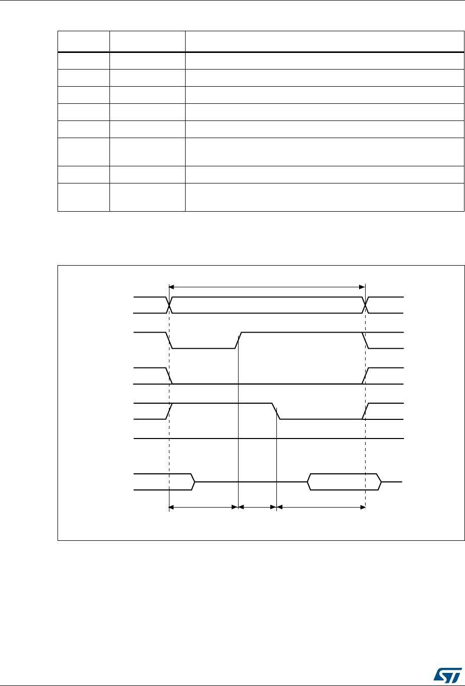
Flexible memory controller (FMC) RM0090
1628/1749 RM0090 Rev 18
Mode D - asynchronous access with extended address
Figure 467. ModeD read access waveforms
Table 279. FMC_BWTRx bit fields
Bit No. Bit name Value to set
31:30 Reserved 0x0
29-28 ACCMOD 0x2
27-24 DATLAT Don’t care
23-20 CLKDIV Don’t care
19-16 BUSTURN Time between NEx high to NEx low (BUSTURN HCLK)
15-8 DATAST Duration of the second access phase (DATAST HCLK cycles) for
write accesses.
7-4 ADDHLD Don’t care
3-0 ADDSET[3:0] Duration of the first access phase (ADDSET HCLK cycles) for write
accesses. Minimum value for ADDSET is 0.
A[25:0]
NOE
ADDSET DATAST
Memory transaction
NEx
D[31:0]
HCLK cycles HCLK cycles
NWE
NADV
data driven
by memory
MS30461V1
High
ADDHLD
HCLK cycles
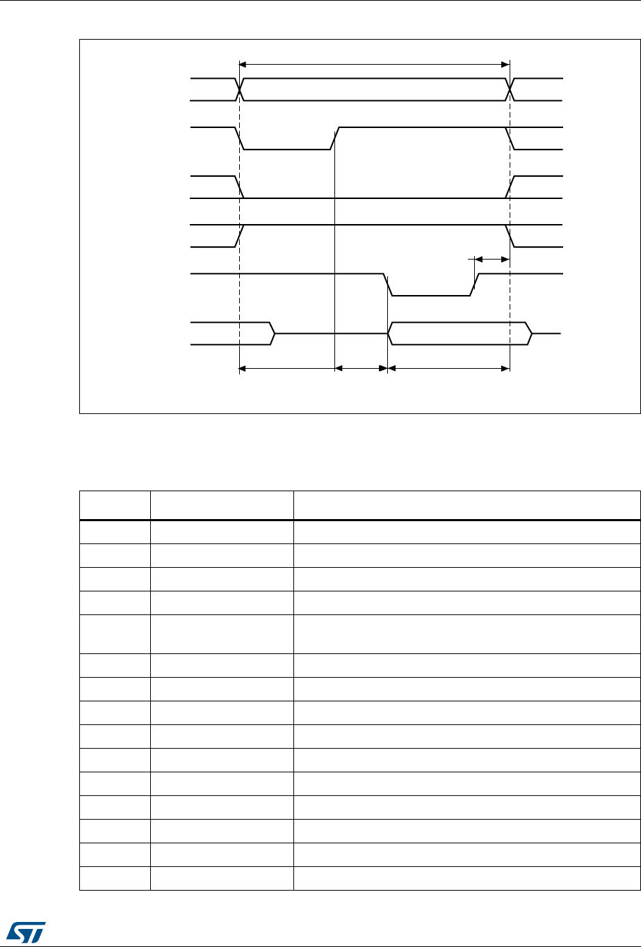
RM0090 Rev 18 1629/1749
RM0090 Flexible memory controller (FMC)
1682
Figure 468. ModeD write access waveforms
The differences with mode1 are the toggling of NOE that goes on toggling after NADV
changes and the independent read and write timings.
Table 280. FMC_BCRx bit fields
Bit No. Bit name Value to set
31-21 Reserved 0x000
20 CCLKEN As needed
19 CBURSTRW 0x0 (no effect in asynchronous mode)
18:16 CPSIZE 0x0 (no effect in asynchronous mode)
15 ASYNCWAIT Set to 1 if the memory supports this feature. Otherwise keep
at 0.
14 EXTMOD 0x1
13 WAITEN 0x0 (no effect in asynchronous mode)
12 WREN As needed
11 WAITCFG Don’t care
10 WRAPMOD 0x0
9 WAITPOL Meaningful only if bit 15 is 1
8 BURSTEN 0x0
7 Reserved 0x1
6 FACCEN Set according to memory support
5-4 MWID As needed
A[25:0]
NOE
ADDSET (DATAST+ 1)
Memory transaction
NEx
D[31:0]
HCLK cycles HCLK cycles
NWE
NADV
data driven by FSMC
MS30462V1
1HCLK
ADDHLD
HCLK cycles

Flexible memory controller (FMC) RM0090
1630/1749 RM0090 Rev 18
3-2 MTYP[1:0] As needed
1 MUXEN 0x0
0 MBKEN 0x1
Table 281. FMC_BTRx bit fields
Bit No. Bit name Value to set
31:30 Reserved 0x0
29-28 ACCMOD 0x3
27-24 DATLAT Don’t care
23-20 CLKDIV Don’t care
19-16 BUSTURN Time between NEx high to NEx low (BUSTURN HCLK)
15-8 DATAST Duration of the second access phase (DATAST HCLK cycles) for
read accesses.
7-4 ADDHLD Duration of the middle phase of the read access (ADDHLD HCLK
cycles)
3-0 ADDSET[3:0] Duration of the first access phase (ADDSET HCLK cycles) for read
accesses. Minimum value for ADDSET is 1.
Table 282. FMC_BWTRx bit fields
Bit No. Bit name Value to set
31:30 Reserved 0x0
29-28 ACCMOD 0x3
27-24 DATLAT Don’t care
23-20 CLKDIV Don’t care
19-16 BUSTURN Time between NEx high to NEx low (BUSTURN HCLK)
15-8 DATAST Duration of the second access phase (DATAST + 1 HCLK cycles) for
write accesses.
7-4 ADDHLD Duration of the middle phase of the write access (ADDHLD HCLK
cycles)
3-0 ADDSET[3:0] Duration of the first access phase (ADDSET HCLK cycles) for write
accesses. Minimum value for ADDSET is 1.
Table 280. FMC_BCRx bit fields (continued)
Bit No. Bit name Value to set
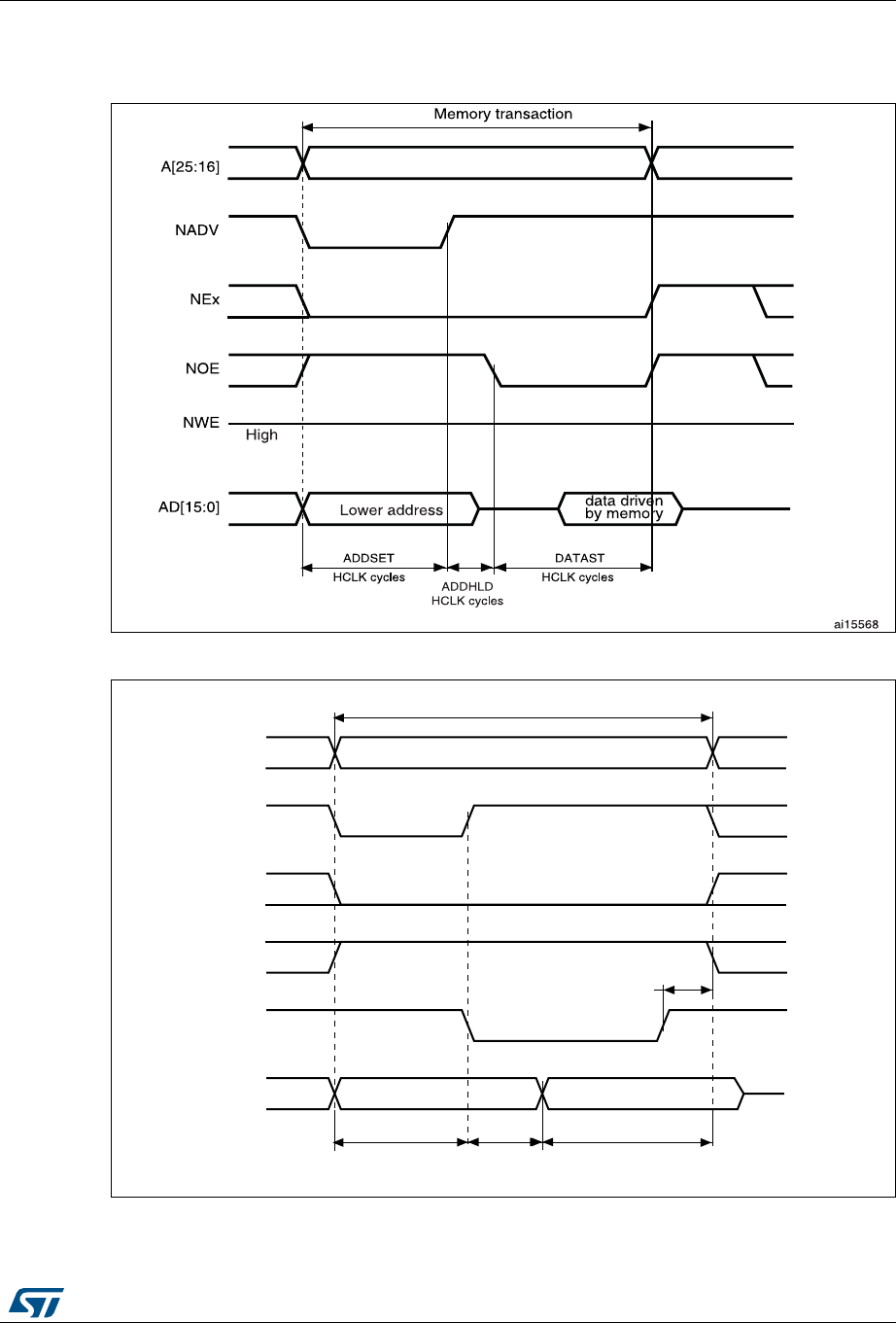
RM0090 Rev 18 1631/1749
RM0090 Flexible memory controller (FMC)
1682
Muxed mode - multiplexed asynchronous access to NOR Flash memory
Figure 469. Muxed read access waveforms
Figure 470. Muxed write access waveforms
The difference with mode D is the drive of the lower address byte(s) on the data bus.
A[25:16]
NOE
ADDSET (DATAST + 1)
Memory transaction
NEx
AD[15:0]
HCLK cycles HCLK cycles
NWE
NADV
data driven by FSMC
ai15569
1HCLK
ADDHLD
HCLK cycles
Lower address

Flexible memory controller (FMC) RM0090
1632/1749 RM0090 Rev 18
WAIT management in asynchronous accesses
If the asynchronous memory asserts the WAIT signal to indicate that it is not yet ready to
accept or to provide data, the ASYNCWAIT bit has to be set in FMC_BCRx register.
Table 283. FMC_BCRx bit fields
Bit No. Bit name Value to set
31-21 Reserved 0x000
20 CCLKEN As needed
19 CBURSTRW 0x0 (no effect in asynchronous mode)
18:16 CPSIZE 0x0 (no effect in asynchronous mode)
15 ASYNCWAIT Set to 1 if the memory supports this feature. Otherwise keep at
0.
14 EXTMOD 0x0
13 WAITEN 0x0 (no effect in asynchronous mode)
12 WREN As needed
11 WAITCFG Don’t care
10 WRAPMOD 0x0
9 WAITPOL Meaningful only if bit 15 is 1
8 BURSTEN 0x0
7 Reserved 0x1
6 FACCEN 0x1
5-4 MWID As needed
3-2 MTYP[1:0] 0x2 (NOR Flash memory)
1 MUXEN 0x1
0 MBKEN 0x1
Table 284. FMC_BTRx bit fields
Bit No. Bit name Value to set
31:30 Reserved 0x0
29-28 ACCMOD 0x0
27-24 DATLAT Don’t care
23-20 CLKDIV Don’t care
19-16 BUSTURN Time between NEx high to NEx low (BUSTURN HCLK)
15-8 DATAST Duration of the second access phase (DATAST HCLK cycles for
read accesses and DATAST+1 HCLK cycles for write accesses).
7-4 ADDHLD Duration of the middle phase of the access (ADDHLD HCLK cycles).
3-0 ADDSET[3:0] Duration of the first access phase (ADDSET HCLK cycles).
Minimum value for ADDSET is 1.
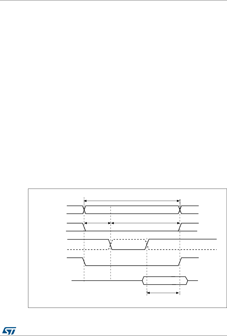
RM0090 Rev 18 1633/1749
RM0090 Flexible memory controller (FMC)
1682
If the WAIT signal is active (high or low depending on the WAITPOL bit), the second access
phase (Data setup phase), programmed by the DATAST bits, is extended until WAIT
becomes inactive. Unlike the data setup phase, the first access phases (Address setup and
Address hold phases), programmed by the ADDSET[3:0] and ADDHLD bits, are not WAIT
sensitive and so they are not prolonged.
The data setup phase must be programmed so that WAIT can be detected 4 HCLK cycles
before the end of the memory transaction. The following cases must be considered:
1. The memory asserts the WAIT signal aligned to NOE/NWE which toggles:
2. The memory asserts the WAIT signal aligned to NEx (or NOE/NWE not toggling):
if
then:
otherwise
where max_wait_assertion_time is the maximum time taken by the memory to assert
the WAIT signal once NEx/NOE/NWE is low.
Figure 471 and Figure 472 show the number of HCLK clock cycles that are added to the
memory access phase after WAIT is released by the asynchronous memory (independently
of the above cases).
Figure 471. Asynchronous wait during a read access waveforms
1. NWAIT polarity depends on WAITPOL bit setting in FMC_BCRx register.
DATAST 4 HCLK×()max_wait_assertion_time+≥
max_wait_assertion_time address_phase hold_phase+>
DATAST 4 HCLK×()max_wait_assertion_time address_phase–hold_phase–()+≥
DATAST 4 HCLK×≥
A[25:0]
NOE
4HCLK
Memory transaction
D[15:0]
NEx
data driven by memory
MS30463V2
address phase data setup phase
NWAIT don’t care don’t care
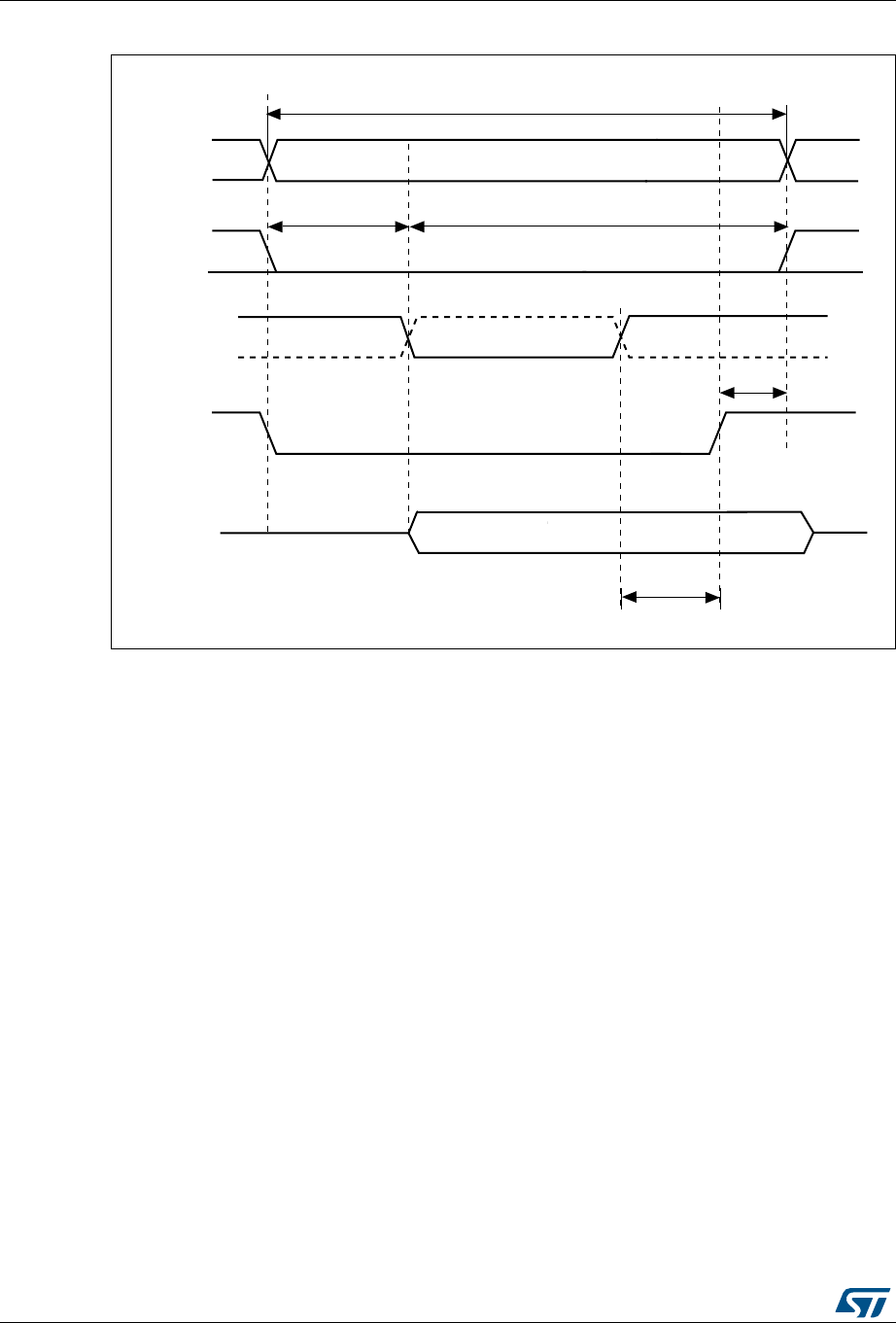
Flexible memory controller (FMC) RM0090
1634/1749 RM0090 Rev 18
Figure 472. Asynchronous wait during a write access waveforms
1. NWAIT polarity depends on WAITPOL bit setting in FMC_BCRx register.
37.5.5 Synchronous transactions
The memory clock, FMC_CLK, is a submultiple of HCLK. It depends on the value of
CLKDIV and the MWID/ AHB data size, following the formula given below:
If MWID is 16 or 8 bits, the FMC_CLK divider ratio is always defined by the programmed
CLKDIV value.
If MWID is 32 bits, the FMC_CLK divider ratio depends also on AHB data size.
Example:
•If CLKDIV=1, MWID=32 bits, AHB data size=8 bits, FMC_CLK=HCLK/4.
•If CLKDIV=1, MWID=16 bits, AHB data size=8 bits, FMC_CLK=HCLK/2.
NOR Flash memories specify a minimum time from NADV assertion to CLK high. To meet
this constraint, the FMC does not issue the clock to the memory during the first internal
clock cycle of the synchronous access (before NADV assertion). This guarantees that the
rising edge of the memory clock occurs in the middle of the NADV low pulse.
Data latency versus NOR memory latency
The data latency is the number of cycles to wait before sampling the data. The DATLAT
value must be consistent with the latency value specified in the NOR Flash configuration
A[25:0]
NWE
Memory transaction
D[15:0]
NEx
data driven by FSMC
MS30464V2
3HCLK
address phase data setup phase
1HCLK
NWAIT don’t care don’t care
FMC_CLK divider ratio max CLKDIV 1+MWID AHB data size()(, )=

RM0090 Rev 18 1635/1749
RM0090 Flexible memory controller (FMC)
1682
register. The FMC does not include the clock cycle when NADV is low in the data latency
count.
Caution: Some NOR Flash memories include the NADV Low cycle in the data latency count, so that
the exact relation between the NOR Flash latency and the FMC DATLAT parameter can be
either:
•NOR Flash latency = (DATLAT + 2) CLK clock cycles
•or NOR Flash latency = (DATLAT + 3) CLK clock cycles
Some recent memories assert NWAIT during the latency phase. In such cases DATLAT can
be set to its minimum value. As a result, the FMC samples the data and waits long enough
to evaluate if the data are valid. Thus the FMC detects when the memory exits latency and
real data are processed.
Other memories do not assert NWAIT during latency. In this case the latency must be set
correctly for both the FMC and the memory, otherwise invalid data are mistaken for good
data, or valid data are lost in the initial phase of the memory access.
Single-burst transfer
When the selected bank is configured in burst mode for synchronous accesses, if for
example an AHB single-burst transaction is requested on 16-bit memories, the FMC
performs a burst transaction of length 1 (if the AHB transfer is 16 bits), or length 2 (if the
AHB transfer is 32 bits) and de-assert the Chip Select signal when the last data is strobed.
Such transfers are not the most efficient in terms of cycles compared to asynchronous read
operations. Nevertheless, a random asynchronous access would first require to re-program
the memory access mode, which would altogether last longer.
Cross boundary page for Cellular RAM 1.5
Cellular RAM 1.5 does not allow burst access to cross the page boundary. The FMC
controller allows to split automatically the burst access when the memory page size is
reached by configuring the CPSIZE bits in the FMC_BCR1 register following the memory
page size.
Wait management
For synchronous NOR Flash memories, NWAIT is evaluated after the programmed latency
period, which corresponds to (DATLAT+2) CLK clock cycles.
If NWAIT is active (low level when WAITPOL = 0, high level when WAITPOL = 1), wait
states are inserted until NWAIT is inactive (high level when WAITPOL = 0, low level when
WAITPOL = 1).
When NWAIT is inactive, the data is considered valid either immediately (bit WAITCFG = 1)
or on the next clock edge (bit WAITCFG = 0).
During wait-state insertion via the NWAIT signal, the controller continues to send clock
pulses to the memory, keeping the Chip Select and output enable signals valid. It does not
consider the data as valid.
In burst mode, there are two timing configurations for the NOR Flash NWAIT signal:
•The Flash memory asserts the NWAIT signal one data cycle before the wait state
(default after reset).
•The Flash memory asserts the NWAIT signal during the wait state
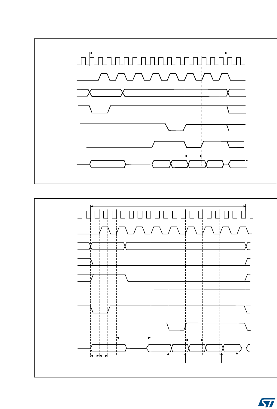
Flexible memory controller (FMC) RM0090
1636/1749 RM0090 Rev 18
The FMC supports both NOR Flash wait state configurations, for each Chip Select, thanks
to the WAITCFG bit in the FMC_BCRx registers (x = 0..3).
Figure 473. Wait configuration waveforms
Figure 474. Synchronous multiplexed read mode waveforms - NOR, PSRAM (CRAM)
1. Byte lane outputs BL are not shown; for NOR access, they are held high, and, for PSRAM (CRAM) access,
addr[15:0] data data
addr[25:16]
Memory transaction = burst of 4 half words
HCLK
CLK
A[25:16]
NADV
NWAIT
(WAITCFG = 1)
A/D[15:0]
inserted wait state
data
NWAIT
(WAITCFG = 0)
ai15798c
Addr[15:0] data data
addr[25:16]
Memory transaction = burst of 4 half words
HCLK
CLK
A[25:16]
NEx
NOE
NWE High
NADV
NWAIT
(WAITCFG=
0)
A/D[15:0]
1 clock
cycle
1 clock
cycle
(DATLAT + 2) inserted wait state
Data strobes ai17723f
CLK cycles
data data
Data strobes

RM0090 Rev 18 1637/1749
RM0090 Flexible memory controller (FMC)
1682
they are held low.
Table 285. FMC_BCRx bit fields
Bit No. Bit name Value to set
31-21 Reserved 0x000
20 CCLKEN As needed
19 CBURSTRW No effect on synchronous read
18-16 CPSIZE As needed (0x1 for CRAM 1.5)
15 ASYNCWAIT 0x0
14 EXTMOD 0x0
13 WAITEN to be set to 1 if the memory supports this feature, to be kept at 0
otherwise
12 WREN no effect on synchronous read
11 WAITCFG to be set according to memory
10 WRAPMOD 0x0
9 WAITPOL to be set according to memory
8 BURSTEN 0x1
7 Reserved 0x1
6 FACCEN Set according to memory support (NOR Flash memory)
5-4 MWID As needed
3-2 MTYP[1:0] 0x1 or 0x2
1 MUXEN As needed
0 MBKEN 0x1
Table 286. FMC_BTRx bit fields
Bit No. Bit name Value to set
31:30 Reserved 0x0
29:28 ACCMOD 0x0
27-24 DATLAT Data latency
27-24 DATLAT Data latency
23-20 CLKDIV
0x0 to get CLK = HCLK (Not supported)
0x1 to get CLK = 2 × HCLK
..
19-16 BUSTURN Time between NEx high to NEx low (BUSTURN HCLK)
15-8 DATAST Don’t care
7-4 ADDHLD Don’t care
3-0 ADDSET[3:0] Don’t care
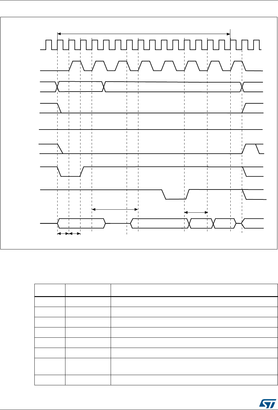
Flexible memory controller (FMC) RM0090
1638/1749 RM0090 Rev 18
Figure 475. Synchronous multiplexed write mode waveforms - PSRAM (CRAM)
1. The memory must issue NWAIT signal one cycle in advance, accordingly WAITCFG must be programmed
to 0.
2. Byte Lane (NBL) outputs are not shown, they are held low while NEx is active.
Addr[15:0] data
addr[25:16]
Memory transaction = burst of 2 half words
HCLK
CLK
A[25:16]
NEx
NOE
NWE
Hi-Z
NADV
NWAIT
(WAITCFG = 0)
A/D[15:0]
1 clock 1 clock
(DATLAT + 2) inserted wait state
ai14731f
CLK cycles
data
Table 287. FMC_BCRx bit fields
Bit No. Bit name Value to set
31-20 Reserved 0x000
20 CCLKEN As needed
19 CBURSTRW 0x1
18-16 CPSIZE As needed (0x1 for CRAM 1.5)
15 ASYNCWAIT 0x0
14 EXTMOD 0x0
13 WAITEN to be set to 1 if the memory supports this feature, to be kept at 0
otherwise.
12 WREN 0x1

RM0090 Rev 18 1639/1749
RM0090 Flexible memory controller (FMC)
1682
11 WAITCFG 0x0
10 WRAPMOD 0x0
9 WAITPOL to be set according to memory
8 BURSTEN no effect on synchronous write
7 Reserved 0x1
6 FACCEN Set according to memory support
5-4 MWID As needed
3-2 MTYP[1:0] 0x1
1 MUXEN As needed
0 MBKEN 0x1
Table 288. FMC_BTRx bit fields
Bit No. Bit name Value to set
31-30 Reserved 0x0
29:28 ACCMOD 0x0
27-24 DATLAT Data latency
23-20 CLKDIV 0x0 to get CLK = HCLK (not supported)
0x1 to get CLK = 2 × HCLK
19-16 BUSTURN Time between NEx high to NEx low (BUSTURN HCLK)
15-8 DATAST Don’t care
7-4 ADDHLD Don’t care
3-0 ADDSET[3:0] Don’t care
Table 287. FMC_BCRx bit fields (continued)
Bit No. Bit name Value to set

Flexible memory controller (FMC) RM0090
1640/1749 RM0090 Rev 18
37.5.6 NOR/PSRAM controller registers
SRAM/NOR-Flash chip-select control registers 1..4 (FMC_BCR1..4)
Address offset: 8 * (x – 1), x = 1...4
Reset value: 0x0000 30DB for Bank1 and 0x0000 30D2 for Bank 2 to 4
This register contains the control information of each memory bank, used for SRAMs,
PSRAM and NOR Flash memories.
3130292827262524232221201918171615141312111098 76543210
Reserved
CCLKEN
CBURSTRW
CPSIZE[2:0]
ASCYCWAIT
EXTMOD
WAITEN
WREN
WAITCFG
WRAPMOD
WAITPOL
BURSTEN
Reserved
FACCEN
MWID[1:0]
MTYP[1:0]
MUXEN
MBKEN
rw rw rw rw rw rw rw rw rw rw rw rw rw rw rw rw rw
Bits 31: 21 Reserved, must be kept at reset value
Bit 20 CCLKEN: Continuous Clock Enable.
This bit enables the FMC_CLK clock output to external memory devices.
0: The FMC_CLK is only generated during the synchronous memory access (read/write
transaction). The FMC_CLK clock ratio is specified by the programmed CLKDIV value in the
FMC_BCRx register (default after reset) .
1: The FMC_CLK is generated continuously during asynchronous and synchronous access. The
FMC_CLK clock is activated when the CCLKEN is set.
Note: The CCLKEN bit of the FMC_BCR2..4 registers is don’t care. It is only enabled through the
FMC_BCR1 register. Bank 1 must be configured in synchronous mode to generate the
FMC_CLK continuous clock.
Note: If CCLKEN bit is set, the FMC_CLK clock ratio is specified by CLKDIV value in the
FMC_BTR1 register. CLKDIV in FMC_BWTR1 is don’t care.
Note: If the synchronous mode is used and CCLKEN bit is set, the synchronous memories
connected to other banks than Bank 1 are clocked by the same clock (the CLKDIV value in
the FMC_BTR2..4 and FMC_BWTR2..4 registers for other banks has no effect.)
Bit 19 CBURSTRW: Write burst enable.
For PSRAM (CRAM) operating in burst mode, the bit enables synchronous accesses during write
operations. The enable bit for synchronous read accesses is the BURSTEN bit in the FMC_BCRx
register.
0: Write operations are always performed in asynchronous mode
1: Write operations are performed in synchronous mode.
Bits 18:16 CPSIZE[2:0]: CRAM page size.
These are used for Cellular RAM 1.5 which does not allow burst access to cross the address
boundaries between pages. When these bits are configured, the FMC controller splits automatically
the burst access when the memory page size is reached (refer to memory datasheet for page size).
000: No burst split when crossing page boundary (default after reset)
001: 128 bytes
010: 256 bytes
011: 512 bytes
100: 1024 bytes
Others: reserved

RM0090 Rev 18 1641/1749
RM0090 Flexible memory controller (FMC)
1682
Bit 15 ASYNCWAIT: Wait signal during asynchronous transfers
This bit enables/disables the FMC to use the wait signal even during an asynchronous protocol.
0: NWAIT signal is not taken in to account when running an asynchronous protocol (default after
reset)
1: NWAIT signal is taken in to account when running an asynchronous protocol
Bit 14 EXTMOD: Extended mode enable.
This bit enables the FMC to program the write timings for non-multiplexed asynchronous accesses
inside the FMC_BWTR register, thus resulting in different timings for read and write operations.
0: values inside FMC_BWTR register are not taken into account (default after reset)
1: values inside FMC_BWTR register are taken into account
Note: When the extended mode is disabled, the FMC can operate in Mode1 or Mode2 as follows:
– Mode 1 is the default mode when the SRAM/PSRAM memory type is selected
(MTYP[1:0] =0x0 or 0x01)
– Mode 2 is the default mode when the NOR memory type is selected (MTYP[1:0] = 0x10).
Bit 13 WAITEN: Wait enable bit.
This bit enables/disables wait-state insertion via the NWAIT signal when accessing the memory in
synchronous mode.
0: NWAIT signal is disabled (its level not taken into account, no wait state inserted after the
programmed Flash latency period)
1: NWAIT signal is enabled (its level is taken into account after the programmed latency period to
insert wait states if asserted) (default after reset)
Bit 12 WREN: Write enable bit.
This bit indicates whether write operations are enabled/disabled in the bank by the FMC:
0: Write operations are disabled in the bank by the FMC, an AHB error is reported,
1: Write operations are enabled for the bank by the FMC (default after reset).
Bit 11 WAITCFG: Wait timing configuration.
The NWAIT signal indicates whether the data from the memory are valid or if a wait state must be
inserted when accessing the memory in synchronous mode. This configuration bit determines if
NWAIT is asserted by the memory one clock cycle before the wait state or during the wait state:
0: NWAIT signal is active one data cycle before wait state (default after reset),
1: NWAIT signal is active during wait state (not used for PSRAM).
Bit 10 WRAPMOD: Wrapped burst mode support.
Defines whether the controller will or not split an AHB burst wrap access into two linear accesses.
Valid only when accessing memories in burst mode
0: Direct wrapped burst is not enabled (default after reset),
1: Direct wrapped burst is enabled.
Note: This bit has no effect as the CPU and DMA cannot generate wrapping burst transfers.
Bit 9 WAITPOL: Wait signal polarity bit.
Defines the polarity of the wait signal from memory used for either in synchronous or asynchronous
mode:
0: NWAIT active low (default after reset),
1: NWAIT active high.
Bit 8 BURSTEN: Burst enable bit.
This bit enables/disables synchronous accesses during read operations. It is valid only for
synchronous memories operating in burst mode:
0: Burst mode disabled (default after reset). Read accesses are performed in asynchronous mode.
1: Burst mode enable. Read accesses are performed in synchronous mode.
Bit 7 Reserved, must be kept at reset value

Flexible memory controller (FMC) RM0090
1642/1749 RM0090 Rev 18
SRAM/NOR-Flash chip-select timing registers 1..4 (FMC_BTR1..4)
Address offset: 0x04 + 8 * (x – 1), x = 1..4
Reset value: 0x0FFF FFFF
Reset value: 0x0FFF FFFF
FMC_BTRx bits are written by software to add a delay at the end of a read /write
transaction. This delay allows matching the minimum time between consecutive
transactions (tEHEL from NEx high to FMC_NEx low) and the maximum time required by the
memory to free the data bus after a read access (tEHQZ).
This register contains the control information of each memory bank, used for SRAMs,
PSRAM and NOR Flash memories.If the EXTMOD bit is set in the FMC_BCRx register, then
this register is partitioned for write and read access, that is, 2 registers are available: one to
configure read accesses (this register) and one to configure write accesses (FMC_BWTRx
registers).
Bit 6 FACCEN: Flash access enable
Enables NOR Flash memory access operations.
0: Corresponding NOR Flash memory access is disabled
1: Corresponding NOR Flash memory access is enabled (default after reset)
Bits 5:4 MWID[1:0]: Memory data bus width.
Defines the external memory device width, valid for all type of memories.
00: 8 bits,
01: 16 bits (default after reset),
10: 32 bits,
11: reserved, do not use.
Bits 3:2 MTYP[1:0]: Memory type.
Defines the type of external memory attached to the corresponding memory bank:
00: SRAM (default after reset for Bank 2...4)
01: PSRAM (CRAM)
10: NOR Flash/OneNAND Flash (default after reset for Bank 1)
11: reserved
Bit 1 MUXEN: Address/data multiplexing enable bit.
When this bit is set, the address and data values are multiplexed on the data bus, valid only with
NOR and PSRAM memories:
0: Address/Data nonmultiplexed
1: Address/Data multiplexed on databus (default after reset)
Bit 0 MBKEN: Memory bank enable bit.
Enables the memory bank. After reset Bank1 is enabled, all others are disabled. Accessing a
disabled bank causes an ERROR on AHB bus.
0: Corresponding memory bank is disabled
1: Corresponding memory bank is enabled

RM0090 Rev 18 1643/1749
RM0090 Flexible memory controller (FMC)
1682
313029282726252423222120191817161514131211109876543210
Reserved
ACCMOD[1:0]
DATLAT[3:0]
CLKDIV3:0]
BUSTURN3:0]
DATAST7:0]
ADDHLD3:0]
ADDSET[3:0]
rw rw rw rw rw rw rw rw rw rw rw rw rw rw rw rw rw rw rw rw rw rw rw rw rw rw rw rw rw rw
Bits 31:30 Reserved, must be kept at reset value
Bits 29:28 ACCMOD[1:0]: Access mode
Specifies the asynchronous access modes as shown in the timing diagrams. These bits are
taken into account only when the EXTMOD bit in the FMC_BCRx register is 1.
00: access mode A
01: access mode B
10: access mode C
11: access mode D
Bits 27:24 DATLAT[3:0]: Data latency for synchronous memory (see note below bit description table)
For synchronous accesses with read/write burst mode enabled (BURSTEN / CBURSTRW bits
set), this field defines the number of memory clock cycles (+2) to issue to the memory before
reading/writing the first data. This timing parameter is not expressed in HCLK periods, but in
FMC_CLK periods. For asynchronous accesses, this value is don't care.
0000: Data latency of 2 CLK clock cycles for first burst access
1111: Data latency of 17 CLK clock cycles for first burst access (default value after reset)
Bits 23:20 CLKDIV[3:0]: Clock divide ratio (for FMC_CLK signal)
Defines the period of FMC_CLK clock output signal, expressed in number of HCLK cycles:
0000: Reserved
0001: FMC_CLK period = 2 × HCLK periods
0010: FMC_CLK period = 3 × HCLK periods
1111: FMC_CLK period = 16 × HCLK periods (default value after reset)
In asynchronous NOR Flash, SRAM or PSRAM accesses, this value is don’t care.
Note: Refer to section 37.5.5: Synchronous transactions for FMC_CLK divider ratio formula)

Flexible memory controller (FMC) RM0090
1644/1749 RM0090 Rev 18
Bits 19:16 BUSTURN[3:0]: Bus turnaround phase duration
These bits are written by software to add a delay at the end of a write-to-read (and read-to-
write) transaction. This delay allows to match the minimum time between consecutive
transactions (tEHEL from NEx high to NEx low) and the maximum time needed by the memory
to free the data bus after a read access (tEHQZ). The programmed bus turnaround delay is
inserted between an asynchronous read (muxed or mode D) or write transaction and any
other asynchronous /synchronous read or write to or from a static bank. The bank can be the
same or different in case of read, in case of write the bank can be different except for muxed
or mode D.
In some cases, whatever the programmed BUSTRUN values, the bus turnaround delay is
fixed as follows:
• The bus turnaround delay is not inserted between two consecutive asynchronous write
transfers to the same static memory bank except for modes muxed and D.
• There is a bus turnaround delay of 1 FMC clock cycle between:
–Two consecutive asynchronous read transfers to the same static memory bank except for
modes muxed and D.
–An asynchronous read to an asynchronous or synchronous write to any static bank or
dynamic bank except for modes muxed and D.
–An asynchronous (modes 1, 2, A, B or C) read and a read from another static bank.
• There is a bus turnaround delay of 2 FMC clock cycle between:
–Two consecutive synchronous writes (burst or single) to the same bank.
–A synchronous write (burst or single) access and an asynchronous write or read transfer to
or from static memory bank (the bank can be the same or different for the case of read.
–Two consecutive synchronous reads (burst or single) followed by any
synchronous/asynchronous read or write from/to another static memory bank.
• There is a bus turnaround delay of 3 FMC clock cycle between:
–Two consecutive synchronous writes (burst or single) to different static bank.
–A synchronous write (burst or single) access and a synchronous read from the same or a
different bank.
0000: BUSTURN phase duration = 0 HCLK clock cycle added
...
1111: BUSTURN phase duration = 15 x HCLK clock cycles added (default value after reset)

RM0090 Rev 18 1645/1749
RM0090 Flexible memory controller (FMC)
1682
Note: PSRAMs (CRAMs) have a variable latency due to internal refresh. Therefore these
memories issue the NWAIT signal during the whole latency phase to prolong the latency as
needed.
With PSRAMs (CRAMs) the filled DATLAT must be set to 0, so that the FMC exits its latency
phase soon and starts sampling NWAIT from memory, then starts to read or write when the
memory is ready.
This method can be used also with the latest generation of synchronous Flash memories
that issue the NWAIT signal, unlike older Flash memories (check the datasheet of the
specific Flash memory being used).
Bits 15:8 DATAST[7:0]: Data-phase duration
These bits are written by software to define the duration of the data phase (refer to Figure 458
to Figure 470), used in asynchronous accesses:
0000 0000: Reserved
0000 0001: DATAST phase duration = 1 × HCLK clock cycles
0000 0010: DATAST phase duration = 2 × HCLK clock cycles
...
1111 1111: DATAST phase duration = 255 × HCLK clock cycles (default value after reset)
For each memory type and access mode data-phase duration, please refer to the respective
figure (Figure 458 to Figure 470).
Example: Mode1, write access, DATAST=1: Data-phase duration= DATAST+1 = 2 HCLK clock
cycles.
Note: In synchronous accesses, this value is don’t care.
Bits 7:4 ADDHLD[3:0]: Address-hold phase duration
These bits are written by software to define the duration of the address hold phase (refer to
Figure 467 to Figure 470), used in mode D or multiplexed accesses:
0000: Reserved
0001: ADDHLD phase duration =1 × HCLK clock cycle
0010: ADDHLD phase duration = 2 × HCLK clock cycle
...
1111: ADDHLD phase duration = 15 × HCLK clock cycles (default value after reset)
For each access mode address-hold phase duration, please refer to the respective figure
(Figure 467 to Figure 470).
Note: In synchronous accesses, this value is not used, the address hold phase is always 1
memory clock period duration.
Bits 3:0 ADDSET[3:0]: Address setup phase duration
These bits are written by software to define the duration of the address setup phase (refer to
Figure 458 to Figure 470), used in SRAMs, ROMs and asynchronous NOR Flash and PSRAM
accesses:
0000: ADDSET phase duration = 0 × HCLK clock cycle
...
1111: ADDSET phase duration = 15 × HCLK clock cycles (default value after reset)
For each access mode address setup phase duration, please refer to the respective figure
(refer to Figure 458 to Figure 470).
Note: In synchronous accesses, this value is don’t care.
In Muxed mode or Mode D, the minimum value for ADDSET is 1.

Flexible memory controller (FMC) RM0090
1646/1749 RM0090 Rev 18
SRAM/NOR-Flash write timing registers 1..4 (FMC_BWTR1..4)
Address offset: 0x104 + 8 * (x – 1), x = 1...4
Reset value: 0x0FFF FFFF
This register contains the control information of each memory bank. It is used for SRAMs,
PSRAMs and NOR Flash memories. When the EXTMOD bit is set in the FMC_BCRx
register, then this register is active for write access.
313029282726252423222120191817161514131211109876543210
Reserved
ACCMOD[1:0]
Reserved
BUSTURN[3:0]
DATAST[7:0]
ADDHLD[3:0]
ADDSET[3:0]
rw rw rw rw rw rw rw rw rw rw rw rw rw rw rw rw rw rw rw rw rw rw
Bits 31:30 Reserved, must be kept at reset value
Bits 29:28 ACCMOD[1:0]: Access mode.
Specifies the asynchronous access modes as shown in the next timing diagrams.These bits are
taken into account only when the EXTMOD bit in the FMC_BCRx register is 1.
00: access mode A
01: access mode B
10: access mode C
11: access mode D
Bits 27:20 Reserved, must be kept at reset value
Bits 19:16 BUSTURN[3:0]: Bus turnaround phase duration
The programmed bus turnaround delay is inserted between an asynchronous write transfer and
any other asynchronous /synchronous read or write transfer to or from a static bank. The bank can
be the same or different in case of read, in case of write the bank can be different expect for muxed
or mode D.
In some cases, whatever the programmed BUSTRUN values, the bus turnaround delay is fixed as
follows:
• The bus turnaround delay is not inserted between two consecutive asynchronous write transfers to
the same static memory bank except for modes muxed and D.
• There is a bus turnaround delay of 2 FMC clock cycle between:
–Two consecutive synchronous writes (burst or single) to the same bank.
–A synchronous write (burst or single) transfer and an asynchronous write or read transfer to or
from static memory bank.
• There is a bus turnaround delay of 3 FMC clock cycle between:
–Two consecutive synchronous writes (burst or single) to different static bank.
–A synchronous write (burst or single) transfer and a synchronous read from the same or a
different bank.
0000: BUSTURN phase duration = 0 HCLK clock cycle added
...
1111: BUSTURN phase duration = 15 HCLK clock cycles added (default value after reset)

RM0090 Rev 18 1647/1749
RM0090 Flexible memory controller (FMC)
1682
37.6 NAND Flash/PC Card controller
The FMC generates the appropriate signal timings to drive the following types of device:
•8- and 16-bit NAND Flash memories
•16-bit PC Card compatible devices
The NAND Flash/PC Card controller can control three external banks, Bank 2, 3 and 4:
•Bank 2 and Bank 3 support NAND Flash devices
•Bank 4 supports PC Card devices.
Each bank is configured through dedicated registers (Section 37.6.8). The programmable
memory parameters include access timings (shown in Table 289) and ECC configuration.
Bits 15:8 DATAST[3:0]: Data-phase duration.
These bits are written by software to define the duration of the data phase (refer toFigure 458 to
Figure 470), used in asynchronous SRAM, PSRAM and NOR Flash memory accesses:
0000 0000: Reserved
0000 0001: DATAST phase duration = 1 × HCLK clock cycles
0000 0010: DATAST phase duration = 2 × HCLK clock cycles
...
1111 1111: DATAST phase duration = 255 × HCLK clock cycles (default value after reset)
Bits 7:4 ADDHLD[3:0]: Address-hold phase duration.
These bits are written by software to define the duration of the address hold phase (refer to
Figure 467 to Figure 470), used in asynchronous multiplexed accesses:
0000: Reserved
0001: ADDHLD phase duration = 1 × HCLK clock cycle
0010: ADDHLD phase duration = 2 × HCLK clock cycle
...
1111: ADDHLD phase duration = 15 × HCLK clock cycles (default value after reset)
Note: In synchronous NOR Flash accesses, this value is not used, the address hold phase is always
1 Flash clock period duration.
Bits 3:0 ADDSET[3:0]: Address setup phase duration.
These bits are written by software to define the duration of the address setup phase in HCLK cycles
(refer to Figure 467 to Figure 470), used in asynchronous accesses:
0000: ADDSET phase duration = 0 × HCLK clock cycle
...
1111: ADDSET phase duration = 15 × HCLK clock cycles (default value after reset)
Note: In synchronous NOR Flash and PSRAM accesses, this value is not used, the address setup
phase is always 1 Flash clock period duration. In muxed mode, the minimum ADDSET value
is 1.

Flexible memory controller (FMC) RM0090
1648/1749 RM0090 Rev 18
37.6.1 External memory interface signals
The following tables list the signals that are typically used to interface NAND Flash memory
and PC Card.
Note: The prefix “N” identifies the signals which are active low.
8-bit NAND Flash memory
t
Theoretically, there is no capacity limitation as the FMC can manage as many address
cycles as needed.
Table 289. Programmable NAND Flash/PC Card access parameters
Parameter Function Access mode Unit Min. Max.
Memory setup
time
Number of clock cycles (HCLK)
required to set up the address
before the command assertion
Read/Write AHB clock cycle
(HCLK) 1 256
Memory wait Minimum duration (in HCLK clock
cycles) of the command assertion Read/Write AHB clock cycle
(HCLK) 2255
Memory hold
Number of clock cycles (HCLK)
during which the address must be
held (as well as the data if a write
access is performed) after the
command de-assertion
Read/Write AHB clock cycle
(HCLK) 1 254
Memory
databus high-Z
Number of clock cycles (HCLK)
during which the data bus is kept
in high-Z state after a write
access has started
Write AHB clock cycle
(HCLK) 1 255
Table 290. 8-bit NAND Flash
FMC signal name I/O Function
A[17] O NAND Flash address latch enable (ALE) signal
A[16] O NAND Flash command latch enable (CLE) signal
D[7:0] I/O 8-bit multiplexed, bidirectional address/data bus
NCE[x] O Chip Select, x = 2, 3
NOE(= NRE) O Output enable (memory signal name: read enable, NRE)
NWE O Write enable
NWAIT/INT[3:2] I NAND Flash ready/busy input signal to the FMC

RM0090 Rev 18 1649/1749
RM0090 Flexible memory controller (FMC)
1682
16-bit NAND Flash memory
Theoretically, there is no capacity limitation as the FMC can manage as many address
cycles as needed.
Table 291. 16-bit NAND Flash
FMC signal name I/O Function
A[17] O NAND Flash address latch enable (ALE) signal
A[16] O NAND Flash command latch enable (CLE) signal
D[15:0] I/O 16-bit multiplexed, bidirectional address/data bus
NCE[x] O Chip Select, x = 2, 3
NOE(= NRE) O Output enable (memory signal name: read enable, NRE)
NWE O Write enable
NWAIT/INT[3:2] I NAND Flash ready/busy input signal to the FMC
Table 292. 16-bit PC Card
FMC signal name I/O Function
A[10:0] O Address bus
NIORD O Output enable for I/O space
NIOWR O Write enable for I/O space
NREG O Register signal indicating if access is in Common or Attribute space
D[15:0] I/O Bidirectional databus
NCE4_1 O Chip Select 1
NCE4_2 O Chip Select 2 (indicates if access is 16-bit or 8-bit)
NOE O Output enable in Common and in Attribute space
NWE O Write enable in Common and in Attribute space
NWAIT I PC Card wait input signal to the FMC (memory signal name IORDY)
INTR I PC Card interrupt to the FMC (only for PC Cards that can generate
an interrupt)
CD I
PC Card presence detection. Active high. If an access is performed
to the PC Card banks while CD is low, an AHB error is generated.
Refer to Section 37.3: AHB interface

Flexible memory controller (FMC) RM0090
1650/1749 RM0090 Rev 18
37.6.2 NAND Flash / PC Card supported memories and transactions
Table 293 shows the supported devices, access modes and transactions. Transactions not
allowed (or not supported) by the NAND Flash / PC Card controller are shown in gray.
37.6.3 Timing diagrams for NAND Flash memory and PC Card
Each PC Card/CompactFlash and NAND Flash memory bank is managed through a set of
registers:
•Control register: FMC_PCRx
•Interrupt status register: FMC_SRx
•ECC register: FMC_ECCRx
•Timing register for Common memory space: FMC_PMEMx
•Timing register for Attribute memory space: FMC_PATTx
•Timing register for I/O space: FMC_PIOx
Each timing configuration register contains three parameters used to define number of
HCLK cycles for the three phases of any PC Card/CompactFlash or NAND Flash access,
plus one parameter that defines the timing for starting driving the data bus when a write
access is performed. Figure 476 shows the timing parameter definitions for common
memory accesses, knowing that Attribute and I/O (only for PC Card) memory space access
timings are similar.
Table 293. Supported memories and transactions
Device Mode R/W
AHB
data size
Memory
data size
Allowed/
not allowed Comments
NAND 8-bit
Asynchronous R 8 8 Y -
Asynchronous W 8 8 Y -
Asynchronous R 16 8 Y Split into 2 FMC accesses
Asynchronous W 16 8 Y Split into 2 FMC accesses
Asynchronous R 32 8 Y Split into 4 FMC accesses
Asynchronous W 32 8 Y Split into 4 FMC accesses
NAND 16-bit
Asynchronous R 8 16 Y -
Asynchronous W 8 16 N -
Asynchronous R 16 16 Y -
Asynchronous W 16 16 Y -
Asynchronous R 32 16 Y Split into 2 FMC accesses
Asynchronous W 32 16 Y Split into 2 FMC accesses
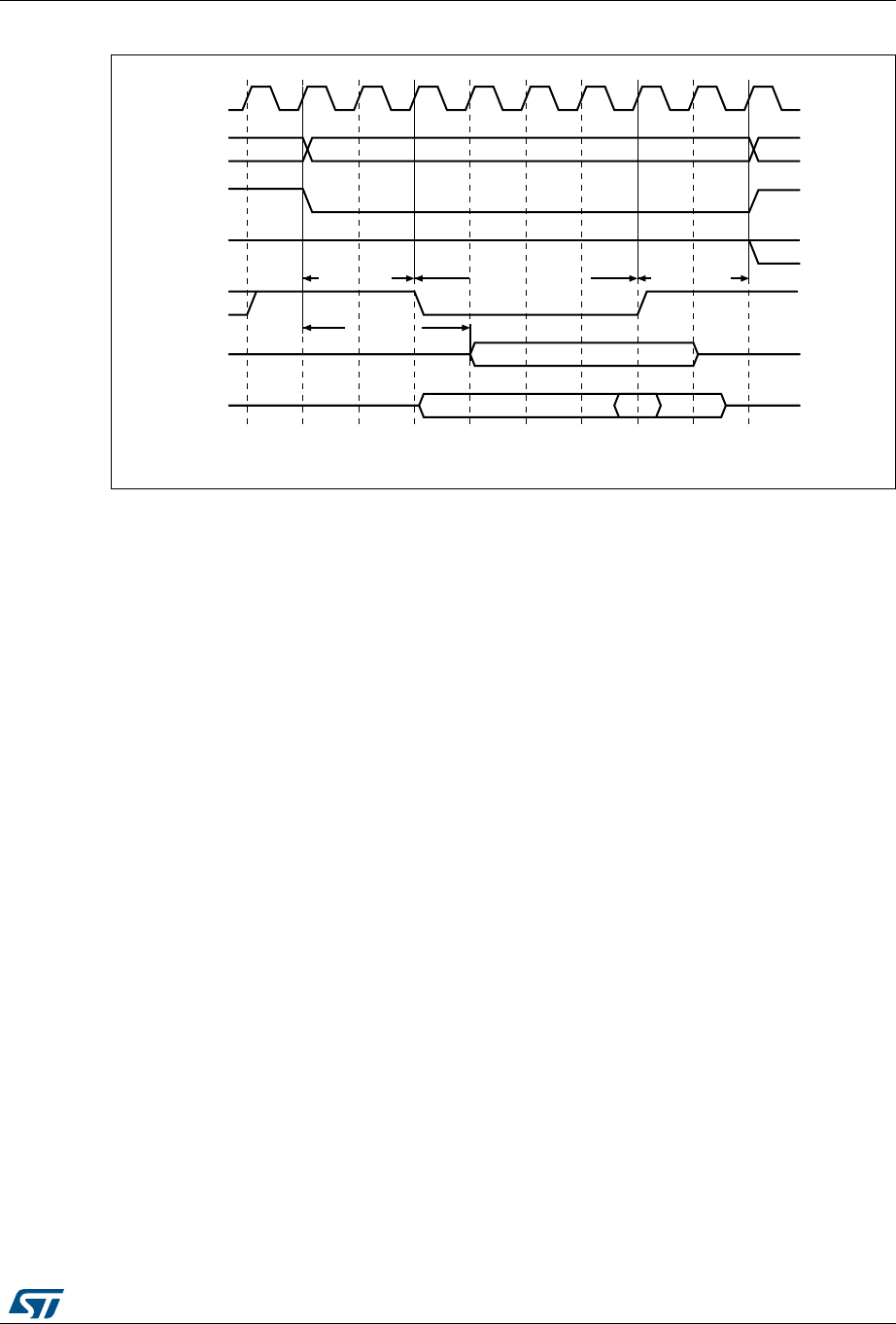
RM0090 Rev 18 1651/1749
RM0090 Flexible memory controller (FMC)
1682
Figure 476. NAND Flash/PC Card controller waveforms for common memory access
1. NOE remains high (inactive) during write accesses. NWE remains high (inactive) during read accesses.
2. For write accesses, the hold phase delay is (MEMHOLD) x HCLK cycles, while it is (MEMHOLD + 2) x
HCLK cycles for read accesses.
37.6.4 NAND Flash operations
The command latch enable (CLE) and address latch enable (ALE) signals of the NAND
Flash memory device are driven by address signals from the FMC controller. This means
that to send a command or an address to the NAND Flash memory, the CPU has to perform
a write to a specific address in its memory space.
A typical page read operation from the NAND Flash device requires the following steps:
3. Program and enable the corresponding memory bank by configuring the FMC_PCRx
and FMC_PMEMx (and for some devices, FMC_PATTx, see Section 37.6.5: NAND
Flash prewait functionality) registers according to the characteristics of the NAND
Flash memory (PWID bits for the data bus width of the NAND Flash, PTYP = 1,
PWAITEN = 0 or 1 as needed, see section Section 37.4.2: NAND Flash memory/PC
Card address mapping for timing configuration).
4. The CPU performs a byte write to the common memory space, with data byte equal to
one Flash command byte (for example 0x00 for Samsung NAND Flash devices). The
LE input of the NAND Flash memory is active during the write strobe (low pulse on
NWE), thus the written byte is interpreted as a command by the NAND Flash memory.
Once the command is latched by the memory device, it does not need to be written
again for the following page read operations.
5. The CPU can send the start address (STARTAD) for a read operation by writing four
byte (or three for smaller capacity devices), STARTAD[7:0], STARTAD[16:9],
STARTAD[24:17] and finally STARTAD[25] (for 64 Mb x 8 bit NAND Flash memories) in
the common memory or attribute space. The ALE input of the NAND Flash device is
active during the write strobe (low pulse on NWE), thus the written byte are interpreted
as the start address for read operations. Using the attribute memory space makes it
possible to use a different timing configuration of the FMC, which can be used to
MS33733V2
HCLK
A[25:0]
NCEx
NREG,
NIOW,
NIOR
NWE,
NOE (1)
write_data
read_data
High
Valid
MEMxSET
+ 1
MEMxWAIT + 1
MEMxHOLD
MEMxHIZ
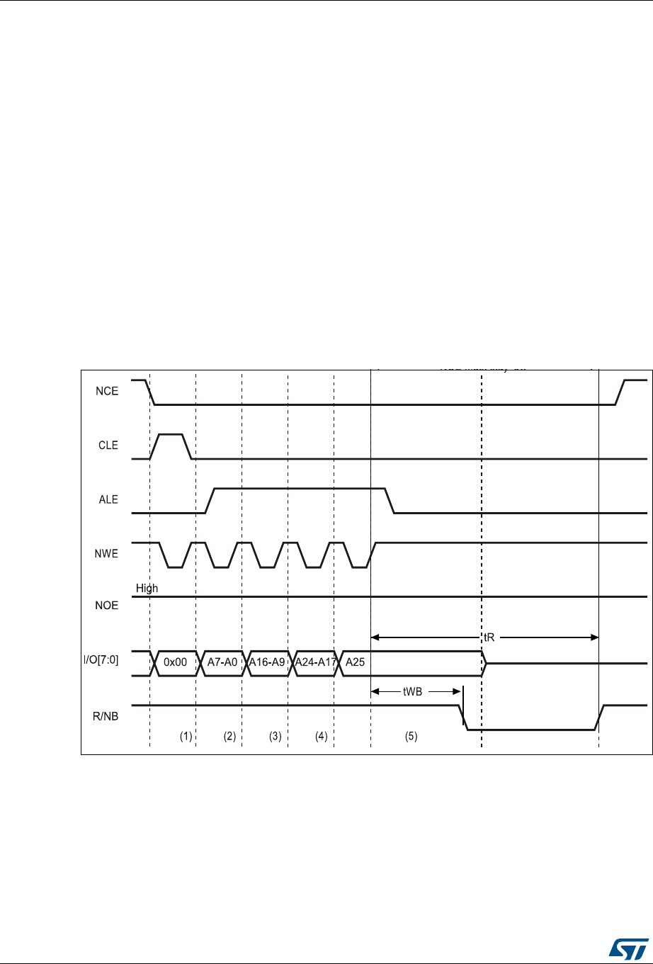
Flexible memory controller (FMC) RM0090
1652/1749 RM0090 Rev 18
implement the prewait functionality needed by some NAND Flash memories (see
details in Section 37.6.5: NAND Flash prewait functionality).
6. The controller waits for the NAND Flash memory to be ready (R/NB signal high), before
starting a new access to the same or another memory bank. While waiting, the
controller holds the NCE signal active (low).
7. The CPU can then perform byte read operations from the common memory space to
read the NAND Flash page (data field + Spare field) byte by byte.
8. The next NAND Flash page can be read without any CPU command or address write
operation. This can be done in three different ways:
– by simply performing the operation described in step 5
– a new random address can be accessed by restarting the operation at step 3
– a new command can be sent to the NAND Flash device by restarting at step 2
37.6.5 NAND Flash prewait functionality
Some NAND Flash devices require that, after writing the last part of the address, the
controller waits for the R/NB signal to go low. (see Figure 457).
Figure 477. Access to non ‘CE don’t care’ NAND-Flash
1. CPU wrote byte 0x00 at address 0x7001 0000.
2. CPU wrote byte A7~A0 at address 0x7002 0000.
3. CPU wrote byte A16~A9 at address 0x7002 0000.
4. CPU wrote byte A24~A17 at address 0x7002 0000.
5. CPU wrote byte A25 at address 0x7802 0000: FMC performs a write access using FMC_PATT2 timing
definition, where ATTHOLD ≥ 7 (providing that (7+1) × HCLK = 112 ns > tWB max). This guarantees that
NCE remains low until R/NB goes low and high again (only requested for NAND Flash memories where
NCE is not don’t care).

RM0090 Rev 18 1653/1749
RM0090 Flexible memory controller (FMC)
1682
When this functionality is required, it can be ensured by programming the MEMHOLD value
to meet the tWB timing. However CPU read accesses to the NAND Flash memory has a hold
delay of (MEMHOLD + 2) x HCLK cycles, while CPU write accesses have a hold delay of
(MEMHOLD) x HCLK cycles.
To cope with this timing constraint, the attribute memory space can be used by
programming its timing register with an ATTHOLD value that meets the tWB timing, and by
keeping the MEMHOLD value at its minimum value. The CPU must then use the common
memory space for all NAND Flash read and write accesses, except when writing the last
address byte to the NAND Flash device, where the CPU must write to the attribute memory
space.
37.6.6 Computation of the error correction code (ECC)
in NAND Flash memory
The FMC PC Card controller includes two error correction code computation hardware
blocks, one per memory bank. They reduce the host CPU workload when processing the
ECC by software.
These two ECC blocks are identical and associated with Bank 2 and Bank 3. As a
consequence, no hardware ECC computation is available for memories connected to Bank
4.
The ECC algorithm implemented in the FMC can perform 1-bit error correction and 2-bit
error detection per 256, 512, 1 024, 2 048, 4 096 or 8 192 byte read or written from/to the
NAND Flash memory. It is based on the Hamming coding algorithm and consists in
calculating the row and column parity.
The ECC modules monitor the NAND Flash data bus and read/write signals (NCE and
NWE) each time the NAND Flash memory bank is active.
The ECC operates as follows:
•When accessing NAND Flash memory bank 2 or bank 3, the data present on the
D[15:0] bus is latched and used for ECC computation.
•When accessing any other address in NAND Flash memory, the ECC logic is idle, and
does not perform any operation. As a result, write operations to define commands or
addresses to the NAND Flash memory are not taken into account for ECC
computation.
Once the desired number of byte has been read/written from/to the NAND Flash memory by
the host CPU, the FMC_ECCR2/3 registers must be read to retrieve the computed value.
Once read, they should be cleared by resetting the ECCEN bit to ‘0’. To compute a new data
block, the ECCEN bit must be set to one in the FMC_PCR2/3 registers.

Flexible memory controller (FMC) RM0090
1654/1749 RM0090 Rev 18
To perform an ECC computation:
1. Enable the ECCEN bit in the FMC_PCR2/3 register.
2. Write data to the NAND Flash memory page. While the NAND page is written, the ECC
block computes the ECC value.
3. Read the ECC value available in the FMC_ECCR2/3 register and store it in a variable.
4. Clear the ECCEN bit and then enable it in the FMC_PCR2/3 register before reading
back the written data from the NAND page. While the NAND page is read, the ECC
block computes the ECC value.
5. Read the new ECC value available in the FMC_ECCR2/3 register.
6. If the two ECC values are the same, no correction is required, otherwise there is an
ECC error and the software correction routine returns information on whether the error
can be corrected or not.
37.6.7 PC Card/CompactFlash operations
Address spaces and memory accesses
The FMC supports CompactFlash devices and PC Cards in Memory mode and I/O mode
(True IDE mode is not supported).
The CompactFlash and PC Cards are made of 3 memory spaces:
•Common Memory space
•Attribute space
•I/O Memory space
The nCE2 and nCE1 pins (FMC_NCE4_2 and FMC_NCE4_1 respectively) select the card
and indicate whether a byte or a word operation is being performed: nCE2 accesses the odd
byte on D15-8 and nCE1 accesses the even byte on D7-0 if A0=0 or the odd byte on D7-0 if
A0=1. The full word is accessed on D15-0 if both nCE2 and nCE1 are low.
The memory space is selected by asserting low nOE for read accesses or nWE for write
accesses, combined with the low assertion of nCE2/nCE1 and nREG.
•If pin nREG=1 during the memory access, the common memory space is selected
•If pin nREG=0 during the memory access, the attribute memory space is selected
The I/O space is selected by asserting nIORD space for read accesses or nIOWR for write
accesses [instead of nOE/nWE for memory space], combined with nCE2/nCE1. Note that
nREG must also be asserted low when accessing I/O space.
Three type of accesses are allowed for a 16-bit PC Card:
•Accesses to Common Memory space for data storage can be either 8-bit accesses at
even addresses or 16-bit AHB accesses.
Note that 8-bit accesses at odd addresses are not supported and nCE2 will not be
driven low. A 32-bit AHB request is translated into two 16-bit memory accesses.
•Accesses to Attribute Memory space where the PC Card stores configuration
information are limited to 8-bit AHB accesses at even addresses.
Note that a 16-bit AHB access will be converted into a single 8-bit memory transfer:
nCE1 will be asserted low, nCE2 will be asserted high and only the even byte on D7-D0
will be valid. Instead a 32-bit AHB access will be converted into two 8-bit memory

RM0090 Rev 18 1655/1749
RM0090 Flexible memory controller (FMC)
1682
transfers at even addresses: nCE1 will be asserted low, NCE2 will be asserted high
and only the even byte will be valid.
•Accesses to I/O space can be either 8-bit or 16 bit AHB accesses.
FMC Bank 4 gives access to those 3 memory spaces as described in Section 37.4.2: NAND
Flash memory/PC Card address mapping and Table 256: NAND/PC Card memory mapping
and timing registers.
Wait feature
The CompactFlash or PC Card may request the FMC to extend the length of the access
phase programmed by MEMWAITx/ATTWAITx/IOWAITx bits, asserting the nWAIT signal
after nOE/nWE or nIORD/nIOWR activation if the wait feature is enabled through the
PWAITEN bit in the FMC_PCRx register. To detect correctly the nWAIT assertion, the
MEMWAITx/ATTWAITx/IOWAITx bits must be programmed as follows:
where max_wait_assertion_time is the maximum time taken by NWAIT to go low once
nOE/nWE or nIORD/nIOWR is low.
Table 294. 16-bit PC-Card signals and access type
nCE2
nCE1
nREG
nOE/nWE
nIORD
A10
A9
A7-1
A0
Space Access type Allowed/not
Allowed
1 0 101XXX-XX Common
Memory
Space
Read/Write byte on D7-D0 YES
0 1 1 0 1 X X X-X X Read/Write byte on D15-D8 Not supported
0 0 1 0 1 X X X-X 0 Read/Write word on D15-D0 YES
X0 00101X-X0
Attribute
Space
Read or Write Configuration
Registers YES
X0 00100X-X0 Read or Write CIS (Card
Information Structure) YES
1 0 001XXX-X1
Attribute
Space
Invalid Read or Write (odd
address) YES
0 1 001XXX-Xx Invalid Read or Write (odd
address) YES
1 0 010XXX-X0
I/O space
Read Even Byte on D7-0 YES
1 0 0 1 0 X X X-X 1 Read Odd Byte on D7-0 YES
1 0 0 1 0 X X X-X 0 Write Even Byte on D7-0 YES
1 0 0 1 0 X X X-X 1 Write Odd Byte on D7-0 YES
0 0 0 1 0 X X X-X 0 Read Word on D15-0 YES
0 0 0 1 0 X X X-X 0 Write word on D15-0 YES
0 1 0 1 0 X X X-X X Read Odd Byte on D15-8 Not supported
0 1 0 1 0 X X X-X X Write Odd Byte on D15-8 Not supported
xxWAITx 4 max_wait_assertion_time
HCLK
-------------------------------------------------------------------+≥

Flexible memory controller (FMC) RM0090
1656/1749 RM0090 Rev 18
After WAIT de-assertion, the FMC extends the WAIT phase for 4 HCLK clock cycles.
37.6.8 NAND Flash/PC Card controller registers
PC Card/NAND Flash control registers 2..4 (FMC_PCR2..4)
Address offset: 0x40 + 0x20 * (x – 1), x = 2..4
Reset value: 0x0000 0018
31302928272625242322212019181716151413121110987654321 0
Reserved
ECCPS[2:0]
TAR[3:0]
TCLR[3:0]
Reserved
ECCEN
PWID[1:0]
PTYP
PBKEN
PWAITEN
Reserved
rw rw rw rw rw rw rw rw rw rw rw rw rw rw rw rw rw
Bits 31:20 Reserved, must be kept at reset value
Bits 19:17 ECCPS[2:0]: ECC page size.
Defines the page size for the extended ECC:
000: 256 byte
001: 512 byte
010: 1024 byte
011: 2048 byte
100: 4096 byte
101: 8192 byte
Bits 16:13 TAR[3:0]: ALE to RE delay.
Sets time from ALE low to RE low in number of AHB clock cycles (HCLK).
Time is: t_ar = (TAR + SET + 2) × THCLK where THCLK is the HCLK clock period
0000: 1 HCLK cycle (default)
1111: 16 HCLK cycles
Note: SET is MEMSET or ATTSET according to the addressed space.
Bits 12:9 TCLR[3:0]: CLE to RE delay.
Sets time from CLE low to RE low in number of AHB clock cycles (HCLK).
Time is t_clr = (TCLR + SET + 2) × THCLK where THCLK is the HCLK clock period
0000: 1 HCLK cycle (default)
1111: 16 HCLK cycles
Note: SET is MEMSET or ATTSET according to the addressed space.
Bits 8:7 Reserved, must be kept at reset value
Bit 6 ECCEN: ECC computation logic enable bit
0: ECC logic is disabled and reset (default after reset),
1: ECC logic is enabled.
Bits 5:4 PWID[1:0]: Data bus width.
Defines the external memory device width.
00: 8 bits
01: 16 bits (default after reset). This value is mandatory for PC Cards.
10: reserved, do not use
11: reserved, do not use

RM0090 Rev 18 1657/1749
RM0090 Flexible memory controller (FMC)
1682
FIFO status and interrupt register 2..4 (FMC_SR2..4)
Address offset: 0x44 + 0x20 * (x-1), x = 2..4
Reset value: 0x0000 0040
This register contains information about the FIFO status and interrupt. The FMC features a
FIFO that is used when writing to memories to transfer up to 16 words of data from the AHB.
This is used to quickly write to the FIFO and free the AHB for transactions to peripherals
other than the FMC, while the FMC is draining its FIFO into the memory. One of these
register bits indicates the status of the FIFO, for ECC purposes.
The ECC is calculated while the data are written to the memory. To read the correct ECC,
the software must consequently wait until the FIFO is empty.
Bit 3 PTYP: Memory type.
Defines the type of device attached to the corresponding memory bank:
0: PC Card, CompactFlash, CF+ or PCMCIA
1: NAND Flash (default after reset)
Bit 2 PBKEN: PC Card/NAND Flash memory bank enable bit.
Enables the memory bank. Accessing a disabled memory bank causes an ERROR on AHB
bus
0: Corresponding memory bank is disabled (default after reset)
1: Corresponding memory bank is enabled
Bit 1 PWAITEN: Wait feature enable bit.
Enables the Wait feature for the PC Card/NAND Flash memory bank:
0: disabled
1: enabled
Note: For a PC Card, when the wait feature is enabled, the MEMWAITx/ATTWAITx/IOWAITx
bits must be programmed to a value as follows:
xxWAITx ≥ 4 + max_wait_assertion_time/HCLK
Where max_wait_assertion_time is the maximum time taken by NWAIT to go low once
nOE/nWE or nIORD/nIOWR is low.
Bit 0 Reserved.
313029282726252423222120191817161514131211109876543210
Reserved
FEMPT
IFEN
ILEN
IREN
IFS
ILS
IRS
r rwrwrwrwrwrw
Bits 31:7 Reserved, must be kept at reset value
Bit 6 FEMPT: FIFO empty.
Read-only bit that provides the status of the FIFO
0: FIFO not empty
1: FIFO empty
Bit 5 IFEN: Interrupt falling edge detection enable bit
0: Interrupt falling edge detection request disabled
1: Interrupt falling edge detection request enabled

Flexible memory controller (FMC) RM0090
1658/1749 RM0090 Rev 18
Common memory space timing register 2..4 (FMC_PMEM2..4)
Address offset: Address: 0x48 + 0x20 * (x – 1), x = 2..4
Reset value: 0xFCFC FCFC
Each FMC_PMEMx (x = 2..4) read/write register contains the timing information for PC Card
or NAND Flash memory bank x. This information is used to access either the common
memory space of the 16-bit PC Card/CompactFlash, or the NAND Flash for command,
address write access and data read/write access.
Bit 4 ILEN: Interrupt high-level detection enable bit
0: Interrupt high-level detection request disabled
1: Interrupt high-level detection request enabled
Bit 3 IREN: Interrupt rising edge detection enable bit
0: Interrupt rising edge detection request disabled
1: Interrupt rising edge detection request enabled
Bit 2 IFS: Interrupt falling edge status
The flag is set by hardware and reset by software.
0: No interrupt falling edge occurred
1: Interrupt falling edge occurred
Note: This bit is set by programming it to 1 by software.
Bit 1 ILS: Interrupt high-level status
The flag is set by hardware and reset by software.
0: No Interrupt high-level occurred
1: Interrupt high-level occurred
Bit 0 IRS: Interrupt rising edge status
The flag is set by hardware and reset by software.
0: No interrupt rising edge occurred
1: Interrupt rising edge occurred
Note: This bit is set by programming it to 1 by software.
313029282726252423222120191817161514131211109876543210
MEMHIZ[7:0] MEMHOLD[7:0] MEMWAIT[7:0] MEMSET[7:0]
rw rw rw rw rw rw rw rw rw rw rw rw rw rw rw rw rw rw rw rw rw rw rw rw rw rw rw rw rw rw rw rw
Bits 31:24 MEMHIZ[7:0]: Common memory x data bus Hi-Z time
Defines the number of HCLK clock cycles during which the data bus is kept Hi-Z after the
start of a PC Card/NAND Flash write access to common memory space on socket x. This is
only valid for write transactions:
0000 0000: 1 HCLK cycle
1111 1110: 255 HCLK cycles
1111 1111: Reserved.

RM0090 Rev 18 1659/1749
RM0090 Flexible memory controller (FMC)
1682
Attribute memory space timing registers 2..4 (FMC_PATT2..4)
Address offset: 0x4C + 0x20 * (x – 1), x = 2..4
Reset value: 0xFCFC FCFC
Each FMC_PATTx (x = 2..4) read/write register contains the timing information for PC
Card/CompactFlash or NAND Flash memory bank x. It is used for 8-bit accesses to the
attribute memory space of the PC Card/CompactFlash or to access the NAND Flash for the
last address write access if the timing must differ from that of previous accesses (for
Ready/Busy management, refer to Section 37.6.5: NAND Flash prewait functionality).
Bits 23:16 MEMHOLD[7:0]: Common memory x hold time
For NAND Flash read accesses to the common memory space, these bits define the
number of (HCLK+2) clock cycles during which the address is held after the command is
deasserted (NWE, NOE).
For NAND Flash write accesses to the common memory space, these bits define the
number of HCLK clock cycles during which the data are held after the command is
deasserted (NWE, NOE).
0000 0000: reserved
0000 0001: 1 HCLK cycle for write accesses, 3 HCLK cycles for read accesses
1111 1110: 254 HCLK cycle for write accesses, 256 HCLK cycles for read accesses
1111 1111: Reserved.
Bits 15:8 MEMWAIT[7:0]: Common memory x wait time
Defines the minimum number of HCLK (+1) clock cycles to assert the command (NWE,
NOE), for PC Card/NAND Flash read or write access to common memory space on socket
x. The duration of command assertion is extended if the wait signal (NWAIT) is active (low)
at the end of the programmed value of HCLK:
0000 0000: reserved
0000 0001: 2 HCLK cycles (+ wait cycle introduced by deasserting NWAIT)
1111 1110: 255 HCLK cycles (+ wait cycle introduced by deasserting NWAIT)
1111 1111: Reserved
Bits 7:0 MEMSET[7:0]: Common memory x setup time
Defines the number of HCLK (+1) clock cycles to set up the address before the command
assertion (NWE, NOE), for PC Card/NAND Flash read or write access to common memory
space on socket x:
0000 0000: 1 HCLK cycle
1111 1110: 255 HCLK cycles
1111 1111: Reserved.
313029282726252423222120191817161514131211109876543210
ATTHIZ[7:0] ATTHOLD[7:0] ATTWAIT[7:0] ATTSET[7:0]
rw rw rw rw rw rw rw rw rw rw rw rw rw rw rw rw rw rw rw rw rw rw rw rw rw rw rw rw rw rw rw rw
Bits 31:24 ATTHIZ[7:0]: Attribute memory x data bus Hi-Z time
Defines the number of HCLK clock cycles during which the data bus is kept in Hi-Z after the
start of a PC CARD/NAND Flash write access to attribute memory space on socket x. Only
valid for write transaction:
0000 0000: 0 HCLK cycle
1111 1110: 255 HCLK cycles
1111 1111: Reserved.

Flexible memory controller (FMC) RM0090
1660/1749 RM0090 Rev 18
I/O space timing register 4 (FMC_PIO4)
Address offset: 0xB0
Reset value: 0xFCFCFCFC
The FMC_PIO4 read/write registers contain the timing information used to access the I/O
space of the 16-bit PC Card/CompactFlash.
Bits 23:16 ATTHOLD[7:0]: Attribute memory x hold time
For PC Card/NAND Flash read accesses to attribute memory space on socket x, these bits
define the number of HCLK clock cycles (HCLK +2) clock cycles during which the address is
held after the command is deasserted (NWE, NOE).
For PC Card/NAND Flash write accesses to attribute memory space on socket x, these bits
define the number of HCLK clock cycles during which the data are held after the command
is deasserted (NWE, NOE).
0000 0000: Reserved
0000 0001: 1 HCLK cycle for write access, 3 HCLK cycles for read accesses
1111 1110: 254 HCLK cycle for write access, 256 HCLK cycles for read accesses
1111 1111: Reserved.
Bits 15:8 ATTWAIT[7:0]: Attribute memory x wait time
Defines the minimum number of HCLK (+1) clock cycles to assert the command (NWE,
NOE), for PC Card/NAND Flash read or write access to attribute memory space on socket x.
The duration for command assertion is extended if the wait signal (NWAIT) is active (low) at
the end of the programmed value of HCLK:
0000 0000: reserved
0000 0001: 2 HCLK cycles (+ wait cycle introduced by deassertion of NWAIT)
1111 1110: 255 HCLK cycles (+ wait cycle introduced by the card deasserting NWAIT)
1111 1111: Reserved
Bits 7:0 ATTSET[7:0]: Attribute memory x setup time
Defines the number of HCLK (+1) clock cycles to set up address before the command
assertion (NWE, NOE), for PC CARD/NAND Flash read or write access to attribute memory
space on socket x:
0000 0000: 1 HCLK cycle
1111 1110: 255 HCLK cycles
1111 1111: Reserved
313029282726252423222120191817161514131211109876543210
IOHIZ[7:0] IOHOLD[7:0] IOWAIT[7:0] IOSET[7:0]
rw rw rw rw rw rw rw rw rw rw rw rw rw rw rw rw rw rw rw rw rw rw rw rw rw rw rw rw rw rw rw rw

RM0090 Rev 18 1661/1749
RM0090 Flexible memory controller (FMC)
1682
Bits 31:24 IOHIZ[7:0]: I/O x data bus Hi-Z time
Defines the number of HCLK clock cycles during which the data bus is kept in Hi-Z after the
start of a PC Card write access to I/O space on socket x. Only valid for write transaction:
0000 0000: 0 HCLK cycle
1111 1111: 255 HCLK cycles
Bits 23:16 IOHOLD[7:0]: I/O x hold time
Defines the number of HCLK clock cycles during which the address is held (and data for write
access) after the command deassertion (NWE, NOE), for PC Card read or write access to I/O
space on socket x:
0000 0000: reserved
0000 0001: 1 HCLK cycle
1111 1111: 255 HCLK cycles
Bits 15:8 IOWAIT[7:0]: I/O x wait time
Defines the minimum number of HCLK (+1) clock cycles to assert the command (SMNWE,
SMNOE), for PC Card read or write access to I/O space on socket x. The duration for
command assertion is extended if the wait signal (NWAIT) is active (low) at the end of the
programmed value of HCLK:
0000 0000: reserved, do not use this value
0000 0001: 2 HCLK cycles (+ wait cycle introduced by deassertion of NWAIT)
1111 1111: 256 HCLK cycles (+ wait cycle introduced by the Card deasserting NWAIT)
Bits 7:0 IOSET[7:0]: I/O x setup time
Defines the number of HCLK (+1) clock cycles to set up the address before the command
assertion (NWE, NOE), for PC Card read or write access to I/O space on socket x:
0000 0000: 1 HCLK cycle
1111 1111: 256 HCLK cycles

Flexible memory controller (FMC) RM0090
1662/1749 RM0090 Rev 18
ECC result registers 2/3 (FMC_ECCR2/3)
Address offset: 0x54 + 0x20 * (x – 1), x = 2 or 3
Reset value: 0x0000 0000
These registers contain the current error correction code value computed by the ECC
computation modules of the FMC controller (one module per NAND Flash memory bank).
When the CPU reads the data from a NAND Flash memory page at the correct address
(refer to Section 37.6.6: Computation of the error correction code (ECC) in NAND Flash
memory), the data read/written from/to the NAND Flash memory are processed
automatically by the ECC computation module. When X byte have been read (according to
the ECCPS field in the FMC_PCRx registers), the CPU must read the computed ECC value
from the FMC_ECCx registers. It then verifies if these computed parity data are the same as
the parity value recorded in the spare area, to determine whether a page is valid, and, to
correct it otherwise. The FMC_ECCRx registers should be cleared after being read by
setting the ECCEN bit to ‘0’. To compute a new data block, the ECCEN bit must be set to ’1’.
313029282726252423222120191817161514131211109876543210
ECC[31:0]
r
Bits 31:0 ECC[31:0]: ECC result
This field contains the value computed by the ECC computation logic. Table 295 describes the
contents of these bit fields.
Table 295. ECC result relevant bits
ECCPS[2:0] Page size in byte ECC bits
000 256 ECC[21:0]
001 512 ECC[23:0]
010 1024 ECC[25:0]
011 2048 ECC[27:0]
100 4096 ECC[29:0]
101 8192 ECC[31:0]

RM0090 Rev 18 1663/1749
RM0090 Flexible memory controller (FMC)
1682
37.7 SDRAM controller
37.7.1 SDRAM controller main features
The main features of the SDRAM controller are the following:
•Two SDRAM banks with independent configuration
•8-bit, 16-bit, 32-bit data bus width
•13-bits Address Row, 11-bits Address Column, 4 internal banks: 4x16Mx32bit
(256 MB), 4x16Mx16bit (128 MB), 4x16Mx8bit (64 MB)
•Word, half-word, byte access
•SDRAM clock can be HCLK/2 or HCLK/3
•Automatic row and bank boundary management
•Multibank ping-pong access
•Programmable timing parameters
•Automatic Refresh operation with programmable Refresh rate
•Self-refresh mode
•Power-down mode
•SDRAM power-up initialization by software
•CAS latency of 1,2,3
•Cacheable Read FIFO with depth of 6 lines x32-bit (6 x14-bit address tag)
37.7.2 SDRAM External memory interface signals
At startup, the SDRAM I/O pins used to interface the FMC SDRAM controller with the
external SDRAM devices must configured by the user application. The SDRAM controller
I/O pins which are not used by the application, can be used for other purposes.
Table 296. SDRAM signals
SDRAM signal I/O
type Description Alternate function
SDCLK O SDRAM clock
SDCKE[1:0] O SDCKE0: SDRAM Bank 1 Clock Enable
SDCKE1: SDRAM Bank 2 Clock Enable
SDNE[1:0] O SDNE0: SDRAM Bank 1 Chip Enable
SDNE1: SDRAM Bank 2 Chip Enable
A[12:0] O Address FMC_A[12:0]
D[31:0] I/O Bidirectional data bus FMC_D[31:0]
BA[1:0] O Bank Address FMC_A[15:14]
NRAS O Row Address Strobe
NCAS O Column Address Strobe
SDNWE O Write Enable
NBL[3:0] O Output Byte Mask for write accesses
(memory signal name: DQM[3:0]) FMC_NBL[3:0]

Flexible memory controller (FMC) RM0090
1664/1749 RM0090 Rev 18
37.7.3 SDRAM controller functional description
All SDRAM controller outputs (signals, address and data) change on the falling edge of the
memory clock (FMC_SDCLK).
SDRAM initialization
The initialization sequence is managed by software. If the two banks are used, the
initialization sequence must be generated simultaneously to Bank 1and Bank 2 by setting
the Target Bank bits CTB1 and CTB2 in the FMC_SDCMR register:
1. Program the memory device features into the FMC_SDCRx register.The SDRAM clock
frequency, RBURST and RPIPE must be programmed in the FMC_SDCR1 register.
2. Program the memory device timing into the FMC_SDTRx register. The TRP and TRC
timings must be programmed in the FMC_SDTR1 register.
3. Set MODE bits to ‘001’ and configure the Target Bank bits (CTB1 and/or CTB2) in the
FMC_SDCMR register to start delivering the clock to the memory (SDCKE is driven
high).
4. Wait during the prescribed delay period. Typical delay is around 100 μs (refer to the
SDRAM datasheet for the required delay after power-up).
5. Set MODE bits to ‘010’ and configure the Target Bank bits (CTB1 and/or CTB2) in the
FMC_SDCMR register to issue a “Precharge All” command.
6. Set MODE bits to ‘011’, and configure the Target Bank bits (CTB1 and/or CTB2) as well
as the number of consecutive Auto-refresh commands (NRFS) in the FMC_SDCMR
register. Refer to the SDRAM datasheet for the number of Auto-refresh commands that
should be issued. Typical number is 8.
7. Configure the MRD field according to your SDRAM device, set the MODE bits to '100',
and configure the Target Bank bits (CTB1 and/or CTB2) in the FMC_SDCMR register
to issue a "Load Mode Register" command in order to program the SDRAM. In
particular:
a) The CAS latency must be selected following configured value in FMC_SDCR1/2
registers
b) The Burst Length (BL) of 1 must be selected by configuring the M[2:0] bits to 000
in the mode register (refer to the SDRAM datasheet). If the Mode Register is not
the same for both SDRAM banks, this step has to be repeated twice, once for
each bank, and the Target Bank bits set accordingly.
8. Program the refresh rate in the FMC_SDRTR register
The refresh rate corresponds to the delay between refresh cycles. Its value must be
adapted to SDRAM devices.
9. For mobile SDRAM devices, to program the extended mode register it should be done
once the SDRAM device is initialized: First, a dummy read access should be performed
while BA1=1 and BA=0 (refer to SDRAM address mapping section for BA[1:0] address
mapping) in order to select the extended mode register instead of Load mode register
and then program the needed value.
At this stage the SDRAM device is ready to accept commands. If a system reset occurs
during an ongoing SDRAM access, the data bus might still be driven by the SDRAM device.
Therefor the SDRAM device must be first reinitialized after reset before issuing any new
access by the NOR Flash/PSRAM/SRAM or NAND Flash/PC Card controller.
Note: If two SDRAM devices are connected to the FMC, all the accesses performed at the same
time to both devices by the Command Mode register (Load Mode Register and Self-refresh
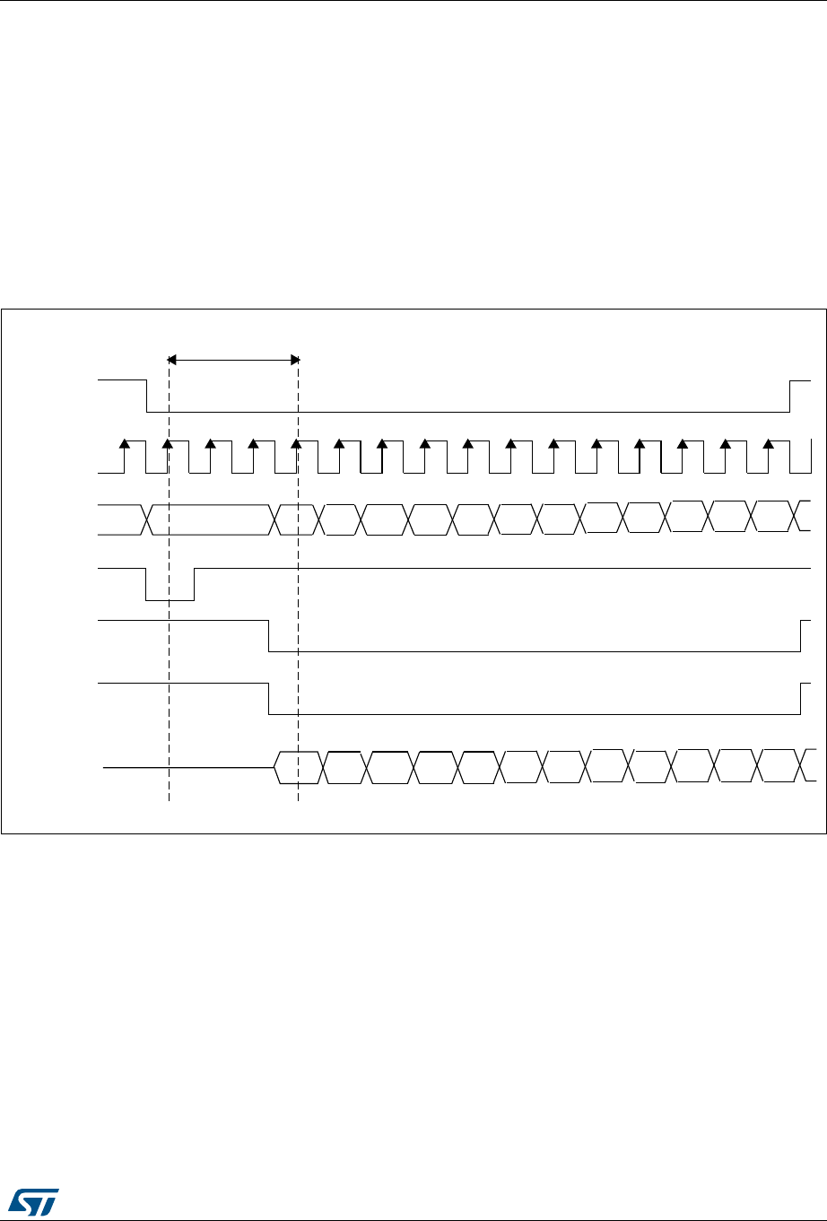
RM0090 Rev 18 1665/1749
RM0090 Flexible memory controller (FMC)
1682
commands) are issued using the timing parameters configured for SDRAM Bank 1 (TMRD,
TRAS and TXSR timings) in the FMC_SDTR1 register.
SDRAM controller write cycle
The SDRAM controller accepts single and burst write requests and translates them into
single memory accesses. In both cases, the SDRAM controller keeps track of the active row
for each bank to be able to perform consecutive write accesses to different banks (Multibank
ping-pong access).
Before performing any write access, the SDRAM bank write protection must be disabled by
clearing the WP bit in the FMC_SDCRx register.
Figure 478. Burst write SDRAM access waveforms
The SDRAM controller always checks the next access.
•If the next access is in the same row or in another active row, the write operation is
carried out,
•if the next access targets another row (not active), the SDRAM controller generates a
precharge command, activates the new row and initiates a write command.
MS30448V3
NRAS
A[12:0]
SDCLK
Row n Colc
SDNE
TRCD = 3
SDNWE
Cola Cold
Colb Cole Colf Cog Colh Coli Colj Colk Coll
NCAS
DATA[31:0] Dnc Dne
Dna Dnf Dng Dnh Dni Dnj Dnk Dnl
Dnb Dnd
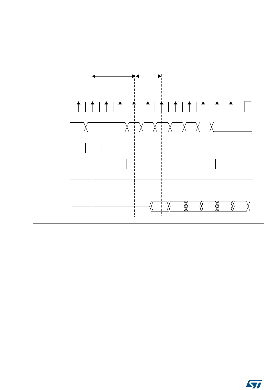
Flexible memory controller (FMC) RM0090
1666/1749 RM0090 Rev 18
SDRAM controller read cycle
The SDRAM controller accepts single and burst read requests and translates them into
single memory accesses. In both cases, the SDRAM controller keeps track of the active row
in each bank to be able to perform consecutive read accesses in different banks (Multibank
ping-pong access).
Figure 479. Burst read SDRAM access
The FMC SDRAM controller features a Cacheable read FIFO (6 lines x 32 bits). It is used to
store data read in advance during the CAS latency period and during the RPIPE delay. The
following the formula is applied:
The RBURST bit must be set in the FMC_SDCR1 register to anticipate the next read
access.
Example:
•CAS latency = 3, RPIPE delay = 0: 4 data (not committed) are stored in the FIFO.
•CAS latency = 3, RPIPE delay = 2: 5 data (not committed) are stored in the FIFO.
The read FIFO features a 14-bit address tag to each line to identify its content: 11 bits for the
column address, 2 bits to select the internal bank and the active row, and 1 bit to select the
SDRAM device
When the end of the row is reached in advance during an AHB burst read, the data read in
advance (not committed) are not stored in the read FIFO. For single read access, data are
correctly stored in the FIFO.
MS30449V3
NRAS
A[12:0]
SDCLK
Row n Colc
SDNE
TRCD = 3
NWE
Cola Cold
Colb Cole Colf
NCAS
DATA[31:0] Dnc DneDna Dnf
Dnb Dnd
CAS latency = 2
Number of anticipated data CAS latency 1 RPIPE delay()2⁄++=
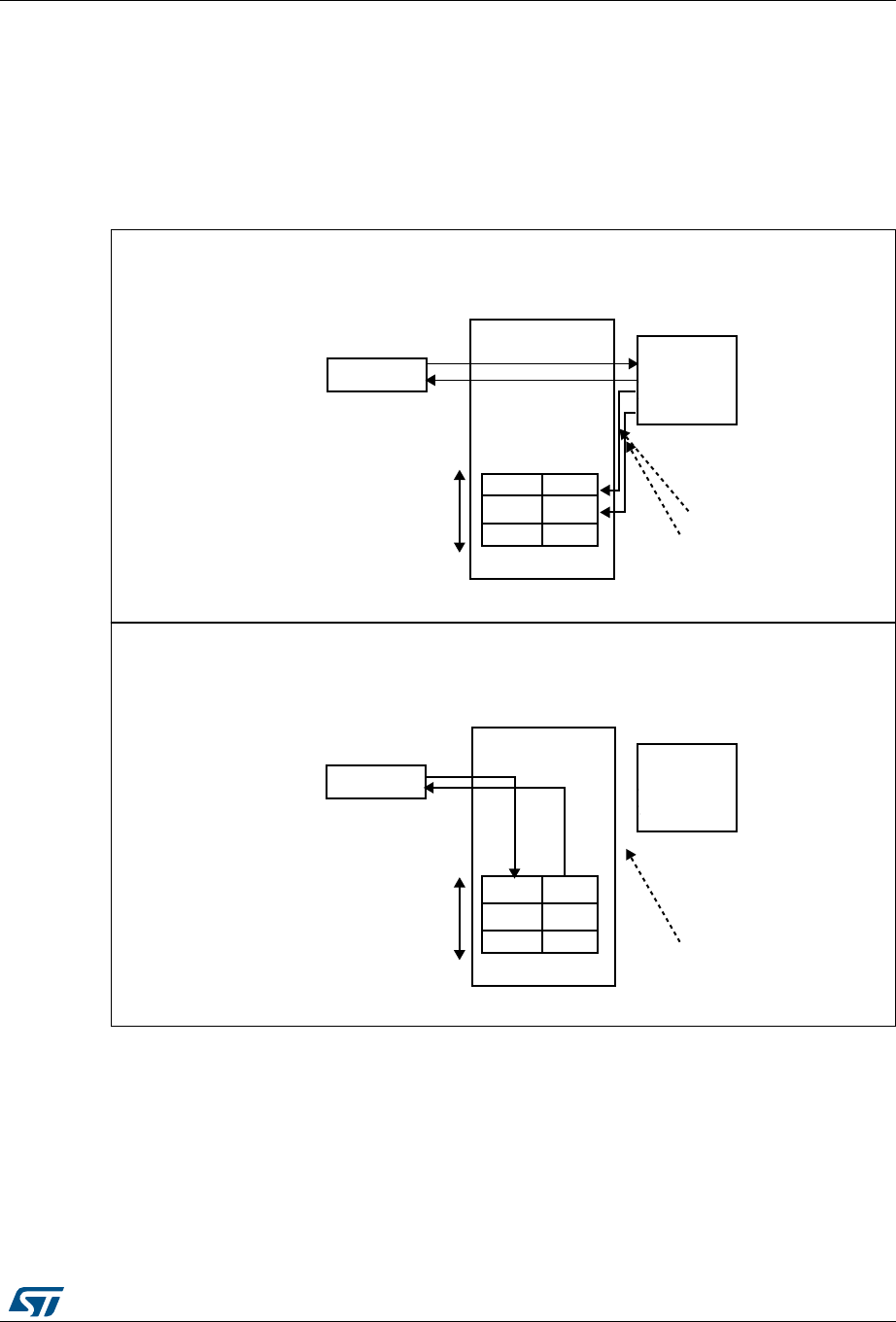
RM0090 Rev 18 1667/1749
RM0090 Flexible memory controller (FMC)
1682
Each time a read request occurs, the SDRAM controller checks:
•If the address matches one of the address tags, data are directly read from the FIFO
and the corresponding address tag/ line content is cleared and the remaining data in
the FIFO are compacted to avoid empty lines.
•Otherwise, a new read command is issued to the memory and the FIFO is updated with
new data. If the FIFO is full, the older data are lost.
Figure 480. Logic diagram of Read access with RBURST bit set (CAS=2, RPIPE=0)
During a write access or a Precharge command, the read FIFO is flushed and ready to be
filled with new data.
After the first read request, if the current access was not performed to a row boundary, the
SDRAM controller anticipates the next read access during the CAS latency period and the
RPIPE delay (if configured). This is done by incrementing the memory address. The
following condition must be met:
•RBURST control bit should be set to ‘1’ in the FMC_SDCR1 register.
MS30445V1
AHB Master
@0x04
@0x08
Data 2
Data 3
... ...
SDRAM
Device
(CAS = 2)
read request@0x00
Data 1
6 lines FIFO
Add. Tag read FIFO
Data stored in FIFO
in advance during
the CAS latency period
Address matches with
one of the address tags
FMC SDRAM Controller
2nd Read access : Requested data was previously stored in the FIFO
1st Read access: Requested data is not in the FIFO
AHB Master
@0x04
@0x08
Data 2
Data 3
... ...
SDRAM
Device
(CAS = 2)
read request@0x04
Data 2
6 lines FIFO
Data read from FIFO
FMC SDRAM Controller
Add. Tag read FIFO

Flexible memory controller (FMC) RM0090
1668/1749 RM0090 Rev 18
The address management depends on the next AHB request:
•Next AHB request is sequential (AHB Burst)
In this case, the SDRAM controller increments the address.
•Next AHB request is not sequential
– If the new read request targets the same row or another active row, the new
address is passed to the memory and the master is stalled for the CAS latency
period, waiting for the new data from memory.
– If the new read request does not target an active row, the SDRAM controller
generates a Precharge command, activates the new row, and initiates a read
command.
If the RURST is reset, the read FIFO is not used.
Row and bank boundary management
When a read or write access crosses a row boundary, if the next read or write access is
sequential and the current access was performed to a row boundary, the SDRAM controller
executes the following operations:
1. Precharge of the active row,
2. Activation of the new row
3. Start of a read/write command.
At a row boundary, the automatic activation of the next row is supported for all columns and
data bus width configurations.
If necessary, the SDRAM controller inserts additional clock cycles between the following
commands:
•Between Precharge and Active commands to match TRP parameter (only if the next
access is in a different row in the same bank),
•Between Active and Read commands to match the TRCD parameter.
These parameters are defined into the FMC_SDTRx register.
Refer to Figure 481 and Figure 482 for read and burst write access crossing a row
boundary.
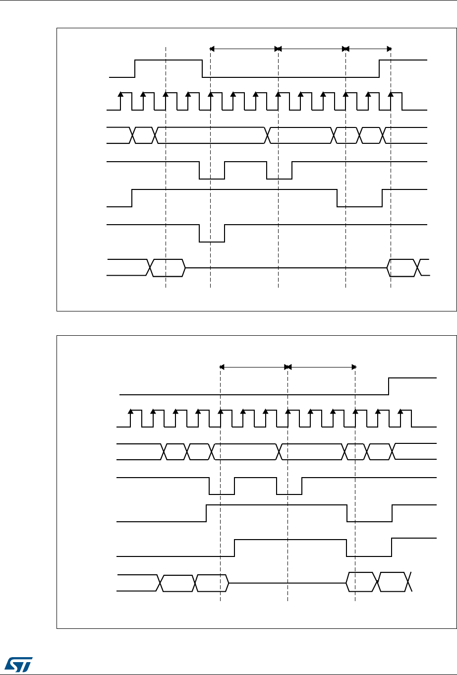
RM0090 Rev 18 1669/1749
RM0090 Flexible memory controller (FMC)
1682
Figure 481. Read access crossing row boundary
Figure 482. Write access crossing row boundary
MS30446V2
Data[31:0]
NCAS
NRA S
A[12:0]
SDCLK
Col a Col a Col bRow n +1
Dna Dn+1 a
SDNE
TRP = 3 CAS latency = 2
NW E
Precharge Activate Row Read Command
Row n
TRCD = 3
MS30447V2
Data[31:0]
NCAS
NRA S
A[12:0]
SDCLK
Cna ColaRow n+1
Dna Dn+1a
SDNE
TRP = 3
NW E
Precharge Activate Row Write command
Colb Colb
Dnb Dn+1b
TRCD = 3

Flexible memory controller (FMC) RM0090
1670/1749 RM0090 Rev 18
If the next access is sequential and the current access crosses a bank boundary, the
SDRAM controller activates the first row in the next bank and initiates a new read/write
command. Two cases are possible:
•If the current bank is not the last one, the active row in the new bank must be
precharged. At a bank boundary, the automatic activation of the next row is supported
for all rows/columns and data bus width configuration.
•For 13-bit row address, 11-bit column address, 4 internal banks and bus width 32-bit
SDRAM memories, if the current bank is the last one and the selected SDRAM device
is connected to Bank 1, the SDRAM controller continues to read/write from the second
SDRAM device (assuming it has been initialized):
a) The SDRAM controller activates the first row (after precharging the active row, if
there is already an active row in the first internal bank, and initiates a new
read/write command.
b) If the first row is already activated, the SDRAM controller just initiates a read/write
command.
Note: At bank boundary, if the current bank is the last one, the automatic activation of the next row
is supported only when addressing 13-bit rows, 11-bit columns, 4 internal banks and 32-bit
data bus SDRAM devices. Otherwise, the SDRAM address range is violated and an AHB
error is generated.
SDRAM controller refresh cycle
The Auto-refresh command is used to refresh the SDRAM device content. The SDRAM
controller periodically issues auto-refresh commands. An internal counter is loaded with the
COUNT value in the register FMC_SDRTR. This value defines the number of memory clock
cycles between the refresh cycles (refresh rate). When this counter reaches zero, an
internal pulse is generated.
If a memory access is ongoing, the auto-refresh request is delayed. However, if the memory
access and the auto-refresh requests are generated simultaneously, the auto-refresh
request takes precedence.
If the memory access occurs during an auto-refresh operation, the request is buffered and
processed when the auto-refresh is complete.
If a new auto-refresh request occurs while the previous one was not served, the RE
(Refresh Error) bit is set in the Status register. An Interrupt is generated if it has been
enabled (REIE = ‘1’).
If SDRAM lines are not in idle state (not all row are closed), the SDRAM controller generates
a PALL (Precharge ALL) command before the auto-refresh.
If the Auto-refresh command is generated by the FMC_SDCMR Command Mode register
(Mode bits = ‘011’), a PALL command (Mode bits =’ 010’) must be issued first.

RM0090 Rev 18 1671/1749
RM0090 Flexible memory controller (FMC)
1682
37.7.4 Low power modes
Two low power modes are available:
•Self-refresh mode
The auto-refresh cycles are performed by the SDRAM device itself to retain data
without external clocking.
•Power-down mode
The auto-refresh cycles are performed by the SDRAM controller.
Self-refresh mode
This mode is selected by setting the MODE bits to ‘101’ and by configuring the Target Bank
bits (CTB1 and/or CTB2) in the FMC_SDCMR register.
The SDRAM clock stops running after a TRAS delay and the internal refresh timer stops
counting only if one of the following conditions is met:
•A Self-refresh command is issued to both devices
•One of the devices is not activated (SDRAM bank is not initialized).
Before entering Self-Refresh mode, the SDRAM controller automatically issues a PALL
command.
If the Write data FIFO is not empty, all data are sent to the memory before activating the
Self-refresh mode and the BUSY status flag remains set.
In Self-refresh mode, all SDRAM device inputs become don’t care except for SDCKE which
remains low.
The SDRAM device must remain in Self-refresh mode for a minimum period of time of
TRAS and can remain in Self-refresh mode for an indefinite period beyond that. To
guarantee this minimum period, the BUSY status flag remains high after the Self-refresh
activation during a TRAS delay.
As soon as an SDRAM device is selected, the SDRAM controller generates a sequence of
commands to exit from Self-refresh mode. After the memory access, the selected device
remains in Normal mode.
To exit from Self-refresh, the MODE bits must be set to ‘000’ (Normal mode) and the Target
Bank bits (CTB1 and/or CTB2) must be configured in the FMC_SDCMR register.
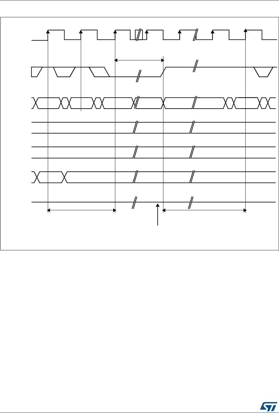
Flexible memory controller (FMC) RM0090
1672/1749 RM0090 Rev 18
Figure 483. Self-refresh mode
Power-down mode
This mode is selected by setting the MODE bits to ‘110’ and by configuring the Target Bank
bits (CTB1 and/or CTB2) in the FMC_SDCMR register.
PRECHARGE
SDCLK
SDCKE
T0 T1 T2 Tn+1 T0+1 T0+2
tRAS(min)
COMMAND NOP AUTO
REFRESH NOP or COMMAND
INHERIT
AUTO
REFRESH
DOM/
DOML/DOMU
A0- A9
A11, A12
A10 ALL
BANKS
Data[31:0] Hi-Z
tRP
Precharge all
active banks Enter Self-refresh mode
CLK stable prior to existing
Self-refresh mode
Exit Self-refresh mode
(restart refresh timebase)
tXSR
MS30450V1
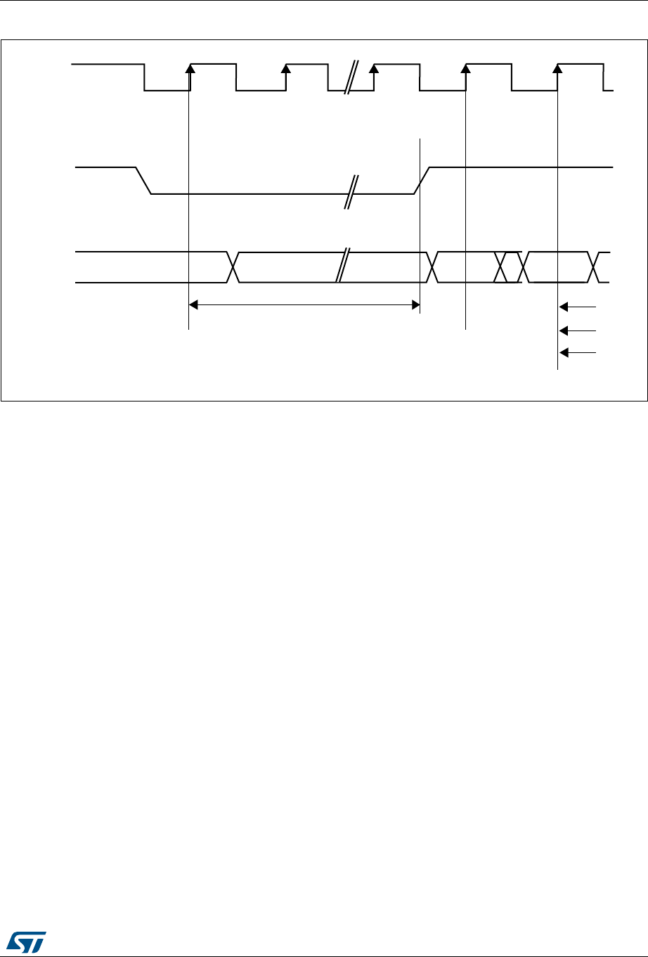
RM0090 Rev 18 1673/1749
RM0090 Flexible memory controller (FMC)
1682
Figure 484. Power-down mode
If the Write data FIFO is not empty, all data are sent to the memory before activating the
Power-down mode.
As soon as an SDRAM device is selected, the SDRAM controller exits from the Power-down
mode. After the memory access, the selected SDRAM device remains in Normal mode.
During Power-down mode, all SDRAM device input and output buffers are deactivated
except for the SDCKE which remains low.
The SDRAM device cannot remain in Power-down mode longer than the refresh period and
cannot perform the Auto-refresh cycles by itself. Therefore, the SDRAM controller carries
out the refresh operation by executing the operations below:
1. Exit from Power-down mode and drive the SDCKE high
2. Generate the PALL command only if a row was active during Power-down mode
3. Generate the auto-refresh command
4. Drive SDCKE low again to return to Power-down mode.
To exit from Power-down mode, the MODE bits must be set to ‘000’ (Normal mode) and the
Target Bank bits (CTB1 and/or CTB2) must be configured in the FMC_SDCMR register.
SDCLK
SDCKE
COMMAND NOP NOP ACTIVE
Input buffers gated offAll banks idle
Enter Power-down Exit Power-down
tRCD
tRAS
tRC
MS30451V1

Flexible memory controller (FMC) RM0090
1674/1749 RM0090 Rev 18
37.7.5 SDRAM controller registers
SDRAM Control registers 1,2 (FMC_SDCR1,2)
Address offset: 0x140+ 4* (x – 1), x = 1,2
Reset value: 0x0000 02D0
This register contains the control parameters for each SDRAM memory bank
313029282726252423222120191817161514131211109876543210
Reserved
RPIPE[1:0]
RBURST.
SDCLK[1:0]
WP
CAS[1:0]
NB
MWID[1:0]
NR[1:0]
NC[1:0]
rw rw rw rw rw rw rw rw rw rw rw rw rw rw rw
Bits 31:15 Reserved, must be kept at reset value
Bits 14:13 RPIPE[1:0]: Read pipe
These bits define the delay, in HCLK clock cycles, for reading data after CAS latency.
00: No HCLK clock cycle delay
01: One HCLK clock cycle delay
10: Two HCLK clock cycle delay
11: reserved, do not use
Note: The corresponding bits in the FMC_SDCR2 register are read only.
Bit 12 RBURST: Burst read
This bit enables burst read mode. The SDRAM controller anticipates the next read commands
during the CAS latency and stores data in the Read FIFO.
0: single read requests are not managed as bursts
1: single read requests are always managed as bursts
Note: The corresponding bit in the FMC_SDCR2 register is don’t care.
Bits 11:10 SDCLK[1:0]: SDRAM clock configuration
These bits define the SDRAM clock period for both SDRAM banks and allow disabling the clock
before changing the frequency. In this case the SDRAM must be re-initialized.
00: SDCLK clock disabled
01: Reserved
10: SDCLK period = 2 x HCLK periods
11: SDCLK period = 3 x HCLK periods
Note: The corresponding bits in the FMC_SDCR2 register are read only.
Bit 9 WP: Write protection
This bit enables write mode access to the SDRAM bank.
0: Write accesses allowed
1: Write accesses ignored
Bits 8:7 CAS[1:0]: CAS Latency
This bits sets the SDRAM CAS latency in number of memory clock cycles
00: reserved, do not use.
01: 1 cycle
10: 2 cycles
11: 3 cycles

RM0090 Rev 18 1675/1749
RM0090 Flexible memory controller (FMC)
1682
Note: Before modifying the RBURST or RPIPE settings or disabling the SDCLK clock, the user
must first send a PALL command to make sure ongoing operations are complete.
SDRAM Timing registers 1,2 (FMC_SDTR1,2)
Address offset: 0x148 + 4 * (x – 1), x = 1,2
Reset value: 0x0FFF FFFF
This register contains the timing parameters of each SDRAM bank
Bit 6 NB: Number of internal banks
This bit sets the number of internal banks.
0: Two internal Banks
1: Four internal Banks
Bits 5:4 MWID[1:0]: Memory data bus width.
These bits define the memory device width.
00: 8 bits
01: 16 bits
10: 32 bits
11: reserved, do not use.
Bits 3:2 NR[1:0]: Number of row address bits
These bits define the number of bits of a row address.
00: 11 bit
01: 12 bits
10: 13 bits
11: reserved, do not use.
Bits 1:0 NC[1:0]: Number of column address bits
These bits define the number of bits of a column address.
00: 8 bits
01: 9 bits
10: 10 bits
11: 11 bits.
313029282726252423222120191817161514131211109876543210
Reserved TRCD[3:0] TRP[3:0 TWR[3:0 TRC[3:0 TRAS[3:0 TXSR[3:0 TMRD[3:0
rw rw rw rw rw rw rw rw rw rw rw rw rw rw rw rw rw rw rw rw rw rw rw rw rw rw rw rw rw rw rw rw
Bits 31:28 Reserved, must be kept at reset value
Bits 27:24 TRCD[3:0]: Row to column delay
These bits define the delay between the Activate command and a Read/Write command in number of
memory clock cycles.
0000: 1 cycle.
0001: 2 cycles
....
1111: 16 cycles

Flexible memory controller (FMC) RM0090
1676/1749 RM0090 Rev 18
Bits 23:20 TRP[3:0]: Row precharge delay
These bits define the delay between a Precharge command and another command in number of
memory clock cycles. The TRP timing is only configured in the FMC_SDTR1 register. If two SDRAM
devices are used, the TRP must be programmed with the timing of the slowest device.
0000: 1 cycle
0001: 2 cycles
....
1111: 16 cycles
Note: The corresponding bits in the FMC_SDTR2 register are don’t care.
Bits 19:16 TWR[3:0]: Recovery delay
These bits define the delay between a Write and a Precharge command in number of memory clock
cycles.
0000: 1 cycle
0001: 2 cycles
....
1111: 16 cycles
Note: TWR must be programmed to match the write recovery time (tWR) defined in the SDRAM
datasheet, and to guarantee that:
TWR ≥ TRAS - TRCD and TWR ≥TRC - TRCD - TRP
Example: TRAS= 4 cycles, TRCD= 2 cycles. So, TWR >= 2 cycles. TWR must be
programmed to 0x1.
If two SDRAM devices are used, the FMC_SDTR1 and FMC_SDTR2 must be programmed
with the same TWR timing corresponding to the slowest SDRAM device.
Bits 15:12 TRC[3:0]: Row cycle delay
These bits define the delay between the Refresh command and the Activate command, as well as d
the delay between two consecutive Refresh commands. It is expressed in number of memory clock
cycles. The TRC timing is only configured in the FMC_SDTR1 register. If two SDRAM devices are
used, the TRC must be programmed with the timings of the slowest device.
0000: 1 cycle
0001: 2 cycles
....
1111: 16 cycles
Note: TRC must match the TRC and TRFC (Auto Refresh period) timings defined in the SDRAM
device datasheet.
Note: The corresponding bits in the FMC_SDTR2 register are don’t care.
Bits 11:8 TRAS[3:0]: Self refresh time
These bits define the minimum Self-refresh period in number of memory clock cycles.
0000: 1 cycle
0001: 2 cycles
....
1111: 16 cycles
Bits 7:4 TXSR[3:0]: Exit Self-refresh delay
These bits define the delay from releasing the Self-refresh command to issuing the Activate
command in number of memory clock cycles.
0000: 1 cycle
0001: 2 cycles
....
1111: 16 cycles
RM0090 Rev 18 1677/1749
RM0090 Flexible memory controller (FMC)
1682
Note: If two SDRAM devices are connected, all the accesses performed simultaneously to both
devices by the Command Mode register (Load Mode Register and Self-refresh commands)
are issued using the timing parameters configured for Bank 1 (TMRD, TRAS and TXSR
timings) in the FMC_SDTR1 register.
The TRP and TRC timings are only configured in the FMC_SDTR1 register. If two SDRAM
devices are used, the TRP and TRC timings must be programmed with the timings of the
slowest device.
SDRAM Command Mode register (FMC_SDCMR)
Address offset: 0x150
Reset value: 0x0000 0000
This register contains the command issued when the SDRAM device is accessed. This
register is used to initialize the SDRAM device, and to activate the Self-refresh and the
Power-down modes. As soon as the MODE field is written, the command will be issued only
to one or to both SDRAM banks according to CTB1 and CTB2 command bits. This register
is the same for both SDRAM banks.
Bits 3:0 TMRD[3:0]: Load Mode Register to Active
These bits define the delay between a Load Mode Register command and an Active or Refresh
command in number of memory clock cycles.
0000: 1 cycle
0001: 2 cycles
....
1111: 16 cycles
313029282726252423222120191817161514131211109876543210
Reserved
MRD[11:0]
NRFS[3:0]
CTB1
CTB2
MODE[2:0]
rwrwrwrwrwrwrwrwrwrwrwrwrwrwrwrwrwwwwww
Bits 31:22 Reserved, must be kept at reset value
Bits 21:9 MRD[11:0]: Mode Register definition
This 13-bit field defines the SDRAM Mode Register content. The Mode Register is programmed using
the Load Mode Register command.
Bits 8:5 NRFS[3:0]: Number of Auto-refresh
These bits define the number of consecutive Auto-refresh commands issued when MODE = ‘011’.
0000: 1 Auto-refresh cycle
0001: 2 Auto-refresh cycles
....
1110: 15 Auto-refresh cycles
1111: Reserved
Bit 4 CTB1: Command Target Bank 1
This bit indicates whether the command will be issued to SDRAM Bank 1 or not.
0: Command not issued to SDRAM Bank 1
1: Command issued to SDRAM Bank 1

Flexible memory controller (FMC) RM0090
1678/1749 RM0090 Rev 18
SDRAM Refresh Timer register (FMC_SDRTR)
Address offset:0x154
Reset value: 0x0000 0000
This register sets the refresh rate in number of SDCLK clock cycles between the refresh
cycles by configuring the Refresh Timer Count value.
Example
where 64 ms is the SDRAM refresh period.
The refresh rate must be increased by 20 SDRAM clock cycles (as in the above example) to
obtain a safe margin if an internal refresh request occurs when a read request has been
accepted. It corresponds to a COUNT value of ‘0000111000000’ (448).
This 13-bit field is loaded into a timer which is decremented using the SDRAM clock. This
timer generates a refresh pulse when zero is reached. The COUNT value must be set at
least to 41 SDRAM clock cycles.
As soon as the FMC_SDRTR register is programmed, the timer starts counting. If the value
programmed in the register is ’0’, no refresh is carried out. This register must not be
reprogrammed after the initialization procedure to avoid modifying the refresh rate.
Each time a refresh pulse is generated, this 13-bit COUNT field is reloaded into the counter.
Bit 3 CTB2: Command Target Bank 2
This bit indicates whether the command will be issued to SDRAM Bank 2 or not.
0: Command not issued to SDRAM Bank 2
1: Command issued to SDRAM Bank 2
Bits 2:0 MODE[2:0]: Command mode
These bits define the command issued to the SDRAM device.
000: Normal Mode
001: Clock Configuration Enable
010: PALL (“All Bank Precharge”) command
011: Auto-refresh command
100: Load Mode Register
101: Self-refresh command
110: Power-down command
111: Reserved
Note: When a command is issued, at least one Command Target Bank bit ( CBT1 or CBT2) must be
set. If both banks are used, the commands must be issued to the two banks at the same time
by setting the CBT1 and CBT2 bits.
Refresh rate SDRAM refresh rate SDRAM clock frequency×()20–=
SDRAM refresh rate SDRAM refresh period Number of rows⁄=
SDRAM refresh rate 64 ms 8196rows()⁄7.81μs==
7.81μs60MHz×468.6=

RM0090 Rev 18 1679/1749
RM0090 Flexible memory controller (FMC)
1682
If a memory access is in progress, the Auto-refresh request is delayed. However, if the
memory access and Auto-refresh requests are generated simultaneously, the Auto-refresh
takes precedence. If the memory access occurs during a refresh operation, the request is
buffered to be processed when the refresh is complete.
This register common to SDRAM bank 1 and bank 2.
.
Note: The programmed COUNT value must not be equal to the sum of the following timings:
TWR+TRP+TRC+TRCD+4 memory clock cycles .
SDRAM Status register (FMC_SDSR)
Address offset: 0x158
Reset value: 0x0000 0000
3130292827262524232221201918171615 14 13121110987654321 0
Reserved REIE COUNT[12:0] CRE
rw rw rw rw rw rw rw rw rw rw rw rw rw rw w
Bits 31: 15 Reserved, must be kept at reset value
Bit 14 REIE: RES Interrupt Enable
0: Interrupt is disabled
1: An Interrupt is generated if RE = 1
Bits 13:1 COUNT[12:0]: Refresh Timer Count
This 13-bit field defines the refresh rate of the SDRAM device. It is expressed in number of memory
clock cycles. It must be set at least to 41 SDRAM clock cycles (0x29).
COUNT = (SDRAM refresh rate x SDRAM clock frequency) - 20
SDRAM refresh rate = SDRAM refresh period / Number of rows
Bit 0 CRE: Clear Refresh error flag
This bit is used to clear the Refresh Error Flag (RE) in the Status Register.
0: no effect
1: Refresh Error flag is cleared
31 30 29 28 27 26 25 24 23 22 21 20 19 18 17 16 15 14 13 12 11 10 9 8 7 6 5 4 3 2 1 0
Reserved
BUSY
MODES2[1:0]
MODES1[1:0]
RE
rrrrrr
Bits 31:5 Reserved, must be kept at reset value
Bit 5 BUSY: Busy status
This bit defines the status of the SDRAM controller after a Command Mode request
0: SDRAM Controller is ready to accept a new request
1; SDRAM Controller is not ready to accept a new request
Bits 4:3 MODES2[1:0]: Status Mode for Bank 2
This bit defines the Status Mode of SDRAM Bank 2.
00: Normal Mode
01: Self-refresh mode
10: Power-down mode

Flexible memory controller (FMC) RM0090
1680/1749 RM0090 Rev 18
37.8 FMC register map
The following table summarizes the FMC registers.
Bits 2:1 MODES1[1:0]: Status Mode for Bank 1
This bit defines the Status Mode of SDRAM Bank 1.
00: Normal Mode
01: Self-refresh mode
10: Power-down mode
Bit 0 RE: Refresh error flag
0: No refresh error has been detected
1: A refresh error has been detected
An interrupt is generated if REIE = 1 and RE = 1
Table 297. FMC register map
Offset Register
31
30
29
28
27
26
25
24
23
22
21
20
19
18
17
16
15
14
13
12
11
10
9
8
7
6
5
4
3
2
1
0
0x00 FMC_BCR1 Reserved
CCLKEN
CBURSTRW
CPSIZE[2:0]
ASYNCWAIT
EXTMOD
WAITEN
WREN
WAITCFG
WRAPMOD
WAITPOL
BURSTEN
Reserved
FACCEN
MWID[1:0]
MTYP[1:0]
MUXEN
MBKEN
0x08 FMC_BCR2 Reserved
CBURSTRW
CPSIZE[2:0]
ASYNCWAIT
EXTMOD
WAITEN
WREN
WAITCFG
WRAPMOD
WAITPOL
BURSTEN
Reserved
FACCEN
MWID[1:0]
MTYP[1:0]
MUXEN
MBKEN
0x10 FMC_BCR3 Reserved
CBURSTRW
CPSIZE[2:0]
ASYNCWAIT
EXTMOD
WAITEN
WREN
WAITCFG
WRAPMOD
WAITPOL
BURSTEN
Reserved
FACCEN
MWID[1:0]
MTYP[1:0]
MUXEN
MBKEN
0x18 FMC_BCR4 Reserved
CBURSTRW
CPSIZE[2:0]
ASYNCWAIT
EXTMOD
WAITEN
WREN
WAITCFG
WRAPMOD
WAITPOL
BURSTEN
Reserved
FACCEN
MWID[1:0]
MTYP[1:0]
MUXEN
MBKEN
0x04 FMC_BTR1 Res.
ACCMOD[1:0
DATLAT[3:0] CLKDIV[3:0] BUSTURN[3:0] DATAST[7:0] ADDHLD[3:0] ADDSET[3:0]
0x0C FMC_BTR2 Res.
ACCMOD[1:0
DATLAT[3:0] CLKDIV[3:0] BUSTURN[3:0] DATAST[7:0] ADDHLD[3:0] ADDSET[3:0]
0x14 FMC_BTR3 Res.
ACCMOD[1:0
DATLAT[3:0] CLKDIV[3:0] BUSTURN[3:0] DATAST[7:0] ADDHLD[3:0] ADDSET[3:0]
0x1C FMC_BTR4 Res.
ACCMOD[1:0
DATLAT[3:0] CLKDIV[3:0] BUSTURN[3:0] DATAST[7:0] ADDHLD[3:0] ADDSET[3:0]
0x104 FMC_BWTR1 Res.
ACCMOD[1:0
Res. BUSTURN[3:0] DATAST[7:0] ADDHLD[3:0] ADDSET[3:0]
RM0090 Rev 18 1681/1749
RM0090 Flexible memory controller (FMC)
1682
0x10C FMC_BWTR2 Res.
ACCMOD[1:0
Res. BUSTURN[3:0] DATAST[7:0] ADDHLD[3:0] ADDSET[3:0]
0x104 FMC_BWTR3 Res.
ACCMOD[1:0
Res. BUSTURN[3:0] DATAST[7:0] ADDHLD[3:0] ADDSET[3:0]
0x10C FMC_BWTR4 Res.
ACCMOD[1:0
Res. BUSTURN[3:0] DATAST[7:0] ADDHLD[3:0] ADDSET[3:0]
0x60 FMC_PCR2 Reserved
ECCPS[2:0]
TAR[3:0]
TCLR[3:0]
Res.
ECCEN
PWID[1:0]
PTYP
PBKEN
PWAITEN
Reserved
0x80 FMC_PCR3 Reserved
ECCPS[2:0]
TAR[3:0]
TCLR[3:0]
Res.
ECCEN
PWID[1:0]
PTYP
PBKEN
PWAITEN
Reserved
0xA0 FMC_PCR4 Reserved
ECCPS[2:0]
TAR[3:0]
TCLR[3:0]
Res.
ECCEN
PWID[1:0]
PTYP
PBKEN
PWAITEN
Reserved
0x64 FMC_SR2 Reserved
FEMPT
IFEN
ILEN
IREN
IFS
ILS
IRS
0x84 FMC_SR3 Reserved
FEMPT
IFEN
ILEN
IREN
IFS
ILS
IRS
0xA4 FMC_SR4 Reserved
FEMPT
IFEN
ILEN
IREN
IFS
ILS
IRS
0x68 FMC_PMEM2 MEMHIZ[7:0] MEMHOLD[7:0] MEMWAIT[7:0] MEMSET[7:0]
0x88 FMC_PMEM3 MEMHIZ[7:0] MEMHOLD[7:0] MEMWAIT[7:0] MEMSET[7:0]
0xA8 FMC_PMEM4 MEMHIZ[7:0] MEMHOLD[7:0] MEMWAIT[7:0] MEMSET[7:0]
0x6C FMC_PATT2 ATTHIZ[7:0] ATTHOLD[7:0] ATTWAIT[7:0] ATTSET[7:0]
0x8C FMC_PATT3 ATTHIZ[7:0] ATTHOLD[7:0] ATTWAIT[7:0] ATTSET[7:0]
0xAC FMC_PATT4 ATTHIZ[7:0] ATTHOLD[7:0] ATTWAIT[7:0] ATTSET[7:0]
0xB0 FMC_PIO4 IOHIZ[7:0] IOHOLD[7:0] IOWAIT[7:0] IOSET[7:0]
0x74 FMC_ECCR2 ECC[31:0]
0x94 FMC_ECCR3 ECC[31:0]
0x140 FMC_SDCR_1 Reserved
RPIPE[1:0]
RBURST
CLK[1:0]
WP
CAS[1:0]
NB
MWID[1:0]
NR[1:0]
NC[1:0]
0x144 FMC_SDCR_2 Reserved
CLK[1:0]
WP
CAS[1:0]
NB
MWID[1:0]
NR[1:0]
NC[1:0]
0x148 FMC_SDTR1 Reserved TRCD[3:0] TRP[3:0] TWR[3:0] TRC[3:0] TRAS[3:0] TXSR[3:0] TMRD[3:0]
0x14C FMC_SDTR2 Reserved TRCD[3:0] TRP[3:0] TWR[3:0] TRC[3:0] TRAS[3:0] TXSR[3:0] TMRD[3:0]
0x150 FMC_SDCMR Reserved
MRD[12:0]
NRFS[3:0]
CTB1
CTB2
MODE[2:0]
Table 297. FMC register map (continued)
Offset Register
31
30
29
28
27
26
25
24
23
22
21
20
19
18
17
16
15
14
13
12
11
10
9
8
7
6
5
4
3
2
1
0

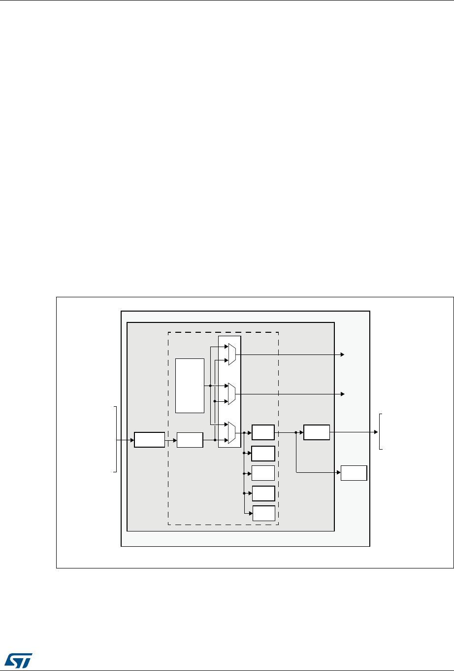
RM0090 Rev 18 1683/1749
RM0090 Debug support (DBG)
1713
38 Debug support (DBG)
This section applies to the whole STM32F4xx family, unless otherwise specified.
38.1 Overview
The STM32F4xx are built around a Cortex®-M4 with FPU core which contains hardware
extensions for advanced debugging features. The debug extensions allow the core to be
stopped either on a given instruction fetch (breakpoint) or data access (watchpoint). When
stopped, the core’s internal state and the system’s external state may be examined. Once
examination is complete, the core and the system may be restored and program execution
resumed.
The debug features are used by the debugger host when connecting to and debugging the
STM32F4xx MCUs.
Two interfaces for debug are available:
•Serial wire
•JTAG debug port
Figure 485. Block diagram of STM32 MCU and Cortex®-M4 with FPU-level debug
support
Note: The debug features embedded in the Cortex®-M4 with FPU core are a subset of the Arm®
CoreSight Design Kit.
estricted Di
Cortex-M4
core
SWJ-DP AHB-AP
Bridge
NVIC
DWT
FPB
ITM
TPIU
DCode
interface
System
interface
Internal private
peripheral bus (PPB)
External private
peripheral bus (PPB)
Bus matrix
Data
Trac e po r t
DBGMCU
STM32F4xx debug support
Cortex-M4 debug s uppo rt
JTMS/
JTDI
JTDO/
NJTRST
JTCK/
SWDIO
SWCLK
TRACESWO
TRACESWO
TRACECK
TRACED[3:0]
MS19908V3

Debug support (DBG) RM0090
1684/1749 RM0090 Rev 18
The Arm® Cortex®-M4 with FPU core provides integrated on-chip debug support. It is
comprised of:
•SWJ-DP: Serial wire / JTAG debug port
•AHP-AP: AHB access port
•ITM: Instrumentation trace macrocell
•FPB: Flash patch breakpoint
•DWT: Data watchpoint trigger
•TPUI: Trace port unit interface (available on larger packages, where the corresponding
pins are mapped)
•ETM: Embedded Trace Macrocell (available on larger packages, where the
corresponding pins are mapped)
It also includes debug features dedicated to the STM32F4xx:
•Flexible debug pinout assignment
•MCU debug box (support for low-power modes, control over peripheral clocks, etc.)
Note: For further information on debug functionality supported by the Arm® Cortex®-M4 with FPU
core, refer to the Cortex®-M4 with FPU -r0p1 Technical Reference Manual and to the
CoreSight Design Kit-r0p1 TRM (see Section 38.2).
38.2 Reference Arm® documentation
•Cortex®-M4 with FPU r0p1 Technical Reference Manual (TRM)
(see Related documents on page 1)
•Arm® Debug Interface V5
•Arm® CoreSight Design Kit revision r0p1 Technical Reference Manual
38.3 SWJ debug port (serial wire and JTAG)
The core of the STM32F4xx integrates the Serial Wire / JTAG Debug Port (SWJ-DP). It is an
Arm® standard CoreSight debug port that combines a JTAG-DP (5-pin) interface and a SW-
DP (2-pin) interface.
•The JTAG Debug Port (JTAG-DP) provides a 5-pin standard JTAG interface to the
AHP-AP port.
•The Serial Wire Debug Port (SW-DP) provides a 2-pin (clock + data) interface to the
AHP-AP port.
In the SWJ-DP, the two JTAG pins of the SW-DP are multiplexed with some of the five JTAG
pins of the JTAG-DP.
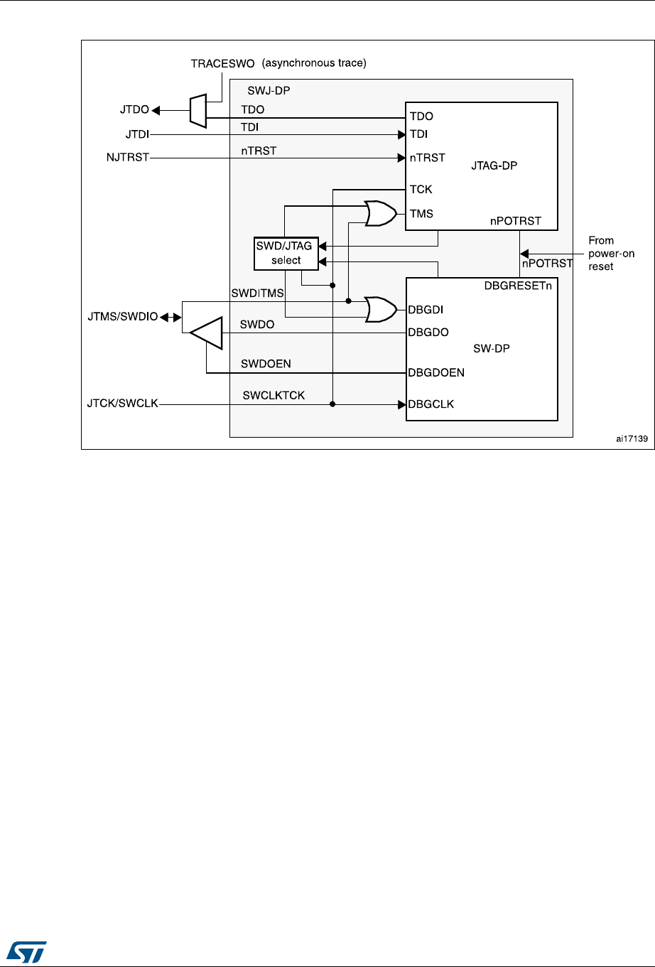
RM0090 Rev 18 1685/1749
RM0090 Debug support (DBG)
1713
Figure 486. SWJ debug port
Figure 486 shows that the asynchronous TRACE output (TRACESWO) is multiplexed with
TDO. This means that the asynchronous trace can only be used with SW-DP, not JTAG-DP.
38.3.1 Mechanism to select the JTAG-DP or the SW-DP
By default, the JTAG-Debug Port is active.
If the debugger host wants to switch to the SW-DP, it must provide a dedicated JTAG
sequence on TMS/TCK (respectively mapped to SWDIO and SWCLK) which disables the
JTAG-DP and enables the SW-DP. This way it is possible to activate the SWDP using only
the SWCLK and SWDIO pins.
This sequence is:
1. Send more than 50 TCK cycles with TMS (SWDIO) =1
2. Send the 16-bit sequence on TMS (SWDIO) = 0111100111100111 (MSB transmitted
first)
3. Send more than 50 TCK cycles with TMS (SWDIO) =1
38.4 Pinout and debug port pins
The STM32F4xx MCUs are available in various packages with different numbers of
available pins. As a result, some functionality (ETM) related to pin availability may differ
between packages.
Debug support (DBG) RM0090
1686/1749 RM0090 Rev 18
38.4.1 SWJ debug port pins
Five pins are used as outputs from the STM32F4xx for the SWJ-DP as alternate functions of
general-purpose I/Os. These pins are available on all packages.
38.4.2 Flexible SWJ-DP pin assignment
After RESET (SYSRESETn or PORESETn), all five pins used for the SWJ-DP are assigned
as dedicated pins immediately usable by the debugger host (note that the trace outputs are
not assigned except if explicitly programmed by the debugger host).
However, the STM32F4xx MCUs offers the possibility of disabling some or all of the SWJ-
DP ports and so, of releasing the associated pins for general-purpose IO (GPIO) usage. For
more details on how to disable SWJ-DP port pins, please refer to Section 8.3.2: I/O pin
multiplexer and mapping.
Note: When the APB bridge write buffer is full, it takes one extra APB cycle when writing the
GPIO_AFR register. This is because the deactivation of the JTAGSW pins is done in two
cycles to guarantee a clean level on the nTRST and TCK input signals of the core.
•Cycle 1: the JTAGSW input signals to the core are tied to 1 or 0 (to 1 for nTRST, TDI
and TMS, to 0 for TCK)
•Cycle 2: the GPIO controller takes the control signals of the SWJTAG IO pins (like
controls of direction, pull-up/down, Schmitt trigger activation, etc.).
Table 298. SWJ debug port pins
SWJ-DP pin name
JTAG debug port SW debug port Pin
assignment
Type Description Type Debug assignment
JTMS/SWDIO I JTAG Test Mode Selection IO Serial Wire Data Input/Output PA13
JTCK/SWCLK I JTAG Test Clock I Serial Wire Clock PA14
JTDI I JTAG Test Data Input - - PA15
JTDO/TRACESWO O JTAG Test Data Output - TRACESWO if async trace is
enabled PB3
NJTRST I JTAG Test nReset - - PB4
Table 299. Flexible SWJ-DP pin assignment
Available debug ports
SWJ IO pin assigned
PA13 /
JTMS /
SWDIO
PA14 /
JTCK /
SWCLK
PA15 /
JTDI
PB3 /
JTDO
PB4 /
NJTRST
Full SWJ (JTAG-DP + SW-DP) - Reset State X X X X X
Full SWJ (JTAG-DP + SW-DP) but without NJTRST X X X X
JTAG-DP Disabled and SW-DP Enabled X X
JTAG-DP Disabled and SW-DP Disabled Released

RM0090 Rev 18 1687/1749
RM0090 Debug support (DBG)
1713
38.4.3 Internal pull-up and pull-down on JTAG pins
It is necessary to ensure that the JTAG input pins are not floating since they are directly
connected to flip-flops to control the debug mode features. Special care must be taken with
the SWCLK/TCK pin which is directly connected to the clock of some of these flip-flops.
To avoid any uncontrolled IO levels, the device embeds internal pull-ups and pull-downs on
the JTAG input pins:
•NJTRST: Internal pull-up
•JTDI: Internal pull-up
•JTMS/SWDIO: Internal pull-up
•TCK/SWCLK: Internal pull-down
Once a JTAG IO is released by the user software, the GPIO controller takes control again.
The reset states of the GPIO control registers put the I/Os in the equivalent state:
•NJTRST: AF input pull-up
•JTDI: AF input pull-up
•JTMS/SWDIO: AF input pull-up
•JTCK/SWCLK: AF input pull-down
•JTDO: AF output floating
The software can then use these I/Os as standard GPIOs.
Note: The JTAG IEEE standard recommends to add pull-ups on TDI, TMS and nTRST but there is
no special recommendation for TCK. However, for JTCK, the device needs an integrated
pull-down.
Having embedded pull-ups and pull-downs removes the need to add external resistors.

Debug support (DBG) RM0090
1688/1749 RM0090 Rev 18
38.4.4 Using serial wire and releasing the unused debug pins as GPIOs
To use the serial wire DP to release some GPIOs, the user software must change the GPIO
(PA15, PB3 and PB4) configuration mode in the GPIO_MODER register. This releases
PA15, PB3 and PB4 which now become available as GPIOs.
When debugging, the host performs the following actions:
•Under system reset, all SWJ pins are assigned (JTAG-DP + SW-DP).
•Under system reset, the debugger host sends the JTAG sequence to switch from the
JTAG-DP to the SW-DP.
•Still under system reset, the debugger sets a breakpoint on vector reset.
•The system reset is released and the Core halts.
•All the debug communications from this point are done using the SW-DP. The other
JTAG pins can then be reassigned as GPIOs by the user software.
Note: For user software designs, note that:
To release the debug pins, remember that they will be first configured either in input-pull-up
(nTRST, TMS, TDI) or pull-down (TCK) or output tristate (TDO) for a certain duration after
reset until the instant when the user software releases the pins.
When debug pins (JTAG or SW or TRACE) are mapped, changing the corresponding IO pin
configuration in the IOPORT controller has no effect.
38.5 STM32F4xx JTAG TAP connection
The STM32F4xx MCUs integrate two serially connected JTAG TAPs, the boundary scan
TAP (IR is 5-bit wide) and the Cortex®-M4 with FPU TAP (IR is 4-bit wide).
To access the TAP of the Cortex®-M4 with FPU for debug purposes:
1. First, it is necessary to shift the BYPASS instruction of the boundary scan TAP.
2. Then, for each IR shift, the scan chain contains 9 bits (=5+4) and the unused TAP
instruction must be shifted in using the BYPASS instruction.
3. For each data shift, the unused TAP, which is in BYPASS mode, adds 1 extra data bit in
the data scan chain.
Note: Important: Once Serial-Wire is selected using the dedicated Arm® JTAG sequence, the
boundary scan TAP is automatically disabled (JTMS forced high).
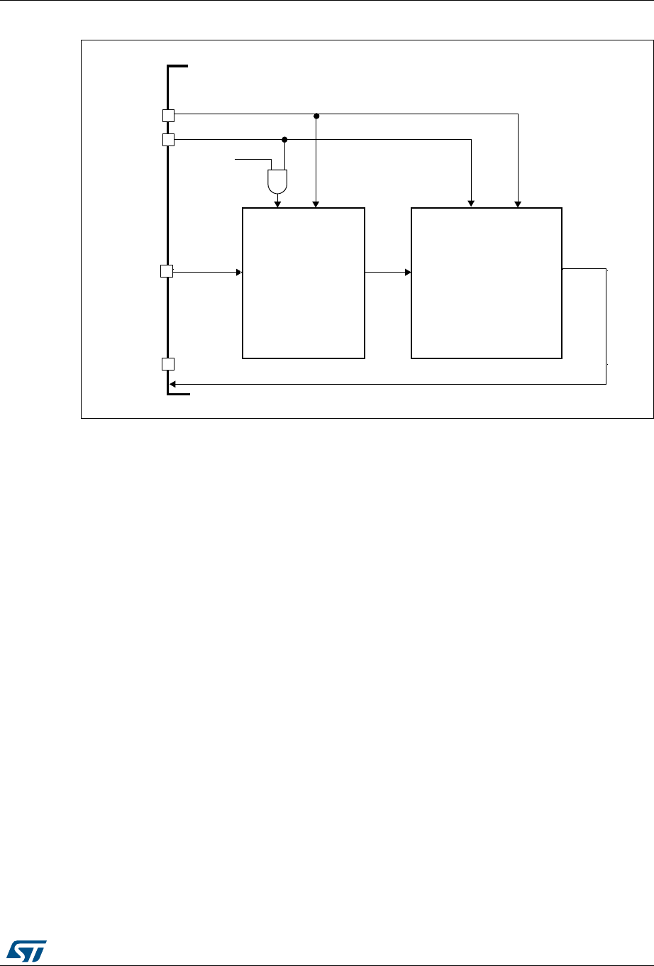
Debug support (DBG) RM0090
1690/1749 RM0090 Rev 18
38.6 ID codes and locking mechanism
There are several ID codes inside the STM32F4xx MCUs. ST strongly recommends tools
designers to lock their debuggers using the MCU DEVICE ID code located in the external
PPB memory map at address 0xE0042000.
38.6.1 MCU device ID code
The STM32F4xx MCUs integrate an MCU ID code. This ID identifies the ST MCU part-
number and the die revision. It is part of the DBG_MCU component and is mapped on the
external PPB bus (see Section 38.16). This code is accessible using the JTAG debug port
(four to five pins) or the SW debug port (two pins) or by the user software. It is even
accessible while the MCU is under system reset.
Only the DEV_ID[11:0] should be used for identification by the debugger/programmer tools.
DBGMCU_IDCODE
Address: 0xE004 2000
Only 32-bits access supported. Read-only.
31 30 29 28 27 26 25 24 23 22 21 20 19 18 17 16
REV_ID[15:0]
rrrrrr r r r r rrrrrr
1514131211109876543210
Reserved DEV_ID[11:0]
rrrrrrrrrrrr
Bits 31:16 REV_ID[15:0] Revision identifier
This field indicates the revision of the device.
STM32F405xx/07xx and STM32F415xx/17xx devices:
0x1000 = Revision A
0x1001 = Revision Z
0x1003 = Revision 1
0x1007 = Revision 2
0x100F= Revision Y and 4
STM32F42xxx and STM32F43xxx devices:
0x1000 = Revision A
0x1003 = Revision Y
0x1007 = Revision 1
0x2001= Revision 3
0x2003= Revision 5 and B
Bits 15:12 Reserved, must be kept at reset value.
Bits 11:0 DEV_ID[11:0]: Device identifier (STM32F405xx/07xx and STM32F415xx/17xx)
The device ID is 0x413.
Bits 11:0 DEV_ID[11:0]: Device identifier (STM32F42xxx and STM32F43xxx)
The device ID is 0x419

RM0090 Rev 18 1691/1749
RM0090 Debug support (DBG)
1713
38.6.2 Boundary scan TAP
JTAG ID code
The TAP of the STM32F4xx BSC (boundary scan) integrates a JTAG ID code equal to .
•0x06413041 for STM32F405xx/07xx and STM32F415xx/17xx devices
•0x06419041 for STM32F42xxx and STM32F43xxx devices
38.6.3 Cortex®-M4 with FPU TAP
The TAP of the Arm® Cortex®-M4 with FPU integrates a JTAG ID code. This ID code is the
Arm® default one and has not been modified. This code is only accessible by the JTAG
Debug Port, it is 0x4BA00477 (corresponds to Cortex®-M4 with FPU r0p1, see
Section 38.2).
38.6.4 Cortex®-M4 with FPU JEDEC-106 ID code
The Arm® Cortex®-M4 with FPU integrates a JEDEC-106 ID code. It is located in the 4 KB
ROM table mapped on the internal PPB bus at address 0xE00FF000_0xE00FFFFF.
This code is accessible by the JTAG Debug Port (4 to 5 pins) or by the SW Debug Port (two
pins) or by the user software.
38.7 JTAG debug port
A standard JTAG state machine is implemented with a 4-bit instruction register (IR) and five
data registers (for full details, refer to the Cortex®-M4 with FPU r0p1 Technical Reference
Manual (TRM), for references, see Section 38.2).
Table 300. JTAG debug port data registers
IR(3:0) Data register Details
1111 BYPASS
[1 bit] -
1110 IDCODE
[32 bits]
ID CODE
0x4BA00477 (Arm® Cortex®-M4 with FPU r0p1 ID Code)
1010 DPACC
[35 bits]
Debug port access register
This initiates a debug port and allows access to a debug port register.
– When transferring data IN:
Bits 34:3 = DATA[31:0] = 32-bit data to transfer for a write request
Bits 2:1 = A[3:2] = 2-bit address of a debug port register.
Bit 0 = RnW = Read request (1) or write request (0).
– When transferring data OUT:
Bits 34:3 = DATA[31:0] = 32-bit data which is read following a read
request
Bits 2:0 = ACK[2:0] = 3-bit Acknowledge:
010 = OK/FAULT
001 = WAIT
OTHER = reserved
Refer to Table 301 for a description of the A[3:2] bits

Debug support (DBG) RM0090
1692/1749 RM0090 Rev 18
1011 APACC
[35 bits]
Access port access register
Initiates an access port and allows access to an access port register.
– When transferring data IN:
Bits 34:3 = DATA[31:0] = 32-bit data to shift in for a write request
Bits 2:1 = A[3:2] = 2-bit address (sub-address AP registers).
Bit 0 = RnW= Read request (1) or write request (0).
– When transferring data OUT:
Bits 34:3 = DATA[31:0] = 32-bit data which is read following a read
request
Bits 2:0 = ACK[2:0] = 3-bit Acknowledge:
010 = OK/FAULT
001 = WAIT
OTHER = reserved
There are many AP Registers (see AHB-AP) addressed as the
combination of:
– The shifted value A[3:2]
– The current value of the DP SELECT register
1000 ABORT
[35 bits]
Abort register
– Bits 31:1 = Reserved
– Bit 0 = DAPABORT: write 1 to generate a DAP abort.
Table 301. 32-bit debug port registers addressed through the shifted value A[3:2]
Address A[3:2] value Description
0x0 00 Reserved, must be kept at reset value.
0x4 01
DP CTRL/STAT register. Used to:
– Request a system or debug power-up
– Configure the transfer operation for AP accesses
– Control the pushed compare and pushed verify operations.
– Read some status flags (overrun, power-up acknowledges)
0x8 10
DP SELECT register: Used to select the current access port and the
active 4-words register window.
– Bits 31:24: APSEL: select the current AP
– Bits 23:8: reserved
– Bits 7:4: APBANKSEL: select the active 4-words register window on the
current AP
– Bits 3:0: reserved
0xC 11
DP RDBUFF register: Used to allow the debugger to get the final result
after a sequence of operations (without requesting new JTAG-DP
operation)
Table 300. JTAG debug port data registers (continued)
IR(3:0) Data register Details

RM0090 Rev 18 1693/1749
RM0090 Debug support (DBG)
1713
38.8 SW debug port
38.8.1 SW protocol introduction
This synchronous serial protocol uses two pins:
•SWCLK: clock from host to target
•SWDIO: bidirectional
The protocol allows two banks of registers (DPACC registers and APACC registers) to be
read and written to.
Bits are transferred LSB-first on the wire.
For SWDIO bidirectional management, the line must be pulled-up on the board (100 KΩ
recommended by Arm®).
Each time the direction of SWDIO changes in the protocol, a turnaround time is inserted
where the line is not driven by the host nor the target. By default, this turnaround time is one
bit time, however this can be adjusted by configuring the SWCLK frequency.
38.8.2 SW protocol sequence
Each sequence consist of three phases:
1. Packet request (8 bits) transmitted by the host
2. Acknowledge response (3 bits) transmitted by the target
3. Data transfer phase (33 bits) transmitted by the host or the target
Refer to the Cortex®-M4 with FPU r0p1 TRM for a detailed description of DPACC and
APACC registers.
The packet request is always followed by the turnaround time (default 1 bit) where neither
the host nor target drive the line.
Table 302. Packet request (8-bits)
Bit Name Description
0 Start Must be “1”
1 APnDP 0: DP Access
1: AP Access
2RnW 0: Write Request
1: Read Request
4:3 A[3:2] Address field of the DP or AP registers (refer to Table 301)
5 Parity Single bit parity of preceding bits
6Stop 0
7Park Not driven by the host. Must be read as “1” by the target because of
the pull-up

Debug support (DBG) RM0090
1694/1749 RM0090 Rev 18
The ACK Response must be followed by a turnaround time only if it is a READ transaction
or if a WAIT or FAULT acknowledge has been received.
The DATA transfer must be followed by a turnaround time only if it is a READ transaction.
38.8.3 SW-DP state machine (reset, idle states, ID code)
The State Machine of the SW-DP has an internal ID code which identifies the SW-DP. It
follows the JEP-106 standard. This ID code is the default Arm® one and is set to
0x2BA01477 (corresponding to Cortex®-M4 with FPU r0p1).
Note: Note that the SW-DP state machine is inactive until the target reads this ID code.
•The SW-DP state machine is in RESET STATE either after power-on reset, or after the
DP has switched from JTAG to SWD or after the line is high for more than 50 cycles
•The SW-DP state machine is in IDLE STATE if the line is low for at least two cycles
after RESET state.
•After RESET state, it is mandatory to first enter into an IDLE state AND to perform a
READ access of the DP-SW ID CODE register. Otherwise, the target will issue a
FAULT acknowledge response on another transactions.
Further details of the SW-DP state machine can be found in the Cortex®-M4 with FPU r0p1
TRM and the CoreSight Design Kit r0p1 TRM.
38.8.4 DP and AP read/write accesses
•Read accesses to the DP are not posted: the target response can be immediate (if
ACK=OK) or can be delayed (if ACK=WAIT).
•Read accesses to the AP are posted. This means that the result of the access is
returned on the next transfer. If the next access to be done is NOT an AP access, then
the DP-RDBUFF register must be read to obtain the result.
The READOK flag of the DP-CTRL/STAT register is updated on every AP read access
or RDBUFF read request to know if the AP read access was successful.
•The SW-DP implements a write buffer (for both DP or AP writes), that enables it to
accept a write operation even when other transactions are still outstanding. If the write
buffer is full, the target acknowledge response is “WAIT”. With the exception of
Table 303. ACK response (3 bits)
Bit Name Description
0..2 ACK
001: FAULT
010: WAIT
100: OK
Table 304. DATA transfer (33 bits)
Bit Name Description
0..31 WDATA or RDATA Write or Read data
32 Parity Single parity of the 32 data bits

RM0090 Rev 18 1695/1749
RM0090 Debug support (DBG)
1713
IDCODE read or CTRL/STAT read or ABORT write which are accepted even if the write
buffer is full.
•Because of the asynchronous clock domains SWCLK and HCLK, two extra SWCLK
cycles are needed after a write transaction (after the parity bit) to make the write
effective internally. These cycles should be applied while driving the line low (IDLE
state)
This is particularly important when writing the CTRL/STAT for a power-up request. If the
next transaction (requiring a power-up) occurs immediately, it will fail.
38.8.5 SW-DP registers
Access to these registers are initiated when APnDP=0
Table 305. SW-DP registers
A[3:2] R/W
CTRLSEL bit
of SELECT
register
Register Notes
00 Read - IDCODE The manufacturer code is not set to ST
code. 0x2BA01477 (identifies the SW-DP)
00 Write - ABORT -
01 Read/Write 0 DP-
CTRL/STAT
Purpose is to:
– request a system or debug power-up
– configure the transfer operation for AP
accesses
– control the pushed compare and pushed
verify operations.
– read some status flags (overrun, power-
up acknowledges)
01 Read/Write 1 WIRE
CONTROL
Purpose is to configure the physical serial
port protocol (like the duration of the
turnaround time)
10 Read - READ
RESEND
Enables recovery of the read data from a
corrupted debugger transfer, without
repeating the original AP transfer.
10 Write - SELECT The purpose is to select the current access
port and the active 4-words register window
11 Read/Write - READ
BUFFER
This read buffer is useful because AP
accesses are posted (the result of a read AP
request is available on the next AP
transaction).
This read buffer captures data from the AP,
presented as the result of a previous read,
without initiating a new transaction

Debug support (DBG) RM0090
1696/1749 RM0090 Rev 18
38.8.6 SW-AP registers
Access to these registers are initiated when APnDP=1
There are many AP Registers (see AHB-AP) addressed as the combination of:
•The shifted value A[3:2]
•The current value of the DP SELECT register
38.9 AHB-AP (AHB access port) - valid for both JTAG-DP
and SW-DP
Features:
•System access is independent of the processor status.
•Either SW-DP or JTAG-DP accesses AHB-AP.
•The AHB-AP is an AHB master into the Bus Matrix. Consequently, it can access all the
data buses (Dcode Bus, System Bus, internal and external PPB bus) but the ICode
bus.
•Bitband transactions are supported.
•AHB-AP transactions bypass the FPB.
The address of the 32-bits AHP-AP resisters are 6-bits wide (up to 64 words or 256 bytes)
and consists of:
c) Bits [7:4] = the bits [7:4] APBANKSEL of the DP SELECT register
d) Bits [3:2] = the 2 address bits of A[3:2] of the 35-bit packet request for SW-DP.
The AHB-AP of the Cortex®-M4 with FPU includes 9 x 32-bits registers:
Refer to the Cortex®-M4 with FPU r0p1 TRM for further details.
Table 306. Cortex®-M4 with FPU AHB-AP registers
Address
offset Register name Notes
0x00 AHB-AP Control and Status
Word
Configures and controls transfers through the AHB
interface (size, hprot, status on current transfer, address
increment type
0x04 AHB-AP Transfer Address -
0x0C AHB-AP Data Read/Write -
0x10 AHB-AP Banked Data 0
Directly maps the 4 aligned data words without rewriting
the Transfer Address Register.
0x14 AHB-AP Banked Data 1
0x18 AHB-AP Banked Data 2
0x1C AHB-AP Banked Data 3
0xF8 AHB-AP Debug ROM Address Base Address of the debug interface
0xFC AHB-AP ID Register -

RM0090 Rev 18 1697/1749
RM0090 Debug support (DBG)
1713
38.10 Core debug
Core debug is accessed through the core debug registers. Debug access to these registers
is by means of the Advanced High-performance Bus (AHB-AP) port. The processor can
access these registers directly over the internal Private Peripheral Bus (PPB).
It consists of 4 registers:
Note: Important: these registers are not reset by a system reset. They are only reset by a power-
on reset.
Refer to the Cortex®-M4 with FPU r0p1 TRM for further details.
To Halt on reset, it is necessary to:
•enable the bit0 (VC_CORRESET) of the Debug and Exception Monitor Control
Register
•enable the bit0 (C_DEBUGEN) of the Debug Halting Control and Status Register.
Table 307. Core debug registers
Register Description
DHCSR
The 32-bit Debug Halting Control and Status Register
This provides status information about the state of the processor enable core debug
halt and step the processor
DCRSR The 17-bit Debug Core Register Selector Register:
This selects the processor register to transfer data to or from.
DCRDR
The 32-bit Debug Core Register Data Register:
This holds data for reading and writing registers to and from the processor selected
by the DCRSR (Selector) register.
DEMCR
The 32-bit Debug Exception and Monitor Control Register:
This provides Vector Catching and Debug Monitor Control. This register contains a
bit named TRCENA which enable the use of a TRACE.

Debug support (DBG) RM0090
1698/1749 RM0090 Rev 18
38.11 Capability of the debugger host to connect under system
reset
The reset system of the STM32F4xx MCU comprises the following reset sources:
•POR (power-on reset) which asserts a RESET at each power-up.
•Internal watchdog reset
•Software reset
•External reset
The Cortex®-M4 with FPU differentiates the reset of the debug part (generally
PORRESETn) and the other one (SYSRESETn)
This way, it is possible for the debugger to connect under System Reset, programming the
Core Debug Registers to halt the core when fetching the reset vector. Then the host can
release the system reset and the core will immediately halt without having executed any
instructions. In addition, it is possible to program any debug features under System Reset.
Note: It is highly recommended for the debugger host to connect (set a breakpoint in the reset
vector) under system reset.
38.12 FPB (Flash patch breakpoint)
The FPB unit:
•implements hardware breakpoints
•patches code and data from code space to system space. This feature gives the
possibility to correct software bugs located in the Code Memory Space.
The use of a Software Patch or a Hardware Breakpoint is exclusive.
The FPB consists of:
•2 literal comparators for matching against literal loads from Code Space and remapping
to a corresponding area in the System Space.
•6 instruction comparators for matching against instruction fetches from Code Space.
They can be used either to remap to a corresponding area in the System Space or to
generate a Breakpoint Instruction to the core.

RM0090 Rev 18 1699/1749
RM0090 Debug support (DBG)
1713
38.13 DWT (data watchpoint trigger)
The DWT unit consists of four comparators. They are configurable as:
•a hardware watchpoint or
•a trigger to an ETM or
•a PC sampler or
•a data address sampler
The DWT also provides some means to give some profiling informations. For this, some
counters are accessible to give the number of:
•Clock cycle
•Folded instructions
•Load store unit (LSU) operations
•Sleep cycles
•CPI (clock per instructions)
•Interrupt overhead
38.14 ITM (instrumentation trace macrocell)
38.14.1 General description
The ITM is an application-driven trace source that supports printf style debugging to trace
Operating System (OS) and application events, and emits diagnostic system information.
The ITM emits trace information as packets which can be generated as:
•Software trace. Software can write directly to the ITM stimulus registers to emit
packets.
•Hardware trace. The DWT generates these packets, and the ITM emits them.
•Time stamping. Timestamps are emitted relative to packets. The ITM contains a 21-bit
counter to generate the timestamp. The Cortex®-M4 with FPU clock or the bit clock rate
of the Serial Wire Viewer (SWV) output clocks the counter.
The packets emitted by the ITM are output to the TPIU (Trace Port Interface Unit). The
formatter of the TPIU adds some extra packets (refer to TPIU) and then output the complete
packets sequence to the debugger host.
The bit TRCEN of the Debug Exception and Monitor Control Register must be enabled
before programming or using the ITM.
38.14.2 Time stamp packets, synchronization and overflow packets
Time stamp packets encode time stamp information, generic control and synchronization. It
uses a 21-bit timestamp counter (with possible prescalers) which is reset at each time
stamp packet emission. This counter can be either clocked by the CPU clock or the SWV
clock.
A synchronization packet consists of 6 bytes equal to 0x80_00_00_00_00_00 which is
emitted to the TPIU as 00 00 00 00 00 80 (LSB emitted first).
A synchronization packet is a timestamp packet control. It is emitted at each DWT trigger.

Debug support (DBG) RM0090
1700/1749 RM0090 Rev 18
For this, the DWT must be configured to trigger the ITM: the bit CYCCNTENA (bit0) of the
DWT Control Register must be set. In addition, the bit2 (SYNCENA) of the ITM Trace
Control Register must be set.
Note: If the SYNENA bit is not set, the DWT generates Synchronization triggers to the TPIU which
will send only TPIU synchronization packets and not ITM synchronization packets.
An overflow packet consists is a special timestamp packets which indicates that data has
been written but the FIFO was full.
Table 308. Main ITM registers
Address Register Details
@E0000FB0 ITM lock access Write 0xC5ACCE55 to unlock Write Access to the other ITM
registers
@E0000E80 ITM trace control
Bits 31-24 = Always 0
Bits 23 = Busy
Bits 22-16 = 7-bits ATB ID which identifies the source of the
trace data.
Bits 15-10 = Always 0
Bits 9:8 = TSPrescale = Time Stamp Prescaler
Bits 7-5 = Reserved
Bit 4 = SWOENA = Enable SWV behavior (to clock the
timestamp counter by the SWV clock).
Bit 3 = DWTENA: Enable the DWT Stimulus
Bit 2 = SYNCENA: this bit must be to 1 to enable the DWT to
generate synchronization triggers so that the TPIU can then
emit the synchronization packets.
Bit 1 = TSENA (Timestamp Enable)
Bit 0 = ITMENA: Global Enable Bit of the ITM
@E0000E40 ITM trace privilege
Bit 3: mask to enable tracing ports31:24
Bit 2: mask to enable tracing ports23:16
Bit 1: mask to enable tracing ports15:8
Bit 0: mask to enable tracing ports7:0
@E0000E00 ITM trace enable Each bit enables the corresponding Stimulus port to generate
trace.
@E0000000-
E000007C
Stimulus port
registers 0-31
Write the 32-bits data on the selected Stimulus Port (32
available) to be traced out.

RM0090 Rev 18 1701/1749
RM0090 Debug support (DBG)
1713
Example of configuration
To output a simple value to the TPIU:
•Configure the TPIU and assign TRACE I/Os by configuring the DBGMCU_CR (refer to
Section 38.17.2 and Section 38.16.3)
•Write 0xC5ACCE55 to the ITM Lock Access Register to unlock the write access to the
ITM registers
•Write 0x00010005 to the ITM Trace Control Register to enable the ITM with Sync
enabled and an ATB ID different from 0x00
•Write 0x1 to the ITM Trace Enable Register to enable the Stimulus Port 0
•Write 0x1 to the ITM Trace Privilege Register to unmask stimulus ports 7:0
•Write the value to output in the Stimulus Port Register 0: this can be done by software
(using a printf function)
38.15 ETM (Embedded trace macrocell)
38.15.1 ETM general description
The ETM enables the reconstruction of program execution. Data are traced using the Data
Watchpoint and Trace (DWT) component or the Instruction Trace Macrocell (ITM) whereas
instructions are traced using the Embedded Trace Macrocell (ETM).
The ETM transmits information as packets and is triggered by embedded resources. These
resources must be programmed independently and the trigger source is selected using the
Trigger Event Register (0xE0041008). An event could be a simple event (address match
from an address comparator) or a logic equation between 2 events. The trigger source is
one of the fourth comparators of the DWT module, The following events can be monitored:
•Clock cycle matching
•Data address matching
For more informations on the trigger resources refer to Section 38.13.
The packets transmitted by the ETM are output to the TPIU (Trace Port Interface Unit). The
formatter of the TPIU adds some extra packets (refer to Section 38.17) and then outputs the
complete packet sequence to the debugger host.
38.15.2 ETM signal protocol and packet types
This part is described in the chapter 7 ETMv3 Signal Protocol of the Arm® IHI 0014N
document.

Debug support (DBG) RM0090
1702/1749 RM0090 Rev 18
38.15.3 Main ETM registers
For more information on registers refer to the chapter 3 of the Arm® IHI 0014N specification.
38.15.4 ETM configuration example
To output a simple value to the TPIU:
•Configure the TPIU and enable the I/IO_TRACEN to assign TRACE I/Os in the
STM32F4xx debug configuration register.
•Write 0xC5AC CE55 to the ETM Lock Access Register to unlock the write access to the
ITM registers
•Write 0x0000 1D1E to the ETM control register (configure the trace)
•Write 0x0000 406F to the ETM Trigger Event register (define the trigger event)
•Write 0x0000 006F to the ETM Trace Enable Event register (define an event to
start/stop)
•Write 0x0200 00000x0000 0001 to the ETM Trace Start/stop register (enable the trace)
•Write 0x0000191E to the ETM Control Register (end of configuration)
38.16 MCU debug component (DBGMCU)
The MCU debug component helps the debugger provide support for:
•Low-power modes
•Clock control for timers, watchdog, I2C and bxCAN during a breakpoint
•Control of the trace pins assignment
38.16.1 Debug support for low-power modes
To enter low-power mode, the instruction WFI or WFE must be executed.
The MCU implements several low-power modes which can either deactivate the CPU clock
or reduce the power of the CPU.
Table 309. Main ETM registers
Address Register Details
0xE0041FB0 ETM Lock Access Write 0xC5ACCE55 to unlock the write access to the
other ETM registers.
0xE0041000 ETM Control This register controls the general operation of the ETM,
for instance how tracing is enabled.
0xE0041010 ETM Status This register provides information about the current status
of the trace and trigger logic.
0xE0041008 ETM Trigger Event This register defines the event that will control trigger.
0xE004101C ETM Trace Enable
Control This register defines which comparator is selected.
0xE0041020 ETM Trace Enable Event This register defines the trace enabling event.
0xE0041024 ETM Trace Start/Stop This register defines the traces used by the trigger source
to start and stop the trace, respectively.

RM0090 Rev 18 1703/1749
RM0090 Debug support (DBG)
1713
The core does not allow FCLK or HCLK to be turned off during a debug session. As these
are required for the debugger connection, during a debug, they must remain active. The
MCU integrates special means to allow the user to debug software in low-power modes.
For this, the debugger host must first set some debug configuration registers to change the
low-power mode behavior:
•In Sleep mode, DBG_SLEEP bit of DBGMCU_CR register must be previously set by
the debugger. This will feed HCLK with the same clock that is provided to FCLK
(system clock previously configured by the software).
•In Stop mode, the bit DBG_STOP must be previously set by the debugger. This will
enable the internal RC oscillator clock to feed FCLK and HCLK in STOP mode.
38.16.2 Debug support for timers, watchdog, bxCAN and I2C
During a breakpoint, it is necessary to choose how the counter of timers and watchdog
should behave:
•They can continue to count inside a breakpoint. This is usually required when a PWM is
controlling a motor, for example.
•They can stop to count inside a breakpoint. This is required for watchdog purposes.
For the bxCAN, the user can choose to block the update of the receive register during a
breakpoint.
For the I2C, the user can choose to block the SMBUS timeout during a breakpoint.
For timers having complementary outputs, when the counter is stopped
(DBG_TIMx_STOP = 1), the outputs are disabled (as if the MOE bit was reset) for safety
purposes.
38.16.3 Debug MCU configuration register
This register allows the configuration of the MCU under DEBUG. This concerns:
•Low-power mode support
•Timer and watchdog counter support
•bxCAN communication support
•Trace pin assignment
This DBGMCU_CR is mapped on the External PPB bus at address 0xE0042004
It is asynchronously reset by the PORESET (and not the system reset). It can be written by
the debugger under system reset.
If the debugger host does not support these features, it is still possible for the user software
to write to these registers.
DBGMCU_CR register
Address: 0xE004 2004
Only 32-bit access supported
POR Reset: 0x0000 0000 (not reset by system reset)

Debug support (DBG) RM0090
1704/1749 RM0090 Rev 18
31 30 29 28 27 26 25 24 23 22 21 20 19 18 17 16
Reserved
15 14 13 12 11 10 9 8 7 6 5 4 3 2 1 0
Reserved
TRACE_
MODE
[1:0]
TRACE
_IOEN Reserved
DBG_
STAND
BY
DBG_
STOP
DBG_
SLEEP
rw rw rw rw rw rw
Bits 31:8 Reserved, must be kept at reset value.
Bits 7:5 TRACE_MODE[1:0] and TRACE_IOEN: Trace pin assignment control
– With TRACE_IOEN=0:
TRACE_MODE=xx: TRACE pins not assigned (default state)
– With TRACE_IOEN=1:
– TRACE_MODE=00: TRACE pin assignment for Asynchronous Mode
– TRACE_MODE=01: TRACE pin assignment for Synchronous Mode with a
TRACEDATA size of 1
– TRACE_MODE=10: TRACE pin assignment for Synchronous Mode with a
TRACEDATA size of 2
– TRACE_MODE=11: TRACE pin assignment for Synchronous Mode with a
TRACEDATA size of 4
Bits 4:3 Reserved, must be kept at reset value.
Bit 2 DBG_STANDBY: Debug Standby mode
0: (FCLK=Off, HCLK=Off) The whole digital part is unpowered.
From software point of view, exiting from Standby is identical than fetching reset vector
(except a few status bit indicated that the MCU is resuming from Standby)
1: (FCLK=On, HCLK=On) In this case, the digital part is not unpowered and FCLK and
HCLK are provided by the internal RC oscillator which remains active. In addition, the MCU
generate a system reset during Standby mode so that exiting from Standby is identical than
fetching from reset
Bit 1 DBG_STOP: Debug Stop mode
0: (FCLK=Off, HCLK=Off) In STOP mode, the clock controller disables all clocks (including
HCLK and FCLK). When exiting from STOP mode, the clock configuration is identical to the
one after RESET (CPU clocked by the 8 MHz internal RC oscillator (HSI)). Consequently,
the software must reprogram the clock controller to enable the PLL, the Xtal, etc.
1: (FCLK=On, HCLK=On) In this case, when entering STOP mode, FCLK and HCLK are
provided by the internal RC oscillator which remains active in STOP mode. When exiting
STOP mode, the software must reprogram the clock controller to enable the PLL, the Xtal,
etc. (in the same way it would do in case of DBG_STOP=0)
Bit 0 DBG_SLEEP: Debug Sleep mode
0: (FCLK=On, HCLK=Off) In Sleep mode, FCLK is clocked by the system clock as
previously configured by the software while HCLK is disabled.
In Sleep mode, the clock controller configuration is not reset and remains in the previously
programmed state. Consequently, when exiting from Sleep mode, the software does not
need to reconfigure the clock controller.
1: (FCLK=On, HCLK=On) In this case, when entering Sleep mode, HCLK is fed by the same
clock that is provided to FCLK (system clock as previously configured by the software).

RM0090 Rev 18 1705/1749
RM0090 Debug support (DBG)
1713
38.16.4 Debug MCU APB1 freeze register (DBGMCU_APB1_FZ)
The DBGMCU_APB1_FZ register is used to configure the MCU under Debug. It concerns
APB1 peripherals. It is mapped on the external PPB bus at address 0xE004 2008.
The register is asynchronously reset by the POR (and not the system reset). It can be
written by the debugger under system reset.
Address : 0xE004 2008
Only 32-bits access are supported.
Power-on reset (POR): 0x0000 0000 (not reset by system reset)
31 30 29 28 27 26 25 24 23 22 21 20 19 18 17 16
Reserved
DBG_CAN2_STOP
DBG_CAN1_STOP
Reserved
DBG_I2C3_SMBUS_TIMEOUT
DBG_I2C2_SMBUS_TIMEOUT
DBG_I2C1_SMBUS_TIMEOUT
Reserved
rw rw rw rw rw
1514131211109876543210
Reserved
DBG_IWDG_STOP
DBG_WWDG_STOP
DBG_RTC_STOP
Reserved
DBG_TIM14_STOP
DBG_TIM13_STOP
DBG_TIM12_STOP
DBG_TIM7_STOP
DBG_TIM6_STOP
DBG_TIM5_STOP
DBG_TIM4_STOP
DBG_TIM3_STOP
DBG_TIM2_STOP
rw rw rw rw rw rw rw rw rw rw rw
Bits 31:27 Reserved, must be kept at reset value.
Bit 26 DBG_CAN2_STOP: Debug CAN2 stopped when Core is halted
0: Same behavior as in normal mode
1: The CAN2 receive registers are frozen
Bit 25 DBG_CAN1_STOP: Debug CAN2 stopped when Core is halted
0: Same behavior as in normal mode
1: The CAN2 receive registers are frozen
Bit 24 Reserved, must be kept at reset value.
Bit 23 DBG_I2C3_SMBUS_TIMEOUT: SMBUS timeout mode stopped when Core is halted
0: Same behavior as in normal mode
1: The SMBUS timeout is frozen
Bit 22 DBG_I2C2_SMBUS_TIMEOUT: SMBUS timeout mode stopped when Core is halted
0: Same behavior as in normal mode
1: The SMBUS timeout is frozen
Bit 21 DBG_I2C1_SMBUS_TIMEOUT: SMBUS timeout mode stopped when Core is halted
0: Same behavior as in normal mode
1: The SMBUS timeout is frozen
Debug support (DBG) RM0090
1706/1749 RM0090 Rev 18
38.16.5 Debug MCU APB2 Freeze register (DBGMCU_APB2_FZ)
The DBGMCU_APB2_FZ register is used to configure the MCU under Debug. It concerns
APB2 peripherals.
This register is mapped on the external PPB bus at address 0xE004 200C
It is asynchronously reset by the POR (and not the system reset). It can be written by the
debugger under system reset.
Address: 0xE004 200C
Only 32-bit access is supported.
POR: 0x0000 0000 (not reset by system reset)
Bit 20:13 Reserved, must be kept at reset value.
Bit 12 DBG_IWDG_STOP: Debug independent watchdog stopped when core is halted
0: The independent watchdog counter clock continues even if the core is halted
1: The independent watchdog counter clock is stopped when the core is halted
Bit 11 DBG_WWDG_STOP: Debug Window Watchdog stopped when Core is halted
0: The window watchdog counter clock continues even if the core is halted
1: The window watchdog counter clock is stopped when the core is halted
Bit 10 DBG_RTC_STOP: RTC stopped when Core is halted
0: The RTC counter clock continues even if the core is halted
1: The RTC counter clock is stopped when the core is halted
Bit 9 Reserved, must be kept at reset value.
Bits 8:0 DBG_TIMx_STOP: TIMx counter stopped when core is halted (x=2..7, 12..14)
0: The clock of the involved timer counter is fed even if the core is halted
1: The clock of the involved timer counter is stopped and the outputs are disabled when the
core is halted
31 30 29 28 27 26 25 24 23 22 21 20 19 18 17 16
Reserved
DBG_TIM11
_STOP
DBG_TIM10
_STOP
DBG_TIM9_
STOP
rw rw rw
15 14 13 12 11 10 9 8 7 6 5 4 3 2 1 0
Reserved
DBG_TIM8_
STOP
DBG_TIM1_
STOP
rw rw
Bits 31:19 Reserved, must be kept at reset value.
Bits 18:16 DBG_TIMx_STOP: TIMx counter stopped when core is halted (x=9..11)
0: The clock of the involved timer counter is fed even if the core is halted
1: The clock of the involved timer counter is stopped and the outputs are disabled when the
core is halted
RM0090 Rev 18 1707/1749
RM0090 Debug support (DBG)
1713
38.17 TPIU (trace port interface unit)
38.17.1 Introduction
The TPIU acts as a bridge between the on-chip trace data from the ITM and the ETM.
The output data stream encapsulates the trace source ID, that is then captured by a trace
port analyzer (TPA).
The core embeds a simple TPIU, especially designed for low-cost debug (consisting of a
special version of the CoreSight TPIU).
Figure 488. TPIU block diagram
Bits 15: Reserved, must be kept at reset value.
Bit 1 DBG_TIM8_STOP: TIM8 counter stopped when core is halted
0: The clock of the involved timer counter is fed even if the core is halted
1: The clock of the involved timer counter is stopped and the outputs are disabled when the
core is halted
Bit 0 DBG_TIM1_STOP: TIM1 counter stopped when core is halted
0: The clock of the involved timer counter is fed even if the core is halted
1: The clock of the involved timer counter is stopped and the outputs are disabled when the
core is halted

Debug support (DBG) RM0090
1708/1749 RM0090 Rev 18
38.17.2 TRACE pin assignment
•Asynchronous mode
The asynchronous mode requires 1 extra pin and is available on all packages. It is only
available if using Serial Wire mode (not in JTAG mode).
•Synchronous mode
The synchronous mode requires from 2 to 6 extra pins depending on the data trace
size and is only available in the larger packages. In addition it is available in JTAG
mode and in Serial Wire mode and provides better bandwidth output capabilities than
asynchronous trace.
TPUI TRACE pin assignment
By default, these pins are NOT assigned. They can be assigned by setting the
TRACE_IOEN and TRACE_MODE bits in the MCU Debug component configuration
register. This configuration has to be done by the debugger host.
In addition, the number of pins to assign depends on the trace configuration (asynchronous
or synchronous).
•Asynchronous mode: 1 extra pin is needed
•Synchronous mode: from 2 to 5 extra pins are needed depending on the size of the
data trace port register (1, 2 or 4):
– TRACECK
– TRACED(0) if port size is configured to 1, 2 or 4
– TRACED(1) if port size is configured to 2 or 4
– TRACED(2) if port size is configured to 4
– TRACED(3) if port size is configured to 4
To assign the TRACE pin, the debugger host must program the bits TRACE_IOEN and
TRACE_MODE[1:0] of the Debug MCU configuration Register (DBGMCU_CR). By default
the TRACE pins are not assigned.
This register is mapped on the external PPB and is reset by the PORESET (and not by the
SYSTEM reset). It can be written by the debugger under SYSTEM reset.
Table 310. Asynchronous TRACE pin assignment
TPUI pin name
Trace synchronous mode STM32F4xx pin
assignment
Type Description
TRACESWO O TRACE Async Data Output PB3
Table 311. Synchronous TRACE pin assignment
TPUI pin name
Trace synchronous mode STM32F4xxpin
assignment
Type Description
TRACECK O TRACE Clock PE2
TRACED[3:0] O TRACE Sync Data Outputs
Can be 1, 2 or 4. PE[6:3]

RM0090 Rev 18 1709/1749
RM0090 Debug support (DBG)
1713
Note: By default, the TRACECLKIN input clock of the TPIU is tied to GND. It is assigned to HCLK
two clock cycles after the bit TRACE_IOEN has been set.
The debugger must then program the Trace Mode by writing the PROTOCOL[1:0] bits in the
SPP_R (Selected Pin Protocol) register of the TPIU.
•PROTOCOL=00: Trace Port Mode (synchronous)
•PROTOCOL=01 or 10: Serial Wire (Manchester or NRZ) Mode (asynchronous mode).
Default state is 01
It then also configures the TRACE port size by writing the bits [3:0] in the CPSPS_R
(Current Sync Port Size Register) of the TPIU:
•0x1 for 1 pin (default state)
•0x2 for 2 pins
•0x8 for 4 pins
38.17.3 TPUI formatter
The formatter protocol outputs data in 16-byte frames:
•seven bytes of data
•eight bytes of mixed-use bytes consisting of:
– 1 bit (LSB) to indicate it is a DATA byte (‘0) or an ID byte (‘1).
– 7 bits (MSB) which can be data or change of source ID trace.
•one byte of auxiliary bits where each bit corresponds to one of the eight mixed-use
bytes:
– if the corresponding byte was a data, this bit gives bit0 of the data.
– if the corresponding byte was an ID change, this bit indicates when that ID change
takes effect.
Table 312. Flexible TRACE pin assignment
DBGMCU_CR
register
Pins
assigned for:
TRACE IO pin assigned
TRACE
_IOEN
TRACE
_MODE
[1:0]
PB3 /JTDO/
TRACESWO
PE2/
TRACECK
PE3 /
TRACED[0]
PE4 /
TRACED[1]
PE5 /
TRACED[2]
PE6 /
TRACED[3]
0XX
No Trace
(default state) Released (1) -
100
Asynchronous
Trace TRACESWO - - Released
(usable as GPIO)
101
Synchronous
Trace 1 bit
Released (1)
TRACECK TRACED[0] - - -
110
Synchronous
Trace 2 bit TRACECK TRACED[0] TRACED[1] - -
111
Synchronous
Trace 4 bit TRACECK TRACED[0] TRACED[1] TRACED[2] TRACED[3]
1. When Serial Wire mode is used, it is released. But when JTAG is used, it is assigned to JTDO.

Debug support (DBG) RM0090
1710/1749 RM0090 Rev 18
Note: Refer to the Arm® CoreSight Architecture Specification v1.0 (Arm® IHI 0029B) for further
information
38.17.4 TPUI frame synchronization packets
The TPUI can generate two types of synchronization packets:
•The Frame Synchronization packet (or Full Word Synchronization packet)
It consists of the word: 0x7F_FF_FF_FF (LSB emitted first). This sequence can not
occur at any other time provided that the ID source code 0x7F has not been used.
It is output periodically between frames.
In continuous mode, the TPA must discard all these frames once a synchronization
frame has been found.
•The Half-Word Synchronization packet
It consists of the half word: 0x7F_FF (LSB emitted first).
It is output periodically between or within frames.
These packets are only generated in continuous mode and enable the TPA to detect
that the TRACE port is in IDLE mode (no TRACE to be captured). When detected by
the TPA, it must be discarded.
38.17.5 Transmission of the synchronization frame packet
There is no Synchronization Counter register implemented in the TPIU of the core.
Consequently, the synchronization trigger can only be generated by the DWT. Refer to the
registers DWT Control Register (bits SYNCTAP[11:10]) and the DWT Current PC Sampler
Cycle Count Register.
The TPUI Frame synchronization packet (0x7F_FF_FF_FF) is emitted:
•after each TPIU reset release. This reset is synchronously released with the rising
edge of the TRACECLKIN clock. This means that this packet is transmitted when the
TRACE_IOEN bit in the DBGMCU_CFG register is set. In this case, the word
0x7F_FF_FF_FF is not followed by any formatted packet.
•at each DWT trigger (assuming DWT has been previously configured). Two cases
occur:
– If the bit SYNENA of the ITM is reset, only the word 0x7F_FF_FF_FF is emitted
without any formatted stream which follows.
– If the bit SYNENA of the ITM is set, then the ITM synchronization packets will
follow (0x80_00_00_00_00_00), formatted by the TPUI (trace source ID added).
38.17.6 Synchronous mode
The trace data output size can be configured to 4, 2 or 1 pin: TRACED(3:0)
The output clock is output to the debugger (TRACECK)
Here, TRACECLKIN is driven internally and is connected to HCLK only when TRACE is
used.
Note: In this synchronous mode, it is not required to provide a stable clock frequency.
The TRACE I/Os (including TRACECK) are driven by the rising edge of TRACLKIN (equal
to HCLK). Consequently, the output frequency of TRACECK is equal to HCLK/2.

RM0090 Rev 18 1711/1749
RM0090 Debug support (DBG)
1713
38.17.7 Asynchronous mode
This is a low cost alternative to output the trace using only 1 pin: this is the asynchronous
output pin TRACESWO. Obviously there is a limited bandwidth.
TRACESWO is multiplexed with JTDO when using the SW-DP pin. This way, this
functionality is available in all STM32F4xx packages.
This asynchronous mode requires a constant frequency for TRACECLKIN. For the standard
UART (NRZ) capture mechanism, 5% accuracy is needed. The Manchester encoded
version is tolerant up to 10%.
38.17.8 TRACECLKIN connection inside the STM32F4xx
In the STM32F4xx, this TRACECLKIN input is internally connected to HCLK. This means
that when in asynchronous trace mode, the application is restricted to use to time frames
where the CPU frequency is stable.
Note: Important: when using asynchronous trace: it is important to be aware that:
The default clock of the STM32F4xx MCUs is the internal RC oscillator. Its frequency under
reset is different from the one after reset release. This is because the RC calibration is the
default one under system reset and is updated at each system reset release.
Consequently, the trace port analyzer (TPA) should not enable the trace (with the
TRACE_IOEN bit) under system reset, because a Synchronization Frame Packet will be
issued with a different bit time than trace packets which will be transmitted after reset
release.
38.17.9 TPIU registers
The TPIU APB registers can be read and written only if the bit TRCENA of the Debug
Exception and Monitor Control Register (DEMCR) is set. Otherwise, the registers are read
as zero (the output of this bit enables the PCLK of the TPIU).
Table 313. Important TPIU registers
Address Register Description
0xE0040004 Current port size
Allows the trace port size to be selected:
Bit 0: Port size = 1
Bit 1: Port size = 2
Bit 2: Port size = 3, not supported
Bit 3: Port Size = 4
Only 1 bit must be set. By default, the port size is one bit. (0x00000001)
0xE00400F0 Selected pin protocol
Allows the Trace Port Protocol to be selected:
Bit1:0=
00: Sync Trace Port Mode
01: Serial Wire Output - manchester (default value)
10: Serial Wire Output - NRZ
11: reserved

Debug support (DBG) RM0090
1712/1749 RM0090 Rev 18
38.17.10 Example of configuration
•Set the bit TRCENA in the Debug Exception and Monitor Control Register (DEMCR)
•Write the TPIU Current Port Size Register to the desired value (default is 0x1 for a 1-bit
port size)
•Write TPIU Formatter and Flush Control Register to 0x102 (default value)
•Write the TPIU Select Pin Protocol to select the sync or async mode. Example: 0x2 for
async NRZ mode (UART like)
•Write the DBGMCU control register to 0x20 (bit IO_TRACEN) to assign TRACE I/Os
for async mode. A TPIU Sync packet is emitted at this time (FF_FF_FF_7F)
•Configure the ITM and write the ITM Stimulus register to output a value
0xE0040304 Formatter and flush
control
Bits 31-9 = always ‘0
Bit 8 = TrigIn = always ‘1 to indicate that triggers are indicated
Bits 7-4 = always 0
Bits 3-2 = always 0
Bit 1 = EnFCont. In Sync Trace mode (Select_Pin_Protocol register
bit1:0=00), this bit is forced to ‘1: the formatter is automatically enabled in
continuous mode. In asynchronous mode (Select_Pin_Protocol register
bit1:0 <> 00), this bit can be written to activate or not the formatter.
Bit 0 = always 0
The resulting default value is 0x102
Note: In synchronous mode, because the TRACECTL pin is not mapped
outside the chip, the formatter is always enabled in continuous mode -this
way the formatter inserts some control packets to identify the source of the
trace packets).
0xE0040300 Formatter and flush
status Not used in Cortex®-M4 with FPU, always read as 0x00000008
Table 313. Important TPIU registers (continued)
Address Register Description

RM0090 Rev 18 1713/1749
RM0090 Debug support (DBG)
1713
38.18 DBG register map
The following table summarizes the Debug registers.
Table 314. DBG register map and reset values
Addr. Register
31
30
29
28
27
26
25
24
23
22
21
20
19
18
17
16
15
14
13
12
11
10
9
8
7
6
5
4
3
2
1
0
0xE004
2000
DBGMCU
_IDCODE REV_ID
Reserved
DEV_ID
Reset value(1) XXXXXXXXXXXXXXXX XXXXXXXXXXXX
0xE004
2004
DBGMCU_CR Reserved
DBG_TIM7_STOP
DBG_TIM6_STOP
DBG_TIM5_STOP
DBG_TIM8_STOP
DBG_I2C2_SMBUS_TIMEOUT
Reserved
TRACE_
MODE
[1:0]
TRACE_
Reserved
DBG_STANDBY
DBG_STOP
DBG_SLEEP
Reset value 00000 000 000
0xE004
2008
DBGMCU_
APB1_FZ Reserved
DBG_CAN2_STOP
DBG_CAN1_STOP
Reserved
DBG_I2C3_SMBUS_TIMEOUT
DBG_I2C2_SMBUS_TIMEOUT
DBG_I2C1_SMBUS_TIMEOUT
Reserved
DBG_IWDG_STOP
DBG_WWDG_STOP
Reserved
DBG_RTC_STOP
DBG_TIM14_STOP
DBG_TIM13_STOP
DBG_TIM12_STOP
DBG_TIM7_STOP
DBG_TIM6_STOP
DBG_TIM5_STOP
DBG_TIM4_STOP
DBG_TIM3_STOP
DBG_TIM2_STOP
Reset value 000000 00 0000000000
0xE004
200C
DBGMCU_
APB2_FZ Reserved
DBG_TIM11_STOP
DBG_TIM10_STOP
DBG_TIM9_STOP
Reserved
DBG_TIM8_STOP
DBG_TIM1_STOP
Reset value 0 0 0 0 0
1. The reset value is product dependent. For more information, refer to Section 38.6.1: MCU device ID code.

Device electronic signature RM0090
1714/1749 RM0090 Rev 18
39 Device electronic signature
The electronic signature is stored in the Flash memory area. It can be read using the
JTAG/SWD or the CPU. It contains factory-programmed identification data that allow the
user firmware or other external devices to automatically match its interface to the
characteristics of the STM32F4xx microcontrollers.
39.1 Unique device ID register (96 bits)
The unique device identifier is ideally suited:
•for use as serial numbers (for example USB string serial numbers or other end
applications)
•for use as security keys in order to increase the security of code in Flash memory while
using and combining this unique ID with software cryptographic primitives and
protocols before programming the internal Flash memory
•to activate secure boot processes, etc.
The 96-bit unique device identifier provides a reference number which is unique for any
device and in any context. These bits can never be altered by the user.
The 96-bit unique device identifier can also be read in single bytes/half-words/words in
different ways and then be concatenated using a custom algorithm.
Base address: 0x1FFF 7A10
Address offset: 0x00
Read only = 0xXXXX XXXX where X is factory-programmed
Address offset: 0x04
Read only = 0xXXXX XXXX where X is factory-programmed
Address offset: 0x08
313029282726252423222120191817161514131211109876543210
UID(31:0)
rrrrrrrrrrrrrrrrrrrrrrrrrrrrrrrr
Bits 31:0 UID(31:0): unique ID bits
31 30 29 28 27 26 25 24 23 22 21 20 19 18 17 16
UID(63:48)
rrrrrrrrrrrrrrrr
15 14 13 12 11 10 9 8 7 6 5 4 3 2 1 0
UID(47:32)
rrrrrrrrrrrrrrrr
Bits 31:0 UID(63:32): 63:32 unique ID bits

RM0090 Rev 18 1715/1749
RM0090 Device electronic signature
1715
Read only = 0xXXXX XXXX where X is factory-programmed
39.2 Flash size
Base address: 0x1FFF 7A22
Address offset: 0x00
Read only = 0xXXXX where X is factory-programmed
31 30 29 28 27 26 25 24 23 22 21 20 19 18 17 16
UID(95:80)
rrrrrrrrrrrrrrrr
1514131211109876543210
UID(79:64)
rrrrrrrrrrrrrrrr
Bits 31:0 UID(95:64): 95:6 Unique ID bits
1514131211109876543210
F_SIZE
rrrrrrrrrrrrrrrr
Bits 15:0 F_ID(15:0): Flash memory size
This bitfield indicates the size of the device Flash memory expressed in Kbytes.
As an example, 0x0400 corresponds to 1024 Kbytes.

Revision history RM0090
1716/1749 RM0090 Rev 18
40 Revision history
Table 315. Document revision history
Date Version Changes
15-Sep-2011 1 Initial release.
19-Oct-2012 2
Updated reference documents and added Table 1: Applicable products on cover
page.
MEMORY:
Updated Section 2: Memory and bus architecture.
PWR:
Updated VDDA and VREF+ decoupling capacitor in Figure 7: Power supply
overview.
Updated case of no external battery in Section 5.1.2: Battery backup domain.
VOSRDY bit changed to read-only in Section 5.4.3: PWR power control/status
register (PWR_CSR).
Removed VDDA in Section 5.2.3: Programmable voltage detector (PVD) and
remove VDDA in PVDO bit description (Section 5.4.3: PWR power control/status
register (PWR_CSR)).
RCC:
Updated Figure 20: Simplified diagram of the reset circuit and minimum reset
pulse duration guaranteed by pulse generator restricted to internal reset
sources.
GPIOs:
Updated Section 8.3.1: General-purpose I/O (GPIO).
DMA:
Updated direct mode description in Section 10.2: DMA main features.
Updated direct mode description in Section : Memory-to-peripheral mode, and
Section 10.3.12: FIFO/: Direct mode.
Updated register access in Section 10.5: DMA registers.
Modified Stream2 /Channel 2 in Table 42: DMA1 request mapping.
Added note related to EN bit in Section 10.5.5: DMA stream x configuration register
(DMA_SxCR) (x = 0..7). Updated definition of NDT[15:0] bits in Section 10.5.6:
DMA stream x number of data register (DMA_SxNDTR) (x = 0..7).
Interrupts:
Updated number of maskable interrupts to 82 in Section 12.1.1: NVIC featuress.
Updated Section 12.2: External interrupt/event controller (EXTI).

RM0090 Rev 18 1717/1749
RM0090 Revision history
1743
19-Oct-2012 2
(continued)
ADC:
Changed ADCCLK frequency to 30 MHz in Section 13.5: Channel-wise
programmable sampling timee.
Added recovery from ADC sequence in Section 13.8.1: Using the DMA and
Section 13.8.2: Managing a sequence of conversions without using the DMA.
Updated AWDIE in Section 13.13.2: ADC control register 1 (ADC_CR1). Added
read and write access in Section 13.13: ADC registers.
Advanced control timers (TIM1 and TIM8):
Updated 16-bit prescaler range in Section 17.2: TIM1 and TIM8 main features.
Updated OC1 block diagram in Figure 114: Output stage of capture/compare
channel (channel 1 to 3).
Updated update event generation in Upcounting mode and Downcounting mode in
Section 17.3.2: Counter modes and Section 17.3.3: Repetition counter.
Updated bits that control the dead-time generation in Section 17.3.11:
Complementary outputs and dead-time insertion.
Updated ways to generate a break in Section 17.3.12: Using the break function.
Changed OCxREF to ETR in the example given in Section 17.3.13: Clearing the
OCxREF signal on an external event and changed
OCREF_CLR to ETRF in Figure 124: Clearing TIMx OCxREF.
Updated configuration for example of counter operation in encoder
interface mode in Section 17.3.16: Encoder interface mode.
Added register access in Section 17.4: TIM1 and TIM8 registers.
Changed definition of ARR[15:0] bits in Section 17.4.12: TIM1 and TIM8 auto-
reload register (TIMx_ARR).
Updated BKE definition in Section 17.4.18: TIM1 and TIM8 break and dead-time
register (TIMx_BDTR).
Table 315. Document revision history (continued)
Date Version Changes

Revision history RM0090
1718/1749 RM0090 Rev 18
19-Oct-2012 2
(continued)
General purpose timers (TIM2 to TIM5):
Removed all references to “repetition counter”.
Added Figure 134: General-purpose timer block diagram.
Updated 16-bit prescaler range in Section 18.2: TIM2 to TIM5 main features.
External clock mode 2 ETR restricted to TIM2 to TIM4 in
Section 18.3.3: Clock selection and Section 18.3.6: PWM input mode.
Updated Section 18.3.9: PWM mode and Section 18.3.11: Clearing the OCxREF
signal on an external event.
Updated Figure 174: Master/Slave timer example to change ITR1 to
ITR0.
Updated read and write access to registers in Section 18.4: TIM2 to TIM5
registerss.
Restored bits 15 to 8 of TIMx_SMCR as well as Table 98: TIMx internal trigger
connection in Section 14.4.3.
Removed note 1 related to OC1M bits in Section 18.4.13: TIMx capture/compare
register 1 (TIMx_CCR1).
Updated TIMx_CCER bit description for TIM2 to TIM5 in
Section 18.4.9: TIMx capture/compare enable register (TIMx_CCER).
General purpose timers (TIM9 to TIM14):
Updated 16-bit prescaler range in Section 19.2.1: TIM9/TIM12 main features and
Section 19.2.2: TIM10/TIM11 and TIM13/TIM14 main features.
Updated Figure 181: General-purpose timer block diagram (TIM10/11/13/14)) to
remove TRGO trigger controller output.
Added register access in Section 19.4: TIM9 and TIM12 registers
and Section 19.5: TIM10/11/13/14 registers.
Basic timers (TIM6 and TIM7):
Removed all references to “repetition counter”.
Updated 16-bit prescaler range in Section 20.2: TIM6 and TIM7 main features.
HASH:
Updated Section 25.3.1: Duration of the processing.
RNG:
Updated Section 24.1: RNG introduction.
Table 315. Document revision history (continued)
Date Version Changes

RM0090 Rev 18 1719/1749
RM0090 Revision history
1743
19-Oct-2012 2
(continued)
RTC:
Updated Figure 237: RTC block diagram.
Added formula to compute fck_apre in Figure 26.3.1: Clock and prescalers.
Updated Section 26.3.9: RTC reference clock detection.
Updated Section : RTC register write protection.
Added RTC_SSR shadow register in Section 26.3.6: Reading the calendar.
Updated description of DC[4:0] bits in Section 26.6.7: RTC calibration register
(RTC_CALIBR).
Renamed RTC_BKxR into RTC_BKPxR in Table 121: RTC register map and reset
values.
Added power-on reset value and changed reset value to system
reset value in Section 26.6.11: RTC sub second register (RTC_SSR).
Updated definition of ALARMOUTTYPE in Section 26.6.17: RTC tamper and
alternate function configuration register (RTC_TAFCR).
I2C:
Modified Section 27.3.8: DMA requests.
Updated bit 14 description in Section 27.6.3: I2C Own address register 1
(I2C_OAR1)).
Updated definition of PE bit and note related to SWRST bit; moved
note related to STOP bit to the whole register in Section 27.6.1: I2C Control register
1 (I2C_CR1).
USART:
Section 30.6.6: Control register 3 (USART_CR3)): removed notes
related to UART5 in DMAT and DMAR description.
Updated TTable 142: Error calculation for programmed baud rates at fPCLK = 42
MHz or fPCLK = 84 Hz, oversampling by 16 and
Table 143: Error calculation for programmed baud rates at fPCLK = 42 MHz or
fPCLK = 84 MHz, oversampling by 8.
SPI/I2S:
Updated Section 28.1: SPI introduction.
Changed I2S simplex communication/mode to half-duplex communication/mode.
Updated flags in reception/transmission modes in Section 28.2.2: I2S features.
Added Frame error flag in Table 128: I2S interrupt requests.
Added register access in Section 28.5: SPI and I2S registers.
Updated ERRIE definition in Section 28.5.2: SPI control register 2 (SPI_CR2).
Renamed TIFRFE to FRE and definition updated in Section 28.5.3: SPI status
register (SPI_SR).
Table 315. Document revision history (continued)
Date Version Changes

Revision history RM0090
1720/1749 RM0090 Rev 18
19-Oct-2012 2
(continued)
SDIO:
Updated value and description for bits [45:40] and [7:1] in Table 176: R4 response.
Updated value at bits [45:40] in Table 178: R5 response.
CAN:
Updated Figure 335: Dual CAN block diagram.
Modified definition of CAN2SB bits in Section : CAN filter master register
(CAN_FMR).
Added register access in Section 32.9: CAN registers
ETHERNET:
Updated standard for precision networked clock synchronization in Section 33.1:
Ethernet introduction and Section 33.2.1: MAC core features.
Updated CR bit definition in Section : Ethernet MAC MII address register
(ETH_MACMIIAR).
Replace RTPR by PM bit in Table 192: Source address filtering.
USB OTG FS
Updated remote wakeup signaling bit and the resume
interrupt in Section : Suspended state.
Added peripheral register access in Section 34.16: OTG_FS control and status
registerss.
Updated INEPTXSA description in OTG_FS_DIEPTXFx.
Changed PHYSEL from bit 7 to bit 6 of the OTG_FS_GUSBCFG
register.
USB OTG HS
Updated remote wakeup signaling bit and the resume
interrupt in Section : Suspended state.
Added peripheral register access in Section 35.12: OTG_HS control and status
registers.
Updated OTG_HS_CID reset value.
Updated INEPTXSA description in OTG_HS_DIEPTXFx.
Updated FSLSPCS for LS host mode, added PHYSEL in Section : OTG_HS host
configuration register (OTG_HS_HCFG).
Renamed PHYSEL into PHSEL and changed from bit 7 to bit 6 of
the OTG_HS_GUSBCFG register.
Updated OTG_HS_DIEPEACHMSK1 and OTG_HS_DOEPEACHMSK1 reset
values.
Table 315. Document revision history (continued)
Date Version Changes

RM0090 Rev 18 1721/1749
RM0090 Revision history
1743
19-Oct-2012 2
(continued)
FSMC:
Updated step b) in Section 36.3.1: Supported memories and transactions.
Updated Table 196: FSMC_BTRx bit fields.
Changed Clock divide ration min in Table 246: Programmable NAND/PC Card
access parameters.
Updated case of synchronous accesses in Section 36.5: NOR Flash/PSRAM
controller.
Changed minimum value for ADDSET to 0 in Table 203, Table 206, Table 207,
Table 209, and Table 210.
Move note from Figure 437: Mode1 write accesses and Figure 436: Mode1 read
accesses. Move note from Figure 439: ModeA write accesses to Figure 438:
ModeA read accesses.
Updated Section : WAIT management in asynchronous accesses.
Added register access in Section 36.5.6: NOR/PSRAM control registers and
Section 36.6.2: NAND Flash / PC Card supported memories and transactions.
Removed caution note in Section 36.6.1: External memory interface signalss.
Updated Table 249: 16-bit PC Card.
Updated step 3 in Section 36.6.4: NAND Flash operations.
Updated Figure 455: Access to non ‘CE don’t care’ NAND-Flash and note below in
Section 36.6.5: NAND Flash prewait functionality.
Updated access to I/O Space in Section 36.6.7: PC Card/CompactFlash
operationss. Updated Table 251: 16-bit PC-Card signals and access type. Updated
BUSTURN bit definition in Section : SRAM/NOR-Flash chip-select timing registers
1..4 (FSMC_BTR1..4)). Changed bits 16 to 19 to BUSTURN in Section :
SRAM/NOR-Flash write timing registers 1..4 (FSMC_BWTR1..4)
DEBUG:
Updated Section 38.4.3: Internal pull-up and pull-down on JTAG pins.
Electronic signature
Updated Section 39: Device electronic signature introduction.
Updated REV_ID[15:0] to add revision Z in Section 39.1: Unique device ID register
(96 bits).
Updated address and example in Section 39.2: Flash size.
Table 315. Document revision history (continued)
Date Version Changes

Revision history RM0090
1722/1749 RM0090 Rev 18
13-Nov-2012 3
Added STM32F42x and STM32F43x devices.
Removed reference du Flash programming manual on cover page. Added
Section 2.3.2: Flash memory overview and Section 3: Embedded Flash memory
interface.
Change RTC_50Hz into RTC_REFIN in Section 8.3.2: I/O pin multiplexer and
mapping. Modified RTC alternate function naming in Section 8: General-purpose
I/Os (GPIO) and Section 26: Real-time clock (RTC).
Updated max. input frequency in Section 26.3.1: Clock and prescalers.
Changed bit access type from ‘rw’ to ‘w’ and bit description updated in
Section 10.5.3: DMA low interrupt flag clear register (DMA_LIFCR) and
Section 10.5.4: DMA high interrupt flag clear register (DMA_HIFCR).
Updated Figure 18: Frequency measurement with TIM5 in Input capture mode.
Updated Section : Signals synchronization in Section 36: Flexible static memory
controller (FSMC)
Section 34: USB on-the-go full-speed (OTG_FS): updated Section Figure 389.:
USB host-only connection, Section : VBUS valid, and Section : Host detection of a
peripheral connection.
Section 35: USB on-the-go high-speed (OTG_HS): updated Section : VBUS valid,
and Section : Detection of peripheral connection by the host.
Table 315. Document revision history (continued)
Date Version Changes

RM0090 Rev 18 1723/1749
RM0090 Revision history
1743
19-Feb-2013 4
Updated Section 2: Memory and bus architecture.
Updated Figure 1: System architecture for STM32F405xx/07xx and
STM32F415xx/17xx devices, and Figure 1: System architecture for
STM32F405xx/07xx and STM32F415xx/17xx devices. Updated Table 4: Memory
mapping vs. Boot mode/physical remap. Updated Figure 5: Sequential 32-bit
instruction execution. removed note 1 from Table 12: Program/erase parallelism.
PWR:
Updated Figure 7: Power supply overview.
Updated Section 5.1.3: Voltage regulator.
Added ADCDC1 bit in Section 5.5.1: PWR power control register (PWR_CR) for
STM32F42xxx and STM32F43xxx.
SYSCFG:
Added ADCxDC2 bit in Section 8.2.3: SYSCFG peripheral mode configuration
register (SYSCFG_PMC) for STM32F42xxx and STM32F43xxx.
ADC:
Updated Section 13.9.3: Interleaved mode, Section 13.9.4: Alternate trigger mode,
and Section 13.9.5: Combined regular/injected simultaneous mode to describe
case of interrupted conversion.
Updated Section : Temperature sensor, VREFINT and VBAT internal channels,
Section 13.10: Temperature sensor, and Section 13.11: Battery charge monitoring.
RTC:
Updated BKP[31:0] bit description in Section 26.6.20: RTC backup registers
(RTC_BKPxR).
I2C:
Updated Section 27.3.5: Programmable noise filter.
Table 315. Document revision history (continued)
Date Version Changes

Revision history RM0090
1724/1749 RM0090 Rev 18
19-Feb-2013 4
(continued)
FSMC:
Updated write FIFO size in Section 36.1: FSMC main features.
Updated Figure 434: FSMC block diagram.
Updated Section 36.5.4: NOR Flash/PSRAM controller asynchronous transactions.
Modified differences between Mode B and mode 1 in Section : Mode 2/B - NOR
Flash.
Modified differences between Mode C and mode 1 in Section : Mode C - NOR
Flash - OE toggling.
Modified differences between Mode D and mode 1 in Section : Mode D -
asynchronous access with extended address.
Updated NWAIT signal in Figure 449: Asynchronous wait during a read access,
Figure 450: Asynchronous wait during a write access, Figure 451: Wait
configurations, Figure 452: Synchronous multiplexed read mode - NOR, PSRAM
(CRAM), and Figure 453: Synchronous multiplexed write mode - PSRAM (CRAM).
Updated Table 195 to Ta ble 214.
Updated Section : SRAM/NOR-Flash chip-select control registers 1..4
(FSMC_BCR1..4).
DEBUG
Updated Figure 485: Block diagram of STM32 MCU and Cortex®-M4 with FPU-
level debug support.
Table 315. Document revision history (continued)
Date Version Changes

RM0090 Rev 18 1725/1749
RM0090 Revision history
1743
15-Sep-2013 5
Added STM32F429xx and STM32F439xx part numbers.
Replaced FSMC by FMC added Chrom-ART Accelerator, LCD-TFT and SAI
interface.
Updated Figure 2: System architecture for STM32F42xxx and STM32F43xxx
devices.
PWR:
Updated Section 5.2.2: Brownout reset (BOR).
Added note related to CSS enabling in Entering Stop mode sections in
Section 5.3.4: Stop mode (STM32F405xx/07xx and STM32F415xx/17xx) and
Section 5.3.5: Stop mode (STM32F42xxx and STM32F43xxx). Updated Stop mode
entry in Table 27 and Table 29.
Updated WUF bit defienition in PWR_CSR registers. Changed CWUF and CSBF
access type to ‘w’ in PWR_CR register.
RCC: Updated LSEBYP bit definition in RCC_BDCR register.
GPIOs:
Updated description of OSPEEDR bits. Removed frequency value in description of
OSPEEDR bits.Corrected typos: "IDRy[15:0]" replaced with "IDRy" in "GPIOx_IDR"
register, "ODRy[15:0]" replaced with "ODRy" in "GPIOx_ODR" register and
"OTy[1:0]" replaced with "OTy" in "GPIOx_OTYPER" register.
DCMI: Updated Section 15.4: DCMI clocks.
IWDG: Corrected Figure 213: Independent watchdog block diagram.
RTC:
Replaced all occurrences of “power-on reset” with “backup domain reset”. Added
caution note under Table 121: RTC register map and reset values. Changed SHPF
bit type to ‘r’ in Section 26.6.4: RTC initialization and status register (RTC_ISR)..
SPI: Updated definition of ERRIE bit in Section 28.5.2: SPI control register 2
(SPI_CR2).
UART:
Updated Section 30.3.8: LIN (local interconnection network) mode.
Removed note in Section 30.3.13: Continuous communication using DMA.
ETHERNET:
Modified ETH_MACA0HR (and ETH_DMABMR reset values.
Updated definitions of TSTS bit in ETH_MACSR, and TSTTR in ETH_PTPTSSR.
Table 315. Document revision history (continued)
Date Version Changes

Revision history RM0090
1726/1749 RM0090 Rev 18
15-Sep-2013 5
(continued)
USB OTG-FS:
Removed note related to VDD range limitation below Figure 387: OTG A-B device
connection and Figure 388: USB peripheral-only connection.
FSMC:
Updated Table 229, Ta ble 232, Table 235, Table 239.
Replaced all occurences of DATALAT by DATLAT and SRAM/CRAM by
SRAM/PSRAM in the whole section.
Updated Section 36.1: FSMC main features. Changed bits 27 to 20 of
FSMC_BWTR1..4 to reserved.
Updated Section 36.6.7: PC Card/CompactFlash operations.
Updated WREN bit in Table 231, Table 232, Table 23 3, Table 236, Table 239,
Table 242, Table 245, and Table 249.
Updated Section 36.5.4: NOR Flash/PSRAM controller asynchronous transactions,
Section : SRAM/NOR-Flash chip-select control registers 1..4 (FSMC_BCR1..4),
Section : SRAM/NOR-Flash chip-select timing registers 1..4 (FSMC_BTR1..4) and
Section : SRAM/NOR-Flash write timing registers 1..4 (FSMC_BWTR1..4).
Updated definition of PWID in Section : PC Card/NAND Flash control registers 2..4
(FSMC_PCR2..4).
FMC:
Updated TRDC definition in Section : SDRAM Timing registers 1,2
(FMC_SDTR1,2).
DEBUG: updated Figure 487: JTAG TAP connections.
Table 315. Document revision history (continued)
Date Version Changes

RM0090 Rev 18 1727/1749
RM0090 Revision history
1743
03-Feb-2014 6
Added note related to over-drive mode unavailable in 1.8 to 2.1 V VDD range
in Section 3.5.1: Relation between CPU clock frequency and Flash
memory read time.
Updated maximum CPU frequency in Section 3.5.2: Adaptive real-time
memory accelerator (ART Accelerator™).
PWR:
Updated Run mode/ over-drive mode in Section 5.1.4: Voltage regulator for
STM32F42xxx and STM32F43xxx.
RCC for STM32F42/43xx:
Changed APB1/2 and AHB maximum frequencies.xw
GPIOs:
Updated Figure 27: Selecting an alternate function on STM32F42xxx and
STM32F43xxx.
DMA:
Updated Section 10.3.7: Pointer incrementation and Section 10.3.11: Single and
burst transfers..
INTERRUPTS AND EVENTS:
Updated Table 62: Vector table for STM32F42xxx and STM32F43xxx.
ADC:
Updated Section 13.3.10: Discontinuous mode/Section : Regular group.
DCMI:
Updated Section 15.5.2: DCMI physical interface.
LTDC:
Updated resolution in note below Figure 82: LCD-TFT Synchronous timings.
TIM1 and 8:
Added note related to IC1F in Section 17.4.7: TIM1 and TIM8 capture/compare
mode register 1 (TIMx_CCMR1).
TIM2 to 5:
Updated note related to IC1F in Section 18.4.7: TIMx capture/compare mode
register 1 (TIMx_CCMR1).
Table 315. Document revision history (continued)
Date Version Changes

Revision history RM0090
1728/1749 RM0090 Rev 18
03-Feb-2014 6
(continued)
TIM9 to 14:
Updated note related to IC1F in Section 19.5.5: TIM10/11/13/14 capture/compare
mode register 1 (TIMx_CCMR1).
RTC:
Updated Section 26.3.11: RTC smooth digital calibration.
Changed ALRBIE to ALRBE (bit 9) in Section 26.6.3: RTC control register
(RTC_CR).
I2C:
Introduced Sm (standard mode) and Fm (fast mode) acronyms.
FSMC:
Updated BUSTURN definition in Table 245: FSMC_BTRx bit fields.
FMC:
Added Mobile LPSDR SDRAM.
Updated Section : SDRAM initialization and Section : SDRAM controller read cycle
and Figure 476: NAND Flash/PC Card controller waveforms for common memory
access.
Updated Section : SRAM/NOR-Flash chip-select control registers 1..4
(FMC_BCR1..4), Section : SRAM/NOR-Flash chip-select timing registers 1..4
(FMC_BTR1..4), Section : SRAM/NOR-Flash write timing registers 1..4
(FMC_BWTR1..4), Section : SDRAM Timing registers 1,2 (FMC_SDTR1,2) and
Section : SDRAM Refresh Timer register (FMC_SDRTR).
Removed mention “default valeur after reset” in Section : Common memory space
timing register 2..4 (FMC_PMEM2..4), Section : Attribute memory space timing
registers 2..4 (FMC_PATT2..4), and Section : I/O space timing register 4
(FMC_PIO4).
Updated BUSTURN definition in Table 288: FMC_BTRx bit fields.
Updated REV_ID bits in Section 38.6.1: MCU device ID code..
Table 315. Document revision history (continued)
Date Version Changes

RM0090 Rev 18 1729/1749
RM0090 Revision history
1743
15-May-2014 7
Embedded Flash memory interface:
Updated Section : Physical remap in STM32F42xxx and STM32F43xxx. Updated
bank 2 selection in Section 2.4: Boot configuration. Updated notes related to MERx
and SER bits in Section : Mass Erase. Updated Section 3.7.5: Proprietary code
readout protection (PCROP). Updated FLASH_OPTCR register reset value for
STM32F42/43xx in Section 3.9.10: Flash option control register (FLASH_OPTCR)
for STM32F42xxx and STM32F43xxx and Section 3.9.11: Flash option control
register (FLASH_OPTCR1) for STM32F42xxx and STM32F43xxx.
RCC (STM32F42/43xx):
Updated PPLN caution note in Section 6.3.2: RCC PLL configuration register
(RCC_PLLCFGR)
SYSCFG
Updated MEM_MODE in Section 9.3.1: SYSCFG memory remap register
(SYSCFG_MEMRMP)
LTDC:
Changed resolution do XGA (1024x768) in Section 16.2: LTDC main features,
Section 16.4.1: LTDC Global configuration parameters, and updated
Section 16.7.3: LTDC Active Width Configuration Register (LTDC_AWCR).
RTC
Added note in Section 26.3.14: Calibration clock output.
TIMER 1/8:
Removed note related to IC1F bits in Section 17.4.7: TIM1 and TIM8
capture/compare mode register 1 (TIMx_CCMR1),
TIM2 to 5:
Replaced IC2S by CC2S.
Updated Figure 161: Output stage of capture/compare channel (channel 1).
Removed note related to IC1F bits in Section 18.4.7: TIMx capture/compare mode
register 1 (TIMx_CCMR1).
TIM9 to 14:
Removed note related to IC1F bits in Section 19.5.5: TIM10/11/13/14
capture/compare mode register 1 (TIMx_CCMR1).
USB OTG-HS:
Updated DSPD definition in Section : OTG_HS device configuration register
(OTG_HS_DCFG).
FSMC
Updated DATLAT bits definition in Section : SRAM/NOR-Flash chip-select timing
registers 1..4 (FSMC_BTR1..4).
Table 315. Document revision history (continued)
Date Version Changes

Revision history RM0090
1730/1749 RM0090 Rev 18
15-May-2014 7
(continued)
FMC
Updated Figure 474: Synchronous multiplexed read mode waveforms - NOR,
PSRAM (CRAM). Updated DATLAT bits definition in Section : SRAM/NOR-Flash
chip-select timing registers 1..4 (FMC_BTR1..4).
Updated FMC_BWTRx register address offsets in Table 297: FMC register map.
DEBUG
Added revision code ‘3’ in Section : DBGMCU_IDCODE.
Table 315. Document revision history (continued)
Date Version Changes

RM0090 Rev 18 1731/1749
RM0090 Revision history
1743
14-Oct-2014 8
Memory and bus architecture:
Updated Table 3: Memory mapping vs. Boot mode/physical remap in
STM32F405xx/07xx and STM32F415xx/17xx and Table 4: Memory mapping vs.
Boot mode/physical remap in STM32F42xxx and STM32F43xxx.
RCC (STM32F40/41xx) and RCC (STM32F42/43xx):
Removed all references to Flash programming manual. Changed
RCC_AHB1LPENR, RCC_APB1LPENR, RCC_APB2LPENR, RCC_PLLI2SCFGR
and RCC_APB2LPENR reset values.
Updated access type to “r” for bits 24 to 31 in RCC_CSR.
GPIOs:
Updated Figure 27: Selecting an alternate function on STM32F42xxx and
STM32F43xxx.
IWDG
Update note in Table 107: Min/max IWDG timeout period (in ms) at 32 kHz (LSI).
CRYPTO and HASH
Removed STM32F405/407xx and STM32F42xx from the whole sections.
Removed STM32F405/407xx and STM32F42xx from the whole section.
TIM10/11/13/14
Added TIMx_DIER description in Section 19.5: TIM10/11/13/14 registers.
ETHERNET:
Updated Table 187: Clock range.
USB OTG FS:
Removed TRDT formula in Section 34.17.7: Worst case response time and added
Table 203: TRDT values.
USB OTG HS:
Removed TRDT formula in Section 35.13.8: Worst case response time and added
Table 213: TRDT values.
FSMC:
Updated EXTMOD definition in Section : SRAM/NOR-Flash chip-select control
registers 1..4 (FSMC_BCR1..4).
Updated ADDSET definition in Section : SRAM/NOR-Flash chip-select timing
registers 1..4 (FSMC_BTR1..4) and Section : SRAM/NOR-Flash write timing
registers 1..4 (FSMC_BWTR1..4).
Table 315. Document revision history (continued)
Date Version Changes

Revision history RM0090
1732/1749 RM0090 Rev 18
14-Oct-2014 8
(continued)
FMC:
Modified step 7 in Section : SDRAM initialization.
Modified SDRAM refresh rate equations and example in Section : SDRAM Refresh
Timer register (FMC_SDRTR) and updated definition of COUNT bits.
Updated EXTMOD definition in Section : SRAM/NOR-Flash chip-select control
registers 1..4 (FMC_BCR1..4).
Updated ADDSET definition in Section : SRAM/NOR-Flash chip-select timing
registers 1..4 (FMC_BTR1..4) and Section : SRAM/NOR-Flash write timing
registers 1..4 (FMC_BWTR1..4).
Table 315. Document revision history (continued)
Date Version Changes

RM0090 Rev 18 1733/1749
RM0090 Revision history
1743
16-Mar-2015 9
PWR:
Updated Section 5.1.2: Battery backup domain.
Updated Table 23: Low-power mode summary to add Return from ISR as entry
condition.
Added Section : Entering low-power mode and Section : Exiting low-power mode.
Updated Section : Entering Sleep mode, Section : Exiting Sleep mode, Table 24:
Sleep-now entry and exit and Table 25: Sleep-on-exit entry and exit.
Updated Section : Entering Stop mode (for STM32F405xx/07xx and
STM32F415xx/17xx), Section : Exiting Stop mode (for STM32F405xx/07xx and
STM32F415xx/17xx) and Table 27: Stop mode entry and exit (for
STM32F405xx/07xx and STM32F415xx/17xx). Updated Section : Entering Stop
mode (STM32F42xxx and STM32F43xxx), Section : Exiting Stop mode
(STM32F42xxx and STM32F43xxx) and Table 29: Stop mode entry and exit
(STM32F42xxx and STM32F43xxx).
Updated Section : Entering Standby mode, Section : Exiting Standby mode and
Table 30: Standby mode entry and exit.
RCC:
Updated bits 24 to 31 access type in Section 7.3.21: RCC clock control & status
register (RCC_CSR).
GPIOs:
Added port A reset value in Section 8.4.3: GPIO port output speed register
(GPIOx_OSPEEDR) (x = A..I/J/K).
DMA:
Update FTH[1:0] description in Section 10.5.10: DMA stream x FIFO control
register (DMA_SxFCR) (x = 0..7).
TIM2/5:
Register format changed to 32 bits instead of 16 in Section 18.4.10: TIMx counter
(TIMx_CNT) and Section 18.4.12: TIMx auto-reload register (TIMx_ARR).
TIM9 to 14:
Updated Table 101: TIMx internal trigger connection
WWDG:
Updated Figure 214: Watchdog block diagram and Section 22.4: How to program
the watchdog timeout.
Updated Figure 215: Window watchdog timing diagram
RNG:
Replaced PLL48CLK by RNG_CLK in the whole section.
Table 315. Document revision history (continued)
Date Version Changes

Revision history RM0090
1734/1749 RM0090 Rev 18
16-Mar-2015 9
(continued)
I2C2:
Updated FREQ[5:0] description in Section 27.6.2: I2C Control register 2 (I2C_CR2).
USART:
Removed note related to RXNEIE in Section : Reception using DMA
FSMC:
Updated Figure 474: Synchronous multiplexed read mode waveforms - NOR,
PSRAM (CRAM).
USB OTG FS
Updated Table 203: TRDT values
FMC
Updated FMC_NL in Figure 456: FMC block diagram.
Updated ‘Memory wait’ and ‘Memory data bus high-z’ parameters in Table 289:
Programmable NAND Flash/PC Card access parameters.
Updated Section : Common memory space timing register 2..4 (FMC_PMEM2..4).
Updated Figure 476: NAND Flash/PC Card controller waveforms for common
memory access.
DEBUG:
Updated REV_ID[15:0) and JTAG ID code in Section 38.6.1: MCU device ID code
and Section 38.6.2: Boundary scan TAP, respectively
Table 315. Document revision history (continued)
Date Version Changes

RM0090 Rev 18 1735/1749
RM0090 Revision history
1743
28-Jul-2015 10
Embedded Flash memory interface
– Updated Section 3.7.5: Proprietary code readout protection (PCROP),
Power controller (PWR)
– Added the last sentence in Subsection: Entering low-power mode of Section 5.3:
Low-power modes,
– Added the bullet points about the interrupt in mode entry in Table 24: Sleep-now
entry and exit, Table 25: Sleep-on-exit entry and exit, Table 27: Stop mode entry
and exit (for STM32F405xx/07xx and STM32F415xx/17xx), Table 29: Stop mode
entry and exit (STM32F42xxx and STM32F43xxx)
– Added the last point to Mode entry, on return from ISR in Table 30: Standby mode
entry and exit,
– Added the note in Section: Entering sleep mode in Section 5.3.3: Sleep mode.
General-purpose I/Os (GPIO)
– Updated OSPEED[1:0] definition of GPIOx_OSPEEDR register in Section 8.4.3:
GPIO port output speed register (GPIOx_OSPEEDR) (x = A..I/J/K)
LCD-TFT Controller (LTDC)
– Corrected the bit field for WHSTPOS in the second bullet point in Section:
Window in Section 16.4.2: Layer programmable parameters.
Advanced-control timers (TIM1&TIM8)
– Added the note in Section 17.3.20: Timer synchronization,
– Updated ETF[3:0] description in Section 17.4.3: TIM1 and TIM8 slave mode
control register (TIMx_SMCR),
– Updated IC1F[3:0] description in Section 17.4.7: TIM1 and TIM8
capture/compare mode register 1 (TIMx_CCMR1),
– Added the note to MMS2 bit description in Section 17.4.8: TIM1 and TIM8
capture/compare mode register 2 (TIMx_CCMR2),
– Added the note to SMS[2:0] bit description in Section 17.4.3: TIM1 and TIM8
slave mode control register (TIMx_SMCR).
General-purpose timers (TIM2 to TIM5)
– Added the note in Section 18.3.15: Timer synchronization,
– Updated SMS[2:0] description in Section 18.4.3: TIMx slave mode control
register (TIMx_SMCR),
– Added the note to MMS2 bit description in Section 18.4.2: TIMx control register 2
(TIMx_CR2),
– Added the note to SMS[2:0] bit description in Section 18.4.3: TIMx slave mode
control register (TIMx_SMCR).
Table 315. Document revision history (continued)
Date Version Changes

Revision history RM0090
1736/1749 RM0090 Rev 18
28-Jul-2015 10
(Continued)
General-purpose timers (TIM9 to TIM14)
– Added the note in Section 19.3.12: Timer synchronization (TIM9/12),
– Added the note to MMS2 bit description,
– Added the note to SMS[2:0] bit description in Section 19.4.2: TIM9/12 slave
mode control register (TIMx_SMCR).
Window watchdog (WWDG)
– Updated.Figure 214: Watchdog block diagram
Controller area network (bxCAN)
– Replaced tCAN with tq,
Flexible static memory controller (FSMC)
– Added the paragraph about Cross boundary page for Cellular RAM 1.5 in
Section 36.5.5: Synchronous transactions,
– Updated MEMHIZx, MEMHOLDx, MEMSETx bit field descriptions for
FSMC_PME2..4 register in Section 36.5.5: Synchronous transactions,
– Updated ATTSET, ATTHOLD, ATTHIZ bit field descriptions for FSMC_PATT2..4
register in Section 36.5.5: Synchronous transactions,
– Updated IRS and IFS bit descriptions for FMC_SR2..4 in Section 36.5.5:
Synchronous transactions,
– Renamed ADDSET as ADDSET[3:0] and MTYP as MTYP[1:0],
– Addition of CPSIZE in FSMC_BCRx bit fields in Table 226: FSMC_BCRx bit
fields, Table 228: FSMC_BCRx bit fields, Table 231: FSMC_BCRx bit fields,
Table 234: FSMC_BCRx bit fields, Table 237: FSMC_BCRx bit fields, Table 240:
FSMC_BCRx bit fields, Table 242: FSMC_BCRx bit fields,
– Added CPIZE[2:0] in FMC_BCR1...4 registers in ,Section 36.5.6: NOR/PSRAM
control registers Section NOR/PSRAM control re
– Added CPSIZE[2:0] for FMC_BCRx registers in Section 36.6.9: FSMC register
map.
Table 315. Document revision history (continued)
Date Version Changes

RM0090 Rev 18 1737/1749
RM0090 Revision history
1743
28-Jul-2015 10
(Continued)
Flexible memory controller (FMC)
– Added the paragraph about Cross boundary page for Cellular RAM 1.5 in
Section 37.5.5: Synchronous transactions,
– Updated BUSTURN bit field description for FMC_BTR1..4 register in
Section 37.5.6: NOR/PSRAM controller registers,
– Updated MEMHIZx, MEMHOLDx, MEMSETx bit field descriptions for
FMC_PME2..4 register in Section 37.6.8: NAND Flash/PC Card controller
registers,
– Updated ATTSET, ATTHOLD, ATTHIZ bit field descriptions for FMC_PATT2..4
register in Section 37.6.8: NAND Flash/PC Card controller registers,
– Updated IRS and IFS bit descriptions for FMC_SR2..4 in Section 37.6.8: NAND
Flash/PC Card controller registers,
– Updated the section SDRAM initialization with the last item in the numbered list in
Section 37.7.5: SDRAM controller registers,
– Renamed ADDSET as ADDSET[3:0] and MTYP as MTYP[1:0],
– Addition of CPSIZE in Table 269: FMC_BCRx bit fields, Table 271: FMC_BCRx
bit fields, Table 274: FMC_BCRx bit fields, Table 277: FMC_BCRx bit fields,
Table 280: FMC_BCRx bit fields, Table 283: FMC_BCRx bit fields, Table 285 :
FMC_BCRx bit fields, Table 287: FMC_BCRx bit fields,
– Added the paragraph about Cross boundary page for Cellular RAM 1.5 in
Section 37.5.5: Synchronous transactions,
– Added CPIZE[2:0] in FMC_BCR1...4 registers in Section 37.5.6: NOR/PSRAM
controller registers,
– Added CPSIZE[2:0] for FMC_BCRx registers in Section 37.8: FMC register map.
Table 315. Document revision history (continued)
Date Version Changes

Revision history RM0090
1738/1749 RM0090 Rev 18
20-Oct-2015 11
Reset and clock controller (RCC)
Updated STM32F405/407/415/417xx Figure 21: Clock tree.
Updated
General purpuse I/O (GPIOs)
Changed definition of OSPEEDR bits in Section 8.4.3: GPIO port output speed
register (GPIOx_OSPEEDR) (x = A..I/J/K).
LCD-TFT display controller (LTDC):
Changed LRDC_IER into LTDC_IER in Section 16.5: LTDC interrupts.
Updated AHBP[11:0], AAV[11:0 and TOTALW[11:0 in Table 92: LTDC register map
and reset values.
Controller area network (bxCAN):
Updated Section 32.3.4: Acceptance filters and Section 32.7.4: Identifier filtering.
Flexible static memory controller (FSMC)
Updated BUSTURN description in Section : SRAM/NOR-Flash write timing
registers 1..4 (FSMC_BWTR1..4) and Section : SRAM/NOR-Flash chip-select
timing registers 1..4 (FSMC_BTR1..4)
Updated note related to IRS and IFS bits in Section : FIFO status and interrupt
register 2..4 (FSMC_SR2..4).
Flexible memory controller (FMC)
Updated paragraph related to the cacheable read FIFO in Section : SDRAM
controller read cycle.
Updated BUSTURN description in Section : SRAM/NOR-Flash write timing
registers 1..4 (FMC_BWTR1..4) and Section : SRAM/NOR-Flash chip-select timing
registers 1..4 (FMC_BTR1..4).
Updated note related to IRS and IFS bits in Section : FIFO status and interrupt
register 2..4 (FMC_SR2..4).
Real-time clock (RTC2)
Updated WUCKSEL prescaler input in Figure 237: RTC block diagram.
Updated 3rd step in Section : Programming the wakeup timer.
Updated WUTWF bit definition in Section 26.6.4: RTC initialization and status
register (RTC_ISR).
Table 315. Document revision history (continued)
Date Version Changes

RM0090 Rev 18 1739/1749
RM0090 Revision history
1743
17-May-2016 12
Embedded Flash memory interface
Removed note related to boot from Bank 2 in Section 2.4: Boot configuration.
Updated notes in Section 3.7.3: Read protection (RDP).
Changed number of LATENCY bits in Section 3.9.2: Flash access control register
(FLASH_ACR) for STM32F42xxx and STM32F43xxx
In Table 9: 1 Mbyte dual bank Flash memory organization (STM32F42xxx and
STM32F43xxx): updated sector 19 size and option bytes (bank 2) address range.
Power control (PWR)
Removed reference to low-power mode in Section 5.1.4: Voltage regulator for
STM32F42xxx and STM32F43xxx, Section : Entering Stop mode (STM32F42xxx
and STM32F43xxx) and Section : Exiting Stop mode (STM32F42xxx and
STM32F43xxx).
Analog-to-digital converter (ADC)
Added note related to ADC_HTR and ADC_LTR register programming in
Section 13.13.7: ADC watchdog higher threshold register (ADC_HTR) and
Section 13.13.8: ADC watchdog lower threshold register (ADC_LTR).
Chrom-Art Accelerator™ controller (DMA2D)
Updated Section 11.3.12: DMA2D transfer control (start, suspend, abort and
completion).
Section 11.5.8: DMA2D foreground PFC control register (DMA2D_FGPFCCR):
updated START bit access type
Section 11.5.10: DMA2D background PFC control register (DMA2D_BGPFCCR):
updated START bit access and description.
LCD-TFT controller (LTDC)
Updated Section 16.3.2: LTDC reset and clocks.
Modified LCD_DE description in Table 89: LCD-TFT pins and signal interface.
Modified Section 16.7.15: LTDC Layerx Window Horizontal Position Configuration
Register (LTDC_LxWHPCR) (where x=1..2) and Section 16.7.16: LTDC Layerx
Window Vertical Position Configuration Register (LTDC_LxWVPCR) (where
x=1..2).
General-purpose timers (TIM2 to TIM5)
Updated Section 18.4.11: TIMx prescaler (TIMx_PSC).
General-purpose timers (TIM9 to TIM14)
Added OPM bit in Section 19.5.1: TIM10/11/13/14 control register 1 (TIMx_CR1).
Updated Section 19.4.9: TIM9/12 prescaler (TIMx_PSC) and Section 19.5.8:
TIM10/11/13/14 prescaler (TIMx_PSC).
Table 315. Document revision history (continued)
Date Version Changes

Revision history RM0090
1740/1749 RM0090 Rev 18
17-May-2016 12
(continued)
General-purpose timers (TIM6 and TIM7)
Updated Section 20.4.7: TIM6 and TIM7 prescaler (TIMx_PSC).
Real-time clock (RTC)
Updated conditions for running under System reset in Section 26.3.7: Resetting the
RTC.
Updated Section 26.3.14: Calibration clock output.
Added note related to TSE in Section 26.6.3: RTC control register (RTC_CR).
Updated caution note related to TAMP1TRG in Section 26.6.17: RTC tamper and
alternate function configuration register (RTC_TAFCR) register.
Universal synchronous asynchronous receiver transmitter (USART)
Replaced all occurrences of nCTS by CTS, nRTS by RTS and SCLK by CK.
Flexible static memory controller (FSMC)
Updated Section 36.3: AHB interface.
Added note related to the hold phase delay below Figure 454: NAND/PC Card
controller timing for common memory access.
Updated Section 36.6.5: NAND Flash prewait functionality.
Updated BUSTURN description in Section : SRAM/NOR-Flash chip-select timing
registers 1..4 (FSMC_BTR1..4).
Updated MEMHOLDx in Section : Common memory space timing register 2..4
(FSMC_PMEM2..4) and ATTHOLD in Section : Attribute memory space timing
registers 2..4 (FSMC_PATT2..4).
Flexible memory controller (FMC)
Updated Section 37.3: AHB interface.
Added note related to the hold phase delay below Figure 476: NAND Flash/PC
Card controller waveforms for common memory access.
Updated Section 37.6.5: NAND Flash prewait functionality.
Updated BUSTURN description in Section : SRAM/NOR-Flash chip-select timing
registers 1..4 (FMC_BTR1..4).
Updated MEMHOLDx in Section : Common memory space timing register 2..4
(FMC_PMEM2..4) and ATTHOLD in Section : Attribute memory space timing
registers 2..4 (FMC_PATT2..4).
Debug (DBG)
Updated value to be programmed to the ETM Trace Start/stop register to enable
the trace in Section 38.15.4: ETM configuration example.
Table 315. Document revision history (continued)
Date Version Changes

RM0090 Rev 18 1741/1749
RM0090 Revision history
1743
20-Sep-2016 13
Analog-to-digital converter (ADC)
Updated DMA mode 1 and DMA mode 3 description in Section 13.9: Multi ADC
mode.
LCD-TFT controller
Updated values to be programmed to LTDC_SSCR in Section : Example of
Synchronous timings configuration
Updated Section 16.4.2: Layer programmable parameters/Windowing.
Advanced-control timers (TIM1 and TIM8)
Updated Section 17.3.21: Debug mode.
Extended Section 17.4.20: TIM1 and TIM8 DMA address for full transfer
(TIMx_DMAR) to 32 bits.
Updated Table 95: Output control bits for complementary OCx and OCxN channels
with break feature output state for MOE = 0.
Updated TIM1 and TIM8 auto-reload register (TIMx_ARR) reset value.
Updated TIMx_CCR1/2/3/4 description when CC1 channel is configured as inputs
and changed bit access type to rw/ro.
General-purpose timers (TIM2 to TIM5)
Updated TIMx auto-reload register (TIMx_ARR) reset value.
Updated TIMx_CCR1/2/3/4 description when CC1 channel is configured as inputs
and changed bit access type to rw/ro.
General-purpose timers (TIM9 to TIM14)
Updated TIM9/12 auto-reload register (TIMx_ARR) and TIM10/11/13/14 auto-
reload register (TIMx_ARR) reset value.
Updated TIMx_CCR1 description when CC1 channel is configured as inputs and
changed bit access type to rw/ro.
Basic timers (TIM6 to TIM7)
Updated TIM6 and TIM7 auto-reload register (TIMx_ARR).
Secure digital input/output interface (SDIO)
Updated Section 31.1: SDIO main features up to 50 MHz.
Updated Section 31.3: SDIO functional description SDIO_CK description.
Updated note removing 48 MHz in Section 31.9.1: SDIO power control register
(SDIO_POWER), Section 31.9.2: SDI clock control register (SDIO_CLKCR),
Section 31.9.4: SDIO command register (SDIO_CMD) and Section 31.9.9: SDIO
data control register (SDIO_DCTRL).
Table 315. Document revision history (continued)
Date Version Changes

Revision history RM0090
1742/1749 RM0090 Rev 18
20-Sep-2016 13
(continued)
FMC
Update BUSTURN bit description in Section : SRAM/NOR-Flash chip-select timing
registers 1..4 (FMC_BTR1..4) and Section : SRAM/NOR-Flash write timing
registers 1..4 (FMC_BWTR1..4).
Debug support
Specified behavior of timers with complementary outputs in Section 38.16.2: Debug
support for timers, watchdog, bxCAN and I2C.
Updated DBG_TIMx_STOP bit description in Section 38.16.4: Debug MCU APB1
freeze register (DBGMCU_APB1_FZ) and Section 38.16.4: Debug MCU APB1
freeze register (DBGMCU_APB1_FZ).
Electronic signature
Updated Section 39.1: Unique device ID register (96 bits).
21-Apr-2017 14
Updated:
–Section 5.5.2: PWR power control/status register (PWR_CSR) for STM32F42xxx
and STM32F43xxx
–Section 6.3.14: RCC APB2 peripheral clock enable register (RCC_APB2ENR)
–Section 14.3.5: DAC output voltage
–Section 38.6.1: MCU device ID code
–Figure 237: RTC block diagram
Deleted:
–Section 7.3.15: RCC APB2 peripheral clock enable register(RCC_APB2ENR)
18-Jul-2017 15
Updated:
–Section 3.9.10: Flash option control register (FLASH_OPTCR) for STM32F42xxx
and STM32F43xxx
–OTG_FS USB configuration register (OTG_FS_GUSBCFG)
–Table 142: Error calculation for programmed baud rates at fPCLK = 42 MHz or
fPCLK = 84 Hz, oversampling by 16 and Table 143: Error calculation for
programmed baud rates at fPCLK = 42 MHz or fPCLK = 84 MHz, oversampling
by 8
23-Apr-2018 16
Updated:
–Section 30.6.1: Status register (USART_SR)
–Section 34.16.4: Device-mode registers
–Section 34.17.6: Operational model
–Section 35.12.4: Device-mode registers
–Section 34: USB on-the-go full-speed (OTG_FS)
–Table 199: Host-mode control and status registers (CSRs)
–Table 205: OTG_FS register map and reset values
–Table 210: Device-mode control and status registers
–Table 215: OTG_HS register map and reset values
Added:
–Figure 412: SOF trigger output to TIM2 ITR1 connection
RXOLNY register changed from SPI_CR2 to SPI_CR1 in Section 28.3.4:
Configuring the SPI for half-duplex communication and Unidirectional receive-only
procedure (BIDIMODE=0 and RXONLY=1)
Table 315. Document revision history (continued)
Date Version Changes

RM0090 Rev 18 1743/1749
RM0090 Revision history
1743
07-Jun-2018 17
Updated:
–Figure 16: Clock tree (STM32F42xxx an STM32F43xxx) and Figure 21: Clock
tree (STM32F405xx/07xx and STM32F415xx/17xx)
–Figure 27: Selecting an alternate function on STM32F42xxx and STM32F43xxx
–Table 61: Vector table for STM32F405xx/07xx and STM32F415xx/17xx and
Table 62: Vector table for STM32F42xxx and STM32F43xxx
–Section 29.17.5: SAI xInterrupt mask register (SAI_xIM) where x is A or B
–Section 38.6.1: MCU device ID code
25-Feb-2019 18
Section 6: Reset and clock control for STM32F42xxx and STM32F43xxx
(RCC)
Updated OTGHSULPILPEN bit description in RCC AHB1 peripheral clock enable in
low power mode register (RCC_AHB1LPENR) and OTGHSULPIEN bit description
in RCC AHB1 peripheral clock register (RCC_AHB1ENR).
Section 7: Reset and clock control for STM32F405xx/07xx and
STM32F415xx/17xx(RCC):
Updated RCC APB2 peripheral clock enabled in low power mode register
(RCC_APB2LPENR) reset value.
Updated OTGHSULPILPEN bit description in RCC AHB1 peripheral clock enable in
low power mode register (RCC_AHB1LPENR) and OTGHSULPIEN bit description
in RCC AHB1 peripheral clock enable register (RCC_AHB1ENR).
Section 13: Analog-to-digital converter (ADC)
Update Section : Dual ADC mode.
Section 17: Advanced-control timers (TIM1 and TIM8)
Updated Figure 113: Capture/compare channel 1 main circuit.
Figure 19: General-purpose timers (TIM9 to TIM14)
Updated Figure 194: Capture/compare channel 1 main circuit.
Section 34: USB on-the-go full-speed (OTG_FS)
Updated Section : SETUP and OUT data transfers and Updated Section : IN data
transfers. Modified Table 200: Device-mode control and status registers.
Section 35: USB on-the-go high-speed (OTG_HS)
Updated Table 208: Core global control and status registers (CSRs) and Table 210:
Device-mode control and status registers.
Updated Section : OTG_HS device IN endpoint transmit FIFO size register
(OTG_HS_DIEPTXFx) (x = 1..5, where x is the FIFO_number), Section : OTG
device endpoint-x control register (OTG_HS_DIEPCTLx) (x = 0..5, where x =
Endpoint_number), Section : OTG_HS device endpoint-x control register
(OTG_HS_DOEPCTLx) (x = 1..5, where x = Endpoint_number), Section : OTG_HS
device endpoint-x interrupt register (OTG_HS_DIEPINTx) (x = 0..5, where
x = Endpoint_number), Section : OTG_HS device endpoint-x interrupt register
(OTG_HS_DOEPINTx) (x = 0..5, where x = Endpoint_number), Section : OTG_HS
device endpoint-x DMA address register (OTG_HS_DIEPDMAx /
OTG_HS_DOEPDMAx) (x = 0..5, where x = Endpoint_number).
Updated Section : SETUP and OUT data transfers and Section : IN data transfers.
Section 38: Debug support (DBG)
Updated REV_ID in DBGMCU_CR register.
Table 315. Document revision history (continued)
Date Version Changes

Index RM0090
1744/1749 RM0090 Rev 18
Index
A
ADC_CCR . . . . . . . . . . . . . . . . . . . . . . . . . . .427
ADC_CDR . . . . . . . . . . . . . . . . . . . . . . . . . . .430
ADC_CR1 . . . . . . . . . . . . . . . . . . . . . . . . . . .416
ADC_CR2 . . . . . . . . . . . . . . . . . . . . . . . . . . .418
ADC_CSR . . . . . . . . . . . . . . . . . . . . . . . . . . .426
ADC_DR . . . . . . . . . . . . . . . . . . . . . . . . . . . .425
ADC_HTR . . . . . . . . . . . . . . . . . . . . . . . . . . .421
ADC_JDRx . . . . . . . . . . . . . . . . . . . . . . . . . . .425
ADC_JOFRx . . . . . . . . . . . . . . . . . . . . . . . . .421
ADC_JSQR . . . . . . . . . . . . . . . . . . . . . . . . . .424
ADC_LTR . . . . . . . . . . . . . . . . . . . . . . . . . . . .422
ADC_SMPR1 . . . . . . . . . . . . . . . . . . . . . . . . .420
ADC_SMPR2 . . . . . . . . . . . . . . . . . . . . . . . . .420
ADC_SQR1 . . . . . . . . . . . . . . . . . . . . . . . . . .422
ADC_SQR2 . . . . . . . . . . . . . . . . . . . . . . . . . .423
ADC_SQR3 . . . . . . . . . . . . . . . . . . . . . . . . . .423
ADC_SR . . . . . . . . . . . . . . . . . . . . . . . . . . . . .415
C
CAN_BTR . . . . . . . . . . . . . . . . . . . . . . . . . .1106
CAN_ESR . . . . . . . . . . . . . . . . . . . . . . . . . .1105
CAN_FA1R . . . . . . . . . . . . . . . . . . . . . . . . .1116
CAN_FFA1R . . . . . . . . . . . . . . . . . . . . . . . .1116
CAN_FiRx . . . . . . . . . . . . . . . . . . . . . . . . . .1117
CAN_FM1R . . . . . . . . . . . . . . . . . . . . . . . . .1115
CAN_FMR . . . . . . . . . . . . . . . . . . . . . . . . . .1114
CAN_FS1R . . . . . . . . . . . . . . . . . . . . . . . . .1115
CAN_IER . . . . . . . . . . . . . . . . . . . . . . . . . . .1103
CAN_MCR . . . . . . . . . . . . . . . . . . . . . . . . . .1097
CAN_MSR . . . . . . . . . . . . . . . . . . . . . . . . . .1099
CAN_RDHxR . . . . . . . . . . . . . . . . . . . . . . . .1113
CAN_RDLxR . . . . . . . . . . . . . . . . . . . . . . . .1113
CAN_RDTxR . . . . . . . . . . . . . . . . . . . . . . . .1112
CAN_RF0R . . . . . . . . . . . . . . . . . . . . . . . . .1102
CAN_RF1R . . . . . . . . . . . . . . . . . . . . . . . . .1103
CAN_RIxR . . . . . . . . . . . . . . . . . . . . . . . . . .1111
CAN_TDHxR . . . . . . . . . . . . . . . . . . . . . . . .1110
CAN_TDLxR . . . . . . . . . . . . . . . . . . . . . . . .1110
CAN_TDTxR . . . . . . . . . . . . . . . . . . . . . . . .1109
CAN_TIxR . . . . . . . . . . . . . . . . . . . . . . . . . .1108
CAN_TSR . . . . . . . . . . . . . . . . . . . . . . . . . .1100
CRC_DR . . . . . . . . . . . . . . . . . . . . . . . . . . . .114
CRC_IDR . . . . . . . . . . . . . . . . . . . . . . . . . . . .114
CRYP_CR . . . . . . . . . . . . . . . . . . . . . . .748, 750
CRYP_DIN . . . . . . . . . . . . . . . . . . . . . . . . . . .754
CRYP_DMACR . . . . . . . . . . . . . . . . . . . . . . .756
CRYP_DOUT . . . . . . . . . . . . . . . . . . . . . . . . 755
CRYP_IMSCR . . . . . . . . . . . . . . . . . . . . . . . . 756
CRYP_IV0LR . . . . . . . . . . . . . . . . . . . . . . . . 760
CRYP_IV0RR . . . . . . . . . . . . . . . . . . . . . . . . 760
CRYP_IV1LR . . . . . . . . . . . . . . . . . . . . . . . . 761
CRYP_IV1RR . . . . . . . . . . . . . . . . . . . . . . . . 761
CRYP_K0LR . . . . . . . . . . . . . . . . . . . . . . . . . 758
CRYP_K0RR . . . . . . . . . . . . . . . . . . . . . . . . . 758
CRYP_K1LR . . . . . . . . . . . . . . . . . . . . . . . . . 759
CRYP_K1RR . . . . . . . . . . . . . . . . . . . . . . . . . 759
CRYP_K2LR . . . . . . . . . . . . . . . . . . . . . . . . . 759
CRYP_K2RR . . . . . . . . . . . . . . . . . . . . . . . . . 759
CRYP_K3LR . . . . . . . . . . . . . . . . . . . . . . . . . 759
CRYP_K3RR . . . . . . . . . . . . . . . . . . . . . . . . . 760
CRYP_MISR . . . . . . . . . . . . . . . . . . . . . . . . . 757
CRYP_RISR . . . . . . . . . . . . . . . . . . . . . . . . . 757
CRYP_SR . . . . . . . . . . . . . . . . . . . . . . . . . . . 753
D
DAC_CR . . . . . . . . . . . . . . . . . . . . . . . . . . . . 445
DAC_DHR12L1 . . . . . . . . . . . . . . . . . . . . . . . 449
DAC_DHR12L2 . . . . . . . . . . . . . . . . . . . . . . . 450
DAC_DHR12LD . . . . . . . . . . . . . . . . . . . . . . 451
DAC_DHR12R1 . . . . . . . . . . . . . . . . . . . . . . 448
DAC_DHR12R2 . . . . . . . . . . . . . . . . . . . . . . 450
DAC_DHR12RD . . . . . . . . . . . . . . . . . . . . . . 451
DAC_DHR8R1 . . . . . . . . . . . . . . . . . . . . . . . 449
DAC_DHR8R2 . . . . . . . . . . . . . . . . . . . . . . . 450
DAC_DHR8RD . . . . . . . . . . . . . . . . . . . . . . . 452
DAC_DOR1 . . . . . . . . . . . . . . . . . . . . . . . . . . 452
DAC_DOR2 . . . . . . . . . . . . . . . . . . . . . . . . . . 452
DAC_SR . . . . . . . . . . . . . . . . . . . . . . . . . . . . 453
DAC_SWTRIGR . . . . . . . . . . . . . . . . . . . . . . 448
DBGMCU_APB1_FZ . . . . . . . . . . . . . . . . . . 1705
DBGMCU_APB2_FZ . . . . . . . . . . . . . . . . . . 1706
DBGMCU_CR . . . . . . . . . . . . . . . . . . . . . . . 1703
DBGMCU_IDCODE . . . . . . . . . . . . . . . . . . 1690
DCMI_CR . . . . . . . . . . . . . . . . . . . . . . . . . . . 467
DCMI_CWSIZE . . . . . . . . . . . . . . . . . . . . . . . 477
DCMI_CWSTRT . . . . . . . . . . . . . . . . . . . . . . 477
DCMI_DR . . . . . . . . . . . . . . . . . . . . . . . . . . . 478
DCMI_ESCR . . . . . . . . . . . . . . . . . . . . . . . . . 475
DCMI_ESUR . . . . . . . . . . . . . . . . . . . . . . . . . 476
DCMI_ICR . . . . . . . . . . . . . . . . . . . . . . . . . . . 474
DCMI_IER . . . . . . . . . . . . . . . . . . . . . . . . . . . 472
DCMI_MIS . . . . . . . . . . . . . . . . . . . . . . . . . . . 473
DCMI_RIS . . . . . . . . . . . . . . . . . . . . . . . . . . . 471
DCMI_SR . . . . . . . . . . . . . . . . . . . . . . . . . . . 470

RM0090 Index
RM0090 Rev 18 1745/1749
DMA_HIFCR . . . . . . . . . . . . . . . . . . . . . . . . .327
DMA_HISR . . . . . . . . . . . . . . . . . . . . . . . . . . .326
DMA_LIFCR . . . . . . . . . . . . . . . . . . . . . . . . . .327
DMA_LISR . . . . . . . . . . . . . . . . . . . . . . . . . . .325
DMA_SxCR . . . . . . . . . . . . . . . . . . . . . . . . . .328
DMA_SxFCR . . . . . . . . . . . . . . . . . . . . . . . . .333
DMA_SxM0AR . . . . . . . . . . . . . . . . . . . . . . . .332
DMA_SxM1AR . . . . . . . . . . . . . . . . . . . . . . . .332
DMA_SxNDTR . . . . . . . . . . . . . . . . . . . . . . . .331
DMA_SxPAR . . . . . . . . . . . . . . . . . . . . . . . . .332
E
ETH_DMABMR . . . . . . . . . . . . . . . . . . . . . .1223
ETH_DMACHRBAR . . . . . . . . . . . . . . . . . . .1236
ETH_DMACHRDR . . . . . . . . . . . . . . . . . . . .1235
ETH_DMACHTBAR . . . . . . . . . . . . . . . . . . .1235
ETH_DMACHTDR . . . . . . . . . . . . . . . . . . . .1235
ETH_DMAIER . . . . . . . . . . . . . . . . . . . . . . .1232
ETH_DMAMFBOCR . . . . . . . . . . . . . . . . . .1234
ETH_DMAOMR . . . . . . . . . . . . . . . . . . . . . .1229
ETH_DMARDLAR . . . . . . . . . . . . . . . . . . . .1225
ETH_DMARPDR . . . . . . . . . . . . . . . . . . . . .1225
ETH_DMARSWTR . . . . . . . . . . . . . . . . . . . .1234
ETH_DMASR . . . . . . . . . . . . . . . . . . . . . . . .1226
ETH_DMATDLAR . . . . . . . . . . . . . . . . . . . .1226
ETH_DMATPDR . . . . . . . . . . . . . . . . . . . . .1224
ETH_MACA0HR . . . . . . . . . . . . . . . . . . . . .1205
ETH_MACA0LR . . . . . . . . . . . . . . . . . . . . . .1206
ETH_MACA1HR . . . . . . . . . . . . . . . . . . . . .1206
ETH_MACA1LR . . . . . . . . . . . . . . . . . . . . . .1207
ETH_MACA2HR . . . . . . . . . . . . . . . . . . . . .1207
ETH_MACA2LR . . . . . . . . . . . . . . . . . . . . . .1208
ETH_MACA3HR . . . . . . . . . . . . . . . . . . . . .1209
ETH_MACA3LR . . . . . . . . . . . . . . . . . . . . . .1209
ETH_MACCR . . . . . . . . . . . . . . . . . . . . . . . .1191
ETH_MACDBGR . . . . . . . . . . . . . . . . . . . . .1202
ETH_MACFCR . . . . . . . . . . . . . . . . . . . . . . .1198
ETH_MACFFR . . . . . . . . . . . . . . . . . . . . . . .1194
ETH_MACHTHR . . . . . . . . . . . . . . . . . . . . .1195
ETH_MACHTLR . . . . . . . . . . . . . . . . . . . . . .1196
ETH_MACIMR . . . . . . . . . . . . . . . . . . . . . . .1205
ETH_MACMIIAR . . . . . . . . . . . . . . . . . . . . .1196
ETH_MACMIIDR . . . . . . . . . . . . . . . . . . . . .1197
ETH_MACPMTCSR . . . . . . . . . . . . . . . . . . .1201
ETH_MACRWUFFR . . . . . . . . . . . . . . . . . .1200
ETH_MACSR . . . . . . . . . . . . . . . . . . . . . . . .1204
ETH_MACVLANTR . . . . . . . . . . . . . . . . . . .1199
ETH_MMCCR . . . . . . . . . . . . . . . . . . . . . . .1210
ETH_MMCRFAECR . . . . . . . . . . . . . . . . . . .1215
ETH_MMCRFCECR . . . . . . . . . . . . . . . . . .1214
ETH_MMCRGUFCR . . . . . . . . . . . . . . . . . .1215
ETH_MMCRIMR . . . . . . . . . . . . . . . . . . . . . 1212
ETH_MMCRIR . . . . . . . . . . . . . . . . . . . . . . 1210
ETH_MMCTGFCR . . . . . . . . . . . . . . . . . . . 1214
ETH_MMCTGFMSCCR . . . . . . . . . . . . . . . 1214
ETH_MMCTGFSCCR . . . . . . . . . . . . . . . . . 1213
ETH_MMCTIMR . . . . . . . . . . . . . . . . . . . . . 1213
ETH_MMCTIR . . . . . . . . . . . . . . . . . . . . . . . 1211
ETH_PTPPPSCR . . . . . . . . . . . . . . . . . . . . 1222
ETH_PTPSSIR . . . . . . . . . . . . . . . . . . . . . . 1218
ETH_PTPTSAR . . . . . . . . . . . . . . . . . . . . . . 1220
ETH_PTPTSCR . . . . . . . . . . . . . . . . . . . . . 1215
ETH_PTPTSHR . . . . . . . . . . . . . . . . . . . . . 1218
ETH_PTPTSHUR . . . . . . . . . . . . . . . . . . . . 1219
ETH_PTPTSLR . . . . . . . . . . . . . . . . . . . . . . 1219
ETH_PTPTSLUR . . . . . . . . . . . . . . . . . . . . 1220
ETH_PTPTSSR . . . . . . . . . . . . . . . . . . . . . . 1221
ETH_PTPTTHR . . . . . . . . . . . . . . . . . . . . . . 1221
ETH_PTPTTLR . . . . . . . . . . . . . . . . . . . . . . 1221
EXTI_EMR . . . . . . . . . . . . . . . . . . . . . . . . . . 384
EXTI_FTSR . . . . . . . . . . . . . . . . . . . . . . . . . . 385
EXTI_IMR . . . . . . . . . . . . . . . . . . . . . . . . . . . 384
EXTI_PR . . . . . . . . . . . . . . . . . . . . . . . . . . . . 386
EXTI_RTSR . . . . . . . . . . . . . . . . . . . . . . . . . . 385
EXTI_SWIER . . . . . . . . . . . . . . . . . . . . . . . . . 386
F
FLITF_FCR . . . . . . . . . . . . . . . . . . . . . . 103, 105
FLITF_FKEYR . . . . . . . . . . . . . . . . . . . . . . . . 100
FLITF_FOPTCR . . . . . . . . . . . . . . 106, 108, 110
FLITF_FOPTKEYR . . . . . . . . . . . . . . . . . . . . 100
FLITF_FSR . . . . . . . . . . . . . . . . . . . . . . 101-102
FSMC_BCR1..4 . . . . . . . . . . . . . . . . . 1577, 1640
FSMC_BTR1..4 . . . . . . . . . . . . . . . . . 1580, 1642
FSMC_BWTR1..4 . . . . . . . . . . . . . . . 1583, 1646
FSMC_PCR2..4 . . . . . . . . . . . . . . . . . . . . . . 1593
FSMC_PMEM2..4 . . . . . . . . . . . . . . . . . . . . 1595
FSMC_SR2..4 . . . . . . . . . . . . . . . . . . . . . . . 1594
G
GPIOx_AFRH . . . . . . . . . . . . . . . . . . . . . . . . 286
GPIOx_AFRL . . . . . . . . . . . . . . . . . . . . . . . . 285
GPIOx_BSRR . . . . . . . . . . . . . . . . . . . . . . . . 284
GPIOx_IDR . . . . . . . . . . . . . . . . . . . . . . . . . . 283
GPIOx_LCKR . . . . . . . . . . . . . . . . . . . . . . . . 284
GPIOx_MODER . . . . . . . . . . . . . . . . . . . . . . 281
GPIOx_ODR . . . . . . . . . . . . . . . . . . . . . . . . . 283
GPIOx_OSPEEDR . . . . . . . . . . . . . . . . . . . . 282
GPIOx_OTYPER . . . . . . . . . . . . . . . . . . . . . . 281
GPIOx_PUPDR . . . . . . . . . . . . . . . . . . . . . . . 282

Index RM0090
1746/1749 RM0090 Rev 18
H
HASH_CR . . . . . . . . . . . . . . . . . . . . . . .782, 785
HASH_CSRx . . . . . . . . . . . . . . . . . . . . . . . . .794
HASH_DIN . . . . . . . . . . . . . . . . . . . . . . . . . . .788
HASH_HR0 . . . . . . . . . . . . . . . . . . . . . . . . . .790
HASH_HR1 . . . . . . . . . . . . . . . . . . . . . . 790-791
HASH_HR2 . . . . . . . . . . . . . . . . . . . . . . 790-791
HASH_HR3 . . . . . . . . . . . . . . . . . . . . . . . . . .791
HASH_HR4 . . . . . . . . . . . . . . . . . . . . . . . . . .791
HASH_IMR . . . . . . . . . . . . . . . . . . . . . . . . . . .792
HASH_SR . . . . . . . . . . . . . . . . . . . . . . . . . . .793
HASH_STR . . . . . . . . . . . . . . . . . . . . . . . . . .789
I
I2C_CCR . . . . . . . . . . . . . . . . . . . . . . . . . . . .870
I2C_CR1 . . . . . . . . . . . . . . . . . . . . . . . . . . . .860
I2C_CR2 . . . . . . . . . . . . . . . . . . . . . . . . . . . .862
I2C_DR . . . . . . . . . . . . . . . . . . . . . . . . . . . . .865
I2C_OAR1 . . . . . . . . . . . . . . . . . . . . . . . . . . .864
I2C_OAR2 . . . . . . . . . . . . . . . . . . . . . . . . . . .864
I2C_SR1 . . . . . . . . . . . . . . . . . . . . . . . . . . . . .865
I2C_SR2 . . . . . . . . . . . . . . . . . . . . . . . . . . . . .868
I2C_TRISE . . . . . . . . . . . . . . . . . . . . . . . . . . .871
IWDG_KR . . . . . . . . . . . . . . . . . . . . . . . . . . .710
IWDG_PR . . . . . . . . . . . . . . . . . . . . . . . . . . .710
IWDG_RLR . . . . . . . . . . . . . . . . . . . . . . . . . .711
IWDG_SR . . . . . . . . . . . . . . . . . . . . . . . . . . .711
O
OTG_FS_CID . . . . . . . . . . . . . . . . . . . . . . . .1290
OTG_FS_DAINT . . . . . . . . . . . . . . . . . . . . .1307
OTG_FS_DAINTMSK . . . . . . . . . . . . . . . . .1308
OTG_FS_DCFG . . . . . . . . . . . . . . . . . . . . . .1302
OTG_FS_DCTL . . . . . . . . . . . . . . . . . . . . . .1303
OTG_FS_DIEPCTL0 . . . . . . . . . . . . . . . . . .1309
OTG_FS_DIEPCTLx . . . . . . . . . . . . . . . . . .1311
OTG_FS_DIEPEMPMSK . . . . . . . . . . . . . . .1309
OTG_FS_DIEPINTx . . . . . . . . . . . . . . . . . . .1318
OTG_FS_DIEPMSK . . . . . . . . . . . . . . . . . . .1305
OTG_FS_DIEPTSIZ0 . . . . . . . . . . . . . . . . . .1320
OTG_FS_DIEPTSIZx . . . . . . . . . . . . . . . . . .1323
OTG_FS_DIEPTXF0 . . . . . . . . . . . . . . . . . .1288
OTG_FS_DIEPTXFx . . . . . . . . . . . . . . . . . .1291
OTG_FS_DOEPCTL0 . . . . . . . . . . . . . . . . .1314
OTG_FS_DOEPCTLx . . . . . . . . . . . . . . . . .1315
OTG_FS_DOEPINTx . . . . . . . . . . . . . . . . . .1319
OTG_FS_DOEPMSK . . . . . . . . . . . . . . . . . .1306
OTG_FS_DOEPTSIZ0 . . . . . . . . . . . . . . . . .1322
OTG_FS_DOEPTSIZx . . . . . . . . . . . . . . . . .1324
OTG_FS_DSTS . . . . . . . . . . . . . . . . . . . . . .1304
OTG_FS_DTXFSTSx . . . . . . . . . . . . . . . . . 1324
OTG_FS_DVBUSDIS . . . . . . . . . . . . . . . . . 1308
OTG_FS_DVBUSPULSE . . . . . . . . . . . . . . 1308
OTG_FS_GAHBCFG . . . . . . . . . . . . . . . . . 1274
OTG_FS_GCCFG . . . . . . . . . . . . . . . . . . . . 1289
OTG_FS_GINTMSK . . . . . . . . . . . . . . . . . . 1283
OTG_FS_GINTSTS . . . . . . . . . . . . . . . . . . 1279
OTG_FS_GOTGCTL . . . . . . . . . . . . . . . . . . 1271
OTG_FS_GOTGINT . . . . . . . . . . . . . . . . . . 1272
OTG_FS_GRSTCTL . . . . . . . . . . . . . . . . . . 1277
OTG_FS_GRXFSIZ . . . . . . . . . . . . . . . . . . 1287
OTG_FS_GRXSTSP . . . . . . . . . . . . . . . . . . 1286
OTG_FS_GRXSTSR . . . . . . . . . . . . . . . . . . 1286
OTG_FS_GUSBCFG . . . . . . . . . . . . . . . . . 1275
OTG_FS_HAINT . . . . . . . . . . . . . . . . . . . . . 1294
OTG_FS_HAINTMSK . . . . . . . . . . . . . . . . . 1295
OTG_FS_HCCHARx . . . . . . . . . . . . . . . . . . 1298
OTG_FS_HCFG . . . . . . . . . . . . . . . . . . . . . 1292
OTG_FS_HCINTMSKx . . . . . . . . . . . . . . . . 1300
OTG_FS_HCINTx . . . . . . . . . . . . . . . . . . . . 1299
OTG_FS_HCTSIZx . . . . . . . . . . . . . . . . . . . 1301
OTG_FS_HFIR . . . . . . . . . . . . . . . . . . . . . . 1292
OTG_FS_HFNUM . . . . . . . . . . . . . . . . . . . . 1293
OTG_FS_HNPTXFSIZ . . . . . . . . . . . . . . . . 1288
OTG_FS_HNPTXSTS . . . . . . . . . . . . . . . . . 1288
OTG_FS_HPRT . . . . . . . . . . . . . . . . . . . . . 1295
OTG_FS_HPTXFSIZ . . . . . . . . . . . . . . . . . . 1291
OTG_FS_HPTXSTS . . . . . . . . . . . . . . . . . . 1293
OTG_FS_PCGCCTL . . . . . . . . . . . . . . . . . . 1325
OTG_HS_CID . . . . . . . . . . . . . . . . . . . . . . . 1429
OTG_HS_DAINT . . . . . . . . . . . . . . . . . . . . . 1450
OTG_HS_DAINTMSK . . . . . . . . . . . . . . . . . 1451
OTG_HS_DCFG . . . . . . . . . . . . . . . . . . . . . 1443
OTG_HS_DCTL . . . . . . . . . . . . . . . . . . . . . 1445
OTG_HS_DEACHINT . . . . . . . . . . . . . . . . . 1454
OTG_HS_DEACHINTMSK . . . . . . . . . . . . . 1455
OTG_HS_DIEPCTLx . . . . . . . . . . . . . . . . . . 1457
OTG_HS_DIEPDMAx . . . . . . . . . . . . . . . . . 1471
OTG_HS_DIEPEACHMSK1 . . . . . . . . . . . . 1455
OTG_HS_DIEPEMPMSK . . . . . . . . . . . . . . 1454
OTG_HS_DIEPINTx . . . . . . . . . . . . . . . . . . 1464
OTG_HS_DIEPMSK . . . . . . . . . . . . . . . . . . 1448
OTG_HS_DIEPTSIZ0 . . . . . . . . . . . . . . . . . 1467
OTG_HS_DIEPTSIZx . . . . . . . . . . . . . . . . . 1469
OTG_HS_DIEPTXFx . . . . . . . . . . . . . . . . . . 1430
OTG_HS_DOEPCTL0 . . . . . . . . . . . . . . . . . 1460
OTG_HS_DOEPCTLx . . . . . . . . . . . . . . . . . 1461
OTG_HS_DOEPDMAx . . . . . . . . . . . . . . . . 1471
OTG_HS_DOEPEACHMSK1 . . . . . . . . . . . 1456
OTG_HS_DOEPINTx . . . . . . . . . . . . . . . . . 1466
OTG_HS_DOEPMSK . . . . . . . . . . . . . . . . . 1449
OTG_HS_DOEPTSIZ0 . . . . . . . . . . . . . . . . 1468

RM0090 Index
RM0090 Rev 18 1747/1749
OTG_HS_DOEPTSIZx . . . . . . . . . . . . . . . . .1470
OTG_HS_DSTS . . . . . . . . . . . . . . . . . . . . . .1447
OTG_HS_DTHRCTL . . . . . . . . . . . . . . . . . .1453
OTG_HS_DTXFSTSx . . . . . . . . . . . . . . . . .1470
OTG_HS_DVBUSDIS . . . . . . . . . . . . . . . . .1451
OTG_HS_DVBUSPULSE . . . . . . . . . . . . . .1452
OTG_HS_GAHBCFG . . . . . . . . . . . . . . . . . .1411
OTG_HS_GCCFG . . . . . . . . . . . . . . . . . . . .1428
OTG_HS_GINTMSK . . . . . . . . . . . . . . . . . .1422
OTG_HS_GINTSTS . . . . . . . . . . . . . . . . . . .1418
OTG_HS_GNPTXFSIZ . . . . . . . . . . . . . . . .1427
OTG_HS_GNPTXSTS . . . . . . . . . . . . . . . . .1427
OTG_HS_GOTGCTL . . . . . . . . . . . . . . . . . .1408
OTG_HS_GOTGINT . . . . . . . . . . . . . . . . . .1409
OTG_HS_GRSTCTL . . . . . . . . . . . . . . . . . .1415
OTG_HS_GRXFSIZ . . . . . . . . . . . . . . . . . . .1426
OTG_HS_GRXSTSP . . . . . . . . . . . . . . . . . .1425
OTG_HS_GRXSTSR . . . . . . . . . . . . . . . . . .1425
OTG_HS_GUSBCFG . . . . . . . . . . . . . . . . . .1412
OTG_HS_HAINT . . . . . . . . . . . . . . . . . . . . .1434
OTG_HS_HAINTMSK . . . . . . . . . . . . . . . . .1434
OTG_HS_HCCHARx . . . . . . . . . . . . . . . . . .1437
OTG_HS_HCDMAx . . . . . . . . . . . . . . . . . . .1443
OTG_HS_HCFG . . . . . . . . . . . . . . . . . . . . .1430
OTG_HS_HCINTMSKx . . . . . . . . . . . . . . . .1441
OTG_HS_HCINTx . . . . . . . . . . . . . . . . . . . .1440
OTG_HS_HCSPLTx . . . . . . . . . . . . . . . . . .1439
OTG_HS_HCTSIZx . . . . . . . . . . . . . . . . . . .1442
OTG_HS_HFIR . . . . . . . . . . . . . . . . . . . . . .1432
OTG_HS_HFNUM . . . . . . . . . . . . . . . . . . . .1432
OTG_HS_HPRT . . . . . . . . . . . . . . . . . . . . . .1435
OTG_HS_HPTXFSIZ . . . . . . . . . . . . . . . . . .1429
OTG_HS_HPTXSTS . . . . . . . . . . . . . . . . . .1433
OTG_HS_PCGCCTL . . . . . . . . . . . . . . . . . .1472
OTG_HS_TX0FSIZ . . . . . . . . . . . . . . . . . . .1427
P
PWR_CR . . . . . . . . . . . . . . . . . . . . . . . .141, 144
PWR_CSR . . . . . . . . . . . . . . . . . . . . . . .142, 147
R
RCC_AHB1ENR . . . . . . . . . . . . . . . . . .180, 242
RCC_AHB1LPENR . . . . . . . . . . . . . . . .189, 250
RCC_AHB1RSTR . . . . . . . . . . . . . . . . .170, 233
RCC_AHB2ENR . . . . . . . . . . . . . . . . . .182, 244
RCC_AHB2LPENR . . . . . . . . . . . . . . . .192, 252
RCC_AHB2RSTR . . . . . . . . . . . . . . . . .173, 236
RCC_AHB3ENR . . . . . . . . . . . . . . . . . .183, 245
RCC_AHB3LPENR . . . . . . . . . . . . . . . .193, 253
RCC_AHB3RSTR . . . . . . . . . . . . . . . . .174, 237
RCC_APB1ENR . . . . . . . . . . . . . . . . . . .183, 245
RCC_APB1LPENR . . . . . . . . . . . . . . . . 193, 254
RCC_APB1RSTR . . . . . . . . . . . . . . . . . 174, 237
RCC_APB2ENR . . . . . . . . . . . . . . . . . . 187, 248
RCC_APB2LPENR . . . . . . . . . . . . . . . . 197, 257
RCC_APB2RSTR . . . . . . . . . . . . . . . . . 178, 240
RCC_BDCR . . . . . . . . . . . . . . . . . . . . . 199, 259
RCC_CFGR . . . . . . . . . . . . . . . . . . . . . 165, 228
RCC_CIR . . . . . . . . . . . . . . . . . . . . . . . 167, 230
RCC_CR . . . . . . . . . . . . . . . . . . . . . . . . 161, 224
RCC_CSR . . . . . . . . . . . . . . . . . . . . . . . 200, 260
RCC_PLLCFGR . . . . . .163, 203, 206, 226, 263
RCC_SSCGR . . . . . . . . . . . . . . . . . . . . 202, 262
RNG_CR . . . . . . . . . . . . . . . . . . . . . . . . . . . . 769
RNG_DR . . . . . . . . . . . . . . . . . . . . . . . . . . . . 770
RNG_SR . . . . . . . . . . . . . . . . . . . . . . . . . . . . 769
RTC_ALRMAR . . . . . . . . . . . . . . . . . . . . . . . 825
RTC_ALRMBR . . . . . . . . . . . . . . . . . . . . . . . 826
RTC_ALRMBSSR . . . . . . . . . . . . . . . . . . . . . 835
RTC_BKxR . . . . . . . . . . . . . . . . . . . . . . . . . . 836
RTC_CALIBR . . . . . . . . . . . . . . . . . . . . . . . . 824
RTC_CALR . . . . . . . . . . . . . . . . . . . . . . . . . . 830
RTC_CR . . . . . . . . . . . . . . . . . . . . . . . . . . . . 818
RTC_DR . . . . . . . . . . . . . . . . . . . . . . . . . . . . 817
RTC_ISR . . . . . . . . . . . . . . . . . . . . . . . . . . . . 820
RTC_PRER . . . . . . . . . . . . . . . . . . . . . . . . . . 823
RTC_SHIFTR . . . . . . . . . . . . . . . . . . . . . . . . 828
RTC_SSR . . . . . . . . . . . . . . . . . . . . . . . . . . . 827
RTC_TR . . . . . . . . . . . . . . . . . . . . . . . . . . . . 816
RTC_TSDR . . . . . . . . . . . . . . . . . . . . . . . . . . 829
RTC_TSSSR . . . . . . . . . . . . . . . . . . . . . . . . . 830
RTC_TSTR . . . . . . . . . . . . . . . . . . . . . . . . . . 828
RTC_WPR . . . . . . . . . . . . . . . . . . . . . . . . . . . 827
RTC_WUTR . . . . . . . . . . . . . . . . . . . . . . . . . 823
S
SDIO_CLKCR . . . . . . . . . . . . . . . . . . . . . . . 1061
SDIO_DCOUNT . . . . . . . . . . . . . . . . . . . . . 1067
SDIO_DCTRL . . . . . . . . . . . . . . . . . . . . . . . 1066
SDIO_DLEN . . . . . . . . . . . . . . . . . . . . . . . . 1065
SDIO_DTIMER . . . . . . . . . . . . . . . . . . . . . . 1064
SDIO_FIFO . . . . . . . . . . . . . . . . . . . . . . . . . 1074
SDIO_FIFOCNT . . . . . . . . . . . . . . . . . . . . . 1073
SDIO_ICR . . . . . . . . . . . . . . . . . . . . . . . . . . 1069
SDIO_MASK . . . . . . . . . . . . . . . . . . . . . . . . 1071
SDIO_POWER . . . . . . . . . . . . . . . . . . . . . . 1060
SDIO_RESPCMD . . . . . . . . . . . . . . . . . . . . 1063
SDIO_RESPx . . . . . . . . . . . . . . . . . . . . . . . 1064
SDIO_STA . . . . . . . . . . . . . . . . . . . . . . . . . . 1068
SPI_CR1 . . . . . . . . . . . . . . . . . . . . . . . . . . . . 916
SPI_CR2 . . . . . . . . . . . . . . . . . . . . . . . . . . . . 918
SPI_CRCPR . . . . . . . . . . . . . . . . . . . . . . . . . 921

Index RM0090
1748/1749 RM0090 Rev 18
SPI_DR . . . . . . . . . . . . . . . . . . . . . . . . . . . . .920
SPI_I2SCFGR . . . . . . . . . . . . . . . . . . . . . . . .922
SPI_I2SPR . . . . . . . . . . . . . . . . . . . . . . . . . . .923
SPI_RXCRCR . . . . . . . . . . . . . . . . . . . . . . . .921
SPI_SR . . . . . . . . . . . . . . . . . . . . . . . . . . . . .919
SPI_TXCRCR . . . . . . . . . . . . . . . . . . . . . . . .922
SYSCFG_EXTICR1 . . . . . . . . . . . . . . . .291, 297
SYSCFG_EXTICR2 . . . . . . . . . . . . . . . .291, 298
SYSCFG_EXTICR3 . . . . . . . . . . . . . . . .292, 298
SYSCFG_EXTICR4 . . . . . . . . . . . . . . . .293, 299
SYSCFG_MEMRMP . . . . . . . . . . . . . . .289, 294
T
TIM2_OR . . . . . . . . . . . . . . . . . . . . . . . . . . . .647
TIM5_OR . . . . . . . . . . . . . . . . . . . . . . . . . . . .647
TIMx_ARR . . . . . . . . . . . . . . 642, 682, 692, 706
TIMx_BDTR . . . . . . . . . . . . . . . . . . . . . . . . . .583
TIMx_CCER . . . . . . . . . . . . . 576, 640, 681, 691
TIMx_CCMR1 . . . . . . . . . . . 572, 636, 678, 688
TIMx_CCMR2 . . . . . . . . . . . . . . . . . . . .575, 639
TIMx_CCR1 . . . . . . . . . . . . . 581, 643, 683, 693
TIMx_CCR2 . . . . . . . . . . . . . . . . . 582, 643, 683
TIMx_CCR3 . . . . . . . . . . . . . . . . . . . . . .582, 644
TIMx_CCR4 . . . . . . . . . . . . . . . . . . . . . .583, 644
TIMx_CNT . . . . . . . . . . 580, 642, 682, 692, 705
TIMx_CR1 . . . . . . . . . . 561, 627, 672, 686, 702
TIMx_CR2 . . . . . . . . . . . . . . . . . . 562, 629, 704
TIMx_DCR . . . . . . . . . . . . . . . . . . . . . . .585, 645
TIMx_DIER . . . . . . . . . . 567, 632, 674, 687, 704
TIMx_DMAR . . . . . . . . . . . . . . . . . . . . . .586, 646
TIMx_EGR . . . . . . . . . . 570, 635, 677, 688, 705
TIMx_PSC . . . . . . . . . . 580, 642, 682, 692, 706
TIMx_RCR . . . . . . . . . . . . . . . . . . . . . . . . . . .581
TIMx_SMCR . . . . . . . . . . . . . . . . . 565, 630, 673
TIMx_SR . . . . . . . . . . . 569, 633, 676, 687, 705
U
USART_BRR . . . . . . . . . . . . . . . . . . . . . . . .1010
USART_CR1 . . . . . . . . . . . . . . . . . . . . . . . .1010
USART_CR2 . . . . . . . . . . . . . . . . . . . . . . . .1013
USART_CR3 . . . . . . . . . . . . . . . . . . . . . . . .1014
USART_DR . . . . . . . . . . . . . . . . . . . . . . . . .1010
USART_GTPR . . . . . . . . . . . . . . . . . . . . . . .1017
USART_SR . . . . . . . . . . . . . . . . . . . . . . . . .1007
W
WWDG_CFR . . . . . . . . . . . . . . . . . . . . . . . . .718
WWDG_CR . . . . . . . . . . . . . . . . . . . . . . . . . .717
WWDG_SR . . . . . . . . . . . . . . . . . . . . . . . . . .718

RM0090 Rev 18 1749/1749
RM0090
1749
IMPORTANT NOTICE – PLEASE READ CAREFULLY
STMicroelectronics NV and its subsidiaries (“ST”) reserve the right to make changes, corrections, enhancements, modifications, and
improvements to ST products and/or to this document at any time without notice. Purchasers should obtain the latest relevant information on
ST products before placing orders. ST products are sold pursuant to ST’s terms and conditions of sale in place at the time of order
acknowledgement.
Purchasers are solely responsible for the choice, selection, and use of ST products and ST assumes no liability for application assistance or
the design of Purchasers’ products.
No license, express or implied, to any intellectual property right is granted by ST herein.
Resale of ST products with provisions different from the information set forth herein shall void any warranty granted by ST for such product.
ST and the ST logo are trademarks of ST. All other product or service names are the property of their respective owners.
Information in this document supersedes and replaces information previously supplied in any prior versions of this document.
© 2019 STMicroelectronics – All rights reserved
