Evaluation Board With STM32H743XI MCU STM32H743I EVAL User Manual
User Manual:
Open the PDF directly: View PDF ![]() .
.
Page Count: 69
- Figure 1. STM32H743I-EVAL Evaluation board (top view)
- 1 Features
- 2 Product marking
- 3 System requirements
- 4 Development toolchains
- 5 Demonstration software
- 6 Ordering information
- 7 Delivery recommendations
- 8 Hardware layout and configuration
- Figure 2. Hardware block diagram
- 8.1 STM32H743I-EVAL Evaluation board layout
- 8.2 STM32H743I-EVAL Evaluation board mechanical drawing
- 8.3 Embedded ST_LINK/V2-1
- 8.4 Power Supply
- 8.5 Clock source
- 8.6 Reset sources
- 8.7 Boot option
- 8.8 Audio
- 8.9 USB OTG1 FS
- 8.10 USB OTG2 HS and FS
- 8.11 RS232
- 8.12 microSD card
- 8.13 External I2C connector
- 8.14 FD-CAN
- 8.15 Ethernet
- 8.16 Memories
- 8.17 Twin Quad-SPI NOR Flash
- 8.18 Analog input
- 8.19 Display and input devices
- 8.20 MFX (Multi Function eXpander)
- 9 Connectors
- 9.1 Ethernet RJ45 connector CN1
- 9.2 RS232 connector CN2
- 9.3 CAN D-type, 9-pin male connector CN3
- 9.4 External I2C connector CN4
- 9.5 Analog input-output connector CN5
- 9.6 Daughterboard extension connector CN6 and CN7
- 9.7 ETM trace debugging connector CN8
- 9.8 JTAG/SWD connector CN9
- 9.9 Power connector CN10
- 9.10 Memory connector CN11 and CN12
- 9.11 microSD connector CN13
- 9.12 USB OTG2 HS Micro-AB connector CN14
- 9.13 USB OTG2 FS Micro-AB connector CN16
- 9.14 USB OTG1 FS Micro-AB connector CN18
- 9.15 Audio jack CN17
- 9.16 Audio jack (speaker) CN19
- 9.17 TFT LCD connector CN20
- 9.18 ST-LINK/V2-1 programming connector CN21
- 9.19 MFX programming connector CN22
- 9.20 ST-LINK/V2-1 USB Micro-B connector CN23
- 9.21 MEMS microphone coupon connectors CN25 and CN26
- Appendix A STM32H743I-EVAL I/O assignment
- Appendix B Electrical schematics
- Figure 21. STM32H743I-EVAL Evaluation board
- Figure 22. STM32H743I-EVAL MCU
- Figure 23. Power
- Figure 24. SRAM, FLASH and SDRAM
- Figure 25. Audio
- Figure 26. LCD connectors
- Figure 27. Ethernet
- Figure 28. USB OTG HS
- Figure 29. USB OTG FS
- Figure 30. RS232
- Figure 31. FDCAN and QSPI
- Figure 32. microSD 3.0 card
- Figure 33. Peripherals
- Figure 34. Extension connectors
- Figure 35. ST-LINK/V2-1
- Figure 36. MFX
- Figure 37. JTAG and trace
- Figure 38. 5.7” LCD board
- Appendix C Board revision history and limitations
- Revision history
June 2017 DocID030511 Rev 1 1/69
1
UM2198
User manual
Evaluation board with STM32H743XI MCU
Introduction
The STM32H743I-EVAL Evaluation board is a high-end development platform for the ARM®
Cortex®-M7-based STM32H743XI microcontroller. The STM32H743I-EVAL Evaluation
board provides access to all the STM32 peripherals for user applications and includes an
embedded ST-LINK debugger/programmer. The full range of the hardware features on the
STM32H743I-EVAL Evaluation board, helps to evaluate all the peripherals (USB OTG HS
and FS, Ethernet, FD-CAN, USART, Audio DAC and ADC, digital microphone, SRAM,
SDRAM, NOR Flash, Twin Quad-SPI Flash, microSD™ 3.0 card and 5.7” 640x480 TFT
color LCD with touch screen) and to develop applications.
The expansion connectors provide an easy way to add specialized features, while ETM
trace is supported through external probes.
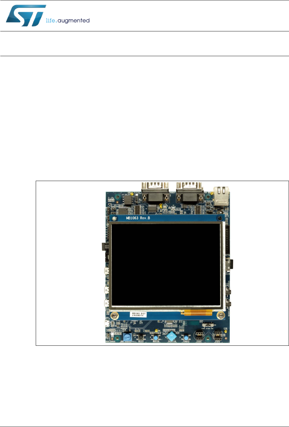
Figure 1. STM32H743I-EVAL Evaluation board (top view)
1. Picture is not contractual.
www.st.com

Contents UM2198
2/69 DocID030511 Rev 1
Contents
1 Features . . . . . . . . . . . . . . . . . . . . . . . . . . . . . . . . . . . . . . . . . . . . . . . . . . . 6
2 Product marking . . . . . . . . . . . . . . . . . . . . . . . . . . . . . . . . . . . . . . . . . . . . 7
3 System requirements . . . . . . . . . . . . . . . . . . . . . . . . . . . . . . . . . . . . . . . . 7
4 Development toolchains . . . . . . . . . . . . . . . . . . . . . . . . . . . . . . . . . . . . . . 7
5 Demonstration software . . . . . . . . . . . . . . . . . . . . . . . . . . . . . . . . . . . . . . 7
6 Ordering information . . . . . . . . . . . . . . . . . . . . . . . . . . . . . . . . . . . . . . . . 8
7 Delivery recommendations . . . . . . . . . . . . . . . . . . . . . . . . . . . . . . . . . . . 8
8 Hardware layout and configuration . . . . . . . . . . . . . . . . . . . . . . . . . . . . . 9
8.1 STM32H743I-EVAL Evaluation board layout . . . . . . . . . . . . . . . . . . . . . . 10
8.2 STM32H743I-EVAL Evaluation board mechanical drawing . . . . . . . . . . . .11
8.3 Embedded ST_LINK/V2-1 . . . . . . . . . . . . . . . . . . . . . . . . . . . . . . . . . . . . 12
8.3.1 Drivers . . . . . . . . . . . . . . . . . . . . . . . . . . . . . . . . . . . . . . . . . . . . . . . . . . 12
8.3.2 ST-LINK/V2-1 firmware upgrade . . . . . . . . . . . . . . . . . . . . . . . . . . . . . . 13
8.4 Power Supply . . . . . . . . . . . . . . . . . . . . . . . . . . . . . . . . . . . . . . . . . . . . . . 13
8.5 Clock source . . . . . . . . . . . . . . . . . . . . . . . . . . . . . . . . . . . . . . . . . . . . . . . 16
8.6 Reset sources . . . . . . . . . . . . . . . . . . . . . . . . . . . . . . . . . . . . . . . . . . . . . 17
8.7 Boot option . . . . . . . . . . . . . . . . . . . . . . . . . . . . . . . . . . . . . . . . . . . . . . . . 17
8.8 Audio . . . . . . . . . . . . . . . . . . . . . . . . . . . . . . . . . . . . . . . . . . . . . . . . . . . . 18
8.9 USB OTG1 FS . . . . . . . . . . . . . . . . . . . . . . . . . . . . . . . . . . . . . . . . . . . . . 19
8.10 USB OTG2 HS and FS . . . . . . . . . . . . . . . . . . . . . . . . . . . . . . . . . . . . . . . 20
8.11 RS232 . . . . . . . . . . . . . . . . . . . . . . . . . . . . . . . . . . . . . . . . . . . . . . . . . . . 20
8.12 microSD card . . . . . . . . . . . . . . . . . . . . . . . . . . . . . . . . . . . . . . . . . . . . . . 21
8.13 External I2C connector . . . . . . . . . . . . . . . . . . . . . . . . . . . . . . . . . . . . . . . 21
8.14 FD-CAN . . . . . . . . . . . . . . . . . . . . . . . . . . . . . . . . . . . . . . . . . . . . . . . . . . 22
8.15 Ethernet . . . . . . . . . . . . . . . . . . . . . . . . . . . . . . . . . . . . . . . . . . . . . . . . . . 22
8.16 Memories . . . . . . . . . . . . . . . . . . . . . . . . . . . . . . . . . . . . . . . . . . . . . . . . . 22

DocID030511 Rev 1 3/69
UM2198 Contents
3
8.17 Twin Quad-SPI NOR Flash . . . . . . . . . . . . . . . . . . . . . . . . . . . . . . . . . . . 23
8.18 Analog input . . . . . . . . . . . . . . . . . . . . . . . . . . . . . . . . . . . . . . . . . . . . . . . 23
8.19 Display and input devices . . . . . . . . . . . . . . . . . . . . . . . . . . . . . . . . . . . . . 23
8.20 MFX (Multi Function eXpander) . . . . . . . . . . . . . . . . . . . . . . . . . . . . . . . . 25
9 Connectors . . . . . . . . . . . . . . . . . . . . . . . . . . . . . . . . . . . . . . . . . . . . . . . 26
9.1 Ethernet RJ45 connector CN1 . . . . . . . . . . . . . . . . . . . . . . . . . . . . . . . . . 26
9.2 RS232 connector CN2 . . . . . . . . . . . . . . . . . . . . . . . . . . . . . . . . . . . . . . . 26
9.3 CAN D-type, 9-pin male connector CN3 . . . . . . . . . . . . . . . . . . . . . . . . . 27
9.4 External I2C connector CN4 . . . . . . . . . . . . . . . . . . . . . . . . . . . . . . . . . . . 27
9.5 Analog input-output connector CN5 . . . . . . . . . . . . . . . . . . . . . . . . . . . . . 28
9.6 Daughterboard extension connector CN6 and CN7 . . . . . . . . . . . . . . . . . 28
9.7 ETM trace debugging connector CN8 . . . . . . . . . . . . . . . . . . . . . . . . . . . 33
9.8 JTAG/SWD connector CN9 . . . . . . . . . . . . . . . . . . . . . . . . . . . . . . . . . . . 33
9.9 Power connector CN10 . . . . . . . . . . . . . . . . . . . . . . . . . . . . . . . . . . . . . . 34
9.10 Memory connector CN11 and CN12 . . . . . . . . . . . . . . . . . . . . . . . . . . . . 34
9.11 microSD connector CN13 . . . . . . . . . . . . . . . . . . . . . . . . . . . . . . . . . . . . . 37
9.12 USB OTG2 HS Micro-AB connector CN14 . . . . . . . . . . . . . . . . . . . . . . . 38
9.13 USB OTG2 FS Micro-AB connector CN16 . . . . . . . . . . . . . . . . . . . . . . . . 39
9.14 USB OTG1 FS Micro-AB connector CN18 . . . . . . . . . . . . . . . . . . . . . . . . 39
9.15 Audio jack CN17 . . . . . . . . . . . . . . . . . . . . . . . . . . . . . . . . . . . . . . . . . . . . 40
9.16 Audio jack (speaker) CN19 . . . . . . . . . . . . . . . . . . . . . . . . . . . . . . . . . . . 40
9.17 TFT LCD connector CN20 . . . . . . . . . . . . . . . . . . . . . . . . . . . . . . . . . . . . 40
9.18 ST-LINK/V2-1 programming connector CN21 . . . . . . . . . . . . . . . . . . . . . 40
9.19 MFX programming connector CN22 . . . . . . . . . . . . . . . . . . . . . . . . . . . . . 40
9.20 ST-LINK/V2-1 USB Micro-B connector CN23 . . . . . . . . . . . . . . . . . . . . . 40
9.21 MEMS microphone coupon connectors CN25 and CN26 . . . . . . . . . . . . 41
Appendix A STM32H743I-EVAL I/O assignment . . . . . . . . . . . . . . . . . . . . . . . . . 42
Appendix B Electrical schematics . . . . . . . . . . . . . . . . . . . . . . . . . . . . . . . . . . . . 48
Appendix C Board revision history and limitations . . . . . . . . . . . . . . . . . . . . . . 67
Revision history . . . . . . . . . . . . . . . . . . . . . . . . . . . . . . . . . . . . . . . . . . . . . . . . . . . . 68

List of tables UM2198
4/69 DocID030511 Rev 1
List of tables
Table 1. Ordering information . . . . . . . . . . . . . . . . . . . . . . . . . . . . . . . . . . . . . . . . . . . . . . . . . . . . . . . 8
Table 2. Mechanical dimensions . . . . . . . . . . . . . . . . . . . . . . . . . . . . . . . . . . . . . . . . . . . . . . . . . . . 11
Table 3. Power related jumpers . . . . . . . . . . . . . . . . . . . . . . . . . . . . . . . . . . . . . . . . . . . . . . . . . . . . 15
Table 4. 25-MHz crystal X1 related solder bridges . . . . . . . . . . . . . . . . . . . . . . . . . . . . . . . . . . . . . . 17
Table 5. 32 KHz crystal X2 related solder bridges . . . . . . . . . . . . . . . . . . . . . . . . . . . . . . . . . . . . . . 17
Table 6. Boot related switches . . . . . . . . . . . . . . . . . . . . . . . . . . . . . . . . . . . . . . . . . . . . . . . . . . . . . 18
Table 7. Boot related jumpers. . . . . . . . . . . . . . . . . . . . . . . . . . . . . . . . . . . . . . . . . . . . . . . . . . . . . . 18
Table 8. Audio related switch and jumper. . . . . . . . . . . . . . . . . . . . . . . . . . . . . . . . . . . . . . . . . . . . . 19
Table 9. USB OTG2 and USART1 function configuration . . . . . . . . . . . . . . . . . . . . . . . . . . . . . . . . 20
Table 10. USART1 related jumpers . . . . . . . . . . . . . . . . . . . . . . . . . . . . . . . . . . . . . . . . . . . . . . . . . . 21
Table 11. CAN related jumpers and solder bridges . . . . . . . . . . . . . . . . . . . . . . . . . . . . . . . . . . . . . . 22
Table 12. Ethernet related jumpers . . . . . . . . . . . . . . . . . . . . . . . . . . . . . . . . . . . . . . . . . . . . . . . . . . 22
Table 13. NOR Flash related jumpers . . . . . . . . . . . . . . . . . . . . . . . . . . . . . . . . . . . . . . . . . . . . . . . . 23
Table 14. LCD module connector (CN20) . . . . . . . . . . . . . . . . . . . . . . . . . . . . . . . . . . . . . . . . . . . . . 24
Table 15. MFX signals . . . . . . . . . . . . . . . . . . . . . . . . . . . . . . . . . . . . . . . . . . . . . . . . . . . . . . . . . . . . 25
Table 16. RJ45 connector CN1 . . . . . . . . . . . . . . . . . . . . . . . . . . . . . . . . . . . . . . . . . . . . . . . . . . . . . 26
Table 17. RS232 connector CN2 with ISP support. . . . . . . . . . . . . . . . . . . . . . . . . . . . . . . . . . . . . . . 26
Table 18. CAN D-type 9-pin male connector CN3 . . . . . . . . . . . . . . . . . . . . . . . . . . . . . . . . . . . . . . . 27
Table 19. I2C EXT connector CN4 . . . . . . . . . . . . . . . . . . . . . . . . . . . . . . . . . . . . . . . . . . . . . . . . . . . 28
Table 20. Analog input-output connector CN5 . . . . . . . . . . . . . . . . . . . . . . . . . . . . . . . . . . . . . . . . . . 28
Table 21. Daughterboard extension connector CN6 . . . . . . . . . . . . . . . . . . . . . . . . . . . . . . . . . . . . . 29
Table 22. Daughterboard extension connector CN7 . . . . . . . . . . . . . . . . . . . . . . . . . . . . . . . . . . . . . 30
Table 23. ETM Trace debugging connector CN8 . . . . . . . . . . . . . . . . . . . . . . . . . . . . . . . . . . . . . . . . 33
Table 24. JTAG/SWD debugging connector CN9 . . . . . . . . . . . . . . . . . . . . . . . . . . . . . . . . . . . . . . . 34
Table 25. Memory connector CN11 . . . . . . . . . . . . . . . . . . . . . . . . . . . . . . . . . . . . . . . . . . . . . . . . . . 35
Table 26. Memory connector CN12 . . . . . . . . . . . . . . . . . . . . . . . . . . . . . . . . . . . . . . . . . . . . . . . . . . 36
Table 27. microSD connector CN13 . . . . . . . . . . . . . . . . . . . . . . . . . . . . . . . . . . . . . . . . . . . . . . . . . . 38
Table 28. USB OTG HS Micro-AB connector CN14 . . . . . . . . . . . . . . . . . . . . . . . . . . . . . . . . . . . . . . 38
Table 29. USB OTG1 FS Micro-AB connector CN18 . . . . . . . . . . . . . . . . . . . . . . . . . . . . . . . . . . . . . 39
Table 30. USB OTG1 FS Micro-AB connector CN18 . . . . . . . . . . . . . . . . . . . . . . . . . . . . . . . . . . . . . 39
Table 31. USB Micro-B connector CN23 (front view) . . . . . . . . . . . . . . . . . . . . . . . . . . . . . . . . . . . . . 40
Table 32. 2.21 MEMS microphone coupon connectors CN25 and CN26. . . . . . . . . . . . . . . . . . . . . . 41
Table 33. STM32H743I-EVAL I/O assignment . . . . . . . . . . . . . . . . . . . . . . . . . . . . . . . . . . . . . . . . . . 42
Table 34. Board revision history and limitations . . . . . . . . . . . . . . . . . . . . . . . . . . . . . . . . . . . . . . . . . 67
Table 35. Document revision history . . . . . . . . . . . . . . . . . . . . . . . . . . . . . . . . . . . . . . . . . . . . . . . . . 68

DocID030511 Rev 1 5/69
UM2198 List of figures
5
List of figures
Figure 1. STM32H743I-EVAL Evaluation board (top view) . . . . . . . . . . . . . . . . . . . . . . . . . . . . . . . . . 1
Figure 2. Hardware block diagram . . . . . . . . . . . . . . . . . . . . . . . . . . . . . . . . . . . . . . . . . . . . . . . . . . . . 9
Figure 3. STM32H743I-EVAL Evaluation board (top side) . . . . . . . . . . . . . . . . . . . . . . . . . . . . . . . . 10
Figure 4. STM32H743I-EVAL Evaluation board mechanical drawing . . . . . . . . . . . . . . . . . . . . . . . . 11
Figure 5. USB composite device . . . . . . . . . . . . . . . . . . . . . . . . . . . . . . . . . . . . . . . . . . . . . . . . . . . . 13
Figure 6. Orientation setting of 5.7-inch LCD daughterboard . . . . . . . . . . . . . . . . . . . . . . . . . . . . . . 25
Figure 7. Ethernet RJ45 connector CN1 (front view) . . . . . . . . . . . . . . . . . . . . . . . . . . . . . . . . . . . . . 26
Figure 8. RS232 connector CN2 (front view) . . . . . . . . . . . . . . . . . . . . . . . . . . . . . . . . . . . . . . . . . . . 26
Figure 9. CAN D-type, 9-pin connector CN3 (front view) . . . . . . . . . . . . . . . . . . . . . . . . . . . . . . . . . . 27
Figure 10. I2C EXT connector CN4 (front view) . . . . . . . . . . . . . . . . . . . . . . . . . . . . . . . . . . . . . . . . . 27
Figure 11. Analog input-output connector CN5 (top view) . . . . . . . . . . . . . . . . . . . . . . . . . . . . . . . . . . 28
Figure 12. ETM trace debugging connector CN8 (top view) . . . . . . . . . . . . . . . . . . . . . . . . . . . . . . . . 33
Figure 13. JTAG/SWD debugging connector CN9 (top view) . . . . . . . . . . . . . . . . . . . . . . . . . . . . . . . 33
Figure 14. Power supply connector CN10 (front view) . . . . . . . . . . . . . . . . . . . . . . . . . . . . . . . . . . . . 34
Figure 15. microSD connector (top view). . . . . . . . . . . . . . . . . . . . . . . . . . . . . . . . . . . . . . . . . . . . . . . 37
Figure 16. USB OTG HS Micro-AB connector CN14 (front view) . . . . . . . . . . . . . . . . . . . . . . . . . . . . 38
Figure 17. USB OTG FS Micro-AB connector CN16 (front view). . . . . . . . . . . . . . . . . . . . . . . . . . . . . 39
Figure 18. USB OTG FS Micro-AB connector CN18 (front view). . . . . . . . . . . . . . . . . . . . . . . . . . . . . 39
Figure 19. USB Micro-B connector CN23 (front view) . . . . . . . . . . . . . . . . . . . . . . . . . . . . . . . . . . . . . 40
Figure 20. MEMS microphone coupon connectors CN25 and CN26 (top view) . . . . . . . . . . . . . . . . . 41
Figure 21. STM32H743I-EVAL Evaluation board . . . . . . . . . . . . . . . . . . . . . . . . . . . . . . . . . . . . . . . . 49
Figure 22. STM32H743I-EVAL MCU . . . . . . . . . . . . . . . . . . . . . . . . . . . . . . . . . . . . . . . . . . . . . . . . . . 50
Figure 23. Power . . . . . . . . . . . . . . . . . . . . . . . . . . . . . . . . . . . . . . . . . . . . . . . . . . . . . . . . . . . . . . . . . 51
Figure 24. SRAM, FLASH and SDRAM . . . . . . . . . . . . . . . . . . . . . . . . . . . . . . . . . . . . . . . . . . . . . . . . 52
Figure 25. Audio. . . . . . . . . . . . . . . . . . . . . . . . . . . . . . . . . . . . . . . . . . . . . . . . . . . . . . . . . . . . . . . . . . 53
Figure 26. LCD connectors . . . . . . . . . . . . . . . . . . . . . . . . . . . . . . . . . . . . . . . . . . . . . . . . . . . . . . . . . 54
Figure 27. Ethernet . . . . . . . . . . . . . . . . . . . . . . . . . . . . . . . . . . . . . . . . . . . . . . . . . . . . . . . . . . . . . . . 55
Figure 28. USB OTG HS . . . . . . . . . . . . . . . . . . . . . . . . . . . . . . . . . . . . . . . . . . . . . . . . . . . . . . . . . . . 56
Figure 29. USB OTG FS . . . . . . . . . . . . . . . . . . . . . . . . . . . . . . . . . . . . . . . . . . . . . . . . . . . . . . . . . . . 57
Figure 30. RS232. . . . . . . . . . . . . . . . . . . . . . . . . . . . . . . . . . . . . . . . . . . . . . . . . . . . . . . . . . . . . . . . . 58
Figure 31. FDCAN and QSPI . . . . . . . . . . . . . . . . . . . . . . . . . . . . . . . . . . . . . . . . . . . . . . . . . . . . . . . . 59
Figure 32. microSD 3.0 card . . . . . . . . . . . . . . . . . . . . . . . . . . . . . . . . . . . . . . . . . . . . . . . . . . . . . . . . 60
Figure 33. Peripherals . . . . . . . . . . . . . . . . . . . . . . . . . . . . . . . . . . . . . . . . . . . . . . . . . . . . . . . . . . . . . 61
Figure 34. Extension connectors . . . . . . . . . . . . . . . . . . . . . . . . . . . . . . . . . . . . . . . . . . . . . . . . . . . . . 62
Figure 35. ST-LINK/V2-1 . . . . . . . . . . . . . . . . . . . . . . . . . . . . . . . . . . . . . . . . . . . . . . . . . . . . . . . . . . . 63
Figure 36. MFX . . . . . . . . . . . . . . . . . . . . . . . . . . . . . . . . . . . . . . . . . . . . . . . . . . . . . . . . . . . . . . . . . . 64
Figure 37. JTAG and trace. . . . . . . . . . . . . . . . . . . . . . . . . . . . . . . . . . . . . . . . . . . . . . . . . . . . . . . . . . 65
Figure 38. 5.7” LCD board . . . . . . . . . . . . . . . . . . . . . . . . . . . . . . . . . . . . . . . . . . . . . . . . . . . . . . . . . . 66

Features UM2198
6/69 DocID030511 Rev 1
1 Features
•STM32H743XIH6 microcontroller with 2 Mbytes of Flash memory and 1 Mbyte of RAM
in TFBGA240+25 package
•5.7” 640x480 TFT-color LCD with touch screen
•Ethernet compliant with IEEE-802.3-2002
•USB OTG HS and FS
•I2C compatible serial interface
•RTC with rechargeable backup battery
•SAI Audio DAC
•ST-MEMS digital microphones
•8-Gbyte (or more) SDIO3.0 interface microSD™ card
•8Mx32-bit SDRAM, 1Mx16bit SRAM and 8Mx16-bit NOR Flash
•1 1-Gbit Twin Quad-SPI NOR Flash memory or two 512Mb Quad-SPI NOR Flash
memories
•Potentiometer
•4 colored LEDs
•Reset, wakeup, tamper or key buttons
•Joystick with 4-direction control and selector
•Board connectors
–Power jack
– 3 USB with Micro-AB
– RS-232 communications
– Ethernet RJ45
– FD-CAN compliant connection
– Stereo headset jack including analog microphone input
– 2 audio jacks for external speakers
–microSD
™ card
– JTAG/SWD and ETM trace
•Board expansion connectors:
– Extension connectors and memory connectors for daughterboard or wire-wrap
board
•Flexible power-supply options: ST-LINK USB VBUS or external sources
•On-board ST-LINK/V2-1 debugger/programmer with USB
re-enumeration capability: mass storage, virtual COM port and debug port
•Comprehensive free software libraries and examples available with the STM32Cube
package

DocID030511 Rev 1 7/69
UM2198 Product marking
68
2 Product marking
Evaluation tools marked as “ES” or “E” are not yet qualified and therefore not ready to be
used as reference design or in production. Any consequences deriving from such usage will
not be at ST charge. In no event, ST will be liable for any customer usage of these
engineering sample tools as reference design or in production.
“E” or “ES” marking examples of location:
•On the targeted STM32 that is soldered on the board (for illustration of STM32 marking,
refer to the STM32 datasheet “Package information” paragraph at the www.st.com
website).
Next to the evaluation tool ordering part number that is stuck or silk-screen printed on the
board.
3 System requirements
•Windows® OS (XP, 7, 8 and 10), Linux® or MacOS™
•USB Type-A to Micro-B cable
4 Development toolchains
•ARM® Keil®: MDK-ARM(a)
•IAR™: EWARM(a)
•GCC-based IDEs: free SW4STM32 from AC6
5 Demonstration software
The demonstration software is preloaded in the STM32H743XI Flash memory for easy
demonstration of the device peripherals in standalone mode. The latest versions of the
demonstration source code and associated documentation can be downloaded from the
www.st.com website.
a. On Windows® only.
Ordering information UM2198
8/69 DocID030511 Rev 1
6 Ordering information
To order the STM32H743I-EVAL Evaluation board, refer to Table 1:
7 Delivery recommendations
Some verifications are needed before using the Evaluation board for the first time, to make
sure that no damage occurred during shipment and that no components are unplugged or
lost.
When the board is extracted from its plastic bag, check that no component remains in the
bag. The main component to verify is the microSD card that may have been ejected from
the connector CN13 (right side of the board).
Caution: There is an explosion risk if the battery is replaced by an incorrect one. Make sure to
dispose of used batteries according to the instructions.
Table 1. Ordering information
Order code Target STM32
STM32H743I-EVAL STM32H743XI
DocID030511 Rev 1 9/69
UM2198 Hardware layout and configuration
68
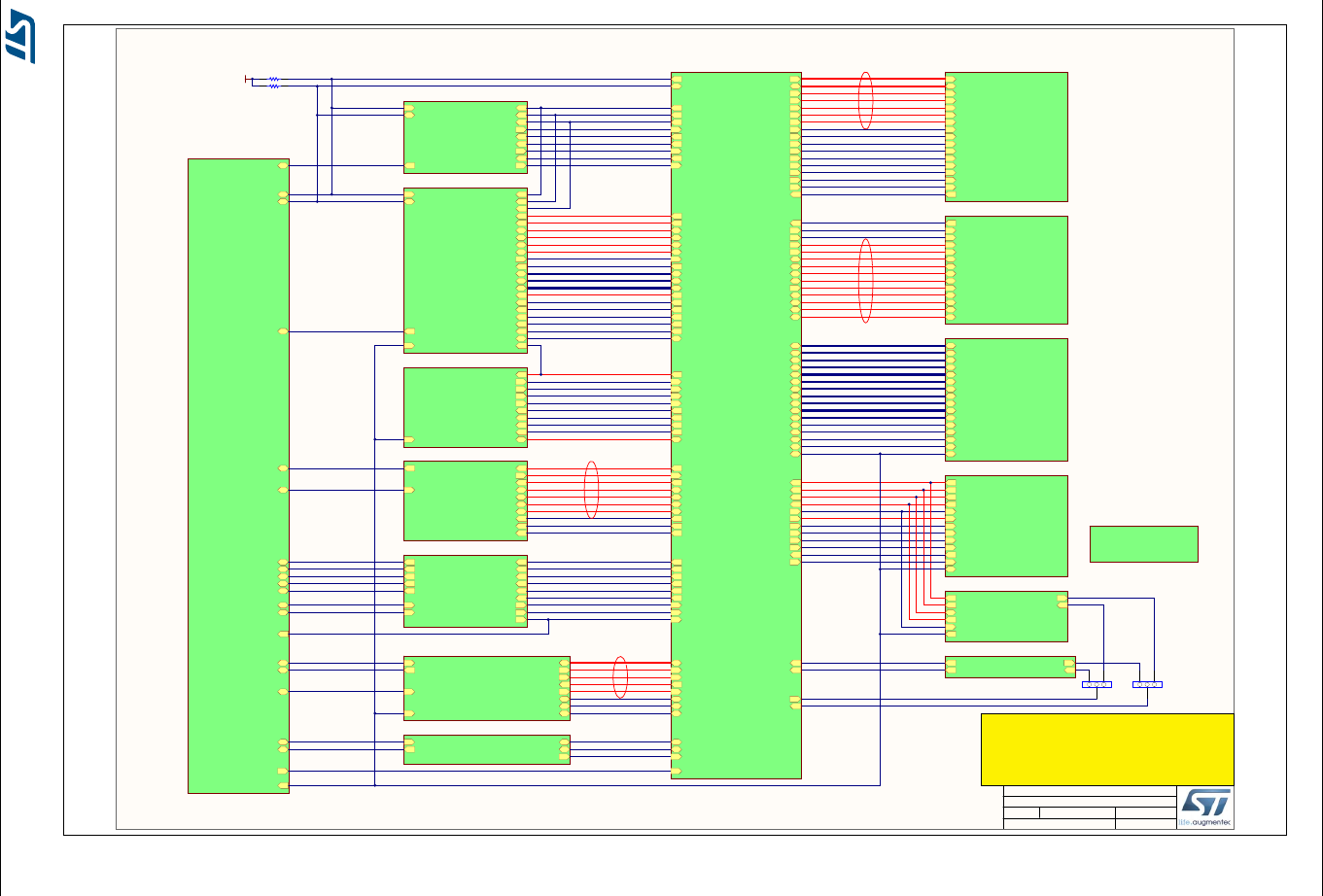
8 Hardware layout and configuration
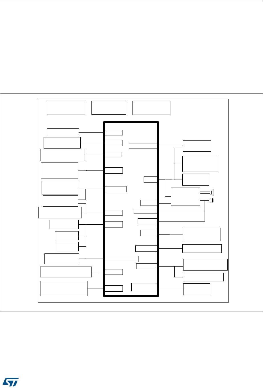
The STM32H743I-EVAL Evaluation board is designed around the STM32H743XIH6
(240+25-pin TFBGA package) microcontroller. The hardware block diagram (see Figure 2)
illustrates the connection between STM32H743XIH6 and the peripherals (SDRAM, SRAM,
NOR Flash, Twin Quad-SPI Flash, color LCD, USB OTG connectors, USART, Ethernet,
Audio, FD-CAN, microSD 3.0 card and embedded ST-LINK). Figure 3 helps users to locate
these features on the Evaluation board. The mechanical dimensions of the board are
showed in Figure 4.
Figure 2. Hardware block diagram
06Y9
670+;,+
9EDWWHU\
$XGLR'$&
DQG
$PSOLILHU
57&
3+<DQG(WKHUQHW
FRQQHFWRU
-7$*DQG7UDFH
FRQQHFWRU '$3
56'%
FRQQHFWRU
.+]FU\VWDO
9%$7
67/,1.9
,&
86%FRQQHFWRU
6:DQG7UDFH
FRQQHFWRU 73,8
9*$
/&'
50,,
6$,
,&
FRQQHFWRU
/&'5*%
0);
-R\VWLFN/('
PLFUR6'FDUG
&$1FRQQHFWRU
)'&$1
.H\:DNHXSDQG
7DPSHUEXWWRQV *3,2
3RWHQWLRPHWHU
$'&
6'00& +63+<DQG86%
FRQQHFWRU
27*
125)ODVK
65$0
)0&
6'5$0
463,
*E\WH7ZLQ
463,)ODVK
27*)6 86%
FRQQHFWRU
8$57
')6'0
3'0
93RZHU
6XSSO\
93RZHU
6XSSO\
96'
3RZHU6XSSO\
Hardware layout and configuration UM2198
10/69 DocID030511 Rev 1
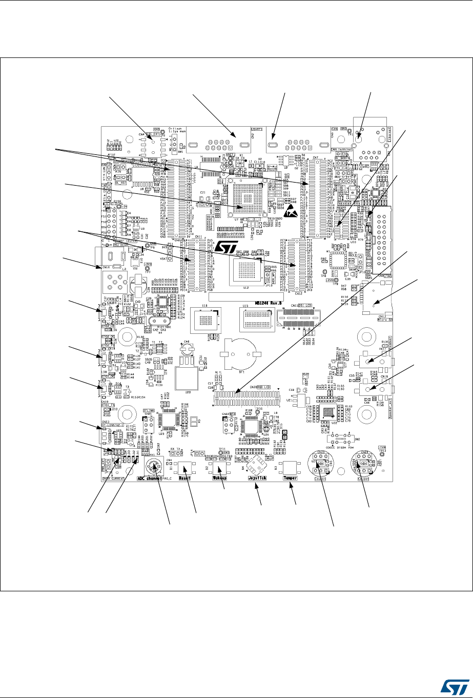
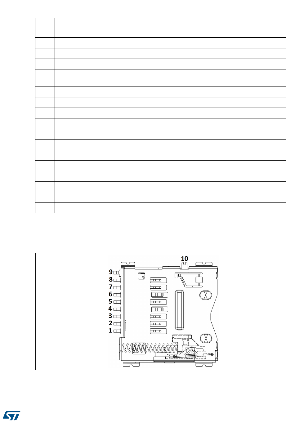
8.1 STM32H743I-EVAL Evaluation board layout
Figure 3. STM32H743I-EVAL Evaluation board (top side)
06Y9
&1
,&H[WHQVLRQFRQQHFWRU
&1&1
([WHQVLRQ
KHDGHU
8
670+;,+
&1&1
0HPRU\KHDGHU
&1
86$57
&1
)'&$1
&1
(WKHUQHW5-FRQQHFWRU
&1
3RZHU-DFN
&1
86%27*+6
&1
86%27*)6
&1
86%27*)6
&1
67/,1.986%
/'
67/,1.9
3RZHURYHUFXUUHQWDODUP
/'
67/,1.9
&20/(' FRORU/('6 593RWHQWLRPHWHU
%5HVHWEXWWRQ
%:DNHXS
EXWWRQ %
-R\VWLFN %
7DPSHU
%XWWRQ 8&1
OHIWGLJLWDOPLFURSKRQH
FRXSRQFRQQHFWRUV
8&1
ULJKWGLJLWDOPLFURSKRQH
FRXSRQFRQQHFWRUV
&1
(7075$&(
&1-7$*6:'
&1
&RORU/&'
FRQQHFWRU
&1
PLFUR6'FDUG
&1
KHDGVHWDXGLRMDFN
&1
VSHDNHURXW
FRQQHFWRU
DocID030511 Rev 1 11/69
UM2198 Hardware layout and configuration
68
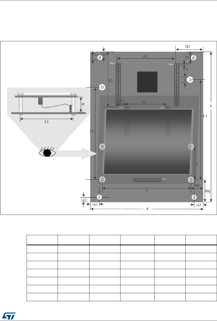
8.2 STM32H743I-EVAL Evaluation board mechanical drawing
Figure 4 and Table 2 show the mechanical dimensions for the MB1246 board with the 5.7”
LCD daughterboard.
Figure 4. STM32H743I-EVAL Evaluation board mechanical drawing
Table 2. Mechanical dimensions
Symbol Size (mm) Symbol Size (mm) Symbol Size (mm)
A1 68.58 e 116.5 My 32.7
A2 48.62 H 8 P1 16.76
a 1.27 Lx1 13.7 P2 55.32
D4.5Lx225 Q139.23
d 3.5 Ly1 5 Q2 9.98
E1 107 Ly2 6.4 X 141.60
E2 114.18 Mx 12.5 Y 172.72

Hardware layout and configuration UM2198
12/69 DocID030511 Rev 1
8.3 Embedded ST_LINK/V2-1
The ST-LINK/V2-1 programming and debugging tool is integrated on the STM32H743I-
EVAL Evaluation board. Compared to ST-LINK/V2 the changes are listed below.
The new features supported on ST-LINK/V2-1 are:
•USB software re-enumeration
•Virtual COM port interface on USB
•Mass storage interface on USB
•USB power management request for more than 100mA power on USB
This feature is no more supported on ST-LINK/V2-1: SWIM interface
For all general information concerning debugging and programming features common
between V2 and V2-1 versions, refer to ST-LINK/V2 in-circuit debugger/programmer for
STM8 and STM32 User manual (UM1075) at the www.st.com website.
Note:1 It is possible to power the Evaluation board through CN23 (Embedded ST-LINK/V2-1 USB
connector) even if an external tool is connected to CN8 (ETM Trace connector) or CN9
(External JTAG and SWD connector).
Note:2 ETM can only work at 50 MHz clock by default because ETM signals are shared with other
peripherals. If better performance of ETM is required (84 MHz/98 MHz), R217, R230, R231,
R234, R236, SB2, SB5, SB8, SB11, SB42, SB57 must be removed to reduce the stub on
ETM signals. In this configuration SAI and PDM are not functional and NOR Flash and the
address of SRAM are limited on A18.
Note:3 ETM trace function would be abnormal as SAI_SDB share the same pins with TRACE_D0,
and TRACE_D0 would be forced high by SAI_SDB. When using ETM trace it is necessary
to set ADCDAT1 pin (SAI_SDB signal of the STM32) of audio codec WM8994ECS/R (U22)
by software to be tri-state.
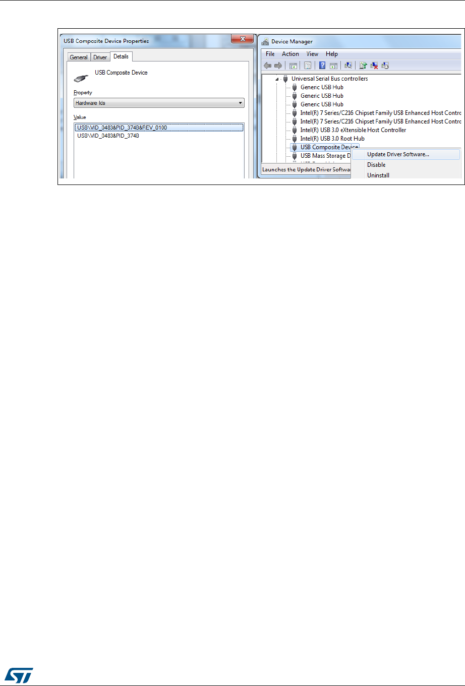
8.3.1 Drivers
Before connecting the STM32H743I-EVAL Evaluation board to a Windows® PC (XP, 7, 8 or
10) through a USB, a driver for the ST-LINK/V2-1 must be installed. It is available at the
www.st.com website.
In case the STM32H743I-EVAL Evaluation board is connected to the PC before the driver is
installed, some STM32H743I-EVAL interfaces may be declared as "unknown" in the PC
device manager. To recover from this situation the user has to install the driver files, and
update the driver of the connected device from the device manager (see Figure 5).
Note: Prefer using the "USB Composite Device" handle for a full recovery.
DocID030511 Rev 1 13/69
UM2198 Hardware layout and configuration
68
Figure 5. USB composite device
8.3.2 ST-LINK/V2-1 firmware upgrade
The ST-LINK/V2-1 embeds a firmware upgrade mechanism for in-situ upgrade through the
USB port. As the firmware may evolve during the life time of the ST-LINK/V2-1 product (for
example new functionalities, bug fixes, support for new microcontroller families), it is
recommended to visit www.st.com before starting to use the STM32H743I-EVAL Evaluation
board and periodically, to stay up-to-date with the latest firmware version.
8.4 Power Supply
The STM32H743I-EVAL Evaluation board is designed to be powered by 5 V DC power
supply and is protected by PolyZen from wrong power plug-in events. It is possible to
configure the Evaluation board to use any of the following six sources for the power supply:
•5 V DC power adapter connected to CN10, the power jack on the board (Power Supply
Unit on silk screen of JP10 (PSU)).
•5 V DC power with 500 mA limitation from CN23, the USB Micro-B connector of ST-
LINK/V2-1 (USB 5 V power source on silkscreen of JP10 (STlk)). If the USB
enumeration succeeds (as explained below), the ST-LINK U5V power is enabled, by
asserting the PWR_EN pin. This pin is connected to a power switch (ST890) that
powers the board. This power switch features also a current limitation to protect the PC
in case of short-circuit on the board. If overcurrent (more than 600 mA) happens on the
board, the LED LD11 lights up.
•5 V DC power with 500 mA limitation from CN14, the USB OTG2 HS Micro-AB
connector (USB 5V power source on silkscreen of JP10 (HS)).
•5 V DC power with 500 mA limitation from CN18, the USB OTG1 FS Micro-AB
connector (USB 5V power source on silkscreen of JP10 (FS1)).
•5 V DC power with 500 mA limitation from CN16, the USB OTG2 FS Micro-AB
connector (USB 5V power source on silkscreen of JP10 (FS2)).
•5 V DC power from CN6 and CN7, the extension connectors for daughterboard
(daughterboard power source on silkscreen of JP10 (D5V)).
The STM32H743I-EVAL Evaluation board can be powered from the ST-LINK/V2-1 USB
connector CN23 (U5V), but only the ST-LINK/V2-1 circuit has the power before USB
enumeration, because the host PC only provides 100 mA to the board at that time. During
the USB enumeration phase the STM32H743I-EVAL board requires 300 mA power from the

Hardware layout and configuration UM2198
14/69 DocID030511 Rev 1
host PC. If the host is able to provide the required power, the enumeration succeeds, the
power transistor U19 (ST890) is switched ON, the red LED LD9 is turned ON, and thus the
STM32H743I-EVAL board is powered and can consume maximum 300 mA current. If the
host PC is not able to provide the requested current, the enumeration fails. Therefore the
STM32 part including the extension board is not powered. As a consequence the red LED
LD9 remains turned OFF. In this case it is mandatory to use an external power supply to
supply extra power.
E5V (from PSU) or D5V can be used as an external power supply in case the current
consumption of the STM32H743I-EVAL board exceeds the allowed current on USB. In this
condition it is still possible to use USB for communication, programming or debugging only,
but it is mandatory to power the board first using E5V or D5V, and then connecting the USB
cable to the PC. Proceeding this way ensures that the enumeration succeeds thanks to the
external power source.
The following power sequence procedure must be respected:
1. Connect jumper JP10 for PSU or D5V side
2. Check that JP15 is removed
3. Connect the external power source to PSU or D5V (daughterboard mounted)
4. Check red LED LD9 is turned ON
5. Connect the PC to USB connector CN23
If this order is not respected, the board may be powered by VBUS first then by E5V or D5V,
and the following risks may be encountered:
1. If more than 300 mA current is needed by the board, the PC may be damaged or
current can be limited by PC. As a consequence the board is not powered correctly.
2. 300 mA is requested at the enumeration phase (since JP15 must be OFF), so there is
risk that the request is rejected and the enumeration does not succeed if PC cannot
provide such current. Consequently the board is not powered (LED LD9 remains OFF).
Note: In case the STM32H743I-EVAL board is powered by a USB charger, there is no USB
enumeration, so the led LD9 remains set to OFF permanently and the board is not powered.
Only in this specific case the jumper JP15 needs to be set to ON, to allow the board to be
powered anyway.
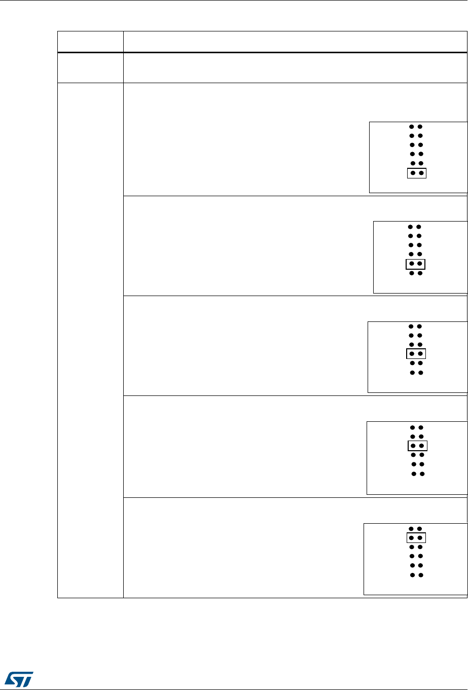
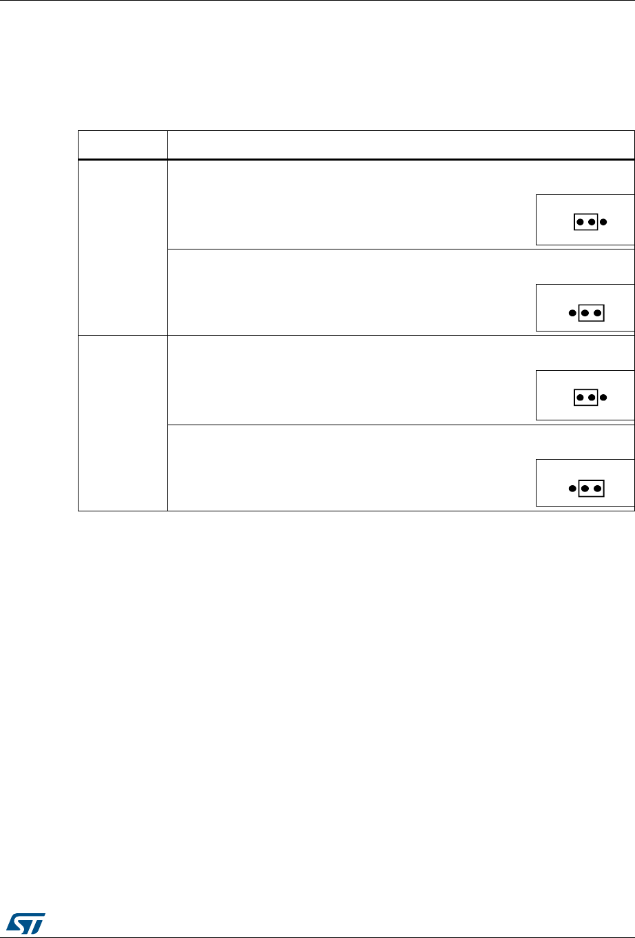
The power supply is configured by setting the related jumpers JP9, JP10 and JP11 as
described in Table 3.
DocID030511 Rev 1 15/69
UM2198 Hardware layout and configuration
68
Table 3. Power related jumpers
Jumper Description
JP9 JP9 is used to measure STM32 current consumption manually by a multimeter.
Default setting: Fitted
JP10
JP10 is used to select one of the six possible power supply resources.
To supply the STM32H743I-EVAL board through the USB connector of the ST-
LINK/V2-1 (CN23) set JP10 as shown to the right: (default setting)
To supply the STM32H743I-EVAL board through the jack (CN10), set JP10 as
shown to the right:
To supply the STM32H743I-EVAL board through the daughterboard connectors
(CN6 and CN7), set JP10 as shown to the right:
To supply the STM32H743I-EVAL board through the USB OTG2 FS (CN16), set
JP10 as shown to the right:
To supply the STM32H743I-EVAL board through the USB OTG1 FS (CN18), set
JP10 as shown to the right:
+6
)6
)6
'9
368
67ON
069
+6
)6
)6
'9
368
67ON
069
+6
)6
)6
'9
368
67ON
069
+6
)6
)6
'9
368
67ON
069
+6
)6
)6
'9
368
67ON
069
Hardware layout and configuration UM2198
16/69 DocID030511 Rev 1
The LED LD9 lights up when the STM32H743I-EVAL Evaluation board is powered by the
5 V correctly.
Note: To avoid the impact of USB PHY, Ethernet PHY and get precise results about current
consumption on JP9, take into account the following cautions:
1) Remove JP5 to avoid Ethernet PHY influence
2) Configure USB HS PHY into low-power mode (Register Address=04, bit 6 in USB PHY)
8.5 Clock source
Two clock sources (X1 and X2) are available on the STM32H743I-EVAL Evaluation board
for the STM32H743XI and RTC embedded. Other clock sources (X3 and X4) are used for
their peripherals:
•X1, 25-MHz crystal for STM32H743XI, it can be disconnected by removing R15 and
R16 when internal RC clock is used
•X2, 32-KHz crystal for embedded RTC
•X3, 25-MHz crystal for Ethernet PHY
•X4, 24-MHz crystal for USB OTG2 HS PHY
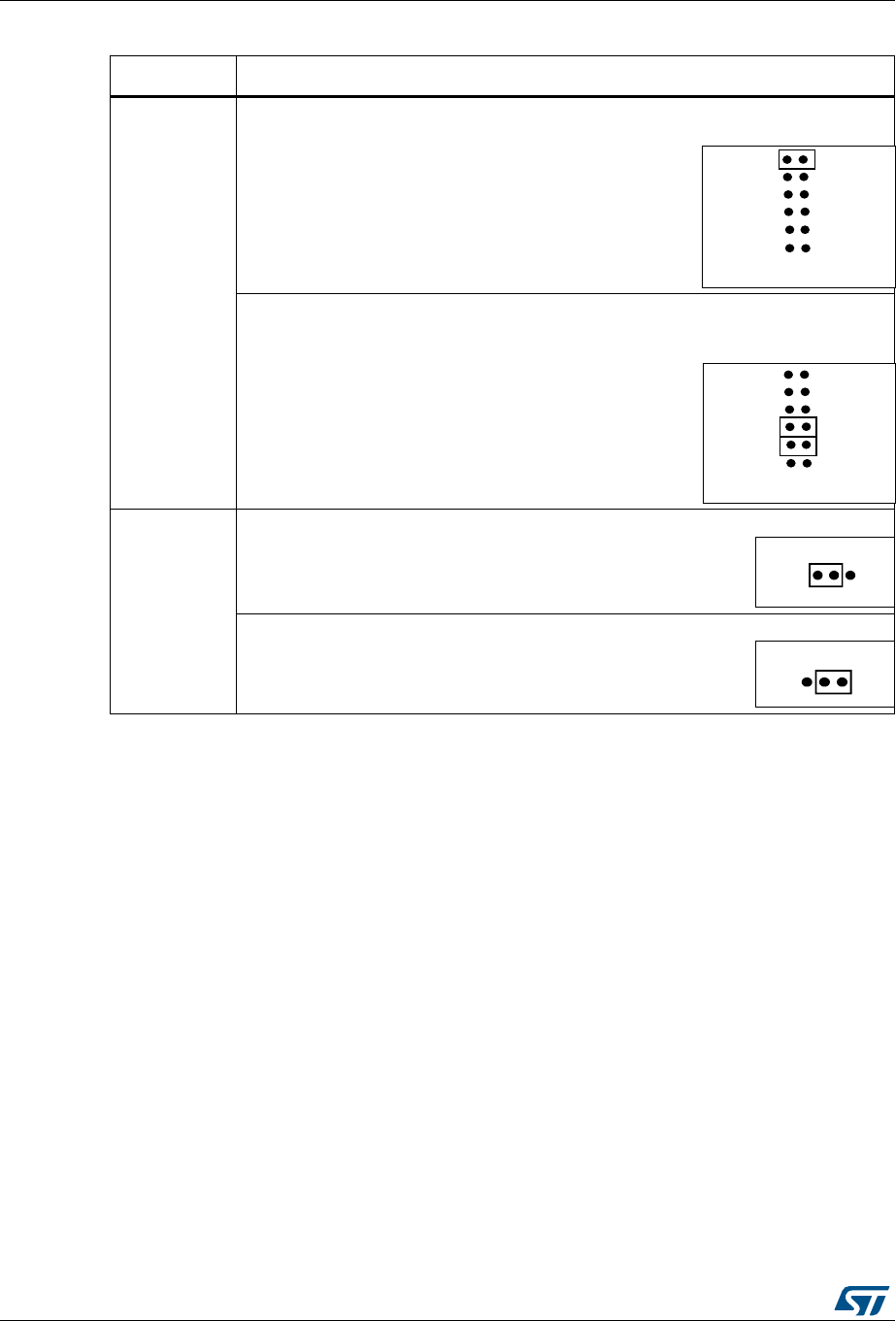
JP10
To supply the STM32H743I-EVAL board through the USB OTG2 HS (CN14), set
JP10 as shown to the right:
To supply the STM32H743I-EVAL board and the daughterboard connected on CN6
and CN7 through the power supply jack (CN10), set JP10 as shown to the right
(daughterboard must not have its power supply connected)
JP11
VBAT is connected to +3.3 V when JP11 is set as shown to the right: (Default setting)
VBAT is connected to the battery when JP11 is set as shown to the right:
Table 3. Power related jumpers (continued)
Jumper Description
+6
)6
)6
'9
368
67ON
069
+6
)6
)6
'9
368
67ON
069
DocID030511 Rev 1 17/69
UM2198 Hardware layout and configuration
68
Note: For Ethernet clock and jumper JP5 configuration refer to Section 8.15.
8.6 Reset sources
The reset signal of STM32H743I-EVAL Evaluation board is low active and the reset sources
include:
•Reset button B1
•Debugging tools from JTAG/SWD connector CN9 and ETM trace connector CN8
•Daughterboard from CN6
•Embedded ST-LINK/V2-1
•RS232 connector CN2 for ISP.
Note: The jumper JP6 has to be closed for RESET handled by pin 8 of RS232 connector CN2
(CTS signal).
8.7 Boot option
The STM32H743I-EVAL Evaluation board can boot from:
•Embedded user Flash
•System memory with boot loader for ISP
•Embedded SRAM for debugging
The boot option is configured by setting the switch SW1 (BOOT) and the boot base address
programmed in the BOOT_ADD0 and BOOT_ADD1 option bytes. The BOOT can be
configured also through the RS232 connector CN2.
Table 4. 25-MHz crystal X1 related solder bridges
Solder bridge Description
SB39
PH0 is connected to 25-MHz crystal when SB39 is open (Default setting).
PH0 is connected to extension connector CN6 when SB39 is closed. In such case
R15 must be removed to avoid disturbance due to the 25-MHz quartz.
SB40
PH1 is connected to 25-MHz crystal when SB40 is open (Default setting).
PH1 is connected to extension connector CN6 when SB40 is closed. In such case
R16 must be removed to avoid disturbance due to the 25-MHz quartz.
Table 5. 32 KHz crystal X2 related solder bridges
Solder
bridge Description
SB1
PC14 is connected to 32-KHz crystal when SB1 is open (Default setting).
PC14 is connected to extension connector CN7 when SB1 is closed. In such case
R18 must be removed to avoid disturbance due to the 32-Khz quartz.
SB4
PC15 is connected to 32-KHz crystal when SB4 is open (Default setting).
PC15 is connected to extension connector CN7 when SB4 is closed. In such case
R17 must be removed to avoid disturbance due to the 32-Khz quartz.
Hardware layout and configuration UM2198
18/69 DocID030511 Rev 1
8.8 Audio
An audio codec WM8994ECS/R with 4 DACs and 2 ADCs inside is connected to the SAI
interface of the STM32H743XI microcontroller to support the TDM feature on SAI port. This
feature is able to implement audio recording on digital and analog microphones and audio
playback of various audio streams on headphone and lineout at the same time.
It communicates with STM32H743XI through I2C1 bus which is shared with LCD and MFX
(Multi Function eXpander).
The analog microphone on the headset is connected to the ADC of the WM8994ECS/R
through the audio jack CN17. External speakers can be connected to WM8994ECS/R
through the audio jack CN19.
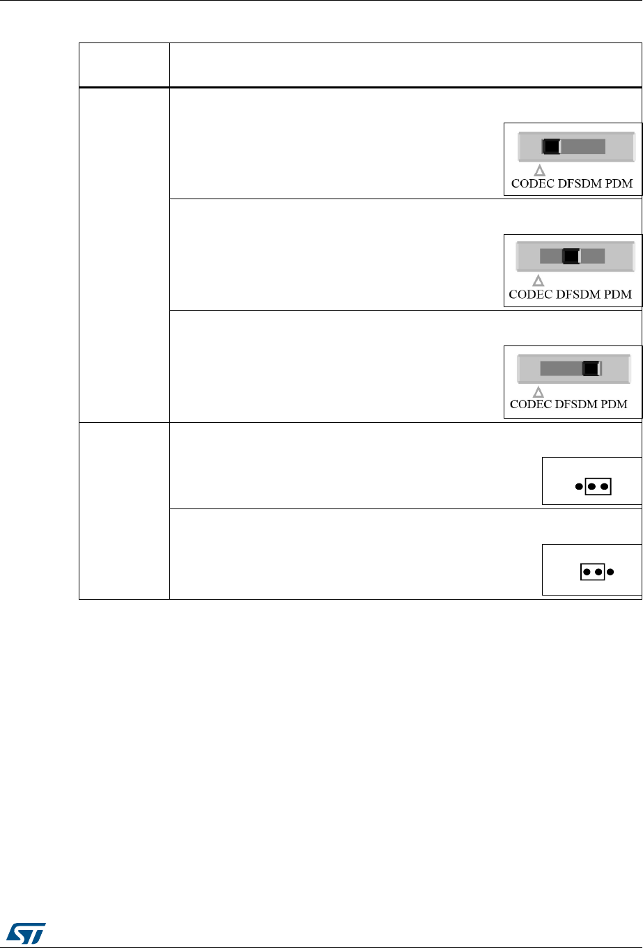
Two digital microphones (ST-MEMS microphones) MP34DT01TR are on the STM32H743I-
EVAL Evaluation board. They can be connected to either an audio codec DFSDM or to the
PDM port of the STM32H743XI, by setting the switch SW2 shown in Table 8. The coupon
connectors CN25 and CN26 can be used to support ST-MEMS microphone STEVAL-
MKI129V1 after removing SB54 and SB55 solder bridges.
Table 6. Boot related switches
Switch
configuration
Boot address
option bytes Boot space
(Default setting)
BOOT_ADD0
[15:0]
CPU boot address defined by user option byte
BOOT_ADD0[15:0]
ST programmed value: Flash at 0x0800 0000.
BOOT_ADD1
[15:0]
CPU boot address defined by user option byte
BOOT_ADD1[15:0]
ST programmed value: System boot loader at 0x0000 0000.
Table 7. Boot related jumpers
Jumper Description
JP3
The Bootloader_BOOT0 is managed by pin 6 of connector CN2 (RS232 DSR signal)
when JP3 is closed. This configuration is used for boot-loader application only.
Default Setting: Not fitted
SW1
0<->1
SW1
0<->1
DocID030511 Rev 1 19/69
UM2198 Hardware layout and configuration
68
Note:1 I2C address of WM8994ECS/R is 0b0011010.
Note:2 PDM clock is on PE2 and it conflicts with SAI_CLK on PE2 by default. When PDM and SAI
functions are used at the same time, SB57 must be removed and SB56 must be closed to
move SAI_CLK to PG7.
8.9 USB OTG1 FS
The STM32H743I-EVAL Evaluation board supports USB OTG1 full-speed communication
through a USB Micro-AB connector (CN18) and USB power switch (U18) connected to
VBUS. The Evaluation board can be powered by this USB connection at 5 V DC with 500 mA
current limitation.
Table 8. Audio related switch and jumper
Switch/
Jumper Description
SW2
Digital microphone is connected to the audio codec when SW2 is set as shown to
the right (Default setting):
Digital microphone is connected to the DFSDM port of STM32H743XI when SW2 is
set as shown to the right:
Digital microphone is connected to the PDM port of STM32H743XI when SW2 is set
as shown to the right:
JP12
Digital microphone power source is connected to +3.3 V power when JP12 is set as
shown to the right (Default setting):
Digital microphone power source is connected to MICBIAS1 from WM8994ECS/R
when JP12 is set as shown to the right:
Hardware layout and configuration UM2198
20/69 DocID030511 Rev 1
A green LED LD10 lights up in one of these cases:
•Power switch (U18) is ON and the STM32H743I-EVAL board works as a USB host
•VBUS is powered by another USB host when the STM32H743I-EVAL board works as a
USB device.
The red LED LD8 lights up when an overcurrent occurs (IVBUS > 500 mA).
Note:1 The STM32H743I-EVAL board should be powered by an external power supply when using
OTG function.
Note:2 JP2 and SB50 must be removed when using USB OTG FS as mentioned in Table 11.
8.10 USB OTG2 HS and FS
The STM32H743I-EVAL Evaluation board supports USB OTG2:
•High-speed communication through a USB Micro-AB connector (CN14), USB
high-speed PHY (U13) for high-speed function
•Full-speed communication through another USB Micro-AB connector (CN16)
The Evaluation board can be powered by these USB connectors (CN14 or CN16) at 5 V DC
with 500 mA current limitation.
As several OTG2 FS signals are shared with the OTG2 HS ULPI bus and USART1, some
PCB reworks are needed when using OTG2 FS (CN16) as shown in Table 9.
A USB power switch (U14) is also connected on VBUS and provides power to either CN14
(with SB27 and SB30 closed and SB28 and SB29 open) or CN16 (with SB28 and SB29
closed and SB27 and SB30 open).
Green LED LD5 (for CN14) or LD7 (for CN16) lights up in one of these cases:
•Power switch (U14) is ON and the STM32H743I-EVAL board works as a USB host.
•VBUS is powered by another USB host when the STM32H743I-EVAL board works as a
USB device.
The red LED LD6 lights up when an overcurrent occurs (IVBUS > 500 mA).
Note: The STM32H743I-EVAL board should be powered by an external power supply when using
OTG function.
8.11 RS232
Communication through RS232 is supported by the D-type, 9-pins connector CN2, which is
connected to the USART1 of the STM32H743XI on the STM32H743I-EVAL Evaluation
Table 9. USB OTG2 and USART1 function configuration
Function Mount Remove
OTG2 HS-CN14 (Default) R104,R105,SB27,SB30 R254,SB48,SB28,SB29
OTG2 FS-CN16 R254,SB48,SB28,SB29
SB47,SB49
R104,R105,SB27,SB30,
SB46,SB51
USART1 (Default) SB46,SB51 SB47,SB49
DocID030511 Rev 1 21/69
UM2198 Hardware layout and configuration
68
board. The signals Bootloader_RESET and Bootloader_BOOT0 are added on the RS232
connector CN2 for ISP support.
The USART1 of the STM32H743XI is shared with the RS232 of the ST-LINK/V2-1
controller. Connection is switched by setting JP7 and JP8.
8.12 microSD card
The 8-Gbyte (or more) microSD card connected to the SDIO 3.0 port of the STM32H743XI
microcontroller is available on the Evaluation board. Detection of the microSD card is
managed by MFX GPIO15.
IP4856CX25/C (M1) is an SD 3.0-compliant, 6-bit-bidirectional, dual-voltage-level translator.
It is implemented on the STM32H743I-EVAL board and it supports SD 3.0, SDR104,
SDR50, DDR50, SDR25, SDR12 and SD 2.0 in high-speed (50 MHz) and default-speed (25
MHz) modes.
8.13 External I2C connector
The I2C1 bus of the STM32H743XI is connected to CN4 on the STM32H743I-EVAL. The
I2C functional daughterboard can be mounted on the CN4 connector and accessed by the
microcontroller through the I2C1 bus.
Table 10. USART1 related jumpers
Jumper Description
JP7
USART1_TX is connected to RS232 when JP7 is set as shown to the right (Default
setting):
USART1_TX is connected to the USART_RX of the ST-LINK/V2-1 controller when
JP7 is set as shown to the right:
JP8
USART1_RX is connected to RS232 when JP8 is set as shown to the right (Default
setting):
USART1_RX is connected to the USART_TX of the ST-LINK/V2-1 controller when
JP8 is set as shown to the right:
Hardware layout and configuration UM2198
22/69 DocID030511 Rev 1
8.14 FD-CAN
The STM32H743I-EVAL Evaluation board supports one channel of the Flexible Data Rate
CAN (FD-CAN) communication bus, based on the 3.3 V CAN transceiver.
The standby signal on the FD-CAN transceiver is controlled by PD3 of the STM32H743XI.
Other FD-CAN signals are shared with USB OTG1 FS signals.
8.15 Ethernet
The STM32H743I-EVAL Evaluation board supports 10M/100M Ethernet communication by
a PHY LAN8742A (U5) and integrated RJ45 connector (CN1). Ethernet PHY is connected
to STM32H743XI through the RMII interface.
A 50-M reference clock can be generated by PHY with 25-M crystal or with 25-M MCO from
STM32H743XI. These two resources can be selected by setting jumper JP5 as shown in
Table 12.
8.16 Memories
An 8M x 32-bit SDRAM is connected to the SDRAM bank1 of the FMC interface of the
STM32H743XI microcontroller.
A 1Mx16-bit SRAM is connected to the NOR/PSRAM2 bank1 of the FMC interface and both
8-bit and 16-bit accesses are allowed by BLN0 and BLN1, connected to BLE and BHE of
SRAM respectively.
Table 11. CAN related jumpers and solder bridges
Jumper Description
JP1 CAN terminal resistor is enabled when JP1 is fitted.
Default setting: Not fitted
JP2 PA12 is connected with FDCAN TX signal when JP2 is fitted.
Default setting: Not fitted
SB50 PA11 is connected with FDCAN RX signal when SB50 is closed.
Default setting: Open
Table 12. Ethernet related jumpers
Jumper Description
JP5
50M RMII reference clock is generated by an external crystal X3 when JP5 is set as
shown to the right: (Default setting)
50M RMII reference clock is generated by MCO at PA8 when JP5 is set as shown to
the right:
DocID030511 Rev 1 23/69
UM2198 Hardware layout and configuration
68
A 128-Mbit NOR Flash is connected to the NOR/PSRAM1 bank1 of the FMC interface. The
16-bit operation mode is selected by pull-up resistor connected to the BYTE pin of NOR
Flash. The write protection can be enabled or disabled, depending on how the jumper JP13
is set, as showed in Table 13.
All signals for memory are also connected on memory connectors CN11 and CN12 for
memory daughterboards.
Limitations can happen when using other peripherals:
1. FMC addressing limitation depending on number of trace data bus used (A18 max for 4
bit ETM to A21 max for 1 bit ETM)
2. FMC addresses limited to A18 when SAI used
3. FMC addresses limited to A22 when PDM is used
In such cases, serial resistors R236 (A19), R231 (A20), R217 (A21) and R230 (A22) should
be removed. Thus memory addresses A19 to A22 are not connected to FMC and they are
pulled down on the board. Memories can be addressed within a limited address range.
By default, all these serial resistors are soldered on the board. If A19 is required, it is
necessary to configure (SAI_SDB) ADCDAT1 pin of audio codec WM8994ECS/R (U22) by
software to be tri-state.
8.17 Twin Quad-SPI NOR Flash
The Quad-SPI Flash is implemented on the STM32H743XI microcontroller of the Evaluation
board either as 1 Twin Quad-SPI NOR Flash (1-Gbit (2*512Mb)) memory or as 2 Quad-SPI
NOR Flash (512Mb) memories.
The two dies in the Twin Quad-SPI Flash memory share the same clock and chip select
signals of the STM32H743XI microcontroller.
8.18 Analog input
The two-pin header CN5 and 10 K ohm potentiometer RV1 is connected to PA0_C of
STM32H743XI as analog input. A low-pass filter can be implemented by replacing R11 and
C7 with the right value of resistor and capacitor as requested by the end-user application.
8.19 Display and input devices
Four general-purpose-color LEDs (LD 1, 2, 3 and 4) are available as display device. LD1
and LD3 are connected on STM32H743XI, LD2 and LD4 are connected on MFX.
Table 13. NOR Flash related jumpers
Jumper Description
JP13
Write protection is enabled when JP13 is fitted while write protection is disabled
when JP13 is not fitted.
Default Setting: Not fitted
Hardware layout and configuration UM2198
24/69 DocID030511 Rev 1
The 4-direction joystick (B4) with selection, Wakeup (B2) and Tamper/key button (B3) are
available as input devices.
5.7” 640x480 TFT color LCD with capacitive touch panel is connected to the RGB LCD
interface of the STM32H743XI microcontroller.
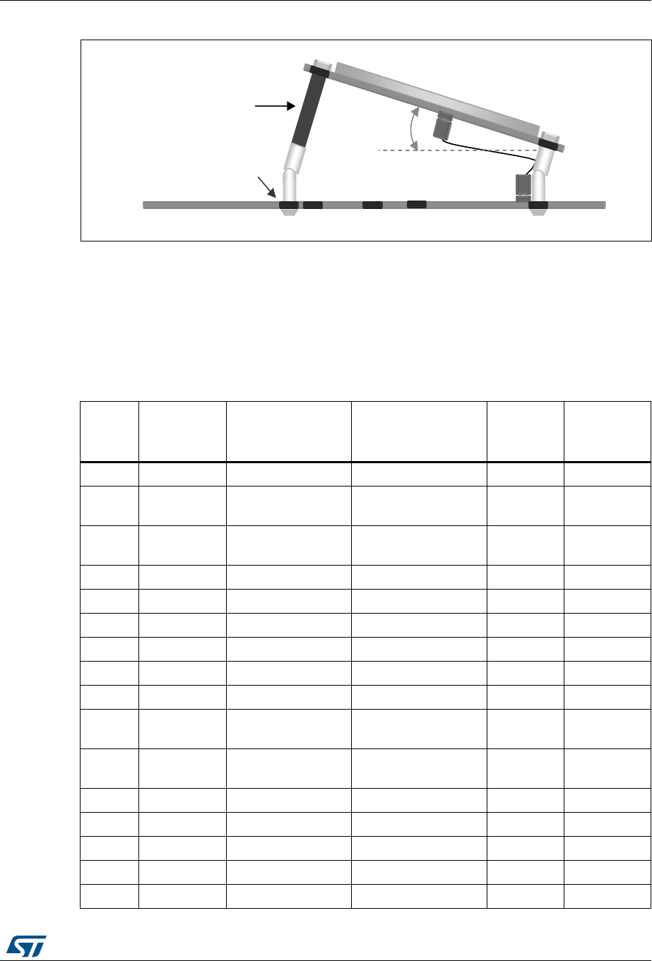
The orientation of the 5.7-inch LCD daughterboard can be changed by means of hinged
standoffs and pillars. Refer to Figure 6 for details.
Table 14. LCD module connector (CN20)
Pin No. Description Pin connection Pin No. Description Pin connection
1GND - 2GND -
3 R0 PI15 4 G0 PJ7
5R1 PJ06G1 PJ8
7R2 PJ18G2 PJ9
9 R3 PJ2 10 G3 PJ10
11 R4 PJ3 12 G4 PJ11
13 R5 PJ4 14 G5 PK0
15 R6 PJ5 16 G6 PK1
17 R7 PJ6 18 G7 PK2
19 GND - 20 GND -
21 B0 PJ12 22 ENB PK7
23 B1 PJ13 24 - -
25 B2 PJ14 26 HSYNC PI12
27 B3 PJ15 28 VSYNC PI13
29 B4 PK3 30 GND -
31 B5 PK4 32 CLK PI14
33 B6 PK5 34 GND -
35 B7 PK6 36 RESET# -
37 GND - 38 I2C1_SDA PB7
39 INT MFX GPIO14 40 I2C1_SCL PB6
41 - - 42 - -
43 BL_CTRL PA6 44 - -
45 5V - 46 - -
47 BLGND - 48 - -
49 BLGND - 50 3.3V -
DocID030511 Rev 1 25/69
UM2198 Hardware layout and configuration
68
Figure 6. Orientation setting of 5.7-inch LCD daughterboard
8.20 MFX (Multi Function eXpander)
MFX circuit on STM32H743I-EVAL Evaluation board acts as IO-expander. The
communication interface between MFX and STM32H743XI is I2C1 bus.
The signals connected to MFX are listed in Table 15.
ϮϬ͘ϱe
,ŽůĞ
ϰĐŵ
Ɖ
ŝůůĂƌ
Table 15. MFX signals
Pin
number
of MFX
Pin name of
MFX MFX functions Function of
STM32H743I-EVAL
Direction
(For MFX)
Terminal
device
15 PA5 MFX_GPIO5 Audio_INT Input Codec
16 PA6 MFX_GPIO6 OTG_FS1_
OverCurrent Input USB_FS1
17 PA7 MFX_GPIO7 OTG_FS1_
PowerSwitchOn Output USB_FS1
18 PB0 MFX_GPIO0 JOY_SEL Input Joystick
19 PB1 MFX_GPIO1 JOY_DOWN Input Joystick
20 PB2 MFX_GPIO2 JOY_LEFT Input Joystick
26 PB13 MFX_GPIO13 SD_LDO_SEL Output microSD
27 PB14 MFX_GPIO14 TOUCH_INT Input LCD
28 PB15 MFX_GPIO15 MicroSDcard Detect Input microSD
29 PA8 MFX_GPIO8 OTG_FS2_
OverCurrent Input USB_FS2
30 PA9 MFX_GPIO9 OTG_FS2_
PowerSwitchOn Output USB_FS2
31 PA10 MFX_GPIO10 LED2 Output LED
32 PA11 MFX_GPIO11 LED4 Output LED
33 PA12 MFX_GPIO12 - - -
39 PB3 MFX_GPIO3 JOY_RIGHT Input Joystick
40 PB4 MFX_GPIO4 JOY_UP Input Joystick
Connectors UM2198
26/69 DocID030511 Rev 1
9 Connectors
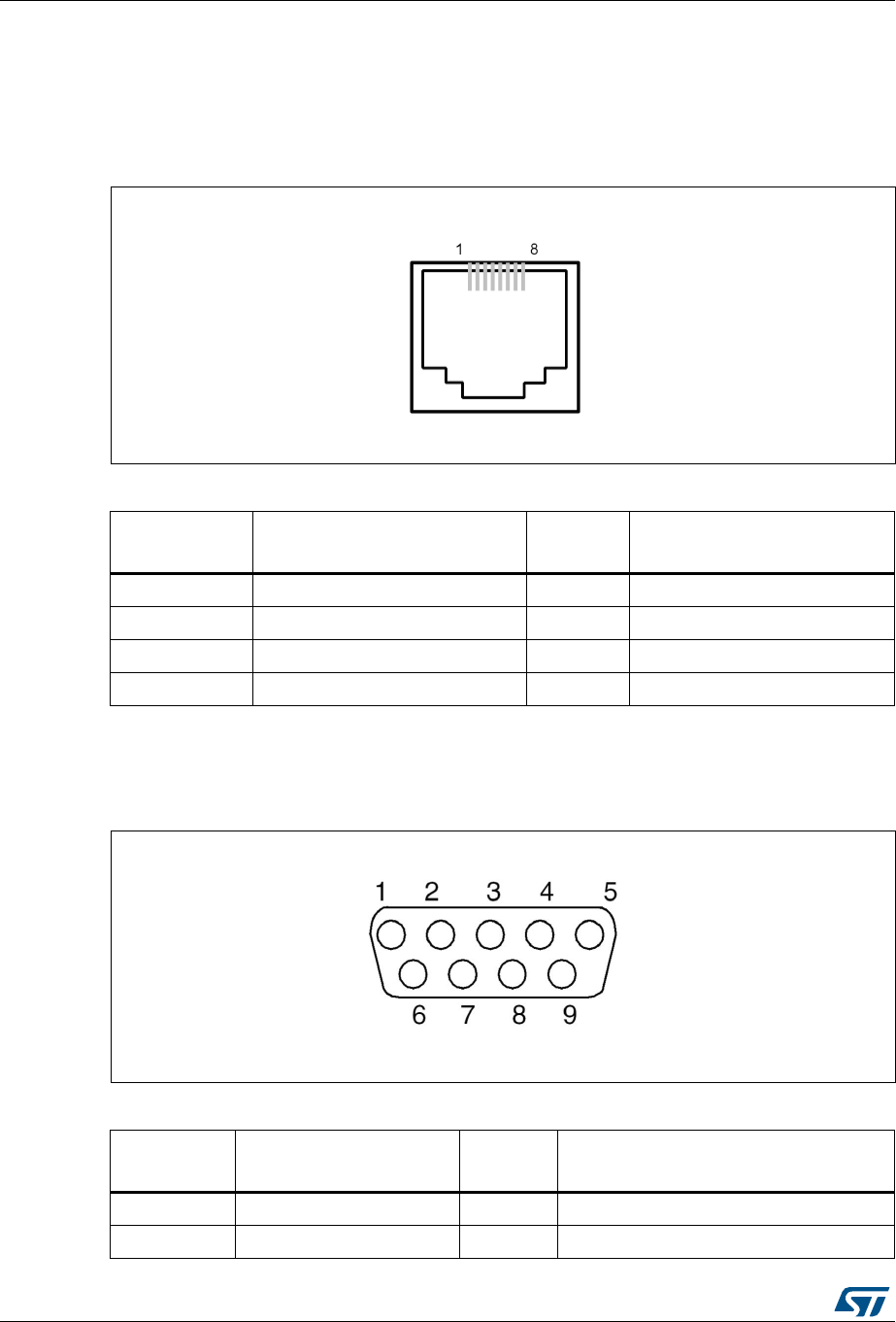
9.1 Ethernet RJ45 connector CN1
Figure 7. Ethernet RJ45 connector CN1 (front view)
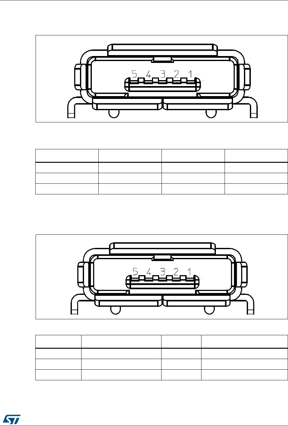
9.2 RS232 connector CN2
Figure 8. RS232 connector CN2 (front view)
Table 16. RJ45 connector CN1
Pin number Description Pin
number Description
1 TxData+ 2 TxData-
3 RxData+ 4 Shield
5 Shield 6 RxData-
7 Shield 8 Shield
Table 17. RS232 connector CN2 with ISP support
Pin number Description Pin
number Description
1 NC 6 Bootloader_BOOT0
2 RS232_RX (PB15) 7 NC
-36
DocID030511 Rev 1 27/69
UM2198 Connectors
68
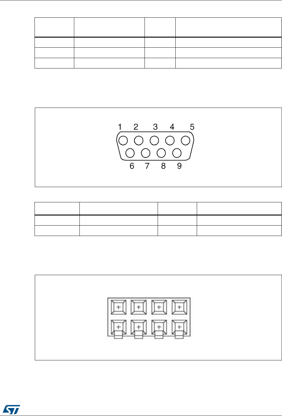
9.3 CAN D-type, 9-pin male connector CN3
Figure 9. CAN D-type, 9-pin connector CN3 (front view)
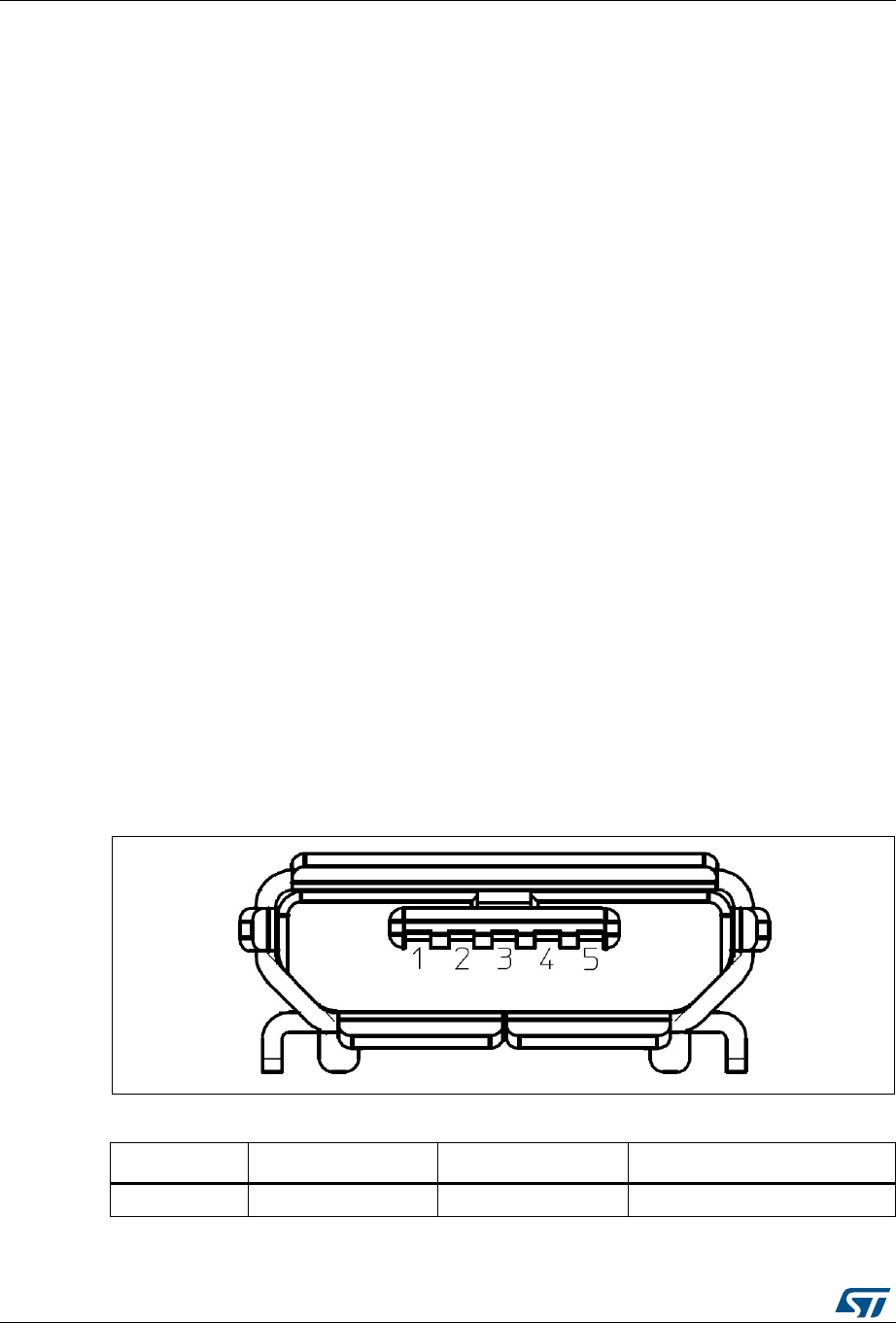
9.4 External I2C connector CN4
Figure 10. I2C EXT connector CN4 (front view)
3 RS232_TX (PB14) 8 Bootloader_RESET
4NC9 NC
5GND- -
Table 17. RS232 connector CN2 with ISP support (continued)
Pin number Description Pin
number Description
Table 18. CAN D-type 9-pin male connector CN3
Pin number Description Pin number Description
1,4,8,9 NC 7 CANH
2 CANL 3,5,6 GND
-36
069
Connectors UM2198
28/69 DocID030511 Rev 1
9.5 Analog input-output connector CN5
Figure 11. Analog input-output connector CN5 (top view)
9.6 Daughterboard extension connector CN6 and CN7
Two 60-pin male headers CN6 and CN7 can be used to connect a daughterboard or a
standard wrapping board to the STM32H743I-EVAL Evaluation board. All GPI/Os are
available on CN6 and CN7 and memory connectors on CN11 and CN12.
The space between these two connectors is defined as a standard that allows developing
common daughterboards for several ST evaluation boards. The standard width between
CN6 pin1 and CN7 pin1 is 2700 mils (68.58 mm).
Each pin on CN6 and CN7 can be used by a daughterboard after disconnecting it from the
corresponding function block on STM32H743I-EVAL Evaluation board. For details refer to
Table 21 and Table 22.
Table 19. I2C EXT connector CN4
Pin number Description Pin number Description
1 I2C1_SDA (PB7) 5 +3.3 V
2NC6NC
3 I2C1_SCL (PB6) 7 GND
4 RESET (PA4) 8 NC
Table 20. Analog input-output connector CN5
Pin number Description Pin number Description
1 analog input-output (PA0_C) 2 GND
06Y9
Ϯ
ϭ

DocID030511 Rev 1 29/69
UM2198 Connectors
68
Table 21. Daughterboard extension connector CN6
Pin Description Alternative function How to disconnect with function block on
STM32H743I-EVAL board
1 PC0 ULPI_STP Remove R124
3 PH0 OSC_IN Remove R15, Close SB39
5 RESET# - -
7 PI11 ULPI_DIR Remove R123
9 PB5 ULPI_D7 Remove R101
11 PF8 QSPI_BK1_IO0 Remove R38
13 PG14 QSPI_BK2_IO3 Remove R27
15 PH3 QSPI_BK2_IO1 Remove R28
17 PH2 QSPI_BK2_IO0 Remove R52
19 PA4 EXT_RESET/LED3 Disconnect CN4, Remove R296
21 PA3 ULPI_D0 Remove R114
23 PF9 QSPI_BK1_IO1 Remove R32
25 PA6 GPIO_LCD_BL_CTRL Disconnect CN15
27 PC4 RMII_RXD0 Remove R41
29 PB0 ULPI_D1 Remove R113
31 PB1 ULPI_D2 Remove R111
33 PJ3 RGB_LCD_R4 Disconnect CN20
35 PA1 RMII_RX_CLK Remove R31
37 PC3 DFSDM_DATA1 Not to dial SW2 to the middle
39 GND - -
41 PJ1 RGB_LCD_R2 Disconnect CN20
43 PJ0 RGB_LCD_R1 Disconnect CN20
45 PB14 USART1_TX/USB_FS2_DM Open SB46, SB47
47 PB15 USART1_RX/USB_FS2_DP Open SB49, SB51
49 D5V - -
51 PB11 ULPI_D4 Remove R109
53 PJ7 RGB_LCD_G0 Remove R24, Disconnect CN20
55 PJ6 RGB_LCD_R7 Disconnect CN20
57 PG6 QSPI_BK1_NCS Open SB6, Remove R19
59 GND - -
2 PC1 RMII_MDC/ PDM1_D1 Open SB38, Not to dial SW2 to the right
4 PF7 QSPI_BK1_IO2 Remove R36
6 PH1 OSC_OUT Remove R16
8 PF6 QSPI_BK1_IO3 Remove R26
Connectors UM2198
30/69 DocID030511 Rev 1
10 GND - -
12 PC2_C - -
14 PC3_C - -
16 PA0_C Potentiometer Open SB43
18 PA1_C - -
20 GND - -
22 PA5 ULPI_CK Remove R118
24 PB2 QSPI_CLK -
26 PH4 ULPI_NXT Remove R117
28 PC5 RMII_RXD1 Remove R39
30 GND - -
32 PG9 QSPI_BK2_IO2 Remove R33
34 PA7 RMII_CRS_DV Remove R44
36 PJ4 RGB_LCD_R5 Disconnect CN20
38 PI15 RGB_LCD_R0 Disconnect CN20
40 PJ2 RGB_LCD_R3 Disconnect CN15, CN20
42 PJ5 RGB_LCD_R6 Disconnect CN20
44 PB13 ULPI_D6/USB_FS2_VBUS Remove R104, R254
46 PB12 ULPI_D5/USB_FS2_ID Remove R105, Open SB48
48 +3V3 - -
50 GND - -
52 PB10 ULPI_D3 Remove R109
54 PJ8 RGB_LCD_G1 Disconnect CN20
56 PJ9 RGB_LCD_G2 Disconnect CN20
58 PJ10 RGB_LCD_G3 Disconnect CN20
60 +5V - -
Table 22. Daughterboard extension connector CN7
Pin Description Alternative function How to disconnect with function block on
STM32H743I-EVAL board
1PF10 LED1 Remove R286, Disconnect CN15, Remove
R294
3 PC15 OSC32_OUT Remove R17, Close SB4
5 PI14 RGB_LCD_CLK Disconnect CN20
7 PI13 RGB_LCD_VSYNC Disconnect CN20
Table 21. Daughterboard extension connector CN6 (continued)
Pin Description Alternative function How to disconnect with function block on
STM32H743I-EVAL board

DocID030511 Rev 1 31/69
UM2198 Connectors
68
9 PC13 KEY_TAMP_1/WKUP2 Remove R193
11 PB8 SDIO_1_CKIN -
13 PK7 RGB_LCD_DE Disconnect CN20
15 PB3 JTDO/TRACESWO Remove R60
17 PK6 RGB_LCD_B7 Remove R199, Disconnect CN20
19 GND - -
21 PK4 RGB_LCD_B5 Remove R201, Disconnect CN20
23 PK3 RGB_LCD_B4 Remove R202, Disconnect CN20
25 PG13 RMII_TXD0 -
27 PA0 KEY_WKUP0 Remove R173, R203
29 PJ15 RGB_LCD_B3 Disconnect CN20
31 PJ11 RGB_LCD_G4 Disconnect CN20
33 PC12 SDIO_1_CK Remove R83
35 PA15 JTDI/CEC Remove R61, Disconnect CN15
37 PG11 RMII_TX_EN -
39 GND - -
41 PD2 SDIO_1_CMD -
43 PA13 JTMS-SWDIO Remove R55
45 PC6 SDIO_1_D0DIR Remove SB58
47 PA10 USB_FS1_ID Disconnect CN18
49 D5V - -
51 PG7 SAI_1_MCLK_A Remove SB56
53 PC9 SDIO_1_D1 -
55 PK0 RGB_LCD_G5 Disconnect CN20
57 PK1 RGB_LCD_G6 Disconnect CN20
59 GND - -
2 PC2 DFSDM_CKOUT Not to dial SW2 to the left
4 PC14 OSC32_IN Remove R18, Close SB1
6 PI12 RGB_LCD_HSYNC Disconnect CN20
8 PA2 RMII_MDIO Remove R47
10 GND - -
12 PI8 GPIO_EXPANDER_INT Remove R185
14 PB9 SDIO_1_CDIR Remove R91
Table 22. Daughterboard extension connector CN7 (continued)
Pin Description Alternative function How to disconnect with function block on
STM32H743I-EVAL board
Connectors UM2198
32/69 DocID030511 Rev 1
16 PB7 I2C_1_SDA Remove R160, R181, R209, Disconnect
CN4, CN15, CN20
18 PB6 I2C_1_SCL Remove R155, R180, R212, Disconnect
CN4, CN15, CN20
20 PB4 NJTRST Remove R79
22 PK5 RGB_LCD_B6 Remove R200, Disconnect CN20
24 PJ13 RGB_LCD_B1 Disconnect CN20
26 PG12 RMII_TXD1 -
28 PJ14 RGB_LCD_B2 Disconnect CN20
30 GND - -
32 PJ12 RGB_LCD_B0 Remove R25, Disconnect CN20
34 PD3 GPIO_CAN_STBY Remove R4
36 PC10 SDIO_1_D2 -
38 PA14 JTCK-SWCLK Remove R59
40 PC11 SDIO_1_D3 Open SB45
42 PC7 SDIO_1_D123DIR Remove R92
44 PC8 SDIO_1_D0 -
46 PA9 USB_FS1_VBUS Remove R255
48 +3.3V - -
50 GND - -
52 PA8 MCO1 Disconnect CN15, Keep JP5 on open
54 PA11 USB_FS1_DM/
FDCAN_1_RXFD Open SB50, SB59
56 PA12 USB_FS1_DP/
FDCAN_1_TXFD Keep JP2 on open, Open SB60
58 PK2 RGB_LCD_G7 Disconnect CN20
60 +5V - -
Table 22. Daughterboard extension connector CN7 (continued)
Pin Description Alternative function How to disconnect with function block on
STM32H743I-EVAL board
DocID030511 Rev 1 33/69
UM2198 Connectors
68
9.7 ETM trace debugging connector CN8
Figure 12. ETM trace debugging connector CN8 (top view)
9.8 JTAG/SWD connector CN9
Figure 13. JTAG/SWD debugging connector CN9 (top view)
Table 23. ETM Trace debugging connector CN8
Pin number Description Pin
number Description
1 +3.3V 2 TMS/PA13
3 GND 4 TCK/PA14
5 GND 6 TDO/PB3
7 KEY 8 TDI/PA15
9GND10RESET#
11 GND 12 TraceCLK/PE2
13 GND 14 TraceD0/PE3 or SWO/PB3
15 GND 16 TraceD1/PE4 or nTRST/PB4
17 GND 18 TraceD2/PE5
19 GND 20 TraceD3/PE6
D^ϯϬϳϮϮsϮ
D^ǀϯϬϳϮϮsϮ
Connectors UM2198
34/69 DocID030511 Rev 1
9.9 Power connector CN10
STM32H743I-EVAL Evaluation board can be powered from a DC 5 V power supply through
the external power supply jack (CN10) shown in Figure 14. The central pin of CN10 must be
positive.
Figure 14. Power supply connector CN10 (front view)
9.10 Memory connector CN11 and CN12
Two 40-pin male headers CN11 and CN12 are used to connect with memory
daughterboard.
All GPIOs are connected on the extension connectors CN6 and CN7, but the GPIOs which
are used for FMC memory signals, are connected on CN11 and CN12.
The space between these two connectors is defined as a standard that allows to develop
common daughterboard. The standard width between CN11 pin1 and CN12 pin1 is 1914
mils (48.62 mm). For details on signals assignment refer to Table 25 and Table 26.
Table 24. JTAG/SWD debugging connector CN9
Pin number Description Pin
number Description
1 +3.3V 2 +3.3V
3 TRST(PB4) 4 GND
5 TDI(PA15) 6 GND
7 TMS/SWDIO(PA13) 8 GND
9 TCK/SWCLK(PA14) 10 GND
11 RTCK 12 GND
13 TDO/SWO(PB3) 14 GND
15 RESET# 16 GND
17 DBGRQ(PJ7) 18 GND
19 DBGACK(PJ12) 20 GND
-36
'&9
*1'
DocID030511 Rev 1 35/69
UM2198 Connectors
68
Table 25. Memory connector CN11
Pin Description Alternative function How to disconnect with function block on
STM32H743I-EVAL board
1 PH6 SDNE1 -
3PF13 A7 -
5PF12 A6 -
7PG1 A11 -
9GND - -
11 PE7 D4 -
13 PE10 D7 -
15 PE12 D9 -
17 PE15 D12 -
19 PE13 D10 -
21 PD11 A16 -
23 PD12 A17 -
25 PG5 A15/BA1 -
27 PH11 D19 -
29 GND - -
31 PD13 A18 -
33 PG2 A12 -
35 PD8 D13 -
37 PD9 D14 -
39 PD14 D0 -
2 PH5 SDNWE -
4PF14 A8 -
6PG0 A10 -
8 PF11 SDNRAS -
10 GND - -
12 PE9 D6 -
14 PE8 D5 -
16 PE11 D8 -
18 PF15 A9 -
20 PE14 D11 -
22 PH8 D16 -
24 PH10 D18 -
26 PH9 D17 -
28 PG4 A14/BA0 -
Connectors UM2198
36/69 DocID030511 Rev 1
30 GND - -
32 PH12 D20 -
34 PG3 A13 -
36 PD10 D15 -
38 PD15 D1 -
40 PG8 SDCLK -
Table 26. Memory connector CN12
Pin Description Alternative function How to disconnect with function block on
STM32H743I-EVAL board
1PF5 A5 -
3PF4 A4 -
5PF3 A3 -
7 PE6 A22/SAI1_SD_A/TRACED3 Open SB2, SB3
9GND - -
11 PE4 A20/SAI1_FS_A/TRACED1 Open SB5, SB7
13 PE3 A19/SAI1_SD_B/TRACED0 Open SB8, SB9
15 PI5 NBL3 -
17 PI4 NBL2 -
19 PG15 SDNCAS -
21 PI10 D31 -
23 PE1 NBL1 -
25 PE0 NBL0 -
27 PG10 NE3 -
29 GND - -
31 PD0 D2 -
33 PI2 D26 -
35 PI1 D25 -
37 PI0 D24 -
39 PH13 D21 -
2 PH7 SDCKE1 -
4 PE5 A21/SAI1_SCK_A/TRACED2 Open SB41, SB42
6 PD6 NWAIT -
8PF2 A2 -
Table 25. Memory connector CN11 (continued)
Pin Description Alternative function How to disconnect with function block on
STM32H743I-EVAL board
DocID030511 Rev 1 37/69
UM2198 Connectors
68
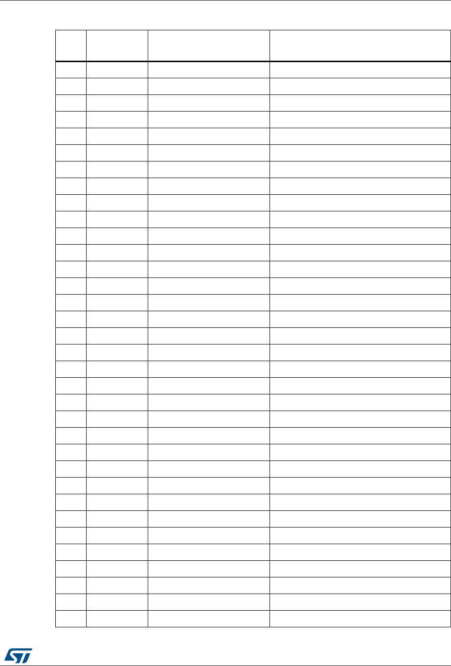
9.11 microSD connector CN13
Figure 15. microSD connector (top view)
10 GND - -
12 PF1 A1 -
14 PF0 A0 -
16 PE2 A23/PDM1_CK1/
SAI1_MCLK_A /TRACECLK Open SB11, SB15, SB57
18 PI7 D29 -
20 PI9 D30 -
22 PI6 D28 -
24 PD7 NE1 -
26 PD5 NWE -
28 PD4 NOE -
30 GND - -
32 PD1 D3 -
34 PI3 D27 -
36 PH15 D23 -
38 PH14 D22 -
40 +3.3V - -
Table 26. Memory connector CN12 (continued)
Pin Description Alternative function How to disconnect with function block on
STM32H743I-EVAL board
Connectors UM2198
38/69 DocID030511 Rev 1
9.12 USB OTG2 HS Micro-AB connector CN14
Figure 16. USB OTG HS Micro-AB connector CN14 (front view)
Table 27. microSD connector CN13
Pin
number Description Pin
number Description
1 SD_DATA2 6 Vss/GND
2 SD_DATA3 7 SD_DATA0
3 SD_CMD 8 SD_DATA1
4 +2.9V_SD 9 GND
5SD_CLK10
MicroSDcard_detect
(MFX GPIO15)
Table 28. USB OTG HS Micro-AB connector CN14
Pin number Description Pin number Description
1V
BUS 4ID
2D-5GND
3D+ - -
DocID030511 Rev 1 39/69
UM2198 Connectors
68
9.13 USB OTG2 FS Micro-AB connector CN16
Figure 17. USB OTG FS Micro-AB connector CN16 (front view)
9.14 USB OTG1 FS Micro-AB connector CN18
Figure 18. USB OTG FS Micro-AB connector CN18 (front view)
Table 29. USB OTG1 FS Micro-AB connector CN18
Pin number Description Pin number Description
1 VBUS (PB13) 4 ID (PB12)
2 D- (PB14) 5 GND
3 D+ (PB15) - -
Table 30. USB OTG1 FS Micro-AB connector CN18
Pin number Description Pin number Description
1V
BUS (PA9) 4 ID (PA10)
2 D- (PA11) 5 GND
3 D+ (PA12) - -
Connectors UM2198
40/69 DocID030511 Rev 1
9.15 Audio jack CN17
A 3.5 mm stereo audio jack CN17 is available on STM32H743I-EVAL Evaluation board to
support headset (headphone and microphone integrated).
9.16 Audio jack (speaker) CN19
A 3.5mm stereo audio jack CN19 for speaker out is available on STM32H743I-EVAL
Evaluation board to support an external speaker.
9.17 TFT LCD connector CN20
A TFT-color LCD board is mounted on CN20. Refer to Section 8.19 for details.
9.18 ST-LINK/V2-1 programming connector CN21
The connector CN21 is used only for embedded ST-LINK/V2-1 programming during board
manufacturing. It is not populated by default and not for end users.
9.19 MFX programming connector CN22
The connector CN22 is used only for MFX (Multi Function eXpander) programming during
board manufacturing. It is not populated by default and not for end users.
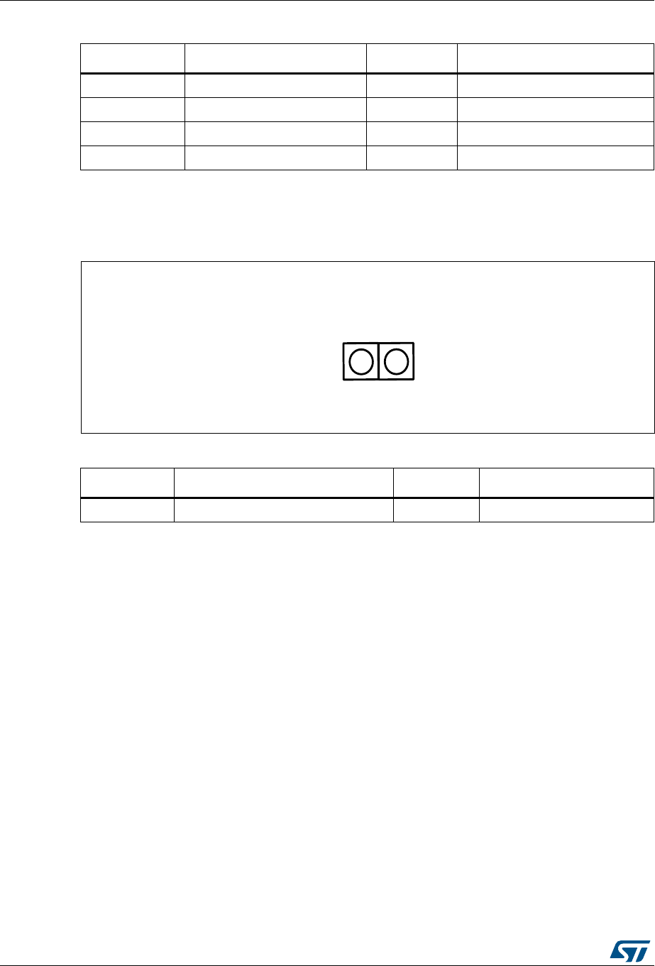
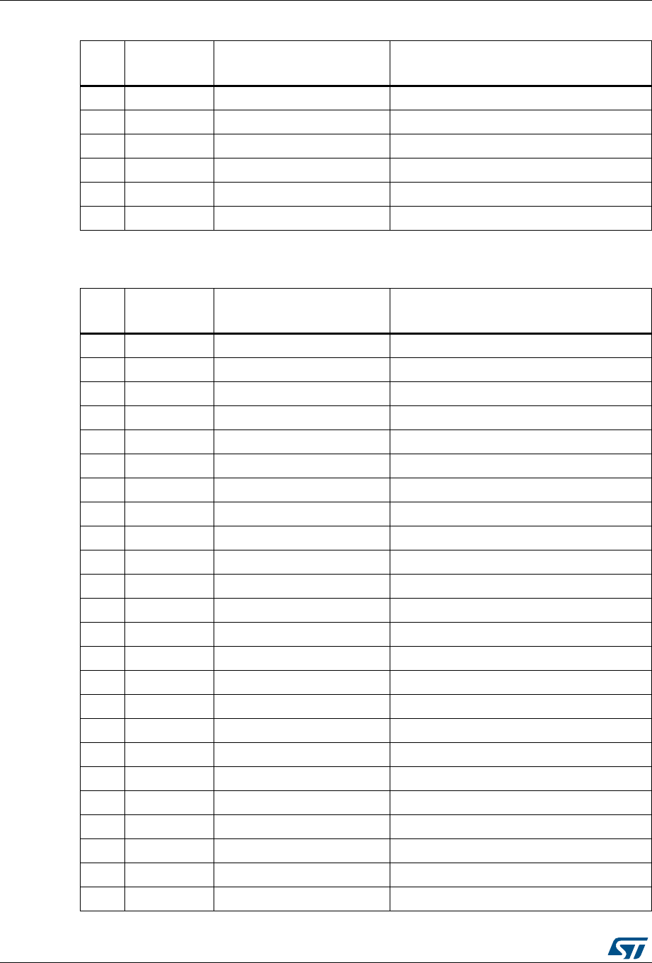
9.20 ST-LINK/V2-1 USB Micro-B connector CN23
The USB Micro-B connector CN23 is used to connect the embedded ST-LINK/V2-1 to a PC
for
programming and debugging purposes.
Figure 19. USB Micro-B connector CN23 (front view)
Table 31. USB Micro-B connector CN23 (front view)
Pin number Description Pin number Description
1V
BUS (power) 4 ID
DocID030511 Rev 1 41/69
UM2198 Connectors
68
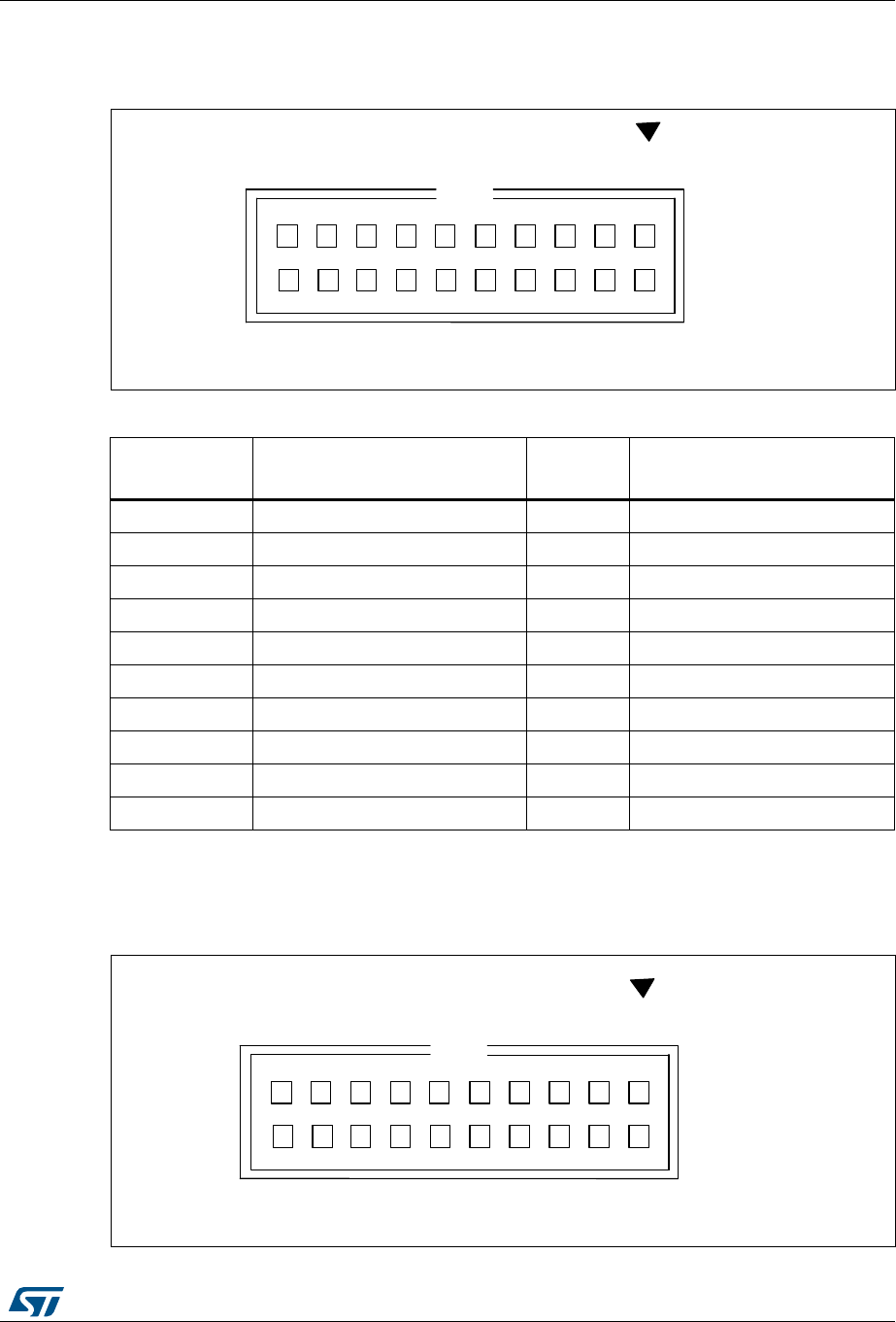
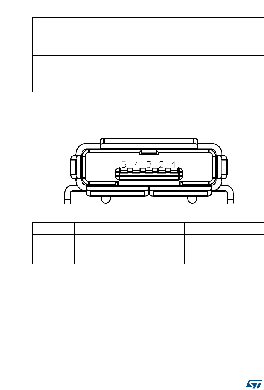
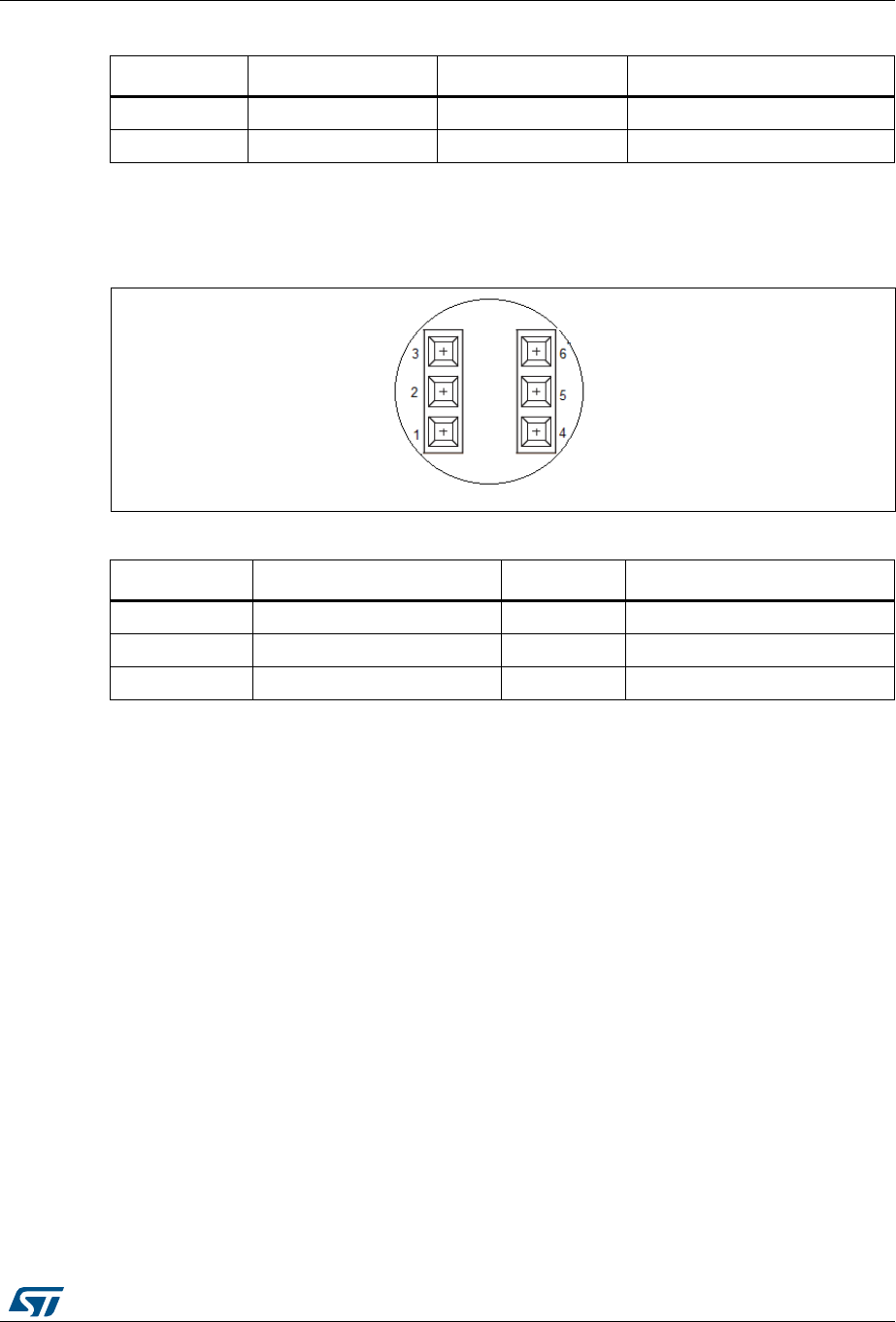
9.21 MEMS microphone coupon connectors CN25 and CN26
Figure 20. MEMS microphone coupon connectors CN25 and CN26 (top view)
2DM 5 GND
3DP - -
Table 31. USB Micro-B connector CN23 (front view) (continued)
Pin number Description Pin number Description
Table 32. 2.21 MEMS microphone coupon connectors CN25 and CN26
Pin number Description Pin number Description
1DATA4 V
DD
2GND5 L/R
3CLK6 NC
STM32H743I-EVAL I/O assignment UM2198
42/69 DocID030511 Rev 1
Appendix A STM32H743I-EVAL I/O assignment
Table 33. STM32H743I-EVAL I/O assignment
Pin No. Pin Name Default function Alternative function
N5 PA0-WKUP KEY_WKUP0 -
N4 PA1 RMII_REF_CLK -
N3 PA2 RMII_MDIO -
U2 PA3 ULPI_D0 -
U3 PA4 EXT_RESET/LED3 -
T3 PA5 ULPI_CK -
R3 PA6 GPIO_LCD_BACKLIGHT_CTRL -
R5 PA7 RMII_CRS_DV -
E15 PA8 MCO1 -
D15 PA9 USB_FS1_VBUS -
D14 PA10 USB_FS1_ID -
E17 PA11 USB_FS1_DM FDCAN_1_RXFD
E16 PA12 USB_FS1_DP FDCAN_1_TXFD
C15 PA13 JTMS-SWDIO -
B14 PA14 JTCK-SWCLK -
A14 PA15 JTDI CEC
U5 PB0 ULPI_D1 -
T5 PB1 ULPI_D2 -
R6 PB2 QSPI_CLK -
C6 PB3 JTDO/TRACESWO -
B7 PB4 NJTRST -
A5 PB5 ULPI_D7 -
B5 PB6 I2C_1_SCL -
C5 PB7 I2C_1_SDA -
D5 PB8 SDIO_1_CKIN -
D4 PB9 SDIO_1_CDIR -
P11 PB10 ULPI_D3 -
P12 PB11 ULPI_D4 -
T14 PB12 ULPI_D5 USB_FS2_ID
U14 PB13 ULPI_D6 USB_FS2_VBUS
U15 PB14 USART1_TX USB_FS2_DM
T15 PB15 USART1_RX USB_FS2_DP
DocID030511 Rev 1 43/69
UM2198 STM32H743I-EVAL I/O assignment
68
L2 PC0 ULPI_STP -
M2 PC1 RMII_MDC PDM1_D1
M3 PC2 DFSDM_CKOUT -
M4 PC3 DFSDM_DATA1 -
T4 PC4 RMII_RXD0 -
U4 PC5 RMII_RXD1 -
F14 PC6 SDIO_1_D0DIR -
F13 PC7 SDIO_1_D123DIR -
E13 PC8 SDIO_1_D0 -
E14 PC9 SDIO_1_D1 -
A13 PC10 SDIO_1_D2 -
B13 PC11 SDIO_1_D3 -
C12 PC12 SDIO_1_CK -
E3 PC13-
ANTI_TAMP KEY_TAMP_1/WKUP2 -
C2 PC14-
OSC32_IN OSC32_IN -
C1 PC15-
OSC32_OUT OSC32_OUT -
D13 PD0 FMC_D2 -
E12 PD1 FMC_D3 -
D12 PD2 SDIO_1_CMD -
B12 PD3 GPIO_CAN_STANDBY -
A12 PD4 FMC_NOE -
A11 PD5 FMC_NWE -
B11 PD6 FMC_NWAIT -
C11 PD7 FMC_NE1 -
U16 PD8 FMC_D13 -
T17 PD9 FMC_D14 -
T16 PD10 FMC_D15 -
R15 PD11 FMC_A16 -
R16 PD12 FMC_A17 -
R17 PD13 FMC_A18 -
P16 PD14 FMC_D0 -
P15 PD15 FMC_D1 -
C4 PE0 FMC_NBL0 -
Table 33. STM32H743I-EVAL I/O assignment (continued)
Pin No. Pin Name Default function Alternative function
STM32H743I-EVAL I/O assignment UM2198
44/69 DocID030511 Rev 1
B4 PE1 FMC_NBL1 -
C3 PE2 PDM1_CK1 FMC_A23/TRACECLK/
SAI_1_MCLK_A
D3 PE3 SAI1_SD_B FMC_A19/TRACED0
D2 PE4 SAI1_FS_A FMC_A20/TRACED1
D1 PE5 SAI1_SCK_A FMC_A21/TRACED2
E5 PE6 SAI1_SD_A FMC_A22/TRACED3
U9 PE7 FMC_D4 -
T9 PE8 FMC_D5 -
P9 PE9 FMC_D6 -
N9 PE10 FMC_D7 -
P10 PE11 FMC_D8 -
R10 PE12 FMC_D9 -
T10 PE13 FMC_D10 -
U10 PE14 FMC_D11 -
R11 PE15 FMC_D12 -
G4 PF0 FMC_A0 -
G3 PF1 FMC_A1 -
G1 PF2 FMC_A2 -
H4 PF3 FMC_A3 -
J5 PF4 FMC_A4 -
J4 PF5 FMC_A5 -
K2 PF6 QSPI_BK1_IO3 -
K3 PF7 QSPI_BK1_IO2 -
K4 PF8 QSPI_BK1_IO0 -
L4 PF9 QSPI_BK1_IO1 -
L3 PF10 LED1 -
T7 PF11 SDR_SDNRAS -
R7 PF12 FMC_A6 -
P7 PF13 FMC_A7 -
P8 PF14 FMC_A8 -
R9 PF15 FMC_A9 -
T8 PG0 FMC_A10 -
U8 PG1 FMC_A11 -
H16 PG2 FMC_A12 -
Table 33. STM32H743I-EVAL I/O assignment (continued)
Pin No. Pin Name Default function Alternative function
DocID030511 Rev 1 45/69
UM2198 STM32H743I-EVAL I/O assignment
68
H15 PG3 FMC_A13 -
H14 PG4 FMC_A14 / SDR_BA0 -
G14 PG5 FMC_A15 / SDR_BA1 -
G15 PG6 QSPI_BK1_NCS -
F16 PG7 SAI_1_MCLK_A -
F15 PG8 SDR_SDCLK -
A10 PG9 QSPI_BK2_IO2 -
A9 PG10 FMC_NE3 -
B9 PG11 RMII_TX_EN -
C9 PG12 RMII_TXD1 -
D9 PG13 RMII_TXD0 -
D8 PG14 QSPI_BK2_IO3 -
D6 PG15 SDR_SDNCAS -
J2 PH0 - OSC_IN OSC_IN -
J1 PH1 -
OSC_OUT OSC_OUT -
N2 PH2 QSPI_BK2_IO0 -
P2 PH3 QSPI_BK2_IO1 -
P3 PH4 ULPI_NXT -
P4 PH5 SDR_SDNWE -
T11 PH6 SDR_SDNE1 -
U13 PH7 SDR_SDCKE1 -
T13 PH8 FMC_D16 -
R13 PH9 FMC_D17 -
P13 PH10 FMC_D18 -
P14 PH11 FMC_D19 -
R14 PH12 FMC_D20 -
D16 PH13 FMC_D21 -
B17 PH14 FMC_D22 -
B16 PH15 FMC_D23 -
A16 PI0 FMC_D24 -
A15 PI1 FMC_D25 -
B15 PI2 FMC_D26 -
C14 PI3 FMC_D27 -
A4 PI4 FMC_NBL2 -
Table 33. STM32H743I-EVAL I/O assignment (continued)
Pin No. Pin Name Default function Alternative function
STM32H743I-EVAL I/O assignment UM2198
46/69 DocID030511 Rev 1
A3 PI5 FMC_NBL3 -
A2 PI6 FMC_D28 -
B3 PI7 FMC_D29 -
E4 PI8- ANTI
TAMP2 GPIO_EXPANDER_INT -
E2 PI9 FMC_D30 -
F3 PI10 FMC_D31 -
F4 PI11 ULPI_DIR -
H1 PI12 RGB_LCD_HSYNC -
H2 PI13 RGB_LCD_VSYNC -
H3 PI14 RGB_LCD_CLK -
P5 PI15 RGB_LCD_R0 -
N6 PJ0 RGB_LCD_R1 -
P6 PJ1 RGB_LCD_R2 -
T6 PJ2 RGB_LCD_R3 -
U6 PJ3 RGB_LCD_R4 -
U7 PJ4 RGB_LCD_R5 -
R12 PJ5 RGB_LCD_R6 -
N15 PJ6 RGB_LCD_R7 -
N14 PJ7 RGB_LCD_G0 -
N13 PJ8 RGB_LCD_G1 -
M14 PJ9 RGB_LCD_G2 -
L14 PJ10 RGB_LCD_G3 -
K14 PJ11 RGB_LCD_G4 -
D11 PJ12 RGB_LCD_B0 -
E10 PJ13 RGB_LCD_B1 -
D10 PJ14 RGB_LCD_B2 -
B10 PJ15 RGB_LCD_B3 -
J14 PK0 RGB_LCD_G5 -
J15 PK1 RGB_LCD_G6 -
H17 PK2 RGB_LCD_G7 -
C8 PK3 RGB_LCD_B4 -
B8 PK4 RGB_LCD_B5 -
A8 PK5 RGB_LCD_B6 -
C7 PK6 RGB_LCD_B7 -
Table 33. STM32H743I-EVAL I/O assignment (continued)
Pin No. Pin Name Default function Alternative function

Electrical schematics UM2198
48/69 DocID030511 Rev 1
Appendix B Electrical schematics
This section provides the design schematics for the STM32H743I-EVAL Evaluation board:
•Overall schematics for the STM32H743I-EVAL, see Figure 21
•STM32H743I-EVALMCU, see Figure 22
•Power, see Figure 23
•SRAM, Flash and SDRAM, see Figure 24
•Audio, see Figure 25
•LCD, see Figure 26
•Ethernet, see Figure 27
•USB OTG HS, see Figure 28
•USB OTG FS, see Figure 29
•RS232, see Figure 30
•FDCAN and Quad-SPI, see Figure 31
•microSD, see Figure 32
•Peripherals, see Figure 33
•Extension connectors, see Figure 34
•ST-LINK, see Figure 35
•MFX, see Figure 36
•JTAG and trace, see Figure 37
•5.7” LCD board, see Figure 38
UM2198 Electrical schematics
DocID030511 Rev 1 49/69
Figure 21. STM32H743I-EVAL Evaluation board
117
MB1246
MB1246 B.2
6/9/2017
Title:
Size: Reference:
Date: Sheet: of
A3 Revision:
STM32H7x3I-EVAL
Project:
N
ote:1. Text in italic placed on a wire doesn't correspond to net name. It just helps to identify
rapidly MCU IO related to this wire.
2.R100/R103/R107's pull up power is changed from 3V3 to VDD_IO of U13 from A.1 to B.1
3.CAN_RX is connected to PA11 instead of PA9 and CAN_TX is connected to PA12 instead of
PA10 from A.1 to B.1
4.SAI1_MCLKA is connected to PE2 instead of PG7 by default from A.1 to B.1
5.IRDA is removed from A.1 to B.1
6.LEDs' connection are changed, in order to avoid conflict with RGB LCD signals from A.1 to
B.1
7. Updated to STM32H7x3I from B.1 to B.2
+3V3 R212 1K5
R209 1K5
3
2
1
JP7
3
2
1
JP8
SAI1_SCKA
SAI1_FSA
SAI1_SDA
SAI1_SDB
Audio_INT
I2C1_SDA
I2C1_SCL
SAI1_MCLKA
DFSDM_CLK
DFSDM_DATA1
PDM1_CLK1
PDM1_D1
U_Audio
Audio.SchDoc
PA[0..15]
PB[0..15]
PC[0..15]
PD[0..15]
PE[0..15]
PF[0..15]
PG[0..15]
PH[0..15]
PI[0..15]
PJ[0..15]
PK[0..7]
RESET#
PA0_C
PA1_C
PC2_C
PC3_C
U_ExtensionConnector
ExtensionConnector.SchDoc
FDCAN1_TX
FDCAN1_RX
FDCAN1_STBY
QSPI_BK1_IO3
QSPI_BK1_IO1
QSPI_BK1_NCS
QSPI_BK1_IO0
QSPI_BK1_IO2
QSPI_CLK
QSPI_BK2_NCS
QSPI_BK2_IO0
QSPI_BK2_IO1
QSPI_BK2_IO2
QSPI_BK2_IO3
U_FDCAN&QSPI
FDCAN&QSPI.SchDoc
FMC_NE1
FMC_NWE
FMC_NOE
FMC_NWAIT
FMC_NBL0
FMC_NBL1
D[0..31]
A[0..23]
SDNCAS
SDNWE
SDNRAS
SDNE1
SDCKE1
SDCLK
FMC_NBL3
FMC_NBL2
FMC_NE3
U_Memory
Memory.SchDoc
MFX_IRQOUT
I2C1_SDA
I2C1_SCL
MFX_IO5
MFX_IO6
MFX_IO7
MFX_IO8
MFX_IO9
MFX_IO10
MFX_IO11
MFX_IO12
MFX_IO13
MFX_IO14
MFX_IO15
MFX_WKUP
MFX_IO0
MFX_IO1
MFX_IO2
MFX_IO3
MFX_IO4
RESET#
U_MFX
MFX.SchDoc
U_Power
Power.SchDoc
STLK_RX
STLK_TXTDI
TRST
TMS/SWDIO
TCK/SWCLK
TDO/SWO
RESET#
U_ST_LINK_V2-1
ST_LINK_V2-1.SCHDOC
OTG_FS1_PowerSwitchOn
OTG_FS1_OverCurrent USB_FS1_DM
USB_FS1_DP
USB_FS1_ID
U_USB_OTG_FS
USB_OTG_FS.SchDoc
SDIO1_CKIN
SDIO1_CDIR
SDIO1_D0DIR
SDIO1_D123DIR
SDIO1_D0
SDIO1_D1
SDIO1_D2
SDIO1_D3
SDIO1_CMD
SDIO1_CLK
SD_LDO_SEL
MicroSDCard_Detect
U_SD card
SD card.SchDoc Same length
208MHz clock
25MHz clock
10MHz clock
Same length
60MHz clock
Same length
90MHz clock
133MHz clock
Same length
10MHz clock
84MHz clock
TDI
RESET#
TRACE_D3
TRACE_D2
TRACE_D1
TRACE_D0
TRACE_CK
TRST
TMS/SWDIO
TCK/SWCLK
TDO/SWO
DBGRQ
DBGACK
U_JTAG&Trace
JTAG&Trace.SchDoc
500MHz clock
ETH_MCO
RMII_TXD0
RMII_TX_EN
RMII_RXD0
RMII_REF_CLK
RMII_CRS_DV
ETH_MDC
ETH_MDIO
RMII_TXD1
RMII_RXD1
RESET#
U_Ethernet
Ethernet.SchDoc
RS232_TX
RS232_RXBootloader_BOOT0
Bootloader_RESET
U_RS232
RS232.SchDoc
JOY_SEL
JOY_DOWN
JOY_LEFT
JOY_RIGHT
JOY_UP
TAMPER_KEY
WAKEUP
Potentiometer
LED4_MIPI
LED3_MIPI
LED1_MIPI
LED2_MIPI
LED1_RGB
LED2_RGB
LED3_RGB
LED4_RGB
U_Peripherals
Peripherals.SchDoc
PA[0..15]
PB[0..15]
PC[0..15]
PD[0..15]
PE[0..15]
PF[0..15]
PG[0..15]
PH[0..15]
PI[0..15]
TMS/SWDIO
TCK/SWCLK
TDI
ULPI_STP
ETH_MDC
RMII_RXD0
RMII_RXD1
SDIO1_D0
EXT_RESET
SDIO1_CLK
TAMPER_KEY
LCD_ENB
SDIO1_CMD
FMC_NOE
FMC_NWE
FMC_NWAIT
FMC_NE1
FMC_NBL3
FMC_NBL2
EXPANDER_INT
ULPI_DIR
LCD_HSYNC
LCD_VSYNC
LCD_CLK
FMC_NBL0
FMC_NBL1
TRACE_CK
TRACE_D0
TRACE_D2
TRACE_D1
SAI1_SDA
TRACE_D3
SAI1_SDB
SAI1_SCKA
SAI1_FSA
SAI1_MCLKA
SDNRAS
SDCLK
FMC_NE3
RMII_TX_EN
RMII_TXD1
SDNCAS
SDCKE1
SDNE1
ULPI_NXT
SDNWE
LCD_G[0..7]
LCD_B[0..7]
D[0..31]
A[0..23]
ULPI_D[0..7]
PJ[0..15]
PK[0..7]
LCD_R[0..7]
QSPI_BK1_IO3
QSPI_BK1_IO2
QSPI_BK1_IO1
QSPI_BK1_IO0DSI_TE
DSI_CK_P
DSI_CK_N
DSI_D0_P
DSI_D0_N
DSI_D1_P
DSI_D1_N
DSI_RESET
LED1_MIPI
LED2_MIPI
LED3_MIPI
LED4_MIPI
RMII_REF_CLK
ETH_MDIO
ULPI_CK
RMII_CRS_DV
LCD_BL_CTRL
USART1_TX
USART1_RX
USB_FS1_ID
FDCAN1_RX
USB_FS1_DM
FDCAN1_TX
USB_FS1_DP
MCO
WAKEUP
TDO/SWO
TRST
I2C1_SCL
I2C1_SDA
USB_FS2_ID
USB_FS2_DM
USB_FS2_DP
QSPI_BK1_NCS
RMII_TXD0
QSPI_CLK
SDIO1_CKIN
SDIO1_CDIR
DFSDM_CLK
DFSDM_DATA1
SDIO1_D0DIR
SDIO1_D123DIR
SDIO1_D1
SDIO1_D2
SDIO1_D3
FDCAN1_STBY
PDM1_CLK1
PDM1_D1
QSPI_BK2_IO2
QSPI_BK2_IO3
QSPI_BK2_IO0
QSPI_BK2_IO1
RESET#
Bootloader_BOOT0
Bootloader_RESET
PA0_C
PA1_C
PC2_C
PC3_C
QSPI_BK2_NCS
CEC
Potentiometer
TRGOUT
TRGIN
LED1_RGB
LED3_RGB
U_MCU
MCU.SchDoc
ULPI_D[0..7]
ULPI_CK
ULPI_DIR
ULPI_NXT
ULPI_STP
USB_RESET
USB_FS2_DM
USB_FS2_DP
OTG_FS2_PowerSwitchOn
OTG_FS2_OverCurrent
USB_FS2_IDRESET#
U_USB_OTG
USB_OTG.SchDoc
LCD_R[0..7]
LCD_HSYNC
LCD_VSYNC
LCD_CLK
LCD_ENB
I2C1_SDA
I2C1_SCL
LCD_B[0..7]
LCD_G[0..7]
TOUCH_INT EXT_RESET
DSI_CK_P
DSI_CK_N
DSI_D0_P
DSI_D0_N
DSI_D1_P
DSI_D1_N
LCD_BL_CTRL
DSI_TE
DSI_RESET
SCLK/MCLK
LRCLK
I2S
CEC
CEC_CLKRESET#
U_LCD Connectors
LCD Connectors.SchDoc
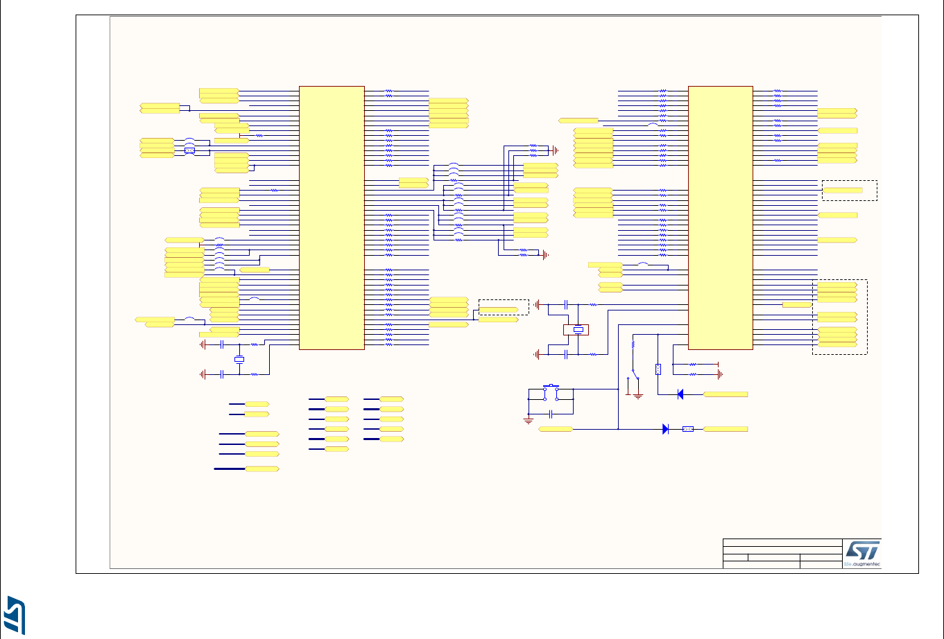
Electrical schematics UM2198
50/69 DocID030511 Rev 1
Figure 22. STM32H743I-EVAL MCU
217
MCU
MB1246 B.2
6/20/2017
Title:
Size: Reference:
Date: Sheet: of
A3 Revision:
STM32H7x3I-EVAL
Project:
PA[0..15] PA[0..15]
PB[0..15] PB[0..15]
PC[0..15] PC[0..15]
PD[0..15] PD[0..15]
PE[0..15] PE[0..15]
PF[0..15] PF[0..15]
PG[0..15] PG[0..15]
PH[0..15] PH[0..15]
PI[0..15] PI[0..15]
PA4
PA5
PA6
PA7
PA11
PA12
PA9
PA10
PA0
PA1
PA15
PA3
PA13
PA14
PA2
PA8
PB5
PB7
PB14
PB15
PB10
PB8
PB9
PB1
PB2
PB3
PB0
PB4
PB11
PB12
PB13
PC0
PC1
PC2
PC3
PC4
PC5
PC6
PC7
PC8
PC9
PC10
PC11
PC12
PC13
ULPI_D0
TMS/SWDIO
TCK/SWCLK
TDI
ULPI_D3
ULPI_D4
ULPI_D6
ULPI_STPETH_MDC
RMII_RXD0
RMII_RXD1
SDIO1_D0
EXT_RESET
SDIO1_CLK
TAMPER_KEY
PJ0
PJ14
PJ15
PJ12
PJ13
PJ1
PJ2
PJ3
PJ4
PJ5
LCD_R1
LCD_R2
LCD_R3
LCD_R4
LCD_R5
LCD_R6
LCD_R7
LCD_B0
LCD_B1
LCD_B2
LCD_B3
LCD_G2
LCD_G3
LCD_G4
PK3
PK4
PK5
PK6
PK7
LCD_B4
LCD_B5
LCD_B6
LCD_B7
LCD_G5
LCD_G6
LCD_ENB
PD0
PD1
PD2
PD3
PD4
PD5
PD6
PD7
PD8
PD9
PD10
PD11
PD12
PD13
PD14
PD15
D2
D3
D13
D14
D15
D0
D1
SDIO1_CMD
FMC_NOE
FMC_NWE
FMC_NWAIT
FMC_NE1
A16
A17
A18
PI0
PI14
PI15
PI9
PI8
PI11
PI10
PI12
PI13
PI1
PI2
PI3
PI4
PI5
PI6
PI7
D24
D25
D26
D27
D28
D29
D30
D31
R256 33
R264 33
R263 33
R267 33
FMC_NBL3
FMC_NBL2
EXPANDER_INT
R243 33
R240 33
R242 33
R246 33
ULPI_DIR
LCD_HSYNC
LCD_VSYNC
LCD_CLK
LCD_R0
PE0
PE14
PE15
PE9
PE8
PE11
PE10
PE12
PE13
PE1
PE2
PE3
PE4
PE5
PE6
PE7
PF0
PF14
PF15
PF9
PF8
PF11
PF10
PF12
PF13
PF1
PF2
PF3
PF4
PF5
PF6
PF7
PG0
PG14
PG15
PG9
PG8
PG11
PG10
PG12
PG13
PG1
PG2
PG3
PG4
PG5
PG6
PG7
PH14
PH15
PH9
PH8
PH11
PH10
PH12
PH13
PH2
PH3
PH4
PH5
PH6
PH7D4
D5
D6
D7
D8
D9
D10
D11
D12
A1
A2
A3
A4
A5
A6
A7
A8
A9
A10
A11
A12
A13
A14
A15
A19
A20
A21
A22
A0
A23
D16
D17
D18
D19
D20
D21
D22
D23
FMC_NBL0
FMC_NBL1
TRACE_CK
TRACE_D0
TRACE_D2
TRACE_D1
SAI1_SDA
TRACE_D3
R54 33
R67 33
R66 33
R280 33
R68 33
R278 33
R70 33
R277 33
R69 33
R224 33
R226 33
R222 33
R223 33
R221 33
R219 33
SAI1_SDB
SAI1_SCKA
SAI1_FSA
SAI1_MCLKA
R252 33 SDNRAS
R250 33
R251 33
R53 33
R279 33
R50 33
R51 33
R261 33
R272 33
SDCLK R268 33
FMC_NE3
RMII_TX_EN R49 33
RMII_TXD1
R245 33
SDNCAS
SDCKE1
SDNE1 R58 33
ULPI_NXT
SDNWE R248 33
R48 33
R37 33
R71 33
R72 33
R276 33
R273 33
R74 33
R258 33
R257 33
R266 33
R269 33
R77 33
R75 33
R76 33
R262 33
R265 33
R73 33
LCD_G[0..7]
LCD_B[0..7]
D[0..31]
A[0..23]
D[0..31]
A[0..23]
ULPI_D[0..7]
ULPI_D[0..7]
PJ[0..15] PJ[0..15]
PK[0..7] PK[0..7]
R249 [N/A]
R247 10K
R270 33
R260 33
R275 33
R274 33
R271 33
R234 33
R236 33
R231 33
R217 33
R230 33
R233 220K
R238 220K
R241 220K
R218 220K
R227 220K
LCD_R[0..7]
LCD_R[0..7]
LCD_G[0..7]
LCD_B[0..7]
R220 0
QSPI_BK1_IO3
QSPI_BK1_IO2
QSPI_BK1_IO1
QSPI_BK1_IO0
R14 33
R13 33
R232 33
R239 33
SB15 Closed
SB9 Closed
SB7 Closed
SB41 Closed
SB3 Closed
SB2 Closed
SB8 Closed
SB5 Closed
SB42 Closed
DSI_TE
DSI_CK_P
DSI_CK_N
DSI_D0_P
DSI_D0_N
DSI_D1_P
DSI_D1_N
DSI_RESET
LED1_MIPI
LED2_MIPI
LED3_MIPI
LED4_MIPI
RMII_REF_CLK
ETH_MDIO
ULPI_CK
RMII_CRS_DV
LCD_BL_CTRL
USART1_TX
VBUS_FS1
USART1_RX
USB_FS1_ID
FDCAN1_RX
USB_FS1_DM
FDCAN1_TX
USB_FS1_DP
MCO
WAKEUP
R255 10K
JP2
PB6
ULPI_D1
ULPI_D2
TDO/SWO
TRST ULPI_D7
I2C1_SCL
I2C1_SDA
ULPI_D5
USB_FS2_ID R254 [N/A]
USB_FS2_DM
USB_FS2_DP
LCD_G0
LCD_G1
LCD_G7
VBUS_FS2
QSPI_BK1_NCS
RMII_TXD0
QSPI_CLK R34 33
SDIO1_CKIN
SDIO1_CDIR
SB48 Open
SB47 Open
SB46 Closed
SB49 Open
SB51 Closed
DFSDM_CLK
DFSDM_DATA1
SDIO1_D0DIR
SDIO1_D123DIR
SDIO1_D1
SDIO1_D2
SDIO1_D3
X2
NX3215SA-32.768KHZ-EXS00A-MU00525
PC14
PC15
FDCAN1_STBY
PDM1_CLK1
SB11 Closed
PDM1_D1
SB38 Closed
R259 33
QSPI_BK2_IO2 R244 33
QSPI_BK2_IO3 R29 33
PH0
PH1
C8 3.9pF
C9 3.9pF
R16 0
QSPI_BK2_IO0 R228 33
QSPI_BK2_IO1 R235 33
PJ6
PJ7
PJ8
PJ9
PJ10
PJ11
PK0
PK1
PK2
PA0_C
PA1_C
PC2_C
PC3_C
RESET#
1
4 3
2
B1
TD-0341 [RESET/Black]
C94
100nF
2
3
1
SW1
09.03290.01
RESET#
BOOT0
+3V3
R3
10K
Bootloader_BOOT0
D3
BAT60JFILM
JP3
Bootloader_RESET
JP6
D1
BAT60JFILM
+3V3
PA0_C
PA1_C
PC2_C
PC3_C
4
1 3
2
X1
NX3225HA-25MHz-EXS00A-CH00343
QSPI_BK2_NCS SB45 Open
CEC
Potentiometer SB43 Closed
TRGOUT
TRGIN
R15 0
SB57 Closed
SB56 OpenSAI1_MCLKA
SAI1_MCLKA
SB58 Closed
LED1_RGB
LED3_RGB
SB59 Closed
SB60 Closed
R17 0
R18 0C11 1.5pF
C10 1.5pF
SB50 Open
PE5 D1
PC1
M2
PC2
M3
PC3
M4
PF9 L4
PA2
N3 PA1
N4
PA6
R3
PA0
N5
PA7
R5
PB11
P12
PD11 R15
PC6
F14
PA8
E15
PA9
D15
PA13
C15
PA15
A14
PC10
A13
PA14
B14
PC11
B13
PD4 A12
PB6
B5
PE1 B4
PF2 G1
PE6 E5
PF13 P7
PB2
R6
PF12 R7
PC7
F13
PB3
C6
PB7
C5
PE0 C4
PA12
E16 PA11
E17
PD14 P16
PD12 R16
PD13 R17
PA5
T3
PC4
T4
PB1
T5
PF11 T7
PE8 T9
PE13 T10
PB12
T14
PB15
T15
PD10 T16
PD9 T17
PA3
U2
PA4
U3
PC5
U4
PB0
U5
PE7 U9
PE14 U10
PB13
U14
PB14
U15
PD8 U16
PE4 D2
PF7 K3
PF6 K2
PF10 L3
PC0
L2
PF8 K4
PF5 J4
PF3 H4
PF14 P8
PE10 N9
PE9 P9
PF15 R9
PE11 P10
PE12 R10
PB10
P11
PE15 R11
PD15 P15
PD1 E12
PC8
E13
PD0 D13
PB4
B7
PB5
A5
PD3 B12
PC12
C12
PD2 D12
PD7 C11
PD6 B11
PD5 A11
PC14-OSC32_IN
C2
PB8
D5
PC9
E14
PA10
D14
PE2 C3
PE3 D3
PB9
D4
PC13
E3
PF1 G3
PF0 G4
PC15-OSC32_OUT
C1
PF4 J5
U7A
STM32H7x3XIH6
NRST
K1
PG3
H15
PG6
G15 PG5
G14
PG8
F15
PG9
A10
PG10
A9
PG11
B9
PG12
C9
PG14
D8
PG7
F16
PG2
H16
PG0
T8
PG1
U8
PG4
H14
PG13
D9
PG15
D6
PH2
N2
PH3
P2
PH5
P4 PH4
P3
PH9
R13
PH12
R14
PH1-OSCOUT
J1
PH15
B16 PH14
B17 PH13
D16
PH6
T11
PH8
T13 PH7
U13
PH0-OSCIN
J2
PH10
P13
PH11
P14
PI15 P5
PJ11 K14
PI2 B15
PI1 A15
PK5 A8
PI12 H1
PJ9 M14
PJ15 B10
PJ14 D10
PK7 D7
PI0 A16
PK2 H17
PJ2 T6
PJ3 U6
PJ4 U7
PI5 A3
PI6 A2
PI9 E2
PI13 H2
PJ0 N6
PJ1 P6
PJ5 R12
PJ8 N13
PJ7 N14
PJ6 N15
PK1 J15
PK0 J14
PK3 C8
PK4 B8
PK6 C7
PI7 B3
PI4 A4
PJ10 L14
PJ12 D11
PI8 E4
PI10 F3
PI3 C14
PI14 H3
PJ13 E10
PI11 F4
PC3_C
R2
PA0_C
T1
PA1_C
T2
PC2_C
R1
NC L16
NC L17
NC M16
NC M17
NC K16
NC K17
PDR_ON
E7
BOOT0
E8
U7B
STM32H7x3XIH6
Reserved for other use
Reserved for other use
Reserved for other use
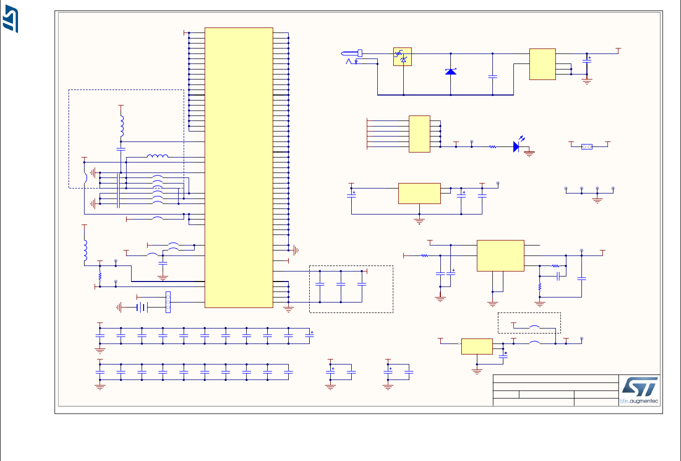
UM2198 Electrical schematics
DocID030511 Rev 1 51/69
Figure 23. Power
317
Power
MB1246 B.2
6/20/2017
Title:
Size: Reference:
Date: Sheet: of
A4 Revision:
STM32H7x3I-EVAL
Project:
Vin
3
GND
1
Vout 2
Tab 4
U20
LD1086D2M33
SV
1
SG
2
CV 3
CG1 4
CG2 5
CG3 6
L3
BNX002-01
C36
220uF
E5V
TP5
5V
+5V
1 2
LD9
red
C46
47uF
C51
10uF C52
100nF
+5V +3V3
TP11
Ground
TP7
+3V3
1
3
2
CN10
DC-10B Z1
SMAJ5.0A-TR C34
100nF
1
2
3
D10
ZEN056V130A24LS
E5V
D5V
U5V_ST_LINK
+3V3 VDD_MCU
JP9
R159
820
VBUS_HS
VBUS_FS1
1 2
3 4
5 6
7 8
9 10
11 12
JP10
Header 6X2
VBUS_FS2
TP2
Ground
TP1
Ground
TP6
Ground
+5V TP9
2V9_SD
R143 1K
C54
[N/A]
C50
4.7uF
+2V9_SD
C48
[N/A]
R134 22K[1%]
R136
16K[1%]
Power Supply 2.9V
[Ceramic]
C47
10uF
+3V3
Vout=1.22*(1+R1/R2)
R1
R2
VDD_MCU
TP3
VDDA
VDDA
VREF+
L9
BEAD(FCM1608KF-601T03)
R216
0
TP4
VREF
VDD_MCU
C27
2.2uF[N/A]
DSI_VDD12
VDD_MCU
Ceramic capacitor (Low ESR <600m ohm)
C26
2.2uF
Only one 2.2uF required on board
C135
100nF
BT1
CR1220 holder
+3V3
C119
100nF
C125
100nF
C127
100nF
C106
1uF C110
100nF
VREF+
C107
1uF
VDDA
C109
100nF
VDD_MCU
C122
100nF
C117
100nF
C133
100nF
C126
100nF
C121
100nF
C114
100nF
C115
100nF
C124
100nF
C123
100nF
VDD_MCU
C130
100nF
C129
100nF
C131
100nF
C132
100nF
C134
100nF
C118
100nF
C21
4.7uF
C120
100nF
L1
2.2uH(LQM2MPN2R2NG0)
3
2
1
JP11
VDD_MCU
VDD_SDC
+5V
VDD_MCU
SB21 Open
SB19 Closed
C128
100nF Vin
3Vout 2
1
Tab 4
U21
LD1117S18TR
C59
10uF
+1V8_LDO
TP12
1V8
+3V3
VDD_SDC
SB36 Open
SB37 Closed
+1V8
C12
4.7uF
SB22
Closed EN
1
GND
2
VO 4
ADJ 5
GND
7
VI
6PG 3
U17
ST1L05BPUR
C29
1uF_X5R_0603
SB13 Closed
SB16 Open
C18 2.2uF
C15 10uF
C28 10uF
C20 [N/A]
SB20 Open
SB14 Open
SB23 ClosedC30 2.2uF
C22 2.2uF SB17 Open
SB10
Open
SB18 Closed
L10
BEAD(FCM1608KF-601T03)
VDD_MCU
VSS K9
VREF- N1
VREF+
M1
VSSA P1
VDD
E11
VSS J7
VDD
K5
NC
F2
VSS H11
VSS L11
VSS K10
VSS L7
VSS G7
VDD
G5
VSS L10
VDD
H5
VDD
E9
VSS K11
VDD
F5
VSS H10
VDD
L5
VSS L8
VSS L9
VSS J11
VSS G11
VSS H7
VSS K7
VSS K8
VSS J10
VSS G10
VDD
G13
VSS R4
VDD
M5 VDD
L13
VSS B6
VCAP3
A7
NC
F1
VDD
E6
VDD
N8
VDD
J13 VDD
H13
VSS A17
VSS C16
VDDLDO2
C17
VCAP2
D17
VDD33USB
F17
VSS G16
VDD50USB
G17
VSS J16
VSS J17
VSS G8
VSS G9
VSS H8
VSS H9
VSS J8
VSS J9
VSS N16
NC N17
VDD P17
VSS U1
VCAP1
U11
VDDLDO1
U12
VSS U17
VSS T12
VSS A1
VBAT
B1
VSS B2
VDDA
L1
VSS J3
VDD
N7
VSS R8
VSS M15
VDD
M13
VDD
N12 VDD
N11
VDDLDO3
A6
VSS L15
VSS K15
VDD
N10
VDD
K13
VSS C10
VSS C13
NC
G2 NC
E1
U7C
STM32H7x3XIH6
Reserved for other use
Reserved for other use
Reserved for other use
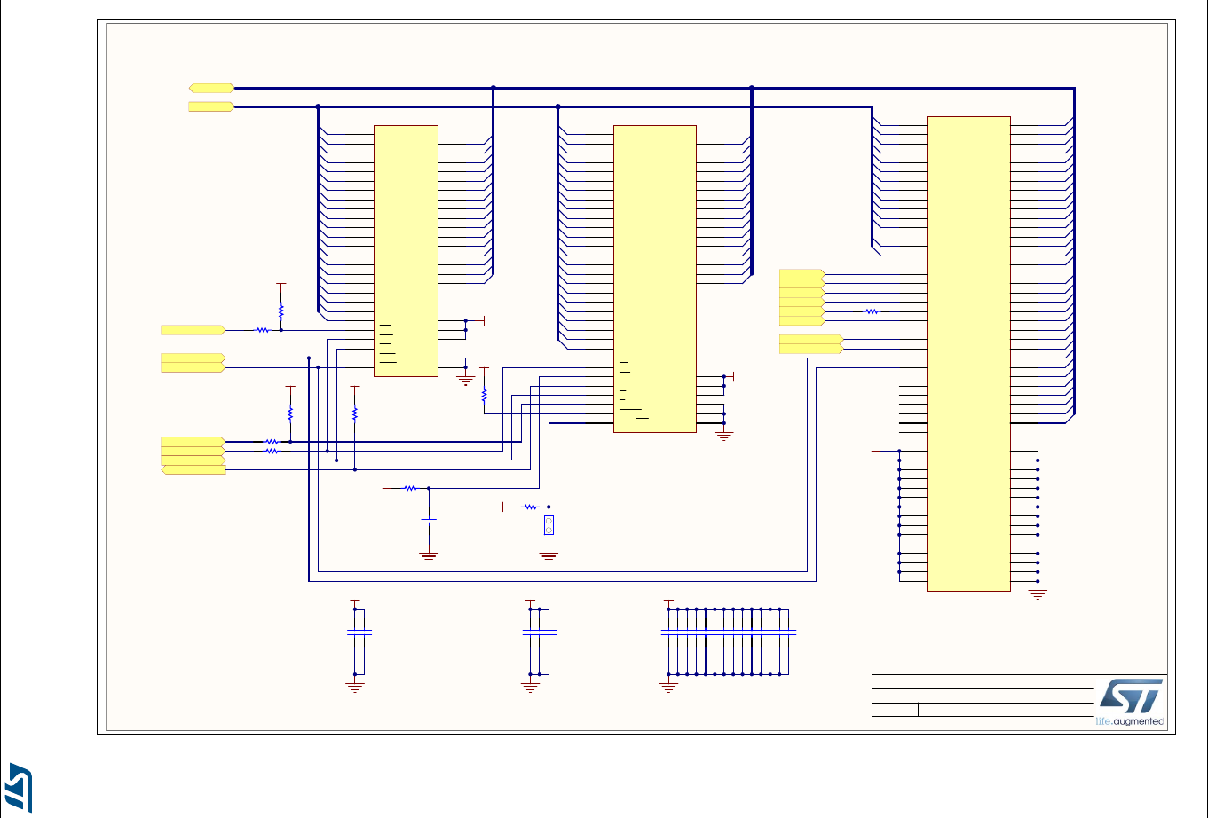
Electrical schematics UM2198
52/69 DocID030511 Rev 1
Figure 24. SRAM, FLASH and SDRAM
417
SRAM & FLASH & SDRAM
MB1246 B.2
6/9/2017
Title:
Size: Reference:
Date: Sheet: of
A4 Revision:
STM32H7x3I-EVAL
Project:
A1
A2
A3
A4
A5
A6
A7
A8
A9
A10
A11
A12
A13
A14
A15
A16
A1
A2
A3
A4
A5
A6
A7
A8
A9
A10
A11
A12
A13
A14
A15
A16
A17
A18
A19
A20
A21
A22
FMC_NE1
FMC_NWE
FMC_NOE
FMC_NWAIT
JP13
A0
A0
A17
A18
D0
D1
D2
D3
D4
D5
D6
D7
D8
D9
D10
D11
D12
D13
D14
D15
D0
D1
D2
D3
D4
D5
D6
D7
D8
D9
D10
D11
D12
D13
D14
D15
Default setting: Open
PE1
PE0
PD5
PD7
PD6
PD4
PG10
FMC_NBL0
FMC_NBL1
A19
A20 A23
A22
B8
A15
D7
A14
C7
A13
A7
A12
B7
A11
D6
A10
C6
A9
A6
A8
B6
A19
D5 A20
D4
W
A5
RP
B5
A21
C5
Vpp/WP
B4
RB
A4
A18
C4
A17
B3
A7
A3
A6
C3
A5
D3
A4
B2
A3
A2
A2
C2
A1
D2
VCCQ D8
A0
E2
E
F2
VSS E8
G
G2
DQ0 E3
DQ8 F3
DQ1 H3
DQ9 G3
DQ2 E4
DQ10 F4
DQ3 H4
DQ11 G4
VCCQ F1
DQ4 H5
DQ12 F5
DQ5 E5
DQ13 G6
DQ6 H6
DQ14 F6
DQ7 E6
DQ15A-1 G7
VSS H7
BYTE
F7
A16
E7
VCC G5
VSS H2
A23
C8
U12
PC28F128M29EWLA
D[0..31]
A[0..23]
D[0..31]
A[0..23]
R128 0
R88 0
SRAM
Nor Flash
+3V3
+3V3
+3V3+3V3
+3V3
+3V3
+3V3
+3V3
D0
D1
D2
D3
D4
D5
D6
D7
D8
D9
D10
D11
D12
D13
D14
D15
D16
D17
D18
D19
D20
D21
D22
D23
D24
D25
D26
D27
D28
D29
D30
D31
A1
A2
A3
A4
A5
A6
A7
A8
A9
A10
A11
A0
SDRAM
A11
H9
A10
G7
A9
J3
A8
H2
A7
H1
A6
G3
A5
G2
A4
G1
A3
F3
A2
F7
A1
G9
A0
G8
NC
E3
DQ0 R8
DQ8 L2
DQ1 N7
DQ9 M3
DQ2 R9
DQ10 M2
DQ3 N8
DQ11 P1
VDDQ
B2
DQ4 P9
DQ12 N2
DQ5 M8
DQ13 R1
DQ6 M7
DQ14 N3
DQ7 L8
DQ15 R2
VSS A3
VDD
A7
DQ16 E8
DQ24 A2
DQ17 D7
DQ25 C3
DQ18 D8
DQ26 A1
DQ19 B9
DQ27 C2
DQ20 C8
DQ28 B1
DQ21 A9
DQ29 D2
DQ22 C7
DQ30 D3
DQ23 A8
DQ31 E2
VSSQ B3
VDDQ
B7 VSSQ B8
VSSQ C1
VDDQ
C9
VSSQ D1
VDDQ
D9
VDDQ
E1
NC
E7
VSSQ E9
VSS F1
VDD
F9
NC
H3
NC
H7
BA0
J7 BA1
H8
NU
K2 NC
K3
VDDQ
L1
VSS L3
VDD
L7
VSSQ L9
VSSQ M1
VDDQ
M9
VSSQ N1
VDDQ
N9
VDDQ
P2 VSSQ P3
VDDQ
P7 VSSQ P8
VSS R3
VDD
R7
DQM0
K9 DQM1
K1 DQM2
F8
CLK
J1 CKE
J2 CS#
J8
DQM3
F2
RAS#
J9 CAS#
K7 WE#
K8
U15
IS42S32800G-6BLI
SDNCAS
SDNWE
SDNRAS
SDNE1
SDCKE1
SDCLK
FMC_NBL3
FMC_NBL2
+3V3
+3V3+3V3+3V3
Place close SDRAMPlace close Nor FlashPlace close SRAM
PH5
PG15
PF11
PH6
PH7
PG8
PI5
PI4
A4
B4
A3
B3
A2
A5
A1
A4
A0
A3
CE
B5
I/O0 B6
I/O1 C5
I/O2 C6
I/O3 D5
VCC D6
VSS D1
I/O4 E5
I/O5 F5
I/O6 F6
I/O7 G6
WE
G5
A16
E4
A15
F4
A14
F3
A13
G4
A12
G3
A11
H5
A10
H4
A9
H3
A8
H2
I/O8 B1
I/O9 C1
I/O10 C2
I/O11 D2
VCC E1
I/O12 E2
I/O13 F2
I/O14 F1
I/O15 G1
BLE
A1
BHE
B2
OE
A2
A7
D4
A6
C4
A5
C3
A17
D3 A18
H1
VSS E6
A19
G2 A20
H6
CE2 A6
U16
IS61WV102416BLL-10MLI
R95 0
A14
A15
FMC_NBL1
FMC_NBL0
R282 0
C33
100nF
C155100nF
C146100nF
C138100nF
C136100nF
C137100nF
C159100nF
C158100nF
C157100nF
C143100nF
C145100nF
C161100nF
C160100nF
C156100nF
C142100nF
C144100nF
C150100nF
C152100nF
C151100nF
C149100nF
R129
10K
R281
10K
R87
10K
R89
10K
R86
10K R96
10K
FMC_NE3
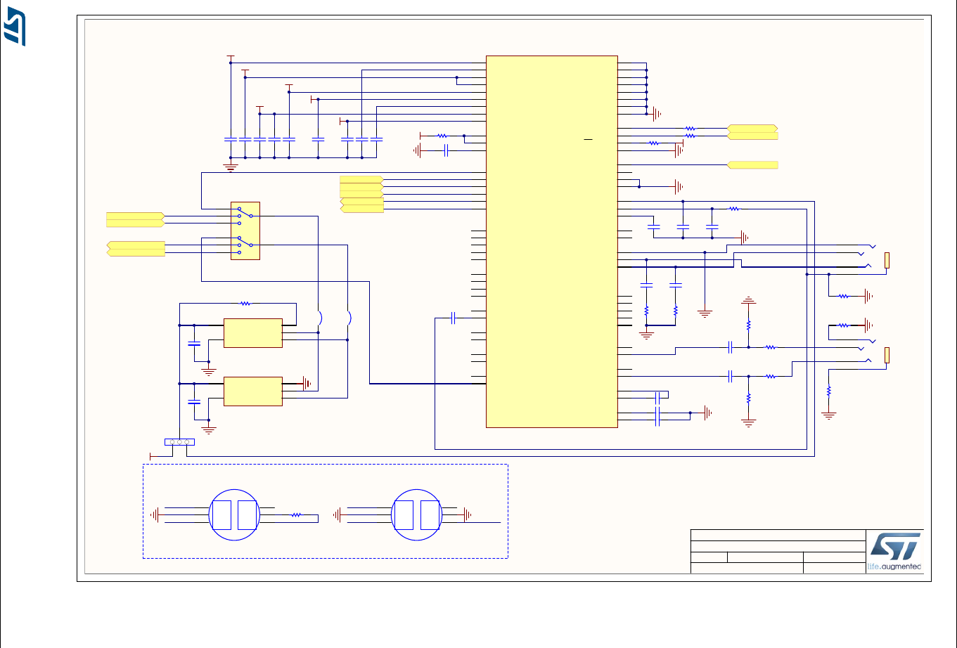
UM2198 Electrical schematics
DocID030511 Rev 1 53/69
Figure 25. Audio
517
Audio
MB1246 B.2
6/20/2017
Title:
Size: Reference:
Date: Sheet: of
A4 Revision:
STM32H7x3I-EVAL
Project:
SAI1_SCKA
2
6
4
3CN17
PJ3028B-3
Default I2C Address:0011010
PE6
ADCDAT1
F2
ADCLRCLK1/GPIO1
G3
AGND D6
CPVDD
G9
CPVOUTN H7
CPVOUTP G7
CS/ADDR G2
DACDAT1
E4
CPGND H9
DCVDD
F1
DBVDD
D2 DGND E2
CPCB H8
AVDD1
D9
BCLK1
G1
CIFMODE A4
CPCA G8
DMICCLK
C6
AGND E7
AGND E8
AVDD2
D8
GPIO2/MCLK2 E1
GPIO3/BCLK2
H2
GPIO4/LRCLK2
F4
GPIO5/DACDAT2
H3
GPIO6/ADCLRCLK2
G4 GPIO7/ADCDAT2
E5
GPIO8/DACDAT3
H4
GPIO9/ADCDAT3
F5
GPIO10/LRCLK3
H5 GPIO11/BCLK3
F6
HP2GND F7
HPOUT1FB G5
HPOUT1L H6
HPOUT1R G6
HPOUT2N F9
HPOUT2P F8
IN1LN
D7 IN1LP
C8
IN1RN
B7 IN1RP
C7
IN2LN/DMICDAT1
B9 IN2LP/VRXN
B8
IN2RN/DMICDAT2
A9 IN2RP/VRXP
A8
LDO1ENA
D4
LDO1VDD
E9
LDO2ENA
D5
LDO2VDD
D1
LINEOUT1N C5
LINEOUT1P B5
LINEOUT2N C4
LINEOUT2P B4
LINEOUTFB A6
LRCLK1
E3
MCLK1 D3
MICBIAS1 A7
MICBIAS2 B6
REFGND A5
SCLK H1
SDA F3
SPKGND1 A1
SPKGND2 C1
SPKMODE A3
SPKOUTLN B1
SPKOUTLP A2
SPKOUTRN C3
SPKOUTRP B3
SPKVDD1
B2
SPKVDD2
C2
VMIDC C9
VREFC
E6
U22
WM8994ECS/R
C75100nF
C68100nF
+3V3
+1V8
+3V3
SAI1_FSA
SAI1_SDA
SAI1_SDB
PE5
PE4
PE3
Audio_INT
C77
1uF
I2C1_SDA
I2C1_SCL
PB7
PB6
SAI1_MCLKA
PG7
R168 2K2
C64100nF
C65100nF
R151
20
R152
20
C62 2.2uF
C61 2.2uF
C63 2.2uF
3
2
1
JP12 MICBIAS1
+3V3
C95100nF
DFSDM_CLK
time slot1 of SAI
time slot0 of SAI
DFSDM_DATA1
PC3
+3V3
C70100nF
+1V8
+3V3
+1V8
C72100nF
C96100nF
To MFX
R163[N/A] +3V3
MFX_GPIO5
R157 4K7
R206 10K
C60 1uF
C691uF
C731uF
C794.7uF
C714.7uF
C744.7uF
C80
4.7uF
C83
4.7uF
C84
4.7uF
PC2
R160 0
R155 0
R149
180
R158
1K
R156
180
C66
4.7uF
C55
4.7uF
2
6
4
3CN19
PJ3028B-3
R145
0
R148
0
R131 [N/A]
R147
1K
GND
5DOUT 4
CLK 3
VDD
1LR 2
U26
MP34DT01TR
GND
5DOUT 4
CLK 3
VDD
1LR 2
U27
MP34DT01TR
MIC_DATA
MIC_CLK
MIC_VDD
SB54
Closed
SB55
Closed
LEFT
RIGHT
Coupon connectors
MIC_DATA MIC_VDD
R207 10K
MIC_VDD
LEFTRIGHT
VDD 4
LR 5
NC 6
DATA
1GND
2CLK
3
CN26
Coupon Connectors
VDD 4
LR 5
NC 6
DATA
1GND
2CLK
3
CN25
Coupon Connectors
MIC_CLK
MIC_DATA
MIC_CLK
7
5
8
32
1
4
6
SW2
MS-23D18
PDM1_CLK1
PDM1_D1
PE2
PC1
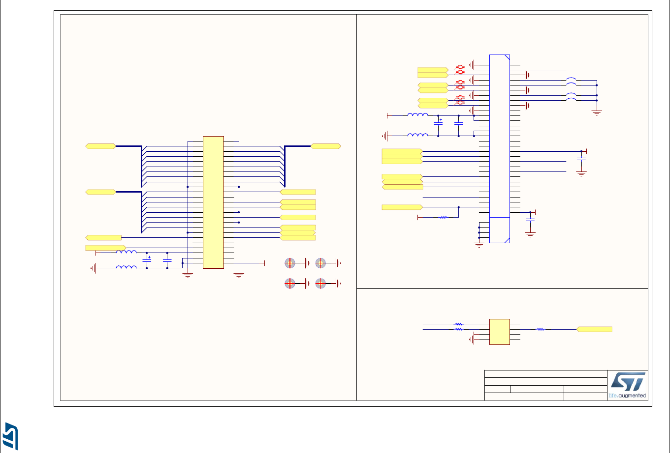
Electrical schematics UM2198
54/69 DocID030511 Rev 1
Figure 26. LCD connectors
617
LCD Connectors
MB1246 B.2
6/20/2017
Title:
Size: Reference:
Date: Sheet: of
A4 Revision:
STM32H7x3I-EVAL
Project:
1 2
3 4
5 6
7 8
9 10
11 12
13 14
15 16
17 18
19 20
21 22
23 24
25 26
27 28
29 30
31 32
33 34
35 36
37 38
39 40
41 42
43 44
45 46
47 48
49 50
CN20
P127B-2*25MGF-079-1A
LCD_R[0..7]
LCD_HSYNC
LCD_VSYNC
LCD_CLK
LCD_ENB
+3V3
I2C1_SDA
I2C1_SCL
LCD Connector
LCD_B[0..7]
LCD_G[0..7]
LCD_R0
LCD_R1
LCD_R2
LCD_R3
LCD_R4
LCD_R5
LCD_R6
LCD_R7
LCD_B0
LCD_B1
LCD_B2
LCD_B3
LCD_B4
LCD_B5
LCD_B6
LCD_B7
LCD_G0
LCD_G1
LCD_G2
LCD_G3
LCD_G4
LCD_G5
LCD_G6
LCD_G7
PJ7
PJ8
PJ9
PJ10
PJ11
PK0
PK1
PK2
PI15
PJ0
PJ1
PJ2
PJ3
PJ4
PJ5
PJ6
PJ12
PJ13
PJ14
PJ15
PK3
PK4
PK5
PK6
PK7
PI12
PI13
PI14
PB7
PB6
+5V
C58
10uF
L7
BEAD(FCM1608KF-601T03) C57
100nF
L6
BEAD(FCM1608KF-601T03)
I2C1_SDA
I2C1_SCL
LCD_G[0..7]LCD_R[0..7]
LCD_B[0..7]
FTSH-125-01-F-DV-K (Samtec)
H1
H2
1 2
3 4
5 6
7 8
CN4
F206A-2*04MGF-A
R210 0
R208 0I2C1_SDA
I2C1_SCL
+3V3
PB7
PB6
EXT_RESET
PA4
SSM-104-L-DH (Samtec)
R211 0
I2C Connector
LCD_BL_CTRL
H3
H4
TOUCH_INT
RESET#
PA6
TOUCH_INT
To MFX
MFX_GPIO14
Extension connector (Reserved for other use)
TOUCH_INT
LCD_BL_CTRL
+5V
C147
10uF
L11
BEAD(FCM1608KF-601T03) C148
100nF
L12 BEAD(FCM1608KF-601T03)
DSI_CK_P
DSI_CK_N
DSI_D0_P
DSI_D0_N
DSI_D1_P
DSI_D1_N
LCD_BL_CTRL
DSI_TE
R286
10K
PB7
PB6
C153
100nF
PJ2
DSI_RESET
1
122
3
344
5
566
7
788
9
910 10
11
11 12 12
13
13 14 14
15
15 16 16
17
17 18 18
19
19 20 20
21
21 22 22
23
23 24 24
25
25 26 26
27
27 28 28
29
29 30 30
31
31 32 32
33
33 34 34
35
35 36 36
37
37 38 38
39
39 40 40
41
41 42 42
43
43 44 44
45
45 46 46
47
47 48 48
49
49 50 50
51
51 52 52
53
53 54 54
55
55 56 56
57
57 58 58
59
59 60 60
61
61
62
62
63
63
64
64
CN15
QSH-030-01-F-D-A
PF10
I2C1_SCL
I2C1_SDA
+3V3
+3V3
SB34 Closed
SB33 Closed
SB31 Closed
SB32 Closed
SCLK/MCLK
LRCLK
I2S
PE6
PE5
PE4
CEC
PA15
CEC_CLK
PA8
DSI_D2_P
DSI_D2_N
DSI_D3_P
DSI_D3_N
+1V8
C154
100nF
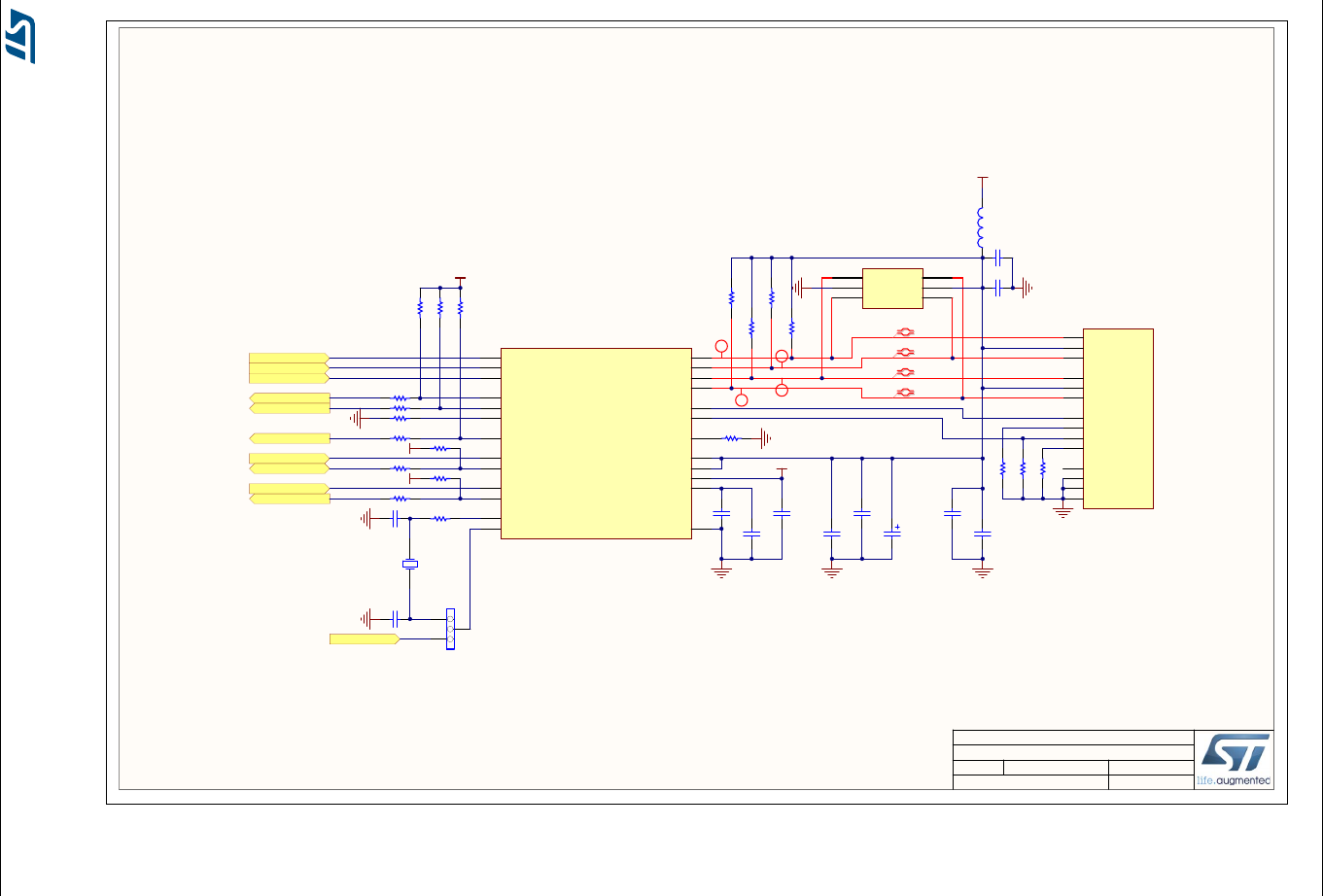
UM2198 Electrical schematics
DocID030511 Rev 1 55/69
Figure 27. Ethernet
717
Ethernet
MB1246 B.2
6/9/2017
Title:
Size: Reference:
Date: Sheet: of
A4 Revision:
STM32H7x3I-EVAL
Project:
TD+
1
TCT
4
TD-
2
RD+
3
RCT
5
RD-
6
NC
7
CHS GND
8
LED(green)_A
9
LED(green)_K
10
LED(Yellow)_A
12
LED(Yellow)_K
11
Shield
13
Shield
14
CN1
J0011D21B
Second source: SI-60116-F
ETH_MCO 3
2
1
JP5
PA8
RMII_TXD0
RMII_TX_EN
RMII_RXD0
RMII_REF_CLK
RMII_CRS_DV
ETH_MDC
ETH_MDIO
RMII_TXD1
RMII_RXD1
MDIO
12 MDC
13
RXD1/MODE1
7RXD0/MODE0
8
RXER/PHYAD0
10
TXEN
16
TXD0
17
TXD1
18
CRS_DV/MODE2
11
nRST
15
XTAL1/CLKIN
5XTAL2
4
GND_EP 25
RBIAS 24
VDDIO 9
VDD1A 19
VDD2A 1
VDDCR 6
RXP 23
RXN 22
TXN 20
TXP 21
nINT/REFCLK0
14
LED2/nINT/nPME/nINTSEL 2
LED1/nINT/nPME/REGOFF 3
U5
LAN8742A-CZ-TR
i
Diff Pair 100ohm
i
Diff Pair 100ohm
i
Diff Pair 100ohm
i
Diff Pair 100ohm
TD_N
TD_P
RD_N
RD_P
R21
12K1
C113
10uF
PG11
PG13
PG12
PC4
PC5
PA7
PC1
PA2
PA1
R42
10K
R40
10K
R45
10K
R43 10K
R8
10K
C112
100nF
C111
100nF
C116
100nF
C103
100nF
C4
100nF
C17
1uF_X5R_0603
C19
470pF
R9
270
R7
270
I/O1
1
GND
2
I/O2
3I/O3 4
Vbus 5
I/O4 6
U3
USBLC6-4SC6
C102
100nF
C16
30pF
C14
30pF
R23
50
R25
50
R22
50
R24
50
L2
BEAD
R41 33
R39 33
R44 33
R46 1K5
R35 10K
1 2
X3
X53T-C20SSA-25.000MHz
R31 33
+3V3
+3V3
+3V3
+3V3
+3V3
R30 0
RESET#
C5
100nF
R47 0
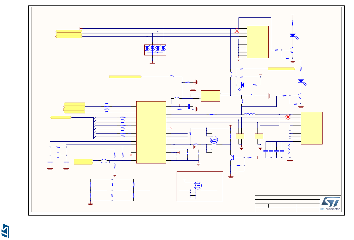
Electrical schematics UM2198
56/69 DocID030511 Rev 1
Figure 28. USB OTG HS
817
USB_OTG_HS
MB1246 B.2
6/9/2017
Title:
Size: Reference:
Date: Sheet: of
A4 Revision:
STM32H7x3I-EVAL
Project:
ULPI_D[0..7]
ULPI_CK
ULPI_D0
ULPI_D1
ULPI_D2
ULPI_D3
ULPI_DIR
ULPI_NXT
ULPI_STP
+5V
R125
3K3
12
LD6
Red
R288
620
C40
4.7uF
VBUS
1
DM
2
DP
3
ID
4
GND
5
Shield
6
USB_Micro-AB receptacle
Shield
7
Shield
8
Shield
9
EXP
10
CN14
475900001
VBUS_HS
PA3
PB0
PB1
PB10
C42
33pF
X4
24MHz
R121
1M
C43
33pF
ULPI_D[0..7]
PB11
PB12
PB13
PB5
ULPI_D4
ULPI_D5
ULPI_D6
ULPI_D7
L5
EXC-3BP121H[BEAD]
L4
EXC-3BP121H[BEAD]
R127
10K
R116 820
R287
330
12
LD5
Green
R122
47K
R119
22K
C44
100nF
C45
100nF
C37
100nF
C38
100nF
USB_RESET
PH4
PI11
PC0
PA5
3
1
2
T5
9013
A1
A2
B1
B2
D12
USBULC6-2F3
A1
A2
B1
B2
D11
ESDA14V2-2BF3
+3V3
+3V3
GND
2
IN
5
EN
4OUT 1
FAULT 3
U14
STMPS2151STR
USB_FS2_DM
USB_FS2_DP
VBUS
1
DM
2
DP
3
ID
4
GND
5
Shield
6
USB_Micro-AB receptacle
Shield
7
Shield
8
Shield
9
EXP
10
CN16
475900001
PB13
PB12
PB14
PB15
R289
330
12
LD7
Green
3
1
2
T6
9013
+3V3
R137
22K
OTG_FS2_PowerSwitchOn
OTG_FS2_OverCurrent
R126 0
USB_FS2_ID
To MFX
From MFX
MFX_GPIO8
MFX_GPIO9
C41 100nF
C139
100nF
C141
100nF
R118 33
R135
47K
VBUS_FS2
R284
[N/A]
+3V3
SB61 closed if reset is
controlled by hardware
SB29 Open
SB30
Closed
SB28
Open
SB27
Closed
1
32
45
6
D13
ESDA6V1BC6
CPEN 17
VBUS 22
ID 23
REFSEL0 8
DP 18
DM 19
RESETB
27
VBAT 21
NXT
2
DIR
31
STP
29
CLKOUT
1
VDD1.8 30
VDD3.3 20
D7
13
D6
10
D5
9
D4
7
D3
6
D2
5
D1
4
D0
3REFSEL1 11
VDD1.8 28
XO
25
NC 12
REFCLK
26
REFSEL2 14
VDDIO 32
RBIAS 24
GNDPAD 33
SPK_R
16 SPK_L
15
U13
USB3320C-EZK
R117 0
R123 0
R124 0
R101 0
R104 0
R105 0
R108 0
R109 0
R111 0
R113 0
R114 0
SB61 Open
R120 8K06_1%
R107
0
R103
0
R100
0
R106
[N/A]
R102
[N/A]
R99
[N/A]
REFSEL0 REFSEL1 REFSEL2
REFSEL0
REFSEL1
REFSEL2
+3V3
R283 0
C140
2.2uF_X7R
+1V8
4
3
5
G
S
D
6
7
8
2
1T1
STS5PF30L
3
1
2
T2
9013
+1V8
R133
1K
R130 10K
R132 10K
R285
[N/A]
C39 100nF
+5V
3
4
5
G
SD
6
2
1
T7
STT4P3LLH6[N/A]
T1_D
T1_D
+3V3
T1_G
T1_G
Backup footprint for T1
VDD_IO
VDD_IO
R298
4K7
VDD_IO
R299
100K
From MFX
MFX_GPIO12
SB52 Open
RESET#
C172 100nF[N/A]
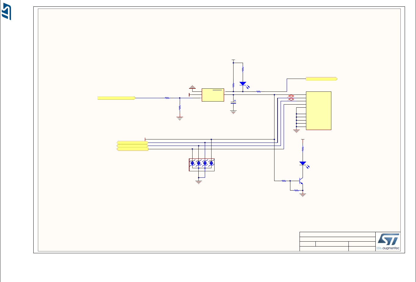
UM2198 Electrical schematics
DocID030511 Rev 1 57/69
Figure 29. USB OTG FS
917
USB_OTG_FS
MB1246 B.2
6/9/2017
Title:
Size: Reference:
Date: Sheet: of
A4 Revision:
STM32H7x3I-EVAL
Project:
+5V
OTG_FS1_PowerSwitchOn
OTG_FS1_OverCurrent
+3V3
12
LD8
Red
R290
620
USB_FS1_DM
USB_FS1_DP
USB_FS1_ID
C53
4.7uF
R141 0
R146 0
GND
2
IN
5
EN
4OUT 1
FAULT 3
U18
STMPS2151STR
VBUS
1
DM
2
DP
3
ID
4
GND
5
Shield
6
USB_Micro-AB receptacle
Shield
7
Shield
8
Shield
9
EXP
10
CN18
475900001
VBUS_FS1
PA9
PA10
PA11
PA12
R165
330
12
LD10
Green
+3V3
R154
22K
From MFX
To MFX
MFX_GPIO6
MFX_GPIO7
R140
10K
R144
47K
R153
47K
3
1
2
T3
9013
1
32
45
6
D14
ESDA6V1BC6
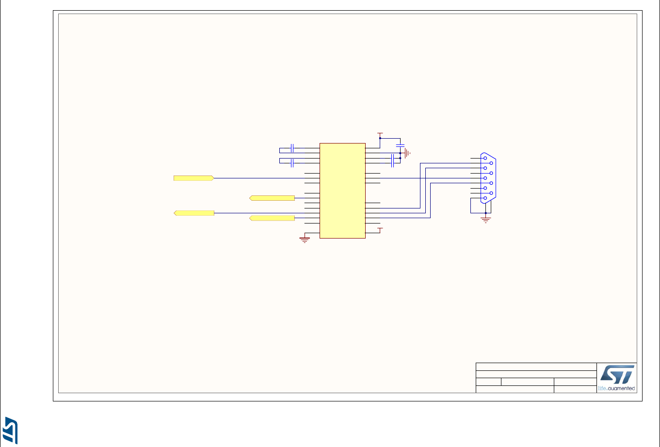
Electrical schematics UM2198
58/69 DocID030511 Rev 1
Figure 30. RS232
10 17
RS232
MB1246 B.2
6/9/2017
Title:
Size: Reference:
Date: Sheet: of
A4 Revision:
STM32H7x3I-EVAL
Project:
RS232_TX
RS232_RX
C2+
1
C2-
2V- 3
R1IN 4
R2IN 5
R3IN 6
R4IN 7
R5IN 8
T1OUT 9
T2OUT 10
T3OUT 11
T3IN
12 T2IN
13 T1IN
14
R5OUT
15 R4OUT
16 R3OUT
17 R2OUT
18 R1OUT
19 R2OUTB
20 R1OUTB
21
nSHDN 22
nEN
23
C1-
24 GND 25
VCC 26
V+ 27
C1+
28
U4
ST3241EBPR
+3V3
+3V3
Bootloader_BOOT0
Bootloader_RESET
PB14
PB15
RXD
TXD
CTS
DSR
RS232
C101 100nF
C3 100nF
C104
100nF
C105
100nF
C6
100nF
1
6
2
7
3
8
4
9
5
CN2
DB9-male USART1
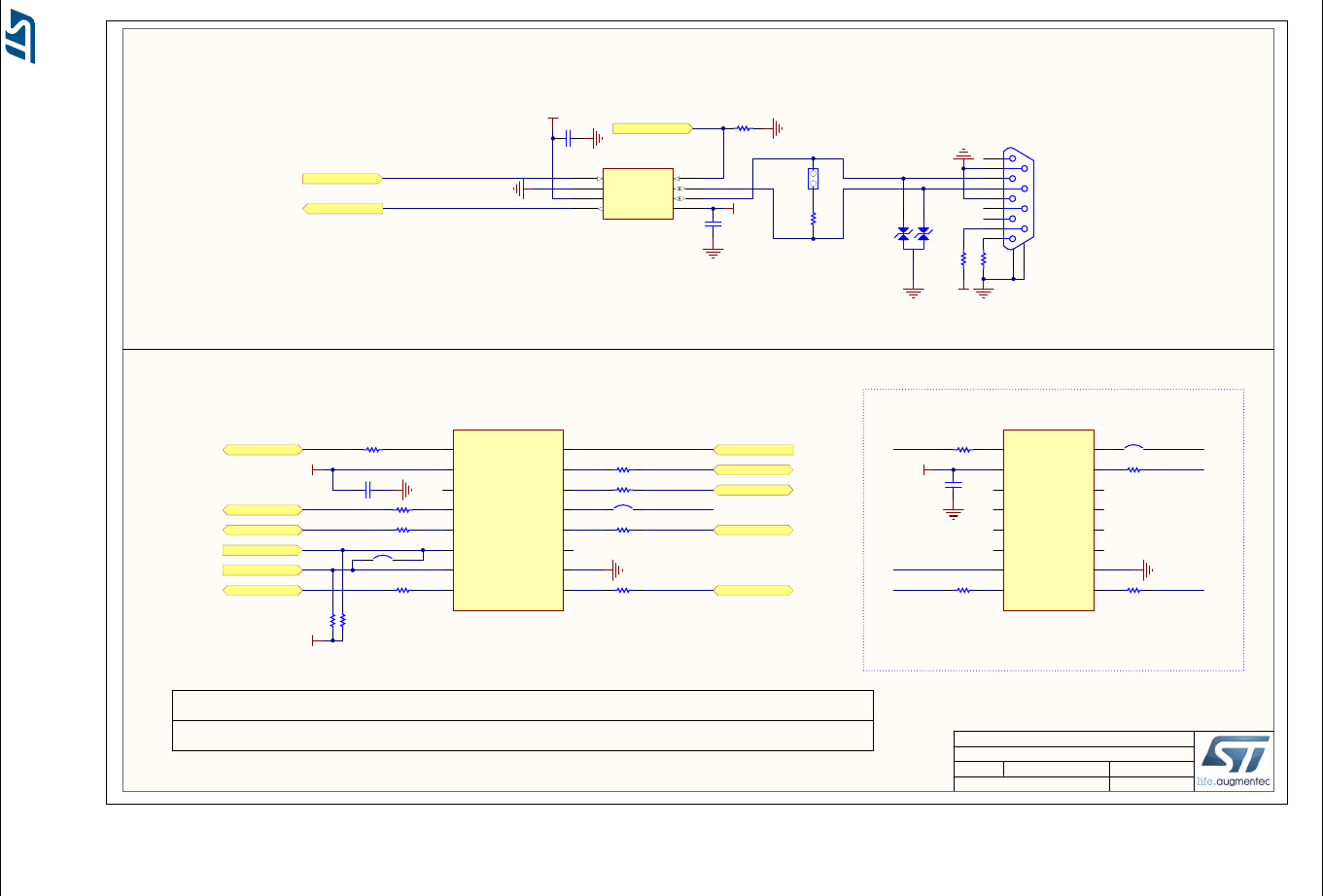
UM2198 Electrical schematics
DocID030511 Rev 1 59/69
Figure 31. FDCAN and QSPI
11 17
FDCAN & QSPI
MB1246 B.2
6/9/2017
Title:
Size: Reference:
Date: Sheet: of
A4 Revision:
STM32H7x3I-EVAL
Project:
FDCAN1_TX
FDCAN1_RX
+3V3
R5
120
JP1
R214
0
R213
[N/A]
Default setting: Open
PA12
PA11
FDCAN
C100
100nF
R4
10K
1
6
2
7
3
8
4
9
5
CN3
DB9-male CAN connector
TXD
1
VSS
2
VDD
3
RXD
4VIO 5
CANL 6
CANH 7
STBY 8
U2
MCP2562FD
+5V
+3V3
C99
100nF
FDCAN1_STBY
3
1
2
D2
ESDCAN02-2BWY
PD3
Twin Quad SPI Flash
C108
100nF[N/A]
+3V3
CS#
7
DQ1
8
NC
6
NC
5NC 12
NC 11
Vss 10
W#/Vpp/DQ2 9
HOLD#/DQ3
1
VCC
2
NC
3
CLK 16
DQ0 15
NC
4NC 13
NC 14
U28
MT25QL512ABB8ESF-0SIT[N/A]
R225 33[N/A]
R229 33[N/A]
R253 33[N/A]
R237 33[N/A]
CS#_1
7
DQ1
8
CS#_2
6
DQ5
5W_2#/DQ6 12
NC 11
Vss 10
W_1#/DQ2 9
HOLD_1#/DQ3
1
VCC
2
RESET#
3
CLK_1 16
DQ0 15
HOLD_2#/DQ7
4CLK_2 13
DQ4 14
U6
MT25TL01GHBB8ESF-0SIT
QSPI_BK1_IO3
QSPI_BK1_IO1
PF9
PF6
QSPI_BK1_NCS
PG6
C13 100nF
+3V3
+3V3
R26 33
R32 33
QSPI_BK1_IO0
QSPI_BK1_IO2
PF8
PF7
QSPI_CLK
PB2
R38 33
R36 33
QSPI_BK2_NCS
R19
10K
R20
10K
QSPI_BK2_IO0
QSPI_BK2_IO1 QSPI_BK2_IO2
QSPI_BK2_IO3 R27 33
R28 33
R52 33
R33 33
SB6 Closed
BK2_IO0
BK2_IO2BK2_IO1
BK2_IO3
BK2_IO3
NCS2
NCS2
BK2_IO1
QSPI_CLK QSPI_CLK
BK2_IO0
BK2_IO2
QSPI_CLK
PG9
PG14
PH2
PH3
SB12 Closed
PC11
Two QSPI Flash solution
SB44 Open
Twin Quad SPI Flash solutions:
One Twin Quad SPI Fllash U6:MT25TL01GHBB8ESF-0SIT U28:NA
Two Quad SPI Fllash U6:MT25QL512ABB8ESF-0SIT U28:MT25QL512ABB8ESF-0SIT R225/R229/R237/R253, SB44, C108 ON R27/R28/R33/R52 OFF
R27/R28/R33/R52 ON R225/R229/R237/R253, SB44, C108 OFF
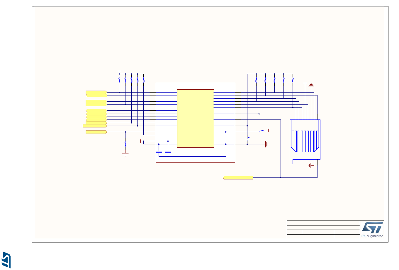
Electrical schematics UM2198
60/69 DocID030511 Rev 1
Figure 32. microSD 3.0 card
12 17
MICRO SD 3.0 Card
MB1246 B.2
6/9/2017
Title:
Size: Reference:
Date: Sheet: of
A4 Revision:
STM32H7x3I-EVAL
Project:
SDIO1_CKIN
SDIO1_CDIR
SDIO1_D0DIR
SDIO1_D123DIR
SDIO1_D0
SDIO1_D1
SDIO1_D2
SDIO1_D3
SDIO1_CMD
PB8
PB9
PC6
PC7
PC8
PC9
PC10
PC11
PD2
SDIO1_CLK
PC12
R82
10K
SD_LDO_SEL
MFX_GPIO13
MICRO SD 3.0 Card
SMS064FF or SMS128FF
1
2
3
4
5
6
7
8
SW2
9
SW1
10
CN13
PJS008-2000
MicroSDCard_Detect
To MFX (input with pull up)
MFX_GPIO15
R112
[N/A] +2V9_SD
+2V9_SD
C35
1uF
+3V3
R84
10K
R97
[N/A]
R98
[N/A]
R115
[N/A]
R110
[N/A]
R93
10K
R92
10K
R91
10K
+3V3
SB26
Closed
TP8
R83
10K
7
4
9
17
8
23
18
1
25
24
19
5
3
22
20
15
6
2
10
21
16
VCCA
B3 VSUPPLY
A4
ENABLE
C2 SEL
B2
100nF100nF
DIR_1_3
E3
DATA0_H
DIR_0
DATA1_H
DATA2_H
DATA3_H
A3
B1
A1
E1
D1
DIR_CMD
A2 CMD_H
D2
CLK_IN
CLK_FB
C1
E2 13
11
14
12
GND
VLDO
VSD_REF
100nF
C3
C4
B4
CD D3
WP E4
DATA0_SD
DATA1_SD
DATA2_SD
DATA3_SD
D5
E5
A5
B5
CLK_SD
CMD_SD
C5
D4
Module board
M1
IP4856CX25/C_Module_REV
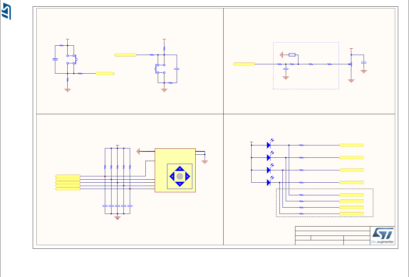
UM2198 Electrical schematics
DocID030511 Rev 1 61/69
Figure 33. Peripherals
13 17
Peripherals
MB1246 B.2
6/20/2017
Title:
Size: Reference:
Date: Sheet: of
A4 Revision:
STM32H7x3I-EVAL
Project:
JOY_SEL
JOY_DOWN
JOY_LEFT
JOY_RIGHT
JOY_UP
C89 10nF[N/A]
C90 10nF[N/A]
C88 10nF[N/A]
C86 10nF[N/A]
C87 10nF[N/A] R188 10K[N/A]
R187 10K[N/A]
R189 10K[N/A]
R191 10K[N/A]
R190 10K[N/A]
R204
220K
C93
[N/A]
R205
100
R203
330
PA0
+3V3
To MFX
+3V3
Buttons
Joystick
R194
4K7
1
4 3
2
B3
USER (Blue) C91
100nF
R192
100
R193
0
TAMPER_KEY
PC13
Tamper & Key Button
+3V3
WAKEUP
1
43
2
B2
WKUP
Wakeup Button
MFX_GPIO0
MFX_GPIO1
MFX_GPIO2
MFX_GPIO3
MFX_GPIO4
13
2
RV13386P-103(10K)
Potentiometer
C7
[N/A]
R11 0
Close to MCU on PCB
PA0_C
R6 0
CN5
Two pin header for external analog input
R10 47 C92
100nF
R12
0
+3V3
Potentiometer
1 2
LD3
Red
1 2
LD2
Orange
1 2
LD4
Blue
1 2
LD1
Green
+3V3
R202 510[MIPI]
R201 680[MIPI]
R200 680[MIPI]
R199 680[MIPI]
LEDs
LED4_MIPI
LED3_MIPI
LED1_MIPI
LED2_MIPI
PK3
PK4
PK5
PK6
COMMON
5
Selection
2
DWON
3
LEFT
1
RIGHT
4
UP
6
GND 7
GND 8
B4
MT-008A
R294 510[RGB]
R295 680[RGB]
R296 680[RGB]
R297 680[RGB]
LED1_RGB
LED2_RGB
LED3_RGB
LED4_RGB
PF10
PA4
MFX_IO10
MFX_IO11
Reserved for other use
Electrical schematics UM2198
62/69 DocID030511 Rev 1
Figure 34. Extension connectors
14 17
Extension Connectors
MB1246 B.2
6/9/2017
Title:
Size: Reference:
Date: Sheet: of
A4 Revision:
STM32H7x3I-EVAL
Project:
1 2
3 4
5 6
7 8
9 10
11 12
13 14
15 16
17 18
19 20
21 22
23 24
25 26
27 28
29 30
31 32
33 34
35 36
37 38
39 40
CN11
P1039-2*20MGF-089-1A
1 2
3 4
5 6
7 8
9 10
11 12
13 14
15 16
17 18
19 20
21 22
23 24
25 26
27 28
29 30
31 32
33 34
35 36
37 38
39 40
CN12
P1039-2*20MGF-089-1A
PA[0..15] PA[0..15]
PB[0..15] PB[0..15]
PC[0..15] PC[0..15]
PD[0..15] PD[0..15]
PE[0..15] PE[0..15]
PF[0..15] PF[0..15]
PG[0..15] PG[0..15]
PH[0..15] PH[0..15]
PI[0..15] PI[0..15]
PJ[0..15] PJ[0..15]
PK[0..7] PK[0..7]
PC14PC15
+3V3
D5V
SB39
Open
SB40
Open
+3V3
D5V
PA4
PA5
PA6
PA7
PA11
PA12
PA9
PA10
PA0
PA1 PA15
PA3
PA13
PA14
PA2
PA8
PB5
PB6
PB7
PB14
PB15
PB10
PB8
PB9
PB1
PB2
PB3
PB0
PB4
PB11
PB12
PB13
PC0 PC1 PC2
PC3
PC4 PC5
PC6
PC7
PC8
PC9
PC10
PC11
PC12
PC13
PJ0
PJ14
PJ15
PJ9
PJ8
PJ11
PJ10
PJ12
PJ13
PJ1
PJ2
PJ3
PJ4
PJ5
PJ6
PJ7
PK0
PK1 PK2
PK3
PK4 PK5
PK6
PK7
PD3
PD6
PF9
PF8
PF10
PF6
PF7
PG6
PG7
PG14
PG11
PG10
PG12PG13PH4
PH6
PH7
PI14
PI15
PI8
PI11
PI12
PI13
PD0 PD1
PD2
PD4
PD5
PD7
PD8
PD9
PD10
PD11
PD12
PD13
PD14
PD15
PE0
PE14
PE15
PE9
PE8
PE11
PE10
PE12
PE13
PE1
PE2
PE3
PE4
PE5
PE6
PE7
PF0
PF1
PF2
PF3
PF4
PF5
PF14
PF15
PF11
PF12
PF13
PG0
PG1
PG2 PG3
PG4
PG5
PG15
PG9
PG8
PH0
PH1
PH14
PH15
PH9
PH8
PH11
PH10
PH12
PH13
PH2
PH3
PH5
PI0
PI9
PI10
PI1
PI2 PI3
PI4
PI5
PI6
PI7
+3V3
Place close Memory
Place close Memory
D2 D3
FMC_NOE
FMC_NWE
FMC_NE1
D13
D14
D15
A16
A17
A18
D0
D1
FMC_NBL0
FMC_NBL1
A23
A19
A20
A21
A22
D4
D5
D6
D7
D8D9
D10 D11
D12
A0
A1
A2
A3
A4
A5
SDNRAS
A6
A7 A8
A9
A11
A12 A13
A14
A15
SDCLK
SDNCAS
SDCKE1
SDNE1 SDNWE
D16
FMC_NE3
D17
D18
D19
D20
D21
D22
D23
D24
D25
D26 D27
FMC_NBL2
D28
D29
D30
D31
FMC_NBL3
Left Right
1 2
3 4
5 6
7 8
9 10
11 12
13 14
15 16
17 18
19 20
21 22
23 24
25 26
27 28
29 30
31 32
33 34
35 36
37 38
39 40
41 42
43 44
45 46
47 48
49 50
51 52
53 54
55 56
57 58
59 60
CN6
P1039-2*30MGF-089-1A
1 2
3 4
5 6
7 8
9 10
11 12
13 14
15 16
17 18
19 20
21 22
23 24
25 26
27 28
29 30
31 32
33 34
35 36
37 38
39 40
41 42
43 44
45 46
47 48
49 50
51 52
53 54
55 56
57 58
59 60
CN7
P1039-2*30MGF-089-1A
+5V +5V
RESET# R215 820
A10
FTR-130-03-L-D-LC (Samtec) FTR-130-03-L-D-LC (Samtec)
FTR-120-03-L-D-LC (Samtec)
FTR-120-03-L-D-LC (Samtec)
FMC_NWAIT
PA0_C
PA1_C
PC2_C
PC3_C
SB1
Open
SB4
Open
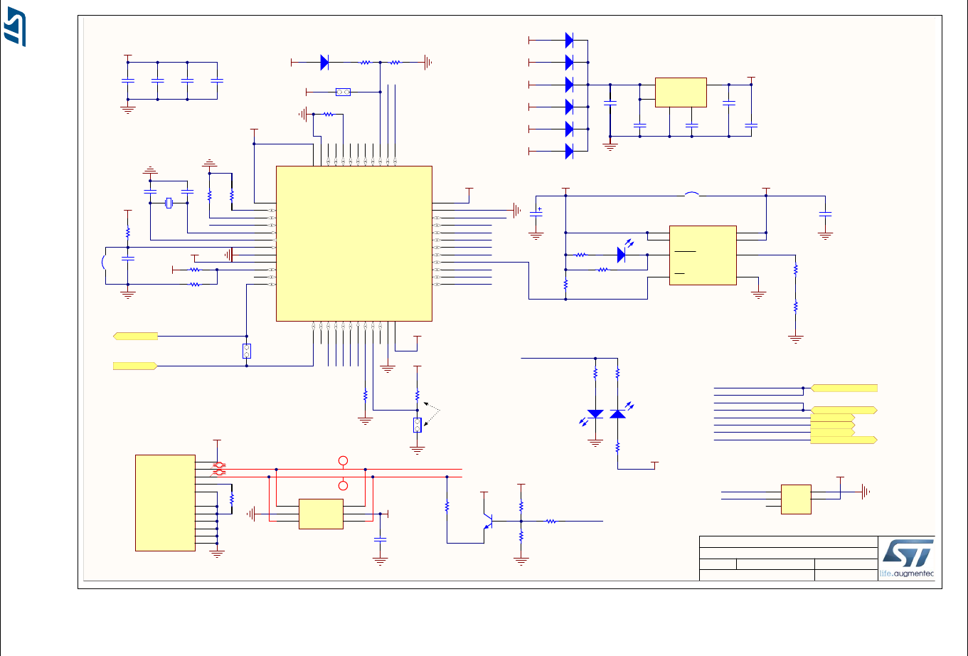
UM2198 Electrical schematics
DocID030511 Rev 1 63/69
Figure 35. ST-LINK/V2-1
15 17
ST-LINK/V2-1
MB1246 B.2
6/9/2017
Title:
Size: Reference:
Date: Sheet: of
A4 Revision:
STM32H7x3I-EVAL
Project:
STM_RST
T_JTCK
T_JTCK
T_JTDO
T_JTDI
T_JTMS
OSC_IN
OSC_OUT
T_NRST
AIN_1
COM
PWR
Board Ident: PC13=0
SWD
T_SWDIO_IN
LED_STLINK
MCO
SB53
Open
CN24
TX
RX
STLINK_RX
STLK_RX
STLK_TX
STLINK_TX
T_SWO
R169
[N/A]
R291
100K
R171
10K
R164 4K7
R167 4K7
C164
100nF
D5V
USB_RENUMn
+3V3_ST_LINK
+3V3_ST_LINK
+3V3_ST_LINK
+3V3_ST_LINK
PWR_EXT
+3V3_ST_LINK
D7
BAT60JFILM
D8
BAT60JFILM
C32
1uF_X5R_0603
C25
10nF_X7R_0603
C23
1uF_X5R_0603
C31
100nF
C24
100nF
+3V3_ST_LINK
E5V
VBAT
1
PA7
17
PC13
2
PA12 33
PC14
3
PB0
18
PC15
4JTMS/SWDIO 34
OSCIN
5
PB1
19
OSCOUT
6
VSS_2 35
NRST
7
PB2/BOOT1
20
VSSA
8
VDD_2 36
VDDA
9
PB10
21
PA0
10
JTCK/SWCLK 37
PA1
11
PB11
22
PA2
12
PA15/JTDI 38
PA3
13
VSS_1
23
PA4
14
PB3/JTDO 39
PA5
15
VDD_1
24
PA6
16
PB4/JNTRST 40
PB12 25
PB5 41
PB13 26
PB6 42
PB14 27
PB7 43
PB15 28
BOOT0 44
PA8 29
PB8 45
PA9 30
PB9 46
PA10 31
VSS_3 47
PA11 32
VDD_3 48
U23
STM32F103CBT6
R162
100K
D9
BAT60JFILM
Power Switch to supply +5V
from STLINK USB
PWR_ENn
+3V3_ST_LINK
1 2
3 4
5
CN21
[N/A]
C67
100nF
C162
100nF
C165
100nF
C166
100nF
+3V3_ST_LINK
+3V3_ST_LINK
JP14
[N/A]
R161
[N/A]
Not Fitted
VBUS_HS
VBUS_FS1
VBUS_FS2
VUSB_ST_LINK
+3V3
LED_STLINK
21
4 3
Red Yellow
LD12
HSMF-A201-A00J1
R196
100
R197
100
R198
0
+3V3_ST_LINK
T_JTCK
T_JTDI
T_JTDO
T_NRST
T_JTMS
T_JRST
TDI
TRST
TMS/SWDIO
TCK/SWCLK
TDO/SWO
RESET#
T_SWO
T_SWDIO_IN
STM_JTMS_SWDIO
STM_JTCK_SWCLK
STM_JTMS_SWDIO
STM_JTCK_SWCLK
D6
BAT60JFILM
D5
BAT60JFILM
D4
BAT60JFILM
Not Fitted
T_JRST
SWIM_PU_CTRL
STL_USB_DM
STL_USB_DP
R176
100K
R292
2K7
R293
4K7
+3V3_ST_LINK
+5V
PB15
PB14
C56
4.7uF
IN
1
IN
2
ON
3GND 4
SET 5
OUT 6
OUT 7
FAULT
8
U19
ST890CDR
VUSB_ST_LINK U5V_ST_LINK
R142 100K
R150
10K
R138
2K2
R139
0
C49
100nF
D16
BAT60JFILM
JP15
1 2 LD11
Red
R195 1K
SB35 Open
USB ST-LINK
R179
1K5
R186
100K
USB_RENUMn
R175
10K
R178
36K
R177 100
+3V3_ST_LINK
I/O1
1
GND
2
I/O2
3I/O2 4
Vbus 5
I/O1 6
U25
USBLC6-2SC6
C170
100nF
i
Diff Pair 90ohm
i
Diff Pair 90ohm
VBUS 1
DM 2
DP 3
ID 4
GND 5
Shield 6
USB_Micro-B receptacle
Shield 7
Shield 8
Shield 9
EXP 10
EXP 11
CN23
1050170001
3
1
2
T4
9013
VUSB_ST_LINK
VUSB_ST_LINK
VUSB_ST_LINK
STL_USB_DM
STL_USB_DP
51
2
GND
3
4
BYPASS
EN
Vin Vout
U9 LDK120M33R
C81
10pF
C78
10pF
1 2
X5
NX3225GD-8.000M-EXS00A-CG04874
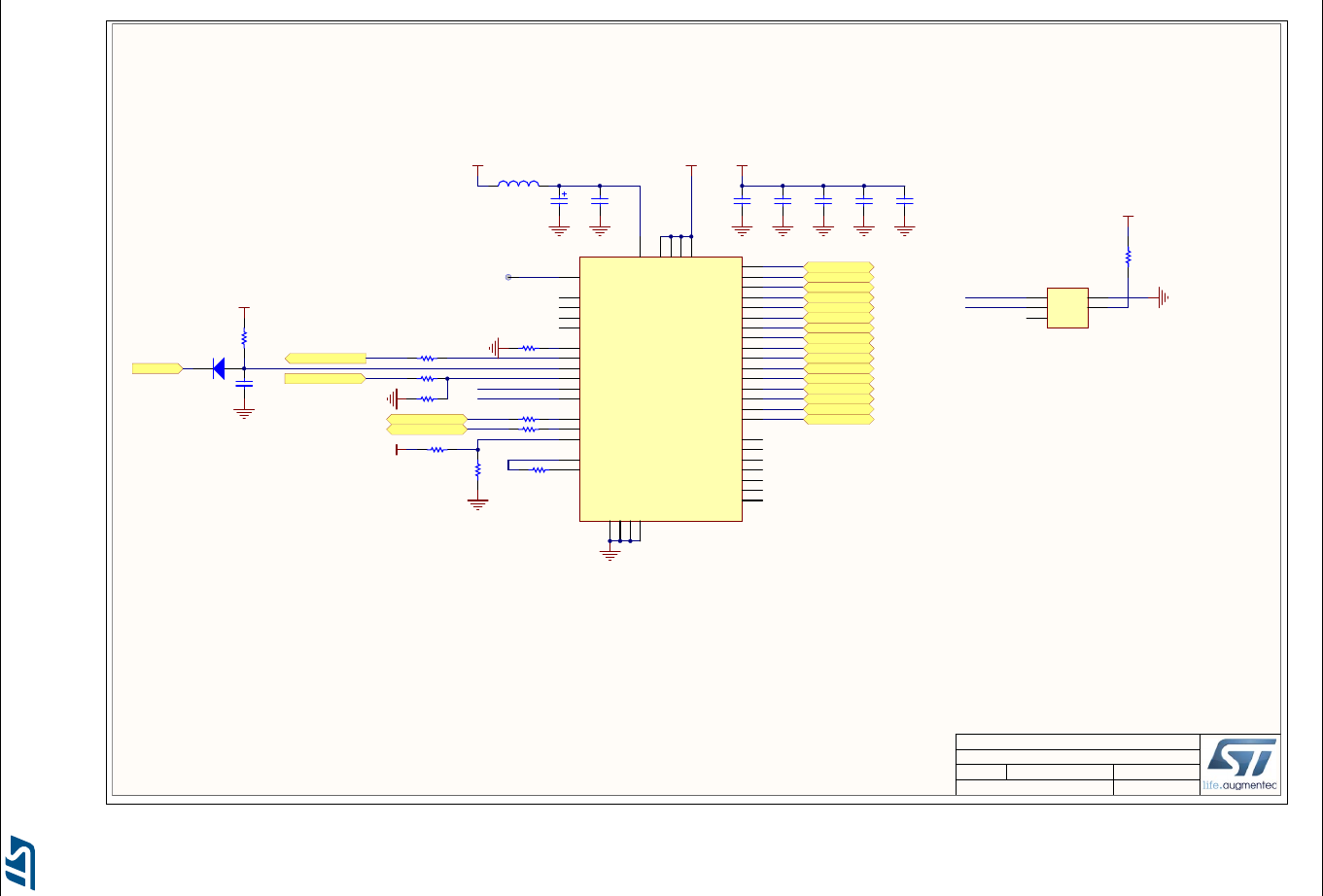
Electrical schematics UM2198
64/69 DocID030511 Rev 1
Figure 36. MFX
16 17
MFX
MB1246 B.2
6/9/2017
Title:
Size: Reference:
Date: Sheet: of
A4 Revision:
STM32H7x3I-EVAL
Project:
MFX_IRQOUT
MFX_SWCLK
MFX
Multi Function eXpander
MFX_SWDIO
R185 0
PI8
MFX_SWDIO
MFX_SWCLK
1 2
3 4
5
CN22
[N/A]
C171
100nF
C167
100nF
C168
100nF
C169
100nF
one capacitor close to each MFX pins:
VDD, VDD_1, VDD_2, VDD_3
C163
100nF
I2C1_SDA
I2C1_SCL R181 0
R180 0
PB6
PB7
R184
10K
R174
47K[N/A]
R170
10K[N/A]
C85
100nF[N/A]
R182
510
L8
Ferrite C76
1uF C82
100nF
R166[N/A]
Loop
MFX_IO5
MFX_IO6
MFX_IO7
MFX_IO8
MFX_IO9
MFX_IO10
MFX_IO11
MFX_IO12
MFX_IO13
MFX_IO14
MFX_IO15
+3V3 +3V3 +3V3
+3V3
+3V3
Default I2C Address:1000010
+3V3 R183 [N/A]
R173 0
MFX_WKUP
TP10
MFX_IO0
MFX_IO1
MFX_IO2
MFX_IO3
MFX_IO4
R172
0
RESET#
D15
BAT60JFILM
MFX_V3
WAKEUP
2NRST
7
TSC_XP/GPO0
10
TSC_XN/GPO1
11
TSC_YP/GPO2
12
TSC_YN/GPO3
13
USART_TX
21
USART_RX
22
SPARE
14
SWDIO
34
SWCLK
37
I2C_SCL
42
I2C_SDA
43
BOOT0
44
I2C_ADDR
45
IRQOUT
46
IDD_CAL/GPO4 3
IDD_SH0 4
IDD_SH1/GPO5 5
IDD_SH2/GPO6 6
IDD_MEAS 25
GPIO0 18
GPIO1 19
GPIO2 20
GPIO3 39
GPIO4 40
GPIO5 15
GPIO6 16
GPIO7 17
GPIO8 29
GPIO9 30
GPIO10 31
GPIO11 32
GPIO12 33
GPIO13 26
IDD_SH3/GPO7 38
GPIO14 27
GPIO15 28
IDD_VDD_MCU 41
VDD 1
VDDA 9
VDD_1 24
VDD_2 36
VDD_3 48
VSSA
8
VSS_1
23
VSS_2
35
VSS_3
47
U24
STM32L152CCT6
PA0
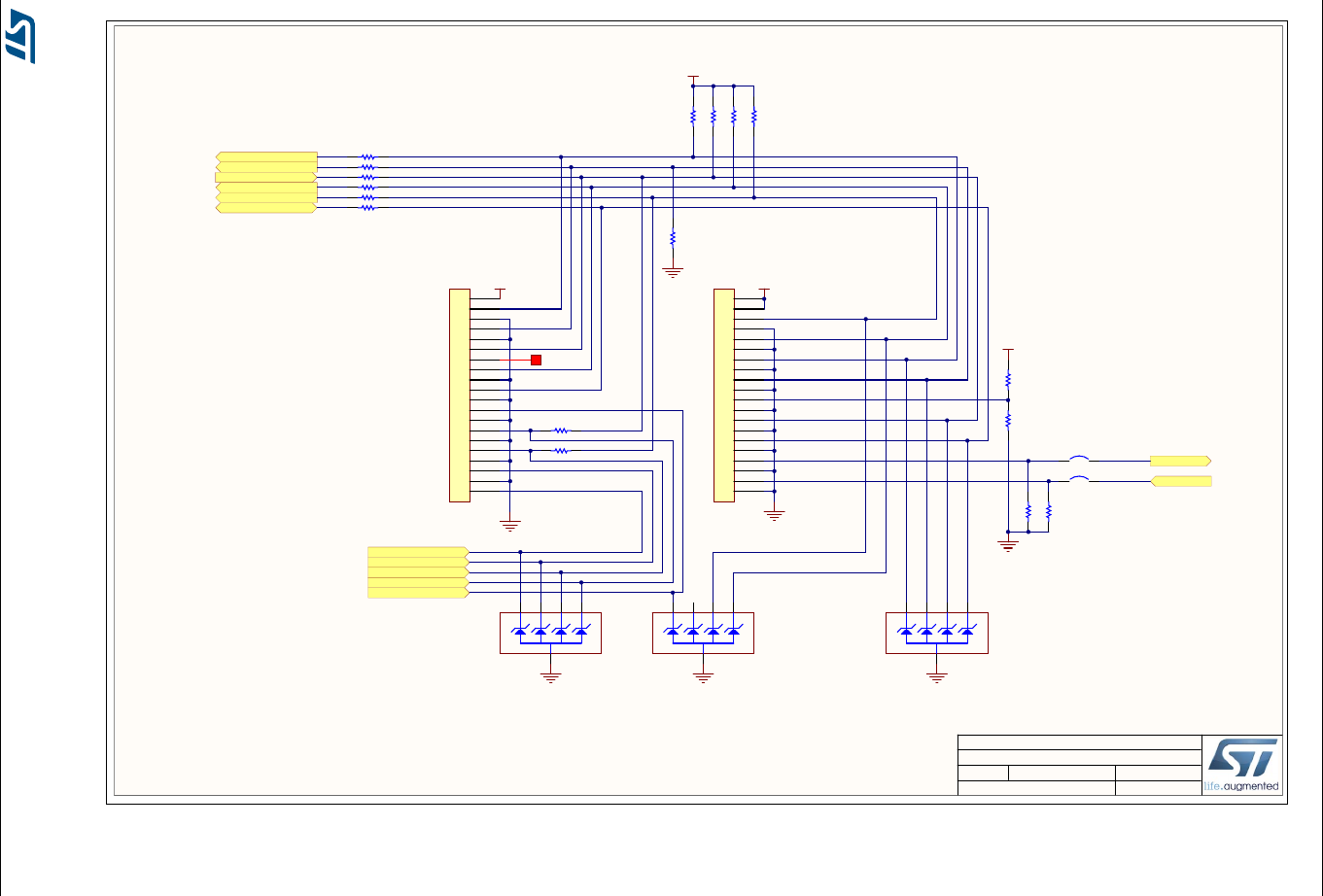
UM2198 Electrical schematics
DocID030511 Rev 1 65/69
Figure 37. JTAG and trace
17 17
JTAG & Trace
MB1246 B.2
6/9/2017
Title:
Size: Reference:
Date: Sheet: of
A4 Revision:
STM32H7x3I-EVAL
Project:
1
2
3
4
5
6
7
8
9
10
11
12
13
14
15
16
17
18
19
20
CN8
P127B-2*10MGF-079-1E7A
R65
[N/A]
R64
[N/A]
R80
[N/A]
R56
[N/A]
R81
[N/A]
1
2
3
4
5
6
7
8
9
10
11
12
13
14
15
16
17
18
19
20
CN9
JTAG
R90
10K
R94
10K
R85
10K
R63 [N/A]
R78 [N/A]
TDI
RESET#
TRACE_D3
TRACE_D2
TRACE_D1
TRACE_D0
TRACE_CK
TRST
TMS/SWDIO
TCK/SWCLK
TDO/SWO
Trace connector JTAG connector
KEY
PA13
PA14
PB3
PA15
PB4
PE6
PE5
PE4
PE3
PE2
R57
[N/A]
+3V3
+3V3
+3V3
+3V3
R55 22
R59 22
R60 22
R61 22
R79 22
R62 22
FTSH-110-01-L-DV (Samtec)
1
3
2
4
5
U10
ESDALC6V1W5
1
3
2
4
5
U8
ESDALC6V1W5
1
3
2
4
5
U11
ESDALC6V1W5
DBGRQ
DBGACK
PJ7
PJ12
SB24 Open
SB25 Open
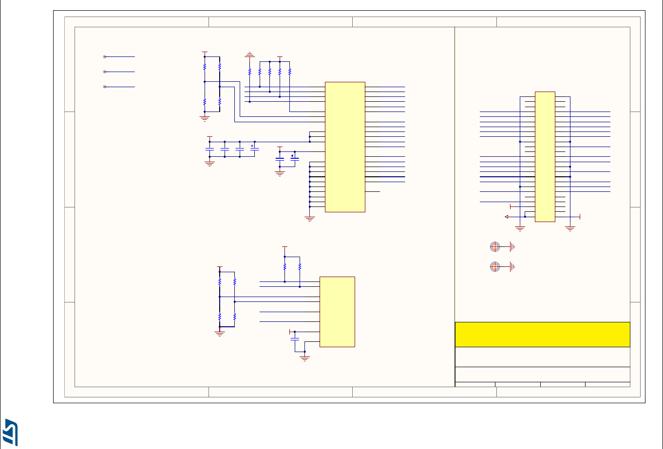
Electrical schematics UM2198
66/69 DocID030511 Rev 1
Figure 38. 5.7” LCD board
1
1
2
2
3
3
4
4
D D
C C
B B
A A
STMicroelectronics
Title:
Number: Rev: Sheet of
B.1(PCB.SCH) Date: 6/7/2013MB1063 1 1
5.7 inch LCD board
Backlight driver & PFC connector for LCD panel
1 2
3 4
5 6
7 8
9 10
11 12
13 14
15 16
17 18
19 20
21 22
23 24
25 26
27 28
29 30
31 32
33 34
35 36
37 38
39 40
41 42
43 44
45 46
47 48
49 50
CN2
P127B-2*25MGF-079-1A
VDD
R2
R3
R4
R5
B2
B3
B4
B5
G2
G3
G4
G5
I2C_SDA
I2C_SCL
ENB
HSYNC
VSYNC
INT
CLK
BL_CTRL
INT
HSYNC
VSYNC
CLK
ENB
R2
4K7
R7
4K7
VDD
R8
[N/A]
R1
[N/A]
VDD
C3
4.7uF
C4
100nF
BLGND
BLVDD
R6
4K7
R5
4K7
R4
4K7
R3
4K7
VDD
DCLK
38
HSYNC
3
VSYNC
8
DE
9
U/D
1
B0 19
B1 18
B2 17
B3 15
B4 14
B5 13
G0 27
G1 26
G2 25
G3 23
G4 22
G5 21
R0 35
R1 34
R2 33
R3 31
R4 30
R5 29
VCC
7
VLED
4
NC 2
ADJ
12
L/R
40
VSS
10
VSS
16
VLED
5
VLED
6
VSS
11
VSS
20
VSS
24
VSS
28
VSS
32
VSS
36
VSS
37
VSS
39
CN1
089H40-000000-G2-C
BL_CTRL
BLVDD
GPIO11/MISO
3
RES
8
INT
7
VCC
1
GND
4
SDA/MOSI
2SCL
5
GPIO10/CS
6
CN3
CSF-2481-081R
I2C_SDA
I2C_SCL
R16
4K7
R15
4K7
VDD
R14
[N/A]
R13
[N/A]
VDD
C5
100nF
Touch panel connector for LCD panel
Connector for motherboard
AM640480G5TNQW-T00H
RST
RST
C1
4.7uF
C2
100nF
TP1
TP2
TP3
GND
BLGND
VDD
R12
[N/A]
R11
[N/A]
VDD
Default I2C Address:1000000
R7
B6
B7
G6
G7
R6
R2
R3
R4
R5
R7
R6
G2
G3
G4
G5
G6
G7
B2
B3
B4
B5
B6
B7
C6
100nF
C7
100nF
R9
4K7
FTSH-125-01-F-DV-K (Samtec)
N
ote1: Text in italic placed on a wire doesn’ t correspond to net name. It just helps to identify
rapidly MCU IO related to this wire.
N
ote2: Pull up resistor R9 was added from Version A.1 to B.1
N
ote3: Backlight On/Off control circuit wass removed from Version A.1 to B.1
H1
H2
DocID030511 Rev 1 67/69
UM2198 Board revision history and limitations
68
Appendix C Board revision history and limitations
Table 34. Board revision history and limitations
Board Version Revision details Known limitations
MB1246 (Main board) B-01 Initial version for STM32H743I-EVAL -
MB1065 (LCD board) B-01 Initial version -

DocID030511 Rev 1 69/69
UM2198
69
IMPORTANT NOTICE – PLEASE READ CAREFULLY
STMicroelectronics NV and its subsidiaries (“ST”) reserve the right to make changes, corrections, enhancements, modifications, and
improvements to ST products and/or to this document at any time without notice. Purchasers should obtain the latest relevant information on
ST products before placing orders. ST products are sold pursuant to ST’s terms and conditions of sale in place at the time of order
acknowledgement.
Purchasers are solely responsible for the choice, selection, and use of ST products and ST assumes no liability for application assistance or
the design of Purchasers’ products.
No license, express or implied, to any intellectual property right is granted by ST herein.
Resale of ST products with provisions different from the information set forth herein shall void any warranty granted by ST for such product.
ST and the ST logo are trademarks of ST. All other product or service names are the property of their respective owners.
Information in this document supersedes and replaces information previously supplied in any prior versions of this document.
© 2017 STMicroelectronics – All rights reserved
