Sec2Cover Sec2 Controlhead_VHF Controlhead VHF
Sec2_Controlhead_VHF Sec2_Controlhead_VHF
User Manual: Sec2-Controlhead_VHF
Open the PDF directly: View PDF ![]() .
.
Page Count: 26

Commercial Series
CM Radios
Controlhead
Service Information
Issue: October 2004

ii
Computer Software Copyrights
The Motorola products described in this manual may include copyrighted Motorola computer programs stored
in semiconductor memories or other media. Laws in the United States and other countries preserve for
Motorola certain exclusive rights for copyrighted computer programs, including the exclusive right to copy or
reproduce in any form, the copyrighted computer program. Accordingly, any copyrighted Motorola computer
programs contained in the Motorola products described in this manual may not be copied or reproduced in
any manner without the express written permission of Motorola. Furthermore, the purchase of Motorola
products shall not be deemed to grant, either directly or by implication, estoppel or otherwise, any license
under the copyrights, patents or patent applications of Motorola, except for the normal non-exclusive royalty-
free license to use that arises by operation of law in the sale of a product.

iii
Table of Contents
Chapter 1 MODEL OVERVIEW
1.0 CM140/CM340 Models ........................................................................................1-1
2.0 CM160/CM360 Models ........................................................................................1-1
Chapter 2 THEORY OF OPERATION
1.0 Introduction ..........................................................................................................2-1
2.0 Controlhead Model for CM140 and CM340 .........................................................2-1
2.1 Power Supplies...............................................................................................2-1
2.2 SPI Interface...................................................................................................2-1
2.3 Keypad Keys ..................................................................................................2-1
2.4 Status LEDs and Backlight Circuit ..................................................................2-1
2.5 Microphone Connector Signals ......................................................................2-1
2.6 Speaker ..........................................................................................................2-3
2.7 Electrostatic Transient Protection...................................................................2-3
3.0 Controlhead Model for CM160 and CM360 .........................................................2-4
3.1 Power Supplies...............................................................................................2-4
3.2 SPI Interface...................................................................................................2-4
3.3 Keypad Keys ..................................................................................................2-5
3.4 LCD Driver......................................................................................................2-5
3.5 Status LEDs and Backlight Circuit ..................................................................2-5
3.6 Microphone Connector Signals ......................................................................2-5
3.7 Speaker ..........................................................................................................2-6
3.8 Electrostatic Transient Protection...................................................................2-6
Chapter 3 TROUBLESHOOTING CHARTS
1.0 Troubleshooting Chart for Controlhead CM140/340 ...........................................3-1
1.1 Controlhead Failure........................................................................................3-1
1.2 Button/Tones Select Error (1 of 2)..................................................................3-2
1.3 Button/Tones Select Error (2 of 2)..................................................................3-3
2.0 Troubleshooting Chart for Controlhead CM160/360 ............................................3-4
2.1 Controlhead Failure .......................................................................................3-4
2.2 Button/Tones Select Error .............................................................................3-5
2.3 Button/Tones Select Error .............................................................................3-6

iv
Chapter 4 CONTROLHEAD PCB/SCHEMATICS/PARTS LISTS
1.0 Allocation of Schematics and Circuit Boards .......................................................4-1
2.0 Controlhead CM140/340 - PCB 8488998U01 Schematics.................................. 4-3
2.1 Controlhead PCB 8488998U01 - Parts List....................................................4-5
3.0 Controlhead CM160/360 - PCB 8489714U01 Schematics .................................4-6
3.1 Controlhead PCB 8489714U01 - Parts List ...................................................4-8
Chapter 1
OVERVIEW
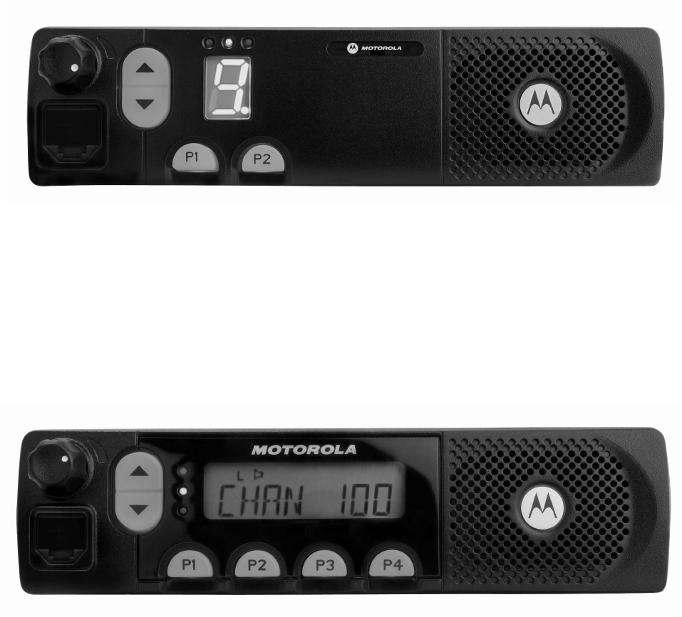
1.0 CM140/CM340Models
The Controlhead contains the internal speaker, the on/off/volume knob, the microphone connector,
several buttons to operate the radio, three indicator Light Emitting Diodes (LED) to inform the user
about the radio status, and a single character 7-segment display for numeric information e.g.
channel number.
2.0 CM160/CM360Models
The Controlhead contains the internal speaker, the on/off/volume knob, the microphone connector,
several buttons to operate the radio, three indicator Light Emitting Diodes (LED) to inform the user
about the radio status, and an 8 character Liquid Crystal Display (LCD) for alpha - numerical
information e.g. channel number or call address name.

1-2 OVERVIEW
Chapter 2
THEORY OF OPERATION
1.0 Introduction
This Chapter provides a detailed theory of operation for the Controlhead circuits. For details of the
trouble shooting refer to the related chapter in this section.
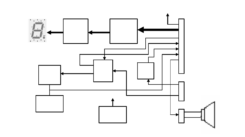
2.0 Controlhead Model for CM140 and CM340
The controlhead contains the internal speaker, the on/off/volume knob, the microphone connector,
several buttons to operate the radio and three indicator Light Emitting Diodes (LED) to inform the
user about the radio status and a 7-segment display for numeric information.
2.1 Power Supplies
The power supply to the control head is taken from the host radio’s 9.3V via connector J803-9, The
9.3V is used for the LEDs and back light, the 5V is used for the LCD driver and level shifter. The
stabilized 3V is used for the other parts.
2.2 SPI Interface
The host radio (master) communicates with the control head through its SPI bus. Three lines are
connected to the shift register (U801):SPI clock (J803-17), SPI MOSI (J803-16) and shift register
chip select (J803-15).
Shift
Register
BCD To
7-segment
Mux.
Control
Keypads
DTMF
Resistors
PTT
circuit
2 pin speaker
connector
7-segment
display
9.3V
Keypad
Backlight
9.3VRow/Column
Control line
Boot_res / SCI
DTMF
Row/Column
Boot_res (DTMF-
Column)/ SCI
(DTMF-Row)
Shift
Register
BCD To
7-segment
Mux.
Control
Keypads
DTMF
Resistors
PTT
circuit
2 pin speaker
connector
7-segment
display
9.3V
Keypad
Backlight
9.3VRow/Column
Control line
Boot_res / SCI
DTMF
Row/Column
Boot_res (DTMF-
Column)/ SCI
(DTMF-Row)

2-2 THEORY OF OPERATION
When the host radio needs to send date to the shift register, the radio asserts the shift register chip
select and the data is loaded to the shift register. For example, the host radio sends data to change
display channel or change LED status.
2.3 Keypad Keys
The control head keypad is a four-key design. All keys are configured as two analog lines read by
µP. The voltage on the analog lines varies between 0V and 3.3 V depending on which key is
pressed. If no key is pressed, the voltage at both lines is 3.3V. The key configuration can be thought
of as a matrix where the two lines represent one row and one column. Each line is connected to a
resistive divider powered by 3.3V. If a button is pressed, it will connect one specific resistor of each
divider line to ground level and thereby reduce the voltages on the analog lines. The voltages of the
lines are A/D converted inside the µP (ports PE 6 - 7) and specify the pressed button. To determine
which key is pressed, the voltage of both lines must be considered.
The same analog lines also support a keypad microphone. A microphone key press is processed in
the same manner like a control head key press.
2.4 Status LED’s and Back Light Circuit
All indicator LEDs (red, yellow, and green) are driven by current sources. To change the LED status
the host radio sends a data message to the control head shift register via the SPI bus. The control
head shift register determines the LED status from the received data and switches the LEDs on or
off via Q5-Q7.
The back light for the keypad is always on. The back light current for the keypad is drawn from the
9.3 V source and controlled by two current sources. The LED current is determined by the resistor
at the emitter of the respective current source transistor.
2.5 Microphone Connector Signals
The MIC_PTT line (J802-3) is grounded when the PTT button on the microphone is pressed. When
released, this line is pulled to 9.3V by R805. Two transistor stages (Q802, Q801 and associated
parts) are used to level shift between 9.3V and 3.3V required for the uP while keeping the same
sense (active low for PTT pressed).
Two of the mic socket lines (J802-2,7) have dual functions depending on the type of microphone or
SCI lead connected. An electronic switch (U803) is used to switch these two lines between mic
keypad operation or SCI operation. The switch (mux) is controlled by the uP through J803-20 with
level shifting (and inversion) provided by transistor Q812. When MUX_CTRL (J803-20) is low the
electronic switch is in the mic keypad mode. The mic socket (J802) pin 2 is connected to the keypad
row line that goes to J803-13 and pin 7 is connected to the keypad column line that goes to J803-12.
When MUX_CTRL (J803-20) is high the electronic switch is in the SCI mode. The mic socket (J802
pin 2) is connected to the SCI line that goes to J803-4 and pin 7 is connected to the BOOT_RES line
that goes to J803-11.
The HOOK line (J802-6) is used to inform the uP which type of microphone or SCI lead is connected
to the microphone socket. The voltage of the HOOK line is monitored by the uP (port PE0,
MIC_SENSE) through a resistor divider on the main board. When the HOOK line is grounded (on
hook condition) or floating (2.8V nominal), the uP sets the mux (U803) for keypad operation to allow
the use of microphones with a keypad. When the HOOK line is connected to 9.3V, the uP sets the
mux for SCI operation. This mode is also used to select low cost mic operation where the gain of the
microphone path is increased (on the main board) to compensate for not having a pre-amp in the low
cost mic.

Controlhead Model for CM140 and CM340 2-3
If the BOOT_RES (J802-7) line is connected to >5V (e.g. 9.3V) at turn-on, the uP will start in boot
mode instead of normal operation. This mode is used to programme new firmware into the FLASH
memory (U404 mainboard).
2.6 Speaker
The controlhead contains a speaker for the receiver audio. The receiver audio signal from the
differential audio output of the audio amplifier located on the radio’s controller is fed via connector
J803-1, 2 to the speaker connector P801 pin 1 and pin 2. The speaker is connected to the speaker
connector P801. The controlhead speaker can be disconnected if an external speaker, connected on
the accessory connector, is used.
2.7 Electrostatic Transient Protection
Electrostatic transient protection is provided for the sensitive components in the controlhead by
diodes VR801, VR802, VR803 and VR804. The diodes limit any transient voltages to tolerable
levels. The associated capacitors provide Radio Frequency Interference (RFI) protection.
2-4 THEORY OF OPERATION
3.0 Controlhead Model for CM160 and CM360
The controlhead contains the internal speaker, the on/off/volume knob, the microphone connector,
several buttons to operate the radio, three indicator Light Emitting Diodes (LED) to inform the user
about the radio status, and an 8 character Liquid Crystal Display (LCD) for alpha - numerical
information e.g. channel number or call address name.
3.1 Power Supplies
The power supply to the control head is taken from the host radio’s 9.3V via connector J103-9, The
9.3V is used for the LEDs and back light, the 5V is used for the LCD driver (U3) and level shifter
(U4). The stabilized 3V is used for the other parts.
3.2 SPI Interface
The host radio (master) communicates with the control head through its SPI bus. Three lines are
connected to the shift register (U8):SPI clock (J103-17), SPI MOSI (J103-16), shift register chip
select (J103-15) and LCD driver chip select (J103-18).
When the host radio needs to send date to the shift register, the radio asserts the shift register chip
select and the data is loaded to the shift register. For example, the host radio sends data to change
display channel or change LED status.
8 pin JACK
connector
9.3V LCD
Shift
Register
Backlight
Control
Mux.
Control
Keypads
Keypad
Resistors
PTT
circuit
2-pin speaker
connector
9.3V
LED
Indicators
Row/Column
Control line
Boot_Res / SCI
DTMF
Row/Column
Boot_Res (DTMF-
Column)/ SCI
(DTMF-Row)
Level
Shifter
LCD
Driver
LED
Backlight
8 pin JACK
connector
9.3V LCD
Shift
Register
Backlight
Control
Mux.
Control
Keypads
Keypad
Resistors
PTT
circuit
2-pin speaker
connector
9.3V
LED
Indicators
Row/Column
Control line
Boot_Res / SCI
DTMF
Row/Column
Boot_Res (DTMF-
Column)/ SCI
(DTMF-Row)
Level
Shifter
LCD
Driver
LED
Backlight

Controlhead Model for CM160 and CM360 2-5
3.3 Keypad Keys
The control head keypad is a four-key design. All keys are configured as two analog lines read by
µP. The voltage on the analog lines varies between 0V and 3.3 V depending on which key is
pressed. If no key is pressed, the voltage at both lines is 3.3V. The key configuration can be thought
of as a matrix where the two lines represent one row and one column. Each line is connected to a
resistive divider powered by 3.3V. If a button is pressed, it will connect one specific resistor of each
divider line to ground level and thereby reduce the voltages on the analog lines. The voltages of the
lines are A/D converted inside the µP (ports PE 6 - 7) and specify the pressed button. To determine
which key is pressed, the voltage of both lines must be considered.
The same analog lines also support a keypad microphone. A microphone key press is processed in
the same manner like a control head key press.
3.4 LCD Driver
The LCD (36 x 4 segemnts) is controlled by U3. It has an on onboard clock controlled by R28
(typically 20kHz measured on pin 2). U3 is operated from the 5V supply and is controlled over the
SPI bus (SPI_CLK J103-17, SPI_MOSI J103-16, LCD chip select J103-18). Chip select is active low.
U2 is used to provide level shifting between the 3.3V logic from the uP and the 5V required by U3.
3.5 Status LED’s and Back Light Circuit
All indicator LEDs (red, yellow, and green) are driven by current sources. To change the LED status
the host radio sends a data message to the control head shift register via the SPI bus. The control
head shift register determines the LED status from the received data and switches the LEDs on or
off via Q8-Q10.
Backlighting for the LCD and keys is provided by a matrix of 21 LEDs arranged in 7 columns of 3
rows. The LEDs are driven from a constant current circuit (Q12, U1 and associated parts). There are
4 levels of baclight: off, low, medium and high, which are controlled by two outputs (pins 15, 1) from
the shift register (U8). The current is controlled by transistor Q12. The op amp U1 monitors the
current by measuring the voltage drop across R26, R27 and adjusting the bias of Q12 to achieve the
required level as set by the combined shift register o/ps. When in the off state, Q11 is also turned on
to clamp the base of Q12 so as to force it off. This ensures that the LEDs are fully off. Q11 is
controlled by pin 3 of the shift register U8.
3.6 Microphone Connector Signals
The MIC_PTT line (J102-3) is grounded when the PTT button on the microphone is pressed. When
released, this line is pulled to 9.3V by R33. Two transistor stages (Q14, Q13 and associated parts)
are used to level shift between 9.3V and 3.3V required for the uP while keeping the same sense
(active low for PTT pressed).
Two of the mic socket lines (J102-2, 7) have dual functions depending on which type of microphone
or SCI lead that is connected. An electronic switch (U41) is used to switch these two lines between
mic keypad operation or SCI operation. The switch (mux) is controlled by the uP through J103-20
with level shifting (and inversion) provided by transistor Q41. When MUX_CTRL (103-20) is low the
electronic switch is in the mic keypad mode. The mic socket (J102) pin 2 is connected to the keypad
row line that goes to J103-13 and pin 7 is connected to the keypad column line that goes to 103-12.
When MUX_CTRL (103-20) is high the electronic switch is in the SCI mode. The mic socket (J102
pin 2) is connected to the SCI line that goes to J103-4 and pin 7 is connected to the BOOT_RES line
that goes to J103-11.

2-6 THEORY OF OPERATION
The HOOK line (J102-6) is used to inform the uP which type of microphone or SCI lead is connected
to the microphone socket. The voltage of the HOOK line is monitored by the uP (port PE0,
MIC_SENSE) through a resistor divider on the main board. When the HOOK line is grounded (on
hook condition) or floating (2.8V nominal), the uP sets the mux (U8) for keypad operation to allow the
use of microphones with a keypad. When the HOOK line is connected to 9.3V, the uP sets the mux
for SCI operation. This mode is also used to select low cost mic operation where the gain of the
microphone path is increased (on the main board) to compensate for not having a pre-amp in the low
cost mic.
If the BOOT_RES (J102-7) line is connected to >5V (e.g. 9.3V) at turn-on then the uP will start in
boot mode instead of normal operation. This mode is used to programme new firmware into the
FLASH memory (U404 mainboard).
3.7 Speaker
The controlhead contains a speaker for the receiver audio. The receiver audio signal from the
differential audio output of the audio amplifier located on the radio’s controller is fed via connector
J103-1, 2 to the speaker connector P101 pin 1 and pin 2. The speaker is connected to the speaker
connector P101. The controlhead speaker can be disconnected if an external speaker, connected on
the accessory connector, is used.
3.8 Electrostatic Transient Protection
Electrostatic transient protection is provided for the sensitive components in the controlhead by
diodes VR1 - VR4. The diodes limit any transient voltages to tolerable levels. The associated
capacitors provide Radio Frequency Interference (RFI) protection.
Chapter 3
TROUBLESHOOTING CHARTS
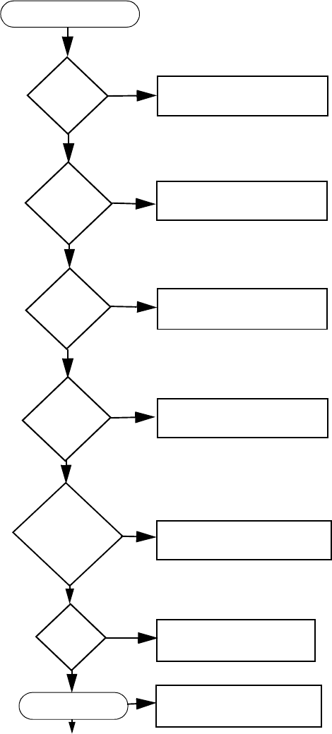
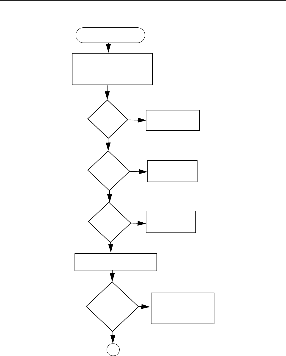
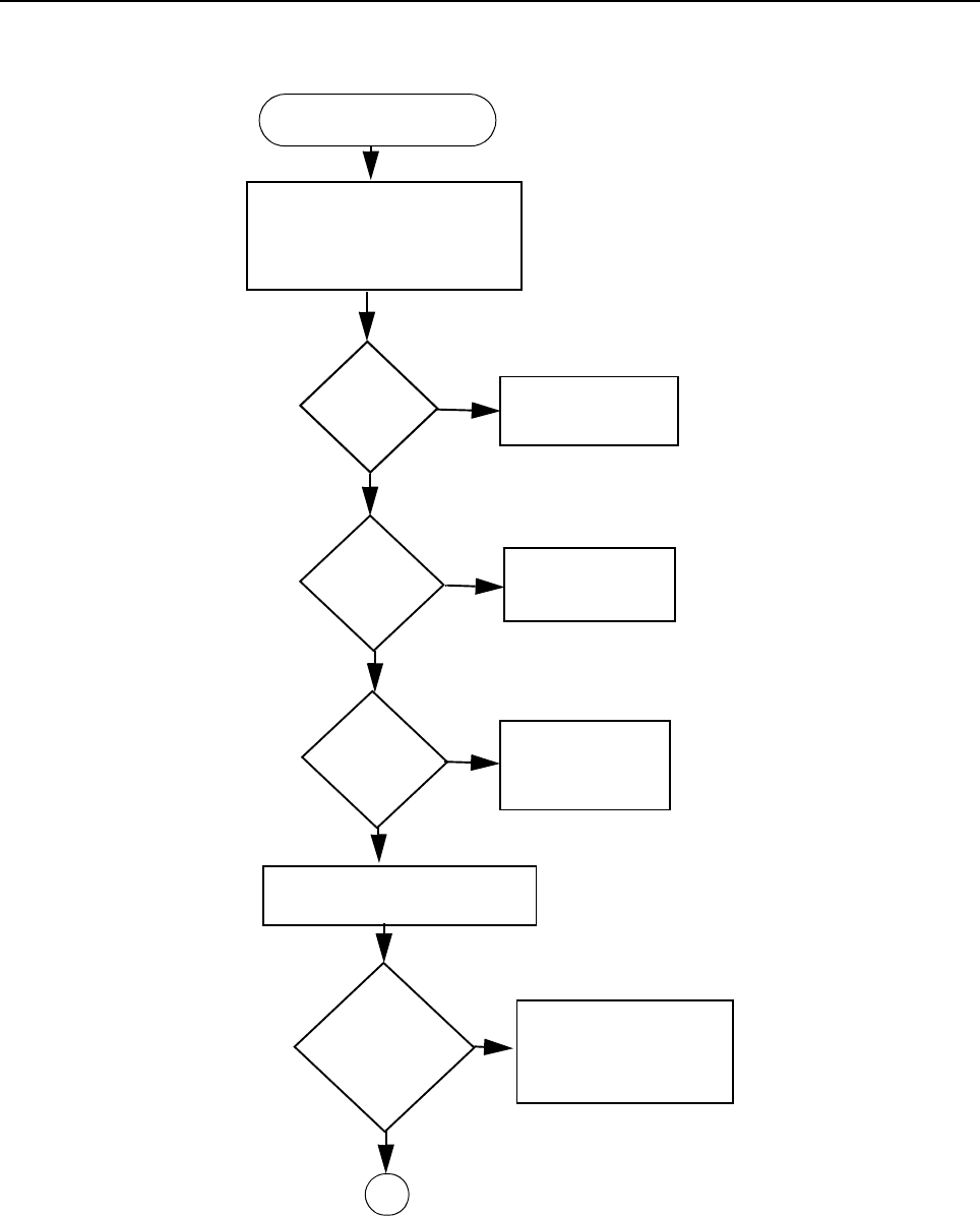
1.0 Controlhead CM140/CM340 Troubleshooting Chart
1.1 Control Head Failure
Back light
OK ?
Check 9.3V on
R808, R809
No
Control Head Check
Power-up
Alert Tone
OK ?
Check Speaker
Connection
No
Power-up
Red LED
Flash?
Check
D801, Q806, U801
No
Channel
Display
OK?
Check
DS801, U801, U802
No
Up/Down
P1 and P2
Alert Tone
Buttons OK?
Check R845, R846
R810, R811
No
EXT
PTT
OK ?
Check Q801, Q802
No
Communication Ok
Check Q803, Q812
Control Head is OK
YES
YES
YES
YES
YES
YES No
3-2 TROUBLESHOOTING CHARTS
1.2 Button/Tones Select Error (Page 1 of 2)
No
Check Voltage Levels on
TP401 (Keypad Col)
and TP402 (Keypad Row)
(see table on next page)
Right
Voltage
Up Key
No
Check R846, R811
on Control Head
Right
Voltage
on Down Key
?
Check Control Head
connectivity continuity
and R429, R430, D401
(main board)
Connect DTMF Mic
to TELCO Connector
YES
Button/Tones Check
Check R845, R810
on Control Head
Right
Voltage
on P1/P2
Keys ?
Is there
0.75 Vdc on
MIC_SENSE
R429, on radio
Check R813, R814
on Control Head
?
A
YES
No
YES
No
Controlhead CM140/CM340 Troubleshooting Chart 3-3
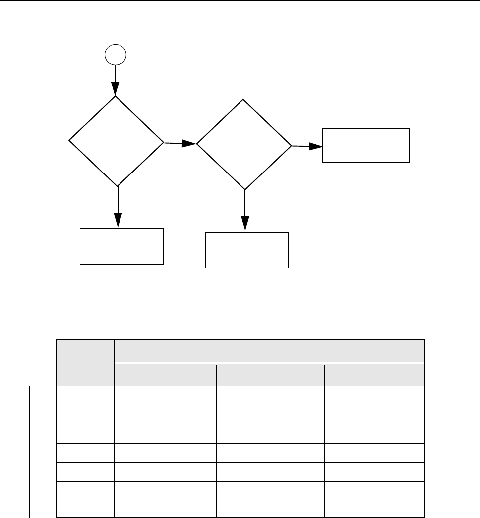
1.3 Button/Tones Select Error (Page 2 of 2)
Key_Col
Voltage
(TP401)
Key_Column Voltage TP401
0.008 V 0.675 V 1.346 V 1.997 V 2.650 V 3.300 V
0.008 V Up
0.675 V 1 2 3
1.346 V 4 5 6 7
1.997 V 8 9 0 *
2.650 V # C B A
3.300 V Down Left Key
P1
Right Key
P2 Idle
Key_Row Voltage TP402
No
Right
Voltage
on DTMF keys
?
Replace
Q812
YES
Button/Tones Keys
Okay
A
Does Q812
on Control Head
operates well
?
Replace U803
on Control Head
YES
No
3-4 TROUBLESHOOTING CHARTS
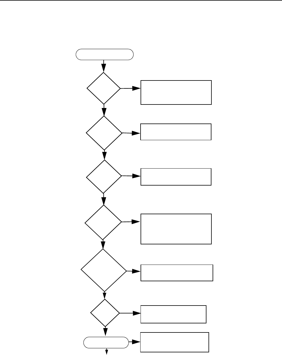
2.0 Controlhead CM160/CM360 Troubleshooting Chart
2.1 Control Head Failure
Back light
OK ?
Check 9.3V on
Q12, U1 and associated
parts and U8
No
Control Head Check
Power-up
Alert Tone
OK ?
Check Speaker
Connection
No
Indicator
LED’S
OK ?
Check
Q8-Q10, U8 and 9.3V
No
Display
OK?
Check LCD
connections, U3 for 5V,
Osc. pins 1 & 2 activity
SCI thru via U4
No
Up/Down
P1 and P2
Alert Tone
Buttons
OK?
Check keypad resistors
No
EXT
PTT
OK ? Check Q13, Q802
No
Communication Ok
Check Q803, Q14 and
associated parts
Control Head is OK
YES
YES
YES
YES
YES
YES No
Controlhead CM160/CM360 Troubleshooting Chart 3-5
2.2 Button/Tones Select Error (Page 1 of 2)
No
Check Voltage Levels on
TP401 (Keypad Col)
and TP402 (Keypad Row)
(see table on next page)
Right
Voltage
Up Key?
No
Check R13, R45
on Control Head
Right
Voltage
on Down
Key?
Check Control Head
connectivity continuity
and R429, R430, D401
(Main Board)
Connect DTMF Mic
to TELCO Connector
YES
Button/Tones Check
Check R12, R49
on Control Head
Right
Voltage
on P1-P4
Keys ?
Is there
0.75 Vdc on
MIC_SENSE
R429, on radio
Check R31, R29
R51, R11
on Control Head
A
YES
No
YES
No

3-6 TROUBLESHOOTING CHARTS
2.3 Button/Tones Select Error (Page 2 of 2)
Key_Col
Voltage
(TP401)
Key_Column Voltage TP401
0.008 V 0.675 V 1.346 V 1.997 V 2.650 V 3.300 V
0.008 V Up
0.675 V 1 2 3
1.346 V 4 5 6 7
1.997 V 8 9 0 *
2.650 V # C B A
3.300 V Down Left Key
P1
Right Key
P2 P3 P4 Idle
Key_Row Voltage TP402
No
Right
Voltage
on DTMF keys
?
Replace
Q41
YES
Button/Tones Keys
Okay
A
Does Q41
on Control Head
operates well
?
Replace U8
on Control Head
YES
No

Chapter 4
CONTROLHEAD PCB / SCHEMATICS / PARTS LISTS
1.0 Allocation of Schematics and Circuit Boards
Table 4-1 Controlhead Diagrams and Parts Lists
PCB :
Controlhead CM140/CM340
8488998U01 Main Board Top Side
8488998U01 Main Board Bottom Side
Page 4-3
Page 4-3
SCHEMATICS
Sheet 1 of 1 Page 4-4
Parts List
8488998U01 Page 4-5
Table 4-2 Controlhead Diagrams and Parts Lists
PCB :
Controlhead CM160/CM360
8489714U01 Main Board Top Side
8489714U01 Main Board Bottom Side
Page 4-6
Page 4-6
SCHEMATICS
Sheet 1 of 1 Page 4-7
Parts List
8489714U01 Page 4-8

4-2 CONTROLHEAD PCB / SCHEMATICS / PARTS LISTS
THIS PAGE INTENTIONALLY LEFT BLANK
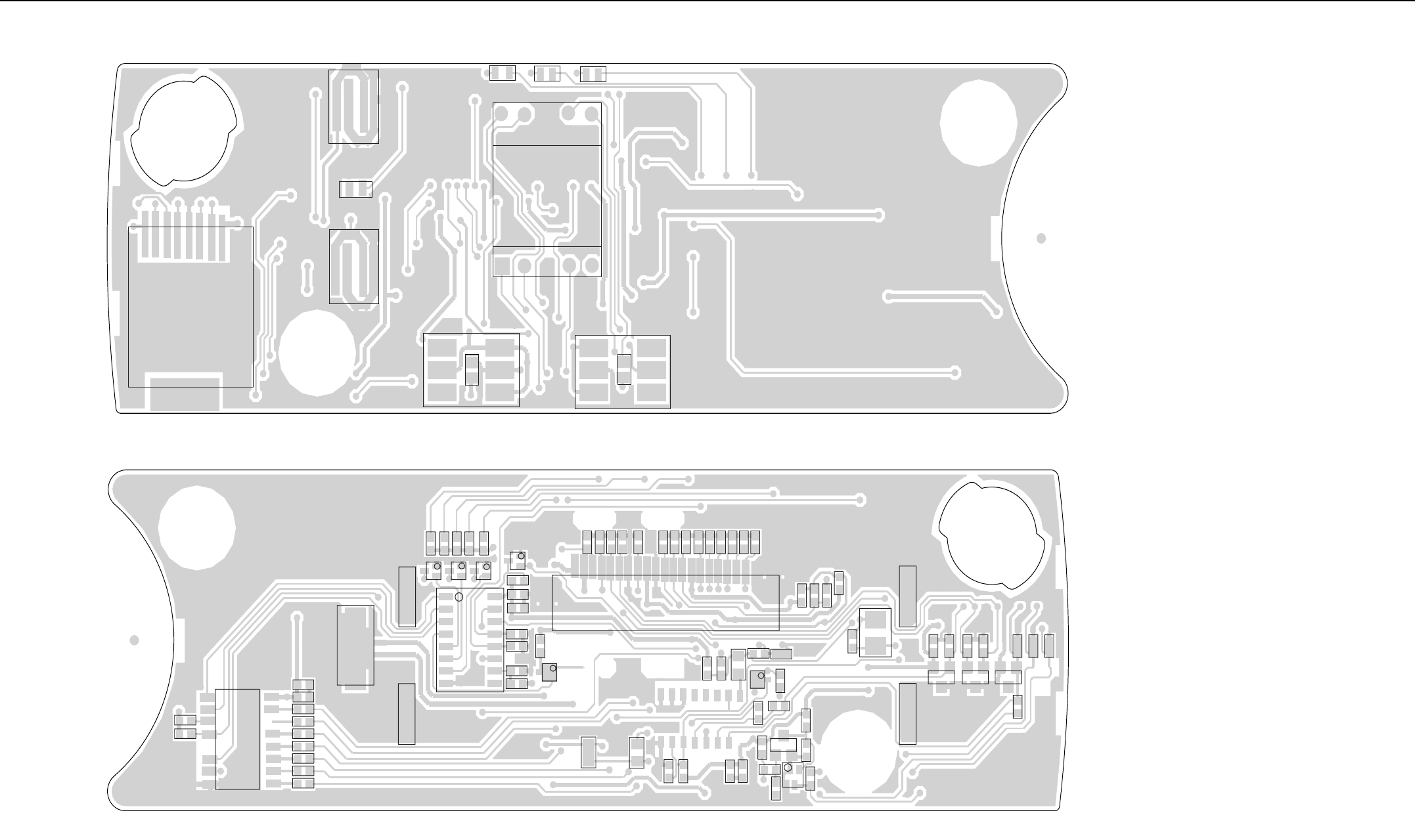
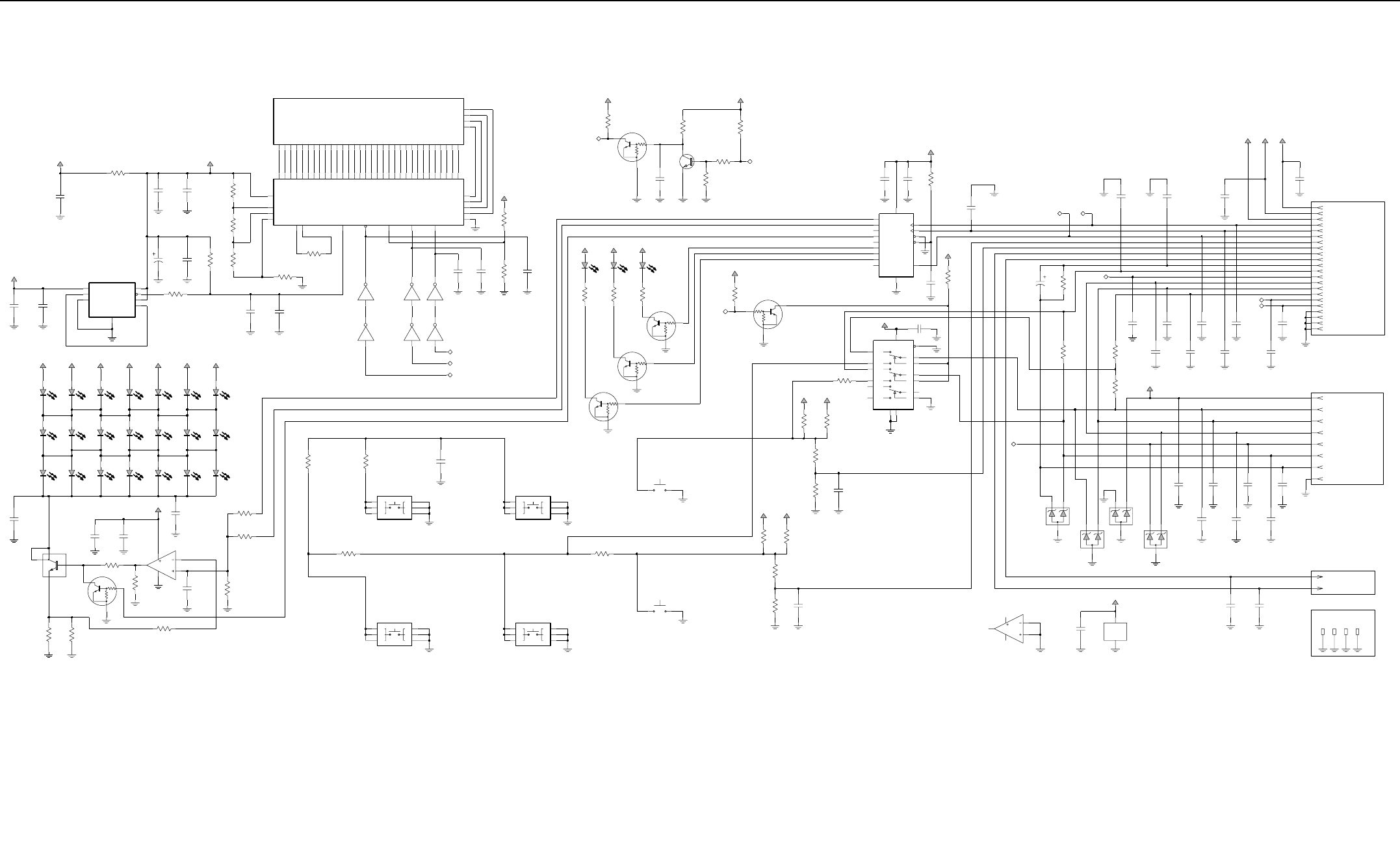
Controlhead CM140/CM340 - PCB 8488998U01 / Schematics 4-3
2.0 Controlhead CM140/CM340 - PCB 8488998U01 / Schematics
SHOWN FROM SIDE 1
D801
S801
D805
J802
D804
SH1
DS801
S802
J805
J804
D806
D802 D803
1
1
111
1
1
1
M801
8488998u01_p3
SHOWN FROM SIDE 2
C801
C802
C803
C804
C805
C806
C807
C808
C809
C810
C811
C812
C813
C814
C815
C816
C817
C818
C819
C820
C821
C822
C823
C824
C825
C826
C827
C832
C833
C834
C836
M802
M803
M804
P801
Q802
Q803
Q804 Q805 Q806
Q811
Q812
R801
R802
R803 R804
R805
R806
R807
R808
R809
R810
R811
R813
R816
R818
R819
R820
R821
R822
R823
R824
R825
R826
R827
R829
R830
R831
R832
R833
R834
R839
R840
R841
R842
R843
R844
R845
R846
R847
R848
R849
R850
U801
VR802VR803 VR804
Q801
R842
J803
Controlhead CM140/CM340
PCB 8488998U01
Top Side
Bottom Side
4-4 Controlhead CM140/CM340 - PCB 8488998U01 / Schematics
DNP
Change to 1% Change to 1%
COL
ROW
COL
DNP
DNPDNP
DNP
DNP
UP
DOWN
DNP
DNP
DNP
ROW
Change to 1%
Change to 1%
Change to 1%
Place under the 7-segment
MIC. PTT
MIC. AUDIO
SPI_MOSI
HOOK
RX. AUDIO
SPKR-
SPKR+
SPKR-
SPKR+
KEY_ROW
KEY_COL
COM/DATA_SEL
SPI_CLK
SH_R_CS
DISP_CS
DIS_RES
BOOT_RES
BOOT_RES
DNP
F1
F2
DNP
RED LED
GREEN LED
YELLOW LED
DNPDNP DNP
THESE ARE THE
ESD PROTECTION
MAIN BOARD CONNECTOR
MICROPHONE CONNECTOR
SPEAKER CONNECTOR
HOOK
9.3 V
MIC. AUDIO
MIC. PTT
SCI
RX. AUDIO
KEYPAD BACKLIGHT
CONTACTS (SPRINGS)
SCI
J803-22
220.p
R845
51.K
R846
VR803
G2
J803-21 G1
J803-10 18
10
BI J803-18
19
J803-19
6
J803-6
J803-4
1
4
J803-1
J803-13 13
17
J803-17
7
9
J803-9
J803-7
12
DISPL_CS
J803-12
20
J803-20
J803-8 8
CH_PTT J803-5 5
3
J803-3
J803-11 11
J803-15
OE
TELCO_PTT
CH_PTT
TELCO_PTT
COMM_CATH_2
ANODE_B
ANODE_A
HDSP-513G
15
16
S802
4
S801
6
C6
5C5
C4
2
J803-16
R809
3.3K
J803-2
D3_3V
SH1
4
3
2
1
SHIELD
0.
PIN2 2
R850
CONTACT
13K
PIN2 2
PIN1
1
J804
CONTACT
R848
PIN1
1
J805
10.K
R849
R844
10.K
R847
D3_3V D3_3V
51.K
10.K
C836
9_3V
R843
10.K
Q812
9_3V
Q811
10.K
22.K
R840
R842
22.K
R839
9_3V9_3V
R832
20.K20.K
R831
R841
C833
100n
10.K
0.
0.
R834
100n
R833
13 X1
MC14053B
3
C832
C9
B10
11
Z1
Z0
5
Z4
Y1
1
Y0
2
Y15
X0
12
X14
VEE
7
VCC 16
GND
8
EN 6
1M804
A
U803
C834
1M803
22.n
1M801
C817
1
M802
20.
VDD 16
LT 3
LE 5
G
VR804 220.p
C2
11
C1 2
BI 4
B2
U802
VSS
8
14 F
15 E
9D2
10
D1 6
C824
12
B1 1
A2
13
A1 7
MC14511BFEL
220.p
C826
220.p
220.p 220.p
C818C816
220.p
C819 C821
220.p
C820
220.p
220.p
C822
C803
220.p
C801
220.p
C805
220.p 220.p 220.p
C809C807 C811
220.p
C813
220.p
220.p
C814
220.p
C812
220.p
C810C806
220.p
C808
220.p 220.p
220.p
9_3VD3_3V
9_3V
C804
9_3V
9_3V
9_3V
9_3V
D3_3V
D3_3V
C802
9_3V D3_3V
33.
33.
R827
33.
R825
R826
R824
R823
R822
33.
33.
33.
33.
R821
1n
C823
10.K
Q802 47.K
R807
R806
10.K
R805
47.K
47.K R804
Q801
R803
680.
R802
R820
680.
3C3
2
C2
1C1
TOUCH_SW_MARLIN
3C3
2
C2
1C1
TOUCH_SW_MARLIN
6
C6
5C5
4
C4
10u
0.
C815
R830
R810
470.
HSMG-C670
D806
R808
300.
0.
R801
HSMG-C670
D804
1
J802-1
5
J802-5
2
J802-2
4
J802-4
3
J802-3
7
J802-7
6
J802-6
8
J802-8
DS801
COMM_CATH_1
ANODE_G
ANODE_F
ANODE_E
ANODE_DP
ANODE_D
ANODE_C
OE
DISPL_CS
BI
R811
0.
22K
R813 R816
D801
13K
D802
HSMH-C670
D803
HSMY-C670
Q804
HSMG-C670
Q805
Q806
1
P801-1
2
P801-2
R818 R819
3.9K
C825
680.
CLK_L 12
U801
100n
Q4
4Q3
3Q2
2Q1
1Q0
15
GND
8
EN_OE 13
CLK_S 11
VCC 16
SEROUT
9SERIN 14
RESET 10
Q7
7Q6
6Q5
5
MC74HC595A
C827
100n 10.K
R829
Q803
20.0
VR802
VR801
20.0
20.0
HSMG-C670
14
J803-14
D805
10K
47K
47K
10K
47K
10K
47K
10K
47K
10K
47K
10K
47K
73B02964C39-O
10K
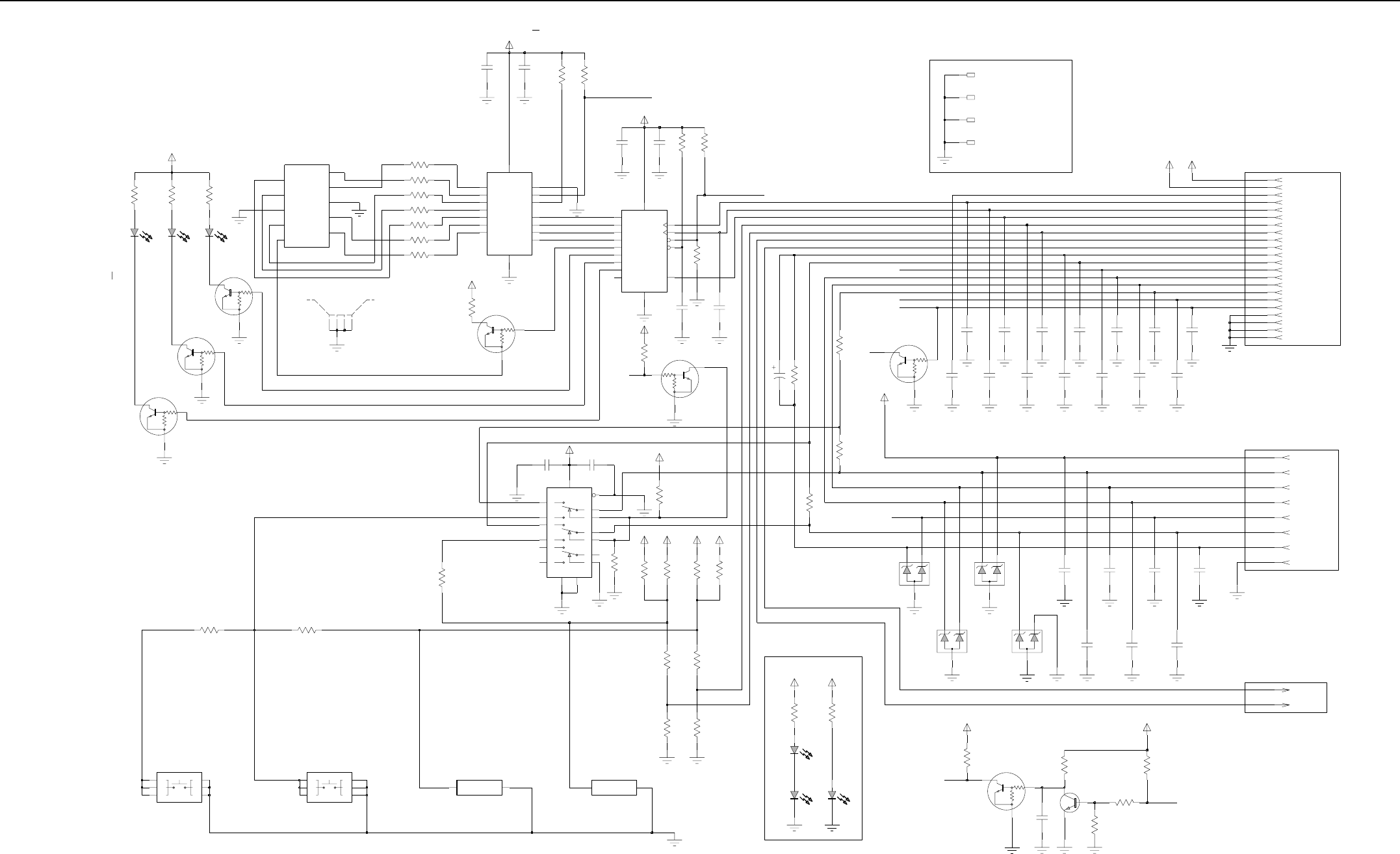
Controlhead CM140/CM340 Schematic
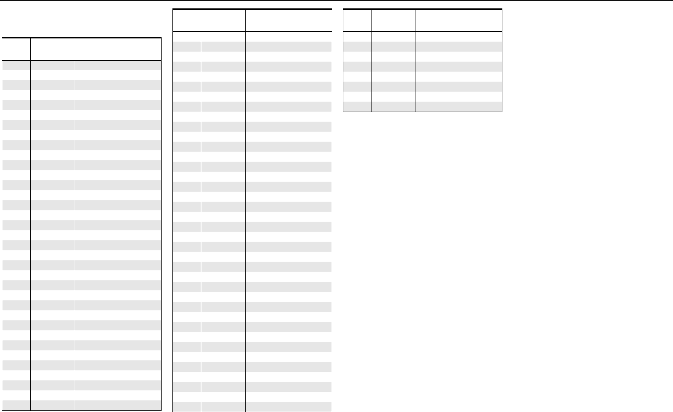
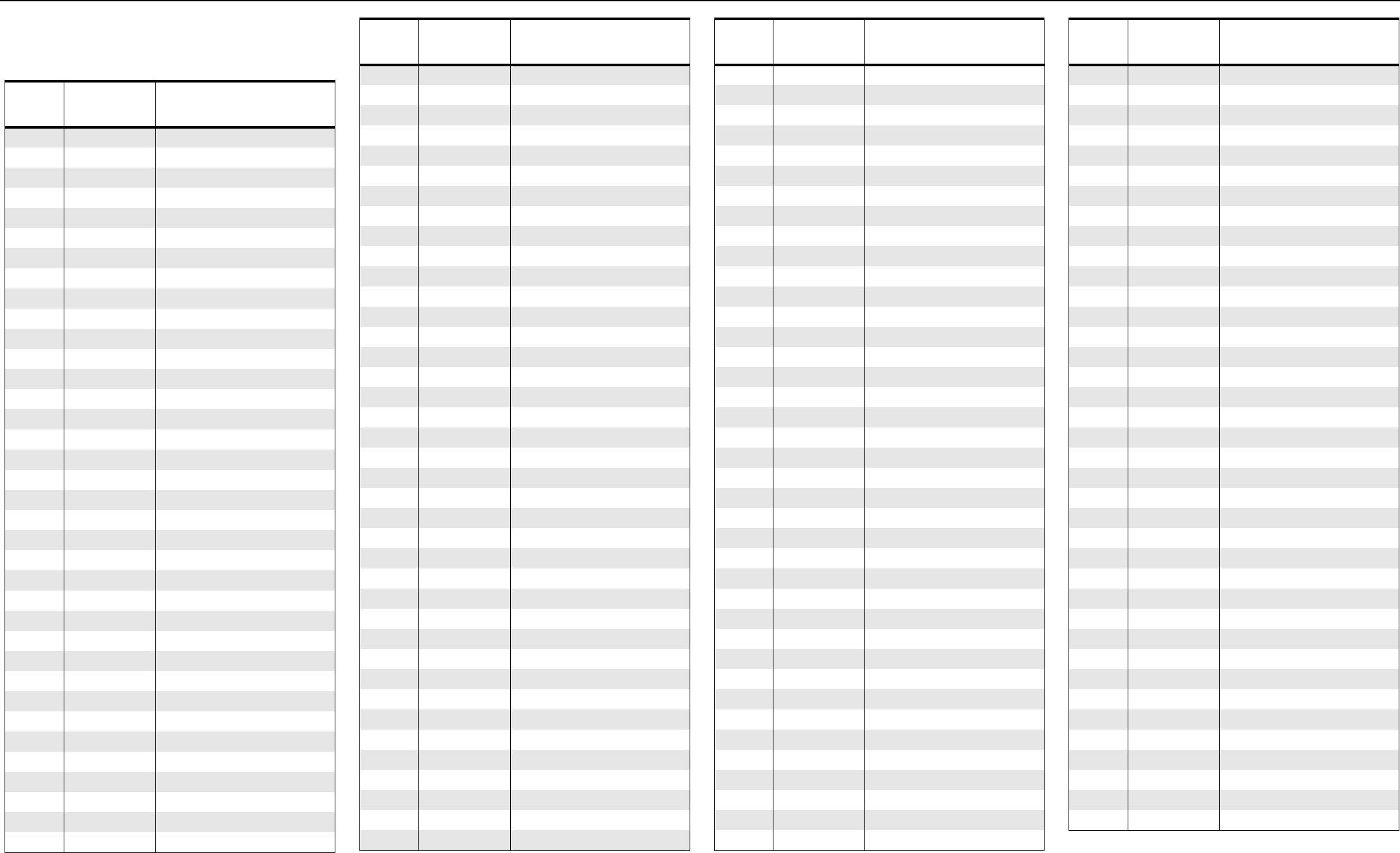
Controlhead CM140/CM340 - PCB 8488998U01 / Schematics 4-5
2.1 Controlhead PCB 8488998U01 Parts
List
Circuit
Ref
Motorola
Part No Description
C802 2113740F59 CAP CHIP REEL CL13
C804 2113740F59 CAP CHIP REEL CL13
C805 2113740F39 CAP CHIP REEL CL1+/-30 33
C806 2113740F39 CAP CHIP REEL CL1+/-30 33
C808 2113740F59 CAP CHIP REEL CL13
C809 2113740F39 CAP CHIP REEL CL1+/-30 33
C810 2113740F39 CAP CHIP REEL CL1+/-30 33
C811 2113740F59 CAP CHIP REEL CL13
C812 2113740F39 CAP CHIP REEL CL1+/-30 33
C813 2113740F59 CAP CHIP REEL CL13
C814 2113740F59 CAP CHIP REEL CL13
C816 2113740F39 CAP CHIP REEL CL1+/-30 33
C817 2113740F39 CAP CHIP REEL CL1+/-30 33
C818 2113740F39 CAP CHIP REEL CL1+/-30 33
C819 2113740F39 CAP CHIP REEL CL1+/-30 33
C820 2113740F39 CAP CHIP REEL CL1+/-30 33
C821 2113740F29 CAP CHIP REEL CL1+/-30 12
C822 2113740F39 CAP CHIP REEL CL1+/-30 33
C823 2113743K15 CER CHIP CAP .100uF
C824 2113740F59 CAP CHIP REEL CL13
C825 2113743K15 CER CHIP CAP .100uF
C826 2113740F59 CAP CHIP REEL CL13
C827 2113743K15 CER CHIP CAP .100uF
C832 2113743K15 CER CHIP CAP .100uF
C833 2113743K15 CER CHIP CAP .100uF
C834 2113743E07 CER CHIP CAP .022uF
C836 2113740F59 CAP CHIP REEL CL13
D801 4805729G74 LED SMT RED HP
D802 4805729G73 LED SMT YEL HP
D803 4805729G75 LED SMT GREEN HP
D804 4805729G75 LED SMT GREEN HP
D805 4805729G75 LED SMT GREEN HP
D806 4805729G75 LED SMT GREEN HP
DS801 5180353L02 7-SEGMENT DISPLAY
J802 0908353Y02 MODULAR 8-PIN STR
J803 0989241U02 FLEX 20-PIN 1mmTOP NON
M801 7588823L03 PAD GROUNFD LCD
M802 7588823L03 PAD GROUNFD LCD
M803 7588823L03 PAD GROUNFD LCD
M804 7588823L03 PAD GROUNFD LCD
P801 2809926G01 CONN 1.25MM 2PIN SURMT
Q801 4809940E02 TSTR NPN DIG DTC114YE
Q802 4813824A10 TSTR NPN 40V .2A GEN P
Q803 4809940E02 TSTR NPN DIG DTC114YE
Q804 4809940E02 TSTR NPN DIG DTC114YE
Q805 4809940E02 TSTR NPN DIG DTC114YE
Q806 4809940E02 TSTR NPN DIG DTC114YE
Q811 4809940E02 TSTR NPN DIG DTC114YE
Q812 4809940E02 TSTR NPN DIG DTC114YE
R801 0662057A01 CHIP RES 10 OHMS 5%
R802 0662057A61 CHIP RES 330 OHMS 5%
R803 0662057A89 CHIP RES 47K OHMS 5%
R804 0662057A89 CHIP RES 47K OHMS 5%
R805 0662057A73 CHIP RES 10K OHMS 5%
R806 0662057A89 CHIP RES 47K OHMS 5%
R807 0662057A73 CHIP RES 10K OHMS 5%
R808 0662057A36 CHIP RES 300 OHMS 5%
R809 0662057A45 CHIP RES 680 OHMS 5%
R810 0662057B47 CHIP RES 0 OHMS +0.5
R811 0662057B47 CHIP RES 0 OHMS +0.5
R813 0662057D08 CHIP RES 22K OHMS 5%
R816 0662057D03 CHIP RES 13K OHMS 5%
R818 0662057A63 CHIP RES 3900 OHMS 5%
R819 0662057A45 CHIP RES 680 OHMS 5%
R820 0662057A45 CHIP RES 680 OHMS 5%
R821 0662057A13 CHIP RES 33 OHMS 5%
R822 0662057A13 CHIP RES 33 OHMS 5%
R823 0662057A13 CHIP RES 33 OHMS 5%
R824 0662057A13 CHIP RES 33 OHMS 5%
R825 0662057A13 CHIP RES 33 OHMS 5%
R826 0662057A13 CHIP RES 33 OHMS 5%
R827 0662057A13 CHIP RES 33 OHMS 5%
R829 0662057A73 CHIP RES 10K OHMS 5%
Circuit
Ref
Motorola
Part No Description
R830 0662057A41 CHIP RES 470 OHMS 5%
R841 0662057A73 CHIP RES 10K OHMS 5%
R842 0662057A73 CHIP RES 10K OHMS 5%
R843 0662057A73 CHIP RES 10K OHMS 5%
R844 0662057A73 CHIP RES 10K OHMS 5%
R845 0662057A90 CHIP RES 51K OHMS 5%
R846 0662057A90 CHIP RES 51K OHMS 5%
R849 0662057D03 CHIP RES 13K OHMS 5%
Circuit
Ref
Motorola
Part No Description
4-6 Controlhead CM160/CM360 - PCB 8489714U01 / Schematics
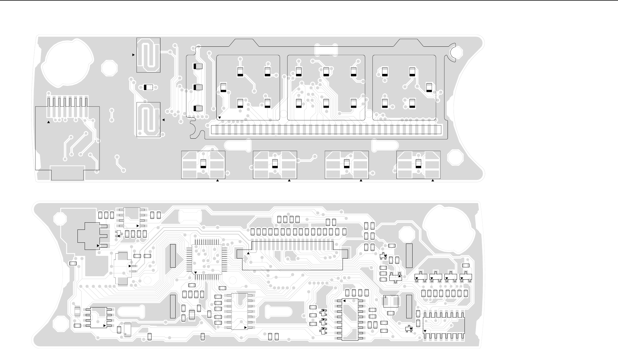
3.0 Controlhead CM160/CM360 - PCB 8489714U01 / Schematics
C40
4
3
2
1
Q12
R19
R26
R27
R20
R24
1
4
58
U1
C11
C26
Q11
C17
R18
C35 C36
2
P101
C19
C23
1
4
58
U18
C21
C22
R11
M4
12
24
37
48
U3
M3
R28 R39
R6
R7
R8
R9
C18
C30
C32
C33
R30
C16
C20
C25 R10
R15
C39
R29
R51
7
8
14
U2
1
J103
C4
C8
C27
C38
C44
C45
C46
C47
C48
C49
C50
C51
C52
C53
C54
C55
C24
R13
R25
R44
R45
R46
R21
R22
R23
Q8 Q9 Q10
16
1
8
9
U8
C7
C15
R14
R40
C1
C14
C58
R16
R17
R31
R54
R3
C56
M2
Q41
R41
16
1
8
9
U41
C2
C3
C5
C29
C34
C42
R42
R43
C6
VR1VR2 VR3 VR4
C43
Q13
Q14
R33
R37
R38
M1
C41
R12
R34
R35
R36
R48
R49
R50
8
7
5
6
3
2
1
4
9
J102
1
S6
D2
1
S5
D4
1
S3
D26
1
S4
D9
1
S1
D20
1
S2
D10
D18
D19
D3
D14
D17
D24
D27
D5
D8
D11
D15
D16
D21
DS1
D12
D13
D22
D23
D25
Controlhead CM160/CM360 PCB
8489714U01
Top Side
Bottom Side
Controlhead CM160/CM360 - PCB 8489714U01 / Schematics 4-7
10K
47K
10K
47K
10K
47K
10K
47K
10K
47K
10K
47K
9.3 V
F1
+
F2
MIC. AUDIO
MIC. PTT
KEY_ROW
KEY_COL
SPI_CLK
-
SPEAKER CONNECTOR
HOOK
MICROPHONE CONNECTOR
MAIN BOARD CONNECTOR
ESD CONTACTS
DIS_RES
DISP_CS
COM/DATA_SEL
SH_R_CS
BOOT_RES
BOOT_RES
SCI
MIC. PTT
SPKR+
SPKR-
UP
DOWN
SPI_MOSI
HOOK
RX. AUDIO
SCI
SPKR+
SPKR-
MIC. AUDIO
F4 F3
RX. AUDIO
0.1uF
C22
Y1C
ZA 14
ZB 15
ZC 4
C23
1000pF
VDD 16
VEE
7
VSS
8
YOA
12
Y0B
2
Y0C
5
13 Y1A
Y1B
1
3
U41
HEF4053B
EN 6
11
SA
SB 10
9
SC
R13
51K
D12
HSMG-C670
D3_3V
19
HSMG-C670
D10
J102-88
J103-19
10
J102-77
C43
J103-10
470pF
C54
0.1uF
R36
47K
HSMG-C670
9_3V
R28
D25
P101-22
680K
51K
R12
R27
10
R7
10K
HSMG-C670
D17
DNF
C5
5C6 6
10K
R34
S2
C1
1C2 2
C3
3C4 4
D23
HSMG-C670
TOUCH_SW
DNF
D14
HSMG-C670
0
R9
MC74HCT04A
U2-6
13 12
12
DNF
C4
1000pF
4
C4
5C5 6
C6
DNF
TOUCH_SW
S6
TOUCH_SW
S3
1C1 2
C2
3C3
10K
R8
DNF
U2-5
MC74HCT04A
11 10
DNF
HSMG-C670
D8
C29
DNF
1000pF
8
DNF
0
R10
U2-4
MC74HCT04A
9
680
DNF
R20
10K
6
C6
9_3V
R23
1C1 C2 2
3C3 4
C4
5C5
D2
HSMG-C670
TOUCH_SW
DNF
S1
1K
R18
10K
R15
100pF
DNF
DNF
J103-1313
C33
220pF
C53
DNF
C35
M3
6
D3_3V
DNF
1000pF
C30
9_3V
J102-6
DNF
100pF
D19
HSMH-C670
12
5V_IN
DNF
C20
2.2uF Q41
J103-12
2.2uF
MC74HCT04A
U2-2
34
C19
J103-1111
9_3V
HSMG-C670
D9
DNF
1000pF
C27
D18
HSMY-C670
DNF
1000pF
C41
4
47K
R38
2
3
1
8
4
9_3V
J102-4
4
V3
5
VDD
7
VREG
16
VSS 6
U1-1
LM2904
SEG4 21
SEG5 22
SEG6 23
SEG7 24
SEG8 25
26
SEG9
9SI
V1
3
V2
42
43
SEG26
SEG27 44
SEG28 45
SEG29 46
SEG3 20
SEG30 47
48
SEG31
35
SEG19 36
SEG2 19
SEG20 37
SEG21 38
SEG22 39
SEG23 40
SEG24 41
SEG25
SEG10 28
SEG11
SEG12 29
SEG13 30
SEG14 31
SEG15 32
SEG16 33
SEG17 34
SEG18
COM2 14
COM3 15
CS
10
C_D
11
OSC1
1OSC2
2
SEG0 17
SEG1 18
27
S1D15100
U3
CK
8
COM0 12
COM1 13
20V
VR3
VR2
20V
VR1
10uF
C1
DNF
20V
Q5
5
Q6
6
Q7
7
RESET 10
SERIN 14
SEROUT
9
VCC 16
CLK_S 11
EN_OE 13
GND
8
Q0
15
Q1
1
Q2
2
3Q3
Q4
4
U8
MC74HC595A
CLK_L 12
DNF
22K
R46
R44
R45
0
J102-55
DNF
20K
3
J103-21G1
R54
13K
J102-3
10K
R39
220pF
DNF
C55
J103-1818
DNF
10K
R6
R29
22K
DNF
C47
220pF
47K
R37
R30
10K
DNF
3
J103-88
130K
J103-3
D4
HSMG-C670
R11
M2 M4
220pF
C46
220pF
DNF
DNF
9_3V
C45
D16
HSMG-C670
R35
D24
HSMG-C670
0
R43
3.3K
R41
DNF
DNF
S5
TOUCH_SW
21
10K
J103-1515
D3_3V
9_3V
1000pF
C24
Q8
9_3V
C32
D3_3V
D3_3V
5V_CH
DNF
100pF
0.1uF
5
7
8
4
9_3V 9_3V
9_3V
DNF
C14
U1-2
LM2904 6
C17
5V_CH
M1
J103-44
DNF
1000pF
1
J103-66
Q9
J103-1
C5
R50
22K
470pF
0
R49
DNF
R48
20K
R42
0
DNF
C48
DNF
DNF
C50
9_3V
220pF
J103-55
470pF
R33
10K
0.1uF
C56
MC74HCT04A
U2-3
56
HSMG-C670
D15
Q10
10K
R19
5V_CH
C3
470pF
9
_3V
470pF
43K
R51
C2
C18
HSMG-C670
D21
PWR_GND
U2-7
GND
7
VCC
14
0.1uF
J103-99
C36
1000pF
R40
DNF
220pF
C44
DNF
10K
C3
3C4 4
C5
5C6 6
9_3V
DNF
S4
TOUCH_SW
C1
1C2 2
C16
0.1uF
DNF
J103-1717
J103-77
1000pF
C42
1000pF
DNF
C38
3.9K
R24
R21
C25
5V_IN
2.2K
DNF
1000pF
Q12
J102-11
Q13
J103-2020
Q14
R16
27K
HSMG-C670
D5
HSMG-C670
D13
0
R25
9_3V
9_3V
VR4
20V
470pF
C49
R31
13K
DNF
4.7uF
C21
DNF
C51
220pF
D20
HSMG-C670
R17
13K
D27
HSMG-C670HSMG-C670
D26
1000pF
C34
DNF
SEG8
13
SEG9
14
680
R22
SEG29
34
SEG3
8
SEG30
35
SEG31
36
SEG4
9
SEG5
10
SEG6
11
SEG7
12
SEG21
26
SEG22
27
SEG23
28
SEG24
29
SEG25
30
31 SEG26
SEG27
32
SEG28
33
SEG14
19
SEG15
20
SEG16
21
SEG17
22
SEG18
23
SEG19
24
SEG2
7
SEG20
25
COM2 3
COM3 4
SEG0
5
SEG1
6
SEG10
15
SEG11
16
SEG12
17
SEG13
18
DNF
LCD_36PIN
DS1
COM0 1
COM1 2
R14
10K
0.1uF
C15
D3_3V
C7
1000pF
16
J102-22
1000pF
C39
J103-16
Q11
DNF
0.1uF
C11
12
1
J103-22G2
U2-1
MC74HCT04A
C40
P101-1
J103-22
DNF
1000pF
J103-1414
9_3V
HSMG-C670
D3
C8
1000pF
9_3V
HSMG-C670
D22
SHUTDOWN
3
1000pF
C6
DNF
LP2951C
5V_TAP 6
5
ERRORFEEDBACK
7
GND
4
INPUT
8OUTPUT 1
SENSE 2
9_3V
DNF
U18
HSMG-C670
D11
C26
1000pF
C58
.022uF
10
470pF
C52
R3
SI
CS
MUX_CTL
ROW
COL
10
R26
TELCO_PTT
CS
CK
MUX_CTL
CH_PTT
CH_PTT
TELCO_PTT
CK
SI
Controlhead CM160/CM360 Schematic
Controlhead CM160/CM360 - PCB 8489714U01 / Schematics 4-8
3.1 Controlhead PCB 8489714U01 Parts
List
Circuit
Ref
Motorola
Part No Description
C1 NOTPLACED CAP, 10uF
C2 2113740F67 CAP, 470pF
C3 2113740F67 CAP, 470pF
C4 2113740F12 CAP CHIP REEL CL1 +/-30 12
C5 2113740F67 CAP, 470pF
C6 2113740F12 CAP CHIP REEL CL1 +/-30 12
C7 2113741F25 CAP, 1000pF
C8 2113741F25 CAP, 1000pF
C11 2113743K15 CAP, 0.1uF
C14 NOTPLACED CAP, 0.1uF
C15 2113743K15 CAP, 0.1uF
C16 2113743K15 CAP, 0.1uF
C17 NOTPLACED CAP, 1000pF
C18 2113743K15 CAP, 0.1uF
C19 2113743F18 CAP, 2.2uF
C20 NOTPLACED CAP, 2.2uF
C21 NOTPLACED CAPP, 4.7uF
C22 2113743K15 CAP, 0.1uF
C23 2113741F25 CAP, 1000pF
C24 2113741F25 CAP, 1000pF
C25 NOTPLACED CAP, 1000pF
C26 2113741F25 CAP, 1000pF
C27 2113740F12 CAP CHIP REEL CL1 +/-30 12
C29 2113740F12 CAP CHIP REEL CL1 +/-30 12
C30 NOTPLACED CAP, 100pF
C32 NOTPLACED CAP, 100pF
C33 NOTPLACED CAP, 100pF
C34 2113740F12 CAP CHIP REEL CL1 +/-30 12
C35 NOTPLACED CAP, 1000pF
C36 NOTPLACED CAP, 1000pF
C38 NOTPLACED CAP, 1000pF
C39 NOTPLACED CAP, 1000pF
C40 NOTPLACED CAP, 1000pF
C41 NOTPLACED CAP, 1000pF
C42 2113740F12 CAP CHIP REEL CL1 +/-30 12
C43 2113743K15 CAP, 0.1uF
C44 NOTPLACED CAP, 220pF
C45 NOTPLACED CAP, 220pF
C46 NOTPLACED CAP, 220pF
C47 NOTPLACED CAP, 220pF
C48 NOTPLACED CAP, 220pF
C49 2113740F67 CAP, 470pF
C50 2113740F67 CAP, 470pF
C51 2113740F12 CAP CHIP REEL CL1 +/-30 12
C52 2113740F67 CAP, 470pF
C53 2113740F12 CAP CHIP REEL CL1 +/-30 12
C54 2113740F67 CAP, 470pF
C55 NOTPLACED CAP, 220pF
C56 2113743K15 CAP, 0.1uF
C58 2113743E07 CAP, .022uF
D2 4805729G75 HSMG-C670
D3 4805729G75 HSMG-C670
D4 4805729G75 HSMG-C670
D5 4805729G75 HSMG-C670
D8 4805729G75 HSMG-C670
D9 4805729G75 HSMG-C670
D10 4805729G75 HSMG-C670
D11 4805729G75 HSMG-C670
D12 4805729G75 HSMG-C670
D13 4805729G75 HSMG-C670
D14 4805729G75 HSMG-C670
D15 4805729G75 HSMG-C670
D16 4805729G75 HSMG-C670
D17 4805729G75 HSMG-C670
D18 4805729G73 HSMY-C670
D19 4805729G74 HSMH-C670
D20 4805729G75 HSMG-C670
D21 4805729G75 HSMG-C670
D22 4805729G75 HSMG-C670
D23 4805729G75 HSMG-C670
D24 4805729G75 HSMG-C670
D25 4805729G75 HSMG-C670
D26 4805729G75 HSMG-C670
D27 4805729G75 HSMG-C670
DS1 NOTPLACED LCD_36PIN
Circuit
Ref
Motorola
Part No Description
J102 0908353Y02 CONN_J
J103 0989241U02 CONN_J
M1 7588823L03 CONTACT
M2 7588823L03 CONTACT
M3 7588823L03 CONTACT
M4 7588823L03 CONTACT
P101 2809926G01 CONN_P
Q8 4809940E02 DTC114YE
Q9 4809940E02 DTC114YE
Q10 4809940E02 DTC114YE
Q11 4809940E02 DTC114YE
Q12 4813824B01 PZT2222A
Q13 4809940E02 DTC114YE
Q14 4813824A10 MMBT3904
Q41 4809940E02 DTC114YE
R3 0662057A01 RES, 10
R6 NOTPLACED RES, 10K
R7 NOTPLACED RES, 10K
R8 NOTPLACED RES, 10K
R9 0662057B47 RES, 0
R10 NOTPLACED RES, 0
R11 0662057B01 RES, 130K
R12 0662057A90 RES, 51K
R13 0662057A90 RES, 51K
R14 0662057A73 RES, 10K
R15 NOTPLACED RES, 10K
R16 0662057A83 RES, 27K
R17 0662057A76 RES, 13K
R18 0662057A49 RES, 1K
R19 0662057A73 RES, 10K
R20 NOTPLACED RES, 10K
R21 0662057A63 RES, 3.9K
R22 0662057A45 RES, 680
R23 0662057A45 RES, 680
R24 0662057A57 RES, 2.2K
R25 0662057B47 RES, 0
R26 0662057A01 RES, 10
R27 0662057A01 RES, 10
R28 0662057B18 RES, 680K
Circuit
Ref
Motorola
Part No Description
R29 0662057A81 RES, 22K
R30 NOTPLACED RES, 10K
R31 0662057A76 RES, 13K
R33 0662057A73 RES, 10K
R34 0662057A73 RES, 10K
R35 0662057A61 RES, 3.3K
R36 0662057A89 RES, 47K
R37 0662057A89 RES, 47K
R38 0662057A89 RES, 47K
R39 0662057A73 RES, 10K
R40 0662057A73 RES, 10K
R41 0662057A73 RES, 10K
R42 NOTPLACED RES, 0
R43 NOTPLACED RES, 0
R44 NOTPLACED RES, 20K
R45 0662057B47 RES, 0
R46 NOTPLACED RES, 22K
R48 NOTPLACED RES, 20K
R49 0662057B47 RES, 0
R50 NOTPLACED RES, 22K
R51 0662057A88 RES, 43K
R54 0662057A76 RES, 13K
S1 NOTPLACED TOUCH_SW
S2 NOTPLACED TOUCH_SW
S3 NOTPLACED TOUCH_SW
S4 NOTPLACED TOUCH_SW
S5 NOTPLACED TOUCH_SW
S6 NOTPLACED TOUCH_SW
U1 5113818A01 LM2904
U2 5113805A05 MC74HCT04A
U3 5102109U01 S1D15100
U8 5113805A75 MC74HC595A
U18 NOTPLACED LP2951C
U41 5184704M60 HEF4053B
VR1 4813830A75 MMBZ20VAL
VR2 4813830A75 MMBZ20VAL
VR3 4813830A75 MMBZ20VAL
VR4 4813830A75 MMBZ20VAL
Circuit
Ref
Motorola
Part No Description
