D E707/E775 E707 Sony 775
User Manual: D-E707
Open the PDF directly: View PDF ![]() .
.
Page Count: 6
MICROFILM
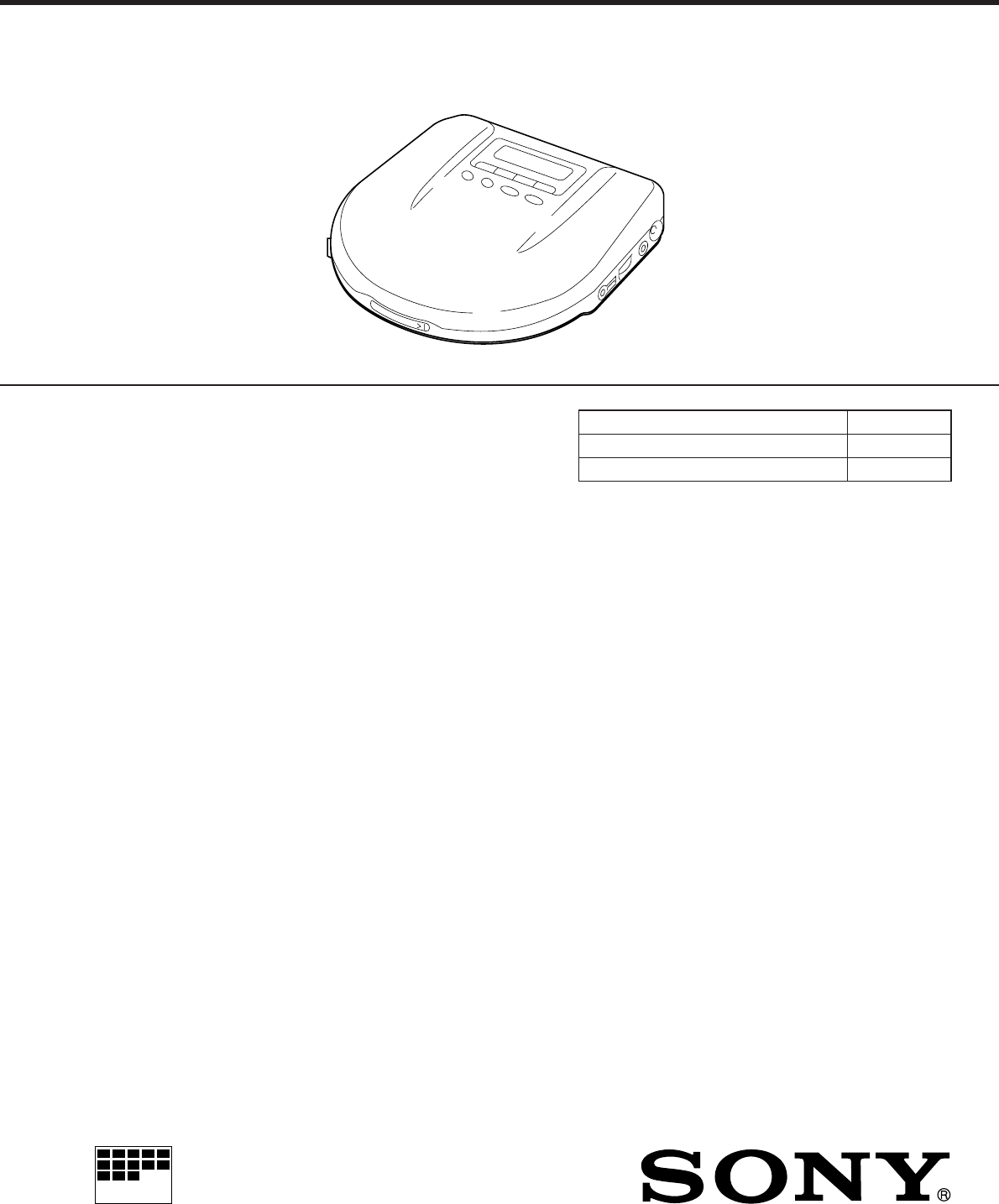
COMPACT DISC COMPACT PLAYER
US Model
Canadian Model
AEP Model
UK Model
E Model
Australian Model
Chinese Model
D-E775
Tourist Model
D-E707
CD player section
System
Compact disc digital audio system
Laser diode properties
Material: GaAlAs
Wavelength: λ=780 nm
Emission duration: Continuous
Laser output: Less than 44.6 µW (This output
is the value measured at a distance of 200
mm from the objective lens surface on the
optical pick-up block with 7 mm aperture.)
Error correction
Sony Super Strategy Cross Interleave Reed
Solomon Code
D-A conversion
1-bit quartz time-axis control
Frequency response
20 – 20,000 Hz +1
–2 dB (measured by EIAJ CP-
307)
Output (at 4.5 V input level)
Headphones (stereo minijack)
15 mW + 15 mW at 16 ohms
Line output (stereo minijack)
Output level 0.7 V rms at 47 kilohms
Recommended load impedance over 10
kilohms
Optical digital output (optical output
connector)
Output level: –21 to –15 dBm
Wavelength: 630 – 690 nm at peak level
General
Power requirements
For the area code of the model you purchased,
check the upper left side of the bar code on the
package.
• Two Sony NH-DM2AA rechargeable
batteries: 2.4 V DC
Two Sony NC-DMAA rechargeable
batteries: 2.4 V DC
• Two LR6 (size AA) batteries: 3 V DC
• AC power adaptor (DC IN 4.5 V jack):
US/Canadian model: 120 V, 60 Hz
AEP/E13 model: 220 – 230 V, 50/60 Hz
UK model: 230 – 240 V, 50 Hz
Australian model: 240 V, 50 Hz
Tourist/E33 model: 100 – 240 V, 50/60 Hz
Hong Kong model: 220 V, 50/60 Hz
Chinese model: 220 V, 50 Hz
• Sony DCC-E245 car battery cord for use on
car battery: 4.5 V DC
Dimensions (w/h/d) (without projecting
parts and controls)
Approx. 131.8 × 23.9 × 142.0 mm
(5 1/4 × 31/32 × 5 5/8 in.)
Mass (without rechargeable batteries)
Approx. 200 g (7.0 oz)
Operating temperature
5 ˚C – 35 ˚C (41 ˚F – 95 ˚F)
SPECIFICATIONS
D-E707/E775
Model Name Using Similar Mechanism D-E700/E705
CD Mechanism Type CDM-2911EBA
Optical Pick-Up Name DAX-11E
Supplied accessories
For the area code of the model you purchased,
check the upper left side of the bar code on the
package.
AC power adaptor (1)
Headphones with remote control (1)*1
Earphones with remote control (1)*2
Rechargeable batteries (2)
AC plug adaptor (1)*3
Battery carrying case (1)
Carrying case (1)
*1Supplied with US model
*2Not supplied with US model
*3Supplied with Tourist, E33 and E13 models
Design and specifications are subject to change
without notice.
• Abbreviation
E13: 220 – 230 V AC area in E model
E33: 100 – 240 V AC area in E model
SERVICE MANUAL
Ver 1.1 1999. 02
D-E707/E775
– 27 – – 28 – – 29 – – 30 –
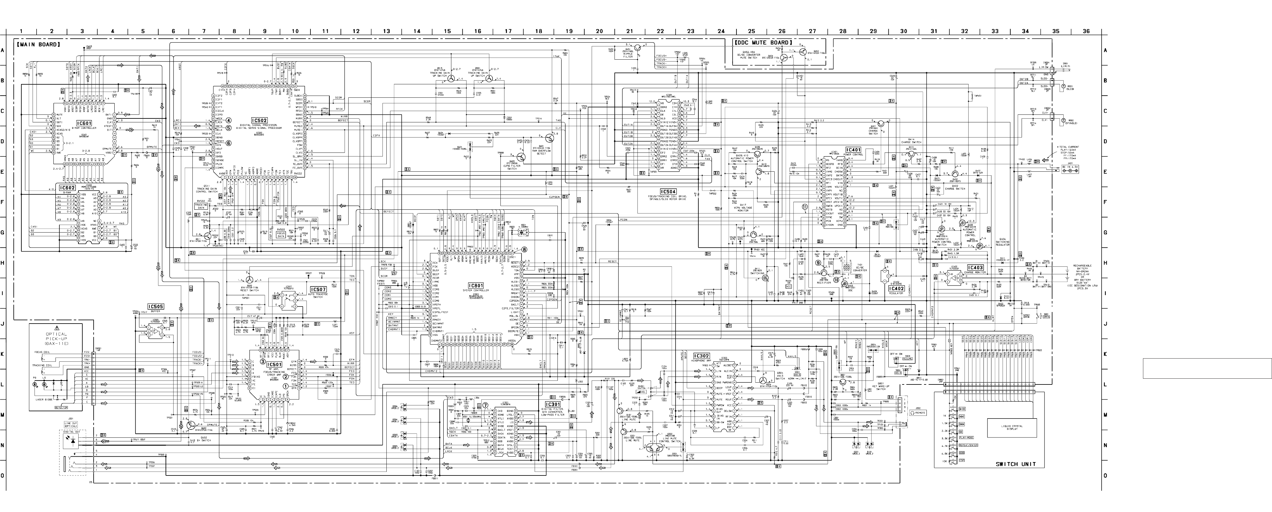
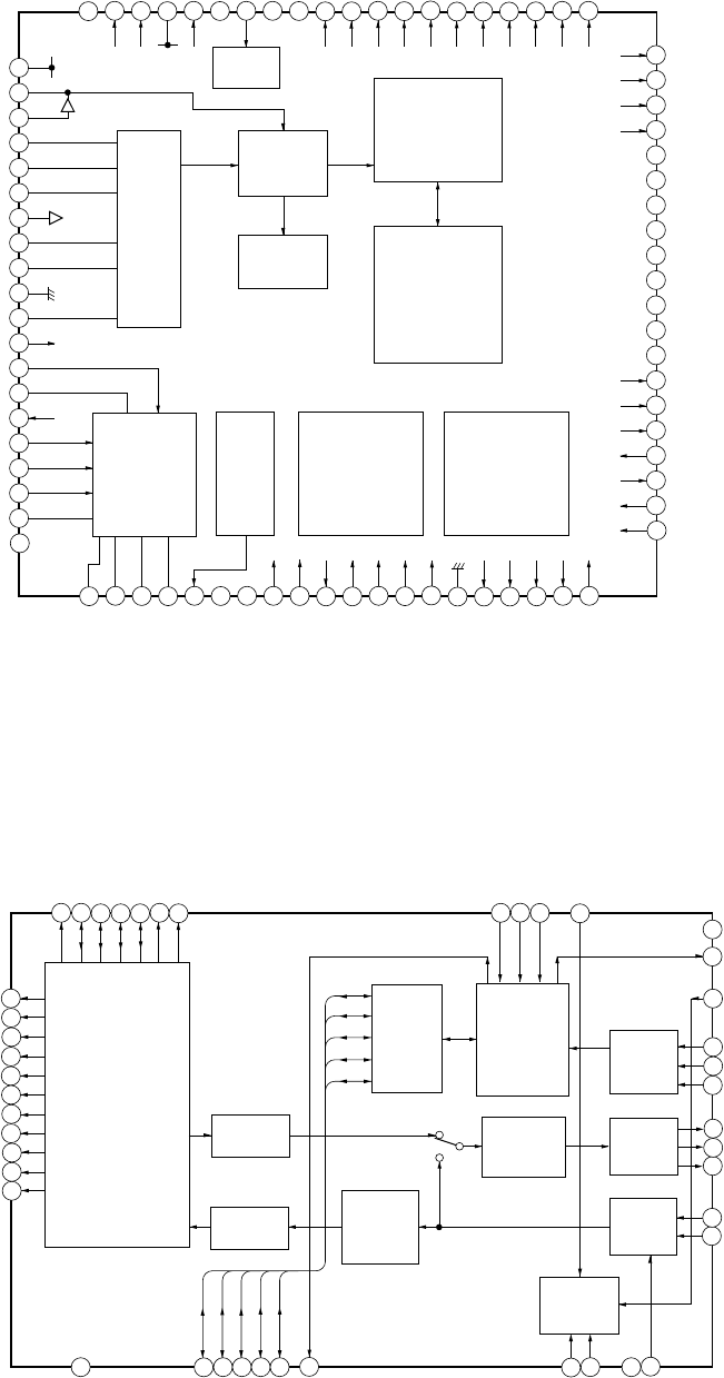
6-5. SCHEMATIC DIAGRAM (SUFFIX-11) • See page 23 for Waveforms. • See page 38 for IC Block Diagrams.
Note on Schematic Diagram:
• All capacitors are in µF unless otherwise noted. pF: µµF
50 WV or less are not indicated except for electrolytics
and tantalums.
• All resistors are in Ω and 1/4 W or less unless otherwise
specified.
•¢: internal component.
•U: B+ Line.
•H: adjustment for repair.
• Power voltage is dc 4.5 V and fed with regulated dc power
supply from external power voltage jack.
• Voltages and waveforms are dc with respect to ground
under conditions in service mode.
no mark : CD PLAY
∗: Impossible to measure
• Voltages are taken with a VOM (Input impedance 10 MΩ).
Voltage variations may be noted due to normal produc-
tion tolerances.
• Waveforms are taken with a oscilloscope.
Voltage variations may be noted due to normal produc-
tion tolerances.
• Circled numbers refer to waveforms.
• Signal path.
J: CD PLAY (ANALOG OUT)
c: CD PLAY (OPTICAL OUT)
Note: The components identified by mark ! or dotted line
with mark ! are critical for safety.
Replace only with part number specified.
D-E707/E775
– 31 – – 32 – – 33 – – 34 –
6-6. SCHEMATIC DIAGRAM (SUFFIX-12) • See page 23 for Waveforms. • See page 38 for IC Block Diagrams.
Note on Schematic Diagram:
• All capacitors are in µF unless otherwise noted. pF: µµF
50 WV or less are not indicated except for electrolytics
and tantalums.
• All resistors are in Ω and 1/4 W or less unless otherwise
specified.
•¢: internal component.
•U: B+ Line.
•H: adjustment for repair.
• Power voltage is dc 4.5 V and fed with regulated dc power
supply from external power voltage jack.
• Voltages and waveforms are dc with respect to ground
under conditions in service mode.
no mark : CD PLAY
∗: Impossible to measure
• Voltages are taken with a VOM (Input impedance 10 MΩ).
Voltage variations may be noted due to normal produc-
tion tolerances.
• Waveforms are taken with a oscilloscope.
Voltage variations may be noted due to normal produc-
tion tolerances.
• Circled numbers refer to waveforms.
• Signal path.
J: CD PLAY (ANALOG OUT)
c: CD PLAY (OPTICAL OUT)
• Abbreviation
FR : French model
Note:
The components identi-
fied by mark ! or dotted
line with mark ! are criti-
cal for safety.
Replace only with part
number specified.
Note:
Les composants identifiés par
une marque ! sont critiques
pour la sécurité.
Ne les remplacer que par une
piéce portant le numéro
spécifié.
D-E707/E775
– 38 – – 39 – – 40 –
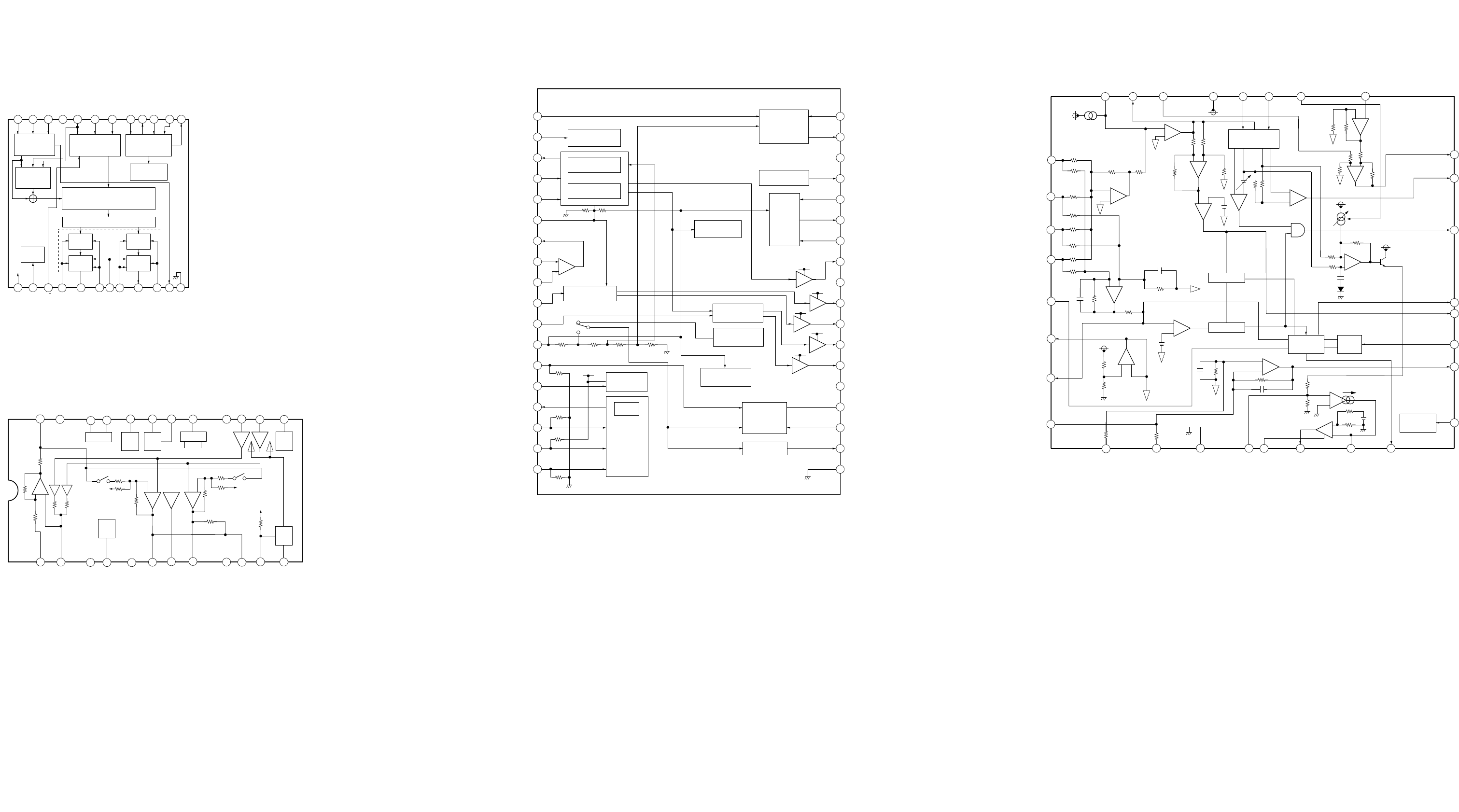
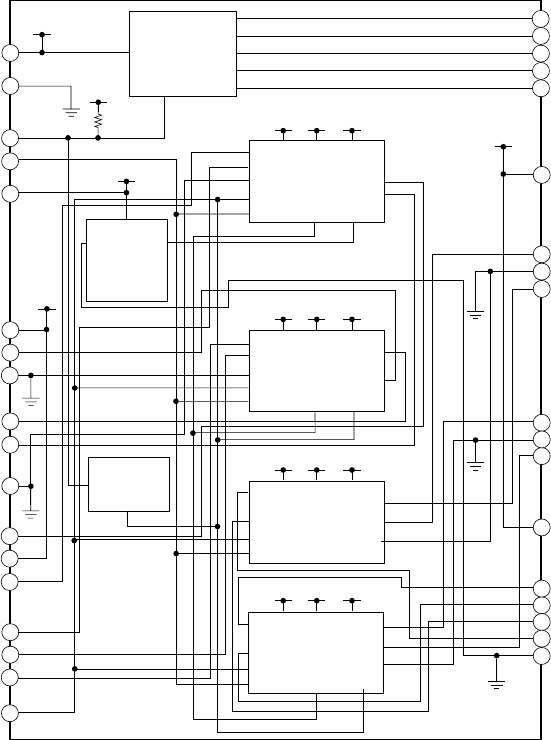
• IC Block Diagrams
IC301 TC9438FNEL
IC302 TA2120FN (EL)
IC401 MPC18A26VMEL IC501 BA6386K
DATA
INTERFACE
CIRCUIT
MICRO COMPUTER
INTERFACE
CIRCUIT OSC
20
TIMING
GENERATOR
DINAMIC
BASS BOOST
CIRCUIT DIGITAL FILTER CIRCUIT
DEEMPHASIS FILTER CIRCUIT
ATTENUATOR OPERATIONAL CIRCUIT
∑-∆ MODULATION CIRCUIT
OUTPUT
CIRCUIT
ANALOG
FILTER
TEST
CIRCUIT
OUTPUT
CIRCUIT
ANALOG
FILTER
24 23 22 21 17 16 15 14
19 18
34 8 10 11 12
1 2 6 7
59
LRCK BCK DATA DBB2
(DBB1)
ATT (EMP)
SHIFT (SM)
LATCH VDX XO XI GNDX MCK
13
VDD T1 VDA RO GNDA VR
P/S GNDA LO VDA ZD GNDD
+
–
+
–
+
–
23 20 19 18 17 16 15 14 13
234 5 678910 11 12
1
24
BIAS BEEP
PW
SW MT
SW
ALC
DET
ATT
SW
PWC
SW
OUT B OUT A
BEEP
IN
BST
PW
BPW
C
BST
NF ADD
OUT RF IN PWC
SW OUT B OUT C OUT A PWR
GND MIX
OUT ALC
IN ALC
DET
ATT
SW
IN AIN BGND
MT
TC
MT
SW
PW
SW
BIAS
BIAS
IN
BST
SW
BST
OUT
VCC
ADD
A
ADD
B
21
22
PW
A
ALC ALC
+
–
1
7
8
9
36
34
28
23
21
20
ERROR AMP
CHARGESW
CHARGE
AMP
DCIN DETECT 35
33
ERROR AMP
PWM2
2
3
4
5
10 PWM1
32
31
30
SYSTEM
CONTROL
OSC2
LOW VCPU
DETECT
12
13
14
15
16
17
18
VCPU
22
BANDGAP
REFERENCE
STEP-UP
DC-DC
CONVERTER
REGULATOR
SAWTOOTH
PWM4
SUB
REFERENCE
11
VG
VG
VG
VG
VG
27
29
26
25
24
19
INM3
RF3
DCIN
CHGSW
BATM
CHGOUT
VIN
VOUT2
NC
VOUTB1
VOUT1
UPCKB1
UPCK1
VG
VDO
SW
VCPU
GND
RS
DCDTB
RF2
INM2
INP2
DTC3
RF1
INM1
INP1
CMP1
DTC1
VREF
SWEN
RSTB
CKOUT
SYNC
PCB
CHGON
6
DET BLOCK
PS PL BL BS
+
–
+
–
+
–
+
–
+
–
+
–
+
15
FOCUS
SWITCH
SCRATCH
CONTROL
RAMP
OSC
+
–
12
16
+
–
24
+
–
25
26
27
28
+
–
2122
23 20 19 17
+
–
+
–
31
30
+
–
29
8
6
11
9
5 7
+
–
4
3
10
1
32
FOCUS BIAS
18
EFM
MIRR
DEFECT
13 FEO
FOK
FON
TEO
DFR
SROCH
PD
LD
CAPC
CAGC
GND
F
E
EI
FE
VC
FBIAS
A
D
B
C
RF- RFO RFI VCC PLH BLT RAGC ASY
14
HOLD BLOCK
LOOP ON
2
–
– 41 –
20
56
55
54
53
52
51
50
49
48
26 27
80 75 73 72
PLL
SUB
CLOCK
GEN
ECC
16k SRAM
SERVO
FILTER CLV SERVO
CONTROL uCOM
INTERFACE
DVDD
AVDD
7476
77
79 78 66 65 64 63 62 61
71 70 69 68 67
1
2
4
5
6
8
9
11
10
3
7VC
12
13
14
15
16
17
18
19
WINDOW
60
59
58
57
47
46
45
44
43
42
41
28 29 30 31 33 34 35 36
32 37 38 39 4025
21 22 23 24
AVDD
ASY
EYE
FCO
PCO
TESTI
VC
ADPFI
ADPFO
AGND
RVCO
FOK
FEIN
FCAPA
FON
TEIN
ATS
TZC
TCAPA
TEST2
FDOUT
TDOUT
SDIN
SDOUT
CLVOUT
TEST3
TEST4
CLVOPP
CLVOPN
CLVOPO
MUTE1
MUTE2
SCRATCH
MIRROR
DGND
RFCK
WFCK
SUBSYQ
SUBDATA
SUBCK
C1FX
C2FX
C2F3
C2F4
N.C
N.C
N.C
N.C
N.C
N.C
N.C
N.C
TEST5
GAINUP
CK176
BUSY
RW
DOUT
DIN
MCK
COMPC
XPLCK
SENS
DVDD
GFS
N.C
SYSCKI
RESET
DGND
CLK
DOCK
DOUTA
LRCK
DE
C2F
C2CLK
C1F1
C1F2
C2F1
C2F2
IC502 BU9326KS
IC601 SM5902AF
ENCODER
GENERAL
PORT INPUT
CONTROL 1
10
DRAM 1/F
DECODER
MICRO
COMPUTER
1/F
ATTENUATOR
INPUT
BUFFER INPUT
1/F
OUTPUT
1/F
INPUT
CONTROL 2
811
22
34
35
36
37
38
39
40
41
42
43
44
33 32 31 30 29 28 27 23
24
25
26
7
20
21
14
16
15
17
19
18
12
13
2
13456
COMPRESSION
MODE
THROUGH
MODE
NWE
D1
D0
D3
D2
NCAS
A10/NCAS2
NRAS
A9
A8
A7
A6
A5
A4
A0
A1
A2
A3
VDD2
UC1
UC2
UC3
UC4
UC5
DIT
NTEST
CLK
VSS
YSRDATA
VDD1
ZSENSE
NRESET
YBLKCK
YFCLK
YFLAG
ZSRDATA
ZLRCK
ZSCK
YSCK
YLRCK
YDMUTE
YMLD
YMDATA
YMCLK
9
– 42 –
IC504 MPC17A51VMEL
CHAGE
PUMP
CLK
VG
C2H
C1H
C1L
C2L
VCG
MOTOR
DRIVER
CH3
CF3
ERR3
VR
OE
OUT3A
OUT3B
MOTOR
DRIVER
CH4
SAWTOOTH
CF4
ERR4
VR
OE
OUT4A
PGND4
OUT4B
2
1
36
35
34
33
34
SAW
GEN
CLK
SAWTOOTH
VLG
VIN12
VCG
VG
5
6
4
7
10
11
9
VLG VG VIN12
VIN34
VLG VG VIN12
VLG VG VIN34
14
12
13
8
15
16
17
24
22
21
27
25
20
MOTOR
DRIVER
CH1
CF1
ERR1
PGND1
VR
OE OUT1A
OUT1B
VLG VG VIN12
LOW
VOLTAGE
DETECTOR
VLG
AGND PSB
18
19
23
26
31
28
29
PSB
SAWTOOTH PSB
SAWTOOTH PSB
PGND3
3
30
C2H
C1H
C1L
C2L
VIN34
OUT3A
PGND3
OUT3B
OUT4B
PGND4
OUT4A
VIN34
CF4
ERR4
ERR3
CF3
AGND
VG
DGNG
CLK
OE
VLG
VIN12
OUT1A
PGND1
OUT1B
OUT2B
PGND2
OUT2A
VIN12
CF2
ERR2
ERR1
CF1
VR
MOTOR
DRIVER
CH2
SAWTOOTH
CF2
ERR2
PGND2
VR
OE
OUT2A
OUT2B
PSB
