System_3000_Memory_Module System 3000 Memory Module
System_3000_Memory_Module System_3000_Memory_Module
User Manual: System_3000_Memory_Module
Open the PDF directly: View PDF ![]() .
.
Page Count: 9
1. Memory Module
The memory module
is
the high speed system memory for the System 3000.
It
has on-
board 32 bit error detection and correction (EDAC), refresh logic, and partial write logic.
There are two interleaved arrays which can read, write, partial write, and refresh
independently. This
is
accomplished
by
interleaving on address bit 2
so
that even and odd
four byte addresses
go
to opposite arrays. Because read operations return 8 bytes of data,
they require both arrays to work together. Each array contains four
39
bit wide banks.
The
39
bits include
32
bits of data and 7 check bits. Depopulated options of the module
are possible
by
stuffing one, two, or
all
four of the banks in each array. This yields an 8,
16, or
32
megabyte memory module.
The memory chips used are 1 megabit dynamic rams
(1
Mb DRAMs). When 4
megabit DRAMs become available, they may be used in the module with only jumper
changes. The stuffing options
will
then be 32, 64, or
128
megabytes per module. The
access time of the DRAMs used must
be
no more than 100 nanoseconds (nS). Nibble
mode
access
and CAS before RAS refresh are the other requirements of the
DRAM
chips. The
ZIP
(zig-zag in-line package) style
is
used
to save module space and make the
arrays more compact
so
that the control lines
will
be shorter.
The size of the data
used
by
the memory module depends on the type of access. Write
cycles use a
32
bit data word. Partial write
cycles
must
be
generated
by
the memory
module's control logic if it detects a write of
less
than four bytes. Read
cycles
return 64
bits to the requester. Burst mode
is
available on a read cycle so that the memory module
r.etums
16
or
32
bytes of data for one read request. Write and 8 byte read cycles last five
50 nsec system clock periods. Partial write
cycles
are nine clocks long. Refresh cycles take
sire
clock periods. The
16
and
32
byte reads take eight and
14
clock periods each,
respectively.
Parity
is
checked
on
input to the module and parity
is
generated on output. Status
registers are readable
by
other modules in the system to determine the memory size of the
module, find the address of an error, see if the memory module
is
in diagnostic mode,
or
various other module characteristics. Control registers are available
so
that other mooules
may enable or disable the memory array, put the module into diagnostic mode, inhibit
error correction,
or
other functions.
1.1 Memory Module Description
1.1.1 Memory Module System Bus Interface
Command, address and data if applicable get clocked into the
bus
input registers every 50
nsec
by
the
20
MHz system clock. The slot identifier field
is
compared with the memory
module's slot number to see if the command
is
meant for this memory module.
If
there
is
a match, the top five bits of the address are checked for equality to
all
ones or
all
zeroes.
If
the bits are
all
ones, the status or control registers are to be accessed.
If
the bits are
all
zeroes, the access
is
to the memory array.
If
the bits are neither
all
zeroes or
all
ones, a
NACK
will
be issued.
If
the transaction
is
not meant for this memory module, no action
will
be taken and new a new command, address, and data
will
be clocked into the bus
Arix Corporation -
CONFIDENTIAL
- 2 -
input register on the next rising edge of the system clock. Array accesses when the input
pipeline register for the arrays is full and accesses
to
nonexistent status
or
control registers
will get a
NACK
response from the memory module.
The
input register may not be used
as a holding register for the memory module because it always gets new data clocked into
it
on
every system clock rising edge.
1.1.2 Status And Control Registers
There are several status and control registers on the memory module. Each bit
that
can be
written can also be read.
The
registers are
all
byte writable using pseudo read-modify-
writes.
The
registers are as follows: Status Control Base Address
Error
Address
Error
Board I.D.
Error
Syndrome Read Error Check Bits Last Check Bits Written Diagnostic
Check Bits
1.1.3 Memory Array Accesses
When a valid memory access gets clocked into the input registers, the address, and data if
applicable
will
get clocked into the input pipeline register on the next system clock's rising
edge.
The
input pipeline register holds commands until the arrays are ready to process
them.
1.1.4 Input Pipeline Register
The
pipeline register
is
two units wide and two units deep. The units here are 32 bits of
address, 32 bits of data if applicable, and a few appropriate control bits. This register is
implemented with nine 520 pipeline registers. Each 520 has two halves, A and B, one for
the odd array and one for the even array. Depending on whether address bit 2
is
even
or
odd, the address, data, and control will be clocked into the A or B half. Clocking data
into the 520
is
done on the rising edge of the 20 MHz system clock, using the
Il
and
10
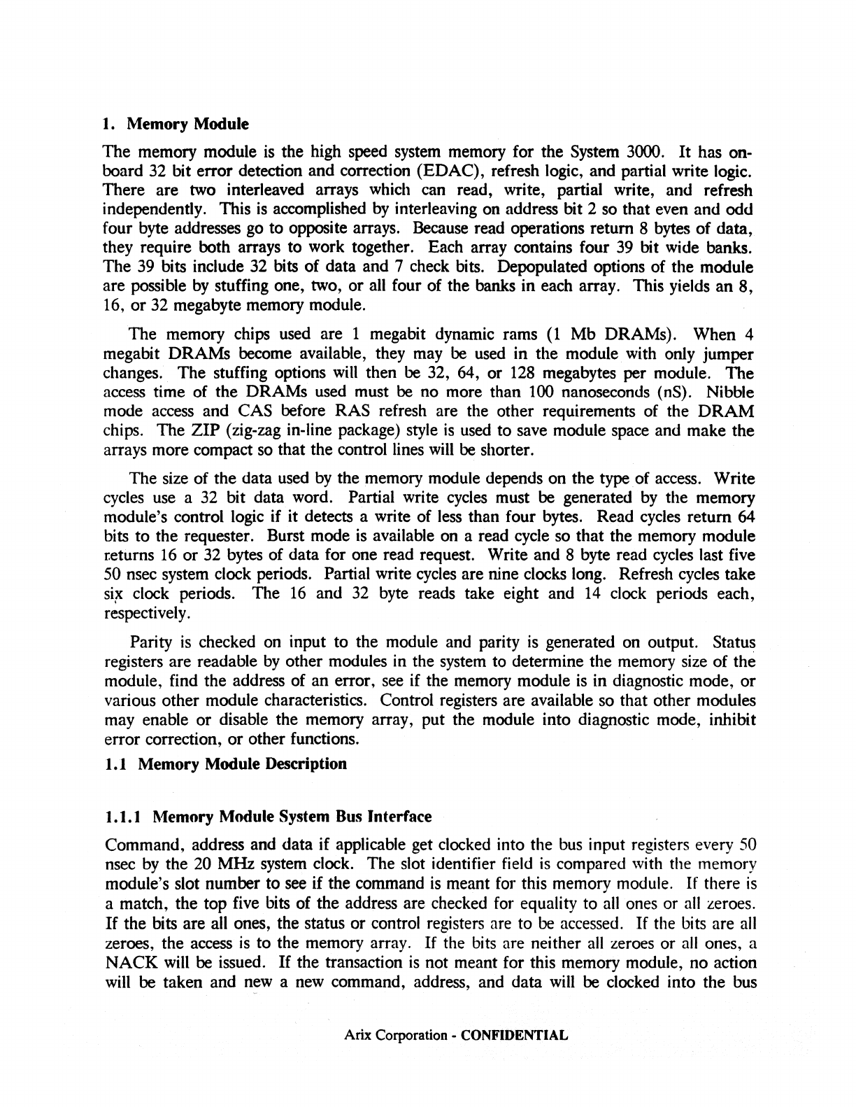
control signals as shown below:
11
10
ACTION
0 0
LOAD
A
0 1
LOADB
1 0
HOLD
1 1
NOTtlSED
The
A and B halves each have two registers,
Al
and A2. and
Bl
and
B2.
Each half
is
set
up like a
FIFO
with new data pushing the previous
Al
or Bl into A2 or
B2
and the data
in A2
or
B2
is
over written.
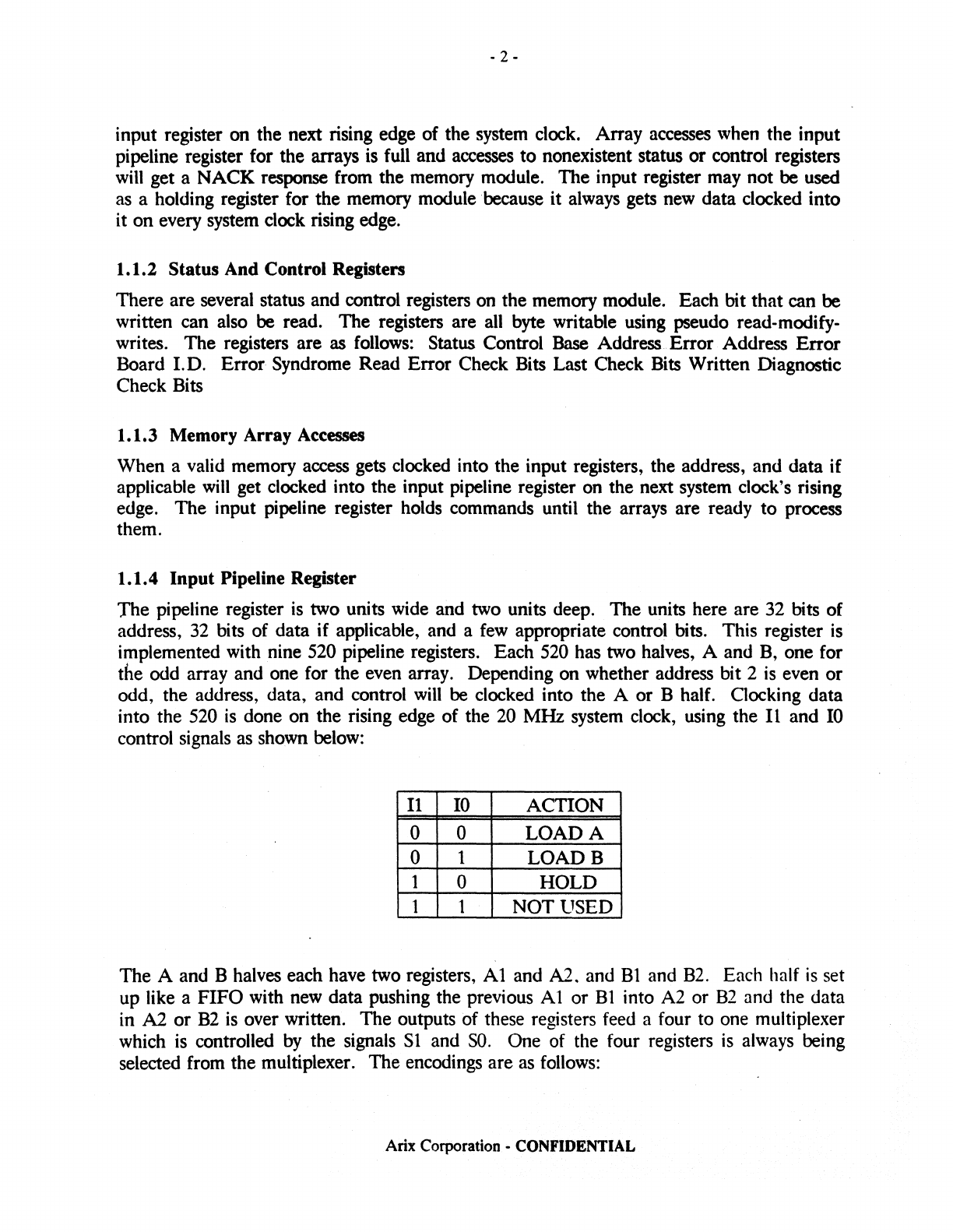
The
outputs of these registers feed a four to one multiplexer
which is controlled
by
the signals
SI
and
SO.
One of the four registers is always being
selected from the multiplexer.
The
encodings are as follows:
Arix Corporation -CONFIDENTIAL
- 3 -
51
SO
OUTPUT
0 0
B2
0 1
B1
1 0 A2
1 1
A1
The default, when no outputs are being used
is
00. To differentiate the default code from
the READ.B2 code, the control signal LATCH.B must
be
tested. The output enable of
the pipeline register
is
always active so that it
always
drives the bus.
t.
t.S
Input Pipeline Register Control
The input pipeline register
is
controlled
by
four PALs.
The
LOAD
PAL
generates the
10
and
It
signals
used
to steer input data to one, the
other, or neither halves of the register. Four signals, one for each register, are also
generated to tell if the register has any data presently
in
it. These signals are A1.FULL,
A2.FULL, B1.FULL, and B2.FULL. The
10
and
11
signals can also be called
LD.At
*
and LD.B1*, respectively. The two signals are mutually exclusive and when neither
is
active the register
is
in the HOLD state.
The
PRIO
PAL
continuously keeps a record of which register has the oldest data
in
it
and therefore has the highest priority.
The
QRD
PAL
keeps track of which registers contain read commands.
. The
READ
PAL
generates the
SO
and
51
signals
used
to select the correct register for
the pipeline register to output. Also generated are
LATCH.A
and LATCH.B, which
latch the input registers to the A and B arrays. The A register
is
enabled when the
pipeline register
is
outputting the
At
or A2 register and the B register
is
enabled when the
pipeline register
is
selecting the
B1
or
B2
register. Both A and B registers are enabled on
a read,
so
that the two arrays are synchronized for the read
cycle.
1. 1.6 Array Input Latches
The output of the pipeline registers feed the 74F373 array address and data latches. The
outputs of the data latches go directly to the DRAM chips data inputs. The outputs of the
array input address latches get multiplexed from twenty row and column address lines to
ten multiplexed address lines. Multiplexing
is
done with 74F241s.
by
connectinga row and
a corresponding column address to each input having complementary output enables with
their tri-state outputs tied together.
1.1.7 Array Organization
Each array contains four banks of dynamic RAM. The banks are
39
bits wide and 1
megabit deep. The
39
bits consist of
32
bits of data and 7 check bits. Depopulation of the
memory module
is
achieved
by
removing one, two, or three banks from each array. In
Arix Corporation -
CONFIDENTIAL
- 4 -
this way. two way interleaving
is
preserved with any stuffing option.
1.1.8 Array Control
Each of the two interleaved arrays has
five
control PALs for generating
DRAM
control
signals. The two arrays can therefore operate independently on
all
cycles
except a read.
The RASP
AL
generates RAS and CAS for each of the four banks in the array.
The MRGP
AL
generates the output enables for the array data input registers and the
632
data latches.
The
EDACPAL
generates the control signals for the
632
EDAC chip and the check
bit registers.
The WEP
AL
generates the write enable signals for each bank of the memory array
as
well
as
the array ready signal.
The CTLP
AL
contains a state counter and outputs signals to tell whether the
cycle
is
a
read, write, refresh, or partial write.
1.1.9 Array Outputs
The output of the DRAMs
in
the array feed a 74F244 whose outputs are shared with the
bidirectional data and check bit pins of a 74AS632 EDAC chip, the input of another
pipeline register used for output read data, the output of the array input data register, and
the input to the DRAM array .
.
1'.1.10 Output Pipeline Register
The pipeline register at the output of each array
is
organized
as
32
bits wide and four
deep. It
is
always used simultaneously with the output pipeline register of the other array.
This
is
because the smallest read unit
is
64
bits.
Control for this
64
bit wide register
is
handled
by
the OUTCTL PAL. Because of the
simple organization of this pipeline register only three signals are needed to control it. The
LOAD* signal outputs from the
PAL
and
COlUlects
to both the
10
and
11
inputs of the
520. When active, the registers are loaded like a FIFO, when inactive, the register
is
in
the hold state. The multiplexor signals,
SO
and
S1,
are used
as
in the input pipeline
register, except that they
always
start
at
00 and increment to output the number of 8 byte
words in the register.
1.1.11 Read Output
The output of the pipeline register goes into a 74F374 register for synchronization with the
system clock before being output through a 74F244 and onto the system
bus.
On
a read
cycle, the memory module makes a request one
clock
before it loads the last 8 bytes of
read data into the pipeline register. The
GRANT
from the arbiter goes to the J input of a
74FI09 J-K flip-flop whose output
is
the output enable for the 74F244 output drivers.
The K input of this 74F109, RD. DONE * , comes from the OUTCTL PAL, and becomes
Arix Corporation -
CONFIDENTIAL
- 5 -
active after the last read data bytes are clocked into the output register.
Inthi~
way, the
memory module drives the bus for 1, 2, or 4 bus clocks, depending on whether it
is
an 8,
16,
or
32 byte read.
The
clear of the 74F109
is
connected to the BOARD. DISABLE line.
With the 74FI09 always cleared, the memory module never drives the system bus.
If
the
GRANT
from the arbiter comes immediately, the data can be clocked into the data output
register during the same clock period that it
is
being driven onto the bus.
1.2 Cycle Descriptions
The
memory module supports six types of memory operations, including three different
types of read cycles. All the cycles consist of a certain number of states, numbered
SO,
S1,
S2, and so on. Each state
is
one system clock period, or 50 nsee. The cycles can be in any
sequence and may start immediately after the preceding cycle's last state. The types
of
cycles with brief descriptions are as follows.
1.2.1 Write Cycle
The write cycle
is
the late write type. This means that while writing, the data output of
the
DRAM
could
be
driving. This
is
acceptable because the tri-state drivers on the
outputs of the
DRAM
array are turned off. The write cycle lasts five clock periods and
will occur only if the
LENGTH
field does not equal one, two, or three bytes.
The
write cycle begins the assertion of RAS in state
S1.
CAS
is
asserted in
S2
and
WE
in
S3.
All three signals are de-asserted in
S4.
Write data and check bits are driven from
S1-1I2
until
S4-1I2.
The
signals
EDAC.Sl
and EDAC.SO are both inactive for the
duration of the cycle, putting the 74AS632
EOAC
chip in the generate mode.
The
check
bits generated are valid about halfway through
S2
.
.
1.2.2 Read Cycle
The normal read cycle returns 8 bytes of data to the requester. The
LENGTH
field
is
checked and must equal five (8 bytes) for this this type of read. Read cycles are different
from the other cycles in that S5, the last state in the cycle, can be the
SO
of a back to back
operation. This
is
because only the 74AS632
EDAC
chip and the output pipeline register
are busy during S5, and the array has already been precharged. Thus, even though the 8
byte read cycle uses five clock periods, it uses states
SO
through
S5
with
S5
as
a possible
overlap to the next cycle's
SO.
To
simplify burst mode reads, the read data
is
corrected
whether or not an error has been detected. Therefore, most of the time correct data is
being automatically corrected again. This procedure adds and extra clock period
to
the
read cycle but it is made up for in control logic simplification.
The
read cycle begins with
RAS
asserted
in
state
S1.
CAS
is
asserted
in
S2
and both
signals are de-asserted in S4. Read data
is
valid just before
S4.
The
EDAC
chip control
signals start with EOAC.S1 and EOAC.SO equal to zero. In
S2.
EOAC.S1
is
activated to
put
the
EOAC
chip into the detection mode. and EDAC.SO
is
activated
in
S4
for the
correction mode. The rising edge of EDAC.SO latches the read data from the DRAMs.
Both signals are deactivated after
S5.
The corrected data
is
driven
by
the 74AS632
EOAC
chip starting in
S5
and
is
valid about halfway through S5. The output pipeline register
Arix Corporation -CONFIDENTIAL
- 6 -
latches the corrected data on the next rising edge after
55.
1.2.3
16
Byte Read Cycle
The
16
byte read begins the same
as
a normal read
cycle,
but it does a nibble mode access
when the 8 byte read would have completed. This type of read lasts 8 clock periods. Like
the 8 byte read, the
16
byte read shares its last state with the following cycle, if it
is
back
to back. Again, even though the
16
byte read
cycle
uses
eight clock periods, it uses states
SO
through
S8,
with
SS
as
a possible overlap to the next cycle's
SO.
When the
cycle
is
a
read and the
LENGTH
field
is
six
(16
bytes), a
16
byte read
will
be
done.
The read
cycle
begins with RAS asserted in state St. CAS
is
asserted in
S2
and only
CAS
is
de-asserted in
S4.
Read data
is
valid just before
S4.
The EDAC chip control
signals start with EDAC.Sl and EDAC.SO equal to zero.
In
S2,
EDAC.Sl
is
activated to
put the EDAC chip into the detection mode, and EDAC.SO
is
activated in
S4
for the
correction mode. The rising edge of EDAC.SO latches the read data from the DRAMs.
EDAC.SO
is
deactivated after the rising edge of
S6.
The corrected data
is
driven by the
74AS632
EDAC
chip starting in
55
and
is
valid about halfway through
SS.
The output
pipeline register latches the corrected data on the rising edge of
S6.
The nibble mode
access
begins with CAS being asserted again
in
55.
Read data
is
valid just before
S7.
The
EDAC chip control signal EDAC.SO
is
activated in
S7
and its rising edge latches the read
data from the DRAMs. RAS and CAS are deactivated in
S7.
EDAC.SO and EDAC.Sl
are deactivated on the next rising edge after
SS.
The corrected data
is
driven by the
74AS632
EDAC
chip starting in
SS
and
is
valid about halfway through
SS.
The output
pipeline register latches the corrected data on the next rising edge after
SS.
1 :2.4 32 Byte Read Cycle
The
32
byte read begins the same
as
a normal read
cycle,
but it does three nibble mode
accesses when the 8 byte read would have completed. This read
cycle
takes
14
clock cycles
to complete. Like the 8 byte read, the
32
byte read shares its last state with the following
cycle, if it
is
back to back. Again, even though the
32
byte read
cycle
uses
14
clock
periods, it
uses
states
SO
through
S14
with
S14
as
a possible overlap to the next cycle's
SO.
When the
cycle
is
a read and the
LENGTH
field
is
seven (32 bytes), the 32 byte read
will
occur.
The read cycle begins with RAS asserted in state
S1.
CAS
is
asserted
in
S2
and only
CAS
is
de-asserted
in
S4.
Read data
is
valid just before
S4.
The EDAC chip control
signals start with EDAC.Sl and EDAC.SO equal to zero. In
S2.
EDAC.Sl
is
activated to
put the
EDAC
chip into the detection mode. and EDAC.SO
is
activated
in
S4
for the
correction mode. The rising edge of EDAC.SO latches the read data from the
DR~Ms.
EDAC.SO
is
deactivated after the rising edge of
S6.
The corrected data
is
driven
by
the
74AS632
EDAC
chip starting in
55
and
is
valid about halfway through
S5.
The output
pipeline register latches the corrected data
on
the rising edge of
S6.
The first nibble mode
access
begins with CAS being asserted again
in
S5.
Read data
is
valid just before
S7.
The
EDAC chip control signal EDAC.SO
is
activated
in
S7
and its rising edge latches the read
data from the DRAMs. CAS
is
deactivated in
S7
and EDAC.
SO
is
deactivated on the
Arix Corporation. CONFIDENTIAL
- 7 -
rising edge of
S9.
The corrected data
is
driven
by
the 74AS632 EDAC chip starting
in
S8
and
is
valid about halfway through
SB.
The output pipeline register latches the corrected
data on the rising edge
of
S9.
The second nibble mode
access
begins
with CAS being
asserted again
in
SB.
Read data
is
valid just before
SlO.
The EDAC chip control signal
EDAC.SO
is
activated in
SlO
and its rising edge latches the read data from the DRAMs.
CAS
is
deactivated
in
SlO
and EDAC.SO
is
deactivated on the rising edge of St2. The
corrected data
is
driven
by
the 74AS632 EDAC chip starting
in
Stl
and
is
valid about
halfway through
SB.
The output pipeline register latches the corrected data on the rising
edge of
S9.
The third nibble mode
access
begins
with CAS being asserted again
in
SIt.
Read data
is
valid just before
S13.
The EDAC chip control signal EDAC.SO
is
activated
in
S13
and its rising edge latches the read data from the DRAMs. RAS and CAS are
deactivated in
S13.
EDAC.SO and EDAC.Sl are deactivated on the next rising edge after
S14.
The corrected data
is
driven
by
the
74AS632
EDAC chip starting in
S14
and
is
valid
about halfway through
SB.
The output pipeline register latches the corrected data on the
next rising edge after
S14.
1.2.5 Partial Write Cycle
The partial write
cycle
is
like a four byte read followed
by
a write. When a write
command
is
clocked onto the memory module, the LENGTH field
is
checked to
determine if a partial write
will
be
needed.
If
the LENGTH
is
1,2, or 3, the lower two
address bits and the LENGTH field are used to generate byte selects for the bytes that
will
be
changed in the partial write
cycle.
The
new
data bytes are merged with corrected data
read from the location to form the
new
4 byte data word which
is
then written. The data
that
is
read
is
corrected whether or not there
is
an error, just like a read
cycle.
If
there
is
an uncorrectable error, the
cycle
continues, and the possibly incorrect data bytes are
written back into the location. The next read to this location
will
produce an
uncorrectable error
if
one of the bad bytes
was
rewritten. The partial write
cycle
lasts nine
clock periods.
The partial write
cycle
begins with RAS asserted in state St. CAS
is
asserted
in
S2
and
both signals are de-asserted in
SB.
Read data
is
valid just before
S4.
The EDAC chip
control signals start with EDAC.Sl and EDAC.SO equal to zero. In
S2,
EDAC.Sl
is
activated to put the EDAC chip into the detection mode, and EDAC.SO
is
activated
in
S4
for the correction mode. The rising edge
of
EDAC.SO latches the read data from the
DRAMs. EDAC.SO and EDAC.Sl are deactivated on the rising edge of
S6.
The
corrected data
is
latched
in
the output latches of the EDAC chip
by
the rising edge of
LEDBO, which occurs after the rising
edge
of
S6.
The data bytes that are not being
changed are then driven.
by
the 74AS632
in
S6,
and the
new
bytes to
be
written are driven
by
the array input latches. Check bits are generated
on
the merged data and
WE
strobes
for one clock period during
S7.
The various data output enables and LEDBO are turned
off in
S8,
preparing the array for another
cycle.
1.2.6 Refresh Cycle
The memory module
uses
CAS before RAS refresh to
save
address counter
logic
and extra
address
bus
drivers. In the CAS before RAS refresh mode, an internal counter in the
Arlx Corporation -CONFIDENTIAL
- 8 -
DRAM
increments with each refresh operation, insuring that
all
.512
rows
will
be
refreshed automatically without having to externally drive the address lines.
The
512 rows
need
to
be refreshed each 8 milliseconds (mS), so refresh cycles must occur every 15.625
microseconds (uS). A counter clocked
by
the 20 MHz system clock counts
to
312,
producing a refresh request every 15.6
uS.
The
refresh cycle
is
initiated
by
the refresh request, which
is
the latched carry output of
a counter.
If
the array is idle, the refresh cycle will start
on
the next rising edge of the
system clock.
If
there
is
another cycle
in
progress, the refresh cycle
will
not start until the
present cycle has completed.
If
there
is
a refresh request active while another cycle
is
going, the array will not activate the
READY
signal until after the refresh cycle to avoid
read synchronization problems. The refresh request gets cleared
by
S3
of the refresh cycle.
The refresh cycle
is
six clock periods long.
It
begins with the activation of CAS in
SI,
and then
RAS
is
asserted in
S2.
CAS
is
then de-asserted at S3, and
RAS
is
deactivated
during
S5.
The
array is ready to begin a new cycle after
S6.
1.3
Error
Handling
Single bit
or
uncorrectable errors may
be
detected on a read or a partial write. Single bit
errors are corrected and an interrupt
is
generated so that a
CPU
may keep track of
corrected errors.
The
CPU
that handles the interrupt may read the syndrome, which
points out the bit in error, the address that the error occurred at, and the slot Ld. of
the
module that was performing the read. Double bit errors will always be detected but can
not be corrected. Multiple bit errors may be detected but
will
not
be
corrected. Reading
tke error information kept for an error clears the registers that hold this information.
Information on additional errors which occur before these registers are cleared
is
lost, that
is"
no new error information will be latched until the old information
is
read.
Single bit errors
do
not affect the operation of a read or partial write cycle, because
data correction takes place automatically. On a read cycle, an uncorrectable error forces a
special message
to
be returned with the bad data. Although there
is
no interrupt
generated, the same error information
is
available as with a single bit error, except
that
the
syndrome now only states that a multiple bit error has occurred.
On
a partial write, the
data bytes are written even if there
is
an uncorrectable error.
It
is
possible to write bad
data back into the location. This will not be detected until the next read
to
this location,
when an uncorrectable error message will be generated if the bits in error were written
back. Single bit
or
uncorrectable errors
will
not cause a
16
byte or 32 byte read
to
abort
before completion and only the error information for the first error encountered will be
kept.
1.4 Diagnostics
Diagnostics
will
do
write and read tests with various patterns to find stuck data bits.
shorted data bits, stuck address bits. shorted address bits. and data bits shorted to address
bits. The address and the bit
in
error
will
be
provided to the diagnostic user. Partial
writes will also be used in place of writes to test the byte merging logic.
The
EDAC
operation
will
be tested to see if the 74AS632
EDAC
chip can generate correct check bits
on a write and partial write, detect single bit and multiple bit errors, correct single bit
Arix Corporation -CONFIDENTIAL
- 9 -
errors. generate an interrupt on a single bit error, and return an llncorrectable error
message on a multiple bit error. Read, write, and partial write loops
will
also be available
to the diagnostic user. All the control and status registers will be accessible and testable
by
the user.
Arix Corporation -CONFIDENTIAL
