TEK_VITS200 TEK VITS200
User Manual: TEK_VITS200
Open the PDF directly: View PDF ![]() .
.
Page Count: 290 [warning: Documents this large are best viewed by clicking the View PDF Link!]
- Instruction Manual
- Table of Contents
- List of Figures
- List of Tables
- General Safety Summary
- ServiceSafety Summary
- Getting Started
- Operating Basics
- Specifications
- Theory of Operation
- Performance Verification
- Adjustment Procedures
- Maintenance
- Replaceable Electrical Parts
- Diagrams/Circuit Board Illustrations
- Replaceable Mechanical Parts
- Index

Instruction Manual
VITS 200
NTSC VITS Inserter
070-8332-04
Warning
The servicing instructions are for use by qualified
personnel only. To avoid personal injury, do not
perform any servicing unless you are qualified to
do so. Refer to all safety summaries prior to
performing service.
Copyright © Tektronix, Inc. All rights reserved.
Tektronix products are covered by U.S. and foreign patents, issued and pending. Information in this publication supercedes
that in all previously published material. Specifications and price change privileges reserved.
Printed in the U.S.A.
Tektronix, Inc., P.O. Box 1000, Wilsonville, OR 97070–1000
TEKTRONIX and TEK are registered trademarks of Tektronix, Inc.
WARRANTY
Tektronix warrants that the products that it manufactures and sells will be free from defects in materials and
workmanship for a period of one (1) year from the date of shipment. If a product proves defective during this
warranty period, Tektronix, at its option, either will repair the defective product without charge for parts and labor,
or will provide a replacement in exchange for the defective product.
In order to obtain service under this warranty, Customer must notify Tektronix of the defect before the expiration
of the warranty period and make suitable arrangements for the performance of service. Customer shall be
responsible for packaging and shipping the defective product to the service center designated by Tektronix, with
shipping charges prepaid. Tektronix shall pay for the return of the product to Customer if the shipment is to a
location within the country in which the Tektronix service center is located. Customer shall be responsible for
paying all shipping charges, duties, taxes, and any other charges for products returned to any other locations.
This warranty shall not apply to any defect, failure or damage caused by improper use or improper or inadequate
maintenance and care. Tektronix shall not be obligated to furnish service under this warranty a) to repair damage
resulting from attempts by personnel other than Tektronix representatives to install, repair or service the product;
b) to repair damage resulting from improper use or connection to incompatible equipment; c) to repair any
damage or malfunction caused by the use of non-Tektronix supplies; or d) to service a product that has been
modified or integrated with other products when the effect of such modification or integration increases the time
or difficulty of servicing the product.
THIS WARRANTY IS GIVEN BY TEKTRONIX IN LIEU OF ANY OTHER WARRANTIES, EXPRESS
OR IMPLIED. TEKTRONIX AND ITS VENDORS DISCLAIM ANY IMPLIED WARRANTIES OF
MERCHANTABILITY OR FITNESS FOR A PARTICULAR PURPOSE. TEKTRONIX’
RESPONSIBILITY TO REPAIR OR REPLACE DEFECTIVE PRODUCTS IS THE SOLE AND
EXCLUSIVE REMEDY PROVIDED TO THE CUSTOMER FOR BREACH OF THIS WARRANTY.
TEKTRONIX AND ITS VENDORS WILL NOT BE LIABLE FOR ANY INDIRECT, SPECIAL,
INCIDENTAL, OR CONSEQUENTIAL DAMAGES IRRESPECTIVE OF WHETHER TEKTRONIX OR
THE VENDOR HAS ADVANCE NOTICE OF THE POSSIBILITY OF SUCH DAMAGES.
Contacting Tektronix
Product
Support For application-oriented questions about a Tektronix measure-
ment product, call toll free in North America:
1-800-TEK-WIDE (1-800-835-9433 ext. 2400)
6:00 a.m. – 5:00 p.m. Pacific time
Or contact us by e-mail:
tm_app_supp@tek.com
For product support outside of North America, contact your
local Tektronix distributor or sales office.
Service
Support Contact your local Tektronix distributor or sales office. Or visit
our web site for a listing of worldwide service locations.
www.tektronix.com
For other
information In North America:
1-800-TEK-WIDE (1-800-835-9433)
An operator will direct your call.
To write us Tektronix, Inc.
P.O. Box 1000
Wilsonville, OR 97070-1000

VITS 200 i
Table of Contents
List of Figures ii. . . . . . . . . . . . . . . . . . . . . . . . . . . . . . . . . . . . . . . . . . . . .
List of Tables iii. . . . . . . . . . . . . . . . . . . . . . . . . . . . . . . . . . . . . . . . . . . . . .
General Safety Summary v. . . . . . . . . . . . . . . . . . . . . . . . . . . . . . . . . . . .
Service Safety Summary vii. . . . . . . . . . . . . . . . . . . . . . . . . . . . . . . . . . . . .
Getting Started
Getting Started 1–1. . . . . . . . . . . . . . . . . . . . . . . . . . . . . . . . . . . . . . . . . . . .
Product Description 1–1. . . . . . . . . . . . . . . . . . . . . . . . . . . . . . . . . . . . . . . . . . . . . . .
Installation 1–4. . . . . . . . . . . . . . . . . . . . . . . . . . . . . . . . . . . . . . . . . . . . . . . . . . . . . .
Options 1–12. . . . . . . . . . . . . . . . . . . . . . . . . . . . . . . . . . . . . . . . . . . . . . . . . . . . . . . . .
Operating Basics
Operating Basics 2–1. . . . . . . . . . . . . . . . . . . . . . . . . . . . . . . . . . . . . . . . . . .
Front Panel 2–1. . . . . . . . . . . . . . . . . . . . . . . . . . . . . . . . . . . . . . . . . . . . . . . . . . . . . .
Remote Control 2–17. . . . . . . . . . . . . . . . . . . . . . . . . . . . . . . . . . . . . . . . . . . . . . . . . .
Video Clapboard 2–20. . . . . . . . . . . . . . . . . . . . . . . . . . . . . . . . . . . . . . . . . . . . . . . . . .
RS-232 Control 2–22. . . . . . . . . . . . . . . . . . . . . . . . . . . . . . . . . . . . . . . . . . . . . . . . . .
Rear Panel 2–35. . . . . . . . . . . . . . . . . . . . . . . . . . . . . . . . . . . . . . . . . . . . . . . . . . . . . .
Specifications
Specifications 3–1. . . . . . . . . . . . . . . . . . . . . . . . . . . . . . . . . . . . . . . . . . . . . .
Theory of Operation
Theory of Operation 4–1. . . . . . . . . . . . . . . . . . . . . . . . . . . . . . . . . . . . . . . .
Test Signal Generation 4–1. . . . . . . . . . . . . . . . . . . . . . . . . . . . . . . . . . . . . . . . . . . . .
Genlock 4–3. . . . . . . . . . . . . . . . . . . . . . . . . . . . . . . . . . . . . . . . . . . . . . . . . . . . . . . .
External Inputs 4–4. . . . . . . . . . . . . . . . . . . . . . . . . . . . . . . . . . . . . . . . . . . . . . . . . . .
Signal and Switching Control 4–5. . . . . . . . . . . . . . . . . . . . . . . . . . . . . . . . . . . . . . .
Character and Source ID Generation 4–7. . . . . . . . . . . . . . . . . . . . . . . . . . . . . . . . . .
Front Panel, Remote Controls, and Controller 4–9. . . . . . . . . . . . . . . . . . . . . . . . . . .
Power Supply Overview 4–12. . . . . . . . . . . . . . . . . . . . . . . . . . . . . . . . . . . . . . . . . . .
Power Supply Detailed Description 4–13. . . . . . . . . . . . . . . . . . . . . . . . . . . . . . . . . . .
Performance Verification
Performance Verification 5–1. . . . . . . . . . . . . . . . . . . . . . . . . . . . . . . . . . . .
Recommended Equipment List 5–1. . . . . . . . . . . . . . . . . . . . . . . . . . . . . . . . . . . . . .
Calibration Data Report 5–3. . . . . . . . . . . . . . . . . . . . . . . . . . . . . . . . . . . . . . . . . . . .
Verification Procedure 5–7. . . . . . . . . . . . . . . . . . . . . . . . . . . . . . . . . . . . . . . . . . . . .
Adjustment Procedures
Adjustment Procedures 6–1. . . . . . . . . . . . . . . . . . . . . . . . . . . . . . . . . . . . . .
Recommended Equipment List 6–1. . . . . . . . . . . . . . . . . . . . . . . . . . . . . . . . . . . . . .

Contents
ii VITS 200
Calibration Procedure 6–3. . . . . . . . . . . . . . . . . . . . . . . . . . . . . . . . . . . . . . . . . . . . . .
Maintenance
Maintenance 7–1. . . . . . . . . . . . . . . . . . . . . . . . . . . . . . . . . . . . . . . . . . . . . . .
Preventive Maintenance 7–1. . . . . . . . . . . . . . . . . . . . . . . . . . . . . . . . . . . . . . . . . . . .
Troubleshooting Aids 7–2. . . . . . . . . . . . . . . . . . . . . . . . . . . . . . . . . . . . . . . . . . . . . .
Diagnostics 7–4. . . . . . . . . . . . . . . . . . . . . . . . . . . . . . . . . . . . . . . . . . . . . . . . . . . . . .
Corrective Maintenance 7–6. . . . . . . . . . . . . . . . . . . . . . . . . . . . . . . . . . . . . . . . . . . .
Test Selectable Parts 7–8. . . . . . . . . . . . . . . . . . . . . . . . . . . . . . . . . . . . . . . . . . . . . . .
Replaceable Electrical Parts List
Replaceable Electrical Parts List 8–1. . . . . . . . . . . . . . . . . . . . . . . . . . . . . .
Schematics
Schematics/Circuit Board Illustrations 9–1. . . . . . . . . . . . . . . . . . . . . . . . .
Replaceable Mechanical Parts List
Replaceable Mechanical Parts List 10–1. . . . . . . . . . . . . . . . . . . . . . . . . . . .
Index
List of Figures
Figure 1–2: Rail Detail for Mounting Slide Tracks 1–8. . . . . . . . . . . . . . .
Figure 1–3: Assembly of Rack Mounting Hardware 1–9. . . . . . . . . . . . . .
Figure 1–4: Mounting Stationary Track Sections (Front Rail Mount) 1–10
Figure 1–5: Mounting Stationary Track Sections (Deep Rack Mount) 1–10
Figure 1–6: Mounting Stationary Track
Sections (Shallow Rack Mount) 1–11. . . . . . . . . . . . . . . . . . . . . . .
Figure 1–7: Racking and Unracking the VITS 200 1–12. . . . . . . . . . . . . . .
Figure 2–1: VITS 200 Front Panel 2–1. . . . . . . . . . . . . . . . . . . . . . . . . . . . .
Figure 2–2: VITS 200 Menu Structure 2–5. . . . . . . . . . . . . . . . . . . . . . . . .
Figure 2–3: Remote Control Connector 2–17. . . . . . . . . . . . . . . . . . . . . . . .
Figure 2–4: Video Clapboard Connections 2–21. . . . . . . . . . . . . . . . . . . . . .
Figure 2–5: Controlling the VITS 200 with a VM700A. 2–22. . . . . . . . . . .
Figure 2–6: VITS 200 Rear Panel. 2–35. . . . . . . . . . . . . . . . . . . . . . . . . . . . .
Figure 3–1: 0% Black 3–8. . . . . . . . . . . . . . . . . . . . . . . . . . . . . . . . . . . . . . .
Figure 3–2: 7.5% Black 3–8. . . . . . . . . . . . . . . . . . . . . . . . . . . . . . . . . . . . . .
Figure 3–3: 10 MHz Sweep 3–8. . . . . . . . . . . . . . . . . . . . . . . . . . . . . . . . . . .

Contents
VITS 200 iii
Figure 3–4: NTC7 Combination 3–9. . . . . . . . . . . . . . . . . . . . . . . . . . . . . . .
Figure 3–5: FCC Composite 3–9. . . . . . . . . . . . . . . . . . . . . . . . . . . . . . . . . .
Figure 3–6: NTC7 Composite 3–9. . . . . . . . . . . . . . . . . . . . . . . . . . . . . . . . .
Figure 3–7: FCC Multiburst 3–10. . . . . . . . . . . . . . . . . . . . . . . . . . . . . . . . . .
Figure 3–8: 50% Gray 3–10. . . . . . . . . . . . . . . . . . . . . . . . . . . . . . . . . . . . . . .
Figure 3–9: SIN X/X 3–10. . . . . . . . . . . . . . . . . . . . . . . . . . . . . . . . . . . . . . . .
Figure 3–10: FCC Color Bars 3–11. . . . . . . . . . . . . . . . . . . . . . . . . . . . . . . .
Figure 3–11: Multipulse 3–11. . . . . . . . . . . . . . . . . . . . . . . . . . . . . . . . . . . . .
Figure 3–12: VIRS 3–12. . . . . . . . . . . . . . . . . . . . . . . . . . . . . . . . . . . . . . . . . .
Figure 3–13: Red Field 3–12. . . . . . . . . . . . . . . . . . . . . . . . . . . . . . . . . . . . . .
Figure 3–14: BTA Ghost Canceller Reference 3–12. . . . . . . . . . . . . . . . . . .
Figure 3–15: Phillips GCR Positive 3–13. . . . . . . . . . . . . . . . . . . . . . . . . . . .
Figure 3–16: Phillips GCR Negative 3–13. . . . . . . . . . . . . . . . . . . . . . . . . . .
Figure 3–17: Korean GCR Positive 3–14. . . . . . . . . . . . . . . . . . . . . . . . . . . .
Figure 3–18: Korean GCR Negative 3–14. . . . . . . . . . . . . . . . . . . . . . . . . . .
Figure 3–19: Cable Multiburst 3–15. . . . . . . . . . . . . . . . . . . . . . . . . . . . . . . .
Figure 3–20: Cable Sweep 3–15. . . . . . . . . . . . . . . . . . . . . . . . . . . . . . . . . . . .
Figure 4–1: Remote Control Connector Pinout. 4–10. . . . . . . . . . . . . . . . . .
Figure 4–2: Basic Operation of T1 4–15. . . . . . . . . . . . . . . . . . . . . . . . . . . . .
Figure 5–1: VM700A Horizontal Timing Measurement Display 5–21. . . .
Figure 7–1: Using the Foldout Pages 7–2. . . . . . . . . . . . . . . . . . . . . . . . . . .
Figure 7–2: Circuit Board Assembly Locations. 7–3. . . . . . . . . . . . . . . . .
List of Tables
Table 1–1: Inserter Board (A1) Operating Mode
Selection Jumpers (Green) 1–5. . . . . . . . . . . . . . . . . . . . . . . . . .
Table 1–2: Controller Board (A3) Operating Mode
Selection Jumpers (Green) 1–5. . . . . . . . . . . . . . . . . . . . . . . . . .
Table 1–3: Inserter Board (A1) Test Jumpers (Red) 1–6. . . . . . . . . . . . . .
Table 1–4: Controller Board (A3) Test Jumpers (Red) 1–7. . . . . . . . . . . .
Table 2–1: Character List for the VITS 200 2–10. . . . . . . . . . . . . . . . . . . .
Table 2–2: Factory VITS assignments for Std and Opt 1C 2–14. . . . . . . .
Table 2–3: Factory VITS assignments for Opt 1J 2–14. . . . . . . . . . . . . . . .

Contents
iv VITS 200
Table 2–4: Binary Standby Message Select 2–19. . . . . . . . . . . . . . . . . . . . .
Table 2–5: Binary VBI Message Select 2–20. . . . . . . . . . . . . . . . . . . . . . . . .
Table 2–6: RS-232 Connector Pin Functions – 25-Pin Serial Ports 2–24. .
Table 2–7: 9-Pin to 25-Pin Adaptor Connections for RS-232 2–24. . . . . .
Table 2–8: SCPI Commands (4.1.1 and 4.2.1) 2–32. . . . . . . . . . . . . . . . . . .
Table 2–9: Defined RS-232 Commands for use with the VITS 200 2–33. .
Table 2–10: RS-232 Mnemonics 2–35. . . . . . . . . . . . . . . . . . . . . . . . . . . . . .
Table 3–1: Program Channel 3–1. . . . . . . . . . . . . . . . . . . . . . . . . . . . . . . . .
Table 3–2: External Inputs 3–2. . . . . . . . . . . . . . . . . . . . . . . . . . . . . . . . . .
Table 3–3: Test Signal and Black Burst General Characteristics 3–3. . .
Table 3–4: Test Signal Characteristics 3–4. . . . . . . . . . . . . . . . . . . . . . . . .
Table 3–5: Genlock Characteristics 3–16. . . . . . . . . . . . . . . . . . . . . . . . . . .
Table 3–6: Power Supply Characteristics 3–16. . . . . . . . . . . . . . . . . . . . . .
Table 3–7: Physical Characteristics 3–17. . . . . . . . . . . . . . . . . . . . . . . . . . .
Table 3–8: Environmental Characteristics 3–18. . . . . . . . . . . . . . . . . . . . . .
Table 3–9: Certifications and compliances 3–18. . . . . . . . . . . . . . . . . . . . . .
Table 6–1: Power Supply Characteristics 6–3. . . . . . . . . . . . . . . . . . . . . .
Table 7–1: Inserter Board Diagnostics 7–5. . . . . . . . . . . . . . . . . . . . . . . . .
Table 7–2: Torque Specifications 7–6. . . . . . . . . . . . . . . . . . . . . . . . . . . . . .
Table 7–3: Test Selectable Parts 7–8. . . . . . . . . . . . . . . . . . . . . . . . . . . . . .

VITS 200 v
General Safety Summary
Review the following safety precautions to avoid injury and prevent damage to
this product or any products connected to it. To avoid potential hazards, use this
product only as specified.
Only qualified personnel should perform service procedures.
Use Proper Power Cord. Use only the power cord specified for this product and
certified for the country of use.
Connect and Disconnect Properly. Do not connect or disconnect probes or test
leads while they are connected to a voltage source.
Ground the Product. This product is grounded through the grounding conductor
of the power cord. To avoid electric shock, the grounding conductor must be
connected to earth ground. Before making connections to the input or output
terminals of the product, ensure that the product is properly grounded.
Observe All Terminal Ratings. To avoid fire or shock hazard, observe all ratings
and markings on the product. Consult the product manual for further ratings
information before making connections to the product.
Do not apply a potential to any terminal, including the common terminal, that
exceeds the maximum rating of that terminal.
Do Not Operate Without Covers. Do not operate this product with covers or panels
removed.
Use Proper Fuse. Use only the fuse type and rating specified for this product.
Avoid Exposed Circuitry. Do not touch exposed connections and components
when power is present.
Wear Eye Protection. Wear eye protection if exposure to high-intensity rays or
laser radiation exists.
Do Not Operate With Suspected Failures. If you suspect there is damage to this
product, have it inspected by qualified service personnel.
Do Not Operate in Wet/Damp Conditions.
Do Not Operate in an Explosive Atmosphere.
Keep Product Surfaces Clean and Dry.
Provide Proper Ventilation. Refer to the manual’s installation instructions for
details on installing the product so it has proper ventilation.
To Avoid Fire or
Personal Injury
General Safety Summary
vi VITS 200
Terms in this Manual. These terms may appear in this manual:
WARNING. Warning statements identify conditions or practices that could result
in injury or loss of life.
CAUTION. Caution statements identify conditions or practices that could result in
damage to this product or other property.
Terms on the Product. These terms may appear on the product:
DANGER indicates an injury hazard immediately accessible as you read the
marking.
WARNING indicates an injury hazard not immediately accessible as you read the
marking.
CAUTION indicates a hazard to property including the product.
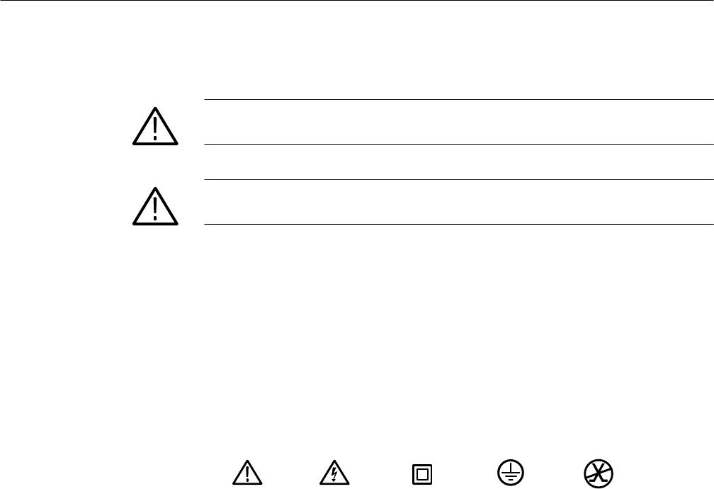
Symbols on the Product. The following symbols may appear on the product:
CAUTION
Refer to Manual WARNING
High Voltage Double
Insulated Protective Ground
(Earth) Terminal Not suitable for
connection to
the public telecom-
munications network
Symbols and Terms

VITS 200 vii
Service Safety Summary
Only qualified personnel should perform service procedures. Read this Service
Safety Summary and the General Safety Summary before performing any service
procedures.
Do Not Service Alone. Do not perform internal service or adjustments of this
product unless another person capable of rendering first aid and resuscitation is
present.
Disconnect Power. To avoid electric shock, switch off the instrument power, then
disconnect the power cord from the mains power.
Use Care When Servicing With Power On. Dangerous voltages or currents may
exist in this product. Disconnect power, remove battery (if applicable), and
disconnect test leads before removing protective panels, soldering, or replacing
components.
To avoid electric shock, do not touch exposed connections.

Service Safety Summary
viii VITS 200

Getting Started

VITS 200 1–1
Getting Started
Product Description
The TEKTRONIX VITS 200 NTSC VITS INSERTER is a high quality signal
generator designed for VITS and data insertion into the program signal. It
provides three different modes of standby operation in the event of program line
failure. The VITS 200 provides a complement of digitally generated test signals,
all of which may be inserted as VITS. There is a one-line source identification
code (recognizable by the VM700A) which may also be inserted in the vertical
interval. There are also four external inputs which will accept other signals or
data to insert in the vertical interval.
The VITS 200 also provides internally-generated text. Up to 15 one-line
messages may be programmed into memory, for insertion into the vertical
interval, and three pages of standby messages can be programmed into memory
for use in standby operation. Control of both the vertical interval text and
standby text is provided through the remote control, as well as the front panel.
All of the operating mode, VITS assignment, and text selections are stored in
nonvolatile memory in case of power line failure.
The VITS 200 uses 12-bit data at an 8 FSC data rate to ensure accurate test signal
generation. These test signals may be used as VIT signals, and may be
programmed to be output as the full field signal if the Program Input should fail.
The test signals are also available at the TEST SIGNAL output on the rear panel.
The signal available at this output may be selected independently of the VIT or
Program Failure signals, except when the VITS 200 is in Standby mode
operation. It then reverts to the selected standby signal. The test signals
generated by the VITS 200 include:
H10 MHz Sweep
HNTC7 Combination
HNTC7 Composite
HFCC Multiburst
H50% Gray
HSIN X / X
HFCC Color Bars
HFCC Composite
HMultipulse
Test Signal Generator

Getting Started
1–2 VITS 200
HVertical Interval Reference Signal (VIRS)
HRed Field
H0 IRE Flat Field (0% Black)
H7.5% Black
For instruments with S/N B020249 and above:
HFCC Composite 20 IRE (Std, Opt 1C only)
HCBC Composite 15°–360° (Opt 1C only)
HBTA Ghost Cancellation Reference (Opt 1J)
HPhillips Ghost Cancellation Reference (Std and Opt 1C)
When called as a full field test signal, only the GCR Positive will be used.
HKorean Ghost Cancellation Reference (Opt 1K)
The VITS 200 may be programmed to insert any internally-generated signal,
external input, or the source identification. These may be inserted on lines 10
through 23 or on lines 17 through 30. VITS can be programmed on even and
odd fields or in a four-field sequence. The VITS 200 may be genlocked to either
the Program signal or the EXTERNAL 1 input. If you like, you can program the
same signal or external input to be inserted on more than one line. This may be
useful in insertion of external data signals, such as Teletext.
Four external inputs are provided for inserting externally-generated test and data
signals. These inputs may be either AC-coupled and clamped, or DC-coupled.
See the Operating Basics section for details of how to change the external input
coupling. The VITS 200 confirms that the inputs are synchronous with the
program signal before allowing it to be inserted in the vertical interval.
When the AUTO VIRS function is selected, the VITS 200 will check the
specified line(s) and field(s) for a VIRS signal on the incoming Program Video.
If VIRS is detected as being present in the proper location, the signal is passed
with no processing. However, if VIRS is not detected on the specified line(s)
and field(s), then the internally-generated VIRS signal will be inserted on them.
The AUTO CAPT function sets the VITS 200 to examine specified line(s) and
field(s) for close-captioned text. This consists of checking the specified line(s)
and field(s) of the incoming program video for any activity greater than 285 mV.
If there is activity above this level, it is passed with no processing. If there is no
activity at this level, then the selected External Input is inserted onto the line.
For example, Auto Capt 1 would insert the signal applied to the EXT 1 input
onto the specified line(s) and field(s) as close-captioned text.
Insert/Delete Functions
Automatic VIRS Detection
Automatic Closed
Captioning Detection

Getting Started
VITS 200 1–3
Maintaining program channel continuity is one of the main considerations in the
VITS 200. Depending on its programming, the VITS 200 provides agile
response to different types of signal or equipment failure. Bypass mode switches
the PROGRAM INput to the PROGRAM OUTPUT, with a delay built into the
path so it matches the Program Channel path. Standby mode allows a page of
text, an internal signal, or an external signal to be applied to the PROGRAM
OUTPUT.
If the power to the VITS 200 fails, the VITS 200 switches to Bypass mode
immediately. The VITS 200 may be programmed to attempt to genlock to the
EXTERNAL 1 input if no video is present at the PROGRAM INput. If video is
present but the VITS 200 cannot genlock to it (non-timebase corrected video, for
example), then the program is passed with no VITS inserted. If there is no video
present, the VITS 200 may be programmed to provide any of the following
responses after a user-adjustable delay:
HSwitch to Relay Bypass (Standby disabled).
HPass the Program channel (no relay bypass).
HSwitch to one of the four external inputs.
HSwitch to an internally-generated test signal, with or without a full page
standby message.
The VITS 200 passes program video through as soon as it is present, and begins
insertion of VITS as soon as it is genlocked.
The VITS 200 can also insert reconstructed sync and burst into the program
signal, in order to ensure the proper amplitude relationships between the inserted
VITS and sync & burst. This does not affect active video to blanking interval
timing. If the program signal is monochrome, the VITS 200 will insert
regenerated sync only.
The VITS 200 includes a text generator which produces a complete set of
alphabetical and numerical characters, along with a selection of special symbols.
Each character is a 32x32 pixel array.
As many as 15 one-line text messages can be programmed into memory. Any
one of these messages may be inserted on lines 10 through 16, or the VITS 200
can be programmed to scroll through any consecutive series of these 15
messages. Test signals or External inputs can also be programmed on lines 10
through 16, and these always take priority over characters.
Up to three full pages of text may be programmed into memory. A page is
defined as a maximum of 13 20-character lines. Any one of the three pages may
be selected if a test signal is chosen as the Standby mode.
Program Channel
Text Generator

Getting Started
1–4 VITS 200
The VITS 200 provides a one-line 16-bit source identification code, providing
16,384 possible codes plus start and stop bits. DIP switches, accessible through
the rear panel, provide quick and easy control of each bit’s state. This ID signal
may be placed on any of the available lines in vertical blanking. The VM700A
Video Measurement Set utilizes this signal in it’s displays and print-outs, to
identify the source of the signal being measured.
Remote control of many of the VITS 200 functions is available through the
rear-panel REMOTE CONTROL connector, a 25-pin ground closure system, and
through the RS-232 connector. Both provide manual switching between Bypass
and Operate modes, page selection and on/off control of the full-page standby
text, message selection and on/off control of the vertical interval text, and full
field test signal selection.
The REMOTE CONTROL connector also drives four indicator lights on the
remote control: Bypass, Genlock, Power and Remote Enable. The ground
closure remote control, however, is not capable of programming the text
messages for the standby pages or the vertical interval text.
Controlling the VITS 200 through the RS-232 port provides full front-panel
control capability, and makes programming and controlling text messages
extremely easy.
Beginning with S/N B020249, the VITS 200 includes a Video Clapboard
function for synchronizing the audio and video path delays in the studio. This
requires the use of an ASG 100 that has been modified for video clapboard
operation. See Section 3 for details.
Installation
At installation time, save the shipping carton and packaging materials for
repackaging in case reshipment becomes necessary.
The following tables give information about circuit board jumpers for the entire
instrument. The ▼ symbol on a circuit board identifies pin 1. Green jumpers are
used to select operating modes; red jumpers are used for testing the instrument.
WARNING. These jumpers are located inside the instrument. Make sure to switch
off the instrument power and unplug the power cord before removing the
instruments top cover. The red jumpers should only be accessed by qualified
service personnel.
Source Identification
Remote Control
Video Clapboard
Packaging
Instrument Configuration

Getting Started
VITS 200 1–5
Table 1–1: Inserter Board (A1) Operating Mode Selection Jumpers (Green)
Function Jumper # Description Factory Setting
Sound-in-sync mode J9
<5> Pins 1–2: No sound-in-sync on PROGRAM IN.
Pins 2–3: Sound-in-sync on PROGRAM IN (blocks
sound-in-sync pulses from the Genlock circuit).
Pins 1–2
Line Select Mode J22
<3> Pins 1–2:Front panel selection of lines 10 through 21 or
lines 17 through 30.
Pins 2–3: Lines 10 through 21 available for VITS.
No Plug: Lines 17 through 30 available for VITS.
Pins 1–2
Bypass Lockout J28
<3> Pins 1–2: Front panel BYPASS button enabled.
Pins 2–3: Front panel BYPASS button disabled.
Pins 1–2
Table 1–2: Controller Board (A3) Operating Mode Selection Jumpers (Green)
Function Jumper # Description Factory Setting
Front Panel Lockout J8
<3> Pins 1–2: Front panel enabled.
Pins 2–3: Front Panel disabled.
Pins 1–2
External 1 Clamp Mode J19
<1> Pins 1–2: Clamp timing derived from External 1 Input.
Pins 2–3: Clamp timing derived from VITS 200 Genlock
(locked to Program Video or free-running).
Pins 1–2
External 2 Clamp Mode J20
<1> Pins 1–2: Clamp timing derived from External 2 Input.
Pins 2–3: Clamp timing derived from VITS 200 Genlock
(locked to Program Video or free-running).
Pins 1–2
External 3 Clamp Mode J21
<2> Pins 1–2: Clamp timing derived from External 3 Input.
Pins 2–3: Clamp timing derived from VITS 200 Genlock
(locked to Program Video or free-running).
Pins 1–2
External 4 Clamp Mode J22
<2> Pins 1–2: Clamp timing derived from External 4 Input.
Pins 2–3: Clamp timing derived from VITS 200 Genlock
(locked to Program Video or free-running).
Pins 1–2
Never Used J49
<5> Never used. Removed at B020249. Pins 1–2

Getting Started
1–6 VITS 200
Table 1–3: Inserter Board (A1) Test Jumpers (Red)
Function Jumper # Description Factory Setting
Genlock Processor Reset J5
<4> Pins 1–2: Reset controlled by hardware watchdog.
Pins 2–3: Holds processor in reset mode.
No Plug: No hardware resets.
Pins 1–2
Hardware Watchdog Reset J6
<4> Pins 1–2: No Reset.
Pins 2–3: Hold in Reset mode.
Pins 1–2
VCO Control J12
<6> Pins 1–2: VCO Control loop closed.
Pins 2–3:VCO Control voltage set to ground, to set VCO
center frequency.
Pins 1–2
Oven Control J13
<6> Pins 1–2: Oscillator oven on.
Pins 2–3: Oscillator oven off.
Pins 1–2
Housekeeping Supply J17
<8> Pins 1–2: Housekeeping supply enabled.
No Plug: Housekeeping supply disabled.
Pins 1–2
Transformer Enable J18
<8> Pins 1–2: Connects power to transformer.
No Plug: Disables Power Supply.
Pins 1–2
Overcurrent Shutdown J19
<8> Pins 1–2: Shutdown enabled
No Plug: Shutdown disabled
Pins 1–2
Power Supply Disconnect
(Jumper Off = Disconnect) J20
<9> Pins Supply
1–2 +12V
3–4 –12V
5–6, 7–8 +5V
9–10, 11–12 –5V
13–14, 15–16 GND (No Jumpers)
ON
ON
ON
ON
OFF
Clock Disable 1J32 Pins 1–2: DAC Clock Enabled
Pins 2–3 DAC Clock Disabled
Pins 1–2
Character Set Up Control 1J33 Pins 1–2: 7.5% Character Set-Up (Std, Opt 1C)
Pins 2–3: 0% Character Set-Up (Opt 1J)
Pins 1–2
Memory Bank Select 1J54 Pins 1–2:Std and Opt 1C signals
Pins 2–3: Opt 1J signals
Pins 1–2
V Drive 1J55 Pins 1–2: Normal operation
Pins 2–3: Not used (VITS 100 ONLY)
Pins 1–2
V Sync 1J56 Pins 1–2: Normal operation
Pins 2–3: Not used (VITS 100 ONLY)
Pins 1–2
Blanking 1J57 Pins 1–2: Normal operation
Pins 2–3: Not used (VITS 100 ONLY)
Pins 1–2
1 B020249 and above.

Getting Started
VITS 200 1–7
Table 1–4: Controller Board (A3) Test Jumpers (Red)
Function Jumper # Description Factory Setting
Controller Reset J6
<3> Pins 1–2: Reset controlled by hardware watchdog.
Pins 2–3: Controller held in reset mode.
No Plug: No hardware resets.
Pins 1–2
Controller PROM Size
(Removed B020249) J7
<3> Pins 1–2: 27C010 or 27C512.
Pins 2–3: 27C512 or 27C256.
Pins 2–3
Display Test* J14
<5> Pins 1–2: Normal Operation.
Pins 2–3: Display Test.
Black Burst Setup
(B020249 & up) J57 Pins 1–2: 7.5% Setup
Pins 2–3:0% Setup (Opt 1J only)
Pins 1–2
*Power must be cycled off and on after moving jumper.
The power supply in this instrument operates over a line frequency range of 48
to 62 Hz and a voltage range of 90 to 250 Vac. See Table 3–6, page 3–16, for
more information about the power supply characteristics. No changes to the
instrument are necessary to operate on either voltage range.
The VITS 200 is shipped with hardware for rackmounting. The instrument fits
in a standard 19-inch rack. Spacing between the front rails of the rack must be at
least 17–3/4 inches to allow clearance for the slide-out tracks.
Rack slides conveniently mount in any rack that has a front-to-rear rail spacing
between 15–1/2 and 28 inches. Six inches of clearance between the instrument’s
rear panel and any rear cabinet panel is required for connector space and to
provide adequate air circulation.
Rack Mounting
Locate the proper rack holes as shown in Fig. 1–1. Notice that the hole spacing
varies with the type of rack. When installing the slides in EIA-type racks, make
certain that the slides are attached to the 1/2 inch-spaced holes.
Mount the rails using enclosed hardware as shown in Fig. 1–2. Figures 1–3
through 1–5 show the rail mounting details for both deep and shallow racks.
Make sure the stationary sections are horizontally aligned and are level and
parallel.
Electrical Installation
Mechanical Installation
Getting Started
1–8 VITS 200
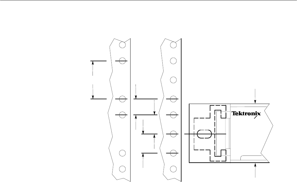
1.734”
1.250” 0.500”
0.625”
0.625”
(left front)
MIL STD 189
SPACING “UNIVERSAL” SPACING
EIA RS310, RETMA
VITS 200
NTSC VITS INSERTER
Figure 1–1: Rail Detail for Mounting Slide Tracks
Getting Started
VITS 200 1–9
CHASSIS SECTION
AUTOMATIC
LATCHES
STATIONARY
SECTION
10–32 PHS
SCREW
10–32 PHS
SCREW
FLAT
NUT
BARS
FLAT NUT BAR
INTERMEDIATE
SECTION
STOP LATCH
HOLE
REAR
MOUNTING
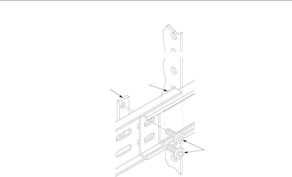
NOTE: Right-hand and left-hand stationary section is designated by the
RH and the LH marked on the rails. Stop latch holes should be towards
the bottom when slides are in place. (The right-hand rail is shown above.)
Figure 1–2: Assembly of Rack Mounting Hardware
Getting Started
1–10 VITS 200
BAR NUT
(Use if the front rail
is not tapped)
Figure 1–3: Mounting Stationary Track Sections (Front Rail Mount)
BAR NUT
REAR RACK RAIL
PNH
SCREWS
Figure 1–4: Mounting Stationary Track Sections (Deep Rack Mount)
Getting Started
VITS 200 1–11
REAR RACK RAIL
PNH
SCREWS
BAR NUT
FLUSH WITH
REAR RACK
RAIL
Figure 1–5: Mounting Stationary Track Sections (Shallow Rack Mount).
Installing the Instrument
Install the instrument in the rack, as shown in Fig. 1–6.
Rack Adjustments
After installation, the slide tracks may bind if they are not properly adjusted. To
adjust the tracks, slide the instrument out about 10 inches, slightly loosen the
screws holding the tracks to the front rails, and allow the tracks to seek an
unbound position. Retighten the screws and check the tracks for smooth
operation by sliding the instrument in and out of the rack several times.
Once the instrument is in place within the rack, tighten the knurled retaining
screw to fasten it securely into the rack.
Getting Started
1–12 VITS 200
TO INSTALL:
1. Pull the slide-out track section to the fully
extended position.
2. Insert the instrument chassis sections into the
slide-out sections.
3. Press the stop latches and push the instrument
toward the rack until the latches snap into their
holes.
4. Again press the stop latches and push the
instrument fully into the rack.
5. Tighten the front-panel retaining screws.
TO REMOVE:
1. Loosen retaining screw and pull instrument
outward until the stop latches snap into the holes.
2. Press stop latches and remove instrument.
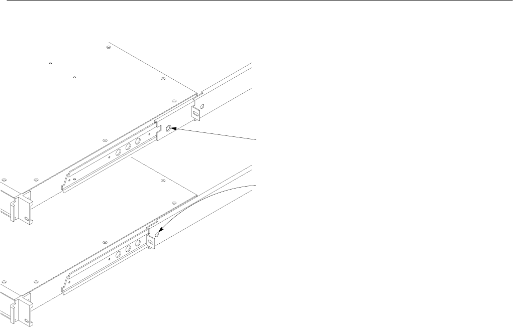
Figure 1–6: Racking and Unracking the VITS 200
Rack Slide Maintenance
The slide-out tracks do not require lubrication. The dark gray finish on the
tracks is a permanent, lubricated coating.
To completely remove the instrument, press both release-latch buttons (visible in
the stop-latch holes) and carefully slide the instrument free from the tracks. Be
sure that all cabling is disconnected before removing the instrument.
Options
This section explains the instrument options that were available at the time of
this printing.
Option 1J offers the entire complement of test signals with the following
changes:
HFCC Color Bars and MultiPulse have a 0% setup level instead of 7.5%
setup.
HThe Sweep Signal has a 4.2 MHz stop frequency, instead of 10 MHz.
Option 1J

Getting Started
VITS 200 1–13
HOption 1J does not have the Phillips Ghost Cancelling Reference signals.
HRed Field amplitude changes (see Specifications for details).
Option 1J is fully documented in this manual.
Option 1C contains several signals requested by the Canadian Broadcasting
Company. These 21 test signals are referred to as CBC Composite 15 through
CBC Composite 360, and are used to identify specific signal sources. These
signals are NTC7 Composite signals, with different phases in the modulated
pulse.
To initialize the test signal set, follow these steps:
1. Hold the TEST SIGNAL button in while turning the VITS 200 on.
2. Continue to hold the TEST SIGNAL button in until the front panel display
says Select Signal Set. The second line of the display will show the
currently-selected signal set.
3. Use the INCREMENT and DECREMENT buttons to select the desired signal
set.
4. Press the SAVE/RECALL button.
If this initialization concerns the Option 1J, as either the incoming or outgoing
signal set, you must reposition jumpers A1J54 (on the Inserter board) and A3J57
(on the Controller board). See the Instrument Configuration section (page 1–4)
for the required jumper positions for each of the options.
Option 1C
Initializing the Signal Sets
(B020249 and above)

Getting Started
1–14 VITS 200

Operating Basics
VITS 200 2–1
Operating Basics
There are three different methods of operating the VITS 200: from the front
panel, through a ground-closure remote control, and through the RS-232 port.
Of these, the ground closure remote control is the most limited. It provides
control of only a part of the instruments capabilities, and limited feedback about
which selections are being made.
The front panel provides full control of all functions, and the display provides
complete information concerning the selections being made.
The RS-232 port also provides full control of all functions, with selection
information appearing on the terminal. This control mode has the benefit of
direct text entry from the keyboard for the vertical interval and standby mode
text messages.
The remainder of this section will discuss each of these control methods in
greater detail, as well as the connectors and switches on the rear panel.
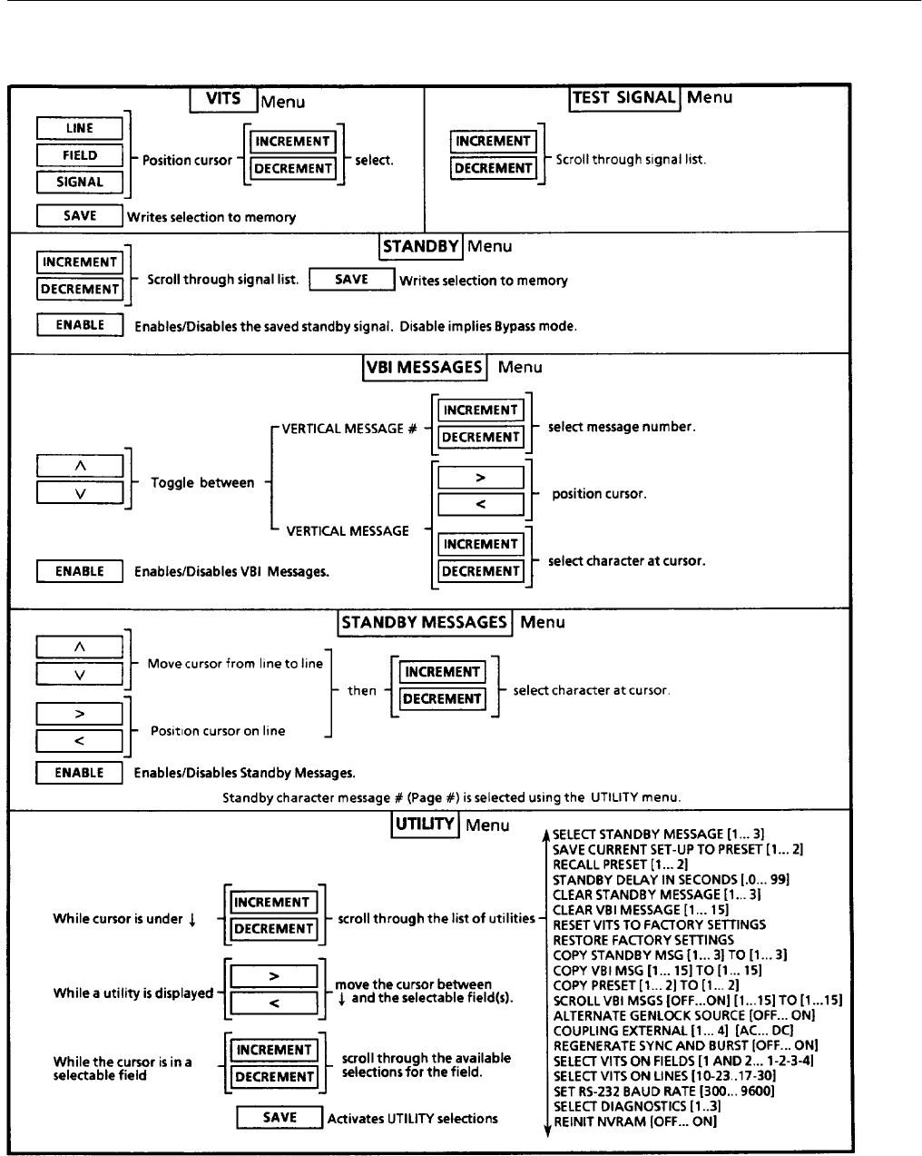
Front Panel
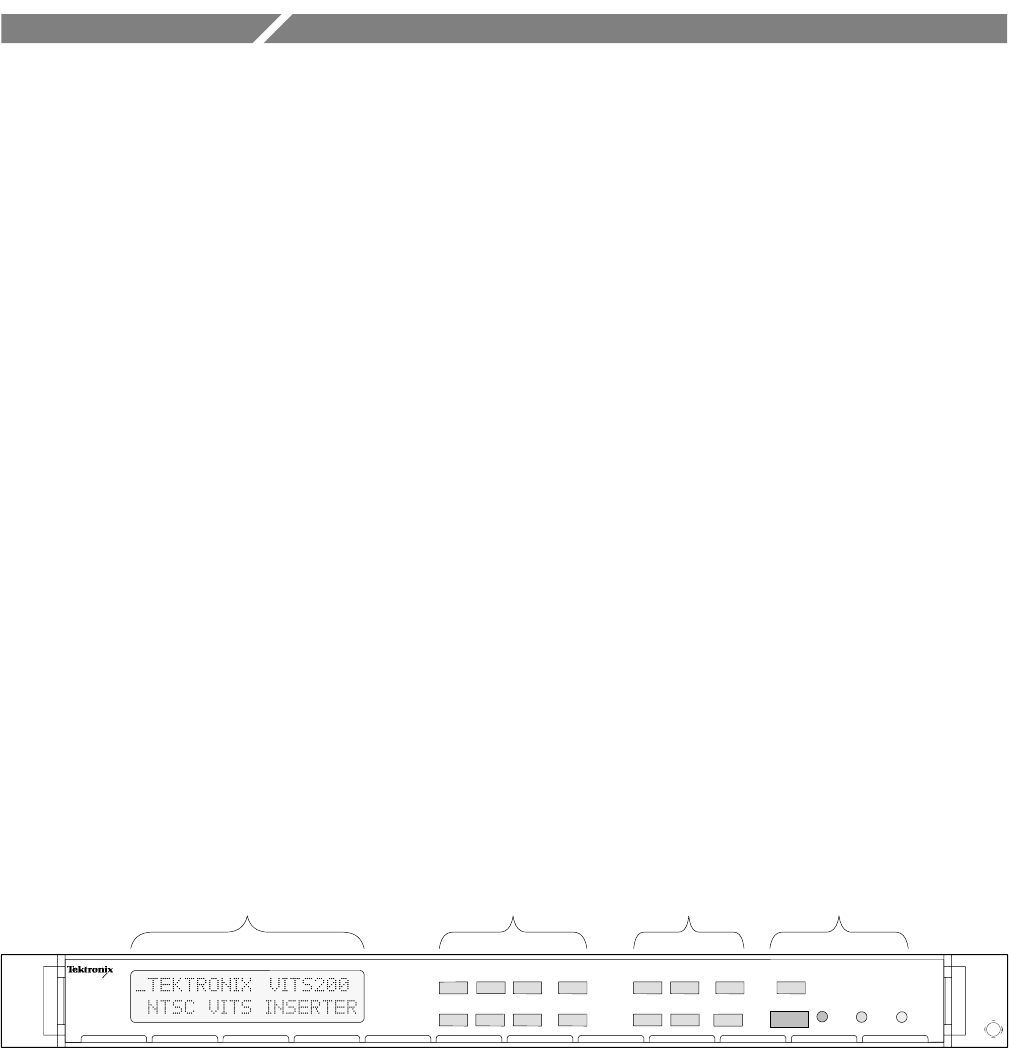
The VITS 200 front panel (see Fig. 2–1) is divided into four main areas: the
Control area, which includes the manual BYPASS button, the FRONT PANEL
DISABLE button, and the three indicator lights; the Menu area, six buttons
which call the menus used to make the various operating selections; the
Selection area, eight buttons used to move through and make selections in the
menus; and the display, which provides two 20-character lines of text about the
menu selections and instrument operation.
VITS 200
NTSC VITS INSERTER
<
LINE >
FIELD
^∨
SIGNAL
INCREMENT
DECREMENT
ENABLE
SAVE/
RECALL
VITS STANDBY
VBI
MESSAGE STANDBY
MESSAGE
TEST SIGNAL
UTILITIES
FRONT PANEL
DISABLE
BYPASS BYPASS UNLOCK POWER
Display Selection Menu Control
Figure 2–1: VITS 200 Front Panel
Operating Basics
2–2 VITS 200
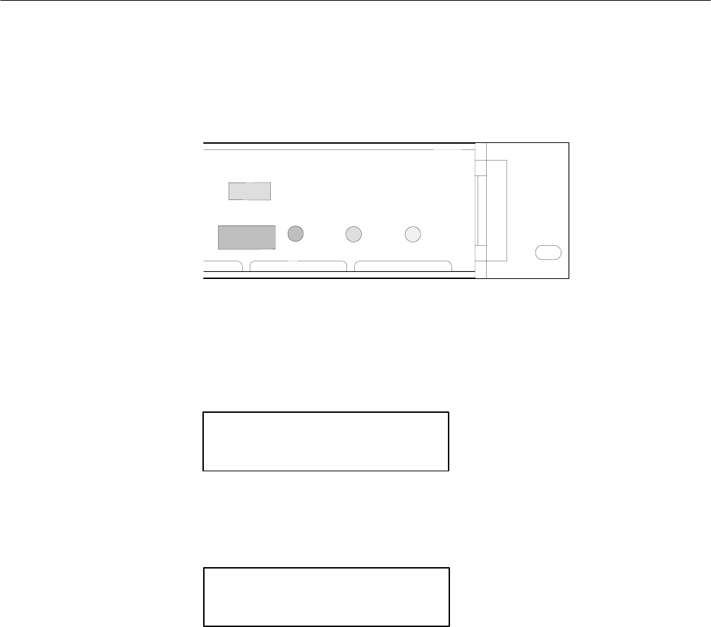
The control area of the front panel contains the FRONT PANEL DISABLE
button, the manual BYPASS button, and the three indicator LEDs: BYPASS,
UNLOCKED, and POWER.
FRONT PANEL
DISABLE
BYPASS BYPASS UNLOCK POWER
FRONT PANEL DISABLE
This button locks out all the rest of the front-panel buttons, except the manual
BYPASS and TEST SIGNAL buttons. When you press FRONT PANEL
DISABLE, the display reads:
FRONT PANEL DISABLED
HOLD [FPD] TO ENABLE
To re-enable the front-panel buttons, press and hold the FRONT PANEL
DISABLE [FPD] button until the display reads:
VITS200 FRONT PANEL
IS NOW ENABLED
(this takes approximately 2 seconds).
BYPASS
This is the manual bypass control. Pressing this button puts the VITS 200 into
Relay Bypass mode; the PROGRAM INPUT is applied directly to the PRO-
GRAM OUTPUT, through a delay line which matches the program channel
through the instrument in normal operation. The BYPASS LED lights to
indicate that the VITS 200 is in Bypass mode. Pressing this button a second
time puts the instrument back into Operate mode.
Bypass Indicator
The BYPASS LED lights to indicate that the instrument is in Bypass mode.
Control

Operating Basics
VITS 200 2–3
When illuminated, the VITS 200 is applying the PROGRAM INPUT directly to
the PROGRAM OUTPUT with no processing.
UNLOCKED Indicator
The UNLOCKED LED lights to indicate that the VITS 200 can not acquire or
maintain genlock. The VITS 200 genlocks to the program input, and can also be
set to use a signal applied to the EXT 1 input as an alternate genlock source if
the program signal fails. This is accomplished through the Alternate Genlock
Source function in the UTILITIES menu.
POWER Indicator
The POWER LED lights to indicate that the VITS 200 is turned on and has
power applied. When the instrument is switched on, the LED does not light
until after the power supply has completed its startup process (approximately one
second).
The selection area of the front panel contains eight push buttons which are used
to move through the selections within a menu, and save the selections to
nonvolatile memory. The button function may change according to the menu
that you are in. See the specific menu descriptions for information on which
buttons are active, and the function they perform in that menu.
<
LINE >
FIELD
^∨
SIGNAL
INCREMENT
DECREMENT
ENABLE
SAVE/
RECALL
Cursor Control (<, >, ∨, ∧)
The four cursor control buttons (<, >, ∨, and ∧) move the cursor around within
the menu. The arrow indicates the direction that the cursor will move. In the
VITS menu, the LINE, FIELD, and SIGNAL nomenclature is active. These
buttons move you to the Line, Field, or Signal selection area of the display,
where you then use the INCREMENT and DECREMENT buttons.
INCREMENT and DECREMENT
The INCREMENT and DECREMENT buttons are used to scroll through the
available selections, such as the character list, when selecting text messages or
the test signal names when selecting a full-field test signal.
Selection

Operating Basics
2–4 VITS 200
ENABLE
The ENABLE button is used to enable and disable the VBI Message, Standby
Message, and Standby modes. Pushing this button while in these menus will
toggle the state of the mode.
SAVE/RECALL
This button saves the user selections to nonvolatile memory. When pressed, the
display will show the word SAVED while writing to memory. It is always
necessary to save VITS selections for them to be inserted. Vertical messages and
standby messages are saved automatically; they do not require use of the
SAVE/RECALL button. This button is also used when recalling previously
saved presets.
The menu buttons are the center group of six push buttons. These are used to
call the menus used in making the VITS assignments, VBI message selections,
Standby mode signal selections, standby message, full-field test signal selec-
tions, and to access the utilities routines. Fig. 2–2 gives a summary of front-pa-
nel operation.
VITS STANDBY
VBI
MESSAGE STANDBY
MESSAGE
TEST SIGNAL
UTILITIES
Menu
Operating Basics
VITS 200 2–5
Figure 2–2: VITS 200 Menu Structure

Operating Basics
2–6 VITS 200
VITS Menu
The VITS menu allows you to select the VITS line, field, and signal assign-
ments. When this button is pressed, the display changes to read:
↓
VITS LINE 10 FLD 1
SIGNAL PASS
Note that the cursor is initially in the Line section of the menu. While in the
VITS menu, the LINE, FIELD, and SIGNAL buttons move the cursor to the
named area, and the INCREMENT and DECREMENT buttons scroll through
the available selections. While the cursor is in the Line area, the INCREMENT
and DECREMENT buttons will scroll through line numbers 10 to 23 (or 17 to
30. See UTILITIES menu). Pressing the FIELD button will move the cursor to
the Field section of the display:
↓
VITS LINE 10 FLD 1
SIGNAL PASS
and the INCREMENT and DECREMENT buttons will scroll through the four
fields or toggle between fields one and two, depending on the selection made in
the Select VITS On Fields function of the UTILITIES menu.
Pressing the SIGNAL button will move the cursor to the bottom line of the
display, in the Signal area:
↓
VITS LINE 10 FLD 1
SIGNAL PASS

Operating Basics
VITS 200 2–7
and the INCREMENT and DECREMENT buttons will scroll through the
available signals which may be inserted as VITS:
H Pass (Program Video) H Auto Capt 1
H Color Bars H Auto Capt 2
H FCC Composite H Auto Capt 3
H MultiPulse H Auto Capt 4
H VIRS H VIRS Auto
H GCR (BTA, Opt 1J 1)H Sin X/X
H GCR (Phillips 1,2)H Source ID
H GCR (Korean 4)H 20 IRE Composite 1,2
H Red Field H Cable Sweep 2,3
H 0% Black H Cable Multiburst 2,3
H 7.5% Black H External 1
H 10 MHz Sweep H External 2
H NTC7 Combination H External 3
H NTC7 Composite H External 4
H MultiBurst H CBC Cmp1 15 – 360 (Opt 1C) 1
H 50% Gray
1 S/N B020249 and above 2 Std and Opt 1C only 3 S/N B020510 and above
4 Opt 1K only
When the Line, Field, and Signal are set as desired, pressing the SAVE/RECALL
button stores the selections in nonvolatile memory and enables insertion, and
you repeat the process for the next line or field.
STANDBY Menu
The STANDBY menu is used to enable or disable the standby function, and to
select which output signal to use if the program signal should fail.
NOTE. If STANDBY mode is disabled, the instrument switches to Bypass mode on
program signal failure.
The delay between program signal failure and the switch to Standby mode may
be set by the user to be between 0 and 99 seconds. See the Standby Delay in
Seconds topic in the UTILITY menu discussion for details.

Operating Basics
2–8 VITS 200
When the STANDBY button is pressed, the display changes to read:
↓
STANDBY MODE DISABLE
SIGNAL 0% Black
The word DISABLE indicates that Standby mode is disabled. Pressing the
front–panel ENABLE button toggles this choice between DISABLE and
ENABLE. The current signal selection is shown as Black 0% Setup, the factory
default. This selection is changed with the INCREMENT and DECREMENT
buttons, which scroll through the list of test signals available for use in Standby
mode:
H 0% Black H External 1
H 7.5% Black H External 2
H 10 MHz Sweep H External 3
H NTC7 Combination H External 4
H NTC7 Composite H CBC Cmp1 15 – 360 (Opt 1C) 1
H MultiBurst H PASS (Program Video)
H 50% Gray H Color Bars
H Sin X/X H FCC Composite
H 20 IRE Composite 1,2 H MultiPulse
H Cable Sweep 2,3 H VIRS
H Cable Multiburst 2,3 H Red Field
1 S/N B020249 and above 2 Std and Opt 1C and above 3 S/N B020510 and above
When the desired signal is showing on the display, press the SAVE/RECALL
button to store the selection in the nonvolatile memory.
TEST SIGNAL Menu
The TEST SIGNAL menu selects the test signal for the rear-panel TEST
SIGNAL output. Making test signal selections does not affect any other aspect
of the VITS 200’s operation.
All VITS selections, vertical characters, and any enabled standby text will be
applied to the selected test signal output while program video is present.
The behavior of this output when program video fails depends on how the VITS
200 is programmed to respond for Standby operation:
HIf the VITS 200 Standby mode is disabled, the TEST SIGNAL output
will continue to provide the selected test signal, and the TEST SIGNAL
menu will continue to operate.

Operating Basics
VITS 200 2–9
HIf the VITS 200 is programmed to provide a test signal for Standby
mode operation, the TEST SIGNAL OUTPUT will switch to that
standby signal, identical to PROGRAM OUT.
HIf the VITS 200 is programmed to switch to one of the EXTERNAL
inputs for the standby signal, the TEST SIGNAL output will switch to
0% Black.
When the TEST SIGNAL button is pressed, the display changes to read:
↓
FULL FIELD TEST
SIGNAL 0% Black
and the INCREMENT and DECREMENT buttons will scroll through the
available test signals:
H 10 MHz Sweep H CBC Cmp1 15 – 360 (Opt 1C) 1
H NTC7 Combination H Color Bars
H NTC7 Composite H FCC Composite
H MultiBurst H MultiPulse
H 50% Gray H VIRS
H SinX/X H GCR
H 20 IRE Composite 1,2 H Red Field
H Cable Sweep 2,3 H 0% Black
H Cable Multiburst 2,3 H 7.5% Black
1 S/N B020249 and above 2 Std and Opt 1C only 3 S/N B020510 and above
The test signals change at the output as soon as the new signal name appears in
the display, and the selection is written to nonvolatile memory automatically.
None of the selection buttons except INCREMENT and DECREMENT have any
effect in this menu.
VBI MESSAGE Menu
The Vertical Blanking Interval (VBI) MESSAGE menu is used to set and select
up to 15 23-character messages which may be inserted in the vertical interval.
When enabled, the selected message appears in the vertical interval on lines 10
through 16. If any of these lines are programmed for VITS signals, the VITS
signal has precedence over the VBI text.
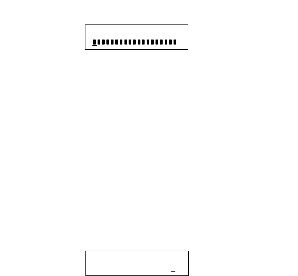
When this button is pressed the display changes to read:

Operating Basics
2–10 VITS 200
VERT MSG 1 DISABLE
>
VERT MSG 1 DISABLE means that the display is showing the VBI (Vertical
Blanking Interval) MESSAGE one, and that the VBI Messages are disabled.
The front-panel ENABLE button toggles this between DISABLED and
ENABLED states. The cursor may be on either line when using the ENABLE
button.
The second line shows the text of the vertical interval message. While there are
only 20 character spaces on the display, the message line can contain up to 23
characters. The > at the right of the message line indicates that the additional
character spaces are to the right.
While on the second line of the display the < and > arrow buttons (LINE and
FIELD) move the cursor left and right. When the cursor is moved to the right
most position, the display shifts four characters to the left. This brings the last
four characters of the message line into view, and a < appears in the leftmost
character space to show that the unseen character spaces are to the left.
To select the characters for the message, move the cursor to each space in turn,
and use the INCREMENT and DECREMENT buttons to select the character for
that position. If the button is held down, the character list scroll rate will speed
up after two or three characters. If that VBI message number is enabled, the
output will change as the characters change on the display. See Table 2–1 for a
list of the available characters.
Table 2–1: Character List for the VITS 200
Display
Char Decimal
(to RAM) Display
Char Decimal
(to RAM) Display
Char Decimal
(to RAM) Display
Char Decimal
(to RAM) Display
Char Decimal
(to RAM)
0 0 C 12 O 24 Sp 36 ? 49
1 1 D 13 P 25 ! 37 ( 51
2 2 E 14 Q 26 # 39 ) 52
3 3 F 15 R 27 * 40 | 75
4 4 G 16 S 28 + 41 ^ 78
5 5 H 17 T 29 , 42 !
#81*
6 6 I 18 U 30 – 43
7 7 J 19 V 31 . 44
8 8 K 20 W 32 / 45
9 9 L 21 X 33 : 46

Operating Basics
VITS 200 2–11
Table 2–1: Character List for the VITS 200 (Cont.)
Display
Char Decimal
(to RAM)
Display
Char
Decimal
(to RAM)
Display
Char
Decimal
(to RAM)
Display
Char
Decimal
(to RAM)
Display
Char
Decimal
(to RAM)
A 10 M 22 Y 34 ; 47
B11 N 23 Z 35 \ 48
* Character number 81 is the cursor, and may not be selected for use as a programmed character.
The ∨ and ∧ buttons will both toggle the cursor between the message text line
and the message number line. When toggled to the upper line the cursor
underlines the message number, and the INCREMENT and DECREMENT
buttons scroll through the 15 message numbers.
If the VBI messages are enabled, the last message selected will be output in the
vertical interval. You may also set the
VITS 200 to scroll through a number of the VBI messages, using the Scroll VBI
MSGS function under the UTILITY menu. If the Vertical Interval messages are
disabled there will be no character in the vertical interval.
The message lines are written directly to memory. This means that a message
will be saved, even through a power interruption in the middle of programming a
line.
STANDBY MESSAGE Menu
The STANDBY MESSAGE menu is used to select and program a full page (13
lines of 20 characters) of text. Three such pages of text may be programmed into
memory for each preset. Any one of these pages may be selected for insertion
into the standby test signal during Standby operation. The other pages may be
selected whenever desired, even during Standby operation. If the standby
message is enabled, it will always be present on the TEST SIGNAL output, over
the selected test signal.
This menu addresses programming the selected page and enabling the message.
NOTE. Page selection is accomplished through the UTILITIES menu.
Programming the full page standby messages is the same as programming the
vertical interval characters, except that there are more lines of text to deal with.
When this button is pressed the display changes to read:
Operating Basics
2–12 VITS 200
STANDBY MSG 1 DISABLE
STANDBY MSG1 DISABLE means that standby channel has page 1 selected,
and it is disabled. The front-panel ENABLE button toggles this between
ENABLED and DISABLED.
The second line of the display shows one of the 13 text lines at a time. Use all
four of the arrow keys to move the cursor across a line and from line to line.
When the cursor is in the extreme right (or left) position trying to move one
more character position in that direction moves to the line below (or above).
Just as with the vertical interval characters, the INCREMENT and DECRE-
MENT buttons are used to select the character at the current cursor position.
UTILITIES Menu
This button operates a little differently than the other menu buttons. While the
other menu buttons deal with one specific function, this button calls a list of
functions. The INCREMENT and DECREMENT buttons are used to scroll
through the functions.
NOTE. No utility function selection will be activated until the SAVE/RECALL
button is pressed.
When the UTILITIES button is first pressed, the display changes to read:
↓
UTIL Select
Standby Message 1
UTIL appears in the upper-left corner to show that you are in the UTILITIES
menu. It changes to SAVED when the SAVE/RECALL button is pressed, to
show that the selection is being written to memory.
The functions available in the UTILITIES menu are:
HSelect Standby Message 1
HSave Current Setup to Preset 1
HRecall Preset 1
HStandby Delay in Seconds 0

Operating Basics
VITS 200 2–13
HClear Standby Message 1
HClear VBI Message 1
HReset VITS To Factory Settings
HRestore Factory Settings
HCopy Standby MSG 1 to 2
HCopy VBI MSG 1 to 2
HCopy Preset 1 to 2
HScroll VBI MSGS OFF 1 to 1
HAlternate Genlock Source OFF
HCoupling External 1 AC
HRegenerate Sync and Burst OFF
HSelect VITS On Fields 1 AND 2
HSelect VITS On Lines 10 23
HReinit NVRAM OFF
Select Standby Message 1 ↓ – This function selects the active standby message.
Either the < or > button will toggle the cursor to the page number section of the
display. The INCREMENT and DECREMENT buttons then scroll through page
numbers 1, 2, and 3. Once the desired page number is displayed, press the
SAVE/RECALL button to store the selection. The selected page can then be
seen on the TEST SIGNAL output, and will be the selected message number in
the STANDBY MESSAGE menu.
Save Current Setup to Preset 1 – This selection will save all of the current user
selections and programming into the NVRAM, as an instrument preset. There
are two presets, which may be recalled as needed. Use the < or > button to
toggle the cursor to the preset number section of the display. The INCREMENT
and DECREMENT buttons then toggle between preset numbers 1 and 2. Once
the desired number is displayed, press the SAVE/RECALL button to store the
selection.
Recall Preset 1 – This selection recalls the presets created by the Save Current
Setup To Preset selection, discussed above. Use the < or > button to toggle the
cursor to the preset number section of the display. The INCREMENT and
DECREMENT buttons then toggle between preset numbers 1 and 2. Once the
desired number is displayed, press the SAVE/ RECALL button to recall the
preset.

Operating Basics
2–14 VITS 200
Standby Delay in Seconds 0 – This selection is used to set the time delay
between loss of program video and the switch to standby. This delay may be set
in one-tenth second intervals between zero and one second, and in one second
intervals between one and ninety-nine seconds.
Clear Standby Message 1 – This function clears a complete standby message
page at a time. Use the < or > button to move the cursor to the page number, and
then use INCREMENT or DECREMENT to select the page number to clear.
When the desired page number is displayed, pressing the SAVE/ RECALL
button clears the page of all text.
Clear VBI Message 1 – This function works the same as the preceding one, but
clears one specified VBI message at a time.
Reset VITS To Factory Settings – This function returns the current VITS
selections to the factory default settings. Press the SAVE/RECALL button to
reset the VITS.
Restore Factory Settings – This function returns the entire VITS 200, except
presets, to the factory defaults for VITS selections, VBI messages, standby
messages, EXT coupling, LINE mode, FIELD mode, alternate genlock, and
regenerated sync selections. Press the SAVE/RECALL button to restore the
instrument defaults.
Table 2–2: Factory VITS assignments for Std and Opt 1C.
Line 17 18 19 20
Field 1 NTC7 Comp Pass Phillips GCR 1,
Pass 2Pass, Korean
GCR 2
Field 2 NTC7 Comb Pass Phillips GCR 1,
Pass 2Pass, Korean
GCR 2
1 Line 19 programmed for VIRS prior to S/N B020510 2 Option 1K
Table 2–3: Factory VITS assignments for Opt 1J.
Line 17 18 19 20
Field 1 FCC Comp BTA GCR Color Bars Sin X/X
Field 2 Multiburst BTA GCR 4.2 MHz Sweep Red Field
Copy Standby MSG 1 to 2 – This function copies all of the text programmed
for one standby message page to another. Use the < and > buttons to place the
cursor in the page number positions, and then use the INCREMENT and
DECREMENT buttons to select the page numbers. When the correct page
numbers are displayed, press the SAVE/RECALL button to write the copy to
memory.

Operating Basics
VITS 200 2–15
Copy VBI MSG 1 to 2 – This function copies the text of one Vertical Interval
Character message to another. Use the < and > buttons to move the cursor to the
vertical character message number positions, and then use the INCREMENT and
DECREMENT buttons to select the message numbers. Press the SAVE/RE-
CALL button to make the copy.
Copy Preset 1 to 2 – This function makes a duplicate of one of the instrument
presets. Use the < and > buttons to move the cursor to the instrument preset
number position, and then use the INCREMENT and DECREMENT buttons to
select the preset numbers. Press the SAVE/RECALL button to make the copy.
Scroll VBI MSGS OFF 1 to 1 – This function selects a range of VBI
messages, and then inserts them into the vertical interval one at a time. Each of
the messages is inserted for approximately five seconds, and the sequence
repeats until it is turned off or the VBI messages are disabled. Use the < and >
buttons to move the cursor between the OFF position and the message number
positions. INCREMENT and DECREMENT toggle the OFF/ON selection when
the cursor is in that position, and scroll through the VBI message numbers when
the cursor is at either of those positions. Press SAVE/RECALL to store the
selection.
Alternate Genlock Source OFF – This selection allows the EXTERNAL 1 input
to be used as an alternate genlock input, during failure of the program video.
When program video returns, the VITS 200 will immediately switch back to it as
the genlock source. Use either the < or > button to move the cursor to the word
OFF, and then use the INCREMENT or the DECREMENT button to toggle the
state between OFF and ON. Pressing SAVE/RECALL stores the selection.
Coupling External 1 AC – This function selects AC or DC coupling for each of
the four external inputs. Use the < or > button to move the cursor to the
coupling mode or the external input number. When the cursor is under the
external input number, the INCREMENT and DECREMENT buttons scroll
through the four inputs, so they may each be set individually. While the cursor
is in the coupling mode section, both the INCREMENT and DECREMENT
buttons toggle the selection between AC and DC. Pressing SAVE/RECALL
stores the selection.
Regenerate Sync and Burst OFF – The VITS 200 can insert sync and burst into
the program video. This utility turns that capability on and off. Press the < or >
button once, to move the cursor to the word OFF (or ON), and press INCRE-
MENT or DECREMENT to toggle the selection. Press the SAVE/RECALL
button to store the selection.
Select VITS On Fields 1 AND 2 – This function allows selection of using odd
and even fields only for VITS assignments, or addressing each of the four fields
separately. Use the < or > button to move the cursor to the field numbers, and
press INCREMENT or DECREMENT to toggle between Fields 1 AND 2 and
Fields 1234. Press the SAVE/RECALL button to store the selection.

Operating Basics
2–16 VITS 200
Select VITS on Lines 10 – 23 – This function selects between lines 10 through
23 (broadcast) and lines 17 through 30 (cable) for VITS assignments. Lines 17
through 23 are the same in both modes, but lines 10 through 16 in broadcast
mode become lines 24 through 30 in cable mode.
Reinit NVRAM OFF – This function selects the Nonvolatile RAM initialization
sequence.
NOTE. This selection clears the NVRAM, and returns the VITS 200 to the factory
selections and programming. ALL USER MADE SELECTIONS AND PRO-
GRAMMING WILL BE LOST.
If you need to reinitialize the NVRAM, use the < or > button to move the cursor
to the word OFF, and use the INCREMENT or DECREMENT button to toggle
the selection to ON. Press the SAVE/RECALL button to make the selection, and
the display should change to read:
Hit save again to RE
INIT NVRAM !!!!!
Wait until this message disappears. Then, when you press the SAVE/RECALL
button a second time, the display will change to read:
When Power is Cycled
NVRAM Will REINIT !!!
This will remain displayed for approximately two seconds. At this time, cycling
the power off and back on will reinitialize the NVRAM.
If you do not want to lose the user selections and programming, press the < or >
button to move the cursor to the word ON, and toggle it back to OFF with the
INCREMENT or DECREMENT button. Press the SAVE/RECALL button, and
you should see:
NVRAM
WLL NOT REINIT !!!
appear on the display, which means that the NVRAM reinitialization sequence
has been aborted.
Operating Basics
VITS 200 2–17
Remote Control
The VITS 200 can be remotely controlled through the 25-pin REMOTE
CONTROL connector on the rear-panel (see Fig. 2–3). Using simple ground
closure, the remote control can lock out the VITS 200 front panel, place the
VITS 200 into Bypass mode, force the VITS 200 into Standby mode, select the
full-field test signal output, and select and enable the VBI messages and the
standby messages. It cannot be used to change the text of the messages,
however.
A Remote Control unit is not a production item, and there are no plans to
offer one as either a standard or optional accessory to the VITS 200.
1
2
3
4
5
6
7
8
9
10
11
12
13
14
15
16
17
18
19
20
21
22
23
24
25 REMOTE SWITCH
GROUND
GROUND
GROUND
UNLOCKED LED
POWER LED
RESERVED
REM12
TEST SIGNAL
FORCE STANDBY
PAGE 0
MESSAGE SELECT BINARY 3
MESSAGE SELECT BINARY 1
MESSAGE SELECT BINARY 2
MESSAGE SELECT BINARY 0 ENABLE VERTICAL INTERVAL TEXT
REMOTE LED
BYPASS SWITCH
BYPASS LED
RESERVED
REM13
REM11
PAGE 1
EXTRA
STANDBY
Figure 2–3: Remote Control Connector
Pins 13, 25 REMOTE ENABLE – When pin 13 is first grounded, the Remote
Control unit is enabled and the VITS 200 front panel is locked out. The Remote
Control must be enabled to use any control pins: the TEST SIGNAL selection
pins and the ENABLE and SELECT pins for the standby and VBI messages.

Operating Basics
2–18 VITS 200
When the Remote Control is enabled, pin 25 will provide power to light an LED
on the Remote Control, and the
VITS 200 display will change to read:
REMOTE ENABLED
FRONT PANEL DISABLED
While in this mode the VITS 200 front-panel push buttons are disabled, except
for the BYPASS, TEST SIGNAL, and FRONT PANEL DISABLE push buttons.
The BYPASS button may still be used to put the VITS 200 into Bypass mode,
and both the VITS 200 and the Remote Control BYPASS indicators will light.
When REMOTE SWITCH pin 13 is open (off), the LED will go out and the
VITS 200 display will change to read:
FRONT PANEL ENABLED
REMOTE DISABLED
This message will remain on the display until one of the VITS 200 Selection
buttons are pressed.
While the Remote Control is enabled, VITS 200 front-panel control may be
regained by pressing and holding the FRONT PANEL DISABLE push button,
just as if the front panel had been disabled by it. After holding the button down
for approximately five seconds, the display will change to read:
VITS200 FRONT PANEL
IS NOW ENABLED
and the REMOTE LED on the Remote Control will go out, even though the
REMOTE SWITCH pin is grounded (enabled). To re-enable the Remote
Control, the REMOTE SWITCH pin must be opened and regrounded.
Pins 22, 23 BYPASS – The BYPASS LED and BYPASS SWITCH pins work
just like the BYPASS push button and indicator on the VITS 200. The BYPASS
LEDs work in parallel. Both of them will light whenever the VITS 200 is in the
Bypass mode of operation.
The BYPASS SWITCH pin will switch the VITS 200 into the Bypass mode of
operation when it is grounded, whether the Remote Control is enabled or not.

Operating Basics
VITS 200 2–19
Pin 10 UNLOCKED LED – This pin drives an LED, which works just like the
one on the VITS 200 front panel. It lights to indicate that the VITS 200 can not
acquire or maintain genlock. This indicator works whether the Remote Control
is enabled or not.
Pin 9 POWER LED – This LED lights when the Remote Control is connected to
the VITS 200, and the VITS 200 is turned on. This indicator works whether the
Remote Control is enabled or not.
Pin 6 TEST SIGNAL – This pin selects the full-field test signal output, when the
Remote Control is enabled. Used with a momentary contact switch to ground,
this pin is just like using the front-panel INCREMENT push button while in the
TEST SIGNAL menu. Pressing the button steps through the twelve test signals,
and holding the button down scrolls through them.
There is one difference between using the front-panel button and the one on the
Remote Control. There is no visual feedback of the selected test signal on either
the Remote Control or the VITS 200 front panel. You must have a monitor of
some sort connected to the TEST SIGNAL output in order to determine the
selected signal.
Pin 5 FORCE STANDBY – Grounding this pin forces the VITS 200 into
Standby mode.
Pins 16, 4, 17 STANDBY MESSAGE – These three pins are used to enable or
disable the standby messages, and to select which of the three pages to output
when in Standby mode. These can only be used to select messages which have
been programmed in through the front panel, or through the RS-232 port. Text
messages cannot be programmed by the Remote Control.
The two pins labeled PAGE 0 and PAGE 1 are used to select the page. Pin 4 is
the LSB and pin 17 is the MSB. See Table 2–4. The only indication on the
Remote Control or the VITS 200 of which standby message has been selected is
the positions of the switches used to control these pins.
Table 2–4: Binary Standby Message Select
Pin 17 Pin 4 Output Page
1 1 Page 1
0 1 Page 1
1 0 Page 2
0 0 Page 3
While the Remote Control is enabled, pin 16 can enable and disable the
STANDBY MESSAGE pages, no matter what the status of the page was under
front panel control.

Operating Basics
2–20 VITS 200
Pins 1, 2, 3, 14, 15 VBI MESSAGE – These five pins are used to enable or
disable the vertical interval messages, and to select which of the 15 messages to
insert into the vertical interval. These can be used only to select messages which
have been programmed in through the front panel or through the RS-232 port.
Text messages cannot be programmed by the Remote Control.
The four VBI MESSAGE pins select the message to be inserted in the vertical
interval, with pin 14 as the LSB and pin 3 as the MSB. See Table 2–5 for
details. As with the STANDBY MESSAGE, the only indication on the Remote
Control or the VITS 200 of which message has been selected is by the switch
positions.
Table 2–5: Binary VBI Message Select
Pin 3 Pin 15 Pin 2 Pin 14 Vertical Message #
1 1 1 1 Message 1
1 1 1 0 Message 1
1 1 0 1 Message 2
1 1 0 0 Message 3
1 0 1 1 Message 4
1 0 1 0 Message 5
1 0 0 1 Message 6
1 0 0 0 Message 7
0 1 1 1 Message 8
0 1 1 0 Message 9
0 1 0 1 Message 10
0 1 0 0 Message 11
0 0 1 1 Message 12
0 0 1 0 Message 13
0 0 0 1 Message 14
0 0 0 0 Message 15
Video Clapboard
Video Clapboard is for timing audio and video delays, so that they may be
synchronized throughout the studio. This function requires a Tektronix ASG 100
modified for Video Clapboard operation. When in use, the VITS 200 will turn
the vertical interval text off and on in a 0.5 second on and 4.5 second off
pattern, and turn the ASG 100 audio tone on and off in the same pattern. The
VBI text will appear following the second vertical interval after the high to low
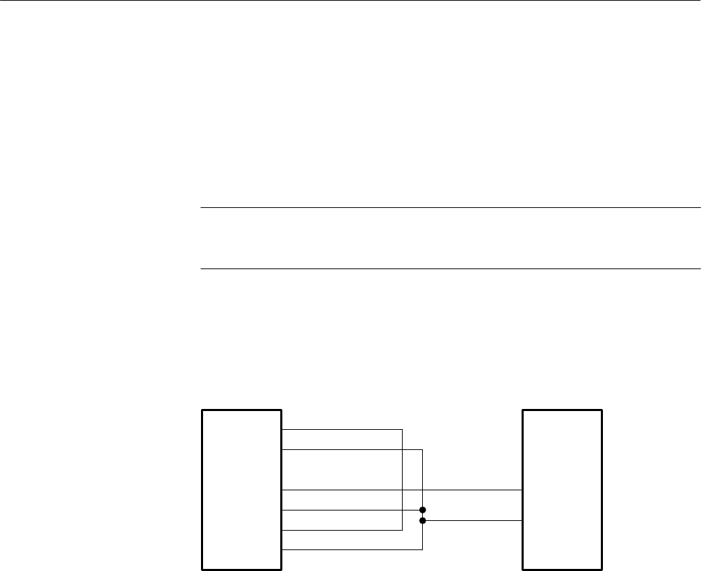
Operating Basics
VITS 200 2–21
transition on pin 13. The VM700A measurement “Audio Video Timing” will
remove this lag before presenting the measured time difference.
Configuring the VITS 200 for Video clapboard operation:
1. Genlock the VITS 200 to a video source.
2. Press the VBI Message button, select VERT MSG 2 and ENABLE it.
NOTE. Any of the vertical interval messages may be used. Message two is used
here by grounding pin 2 of the VITS 200 remote connector. To use another
message, ground the appropriate selection pins for it (see Table 2–5).
3. Enter some text for the Vertical Message. A minimum of one character is
required.
4. Connect the VITS 200 and ASG 100 remote connectors as shown in
Figure 2–4.
VITS 200
REMOTE ASG 100
REMOTE
1
2
8
13
20
24
1
5
Enable VBI Text
Remote Enable
Ground
VBI SEL BIN 1
REM 14
REM 13
Figure 2–4: Video Clapboard Connections

Operating Basics
2–22 VITS 200
RS-232 Control
The VITS 200 may be controlled through a 3-wire RS-232 interface, or by any
device that can generate or transmit commands in ASCII characters. Using XON
and XOFF makes it possible to control the VITS 200 directly from an ASCII
terminal, personal computer (PC), or a VM700A (See Figure 2–5).
Copy
Port: Serial Port 1
format: Epson LQ
Report
Port: None
Format: Epson LQ
LogPort: None
Format: Epson LQ
Control Port: Serial Port 0
Remote Control
Port: None
Prompt: VM700>
Message Display: Remote
Non-SLIP Interfacing Mode: Terminal
Port 0
Protocol: None
Baud Rate: 9600
Flow Control: XON/XOFF
Character Size: 8
Parity: None
Reset Character: None
Carrier Detect: Disabled
Port 1Protocol: None
Baud Rate: 19200
Flow Control: None
Character Size: 8
Parity: None
Reset Character: None
Carrier Detect: Disabled
Communications Setup
First, designate and configure the VM700A
communication port to use with the VITS 200. This
is accomplished by selecting the VM700A front
panel configure button, then select the “Configure
Files” softkey on the touch-panel screen menu.
Finally, select the “Communications Setup” softkey.
In the Communications Setup, designate your
choice of control port (Serial Port 0 or 1) and then
set the parity, baud rate, and flow control for that
port. The example shown here has the VITS 200
connected to the VM700A serial port 0.
Sending Commands to the VITS 200
Communication with the VITS 200 is accomplished
with simple user-created functions. An example of
one such function which changes the VITS 200
TEST SIGNAL output to a Color Bar signal, lets
call it CBAR, would look like this:
control :tsig CBR ^M
This function may be executed directly by pressing
the VM700A front panel “Function” key and then
selecting the CBAR softkey. It may also be
executed by embedding it in another function with
the VM700A “Playback” command. See the
VM700A Users Manual and “Controlling RS-232C
Devices with the VM700A” (21W-7108) for more
information.
Figure 2–5: Controlling the VITS 200 with a VM700A.

Operating Basics
VITS 200 2–23
Typically, RS-232 control will be implemented with a PC which is running
terminal-emulation or communication software, such as PROCOMM or
SmartComm. Depending on the software used, commands that specify VITS
200 settings may be entered directly through the keyboard or by transmitting text
files containing any number of commands. Many communications applications
also permit the assignment of command “scripts” to function keys or key
combinations.
RS-232 control will permit the operator to learn the current settings of the
VITS 200 and change them from the terminal. New settings may be specified by
name (e.g. “LINE”) or value (e.g. “15”), eliminating the need to scroll through a
list of choices as with the front panel controls or with the ground-closure remote.
RS-232 commands and command syntax are explained in the following RS-232
COMMANDS discussion. Some of the ways to use RS-232 control are:
HEnter commands directly through the keyboard. The value of this
approach is somewhat limited, however, because typing commands such
as :STANdby:SIGNal SXX can quickly become tedious.
As an example, to use EXTERNAL 1 input as a VITS on Line 19 Field
1, you would enter the following commands:
:VITS:LINe 19
:VITS:FIELd 1
:VITS:SIGNal EX1
:VITS:SAVe
These commands may be issued in any order, except for the SAVe
command. it must be the last one issued, and it must be issued before
any VITS changes will take effect.
HAssign key combinations or function keys to certain settings or
commands so that the VITS 200 can be controlled with a few keystrokes.
For example, if the script “:VITS:LMOD 10–21” is associated with the
F1 key, and “:VITS:LMOD 17–30” is associated with the F2 key,
switching between standard and cable mode VITS assignments becomes
an easy matter. (Note that key assignment is not a standard feature of all
communication software; check your software manual.)
HWhile running communication software, execute simple programs to
automate repetitive adjustments, or substitute short mnemonic strings for
long commands. Many of the popular communications packages have
this capability.
HSave an unlimited number of presets in the form of individual text files.
One such file could program in an entire standby message page and then
select it, saving several hundred keystrokes. This is one way to have
more than the three preset messages on tap if they should be needed.

Operating Basics
2–24 VITS 200
Cable
If the RS-232 port is a DB25 connector, use a straight-through cable as described
in Table 2–6. Do not use a “null modem” cable. If the port is a male DB9
connector, as on many IBM- compatible PCs, use a cable or adapter as described
in Table 2–7. If the device uses a non-standard connector, determine which pins
perform the functions listed in the center column of Table 2–7 and connect them
through the appropriate pins of a DB25 connector as listed in the left column.
Table 2–6: RS-232 Connector Pin Functions – 25-Pin Serial Ports
VITS 200
(25-Pin Female) Pin/Conductor PC
(25-Pin Male)
GND (Shield) 1GND (Shield)
RxD 2 TxD
TxD 3 RxD
Signal GND 7Signal GND
Table 2–7: 9-Pin to 25-Pin Adaptor Connections for RS-232
DB25
Pin Number RS-232 Function DB9
Pin Number
2 TxD 3
3 RxD 2
7Signal GND 5
Communications Parameters
HTTY or VT100 TERMINAL EMULATION.
HXON/XOFF Flow Control.
H8 Data bits, no Parity, 1 Stop bit.
HLocal Echo (or Half Duplex).
Text Commands and Command Files
For best results, follow these guidelines when sending text to the VITS 200:
HSend one line at a time; wait for a carriage return between lines. (The
VITS 200 will send a carriage return to signal that it has executed a
command only if it is in TERM mode.)
Hardware and Software
Requirements for RS-232
Control

Operating Basics
VITS 200 2–25
HLines may be up to 128 characters.
HEnd each line, including the last one, with a carriage return.
RS-232 commands may be used to query the VITS about the setting of particular
variables, or to set the variable to a specific value. The basic syntax is:
:COMMAND?
or
:COMMAND parameter
where the first form is a query and the second will set the variable. Important
points to remember are:
HCommands always begin with a colon (:) or an asterisk (*).
HThere is never a space between the variable name (command header) and the
question mark in a query.
HThere is always a space between the header and the command parameter.
HCommands are not case-sensitive; headers and parameters may be entered in
either capitals or lower case. For clarity in this manual, the mnemonic form
of the header is capitalized, and the remaining characters of the complete
form are shown in lower case. Either form may be used; entering :PRES?
will have the same effect as entering :PRESET?. Parameters will be shown
in italics.
HParameters can be either numeric or character strings. String parameters,
such as VBI and Standby message text strings must be enclosed in double
quotes.
HCompound headers (such as :VITS:LMOD) are limited to those predefined
for the VITS 200.
HA line can contain several commands, if they are separated by a semicolon
(:COMMAND parameter1;:COMMAND parameter2;...), but no line may
exceed 128 characters.
:AltGENlock
Parameters: ON or OFF
Turns the Alternate Genlock function, where EXT 1 is used as an alternate
genlock source if the signal at the PROGRAM INPUT fails, ON or OFF. Query
returns the current status.
:ByPASs
Parameters: ON or OFF
RS-232 Commands

Operating Basics
2–26 VITS 200
:BYPASS ON is the RS-232 equivalent of pushing the front panel BYPASS
button in, and OFF is the equivalent of releasing it. A query will return the
current state of the VITS 200 mode, but will not distinguish the reason it’s in
that mode.
:COMMunicate?
Parameters: None, query only
Query returns the current Baud rate (300 to 9600) and communications mode
(Terminal, SCPI, or VM700).
COMMunicate:MODe
Parameters: Mode
Sets the communications mode to SCPI, TERM, or VM700. Query returns the
currently set mode.
COMMunicate:SERial:BAUD
Parameters: 300, 600, 1200, 2400, 4800, or 9600
Sets the baud rate for serial communication. Query returns the current baud rate.
:COUPling
Parameters: 1 to 4, AC or DC
Sets the individual ext inputs coupling mode. EXT INPUT 1 through EXT
INPUT 4 may be set to be AC or DC coupling. A query will return the current
coupling status for all four of the External Inputs.
:HELP?
Parameters: None, query only
Returns a list of available commands.
*IDN?
Parameters: None, query only
This query is used to verify which device is connected to the active serial port.
:PRESet?
Parameters: None, query only
Query returns the current Preset number (1 or 2).
:PRESet:COPY
Parameters: Preset #, Preset #
Copies the first specified preset (1 or 2) to the second (1 or 2).
PRESet:RECall
Parameters: Preset #

Operating Basics
VITS 200 2–27
Recalls the specified preset (1 or 2).
:PRESet:SAVe
Parameters: Preset #
Saves the current instrument setup as the specified preset (1 or 2).
:REINitnvram
Parameters: ENA or DIS
This is the first step of reinitializing the NVRAM to the factory settings. When
this is ENAbled, a *RST command will reset ALL of the VITS 200 settings to
the factory defaults. When REINitnvram is set to DISable, an RST command
will have no effect.
:RESYnc
Parameters: ON or OFF
When set ON, the VITS 200 will insert regenerated sync and burst. When set
OFF, the program video sync and burst is passed to the output. Query returns the
current selection.
*RST
Parameters: None
No parameters, no query. All settings will be reset to their factory defaults.
REINitnvram must be set to ENAble for this to have any effect.
:SoftwareVER?
Parameters: None, query only
This query will return the VITS 200 software version level.
:STANdby
Parameters: ENA or DIS
Enables or disables standby mode operation. Query returns the current mode
state.
:STANdby:DELay
Parameters: 0.0 1.0 seconds (0.1 sec increments)
1 99 seconds (1 second increment)
Sets the delay time between the loss of program video and switching to Standby
operation. Below 1.0 second you may use 0.1 second increments, down to 0.0
seconds for an immediate switch. Between 1 and 99 seconds, you must use 1
second increments. Query returns the current delay time.
:STANdby:FORCe
Parameters: ON or OFF

Operating Basics
2–28 VITS 200
ON forces the VITS 200 into Standby mode, even if locked to program video.
OFF is the default setting.
:StandbyMES
Parameters: ENA or DIS
Enables or disables the Standby Message function. Query returns the current
status.
:StandbyMES:ADD
Parameters: “TXT”
Adds text to the currently open Standby message, starting at the current line and
column. Cursor is auto-incrementing.
:StandbyMES:CLeaR
Parameters: Msg #
Clears any text in the specified Standby message (1 to 3).
:StandbyMES:CLOSe
Parameters: None
Closes the currently open Standby message.
:StandbyMES:COPY
Parameters: Msg #, Msg #
Copies the text from the first specified Standby message (1 to 3) to the second (1
to 3).
:StandbyMES:EDIT
Parameters: Msg #
Opens the specified Standby message number (1 to 3) for editing. Query returns
the number of the current open message.
:StandbyMES:MESSage
Parameters: Msg #, Line#, “TXT”
This command programs Standby messages. The parameters are the Standby
message number (1 to 3), the line within the message (1 to 13), and the message
text (1 to 20 characters).
:StandbyMES:MOVe
Parameters: Line #, Column #
Moves the cursor to the specified line and column in the open Standby message.
Query returns the current line and column numbers.

Operating Basics
VITS 200 2–29
:StandbyMES:REPLace
Parameters: “TXT”
Replaces text in the currently open Standby message, starting at the current line
and column. Cursor does not move.
:StandbyMES:SELect
Parameters: Msg #
Calls a Standby message by number (1 to 3) for insertion. Query returns the
current Standby message number.
:STANdby:SIGNal
Parameters: Signal mnemonic
Selects the test signal to use as the Standby signal. Use the RS-232 mnemonic
for the test signal name. Query returns the current selection.
:SYSTem:ERRor?
Parameters: None, query only
This query will return a message reporting any existing error condition in the
VITS 200.
:SYSTem:VERSion?
Parameters: None, query only
This query will return the SCPI version that the VITS 200 conforms to.
:TestSIGnal
Parameters: “Signal mnemonic”
Selects the signal for the TEST SIGNAL output. Use the RS-232 mnemonic for
the test signal name. Query returns the current selection.
:VerticalMES
Parameters: ENA or DIS
Enables and disables the Vertical Blanking Interval messages. Query returns the
current status.
:VerticalMES:ADD
Parameters: “TXT”
Adds text to the currently open VBI Message. Cursor is auto-incrementing. An
ampersand (&) is used as a pass character.
:VerticalMES:CLeaR
Parameters: Msg #
Clears the specified VBI message text.

Operating Basics
2–30 VITS 200
:VerticalMES:CLOSe
Parameters: None
Closes the currently open VBI Message.
:VerticalMES:COPY
Parameters: Msg #, Msg #
Copies the text of the first VBI Message number (1 to 15) to the second VBI
Message number (1 to 15).
:VerticalMES:EDIT
Parameters: Msg #
Opens the specified VBI Message number (1 to 15) for editing. Query returns
the currently open message.
:VerticalMES:MESSage
Parameters: Msg #, “TXT”
This command programs Vertical Blanking Interval messages. The parameters
are the VBI Message number (1 to 15) , followed by the message text (1 to 23
characters).
:VerticalMES:MOVe
Parameters: Column #
Moves the cursor to the specified column number in the currently open VBI
Message.
:VerticalMES:REPLace
Parameters: “TXT”
Replaces text in the currently open VBI Message. The cursor does not move.
An ampersand (&) is used as a pass character.
:VerticalMES:SCRoll
Parameters: ON, #, # or OFF
Turns the VBI Message scroll feature ON, in which case you must specify the
starting and ending message numbers, or OFF. Query returns the current ON or
OFF state.
:VerticalMES:SELect
Parameters: Msg #
This command selects a particular VBI message number for insertion. Query
returns the current message number.
:VITS?
Parameters: None, query only

Operating Basics
VITS 200 2–31
When used as a query, this will return current Field Mode, Line Mode, Line
number, field number, and assigned signal.
:VITS:CLeaR
Parameters: None
Clears the current VITS assignments.
:VITS:FIELd
Parameters: Field number
Addresses a specific field for VITS assignment.
:VITS:FieldMODe
Parameters: 2FieLD or 4FieLD
Sets the Field Mode to 2 field (even/odd), or to 4 field (Fields 1, 2, 3, 4). Query
returns current setting.
:VITS:LINe
Parameters: Line number
Addresses specific line number in the current Line Mode range, for VITS
assignment. Query returns current selection.
:VITS:LineMODe
Parameters: 10–23 or 17–30
Sets the VITS Line Mode to the standard VITS lines (lines 10–23) or to the cable
VITS lines (lines 17–30). Query returns current selection.
:VITS:RESet
Parameters: None
Resets the VITS assignments to the factory selections.
:VITS:SAVe
Parameters: None
Saves the VITS assignments to nonvolatile memory. MUST be used for any
VITS assignment changes to take effect.
:VITS:SIGNal
Parameters: “Signal mnemonic”
Specifies the signal for use as VITS on the current line and field. Use the
RS-232 mnemonic for the test signal name. Query returns the current selection.

Operating Basics
2–32 VITS 200
Table 2–8: SCPI Commands (4.1.1 and 4.2.1)
Command Header Purpose Parameter Example
*CLS No Action Clear Status command
*ESE No Action Standard Event Status Enable command
*ESE No Action Standard Event Status Enable query
*ESR No Action Standard Event Status Register query
*OPC No Action Operation Complete command
*OPC? No Action Operation Complete query
*SRE No Action Service Request Enable command
*SRE? No Action Service Request Enable query
*STB? No Action Read Status Bite query
*TST? No Action Self-test query
*WAI No Action Wait-to-continue command
*IDN? Identification query No Parameters
*RST Resets the VITS 200 to the factory defaults. Must have set
REINitnvram to ENAble for this to have any effect.
No Parameters
:SYSTem
:ERRor?
:VERSion? Returns the SCPI version this instrument complies to. Query
only.
:STATus
:OPERation
:EVENt?
:CONDition
:ENAble
:ENAble?
:QUEStionable
:EVENt?
:CONDition
:ENAble
:ENAble?
:PRESet
No Action
No Action
No Action
No Action
No Action
No Action
No Action
No Action
No Action
No Action
No Action
No Action

Operating Basics
VITS 200 2–33
Table 2–9: Defined RS-232 Commands for use with the VITS 200
Command Header Purpose Parameter
Example
:HELP?
:SoftwareVER? Returns the VITS 200 software version. Query only. No Parameters
:VITS?
:FieldMODe? [text]
:LineMODe? [text]
:LINe? [#]
:FIELd? [#]
:SIGNal? [text]
:SAVe
:CLeaR
:RESet
Command/query. Query returns all of the following:
Selects/queries between 2 and 4 field mode of operation.
Selects/queries standard or cable VITS assignments (lines
10–23 or 17–30).
Addresses/queries specific line for VITS assignment (10–23 or
17–30).
Addresses/queries field assignment for VITS (1, 2, 3, or 4).
Selects/queries test signal for VITS.
Saves new VITS assignments. Must be used for new assign-
ment changes to take effect.
Clears VITS assignments in current setup.
Resets VITS assignments.
2 FieLD
10–23
15
2
CBR (RS-232 mne-
monic)
No Parameters
No Parameters
No Parameters
:TestSIGnal [text] Selects the Full Field Test Signal output. CBR (RS-232 mne-
monic)
:STANdby? [text ]
:SIGNal? [text]
:DELay? [#]
:FORCe [text]
ENAble or DISable standby mode or query status.
Selects/queries the standby test signal.
Sets/queries the delay time for switching to standby mode
(0.0199 sec).
Forces the VITS 200 standby mode ON or OFF.
ENA
CBR (RS-232 mne-
monic)
0.5
OFF
:AltGENlock? Sets/queries whether EXTERNAL 1 is ON or OFF as alternate
genlock source.
OFF
:RESYnc? Sets/queries whether regenerated sync and burst is ON or OFF. ON
:COUPling? [#],[text] Sets/queries whether specified EXTERNAL INPUT # (1–4) to
AC or DC coupling.
3, DC
:REINitnvram? ENAbles the NVRAM reinitialization sequence (Requires an
*RS T command to actually reinitialize the NVRAM.) or DIS-
ables the NVRAM reinitialization sequence (An *RST com-
mand will NOT reinitialize the NVRAM). Query will tell
whether it is ENAbled or DISabled.
DIS
:ByPASs? Sets/queries whether bypass is ON or OFF. ON

Operating Basics
2–34 VITS 200
Table 2–9: Defined RS-232 Commands for use with the VITS 200 (Cont.)
Command Header Parameter
Example
Purpose
:VerticalMES? [txt]
:MESSage [#],[txt]
:SELect ? [#]
:SCRoll? ON,[#],[#]/OFF
:CLeaR [#]
:COPY [#],[#]
:EDIT? [#]
:MOVe? [#]
:ADD [text]
:REPLace [text]
:CLOSe
ENAble or DISable VBI Messages, can also query status
Programs specified VBI Message [1–15] text [1–23 characters]
Calls specified VBI Message for insertion, queries which mes-
sage is current
Turns Scroll ON for starting message # to ending message #, or
turns scroll OFF. Query returns status.
Clears specified VBI Message text
Copies one VBI Message to another
Opens specified VBI Message # for editing
Moves
Adds text to open VBI Message, with auto-incrementing cursor
Replace text to open VBI Message, cursor does not move
Closes open VBI Message
DIS
11, “1–23 charac-
ters”
13
ON, 2, 12
11
11, 12
12
“string” (“&” = pass
character)
“string” (“&” = pass
character)
No Parameters
:StandbyMES? [txt]
:MESSage? [#], [#], [txt]
:SELect? [#]
:CLeaR [#]
:COPY [#],[#]
:EDIT? [#]
:MOVe? [#],[#]
:ADD [text]
:REPLace [text]
:CLOSe
ENAble or DISable standby messages
Programs/queries specified Standby Message #, Line #, text
(1–20 characters)
Calls/queries specified Standby Message text for insertion
Clears specified Standby Message text
Copies one Standby Message to another
Opens/queries specified Standby Message # for editing
Moves to/queries specified line, column of open Standby Mes-
sage
Adds text to open Standby Message, with auto-incrementing
cursor
Replace text in open Standby Message, cursor does not move
Closes open Standby Message
DIS
2, 11, Text
2
3
1, 3
2
12, 15
Text String
Text String
No Parameters
:PRESet?
:RECall [#]
:SAVe [#]
:COPY [#],[#]
:CLeaR [#]
Recalls specified preset # (1 or 2)
Saves current setup as specified preset # (1 or 2)
Copies one preset to the other
Clears specified preset # (1 or 2)
2
1
2, 1
2
:COMMunicate
:SERial
:BAUD? [#]
:MODe
Sets/queries VITS 200 baud rate (300 9600 baud)
Sets serial mode to SCPI, VM700, or TERM.
4800
VM700
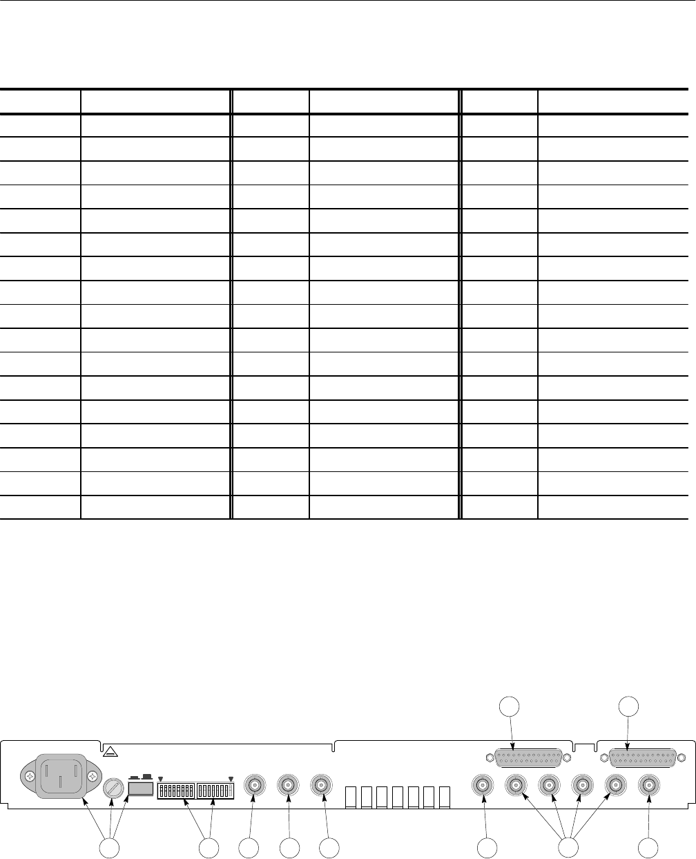
Operating Basics
VITS 200 2–35
Table 2–10: RS-232 Mnemonics
Mnemonic Signal Name Mnemonic Signal Name Mnemonic Signal Name
PAS Pass AC2 Auto Capt 2 090 CBC Composite 90 3
CBR Color Bars AC 3 Auto Capt 3 100 CBC Composite 100 3
FCP FCC Composite AC4 Auto Capt 4 110 CBC Composite 110 3
MP0 Multi Pulse VRD VIRS Auto detect 120 CBC Composite 120 3
VIR VIRS SXX SIN X/X 135 CBC Composite 135 3
GCR Ghost Cancellation SID Source ID 150 CBC Composite 150 3
RFL Red Field 20I FCC Comp 20 IRE 2165 CBC Composite 165 3
P00 0% Black EX1 Extern 1 225 CBC Composite 225 3
PD1 7.5% B lack EX2 Extern 2 240 CBC Composite 240 3
HSW 10 MHz Sweep EX3 Ex tern 3 255 CBC Composite 255 3
HSW 14.2 MHz Sweep EX4 Extern 4 285 CBC Composite 285 3
CMB NTC7 Combination 015 CBC Composite 15 3300 CBC Composite 300 3
NCP NTC7 Composite 030 CBC Compo site 30 3315 CBC Composite 315 3
MB0 Multiburst 045 CBC Composite 45 3330 CBC Composite 330 3
PD5 50% Gray 060 CBC Compo site 60 3345 CBC Composite 345 3
AC1 Auto Capt 1 075 CBC Composite 75 3360 CBC Composite 360 3
CSW Cable Sweep 4CMU Cable Multiburst 4
1 Opt 1J only. 2 Not available in Opt 1J signal set. 3 Opt 1C only. 4 S/N B020510 and above.
Rear Panel
The VITS 200 rear panel, shown in Fig. 2–6, contains the line power socket,
fuse, and power switch; the source ID selection switches, and assorted connec-
tors. Fig. 2–6 is explained on the following page.
REMOTE RS-232
FUSE POWER
OFFON START STOP
SOURCE ID
PROGRAM
IN PROGRAM
OUT MONITOR
OUT
TEST SIGNAL EXT 1 EXT 2 EXT 3 EXT 4 BLACK BURST
90–250 VOLTS
60 VA MAX 50–60HZ REPLACE ONLY
WITH 250V 1.5A
MED FUSE
TO AVOID ELECTRICAL SHOCK POWER CORD
PROTECTIVE GROUND MUST BE CONNECTED
TO EARTH GROUND
WARNING
Figure 2–6: VITS 200 Rear Panel.

Operating Basics
2–36 VITS 200
1. POWER The AC power connector, fuse, and power switch. The VITS 200 uses
a power supply which can accept line voltages from 90 to 250 VAC without
changing ranges or fuses.
2. SOURCE ID Two DIP switches used to select the source identification code, a
one-line, 16-bit word with 16,384 possible combinations. This identification
signal can be inserted as one of the VITS signals, on any of the available vertical
interval lines.
3. PROGRAM IN Program video input, onto which VITS will be inserted. This
input is internally ac-coupled and clamped to ground, and is internally termi-
nated in 75, except when the VITS 200 is in Bypass mode.
4. PROGRAM OUT Outputs the program video with user-selected VITS and
vertical interval messages inserted. If the program video fails, the VITS 200
switches to the user-selected Standby signal with, if selected, one of the three full
page standby messages as the output. If the power to the VITS 200 fails, a relay
bypass switches the program video directly to this connector.
5. MONITOR OUT This connector provides the same output as the PROGRAM
OUT connector, with one exception. During power failure this connector has no
output.
6. TEST SIGNAL This connector provides the full-field test signal selected by the
user, with any selected VITS, vertical interval messages, and standby text page
inserted on it.
7. REMOTE CONTROL This 25-pin connector provides remote ground-closure
control of manual bypass operation, force Standby mode, vertical interval
messages, standby messages, and full-field test signal output. It also provides
lines which drive bypass, unlocked, and power indicators.
8. RS-232 This 25-pin connector allows remote control of the VITS 200 with data
which complies with the RS-232C standard.
9. EXTERNAL INPUTS These four inputs: EXT 1, EXT 2, EXT 3, and EXT 4,
may be used to input external signals, such as additional test signals or teletext,
which may be inserted into the vertical interval or used as standby signals. In
addition EXT 1 may be selected as an alternate genlock input, for use during
failure of the program video signal.
10. BLACK BURST This output provides regenerated sync and burst with a 7.5%
setup flat field signal.

Specifications

VITS 200 3–1
Specifications
This section lists the performance requirements for the VITS 200, along with
pertinent supplemental information. Performance requirements may be verified
with the performance check procedure in Section 5 of the manual.
Items listed as Performance Requirements are quantitative, and are stated with
tolerance limits. All Performance Requirements are guaranteed.
Items listed as Supplemental Information are not normally verified by the
Performance Check Procedure; they are either explanatory notes or typical
operating characteristics which are not guaranteed.
PERFORMANCE CONDITIONS
The Performance Requirements listed in this section apply over an ambient temperature
range of 0° C to +50° C. The rated accuracies are valid when the instrument is
calibrated at an ambient temperature in the range of 20° C to 30° C, after a warm-up
time of 20 minutes.
The test equipment used to verify performance requirements must be calibrated and
working within the limits specified in the Recommended Test Equipment list.
Table 3–1: Program Channel
Characteristics Performance Requirements Supplemental Information
Gain Unity " 1%
Frequency Response "1% to 5.5 MHz
"3% to 10 MHz
Chrominance-to-Luminance Gain "0.5%
Chrominance-to-Luminance Delay v5 ns
Diff Phase v0.2°
Diff Gain v0.2%
Line Tilt v0.5%
DC Output Level 0 V " 10 mV
DC Matching of Inserted Test Signal to
Program Signal "3 mV
Phase Match – Relay Bypass Path to
Signal Processing Path "1° at FSC
Crosstalk w60 dB down to 5.5 MHz Typically >70 dB
Hum Rejection 50 dB Measured right after burst.
Keyboard (No Noise) Too small to measure on VM700A.

Specifications
3–2 VITS 200
Table 3–1: Program Channel (Cont.)
Characteristics Supplemental InformationPerformance Requirements
Insertion Transients v10 mV Measured on 1780. Typically <5 mV.
Input Impedance 75 W
Return Loss 36 dB to 5 MHz PROGRAM IN, PROGRAM OUT, and
MONITOR OUT
Phase Matching of Inserted Test Signal to
Program Video "1°Program Sync and Burst Normal Level
Pulse to Bar Ratio 100%"0.5% Typically within "0.25%
Signal to Noise Ratio >70 dB Unweighted Filter at 5 MHz. Measured
91 dB on VM700A, relative to reference.
Table 3–2: External Inputs
Characteristics Performance Requirements Supplemental Information
Gain Unity "1%
Frequency Response "1% to 5 MHz
"3% to 10 MHz
Chrominance-to-Luminance Gain "0.5%
Chrominance-to-Luminance Delay v5 ns
Diff Phase v0.3°
Diff Gain v0.3%
Line Tilt v0.5%
DC Offset (DC Coupled) 0 V DC "10 mV Internally DC coupled
Program Video to External Signal DC
Match 3 mV No hum, internally AC coupled
Crosstalk w60 dB down to 5.5 MHz Any channel to any other
Hum Rejection Typically 60 dB, measured right after burst.
Keyboard (No Noise) Too small to measure on VM700A.
Input Impedance 75 W
Return Loss 36 dB to 5 MHz
Program to External Channel Timing
Difference Typically "2°
Signal to Noise Ratio >70 dB 84 dB AC Coupled, 87 dB DC Coupled,
relative to reference on VM700A with an
unweighted 5 MHz low pass filter.

Specifications
VITS 200 3–3
Table 3–3: Test Signal and Black Burst General Characteristics
Characteristics Performance Requirements Supplemental Information
Frequency Response "1% to 5 MHz
"5% to 10 MHz
Luminance Amplitude Accuracy "1%
Chrominance-to-Luminance Gain "0.5%
Chrominance-to-Luminance Delay v5 ns
Diff Phase v0.3°
Diff Gain v0.3%
Line Tilt "0.5%
Output Impedance 75 W
Return Loss 36 dB to 5 MHz
Signal to Noise Ratio
Test Signal
Black Burst >78 dB
>70 dB
On VM700A with an unweighted 5 MHz low
pass filter
Spurious Signals (5 MHz 50 MHz) >55 dB down
Pulse to Bar Ratio 100% "0.5%
K Factor (K2T) 0.3% Typically 0.2
Crosstalk w60 dB down
DC Offset 0 V DC "10 mV
SCH Phase Accuracy 0 "5°< "2.5° typical
Luminance Rise Time 140 ns "20 ns
Chrominance Rise Time 300 ns "35 ns
Sync Amplitude 285 mV "3 mV
Sync Rise Time 140 ns "20 ns
BurstAmplitude
Rise Time
Delay from Sync
Duration
285 mV "6 mV p-p
300 ns "35 ns
5.3 s "100 ns
2.5 s "100 ns From 50% point of Sync
9 cycles of subcarrier
Breezeway Duration 600 ns "100 ns.
Front Porch Duration 1.5 ms 100 ns 50% amplitude point
Horizontal Sync Duration 4.7 ms 100 ns 50% amplitude point
Equalizing Pulse Duration 2.3 ms 100 ns 50% amplitude point

Specifications
3–4 VITS 200
Table 3–4: Test Signal Characteristics
Characteristics Performance Requirements Supplemental Information
0% Black 0 IRE Luminance with sync and burst See Figure 3–1 for timing information.
7.5% Black 7.5 IRE Luminance with sync and burst See Figure 3–2 for timing information.
10 MHz Sweep
Pedestal
Amplitude
Rise Time
Sweep Amplitude
Start Frequency
Stop Frequency
Std, Opt 1C
Opt 1J
45 IRE
250 ns 25 ns
50 IRE
1 MHz
10 MHz
4.2 MHz
See Figure 3–3 for timing information.
Frequency increases 1MHz/div, viewed at
line rate on a waveform monitor ( Std and
Opt 1C).
NTC7 Combination
White Reference Bar
Amplitude
Rise Time
Multiburst Packets
Amplitude
Average Level
Frequencies
Packet Rise Time
500 kHz and 1.0 MHz
Other Packets
Modulated Pedestal
Pedestal
Amplitude
Rise Time
Chrominance
Amplitude
20 IRE
40 IRE
80 IRE
Phase
Relative to Burst
Rise Time
100 IRE 0.7 IRE
250 ns 25 ns
50 IRE 0.5 IRE p-p
50 IRE 0.5 IRE
500 kHz, 1.0 MHz, 2.0 MHz, 3.0MHz, 3.58
MHz, 4.2 MHz
50 IRE 0.5 IRE
250 ns 25 ns
20.01 IRE 0.5 IRE
40.02 IRE 0.5 IRE
80.04 IRE .5 IRE
90° 0.5°
400 ns 40 ns
See Figure 3–4 for timing information.
140 ns typical (sin2 shaped packets)
400 ns typical (sin2 shaped packets)

Specifications
VITS 200 3–5
Table 3–4: Test Signal Characteristics (Cont.)
Characteristics Supplemental InformationPerformance Requirements
FCC/NTC7 Composite
Modulated 5-step Staircase
Luminance
Amplitude
FCC
NTC7
Riser Amplitude
Rise Time
Chrominance
Phase
Amplitude
Envelope Rise Time
FCC
NTC7
2T Pulse
Pulse-to-Bar Ratio
Half Amplitude Duration (HAD)
Ringing
Modulated SIN2 Pulse
Pulse-to-Bar Peak Amplitude
Half Amplitude Duration
Phase
Bar Amplitude
Rise Time
FCC
NTC7
80.4 IRE 0.7 IRE
90.2 IRE 0.7 IRE
1/5 of 5-step amplitude 0.5%
250 ns 25 ns
Same as burst 0.3°
40 IRE 0.5 IRE
375 ns 37.5 ns
400 ns 40 ns
100% 0.5%
250 ns 25 ns
1.0 IRE or less
100%
1.563 s 150 ns
60.8° 1°
100 IRE 1 IRE
250 ns 25 ns
125 ns 15 ns
See Figure 3–5 for FCC Composite timing
information.
See Figure 3–6 for NTC7 Composite timing
information.
20 IRE Composite Same as FCC Composite except Staircase.
Chrominance Amplitude is 20 IRE 0.5
IRE.
FCC Multiburst
White Reference Bar Amplitude
Packet Amplitudes
Pedestal
Burst Frequencies
Packet Rise Time
500 kHz
Other Packets
100 IRE
60 IRE p-p
40 IRE
500 kHz, 1.25 MHz, 2.0 MHz, 3.0MHz,
3.58 MHz, 4.1 MHz
See Figure 3–7 for timing information.
140 ns typical (sin2 shaped packets)
400 ns typical (sin2 shaped packets)
50% Gray 50 IRE Luminance with sync and burst See Figure 3–8 for timing information.
Sin X/X
Bandwidth
Pedestal
Peak
4.75 MHz
24 IRE
90 IRE
See Figure 3–9 for timing information.
Peak amplitude from pedestal

Specifications
3–6 VITS 200
Table 3–4: Test Signal Characteristics (Cont.)
Characteristics Supplemental InformationPerformance Requirements
FCC Color Bars
Luminance Rise Time
Color Bars
White
Yellow
Cyan
Green
Magenta
Red
Blue
Black
250 ns 25 ns
Lum Ampl Subc Ampl Subc Phase
(mV) (mV p-p) (deg)
714.3 0.0 0.0
494.3 444.2 167.1
400.7 630.1 283.4
345.7 588.5 240.8
256.0 588.5 60.8
202.1 630.1 103.4
107.8 444.2 347.1
53.5 0.0 0.0
See Figure 3–10 for timing information.
Multipulse
Amplitudes
Frequencies 80 IRE
1.0 MHz, 2.0 MHz, 3.0 MHz, 3.58 MHz,
and 4.2 MHz
See Figure 3–11 for timing information.
Vertical Interval Reference Signal (VIRS)
Chrominance Reference
Amplitude
Phase
Envelope Rise Time (SIN2
shaped)
Average Level of Chrominance
Luminance Reference
50 IRE Level
Black Reference
40 IRE
Same as burst 0.3
1 ms 100 ns
70 IRE
50 IRE
7.5 IRE
See Figure 3–12 for timing information.
Red Field
Luminance
Amplitude
Std, Opt 1C
Opt 1J
Rise Time
Chrominance
Amplitude
Std, Opt 1C
Opt 1J
Phase
Rise Time
202.2 mV 1%
160.72 mV 1%
250 ns 25 ns
630.1 mV 1%
681.23 mV %
103.4° 0.3°.
400 ns 40 ns
See Figure 3–13 for timing information.
BTA Ghost Canceller Reference (GCR)
Bar Amplitude
Positive Peak
Negative Peak
Fall time
70 IRE
77.3 IRE
–3.9 IRE
250 ns
See Figure 3–14 for timing information.

Specifications
VITS 200 3–7
Table 3–4: Test Signal Characteristics (Cont.)
Characteristics Supplemental InformationPerformance Requirements
GCR Phillips (STD, Opt 1C)
(B020249 and above)
Pedestal Amplitude
Chrominance Amplitude
Spectrum
VIT Sequence
30 IRE 0.5 IRE
80 IRE 1 IRE
Flat to 4.1 MHz. –3 dB at 4.3 MHz
See Fig. 3–15 (GCR Positive) and 3–16
(GCR Negative) for timing information.
GCR Positive – Fields 1, 3, 6, and 8
GCR Negative – Fields 2, 4, 5, and 7
GCR Korean (Opt 1K)
(B020249 and above)
Pedestal Amplitude
Chrominance Amplitude
VIT Sequence
30 IRE 0.5 IRE
80 IRE 0.5 IRE
See Fig. 3–17 (GCR Positive) and 3–18
(GCR Negative) for timing information.
GCR Positive – Fields 1, 3, 5, and 7
GCR Negative – Fields 2, 4, 6, and 8
Cable Multiburst
(S/N: B020510 & above)
White Reference Bar Amplitude
Packet Amplitudes
Pedestal Amplitudes
Burst Frequencies
Packet Rise Time
500 kHz
Other Packets
60 IRE
60 IRE
60 IRE
500 kHz, 1.25 MHz, 2.0 MHz, 3.0 MHz,
3.75 MHz, 4.0 MHz
See Figure for timing information.
140 ns typical (sin2 shaped packets)
400 ns typical (sin2 shaped packets)
Cable Sweep
(S/N: B020510 & above)
Pedestal Amplitude
Sweep
Amplitude
Frequencies
Start
Stop
50 IRE
100 IRE
0.1 MHz
4.2 MHz
Specifications
3–8 VITS 200
Figure 3–1: 0% Black
Figure 3–2: 7.5% Black
Figure 3–3: 10 MHz Sweep
Specifications
VITS 200 3–9
Figure 3–4: NTC7 Combination
Figure 3–5: FCC Composite
Figure 3–6: NTC7 Composite
Specifications
3–10 VITS 200
Figure 3–7: FCC Multiburst
Figure 3–8: 50% Gray
IRE
Figure 3–9: SIN X/X
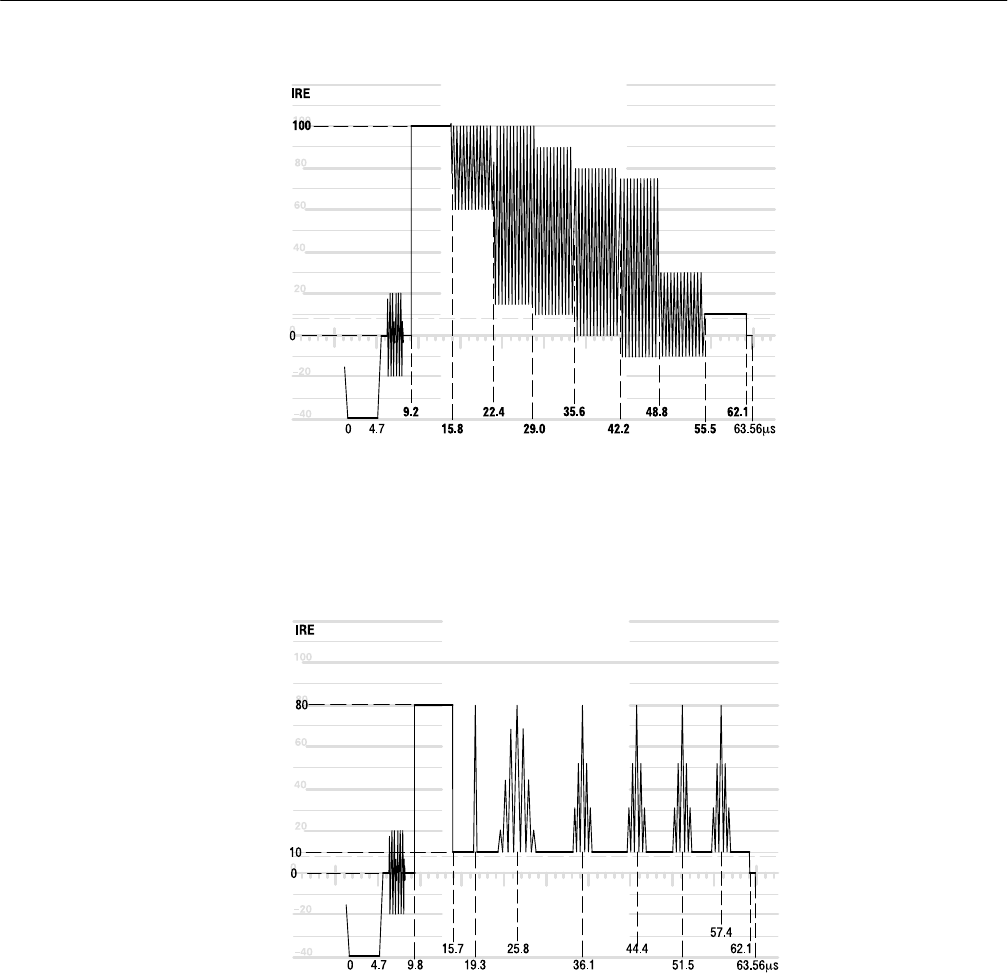
Specifications
VITS 200 3–11
Figure 3–10: FCC Color Bars
IRE
Figure 3–11: Multipulse
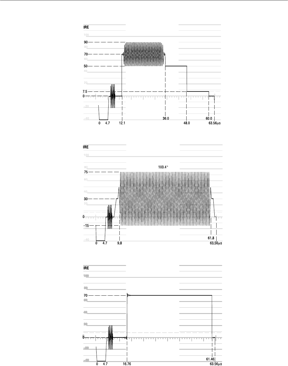
Specifications
3–12 VITS 200
Figure 3–12: VIRS
Figure 3–13: Red Field
Figure 3–14: BTA Ghost Canceller Reference
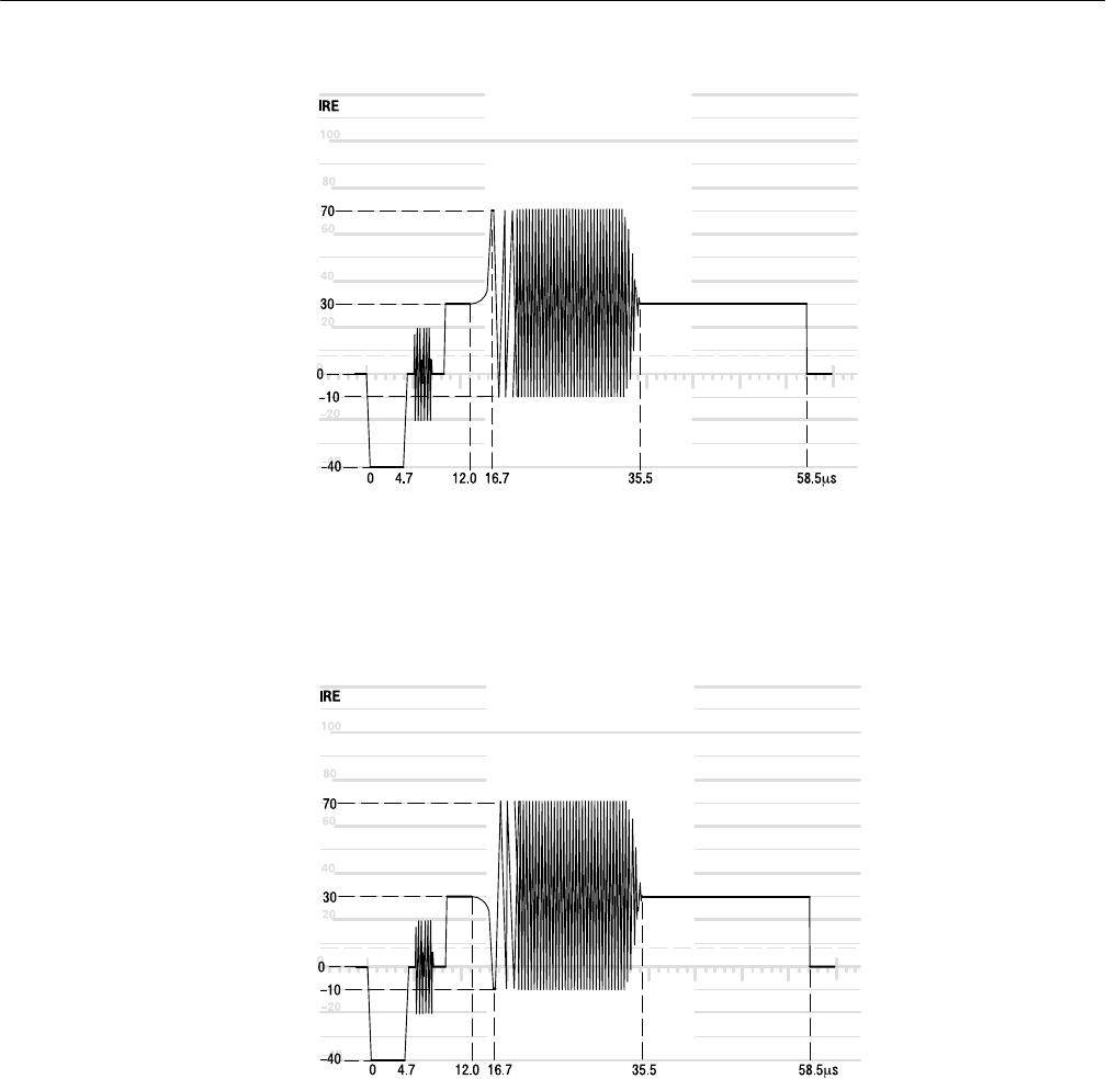
Specifications
VITS 200 3–13
Figure 3–15: Phillips GCR Positive
Figure 3–16: Phillips GCR Negative
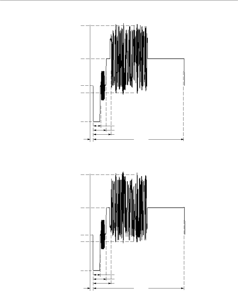
Specifications
3–14 VITS 200
70
30
IRE
–10
–40
1.5 ms 61.9 ms
11.5 ms
8.75 ms
4.7 ms
0
Figure 3–17: Korean GCR Positive
70
30
IRE
–10
–40
1.5 ms 61.9 ms
11.5 ms
8.75 ms
4.7 ms
0
Figure 3–18: Korean GCR Negative
Specifications
VITS 200 3–15
Figure 3–19: Cable Multiburst
Figure 3–20: Cable Sweep

Specifications
3–16 VITS 200
Table 3–5: Genlock Characteristics
Characteristics Performance Requirements Supplemental Information
Burst Lock
Genlock Phase Change with Input
Amplitude
Genlock Phase Change with Input
Signal APL
Frequency Dependence on Input Burst
Lock Range
Frequency
Amplitude
Genlock Phase Jitter with Input
Amplitude Change
2° burst phase change for input sync or
burst amplitude range of 287mV 3 dB
4° burst phase change for amplitude
range of 287mV 6 dB
1° burst phase change over 10% to 90%
APL
1° burst phase change for 20 Hz
change in incoming subcarrier
3.579545 MHz 20 Hz
+6 dB to –12 dB
For either composite video or burst
amplitude errors
Typically to –21 dB
Typically 0.2° peak for input sync or
burst amplitude range of 287 mV 3dB;
no noise on input signal.
Typically 0.4° peak for input amplitude
range of 287 mV 6 dB; no noise on input
signal.
Sync Lock Jitter 10 ns for input sync amplitude range of
287 mV 3 dB No noise on input signal
Noise Performance Locks to 28 dB S/N Ratio Video
Table 3–6: Power Supply Characteristics
Characteristics Performance Requirements Supplemental Information
Output Voltages
+5 V
5.2 V
12 V
200 mV From 1A to 3 A (voltage
adjustable)
300 mV From 0.5 A to 1 A
240 mV From 0.05 A to 0.2 A (post
regulated from 14.5 V by linear regula-
tors)
Output Ripple
+5 V
5.2 V
12 V
50 mV switching ripple
5 mV line frequency ripple
50 mV switching ripple
10 mV line frequency ripple
10 mV switching ripple
5 mV line frequency ripple
Line Input Range Regulates from 90 to 250 VAC.

Specifications
VITS 200 3–17
Table 3–6: Power Supply Characteristics (Cont.)
Characteristics Supplemental InformationPerformance Requirements
Minimum Load 10 watt minimum load required to operate.
However, output voltages other than +5 V
may not meet specifications outside the
listed currents. At zero load the power
supply cycles on and off.
Power Consumption 40 – 50 W
Overvoltage Protection The 5 V output is protected by a crowbar
circuit that engages at approximately 5.7 V.
Overvoltage protection causes the power
supply to cycle by engaging the primary
side current limit time-out circuit (described
below).
Power 75 VA maximum, controlled by primary side
current limit circuits. Power supply cycles
on and off when power limit is reached.
Short-Circuit Protection All outputs are protected by the primary
side current limit and time-out circuits. In
addition, the 12 V outputs are limited to
1 A by the linear regulators.
Efficiency 70% nominal
Fan Drive 15 V to 16.5 V, as determined by supply
load.
Table 3–7: Physical Characteristics
Characteristics Performance Requirements Supplemental Information
Dimensions
Height
Width
Length
1.734 inches (4.404 cm)
19.0 inches (48.3 cm)
18.4 inches (46.7 cm)
Net Weight 9.5 lbs (4.3 kg)
Shipping Weight 21.5 lbs (9.8 kg)

Specifications
3–18 VITS 200
Table 3–8: Environmental Characteristics
Characteristics Performance Requirements Supplemental Information
Temperature
Nonoperating
Operating –40° to +65° C (–40° to +149° F)
0° to +50 °C (32° to 122° F)
Altitude
Nonoperating
Operating To 50,000 ft (15,240 m)
To 15,000 ft (4,572 m)
Vibration (Operating) Fifteen minutes each axis at 0.025 inch.
Frequency varied from 105510 Hz in
4-minute cycles with the instrument
secured to the vibration platform; ten
minutes each axis at any resonant point or
at 55 Hz.
Shock 50 G’s, 1/2 sine, 11 ms duration, three
guillotine shocks per side.
Transportation Qualified under NTSA Test Procedure 1A,
Category II (36-inch drop).
Table 3–9: Certifications and compliances
Category Standards or description
EC Declaration of Conformity –
EMC 1Meets intent of Directive 89/336/EEC for Electromagnetic Compatibility. Compliance was
demonstrated to the following specifications as listed in the Official Journal of the European Union:
EN 50081-1 Emissions:
EN 55022 Class B Radiated and Conducted Emissions
EN 50082-1 Immunity:
IEC 801-2 Electrostatic Discharge Immunity
IEC 801-3 RF Electromagnetic Field Immunity
IEC 801-4 Electrical Fast Transient/Burst Immunity
1High-quality shielded cables must be used to ensure compliance to the above listed
standards.
FCC Compliance Emissions comply with FCC Code of Federal Regulations 47, Part 15, Subpart B, Class A Limits.
Installation (Overvoltage)
Category Terminals on this product may have different installation (overvoltage) category designations. The
installation categories are:
CAT III Distribution-level mains (usually permanently connected). Equipment at this level is
typically in a fixed industrial location.
CAT II Local-level mains (wall sockets). Equipment at this level includes appliances, portable
tools, and similar products. Equipment is usually cord-connected.
CAT I Secondary (signal level) or battery operated circuits of electronic equipment.

Specifications
VITS 200 3–19
Table 3–9: Certifications and compliances (cont.)
Category Standards or description
Pollution Degree A measure of the contaminates that could occur in the environment around and within a product.
Typically the internal environment inside a product is considered to be the same as the external.
Products should be used only in the environment for which they are rated.
Pollution Degree 1 No pollution or only dry, nonconductive pollution occurs. Products in
this category are generally encapsulated, hermetically sealed, or
located in clean rooms.
Pollution Degree 2 Normally only dry, nonconductive pollution occurs. Occasionally a
temporary conductivity that is caused by condensation must be
expected. This location is a typical office/home environment.
Temporary condensation occurs only when the product is out of
service.
Pollution Degree 3 Conductive pollution, or dry, nonconductive pollution that becomes
conductive due to condensation. These are sheltered locations where
neither temperature nor humidity is controlled. The area is protected
from direct sunshine, rain, or direct wind.
Pollution Degree 4 Pollution that generates persistent conductivity through conductive
dust, rain, or snow. Typical outdoor locations.
Safety Standards
U.S. Nationally Recognized
Testing Laboratory Listing UL1244 Standard for electrical and electronic measuring and test equipment.
Canadian Certification CAN/CSA C22.2 No. 231 CSA safety requirements for electrical and electronic measuring and
test equipment.
European Union Compliance Low Voltage Directive 73/23/EEC, amended by 93/69/EEC
EN 61010-1 Safety requirements for electrical equipment for measurement,
control, and laboratory use.
Additional Compliance IEC61010-1 Safety requirements for electrical equipment for measurement,
control, and laboratory use.
Safety Certification Compliance
Temperature, operating +5 to +40_ C
Altitude (maximum operating) 2000 meters
Equipment Type Test and measuring
Safety Class Class 1 (as defined in IEC 1010-1, Annex H) – grounded product
Overvoltage Category Overvoltage Category II (as defined in IEC 1010-1, Annex J)
Pollution Degree Pollution Degree 2 (as defined in IEC 1010-1). Note: Rated for indoor use only.

Specifications
3–20 VITS 200

The following servicing instructions are for use only by qualified personnel. To
avoid injury, do not perform any servicing other than that stated in the operating
instructions unless you are qualified to do so. Refer to all Safety Summaries before
performing any service.
WARNING

Theory of Operation

VITS 200 4–1
Theory of Operation
The VITS 200 contains three boards:
A1 Inserter,
A2 Front Panel, and
A3 Controller.
The Front Panel board contains only momentary contact switches and a
connector, and needs no further discussion.
The Controller and Inserter boards interact quite intimately; therefore some of
the circuit discussions will include parts of both boards.
This description will include the following sections:
Test Signal Generation
Genlock
External Inputs
Signal and Switching Control
Character Generation
Front Panel and Controller
Power Supply
When a new function is mentioned, the board name and reference designator for
the part which performs that function will be put in parentheses; for example:
The timing for the channel switch (A1U64) is generated by the Horizontal
Timing PROM (A1U27).
Test Signal Generation
Test signal circuitry is located on the Inserter board and is found on the
following schematics: Inserter<1>, Source ID and Bypass Controls <3>, and
Analog Output <7>.
Test signals are generated by clocking data from PROMs to a digital-to-analog
converter at an 8 FSC rate (28.636363 MHz). The output of this DAC is filtered
and buffered before driving the Test Signal Output, the black burst channel
switch (A3U60), and the VITS insertion channel switch (A1U64).
Test signal generation starts with a 4 FSC clock which clocks the Horizontal
Counters (A1U28, schematic 3), to provide 910 counts per line of video. This
part also decodes backporch clamp pulse “CLAMP”, for clamping the test signal.
The Horizontal Counter drives the Horizontal Decoder PROM (A1U27,
schematic 3) which provides timing signals for various functions. The Horizon-
tal Counters are reset by a pulse, “[FRAME]”, from the Genlock circuitry so that

Theory of Operation
4–2 VITS 200
the test signals are timed with program video. A pulse once per line from the
Horizontal Decoder PROM enables the Vertical Counters (A1U24, schematic 3).
The Vertical Counters drive the Vertical Decoder PROM (A1U25, schematic 3).
The Vertical Decoder PROM is latched twice per line by A1U26.
Test signal data is stored in PROMs A1U4, A1U5, and A1U6, shown on
schematic 1. A1U4 and A1U5 store the eight MSBs of alternate data samples
and U6 stores the four LSBs for samples from both U4 and U5. The outputs of
U4 and U5 are multiplexed (A1U82 and A1U83, schematic 1), to increase the
data rate from 4 FSC to 8 FSC, and latched (A1U1, schematic 1) before being
converted to ECL levels (A1U9, A1U10, schematic 1) for the DAC (A1U65,
schematic 7). The four LSBs are latched by A1U3 (schematic 1) and then
selected by a multiplexer (A1U7, schematic 1) before being converted to ECL
levels by A1U11 (schematic 1) for the DAC.
Data is stored in these PROMs in blocks of eight. These blocks of data are
addressed by the Block PROM, A1U13 (schematic 1), and two test signal select
lines. When the test signal select circuitry calls for a certain signal, the Block
PROM (A1U13) uses V1 to determine the correct phase of subcarrier, “HALF-
LINE” to determine when to generate a half line, and the seven MSBs of
horizontal count to select the appropriate blocks of data.
The 12-bit Tektronix DAC, A1U65 (schematic 7), turns the data into analog
voltage levels at an 8 FSC rate. A one-volt reference is generated for the DAC
by A1U84 (schematic 7) and associated parts. The analog signal is then filtered
by a seven-pole filter (A1L12, A1L13, A1L14, and associated capacitors, on
schematic 7) with one second-order group delay correction stage (A1T2,
schematic 7).
The signal is AC coupled to a buffer and clamped (A1U67, schematic 7) to
remove any DC level change with temperature. This allows the test signal DC
level to match the Program Video DC level very accurately.
This video buffer drives the TEST SIGNAL OUTPUT bnc (A3J54, schematic 6),
the Black Burst circuitry (A3U60, schematic 6), and the channel switch (A1U64,
schematic 7), which switches between Program Video, VITS, and external
inputs. The output of the channel switch, A1U64, drives the MONITOR
OUTPUT bnc and the PROGRAM OUTPUT bnc.
The Program Output goes through a relay (A1K2, schematic 7) which switches
the Program Input through a delay line (A1L7, A1L3, C52, schematic 7) to the
Program Output when the power shuts off or when the front-panel RELAY
BYPASS button is pushed. The delay line in this Relay Bypass mode matches
the time it takes when the video travels through the processing circuitry. Control
of this relay will be explained in the CONTROLLER discussion of this section.
Black burst output is generated by switching off the active video and leaving the
sync and burst. The test signal from A1U67 (schematic 7) goes over a cable to

Theory of Operation
VITS 200 4–3
the black burst channel switch, A3U60 (schematic 6), which switches between
the test signal and ground at the appropriate times.
Genlock
The Genlock circuitry is located on the Inserter board and is found on the
following schematics: Genlock <4>, Input <5>, and Clocks and Genlock
Offset <6>.
The Program Input is buffered and clamped by A1U42 (schematic 5). The video
then enters the sync stripper IC, A1U44. This IC not only strips off composite
sync but also generates back porch timing for clamping.
Comp sync and back porch timing are level shifted to TTL levels by A1Q1,
A1Q3, A1VR1, and A1VR2 (schematic 5) and gated together by A1U57a and
A1U57b (schematic 5), to get a clamp pulse to control A1U42. A1U44 also
generates a program present signal as long as video greater than 35 dB is present.
The controller, A3U23 (schematic 3), uses this signal to determine whether or
not to try to lock to Program Video or to try to lock to the alternate genlock
source, External 1. The alternate genlock mode must be enabled for this to be
used.
Input buffer A1U42 also drives the analog-to-digital converter (ADC), A1U43
on schematic 5, for the genlock. The ADC has three inputs, two of which are
used. Program Video drives one of the inputs and EXTernal 1 drives the other.
Either can be used by the genlock circuit, as chosen by the controller. The ADC
has an AGC and clamp, with “SYNCTIP” and “BACKPORCH” providing timing.
The clamped and AGC’d video is then routed through an anti-aliasing filter
(A1L1, A1C19, A1C20, and A1C21 on schematic 5) and brought back into the
ADC where it is digitized. The digital output goes into a PAL where it is
inverted and latched. “SIS_TM” from the genlock ASIC (A1U29, schematic 4),
if enabled, holds the same sample across the bottom of sync to block Sound-in-
Sync pulses from reaching the genlock circuitry.
The data then goes to the genlock ASIC (A1U29, schematic 4) which has RAM,
counters, decoders, and other circuitry necessary for genlocking. The composite
sync from the chosen genlock input is also routed to the genlock ASIC through a
PAL (A1U70, schematic 3) and is controlled by the same line that chooses the
genlock input, “GLSEL1”. The genlock ASIC uses the comp sync to roughly
position the Horizontal and Vertical Counters within it.
The genlock processor (A1U35, schematic 4), an 8 MHz Z80, uses the data to
calculate the SCH of the incoming video to determine the correct color framing.
It then uses the digitized color subcarrier burst to determine the tangent of the
phase angle between the system clock and the burst. This tangent is used to look
up the arctangent (that is, the angle itself), which is stored in PROM A1U33

Theory of Operation
4–4 VITS 200
(schematic 4). The arctangent is then used as a correction to the system clock, a
VCO on A1 schematic 6, thus making a phase-locked loop.
The correction is an eight-bit word which is sent to DAC A1U59 on schematic 6.
The output of the DAC is integrated by an opamp (A1U61A, schematic 6) and a
capacitor, A1C46. An analog switch (A1U60, schematic 6) is used to short the
integrator when not genlocking, and to change the loop characteristics once lock
is securely acquired. The processor also increases loop gain once lock has been
acquired, and tells the genlock ASIC to send out a frame reset pulse which aligns
the test signal counters with the genlock counters.
There are several other parts which support the genlock function. A1Y39, on
schematic 4, is the clock for the genlock processor (NOT the system clock,
VCO). A1U31, schematic 4, is a hardware watchdog which resets the processor
if it fails to receive an “awake” signal from the processor within the right amount
of time. A1U38, schematic 4, latches control signals “GLK/[INT]” and
“ACQ/[HOLD]” for the analog switch, A1U60, schematic 6; the signal
“LOCKED”, which tells the rest of the VITS 200 that genlock has been achieved;
and the signal “CLAPBRD”, which is used in the Video Clapboard feature,
described later. Counter/timer A1U30, schematic 4, is used to distinguish
between even and odd fields of video.
Genlock sub-clock cycle timing can be adjusted up to 90 with A1S7, schematic
4. The VITS signals are timed to program video input at the factory, and should
not need adjustment.
Diagnostics may be run on the genlock circuit by manually rotating A1S8,
schematic 4.
External Inputs
The External Inputs circuitry is located on the Controller board and is found on
the following schematics: External Inputs 1 & 2 <1>, External Inputs 3 & 4 <2>,
Input <5>, and Clocks and Genlock Offset <6>.
There are four external inputs to the VITS 200, each of which may be selected
for any lines of the vertical blanking interval just like a VITS signal. As the four
external inputs are identical, this discussion will focus on the EXTernal 1 input.
The EXTernal 1 input is internally terminated in 75 ohms (A3R1, schematic 1)
and AC-coupled by A3C1 to buffer and clamp amplifier A3U1, on schematic 1.
The video buffer drives a separate sync stripper (A3U3, schematic 1) for the
channel. The buffer and clamp amplifier and the sync stripper work the same as
for the Program Video input. Refer to the GENLOCK section of this discussion
for more details.
The external inputs have some features not found on the Program Input. The
clamp for the external input can be run from its own sync stripper, or from the

Theory of Operation
VITS 200 4–5
system timing; that is, a clamp pulse derived from the test signal counters. This
is a jumper selection, made with A3J19 (schematic 1) for the EXTernal 1 input.
The external input comp sync is compared to system sync timing pulse
“[SYNCT]” by A3U6A (schematic 1), to check that they are timed close to each
other. “[SYNCT]” is a negative-going 10.8 s pulse which frames the acceptable
time for sync pulses to occur. If any portion of the positive-going external input
comp sync occurs outside of this period, one-shot A3U7A (schematic 1) is
triggered to produce the “BADSYNC1” pulse.
The “BADSYNC1” output is monitored by A3U12 (schematic 6), which does not
allow insertion into Program Video if the “BADSYNC1” pulse occurs. This
protects the program from getting a sync pulse somewhere out in the middle of a
line.
The external input may be changed to DC coupling. This selection is made in
the UTILITIES menu. When this coupling mode is selected, the gate of FET
A3Q1, pulled down to 12V by “DC/[AC1]” for AC coupling, is pulled up to
the level of its source. The FET is then turned on, shorting out the AC-coupling
capacitor, A3C1.
While DC coupled, the external input comp sync is not monitored, nor is
insertion inhibited if sync is not correctly timed. The “CLAMP” pulse to the
input buffer is turned off (A3U55A, A3U56A), and clamp capacitor A3C3 is
shorted to ground by A3U57 on schematic 6. DC coupling of an external input,
then, allows the insertion of signals which do not have sync pulses.
While DC coupled, the DC level may be adjusted with A3R60 When AC
coupled the clamp level may be adjusted with A3R9. A3R15 is used to adjust
the external input gain.
The video from the external input buffer is applied to channel switch A3U41
(schematic 5), which is controlled line-by-line by the signal selection circuitry.
External input channel switch A3U41 drives the program channel switch, A1U64
on schematic 7, which switches between Program Video, VITS signals, and
external input signals.
Signal and Switching Control
The Signal and Switching Control circuitry is located on the Controller board
and is found on the following schematics: Microprocessor Kernel <3>, and Test
Signal & Char Sel Memory <4>.
The circuitry for controlling the test signal generator, the external input channel
switch, and the program channel switch resides on both the A3 Controller board
and the A1 Inserter board. The controller (A3U23, schematic 3) stores VITS
selections in RAM (A3U29, schematic 4) which is addressed by the system

Theory of Operation
4–6 VITS 200
counters each line. The RAM output controls the channel switches and test
signal generation.
The addressing for the test signal select RAM (A3U29, schematic 4) comes from
the vertical decoding PROM (A1U25, schematic 3). The RAM does not contain
a location for every line in the field so it is necessary to decode the vertical
count. The RAM addressing goes through a buffer which can be tri-stated
(A3U36, schematic 4) while the controller (A3U23, schematic 3) is writing into
the RAM.
The output of the RAM is latched in a PAL (A3U38, schematic 4) where control
signals for the external input channel switch (A3U41, schematic 5) are decoded.
Two signals, “VSYNC” and “VDRIVE”, which come from the vertical decoder
PROM, force the output of U38 to select the vertical sync signal regardless of
the output of the RAM. The controller uses that time to write to the RAM.
The signal “BADSYNC” is used by A3U38 to inhibit the selection of an external
input when the sync from that input does not properly line up with the system
sync. The decoded control signals for the external input channel switch are
latched again by A3U58 (schematic 4) so they match the delay through the rest
of the selection circuitry. A3U58 uses “BADSYNCEX” during alternate genlock
mode to inhibit insertion of external inputs which have sync pulses that are not
aligned with EXTernal 1 input, which is being used as the genlock source.
A3U58 is also used to invert “[SYNCT]” to get “BLKBRST” which controls the
black burst channel switch.
From U38 the test signal select lines FPTS[0..7] go to the A1 Inserter board.
Two PALS, A1U16 and A1U17 (schematic 1), decode control signals and latch
the signal selections. A1U16 latches the lower six bits to the test signal PROMs,
decodes when the source ID signal is requested, and determines when it is okay
to generate characters. It uses the two MSBs to determine what the program
channel switch should select: Program Video, test signals, or external inputs.
The “VDRIVE” input to A1U16 is used to hold the two MSBs constant while the
controller writes other choices into the RAM.
A1U17 decodes when VIRS AUTO has been requested. It enables the circuitry
which compares Program Video with the VIRS test signal to see if VIRS is
already present on Program Video (Inserter schematic 5). A1U46 (schematic 5)
is an operational amplifier which subtracts low-pass filtered Program Video from
filtered test signals, and drives a window comparator (A1U47A and A1U47B,
schematic 5).
If the program signal and the test signal match closely enough, the comparator
output remains high and the output of OR gate A1U48A (schematic 5) remains
high, and one-shot A1U71B (schematic 5) is not triggered. The OR gate can
only trigger the one shot when A1U17 determines that VIRS AUTO has been
requested and drives “[VIRSAMP]” active low. “VIRSPRES” from A1U71B
returns to A1U17 and “CCVIRS” from A1U17 is sent to A1U14 (schematic 1) to
control insertion.

Theory of Operation
VITS 200 4–7
Similarly, when AUTO CAPT [1..4] is requested as a VITS, A1U17 (schematic
1) uses “CCLINE” to enable A1U41 (schematic 5) to look for close captioning
on the selected video line on the genlock input. A1U41 drives “CAPTION” high
whenever video goes above approximately 285 mV.
If “CAPTION” is activated by close-captioning pulses, one-shot A1U71A is
triggered. “CCPRES” goes back to A1U17 (schematic 1), which activates
“CCVIRS”. This tells A1U14 whether to pass the close captioning or to switch
to one of the four external inputs when close captioning is not on the Program
Video.
A1U17 also decodes “DVDRIVE” and “DVSYNC” which are delayed from
“VDRIVE” and “VSYNC” by a half line and therefore are timed with the actual
test signals that are generated.
U14 takes the information from A1U16 and A1U17, the insertion timing
“CHSWT”, regeneration of sync and burst request and timing, character present
signal, and other timing signals and determines three control signals: two for the
program channel switch, “SW0” and “SW1”, and one to choose between character
generation and test signal generation, “TS/[CHAR]”.
Character and Source ID Generation
The Character and Source ID Generation circuitry is located on the Inserter board
and is found on the following schematics: Inserter <1> and Source ID & Bypass
Controls <3>.
While the source ID circuitry is located entirely on the Inserter board, the
character-generation circuitry is divided between the Inserter board and the
Controller board. The character generator and the source ID generator share two
ICs (A1U12 and A1U15, schematic 1) which form a state machine to generate
the data for shaped pulse edges. When source ID pulses or characters are called
for, the test signal data latch outputs (A1U1, schematic 1) become high
impedance and the outputs of A1U12 are enabled. The character or ID data then
goes to the DAC (A1U65, schematic 8) which converts the data to actual analog
pulses.
When the state machine sees a low-to-high transition, it counts up to six and
stops. When the state machine sees a high-to-low transition, it counts back to
zero and stops. This count goes to A1U12, where it is decoded into the data
which produces rising and falling shaped edges out of the DAC.
The source-identification signal is one line of video with up to 16 pulses on it,
which can be recognized by a TEKTRONIX VM700A. The VM700A expects a
start and a stop bit, but the other 14 bits (pulses) can be used to identify up to
16,384 sources (214).

Theory of Operation
4–8 VITS 200
The 16 bits can be set or cleared by two sets of DIP switches (A1S5 and A1S6,
schematic 3) accessible through the rear panel of the instrument. The 16 bits are
loaded into two shift registers (A1U22 and A1U23, schematic 3) once every line
by a signal decoded from the Horizontal Counters. The bits are then shifted out
by “IDCLOCK”, a clock which is also decoded from the Horizontal Counters.
The serialized ID bits go to A1U15 (schematic 1) where they are gated with
“IDCLOCK” and latched by the eight times subcarrier (8 FSC) clock. If Source
ID is chosen for a certain line, A1U16 (schematic 1) activates “IDEN” which
causes the state machine in A1U15 to be controlled by the latched ID signal.
Character generation begins on the Controller board, A3. Controller A3U23
writes VBI (Vertical Blanking Interval) character selections made from the front
panel or RS-232 into RAM (A3U32, schematic 4) during the vertical sync. The
top 512 bytes contain the 15 different vertical blanking interval messages. Each
vertical message may be up to 23 characters. The lower three blocks of 512
bytes hold three different pages, or frames, of character messages. Each page
may contain 20 characters across by 13 lines down, for a total of 260 characters
per page. In the RAM each character is represented by one byte.
During the vertical blanking interval, P0 and P1 are forced high by “[BLANK]”
(A3U39C and D, schematic 4) to select the block of RAM holding the vertical
interval messages. During the active portion of the picture frame one of the
lower three blocks of data is addressed by CA9 and CA10 from the controller.
Part of the lower nine address bits come from a vertical decoder PROM (A3U37,
schematic 4), and the remainder come from the Horizontal Counters. The
address lines driven by the Horizontal Counters change the character slot in the
RAM as the video scans right over the picture frame. The address lines from the
vertical decoder PROM tell the RAM when a new line of characters is needed.
This addressing is latched by A3U34 (schematic 4) which goes to high imped-
ance when the controller is writing to the RAM.
From the RAM, the bytes, each representing a character, go to the pixel PROM
(A3U31, schematic 4). The pixel PROM contains an array of 32 by 32 pixels for
each character. The pixels are made by serializing 8-bit words out of the pixel
PROM. “BH3” and “BH4” select these four words as the video scans horizontal-
ly. “FLD” takes care of the field interlace. The 16 lines per field per character
are addressed by “DV[0..3]” from vertical decoder PROM A3U37 (schematic
4).
A3U30 (schematic 4) serializes the data. Data is loaded every eight clock cycles
(4 FSC) by “CHLOAD” from A3U35 (schematic 4). A3U30 shifts the pixel data
over to the Inserter board where it is given shaped edges by the state machine
described in the source ID description.
A3U35 (schematic 4) performs several functions besides deriving “CHLOAD”
from the Horizontal Counters. It also looks at the data coming out of the RAM
to determine if a character is being called. If it is, “CHARPRES” is asserted

Theory of Operation
VITS 200 4–9
unless characters have been disabled by “[CHAREN]” or “[VCHAREN]” from
the controller. “[CHAREN]” enables or disables the characters in the active
picture area, and “[VCHAREN]” enables or disables characters in the vertical
blanking interval. The vertical blanking lines are defined by “[BLANK]”.
”DATACOMP”, from the Inserter board, indicates when the level of the character
pulse is approximately equal to or greater than the test signal data. This signal
controls when “[CHARPRES]” is deasserted, so that the transition from
character to test signal will be smooth. Bit 7 from RAM A3U32 is used to invert
the data coming from the serializer, A3U30, when a cursor is desired. This bit
should be set for only one location in the RAM at a time. The data inversion
occurs in A1U15 (schematic 1).
Front Panel, Remote Controls, and Controller
The Front Panel, Remote Controls, and Controller circuitry is located on the
Controller board and is found on the following schematics: Microprocessor
Kernel <3>, External Multiplexer <5>, and Processor I/O <7>.
All functions of the VITS 200 may be controlled from the front panel. The
momentary contact switches on the front panel are debounced by A3U19
(schematic 3), which then outputs a code which indicates the activated switch
and sends an interrupt to the controller (A3U23, schematic 3).
Control of the VITS 200 may also be accomplished through the RS-232 port. A
cable attaches the rear panel RS-232 connector to A3J11 (schematic 5). A3U40
(schematic 5) level shifts the RS-232 data to and from TTL levels for the
controller. The controller has two RS-232 interfaces built into it.
The third control method for the VITS 200 is a ground closure remote which can
be connected to the rear-panel REMOTE CONTROL connector. A cable
connects this to A3J12 on the Controller board (schematic 5), see Fig. 71. Note
that there is not a one-to-one correspondence between the pins on the board and
on the rear-panel connector. Pin numbers in this discussion refer to the pins of
A3J12. Pins 1 through 15 connect to tri-state buffers (A3U50 and A3U62,
schematic 7) which the controller can read. Capacitors and diodes (A3CR2,
A3CR3, and A3CR4, schematic 7) protect these inputs from static discharge.
Remote Controls
Theory of Operation
4–10 VITS 200
1
13
14
25
REM1
REM0
REM2
REM3
REM4
REM5
REM6
REM7
REM7
REM7
REM10
REM11
REM12
REM13
REM14
REM15
RPOWERIND
RBYPASSIND
RUNLOCKIND
RBYPASS
GND
GND
GND
REMIND
REMEN
12
NC
25 26
(ENABLE VERT INT TEXT)
(MESSAGE SELECT BIN 0)
(MESSAGE SELECT BIN 1)
(MESSAGE SELECT BIN 2)
(MESSAGE SELECT BIN 3)
(STANDBY)
(PAGE 0)
(PAGE 1)
(FORCE STANDBY)
(EXTRA)
(TEST SIGNAL)
(RESERVED)
(RESERVED)
(RESERVED)
(POWER LED)
(BYPASS LED)
(UNLOCKED LED)
(BYPASS SWITCH)
(REMOTE LED)
(REMOTE SWITCH)
J12
A3 CONTROLLER BD REMOTE
CONTROL
REAR PANEL
Figure 4–1: Remote Control Connector Pinout.
Pin 16 is driven by an open collector transistor (A3Q40, schematic 7), and pulls
down when the VITS 200 is in Standby mode. This is intended to be used as a
trigger for other instruments with ground closure remotes, such as the TEKTRO-
NIX ASG 100. Pin 17 is intended to drive an LED to indicate power on. Pins
18 and 19 are to drive LEDs indicating when the VITS 200 is in Bypass mode
and when it is not genlocked (UNLOCKED). A3U43A and A3U43B (schematic
5) are used as buffers to drive A3Q17 and A3Q18, respectively. Both transistors
work in the same manner; when the buffer inputs are high, the base of the
transistor is pulled up to +5V and is turned completely off. When the buffer
inputs are low, the transistor is saturated and drives current to the LED in the

Theory of Operation
VITS 200 4–11
remote. The current to the remote LEDs is limited by collector resistors A3R149
and A3R150.
Pin 20 of the ground closure remote forces the VITS 200 into Relay Bypass
mode when pulled low by the remote. Pin 20 is ORed (A3U59, schematic 5)
with a bypass control line from the controller, and then sent to the Inserter board
bypass controller (A1U70, schematic 3). Pins 21 through 23 are grounds. Pin
24 is intended to drive an LED indicating when the ground closure remote has
control of the VITS 200. Pin 25 is connected to the controller, and is pulled low
by the remote to request control of the VITS 200.
A3Y1 (schematic 5) is the clock for the controller (A3U23, schematic 3).
A3U44A and A3U44B (schematic 5) convert the clock output to a differential
signal before it goes to the controller. A3U17 (schematic 3) is a hardware
watchdog for the controller. If it is not given an “[AWAKE]” signal every so
often, it assumes that the processor is not functioning correctly and resets it. It
will also reset the processor if the +5V supply drops below +4.5V.
The address space of the controller is decoded by A3U21 (schematic 3) to get
chip enables and latch pulses. A3U28 (schematic 3) generates output enables for
the software PROM (A3U26, schematic 3), the stack RAM (A3U18, schematic
3), and the nonvolatile RAM (A3U27, schematic 3). A3U28 also generates the
output enables and read/write signals for the test signal select RAM (A3U29,
schematic 4) and the character select RAM (A3U32, schematic 4).
The controller latches addresses to the test signal RAM with A3U22 (schematic
3) and reads and writes data to the RAM via A3U25 (schematic 3), a bidirection-
al tristate buffer. Similarly, the controller latches addresses to the character select
RAM with A3U20 (schematic 3) and reads and writes data to the RAM via
A3U24 (schematic 3). An extended data bus is accessed via A3U53 (schematic
7).
On the extended bus are tristate buffers A3U52 (schematic 7) for reading
front-panel encoder A3U19 (schematic 3), A3U51 (schematic 7) for reading
status bits from the genlock processor, and A3U50 and A3U62 (schematic 7) for
reading the ground closure remote.
Output enables for A3U50, A3U51, A3U53, and A3U62 are generated by
A3U54 (schematic 7). Also on the extended data bus are latch A3U47 (schemat-
ic 7) for front-panel display data, latch A3U48 (schematic 7) to control the
external input clamps and genlock diagnostics, and latch A3U61 (schematic 7)
for various control signals.
A3U61 pin 19 controls the regeneration of sync and burst. A3U61 pin 16 allows
the controller to put the VITS 200 into Bypass mode. A3U61 pin 15 allows the
controller to put the VITS 200 into Standby mode. A3U61 pin 12 selects
between the mode that allows programming of lines 10 through 23 and the mode
that allows programming of lines 17 through 30. A3U61 pin 9 controls whether
Controller

Theory of Operation
4–12 VITS 200
the VITS 200 tries to lock to program input or EXTernal 1 input. This line
switches the input to the genlock A/D (A1U43, schematic 5), the back porch
signal to the A/D, and the comp sync to the genlock with A1U70 (schematic 3).
A3U61 pin 6 drives the remote indicator output. A3U61 pin 5 goes to A1U14
(schematic 1) and allows the controller to inhibit insertion of test signals while
still passing program signal.
Power Supply Overview
The power supply is located on the Inserter board and is found on schematics
<8> and <9>. This type of power supply is called a current-mode-controlled,
discontinuous, flyback, switching power supply. The current output is distrib-
uted between the four supplies as follows:
+12V 0.5 Amps max
+5V 4 Amps max
5V 1.5 Amps max
12V 0.2 Amps max
The power inductor, T1 (schematic 8), is driven by switching the voltage to its
primary winding on and off at a rate of approximately 45kHz. T1 is not used as
a transformer, but as an energy storage device; the energy is stored in the primary
during the first half of the switching cycle, while voltage is being applied. On
the second half of the switching cycle, voltage to the primary is switched off and
the energy stored in T1 is transferred to the secondaries.
Regulation is accomplished through feedback from the +5V supply to the Pulse
Width Modulator, U78 (schematic 8), controlling voltage to the primary. This
varies the length of time that voltage is applied to the primary, causing it to store
either more or less energy.
There is also circuitry to provide for operation from both 110 and 220 VAC
supplies, overvoltage protection (crowbar) on the +5V supply, and shutdown
circuitry which forces a restart of the supply if it remains in current limit for
more than a short period of time (<1 sec).
WARNING. All primary voltages are referenced to a floating ground, not chassis
ground. An isolation transformer or a differential amplifier is therefore required
for troubleshooting the circuitry in the primary and the Pulse Width Modulator,
and in their supporting circuits.

Theory of Operation
VITS 200 4–13
Power Supply Detailed Description
This circuitry filters and rectifies the input AC voltage directly off the line,
placing a DC voltage on C110.
The line current passes through line filter LF1, fuse F1, and power switch S10,
and is applied to full-wave bridge rectifier CR12 (all on schematic 8). Two of
the diodes within CR12 will conduct on each half-cycle of the AC input, causing
charge to build up on C110. The voltage on C110 will vary anywhere from 120
VDC at low-line (90 VAC) to 350 VDC at high-line (250 VAC).
Thermistor RT1 limits inrush current on power-up, RV1 is a MOV (metal-oxide-
varistor) which will clip any high-voltage spikes on the AC line before they get
to the switching circuits. R157 discharges C110 when power is turned off. DS4
and associated parts form a relaxation oscillator, so DS4 blinks when the
instrument is powered up. L17 and C96 form a low-pass filter to keep noise
developed by the Power Supply from getting onto C110 and out the line cord.
C85 and C86 also attenuate internal noise which could get to the line cord.
These circuits supply the power to start and maintain oscillation of the Pulse
Width Modulator, so long as the input AC voltage is sufficient to maintain
regulation.
When the VITS 200 is first turned on, C113 charges through R154. When the
charge across C113 reaches approximately 16V, Pulse Width Modulator U78
begins to switch Q16 on and off through the emitter drive circuitry (Q17, CR22,
CR21, and associated circuitry). The power to maintain the +16V charge on
C113 is now provided by the housekeeping winding of T1, pins 5 and 6, through
CR9.
If there is insufficient power to maintain the charge on C113 for any reason, such
as the removal of P17, then the charge on C115 is quickly depleted. U78 will
stop oscillation when the voltage on C115 drops to approximately 10V. Then,
C113 will slowly charge again through R154, and the kick start sequence will be
repeated.
Jumper P17 may be used as a troubleshooting jumper. With P17 pulled and
power applied to T1 through P18, the housekeeping winding will be disabled and
the power supply will start to come up and quickly shut down as charge drains
from C113. This sequence will repeat as C113 charges and discharges. In this
manner the kick start sequence and the operation of the supply can be verified
before leaving the supply on full time.
The heart of this power supply is T1, the multi-winding power inductor. The
operation of T1 is as follows (see Fig. 4–2). Inductor T1 is initially uncharged
(has zero magnetic flux and no current in the primary winding). Q16 and Q17,
Input and AC to DC
Converter <8>
Kick Starter and
Housekeeping Supply <8>
Power Inductor
Operation <8>

Theory of Operation
4–14 VITS 200
acting as a switch, are turned on by the drive pulse from U78. This places the
voltage developed on C110 across the primary winding
The polarity of this voltage is such that the voltages induced in the secondaries
all reverse bias their respective diodes (note the polarity dots). In this way, there
is no current flowing in the secondaries while current is flowing in the primary.
The primary current builds as a linear ramp, storing energy in T1 according to
the relationship E=1/2Li2, where L is the primary inductance and i is the current
flowing through it.
The current path is broken when Q16 and Q17 are switched off, so current stops
flowing in the primary. The flyback action of T1 then causes the voltages in the
secondaries to reverse polarities, and all their diodes to turn on. The current in
the secondaries linearly ramps down as the energy which was stored in T1’s
primary is delivered to the load, charging the output capacitors.
When all of the energy which was stored in T1 during the first half of this cycle
is delivered to the load, the current in the secondaries is at zero, and the diodes
turn off. There is no current flowing in either the primary or the secondaries
until Q16 and Q17 are turned back on to start the next cycle. As there is not a
continuous flow of energy in T1, this is called discontinuous flyback operation.
At low line voltages, or high loads, all the power in inductor T1 may not be
transferred to the load during the second half of the cycle, in which case the
diodes will not be off when Q16 turns back on. There will also be some energy
still stored in T1 at the end of the cycle (at low line or high load).
Load regulation is provided by sensing the +5V supply with a divider comprised
of R168, R169, and R170, and using U74 to convert this to an error signal. This
error signal is optically coupled through U75 back to the Pulse Width Modulator,
U78. Pulse Width Modulator U78 uses the error signal to vary the width of the
pulse which drives Q17.
When the +5V goes too high, U78 narrows the pulse width. This reduces the
amount of energy stored in T1 and, therefore, the amount transferred to the load,
so the +5V goes down. Contrariwise, when the +5V is too low, the pulse width
is increased, increasing the amount of energy stored in T1, and then transferred
to the load, so the voltage goes up.
Jumper P18 is included for troubleshooting. Removing P18 will interrupt power
to T1, which will allow inspection of U78 and the Q16 emitter drive circuits.
Once U78 and Q16 have checked out, high voltage can be applied to T1.
Theory of Operation
VITS 200 4–15
C110
V in
Housekeeping
Winding
Q16,
Q17
+5V
–5V
+12V
–12V
+15V
–15V
T1
+
–
+
–
+
–
+
–
+
–
CURRENT IN
PRIMARY
CURRENT IN
SECONDARIES
VOLTAGE
ACROSS +5V
SECONDARY
VOLTAGE
ACROSS –5V
SECONDARY
VOLTAGE
ACROSS
PRIMARY
OUTPUT
DIODES ON OUTPUT
DIODES OFF
V IN
0V
+5.6V
0V
–V
+V
0V
–5.6V
Q16 ON Q16 OFF
Figure 4–2: Basic Operation of T1

Theory of Operation
4–16 VITS 200
Pulse Width Modulator U78 is a current-mode controller. It uses inputs from the
primary circuit and from the +5V output to vary the width of the pulse which
controls Q16, as mentioned earlier. This regulates the secondary voltages
throughout variations in the input voltage, output load, and temperature. Current
mode control works by allowing the current flowing in the primary to reach a
peak level that is set by the output of the error amplifier, which is controlled by
the +5V output. The current in the primary winding is sensed by R163 and
applied to U78–3 as a voltage (“I SENSE”).
At the start of the cycle, the oscillator sets the flip-flop within U78, turning Q16
and Q17 on. The primary current, and therefore the voltage to U78–3, ramps up
until the level is sufficient to trip the comparator. This resets the flip-flop,
ending the drive pulse to Q17, and the energy stored in the transformer is
transferred to the secondaries.
Line regulation is accomplished automatically without voltage feedback. As the
input voltage increases, the slope of the ramp increases, and the trip point is
reached sooner. This results in a narrower pulse width. A decrease in line
voltage causes a decrease in the slope of the ramp, and it takes longer to reach
the trip point. The same peak current is reached in both cases, however, so the
same amount of energy is transferred to the load. Line regulation, then, is
achieved before variations in output voltage can occur.
Load regulation is accomplished by sensing the +5V output, resistively dividing
it to 2.5V, comparing this 2.5V to a 2.5V reference, and developing an error
signal to feed back to the Pulse Width Modulator, U78. U74 is a band-gap
reference set to function as an error amplifier with a 2.5V internal reference. Pin
3 of U74 provides the error signal; which is coupled to U78 through opto-isola-
tor U75.
If the load increases, the signal at U78–2 drops in voltage. This causes U78 to
increase the pulse width, and thus the current and power through T1. On the
other hand, if the load decreases, the +5V increases momentarily. The output
pulse width then decreases along with the current in T1, and less power is
transferred to the secondaries. In this way, the +5V is kept constant through
changes in the load.
A portion of the timing ramp at U78–4 is added to “ISENSE” by Q180, to
improve noise immunity.
Current limit is provided for the primary circuit by the internal circuitry of U78.
If the ramp voltage at U78–2 ever reaches 1V, the output drive pulse ends. This
shuts Q16 and Q17 off, so no further voltage is supplied. Thus, the maximum
primary current in T1 is limited to approximately 1.5 Amps, which corresponds
to a maximum power level of approximately 60 Watts.
As the supply goes into current limit, U76A and Q18 come into play. U78–1 is
an indication of the peak current in T1. This voltage is fed to the inverting input
Pulse Width Modulator
and Error Amplifier <8>
Current Limit <8>

Theory of Operation
VITS 200 4–17
of comparator U76 and compared to a fixed voltage set by divider R161, R171,
and R160. R171 is an output power adjustment, which is set so the trip point
will be approximately 70 Watts. If U78–1 goes high enough to trip U76A–1
low, then C99 will start to charge.
If the current limit condition persists long enough for the charge on C99 to reach
700 or 800 mV, Q18 is turned on. This applies the reference voltage from
U78–8 directly to U78–3, shutting down the supply and forcing a kick start. The
supply will then cycle through kick start, current limit, and shutdown continu-
ously until the problem is corrected. Jumper P9 is included for troubleshooting;
its removal will disable the current limit shutdown circuits.
Q16 is a high (1000V) blocking voltage power transistor. To prevent transistor
failure and ensure proper operation, Q16’s base must have a large forward
current during the on-time and a large momentary reverse current pulse during
turn-off. This is accomplished by using an FET in the emitter to turn Q16 on
and off. The modulated pulse from U78–6 drives FET Q17.
When Q17 turns on, base current flows in Q16 through R149 and CR22. Q16
then turns on and current flows in the primary winding of T1, through Q16, Q17,
R163, and into the floating ground. CR20 keeps Q16 from going into hard
saturation by diverting some of the base current into the collector when Q16
turns completely on.
When Q17 turns off, the current path from Q16’s collector to emitter no longer
exists. For a brief time the collector current becomes reverse flowing base
current in Q16, and flows out of Q16’s base through CR21 and into the
housekeeping capacitor, C113. This turns Q16 off very rapidly.
When Q16 is turned off, a voltage spike appears at its collector. A combination
of reflected secondary voltages, input voltage, and transformer leakage induc-
tance can combine to produce a voltage spike of high magnitude. A snubber
circuit consisting of R153, CR19, and C97 dissipates some of the energy in T1
leakage inductance.
The secondary circuits all work in the same manner. As mentioned earlier under
basic operation, during the first half of the cycle all their diodes are reverse
biased, so there is no current flow. On the second half of the cycle, when Q16 is
shut off, the flyback action reverses the polarities of the secondaries, and the
diodes are forward biased. This allows the energy stored within T1 to charge up
the capacitors in the secondaries. The +5Vp and –5Vp supplies use LC filters
from this point, to further smooth the voltage and eliminate most of the ripple.
12V is generated from 15V at the output of the transformer, T1. The 15V
at C102 and C103 passes through RC filters and is applied to the three-terminal
linear regulators (U73 and U85) to derive the 12V outputs.
Base Drive and
Snubber <8>
Secondary Circuits <8>
12 Volts Generation <8>

Theory of Operation
4–18 VITS 200
Overvoltage protection is provided on the +5V output by a crowbar circuit
composed of Q15, VR4, and R146. If the +5V output exceeds approximately
+5.5V, VR4 will start to conduct. When VR4 is drawing enough current through
R146 to raise SCR Q15’s gate voltage above its cathode by approximately 0.7V,
Q15 will turn on. This shorts the +5V output to ground, forcing the primary
circuit into current limit.
A regulated 5V is used by the ADC (A1U43, schematic 5) and the DAC
(A1U59, schematic 6). These regulated supplies are generated from the 12V
supplies, which are applied to three-terminal linear regulators (U52 and U53) to
derive the 5V supplies.
Open Circuit
Protection <8>
Regulated 5 Volts <9>

Performance Verification

VITS 200 5–1
Performance Verification
The specifications for this instrument can be verified using the following
step-by-step procedure. Equipment that is called out in this procedure is assumed
to be operating correctly and within calibration.
An accuracy ratio of 4:1 or better for warranted measurement specifications will
be obtained using the equipment called out in the “Recommended Equipment
List,” with the following exceptions. Accuracy ratio for the equipment used to
measure:
Monitor Out Gain Accuracy is 1.5:1
External Reference Return Loss is 3.1:1
Test Signal: K Factor is 1:1
SCH Phase is 1:1
Sync Amplitude is 2:1
The performance verification procedures should be performed at regular intervals
to ensure that instrument performance is within tolerance. The recommended
interval for performance verification is 2000 hours of operation, or at least every
12 months.
Recommended Equipment List
The following equipment and accessory items are required to do the Performance
Verification Procedure. Broad specifications are followed by an example of
equipment that meets these specifications.
1. Variable Autotransformer
For example: General Radio Metered Auto Transformer W10MT3W. If
220V operation must be checked, a conversion transformer or appropriate
220 volt autotransformer is needed.
2. NTSC Video Measurement Set
For example: Tektronix VM 700A, Option 01
3. Multimeter
Capable of measuring: 0–20 VDC, Accuracy ±0.7%
For example: Tektronix DM252
Electrical Instruments

Performance Verification
5–2 VITS 200
4. Frequency Counter
Capable of measuring frequencies up to 30 MHz at ECL levels
Accuracy: within 10 Hz at 28.6 MHz
For example: Tektronix DC503A
5. Peak-to-Peak Detector
Detector to calibrate the frequency response flatness
Input signal to 1 Vp-p, ±0.2% flatness from 50 kHz to 10 MHz
For example: Tektronix Peak-to-Peak Detector: Part No. 015–0408–00
6. Detector Head
For example: Tektronix 015–0413–00
7. Oscilloscope
Vertical Amplifier: 40 MHz Bandwidth, 1 mV Sensitivity
Accuracy: 0.25%
Time Base: 5 msec/div to 2 msec/div, capable of dual time base and accepting
external triggering
For example: Tektronix 11403 with a 11A34 Vertical Amplifier
8. Oscilloscope 10X Probe
For example: Tektronix P6137
9. NTSC Vectorscope and Waveform Monitor
Capable of displaying line-rate and field-rate signals, bandwidth of 50 KHz
to 6 MHz. Equipped with an internal variable amplitude calibrator (VAC).
Capable of measuring phase, differential phase, differential gain.
For example: Tektronix 1780R
10. NTSC Video Generator
Capable of producing: NTC7 Composite, FlatField, Multiburst, and Red
Field.
For example: Tektronix TSG-170D
11. Spectrum Analyzer
Capable of measuring signals from 1 MHz to 50 MHz.
Frequency span of 1 MHz/div to 10 MHz/div, 30 kHz resolution.
Equipped with internal tracking generator.
For example: Tektronix 2712 Option 04

Performance Verification
VITS 200 5–3
12. Step Attenuator
1 dB steps; DC coupled with 75Ω impedance; flat response to 5.5 MHz.
For example: Tektronix 1434
13. White Noise Generator
Capable of inserting white noise on composite video with a signal-to-noise
ratio of 28 dB.
For example: Tektronix 1434
14. Hum Noise Generator
Capable of inserting hum noise on composite video with a signal-to-noise
ratio of 0 dB.
For example: Tektronix 1434
15. 75Ω Return Loss Bridge
50 dB return loss balanced, 50 kHz to 5 MHz
For example: Wide Band Engineering A57TLSCR with A56T75B (75Ω
terminator)
16. 75Ω Terminators
Two – 0.025% end-line terminators
One – feedthrough terminator
For example: Tektronix End-line Terminator, Part No. 011–0102–01
Tektronix Feedthrough Terminator, Part No. 011–0103–00
17. BNC Coax Cables
75Ω low loss video cables
For example: Tektronix Part No. 012–0159–02
18. BNC Adapter
For example: Tektronix Part No. 103–0028–00
Calibration Data Report
The Calibration Data Report that follows can be used to document instrument
performance. In addition, it can be used as a short-form Performance Check for
those familiar with the Performance Verification Procedure.
Auxiliary Equipment

Performance Verification
5–4 VITS 200
Calibration Data Report
Instrument VITS 200 Cal. Date_____________________
Serial Number___________________
Certificate Number 1______________ Technician____________________
Procedure 070-8967-00 Revision Date______________________________
Characteristics Performance Requirement Step Incoming Outgoing
Power Supply Characteristics
Line Input Range Regulates from 90 VAC to 250 VAC 6
Program Channel
Gain Unity 1% 10
Frequency Response 1% to 5.5 MHz
3% to 10 MHz 42
Chrominance-to-Luminance Gain 0.5% 11
Chrominance-to-Luminance Delay 5 ns 11
Diff Phase 0.2°12
Diff Gain 0.2% 12
Line Tilt 0.5% 10
DC Output Level 0 V 10 mV 7
DC Matching of Inserted Test Signal to
Program Signal 3 mV 7
Phase Match — Relay Bypass Path to
Signal Processing Path 1° at FSC 9
Hum Rejection 50 dB 15
Insertion Transients 10 mV 7
Input Impedance 75 Ω40
Return Loss 36 dB to 5 MHz 40
Phase Matching of Inserted Test
Signal to Program Video 1°8
Pulse-to-Bar Ratio 100% 0.5% 13
Signal-to-Noise Ratio >70 dB 14
External Input
Gain Unity 1% 17
Frequency Response 1% to 5 MHz
3% to 10 MHz 43

Performance Verification
VITS 200 5–5
OutgoingIncomingStepPerformance RequirementCharacteristics
Chrominance-to-Luminance Gain 0.5% 18
Chrominance-to-Luminance Delay 5 ns 18
Diff Phase 0.3°19
Diff Gain 0.3% 19
Line Tilt 0.5% 17
DC Offset (DC Coupled) 0 VDC 10 mV 7
Program Video to
External Signal DC Match 3 mV 7
Input Impedance 75 ΩW40
Return Loss 36 dB to 5 MHz 40
Signal-to-Noise Ratio >70 dB 20
Test Signal and Black Burst
General Characteristics
Frequency Response 1% to 5 MHz
5% to 10 MHz 44
Luminance Amplitude Accuracy 1% 22
Chrominance-to-Luminance Gain 0.5% 23
Chrominance-to-Luminance Delay 5 ns 23
Diff Phase 0.3°24
Diff Gain 0.3% 24
Line Tilt 0.5% 22
Output Impedance 75 Ω40
Return Loss 36 dB to 5 MHz 40
Signal-to-Noise Ratio
Test Signal
Black Burst > 78 dB
> 70 dB 27
27
Spurious Signals (5 MHz–50 MHz) > 55 dB down 41
Pulse to Bar Ratio 100% 0.5% 33
K Factor (K2T) 0.3% 25
DC Offset 0 VDC 10 mV 7
SCH Phase Accuracy 0 5°26
Luminance Rise Time 140 ns 20 ns 29
Chrominance Rise Time 300 ns 35 ns 30

Performance Verification
5–6 VITS 200
OutgoingIncomingStepPerformance RequirementCharacteristics
Sync Amplitude
Rise Time 285 mV 3 mV
140 ns 20 ns 28
28
Burst Amplitude
Rise Time
Delay from Sync
Duration
285 mV 6 mVp-p
300 ns 35 ns
5.3 ms 100 ns
2.5 ms 100 ns
28
28
28
28
Breezeway Duration 600 ns 100 ns 28
Front Porch Duration 1.5 ms 100 ns 31
Horizontal Sync Duration 4.7 ms 100 ns 28
Equalizing Pulse Duration 2.3 ms 100 ns 32
Genlock Characteristics
Burst Lock
Genlock Phase Change
with Input Amplitude
Genlock Phase Change
with Input Signal APL
Frequency Dependence on
Input Burst
Lock Range
Frequency
Amplitude
2° burst phase change for input
sync or burst amplitude range of
287 mV 3 dB
4° burst phase change for
amplitude range of 287 mV 6 dB
1° burst phase change over 10%
to 90% APL
1° burst phase change for
20 Hz change in incoming
subcarrier
3.579545 MHz 20 Hz
+6 dB to –12 dB
37
36
34
38
38
36
Sync Lock Jitter 10 ns for input sync amplitude
range of 287 mV 3 dB 35
Noise Performance Locks to 28 dB S/N Ratio Video 39
1 Certificate number not provided, unless “Certificate of Traceability” is issued.

Performance Verification
VITS 200 5–7
Verification Procedure
1. Turn On
a. Connect the
VITS 200 AC power cord to the variable autotransformer. Set the variac
for 120 volts. Set the mains Power switch for the variac to On.
b. Turn the
VITS 200 POWER ON.
c. Apply power to the test gear and allow the instruments to warm up as
specified by the manufacturer.
NOTE. Steps 2 through 5 store reference signals in the VM700A that are later
recalled during the performance verification.
2. Reference Gain and Line Tilt
a. Connect the output of the TSG–170D to Channel A of the VM700A.
Terminate the Ch. A loopthrough with a precision 75 W terminator.
b. Select the NTC7 Composite signal from the TSG–170D other signals,
Bar, Pulse, Mod Pulse & Mod Stairstep.
May have to scroll through Other Signals watching the VM700A Wfm
readout for NTC-7 Composite.
c. Store the NTC7 reference Bar & Line Time signal on the VM700A.
i. Press Measure.
ii. Press BAR LINE TIME soft key (on screen).
iii. Press Average and Menu.
iv. Press Reference soft key.
v. Press Store (1) Reference soft key.
3. Reference Chroma-to-Luminance Gain and Delay
a. Store the NTC7 reference C–L Gain + Delay signal on the VM700A.
i. Press Measure.
ii. Press Chrom Lum Gain Delay soft key (on screen).
iii. Press Average and Menu.
iv. Press Reference soft key.

Performance Verification
5–8 VITS 200
v. Press Store (1) Reference soft key.
4. Reference Diff Phase and Diff Gain
a. Store the NTC7 reference Diff Phase + Gain signal on the VM700A.
i. Press Measure.
ii. Press DGDP soft key (on screen).
iii. Press Average and Menu.
iv. Press Reference soft key.
v. Press Store (1) Reference soft key.
5. Reference Signal to Noise
a. Press Waveform on the VM700A.
b. Press Black Burst from the TSG–170D 100/10 button.
c. Store the Black Burst reference Noise Spectrum signal on the VM700A.
i. Press Measure.
ii. Press NOISE SPECTRUM soft key (on screen).
iii. Press Average and Menu.
iv. Press Filters Selection.
v. Press Low Pass 5.0 MHz.
vi. Press Menu.
vii. Press Reference soft key.
viii.Press Store (1) Reference soft key.
6. Line Input Range
REQUIREMENT — Stable operation over an AC input range of 90–250 V.
a. CHECK – for stable instrument operation while varying the autotrans-
former over the 90–250 V range.

Performance Verification
VITS 200 5–9
7. Program, External, and Test Signal DC Levels
REQUIREMENT — DC Offset: 0 VDC 10 mV.
Insertion Transients: 10 mV.
DC Matching of Inserted Test Signal to Program Signal: 3 mV.
Program Video to External Signal DC Match: 3 mV.
a. Connect the TSG–170D to the
VITS 200 rear panel PROGRAM IN.
b. Set the
VITS 200 as follows:
i. Press VITS.
ii. INCREMENT or DECREMENT to Line 15.
iii. Select 0% Black Set.
iv. Press SAVE.
v. Press LINE.
vi. Select Line 11.
vii. Press SIGNAL.
viii.Select External 1.
ix. Press SAVE.
x. INCREMENT to next line.
xi. Repeat steps viii and ix for the remaining Externals.
c. Connect a 75W cable from 1780R CH A to
VITS 200 PROGRAM OUT (terminate CH A with precision 75W
Terminator).
d. Set the 1780R for DC level checks.
i. Press Configure on the 1780R.
ii. Check that DC Restorer is set to OFF.
iii. Set Coupling to Ground.
iv. Set Gain for X5 Waveform.
v. Use Vertical Position to set the Waveform Monitor trace to the 0 IRE
Line.
vi. Set Coupling to DC on the Vectorscope display.

Performance Verification
5–10 VITS 200
vii. Cancel Configure by pressing it again.
viii. Set 1780R for one line display.
e. CHECK – for Blanking at 0 V 10 mV (3 minor div).
f. Move the cable from PROGRAM OUT to MONITOR OUT on the
VITS 200.
g. CHECK – that the MONITOR OUT Blanking is 0V 10 mV (3
minor div).
h. Move the cable from MONITOR OUT to TEST SIGNAL.
i. CHECK – that the TEST SIGNAL DC level is 0V 10 mV (3 minor
div).
j. Move the cable from TEST SIGNAL to PROGRAM OUT.
k. On the 1780R select Line 15.
l. On the 1780R Vectorscope display, select Field ALL from the Line Sel
Menu.
m. CHECK – for match of inserted 0% Black to the lines from Fields 2–4
(3 mV match between traces, 1 minor div).
n. Use Utilities to set Externals to DC coupling saving each.
i. Select UTILITIES from
VITS 200 Front Panel.
ii. Use Decrement to select Coupling External 1.
iii. Use an arrow button to move the cursor to AC.
iv. Use Increment or Decrement to change to DC.
v. Press SAVE.
vi. Repeat steps ii through v for Ext 2 through 4.
o. On the 1780R select Line 11.
p. CHECK – that the active portion of Line 11 is 0 V 10 mV (3 minor
div).
q. On the 1780R select Field 1 Line 12.
r. CHECK – that the active portion of Line 12 is 0 V 10 mV (3 minor
div).
s. On the 1780R select Field 1 Line 13.

Performance Verification
VITS 200 5–11
t. CHECK – that the active portion of Line 13 is 0 V 10 mV (3 minor
div).
u. On the 1780R select Field 1 Line 14.
v. CHECK – that the active portion of Line 14 is 0 V 10 mV (3 minor
div).
w. CHECK – using the 1780R Magnifier, that the insertion point just after
burst is 10 mVp-p.
x. CHECK – that any insertion transients are 10 mVp-p while cycling
through Lines 10 through 20 (insertion transients appear before sync and
following burst).
y. Cancel Magnifier on the 1780R.
z. Set Externals to AC coupling (see step n).
aa. CHECK – that the active portion of Line 11 matches signal porch
3 mV (1 minor div on 1780R).
ab. CHECK – that the active portion of Line 12 matches signal porch
3 mV (1 minor div on 1780R).
ac. CHECK – that the active portion of Line 13 matches the signal porch
3 mV (1 minor div on 1780R).
ad. CHECK – that the active portion of Line 14 matches the signal porch
3 mV (1 minor div on 1780R).
ae. CHECK – using the 1780R Magnifier, that the insertion points before
sync and just after burst are 10 mV p-p.
af. CHECK – while cycling through Lines 10 to 20, that any insertion
transients are 10 mVp-p.
ag. Cancel Line Select, Magnifier, and X5 Waveform Gain on the 1780R.
8. Phase Matching of Inserted Test Signal to Program Video
REQUIREMENT — 1°.
a. Connect 1410 Subcarrier to SUBC (Subcarrier out from the 1410 to the
1780R Ext CW Ref).
b. Connect 1410 rear panel J1 Black Burst to SYNC (Black Burst out of
the 1410 to the 1780R External Ref input).
Program Channel Checks

Performance Verification
5–12 VITS 200
c. Ensure the 1410 Switcher Output is connected to the
VITS 200 rear panel PROGRAM IN.
d. Select the Linearity Module from the 1410 Switcher.
e. Select Mod Ramp from the 1410 Linearity Module.
i. Ramp and both 180 Subcarrier buttons in.
ii. Knob to 50%.
f. Ensure the
VITS 200 PROGRAM OUT is connected to the 1780R CH 1 Input.
g. Set the 1780R for External CW Ref by holding down the REF button.
h. Select Measure and Diff Phase from the 1780R.
i. Set the Burst vector to the outer circle and 0° on the 1780R Vectorscope.
Use the phase control to null the burst on the waveform CRT.
j. Set the
VITS 200 to Regenerate Sync and Burst.
i. Select UTILITIES from
VITS 200 Front Panel.
ii. Use DECREMENT to select Regenerate Sync and Burst.
iii. Use the LINE button to move the cursor to OFF.
iv. Use INCREMENT/DECREMENT to change to ON.
v. Press SAVE.
k. CHECK – that the regenerated burst is at 0° 1° on the 1780R
Vectorscope. Check that the diff phase portion of the regenerated burst
matches the position of the 1410 burst as displayed on the waveform
CRT.
9. Phase Match — Relay Bypass Path to Signal Processing Path
REQUIREMENT — 1° at FSC.
a. Use the
VITS 200 Utilities menu to cancel Regenerate Sync and Burst.
i. Select UTILITIES from
VITS 200 front panel.
ii. Use DECREMENT to select Regenerate Sync and Burst.
iii. Use the LINE button to move the cursor to ON.

Performance Verification
VITS 200 5–13
iv. Use INCREMENT or DECREMENT to change to OFF.
v. Press SAVE.
b. Use the 1780R knob to null the Burst Diff Phase display.
c. Press REFERENCE SET on the 1780R.
d. Press the BYPASS switch on the
VITS 200 front panel.
e. CHECK – that the vector moves less than 1° as seen on the Burst Diff
Phase display on the 1780R.
f. Press the BYPASS switch to return the
VITS 200 to normal operation.
10. Relative Gain and Line Tilt
REQUIREMENT — Gain: Unity " 1%. Line Tilt: v 0.5%.
a. Connect a cable from the
VITS 200 MONITOR OUT to the VM700A Channel A input
b. Connect the test signal generator output cable to the
VITS 200 PROGRAM IN.
c. Set the generator to output NTC7 Composite.
d. Select Relative to Ref Bar & Line Time on the VM700A.
i. Select Measure.
ii. Select BAR LINE TIME soft key (on screen).
iii. Select Menu, and then the Relative to Ref and Use (1) Reference soft
keys.
iv. Select Average.
e. CHECK – that the Bar Tilt is t 0.5%.
f. Move the VM700A coax from Monitor Out to Program Out.
g. CHECK – that the Bar Tilt is < 0.5%.
11. Relative Chrominance-to-Luminance Gain and Delay
REQUIREMENT — Gain: "0.5%. Delay: v 0.5%.
a. Select Relative to Ref C–L Gain + Delay on the VM700A.
i. Select Measure.

Performance Verification
5–14 VITS 200
ii. Select ChromLum Gain Delay soft key (on screen).
iii. Select Menu, and then the Relative to Ref and Use (1) Reference soft
keys.
iv. Select Average.
b. CHECK – that the Chroma Gain is 100.0 0.5%.
c. CHECK – that the Chroma Delay is 0.0 5 ns.
d. Move the VM700A coax from Program Out to Monitor Out.
e. CHECK – that the Chroma Gain is 100.0 0.5%.
f. CHECK – that the Chroma Delay is 0.0 5 ns.
12. Relative Diff Phase and Diff Gain
REQUIREMENT — Phase: 0.2_. Gain: 0.2%.
a. Select Relative to Ref Diff Phase + Gain on the VM700A.
i. Select Measure.
ii. Select DGDP soft key (on screen).
iii. Select Menu, and then the Relative to Ref and Use (1) Reference soft
keys.
iv. Select Average.
b. CHECK – that the Differential Gain is 0.2%.
c. CHECK – that the Differential Phase is 0.2_.
d. Move the VM700A coax from Monitor Out to Program Out.
e. CHECK – that the Differential Gain is 0.2%.
f. CHECK – that the Differential Phase is 0.2_.
13. Pulse-to-Bar Ratio
REQUIREMENT — 100% 0.5%.
a. Connect the NTC7 Composite signal from the TSG–170D to the
VM700A CH A Input with a barrel connector.
b. Select Measure.
c. Select K FACTOR soft key (on screen).
d. Note the PB Ratio on the VM700A screen.

Performance Verification
VITS 200 5–15
e. Remove barrel and connect the coax from VM700A to PROGRAM
OUT on the
VITS 200.
f. Connect the coax from the TSG–170D to the
VITS 200 PROGRAM IN.
g. CHECK – that the PB Ratio is within 0.5% of the above noted Ratio.
h. Move the coax from PROGRAM OUT to MONITOR OUT.
i. CHECK – that the PB Ratio is within 0.5% of the above noted Ratio.
14. Signal-to-Noise Ratio
REQUIREMENT — >70 dB.
a. Select Black Burst from the TSG–170D 100/10 button.
b. CHECK – the Black Burst Noise Spectrum on the VM700A.
i. Select Measure.
ii. Select NOISE SPECTRUM soft key (on screen).
iii. Select Menu, and then the Relative to Ref and Use (1) Reference soft
keys.
iv. Select Average.
c. CHECK – that the Noise Level number is > 70 dB.
d. Move the VM700A coax from MONITOR OUT to PROGRAM OUT.
e. CHECK – that the Noise Level number is > 70 dB.
15. Hum Rejection
REQUIREMENT — 50 dB.
a. Connect the TSG–170D to the 1434 Video Input.
b. Connect the 1434 OUTPUT to the
VITS 200 PROGRAM IN.
c. Turn Hum ON in 1434 CH B Section.
d. Use the 1434 Attenuator Select “Fast” and “–” buttons together until the
B ATTEN dB display shows 00.
e. Ensure VM700A CH A connected to PROGRAM OUT of
VITS 200.
f. Select Waveform on the VM 700A.

Performance Verification
5–16 VITS 200
g. Select Menu, Clamp Couple, and DC Coupling on the VM700A.
h. Expand the signal vertically around burst until the range of the IRE:FIX
scale is about –1 to 2 at full screen.
i. Check that hum is present on the porch before and after Sync.
j. Move the color back porch to the horizontal line near 0.0 on the
IRE:FLT scale.
k. CHECK – using the IRE:FLT scale, that while the porch before burst
drifts up and down at hum rate, that the back porch following burst drifts
less than 0.32 IRE at the hum rate.
l. Turn Hum OFF in 1434 CH B Section.
16. Program Channel Pulse-to-Bar Ratio
REQUIREMENT — 100 0.5%.
a. Connect two 75W bnc cables with a barrel connector, and then attach one
end to the TSG–170D TEST SIGNAL output. Attach a 75W feedthrough
terminator to the cable assemblies free end, and then connect the
assembly to CH 1 of the 11A34.
b. Verify that NTC7 Compos(ite) is selected as the
VITS 200 Full Field Test Signal.
c. Set the 11K oscilloscope:
i. Enable CH 1 on the 11A34.
ii. Press the Waveform hard key and then set the following:
Control Setting
Vertical Desc AVG C1 Fast. . . . . . . . . . . . . .
Horizontal Desc Main @ 10240 pts. . . . . . . . . . . .
Acquire Desc continuous. . . . . . . . . . . . . .
Vert Size: C1 5 mV/div. . . . . . . . . . . . . .
Vert Offset: C1 710 mV. . . . . . . . . . . . .
Impedance 1 MW. . . . . . . . . . . . . . . .
Coupling DC. . . . . . . . . . . . . . . . . .
BW Limit 300 MHz. . . . . . . . . . . . . . . . .
iii. Press the Trigger hard key and then set the following:
Control Setting
Trigger Select main. . . . . . . . . . . . . .
Source C1. . . . . . . . . . . . . . . . . . .
Level 703.5 mV. . . . . . . . . . . . . . . . . . . .
Trigger Holdoff 33.4 ms. . . . . . . . . . . .
Main Size 10 ms/div. . . . . . . . . . . . . . . . .

Performance Verification
VITS 200 5–17
Main Pos –2 ms. . . . . . . . . . . . . . . . .
Mode Auto. . . . . . . . . . . . . . . . . . . .
Coupling DC. . . . . . . . . . . . . . . . . .
Slope –. . . . . . . . . . . . . . . . . . . .
iv. Select Cursors from the top of the display and set Cursor Type to
Horizontal Bars.
v. Set one cursor at the top of the white bar and place the other cursor
at the top of the 2T pulse.
d. NOTE – the ∆V readout.
e. Remove the barrel connector.
f. Connect the TSG–170D cable to the
VITS 200 PROGRAM IN.
g. Connect the 11A34 CH 1 cable to the
VITS 200 PROGRAM OUT.
h. Set one cursor at the top of the white bar and place the other cursor at the
top of the 2T pulse.
i. CHECK – that the difference between the ∆V readout in step d and the
current ∆V readout is 3.5 mV.
17. Relative Gain and Line Tilt
REQUIREMENT — Gain: Unity 1%. Line Tilt: 0.5%.
a. Disconnect the output of the TSG–170D from the 1434 and then
reconnect it to the
VITS 200 External 1.
b. Set
VITS 200 STANDBY to Extern(al) 1.
c. Select NTC7 Composite from the TSG–170D Other Signals.
d. Select Relative to Ref Bar & Line Time on the VM700A.
i. Select Measure.
ii. Select BAR LINE TIME soft key (on screen).
e. CHECK – that the Bar Level is 100 IRE 1 IRE.
f. CHECK – that the Bar Tilt is 0.5%.
External Channel Checks

Performance Verification
5–18 VITS 200
18. Chroma-to-Luminance Gain and Delay
REQUIREMENT — Gain: "0.5%. Delay: v5 ns.
a. Select Relative to Ref C–L Gain + Delay on the VM700A.
i. Select Measure.
ii. Select ChromLum Gain Delay soft key (on screen).
b. CHECK – that the Chroma Gain is 100.0 "0.5%.
c. CHECK – that the Chroma Delay is v5 ns.
19. Differential Phase and Gain
REQUIREMENT — Differential Phase: v0.3°. Differential Gain v0.3%.
a. Select Relative to Ref Diff Phase + Gain on the VM700A.
i. Select Measure.
ii. Select DGDP soft key (on screen).
b. CHECK – that the Differential Gain is v0.3%.
c. CHECK – that the Differential Phase is v0.3°.
20. Signal-to-Noise
REQUIREMENT — u70 dB.
a. Select Waveform on the VM700A.
b. Select Black Burst from the TSG–170D 100/10 button.
c. Select Noise Spectrum on the VM700A.
i. Select Measure.
ii. Select NOISE SPECTRUM soft key (on screen).
d. CHECK – that the Noise Level number is > 70 dB.
21. Repeat steps 17 through 20 for External Channels 2, 3, and 4.
Test Signal Checks

Performance Verification
VITS 200 5–19
22. Line Tilt and Luminance Amplitude Accuracy
REQUIREMENT — Line Tilt: 0.5%.
Luminance Amplitude Accuracy: 1%.
a. Connect a 75W coaxial cable from the VM700A to the
VITS 200 TEST SIGNAL output.
b. Verify that the test signal generator is connected to the
VITS 200. PROGRAM IN.
c. Select NTC7 Composite as the
VITS 200 Full Field Test Signal.
d. Select Relative Bar Line Time on the VM700A.
i. Select Measure.
ii. Select Bar Line Time soft key.
iii. Select Menu.
iv. Select Relative to Ref soft key.
v. Select Use (2) Reference soft key.
vi. Select Average.
e. CHECK – that the Bar Tilt is 0.5%.
f. CHECK – that the Bar Level (Luminance Amplitude Accuracy) is
100 IRE 1 IRE.
23. Chrominance-to-Luminance Gain and Delay
REQUIREMENT — Gain: 0.5%. Delay: 5 ns.
a. Select Relative Chroma Luminance on the VM 700A.
i. Press Measure, ChromLum GainDelay soft key, Menu, and Relative
to Ref.
ii. Press Use (2) Reference soft key.
iii. Select Average
b. CHECK – that the Chroma Gain Shown on the VM700A is 100 0.5%.
c. CHECK – that the Chroma Delay shown on the VM700A is 0 5 ns.

Performance Verification
5–20 VITS 200
24. Diff Phase and Gain
REQUIREMENT — Diff Phase: 0.3°. Diff Gain: 0.3 %.
a. Select Relative Diff Gain and Phase on the VM 700A.
i. Select Measure, DGDP soft key, Menu, and Relative to Ref soft key.
ii. Select Use (2) Reference soft key.
iii. Select Average.
b. CHECK – Diff Gain 0.3 %.
c. Select Use (2) Reference soft key to cancel the Reference function.
d. CHECK – Diff Phase 0.3°.
25. K-Factor
REQUIREMENT — K-Factor: 0 0.3%.
a. Select Measure, K_FACTOR soft key, and Average.
b. CHECK – that the K–2T is 0 0.3%.
26. SCH Phase
REQUIREMENT — 0°5°
a. Select Measure, SCH_Phase soft key, and Average.
b. CHECK – that the SCH Phase is 0°5°.
27. Signal-to-Noise Ratio
REQUIREMENT — Test Signal: >78 dB. Black Burst: >70 dB.
a. Select TEST SIGNAL on the
VITS 200.
b. Use DECREMENT to select 0% BLACK.
c. Select Measure, Noise Spectrum soft key, Menu, and Relative to Ref soft
key.
d. Cancel Relative to Ref by pressing Use (1) Reference soft key.
e. CHECK – that the Noise Level number is >78 dB.
f. Move the VM700A cable from the TEST SIGNAL to the BLACK
BURST output.
g. CHECK – that the Noise Level is >70 dB.
Performance Verification
VITS 200 5–21
28. Sync Amplitude, Burst Amplitude, Sync Rise Time, Burst Delay from Sync,
Burst Duration, Breezeway Duration
REQUIREMENT — Sync Amplitude: 285 mV 3 mVp-p.
Sync Duration: 4.7 ms 100 ns. Sync Rise Time: 140 ns 20 ns.
Burst Delay from Sync: 5.3 ms 100 ns. Burst Duration: 2.5 ms 100 ns.
Burst Amplitude: 285 mV 6 mVp-p.
Breezeway Duration: 600 ns 100 ns.
a. Select Measure, H_Timing soft key, and Average. See Figure 5–1.
Burst Amplitude
Sync Rise Time
Burst Delay from Sync
Sync Duration
Sync Amplitude
Figure 5–1: VM700A Horizontal Timing Measurement Display
b. CHECK – that Sync Amplitude is 285 mV 3 mVp-p (40 IRE 0.5
IRE).
c. CHECK – that Sync Duration is 4.7 ms 100 ns.
d. CHECK – that Sync Rise Time is 140 ns 20 ns.
e. CHECK – that Burst Delay from Sync is 5.3 ms 100 ns.

Performance Verification
5–22 VITS 200
f. CHECK – that Burst Duration is 2.5 ms 100 ns: multiply number of
Burst cycles by 280 ns.
g. CHECK – that Burst Amplitude is 285 mV 6 mVp-p (40 IRE 0.5
IRE).
h. CHECK – that Breezeway Duration is 600 ns 100 ns.
To check Breezeway Duration subtract Sync Duration from Burst Delay
from Sync.
29. Luminance Rise Time
REQUIREMENT — 140 ns 20 ns.
a. Disconnect VM700A from Black Burst. Connect the
VITS 200 TEST SIGNAL to 1780R Video A.
b. Select NTC7 Composite as the
VITS 200 test signal.
c. On the 1780R:
i. Set REF to INT.
ii. Use the variable waveform gain control to set bar amplitude from
0 IRE to 100 IRE.
d. Ensure signal starts at 0 mark on graticule and rises to 1.0 mark.
e. Set time cursors at 10 IRE and 90 IRE on the rising edge of BAR.
f. CHECK – DT (in circle at bottom of screen) is 140 ns 20 ns.
30. Chrominance Rise Time
REQUIREMENT — 300 ns 35 ns.
a. Set 1780R WAVEFORM GAIN control to VAR and X5.
b. Adjust vertical position to match blanking level to 0.0 mark on graticule.
c. Adjust the 1780R WAVEFORM GAIN knob so the top of burst falls on
the 100 IRE graticule line.
d. Set the 1780R Magnifier to 0.50 ms/div.
e. Place one of the time cursors at the 10 IRE graticule line on the leading
edge of burst. Place the other cursor on the 90 IRE graticule line on the
leading edge of burst.
f. CHECK – DT is 300 ns 35 ns.
g. Turn off the 1780R Magnifier.

Performance Verification
VITS 200 5–23
31. Front Porch Duration
REQUIREMENT — 1.5 ms 100 ns.
a. Set the
VITS 200 TEST SIGNAL to 7.5% Black.
b. Use variable gain to put sync tip and blanking 100 IRE apart (use the
graticules).
c. Set Time cursor 1 to 50 IRE.
d. Put Time cursor 2 to 50% point on the falling edge of 7.5% Black.
e. CHECK – DT is 1.5 ms 20 ns.
f. Cancel the 1780R variable gain and X5 waveform gain.
32. Equalizing Pulse Duration
REQUIREMENT — 2.3 ms 100 ns.
a. On the 1780R use Line Mode to view line 7.
b. Set the time/dive to 0.50 ms/div (use the magnifier).
c. CHECK – using the graticules, that from leading 50% of equalizer pulse
to trailing edge of equalizer pulse is 2.3 ms 100 ns.
33. Pulse-to-Bar Ratio
REQUIREMENT — 100 0.5%.
a. Connect two 75W bnc cables with a barrel connector, and then attach one
end to the TSG–170D TEST SIGNAL output. Attach a 75W feedthrough
terminator to the cable assembly, and then connect the assembly to CH 1
of the 11A34.
b. Select NTC7 Compos(ite) as the
VITS 200 Full Field Test Signal.
c. Set the 11K oscilloscope:
i. Enable CH 1 on the 11A34.
ii. Press the Waveform hard key and then set the following:
Control Setting
Vertical Desc AVG C1 Fast. . . . . . . . . . . . . .
Horizontal Desc Main @ 10240 pts. . . . . . . . . . . .
Acquire Desc continuous. . . . . . . . . . . . . .
Vert Size: C1 5 mV/div. . . . . . . . . . . . . .
Vert Offset: C1 710 mV. . . . . . . . . . . . .

Performance Verification
5–24 VITS 200
Impedance 1 MW. . . . . . . . . . . . . . . .
Coupling DC. . . . . . . . . . . . . . . . . .
BW Limit 300 MHz. . . . . . . . . . . . . . . . .
iii. Press the Trigger hard key and then set the following:
Control Setting
Trigger Select main. . . . . . . . . . . . . .
Source C1. . . . . . . . . . . . . . . . . . .
Level 703.5 mV. . . . . . . . . . . . . . . . . . . .
Trigger Holdoff 33.4 ms. . . . . . . . . . . .
Main Size 10 ms/div. . . . . . . . . . . . . . . . .
Main Pos –2 ms. . . . . . . . . . . . . . . . .
Mode Auto. . . . . . . . . . . . . . . . . . . .
Coupling DC. . . . . . . . . . . . . . . . . .
Slope –. . . . . . . . . . . . . . . . . . . .
iv. Select Cursors from the top of the display and set Cursor Type to
Horizontal Bars.
v. Set one cursor at the top of the white bar and place the other cursor
at the top of the 2T pulse.
d. CHECK – that the ∆V readout is 3.5 mV.
34. Phase Change with Input Signal APL
REQUIREMENT — 1° burst phase change over 10% to 90% APL.
a. Check that the 1410 J1 output is connected to the 1780R External
Reference.
b. Check that the 1410 SUBCARRIER is connected to the 1780R Ext CW
Ref.
c. Connect the 1410 Switcher or Linearity module output to the 1434
VIDEO INPUT.
d. Connect the 1434 VIDEO OUTPUT to the
VITS 200 PROGRAM IN.
e. Set the following 1434 Video Noise Generator controls:
Control Setting
CH A Impulse OFF (OUT). . . . . . . . . . . . .
CH A Input ATTEN (IN). . . . . . . . . . . . . . .
Genlock Checks

Performance Verification
VITS 200 5–25
Ext OFF (OUT). . . . . . . . . . . . . . . . . . . . .
Gate OFF (OUT). . . . . . . . . . . . . . . . . . . .
White OFF (OUT). . . . . . . . . . . . . . . . . . .
5 kHz OFF (OUT). . . . . . . . . . . . . . . . . . .
CH B Impulse OFF (OUT). . . . . . . . . . . . .
Input Direct (OUT). . . . . . . . . . . . . . . . . . . .
Ext OFF (OUT). . . . . . . . . . . . . . . . . . . . .
Gate OFF (OUT). . . . . . . . . . . . . . . . . . . .
White OFF (OUT). . . . . . . . . . . . . . . . . . .
Hum OFF (OUT). . . . . . . . . . . . . . . . . . . .
Attenuator Select A. . . . . . . . . .
Gain ON (IN). . . . . . . . . . . . . . . . . . . .
+3 dB/+6 dB 6 dB (IN). . . . . . . . . . . . .
f. Push the 1434 Attenuator Select “+” or “–” button until 06 is displayed
on the A ATTEN dB display. This is normal 0 dB output.
g. Select the 1410 Linearity Module.
h. Connect the
VITS 200 TEST SIGNAL to the 1780R CH 1 Input.
i. Select Test Signal on the
VITS 200 then use Decrement to select Red Field as the Full Field Test
Signal.
j. Set the 1780R for External Ref + CW by holding in the REF button.
k. Select Measure and DIFF PHASE from the 1780R.
l. Set the Red vector to the outer circle and 0_ on the 1780R Vectorscope.
Set the Red bar to null on the 1780R waveform monitor.
m. Select AC Bounce from the 1410 TSG3 Linearity Module.
n. CHECK – that the Red bar phase shifts ≤ 1_ (10 IRE or by Readout).
o. Cancel Bounce on the Linearity module.

Performance Verification
5–26 VITS 200
35. Sync Lock Jitter
REQUIREMENT — 10 ns for input sync amplitude range of 287 mV
3 dB.
a. Select the 1410 Color Bars module from the Switcher.
b. Set the 1410 Color Bar module for Full Field Color Bars.
c. Cancel Burst on the 1410 Color bar module.
d. Set the 1434 Attenuation to + 3 dB (A ATTEN dB display shows 03).
e. Set the Red vector to the outer circle and 0_ on the 1780R Vectorscope.
f. CHECK – that the Sync edge jitter is ≤ 12_ while changing the 1434
Attenuation from + 3 dB to – 3 dB (A ATTEN dB display from 03 to
09).
g. Return Burst to the Color Bar signal.
36. Lock Range, Phase Change and Jitter with Input Amplitude
REQUIREMENT — Phase Change with Input Amplitude: ≤ 3° burst phase
change for amplitude range of 287 mV 6 dB.
Sync Lock Jitter: ≤ 10 ns for input sync amplitude range of 287 mV 3 dB.
Amplitude Lock Range: +6 dB to –12 dB.
a. Return the 1434 Attenuation to + 6 dB (A ATTEN dB display
shows 00).
b. Set the Red vector to the outer circle and 0_ on the 1780R Vectorscope.
Set the Red bar to null on the 1780R waveform monitor.
c. CHECK – that the Red bar phase changes ≤ 4_ and that the
VITS 200 maintains lock while changing the 1434 Attenuation from + 6
dB to – 6 dB (A ATTEN dB display from 00 to 12).
d. Continue increasing the 1434 Attenuation to – 12 dB (A ATTEN dB
display shows 18).
e. CHECK – that the
VITS 200 maintains lock.
f. Set the 1434 Attenuation to –3 dB (A ATTEN dB display shows 09).
g. Set the Red vector to the outer circle and 0_ on the 1780R Vectorscope.
Set the Red bar to null on the 1780R waveform monitor.
h. CHECK – that the Red bar phase changes ≤ 2_ while changing the 1434
Attenuation from – 3 dB to + 3 dB (A ATTEN dB display from 09
to 03).

Performance Verification
VITS 200 5–27
i. Return the 1434 Attenuation to 0 dB (A ATTEN dB display shows 06).
37. Phase Change and Jitter with Burst Amplitude
REQUIREMENT — ≤ 2° burst phase change for input sync or burst
amplitude range of 287 mV 3 dB.
a. Move the 1434 Input coax from the 1410 switcher output to Black Burst
out of the 1410 SPG2A Option AA module.
b. Connect Program Out to the VM 700A CH A Input.
c. VM 700A Select Measure and H TIMING and turn off Average. Burst
should measure about 40 IRE.
d. Use the 1410 SPG2A Variable Burst control to vary the Burst amplitude
down to 28 IRE (–3 dB) as seen on the VM 700A.
e. Set the Red vector to the outer circle and 0_ on the 1780R Vectorscope.
Set the Red bar to null on the 1780R waveform monitor.
f. CHECK – that the Red bar phase changes ≤ 2_ as the Burst amplitude is
varied from 28 IRE to 56 IRE (– 3 dB to + 3 dB). Most extreme shift
may be at other than + or – 3 dB.
g. Set the Burst amplitude up to 80 IRE as seen on the VM 700A (+ 6 dB).
h. Set the bar to null on the 1780R waveform monitor.
i. CHECK – that the Red bar phase changes ≤ 3_ as the Burst amplitude is
varied from 80 IRE to 20 IRE (+ 6 dB to – 6 dB). Most extreme shift
may be at other than + or – 6 dB.
j. Return the 1410 SPG2A Variable Burst control to normal (detente).
38. Phase Shift over Frequency
REQUIREMENT — Frequency: 3.579545 MHz 20 Hz.
a. Set the Red vector to the outer circle and 0_ on the 1780R Vectorscope.
Set the Red bar to null on the 1780R waveform monitor.
b. Set the 1410 SPG2A Option AA module for 20 Hz offset.
c. Enable the 20 Hz offset.
d. CHECK – after the genlock has settled that the Red bar has shifted less
than 1_ (10 IRE or by Readout).
e. Change the 20 Hz offset polarity (+ to – or – to +).
f. CHECK – after the genlock has settled, that the Red bar has shifted less
than 1_ (10 IRE or by Readout).

Performance Verification
5–28 VITS 200
g. Turn off the 20 Hz offset on the 1410.
39. Noise Performance
REQUIREMENT — Locks to 28 dB S/N Ratio Video.
a. Set 1434 Attenuator Select to B and push the 1434 Attenuator Select
“Fast” and “+” simultaneously together until the B ATTEN dB display
shows 28.
b. Turn White Noise ON in 1434 CH B Section.
c. CHECK – that the
VITS 200 remains locked.
d. Turn White Noise OFF in 1434 CH B Section.
e. Disconnect the 1434 from the
VITS 200.
NOTE. Input and Output Impedance specifications are guaranteed to be within
specification by successfully completing the Return Loss checks.
40. Return Loss
REQUIREMENT — 36 dB to 5 MHz.
a. Connect a precision 50 W cable from the spectrum analyzer RF Input to
the RF Output on the RF Bridge.
b. Connect a precision 50 W cable from the spectrum analyzer TG Output
to the RF Input on the RF Bridge.
c. Select Demod/TG on the spectrum analyzer. Turn on the tracking
generator and set the Fixed Level to 0.00 dBm.
d. Set the spectrum analyzer Span/Div to 1 MHz, Resolution Bandwidth to
30 kHz, and the Center Frequency to 2 MHz.
e. Set the spectrum analyzer Reference Level to the first major division
down from the top on the analyzer display.
f. Set the Vertical Scale to 10 dB.
g. Set a Marker to 5 MHz.
h. Reconnect the cable to the RF Bridge.
Return Loss, and
Input/Output Impedance
Checks

Performance Verification
VITS 200 5–29
i. NOTE – the Marker Reference Level readout.
j. Adjust the spectrum analyzer External Attenuation Amplitude by the
amount noted in the previous step.
k. On the spectrum analyzer select the Input menu — External Atten/Ampl.
Note: The Marker Reference Level Readout should now be 0.00 dBm.
l. Connect the precision high-frequency terminator to the Device Under
Test connector on the RF Bridge.
m. CHECK – that the frequency response from 0 MHz to 5 MHz is
40 dBm.
n. Return the spectrum analyzer Frequency Marker to 5 MHz if it was
moved.
o. Remove the precision high-frequency terminator from the RF Bridge.
p. Connect the Device Under Test connector on the RF Bridge to the
VITS 200 PROGRAM IN.
q. CHECK – that the Marker Reference Level readout on the spectrum
analyzer is 36 dBm down.
r. Connect the precision high-frequency terminator to the
VITS 200 PROGRAM OUT.
s. Set the
VITS 200 to Bypass.
t. CHECK – that the Marker Reference Level readout is 36 dBm down.
u. Set the
VITS 200 to Operate mode.
v. Remove the precision high-frequency terminator from the
VITS 200 PROGRAM OUT.
w. Connect the Device Under Test connector on the RF Bridge to the
VITS 200 PROGRAM OUT.
x. CHECK – that the Marker Level readout is 36 dBm down.
y. Connect the Device Under Test connector on the RF Bridge to the
VITS 200 MONITOR OUT.
z. CHECK – that the Marker Level readout is 36 dBm down.
aa. Remove the twelve screws that secure the
VITS 200 top cover.

Performance Verification
5–30 VITS 200
ab. On the Inserter board move J32 to pins 2 & 3 (disables the DAC clock).
Place the lid over the instrument but do not replace the screws.
ac. Connect the Device Under Test connector on the RF Bridge to the
VITS 200 TEST SIGNAL output.
ad. CHECK – that the Marker Level readout is 36 dBm down.
ae. Move J32 back to pins 1 & 2.
af. Connect the Device Under Test connector to the
VITS 200 EXT 1 input.
ag. CHECK – that the Marker Level readout is 36 dBm down.
ah. Connect the Device Under Test connector to the
VITS 200 EXT 2 input.
ai. CHECK – that the Marker Level readout is 36 dBm down.
aj. Connect the Device Under Test connector to the
VITS 200 EXT 3 input.
ak. CHECK – that the Marker Level readout is 36 dBm down.
al. Connect the Device Under Test connector to the
VITS 200 EXT 4 input.
am.CHECK – that the Marker Level readout is 36 dBm down.
an. On the Controller board move J55 and J56 to their respective 2 & 3 pins.
ao. Connect the Device Under Test connector to the
VITS 200 BLACK BURST output.
ap. CHECK – that the Marker Level readout is 36 dBm down.
aq. Remove the RF Bridge from the
VITS 200 BLACK BURST output.
ar. Move Controller board jumpers J55 and J56 back to pins 1 & 2.
Move Inserter board jumper J32 back to pins 1 & 2.
as. Select External Atten/Ampl from the spectrum analyzer’s Input menu.
at. Set the spectrum analyzer External Attenuation back to 0 dBm.
41. Test Signal Spurious Signals
REQUIREMENT — 55 dB down.
a. Set the following on the spectrum analyzer:

Performance Verification
VITS 200 5–31
Control Setting
Center Frequency 10 MHz. . . . . . . . . .
Reference Level 0 dB. . . . . . . . . . .
Freq Span/Div 10 MHz. . . . . . . . . . . . .
b. Connect a minimum loss pad to the spectrum analyzer RF Input.
c. Connect a 75 W BNC cable to the min. loss pad, and the other end to the
VITS 200 TEST SIGNAL output.
d. Set the
VITS 200 Standby to Red Field, Enable, and Save.
e. Select Max. Hold on the spectrum analyzer.
f. Set the spectrum analyzer Frequency Marker to the top of the chromi-
nance spike of the red field.
g. Set the spectrum analyzer Marker control to Differential mode.
h. CHECK – by leaving the one marker at the top of the red field spike and
moving the other marker to any spurious spikes (out to 50 MHz), that all
spurious spikes are >55 dBm down as displayed on the Differential
Marker Level readout.

Performance Verification
5–32 VITS 200
NOTE. Crosstalk specifications are guaranteed to be within specification by
successfully completing the Frequency Response checks.
42. Program Channel Frequency Response
REQUIREMENT — 1% to 5.5 MHz. 3% to 10 MHz.
a. Set the 1410 TSG 6, Multiburst module:
Control Setting (switch position)
Frequency Range High (out). . . . . . . . . .
Markers On (in). . . . . . . . . . . . . . . . . .
Composite On (in). . . . . . . . . . . . . . . .
Amplitude Full (in). . . . . . . . . . . . . . . .
Sweep On (in). . . . . . . . . . . . . . . . . . .
others (out). . . . . . . . . . . . . . . . . . . . . . . . . . . . . . . . .
b. Connect Sweep out from the 1410 to the P-P Detector Head Input with a
75 Ω coax and barrel connector.
c. Connect 75 Ω coax from Detector Head Output to P-P Detector + Input.
d. Enable P-P Detector + Input.
e. Set + Input Level to light green LED (full clockwise).
f. Connect 75 Ω coax from P-P detector Output to Test Scope plug in
11A34 CH 1.
g. Store waveform of detected sweep as a reference.
h. Set the 11K oscilloscope with 11A34 module installed in center slot:
Control Setting
Vertical 5 mV/div. . . . . . . . . . . . . . . . . .
Horizontal 2 ms/div. . . . . . . . . . . . . . . .
Horizontal Desc 10240. . . . . . . . . . .
Acquire Desc continuous. . . . . . . . . . . . .
Trigger Select main. . . . . . . . . . . . .
Source C1. . . . . . . . . . . . . . . . . . .
Level 20% or as needed to stabilize waveform. . . . . . . . . . . . . . . . . . . .
Time Holdoff 6 ms. . . . . . . . . . . . .
Mode Auto Level. . . . . . . . . . . . . . . . . . . .
Coupling DC. . . . . . . . . . . . . . . . .
Slope –. . . . . . . . . . . . . . . . . . . .
Vertical Position as needed to view waveform. . . . . . . . . . .
Horizontal Mag. 1x. . . . . . . . . . .
Frequency Response and
Crosstalk

Performance Verification
VITS 200 5–33
i. Remove the barrel between the P-P Detector Head and the 1410 coax.
j. Move the 1410 Sweep Out coax to the
VITS 200 PROGRAM IN.
k. Connect the P-P Detector Head Input to the
VITS 200 Program Out.
l. Recall the previously stored waveform and then overlay the Sweep
envelope on top of stored waveform.
m. CHECK — that the Sweep envelope (top of waveform) matches the
stored waveform ± 4.3 mV from 2 MHz to 6 MHz (2nd Marker to 4th
Marker).
NOTE. Touching the up and down Vertical symbol at the left side of the screen,
allows you to use the lower Knob to position one trace vertically to help check
waveform match.
Touching CURSORS, at the top of the screen, allows you to use the Knobs to
move the two cursors to help make measurements.
Only A. or B. works at one time. To change the Knob function to the one you
want, touch the proper selection.
n. CHECK — Sweep Waveform top matches the stored waveform ± 12.9
mV from 6 MHz to 10 MHz (4th marker to 6th marker).
o. Move the P-P Detector Head and coax from Program Out to Monitor
Out.
p. CHECK — that the Sweep envelope matches the pattern ± 4.3 mV from
2 MHz to 6 MHz (2nd marker to 4th).
q. CHECK — that the Sweep envelope matches the pattern ± 12.9 mV
from 6 MHz to 10 MHz (4th marker to 6th).
43. External 1 Frequency Response
REQUIREMENT — 1% to 5 MHz. 3% to 10 MHz.
a. Move the Sweep coax from PROGRAM IN to External 1.
b. Set the
VITS 200 Standby to External 1.
i. Press Standby on the
VITS 200 Front Panel.
ii. Use the Increment or Decrement to set the Standby Signal to
External 1.

Performance Verification
5–34 VITS 200
iii. Press Save.
c. CHECK — that the Sweep envelope matches the pattern ± 4.3 mV from
2 MHz to 6 MHz (2nd Marker to 4th Marker).
d. CHECK — Sweep envelope matches the pattern ± 12.9 mV from
6 MHz to 10 MHz (4th marker to 6th).
e. Move the Sweep coax from External 1 to External 2.
f. Set Standby to External 2 and Save.
g. CHECK — that the Sweep envelope matches the pattern ± 4.3 mV from
2 MHz to 6 MHz (2nd Marker to 4th Marker).
h. CHECK — that the Sweep envelope matches the pattern ± 12.9 mV
from 6 MHz to 10 MHz (4th marker to 6th).
i. Move the Sweep coax from External 2 to External 3.
j. Set Standby to External 3 and Save.
k. CHECK — that the Sweep envelope matches the pattern ± 4.3 mV from
2 MHz to 6 MHz (2nd Marker to 4th Marker).
l. CHECK — that the Sweep envelope matches the pattern ± 12.9 mV
from 6 MHz to 10 MHz (4th marker to 6th).
m. Move the Sweep coax from External 3 to External 4.
n. Set Standby to External 4 and Save.
o. CHECK — that the Sweep envelope matches the pattern ± 4.3 mV from
2 MHz to 6 MHz (2nd Marker to 4th Marker).
p. CHECK — Sweep envelope matches the pattern ± 12.9 mV from 6 MHz
to 10 MHz (4th marker to 6th).
q. Move the Sweep coax from External 4 to Program In.
44. Test Signals Frequency Response
REQUIREMENT — 1% to 5 MHz. 5% to 10 MHz.
a. If your Instrument has a 1J option you will need to select the USA test
signal set. To change the signal set perform the following steps,
otherwise go to step b:
i. Turn off the
VITS 200.

Performance Verification
VITS 200 5–35
ii. Hold in the Front Panel TEST SIGNAL button while turning the
instrument back on; hold the button in until the front panel message
reads “Select Signal Set Used.”
iii. Decrement to “USA 1V” and press SAVE.
iv. On the Inserter board move J54 to pins 1 & 2.
b. Decrement to 10 MHz Sweep as the Full Field Test Signal.
c. Connect the precision 75 Ω terminator to CH1 of the 11A34 in the
11403A scope. Connect the Low Loss 75 Ω coax from the terminator to
TEST SIGNAL on the
VITS 200.
d. Connect a probe from CH3 of the 11A34 in the 11403A scope to U24
Pin 7 on the
VITS 200 Inserter board.
e. Set 11K Scope:
i. Press Utility and initialize.
ii. Enable CH3 on the 11A34.
iii. Press the Trigger hard key and then set the following:
Control Setting
Trigger Select main. . . . . . . . . . . . . .
Source C3. . . . . . . . . . . . . . . . . . .
Vertical Size CH3 2V/div. . . . . . . . . . .
Vertical Offset CH3 0 V. . . . . . . . .
Level 350 mV. . . . . . . . . . . . . . . . . . . .
Time Holdoff 20 ms. . . . . . . . . . . . . .
Main Size 50 ms/div. . . . . . . . . . . . . . . . .
Main Position –410 ms. . . . . . . . . . . . . .
Mode Auto. . . . . . . . . . . . . . . . . . . .
Coupling DC. . . . . . . . . . . . . . . . . .
Window Holdoff HO: none. . . . . . . . . . . Trig: main
Slope –. . . . . . . . . . . . . . . . . . . .
iv. Enable CH1 on the 11A34.
v. Select Window1 soft key.
vi. Set: Window Size 5 ms/div
Window Pos. –370.5 ms
vii. Press the Waveform hard key, and then set the following:

Performance Verification
5–36 VITS 200
Control Setting
Vertical Desc Avg C1 Fast. . . . . . . . . . . . . .
Horizontal Desc Window @ 10240 pts. . . . . . . . . . . . Main @ 5120 pts
Acquire Desc Continuous. . . . . . . . . . . . . .
Vert Size: C1 3.6 mV/div. . . . . . . . . . . . . .
Vert Offset: C1 507.6 mV. . . . . . . . . . . . .
Impedance 1 MW. . . . . . . . . . . . . . . .
Coupling DC. . . . . . . . . . . . . . . . . .
BW Limit 300 MHz. . . . . . . . . . . . . . . . .
f. Touch the lower waveform to enable control of it.
g. Select the vertical arrows that appear at center screen on the 11k scope.
h. Select cursors from the top of the lower window part of the 11403A
screen, and then set cursor type to Horizontal Bars.
i. Use the upper knob to set one cursor to the amplitude of the flag on the
left of the screen.
j. CHECK – that the sweep out to 5 MHz (4th major division after start of
sweep) is within 1% (3.6 mV) of the flag cursor.
May have to wait for signal to settle.
k. Use the lower knob to set the second cursor 3.6 mV above or below the
first cursor depending on sweep signal.
l. CHECK – that the sweep past 5 MHz is within 5% (17.8 mV) of
the flag cursor. Use the lower knob to set the second cursor 17.8 mV
above or below the first cursor depending on sweep signal.
m. If the instrument has the 1J option then perform the following step,
otherwise skip to step n.
i. Turn off the
VITS 200.
ii. Press and hold the TEST SIGNAL key and turn the instrument back
on.
iii. When the message displayed is “Select Signal Set Used”, increment
to JAPAN 1V.
iv. Press SAVE, then move J54 to pins 2 and 3 on the Inserter board.
n. Install the lid on the instrument with the twelve screws removed earlier.
This completes the Performance Check procedure.

Adjustment Procedures

VITS 200 6–1
Adjustment Procedures
Recommended Equipment List
The following equipment and accessory items are required to perform the
Adjustment Procedures. Broad specifications are followed by an example of
specific equipment that meet these specifications.
1. Variable Autotransformer
For example: General Radio Metered Auto Transformer W10MT3W. If
220V operation must be checked, a conversion transformer or appropriate
220 volt autotransformer is needed.
2. NTSC Test Signal Generator
Capable of producing: NTC7 Composite, FlatField, Multiburst, and Red
Field
For example: Tektronix TSG–170A
3. Multimeter
Capable of measuring: 5 Vdc, Accuracy ±0.1%
For example: Tektronix DM252
4. Oscilloscope
Vertical Amplifier: 40 MHz Bandwidth, 1 mV Sensitivity
Accuracy: 0.25%
Time Base: 5 msec/div to 2 msec/div, capable of dual time base and accepting
external triggering
For example: Tektronix 11403 with a 11A34 Vertical Amplifier
5. Oscilloscope 10X Probe
For example: Tektronix P6137
Electrical Instruments

Adjustment Procedure
6–2 VITS 200
6. NTSC Vectorscope and Waveform Monitor
Capable of displaying line-rate and field-rate signals, bandwidth of 50 KHz
to 6 MHz. Equipped with an internal variable amplitude calibrator (VAC).
Capable of measuring phase, differential phase, differential gain.
For example: Tektronix 1780R
7. NTSC Video Measurement Set
For example: Tektronix VM 700A, Option 01
8. Frequency Counter
Capable of measuring frequencies up to 30 MHz at ECL levels.
Accuracy: within 10 Hz at 28.6 MHz
For example: Tektronix DC503A
9. Accurate Frequency Standard
For example: National Bureau of Standards WWV signal
10. 75Ω Terminators
Two – 0.025% end-line terminators
One – feedthrough terminator
For example: Tektronix End-line Terminator, Part No. 011–0102–01
Tektronix Feedthrough Terminator, Part No. 011–0103–00
11. BNC Coax Cables
75Ω low loss video cables
For example: Tektronix Part No. 012–0159–02
12. BNC Adapter (Barrel Connector)
For example: Tektronix Part No. 103–0028–00
Auxiliary Equipment

Adjustment Procedure
VITS 200 6–3
Calibration Procedure
HConnect the
VITS 200 AC power cord to the variable autotransformer. Turn the power on
and set the autotransformer to 110 V.
HConnect the test signal generator output to the
VITS 200 PROGRAM IN with a 75 ohm coax.
HTurn on all test equipment and allow for any required warm-up period.
1. Adjust +5 Volts Supply
a. Connect multimeter to TP2 (test point 2) on the Inserter board
b. ADJUST – R170 (power supply section of Inserter board) for 5.0 V.
c. CHECK – all power supply characteristics listed in Table 6–1.
Table 6–1: Power Supply Characteristics
Supply Voltage Switching Ripple Line Ripple
+5.0 +4.95 to +5.05 < 100 mV < 10 mV
-5.2 –4.9 to –5.5 < 100 mV < 20 mV
+12 +11.64 to +12.36 < 20 mV < 10 mV
–12 –11.64 to –12.36 < 20 mV < 10 mV
2. Inserter Board
a. Connect scope to U44 Pin 18.
b. Verify that the test signal generator is connected to PROGRAM IN.
c. Select NTC7 Composite as the test signal generator output signal.
d. ADJUST – R40 (Inserter board) for a clean 6.0 V trace.
e. Check that both the Front Panel UNLOCK and BYPASS LEDs are off.
Preliminary Setup
Power Supply
Adjustments
Genlock Adjustments

Adjustment Procedure
6–4 VITS 200
3. Controller Board
a. Move the test signal generator output to EXT 1.
b. Connect the scope to Pin 18 of U3.
c. ADJUST – R32 for 6.0 V.
d. Move the test signal to EXT 2.
e. Connect the scope to Pin 18 of U4.
f. ADJUST – R35 for 6.0 V.
g. Move the test signal to EXT 3.
h. Connect the scope to Pin 18 of U11.
i. ADJUST – R92 for 6.0 V.
j. Move the test signal to EXT 4.
k. Connect the scope to Pin 18 of U9.
l. ADJUST – R93 for 6.0 V.
4. Program, External, and Test Signal DC Levels
a. Set the
VITS 200 as follows:
i. Press VITS.
ii. INCREMENT or DECREMENT to Line 15.
iii. Select 0% Black Set.
iv. Press SAVE.
v. Press LINE.
vi. Select Line 11.
vii. Press SIGNAL.
viii.Select External 1.
ix. Press SAVE.
x. INCREMENT to next line.
xi. Repeat steps vii through x for the remaining Externals.
DC Level Adjustments

Adjustment Procedure
VITS 200 6–5
b. Connect a 75W cable from the 1780R CH A to the
VITS 200 PROGRAM OUT (terminate CH A loopthrough with
precision 75W terminator).
c. Connect the test signal generator to the
VITS 200 PROGRAM IN.
d. Set the 1780R for DC level Checks.
i. Press Configure on the 1780R.
ii. Check that DC Restorer is set to OFF.
iii. Set Coupling to Ground.
iv. Set Gain for X5 Waveform.
v. Align trace with the base line of the waveform display graticule.
vi. Set Coupling to DC on the Vectorscope display.
vii. Cancel Configure by pressing it again.
viii.Set 1780R for one line display.
e. ADJUST – R30 (Inserter board) for Blanking at 0 IRE on waveform
display graticule.
f. CHECK – that the PROGRAM OUT blanking level matches the trace
position when no signal is applied (remove and then replace the coax).
g. Move the cable from PROGRAM OUT to MONITOR OUT.
h. CHECK – that the Monitor Out Blanking is 0V 10 mV (3 minor div).
i. Connect PROGRAM OUT to 1780R CH A.
j. Set the 1780R for LINE SELECT, Line 15, and X5 Waveform Gain.
k. Select Field All from the Line Sel Menu on the 1780R Vectorscope
display.
l. ADJUST – R127 (Inserter board) to match inserted % Black to the lines
from Fields 2–4.
m. Move the cable from PROGRAM OUT to TEST SIGNAL.
n. CHECK – that the Test Signal DC level is 0 V 10 mV (3 minor div).
o. Move the cable from TEST SIGNAL to PROGRAM OUT.
p. Use Utilities to set Externals to DC coupling saving each.

Adjustment Procedure
6–6 VITS 200
i. Select UTILITIES from
VITS 200 Front Panel.
ii. Use Decrement to select Coupling External 1.
iii. Use an arrow button to move the cursor to AC.
iv. Use Increment or Decrement to change to DC.
v. Press SAVE.
vi. Repeat steps ii through v for Externals 2 through 4.
q. On the 1780R select Line 11.
r. ADJUST – R60 (Controller board) to match Line 11 Inserted level to the
level of Fields 2 and 4.
s. On the 1780R select Field 1 Line 12.
t. ADJUST – R61 (Controller board) to match Line 12 Inserted level to the
level of Fields 2 and 4.
u. On the 1780R select Field 1 Line 13.
v. ADJUST – R119 (Controller board) to match Line 13 Inserted level to
the level of Fields 2 and 4.
w. On the 1780R select Field 1 Line 14.
x. ADJUST – R122 (Controller board) to match Line 14 Inserted level to
the level of Fields 2 and 4.
y. Select Utilities, Coupling External, and save all Externals to AC
coupling.
z. ADJUST – R9 to match Line 11 Inserted level to the level of Fields 2
and 4.
aa. ADJUST – R12 to match Line 12 Inserted level to the level of Fields 2
and 4.
ab. ADJUST – R68 to match Line 13 Inserted level to the level of Fields 2
and 4.
ac. ADJUST – R71 to match Line 14 Inserted level to the level of Fields 2
and 4.

Adjustment Procedure
VITS 200 6–7
5. Inserter Board
a. Connect the test signal generator output coax to the input coax of the
1780R with a barrel connector.
b. Select the NTC7 Composite signal from the generator.
c. Cancel Line Select on the 1780R then turn on the X5 Waveform Gain.
d. Use the 1780R WFM + CAL to check the amplitude of the signal.
Note the amplitude.
e. Remove the barrel connector and connect the generator coax to
PROGRAM IN.
f. Connect the 1780R coax to PROGRAM OUT.
g. ADJUST – R33 to match the amplitude noted in step d. PROGRAM
OUT amplitude should match within ±2 mV.
h. Move the 1780R input coax from PROGRAM OUT to TEST SIGNAL.
i. Select TEST SIGNAL on the
VITS 200 and increment to NTC7 Compos(ite).
j. ADJUST – R122 on the inserter board for 714 mV.
6. Controller Board
a. Move 1780R input coax from TEST SIGNAL to PROGRAM OUT.
b. Move the test signal generator coax to EXT 1.
c. Set STANDBY to Extern 1.
i. Press STANDBY on the
VITS 200 front panel.
ii. Use DECREMENT to select Extern 1.
iii. Press SAVE and then ENABLE on the
VITS 200 front panel.
d. ADJUST – R15 to match the amplitude noted in step 5–d.
e. Move the test signal generator coax to EXT 2.
f. Set STANDBY to Extern 2.
g. ADJUST – R57 to match the amplitude noted in step 5–d.
h. Move the test signal generator coax to EXT 3.
Gain Adjustments

Adjustment Procedure
6–8 VITS 200
i. Set STANDBY to Extern 3.
j. ADJUST – R78 to match the amplitude noted in step 5–d.
k. Move the test signal generator coax to EXT 4.
l. Set STANDBY to Extern 4.
m. ADJUST – R79 to match the amplitude noted in step 5–d.
7. Overall Frequency Response
a. Connect the test signal generator to the
VITS 200 PROGRAM IN.
b. Connect coax from 1780R to the
VITS 200 TEST SIGNAL output.
c. Select Test Signal on the
VITS 200 and Increment to Sin X/X.
d. Select X5 Waveform Gain on the 1780R.
e. ADJUST – T2 (Inserter board) for matched tips of Sin X/X signal.
f. Decrement to 10 MHz Sweep as the Full Field Test Signal.
g. ADJUST – R210 and C165 for the best frequency response on 1780R.
h. Connect coax from VM 700A to the
VITS 200 TEST SIGNAL output.
i. Increment to NTC7 Compos(ite) as the Full Field Test Signal.
j. Select Chroma Luminance Delay Gain on the VM 700A.
i. Select Measure.
ii. Select ChromLum Gain Delay soft key (on screen).
iii. Select Average.
NOTE. This method of using the VM700A Chroma Luminance Delay and Gain
Measurement provides an accuracy ratio of 1:1.
k. ADJUST – R210 for a Chroma Gain of 100 0.5% (99.5 to 100.5).
Frequency Response
Adjustments

Adjustment Procedure
VITS 200 6–9
l. If your Instrument has a 1J option you will need to select the USA test
signal set. To change the signal set perform the following steps,
otherwise go to step m:
i. Turn off the
VITS 200.
ii. Hold in the Front Panel TEST SIGNAL button while turning the
instrument back on. Continue holding the button in until the front
panel message reads “Select Signal Set Used.”
iii. Decrement to “USA 1V” and press SAVE.
iv. On the Inserter board move J54 to pins 1 & 2.
m. Decrement to 10 MHz Sweep as the Full Field Test Signal.
n. Connect the precision 75 Ω feedthrough terminator to CH 1 of the
11A34 in the 11403A scope. Connect the Low Loss 75 Ω coax from the
terminator to Test Signal on the
VITS 200.
o. Connect a probe from CH 3 of the 11A34 to U24 Pin 7 on the
VITS 200 Inserter board (11A34 installed in the center slot of the
11403A).
p. Set 11K Scope:
i. Press Utility and initialize.
ii. Enable CH 3 on the 11A34.
iii. Press the Trigger hard key and then set the following:
Control Setting
Trigger Select main. . . . . . . . . . . . . .
Source C3. . . . . . . . . . . . . . . . . . .
Vertical Size CH3 2V/div. . . . . . . . . . .
Vertical Offset CH3 0 V. . . . . . . . .
Level 350 mV. . . . . . . . . . . . . . . . . . . .
Time Holdoff 20 ms. . . . . . . . . . . . . .
Main Size 50 ms/div. . . . . . . . . . . . . . . . .
Main Position –410 ms. . . . . . . . . . . . . .
Mode Auto. . . . . . . . . . . . . . . . . . . .
Coupling DC. . . . . . . . . . . . . . . . . .
Window Holdoff HO: none. . . . . . . . . . . Trig: main
Slope –. . . . . . . . . . . . . . . . . . . .
iv. Enable CH 1 on the 11A34.

Adjustment Procedure
6–10 VITS 200
v. Select Window1 soft key.
vi. Set: Window Size 5 ms/div
Window Pos. –370.5 ms
vii. Press the Waveform hard key and then set the following:
Control Setting
Vertical Desc Avg C1 Fast. . . . . . . . . . . . . .
Horizontal Desc Window @ 10240 pts. . . . . . . . . . . . Main @ 5120 pts
Acquire Desc Continuous. . . . . . . . . . . . . .
Vert Size: C1 3.6 mV/div. . . . . . . . . . . . . .
Vert Offset: C1 507.6 mV. . . . . . . . . . . . .
Impedance 1 MW. . . . . . . . . . . . . . . .
Coupling DC. . . . . . . . . . . . . . . . . .
BW Limit 300 MHz. . . . . . . . . . . . . . . . .
q. Touch the lower waveform to enable control of it.
r. Select the vertical arrows that appear at center screen on the 11k scope.
s. Select cursors from the top of the lower window part of the 11403A
screen, and then set cursor type to Horizontal Bars.
t. Use the upper knob to set one cursor to the amplitude of the flag on the
left of the screen.
NOTE. All Frequency Response adjustments are interactive. If adjustment is
necessary in the following steps, the entire procedure will have to be repeated
until no adjustment is necessary.
u. ADJUST – if necessary, the sweep from 5 MHz to 10 MHz with L12 and
L13.
v. ADJUST – if necessary, R210 and C165 for the best frequency response
possible.
w. CHECK – that the frequency response is ±1% (3.5 mV) out to 5.5 MHz,
and ±5 % 〈±17.5 mV) from 5.5 MHz to 10 MHz.
x. If adjustments were made in steps u or v, repeat the entire Frequency
Response Adjustment procedure.
y. If instrument is a 1J option, return J54 (Inserter board) to pins 2 and 3,
and select JAPAN 1V as signal set, and SAVE.

Adjustment Procedure
VITS 200 6–11
8. Oscillator Adjustment
a. Disconnect signal to PROGRAM IN.
b. Connect scope probe from CH A of the DC503A to TP 11 on the Inserter
board.
c. Connect WWV signal to CH B of the DC503A, and set FUNCTION
switch to RATIO A/B.
d. Remove plastic plug from oscillator C19 (Inserter board).
e. ADJUST – oscillator C19 (adjustment under plug in oven cover) for
28.636364 MHz ±1 Hz.
f. Replace the C19 plug.
Oscillator Adjustment

Adjustment Procedure
6–12 VITS 200

Maintenance

VITS 200 7–1
Maintenance
This section has four main parts: preventive maintenance, troubleshooting aids,
diagnostics, and corrective maintenance.
Preventive Maintenance
Under average environmental conditions, preventive maintenance should be done
about every 2000 hours. This includes cleaning, visual inspection, a perfor-
mance check, and, if needed, calibration. See Section 5 for performance check
and calibration procedures.
Clean the instrument often enough to prevent dust or dirt from accumulating in
or on it. Dirt prevents efficient heat dissipation. It also provides high-resistance
electrical leakage paths between conductors or components in a humid environ-
ment.
Static discharge can damage any semiconductor component in this instrument.
This instrument contains electrical components that are susceptible to damage
from static discharge. Static voltages of 1kV to 30kV are common in unpro-
tected environments.
Observe the following precautions to avoid damage:
1. Minimize handling of static-sensitive components.
2. Transport and store static-sensitive components or assemblies in their
original containers, on a metal rail, or on conductive foam. Label any
package that contains static-sensitive assemblies or components.
3. Discharge the static voltage from your body by wearing a wrist strap while
handling these components. Servicing static-sensitive assemblies or
components should be performed only at a static-free work station by
qualified personnel.
4. Nothing capable of generating or holding a static charge should be allowed
on the work station surface.
5. Keep the component leads shorted together whenever possible.
6. Pick up components by the body, never by the leads.
7. Do not slide the components over any surface.
Cleaning
Static-Sensitive
Components
Maintenance
7–2 VITS 200
8. Avoid handling components in areas that have a floor or work surface
covering capable of generating a static charge.
9. Use a soldering iron that is connected to earth ground.
10. Use only special antistatic, suction-type or wick-type desoldering tools.
Troubleshooting Aids
The following is miscellaneous information about schematics, circuit board
illustrations, component numbering, and assembly numbering.
NOTE. No repair should be attempted during the warranty period.
The foldout pages at the back of the manual contain block and schematic
diagrams and circuit board illustrations. See Figure 7–1.
SCHEMATIC
CIRCUIT BOARD
ILLUSTRATIONS
PARTS LOCATING
CHART
THEORY OF OPERATION OR
ADJUSTMENT PROCEDURE
SCHEMATIC
Figure 7–1: Using the Foldout Pages
Foldout Pages
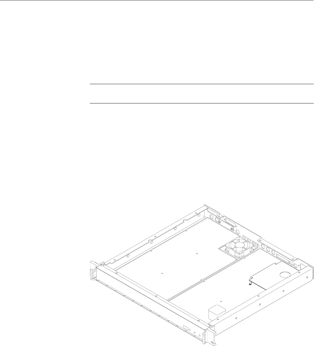
Maintenance
VITS 200 7–3
The circuit number and electrical value of each component is shown on the
diagrams. The first page in the Diagrams section explains the schematic
symbols. The Replaceable Electrical Parts List gives a complete description of
each component. Those portions of the circuit that are mounted on circuit boards
or assemblies are enclosed in a heavy border, with the name and assembly
number shown on the border.
NOTE. Check the Change Information section at the rear of the manual for
inserts describing corrections and modifications to the instrument and manual.
Electrical components, connectors, and test points are identified on circuit board
illustrations located on the inside fold of the corresponding circuit diagram or the
back of the preceding diagram.
The circuit board assemblies are assigned assembly numbers starting with A1.
Figure 7–2 shows the location of the circuit board assemblies in the instrument.
This illustration also shows the location of chassis-mounted components.
A1
A3
A1A1
A2
Figure 7–2: Circuit Board Assembly Locations.
Circuit boards have been assigned an assembly number so that they may be
ordered from Tektronix, Inc. They are as follows:
Diagrams
Circuit Board Illustrations
Assembly and Circuit
Numbering

Maintenance
7–4 VITS 200
A1 Inserter Board Assembly
A1A1 Crystal Oven Board Assembly
A2 Front Panel Board Assembly
A3 Controller Board Assembly
The part numbers for ordering these boards are given on the first page of the
Replaceable Electrical Parts List.
The Replaceable Electrical Parts List is arranged in assembly-by-assembly order,
as designated by ANSI Standard Y32.16– 1975. Each component is assigned a
circuit number according to its location within an assembly. The circuit number,
in the parts list, is made up by combining the assembly number and the circuit
number.
EXAMPLE: R123 on A2 would be listed in the Replaceable Parts List as
A2R123.
In the Replaceable Electrical Parts List, assemblies are listed first, followed by
circuit board-mounted parts in alpha numeric order.
NOTE. The complete part number shown in the parts list should be used when
ordering replacement parts.
Diagnostics
Both the Inserter and the Controller boards contain their own diagnostic routines,
which are divided into two types: power-up diagnostics and user diagnostics.
The Controller board power up diagnostics are automatically executed one time
by the P, when the instrument is powered up or reset. These diagnostics show
failure information on the front-panel display. Controller board user diagnostics,
not enabled at the time of this printing, may be accessed through the front-panel
UTILITIES menu.
Inserter board power-up diagnostics are also executed automatically. These are
the RAM, ARCTAN, and CTC tests. If any of these fail, the UNLOCKED LED
on the front-panel lights, and the instrument re-runs them. The VITS 200 will
not lock to program video until the power-up diagnostics are completed
successfully. User diagnostics for the Inserter board are accessed through rotary
switch A1S8. See Table 7–1 for descriptions of these diagnostic routines.
Two Types of Diagnostics

Maintenance
VITS 200 7–5
Table 7–1: Inserter Board Diagnostics
S8
Setting Test Description Test Result Indication
0 None Normal Genlock setting, no diagnostics. NA
1Do not use This position is not used for the VITS 200. NA
2RAM Tests Writes to and then reads from all the mP RAM
locations in the genlock IC (A1U29 ), and
compares the two. Writes to and reads from all
sample RAM locations in the genlock IC, and
compares the two. During power-up diagnostics,
this test is run once.
On failure, lights the UNLOCKED LED, and the
instrument will not lock to program video.
3ARCTAN PROM
Test Computes the checksum of the arctangent
EPROM (A1U33), and compares the value with
one that has been written in the processor
EPROM. This test is run continuously. During
power up diagnostics, this test is run once.
On failure, lights the UNLOCKED led, and the
instrument will not lock to program video.
4CTC Test This test sets up the Counter Timer Chip (CTC)
(A1U30) as timers, and checks to see that they
can generate interrupts. Each of the CTC’s four
sections are set up to interrupt after 4096
processor clock cycles. If any of the CTC’s
sections have not interrupted within the allocated
time, the test fails. During power-up diagnostics,
this test is run once.
On failure, lights the UNLOCKED led, and the
instrument will not lock to program video.
5Do not use This position is not used for the VITS 200. NA
6Do not use This position is not used for the VITS 200. NA
7Port Test Counts from 0–255 on the I/O ports of the the
microprocessor system. This is the ED0-ED7
bus.
Used to check the data and load paths connected
to the I/O ports. ED0ED7 bus should show a
binary count pattern when viewed with a scope
8VCO DAC Test Generates a field rate ramp at the VCO DAC for
checking the genlock DAC. This ramp may be
viewed at A1J12–2.
Used to check the VCO DAC and Integrator.
9Sampler Test 1 Acquires a sample of sync and burst via the
genlock input, and then reconstructs the sampled
sync and burst at equivalent time through the
VCO DAC A1J12–2. A1C46 (schematic 6) must
be shorted out for this test.
Used to check the Genlock Acquisition circuitry.
ASampler Test 2 Sets up the genlock acquisition system to sample
incoming video continuously, for checking
acquisition timing.
Use a scope to check genlock timing pulses on
CTC A1U30 pins 20–23. Trigger on input video.
BDo not use This position is not used for the VITS 200. NA
CDo not use This position is not used for the VITS 200. NA
DDo not use This position is not used for the VITS 200. NA
EDo not use This position is not used for the VITS 200. NA
FDo not use This position is not used for the VITS 200. NA

Maintenance
7–6 VITS 200
When selecting Inserter board user diagnostics, set A1S8 to the position for the
desired diagnostic and cycle the power off and on, or momentarily move A1P5
to the pins 2–3 position to reset the mP. The mP will then run through the
power-up process, poll the diagnostic port, and run the selected diagnostic.
User diagnostics are free-running, continuous-loop routines which allow a data
path to be tested. The P sends a periodic signal through the path under test. The
signal can then be viewed on a scope, at points along the path, to isolate
problems.
Corrective Maintenance
Corrective maintenance deals with obtaining replacement parts, torque specifica-
tions, and component replacement.
Replacement parts are available from or through the local Tektronix, Inc., field
office or representative.
When ordering parts, be sure to include the following information in your order:
1. Instrument type (and option numbers, if any)
2. Instrument serial number
3. Description of the part, as it appears in the Replaceable Electrical or
Mechanical Parts Lists.
4. The Tektronix part number
If a part that has been ordered is replaced with a new or improved part, the local
Tektronix field office or representative will contact you concerning any change in
the part number. After repair, the circuits may need readjustment.
Only #4, #6, and #8 screws are used in the VITS 200. Table 7–2 shows the
torque ranges for these.
Table 7–2: Torque Specifications
Screw # Torque Range
(in inch pounds)
4 3 1/2 – 5
67 – 9
814 – 18
Obtaining Replacement
Parts
Torque Specifications

Maintenance
VITS 200 7–7
Disconnect the instrument power cord before replacing components.
WARNING. Disconnect the instrument power cord before replacing components.
Use the following procedures to remove circuit board assemblies. Reverse the
order of the removal procedures to reinstall or replace an assembly.
Front Panel Removal
1. Disconnect the three front-panel cable assemblies from the Controller board.
2. Remove the three screws along the front edge, on the bottom of the
VITS 200.
3. Lift the front-panel assembly away from the VITS 200.
Inserter Board Removal
1. Remove the Front Panel, as described above.
2. Remove the retaining nuts on the three BNC connectors that extend through
the rear panel.
3. Disconnect the three ribbon cables and four coax cables which connect the
Inserter and Controller boards.
4. Remove the three mounting screws securing the power supply shield, and lift
the shield off of the Inserter board.
5. Remove the two screws securing the motor base to the rear panel.
6. Remove the seven mounting screws securing the Inserter board to the bottom
pan.
7. Slide the inserter board towards the front of the instrument until the BNC
connectors clear the rear panel, and then lift the board away from the
instrument.
Oven Assembly Removal
1. Remove the Inserter board, as described earlier.
2. Remove the two screws at the sides of the plastic insulating case and lift off
the top part of the case.
3. Remove the screw and nut that attach the power transistor to the outside of
the metal oven.
Replacing Circuit
Assemblies

Maintenance
7–8 VITS 200
4. Remove the oven from the Inserter board by carefully pulling the oven off
the seven square pins that attach it to the Inserter board.
5. Remove the screw attaching the metal cover to the oven.
6. Remove the screw attaching the circuit board to the oven and pull the
oscillator out of the oven.
Controller Board Removal
1. Disconnect the REMOTE and RS-232 ribbon cables.
2. Remove the retaining nuts on the six BNC connectors that extend through
the rear panel.
3. Disconnect the three ribbon cables and four coax cables which connect the
Controller and Inserter boards.
4. Disconnect the three front-panel cable assemblies from the Controller board.
5. Remove the nine mounting screws.
6. Carefully angle the front of the circuit board up and slide it forward until the
BNC connectors clear the rear panel, and then lift the board away from the
instrument.
Test Selectable Parts
Test selectable capacitors A1C31, A3C66, A3C67, A3C68, and A3C69 are
normally not needed. These capacitors are only installed when the associated
integrated circuit pin 18 cannot be adjusted for a clean 6V 1V during the
Genlock Adjustment procedure (see Table ). When needed, these capacitors are
usually 130 pF, but may be selected from the range of 0 pF to 470 pF.
Table 7–3: Test Selectable Parts
Pin 18 of Add Capacitor In Parallel With
A1U44 A1C31 A3C11
A3U3 A3C66 A3C7
A3U4 A3C67 A3C8
A3U9 A3C69 A3C31
A3U11 A3C68 A3C32

Replaceable Electrical Parts List

VITS 200 8–1
Replaceable Electrical Parts
This section contains a list of the components that are replaceable for the
VITS 200. Use this list to identify and order replacement parts. There is a
separate Replaceable Electrical Parts list for each instrument.
Parts Ordering Information
Replacement parts are available from or through your local Tektronix, Inc., Field
Office or representative.
Changes to Tektronix instruments are sometimes made to accommodate
improved components as they become available and to give you the benefit of
the latest circuit improvements. Therefore, when ordering parts, it is important to
include the following information in your order.
HPart number
HInstrument type or model number
HInstrument serial number
HInstrument modification number, if applicable
If a part you have ordered has been replaced with a new or improved part, your
local Tektronix, Inc., Field Office or representative will contact you concerning
any change in part number.
Change information, if any, is located at the rear of this manual.
Using the Replaceable Electrical Parts List
The tabular information in the Replaceable Electrical Parts list is arranged for
quick retrieval. Understanding the structure and features of the list will help you
find all of the information you need for ordering replaceable parts.
The Mfg. Code Number to Manufacturer Cross Index for the electrical parts list
is located immediately after this page. The cross index provides codes, names,
and addresses of manufacturers of components listed in the electrical parts list.
Abbreviations conform to American National Standards Institute (ANSI)
standard Y1.1.
A list of assemblies can be found at the beginning of the electrical parts list. The
assemblies are listed in numerical order. When the complete component number
of a part is known, this list will identify the assembly in which the part is
located.
Cross Index–Mfr. Code
Number to Manufacturer
Abbreviations
List of Assemblies
Replaceable Electrical Parts
8–2 VITS 200
Column Descriptions
The component circuit number appears on the diagrams and circuit board
illustrations, located in the diagrams section. Assembly numbers are also marked
on each diagram and circuit board illustration, in the Diagram section and on the
mechanical exploded views, in the mechanical parts list. The component number
is obtained by adding the assembly number prefix to the circuit number.
Example a. Component Number
A23R1234 A23 R1234
Assembly Number Circuit Number
Read: Resistor 1234 of Assembl
y
23
Example b. Component Number
A23A2R1234 A23 R1234
Assembly Number
Circuit
Number
Read: Resistor 1234 of Subassembly 2 of Assembly 23
A2
Subassembly Number
The electrical parts list is arranged by assemblies in numerical sequence (A1,
with its subassemblies and parts, precedes A2, with its subassemblies and parts).
Mechanical subparts to the circuit boards are listed in the electrical parts list.
These mechanical subparts are listed with their associated electrical part (for
example, fuse holder follows fuse).
Chassis-mounted parts and cable assemblies have no assembly number prefix
and are located at the end of the electrical parts list.
Indicates part number to be used when ordering replacement part from
Tektronix.
Column three (3) indicates the serial or assembly number at which the part was
first used. Column four (4) indicates the serial or assembly number at which the
part was removed. No serial or assembly number entered indicates part is good
for all serial numbers.
An item name is separated from the description by a colon (:). Because of space
limitations, an item name may sometimes appear as incomplete. Use the U.S.
Federal Catalog handbook H6-1 for further item name identification.
The mechanical subparts are shown as *ATTACHED PARTS* / *END AT-
TACHED PARTS* or *MOUNTING PARTS* / *END MOUNTING PARTS* in
column five (5).
Indicates the code number of the actual manufacturer of the part. (Code to name
and address cross reference can be found immediately after this page.)
Indicates actual manufacturer’s part number.
Component No.
(Column 1)
Tektronix Part No.
(Column 2)
Serial/Assembly No.
(Column 3 and 4)
Name and Description
(Column 5)
Mfr. Code
(Column 6)
Mfr. Part No. (Column 7)

Replaceable Electrical Parts
VITS 200 8–3
Cross Index – Mfr. Code Number To Manufacturer
Mfr.
Code. Manufacturer Address City, State, Zip Code
D5243 ROEDERSTEIN ERNST GMBH LUDMILLASTRASSE 23 8300 LANDSHUT GERMANY
TK0213 TOPTRON CORP TOKYO JAPAN
TK0409 HUMKE KEN R 2211 NW NICOLAI
PO BOX 5128 PORTLAND OR 97208
TK0435 LEWIS SCREW CO 4300 S RACINE AVE CHICAGO IL 60609–3320
TK0515 EVOX–RIFA INC 100 TRI–STATE INTERNATIONAL
SUITE 290 LINCOLNSHIRE IL 60015
TK0679 DILECTRON INC 2669 S MRYTLE AVE MONROVIA CA 91016
TK0891 MICONICS 1 FAIRCHILD AVE PLAINVIEW NY 11803
TK0977 ELECTRICAL INSULATION SUPPLIERS, INC
–(DIST) 3549 N W YEON PORTLAND OR 97210
TK1547 MOORE ELECTRONICS INC (DIST) 19500 SW 90TH COURT
PO BOX 1030 TUALATIN OR 97062
TK1727 PHILIPS NEDERLAND BV
AFD ELONCO POSTBUS 90050 5600 PB EINDHOVEN THE NETHERLANDS
TK1743 UNITRODE (UK) LTD 6 CRESSWELL PARK
BLACKHEATH LONDON SE 3 9RD ENGLAND
TK1828 LITE SPECIALTY METAL WORKS 20460 SW AVERY CT TUALATIN OR 97062
TK1913 WIMA
THE INTER–TECHNICAL GROUP IND 2269 SAW MILL RIVER ROAD
PO BOX 127 ELMSFORD NY 10523
TK1989 GASKET SPECIALTIES 4968 NE 122ND AVE PORTLAND OR 97220
TK2058 TDK CORPORATION OF AMERICA 1600 FEEHANVILLE DRV MOUNT PROSPECT, IL 60056
TK2073 TOKYO AMERICA INC 565 W GULF ROAD ARLINGTON HEIGHTS IL 60005
TK2262 RPM ENTERPRISES
SUB OF MICROSEMI CORP 3305 W CASTOR ST SANTA ANA CA 92704
TK2424 CHAMPION TECHNOLOGIES 2553 N EDGINGTON ST FRANKLIN PARK IL 60131
TK2598 MAXIM – ASIC 120 SAN GABRIEL DRV SUNNYVALE, CA 94086
0B0A9 DALLAS SEMICONDUCTOR CORP 4350 BELTWOOD PKWY SOUTH DALLAS TX 75244
0GV52 SCHAFFNER EMC INC 9–B FADEM ROAD SPRINGFIELD, NJ 07081
0H1N5 TOSHIBA MARCON ELECTRONICS
AMERICA CORPORATION 998 FIRST EDGE DRV VERNON HILLS IL 60061
0JR03 ZMAN MAGNETICS INC 7633 S 180th KENT WA 98032
0JR04 TOSHIBA AMERICA INC
ELECTRONICS COMPONENTS DIV 9775 TOLEDO WAY IRVINE CA 92718
0JR05 TRIQUEST CORP 3000 LEWIS AND CLARK HWY VANCOUVER WA 98661–2999
0KB01 STAUFFER SUPPLY 810 SE SHERMAN PORTLAND OR 97214
0LUA3 PHILIPS COMPONENTS 100 PROVIDENCE PIKE SLATERSVILLE, RI 02876
0MS63 QUALITY TECHNOLOGIES CORP 610 N MARY AVENUE SUNNYVALE CA 94086
00213 NYTRONICS COMPONENTS GROUP INC
SUBSIDIARY OF NYTRONICS INC ORANGE ST DARLINGTON SC 29532
00779 AMP INC 2800 FULLING MILL
PO BOX 3608 HARRISBURG PA 17105
01295 TEXAS INSTRUMENTS INC
SEMICONDUCTOR GROUP 13500 N CENTRAL EXPY
PO BOX 655303 DALLAS TX 75262–5303
02875 HUDSON TOOL AND DIE CO INC 18 MALVERN ST NEWARK NJ 07105–1511
04222 AVX/KYOCERA
DIV OF AVX CORP 19TH AVE SOUTH
P O BOX 867 MYRTLE BEACH SC 29577

Replaceable Electrical Parts
8–4 VITS 200
Mfr.
Code. City, State, Zip CodeAddressManufacturer
04713 MOTOROLA INC
SEMICONDUCTOR PRODUCTS SECTOR 5005 E MCDOWELL RD PHOENIX AZ 85008–4229
05276 ITT POMONA ELECTRONICS DIV 1500 E 9TH ST
PO BOX 2767 POMONA CA 91766–3835
06090 RAYCHEM CORP 300 CONSTITUTION DRV MENLO PARK CA 94025–1111
07716 IRC, INC 2850 MT PLEASANT AVE BURLINGTON IA 52601
09023 CORNELL–DUBILIER ELECTRONICS
DIV FEDERAL PACIFIC ELECTRIC CO 2652 DALRYMPLE ST SANFORD NC 27330
09922 BURNDY CORP 1 RICHARDS AVE NORWALK CT 06856
1CH66 PHILIPS SEMICONDUCTORS 811 E ARQUES AVENUE
PO BOX 3409 SUNNYVALE CA 94088–3409
1ES66 MAXIM INTEGRATED PRODUCTS INC 120 SAN GABRIEL DRV SUNNYVALE CA 94086
1Y013 DEANCO, ACACIA DIVISION 3101 SW 153RD DRV BEAVERTON OR 97006
11236 CTS CORPORATION
RESISTOR NETWORKS DIVISION 406 PARR ROAD BERNE IN 46711–9506
11502 IRC, INC PO BOX 1860 BOONE NC 28607–1860
12969 MICROSEMI CORPORATION
WATERTOWN DIVISION 530 PLEASANT STREET WATERTOWN MA 02172
13103 THERMALLOY CO INC 2021 W VALLEY VIEW LN
PO BOX 810839 DALLAS TX 75381
14936 GENERAL INSTRUMENT CORP
POWER SEMICONDUCTOR DIV 600 W JOHN ST HICKSVILLE NY 11802–0709
15454 KETEMA
RODAN DIVISION 2900 BLUE STAR STREET ANAHEIM CA 92806–2591
15513 DATA DISPLAY PRODUCTS 301 CORAL CIR EL SEGUNDO CA 90245–4620
17856 SILICONIX INC 2201 LAURELWOOD RD SANTA CLARA CA 95054–1516
18565 CHOMERICS INC 77 DRAGON COURT WOBURN MA 01801–1039
18796 MURATA ELECTRONICS NORTH AMERICA INC.
STATE COLLEGE OPERATIONS 1900 W COLLEGE AVE STATE COLLEGE PA 16801–2723
19701 PHILIPS COMPONENTS DISCRETE PRODUCTS
DIV RESISTIVE PRODUCTS FACILITY
AIRPORT ROAD
PO BOX 760 MINERAL WELLS TX 76067–0760
2K262 BOYD CORP 6136 NE 87th AVE
PO BOX 20038 PORTLAND OR 97220
2W944 PAPST MECHATRONIC CORP AQUIDNECK INDUSTRIAL PK NEWPORT RI 02840
22526 BERG ELECTRONICS INC (DUPONT) 857 OLD TRAIL RD ETTERS PA 17319
24355 ANALOG DEVICES INC 1 TECHNOLOGY DRV NORWOOD MA 02062
24546 DALE ELECTRONICS
A VISHAY INTERTECHNOLOGY INC CO 550 HIGH ST BRADFORD PA 16701–3737
26364 COMPONENTS CORP 6 KINSEY PLACE DENVILLE NJ 07834–2611
27014 NATIONAL SEMICONDUCTOR CORP 2900 SEMICONDUCTOR DR SANTA CLARA CA 95051–0606
31223 MICRO PLASTICS INC 20821 DEARBORN ST CHATSWORTH CA 91311–5916
31918 ITT SCHADOW INC 8081 WALLACE RD EDEN PRAIRIE MN 55344–2224
33096 COLORADO CRYSTAL CORP 2303 W 8TH ST LOVELAND CO 80537–5268
34335 ADVANCED MICRO DEVICES 901 THOMPSON PL
PO BOX 3453 SUNNYVALE CA 94086–3413
34371 HARRIS CORP
HARRIS SEMICONDUCTOR PRODUCTS GROUP 200 PALM BAY BLVD
PO BOX 883 MELBOURNE FL 32919
4T165 NEC ELECTRONICS USA INC
ELECTRON DIV 475 ELLIS ST
PO BOX 7241 MOUNTAIN VIEW CA 94039

Replaceable Electrical Parts
VITS 200 8–5
Mfr.
Code. City, State, Zip CodeAddressManufacturer
48726 UNITRODE INTEGRATED CIRCUITS CORP
(UICC) 7 CONTINENTAL BLVD
PO BOX 399 MERRIMACK NH 03054–0399
5Y400 TRIAX METAL PRODUCTS INC
DIV OF BEAVERTON PARTS MFG CO 1800 NW 216TH AVE HILLSBORO OR 97124–6629
50139 ALLEN–BRADLEY CO
ELECTRONIC COMPONENTS 1414 ALLEN BRADLEY DR EL PASO TX 79936
51406 MURATA ELECTRONICS NORTH AMERICA INC
HEADQUARTERS AND GEORGIA OPERATIONS 2200 LAKE PARK DR SMYRNA GA 30080
52763 STETCO INC 3344 SCHIERHORN FRANKLIN PARK IL 60131
53387 3M COMPANY
ELECTRONIC PRODUCTS DIV 3M AUSTIN CENTER AUSTIN TX 78769–2963
54937 DEYOUNG MANUFACTURING INC 12920 NE 125TH WAY KIRKLAND WA 98034–7716
55285 BERGQUIST CO INC THE 5300 EDINA INDUSTRIAL BLVD MINNEAPOLIS MN 55435–3707
55680 NICHICON /AMERICA/ CORP 927 E STATE PKY SCHAUMBURG IL 60195–4526
56708 ZILOG INC 1315 DELL AVE CAMPBELL CA 95008–6609
56845 DALE ELECTRONICS INC 2300 RIVERSIDE BLVD
PO BOX 74 NORFOLK NE 68701–2242
57668 ROHM CORPORATION 15375 BARRANCA PARKWAY
SUITE B207 IRVINE CA 92718
59492 QUARTZTEK INC 20 S 48TH AVE PHOENIX AZ 85043–3820
61429 FOX ELECTRONICS
DIV OF FOX ELECTRONICS INC 5842 CORPORATION CIRCLE FOR MEYERS FL 33905
61529 AROMAT CORP 629 CENTRAL AVE NEW PROVIDENCE NJ 07974
61935 SCHURTER INC 1016 CLEGG COURT PETALUMA CA 94952–1152
61964 OMRON ELECTRONICS INC 1 EAST COMMERCE SCHAUMBURG IL 60173
62643 UNITED CHEMICON INC 9801 W HIGGINS ST
SUITE 430 ROSEMONT, IL 60018–4771
62786 HITACHI AMERICA LTD
HITACHI PLAZA 2000 SIERRA POINT PARKWAY BRISBANE CA 94005
64154 LAMB INDUSTRIES INC 4826 SW SCHOLLS FERRY ROAD PORTLAND OR 97225
64762 ELANTEC INC 1996 TAROB COURT MILPITAS CA 95035–6824
65786 CYPRESS SEMICONDUCTOR CORP 3901 N 1ST ST SAN JOSE CA 95134–1506
66302 VLSI TECHNOLOGY INC 1109 MCKAY DR SAN JOSE CA 95131–1706
71400 BUSSMANN
DIV OF COOPER INDUSTRIES INC 114 OLD STATE RD
PO BOX 14460 ST LOUIS MO 63178
75042 IRC ELECTRONIC COMPONENTS
PHILADELPHIA DIV
TRW FIXED RESISTORS
401 N BROAD ST PHILADELPHIA PA 19108–1001
75498 MULTICOMP INC 3005 SW 154TH TERRACE #3 BEAVERTON OR 97006
80009 TEKTRONIX INC 14150 SW KARL BRAUN DR
PO BOX 500 BEAVERTON OR 97077–0001
81073 GRAYHILL INC 561 HILLGROVE AVE
PO BOX 10373 LA GRANGE IL 60525–5914
9M860 ELECTRONIC SUB ASSEMBLY MFG CORP
(ESAM) 930 SE M STREET
PO BOX 376 GRANTS PASS OR 97526–3248
91293 JOHANSON MFG CO 400 ROCKWAY VALLEY RD BOONTON NJ 07005
91637 DALE ELECTRONICS INC 2064 12TH AVE
PO BOX 609 COLUMBUS NE 68601–3632

Replaceable Electrical Parts
8–6 VITS 200
Replaceable Electrical Parts
Component
Number Tektronix
Part Number Serial / Assembly Number
Effective Discontinued Name & Description Mfr.
Code Mfr. Part
Number
A1 671–2132–00 B010100 B010118 CIRCUIT BD ASSY:INSERTER 80009 671213200
A1 671–2132–01 B010119 B010122 CIRCUIT BD ASSY:INSERTER 80009 671213201
A1 671–2132–02 B010123 B010202 CIRCUIT BD ASSY:INSERTER 80009 671213202
A1 671–2132–03 B010203 B010239 CIRCUIT BD ASSY:INSERTER 80009 671213203
A1 671–2132–04 B010240 B020248 CIRCUIT BD ASSY:INSERTER 80009 671213204
A1 671–2132–05 B020249 B020271 CIRCUIT BD ASSY:INSERTER 80009 671213205
A1 671–2132–06 B020272 B020305 CIRCUIT BD ASSY:INSERTER 80009 671213206
A1 671–2132–07 B020306 B020395 CIRCUIT BD ASSY:INSERTER 80009 671213207
A1 671–2132–08 B020396 B020412 CIRCUIT BD ASSY:INSERTER 80009 671213208
A1 671–2132–09 B020413 B020447 CIRCUIT BD ASSY:INSERTER 80009 671213209
A1 671–2132–10 B020448 B020509 CIRCUIT BD ASSY:INSERTER 80009 671213210
A1 671–2132–11 B020510 B020536 CIRCUIT BD ASSY:INSERTER 80009 671213211
A1 671–2132–12 B020537 B020549 CIRCUIT BD ASSY:INSERTER 80009 671213212
A1 671–2132–13 B020550 B020762 CIRCUIT BD ASSY:INSERTER 80009 671213213
A1 671–2132–14 B020763 B021118 CIRCUIT BD ASSY:INSERTER 80009 671213214
A1 671–2132–15 B021119 CIRCUIT BD ASSY:INSERTER 80009 671213215
(STANDARD ONLY)
A1 671–2545–00 B010100 B010122 CIRCUIT BD ASSY:INSERTER 80009 671254500
A1 671–2545–01 B010123 B010164 CIRCUIT BD ASSY:INSERTER 80009 671254501
A1 671–2545–02 B010165 B010202 CIRCUIT BD ASSY:INSERTER 80009 671254502
A1 671–2545–03 B010203 B010239 CIRCUIT BD ASSY:INSERTER 80009 671254503
A1 671–2545–04 B010240 B020248 CIRCUIT BD ASSY:INSERTER 80009 671254504
A1 671–2132–05 B020249 B020271 CIRCUIT BD ASSY:INSERTER 80009 671213205
A1 671–2132–06 B020272 B020305 CIRCUIT BD ASSY:INSERTER 80009 671213206
A1 671–2132–07 B020306 B020395 CIRCUIT BD ASSY:INSERTER 80009 671213207
A1 671–2132–08 B020396 B020412 CIRCUIT BD ASSY:INSERTER 80009 671213208
A1 671–2132–09 B020413 B020447 CIRCUIT BD ASSY:INSERTER 80009 671213209
A1 671–2132–10 B020448 B020509 CIRCUIT BD ASSY:INSERTER 80009 671213210
A1 671–2132–11 B020510 B020536 CIRCUIT BD ASSY:INSERTER 80009 671213211
A1 671–2132–12 B020537 B020549 CIRCUIT BD ASSY:INSERTER 80009 671213212
A1 671–2132–13 B020550 B020762 CIRCUIT BD ASSY:INSERTER 80009 671213213
A1 671–2132–14 B020763 B021118 CIRCUIT BD ASSY:INSERTER 80009 671213214
A1 671–2132–15 B021119 CIRCUIT BD ASSY:INSERTER 80009 671213215
(OPTION 1J ONLY)
A1A1 119–4328–00 671–2132–00 671–2132–03 OVEN ASSEMBLY:VITS100/200,28MHZ 80009 119432800
A1A1 119–4328–01 671–2132–04 671–2132–13 OVEN ASSEMBLY:VITS100/200,28MHZ 80009 119432801
A1A1 119–4328–02 671–2132–14 OVEN ASSEMBLY:VITS100/200,28MHZ 80009 119432802
(STANDARD ONLY)
A1A1 119–4328–00 671–2545–00 671–2545–03 OVEN ASSEMBLY:VITS100/200,28MHZ 80009 119432800
A1A1 119–4328–01 671–2545–04 671–2132–13 OVEN ASSEMBLY:VITS100/200,28MHZ 80009 119432801
A1A1 119–4328–02 671–2132–14 OVEN ASSEMBLY:VITS100/200,28MHZ 80009 119432802
(OPTION 1J ONLY)
A2 671–2133–00 CIRCUIT BD ASSY:FRONT PANEL 80009 671213300
A3 671–2131–00 B010100 B010118 CIRCUIT BD ASSY:CONTROLLER 80009 671213100
A3 671–2131–01 B010119 B020248 CIRCUIT BD ASSY:CONTROLLER 80009 671213101
A3 671–2131–02 B020249 B020294 CIRCUIT BD ASSY:CONTROLLER 80009 671213102
A3 671–2131–03 B020295 B020509 CIRCUIT BD ASSY:CONTROLLER 80009 671213103
A3 671–2131–04 B020510 B020777 CIRCUIT BD ASSY:CONTROLLER 80009 671213104
A3 671–2131–05 B020778 CIRCUIT BD ASSY:CONTROLLER 80009 671213105
A4 119–4078–00 DISPLAY,FLAT PL:VACUUM FLOURESCENT,2 X 40;ALPHA-
NUMERIC,5 X 7 DOT MATRIX,DC/DC AC CONVERT,CHAR
GEN, LOGIC & MICRO COMP
4T165 FC20X2JA–BB
A1 671–2132–00 B010100 B010118 CIRCUIT BD ASSY:INSERTER 80009 671213200
A1 671–2132–01 B010119 B010122 CIRCUIT BD ASSY:INSERTER 80009 671213201
A1 671–2132–02 B010123 B010202 CIRCUIT BD ASSY:INSERTER 80009 671213202

Replaceable Electrical Parts
VITS 200 8–7
Component
Number Mfr. Part
Number
Mfr.
Code
Name & Description
Serial / Assembly Number
Effective Discontinued
Tektronix
Part Number
A1 671–2132–03 B010203 B010239 CIRCUIT BD ASSY:INSERTER 80009 671213203
A1 671–2132–04 B010240 B020248 CIRCUIT BD ASSY:INSERTER 80009 671213204
A1 671–2132–05 B020249 B020271 CIRCUIT BD ASSY:INSERTER 80009 671213205
A1 671–2132–06 B020272 B020305 CIRCUIT BD ASSY:INSERTER 80009 671213206
A1 671–2132–07 B020306 B020395 CIRCUIT BD ASSY:INSERTER 80009 671213207
A1 671–2132–08 B020396 B020412 CIRCUIT BD ASSY:INSERTER 80009 671213208
A1 671–2132–09 B020413 B020447 CIRCUIT BD ASSY:INSERTER 80009 671213209
A1 671–2132–10 B020448 B020509 CIRCUIT BD ASSY:INSERTER 80009 671213210
A1 671–2132–11 B020510 B020536 CIRCUIT BD ASSY:INSERTER 80009 671213211
A1 671–2132–12 B020537 B020549 CIRCUIT BD ASSY:INSERTER 80009 671213212
A1 671–2132–13 B020550 B020762 CIRCUIT BD ASSY:INSERTER 80009 671213213
A1 671–2132–14 B020763 B021118 CIRCUIT BD ASSY:INSERTER 80009 671213214
A1 671–2132–15 B021119 CIRCUIT BD ASSY:INSERTER 80009 671213215
(STANDARD ONLY)
A1 671–2545–00 B010100 B010122 CIRCUIT BD ASSY:INSERTER 80009 671254500
A1 671–2545–01 B010123 B010164 CIRCUIT BD ASSY:INSERTER 80009 671254501
A1 671–2545–02 B010165 B010202 CIRCUIT BD ASSY:INSERTER 80009 671254502
A1 671–2545–03 B010203 B010239 CIRCUIT BD ASSY:INSERTER 80009 671254503
A1 671–2545–04 B010240 B020248 CIRCUIT BD ASSY:INSERTER 80009 671254504
A1 671–2132–05 B020249 B020271 CIRCUIT BD ASSY:INSERTER 80009 671213205
A1 671–2132–06 B020272 B020305 CIRCUIT BD ASSY:INSERTER 80009 671213206
A1 671–2132–07 B020306 B020395 CIRCUIT BD ASSY:INSERTER 80009 671213207
A1 671–2132–08 B020396 B020412 CIRCUIT BD ASSY:INSERTER 80009 671213208
A1 671–2132–09 B020413 B020447 CIRCUIT BD ASSY:INSERTER 80009 671213209
A1 671–2132–10 B020448 B020509 CIRCUIT BD ASSY:INSERTER 80009 671213210
A1 671–2132–11 B020510 B020536 CIRCUIT BD ASSY:INSERTER 80009 671213211
A1 671–2132–12 B020537 B020549 CIRCUIT BD ASSY:INSERTER 80009 671213212
A1 671–2132–13 B020550 B020762 CIRCUIT BD ASSY:INSERTER 80009 671213213
A1 671–2132–14 B020763 B021118 CIRCUIT BD ASSY:INSERTER 80009 671213214
A1 671–2132–15 B021119 CIRCUIT BD ASSY:INSERTER 80009 671213215
(OPTION 1J ONLY)
*ATTACHED PARTS*
131–0157–00 TERMINAL,PIN:0.25 L X 0.04 OD,BRS,SLDR PL 05276 013–100–1000–47
200–3266–01 CAP,HEAT SINK:PLASTIC
(USED WITH OVEN ASSEMBLY) 0JR05 200–3266–01
210–0586–00 NUT,PL,ASSEM WA:4–40 X 0.25,STL CD PL
(USED WITH OVEN ASSEMBLY) TK0435 ORDER BY DESC
211–0021–00 SCREW,MACHINE:4–40 X 1.25,PNH,STL
(USED WITH OVEN ASSEMBLY) TK0435 ORDER BY DESC
211–0513–00 SCREW,MACHINE:6–32 X 0.625,PNH,STL
(QUANTITY 2, USED WITH OVEN ASSEMBLY) TK0435 ORDER BY DESC
348–0935–00 GASKET:2.0 X 1.7,NEOPRENE
(USED WITH OVEN ASSEMBLY) TK1989 ORDER BY DESC
432–0154–00 BASE,HEAT SINK:PLASTIC
(USED WITH OVEN ASSEMBLY) 80009 432015400
*END ATTACHED PARTS*
A1C1 281–0775–01 CAP,FXD,CER:MCL;0.1UF,20%,50V,Z5U,0.170 04222 SA105E104MAA
A1C2 281–0809–00 CAP,FXD,CER:MLC;200 PF,5%,100V,0.100 X0.170 04222 SA101A201JAA
A1C3 290–0990–00 CAP,FXD,ALUM:10UF,20%,50V,8X11.5 55680 UET1H100MPH
A1C4 281–0765–00 CAP,FXD,CER DI:100PF,5%,100V 04222 SA102A101JAA
A1C5 283–0100–00 CAP,FXD,CER DI:0.0047UF,10%,200V 04222 SR302A472KAA
A1C6 283–0129–00 CAP,FXD,CER DI:0.56UF,20%,100V 04222 SR501C564MAA
A1C7 281–0773–00 CAP,FXD,CER:MLC;0.01UF,10%,100V TK1743 CGB103KEX
A1C8 281–0925–01 CAP,FXD,CER:MLC;0.22UF,20%,50V,Z5U.0.170 X 0.120 04222 SA115E224MAA
A1C9 281–0707–00 CAP,FXD,CER DI:15000PF,10%,200V 04222 MA302C153KAA
A1C10 281–0925–01 CAP,FXD,CER:MLC;0.22UF,20%,50V,Z5U.0.170 X 0.120 04222 SA115E224MAA
A1C11 283–0100–00 CAP,FXD,CER DI:0.0047UF,10%,200V 04222 SR302A472KAA
A1C12 281–0925–01 CAP,FXD,CER:MLC;0.22UF,20%,50V,Z5U.0.170 X 0.120 04222 SA115E224MAA
A1C13 281–0775–01 CAP,FXD,CER:MCL;0.1UF,20%,50V,Z5U,0.170 04222 SA105E104MAA

Replaceable Electrical Parts
8–8 VITS 200
Component
Number Mfr. Part
Number
Mfr.
Code
Name & Description
Serial / Assembly Number
Effective Discontinued
Tektronix
Part Number
A1C14 290–0782–01 CAP,FXD,ALUM:4.7UF,20%,35V,ESR=42.33 OHM(120HZ,20C) 55680 UVX1V4R7MAA1TD
A1C15 281–0772–00 671–2132–12 CAP,FXD,CER:MLC;4700PF,10%,100V,0.100 X 04222 SA101C472KAA
*ATTACHED PARTS*
162–0607–00 671–2132–12 INSUL SLVG,ELEC:HT SHRINK,0.046 ID,BLK0.013 THK W 06090 VERSAFIT
*END ATTACHED PARTS*
A1C16 290–0782–01 CAP,FXD,ALUM:4.7UF,20%,35V,ESR=42.33 OHM(120HZ,20C) 55680 UVX1V4R7MAA1TD
A1C17 281–0925–01 CAP,FXD,CER:MLC;0.22UF,20%,50V,Z5U.0.170 X 0.120 04222 SA115E224MAA
A1C18 281–0909–00 CAP,FXD,CER:MLC;0.022UF,20%,50V,0.100 X TK2058 DA12X7R1H223M–T
A1C19 281–0757–00 CAP,FXD,CER:MLC;10PF,10%,200V,NPO,0.100 04222 SA102A100KAA
A1C20 281–0810–00 CAP,FXD,CER:MLC;5.6PF,+/–0.5PF,100V,0.100 X 0.170 04222 SA102A5R6DAA
A1C21 281–0819–00 CAP,FXD,CER:MLC;33 PF,5%,50V,0.100 X 0.170 04222 SA102A330JAA
A1C22 283–0177–00 CAP,FXD,CER DI:1UF,+80–20%,25V 04222 SR303E105ZAA
A1C23 281–0775–01 CAP,FXD,CER:MCL;0.1UF,20%,50V,Z5U,0.170 04222 SA105E104MAA
A1C24 281–0775–01 CAP,FXD,CER:MCL;0.1UF,20%,50V,Z5U,0.170 04222 SA105E104MAA
A1C25 281–0775–01 CAP,FXD,CER:MCL;0.1UF,20%,50V,Z5U,0.170 04222 SA105E104MAA
A1C26 281–0775–01 CAP,FXD,CER:MCL;0.1UF,20%,50V,Z5U,0.170 04222 SA105E104MAA
A1C27 281–0775–01 CAP,FXD,CER:MCL;0.1UF,20%,50V,Z5U,0.170 04222 SA105E104MAA
A1C28 281–0775–01 CAP,FXD,CER:MCL;0.1UF,20%,50V,Z5U,0.170 04222 SA105E104MAA
A1C29 281–0775–01 CAP,FXD,CER:MCL;0.1UF,20%,50V,Z5U,0.170 04222 SA105E104MAA
A1C30 281–0775–01 CAP,FXD,CER:MCL;0.1UF,20%,50V,Z5U,0.170 04222 SA105E104MAA
A1C31 283–0108–00 671–2132–13 CAP,FXD,CER DI:220PF,10%,200V 04222 SR152A221KAA
A1C33 281–0775–01 CAP,FXD,CER:MCL;0.1UF,20%,50V,Z5U,0.170 04222 SA105E104MAA
A1C34 281–0775–01 CAP,FXD,CER:MCL;0.1UF,20%,50V,Z5U,0.170 04222 SA105E104MAA
A1C36 290–0942–00 CAP,FXD,ELCTLT:100UF,+100–10%,25V,ALUMINUM 0H1N5 CEUFM1E101
A1C37 281–0775–01 CAP,FXD,CER:MCL;0.1UF,20%,50V,Z5U,0.170 04222 SA105E104MAA
A1C38 281–0775–01 CAP,FXD,CER:MCL;0.1UF,20%,50V,Z5U,0.170 04222 SA105E104MAA
A1C39 281–0928–00 CAP,FXD,CER DI:150PF,5% 04222 SA101A151JAA
A1C40 281–0862–00 CAP,FXD,CER:MLC;1000PF,20%,100V,X7R,0.100 X 0.170 04222 SA101C102MAA
A1C41 281–0775–01 CAP,FXD,CER:MCL;0.1UF,20%,50V,Z5U,0.170 04222 SA105E104MAA
A1C42 281–0862–00 CAP,FXD,CER:MLC;1000PF,20%,100V,X7R,0.100 X 0.170 04222 SA101C102MAA
A1C43 281–0775–01 CAP,FXD,CER:MCL;0.1UF,20%,50V,Z5U,0.170 04222 SA105E104MAA
A1C46 290–0990–00 CAP,FXD,ALUM:10UF,20%,50V,8X11.5 55680 UET1H100MPH
A1C51 281–0775–01 CAP,FXD,CER:MCL;0.1UF,20%,50V,Z5U,0.170 04222 SA105E104MAA
A1C52 283–0633–00 CAP,FXD,MICA DI:77PF,1%,100V TK0891 RDM15ED770F03
A1C53 290–0990–00 CAP,FXD,ALUM:10UF,20%,50V,8X11.5 55680 UET1H100MPH
A1C54 281–0775–01 CAP,FXD,CER:MCL;0.1UF,20%,50V,Z5U,0.170 04222 SA105E104MAA
A1C55 281–0775–01 CAP,FXD,CER:MCL;0.1UF,20%,50V,Z5U,0.170 04222 SA105E104MAA
A1C56 281–0775–01 CAP,FXD,CER:MCL;0.1UF,20%,50V,Z5U,0.170 04222 SA105E104MAA
A1C57 281–0775–01 CAP,FXD,CER:MCL;0.1UF,20%,50V,Z5U,0.170 04222 SA105E104MAA
A1C58 281–0775–01 CAP,FXD,CER:MCL;0.1UF,20%,50V,Z5U,0.170 04222 SA105E104MAA
A1C59 281–0757–00 CAP,FXD,CER:MLC;10PF,10%,200V,NPO,0.100 04222 SA102A100KAA
A1C60 281–0810–00 CAP,FXD,CER:MLC;5.6PF,+/–0.5PF,100V,0.100 X 0.170 04222 SA102A5R6DAA
A1C61 281–0810–00 CAP,FXD,CER:MLC;5.6PF,+/–0.5PF,100V,0.100 X 0.170 04222 SA102A5R6DAA
A1C65 283–0690–00 CAP,FXD,MICA DI:560PF,1%,300V TK0891 RDM15FC561F03
A1C66 283–0647–01 CAP,FXD,MICA DI:70PF,1%,500V,TAPE & AMMO PACK 09023 CDA15ED700F03
A1C67 283–0156–00 671–2132–00 671–2132–04 CAP,FXD,CER DI:1000PF,+80–20%,200VSQUARE 04222 SR152E102ZAA
A1C67 283–0000–04 671–2132–05 CAP,FXD,CER DI:0.001UF,+100–0X,500V 18796 DD05–90HAY5U102
A1C67 283–0156–00 671–2545–00 671–2545–04 CAP,FXD,CER DI:1000PF,+80–20%,200VSQUARE 04222 SR152E102ZAA
A1C67 283–0000–04 671–2132–05 CAP,FXD,CER DI:0.001UF,+100–0X,500V 18796 DD05–90HAY5U102
A1C68 281–0775–01 CAP,FXD,CER:MCL;0.1UF,20%,50V,Z5U,0.170 04222 SA105E104MAA
A1C69 281–0775–01 CAP,FXD,CER:MCL;0.1UF,20%,50V,Z5U,0.170 04222 SA105E104MAA
A1C70 290–0942–00 CAP,FXD,ELCTLT:100UF,+100–10%,25V,ALUMINUM 0H1N5 CEUFM1E101
A1C71 281–0775–01 CAP,FXD,CER:MCL;0.1UF,20%,50V,Z5U,0.170 04222 SA105E104MAA
A1C72 281–0775–01 CAP,FXD,CER:MCL;0.1UF,20%,50V,Z5U,0.170 04222 SA105E104MAA
A1C73 283–0648–01 CAP,FXD,MICA DI:10PF,5%,500VTAPED & REELED TK0891 RDM15CD100D03
A1C74 283–0600–01 CAP,FXD,MICA DI:43PF,5%,500VTAPE & AMMO PACK 09023 CDA10ED430J03
A1C75 283–0615–01 CAP,FXD,MICA DI:33PF,5%,500V,TAPE & AMMO PACK 09023 CDA15ED330J03
A1C76 283–0768–00 CAP,FXD,MICA DI:132 PF,1%,500V TK0891 RDM15FD132OFO3

Replaceable Electrical Parts
VITS 200 8–9
Component
Number Mfr. Part
Number
Mfr.
Code
Name & Description
Serial / Assembly Number
Effective Discontinued
Tektronix
Part Number
A1C77 283–0769–00 CAP,FXD,MICA DI:278 PF,1%,500V TK0891 RDM15FD278OFO3
A1C78 283–0788–00 CAP,FXD,MICA DI:267PF,1%,500V TK0891 RDM15FD2670F03
A1C79 283–0633–00 CAP,FXD,MICA DI:77PF,1%,100V TK0891 RDM15ED770F03
A1C83 283–0177–00 CAP,FXD,CER DI:1UF,+80–20%,25V 04222 SR303E105ZAA
A1C84 285–1252–00 CAP,FXD,PLASTIC:0.15UF,10%,250VAC D5243 F1772–415–2000
A1C85 285–1196–00 CAP,FXD,PPR DI:0.01UF,20%,250V TK0515 PME 290 MB 5100
A1C86 285–1196–00 CAP,FXD,PPR DI:0.01UF,20%,250V TK0515 PME 290 MB 5100
A1C87 283–0211–00 CAP,FXD,CER DI:0.1UF,10%,200V 04222 SR302C104KAA
A1C88 283–0481–00 CAP,FXD,CER DI:220PF,10%,250VAC 18796 DE7090B221KVA1–
A1C89 281–0775–01 CAP,FXD,CER:MCL;0.1UF,20%,50V,Z5U,0.170 04222 SA105E104MAA
A1C91 290–1069–00 671–2132–00 671–2132–04 CAP,FXD,ALUM:1000UF,20%,6.3V,12.5MM X 25MM 55680 UPL1E102MHH
A1C91 290–1301–00 671–2132–05 CAP,FXD,ALUM:2700UF,20%,10V,12.5 X 30MM
(0.492 X 1.180) 0H1N5 CEEFM1A272M7
A1C91 290–1069–00 671–2545–00 671–2545–04 CAP,FXD,ALUM:1000UF,20%,6.3V,12.5MM X 25MM 55680 UPL1E102MHH
A1C91 290–1301–00 671–2132–05 CAP,FXD,ALUM:2700UF,20%,10V,12.5 X 30MM
(0.492 X 1.180) 0H1N5 CEEFM1A272M7
A1C92 290–1292–00 671–2132–00 671–2132–04 CAP,FXD,ALUM:4700UF,20%,6.3V,23 X 32MM;RADIAL,LOW
IMPED,105 DEG,BULK 62643 767D472M6R3HE1C
A1C92 290–1301–00 671–2132–05 CAP,FXD,ALUM:2700UF,20%,10V,12.5 X 30MM
(0.492 X 1.180) 0H1N5 CEEFM1A272M7
A1C92 290–1292–00 671–2545–00 671–2545–04 CAP,FXD,ALUM:4700UF,20%,6.3V,23 X 32MM;RADIAL,LOW
IMPED,105 DEG,BULK 62643 767D472M6R3HE1C
A1C92 290–1301–00 671–2132–05 CAP,FXD,ALUM:2700UF,20%,10V,12.5 X 30MM
(0.492 X 1.180) 0H1N5 CEEFM1A272M7
A1C94 290–0942–00 CAP,FXD,ELCTLT:100UF,+100–10%,25V,ALUMINUM 0H1N5 CEUFM1E101
A1C95 290–0942–00 CAP,FXD,ELCTLT:100UF,+100–10%,25V,ALUMINUM 0H1N5 CEUFM1E101
A1C96 285–1331–00 CAP,FXD,MTLZD:0.47UF,5%,400V TK1913 MKS4 .47/400/5
A1C97 285–1329–00 CAP,FXD,PLASTIC:METALIZED FILM;680PF,10%,1600V,
POLYPROPYLENE,.70X.43 TK1913 FKP1 680/1600/1
A1C98 281–0775–01 CAP,FXD,CER:MCL;0.1UF,20%,50V,Z5U,0.170 04222 SA105E104MAA
A1C99 290–0755–00 671–2132–00 671–2132–04 CAP,FXD,ELCTLT:100UF,+50%–20%,10WVDC 0H1N5 CEUSM1C101
A1C99 290–0973–01 671–2132–05 CAP,FXD,ALUM:100UF,20%,25VDC 55680 UVX1E101MEA1TA
A1C99 290–0755–00 671–2545–00 671–2132–04 CAP,FXD,ELCTLT:100UF,+50%–20%,10WVDC 0H1N5 CEUSM1C101
A1C99 290–0973–01 671–2132–05 CAP,FXD,ALUM:100UF,20%,25VDC 55680 UVX1E101MEA1TA
A1C100 283–0177–00 CAP,FXD,CER DI:1UF,+80–20%,25V 04222 SR303E105ZAA
A1C101 283–0177–00 CAP,FXD,CER DI:1UF,+80–20%,25V 04222 SR303E105ZAA
A1C102 290–1034–00 671–2132–00 671–2132–04 CAP,FXD,ALUM:330UF,20%,25V,13 X 25MM 55680 UPL1J331MHH
A1C102 290–1302–00 671–2132–05 CAP,FXD,ALUM:1000UF,20%,35V,12.5 X 30MM
(0.492 X 1.180) 0H1N5 CEEFM1V102M7
A1C102 290–1034–00 671–2545–00 671–2545–04 CAP,FXD,ALUM:330UF,20%,25V,13 X 25MM 55680 UPL1J331MHH
A1C102 290–1302–00 671–2132–05 CAP,FXD,ALUM:1000UF,20%,35V,12.5 X 30MM
(0.492 X 1.180) 0H1N5 CEEFM1V102M7
A1C103 290–1034–00 671–2132–00 671–2132–04 CAP,FXD,ALUM:330UF,20%,25V,13 X 25MM 55680 UPL1J331MHH
A1C103 290–1302–00 671–2132–05 CAP,FXD,ALUM:1000UF,20%,35V,12.5 X 30MM
(0.492 X 1.180) 0H1N5 CEEFM1V102M7
A1C103 290–1034–00 671–2545–00 671–2545–04 CAP,FXD,ALUM:330UF,20%,25V,13 X 25MM 55680 UPL1J331MHH
A1C103 290–1302–00 671–2132–05 CAP,FXD,ALUM:1000UF,20%,35V,12.5 X 30MM
(0.492 X 1.180) 0H1N5 CEEFM1V102M7
A1C104 290–0943–00 CAP,FXD,ALUM:47UF,+50–20%,25V,6 X 11MM 0H1N5 CEUSM1E470–Q
A1C105 290–0943–00 CAP,FXD,ALUM:47UF,+50–20%,25V,6 X 11MM 0H1N5 CEUSM1E470–Q
A1C106 283–0177–00 CAP,FXD,CER DI:1UF,+80–20%,25V 04222 SR303E105ZAA
A1C107 283–0177–00 CAP,FXD,CER DI:1UF,+80–20%,25V 04222 SR303E105ZAA
A1C108 283–0177–00 CAP,FXD,CER DI:1UF,+80–20%,25V 04222 SR303E105ZAA
A1C109 283–0177–00 CAP,FXD,CER DI:1UF,+80–20%,25V 04222 SR303E105ZAA
A1C110 290–1291–00 671–2132–00 671–2132–04 CAP,FXD,ALUM:150UF,20%,400V,30 X 30MM;SNAPIN,105
DEG,BULK 0H1N5 CEAUF2G151M30
A1C110 290–1301–00 671–2132–05 CAP,FXD,ALUM:2700UF,20%,10V,12.5 X 30MM
(0.492 X 1.180) 0H1N5 CEEFM1A272M7

Replaceable Electrical Parts
8–10 VITS 200
Component
Number Mfr. Part
Number
Mfr.
Code
Name & Description
Serial / Assembly Number
Effective Discontinued
Tektronix
Part Number
A1C110 290–1291–00 671–2545–00 671–2545–04 CAP,FXD,ALUM:150UF,20%,400V,30 X 30MM;SNAPIN,105
DEG,BULK 0H1N5 CEAUF2G151M30
A1C110 290–1301–00 671–2132–05 CAP,FXD,ALUM:2700UF,20%,10V,12.5 X 30MM
(0.492 X 1.180) 0H1N5 CEEFM1A272M7
A1C111 281–0773–00 CAP,FXD,CER:MLC;0.01UF,10%,100V TK1743 CGB103KEX
A1C112 283–0249–00 CAP,FXD,CER DI:0.068UF,10%,50V 04222 SR215C683KAA
A1C113 290–0942–00 CAP,FXD,ELCTLT:100UF,+100–10%,25V,ALUMINUM 0H1N5 CEUFM1E101
A1C114 283–0197–02 CAP,FXD,CER DI:470PF,5%,50V TAPED & REELED 04222 SR591A471JAAAP1
A1C115 283–0177–00 CAP,FXD,CER DI:1UF,+80–20%,25V 04222 SR303E105ZAA
A1C116 283–0238–00 CAP,FXD,CER DI:0.01UF,10%,50V 04222 SR075C103KAA
A1C117 283–0024–00 CAP,FXD,CER:MLC;0.1UF,20%,50V,X7R,0.200 04222 SR215C104MAA
A1C118 283–0359–00 CAP,FXD,CER DI:1000PF,10%,200V 04222 SR212A102KAA
A1C119 283–0863–00 CAP,FXD,CER DI:CER CHIP,0.1UF,20%,25V,TYPE X7R 12969 24D104MBX
A1C120 283–0863–00 CAP,FXD,CER DI:CER CHIP,0.1UF,20%,25V,TYPE X7R 12969 24D104MBX
A1C121 281–0775–01 CAP,FXD,CER:MCL;0.1UF,20%,50V,Z5U,0.170 04222 SA105E104MAA
A1C122 281–0775–01 CAP,FXD,CER:MCL;0.1UF,20%,50V,Z5U,0.170 04222 SA105E104MAA
A1C123 281–0775–01 CAP,FXD,CER:MCL;0.1UF,20%,50V,Z5U,0.170 04222 SA105E104MAA
A1C124 281–0775–01 CAP,FXD,CER:MCL;0.1UF,20%,50V,Z5U,0.170 04222 SA105E104MAA
A1C125 281–0775–01 CAP,FXD,CER:MCL;0.1UF,20%,50V,Z5U,0.170 04222 SA105E104MAA
A1C126 281–0775–01 CAP,FXD,CER:MCL;0.1UF,20%,50V,Z5U,0.170 04222 SA105E104MAA
A1C128 281–0775–01 CAP,FXD,CER:MCL;0.1UF,20%,50V,Z5U,0.170 04222 SA105E104MAA
A1C129 281–0775–01 CAP,FXD,CER:MCL;0.1UF,20%,50V,Z5U,0.170 04222 SA105E104MAA
A1C130 281–0775–01 CAP,FXD,CER:MCL;0.1UF,20%,50V,Z5U,0.170 04222 SA105E104MAA
A1C131 281–0775–01 CAP,FXD,CER:MCL;0.1UF,20%,50V,Z5U,0.170 04222 SA105E104MAA
A1C132 281–0775–01 CAP,FXD,CER:MCL;0.1UF,20%,50V,Z5U,0.170 04222 SA105E104MAA
A1C133 281–0775–01 CAP,FXD,CER:MCL;0.1UF,20%,50V,Z5U,0.170 04222 SA105E104MAA
A1C134 281–0775–01 CAP,FXD,CER:MCL;0.1UF,20%,50V,Z5U,0.170 04222 SA105E104MAA
A1C135 281–0775–01 CAP,FXD,CER:MCL;0.1UF,20%,50V,Z5U,0.170 04222 SA105E104MAA
A1C136 281–0775–01 CAP,FXD,CER:MCL;0.1UF,20%,50V,Z5U,0.170 04222 SA105E104MAA
A1C137 281–0775–01 CAP,FXD,CER:MCL;0.1UF,20%,50V,Z5U,0.170 04222 SA105E104MAA
A1C139 281–0775–01 CAP,FXD,CER:MCL;0.1UF,20%,50V,Z5U,0.170 04222 SA105E104MAA
A1C140 281–0775–01 CAP,FXD,CER:MCL;0.1UF,20%,50V,Z5U,0.170 04222 SA105E104MAA
A1C141 281–0775–01 CAP,FXD,CER:MCL;0.1UF,20%,50V,Z5U,0.170 04222 SA105E104MAA
A1C142 281–0775–01 CAP,FXD,CER:MCL;0.1UF,20%,50V,Z5U,0.170 04222 SA105E104MAA
A1C143 281–0775–01 CAP,FXD,CER:MCL;0.1UF,20%,50V,Z5U,0.170 04222 SA105E104MAA
A1C144 281–0775–01 CAP,FXD,CER:MCL;0.1UF,20%,50V,Z5U,0.170 04222 SA105E104MAA
A1C145 281–0775–01 CAP,FXD,CER:MCL;0.1UF,20%,50V,Z5U,0.170 04222 SA105E104MAA
A1C146 281–0775–01 CAP,FXD,CER:MCL;0.1UF,20%,50V,Z5U,0.170 04222 SA105E104MAA
A1C147 281–0775–01 CAP,FXD,CER:MCL;0.1UF,20%,50V,Z5U,0.170 04222 SA105E104MAA
A1C148 281–0775–01 CAP,FXD,CER:MCL;0.1UF,20%,50V,Z5U,0.170 04222 SA105E104MAA
A1C149 281–0775–01 CAP,FXD,CER:MCL;0.1UF,20%,50V,Z5U,0.170 04222 SA105E104MAA
A1C150 281–0775–01 CAP,FXD,CER:MCL;0.1UF,20%,50V,Z5U,0.170 04222 SA105E104MAA
A1C152 281–0775–01 CAP,FXD,CER:MCL;0.1UF,20%,50V,Z5U,0.170 04222 SA105E104MAA
A1C153 281–0775–01 CAP,FXD,CER:MCL;0.1UF,20%,50V,Z5U,0.170 04222 SA105E104MAA
A1C154 281–0775–01 CAP,FXD,CER:MCL;0.1UF,20%,50V,Z5U,0.170 04222 SA105E104MAA
A1C155 281–0775–01 671–2132–00 671–2132–04 CAP,FXD,CER:MCL;0.1UF,20%,50V,Z5U,0.170 04222 SA105E104MAA
A1C155 281–0775–01 671–2545–00 671–2545–04 CAP,FXD,CER:MCL;0.1UF,20%,50V,Z5U,0.170 04222 SA105E104MAA
A1C156 281–0775–01 CAP,FXD,CER:MCL;0.1UF,20%,50V,Z5U,0.170 04222 SA105E104MAA
A1C157 281–0775–01 CAP,FXD,CER:MCL;0.1UF,20%,50V,Z5U,0.170 04222 SA105E104MAA
A1C158 281–0775–01 CAP,FXD,CER:MCL;0.1UF,20%,50V,Z5U,0.170 04222 SA105E104MAA
A1C159 281–0775–01 CAP,FXD,CER:MCL;0.1UF,20%,50V,Z5U,0.170 04222 SA105E104MAA
A1C160 281–0775–01 CAP,FXD,CER:MCL;0.1UF,20%,50V,Z5U,0.170 04222 SA105E104MAA
A1C161 281–0775–01 CAP,FXD,CER:MCL;0.1UF,20%,50V,Z5U,0.170 04222 SA105E104MAA
A1C162 281–0775–01 CAP,FXD,CER:MCL;0.1UF,20%,50V,Z5U,0.170 04222 SA105E104MAA
A1C163 281–0775–01 CAP,FXD,CER:MCL;0.1UF,20%,50V,Z5U,0.170 04222 SA105E104MAA
A1C164 290–0990–00 CAP,FXD,ALUM:10UF,20%,50V,8X11.5 55680 UET1H100MPH
A1C165 281–0265–00 CAP,VAR,CER DI:5.2–30PF,100V 51406 TZ03R300FR169
A1C167 281–0775–01 CAP,FXD,CER:MCL;0.1UF,20%,50V,Z5U,0.170 04222 SA105E104MAA

Replaceable Electrical Parts
VITS 200 8–11
Component
Number Mfr. Part
Number
Mfr.
Code
Name & Description
Serial / Assembly Number
Effective Discontinued
Tektronix
Part Number
A1C168 281–0775–01 CAP,FXD,CER:MCL;0.1UF,20%,50V,Z5U,0.170 04222 SA105E104MAA
A1C169 281–0775–01 CAP,FXD,CER:MCL;0.1UF,20%,50V,Z5U,0.170 04222 SA105E104MAA
A1C170 281–0775–01 CAP,FXD,CER:MCL;0.1UF,20%,50V,Z5U,0.170 04222 SA105E104MAA
A1C171 281–0775–01 CAP,FXD,CER:MCL;0.1UF,20%,50V,Z5U,0.170 04222 SA105E104MAA
A1C172 281–0775–01 CAP,FXD,CER:MCL;0.1UF,20%,50V,Z5U,0.170 04222 SA105E104MAA
A1C173 281–0775–01 CAP,FXD,CER:MCL;0.1UF,20%,50V,Z5U,0.170 04222 SA105E104MAA
A1C174 281–0775–01 CAP,FXD,CER:MCL;0.1UF,20%,50V,Z5U,0.170 04222 SA105E104MAA
A1C175 281–0809–00 CAP,FXD,CER:MLC;200 PF,5%,100V,0.100 X0.170 04222 SA101A201JAA
A1C176 281–0775–01 CAP,FXD,CER:MCL;0.1UF,20%,50V,Z5U,0.170 04222 SA105E104MAA
A1C177 281–0775–01 CAP,FXD,CER:MCL;0.1UF,20%,50V,Z5U,0.170 04222 SA105E104MAA
A1C178 281–0775–01 CAP,FXD,CER:MCL;0.1UF,20%,50V,Z5U,0.170 04222 SA105E104MAA
A1C179 281–0775–01 CAP,FXD,CER:MCL;0.1UF,20%,50V,Z5U,0.170 04222 SA105E104MAA
A1C180 281–0775–01 CAP,FXD,CER:MCL;0.1UF,20%,50V,Z5U,0.170 04222 SA105E104MAA
A1C181 281–0775–01 CAP,FXD,CER:MCL;0.1UF,20%,50V,Z5U,0.170 04222 SA105E104MAA
A1C182 281–0759–00 CAP,FXD,CER:MLC;22PF,10%,100V,0.100 X 0.170 04222 SA102A220KAA
A1C183 281–0819–00 CAP,FXD,CER:MLC;33 PF,5%,50V,0.100 X 0.170 04222 SA102A330JAA
A1C184 281–0775–01 CAP,FXD,CER:MCL;0.1UF,20%,50V,Z5U,0.170 04222 SA105E104MAA
A1C185 283–0359–00 671–2132–01 CAP,FXD,CER DI:1000PF,10%,200V 04222 SR212A102KAA
A1C500 290–0943–02 CAP,FXD,ELCTLT:47UF,20%,25V TAPED & REELED 55680 UVX1E470MDA1TD
A1C501 283–0221–00 CAP,FXD,CER DI:0.47UF,20%,50V 04222 SR305C474MAA
A1C503 281–0775–01 CAP,FXD,CER:MCL;0.1UF,20%,50V,Z5U,0.170 04222 SA105E104MAA
A1C504 290–1313–00 CAP,FXD,ALUM:10UF,20%,50V,8 X 11MM;105 DEG,RADIAL 55680 UET1H100MPH1TA
A1C505 290–1313–00 CAP,FXD,ALUM:10UF,20%,50V,8 X 11MM;105 DEG,RADIAL 55680 UET1H100MPH1TA
A1C506 283–0669–00 CAP,FXD,MICA DI:360PF,1%,500V TK0891 RDM15FD361F03
A1C507 281–0782–00 CAP,FXD,CER DI:33 PF,10%,500V 52763 2RDPZZ007 33POK
A1C508 283–0177–05 CAP,FXD,CER DI:1UF,+80–20%,25V 04222 SR303E105ZAAAP1
A1C509 283–0223–00 671–2132–05 CAP,FXD,CER DI:3PF,+/–5PF,50V TK0679 TC501–NPO–309D
A1C510 281–0775–01 671–2132–05 CAP,FXD,CER:MCL;0.1UF,20%,50V,Z5U,0.170 04222 SA105E104MAA
A1C511 281–0775–01 671–2132–05 CAP,FXD,CER:MCL;0.1UF,20%,50V,Z5U,0.170 04222 SA105E104MAA
A1E1 337–1417–00 671–2132–00 671–2132–04 SHIELD,ELEC:0.55 SQ X 0.685 INCH HIGH 02875 SO–9649–CN
A1E1 337–1417–00 671–2545–00 671–2545–04 SHIELD,ELEC:0.55 SQ X 0.685 INCH HIGH 02875 SO–9649–CN
A1F1 159–0160–00 FUSE,CARTRIDGE:3AG,1.5 A,250 V,18 SEC,ULSAF CONT
(FOR 90–250VAC OPERATION) 71400 MDL–1.5
*MOUNTING PARTS*
200–2264–00 CAP,FUSEHOLDER:3AG FUSES, 61935 FEK 031 1666
204–0906–00 BODY,FUSEHOLDER:3AG & 5 X 20MM FUSES 61935 TYPE FAU 031.35
*END MOUNTING PARTS*
A1J2 131–3364–00 CONN,HDR:PCB;MALE,STR,2 X 17,0.1 CTR,0.365D 53387 2534–6002UB
A1J3 131–3323–00 CONN,HDR:PCB;MALE,STR,2 X 20,0.1 CTR,0.365D 22526 66506–025
A1J4 131–3364–00 CONN,HDR:PCB;MALE,STR,2 X 17,0.1 CTR,0.365D 53387 2534–6002UB
A1J5 131–0608–00 CONN,TERMINAL:PRESSFIT/PCB;MALE,STR,0.025SQ,0.248
MLG X 0.137 TAIL,50 GOLD,PHZ BRZ,W/FERRULE
(QUANTITY 3)
22526 48283–018
A1J6 131–0608–00 CONN,TERMINAL:PRESSFIT/PCB;MALE,STR,0.025SQ,0.248
MLG X 0.137 TAIL,50 GOLD,PHZ BRZ,W/FERRULE
(QUANTITY 3)
22526 48283–018
A1J9 131–0608–00 CONN,TERMINAL:PRESSFIT/PCB;MALE,STR,0.025SQ,0.248
MLG X 0.137 TAIL,50 GOLD,PHZ BRZ,W/FERRULE
(QUANTITY 3)
22526 48283–018
A1J10 131–3378–00 CONN,RF JACK:BNC;50 OHM,FEMALE,RTANG,PCB/REAR
PNL,0.5–28 THD,0.625 H X 0.187 TAIL,W/O 00779 227677–1
A1J11 131–0787–00 TERMINAL,PIN:PCB/PRESSFIT;MALE,STR,0.025 SQ,0.448
MLG X 0.137 TAIL,0.600 L,PHOS BRZ,50 GOLD
(QUANTITY 5)
22526 47359–001
A1J12 131–0608–00 CONN,TERMINAL:PRESSFIT/PCB;MALE,STR,0.025SQ,0.248
MLG X 0.137 TAIL,50 GOLD,PHZ BRZ,W/FERRULE
(QUANTITY 3)
22526 48283–018

Replaceable Electrical Parts
8–12 VITS 200
Component
Number Mfr. Part
Number
Mfr.
Code
Name & Description
Serial / Assembly Number
Effective Discontinued
Tektronix
Part Number
A1J13 131–0608–00 CONN,TERMINAL:PRESSFIT/PCB;MALE,STR,0.025SQ,0.248
MLG X 0.137 TAIL,50 GOLD,PHZ BRZ,W/FERRULE
(QUANTITY 3)
22526 48283–018
A1J14 131–3378–00 CONN,RF JACK:BNC;50 OHM,FEMALE,RTANG,PCB/REAR
PNL,0.5–28 THD,0.625 H X 0.187 TAIL,W/O 00779 227677–1
A1J15 131–3378–00 CONN,RF JACK:BNC;50 OHM,FEMALE,RTANG,PCB/REAR
PNL,0.5–28 THD,0.625 H X 0.187 TAIL,W/O 00779 227677–1
A1J17 131–0608–00 CONN,TERMINAL:PRESSFIT/PCB;MALE,STR,0.025SQ,0.248
MLG X 0.137 TAIL,50 GOLD,PHZ BRZ,W/FERRULE
(QUANTITY 2)
22526 48283–018
A1J18 131–0608–00 CONN,TERMINAL:PRESSFIT/PCB;MALE,STR,0.025SQ,0.248
MLG X 0.137 TAIL,50 GOLD,PHZ BRZ,W/FERRULE
(QUANTITY 2)
22526 48283–018
A1J19 131–0608–00 CONN,TERMINAL:PRESSFIT/PCB;MALE,STR,0.025SQ,0.248
MLG X 0.137 TAIL,50 GOLD,PHZ BRZ,W/FERRULE
(QUANTITY 2)
22526 48283–018
A1J20 131–0608–00 CONN,TERMINAL:PRESSFIT/PCB;MALE,STR,0.025SQ,0.248
MLG X 0.137 TAIL,50 GOLD,PHZ BRZ,W/FERRULE
(QUANTITY 16)
22526 48283–018
A1J21 131–0608–00 CONN,TERMINAL:PRESSFIT/PCB;MALE,STR,0.025SQ,0.248
MLG X 0.137 TAIL,50 GOLD,PHZ BRZ,W/FERRULE
(QUANTITY 2)
22526 48283–018
A1J22 131–0608–00 CONN,TERMINAL:PRESSFIT/PCB;MALE,STR,0.025SQ,0.248
MLG X 0.137 TAIL,50 GOLD,PHZ BRZ,W/FERRULE
(QUANTITY 3)
22526 48283–018
A1J27 131–0608–00 CONN,TERMINAL:PRESSFIT/PCB;MALE,STR,0.025SQ,0.248
MLG X 0.137 TAIL,50 GOLD,PHZ BRZ,W/FERRULE
(QUANTITY 10)
22526 48283–018
A1J28 131–0608–00 CONN,TERMINAL:PRESSFIT/PCB;MALE,STR,0.025SQ,0.248
MLG X 0.137 TAIL,50 GOLD,PHZ BRZ,W/FERRULE
(QUANTITY 3)
22526 48283–018
A1J32 131–0608–00 CONN,TERMINAL:PRESSFIT/PCB;MALE,STR,0.025SQ,0.248
MLG X 0.137 TAIL,50 GOLD,PHZ BRZ,W/FERRULE
(QUANTITY 3)
22526 48283–018
A1J33 131–0608–00 CONN,TERMINAL:PRESSFIT/PCB;MALE,STR,0.025SQ,0.248
MLG X 0.137 TAIL,50 GOLD,PHZ BRZ,W/FERRULE
(QUANTITY 3)
22526 48283–018
A1J50 131–0608–00 CONN,TERMINAL:PRESSFIT/PCB;MALE,STR,0.025SQ,0.248
MLG X 0.137 TAIL,50 GOLD,PHZ BRZ,W/FERRULE
(QUANTITY 2)
22526 48283–018
A1J51 131–0608–00 CONN,TERMINAL:PRESSFIT/PCB;MALE,STR,0.025SQ,0.248
MLG X 0.137 TAIL,50 GOLD,PHZ BRZ,W/FERRULE
(QUANTITY 2)
22526 48283–018
A1J52 131–0608–00 CONN,TERMINAL:PRESSFIT/PCB;MALE,STR,0.025SQ,0.248
MLG X 0.137 TAIL,50 GOLD,PHZ BRZ,W/FERRULE
(QUANTITY 2)
22526 48283–018
A1J53 131–0608–00 CONN,TERMINAL:PRESSFIT/PCB;MALE,STR,0.025SQ,0.248
MLG X 0.137 TAIL,50 GOLD,PHZ BRZ,W/FERRULE
(QUANTITY 2)
22526 48283–018
A1J54 131–0608–00 671–2132–05 CONN,TERMINAL:PRESSFIT/PCB;MALE,STR,0.025SQ,0.248
MLG X 0.137 TAIL,50 GOLD,PHZ BRZ,W/FERRULE
(QUANTITY 3)
22526 48283–018
A1J55 131–0608–00 671–2132–05 CONN,TERMINAL:PRESSFIT/PCB;MALE,STR,0.025SQ,0.248
MLG X 0.137 TAIL,50 GOLD,PHZ BRZ,W/FERRULE
(QUANTITY 3)
22526 48283–018
A1J56 131–0608–00 671–2132–05 CONN,TERMINAL:PRESSFIT/PCB;MALE,STR,0.025SQ,0.248
MLG X 0.137 TAIL,50 GOLD,PHZ BRZ,W/FERRULE
(QUANTITY 3)
22526 48283–018
A1J57 131–0608–00 671–2132–05 CONN,TERMINAL:PRESSFIT/PCB;MALE,STR,0.025SQ,0.248
MLG X 0.137 TAIL,50 GOLD,PHZ BRZ,W/FERRULE
(QUANTITY 3)
22526 48283–018

Replaceable Electrical Parts
VITS 200 8–13
Component
Number Mfr. Part
Number
Mfr.
Code
Name & Description
Serial / Assembly Number
Effective Discontinued
Tektronix
Part Number
A1K2 148–0232–00 RELAY,ARM:2 FORM C,75 OHM,COIL,12V 411 OHM,CON-
TACTS,24VDC 1A,INSERTION LOSS 1DB MAX @900MHZ 61529 RG2E–12V
A1L1 108–0459–00 671–2132–00 671–2132–04 COIL,RF:FIXED,39.5UH 0JR03 108–0459–00
A1L1 108–1544–00 671–2132–05 COIL,RF:INDUCTOR;FXD,39.5UH,10%,Q=100,TAPPED,
SHIELDED,POWEREDIRON 0JR03 108–1544–00 (Z–
A1L1 108–1544–00 671–2132–05 COIL,RF:INDUCTOR;FXD,39.5UH,10%,Q=100,TAPPD,
SHIELDED,POWEREDIRON 0JR03 108–1544–00 (Z–
A1L1 108–0459–00 671–2545–00 671–2545–04 COIL,RF:FIXED,39.5UH 0JR03 108–0459–00
*ATTACHED PARTS*
162–0532–00 INSUL SLVG,ELEC:HT SHRINK,0.375 IDPOLYOLEFI-
N,BLK,0.022 THK W 06090 VERSAFIT
*END ATTACHED PARTS*
A1L2 108–0215–00 COIL,RF:INDUCTOR;FXD,1.1UH,10%,38AWG,31
TURNS,276–0020–00 FORM,NYLON 0JR03 108–0215–00
A1L3 108–0215–00 COIL,RF:INDUCTOR;FXD,1.1UH,10%,38AWG,31
TURNS,276–0020–00 FORM,NYLON 0JR03 108–0215–00
A1L6 108–0912–00 COIL,RF:FIXED,83NH 0JR03 108–0912–00
A1L7 108–0182–00 COIL,RF:FIXED,293NH 0JR03 108–0182–00
A1L8 108–0182–00 COIL,RF:FIXED,293NH 0JR03 108–0182–00
A1L12 114–0364–00 COIL,RF:VARIABLE,1.42–1.68UHPOT CORE 54937 500–3893
A1L13 114–0364–00 COIL,RF:VARIABLE,1.42–1.68UHPOT CORE 54937 500–3893
A1L14 114–0463–00 COIL,RF:VAR 0.90UH – 1.07UH, PRESET/SECURED 54937 500–4752
A1L15 108–1263–00 INDUCTOR,FXD:POWER;10UH,10%,I<2.1A,RDC<0.043
OHM,Q>20,SRF>19MHZ TK2058 TSL0707–100K1R9
A1L16 108–0554–00 INDUCTOR,FXD:POWER;5UH,20%,I<10A,DCR<0.01
OHM,17.5 TURNS/2LAYERS ONCORE 276–0147–00 0JR03 108–0554–00
A1L17 108–0959–00 COIL,RF:FIXED,150UH 0JR03 108–0959–00
A1L18 108–1212–00 COIL,RF:FIXED,9UH,2% 0JR03 108–1212–00
A1L19 108–1212–00 COIL,RF:FIXED,9UH,2% 0JR03 108–1212–00
A1L20 108–1204–00 COIL,RF:FIXED,1.51 UH,1% 0JR03 108–1204–00
A1L21 108–1206–00 COIL,RF:FIXED,413NH,1% 0JR03 108–1206–00
A1P5 131–0993–02 BUS,CONDUCTOR:SHUNT ASSEMBLY,RED 00779 1–850100–O
A1P6 131–0993–02 BUS,CONDUCTOR:SHUNT ASSEMBLY,RED 00779 1–850100–O
A1P9 131–0993–05 BUS,CONDUCTOR:SHUNT ASSEMBLY,GREEN 00779 850100–5
A1P12 131–0993–02 BUS,CONDUCTOR:SHUNT ASSEMBLY,RED 00779 1–850100–O
A1P13 131–0993–02 BUS,CONDUCTOR:SHUNT ASSEMBLY,RED 00779 1–850100–O
A1P17 131–0993–02 BUS,CONDUCTOR:SHUNT ASSEMBLY,RED 00779 1–850100–O
A1P18 131–0993–02 BUS,CONDUCTOR:SHUNT ASSEMBLY,RED 00779 1–850100–O
A1P19 131–0993–02 BUS,CONDUCTOR:SHUNT ASSEMBLY,RED 00779 1–850100–O
A1P20 131–0993–02 BUS,CONDUCTOR:SHUNT ASSEMBLY,RED 00779 1–850100–O
A1P22 131–0993–05 BUS,CONDUCTOR:SHUNT ASSEMBLY,GREEN 00779 850100–5
A1P28 131–0993–05 BUS,CONDUCTOR:SHUNT ASSEMBLY,GREEN 00779 850100–5
A1P32 131–0993–02 BUS,CONDUCTOR:SHUNT ASSEMBLY,RED 00779 1–850100–O
A1P33 131–0993–02 BUS,CONDUCTOR:SHUNT ASSEMBLY,RED 00779 1–850100–O
A1P34 131–0993–02 BUS,CONDUCTOR:SHUNT ASSEMBLY,RED 00779 1–850100–O
A1P35 131–0993–02 BUS,CONDUCTOR:SHUNT ASSEMBLY,RED 00779 1–850100–O
A1P36 131–0993–02 BUS,CONDUCTOR:SHUNT ASSEMBLY,RED 00779 1–850100–O
A1P37 131–0993–02 BUS,CONDUCTOR:SHUNT ASSEMBLY,RED 00779 1–850100–O
A1P38 131–0993–02 BUS,CONDUCTOR:SHUNT ASSEMBLY,RED 00779 1–850100–O
A1P54 131–0993–02 671–2132–05 BUS,CONDUCTOR:SHUNT ASSEMBLY,RED 00779 1–850100–O
A1P55 131–0993–02 671–2132–05 BUS,CONDUCTOR:SHUNT ASSEMBLY,RED 00779 1–850100–O
A1P56 131–0993–02 671–2132–05 BUS,CONDUCTOR:SHUNT ASSEMBLY,RED 00779 1–850100–O
A1P57 131–0993–02 671–2132–05 BUS,CONDUCTOR:SHUNT ASSEMBLY,RED 00779 1–850100–O
A1Q1 151–0190–00 XSTR,SIG:BIPOLAR,NPN;40V,200MA,300MHZ,AMPL 04713 2N3904
A1Q2 151–0190–00 XSTR,SIG:BIPOLAR,NPN;40V,200MA,300MHZ,AMPL 04713 2N3904
A1Q3 151–0190–00 XSTR,SIG:BIPOLAR,NPN;40V,200MA,300MHZ,AMPL 04713 2N3904
A1Q4 151–0622–00 XSTR,SIG:BIPOLAR,PNP;40V,1.0A,50MHZ,AMPL 04713 MPS6727
A1Q5 151–0710–00 XSTR,SIG:BIPOLAR,NPN;40V,1.0A,50MHZ,AMPL 04713 MPSW01A
A1Q6 151–0342–00 XSTR,SIG:BIPOLAR,PNP;60V,50MA,40MHZ,AMPL 04713 MPS4249

Replaceable Electrical Parts
8–14 VITS 200
Component
Number Mfr. Part
Number
Mfr.
Code
Name & Description
Serial / Assembly Number
Effective Discontinued
Tektronix
Part Number
A1Q7 151–0341–00 XSTR,SIG:BIPOLAR,NPN;45V,50MA,40MHZ,AMPL 04713 MPS6520
A1Q8 151–0190–00 XSTR,SIG:BIPOLAR,NPN;40V,200MA,300MHZ,AMPL 04713 2N3904
A1Q9 151–0656–00 XSTR,PWR:BIPOLAR,NPN;80V,8.0A,4.0MHZ,DARLING-
TON,AMPL 04713 2N6044
A1Q11 151–0190–00 XSTR,SIG:BIPOLAR,NPN;40V,200MA,300MHZ,AMPL 04713 2N3904
A1Q12 151–0254–00 XSTR,SIG:BIPOLAR,NPN;30V,500MA,125MHZ,AMPL,DAR-
LINGTON 0JR04 MPS–A14
A1Q13 151–0190–00 XSTR,SIG:BIPOLAR,NPN;40V,200MA,300MHZ,AMPL 04713 2N3904
A1Q14 151–0190–00 XSTR,SIG:BIPOLAR,NPN;40V,200MA,300MHZ,AMPL 04713 2N3904
A1Q15 151–0528–00 THYRISTOR,PWR:BIPOLAR,SCR;50V,16A RMS,PHASE 04713 2N6400
A1Q16 151–0908–00 XSTR,PWR:BIPOLAR,NPN;500V
VCEO,1000VVCEV,5A,SWITCHING 04713 MJH16002A
*ATTACHED PARTS*
210–0589–00 NUT,SLFLKG,HEX:4–40 X 0.246,STL CD PL TK0409 CF22NM40
210–1178–00 WASHER,SHLDR:U/W TO–220 XSTR 13103 7721–7PPS
211–0097–00 SCREW,MACHINE:4–40 X 0.312,PNH,STL TK0435 ORDER BY DESC
214–2953–00 HEAT SINK,SEMIC:XSTR,TO–220;VERTICALMOUNT,SLOT
HOLE,(3)SOLDERABLE TABS,COPPER,BLACK PAINT 13103 6030B–TT
342–0354–00 INSULATOR,PLATE:XSTR,SILICONE RUBBER 2K262 342–0354–00
*END ATTACHED PARTS*
A1Q17 151–1171–00 XSTR,PWR:MOS,N–CH;50V,12A,0.12 OHM 04713 MTP15N05E
A1Q18 151–0188–00 XSTR,SIG:BIPOLAR,PNP;40V,200MA,250MHZ,AMPL 04713 2N3906
A1Q180 151–0190–00 XSTR,SIG:BIPOLAR,NPN;40V,200MA,300MHZ,AMPL 04713 2N3904
A1R3 307–0539–00 RES NTWK,FXD,FI:(7)510 OHM,10%,1W 11236 750–81–R510 OHM
A1R4 307–0539–00 RES NTWK,FXD,FI:(7)510 OHM,10%,1W 11236 750–81–R510 OHM
A1R5 307–0650–00 RES NTWK,FXD,FI:9,2.7K OHM,5%,0.150W 11236 750–101–R2.7K
A1R6 307–0446–00 RES NTWK,FXD,FI:10K OHM,20%,(9)RES 11236 750–101–R10K
A1R7 307–0446–00 RES NTWK,FXD,FI:10K OHM,20%,(9)RES 11236 750–101–R10K
A1R8 307–0446–00 RES NTWK,FXD,FI:10K OHM,20%,(9)RES 11236 750–101–R10K
A1R9 307–0446–00 RES NTWK,FXD,FI:10K OHM,20%,(9)RES 11236 750–101–R10K
A1R10 322–3235–00 RES,FXD:METAL FILM;2.74K OHM,1%,0.2W,TC=100 91637 CCF501G27400F
A1R11 307–0650–00 RES NTWK,FXD,FI:9,2.7K OHM,5%,0.150W 11236 750–101–R2.7K
A1R12 307–0650–00 RES NTWK,FXD,FI:9,2.7K OHM,5%,0.150W 11236 750–101–R2.7K
A1R13 307–0650–00 RES NTWK,FXD,FI:9,2.7K OHM,5%,0.150W 11236 750–101–R2.7K
A1R14 322–3235–00 RES,FXD:METAL FILM;2.74K OHM,1%,0.2W,TC=100 91637 CCF501G27400F
A1R18 322–3306–00 RES,FXD:METAL FILM;15K OHM,1%,0.2W,TC=100 PPM 91637 CCF50–2–G1502F
A1R19 322–3147–00 RES,FXD:METAL FILM;332 OHM,1%,0.2W,TC=100 PPM 91637 CCF501G332R0F
A1R20 322–3318–00 RES,FXD:METAL FILM;20K OHM,1%,0.2W,TC=100 PPM 91637 CCF501G20001F
A1R21 322–3318–00 RES,FXD:METAL FILM;20K OHM,1%,0.2W,TC=100 PPM 91637 CCF501G20001F
A1R22 322–3318–00 RES,FXD:METAL FILM;20K OHM,1%,0.2W,TC=100 PPM 91637 CCF501G20001F
A1R23 322–3193–00 RES,FXD:METAL FILM;1K OHM,1%,0.2W,TC=100 PPM 91637 CCF501G10000F
A1R24 322–3295–00 RES,FXD:METAL FILM;11.5K OHM,1%,0.2W,TC=100 91637 CCF50G11501F
A1R25 322–3126–01 RES,FXD,FILM:200 OHM,0.5%,0.2W,TC=TOSMALL BODY 91637 CCF501G200R0D
A1R26 322–3126–01 RES,FXD,FILM:200 OHM,0.5%,0.2W,TC=TOSMALL BODY 91637 CCF501G200R0D
A1R27 322–3295–00 RES,FXD:METAL FILM;11.5K OHM,1%,0.2W,TC=100 91637 CCF50G11501F
A1R28 322–3258–00 RES,FXD:METAL FILM;4.75K OHM,1%,0.2W,TC=100 56845 CCF50–2–G4751FT
A1R29 322–3482–02 RES,FXD,FILM:14.2K OHM,5%,0.2W,TC=TO 91637 CCF501D14201D
A1R30 311–2230–00 RES,VAR,TRMR:CERMET;500 OHM,20%,0.5W,0.197SQ,TOP
ADJUST TK2073 GF06UT2 501 M L
A1R31 322–3304–00 RES,FXD,FILM:14.3K OHM,1%,0.2W,TC=T0TAPED & 91637 CCF50G14301F
A1R32 322–3143–00 671–2132–00 671–2132–12 RES,FXD,FILM:301 OHM,1%,0.2W,TC=T0MI,SM BODY 91637 CCF501G301ROF
A1R32 322–3154–00 671–2132–13 RES,FXD:METAL FILM;392 OHM,1%,0.2W,TC=100 PPM 91637 CCF501G392R0F
A1R33 311–2226–00 671–2132–00 671–2132–02 RES,VAR,TRMR:CERMET;50 OHM,20%,0.5W,0.197 SQ,TOP
ADJUST TK2073 GF06UT2 500 M L
A1R33 311–2227–00 671–2132–03 671–2132–12 RES,VAR,TRMR:CERMET;100 OHM,20%,0.5W,0.197SQ,TOP
ADJUST TK2073 GF06UT2 101 M L
A1R33 311–2228–00 671–2132–13 RES,VAR,TRMR:CERMET;200 OHM,20%,0.5W,0.197SQ,TOP
ADJUST TK2073 GF06UT2 201 M L

Replaceable Electrical Parts
VITS 200 8–15
Component
Number Mfr. Part
Number
Mfr.
Code
Name & Description
Serial / Assembly Number
Effective Discontinued
Tektronix
Part Number
A1R33 311–2226–00 671–2545–00 671–2545–02 RES,VAR,TRMR:CERMET;50 OHM,20%,0.5W,0.197 SQ,TOP
ADJUST TK2073 GF06UT2 500 M L
A1R33 311–2227–00 671–2545–03 RES,VAR,TRMR:CERMET;100 OHM,20%,0.5W,0.197SQ,TOP
ADJUST TK2073 GF06UT2 101 M L
A1R34 322–3143–00 671–2132–00 671–2132–12 RES,FXD,FILM:301 OHM,1%,0.2W,TC=T0MI,SM BODY 91637 CCF501G301ROF
A1R34 322–3154–00 671–2132–13 RES,FXD:METAL FILM;392 OHM,1%,0.2W,TC=100 PPM 91637 CCF501G392R0F
A1R35 322–3154–00 RES,FXD:METAL FILM;392 OHM,1%,0.2W,TC=100 PPM 91637 CCF501G392R0F
A1R36 322–3222–00 RES,FXD:METAL FILM;2K OHM,1%,0.2W,TC=100 PPM 91637 CCF501G20000F
A1R37 322–3143–00 RES,FXD,FILM:301 OHM,1%,0.2W,TC=T0MI,SM BODY 91637 CCF501G301ROF
A1R38 322–3143–00 RES,FXD,FILM:301 OHM,1%,0.2W,TC=T0MI,SM BODY 91637 CCF501G301ROF
A1R39 322–3126–01 RES,FXD,FILM:200 OHM,0.5%,0.2W,TC=TOSMALL BODY 91637 CCF501G200R0D
A1R40 311–2238–00 RES,VAR,TRMR:CERMET;50K OHM,20%,0.5W,0.197SQ,SIDE
ADJUST TK2073 GF06UT2 503 M L
A1R41 322–3392–00 RES,FXD,FILM:118K OHM,1%,0.2W,TC=T0MI,SMALL 91637 CCF501G11802F
A1R42 322–3295–00 RES,FXD:METAL FILM;11.5K OHM,1%,0.2W,TC=100 91637 CCF50G11501F
A1R43 322–3347–00 671–2132–00 671–2132–00 RES,FXD,FILM:40.2K OHM,1%,0.2W,TC=T0MI,SMALL BODY 91637 CCF50–2–G40201F
A1R43 322–3385–00 671–2132–01 RES,FXD:METAL FILM;100K OHM,1%,0.2W,TC=100PPM 91637 CCF501G10002F
A1R43 322–3347–00 671–2545–00 671–2545–04 RES,FXD,FILM:40.2K OHM,1%,0.2W,TC=T0MI,SMALL BODY 91637 CCF50–2–G40201F
A1R43 322–3385–00 671–2132–05 RES,FXD:METAL FILM;100K OHM,1%,0.2W,TC=100PPM 91637 CCF501G10002F
A1R44 322–3258–00 RES,FXD:METAL FILM;4.75K OHM,1%,0.2W,TC=100 56845 CCF50–2–G4751FT
A1R45 322–3373–00 RES,FXD,FILM:75K OHM,1%,0.2W,TC=T0MI,SM BODY 91637 CCF501G75001F
A1R46 322–3177–00 RES,FXD:METAL FILM;681 OHM,1%,0.2W,TC=100 PPM 91637 CCF50–2G681R0F
A1R47 322–3306–00 RES,FXD:METAL FILM;15K OHM,1%,0.2W,TC=100 PPM 91637 CCF50–2–G1502F
A1R48 322–3222–00 RES,FXD:METAL FILM;2K OHM,1%,0.2W,TC=100 PPM 91637 CCF501G20000F
A1R49 322–3222–00 RES,FXD:METAL FILM;2K OHM,1%,0.2W,TC=100 PPM 91637 CCF501G20000F
A1R50 322–3223–00 RES,FXD,FILM:2.05K OHM,1%,0.2W,TC=T0MI,SMALL BODY 91637 CCF501G20500F
A1R51 322–3235–00 RES,FXD:METAL FILM;2.74K OHM,1%,0.2W,TC=100 91637 CCF501G27400F
A1R52 322–3193–00 RES,FXD:METAL FILM;1K OHM,1%,0.2W,TC=100 PPM 91637 CCF501G10000F
A1R53 322–3193–00 RES,FXD:METAL FILM;1K OHM,1%,0.2W,TC=100 PPM 91637 CCF501G10000F
A1R54 322–3414–00 671–2132–00 671–2132–00 RES,FXD:METAL FILM;200K OHM,1%,0.2W,TC=100PPM 91637 CCF501G20002F
A1R54 322–3443–00 671–2132–01 RES,FXD,FILM:402K OHM,1%,0.2W,TC=T0MI,SMALL 91637 CCF501G40202F
A1R54 322–3414–00 671–2545–00 671–2545–04 RES,FXD:METAL FILM;200K OHM,1%,0.2W,TC=100PPM 91637 CCF501G20002F
A1R54 322–3443–00 671–2132–05 RES,FXD,FILM:402K OHM,1%,0.2W,TC=T0MI,SMALL 91637 CCF501G40202F
A1R55 322–3001–00 RES,FXD:METAL FILM;10 OHM,1%,0.2W,TC=100 PPM 91637 CCF501G10R00F
A1R56 322–3231–00 RES,FXD,FILM:2.49K OHM,1%,0.2W,TC=T0MI,SMALL BODY 91637 CCF50–1G24900F
A1R57 322–3243–00 RES,FXD:METAL FILM;3.32K OHM,1%,0.2W,TC=100 91637 CCF50–1–G33200F
A1R58 322–3260–00 RES,FXD,FILM:4.99K OHM,1%,0.2W,TC=T0TAPED & 91637 CCF501G49900F
A1R59 322–3193–00 RES,FXD:METAL FILM;1K OHM,1%,0.2W,TC=100 PPM 91637 CCF501G10000F
A1R60 322–3164–00 RES,FXD,FILM:499 OHM,1%,0.2W,TC=T0MI,SM BODY 91637 CCF501G499ROF
A1R61 322–3193–00 RES,FXD:METAL FILM;1K OHM,1%,0.2W,TC=100 PPM 91637 CCF501G10000F
A1R62 322–3164–00 RES,FXD,FILM:499 OHM,1%,0.2W,TC=T0MI,SM BODY 91637 CCF501G499ROF
A1R63 322–3289–00 RES,FXD:METAL FILM;10K OHM,1%,0.2W,TC=100 PPM 91637 CCF50G10001F
A1R64 322–3289–00 RES,FXD:METAL FILM;10K OHM,1%,0.2W,TC=100 PPM 91637 CCF50G10001F
A1R65 322–3289–00 RES,FXD:METAL FILM;10K OHM,1%,0.2W,TC=100 PPM 91637 CCF50G10001F
A1R66 317–0047–00 RES,FXD,CMPSN:4.7 OHM,5%,0.125W 50139 BB47G5
A1R67 317–0047–00 RES,FXD,CMPSN:4.7 OHM,5%,0.125W 50139 BB47G5
A1R68 322–3165–00 RES,FXD,FILM:511 OHM,1%,0.2W,TC=T0MI,SM BODY 91637 CCF501G511R0F
A1R69 322–3318–00 RES,FXD:METAL FILM;20K OHM,1%,0.2W,TC=100 PPM 91637 CCF501G20001F
A1R70 322–3385–00 RES,FXD:METAL FILM;100K OHM,1%,0.2W,TC=100PPM 91637 CCF501G10002F
A1R71 322–3385–00 RES,FXD:METAL FILM;100K OHM,1%,0.2W,TC=100PPM 91637 CCF501G10002F
A1R72 322–3230–00 RES,FXD,FILM:2.43K OHM,1%,0.2W,TC=T0MI,SMALL BODY 91637 CCF50–2–G2431FT
A1R73 322–3273–00 RES,FXD:METAL FILM;6.81K OHM,1%,0.2W,TC=100 91637 CCF50–2–G68100F
A1R74 322–3239–00 RES,FXD,FILM:3.01K OHM,1%,0.2W,TC=T0MI,SMALL BODY 91637 CCF501G30100F
A1R76 322–3250–00 RES,FXD:METAL FILM;3.92K OHM,1%,0.2W,TC=100 91637 CCF50–2F39200F
A1R77 322–3193–00 RES,FXD:METAL FILM;1K OHM,1%,0.2W,TC=100 PPM 91637 CCF501G10000F
A1R78 322–3354–00 RES,FXD:METAL FILM;47.5K OHM,1%,0.2W,TC=100 91637 CCF501G47501F
A1R79 322–3414–00 RES,FXD:METAL FILM;200K OHM,1%,0.2W,TC=100PPM 91637 CCF501G20002F
A1R80 322–3354–00 RES,FXD:METAL FILM;47.5K OHM,1%,0.2W,TC=100 91637 CCF501G47501F

Replaceable Electrical Parts
8–16 VITS 200
Component
Number Mfr. Part
Number
Mfr.
Code
Name & Description
Serial / Assembly Number
Effective Discontinued
Tektronix
Part Number
A1R81 322–3414–00 RES,FXD:METAL FILM;200K OHM,1%,0.2W,TC=100PPM 91637 CCF501G20002F
A1R82 322–3318–00 RES,FXD:METAL FILM;20K OHM,1%,0.2W,TC=100 PPM 91637 CCF501G20001F
A1R83 308–0677–00 RES,FXD,WW:1 OHM,5%,2W 75042 SPH 1 OHM 5 PER
A1R86 322–3442–00 RES,FXD,FILM:392K OHM,1%,0.2W,TC=T0MI,SMALL 91637 CCF50–2G39202F
A1R87 322–3318–00 RES,FXD:METAL FILM;20K OHM,1%,0.2W,TC=100 PPM 91637 CCF501G20001F
A1R88 322–3222–00 RES,FXD:METAL FILM;2K OHM,1%,0.2W,TC=100 PPM 91637 CCF501G20000F
A1R89 322–3222–00 RES,FXD:METAL FILM;2K OHM,1%,0.2W,TC=100 PPM 91637 CCF501G20000F
A1R90 322–3346–00 RES,FXD:METAL FILM;39.2K OHM,1%,0.2W,TC=100 91637 CCF50–2–G39201F
A1R91 322–3226–00 RES,FXD:METAL FILM;2.21K OHM,1%,0.2W,TC=100 91637 CCF501G22100F
A1R92 322–3258–00 RES,FXD:METAL FILM;4.75K OHM,1%,0.2W,TC=100 56845 CCF50–2–G4751FT
A1R98 322–3039–00 RES,FXD,FILM:24.9 OHM,1%,0.2W,TC=T0,SMALL BODY 91637 CCF50–2–G24R90F
A1R99 322–3085–00 RES,FXD:METAL FILM;75 OHM,1%,0.2W,TC=100 PPM 91637 CCF501G75R00F
A1R100 322–3085–00 RES,FXD:METAL FILM;75 OHM,1%,0.2W,TC=100 PPM 91637 CCF501G75R00F
A1R101 322–3222–00 RES,FXD:METAL FILM;2K OHM,1%,0.2W,TC=100 PPM 91637 CCF501G20000F
A1R102 322–3239–00 RES,FXD,FILM:3.01K OHM,1%,0.2W,TC=T0MI,SMALL BODY 91637 CCF501G30100F
A1R103 322–3085–07 RES,FXD:METAL FILM;75 OHM,0.1%,0.2W,TC=25 PPM 91637 CCF502–C75ROOBT
A1R104 322–3114–00 RES,FXD:METAL FILM;150 OHM,1%,0.2W,TC=100 PPM 91637 CCF50–2–G1500F
A1R105 322–3114–00 RES,FXD:METAL FILM;150 OHM,1%,0.2W,TC=100 PPM 91637 CCF50–2–G1500F
A1R106 322–3193–00 RES,FXD:METAL FILM;1K OHM,1%,0.2W,TC=100 PPM 91637 CCF501G10000F
A1R108 322–3085–07 RES,FXD:METAL FILM;75 OHM,0.1%,0.2W,TC=25 PPM 91637 CCF502–C75ROOBT
A1R109 322–3289–00 RES,FXD:METAL FILM;10K OHM,1%,0.2W,TC=100 PPM 91637 CCF50G10001F
A1R110 322–3201–00 RES,FXD:METAL FILM;1.21K OHM,1%,0.2W,TC=100 91637 CCF501G12100F
A1R111 322–3201–00 RES,FXD:METAL FILM;1.21K OHM,1%,0.2W,TC=100 91637 CCF501G12100F
A1R112 322–3085–07 RES,FXD:METAL FILM;75 OHM,0.1%,0.2W,TC=25 PPM 91637 CCF502–C75ROOBT
A1R113 322–3085–07 RES,FXD:METAL FILM;75 OHM,0.1%,0.2W,TC=25 PPM 91637 CCF502–C75ROOBT
A1R114 322–1618–07 RES,FXD,FILM:400 OHM,0.1%,0.2W,TC=T9 91637 CCF501C400R0B
A1R115 322–1618–07 RES,FXD,FILM:400 OHM,0.1%,0.2W,TC=T9 91637 CCF501C400R0B
A1R116 322–1618–07 RES,FXD,FILM:400 OHM,0.1%,0.2W,TC=T9 91637 CCF501C400R0B
A1R117 322–1618–07 RES,FXD,FILM:400 OHM,0.1%,0.2W,TC=T9 91637 CCF501C400R0B
A1R118 322–3085–00 RES,FXD:METAL FILM;75 OHM,1%,0.2W,TC=100 PPM 91637 CCF501G75R00F
A1R119 322–3085–00 RES,FXD:METAL FILM;75 OHM,1%,0.2W,TC=100 PPM 91637 CCF501G75R00F
A1R120 322–3154–00 RES,FXD:METAL FILM;392 OHM,1%,0.2W,TC=100 PPM 91637 CCF501G392R0F
A1R121 322–3222–00 RES,FXD:METAL FILM;2K OHM,1%,0.2W,TC=100 PPM 91637 CCF501G20000F
A1R122 311–2226–00 RES,VAR,TRMR:CERMET;50 OHM,20%,0.5W,0.197 SQ,TOP
ADJUST TK2073 GF06UT2 500 M L
A1R123 322–3101–00 RES,FXD,FILM:110 OHM,1%,0.2W,TC=TOMI,SM BODY 91637 CCF50–2G110R0F
A1R124 322–3167–00 RES,FXD,FILM:536 OHM,1%,0.2W,TC=T0MI,SM BODY 57668 CRB20 FXE 536E
A1R125 322–3482–02 RES,FXD,FILM:14.2K OHM,5%,0.2W,TC=TO 91637 CCF501D14201D
A1R126 322–3304–00 RES,FXD,FILM:14.3K OHM,1%,0.2W,TC=T0 91637 CCF50G14301F
A1R127 311–2230–00 RES,VAR,TRMR:CERMET;500 OHM,20%,0.5W,0.197SQ,TOP
ADJUST TK2073 GF06UT2 501 M L
A1R130 322–3085–00 RES,FXD:METAL FILM;75 OHM,1%,0.2W,TC=100 PPM 91637 CCF501G75R00F
A1R132 322–3138–00 RES,FXD,FILM:267 OHM,1%,0.2W,TC=T0MI,SM BODY 91637 CCF501G267R0F
A1R133 322–3135–00 RES,FXD,FILM:249 OHM,1%,0.2W,TC=T0MI,SM BODY 91637 CCF501G249R0F
A1R134 322–3135–00 RES,FXD,FILM:249 OHM,1%,0.2W,TC=T0MI,SM BODY 91637 CCF501G249R0F
A1R135 322–3235–00 RES,FXD:METAL FILM;2.74K OHM,1%,0.2W,TC=100 91637 CCF501G27400F
A1R137 322–3254–00 RES,FXD,FILM:4.32K OHM,1%,0.2W,TC=T0MI,SMALL BODY 91637 CCF502G4321FT
A1R138 322–3254–00 RES,FXD,FILM:4.32K OHM,1%,0.2W,TC=T0MI,SMALL BODY 91637 CCF502G4321FT
A1R141 322–3414–00 RES,FXD:METAL FILM;200K OHM,1%,0.2W,TC=100PPM 91637 CCF501G20002F
A1R142 322–3235–00 RES,FXD:METAL FILM;2.74K OHM,1%,0.2W,TC=100 91637 CCF501G27400F
A1R143 315–0226–00 RES,FXD,FILM:22M OHM,5%,0.25W 50139 CB2265
A1R144 315–0105–00 RES,FXD,FILM:1M OHM,5%,0.25W TK1727 SFR25 2322–181–
A1R145 315–0106–00 RES,FXD,FILM:10M OHM,5%,0.25W TK1727 SFR25 2322–181–
A1R146 315–0102–00 RES,FXD,FILM:1K OHM,5%,0.25W TK1727 SFR25 2322–181–
A1R147 315–0270–00 RES,FXD,FILM:27 OHM,5%,0.25W TK1727 SFR25 2322–181–
A1R149 308–0585–00 671–2132–00 671–2132–04 RES,FXD,WW:50 OHM,0.5%,5W 91637 RS550R00D T/R
A1R149 308–0223–00 671–2132–05 RES,FXD,WW:35 OHM,5%,3W 00213 1240S–35–5
A1R149 308–0585–00 671–2545–00 671–2545–04 RES,FXD,WW:50 OHM,0.5%,5W 91637 RS550R00D T/R

Replaceable Electrical Parts
VITS 200 8–17
Component
Number Mfr. Part
Number
Mfr.
Code
Name & Description
Serial / Assembly Number
Effective Discontinued
Tektronix
Part Number
A1R149 308–0223–00 671–2132–05 RES,FXD,WW:35 OHM,5%,3W 00213 1240S–35–5
A1R150 315–0100–00 RES,FXD,FILM:10 OHM,5%,0.25W, TK1727 SFR25 2322–182–
A1R151 315–0103–00 RES,FXD,FILM:10K OHM,5%,0.25W TK1727 SFR25 2322–181–
A1R152 322–3210–00 RES,FXD:METAL FILM;1.5K OHM,1%,0.2W,TC=100PPM 91637 CCF501G15000F
A1R153 301–0274–00 671–2132–00 671–2132–04 RES,FXD,FILM:270K OHM,5%,0.5W 19701 5053CX270K0J
A1R153 303–0274–00 671–2132–05 RES,FXD,CMPSN:270K OHM,5%,1W 80009 303027400
A1R154 305–0104–00 RES,FXD,CMPSN:100K OHM,5%,2W 11502 GF–3 OR GS–3 10
A1R155 308–0555–00 RES,FXD,WW:5 OHM,5%,3W 00213 1200S–5.0–5
A1R156 308–0555–00 RES,FXD,WW:5 OHM,5%,3W 00213 1200S–5.0–5
A1R157 301–0274–00 671–2132–00 671–2132–04 RES,FXD,FILM:270K OHM,5%,0.5W 19701 5053CX270K0J
A1R157 303–0274–00 671–2132–05 RES,FXD,CMPSN:270K OHM,5%,1W 80009 303027400
A1R158 322–3235–00 RES,FXD:METAL FILM;2.74K OHM,1%,0.2W,TC=100 91637 CCF501G27400F
A1R159 322–3289–00 RES,FXD:METAL FILM;10K OHM,1%,0.2W,TC=100 PPM 91637 CCF50G10001F
A1R160 322–3281–00 RES,FXD:METAL FILM;8.25K OHM,1%,0.2W,TC=100 91637 CCF501G82500F
A1R161 322–3258–00 RES,FXD:METAL FILM;4.75K OHM,1%,0.2W,TC=100 56845 CCF50–2–G4751FT
A1R162 322–3314–00 RES,FXD:METAL FILM;18.2K OHM,1%,0.2W,TC=100 91637 CCF501G18201F
A1R163 308–0679–00 RES,FXD:0.51 OHM,5%,2W 91637 CPF–2–0R51JT1
A1R164 322–3347–00 RES,FXD,FILM:40.2K OHM,1%,0.2W,TC=T0MI,SMALL BODY 91637 CCF50–2–G40201F
A1R165 322–3289–00 RES,FXD:METAL FILM;10K OHM,1%,0.2W,TC=100 PPM 91637 CCF50G10001F
A1R166 322–3162–00 RES,FXD:METAL FILM;475 OHM,1%,0.2W,TC=100 PPM 91637 CCF50G475R0F
A1R167 322–3402–00 RES,FXD:METAL FILM;150K OHM,1%,0.2W,TC=100PPM 91637 CCF50G15002F
A1R168 322–3222–00 RES,FXD:METAL FILM;2K OHM,1%,0.2W,TC=100 PPM 91637 CCF501G20000F
A1R169 322–3210–00 RES,FXD:METAL FILM;1.5K OHM,1%,0.2W,TC=100PPM 91637 CCF501G15000F
A1R170 311–2231–00 RES,VAR,TRMR:CERMET;1K OHM,20%,0.5W,0.197 SQ,TOP
ADJUST TK2073 GF06UT2 102 M L
A1R171 311–2231–00 RES,VAR,TRMR:CERMET;1K OHM,20%,0.5W,0.197 SQ,TOP
ADJUST TK2073 GF06UT2 102 M L
A1R172 322–3318–00 RES,FXD:METAL FILM;20K OHM,1%,0.2W,TC=100 PPM 91637 CCF501G20001F
A1R173 322–3239–00 RES,FXD,FILM:3.01K OHM,1%,0.2W,TC=T0MI,SMALL BODY 91637 CCF501G30100F
A1R174 322–3258–00 RES,FXD:METAL FILM;4.75K OHM,1%,0.2W,TC=100 56845 CCF50–2–G4751FT
A1R175 322–3289–00 RES,FXD:METAL FILM;10K OHM,1%,0.2W,TC=100 PPM 91637 CCF50G10001F
A1R177 307–0650–00 RES NTWK,FXD,FI:9,2.7K OHM,5%,0.150W 11236 750–101–R2.7K
A1R178 307–0650–00 RES NTWK,FXD,FI:9,2.7K OHM,5%,0.150W 11236 750–101–R2.7K
A1R179 307–0650–00 RES NTWK,FXD,FI:9,2.7K OHM,5%,0.150W 11236 750–101–R2.7K
A1R180 322–3289–00 RES,FXD:METAL FILM;10K OHM,1%,0.2W,TC=100 PPM 91637 CCF50G10001F
A1R184 322–3225–00 RES,FXD,FILM:2.15K OHM,1%,0.2W,TC=T0 91637 CCF501G21500F
A1R185 322–3143–00 RES,FXD,FILM:301 OHM,1%,0.2W,TC=T0MI,SM BODY 91637 CCF501G301ROF
A1R190 322–3165–00 RES,FXD,FILM:511 OHM,1%,0.2W,TC=T0MI,SM BODY 91637 CCF501G511R0F
A1R191 322–3165–00 RES,FXD,FILM:511 OHM,1%,0.2W,TC=T0MI,SM BODY 91637 CCF501G511R0F
A1R192 322–3235–00 RES,FXD:METAL FILM;2.74K OHM,1%,0.2W,TC=100 91637 CCF501G27400F
A1R206 322–3137–00 RES,FXD,FILM:261 OHM,1%,0.2W,TC=T0MI,SM BODY 91637 CCF501G261R0F
A1R207 322–3117–00 RES,FXD,FILM:162 OHM,1%,0.2W,TC=T0MI,SM BODY 91637 CCF501G162R0F
A1R208 322–3306–00 RES,FXD:METAL FILM;15K OHM,1%,0.2W,TC=100 PPM 91637 CCF50–2–G1502F
A1R209 322–3114–00 RES,FXD:METAL FILM;150 OHM,1%,0.2W,TC=100 PPM 91637 CCF50–2–G1500F
A1R210 311–2227–00 RES,VAR,TRMR:CERMET;100 OHM,20%,0.5W,0.197SQ,TOP
ADJUST TK2073 GF06UT2 101 M L
A1R211 322–3135–00 RES,FXD,FILM:249 OHM,1%,0.2W,TC=T0MI,SM BODY 91637 CCF501G249R0F
A1R212 322–3135–00 RES,FXD,FILM:249 OHM,1%,0.2W,TC=T0MI,SM BODY 91637 CCF501G249R0F
A1R213 322–3135–00 RES,FXD,FILM:249 OHM,1%,0.2W,TC=T0MI,SM BODY 91637 CCF501G249R0F
A1R214 322–3164–00 RES,FXD,FILM:499 OHM,1%,0.2W,TC=T0MI,SM BODY 91637 CCF501G499ROF
A1R215 322–3235–00 671–2132–00 671–2132–04 RES,FXD:METAL FILM;2.74K OHM,1%,0.2W,TC=100 91637 CCF501G27400F
A1R215 322–3235–00 671–2545–00 671–2545–04 RES,FXD:METAL FILM;2.74K OHM,1%,0.2W,TC=100 91637 CCF501G27400F
A1R216 322–3318–00 RES,FXD:METAL FILM;20K OHM,1%,0.2W,TC=100 PPM 91637 CCF501G20001F
A1R217 307–1318–00 RES NTWK,FXD,FI:(2) 162 OHM,(2) 260 OHM,2%,0.125W 91637 CSC04B–05–162/2
A1R218 307–1318–00 RES NTWK,FXD,FI:(2) 162 OHM,(2) 260 OHM,2%,0.125W 91637 CSC04B–05–162/2
A1R219 307–1318–00 RES NTWK,FXD,FI:(2) 162 OHM,(2) 260 OHM,2%,0.125W 91637 CSC04B–05–162/2
A1R220 322–3165–00 RES,FXD,FILM:511 OHM,1%,0.2W,TC=T0MI,SM BODY 91637 CCF501G511R0F
A1R221 322–3165–00 RES,FXD,FILM:511 OHM,1%,0.2W,TC=T0MI,SM BODY 91637 CCF501G511R0F

Replaceable Electrical Parts
8–18 VITS 200
Component
Number Mfr. Part
Number
Mfr.
Code
Name & Description
Serial / Assembly Number
Effective Discontinued
Tektronix
Part Number
A1R222 322–3165–00 RES,FXD,FILM:511 OHM,1%,0.2W,TC=T0MI,SM BODY 91637 CCF501G511R0F
A1R223 322–3165–00 RES,FXD,FILM:511 OHM,1%,0.2W,TC=T0MI,SM BODY 91637 CCF501G511R0F
A1R224 322–3165–00 RES,FXD,FILM:511 OHM,1%,0.2W,TC=T0MI,SM BODY 91637 CCF501G511R0F
A1R225 322–3165–00 RES,FXD,FILM:511 OHM,1%,0.2W,TC=T0MI,SM BODY 91637 CCF501G511R0F
A1R226 322–3165–00 RES,FXD,FILM:511 OHM,1%,0.2W,TC=T0MI,SM BODY 91637 CCF501G511R0F
A1R227 322–3001–00 RES,FXD:METAL FILM;10 OHM,1%,0.2W,TC=100 PPM 91637 CCF501G10R00F
A1R228 322–3193–00 RES,FXD:METAL FILM;1K OHM,1%,0.2W,TC=100 PPM 91637 CCF501G10000F
A1R229 322–3193–00 RES,FXD:METAL FILM;1K OHM,1%,0.2W,TC=100 PPM 91637 CCF501G10000F
A1R230 322–3210–00 RES,FXD:METAL FILM;1.5K OHM,1%,0.2W,TC=100PPM 91637 CCF501G15000F
A1R231 322–3135–00 RES,FXD,FILM:249 OHM,1%,0.2W,TC=T0MI,SM BODY 91637 CCF501G249R0F
A1R500 301–0105–00 671–2132–00 671–2132–04 RES,FXD,FILM:1M OHM,5%,0.50W 19701 5053CX1M000J
A1R500 303–0105–00 671–2132–05 RES,FXD,CMPSN:1M OHM,5%,1W 24546 FP32 OR FP1 1 M
A1R500 301–0105–00 671–2545–00 671–2545–04 RES,FXD,FILM:1M OHM,5%,0.50W 19701 5053CX1M000J
A1R500 303–0105–00 671–2132–05 RES,FXD,CMPSN:1M OHM,5%,1W 24546 FP32 OR FP1 1 M
A1R501 322–3318–00 RES,FXD:METAL FILM;20K OHM,1%,0.2W,TC=100 PPM 91637 CCF501G20001F
A1R502 322–3335–00 RES,FXD,FILM:30.1K OHM,1%,0.2W,TC=T0MI,SMALL BODY 91637 CCF501G30101F
A1R503 322–3289–00 RES,FXD:METAL FILM;10K OHM,1%,0.2W,TC=100 PPM 91637 CCF50G10001F
A1R504 322–3385–00 671–2132–00 671–2132–05 RES,FXD:METAL FILM;100K OHM,1%,0.2W,TC=100PPM 91637 CCF501G10002F
A1R504 322–3289–00 671–2132–06 RES,FXD:METAL FILM;10K OHM,1%,0.2W,TC=100 PPM 91637 CCF50G10001F
A1R504 322–3385–00 671–2545–00 671–2132–05 RES,FXD:METAL FILM;100K OHM,1%,0.2W,TC=100PPM 91637 CCF501G10002F
A1R504 322–3289–00 671–2132–06 RES,FXD:METAL FILM;10K OHM,1%,0.2W,TC=100 PPM 91637 CCF50G10001F
A1R506 322–3097–00 RES,FXD:METAL FILM;100 OHM,1%,0.2W,TC=100 PPM 91637 CCF501G100R0F
A1R508 322–3318–00 671–2132–05 RES,FXD:METAL FILM;20K OHM,1%,0.2W,TC=100 PPM 91637 CCF501G20001F
A1S1 260–1721–00 SWITCH,ROCKER:8,SPST,125MA,30VDC 81073 76SB08S
A1S2 260–1721–00 SWITCH,ROCKER:8,SPST,125MA,30VDC 81073 76SB08S
A1S3 260–1721–00 SWITCH,ROCKER:8,SPST,125MA,30VDC 81073 76SB08S
A1S4 260–1721–00 SWITCH,ROCKER:8,SPST,125MA,30VDC 81073 76SB08S
A1S5 260–2447–00 SWITCH,ROCKER:SINGLE,RTANG 81073 76SB08S RA
A1S6 260–2447–00 SWITCH,ROCKER:SINGLE,RTANG 81073 76SB08S RA
A1S7 260–1721–00 SWITCH,ROCKER:8,SPST,125MA,30VDC 81073 76SB08S
A1S8 260–2126–00 SWITCH,ROTARY:MEMORY SELECTOR 64154 41J34G
A1S9 260–2443–00 SWITCH,PWR:DPDT;PUSH PUSH ALT ACT,PC PINS,6A
250VAC/1A 100VDC,36A AC SURGE,RIGHT ANG
MNT,W/HARD END WIRE BAIL
31918 NE18–00–EE–N–47
*ATTACHED PARTS*
366–1160–00 PUSH BUTTON:CHARCOAL,0.523 X 0.253 X 0.43 80009 366116000
*END ATTACHED PARTS*
A1S10 260–2443–00 SWITCH,PWR:DPDT;PUSH PUSH ALT ACT,PC PINS,6A
250VAC/1A 100VDC,36A AC SURGE,RIGHT ANG
MNT,W/HARD END WIRE BAIL
31918 NE18–00–EE–N–47
*ATTACHED PARTS*
366–1160–00 PUSH BUTTON:CHARCOAL,0.523 X 0.253 X 0.43 80009 366116000
*END ATTACHED PARTS*
A1T1 120–1831–00 TRANSFORMER,RF:FLYBACK,OUTPUTS +/–15 & +/–5, 75498 128–8038–00
A1T2 120–1861–00 TRANSFORMER,RF:VAR 1.40 – 1.65UH, PRESET/SECURED
TO 1.55 UH, +/– 1%Q=160, POT CORE 54937 500–4757
A1U1 156–1704–00 IC,DIGITAL:FTTL,FLIP FLOP;OCTAL D–TYPE, 3–STATE 01295 SN74F374N
A1U3 156–1704–00 IC,DIGITAL:FTTL,FLIP FLOP;OCTAL D–TYPE, 3–STATE 01295 SN74F374N
A1U4 160–8612–00 671–2132–00 671–2132–04 IC,MEMORY:CMOS,EPROM;8K X 8,40NS,RGTRED 80009 160861200
A1U4 160–8612–01 671–2132–05 671–2132–10 IC,MEMORY:CMOS,EPROM;8K X 8 80009 160861201
A1U4 160–8612–02 671–2132–11 IC,MEMORY:CMOS,PROM;32K X 8,40NS,RGTRED 80009 160861202
A1U4 160–8867–00 671–2545–00 671–2545–01 IC,MEMORY:CMOS,PROM;8K X 8,40NS,RGTRED 80009 160886700
A1U4 160–8867–01 671–2545–02 671–2545–02 IC,MEMORY:CMOS,EPROM;32K X 8 80009 160886701
A1U4 160–8867–02 671–2545–02 671–2545–04 IC,MEMORY:CMOS,EPROM;32K X 8 80009 160886702
A1U4 160–8612–01 671–2132–05 IC,MEMORY:CMOS,EPROM;8K X 8 80009 160861201
A1U4 160–9573–00 IC,MEMORY:CMOS,8K X 8,EPROM (Opt 1C Philips GCR) 80009 160957300
A1U4 163–1015–00 IC,MEMORY:CMOS,32K X 8,EPROM (Opt 1K Korean GCR) 80009 163101500
*MOUNTING PARTS*

Replaceable Electrical Parts
VITS 200 8–19
Component
Number Mfr. Part
Number
Mfr.
Code
Name & Description
Serial / Assembly Number
Effective Discontinued
Tektronix
Part Number
136–1038–00 SOCKET,DIP:PCB;STR,28 POS,2 X 14,0.1X 0.3CTR,0.185 H
X 0.130 TAIL,TIN,BD RETENTION,BECU 00779 2–382571–3
*END MOUNTING PARTS*
A1U5 160–8613–00 671–2132–00 671–2132–04 IC,MEMORY:CMOS,EPROM;8K X 8,40NS,RGTRED 80009 160861300
A1U5 160–8613–01 671–2132–05 671–2132–10 IC,MEMORY:CMOS,EPROM;8K X 8 80009 160861301
A1U5 160–8613–02 671–2132–11 IC,MEMORY:CMOS,PROM;32K X 8,40NS,RGTRED 80009 160861302
A1U5 160–8868–00 671–2545–00 671–2545–01 IC,MEMORY:CMOS,PROM;8K X 8,40NS,RGTRED 80009 160886800
A1U5 160–8868–01 671–2545–02 671–2545–02 IC,MEMORY:CMOS,EPROM;32K X 8 80009 160886801
A1U5 160–8868–02 671–2545–02 671–2545–04 IC,MEMORY:CMOS,EPROM;32K X 8 80009 160886802
A1U5 160–8613–01 671–2132–05 671–2132–10 IC,MEMORY:CMOS,EPROM;8K X 8 80009 160861301
A1U5 160–8613–02 671–2132–11 IC,MEMORY:CMOS,PROM;32K X 8,40NS,RGTRED 80009 160861302
A1U5 160–9574–00 IC,MEMORY:CMOS,8K X 8,EPROM (Opt 1C Philips GCR) 80009 160957400
A1U5 163–1016–00 IC,MEMORY:CMOS,32K X 8,EPROM (Opt 1K Korean GCR) 80009 163101600
*MOUNTING PARTS*
136–1038–00 SOCKET,DIP:PCB;STR,28 POS,2 X 14,0.1X 0.3CTR,0.185 H
X 0.130 TAIL,TIN,BD RETENTION,BECU 00779 2–382571–3
*END MOUNTING PARTS*
A1U6 160–8614–00 671–2132–00 671–2132–04 IC,MEMORY:CMOS,EPROM;8K X 8,40NS,RGTRED 80009 160861400
A1U6 160–8614–01 671–2132–05 671–2132–10 IC,MEMORY:CMOS,EPROM;8K X 8 80009 160861401
A1U6 160–8614–02 671–2132–11 IC,MEMORY:CMOS,PROM;32K X 8,40NS,RGTRED 80009 160861402
A1U6 160–8869–00 671–2545–00 671–2545–01 IC,MEMORY:CMOS,PROM;8K X 8,40NS,RGTRED 80009 160886900
A1U6 160–8869–01 671–2545–02 671–2545–02 IC,MEMORY:CMOS,EPROM;32K X 8 80009 160886901
A1U6 160–8869–02 671–2545–02 671–2545–04 IC,MEMORY:CMOS,EPROM;32K X 8 80009 160886902
A1U6 160–8614–01 671–2132–05 671–2132–10 IC,MEMORY:CMOS,EPROM;8K X 8 80009 160861401
A1U6 160–8614–02 671–2132–11 IC,MEMORY:CMOS,PROM;32K X 8,40NS,RGTRED 80009 160861402
A1U6 160–9575–00 IC,MEMORY:CMOS,8K X 8,EPROM (Opt 1C Philips GCR) 80009 160957500
A1U6 163–1017–00 IC,MEMORY:CMOS,32K X 8,EPROM (Opt 1K Korean GCR) 80009 163101700
*MOUNTING PARTS*
136–1038–00 SOCKET,DIP:PCB;STR,28 POS,2 X 14,0.1X 0.3CTR,0.185 H
X 0.130 TAIL,TIN,BD RETENTION,BECU 00779 2–382571–3
*END MOUNTING PARTS*
A1U7 156–1909–00 IC,DIGITAL:FTTL,MUX;QUAD 2–TO–1 DATA SELECTOR 01295 SN74F157AN
A1U8 156–1702–00 671–2132–00 671–2132–04 IC,DIGITAL:TTL,RGTR;10–BIT BFRED, NONINV, 3–STATE 34335 AM29821PC
A1U8 156–2063–00 671–2132–05 IC,DGTL:ALSTTL,FLIP FLOP;OCTAL NONINV
D–TYPE,3–STATE 01295 SN74ALS374AN
A1U8 156–1702–00 671–2545–00 671–2545–04 IC,DIGITAL:TTL,RGTR;10–BIT BFRED, NONINV, 3–STATE 34335 AM29821PC
A1U8 156–2063–00 671–2132–05 IC,DIGITAL:ALSTTL,FLIP FLOP;OCTAL NONINV D–TYPE,
3–STATE 01295 SN74ALS374AN
A1U9 156–2289–00 IC,DIGITAL:ECL,TRANSLATOR;QUAD TTL–TO–ECL 04713 MC10H124P
A1U10 156–2289–00 IC,DIGITAL:ECL,TRANSLATOR;QUAD TTL–TO–ECL 04713 MC10H124P
A1U11 156–2289–00 IC,DIGITAL:ECL,TRANSLATOR;QUAD TTL–TO–ECL 04713 MC10H124P
A1U12 160–8601–00 671–2132–00 671–2132–06 IC,DIGITAL:CMOS,PLD;EEPLD,16V8,25NS,90MA 80009 160860100
A1U12 160–8601–01 671–2132–07 IC,DIGITAL:CMOS,PLD;EEPLD,16V8,25NS,90MA 80009 160860101
A1U12 160–8601–00 671–2545–00 671–2132–06 IC,DIGITAL:CMOS,PLD;EEPLD,16V8,25NS,90MA 80009 160860100
A1U12 160–8601–01 671–2132–07 IC,DIGITAL:CMOS,PLD;EEPLD,16V8,25NS,90MA 80009 160860101
*MOUNTING PARTS*
136–0752–00 SKT,PL–IN ELEK:MICROCIRCUIT,20 DIP 09922 DILB20P–108
*END MOUNTING PARTS*
A1U13 160–8606–00 671–2132–00 671–2132–04 IC,MEMORY:CMOS,EPROM;32K X 8,W/3 STATE OUT 80009 160860600
A1U13 160–8606–01 671–2132–05 671–2132–10 IC,MEMORY:CMOS,EPROM;64K X 16 80009 160860601
A1U13 160–8606–02 671–2132–11 IC,MEMORY:CMOS,EPROM;64K X
16,150NS,OTP,27C210,PLCC44 80009 160860602
A1U13 160–8870–00 671–2545–00 671–2545–01 IC,MEM:CMOS,EPROM;32K X 8 W/3–STATE
OUT,27C256–250,DIP28.6 80009 160887000
A1U13 160–8870–01 671–2545–02 671–2545–02 IC,MEMORY:CMOS,EPROM;32K X 8 WITH 3 STATE OUT 80009 160887001
A1U13 160–8870–02 671–2545–02 671–2545–04 IC,MEMORY:CMOS,EPROM;32K X WITH 3 STATE OUT 80009 160887002
A1U13 160–8606–01 671–2132–05 671–2132–10 IC,MEMORY:CMOS,EPROM;64K X 16 80009 160860601
A1U13 160–8606–02 671–2132–11 IC,MEM:CMOS,EPROM;64K X 16,150NS,OTP,27C210,
PLCC44 80009 160860602

Replaceable Electrical Parts
8–20 VITS 200
Component
Number Mfr. Part
Number
Mfr.
Code
Name & Description
Serial / Assembly Number
Effective Discontinued
Tektronix
Part Number
A1U13 160–9576–00 IC,MEMORY:CMOS,EPROM;32K X 8, (Opt 1C Philips GCR) 80009 160957600
A1U13 163–1018–00 IC,MEMORY: CMOS,EPROM;64K X 16 (Opt 1K Korean GCR) 80009 163101800
*MOUNTING PARTS*
136–0755–00 SOCKET,DIP:PCB;FEMALE,STR,2 X 14,28 POS,0.1 X 0.6
CTR,0.175 H X0.130 TAIL,BECU,TIN,ACCOM 0.008–0.0015 X
0.014–0.022
09922 DILB28P–108
*END MOUNTING PARTS*
A1U14 160–8602–00 671–2132–00 671–2132–04 IC,DIGITAL:CMOS,PLD;OTP,22V10,25NS,33.3MHZ,90MA 80009 160860200
A1U14 160–8602–00 671–2545–00 671–2545–04 IC,DIGITAL:CMOS,PLD;OTP,22V10,25NS,33.3MHZ,90MA 80009 160860200
*MOUNTING PARTS*
136–0925–00 671–2132–00 671–2132–04 SOCKET,DIP:PCB;24 POS,2 X 12,0.1 X 0.3 CTR,0.196 H X
0.130 TAIL,BECU,TIN,ACCOM 0.008–0.015THRU 0.014 X
0.022 LEADS
00779 2–641932–3
*END MOUNTING PARTS*
A1U15 160–8603–00 IC,DIGITAL:CMOS,PLD;OTP,22V10,25NS,33.3MHZ,90MA 80009 160860300
*MOUNTING PARTS*
136–0925–00 SOCKET,DIP:PCB;24 POS,2 X 12,0.1 X 0.3 CTR,0.196 H X
0.130 TAIL,BECU,TIN,ACCOM 0.008–0.015THRU 0.014 X
0.022 LEADS
00779 2–641932–3
*END MOUNTING PARTS*
A1U16 160–8607–00 671–2132–00 671–2132–04 IC,DIGITAL:CMOS,PLD;OTP,22V10,25NS,33.3MHZ,90MA 80009 160860700
A1U16 160–8607–01 671–2132–05 IC,DIGITAL:CMOS,PLD;OTP,22V10,25NS,33.3MHZ,90MA 80009 160860701
A1U16 160–8607–00 671–2545–00 671–2545–04 IC,DIGITAL:CMOS,PLD;OTP,22V10,25NS,33.3MHZ,90MA 80009 160860700
A1U16 160–8607–01 671–2132–05 IC,DIGITAL:CMOS,PLD;OTP,22V10,25NS,33.3MHZ,90MA 80009 160860701
*MOUNTING PARTS*
136–0925–00 SOCKET,DIP:PCB;24 POS,2 X 12,0.1 X 0.3 CTR,0.196 H X
0.130 TAIL,BECU,TIN,ACCOM 0.008–0.015THRU 0.014 X
0.022 LEADS
00779 2–641932–3
*END MOUNTING PARTS*
A1U17 160–8604–00 671–2132–00 671–2132–00 IC,DIGITAL:CMOS,PLD;EEPLD,16V8,25NS,90MA 80009 160860400
A1U17 160–8604–01 671–2132–01 IC,DIGITAL:CMOS,PLD;EEPLD,16V8,25NS,90MA 80009 160860401
*MOUNTING PARTS*
136–0752–00 SKT,PL–IN ELEK:MICROCIRCUIT,20 DIP 09922 DILB20P–108
*END MOUNTING PARTS*
A1U18 156–0470–02 IC,DIGITAL:LSTTL,MUX/ENCODER 01295 SN74LS251N
A1U19 156–0470–02 IC,DIGITAL:LSTTL,MUX/ENCODER 01295 SN74LS251N
A1U20 156–0470–02 IC,DIGITAL:LSTTL,MUX/ENCODER 01295 SN74LS251N
A1U21 156–0470–02 IC,DIGITAL:LSTTL,MUX/ENCODER 01295 SN74LS251N
A1U22 156–2141–00 IC,DIGITAL:LSTTL,SHIFT RGTR;8–BIT, WITH 01295 SN74LS597N
A1U23 156–2141–00 IC,DIGITAL:LSTTL,SHIFT RGTR;8–BIT, WITH 01295 SN74LS597N
A1U24 160–8615–00 671–2132–00 671–2132–01 IC,DGTL:CMOS,PLD;OPT,DUAL CLK,16MACROCELL,35NS 80009 160861500
A1U24 160–8615–01 671–2132–02 671–2132–04 IC,DIGITAL:CMOS,PLD;OPT,DUAL CLOCK 80009 160861501
A1U24 160–8615–02 671–2132–05 IC,DIGITAL:CMOS,PLD;OPT,DUAL CLOCK 80009 160861502
A1U24 160–8615–00 671–2545–00 671–2545–00 IC,DGTL:CMOS,PLD;OPT,DUAL CLK,16MACROCELL,35NS 80009 160861500
A1U24 160–8615–01 671–2545–01 671–2545–02 IC,DIGITAL:CMOS,PLD;OPT,DUAL CLOCK 80009 160861501
A1U24 160–8615–02 671–2132–05 IC,DIGITAL:CMOS,PLD;OPT,DUAL CLOCK 80009 160861502
A1U24 160–8615–02 671–2545–02 671–2545–04 IC,DIGITAL:CMOS,PLD;OPT,DUAL CLOCK 80009 160861502
*MOUNTING PARTS*
136–0925–00 SOCKET,DIP:PCB;24 POS,2 X 12,0.1 X 0.3 CTR,0.196 H X
0.130 TAIL,BECU,TIN,ACCOM 0.008–0.015THRU 0.014 X
0.022 LEADS
00779 2–641932–3
*END MOUNTING PARTS*
A1U25 160–8609–00 IC,MEMORY:CMOS,EPROM;16K X 8,150NS,27C128 80009 160860900
*MOUNTING PARTS*
136–0755–00 SOCKET,DIP:PCB;FEMALE,STR,2 X 14,28 POS,0.1 X 0.6
CTR,0.175 H X0.130 TAIL,BECU,TIN,ACCOM 0.008–0.0015 X
0.014–0.022
09922 DILB28P–108
*END MOUNTING PARTS*

Replaceable Electrical Parts
VITS 200 8–21
Component
Number Mfr. Part
Number
Mfr.
Code
Name & Description
Serial / Assembly Number
Effective Discontinued
Tektronix
Part Number
A1U26 156–1998–00 IC,DIGITAL:ALSTTL,FLIP FLOP;OCTAL
D–TYPE,CLEAR;74ALS273,DIP,20.3,TUBE 80009 156199800
A1U27 160–8764–00 IC,MEMORY:CMOS,PROM;1K X 8,4ONS 80009 160876400
*MOUNTING PARTS*
136–0925–00 SOCKET,DIP:PCB;24 POS,2 X 12,0.1 X 0.3 CTR,0.196 H X
0.130 TAIL,BECU,TIN,ACCOM 0.008–0.015THRU 0.014 X
0.022 LEADS
00779 2–641932–3
*END MOUNTING PARTS*
A1U28 160–8616–00 671–2132–00 671–2132–01 IC,DGTL:CMOS,PLD;OPT,DUAL CLK,16MACROCELL,35NS 80009 160861600
A1U28 160–8616–01 671–2132–02 671–2132–11 IC,DIGITAL:CMOS,PLD;OTP,EP610,35NS,37MHZ 80009 160861601
A1U28 160–8616–02 671–2132–12 IC,DIGITAL:CMOS,PLD;OPT,DUAL CLOCK 80009 160861602
A1U28 160–8616–00 671–2545–00 671–2545–00 IC,DGTL:CMOS,PLD;OPT,DUAL CLK,16MACROCELL,35NS 80009 160861600
A1U28 160–8616–01 671–2545–01 IC,DIGITAL:CMOS,PLD;OTP,EP610,35NS,37MHZ 80009 160861601
*MOUNTING PARTS*
136–0925–00 SOCKET,DIP:PCB;24 POS,2 X 12,0.1 X 0.3 CTR,0.196 H X
0.130 TAIL,BECU,TIN,ACCOM 0.008–0.015THRU 0.014 X
0.022 LEADS
00779 2–641932–3
*END MOUNTING PARTS*
A1U29 156–6117–00 IC,ASIC:CMOS,CUSTOM;Z80 GENLOCK IC,ADG236 66302 VF4697QC–CC0001
*MOUNTING PARTS*
136–0965–00 SOCKET,PLCC:PCB;84,0.05 CTR,0.360 H X0.125 00779 821573–1
*END MOUNTING PARTS*
A1U30 156–3715–00 IC,PROCESSOR:CMOS,PRPHL;CNTR/TIMERCKT,8MHZ 56708 Z84C3008PEC
*MOUNTING PARTS*
136–0755–00 SOCKET,DIP:PCB;FEMALE,STR,2 X 14,28 POS,0.1 X 0.6
CTR,0.175 H X0.130 TAIL,BECU,TIN,ACCOM 0.008–0.0015 X
0.014–0.022
09922 DILB28P–108
*END MOUNTING PARTS*
A1U31 156–3050–00 IC,MISC:CMOS,PWR SUPPLY SUPERVISOR;MPU RESET
GEN,5V SUPPLY SENSING,MPU WATCHDOGTIMER 0B0A9 DS1232
A1U32 160–8610–00 671–2132–00 671–2132–04 IC,MEMORY:CMOS,EPROM;16K X 8,120NS,27C512 80009 160861000
A1U32 160–8610–01 671–2132–05 671–2132–07 IC,MEMORY:CMOS,EPROM;16K X 8 80009 160861001
A1U32 160–8610–02 671–2132–08 671–2132–08 IC,MEMORY:CMOS,EPROM;32K X 8,120NS 80009 160861002
A1U32 160–8610–03 671–2132–09 671–2132–11 IC,MEMORY:CMOS,EPROM;32K X 8,120NS 80009 160861003
A1U32 160–8610–04 671–2132–12 671–2132–12 IC,MEMORY:CMOS,EPROM;32K X 8,120NS 80009 160861004
A1U32 160–8610–05 671–2132–13 IC,MEMORY:CMOS,EPROM;32K X 8,120NS 80009 160861005
A1U32 160–8610–00 671–2545–00 671–2545–04 IC,MEMORY:CMOS,EPROM;16K X 8,120NS,27C512 80009 160861000
A1U32 160–8610–01 671–2132–05 IC,MEMORY:CMOS,EPROM;16K X 8 80009 160861001
*MOUNTING PARTS*
136–0755–00 SOCKET,DIP:PCB;FEMALE,STR,2 X 14,28 POS,0.1 X 0.6
CTR,0.175 H X0.130 TAIL,BECU,TIN,ACCOM 0.008–0.0015 X
0.014–0.022
09922 DILB28P–108
*END MOUNTING PARTS*
A1U33 160–8611–00 IC,MEMORY:CMOS,EPROM;64K X 8,150NS,27C512 80009 160861100
*MOUNTING PARTS*
136–0755–00 SOCKET,DIP:PCB;FEMALE,STR,2 X 14,28 POS,0.1 X 0.6
CTR,0.175 H X0.130 TAIL,BECU,TIN,ACCOM 0.008–0.0015 X
0.014–0.022
09922 DILB28P–108
*END MOUNTING PARTS*
A1U34 156–1998–00 IC,DIGITAL:ALSTTL,FLIP FLOP;OCTAL D–TYPE, W/CLEAR 01295 SN74ALS273N
A1U35 156–3728–00 IC,PROCESSOR:CMOS,MICROPROCESSOR;8–BIT,8MHZ 56708 Z84C0008PEC
*MOUNTING PARTS*
136–0757–00 SOCKET,DIP:PCB;FEMALE,STR,2 X 20,40 POS,0.1 X 0.6
CTR,0.175 H X0.130 TAIL,BECU,TIN,ACCOM 0.008–0.015 X
0.014–0.022 IC
09922 DILB40P–108
*END MOUNTING PARTS*
A1U36 156–1754–02 IC,DGTL:ALSTTL,BFR/DRVR;OCTALNONINV, HI
DRV,3–STATE 01295 SN74ALS244A–1N

Replaceable Electrical Parts
8–22 VITS 200
Component
Number Mfr. Part
Number
Mfr.
Code
Name & Description
Serial / Assembly Number
Effective Discontinued
Tektronix
Part Number
A1U37 156–1754–02 IC,DIGITAL:ALSTTL,BFR/DRVR;OCTALNONINV, HIGH DRV,
3–STATE 01295 SN74ALS244A–1N
A1U38 156–1998–00 IC,DIGITAL:ALSTTL,FLIP FLOP;OCTAL D–TYPE, W/CLEAR 01295 SN74ALS273N
*MOUNTING PARTS*
136–0752–00 SKT,PL–IN ELEK:MICROCIRCUIT,20 DIP 09922 DILB20P–108
*END MOUNTING PARTS*
A1U40 156–1998–00 671–2132–00 671–2132–04 IC,DIGITAL:ALSTTL,FLIP FLOP;OCTAL D–TYPE, W/CLEAR 01295 SN74ALS273N
A1U40 156–1998–00 671–2545–00 671–2545–04 IC,DIGITAL:ALSTTL,FLIP FLOP;OCTAL D–TYPE, W/CLEAR 01295 SN74ALS273N
A1U41 160–8608–00 IC,DIGITAL:CMOS,PLD;OPT,22V10,25NS,33.3MHZ,90MA 80009 160860800
*MOUNTING PARTS*
136–0925–00 SOCKET,DIP:PCB;24 POS,2 X 12,0.1 X 0.3 CTR,0.196 H X
0.130 TAIL,BECU,TIN,ACCOM 0.008–0.015THRU 0.014 X
0.022 LEADS
00779 2–641932–3
*END MOUNTING PARTS*
A1U42 156–4150–00 IC,LINEAR:BIPOLAR,AMPL;100MHZ,CURRENTFEED-
BACK,SAMPLE/HOLD,VIDEO DC RESTORATION 64762 EL2090CN
*MOUNTING PARTS*
136–0728–00 SKT,PL–IN ELEK:MICROCKT,14 CONTACT 09922 DILB14P–108
*END MOUNTING PARTS*
A1U43 156–4197–00 IC,MISC:BIPOLAR,VIDEO SUBSYSTEM;ANALOG
INTERFACE WITH 8–BIT,30MSPS A/D 1CH66 TDA8708N
*MOUNTING PARTS*
136–0755–00 SOCKET,DIP:PCB;FEMALE,STR,2 X 14,28 POS,0.1 X 0.6
CTR,0.175 H X0.130 TAIL,BECU,TIN,ACCOM 0.008–0.0015 X
0.014–0.022
09922 DILB28P–108
*END MOUNTING PARTS*
A1U44 156–3131–00 IC,MISC:BIPOLAR,VIDEO SUBSYSTEM;HORIZSYNC
PROCESSOR 1CH66 TDA2595N
A1U46 156–1191–01 IC,LINEAR:BIFET,OP–AMP;6MV VOS 01295 TL072ACP
A1U47 156–1226–01 IC,LINEAR:BIPOLAR,COMPARATOR 1CH66 LM319N
A1U48 156–2093–00 IC,DIGITAL:ALSTTL,GATE;QUAD 2–INPUT OR 01295 SN74ALS32N
A1U50 156–0853–00 IC,LINEAR:BIPOLAR,OP–AMP;DUAL,SINGLESUPPLY 01295 LM358P
A1U51 156–1173–00 IC,LINEAR:BIPOLAR,V REF;POS,2.5V,1.0%,40PPM,SERIES 04713 MC1403U
A1U52 156–0277–00 IC,LINEAR:BIPOLAR,VR;POSITIVE,5.0V,1.0A,4% 01295 UA7805CKC
A1U53 156–0846–00 IC,LINEAR:BIPOLAR,VR;NEGATIVE,–5.0V,1.0A,4.0% 27014 LM7905CT
A1U54 156–0316–04 IC,DIGITAL:ECL,TRANSLATOR;QUAD ECL TOTTL 04713 MC10125P
A1U55 156–1640–00 IC,DIGITAL:ECL,RECEIVER;TRIPLE LINE 04713 MC10H116P
A1U56 156–0158–07 IC,LINEAR:BIPOLAR,OP–AMP 01295 MC1458P
A1U57 156–1707–00 IC,DIGITAL:FTTL,GATE;QUAD 2–INPUT NAND 04713 MC74F00N
A1U59 156–1367–00 IC,CONVERTER:CMOS,D/A;8 BIT,400NS,CURRENT
OUT,MPU COMPATIBLE,MULTIPLYING 24355 AD7524JN
A1U60 156–1850–00 IC,MISC:CMOS,ANALOG SWITCH;QUAD 17856 DG211CJ
A1U61 156–0158–07 IC,LINEAR:BIPOLAR,OP–AMP 01295 MC1458P
A1U62 156–0316–04 IC,DIGITAL:ECL,TRANSLATOR;QUAD ECL TOTTL 04713 MC10125P
A1U63 156–1640–00 IC,DIGITAL:ECL,RECEIVER;TRIPLE LINE 04713 MC10H116P
A1U64 234–0428–20 QUICK CHIP:VIDEO CHANNEL SWITCH,PKG TK2598 234042820
*MOUNTING PARTS*
136–0752–00 SKT,PL–IN ELEK:MICROCIRCUIT,20 DIP 09922 DILB20P–108
*END MOUNTING PARTS*
A1U65 155–0316–02 IC,ASIC:BIPOLAR,12 BIT D/A CONV;FULL CUSTOM,M460 TK2598 155031602
*MOUNTING PARTS*
136–0871–00 SOCKET,PLCC:PCB;68 POS,0.05 CTR,0.360H X0.125
TAIL,TIN,0.1 CTRPCB,0.060 SHOULDER HEIGHT 00779 3–821574–1
*END MOUNTING PARTS*
A1U67 156–4150–00 IC,LINEAR:BIPOLAR,AMPL;100MHZ,CURRENTFEED-
BACK,SAMPLE/HOLD,VIDEO DC RESTORATION 64762 EL2090CN
*MOUNTING PARTS*
136–0728–00 SKT,PL–IN ELEK:MICROCKT,14 CONTACT 09922 DILB14P–108
*END MOUNTING PARTS*

Replaceable Electrical Parts
VITS 200 8–23
Component
Number Mfr. Part
Number
Mfr.
Code
Name & Description
Serial / Assembly Number
Effective Discontinued
Tektronix
Part Number
A1U70 160–8605–00 671–2132–00 671–2132–04 IC,DIGITAL:CMOS,PLD;OTP,22V10,25NS,33.3MHZ,90MA 80009 160860500
A1U70 160–8605–01 671–2132–05 IC,DIGITAL:CMOS,PLD;OTP,22V10,25NS,33.3MHZ,90MA 80009 160860501
A1U70 160–8605–00 671–2545–00 671–2545–04 IC,DIGITAL:CMOS,PLD;OTP,22V10,25NS,33.3MHZ,90MA 80009 160860500
A1U70 160–8605–01 671–2132–05 IC,DIGITAL:CMOS,PLD;OTP,22V10,25NS,33.3MHZ,90MA 80009 160860501
*MOUNTING PARTS*
136–0925–00 SOCKET,DIP:PCB;24 POS,2 X 12,0.1 X 0.3 CTR,0.196 H X
0.130 TAIL,BECU,TIN,ACCOM 0.008–0.015THRU 0.014 X
0.022 LEADS
00779 2–641932–3
*END MOUNTING PARTS*
A1U71 156–1335–00 IC,DIGITAL:LSTTL,MULTIVIBRATOR;DUAL RETRIGMO-
NOSTABLE 27014 DM96LS02N
A1U72 156–2558–00 IC,LINEAR:BIPOLAR,VR;POSITIVE,12V,1.5A,2% 01295 TL780–12CKC
A1U73 156–2559–00 IC,LINEAR:BIPOLAR,VR;NEGATIVE,–12V,1.5A,2% 48726 UC7912ACT
*ATTACHED PARTS*
210–0586–00 NUT,PL,ASSEM WA:4–40 X 0.25,STL CD PL TK0435 ORDER BY DESC
210–1178–00 WASHER,SHLDR:U/W TO–220 XSTR 13103 7721–7PPS
211–0097–00 SCREW,MACHINE:4–40 X 0.312,PNH,STL TK0435 ORDER BY DESC
214–3478–00 HEAT SINK,SEMIC:XSTR,TO–202;HORZ/VERT 13103 6278B
342–0563–00 INSULATOR,PLATE:XSTR,FIBERGLASS REINFORCED
SILICON RUBBER 18565 69–11–8805–1674
*END ATTACHED PARTS*
A1U74 156–1631–00 IC,LINEAR:BIPOLAR,VR;SHUNT,ADJUSTABLE,100MA 01295 TL431CLP
A1U75 156–0885–00 CPLR,OPTOELECTR:LED,5KV ISOLATION 0MS63 H11AX861
A1U76 156–1225–01 IC,LINEAR:BIPOLAR,COMPARATOR 01295 LM393P
A1U78 156–2524–00 IC,LINEAR:BIPOLAR,SW–REGULATOR CONTROL-
LER;PWM,CURRENT MODE,SINGLE TOTEM POLE OUTPUT 48726 UC3842N
A1U80 160–8762–00 IC,DIGITAL:CMOS,PLD;EEPLD,16V8,25NS,90MA 80009 160876200
*MOUNTING PARTS*
136–0752–00 SKT,PL–IN ELEK:MICROCIRCUIT,20 DIP 09922 DILB20P–108
*END MOUNTING PARTS*
A1U81 156–1639–00 IC,DIGITAL:ECL,FLIP FLOP;DUAL D–TYPE MASTER–SLAVE 04713 MC10H131P
A1U82 156–1909–00 IC,DIGITAL:FTTL,MUX;QUAD 2–TO–1 DATA SELECTOR 01295 SN74F157AN
A1U83 156–1909–00 IC,DIGITAL:FTTL,MUX;QUAD 2–TO–1 DATA SELECTOR 01295 SN74F157AN
A1U84 156–1338–01 IC,LIN:BIPOLAR,OP–AMP;HI OUT DRV,MAX NOISE SPECS 01295 NE5534AP
A1U85 156–2558–00 IC,LINEAR:BIPOLAR,VR;POSITIVE,12V,1.5A,2% 01295 TL780–12CKC
*ATTACHED PARTS*
210–0586–00 NUT,PL,ASSEM WA:4–40 X 0.25,STL CD PL TK0435 ORDER BY DESC
210–1178–00 WASHER,SHLDR:U/W TO–220 XSTR 13103 7721–7PPS
211–0097–00 SCREW,MACHINE:4–40 X 0.312,PNH,STL TK0435 ORDER BY DESC
342–0563–00 INSULATOR,PLATE:XSTR,FIBERGLASS REINFORCED
SILICON RUBBER 18565 69–11–8805–1674
*END ATTACHED PARTS*
A1U86 156–2063–00 671–2132–05 IC,DIGITAL:ALSTTL,FLIP FLOP;OCTAL NONINV D–TYPE,
3–STATE 01295 SN74ALS374AN
A1U87 160–9405–00 671–2132–05 IC,DIGITAL: 80009 160940500
*MOUNTING PARTS*
136–0925–00 671–2132–05 SOCKET,DIP:PCB;24 POS,2 X 12,0.1 X 0.3 CTR,0.196 H X
0.130 TAIL,BECU,TIN,ACCOM 0.008–0.015THRU 0.014 X
0.022 LEADS
00779 2–641932–3
*END MOUNTING PARTS*
A1W1 131–4566–00 671–2132–00 671–2132–04 BUS,CONDUCTOR:0 OHM,300 SPACING,MI,DUM RES 91637 FRJ–50
A1W1 131–4566–00 671–2545–00 671–2545–04 BUS,CONDUCTOR:0 OHM,300 SPACING,MI,DUM RES 91637 FRJ–50
A1Y39 158–0391–00 OSC,XTAL CLOCK:8.0 MHZ,+/–0.01% HCMOS,CL 15PF,4 PIN
14 PIN COMPATIBLE PKG 61429 F5C–8.0 MHZ
A1CR5 152–0141–02 DIODE,SIG:ULTRA FAST;40V,150MA,4NS,2PF 27014 FDH9427
A1CR7 152–0141–02 DIODE,SIG:ULTRA FAST;40V,150MA,4NS,2PF 27014 FDH9427
A1CR8 152–0141–02 DIODE,SIG:ULTRA FAST;40V,150MA,4NS,2PF 27014 FDH9427
A1CR9 152–0601–01 DIODE,RECT:ULTRA FAST;150V,25NS,35A IFSM 04713 MUR115RL
A1CR10 152–0601–01 DIODE,RECT:ULTRA FAST;150V,25NS,35A IFSM 04713 MUR115RL

Replaceable Electrical Parts
8–24 VITS 200
Component
Number Mfr. Part
Number
Mfr.
Code
Name & Description
Serial / Assembly Number
Effective Discontinued
Tektronix
Part Number
A1CR11 152–0601–01 DIODE,RECT:ULTRA FAST;150V,25NS,35A IFSM 04713 MUR115RL
A1CR12 152–0497–00 DIODE,RECT:BRIDGE,600V,1.5A,1.05VF 14936 2KBP06M
A1CR13 152–0582–00 DIODE,RECT:SCHTKY;20V,3A,.475VF,80A IFSM 04713 1N5820
A1CR14 152–0884–00 DIODE,RECT:SCHTKY;35V,16A,150A IFSM,630MVF 04713 MBR1635
*ATTACHED PARTS*
210–0586–00 NUT,PL,ASSEM WA:4–40 X 0.25,STL CD PL TK0435 ORDER BY DESC
210–1178–00 WASHER,SHLDR:U/W TO–220 XSTR 13103 7721–7PPS
211–0097–00 SCREW,MACHINE:4–40 X 0.312,PNH,STL TK0435 ORDER BY DESC
214–2953–00 HEAT SINK,SEMIC:XSTR,TO–220;VERTICALMOUNT,SLOT
HOLE,(3)SOLDERABLE TABS,COPPER,BLACK PAINT 13103 6030B–TT
342–0563–00 INSULATOR,PLATE:XSTR,FIBERGLASS REINFORCED
SILICON RUBBER 18565 69–11–8805–1674
*END ATTACHED PARTS*
A1CR15 152–0141–02 DIODE,SIG:ULTRA FAST;40V,150MA,4NS,2PF 27014 FDH9427
A1CR16 152–0601–01 DIODE,RECT:ULTRA FAST;150V,25NS,35A IFSM 04713 MUR115RL
A1CR17 152–0601–01 DIODE,RECT:ULTRA FAST;150V,25NS,35A IFSM 04713 MUR115RL
A1CR18 152–0141–02 DIODE,SIG:ULTRA FAST;40V,150MA,4NS,2PF 27014 FDH9427
A1CR19 152–1085–00 DIO,RECT:ULTRA FAST;1000V,1A,30A IFSM,75NS SOFT
RCVRY 0LUA3 BYV26E
A1CR20 152–1085–00 DIODE,RECT:ULTRA FAST;1000V,1A,30A IFSM,75NS SOFT
RECOVERY 0LUA3 BYV26E
A1CR21 152–0601–01 DIODE,RECT:ULTRA FAST;150V,25NS,35A IFSM 04713 MUR115RL
A1CR22 152–0601–01 DIODE,RECT:ULTRA FAST;150V,25NS,35A IFSM 04713 MUR115RL
A1CR24 152–0601–01 DIODE,RECT:ULTRA FAST;150V,25NS,35A IFSM 04713 MUR115RL
A1CR25 152–0964–00 DIODE,SIG:ULTRA FAST;ARRAY,6 COM CATH/COMANODE
PAIR,12 DIODES,50V,200MA,4NS,2.5PF TK2262 DM 308BT100SP–4
A1CR26 152–0141–02 DIODE,SIG:ULTRA FAST;40V,150MA,4NS,2PF 27014 FDH9427
A1CR27 152–0964–00 671–2132–05 DIODE,SIG:ULTRA FAST;ARRAY,6 COM CATH/COMANODE
PAIR,12 DIODES,50V,200MA,4NS,2.5PF TK2262 DM 308BT100SP–4
A1CR28 152–0964–00 671–2132–05 DIODE,SIG:ULTRA FAST;ARRAY,6 COM CATH/COMANODE
PAIR,12 DIODES,50V,200MA,4NS,2.5PF TK2262 DM 308BT100SP–4
A1CR29 152–0964–00 671–2132–05 DIODE,SIG:ULTRA FAST;ARRAY,6 COM CATH/COMANODE
PAIR,12 DIODES,50V,200MA,4NS,2.5PF TK2262 DM 308BT100SP–4
A1DS1 150–1090–00 DIODE,OPTO:LED;RED,626NM,4MCD AT 10MA,60 DEG
VIEW ANGLE,RT ANGLE MT W/EVEN SHEARED LEADS 15513 SP850211
A1DS2 150–1120–00 DIODE,OPTO:LED;AMBER,583NM,8MCD AT 20MA,T1 15513 PCL200–BA
A1DS3 150–1111–00 LT EMITTING DIO:GREEN,D565NM,35MA 15513 PCL200–MG
A1DS4 150–0035–00 LAMP,GLOW:NEON;90V,0.3MA,AID–T,WIRE LD TK0213 JH005/3011JA
A1LF1 119–1946–00 FILTER,RFI:1A,250V,400HZ W/PC TERMINAL 0GV52 FN326–1/02–K–D–
A1RT1 307–0746–00 RES,THERMAL:5 OHM,10%,7A/DEG C 15454 SG200–S STRAI
A1RV1 307–0663–00 RES,V SENSITIVE:330 V,0.25 W 34371 V250LA4
A1TP1 214–4085–00 TERM,TEST POINT:0.070 ID,0.220 H,0.063 DIAPCB,0.015 X
0.032 BRASS,W/RED NYLON COLLAR 26364 104–01–02
A1TP2 214–4085–00 TERM,TEST POINT:0.070 ID,0.220 H,0.063 DIAPCB,0.015 X
0.032 BRASS,W/RED NYLON COLLAR 26364 104–01–02
A1TP3 214–4085–00 TERM,TEST POINT:0.070 ID,0.220 H,0.063 DIAPCB,0.015 X
0.032 BRASS,W/RED NYLON COLLAR 26364 104–01–02
A1TP4 214–4085–00 TERM,TEST POINT:0.070 ID,0.220 H,0.063 DIAPCB,0.015 X
0.032 BRASS,W/RED NYLON COLLAR 26364 104–01–02
A1TP5 214–4085–00 TERM,TEST POINT:0.070 ID,0.220 H,0.063 DIAPCB,0.015 X
0.032 BRASS,W/RED NYLON COLLAR 26364 104–01–02
A1TP6 214–4085–00 TERM,TEST POINT:0.070 ID,0.220 H,0.063 DIAPCB,0.015 X
0.032 BRASS,W/RED NYLON COLLAR 26364 104–01–02
A1TP7 214–4085–00 TERM,TEST POINT:0.070 ID,0.220 H,0.063 DIAPCB,0.015 X
0.032 BRASS,W/RED NYLON COLLAR 26364 104–01–02
A1TP8 214–4085–00 TERM,TEST POINT:0.070 ID,0.220 H,0.063 DIAPCB,0.015 X
0.032 BRASS,W/RED NYLON COLLAR 26364 104–01–02
A1TP9 214–4085–00 TERM,TEST POINT:0.070 ID,0.220 H,0.063 DIAPCB,0.015 X
0.032 BRASS,W/RED NYLON COLLAR 26364 104–01–02

Replaceable Electrical Parts
VITS 200 8–25
Component
Number Mfr. Part
Number
Mfr.
Code
Name & Description
Serial / Assembly Number
Effective Discontinued
Tektronix
Part Number
A1TP10 214–4085–00 TERM,TEST POINT:0.070 ID,0.220 H,0.063 DIAPCB,0.015 X
0.032 BRASS,W/RED NYLON COLLAR 26364 104–01–02
A1TP11 214–4085–00 671–2132–05 TERM,TEST POINT:0.070 ID,0.220 H,0.063 DIAPCB,0.015 X
0.032 BRASS,W/RED NYLON COLLAR 26364 104–01–02
A1VR1 152–0760–00 DIODE,ZENER:6.2V,2%,0.4W 04713 SZG30205
A1VR2 152–0760–00 DIODE,ZENER:6.2V,2%,0.4W 04713 SZG30205
A1VR3 152–0688–00 DIODE,ZENER:2.4V,5%,0.4W 04713 1N4370A
A1VR4 152–0662–00 671–2132–00 671–2132–04 DIODE,ZENER:5V,1%,0.4W 04713 SZG195RL
A1VR4 152–0279–00 671–2132–05 DIODE,ZENER:5.1V,5%,0.4W 04713 1N751ARL
A1VR4 152–0662–00 671–2545–00 671–2545–04 DIODE,ZENER:5V,1%,0.4W 04713 SZG195RL
A1VR4 152–0279–00 671–2132–05 DIODE,ZENER:5.1V,5%,0.4W 04713 1N751ARL
A1A1 119–4328–00 671–2132–00 671–2132–03 OVEN ASSEMBLY:VITS100/200,28MHZ 80009 119432800
A1A1 119–4328–01 671–2132–04 671–2132–13 OVEN ASSEMBLY:VITS100/200,28MHZ 80009 119432801
A1A1 119–4328–02 671–2132–14 OVEN ASSEMBLY:VITS100/200,28MHZ 80009 119432802
(STANDARD ONLY)
A1A1 119–4328–00 671–2545–00 671–2545–03 OVEN ASSEMBLY:VITS100/200,28MHZ 80009 119432800
A1A1 119–4328–01 671–2545–04 671–2132–13 OVEN ASSEMBLY:VITS100/200,28MHZ 80009 119432801
A1A1 119–4328–02 671–2132–14 OVEN ASSEMBLY:VITS100/200,28MHZ 80009 119432802
(OPTION 1J ONLY)
*ATTACHED PARTS*
134–0209–00 BUTTON,PLUG:0.187 DIA HOLE,PLASTIC 31223 62PP018BM14
162–0581–00 INSUL SLVG,ELEC:0.027 ID,PTFE,CLEAR
(QUANTITY 0.0420 FT) TK0977 PER TEK DOCUMEN
200–3264–00 COVER,TOP:ALUMINUM 5Y400 ORDER BY DESC
211–0244–00 SCR,ASSY WSHR:4–40 X 0.312,PNH,STL,CD PL,POZ,MACH
(QUANTITY 2) TK0435 7772–312
214–3863–01 119–4328–00 119–4328–01 HEAT SINK,ELEC:ALUMINUM TK1828 ORDER BY DESC
214–4585–00 119–4328–02 HTSK,ELEC:1.55 X 0.96,YEL CHROMATECVRSN COATING 80009 214458500
253–0143–00 119–4328–02 TAPE,PRESS SENS:KAPTON,1.0 X 0.00136YDS PER
(QUANTITY 1.250 INCHES) 80009 253014300
342–0991–00 119–4328–02 INSULATOR: 55285 342–0991–00
*END ATTACHED PARTS*
A1A1C6 283–5025–00 119–4328–00 119–4328–00 CAP,FXD,CER:MLC;220PF,5%,50V,NPO,1206 TK2058 C3216COG1H221J–
A1A1C6 283–5001–00 119–4328–01 CAP,FXD,CER:MLC;100PF,5%,50V,NPO,1206 TK2058 C3216C0G1H101J–
A1A1C8 283–5238–00 CAP,FXD,CER:MLC;150PF,5%,100V,NPO,1206 04222 12061A151JAT1A
A1A1C15 283–5008–00 CAP,FXD,CER:MLC;12PF,5%,50V,NPO,1206 TK2058 C3216C0G1H120J–
A1A1C16 283–5163–00 CAP,FXD,CER:MLC;36PF,1%,100V,NPO,0.08X0.05 04222 08051A360FAT2A
A1A1C17 283–5004–00 CAP,FXD,CER:MLC;0.1UF,10%,25V,X7R,1206 TK2058 C3216X7R1E104K–
A1A1C18 283–5004–00 CAP,FXD,CER:MLC;0.1UF,10%,25V,X7R,1206 TK2058 C3216X7R1E104K–
A1A1C19 281–0165–00 CAP,VAR,AIR DI:0.8–10PF,250V 91293 5201/3469
A1A1P33 131–2002–00 CONN,BOX:PCB;FEMALE,RTANG,1 X 5,0.1 CTR,0.14 X 0.115
TAIL,2 X5 PCB,0.31 X 0.1 CTR PTH,40 GOLD,SIDE
ENTRY,DAP
22526 65001–110
A1A1Q10 151–5035–00 XSTR,SIG:BIPOLAR,NPN;25V,30MA,650MHZ,AMPL 04713 MMBTH10LT1
A1A1R1 321–5043–00 RES,FXD:THICK FILM;47.5 OHM,1%,0.125W,TC=100 PPM 57668 MCR18FWEA47E5
A1A1R3 307–1161–00 RES,FXD,FILM:1M OHM,5%,0.062W,0805,8MMTAPED 50139 ACD1004JT
A1A1R4 321–5280–00 RES,FXD:THICK FILM;20K OHM,1%,0.125W,TC=100 91637 CRCW1206–2002FT
A1A1R5 321–5280–00 RES,FXD:THICK FILM;20K OHM,1%,0.125W,TC=100 91637 CRCW1206–2002FT
A1A1R9 321–5007–00 119–4328–00 119–4328–00 RES,FXD:THICK FILM;121 OHM,1%,0.125W,TC=100 50139 BCK1210FT
A1A1R9 321–5012–00 119–4328–01 RES,FXD:THICK FILM;332 OHM,1%,0.125W,TC=100 50139 BCK3320FT
A1A1Y1 ––––––––––– XTAL,UNIT,QTZ:28.636360 MHZ,5 PPM,PARALLEL,CL 32PF,2
MW DRV LEVEL;HC–43U
(REPLACEABLE AT A1A1 ONLY)
A1A1CR14 152–0612–00 DIODE,SIG:VVC;50V,15–20PF,C4/30=2.33,Q=15 04713 SMV1561
A1A1RT11 307–0181–01 RES,THERMAL:20K OHM,5%,AT 60 DEG C 91637 C771
A2 671–2133–00 CIRCUIT BD ASSY:FRONT PANEL 80009 671213300
A2J1 131–3152–00 CONN,HDR:PCB;MALE,STR,2 X 8,0.1 CTR,0.365H X 0.112
TAIL,SHRD/4 SIDES,CTR PLZ,30 GOLD 53387 2516–6002UB

Replaceable Electrical Parts
8–26 VITS 200
Component
Number Mfr. Part
Number
Mfr.
Code
Name & Description
Serial / Assembly Number
Effective Discontinued
Tektronix
Part Number
A2S1 260–2401–00 SWITCH,PUSH:SPST;MOM,NO,150 GRM
FRC,SEALED,50MA,24VDC,100M OHM 61964 B3E–1000
*ATTACHED PARTS*
366–0683–00 PUSH BUTTON:SWITCH CAP 0JR05 366–0683–00
*END ATTACHED PARTS*
A2S2 260–2401–00 SWITCH,PUSH:SPST;MOM,NO,150 GRM
FRC,SEALED,50MA,24VDC,100M OHM 61964 B3E–1000
*ATTACHED PARTS*
366–0683–00 PUSH BUTTON:SWITCH CAP 0JR05 366–0683–00
*END ATTACHED PARTS*
A2S3 260–2401–00 SWITCH,PUSH:SPST;MOM,NO,150 GRM
FRC,SEALED,50MA,24VDC,100M OHM 61964 B3E–1000
*ATTACHED PARTS*
366–0683–00 PUSH BUTTON:SWITCH CAP 0JR05 366–0683–00
*END ATTACHED PARTS*
A2S4 260–2401–00 SWITCH,PUSH:SPST;MOM,NO,150 GRM
FRC,SEALED,50MA,24VDC,100M OHM 61964 B3E–1000
*ATTACHED PARTS*
366–0683–00 PUSH BUTTON:SWITCH CAP 0JR05 366–0683–00
*END ATTACHED PARTS*
A2S5 260–2401–00 SWITCH,PUSH:SPST;MOM,NO,150 GRM
FRC,SEALED,50MA,24VDC,100M OHM 61964 B3E–1000
*ATTACHED PARTS*
366–0683–00 PUSH BUTTON:SWITCH CAP 0JR05 366–0683–00
*END ATTACHED PARTS*
A2S6 260–2401–00 SWITCH,PUSH:SPST;MOM,NO,150 GRM
FRC,SEALED,50MA,24VDC,100M OHM 61964 B3E–1000
*ATTACHED PARTS*
366–0683–00 PUSH BUTTON:SWITCH CAP 0JR05 366–0683–00
*END ATTACHED PARTS*
A2S7 260–2401–00 SWITCH,PUSH:SPST;MOM,NO,150 GRM
FRC,SEALED,50MA,24VDC,100M OHM 61964 B3E–1000
*ATTACHED PARTS*
366–0683–00 PUSH BUTTON:SWITCH CAP 0JR05 366–0683–00
*END ATTACHED PARTS*
A2S8 260–2401–00 SWITCH,PUSH:SPST;MOM,NO,150 GRM
FRC,SEALED,50MA,24VDC,100M OHM 61964 B3E–1000
*ATTACHED PARTS*
366–0683–00 PUSH BUTTON:SWITCH CAP 0JR05 366–0683–00
*END ATTACHED PARTS*
A2S9 260–2401–00 SWITCH,PUSH:SPST;MOM,NO,150 GRM
FRC,SEALED,50MA,24VDC,100M OHM 61964 B3E–1000
*ATTACHED PARTS*
366–0683–00 PUSH BUTTON:SWITCH CAP 0JR05 366–0683–00
*END ATTACHED PARTS*
A2S10 260–2401–00 SWITCH,PUSH:SPST;MOM,NO,150 GRM
FRC,SEALED,50MA,24VDC,100M OHM 61964 B3E–1000
*ATTACHED PARTS*
366–0683–00 PUSH BUTTON:SWITCH CAP 0JR05 366–0683–00
*END ATTACHED PARTS*
A2S11 260–2401–00 SWITCH,PUSH:SPST;MOM,NO,150 GRM
FRC,SEALED,50MA,24VDC,100M OHM 61964 B3E–1000
*ATTACHED PARTS*
366–0683–00 PUSH BUTTON:SWITCH CAP 0JR05 366–0683–00
*END ATTACHED PARTS*
A2S12 260–2401–00 SWITCH,PUSH:SPST;MOM,NO,150 GRM
FRC,SEALED,50MA,24VDC,100M OHM 61964 B3E–1000
*ATTACHED PARTS*
366–0683–00 PUSH BUTTON:SWITCH CAP 0JR05 366–0683–00

Replaceable Electrical Parts
VITS 200 8–27
Component
Number Mfr. Part
Number
Mfr.
Code
Name & Description
Serial / Assembly Number
Effective Discontinued
Tektronix
Part Number
*END ATTACHED PARTS*
A2S13 260–2401–00 SWITCH,PUSH:SPST;MOM,NO,150 GRM
FRC,SEALED,50MA,24VDC,100M OHM 61964 B3E–1000
*ATTACHED PARTS*
366–0683–00 PUSH BUTTON:SWITCH CAP 0JR05 366–0683–00
*END ATTACHED PARTS*
A2S14 260–2401–00 SWITCH,PUSH:SPST;MOM,NO,150 GRM
FRC,SEALED,50MA,24VDC,100M OHM 61964 B3E–1000
*ATTACHED PARTS*
366–0683–00 PUSH BUTTON:SWITCH CAP 0JR05 366–0683–00
*END ATTACHED PARTS*
A2S15 260–2401–00 SWITCH,PUSH:SPST;MOM,NO,150 GRM
FRC,SEALED,50MA,24VDC,100M OHM 61964 B3E–1000
*ATTACHED PARTS*
366–0683–00 PUSH BUTTON:SWITCH CAP 0JR05 366–0683–00
*END ATTACHED PARTS*
A3 671–2131–00 B010100 B010118 CIRCUIT BD ASSY:CONTROLLER 80009 671213100
A3 671–2131–01 B010119 B020248 CIRCUIT BD ASSY:CONTROLLER 80009 671213101
A3 671–2131–02 B020249 B020294 CIRCUIT BD ASSY:CONTROLLER 80009 671213102
A3 671–2131–03 B020295 B020509 CIRCUIT BD ASSY:CONTROLLER 80009 671213103
A3 671–2131–04 B020510 B020777 CIRCUIT BD ASSY:CONTROLLER 80009 671213104
A3 671–2131–05 B020778 CIRCUIT BD ASSY:CONTROLLER 80009 671213105
*ATTACHED PARTS*
131–0157–00 TERMINAL,PIN:0.25 L X 0.04 OD,BRS,SLDR PL
(QUANTITY 3) 05276 013–100–1000–47
*END ATTACHED PARTS*
A3C1 290–0990–00 CAP,FXD,ALUM:10UF,20%,50V,8X11.5 55680 UET1H100MPH
A3C2 290–0990–00 CAP,FXD,ALUM:10UF,20%,50V,8X11.5 55680 UET1H100MPH
A3C3 281–0765–00 CAP,FXD,CER DI:100PF,5%,100V 04222 SA102A101JAA
A3C4 281–0765–00 CAP,FXD,CER DI:100PF,5%,100V 04222 SA102A101JAA
A3C5 281–0925–01 CAP,FXD,CER:MLC;0.22UF,20%,50V,Z5U.0.170 X 0.120 04222 SA115E224MAA
A3C6 281–0925–01 CAP,FXD,CER:MLC;0.22UF,20%,50V,Z5U.0.170 X 0.120 04222 SA115E224MAA
A3C7 283–0100–00 CAP,FXD,CER DI:0.0047UF,10%,200V 04222 SR302A472KAA
A3C8 283–0100–00 CAP,FXD,CER DI:0.0047UF,10%,200V 04222 SR302A472KAA
A3C9 281–0773–00 CAP,FXD,CER:MLC;0.01UF,10%,100V TK1743 CGB103KEX
A3C10 281–0773–00 CAP,FXD,CER:MLC;0.01UF,10%,100V TK1743 CGB103KEX
A3C11 281–0925–01 CAP,FXD,CER:MLC;0.22UF,20%,50V,Z5U.0.170 X 0.120 04222 SA115E224MAA
A3C12 281–0925–01 CAP,FXD,CER:MLC;0.22UF,20%,50V,Z5U.0.170 X 0.120 04222 SA115E224MAA
A3C13 281–0707–00 CAP,FXD,CER DI:15000PF,10%,200V 04222 MA302C153KAA
A3C14 281–0707–00 CAP,FXD,CER DI:15000PF,10%,200V 04222 MA302C153KAA
A3C15 283–0179–00 CAP,FXD,CER DI:0.68UF,10%,100V 04222 SR501C684KAA
A3C16 283–0100–00 CAP,FXD,CER DI:0.0047UF,10%,200V 04222 SR302A472KAA
A3C17 283–0179–00 CAP,FXD,CER DI:0.68UF,10%,100V 04222 SR501C684KAA
A3C18 283–0100–00 CAP,FXD,CER DI:0.0047UF,10%,200V 04222 SR302A472KAA
A3C19 281–0775–01 CAP,FXD,CER:MCL;0.1UF,20%,50V,Z5U,0.170 04222 SA105E104MAA
A3C20 281–0775–01 CAP,FXD,CER:MCL;0.1UF,20%,50V,Z5U,0.170 04222 SA105E104MAA
A3C21 281–0925–01 CAP,FXD,CER:MLC;0.22UF,20%,50V,Z5U.0.170 X 0.120 04222 SA115E224MAA
A3C22 281–0925–01 CAP,FXD,CER:MLC;0.22UF,20%,50V,Z5U.0.170 X 0.120 04222 SA115E224MAA
A3C23 281–0775–01 CAP,FXD,CER:MCL;0.1UF,20%,50V,Z5U,0.170 04222 SA105E104MAA
A3C24 281–0775–01 CAP,FXD,CER:MCL;0.1UF,20%,50V,Z5U,0.170 04222 SA105E104MAA
A3C25 281–0925–01 CAP,FXD,CER:MLC;0.22UF,20%,50V,Z5U.0.170 X 0.120 04222 SA115E224MAA
A3C26 281–0925–01 CAP,FXD,CER:MLC;0.22UF,20%,50V,Z5U.0.170 X 0.120 04222 SA115E224MAA
A3C27 290–0990–00 CAP,FXD,ALUM:10UF,20%,50V,8X11.5 55680 UET1H100MPH
A3C28 290–0990–00 CAP,FXD,ALUM:10UF,20%,50V,8X11.5 55680 UET1H100MPH
A3C29 281–0765–00 CAP,FXD,CER DI:100PF,5%,100V 04222 SA102A101JAA
A3C30 281–0765–00 CAP,FXD,CER DI:100PF,5%,100V 04222 SA102A101JAA
A3C31 283–0100–00 CAP,FXD,CER DI:0.0047UF,10%,200V 04222 SR302A472KAA
A3C32 283–0100–00 CAP,FXD,CER DI:0.0047UF,10%,200V 04222 SR302A472KAA

Replaceable Electrical Parts
8–28 VITS 200
Component
Number Mfr. Part
Number
Mfr.
Code
Name & Description
Serial / Assembly Number
Effective Discontinued
Tektronix
Part Number
A3C33 281–0773–00 CAP,FXD,CER:MLC;0.01UF,10%,100V TK1743 CGB103KEX
A3C34 281–0773–00 CAP,FXD,CER:MLC;0.01UF,10%,100V TK1743 CGB103KEX
A3C35 281–0707–00 CAP,FXD,CER DI:15000PF,10%,200V 04222 MA302C153KAA
A3C36 281–0707–00 CAP,FXD,CER DI:15000PF,10%,200V 04222 MA302C153KAA
A3C37 283–0179–00 CAP,FXD,CER DI:0.68UF,10%,100V 04222 SR501C684KAA
A3C38 283–0100–00 CAP,FXD,CER DI:0.0047UF,10%,200V 04222 SR302A472KAA
A3C39 283–0179–00 CAP,FXD,CER DI:0.68UF,10%,100V 04222 SR501C684KAA
A3C40 283–0100–00 CAP,FXD,CER DI:0.0047UF,10%,200V 04222 SR302A472KAA
A3C41 281–0775–01 CAP,FXD,CER:MCL;0.1UF,20%,50V,Z5U,0.170 04222 SA105E104MAA
A3C42 281–0775–01 CAP,FXD,CER:MCL;0.1UF,20%,50V,Z5U,0.170 04222 SA105E104MAA
A3C43 281–0925–01 CAP,FXD,CER:MLC;0.22UF,20%,50V,Z5U.0.170 X 0.120 04222 SA115E224MAA
A3C44 281–0925–01 CAP,FXD,CER:MLC;0.22UF,20%,50V,Z5U.0.170 X 0.120 04222 SA115E224MAA
A3C45 281–0925–01 CAP,FXD,CER:MLC;0.22UF,20%,50V,Z5U.0.170 X 0.120 04222 SA115E224MAA
A3C46 281–0925–01 CAP,FXD,CER:MLC;0.22UF,20%,50V,Z5U.0.170 X 0.120 04222 SA115E224MAA
A3C47 281–0775–01 CAP,FXD,CER:MCL;0.1UF,20%,50V,Z5U,0.170 04222 SA105E104MAA
A3C48 281–0775–01 CAP,FXD,CER:MCL;0.1UF,20%,50V,Z5U,0.170 04222 SA105E104MAA
A3C49 281–0775–01 CAP,FXD,CER:MCL;0.1UF,20%,50V,Z5U,0.170 04222 SA105E104MAA
A3C50 281–0775–01 CAP,FXD,CER:MCL;0.1UF,20%,50V,Z5U,0.170 04222 SA105E104MAA
A3C51 281–0756–00 CAP,FXD,CER:MLC;2.2PF,+/–0.5PF,200V,NPO,0.100 X 0.170 04222 SA102A2R2DAA
A3C52 281–0811–00 CAP,FXD,CER:MLC;10PF,10%,200V,0.100 X 0.170 04222 SA102A100KAA
A3C53 281–0756–00 CAP,FXD,CER:MLC;2.2PF,+/–0.5PF,200V,NPO,0.100 X 0.170 04222 SA102A2R2DAA
A3C54 281–0775–01 CAP,FXD,CER:MCL;0.1UF,20%,50V,Z5U,0.170 04222 SA105E104MAA
A3C55 281–0775–01 CAP,FXD,CER:MCL;0.1UF,20%,50V,Z5U,0.170 04222 SA105E104MAA
A3C56 281–0775–01 CAP,FXD,CER:MCL;0.1UF,20%,50V,Z5U,0.170 04222 SA105E104MAA
A3C57 281–0775–01 CAP,FXD,CER:MCL;0.1UF,20%,50V,Z5U,0.170 04222 SA105E104MAA
A3C58 283–0177–00 CAP,FXD,CER DI:1UF,+80–20%,25V 04222 SR303E105ZAA
A3C59 290–0942–00 CAP,FXD,ELCTLT:100UF,+100–10%,25V,ALUMINUM 0H1N5 CEUFM1E101
A3C60 283–0177–00 CAP,FXD,CER DI:1UF,+80–20%,25V 04222 SR303E105ZAA
A3C61 290–0804–00 CAP,FXD,ELCTLT:10UF,+50–20%,25V 0H1N5 CEUSM1E100
A3C62 290–0804–00 CAP,FXD,ELCTLT:10UF,+50–20%,25V 0H1N5 CEUSM1E100
A3C63 290–0804–00 CAP,FXD,ELCTLT:10UF,+50–20%,25V 0H1N5 CEUSM1E100
A3C64 290–0804–00 CAP,FXD,ELCTLT:10UF,+50–20%,25V 0H1N5 CEUSM1E100
A3C65 290–0804–00 CAP,FXD,ELCTLT:10UF,+50–20%,25V 0H1N5 CEUSM1E100
A3C66 283–0108–00 671–2131–04 CAP,FXD,CER DI:220PF,10%,200V 04222 SR152A221KAA
A3C67 283–0108–00 671–2131–04 CAP,FXD,CER DI:220PF,10%,200V 04222 SR152A221KAA
A3C68 283–0108–00 671–2131–04 CAP,FXD,CER DI:220PF,10%,200V 04222 SR152A221KAA
A3C69 283–0108–00 671–2131–04 CAP,FXD,CER DI:220PF,10%,200V 04222 SR152A221KAA
A3C71 281–0863–00 CAP,FXD,CER:MLC;240PF,5%,100V,0.100 X 0.170 04222 SA101A241JAA
A3C72 281–0863–00 CAP,FXD,CER:MLC;240PF,5%,100V,0.100 X 0.170 04222 SA101A241JAA
A3C73 281–0863–00 CAP,FXD,CER:MLC;240PF,5%,100V,0.100 X 0.170 04222 SA101A241JAA
A3C74 281–0863–00 CAP,FXD,CER:MLC;240PF,5%,100V,0.100 X 0.170 04222 SA101A241JAA
A3C75 281–0775–01 CAP,FXD,CER:MCL;0.1UF,20%,50V,Z5U,0.170 04222 SA105E104MAA
A3C76 281–0775–01 CAP,FXD,CER:MCL;0.1UF,20%,50V,Z5U,0.170 04222 SA105E104MAA
A3C77 281–0775–01 CAP,FXD,CER:MCL;0.1UF,20%,50V,Z5U,0.170 04222 SA105E104MAA
A3C78 281–0775–01 CAP,FXD,CER:MCL;0.1UF,20%,50V,Z5U,0.170 04222 SA105E104MAA
A3C80 281–0775–01 CAP,FXD,CER:MCL;0.1UF,20%,50V,Z5U,0.170 04222 SA105E104MAA
A3C81 281–0775–01 CAP,FXD,CER:MCL;0.1UF,20%,50V,Z5U,0.170 04222 SA105E104MAA
A3C82 281–0775–01 CAP,FXD,CER:MCL;0.1UF,20%,50V,Z5U,0.170 04222 SA105E104MAA
A3C83 281–0775–01 CAP,FXD,CER:MCL;0.1UF,20%,50V,Z5U,0.170 04222 SA105E104MAA
A3C84 281–0775–01 CAP,FXD,CER:MCL;0.1UF,20%,50V,Z5U,0.170 04222 SA105E104MAA
A3C85 281–0775–01 CAP,FXD,CER:MCL;0.1UF,20%,50V,Z5U,0.170 04222 SA105E104MAA
A3C87 281–0775–01 CAP,FXD,CER:MCL;0.1UF,20%,50V,Z5U,0.170 04222 SA105E104MAA
A3C88 281–0775–01 CAP,FXD,CER:MCL;0.1UF,20%,50V,Z5U,0.170 04222 SA105E104MAA
A3C89 281–0775–01 CAP,FXD,CER:MCL;0.1UF,20%,50V,Z5U,0.170 04222 SA105E104MAA
A3C90 281–0775–01 CAP,FXD,CER:MCL;0.1UF,20%,50V,Z5U,0.170 04222 SA105E104MAA
A3C91 281–0775–01 CAP,FXD,CER:MCL;0.1UF,20%,50V,Z5U,0.170 04222 SA105E104MAA
A3C92 281–0775–01 CAP,FXD,CER:MCL;0.1UF,20%,50V,Z5U,0.170 04222 SA105E104MAA
A3C93 281–0775–01 CAP,FXD,CER:MCL;0.1UF,20%,50V,Z5U,0.170 04222 SA105E104MAA

Replaceable Electrical Parts
VITS 200 8–29
Component
Number Mfr. Part
Number
Mfr.
Code
Name & Description
Serial / Assembly Number
Effective Discontinued
Tektronix
Part Number
A3C94 281–0775–01 CAP,FXD,CER:MCL;0.1UF,20%,50V,Z5U,0.170 04222 SA105E104MAA
A3C95 281–0775–01 CAP,FXD,CER:MCL;0.1UF,20%,50V,Z5U,0.170 04222 SA105E104MAA
A3C96 281–0775–01 CAP,FXD,CER:MCL;0.1UF,20%,50V,Z5U,0.170 04222 SA105E104MAA
A3C97 281–0775–01 CAP,FXD,CER:MCL;0.1UF,20%,50V,Z5U,0.170 04222 SA105E104MAA
A3C98 281–0775–01 CAP,FXD,CER:MCL;0.1UF,20%,50V,Z5U,0.170 04222 SA105E104MAA
A3C99 281–0775–01 CAP,FXD,CER:MCL;0.1UF,20%,50V,Z5U,0.170 04222 SA105E104MAA
A3C100 281–0775–01 CAP,FXD,CER:MCL;0.1UF,20%,50V,Z5U,0.170 04222 SA105E104MAA
A3C101 281–0775–01 CAP,FXD,CER:MCL;0.1UF,20%,50V,Z5U,0.170 04222 SA105E104MAA
A3C102 281–0775–01 CAP,FXD,CER:MCL;0.1UF,20%,50V,Z5U,0.170 04222 SA105E104MAA
A3C103 281–0775–01 CAP,FXD,CER:MCL;0.1UF,20%,50V,Z5U,0.170 04222 SA105E104MAA
A3C104 281–0775–01 CAP,FXD,CER:MCL;0.1UF,20%,50V,Z5U,0.170 04222 SA105E104MAA
A3C105 281–0775–01 CAP,FXD,CER:MCL;0.1UF,20%,50V,Z5U,0.170 04222 SA105E104MAA
A3C106 281–0775–01 CAP,FXD,CER:MCL;0.1UF,20%,50V,Z5U,0.170 04222 SA105E104MAA
A3C107 281–0775–01 CAP,FXD,CER:MCL;0.1UF,20%,50V,Z5U,0.170 04222 SA105E104MAA
A3C108 281–0775–01 CAP,FXD,CER:MCL;0.1UF,20%,50V,Z5U,0.170 04222 SA105E104MAA
A3C109 281–0775–01 CAP,FXD,CER:MCL;0.1UF,20%,50V,Z5U,0.170 04222 SA105E104MAA
A3C111 281–0775–01 CAP,FXD,CER:MCL;0.1UF,20%,50V,Z5U,0.170 04222 SA105E104MAA
A3C112 281–0775–01 CAP,FXD,CER:MCL;0.1UF,20%,50V,Z5U,0.170 04222 SA105E104MAA
A3C113 281–0775–01 CAP,FXD,CER:MCL;0.1UF,20%,50V,Z5U,0.170 04222 SA105E104MAA
A3C114 281–0775–01 CAP,FXD,CER:MCL;0.1UF,20%,50V,Z5U,0.170 04222 SA105E104MAA
A3C115 281–0775–01 CAP,FXD,CER:MCL;0.1UF,20%,50V,Z5U,0.170 04222 SA105E104MAA
A3C116 281–0775–01 CAP,FXD,CER:MCL;0.1UF,20%,50V,Z5U,0.170 04222 SA105E104MAA
A3C117 281–0775–01 CAP,FXD,CER:MCL;0.1UF,20%,50V,Z5U,0.170 04222 SA105E104MAA
A3C118 281–0775–01 CAP,FXD,CER:MCL;0.1UF,20%,50V,Z5U,0.170 04222 SA105E104MAA
A3C119 281–0775–01 CAP,FXD,CER:MCL;0.1UF,20%,50V,Z5U,0.170 04222 SA105E104MAA
A3C120 281–0775–01 CAP,FXD,CER:MCL;0.1UF,20%,50V,Z5U,0.170 04222 SA105E104MAA
A3C121 281–0775–01 CAP,FXD,CER:MCL;0.1UF,20%,50V,Z5U,0.170 04222 SA105E104MAA
A3C122 281–0775–01 CAP,FXD,CER:MCL;0.1UF,20%,50V,Z5U,0.170 04222 SA105E104MAA
A3C123 281–0775–01 CAP,FXD,CER:MCL;0.1UF,20%,50V,Z5U,0.170 04222 SA105E104MAA
A3C124 281–0775–01 CAP,FXD,CER:MCL;0.1UF,20%,50V,Z5U,0.170 04222 SA105E104MAA
A3C125 281–0775–01 CAP,FXD,CER:MCL;0.1UF,20%,50V,Z5U,0.170 04222 SA105E104MAA
A3C130 281–0811–00 CAP,FXD,CER:MLC;10PF,10%,200V,0.100 X 0.170 04222 SA102A100KAA
A3C131 281–0756–00 CAP,FXD,CER:MLC;2.2PF,+/–0.5PF,200V,NPO,0.100 X 0.170 04222 SA102A2R2DAA
A3C132 290–0942–00 CAP,FXD,ELCTLT:100UF,+100–10%,25V,ALUMINUM 0H1N5 CEUFM1E101
A3C133 283–0177–00 CAP,FXD,CER DI:1UF,+80–20%,25V 04222 SR303E105ZAA
A3C134 281–0756–00 CAP,FXD,CER:MLC;2.2PF,+/–0.5PF,200V,NPO,0.100 X 0.170 04222 SA102A2R2DAA
A3C135 281–0775–01 CAP,FXD,CER:MCL;0.1UF,20%,50V,Z5U,0.170 04222 SA105E104MAA
A3C136 281–0775–01 CAP,FXD,CER:MCL;0.1UF,20%,50V,Z5U,0.170 04222 SA105E104MAA
A3C137 281–0775–01 CAP,FXD,CER:MCL;0.1UF,20%,50V,Z5U,0.170 04222 SA105E104MAA
A3C138 281–0775–01 CAP,FXD,CER:MCL;0.1UF,20%,50V,Z5U,0.170 04222 SA105E104MAA
A3C139 283–0177–00 CAP,FXD,CER DI:1UF,+80–20%,25V 04222 SR303E105ZAA
A3C140 290–0942–00 CAP,FXD,ELCTLT:100UF,+100–10%,25V,ALUMINUM 0H1N5 CEUFM1E101
A3C141 281–0775–01 CAP,FXD,CER:MCL;0.1UF,20%,50V,Z5U,0.170 04222 SA105E104MAA
A3C142 281–0775–01 CAP,FXD,CER:MCL;0.1UF,20%,50V,Z5U,0.170 04222 SA105E104MAA
A3C143 281–0775–01 CAP,FXD,CER:MCL;0.1UF,20%,50V,Z5U,0.170 04222 SA105E104MAA
A3C144 281–0775–01 CAP,FXD,CER:MCL;0.1UF,20%,50V,Z5U,0.170 04222 SA105E104MAA
A3C145 281–0775–01 CAP,FXD,CER:MCL;0.1UF,20%,50V,Z5U,0.170 04222 SA105E104MAA
A3C146 281–0775–01 CAP,FXD,CER:MCL;0.1UF,20%,50V,Z5U,0.170 04222 SA105E104MAA
A3C147 281–0775–01 CAP,FXD,CER:MCL;0.1UF,20%,50V,Z5U,0.170 04222 SA105E104MAA
A3C148 281–0775–01 CAP,FXD,CER:MCL;0.1UF,20%,50V,Z5U,0.170 04222 SA105E104MAA
A3C149 281–0775–01 CAP,FXD,CER:MCL;0.1UF,20%,50V,Z5U,0.170 04222 SA105E104MAA
A3C150 290–0942–00 CAP,FXD,ELCTLT:100UF,+100–10%,25V,ALUMINUM 0H1N5 CEUFM1E101
A3C151 290–0942–00 CAP,FXD,ELCTLT:100UF,+100–10%,25V,ALUMINUM 0H1N5 CEUFM1E101
A3C152 290–0942–00 CAP,FXD,ELCTLT:100UF,+100–10%,25V,ALUMINUM 0H1N5 CEUFM1E101
A3C153 290–0942–00 CAP,FXD,ELCTLT:100UF,+100–10%,25V,ALUMINUM 0H1N5 CEUFM1E101
A3C154 281–0775–01 CAP,FXD,CER:MCL;0.1UF,20%,50V,Z5U,0.170 04222 SA105E104MAA
A3C155 281–0775–01 CAP,FXD,CER:MCL;0.1UF,20%,50V,Z5U,0.170 04222 SA105E104MAA
A3C156 281–0775–01 CAP,FXD,CER:MCL;0.1UF,20%,50V,Z5U,0.170 04222 SA105E104MAA

Replaceable Electrical Parts
8–30 VITS 200
Component
Number Mfr. Part
Number
Mfr.
Code
Name & Description
Serial / Assembly Number
Effective Discontinued
Tektronix
Part Number
A3C157 281–0775–01 CAP,FXD,CER:MCL;0.1UF,20%,50V,Z5U,0.170 04222 SA105E104MAA
A3C158 281–0811–00 CAP,FXD,CER:MLC;10PF,10%,200V,0.100 X 0.170 04222 SA102A100KAA
A3C159 281–0770–00 CAP,FXD,CER DI:1000PF,20%,100V 04222 SA101C102MAA
A3C160 281–0770–00 CAP,FXD,CER DI:1000PF,20%,100V 04222 SA101C102MAA
A3C161 281–0770–00 CAP,FXD,CER DI:1000PF,20%,100V 04222 SA101C102MAA
A3C162 281–0770–00 CAP,FXD,CER DI:1000PF,20%,100V 04222 SA101C102MAA
A3C163 290–0942–00 CAP,FXD,ELCTLT:100UF,+100–10%,25V,ALUMINUM 0H1N5 CEUFM1E101
A3C164 283–0359–00 671–2131–01 CAP,FXD,CER DI:1000PF,10%,200V 04222 SR212A102KAA
A3C165 283–0359–00 671–2131–01 CAP,FXD,CER DI:1000PF,10%,200V 04222 SR212A102KAA
A3C166 283–0359–00 671–2131–01 CAP,FXD,CER DI:1000PF,10%,200V 04222 SR212A102KAA
A3C167 283–0359–00 671–2131–01 CAP,FXD,CER DI:1000PF,10%,200V 04222 SR212A102KAA
A3J1 131–3378–00 CONN,RF JACK:BNC;50 OHM,FEMALE,RTANG,PCB/REAR
PNL,0.5–28 THD,0.625 H X 0.187 TAIL,W/O 00779 227677–1
A3J2 131–3378–00 CONN,RF JACK:BNC;50 OHM,FEMALE,RTANG,PCB/REAR
PNL,0.5–28 THD,0.625 H X 0.187 TAIL,W/O 00779 227677–1
A3J3 131–3378–00 CONN,RF JACK:BNC;50 OHM,FEMALE,RTANG,PCB/REAR
PNL,0.5–28 THD,0.625 H X 0.187 TAIL,W/O 00779 227677–1
A3J4 131–3378–00 CONN,RF JACK:BNC;50 OHM,FEMALE,RTANG,PCB/REAR
PNL,0.5–28 THD,0.625 H X 0.187 TAIL,W/O 00779 227677–1
A3J5 131–3152–00 CONN,HDR:PCB;MALE,STR,2 X 8,0.1 CTR,0.365H X 0.112
TAIL,SHRD/4 SIDES,CTR PLZ,30 GOLD 53387 2516–6002UB
A3J6 131–0608–00 CONN,TERMINAL:PRESSFIT/PCB;MALE,STR,0.025SQ,0.248
MLG X 0.137 TAIL,50 GOLD,PHZ BRZ,W/FERRULE
(QUANTITY 3)
22526 48283–018
A3J7 131–0608–00 CONN,TERMINAL:PRESSFIT/PCB;MALE,STR,0.025SQ,0.248
MLG X 0.137 TAIL,50 GOLD,PHZ BRZ,W/FERRULE
(QUANTITY 3)
22526 48283–018
A3J8 131–0608–00 CONN,TERMINAL:PRESSFIT/PCB;MALE,STR,0.025SQ,0.248
MLG X 0.137 TAIL,50 GOLD,PHZ BRZ,W/FERRULE
(QUANTITY 3)
22526 48283–018
A3J9 131–3364–00 CONN,HDR:PCB;MALE,STR,2 X 17,0.1 CTR,0.365D 53387 2534–6002UB
A3J10 131–3323–00 CONN,HDR:PCB;MALE,STR,2 X 20,0.1 CTR,0.365D 22526 66506–025
A3J11 131–3362–00 CONN,HDR:PCB;MALE,STR,2 X 13,0.1 CTR,0.365D 53387 2526–6002UB
A3J12 131–3362–00 CONN,HDR:PCB;MALE,STR,2 X 13,0.1 CTR,0.365D 53387 2526–6002UB
A3J13 131–3364–00 CONN,HDR:PCB;MALE,STR,2 X 17,0.1 CTR,0.365D 53387 2534–6002UB
A3J14 131–0608–00 CONN,TERMINAL:PRESSFIT/PCB;MALE,STR,0.025SQ,0.248
MLG X 0.137 TAIL,50 GOLD,PHZ BRZ,W/FERRULE
(QUANTITY 3)
22526 48283–018
A3J15 131–5356–00 CONN,HDR:PCB;MALE,STR,1 X 2,0.98 CTR,295 MLG X
0.137 TAIL,PLZWALL,TIN 00779 171825–2
A3J16 131–3362–00 CONN,HDR:PCB;MALE,STR,2 X 13,0.1 CTR,0.365D 53387 2526–6002UB
A3J17 131–3364–00 CONN,HDR:PCB;MALE,STR,2 X 17,0.1 CTR,0.365D 53387 2534–6002UB
A3J18 131–3378–00 CONN,RF JACK:BNC;50 OHM,FEMALE,RTANG,PCB/REAR
PNL,0.5–28 THD,0.625 H X 0.187 TAIL,W/O 00779 227677–1
A3J19 131–0608–00 CONN,TERMINAL:PRESSFIT/PCB;MALE,STR,0.025SQ,0.248
MLG X 0.137 TAIL,50 GOLD,PHZ BRZ,W/FERRULE
(QUANTITY 3)
22526 48283–018
A3J20 131–0608–00 CONN,TERMINAL:PRESSFIT/PCB;MALE,STR,0.025SQ,0.248
MLG X 0.137 TAIL,50 GOLD,PHZ BRZ,W/FERRULE
(QUANTITY 3)
22526 48283–018
A3J21 131–0608–00 CONN,TERMINAL:PRESSFIT/PCB;MALE,STR,0.025SQ,0.248
MLG X 0.137 TAIL,50 GOLD,PHZ BRZ,W/FERRULE
(QUANTITY 3)
22526 48283–018
A3J22 131–0608–00 CONN,TERMINAL:PRESSFIT/PCB;MALE,STR,0.025SQ,0.248
MLG X 0.137 TAIL,50 GOLD,PHZ BRZ,W/FERRULE
(QUANTITY 3)
22526 48283–018
A3J49 131–0608–00 CONN,TERMINAL:PRESSFIT/PCB;MALE,STR,0.025SQ,0.248
MLG X 0.137 TAIL,50 GOLD,PHZ BRZ,W/FERRULE
(QUANTITY 3)
22526 48283–018

Replaceable Electrical Parts
VITS 200 8–31
Component
Number Mfr. Part
Number
Mfr.
Code
Name & Description
Serial / Assembly Number
Effective Discontinued
Tektronix
Part Number
A3J50 131–0608–00 CONN,TERMINAL:PRESSFIT/PCB;MALE,STR,0.025SQ,0.248
MLG X 0.137 TAIL,50 GOLD,PHZ BRZ,W/FERRULE
(QUANTITY 2)
22526 48283–018
A3J51 131–0608–00 CONN,TERMINAL:PRESSFIT/PCB;MALE,STR,0.025SQ,0.248
MLG X 0.137 TAIL,50 GOLD,PHZ BRZ,W/FERRULE
(QUANTITY 2)
22526 48283–018
A3J52 131–0608–00 CONN,TERMINAL:PRESSFIT/PCB;MALE,STR,0.025SQ,0.248
MLG X 0.137 TAIL,50 GOLD,PHZ BRZ,W/FERRULE
(QUANTITY 2)
22526 48283–018
A3J53 131–0608–00 CONN,TERMINAL:PRESSFIT/PCB;MALE,STR,0.025SQ,0.248
MLG X 0.137 TAIL,50 GOLD,PHZ BRZ,W/FERRULE
(QUANTITY 2)
22526 48283–018
A3J54 131–3378–00 CONN,RF JACK:BNC;50 OHM,FEMALE,RTANG,PCB/REAR
PNL,0.5–28 THD,0.625 H X 0.187 TAIL,W/O 00779 227677–1
A3L1 108–0311–00 COIL,RF:FIXED,150NH 0JR03 108–0311–00
A3L2 108–0311–00 COIL,RF:FIXED,150NH 0JR03 108–0311–00
A3L3 108–0311–00 COIL,RF:FIXED,150NH 0JR03 108–0311–00
A3L4 108–0311–00 COIL,RF:FIXED,150NH 0JR03 108–0311–00
A3L6 108–1212–00 COIL,RF:FIXED,9UH,2% 0JR03 108–1212–00
A3L7 108–1212–00 COIL,RF:FIXED,9UH,2% 0JR03 108–1212–00
A3L8 108–1212–00 COIL,RF:FIXED,9UH,2% 0JR03 108–1212–00
A3L9 108–1212–00 COIL,RF:FIXED,9UH,2% 0JR03 108–1212–00
A3P6 131–0993–02 BUS,CONDUCTOR:SHUNT ASSEMBLY,RED 00779 1–850100–O
A3P7 131–0993–02 BUS,CONDUCTOR:SHUNT ASSEMBLY,RED 00779 1–850100–O
A3P8 131–0993–05 BUS,CONDUCTOR:SHUNT ASSEMBLY,GREEN 00779 850100–5
A3P14 131–0993–02 BUS,CONDUCTOR:SHUNT ASSEMBLY,RED 00779 1–850100–O
A3P19 131–0993–05 BUS,CONDUCTOR:SHUNT ASSEMBLY,GREEN 00779 850100–5
A3P20 131–0993–05 BUS,CONDUCTOR:SHUNT ASSEMBLY,GREEN 00779 850100–5
A3P21 131–0993–05 BUS,CONDUCTOR:SHUNT ASSEMBLY,GREEN 00779 850100–5
A3P22 131–0993–05 BUS,CONDUCTOR:SHUNT ASSEMBLY,GREEN 00779 850100–5
A3P49 131–0993–05 BUS,CONDUCTOR:SHUNT ASSEMBLY,GREEN 00779 850100–5
A3Q1 151–1059–00 XSTR,SIG:JFET,N–CH;10V,30MA(MIN),30OHM,300MW 04713 MPF4391
A3Q2 151–1059–00 XSTR,SIG:JFET,N–CH;10V,30MA(MIN),30OHM,300MW 04713 MPF4391
A3Q3 151–0190–00 XSTR,SIG:BIPOLAR,NPN;40V,200MA,300MHZ,AMPL 04713 2N3904
A3Q4 151–0190–00 XSTR,SIG:BIPOLAR,NPN;40V,200MA,300MHZ,AMPL 04713 2N3904
A3Q6 151–0190–00 XSTR,SIG:BIPOLAR,NPN;40V,200MA,300MHZ,AMPL 04713 2N3904
A3Q7 151–0190–00 XSTR,SIG:BIPOLAR,NPN;40V,200MA,300MHZ,AMPL 04713 2N3904
A3Q8 151–0190–00 XSTR,SIG:BIPOLAR,NPN;40V,200MA,300MHZ,AMPL 04713 2N3904
A3Q9 151–1059–00 XSTR,SIG:JFET,N–CH;10V,30MA(MIN),30OHM,300MW 04713 MPF4391
A3Q10 151–1059–00 XSTR,SIG:JFET,N–CH;10V,30MA(MIN),30OHM,300MW 04713 MPF4391
A3Q11 151–0190–00 XSTR,SIG:BIPOLAR,NPN;40V,200MA,300MHZ,AMPL 04713 2N3904
A3Q12 151–0190–00 XSTR,SIG:BIPOLAR,NPN;40V,200MA,300MHZ,AMPL 04713 2N3904
A3Q13 151–0190–00 XSTR,SIG:BIPOLAR,NPN;40V,200MA,300MHZ,AMPL 04713 2N3904
A3Q14 151–0190–00 XSTR,SIG:BIPOLAR,NPN;40V,200MA,300MHZ,AMPL 04713 2N3904
A3Q17 151–0220–00 XSTR,SIG:BIPOLAR,PNP;40V,200MA,400MHZ,AMPL 27014 S036228.22
A3Q18 151–0220–00 XSTR,SIG:BIPOLAR,PNP;40V,200MA,400MHZ,AMPL 27014 S036228.22
A3Q40 151–0190–00 XSTR,SIG:BIPOLAR,NPN;40V,200MA,300MHZ,AMPL 04713 2N3904
A3R1 322–3085–07 RES,FXD:METAL FILM;75 OHM,0.1%,0.2W,TC=25 PPM 91637 CCF502–C75ROOBT
A3R2 322–3085–07 RES,FXD:METAL FILM;75 OHM,0.1%,0.2W,TC=25 PPM 91637 CCF502–C75ROOBT
A3R3 322–3306–00 RES,FXD:METAL FILM;15K OHM,1%,0.2W,TC=100 PPM 91637 CCF50–2–G1502F
A3R4 322–3306–00 RES,FXD:METAL FILM;15K OHM,1%,0.2W,TC=100 PPM 91637 CCF50–2–G1502F
A3R5 322–3335–00 RES,FXD,FILM:30.1K OHM,1%,0.2W,TC=T0MI,SMALL BODY 91637 CCF501G30101F
A3R6 322–3335–00 RES,FXD,FILM:30.1K OHM,1%,0.2W,TC=T0MI,SMALL BODY 91637 CCF501G30101F
A3R7 322–3482–02 RES,FXD,FILM:14.2K OHM,5%,0.2W,TC=TO 91637 CCF501D14201D
A3R8 322–3304–00 RES,FXD,FILM:14.3K OHM,1%,0.2W,TC=T0 91637 CCF50G14301F
A3R9 311–2230–00 RES,VAR,TRMR:CERMET;500 OHM,20%,0.5W,0.197SQ,TOP
ADJUST TK2073 GF06UT2 501 M L
A3R10 322–3482–02 RES,FXD,FILM:14.2K OHM,5%,0.2W,TC=TO 91637 CCF501D14201D
A3R11 322–3304–00 RES,FXD,FILM:14.3K OHM,1%,0.2W,TC=T0 91637 CCF50G14301F

Replaceable Electrical Parts
8–32 VITS 200
Component
Number Mfr. Part
Number
Mfr.
Code
Name & Description
Serial / Assembly Number
Effective Discontinued
Tektronix
Part Number
A3R12 311–2230–00 RES,VAR,TRMR:CERMET;500 OHM,20%,0.5W,0.197SQ,TOP
ADJUST TK2073 GF06UT2 501 M L
A3R13 322–3178–00 RES,FXD,FILM:698 OHM,1%,0.2W,TC=T0MI,SM BODY 91637 CCF50–2G698ROF
A3R14 322–3178–00 RES,FXD,FILM:698 OHM,1%,0.2W,TC=T0MI,SM BODY 91637 CCF50–2G698ROF
A3R15 311–2228–00 RES,VAR,TRMR:CERMET;200 OHM,20%,0.5W,0.197SQ,TOP
ADJUST TK2073 GF06UT2 201 M L
A3R16 322–3167–00 RES,FXD,FILM:536 OHM,1%,0.2W,TC=T0MI,SM BODY 57668 CRB20 FXE 536E
A3R17 322–3167–00 RES,FXD,FILM:536 OHM,1%,0.2W,TC=T0MI,SM BODY 57668 CRB20 FXE 536E
A3R18 322–3154–00 RES,FXD:METAL FILM;392 OHM,1%,0.2W,TC=100 PPM 91637 CCF501G392R0F
A3R19 322–3222–00 RES,FXD:METAL FILM;2K OHM,1%,0.2W,TC=100 PPM 91637 CCF501G20000F
A3R20 322–3154–00 RES,FXD:METAL FILM;392 OHM,1%,0.2W,TC=100 PPM 91637 CCF501G392R0F
A3R21 322–3222–00 RES,FXD:METAL FILM;2K OHM,1%,0.2W,TC=100 PPM 91637 CCF501G20000F
A3R22 322–3143–00 RES,FXD,FILM:301 OHM,1%,0.2W,TC=T0MI,SM BODY 91637 CCF501G301ROF
A3R23 322–3143–00 RES,FXD,FILM:301 OHM,1%,0.2W,TC=T0MI,SM BODY 91637 CCF501G301ROF
A3R24 322–3126–01 RES,FXD,FILM:200 OHM,0.5%,0.2W,TC=TO,SMALL BODY 91637 CCF501G200R0D
A3R25 322–3126–01 RES,FXD,FILM:200 OHM,0.5%,0.2W,TC=TOSMALL BODY 91637 CCF501G200R0D
A3R26 322–3143–00 RES,FXD,FILM:301 OHM,1%,0.2W,TC=T0MI,SM BODY 91637 CCF501G301ROF
A3R27 322–3143–00 RES,FXD,FILM:301 OHM,1%,0.2W,TC=T0MI,SM BODY 91637 CCF501G301ROF
A3R28 322–3143–00 RES,FXD,FILM:301 OHM,1%,0.2W,TC=T0MI,SM BODY 91637 CCF501G301ROF
A3R30 322–3306–00 RES,FXD:METAL FILM;15K OHM,1%,0.2W,TC=100 PPM 91637 CCF50–2–G1502F
A3R31 322–3306–00 RES,FXD:METAL FILM;15K OHM,1%,0.2W,TC=100 PPM 91637 CCF50–2–G1502F
A3R32 311–2238–00 RES,VAR,TRMR:CERMET;50K OHM,20%,0.5W,0.197SQ,SIDE
ADJUST TK2073 GF06UT2 503 M L
A3R33 322–3295–00 RES,FXD:METAL FILM;11.5K OHM,1%,0.2W,TC=100 91637 CCF50G11501F
A3R34 322–3385–00 RES,FXD:METAL FILM;100K OHM,1%,0.2W,TC=100PPM 91637 CCF501G10002F
A3R35 311–2238–00 RES,VAR,TRMR:CERMET;50K OHM,20%,0.5W,0.197SQ,SIDE
ADJUST TK2073 GF06UT2 503 M L
A3R36 322–3392–00 RES,FXD,FILM:118K OHM,1%,0.2W,TC=T0MI,SMALL 91637 CCF501G11802F
A3R37 322–3392–00 RES,FXD,FILM:118K OHM,1%,0.2W,TC=T0MI,SMALL 91637 CCF501G11802F
A3R38 322–3295–00 RES,FXD:METAL FILM;11.5K OHM,1%,0.2W,TC=100 91637 CCF50G11501F
A3R39 322–3385–00 RES,FXD:METAL FILM;100K OHM,1%,0.2W,TC=100PPM 91637 CCF501G10002F
A3R40 322–3235–00 RES,FXD:METAL FILM;2.74K OHM,1%,0.2W,TC=100 91637 CCF501G27400F
A3R41 322–3235–00 RES,FXD:METAL FILM;2.74K OHM,1%,0.2W,TC=100 91637 CCF501G27400F
A3R42 322–3235–00 RES,FXD:METAL FILM;2.74K OHM,1%,0.2W,TC=100 91637 CCF501G27400F
A3R44 322–3373–00 RES,FXD,FILM:75K OHM,1%,0.2W,TC=T0MI,SM BODY 91637 CCF501G75001F
A3R45 322–3373–00 RES,FXD,FILM:75K OHM,1%,0.2W,TC=T0MI,SM BODY 91637 CCF501G75001F
A3R46 322–3258–00 RES,FXD:METAL FILM;4.75K OHM,1%,0.2W,TC=100 56845 CCF50–2–G4751FT
A3R47 322–3177–00 RES,FXD:METAL FILM;681 OHM,1%,0.2W,TC=100 PPM 91637 CCF50–2G681R0F
A3R48 322–3177–00 RES,FXD:METAL FILM;681 OHM,1%,0.2W,TC=100 PPM 91637 CCF50–2G681R0F
A3R49 322–3258–00 RES,FXD:METAL FILM;4.75K OHM,1%,0.2W,TC=100 56845 CCF50–2–G4751FT
A3R50 322–3235–00 RES,FXD:METAL FILM;2.74K OHM,1%,0.2W,TC=100 91637 CCF501G27400F
A3R51 322–3469–00 RES,FXD,FILM:750K OHM,1%,0.2W,TC=T0MI,SMALL 91637 CCF501G75002F
A3R52 322–3469–00 RES,FXD,FILM:750K OHM,1%,0.2W,TC=T0MI,SMALL 91637 CCF501G75002F
A3R54 322–3235–00 RES,FXD:METAL FILM;2.74K OHM,1%,0.2W,TC=100 91637 CCF501G27400F
A3R55 322–3235–00 RES,FXD:METAL FILM;2.74K OHM,1%,0.2W,TC=100 91637 CCF501G27400F
A3R56 322–3223–00 RES,FXD,FILM:2.05K OHM,1%,0.2W,TC=T0MI,SMALL BODY 91637 CCF501G20500F
A3R57 311–2228–00 RES,VAR,TRMR:CERMET;200 OHM,20%,0.5W,0.197SQ,TOP
ADJUST TK2073 GF06UT2 201 M L
A3R58 322–3289–00 RES,FXD:METAL FILM;10K OHM,1%,0.2W,TC=100 PPM 91637 CCF50G10001F
A3R59 322–3302–00 RES,FXD,FILM:13.7K OHM,1%,0.2W,TC=T0MI,SMALL BODY 91637 CCF502G13701F
A3R60 311–2234–00 RES,VAR,TRMR:CERMET;5K OHM,20%,0.5W,0.197 SQ,TOP
ADJUST TK2073 GF06UT2 502 M L
A3R61 311–2234–00 RES,VAR,TRMR:CERMET;5K OHM,20%,0.5W,0.197 SQ,TOP
ADJUST TK2073 GF06UT2 502 M L
A3R62 322–3289–00 RES,FXD:METAL FILM;10K OHM,1%,0.2W,TC=100 PPM 91637 CCF50G10001F
A3R63 322–3302–00 RES,FXD,FILM:13.7K OHM,1%,0.2W,TC=T0MI,SMALL BODY 91637 CCF502G13701F
A3R64 322–3085–07 RES,FXD:METAL FILM;75 OHM,0.1%,0.2W,TC=25 PPM 91637 CCF502–C75ROOBT
A3R65 322–3085–07 RES,FXD:METAL FILM;75 OHM,0.1%,0.2W,TC=25 PPM 91637 CCF502–C75ROOBT
A3R66 322–3482–02 RES,FXD,FILM:14.2K OHM,5%,0.2W,TC=TO 91637 CCF501D14201D

Replaceable Electrical Parts
VITS 200 8–33
Component
Number Mfr. Part
Number
Mfr.
Code
Name & Description
Serial / Assembly Number
Effective Discontinued
Tektronix
Part Number
A3R67 322–3304–00 RES,FXD,FILM:14.3K OHM,1%,0.2W,TC=T0 91637 CCF50G14301F
A3R68 311–2230–00 RES,VAR,TRMR:CERMET;500 OHM,20%,0.5W,0.197SQ,TOP
ADJUST TK2073 GF06UT2 501 M L
A3R69 322–3482–02 RES,FXD,FILM:14.2K OHM,5%,0.2W,TC=TO 91637 CCF501D14201D
A3R70 322–3304–00 RES,FXD,FILM:14.3K OHM,1%,0.2W,TC=T0 91637 CCF50G14301F
A3R71 311–2230–00 RES,VAR,TRMR:CERMET;500 OHM,20%,0.5W,0.197SQ,TOP
ADJUST TK2073 GF06UT2 501 M L
A3R72 322–3335–00 RES,FXD,FILM:30.1K OHM,1%,0.2W,TC=T0MI,SMALL BODY 91637 CCF501G30101F
A3R73 322–3335–00 RES,FXD,FILM:30.1K OHM,1%,0.2W,TC=T0MI,SMALL BODY 91637 CCF501G30101F
A3R74 322–3306–00 RES,FXD:METAL FILM;15K OHM,1%,0.2W,TC=100 PPM 91637 CCF50–2–G1502F
A3R75 322–3306–00 RES,FXD:METAL FILM;15K OHM,1%,0.2W,TC=100 PPM 91637 CCF50–2–G1502F
A3R76 322–3178–00 RES,FXD,FILM:698 OHM,1%,0.2W,TC=T0MI,SM BODY 91637 CCF50–2G698ROF
A3R77 322–3178–00 RES,FXD,FILM:698 OHM,1%,0.2W,TC=T0MI,SM BODY 91637 CCF50–2G698ROF
A3R78 311–2228–00 RES,VAR,TRMR:CERMET;200 OHM,20%,0.5W,0.197SQ,TOP
ADJUST TK2073 GF06UT2 201 M L
A3R79 311–2228–00 RES,VAR,TRMR:CERMET;200 OHM,20%,0.5W,0.197SQ,TOP
ADJUST TK2073 GF06UT2 201 M L
A3R80 322–3167–00 RES,FXD,FILM:536 OHM,1%,0.2W,TC=T0MI,SM BODY 57668 CRB20 FXE 536E
A3R81 322–3167–00 RES,FXD,FILM:536 OHM,1%,0.2W,TC=T0MI,SM BODY 57668 CRB20 FXE 536E
A3R82 322–3154–00 RES,FXD:METAL FILM;392 OHM,1%,0.2W,TC=100 PPM 91637 CCF501G392R0F
A3R83 322–3222–00 RES,FXD:METAL FILM;2K OHM,1%,0.2W,TC=100 PPM 91637 CCF501G20000F
A3R84 322–3154–00 RES,FXD:METAL FILM;392 OHM,1%,0.2W,TC=100 PPM 91637 CCF501G392R0F
A3R85 322–3222–00 RES,FXD:METAL FILM;2K OHM,1%,0.2W,TC=100 PPM 91637 CCF501G20000F
A3R86 322–3143–00 RES,FXD,FILM:301 OHM,1%,0.2W,TC=T0MI,SM BODY 91637 CCF501G301ROF
A3R87 322–3143–00 RES,FXD,FILM:301 OHM,1%,0.2W,TC=T0MI,SM BODY 91637 CCF501G301ROF
A3R88 322–3126–01 RES,FXD,FILM:200 OHM,0.5%,0.2W,TC=TOSMALL BODY 91637 CCF501G200R0D
A3R89 322–3143–00 RES,FXD,FILM:301 OHM,1%,0.2W,TC=T0MI,SM BODY 91637 CCF501G301ROF
A3R90 322–3143–00 RES,FXD,FILM:301 OHM,1%,0.2W,TC=T0MI,SM BODY 91637 CCF501G301ROF
A3R91 322–3126–01 RES,FXD,FILM:200 OHM,0.5%,0.2W,TC=TOSMALL BODY 91637 CCF501G200R0D
A3R92 311–2238–00 RES,VAR,TRMR:CERMET;50K OHM,20%,0.5W,0.197SQ,SIDE
ADJUST TK2073 GF06UT2 503 M L
A3R93 311–2238–00 RES,VAR,TRMR:CERMET;50K OHM,20%,0.5W,0.197SQ,SIDE
ADJUST TK2073 GF06UT2 503 M L
A3R94 322–3392–00 RES,FXD,FILM:118K OHM,1%,0.2W,TC=T0MI,SMALL 91637 CCF501G11802F
A3R95 322–3392–00 RES,FXD,FILM:118K OHM,1%,0.2W,TC=T0MI,SMALL 91637 CCF501G11802F
A3R96 322–3295–00 RES,FXD:METAL FILM;11.5K OHM,1%,0.2W,TC=100 91637 CCF50G11501F
A3R97 322–3295–00 RES,FXD:METAL FILM;11.5K OHM,1%,0.2W,TC=100 91637 CCF50G11501F
A3R98 322–3385–00 RES,FXD:METAL FILM;100K OHM,1%,0.2W,TC=100PPM 91637 CCF501G10002F
A3R99 322–3385–00 RES,FXD:METAL FILM;100K OHM,1%,0.2W,TC=100PPM 91637 CCF501G10002F
A3R100 322–3235–00 RES,FXD:METAL FILM;2.74K OHM,1%,0.2W,TC=100 91637 CCF501G27400F
A3R101 322–3235–00 RES,FXD:METAL FILM;2.74K OHM,1%,0.2W,TC=100 91637 CCF501G27400F
A3R102 322–3306–00 RES,FXD:METAL FILM;15K OHM,1%,0.2W,TC=100 PPM 91637 CCF50–2–G1502F
A3R103 322–3306–00 RES,FXD:METAL FILM;15K OHM,1%,0.2W,TC=100 PPM 91637 CCF50–2–G1502F
A3R105 322–3373–00 RES,FXD,FILM:75K OHM,1%,0.2W,TC=T0MI,SM BODY 91637 CCF501G75001F
A3R106 322–3373–00 RES,FXD,FILM:75K OHM,1%,0.2W,TC=T0MI,SM BODY 91637 CCF501G75001F
A3R107 322–3258–00 RES,FXD:METAL FILM;4.75K OHM,1%,0.2W,TC=100 56845 CCF50–2–G4751FT
A3R108 322–3177–00 RES,FXD:METAL FILM;681 OHM,1%,0.2W,TC=100 PPM 91637 CCF50–2G681R0F
A3R109 322–3258–00 RES,FXD:METAL FILM;4.75K OHM,1%,0.2W,TC=100 56845 CCF50–2–G4751FT
A3R110 322–3177–00 RES,FXD:METAL FILM;681 OHM,1%,0.2W,TC=100 PPM 91637 CCF50–2G681R0F
A3R111 322–3469–00 RES,FXD,FILM:750K OHM,1%,0.2W,TC=T0MI,SMALL 91637 CCF501G75002F
A3R112 322–3235–00 RES,FXD:METAL FILM;2.74K OHM,1%,0.2W,TC=100 91637 CCF501G27400F
A3R113 322–3469–00 RES,FXD,FILM:750K OHM,1%,0.2W,TC=T0MI,SMALL 91637 CCF501G75002F
A3R114 322–3235–00 RES,FXD:METAL FILM;2.74K OHM,1%,0.2W,TC=100 91637 CCF501G27400F
A3R115 322–3235–00 RES,FXD:METAL FILM;2.74K OHM,1%,0.2W,TC=100 91637 CCF501G27400F
A3R119 311–2234–00 RES,VAR,TRMR:CERMET;5K OHM,20%,0.5W,0.197 SQ,TOP
ADJUST TK2073 GF06UT2 502 M L
A3R120 322–3289–00 RES,FXD:METAL FILM;10K OHM,1%,0.2W,TC=100 PPM 91637 CCF50G10001F
A3R121 322–3302–00 RES,FXD,FILM:13.7K OHM,1%,0.2W,TC=T0MI,SMALL BODY 91637 CCF502G13701F

Replaceable Electrical Parts
8–34 VITS 200
Component
Number Mfr. Part
Number
Mfr.
Code
Name & Description
Serial / Assembly Number
Effective Discontinued
Tektronix
Part Number
A3R122 311–2234–00 RES,VAR,TRMR:CERMET;5K OHM,20%,0.5W,0.197 SQ,TOP
ADJUST TK2073 GF06UT2 502 M L
A3R123 322–3289–00 RES,FXD:METAL FILM;10K OHM,1%,0.2W,TC=100 PPM 91637 CCF50G10001F
A3R124 322–3302–00 RES,FXD,FILM:13.7K OHM,1%,0.2W,TC=T0MI,SMALL BODY 91637 CCF502G13701F
A3R125 322–3235–00 RES,FXD:METAL FILM;2.74K OHM,1%,0.2W,TC=100 91637 CCF501G27400F
A3R126 322–3235–00 RES,FXD:METAL FILM;2.74K OHM,1%,0.2W,TC=100 91637 CCF501G27400F
A3R127 322–3289–00 RES,FXD:METAL FILM;10K OHM,1%,0.2W,TC=100 PPM 91637 CCF50G10001F
A3R128 322–3235–00 RES,FXD:METAL FILM;2.74K OHM,1%,0.2W,TC=100 91637 CCF501G27400F
A3R129 322–3235–00 RES,FXD:METAL FILM;2.74K OHM,1%,0.2W,TC=100 91637 CCF501G27400F
A3R130 322–3235–00 RES,FXD:METAL FILM;2.74K OHM,1%,0.2W,TC=100 91637 CCF501G27400F
A3R131 322–3235–00 RES,FXD:METAL FILM;2.74K OHM,1%,0.2W,TC=100 91637 CCF501G27400F
A3R132 322–3254–00 RES,FXD,FILM:4.32K OHM,1%,0.2W,TC=T0MI,SMALL BODY 91637 CCF502G4321FT
A3R133 322–3254–00 RES,FXD,FILM:4.32K OHM,1%,0.2W,TC=T0MI,SMALL BODY 91637 CCF502G4321FT
A3R134 322–3254–00 RES,FXD,FILM:4.32K OHM,1%,0.2W,TC=T0MI,SMALL BODY 91637 CCF502G4321FT
A3R135 322–3138–00 RES,FXD,FILM:267 OHM,1%,0.2W,TC=T0MI,SM BODY 91637 CCF501G267R0F
A3R136 322–3130–00 RES,FXD:METAL FILM;221 OHM,1%,0.2W,TC=100 PPM 57668 RB20FX221E
A3R137 322–3235–00 RES,FXD:METAL FILM;2.74K OHM,1%,0.2W,TC=100 91637 CCF501G27400F
A3R138 321–0773–03 RES,FXD,FILM:400 OHM,0.25%,0.125W,TC=T2 19701 5033RC400R0C
A3R139 321–0912–03 RES,FXD,FILM:408 OHM,0.25%,0.125W,TC=T2 07716 CEA 408OHM 0.25
A3R140 322–3085–00 RES,FXD:METAL FILM;75 OHM,1%,0.2W,TC=100 PPM 91637 CCF501G75R00F
A3R141 322–3201–00 RES,FXD:METAL FILM;1.21K OHM,1%,0.2W,TC=100 91637 CCF501G12100F
A3R142 322–3289–00 RES,FXD:METAL FILM;10K OHM,1%,0.2W,TC=100 PPM 91637 CCF50G10001F
A3R143 321–0773–03 RES,FXD,FILM:400 OHM,0.25%,0.125W,TC=T2 19701 5033RC400R0C
A3R144 321–0912–03 RES,FXD,FILM:408 OHM,0.25%,0.125W,TC=T2 07716 CEA 408OHM 0.25
A3R145 322–3001–00 RES,FXD:METAL FILM;10 OHM,1%,0.2W,TC=100 PPM 91637 CCF501G10R00F
A3R146 322–3001–00 RES,FXD:METAL FILM;10 OHM,1%,0.2W,TC=100 PPM 91637 CCF501G10R00F
A3R148 322–3254–00 RES,FXD,FILM:4.32K OHM,1%,0.2W,TC=T0MI,SMALL BODY 91637 CCF502G4321FT
A3R149 322–3135–00 RES,FXD,FILM:249 OHM,1%,0.2W,TC=T0MI,SM BODY 91637 CCF501G249R0F
A3R150 322–3135–00 RES,FXD,FILM:249 OHM,1%,0.2W,TC=T0MI,SM BODY 91637 CCF501G249R0F
A3R160 322–3085–07 RES,FXD:METAL FILM;75 OHM,0.1%,0.2W,TC=25 PPM 91637 CCF502–C75ROOBT
A3R163 322–3239–00 RES,FXD,FILM:3.01K OHM,1%,0.2W,TC=T0MI,SMALL BODY 91637 CCF501G30100F
A3R170 322–3210–00 RES,FXD:METAL FILM;1.5K OHM,1%,0.2W,TC=100PPM 91637 CCF501G15000F
A3R183 307–0650–00 RES NTWK,FXD,FI:9,2.7K OHM,5%,0.150W 11236 750–101–R2.7K
A3R184 307–0851–00 RES NTWK,FXD,FI:(8),220 OHM,2%,0.25W 11236 761–3–R220 OHM
A3R185 322–3130–00 RES,FXD:METAL FILM;221 OHM,1%,0.2W,TC=100 PPM 57668 RB20FX221E
A3R186 322–3115–00 RES,FXD,FILM:154 OHM,1%,0.2W,TC=T0MI,SM BODY 56845 CCF502G154R0F
A3R187 322–3114–00 RES,FXD:METAL FILM;150 OHM,1%,0.2W,TC=100 PPM 91637 CCF50–2–G1500F
A3R188 321–0773–03 RES,FXD,FILM:400 OHM,0.25%,0.125W,TC=T2 19701 5033RC400R0C
A3R189 321–0773–03 RES,FXD,FILM:400 OHM,0.25%,0.125W,TC=T2 19701 5033RC400R0C
A3R190 322–3001–00 RES,FXD:METAL FILM;10 OHM,1%,0.2W,TC=100 PPM 91637 CCF501G10R00F
A3R191 322–3201–00 RES,FXD:METAL FILM;1.21K OHM,1%,0.2W,TC=100 91637 CCF501G12100F
A3R192 321–0773–03 RES,FXD,FILM:400 OHM,0.25%,0.125W,TC=T2 19701 5033RC400R0C
A3R193 321–0912–03 RES,FXD,FILM:408 OHM,0.25%,0.125W,TC=T2 07716 CEA 408OHM 0.25
A3R194 322–3001–00 RES,FXD:METAL FILM;10 OHM,1%,0.2W,TC=100 PPM 91637 CCF501G10R00F
A3R195 322–3289–00 RES,FXD:METAL FILM;10K OHM,1%,0.2W,TC=100 PPM 91637 CCF50G10001F
A3R196 307–0650–00 RES NTWK,FXD,FI:9,2.7K OHM,5%,0.150W 11236 750–101–R2.7K
A3R197 307–0851–00 RES NTWK,FXD,FI:(8),220 OHM,2%,0.25W 11236 761–3–R220 OHM
A3R198 322–3254–00 RES,FXD,FILM:4.32K OHM,1%,0.2W,TC=T0MI,SMALL BODY 91637 CCF502G4321FT
A3R199 322–3295–00 RES,FXD:METAL FILM;11.5K OHM,1%,0.2W,TC=100 91637 CCF50G11501F
A3U1 156–4150–00 IC,LINEAR:BIPOLAR,AMPL;100MHZ,CURRENTFEED-
BACK,SAMPLE/HOLD,VIDEO DC RESTORATION 64762 EL2090CN
*MOUNTING PARTS*
136–0728–00 SKT,PL–IN ELEK:MICROCKT,14 CONTACT 09922 DILB14P–108
*END MOUNTING PARTS*
A3U2 156–4150–00 IC,LINEAR:BIPOLAR,AMPL;100MHZ,CURRENTFEED-
BACK,SAMPLE/HOLD,VIDEO DC RESTORATION 64762 EL2090CN
*MOUNTING PARTS*
136–0728–00 SKT,PL–IN ELEK:MICROCKT,14 CONTACT 09922 DILB14P–108

Replaceable Electrical Parts
VITS 200 8–35
Component
Number Mfr. Part
Number
Mfr.
Code
Name & Description
Serial / Assembly Number
Effective Discontinued
Tektronix
Part Number
*END MOUNTING PARTS*
A3U3 156–3131–00 IC,MISC:BIPOLAR,VIDEO SUBSYSTEM;HORIZSYNC
PROCESSOR 1CH66 TDA2595N
A3U4 156–3131–00 IC,MISC:BIPOLAR,VIDEO SUBSYSTEM;HORIZSYNC
PROCESSOR 1CH66 TDA2595N
A3U5 156–2091–00 IC,DIGITAL:ALSTTL,GATE;QUAD 2–INPUT NAND 01295 SN74ALS00AN
A3U6 156–2113–00 IC,DIGITAL:ALSTTL,GATE;QUAD 2–INPUT AND 01295 SN74ALS08N
A3U7 156–1335–00 IC,DIGITAL:LSTTL,MULTIVIBRATOR;DUAL RETRIGMO-
NOSTABLE 27014 DM96LS02N
A3U8 156–4150–00 IC,LINEAR:BIPOLAR,AMPL;100MHZ,CURRENTFEED-
BACK,SAMPLE/HOLD,VIDEO DC RESTORATION 64762 EL2090CN
*MOUNTING PARTS*
136–0728–00 SKT,PL–IN ELEK:MICROCKT,14 CONTACT 09922 DILB14P–108
*END MOUNTING PARTS*
A3U9 156–3131–00 IC,MISC:BIPOLAR,VIDEO SUBSYSTEM;HORIZSYNC
PROCESSOR 1CH66 TDA2595N
A3U10 156–4150–00 IC,LINEAR:BIPOLAR,AMPL;100MHZ,CURRENTFEED-
BACK,SAMPLE/HOLD,VIDEO DC RESTORATION 64762 EL2090CN
*MOUNTING PARTS*
136–0728–00 SKT,PL–IN ELEK:MICROCKT,14 CONTACT 09922 DILB14P–108
*END MOUNTING PARTS*
A3U11 156–3131–00 IC,MISC:BIPOLAR,VIDEO SUBSYSTEM;HORIZSYNC
PROCESSOR 1CH66 TDA2595N
A3U12 160–8577–00 IC,DIGITAL:CMOS,PLD;EEPLD,16V8,25NS,90MA,16V8–25,
DIP20.3,TUBE 80009 160857700
*MOUNTING PARTS*
136–0752–00 SKT,PL–IN ELEK:MICROCIRCUIT,20 DIP 09922 DILB20P–108
*END MOUNTING PARTS*
A3U15 156–2091–00 IC,DIGITAL:ALSTTL,GATE;QUAD 2–INPUT NAND 01295 SN74ALS00AN
A3U16 156–1335–00 IC,DIGITAL:LSTTL,MULTIVIBRATOR;DUAL RETRIGMO-
NOSTABLE 27014 DM96LS02N
A3U17 156–3050–00 IC,MISC:CMOS,PWR SPLY SUPERVISOR;MPU RESET
GENERATOR,5V SPLY SENSING,MPU WATCHDOGTIMER 0B0A9 DS1232
A3U18 156–3251–00 IC,MEMORY:CMOS,SRAM;32K X 8,120NS 62786 HM62256ALP–12
*MOUNTING PARTS*
136–0963–00 SKT,PL–IN ELEK:MICROCKT,32 PIN 00779 2–644018–3
*END MOUNTING PARTS*
A3U19 156–1215–01 IC,DIGITAL:CMOS,MUX/ENCODER 27014 MM74C923N
A3U20 156–2342–00 IC,DIGITAL:ALSTTL,LATCH;10–BIT D–TYPE,3–STATE 01295 SN74ALS841NT
A3U21 160–8584–00 671–2131–00 671–2131–01 IC,DIGITAL:STTL,PLD;PAL,20L10A,30NS,165MA 80009 160858400
A3U21 160–8584–01 671–2131–02 671–2131–02 IC,DIGITAL:STTL,PLD;PAL 80009 160858401
A3U21 160–8584–02 671–2131–03 IC,DIGITAL:CMOS,PLD;OTP,22V10,25NS,33.3MHZ,90MA 80009 160858402
*MOUNTING PARTS*
136–0925–00 SOCKET,DIP:PCB;24 POS,2 X 12,0.1 X 0.3 CTR,0.196 H X
0.130 TAIL,BECU,TIN,ACCOM 0.008–0.015THRU 0.014 X
0.022 LEADS
00779 2–641932–3
*END MOUNTING PARTS*
A3U22 156–1065–00 IC,DIGITAL:LSTTL,LATCH;OCTAL D TRANSPARENT 01295 SN74LS373N
A3U23 156–6319–00 IC,PROCESSOR:CMOS,MICROCOMPUTER;16–BIT
INTERNAL,5MHZ,ROMLESS,V25 4T165 UPD70320L
*MOUNTING PARTS*
136–0965–00 SOCKET,PLCC:PCB;84,0.05 CTR,0.360 H X0.125 00779 821573–1
*END MOUNTING PARTS*
A3U24 156–1748–02 IC,DIGITAL:ALSTTL,TRANSCEIVER;OCTAL NONINV 01295 SN74ALS245AN
A3U25 156–1748–02 IC,DIGITAL:ALSTTL,TRANSCEIVER;OCTAL NONINV 01295 SN74ALS245AN
A3U26 160–8586–00 671–2131–00 671–2131–01 IC,MEMORY:CMOS,EPROM;64K X 8 80009 160858600
A3U26 160–8586–01 671–2131–02 671–2131–03 IC,MEMORY:CMOS,EPROM;64K X 8,27C512 80009 160858601
A3U26 160–8586–03 671–2131–04 IC,MEMORY:CMOS,EPROM;64K X 8,150NS 80009 160858603
A3U26 160–9577–00 IC,MEMORY:CMOS,EPROM;64K X 8 (Opt 1C Philips GCR) 80009 160957700

Replaceable Electrical Parts
8–36 VITS 200
Component
Number Mfr. Part
Number
Mfr.
Code
Name & Description
Serial / Assembly Number
Effective Discontinued
Tektronix
Part Number
A3U26 163–1014–00 IC,MEMORY: CMOS,EPROM;64K X 8 (Opt 1K Korean GCR) 80009 163101400
*MOUNTING PARTS*
136–0963–00 SKT,PL–IN ELEK:MICROCKT,32 PIN 00779 2–644018–3
*END MOUNTING PARTS*
A3U27 156–2991–00 IC,MEM:CMOS,NVRAM;8K X 8,200NS,SRAM,INTEGRAL
BTRY 0B0A9 DS1225Y
*MOUNTING PARTS*
136–0755–00 SOCKET,DIP:PCB;FEMALE,STR,2 X 14,28 POS,0.1 X 0.6
CTR,0.175 H X0.130 TAIL,BECU,TIN,ACCOM 0.008–0.0015 X
0.014–0.022
09922 DILB28P–108
*END MOUNTING PARTS*
A3U28 160–8578–00 671–2131–00 671–2131–02 IC,DIGITAL:CMOS,PLD;EEPLD,16V8,25NS,90MA 80009 160857800
A3U28 160–8578–01 671–2131–03 IC,DIGITAL:CMOS,PLD;EEPLD,16V8,25NS,90MA 80009 160857801
*MOUNTING PARTS*
136–0752–00 SKT,PL–IN ELEK:MICROCIRCUIT,20 DIP 09922 DILB20P–108
*END MOUNTING PARTS*
A3U29 156–2992–00 IC,MEMORY:CMOS,SRAM;2K X 8,35NS,OE 65786 CY7C128A–35PC
A3U30 156–2259–00 IC,DIGITAL:FTTL,RGTR;8–BIT UNIVERSAL SHIFT 01295 SN74F299N
A3U31 160–8581–00 IC,MEMORY:CMOS,EPROM;16K X 8 80009 160858100
*MOUNTING PARTS*
136–0755–00 SOCKET,DIP:PCB;FEMALE,STR,2 X 14,28 POS,0.1 X 0.6
CTR,0.175 H X0.130 TAIL,BECU,TIN,ACCOM 0.008–0.0015 X
0.014–0.022
09922 DILB28P–108
*END MOUNTING PARTS*
A3U32 156–2992–00 IC,MEMORY:CMOS,SRAM;2K X 8,35NS,OE 65786 CY7C128A–35PC
A3U33 156–0982–03 IC,DIGITAL:LSTTL,FLIP FLOP 01295 SN74LS374N
A3U34 156–1702–00 IC,DGTL:TTL,RGTR;10–BIT BFRED, NONINV, 3–STATE 34335 AM29821PC
A3U35 160–8579–00 671–2131–00 671–2131–01 IC,DGTL:CMOS,PLD;EEPLD,16V8,25NS,90MA,16V8–25,DIP2
0.3,TUBE 80009 160857900
A3U35 160–8579–01 671–2131–02 IC,DIGITAL:CMOS,PLD;EEPLD,16V8,25NS,90MA 80009 160857901
*MOUNTING PARTS*
136–0752–00 SKT,PL–IN ELEK:MICROCIRCUIT,20 DIP 09922 DILB20P–108
*END MOUNTING PARTS*
A3U36 156–1065–00 IC,DIGITAL:LSTTL,LATCH;OCTAL D TRANSPARENT 01295 SN74LS373N
A3U37 160–8582–00 IC,MEMORY:CMOS,EPROM;16K X 8 80009 160858200
*MOUNTING PARTS*
136–0755–00 SOCKET,DIP:PCB;FEMALE,STR,2 X 14,28 POS,0.1 X 0.6
CTR,0.175 H X0.130 TAIL,BECU,TIN,ACCOM 0.008–0.0015 X
0.014–0.022
09922 DILB28P–108
*END MOUNTING PARTS*
A3U38 160–8583–00 IC,DIGITAL:CMOS,PLD;OTP,22V10,25NS,33.3MHZ,90MA 80009 160858300
*MOUNTING PARTS*
136–0925–00 SOCKET,DIP:PCB;24 POS,2 X 12,0.1 X 0.3 CTR,0.196 H X
0.130 TAIL,BECU,TIN,ACCOM 0.008–0.015THRU 0.014 X
0.022 LEADS
00779 2–641932–3
*END MOUNTING PARTS*
A3U39 156–0382–02 IC,DIGITAL:LSTTL,GATES 01295 SN74LS00N
*MOUNTING PARTS*
136–0728–00 SKT,PL–IN ELEK:MICROCKT,14 CONTACT 09922 DILB14P–108
*END MOUNTING PARTS*
A3U40 156–2724–00 IC,MISC:CMOS,INTERFACE;DUAL RS–232LINE DRVR/RE-
CEIVER,+5V VCC,EXTERNAL CAPS REQUIRED 1ES66 MAX232EPE
A3U41 234–0428–20 QUICK CHIP:VIDEO CHANNEL SWITCH,PKG TK2598 234042820
*MOUNTING PARTS*
136–0752–00 SKT,PL–IN ELEK:MICROCIRCUIT,20 DIP 09922 DILB20P–108
*END MOUNTING PARTS*
A3U42 156–2321–00 IC,DIGITAL:ASTTL,GATE;QUAD 2–INPUT AND 01295 SN74AS08N
A3U43 156–0728–02 IC,DIGITAL:LSTTL,GATES 01295 SN74LS09N
A3U44 156–3142–00 IC,DIGITAL:HCTCMOS,GATE;QUAD 2–INPUT NAND 01295 SN74HCT00N

Replaceable Electrical Parts
VITS 200 8–37
Component
Number Mfr. Part
Number
Mfr.
Code
Name & Description
Serial / Assembly Number
Effective Discontinued
Tektronix
Part Number
A3U47 156–1998–00 IC,DIGITAL:ALSTTL,FLIP FLOP;OCTAL D–TYPE, W/CLEAR 01295 SN74ALS273N
A3U48 156–1998–00 IC,DIGITAL:ALSTTL,FLIP FLOP;OCTAL D–TYPE, W/CLEAR 01295 SN74ALS273N
*MOUNTING PARTS*
136–0752–00 SKT,PL–IN ELEK:MICROCIRCUIT,20 DIP 09922 DILB20P–108
*END MOUNTING PARTS*
A3U50 156–1754–02 IC,DIGITAL:ALSTTL,BFDRVR/R;OCTALNONINV, HIGH DRV,
3–STATE 01295 SN74ALS244A–1N
A3U51 156–1754–02 IC,DIGITAL:ALSTTL,BFR/DRVR;OCTALNONINV, HIGH DRV,
3–STATE 01295 SN74ALS244A–1N
A3U52 156–1754–02 IC,DIGITAL:ALSTTL,BFR/DRVR;OCTALNONINV, HIGH DRV,
3–STATE 01295 SN74ALS244A–1N
A3U53 156–1748–02 IC,DIGITAL:ALSTTL,TRANSCEIVER;OCTAL NONINV 01295 SN74ALS245AN
A3U54 160–8580–00 671–2131–00 671–2131–01 IC,DIGITAL:CMOS,PLD;EEPLD,16V8,25NS,90MA,16V8–25,
DIP20.3,TUBE 80009 160858000
A3U54 160–8580–01 671–2131–02 IC,DIGITAL:CMOS,PLD;EEPLD,16V8,25NS,90MA 80009 160858001
*MOUNTING PARTS*
136–0752–00 SKT,PL–IN ELEK:MICROCIRCUIT,20 DIP 09922 DILB20P–108
*END MOUNTING PARTS*
A3U55 156–2093–00 IC,DIGITAL:ALSTTL,GATE;QUAD 2–INPUT OR 01295 SN74ALS32N
A3U56 156–2091–00 IC,DIGITAL:ALSTTL,GATE;QUAD 2–INPUT NAND 01295 SN74ALS00AN
A3U57 156–1850–00 IC,MISC:CMOS,ANALOG SWITCH;QUAD 17856 DG211CJ
A3U58 160–8585–00 IC,DIGITAL:CMOS,PLD;EEPLD,16V8,25NS,90MA 80009 160858500
*MOUNTING PARTS*
136–0752–00 SKT,PL–IN ELEK:MICROCIRCUIT,20 DIP 09922 DILB20P–108
*END MOUNTING PARTS*
A3U59 160–8761–00 IC,DIGITAL:CMOS,PLD;EEPLD,16V8,25NS,90MA 80009 160876100
*MOUNTING PARTS*
136–0752–00 SKT,PL–IN ELEK:MICROCIRCUIT,20 DIP 09922 DILB20P–108
*END MOUNTING PARTS*
A3U60 234–0428–20 QUICK CHIP:VIDEO CHANNEL SWITCH,PKG TK2598 234042820
*MOUNTING PARTS*
136–0752–00 SKT,PL–IN ELEK:MICROCIRCUIT,20 DIP 09922 DILB20P–108
*END MOUNTING PARTS*
A3U61 156–1998–00 IC,DIGITAL:ALSTTL,FLIP FLOP;OCTAL D–TYPE, W/CLEAR 01295 SN74ALS273N
*MOUNTING PARTS*
136–0752–00 SKT,PL–IN ELEK:MICROCIRCUIT,20 DIP 09922 DILB20P–108
*END MOUNTING PARTS*
A3U62 156–1754–02 IC,DIGITAL:ALSTTL,BFR/DRVR;OCTALNONINV, HIGH
DRV,3–STATE 01295 SN74ALS244A–1N
A3U63 156–0411–00 IC,LINEAR:BIPOLAR,COMPARATOR;QUAD,SGL SPLY,300NS 01295 LM339N
A3Y1 119–1555–00 OSCILLATOR,RF:4MHZ,0.01%,CRYSTALDEC.CERTIFIED TK2424 RASCO PLUS 4.0
A3CR2 152–0964–00 DIODE,SIG:ULTRA FAST;ARRAY,6 COM CATH/COMANODE
PAIR,12 DIODES,50V,200MA,4NS,2.5PF TK2262 DM 308BT100SP–4
A3CR3 152–0964–00 DIODE,SIG:ULTRA FAST;ARRAY,6 COM CATH/COMANODE
PAIR,12 DIODES,50V,200MA,4NS,2.5PF TK2262 DM 308BT100SP–4
A3CR4 152–0964–00 DIODE,SIG:ULTRA FAST;ARRAY,6 COM CATH/COMANODE
PAIR,12 DIODES,50V,200MA,4NS,2.5PF TK2262 DM 308BT100SP–4
A3TP1 214–4085–00 TERM,TEST POINT:0.070 ID,0.220 H,0.063 DIAPCB,0.015 X
0.032 BRASS,W/RED NYLON COLLAR 26364 104–01–02
A3TP2 214–4085–00 TERM,TEST POINT:0.070 ID,0.220 H,0.063 DIAPCB,0.015 X
0.032 BRASS,W/RED NYLON COLLAR 26364 104–01–02
A3TP3 214–4085–00 TERM,TEST POINT:0.070 ID,0.220 H,0.063 DIAPCB,0.015 X
0.032 BRASS,W/RED NYLON COLLAR 26364 104–01–02
A3TP4 214–4085–00 TERM,TEST POINT:0.070 ID,0.220 H,0.063 DIAPCB,0.015 X
0.032 BRASS,W/RED NYLON COLLAR 26364 104–01–02
A3TP5 214–4085–00 TERM,TEST POINT:0.070 ID,0.220 H,0.063 DIAPCB,0.015 X
0.032 BRASS,W/RED NYLON COLLAR 26364 104–01–02
A3TP6 214–4085–00 TERM,TEST POINT:0.070 ID,0.220 H,0.063 DIAPCB,0.015 X
0.032 BRASS,W/RED NYLON COLLAR 26364 104–01–02

Replaceable Electrical Parts
8–38 VITS 200
Component
Number Mfr. Part
Number
Mfr.
Code
Name & Description
Serial / Assembly Number
Effective Discontinued
Tektronix
Part Number
A3TP7 214–4085–00 TERM,TEST POINT:0.070 ID,0.220 H,0.063 DIAPCB,0.015 X
0.032 BRASS,W/RED NYLON COLLAR 26364 104–01–02
A3TP8 214–4085–00 TERM,TEST POINT:0.070 ID,0.220 H,0.063 DIAPCB,0.015 X
0.032 BRASS,W/RED NYLON COLLAR 26364 104–01–02
A3TP9 214–4085–00 TERM,TEST POINT:0.070 ID,0.220 H,0.063 DIAPCB,0.015 X
0.032 BRASS,W/RED NYLON COLLAR 26364 104–01–02
A3TP10 214–4085–00 TERM,TEST POINT:0.070 ID,0.220 H,0.063 DIAPCB,0.015 X
0.032 BRASS,W/RED NYLON COLLAR 26364 104–01–02
A3TP11 214–4085–00 TERM,TEST POINT:0.070 ID,0.220 H,0.063 DIAPCB,0.015 X
0.032 BRASS,W/RED NYLON COLLAR 26364 104–01–02
A3VR1 152–0760–00 DIODE,ZENER:6.2V,2%,0.4W 04713 SZG30205
A3VR2 152–0760–00 DIODE,ZENER:6.2V,2%,0.4W 04713 SZG30205
A3VR3 152–0760–00 DIODE,ZENER:6.2V,2%,0.4W 04713 SZG30205
A3VR4 152–0760–00 DIODE,ZENER:6.2V,2%,0.4W 04713 SZG30205
A3VR5 152–0760–00 DIODE,ZENER:6.2V,2%,0.4W 04713 SZG30205
A3VR6 152–0760–00 DIODE,ZENER:6.2V,2%,0.4W 04713 SZG30205
A3VR7 152–0760–00 DIODE,ZENER:6.2V,2%,0.4W 04713 SZG30205
A3VR8 152–0760–00 DIODE,ZENER:6.2V,2%,0.4W 04713 SZG30205
A4 119–4078–00 DISPLAY,FLAT PL:VACUUM FLOURESCENT,2 X 40;ALPHA-
NUMERIC,5 X 7 DOT MATRIX,DC/DC AC CONVERT,CHAR
GEN, LOGIC & MICRO COMP
4T165 FC20X2JA–BB
B100 119–4270–00 FAN,TUBEAXIAL:12 VDC,2.6W,0.22A,4200
RPM,32DB,16.6CFM,60X60MM,25MMTHICK,W/288MM
LEADS&SLEEVE,W/CONNECT,FBA TYPE
2W944 612
W2 174–0034–00 CA ASSY,SP,ELEC:28 AWG,3.0 L,RIBBON,2X17 X 2X17 0.1
CTR BOX(CONNECTED AT A1J2 & A3J9) TK1547 ORDER BY DESC
W3 174–2190–00 CA ASSY,SP,ELEC:40,28 AWG,3.0 L,RIBBON,2 X20,0.1
CTR,RCPT X 2 X 20,0.1 CTR,RCPT
(CONNECTED AT A1J3 & A3J10)
80009 174219000
W4 174–0034–00 CA ASSY,SP,ELEC:28 AWG,3.0 L,RIBBON,2X17 X 2X17 0.1
CTR BOX
(CONNECTED AT A1J4 & A3J17)
TK1547 ORDER BY DESC
W11 174–1460–00 B010100 B020321 CA ASSY,SP,ELEC:26,28 AWG,10.0 L 1Y013 174–1460–00
W11 174–1460–01 B020322 CA ASSY,SP:11.0 L
(CONNECTED AT A3J11 TO ”RS232” REAR PNL) 80009 174146001
*MOUNTING PARTS*
214–3903–01 SCR,JACK:4–40 X 0.312 EXT THD,4–40 INT THD,0.188
HEX,STEEL,CAD PLATE
(QUANTITY 2)
80009 214–3903–01
*END MOUNTING PARTS*
W12 174–1460–00 B010100 B020321 CA ASSY,SP,ELEC:26,28 AWG,10.0 L 1Y013 174–1460–00
W12 174–1460–01 B020322 CA ASSY,SP:11.0 L
(CONNECTED AT A3J12 TO ”REMOTE” REAR PNL) 80009 174146001
*MOUNTING PARTS*
214–3903–01 SCR,JACK:4–40 X 0.312 EXT THD,4–40 INT THD,0.188
HEX,STEEL,CAD PLATE
(QUANTITY 2)
80009 214–3903–01
*END MOUNTING PARTS*
W13 174–0034–00 CA ASSY,SP,ELEC:28 AWG,3.0 L,RIBBON,2X17 X 2X17 0.1
CTR BOX
(CONNECTED AT A3J13 & A4P1)
TK1547 ORDER BY DESC
W15 174–2383–00 CA ASSY,SP,ELEC:2,26 AWG,8.0 L,RIBBON
(CONNECTED AT A3J15 & A4P2) TK1547 174–2383–00
W50 174–0080–01 CABLE ASSY,RF:75 OHM COAX,9.0 L
(CONNECTED AT A1J50 TO A3J50) 9M860 ORDER BY DESC
W51 174–2594–00 CABLE ASSY,RF:75 OHM COAX,13.0 L,W/CONN &HOLDER
(CONNECTED AT A1J51 TO A3J51) TK1547 174–2594–00

Replaceable Electrical Parts
VITS 200 8–39
Component
Number Mfr. Part
Number
Mfr.
Code
Name & Description
Serial / Assembly Number
Effective Discontinued
Tektronix
Part Number
W52 174–0080–01 CABLE ASSY,RF:75 OHM COAX,9.0 L
(CONNECTED AT A1J52 TO A3J52) 9M860 ORDER BY DESC
W53 174–0080–01 CABLE ASSY,RF:75 OHM COAX,9.0 L
(CONNECTED AT A1J53 TO A3J53) 9M860 ORDER BY DESC

Replaceable Electrical Parts
8–40 VITS 200

Schematics

9–1
VITS 200
Diagrams/Circuit Board Illustrations
Symbols
Graphic symbols and class designation letters are based on ANSI Standard
Y32.2–1975.
Logic symbology is based on ANSI Y32.14–1973 in terms of positive logic.
Logic symbols depict the logic function performed and may differ from the
manufacturer’s data.
Overline, parenthesis, or leading slash indicate a low asserting state.
Example: ID CONTROL, (ID CONTROL), or /ID CONTROL.
Abbreviations are based on ANSI Y1.1–1972.
Other ANSI standards that are used in the preparation of diagrams by Tektronix,
Inc. are:
Y14.15, 1966 — Drafting Practices.
Y14.2, 1973 — Line Conventions and Lettering.
Y10.5, 1968 — Letter Symbols for Quantities Used in Electrical
Science and Electrical Engineering.
American National Standard Institute
1430 Broadway, New York, New York 10018
Component Values
Electrical components shown on the diagrams are in the following units unless
noted otherwise:
Capacitors Values one or greater are in picofarads (pF).
Values less than one are in
microfarads (mF).
Resistors Ohms (W).
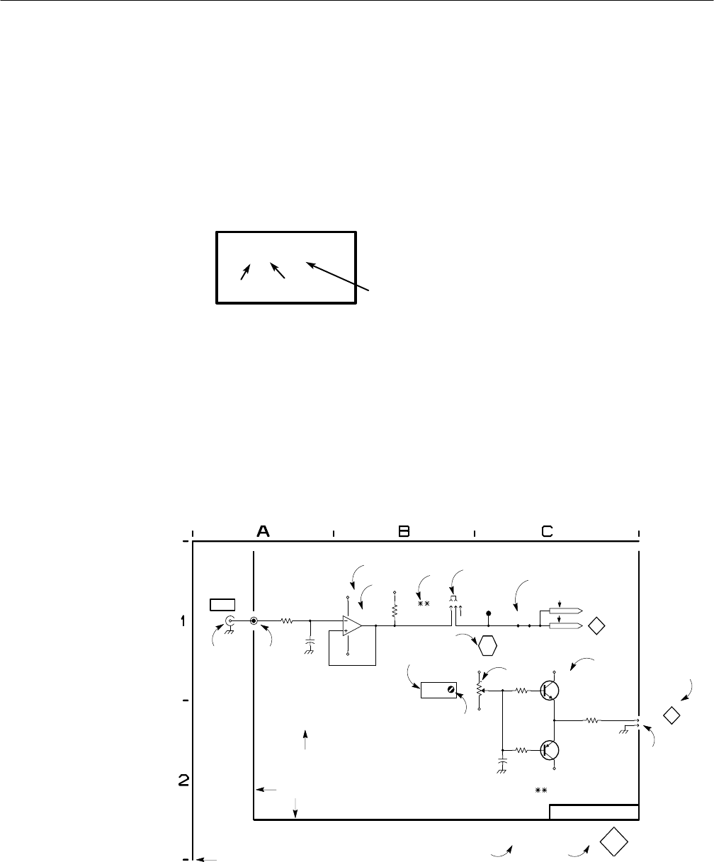
Diagrams/Circuit Board Illustrations
9–2 VITS 200
The following information and special symbols may appear in this manual.
Assembly Numbers Each assembly in the instrument is assigned an assembly number (e.g., A20).
The assembly number appears on the diagram (in circuit board outline), circuit
board illustration title, and lookup table for the schematic diagram.
The Replaceable Electrical Parts List is arranged by assembly number in
numerical sequence; the components are listed by component number. Example:
Chassis–mounted components
have no Assembly No. prefix.
See end of Replaceable Electrical
Parts List
Assembly
Number
Component Number
Schematic Circuit
Number
Grid Coordinates
The schematic diagram and circuit board component location illustration have
grids. A lookup table with the grid coordinates is provided for ease of locating
the component. Only the components illustrated on the facing diagram are listed
in the lookup table.
When more than one schematic diagram is used to illustrate the circuitry on a
circuit board, the circuit board illustration will only appear opposite the first
diagram; the lookup table will list the diagram number of other diagrams that the
other circuitry appears on.
WIRE STRAP
MODULE
PLUG
P1 NEGATIVE
PORTS
IC TYPE
CHANGED
PART
+12V
DECOUPLED OR
FILTERED VOLTAGE
R500
20K
+12V3
REAR
PANE L
INPUT
BNC
J1
(FEMALE) PAD FRONT PANEL
NOMENCLATURE
C1
10UF
2
3 6
7
4
U1
741
-12V
R5
1.0 NC
ROTATE
H
HEAT SINK
2
REFER TO
WAVEFORM
123
J1
R4
20K Q8
W4
0 OHM
+11.8V +15V
-11.8V
TP1
/VIDEO
(VIDEO)
R55
100.0
CLOCKWISE
AJUSTMENT
1
2
J3 12
W751
A3
ANALOG
BOARD
SCHEMATIC &
BOARD REF
PART NAME,
2
R100
R85
SEL
SEE PARTS LIST
FOR SELECTION
CRITERIA
SQUARE PIN
CONNECTOR
PART OF A1 MAIN BOARD
R56
100.0
Q6
-15V
SEE PARTS LIST FOR
EARLIER VALUES AND
SERIAL NUMBER RANGES.
C27
0.1UF
SCREWDRIVER
ADJUSTMENT
CIRCUIT BOARD
OUTLINE
& SNUBBER
BASE DRIVE
TITLE
FUNCTION BLOCK
INSTRUMENT NAME
SCHEMATIC NAME & NUMBER ASSEMBLY NUMBER
VERTICAL INPUT 1
A1
COMPONENT LOCATOR GRID

Replaceable Mechanical Parts List

VITS 200
C1 5 D5 F5
C2 5 E4 C6
C3 5 A1 B5
C4 5 C2 C4
C5 5 F2 D5
C6 5 E2 D5
C7 5 E2 D5
C8 5 F2 D5
C9 5 F2 E5
C10 5 E2 E5
C11 5 D1 D5
C12 5 D1 E5
C13 5 B2 C5
C14 5 D4 G5
C15 5 E1 D5
C16 5 D4 F4
C17 5 D5 E4
C18 5 D5 E4
C19 5 F5 E4
C20 5 F5 E4
C21 5 F5 E4
C22 5 G3 L7
C23 5 E5 E4
C24 9 E3 D7
C25 9 E4 E7
C26 9 D3 D7
C27 9 G3 D7
C28 9 G3 E6
C29 9 G3 F6
C30 9 G3 F6
C31 5 D2 D4
C33 9 D1 E6
C34 9 D2 F6
C36 9 E2 G7
C37 9 E1 E6
C38 9 E2 F6
C39 7 C1 L3
C40 7 E2 M3
C41 7 D2 L3
C42 7 E2 K3
C43 7 C5 M2
C46 7 E4 L3
C51 7 B5 G8
C52 7 F4 B5
C53 7 H4 A5
C54 7 B4 B7
C55 7 B4 B7
C56 7 B4 A7
C57 7 C4 A7
C58 7 B5 A7
C59 7 D5 A8
C60 7 E4 A7
C61 7 D5 A7
C65 7 E2 D8
C66 7 E2 D7
C67 7 G2 C7
C68 7 F2 C8
C69 7 C5 B8
C70 7 C5 B8
C71 7 C5 B8
C72 7 G2 C7
C73 7 D1 F7
C74 7 D1 E7
C75 7 E1 E7
C76 7 D2 F7
C77 7 D2 F7
C78 7 D2 F7
C79 7 E2 E7
C83 5 H4 L7
C84 8 B1 C3
C85 8 C1 B1
C86 8 C2 B1
C87 8 D2 C2
C88 8 E1 G1
C89 8 G4 J4
C91 8 F4 H2
C92 8 F4 I3
C94 8 G4 I2
C95 8 G4 I3
C96 8 D3 E1
C97 8 E4 D2
C98 8 F5 F3
C99 8 B3 D3
C100 8 G2 I2
C101 8 G3 I1
C102 8 F2 H1
C103 8 F3 H1
C104 8 F2 I2
C105 8 F3 I1
C106 8 G2 J2
C107 8 G3 J1
C108 8 G4 H3
C109 8 F4 H2
C110 8 C2 C1
C111 8 D3 E3
C112 8 F5 G3
C113 8 E3 D2
C114 8 C4 D3
C115 8 D3 E3
C116 8 F4 H2
C117 8 C2 F3
C118 8 C3 E3
C119 7 G1 C6
C120 5 C1 D4
C121 9 B4 P7
C122 9 C4 O6
C123 9 C4 P6
C124 9 D4 O5
C125 7 G3 H5
C126 9 B5 H4
C128 7 H3 H5
C129 9 D4 N5
C130 9 D4 M7
C131 9 E4 M7
C132 9 E4 K5
C133 1 F5 L6
C134 9 F4 M6
C135 4 A3 O4
C136 4 E5 N1
C137 9 F4 P1
C139 9 F4 I5
C140 9 B5 M4
C141 9 C5 N4
C142 1 G5 H5
C143 1 G5 F6
C144 1 G5 K3
C145 9 C5 E5
C146 9 D5 J5
C147 9 D5 J4
C148 1 H5 J6
C149 9 D5 G5
C150 5 A5 G4
C152 9 E5 I7
C153 9 E5 J6
C154 1 H5 G5
C156 9 F5 D6
C157 5 B5 D5
C158 5 B5 C4
C159 5 B5 C4
C160 5 H4 L4
C161 3 C5 L7
C162 9 F5 O2
C163 9 F5 N2
C164 7 E2 D7
C165 7 D1 C7
C167 9 D5 K3
C168 9 D5 F5
C169 9 F5 N3
C170 9 F5 C6
C171 9 F5 G5
C172 9 G3 M1
C173 9 G3 K4
C174 9 E1 K4
C175 5 D3 C6
C176 7 C2 H7
C177 7 B2 H7
C178 7 C2 G7
C179 7 B2 F6
C180 7 B2 G7
C181 7 A2 F6
C182 7 A2 E6
C183 7 E1 C7
C184 3 C5 L7
C185 5 D2 D4
C500 8 G2 H3
C501 8 B4 D3
C503 9 C5 L4
C504 9 H3 H4
C505 9 H3 G4
C506 7 E2 D8
C507 5 E5 E4
C508 8 A3 D3
C509 5 C2 C4
C510 7 D2 G7
C511 7 D2 G7
C512 8 F4 I3
CR5 7 F4 L3
CR7 7 G3 B5
CR8 7 F3 B5
CR9 8 E2 F3
CR10 8 F2 H1
CR11 8 F3 H1
CR12 8 C1 C2
CR13 8 F4 H2
CR14 8 F3 H3
CR15 8 G2 J2
CR16 8 H2 J2
CR17 8 H3 J1
CR18 8 G3 J1
CR19 8 E4 E1
CR20 8 E3 E1
CR21 8 E3 E2
CR22 8 E3 E2
CR24 8 G2 I4
CR25 3 B5 I7
CR26 8 B4 D3
CR27 3 E3 A4
CR28 3 E4 B4
CR29 3 E4 B5
DS1 3 D5 Q2
DS2 3 E5 Q1
DS3 3 E5 Q1
DS4 8 D2 B2
F1 8 A1 A3
J2 3 A3 F7
J3 3 H2 I7
J4 3 A2 L7
J5 4 B2 P5
J6 4 A1 P5
J9 5 G4 K4
J10 5 A1 A6
J11 7 C1 K1
J12 7 G3 M2
J13 7 D4 M2
J14 7 H5 A7
J15 7 H4 A6
J17 8 E2 E2
J18 8 E3 F1
J19 8 C4 E3
J20 9 B1 J2
J21 8 H2 I4
J22 3 E3 J7
J27 3 A5 J7
J28 3 D4 P2
J32 7 F2 H4
J33 1 F2 H7
J50 7 H1 C7
J51 7 H1 B6
J52 5 A4 G4
J53 7 A4 B7
J54 1 A1 N6
J55 1 B4 N8
J56 1 B4 M7
J57 1 B4 M7
K2 7 G4 A6
L1 5 F5 F4
L2 9 D2 D6
L3 9 E4 E6
L6 7 G4 A6
L7 7 F4 B6
L8 7 F4 B6
L12 7 D2 F7
L13 7 D2 F7
L14 7 E2 E7
L15 8 G4 I2
L16 8 G3 J3
L17 8 D1 D1
L18 7 G1 D6
L19 5 C1 D4
L20 7 E1 C7
L21 7 E2 D8
LF1 8 A1 A2
P5 4 B2
P6 4 A1
P9 5 G4
P12 7 G3
P13 7 D4
P17 8 E2
P18 8 E3
P19 8 C4
P20 9 B1
P22 3 E3
P28 3 D4
P32 7 F2
P33 1 F2
P34 9 B1
P35 9 B1
P36 9 B1
P37 9 B1
P38 9 B1
P54 1 A1
P55 1 B4
P56 1 B4
P57 1 B4
Q1 5 F1 D5
Q2 5 F2 D6
Q3 5 G2 D5
Q4 9 G2 D6
Q5 9 G3 E7
Q6 9 G2 D6
Q7 9 G4 E6
Q8 7 D1 K2
Q9 7 E4 L1
Q11 7 F4 A6
Q12 7 G3 A5
Q13 3 D5 P2
Q14 3 E5 P2
Q15 8 G4 J3
Q16 8 E3 E1
Q17 8 E4 D2
Q18 8 C4 E3
Q180 8 D3 E4
R3 1 G2 F6
R4 1 G3 H6
R5 1 A3 M8
R6 2 C1 N7
R7 2 C2 N6
R8 2 C3 N6
R9 2 C4 N5
R10 3 B3 L8
R11 3 F4 A5
R12 3 F4 A4
R13A 3 D3 J7
R13B 3 C3 J7
R13C 3 C5 J7
R13D 3 B3 J7
R13E 3 B3 J7
R13F 3 C3 J7
R13G 3 A5 J7
R13H 3 B5 J7
R13I 3 B2 J7
R14 3 F2 H6
R18 5 A1 C5
R19 5 D5 E4
R20 5 D3 C6
R21 5 D3 C7
R22 5 E3 C6
R23 5 E3 C6
R24 5 F3 C6
R25 5 E3 C6
R26 5 E3 C5
R27 5 E4 C5
R28 5 F3 C6
R29 5 B2 C5
R30 5 B2 C5
R31 5 B2 C5
R32 5 B1 B5
R33 5 B1 B4
R34 5 C1 B5
R35 5 C1 C4
R36 5 C1 B5
R37 5 C4 F4
R38 5 C4 C4
R39 5 D1 C4
R40 5 D2 D4
R41 5 D2 D4
R42 5 D2 D4
R43 5 D2 D5
R44 5 E2 C5
R45 5 F2 D5
R46 5 F2 D5
R47 5 F1 D6
R48 5 G2 D6
R49 5 F3 D6
R50 5 G2 E6
R51 5 G2 E6
R52 5 E5 F4
R53 5 E5 E4
R54 5 G3 L7
R55 5 E5 E6
R56 9 E2 D7
R57 9 E3 E7
R58 9 F4 E6
R59 9 F4 E7
R60 9 G4 E7
R61 9 F2 D6
R62 9 F2 D7
R63 9 G3 E7
R64 9 G3 E6
R65 9 G3 E6
R66 9 G2 D6
R67 9 G4 E6
R68 7 C1 K3
R69 7 D1 K3
R70 7 D1 K3
R71 7 D2 L3
R72 7 D1 K3
R73 7 E2 L3
R74 7 E2 K3
R76 7 D2 L3
R77 7 D5 M3
R78 7 C5 N2
R79 7 D5 M2
R80 7 C4 M3
R81 7 C4 M3
R82 7 C4 N3
R83 7 E5 M1
R86 7 G4 L3
R87 7 G4 L3
R88 7 F4 L3
R89 7 F4 M3
R90 7 E4 L3
R91 7 E4 L3
R92 7 E3 L4
R98 7 D2 F6
R99 7 E2 D7
R100 7 A4 B5
R101 7 B2 F6
R102 7 B2 F6
R103 7 G1 C7
R104 7 G3 B7
R105 7 G2 B7
R106 7 F4 A6
R108 7 G4 A6
R109 7 H3 A5
R110 7 E5 A7
R111 7 D5 A7
R112 7 E4 B7
R113 7 D5 A8
R114 7 D5 A7
R115 7 D5 A7
R116 7 D4 A7
R117 7 E4 A7
R118 7 A4 B7
R119 7 C4 B7
R120 7 G1 C7
R121 7 F1 C7
R122 7 F1 B8
R123 7 F1 C7
R124 7 F1 B7
R125 7 E2 D7
R126 7 E2 C7
R127 7 E2 C7
R130 7 B4 B7
R132 3 E5 P1
R133 3 D5 Q2
R134 3 E5 Q2
R135 3 C4 O2
R137 3 D5 Q2
R138 3 D5 Q2
R141 5 H4 L7
R142 5 H5 L7
R143 8 A1 B2
R144 8 B1 B3
R145 8 D1 B2
R146 8 H4 J4
R147 8 F4 H2
R149 8 E3 E2
R150 8 E4 D2
R151 8 D4 E3
R152 8 E4 D3
R153 8 E3 E1
R154 8 D2 D2
R155 8 F3 I1
R156 8 F2 I2
R157 8 C1 C2
R158 8 C5 F3
R159 8 C4 F3
R160 8 A5 C3
R161 8 A4 C3
R162 8 B3 D3
R163 8 E4 D2
R164 8 A4 C3
R165 8 B3 D3
R166 8 E5 G3
R167 8 E5 G3
R168 8 F5 G3
R169 8 F5 G3
R170 8 F5 G3
R171 8 A4 C3
R172 8 B4 D3
R173 8 D3 E3
R174 8 C4 E3
R175 8 C3 E3
R177 4 E1 N4
R178 4 D1 M5
R179A 4 B5 P2
R179B 4 B3 P2
R179C 4 C3 P2
R179D 4 G3 P2
R179E 4 G5 P2
R179F 4 G5 P2
R179G 4 G5 P2
R179H 4 E1 P2
R179I 4 A5 P2
R180 8 D3 E4
R184 8 D4 D4
R185 5 D4 G4
R190 7 E1 K3
R191 7 E1 K3
R192 5 C4 L8
R206 7 F1 J4
R207 7 F1 J5
R208 7 E2 D7
R209 7 G1 C7
R210 7 E1 C7
R211 3 D5 J7
R212 3 D5 J7
R213 3 A5 I7
R214 5 B1 C5
R216 5 D3 C6
R217 7 G1 G5
R218 7 F2 I4
R219 7 G2 H6
R220 7 G2 I5
R221 7 G2 I4
R222 7 F2 K3
R223 7 F2 K3
R224 7 F1 K3
R225 7 G1 J4
R226 7 G1 J5
R227 7 B2 F6
R228 7 B2 F6
R229 7 A2 F7
R230 7 A2 F6
R231 3 B5 K7
R500 8 A2 C1
R501 8 A2 C1
R502 8 A3 C1
R503 8 B4 D4
R504 8 B4 D3
R506 7 E1 C7
R507 5 C2 D4
R508 5 C2 C4
RT1 8 B1 C3
RV1 8 B1 C3
S1 2 B1 O8
S2 2 B2 N7
S3 2 B3 N6
S4 2 B4 N6
S5 3 F5 A5
S6 3 F4 A4
S7 4 D2 N5
S8 4 C1 L4
S9B 3 C5 Q3
S10A 8 B1 B4
S10B 8 B1 B4
T1 8 E2 G1
T2 7 E2 D7
TP1 9 B2 K2
TP2 9 B2 K2
TP3 8 D2 D2
TP4 9 B3 J2
TP5 9 B2 J1
TP6 9 B1 K1
TP7 9 B3 N1
TP8 9 B3 D4
TP9 9 C3 O8
TP10 9 C3 E6
TP11 7 F1 J3
U1 1 F4 I6
U3 1 E1 J5
U4 1 D4 L6
U5 1 D5 L5
U6 1 D1 L5
U7 1 F1 J5
U8 1 C1 L6
U9 1 G2 H6
U10 1 G2 G6
U11 1 G1 F6
U12 1 F3 I5
U13 1 B1 M6
U15 1 E2 H5
U16 1 B3 M8
U17 1 B5 M7
U18 2 F1 O8
U19 2 F2 O7
U20 2 F3 O6
U21 2 F4 O6
U22 3 G4 A5
U23 3 G5 A4
U24 3 D2 H7
U25 3 E3 H7
U26 3 F3 I6
U27 3 D1 I7
U28 3 C1 J7
U29 4 D3 N3
U30 4 F4 O2
U31 4 A2 O5
U32 4 F3 M4
U33 4 H4 M2
U34 4 G4 O2
U35 4 B3 N4
U36 4 F1 M5
U37 4 F2 M5
U38 4 G3 N5
U41 5 G4 G4
U42 5 B1 C5
U43 5 E4 E5
U44 5 E1 D5
U46A 5 E3 B6
U47A 5 F3 B6
U47B 5 F3 B6
U48A 5 G4 K7
U50A 9 F2 D6
U50B 9 F3 D6
U51 9 D2 D6
U52 9 D1 E6
U53 9 D2 F6
U54 7 H1 H5
U55A 7 D1 K3
U55B 7 F2 K3
U55C 7 F1 k3
U56A 7 D4 M3
U56B 7 D2 M3
U57A 5 G2 K7
U57B 5 H2 K7
U57C 1 D2 K7
U57D 3 E1 K7
U59 7 D3 K4
U60 7 F4 M3
U61A 7 E3 L3
U62 7 H3 G5
U63A 7 F2 H4
U63B 7 E3 H4
U63C 7 F3 H4
U64 7 C4 A7
U65 7 C1 G7
U67 7 F2 C7
U70 3 C4 L7
U71A 5 H4 L7
U71B 5 G3 L7
U72 8 F2 H4
U73 8 G3 J1
U74 8 E5 F4
U75 8 E4 F3
U76A 8 B4 D3
U76B 8 B4 D3
U78 8 C3 E3
U80 4 F4 K4
U81A 7 F1 I4
U82 1 E4 K6
U83 1 E5 J6
U84 7 A2 F6
U85 8 G2 I2
U86 1 C1 L6
U87 1 C4 M7
VR1 5 F2 D6
VR2 5 G2 D6
VR3 7 D5 M2
VR4 8 G4 J4
Y39 4 A3 O5
A1 Inserter Board and Diagram <1> Component Locator
A1 Inserter Board
671-2132-05 & Up
Lookup Chart
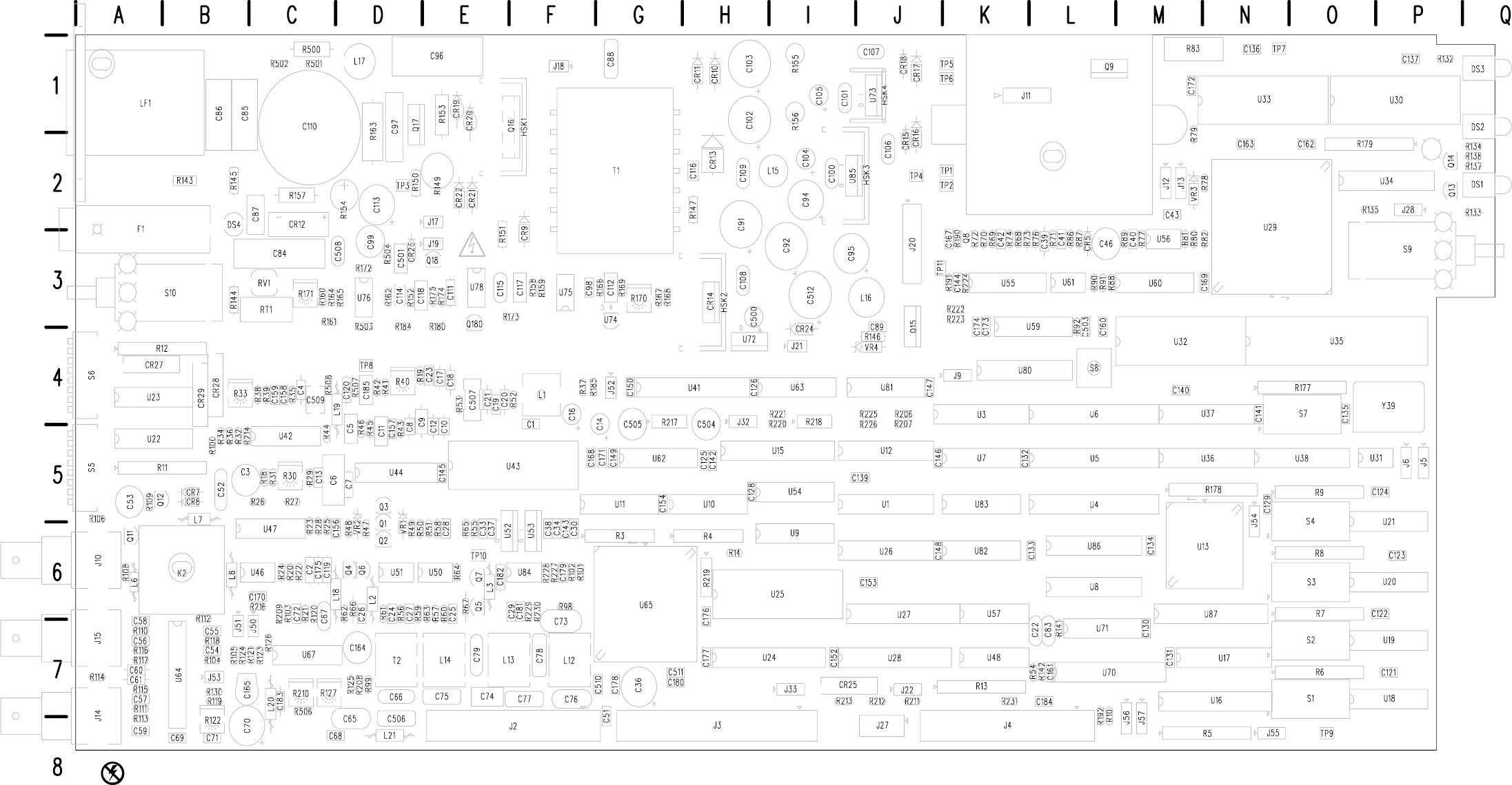
VITS 200
Component locator for diagram <1>
located on back of this page.
A1 Inserter Board
Static Sensitive Devices
See Maintenance Section
671-2132-05 & Up
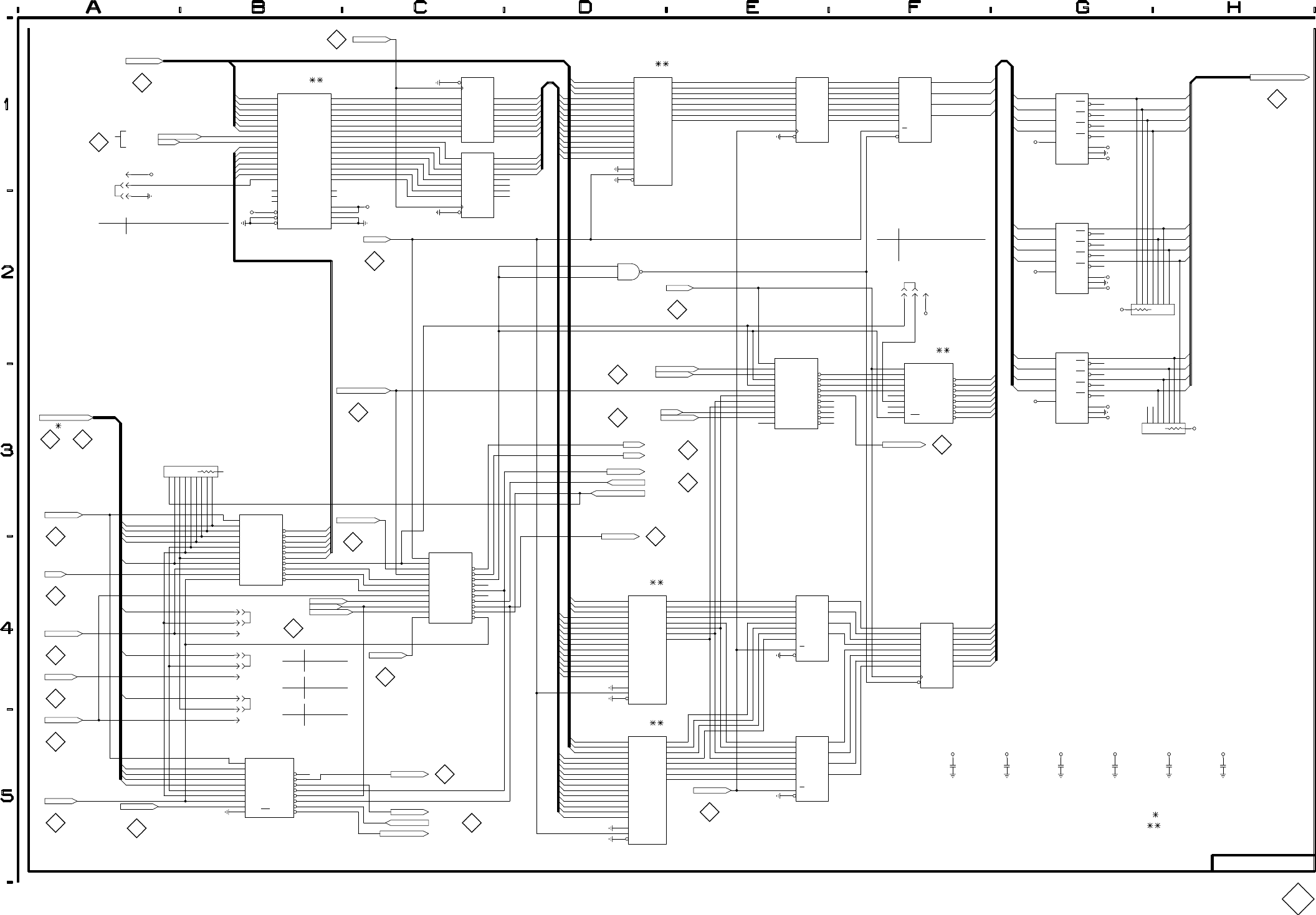
'&,- '&,-
'&
+
+
+
+
(
$
$
$
$
$
$
$
$
"
(
$
$
$
$
$
$
$
$
"
(
&
#
&
(
+
(
,- ,-
(
!
'&
'&
'&
'&
'&
'&
)
(
(
)
#
)
$
$
$
$
$
$
$
$
$
$
$
$
$
$
$
$
"
#
)
)##
!
!
!
!
!
!
!
(
$
$
$
$
$
$
$
$
"
(
&
#
'&
'&
'&
'&
'&
'&
'&
)
)
'&
'&
'&
'&
)
$
$
$
$
$
$
$
$
)
!
)
(
(
'&
'&
'&
'&
)
)
)
'&
'&
'&
'&
)
$
$
$
$
$
$
$
$
)
!
)
(
%
%'&
&
)
&'(#"!'%"
%'%
*'&'(#
&'!%"#'
"#'
*'"('&'(#
#
&
'&%
!
(
(
'&%
(
)
"%+!&'
&'!%"#'"!&
"#'"!&!&
#'&,-
(
#'&,-
%#%&
%#%&
&*
&*
(
(
%'
(%&"%
"
"
"
"
"
"
"
"
"
"
"
(
#)
(
(
'&
'&
'&
'&
'&
'&
'&
'" #
'&
&''
&''
&''
&''
"
(
)
'&
'&
'&
'&
'&
'&
'&
'&
)
)
)
%
$
$
$
$
$
$
$
$
)
!
)
(
)
(
(
)%)
&
)%&
$!'
'&
'&
'&
'&
'&
'&
%&+!
!
"
"
"
"
"
"
"
"
"
"
(
#)
#'&
#'&
#'&
#'&
#'&
%
.
"
"
"
"
"
"
"
"
"
"
(
#)
)%)
)
)
)'
(
(
)%)
)&+!
(
(
#'&
#'&
#'& #
#
#
&'+
&*'
&+!'
"!"%
)%)
)'&
)'&
)'&
)'&
)&+!
!!
!
(
(
(
(
#
&
(
+
+
+
+
+
(
'&
'&
'&
'&
'&
'&
'&
'&
%'&
&
$
$
$
$
$
$
$
$
"
(
)
/
) ) ) )
/
/
/
!"' !"'(&"!)'&
&#%'&&'"%%%)(&
!&%!( %%!&
)
/
/
#
+
+
+
+
(
(
(
(
(
#
&
(
+
)%)
&*'
)%&
)&+!
!
)%&#%&
)%& #
(
)'&
)'&
#'&
#'&
#'&
#'&
#%&
(
"
(
)
!
(
VITS 200 REV AUG 1995 TEST SIGNAL MEMORY
P/O A1 INSERTER BOARD
1
671–2132–05 & UP
VITS 200

VITS 200
C1 D5 5 F4
C1 D5 5 F4
C2 E4 5 C6
C3 A1 5 B5
C4 C2 5 C4
C5 F2 5 D5
C6 E2 5 D5
C7 E2 5 D5
C8 E2 5 D5
C9 F2 5 D5
C10 E2 5 E5
C11 D1 5 D5
C12 D1 5 E5
C13 B2 5 C5
C14 D4 5 G4
C16 C4 5 F4
C17 D5 5 E4
C18 D5 5 E4
C19 F5 5 E4
C20 F5 5 E4
C21 F5 5 E4
C22 G3 5 L7
C23 E5 5 E4
C24 E3 9 D7
C25 E4 9 E7
C26 D3 9 D7
C27 G3 9 D7
C28 G3 9 E6
C29 H3 9 F6
C30 H3 9 F6
C33 D1 9 E6
C34 D2 9 F6
C36 E2 9 D8
C37 E1 9 E6
C38 E2 9 F6
C39 C1 6 L3
C40 E2 6 M3
C41 D2 6 L3
C42 E2 6 K3
C43 C5 6 M2
C46 E4 6 L3
C51 B5 7 G7
C52 F4 7 B5
C53 H4 7 B5
C54 B4 7 B7
C55 B4 7 B7
C56 B4 7 A7
C57 C4 7 A7
C58 B5 7 A7
C59 D5 7 A8
C60 E4 7 A7
C61 D5 7 A7
C65 E2 7 D8
C66 E2 7 D7
C67 G2 7 C6
C68 F2 7 C8
C69 C5 7 B8
C70 C5 7 B8
C71 C5 7 B8
C72 G2 7 C7
C73 D1 7 F7
C74 D1 7 E7
C75 E1 7 E7
C76 D2 7 F7
C77 D2 7 F7
C78 D2 7 F7
C79 E2 7 E7
C83 H4 5 L7
C84 B1 8 C3
C85 C1 8 B1
C86 C2 8 B2
C87 D2 8 C2
C88 E1 8 G1
C89 G4 8 J4
C91 F4 8 H2
C92 F4 8 I3
C94 G4 8 I2
C95 G4 8 J3
C96 D3 8 E1
C97 E4 8 D1
C98 F5 8 F3
C99 B3 8 D3
C100 G2 8 I2
C101 G3 8 I1
C102 F2 8 H1
C103 F3 8 H1
C104 F2 8 I2
C105 F3 8 I1
C106 G2 8 J2
C107 G3 8 J1
C108 F4 8 H3
C109 F4 8 H2
C110 C2 8 C1
C111 D3 8 E3
C112 F5 8 G3
C113 E3 8 D2
C114 C4 8 D3
C115 D3 8 F3
C116 F4 8 H2
C117 C2 8 F3
C118 C3 8 E3
C119 G1 7 C6
C120 C1 5 C4
C121 B4 9 P7
C122 C4 9 O6
C123 C4 9 P6
C124 D4 9 O5
C125 G3 6 H5
C126 B5 9 H4
C128 H3 6 M5
C129 D4 9 N5
C130 D4 9 M7
C131 E4 9 M7
C132 E4 9 K5
C133 F5 1 K6
C134 F4 9 M6
C135 A3 4 O4
C136 E5 4 N1
C137 F4 9 P1
C139 F4 9 I5
C140 B5 9 M4
C141 C5 9 N4
C142 G5 1 H5
C143 G5 1 F6
C144 G5 1 K3
C145 C5 9 E5
C146 D5 9 J5
C147 D5 9 L4
C148 H5 1 J6
C149 D5 9 G5
C150 A5 5 G4
C152 E5 9 I7
C153 E5 9 J6
C154 H5 1 G5
C155 C5 7 G7
C156 F5 9 D6
C157 B5 5 D5
C158 B5 5 C4
C159 B5 5 C4
C160 H4 5 L4
C161 C4 3 L7
C162 F5 9 O2
C163 F5 9 N2
C164 E2 7 D7
C165 E1 7 C7
C167 D5 9 K3
C168 D5 9 F5
C169 F5 9 N3
C170 F5 9 C6
C171 F5 9 G5
C172 G3 9 M1
C173 G3 9 K4
C174 E1 9 K4
C175 D3 5 C6
C176 C2 7 H7
C177 B2 7 H7
C178 C2 7 G7
C179 B2 7 F6
C180 B2 7 G7
C181 A2 7 F6
C182 A2 7 E6
C183 E1 7 C7
C184 C5 3 L7
C185 * D2 5 D4
C500 G2 8 H3
C501 B4 8 D3
C502 F3 8 G1
C503 C5 9 L4
C504 H3 9 K4
C505 H3 9 K4
CR5 F4 6 L3
CR7 G3 7 B5
CR8 F3 7 B5
CR9 E2 8 F3
CR10 F2 8 H1
CR11 F3 8 H1
CR12 C1 8 C2
CR13 F4 8 H2
CR14 F3 8 H3
CR15 G2 8 J2
CR16 H2 8 J2
CR17 H3 8 J1
CR18 G3 8 J1
CR19 E4 8 E1
CR20 E3 8 E1
CR21 E3 8 E2
CR22 E3 8 E2
CR24 G2 8 I4
CR25 B5 3 I7
CR26 B4 8 D3
DS1 D5 3 Q2
DS2 E5 3 Q2
DS3 E5 3 Q1
DS4 D2 8 B2
E1 F5 5 F4
F1 A1 8 A3
J1 C4 1 J6
J2 A3 3 G7
J3 H2 3 H7
J4 A2 3 K7
J5 B2 4 P5
J6 A1 4 P5
J9 G4 5 L4
J10 A1 5 A6
J11 C1 6 K1
J12 G3 6 M2
J13 D4 6 M2
J14 H5 7 A7
J15 H4 7 A6
J17 E2 8 E3
J18 E3 8 F1
J19 C4 8 E3
J20 B1 9 J2
J21 H2 8 I4
J22 B2 3 J7
J27 A5 3 J7
J28 D4 3 P2
J32 B4 1 H7
J33 B4 3 I7
J50 H1 7 C7
J51 H1 7 B7
J52 D4 5 G4
J53 B4 7 B7
K2 G4 7 A6
L1 F5 5 E4
L2 D2 9 D6
L3 E4 9 E6
L6 G4 7 A6
L7 F4 7 B6
L8 F4 7 B6
L12 D2 7 F7
L13 D2 7 F7
L14 E2 7 E7
L15 G4 8 H2
L16 G3 8 J3
L17 D1 8 D1
L18 G1 7 D6
L19 C1 5 C4
L20 E1 7 C8
LF1 A1 8 A2
P1 C4 1
P5 B2 4
P6 A1 4
P9 G4 5
P12 G3 6
P13 D4 6
P17 E2 8
P18 E3 8
P19 C4 8
P20 B1 9
P21 H2 8
P22 B2 3
P28 D4 3
P32 B4 1
P33 B4 3
P34 B1 9
P35 B1 9
P36 B1 9
P37 B1 9
P38 B1 9
Q1 F1 5 D6
Q2 F2 5 D6
Q3 G2 5 D5
Q4 G2 9 D6
Q5 G3 9 E7
Q6 G2 9 D6
Q7 G4 9 E6
Q8 D1 6 K2
Q9 E4 6 L1
Q11 F4 7 A6
Q12 G3 7 A5
Q13 D5 3 P2
Q14 E5 3 P2
Q15 G4 8 J3
Q16 E3 8 E1
Q17 E4 8 D2
Q18 C4 8 E3
Q180 D3 8 E4
R3 G2 1 G6
R4 G3 1 H6
R5 A3 1 N8
R6 C1 2 N7
R7 C2 2 N7
R8 C3 2 N6
R9 C4 2 O5
R10 B3 3 M8
R11 F4 3 A5
R12 F4 3 A4
R13 A2 3 K7
R14 F2 3 H6
R18 A1 5 C5
R19 D5 5 E4
R20 D3 5 C6
R21 D3 5 C7
R22 E3 5 C6
R23 E3 5 C6
R24 F3 5 C6
R25 E3 5 C6
R26 E3 5 C5
R27 E4 5 C5
R28 F3 5 C6
R29 B2 5 C5
R30 B2 5 C5
R31 B2 5 C5
R32 B1 5 C5
R33 B1 5 B4
R34 C1 5 B5
R35 C1 5 C4
R36 C1 5 B5
R37 C4 5 F4
R38 C4 5 C4
R39 D1 5 C4
R40 D2 5 D4
R41 D2 5 D4
R42 D2 5 D4
R43 D2 5 D5
R44 E2 5 D5
R45 F2 5 D5
R46 F2 5 D5
R47 F1 5 D6
R48 G2 5 D6
R49 F3 5 D6
R50 G2 5 E6
R51 G2 5 E6
R52 E5 5 F4
R53 E5 5 E4
R54 G3 5 L7
R55 E5 5 E6
R56 E2 9 D7
R57 E3 9 E7
R58 F4 9 E6
R59 F4 9 D7
R60 G4 9 E7
R61 F2 9 D7
R62 F2 9 D7
R63 G3 9 E7
R64 G3 9 E6
R65 G3 9 E6
R66 G2 9 D6
R67 G4 9 E6
R68 C1 6 K3
R69 D1 6 K3
R70 D1 6 K3
R71 D2 6 L3
R72 D1 6 K3
R73 E2 6 L3
R74 E2 6 K3
R76 D2 6 L3
R77 D5 6 M3
R78 C5 6 N2
R79 D5 6 M2
R80 C4 6 M3
R81 C4 6 M3
R82 C4 6 N3
R83 E5 6 M1
R86 G4 6 L3
R87 G4 6 L3
R88 F4 6 L3
R89 F4 6 M3
R90 E4 6 L3
R91 E4 6 L3
R92 E3 6 L4
R98 D2 7 F6
R99 E2 7 D7
R100 A4 7 B5
R101 B2 7 F6
R102 B2 7 F6
R103 G1 7 C7
R104 G3 7 B7
R105 G2 7 B7
R106 F4 7 A6
R108 G4 7 A6
R109 H3 7 A5
R110 E5 7 A7
R111 D5 7 A7
R112 E4 7 B7
R113 D5 7 A8
R114 D5 7 A7
R115 D5 7 A7
R116 D4 7 A7
R117 E4 7 A7
R118 A4 7 B7
R119 C4 7 B7
R120 G1 7 C7
R121 F1 7 C7
R122 F1 7 C8
R123 F1 7 C7
R124 F1 7 B7
R125 E2 7 C8
R126 E2 7 C7
R127 E2 7 C7
R130 B4 7 B7
R132 E5 3 P1
R133 3 D5 Q2
R134 3 E5 Q2
R135 3 C4 O2
R137 3 D5 Q2
R138 3 D5 Q2
R141 5 H4 L7
R142 5 H5 L7
R143 8 A1 B2
R144 8 B1 B3
R145 8 D1 B2
R146 8 H4 J4
R147 8 F4 H2
R149 8 E3 E2
R150 8 E4 E2
R151 8 D4 E3
R152 8 E4 D3
R153 8 E3 E2
R154 8 D2 D2
R155 8 F3 I1
R156 8 F2 I1
R157 8 C1 C2
R158 8 C5 F3
R159 8 C4 F3
R160 8 A5 C3
R161 8 A4 D3
R162 8 B3 D3
R163 8 E4 D2
R164 8 A4 C3
R165 8 B3 D3
R166 8 E5 G3
R167 8 E5 G3
R168 8 F5 G3
R169 8 F5 G3
R170 8 F5 G3
R171 8 A4 C3
R172 8 B4 D3
R173 8 D3 E3
R174 8 C4 E3
R175 8 C3 E3
R177 4 E1 N4
R178 4 D1 M6
R179A 4 B5 P2
R179B 4 B3 P2
R179C 4 C3 P2
R179D 4 G3 P2
R179E 4 G5 P2
R179F 4 G5 P2
R179G 4 G5 P2
R179H 4 E1 P2
R179I 4 A5 P2
R180 8 D3 E4
R184 8 D4 D4
R185 5 D4 F4
R190 7 E1 K3
R191 7 E1 K3
R192 5 C4 L8
R206 7 F1 J4
R207 7 F1 J5
R208 7 E2 D7
R209 7 G1 C7
R210 7 E1 C7
R211 3 D5 J7
R212 3 D5 J7
R213 3 A5 I7
R214 5 B1 B5
R215 1 C3 G7
R216 5 D3 C6
R217 7 G1 G5
R218 7 F2 I4
R219 7 G2 H6
R220 7 G2 I5
R221 7 G2 I4
R222 7 F2 K3
R223 7 F2 K3
R224 7 F1 K3
R225 7 G1 J4
R226 7 G1 J5
R227 7 B2 F6
R228 7 B2 F6
R229 7 A2 F7
R230 7 A2 F6
R231 3 B5 K7
R500 8 A2 C1
R501 8 A2 C1
R502 8 A3 C1
R503 8 B4 D4
R504 8 B4 D3
R505 5 H5 L7
R506 7 E1 C7
RT1 8 B1 C3
RV1 8 B1 C3
S1 2 B1 N8
S2 2 B2 N7
S3 2 B3 N6
S4 2 B4 N6
S5 3 F5 A5
S6 3 F4 A4
S7 4 D2 N5
S8 4 C1 M8
S9 3 C5 Q3
S10A 8 B1 B4
S10B 8 B1 B4
T1 8 E2 G1
T2 7 E2 D7
TP1 9 B2 K2
TP2 9 B2 K2
TP3 8 D2 D2
TP4 9 B3 J2
TP5 9 B2 J1
TP6 9 B1 K1
TP7 9 B3 N1
TP8 9 B3 D4
TP9 9 C3 O8
TP10 9 C3 E6
U1 1 F4 I6
U3 1 E1 J5
U4 1 D4 L6
U5 1 D5 L5
U6 1 D1 L5
U7 1 F1 J5
U8 1 C1 M6
U9 1 G2 H6
U10 1 G2 G6
U11 1 G1 F6
U12 1 F3 I5
U13 1 B1 L6
U14 1 C3 M7
U15 1 E2 H5
U16 1 B3 M8
U17 1 B5 M7
U18 2 F1 O8
U19 2 F2 O7
U20 2 F3 O6
U21 2 F4 O6
U22 3 G4 A5
U23 3 G5 A5
U24 3 D2 H7
U25 3 E3 H7
U26 3 F3 I6
U27 3 D1 I7
U28 3 C1 J7
U29 4 D3 N3
U30 4 F4 O2
U31 4 A2 O5
U32 4 F3 M4
U33 4 H4 M2
U34 4 G4 O2
U35 4 B3 N4
U36 4 F1 M6
U37 4 F2 M5
U38 4 G3 N5
U40 4 G2 M5
U41 5 G4 G4
U42 5 B1 C5
U43 5 E4 E5
U44 5 E1 D5
U46A 5 E3 B6
U47A 5 F3 B6
U47B 5 F3 B6
U48A 5 G4 K7
U50A 9 F2 D6
U50B 9 F3 D6
U51 9 D2 D6
U52 9 D1 E6
U53 9 D2 F6
U54 7 H1 H5
U55A 7 D1 K3
U55B 7 F2 K3
U55C 7 F1 K3
U56A 7 D4 M3
U56B 7 D2 M3
U57A 5 G2 K7
U57B 5 H2 K7
U57C 1 D2 K7
U57D 3 E1 K7
U59 7 D3 K4
U60 7 F4 M3
U61A 7 E3 L3
U62 7 H3 G5
U63A 7 F2 H4
U63B 7 E3 H4
U63C 7 F3 H4
U64 7 C4 A7
U65 7 C1 G7
U67 7 F2 C7
U70 3 C4 L7
U71A 5 H4 L7
U71B 5 G3 L7
U72 8 F2 H4
U73 8 G3 J1
U74 8 E5 G4
U75 8 E4 F3
U76A 8 B4 D3
U76B 8 B4 D3
U78 8 C3 E3
U80 4 F4 K4
U81A 7 F1 I4
U82 1 E4 K6
U83 1 E5 J6
U84 7 A2 F6
U85 8 G2 I2
VR1 5 F2 D6
VR2 5 G2 D6
VR3 7 D5 M2
VR4 8 G4 J4
W1 4 A3 P4
Y39 4 A3 O5
A1 Inserter Board and Diagram <1> Component Locator
A1 Inserter Board
671-2132-00 – 04
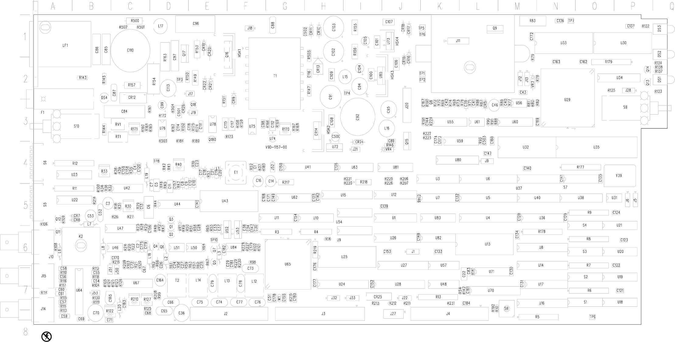
VITS 200
Component locator for diagram <1>
located on back of this page.
A1 Inserter Board
Static Sensitive Devices
See Maintenance Section
671-2132-00 – 04
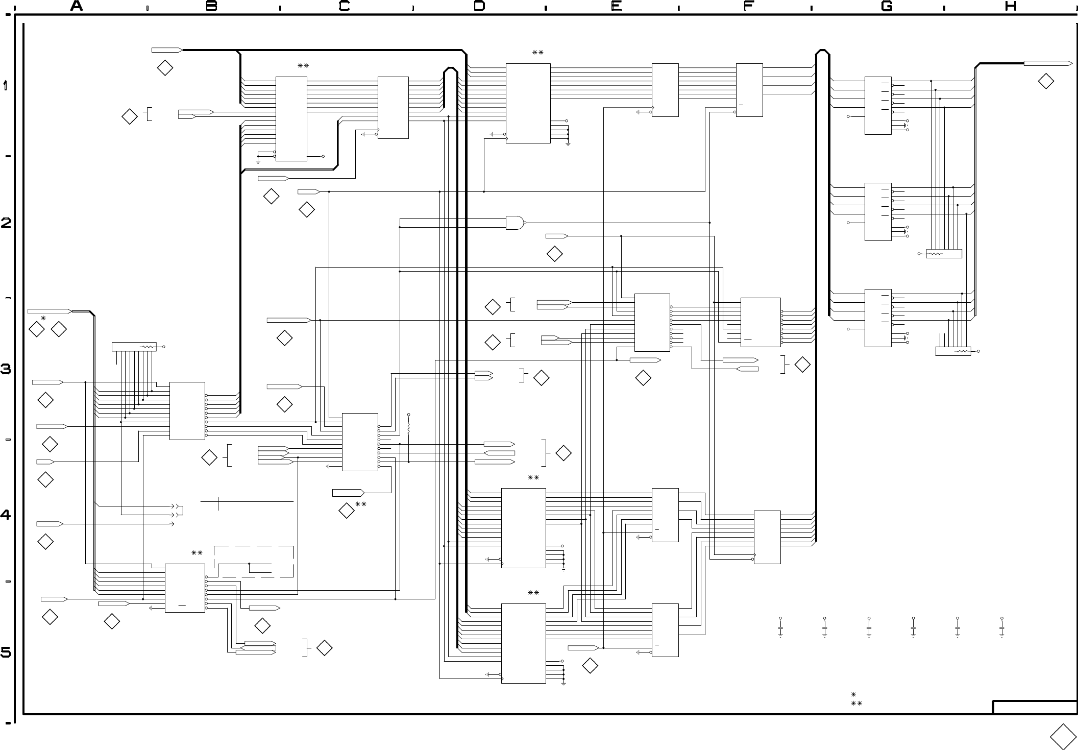
'&-. '&-.
'&
,
,
,
,
(
$
$
$
$
$
$
$
$
"
(
!
!
!
!
)
&
(
,
-. -.
(
!
)
(
(
'&
'&
'&
'&
'&
'&
'&
'&
)
"
)##
(
'&
'&
$
$
$
$
$
$
$
$
$
$
"
(
)
#
'&
'&
'&
'&
'&
'&
'&
)
)
'&
'&
'&
'&
)
$
$
$
$
$
$
$
$
)
!
)
(
(
'&
'&
'&
'&
)
)
)
'&
'&
'&
'&
)
$
$
$
$
$
$
$
$
)
!
)
(
%
%'&
&
&
'&%
!
(
(
(
(
#'&-.
(
#'&-.
)
%
/
%#%&
&*
&*
%#%&
(
(
%'
(%&"%
"
%&!
"
"
"
"
"
"
"
"
"
"
(
#)
(
(
'&
'&
'&
'&
'&
'&
'&
'" #
'&
&''
&''
&''
&''
'+
"
(
) '&
'&
'&
'&
'&
'&
'&
'&
)
)
)
%
$
$
$
$
$
$
$
$
)
!
)
(
)
(
)
&
)%)
!'
%
/
&,!'
&*'
&',
!
%&,!
"
"
"
"
"
"
"
"
"
"
(
#)
#'&
#'&
#'&
#'&
#'&
#'&
!
'&
'&
'&
'&
'&
'&#'&
#%"
'&'&
+'%
"
"
"
"
"
"
"
"
"
"
(
#)
(
(
(
(
)'
)
)%)
(
(
(
)&,!
(
#'&
#'&
#'&
#'&
#'&
"
(
)
#
%&!
(
(
"&
"'"!
"&
'&
'&
!
!
!
!
)
&
(
,
)
,
,
,
,
(
'&
'&
'&
'&
'&
'&
'&
'&
%'&
&
$
$
$
$
$
$
$
$
"
(
)
0
) ) ) )
0
0
0
)
0
0
#
)
(
,
,
,
,
(
'&
'&
!
!
!
!
)
&
(
,
)%&#%&
)&,!
!
)%&
)%& #
(
(
(
(
)%)
#'&
#'&
#%&
(
VITS 200 %)!") TEST SIGNAL MEMORY
!"' !"'(&"!)'&
!"' &#%'&&'"%%%)(&
!&%!( %%!& P/O A1 INSERTER BOARD
1
671–2132–00 – 04

VITS 200
R6 C1 N7
R7 C2 N6
R8 C3 N6
R9 C4 N5
S1 B1 O8
S2 B2 N7
S3 B3 N6
S4 B4 N6
U18 F1 O8
U19 F2 O7
U20 F3 O6
U21 F4 O6
Schematic Diagram <2>
A1 Component Locator Chart
Assembly A1.
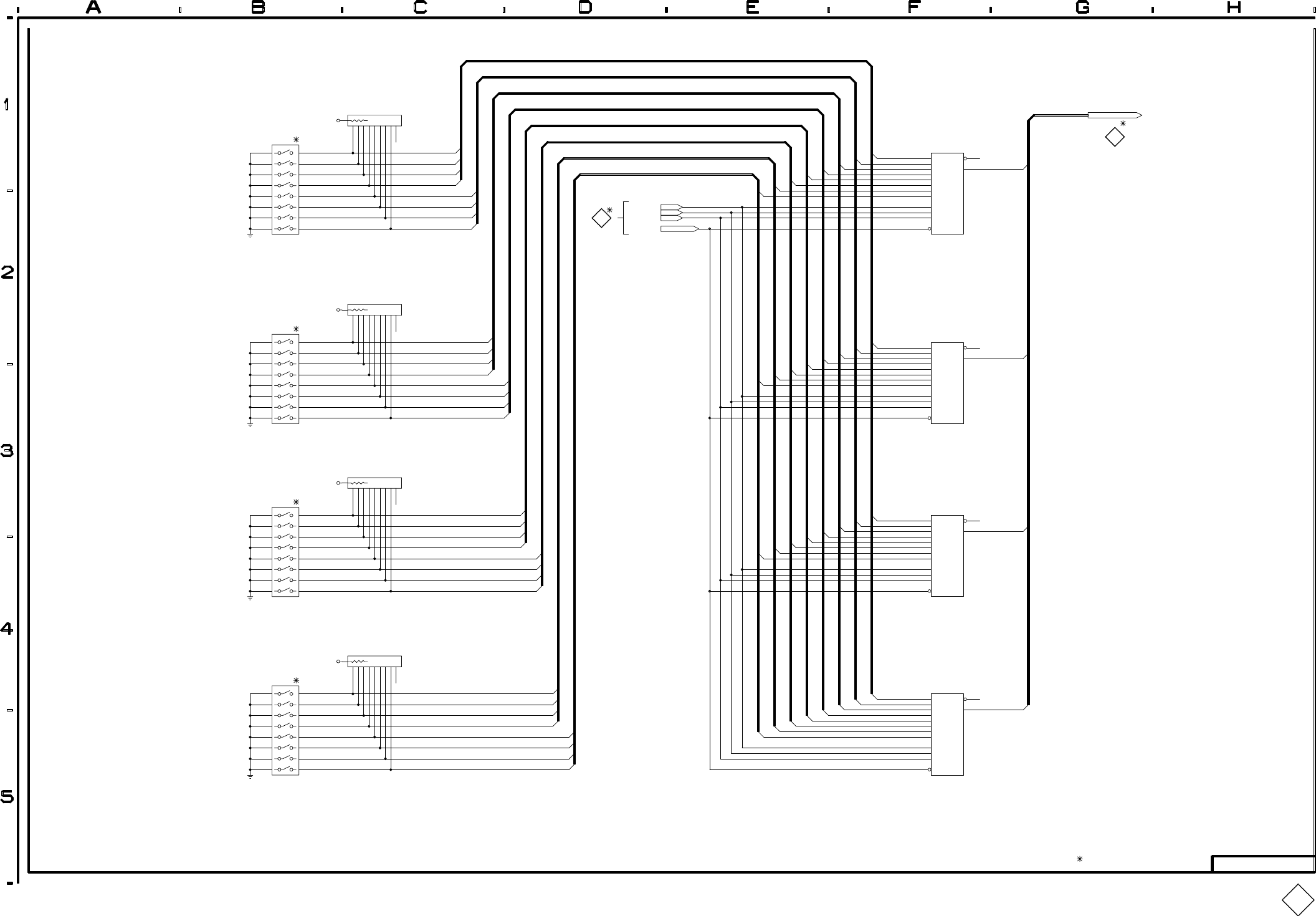
'(
'(
"!"!!"
$
!
)
#
#
#
#
$
'(
'(
'(
'(
'(
'(
"!
$
%
&
#
!
"!'( "!'(
#
$
$
$
)
!
"!
$
$
%
&
#
!
"!
$
$
%
&
#
!
$
)
!
$
!
)
"!
%
&
#
!
$
$
VITS 200 REV AUG 1995 TEST SIGNAL SELECT
" "#!$"!
2
P/O A1 INSERTER BOARD
671–2132–00 & UP

VITS 200
C161 C5 L7
C184 C5 L7
CR25 B5 I7
CR27 E3 A4
CR28 E4 B4
CR29 E4 B5
DS1 D5 Q2
DS2 E5 Q1
DS3 E5 Q1
J2 A3 F7
J3 H2 I7
J4 A2 L7
J22 E3 J7
J27 A5 J7
J28 D4 P2
P22 E3
P28 D4
Q13 D5 P2
Q14 E5 P2
R10 B3 L8
R11 F4 A5
R12 F4 A4
R13A D3 J7
R13B C3 J7
R13C C5 J7
R13D B3 J7
R13E B3 J7
R13F C3 J7
R13G A5 J7
R13H B5 J7
R13I B2 J7
R14 F2 H6
R132 E5 P1
R133 D5 Q2
R134 E5 Q2
R135 C4 O2
R137 D5 Q2
R138 D5 Q2
R211 D5 J7
R212 D5 J7
R213 A5 I7
R231 B5 K7
S5 F5 A5
S6 F4 A4
S9B C5 Q3
U22 G4 A5
U23 G5 A4
U24 D2 H7
U25 E3 H7
U26 F3 I6
U27 D1 I7
U28 C1 J7
U57D E1 K7
U70 C4 L7
Schematic Diagram <3> Component Locator Chart
671–2132–05 & Up
The schematic diagram has an alphanumeric grid to assist in locating parts within that diagram.
Assembly A1.
(Partial Assembly A1 also shown on schematic 1, 2, and 4 thru 9).
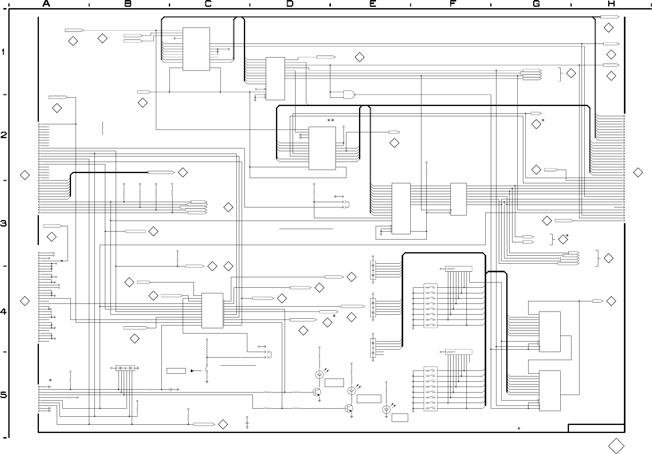
,-
(
,-
"
"
"
"
"
"
"
"
"
"
"
"
"
"
"
"
(
#
)%)
)&+!
(
%
(
(
"
(
&+!'
(
#
)
)
&*'
"
&+!'
)'
!'
&
#
(
&+!'# (
(
&+!'
)'
" (
(
(
(
&*'
#
(
(
)
)
)
)
)
)
)
)
)
)
"%
"!'%"%
(
(
)
%
/
)
)
)
)
)
)
)
(
)
)
)
)
%
)
)
"
"
"
"
"
"
"
"
"
"
"
"
"
"
"
"
(
#
#"!'%"
%
(
+#&&
#&'!+
"
#"!'%"
+#&&
#&'!+
&
%&+!
#%"#%&
%
/
!"'(&
"%
"!'%"%
)
#'&,-
#'&
#'&
#'&
#'&
#'&
#'&
#'&
#'&
%#%&
(%&"%
%'
'" #
%
/
)%&
%'
(%&"%
'" #
#'&,-
%
%#%&
%
/
%
/
%
/
) ) )
(
(
(
(
(
!&' "
%
/
)
)
)
)
)
)
)
)
)
)
)
)
)
#
"
#
)##
(
! "
)
)
)
)
)'
)&+!
$
$
$
$
$
$
$
$
%
(
&
)%)
!
#%
(
)
)
)
)
)
)
)
%
#%
&*'
#
)%)
)&+!
)'
!
&+!'
!'
(
(
(
!
)%)
)
)
)
)&+!
(
(
!
)
#
#
&
%
/
)
%
#
#
#
#
#
#
&'+
(
%
%"!'#!&'"!!
)'&"!!&'%"(
!"#()'&"!!&'%"(
&+!.!
(
&
(
%
/
)
(
(
"
"
"
"
"
"
"
"
"
"
(
#)
#%"#%&
)
)
)
)
)
)
(
(
"%
"!'%"%
%
%
#%"#"%
(
&+!
#"%
)
%
/
#%"&+!
"
&
#%"#%&
!'
+#&&
)
"
#
+#&&
$!'
(
)
%
)
)
%
%
#
#
#
#
#
#
#
#
#
#
#"%
(
(
#
#
#
#
#
#
)
%
/ "
#
#
#
#
#
#
#
# &%
$
&%
&%"
&%%
%
(
&
(
"
#
#
#
#
#
#
#
#
&%
$
&%
&%"
&%%
%
(
&
#
#
#
#
#
#
#
#
&
)
)
+#&&
(!"
#"*%
&
%
%
&
$
#+#&&
)
%
%
/
&
%
/
%
+#&&""('
$
+#&&
%
(''"!&
(''"!!
0
&
%
/
)
)
%
/
(
)
)
%
%
!'
%
/
)
#&'!+
VITS 200
%&+! %&+!
0
REV AUG 1995 H&V COUNTERS,DECODERS, SOURCE IDENTIFICATION & BYPASS CONTROLS
P/O A1 INSERTER BOARD!"' !"'(&"!)'&
671–2132–05 & UP
3

VITS 200
C161 C4 L7
C184 C5 L7
CR25 B5 I7
DS1 D5 Q2
DS2 E5 Q2
DS3 E5 Q1
J2 A3 G7
J3 H2 H7
J4 A2 K7
J22 B2 J7
J27 A5 J7
J28 D4 P2
J33 B4 I7
P22 B2
P28 D4
P33 B4
Q13 D5 P2
Q14 E5 P2
R10 B3 M8
R11 F4 A5
R12 F4 A4
R13 A2 K7
R14 F2 H6
R132 E5 P1
R133 D5 Q2
R134 E5 Q2
R135 C4 O2
R137 D5 Q2
R138 D5 Q2
R211 D5 J7
R212 D5 J7
R213 A5 I7
R231 B5 K7
S5 F5 A5
S6 F4 A4
S9 C5 Q3
U22 G4 A5
U23 G5 A5
U24 D2 H7
U25 E3 H7
U26 F3 I6
U27 D1 I7
U28 C1 J7
U57D E1 K7
U70 C4 L7
Schematic Diagram <3> Component Locator Chart
671-2132-00 & 04
The schematic diagram has an alphanumeric grid to assist in locating parts within that diagram.
Assembly A1.
(Partial Assembly A1 also shown on schematic 1, 2, 3, and 5 thru 9).
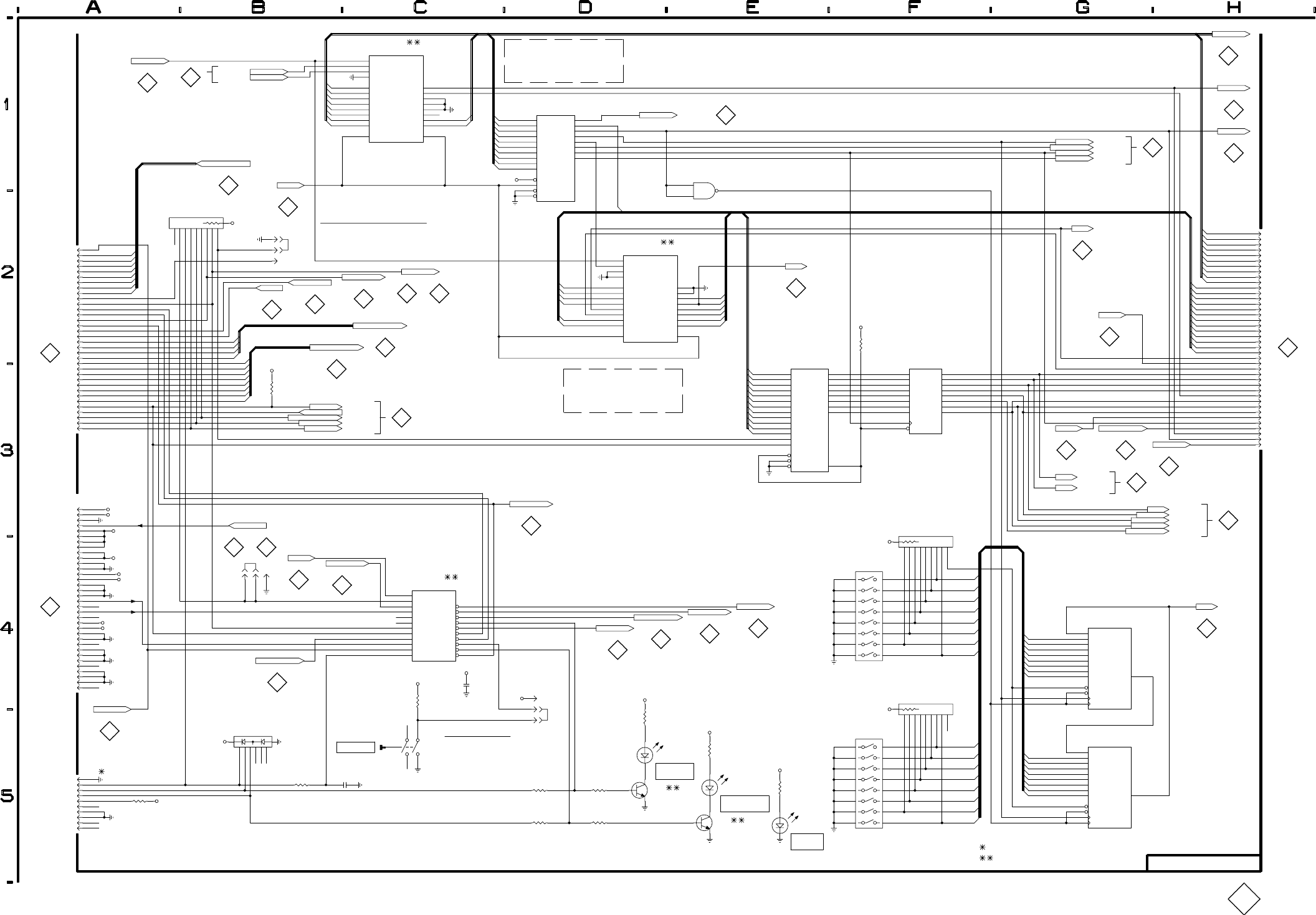
-.
(
-.
(
!""!!'"!
2
(
(
(
"
"
"
"
"
"
"
"
"
"
"
"
"
"
"
"
(
#
)%)
)&,!
(
(
(
%
&''-.
&''-.
(
&,!'
(
#
)
)
&*'
"
&,!'
)'
!'
&
#
(
&,!'# (
(
&,!'
)'
" (
(
(
(
&*'
#
(
(
)
)
)
)
)
)
)
)
)
)
"%
"!'%"%
(
(
)
%
0
)
)
)
)
)
)
)
(
)
)
)
)
%
)
)
"
"
"
"
"
"
"
"
"
"
"
"
"
"
"
"
(
#
&
#%"#%&
-. -.
%
%&,! (
(
%
(
#
!&' "
%"!'#!&'"!!
)'&"!!&'%"(
!"#()'&"!!&'%"(
(
&''
&''
&''
&''
&''
&''
&''
&''
)
"
#"!'%"
'+
,#&&
#&'!,
(
&
%&,!
'+
#%"#%&
%
0
"%
"!'%"%
#'&-.
#'&
#'&
#'&
#'&
#'&
#'&
#'&
#'&
%#%&
(%&"%
%'
'" #
%
0
)
%'
(%&"%
'" #
#'&-.
(
%#%&
(
(
(
(
(
(
(
(
(
!""!!'"!
2
)
)
)
)
)
)
)
)
)
)
)
)
"
#
)##
(
)
)
)
)
)'
)&,!
$
$
$
$
$
$
$
$
%
(
&
"!"%
%+) !'
(
(
(
)
)
)
)
)
)
)
%
"!"%
&*'
#
)%)
)&,!
)'
!
&,!'
%+)
!'
(
(
(
(
!
)%)
)
)
)
)&,!
(
(
!
)
#
#
&
%
0
,#&&
%
#%"&,!
#"!'%"
#&'!,
(
,#&&
"
"
"
"
"
"
"
"
"
"
(
#)
(
%&!
(
(
)
)
)
)
)
)
#
"%
"!'%"%
#%"#"%
&,!
&
#"%
"
%
%
(
)
%
0
#"%
,#&&
)
"
#
)
(
1
)
&,!/!
&',
(
%
(
(
#
#
#
#
#
#
)
%
0 "
#
#
#
#
#
#
#
# &%
$
&%
&%"
&%%
%
(
&
(
"
#
#
#
#
#
#
#
#
&%
$
&%
&%"
&%%
%
(
&
#
#
#
#
#
#
#
#
&
)
)
,#&&
(!"
#"*%
&
%
%
&
$
#,#&&
%
%
0
&
%
0
%
,#&&""('
$
,#&&
%
& (''"!&
(''"!!
1
% ,#&&
)
)
(
%
%
VITS 200 REV NOV 1992 H&V COUNTERS,DECODERS, SOURCE IDENTIFICATION & BYPASS CONTROLS
!"' !"'(&"!)'&
!"' &#%'&&'"%%%)(&
!&%!( %%!& P/O A1 INSERTER BOARD
671–2132–00 – 04
3

VITS 200
C135 A3 O4
C136 E5 N1
J5 B2 P5
J6 A1 P5
P5 B2
P6 A1
R177 E1 N4
R178 D1 M5
R179A B5 P2
R179B B3 P2
R179C C3 P2
R179D G3 P2
R179E G5 P2
R179F G5 P2
R179G G5 P2
R179H E1 P2
R179I A5 P2
S7 D2 N5
S8 C1 L4
U29 D3 N3
U30 F4 O2
U31 A2 O5
U32 F3 M4
U33 H4 M2
U34 G4 O2
U35 B3 N4
U36 F1 M5
U37 F2 M5
U38 G3 N5
U80 F4 K4
Y39 A3 O5
Schematic Diagram <4> Component Locator Chart
The schematic diagram has an alphanumeric grid to assist in locating parts within that diagram.
Assembly A1.
(Partial Assembly A1 also shown on schematic 1, 2, 3, and 5 thru 9).
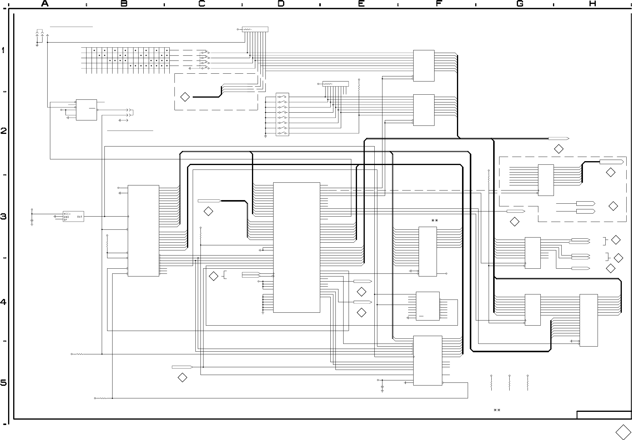
+5V 1
234567891
0
R178
2.7k
J6
1 - 2 NO RESET
2 - 3 HOLD IN RESET MODE
HARDWARE WATCHDOG RESET
P6
123
J6
01234567
1
2
4
8
ST
7
PBRST
1 TD
2
TOL
3
RST 5
RST 6
GND
4 VCC
8
U31
DS1232
89ABCDEF
5
1
2
4
8
S8
J4-3
3DIAG[0..3]
P10
P11
P12
P13
P20
P8
1 16
2 15
3 14
4 13
5 12
6 11
7 10
8 9
S7
DIAG0
DIAG1
DIAG2
DIAG3
P20
P21
+5V
+5V
P10
P11
P12
P13
(DIAG)
1
234567891
0
R177
2.7k
1
9
R179H
2.7k
DIAG0
DIAG1
DIAG2
DIAG3
ED0
ED1
ED0
ED1
ED2
ED3
ED4
ED5
ED6
ED7
1A1
2 1Y1 18
1A2
4 1Y2 16
1A3
6 1Y3 14
1A4
8 1Y4 12
2A1
11 2Y1 9
2A2
13 2Y2 7
2A3
15 2Y3 5
2A4
17 2Y4 3
1G
1
2G
19
U36
74ALS244
1A1
2 1Y1 18
1A2
4 1Y2 16
1A3
6 1Y3 14
1A4
8 1Y4 12
2A1
11 2Y1 9
2A2
13 2Y2 7
2A3
15 2Y3 5
2A4
17 2Y4 3
1G
1
2G
19
U37
74ALS244
ED[0..7] ED[0..7]
U59
6
U40
ED2
ED3
ED4
ED5
ED6
ED7
P22
P23
P24
P25
P26
P27
(OFFSET)
P21
P22
P23
P24
P25
P26
P27
J5
671-2132-00 - 04
+5V
P8
uP_CLK
(AWAKE)
1
2
3
J5 P5
NO PLUG NO HARDWARE RESETS
1 - 2 NORMAL OPERATION
2 - 3 RESET
GENLOCK PROCESSOR RESET
+5V
C135
0.1uF
+5V
uP_CLK
Y39
A0 30
A1 31
A2 32
A3 33
A4 34
A5 35
A6 36
A7 37
A8 38
A9 39
A10 40
A11 1
A12 2
A13 3
A14 4
A15 5
D0 14
D1 15
D2 12
D3 8
D4 7
D5 9
D6 10
D7 13
M1 27
MREQ 19
IORQ 20
WR 22
RD 21
RFSH 28
HALT 18
WAIT
24
INT
16
NMI
17
RESET
26
BUSRQ
25
BUSAK 23
CLK
6
VCC
11
GND
29
U35
8mhz804c008
A0
A1
A2
A3
A4
A5
A6
A7
A8
A9
A10
A11
A12
A13
LAD[0..7]
U41
5
A0
A1
A2
A3
A4
A5
A6
A7
A8
A12
A13
A14
A15
LAD0
LAD[0..7]
PA0
74
PA1
73
PA2
72
PA3
71
PA4
69
PA5
68
PA6
67
PA7
66
PA8
65
PA12
64
PA13
63
PA14
62
PA15
61
PAD0
20
PAD1
21
PAD2
23
PAD3
24
PAD4
25
PAD5
26
PAD6
27
PAD7
28
PI_O0 9
PI_O1 8
PI_O2 7
PI_O3 6
PI_O4 5
PI_O6 4
PI_O8 3
PI_O9 1
PI_O10 84
PI_O11 83
PI_O12 82
PI_O13 81
PI_O14 80
PI_O15 79
PSTD0
15
PSTD1
14
PSTD2
13
PD0 60
PD1 59
PD2 57
PD3 56
PD4 54
PD5 53
PD6 52
PD7 50
PED0 41
PED1 40
PED2 39
PED3 37
PED4 36
PED5 34
PED6 33
PED7 32
PMREQ
48
PIORQ
47
PRD
46
PWR
45
PM1
44
PCSYNC_IN
18
PSYSCLK
30
PFLPCLK
29
PSOFT_RST 49
PEPROM_EN 43
PCTC_EN 42
PCLMP_TM 19
PSIS_TM 17
PV_CLAMP 16
PUNLCK 12
PDFLD_REF 11
PSAMP_FIN 77
PSTART_SMP 76
PS_HSYNC 75
VDD
2
VDD
22
VDD
35
VDD
55
GND
10
GND
31
GND
38
GND
51
GND
58
GND
70
GND
78
U29
ADG236
(DIAG)
(CONTROL)
(OFFSET)
(ATAN)
(DIVISOR)
(AWAKE)
VCODAC VCODAC
+5V
U59-13
6
1
5
R179D
2.7k
74ALS273
D1
3 Q1 2
D2
4 Q2 5
D3
7 Q3 6
D4
8 Q4 9
D5
13 Q5 12
D6
14 Q6 15
D7
17 Q7 16
D8
18 Q8 19
CLK
11
CLR
1
ED0
ED1
ED2
ED3
ED4
ED5
ED6
ED7
(STATUS)
P3
STAT0
STAT1
STAT2
STAT3
STAT4
STAT5
STAT6
STAT7
U38-9
U38-12
STAT[0..7]
J4
3
671-2132-00 - 04
MONOCHR J3-40
U14-4
1
GLK/INT
LOCKED
CLAPBRD
U70-11
J3-40 3
U60-8
U60-1
6
MONOCHR U87-13 1
P3
ED0
ED1
ED2
ED3
ED4
ED5
ED6
ED7
ACQ/HOLD
D1
3 Q1 2
D2
4 Q2 5
D3
7 Q3 6
D4
8 Q4 9
D5
13 Q5 12
D6
14 Q6 15
D7
17 Q7 16
D8
18 Q8 19
CLK
11
CLR
1
U38
74ALS273
(CONTROL)
D0
D1
D2
D3
D4
D5
D6
D7
A0
A1
A2
A3
A4
A5
A6
A7
A8
A9
A10
A11
A12
A13
+5V
A14
A0
10
A1
9
A2
8
A3
7
A4
6
A5
5
A6
4
A7
3
A8
25
A9
24
A10
21
A11
23
A12
2
A13
26
A14
27
CE
20
OE
22 VPP 1
D0 11
D1 12
D2 13
D3 15
D4 16
D5 17
D6 18
D7 19
U32
27C256
D0
D1
D2
D3
D4
D5
D6
D7
EPROM_EN
ED0
ED1
ED2
ED3
ED4
ED5
ED6
ED7
SIS_TM
P2
SYSCLK
FLPCLK
LAD1
LAD2
LAD3
LAD4
LAD5
LAD6
LAD7
+5V
MREQ
IORQ
RD
WR
CSYNC_IN
RM1
A14
A15
D0
D1
D2
D3
D4
D5
D6
D7
WR
MREQ
IORQ
RD
M1
+5V
U54-13
U54-5
6
1
4
R179C
2.7k
+5V
(RESET)
1
3
R179B
2.7k
(FRAME)
J9-3
5
U28-2
3
A0
A1
D0
D1
D2
M1
uP_CLK
CK/TRG0
23
CK/TRG1
22
CK/TRG2
21
CK/TRG3
20
CLK
15
CS0
18
CS1
19
IEI
13
CE
16
M1
14
IORQ
10
RD
6
RESET
17
VCC
24
D0 25
D1 26
D2 27
D3 28
D4 1
D5 2
D6 3
D7 4
TO0 7
TO1 8
TO2 9
INT 12
IEO 11
GND
5
U30
z84c3008
RM1
I0/CLK
1
I1
2
I2
3
I3
4
I4
5
I5
6
I6
7
I7
8
I8
9
I9/OE
11
F0 19
F1 18
F2 17
F3 16
F4 15
F5 14
F6 13
F7 12
U80
GAL16V8-M
156-2983-00
136-0752-00
ED0
ED1
ED2
ED3
ED4
ED5
ED6
ED7
P3
A8
A9
A10
A11
A12
A13
A14
A15
(ATAN)
(DIVISOR)
D1
3 Q1 2
D2
4 Q2 5
D3
7 Q3 6
D4
8 Q4 9
D5
13 Q5 12
D6
14 Q6 15
D7
17 Q7 16
D8
18 Q8 19
CLK
11
CLR
1
U34
74ALS273
ED0
ED1
ED2
ED3
ED4
ED5
ED6
ED7
A0
10
A1
9
A2
8
A3
7
A4
6
A5
5
A6
4
A7
3
A8
25
A9
24
A10
21
A11
23
A12
2
A13
26
A14
27
A15
1
CE
20
OE/VPP
22
D0 11
D1 12
D2 13
D3 15
D4 16
D5 17
D6 18
D7 19
U33
27C512
+5V +5V +5V
UNUSED PULL-UP RESISTORS
1
6
R179E
2.7k
1
7
R179F
2.7k
1
8
R179G
2.7k
P2
D3
D4
D5
D6
D7
M1
RD
(INT)
uP_CLK
+5V
IORQ
(RESET)
CSYNC_IN
C136
0.1uF
CSYNC_IN
U70-22
3
+5V
+5V 1 10
R179I
2.7k
1 2
R179A
2.7k
(INT)
VITS 200 REV AUG 1995
NOTE: SEE PARTS LIST FOR EARLER VALUES
AND SERIAL NUMBER RANGES
4
P/O A1 INSERTER BOARD
GENLOCK
671–2132–00 & UP

C1 D5 F5
C2 E4 C6
C3 A1 B5
C4 C2 C4
C5 F2 D5
C6 E2 D5
C7 E2 D5
C8 F2 D5
C9 F2 E5
C10 E2 E5
C11 D1 D5
C12 D1 E5
C13 B2 C5
C14 D4 G5
C15 E1 D5
C16 D4 F4
C17 D5 E4
C18 D5 E4
C19 F5 E4
C20 F5 E4
C21 F5 E4
C22 G3 L7
C23 E5 E4
C31 D2 D4
C83 H4 L7
C120 C1 D4
C150 A5 G4
C157 B5 D5
C158 B5 C4
C159 B5 C4
C160 H4 L4
C175 D3 C6
C185 D2 D4
C507 E5 E4
C509 C2 C4
J9 G4 K4
J10 A1 A6
J52 A4 G4
L1 F5 F4
L19 C1 D4
P9 G4
Q1 F1 D5
Q2 F2 D6
Q3 G2 D5
R18 A1 C5
R19 D5 E4
R20 D3 C6
R21 D3 C7
R22 E3 C6
R23 E3 C6
R24 F3 C6
R25 E3 C6
R26 E3 C5
R27 E4 C5
R28 F3 C6
R29 B2 C5
R30 B2 C5
R31 B2 C5
R32 B1 B5
R33 B1 B4
R34 C1 B5
R35 C1 C4
R36 C1 B5
R37 C4 F4
R38 C4 C4
R39 D1 C4
R40 D2 D4
R41 D2 D4
R42 D2 D4
R43 D2 D5
R44 E2 C5
R45 F2 D5
R46 F2 D5
R47 F1 D6
R48 G2 D6
R49 F3 D6
R50 G2 E6
R51 G2 E6
R52 E5 F4
R53 E5 E4
R54 G3 L7
R55 E5 E6
R141 H4 L7
R142 H5 L7
R185 D4 G4
R192 C4 L8
R214 B1 C5
R216 D3 C6
R507 C2 D4
R508 C2 C4
U41 G4 G4
U42 B1 C5
U43 E4 E5
U44 E1 D5
U46A E3 B6
U47A F3 B6
U47B F3 B6
U48A G4 K7
U57A G2 K7
U57B H2 K7
U71A H4 L7
U71B G3 L7
VR1 F2 D6
VR2 G2 D6
Schematic Diagram <5> Component Locator Chart
The schematic diagram has an alphanumeric grid to assist in locating parts within that diagram.
Assembly A1.
(Partial Assembly A1 also shown on schematic 1 thru 4 and 6, 9).
1
15
L19
9uH
C120
240pF
R35
392
PROGRAM IN
PROGIN
+10V
J10
PROGRAM
GAIN
ADJUST
K2-4
7
R214
499
R18
15.0k
R32
301.0
C3
10uF
R33
100
R34
301.0
R36
2.00k
+10V
VIDIN-
1
VIDIN+
3
S/H+
5
S/H-
6
HCNTL
7 CHOLD 9
VIDOUT 13
S/H OUT 11
V+ 14
V- 12
GND 4
NC
2
NC
8
NC
10
U42
EL2090
VIDEO
R100
7
R39
200.0
C12
0.22uF
C4
100pF C11
.0047uF
C10
0.22uF
FB PLSE
2
COMP VID
11
EHT
8
HOSC
14
H OSC
16
CNTL OUT 1
PH DET 3
HORZ OUT 4
CASTLE 6
MUTE 7
50% POINT 10
COIN DET 13
IDENT 12
LIMIT 17
PHASE DET 18
COMP SYNC 9
GND
5 VCC
U44
TDA2595
+12V
+12V
Q1
R47
15.0k
+12V
Q3
U70-3
3
4
5
6
U57B
74F00
PROGPRES
PROGSYNC
VR2
6.2V
J4-16
3
1
2
3
U57A
74F00
R48
2.00k
+12V
Q2
C9
.015uF
R45
75.0k
R44
4.75k
R46
681.0
VR1
6.2V
R50
2.05k
R51
2.74k
+12V
C7
.01uF
C8
0.22uF
R43
100.0K
C185
.001uF
+12V
R40
50.0k
R41
118.0k
R42
11.5k
-10V
C509
R507 R508
3pF
20.0k
71.5k
S/N B020527 & BELOW
-10V
PROGRAM
OFFSET
ADJUST
C13
0.1uF
R29
14.2k
R31
14.3k
R30
500
CLAMP, AND SYNC
STRIPPER
VIDEO INPUT BUFFER,
U42-9
C4
100pF
671-2132-00 - 04
TESTSIG
U67-13
7
R21
20.0k VIRS DETECT
C175
200pF
+12V
+12V
+5V
C6
0.56uF
R24
11.5k R28
4.75k
C5
.0047uF
R49
2.00k
+5V
PROGPORCH
U70-9
3
VIRSPRES
U17-13
1
+5V
1
2
3
U48A
74ALS32
C
X
1
5
R
X
1
4
A
12
B
11 C
L
1
3
Q10
Q 9
U71B
96LS02
R54
402.0k
C22
1uF
-12V
(VIRSAMP)
R25
200.0
U17-12
1
4
5
12
1
63
U47A
LM319
9
10
7
8
U47B
LM319
-12V
-12V
+12V
3
2
1
8
4
U46A
LF353
R22
20.0k
C2
200pF
R26
200.0
R27
11.5k
R23
1.0k
VIDEO
R20
20.0k
R216
20.0k
GLSEL1
+5V
J4-11
3
R192
2.74k
CLKD
R19
332
12
J52
C16
4.7uF
R38
301.0
R37
301.0
C14
4.7uF
R185
301 AD0
AD1
AD2
AD3
AD4
AD5
AD6
AD7
1 - 2 NO SOUND-IN-SYNC OPERATION
2 - 3 SOUND-IN-SYNC OPERATION
R52
1.0k
VIN0
16
VIN1
17
VIN2
18
D0 13
D1 12
D2 11
D3 10
D4 4
D5 3
D6 2
D7 1
I0
14
I1
15
CLK
5
ANOUT 19
OF
9
DEC
21
GATEA
27
GATEB
26
CLAMP
24
AGC
25
AGND 23
DGND 8
VCCO 7
VCCA 22
VCCD 6
ADCIN
20
RPEAK
28
U43
TDA8708
SIS_TM
AD0
AD1
AD2
AD3
AD4
AD5
AD6
AD7
CCLINE
U29-17
4
J9
SOUND-IN-SYNC MODE
L1
39.5uH
LAD0
LAD1
LAD2
LAD3
LAD4
LAD5
LAD6
LAD7
LAD[0..7]
GENLOCK A/D
CAPTION
C
X
1
R
X
2
A
4
B
5 C
L
3
Q 6
Q 7
U71A
96LS02
P9
1
2
3
J9
I1/CLK
1
I2
2
I3
3
I4
4
I5
5
I6
6
I7
7
I8
8
I9
9
I10
10
I11
11
I12
13 IO10 14
IO9 15
IO8 16
IO7 17
IO6 18
IO5 19
IO4 20
IO3 21
IO2 22
IO1 23
U41
PAL22V10
C83
1uF
LAD[0..7]
4
U29
+5V
CCPRES
C160
0.1uF
R141
200.0k
+5V
U17-9
1
R142
2.74k
RSLINE
J2-4
3
RXDV
J3-35
3
U17-17
1
C19
10pF
C21
33pF
C20
5.6pF
C507
33pF
U41-13
671-2132-00
U41-14
671-2132-00 - 04
+5R
+5V R55
10.0
C23
0.1uF
R53
1.0k
+5V
C18
.022uF C17
0.22uF
C1
0.1uF
U62-13
6
-10V
+12V
SYNCTIP
BACKPORCH
C157
0.1uF
C159
0.1uF
U27-9
3
U70-21
3
+10V+5V
C150
0.1uF
C158
0.1uF
VITS 200
REV JAN 1996
PROGRAM INPUT, SYNC STRIPPER, VIRS DETECTION, & GENLOCK A/D INPUT
NOTE: SEE PARTS LIST FOR EARLER VALUES
AND SERIAL NUMBER RANGES
5
P/O A1 INSERTER BOARD
VITS 200
C39 C1 L3
C40 E2 M3
C41 D2 L3
C42 E2 K3
C43 C5 M2
C46 E4 L3
C125 G3 H5
C128 H3 H5
CR5 F4 L3
J11 C1 K1
J12 G3 M2
J13 D4 M2
J32 F2 H5
P12 G3 M2
P13 D4 M2
P32 F2 H5
Q8 D1 K3
Q9 E4 L1
R68 C1 K3
R69 D1 K3
R70 D1 K3
R71 D2 L3
R72 D1 K3
R73 E2 L3
R74 E2 K3
R76 D2 L3
R77 D5 M3
R78 C5 N2
R79 D5 M2
R80 C4 M3
R81 C4 M3
R82 C4 N3
R83 E5 M1
R86 G4 L3
R87 G4 L3
R88 F4 L3
R89 F4 M3
R90 E4 L3
R91 E4 L3
R92 E3 L4
R190 E1 K3
R191 E1 K3
R206 F1 J4
R207 F1 J5
R217 G1 G5
R218 F2 I5
R219 G2 H6
R220 G2 I5
R221 G2 I4
R222 F2 K3
R223 F2 K3
R224 F1 K3
R225 G1 J4
R226 G1 J5
TP11 F1 K3
U54 H1 I5
U55A D1 K3
U55B F2 K3
U55C F1 K3
U56A D4 M3
U56B D2 M3
U59 D3 K4
U60 F4 M3
U61A E3 L3
U62 H3 G5
U63A F2 I4
U63B E3 I4
U63C F3 I4
U81A F1 J4
VR3 D5 M2
A1A1 Oven Board
C6 B2
C8 B2
C15 A2
C16 A2
C17 B1
C18 B1
C19 A2
CR14 A1
P33 C1
Q10 B2
R1 C1
R3 A1
R4 B1
R5 B2
R9 B2
RT11 B2
Y1 A2
Schematic Diagram <6> Component Locator Chart
The schematic diagram has an alphanumeric grid to assist in locating parts within that diagram.
Assembly A1 & A1A1.
(Partial Assembly A1 also shown on schematic 1 thru 5 and 7, 8, 9).
Front
Back
A1A1 Oven Board
119–4228–00
$
$
$
/
$
-
(
/
"
$
(
(
$
.
$
-
$
-
#
'
$
-
(
( (
$
$
((
'
$
$
$
%
$
#
#
(
(
(
'
&"
&"
(
( (
$
$
(
#
#
#
#
(
(
(
'
"
'
'
'
%*%
'
'
'
'
'
(
(
% %
(
$
(
$
'
"
'
$
$
-
.
$
-
.
$
-
/
'
$*%&!( !$
#
$&
-
$
%"$&%%&!$$$('%
%$ '$$%
.
.
.
*
0 $
-
.
.
!
$#
!&
'
(
(
/
$
$
(
'
'
'
$
(
( (
(
%
$
%
#
#
#
#
(
(
(
'
$
%
%
'
(
'
/
(
$
-
(!! &$!
!$!"$&!
(! &$$#' *'%&
$
"
!$$&!
(
$
'
$
-
$
-
$ (
(
(
$
-
$
-
$
-
'
/
(
+,
($
%
)$
(
$
'
+,
(!
'
'
(
(
(
$
-
$
-
$
-
!( ! &$!
!%&!$!( !
!%&!$!( !
'
$
- "
#!
&
(
(
'
'
#
(
(
(
$
!
($
(
(
/
$
-
(
$
-
VITS 200 REV AUG 1995
!& %"$&%%&!$$$('%
%$ '$$% P/O A1 INSERTER BOARD
6CLOCKS
671–2132–00 & UP

VITS 200
C39 C1 L3
C40 E2 M3
C41 D2 L3
C42 E2 K3
C43 C5 M2
C46 E4 L3
C51 B5 G8
C52 F4 B5
C53 H4 A5
C54 B4 B7
C55 B4 B7
C56 B4 A7
C57 C4 A7
C58 B5 A7
C59 D5 A8
C60 E4 A7
C61 D5 A7
C65 E2 D8
C66 E2 D7
C67 G2 C7
C68 F2 C8
C69 C5 B8
C70 C5 B8
C71 C5 B8
C72 G2 C7
C73 D1 F7
C74 D1 E7
C75 E1 E7
C76 D2 F7
C77 D2 F7
C78 D2 F7
C79 E2 E7
C119 G1 C6
C125 G3 H5
C128 H3 H5
C164 E2 D7
C165 D1 C7
C176 C2 H7
C177 B2 H7
C178 C2 G7
C179 B2 F6
C180 B2 G7
C181 A2 F6
C182 A2 E6
C183 E1 C7
C506 E2 D8
C510 D2 G7
C511 D2 G7
CR5 F4 L3
CR7 G3 B5
CR8 F3 B5
J11 C1 K1
J12 G3 M2
J13 D4 M2
J14 H5 A7
J15 H4 A6
J32 F2 H4
J50 H1 C7
J51 H1 B6
J53 A4 B7
K2 G4 A6
L6 G4 A6
L7 F4 B6
L8 F4 B6
L12 D2 F7
L13 D2 F7
L14 E2 E7
L18 G1 D6
L20 E1 C7
L21 E2 D8
P12 G3
P13 D4
P32 F2
Q8 D1 K2
Q9 E4 L1
Q11 F4 A6
Q12 G3 A5
R68 C1 K3
R69 D1 K3
R70 D1 K3
R71 D2 L3
R72 D1 K3
R73 E2 L3
R74 E2 K3
R76 D2 L3
R77 D5 M3
R78 C5 N2
R79 D5 M2
R80 C4 M3
R81 C4 M3
R82 C4 N3
R83 E5 M1
R86 G4 L3
R87 G4 L3
R88 F4 L3
R89 F4 M3
R90 E4 L3
R91 E4 L3
R92 E3 L4
R98 D2 F6
R99 E2 D7
R100 A4 B5
R101 B2 F6
R102 B2 F6
R103 G1 C7
R104 G3 B7
R105 G2 B7
R106 F4 A6
R108 G4 A6
R109 H3 A5
R110 E5 A7
R111 D5 A7
R112 E4 B7
R113 D5 A8
R114 D5 A7
R115 D5 A7
R116 D4 A7
R117 E4 A7
R118 A4 B7
R119 C4 B7
R120 G1 C7
R121 F1 C7
R122 F1 B8
R123 F1 C7
R124 F1 B7
R125 E2 D7
R126 E2 C7
R127 E2 C7
R130 B4 B7
R190 E1 K3
R191 E1 K3
R206 F1 J4
R207 F1 J5
R208 E2 D7
R209 G1 C7
R210 E1 C7
R217 G1 G5
R218 F2 I4
R219 G2 H6
R220 G2 I5
R221 G2 I4
R222 F2 K3
R223 F2 K3
R224 F1 K3
R225 G1 J4
R226 G1 J5
R227 B2 F6
R228 B2 F6
R229 A2 F7
R230 A2 F6
R506 E1 C7
T2 E2 D7
TP11 F1 J3
U54 H1 H5
U55A D1 K3
U55B F2 K3
U55C F1 K3
U56A D4 M3
U56B D2 M3
U59 D3 K4
U60 F4 M3
U61A E3 L3
U62 H3 G5
U63A F2 H4
U63B E3 H4
U63C F3 H4
U64 C4 A7
U65 C1 G7
U67 F2 C7
U81A F1 I4
U84 A2 F6
VR3 D5 M2
Schematic Diagram <7> Component Locator Chart
The schematic diagram has an alphanumeric grid to assist in locating parts within that diagram.
Assembly A1.
(Partial Assembly A1 also shown on schematic 1 thru 6 and 8, 9).
('&'&!
1
0
%
'&,-
(
(
(
&
'&,-
'&
'&
'&
'&
'&
&
&
)%
"('
"('
!
!
"('
"('
!
!
!
!
!
!
!
!
!
!
!
!
!
!
!
!
!
!
!
!
!
!
!
!
'&'
'&'
'&'
'&'
'&'
'&'
'&'
" #
" #
" #
)%
)%
)%
!
!
!
!
&(
&(
(
0
0
1
1
0
0
%
%
1
1
%
.
)!
)!
&
&
!'
"
)"('
&"('
)
)
!
!
!
!
(
%
%
%
'&'&
%
%
*
*
"!'%"%
"%
)
)
%
%
1
1
#
(
)
%
'
%
.
%
.
0
0
0
%
1
'
0
0
/
%
1
0
0
1
&!"*
'&
'&
'&
'&
'&
'&
'&
&
)
)
)
1
%
.
%
.
1
1
1
)
)
)
%
.
1
(
%
0
)
%
.
%
.
1
)
)
(
(
(
(
*
)
)
0
)
%
.
0
/
'&'&!
1
%
#%"% "('
)
)
)
%
%
.
$
1
)
$
%
%
.
+#&&
(
)"
(
"!'%"%
"%
%
%
%
1
(
(
&*
&*
'&'&!
%
1
1
1
!
!
!
!
#
!
"('
!)
"('
!)
)
)
)
)
!
)
(
&*
%
%
%
%
%
.
%
0
/
/
/
%
0
#%"!
"!'"%"('
)
0
)
%
%
%
.
%
0
) %
%% %
1
1
1
1
1
"
%
VITS 200 %)(
!"' &#%'&&'"%%%)(&
!&%!( %%!& #"!&%'%"%
ANALOG OUTPUT
(#
7

VITS 200
C84 B1 C3
C85 C1 B1
C86 C2 B1
C87 D2 C2
C88 E1 G1
C89 G4 J4
C91 F4 H2
C92 F4 I3
C94 G4 I2
C95 G4 I3
C96 D3 E1
C97 E4 D2
C98 F5 F3
C99 B3 D3
C100 G2 I2
C101 G3 I1
C102 F2 H1
C103 F3 H1
C104 F2 I2
C105 F3 I1
C106 G2 J2
C107 G3 J1
C108 G4 H3
C109 F4 H2
C110 C2 C1
C111 D3 E3
C112 F5 G3
C113 E3 D2
C114 C4 D3
C115 D3 E3
C116 F4 H2
C117 C2 F3
C118 C3 E3
C500 G2 H3
C501 B4 D3
C508 A3 D3
C512 F4 I3
CR9 E2 F3
CR10 F2 H1
CR11 F3 H1
CR12 C1 C2
CR13 F4 H2
CR14 F3 H3
CR15 G2 J2
CR16 H2 J2
CR17 H3 J1
CR18 G3 J1
CR19 E4 E1
CR20 E3 E1
CR21 E3 E2
CR22 E3 E2
CR24 G2 I4
CR26 B4 D3
DS4 D2 B2
F1 A1 A3
J17 E2 E2
J18 E3 F1
J19 C4 E3
J21 H2 I4
L15 G4 I2
L16 G3 J3
L17 D1 D1
LF1 A1 A2
P17 E2
P18 E3
P19 C4
Q15 G4 J3
Q16 E3 E1
Q17 E4 D2
Q18 C4 E3
Q180 D3 E4
R143 A1 B2
R144 B1 B3
R145 D1 B2
R146 H4 J4
R147 F4 H2
R149 E3 E2
R150 E4 D2
R151 D4 E3
R152 E4 D3
R153 E3 E1
R154 D2 D2
R155 F3 I1
R156 F2 I2
R157 C1 C2
R158 C5 F3
R159 C4 F3
R160 A5 C3
R161 A4 C3
R162 B3 D3
R163 E4 D2
R164 A4 C3
R165 B3 D3
R166 E5 G3
R167 E5 G3
R168 F5 G3
R169 F5 G3
R170 F5 G3
R171 A4 C3
R172 B4 D3
R173 D3 E3
R174 C4 E3
R175 C3 E3
R180 D3 E4
R184 D4 D4
R500 A2 C1
R501 A2 C1
R502 A3 C1
R503 B4 D4
R504 B4 D3
RT1 B1 C3
RV1 B1 C3
S10A B1 B4
S10B B1 B4
T1 E2 G1
TP3 D2 D2
U72 F2 H4
U73 G3 J1
U74 E5 F4
U75 E4 F3
U76A B4 D3
U76B B4 D3
U78 C3 E3
U85 G2 I2
VR4 G4 J4 C
Schematic Diagram <8> Component Locator Chart
The schematic diagram has an alphanumeric grid to assist in locating parts within that diagram.
Assembly A1.
(Partial Assembly A1 also shown on schematic 1 thru 7 and 9).
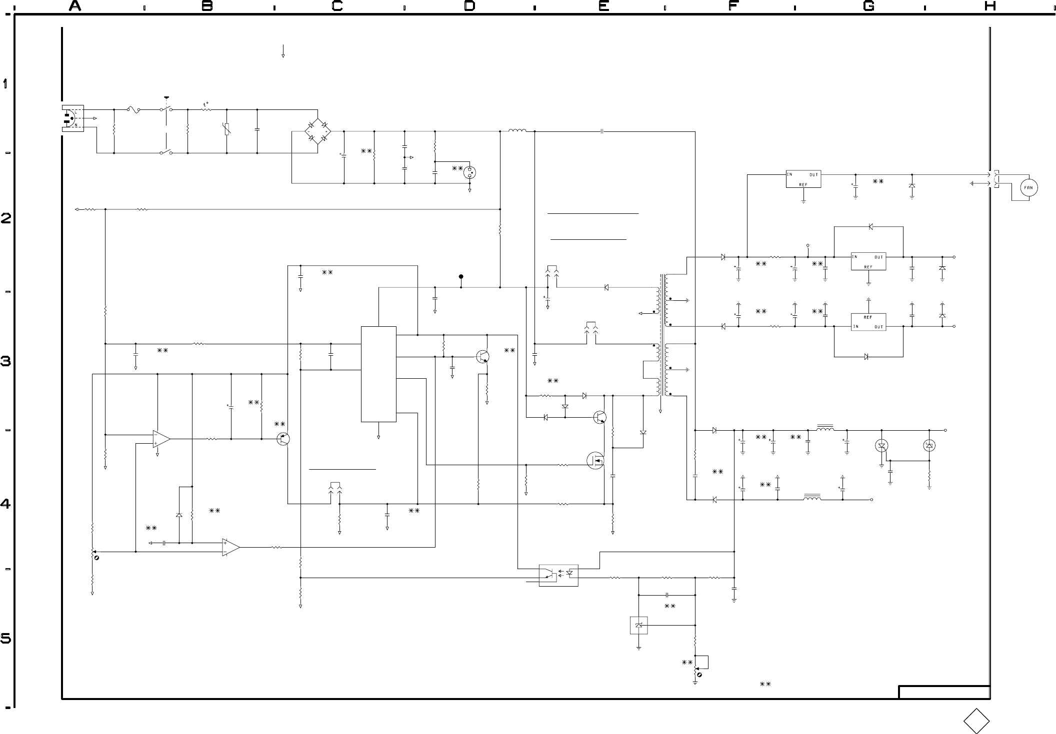
#
$"
$"'
$"
!
%
%
!!
%"&
%"&
"
!
!
"
!#
!%
%
!
-
$
-
!
*
- "
!
$
,
%
%
!
!
!
$
-
-
-
!
$
!
-
-
$""$'
$""$'
$$""$'"
#!"!!
!!#
$""&!"$'
!
-
!
!
*
!
!
*
-
!
*
%
"
%!
#
%
$#
$
-
-
#
%
-
!
*
-
!
#
-
-
! !
-
-
!
%
!
$
-
-
-
-
!
*
%
- %!
%
!
!
-
-
-
-
!
!
!
!
!
* !
!
*
,
!
!
*
!
*
%!$!!#"$#&
"$#&
-(
!
*
!
*
$
%
!
*
!
*
!
!
*
!
*
$
!
*
!
*
!
*
$"$#&"
$
,
!
*
$
"
!
!
*
!
)+
!
!
*
!
-
-
-
-
%
$#$#
-
!
*
-
!
*
$
#
!
*
VITS 200 REV AUG 1995
%#
$"# # "!#""#!!!%$"
"!$!!" P/O A1 INSERTER BOARD
POWER SUPPLY 8
671–2132–00 & UP

VITS 200
C24 E3 D7
C25 E4 E7
C26 D3 D7
C27 G3 D7
C28 G3 E6
C29 G3 F6
C30 G3 F6
C33 D1 E6
C34 D2 F6
C36 E2 G7
C37 E1 E6
C38 E2 F6
C121 B4 P7
C122 C4 O6
C123 C4 P6
C124 D4 O5
C126 B5 H4
C129 D4 N5
C130 D4 M7
C131 E4 M7
C132 E4 K5
C134 F4 M6
C137 F4 P1
C139 F4 I5
C140 B5 M4
C141 C5 N4
C145 C5 E5
C146 D5 J5
C147 D5 J4
C149 D5 G5
C152 E5 I7
C153 E5 J6
C156 F5 D6
C162 F5 O2
C163 F5 N2
C167 D5 K3
C168 D5 F5
C169 F5 N3
C170 F5 C6
C171 F5 G5
C172 G3 M1
C173 G3 K4
C174 E1 K4
C503 C5 L4
C504 H3 H4
C505 H3 G4
J20 B1 J2
L2 D2 D6
L3 E4 E6
P20 B1
P34 B1
P35 B1
P36 B1
P37 B1
P38 B1
Q4 G2 D6
Q5 G3 E7
Q6 G2 D6
Q7 G4 E6
R56 E2 D7
R57 E3 E7
R58 F4 E6
R59 F4 E7
R60 G4 E7
R61 F2 D6
R62 F2 D7
R63 G3 E7
R64 G3 E6
R65 G3 E6
R66 G2 D6
R67 G4 E6
TP1 B2 K2
TP2 B2 K2
TP4 B3 J2
TP5 B2 J1
TP6 B1 K1
TP7 B3 N1
TP8 B3 D4
TP9 C3 O8
TP10 C3 E6
U50A F2 D6
U50B F3 D6
U51 D2 D6
U52 D1 E6
U53 D2 F6
Schematic Diagram <9> Component Locator Chart
The schematic diagram has an alphanumeric grid to assist in locating parts within that diagram.
Assembly A1.
(Partial Assembly A1 also shown on schematic 1 thru 8).
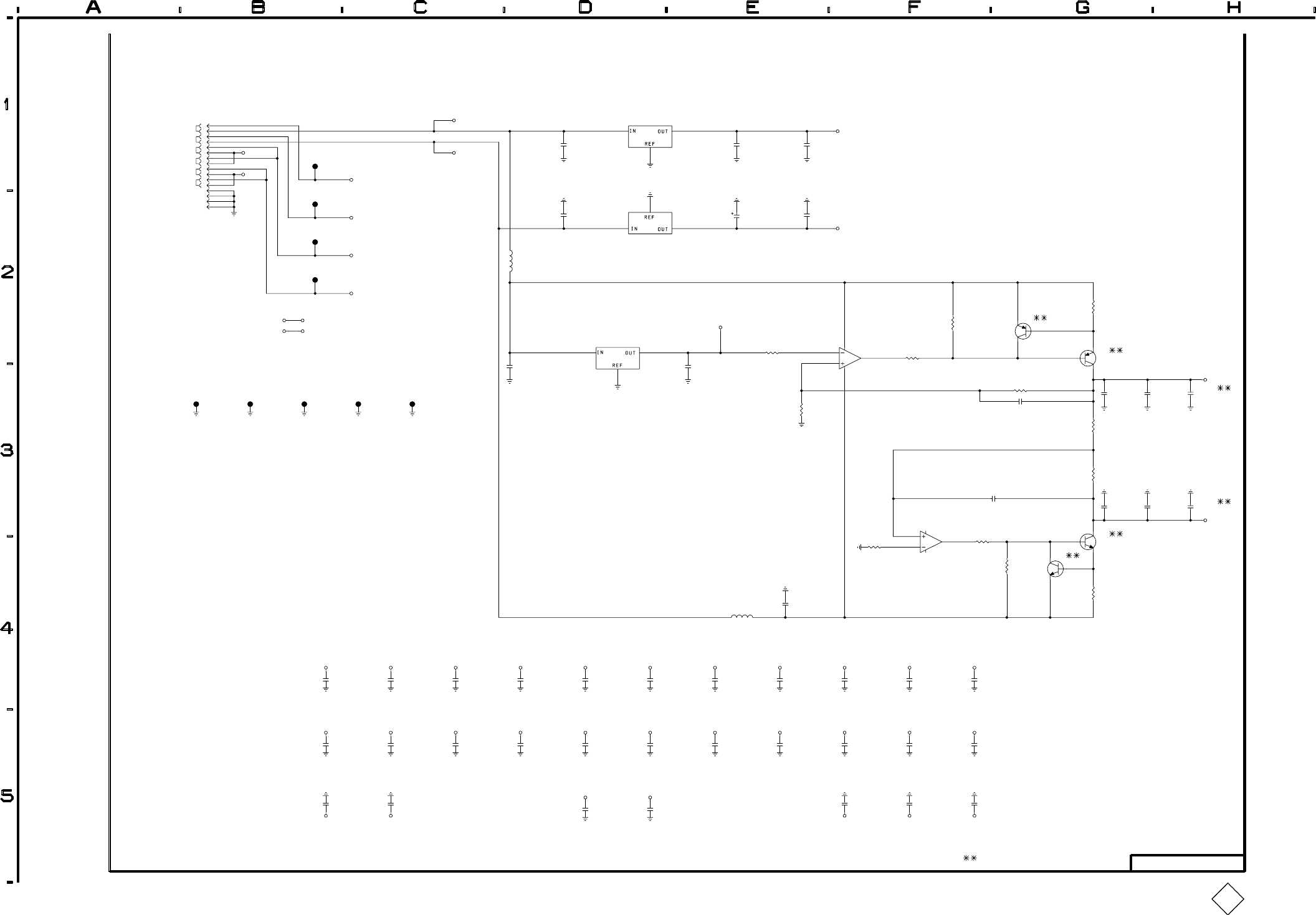
$
$
$
$
$
$
$#"#"
$#"#"
$#"#"
!
$#"#"
!
$
$
$
$
$
"
$
"
$
$
&
#
&
&
$
&
&
$
&
&
#
$
$
$
$
$
$
$
"
$
"
$
"
"
"
"
"
&
#
&
%
%
%
#
%
&
&
&
%
&
$
$
%
&
&
&
&
%
#
%
##
$ $
&
&
&
## #
$ $ $
&
&
# # #
$ $ $
&
&
&
&
&
## #
$$$
&
&
&
$
# ##
$ $ $
$ $
&
&
&
&
&
&
$
# ##
$ $ $
&
&
&
&
# ##
$$$
$
&
&
&
##
$$
$$
&
&
&
&
&
VITS 200 REV AUG 1995 REGULATOR & DECOUPLING CAPS
" ! "!!" $#!
! # ! P/O A1 INSERTER BOARD
671–2132–00 & UP
9
VITS 200
VITS 200
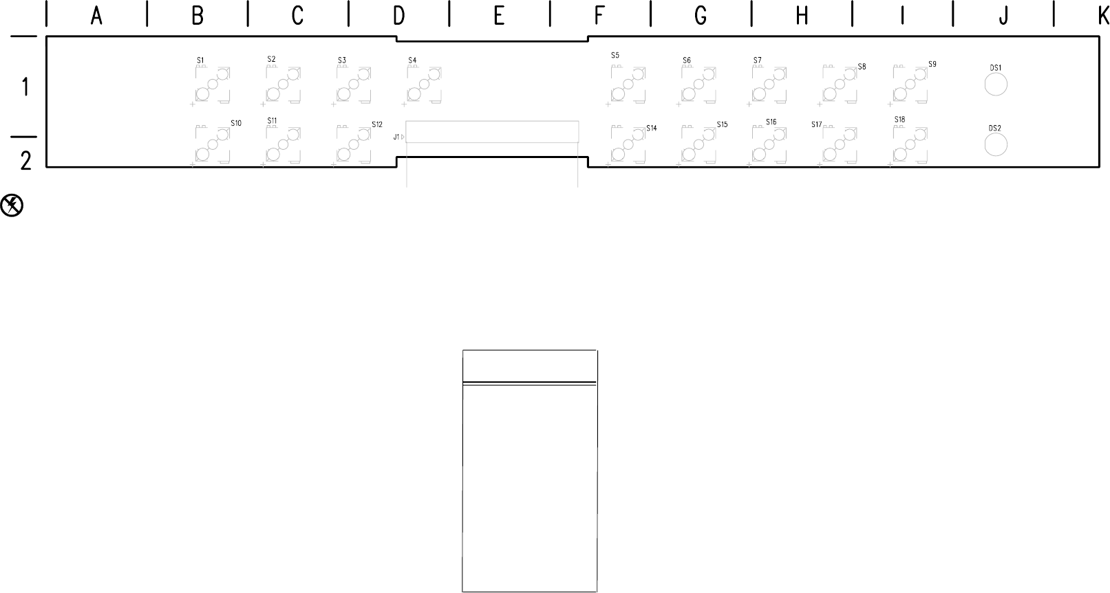
VITS 200
Static Sensitive Devices
See Maintenance Section
J1 H2 I1
S1 B1 C1
S2 C1 C1
S3 D1 B1
S4 E1 A1
S5 B2 C2
S6 C2 C2
S7 D2 B2
S8 E2 A2
S9 B3 E1
S10 C3 E1
S11 D3 F1
S12 E3 H1
S13 B4 E2
S14 C4 E2
S15 D4 F2
A2 Front Panel Board
Diagram <1> Component Locator
Assembly A2.
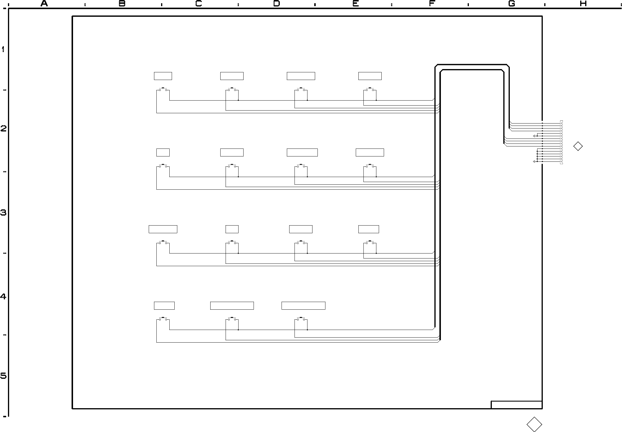
!
#
#
#
#
"
"
"
"
"
"
"
"
#
"
"
"
"
"
"
"
"
"
"
"
"
#
"
"
"
"
#
"
"
"
"
#
#
" "
#
"
""
"
VITS 200 REV AUG 1995 FRONT PANEL 1
A2 FRONT PANEL BOARD
VITS 200

VITS 200
C1 1 B1 A4
C2 1 B4 A5
C3 1 C2 C4
C4 1 C4 D5
C5 1 D1 D5
C6 1 D4 D5
C7 1 D2 F5
C8 1 D4 F6
C9 1 E2 F4
C10 1 E5 F5
C11 1 E4 G5
C12 1 E2 G4
C13 1 F2 G4
C14 1 E4 G5
C15 1 E5 F5
C16 1 F5 G5
C17 1 E3 F4
C18 1 F3 G4
C19 1 H4 H6
C20 1 H3 H6
C21 1 E2 G4
C22 1 E4 G5
C23 1 B2 D5
C24 1 B5 D5
C25 2 D1 D6
C26 2 D4 D7
C27 2 B2 A6
C28 2 B4 A7
C29 2 C4 D7
C30 2 C2 D6
C31 2 D4 F8
C32 2 D2 F7
C33 2 E5 F8
C34 2 E2 F6
C35 2 E2 G6
C36 2 E4 G8
C37 2 E3 G6
C38 2 E3 G6
C39 2 E5 F8
C40 2 E5 G8
C41 2 H4 H8
C42 2 H3 H8
C43 2 E2 G6
C44 2 E2 G6
C45 2 E4 G7
C46 2 E4 G7
C47 2 B2 D6
C48 2 B5 D7
C49 3 B2 N2
C50 3 A2 O2
C51 5 F1 E7
C52 5 F2 F6
C53 5 G1 E7
C54 5 D1 E6
C55 5 D1 D6
C56 5 D1 D7
C57 5 D1 E7
C58 5 E1 D7
C59 5 E1 E6
C60 5 E2 E7
C61 5 C4 K8
C62 5 B4 L8
C63 5 C4 K8
C64 5 C4 K8
C65 5 C4 L8
C66 1 D2
C67 1 D4
C68 2 D2
C69 2 D4
C71 1 B2 C5
C72 1 B4 C6
C73 2 B2 C7
C74 2 B4 C7
C75 7 A5 N2
C76 7 A5 M2
C77 7 A5 M2
C78 7 B5 K2
C80 7 B5 L3
C81 7 B5 L3
C82 7 B5 N3
C83 7 C5 N4
C84 7 C5 M5
C85 7 C5 L5
C87 7 D5 J3
C88 7 D5 I3
C89 7 D5 I3
C90 7 E5 G2
C91 7 E5 H3
C92 7 E5 I4
C93 7 E5 J4
C94 7 F5 J5
C95 7 F5 I5
C96 7 F5 J2
C97 7 G5 I1
C98 7 G5 I2
C99 7 G5 F2
C100 7 H5 E2
C101 7 C4 K6
C102 7 C4 K6
C103 7 A3 K6
C104 7 B4 K6
C105 7 B4 K6
C106 7 D4 K6
C107 7 C4 K6
C108 7 B4 K6
C109 7 B4 K6
C111 7 A5 B4
C112 7 A5 B5
C113 7 A5 C6
C114 7 B5 C7
C115 7 D5 C7
C116 7 D5 C6
C117 7 D5 D5
C118 7 E5 C4
C119 7 B5 G8
C120 7 B5 F7
C121 7 C5 G5
C122 7 C5 G4
C123 7 H5 L4
C124 7 H5 N6
C125 7 E5 D5
C130 6 F1 A8
C131 6 E1 B8
C132 6 E2 D8
C133 6 D2 B8
C134 6 F1 B8
C135 6 C1 C8
C136 6 C1 C8
C137 6 C1 C8
C138 6 C1 C8
C139 6 D2 D8
C140 6 D2 D8
C141 6 E2 D7
C142 7 D5 K6
C143 7 C5 K6
C144 7 C5 L7
C145 7 C5 L7
C146 7 C5 L7
C149 7 B5 L7
C150 5 E5 E3
C151 5 D5 D2
C152 5 D5 D2
C153 5 D5 E3
C154 5 C5 E8
C155 5 C5 E2
C156 5 B5 D2
C157 5 B5 H5
C158 6 G2 A4
C159 1 A2 B5
C160 1 A4 B6
C161 2 A2 B7
C162 2 A5 B8
C163 6 E2 E8
C164 1 D2 F5
C165 1 D4 F6
C166 2 D2 F7
C167 2 D5 F8
CR2 7 C3 J5
CR3 7 C3 J5
CR4 7 C4 K7
CR5 7 F4 L7
CR6 7 F4 L7
CR7 4 G4 I7
J1 1 A1 A4
J2 1 A4 A5
J3 2 A4 A7
J4 2 A1 A6
J5 3 A1 O1
J6 3 B3 K6
J8 3 C1 M4
J9 5 H1 F1
J10 5 A1 I1
J11 5 A4 J8
J12 5 H3 J6
J13 5 H2 O7
J14 5 G3 O6
J15 5 A4 O8
J16 5 H4 K8
J17 5 A3 L1
J18 6 H2 A8
J19 1 H3 I7
J20 1 H5 G6
J21 2 G2 G6
J22 2 G5 H7
J50 6 A2 A4
J51 6 A1 C8
J52 1 H1 D4
J53 5 H2 E5
J54 6 H2 A4
J55 6 C2 E8
J56 6 C2 E8
J57 6 D1 B8
L1 1 A2 A5
L2 1 A4 A6
L3 2 A4 A7
L4 2 A2 A6
L6 1 B2 C4
L7 1 B4 C6
L8 2 B2 C6
L9 2 B4 C7
P3 3 C1
P6 3 B4
P14 5 G3
P19 1 H3
P20 1 H5
P21 2 G2
P22 2 G5
P55 6 C2
P56 6 C2
P57 6 D1
Q1 1 B2 B4
Q2 1 B4 B5
Q3 1 F2 G4
Q4 1 F2 G4
Q6 1 F4 G5
Q7 1 F4 G6
Q8 1 G2 G5
Q9 2 B2 B6
Q10 2 B4 B7
Q11 2 F2 G6
Q12 2 F4 G8
Q13 2 F4 G8
Q14 2 F2 G7
Q17 5 F3 K5
Q18 5 G3 K5
Q40 7 F4 L7
Q41 1 A2 B5
Q42 1 A4 B6
Q43 2 A2 B7
Q44 2 B4 B8
R1 1 A2 A5
R2 1 A4 A6
R3 1 B2 A5
R4 1 B4 A6
R5 1 A4 A6
R6 1 A2 A5
R7 1 B2 D5
R8 1 B2 D5
R9 1 B2 D5
R10 1 B4 D5
R11 1 B5 D5
R12 1 B4 D6
R13 1 B1 B4
R14 1 B3 B5
R15 1 B1 B4
R16 1 C1 B4
R17 1 C3 B5
R18 1 C1 B4
R19 1 C1 B4
R20 1 C3 B5
R21 1 C4 B5
R22 1 D3 D5
R23 1 D3 E6
R24 1 D4 C5
R25 1 D1 C4
R26 1 D1 D4
R27 1 D1 E6
R28 1 D1 D4
R30 1 F2 H5
R31 1 F4 G6
R32 1 C2 F4
R33 1 D2 F5
R34 1 D2 E5
R35 1 C5 F5
R36 1 D5 F6
R37 1 D2 E5
R38 1 D5 F6
R39 1 D5 F6
R40 1 F3 H5
R41 1 F5 H6
R42 1 F2 H4
R44 1 E2 F4
R45 1 E5 F5
R46 1 E2 F4
R47 1 F2 F4
R48 1 F5 F5
R49 1 E5 F5
R50 1 H4 I6
R51 1 H3 H6
R52 1 H4 H6
R54 1 G5 H6
R55 1 G2 H5
R56 1 F2 H4
R57 1 B3 B5
R58 1 B1 B5
R59 1 B1 C5
R60 1 B1 C5
R61 1 B3 C6
R62 1 B3 B6
R63 1 B3 C6
R64 2 A4 A7
R65 2 A2 A7
R66 2 B2 D6
R67 2 B2 D6
R68 2 B2 D7
R69 2 B4 D7
R70 2 B5 D7
R71 2 B5 D7
R72 2 A2 A7
R73 2 A4 A7
R74 2 B2 A7
R75 2 B4 A7
R76 2 B1 B6
R77 2 B4 B7
R78 2 B1 B6
R79 2 B3 B7
R80 2 C3 B7
R81 2 C1 B6
R82 2 C1 B6
R83 2 C1 B6
R84 2 C3 B7
R85 2 C4 B7
R86 2 C1 D6
R87 2 D1 E6
R88 2 C1 C6
R89 2 C3 D7
R90 2 C3 E6
R91 2 C4 C7
R92 2 C2 F7
R93 2 C5 F8
R94 2 D5 F8
R95 2 D2 F7
R96 2 D2 F7
R97 2 D5 F8
R98 2 D2 F7
R99 2 D5 F8
R100 2 F2 H7
R101 2 F5 H8
R102 2 F4 G8
R103 2 F2 H7
R105 2 E2 G6
R106 2 E5 F8
R107 2 E5 F8
R108 2 E5 G8
R109 2 E2 F6
R110 2 E2 G6
R111 2 H3 H8
R112 2 H4 H8
R113 2 H3 H8
R114 2 F5 G8
R115 2 F2 H7
R119 2 A1 C7
R120 2 A1 C7
R121 2 A1 B7
R122 2 A3 C8
R123 2 A3 C7
R124 2 A3 B8
R125 3 A4 K5
R126 3 C1 N4
R127 3 B4 L5
R128 3 B3 L5
R129 4 G1 G2
R130 4 A5 K2
R131 5 B1 H4
R132 5 F3 J5
R133 5 F3 J5
R134 5 F4 K5
R135 5 G4 J5
R136 5 G4 K6
R137 5 G3 N6
R138 5 F2 E7
R139 5 F2 E7
R141 5 F1 E7
R142 5 F1 E7
R143 5 G1 E7
R144 5 G1 E7
R145 5 E1 E6
R146 5 E2 F7
R148 5 E3 K5
R149 5 F4 J5
R150 5 G3 K5
R160 6 F2 A8
R163 6 D4 G3
R170 6 D4 G3
R183 7 B3 J5
R184 7 D3 N6
R185 5 G4 M7
R186 6 C1 C8
R187 6 B1 C8
R188 6 E2 B8
R189 6 E2 B8
R190 6 E1 D8
R191 6 F1 A8
R192 6 G1 B8
R193 6 F1 B8
R194 6 D2 D8
R195 6 F1 B8
R196 7 B4 J6
R197 7 D4 K7
R198 7 F4 M7
R199 6 D1 C8
R200 1 A4 B6
R201 1 A2 B5
R202 1 C3 D5
R203 1 C1 D4
R204 2 C4 D7
R205 2 C1 D6
R206 2 A2 B7
R207 2 A4 B8
TP1 7 E5 A4
TP2 7 F5 A8
TP3 7 F5 D8
TP4 7 F5 E4
TP5 7 G5 E1
TP6 7 G5 J1
TP7 7 G5 I5
TP8 7 G5 J8
TP9 7 H5 M7
TP10 7 H5 O4
TP11 7 H5 N1
U1 1 C1 C4
U2 1 C4 C6
U3 1 D1 F5
U4 1 D4 F6
U5A 1 G2 H5
U5B 1 H2 H5
U5C 1 G4 H5
U5D 1 G5 H5
U6A 1 G3 H5
U6B 1 G4 H5
U6C 2 G3 H5
U6D 2 G4 H5
U7A 1 H3 H6
U7B 1 H4 H6
U8 2 B4 C7
U9 2 D4 F8
U10 2 B1 C6
U11 2 D1 F7
U12 6 D3 F4
U15A 2 G2 H7
U15B 2 G2 H7
U15C 2 G4 H7
U15D 2 G4 H7
U16A 2 G3 H8
U16B 2 G4 H8
U17 3 B4 K5
U18 3 F2 L6
U19 3 B1 N2
U20 3 G3 K3
U21 3 D1 J4
U22 3 G3 M2
U23 3 C2 L5
U24 3 G4 L4
U25 3 G5 L3
U26 3 F3 N3
U27 3 F5 N4
U28 3 D3 J4
U29 4 C4 K2
U30 4 G1 F3
U31 4 F1 E2
U32 4 E2 I3
U33 4 B3 H3
U34 4 C2 I2
U35 4 E3 H4
U36 4 B4 I2
U37 4 B2 G2
U38 4 E4 J2
U39A 4 A5 I4
U39B 4 B2 I4
U39C 4 E3 I4
U39D 4 E3 I4
U40 5 C4 K8
U41 5 D1 D6
U42A 5 B1 H4
U42B 5 B2 H4
U43A 5 F3 J5
U43B 5 E3 J5
U43C 5 F3 J5
U43D 5 F3 J5
U44A 5 F5 I5
U44B 5 F5 I5
U47 7 F1 N6
U48 7 F2 L2
U50 7 E3 N5
U52 7 E1 N2
U53 7 E2 M2
U54 7 C2 I4
U55A 1 B3 H8
U55B 1 B5 H8
U55C 2 B3 H8
U55D 2 B5 H8
U56A 1 B3 G8
U56B 1 B5 G8
U56C 2 B3 G8
U56D 2 B5 G8
U57 6 E3 E8
U58 4 G5 H6
U59 5 E4 N7
U60 6 D1 C8
U61 7 F3 N7
U62 7 E4 L7
U63A 6 E4 F3
U63B 6 E5 F3
U63C 6 E5 F3
U63D 6 E4 F3
U64 6 F3 C5
VR1 1 F2 H5
VR2 1 F4 H6
VR3 1 F4 H6
VR4 1 G2 H5
VR5 2 F2 H7
VR6 2 F5 H8
VR7 2 F4 G8
VR8 2 F2 H7
Y1 5 E5 L8
A3 Controller Board and Diagram <1> Component Locator
A3 Controller Board
671–2131–02 & Up
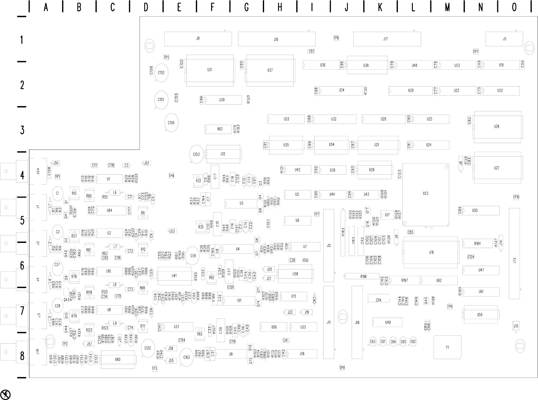
VITS 200
A3 Controller Board
Static Sensitive Devices
See Maintenance Section
671-2131-02 & Up

VITS 200
C1 B1 1 A4
C2 B4 1 A5
C3 C2 1 C4
C4 C4 1 D5
C5 D1 1 D5
C6 D4 1 D5
C7 D2 1 F5
C8 D4 1 F6
C9 E2 1 F4
C10 E5 1 F5
C11 E4 1 G5
C12 E2 1 G4
C13 F2 1 G4
C14 E4 1 G5
C15 E5 1 F5
C16 F5 1 G5
C17 E3 1 F4
C18 F3 1 G4
C19 H4 1 H6
C20 H3 1 H6
C21 E2 1 G4
C22 E4 1 G5
C23 B2 1 D5
C24 B5 1 D5
C25 D1 2 D6
C26 D4 2 D7
C27 B2 2 A6
C28 B4 2 A7
C29 C4 2 D7
C30 C2 2 D6
C31 D4 2 F8
C32 D2 2 F7
C33 E5 2 F8
C34 E2 2 F6
C35 E2 2 G6
C36 E4 2 G8
C37 E3 2 G6
C38 E3 2 G6
C39 E5 2 F8
C40 E5 2 G8
C41 H4 2 H8
C42 H3 2 H8
C43 E2 2 G6
C44 E2 2 G6
C45 E4 2 G7
C46 E4 2 G7
C47 B2 2 D6
C48 B5 2 D7
C49 B2 3 N2
C50 A2 3 O2
C51 F1 5 E7
C52 F1 5 F6
C53 G1 5 E7
C54 D1 5 E6
C55 D1 5 D6
C56 D1 5 D7
C57 D1 5 E7
C58 E1 5 D7
C59 E1 5 E6
C60 E2 5 E7
C61 C4 5 K8
C62 B4 5 L8
C63 C4 5 K8
C64 C4 5 K8
C65 C4 5 L8
C71 B2 1 C5
C72 B4 1 C6
C73 B2 2 C7
C74 B4 2 C7
C75 A5 7 N2
C76 A5 7 M2
C77 A5 7 M2
C78 B5 7 K2
C80 B5 7 L3
C81 B5 7 L3
C82 B5 7 N3
C83 C5 7 N4
C84 C5 7 M5
C85 C5 7 L5
C87 D5 7 J3
C88 D5 7 I3
C89 D5 7 I3
C90 E5 7 G2
C91 E5 7 H3
C92 E5 7 I4
C93 E5 7 J4
C94 F5 7 J5
C95 F5 7 I5
C96 F5 7 J2
C97 G5 7 I1
C98 G5 7 I2
C99 G5 7 F2
C100 H5 7 E2
C101 C4 7 K6
C102 C4 7 K6
C103 A3 7 K6
C104 B4 7 K6
C105 B4 7 K6
C106 D4 7 K6
C107 C4 7 K6
C108 B4 7 K6
C109 B4 7 K6
C111 A5 7 B4
C112 A5 7 B5
C113 A5 7 C6
C114 B5 7 C7
C115 D5 7 C7
C116 D5 7 C6
C117 D5 7 D5
C118 E5 7 C4
C119 B5 7 G8
C120 B5 7 F7
C121 C5 7 G5
C122 C5 7 G4
C123 H5 7 L4
C124 H5 7 N6
C125 E5 7 D5
C130 F1 6 A8
C131 E1 6 B8
C132 E2 6 D8
C133 D2 6 B8
C134 F1 6 B8
C135 C1 6 C8
C136 C1 6 C8
C137 C1 6 C8
C138 C1 6 C8
C139 D2 6 D8
C140 D2 6 D8
C141 E2 6 D7
C142 D5 7 K6
C143 C5 7 K6
C144 C5 7 L7
C145 C5 7 L7
C146 C5 7 L7
C149 B5 7 L7
C150 E5 5 E3
C151 D5 5 D2
C152 D5 5 D2
C153 D5 5 E3
C154 C5 5 E8
C155 C5 5 E2
C156 B5 5 D2
C157 B5 5 H5
C158 G2 6 A4
C159 A2 1 B5
C160 A4 1 B6
C161 A2 2 B7
C162 A5 2 B8
C163 E2 6 E8
C164 * D2 1 F5
C165 * D4 1 F6
C166 * D2 2 F7
C167 * D5 2 F8
CR2 C3 7 J5
CR3 C3 7 J5
CR4 C4 7 K7
CR5 F4 7 L7
CR6 F4 7 L7
CR7 G4 4 I7
J1 A1 1 A4
J2 A4 1 A5
J3 A4 2 A7
J4 A1 2 A6
J5 A1 3 O1
J6 B3 3 K6
J7 * E4 3 M3
J8 C1 3 M4
J9 H1 5 F1
J10 A1 5 I1
J11 A4 5 J8
J12 H3 5 J6
J13 H2 5 O7
J14 G3 5 O6
J15 A4 5 O8
J16 H4 5 K8
J17 A3 5 L1
J18 H2 6 A8
J19 H3 1 I7
J20 H5 1 G6
J21 G2 2 G6
J22 G5 2 H7
J50 A2 6 A4
J51 A1 6 C8
J52 D1 1 D4
J53 F2 5 E5
J54 H2 6 A4
J55 C2 6 E8
J56 C2 6 E8
J57 D1 6 B8
L1 A2 1 A5
L2 A4 1 A6
L3 A4 2 A7
L4 A2 2 A6
L6 B2 1 C4
L7 B4 1 C6
L8 B2 2 C6
L9 B4 2 C7
P3 C1 3 M4
P6 B4 3 K6
P14 F3 5 O6
P19 H3 1 I7
P20 H5 1 G6
P21 G2 2 G6
P22 G5 2 H7
P55 C2 6 E8
P56 C2 6 E8
P57 D1 6 B8
Q1 B2 1 B4
Q2 B4 1 B5
Q3 F2 1 G4
Q4 F2 1 G4
Q6 F4 1 G5
Q7 F4 1 G6
Q8 G2 1 G5
Q9 B2 2 B6
Q10 B4 2 B7
Q11 F2 2 G6
Q12 F4 2 G8
Q13 F4 2 G8
Q14 F2 2 G7
Q17 F3 5 K5
Q18 G3 5 K5
Q40 F4 7 L7
Q41 A2 1 B5
Q42 A4 1 B6
Q43 A2 2 B7
Q44 B4 2 B8
R1 A2 1 A5
R2 A4 1 A6
R3 B2 1 A5
R4 B4 1 A6
R5 A4 1 A6
R6 A2 1 A5
R7 B2 1 D5
R8 B2 1 D5
R9 B2 1 D5
R10 B4 1 D5
R11 B5 1 D5
R12 B4 1 D6
R13 B1 1 B4
R14 B3 1 B5
R15 B1 1 B4
R16 C1 1 B4
R17 C3 1 B5
R18 C1 1 B4
R19 C1 1 B4
R20 C3 1 B5
R21 C4 1 B5
R22 D3 1 D5
R23 D3 1 E6
R24 D4 1 C5
R25 D1 1 C4
R26 D1 1 D4
R27 D1 1 E6
R28 D1 1 D4
R30 F2 1 H5
R31 F4 1 G6
R32 C2 1 F4
R33 D2 1 F5
R34 D2 1 E5
R35 C5 1 F5
R36 D5 1 F6
R37 D2 1 E5
R38 D5 1 F6
R39 D5 1 F6
R40 F3 1 H5
R41 F5 1 H6
R42 F2 1 H4
R44 E2 1 F4
R45 E5 1 F5
R46 E2 1 F4
R47 F2 1 F4
R48 F5 1 F5
R49 E5 1 F5
R50 H4 1 I6
R51 H3 1 H6
R52 H4 1 H6
R54 G5 1 H6
R55 G2 1 H5
R56 F2 1 H4
R57 B3 1 B5
R58 B1 1 B5
R59 B1 1 C5
R60 B1 1 C5
R61 B3 1 C6
R62 B3 1 B6
R63 B3 1 C6
R64 A4 2 A7
R65 A2 2 A7
R66 B2 2 D6
R67 B2 2 D6
R68 B2 2 D7
R69 B4 2 D7
R70 B5 2 D7
R71 B5 2 D7
R72 A2 2 A7
R73 A4 2 A7
R74 B2 2 A7
R75 B4 2 A7
R76 B1 2 B6
R77 B4 2 B7
R78 B1 2 B6
R79 B3 2 B7
R80 C3 2 B7
R81 C1 2 B6
R82 C1 2 B6
R83 C1 2 B6
R84 C3 2 B7
R85 C4 2 B7
R86 C1 2 D6
R87 D1 2 E6
R88 C1 2 C6
R89 C3 2 D7
R90 C3 2 E6
R91 C4 2 C7
R92 C2 2 F7
R93 C5 2 F8
R94 D5 2 F9
R95 D2 2 F7
R96 D2 2 F7
R97 D5 2 F8
R98 D2 2 F7
R99 D5 2 F8
R100 F2 2 H7
R101 F5 2 H8
R102 F4 2 G8
R103 F2 2 H7
R105 E2 2 G6
R106 E5 2 F8
R107 E5 2 F8
R108 E5 2 G8
R109 E2 2 F6
R110 E2 2 G6
R111 H3 2 H8
R112 H4 2 H8
R113 H3 2 H8
R114 F5 2 G8
R115 F2 2 H7
R119 A1 2 C7
R120 A1 2 C7
R121 A1 2 B7
R122 A3 2 C8
R123 A3 2 C7
R124 A3 2 B8
R125 A4 3 K5
R126 C1 3 N4
R127 B4 3 L5
R128 B3 3 L5
R129 G1 4 G2
R130 A5 4 K2
R131 B1 5 H4
R132 F3 5 J5
R133 F3 5 J5
R134 F4 5 K5
R135 G4 5 J5
R136 G4 5 K6
R137 G3 5 N6
R138 F2 5 E7
R139 F2 5 E7
R140 F2 5 F6
R141 F1 5 E7
R142 F1 5 E7
R143 G1 5 E7
R144 G1 5 E7
R145 E1 5 E6
R146 E2 5 F7
R148 E3 5 K5
R149 F4 5 J5
R150 G3 5 K5
R160 F2 6 A8
R163 D4 6 G3
R170 D4 6 G3
R183 B3 7 J5
R184 D3 7 N6
R185 G4 5 M7
R186 C1 6 C8
R187 B1 6 C8
R188 E2 6 B8
R189 E2 6 B8
R190 E1 6 D8
R191 F1 6 A8
R192 G1 6 B8
R193 F1 6 B8
R194 D2 6 D8
R195 F1 6 B8
R196 B4 7 J6
R197 D4 7 K7
R198 F4 7 M7
R199 D1 6 C8
R200 A4 1 B6
R201 A2 1 B5
R202 C3 1 D5
R203 C1 1 D4
R204 C4 2 D7
R205 C1 2 D6
R206 2 A2 B7
R207 2 A4 B8
TP1 7 E5 A4
TP2 7 F5 A8
TP3 7 F5 D8
TP4 7 F5 E4
TP5 7 G5 E1
TP6 7 G5 J1
TP7 7 G5 I5
TP8 7 G5 J8
TP9 7 H5 M7
TP10 7 H5 O4
TP11 7 H5 N1
U1 1 C1 C4
U2 1 C4 C6
U3 1 D1 F5
U4 1 D4 F6
U5A 1 G2 H5
U5B 1 H2 H5
U5C 1 G4 H5
U5D 1 G5 H5
U6A 1 G3 H5
U6B 1 G4 H5
U6C 2 G3 H5
U6D 2 G4 H5
U7A 1 H3 H6
U7B 1 H4 H6
U8 2 B4 C7
U9 2 D4 F8
U10 2 B1 C6
U11 2 D1 F7
U12 6 D3 F4
U15A 2 G2 H7
U15B 2 G2 H7
U15C 2 G4 H7
U15D 2 G4 H7
U16A 2 G3 H8
U16B 2 G4 H8
U17 3 B4 K5
U18 3 F2 L6
U19 3 B1 N2
U20 3 G3 K3
U21 3 D1 J4
U22 3 G3 M2
U23 3 C2 L5
U24 3 G4 L4
U25 3 G5 L3
U26 * 3 F3 N3
U27 3 F5 N4
U28 3 D3 J4
U29 4 C4 K2
U30 4 G1 F3
U31 4 F1 E2
U32 4 E2 I3
U33 4 B3 H3
U34 4 C2 I2
U35 4 E3 H4
U36 4 B4 I2
U37 4 B2 G2
U38 4 E4 J2
U39A 4 A5 I4
U39B 4 B2 I4
U39C 4 E3 I4
U39D 4 E3 I4
U40 5 C4 K8
U41 5 D1 D6
U42A 5 B1 H4
U42B 5 B2 H4
U43A 5 F3 J5
U43B 5 E3 J5
U43C 5 F3 J5
U43D 5 F3 J5
U44A 5 F5 I5
U44B 5 F5 I5
U47 7 F1 N6
U48 7 F2 L2
U50 7 E3 N5
U52 7 E1 N2
U53 7 E2 M2
U54 7 C2 I4
U55A 1 B3 H8
U55B 1 B5 H8
U55C 2 B3 H8
U55D 2 B5 H8
U56A 1 B3 G8
U56B 1 B5 G8
U56C 2 B3 G8
U56D 2 B5 G8
U57 6 E3 E8
U58 4 G5 H6
U59 5 E4 N7
U60 6 D1 C8
U61 7 F3 N7
U62 7 E4 L7
U63A 6 E4 F3
U63B 6 E5 F3
U63C 6 E5 F3
U63D 6 E4 F3
U64 6 F3 C5
VR2 1 F4 H6
VR3 1 F4 H6
VR4 1 G2 H5
VR5 2 F2 H7
VR6 2 F5 H8
VR7 2 F4 G8
VR8 2 F2 H7
Y1 5 E5 L8
A3 Controller Board and Diagram <1> Component Locator
A3 Controller Board
671-2131-00 – 01
* See parts list for serial number ranges.
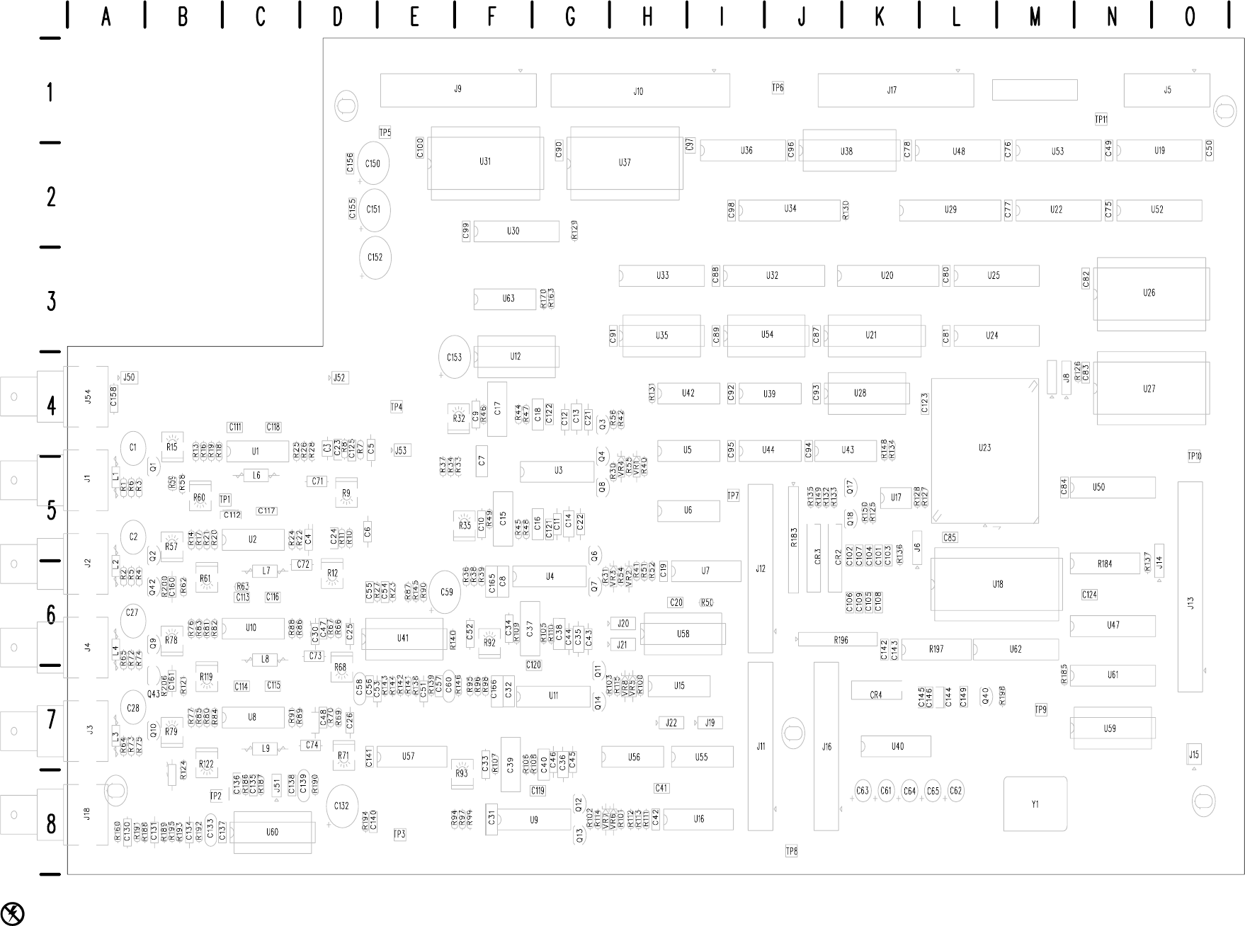
VITS 200
A3 Controller Board
Static Sensitive Devices
See Maintenance Section
671-2131-00 – 01
C163
C162
R123
C29
C159
C160
C162
U51
J7
J49
C148
C147
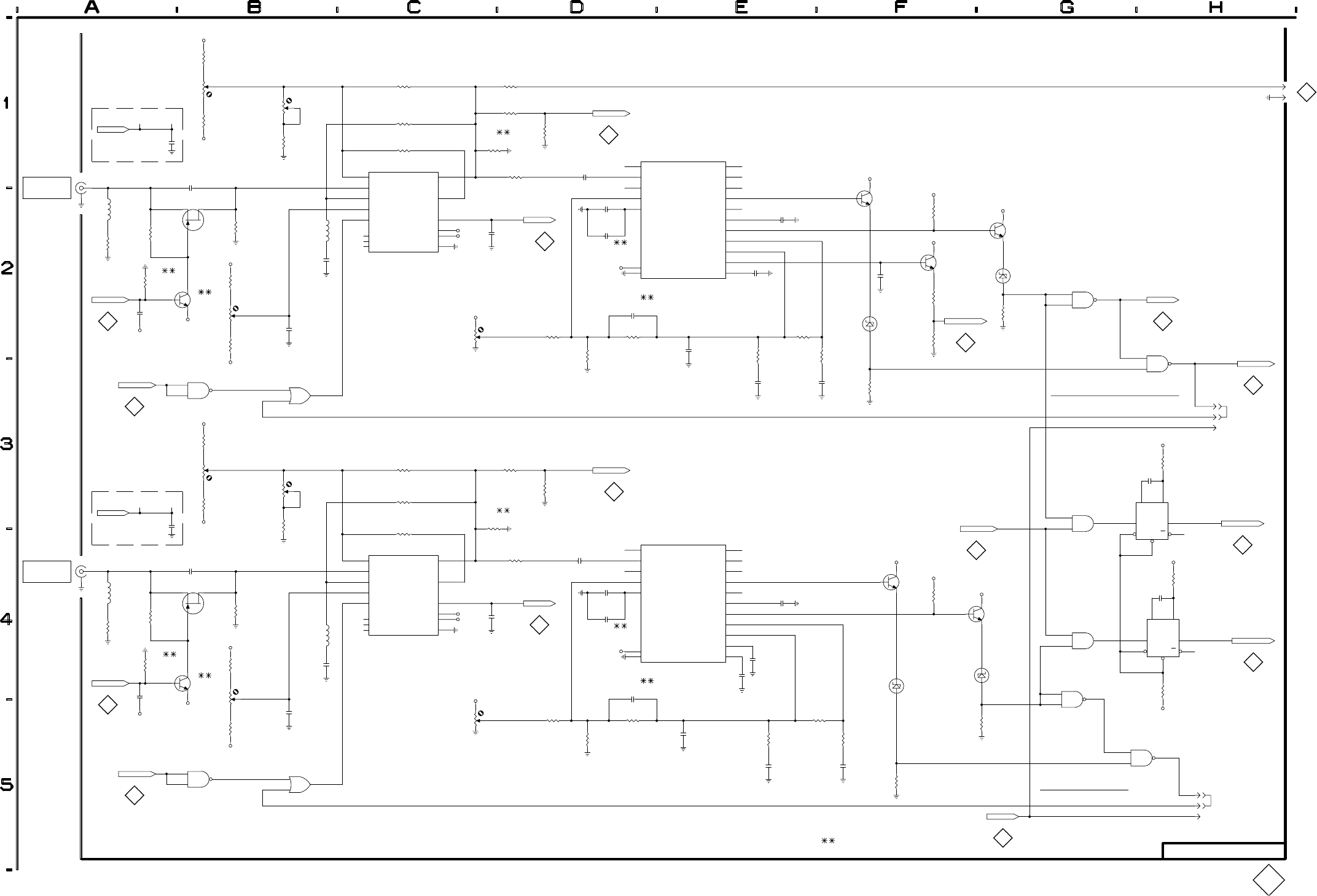
!&%'%
"%
%
%
)
%
-
%
-
*'%!
!#('
)
"&'
"(#
.
%
-
%
'" '"
$
/
0
!
%
%
-
)!
)!
&
&
!'
"
)"('
&"('
)
)
!
!
!
!
(
%
%
!
!
*')
%
(
%
%
0
0
%
!
!
!
#&
" #)
'
"&
"&
!'"('
#'
"%,"('
&'
('
#"!'
"!'
!'
'
#&'
" #&+!
!
)
(
'
)
)
%
-
$
&+!
)
%
-
)%
)
(
&
*'#%&
)
(
)%
)
%
-
%
-
$
$
0
!
%
-
0
0
/
)
)
)
)
"
%
-
%
-
%
-
(&'
"&'"%
"%,"!'
/
(
%!/
'&'&
0
0
/
)
%
%
-
%
-
"&'
"(#
%
-
%
(
)
)
%
-
$
$
/
#
)
)
(
(
&
%
-
%
-
(
&
%
-
%
-
0
0
%
-
%
0
)
#
(
&
%
-
*'%! # "
*'%! #' !
!'%! #' !
#"%
#
&+! &+!
)
(
#(#
*
%
*
$
$
(
&
%
-
(
&
0
)
)
&+!'
$
!
!
!
#&
" #)
'
"&
"&
!'"('
#'
"%,"('
&'
('
#"!'
"!'
!'
'
#&'
" #&+!
!
)
(
'
!
!
*')
(
%
%
%
0
%
!
%
%
-
)!
)!
&
&
!'
"
)"('
&"('
)
)
!
!
!
!
(
%
%
%
)
"(#
"&'
.
%
-
%
-
%
'" '"
$
/
0
!#('
*'%!
)
%
-
%
$
%
-
"&'
%
-
%
(
)
%
-
$
/
"(#
0
/
)
)
)
)
"
"%,"!'
/
0
(
%!/
'&'&
!
0
0
0
/
)
)%
)
%
-
)%
)
$
)
#(#
(
&
(
&
*
%
*
$
$
(
&
%
-
0
&+! &+!
(
#
(
&
*'%! # "
*'%! #' !
!'%! #' !
#
%
%
-
%
-
%
-
0
0 %
-
0
%
-
%
-
%
-
%
-
(&'
"&'"%
0
(
&
)
#
(
(
&
%
-
)
VITS 200
!"'
REV AUG 1995
!&%!( %%!&
&#%'&&'"%%%)(&
EXTERNAL INPUTS 1 & 2
671–2131–00 & UP
P/O A3 CONTROLLER BOARD
1

VITS 200
C25 D1 D6
C26 D4 D7
C27 B2 A6
C28 B4 A7
C29 C4 D7
C30 C2 D6
C31 D4 F8
C32 D2 F7
C33 E5 F8
C34 E2 F6
C35 E2 G6
C36 E4 G8
C37 E3 G6
C38 E3 G6
C39 E5 F8
C40 E5 G8
C41 H4 H8
C42 H3 H8
C43 E2 G6
C44 E2 G6
C45 E4 G7
C46 E4 G7
C47 B2 D6
C48 B5 D7
C68 D2
C69 D4
C73 B2 C7
C74 B4 C7
C161 A2 B7
C162 A5 B8
C166 D2 F7
C167 D5 F8
J3 A4 A7
J4 A1 A6
J21 G2 G6
J22 G5 H7
L3 A4 A7
L4 A2 A6
L8 B2 C6
L9 B4 C7
P21 G2
P22 G5
Q9 B2 B6
Q10 B4 B7
Q11 F2 G6
Q12 F4 G8
Q13 F4 G8
Q14 F2 G7
Q43 A2 B7
Q44 B4 B8
R64 A4 A7
R65 A2 A7
R66 B2 D6
R67 B2 D6
R68 B2 D7
R69 B4 D7
R70 B5 D7
R71 B5 D7
R72 A2 A7
R73 A4 A7
R74 B2 A7
R75 B4 A7
R76 B1 B6
R77 B4 B7
R78 B1 B6
R79 B3 B7
R80 C3 B7
R81 C1 B6
R82 C1 B6
R83 C1 B6
R84 C3 B7
R85 C4 B7
R86 C1 D6
R87 D1 E6
R88 C1 C6
R89 C3 D7
R90 C3 E6
R91 C4 C7
R92 C2 F7
R93 C5 F8
R94 D5 F8
R95 D2 F7
R96 D2 F7
R97 D5 F8
R98 D2 F7
R99 D5 F8
R100 F2 H7
R101 F5 H8
R102 F4 G8
R103 F2 H7
R105 E2 G6
R106 E5 F8
R107 E5 F8
R108 E5 G8
R109 E2 F6
R110 E2 G6
R111 H3 H8
R112 H4 H8
R113 H3 H8
R114 F5 G8
R115 F2 H7
R119 A1 C7
R120 A1 C7
R121 A1 B7
R122 A3 C8
R123 A3 C7
R124 A3 B8
R204 C4 D7
R205 C1 D6
R206 A2 B7
R207 A4 B8
U6C G3 H5
U6D G4 H5
U8 B4 C7
U9 D4 F8
U10 B1 C6
U11 D1 F7
U15A G2 H7
U15B G2 H7
U15C G4 H7
U15D G4 H7
U16A G3 H8
U16B G4 H8
U55C B3 H8
U55D B5 H8
U56C B3 G8
U56D B5 G8
VR5 F2 H7
VR6 F5 H8
VR7 F4 G8
VR8 F2 H7
Schematic Diagram <2> A3 Component Locator Chart
The schematic diagram has an alphanumeric grid to assist in locating parts within that diagram.
Assembly A3.
(Partial Assembly A3 also shown on schematic 1 and 3 thru 7.
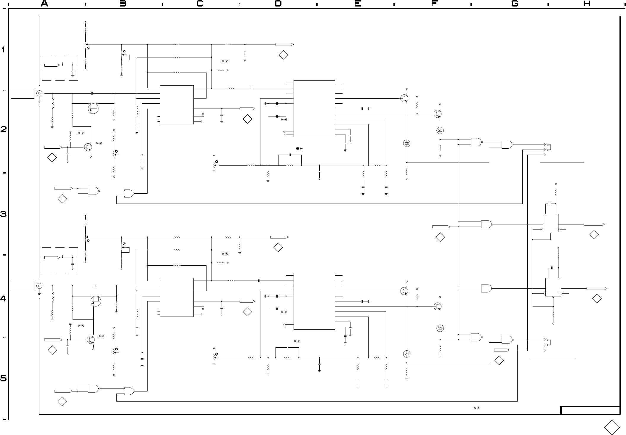
)
%
-
*'%!
!#('
)
"&'
"(# !
.
%
-
%
-
%
%
'" '"
/
% $
0
%
)!
)!
&
&
!'
"
)"('
&"('
)
)
!
!
!
!
(
%
-
%
!
!
*')
(
%
%
%
#&
" #)
'
"&
"&
!'"('
#'
"%,"('
&'
('
#"!'
"!'
!'
'
#&'
" #&+!
!
)
(
'
0
%
!
!
!
)
)
$
#
(
&
#
)
%
-
)%
)
)%
)
%
-
(
&
$
!
0
0
0
)
"
"&'"%
"%,"!'
/
/
(
%!/
'&'&
0
)
)
)
"
0
0 %
-
/
)
%
%
-
(
$
"(#
"&'
%
-
%
%
-
)
)
$
%
-
/
)
)
#
(
(
&
(
&
%
-
%
-
%
-
%
-
%
-
(&'
0
%
-
%
-
0
%
0
%
-
)
(
&
*
%
*
$
$
(
&
%
-
0
!'%! #' !
*'%! # "
*'%! #' !
&+! &+!
(
)
#(#
*
%
*
$
$
(
&
%
-
0
&+!'
!!
*')
(
%
%
%
#&
" #)
'
"&
"&
!'"('
#'
"%,"('
&'
('
#"!'
"!'
!'
'
#&'
" #&+!
!
)
(
'
0
%
)!
)!
&
&
!'
"
)"('
&"('
)
)
!
!
!
!
(
%
-
%
%
)
!
"&'
"(#
%
-
%
-
%
%
'" '"
/
% $
*'%!
!#('
)
%
%
-
$
%
-
.
%
-
%
-
$
0
)
)
"
0
/
!
)
"
/
0
(
%!/
'&'&
!
!
!
0
0
0
)
)
)
)%
)
%
-
(
&
$
$
)
#(#
(
&
%
-
(
&
#
&+! &+!
(
#
*'%! # "
*'%! #' !
!'%! #' !
%
-
)%
)
%
-
%
-
%
-
0
%
0
0
%
-
%
-
%
-
(&'
"&'"%
"%,"!'
/
)
0
%
-
)
#
(
(
&
(
&
(
"(#
"&'
%
%
-
)
)
/
VITS 200 REV AUG 1995
!"'
EXTERNAL INPUTS 3 & 4
!&%!( %%!&
&#%'&&'"%%%)(&
671–2131–00 & UP
2
P/O A3 CONTROLLER BOARD

VITS 200
C49 B2 N2
C50 A2 O2
J5 A1 O1
J6 B3 K6
J8 C1 M4
P3 C1
P6 B4
R125 A4 K5
R126 C1 N4
R127 B4 L5
R128 B3 L5
U17 B4 K5
U18 F2 L6
U19 B1 N2
U20 G3 K3
U21 D1 J4
U22 G3 M2
U23 C2 L5
U24 G4 L4
U25 G5 L3
U26 F3 N3
U27 F5 N4
U28 D3 J4
Schematic Diagram <3> Component Locator Chart
The schematic diagram has an alphanumeric grid to assist in locating parts within that diagram.
Assembly A3.
(Partial Assembly A3 also shown on schematic 1, 2, and 4 thru 7).
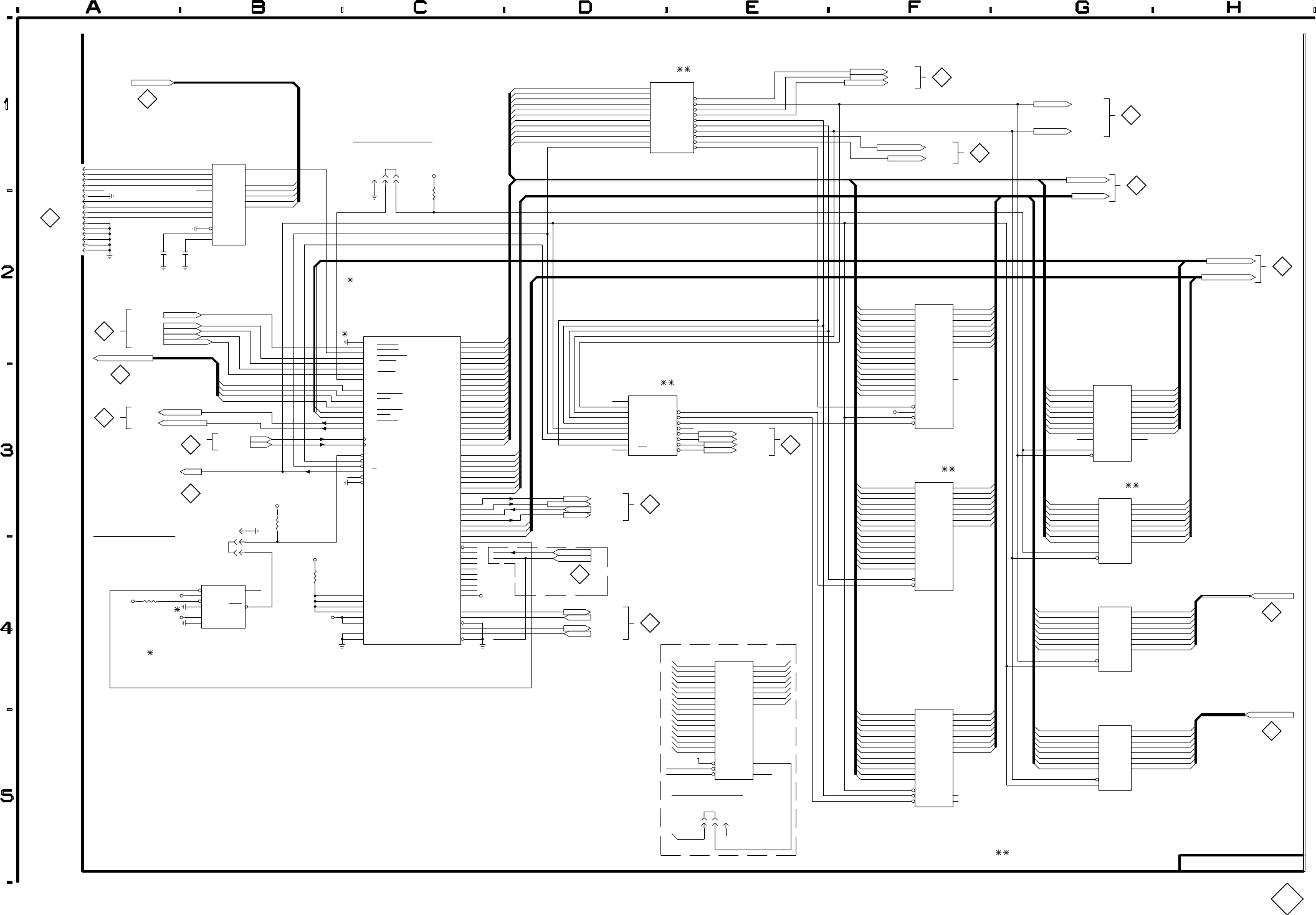
!$
$'+
&!#(
)
)
)
#
#
#
#
#
#
#
#
#
#
)
$ *
$/0 $/0
&#"($"
#&
$"(
$
$
$
$
$
-
-
-
-
-
,
,
,
,
#
!
#'
)
*
&
1
$
&#"($" ##)(
&#"($" "
&#"($" '
/0
/0
!&%
!$
&!
$'+
&!#(
"*&!
$&#!
('&!
'$ -
'((
'&! '$ -
'((
/0
/0
)
)
/0
/0
&!
('&!
)
)
/0
('/0
/0
('/0
"
'
'
+
#
)
('/0
$)$$ ##)(
!'(
!&%
&+
/0
$"!
$"($
$"($
$"($"(
$"($#
$(#)(
$'#
$&-
$!&%
$!
$(
$!&%
$!
$(
$
$ &%
$
$
$
$
$
$
$
,
,
&'(
!('
$ #)(
$(
$(
$(
$(
$(
$(
$(
$(
!&%
&+
#'(
*(
"
*
*
&&%
('
&,
(,
('
&,
(,
"
)
$
"#(&#)" #+
'"
'"#*
"#()$"&#)"
*&*
#
-$''
"
&
2
2
,
,
*&
*&
*&
*&
*&/0 *&/0
&!#("
&"
*&"
)
)
)
)
!'(
&+
&!
('&!
$&#!
"*&!
!&%
!'(
'&!
#
)
*
&+
('&+
#
('#
$#
"*#
'&#
)
)
)
)
&+ *
'&!
$)$
&!
%
%
%
%
%
%
%
%
%
%
#
)
'
('
('
('
('
('
('
('
('
$)$
('&!
%
%
%
%
%
%
%
%
#
"
)
'
$&#!
$#
#*$$
)
('
('
#!(
)'-
('
+
+&
!#"#&
&' "
&+
*
*
!&%
&'(
&
1
&
1
&+
+
)
'(
$&'(
(
(#
&'(
&'(
"
*
)
'
#"(&# &&'(
"#$ )"#&+&&'('
"#&! #$&(#"
&'(
$
*
*
*
&
1
"#()$"&#)"
"#(&#)" #+
'"
'"#*
*
(,
&, &,
(,
&, &,
(,
(,
*
)
#
$!
*$$
"
)
)
)
)
"
"
#
+
)
'
&+
&!
&
)
'
/0
/0
('/0
('/0
&+
('
('
('
('
('
('
('
('
('&!
&
)
'
&+
"*&!
"*#
#"(&# &$&#!'.
#&
#&
$&#!
$#
#
#
*
*
$
#
*
VITS 200 &*)
"#(
MICROPROCESSOR KERNEL
"'& ")!&&"'
'$&(' '(#&& &* )'
)$
$##"(&# &#&
3

VITS 200
CR7 G4 I7
R129 G1 G2
R130 A5 K2
U29 C4 K2
U30 G1 F3
U31 F1 E2
U32 E2 I3
U33 B3 H3
U34 C2 I2
U35 E3 H4
U36 B4 I2
U37 B2 G2
U38 E4 J2
U39A A5 I4
U39B B2 I4
U39C E3 I4
U39D E3 I4
U58 G5 H6
Schematic Diagram <4> Component Locator Chart
671-2131-02 & UP
The schematic diagram has an alphanumeric grid to assist in locating parts within that diagram.
Assembly A3.
(Partial Assembly A3 also shown on schematic 1, 2, 3, and 5 thru 7).
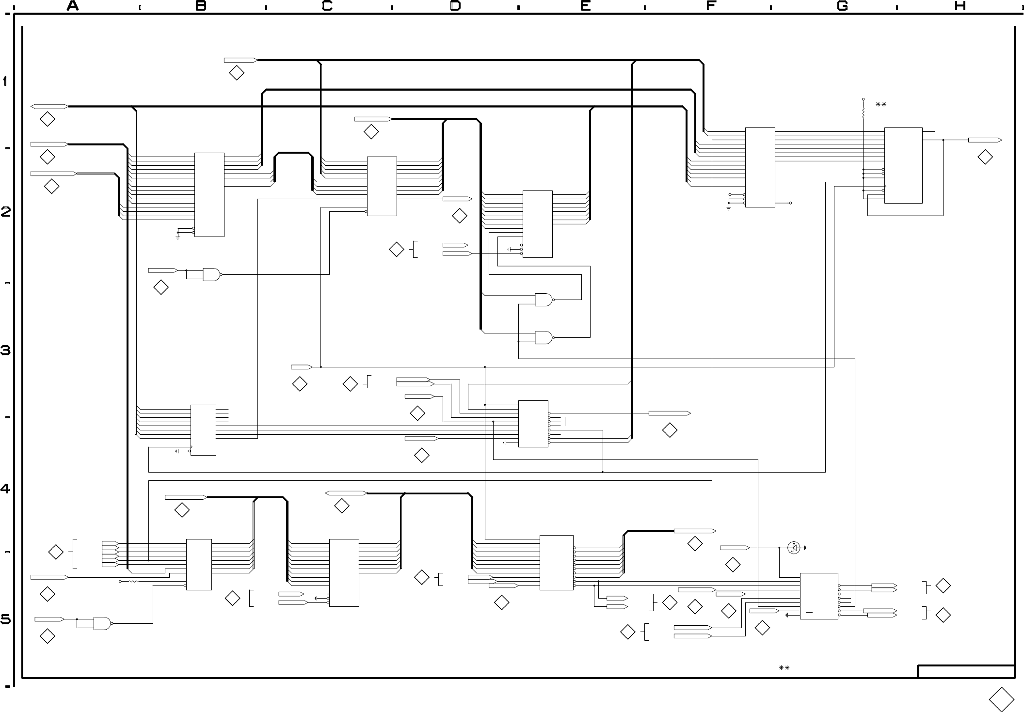
-.
-. -.
-.
)-.
-.
)-.
)
)
")##
(
)
)
)-.
)-.
-.
-.
$
$
$
$
$
$
$
$
$
$
"
(
'
"
#
)##
(
)
)
)
)
)-.
-.
$
$
$
$
$
$
$
$
$
$
&
&
%
&%
&
(
)
%
%'
"
)
)
"
*
(
#
#
(
(
(%&"%
%*
"
(%&"%
)
)
)
)
)
)
)
)
)
)
%
)
)
)
)
)
)
)
)
)%
)%
)%
)%
)%-.
)
)
)%-.
%
(
&
(
%
#
#
$!
(
&
(
&
$!
%#%&
!
(&!'%!,
"
%#%&
(
)
!
'" #
%!
)%!
!
'" #
(
(
(
$
$
$
$
$
$
$
$
"
(
&
"
'&-.
)
)
)
)
)
)
)
)
$
$
$
$
$
$
$
$
"
!
(
&
"
*
(
'&-.
'&-.
'&
'&
'&
'&
'&
'&
'&
'&
'&
'&
'&
'&
'&-.
"
"
"
"
"
"
"
"
"
"
(
#)
#'&
#'&
#'&
#'&-.
'&
'&
'&
'&
#'&-.
)'
"
%
(
(
(
"
(
)
%&'
+'
+'
%&'
(
(
(
&,!'
&,!+
)%&
!!
!'
!
+'
+'
#'&
#'&
#'&
#'&
#'&
'&
'&
'&
'&
(
(
(
)&,!
)%)
&,!
'&
'&
'&
'&
(
(
'&%*
'&"
'&
'&
'&
'&
'&
'&
'&
'&
'&
'&
'&
%
/
%
#(#
'&%
'&%
#&'!,
)
)
(
&
(
(
#&'!,
'&%
VITS 200 REV AUG 1995 TEST SIGNAL & CHARACTER SELECTION MEMORY
!"'
671–2131–02 & UP
!&%!( %%!&
&#%'&&'"%%%)(&
4
P/O A3 CONTROLLER BOARD

VITS 200
CR7 G4 I7
R129 G1 G2
R130 A5 K2
U29 C4 K2
U30 G1 F3
U31 F1 E2
U32 E2 I3
U33 B3 H3
U34 C2 I2
U35 E3 H4
U36 B4 I2
U37 B2 G2
U38 E4 J2
U39A A5 I4
U39B B2 I4
U39C E3 I4
U39D E3 I4
U58 G5 H6
Schematic Diagram <4> Component Locator Chart
671-2131-00 – 01
The schematic diagram has an alphanumeric grid to assist in locating parts within that diagram.
Assembly A3.
(Partial Assembly A3 also shown on schematic 1, 2, 3, 4, and 6 thru 7).
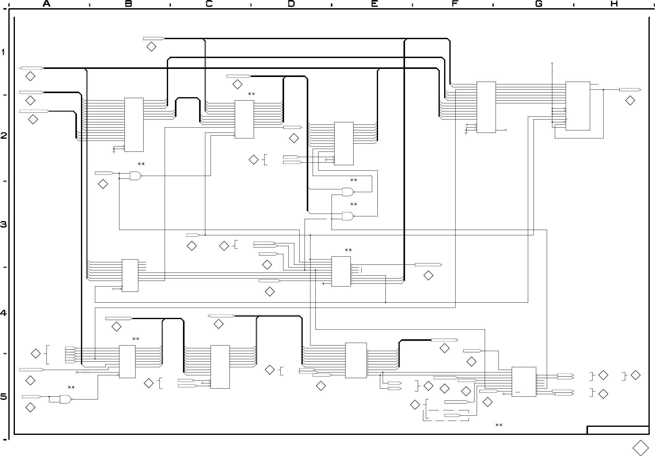
-.
-. -.
-.
)-.
-.
)-.
)
)
")##
(
)
)
)-.
)-.
-. -.
$
$
$
$
$
$
$
$
$
$
"
(
)
)
)
)
)-.
-.
"
#
)##
(
)
$
$
$
$
$
$
$
$
$
$
&
&
%
&%
&
(
%
/
%'
"
)
)
#
#
"
*
(
(%&"% (%&"%
%*
(
(
"
)
)
)
)
)
)
)
)
)
)
%
)
)
)
)
)
)
)
)
)%
)%
)%
)%
)%-.
)
)
)%-.
%
(
(
&
%
%
#
#
(
&
(
&
%#%&
"
(&!'%!,
%#%&
(
)
'" #
'" #
%!
)%!
!
(
(
(
"
$
$
$
$
$
$
$
$
"
(
&
'&-.
)
)
)
)
)
)
)
)
$
$
$
$
$
$
$
$
"
!
(
&
'&-.
'&
'&
'&
'&
'&
'&
'&
'&
'&-.
"
*
(
'&
'&
'&
'&
'&-.
#'&
#'&
#'&
#'&-.
'&
'&
'&
'&
"
"
"
"
"
"
"
"
"
"
(
#)
!
#'&-.
)'
"
(
(
(
(
(
(
%&'
+'
+'
%&'
"
(
)
&,!'
&,!+
(
(
(
%&!
!
!'
(
(
#'&
#'&
#'&
#'&
#'&
'&
'&
'&
'&
+'
+'
'&
'&
'&
'&
)&,!
)%)
&,!
(
'&
'&
'&
'&
'&
'&
'&
'&
'&
'&
'&
'&%*
'&"
(
(
#(#
'&%
'&%
)
#&'!,
)
%
%
/
(
&
#&'!,
(
'&%
(
VITS 200 REV OCT 1992 TEST SIGNAL & CHARACTER SELECTION MEMORY
!"'
671–2131–00 – 01
!&%!( %%!&
&#%'&&'"%%%)(&
4
P/O A3 CONTROLLER BOARD

C51 F1 E7
C52 F2 F6
C53 G1 E7
C54 D1 E6
C55 D1 D6
C56 D1 D7
C57 D1 E7
C58 E1 D7
C59 E1 E6
C60 E2 E7
C61 C4 K8
C62 B4 L8
C63 C4 K8
C64 C4 K8
C65 C4 L8
C150 E5 E3
C151 D5 D2
C152 D5 D2
C153 D5 E3
C154 C5 E8
C155 C5 E2
C156 B5 D2
C157 B5 H5
J9 H1 F1
J10 A1 I1
J11 A4 J8
J12 H3 J6
J13 H2 O7
J14 G3 O6
J15 A4 O8
J16 H4 K8
J17 A3 L1
J53 H2 E5
P14 G3
Q17 F3 K5
Q18 G3 K5
R131 B1 H4
R132 F3 J5
R133 F3 J5
R134 F4 K5
R135 G4 J5
R136 G4 K6
R137 G3 N6
R138 F2 E7
R139 F2 E7
R141 F1 E7
R142 F1 E7
R143 G1 E7
R144 G1 E7
R145 E1 E6
R146 E2 F7
R148 E3 K5
R149 F4 J5
R150 G3 K5
R185 G4 M7
U40 C4 K8
U41 D1 D6
U42A B1 H4
U42B B2 H4
U43A F3 J5
U43B E3 J5
U43C F3 J5
U43D F3 J5
U44A F5 I5
U44B F5 I5
U59 E4 N7
Y1 E5 L8
Schematic Diagram <5> Component Locator Chart
671-2131-02 & UP
The schematic diagram has an alphanumeric grid to assist in locating parts within that diagram.
Assembly A3.
(Partial Assembly A3 also shown on schematic 1 thru 4 and 6, 7).
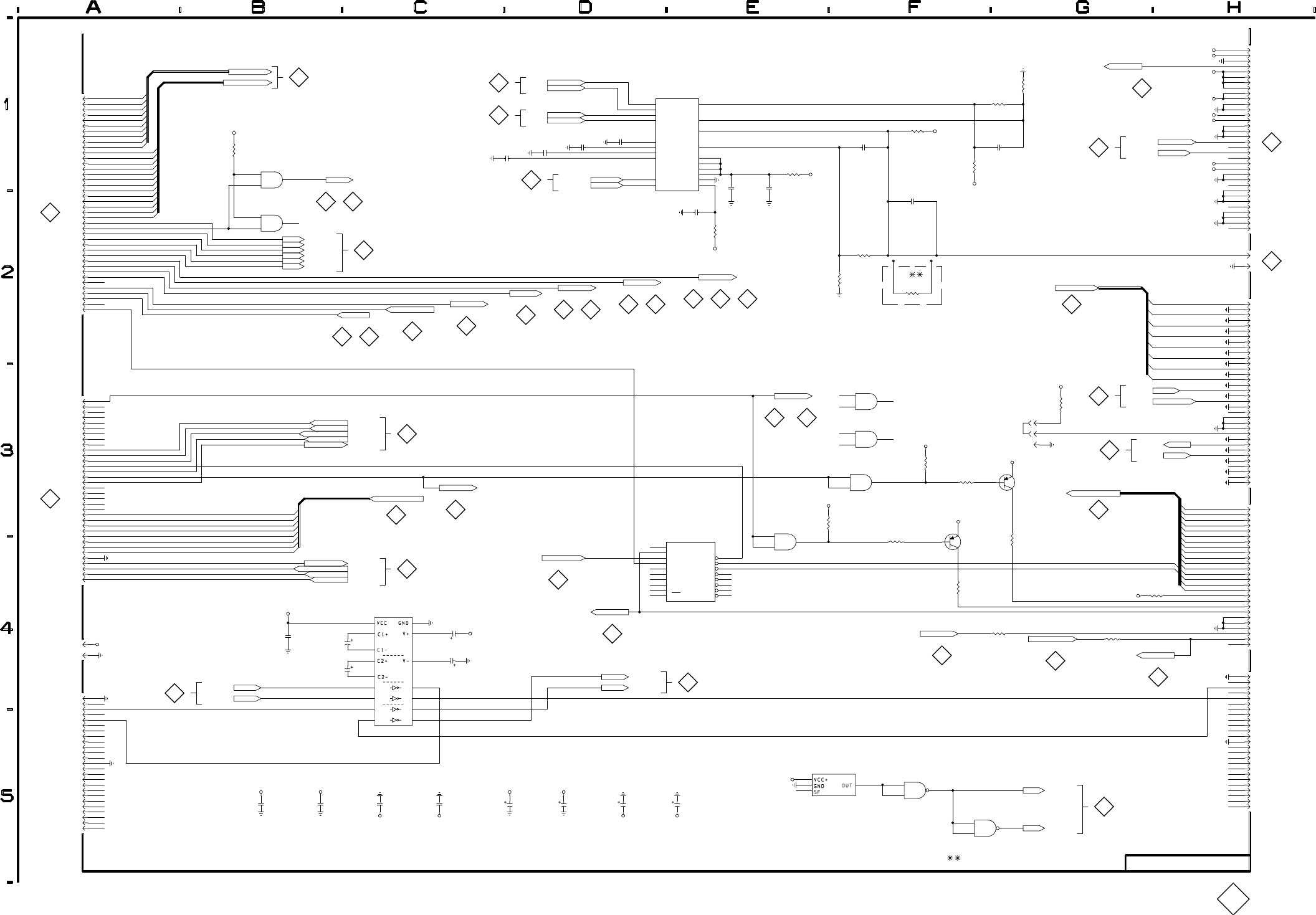
(
(
(
'
$
($%
$
$
*&(
,-
(,-
,-
(,-
%$&$
!$
$
.
'
%
(
(
(
(
(
(
(
(
(
(
(
(
'
'
$
$
'
'
0
0
0
0
*&(
*&(
*&(
*&
*&
"
!'&
(
!'&
(
(
(
(
(
(
'
%)
$
0
0
0
$
$
/
/
/
$
.
$
(
(
'
'
%+
"!$
!$
%$&$
$
(
(
(
$
%$&$
!$
%"+! &!$
,- ,-
$
$
$
'
'
'
$
'
%+ &
$
'
'
'
'
($(
(%+
'
'
(
(
(
(
$
"
(&
&
'
'
'
'
'
'
'
%
(
(
$
!
(%+
($(
%+ &
"
&
(&
"$
!
"%& +
%
%
'
'
'
'
'
%
"%& +
"$!"$%
$%+
%
'
'
!
$
.
'
%
'
%
( '
'
'
'
$
.
"
!&
'%+
)$
&%&
(
%"+
$*
$$"
$!&
$
$
$
$
$
$
$
$
$
$
$
$
$
$
$
$
$
$,- $,-
(
$
$
$
$
.
$
. $
.
$
'
%
(
(
#
#
'
%
"! &$!
+"%%
$
$
!
'
(
'
"+"%% "+"%%
'
'
'
'
'
&!"
$&
'$%!$
"&%,-
$"$%
+"%%
"&%,-
"&%
"&%
"&%
"&%
"&%
"&%
"&%
"&%
"! &$!
+"%%
$%+
"$!$%
&!"
$"$%
$&
'$%!$
%$&$
!$
%"+
%"+"!)$
'
'
&*
&*
(
'
*
(
0
0
0
0
0
$
$*
$*
$+"%%
(
'
'
$+"%%
'
$
$
$
'
$
$
$!&
$"!)$
$+"%%
$' !
$+"%%
(
&$
$%!
'
'
*
*
'
&
'
&
+
1
0
(
(
0
0
0
( (
(
0
0
0
(
( (
0
(
$$"
$%
VITS 200 REV AUG 1995 CONNECTORS & EXTERNAL MULTIPLEXER
%$ '$$ %
%"$&%%&!$$$('% !& P/O A3 CONTROLLER BOARD
671–2131–02 & UP
5

VITS 200
C51 F1 E7
C52 F1 F6
C53 G1 E7
C54 D1 E6
C55 D1 D6
C56 D1 D7
C57 D1 E7
C58 E1 D7
C59 E1 E6
C60 E2 E7
C61 C4 K8
C62 B4 L8
C63 C4 K8
C64 C4 K8
C65 C4 L8
C150 E5 E3
C151 D5 D2
C152 D5 D2
C153 D5 E3
C154 C5 E8
C155 C5 E2
C156 B5 D2
C157 B5 H5
J9 H1 F1
J10 A1 I1
J11 A4 J8
J12 H3 J6
J13 H2 O7
J14 G3 O6
J15 A4 O8
J16 H4 K8
J17 A3 L1
J53 F2 E5
P14 F3 O6
Q17 F3 K5
Q18 G3 K5
R131 B1 H4
R132 F3 J5
R133 F3 J5
R134 F4 K5
R135 G4 J5
R136 G4 K6
R137 G3 N6
R138 F2 E7
R139 F2 E7
R140 F2 F6
R141 F1 E7
R142 F1 E7
R143 G1 E7
R144 G1 E7
R145 E1 E6
R146 E2 F7
R148 E3 K5
R149 F4 J5
R150 G3 K5
R185 G4 M7
U40 C4 K8
U41 D1 D6
U42A B1 H4
U42B B2 H4
U43A F3 J5
U43B E3 J5
U43C F3 J5
U43D F3 J5
U44A F5 I5
U44B F5 I5
U59 E4 N7
Y1 E5 L8
Schematic Diagram <5> Component Locator Chart
671-2131-00 – 01
The schematic diagram has an alphanumeric grid to assist in locating parts within that diagram.
Assembly A3.
(Partial Assembly A3 also shown on schematic 1 thru 6 and 8 thru 9).
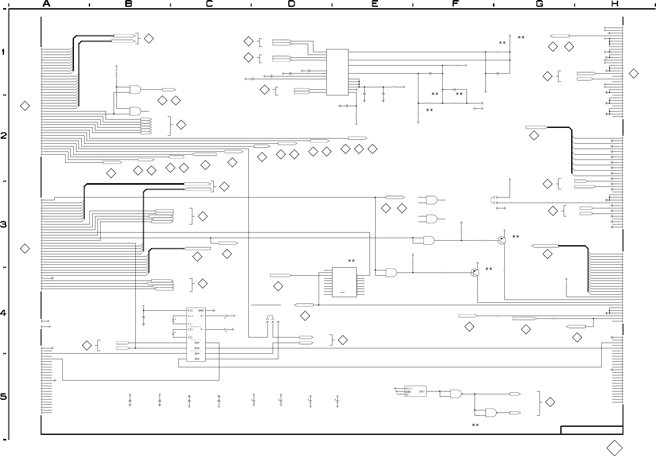
(
(
(
$
$%
'
'
*&(
$
$
,-
,-
(,- (,-
%$&$
!$
(
(
(
(
(
(
(
(
(
(
(
(
$
.
'
%
'
'
*&(
*&(
*&(
$
$
'
'
0
0
0
0
*&
*&
$
"
!'&
(
!'&
(
(
(
(
(
(
'
%)
0
$
0
0
(
(
$
$
/
$
/
$
.
/
$
%+
"!$
'
'
$
(
(
(
$
!$
%$&$
,- ,-
%"+! &!$
$
$
%+ &
'
'
'
$
'
($(
(%+
'
'
'
'
(
(
(
(
$
"
(&
%)&
'
'
'
'
'
'
&
'
'
(
(
$
! !$ ! !$
!
'
(%+
($(
%+ &
"
%)&
&
'
%
(&
$*(
'
%&&
%&&
%&&
%&&
%&&
%&&
%&&
%&&
!
"%& +
%
%
%&&,- %&&,-
%
"%& +
"$!"$%
,- ,-
$%+
'
'
'
'
'
%
!
'
'
(
$
.
'
%
'
% "
!&
'%+
(
)$
&%&
'
'
'
'
$
.
$*
%"+
$
$
$
$
$
$
$
$
$
$
$
$
$
$
$
$
$$"
$!&
(
(
$,-
$,-
$
$
(
(
$
.
$
. $
.
$
'
%
#
#
"! &$!
+"%%
'
%
!
'
(
"+"%%
"+"%%
'
&!"
$&
'$%!$
"&%,- "&%,-
$"$%
'
'
'
'
+"%%
'
"&%
"&%
"&%
"&%
"&%
"&%
"&%
"&%
"! &$!
+"%%
$%+
"$!$%
&!"
$"$%
$&
'$%!$
&*
%$&$
!$
%"+
&*
(
%"+"!)$
&*
'
'
(
'
*
0
0
0
0
0
$*
$*
$+"%%
(
$
$
$*(
"
$%%!'$
!&+&
" &
$+"%%
'
'
$
'
$
$"!)$
$+"%%
$' !
$+"%%
$
$
$!&
'
$
&$
$%!
*
*
'
'
'
&
'
&
(
(
+
1
0
( (
(
0
0
0
(
( (
0
0
0
(
0
$$"
$%
VITS 200 REV MAY 1993 CONNECTORS & EXTERNAL MULTIPLEXER
%$ '$$ %
%"$&%%&!$$$('% !&
P/O A3 CONTROLLER BOARD
671–2131–00 – 01
5

C130 F1 A8
C131 E1 B8
C132 E2 D8
C133 D2 B8
C134 F1 B8
C135 C1 C8
C136 C1 C8
C137 C1 C8
C138 C1 C8
C139 D2 D8
C140 D2 D8
C141 E2 D7
C158 G2 A4
C163 E2 E8
J18 H2 A8
J50 A2 A4
J51 A1 C8
J54 H2 A4
J55 C2 E8
J56 C2 E8
J57 D1 B8
P55 C2
P56 C2
P57 D1
R160 F2 A8
R163 D4 G3
R170 D4 G3
R186 C1 C8
R187 B1 C8
R188 E2 B8
R189 E2 B8
R190 E1 D8
R191 F1 A8
R192 G1 B8
R193 F1 B8
R194 D2 D8
R195 F1 B8
R199 D1 C8
U12 D3 F4
U57 E3 E8
U60 D1 C8
U63A E4 F3
U63B E5 F3
U63C E5 F3
U63D E4 F3
U64 F3 C5
Schematic Diagram <6> Component Locator Chart
671-2131-02 and UP
The schematic diagram has an alphanumeric grid to assist in locating parts within that diagram.
Assembly A3.
(Partial Assembly A3 also shown on schematic 1 thru 5 and 7).
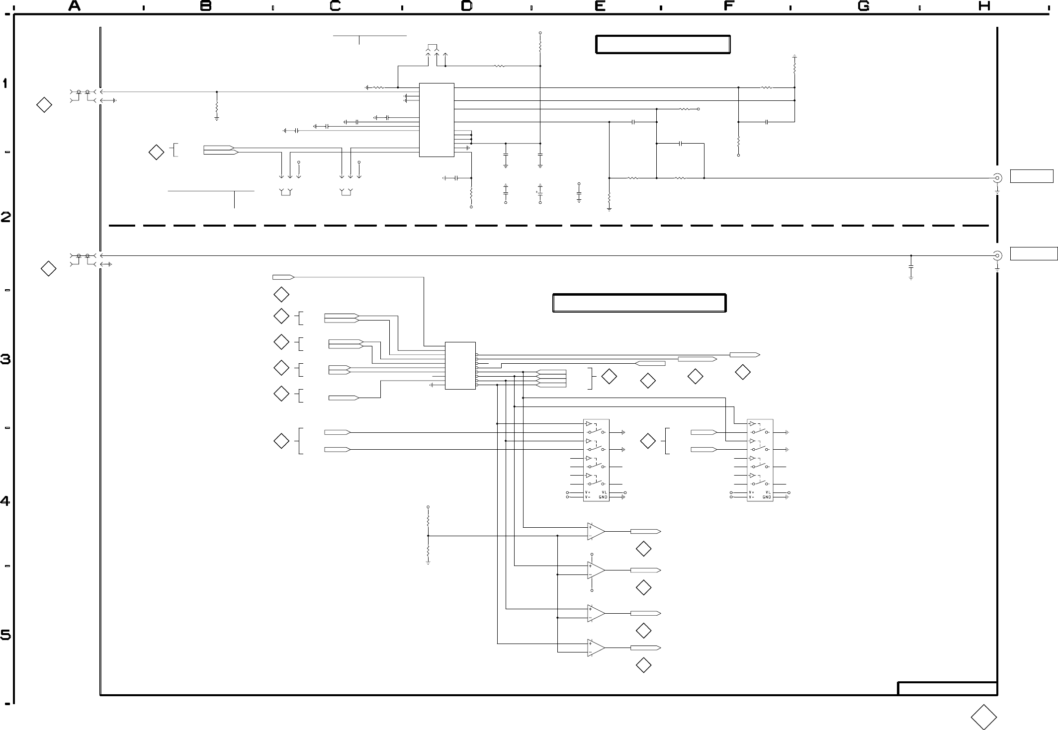
!
$!"#"&#
!
%
!
$!"#"#$
"#$
"#$
"!#!
!
&
!"#
!"#
#"%
!
$
$
+
+
+
% %
+
!
+
$#
%
$#
%
%
%
%
%
%
$
"&
+
*
!
*
*
!
)
!
%
%
#"#"
$!"#
*
!
+
+
!
!
%
%
!
+
+
%
%
#"
"#$
&
#"#"
"!#!
!
$
$
$
$
$
$
$
"(
"(
'#
"(
"(
$
%
"(
"(
"(
"(
$ #!
$
$
$
$
$
$
"(
"('
$
$
$
$
$
$
$
'#
"
!
!
%
$
%
%
%
%
$
!
%
%
%
$
$
%
!
!
!
VITS 200 REV AUG 1995 BLACK BURST, CLAMP CONTROL
P/O A3 CONTROLLER BOARD
671–2131–02 & UP
6

C130 F1 A8
C131 E1 B8
C132 E2 D8
C133 D2 B8
C134 F1 B8
C135 C1 C8
C136 C1 C8
C137 C1 C8
C138 C1 C8
C139 D2 D8
C140 D2 D8
C141 E2 D7
C158 G2 A4
C163 E2 E8
J18 H2 A8
J50 A2 A4
J51 A1 C8
J54 H2 A4
J55 C2 E8
J56 C2 E8
J57 D1 B8
P55 C2 E8
P56 C2 E8
P57 D1 B8
R160 F2 A8
R163 D4 G3
R170 D4 G3
R186 C1 C8
R187 B1 C8
R188 E2 B8
R189 E2 B8
R190 E1 D8
R191 F1 A8
R192 G1 B8
R193 F1 B8
R194 D2 D8
R195 F1 B8
R199 D1 C8
U12 D3 F4
U57 E3 E8
U60 D1 C8
U63A E4 F3
U63B E5 F3
U63C E5 F3
U63D E4 F3
U64 F3 C5
Schematic Diagram <6> Component Locator Chart
671-2131-00 – 01
The schematic diagram has an alphanumeric grid to assist in locating parts within that diagram.
Assembly A3.
(Partial Assembly A3 also shown on schematic 1 thru 5 and 7).
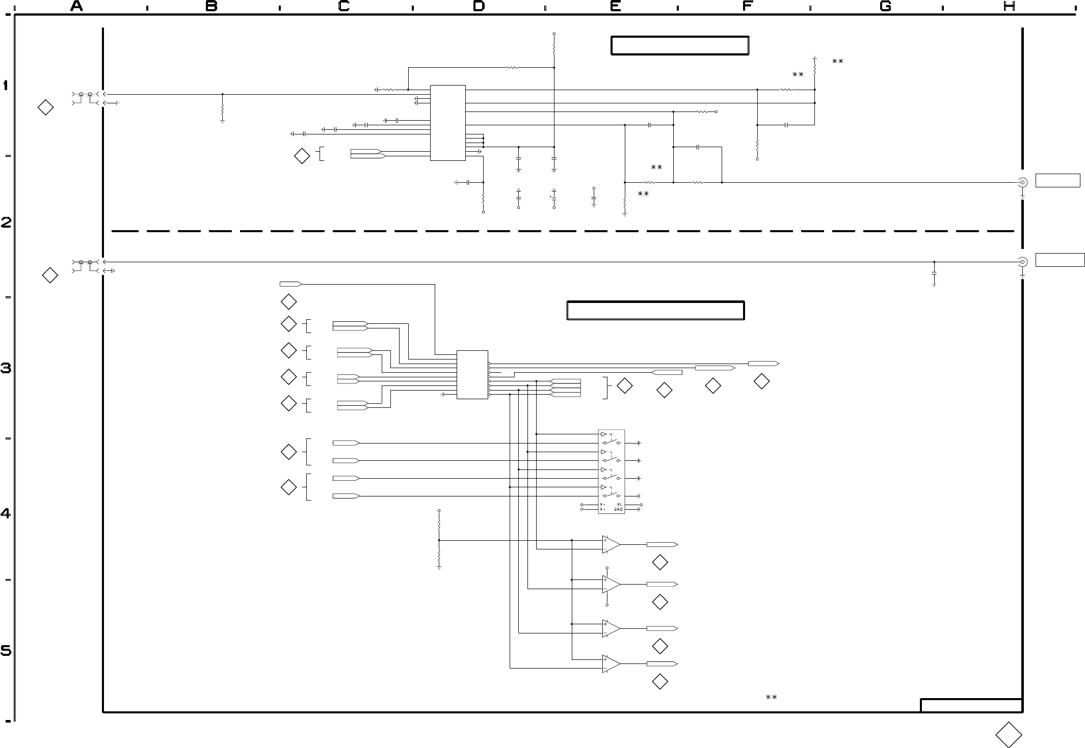
"
&
%"#$#'$
"
"
#"$"
"
"
!#)
'
,
,
,
"#$
"#$
%
%
,
!
%$
&
%$
&
&
&
&
&
&
%
#'
,
"
,
+
&
&
"
+
"
*
"
+
!#)
$#$#
+
"
&
"
"
,
&
,
&
&
"
,
,
$#$#
'
#"$"
"
#)
#)
($
#)
#)
%
%
%
%
%
%
%
#)
#)
#)
#)
%
&
%
%
%
%
! %! $"
#)
%
#)(
%
!
!
!
!
!
!
!
%
($
#
#
%
%
%
%
%
%
&
"
"
&&
&
!
&
"
%
%
&
"
"
"
%
%
VITS 200 REV OCT 1992 BLACK BURST, CLAMP CONTROL
#"%""#
#!"$##$ """&%# $
P/O A3 CONTROLLER BOARD
671–2131–00 – 01
6

VITS 200
C75 A5 N2
C76 A5 M2
C77 A5 M2
C78 B5 K2
C80 B5 L3
C81 B5 L3
C82 B5 N3
C83 C5 N4
C84 C5 M5
C85 C5 L5
C87 D5 J3
C88 D5 I3
C89 D5 I3
C90 E5 G2
C91 E5 H3
C92 E5 I4
C93 E5 J4
C94 F5 J5
C95 F5 I5
C96 F5 J2
C97 G5 I1
C98 G5 I2
C99 G5 F2
C100 H5 E2
C101 C4 K6
C102 C4 K6
C103 A3 K6
C104 B4 K6
C105 B4 K6
C106 D4 K6
C107 C4 K6
C108 B4 K6
C109 B4 K6
C111 A5 B4
C112 A5 B5
C113 A5 C6
C114 B5 C7
C115 D5 C7
C116 D5 C6
C117 D5 D5
C118 E5 C4
C119 B5 G8
C120 B5 F7
C121 C5 G5
C122 C5 G4
C123 H5 L4
C124 H5 N6
C125 E5 D5
C142 D5 K6
C143 C5 K6
C144 C5 L7
C145 C5 L7
C146 C5 L7
C149 B5 L7
CR2 C3 J5
CR3 C3 J5
CR4 C4 K7
CR5 F4 L7
CR6 F4 L7
Q40 F4 L7
R183 B3 J5
R184 D3 N6
R196 B4 J6
R197 D4 K7
R198 F4 M7
TP1 E5 A4
TP2 F5 A8
TP3 F5 D8
TP4 F5 E4
TP5 G5 E1
TP6 G5 J1
TP7 G5 I5
TP8 G5 J8
TP9 H5 M7
TP10 H5 O4
TP11 H5 N1
U47 F1 N6
U48 F2 L2
U50 E3 N5
U52 E1 N2
U53 E2 M2
U54 C2 I4
U61 F3 N7
U62 E4 L7
Schematic Diagram <7> Component Locator Chart
The schematic diagram has an alphanumeric grid to assist in locating parts within that diagram.
Assembly A3.
(Partial Assembly A3 also shown on schematic 1 thru 6).
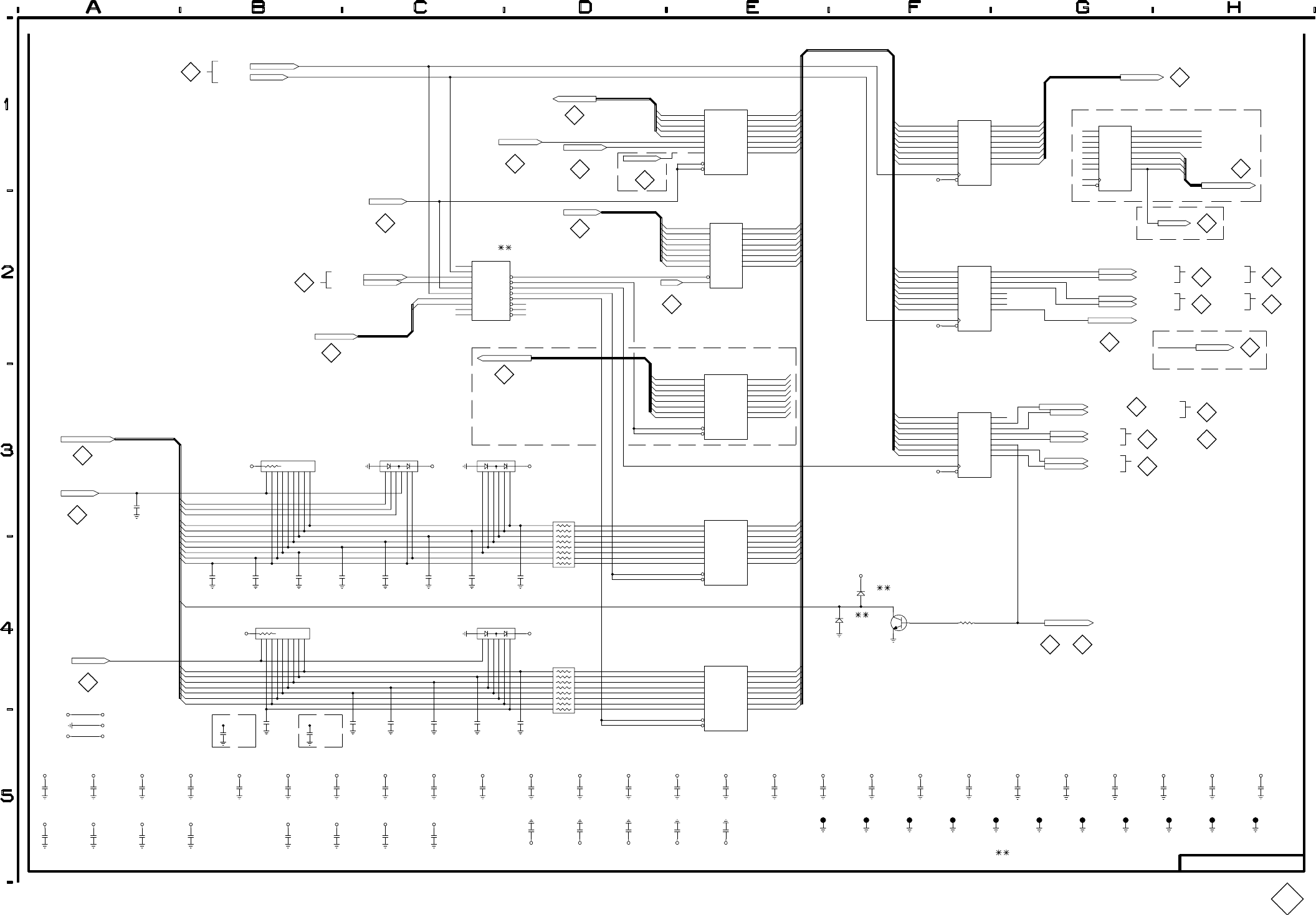
DD[0..7] DD[0..7] 5
ED[0..7]
(CLAMP)
(DISPLAY)
U21-16
U21-23
3
(FPSW)
FP[0..4]
FP[0..4]
PROGPRES
EXT1PRES
3
J17-16
5
R56
1J10-40
5
MONOCHR
671-2131-00 -01
ED0
ED1
ED2
ED3
ED4
ED5
ED6
ED7
FP0
FP1
FP2
FP3
FP4
1A1
2 1Y1 18
1A2
4 1Y2 16
1A3
6 1Y3 14
1A4
8 1Y4 12
2A1
11 2Y1 9
2A2
13 2Y2 7
2A3
15 2Y3 5
2A4
17 2Y4 3
1G
1
2G
19
U52
74ALS244
ED0
ED1
ED2
ED3
ED4
ED5
ED6
ED7
VCC
(DISPLAY)
D1
3 Q1 2
D2
4 Q2 5
D3
7 Q3 6
D4
8 Q4 9
D5
13 Q5 12
D6
14 Q6 15
D7
17 Q7 16
D8
18 Q8 19
CLK
11
CLR
1
U47
74ALS273
DD0
DD1
DD2
DD3
DD4
DD5
DD6
DD7
U48
74ALS273
D1
3 Q1 2
D2
4 Q2 5
D3
7 Q3 6
D4
8 Q4 9
D5
13 Q5 12
D6
14 Q6 15
D7
17 Q7 16
D8
18 Q8 19
CLK
11
CLR
1
CLAMP1
CLAMP2
CLAMP3
CLAMP4
DIAG0
DIAG1
DIAG2
DIAG3
671-2131-00 - 01
5
DIAG[0..3]
U56A-2
U56B-4 1
U12-15
U12-14 6
U58-7
4
U56C-10
U56D-12 2
U12-13
U12-12 6
U12-8
6
CLAMP1
CLAMP2
CLAMP3
CLAMP4
CLAMP1
CLAMP2
CLAMP3
CLAMP4
(BLANKEN)
DIAG3
U58-7
4
671-2131-00 - 01
671-2131-01
ED0
ED1
ED2
ED3
ED4
ED5
ED6
ED7
VCC
(CLAMP)
D1
3 Q1 2
D2
4 Q2 5
D3
7 Q3 6
D4
8 Q4 9
D5
13 Q5 12
D6
14 Q6 15
D7
17 Q7 16
D8
18 Q8 19
CLK
11
CLR
1
U48
74ALS273
D0
D1
D2
D3
D4
D5
D6
D7
ED0
ED1
ED2
ED3
ED4
ED5
ED6
ED7
R/W
U23-83
3
A1 2
B1
18
A2 3
B2
17
A3 4
B3
16
A4 5
B4
15
A5 6
B5
14
A6 7
B6
13
A7 8
B7
12
A8 9
B8
11
G
19
DIR
1
U53
74ALS245
D[0..7]
D[0..7]
3
(CONTROL)
(REMOTE1)
(REMOTE2)
(STAT1)
I0/CLK
1
I1
2
I2
3
I3
4
I4
5
I5
6
I6
7
I7
8
I8
9
I9
11
F0 19
F1 18
F2 17
F3 16
F4 15
F5 14
F6 13
F7 12
U54
PAL16L8
A[0..19] A[0..19]
A0
A1
U21-21
3
(REMOTE)
(STAT)
U21-20
U21-153
REM[0..15]
5
REM[0..15]
1
234567891
0
R183
2.7k
3
8 1
765432
CR2
5
8 1
765432
CR3
STAT[0..7] STAT[0..7]
671-2131-00 - 01
STAT0
STAT1
STAT2
STAT3
STAT4
STAT5
STAT6
STAT7
(STAT1)
(STAT1)
ED0
ED1
ED2
ED3
ED4
ED5
ED6
ED7
U51
74ALS244
1A1
2 1Y1 18
1A2
4 1Y2 16
1A3
6 1Y3 14
1A4
8 1Y4 12
2A1
11 2Y1 9
2A2
13 2Y2 7
2A3
15 2Y3 5
2A4
17 2Y4 3
1G
1
2G
19
ED0
ED1
ED2
ED3
ED4
ED5
ED6
ED7
D1
3 Q1 2
D2
4 Q2 5
D3
7 Q3 6
D4
8 Q4 9
D5
13 Q5 12
D6
14 Q6 15
D7
17 Q7 16
D8
18 Q8 19
CLK
11
CLR
1
U61
74ALS273
FPBYPASS
GLSEL1
REMIND
J17-11
J17-10 5
(INHIBIT)
U59-3
J17-14 5
LINESEL
U58-6 4
U61-12
J10-37
R185 5
U12-9
6
GLSEL0
(RESYNC)
VCC
(CONTROL)
+5V
CR6
ED0
ED1
ED2
ED3
ED4
ED5
ED6
ED7
(REMOTE1)
(REMOTE1)
1A1
2 1Y1 18
1A2
4 1Y2 16
1A3
6 1Y3 14
1A4
8 1Y4 12
2A1
11 2Y1 9
2A2
13 2Y2 7
2A3
15 2Y3 5
2A4
17 2Y4 3
1G
1
2G
19
U50
74ALS244
+5V
1 16
2 15
3 14
4 13
5 12
6 11
7 10
8 9
R184
220
C101
0.1uF
C106
0.1uF
+5V
C104
0.1uF
C109
0.1uF
C102
0.1uF
C107
0.1uF
REM0
REM1
REM2
REM3
REM4
REM5
REM6
REM7
REM8
REM9
REM10
+5V
C103
0.1uF
C108
0.1uF
C105
0.1uF
(REMEN)
J12-25
5
RBYPASS
J12-20
5
+5V
REM8
REM9
REM10
REM11
REM12
REM13
REM14
REM15
+5V 1
234567891
0
R196
2.7k
VCC
+5V
1 16
2 15
3 14
4 13
5 12
6 11
7 10
8 9
R197
220
8 1
765432
CR4
ED0
ED1
ED2
ED3
ED4
ED5
ED6
ED7
1A1
2 1Y1 18
1A2
4 1Y2 16
1A3
6 1Y3 14
1A4
8 1Y4 12
2A1
11 2Y1 9
2A2
13 2Y2 7
2A3
15 2Y3 5
2A4
17 2Y4 3
1G
1
2G
19
U62
74ALS244
Q40 R198
4.32k
CR5 FPSTANDBY
U36-18
4
J17-12
5
TP10 TP11
C123
0.1uF
C124
0.1uF
+5V+5V
C99
0.1uF
TP6 TP7 TP8 TP9
C97
0.1uF
C98
0.1uF
C100
0.1uF
+5V+5V+5V+5V
TP2 TP3 TP4 TP5
C94
0.1uF
C95
0.1uF
C96
0.1uF
+5V+5V+5V+5V
-10V -10V
(REMOTE2)
(REMOTE2)
TP1
C118
0.1uF
C90
0.1uF
C91
0.1uF
C125
0.1uF
C92
0.1uF
C93
0.1uF
+5V+5V+5V
-10V -10V -10V
C142
0.1uF
C143
0.1uF
C85
0.1uF
C87
0.1uF
C88
0.1uF
C115
0.1uF
C116
0.1uF
C89
0.1uF
C117
0.1uF
+5V+5V+5V+5V
+12V +12V +12V +12V
C144
0.1uF
C145
0.1uF
C146
0.1uF
C81
0.1uF
C82
0.1uF
C119
0.1uF
C121
0.1uF
C122
0.1uF
C120
0.1uF
C84
0.1uF
C83
0.1uF
+5V+5V+5V+5V
C147
0.1uF
REM13
+10V +10V +10V
C112
0.1uF
C113
0.1uF
C114
0.1uF
C76
0.1uF
C77
0.1uF
C78
0.1uF
C80
0.1uF
C149
0.1uF
VEE
GND
+5V+5V+5V+5V
C148
0.1uF
REM14
671-2131-00 - 01
+10V
C111
0.1uF
C75
0.1uF
-5V
+5V
VITS 200 REV AUG 1995
NOTE:
PROCESSOR I/O
AND SERIAL NUMBER RANGES.
SEE PARTS LIST FOR EARLIER VALUES 671–2131–00 & UP
7
P/O A3 CONTROLLER BOARD
VITS 200

10–1VITS 200
Replaceable Mechanical Parts
This section contains a list of the components that are replaceable for the
VITS 200. Use this list to identify and order replacement parts. There is a
separate Replaceable Mechanical Parts list for each instrument.
Parts Ordering Information
Replacement parts are available from or through your local Tektronix, Inc., Field
Office or representative.
Changes to Tektronix instruments are sometimes made to accommodate
improved components as they become available and to give you the benefit of
the latest circuit improvements. Therefore, when ordering parts, it is important to
include the following information in your order.
HPart number
HInstrument type or model number
HInstrument serial number
HInstrument modification number, if applicable
If a part you have ordered has been replaced with a new or improved part, your
local Tektronix, Inc., Field Office or representative will contact you concerning
any change in part number.
Change information, if any, is located at the rear of this manual.
Using the Replaceable Mechanical Parts List
The tabular information in the Replaceable Mechanical Parts list is arranged for
quick retrieval. Understanding the structure and features of the list will help you
find all of the information you need for ordering replaceable parts.
The Mfg. Code Number to Manufacturer Cross Index for the mechanical parts
list is located immediately after this page. The cross index provides codes,
names, and addresses of manufacturers of components listed in the mechanical
parts list.
Abbreviations conform to American National Standards Institute (ANSI)
standard Y1.1.
Chassis-mounted parts and cable assemblies are located at the end of the
Replaceable Electrical Parts list.
Cross Index–Mfr. Code
Number to Manufacturer
Abbreviations
Chassis Parts

Replaceable Mechanical Parts
10–2 VITS 200
Column Descriptions
Items in this section are referenced by figure and index numbers to the illustra-
tions.
Indicates part number to be used when ordering replacement part from
Tektronix.
Column three (3) indicates the serial number at which the part was first used.
Column four (4) indicates the serial number at which the part was removed. No
serial number entered indicates part is good for all serial numbers.
This indicates the quantity of mechanical parts used.
An item name is separated from the description by a colon (:). Because of space
limitations, an item name may sometimes appear as incomplete. Use the U.S.
Federal Catalog handbook H6-1 for further item name identification.
Following is an example of the indentation system used to indicate relationship.
1 2 3 4 5 Name & Description
Assembly and/or Component
Mounting parts for Assembly and/or Component
*MOUNTING PARTS*/*END MOUNTING PARTS*
Detail Part of Assembly and/or Component
Mounting parts for Detail Part
*MOUNTING PARTS*/*END MOUNTING PARTS*
Parts of Detail Part
Mounting parts for Parts of Detail Part
*MOUNTING PARTS*/*END MOUNTING PARTS*
Mounting Parts always appear in the same indentation as the Item it mounts,
while the detail parts are indented to the right. Indented items are part of and
included with, the next higher indentation. Mounting parts must be purchased
separately, unless otherwise specified.
Indicates the code number of the actual manufacturer of the part. (Code to name
and address cross reference can be found immediately after this page.)
Indicates actual manufacturer’s part number.
Figure & Index No.
(Column 1)
Tektronix Part No.
(Column 2)
Serial No.
(Column 3 and 4)
Qty (Column 5)
Name and Description
(Column 6)
Mfr. Code
(Column 7)
Mfr. Part Number
(Column 8)

Replaceable Mechanical Parts
VITS 200 10–3
Cross Index – Mfr. Code Number To Manufacturer
Mfr.
Code Manufacturer Address City, State, Zip Code
TK0435 LEWIS SCREW CO 4300 S RACINE AVE CHICAGO IL 60609–3320
TK0941 BEARINGS INC (DIST) 2720 NW 29TH
PO BOX 3005 PORTLAND OR 97210–1702
TK1465 BEAVERTON PARTS MFG CO 1800 NW 216TH AVE HILLSBORO OR 97124–6629
TK1947 NORTHWEST ETCH TECHNOLOGY 2601 S HOOD ST
PO BOX 110610 TACOMA, WA 98411–0610
TK2402 PANEL VIEW 2900 sw 219th
SUITE 761 HILLSBORO, OR 97123
TK2548 XEROX BUSINESS SERVICES
DIV OF XEROX CORPORATION 14181 SW MILLIKAN WAY BEAVERTON OR 97077
0J4C1 TVT DIECASTING AND MFG INC 7330 SW LANDMARK LANE PORTLAND OR 97223
0J9P4 DELTA ENGINEERING 19500 SW TETON TUALATIN OR 97062
0KBZ5 MORELLIS Q & D PLASTICS 1812 16TH AVE FOREST GROVE OR 97116
0KB01 STAUFFER SUPPLY 810 SE SHERMAN PORTLAND OR 97214
06666 GENERAL DEVICES CO INC 1410 S POST RD
PO BOX 39100 INDIANAPOLIS IN 46239–9632
09422 PLASTIC STAMPING CORP 2216 W ARMITAGE AVE CHICAGO IL 60647–4461
2W944 PAPST MECHATRONIC CORP AQUIDNECK INDUSTRIAL PK NEWPORT RI 02840
4T165 NEC ELECTRONICS USA INC
ELECTRON DIV 475 ELLIS ST
PO BOX 7241 MOUNTAIN VIEW CA 94039
73743 FISCHER SPECIAL MFG CO 111 INDUSTRIAL RD COLD SPRING KY 41076–9749
80009 TEKTRONIX INC 14150 SW KARL BRAUN DR
PO BOX 500 BEAVERTON OR 97077–0001
80126 PACIFIC ELECTRICORD CO 747 W REDONDO BEACH
PO BOX 10 GARDENA CA 90247–4203

Replaceable Mechanical Parts
10–4 VITS 200
Replaceable Mechanical Parts
Fig. &
Index
No. Tektronix
Part No. Serial Number
Effective Dscont Qty
Name & Description Mfr.
Code Mfr. Part No.
1–1 200–3972–00 1 COVER,TOP:ALUMINUM
*MOUNTING PARTS* 0J9P4 200–3972–00
–2 211–0538–00 12 SCREW,MACHINE:6–32 X 0.312,FLH,100 DEG,STL
*END MOUNTING PARTS* TK0435 ORDER BY DESC
–3 367–0437–03 1 HANDLE:ALUMINUM
*MOUNTING PARTS* 0J4C1 367–0437–03
–4 211–0538–00 2 SCREW,MACHINE:6–32 X 0.312,FLH,100 DEG,STL
*END MOUNTING PARTS* TK0435 ORDER BY DESC
–5 367–0437–01 1 HANDLE:ALUMINUM
*MOUNTING PARTS* 0J4C1 367–0437–01
–6 211–0538–00 2 SCREW,MACHINE:6–32 X 0.312,FLH,100 DEG,STL
*END MOUNTING PARTS* TK0435 ORDER BY DESC
–7 213–0940–00 1 THUMBSCREW:10–32 X 1.15,0.375 OD,SST 80009 213094000
–8 210–0894–00 1 WASHER,FLAT:0.19 ID X 0.438 OD X 0.031 POLTHN 09422 ORDER BY DESC
–9 354–0025–00 1 RING,RETAINING:EXTERNAL,U/O 0.187 DIA SFT TK0941 555–18MI
–10 426–2434–01 1 FRAME,FRONT:ALUMINUM
*MOUNTING PARTS* 80009 426243401
–11 211–0541–00 3 SCREW,MACHINE:6–32 X 0.25,FLH,100 DEG,STL
*END MOUNTING PARTS* TK0435 ORDER BY DESC
–12 ––––––––––– 1 CIRCUIT BD ASSY:FRONT PANEL
(SEE A2 REPL)
*MOUNTING PARTS*
–13 211–0012–00 6 SCREW,MACHINE:4–40 X 0.375,PNH,STL
*END MOUNTING PARTS* TK0435 ORDER BY DESC
–14 ––––––––––– 1 DISPLAY,FLAT PL:VACUUM FLOURESCENT,2 X 40;ALPHA-
NUMERIC,5 X 7 DOT MATRIX,DC/DC AC CONVERT,CHAR
GEN, LOGIC & MICRO COMP
(SEE A4 REPL)
*MOUNTING PARTS*
–15 211–0012–00 4 SCREW,MACHINE:4–40 X 0.375,PNH,STL
*END MOUNTING PARTS* TK0435 ORDER BY DESC
–16 378–0384–00 1 FILTER,DISPLAY:ACRYLIC,BLUE TK2402 378–0384–00
–17 337–3845–00 1 SHIELD,ELEC:PLASTIC 0KBZ5 337–3845–00
–18 333–3956–00 1 PANEL,FRONT:VITS200 0J9P4 333–3956–00
–19 337–3846–00 1 SHIELD,ELEC:POWER SUPPLY
*MOUNTING PARTS* 80009 337384600
–20 211–0244–00 3 SCR,ASSY WSHR:4–40 X 0.312,PNH,STL,CD PL,POZ,MACH
*END MOUNTING PARTS* TK0435 7772–312
–21 ––––––––––– 1 CIRCUIT BD ASSY:INSERTER
(SEE A1 REPL)
*MOUNTING PARTS*
–22 211–0244–00 7 SCR,ASSY WSHR:4–40 X 0.312,PNH,STL,CD PL,POZ,MACH TK0435 7772–312
–23 220–0497–00 3 NUT,PLAIN,HEX:0.5–28 X 0.562 HEX,BRS CD PL 73743 ORDER BY DESC
–24 210–1039–00 3 WASHER,LOCK:0.521 ID,INT,0.025 THK,SST 0KB01 1224–02–00–0541
–25 211–0014–00 2 SCREW,MACHINE:4–40 X 0.5,PNH,STL TK0435 ORDER BY DESC
–26 337–3796–00
337–3796–01 B010100
B020791 B020790 1
1SHIELD,ELEC:LINE FILTER,ALUMINUM
SHIELD,ELEC:0.032 BRASS,C26000,0.5 HARD
*END MOUNTING PARTS*
TK1947
80009 337–3796–00
337379601
–27 131–3573–00 1 CONN,PLUG,ELEC:MALE,W/LOCKING ADAPTER 80126 B–0779
–28 337–3844–00 1 SHIELD,ELEC:POWER SUPPLY,PLASTIC 80009 337384400
–29 ––––––––––– 1 CIRCUIT BD ASSY:CONTROLLER
(SEE A3 REPL)
*MOUNTING PARTS*
–30 211–0244–00 9 SCR,ASSY WSHR:4–40 X 0.312,PNH,STL,CD PL,POZ,MACH TK0435 7772–312
–31 220–0497–00 6 NUT,PLAIN,HEX:0.5–28 X 0.562 HEX,BRS CD PL 73743 ORDER BY DESC

Replaceable Mechanical Parts
VITS 200 10–5
Fig. &
Index
No. Mfr. Part No.
Mfr.
Code
Name & Description
Qty
Serial Number
Effective Dscont
Tektronix
Part No.
–32 210–1039–00 6 WASHER,LOCK:0.521 ID,INT,0.025 THK,SST
*END MOUNTING PARTS* 0KB01 1224–02–00–0541
–33 407–4134–00 1 BRKT,FAN,MTG:SPG1000
*MOUNTING PARTS* 80009 407413400
–34 211–0538–00 2 SCREW,MACHINE:6–32 X 0.312,FLH,100 DEG,STL
*END MOUNTING PARTS* TK0435 ORDER BY DESC
–35 ––––––––––– 1 FAN,TUBEAXIAL:12 VDC,2.6W,0.22A,4200 RPM,32DB,
16.6CFM,60X60MM,25MMTHICK,W/288MM LEADS &
SLEEVE,W/CONNECT,FBA TYPE
(SEE B100 REPL)
–36 211–0619–00 2 SCREW,MACHINE:6–32 X 1.5,FLH,100 DEG,STL CDPL,POZ TK0435 ORDER BY DESC
–37 210–0457–00 2 NUT,PL,ASSEM WA:6–32 X 0.312,STL CD PL
*END MOUNTING PARTS* TK0435 ORDER BY DESC
–38 351–0104–03 1 SL SECT,DWR EXT:12.625 L,W/O HARDWARE
*MOUNTING PARTS* 06666 C–720–3 (WITHOU
–39 212–0004–00 8 SCREW,MACHINE:8–32 X 0.312,PNH,STL
*END MOUNTING PARTS* TK0435 ORDER BY DESC
–40 200–3973–00
200–3973–01 B010100
B020249 B020248 1
1COVER,BOTTOM:ALUMINUM,PAN
COVER,BOTTOM:ALUMINUM,PAN
STANDARD ACCESSORIES
0J9P4
80009 200–3973–00
200397301
–41 161–0216–00
070–8332–04
351–0751–01
351–0859–00 B010100
B020336 B020335
1
1
1
1
CABLE ASSY,PWR:3,18 AWG,2.5M L,BLACK
MANUAL,TECH:INSTRUCTION,VITS200
TRK,SL OUT SECT:STA & INTERMEDIATE SAF CONT
TRK SL OUT SECT:STA & INTERMEDIATE SAF CONT
80126
TK2548
06666
06666
C7120–25M–BL
070833204
CC3442–99–0006
CC3442–99–0005

Replaceable Mechanical Parts
10–6 VITS 200

Index

VITS 200 Index–1
Index
%+645.&/5 30$&%63&4
&$0..&/%&% 26*1.&/5 *45
44&.#-: 6.#&3*/( 306#-&4)005*/( *%4
650."5*$ ! &5&$5*0/
-"$, 6345 &/&3"- 1&$*'*$"5*0/4
:1"44
)"3"$5&3 "/% 063$& &/&3"5*0/ )&03: 0'
1&3"5*0/
*3$6*5 0"3% --6453"5*0/4 306#-&4)005*/( *%4
*3$6*5 6.#&3*/( 306#-&4)005*/( *%4
-04&% "15*0/ &5&$5*0/
0/530--&3 )&03: 0' 1&3"5*0/
033&$5*7& "*/5&/"/$&
#5"*/*/( &1-"$&.&/5 "354
&1-"$*/( *3$6*5 44&.#-*&4
0326& 1&$*'*$"5*0/4
63403 0/530-
&$3&.&/5 6550/
*"(/045*$4
*"(3".4 306#-&4)005*/( *%4
/"#-& 6550/
/7*30/.&/5"- 1&$*'*$"5*0/4
95&3/"- /1654
1&$*'*$"5*0/4
)&03: 0' 1&3"5*0/
0-%065 "(&4 306#-&4)005*/( *%4
30/5 "/&-
&.07"-
)&03: 0' 1&3"5*0/
30/5 "/&- *4"#-&
30/5 "/&- &.07"-
03&"/
)*--*14
&/-0$,
1&$*'*$"5*0/4
)&03: 0' 1&3"5*0/
/$3&.&/5 6550/
/4&35&-&5& 6/$5*0/4
/45"--"5*0/
-&$53*$"-
&$)"/*$"-
"$, 06/5*/(
/4536.&/5 0/'*(63"5*0/
&/64
5"/%#:
5"/%#: &44"(&
&45 *(/"-
5*-*5*&4
! &44"(&
!
#5"*/*/( &1-"$&.&/5 "354 033&$5*7& "*/5&;
/"/$&
15*0/4
15*0/
15*0/
"$,"(*/(
&3'03."/$& !&3*'*$"5*0/
"-*#3"5*0/ "5" &1035
03.
&$0..&/%&% 26*1.&/5 *45
69*-*"3: 26*1.&/5
-&$53*$"- /4536.&/54
!&3*'*$"5*0/ 30$&%63&
):4*$"- 1&$*'*$"5*0/4
08&3
08&3 611-: 1&$*'*$"5*0/4
08&3 611-: &5"*-&% &4$3*15*0/ )&03: 0' 1;
&3"5*0/
08&3 611-: 7&37*&8 )&03: 0' 1&3"5*0/
3&7&/5*7& "*/5&/"/$&
-&"/*/(
5"5*$ &/4*5*7& 0.10/&/54
30%6$5 &4$3*15*0/
650."5*$ ! &5&$5*0/
-04&% "15*0/ &5&$5*0/
/4&35&-&5& 6/$5*0/4
30(3". )"//&-
&.05& 0/530-
063$& %&/5*'*$"5*0/
&45 *(/"- &/&3"503
&95 &/&3"503
!*%&0 -"1#0"3%

Index
Index–2 VITS 200
Program Channel, 1-3
Specifications, 3-1
Rack Mounting, 1-7
Remote Control, 2-17
Connector, 2-17
Remote Controls, Theory of Operation, 4-9
Replacing Circuit Assemblies, Corrective MainteĆ
nance, 7-7
RSĆ232, 2-22
Commands, 2-25
Hardware & Software Requirements, 2-24
SCPI Commands, 2-32
Save/Recall Button, 2-4
Signal and Switching Control, Theory of Operation,
4-5
Source Identification, 1-4
Specifications, 3-1
Black Burst General, 3-3
Environmental, 3-18
External Inputs, 3-2
Genlock, 3-16
Physical, 3-17
Power Supply, 3-16
Program Channel, 3-1
Test Signal, 3-4
Test Signal General, 3-3
Standby Menu, 2-7
Standby Message Menu, 2-11
Test Selectable Parts, 7-8
Test Signal
General Specifications, 3-3
Generation, Theory of Operation, 4-1
Generator, 1-1
Menu, 2-8
Specifications, 3-4
Text Generator, 1-3
Theory of Operation, 4-1
Character and Source ID Generation, 4-7
Controller, 4-11
External Inputs, 4-4
Front Panel, 4-9
Genlock, 4-3
Power Supply
Detailed Description, 4-13
Overview, 4-12
Remote Controls, 4-9
Signal and Switching Control, 4-5
Test Signal Generation, 4-1
Torque Specifications, Corrective Maintenance, 7-6
Troubleshooting Aids, 7-2
Assembly & Circuit Numbering, 7-3
Circuit Board Illustrations, 7-3
Diagrams, 7-3
Foldout Pages, 7-2
Unlocked LED, 2-3
Utilities Menu, 2-12
VBI Message Menu, 2-9
Video Clapboard, 2-20
VITS Menu, 2-6
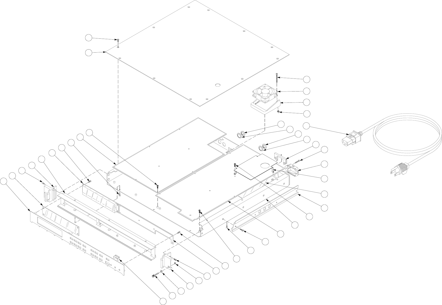
VITS 200
FIG. 1 EXPLODED VIEW
A1
A3
A4
A2
