Current Shunt Monitors (Rev. A) TEXAS MONITOR GUIDE
User Manual:
Open the PDF directly: View PDF ![]() .
.
Page Count: 7
2014www.ti.com/currentshuntmonitor
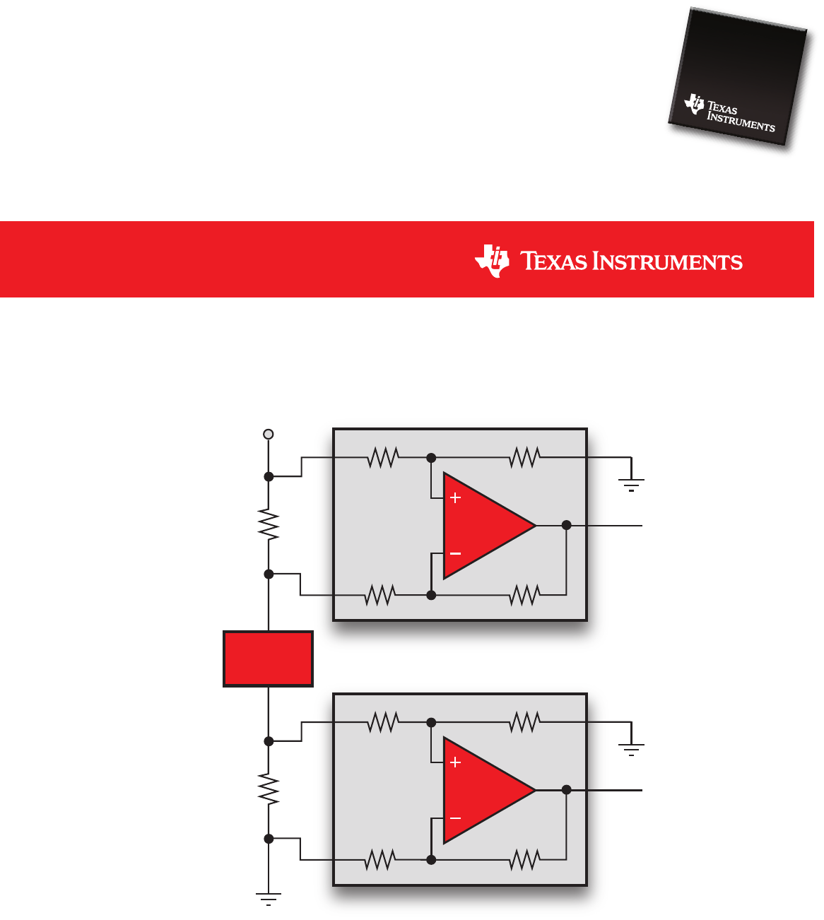
Current Shunt Monitors
Load
High-Side
Sensing
Power
Supply
Low-Side
Sensing
VOUT
VOUT
Current
Shunt

Current Shunt Monitors
Current Shunt Monitors Texas Instruments 2014
•
Current shunt monitors are also
referred to as current sense amplifiers.
•
Current shunt monitors are designed
to monitor the current flow by
measuring the voltage drop across a
resistor placed in the current path.
•
Current sense amplifiers tend to be
easier to design, more precise, less
prone to noise and lower cost than
magnetic current sensors.
Current to be
measured
Current to be
measured
RSHUNT Voltmeter
V
Common Mode Range:
This specification defines the DC
voltage range at the input of an
amplifier with respect to ground.
Current shunt monitors are typically
designed to accept common mode
voltages well beyond the chip supply
voltage. For example, the INA282
is capable of accepting a common
mode voltage from -14V to +80V while
running on a supply as low as 2.7V.
Offset Voltage:
The differential DC error at the input
of the amplifier. Historically, to reduce
the impact of amplifiers with high
offsets, larger shunt resistors are used
to increase the measured voltage
drop. Today, TI is able to offer current
sensing solutions with offsets as low
as 10µV, enabling higher precision
measurements at low currents and the
use of smaller shunt resistances for
improved system efficiency.
CMRR
(Common Mode Rejection Ratio):
CMRR is the ability of the amplifier
to reject signals common to the
differential inputs. This is important
in the ability to measure small signals
superimposed upon a large voltage.
TI’s portfolio offers solutions with
CMRR as high as 140dB.
Digital Output: Simple all-in-one solution integrating the
ADC/MUX with programmable switching. Provides
measurements in amps, volts and watts across the I2C
interface for a complete power monitoring solution.
GND
VBUS
V
I
VIN+
VIN
I C
Interface
2
SDA
SCL
A0
A1
Alert Register
Alert
Voltage Register
Current Register
ADC
Power Register
VREF
VOUT
VIN+
VIN-
Voltage Output: High precision, lowest power and
industry’s smallest form factors. Fixed gain options
ranging from 14V/V to 1000V/V. Variable gain may be
set through an external resistor.
Current Output: Variable gain set through
external resistor. Highest bandwidth options.
VOUT
VIN+
VIN-
2
Output Types
Key Parameters
What are Current Shunt Monitors?
Current Shunt Monitors Texas Instruments 2014
LOAD
–5V
+5V
+5V
I2C
FS = 0.2V
G = 4
3kΩ
1kΩ
RS
50mV
Shunt
RPD
(1)
49 .9 kΩ
OPA335
ADS1114
-
+
Power
Supply
PGA Gain = 16
256V FS
Note: (1) Pull-down resistor to
allow accurate swing to OV.
Advantages:
• Typically only requires an op amp
such as OPA335
• Straightforward, easy
• Inexpensive
Disadvantages:
• Undesirable resistance in the load’s
ground path
• Cannot detect fault conditions
(short/open circuits)
• Requires precision external
components to achieve and
maintain high accuracy
Advantages over op amps as a
low-side monitor:
• Integrated gain resistors
• Excellent matching that requires
more expensive external precision
resistors with an op amp approach
• Integrated resistors approach
reduces board space requirements
Disadvantages over op amps:
• Fixed gain settings reduce flexibility
in maximizing the full-scale range of
the following ADC stage
Low-side current sensing techniques connect the current sense element
between the load and ground.
When to choose low-side sensing: Always choose low-side sensing if the
system can tolerate disturbances on the ground path.
High-side monitors are designed
to accommodate input voltages
that exceed the power supply
voltage. However, many of our
current shunt monitors have
common-mode ranges that include
or even go below ground. This
makes them excellent low-side
current shunt monitors as well.
Advantages:
• Eliminates ground disturbances
associated with low-side sensing
• Able to detect fault conditions
Disadvantages:
• Difficult to use standard op amp.
Resistors must be precisely matched
to obtain acceptable common mode
rejection ratios (CMRR)
• A 0.01% deviation in resistor
value lowers the CMRR to 86dB
approach
• A 0.1% deviation in resistor value
lowers the CMRR to 66dB
• A 1% deviation in resistor value
lowers the CMRR to 46dB
• Must withstand very high, dynamic
changes in common mode voltage
High-side current sensing techniques connect the current sense element
between the supply and the load.
When to choose high-side sensing:
• System cannot tolerate ground disturbance of low side sensing
• System needs to be able to identify shorts to ground
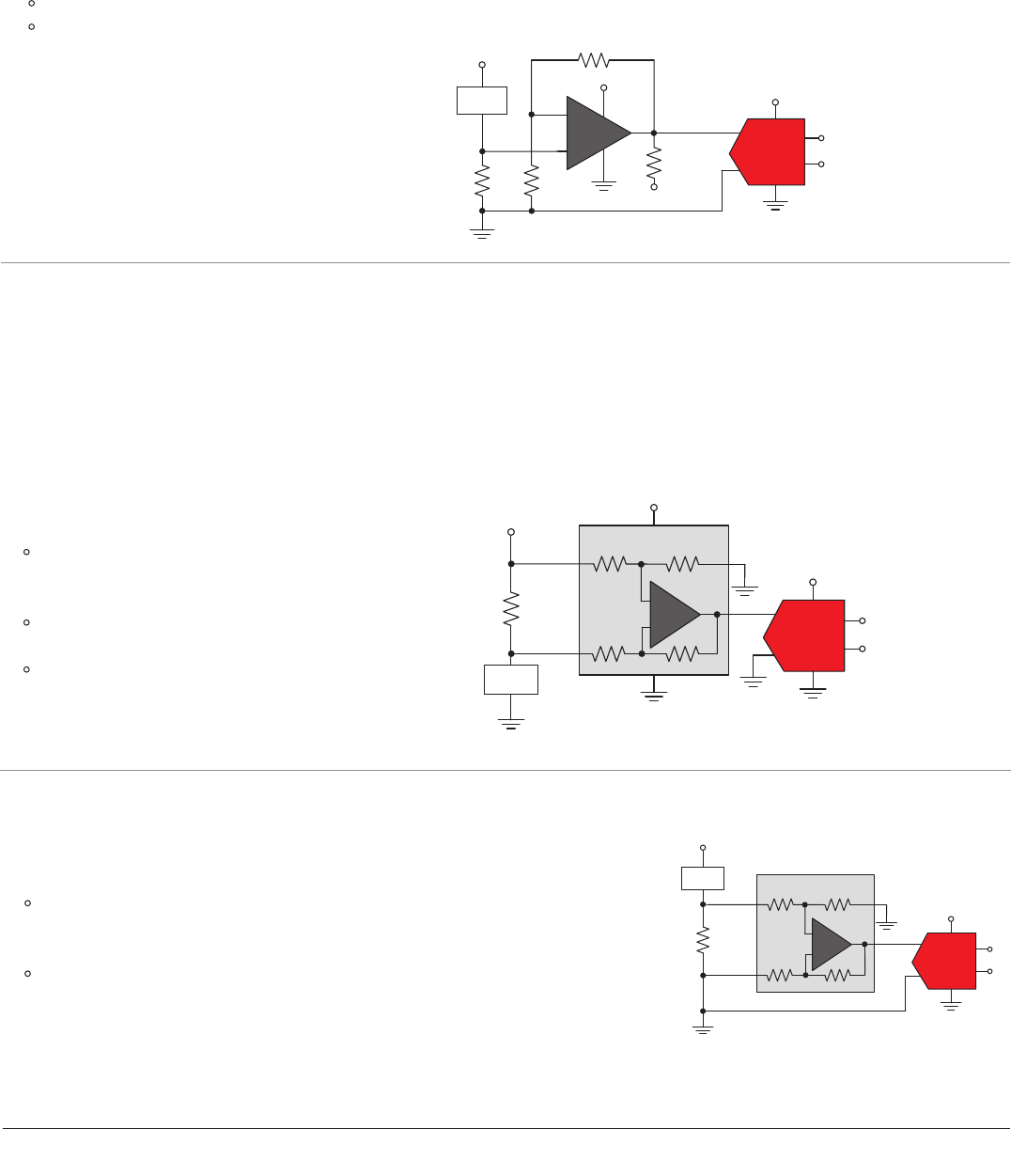
LOAD
+5V
Power
Supply
I2C
RS
ADS1114
-
+
INA 210
+5V
High-Side
Sensing
3
High-Side Measurements
Low-Side Measurements With a High-Side Monitor
Current Shunt Monitors
Low-Side Measurements
LOAD
I2C
RS
20mV
Shunt
ADS1114
Power Supply
PGA Gain = 1
4.096V FS
INA210
-
+
+5V
Current Shunt Monitors Texas Instruments 2014
Current Shunt Monitors
4
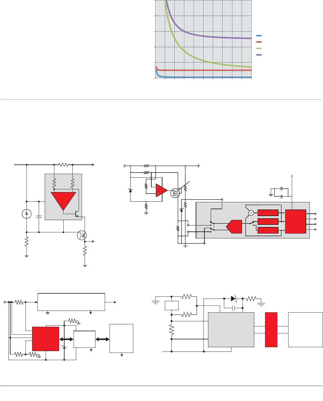
• For small differential signals at the
input, the error is dominated by the
amplifier’s offset voltage. Low input
offsets are critical to achieving
accurate measurements at the low
end of the dynamic range.
• For large differential signals at the
input, the error is dominated by the
amplifier’s gain error.
0%
2%
4%
6%
8%
10%
0 10 20 30 40 50 60 70 80 90 100
Total Error %
Differential Voltage (mV)
Total Error vs. Differential Input Voltage
10µV; 0.1%
10µV; 1%
1mV; 1%
1mV; 5%
Offset; Gain Error
Extending the Common Mode Range
Example 1: MOSFET and Zener
GND
V+
VIN -
V
DZ1
39V
zener
Q1
BSS92
OUT
1
5
2
3 4
R
0.1Ω
S
VIN +
RL
Supply
+160 to
+200V
R1
330kΩ
C1
0.1µF
5kΩ 5kΩ
OUT
50kΩ
(1V at 1A)
IC1 INA168
(200 µA/V)
Load
Up to 1A
+ -
Intermediate
Power Bus
LMP92064
RSENSE
VIN
SPI Bus
GND
VDD
–48V
SPI Bus
INCP
INCN
INVG
INVP
System
Management
Controller
Digital
Isolators
Isolated
Power
Converter
Example 3: Isolated SPI Interface Example 4: Isolated I2C Interface
Example 2: Current Follower
With additional circuitry, current shunts can be configured to operate beyond the specified common mode range by
using one of the following techniques.
Total Error
From
Supply Load
10kΩ
Data
(SDA)
Clock
(SCL)
Two-Wire
Interface
VIN+
ADC
INA220
GND
A0
A1
VIN-
VS (Supply Voltage)
VBUS
RG
10µF
0.1µF
+3.3V to +5V
V
I
OPA333
100Ω
35.7kΩ
13.7kΩ
Shunt
RSHUNT
5.1V
Zener
24V
Tranzorb
RL
Voltage Register
Current Register
Power Register
MOSFET rated to
standoff supply voltage
such as BSS84 for
up to 50V
(Bus Voltage Input)
100Ω
+5V Zener RZ
I2C I2C
ISO1541
–48V
RSENSE
I2C
System
Management
Controller
INA220
LOAD
VS
VBUS
V+
V–
GND

INA226: Highest precision solution on
the market
• Integrated ADC and MUX with
programmable sampling
• Common mode range = 0V to 36V
• Offset (max) = 10µV
• Gain error (max) = 0.1%
• CMRR (typ) = 140dB
• Lower cost alternative: INA219,
INA230
INA210: Precision voltage output
• Gain options: 50V/V, 100V/V,
200V/V, 500V/V, 1000V/V
• Common mode range: –0.3V to 26V
• Offset (max) = 35µV
• Gain error (max) = 1%
• CMRR (typ) = 140dB
• Lower cost alternative: INA199
INA216: Designed for portable battery
powered applications
• Gain options: 25V/V, 50V/V, 100V/V,
200V/V
• Common mode range = 1.8V to 5.5V
• Offset (max) = 75µV
• Gain error (max) = 0.2%
• Quiescent current = 25µA
• CMRR (typ) = 108dB
• 0.76 x 0.76mm WCSP or QFN
package available
INA3221: Triple-channel digital shunt
and bus voltage monitor
• Integrated ADC and MUX with
programmable sampling
• Common mode range = 0V to 26V
• Offset error (max) = 80µV
• Gain error (max): 0.5%
• Quiescent current = 450µA
INA282: Widest common mode
range + precision
• Common mode range = -14V to 80V
• Offset (max) = 70µV
• Offset drift (max) = 1.5µV/ºC
• Gain error (max) = 1.4%
• CMRR (typ) = 140dB
• Lower cost alternative: INA193,
LMP8601
LMP8640: High bandwidth and
high voltage
• Bandwidth = 950kHz
• Common mode range: -2V to 76V
• Offset (max) = 900µV
• Gain error = 0.25%
• CMRR (min) = 103dB
• Lower cost alternative: LMP8645
AMC1200: 4kV isolated amplifier
• Offset (max) = 1.5mV
• Offset drift (max) = 10µV/K
• Gain error (max) = 1%
• CMRR (typ) = 108dB
LMP8481: High voltage
• Bandwidth = 270kHz
• Common mode range = 4.0V to 76V
• Offset (max) = 400µV
• Gain error (max) = 1.2%
• CMRR (typ) = 124dB
• Lower cost alternative: LMP8480
LMP92064: Simultaneous sampling
current/voltage monitor
• 125ksamples/sec
• Bandwidth = 70kHz
• Offset (max) = 60µV
• Gain error (max) = 0.75%
Applications:
• Battery gauge:
(Coulomb Counting)
• Power supplies
• Inductive charging
• Graphics cards
• Desktops / laptops / servers
• Tablets / E-books
• Smartphones & feature phones
• Basestations
• Networking
• Industrial automation
• Automotive
• Medical
• Motor control
• Battery backups
• Inverters
• Solar
INA225: Programmable gain,
zero-drift current sense amplifier
• 4-pin selectable gain settings
• Bandwidth = 100kHz @ 100V/V
• Offset (max) = 125µV
• Gain error (max) = 0.50%
INA300: Over current detector
• Input/output response time = 10µs
• Programmable threshold:
0 to 250mV
• Hysteresis of 2, 5, or 10mV
Current Shunt Monitors Texas Instruments 2014
Current Shunt Monitors
Featured Products
5

SLYB194A
© 2014 Texas Instruments Incorporated
The platform bar and E2E are trademarks of Texas Instruments. All other trademarks
are the property of their respective owners.
TI Worldwide Technical Support
Internet
TI Semiconductor Product Information Center
Home Page
support.ti.com
TI E2E™ Community Home Page
e2e.ti.com
Product Information Centers
Americas Phone +1(512) 434-1560
Brazil Phone 0800-891-2616
Mexico Phone 0800-670-7544
Fax +1(972) 927-6377
Internet/Email support.ti.com/sc/pic/americas.htm
Europe, Middle East, and Africa
Phone
European Free Call 00800-ASK-TEXAS
(00800 275 83927)
International +49 (0) 8161 80 2121
Russian Support +7 (4) 95 98 10 701
Note: The European Free Call (Toll Free) number is not active in
all countries. If you have technical difficulty calling the free call
number, please use the international number above.
Fax +(49) (0) 8161 80 2045
Internet www.ti.com/asktexas
Direct Email asktexas@ti.com
Japan
Fax International +81-3-3344-5317
Domestic 0120-81-0036
Internet/Email International support.ti.com/sc/pic/japan.htm
Domestic www.tij.co.jp/pic
Asia
Phone Toll-Free Number
Note: Toll-free numbers may not support
mobile and IP phones.
Australia 1-800-999-084
China 800-820-8682
Hong Kong 800-96-5941
India 000-800-100-8888
Indonesia 001-803-8861-1006
Korea 080-551-2804
Malaysia 1-800-80-3973
New Zealand 0800-446-934
Philippines 1-800-765-7404
Singapore 800-886-1028
Taiwan 0800-006800
Thailand 001-800-886-0010
International +86-21-23073444
Fax +86-21-23073686
Email tiasia@ti.com or ti-china@ti.com
Internet support.ti.com/sc/pic/asia.htm
A021014
Important Notice: The products and services of Texas Instruments
Incorporated and its subsidiaries described herein are sold subject to TI’s
standard terms and conditions of sale. Customers are advised to obtain the
most current and complete information about TI products and services
before placing orders. TI assumes no liability for applications assistance,
customer’s applications or product designs, software performance, or
infringement of patents. The publication of information regarding any other
company’s products or services does not constitute TI’s approval, warranty
or endorsement thereof.

IMPORTANT NOTICE
Texas Instruments Incorporated and its subsidiaries (TI) reserve the right to make corrections, enhancements, improvements and other
changes to its semiconductor products and services per JESD46, latest issue, and to discontinue any product or service per JESD48, latest
issue. Buyers should obtain the latest relevant information before placing orders and should verify that such information is current and
complete. All semiconductor products (also referred to herein as “components”) are sold subject to TI’s terms and conditions of sale
supplied at the time of order acknowledgment.
TI warrants performance of its components to the specifications applicable at the time of sale, in accordance with the warranty in TI’s terms
and conditions of sale of semiconductor products. Testing and other quality control techniques are used to the extent TI deems necessary
to support this warranty. Except where mandated by applicable law, testing of all parameters of each component is not necessarily
performed.
TI assumes no liability for applications assistance or the design of Buyers’ products. Buyers are responsible for their products and
applications using TI components. To minimize the risks associated with Buyers’ products and applications, Buyers should provide
adequate design and operating safeguards.
TI does not warrant or represent that any license, either express or implied, is granted under any patent right, copyright, mask work right, or
other intellectual property right relating to any combination, machine, or process in which TI components or services are used. Information
published by TI regarding third-party products or services does not constitute a license to use such products or services or a warranty or
endorsement thereof. Use of such information may require a license from a third party under the patents or other intellectual property of the
third party, or a license from TI under the patents or other intellectual property of TI.
Reproduction of significant portions of TI information in TI data books or data sheets is permissible only if reproduction is without alteration
and is accompanied by all associated warranties, conditions, limitations, and notices. TI is not responsible or liable for such altered
documentation. Information of third parties may be subject to additional restrictions.
Resale of TI components or services with statements different from or beyond the parameters stated by TI for that component or service
voids all express and any implied warranties for the associated TI component or service and is an unfair and deceptive business practice.
TI is not responsible or liable for any such statements.
Buyer acknowledges and agrees that it is solely responsible for compliance with all legal, regulatory and safety-related requirements
concerning its products, and any use of TI components in its applications, notwithstanding any applications-related information or support
that may be provided by TI. Buyer represents and agrees that it has all the necessary expertise to create and implement safeguards which
anticipate dangerous consequences of failures, monitor failures and their consequences, lessen the likelihood of failures that might cause
harm and take appropriate remedial actions. Buyer will fully indemnify TI and its representatives against any damages arising out of the use
of any TI components in safety-critical applications.
In some cases, TI components may be promoted specifically to facilitate safety-related applications. With such components, TI’s goal is to
help enable customers to design and create their own end-product solutions that meet applicable functional safety standards and
requirements. Nonetheless, such components are subject to these terms.
No TI components are authorized for use in FDA Class III (or similar life-critical medical equipment) unless authorized officers of the parties
have executed a special agreement specifically governing such use.
Only those TI components which TI has specifically designated as military grade or “enhanced plastic” are designed and intended for use in
military/aerospace applications or environments. Buyer acknowledges and agrees that any military or aerospace use of TI components
which have not been so designated is solely at the Buyer's risk, and that Buyer is solely responsible for compliance with all legal and
regulatory requirements in connection with such use.
TI has specifically designated certain components as meeting ISO/TS16949 requirements, mainly for automotive use. In any case of use of
non-designated products, TI will not be responsible for any failure to meet ISO/TS16949.
Products Applications
Audio www.ti.com/audio Automotive and Transportation www.ti.com/automotive
Amplifiers amplifier.ti.com Communications and Telecom www.ti.com/communications
Data Converters dataconverter.ti.com Computers and Peripherals www.ti.com/computers
DLP® Products www.dlp.com Consumer Electronics www.ti.com/consumer-apps
DSP dsp.ti.com Energy and Lighting www.ti.com/energy
Clocks and Timers www.ti.com/clocks Industrial www.ti.com/industrial
Interface interface.ti.com Medical www.ti.com/medical
Logic logic.ti.com Security www.ti.com/security
Power Mgmt power.ti.com Space, Avionics and Defense www.ti.com/space-avionics-defense
Microcontrollers microcontroller.ti.com Video and Imaging www.ti.com/video
RFID www.ti-rfid.com
OMAP Applications Processors www.ti.com/omap TI E2E Community e2e.ti.com
Wireless Connectivity www.ti.com/wirelessconnectivity
Mailing Address: Texas Instruments, Post Office Box 655303, Dallas, Texas 75265
Copyright © 2014, Texas Instruments Incorporated
