TL866II Instructions
User Manual:
Open the PDF directly: View PDF ![]() .
.
Page Count: 54
- 1. Programmer Overview
- 2. Software installation
- 3. Quick start
- 4. Programmer features detailed
- 4.1 Main menu summary
- 4.2 Programmer operation function
- 5. NAND Flash programming instructions
- 6. NAND Flash Copy Method
- 7. Appendix

XGecu TL866 Ⅱ Universal Programmer Instructions V1.01
1
Haikou Xingong Electronics Co., Ltd. http://www.xgecu.com
1. Programmer Overview
1.1 Performance Introduction
Carefully built low-cost professional programmer, high-density chip production process, a
unified user interface, easy to use, functional integrity, application software, reliable
operation, code small, faster execution. supported operating system:
WINXP WIN2003 WIN2008 VISTA WIN7 WIN8 WIN10 32-bit or 64-bit operating system
- The programming speed is greatly improved . It is suitable for small batch production
and supports 4 programmers for one computer.
- A wide range of chip support, the initial version supports the chip 15000+, supports
a variety of 24 25 26 27 28 29 37 39 49 50 series of serial and parallel memory chips,
microcontroller 51 series, ATMEL AVR ATMEGA AT90 series, MICROCHIP PIC10 PIC12 PIC16
PIC18 series microcontroller , GAL programmable logic device programming, SRAM test,
54/74 and CMOS4000 integrated circuit integrated functional test.
Support NAND Flash chip, the function is complete and comprehensive, the capacity
supports to 8Gbits.
25 series Nor Flash capacity support to 512Mbits.
- Pin contact check function, poor contact pin can pinpoint
- Ultra-low power consumption: the entire programmer uses ultra-low-power chips, using
USB interface, the first truly all chip programming without external power integrated
programmer. Portable performance super: the world's smallest volume, size 10CM * 6CM
* 2.5CM, only the size of the driver's license.
- Programmable VCC from 1.8V to 6.5V, VPP from 1.8V to 18V chip
- Chip serial number secondary development functions: Programmer built a variety of
commonly used automatic numbering function. And can use a custom algorithm to achieve
any sequence number through DLL dynamic library. This feature allows you to produce
a unique identification information for each chip in mass production. The logo can
also be encrypted with a custom algorithm to more effectively protect your product's
rights.
- Universal serial programming interface ICSP (to support both high-voltage parallel
programming and low-voltage serial programming). Note: ICSP now supports 24-Series
25 Series 93 Series Serial Integrated Circuits, ATMEL89S51,52, AVR ATMEGAxxx Full
Series, and MICROCHIP PIC10Fxxx 12Fxxx 16Fxxx 18Fxxx Full Series, and the new series
of SYNCMOS SM59Dxx SM59Rxx full range chips for in-circuit serial programming.
- Powerful 54 / 74F / LS / HC CMOS4000 Series Integrated Functionality Tests: The First
Development Programmer to Test Common Logic ICs True, Test Errors Locating Logic Gate
Circuits, Test Arbitrary Possible input combinations.

XGecu TL866 Ⅱ Universal Programmer Instructions V1.01
2
Haikou Xingong Electronics Co., Ltd. http://www.xgecu.com
1.2 Programmer chip support range
- Variety of 26 27 28 29 37 39 49 50 series of parallel ROM, EPROM, EEPROM
Fast, full support. Support TSOP32 TSOP40 TSOP48 chips to 64MBits, will join the TSOP56
pin support.
(TL866II programming voltage VPP only supports up to 18V, for early 27C series ROM, the
chip with 21V 25V VPP voltage no longer supports writing, but can be read. If it is used,
the VPP with the same type of programming voltage can be used as 13V or 12V chip
replacement, for example: 27C32 21V or13V Vpp chip ,Pay attention to the VPP voltage)
- 24 25 35 45 85 93 95 Series Serial EEPROM
Serial Series Chip Support Full, Supports Chip Capacity 25 Series 8 or 16PIN to 512MBits
(64M Bytes)
- NAND FLASH chip supports up to 8Gbits
- MCU series, hundreds of models of 51 series of microcomputer
- AVR microcontroller package scratch ATMEGA series ATtiny series AT90XXX series of
microcontrollers, all AVR ATMEGAxxx chip also supports the ICSP interface for SPI serial
download programming. Support AVR one-to-one soft-key with RC correction byte.
- MICROCHIP PIC10 PIC12 PIC16 PIC18 Series Microcontroller:
PIC series of more than 300 models, more than 900 package chip support, currently supports
one of the most complete PIC chip integrated programmer. For various types of PIC
monolithic, in strict accordance with the manufacturer's manual requirements, the optimal
programming, programming speed is excellent. The vast majority of chips support both
ISCP online programming and programming through programming sockets.
- GAL programmable logic device programming
- SRAM test
Support for common 24 61 62 DS12 series SRAM test, respectively, to data line testing,
address line testing, memory unit incremental testing and unit testing.
- Super performance 54 / 74F / LS / HC CMOS4000 series integrated circuit integrated
function test:
The first development-type programmer to really test common logic ICs to test for errors
that can be located to logic gates, and to test any possible combinations of inputs in
an integrated circuit when testing.
XGecu TL866 Ⅱ Universal Programmer Instructions V1.01
3
Haikou Xingong Electronics Co., Ltd. http://www.xgecu.com
2. Software installation
2.1.1 Download and install the application
Temporarily shut down antivirus software when installation.
When installing a 64-bit operating system, run the EXE installation package as an
administrator.
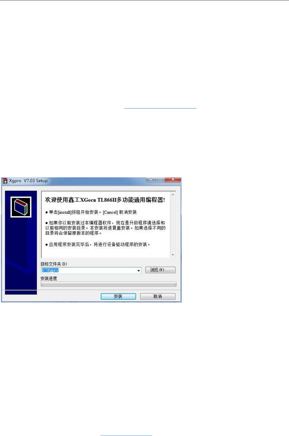
Download the Xgpro_setup.exe file from http://www.xgecu.com/en and double-click the file to
go to the installer interface. As follows: (The installation file contains the contents of
this manual.) Click [Install] to start the application installation. The following screen
will pop up:
Note: When WIN7 64-bit operating system is installed, right-click the XgproVxxx_setup.exe
file and select Run as administrator. Enter the directory you want to install here. Click
Install to start the installation of the application.
Click Install until done.
2.1.2 Install USB driver
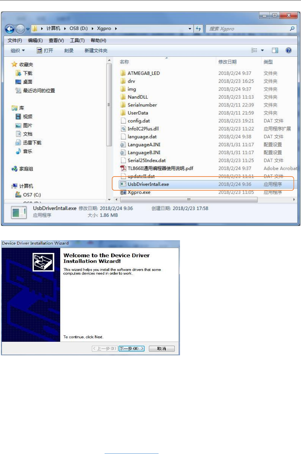
In the installation directory (D: \ xgpro) to find UsbDiverInstall.exe file,you can double-
click to run.
XGecu TL866 Ⅱ Universal Programmer Instructions V1.01
5
Haikou Xingong Electronics Co., Ltd. http://www.xgecu.com
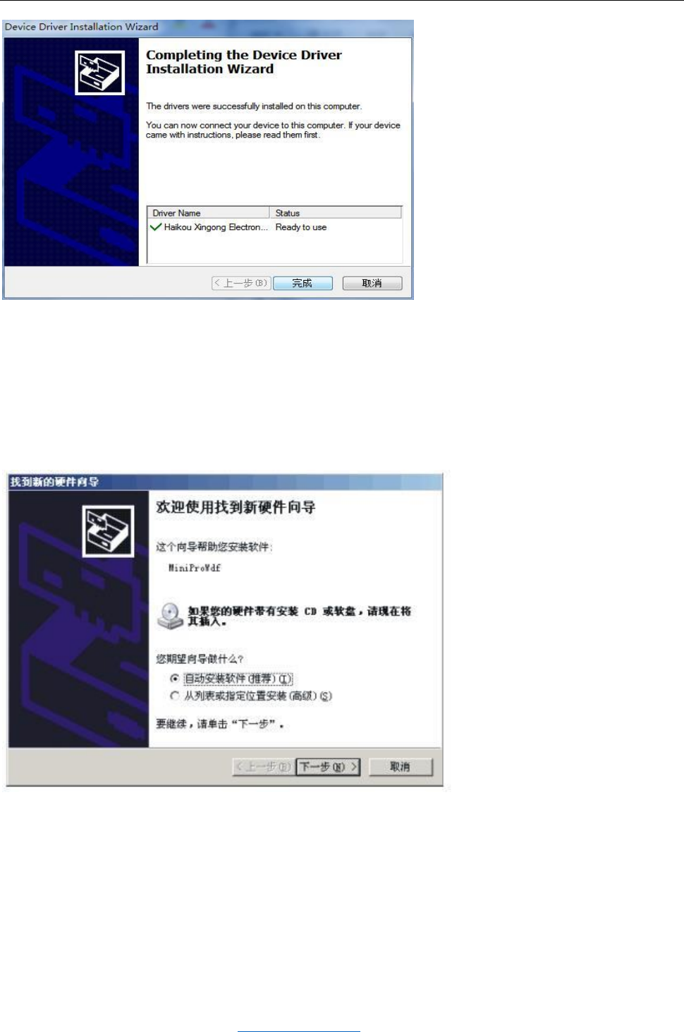
USB driver installation is complete.
2.1.3 Equipment installation
After completing the above installation, then insert the programmer into the USB port, the
operating system will find the hardware, as follows:
Select [Automatically install software], click Next, windows will be automatically installed,
until the successful completion of the installation.
(Note: In this process, the driver will change the registry. If the firewall software is
installed, please release the software, windows will also prompt the driver without a digital
visa, to confirm the installation).
If the automatic installation does not attack, you can also choose to install USB driver
files in the installation directory (D: \ xgpro \ drv). Installation is complete, open the
XGecu TL866 Ⅱ Universal Programmer Instructions V1.01
6
Haikou Xingong Electronics Co., Ltd. http://www.xgecu.com
desktop run programmer software.
You can run Xgpro.exe also in the installation directory (D: \ xgpro).
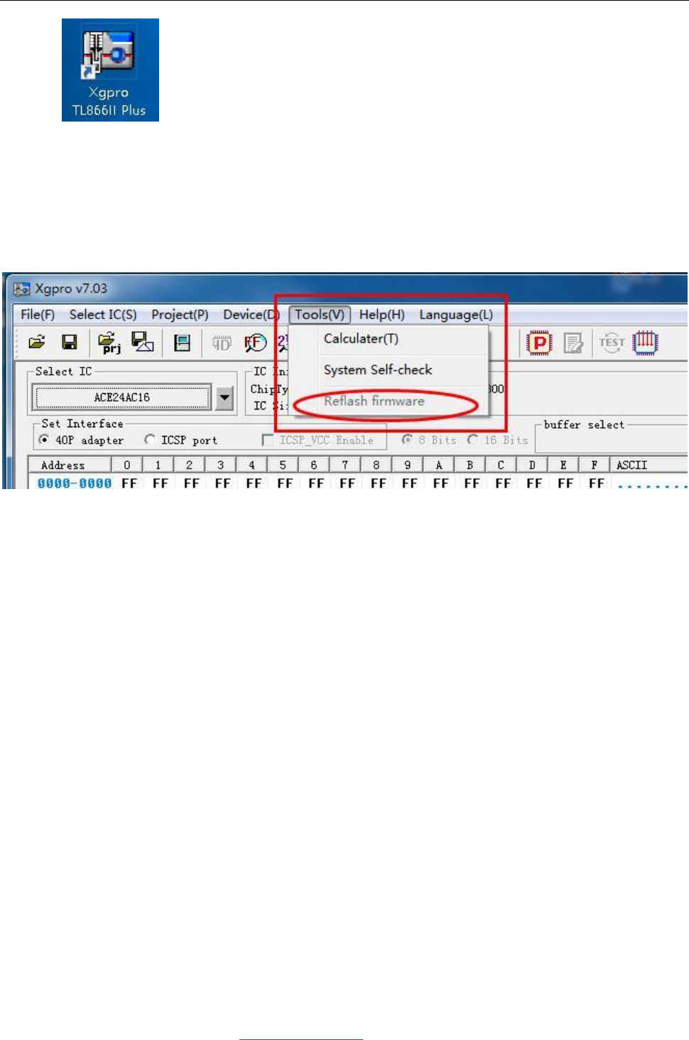
2.1.4 Firmware Refresh
The first time you use or upgrade the firmware may need to be updated, in the software's main
menu, a refresh operation, as shown below:
XGecu TL866 Ⅱ Universal Programmer Instructions V1.01
7
Haikou Xingong Electronics Co., Ltd. http://www.xgecu.com
3. Quick start
3.1 Hardware preparation and select the correct chip type
After you make sure that the universal programmer application and the USB driver are properly
installed, connect the USB communication cable. At this time, the red power indicator of the
programmer indicates that the connection is normal (lighting state), the yellow indicator is off
waiting for programming (if the yellow indicator is blinking, the USB driver is installed
incorrectly, or the USB programmer device driver is not installed) Can enter the next step.
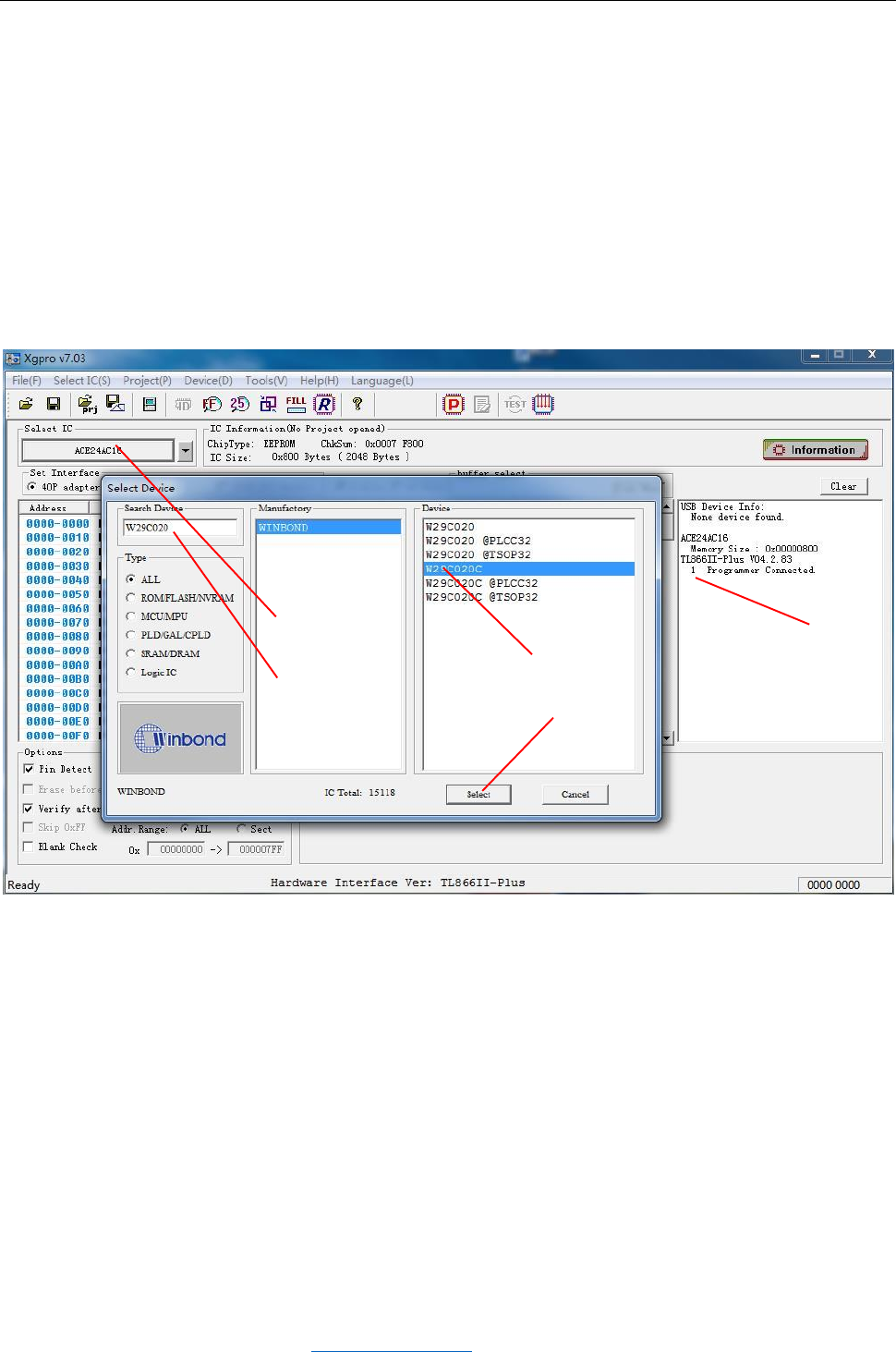
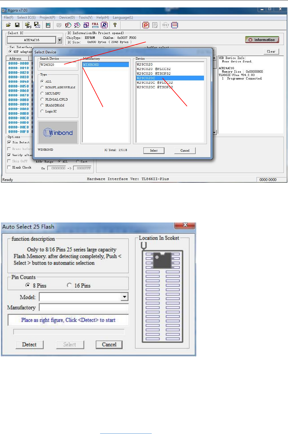
1、 1 Programmer Connected indicates that the programmer is connected
2、 Click the chip select this button, pop up the chip selection dialog box,
3、 In the search chip, enter the chip type to read and write (in this case W29C020C)
4、 Click on the correct model Note: @ PLCC32 @ TSOP32 chip package no @ label refers to the
DIP package
5、 Choose [Select]
1
2
3
4
5
XGecu TL866 Ⅱ Universal Programmer Instructions V1.01
8
Haikou Xingong Electronics Co., Ltd. http://www.xgecu.com
3.2 Read the chip and save the file
Complete the steps in section 3.1 after selecting the chip to finish
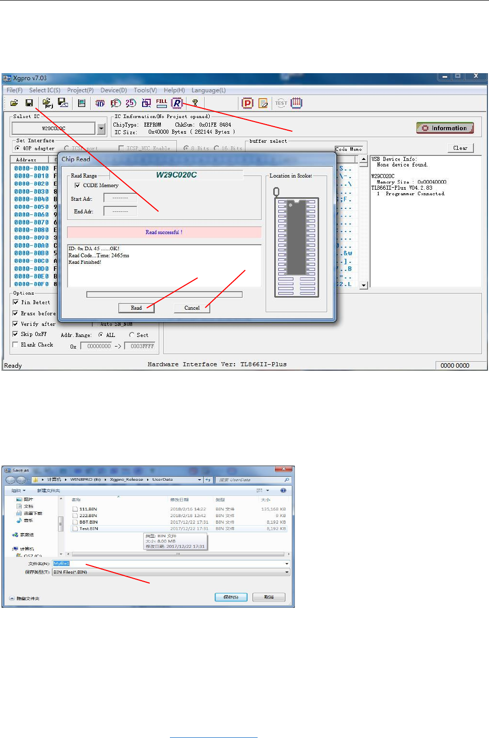
1、 Click the [R] button in the toolbar above to pop up the read dialog box.
2、 In the read dialog box, click the [Read] button.
3、 After reading, click [Cancel] button.
4、 Click Save File (you can also select <Save File> in the File menu). After entering the
file name as shown below, save the file.
3.3 Burn the contents of the file to the chip
Complete the steps in section 3.1 after selecting the chip to finish
1
3
2
1
3
3
3
3
4
1
3
3
Enter the file name
XGecu TL866 Ⅱ Universal Programmer Instructions V1.01
9
Haikou Xingong Electronics Co., Ltd. http://www.xgecu.com
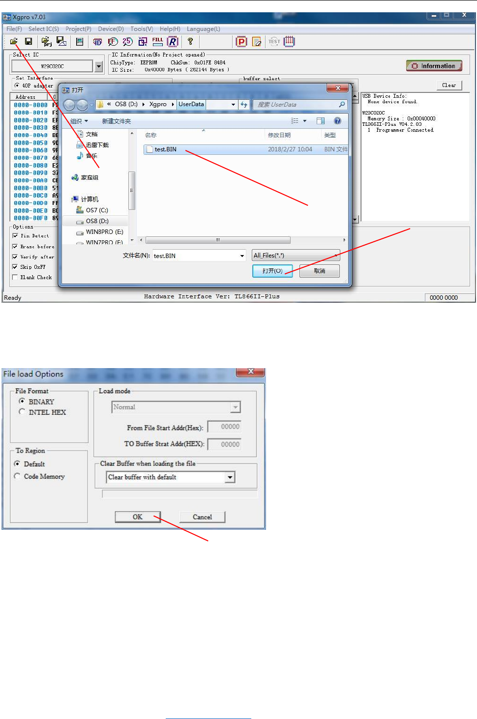
1. Click on the figure shown in 1, open the data file, open the file dialog box
2. Choose to open the data file (Test.BIN)
3. Click 【Open】, the following pop-up file options dialog box pops up, according to the
default settings, click 【OK】 button.
4. Click [OK], then the contents of the file has been transferred to the computer memory
buffer.
1
1
3
3
2
1
1
3
3
1
3
3
3
4
1
1
3
3
1
3
3
XGecu TL866 Ⅱ Universal Programmer Instructions V1.01
10
Haikou Xingong Electronics Co., Ltd. http://www.xgecu.com
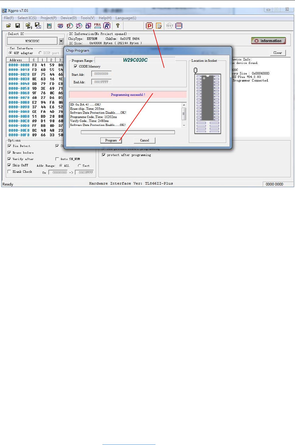
5. Click [P] button on the tools bar, chip programming dialog box is pop-up.
6. Click [Program], start to burn the chip, there is no error message when burning, that is
the burn is completed.
7. If you need to burn more chips, put a new chip, click on the "programm" to start a new
programming.
6
1
1
3
3
1
3
3
5
1
1
3
3
1
3
3
XGecu TL866 Ⅱ Universal Programmer Instructions V1.01
11
Haikou Xingong Electronics Co., Ltd. http://www.xgecu.com
4. Programmer features detailed
4.1 Main menu summary
Menu command summary
File menu
Open, save, cache operation function, exit
Chip selection
menu
Press the menu list to select the programmed chip, 25 auto recognition
Project menu
Open Project, Save Project, Save Project as, Close Project, Project
Properties, Project Password Change
Device menu
Read chip content, chip ID, Verify chip, programming chip, erase chip,
Blank check , automatic Serials number, testing , Multi-Programming, NAND
bad block check
Tools menu
Calculator, programmer self-check, Refresh firmware
Help menu
Help , about, Upgrade online
Language menu
Choose a language
Edit buffer
In the cache to find the corresponding hexadecimal value or ASCII string,
data, copy, copy, paste, fill, part of the save as TXT file
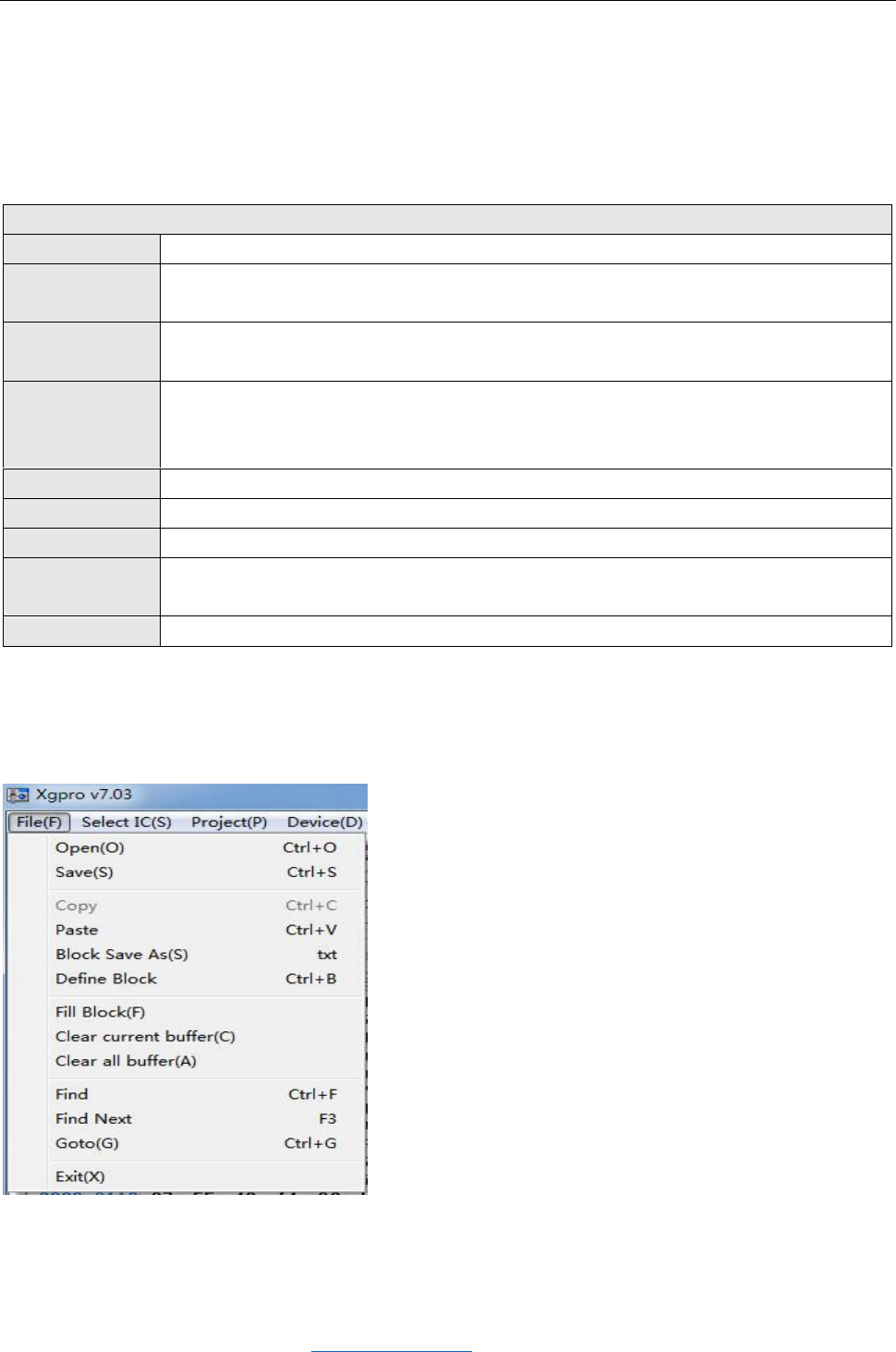
4.1.1 File menu
File menu items are as follows:
open a file:
Load hexadecimal files or binary files to the specified buffer, GAL chip for loading JED
XGecu TL866 Ⅱ Universal Programmer Instructions V1.01
12
Haikou Xingong Electronics Co., Ltd. http://www.xgecu.com
format files.
NAND FLASH operation, open the file, the file is transferred to the BBT buffer.
Save to file
Save the current cache to HEX file in hexadecimal format or BIN file in binary format, save
as JED format file when GAL chip. NAND FLASH operation, save the file, is to save the BBT
buffer to file.
Note: For MICROCHIP microcontrollers, HEX files will load into the MiroChip IDE development
environment to generate HEX files into the full buffer, save all buffered HEX files and be
fully compatible with the MICROCHIP IDE development environment.
For the Bin file to save and open, the default is CodeMemory content + Data Memory content
(if it exists)
For MICROCHIP microcontrollers, Bin also stores configuration information (sorted by
Microchip address)
Copy, paste, save as block, block definition, block fill, clear the current cache, clear all
the cache
These menu functions can be called using the shortcut keys or the right-click menu.
See file editing features ---> Edit buffer
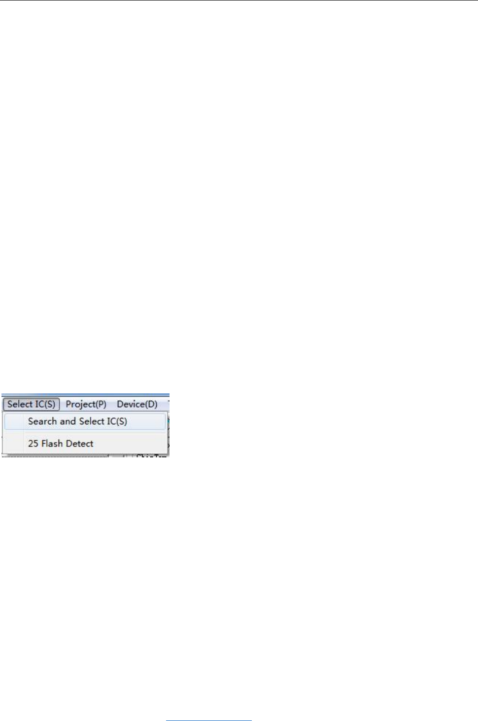
4.1.2 Chip selection menu
Click <Search and Select IC>
XGecu TL866 Ⅱ Universal Programmer Instructions V1.01
13
Haikou Xingong Electronics Co., Ltd. http://www.xgecu.com
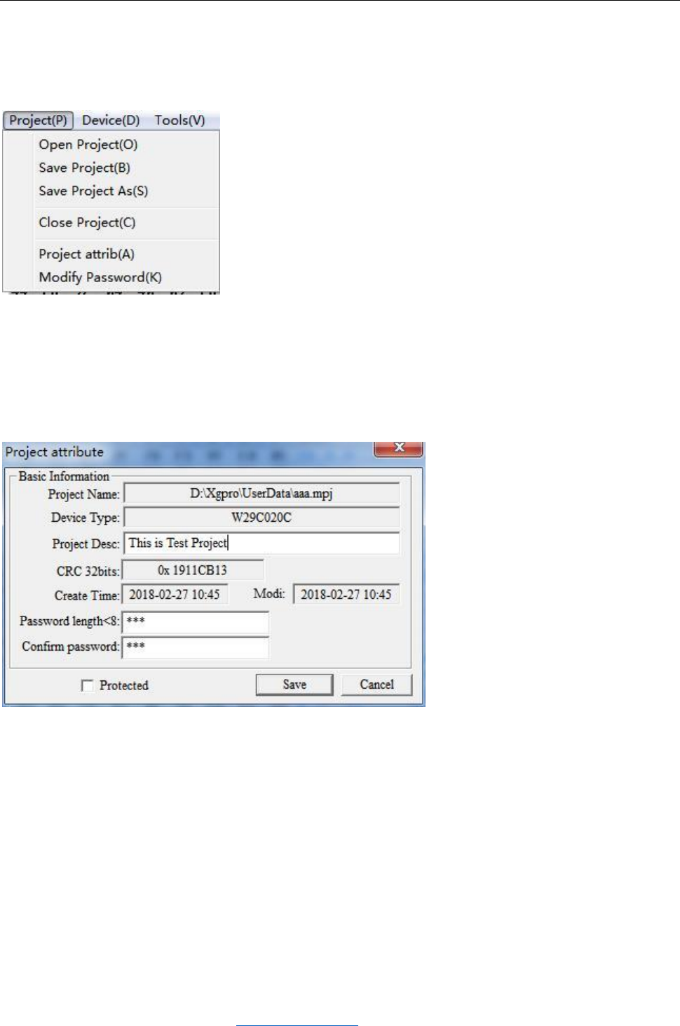
25 Flash Detect:
automatic recognition of 25-series Nor Flash with 8-pin and 16-pin. Note: Because many chip
IDs are the same and all results have more than one, you need to choose an accurate model
according to the result of recognition.
First select the pin number of the chip and click <Detect> to start recognizing
4.1.3 Project menu
Project files are created to better maintain the programming of the chip. It is a file that
holds all current buffer data and working environment settings, including information about
Enter IC Name and Search
Select a Manufactory
Select a Chip
XGecu TL866 Ⅱ Universal Programmer Instructions V1.01
14
Haikou Xingong Electronics Co., Ltd. http://www.xgecu.com
the current device, settings for all operating options, and auto-related settings. Its easy
to use daily volume production. Project can be set password protection, to a certain extent,
can protect the safety of the product .
Project menu items are as follows:
Save the project
After setting the required parameters of the chip in the application program, select [Project]
- [Save Project] to create a project. And in the window of the information area display
project information. Click [Save Project], enter the project name and click OK to pop up the
following project dialog box:
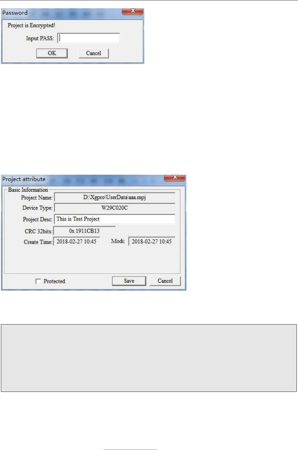
1, the password is blank, the current project does not set password protection.
2, if the project is set to protect mode, the password must be entered. Set to Engineering
After the protection mode, the relevant data of the project will not be changed. And some
functions of the programmer are disabled.
Open the project
Open an existing project, select [Project] - [Open Project], select the project name in the
open window and click OK. If the project is set password, the following dialog box will pop
up. (If you do not set the password directly open the project)
XGecu TL866 Ⅱ Universal Programmer Instructions V1.01
15
Haikou Xingong Electronics Co., Ltd. http://www.xgecu.com
Note: For the TL866 programmer's older version of the project file, you can also open the
call here.
Save the project as:
Save the current project as another project name. Operation Reference 【Save Project】.
Close the current project
Close the open project. Switch to normal programming mode, close the project and clear
the current buffer data.
Project properties
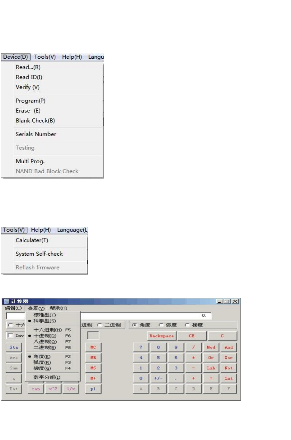
Select [Project] - [Project Properties], pop-up property settings dialog box. Project
Properties dialog box can be more change the project description and project protection mode.
Enter the project password when saving.
Change the project password
set a new project password
prompt:
1, the exact project description can distinguish a large number of projects. Project
mode general use in mass production.
2, the project file has been encrypted to protect the project password to prevent the
project file copy. To a certain extent, the data can be protected.
3, 32-bit CRC checksum is saved when the project file is saved or opened, to prevent
other uncertain factors such as storage file corruption.
XGecu TL866 Ⅱ Universal Programmer Instructions V1.01
16
Haikou Xingong Electronics Co., Ltd. http://www.xgecu.com
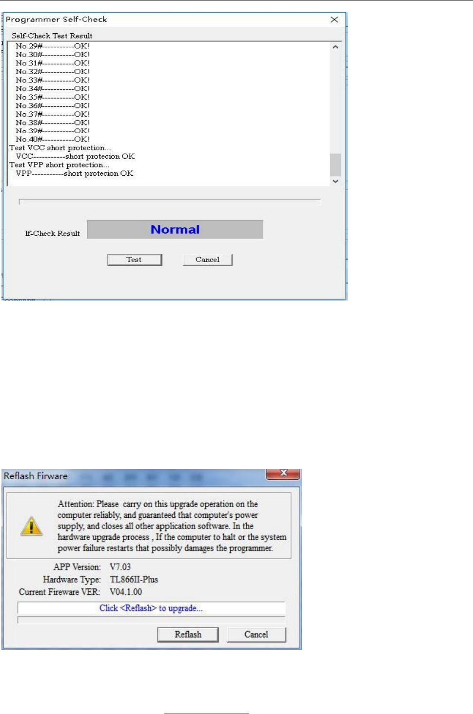
4.1.4 Device menu
This menu function is to chip programming operation, with the content see 4.2 programmer
operation function, Menu items as shown below:
4.1.5 System Tools menu
Tools menu items are as follows:
Calculator: This is a calculator that comes with Windows, which makes it easy to calculate
various formats when switching to scientific mode.
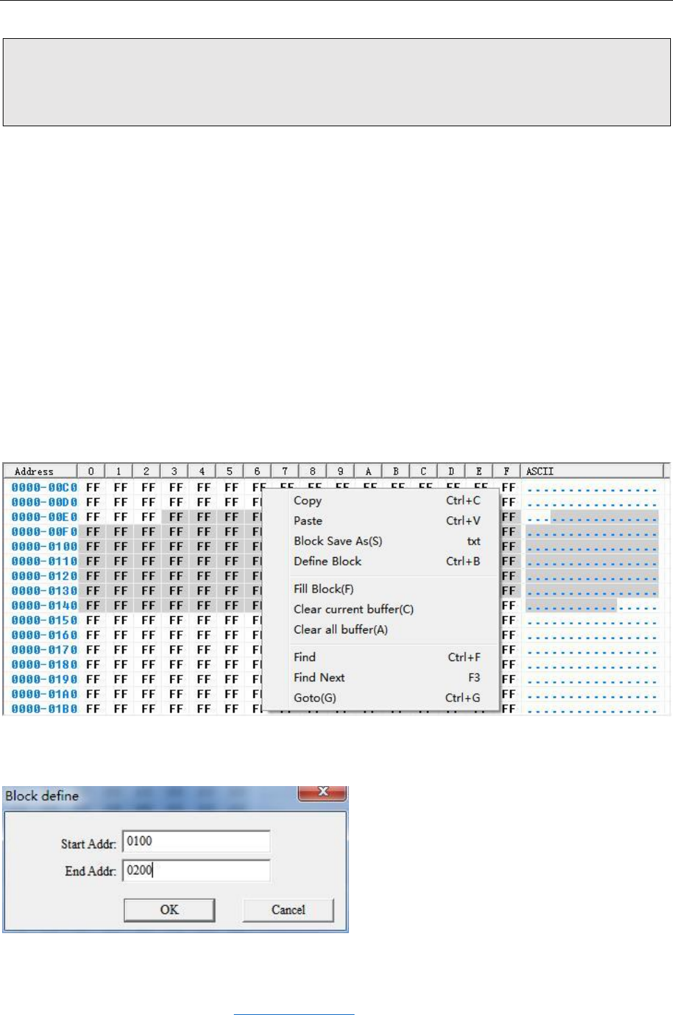
Programmer self-test: The programmer hardware self-test operation.
Click to pop up the following dialog:
XGecu TL866 Ⅱ Universal Programmer Instructions V1.01
17
Haikou Xingong Electronics Co., Ltd. http://www.xgecu.com
Note: Before starting the programmer's self-test, please remove the IC and ICSP cable from
the 40PIN socket. During self-test, the programmer will test VPP, VCC and GND for all pins
and perform internal short-circuit overcurrent test Apply VPP VCC and GND to one pin).
Inserting the IC may damage the IC inserted in it. After the test is completed, the test of
each power supply is displayed in the dialog box.
Firmware FLASH Refresh:
Programmer hardware firmware update process.
When upgrading a new version of the application, such as the need to upgrade the FLASH program
to update, the application will prompt for a firmware update when entering, if you do not
need to refresh, then the refresh function is disabled. Click <Firmware FLASH Refresh> to
pop up the following dialog box:
Click the button to refresh, refresh the total time of about 15 seconds. Click <Cancel> to
XGecu TL866 Ⅱ Universal Programmer Instructions V1.01
18
Haikou Xingong Electronics Co., Ltd. http://www.xgecu.com
exit the refresh.
Note when refreshing:
Do not use an external USB hub refresh, direct access to the computer USB port, It may
not be reset when using external HUB.
Turn off all other programs, and ensure that the computer power supply is reliable!
4.1.6 Edit buffer
Programmer software can modify the contents of the buffer, commonly used functions are:
Buffer block definition
Buffer block fill
copy and paste
Save the block as
Clear the buffer
Find, find next
Goto : Locate the address
Buffer block definition
Block definition in two ways: The first method is: in the buffer zone, press the left mouse
button, move the mouse, select a block of data. Figure is as follows:
The second method is as follows: Select 【Block Definition】 in 【Main Menu】 or 【Right Key
Menu】 or press the shortcut key "CTRL + B" to pop up the following dialog box, enter the
start address and end address, press OK to finish Block definition.
You can perform subsequent block operations on the defined data blocks: block copy, block
fill, block save as TXT file
XGecu TL866 Ⅱ Universal Programmer Instructions V1.01
19
Haikou Xingong Electronics Co., Ltd. http://www.xgecu.com
FILL Block
Padding buffer refers to the program code buffer in a continuous address of the data are all
replaced by a fixed value.
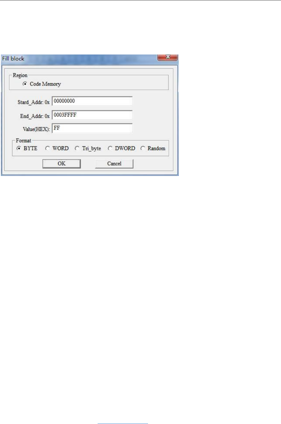
Pop-up mouse 【Mouse Right Button menu】 select 【FILL Block】, pop-up the following dialog
box
A. Region: Buffer selection , the default value for the current window display buffer.
B. To fill the start address and end address of the block, the default value is: If a block
is defined, define the start to the end of the data block. If no block is defined, then
the full buffer size for the current buffer.
C. Fill value, the longest allow 4 bytes. If the fill-in method is random, the value has
nothing to do with it.
D. Fill-in mode, the default mode: If the chip according to 8-bit programming, the default
single-byte mode, if the chip is programmed in 16-bit mode is double-byte mode, you are
free to change the way you want to fill in .
copy
After the definition of the data block, you can pop-up mouse right-click menu, select 【copy】,
then the contents of the block has been copied to the WINDOWS clipboard. You can also press
CTRL + C keys to complete the copy.
Paste
Function: Fills in the contents of the clipboard to the buffer.
Action: Move the cursor to the start address of the buffer you want to fill in. Press
CTRL + V. Paste complete.
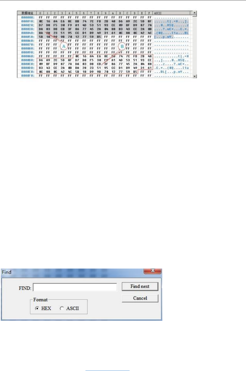
Effect of copying data from area A to area B
XGecu TL866 Ⅱ Universal Programmer Instructions V1.01
20
Haikou Xingong Electronics Co., Ltd. http://www.xgecu.com
Note: In order to speed up the pasting speed, the data format of the clipboard is a
binary format specially used by this programmer. Therefore, other WINDOW applications can not
directly use this program to copy data to the clipboard. If you want to copy data blocks to
other applications Use, please use [block as TXT file function.
Block Save as
This function outputs the data block you defined as TXT text file, which is convenient for
designers to use when programming. The text format is automatically arranged in 16-bit or 8-
bit mode. Operation method: After defining the buffer block, right-click the mouse, pop-up
menu, select [Block Save as]
Clear the buffer
Empty the current buffer: Function: Empty the buffer displayed in the application's current
window.
Clear All Buffers: Function: Clear all the chip's buffers at default values.
Find, find next
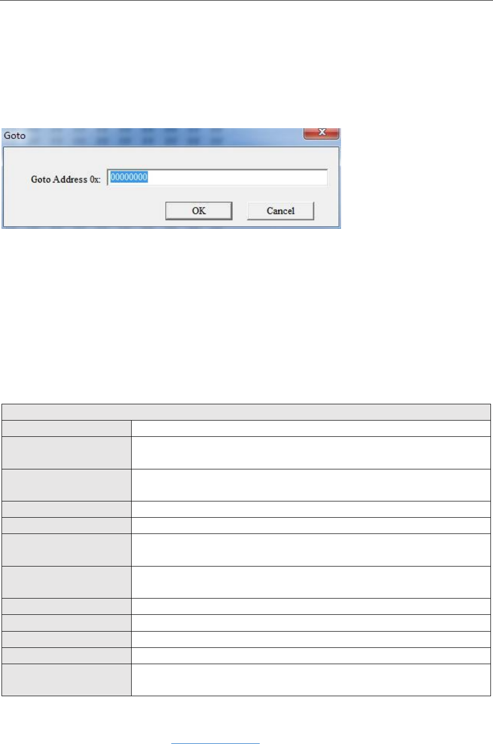
Function: Find the HEX or ASCII string in the current buffer. Operation: Press CTRL + F or
click 【Find】 in the right front menu to pop up the following dialog box:
Enter the HEX value or ASCII string to find in the input box, and finally click the Find
button in the dialog box. When there is a hexadecimal data or string matching this in the
program code buffer, the cursor will be positioned to the address of the first content that
matches the content being searched, and the F3 key will be pressed to continue searching for
XGecu TL866 Ⅱ Universal Programmer Instructions V1.01
21
Haikou Xingong Electronics Co., Ltd. http://www.xgecu.com
the next one. Until the buffer all search is completed.
Goto:Locate the address
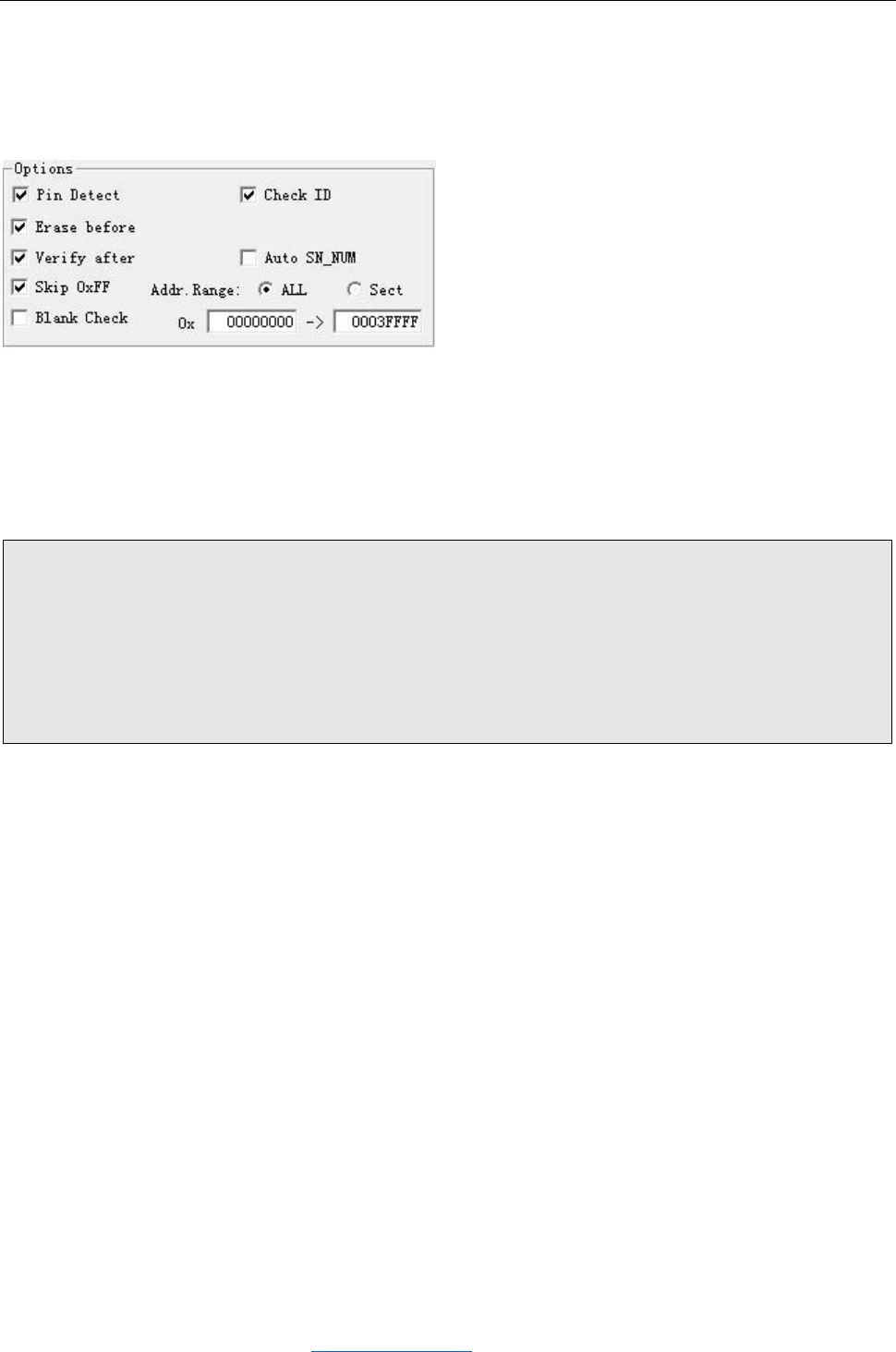
Function: The cursor moves to the address specified by the current buffer.
Operation: Press the shortcut key CTRL + G, or press the right mouse button to pop up the
menu to select 【Goto】, the following dialog box will pop up:
Enter the address, press the OK button, the cursor will move to the address
4.2 Programmer operation function
Programmer operating functions
Choose the chip
Press the menu list to select the programmed chip
Read the chip
Read into the contents of the chip to the PC cache (Note: NAND read
directly into the file)
Programming chip
Caches the contents of the buffer (NAND file contents) into the
chip
Erase the chip
Erase the contents of the chip completely
Blank Check
Check if the current status of the chip is not programmed.
Verify
Check the contents of the chip and the buffer is the same, you can
mark different.
Set configuration word
Mainly set the protection bit, fuse bits, encryption bits and so
on.
Set Serials number
Add a serial number to the chip
Programmer self-Check
Check the programmer programming port function is normal
ICSP programming
ICSP serial programming function interface, and how to use it
RAM test
Test common static RAM chips
Digital logic test
Test 54 74 series, CMOS4000 / MC14xxx series digital integrated
circuits
XGecu TL866 Ⅱ Universal Programmer Instructions V1.01
22
Haikou Xingong Electronics Co., Ltd. http://www.xgecu.com
4.2.1 Programming settings
Set the options as shown in the following figure, generally default settings can be used,
Not necessary to change.
4.2.1.1 Pin Detect
Before operating the chip, the software automatically checks the chip pins for good contact
and checks, which in most cases avoids programming or reading errors caused by poor pin
contact.
Poor contact with the pin the extreme situation:
When the pin is particularly serious oxidation, the individual pins may not be completely
disconnected (for example, equivalent to a 3-10K contact resistance), in this case can not
determine whether the contact is good, programming errors may occur, so that to old chip ,
Should carefully handle the pin.
(Soaked in dilute hydrochloric acid for 30 seconds, removed after washing with water to
dry, to achieve the best results)
For very few chips, there may be some pins that can not pass the pin contact check. In this
case, this option should be temporarily canceled while ensuring that the pins are in good
contact. No pin check will be performed until the chip is read or written.
4.2.1.2 Erase before programming
Before programming, the first run chip erase.
Some chips have no erase function, this option will be disabled. For example, most 27Cxxx
chips are OTP ROM or UVROM. Is not erasable or no electric erase function. 24 series 25
series EEPROM 93 series chips, this function is also disabled when there is no special
erase command, which means that these chips can be rewritten directly without erasing. (If
the user must want to Blank the chip content, that is, 0xFF will be written to the chip's
entire storage space)

XGecu TL866 Ⅱ Universal Programmer Instructions V1.01
23
Haikou Xingong Electronics Co., Ltd. http://www.xgecu.com
4.2.1.3 Verification after programming
Under normal circumstances, this must be selected, otherwise the data may be wrong after
the programming is completed.
4.2.1.4 Skip writing 0xFF
For FF data block will skip the write operation, can greatly improve the programming
efficiency. When this option is verify, the verify will also be skipped
4.2.1.5 Check ID
Many chips have a chip inside the Identification (ID), the content is generally composed
of two or more bytes, the first byte is usually the manufacturer code (Manufacture ID),
followed by the chip type or chip capacity. Different chip, ID will be different, the
function of this option is to prevent incorrect chip into. This option checks the chip ID
before reading or writing to the chip. If it continues correctly, this function is optional.
Operation will be aborted if the ID error. The default option is enable .
Similar chips not supported in the list of the chip, Their programming method may be same ,
you can choose other manufacturers IC with the same capacity of the chip for burning.
Because the ID will be different, before burning, cancel the ID check
4.2.1.6 Address range
You can set the address range of the programming chip, mass production can improve efficiency.
4.2.1.7 Blank Check before programming
In addition to 27 series UVROM, this generally do not need to select,
4.2.1.8 Auto SN_NUM
See Section 4.2.9 Setting Serials Number
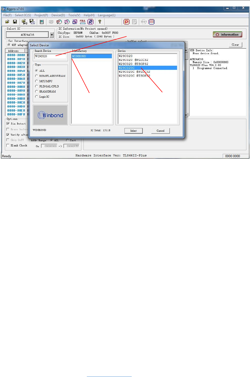
4.2.2 Choose the chip
Select the chip to be programmed and click the <Select IC button> in the upper left corner
of the software
XGecu TL866 Ⅱ Universal Programmer Instructions V1.01
24
Haikou Xingong Electronics Co., Ltd. http://www.xgecu.com
Select the chip package must pay attention to the choice. Part of the chip package, pin
order may be different. For the same type of package IC if not listed in the various packages,
for non-DIP package chip as long as the control IC product manual, direct connection to the
corresponding pin can be programmed.
4.2.3 Read the chip
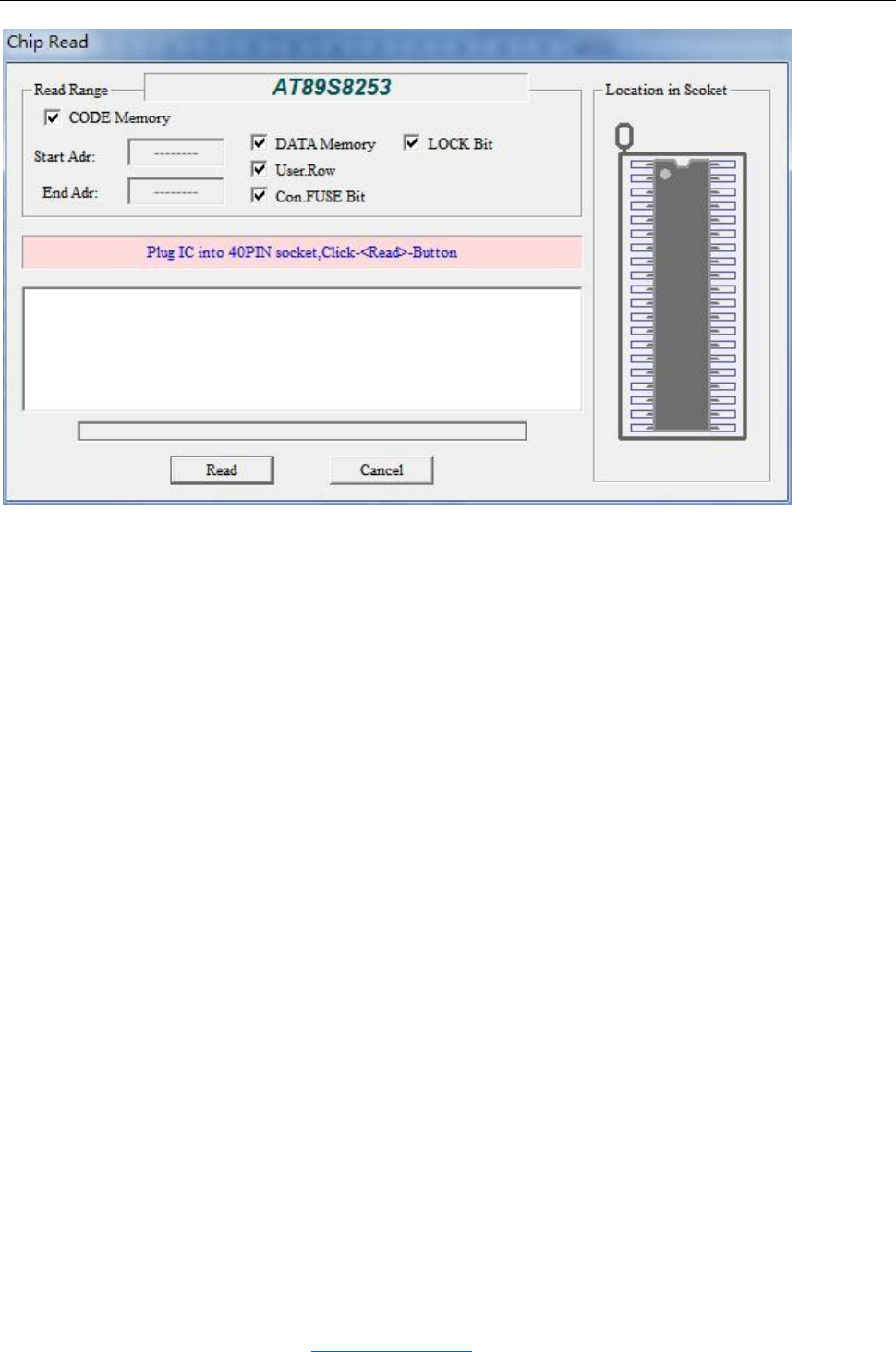
Read the chip: Read data to Buffer from the chip . Different chips read the window may be
different, the following to read AT89S8253, for example, shows how to read the chip, click
the toolbar [R] button, the following dialog box pops up
Enter IC Name and Search
Select a Manufactory
Select a Chip
XGecu TL866 Ⅱ Universal Programmer Instructions V1.01
25
Haikou Xingong Electronics Co., Ltd. http://www.xgecu.com
First, set the Read Range, including [CODE], [DATA], [FUSE], [LOCK], invalid when reading the
start address and ending address. Press 【read】 button to start reading chip data, note:
read the value as 0xFF if the chip is encrypted. After the reading is completed, in the
information field, each buffer read time is displayed.
Note: The read operation is generally not an error, if you want to verify the read data
is correct, then use the verification function verification, specific methods of operation,
please check the verification instructions, the programmer on the chip before the operation
will first check the chip ID value.
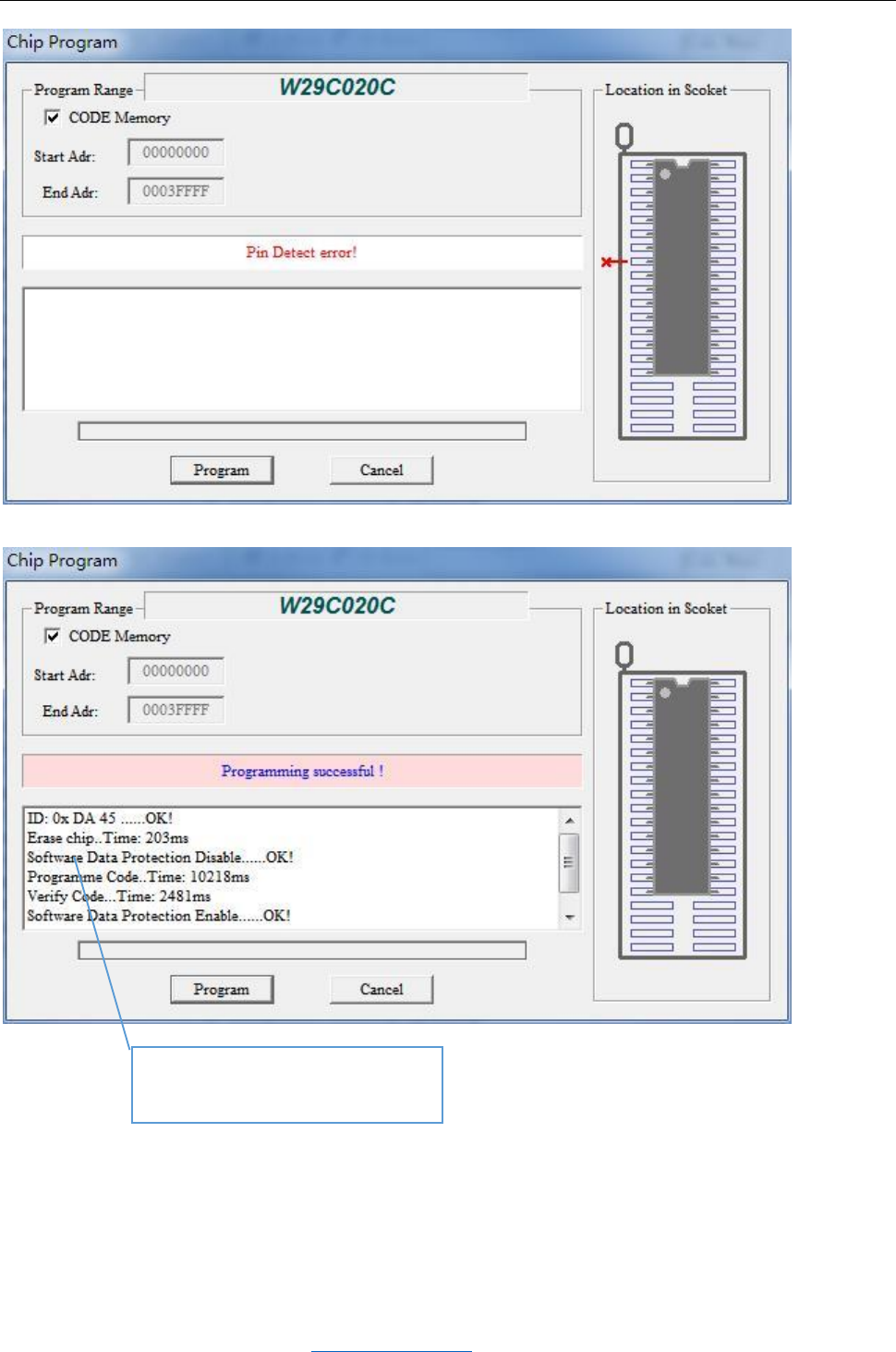
4.2.4 Programming chip
Click the <P> button in the toolbar, the programming dialog box is as follows
Take W29C020 as an example, if the pin has bad contact, the following shows the bad pin status
XGecu TL866 Ⅱ Universal Programmer Instructions V1.01
26
Haikou Xingong Electronics Co., Ltd. http://www.xgecu.com
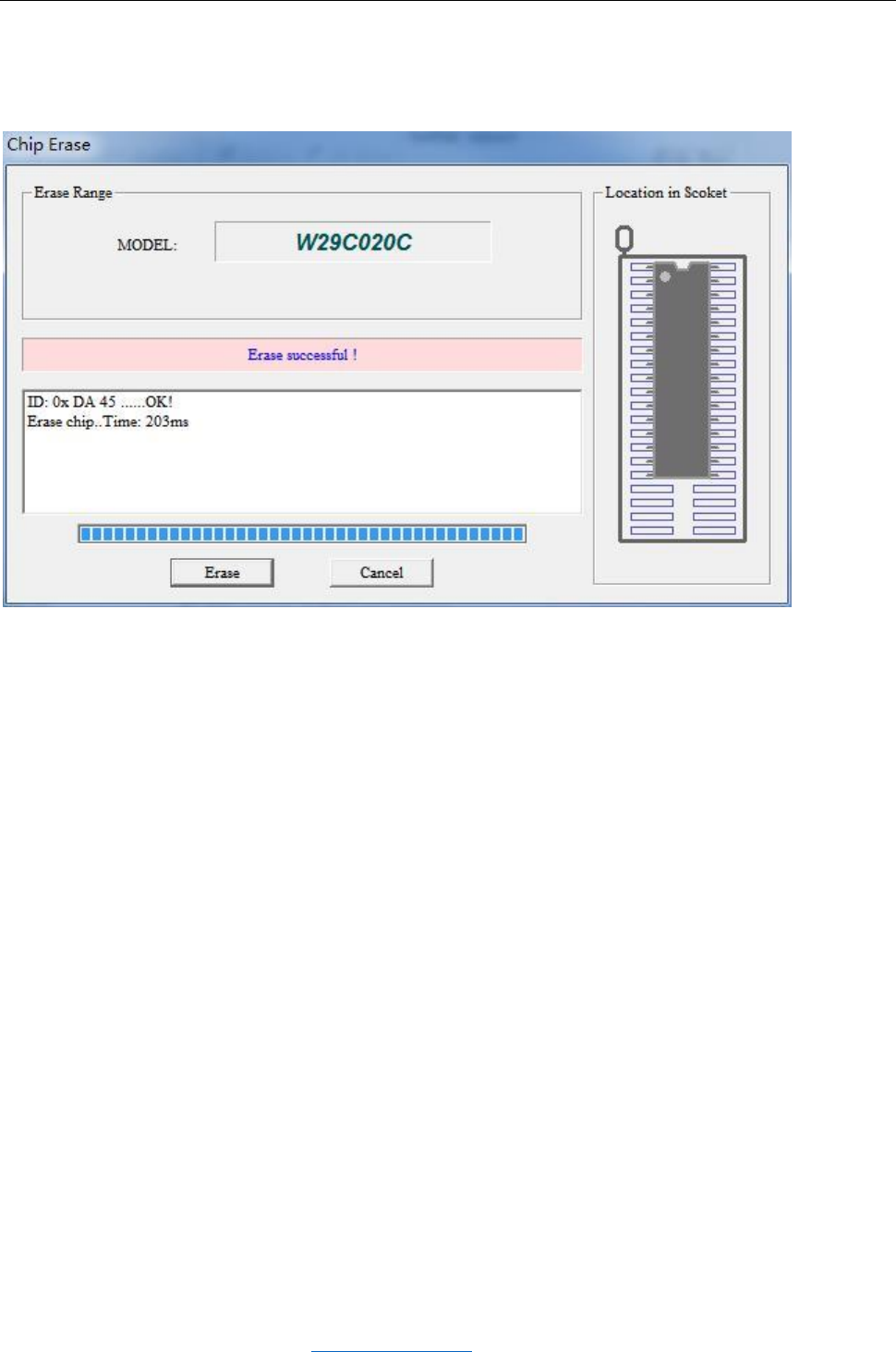
Normal programming as shown below
Most chips, the programmer in the programming process for automatic verification, if found
during programming errors will immediately terminate the programming.
If the user chooses the "Auto SN_NUM" option, the chip number in the buffer will automatically
increase according to the setting after chip programming.
In order to ensure the correct programming data, it is recommended that the user always
perform verification.
The information box shows all
the operations and processes
The time consumed
XGecu TL866 Ⅱ Universal Programmer Instructions V1.01
27
Haikou Xingong Electronics Co., Ltd. http://www.xgecu.com
4.2.5 Erase the chip
Click on the [Erase] button on the erasable chip to pop up the following dialog box:
By default, the chip ID is checked before erasing. For a very few MCUs, some chips can not
read the chip ID after being encrypted. In this case, cancel the ID check in the main interface,
otherwise the ID check is incorrect. Click the [Erase] button in the dialog box, after erase
is completed, the erase time is displayed.
4.2.6 Blank Check
By default, the chip ID is checked before erasing, and the area where the chip is to be checked
can be selected first if it is empty. The default is all. Click on the [check empty] button in
the dialog box, start to check the empty operation, the completion of the display to check the
time of the various regions of the time. If you check empty during the chip was found to be non-
empty, then check the empty, and display non-empty area address and store value.
4.2.7 Verify the chip
Before Verify, select the area want to be checked . The default is all. Click the Verify Button
in the dialog box to start the verify operation. If all the data are the same, the time spent in
verifying each area will be displayed after completion.
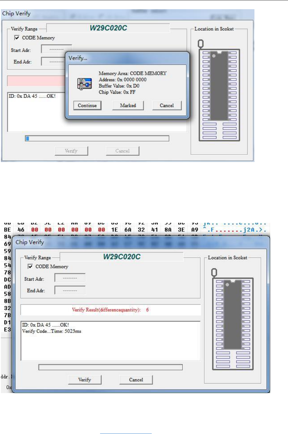
If you find that the chip data is different during the verification, the following dialog box will
pop up:
XGecu TL866 Ⅱ Universal Programmer Instructions V1.01
28
Haikou Xingong Electronics Co., Ltd. http://www.xgecu.com
Click [Continue]: Will continue to compare if there are different then will pop up the same
dialog box prompts.
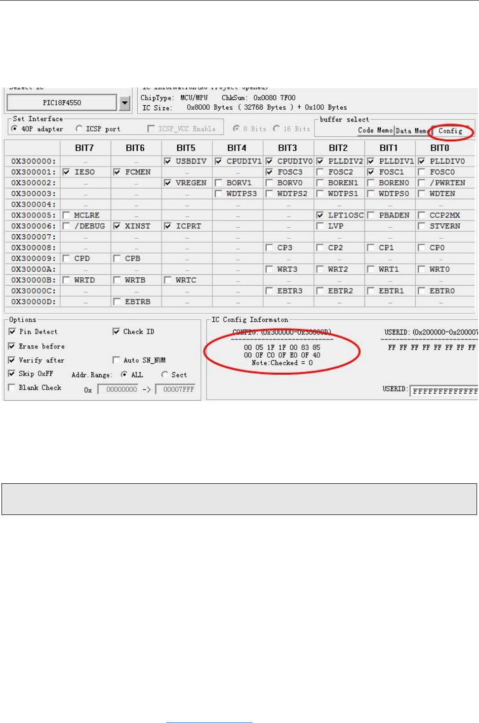
Click 【marked】: will compare the entire contents of the chip, in the process of comparison,
if found different will not pop-up prompts, until done, the number of tips are different, and
in the buffer zone in red font shows different units (Except NAND), as shown below.
Click [Cancel]: will exit directly, not for later comparison.
XGecu TL866 Ⅱ Universal Programmer Instructions V1.01
29
Haikou Xingong Electronics Co., Ltd. http://www.xgecu.com
4.2.8 Set configuration
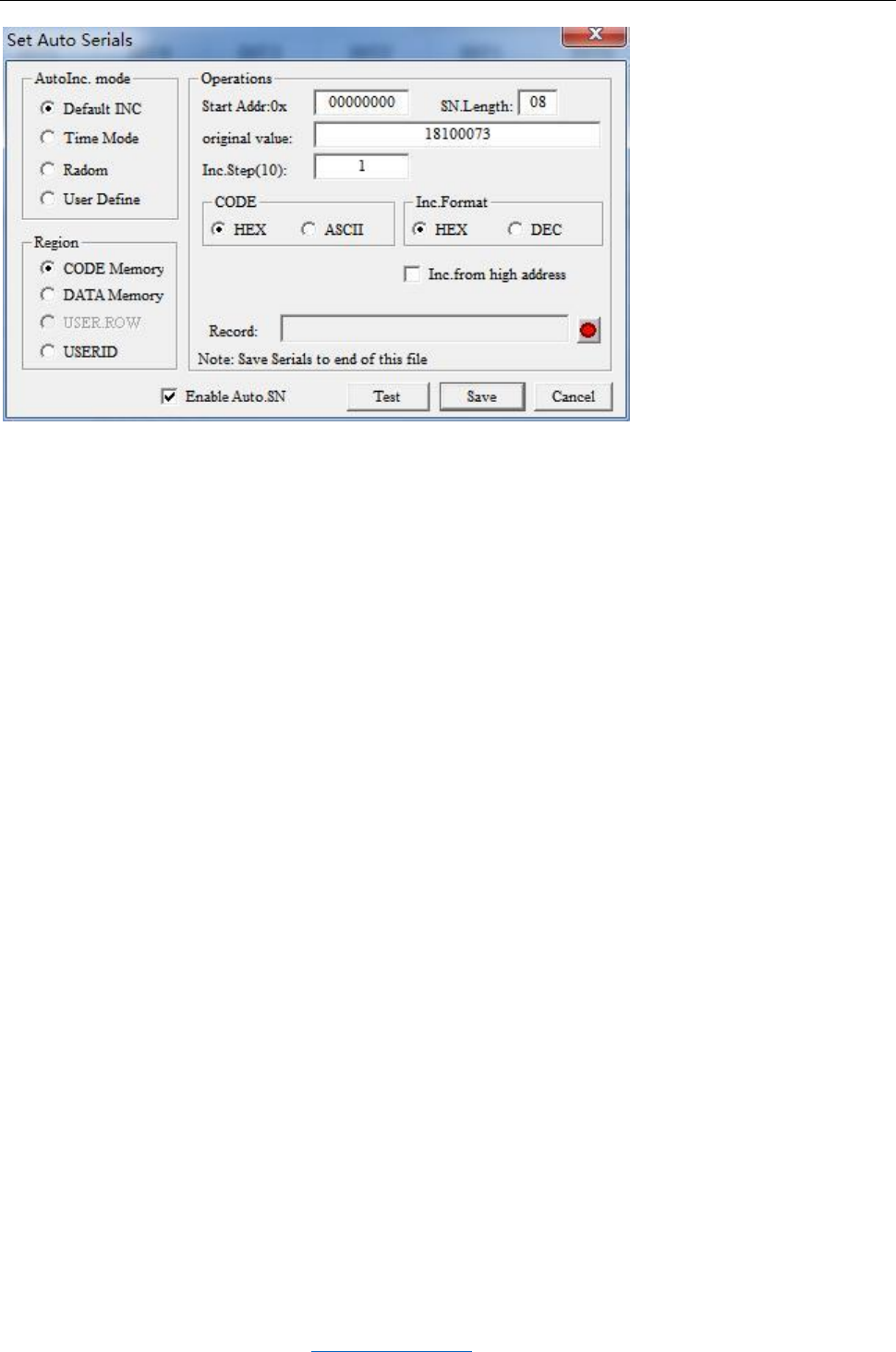
Click the [Config] button in the chip buffer selection bar to pop up the following interface
(chip type PIC18F4550):
The content of the configuration information in the lower red circle corresponds to the
configuration interface: Click the configuration interface, the value in the configuration
is automatically changed.
Different chip configuration information is different, so the user first view the chip's data
sheet, and in accordance with the specific needs of the correct configuration of the chip.
Chip configuration word, need to understand the role of each bit in the configuration
word
4.2.9 Setting Serials Number
Serials number setting function is to automatically add a Serials number in t memory area of
the chip can be easily used. Add time or a unique serial number, etc., the programmer has a
variety of numbering algorithms available to meet a variety of user requirements.
Click <Main Menu> --- <Device> --- <Serials Number> to pop up the following dialog box:
XGecu TL866 Ⅱ Universal Programmer Instructions V1.01
30
Haikou Xingong Electronics Co., Ltd. http://www.xgecu.com
First select the automatic numbering algorithm, in the dialog box there are four algorithms
to choose, the following for a variety of numbering algorithm for a separate description.
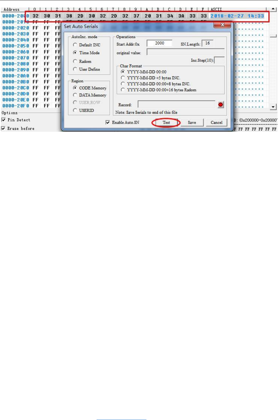
4.2.9.1 The default incremental algorithm (Default INC)
The setting interface of the algorithm is as shown in the figure above. The function of
the algorithm is to add a number of a set length in the address where the set storage area
starts, and the number increases by each step. After setting the parameters, you can press
the button to test and check the changing rules under various parameter settings.
The initial value and step size can be set in the dialog box.
Set the parameters and test the correct, set the log file, if empty, the log file is
invalid, the program will not record the data to the file, if you set the log file, after
each programming, put you The set number is added to the end of the log file.
Finally, <Enable Auto SN> checked, and <Save> button.
4.2.9.2 Time Mode algorithm
Time algorithm dialog interface as shown below: At 0x2000, put in a time data
XGecu TL866 Ⅱ Universal Programmer Instructions V1.01
31
Haikou Xingong Electronics Co., Ltd. http://www.xgecu.com
There are four time code formats, namely:
(1) Date + time number Total length: 16 bytes
When programming add the date and time in the specified location, the total length
is 16bytes.
(2) Date Increment number of +5 bytes Total length: 16 bytes
The incremental part of the content can be set initial value and step.
(3) Date + time + 8-byte incremental number Total length: 24 bytes
The incremental part of the content can be set initial value and step.
(4) Date + Time + 16 bytes Random Numbering Total length: 32 bytes
Of these, 16 bytes are randomly generated bytes that generate a unique serial number for the
product. In this way, the log file must be set so that the generated code is recorded in the
file. Otherwise you do not know the product number is what.
The back of the operation steps is same as "default INC"
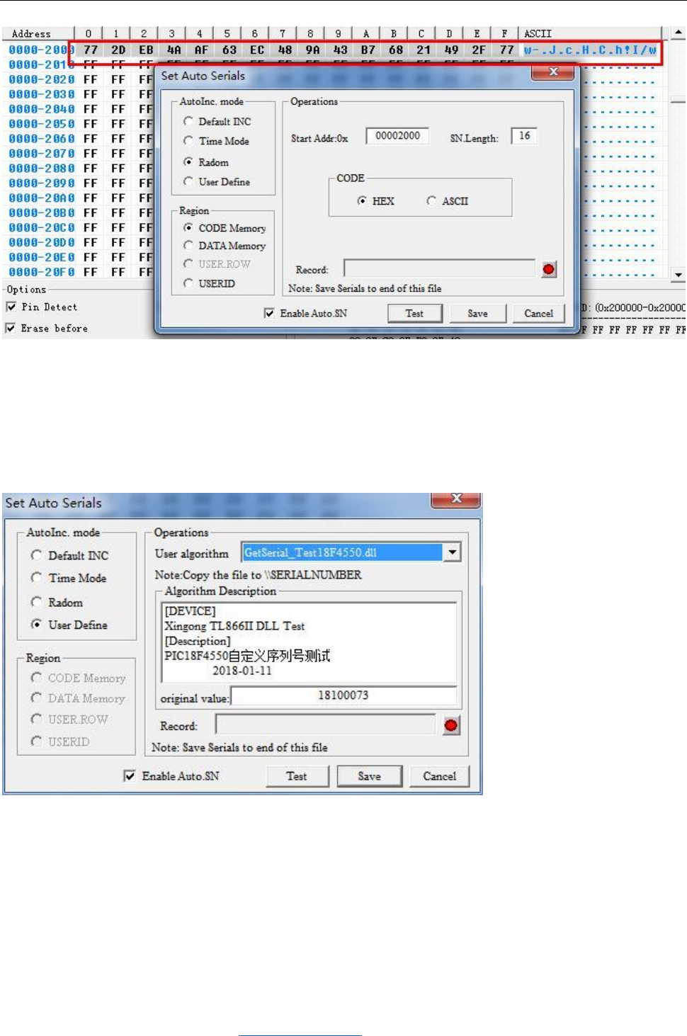
4.2.9.3 Random algorithm
The algorithm generates a random number of the specified length, as shown below: At the
beginning of the address 0x2000, put 16 bytes of random data
XGecu TL866 Ⅱ Universal Programmer Instructions V1.01
32
Haikou Xingong Electronics Co., Ltd. http://www.xgecu.com
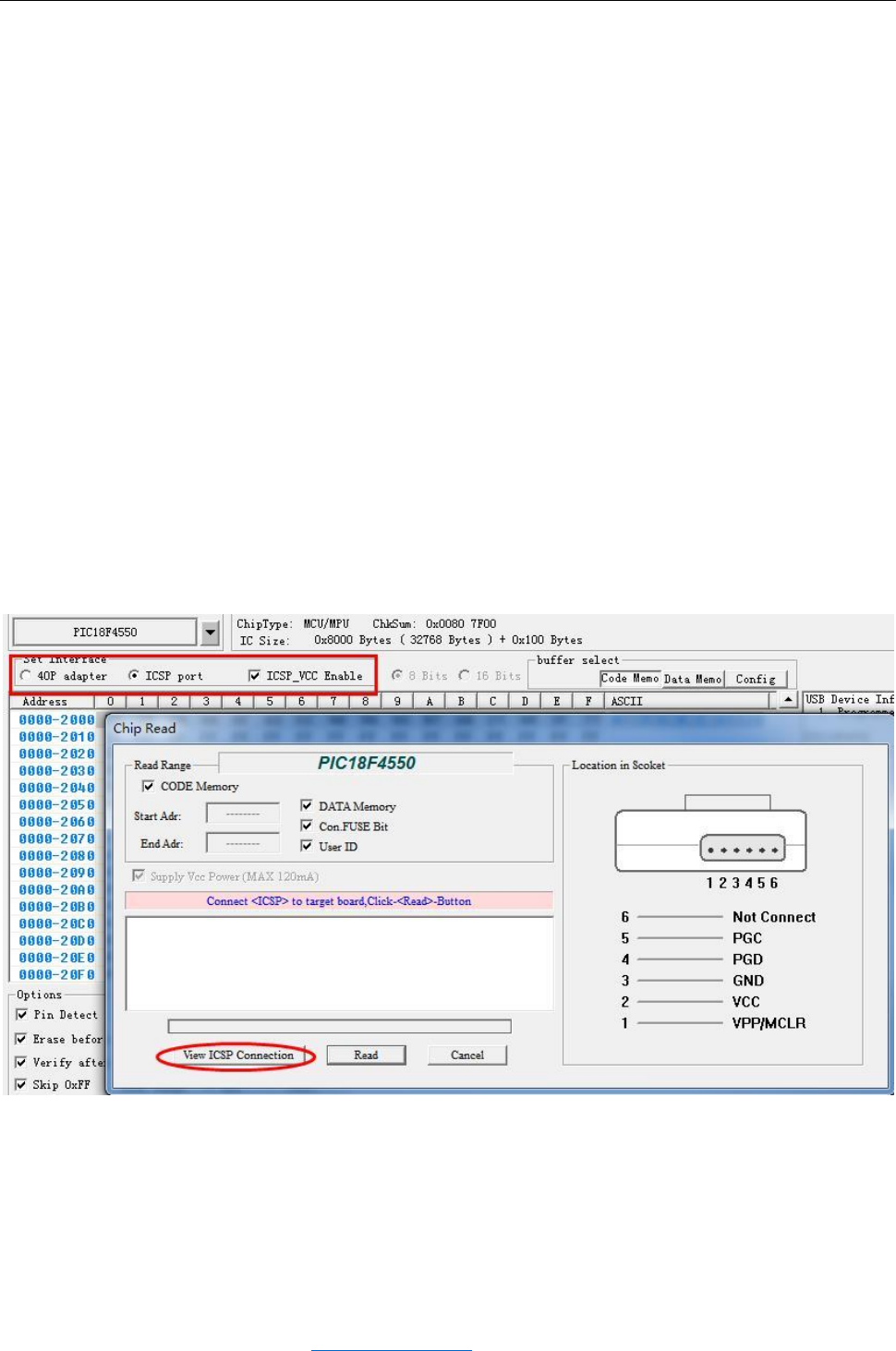
4.2.9.4 User-defined algorithm
User-defined algorithm has a strong flexibility, you can set any number of algorithms, the
use of detailed look at the directory .. \\ Serialnumber \ source_dll VC ++ source code
comments. The interface is as follows:
AVR microcontroller RC correction byte encryption method, fully use here to call DLL dynamic
library,
.. \ TAMEGA_LED directory contains all the source code and test methods.
After making the DLL file, you just copy it to the subdirectory .. \\ Serialnumber in the
application directory. Set in the user algorithm file list, select your algorithm file. The
following steps are the same as the other algorithms.
important hint:
1、 After setting the above, the programmer will not automatically add the number you set to
the chip during the programming operation. To add the number automatically, you must also
XGecu TL866 Ⅱ Universal Programmer Instructions V1.01
33
Haikou Xingong Electronics Co., Ltd. http://www.xgecu.com
select <Auto SN_NUM> in the main interface.
2、 The main interface can be selected in the condition of <Auto SN_NUM> is, you must first
set the numbering algorithm, and in the algorithm set <Enable Auto.SN>.
3、 In the main interface, select <Auto SN_NUM>, if you re-set the numbering algorithm, the
main interface <Auto SN_NUM> button must be re-selected.
4、 After changing the programming chip type, you must reset the number setting algorithm.
5、 In Project mode, the algorithm is saved in the project file, can open the project file
directly, and automatically transferred to the automatic numbering algorithm. Therefore,
mass production is generally used in Project mode, simple and convenient.
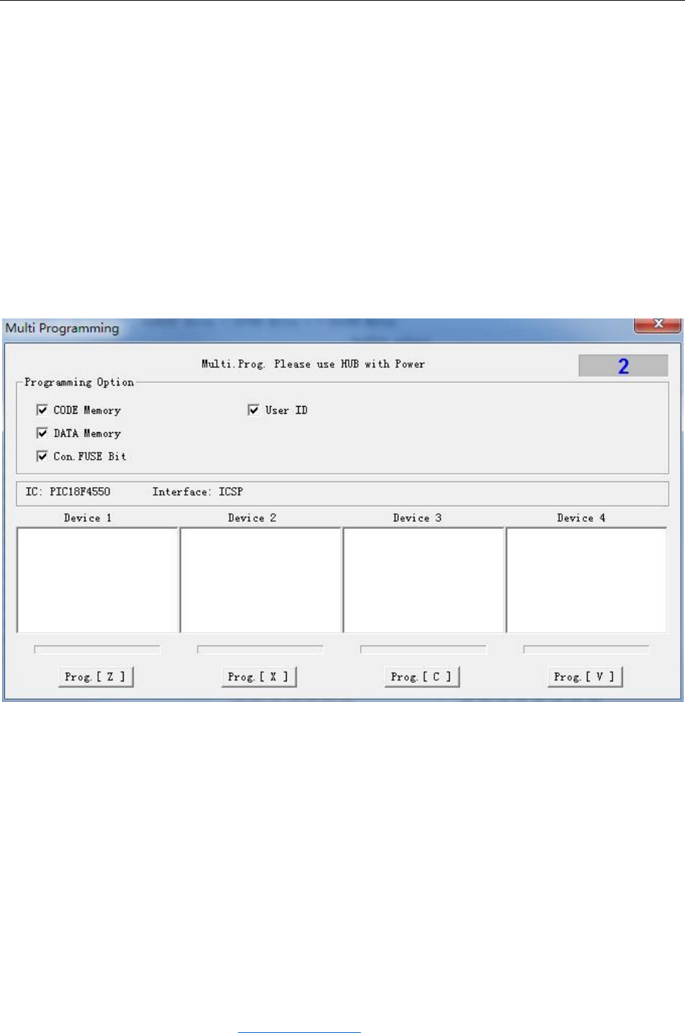
4.2.10 ICSP programming
about serial programmable chips, the programmer can programming chips through a ICSP interface
on the target board .First select ICSP port in the main interface of the "Set Interface
options bar", , then [ICSP_VCC_ENABLE] To allow the state, the default [ICSP_VCC_ENABLE] is
selected, that means programmer provide VCC power to the target board . Note that the
programmer VCC power supply can provide a maximum current of 120ma, if the target board
requires more power, please use the target board from the external power supply.
If you do not need the programmer to provide power, do not check the [ICSP_VCC_ENABLE]
button, so that when programming the VCC pin will not have VCC power supply. As shown below:
When the next operation, reading, erasing, Verify, programming and other operations, it will
be operated from the ICSP port. When operation, the 40PIN universal socket can not be inserted
into the chip at the same time. Click the [Read] button on the toolbar to pop up the following
dialogue Box: (Note that the dialog box for reading, erasing, checking, etc. is the same as
this one). ICSP port on the right shows the wiring diagram, a more detailed wiring diagram
can click [View ICSPConnection]
ICSP chip support:
XGecu TL866 Ⅱ Universal Programmer Instructions V1.01
34
Haikou Xingong Electronics Co., Ltd. http://www.xgecu.com
1、 24 Series 25 Series 93 Series,
2、 ATMEL89S51, 52, AVR ATMEGA full range, Note: High-voltage parallel programming, low-
voltage ISP programming
3、 MICROCHIP PIC10Fxxx 12Fxxx 16Fxxx 18Fxxx full range,
4、 New Mao SYNCMOS SM59Dxx SM59Rxx full range of chips
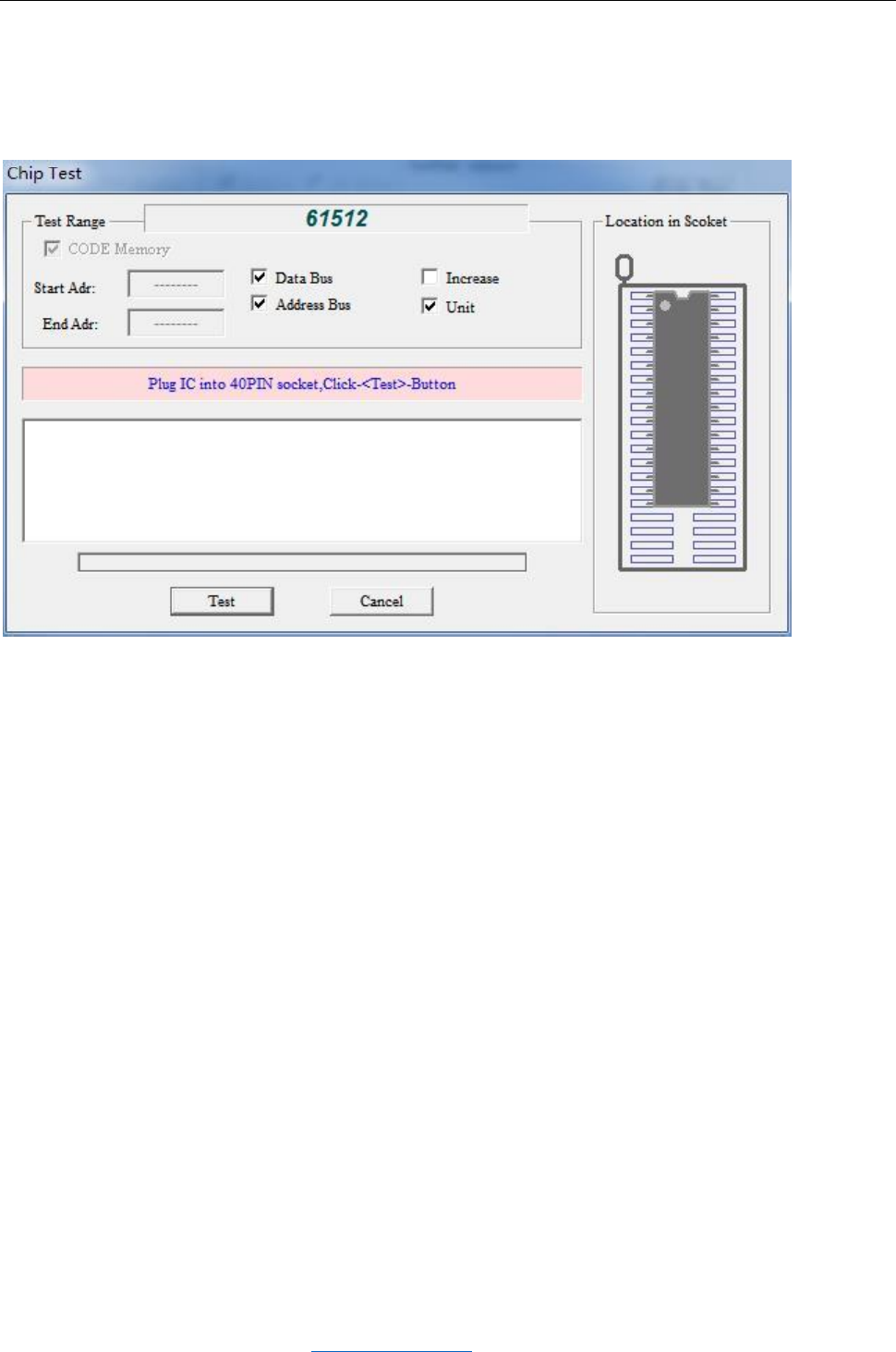
4.2.11 Multi-machine programming
Software supports up to 4 programmers at the same time programming (NAND FLASH not to hold
multi-machine programming).
USB Expansion Please choose to use a good quality USB hub with power supply,
Multi-machine programming interface is as follows: Multi-machine programming automatic Serials
numbering function can be used normally.
Multi-machine programming can use shortcut keys [Z] [X] [C] [V], start the corresponding
programmer.
XGecu TL866 Ⅱ Universal Programmer Instructions V1.01
35
Haikou Xingong Electronics Co., Ltd. http://www.xgecu.com
4.2.12 RAM test
Select the corresponding model of the RAM chip, click the toolbar 【test】 button, the following
dialog box pops up:
RAM test There are 4 ways, through these four methods of testing, basically can test the RAM
unit function is normal.
General programmer only read and write to the RAM unit is not tested out of RAM is good or
bad. For example, if two adjacent address lines are short-circuited, you are simply reading
and writing data to the RAM cell and it is impossible to detect the problem. So just one way
to test is incomplete test.
Insert the chip, click [test] button, you can test the RAM.
XGecu TL866 Ⅱ Universal Programmer Instructions V1.01
36
Haikou Xingong Electronics Co., Ltd. http://www.xgecu.com
4.2.13 Digital logic test
The programmer may be able to really test the 74 series CMOS4000 series integrated circuit,
the test can locate a gate fault.Select the corresponding digital logic integrated chip,
click the [test] button in the toolbar, the following dialog box will pop up:
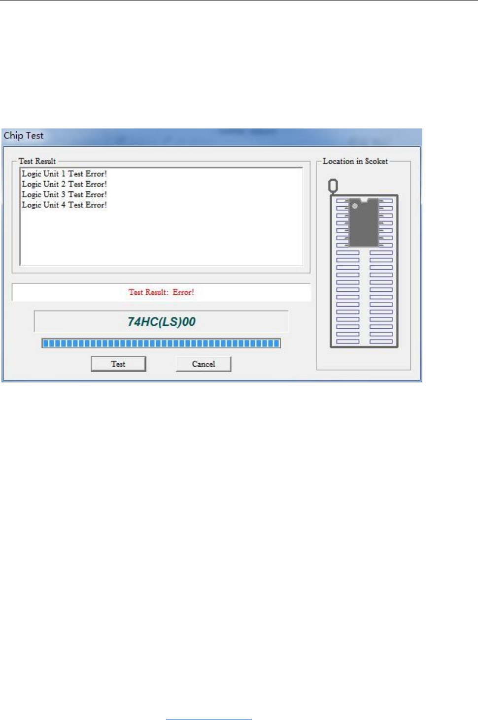
The above is the 74HC00 test results, under normal circumstances shows that each logic
unit test is normal, the message box shows a variety of input combinations tested. If a gate
of the integrated circuit is wrong, for example, the 74HC00 PIN1 is bent and broken. The test
result is as follows: The chip is wrong.
Depending on the chip, the number of logic cells is different. The logic unit number is
the same as the IC manual.

XGecu TL866 Ⅱ Universal Programmer Instructions V1.01
37
Haikou Xingong Electronics Co., Ltd. http://www.xgecu.com
5. NAND Flash programming instructions
5.1 NAND FLASH features:
A. NOR Flash Fully random access to memory-mapped and dedicated interface (such as EPROM)
address and data lines. NAND flash memory addressless line. It is through the 8/16-
bit wide interface bus to send commands, addresses and data to the internal registers,
so many master control provides a more flexible configuration, NAND flash structure,
emphasizing lower cost per bit, higher performance , And like the disk can easily
upgrade through the interface, NAND lower cost, larger capacity.
B. Nand Flash allows bad blocks to exist. Due to the NAND production process, the chip
will randomly appear in the factory bad blocks. The bad blocks have been initialized
at the factory and marked as unusable in the special area. If bad blocks appear during
use, they also need to be marked.
C. Easy to bit reversal. NAND FLASH more easy to bit reversal, if bit reversal appears in
the key files, will cause the system to hang up. Therefore, in the use of NAND FLASH
at the same time, the need to use ECC / EDC and other algorithms to ensure reliability.
D. Spare zone exists. Because NAND FLASH has the above two special places, Spare area
plays the role of deposit bad block mark, ECC value and chip information and file
information.
E. NAND FLASH must be bad block processing
NAND FLASH bad blocks deal with a lot of different companies or system providers will choose
different bad block handling methods to meet the needs of product development. TL866II
programmer defines the commonly used three methods for the user to choose to use. And the
combination of user-defined ECC algorithm for flexible applications.
5.2 Main interface:
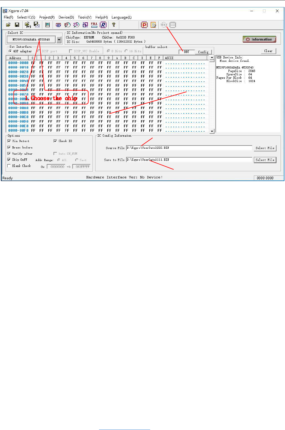
Select a chip, the software interface as shown in Figure 1-1:
XGecu TL866 Ⅱ Universal Programmer Instructions V1.01
38
Haikou Xingong Electronics Co., Ltd. http://www.xgecu.com
1、 Click this button <Select IC>
2、 Custom <BBT> Bad Block Table button
TL866II programmer, set an optional block size custom table, the table can generally be used
as a dedicated bad block table BBT, when the contents in the file is burn finished, followed
by the contents of this table can be written to and location that user set in the
configuration interface. However, the block index number written by BBT parameter settings
need to ensure that the address blocks do not overlap.
(1) The data in the BBT can be changed in the DLL custom function according to the actual
burning result of the chip.
(2) The BBT can be loaded with initial values: The file can be opened in the File menu and
the data is pre-loaded into the BBT table.
(3) This table is ignored if the option Enable BBT Programming to Block is not selected
in the programming configuration.
3、 Before reading the chip: you need to first set the file name of the archive
When programming a chip: Set the source data file name to be written to the chip.
Note: In NAND programming, the data is written directly to the chip from the set <Source
file>. Read the contents of the chip is saved directly to the file.
This operation is different from other chips, other non-NAND chip operations: programming,
the buffer data (in memory) is written to the chip. Read the chip data is read into the
computer buffer. When saving a file, the data in the cache is saved to a disk file. Open
the file is that the disk file data transferred to the computer memory.
3. The document to be written
4 archives when reading the chip
Custom bad block table
data
2.Custom bad block table button

XGecu TL866 Ⅱ Universal Programmer Instructions V1.01
39
Haikou Xingong Electronics Co., Ltd. http://www.xgecu.com
In NAND, <save file> and <open file> are operations on the BBT table's memory buffer.
This document MT29F1G08ABAEA, for example, describes the TL866II programmer NAND FLASH burning
method
The MT29F1G08 consists of 1024 blocks, the TL866II programmer operates on a block basis with
index numbers 0-1023.Each block has 64 pages (pages), each block is processed in the order
of pages written to the chip.
Each page size: 2048 bytes (Page size) + 64 bytes (Spare size) = 2112 bytes
The total chip capacity is: 2112 * 64 (pages) * 1024 (Block Block) = 138,412,032 bytes.
XGecu TL866 Ⅱ Universal Programmer Instructions V1.01
40
Haikou Xingong Electronics Co., Ltd. http://www.xgecu.com
5.3 Configuration interface
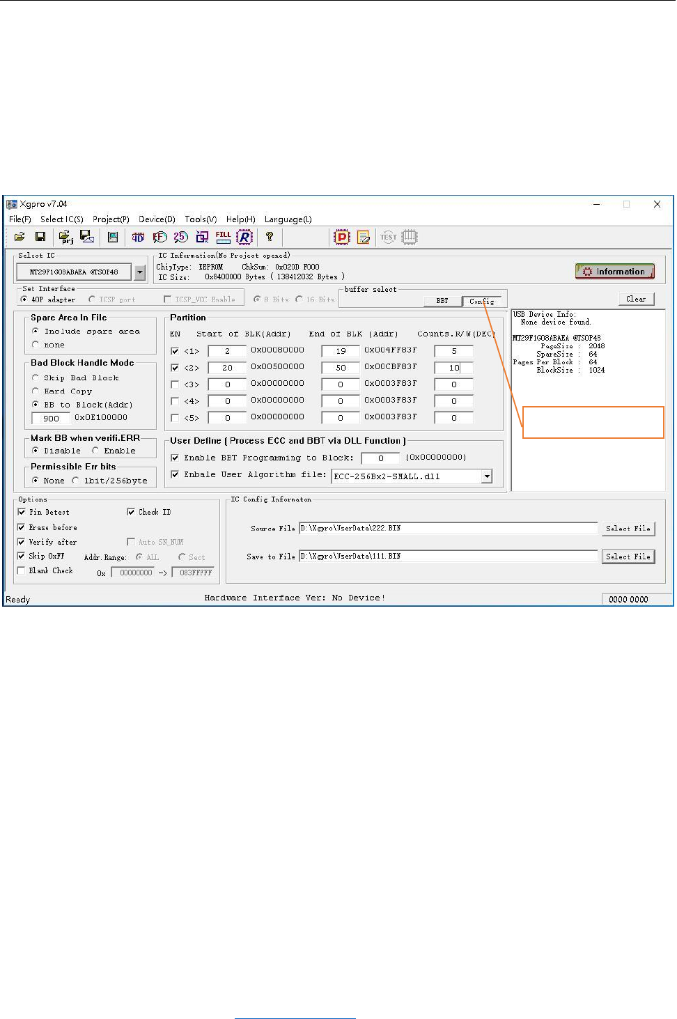
As shown below, click <Config> button to enter the programming Configration interface.
The exact configuration of the programming parameters is the key chip can be programming
normally.
Figure 1-2:
.
5.4 Configuration instructions
Spare Area In file
Include spare Area
Due to the special nature of NAND FLASH, the data in the user file contains the Spare Area
data according to the actual situation.
If not include:
Spread Area (redundant area 64 bytes) data will not be saved in the saved file when reading
the chip contents.
When programming (writing) a chip, the programmer only reads PageSize (1024) bytes of data
from the file, and the next 64 bytes of data (SpareSIze) will default to blank data (0xFF).
This situation, the general need to use user-defined algorithm files, the data in the redundant
area according to user requirements correctly filled in.
Config Button

XGecu TL866 Ⅱ Universal Programmer Instructions V1.01
41
Haikou Xingong Electronics Co., Ltd. http://www.xgecu.com
Bad Block Handle Mode
There are three ways to deal with bad blocks:
Skip Bad Block:
In the process of reading and writing chips if found bad blocks, TL866II programmer will
skip the bad block directly to the next block of data to read or write. Write Flow as
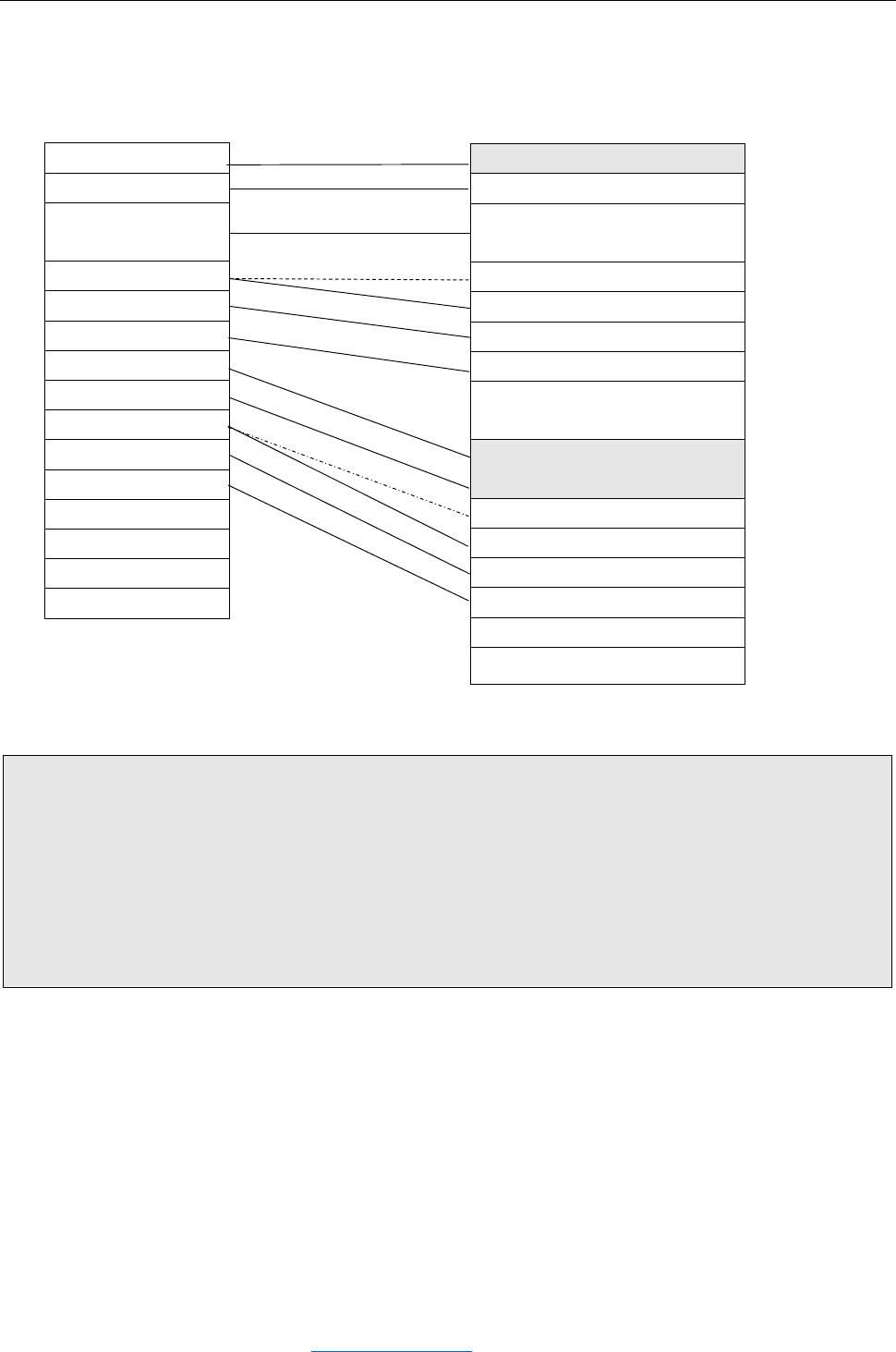
shown below Table 1-1:
Data Nand Flash
Hard Copy: Forces the data to be read or written regardless of whether or not the block has
a bad block mark, and stops programming if an error occurs during programming. This method
is usually technical maintenance, the use of memory chips replacement method.
BB to Block: Found bad blocks written to the beginning of a particular block, so the
advantage is to make the system logically feel the memory is still a continuous area,
usually used in conjunction with the partition (Partition). In the following example
configuration details. Enter the number in the edit box (Example: 900) is the replacement
block index (address) actually written to flash when a bad block is found
Mark BB When Verify Error:
When a parity error occurs after programming the data, this block is automatically marked
as bad and the data is written to the next block (Skip Bad Block), or the data is written
to a specific block . (BB to Block alternative address)
If not, the programming will be terminated when the verification error occurs.
Permissible ERR bits
None: does not allow an error to occur
1bits / 256bytes: One bit error per 256 bytes. Bit flipping may occur when reading NAND
FLASH chip and will not be considered as an error if a bit error (256 consecutive bytes)
is detected during verification. However, spare area in the data is still not allowed to
appear any bit error.
Partition
Divide the file contents into NAND FLASH. Or according to the requirements of the partition
Bad Block
Bad Block
.

XGecu TL866 Ⅱ Universal Programmer Instructions V1.01
42
Haikou Xingong Electronics Co., Ltd. http://www.xgecu.com
read into the file.
The software allows the file content is set to 5 partitions, programming respectively.
EN Options: Select whether to allow the partition.
Start of BLK: partition start block index number
End of BLK: partition end block index number
Counts of R / W: The number of blocks the programming software actually reads or programming
to this partition.
Partition parameter setting requirements:
A. All the block index number, can not be greater than NAND FLASH actually contains the
number of blocks.
B. Start of BLK ≦ End of Block, Counts of R / W ≦ (End of Block s - Start of BLK + 1)
The number of blocks actually written during partitioning (Counts of R / W) is preferably
smaller than the block size of several blocks . Make it have some margin
C. The Start of BLK for the next partition should be larger than the End of Block for the
previous partition
If you use the BB To Block option, the Bad Block replacement address should not be included
in any of these partitions. If you use a BBT table, the BBT tables should not be included
in any of these partitions.
Enable BBT Programming to Block xx
The data in the BBT table is programmed to xx BLOCK
When this option is enabled, the programmer finally writes the contents of the BBT table
to the specified xx block after all partitions (or all file data) have been written to
FLASH.
Enable User Algorithm file
Enable user-defined algorithm file
In the custom algorithm file, the user can process any data in the block before the data
processing or automatic serial number calculation, as well as ECC algorithm and so on.
BBT table data can also be automatically filled according to the bad blocks in the
programming process, so that the user can verify that the application reads the contents
correctly.
Specific methods of operation, please refer to DLL dynamic function of the original code
comments.
XGecu TL866 Ⅱ Universal Programmer Instructions V1.01
43
Haikou Xingong Electronics Co., Ltd. http://www.xgecu.com
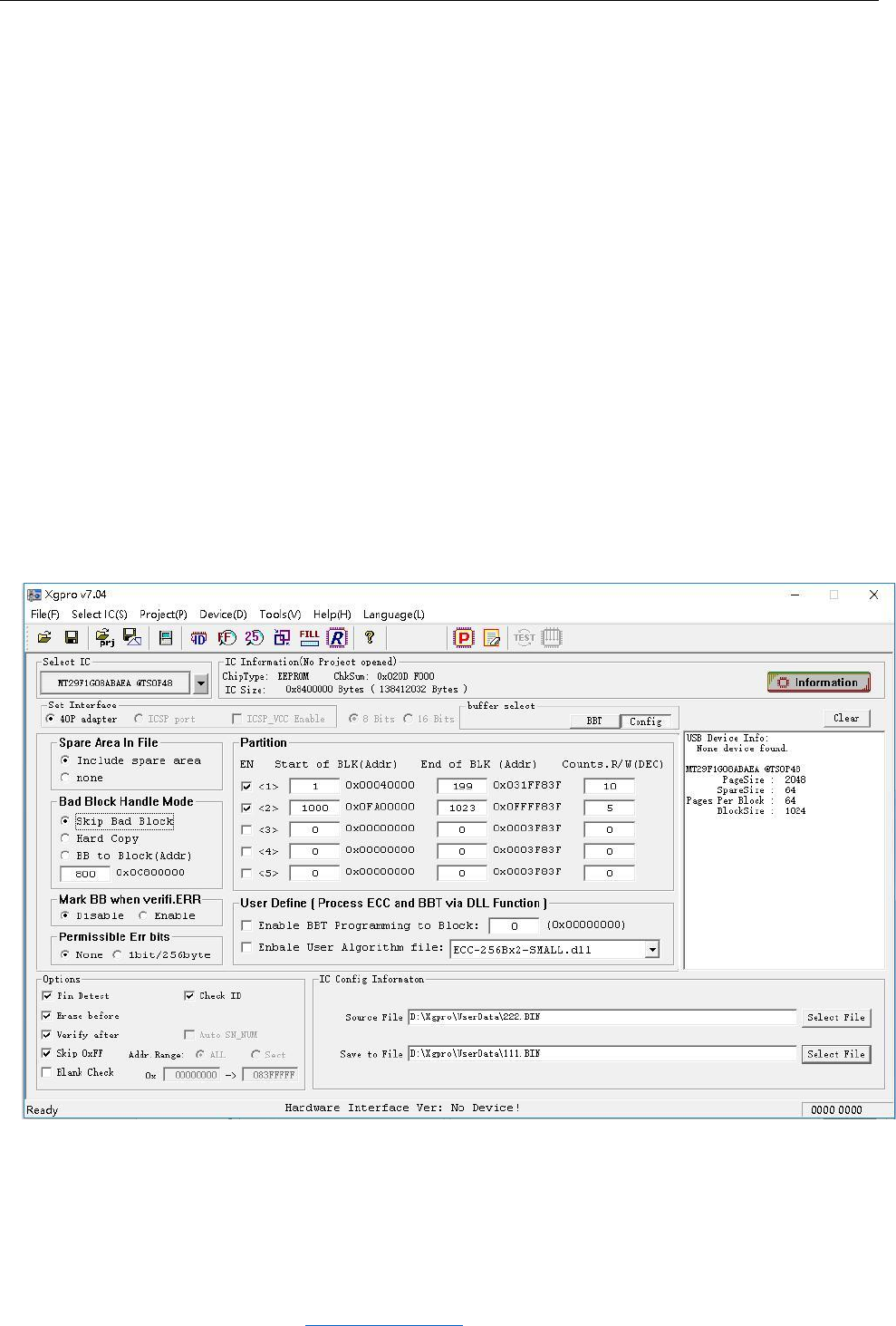
5.5 Configuration Example 1 (MT29F1G08)
1) Programming the flash with 2 partition table .
2) Bad block processing mode: Skip bad block.
3) File data: include spare area (generally the original data file needs to be handled
Spare area)
4) Use 2 partitions
1st partition: from 0 # -199 # A total of 200 BLOCK, the actual data length is 10 BLOCK
The second partition: from 1000 # - 1023 # A total of 24 BLOCKs, the actual write data
length is 5 BLOCKs
The written data file is: 222.BIN (Note: NAND programming can only use binary format
files)
Through the above settings, the programming operation can be performed.
If the file is not long enough, then the programming is finished.
If the length of the file exceeds the length of the BLOCK (15 blocks) data to be written,
programming is completed after the set number of BLOCKs have been written.
Configuration interface as shown below: Figure 1-3:
XGecu TL866 Ⅱ Universal Programmer Instructions V1.01
44
Haikou Xingong Electronics Co., Ltd. http://www.xgecu.com
The operation results are shown in Table 1-2:
File data Nand Flash
2112x64 bytes
Skipped
0# block 1th partition start
1# Block
2#…..7# block
8# Bad Block skipped
9# block
10#
11# 10 blocks end
…….
1000# Block 2th Partition
start
1001# bad Block skipped
1002#
1003#
1004#
The file starts
2112x64 bytes
2112 x64 bytes
*6 blocks
2112 x64 bytes
2112 x64 bytes
2112 x64 bytes
2112 x64 bytes
2112 x64 bytes
2112 x64 bytes
2112 x64 bytes
2112 x64 bytes
note:
In this configuration example, read or verify the chip, always by partition.
When reading:
1、 Read 10 blocks saved to the file from Partition 1.
2、 Read 5 blocks saved to the file from Partition 2.
3、 Read completed.
With setting up partitions flexibility, you can read or write a few or a single BLOCK
of data individually,
XGecu TL866 Ⅱ Universal Programmer Instructions V1.01
45
Haikou Xingong Electronics Co., Ltd. http://www.xgecu.com
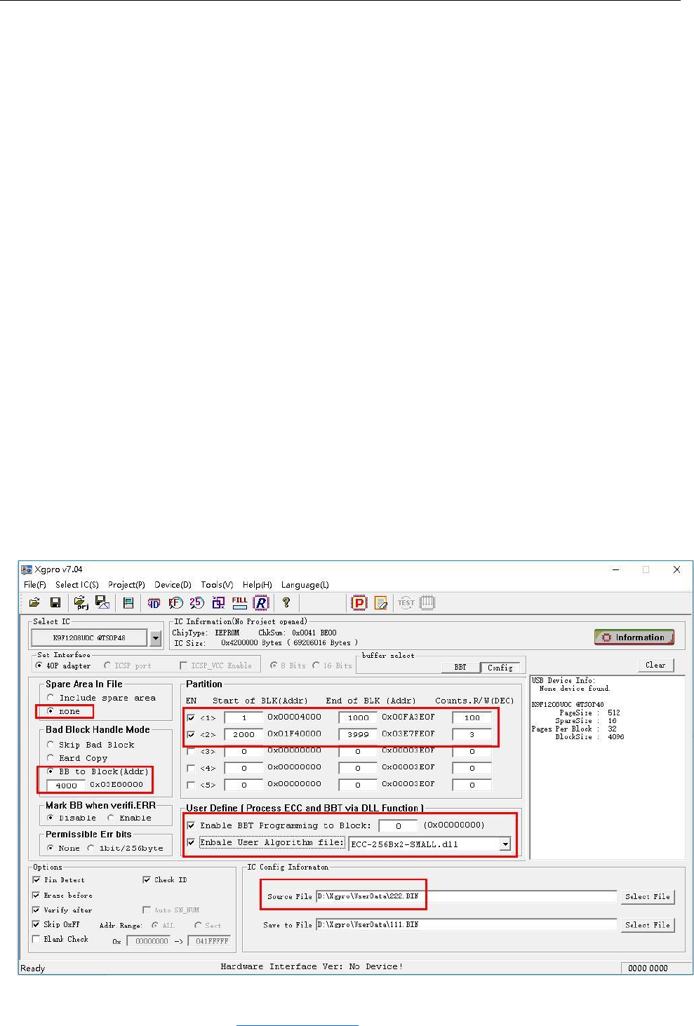
5.6 Configuration Example 2 (K9F1208U0C)
To K9F1208U0C example chip capacity: (512 +16) * 32 * 4096 blocks
K9F1208U0C parameter::
Page Size: 512 bytes
Spare size: 16 bytes
Pages Per Block : 32 pages
Block Size : 4096
1) Use (Partition) partition table NAND FLASH into the file write operation
2) Bad block processing mode: BB to Block 4000, found a bad block, write block 4000 #
start position
3) File data: not include spare area (Spare area in the DLL processing content)
4) Using 2 partitions,
1ST partition: from 0 # -1000 # A total of 1001 BLOCK, the actual length of 100 BLOCK.
2ST partition:from 2000 # - 3999 # A total of 1000 BLOCK, the actual length of 3 BLOCK.
5) The written data file is: 222.BIN (Note: NAND programming can only use binary format
files)
6) Enable BBT Programming to Block 0. The contents of the BBT table are assigned to 0 #
Block.
7) Enable User Algorithm file, enable the algorithm file, ECC_256Bx2-SMALL.dll, (the DLL
instance only calculates the ECC value into the spare area, the user can modify the DLL
function according to the actual need, modify the contents of the BBT table)
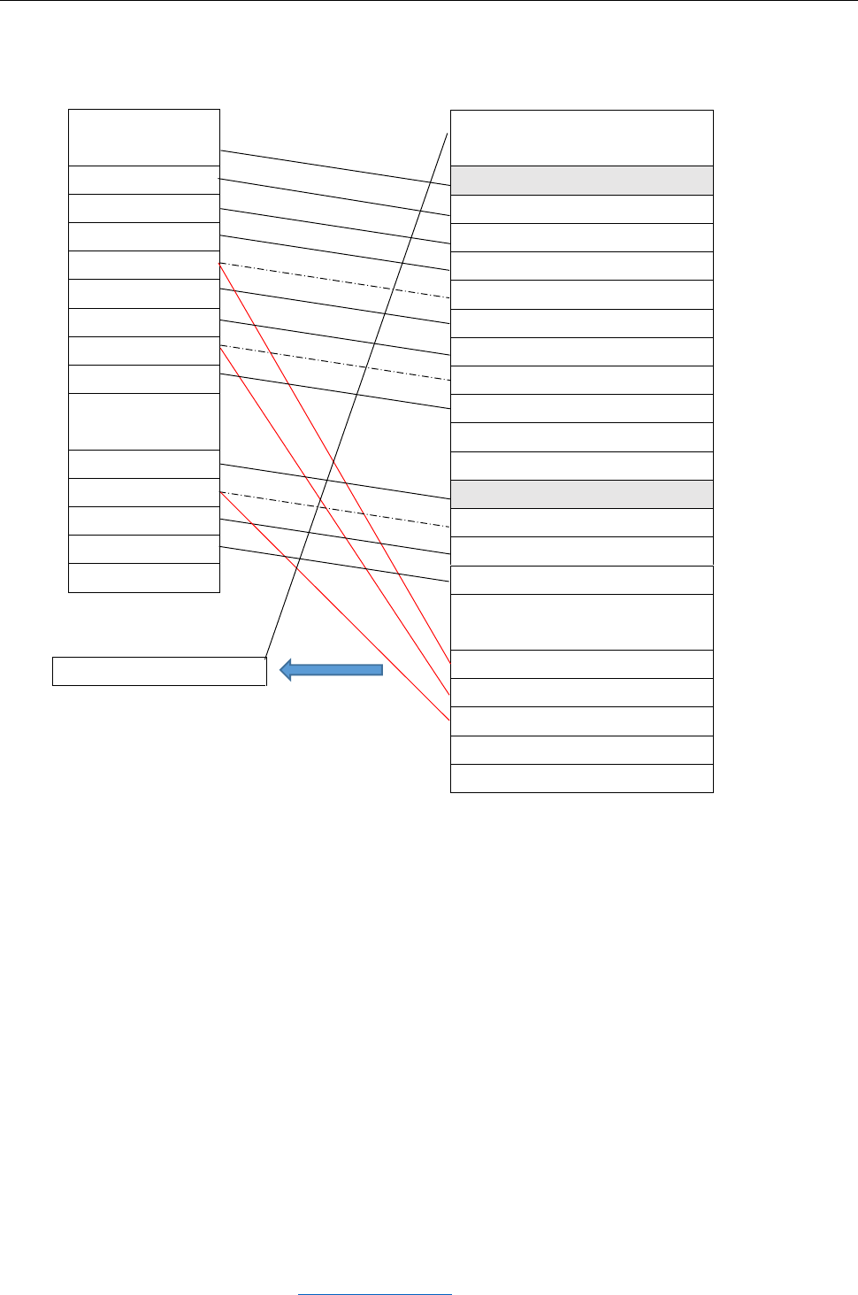
8) Proramming Flow shown in Table 1-3.
Figure 1-4:
XGecu TL866 Ⅱ Universal Programmer Instructions V1.01
46
Haikou Xingong Electronics Co., Ltd. http://www.xgecu.com
Table 1-3: Programming Flow:
File data (Not include spare) (512+16)x32bytes NAND Flash
BBT to block 0#
BBT (512+16)x32 bytes
Option User Algorithm
Note: 16 bytes Spare Area Data get from DLL function or all are 0xFF
5.7 Save the project file
All the configuration parameters and BBT table contents can be "saved project" after the
setting is completed. When it is used again, it can be directly programmed after opening
the project file and is suitable for mass production.
0# block for BBT
1# Block 1th partition start
2# block
……..
N# block
N+1# Bad Block
N+2#
…….
Bad Block
…….
2000# 2th Partition start
2001# Bad Block
2002#
2003# Programming Over
……..
4000 # Block start for BB
4001#
4002#
The file starts
512x32 bytes
512x32 bytes
……
512x32 bytes
512x32 bytes
512x32 bytes
……
512x32 bytes
512x32 bytes
……
512x32 bytes
512x32 bytes
512x32 bytes
512x32 bytes
…..

XGecu TL866 Ⅱ Universal Programmer Instructions V1.01
47
Haikou Xingong Electronics Co., Ltd. http://www.xgecu.com
6. NAND Flash Copy Method
6.1 Attention
In the process of repairing the equipment, we often need to read data from a mother chip,
copied to a new chip, and then welded to the circuit board to run, in order to ensure the
chip can operate normally, the user needs to pay attention to the following point:
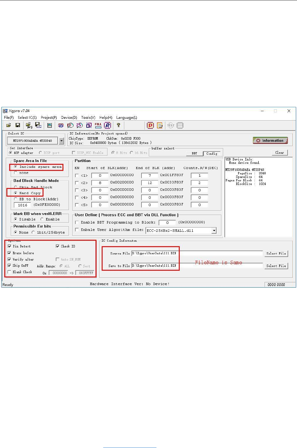
1) Configuration: with TL866II programmer software default settings.
The following figure options, you must use Hard Copy, and the file data must include:
include Spare area, all other options are default. When read in this configured mode,
the programmer software can read the entire contents of the chip (including the contents
of the bad block) to the file.
2) Some NAND FLASH chips have a unique ID, embedded system applications may read the unique ID,
and encryption operations in the program, because the unique ID is the chip factory has been
set when the factory , Can not be changed, can not be copied. In this case, even if you copy
the entire contents of the chip correctly (Include the contents of the OTP Area described
later), the new chip will not work properly.
Example: MT29F4G08ABA has 16 + 16 bytes unique ID, can only read, can not be rewritten.
Whether the application uses this method for encryption requires the user to determine
whether the chip has a unique ID according to the chip's datasheet. If yes, and if Unique
ID encryption is used, this chips can not be replaced unless you can modify the embedded
system's software.
3) OTP Area (one-time programmed memory area)
OTP Area is only part of the Nand Flash chip exists, specifically whether or not to see
the relevant chip data sheet
Example: The MT29F4G08ABA has 30 pages (30Pages * 2112 bytes) of OTP data. The TL866II does
not yet have the time to program and read the OTP Area of some NAND FLASH chips. If the OTP
Area is used in the application, The OTP data can not be copied.
(If you need to copy OTP, you can contact us)
XGecu TL866 Ⅱ Universal Programmer Instructions V1.01
48
Haikou Xingong Electronics Co., Ltd. http://www.xgecu.com
6.2 Copy steps
6.2.1 Step 1: Choose files and settings
Select or enter the file name, <save to file> and <Source file> have the same file name
Spare Area In File: Include Spare Area
Bad Block Handle Mode: Hard Copy
All other options are default settings. Figure 1-5 shows the configuration.
Figure 1-5:
XGecu TL866 Ⅱ Universal Programmer Instructions V1.01
49
Haikou Xingong Electronics Co., Ltd. http://www.xgecu.com
6.2.2 Step 2 : Read the chip
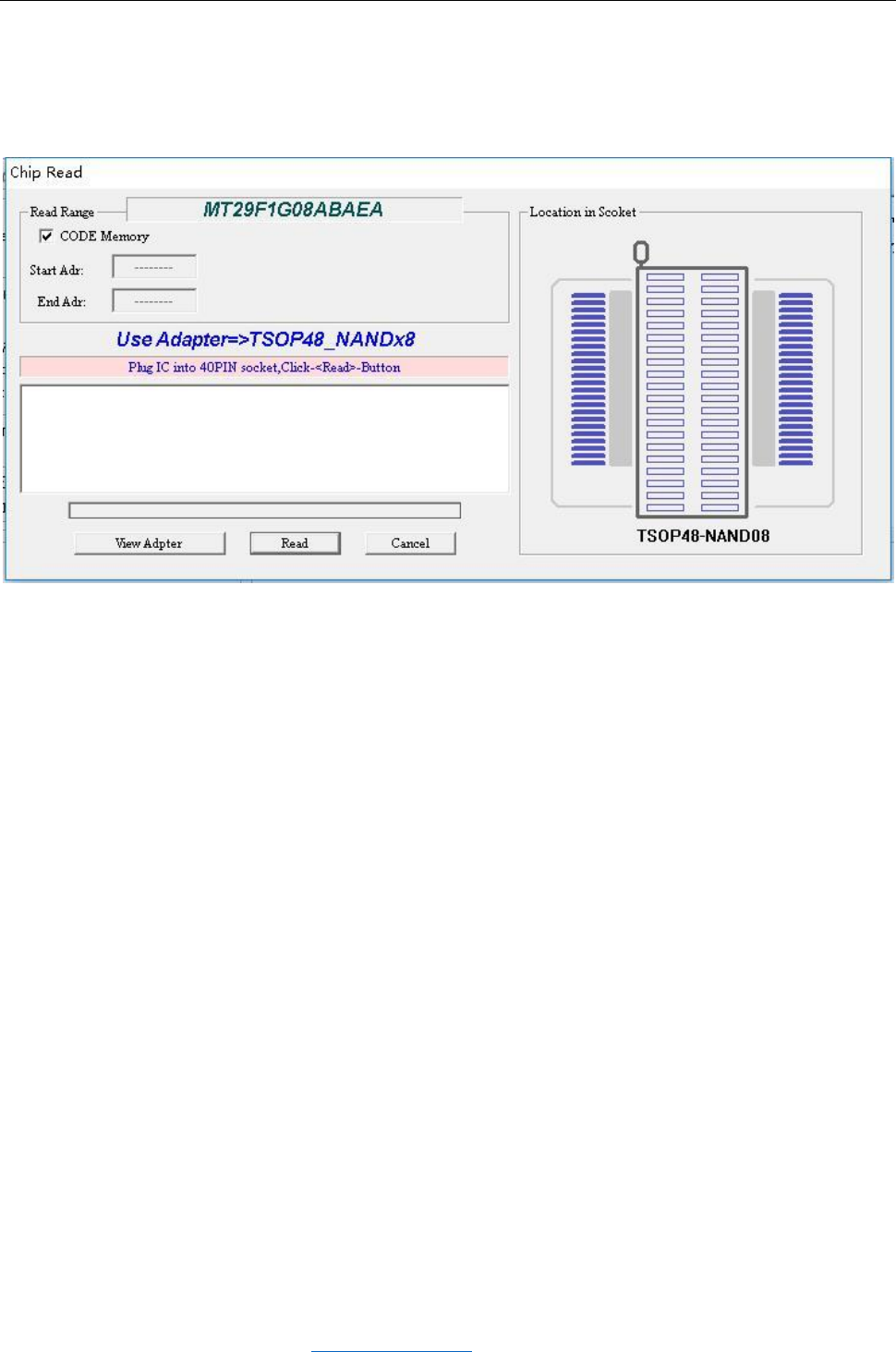
Click the <R> button on the toolbar and use a NAND08-specific adapter to place the chip. The
following dialog box will pop up
Note: This program has a pin contact check function, if there is poor contact with the use
of the pin, there will be bad tips, a small number of pins on individual chips may not be
able to use the pin to check, to ensure good contact can be Temporarily disable the pin check
function (in the lower left corner of the main interface programming options).
Until finished reading. After the reading is completed, you can click < Verify> in the main
menu to perform a data verification to ensure the correctness of data read in. (The
verification speed may be much faster than reading Speed is a normal, because TL866II
programmer software will skipped blank block automatically )
XGecu TL866 Ⅱ Universal Programmer Instructions V1.01
50
Haikou Xingong Electronics Co., Ltd. http://www.xgecu.com
6.2.3 Step 3: Programming new chip
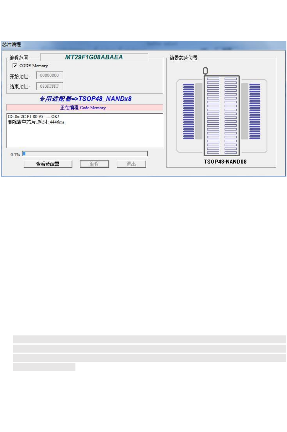
Replace the new chip, click the <P> button on the toolbar, the following interface pops up:
Note:
A. Writing chips may be faster than the reading , not surprising, because the software
automatically skip the blank area in programming .
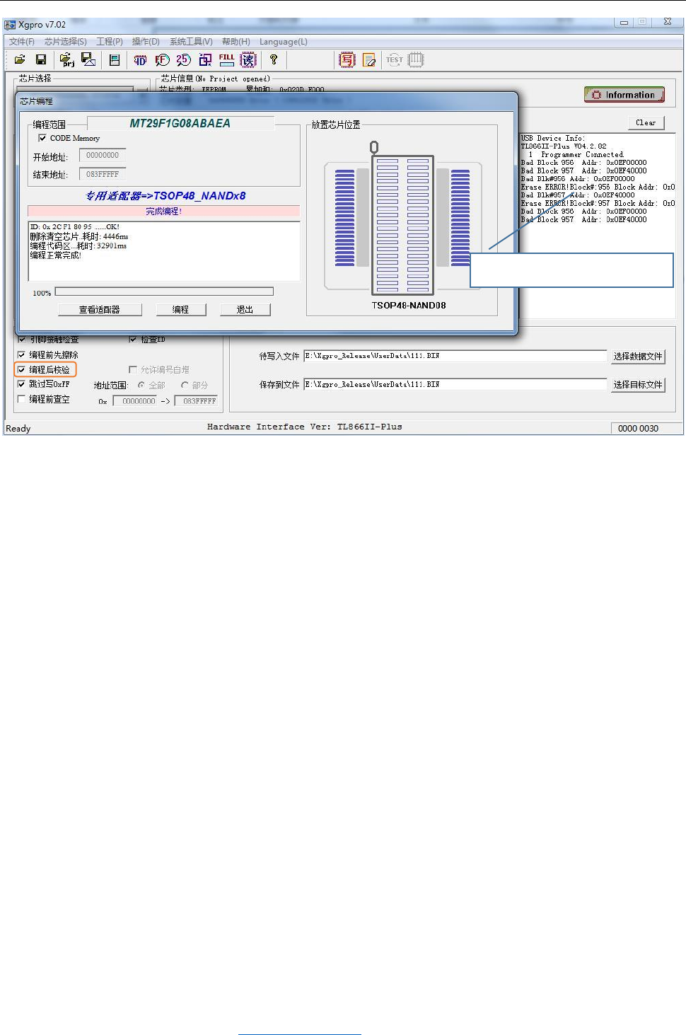
B. In reading, deleting, burning process, if there is a bad block , Bad Block Messages will
appear in the right message box , but it does not affect reading and writting.
C. No necessary to check the bad block information of source chip and the new chip before
copy , as long as the programming is correct, there is no error to stop. the new chip
will be available. if there is a bad block in the new chip, the software found the Data
is empty data here, the software can automatically skip.
If the new chip has a bad block, the source chip has data that needs to be written to
this bad block. . When copying, it can not be written to this bad block. The programming
is terminated. Please switch to another new chip to programming.
Because of maintenance technicians, generally do not know how the chip data structure,
how to deal with bad blocks. So only hard copy directly, the TL866II programmer software
process blank data by skipping, so to avoid the problem that bad blocks of new chips
can not be written .
D. Programming and verification in NAND Flash programming is done in blocks, as long as the
option "Verify after programming" is selected in the lower left corner of <Programming
Options>. After the programming is completed, the verification is completed at the same
time, and the verification does not need to be done again.
XGecu TL866 Ⅱ Universal Programmer Instructions V1.01
51
Haikou Xingong Electronics Co., Ltd. http://www.xgecu.com
6.3 File address calculation method
Calculated in two cases:
1) File contains Spare Area
Data Location in File = nBlock *(Page Size + Spare Size) * Number of Pages per Block
2) File does not contain Spare Area
Location of the data in the file = nBlock * Page Size * Pages per block
Bad block information
display

XGecu TL866 Ⅱ Universal Programmer Instructions V1.01
52
Haikou Xingong Electronics Co., Ltd. http://www.xgecu.com
7. Appendix
7.1 Disclaimer
(1) Products that have been repaired, manipulated or altered by any organization or individual
not duly authorized by us are not covered under the warranty.
(2) Locks and other products in the man-made damage, not under the responsibility of repair.
(3) Due to hardware failures or software defects caused by the expansion of the joint
responsibility.
Special
Due to the programmer, many kinds of chip support, complex software system, errors or defects
are inevitable. In mass production, special OTP one-time programming chip, you must confirm
that the programming is correct, in order to mass production. The company is not responsible
for the joint expansion losses caused by hardware failure or software defects. If you find
a problem or have a good opinion of our products, please contact us.
7.2 Warranty
Within the normal range of use, from the date of purchase of the product within one year, if the
product fails can be free warranty.
7.3 Contact us
With the software update, the contents of this manual are for reference only, product
application software shall prevail.
You can download the latest application at http://www.xgecu.com/en.
Name: Haikou Xingong Electronics Co., Ltd.
Address: Haikou City, Hainan Province, 80 QiuHaiDaDao, JInRen Hotel on the 4th floor
Zip code: 570311
EMIAL:532007590@QQ.com
TEL: 0898-68681816

XGecu TL866 Ⅱ Universal Programmer Instructions V1.01
53
Haikou Xingong Electronics Co., Ltd. http://www.xgecu.com
7.4 FAQ (frequently asked questions)
1. Device unavailable or error
Usually the USB driver is not installed, or the driver is prohibited by anti-virus
software. At this moment, the yellow light on the USB programmer blinks rapidly.
Solution: Refer to section 2.1.2, reinstall the USB device driver.
2. There was an error updating the firmware refresh, unable to refresh
Usually use the USB hub, do not use an external hub when refreshing, the device plugged
directly into the computer's USB port, upgrade refresh. If you do not still solve the
problem, you try to refresh it on another computer.
3. Pin Detect Errors
Case 1: the old chip, there will often lead to poor contact tips, carefully handle the
pin.
Case 2: If using an adapter, use a multimeter to measure if the adapter pins are normal.
Case 3: Individual pins of individual chips may not support the pin contact check. In
this case, the pin check function may be temporarily canceled in the lower left corner
of the main interface.
4. ID error detected
Many chips have a chip inside the Identification (ID), the content is generally composed
of two or more bytes, the first byte is usually the manufacturer code (Manufacture ID),
followed by the chip type or chip capacity. Different chip, ID will be different, the
function of this option is to prevent incorrect chip into. This option checks the chip
ID before reading or writing to the chip. If it continues correctly, this function is
optional. Operation will be aborted if the ID error. The default option is enable .
Similar chips not supported in the list of the chip, Their programming method may be same ,
you can choose other manufacturers IC with the same capacity of the chip for burning.
Because the ID will be different, before burning, cancel the ID check
For a very small part of the microcontroller, ID can not be read after Encrypting the chip .
At this time, the ID check should be canceled in the main interface, otherwise, the ID
check is incorrect.

XGecu TL866 Ⅱ Universal Programmer Instructions V1.01
54
Haikou Xingong Electronics Co., Ltd. http://www.xgecu.com
5. Programming about 27C Series while VPP voltage is 21V or 25V
TL866II programming voltage VPP is only supported up to 18V, for the early 27C series ROM
with 21V or 25V VPP voltage no longer be supported writing, but can be read.
If you want to use this kind of IC, you can read form the IC(Vpp is 21V or 25V). and buy a
new IC (VPP is 13V) to replace it. 27Cxx Serials Chip can be replaced directly.
Do not use the external power supply to enhance the programming voltage for forced
programming, when the chip is damaged, 21V / 25V high voltage may go back to the programmer's
internal, will damage the programmer hardware.
