TMS320F2837xD/S And TMS320F2807x Safety Manual UG (Rev. B) TMS320F2837x DS
User Manual:
Open the PDF directly: View PDF ![]() .
.
Page Count: 98
- Safety Manual for TMS320F2837xD/S and TMS320F2807x
- 1 Introduction
- 2 System Integrator Development Interface Agreement
- 3 C2000 Development Process for Management of Systematic Faults
- 4 TMS320F2837xD/S and TMS320F2807x MCU Architecture for Management of Random Faults
- 5 Brief Description of Safety Elements
- 6 Brief Description of Diagnostics
- 6.1 C2000 MCU Infrastructure Components
- 6.1.1 Clock Integrity Check Using CPU Timer
- 6.1.2 Clock Integrity Check Using HRPWM
- 6.1.3 EALLOW and MEALLOW Protection for Critical Registers
- 6.1.4 Efuse Autoload Self-Test
- 6.1.5 Efuse ECC
- 6.1.6 Efuse ECC Logic Self-Test
- 6.1.7 External Clock Monitoring via XCLKOUT
- 6.1.8 External Monitoring of Warm Reset (XRSn)
- 6.1.9 External Voltage Supervisor
- 6.1.10 External Watchdog
- 6.1.11 Glitch Filtering on Reset Pins
- 6.1.12 Hardware Disable of JTAG Port
- 6.1.13 Internal Watchdog (WD)
- 6.1.14 Lock Mechanism for Control Registers
- 6.1.15 Missing Clock Detect (MCD)
- 6.1.16 NMIWD Reset Functionality
- 6.1.17 NMIWD Shadow Registers
- 6.1.18 Multi-Bit Enable Keys for Control Registers
- 6.1.19 Online Monitoring of Temperature
- 6.1.20 Periodic Software Read Back of Static Configuration Registers
- 6.1.21 Peripheral Clock Gating (PCLKCR)
- 6.1.22 Peripheral Soft Reset (SOFTPRES)
- 6.1.23 PLL Lock Profiling Using On-Chip Timer
- 6.1.24 Reset Cause Information
- 6.1.25 Software Read Back of Written Configuration
- 6.1.26 Software Test of ERRORSTS Functionality
- 6.1.27 Software Test of Missing Clock Detect Functionality
- 6.1.28 Software Test of Reset
- 6.1.29 Software Test of Watchdog(WD) Operation
- 6.2 Processing Elements
- 6.2.1 CLA Handling of Illegal Operation and Illegal Results
- 6.2.2 CLA Liveness Check Using CPU
- 6.2.3 CPU Hardware Built-In Self-Test (HWBIST)
- 6.2.4 CPU Hardware Built-In Self-Test (HWBIST) Auto-Coverage
- 6.2.5 CPU Hardware Built-In Self-Test (HWBIST) Fault Injection Capability
- 6.2.6 CPU Hardware Built-In Self-Test (HWBIST) Timeout Feature
- 6.2.7 CPU Handling of Illegal Operation, Illegal Results and Instruction Trapping
- 6.2.8 Reciprocal Comparison by Software
- 6.2.9 Software Test of CLA
- 6.2.10 Software Test of CPU
- 6.2.11 Stack Overflow Detection
- 6.2.12 VCU CRC Check of Static Memory Contents
- 6.2.13 VCU CRC Auto Coverage
- 6.2.14 Disabling of Unused CLA Task Trigger Sources
- 6.3 Memory (Flash, SRAM and ROM)
- 6.3.1 Bit Multiplexing in Flash Memory Array
- 6.3.2 Bit Multiplexing in SRAM Memory Array
- 6.3.3 Data Scrubbing to Detect/Correct Memory Errors
- 6.3.4 Flash ECC
- 6.3.5 Flash Program Verify and Erase Verify Check
- 6.3.6 Software Test of ECC Logic
- 6.3.7 Software Test of Flash Prefetch, Data Cache and Wait-States
- 6.3.8 Access Protection Mechanism for Memories
- 6.3.9 SRAM ECC
- 6.3.10 SRAM Parity
- 6.3.11 Software Test of Parity Logic
- 6.3.12 Software Test of SRAM
- 6.4 On-Chip Communication Including Bus-Arbitration
- 6.4.1 1oo2 Software Voting Using Secondary Free Running Counter
- 6.4.2 DMA Overflow Interrupt
- 6.4.3 Event Timestamping Using IPC Counter
- 6.4.4 Maintaining Interrupt Handler for Unused Interrupts
- 6.4.5 Majority Voting and Error Detection of Link Pointer
- 6.4.6 PIE Double SRAM Comparison Check
- 6.4.7 PIE Double SRAM Hardware Comparison
- 6.4.8 Power-Up Pre-Operational Security Checks
- 6.4.9 Software Check of X-BAR Flag
- 6.4.10 Software Test of ePIE Operation Including Error Tests
- 6.4.11 Disabling of Unused DMA Trigger Sources
- 6.5 Digital I/O
- 6.5.1 ECAP Application Level Safety Mechanism
- 6.5.2 ePWM Application Level Safety Mechanism
- 6.5.3 ePWM Fault Detection Using XBAR
- 6.5.4 ePWM Safe State Assertion Using Trip Mechanism
- 6.5.5 ePWM Synchronization Check
- 6.5.6 eQEP Application Level Safety Mechanisms
- 6.5.7 eQEP Quadrature Watchdog
- 6.5.8 eQEP Software Test of Quadrature Watchdog Functionality
- 6.5.9 Hardware Redundancy
- 6.5.10 HRPWM Built-In Self-Check and Diagnostic Capabilities
- 6.5.11 Information Redundancy Techniques
- 6.5.12 Monitoring of ePWM by eCAP
- 6.5.13 Monitoring of ePWM by ADC
- 6.5.14 Online Monitoring of Interrupts and Events
- 6.5.15 SDFM Comparator Filter for Online Monitoring
- 6.5.16 SD Modulator Clock Fail Detection Mechanism
- 6.5.17 Software Test of Function Including Error Tests
- 6.6 Analogue I/O
- 6.6.1 ADC Information Redundancy Techniques
- 6.6.2 ADC Input Signal Integrity Check
- 6.6.3 ADC Signal Quality Check by Varying Acquisition Window
- 6.6.4 CMPSS Ramp Generator Functionality Check
- 6.6.5 DAC to ADC Loopback Check
- 6.6.6 DAC to Comparator Loopback Check
- 6.6.7 Opens/Shorts Detection Circuit for ADC
- 6.6.8 VDAC Conversion by ADC
- 6.6.9 Disabling Unused Sources of SOC Inputs to ADC
- 6.7 Data Transmission
- 6.7.1 Bit Error Detection
- 6.7.2 CRC in Message
- 6.7.3 DCAN Acknowledge Error Detection
- 6.7.4 DCAN Form Error Detection
- 6.7.5 DCAN Stuff Error Detection
- 6.7.6 EMIF Access Latency Profiling Using On-Chip Timer
- 6.7.7 EMIF Access Protection Mechanism
- 6.7.8 EMIF Asynchronous Memory Timeout Protection Mechanism
- 6.7.9 I2C Access Latency Profiling Using On-Chip Timer
- 6.7.10 Information Redundancy Techniques Including End-to-End Safeing
- 6.7.11 I2C Data Acknowledge Check
- 6.7.12 McBSP Receiver Overrun Detection
- 6.7.13 McBSP Receiver Sync Error Detection
- 6.7.14 McBSP Transmitter Sync Error Detection
- 6.7.15 McBSP Transmitter Underflow Detection
- 6.7.16 Parity in Message
- 6.7.17 SCI Break Error Detection
- 6.7.18 SCI Frame Error Detection
- 6.7.19 SCI Overrun Error Detection
- 6.7.20 Software Test of Function Using I/O Loopback
- 6.7.21 SPI Data Overrun Detection
- 6.7.22 Transmission Redundancy
- 6.1 C2000 MCU Infrastructure Components
- 7 References
- Appendix A Safety Architecture Configurations
- Appendix B Terms and Definitions
- Appendix C Summary of Safety Features and Diagnostics
- Revision History
- Important Notice

1
SPRUI78B–July 2016–Revised June 2018
Submit Documentation Feedback Copyright © 2016–2018, Texas Instruments Incorporated
Safety Manual for TMS320F2837xD/S and TMS320F2807x
User's Guide
SPRUI78B–July 2016–Revised June 2018
Safety Manual for TMS320F2837xD/S and TMS320F2807x
This document is the Functional Safety Manual for the Delfino™ TMS320F2837xD/S and Piccolo™
TMS320F2807x MCU series from Texas Instruments C2000™ real-time microcontroller product line. The
C2000 product line utilizes a common safety architecture that is implemented for multiple products in
automotive and industrial applications.
Contents
1 Introduction ................................................................................................................... 2
2 System Integrator Development Interface Agreement.................................................................. 7
3 C2000 Development Process for Management of Systematic Faults............................................... 10
4 TMS320F2837xD/S and TMS320F2807x MCU Architecture for Management of Random Faults ............. 18
5 Brief Description of Safety Elements .................................................................................... 31
6 Brief Description of Diagnostics .......................................................................................... 46
7 References .................................................................................................................. 69
Appendix A Safety Architecture Configurations.............................................................................. 70
Appendix B Terms and Definitions ............................................................................................ 73
Appendix C Summary of Safety Features and Diagnostics ................................................................ 75
List of Figures
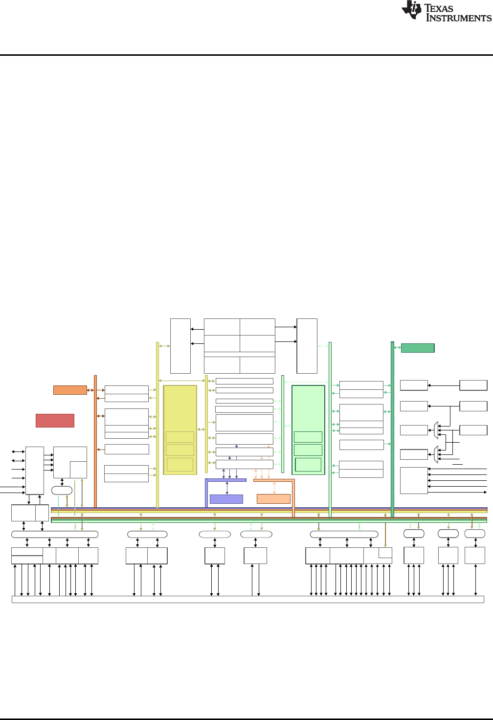
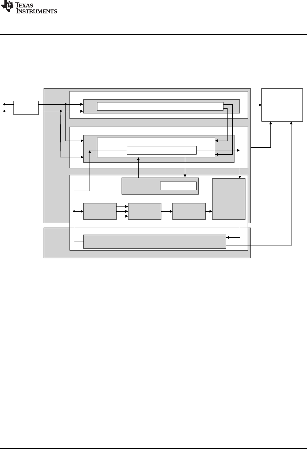
1 Functional Block Diagram of TMS320F2837xD MCU .................................................................. 4
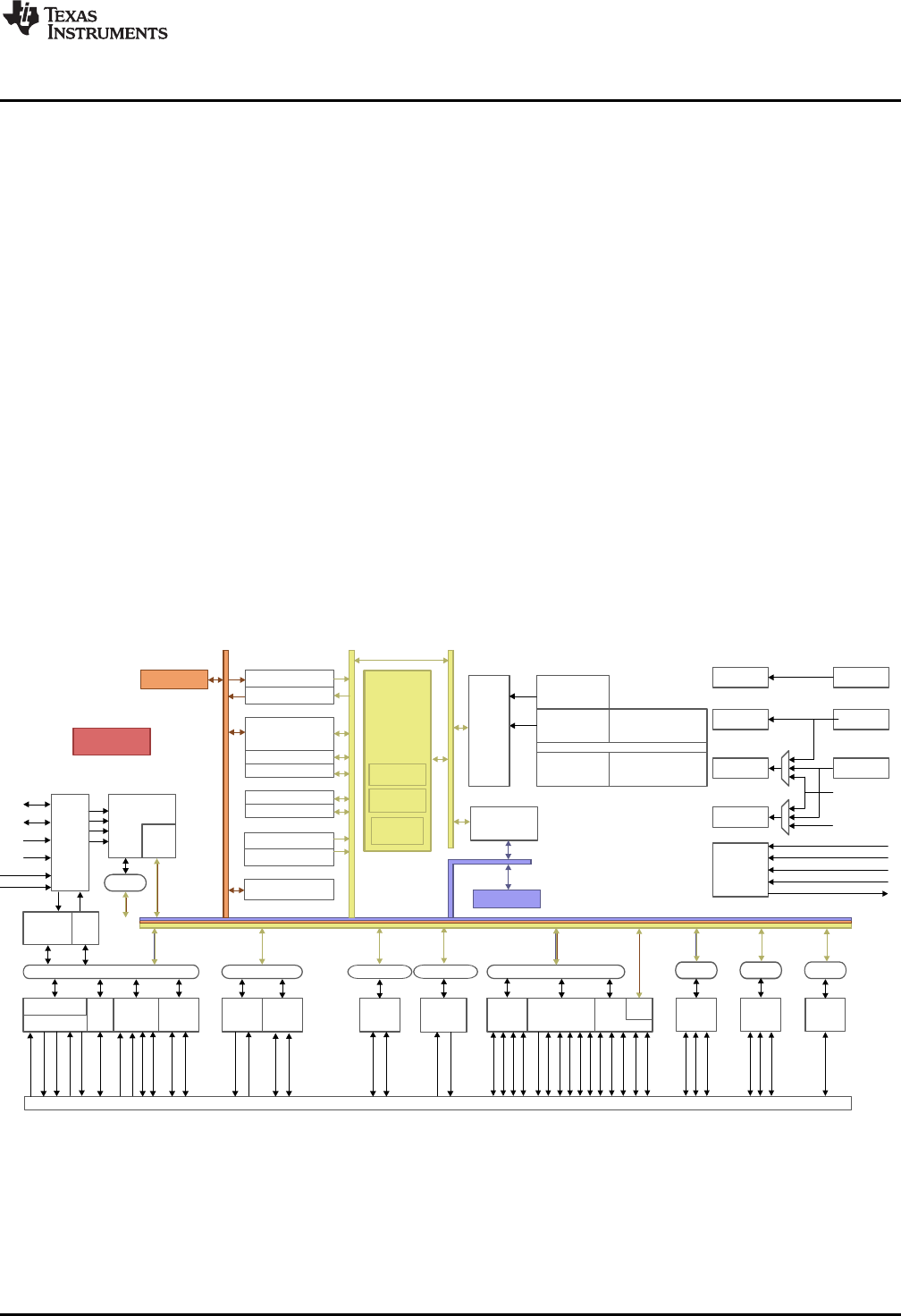
2 Functional Block Diagram of TMS320F2837xS MCU................................................................... 5
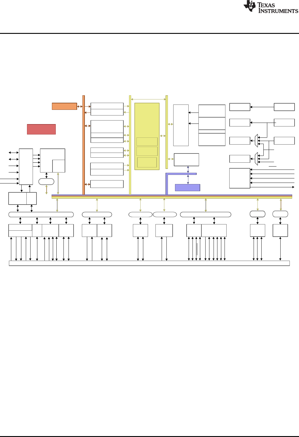
3 Functional Block Diagram of TMS320F2807x MCU .................................................................... 6
4 TI (Companywide) New Product Development Flow .................................................................. 12
5 TI Business Debrief Process Model ..................................................................................... 13
6 Application of fRMethodology Flow in C2000 Context ................................................................ 15
7 Software Development V Model.......................................................................................... 17
8 Definition of the C2000 MCU Used in a Compliant Item.............................................................. 18
9 E-GAS System Overview From Standard............................................................................... 19
10 VDA E-Gas Monitoring Concept Applied to C2000 MCU............................................................. 20
11 Relationship Between DTI, Fault Reaction Time and FTTI........................................................... 21
12 Illustration of FTTI.......................................................................................................... 21
13 Reciprocal Comparison Implementation ................................................................................ 23
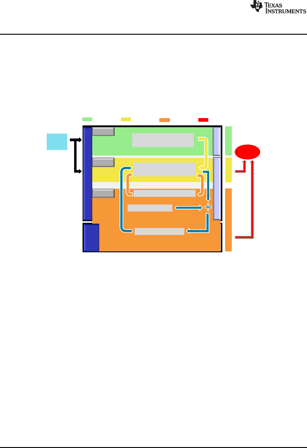
14 C2000 MCU Delfino F2837xD With Safety Features.................................................................. 25
15 C2000 MCU Delfino F2837xD Device Block Diagram With Safety Partitioning ................................... 26
16 C2000 MCU Safe State Definition ....................................................................................... 27
17 C2000 MCU Device Operating States................................................................................... 28
18 C2000 MCU CPU Start-Up Timeline .................................................................................... 29
19 Fault Response Severity .................................................................................................. 30
20 Generic Hardware of a System........................................................................................... 31
21 CLA Liveness Check....................................................................................................... 51
22 ePWM Fault Detection Using X-BAR.................................................................................... 58
23 Monitoring of ePWM by ADC ............................................................................................. 61
24 DAC to ADC Loopback.................................................................................................... 64
25 Opens/Shorts Detection Circuit........................................................................................... 64

Introduction
www.ti.com
2SPRUI78B–July 2016–Revised June 2018
Submit Documentation Feedback
Copyright © 2016–2018, Texas Instruments Incorporated
Safety Manual for TMS320F2837xD/S and TMS320F2807x
26 McBSP Reception Data Path............................................................................................. 67
27 McBSP Transmission Data Path ......................................................................................... 67
28 ISO26262 Illustration of Item, System, Component, Hardware Part and Software Unit .......................... 73
List of Tables
1 Acronyms and Expansions ................................................................................................. 3
2 ADC Open-Shorts Detection Circuit Truth Table....................................................................... 65
3 Safety Architecture Configurations....................................................................................... 70
4 Summary Table Legend................................................................................................... 75
5 Summary of Safety Features and Diagnostic........................................................................... 76
Trademarks
Delfino, Piccolo, C2000, SafeTI are trademarks of Texas Instruments.
All other trademarks are the property of their respective owners.
1 Introduction
The products supported by this document are developed according to a quality managed (QM) process
and marketed as SafeTI-QM (http://www.ti.com/ww/en/functional_safety/safeti/SafeTI-Quality-
Managed.html) for use in functional safety related system designs. SafeTI component design package
(see Section 2.1) associated with this device includes documentation to support evaluation of suitability for
use in functional safety system designs. This Functional Safety Manual is part of the SafeTI design
package to aid customers who are designing systems in compliance with ISO26262 or IEC61508
functional safety standards.
1.1 About This Document
This Functional Safety Manual provides information needed by system developers to assist in the creation
of a functional safety system using a C2000 microcontroller (MCU). This document contains:
• Overview of Delfino TMS320F2837xD/S and Piccolo TMS320F2807x MCU product architectures
• Overview of the development process utilized to reduce systematic failures
• Overview of the safety architecture for management of random failures
• Details of architecture partitions and implemented safety mechanisms
It is expected that the user of this document should have a general familiarity with the Delfino
TMS320F2837xD/S and Piccolo TMS320F2807x MCU product family. More information can be found at
http://www.ti.com/C2000. This document is intended to be used in conjunction with the device-specific
data sheets, technical reference manuals, and other documentation for the products being supplied.

www.ti.com
Introduction
3
SPRUI78B–July 2016–Revised June 2018
Submit Documentation Feedback Copyright © 2016–2018, Texas Instruments Incorporated
Safety Manual for TMS320F2837xD/S and TMS320F2807x
1.2 Acronyms Used in This Document
Table terms and definitions ready for reference are listed in Table 1.
Table 1. Acronyms and Expansions
Acronyms Expansion
ADC Analog-to-Digital Converter
ASIL Automotive Safety Integrity Level (ISO 26262)
CLA Control Law Accelerator
CPU Central Processing Unit
CRC Cyclic Redundancy Check
DAC Digital-to-Analog Converter
DTI Diagnostic Test Interval
E/E/PE Electrical/Electronic/Programmable Electronic
E2E End-to-End Protocol
EMIF External Memory Interface
ePIE enhanced Peripheral Interrupt Expansion
ePWM enhanced Pulse Width Modulator
eQEP enhanced Quadrature Encoder Pulse
EUC Equipment Under Control
FMEDA Failure Mode Effects and Diagnostic Analysis
FPU Floating Point Unit
FSA Functional Safety Assessment
FSM Functional Safety Manual
FTA Fault Tree Analysis
FTTI Fault Tolerant Time Interval
HARA Hazard Analysis and Risk Assessment
HFT Hardware Fault Tolerance
IEC International Electro Technical Commission
ISO International Organization for Standardization
MCU Microcontroller Unit
MTBF Mean Time Between Failure
OTP One Time Configurable
PWM Pulse Width Modulator
SIL Safety Integrity Level
TI Texas Instruments Inc.
TMU Trigonometric Math Unit
VCU Viterbi, Complex Math and CRC Unit
Data Bus Bridge
16-/12-bit ADC
x 4
ADC
Result
Regs
Peripheral Frame 1
GPIO MUX, Input X-BAR, Output X-BAR
Secure Memories
shown in Red
Comparator
Subsystem
(CMPSS)
DAC
x 3
Config
Data Bus
Bridge
ePWM-1/../12 eCAP-
1/../6 eQEP-1/2/3
HRPWM-1/../8
SDFM-1/2
EXTSYNCIN
EXTSYNCOUT
TZ1-TZ6
ECAPx
EQEPxA
EQEPxB
EPWMxA
EPWMxB
EQEPxI
EQEPxS
SDx_Dy
SDx_Cy
SCI-
A/B/C/D
(16 L FIFO)
I2C-A/B
(16 L FIFO)
Data Bus Bridge
SCITXDx
SCIRXDx
SDAx
SCLx
CAN-
A/B
(32-MBOX)
CANRXx
CANTXx
Data Bus Bridge
USBDP
USBDM
USB
Ctrl /
PHY
GPIO
Data Bus
Bridge
GPIOn
EMIF1
Data Bus
Bridge
EM1Dx
EM1Ax
EM1CTLx
EMIF2
Data Bus
Bridge
EM2Dx
EM2Ax
EM2CTLx
A
D
B
C
JTAG
AUXCLKIN
External Crystal or
Oscillator
Watchdog
Main PLL
Aux PLL
INTOSC1
INTOSC2
Low-Power
Mode Control GPIO MUX
TRST
TCK
TDI
TMS
TDO
MEMCPU1
CPU1.CLA1 Bus
C28 CPU-1
CPU Timer 0
CPU Timer 1
CPU Timer 2
ePIE
up to 192(
interrupts)
WD Timer
NMI-WDT
CPU1.CLA1 to CPU1
128x16 MSG RAM
CPU1 to CPU1.CLA1
128x16 MSG RAM
Boot-ROM 32Kx16
Nonsecure
S
Secure-ROM 32Kx16
ecure
CPU1.D0 RAM 2Kx16
CPU1.D1 RAM 2Kx16
CPU1 Local Shared
6x 2Kx16
LS0-LS5 RAMs
CPU1.CLA1
CPU1.DMA
FPU
VCU-II
TMU
Analog
MUX
A5:0
B5:0
C5:2
ADCIN14
ADCIN15
D5:0
Peripheral Frame 2
SPI-
A/B/C
(16 L FIFO)
SPISIMOx
SPISOMIx
SPICLKx
SPISTEx
McBSP-A/B
MDXx
MRXx
MCLKXx
MCLKRx
MFSXx
MFSRx
UPPAD[7:0]
UPPACLK
UPPAEN
UPPAWT
UPPAST
uPP RAM
CPU1.CLA1 Data ROM
(4Kx16)
CPU1 Buses
Copyright © 2016, Texas Instruments Incorporated
CPU2 Buses
PSWD
Dual
Code
Security
Module
+
Emulation
Code
Security
Logic
(ECSL)
PUMP
Flash
256K x 16
Secure
User-Configurable
DCSM
OTP
1K x 16
OTP/Flash
Wrapper
User-Configurable
DCSM
OTP
1K x 16
Flash
256K x 16
Secure
PSWD
Dual
Code
Security
Module
+
Emulation
Code
Security
Logic
(ECSL)
C28 CPU-2
CPU Timer 0
CPU Timer 1
CPU Timer 2
ePIE
up to 192(
interrupts)
WD Timer
NMI-WDT
FPU
VCU-II
TMU
MEMCPU2
CPU1.M0 RAM 1KX16
CPU1.M1 RAM 1KX16
CPU1.M0 RAM 1KX16
CPU1.M1 RAM 1KX16
Interprocessor
Communication
(IPC)
Module
Global Shared
16x 4Kx16
GS0-GS15 RAMs
CPU2.DMA
CPU1 to CPU2
1Kx16 MSG RAM
CPU1 to CPU2
1Kx16 MSG RAM
CPU1.CLA1 Bus
CPU1.CLA1 Bus
CPU2.CLA1
OTP/Flash
Wrapper
CPU1.CLA1 to CPU1
128x16 MSG RAM
CPU1 to CPU1.CLA1
128x16 MSG RAM
Boot-ROM 32Kx16
Nonsecure
S
Secure-ROM 32Kx16
ecure
CPU1.D0 RAM 2Kx16
CPU1.D1 RAM 2Kx16
CPU1 Local Shared
6x 2Kx16
LS0-LS5 RAMs
CPU1.CLA1 Data ROM
(4Kx16)
Introduction
www.ti.com
4SPRUI78B–July 2016–Revised June 2018
Submit Documentation Feedback
Copyright © 2016–2018, Texas Instruments Incorporated
Safety Manual for TMS320F2837xD/S and TMS320F2807x
1.3 C2000 Architecture and Product Overview
The TMS320F2837xD/S and TMS320F2807x are powerful 32-bit floating-point microcontroller unit (MCU)
designed for advanced closed-loop control in automotive and industrial applications.
1.3.1 TMS320F2837xD Delfino MCU
TMS320F2837xD supports two instances of the C28x + CLA architecture (four processing elements) that
significantly boosts system performance. The integrated analog and control peripherals also let designers
consolidate control architectures and reduce multiprocessor use in some of the high-end systems.
The C28x CPUs are further boosted by the Trigonometric Math Unit (TMU) accelerator that enables fast
execution of algorithms with trigonometric operations common in transforms and torque loop calculations.
The Viterbi, Complex Math and CRC Unit (VCU) accelerator reduces the time for complex math
operations common in encoded applications. Users may refer to Accelerators: Enhancing the Capabilities
of the C2000™ MCU Family to see how the accelerators can be employed to increase the performance of
the MCU in many real-time applications.
The CLA is an independent 32-bit floating-point accelerator that runs at the same speed as the main C28x
CPU, responding to peripheral triggers with minimum event latency and executing code concurrently with
the main CPU.
The TMS320F2837xD supports up to 1MB (512KW) of onboard Flash memory with error correction code
(ECC) and up to 204KB (102KW) of SRAM. Two 128-bit secure zones are also available on each CPU for
code protection.
Figure 1. Functional Block Diagram of TMS320F2837xD MCU
Data Bus Bridge
16-/12-bit ADC
x 4
ADC
Result
Regs
Peripheral Frame 1
GPIO MUX, Input X-BAR, Output X-BAR
Secure Memories
shown in Red
Comparator
Subsystem
(CMPSS)
DAC
x 3
Config
Data Bus
Bridge
ePWM-1/../12 eCAP-
1/../6 eQEP-1/2/3
HRPWM-1/../8
SDFM-1/2
EXTSYNCIN
EXTSYNCOUT
TZ1-TZ6
ECAPx
EQEPxA
EQEPxB
EPWMxA
EPWMxB
EQEPxI
EQEPxS
SDx_Dy
SDx_Cy
SCI-
A/B/C/D
(16L FIFO)
I2C-A/B
(16L FIFO)
Data Bus Bridge
SCITXDx
SCIRXDx
SDAx
SCLx
CAN-
A/B
(32-MBOX)
CANRXx
CANTXx
Data Bus Bridge
USBDP
USBDM
USB
Ctrl /
PHY
GPIO
Data Bus
Bridge
GPIOn
EMIF1
Data Bus
Bridge
EM1Dx
EM1Ax
EM1CTLx
EMIF2
Data Bus
Bridge
EM2Dx
EM2Ax
EM2CTLx
A
D
B
C
JTAG
AUXCLKIN
External Crystal or
Oscillator
Watchdog
Main PLL
Aux PLL
INTOSC1
INTOSC2
Low-Power
Mode Control GPIO MUX
TRST
TCK
TDI
TMS
TDO
MEMCPU1
Global Shared
16x 4Kx16
GS0-GS15 RAMs
CPU1.CLA1 Bus
C28 CPU-1
CPU Timer 0
CPU Timer 1
CPU Timer 2
ePIE
up to 192(
interrupts)
WD Timer
NMI-WDT
CPU1.CLA1 Data ROM
(4Kx16)
CPU1.CLA1 to CPU1
128x16 MSG RAM
CPU1 to CPU1.CLA1
128x16 MSG RAM
Boot-ROM 32Kx16
Nonsecure
S
Secure-ROM 32Kx16
ecure
CPU1.M0 RAM 1Kx16
CPU1.M1 RAM 1Kx16
CPU1.D0 RAM 2Kx16
CPU1.D1 RAM 2Kx16
CPU1 Local Shared
6x 2Kx16
LS0-LS5 RAMs
CPU1.CLA1
CPU1.DMA
PSWD
Dual
Code
Security
Module
+
Emulation
Code
Security
Logic
(ECSL)
PUMP
Flash Bank 0
256K x 16
Secure
(F28377S, F23875S only)
256K x 16
Secure
Flash Bank 1
User-Configurable
DCSM
OTP
1K x 16
Flash Wrapper for
Bank 0
FPU
VCU-II
TMU
Analog
MUX
A5:0
B5:0
C5:2
ADCIN14
ADCIN15
D5:0
Peripheral Frame 2
SPI-
A/B/C
(16L FIFO)
SPISIMOx
SPISOMIx
SPICLKx
SPISTEx
McBSP-A/B
MDXx
MRXx
MCLKXx
MCLKRx
MFSXx
MFSRx
UPPAD[7:0]
UPPACLK
UPPAEN
UPPAWT
UPPAST
uPP RAM
(F28377S, F28375S only)
Flash Wrapper for
Bank 1
CPU1 Buses
Copyright © 2016, Texas Instruments Incorporated
www.ti.com
Introduction
5
SPRUI78B–July 2016–Revised June 2018
Submit Documentation Feedback Copyright © 2016–2018, Texas Instruments Incorporated
Safety Manual for TMS320F2837xD/S and TMS320F2807x
Performance analog and control peripherals are also integrated to further enable system consolidation.
Four independent 12/16-bit ADCs provide precise and efficient management of multiple analog signals,
which ultimately boosts system throughput. The new sigma-delta filter module (SDFM) works in
conjunction with the sigma-delta modulator to enable isolated current shunt measurements. The
Comparator Subsystem (CMPSS) with windowed comparators allows for protection of power stages when
current limit conditions are exceeded or not met. Other analog and control peripherals include the Digital-
to-Analog Converter (DAC), Pulse Width Modulation (PWM), Enhanced Capture (eCAP), Enhanced
Quadrature Encoder Pulse (eQEP) and other peripherals. Peripherals such as External Memory Interface
(EMIF) and Controller Area Network (CAN) modules (ISO11898-1/CAN 2.0B-compliant) extend the
connectivity of the C2000 MCUs.
The device configurations supported by this safety manual for TMS320F2837xD MCUs is outlined in the
TMS320F2837xD Dual-Core Delfino™ Microcontrollers Data Sheet. Not all variants are available in all
packages or all temperature grades. To confirm availability, contact your local Texas Instruments sales
and marketing.
1.3.2 TMS320F2837xS Delfino MCU
TMS320F2837xS supports a single-instance of the C28x + CLA architecture (two processing elements).
The integrated analog and control peripherals also let designers consolidate control architectures and
bring down multiprocessor use in some of the high-end systems.
The TMS320F2837xS supports up to 1MB (512KW) of onboard Flash memory with error correction code
(ECC) and up to 164KB (82KW) of SRAM. Two 128-bit secure zones are also available on the CPU for
code protection.
Performance analog and control peripherals are also integrated on this C2000 MCU to further enable
system consolidation, similar to the TMS320F2837xD.
Figure 2. Functional Block Diagram of TMS320F2837xS MCU
The device configurations supported by this safety manual for TMS320F2837xS MCUs is outlined in the
TMS320F2837xS Delfino™ Microcontrollers Data Sheet. Not all variants are available in all packages or
all temperature grades. To confirm availability, contact your local Texas Instruments sales and marketing.
Data Bus Bridge
16-/12-bit ADC
x 4
ADC
Result
Regs
Peripheral Frame 1
GPIO MUX, Input X-BAR, Output X-BAR
Secure Memories
shown in Red
Comparator
Subsystem
(CMPSS)
DAC
x 3
Config
Data Bus
Bridge
ePWM-1/../12 eCAP-
1/../6 eQEP-1/2/3
HRPWM-1/../8
SDFM-1/2
EXTSYNCIN
EXTSYNCOUT
TZ1-TZ6
ECAPx
EQEPxA
EQEPxB
EPWMxA
EPWMxB
EQEPxI
EQEPxS
SDx_Dy
SDx_Cy
SCI-
A/B/C/D
(16L FIFO)
I2C-A/B
(16L FIFO)
Data Bus Bridge
SCITXDx
SCIRXDx
SDAx
SCLx
CAN-
A/B
(32-MBOX)
CANRXx
CANTXx
Data Bus Bridge
USBDP
USBDM
USB
Ctrl /
PHY
GPIO
Data Bus
Bridge
GPIOn
EMIF1
Data Bus
Bridge
EM1Dx
EM1Ax
EM1CTLx
A
D
B
C
JTAG
AUXCLKIN
External Crystal or
Oscillator
Watchdog
Main PLL
Aux PLL
INTOSC1
INTOSC2
Low-Power
Mode Control GPIO MUX
TRST
TCK
TDI
TMS
TDO
MEMCPU1
Global Shared
16x 4Kx16
GS0-GS15 RAMs
CPU1.CLA1 Bus
C28 CPU-1
CPU Timer 0
CPU Timer 1
CPU Timer 2
ePIE
up to 192(
interrupts)
WD Timer
NMI-WDT
CPU1.CLA1 Data ROM
(4Kx16)
CPU1.CLA1 to CPU1
128x16 MSG RAM
CPU1 to CPU1.CLA1
128x16 MSG RAM
Boot-ROM 32Kx16
Nonsecure
S
Secure-ROM 32Kx16
ecure
CPU1.M0 RAM 1Kx16
CPU1.M1 RAM 1Kx16
CPU1.D0 RAM 2Kx16
CPU1.D1 RAM 2Kx16
CPU1 Local Shared
6x 2Kx16
LS0-LS5 RAMs
CPU1.CLA1
CPU1.DMA
PSWD
Dual
Code
Security
Module
+
Emulation
Code
Security
Logic
(ECSL)
PUMP
Flash Bank 0
256K x 16
Secure
User-Configurable
DCSM
OTP
1K x 16
OTP/Flash
Wrapper
FPU
VCU-II
TMU
Analog
MUX
A5:0
B5:0
C5:2
ADCIN14
ADCIN15
D5:0
Peripheral Frame 2
SPI-
A/B/C
(16L FIFO)
SPISIMOx
SPISOMIx
SPICLKx
SPISTEx
McBSP-A/B
MDXx
MRXx
MCLKXx
MCLKRx
MFSXx
MFSRx
CPU1 Buses
Copyright © 2016, Texas Instruments Incorporated
Introduction
www.ti.com
6SPRUI78B–July 2016–Revised June 2018
Submit Documentation Feedback
Copyright © 2016–2018, Texas Instruments Incorporated
Safety Manual for TMS320F2837xD/S and TMS320F2807x
1.3.3 TMS320F2807x Piccolo MCU
The F2807x supports a single-instance of the C28x + CLA architecture (two processing elements). The
integrated analog and control peripherals also let designers consolidate control architectures and reduce
multiprocessor use in some of the high-end systems.
The F2807x device supports up to 512KB (256KW) of ECC-protected onboard Flash memory and up to
100KB (50KW) of SRAM with parity. Two independent security zones are also available for 128-bit code
protection of the main C28x.
Figure 3. Functional Block Diagram of TMS320F2807x MCU
The performance analog subsystem of the TMS320F2807x MCUs consist of up to three 12-bit ADCs,
which enable simultaneous management of three independent power phases, and up to eight windowed
comparator subsystems (CMPSSs), allowing very fast, direct trip of the PWMs in overvoltage or
overcurrent conditions. In addition, the device has three 12-bit DACs, and precision control peripherals
such as enhanced pulse width modulators (ePWMs) with fault protection, eQEP peripherals, and eCAP
units. Connectivity peripherals such as dual CAN modules (ISO11898-1/CAN 2.0B compliant) add
connectivity to your application.
The device configurations supported by this safety manual for TMS320F2807x MCUs is outlined in the
TMS320F2807x Piccolo™ Microcontrollers Data Sheet. Not all variants are available in all packages or all
temperature grades. To confirm availability, contact your local Texas Instruments sales and marketing.

www.ti.com
System Integrator Development Interface Agreement
7
SPRUI78B–July 2016–Revised June 2018
Submit Documentation Feedback Copyright © 2016–2018, Texas Instruments Incorporated
Safety Manual for TMS320F2837xD/S and TMS320F2807x
2 System Integrator Development Interface Agreement
You, as a system and equipment manufacturer or designer, are responsible to ensure that your systems
(and any TI hardware or software components incorporated in your systems) meet all applicable safety,
regulatory, and system-level performance requirements. All application and safety related information in
this document (including application descriptions, suggested safety measures, suggested TI products, and
other materials) is provided for reference only. You understand and agree that your use of TI components
in safety critical applications is entirely at your risk, and that you (as buyer) agree to defend, indemnify,
and hold TI harmless from any and all damages, claims, suits, or expense resulting from such use.
The products supported by this functional safety manual could be implemented as unique silicon designs
or may be shared silicon designs that have elements disabled or not guaranteed by specification, even if
present in silicon. Only the capabilities that are enabled in the device as specified in the device-specific
data sheet and technical reference manual are to be used for safety feature enhancements or safety
software implementation. Capabilities that are not part of the device, even though it is supported in the
superset of the device family, are not guaranteed to be present and operate.
The effectiveness of the hardware safety mechanisms is noted in the detailed safety analysis report. This
information should be used to determine the strategy for utilizing safety mechanisms. The technical and
implementation details of each safety mechanism can be found in the device-specific technical reference
manual. Depending on the safety standard and end equipment targeted, it may be necessary to manage
not only single point faults, but also latent faults. Many of the safety mechanisms described in this
document can be used as primary diagnostics, diagnostics for latent fault, or both. When considering
system design for management of latent faults, failure of execution resources for software diagnostics,
such as failure of CPU and memories need to be considered.
2.1 SafeTI™ Design Packages for Functional Safety Applications
SafeTI design packages for functional safety applications are used in a variety of safety-related
applications, including digital power, electric vehicles, industrial machinery, industrial process, medical,
automotive, rail, and aviation. SafeTI products help TI customers get to market quickly with safety critical
systems targeting compliance to safety standards such as ISO 26262, IEC 61508, and IEC 60730 (in
Europe)/ UL 1998 (in the United States). The C2000 MCUs TMS320F2837xD/S and TMS320F2807x are
being offered with SafeTI QM and SafeTI-60730 (UL 1998) design packages for functional safety
applications.
•SafeTI-QM design packages for functional safety applications include hardware, software, and tools
which are developed according to a quality managed (QM) process for use in functional safety related
system designs. These design packages include documentation to support easy evaluation of
suitability for use in functional safety system designs with application of appropriate system level
measures. The C2000 MCUs TMS320F2837xD/S and TMS320F2807x are automotive-qualified
products and comply with the quality management standards of ISO 9001 and ISO/TS16949. In
addition as SafeTI QM offerings, we provide additional documentation (functional safety manual and
safety analysis report) to assist customers in certifying their systems to ISO26262 and/or IEC61508
functional safety standards.
•SafeTI-60730 design packages for functional safety applications include software self-test libraries
developed in accordance with IEC 60730:2008 requirements to support safety systems of Class A,
Class B or Class C. These design packages help manufacturers of automatic controls for household
and similar use, to quickly and easily achieve applicable system certification. The TMS320F2837xD/S
and TMS320F2807x can be used by customers to achieve system level certification up to IEC 60730
Class C and/or UL 1998 Class 2 levels.
2.2 System Integrator Activities
The system integrator is responsible for carrying out a number of product development activities. These
activities carried out may include but are not limited to the information discussed in the following
subsections.

System Integrator Development Interface Agreement
www.ti.com
8SPRUI78B–July 2016–Revised June 2018
Submit Documentation Feedback
Copyright © 2016–2018, Texas Instruments Incorporated
Safety Manual for TMS320F2837xD/S and TMS320F2807x
2.2.1 Operational and Environmental Constraints
• Verify that the implementation of the TI component in the system design is compliant to requirements
in TI documentation. This includes but is not limited to the requirements found in technical reference
manuals, data sheets, errata documents, safety manuals and safety analysis reports.
• Verify that the system operational lifetime (power-on hours) does not exceed lifetime specifications for
the TI component, as specified in the device data sheet. If the operational lifetime (power-on hours) is
not specified in the data sheet, contact a TI quality/reliability engineering representative. For more
information, see [1].
• Adhere to the device handling requirements based on JEDEC handling standards J-STD-020 [2] and J-
STD-033 [3].
• Define a mechanism for reporting of the field failures back to Texas Instruments.
• Define system maintenance requirements. This C2000 MCU does not require maintenance.
• Define system repair requirements. This C2000 MCU is non-repairable with respect to permanent
faults. A power-on reset of the C2000 MCU may be considered a repair activity for transient faults per
some definitions of system repair requirements.
• Define system decommissioning requirements. This C2000 MCU has no specific decommissioning
requirements.
• Define system disposal requirements. This C2000 MCU has no specific disposal requirements.
2.2.2 Safety Concept Definition
• Define the safety functions and verify that the microcontroller behaves properly to support execution of
the defined safety function. This C2000 MCU is a generic product which is capable of supporting a
variety of safety functions.
• Define the system-level safe state concept considering safe-state entry, maintenance of safe state, and
safe-state exit as appropriate to the application and verify correct implementation ( see Section 4.2.4).
• Define the system-level error-handling concept and verify correct implementation.
• Define appropriate overall timing requirements for safety metrics to be calculated for the application
(see Section 4.1.2).
• Define appropriate safety metric targets for the application.
2.2.3 Safety Concept Implementation
• Select and implement an appropriate set of diagnostics and safety mechanisms from the
TMS320F2837xD/S and TMS320F2807x MCU safety manuals necessary to satisfy the requirements of
the targeted functional safety standards and safety concept. Depending on the results of the system
level safety analysis, it may not be necessary to implement all of the diagnostic measures that the
TMS320F2837xD/S and TMS320F2807x MCU Development Team has identified.
• Ensure that any additional system level hardware or software diagnostics created or implemented by
the system integrator are developed with an appropriate process to avoid systematic faults and is
capable of detecting/preventing random faults.
• Define an appropriate Diagnostic Test Interval (DTI) per diagnostic to be implemented.
2.2.4 Verification of Safety Concept Including Safety Metric Calculation
• Verify the behavior of the TMS320F2837xD/S and TMS320F2807x MCU outputs in the system when it
is in a fault condition.
• Both Functional Logic and Diagnostic Logic could fail. It is the responsibility of the system integrator to
evaluate both failure modes based on the specific application usage and the specific diagnostics
applied. C2000 MCU Development Team’s safety analysis for the C2000 MCU considers all fault
models noted in IEC 61508-2 Annex A [4] and ISO26262-5 Annex D [5] for both permanent and
transient failure modes.
• Ensure that the system design considers system level diagnostics recommended by the
TMS320F2837xD/S and TMS320F2807x MCU Development Team, such as external voltage
supervision, external watchdog, and so forth (see Section 4).

www.ti.com
System Integrator Development Interface Agreement
9
SPRUI78B–July 2016–Revised June 2018
Submit Documentation Feedback Copyright © 2016–2018, Texas Instruments Incorporated
Safety Manual for TMS320F2837xD/S and TMS320F2807x
• Verify that the implemented diagnostics meet the target diagnostic test interval for every diagnostic.
• Estimate failure rates and diagnostic coverage per failure mode with respect to specific application
usage. The TMS320F2837xD/S and TMS320F2807x MCU Development team provides tools to
support this activity in the FMEDA.
• Verify that environmental and operational constraints are properly modeled in the FMEDA to provide
failure rate estimates.
• Verify that appropriate on-chip design elements are selected in the FMEDA for the specific safety
function under analysis.
• Verify that targeted safety metrics are calculated and achieved.
• Verify the diagnostic coverage achieved by the implemented system and software based diagnostics.
• Verify that the safety analysis considers TMS320F2837xD/S and TMS320F2807x MCU elements that
are necessary to support the primary function, such as clock, power, and similar items. Many times the
focus of analysis is the functional data path but the elements necessary to support proper operation
should also be considered.
• Execute a co-existence/freedom from interference analysis per the targeted standard to confirm that
implemented functionality can co-exist without interference.
2.3 Product Safety Constraints
• The TMS320F2837xD/S and TMS320F2807x MCU family of C2000 MCUs are similar to Type B
devices, as defined in IEC 61508-2:2010, section 7.4.4.1.3.
• This device claims no hardware fault tolerance, (for example, no claims of HFT > 0), as defined in IEC
61508:2010
• For safety components developed according to many safety standards, it is expected that the
component safety manual will provide a list of product safety constraints. For a simple component or
more complex components developed for a single application, this is a reasonable response. However,
the TMS320F2837xD/S and TMS320F2807x MCU product family is both a complex design and is not
developed targeting a single, specific application. Therefore, a single set of product safety constraints
cannot govern all viable uses of the product.
2.4 Suggestions for Improving Freedom From Interference
The following steps may be useful for improving independence of function when using the
TMS320F2837xD/S and TMS320F2807x MCU:
1. Hold peripherals clocks disabled if the available peripherals are unused.
2. Hold peripherals in reset if the available peripherals are unused.
3. Power down the analog components cores if they are not used.
4. When possible, separate critical I/O functions by using non adjacent I/O pins/balls.
5. Partition the memory as per the application requirements to respective processing units and configure
the Access Protection Mechanism for Memories, for each memory instance such that only the
permitted masters have access to memory.
6. Dual Zone Code Security Module (DCSM) can be used for functional safety as firewall to protect
shared memories, where functions with different safety integrity levels can be executed from different
security zones (zone1, zone2 and unsecured zone) thus mitigating risk originating due to interference
among these.
7. Disabling of SOC Inputs to ADC can help avoid interference from unused peripherals to disturb
functionality of ADC.
8. Disabling of Unused CLA Task Trigger Sources and Disabling of Unused DMA Trigger Sources will
mitigate risk of interference caused due to the trigger events.

System Integrator Development Interface Agreement
www.ti.com
10 SPRUI78B–July 2016–Revised June 2018
Submit Documentation Feedback
Copyright © 2016–2018, Texas Instruments Incorporated
Safety Manual for TMS320F2837xD/S and TMS320F2807x
2.5 Suggestions for Addressing Common Cause Failures
System Integrator needs to execute a dependent failure/common cause failure analysis to consider
possible dependent/common cause failures on the sub-elements of the TMS320F2837xD/S and
TMS320F2807x MCU, including pin level connections.
• Consider a relevant list of dependent failure initiators, such as the lists found in the draft ISO/PAS
19451 document, “Application of ISO 26262 to Semiconductors”.
• Verify that the dependent failure analysis considers the impact of the software tasks running on the
TMS320F2837xD/S and TMS320F2807x MCU, including hardware and software interactions.
• Verify that the dependent failure analysis considers the impact of pin/ball level interactions on the
TMS320F2837xD/S and TMS320F2807x MCU package, including aspects related to the selected I/O
multiplexing.
The following may be useful for addressing the common cause failures when using the C2000 MCU:
•External Watchdog
•External Voltage Supervisor
•External Clock Monitoring via XCLKOUT
• Using different voltage references and SOC trigger sources for ADC (see Section 6.5.9)
• To avoid common clock failure affecting Internal Watchdog(WD) and CPU, it is recommended to use
either INTOSC2 or X1/X2 as clock source to PLL
• Using PWM modules from different sync groups for implementing Hardware Redundancy
• Using GPIO pins from different groups when implementing Hardware Redundancy for GPIO pins
2.6 Support for System Integrator Activities
If you have any questions regarding usage of the TI documentation for system integration or if you have
questions regarding TMS320F2837xD/S and TMS320F2807x MCU level functional safety standard work
products not provided as part of the TI documentation package, contact TI support.
3 C2000 Development Process for Management of Systematic Faults
For Functional Safety critical systems it is necessary to manage both systemic faults and detect/prevent
random faults. Texas Instruments has created a development process for safety critical semiconductors
that greatly reduces probability of systematic failure. This process builds on a standard Quality Managed
(QM) development process as the foundation for safety critical development. A second layer of
development activities that are specific to safety critical developments targeting IEC 61508 and ISO 26262
then augments this standard QM process.
In 2007, TI first saw the need to augment this standard QM development process in order to develop
products according to IEC 61508. TI engaged with safety industry leader exida consulting to ensure the
development was compliant to the IEC 61508 standard. During 2008, a process for safety critical
development according to IEC 61508 first edition was implemented at TI. By mid-2009, it became clear
that the emerging IEC 61508 second edition and ISO 26262 functional safety standards would require
enhanced process flow capabilities. Due to the lack of maturity of these draft standards, it was not
possible to implement a development process that ensured compliance before final versions of the
standards were available.
TI joined the ISO 26262 working group in mid-2009 as a way to better understand and influence the
standard as applicable to microcontroller development. As part of the US Technical Advisory Group (TAG)
and international working group for ISO 26262, TI has notable contributions to:
• ISO 26262-5; Annex D - informative section describing failure modes and recommended diagnostics
for hardware components, enhanced by TI's detailed knowledge of silicon failure modes and
effectiveness of diagnostic methods
• ISO 26262-10; Clause 9 - informative section describing development of safety elements out of
context, a technique that legitimizes and enables the use of Commercial Off The Shelf (COTS) safety
critical components
• ISO 26262-10; Annex A - informative section describing how to apply ISO 26262 to microcontrollers,
influenced by TI's lessons learned in application of IEC 61508 to microcontroller development

www.ti.com
C2000 Development Process for Management of Systematic Faults
11
SPRUI78B–July 2016–Revised June 2018
Submit Documentation Feedback Copyright © 2016–2018, Texas Instruments Incorporated
Safety Manual for TMS320F2837xD/S and TMS320F2807x
In mid-2010, TI started developing a process flow compliant to IEC 61508 2nd edition and ISO 26262 draft
baseline 18. TI worked with Yogitech in the ISO 26262 international working group and found that the
companies have complementary capabilities. A partnership for engineering services and safety consulting
services to accelerate new safety-related product development was formed between the two companies.
Yogitech's existing fRMethodology development process and TI's IEC 61508 development process were
merged and enhanced to create a new process addressing both ISO 26262 and IEC 61508 2nd edition.
This process has gone through a process of continual improvement as ISO 26262 standards development
continues.
3.1 TI's Hardware Development Process
The C2000 Development Team has been developing microcontrollers for real time control and energy
conversion applications for over 20 years. Many of the end applications of C2000 in the Industrial and
Automotive segments have stringent requirements on product quality management and reliability. Though
C2000 MCUs are not explicitly developed in compliance to a functional safety standard, the C2000 MCU
development process incorporates elements necessary to manage systematic faults. This quality
managed development methodology for design, test and manufacture of integrated circuits and systems
has been certified by Bureau Veritas Certification to be compliant with ISO 9001 and ISO 14001:2004
standards. Additionally, TI sites have participated in TS 16949 certification since 2004. The scope of TI’s
TS 16949:2009 certificate is "the design and manufacture of integrated circuits". All C2000 MCUs are
manufactured and tested at TS 16949 compliant facilities. For up-to-date information on TI quality process
certifications, see http://www.ti.com/quality.
• TI’s Standard HW development follows a phased stage-gate process that is illustrated in Figure 4. The
key elements of the flow are:
– Assess: New Product Development (NPD) opportunities are assessed for their viability
– Plan: Once NPD is past the assess phase, cross-functional teams develop a functional specification
and establish a Product Boundary Agreement.
• As shown in Figure 4, all aspects of the product development including design, design
verification, application level validation, post silicon characterization, qualification and whole
product requirements are documented and planned.
– Create: All pre-silicon steps from plan phase are executed. The create phase ends with mask
generation (first step of manufacturing the integrated circuit).
– Validate: product is characterized, qualified and whole product requirements are fulfilled before
releasing the product to market.
– Sustain: Product ramp is monitored and as needed product support is provided including but not
limited to customer notification in case of production offload to a different manufacturing site or
documentation/communication of issues (if any).
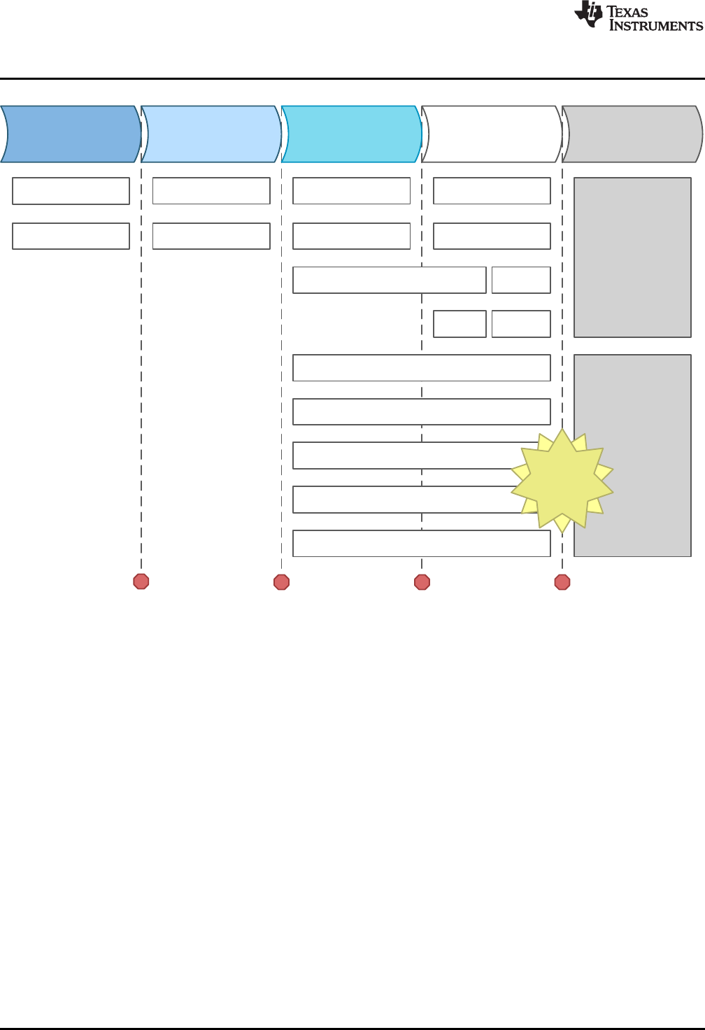
Phase 1
Assess Phase 2
Plan Phase 3
Create Phase 4
Validate Sustain
(after NPDE)
Identify New Product
Opportunities
Develop Product Proposal
Develop Project Plan and
Boundary Agreement
Develop Project
Specification
Design and Layout
Design Verification
Develop Test and Validation HW/SW
Qualify Product
Release
Test HW/SW
Monitor
Ramp
Product
Support
Develop Datasheet, Documentation and Marketing Colateral
Manage Execution and Risks
Sample
Customers
Debrief Reviews
Release to
Market
Develop Software
New Product Development Execution Reviews
Validate Product
Build Intial
Inventory
Create Review Ramp ReviewProject Plan Review
Kickoff Review
C2000 Development Process for Management of Systematic Faults
www.ti.com
12 SPRUI78B–July 2016–Revised June 2018
Submit Documentation Feedback
Copyright © 2016–2018, Texas Instruments Incorporated
Safety Manual for TMS320F2837xD/S and TMS320F2807x
Figure 4. TI (Companywide) New Product Development Flow
Project Teams Execute Debrief Reviews
‡)XOO&URVV)XQFWLRQDO7HDP3DUWLFLSDWLRQ
‡5HIOHFWRQ$FFRPSOLVKPHQWV/Issues
‡'ULYH,VVXHV'RZQWR7UXH5RRW&DXVH/HYHO
‡(3 X 5 Why Understanding)
‡,GHQWLI\$FWLRQVWKDW$GGUHVV6\VWHPDWLF,VVXHV
‡with Clear Who, What and When Deliverables
Fan-Out Across TI
‡6KDUH³1HZ´%HVW3UDFWLFHVZLWK
‡the Playbook Best Practice Team
‡,VVXH$OHUWV(Alert System Link)
‡for Systematic Issues/Solutions
‡$SSO\/HVVRQV/HDQHGWR1HZ3URMHFWV...
Execution Review Focus
‡%HVW3UDFWLFHVDQG/HVVRQHG/HDUQHG&DSWXUHG
‡ (Business Debrief Lessons Leaned File)
‡2SHQ$FWLRQV5HYLHZHGWKUX&ORVXUH
‡%XVLQHVV/RRN-Across and Fan-out
New
Project
Kick-Off
Project
Debrief
Share Best
Practices/
Lessons Learned
Fan-Out
Across TI
Implement
Corrective/Preventive
Actions
www.ti.com
C2000 Development Process for Management of Systematic Faults
13
SPRUI78B–July 2016–Revised June 2018
Submit Documentation Feedback Copyright © 2016–2018, Texas Instruments Incorporated
Safety Manual for TMS320F2837xD/S and TMS320F2807x
• Company wide required minimum best practices mandate a debrief model (shown in Figure 5) at all
stages of hardware and system development which further underscores C2000 MCU team’s
commitment to meeting the highest quality standards and continuously improving on them.
Figure 5. TI Business Debrief Process Model

C2000 Development Process for Management of Systematic Faults
www.ti.com
14 SPRUI78B–July 2016–Revised June 2018
Submit Documentation Feedback
Copyright © 2016–2018, Texas Instruments Incorporated
Safety Manual for TMS320F2837xD/S and TMS320F2807x
3.2 Yogitech fRMethodology Enhanced Development Process
The C2000 MCU Development Team engaged with Yogitech in starting in 2014 to complete an
independent Safety Architecture Assessment of the C2000 MCU Family. This analysis completed by
Yogitech, addressed HW random failures and dependent failures. The aim of the analysis was to prepare
the Functional Safety Manual and FMEDA for the C2000 MCUs by clearly describing how to use the
C2000 MCU in safety critical applications including the description of the application level safety
mechanisms.
The C2000 MCU Development Team leveraged Yogitech’s fRMethodology to generate collateral (like this
Functional Safety Manual and Safety Analysis report – Quantitative FMEDA) needed by customers to get
their systems certified to the applicable Functional Safety Standards. Yogitech’s fRMethodology is a
systematic workflow for performing detailed safety analysis on integrated circuits using a patented white
box approach, allowing exploration/evaluation of design safety architecture.
• fRMethodology (proprietary to YOGITECH) mainly consists of:
– Dividing the component into elementary parts by using automatic tools to guarantee the
completeness of the analysis
– Computing the safety metrics by investigating the fault models of each elementary part, attributing
the failure rate, the safeness (Fsafe) and estimating the diagnostic coverage of the planned hardware
or software safety mechanism
– Verifying the safety metrics by fault injection campaign that involves simulating permanent, transient
and common cause faults
Divide the IC in Parts
Estimate their failure rate:
),,( DCSf elempart
OO
ASIL
targets
met?
Identify weak parts with
a criticality ranking
For weak parts, identify
HW/SW counter-
measures
Re-estimate DC
Go to final
implementation
No
Yes
What-if analysis
www.ti.com
C2000 Development Process for Management of Systematic Faults
15
SPRUI78B–July 2016–Revised June 2018
Submit Documentation Feedback Copyright © 2016–2018, Texas Instruments Incorporated
Safety Manual for TMS320F2837xD/S and TMS320F2807x
• The details of fRMethodology flow applied in the C2000 MCU development context is shown in
Figure 6.
Figure 6. Application of fRMethodology Flow in C2000 Context

C2000 Development Process for Management of Systematic Faults
www.ti.com
16 SPRUI78B–July 2016–Revised June 2018
Submit Documentation Feedback
Copyright © 2016–2018, Texas Instruments Incorporated
Safety Manual for TMS320F2837xD/S and TMS320F2807x
3.3 TI’s Enhanced Safety Development Process
TI’s enhanced safety development process is a merger of TI’s standard HW development process and
Yogitech fRMethodology flow for functional safety compliant development. The goal of the process
development is to take the best aspects of each flow and collaborate, resulting in the best in class
capabilities to reduce systematic faults. The process flow targets compliance to IEC 61508 and ISO
26262, and is continuously improved to incorporate new features of emerging functional safety standards.
These functional safety standards are specifically targeted because TI believes they best represent the
state of the art in functional safety development for semiconductors. While not directly targeted at other
functional safety standards, it is expected that products developed to an industry state-of-the-art can be
readily utilized in other functional safety systems. This enhanced development process has been
assessed and certified by TUEV SUED for compliance to IEC 61508 and ISO 26262 The development
process applied to the C2000 silicon covered by this document incorporates all changes through IEC
61508-2:2010 (second edition) and the ISO 26262-5:2011 international standard release.
• During New Product Development, assumptions are made on system level design, functional safety
concepts, and requirements based on C2000 MCU development team’s expertise with systems.
Combined qualitative and quantitative or similar functional safety analysis techniques are used to
assess potential silicon failure modes and diagnostic techniques needed to detect/prevent random
fails. Failure and failure mode distribution estimations are based on multiple industry standards as well
as TI manufacturing data and field failure rate information.
• Decommissioning: The responsibility for any required decommission impact analysis, decommissioning
planning and reporting shall reside with the end equipment company branding the end application
product. Semiconductor components typically do not have functional safety related decommissioning
requirements. Depending on the type of hardware component produced, it may be necessary for the
C2000 MCU team to assist the end equipment developer in the plans for decommission or disposal of
deployed products.
3.4 C2000 Safety Diagnostics Library
Safety Diagnostics Libraries (SDLs) that are compliant to IEC 60730-1: 2010; Annex H are developed with
all necessary work products and best practices to minimize systematic faults. These software libraries can
also help assist customers develop applications compliant with the IEC 60335 and other standards.
• The software development model used is the “V” Model depicted in Figure 7 where each life cycle
phase ends with a cross-functional review called Checkpoint (CP) review.
• In some cases, the releases may have to iterate through the checkpoints multiple times. Approval to
proceed to next Checkpoint is obtained at the end of the Checkpoint review from identified
stakeholders. Verification methods like peer reviews are planned and conducted for work products as
per verification plan.
– Appropriate tailoring is adopted and documented based on the project requirements.
• Detailed supporting procedures are documented to ensure functional safety throughout the project life
cycle. Additional tools and techniques respecting the safety integrity levels of the targeted standards
are applied at each development phase.
• Functional safety audits and assessments are planned and conducted as per defined procedure.
Qualified personnel with adequate independence as required by the targeted standards and safety
levels do these audits and assessments.
Safety Test
Matrix
Integration
Test Matrix
Unit Test Plan
Test Strategy
Coding
Integration
Testing
Unit Testing
Req Testing Closure
Architecture
Design
Module
Design
Safety
Requirements
Commissioning
SWFMEA SW Verification
CP1 CP2 CP2 CP4 CP5
CP3A CP3A CP3B
CP3BCP3BCP3A
CP3B
CP3A
Copyright © 2016, Texas Instruments Incorporated
www.ti.com
C2000 Development Process for Management of Systematic Faults
17
SPRUI78B–July 2016–Revised June 2018
Submit Documentation Feedback Copyright © 2016–2018, Texas Instruments Incorporated
Safety Manual for TMS320F2837xD/S and TMS320F2807x
Figure 7. Software Development V Model
Sensor Processing
Element Actuator
SRemote
Controller
MCU
A
Remote
Controller
SRemote
Controller
A
Remote
Controller
Sensor
Actuator
Processing Element
TMS320F2837xD/S and TMS320F2807x MCU Architecture for Management of Random Faults
www.ti.com
18 SPRUI78B–July 2016–Revised June 2018
Submit Documentation Feedback
Copyright © 2016–2018, Texas Instruments Incorporated
Safety Manual for TMS320F2837xD/S and TMS320F2807x
4 TMS320F2837xD/S and TMS320F2807x MCU Architecture for Management of
Random Faults
The C2000 MCU product architecture includes many safety mechanisms, which can detect and respond to
random faults when used correctly. This section of the document describes the architectural safety
concept for the C2000 MCU family of devices.
4.1 Functional Safety Concept
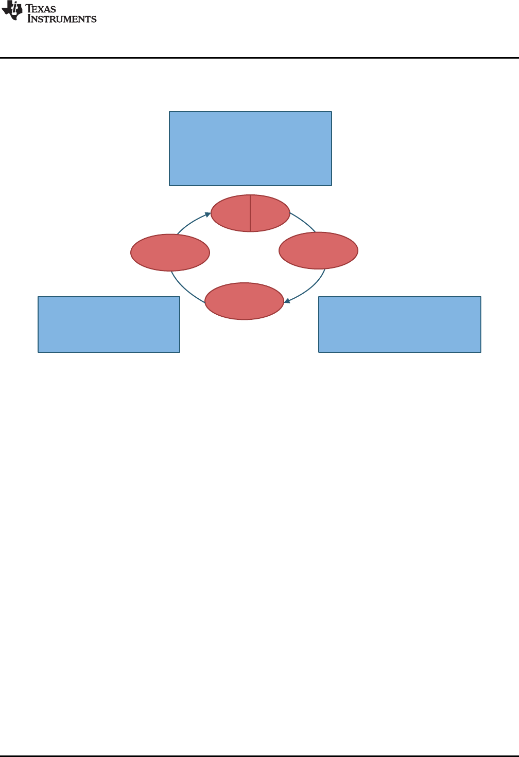
To stay as general as possible, the safety concept assumes the MCU playing the role of a processing unit
(or part of it) and connected to remote controller(s) by means of a communication bus as shown in
Figure 8. The communication bus is directly or indirectly connected to sensor(s) and actuator(s).
(Reference: Yogitech Initial Safety Analysis Report - YT_D3).
IEC 61508:1 clause 8.2.12 defines a compliant item as any item (for example an element) on which a
claim is being made with respect to the clauses of IEC 61508 series. A system including
TMS320F2837xD/S or TMS320F2807x microcontroller as indicated by Figure 8 can be used in a
compliant item according to IEC61508.
Figure 8. Definition of the C2000 MCU Used in a Compliant Item
Level 1
ECU Functions
Level 2
Function Monitoring
Level 3
Fault Reaction
Memory Test
Level 2
Quest Spec.
Test Data
Function Spec
Instruction Test
Response
Contribution
Linking
Monitor Modules
Function
Controller
Monitoring
Controller
Input
Signals
Power
Determining Output
Stages/
Safety-Relevant
Bus Communication
Enable
Enable
Program Flow Check
Question Answer
www.ti.com
TMS320F2837xD/S and TMS320F2807x MCU Architecture for Management of Random Faults
19
SPRUI78B–July 2016–Revised June 2018
Submit Documentation Feedback Copyright © 2016–2018, Texas Instruments Incorporated
Safety Manual for TMS320F2837xD/S and TMS320F2807x
4.1.1 VDA E-GAS Monitoring Concept
The standardized E-GAS monitoring concept [6] for engine management systems generated by the
German VDA working group “E-Gas-Arbeitskreis” is an example of a well-trusted safety-architecture that
may be used for applications other than engine management systems provided it fits the purpose of the
new application in terms of diagnosis feasibility, environment constraints, time constraints, robustness, and
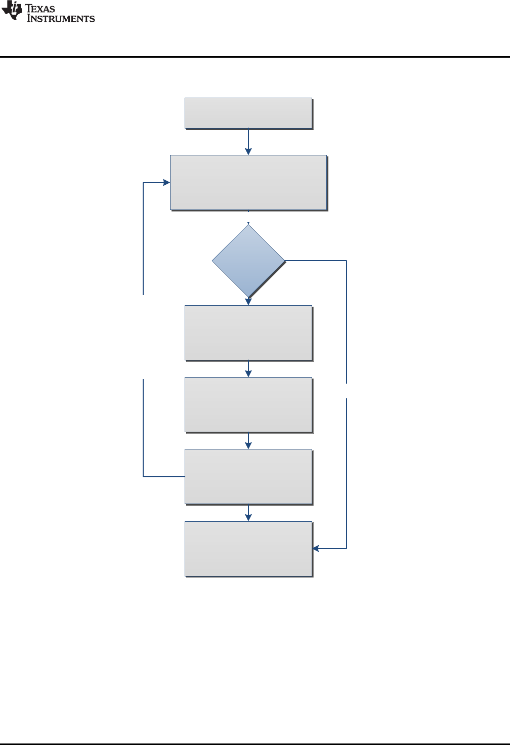
so forth [7]. For more information, see Figure 9.
Figure 9. E-GAS System Overview From Standard
Monitor
Safe
State
Level 1
Primary
Input
Signals
Main Function
Level 2 Monitoring Function
Program Flow
Level 3 Verify Sequence
CLA
Device Self-Test
Q&A Monitor
Diagnostics
Real-Time Control Fault-Response
External
Monitor
Safety Related Fault Detection Monitoring Sequence
Monitor
cross-check
28X
C2000
Q & A
Q & A
28X
C2000
TMS320F2837xD/S and TMS320F2807x MCU Architecture for Management of Random Faults
www.ti.com
20 SPRUI78B–July 2016–Revised June 2018
Submit Documentation Feedback
Copyright © 2016–2018, Texas Instruments Incorporated
Safety Manual for TMS320F2837xD/S and TMS320F2807x
The TMS320F2837xD/S and TMS320F2807x MCU device family supports heterogeneous asymmetric
architecture and their functional safety features lend themselves to an E-GAS concept implementation at
system level as indicated in Figure 10. In the first level (Level 1), the functions required for the system
mission are computed. Second level (Level 2) checks the correct formation in first level based on selected
set of parameters. Third level (Level 3) implements an additional external monitoring element, for the
correct carrying out of the mission in the first level and/or monitoring in the second level. The exact
functional safety implementation and the modules used for realizing Level 1 and Level 2 and the external
monitoring device for realizing Level 3 are left to the system designer. Though Figure 10 indicates CLA
implementing Level1 and CPU(28x) implementing Level2 of the EGAS monitoring concept, both the
processing units are capable of implementing either of the levels. The application can determine the
partitioning based on the system requirements.
Figure 10. VDA E-Gas Monitoring Concept Applied to C2000 MCU
Check OK
Check OK Check NOT OK
Level2/Level3
function Level1
function
Cross check Period (Tcc)
FTTI Budget for the MCU
Delay for MCU to
enter safe state,
Td
Tcc + Td < FTTI
Fault
Normal Operation Unsafe State
Safe State
Fault
Detection
Hazard
Avoided
T <= DTI
Fault Reaction
Time
FTTI
www.ti.com
TMS320F2837xD/S and TMS320F2807x MCU Architecture for Management of Random Faults
21
SPRUI78B–July 2016–Revised June 2018
Submit Documentation Feedback Copyright © 2016–2018, Texas Instruments Incorporated
Safety Manual for TMS320F2837xD/S and TMS320F2807x
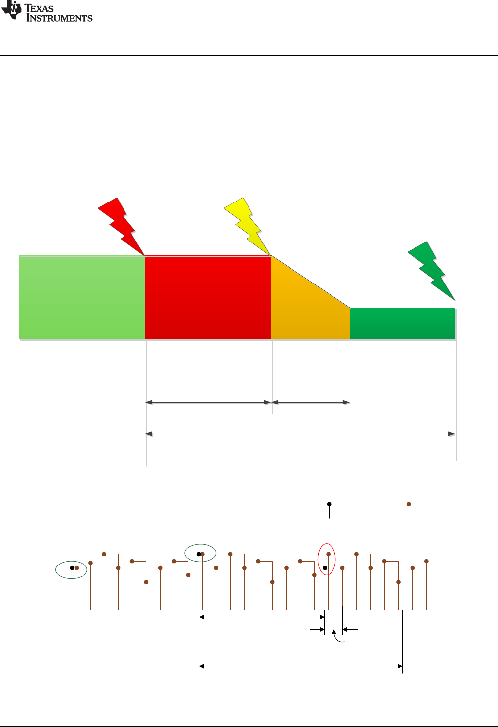
4.1.2 Fault Tolerant Time Interval (FTTI)
Various safety mechanisms in the devices are either always-on (see SRAM ECC,CPU Handling of Illegal
Operation, Illegal Results and Instruction Trapping, and so forth) or executed periodically (see CPU
Hardware Built-In Self-Test (HWBIST),VCU CRC Check of Static Memory Contents, and so forth) by the
application software. The time between the executions of online diagnostic tests by a safety mechanism is
termed as Diagnostic test interval (DTI). Once the fault is detected, depending on the fault reaction of the
associated fault (for example, external system reaction to ERRORSTS pin assertion), the system will enter
in the safe-state. The time-span in which a fault or faults can be present in a system before a hazardous
event occurs is called Fault Tolerant Time Interval (FTTI) as defined in ISO26262. This is similar to
Process Safety Time (PST) defined in IEC61508. Figure 11 illustrates the relationship between DTI, Fault
Reaction Time and FTTI.
Figure 11. Relationship Between DTI, Fault Reaction Time and FTTI
Figure 12. Illustration of FTTI

TMS320F2837xD/S and TMS320F2807x MCU Architecture for Management of Random Faults
www.ti.com
22 SPRUI78B–July 2016–Revised June 2018
Submit Documentation Feedback
Copyright © 2016–2018, Texas Instruments Incorporated
Safety Manual for TMS320F2837xD/S and TMS320F2807x
The frequency and extent of each of the Level 2 and Level 3 checks should be consistent with the Fault
Tolerant Time Interval (FTTI). Figure 12 illustrates the frequency of the required checks. The checks
should be such that single point faults of the microcontroller should be detected and responded to, such
that the TMS320F2837xD/S and TMS320F2807x MCU enters a safe state within the FTTI budget. The
microcontroller on detection of a fault enters into one of the safe states as illustrated in Figure 16. An
example of a diagnostic for single point faults is ECC/Parity for memories.
The proposed functional safety concept, subsequent functional safety features and configurations
explained in this document are for reference purpose only. The system and equipment designer or
manufacturer is responsible to ensure that the end systems (and any Texas Instruments hardware or
software components incorporated in the systems) meet all applicable safety, regulatory and system-level
performance requirements.
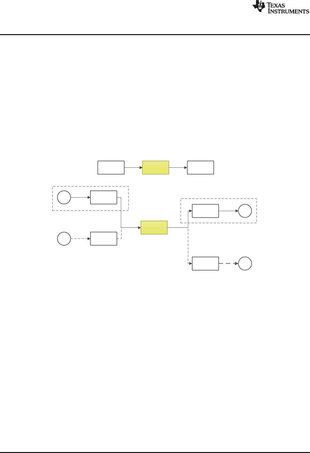
4.2 TMS320F2837xD/S and TMS320F2807x MCU Safety Philosophy
4.2.1 TMS320F2837xD MCU Safety Philosophy
TMS320F2837xD class of devices have two CPU subsystems. The two CPU subsystems can work
independent of each other. Each CPU subsystem has a pair of diverse processing units (C28x and CLA)
with different hardware architecture, instruction set and software tools. All four processing units can be
used to execute main function (Level 1 of VDA E-gas concept). The hardware diagnostic capabilities for
the processing units (CPU Hardware Built-In Self-Test (HWBIST)), CPU Handling of Illegal Operation,
Illegal Results and Instruction Trapping,Software Test of CLA,CLA Handling of Illegal Operation and
Illegal Results,Internal Watchdog (WD) and so forth) can be used to implement the Level 2 monitoring as
per the VDA E-gas concept. This implementation results in four independent processing channels for
TMS320F2837xD.
Another possible option for TMS320F2837xD will be to dedicate the second processing unit of each CPU
subsystem for implementing Level 2 monitoring as illustrated in Figure 13. Due to diversity of the
processing units, we can implement a 1oo1D architecture using “reciprocal comparison by software in
separate processing units” providing high diagnostic coverage for the processing units (ISO26262-5, Table
D.4 and IEC61508-2, Table A.4). This implementation will have two independent processing channels for
TMS320F2837xD. Heterogeneous CPU cores minimize possibility of common mode failures while
implementing this reciprocal comparison thereby improving confidence in its Diagnostic Coverage. The
major safety features of TMS320F2837xD are shown in Figure 14.
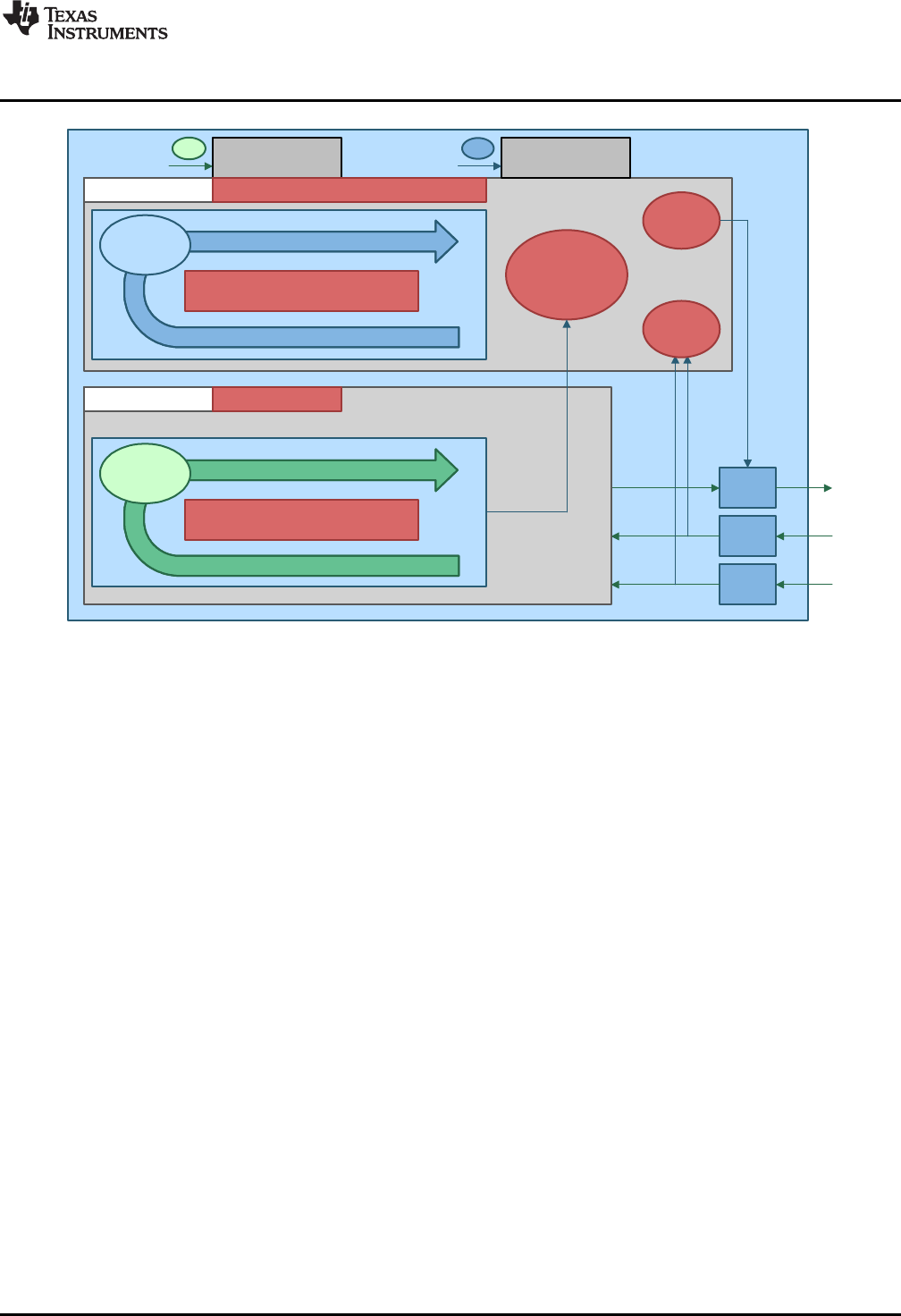
Output
Input
Input
Algorithm
Parameter Check
Typical Flow
Main Function Safety Flow
Monitoring Function
CPU1 Monitoring Function
Main Function Monitoring
+Non-Critical Mission Logic
CPU2 Main Function
Main Function
Input Check
Shut-Down
Control
Output
Enable
Copyright © 2016, Texas Instruments Incorporated
www.ti.com
TMS320F2837xD/S and TMS320F2807x MCU Architecture for Management of Random Faults
23
SPRUI78B–July 2016–Revised June 2018
Submit Documentation Feedback Copyright © 2016–2018, Texas Instruments Incorporated
Safety Manual for TMS320F2837xD/S and TMS320F2807x
Figure 13. Reciprocal Comparison Implementation
4.2.2 TMS320F2837xS and TMS320F2807x MCU Safety Philosophy
TMS320F2837xS and TMS320F2807x class of devices have a single CPU subsystem. The CPU
subsystem has a pair of diverse processing units (C28x and CLA) with different hardware architecture,
instruction set and software tools. Both processing units can be used to execute main function (Level 1 of
VDA E-gas concept). The inherent diagnostic capabilities for the processing (CPU Hardware Built-In Self-
Test (HWBIST),CPU Handling of Illegal Operation, Illegal Results and Instruction Trapping, CLA, CLA
Handling of Illegal Operation and Illegal Results,Internal Watchdog (WD) and so forth) can be used to
implement the Level 2 monitoring as per the VDA E-gas concept. This implementation results in having
two independent processing units for TMS320F2837xS/TMS320F2807x.
Another possible option for TMS320F2837xS/TMS320F2807x will be to dedicate the second processing
unit of the CPU subsystem for implementing Level 2 monitoring as illustrated in Figure 13. Due to diversity
of the processing units, a 1oo1D architecture can be implemented using “reciprocal comparison by
software in separate processing units” providing high diagnostic coverage for the processing units
(ISO26262-5, Table D.4 and IEC61508-2, Table A.4). Heterogeneous CPU cores minimize possibility of
common mode failures while implementing this reciprocal comparison thereby improving confidence in its
Diagnostic Coverage. This implementation will have a single independent processing channel for
TMS320F2837xS.

TMS320F2837xD/S and TMS320F2807x MCU Architecture for Management of Random Faults
www.ti.com
24 SPRUI78B–July 2016–Revised June 2018
Submit Documentation Feedback
Copyright © 2016–2018, Texas Instruments Incorporated
Safety Manual for TMS320F2837xD/S and TMS320F2807x
The product safety philosophy is explained based on 1oo1D safety configuration implemented using
reciprocal comparison and other hardware diagnostics. Figure 15 illustrates safety partitioning based on
the diagnostics employed. The various layers implemented are:
• Reciprocal Comparison Layer (RED) – This is the region of logic used for all processing operations.
This logic has a one processing unit executing the main functionality (Level 1), second processing unit
with specific assumptions of use and other hardware diagnostic elements executing monitoring
functionality (Level 2). The memories closely coupled with C28x and CLA are protected with either
ECC or parity. This region with high diagnostic coverage for both single point faults and latent faults
can be used for performing software diagnostic on other design elements. The diverse processing
(C28x and CLA) have different hardware architecture, instruction set and software tools. However, they
share common power, clock, reset, bus and infrastructure elements. System integrator needs to
independently perform common cause failure analysis and freedom from interference analysis and
implement the necessary safety measures (for example, External Watchdog,Access Protection
Mechanism for Memories, and so forth) to address the concerns which may come up from the
analysis.
• Blended Layer (BLACK) – This is the region of logic that includes safety critical peripherals. This region
has a mix of (predominantly) software and hardware diagnostics. Application protocols (for example,
end-to-end Safeing techniques used in communication protocols) and application related checks (for
example, measured values falls within the safe operating limit) are used to support functionally safe
operation.
• Offline Layer (BLUE) – This region of logic has very limited or no integrated hardware diagnostics.
Many features in this layer (for example, debug, test, calibration functions, and so forth) are used for
production test or application debug and not used during regular operation. Techniques are employed
to avoid freedom from interference to main application by the logic elements in this layer.
Due to the inherent versatility of the device architecture, several software voting based safety
configurations are possible. Some of the safety configurations possible with TMS320F2837xD for
improving diagnostic coverage are explained in Table 3. While implementing these configurations, system
integrator needs to consider the potential common mode failures and address them in an appropriate
manner. This may suitably be modified to adapt to TMS320F2837xS and TMS320F2807x requirements
based on the availability of processing units. (As stated earlier, the device claims no hardware fault
tolerance, (for example, no claims of HFT > 0), as defined in IEC 61508:2010).
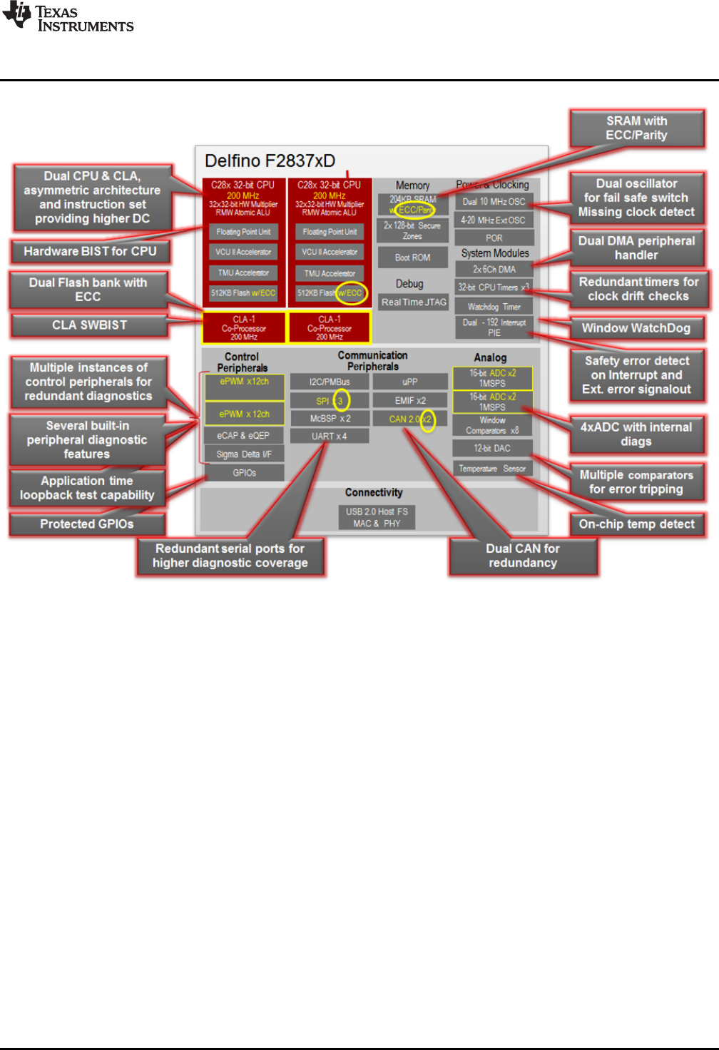
www.ti.com
TMS320F2837xD/S and TMS320F2807x MCU Architecture for Management of Random Faults
25
SPRUI78B–July 2016–Revised June 2018
Submit Documentation Feedback Copyright © 2016–2018, Texas Instruments Incorporated
Safety Manual for TMS320F2837xD/S and TMS320F2807x
Figure 14. C2000 MCU Delfino F2837xD With Safety Features
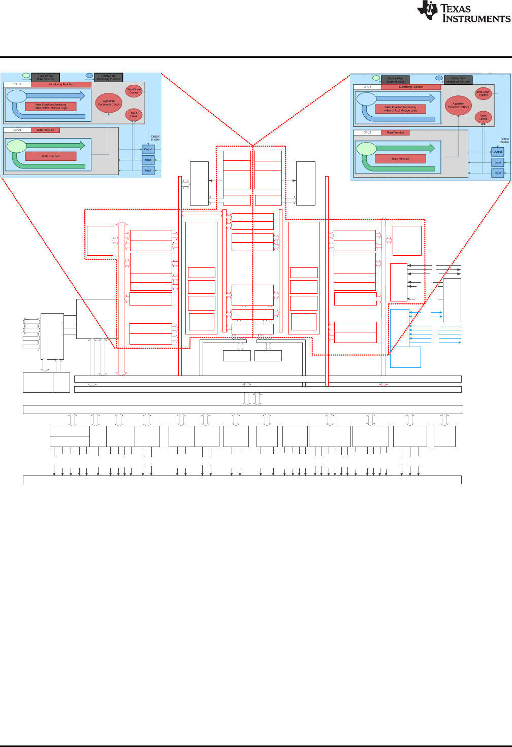
ADC x4
@ 4 msps
Analog
Mux
A
B
C
ETPWM-1/../12 ECAP-
1/../6
Peripheral Bridge
ECAPx
TZ1-6
EPWMxA
EPWMxB
ESYNCI
ESYNCO
EQEP-1/2/3
EQEPxA
EQEPxB
EQEPxI
EQEPxS
HRPWM-1/../8
SD-1/../ 8
SDDx
SDCx
SCI-A/B/C/D
(16L FIFO) I2C-A/B
(16L FIFO)
SDAx
SCLx
SCIRXDx
SCITXDx
USB-0 Ctrl /
PHY
USB0DP
USB0DM
CLA2 Bus
CPU2 Buses
Global Shared
16x 4Kx16
GS0-15 RAMs 7 Ext Interrupts
DCAN-A/B
(32-mbox)
GPIO MUX
EMU0
EMU1
INTOSC
1,
INTOSC
2,
EXTOSC
,
PLL,
XCLKIN
CANTXx
CANRXx
LPM Wakeup
PUMP
OTP/Flash
Wrapper
CLA Data ROM
(4Kx16)
McBSP-A/B
MCLKXx
MCLKRx
EQEPxI
MVSRx
MDXx
MRXx
UPP
UPPAEN
UPPAST
UPPAWT
UPPACLK
UPPAD[7:0]
EMIF1/2
SPI-A/B/C
(16L FIFO)
SPISIMOx
SPISOMIx
SPICLKx
SPISTEx
CPU1.M0 RAM 1Kx16
CPU1.M1 RAM 1Kx16
CPU1.CLA1 CPU2.CLA1
JTAG
DMA1 DMA2
CPU2 to CPU2.CLA1
128x16 MSG RAM
CPU2.CLA1 to CPU2
128x16 MSG RAM
CPU1.CLA1 to CPU 1
128x16 MSG RAM
CPU1 to CPU1.CLA1
128x16 MSG RAM
CPU1 Local Shared 6x
2Kx16
LS0-5 RAMs
CPU2 Local Shared
6x 2Kx16
LS0-5 RAMs
CPU2.M0 RAM 1Kx16
CPU2.M1 RAM 1Kx16
CPU1.D0 RAM 2Kx16
CPU1.D1 RAM 2Kx16
CPU1.D0 RAM 2Kx16
CPU1.D1 RAM 2Kx16
FLASH
256Kx16
Secure
CLA Data ROM
(4Kx16)
Boot-ROM 32Kx16
Non Secure
Secure-ROM 32Kx16
Secure
CLA1 Bus
OTP/Flash
Wrapper
FLASH
256Kx16
Secure
XDn
XDAn
Dual
Code
Security
Module
+
ECSL
Dual
Code
Security
Module
+
ECSL
User OTP
1Kx16
PSWD
Boot-ROM 32Kx16
Non Secure
Secure-ROM 32Kx16
Secure
PSWD
TCK
TDI
TMS
TDO
TRSTn
X2
XRSn
X1
GPIO
Mux
TI-OTP 1Kx16
User OTP
1Kx16
TI-OTP 1Kx16
XCTLn
GPIO
MEMCPU1
A5:0
B7:0
C5:0
CPU2 Buses CPU2 Buses
D
D5:0
Comparator
SubSystem
(CMPSS) DAC x3
C28 CPU-1
FPU-II
VCU-II
TMU
CPU Timer 0
CPU Timer 1
CPU Timer 2
ePIE
(up to 192
interrupts )
WD Timer
NMI-WDT
C28 CPU-2
FPU-II
VCU-II
TMU
CPU Timer 0
CPU Timer 1
CPU Timer 2
ePIE
(up to 192
interrupts)
WD Timer
NMI-WDT
CPU1 to CPU2
1Kx16 MSG RAM
HWBIST HWBIST
DFT subsystem
CPU2 to CPU1
1Kx16 MSG RAM
TMS320F2837xD/S and TMS320F2807x MCU Architecture for Management of Random Faults
www.ti.com
26 SPRUI78B–July 2016–Revised June 2018
Submit Documentation Feedback
Copyright © 2016–2018, Texas Instruments Incorporated
Safety Manual for TMS320F2837xD/S and TMS320F2807x
Figure 15. C2000 MCU Delfino F2837xD Device Block Diagram With Safety Partitioning
4.2.3 Assumed Safety Requirements
The following requirements (assumed safety requirements) (at a minimum) need to be implemented by the
Level 3 checker (VDA E-gas concept) realized using external components.
• External voltage monitor to supervise the power supply provided to the TMS320F2837xD/S and
TMS320F2807x MCU
• External Watchdog timer that can be used for diagnostic purposes
• Components required for taking the system to safe state as per the TMS320F2837xD/S and
TMS320F2807x MCU safe state defined in Section 4.2.4.
4.2.4 C2000 MCU Safe State
Referring to Figure 16, the safe state of the C2000 MCU is defined as the one in which:
• TMS320F2837xD/S and TMS320F2807x MCU Reset is asserted
• Power supply to TMS320F2837xD/S and TMS320F2807x MCU is disabled using an external
supervisor as a result of Level 3 check failure. In general, a power supply failure is not considered in
detail in this analysis as it is assumed that the system level functionality exists to manage this
condition.
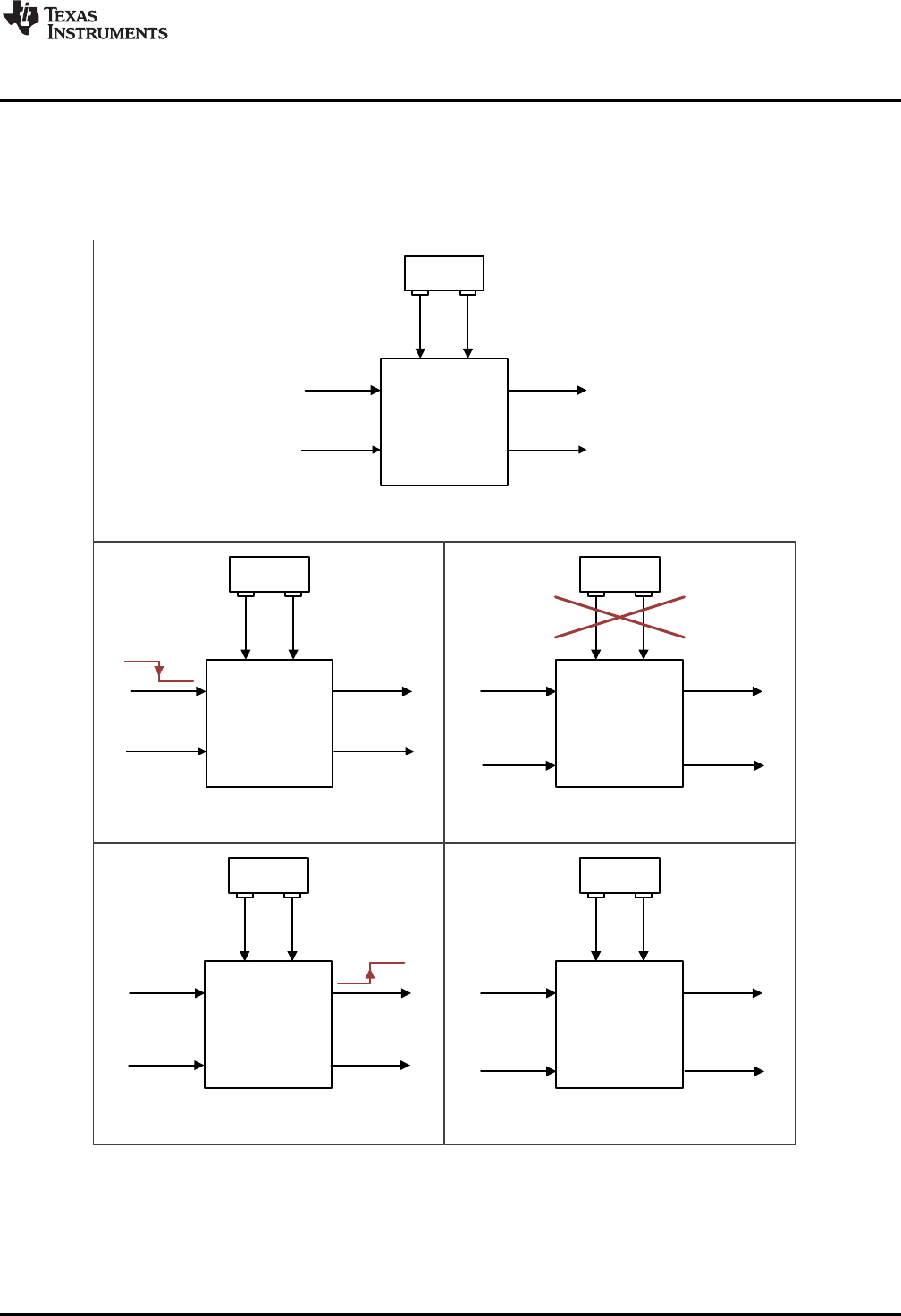
Copyright © 2016, Texas Instruments Incorporated
+ -
TMS320F2837xD
TMS320F2837xS
TMS320F2807x
XRSn
Input Output
ERRORSTS
3. Safe state: MCU is
kept in reset
+ -
TMS320F2837xD
TMS320F2837xS
TMS320F2807x
XRSn
Input Output
ERRORSTS
2. Safe state: Power supply cut-off or
not in proper operating range.
+ -
TMS320F2837xD
TMS320F2837xS
TMS320F2807x
XRSn
Input Output
Tristated
ERRORSTS
5. Safe state: MCU
Output is tristated
+ -
TMS320F2837xD
TMS320F2837xS
TMS320F2807x
XRSn
Input Output
ERRORSTS
4. Safe state: ERRORSTS
pin is asserted
+ -
TMS320F2837xD
TMS320F2837xS
TMS320F2807x
XRSn
Output
ERRORSTS
1. Proper Operational State
Input
www.ti.com
TMS320F2837xD/S and TMS320F2807x MCU Architecture for Management of Random Faults
27
SPRUI78B–July 2016–Revised June 2018
Submit Documentation Feedback Copyright © 2016–2018, Texas Instruments Incorporated
Safety Manual for TMS320F2837xD/S and TMS320F2807x
• External system is informed using one of TMS320F2837xD/S and TMS320F2807x MCU’s IO pins as a
result of Level 2 check failure (for example, ERRORSTS pin is asserted).
• Output of the TMS320F2837xD/S and TMS320F2807x MCU driving the actuator is forced to inactive
mode as a result of Level 2 check failure (for example, GPIO pins corresponding to the mission
function is tri-stated).
Figure 16. C2000 MCU Safe State Definition
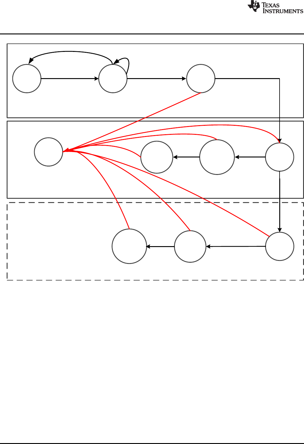
Powered Off Reset State Cold Boot
Warm Boot
Pre-Operational
Operational
Pre-
Operational
Operational
Power removed
Power applied
Chip Pin Reset
released
Defined Safe State
conditions
CPU1 Reset
released
Device boot phase
CPU1SS operation
CPU2SS operation (optional
applicable to TMS320F2837xD only))
CPU2 Reset
released
Safe State
XRSn = 0
Warm Boot
TMS320F2837xD/S and TMS320F2807x MCU Architecture for Management of Random Faults
www.ti.com
28 SPRUI78B–July 2016–Revised June 2018
Submit Documentation Feedback
Copyright © 2016–2018, Texas Instruments Incorporated
Safety Manual for TMS320F2837xD/S and TMS320F2807x
Figure 17. C2000 MCU Device Operating States
4.2.5 Operating States
The TMS320F2837xD/S and TMS320F2807x MCU products have a common architectural definition of
operating states. These operating states should be observed by the system developer in their software
and system level design concepts. The operating states state machine is shown in Figure 17. The
operating states can be classified into device boot phase and CPU1SS operation phase (applicable to all
the devices), and CPU2SS operation phase (applicable to TMS320F2837xD class of devices). CPU2SS
operation phase is initiated by CPU1SS operation phase. Any critical errors in either CPU1SS operation
phase or CPU2SS operation phase cause the device to enter into safe state.
The various states of the device operating states state machine are:
• Powered Off - This is the initial operating state of C2000 MCU. No power is applied to either core or
I/O power supply and the device is non-functional. An external supervisor can perform this action
(power-down the C2000 MCU) in any of the C2000 MCU states as response to a system level fault
condition or a fault condition indicated by the C2000 MCU.
• Reset State – In this state, the device reset is asserted either using the external pins or using any of
the internal sources.
• Safe State – In the Safe state, the device is either not performing any functional operations or an
internal fault condition is indicated using the device I/O pins.
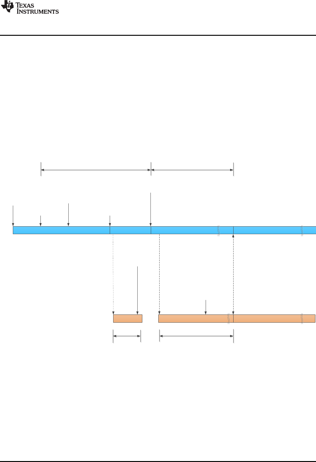
CPU2 Execute
Cold Boot
Warm Boot
Power Applied
Efuse autoload
(cold boot phase) Boot ROM execution and
security initialization
(Warm boot phase)
Reset Released
CPU2 Reset released
Pre operational checks by
CPU1 (Verify RAM, Flash,
Watchdog, CPU, Y..)
Pre operational checks by
CPU2 (Verify RAM, Flash,
Watchdog, CPU, Y..)
Operational Phase
Application start handshake
Operational Phase
Pre Operational Phase
Pre Operational Phase
Warm Boot
Boot ROM execution and
security initialization
(Warm boot phase)
CPU1SS Start-up
Timeline
CPU2SS Start-up
Timeline (optional)
TI boot code execution. Can be characterized
based on device configuration Customer code
TI boot code Customer code
www.ti.com
TMS320F2837xD/S and TMS320F2807x MCU Architecture for Management of Random Faults
29
SPRUI78B–July 2016–Revised June 2018
Submit Documentation Feedback Copyright © 2016–2018, Texas Instruments Incorporated
Safety Manual for TMS320F2837xD/S and TMS320F2807x
• Cold Boot - In the cold boot state, key analog elements, digital control logic, and debug logic are
initialized. The CPU remains powered but in reset. When the cold boot process is completed, the reset
of the master CPU is internally released, leading to the warm boot stage.
• Warm Boot - The CPU begins execution from Boot ROM during the warm boot stage. CPU initializes
the device security (all memories come up as secure at the beginning of the warm boot and this stage
configures the security as needed for the particular system), exception handling and calibration of
analog components and initializes the peripheral boot mode if required. For more details regarding
boot process, see the device-specific boot ROM specification.
• Pre-operational - Transfer of control from boot code to customer code takes place during this phase.
Application specific configurations (for example, clock frequency, peripheral enable, pinmux, and so
forth) are performed in this phase. Boot time self-test/proof-test required to ensure proper device
operation is performed during this phase.
• Operational – This marks the system exiting the pre-operational state and entering the functional state.
The device is capable of supporting safety critical functionality during operational mode.
The device start-up timeline for both the CPUs are shown in Figure 18.
Figure 18. C2000 MCU CPU Start-Up Timeline

x Device Powerdown
x Assertion of XRSn pin
x Assertion of CPU Reset
x NMI and assertion of ERRORSTS pin
x CPU Interrupt
TMS320F2837xD/S and TMS320F2807x MCU Architecture for Management of Random Faults
www.ti.com
30 SPRUI78B–July 2016–Revised June 2018
Submit Documentation Feedback
Copyright © 2016–2018, Texas Instruments Incorporated
Safety Manual for TMS320F2837xD/S and TMS320F2807x
4.2.6 Management of Faults
The TMS320F2837xD/S and TMS320F2807x MCU product architecture provides different levels of fault
indication from internal safety mechanisms using CPU Interrupt, Non Maskable Interrupt (NMI), assertion
of ERRORSTS pin, assertion of CPU input reset and assertion of warm reset (XRSn). The fault response
is the action that is taken by the TMS320F2837xD/S and TMS320F2807x MCU or system when a fault is
indicated. Multiple potential fault responses are possible during a fault indication. The system integrator is
responsible to determine which fault response should be taken to ensure consistency with the system
safety concept. The fault indication ordered in terms of severity (device power down being the most
severe) is shown in Figure 19.
Figure 19. Fault Response Severity
• Device Powerdown: This is the highest priority fault response where the external component (see
Section 4.2.3) detects malfunctioning of the device or other system components and powers down the
TMS320F2837xD/S and TMS320F2807x MCU. From this state, it is possible to re-enter cold boot to
attempt recovery.
• Assertion of XRSn: The XRSn reset could be generated from an internal or external monitor that
detects a critical fault having potential to violate safety goal. Internal sources generate this fault
response when the TMS320F2837xD/S and TMS320F2807x MCU is not able to handle the internal
fault condition by itself (for example, CPU1 (master CPU) is not able to handle NMI by itself). From this
state, it is possible to re-enter cold boot and attempt recovery.
• Assertion of CPU Reset: CPU Reset changes the state of the CPU from pre-operational or operational
state to warm boot phase. The CPU Reset is generated from an internal monitor that detects any
security violations. On a properly working system, the security violations may be the secondary effect
due to a fault condition. In addition, CPU2 subsystem generates this fault response when it is not able
to handle the internal fault condition by itself (for example, CPU2 is not able to handle NMI by itself).
From this state, it is possible to re-enter warm boot phase and attempt recovery.
• Non Maskable Interrupt (NMI) and assertion of ERRORSTS pin: C28x CPU supports a Non Maskable
Interrupt (NMI), which has a higher priority than all other interrupts. Each CPU subsystem is equipped
with a NMIWD module responsible for generating NMI to the C28x CPU. ERRORSTS pin will also be
asserted along with NMI. Depending on the system level requirements, the fault can be handled either
internal to the TMS320F2837xD/S and TMS320F2807x MCU using software or at the system level
using the ERRORSTS pin information.
• CPU Interrupt: CPU interrupt allows events external to the CPU to generate a program sequence
context transfer to an interrupt handler where software has an opportunity to manage the fault. The
peripheral interrupt expansion (PIE) block multiplexes multiple interrupt sources into a smaller set of
CPU interrupt inputs.
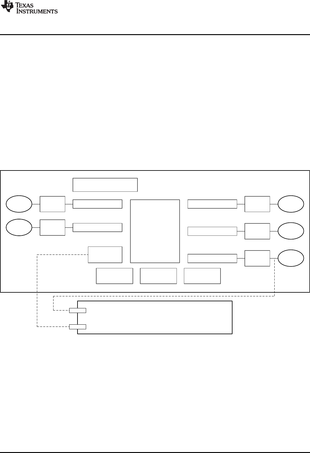
D.2 E/E System
D.2 E/E System
D.11
Sensor
D.11
Sensor
D.3
Connector
D.3
Connector
D.7 Digital I.
D.7 Analogue I.
D.8 Bus interface
D.9 Power Supply
D.4
Processing Unit
D.3 Relay
D.7 Digital O.
D.7 Analogue O.
D.3
Connector
D.3
Connector
D.3
Connector
D.12
Actuator
D.12
Actuator
D.12
Actuator
D.6 RAM D.5 ROM D.10 Clock
www.ti.com
Brief Description of Safety Elements
31
SPRUI78B–July 2016–Revised June 2018
Submit Documentation Feedback Copyright © 2016–2018, Texas Instruments Incorporated
Safety Manual for TMS320F2837xD/S and TMS320F2807x
5 Brief Description of Safety Elements
This section contains a brief description of the elements on the TMS320F2837xD/S and TMS320F2807x
MCU device family, organized based on the classification of parts of generic hardware of a system [8] as
indicated in Figure 20. For a full functional description of any of these modules, see the device-specific
technical reference manual. The brief description of the hardware part is followed by the list of primary
safety mechanisms that can be employed to provide diagnostic coverage to the hardware part. Some
safety standards have the requirement to provide diagnostic coverage for the primary diagnostic measures
(for example, Latent Fault Metric requirement from ISO26262). These measures are called as test of
diagnostics. Primary diagnostics of type “Software” and “Hardware/Software” involves execution of the
software on the processing units viz. CPU and CLA and also use many of the MCU parts like
Interconnect, Memory (Flash, SRAM and ROM) and TMS320F2837xD/S and TMS320F2807x MCU
infrastructure components (Clock, Power, Reset and JTAG). In order to ensure integrity of the
implemented primary diagnostics and their associated diagnostic coverage values, measures to protect
execution of primary diagnostics on respective processing units needs to be implemented. Appropriate
combination of test of diagnostics is recommended to be implemented for parts of the MCU contributing
the successful operation of the processing units. For diagnostics for these parts, see the respective
sections in this safety manual. In case, separate test of diagnostic measures exist for a primary diagnostic
measure, they are mentioned along with the respective hardware part.
Figure 20. Generic Hardware of a System
5.1 C2000 MCU Infrastructure Components
5.1.1 Power Supply
The TMS320F2837xD/S and TMS320F2807x MCU device family requires an external device to supply the
necessary voltage and current for proper operation. Separate voltage rails are available for core (1.2 V),
Analog (3.3 V), Flash (3.3 V) and I/O logic (3.3 V). Following mechanisms can be used to improve the
diagnostic coverage of C2000 MCU power supply.
•External Voltage Supervisor
•External Watchdog (using GPIO or a serial interface)

Brief Description of Safety Elements
www.ti.com
32 SPRUI78B–July 2016–Revised June 2018
Submit Documentation Feedback
Copyright © 2016–2018, Texas Instruments Incorporated
Safety Manual for TMS320F2837xD/S and TMS320F2807x
NOTE:
• Having independent voltage supervision at system level is an assumption used while
performing safety analysis.
• Devices can be implemented with multiple power rails that are intended to be ganged
together on the system PCB. For proper operation of power diagnostics, it is
recommended to implement one voltage supervisor per ganged rail.
• Common mode failure analysis of the external voltage supervisor along with
TMS320F2837xD/S and TMS320F2807x MCU is useful to determine dependencies in
the voltage generation and supervision circuitry.
• Customer can consider using TI TPS6538x power supply and safety companion device
for voltage supervision at system level.
5.1.2 Clock
The C2000 MCU device family products are primarily synchronous logic devices and as such require clock
signals for proper operation. The clock management logic includes clock sources, clock generation logic
including clock multiplication by phase lock loops (PLLs), clock dividers, and clock distribution logic. The
registers that are used to program the clock management logic are located in the system control module.
The following tests can be applied as diagnostics for this module (to provide diagnostic coverage on a
specific function):
•Missing Clock Detect (MCD)
•Clock Integrity Check Using CPU Timer
•Clock Integrity Check Using HRPWM
•Internal Watchdog (WD)
•External Watchdog
•Periodic Software Read Back of Static Configuration Registers
•Software Read Back of Written Configuration
•PLL Lock Profiling Using On-Chip Timer
•Peripheral Clock Gating (PCLKCR)
The following tests can be applied as test-for-diagnostics on this module to meet Latent Fault Metric
Requirements:
•Software Test of Watchdog (WD) Operation
•Software Test of Missing Clock Detect Functionality
NOTE:
• Higher diagnostic coverage can be obtained by setting tighter bounds when checking
clock integrity using Timer2.
• TI recommends the use of an external watchdog over an internal watchdog for mitigating
the risk due to common mode failure. TI also recommends the use of a program
sequence, windowed, or question and answer watchdog as opposed to a single
threshold watchdog due to the additional failure modes that can be detected by a more
advanced watchdog.
• Driving a high-frequency clock output on the XCLKOUT pin may have EMI implications.
The selected clock needs to be scaled suitably before sending out through IO.

www.ti.com
Brief Description of Safety Elements
33
SPRUI78B–July 2016–Revised June 2018
Submit Documentation Feedback Copyright © 2016–2018, Texas Instruments Incorporated
Safety Manual for TMS320F2837xD/S and TMS320F2807x
5.1.3 Reset
The power-on reset (PORn) generates an internal warm reset signal to reset the majority of digital logic as
part of the boot process. The warm reset can also be provided at device level as an I/O pin (XRSn) with
open drain implementation. Diagnostic capabilities like NMI watchdog and Watchdog are capable of
issuing a warm reset. For more information on the reset functionality, see the device-specific data sheet.
The following tests can be applied as diagnostics for this module to provide diagnostic coverage on a
specific function.
•External Monitoring of Warm Reset (XRSn)
•Reset Cause Information
•Glitch Filtering on Reset Pins
•NMIWD Shadow Registers
•Periodic Software Read Back of Static Configuration Registers
•Software Read Back of Written Configuration
•NMIWD Reset Functionality
•Peripheral Soft Reset (SOFTPRES)
The following tests can be applied as test-for-diagnostics on this module to meet Latent Fault Metric
Requirements:
•Software Test of Watchdig (WD) Operation
NOTE:
• Internal watchdogs are not a viable option for reset diagnostics as the monitored reset
signals interact with the internal watchdogs.
• Customer can consider using TI TPS6538x power supply and safety companion device
for reset supervision at system level.
5.1.4 System Control Module and Configuration Registers
The system control module contains the memory-mapped registers to configure clock, analog peripherals
settings and other system related controls. The system control module is also responsible for generating
the synchronization of system resets and delivering the warm reset (XRSn). The configuration registers
include the registers within peripherals that are not required to be updated periodically.
The following tests can be applied as diagnostics for this module (to provide diagnostic coverage on a
specific function):
•Multi-Bit Enable Keys for Control Registers
•Lock Mechanism for Control Registers
•Software Read Back of Written Configuration
•Periodic Software Read Back of Static Configuration Registers
•Online Monitoring of Temperature
•Peripheral Clock Gating (PCLKCR)
•Peripheral Soft Reset (SOFTPRES)
•EALLOW and MEALLOW Protection for Critical Registers
•Software Test of ERRORSTS Functionality
NOTE:
• Review the Clock and Reset sections as these features are closely controlled by the
system control module.
• Customer can consider using TI TPS6538x power supply and safety companion device
for ERRORSTS pin supervision at system level.

Brief Description of Safety Elements
www.ti.com
34 SPRUI78B–July 2016–Revised June 2018
Submit Documentation Feedback
Copyright © 2016–2018, Texas Instruments Incorporated
Safety Manual for TMS320F2837xD/S and TMS320F2807x
5.1.5 Efuse Static Configuration
The TMS320F2837xD/S and TMS320F2807x MCU device family supports a boot time configuration of
certain functionality (such as trim values for analog macros) with the help of Efuse structures. The Efuses
are read automatically after power-on reset by an autoload function.
The following tests can be applied as diagnostics for this module (to provide diagnostic coverage on a
specific function):
•Efuse Autoload Self-Test
•Efuse ECC
•Periodic Software Read Back of Static Configuration Registers
The following tests can be applied as a test-for-diagnostic on this module:
•Efuse ECC Logic Self-Test
5.1.6 JTAG Debug, Trace, Calibration, and Test Access
The TMS320F2837xD/S and TMS320F2807x MCU device family supports debug, test, and calibration
implemented over an IEEE 1149.1 JTAG debug port. The physical debug interface is internally connected
to a TI debug logic (ICEPICK), which arbitrates access to test, debug, and calibration logic. Boundary
scan is connected in parallel to the ICEPICK to support usage without preamble scan sequences for
easiest manufacturing board test. The following tests can be applied as diagnostics for this module (to
provide diagnostic coverage on a specific function):
•Hardware Disable of JTAG Port
•Internal Watchdog (WD)
•External Watchdog
5.2 Processing Elements
5.2.1 C28x Central Processing Unit (CPU)
The CPU is a 32-bit fixed-point processor with Floating point, Viterbi, Complex Math and CRC Unit (VCU)
and Trigonometric Math Unit (TMU) co-processors. This device draws from the best features of digital
signal processing; reduced instruction set computing (RISC); and microcontroller architectures, firmware,
and tool sets. The CPU features include a modified Harvard architecture and circular addressing. The
RISC features are single-cycle instruction execution, and register-to-register operations. The modified
Harvard architecture of the CPU enables instruction and data fetches to be performed in parallel. The
CPU does this over six separate address/data buses. Its unique architecture makes it amenable to
integrate safety features external to CPU but on chip, to provide improved diagnostic coverage.
The following tests can be applied as diagnostics for this module (to provide diagnostic coverage on a
specific function):
•Reciprocal Comparison by Software
•CPU Hardware Built-In Self-Test (HWBIST)
•Software Test of CPU
•Periodic Software Read Back of Static Configuration Registers
•Access Protection Mechanism for Memories
•Hardware Disable of JTAG Port
•CPU Handling of Illegal Operation, Illegal Results and Instruction Trapping
•Internal Watchdog (WD)
•External Watchdog
•Information Redundancy Techniques
•Stack Overflow Detection

www.ti.com
Brief Description of Safety Elements
35
SPRUI78B–July 2016–Revised June 2018
Submit Documentation Feedback Copyright © 2016–2018, Texas Instruments Incorporated
Safety Manual for TMS320F2837xD/S and TMS320F2807x
The following tests can be applied as test-for-diagnostics on this module:
•CPU Hardware Built-In Self-Test (HWBIST) Auto Coverage
•CPU Hardware Built-In Self-Test (HWBIST) Fault Injection Capability
•CPU Hardware Built-In Self-Test (HWBIST) Timeout Feature
•VCU CRC Auto Coverage
NOTE: Measures to Mitigate Common Cause Failure in CPU Subsystem: Common-cause failures
are one of the important failure modes when a safety-related design is implemented in a
silicon device. The contribution of hardware and software dependent failures is estimated on
a qualitative basis because no general and sufficiently reliable method exists for quantifying
such failures. System Integrator should perform a detailed analysis based on the inputs from
ISO26262- 10, Table A.7 and IEC61508 ed2 PART 2 Annex E (BetaIC method).
5.2.2 Control Law Accelerator
The Control Law Accelerator (CLA) is an independent, fully-programmable, 32-bit floating-point math
accelerator with independent ISA and independent compiler and it helps concurrent control-loop
execution. The low interrupt-latency of the CLA allows it to read ADC samples "just-in-time." This
significantly reduces the ADC sample to output delay to enable faster system response and higher MHz
control loops.
The following tests can be applied as diagnostics for this module (to provide diagnostic coverage on a
specific function):
•Reciprocal Comparison by Software
•Software Test of CLA
•CLA Handling of Illegal Operation and Illegal Results
•Software Read Back of Written Configuration
•Periodic Software Read Back of Static Configuration Registers
•Information Redundancy Techniques
•CLA Liveness Check Using CPU
•Access Protection Mechanism for Memories
•Disabling of Unused CLA Task Trigger Sources
5.3 Memory (Flash, SRAM and ROM)
5.3.1 Embedded Flash Memory
The embedded Flash memory is a non-volatile memory that is tightly coupled to the C28x CPU. Each
CPUSS have its own dedicated flash memory. The Flash memory is not accessible by CLA or DMA. The
Flash memory is primarily used for CPU instruction access, though data access is also possible. Access
to the Flash memory can take multiple CPU cycles depending upon the device frequency and flash wait
state configuration. Flash wrapper logic provides prefetch and data cache to improve performance.
The following tests can be applied as diagnostics for this module (to provide diagnostic coverage on a
specific function):
The following tests can be applied as a test-for-diagnostic on this module:
•Bit Multiplexing in Flash Memory Array
•Periodic Software Read Back of Static Configuration Registers
•Software Read Back of Written Configuration
•Flash Program Verify and Erase Verify Check
•Software Test of Flash Prefetch, Data Cache and Wait-States
•Internal Watchdog (WD)
•External Watchdog

Brief Description of Safety Elements
www.ti.com
36 SPRUI78B–July 2016–Revised June 2018
Submit Documentation Feedback
Copyright © 2016–2018, Texas Instruments Incorporated
Safety Manual for TMS320F2837xD/S and TMS320F2807x
•Data Scrubbing to Detect/Correct Memory Errors
•CPU Handling of Illegal Operation, Illegal Results and Instruction Trapping
•Hardware Redundancy
5.3.2 Embedded SRAM
The TMS320F2837xD/S and TMS320F2807x MCU device family has the following types of SRAMs with
different characteristics.
• Dedicated to each CPU (M0, M1, and Dx RAM)
• Shared between the CPU and its own CLA (LSx RAM)
• Shared between the CPU and DMA of both subsystems (GSx RAM)
• Used to send and receive messages between processors (MSGRAM)
All these RAMs are highly configurable to achieve control for write access and fetch access from different
masters. All dedicated RAMs are enabled with the ECC feature (both data and address) and shared
RAMs are enabled with the Parity (both data and address) feature. Each RAM has its own controller which
implements access protection, security related features and ECC/Parity features for that RAM.
The following tests can be applied as diagnostics for this module (to provide diagnostic coverage on a
specific function):
•SRAM ECC
•SRAM Parity
•Software Test of SRAM
•Bit Multiplexing in SRAM Memory Array
•Periodic Software Read Back of Static Configuration Registers
•Software Read Back of Written Configuration
•Data Scrubbing to Detect/Correct Memory Errors
•Software Test of Function Including Error Tests
•Access Protection Mechanism for Memories
•Lock Mechanism for Control Registers
•Information Redundancy Techniques
•CPU Handling of Illegal Operation, Illegal Results and Instruction Trapping
•Internal Watchdog (WD)
•External Watchdog
•CLA Handling of Illegal Operation and Illegal Results
The following tests can be applied as a test-for-diagnostic on this module:
•Software Test of ECC Logic
•Software Test of Parity Logic
•VCU CRC Auto Coverage
5.3.3 Embedded ROM
The TMS320F2837xD/S and TMS320F2807x MCU device family has the following types of ROMs for
each CPU subsystem:
• Boot ROM helps to boot the device and contain functions for security initialization, device calibration
and support different boot modes
• CLA Data ROM contains math tables for CLA application usage

www.ti.com
Brief Description of Safety Elements
37
SPRUI78B–July 2016–Revised June 2018
Submit Documentation Feedback Copyright © 2016–2018, Texas Instruments Incorporated
Safety Manual for TMS320F2837xD/S and TMS320F2807x
The following tests can be applied as diagnostics for this module (to provide diagnostic coverage on a
specific function):
•Periodic Software Read Back of Static Configuration Registers
•Software Read Back of Written Configuration
•Software Test of Function Including Error Tests
•CPU Handling of Illegal Operation, Illegal Results and Instruction Trapping
•Internal Watchdog (WD)
•External Watchdog
•Power-Up Pre-Operational Security Checks
The following tests can be applied as a test-for-diagnostic on this module:
•VCU CRC Auto Coverage
5.4 On-Chip Communication Including Bus-Arbitration
5.4.1 Device Interconnect
The device interconnects links the multiples masters and slaves within the device. The device interconnect
logic comprises of static master selection muxes, dynamic arbiters and protocol convertors required for
various bus masters (CPU, CLA, DMA) to transact with the peripherals and memories.
The following tests can be applied as diagnostics for this module (to provide diagnostic coverage on a
specific function):
•Software Test of Function Including Error Tests
•Internal Watchdog (WD)
•External Watchdog
•Periodic Software Read Back of Static Configuration Registers
•Software Read Back of Written Configuration
•CPU Handling of Illegal Operation, Illegal Results and Instruction Trapping
•CLA Handling of Illegal Operation and Illegal Results
5.4.2 Direct Memory Access (DMA)
The direct memory access (DMA) module provides a hardware method of transferring data between
peripherals and/or memory without intervention from the CPU, thereby freeing up bandwidth for other
system functions. Additionally, the DMA has the capability to orthogonally rearrange the data as it is
transferred as well as “ping-pong” data between buffers. These features are useful for structuring data into
blocks for optimal CPU processing.
The following tests can be applied as diagnostics for this module (to provide diagnostic coverage on a
specific function):
•Information Redundancy Techniques
•Transmission Redundancy
•Software Read Back of Written Configuration
•Periodic Software Read Back of Static Configuration Registers
•Software Test of Function Including Error Tests
•Access Protection Mechanism for Memories
•DMA Overflow Interrupt
•Disabling of Unused DMA Trigger Sources

Brief Description of Safety Elements
www.ti.com
38 SPRUI78B–July 2016–Revised June 2018
Submit Documentation Feedback
Copyright © 2016–2018, Texas Instruments Incorporated
Safety Manual for TMS320F2837xD/S and TMS320F2807x
5.4.3 Inter Processor Communication (IPC)
The Inter-Processor Communications (IPC) module allows communication between the two CPU
subsystems. The module includes message RAMs, IPC flags and interrupts, command registers, flash
pump semaphore, clock configuration semaphore and a free running counter that are used to provide
reliable communication and synchronization between the two CPUs.
The following tests can be applied as diagnostics for this module (to provide diagnostic coverage on a
specific function):
•Information Redundancy Techniques Including End-to-End Safeing
•Transmission Redundancy
•Software Test of Function Including Error Tests
•Event Timestamping Using IPC Counter
•Periodic Software Read Back of Static Configuration Registers
•Software Read Back of Written Configuration
5.4.4 Enhanced Peripheral Interrupt Expander (ePIE) Module
The enhanced Peripheral Interrupt Expander (ePIE) module is used to interface peripheral interrupts to the
C28x CPU. It provides configurable masking on a per interrupt basis. The PIE module includes a local
SRAM that is used to hold the address of the interrupt handler per interrupt.
The following tests can be applied as diagnostics for this module (to provide diagnostic coverage on a
specific function):
•PIE Double SRAM Hardware Comparison
•Software Test of SRAM
•Software Test of ePIE Operation Including Error Tests
•Periodic Software Read Back of Static Configuration Registers
•Software Read Back of Written Configuration
•Maintaining Interrupt Handler for Unused Interrupts
•Online Monitoring of Interrups and Events
The following tests can be applied as a test-for-diagnostic on this module:
•PIE Double SRAM Comparison Check
5.4.5 Dual Zone Code Security Module (DCSM)
The dual code security module (DCSM) is a security feature incorporated in this device. It prevents access
and visibility to on-chip secure memories (and other secure resources) to unauthorized persons. It also
prevents duplication and reverse engineering of proprietary code. Each CPU subsystem has its own dual
zone CSM for code protection.
The following tests can be applied as diagnostics for this module (to provide diagnostic coverage on a
specific function):
•Multi-Bit Enable Keys for Control Registers
•Majority Voting and Error Detection of Link Pointer
•Software Read Back of Written Configuration
•Periodic Software Read Back of Static Configuration Registers
•Software Test of Function Including Error Tests
•CPU Handling of Illegal Operation, Illegal Results and Instruction Trapping
•CLA Handling of Illegal Operation and Illegal Results
•VCU CRC Check of Static Memory Contents
•External Watchdog
•Power-Up Pre-Operational Security Checks

www.ti.com
Brief Description of Safety Elements
39
SPRUI78B–July 2016–Revised June 2018
Submit Documentation Feedback Copyright © 2016–2018, Texas Instruments Incorporated
Safety Manual for TMS320F2837xD/S and TMS320F2807x
5.4.6 CrossBar (X-BAR)
The crossbars (X-BAR) provide flexibility to connect device inputs, outputs, and internal resources in a
variety of configurations. The device contains a total of three X-BARs: Input X-BAR, Output X-BAR, and
ePWM X-BAR. The Input X-BAR has access to every GPIO and can route each signal to any (or multiple)
of the IP blocks (for example, ADC, eCAP, ePWM, and so forth). This flexibility relieves some of the
constraints on peripheral muxing by just requiring any GPIO pin to be available. The ePWM X-BAR is
connected to the Digital Compare (DC) submodule of each ePWM module for actions such as trip zones.
The GPIO Output X-BAR takes signals from inside the device and brings them out to a GPIO.
The following tests can be applied as diagnostics for this module (to provide diagnostic coverage on a
specific function):
•Software Test of Function Including Error Tests
•Hardware Redundancy
•Periodic Software Read Back of Static Configuration Registers
•Software Read Back of Written Configuration
•Software Check of X-BAR Flag
5.4.7 Timer
Each CPU subsystem is provided with three 32-bit CPU-Timers (TIMER0/1/2). The module provides the
Operating System (OS) timer for the device. The OS timer function is used to generate internal event
triggers or interrupts as needed to provide periodic operation of safety critical functions. The capabilities of
the module enable it to be used for clock monitoring as well.
The following tests can be applied as diagnostics for this module (to provide diagnostic coverage on a
specific function):
•1oo2 Software Voting Using Secondary Free Running Counter
•Periodic Software Read Back of Static Configuration Registers
•Software Read Back of Written Configuration
•Software Test of Function Including Error Tests
5.5 Digital I/O
5.5.1 General-Purpose Input/Output (GPIO) and Pinmuxing
The General Purpose Input/Output (GPIO) module provides software configurable mapping of internal
module I/O functionality to device pins. These pins can be individually selected to operate as digital I/O
(also called GPIO mode), or connected to one of several peripheral I/O signals.
The following tests can be applied as diagnostics for this module (to provide diagnostic coverage on a
specific function):
•Lock Mechanism for Control Registers
•Periodic Software Read Back of Static Configuration Registers
•Software Read Back of Written Configuration
•Software Test of Function Using I/O Loopback
•Hardware Redundancy

Brief Description of Safety Elements
www.ti.com
40 SPRUI78B–July 2016–Revised June 2018
Submit Documentation Feedback
Copyright © 2016–2018, Texas Instruments Incorporated
Safety Manual for TMS320F2837xD/S and TMS320F2807x
5.5.2 Enhanced Pulse Width Modulators (ePWM)
The enhanced Pulse Width Modulator (ePWM) peripheral is a key element in digital motor control and
power electronic systems. Some of the ePWM module instances support a High-Resolution Pulse Width
Modulator (HRPWM) mode to improve the time resolution. For more information on the ePWM instances
supporting the HRPWM mode, see the device-specific data sheet and reference manual.
The following tests can be applied as diagnostics for this module (to provide diagnostic coverage on a
specific function):
•Software Test of Function Including Error Tests
•Hardware Redundancy
•Monitoring of ePWM by eCAP
•Periodic Software Read Back of Static Configuration Registers
•Software Read Back of Written Configuration
•ePWM Fault Detection using XBAR
•ePWM Synchronization Check
•ePWM Safe State Assertion Using Trip Mechanism
•ePWM Application Level Safety Mechanism
•Online Monitoring of Interrupts and Events
•Monitoring of ePWM by ADC
5.5.3 High Resolution PWM (HRPWM)
HRPWM module extends the time resolution capabilities of the conventionally derived digital pulse width
modulator (PWM). HRPWM is typically used when PWM resolution falls below ~ 9-10 bits. The HRPWM is
based on micro edge positioner (MEP) technology. MEP logic is capable of positioning an edge very finely
by sub-dividing one coarse system clock of a conventional PWM generator. The time step accuracy is of
the order of 150 ps.
The following tests can be applied as diagnostics for this module (to provide diagnostic coverage on a
specific function):
•HRPWM Built-In Self-Check and Diagnostic Capabilities
•Hardware Redundancy
•Monitoring of ePWM by eCAP
•Periodic Software Read Back of Static Configuration Registers
•Software Read Back of Written Configuration
5.5.4 Enhanced Capture (eCAP)
The enhanced CAPture (eCAP) module provides input capture functionality for systems where accurate
timing of external events is important. The eCAP module features include speed measurements of rotating
machinery (for example, toothed sprockets sensed via Hall sensors), elapsed time measurements
between position sensor pulses, period and duty cycle measurements of pulse train signals and decoding
current or voltage amplitude derived from duty cycle encoded current/voltage sensors.
The following tests can be applied as diagnostics for this module (to provide diagnostic coverage on a
specific function):
•Software Test of Function Including Error Tests
•Information Redundancy Techniques
•Monitoring of ePWM by eCAP
•Periodic Software Read Back of Static Configuration Registers
•Software Read Back of Written Configuration
•ECAP Application Level Safety Mechanism
•Hardware Redundancy

www.ti.com
Brief Description of Safety Elements
41
SPRUI78B–July 2016–Revised June 2018
Submit Documentation Feedback Copyright © 2016–2018, Texas Instruments Incorporated
Safety Manual for TMS320F2837xD/S and TMS320F2807x
NOTE: Use of a sensorless positioning algorithm can provide information redundancy through
plausibility checking of eCAP results.
5.5.5 Enhanced Quadrature Encoder Pulse (eQEP)
The enhanced Quadrature Encoder Pulse (eQEP) module is used for direct interface with a linear or rotary
incremental encoder to get position, direction, and speed information from a rotating machine for use in a
high-performance motion and position-control system. The following tests can be applied as diagnostics
for this module (to provide diagnostic coverage on a specific function):
•Software Test of Function Including Error Tests
•eQEP Quadrature Watchdog
•Information Redundancy Techniques
•Software Read Back of Written Configuration
•Periodic Software Read Back of Static Configuration Registers
•eQEP Application Level Safety Mechanisms
•Hardware Redundancy
The following tests can be applied as a test-for-diagnostic on this module:
•eQEP Software Test of Quadrature Watchdog Functionality
NOTE: Use of a sensorless positioning algorithm can provide information redundancy through
plausibility checking of eQEP results.
5.5.6 Sigma Delta Filter Module (SDFM)
Sigma Delta Filter Module (SDFM) is a four-channel digital filter designed specifically for current
measurement and resolver position decoding in motor control applications. Each channel can receive an
independent delta-sigma (ΔΣ) modulator bit stream. The bit streams are processed by four individually-
programmable digital decimation filters. The filter set includes a fast comparator for immediate digital
threshold comparisons for over-current and under-current monitoring.
•SDFM Comparator Filter for Online Monitoring
•Information Redundancy Techniques
•SD Modulator Clock Fail Detection Mechanism
•Periodic Software Read Back of Static Configuration Registers
•Software Read Back of Written Configuration
•Software Test of Function Including Error Tests
•Hardware Redundancy
5.5.7 External Interrupt (XINT)
Interrupts from external sources can be provided to the device using GPIO pins with help of XINT module.
The module allows configuring the GPIOs to be selected as interrupt sources. The polarity of the interrupts
can also be configured with this module.
The following tests can be applied as diagnostics for this module (to provide diagnostic coverage on a
specific function):
•Software Test of Function Including Error Tests
•Periodic Software Read Back of Static Configuration Registers
•Software Read Back of Written Configuration
•Hardware Redundancy

Brief Description of Safety Elements
www.ti.com
42 SPRUI78B–July 2016–Revised June 2018
Submit Documentation Feedback
Copyright © 2016–2018, Texas Instruments Incorporated
Safety Manual for TMS320F2837xD/S and TMS320F2807x
5.6 Analogue I/O
5.6.1 Analog-to-Digital Converter (ADC)
The Analog-to-Digital Converter (ADC) module is used to convert analog inputs into digital values. Results
are stored in internal registers for later transfer by CLA, DMA or CPU. The C2000 MCU device family
products implement up to four modules with shared channels used for fast conversion (ping-pong
method).
The following tests can be applied as diagnostics for this module (to provide diagnostic coverage on a
specific function):
•Software Test of Function Including Error Tests
•DAC to ADC Loopback Check
•ADC Information Redundancy Techniques
•Opens/Shorts Detection Circuit for ADC
•Software Read Back of Written Configuration
•Periodic Software Read Back of Static Configuration Registers
•ADC Signal Quality Check by Varying Acquisition Window
•ADC Input Signal Integrity Check
•Monitoring of ePWM by ADC
•Hardware Redundancy
•Disabling Unused Sources of SOC Inputs to ADC
NOTE:
• ADC module voltages should be supervised as noted in the device-specific data sheet.
• To reduce probability of common mode failure, user should consider implementing
multiple channels (information redundancy) using non adjacent pins and different voltage
reference.
5.6.2 Buffered Digital to Analog Converter (DAC)
The buffered DAC module consists of an internal reference DAC and an analog output buffer that is
capable of driving an external load. An integrated pull-down resistor on the DAC output helps to provide a
known pin voltage when the output buffer is disabled. Software writes to the DAC value register can take
effect immediately or can be synchronized with PWMSYNC events.
The following tests can be applied as diagnostics for this module (to provide diagnostic coverage on a
specific function):
•Software Test of Function Including Error Tests
•DAC to ADC Loopback Check
•Lock Mechanism for Control Registers
•Software Read Back of Written Configuration
•Periodic Software Read Back of Static Configuration Registers
•DAC to Comparator Loopback Check
•Hardware Redundancy

www.ti.com
Brief Description of Safety Elements
43
SPRUI78B–July 2016–Revised June 2018
Submit Documentation Feedback Copyright © 2016–2018, Texas Instruments Incorporated
Safety Manual for TMS320F2837xD/S and TMS320F2807x
5.6.3 Comparator Subsystem (CMPSS)
The Comparator Subsystem (CMPSS) consists of analog comparators and supporting components that
are combined into a topology that is useful for power applications such as peak current mode control,
switched-mode power, power factor correction, and voltage trip monitoring. The comparator subsystem is
built around a pair of analog comparators and helps detection of signal exception conditions including
High/Low thresholds. The positive input of the comparator is always driven from an external pin, but the
negative input can be driven by either an external pin or by an internal programmable 12-bit DAC. Each
comparator output passes through a programmable digital filter that can remove spurious trip signals. A
ramp generator circuit is optionally available to control the internal DAC value for one comparator in the
subsystem.
The following tests can be applied as diagnostics for this module (to provide diagnostic coverage on a
specific function):
•Software Test of Function Including Error Tests
•Software Read Back of Written Configuration
•Periodic Software Read Back of Static Configuration Registers
•Lock Mechanism for Control Registers
•VDAC Conversion by ADC
•CMPSS Ramp Generator Functionality Check
•Hardware Redundancy
5.7 Data Transmission
5.7.1 Controller Area Network (DCAN)
The Controller Area Network (DCAN) interface provides medium throughput networking with event based
triggering, compliant to the CAN protocol. The DCAN modules requires an external transceiver to operate
on the CAN network. The following tests can be applied as diagnostics for this module (to provide
diagnostic coverage on a specific function):
•Software Test of Function Using I/O Loopback
•Information Redundancy Techniques Including End-to-End Safeing
•SRAM Parity
•Software Test of SRAM
•Bit Multiplexing in SRAM Memory Array
•Periodic Software Read Back of Static Configuration Registers
•Software Read Back of Written Configuration
•Transmission Redundancy
•DCAN Stuff Error Detection
•DCAN Form Error Detection
•DCAN Acknowledge Error Detection
•Bit Error Detection
•CRC in Message
•Hardware Redundancy
The following tests can be applied as a test-for-diagnostic on this module:
•Software Test of Parity Logic

Brief Description of Safety Elements
www.ti.com
44 SPRUI78B–July 2016–Revised June 2018
Submit Documentation Feedback
Copyright © 2016–2018, Texas Instruments Incorporated
Safety Manual for TMS320F2837xD/S and TMS320F2807x
5.7.2 Serial Peripheral Interface (SPI)
The Serial Peripheral Interface (SPI) modules provide serial I/O compliant to the SPI protocol. SPI
communications are typically used for communication to smart sensors and actuators, serial memories,
and external logic such as a watchdog device.
The following tests can be applied as diagnostics for this module (to provide diagnostic coverage on a
specific function):
•Software Test of Function Using I/O Loopback
•Information Redundancy Techniques Including End-to-End Safeing
•Periodic Software Read Back of Static Configuration Registers
•Software Read Back of Written Configuration
•Transmission Redundancy
•SPI Data Overrun Detection
•Hardware Redundancy
5.7.3 Serial Communication Interface (SCI)
The module provides serial I/O capability for typical asynchronous Serial Communication Interface (SCI)
protocols, such as UART. Depending on the serial protocol used, an external transceiver may be
necessary.
The following tests can be applied as diagnostics for this module (to provide diagnostic coverage on a
specific function):
•Software Test of Function Using I/O Loopback
•Parity in Message
•Information Redundancy Techniques Including End-to-End Safeing
•SCI Overrun Error Detection
•SCI Break Error Detection
•SCI Frame Error Detection
•Periodic Software Read Back of Static Configuration Registers
•Software Read Back of Written Configuration
•Transmission Redundancy
•Hardware Redundancy
5.7.4 Inter-Integrated Circuit (I2C)
The Inter-Integrated Circuit (I2C) module provides a multi-master serial bus compliant to the I2C protocol.
The following tests can be applied as diagnostics for this module (to provide diagnostic coverage on a
specific function):
•Software Test of Function Using I/O Loopback
•Information Redundancy Techniques Including End-to-End Safeing
•I2C Data Acknowledge Check
•Periodic Software Read Back of Static Configuration Registers
•Software Read Back of Written Configuration
•Transmission Redundancy
•I2C Access Latency Profiling Using On-Chip Timer
•Hardware Redundancy

www.ti.com
Brief Description of Safety Elements
45
SPRUI78B–July 2016–Revised June 2018
Submit Documentation Feedback Copyright © 2016–2018, Texas Instruments Incorporated
Safety Manual for TMS320F2837xD/S and TMS320F2807x
5.7.5 Multi-Channel Buffered Serial Port (MCBSP)
This device provides up to two high-speed multichannel buffered serial ports (McBSPs) that allow direct
interface to codecs and other devices in a system. The McBSP consists of a data-flow path and a control
path connected to external devices by six pins. Data is communicated to devices interfaced with the
McBSP via the data transmit (DX) pin for transmission and via the data receive (DR) pin for reception.
Control information in the form of clocking and frame synchronization is communicated via the following
pins: transmit clock (CLKX ), receive clock (CLKR), transmit frame synchronization (FSX), and receive
frame synchronization (FSR).
The following tests can be applied as diagnostics for this module (to provide diagnostic coverage on a
specific function):
•Software Test of Function Using I/O Loopback
•Information Redundancy Techniques Including End-to-End Safeing
•Periodic Software Read Back of Static Configuration Registers
•Software Read Back of Written Configuration
•Transmission Redundancy
•McBSP Receiver Overrun Detection
•McBSP Transmitter Underflow Detection
•McBSP Receiver Sync Error Detection
•McBSP Transmitter Sync Error Detection
•Hardware Redundancy
5.7.6 External Memory Interface (EMIF)
The External Memory Interface (EMIF) is used to provide device access to off-chip memories or devices,
which support a memory interface. Support is provided for both synchronous (SDRAM) and asynchronous
(NOR Flash, SRAM) memories. The following tests can be applied as diagnostics for this module (to
provide diagnostic coverage on a specific function):
•Information Redundancy Techniques
•VCU CRC Check of Static Memory Contents
•Periodic Software Read Back of Static Configuration Registers
•Software Read Back of Written Configuration
•Transmission Redundancy
•EMIF Access Protection Mechanism
•Software Test of Function Including Error Tests
•EMIF Access Latency Profiling Using On-Chip Timer
•EMIF Asynchronous Memory Timeout Protection Mechanism
•Hardware Redundancy
NOTE: Safety critical data from external memories can be transferred or copied to internal memory
for higher integrity operations.
5.8 Not Safety Related Elements
The following elements are not recommended to be used in safety related applications implemented using
TMS320F2837xD/S and TMS320F2807x. If used in the end system, applicable measures listed in section
'Suggestions for Improving Freedom From Interference' should be implemented to avoid a cascading
failure from these elements adversely affecting implemented safety functions.
• Universal Serial Bus (USB)
• Controller Universal Parallel Port (uPP)

Brief Description of Diagnostics
www.ti.com
46 SPRUI78B–July 2016–Revised June 2018
Submit Documentation Feedback
Copyright © 2016–2018, Texas Instruments Incorporated
Safety Manual for TMS320F2837xD/S and TMS320F2807x
6 Brief Description of Diagnostics
This section provides a brief summary of the diagnostic mechanisms available on the TMS320F2837xD/S
and TMS320F2807x MCU device family. The diagnostic mechanisms are arranged as per the device
portioning given in Figure 20. At places where the safety mechanism is applicable for more than one
component, it is placed at an appropriate place based on the applicable use case scenario. For a detailed
description or implementation details for a diagnostic, see the device-specific technical reference manual.
6.1 C2000 MCU Infrastructure Components
6.1.1 Clock Integrity Check Using CPU Timer
It is recommended to use the CPU Timer module to detect incorrect clock frequencies and drift between
clock sources. CPU Timer2 has a programmable counter whose prescale value and clock source can be
selected. Using the system clock as reference time base and frequency relationship between selected
clock and system clock can be ascertained. For more information on the clock selection options
implemented, see the device-specific data sheet. Higher diagnostic coverage can be obtained by setting
tighter bounds when checking clock integrity using Timer2. Common cause failures can be reduced by
using different clock sources and different prescale values for the reference clock and measured clock.
The Timer diagnostic is not enabled by default and must be enabled via software. The cyclical check
applied by the Timer module provides an inherent level of self-checking (auto-coverage), which can be
considered for application in latent fault diagnostics.
6.1.2 Clock Integrity Check Using HRPWM
Calibration logic of OTTO (HRPWM) can be used to detect incorrect system clock (SYSCLK) frequencies.
The clock whose frequency needs to be measured is configured as the system clock and the auto-
calibration function is executed. The result obtained from the calibration function can be checked against
the predetermined range of value to detect incorrect clock frequency or frequency drift. Error response,
diagnostic testability, and any necessary software requirements are defined by the software implemented
by the system integrator.
6.1.3 EALLOW and MEALLOW Protection for Critical Registers
EALLOW (CPU, DMA) and MEALLOW (CLA) protection enables write access to emulation and other
protected registers. CPU (CLA) can set this bit using EALLOW (MEALLOW) instruction and cleared using
EDIS (MEDIS) instruction. The protection can be used to prevent data being written to the wrong place,
which would happen with conditions like boundary exceeding, incorrect pointers, stack overflow or
corruption, and so forth. Reads from the protected registers are always allowed. It is recommended to
disable the protection once write for the protected registers are complete.
6.1.4 Efuse Autoload Self-Test
Efuse provides a capability to ensure proper loading of the efuse values to all the registers. The capability
is enabled by default and configuration cannot be changed by software. Any error in this process will be
indicated via ERRORSTS. The device reset is asserted and autoload is re-attempted when the error
occurs.
6.1.5 Efuse ECC
The Efuse utilize a SECDED ECC diagnostic to detect (and correct in case of single bit errors) incorrect
configuration values fetched from the fuse ROM. Errors are indicated via ERRORSTS. This diagnostic is
ON by default and this configuration cannot be changed by software. It covers only data bits of the EFUSE
ROM. The device reset is asserted and autoload is re-attempted when the error occurs.
6.1.6 Efuse ECC Logic Self-Test
The Efuse controller has a self-test logic that executes automatically before the efuse operation. Error is
indicated via ERRORSTS and system control configuration register. The device will remain in reset state
as long as the error occurs.

www.ti.com
Brief Description of Diagnostics
47
SPRUI78B–July 2016–Revised June 2018
Submit Documentation Feedback Copyright © 2016–2018, Texas Instruments Incorporated
Safety Manual for TMS320F2837xD/S and TMS320F2807x
6.1.7 External Clock Monitoring via XCLKOUT
The TMS320F2837xD/S and TMS320F2807x MCU device family provides capability to export select
internal clocking signals for external monitoring. This feature can be configured via software by
programming registers in the system control module. To determine the number of external clock outputs
implemented and the register mapping of internal clocks that can be exported, see the device-specific
data sheet. Export of internal clocks on the XCLKOUT outputs is not enabled by default and must be
enabled via software. It is possible to disable and configure this diagnostic via software.
6.1.8 External Monitoring of Warm Reset (XRSn)
The XRSn warm reset signal is implemented as an open drain I/O pin. An external monitor can be utilized
to detect expected or unexpected changes to the state of the internal warm reset control signal and
ensuring proper signaling (for example, low duration) when it is asserted. Error response, diagnostic
testability, and any necessary software requirements are defined by the external monitor selected by the
system integrator.
6.1.9 External Voltage Supervisor
Texas Instruments highly recommends the use of an external voltage supervisor to monitor all voltage
rails. The voltage supervisor should be configured with overvoltage and under voltage thresholds matching
the voltage ranges supported by the target device (as noted in the device-specific data sheet). Error
response, diagnostic testability, and any necessary software requirements are defined by the external
voltage supervisor selected by the system integrator.
6.1.10 External Watchdog
External watchdog helps to reduce common mode failure, as it utilizes clock, reset, and power that are
separate from the system being monitored. Error response, diagnostic testability, and any necessary
software requirements are defined by the external watchdog selected by the system integrator.
Texas Instruments highly recommends the use of an external watchdog in addition to the internally
provided watchdogs. An internal or external watchdog can provide an indication of inadvertent activation of
logic which results in impact to safety critical execution. Any watchdog added externally should include a
combination of temporal and logical monitoring of program sequence [IEC61508-7, clause A.9.3] or other
appropriate methods such that high diagnostic effectiveness can be claimed.
6.1.11 Glitch Filtering on Reset Pins
Glitch filters are implemented on functional and JTAG reset of the device. These structures filter out noise
and transient signal spikes on the input reset pins in order to reduce unintended activation of the reset
circuitry. The glitch filters are enabled by default and operates continuously. Their behavior cannot be
changed by the software.
6.1.12 Hardware Disable of JTAG Port
The JTAG debug port can be physically disabled to prevent JTAG access in deployed systems. The
recommended scheme is to hold test clock (TCK) to ground and hold Test Mode Select (TMS) high.
Disabling of the JTAG port also provides coverage for inadvertent activation of many debug and trace
activities, since these are often initiated via an external debug tool that writes commands to the device
using the JTAG port.
6.1.13 Internal Watchdog (WD)
The internal watchdog has two modes of operation: normal watchdog (WD) and windowed watchdog
(WWD). The system integrator can select to use one mode or the other but not both at the same time. For
details of programming the internal watchdogs, see the device-specific technical reference manual. The
WD is a traditional single threshold watchdog. The user programs a timeout value to the watchdog and
must provide a predetermined WDKEY to the watchdog before the timeout counter expires. Expiration of
the timeout counter or an incorrect WDKEY triggers an error response. The WD can issue either a warm
system reset or a CPU maskable interrupt upon detection of a failure. The WD is enabled after reset.

Brief Description of Diagnostics
www.ti.com
48 SPRUI78B–July 2016–Revised June 2018
Submit Documentation Feedback
Copyright © 2016–2018, Texas Instruments Incorporated
Safety Manual for TMS320F2837xD/S and TMS320F2807x
In case of WWD, user programs an upper bound and lower bound to create a time window during which
the software must provide a predetermined WDKEY to the watchdog. Failure to receive the correct
response within the time window or an incorrect WDKEY triggers an error response. The WWD can issue
either a warm system reset or a CPU maskable interrupt upon detection of a failure. Normal WD operation
is enabled by default after reset. Additional configuration need to be performed to enable the WWD
operation. For details of programming the internal watchdogs, see the device-specific technical reference
manual. The use of the time window allows detection of additional clocking failure modes as compared to
the WD implementation.
6.1.14 Lock Mechanism for Control Registers
The module contains a lock mechanism for protection of critical control registers. Once the associated
LOCK register bits are set, the write accesses to the registers are blocked. Locked registers cannot be
updated by software. Once locked, only reset can unlock the registers.
6.1.15 Missing Clock Detect (MCD)
The missing clock detector (MCD) is a safety diagnostic that can be used to detect failure of PLL
reference clock. MCD utilizes the embedded 10 MHz internal oscillator (INTOSC1). This circuit only
detects complete loss of PLL reference clock and does not do any detection of frequency drift. The MCD
circuit is enabled by default during the power-on reset state. The diagnostic can be disabled via software.
6.1.16 NMIWD Reset Functionality
On receiving an NMI, the software can attempt recovery from the NMI condition. Based on the severity
and type of the fault condition, recovery may not always be successful. In such a situation, an additional
protection is provided by having an independent watchdog monitoring the NMI recovery. If the attempted
recovery is not successful, a reset is issued. The timeout for reset can be configured (using NMIWDPRD)
based on the FTTI of the device.
6.1.17 NMIWD Shadow Registers
The use of a two stage cold and warm reset scheme on the device allows the implementation of NMIWD
shadow registers. Shadow registers are reset only by power-on/cold reset. These registers are used to
store the NMIFLG information before reset assertion. This information can be used by the application
software to provide additional information on the NMI status of the device before the last warm reset
operation.
6.1.18 Multi-Bit Enable Keys for Control Registers
This module includes features to support avoidance of unintentional control register programmation.
Implementation of multi-bit keys for critical control registers is one such feature (for example,
EPWM_REGS.EPWMLOCK and so forth). The multi-bit keys are particularly effective for avoiding
unintentional activation. For more details on the registers for which the diagnostic is applicable, see the
device-specific technical reference manual. The operation of this safety mechanism is continuous and
cannot be altered by the software. This mechanism can be tested by generating software transactions with
and without correct keys and observing the updated register value.
6.1.19 Online Monitoring of Temperature
The internal temperature sensor measures the junction temperature of the device. The output of the
sensor can be sampled with the ADC through an internal connection. This can be enabled on channel
ADCIN13 on ADCA by setting the ENABLE bit in the TSNSCTL register.
Micro Edge Positioning (MEP) block of HRPWM Built-In Self-Check and Diagnostic Capabilities can also
be used to detect variations in temperature and voltage.

www.ti.com
Brief Description of Diagnostics
49
SPRUI78B–July 2016–Revised June 2018
Submit Documentation Feedback Copyright © 2016–2018, Texas Instruments Incorporated
Safety Manual for TMS320F2837xD/S and TMS320F2807x
6.1.20 Periodic Software Read Back of Static Configuration Registers
Configuration registers are typically configured in the beginning and hold the value till the particular task
execution. Periodic read back of configuration registers can provide a diagnostic for inadvertent writes or
disturb of these registers.
The diagnostic coverage can be improved by extending the test to include read back of the flag registers
that are expected to remain constant (for example, PLL lock status, EQEP phase error flag, and so forth)
during the device operation as well. Error response, diagnostic testability, and any necessary software
requirements are defined by the software implemented by the system integrator.
The diagnostic coverage of some peripherals can be further enhanced by applying some module specific
tests as follows:
• For improving the enhanced peripheral interrupt expander (EPIE) coverage, the PIE flag registers can
be periodically checked to ensure that all pending interrupts are serviced by reading the PIE flag
registers (PIE_CTRL_REGS.PIEIFRx.all) and the peripheral interrupt flag registers.
• While serving the interrupt, the ISR routine can check for flag setting in peripheral as well as PIE to
ensure that correct interrupt is being serviced.
Since CLA configuration registers are accessible to C28x CPU only, this safety mechanism for CLA
module has to be executed by C28x CPU.
6.1.21 Peripheral Clock Gating (PCLKCR)
Peripherals can be clock gated on a per peripheral basis. This can be utilized to disable unused features
such that they cannot interfere with active safety functions. This safety mechanism is enabled after reset.
Software must configure and disable this mechanism to use a particular peripheral. It is possible to lock
the particular configuration to avoid inadvertent writes.
6.1.22 Peripheral Soft Reset (SOFTPRES)
Peripherals can be kept in reset on a per peripheral basis. This can be utilized to reset the unused
features such that they cannot interfere with active safety functions. These safety mechanisms are
disabled after reset. Software must configure and enable these mechanisms.
6.1.23 PLL Lock Profiling Using On-Chip Timer
Clock setup for the TMS320F2837xD/S and TMS320F2807x MCU device family includes selecting the
appropriate clock source, configuring the PLL multiplier, waiting for the lock status and switching the clock
to the PLL output once the internal lock status is set. The time required for the PLL lock sequence can be
profiled using on-chip timer to detect faults in the PLL wrapper logic. Once the PLL is locked, the
frequency of the output clock can be checked by using the following:
•Clock Integrity Check Using CPU Timer
•Clock Integrity Check Using HRPWM
•External Clock Monitoring via XCLKOUT to ensure proper clock output
6.1.24 Reset Cause Information
The system control module provides a status register (RESC) that latches the cause of the most recent
reset event. Application software executed during boot-up can check the status of this register to
determine the cause of the last reset event. This information can be used by the software to identify the
cause and manage failure recovery if required.
6.1.25 Software Read Back of Written Configuration
In order to ensure proper configuration of memory-mapped registers in this module, it is recommended for
software implement a test to confirm proper configuration of all control register by reading back the
contents. This test also provides diagnostic coverage for the peripheral bus interface and peripheral
interconnect bridges.

Brief Description of Diagnostics
www.ti.com
50 SPRUI78B–July 2016–Revised June 2018
Submit Documentation Feedback
Copyright © 2016–2018, Texas Instruments Incorporated
Safety Manual for TMS320F2837xD/S and TMS320F2807x
Since CLA configuration registers are accessible to C28x CPU only, this safety mechanism for CLA
module has to be executed by C28x CPU.
6.1.26 Software Test of ERRORSTS Functionality
As indicated in Figure 16, ERRORSTS pin is an integral part of MCU safety concept used for indicating to
an external system about a critical error occurring within in the MCU. Proper functioning of ERRORSTS
pin and error handling of the system external to MCU can be checked by asserting ERRORSTS pin by
generating an error condition using one of the software provided ways (for example, asserting
CLOCLKFAIL NMIFLG by updating the NMIFLGFRC.bit.CLOCKFAIL). Error response, diagnostic
testability, and any necessary system requirements are defined by the system integrator.
6.1.27 Software Test of Missing Clock Detect Functionality
Proper operation of Missing Clock Detect (MCD) functionality can be checked by configuring
MCDCR.OSCOFF. The diagnostic test can check for issue of missing clock NMI and setting of missing
clock status flag (MCDCR.MCLKSTS).
6.1.28 Software Test of Reset
A software test for detecting basic functionality as well as errors for reset sources and reset logic can be
implemented. Each of the reset sources (including peripheral resets, DEV_CFG_REGS.SOFTPRESx)
except PORn can be generated internally and the basic reset functionality can be checked by ensuring the
correct setting of reset cause register and making sure only the intended logic is reset.
In order to confirm if individual peripherals have received the reset correctly, software can run a peripheral
specific test of functionality and confirm the expected state of the peripheral after reset. Depending on the
complexity of peripheral this software test of functionality can include testing of complex features of the
peripheral including error tests necessary to confirm correct propagation of reset. For peripheral specific
Software Test of Function including Error tests, see the device-specific safety mechanism listed for the
peripheral.
6.1.29 Software Test of Watchdog(WD) Operation
A basic test of the internal watchdog operation can be performed via software including checking of error
response by configuring the expected lower and higher threshold value for servicing WDKEY followed by
servicing or not servicing the WDKEY during the programmed threshold values. If reset is detrimental to
the system operation, the test can be performed by configuring the internal watchdog in Interrupt mode
(SCSR.WDENINT) and reverting back to reset mode after completion of the test.
6.2 Processing Elements
6.2.1 CLA Handling of Illegal Operation and Illegal Results
The CLA co-processor has built in mechanisms to detect execution of an illegal instruction (illegal
opcode), floating point underflow or overflow conditions. CLA will interrupt CPU under such conditions.
Any access to an invalid memory range will return 0x00000000 data. Access to an erased flash (default
state for a new device) will return 0xFFFFFFFF. Both 0x00000000 and 0xFFFFFFFF are decoded as
invalid instructions so that an erased flash, cleared memory, or an invalid address will generate an
interrupt to CPU. CPU can decode the interrupt cause by checking the required CLA flags. Error
response, diagnostic testability, and any necessary software requirements are defined by the software
implemented by the system integrator.
6.2.2 CLA Liveness Check Using CPU
CLA doesn’t have an independent watchdog of its own. Hence, it is recommended to perform liveness
check periodically by the CPU. Typically, sequential set of events is used to trigger the watchdog (for
example, completion of CPU Task1, CLA1 Task1, CPU1 Task2, and CLA1 Task2). The output of the CLA
liveness check can be used as one of the tasks to decide the watchdog triggering as indicated in
Figure 21. The liveness check can be based on application-specific parameters as illustrated in the VDA
Egas concept [6] to improve the diagnostic coverage.
Watchdog
CPU Watchdog Function
CPU1 Task1 CPU1 Task2
CLA1 Task1 CLA1 Task1
CPU1 Task1 CPU1 Task2
CLA1 Task1 CLA1 Task1
www.ti.com
Brief Description of Diagnostics
51
SPRUI78B–July 2016–Revised June 2018
Submit Documentation Feedback Copyright © 2016–2018, Texas Instruments Incorporated
Safety Manual for TMS320F2837xD/S and TMS320F2807x
Figure 21. CLA Liveness Check
6.2.3 CPU Hardware Built-In Self-Test (HWBIST)
The C2000 MCU device family has hardware logic to provide a very high diagnostic coverage on the
CPUs at a transistor level during start-up and application time. This logic utilizes Design for Test (DfT)
structures inserted into the device for rapid execution of high quality manufacturing tests, but with an
internal test engine rather than external automated test equipment (ATE). This technique has proven to be
effective in providing high coverage in less time.
The HWBIST tests must be triggered by the software. User may select to run all tests, or only a subset of
the tests based on the execution time allocated to the HWBIST diagnostic. This time sliced test feature
enables the HWBIST to be used effectively as a runtime diagnostic with execution of test in parallel with
the application. Execution of HWBIST results in a much higher level of transistor switching per clock cycle
than during normal software execution due to the high efficiency of the test. The special requirements for
HWBIST need to be understood and taken care by the system integrator. HWBIST execution failure will
trigger NMI to the same CPU and other CPUs (if available based on the device configuration). After
HWBIST execution, reset is issued to the CPU and the CPU context is restored.
6.2.4 CPU Hardware Built-In Self-Test (HWBIST) Auto-Coverage
The HWBIST diagnostic is based on a 512-bit signature capture. For a given test, only one code is valid
out of 2512 possibilities. Therefore, if there is a fault in the HWBIST logic, it is extremely unlikely that the
correct passing code will be generated via the fault. The cyclical check applied by the HWBIST module
provides an inherent level of self-checking (auto-coverage), which can be considered for application in
latent fault diagnostics.
6.2.5 CPU Hardware Built-In Self-Test (HWBIST) Fault Injection Capability
HWBIST diagnostic has capability helps to inject faults and check the correct functioning of the CPU
Hardware Built-In Self-Test (HWBIST) Auto-Coverage and CPU Hardware Built-In Self-Test (HWBIST)
Timeout feature. This can be used to provide latent fault coverage of the diagnostic logic.
6.2.6 CPU Hardware Built-In Self-Test (HWBIST) Timeout Feature
HWBIST module expects the self-test to be completed within a certain time frame. If the test is not
completed within this time frame, the test is stopped immediately, CPU is reset and NMI (and hence
ERRORSTS) is issued to recover from the indeterminate state. This feature is enabled by default once the
HWBIST module enters into self-test mode and cannot be disabled by software. After coming out from
reset, CPU can read the HWBIST status registers to understand the reset cause and take the required
action.

Brief Description of Diagnostics
www.ti.com
52 SPRUI78B–July 2016–Revised June 2018
Submit Documentation Feedback
Copyright © 2016–2018, Texas Instruments Incorporated
Safety Manual for TMS320F2837xD/S and TMS320F2807x
6.2.7 CPU Handling of Illegal Operation, Illegal Results and Instruction Trapping
The C28x CPU includes diagnostics for illegal operations, illegal results (underflow and overflow
conditions) and instructions trapping (illegal opcode) that can serve as safety mechanisms. Any access to
an invalid memory range will return 0x00000000 data. Access to an erased flash (default state for a new
device) will return 0xFFFFFFFF. Both 0x00000000 and 0xFFFFFFFF are decoded as invalid instructions
so that an erased flash or cleared memory, or an invalid address will force the CPU to ITRAP. Installation
of software handlers to support the hardware illegal operation and instruction trapping is highly
recommended
Examples of CPU illegal operation, illegal results and instruction traps include:
•Illegal instruction
•TMS320C28x FPU Primer (SPRAAN9)
6.2.8 Reciprocal Comparison by Software
Each CPU subsystem has a pair of diverse processing units (C28 and CLA) with different architecture and
instruction set. This enables one processing unit to be used for handling the time critical portion code
(control CPU) and other processing unit (supervisor CPU) to execute non critical portion of the code,
perform diagnostic functions and supervise execution of the control CPU as indicated in Figure 13.
In case of identification of fault during diagnostic functions of the supervisor CPU, it can cause the
TMS320F2837xD/S and TMS320F2807x MCU to move to a safe state. This concept, “reciprocal
comparison by software in separate processing units” acts as a 1oo1D structure providing high diagnostic
coverage for the processing units as per ISO26262-5, Table D.4. The comparison need to be performed
several times during a FTTI. Reciprocal comparison is a software diagnostic feature and hence care
should be taken to avoid common mode failures. The final attained coverage will depend on quality of
comparison (determined by extend and frequency of cross checking). The proposed cross checking
mechanism allows for hardware and software diversity since different processors with different instruction
set and compiler is used for enabling this. The diversity can be further increased by having separate
algorithms being executed in both the cores. In case, failure is identified during reciprocal comparison,
NMI can be triggered by software and this in turn will assert ERRORSTS.
6.2.9 Software Test of CLA
It is possible to test the integrity of various CLA blocks (register bank, control unit, datapath, and so forth)
using software-based self-test library (STL). Based on the safety requirement, this test can be performed
at start-up or during application time. For details on implementing the particular test, see the safety
package delivered with the specific C2000 MCU device. Error response, diagnostic testability, and any
necessary software requirements are defined by the software implemented by the system integrator.
6.2.10 Software Test of CPU
It is possible to test the integrity of various CPU logic (FPU, VCU, TMU, and so forth) using CPU itself.
Based on the safety requirement, this test can be performed at start-up or during application time. For
details on implementing the particular test, check the safety package delivered with the specific
TMS320F2837xD/S and TMS320F2807x MCU device. Error response, diagnostic testability, and any
necessary software requirements are defined by the software implemented by the system integrator.
6.2.11 Stack Overflow Detection
A stack overflow in a safety application generally produces a catastrophic software crash due to data
corruption, lost return addresses, or both. Hence it is important to detect an impending stack overflow.
Capability exist on the C20TMS320F2837xD/S and TMS320F2807x00 MCU device family that, when
properly configured, allow for runtime detection of a stack overflow before it occurs. For more information,
see Online Stack Overflow Detection on the TMS320C28x DSP. Detection of an impending stack overflow
triggers a maskable interrupt. Programmed error response and any necessary software requirements are
defined by the system integrator.

www.ti.com
Brief Description of Diagnostics
53
SPRUI78B–July 2016–Revised June 2018
Submit Documentation Feedback Copyright © 2016–2018, Texas Instruments Incorporated
Safety Manual for TMS320F2837xD/S and TMS320F2807x
6.2.12 VCU CRC Check of Static Memory Contents
The TMS320F2837xD/S and TMS320F2807x MCU device family includes co-processor implementing
cyclic redundancy check (CRC) using standard polynomial. The CRC module can be used to test the
integrity of SRAM/Flash/OTP/external memory contents by calculating a CRC for all memory contents and
comparing this value to a previously generated "golden" CRC. The comparison of results, indication of
fault, and fault response are the responsibility of the software managing the test. The cyclical check
applied by the CRC logic provides an inherent level of self-checking (auto-coverage), which can be
considered for application in latent fault diagnostics.
6.2.13 VCU CRC Auto Coverage
The VCU CRC diagnostic is based on a 32-bit polynomial. For a given test, only one code is valid out of
232 possibilities. Therefore, if there is a fault in the VCU CRC logic or associated datapath, it is extremely
unlikely that the correct passing code will be generated via the fault.
6.2.14 Disabling of Unused CLA Task Trigger Sources
The CLA can receive input task triggers from various peripherals and software. To avoid interference from
unused trigger sources resulting in disturbance to CLA operation it is recommended to disable these in
application.
6.3 Memory (Flash, SRAM and ROM)
6.3.1 Bit Multiplexing in Flash Memory Array
The Flash modules implemented in the TMS320F2837xD/S and TMS320F2807x MCU device family have
a bit multiplexing scheme implemented such that the bits accessed to generate a logical (CPU) word are
not physically adjacent. This scheme helps to reduce the probability of physical multi-bit faults resulting in
logical multi-bit faults; rather they manifest as multiple single bit faults. As the SECDED Flash ECC can
correct a single bit fault and detect double bit fault in a logical word, this scheme improves the usefulness
of the Flash ECC diagnostic. Bit multiplexing is a feature of the flash memory and cannot be modified by
the software.
6.3.2 Bit Multiplexing in SRAM Memory Array
The SRAM modules implemented in the TMS320F2837xD/S and TMS320F2807x MCU device family have
a bit multiplexing scheme implemented such that the bits accessed to generate a logical (CPU) word are
not physically adjacent. This scheme helps to reduce the probability of physical multi-bit faults resulting in
logical multi-bit faults rather they manifest as multiple single bit faults. The SECDED SRAM ECC
diagnostic can correct a single bit fault and detect double bit fault in a logical word. Similarly, the SRAM
parity diagnostic can detect single bit faults. This scheme improves the usefulness of the SRAM ECC and
parity diagnostic. Bit multiplexing is a feature of the SRAM and cannot be modified by the software.
6.3.3 Data Scrubbing to Detect/Correct Memory Errors
For memories with ECC/Parity, data scrubbing can be used to provide latent fault diagnostic coverage.
Bus masters (CPU, CLA or DMA) can be configured to provide dummy reads to the memory (provided a
particular bus master has access to the memory) and the read data can be checked by the built-in
ECC/Parity logic. In the case of SRAMs with ECC protection, single bit errors are corrected and written
back. For both SRAMs and Flash, interrupt is issued once the count exceeds the preset threshold in the
case of correctable errors and NMI will be issued in the case of uncorrectable errors.
Since the contents of Flash memory are static, VCU CRC Check of Static Memory Contents provides
better diagnostic coverage compared to this diagnostic.

Brief Description of Diagnostics
www.ti.com
54 SPRUI78B–July 2016–Revised June 2018
Submit Documentation Feedback
Copyright © 2016–2018, Texas Instruments Incorporated
Safety Manual for TMS320F2837xD/S and TMS320F2807x
6.3.4 Flash ECC
The on-chip Flash memory is supported by single error correction, double error detection (SECDED) error
correcting code (ECC) diagnostic. In this SECDED scheme, an 8-bit code word is used to store the ECC
of 64 bit data and corresponding address. The ECC decoding logic at the flash bank output checks the
correctness of memory content. ECC evaluation is done on every data/program read. The data/program
interconnects that connect the CPU and Flash memory is not protected by ECC. Detected correctable
errors can be corrected or not corrected, depending on whether correction functionality is enabled. Single
bit address ECC errors are flagged as uncorrectable errors. Errors that cannot be corrected will generate
an NMI and ERRORSTS pin is asserted. Count of the corrected errors (single bit data errors) is monitored
by the flash wrapper and an interrupt is generated once the count exceeds the programmed threshold.
The corrupted memory address of the last error location is also logged in flash wrapper.
6.3.5 Flash Program Verify and Erase Verify Check
Whenever any program and erase operation is done, the flash controller will perform program and erase
verify check. If the program and erase operation is failed, FSM status register (FMSTAT) will indicate the
error by setting the corresponding flags into the status register.
6.3.6 Software Test of ECC Logic
It is possible to test the functionality of the SRAM ECC by injecting single bit and double bit errors in test
mode and performing reads on locations with ECC errors, and checking for the error response. Flash ECC
logic can be checked with the help of ECC test registers (FECC_CTRL, FADDR_TEST, FECC_TEST,
FDATAH_TEST, FDATAL_TEST). Correct functioning of error counter and threshold interrupt associated
with single bit errors can also be verified using this technique. Error response, diagnostic testability, and
any necessary software requirements are defined by the software implemented by the system integrator.
For additional details on implementing this diagnostic for SRAM and FLASH memory, see the Application
Test Hooks for Error Detection and Correction and SECDED Logic Correctness Check sections in the
TMS320F2837xD Dual-Core Delfino Microcontrollers Technical Reference Manual.
6.3.7 Software Test of Flash Prefetch, Data Cache and Wait-States
Once enabled, Prefetch logic keeps fetching the next 128-bit row (4 x 32-bit words) from flash bank. On
detecting the discontinuity, the Prefetch buffer will be cleared. A software test can be performed to
ascertain the proper behavior of this logic. The following sequence of operation can be performed.
1. Disable the Prefetch mechanism, enable the timer and Watchdog. Execute a particular function which
might have linear code and code with multiple discontinuities. Store the time “time_1” (timer value)
taken for executing this function.
2. Enable the Prefetch mechanism and execute the same function again. Store the time “time_2” (timer
value) taken for executing this function. This value should be less than the time_1 (time_1 > time_2).
We can mark this timer value as a GOLDEN value and should expect the same timer values for each
run of the same function.
3. Since each flash bank row has 4 x32 bit words, number of rows fetched from the flash bank varies as
per the code alignment within the flash bank. Hence user needs to make sure that the Prefetch logic
test function should be aligned/located in particular location within flash to guarantee the same timing
behavior and does not vary compile to compile.
Similar timer-based profiling can be performed to ascertain proper functioning of the data cache and wait
states.

www.ti.com
Brief Description of Diagnostics
55
SPRUI78B–July 2016–Revised June 2018
Submit Documentation Feedback Copyright © 2016–2018, Texas Instruments Incorporated
Safety Manual for TMS320F2837xD/S and TMS320F2807x
6.3.8 Access Protection Mechanism for Memories
All volatile memory blocks (including external memories) except for M0/M1 on both subsystems have
different levels of protection. This capability allows the user to enable or disable specific access (for
example, Fetch, Write) to individual RAM blocks from individual masters (CPU1, CPU2, CPU1.CLA1,
CPU2.CLA1, CPU1.DMA1, CPU2.DMA1). There is no protection for read accesses, therefore, reads are
always allowed from all the masters which have access to that RAM block. To identify conditions when the
master access to an SRAM is blocked, see the device-specific technical reference manual. This
configuration can be changed during run-time and allows memory to block access from specific masters or
specific application threads within the same master. This capability helps support freedom from
interference requirements required by some applications.
6.3.9 SRAM ECC
Selected on-chip SRAMs support SECDED ECC diagnostic with separate ECC bits for data and address.
For the specific address ranges that support ECC, see the TMS320F2837xD/S and TMS320F2807x MCU
device-specific data sheet. In SECDED scheme, a 21-bit code word is used to store the ECC data
calculated independently for each 16 bit of data and for address. The ECC logic for the SRAM access is
located in the SRAM wrapper. The ECC is evaluated directly at the memory output and data is sent to
CPU after the data integrity check. The data and address interconnects from SRAM to the CPU is not
protected using ECC. Detected correctable errors are corrected and it is possible to monitor the number of
corrected errors. The SRAM wrapper can be configured to trigger an interrupt once the number of
corrected errors crosses a threshold. Uncorrectable SRAM errors trigger an NMI and the ERRORSTS pin
is asserted. The ECC logic for the SRAM is enabled at reset. For more information regarding memories
supporting ECC, see the TMS320F2837xD/S and TMS320F2807x MCU device-specific data sheet.
6.3.10 SRAM Parity
Selected on-chip SRAMs support parity diagnostic with separate parity bits for data and address. For the
specific address ranges that support parity, see the device-specific data sheet. In the parity scheme, a 3-
bit code word is used to store the parity data calculated independently for each 16 bit of data and for
address. The parity generation and check logic for the SRAM is located in the SRAM wrapper. The parity
is checked directly at the memory output and data is sent to CPU after the data integrity check. The data
and address interconnect from SRAM to the CPU is not protected using parity. SRAM parity errors trigger
an NMI and the ERRORSTS is asserted. The parity logic for the SRAM is enabled at reset. For more
information regarding memories supporting parity, see the TMS320F2837xD/S and TMS320F2807x MCU
device-specific data sheet.
6.3.11 Software Test of Parity Logic
It is possible to test the functionality of parity error detection logic by forcing a parity error into the data or
parity memory bits, and observing whether the parity error detection logic reports an error. Parity can also
be calculated manually and compared to the hardware calculated value stored in the parity memory bits.
6.3.12 Software Test of SRAM
It is possible to test the integrity of SRAM (bit cells, address decoder and sense amplifier logic) using the
CPU. Based on the safety requirement, this test can be performed at start-up or during application time. If
the SRAM contents are static, a CRC check using VCU can also be performed in place of destructive test
(test where memory contents need to be restored after the test). For details on implementing this
particular test, check the safety package delivered with this specific C2000 MCU device.

Brief Description of Diagnostics
www.ti.com
56 SPRUI78B–July 2016–Revised June 2018
Submit Documentation Feedback
Copyright © 2016–2018, Texas Instruments Incorporated
Safety Manual for TMS320F2837xD/S and TMS320F2807x
6.4 On-Chip Communication Including Bus-Arbitration
6.4.1 1oo2 Software Voting Using Secondary Free Running Counter
The TIMER module contains three counters that can be used to provide an operating system time base.
While one counter is used as the operating system time base, it is possible to use one of the other
counters as a diagnostic on the first, using periodic check via software of the counter values in the two
timers. The second counter can be fed with a different clock source and a different prescale configuration
can be selected to avoid common mode errors. Error response, diagnostic testability, and any necessary
software requirements are defined by the software implemented by the system integrator.
6.4.2 DMA Overflow Interrupt
DMA supports latching one additional trigger event. Before DMA services this latched event if additional
event occurs DMA overflow interrupt is generated, such that, the CONTROL_REG.PERINTFLG is set and
another interrupt event occurs. The CONTROL_REG.PERINTFLG being set indicates a previous
peripheral event is latched and has not been serviced by the DMA
6.4.3 Event Timestamping Using IPC Counter
IPC has a 64-bit free-running IPCCOUNTERH/L that can be used for time stamping events between the
processors. The time stamp can be sent along with the payload and this information can be used by the
software running on the receiver CPU to determine the time required for completing the command. If the
message is not received within the expected time limit, the receiver CPU can initiate an error response.
The round trip delay can be estimated by the transmitter CPU based on the message acknowledge send
by receiver CPU.
6.4.4 Maintaining Interrupt Handler for Unused Interrupts
The C2000 MCU devices contain a large number of interrupts; a typical application only uses a very small
subset of all the available interrupts. Multiple configurations are possible for the unused interrupts. This
includes disabling of the unused interrupts, enabling the unused interrupts and return to the application in
the interrupt service routine (ISR), and so forth. Receiving of an interrupt not used in the application might
be an early indication of some faulty scenarios within the C2000 MCU. Hence, it is highly recommended to
enable all the interrupts and configure the ISR to a common routine for logging or error handling.
6.4.5 Majority Voting and Error Detection of Link Pointer
The link pointer OTP location is not protected by ECC. To provide better security to the customer code
and enable application safety, majority voting and data consistency based error detection is implemented.
The location of the zone select region in OTP is decided based on the value of three 29-bit link pointers
(Zx-LINKPOINTERx) programmed in the OTP of each zone of each CPU subsystems. The final value of
the link pointer is resolved in hardware when a dummy read is issued to all the link pointers by comparing
all the three values (bit-wise voting logic). Any error in the resolution of the final link pointer value will set
the Zx_LINKPOINTERERR register.
6.4.6 PIE Double SRAM Comparison Check
In order to check the PIE double SRAM comparison feature and the fault handling, it is possible to inject
different data to both the SRAMs. On accessing the particular location, in which there is data mismatch,
the CPU will jump to error management routine. For details for implementation of this check, see the
device-specific documentation.
6.4.7 PIE Double SRAM Hardware Comparison
PIE SRAM address space is duplicated and data is placed in two memories. During write operations both
the SRAMs are simultaneously updated and on reading the values from both the memories are compared.
In case of error during comparison, the CPU will branch to a pre-defined location based on the user
configuration. The location will have the routine for error management.

www.ti.com
Brief Description of Diagnostics
57
SPRUI78B–July 2016–Revised June 2018
Submit Documentation Feedback Copyright © 2016–2018, Texas Instruments Incorporated
Safety Manual for TMS320F2837xD/S and TMS320F2807x
6.4.8 Power-Up Pre-Operational Security Checks
During the device boot, it goes through various phases as indicated in Figure 17. In the pre-operational
phase (before starting the application), the application code is expected to perform a set of checks to
ensure correct initialization of device security which includes checks to confirm correct link-pointer
settings, CRC lock setting, correct partitioning of secure RAM blocks and Flash sectors (Grab Bits), setting
for execute only protection for secure RAM blocks and Flash sectors, correct partitioning of the CLA and
Flash Bank2 and correct settings for boot configuration. Before starting the execution of downloaded code
user should check the integrity of the code using CRC function. Once pre-operational checks are
successfully completed with expected results, the device can enter the application phase.
6.4.9 Software Check of X-BAR Flag
X-BAR flag registers are used to flag the inputs of the ePWM and output X-Bars to provide software
knowledge of the input sources which got triggered. This flag registers can be periodically read to
ascertain that no ePWM tripzones, ePWM syncing or GPIO output signaling is missed.
6.4.10 Software Test of ePIE Operation Including Error Tests
A software test for testing the basic functionality as well as failure modes such as continuous interrupts, no
interrupts, and crossover interrupts can be implemented. Such testing can be based on generating the
interrupts from the peripherals (using either software force capability, for example,
ECAP_REGS.ECFRC.CTROVF or creating the interrupt scenario functionally, for example, creating a
counter overflow condition in ECAP) and ensuring that the interrupt is serviced and serviced in proper
order. Error response, diagnostic testability, and any necessary software requirements are defined by the
software implemented by the system integrator.
6.4.11 Disabling of Unused DMA Trigger Sources
The unintended trigger of DMA transfers could corrupt critical data and that could be a potential source of
interference to safety critical applications. In order to avoid initiation of the unintended DMA transfers, it is
recommended that unused DMA channels and DMA trigger sources are disabled at source or by
configuring DMACHSRCSELx registers.
6.5 Digital I/O
6.5.1 ECAP Application Level Safety Mechanism
ECAP module outputs can be checked for saturation, zero width or out of range based on the application
requirement. While measuring the speed of rotating machinery, the application can set bounds on the
measured speed based on the operating profile. Similar bound settings are possible for other application
scenarios like period and duty cycle measurement, decoding current or voltage from the duty cycle of the
encoded current or voltage sensors, and so forth. Online monitoring of periodic interrupts can also be
performed for improved diagnostic coverage based on the application profile.
6.5.2 ePWM Application Level Safety Mechanism
ePWM is typically used in closed loop control applications where various control techniques (for example,
PID control) are employed. In such applications, it is possible to monitor various parameters of the control
algorithm (control parameters, interrupt frequency, and so forth) to ensure that the application is within the
safe operating range.
6.5.3 ePWM Fault Detection Using XBAR
A combination of ePWM outputs feedback to input X-BAR, GPIO inversion logic and Digital Compare (DC)
submodule of ePWM can be used for implementing simple (for example, signal cross over) but effective
anomaly checks on the PWM outputs. The feature can be used to trip the PWM and enter safe state if any
anomaly is detected.
TZ Event
GPIO Logic
(Inverts one signal) Input X-BAR
DC Event
EPWM1A
EPWM2B
EPWM1A
!EPWM2B
TZ1
TZ2
TZ1 & !TZ2
EPWM1A & !(!EPWM2B)
DC Event
GPIO Logic
(Inverts one signal) Input X-BAR
EPWM1A
EPWM2B
TZ1 & !TZ2
EPWM1A & !(!EPWM2B)
!EPWM2B
EPWM1A
TZ1
TZ2
Brief Description of Diagnostics
www.ti.com
58 SPRUI78B–July 2016–Revised June 2018
Submit Documentation Feedback
Copyright © 2016–2018, Texas Instruments Incorporated
Safety Manual for TMS320F2837xD/S and TMS320F2807x
Figure 22. ePWM Fault Detection Using X-BAR
6.5.4 ePWM Safe State Assertion Using Trip Mechanism
ePWM safe state can be asserted based on the configuration (for example, pin-high, pin-low, pin-tristate)
using any of the GPIO pins which can be flexibly mapped to be the trip-zone input and/or trip inputs to the
trip-zone submodule and digital compare submodule. The digital compare (DC) submodule compares
signals external to the ePWM module (for instance, CMPSSx signals from the analog comparators) to
directly generate PWM events/actions which then feed to the event-trigger, trip-zone, and time-base
submodules. Additionally, blanking window functionality is supported to filter noise or unwanted pulses
from the DC event signals.
6.5.5 ePWM Synchronization Check
ePWM modules can be chained together via a clock synchronization scheme that allows them to operate
as a single system when required. In the synchronous mode of operation, it is critical to check the proper
synchronization of the various PWM instances to avoid catastrophic conditions. The synchronization of the
various PWMs can be checked by reading the reading TBSTS.SYNCI bit of ePWM module. The proper
phase relationship intended as a result of the sync operation can be crosschecked by comparing the
TBCTR register value.
6.5.6 eQEP Application Level Safety Mechanisms
eQEP is typically used in closed loop control applications to have direct interface with a linear or rotary
incremental encoder to get position, direction, and speed information from a rotating machine for use in
high-performance motion and position-control system. In such applications, it is possible to monitor eQEP
outputs for saturation, zero value or out of range based on the application requirement. While estimating
the speed/position of rotating machinery, the application can set bounds on the measured speed/position
based on the operating profile. Online monitoring of periodic interrupts from eQEP can also be performed
for improved diagnostic coverage based on the application profile.
6.5.7 eQEP Quadrature Watchdog
eQEP peripheral contains a 16-bit watchdog timer that monitors the quadrature-clock to indicate proper
operation of the motion-control system. The eQEP watchdog timer is clocked from SYSCLKOUT/64 and
the quadrate clock event (pulse) resets the watchdog timer. If no quadrature-clock event is detected until a
period match, then the watchdog timer will time out and the watchdog interrupt flag will be set. The
timeout value is programmable through the watchdog period register.

www.ti.com
Brief Description of Diagnostics
59
SPRUI78B–July 2016–Revised June 2018
Submit Documentation Feedback Copyright © 2016–2018, Texas Instruments Incorporated
Safety Manual for TMS320F2837xD/S and TMS320F2807x
6.5.8 eQEP Software Test of Quadrature Watchdog Functionality
A software test can be used to test for basic functionality of the quadrature watchdog as well as to inject
diagnostic errors and check for proper error response. Such a test can be executed at boot or periodically.
Software requirements necessary are defined by the software implemented by the system integrator.
6.5.9 Hardware Redundancy
Hardware redundancy techniques can be applied via hardware or as a combination of hardware and
software to provide runtime diagnostic. In this implementation, redundant hardware resources are utilized
to provide diagnostic coverage for elements within and outside (wiring harness, connectors, transceiver)
TMS320F2837xD/S and TMS320F2807x MCU.
In case of peripherals like GPIO, XBAR, PWM, OTTO, DAC, CMPSS, XINT and so forth, hardware
redundancy can be implemented by having multi-channel parallel outputs (where independent outputs are
used for transmitting information, and failure detection is carried out via internal or external comparators)
or input comparison/voting (comparison of independent inputs to ensure compliance with a defined
tolerance range (time, value)). In such scenarios, the system can be designed such that the failure of one
input/output does not cause the system to go into a dangerous state. While servicing the error conditions
(redundancy conditions) as in two redundant sources tripping the PWM, always read-back the status flags
and ensure that both sources are active while tripping and thus providing latent fault coverage for the trip
logic.
In case of peripherals like SDFM, ADC, ECAP, EQEP and so forth, hardware redundancy may be
implemented by having multiple instance of the peripheral sample the same input and simultaneously
perform the same operation followed by cross check of the output values.
In case of communication peripherals like DCAN, SPI, SCI, I2C, McBSP and so forth hardware
redundancy during signal reception can be implemented by having multiple instance of the peripheral
receive the same data followed by comparison to ensure data integrity. Hardware redundancy during
transmission can be employed by having complete redundant signal path (wiring harness, connectors,
transceiver) from the transmitter to receiver or by sampling the transmitted data by a redundant peripheral
instance followed by data integrity check.
Hardware Redundancy for device interconnect, External Memory Interface (EMIF) and flash
(bank/pump/pre-fetch and data buffer) can be implemented by simultaneous data storage/transmission
using two different module instances independently, fetched by independent processing units for
computation followed by comparison of the computed results. CPU1 fetching data using first EMIF
instance, CPU1.CLA1 fetching data using second EMIF instance and both interdependently processing
the inputs and implementing a reciprocal comparison is an example of Hardware Redundancy
implementation for EMIF and device interconnect.
While implementing hardware redundancy for ADC and DAC modules, additional care needs to be taken
to ensure common cause failures do not impact both instances in same way. Reference voltage sources
configured for redundant module instances should be independent. Additionally for ADC SOC trigger
sources used for redundant ADC instance should be configured to different PWM module instance. In
case of DAC module the comparator can be implemented using an external device.
While implementing hardware redundancy for the PWM module, it is recommended that PWM module
instance used is part of separate sync chains. This is to avoid common cause failure on sync signal
affecting both the PWM modules in same way.
While implementing hardware redundancy for GPIO module, it is recommended to use GPIO pins from
different GPIO groups to avoid common cause failures.

Brief Description of Diagnostics
www.ti.com
60 SPRUI78B–July 2016–Revised June 2018
Submit Documentation Feedback
Copyright © 2016–2018, Texas Instruments Incorporated
Safety Manual for TMS320F2837xD/S and TMS320F2807x
6.5.10 HRPWM Built-In Self-Check and Diagnostic Capabilities
The micro edge positioner (MEP) logic in HRPWM is capable of placing an edge in one of 255 discrete
time steps. The size of these steps is of the order of 150 ps. For typical MEP step size, see the device-
specific data sheet. The MEP step size varies based on worst-case process parameters, operating
temperature, and voltage. MEP step size increases with decreasing voltage and increasing temperature
and decreases with increasing voltage and decreasing temperature. Applications that use the HRPWM
feature should use the TI-supplied MEP scale factor optimization (SFO) software function. The SFO
function helps to dynamically determine the number of MEP steps per EPWMCLK period while the
HRPWM is in operation.
The HRPWM module has built in self-check and diagnostic capabilities that can be used to determine the
optimum MEP scale factor value for any operating condition. TI provides a C-callable library containing
one SFO function that utilizes this hardware and determines the optimum MEP scale factor. For a given
System Clock frequency at a given temperature, a known MEP scale factor value is returned by the SFO
determination function. Proper System Clock frequency operation is verified by comparing the MEP scale
factor value returned with the expected value.
6.5.11 Information Redundancy Techniques
Information redundancy techniques can be applied via software as an additional runtime diagnostic. In
order to provide diagnostic coverage for network elements outside the C2000 MCU (wiring harness,
connectors, transceiver) end-to-end safety mechanisms are applied. These mechanisms can also provide
diagnostic coverage inside the C2000 MCU.
In the case of processing elements (CPU and CLA), this refers to multiple executions of the code and
software based cross checking to ensure correctness. The multiple execution and result comparison may
be based on either the same code executed multiple times or diversified software code implemented. For
details regarding the implementation, see the ISO26262-5, D.2.3.4. In the case of DMA, this refers to an
addition of information (SECDED codes, Parity codes, CRC, and so forth) to data (payload), enabling data
consistency check at the receiver side.
In the case of DMA and EMIF, this refers to the addition of information (SECDED codes, Parity codes,
CRC, and so forth) to data (payload), enabling data consistency check at the receiver side.
Typical control applications involve measuring three phase the voltage and current. These values are
either sampled directly using the on chip ADC or send to the TMS320F2837xD/S and TMS320F2807x
MCU by the sensors which are captured using ECAP, SDFM, and so forth. In such scenarios, the
correlation between input signals can be used to check the integrity (for example, if the three phase
voltage, V1, V2, V3 is being measured, the function V1+ V2+ V3= 0 can be used to provide diagnostic
coverage for input signal integrity).
In the case of SRAM and FLASH memory, critical data, program, variables, and so forth can be stored
redundantly and compared before it is getting used. Care should be taken to avoid compiler optimizing
code containing redundant data/programs.
6.5.12 Monitoring of ePWM by eCAP
The ePWM outputs can be monitored for proper operation by an input capture peripheral, such as the
eCAP. The connection between ePWM output and eCAP input can be made either externally in the board
or internally using XBAR. Error response, diagnostic testability, and any necessary software requirements
are defined by the software implemented by the system integrator. Similarly eCAP can be tested by
periodically measuring ePWM pulse width. XINTxCTR (counter of XINT module), capture mode of eQEP
and DCCAP (PWM event filter unit) can also be used to detect rising/falling edges of the PWM and extract
the timestamping information. This information can be further used to build additional diagnostics.
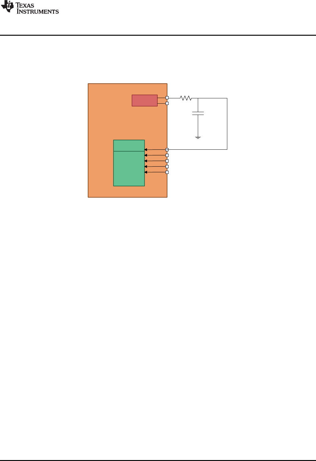
ADC
PWM1 B
A
A0
A1
A2
A3
A4
www.ti.com
Brief Description of Diagnostics
61
SPRUI78B–July 2016–Revised June 2018
Submit Documentation Feedback Copyright © 2016–2018, Texas Instruments Incorporated
Safety Manual for TMS320F2837xD/S and TMS320F2807x
6.5.13 Monitoring of ePWM by ADC
The ePWM outputs can be monitored for proper operation by ADC using a board level feedback as
indicated in Figure 23. The technical details for implementing such a loopback like signal resolution, and
so forth is provided in the link [9]. Error response, diagnostic testability, and any necessary software
requirements are defined by the software implemented by the system integrator.
Figure 23. Monitoring of ePWM by ADC
6.5.14 Online Monitoring of Interrupts and Events
For interrupts and events, failure can be detected using information about the time behavior of the system.
The monitored signals can be either periodic or aperiodic.
For a typical closed loop control application, most of the critical events are periodic in nature and these
periodic events can be monitored and incoherence in the events can be used for fault detection. A few
places where online monitoring periodic interrupts and events can be employed include:
• Periodic generation of ADC start of conversion (SoC) (x): ADC SoC signal can be used to generate an
external interrupt (XINT) with the help of X-BAR. The occurrence of periodic interrupts can be
monitored.
• Periodic DMA trigger: Some of the DMA events may also be periodic in nature (for example, copy of
ADC results, updating of CMPA register, and so forth). DMA supports interrupt generation on the
completion of the DMA action and this capability can be used for online monitoring.
• Periodic occurrence of ECAP and EQEP interrupts
Monitoring of interrupts and events which are normally not expected during the correct operation can also
be used to improve the diagnostic coverage (e.g: ECC correctable error interrupt).
6.5.15 SDFM Comparator Filter for Online Monitoring
Comparator unit of SDFM can be used for online monitoring of primary filter’s operation. The comparator
filter has a configurable sinc filter whose output is compared with two programmed threshold levels to
detect over and under-value conditions. In case comparator filter’s data output crosses low or high
threshold limit, it will fire interrupt to the CPU.
6.5.16 SD Modulator Clock Fail Detection Mechanism
When SD modulator clock fails or goes missing for 256 continuous system clock cycles, clock fail
detection submodule in the input control unit of SD modulator detects the failure and generates an
interrupt to CPU. This mechanism can be used to detect missing modulator clock faults or any faults in
digital IO connecting modulator clock.

Brief Description of Diagnostics
www.ti.com
62 SPRUI78B–July 2016–Revised June 2018
Submit Documentation Feedback
Copyright © 2016–2018, Texas Instruments Incorporated
Safety Manual for TMS320F2837xD/S and TMS320F2807x
6.5.17 Software Test of Function Including Error Tests
A software test can be utilized to test basic functionality of the module and to inject diagnostic errors and
check for proper error response. Such a test can be executed at boot or periodically. Software
requirements necessary are defined by the software implemented by the system integrator.
Ideas for creating some module specific tests functionality and error tests are given below:
• SDFM functionality can be checked by sending a known input test sequence to the C2000 MCU,
process it using the digital decimation filters and cross check the value against a known value. For
detecting faults in comparator interrupt generation logic, a test pattern can be created to configure the
high/low threshold register values to min/max values respectively. Interrupt should always be
generated with such a configuration.
• DMA functionality can be checked by transferring a known good data from a source memory to the
destination memory and checking for data integrity after the transfer. The transfer can be initiated
using the software trigger available (CONTROL.PERINTFRC). On chip timer can be used to profile the
time required for such a data transfer.
• EMIF functionality can be checked by moving a known good data from an external memory to the
internal memory and vice versa and checking for data consistency using CRC or other mechanisms.
The test should be repeated for all the masters having access to the external memories. In addition,
the test should provide coverage to all the interface pins used for connecting external memory to the
C2000 MCU.
• Software test of input and output X-BAR module can be performed by having a loop created (output X-
BAR can be used as stimulus to input X-BAR) using the input and output X-BAR, sending a known test
sequence at the input and observing it at the final output. Integrity of ePWM X-BAR can be checked by
sending the test stimulus and observing the response using ePWM trip or sync functionality.
• Software test of XINT functionality can be checked by configuring the input X-BAR and forcing the
corresponding GPIO register to generate an interrupt. The diagnostic coverage can be enhanced by
performing checks for the polarity (XINTxCR.POLARITY) and enable (XINTxCR.ENABLE) functionality
as well.
• IPC functionality can be checked by using interrupts or polling method by periodically sending test
commands and message as defined by software. Time stamping information using the
IPCCOUNTERH/L can be embedded along with the message to estimate the delay in communication.
• ECAP and EQEP functionality can be checked by looping back the PWM or GPIO outputs to the
respective module inputs, providing a known good sequence as required by the module and observing
the module output. In the case of ECAP, the test can be done internally with the help of input X-BAR.
• ROM prefetch functionality can be checked using similar techniques as given in Section 6.3.7.
• The PWM module consists of Time-Base (TB), Counter Compare (CC), Action Qualifier (AQ), Dead-
Band Generator (DB), PWM Chopper (PC), Trip Zone (TZ), Event Trigger (ET) and Digital Compare
(DC) sub-modules. The individual sub-modules can be tested by providing suitable stimulus using
PWM and observing the response using one of the capture (time stamping) modules (eCAP, XINT,
eQEP, etc.). It is recommended to cover the various register values associated with application
configuration while performing the software test. Due to the regular linear nature of the various sub-
modules, it is possible to get high coverage using a software test.
• A software test of SRAM wrapper logic should provide diagnostic coverage for arbitration between
various masters having access to the particular SRAM and correct functioning of access protection.
This is in addition to the test used to provide coverage of SRAM bit cells (see Section 6.3.12).
• A software test function in DCSM can be implemented independently in zone1, zone2 and unsecured
zone to check DCSM functionality. Device security configurations are loaded from OTP to DCSM
during the device boot phase. The test function can implement access filtering checks (read-write and
execute permissions) to RAMs and flash sectors belonging to the same zone and different zone. An
additional check for EXEONLY configuration can also be implemented for the RAMs and flash sectors
to ensure that all access other than execute access is blocked.

www.ti.com
Brief Description of Diagnostics
63
SPRUI78B–July 2016–Revised June 2018
Submit Documentation Feedback Copyright © 2016–2018, Texas Instruments Incorporated
Safety Manual for TMS320F2837xD/S and TMS320F2807x
6.6 Analogue I/O
6.6.1 ADC Information Redundancy Techniques
Information redundancy techniques can be applied via software for providing runtime diagnostic coverage
on ADC conversions. Time redundancy technique can be applied where multiple conversions on same
ADC followed by comparison of results done in software. In addition, the correlation between input signals
can be used to check the integrity (for example, if the three phase voltage, V1, V2, V3is being measured
using ADC, the function V1+ V2+ V3= 0 can be used to provide diagnostic coverage for input signal
integrity and ADC conversion).
Error response, diagnostic testability, and any necessary software requirements are defined by the
software implemented by the system integrator.
6.6.2 ADC Input Signal Integrity Check
ADC input signal integrity can be checked using a mix of hardware and software runtime diagnostic on
ADC conversions. Filtering or plausibility check (for example, value fall in an expected range) of the
converted values can be performed using some of the built in hardware mechanisms available within the
device. Plausibility check of the input signal can be checked with the help of comparator by setting the
proper high and low threshold values. The plausibility check of converted results can be checked by using
ADC Post Processing Block.
6.6.3 ADC Signal Quality Check by Varying Acquisition Window
External signal sources vary in their ability to drive an analog signal quickly and effectively. In order to
achieve rated resolution, the signal source needs to charge the sampling capacitor in the ADC core to
within 0.5 LSBs of the signal voltage. The acquisition window is the amount of time the sampling capacitor
is allowed to charge and is configurable for SOCx by the ADCSOCxCTL.ACQPS register. This
configurable parameter can be also used to provide diagnostic coverage for the input signal path and ADC
sampling capacitor logic. The test can be done by redundant conversion of the same input signal by ADC
using the preset ACQPS configuration and an ACQPS configuration higher than the preset configuration.
The results thus obtained have to be within a pre-defined range determined by the application and ADC
specification parameters.
6.6.4 CMPSS Ramp Generator Functionality Check
CMPSS ramp generation functionality is used in certain control applications (for example, peak current
mode control). The functionality of ramp generator can be checked by reading back the contents of
DACHVALA register and ensuring that the register value is periodically updated based on the RAMPDLY,
RAMPDECVAL and RAMPMAXREF. Error response, diagnostic testability, and any necessary software
requirements are defined by the software implemented by the system integrator.
6.6.5 DAC to ADC Loopback Check
Integrity of DAC and ADC can be checked monitoring DAC output using ADC. DAC can be configured
using software to provide a set of predetermined voltage levels. These voltage levels can be measured by
the ADC and results thus obtained can be cross checked against the expected value to ensure proper
functioning of DAC and ADC. This technique can be applied during run time as well to ensure that proper
voltage levels are being driven from DAC.
For more information on the DAC channels that can be sampled by ADC without external board level
connections, see the device-specific data sheet or technical reference manual. While performing the
loopback checks for 16-bit differential input mode, two DACs should be used to provide input the ADC. To
avoid common cause failures, it is recommended to keep the references voltages of the ADC and DAC
different while performing the test. In addition, the input signal to ADC should not be driven by any other
sources while the test is being performed.
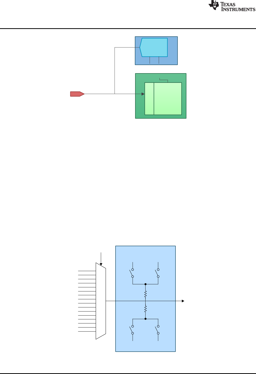
CHSEL
0
ADCIN0
1
ADCIN1
2
ADCIN2
3
ADCIN3
4
ADCIN4
5
ADCIN5
6
ADCIN6
7
ADCIN7
8
ADCIN8
9
ADCIN9
10
ADCIN10
11
ADCIN11
ADCIN12 12
13
ADCIN13
14
ADCIN014
15
ADCIN15
S2
VDDA
S1
VSSA
Opens/Shorts Detection Circuit
S3
VDDA
S4
VSSA
5 kW
7 kW
To S+H
12-bit
Buffered
DAC
VREFVDAC
Ax/DACy
ADC-A
12/16-bit
0
1
.
.
VREF1
Brief Description of Diagnostics
www.ti.com
64 SPRUI78B–July 2016–Revised June 2018
Submit Documentation Feedback
Copyright © 2016–2018, Texas Instruments Incorporated
Safety Manual for TMS320F2837xD/S and TMS320F2807x
Figure 24. DAC to ADC Loopback
6.6.6 DAC to Comparator Loopback Check
The DAC outputs can be looped back to comparator inputs to check whether the outputs being driven are
at proper voltage levels. The connections need to be provided externally on the board to enable this
check. Higher diagnostic coverage can be obtained by configuring tighter limits to the comparator. This
technique can also be used to detect control flow errors which cause the DAC output to be set at a value
outside the applications safe operating range.
6.6.7 Opens/Shorts Detection Circuit for ADC
An opens/shorts detection circuit is provided to allow customers to detect faults in the ADC input channel.
This capability is valid only in single ended mode. For system integrator using differential mode, ADC
need to be configured in 12-bit single ended mode to perform this test. Error response, diagnostic
testability, and any necessary software requirements are defined by the software implemented by the
system integrator. This capability is deprecated in few part numbers. Confirm the feature availability before
using this diagnostic.
The following circuit and configuration selected by programmable register bits to control switches S1, S2,
S3, S4 allows controlling input ADC channel to test for Open/Shorts conditions.
Figure 25. Opens/Shorts Detection Circuit

www.ti.com
Brief Description of Diagnostics
65
SPRUI78B–July 2016–Revised June 2018
Submit Documentation Feedback Copyright © 2016–2018, Texas Instruments Incorporated
Safety Manual for TMS320F2837xD/S and TMS320F2807x
Table 2. ADC Open-Shorts Detection Circuit Truth Table
ADCOSDETECT.DETEC
TCFG Source Voltage S4 S3 S2 S1 Drive Impedance
0 Off Open Open Open Open Open
1 Zero Scale Closed Open Open Closed 5K || 7K
2 Full Scale Open Closed Closed Open 5K || 7K
3 5/12 VDDA Open Closed Open Closed 5K || 7K
4 7/12 VDDA Closed Open Closed Open 5K || 7K
5 Zero Scale Open Open Open Closed 5K
6 Full Scale Open Open Closed Open 5K
7 Zero Scale Closed Open Open Open 7K
6.6.8 VDAC Conversion by ADC
Reference voltage input to COMPDACs (VDAC) is double bonded with ADCB input. For detecting faults in
VDAC supply and corresponding analog I/O, it can be converted by ADC. The ADC result output can be
cross checked against the expected output to identify any faults. Programmed error response and any
necessary software requirements are defined by the system integrator.
6.6.9 Disabling Unused Sources of SOC Inputs to ADC
The start of conversion (SOC) signal input to the ADC module can be triggered by multiple sources,
mainly Software, CPU Timers, GPIO, and PWM module instances. In order to achieve freedom from
interference due to a fault originating from an peripheral not used in implementing the safety function and
cascading into ADC, it is recommended that application configures only the requires SOC triggers. This is
a way to avoid faults originating from an outside source to impact functionality of ADC.
6.7 Data Transmission
6.7.1 Bit Error Detection
When this module transmits information onto its Bus, it can also monitor the Bus to ensure that the
transmitted information is appearing as expected on the Bus. If the expected values are not read back
from the Bus, the hardware can flag the error and signal an interrupt to the CPU. This feature must be
enabled and configured in software.
6.7.2 CRC in Message
This module appends a CRC word along with the message. The CRC values are calculated and
transmitted by the transmitter, and then re-calculated by the receiver. If the CRC value calculated by the
receiver does not match the transmitted CRC value, a CRC error will be flagged. Error response and any
necessary software requirements are defined by the system integrator.
6.7.3 DCAN Acknowledge Error Detection
When a node on the CAN network receives a transmitted message, it sends an acknowledgment that it
received the message successfully. When a transmitted message is not acknowledged by the recipient
node, the transmitting DCAN will flag an Acknowledge Error. Error response and any necessary software
requirements are defined by the system integrator.
6.7.4 DCAN Form Error Detection
Certain types of frames in the DCAN have a fixed format per the CAN protocol. When a receiver receives
a bit in one of these frames that violate the protocol, the module will flag a Form Error. Error response and
any necessary software requirements are defined by the system integrator.

Brief Description of Diagnostics
www.ti.com
66 SPRUI78B–July 2016–Revised June 2018
Submit Documentation Feedback
Copyright © 2016–2018, Texas Instruments Incorporated
Safety Manual for TMS320F2837xD/S and TMS320F2807x
6.7.5 DCAN Stuff Error Detection
In the CAN message protocol, several of the frame segments are coded through bit stuffing. Whenever a
transmitter detects five consecutive bits of identical value in the bit stream to be transmitted, it
automatically inserts a complementary bit into the actual transmitted bit stream. If a 6th consecutive equal
bit is detected in a received segment that should have been coded by bit stuffing, the DCAN module will
flag a Stuff Error. Error response and any necessary software requirements are defined by the system
integrator.
6.7.6 EMIF Access Latency Profiling Using On-Chip Timer
Each EMIF access takes fixed number of cycles for completing an access (read/write) to external memory.
Once the access latency is obtained, timer module can be used for profiling data transfers to both
asynchronous memories (with and without WAIT/READY handshake) and SDRAM memories.
6.7.7 EMIF Access Protection Mechanism
This mechanism provides code protection by preventing unauthorized fetch or writes access thus
identifying execution of unauthorized code or unwarranted corruption of external memory contents. The
feature enables freedom from interference for the software code and data.
6.7.8 EMIF Asynchronous Memory Timeout Protection Mechanism
Asynchronous memories have fixed write and read access timings achieved using wait states. Some
memories support handshake in addition to wait states configuration using WAIT/READY signal. Using
WAIT/READY signal and timeout counters message delays and hang conditions caused can be detected.
An error interrupt will be generated once timeout counters expire and current read/write access will be
discarded removing stall to the requested master.
6.7.9 I2C Access Latency Profiling Using On-Chip Timer
Each I2C message takes fixed number of system clock cycles for completing the transaction. The master
can detect the transaction completion based on message acknowledge signaling from the slave. On chip
timer module can be used for profiling the time required for completing each transaction.
6.7.10 Information Redundancy Techniques Including End-to-End Safeing
Information redundancy techniques can be applied via software as an additional runtime diagnostic. There
are many techniques that can be applied, such as read back of written values and multiple reads of the
same target data with comparison of results.
In order to provide diagnostic coverage for network elements outside the C2000 MCU (wiring harness,
connectors, transceiver) end-to-end safety mechanisms are applied. These mechanisms can also provide
diagnostic coverage inside the C2000 MCU. There are many different schemes applied, such as additional
message checksums, redundant transmissions, time diversity in transmissions, and so forth. Most
commonly checksums are added to the payload section of a transmission to ensure the correctness of a
transmission. These checksums are applied in addition to any protocol level parity and checksums. As the
checksum is generated and evaluated by the software at either end of the communication, the whole
communication path is safed, resulting in end-to-end safeing.
Any end-to-end communications diagnostics implemented should consider the failure modes and potential
mitigating safety measures described in IEC 61784-3:2010 and summarized in IEC 61784-3:2010, Table
1.
6.7.11 I2C Data Acknowledge Check
When a node on the I2C network receives a byte (address or data), it sends an acknowledgment that the
address is acknowledged or the data byte is received successfully. When a transmitted message is not
acknowledged by the recipient I2C, the transmitting I2C will flag NACK. Necessary software requirements
are defined by the system integrator. For example a function which needs to transfer 4 bytes of data and
can sent CRC as 5th byte. The device software can be designed such that the acknowledge is not
provided if the data and CRC doesn’t match.
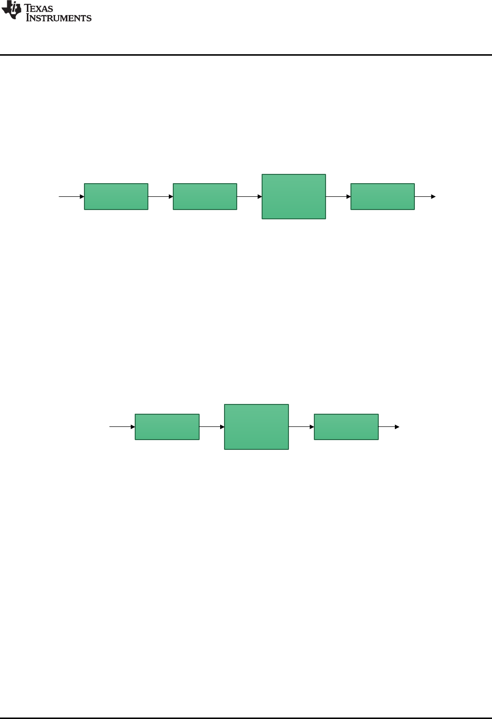
DXR Compress or
do not modify XSR Data Tx
From CPU or
DMA
RSR RBR Expand or
Justify and bit fill DRR To CPU
or DMA
Data Rx
www.ti.com
Brief Description of Diagnostics
67
SPRUI78B–July 2016–Revised June 2018
Submit Documentation Feedback Copyright © 2016–2018, Texas Instruments Incorporated
Safety Manual for TMS320F2837xD/S and TMS320F2807x
6.7.12 McBSP Receiver Overrun Detection
When McBSP is in receive mode, the Receive Shift Register (RSR) receives the data first, then transfers
the contents to the Receive Buffer Register (RBR), Data Receive Register (DRR) and subsequently gets
acted upon by the bus master (CPU or DMA). When the DRR is not read since the last data copy from the
RBR, the receiver does not copy a new word from the RBR to DRR and from the Receive Shift Register
(RSR) to the RBR. The RFULL = 1 flag indicates this error condition, wherein, any new serial data that
arrives will replace the contents of the RSR, and the previous received word is lost. RFULL = 1 flag
condition does not generate an interrupt and CPU has to periodically poll the signal to test the occurrence
of error.
Figure 26. McBSP Reception Data Path
6.7.13 McBSP Receiver Sync Error Detection
An unexpected receive frame-synchronization pulse is one that begins the next frame transfer before all
the bits of the current frame have been received. Such a pulse causes data reception to abort and restart.
The current word is lost and this is indicated by the RSYNCERR = 1 flag. This can generate an interrupt to
the CPU.
6.7.14 McBSP Transmitter Sync Error Detection
An unexpected transmit frame-synchronization pulse is one that begins the next frame transfer before all
the bits of the current frame have been transmitted. Such a pulse causes the current data transmission to
abort and restart. The current word is lost and this is indicated by the XSYNCERR=1 flag. This can
generate an interrupt to the CPU.
Figure 27. McBSP Transmission Data Path
6.7.15 McBSP Transmitter Underflow Detection
For McBSP transmission, CPU or DMA controller writes data to the Data Transmit Register (DXR). When
new data arrives in DXR, McBSP copies the content of the DXR to the Transmit Shift Register (XSR). On
reception of transmit frame-synchronization pulse, McBSP shifts data bits from the XSR to the transmit
pin. If new data is not loaded into the DXR before a new frame-synchronization signal arrives, the previous
data in the DXR is sent again. The XEMPTY = 0 flag indicates this error condition. This continues for
every new frame-synchronization pulse that arrives until the DXR is loaded with new data. XEMPTY = 0
flag condition does not generate an interrupt and CPU has to periodically poll the signal to test the
occurrence of error.
6.7.16 Parity in Message
This module supports insertion of a parity bit into the data payload of every outgoing message by
hardware. Evaluation of incoming message parity is also supported by hardware. Detected errors
generate an interrupt to the CPU.
6.7.17 SCI Break Error Detection
A SCI break detect condition occurs when the SCIRXD is low for ten bit periods following a missing stop
bit. This action sets the BRKDT flag bit (SCIRXST, bit 5) and initiates an interrupt.

Brief Description of Diagnostics
www.ti.com
68 SPRUI78B–July 2016–Revised June 2018
Submit Documentation Feedback
Copyright © 2016–2018, Texas Instruments Incorporated
Safety Manual for TMS320F2837xD/S and TMS320F2807x
6.7.18 SCI Frame Error Detection
When receiving serial data, each byte of information on the SCI has an expected format. If the received
message does not match this, the SCI hardware can flag an error and generate an interrupt to the CPU.
This feature must be enabled and configured in software.
6.7.19 SCI Overrun Error Detection
If the SCI RX buffer receives new data before the previous data has been read, the existing data will be
overwritten and lost. If this occurs, the SCI hardware can flag the error and generate an interrupt to the
CPU. This feature must be enabled and configured in software.
6.7.20 Software Test of Function Using I/O Loopback
Most communication modules support digital or analog loopback capabilities for the I/Os. To confirm the
implemented loopback capabilities of the module, see the device-specific technical reference manual.
Digital loopback tests the signal path to the module boundary. Analog loopback tests the signal path from
the module to the I/O cell with output driver enabled. For best results any tests of the functionality should
include the I/O loopback.
6.7.21 SPI Data Overrun Detection
If SPI RX buffer receives new data before the previous data has been read, the existing data will be
overwritten and lost. If this occurs, SPI hardware can flag the error and generate an interrupt to the CPU.
This feature must be enabled and configured in software.
6.7.22 Transmission Redundancy
The information is transferred several times in sequence using the same module instance and compared.
When the same data path is used for duplicate transmissions, transmission redundancy will only by useful
for detecting transient faults. The diagnostic coverage can be improved by sending inverted data during
the redundant transmission.
In order to provide diagnostic coverage of device interconnects and EMIF, read back of written data (in
case of data writes) and multiple read backs of information (in case of data reads) can be employed.

www.ti.com
References
69
SPRUI78B–July 2016–Revised June 2018
Submit Documentation Feedback Copyright © 2016–2018, Texas Instruments Incorporated
Safety Manual for TMS320F2837xD/S and TMS320F2807x
7 References
1. Calculating Useful Lifetimes of Embedded Processors
2. Moisture/Reflow Sensitivity Classification for Nonhermetic Solid State Surface Mount Devices,
https://www.jedec.org/standards-documents/docs/jesd-22-a112
3. Handling, Packing, Shipping and Use of Moisture/Reflow Sensitive Surface Mount Devices,
http://www.jedec.org/sites/default/files/docs/jstd033b01.pdf
4. IEC61508 Functional Safety of Electrical/Electronic/Programmable Electronic Safety-Related Systems,
International Electrotechnical Commission, 1998.
5. ISO26262–Road Vehicles-Functional Safety, International Standard ISO/FDIS, vol. 26262, 2011.
6. Standardized E-Gas Monitoring Concept for Gasoline and Diesel Engine Control Units
7. J. Astruc and N. Becker, Toward the Application of ISO 26262 for Real-Life Embedded Mechatronic
Systems, in International Conference on Embedded Real Time Software and Systems. ERTS2, 2010.
8. ISO26262–Road Vehicles-Functional Safety, Part 5: Product development at the hardware level,
Appendix D, International Standard ISO/FDIS, vol. 26262, 2011.
9. Using PWM Output as a Digital-to-Analog Converter on a TMS320F280x Digital Signal Controller
10. W. M. Goble and H. Cheddie, Safety Instrumented Systems Verification: Practical Probabilistic
Calculations. Isa, 2004.
11. TMS320C28x FPU Primer
12. Online Stack Overflow Detection on the TMS320C28x DSP
13. TMS320F2837xD Dual-Core Delfino™ Microcontrollers Data Sheet
14. TMS320F2837xS Delfino™ Microcontrollers Data Sheet
15. TMS320F2807x Piccolo™ Microcontrollers Data Sheet
16. TMS320F2837xD Dual-Core Delfino Microcontrollers Technical Reference Manual
17. IEC-60730 official website. Available online at http://www.iec.ch.
18. IEC-61784 official website. Available online at http://www.iec.ch.
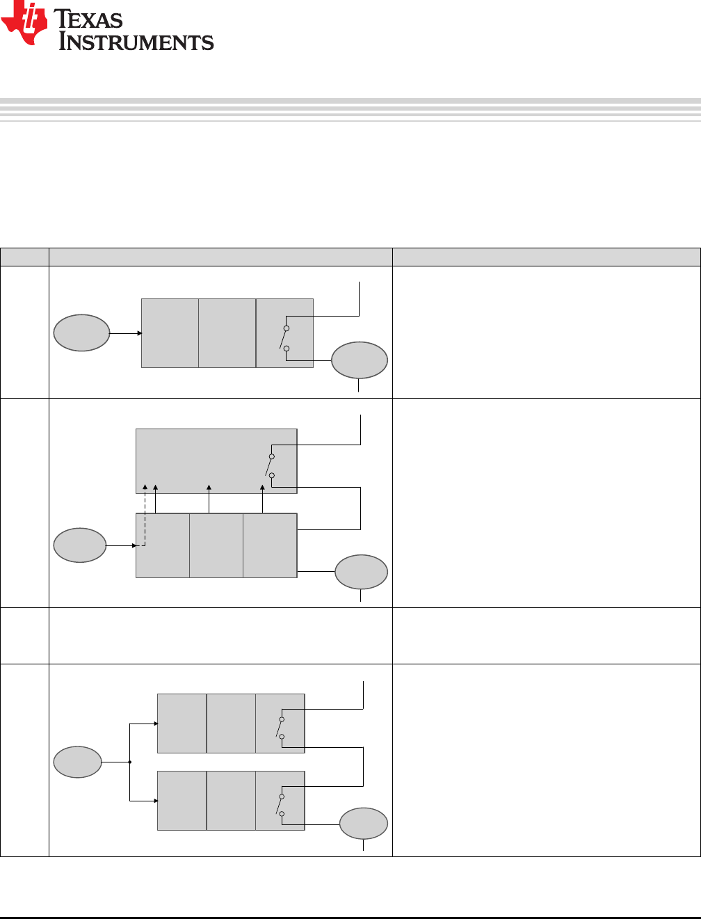
Sensor
Input
Circuit Processing
Unit
Output Circuit
Input
Circuit Processing
Unit
Output Circuit
Actuator
Final Element
+
-
Input
Circuit
Sensor
Diagnostic Circuit
Actuator
Final Element
+
-
Processing
Unit
Output Circuit
Sensor Input
Circuit Processing
Unit
Output Circuit
Actuator
Final Element
+
-
70 SPRUI78B–July 2016–Revised June 2018
Submit Documentation Feedback
Copyright © 2016–2018, Texas Instruments Incorporated
Safety Architecture Configurations
Appendix A
SPRUI78B–July 2016–Revised June 2018
Safety Architecture Configurations
A.1 Safety Architecture Configurations
The various redundancy architectures possible for the safety instrumented systems are indicated in
Table 3. For more information, see [10].
Table 3. Safety Architecture Configurations
Diagnostic Implementation
1 1oo1 Architecture NA
2 1oo1D Diagnostic channel is implemented using various hardware
diagnostic features like Watchdog, and so forth.
3 1oo1D
Same figure as above. Diagnostic channel is implemented using reciprocal
comparison (uses two processing units for implementing
reciprocal comparison) and other hardware diagnostic
features.
4 1oo2 Two different processing units are used to implement one
channel.
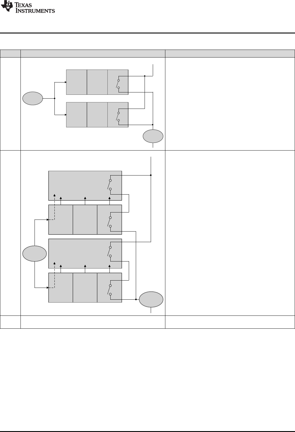
Diagnostic Circuit
Diagnostic Circuit
Sensor
Input
Circuit Processing
Unit
Output Circuit
Input
Circuit Processing
Unit
Output Circuit
Actuator
Final Element
+
-
Sensor
Input
Circuit Processing
Unit
Output Circuit
Input
Circuit Processing
Unit
Output Circuit
Actuator
Final Element
+
-
www.ti.com
Safety Architecture Configurations
71
SPRUI78B–July 2016–Revised June 2018
Submit Documentation Feedback Copyright © 2016–2018, Texas Instruments Incorporated
Safety Architecture Configurations
Table 3. Safety Architecture Configurations (continued)
Diagnostic Implementation
5 2oo2 Two different processing units are used to implement one
channel.
6 2oo2D Two 1oo1D structures of #2 wired together to implement a
safe channel.
7 2oo2D
Same figure as above. Two 1oo1D structures of #3 wired together.
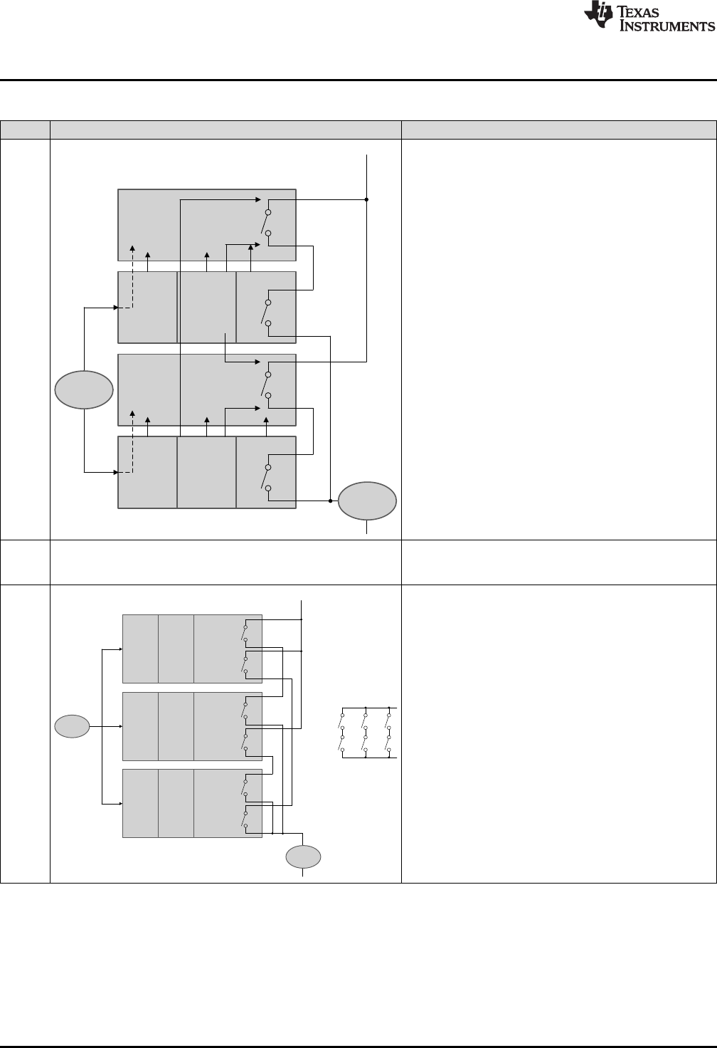
Sensor
Actuator
Final Element
-
Input
Circuit Processing
Unit
Output Circuit 1
Output Circuit 2
Input
Circuit Processing
Unit
Output Circuit 1
Output Circuit 2
Input
Circuit Processing
Unit
Output Circuit 1
Output Circuit 2
A
B
A
C
B
C
Voting Circuit
Diagnostic
Circuit
Diagnostic
Circuit
Sensor
Input
Circuit Processing
Unit
Output Circuit
Input
Circuit Processing
Unit
Output Circuit
Actuator
Final Element
+
-
Safety Architecture Configurations
www.ti.com
72 SPRUI78B–July 2016–Revised June 2018
Submit Documentation Feedback
Copyright © 2016–2018, Texas Instruments Incorporated
Safety Architecture Configurations
Table 3. Safety Architecture Configurations (continued)
Diagnostic Implementation
8 1oo2D Similar to 2oo2D implementation of #6 with additional
control lines wired to control one set of units using the other
unit
9 1oo2D
Same figure as above. Similar to 2oo2D implementation of #7 with additional
control lines wired to control one set of units using the other
unit.
10 2oo3 Use three different processing units to implement majority
voting. The fourth channel can be used either standalone or
with hardware diagnostic features.
Item
(e.g. Airbag Controller)
Function
(e.g. Airbag)
System/Sub-system
(e.g. Sensor) System/Sub-system
(e.g. Controller) System/Sub-system
(e.g. Actuator)
Component
(e.g. MCU)
Electric and Electronic
Part Communication Mechanical Part
Component
(e.g. Application
software)
Hardware Part
(e.g: CPU)
Software Unit
(e.g: SRAM test
module)
Element
Item
73
SPRUI78B–July 2016–Revised June 2018
Submit Documentation Feedback Copyright © 2016–2018, Texas Instruments Incorporated
Terms and Definitions
Appendix B
SPRUI78B–July 2016–Revised June 2018
Terms and Definitions
B.1 Terms and Definitions
• IEC60730: The IEC 60730 standard covers mechanical, electrical, electronic, EMC, and abnormal
operation of ac appliances. It is used in the design of design of white goods and other appliances to
improve customer safety using software test libraries developed in accordance with this standard.
• IEC61508: Functional safety standard for E/E/PE safety-related systems. This is intended to be a basic
functional safety standard applicable to all kinds of industry. It defines functional safety as: “part of the
overall safety relating to the EUC (Equipment Under Control) and the EUC control system which
depends on the correct functioning of the E/E/PE safety-related systems, other technology safety-
related systems and external risk reduction facilities” [4].
• ISO13849: provides safety requirements and guidance for the design and integration of safety-related
parts of control systems (SRP/CS), including software design.
• M out of N (MooN) architecture: A safety instrumented system where ‘M’ channels out of ‘N’ channels
are required for functionally safe operation. (for example, 2oo3, 2 out of 3 architecture, where majority
voting is used to implement a safety function).
Figure 28. ISO26262 Illustration of Item, System, Component, Hardware Part and Software Unit
• M out of N Channel Architecture with diagnostics (MooND).
• Functional Safety: Part of the overall safety relating to the EUC and the EUC control system that
depends on the correct functioning of the E/E/PE safety-related systems and other risk reduction
measures
• Item: system or array of systems to implement a function at the vehicle level, to which ISO 26262 is
applied (for example, power steering of a car).

Terms and Definitions
www.ti.com
74 SPRUI78B–July 2016–Revised June 2018
Submit Documentation Feedback
Copyright © 2016–2018, Texas Instruments Incorporated
Terms and Definitions
• Element: System or part of a system including components, hardware, software, hardware parts, and
software units.
• System: set of elements that relates at least a sensor, a controller and an actuator with one another
• Component: Non-system level element that is logically and technically separable and is comprised of
hardware parts and software units.
• Hardware part: Hardware that cannot be subdivided (for example, CPU).
• Software unit: Atomic level software component of the software architecture that can be subjected to
stand-alone testing (for example, SRAM test module).
• Failure: termination of the ability of an element, to perform a function as required.
• Failure mode: manner in which an element or an item fails.
• Single Point Fault: Fault in an element that is not covered by a safety mechanism and that leads
directly to the violation of a safety goal.
• Single-point failure: Failure that results from a single-point fault and that leads directly to the violation
of a safety goal.
• Multiple-point fault: Individual fault that, in combination with other independent faults, leads to a
multiple-point failure.
• Multiple-point failure: Failure resulting from the combination of several independent faults, which leads
directly to the violation of a safety goal. For a multiple-point failure to directly violate a safety goal,
presence of all independent faults is necessary.
• Multiple-point fault detection interval: time span to detect multiple-point fault before it can contribute to
a multiple-point failure.
• Latent fault: multiple-point fault whose presence is not detected by a safety mechanism nor perceived
by the driver within the multiple-point fault detection interval.
• Functional Safety Assessment: Investigation, based on evidence, to judge the functional safety
achieved by one or more E/E/PE safety-related systems and/or other risk reduction measures.
• Functional Safety Audit: Systematic and independent examination to determine whether the
procedures specific to the functional safety requirements to comply with the planned arrangements are
implemented effectively and are suitable to achieve the specified objectives.
• Hazard and Risk Analysis (IEC61508)/Hazard Analysis and Risk Assessment (ISO26262): An end
equipment level functional safety analysis that is used to identify safety functions and/or functional
safety goals. This process also establishes the SIL (IEC61508) or ASIL (ISO26262), which defines the
level of risk reduction necessary per safety function and/or functional safety goal.
• Process Tailoring: The act of changing a development process or functional safety lifecycle to match
needs of a business engagement. Requirements can be moved from phase to phase or performed by
other developers, but removal of process requirements is not allowed.
• Quality Managed: Describes a design element which is developed compliant to applicable quality
standards but is not developed compliant to applicable functional safety standards. It may be possible
to use a quality managed design element in a specific functional safety design contingent upon results
of a functional safety qualification.
• Safety Requirement Decomposition: Safety requirements decomposition is the process in which safety
requirements are split into a series of redundant safety requirements at a lower level of abstraction in
order to support tailoring of the SIL (ISO26262)/ASIL (ISO26262) compliance requirements of design
elements at the lower level of abstraction. For example, a requirement for a peripheral function with
high safety integrity might be addressed by redundant instances of a peripheral with lower safety
integrity.
• For the full list of applicable terms and their definitions for ISO26262, see the ISO26262-1:2011, Road
vehicles — Functional safety — Part 1: Vocabulary.
• For the full list of applicable terms and their definitions for IEC61508, see the IEC61508, Functional
safety of electrical/electronic/programmable electronic safety-related systems – Part 4: Definitions and
abbreviations.

75
SPRUI78B–July 2016–Revised June 2018
Submit Documentation Feedback Copyright © 2016–2018, Texas Instruments Incorporated
Summary of Safety Features and Diagnostics
Appendix C
SPRUI78B–July 2016–Revised June 2018
Summary of Safety Features and Diagnostics
C.1 Summary of Safety Features and Diagnostics
Table 4. Summary Table Legend
Unique Identifier Identifier used to reference the contents.
Safety Feature or
Diagnostic Safety feature
Usage Each test listed in this chart can be one of two types. A "diagnostic" test or a "test for diagnostic".
Diagnostic: Provides coverage for faults on a primary function of the device. It may, in addition, provide fault
coverage on other diagnostics, and can therefore be also used as a test-for-diagnostic in certain cases
Test-for-Diagnostic Only: Does NOT provide coverage for faults on a primary function of the device. It's only
purpose is to provide fault coverage on other diagnostics
Diagnostic Type Hardware - A diagnostic which is implemented by TI in silicon and can communicate error status upon the
detection of failures. It may require software to enable the diagnostic and/or to take action upon the detection of
a failure.
Software - A test recommended by TI which must be created by the software implementer. This test may use
additional hardware implemented on the device by TI.
Hardware / Software - A test recommended by TI which requires both, diagnostic hardware which has been
implemented in silicon by TI, and which requires software that must be created by the software implementer.
System - A diagnostic implemented externally of the microcontroller
Diagnostic Operation This can be one among the following:
(i) Bootup (enabled by default)
(ii) Continuous - Enabled at reset: Hardware safety mechanism that is enabled by default at reset.
(iii) Continuous - Enabled by software: Hardware safety mechanism that needs to be enabled by software.
(iv) On demand (Software defined): Software or Hardware-software safety mechanism that gets activated in the
diagnostic test interval by the software
(v) System defined: Implemented by the system.
Test Execution Time This column lists the time required for this diagnostic to complete.
Action on Detected Fault The response this diagnostic takes when an error is detected.
For software-driven tests, this action is often software implementation-dependent.
Error Reporting Time Typical time required for diagnostic to indicate a detected fault to the system. For safety mechanisms where
fault detection time is known, this value is indicated. For software-driven tests, this time is often software
implementation-dependent.
Summary of Safety Features and Diagnostics
www.ti.com
76 SPRUI78B–July 2016–Revised June 2018
Submit Documentation Feedback
Copyright © 2016–2018, Texas Instruments Incorporated
Summary of Safety Features and Diagnostics
Table 5. Summary of Safety Features and Diagnostic
Device Partition Unique
Identifier Safety Feature or Diagnostic Usage Diagnostic Type Diagnostic
Operation Test Execution
Time Action on
Detected Fault Error Reporting
Time
Power Supply PWR1 External Voltage Supervisor Diagnostic System defined Continuous -
Enabled at reset Zero or very low
overhead System defined System defined
PWR2 External Watchdog Diagnostic System defined System defined System defined System defined System defined
Clock CLK1 Missing Clock Detect (MCD) Diagnostic Hardware Continuous -
Enabled at reset Zero or very low
overhead
NMI with
ERRORSTS
assertion
Clock switch to
internal oscillator
0.8 2ms
CLK2 Clock Integrity Check Using CPU
Timer Diagnostic Hardware -
Software On demand
(Software defined) Software defined Software defined Software defined
CLK3 Clock Integrity Check Using
HRPWM Diagnostic Hardware -
Software On demand
(Software defined) Software defined Software defined Software defined
CLK5 External Clock Monitoring via
XCLKOUT Diagnostic System defined System defined System defined System defined System defined
CLK6 Internal Watchdog (WD) Diagnostic Hardware Continuous -
Enabled at reset Zero or very low
overhead Device reset or
interrupt as per
configuration
Software defined
CLK7 External Watchdog Diagnostic System defined System defined System defined System defined System defined
CLK8 Periodic Software Read Back of
Static Configuration Registers Diagnostic Software On demand
(Software defined) Software defined Software defined Software defined
CLK9 Software Read Back of Written
Configuration Diagnostic Software On demand
(Software defined) Software defined Software defined Software defined
CLK10 Software Test of Watchdog (WD)
Operation Test for
diagnostic Software On demand
(Software defined) Software defined Software defined Software defined
CLK12 Software Test of Missing Clock
Detect Functionality Test for
diagnostic Hardware -
Software On demand
(Software defined) Software defined Software defined Software defined
CLK13 PLL Lock Profiling using On-Chip
Timer Diagnostic Hardware -
Software On demand
(Software defined) Software defined Software defined Software defined
CLK14 Peripheral Clock Gating (PCLKCR) Diagnostic Hardware On demand
(Software defined) NA (Fault
Avoidance) NA (Fault
avoidance
technique)
NA (Fault
avoidance
technique)
Reset RST1 External Monitoring of Warm Reset
(XRSn) Diagnostic System defined System defined System defined System defined System defined
RST2 Reset Cause Information Diagnostic Hardware -
Software On demand
(Software defined) NA (Fault
Avoidance) NA (Fault
avoidance
technique)
NA (Fault
avoidance
technique)
RST3 Software Test of Reset Diagnostic Software On demand
(Software defined) Software defined Software defined Software defined
RST4 Glitch Filtering on Reset Pins Diagnostic Hardware Continuous -
Enabled at reset NA (Fault
Avoidance) NA (Fault
avoidance
technique)
NA (Fault
avoidance
technique)
www.ti.com
Summary of Safety Features and Diagnostics
77
SPRUI78B–July 2016–Revised June 2018
Submit Documentation Feedback
Copyright © 2016–2018, Texas Instruments Incorporated
Summary of Safety Features and Diagnostics
Table 5. Summary of Safety Features and Diagnostic (continued)
Device Partition Unique
Identifier Safety Feature or Diagnostic Usage Diagnostic Type Diagnostic
Operation Test Execution
Time Action on
Detected Fault Error Reporting
Time
Reset (cont) RST5 NMIWD Shadow Registers Diagnostic Hardware -
Software On demand
(Software defined) NA (Fault
Avoidance) NA (Fault
avoidance
technique)
NA (Fault
avoidance
technique)
RST6 Periodic Software Read Back of
Static Configuration Registers Diagnostic Software On demand
(Software defined) Software defined Software defined Software defined
RST7 Software Read Back of Written
Configuration Diagnostic Software On demand
(Software defined) Software defined Software defined Software defined
RST8 NMIWD Reset Functionality Diagnostic Hardware Continuous -
Enabled at reset Zero or very low
overhead Device reset Software defined
RST9 Peripheral Soft Reset (SOFTPRES) Diagnostic Hardware On demand
(Software defined) NA (Fault
Avoidance) NA (Fault
avoidance
technique)
NA (Fault
avoidance
technique)
System Control
Module and
Configuration
Registers
SYS1 Multi-Bit Enable Keys for Control
Registers Diagnostic Hardware Continuous -
Enabled at reset NA (Fault
Avoidance) NA (Fault
avoidance
technique)
NA (Fault
avoidance
technique)
SYS2 Lock Mechanism for Control
Registers Diagnostic Hardware Continuous -
Enabled by
software
NA (Fault
Avoidance) NA (Fault
avoidance
technique)
NA (Fault
avoidance
technique)
SYS3 Software Read Back of Written
Configuration Diagnostic Software On demand
(Software defined) Software defined Software defined Software defined
SYS4 Periodic Software Read Back of
Static Configuration Registers Diagnostic Software On demand
(Software defined) Software defined Software defined Software defined
SYS5 Online Monitoring of Temperature Diagnostic Hardware -
Software On demand
(Software defined) Software defined Software defined Software defined
SYS6 Peripheral Clock Gating (PCLKCR) Diagnostic Hardware On demand
(Software defined) NA (Fault
Avoidance) NA (Fault
avoidance
technique)
NA (Fault
avoidance
technique)
SYS7 Peripheral Soft Reset (SOFTPRES) Diagnostic Hardware On demand
(Software defined) NA (Fault
Avoidance) NA (Fault
avoidance
technique)
NA (Fault
avoidance
technique)
SYS8 EALLOW and MEALLOW
Protection for Critical Registers Diagnostic Hardware Continuous -
Enabled at reset NA (Fault
Avoidance) NA (Fault
avoidance
technique)
NA (Fault
avoidance
technique)
SYS9 Software Test of ERRORSTS
Functionality Diagnostic Hardware-
Software On demand
(software defined) Software defined Software defined Software defined
Summary of Safety Features and Diagnostics
www.ti.com
78 SPRUI78B–July 2016–Revised June 2018
Submit Documentation Feedback
Copyright © 2016–2018, Texas Instruments Incorporated
Summary of Safety Features and Diagnostics
Table 5. Summary of Safety Features and Diagnostic (continued)
Device Partition Unique
Identifier Safety Feature or Diagnostic Usage Diagnostic Type Diagnostic
Operation Test Execution
Time Action on
Detected Fault Error Reporting
Time
EFuse EFUSE1 Efuse Autoload Self-Test Diagnostic Hardware Bootup (enabled
by default) Zero or very low
overhead Device reset <400 CPU cycles
EFUSE2 Efuse ECC Diagnostic Hardware Bootup (enabled
by default) Zero or very low
overhead Device reset <400 CPU cycles
EFUSE4 Efuse ECC Logic Self-Test Test for
diagnostic Hardware Bootup (enabled
by default) Zero or very low
overhead Device reset <400 CPU cycles
EFUSE5 Periodic Software Read Back of
Static Configuration Registers Diagnostic Software On demand
(Software defined) Software defined Software defined Software defined
Debug logic JTAG1 Hardware Disable of JTAG Port Diagnostic System defined Continuous -
Enabled at reset NA (Fault
Avoidance) NA (Fault
avoidance
technique)
NA (Fault
avoidance
technique)
JTAG3 Internal Watchdog (WD) Diagnostic Hardware Continuous -
Enabled at reset Zero or very low
overhead Device reset or
interrupt as per
configuration
Software defined
JTAG4 External Watchdog Diagnostic System defined System defined System defined System defined System defined
C28x Central
Processing Unit CPU1 Reciprocal Comparison by
Software Diagnostic Hardware -
Software On demand
(Software defined) Software defined Software defined Software defined
CPU2 CPU Hardware Built-In Self-Test
(HWBIST) Diagnostic Hardware On demand
(Software defined) Software defined NMI with
ERRORSTS
assertion
Typically <1 μS to
notify *(Interrupt
Handling Time is
System Load and
Software
Dependent)
CPU3 Software Test of CPU Diagnostic Software On demand
(Software defined) Software defined Software defined Software defined
CPU4 Periodic Software Read Back of
Static Configuration Registers Diagnostic Software On demand
(Software defined) Software defined Software defined Software defined
CPU5 Access Protection Mechanism for
Memories Diagnostic Hardware Continuous -
Enabled by
software
Zero or very low
overhead Interrupt to CPU Typically <1 μS to
notify *(Interrupt
Handling Time is
System Load and
Software
Dependent)
CPU6 Hardware Disable of JTAG Port Diagnostic System defined Continuous -
Enabled at reset NA (Fault
Avoidance) NA (Fault
avoidance
technique)
NA (Fault
avoidance
technique)
CPU7 CPU Handling of Illegal Operation,
Illegal Results and Instruction
Trapping
Diagnostic Hardware Continuous -
Enabled at reset Zero or very low
overhead Interrupt to CPU Typically <1 μS to
notify *(Interrupt
Handling Time is
System Load and
Software
Dependent)
www.ti.com
Summary of Safety Features and Diagnostics
79
SPRUI78B–July 2016–Revised June 2018
Submit Documentation Feedback
Copyright © 2016–2018, Texas Instruments Incorporated
Summary of Safety Features and Diagnostics
Table 5. Summary of Safety Features and Diagnostic (continued)
Device Partition Unique
Identifier Safety Feature or Diagnostic Usage Diagnostic Type Diagnostic
Operation Test Execution
Time Action on
Detected Fault Error Reporting
Time
C28x Central
Processing Unit
(cont)
CPU8 Internal Watchdog (WD) Diagnostic Hardware Continuous -
Enabled at reset Zero or very low
overhead Device reset or
interrupt as per
configuration
Software defined
CPU9 External Watchdog Diagnostic System defined System defined System defined System defined System defined
CPU10 Information Redundancy
Techniques Diagnostic Software On demand
(Software defined) Software defined Software defined Software defined
CPU11 CPU Hardware Built-In Self-Test
(HWBIST) Auto Coverage Test for
diagnostic Hardware Continuous -
Enabled at reset Zero or very low
overhead NMI with
ERRORSTS
assertion
Typically <1 μS to
notify *(Interrupt
Handling Time is
System Load and
Software
Dependent)
CPU12 CPU Hardware Built-In Self-Test
(HWBIST) Fault Injection Capability Test for
diagnostic Hardware -
Software On demand
(Software defined) Software defined Software defined Software defined
CPU13 CPU Hardware Built-In Self-Test
(HWBIST) Timeout Feature Test for
diagnostic Hardware Continuous -
Enabled at reset Zero or very low
overhead NMI with
ERRORSTS
assertion
Typically <1 μS to
notify *(Interrupt
Handling Time is
System Load and
Software
Dependent)
CPU14 Stack Overflow Detection Diagnostic Hardware Continuous -
Enabled by
software
Zero or very low
overhead Interrupt to CPU Typically <1 μS to
notify *(Interrupt
Handling Time is
System Load and
Software
Dependent)
CPU15 VCU CRC Auto Coverage Test for
diagnostic Hardware Continuous -
Enabled at reset Zero or very low
overhead Software defined Software defined

Summary of Safety Features and Diagnostics
www.ti.com
80 SPRUI78B–July 2016–Revised June 2018
Submit Documentation Feedback
Copyright © 2016–2018, Texas Instruments Incorporated
Summary of Safety Features and Diagnostics
Table 5. Summary of Safety Features and Diagnostic (continued)
Device Partition Unique
Identifier Safety Feature or Diagnostic Usage Diagnostic Type Diagnostic
Operation Test Execution
Time Action on
Detected Fault Error Reporting
Time
Control Law
Accelerator (CLA) CLA1 Reciprocal Comparison by
Software Diagnostic Hardware -
Software On demand
(Software defined) Software defined Software defined Software defined
CLA2 Software Test of CLA Diagnostic Software On demand
(Software defined) Software defined Software defined Software defined
CLA3 CLA Handling of Illegal Operation
and Illegal Results Diagnostic Hardware Continuous -
Enabled at reset Zero or very low
overhead Interrupt to CPU Typically <1 μS to
notify *(Interrupt
Handling Time is
System Load and
Software
Dependent)
CLA4 Software Read Back of Written
Configuration Diagnostic Software On demand
(Software defined) Software defined Software defined Software defined
CLA5 Periodic Software Read Back of
Static Configuration Registers Diagnostic Software On demand
(Software defined) Software defined Software defined Software defined
CLA7 Information Redundancy
Techniques (multiple execution) Diagnostic Software On demand
(Software defined) Software defined Software defined Software defined
CLA8 CLA Liveness Check Using CPU Diagnostic Software On demand
(Software defined) Software defined Software defined Software defined
CLA9 Access Protection Mechanism for
Memories Diagnostic Hardware Continuous -
Enabled by
software
Zero or very low
overhead Interrupt to CPU Typically <1 μS to
notify *(Interrupt
Handling Time is
System Load and
Software
Dependent)
Flash FLASH1 Flash ECC Diagnostic Hardware Continuous -
Enabled at reset Zero or very low
overhead NMI with
ERRORSTS
assertion or
interrupt to CPU
based on error
severity
Typically <1 μS to
notify *(Interrupt
Handling Time is
System Load and
Software
Dependent)
FLASH2 VCU CRC Check of Static Memory
Contents Diagnostic Hardware -
Software On demand
(Software defined) Software defined Software defined Software defined
FLASH3 Bit Multiplexing in Flash Memory
Array Diagnostic Hardware Continuous -
Enabled at reset NA (Fault
Avoidance) NA (Fault
avoidance
technique)
NA (Fault
avoidance
technique)
FLASH4 Periodic Software Read Back of
Static Configuration Registers Diagnostic Software On demand
(Software defined) Software defined Software defined Software defined
FLASH5 Software Read Back of Written
Configuration Diagnostic Software On demand
(Software defined) Software defined Software defined Software defined
FLASH6 Software Test of ECC Logic Test for
diagnostic Hardware -
Software On demand
(Software defined) Software defined Software defined Software defined
www.ti.com
Summary of Safety Features and Diagnostics
81
SPRUI78B–July 2016–Revised June 2018
Submit Documentation Feedback
Copyright © 2016–2018, Texas Instruments Incorporated
Summary of Safety Features and Diagnostics
Table 5. Summary of Safety Features and Diagnostic (continued)
Device Partition Unique
Identifier Safety Feature or Diagnostic Usage Diagnostic Type Diagnostic
Operation Test Execution
Time Action on
Detected Fault Error Reporting
Time
Flash (cont) FLASH7 Flash Program Verify and Erase
Verify Check Diagnostic Hardware -
Software On demand
(Software defined) Software defined Software defined Software defined
FLASH8 Software Test of Flash Prefetch,
Data Cache and Wait-States Diagnostic Software On demand
(Software defined) Software defined Software defined Software defined
FLASH9 Internal Watchdog (WD) Diagnostic Hardware Continuous -
Enabled at reset Zero or very low
overhead Device reset or
interrupt as per
configuration
Software defined
FLASH10 External Watchdog Diagnostic System defined System defined System defined System defined System defined
FLASH11 Data Scrubbing to Detect/Correct
Memory Errors Diagnostic Hardware -
Software On demand
(Software defined) Software defined NMI with
ERRORSTS
assertion or
interrupt to CPU
based on error
severity
Typically <1 μS to
notify *(Interrupt
Handling Time is
System Load and
Software
Dependent)
FLASH12 CPU Handling of Illegal Operation,
Illegal Results and Instruction
Trapping
Diagnostic Hardware Continuous -
Enabled at reset Zero or very low
overhead Interrupt to CPU Typically <1 μS to
notify *(Interrupt
Handling Time is
System Load and
Software
Dependent)
FLASH13 Hardware Redundancy Diagnostic Hardware -
Software On demand
(Software defined) System defined System defined System defined
SRAM SRAM1 SRAM ECC Diagnostic Hardware Continuous -
Enabled at reset Zero or very low
overhead NMI with
ERRORSTS
assertion or
interrupt to CPU
based on error
severity
Typically <1 μS to
notify *(Interrupt
Handling Time is
System Load and
Software
Dependent)
SRAM2 SRAM Parity Diagnostic Hardware Continuous -
Enabled at reset Zero or very low
overhead NMI with
ERRORSTS
assertion
Typically <1 μS to
notify *(Interrupt
Handling Time is
System Load and
Software
Dependent)
SRAM3 Software Test of SRAM Diagnostic Software On demand
(Software defined) Software defined Software defined Software defined
SRAM4 Bit Multiplexing in SRAM Memory
Array Diagnostic Hardware Continuous -
Enabled at reset NA (Fault
Avoidance) NA (Fault
avoidance
technique)
NA (Fault
avoidance
technique)
SRAM5 Periodic Software Read Back of
Static Configuration Registers Diagnostic Software On demand
(Software defined) Software defined Software defined Software defined

Summary of Safety Features and Diagnostics
www.ti.com
82 SPRUI78B–July 2016–Revised June 2018
Submit Documentation Feedback
Copyright © 2016–2018, Texas Instruments Incorporated
Summary of Safety Features and Diagnostics
Table 5. Summary of Safety Features and Diagnostic (continued)
Device Partition Unique
Identifier Safety Feature or Diagnostic Usage Diagnostic Type Diagnostic
Operation Test Execution
Time Action on
Detected Fault Error Reporting
Time
SRAM (cont) SRAM6 Software Read Back of Written
Configuration Diagnostic Software On demand
(Software defined) Software defined Software defined Software defined
SRAM7 Data Scrubbing to Detect/Correct
Memory Errors Diagnostic Hardware -
Software On demand
(Software defined) Software defined NMI with
ERRORSTS
assertion or
interrupt to CPU
based on error
severity
Typically <1 μS to
notify *(Interrupt
Handling Time is
System Load and
Software
Dependent)
SRAM8 VCU CRC Check of Static Memory
Contents Diagnostic Hardware -
Software On demand
(Software defined) Software defined Software defined Software defined
SRAM10 Software Test of Function Including
Error Tests Diagnostic Software On demand
(Software defined) Software defined Software defined Software defined
SRAM11 Access Protection Mechanism for
Memories Diagnostic Hardware Continuous -
Enabled by
software
Zero or very low
overhead Interrupt to CPU Typically <1 μS to
notify *(Interrupt
Handling Time is
System Load and
Software
Dependent)
SRAM12 Lock Mechanism for Control
Registers Diagnostic Hardware Continuous -
Enabled by
software
NA (Fault
Avoidance) NA (Fault
avoidance
technique)
NA (Fault
avoidance
technique)
SRAM13 Software Test of ECC Logic Test for
diagnostic Hardware -
Software On demand
(Software defined) Software defined Software defined Software defined
SRAM14 Software Test of Parity Logic Test for
diagnostic Hardware -
Software On demand
(Software defined) Software defined Software defined Software defined
SRAM16 Information Redundancy
Techniques Diagnostic Software On demand
(Software defined) Software defined Software defined Software defined
SRAM17 CPU Handling of Illegal Operation,
Illegal Results and Instruction
Trapping
Diagnostic Hardware Continuous -
Enabled at reset Zero or very low
overhead Interrupt to CPU Typically <1 μS to
notify *(Interrupt
Handling Time is
System Load and
Software
Dependent)
SRAM18 Internal Watchdog (WD) Diagnostic Hardware Continuous -
Enabled at reset Zero or very low
overhead Device reset or
interrupt as per
configuration
Software defined
SRAM19 External Watchdog Diagnostic System defined System defined System defined System defined System defined
www.ti.com
Summary of Safety Features and Diagnostics
83
SPRUI78B–July 2016–Revised June 2018
Submit Documentation Feedback
Copyright © 2016–2018, Texas Instruments Incorporated
Summary of Safety Features and Diagnostics
Table 5. Summary of Safety Features and Diagnostic (continued)
Device Partition Unique
Identifier Safety Feature or Diagnostic Usage Diagnostic Type Diagnostic
Operation Test Execution
Time Action on
Detected Fault Error Reporting
Time
SRAM (cont) SRAM20 CLA handling of illegal operation
and illegal results Diagnostic Hardware Continuous -
Enabled at reset Zero or very low
overhead Interrupt to CPU Typically <1 μS to
notify *(Interrupt
Handling Time is
System Load and
Software
Dependent)
ROM ROM1 VCU CRC Check of Static Memory
Contents Diagnostic Hardware -
Software On demand
(Software defined) Software defined Software defined Software defined
ROM2 Periodic Software Read Back of
Static Configuration Registers Diagnostic Software On demand
(Software defined) Software defined Software defined Software defined
ROM3 Software Read Back of Written
Configuration Diagnostic Software On demand
(Software defined) Software defined Software defined Software defined
ROM4 Software Test of Function Including
Error Tests Diagnostic Software On demand
(Software defined) Software defined Software defined Software defined
ROM5 CPU Handling of Illegal Operation,
Illegal Results and Instruction
Trapping
Diagnostic Hardware Continuous -
Enabled at reset Zero or very low
overhead Interrupt to CPU Typically <1 μS to
notify *(Interrupt
Handling Time is
System Load and
Software
Dependent)
ROM6 Internal Watchdog (WD) Diagnostic Hardware Continuous -
Enabled at reset Zero or very low
overhead Device reset or
interrupt as per
configuration
Software defined
ROM7 External Watchdog Diagnostic System defined System defined System defined System defined System defined
ROM8 Power-Up Pre-Operational Security
Checks Diagnostic Software On demand
(Software defined) Software defined Software defined Software defined
Device
Interconnect INC1 Software Test of Function Including
Error Tests Diagnostic Software On demand
(Software defined) Software defined Software defined Software defined
INC2 Internal Watchdog (WD) Diagnostic Hardware Continuous -
Enabled at reset Zero or very low
overhead Device reset or
interrupt as per
configuration
Software defined
INC3 External Watchdog Diagnostic System defined System defined System defined System defined System defined
INC4 Periodic Software Read Back of
Static Configuration Registers Diagnostic Software On demand
(Software defined) Software defined Software defined Software defined
INC5 Software Read Back of Written
Configuration Diagnostic Software On demand
(Software defined) Software defined Software defined Software defined
INC6 CPU Handling of Illegal Operation,
Illegal Results and Instruction
Trapping
Diagnostic Hardware Continuous -
Enabled at reset Zero or very low
overhead Interrupt to CPU Typically <1 μS to
notify *(Interrupt
Handling Time is
System Load and
Software
Dependent)

Summary of Safety Features and Diagnostics
www.ti.com
84 SPRUI78B–July 2016–Revised June 2018
Submit Documentation Feedback
Copyright © 2016–2018, Texas Instruments Incorporated
Summary of Safety Features and Diagnostics
Table 5. Summary of Safety Features and Diagnostic (continued)
Device Partition Unique
Identifier Safety Feature or Diagnostic Usage Diagnostic Type Diagnostic
Operation Test Execution
Time Action on
Detected Fault Error Reporting
Time
Device
Interconnect (cont) INC7 CLA Handling of Illegal Operation
and Illegal Results Diagnostic Hardware Continuous -
Enabled at reset Zero or very low
overhead Interrupt to CPU Typically <1 μS to
notify *(Interrupt
Handling Time is
System Load and
Software
Dependent)
INC8 Transmission Redundancy Diagnostic Software On demand
(Software defined) Software defined Software defined Software defined
INC9 Hardware Redundancy Diagnostic Hardware -
Software On demand
(Software defined) Software defined Software defined Software defined
Direct Memory
Access (DMA) DMA2 Information Redundancy
Techniques Diagnostic Software On demand
(Software defined) Software defined Software Defined Software defined
DMA3 Transmission Redundancy Diagnostic Software On demand
(Software defined) Software defined System Defined Software defined
DMA4 Periodic Software Read Back of
Static Configuration Registers Diagnostic Software On demand
(Software defined) Software defined Software defined Software defined
DMA5 Software Read Back of Written
Configuration Diagnostic Software On demand
(Software defined) Software defined Software defined Software defined
DMA6 Software Test of Function Including
Error Tests Diagnostic Software On demand
(Software defined) Software defined Software Defined Software defined
DMA7 DMA Overflow Interrupt Diagnostic Hardware Continuous -
Enabled at reset Zero or very low
overhead Interrupt to CPU Typically <1 μS to
notify *(Interrupt
Handling Time is
System Load and
Software
Dependent)
DMA8 Access Protection Mechanism for
Memories Diagnostic Hardware Continuous -
Enabled by
software
Zero or very low
overhead Interrupt to CPU Typically <1 μS to
notify *(Interrupt
Handling Time is
System Load and
Software
Dependent)
DMA9 Disabling of Unused DMA Trigger
Sources Fault
avoidance Software On demand
(Software defined) Software defined Software defined Software defined
Inter Processor
Communication
(IPC)
IPC1 Information Redundancy
Techniques Including End-to-End
Safeing
Diagnostic Software On demand
(Software defined) Software defined Software defined Software defined
IPC2 Transmission Redundancy Diagnostic Hardware -
Software On demand
(Software defined) Software defined Software defined Software defined
IPC3 Software Test of Function Including
Error Tests Diagnostic Software On demand
(Software defined) Software defined Software defined Software defined
www.ti.com
Summary of Safety Features and Diagnostics
85
SPRUI78B–July 2016–Revised June 2018
Submit Documentation Feedback
Copyright © 2016–2018, Texas Instruments Incorporated
Summary of Safety Features and Diagnostics
Table 5. Summary of Safety Features and Diagnostic (continued)
Device Partition Unique
Identifier Safety Feature or Diagnostic Usage Diagnostic Type Diagnostic
Operation Test Execution
Time Action on
Detected Fault Error Reporting
Time
IPC4 Event Timestamping Using IPC
Counter Diagnostic Hardware -
Software On demand
(Software defined) Software defined Software defined Software defined
Inter Processor
Communication
(IPC) (cont)
IPC5 Periodic Software Read Back of
Static Configuration Registers Diagnostic Software On demand
(Software defined) Software defined Software defined Software defined
IPC6 Software Read Back of Written
Configuration Diagnostic Software On demand
(Software defined) Software defined Software defined Software defined
Enhanced
Peripheral
Interrupt Expander
(ePIE)
PIE1 PIE Double SRAM Hardware
Comparison Diagnostic Hardware Continuous -
Enabled at reset Zero or very low
overhead CPU exception for
single core device,
NMI with
ERRORSTS
assertion for dual
core device
Typically <1 μS to
notify *(Interrupt
Handling Time is
System Load and
Software
Dependent)
PIE2 Software Test of SRAM Diagnostic Software On demand
(Software defined) Software defined Software defined Software defined
PIE3 Software Test of ePIE Operation
Including Error Tests Diagnostic Hardware -
Software On demand
(Software defined) Software defined Software defined Software defined
PIE4 Periodic Software Read Back of
Static Configuration Registers Diagnostic Software On demand
(Software defined) Software defined Software defined Software defined
PIE5 Software Read Back of Written
Configuration Diagnostic Software On demand
(Software defined) Software defined Software defined Software defined
PIE6 PIE Double SRAM Comparison
Check Test for
diagnostic Software On demand
(Software defined) Software defined Software defined Software defined
PIE7 Maintaining Interrupt Handler for
Unused Interrupts Diagnostic Hardware Continuous -
Enabled by
software
Zero or very low
overhead Software defined Software defined
PIE8 Online Monitoring of Interrupts and
Events Diagnostic Software On demand
(Software defined) Software defined Software defined Software defined
PIE9 Hardware Redundancy Diagnostic Software On demand
(Software defined) Software defined Software defined Software defined
Dual Zone Code
Security Module
(DCSM)
DCSM1 Multi-Bit Enable Keys for Control
Registers Diagnostic Hardware Continuous -
Enabled at reset NA (Fault
Avoidance) NA (Fault
avoidance
technique)
NA (Fault
avoidance
technique)
DCSM2 Majority Voting and Error Detection
of Link Pointer Diagnostic Hardware Continuous -
Enabled at reset NA (Fault
Avoidance) NA (Fault
avoidance
technique)
NA (Fault
avoidance
technique)
DCSM3 Periodic Software Read Back of
Static Configuration Registers Diagnostic Software On demand
(Software defined) Software defined Software defined Software defined
DCSM4 Software Test of Function Including
Error Tests Diagnostic Software On demand
(Software defined) Software defined Software defined Software defined
Summary of Safety Features and Diagnostics
www.ti.com
86 SPRUI78B–July 2016–Revised June 2018
Submit Documentation Feedback
Copyright © 2016–2018, Texas Instruments Incorporated
Summary of Safety Features and Diagnostics
Table 5. Summary of Safety Features and Diagnostic (continued)
Device Partition Unique
Identifier Safety Feature or Diagnostic Usage Diagnostic Type Diagnostic
Operation Test Execution
Time Action on
Detected Fault Error Reporting
Time
DCSM5 Software Read Back of Written
Configuration Diagnostic Software On demand
(Software defined) Software defined Software defined Software defined
Dual Zone Code
Security Module
(DCSM) (cont)
DCSM6 CPU Handling of Illegal Operation,
Illegal Results and Instruction
Trapping
Diagnostic Hardware Continuous -
Enabled at reset Zero or very low
overhead Interrupt to CPU Typically <1 μS to
notify *(Interrupt
Handling Time is
System Load and
Software
Dependent)
DCSM7 CLA Handling of Illegal Operation
and Illegal Results Diagnostic Hardware Continuous -
Enabled at reset Zero or very low
overhead Interrupt to CPU Typically <1 μS to
notify *(Interrupt
Handling Time is
System Load and
Software
Dependent)
DCSM8 VCU CRC Check of Static Memory
Contents Diagnostic Hardware -
Software On demand
(Software defined) Software defined Software defined Software defined
DCSM9 External Watchdog Diagnostic System defined System defined System defined System defined System defined
DCSM10 Power-Up Pre-Operational Security
Checks Diagnostic Software On demand
(Software defined) Software defined Software defined Software defined
DCSM11 Hardware Redundancy Diagnostic Software On demand
(Software defined) Software defined Software defined Software defined
Cross Bar (XBAR) XBAR1 Software Test of Function Including
Error Tests Diagnostic Software On demand
(Software defined) Software defined Software defined Software defined
XBAR2 Hardware Redundancy Diagnostic Hardware Continuous -
Enabled by
software
Zero or very low
overhead Software defined Software defined
XBAR3 Periodic Software Read Back of
Static Configuration Registers Diagnostic Software On demand
(Software defined) Software defined Software defined Software defined
XBAR4 Software Read Back of Written
Configuration Diagnostic Software On demand
(Software defined) Software defined Software defined Software defined
XBAR5 Software Check of XBAR Flag Diagnostic Software On demand
(Software defined) Software defined Software defined Software defined
Timer TIM1 1oo2 Software Voting Using
Secondary Free Running Counter Diagnostic Hardware -
Software On demand
(Software defined) Software defined Software defined Software defined
TIM2 Periodic Software Read Back of
Static Configuration Registers Diagnostic Software On demand
(Software defined) Software defined Software defined Software defined
TIM3 Software Read Back of Written
Configuration Diagnostic Software On demand
(Software defined) Software defined Software defined Software defined
TIM4 Software Test of Function Including
Error Tests Diagnostic Software On demand
(Software defined) Software defined Software defined Software defined
www.ti.com
Summary of Safety Features and Diagnostics
87
SPRUI78B–July 2016–Revised June 2018
Submit Documentation Feedback
Copyright © 2016–2018, Texas Instruments Incorporated
Summary of Safety Features and Diagnostics
Table 5. Summary of Safety Features and Diagnostic (continued)
Device Partition Unique
Identifier Safety Feature or Diagnostic Usage Diagnostic Type Diagnostic
Operation Test Execution
Time Action on
Detected Fault Error Reporting
Time
General Pupose
I/O and
Multiplexing (GPIO
and PINMUX)
GPIO1 Lock Mechanism for Control
Registers Diagnostic Hardware Continuous -
Enabled by
software
NA (Fault
Avoidance) NA (Fault
avoidance
technique)
NA (Fault
avoidance
technique)
GPIO2 Periodic Software Read Back of
Static Configuration Registers Diagnostic Software On demand
(Software defined) Software defined Software defined Software defined
GPIO3 Software Read Back of Written
Configuration Diagnostic Software On demand
(Software defined) Software defined Software defined Software defined
GPIO4 Software Test of Function Using I/O
Loopback Diagnostic Software On demand
(Software defined) Software defined Software defined Software defined
GPIO5 Hardware Redundancy Diagnostic Hardware -
Software On demand
(Software defined) Software defined Software defined Software defined
Enhanced Pulse
Width Modulators
(ePWM)
PWM1 Software Test of Function Including
Error Tests Diagnostic Software On demand
(Software defined) Software defined Software defined Software defined
PWM2 Hardware Redundancy Diagnostic Hardware Continuous -
Enabled by
software
Zero or very low
overhead Software defined Software defined
PWM3 Monitoring of ePWM by eCAP Diagnostic Hardware -
Software On demand
(Software defined) Software defined Software defined Software defined
PWM4 Periodic Software Read Back of
Static Configuration Registers Diagnostic Software On demand
(Software defined) Software defined Software defined Software defined
PWM5 Software Read Back of Written
Configuration Diagnostic Software On demand
(Software defined) Software defined Software defined Software defined
PWM8 ePWM Fault Detection using XBAR Diagnostic Hardware Continuous -
Enabled by
software
Zero or very low
overhead Software defined Software defined
PWM9 ePWM Synchronization Check Diagnostic Software On demand
(Software defined) Software defined Software defined Software defined
PWM10 ePWM Safe State Assertion Using
Trip Mechanism Diagnostic Hardware Continuous -
Enabled by
software
NA (Fault
Avoidance) NA (Fault
avoidance
technique)
NA (Fault
avoidance
technique)
PWM11 ePWM Application Level Safety
Mechanism Diagnostic Software On demand
(Software defined) Software defined Software defined Software defined
PWM12 Online Monitoring of Interrupts and
Events Diagnostic Software On demand
(Software defined) Software defined Software defined Software defined
PWM13 Monitoring of ePWM by ADC Diagnostic System defined On demand
(Software defined) On demand
(Software defined) Software defined Software defined
Summary of Safety Features and Diagnostics
www.ti.com
88 SPRUI78B–July 2016–Revised June 2018
Submit Documentation Feedback
Copyright © 2016–2018, Texas Instruments Incorporated
Summary of Safety Features and Diagnostics
Table 5. Summary of Safety Features and Diagnostic (continued)
Device Partition Unique
Identifier Safety Feature or Diagnostic Usage Diagnostic Type Diagnostic
Operation Test Execution
Time Action on
Detected Fault Error Reporting
Time
High Resolution
Pulse Width
Modulator
(HRPWM)
OTTO1 HRPWM Built-In Self-Check and
Diagnostic Capabilities Diagnostic Software On demand
(Software defined) Software defined Software defined Software defined
OTTO2 Hardware Redundancy Diagnostic Hardware On demand
(Software defined) Software defined Software defined Software defined
OTTO3 Monitoring of ePWM by eCAP Diagnostic Hardware -
Software On demand
(Software defined) Software defined Software defined Software defined
OTTO4 Periodic Software Read Back of
Static Configuration Registers Diagnostic Software On demand
(Software defined) Software defined Software defined Software defined
OTTO5 Software Read Back of Written
Configuration Diagnostic Software On demand
(Software defined) Software defined Software defined Software defined
Enhanced Capture
(ECAP) CAP1 Software Test of Function Including
Error Tests Diagnostic Software On demand
(Software defined) Software defined Software defined Software defined
CAP2 Information Redundancy
Techniques Diagnostic Hardware -
Software On demand
(Software defined) Software defined Software defined Software defined
CAP3 Monitoring of ePWM by eCAP Diagnostic Hardware -
Software On demand
(Software defined) Software defined Software defined Software defined
CAP4 Periodic Software Read Back of
Static Configuration Registers Diagnostic Software On demand
(Software defined) Software defined Software defined Software defined
CAP5 Software Read Back of Written
Configuration Diagnostic Software On demand
(Software defined) Software defined Software defined Software defined
CAP6 ECAP Application Level Safety
Mechanism Diagnostic Software On demand
(Software defined) Software defined Software defined Software defined
CAP7 Hardware Redundancy Diagnostic Hardware -
Software On demand
(Software defined) Software defined Software defined Software defined
Enhanced
Quadrature
Encoder Pulse
(eQEP)
QEP1 Software Test of Function Including
Error Tests Diagnostic Software On demand
(Software defined) Software defined Software defined Software defined
QEP2 eQEP Quadrature Watchdog Diagnostic Hardware Continuous -
Enabled by
software
Zero or very low
overhead Interrupt to CPU Typically <1 μS to
notify *(Interrupt
Handling Time is
System Load and
Software
Dependent)
QEP3 Information Redundancy
Techniques Diagnostic Hardware -
Software On demand
(Software defined) Software defined Software defined Software defined
QEP4 Periodic Software Read Back of
Static Configuration Registers Diagnostic Software On demand
(Software defined) Software defined Software defined Software defined
www.ti.com
Summary of Safety Features and Diagnostics
89
SPRUI78B–July 2016–Revised June 2018
Submit Documentation Feedback
Copyright © 2016–2018, Texas Instruments Incorporated
Summary of Safety Features and Diagnostics
Table 5. Summary of Safety Features and Diagnostic (continued)
Device Partition Unique
Identifier Safety Feature or Diagnostic Usage Diagnostic Type Diagnostic
Operation Test Execution
Time Action on
Detected Fault Error Reporting
Time
Enhanced
Quadrature
Encoder Pulse
(eQEP) (cont)
QEP5 Software Read Back of Written
Configuration Diagnostic Software On demand
(Software defined) Software defined Software defined Software defined
QEP6 eQEP Application Level Safety
Mechanisms Diagnostic Software On demand
(Software defined) Software defined Software defined Software defined
QEP7 Hardware Redundancy Diagnostic Hardware -
Software On demand
(Software defined) Software defined Software defined Software defined
Sigma Delta Filter
Module (SDFM) SDFM1 SDFM Comparator Filter for Online
Monitoring Diagnostic Hardware Continuous -
Enabled at reset Zero or very low
overhead Interrupt to CPU Typically <1 μS to
notify *(Interrupt
Handling Time is
System Load and
Software
Dependent)
SDFM2 Information Redundancy
Techniques Diagnostic Hardware -
Software On demand
(Software defined) Software defined Software defined Software defined
SDFM3 SD Modulator Clock Fail Detection
Mechanism Diagnostic Hardware Continuous -
Enabled at reset Zero or very low
overhead Interrupt to CPU Typically <1 μS to
notify *(Interrupt
Handling Time is
System Load and
Software
Dependent)
SDFM4 Periodic Software Read Back of
Static Configuration Registers Diagnostic Software On demand
(Software defined) Software defined Software defined Software defined
SDFM5 Software Read Back of Written
Configuration Diagnostic Software On demand
(Software defined) Software defined Software defined Software defined
SDFM6 Software Test of Function Including
Error Tests Diagnostic Software On demand
(Software defined) Software defined Software defined Software defined
SDFM7 Hardware Redundancy Diagnostic Hardware -
Software On demand
(Software defined) Software defined Software defined Software defined
XINT XINT1 Software Test of Function Including
Error Tests Diagnostic Software On demand
(Software defined) Software defined Software defined Software defined
XINT2 Periodic Software Read Back of
Static Configuration Registers Diagnostic Software On demand
(Software defined) Software defined Software defined Software defined
XINT3 Software Read Back of Written
Configuration Diagnostic Software On demand
(Software defined) Software defined Software defined Software defined
XINT4 Hardware Redundancy Diagnostic Hardware Continuous -
Enabled by
software
Zero or very low
overhead Software defined Software defined
Analog to Digital
Converter (ADC) ADC1 Software Test of Function Including
Error Tests Diagnostic Software On demand
(Software defined) Software defined Software defined Software defined

Summary of Safety Features and Diagnostics
www.ti.com
90 SPRUI78B–July 2016–Revised June 2018
Submit Documentation Feedback
Copyright © 2016–2018, Texas Instruments Incorporated
Summary of Safety Features and Diagnostics
Table 5. Summary of Safety Features and Diagnostic (continued)
Device Partition Unique
Identifier Safety Feature or Diagnostic Usage Diagnostic Type Diagnostic
Operation Test Execution
Time Action on
Detected Fault Error Reporting
Time
Analog to Digital
Converter (ADC)
(cont)
ADC2 DAC to ADC Loopback Check Diagnostic Hardware -
Software On demand
(Software defined) Software defined Software defined Software defined
ADC3 ADC Information Redundancy
Techniques Diagnostic Hardware -
Software On demand
(Software defined) Software defined Software defined Software defined
ADC4 Opens/Shorts Detection Circuit for
ADC Diagnostic Hardware -
Software On demand
(Software defined) Software defined Software defined Software defined
ADC5 Software Read Back of Written
Configuration Diagnostic Software On demand
(Software defined) Software defined Software defined Software defined
ADC6 Periodic Software Read Back of
Static Configuration Registers Diagnostic Software On demand
(Software defined) Software defined Software defined Software defined
ADC7 ADC Signal Quality Check by
Varying Acquisition Window Diagnostic Hardware -
Software On demand
(Software defined) Software defined Software defined Software defined
ADC8 ADC Input Signal Integrity Check Diagnostic Hardware Continuous -
Enabled by
software
Zero or very low
overhead Software defined Software defined
ADC9 Monitoring of ePWM by ADC Diagnostic System defined System defined On demand
(Software defined) Software defined Software defined
ADC10 Hardware Redundancy Diagnostic Hardware -
Software On demand
(Software defined) Software defined Software defined Software defined
DAC1 Software Test of Function Including
Error Tests Diagnostic Software On demand
(Software defined) Software defined Software defined Software defined
BUFDAC DAC2 DAC to ADC Loopback Check Diagnostic Hardware -
Software On demand
(Software defined) Software defined Software defined Software defined
DAC3 Lock Mechanism for Control
Registers Diagnostic Hardware Continuous -
Enabled by
software
NA (Fault
Avoidance) NA (Fault
avoidance
technique)
NA (Fault
avoidance
technique)
DAC4 Software Read Back of Written
Configuration Diagnostic Software On demand
(Software defined) Software defined Software defined Software defined
DAC5 Periodic Software Read Back of
Static Configuration Registers Diagnostic Software On demand
(Software defined) Software defined Software defined Software defined
DAC6 Hardware Redundancy Diagnostic Hardware -
Software On demand
(Software defined) Software defined Software defined Software defined
DAC7 DAC to Comparator Loopback
Check Diagnostic Hardware -
Software On demand
(Software defined) Software defined Software defined Software defined
CMPSS CMPSS1 Software Test of Function Including
Error Tests Diagnostic Software On demand
(Software defined) Software defined Software defined Software defined
CMPSS3 Hardware Redundancy Diagnostic Hardware Continuous -
Enabled by
software
Software defined Software defined Software defined
www.ti.com
Summary of Safety Features and Diagnostics
91
SPRUI78B–July 2016–Revised June 2018
Submit Documentation Feedback
Copyright © 2016–2018, Texas Instruments Incorporated
Summary of Safety Features and Diagnostics
Table 5. Summary of Safety Features and Diagnostic (continued)
Device Partition Unique
Identifier Safety Feature or Diagnostic Usage Diagnostic Type Diagnostic
Operation Test Execution
Time Action on
Detected Fault Error Reporting
Time
CMPSS (cont) CMPSS4 Software Read Back of Written
Configuration Diagnostic Software On demand
(Software defined) Software defined Software defined Software defined
CMPSS5 Periodic Software Read Back of
Static Configuration Registers Diagnostic Software On demand
(Software defined) Software defined Software defined Software defined
CMPSS6 Lock Mechanism for Control
Registers Diagnostic Hardware Continuous -
Enabled by
software
NA (Fault
Avoidance) NA (Fault
avoidance
technique)
NA (Fault
avoidance
technique)
CMPSS7 VDAC Conversion by ADC Diagnostic Hardware -
Software On demand
(Software defined) Software defined Software defined Software defined
CMPSS8 CMPSS Ramp Generator
Functionality Check Diagnostic Software On demand
(Software defined) Software defined Software defined Software defined
Controller Area
Network (DCAN) CAN1 Software Test of Function Using I/O
Loopback Diagnostic Hardware -
Software On demand
(Software defined) Software defined Software defined Software defined
CAN2 Information Redundancy
Techniques Including End-to-End
Safeing
Diagnostic Software On demand
(Software defined) Software defined Software defined Software defined
CAN3 SRAM Parity Diagnostic Hardware Continuous -
Enabled by
software
Zero or very low
overhead Interrupt to CPU Typically <1 μS to
notify *(Interrupt
Handling Time is
System Load and
Software
Dependent)
CAN4 Software Test of SRAM Diagnostic Software On demand
(Software defined) Software defined Software defined Software defined
CAN5 Bit Multiplexing in SRAM Memory
Array Diagnostic Hardware Continuous -
Enabled at reset NA (Fault
Avoidance) NA (Fault
avoidance
technique)
NA (Fault
avoidance
technique)
CAN7 Periodic Software Read Back of
Static Configuration Registers Diagnostic Software On demand
(Software defined) Software defined Software defined Software defined
CAN8 Software Read Back of Written
Configuration Diagnostic Software On demand
(Software defined) Software defined Software defined Software defined
CAN9 Transmission Redundancy Diagnostic Hardware -
Software On demand
(Software defined) Software defined Software defined Software defined
CAN10 DCAN Stuff Error Detection Diagnostic Hardware Continuous -
Enabled at reset zero or very low
overhead Interrupt to CPU Typically <1 μS to
notify *(Interrupt
Handling Time is
System Load and
Software
Dependent)

Summary of Safety Features and Diagnostics
www.ti.com
92 SPRUI78B–July 2016–Revised June 2018
Submit Documentation Feedback
Copyright © 2016–2018, Texas Instruments Incorporated
Summary of Safety Features and Diagnostics
Table 5. Summary of Safety Features and Diagnostic (continued)
Device Partition Unique
Identifier Safety Feature or Diagnostic Usage Diagnostic Type Diagnostic
Operation Test Execution
Time Action on
Detected Fault Error Reporting
Time
Controller Area
Network (DCAN)
(cont)
CAN11 DCAN Form Error Detection Diagnostic Hardware Continuous -
Enabled at reset Zero or very low
overhead Interrupt to CPU Typically <1 μS to
notify *(Interrupt
Handling Time is
System Load and
Software
Dependent)
CAN12 DCAN Acknowledge Error
Detection Diagnostic Hardware Continuous -
Enabled at reset Zero or very low
overhead Interrupt to CPU Typically <1 μS to
notify *(Interrupt
Handling Time is
System Load and
Software
Dependent)
CAN13 Bit Error Detection Diagnostic Hardware Continuous -
Enabled by
software
Zero or very low
overhead Interrupt to CPU Typically <1 μS to
notify *(Interrupt
Handling Time is
System Load and
Software
Dependent)
CAN14 CRC in Message Diagnostic Hardware Continuous -
Enabled at reset Zero or very low
overhead Interrupt to CPU Typically <1 μS to
notify *(Interrupt
Handling Time is
System Load and
Software
Dependent)
CAN15 Software Test of Parity Logic Test for
diagnostic Software On demand
(Software defined) Software defined Software defined Software defined
CAN16 Hardware Redundancy Diagnostic Hardware -
Software On demand
(Software defined) Software defined Software defined Software defined
Serial Peripheral
Interface (SPI) SPI1 Software Test of Function Using I/O
Loopback Diagnostic Hardware -
Software On demand
(Software defined) Software defined Software defined Software defined
SPI2 Information Redundancy
Techniques Including End-to-End
Safeing
Diagnostic Software On demand
(Software defined) Software defined Software defined Software defined
SPI3 Periodic Software Read Back of
Static Configuration Registers Diagnostic Software On demand
(Software defined) Software defined Software defined Software defined
SPI4 Software Read Back of Written
Configuration Diagnostic Software On demand
(Software defined) Software defined Software defined Software defined
SPI5 Transmission Redundancy Diagnostic Hardware -
Software On demand
(Software defined) Software defined Software defined Software defined

www.ti.com
Summary of Safety Features and Diagnostics
93
SPRUI78B–July 2016–Revised June 2018
Submit Documentation Feedback
Copyright © 2016–2018, Texas Instruments Incorporated
Summary of Safety Features and Diagnostics
Table 5. Summary of Safety Features and Diagnostic (continued)
Device Partition Unique
Identifier Safety Feature or Diagnostic Usage Diagnostic Type Diagnostic
Operation Test Execution
Time Action on
Detected Fault Error Reporting
Time
Serial Peripheral
Interface (SPI)
(cont)
SPI6 SPI Data Overrun Detection Diagnostic Hardware Continuous -
Enabled by
software
Zero or very low
overhead Interrupt to CPU Typically <1 μS to
notify *(Interrupt
Handling Time is
System Load and
Software
Dependent)
SP17 Hardware Redundancy Diagnostic Hardware -
Software On demand
(Software defined) Software defined Software defined Software defined
Serial
Communications
Interface (SCI)
SCI1 Software Test of Function Using I/O
Loopback Diagnostic Hardware -
Software On demand
(Software defined) Software defined Software defined Software defined
SCI2 Parity in Message Diagnostic Hardware Continuous -
Enabled by
software
Zero or very low
overhead Interrupt to CPU Typically <1 μS to
notify *(Interrupt
Handling Time is
System Load and
Software
Dependent)
SCI3 Information Redundancy
Techniques Including End-to-End
Safeing
Diagnostic Software On demand
(Software defined) Software defined Software defined Software defined
SCI4 SCI Overrun Error Detection Diagnostic Hardware Continuous -
Enabled by
software
Zero or very low
overhead Interrupt to CPU Typically <1 μS to
notify *(Interrupt
Handling Time is
System Load and
Software
Dependent)
SCI5 SCI Break Error Detection Diagnostic Hardware Continuous -
Enabled by
software
Zero or very low
overhead Interrupt to CPU Typically <1 μS to
notify *(Interrupt
Handling Time is
System Load and
Software
Dependent)
SCI6 SCI Frame Error Detection Diagnostic Hardware Continuous -
Enabled by
software
Zero or very low
overhead Interrupt to CPU Typically <1 μS to
notify *(Interrupt
Handling Time is
System Load and
Software
Dependent)
SCI7 Periodic Software Read Back of
Static Configuration Registers Diagnostic Software On demand
(Software defined) Software defined Software defined Software defined
SCI8 Software Read Back of Written
Configuration Diagnostic Software On demand
(Software defined) Software defined Software defined Software defined
Summary of Safety Features and Diagnostics
www.ti.com
94 SPRUI78B–July 2016–Revised June 2018
Submit Documentation Feedback
Copyright © 2016–2018, Texas Instruments Incorporated
Summary of Safety Features and Diagnostics
Table 5. Summary of Safety Features and Diagnostic (continued)
Device Partition Unique
Identifier Safety Feature or Diagnostic Usage Diagnostic Type Diagnostic
Operation Test Execution
Time Action on
Detected Fault Error Reporting
Time
Serial
Communications
Interface (SCI)
(cont)
SCI9 Transmission Redundancy Diagnostic Hardware -
Software On demand
(Software defined) Software defined Software defined Software defined
SCI20 Hardware Redundancy Diagnostic Hardware -
Software On demand
(Software defined) Software defined Software defined Software defined
Inter-Integrated
Circuit (I2C) I2C1 Software Test of Function Using I/O
Loopback Diagnostic Hardware -
Software On demand
(Software defined) Software defined Software defined Software defined
I2C2 I2C Data Acknowledge Check Diagnostic Software On demand
(Software defined) Software defined Software defined Software defined
I2C3 Information Redundancy
Techniques Including End-to-End
Safeing
Diagnostic Software On demand
(Software defined) Software defined Software defined Software defined
I2C4 Periodic Software Read Back of
Static Configuration Registers Diagnostic Software On demand
(Software defined) Software defined Software defined Software defined
I2C5 Software Read Back of Written
Configuration Diagnostic Software On demand
(Software defined) Software defined Software defined Software defined
I2C6 Transmission Redundancy Diagnostic Hardware -
Software On demand
(Software defined) Software defined Software defined Software defined
I2C7 I2C Access Latency Profiling Using
On-Chip Timer Diagnostic Hardware -
Software On demand
(Software defined) Software defined Software defined Software defined
IC28 Hardware Redundancy Diagnostic Hardware -
Software On demand
(Software defined) Software defined Software defined Software defined
www.ti.com
Summary of Safety Features and Diagnostics
95
SPRUI78B–July 2016–Revised June 2018
Submit Documentation Feedback
Copyright © 2016–2018, Texas Instruments Incorporated
Summary of Safety Features and Diagnostics
Table 5. Summary of Safety Features and Diagnostic (continued)
Device Partition Unique
Identifier Safety Feature or Diagnostic Usage Diagnostic Type Diagnostic
Operation Test Execution
Time Action on
Detected Fault Error Reporting
Time
MultiChannel
Buffer Serial Port
(McBSP)
MCBSP1 Software Test of Function Using I/O
Loopback Diagnostic Hardware -
Software On demand
(Software defined) Software defined Software defined Software defined
MCBSP2 Information Redundancy
Techniques Including End-to-End
Safeing
Diagnostic Software On demand
(Software defined) Software defined Software defined Software defined
MCBSP3 Periodic Software Read Back of
Static Configuration Registers Diagnostic Software On demand
(Software defined) Software defined Software defined Software defined
MCBSP4 Software Read Back of Written
Configuration Diagnostic Software On demand
(Software defined) Software defined Software defined Software defined
MCBSP5 Transmission Redundancy Diagnostic Hardware -
Software On demand
(Software defined) Software defined Software defined Software defined
MCBSP6 McBSP Receiver Overrun
Detection Diagnostic Hardware Continuous -
Enabled at reset Software defined Setting of status
flag Software defined
MCBSP7 McBSP Transmitter Underflow
Detection Diagnostic Hardware Continuous -
Enabled at reset Software defined Setting of status
flag Software defined
MCBSP8 McBSP Receiver Sync Error
Detection Diagnostic Hardware Continuous -
Enabled by
software
Zero or very low
overhead Interrupt to CPU Typically <1 μS to
notify *(Interrupt
Handling Time is
System Load and
Software
Dependent)
MCBSP9 McBSP Transmitter Sync Error
Detection Diagnostic Hardware Continuous -
Enabled by
software
Zero or very low
overhead Interrupt to CPU Typically <1 μS to
notify *(Interrupt
Handling Time is
System Load and
Software
Dependent)
MCBSP10 Hardware Redundancy Diagnostic Hardware -
Software On demand
(Software defined) Software defined Software defined Software defined
External Memory
Interface (EMIF) EMIF1 Information Redundancy
Techniques Diagnostic Software On demand
(Software defined) Software defined Software defined Software defined
EMIF2 VCU CRC Check of Static Memory
Contents Diagnostic Hardware -
Software On demand
(Software defined) Software defined Software defined Software defined
EMIF3 Periodic Software Read Back of
Static Configuration Registers Diagnostic Software On demand
(Software defined) Software defined Software defined Software defined
EMIF4 Software Read Back of Written
Configuration Diagnostic Software On demand
(Software defined) Software defined Software defined Software defined
EMIF5 Transmission Redundancy Diagnostic Software On demand
(Software defined) Software defined Software defined Software defined
Summary of Safety Features and Diagnostics
www.ti.com
96 SPRUI78B–July 2016–Revised June 2018
Submit Documentation Feedback
Copyright © 2016–2018, Texas Instruments Incorporated
Summary of Safety Features and Diagnostics
Table 5. Summary of Safety Features and Diagnostic (continued)
Device Partition Unique
Identifier Safety Feature or Diagnostic Usage Diagnostic Type Diagnostic
Operation Test Execution
Time Action on
Detected Fault Error Reporting
Time
External Memory
Interface (EMIF)
(cont)
EMIF6 EMIF Access Protection
Mechanism Diagnostic Hardware Continuous -
Enabled by
software
Zero or very low
overhead Interrupt to CPU Typically <1 μS to
notify *(Interrupt
Handling Time is
System Load and
Software
Dependent)
EMIF7 EMIF Asynchronous Memory
Timeout Protection Mechanism Diagnostic Hardware Continuous -
Enabled by
software
Zero or very low
overhead Interrupt to CPU Typically <1 μS to
notify *(Interrupt
Handling Time is
System Load and
Software
Dependent)
EMIF8 EMIF Access Latency Profiling
Using On-Chip Timer Diagnostic Hardware -
Software On demand
(Software defined) Software defined Software defined Software defined
EMIF9 Software Test of Function Including
Error Tests Diagnostic Software On demand
(Software defined) Software defined Software defined Software defined
EMIF10 Hardware Redundancy Diagnostic Hardware -
Software On demand
(Software defined) Software defined Software defined Software defined

www.ti.com
Revision History
97
SPRUI78B–July 2016–Revised June 2018
Submit Documentation Feedback Copyright © 2016–2018, Texas Instruments Incorporated
Revision History
Revision History
NOTE: Page numbers for previous revisions may differ from page numbers in the current version.
Changes from A Revision (December 2016) to B Revision ........................................................................................... Page
• Updates were made in Section 1........................................................................................................ 1
• 'C2000' was changed to 'TMS320F2837xD/S and TMS320F2807x' throughout the document. ............................... 1
• Updates were made in Section 1.1..................................................................................................... 2
• Update was made in Section 1.3........................................................................................................ 4
• Update was made in Section 1.3.1...................................................................................................... 4
• Updates were made in Section 1.3.1................................................................................................... 4
• Update was made in Section 1.3.3...................................................................................................... 6
• Updates were made in Section 2.2.3................................................................................................... 8
• Updates were made in Section 2.2.4................................................................................................... 8
• Updates were made in Section 2.4..................................................................................................... 9
• Updates were made in Section 2.5.................................................................................................... 10
• Update was made in Section 2.6...................................................................................................... 10
• All of Section 3 was updated. .......................................................................................................... 10
• Updates were made in Section 4.1.1.................................................................................................. 19
• Update was made in Section 4.1.2.................................................................................................... 21
• Update was made in Section 4.2.2.................................................................................................... 23
• Updates were made in Section 4.2.4.................................................................................................. 26
• Updates were made in Section 4.2.6.................................................................................................. 30
• Updates were made in Section 5...................................................................................................... 31
• Updates were made in Section 5.1.2.................................................................................................. 32
• Updates were made in Section 5.3.3.................................................................................................. 36
• Update was made in Section 5.4.2.................................................................................................... 37
• Update was made in Section 5.5.2.................................................................................................... 40
• Update was made in Section 5.5.3.................................................................................................... 40
• Updates were made in Section 5.6.1.................................................................................................. 42
• Universal Serial Bus (USB) and Universal Parallel Port (uPP) sections were removed........................................ 45
• Update was made in Section 6.1.1.................................................................................................... 46
• Update was made in Section 6.1.5.................................................................................................... 46
• Update was made in Section 6.1.12................................................................................................... 47
• Updates were made in Section 6.1.14................................................................................................ 48
• Update was made in Section 6.1.18................................................................................................... 48
• Update was made in Section 6.1.20................................................................................................... 49
• Update was made in Section 6.1.25................................................................................................... 49
• Update was made in Section 6.1.28................................................................................................... 50
• Update was made in Section 6.1.29................................................................................................... 50
• Added new Section 6.2.14.............................................................................................................. 53
• Update was made in Section 6.3.6.................................................................................................... 54
• Added new Section 6.4.11.............................................................................................................. 57
• Updates were made in Section 6.5.9.................................................................................................. 59
• Updates were made in Section 6.6.1.................................................................................................. 63
• Update were made in Section 6.6.7................................................................................................... 64
• Added new Section 6.6.9.Section 6.6.9............................................................................................... 65
• Update was made in Section A.1...................................................................................................... 70
• Update was made in Section C.1...................................................................................................... 75
• Updates were made in Table 5........................................................................................................ 76

IMPORTANT NOTICE FOR TI DESIGN INFORMATION AND RESOURCES
Texas Instruments Incorporated (‘TI”) technical, application or other design advice, services or information, including, but not limited to,
reference designs and materials relating to evaluation modules, (collectively, “TI Resources”) are intended to assist designers who are
developing applications that incorporate TI products; by downloading, accessing or using any particular TI Resource in any way, you
(individually or, if you are acting on behalf of a company, your company) agree to use it solely for this purpose and subject to the terms of
this Notice.
TI’s provision of TI Resources does not expand or otherwise alter TI’s applicable published warranties or warranty disclaimers for TI
products, and no additional obligations or liabilities arise from TI providing such TI Resources. TI reserves the right to make corrections,
enhancements, improvements and other changes to its TI Resources.
You understand and agree that you remain responsible for using your independent analysis, evaluation and judgment in designing your
applications and that you have full and exclusive responsibility to assure the safety of your applications and compliance of your applications
(and of all TI products used in or for your applications) with all applicable regulations, laws and other applicable requirements. You
represent that, with respect to your applications, you have all the necessary expertise to create and implement safeguards that (1)
anticipate dangerous consequences of failures, (2) monitor failures and their consequences, and (3) lessen the likelihood of failures that
might cause harm and take appropriate actions. You agree that prior to using or distributing any applications that include TI products, you
will thoroughly test such applications and the functionality of such TI products as used in such applications. TI has not conducted any
testing other than that specifically described in the published documentation for a particular TI Resource.
You are authorized to use, copy and modify any individual TI Resource only in connection with the development of applications that include
the TI product(s) identified in such TI Resource. NO OTHER LICENSE, EXPRESS OR IMPLIED, BY ESTOPPEL OR OTHERWISE TO
ANY OTHER TI INTELLECTUAL PROPERTY RIGHT, AND NO LICENSE TO ANY TECHNOLOGY OR INTELLECTUAL PROPERTY
RIGHT OF TI OR ANY THIRD PARTY IS GRANTED HEREIN, including but not limited to any patent right, copyright, mask work right, or
other intellectual property right relating to any combination, machine, or process in which TI products or services are used. Information
regarding or referencing third-party products or services does not constitute a license to use such products or services, or a warranty or
endorsement thereof. Use of TI Resources may require a license from a third party under the patents or other intellectual property of the
third party, or a license from TI under the patents or other intellectual property of TI.
TI RESOURCES ARE PROVIDED “AS IS” AND WITH ALL FAULTS. TI DISCLAIMS ALL OTHER WARRANTIES OR
REPRESENTATIONS, EXPRESS OR IMPLIED, REGARDING TI RESOURCES OR USE THEREOF, INCLUDING BUT NOT LIMITED TO
ACCURACY OR COMPLETENESS, TITLE, ANY EPIDEMIC FAILURE WARRANTY AND ANY IMPLIED WARRANTIES OF
MERCHANTABILITY, FITNESS FOR A PARTICULAR PURPOSE, AND NON-INFRINGEMENT OF ANY THIRD PARTY INTELLECTUAL
PROPERTY RIGHTS.
TI SHALL NOT BE LIABLE FOR AND SHALL NOT DEFEND OR INDEMNIFY YOU AGAINST ANY CLAIM, INCLUDING BUT NOT
LIMITED TO ANY INFRINGEMENT CLAIM THAT RELATES TO OR IS BASED ON ANY COMBINATION OF PRODUCTS EVEN IF
DESCRIBED IN TI RESOURCES OR OTHERWISE. IN NO EVENT SHALL TI BE LIABLE FOR ANY ACTUAL, DIRECT, SPECIAL,
COLLATERAL, INDIRECT, PUNITIVE, INCIDENTAL, CONSEQUENTIAL OR EXEMPLARY DAMAGES IN CONNECTION WITH OR
ARISING OUT OF TI RESOURCES OR USE THEREOF, AND REGARDLESS OF WHETHER TI HAS BEEN ADVISED OF THE
POSSIBILITY OF SUCH DAMAGES.
You agree to fully indemnify TI and its representatives against any damages, costs, losses, and/or liabilities arising out of your non-
compliance with the terms and provisions of this Notice.
This Notice applies to TI Resources. Additional terms apply to the use and purchase of certain types of materials, TI products and services.
These include; without limitation, TI’s standard terms for semiconductor products http://www.ti.com/sc/docs/stdterms.htm), evaluation
modules, and samples (http://www.ti.com/sc/docs/sampterms.htm).
Mailing Address: Texas Instruments, Post Office Box 655303, Dallas, Texas 75265
Copyright © 2018, Texas Instruments Incorporated
