TMS_9902_Asynchronous_Communications_Controller_Jan77 TMS 9902 Asynchronous Communications Controller Jan77
User Manual: TMS_9902_Asynchronous_Communications_Controller_Jan77
Open the PDF directly: View PDF ![]() .
.
Page Count: 33
The
Engineering
Staff
of
TEX
AS IN
ST
R
UMENTS
IN
CORPORATED
Semiconductor
Group
TMS
9902
ASYNCHRONOUS
COMMUNICATION
CONTROLLER
JANUARY 1977
TEXAS
INSTRUM
ENTS
INCORPORATLD
Information
contained
in
this
publication
is
believed
to
be
accurate
and
reliable.
However,
responsibility
is assumed
neither
for
its
use
nor
for
any
infringement
of
patents
or
rights
of
others
that
may
result
from
its use.
No
license is
granted
by
implication
or
otherwise
under
any
patent
or
patent
right
of
Texas
Instruments
or
others.
PRELIMINARY
DATA
SHEET:
Supplementary
data
may
be
published
at
a
later
date.
Copyright
©
1976
Texas
Instruments
Incorporated
TABLE
OF CONTENTS
1.
INTRODUCTION
2.
DEVICE INTERFACE
2.1
2.2
2.3
2.4
CPU
Interface.
. .
Asynchronous
Communication
Channel Interface
Interrupt
Output
Clock
Input
3.
DEVICE OPERATION
3.1 Control
and
Data
Output
3.1.1 Control Register
3.1.2
I nterval Register
3.1.3
Receiv~
Data Rate Register
3.1.4
Transmit
Data Rate Register
3.1.5
Transmit
Buffer Register
3.2
Status
and
Data
Input
. . . .
3.3
Transmitter
Operation . . . .
3.3.1
Transmitter
Initialization
3.3.2
Data Transmission
3.3.3
BREAK Transmission .
3.3.4
Transmission
Termination
3.4
Receiver
Operation
. . . .
3.4.1 Receiver Initialization
3.4.2
Start
Bit Detection
3.4.3
Data Reception
3.5 Interval
Timer
Operation
4. DEVICE APPLICATION
4.1 Device Initialization
4.1.1 Initial ization Program
4.1.2
Control
Register.
.
4.1.3
I nterval Register . .
4.1.4
Receive Data Rate Register
4.1.5
Transmit
Data Rate Register
4.2
Data Transmission
4.3
Data Reception . . . . . . .
4.4
Register Loading
After
Initialization
4.5
TMS
9902
Pin Assignments
and
Functions
5.
TMS 9902 ELECTRICAL SPECIFICATIONS
6.
5.1 Absolute Maximum Ratings Over Operating Free Air
Temperature
Range
5.2
Recommended Operating Conditions . . . . . . . . . . . .
5.3
Electrical Characteristics Over Full Range
of
Recommended Operating Conditions
5.4
Timing Requirements Over Full Range
of
Recommended
Operating Conditions .
5.5
Switching Characteristics Over Full Range
of
Recommended
Operating Conditions
MECHANICAL
DATA
iii
1
3
3
7
9
9
10
10
11
15
15
15
17
17
17
17
17
17
19
20
20
20
21
21
22
22
22
23
24
25
25
25
26
26
28
Figure 1
Figure 2
Table 1
Tabie 2
Table 3
Table 4
Table 5
LIST OF ILLUSTRATIONS
TMS 9902 ACC I n A TMS 9980
System
TMS 9902 ACC I n A TMS 9980
System
LIST OF TABLES
TMS 9902 ACC
Output
Bit Address Assignments
TiviS
9902 ACC Register Load
Seiection
Control Register Bit Address Assignments
CRU
Output
Bit Address
Assignments.
.
TMS 9902 ACC
Input
Bit Address Assignments
iv
2
2
5
6
7
12
13
1.
INTRODUCTION
The
TMS
9902
Asynchronous
Communication
Controller (ACC)
is
a peripheral device for
the
TMS
9900
family
of
microprocessors.
The
ACC provides an interface
between
the
microprocessor and a serial
asynchronous
communication
channel, performing
the
timing
and
data
serialization
and
deserialization,
thus
facilitating
the
control
of
the
asynchronous
channel by
the
microprocessor. Key features
of
the
TMS
9902
ACC are as follows:
o 5·
to
a·bit
character
length
o 1, 1
1/2,
or
2
stop
bits
o Even,
odd,
or
no
parity
o Fully programmable
data
rate generation
o Interval
timer
with
resolution
from
64
to
16,320
J.lS
o Fully
TTL
compatible,
including single
power
supply.
2.
DEVICE INTERFACE
The
relationship
of
the
ACC
to
other
components
in
the
system
is
shown
in
Figures 1 and 2.
The
ACC
is
connected
to
the
asynchronous
channel
through
level shifters which translate
the
TTL
inputs
and
outputs
to
the
appropriate
levels
(e.g., RS·232C,
TTY
current
loop,
etc.).
The
microprocessor transfers
data
to
and
from
the
ACC via
the
Communication
Register Unit (CRU).
~1
CPU
INTERFACE
The
ACC interfaces
to
the
CPU
through
the
Communication
Register Unit (CRUl.
The
CRU interface consists
of
five
address·select lines
(SO-S4),
chip enable (CE),
and
three
CRU
control
lines (CRUIN, CRUOUT, and CRUCLKl. When
CE becomes active (low),
the
five select lines address
the
CRU bit being accessed. When
data
is
being
transferred
to
the
ACC
from
the
CPU,
CRUOUT
contains
the
valid
datum
which
is
strobed
by CRUCLK. When ACC
data
is being read,
CRUIN
is
the
datum
output
by
the
ACC.
2.2
ASYNCHRONOUS COMMUNICATION
CHANNEL
INTERFACE
The
interface
to
the
asynchronous
communication
channel consists
of
an
output
control
line (RTS),
two
input
status
lines (DSR
and
CTS),
and
serial
transmit
(XOUT) and receive (RIN)
data
lines.
The
request·to·send
line (RTS)
is
active
(low) whenever
the
transmitter
is
activated. However, before
data
transmission begins,
the
clear·to·send (CTS)
input
must
be active.
The
data
set
ready (DSR)
input
does
not
affect
the
receiver
or
transmitter.
When DSR
or
CTS changes
level, an
interrupt
is
generated.
2.3
INTERRUPT
OUTPUT
The
interrupt
output
(I NT)
is
active (low)
when
any
of
the
following
conditions
occur
and
the
corresponding
interrupt
has been enabled by
the
CPU:
2
I/O
INTERRUPTS
SERIAL
{
ASYNCH-
RONOUS
ifF
LEVEL
SHIFTERS
FIGURE
1 - TMS
9902
ACC IN A TMS
9900
SYSTEM
FIGURE
2 - TMS
9902
ACC IN A TMS
9980
SYSTEM
TMS 9900
CPU
TMS9980
CPU
MEMORY
ifF
MEMORY
I/F
(1
) D5 R
or
CT5 changes levels (DSCH = 1);
(2) a character has been received
and
stored
in
the
Receive Buffer Register
(RBRL
= 1);
(3)
the
Transmit
Buffer Register
is
empty
(XBRE = 1);
or
(4)
the
selected time interval has elapsed (TIME
LP
= 1).
The
logical relationship
of
the
interrupt
output
is
shown
below.
2.4
CLOCK INPUT
The clock
input
to
the
ACC
(¢)
is
normally provided by
the
CP3
output
of
the
TIM
9904
(9900
systems)
or
the
TMS
9980
(9980
systems). This clock
input
is
used
to
generate
the
internal device clock, which provides
the
time base
for
the
transmitter,
receiver,
and
interval
timer
of
the
ACC.
3.
DEVICE
OPERATION
3.1 CONTROL AND DATA OUTPUT
Data
and
control
information
is
transferred
to
the
ACC using CE,
SO-54,
CRUOUT,
and
CRUCLK.
The
diagrams
below
show
the
connection
of
the
ACC
to
the
TMS
9900
and
TMS
9980
CPUs.
The
high-order
CPU
address lines are
used
to
decode
the
CE signal when
the
device
is
being selected. The low-order address lines are
connected
to
the
five
address-select lines
(SO-54).
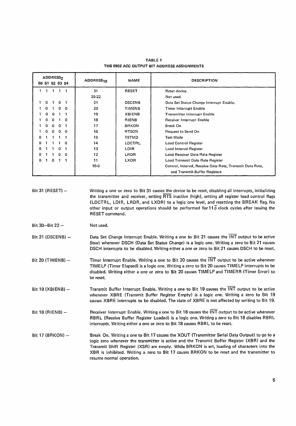
Table 1 describes
the
output
bit
address assignments
for
the
ACC.
3
TMS
9902 TMS 9900
¢
</>3TTL
FROM
TIM
9904
..
CRUCLK
CRUCLK
CRUOUT CRUOUT
CRUIN
CRUIN
SO
A10
S1
-
A11
S2
A12
S3
A13
S4
A14
CE
I'"'
4DECODE~
AO-A9
TMS
9902 TMS 9980
¢ -
if;
CRUCLK CRUCLK
CRUOUT
A13
CRUIN
CRUIN
SO
A8
Sl
A9
S2
A10
S3
All
S4
A12
CE
h
1DECODE~
AO-A7
4
ADDRESS2
SO
S1
S2
S3 S4
1 1 1 1 1
1 0 1 0 1
1 0 1 0 0
1 0 0 1 1
1 0 0 1 0
1 0 0 0 1
1 0 0 0 0
0 1 1 1 1
0 1 1 1 0
0 1 1 0 1
0 1 1 0 0
0 1 0 1 1
Bit
31
(RESET)-
Bit
30-Bit
22
-
Bit
21
(DSCENB) -
Bit
20
(TIMENB) -
Bit
19
(XBIENB) -
Bit
18
(RIENB)-
Bit 17 (BRKON) -
TABLE
1
TMS
9902
ACC
OUTPUT
BIT
ADDRESS
ASSIGNMENTS
ADDRESS10
NAME
DESCRIPTION
31
RESET Reset device.
30-22
Not
used.
21
DSCENB Data Set Status Change
Interrupt
Enable.
20
TIMENB
Timer
I
nterrupt
Enable
19
XBIENB
Transmitter
Interrupt
Enable
18
RIENB
Receiver I
nterrupt
Enable
17
BRKON
Break On
16 RTSON Request
to
Send On
15
TSTMD
Test Mode
14
LDCTRL
Load
Control
Register
13
LDIR
Load Interval Register
12
LRDR
Load Receiver Data Rate Register
11
LXDR
Load
Transmit
Data Rate Register
10-0
Control,
Interval, Receive Data Rate,
Transmit
Data Rate,
and
Transmit
Buffer
Registers
Writing a one
or
zero
to
Bit
31
causes
the
device
to
be reset, disabling all
interrupts,
initializing
the
transmitter
and
receiver, setting RTS inactive (high), setting all register load
control
flags
(LDCTRL, LDIR, LRDR,
and
LXDR)
to
a logic one level,
and
resetting
the
BREAK flag. No
other
input
or
output
operations should be performed
for
11
if)
clock cycles
after
issuing
the
RESET
command.
Not
used.
Data
Set
Change
Interrupt
Enable. Writing a
one
to
Bit
21
causes
the
I NT
output
to
be active
(low) whenever DSCH (Data
Set
Status
Change)
is
a logic
one.
Writing a zero
to
Bit
21
causes
DSCH
interrupts
to
be disabled. Writing
either
a one
or
zero
to
Bit
21
causes DSCH
to
be reset.
Timer
Interrupt
Enable. Writing a
one
to
Bit
20
causes
the
I NT
output
to
be active whenever
TIMELP (Timer Elapsed)
is
a logic one. Writing a zero
to
Bit 20 causes TIMELP
interrupts
to
be
disabled. Writing
either
a
one
or
zero
to
Bit
20
causes TIMELP
and
TIMERR (Timer Error)
to
be reset.
Transmit
Buffer
Interrupt
Enable. Writing a
one
to
Bit
19
causes
the
INT
output
to
be active
whenever XBRE (Transmit Buffer Register Empty)
is
a logic one. Writing a zero
to
Bit
19
causes XBRE
interrupts
to
be disabled.
The
state
of
XBRE
is
not
affected by writing
to
Bit 19.
Receiver
Interrupt
Enable. Writing a
one
to
Bit
18
causes
the
I NT
output
to
be active whenever
RBRL (Receive Buffer Register Loaded)
is
a logic one. Writing a zero
to
Bit 18 disables RBRL
interrupts. Writing
either
a
one
or
zero
to
Bit
18
causes RBRL
to
be reset.
Break On. Writing a
one
to
Bit 17 causes
the
XOUT (Transmitter Serial Data
Output)
to
go
to
a
logic zero whenever
the
transmitter
is
active
and
the
Transmit
Buffer Register (XBR)
and
the
Transmit
Shift
Register (XSR) are
empty.
While BRKON
is
set,
loading
of
characters
into
the
XBR
is
inhibited. Writing a zero
to
Bit
17
causes BRKON
to
be reset
and
the
transmitter
to
resume normal operation.
5
Bit
16
(RTSON) -
Bit
15
(TSTMD)-
Bits
14-11
-
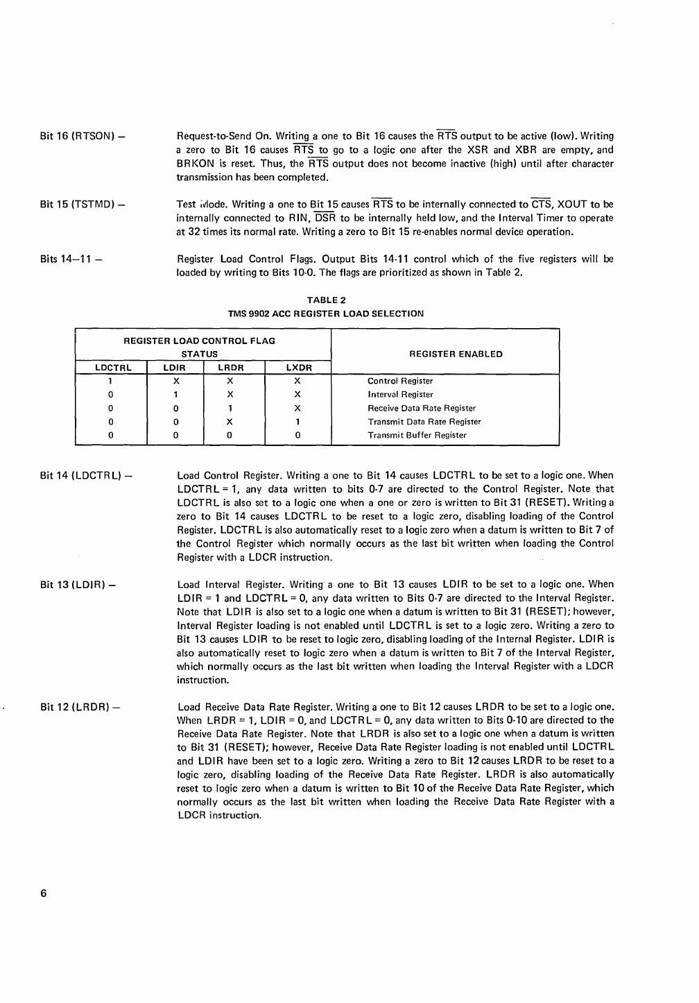
Request-to-Send On. Writing a
one
to
Bit
16
causes
the
RTS
output
to
be active (low). Writing
a zero
to
Bit
16
causes RTS
to
go
to
a logic
one
after
the
XSR and XBR are
empty,
and
BRKON
is
reset.
Thus,
the
RTS
output
does
not
become inactive (high) until
after
character
transmission has been
completed.
Test
ilflode. Writing a
one
to
Bit
15
causes RTS
to
be internally
connected
to
CTS, XOUT
to
be
internally
connected
to
RIN, DSR
to
be internally held low,
and
the
Interval
Timer
to
operate
at
32
times
its normal rate. Writing a zero
to
Bit
15
re-enables normal device
operation.
Register Load Control Flags.
Output
Bits 14-11 control which
of
the
five registers will be
loaded by writing
to
Bits 10-0.
The
flags are prioritized as
shown
in
Table 2.
TABLE
2
TMS
9902
ACC
REGISTER
LOAD
SELECTION
REGISTER
LOAD
CONTROL
FLAG
LDCTRL
1
0
0
0
0
Bit
14
(LDCTR
L)
-
Bit
13
(LDIR) -
Bit
12
(LRDR)
-
6
STATUS
REGISTER
ENABLED
LOlA
LRDR
LXDR
X X X
Control
Register
1 X X Interval
Register
0 1 X Receive
Data
Rate
Register
0 X 1
Transmit
Data
Rate
Register
0 0 0
Transmit
Buffer
Register
Load Control Register. Writing a
one
to
Bit
14
causes LDCTR L
to
be
set
to
a logic
one.
When
LDCTRL = 1, any
data
written
to
bits 0-7 are
directed
to
the
Control Register. Note
that
LDCTRL
is
also set
to
a logic
one
when a
one
or
zero
is
written
to
Bit 31
(RESET).
Writing a
zero
to
Bit
14
causes LDCTR L
to
be reset
to
a logic zero, disabling loading
of
the
Control
Register. LDCTR L
is
also
automatically
reset
to
a logic zero
when
a
datum
is
written
to
Bit 7
of
the
Control Register which
normally
occurs as
the
last
bit
written
when
loading
the
Control
Register with a LDCR
instruction.
Load Interval Register. Writing a
one
to
Bit
13
causes LDIR
to
be
set
to
a logic
one.
When
LDIR = 1
and
LDCTRL = 0,
any
data
written
to
Bits 0-7 are directed
to
the
Interval Register.
Note
that
LDIR
is
also
set
to
a logic
one
when
a
datum
is
written
to
Bit 31 (RESET); however,
Interval Register loading is
not
enabled until LDCTR L
is
set
to
a logic zero. Writing a zero
to
Bit
13
causes LDIR
to
be reset
to
logic zero, disabling loading
of
the
Internal Register.
LDI
R is
also
automatically
reset
to
logic zero when a
datum
is
written
to
Bit 7
of
the
Interval Register,
which
normally
occurs as
the
last
bit
written
when
loading
the
Interval Register
with
a LDCR
instruction.
Load Receive Data Rate Register. Writing a
one
to
Bit
12
causes
LR
DR
to
be
set
to
a logic
one.
When LRDR = 1, LDIR =
0,
and
LDCTRL =
0,
any
data
written
to
Bits 0-10 are
directed
to
the
Receive Data Rate Register.
Note
that
LRDR
is
also set
to
a logic
one
when a
datum
is
written
to
Bit
31
(R ESET); however, Receive Data Rate Register loading
is
not
enabled
until LDCTR L
and
LDIR have been
set
to
a logic zero. Writing a zero
to
Bit
12
causes LRDR
to
be
resettoa
logic zero, disabling loading
of
the
Receive Data Rate Register. LRDR
is
also
automatically
reset
to
logic zero
when
a
datum
is
written
to
Bit
10
of
the
Receive Data Rate Register, which
normally occurs as
the
last
bit
written
when
loading
the
Receive Data Rate Register
with
a
LDCR instruction.
Bit
11
(LXDR) -
3.1.1
Control
Register
Load
Transmit
Data Rate Register. Writing a
one
to
Bit
11
causes LXDR
to
be
set
to
a logic
one. When LXDR = 1, LDIR = 0,
and
LDCTRL = 0,
any
data
written
to
Bits
0-10
are
directed
to
the
Transmit
Data Rate Register. Note
that
loading
of
both
the
Receive
and
Transmit
Data
Rate Registers
is
enabled
when
LDCTR L =
0,
LDI
R =
0,
LRDR = 1,
and
LXDR = 1;
thus
these
two
registers may be loaded
simultaneously
when
data
are received and
transmitted
at
the
same
rate. LXDR
is
also
set
to
a logic
one
when
a
datum
is
written
to
Bit 31
(RESET);
however,
Transmit
Data Rate Register loading
is
not
enabled until LDCTR
Land
LDI
R have been reset
to
logic zero. Writing a zero
to
Bit
11
causes LXDR
to
be
reset
to
logic zero, disabling loading
of
the
Transmit
Data Rate Register. Since Bit
11
is
the
next
bit
addressed
after
loading
the
Transmit
Data Rate Register,
the
register may be loaded
and
the
LXDR flag reset
with
a single
LDCR
instruction
where
12
bits (Bits 0-11) are
written,
with
a zero
written
to
Bit 11.
The
Control Register
is
loaded
to
select
character
length, device clock
operation,
parity,
and
the
number
of
stop
bits
for
the
transmitter.
Table 3 shows
the
bit
address assignments for
the
Control Register.
7
MSB
Bits 7
and
6
(SBS1
and
SBS2) -
TABLE
3
CONTROL
REGISTER
BIT
ADDRESS
ASSIGNMENTS
ADDRESS
10
NAME
DESCRIPTION
6
7
SBS1
}
_Stop
Bit
Select
6 SBS2
5 PENB Parity Enable
4 PODD Odd Parity Select
-
3
CLK4M
4>
Input
Divide Select
2 -
Not
Used
1 RCL1 }
0 RCLO
-Character
Length Select
5 4 3 2 o
LSB
Stop
Bit Selection.
The
number
of
stop
bits
to
be
appended
to
each
transmitter
character
is
selected by Bits 7 and 6
of
the
Control Register as shown below.
The
receiver
only
tests for a
single
stop
bit, regardless
of
the
status
of
Bits 7 and 6.
SBS1
SBS2
NUMBER
OF
TRANSMITTED
BIT7
BIT6
STOP BITS
0 0
1%
0 1 2
1 0 1
1 1 1
STOP
BIT
SELECTION
7
Bits 5
and
4
(PENB
and
PODD)
-
Bit 3 (CLK4M) -
Bits 1
and
0
(RCL1
and
RCLO) -
8
Parity
Selection.
The
type
of
parity
to
be
generated
for
transmission
and
detected
for
reception
is
selected
by
Bits 5
and
4
of
the
Control
Register as
shown
below.
When
parity
is
enabled
(PENB =
1),
the
parity
bit
is
transmitted
and
received in
addition
to
the
number
of
bits
selected
for
the
character
length.
Odd
parity
is
such
that
the
total
number
of
ones
in
the
character
and
parity
bit,
exclusive
of
stop
bit(s),
will be
odd.
For
even
parity,
the
total
number
of
ones
will
be even.
PENB PODD
BITS
BIT
4
PARITY
0 0 None
0 1 None
1 0 Even
1 1 Odd
PARITY
SElECTION
¢ I
nput
Divide
Select.
The
¢
input
to
the
TMS
9902
ACC
is
used
to
generate
internal
dynamic
logic
clocking
and
to
establish
the
time
base
for
the
Interval
Timer,
Transmitter,
and
Receiver.
The
¢
input
is
internally
divided
by
either
3
or
4
to
generate
the
two-phase
internal
clocks
required
for
MOS logic,
and
to
establish
the
basic
internal
operating
frequency
(fint)
and
internal
clock
period
(tint).
When
Bit 3
of
the
Control
Register
is
set
to
a logic
one
(CLK4M
= 1), ¢
is
internally
divided
by
4,
and
when
CLK4M
= 0,
(fj
is
divided
by
3.
For
example,
when
f(Ji
= 3 MHz, as in a
standard
3 MHz TMS
9900
system,
and
CLK4M
=
0,
(fj
is
internally
divided
by
3
to
generate
an
internal
clock
period
tint
of
1
J.1s.
The
figure
below
shows
the
operation
of
the
internal
clock
divider
circuitry.
The
internal
clock
frequency
should
be
no
greater
than
1.1 MHz;
thus,
when
f(fj>
3.3
MHz, CLK4M
should
be
set
to
a logic
one.
¢1
int
(j)
External
Input
n=4
if
CLK4m=1
n=3
if
CLK4m=0
¢2
int
INTERNAL
CLOCK
DIVIDER
CIRCUITRY
}
to
internal
logic
. f¢
flnt=
-n
tint
=
_1-
fint
n
f¢
Character
Length
Select.
The
number
of
data
bits
in
each
transmitted
and
received
character
is
determined
by
Bits 1
and
0
of
the
Control
Register
as
shown
below.
RCL1 RCLO
CHARACTER
BIT
1
BITO
LENGTH
0 0 5 Bits
0 1 6 Bits
1 0 7 Bits
1 1 8 Bits
CHARACTER
LENGTH
SELECTION
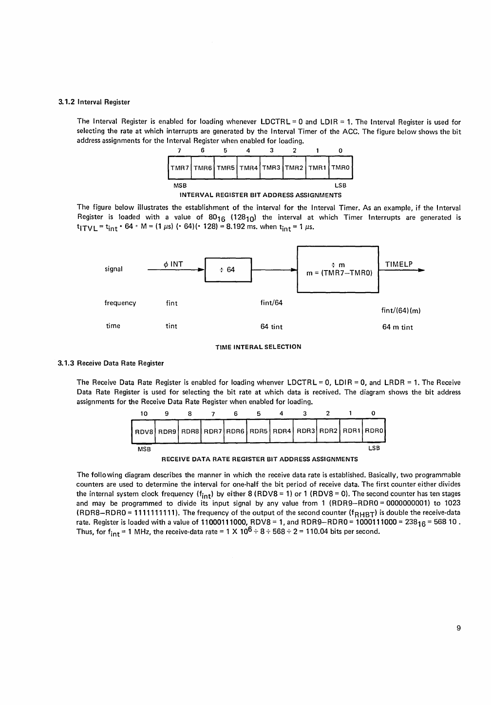
3.1.2
Interval Register
The
I nterval Register
is
enabled
for
loading whenever LDCTR L = 0 and
LD
I R = 1.
The
I nterval Register
is
used for
selecting
the
rate
at
which
interrupts
are generated by
the
Interval
Timer
of
the
ACC.
The
figure below shows
the
bit
address assignments for
the
Interval Register when
enabled
for
loading.
7
654
320
MSB LSB
INTERVAL
REGISTER
BIT
ADDRESS
ASSIGNMENTS
The
figure
below
illustrates
the
establishment
of
the
interval
for
the
Interval Timer. As an
example,
if
the
Interval
Register
is
loaded with a value
of
8016
(12810)
the
interval
at
which
Timer
Interrupts
are generated
is
tlTVL
=
tint
0
64
0 M =
(1
ps)
(0
64)(0 128) =
8.192
ms.
when
tint
= 1 ps.
I TIMELP
I
...
64
I
...
m
m =
(TMR7-TMRO)
signal
ct>INT
~I
frequency
fint
fint/64
fint/(64)
(m)
time
tint
64
tint
64
m
tint
TIME
INTERAL
SELECTION
3.1.3
Receive Data Rate Register
The
Receive Data Rate Register
is
enabled
for
loading whenver LDCTRL =
0,
LDI
R =
0,
and
LRDR = 1.
The
Receive
Data Rate Register
is
used
for
selecting
the
bit
rate
at
which
data
is
received.
The
diagram shows
the
bit
address
assignments
for
the
Receive Data Rate Register
when
enabled
for
loading.
10
9 8 7 6 5 4 3 2 0
MSB LSB
RECEIVE
DATA
RATE
REGISTER
BIT
ADDRESS ASSIGNMENTS
The
following
diagram describes
the
manner
in
which
the
receive
data
rate
is
established. Basically,
two
programmable
counters
are used
to
determine
the
interval
for
one-half
the
bit
period
of
receive data.
The
first
counter
either
divides
the
internal
system
clock
frequency
(fint) by
either
8
(RDV8
= 1)
or
1
(RDV8
= 0).
The
second
counter
has
ten
stages
and
may be
programmed
to
divide its
input
signal by
any
value from 1
(RDR9-RDRO
=
0000000001)
to
1023
(R
DR8-R
D
RO
=
1111111111).
The
frequency
of
the
output
of
the
second
counter
(fR HBT)
is
double
the
receive-data
rate. Register
is
loaded
with
a value
of
11000111000,
RDV8
= 1,
and
RDR9-RDRO
=
1000111000
=
23816
=
568
10
.
Thus,
for
fint
= 1 MHz,
the
receive-data rate = 1 X
10
6
78756872
=
110.04
bits per second.
9
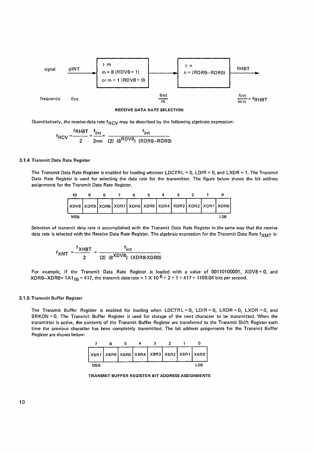
signal
¢INT
frequency fint
-i-m
m = S (RDVS =
1)
or
m = 1 (RDVS = 0)
fint
m
RECEIVE
DATA
RATE
SELECTION
-i-
n
n =
(RDR9-RDRO)
Quantitatively,
the
receive-data rate fRCV may be described by
the
following algebraic expression:
fRHBT f
int
f
int
fRCV=--=-=
2
2mn
(2) (SRDVS)
(RDR9-RDRO)
RHBT
fint
m:n=
fRHBT
3.1.4
Transmit Data Rate Register
The
Transmit
Data Rate Register
is
enabled for loading whenver LDCTR L = 0,
LDI
R = 0,
and
LXD
R = 1.
The
Transmit
Data Rate Register
is
used
for
selecting
the
data rate for
the
transmitter.
The figure below shows the bit address
assignments
for
the
Transmit
Data Rate Register.
10 9 8 7 6 5 4 3 2 o
MSB
LSB
Selection
of
transmit
data rate
is
accomplished with
the
Transmit Data Rate Register
in
the
same way
that
the
receive
data rate
is
selected with
the
Receive Data Rate Register.
The
algebraic expression
for
the
Transmit
Data Rate fXMT
is:
=
fXHBT
fXMT 2 (2) (SXDVS) (XDR9-XDBO)
For
example, if
the
Transmit
Data Rate Register
is
loaded with a value
of
00110100001,
XDVS=O,
and
XDR9-XDRO=
1A
116
=
417,
the
transmit
data
rate = 1 X
10
6
-72
-71
-7417
=
1199.04
bits per
second.
3.1.5
Transmit
Buffer Register
10
The
Transmit
Buffer Register
is
enabled for loading when LDCTR L =
0,
LDI
R =
0,
LRDR =
0,
LXDR =
0,
and
B R KON =
O.
The
Transmit
Buffer Register
is
used
for
storage
of
the
next
character
to
be
transmitted.
When
the
transmitter
is
active,
the
contents
of
the
Transmit
Buffer Register are transferred
to
the
Transmit
Shift
Register each
time
the
previous
character
has been completely
transmitted.
The bit address assignments
for
the
Transmit
Buffer
Register are
shown
below:
7 6 5 4 3 2 o
MSB
TRANSMIT
BUFFER
REGISTER
BIT
ADDRESS ASSIGNMENTS
All 8 bits should be transferred
into
the
register, regardless of
the
selected character length.
The
extraneous
high·order
bits will be ignored
for
transmission purposes; however, loading
of
bit
7
is
internally
detected
to
cause
the
Transmit
Buffer Register
Empty
(XBRE)
status
flag
to
be reset.
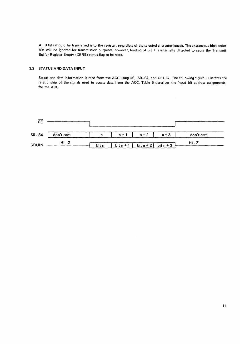
3.2
STATUS AND DATA INPUT
Status
and
data
information
is
read
from
the
ACC using CE,
SO-54,
and
CRUIN.
The
following figure illustrates the
relationship
of
the
signals used
to
access
data
from
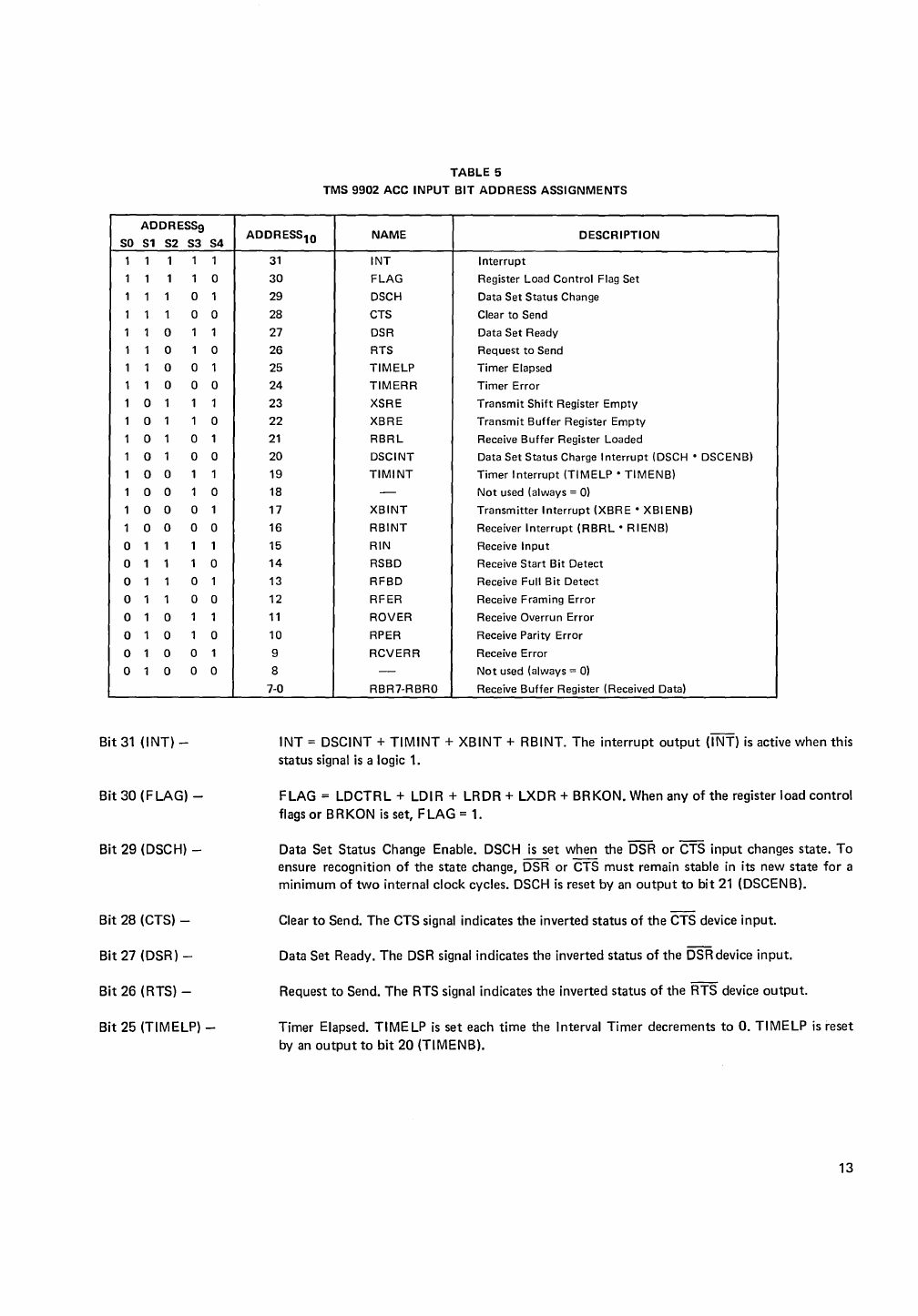
the ACC. Table 5 describes
the
input
bit
address assignments
for
the
ACC.
SO
-S4
don't
care n
n+1
n+2
n+3
don't
care
CRUIN
Hi - Z
bit
n
bit
n + 1
bit
n + 2 I
bit
n + 3
Hi
- Z
11
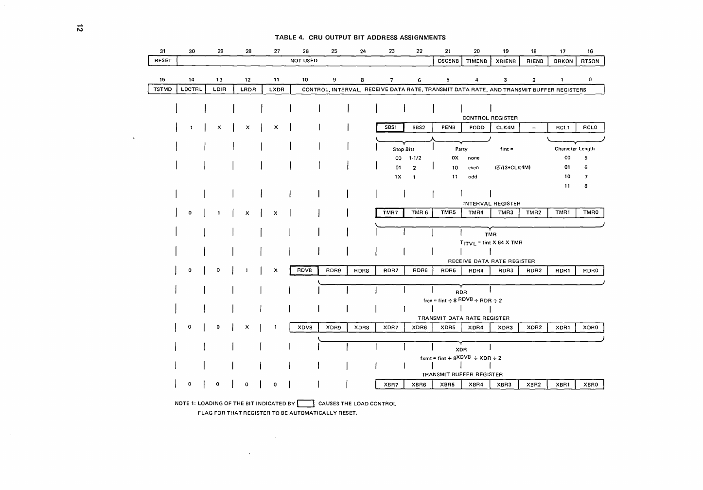
TABLE 4.
CRU
OUTPUT
BIT
ADDRESS ASSIGNMENTS
31
30
29
28
27
26
25 24 23 22
21
20
19
18 17 16
NOT
USED
15 14
13
12
11
10 4
CONTROL,INTERVAL,
RECEIVE
DATA
RATE,
TRANSMIT
DATA
RATE,
AND
TRANSMIT
BUFFER
REGISTERS
CCNTROL
REGISTER
X X X
SBS1
SBS2 PENB I PODD I
CLK4M
I RCL1 I RCLO I
~
"----v---'
I
Stop
Bits I Party
fint
= Character Length
00
1-1/2
OX
none
00
01
10
even fij)1(3+CLK4M)
01
6
1X
11
odd
10
11
INTERVAL
REGISTER
X X
TMR7
TMR
6
TMR5 TMR4
I
TMR3
TMR2
TMR1 TMRO
)
y
TMR
TITVL
=
tint
X
64
X
TMR
I
RECEIVE
DATA
RATE
REGISTER
X
RDV8
RDR9
RDRS
RDR7 RDR6
RDR5
I
RDR4
RDR3
RDR2
RDR1 RDRO
RDR
frcv =
fint
-;-
S RDVS
-;-
RDR
-;.-
2
I
TRANSMIT
DATA
RATE
REGISTER
X
XDVS
XDR9
XDRS
XDR7
XDR6 XDR5
I
XDR4
XDR3
XDR2
XDR1 XDRO
)
XDR
fxmt
=
fint
-;-
SXDV8
-;-
XDR
-;-
2
I I I
TRANSMIT
BUFFER
REGISTER
0
XBR7
XBR6
XBR5
XBR4
XBR3 XBR2
XBR1 XBRO
NOTE
1:
LOADING
OF
THE
BIT
INDICATED
BY
c::::l CAUSES
THE
LOAD
CONTROL
FLAG
FOR
THAT
REGISTER
TO
BE
AUTOMATICALLY
RESET.
ADDRESS9
SO
S1
S2
S3 S4
1 1 1 1 1
1 1 1 1 0
1 1 1 0 1
1 1 1 0 0
1 1 0 1 1
1 1 0 1 0
1 1 0 0 1
1 1 0 0 0
1 0 1 1 1
1 0 1 1 0
1 0 1 0 1
1 0 1 0 0
1 0 0 1 1
1 0 0 1 0
1 0 0 0 1
1 0 0 0 0
0 1 1 1 1
0 1 1 1 0
0 1 1 0 1
0 1 1 0 0
0 1 0 1 1
0 1 0 1 0
0 1 0 0 1
0 1 0 0 0
Bit 31
(lNT)
-
Bit
30
(FLAG) -
Bit
29
(DSCH) -
Bit
28
(CTS) -
Bit
27
(DSR) -
Bit
26
(RTS) -
Bit
25
(TIMELP) -
TABLE
5
TMS
9902
ACC
INPUT
BIT
ADDRESS ASSIGNMENTS
ADDRESS
10
NAME
DESCRIPTION
31
INT
Interrupt
30
FLAG
Register
load
Control Flag Set
29 DSCH Data Set Status Change
28 CTS Clear
to
Send
27 DSR Data Set Ready
26 RTS Request
to
Send
25
TIMElP
Timer
Elapsed
24
TIMERR
Timer
Error
23 XSRE Transmit
Shift
Register
Empty
22
XBRE
Transmit
Buffer
Register
Empty
21
RBRl
Receive
Buffer
Register Loaded
20
DSCINT Data Set Status Charge
Interrupt
(DSCH • DSCENB)
19
TIMINT
Timer
Interrupt
(TIMELP
•
TIMENB)
18 -
Not
used
(always =
0)
17
XBINT
Transmitter
Interrupt
(XBRE
•
XBIENB)
16
RBINT
Receiver
Interrupt
(RBRl·
RIENB)
15
RIN
Receive
Input
14
RSBD Receive Start
Bit
Detect
13
RFBD
Receive Full
Bit
Detect
12 RFER Receive Framing
Error
11
ROVER Receive Overrun
Error
10 RPER Receive Parity
Error
9
RCVERR
Receive Error
8 -
Not
used (always =
0)
7-0 RBR7-RBRO Receive
Buffer
Register (Received Data)
INT = DSCINT + TIMINT + XBINT + RBINT.
The
interrupt
output
(lNT)
is
active
when
this
status
signal
is
a logic 1.
FLAG = LDCTRL + LDIR + LRDR + LXDR + BRKON. When
any
of
the
register load
control
flags
or
BRKON
is
set,
FLAG
= 1.
Data
Set
Status
Change Enable. DSCH
is
set
when
the
DSR
or
CTS
input
changes
state.
To
ensure recognition
of
the
state
change, DSR
or
CTS
must
remain stable
in
its new
state
for
a
minimum
of
two
internal
clock
cycles. DSCH
is
reset by an
output
to
bit
21
(DSCENB).
Clear
to
Send.
The
CTS signal indicates
the
inverted
status
of
the
CTS device
input.
Data
Set
Ready.
The
DSR signal indicates
the
inverted
status
of
the
DSRdevice
input.
Request
to
Send.
The
RTS signal indicates
the
inverted
status
of
the
RTS device
output.
Timer Elapsed. TIMELP
is
set
each
time
the
Interval
Timer
decrements
to
O.
TIMELP
is
reset
by an
output
to
bit
20
(TIMENB).
13
Bit
24
(TIMERR) -
Bit
23
(XSRE) -
Bit
22
(XBRE) -
Bit
21
(RBR
L)
-
Bit
20
(DSCINT) -
Bit
19
(TIM INT) -
Bit
17
(XBINT) -
Bit
16
(RBINT)-
Bit
15
(RIN)-
Bit
14
(RSBD) -
Bit
13
(RFBD) -
Bit
12
(RFER)-
Bit
11
(ROVER)
-
14
Timer
Error. TIMERR
is
set
whenever
the
Interval
timer
decrements
to
0
and
TIMELP
is
already set, indicating
that
the
occurrence
of
TIMELP was
not
recognized
and
cleared by
the
CPU before
subsequent
intervals elapsed. TIMERR
is
reset by an
output
to
bit
20
(TiMENB).
Transmit
Shift
Register
Empty.
When XSRE = 1,
no
data
is
currently
being
transmitted
and
the
XOUT
output
is
at
logic 1 unless
BR
KON is set. When XSRE =
0,
transmission
of
data
is
in
progress.
Transmit
Buffer Register
Empty.
When XBRE = 1, the
transmit
buffer
register does
not
contain
the
next
character
to
be
transmitted.
XBRE
is
set each time
the
contents
of
the
transmit
buffer
register are
transferred
to
the
transmit
shift
register, XBR E
is
reset
by
an
output
to
bit
7
of
the
transmit
buffer
register (XBR7), indicating
that
a
character
has been loaded.
Receive Buffer Register Loaded. R B R L
is
set
when
a
complete
character
has been assembled in
the
receive
shift
register
and
the
character
is
transferred
to
the
receive
buffer
register. R
BR
Lis
reset by an
output
to
bit
18
(RIENB).
Data
Set
Status
Change
Interrupt.
DSCINT = DSCH
(input
bit
29) • DSCENB
(output
bit 21).
DSCINT indicates
the
presence
of
an
enabled
interrupt
caused by
the
changing
of
state
of
DSR
or
CTS.
Timer
Interrupt.
TIMINT =
TlMELP
(input
bit
25) • TIMENB
(output
bit
20).
TIMINT
indicates
the
presence
of
an
enabled
interrupt
caused by
the
interval
timer.
Transmitter
Interrupt.
XBINT = XBRE
(input
bit
22) • XBIENB
(output
bit
19). XBINT
indicates
the
presence
of
an
enabled
interrupt
caused by
the
transmitter.
Receiver
Interrupt.
RBINT = RBRL
(input
bit 21) • RIENB
(output
bit
18). RBINT indicates
the
presence
of
an
enabled
interrupt
caused by the receiver.
Receive
Input.
RIN indicates
the
status
of
the
RIN
input
to
the
device.
Receive
Start
Bit Detect. RSBD
is
set one-half
bit
time
after
the
l-to-O
transition
of
RIN
indicating
the
start
bit
of
a
character.
If RIN
is
not
still 0
at
this
point
in
time,
RSBD
is
reset.
Otherwise, RSBD remains
true
until
the
complete
character
has been received. This
bit
is
normally used for testing purposes.
Receive Full Bit Detect. RFBD
is
set
one
bit
time
after
RSBD
is
set
to
indicate
the
sample
point
for
the
first
data
bit
of
the
received
character.
RSBD
is
reset when
the
character
has been
completely
received. This
bit
is
normally
used
for
testing purposes.
Receive Framing Error.
RFER
is
set
when a
character
is received in which
the
stop
bit, which
should
be a logic 1, is a logic
O.
RFER
should
only
be read
when
RBRL
(input
bit
21)
is
a 1.
RFER
is
reset when a
character
with
the
correct
stop
bit
is
received.
Receive Overrun Error. ROVER
is
set
when a new
character
is
received before
the
RBR L flag
(input
bit 21)
is
reset, indicating
that
the
CPU failed
to
read
the
previous
character
and
reset
R B R L before
the
present
character
is
completely
received. ROVE R
is
reset
when
a
character
is
received
and
RBRL
is
0
when
the
character
is
transferred
to
the
receive buffer register.
Bit
10
(RPER) -
Bit 9
(RCVERR)-
Bit
7-Bit
0
(RBR7-RBRO)
-
Receive Parity Error. RPER
is
set
when a character
is
received in which
the
parity
is
incorrect.
RPER
is
reset
when
a character with
correct
parity
is
received.
Receive Error. RCVERR =
RFER
+ ROVER + RPER. RCVERR indicates
the
presence of an
error
in
the
most
recently received character.
Receive Buffer Register.
The
receive buffer register contains
the
most
recently received
character. For
character
lengths
of
fewer
than
8 bits the character
is
right justified, with unused
most
significant bit(s)
all
zero(es). The presence
of
valid
data
in
the
receive buffer register
is
indicated when RBRL
is
a logic 1.
3.3
TRANSMITTER OPERATION
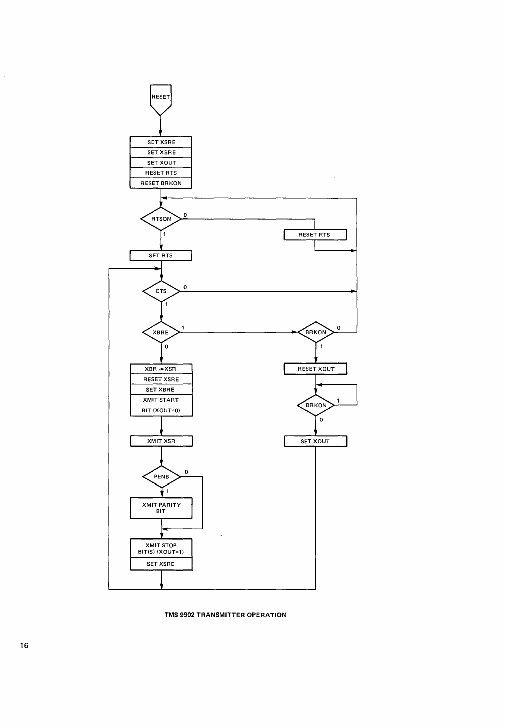
3.3.1
Transmitter
Initialization
The
operation
of
the
transmitter
is
described in
the
following flow
chart.
The
transmitter
is
initialized by issuing
the
RESET
command
(output
to
bit 31), which cause
the
internal signals XSRE
and
XBRE
to
be set, and BRKON
to
be
reset. Device
outputs
RTS
and
XOUT are set, placing
the
transmitter
in its idle state. When RTSON
is
set
by
the
CPU,
the
RTS
output
becomes active
and
the
transmitter
becomes active when CTS goes low.
3.3.2
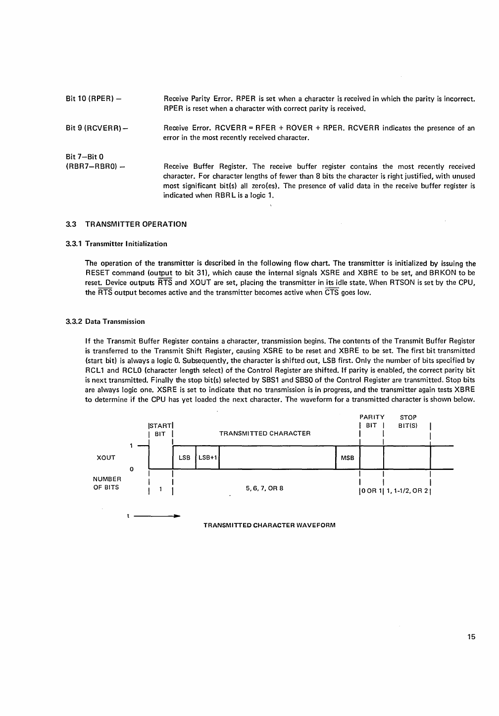
Data Transmission
If
the
Transmit
Buffer Register contains a character, transmission begins. The
contents
of
the
Transmit
Buffer Register
is
transferred
to
the
Transmit
Shift
Register, causing XSRE
to
be reset
and
XBRE
to
be set. The first
bit
transmitted
(start bit)
is
always a logic
O.
Subsequently,
the
character
is
shifted
out,
LSB
first. Only
the
number
of
bits specified by
RCL1
and
RCLO
(character length select)
of
the
Control Register are shifted. If parity
is
enabled,
the
correct
parity
bit
is
next
transmitted.
Finally
the
stop
bit(s) selected by SBS1
and
SBSO
of
the
Control Register are
transmitted.
Stop
bits
are always logic one. XSRE
is
set
to
indicate
that
no
transmission
is
in progress,
and
the
transmitter
again tests XBRE
to
determine if
the
CPU
has
yet
loaded
the
next
character. The waveform for a
transmitted
character
is
shown below.
XOUT
NUMBER
OF BITS
ISTARTI
o 1 BIT i
I I
I I
I I
TRANSMITTED
CHARACTER
5,6,7,
OR 8
TRANSMITTED
CHARACTER
WAVEFORM
PARITY
STOP
I
BIT
I BIT(S)
I I
MSB I I
I I
I I I
IDOR
111,1-1/2,OR21
15
16
SET
XBRE
SET
XOUT
RESET RTS
RESET XSRE
SET
XBRE
XMITSTART
BIT
(XOUT=O)
XMIT
STOP
BIT(S)
(XOUT=1)
SET XSRE
TMS 9902
TRANSMITTER
OPERATION
3.3.3
BREAK Transmission
The
BREAK message
is
transmitted
only if XBRE = 1, CTS =
0,
and
BRKON = 1.
After
transmission
of
the
BREAK
message begins, loading
of
the
Transmit
Buffer Register
is
inhibited
and
XOUT
is
reset. When BRKON
is
reset
by
the
CPU, XOUT
is
set
and
normal
operation
continues.
It
is
important
to
note
that
characters
loaded
into
the
Transmit
Buffer Register are
transmitted
prior
to
the
BR
EAK message regardless
of
whether
the
character
has been loaded
into
the
Transmit
Shift
Register before
BR
KON
is
set.
Any
character
to
be
transmitted
subsequent
to
transmission
of
the
BR
EAK message
may
not
be loaded
into
the
Transmit
Buffer Register until
after
BR
KON
is
reset.
3.3.4
Transmission
Termination
Whenever XSRE = 1 and BRKON = 0,
the
transmitter
is
idle, with XOUT
set
to
one. If RTSON
is
reset
at
this
time,
the
RTS device
output
will go inactive, disabling
further
data
transmission until RTSON is again set. RTS will
not
go
inactive, however, until
any
characters loaded
into
the
Transmit
Buffer Register prior
to
resetting RTSON are trans-
mitted
and
BRKON =
o.
3.4
RECEIVER
OPERATION
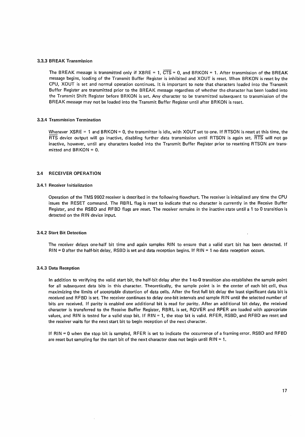
3.4.1 Receiver Initialization
Operation
of
the
TMS
9902
receiver
is
described in
the
following
flowchart.
The
receiver
is
initialized any
time
the
CPU
issues
the
RESET
command.
The
RBRl
flag
is
reset
to
indicate
that
no
character
is
currently
in
the
Receive Buffer
Register,
and
the
RSBD
and
RF
BD
flags are reset.
The
receiver remains
in
the
inactive
state
until a 1
to
a
transition
is
detected
on
the
RIN device
input.
3.4.2
Start
Bit
Detection
The
receiver delays one-half
bit
time
and
again samples RIN
to
ensure
that
a valid
start
bit
has been
detected.
If
RIN = a
after
the
half-bit delay, RSBD
is
set
and
data
reception
begins. If RIN = 1
no
data
reception
occurs.
3.4.3
Data
Reception
In
addition
to
verifying
the
valid
start
bit,
the
half-bit delay
after
the
1-to-0 transition also establishes
the
sample
point
for
all
subsequent
data bits
in
this character.
Theoretically,
the
sample
point
is
in
the
center
of
each
bit
cell,
thus
maximizing
the
limits
of
acceptable
distortion
of
data
cells.
After
the
first full bit delay
the
least significant
data
bit
is
received
and
R F
BD
is
set.
The
receiver
continues
to
delay
one-bit
intervals and sample R I N until
the
selected
number
of
bits are received. If parity
is
enabled
one
additional
bit
is
read for parity.
After
an additional
bit
delay,
the
received
character
is
transferred
to
the
Receive Buffer Register,
RBRl
is
set,
ROVER and RPER are loaded
with
appropriate
values,
and
RIN
is
tested
for
a valid
stop
bit.
If RIN = 1,
the
stop
bit
is
valid.
RFER,
RSBD,
and
RFBD are
reset
and
the
receiver waits
for
the
next
start
bit
to
begin
reception
of
the
next
character.
If RIN = a
when
the
stop
bit
is
sampled,
RFER
is
set
to
indicate
the
occurrence
of
a framing error. RSBD
and
RFBD
are reset
but
sampling
for
the
start
bit
of
the
next
character
does
not
begin until R I N =
1.
17
TMS
9902
RECEIVER
OPERATION
18
ISTARTI
RIN
3.5
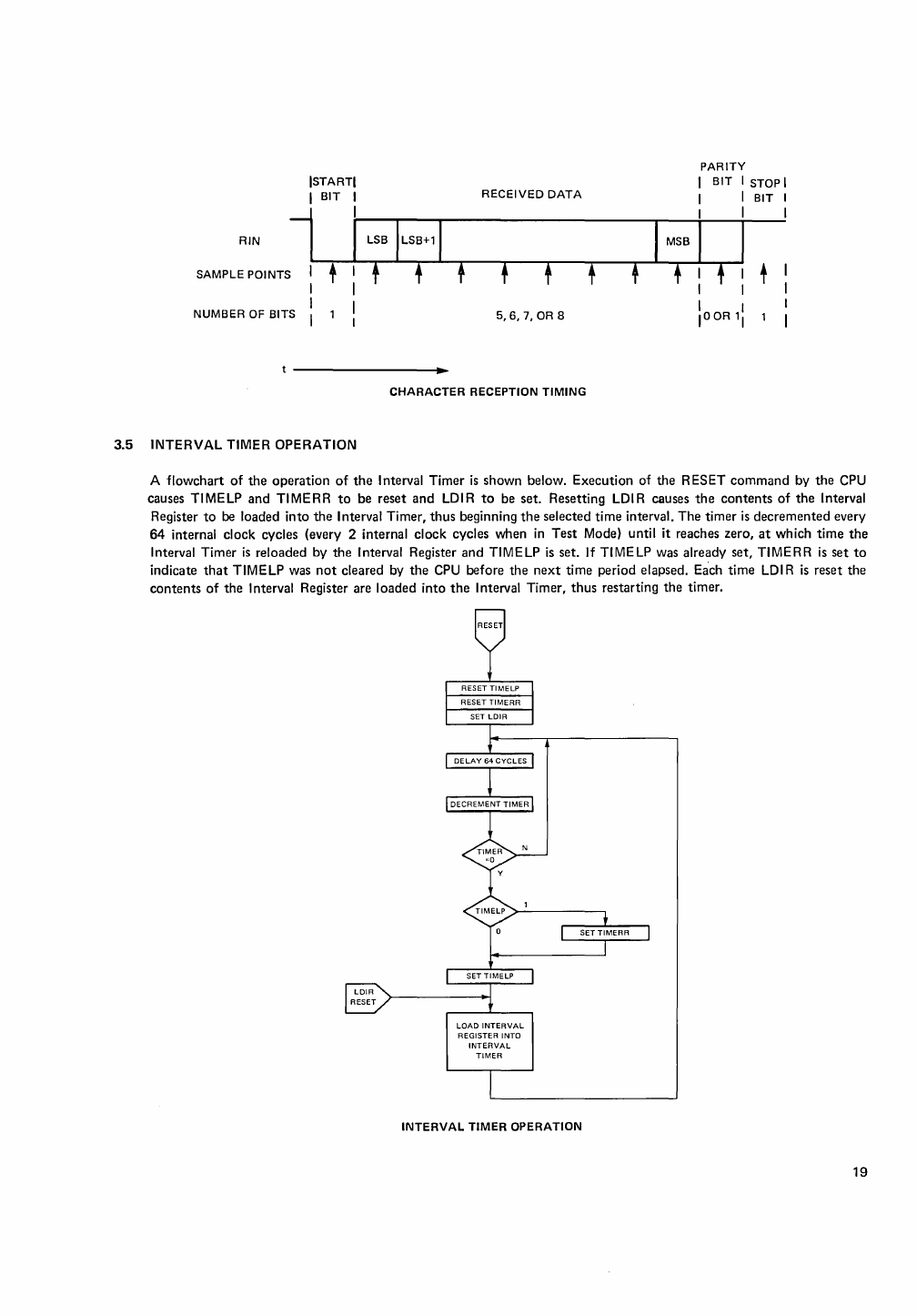
INTERVAL TIMER OPERATION
PARITY
BIT
A flowchart
of
the
operation
of
the
Interval
Timer
is
shown below. Execution of the RESET
command
by
the
CPU
causes TI MELP
and
TI
ME
RR
to
be reset
and
LDI
R
to
be set. Resetting
LDI
R causes
the
contents
of
the
Interval
Register
to
be
loaded
into
the
Interval Timer,
thus
beginning
the
selected time interval.
The
timer
is
decremented
every
64
internal clock cycles (every 2 internal
clock
cycles when
in
Test Mode) until it reaches zero,
at
which
time
the
Interval Timer
is
reloaded by
the
Interval Register
and
TIMELP
is
set. If TIMELP was already
set,
TIMERR
is
set
to
indicate
that
TIMELP was
not
cleared by
the
CPU
before
the
next
time period elapsed. Each time
LDI
R
is
reset the
contents
of
the Interval Register are loaded into
the
Interval Timer,
thus
restarting
the
timer.
LOIR
RESET
LOAD
INTERVAL
REGISTER
INTO
INTERVAL
TIMER
INTERVAL
TIMER
OPERATION
19
4. DEVICE APPLICATION
This
section
describes
the
software
interface
between
the
CPU
and
the
TMS
9902
ACC
and
discusses
some
of
the
design
considerations
in
the
use
of
this device
in
asynchronous
communications
applications.
4.1 DEVICE
INITIALIZATION
The
ACC
is
initialized by
the
CPU issuing
the
RESET
command,
followed
by loading
the
Control,
Interval, Receive
Data Rate,
and
Transmit
Data Rate registers. Assume
that
the
value
to
be loaded
into
the
CRU Base Register (register
12) in
order
to
point
to
bit
0
is
004016.
I n
this
application,
characters
will have 7 bits
of
data
plus even
parity
and
one
stop
bit.
The
(ji
input
to
the
ACC
is
a 3 MHz signal.
The
ACC will divide
this
signal
frequency
by 3
to
generate
an
internal
clock
frequency
of
1 MHz.
An
interrupt
will be
generated
by
the
Interval
Timer
every
1.6
milliseconds
when
timer
interrupts
are
enabled.
The
transmitter
will
operate
at
a
data
rate
of
300
bits
per
second,
and
the
receiver will
operate
at
1200
bits
per
second.
Had
it
been desired
that
both
the
transmitter
and
receiver
operate
at
300
bits
per
second,
the
"LDCR
@RDR,11"
instruction
would
have been
deleted,
and
the
"LDCR
@XDR,12"
instruction
would
have
caused
both
data
rate
registers
to
be
loaded
and
LRDR
and
LXDR
to
have been reset.
4.1.1 Initialization Program
The
initialization
program
for
the
configuration
previously described
is
as
shown
below.
The
RESET
command
disables
all
interrupts,
initializes all
controllers,
sets
the
four
register load
control
flags (LDCTR
L,
LDI
R,
LRDR,
and
LXDR).
Loading
the
last
bit
of
each
of
the
registers causes
the
load
control
flag
to
be
automatically
reset.
CNTRL
INTVL
RDR
XDR
LI
SBO
LDCR
LDCR
LDCR
LDCR
BYTE
BYTE
DATA
DATA
R12,
>40
31
@CNTRL,8
@INTVL, 8
@RDR, 11
@XDR,
12
>A2
1600/64
>1A1
>4DO
INITIALIZE
CRU BASE
RESET
COMMAND
LOAD
CONTROL
AND
RESET
LDCTRL
LOAD
INTERVAL
AND
RESET
LDIR
LOAD RDR AND
RESET
LRDR
LOAD XDR AND
RESET
LXDR
The
RESET
command
initializes all
subcontrollers,
disables
interrupts,
and
sets
LDCTRL,
LDIR,
LRDR,
and
LXDR,
enabling loading
of
the
control
register.
4.1.2
Control
Register
The
options
described
previously are selected by loading
the
value
shown
below.
20
VALUE
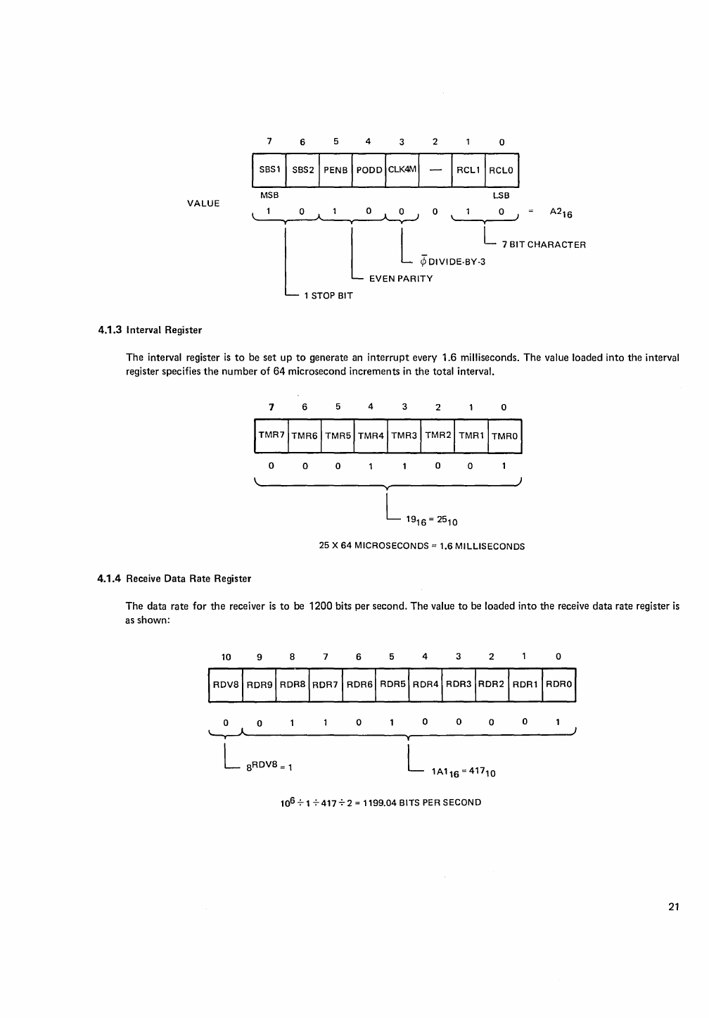
4.1.3
Interval Register
7 6 5 4 3 2 o
SSS'
I
sas21
PENS
I
POOOICLK4M1
MSB
LSB
T 0 A 1 0
~
0
'/
0
A2
16
l l L
-L 7
BIT
CHARACTER
¢
DIVIDE·BY·3
EVEN
PARITY
1 STOP
BIT
The interval register
is
to
be
set
up
to
generate an
interrupt
every
1.6
milliseconds. The value loaded
into
the
interval
register specifies
the
number
of
64
microsecond increments in
the
total interval.
7 6 5 4 3 2 o
o o o o o
~~----------------~y~------------------)
L
'9'6
= 2510
25 X
64
MICROSECONDS = 1.6
MILLISECONDS
4.1.4
Receive Data Rate Register
The data rate
for
the
receiver
is
to
be
1200
bits per second.
The
value
to
be loaded
into
the
receive
data
rate register
is
as shown:
10 9 S 7 6 5 4 3 2 o
o 0 o o o o o
~----------------------~T~--------------------~
L
SRDVS=
1 L
1A116
=
417
10
106
-;'1-;'417-;'2
= 1199.04 BITS
PER
SECOND
21
4.1.5 Transmit Data Rate Register
The data rate for the transmitter
is
to
be
300 bits per second. The value to
be
loaded into the transmit data rate register
is:
10 9 8 7 6 5 4 3 2 o
1 0 0
000
o o
~--------------------~------------------~
L .xov
•••
L
0016=
208
1 X 10⁶
-:-8-:-208-:-2=
300.48 BITS
PER
SECOND
4.2
DATA
TRANSMISSION
The subroutine shown below demonstrates a simple loop for the transmitting of a block of data.
LI
RO,L1STAD INITIALIZE LIST POINTER
LI
R1, COUNT INITIALIZE
BLOCK
COUNT
LI
R12, CRUBAS INITIALIZE
CRU
BASE
SBO
16 TURN
ON
TRANSMITTER
XMTLP
TB
22
WAIT
FOR
XBRE
= 1
JNE
XMTLP
LDCR
*RO+,8
LOAD
CHARACTER INCREMENT POINTER RESET
XBRE
DEC
R1
DECREMENT COUNT
JNE
XMTLP
LOOP
IF
NOT
COMPLETE
SBZ 16 TURN OFF TRANSMITTER
After initializing the list pointer, block count, and
CRU
base address.
RTSON
is
set to cause the transmitter and the
RTS
output to become active. Data transmission does
not
begin, however, until the
CTS
input becomes active. After
the final character
is
loaded into the transmit buffer register,
RTSON
is
reset. The transmitter and the
RTS
output
do
not become inactive until the final character has been completely transmitted.
4.3
DATA
RECEPTION
The software shown below
will
cause a block of data to be received and stored
in
memory.
22
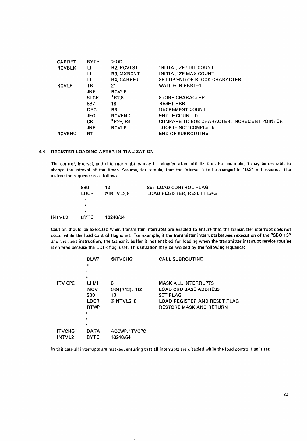
CARRET
BYTE
>OD
RCVBLK
LI
R2, RCVLST INITIALIZE LIST COUNT
LI
R3, MXRCNT INITIALIZE
MAX
COUNT
LI
R4, CARRET SET
UP
END
OF
BLOCK
CHARACTER
RCVLP
TB
21
WAIT
FOR
RBRL=1
JNE
RCVLP
STCR *R2,8 STORE CHARACTER
SBZ 18 RESET RBRL
DEC
R3
DECREMENT COUNT
JEQ
RCVEND
EN
D
IF
COUNT=O
CB
*R2+,
R4
COMPARE
TO
EOB
CHARACTER, INCREMENT POINTER
JNE
RCVLP
LOOP
IF
NOT
COMPLETE
RCVEND
RT
END
OF
SUBROUTINE
4.4 REGISTER LOADING AFTER INITIALIZATION
The control, interval, and data rate registers may
be
reloaded after initialization. For example, it may
be
desirable to
change the interval of the timer. Assume, for sample,
that
the interval
is
to
be
changed to 10.24 milliseconds. The
instruction sequence
is
as
follows:
INTVL2
SBO
LDCR
BYTE
13
@INTVL2,8
10240/64
SET
LOAD
CONTROL
FLAG
LOAD
REGISTER, RESET
FLAG
Caution should
be
exercised when transmitter interrupts are enabled
to
ensure
that
the transmitter interrupt does not
occur while the load control
flag
is
set. For example,
if
the transmitter interrupts between execution of the "SBO
13"
and the next instruction, the transmit buffer
is
not enabled for loading when the transmitter interrupt service routine
is
entered because the
LDI
R flag
is
set. This situation may
be
avoided
by
the following sequence:
lTV
CPC
ITVCHG
INTVL2
BLWP
LI
MI
MOV
SBO
LDCR
RTWP
DATA
BYTE
@ITVCHG
o
@24(R13), RIZ
13
@INTVL2, 8
ACCWP,
ITVCPC
10240/64
CALL SUBROUTINE
MASK
ALL INTERRUPTS
LOAD
CRU
BASE
ADDRESS
SET FLAG
LOAD
REGISTER
AND
RESET FLAG
RESTORE
MASK
AND
RETURN
In
this case
all
interrupts are masked, ensuring
that
all
interrupts are disabled while the load control flag
is
set.
23
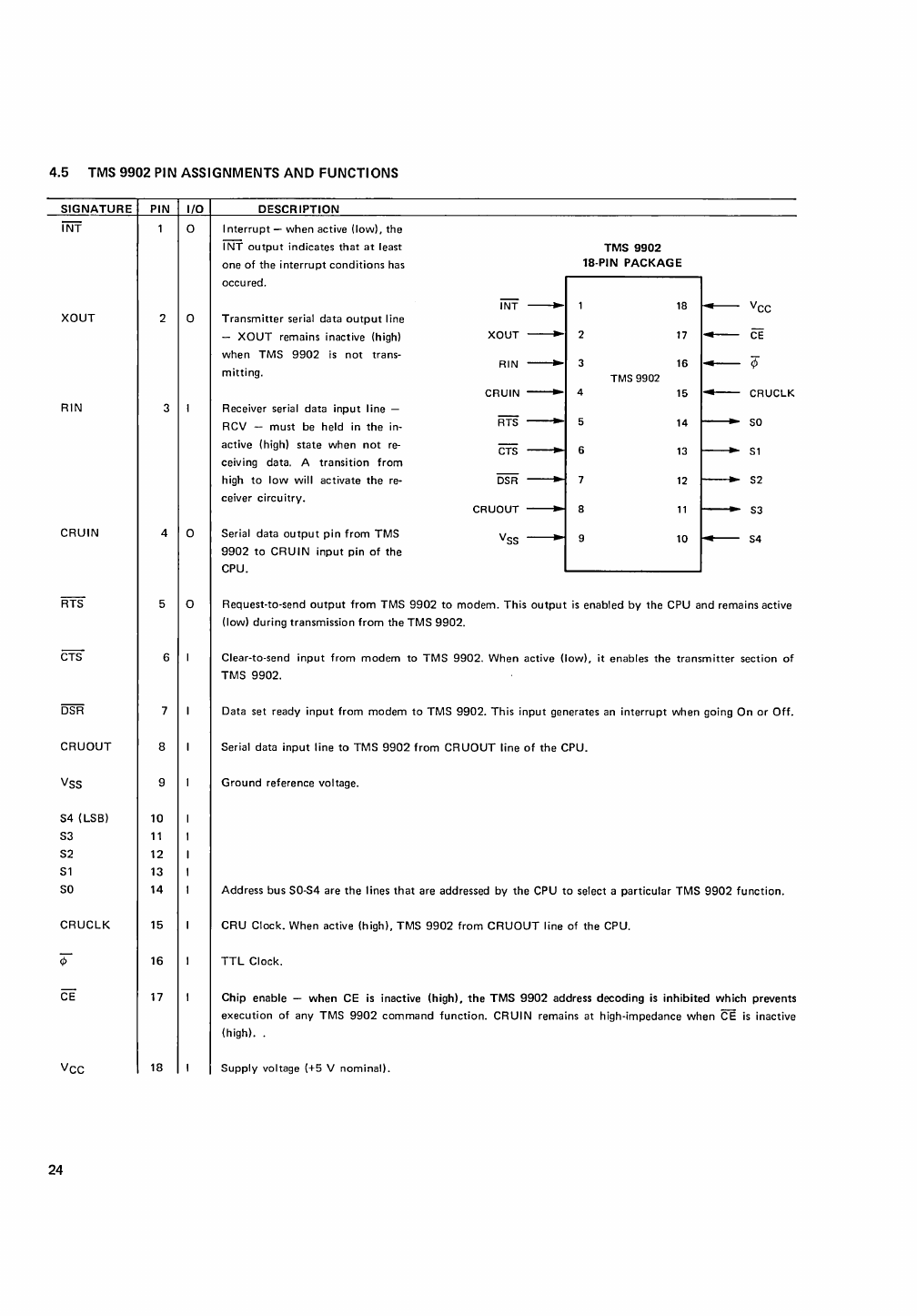
4.5
TMS
9902 PIN ASSIGNMENTS
AND
FUNCTIONS
SIGNATURE
PIN
I/O
DESCRIPTION
INT
1 0
Interrupt
-when active
(low),
the
ii\iT
output
indicates
that
at
least
TMS
9902
one
of
the
interrupt
conditions
has
1B-PIN
PACKAGE
occured.
INT -- 1
18
f--
VCC
XOUT
2 0
Transmitter
serial data
output
line
-
XOUT
remains inactive (high) XOUT -- 2
17
.-
CE
when
TMS
9902
is
not
trans-
¢!
RIN
--
3
16
.-
mitting.
TMS
9902
CRUIN -- 4
15
.-
CRUCLK
RIN
3 I Receiver serial data
input
line
-
RCV
-
must
be
held
in
the
in-
RTS
--.
5
14
f----
SO
active (high) state when
not
re-
CTS
-6
13
f----
S1
ceiving data. A
transition
from
high
to
low
will
activate
the
re-
DSR
-7
12
I---
S2
ceiver
circuitry.
CRUOUT -
f-----
8
11
S3
CRUIN
4 0 Serial data
output
pin
from
TMS
V
SS
-9
10
I---
S4
9902
to
CRUIN
input
pin
of
the
CPU.
RTS 5 0 Request-to-send
output
from
TMS
9902
to
modem.
This
output
is
enabled
by
the CPU and remains active
(low)
during
transmission
from
the
TMS
9902.
CTS 6 I Clear-to-send
input
from
modem
to
TMS
9902.
When active
(low),
it
enables the
transmitter
section
of
TMS
9902.
DSR 7 I Data set ready
input
from
modem
to
TMS
9902.
This
input
generates
an
interrupt
when going
On
or
Off.
CRUOUT
8 I Serial data
input
line
to
TMS
9902
from
CRUOUT
line
of
the
CPU.
VSS 9 I
Ground
reference voltage.
S4 (LSB)
10
I
S3
11
I
S2
12
I
S1
13 I
SO
14
I Address bus
SO-S4
are
the
lines
that
are addressed
by
the CPU
to
select a
particular
TMS
9902
function.
CRUCLK
15 I
CRU
Clock.
When active
(high),
TMS
9902
from
CRUOUT
line
of
the CPU.
-;p
16
I
TTL
Clock.
CE
17
I
Chip
enable -
when
CE is inactive
(high),
the
TMS
9902
address decoding
is
inhibited
which
prevents
execution
of
any
TMS
9902
command
function.
CRUIN
remains at high-impedance
when
CE
is
inactive
(high). .
VCC 18 I
Supply
voltage (+5 V
nominal).
24
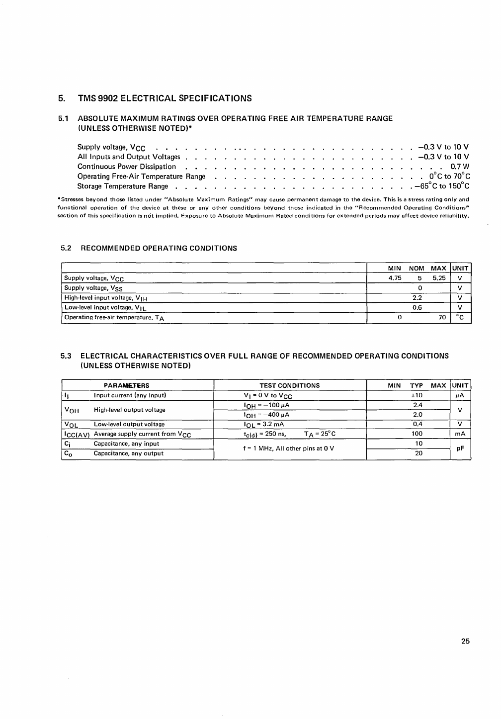
5.
TMS 9902 ELECTRICAL SPECIFICATIONS
5.1 ABSOLUTE
MAXIMUM
RATINGS OVER OPERATING FREE
AIR
TEMPERATURE RANGE
(UNLESS OTHERWISE
NOTED)*
Supply voltage,
VCC
All
Inputs and
Output
Voltages
Continuous Power Dissipation
Operating Free-Air Temperature Range
Storage Temperature Range .
-0.3
V
to
10 V
-0.3Vtol0V
0.7W
.
O°C
to
70°C
.
-65°C
to
150°C
·Stresses
beyond
those
listed
under
"Absolute
Maximum
Ratings"
may
cause
permanent
damage
to
the
device.
This
is a
stress
rating
only
and
functional
operation
of
the
device
at
these
or
any
other
conditions
beyond
those
indicated
in
the
"Recommended
Operating
Conditions"
section
of
this
specification
is
not
implied.
Exposure
to
Absolute
Maximum
Rated
conditions
for
extended
periods
may
affect
device
reliability.
5.2 RECOMMENDED OPERATING CONDITIONS
MIN
NOM
MAX
Supply
voltage. VCC 4.75 5 5.25
Supply voltage, VSS 0
High-level
input
voltage,
VIH
2.2
Low-level
input
voltage.
VI
L
0.6
Operating free-air temperature. T A 0
70
5.3
ELECTRICAL CHARACTERISTICS OVER
FULL
RANGE
OF
RECOMMENDED OPERATING CONDITIONS
(UNLESS OTHERWISE NOTED)
PARAME.TERS
TEST
CONDITIONS
MIN
TYP
MAX
II
I
nput
current
(any
input)
VI
= 0 V
to
VCC
±10
VOH
IOH
=
-100jlA
2.4
High-level
output
voltage
IOH
=
-400
jlA
2.0
VOL
Low-level
output
voltage
IOL
=
3.2
rnA
0.4
ICC(AV)
Average supply
current
from
VCC
tc(¢)
=
250
ns. T A =
25°C
100
Ci Capacitance. any
input
10
Co Capacitance. any
output
f = 1
MHz.
All
other
pins
at
0 V
20
UNIT
V
V
V
V
°c
UNIT
jlA
V
V
rnA
pF
25
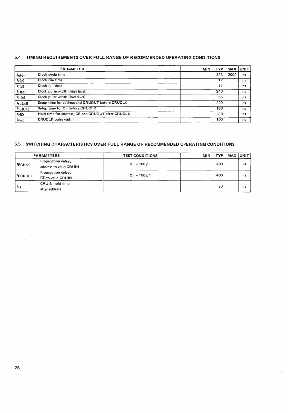
5.4
TIMING
REQUIREMENTS
OVER
FULL
RANGE OF RECOMMENDED OPERATING CONDITIONS
PARAMETER
MIN
TYP
MAX
UNIT
tc(CP)
Clock
cycle
time
333
2000
ns
trlCP)
Clock
rise
time
12
ns
tf(cp)
Clock
fall
time
12
ns
tH(CP)
Clock
pulse
width
(high level)
240
ns
tL(CP)
Clock
pulse
width
(low
level) 55 ns
tsu(ad)
Setup
time
for
address
and
CRUOUT
before
CRUCLK
220
ns
tsu(CE)
Setup
time
for
CE
before
CRUCLK
180
ns
tHO
Hold
time
for
address,
CE
and
CRUOUT
after
CRUCLK
80
ns
twcc
CRUCLK
pulse
width
100
ns
5.5 SWITCHING CHARACTERISTICS OVER
FULL
RANGE OF RECOMMENDED OPERATING CONDITIONS
PARAMETERS
TEST
CONDITIONS
MIN
TYP
MAX
UNIT
tPCI(ad)
Propagation
delay,
CL
=
100
pF
400
address-to-valid
CRUIN
ns
tPCI(CE)
Propagation
delay,
CL
=
100
pF
400
CE-to-valid
CRUIN
ns
CRUIN
hold
time
tH
20
ns
after
address
26
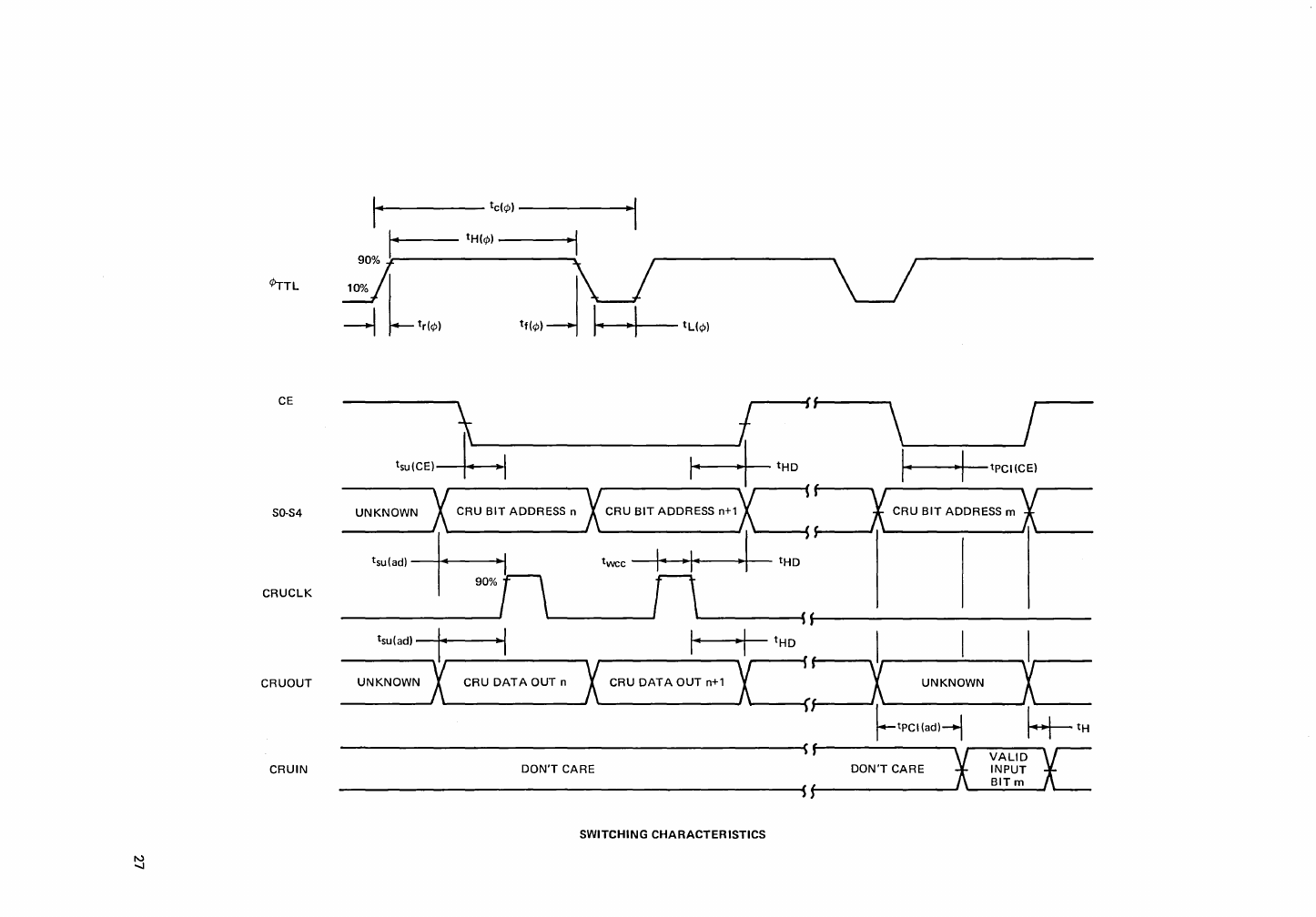
I-
tc(<P1
-I
~.
tH(<p1
-I
rl>-rTL
~v
V
1~
l
-l
tr(<P1
tf(<pl
I-
-\
tL(<P1
CE
~
H \ I
t'"tCE)~
I·
II
tpCI(CEI
SO-S4
UNKNOWN
CRU
BIT
ADDRESS n CRU
BIT
ADDRESS n+1 X
CRU
BIT ADDRESS m X
twcc
I·
-I-
tHD
CRUCLK
n H
tsu(adl
I-
-I
tHD
~
X
CRUOUT
UNKNOWN
CRU
DATA
OUT
n X
CRU
DATA
OUT
n+1
X
~:
UNKNOWN
!-=tPCI
(adl-j
H-tH
CRUIN
DON'T
CARE
DON'T
CARE
SWITCHING
CHARACTERISTICS
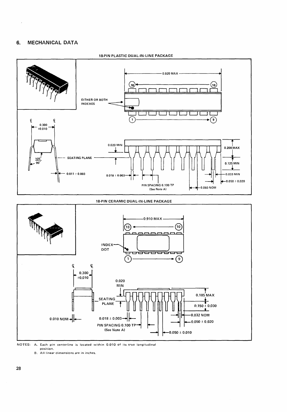
6. MECHANICAL DATA
£ £
18-PIN
PLASTIC
DUAL-IN-LiNE
PACKAGE
~'9~MAX;;;;1
~~~~~~RBOTH~€:::::::
I
(0------------..
CD
rr
'::::~
~
--
SEATINGPlAN'
~~
~
0.0" MIN f
--.L
~~
T
0.125MIN
"'"'"00'--1
r-
~
~I
,,':"N
1\
0.011 !O.OOJ
I I I
~
0.050 ± 0.020
PIN SPACING 0.100
TP
(See
Note
Al 0.060 NOM
18-PIN
CERAMIC
DUAL-IN-LiNE
PACKAGE
0-----0
0.020
MIN
r
±~:~~~j
A
SEATlNG1~~---'
-
PLANEt
0.010NOM~1----
0.018±0.003-.J1--
I
PIN SPACING 0.100
TP-j
(See
Note
AI
NOTES:
A.
Each
pin
centerline
is
located
within
0.010
of
its
true
longitudinal
position.
B.
All
linear
dimensions
are
in
inches.
28

TI
worldwide sales offices
ALABAMA
304
Wynn
Drive
Huntsville. Alabama
35806
205-837-7530
ARIZONA
4820
N. Black Canyon
Hwy.
Suite
202
Phoenix,
Arizona
85017
602-249-1313
CALIFORNIA
3186J
Airway
Costa
Mesa,
California
92626
714-540-7311
831 S. Douglas St.
EI
Segundo,
California
90245
213-973-2571
7827
Convoy
Ct
.•
Suite
412
San
Diego.
California
92111
714-279-2622
176
Palomar Avenue
Sunnyvale,
California
94086
408-732-1840
COLORADO
9725
E.
Hampden
St.,
Suite
301
Denver, Colorado 80231
303-751-1780
CONNECTICUT
Whitney
Towers
2405
Whitney
Avenue
Hamden,
Connecticut
06518
203-281-0074
ARGENTINA
Texas
Instruments
Argentina
S.A.I.C.F.
C.C.
80x
2296-Correo
Central
Buenos
Aires,
Argentina
748-1141
ASIA
Texas
Instruments
Asia Limited
5F
Aoyama
Tower
Bldg.
24-15
Minami
Aoyama
Chame
Minato-ku.
Tokyo
101,
Japan
402-6171
11 A-15
Chatham
Road
First
Floor,
KowlOOn
Hong
Kong
3-670061
Texas
Instruments
Singapore
(PTE)
Ltd.
21
Kallang Place
Singapore
1, Rep.
of
Singapore
258-1122
Texas
Instruments
Taiwan
Limited
P.O_
80.
3999
Taipei,
Chung
Ho, Taiwan
921
623
Texas
Instruments
Malaysia
SON.
BHO.
Number
1
Lorong
Enggang
33
Kuala
Lampur
1!;
..
01,
Malaysia
647911
AUSTRALIA
Texas
I
nstruments
Australia Ltd.
Suite
205,
118
Gr.t
North
Road
Five Dock N.S.W.
2046
Australia
831-2555
Box
63,
Post
Office
171-175
Philip HighwaV
Elizabeth
5112
South
Australia
25!>-2066
FLORIDA
4600
West Commercial Blvd.
Fort
Lauderdale.
Florida
33319
305-733-3300
2221 Lee Road, Suite
108
Winter
Park,
Florida
32789
305-644-3535
ILLINOIS
1701
E.
Lake Avenue, Suite
300
Glenview,
Illinois
60025
~12-729-5710
INDIANA
3705
Aupp
Drive
Arch
Building
Fort
Wayne, Indiana
46805
219-484-0606
2346
S.
Lynhurst
Dr.,
Suite
101
Indianapolis,
Indiana
46241
317-248-8555
MASSACHUSETTS
504
Totten
Pond
Road
Waltham
..
Mass.02154
617-890-7400
MICHIGAN
Central Park Plaza
26211
Central Park Blvd.,
Suite
215
Southfield.
Michigan
48076
313-353-0830
MINNESOTA
A_I.C. Bld9 ..
Suite
202
7615
Metro
Blvd.
Edina, Minn.
55435
612-835-2900
BELGIUM
Texas
Instru~nts
Belgium
21 Avenue
Ed.Lacomble
1040
Brussels
217339623
BRAZIL
Texas
InstrumentQs E
lectronicos
do
BraSil
Ltda.
Rua
Joao
Annes,
15J.Lapa
Coi'a
Postal 30_103. CEP
01.000
Sao
Paulo,
SP,
Brasil
260-2956
CANADA
Texas
Instruments
Incorporated
945 McCaffery
Street
St.
Laurent
H4T1N3
Quebec.
Canada
514-341-3232
280
Centre
Str.
East
Richmond
Hill
(Torontol
OntariO,
Canada
416-889-7373
DENMARK
Texas
Instruments
Denmark
460,
Marielundvej
2130
Harlev,
Denmark
1011917400
FINLAND
Texas
Instruments
Finland
OY
Fredrikinkatu
15.
A7
Helsinki
la,
Fin~and
447171
MISSOURI
12401
E_
43rd
Street
Independence,
Missouri
64055
816-836-2676
NEW
JERSEY
1245
Westfield Ave., P.O. Box
885
Clark,
New
Jersey
07066
201-574-9800
NEW
MEXICO
1101 Cardenas Drive. N.E.,
Room
215
Albuquerque,
New Mexico
87110
505-265-8491
NEW
YORK
6700
Old
Collamer
Rd.
East Syracuse. New
York
13051
315-463-9291
112
Nanticoke
Ave., P.O. Box
618
Endicott.
New
York
13760
607·785-9987
201
South
Avenue
Poughkeepsie. New
York
12601
914-473-2900
1210
Jefferson
Rd.
Rochester.
New York
14623
716-461·1800
1
Huntington
Ouadrangle.
Suite
leOl
Melville, New York
11746
516-293-2560
NORTH
CAROLINA
1001 East Blvd.
Charlotte.
N.C.
28203
704-372-8780
OHIO
Belmont
Bldg.,
Suite
120
28790
Chagrin Blvd.
Cleveland. Oh io
44122
216-464-2990
Hawley Bldg.,
Suite
101
4140
Linden
Avenue
Dayton.
Ohio
45432
513-253-3121
FRANCE
Texas
Instruments
France
Boite Postale 5
06
Villeneuve·Loubet,
France
310364
La Boursidiere, Bloc A
R.N.
186,92350
Le Plessis
Robinson
630.23_43
30--31
Quai
Rambaud
69 Lyon,
France
427850
GERMANY
Texas
Instruments
Deutschland
GmbH
Haggerty
Str.
1
8050
Freising,
Germany
08161/80-1
Frankfurter
Ring
243
8000
Munich
40,
Germany
089/325011-15
Lazarettstrasse,19
4300 Essen,
Germany
02141/20916
Krugerstrasse
24
1000
Berlin
49,
Germany
0311/7444041
Akazlenstrasse
22
..
26
6230
Frankfurt
-
Griesheim
Germany
0611/39 90 61
Steimbker
Hof SA
3(X)() Hannover.
Germany
0511/556041
Krefelderstrasse
11
..
15
7000
Stuttgart
SO,
Germany
0711/54
7001
OREGON
10700
S.W. Beaverton Hwy.
Suite
11
Beaverton.
Oregon
97005
503-643-6750
PENNSYLVANIA
275
Commerce
Drive,
Suite
300
Fort
Washington.
Pa.
19034
215-643-6450
TEXAS
6000
Denton
Drive
P
.0_
Bo.
5012.
MIS 366
Dallas,
Texas
75222
214-238-6805
P_O.
Bo.
5012.
MIS 7
Dallas.
Texas
75222
214-238-4881
P.O_
Bo.
5012.
MIS 288
Dallas,
Texas
75222
214-238-2616
8600
Commerce
Park Drive
Houston.
Texas
77036
713-777-4891
VIRGINIA
3930
Beulah
Rd_
Richmond,
Virginia
23234
804-275-8148
WASHINGTON
700
112th
N.E
.•
Suite
10
Bellevue. Washington
98004
206-455-3480
WASHINGTON.D_C_
1500
Wilson Blvd.,
Suite
1100
Arlington.
Virginia
22209
703-525-0336
ITALY
Texas
Instruments
Itaha
SpA
Via Della Giustizla 9
20125
Milan.
Italy
02-6883141
Via L. Manclnella 65
00199
Roma.
Italy
06-837745
Via
Montebello
27
10124
TorinO. Italy
011-832276
MEXICO
Texas
Instruments
de
MexiCO
S.A.
Poniente
116
#489
Col. Industrial Vallejo
Mexico
City,
D.F., Mexico
567-92-00
NETHERLANDS
Texas
Instruments
Holland N.V.
Entrepot
Gebouw·Kamer
225
P_O.
Bo.
7603
Schiphol
..
Centrum
020-17
36
36
NORWAY
Texa,
Instrument$
Norway
A/S
Sentrumskontorene
Srugaten
1
Oslo
1, Norway
331880
SWEDEN
Texas
Instruments
Sweden
AS
S
..
104
40
Stockholm
14
Skeppargatan
26
679835
UNITED
KINGDOM
Texas
Instruments
Limited
Manton
Lane
Bedford,
England
0234-67466
Printed
in U.S.A.
