TN1290 Memory Usage Guide For MachXO3L Devices Mach XO3
User Manual:
Open the PDF directly: View PDF ![]() .
.
Page Count: 54
- Memory Usage Guide for MachXO3 Devices
- Introduction
- Memories in MachXO3L/LF Devices
- Utilizing IPexpress
- IPexpress Memory Modules
- FIFO_DC Flags
- FIFO_DC Dual and Dynamic Threshold Options
- FIFO_DC Operation
- MachXO3L/LF Primitives
- Initializing Memory
- Technical Support Assistance
- Revision History
- Appendix A. Attribute Definitions
- Appendix B. Setting FIFO_DC Pointer Attributes

www.latticesemi.com 1TN1290_01.1
March 2015 Technical Note TN1290
© 2015 Lattice Semiconductor Corp. All Lattice trademarks, registered trademarks, patents, and disclaimers are as listed at www.latticesemi.com/legal. All other brand
or product names are trademarks or registered trademarks of their respective holders. The specifications and information herein are subject to change without notice.
Introduction
This technical note discusses the memory usage for the Lattice MachXO3™ PLD family. It is intended to be used
by design engineers as a guide in integrating the EBR and PFU based memories for these devices in Diamond®.
The architecture of these devices provides resources for memory intensive applications. The sysMEM™ Embed-
ded Block RAM (EBR) complements the distributed PFU-based memory. Single-Port RAM, Dual-Port RAM,
Pseudo Dual-Port RAM, FIFO and ROM memories can be constructed using the EBR. LUTs and PFU can imple-
ment Distributed Single-Port RAM, Dual-Port RAM and ROM.
The capabilities of the EBR Block RAM and PFU RAM are referred to as primitives and are described later in this
document. Designers can utilize the memory primitives in two ways:
•Via IPexpress™ – The IPexpress GUI allows users to specify the memory type and size that is required. IPex-
press takes this specification and constructs a netlist to implement the desired memory by using one or more of
the memory primitives.
•Via the PMI (Parameterizable Module Instantiation) – PMI allows experienced users to skip the graphical inter-
face and utilize the configurable memory modules on the fly from the Diamond® Project Navigator. The parame-
ters and the control signals needed either in Verilog or VHDL can be set. The top-level design will have the
parameters defined and signals declared so the interface can automatically generate the black box during syn-
thesis.
In addition to familiar Block RAM and PFU RAM primatives, MachXO3LF-640 and higher density devices (Only)
provide a new User Flash Memory (UFM) block, which can be used for a variety of applications including storing a
portion of the configuration image, storing and initializing EBR data, storing PROM data or as a general purpose
non-volatile user Flash memory. The UFM block connects to the device core through the embedded function block
WISHBONE interface. Designers can also access the UFM block through the JTAG, I2C and SPI interfaces of the
device. The UFM block offers the following features:
• Non-volatile storage up to 256 kbits
• Byte addressable for read access. Write access is performed in 128-byte pages.
• Program, erase, and busy signals
• Auto-increment addressing
• WISHBONE interface
• External access is provided through JTAG, I2C and SPI interfaces
For more information on the UFM, please refer to TN1293, Using Hardened Control Functions in MachXO3
Devices.
The remainder of this document discusses these approaches, utilizing IPexpress, PMI inference, memory modules
and memory primitives.
Memory Usage Guide for
MachXO3 Devices
2
Memory Usage Guide for MachXO3 Devices
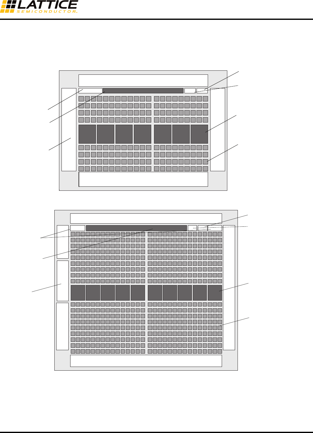
Memories in MachXO3L/LF Devices
All MachXO3L/LF devices contain an array of logic blocks called PFUs surrounded by Programmable I/O Cells
(PICs). This is shown in Figures 1 and 2.
Figure 1. Top View of the MachXO3L/LF-1300 Device
Figure 2. Top View of the MachXO3L/LF-4300 Device
The PFU contains the building blocks for logic and Distributed RAM and ROM. Some PFUs provide the logic build-
ing blocks without the distributed RAM. This document describes the memory usage and implementation for both
Embedded Memory Blocks (EBRs) and Distributed RAM of the PFU. Refer to DS1047, MachXO3 Family Data
Sheet for details on the hardware implementation of the EBR and Distributed RAM.
sysMEM Embedded
Block RAM (EBR)
sysCLOCK PLL
PIOs Arranged into
sysIO Banks
Programmable Function Units
with Distributed RAM (PFUs)
Embedded Function
Block (EFB)
NVCM1 (MachXO3L)/
UFM (MachXO3LF)
On-chip Configuration
NVCM (MachXO3L)
/UFM (MachXO3LF)
sysMEM Embedded
Block RAM (EBR)
Programmable Function Units
with Distributed RAM (PFUs)
On-chip Configuration
NVCM (MachXO3L)/
UFM (MachXO3LF)
sysCLOCK PLL
PIOs Arranged into
sysIO Banks
Embedded
Function Block(EFB)
NVCM1 (MachXO3L)/
UFM (MachXO3LF)

3
Memory Usage Guide for MachXO3 Devices
Utilizing IPexpress
Designers can utilize IPexpress to easily specify a variety of memories in their designs. These modules will be con-
structed using one or more memory primitives along with general purpose routing and LUTs as required. The avail-
able primitives are:
• Single Port RAM (RAM_DQ) – EBR based
• Dual Port RAM (RAM_DP_TRUE) – EBR based
• Pseudo Dual Port RAM (RAM_DP) – EBR based
• Read Only Memory (ROM) – EBR based
• First In First Out Memory (FIFO_DC) – EBR based
• Distributed Single Port RAM (Distributed_SPRAM) – PFU based
• Distributed Dual Port RAM (Distributed_DPRAM) – PFU based
• Distributed ROM (Distributed_ROM) – PFU based
• RAM-based Shift Register - PFU based
4
Memory Usage Guide for MachXO3 Devices
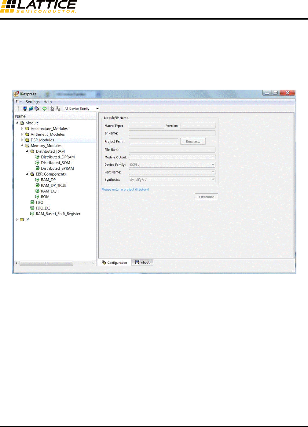
IPexpress Flow
For generating any of these memories, create (or open) a project for the MachXO3L/LF devices.
From the Project Navigator, select Tools > IPexpress. Alternatively, users can also click on the IPexpress button in
the toolbar when MachXO3L/LF devices are targeted in the project.
This opens the IPexpress window as shown in Figure 3.
Figure 3. IPexpress – Main Window
The left pane of this window has the Module Tree. The EBR-based Memory Modules are under the
EBR_Components and the PFU-based Distributed Memory Modules are under Distributed_RAM as shown in
Figure 3.
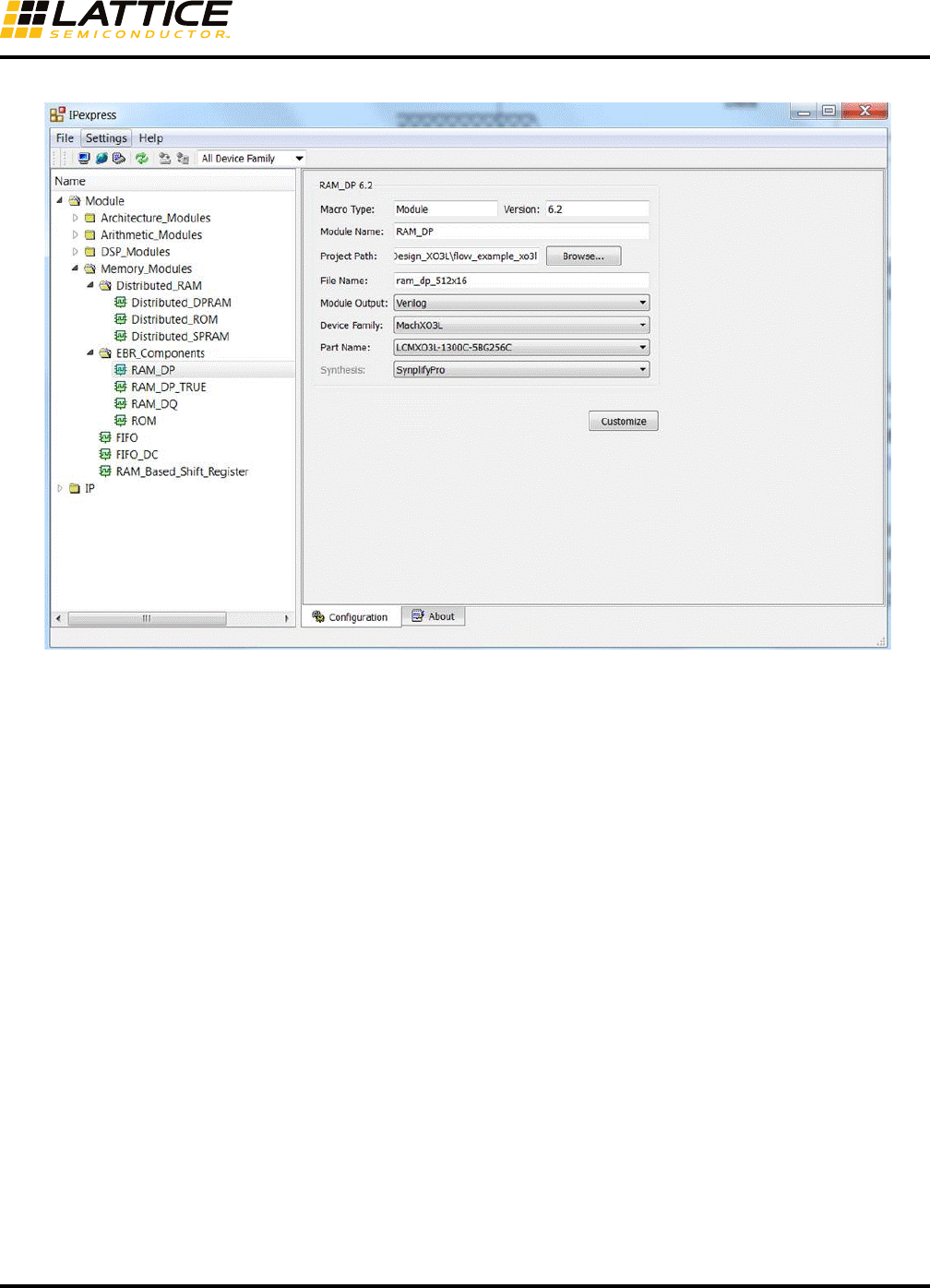
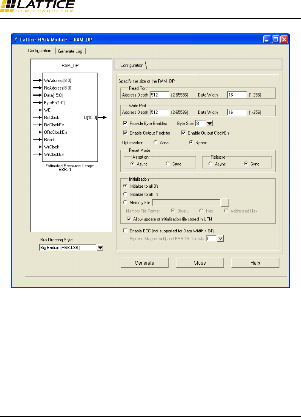
As an example, let us consider generating an EBR-based Pseudo Dual Port RAM of size 512x16. Select RAM_DP
under the EBR_Components. The right pane changes as shown in Figure 4.
5
Memory Usage Guide for MachXO3 Devices
Figure 4. Example Generating Pseudo Dual Port RAM (RAM_DP) Using IPexpress
In this right pane, options like the Macro Type and Module_Name are device and selected module dependent.
These cannot be changed in IPexpress.
Users can change the directory where the generated modules will be placed by clicking the Browse button in the
Project Path.
The File Name text box allows users to specify an entity name for the module they are about to generate. Users
must provide this entity name.
Design entry, Verilog or VHDL, by default, is the same as the project type. If the project is a VHDL project, the
selected design entry option will be “VHDL”, and “Verilog-HDL” if the project type is Verilog-HDL. Schematic support
may also be selected with either HDL type.
When launched from within Project Navigator, the Device Family and Part Name pull-down menus are filled in by
default and cannot be changed by the user. However, when IPexpress is launched as a stand-alone application,
these menus allow users to select different devices within a device family, MachXO3L/LF in this example.
When finished, click the Customize button.
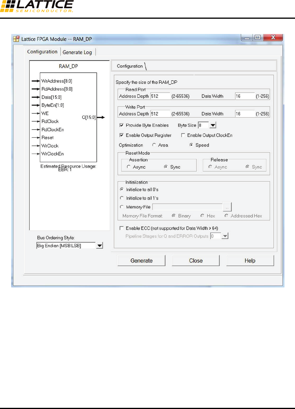
This opens another window where users can customize the RAM (Figure 5).
6
Memory Usage Guide for MachXO3 Devices
Figure 5. Example Generating Pseudo Dual Port RAM (RAM_DP) Module Customization (MachXO3L)
7
Memory Usage Guide for MachXO3 Devices
Figure 6. Example Generating Pseudo Dual Port RAM (RAM_DP) Module Customization (MachXO3LF)
The left side of this window shows the block diagram of the module. The right side includes the Configuration tab
The left side of this window shows the block diagram of the module. The right side includes the Configuration tab
where users can choose options to customize the RAM_DP (such as specify the address port sizes and data
widths).
Users can specify the address depth and data width for the Read Port and the Write Port in the text boxes pro-
vided. In this example we are generating a Pseudo Dual Port RAM of size 512 x 16. Users can also create RAMs of
different port widths for Pseudo Dual Port and True Dual Port RAMs.
The Input Data and the Address Control is always registered, as the hardware only supports the clocked write
operation for the EBR-based RAMs. The check box Enable Output Register inserts the output registers in the
Read Data Port, as the output registers are optional for EBR-based RAMs.
Clock Enable control is always provided for Input Data and Address signals. When Output Registers are enabled,
separate Output Clock Enables can be selected.
8
Memory Usage Guide for MachXO3 Devices
Users can specify the use of Byte Enables. Byte Enables can be used to mask the input data so that only specific
bytes of memory are overwritten. The unwritten bytes retain the previously written data.
The Reset Mode of the memory can be specified by the user for both assertion and release. For the synchronous
reset, the clock should be there and reset signal should satisfy setup/hold time requirements for both asserting and
deasserting edges. The write function is automatically disabled during a synchronous reset because the CS regis-
ters are reset, but the write is not disabled during an asynchronous reset operation.
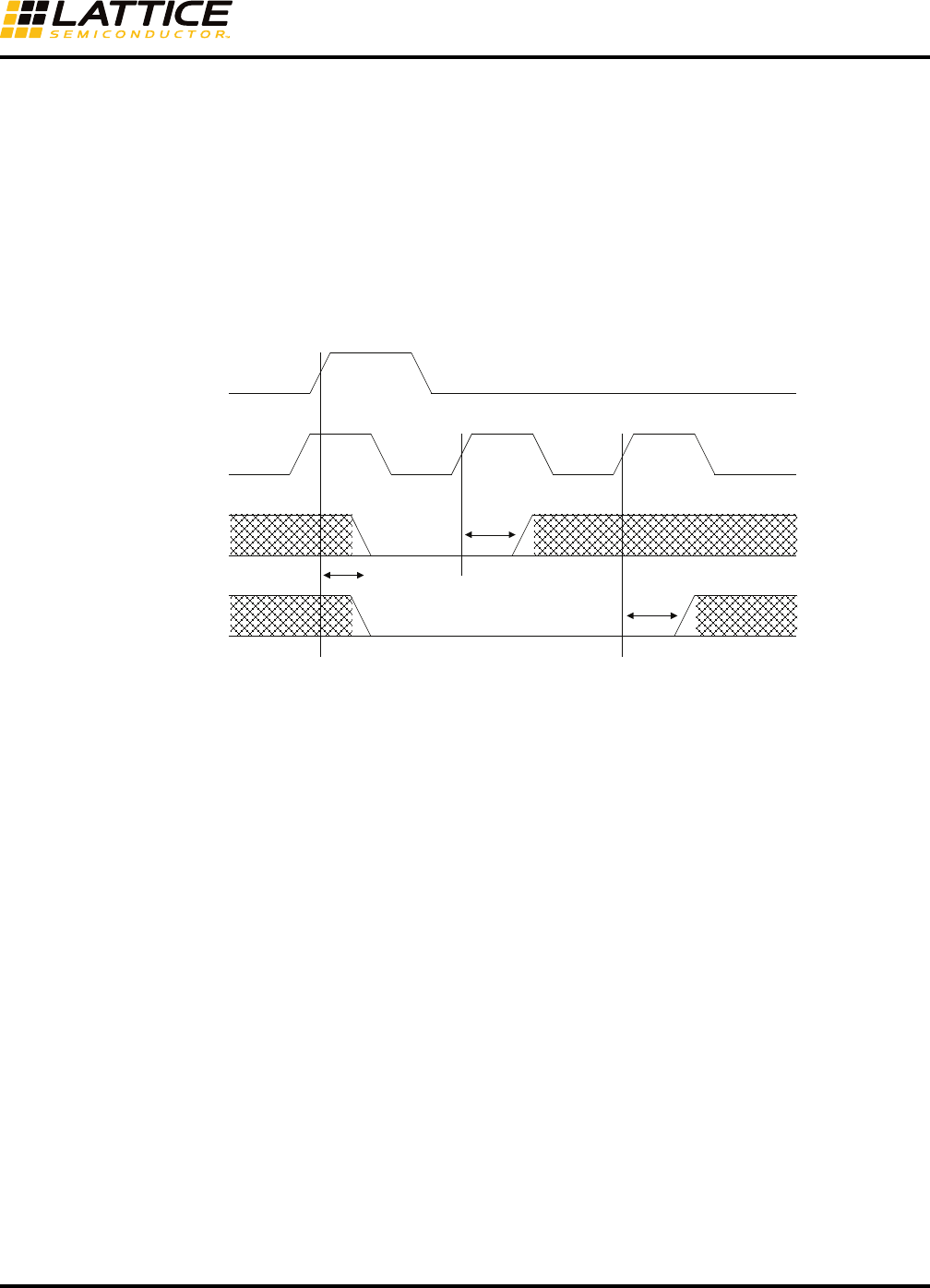
The asynchronous reset can be programmed to be released (de-asserted) synchronously. As shown in Figure 7,
when de-asserted synchronously, the first clock edge after reset will release the internal reset to all registers that
have asynchronous reset, such as the data output registers, the FIFO counters and the FIFO flag registers.
Figure 7. Asynchronous Reset with Synchronous Release
Memory may be initialized at configuration to all 1s or all 0s. To maximize the number of NVCM/Flash bits, initialize
the EBRs to an all 0's pattern. Initializing to an all 0’s pattern does not use up NVCM/UFM bits. Users can also ini-
tialize their memory with the contents specified in the Memory File. It is optional to provide this file for RAM; how-
ever for ROM, the Memory File is required. These files can be of Binary, Hex or Addressed Hex format. The details
of these formats are discussed in the Initialization File section of this document.
Traditionally, the initialization Memory File is static and is stored in the device configuration bitstream. Alternatively,
the MachXO3LF (Only) architecture allows the memory initialization data to be stored in UFM where it may be
accessed and/or dynamically modified by the user. To enable this feature, select Allow Update of initialization file
stored in UFM. For details of this feature, please refer to TN1293, Using Hardened Control Functions in MachXO3
Devices.
At this point, users can click the Generate button to generate the module they have customized. A VHDL or Verilog
netlist is then generated and placed in the specified location. Users can incorporate this netlist in their designs. In
addition, an instantiation template file (*_tmpl.v or .vhd), a Lattice Parameter file (*.lpc), a testbench template file
(tb_*_tmpl.v or .vhd), and two log files (*_generate.log, *.srp) are generated. Finally, a schematic symbol file
(*.sym) is created if Design Entry type is Schematic/VHDL or Schematic/Verilog.
Once the module is generated, user can either instantiate the *.lpc or the Verilog-HDL/ VHDL file in top-level mod-
ule of their design.
RESET
CLOCK
Unregistered
Data Out
Registered
Data Out
First Valid
Data
First Valid
Data
Asynchronous
Assertion
Synchronous
Release
9
Memory Usage Guide for MachXO3 Devices
ECC in Memory Modules
IPexpress allows users to implement Error Check Codes in the EBR-based memory modules. There is a checkbox
to enable ECC in the configuration tab for the module.
If you choose to use ECC, you will have a 2-bit error signal and the error codes are as below:
• Error[1:0] = “00” – Indicates there is no error.
• Error[1:0] = “01” – Indicates there was a 1-bit error which was fixed.
• Error[1:0] = “10” – Indicates there was a 2-bit error which cannot be corrected.
• Error[1:0] = “11” – Not used.
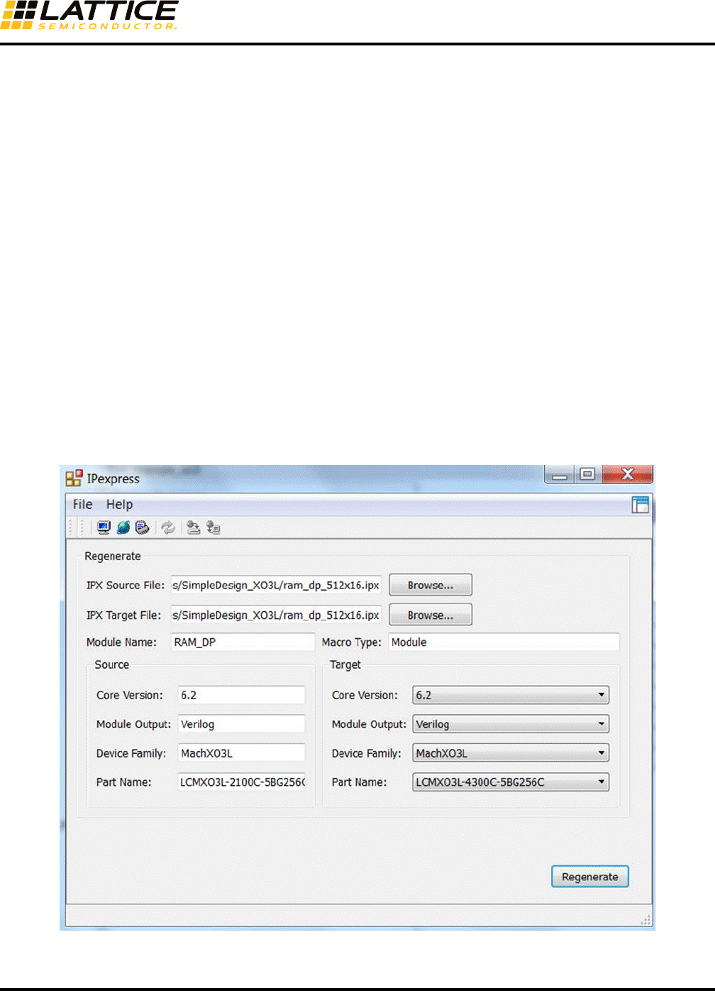
IP Regeneration/Modification
Sometimes it is useful to regenerate or modify a previously generated module. By regenerating a customized mod-
ule or IP you can modify any of its settings including: device type, design entry method, and any of the options spe-
cific to the module. You can also update older modules or IP to the latest version. From the IPexpress main window,
click the Regenerate button.
In the Select a Parameter File dialog box, choose the Lattice Parameter Configuration (.lpc) file of the module or
IP you wish to regenerate, and click Open.
This opens a dialog box as shown in Figure 8.
Figure 8. Example Regenerating/Modifying IP
10
Memory Usage Guide for MachXO3 Devices
The Select Target Core Version, Design Entry, and Device dialog box shows the current settings for the module
or IP in the Source Value box. Make your new settings in the Target Value box.
If you want to generate a new set of files in a new location, set the location in the LPC Target File box. The base of
the .lpc file name will be the base of all the new file names. The LPC Target File must end with a .lpc extension.
Click Next, and proceed with module customization as before.
The various memory modules, both EBR and Distributed, are discussed in detail in the following sections.
Utilizing PMI
Parameterizable Module Instantiation (PMI) allows experienced users to skip the graphical interface and utilize the
configurable memory modules on-the-fly from the Diamond Project Navigator.
The necessary parameters and control signals can be set in either Verilog or VHDL. The top-level design includes
the defined memory parameters and declared signals. The interface can then automatically generate the black box
during synthesis and Diamond can generate the netlist on-the-fly. Lattice memories are the same as industry stan-
dard memories, so you can get the parameters for each module from any memory-related guide, which is available
through the on-line help system.
PMI modules are instantiated the same way other modules are in your HDL. The process is similar to the process
for IPexpress with the addition of setting parameters to customize the module. The Diamond software provides a
template for the Verilog or VHDL instantiation command that specifies the customized module’s ports and parame-
ters. Refer to the Diamond online help section “Instantiating a PMI Module” for further information.
Memory Module Inference
Finally, memories may be instantiated within Verilog or VHDL modules through inference. The HDL constructs for
memory inferencing is synthesis vendor dependant. Refer to the documentation provided by the synthesis engine
vendor for correct inference constructs and attribute settings.
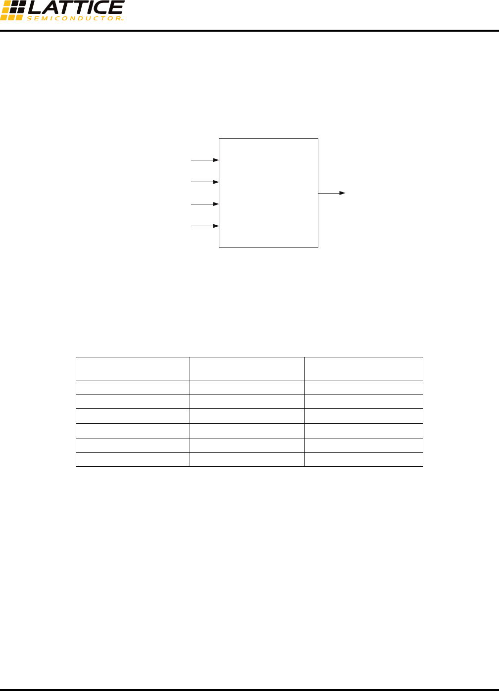
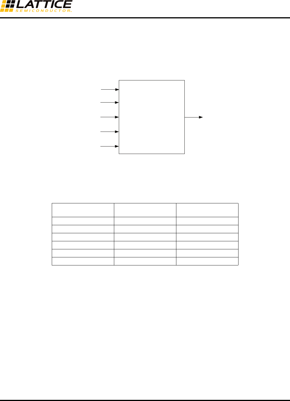
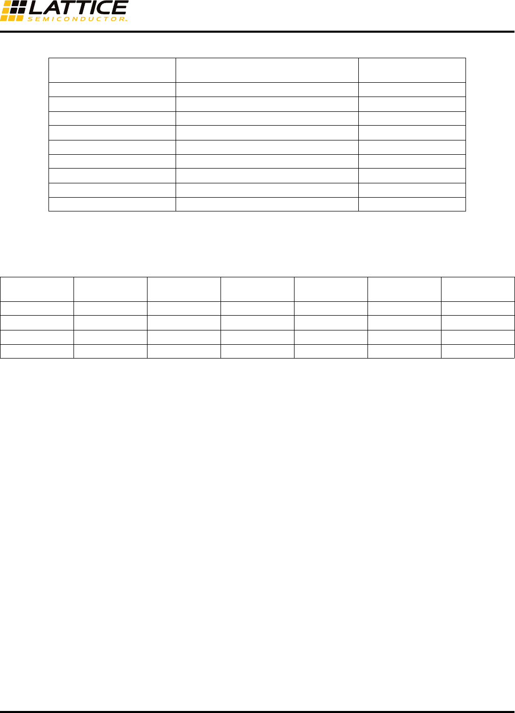
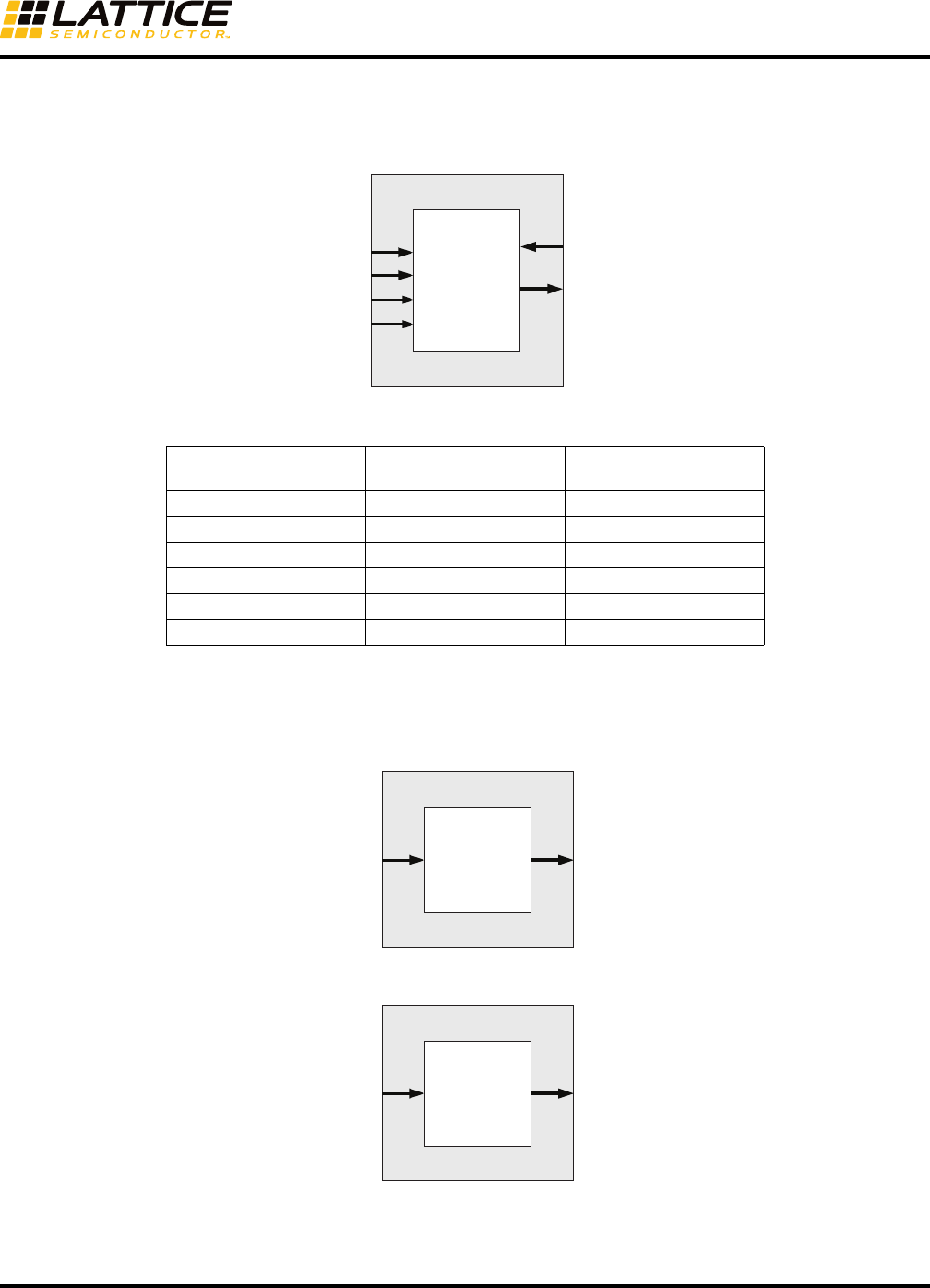
IPexpress Memory Modules
Single Port RAM (RAM_DQ) – EBR Based
The EBR blocks in the MachXO3L/LF devices can be configured as Single Port RAM (RAM_DQ). IPexpress allows
users to generate the Verilog-HDL or VHDL netlist for the memory size, as per design requirements.
IPexpress generates the memory module as shown in Figure 9.
Figure 9. Single Port Memory Module Generated by IPexpress
RAM_DQ
EBR-Based Single Port
Memory
Clock
ClockEn
Reset
WE
Address
Data
Q
OClockEn
ByteEn

11
Memory Usage Guide for MachXO3 Devices
Since the device has a number of EBR blocks, the generated module makes use of these EBR blocks, or primi-
tives, and cascades them to create the memory sizes specified by the user in the IPexpress GUI. For memory sizes
smaller than an EBR block, the module will be created in one EBR block. For memory sizes larger than one EBR
block, multiple EBR blocks can be cascaded in depth or width (as required to create these sizes).
In Single Port RAM mode, the input data and address for the ports are registered at the input of the memory array.
The output data of the memory is optionally registered at the output.
The various ports and their definitions for the Single Port Memory are listed in Table 1.
Table 1. EBR-Based Single Port Memory Port Definitions
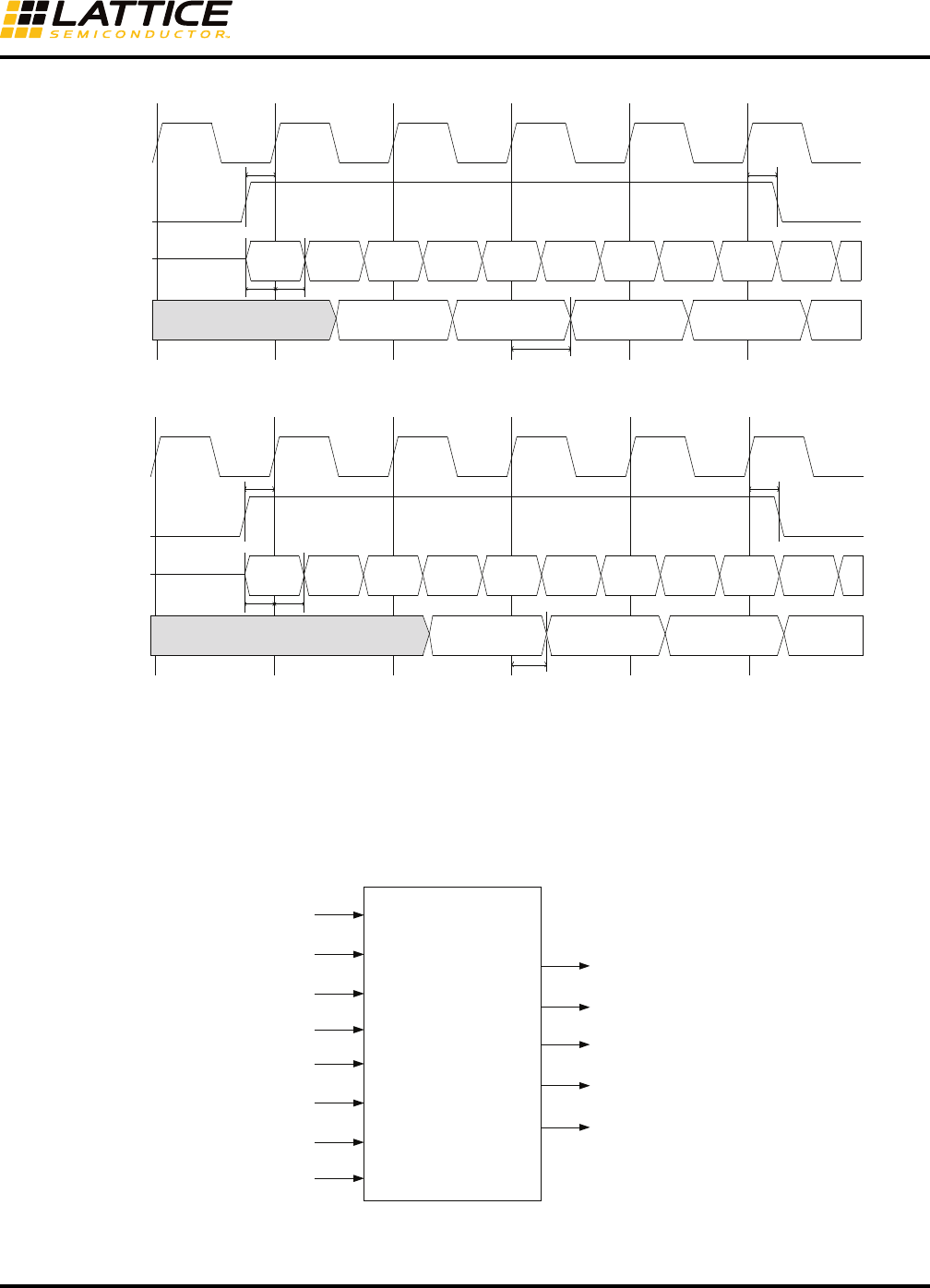
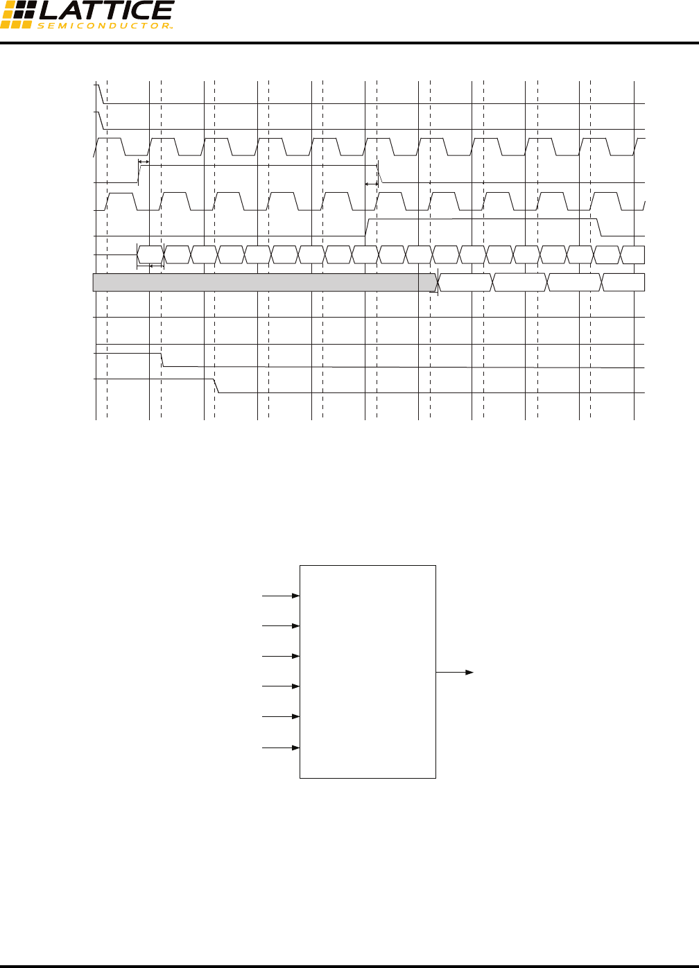
The Single Port RAM (RAM_DQ) can be configured in NORMAL, READ BEFORE WRITE or WRITE THROUGH
modes. Each of these modes affects what data comes out of the port Q of the memory during the write operation
followed by the read operation at the same memory location.
IPexpress implements the MachXO3L/LF Single Port RAM (RAM_DQ) using an appropriately configured DP8KC
primitive.
Figures 10 through 15 show the internal timing waveforms for the Single Port RAM (RAM_DQ).
Port Name
in the Generated Module Description Active State
Clock Clock Rising Clock Edge
ClockEn1 Clock Enable Active High
*OClockEn2Output Clock Enable Active High
Reset3 Reset Active High
*ByteEn4Byte Enable Active High
WE Write Enable Active High
Address Address Bus —
Data Data In —
Q Data Out —
*ERROR Error Check Code Active High
*Denotes optional port
1. ClockEn is used as clock enable for all the input registers.
2. OClockEn can be used as clock enable for the optional output registers. This allows the full
pipeline of data to be output, including the last word.
3. Reset resets only the optional output registers of the RAM. It does not reset the input regis-
ters or the contents of memory.
4. ByteEn can be used to mask the input data so that only specific bytes of memory are over-
written.
12
Memory Usage Guide for MachXO3 Devices
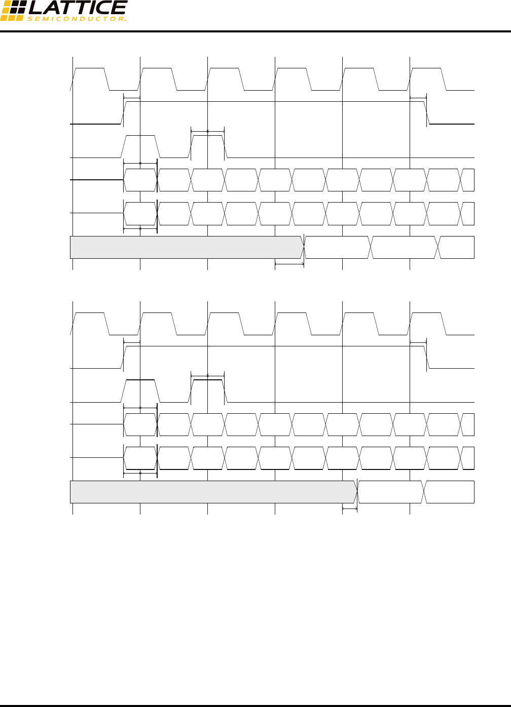
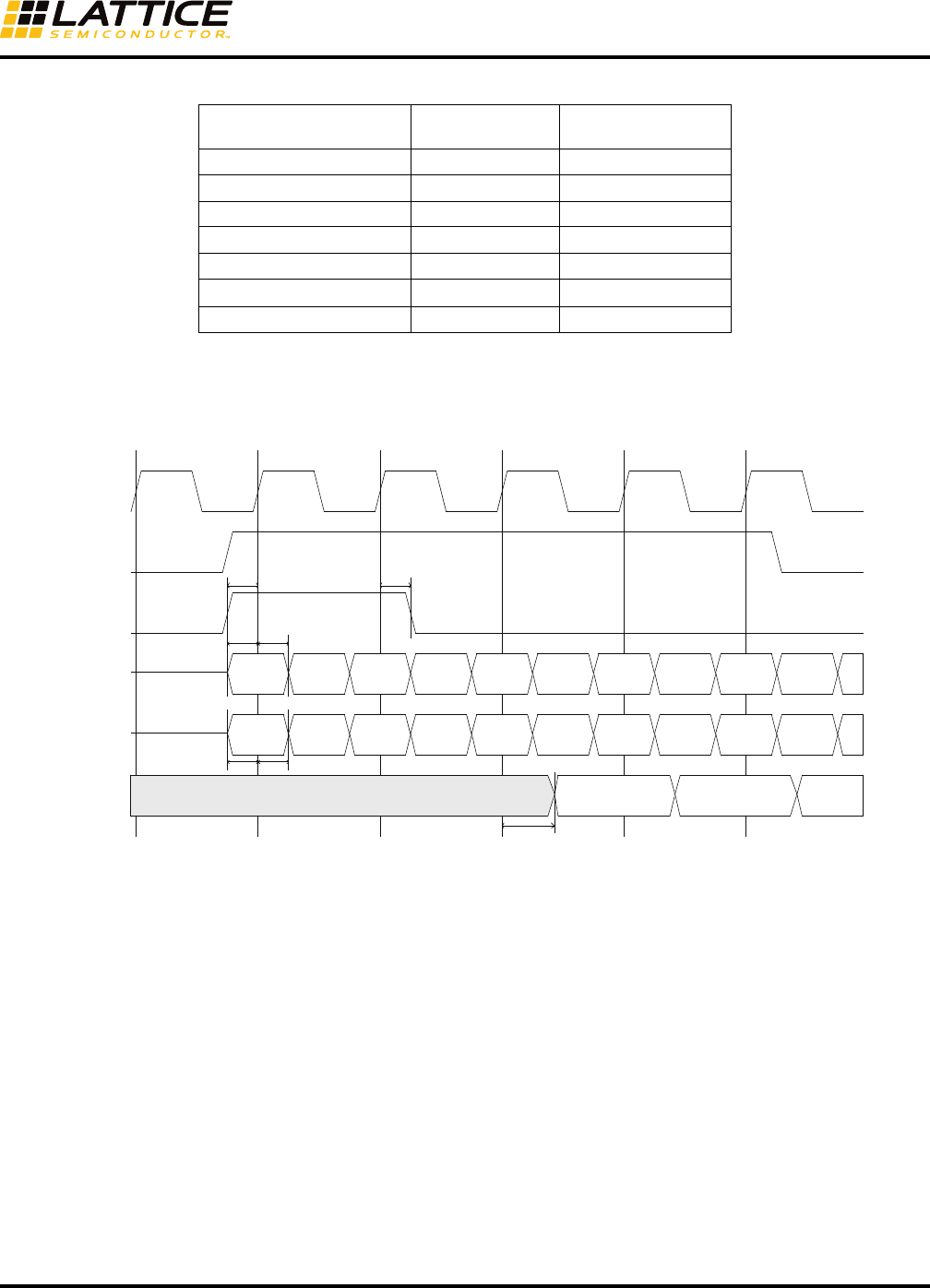
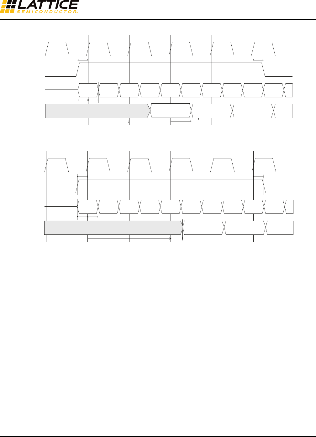
Figure 10. Single Port RAM Timing Waveform – NORMAL Mode, Without Output Registers
Figure 11. Single Port RAM Timing Waveform – NORMAL Mode, With Output Registers
Add_0 Add_1 Add_0 Add_1 Add_2
Data_0 Data_1
Invalid Data Data_0
Clock
WE
Address
Data
Q
ClockEn
t
SUWREN_EBR
t
HWREN_EBR
t
SUADDR_EBR
t
HADDR_EBR
t
SUDATA_EBR
t
HDATA_EBR
t
SUCE_EBR
t
HCE_EBR
t
CO_EBR
Data_1 Data_2
Add_0 Add_1 Add_0 Add_1 Add_2
Data_0 Data_1
Invalid Data Data_0 Data_1
Clock
WE
Address
Data
Q
ClockEn
t
SUWREN_EBR
t
HWREN_EBR
t
SUADDR_EBR
t
HADDR_EBR
t
SUDATA_EBR
t
HDATA_EBR
t
SUCE_EBR
t
HCE_EBR
t
COO_EBR

13
Memory Usage Guide for MachXO3 Devices
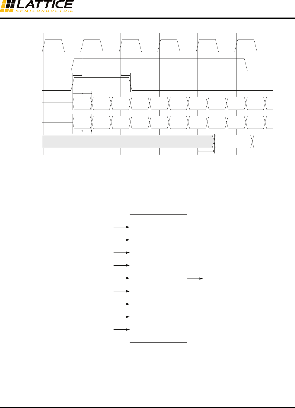
Figure 12. Single Port RAM Timing Waveform – READ BEFORE WRITE Mode, Without Output Registers
Figure 13. Single Port RAM Timing Waveform – READ BEFORE WRITE Mode, With Output Registers
Add_0 Add_0 Add_1 Add_1 Add_2
New
Data_0
New
Data_1
Invalid Data New_Data_0
Clock
WE
Address
Data
Q
ClockEn
t
SUWREN_EBR
t
HWREN_EBR
t
SUADDR_EBR
t
HADDR_EBR
t
SUDATA_EBR
t
HDATA_EBR
t
SUCE_EBR
t
HCE_EBR
t
CO_EBR
Old_Data_1Old_Data_0 New_Data_1
Add_0 Add_0 Add_1 Add_1 Add_2
New
Data_0
New
Data_1
Invalid Data New_Data_0
Clock
WE
Address
Data
Q
ClockEn
t
SUWREN_EBR
t
HWREN_EBR
t
SUADDR_EBR
t
HADDR_EBR
t
SUDATA_EBR
t
HDATA_EBR
t
SUCE_EBR
t
HCE_EBR
t
COO_EBR
Old_Data_1Old_Data_0 New
Data_1
14
Memory Usage Guide for MachXO3 Devices
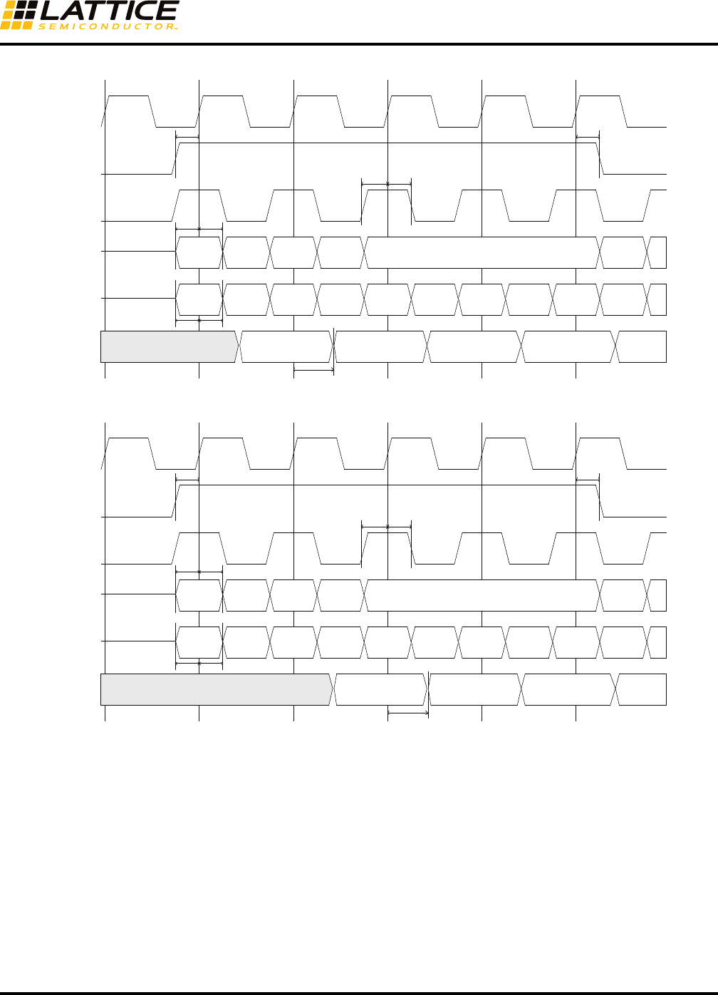
Figure 14. Single Port RAM Timing Waveform – WRITE THROUGH Mode, Without Output Registers
Figure 15. Single Port RAM Timing Waveform – WRITE THROUGH Mode, With Output Registers
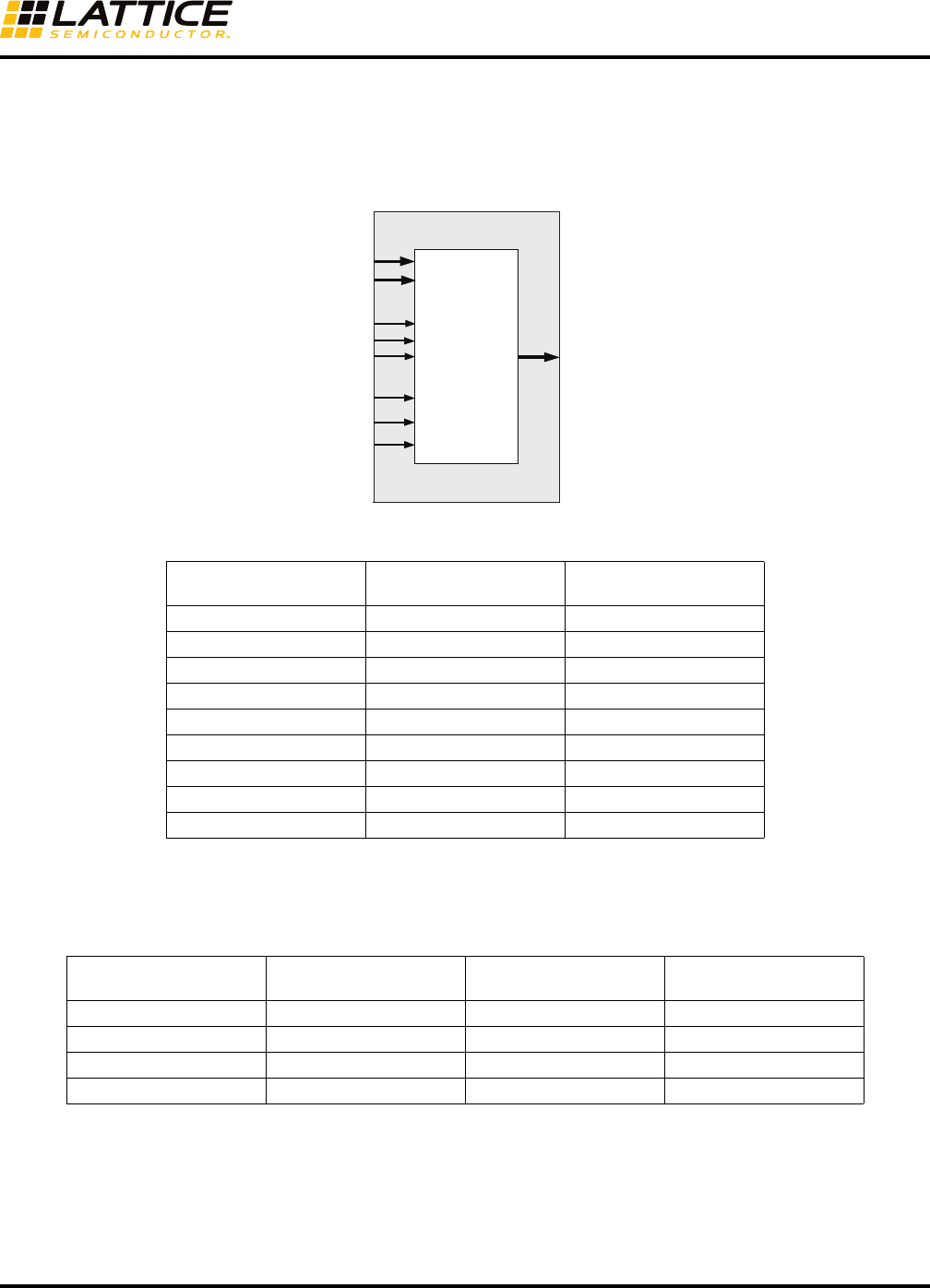
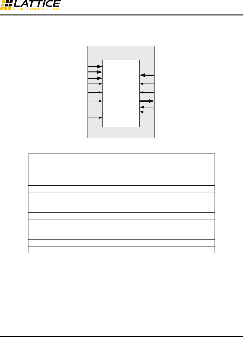
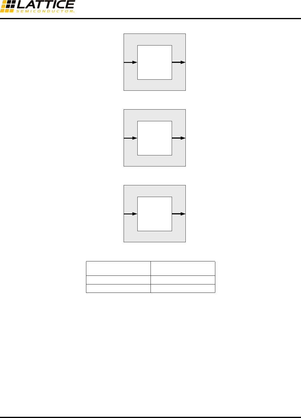
Dual Port RAM (RAM_DP_TRUE) – EBR Based
The EBR blocks in MachXO3L/LF devices can be configured as True-Dual Port RAM (RAM_DP_TRUE). IPexpress
allows users to generate the Verilog-HDL or VHDL netlists for various memory sizes depending on design require-
ments.
IPexpress generates the memory module as shown in Figure 16.
Add_0 Add_1 Add_0
Data_0 Data_1 Data_2 Data_3 Data_4
Invalid Data Data_1
Clock
WE
Address
Data
Q
ClockEn
t
SUWREN_EBR
t
HWREN_EBR
t
SUADDR_EBR
t
HADDR_EBR
t
SUDATA_EBR
t
HDATA_EBR
t
SUCE_EBR
t
HCE_EBR
t
CO_EBR
Data_2Data_0 Data_3 Data_4
Add_0 Add_1 Add_0
Data_0 Data_1 Data_2 Data_3 Data_4
Invalid Data Data_1
Clock
WE
Address
Data
Q
ClockEn
tSUWREN_EBR tHWREN_EBR
tSUADDR_EBR tHADDR_EBR
tSUDATA_EBR tHDATA_EBR
tSUCE_EBR tHCE_EBR
tCOO_EBR
Data_2Data_0 Data_3
15
Memory Usage Guide for MachXO3 Devices
Figure 16. True Dual Port Memory Module Generated by IPexpress
Since the device has a number of EBR blocks, the generated module makes use of these EBR blocks, or primi-
tives, and cascades them to create the memory sizes specified by the user in the IPexpress GUI. For memory sizes
smaller than an EBR block, the module will be created in one EBR block. For memory sizes larger than one EBR
block, multiple EBR blocks can be cascaded in depth or width (as required to create these sizes).
In True Dual Port RAM mode, the input data and address for the ports are registered at the input of the memory
array. The output data of the memory is optionally registered at the output.
The various ports and their definitions for True Dual Port Memory are in Table 2.
Table 2. EBR-Based True Dual Port Memory Port Definitions
The True Dual Port RAM (RAM_DP_TRUE) can be configured as NORMAL, READ BEFORE WRITE or WRITE
THROUGH modes. Each of these modes affects what data comes out of the port Q of the memory during the write
operation followed by the read operation at the same memory location.
Port Name
in the Generated Module Description Active State
DataInA, DataInB Input Data port A and port B —
AddressA, AddressB Address Bus port A and port B —
ClockA, ClockB Clock for PortA and PortB Rising Clock Edge
ClockEnA, ClockEnB1Clock Enables for Port CLKA and CLKB Active High
*OClockEnA, *OClockEnB2Output Clock Enables for PortA and PortB Active High
WrA, WrB Write enable port A and port B Active High
ResetA, ResetB3Reset for PortA and PortB Active High
QA, QB Output Data port A and port B —
*ByteEnA, *ByteEnB4Byte Enable port A and port B Active High
*ERROR Error Check Code Active High
*Denotes optional port
1. ClockEnA/B are used as clock enable for all the input registers.
2. OClockEnA/B can be used as clock enable for the optional output registers. This allows the full pipeline of data to be output, includ-
ing the last word.
3. Reset resets only the optional output registers of the RAM. It does not reset the input registers or the contents of memory.
4. ByteEnA/B can be used to mask the input data so that only specific bytes of memory are overwritten.
RAM_DP_TRUE
EBR-Based True Dual Port
Memory
DataInA
AddressA
ClockEnA
ClockEnB
WrA
ResetA
QA
QB
ClockA
DataInB
AddressB
OClockEnA
OClockEnB
WrB
ResetB
ClockB
16
Memory Usage Guide for MachXO3 Devices
IPexpress implements the MachXO3L/LF True Dual Port RAM (RAM_DP_TRUE) using the DP8KC primitive.
Figure 17 through Figure 22 show the internal timing waveforms for the True Dual Port RAM (RAM_DP_TRUE).
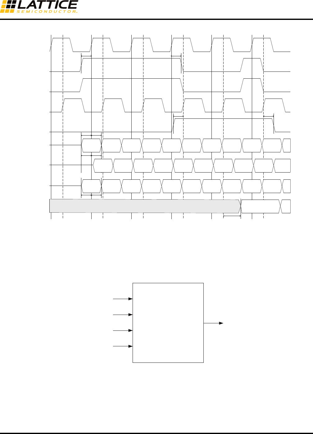
Figure 17. True Dual Port RAM Timing Waveform – NORMAL Mode, without Output Registers
Add_A0 Add_A1 Add_A0 Add_A1 Add_A2
Data_A0 Data_A1
Invalid Data Data_A0
ClockA
WrA
AddressA
DataA
QA
ClockEnA
t
SUWREN_EBR
t
HWREN_EBR
t
SUADDR_EBR
t
HADDR_EBR
t
SUDATA_EBR
t
HDATA_EBR
t
SUCE_EBR
t
HCE_EBR
t
CO_EBR
Data_A1 Data_A2
Add_B0 Add_B1 Add_B0 Add_B1 Add_B2
Data_B0 Data_B1
Invalid Data Data_B0
ClockB
WrB
AddressB
DataB
QB
ClockEnB
t
SUWREN_EBR
t
HWREN_EBR
t
SUADDR_EBR
t
HADDR_EBR
t
SUDATA_EBR
t
HDATA_EBR
t
SUCE_EBR
t
HCE_EBR
t
CO_EBR
Data_B1 Data_B2
17
Memory Usage Guide for MachXO3 Devices
Figure 18. True Dual Port RAM Timing Waveform – NORMAL Mode with Output Registers
Add_A0 Add_A1 Add_A0 Add_A1 Add_A2
Data_A0 Data_A1
ClockA
WrA
AddressA
DataA
QA
ClockEnA
t
SUWREN_EBR
t
HWREN_EBR
t
SUADDR_EBR
t
HADDR_EBR
t
SUDATA_EBR
t
HDATA_EBR
t
SUCE_EBR
t
HCE_EBR
Add_B0 Add_B1 Add_B0 Add_B1 Add_B2
Data_B0 Data_B1
Invalid Data Data_B0
ClockB
WrB
AddressB
DataB
QB
ClockEnB
t
SUWREN_EBR
t
HWREN_EBR
t
SUADDR_EBR
t
HADDR_EBR
t
SUDATA_EBR
t
HDATA_EBR
t
SUCE_EBR
t
HCE_EBR
t
COO_EBR
Data_B1
Invalid Data Data_A0
t
COO_EBR
Data_A1

18
Memory Usage Guide for MachXO3 Devices
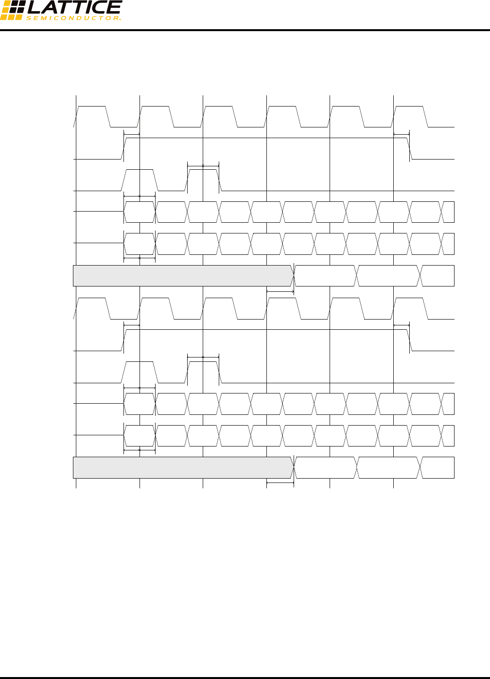
Figure 19. True Dual Port RAM Timing Waveform – READ BEFORE WRITE Mode, without Output Registers
Add_A0 Add_A0 Add_A1 Add_A1 Add_A2
New
Data_A0
New
Data_A1
Invalid Data New_Data_A0
ClockA
WrA
AddressA
DataA
QA
ClockEnA
tSUWREN_EBR tHWREN_EBR
tSUADDR_EBR tHADDR_EBR
tSUDATA_EBR tHDATA_EBR
tSUCE_EBR tHCE_EBR
tCO_EBR
Old_Data_A1Old_Data_A0 New_Data_A1
Add_B0 Add_B0 Add_B1 Add_B1 Add_B2
New
Data_B0
New
Data_B1
Invalid Data New_Data_B0
ClockB
WrB
AddressB
DataB
QB
ClockEnB
tSUWREN_EBR tHWREN_EBR
tSUADDR_EBR tHADDR_EBR
tSUDATA_EBR tHDATA_EBR
tSUCE_EBR tHCE_EBR
tCO_EBR
Old_Data_B1Old_Data_B0 New_Data_B1

19
Memory Usage Guide for MachXO3 Devices
Figure 20. True Dual Port RAM Timing Waveform – READ BEFORE WRITE Mode, with Output Registers
Add_A0 Add_A0 Add_A1 Add_A1 Add_A2
New
Data_A0
New
Data_A1
Invalid Data New_Data_A0
ClockA
WrA
AddressA
DataA
QA
ClockEnA
tSUWREN_EBR tHWREN_EBR
tSUADDR_EBR tHADDR_EBR
tSUDATA_EBR tHDATA_EBR
tSUCE_EBR tHCE_EBR
tCOO_EBR
Old_Data_A1Old_Data_A0 New
Data_A1
Add_B0 Add_B0 Add_B1 Add_B1 Add_B2
New
Data_B0
New
Data_B1
Invalid Data New_Data_B0
ClockB
WrB
AddressB
DataB
QB
ClockEnB
tSUWREN_EBR tHWREN_EBR
tSUADDR_EBR tHADDR_EBR
tSUDATA_EBR tHDATA_EBR
tSUCE_EBR tHCE_EBR
tCOO_EBR
Old_Data_B1Old_Data_B0 New
Data_B1

20
Memory Usage Guide for MachXO3 Devices
Figure 21. True Dual Port RAM Timing Waveform – WRITE THROUGH Mode, without Output Registers
Add_A0 Add_A1 Add_A0
Data_A0 Data_A1 Data_A2 Data_A3 Data_A4
Invalid Data
Data_A1
ClockA
WrA
AddressA
DataA
QA
ClockEnA
t
SUWREN_EBR
t
HWREN_EBR
t
SUADDR_EBR
t
HADDR_EBR
t
SUDATA_EBR
t
HDATA_EBR
t
SUCE_EBR
t
HCE_EBR
t
CO_EBR
Data_A2Data_A0 Data_A3 Data_A4
Add_B0 Add_B1 Add_B0
Data_B0 Data_B1 Data_B2 Data_B3 Data_B4
Invalid Data
Data_B1
ClockB
WrB
AddressB
DataB
QB
ClockEnB
t
SUWREN_EBR
t
HWREN_EBR
t
SUADDR_EBR
t
HADDR_EBR
t
SUDATA_EBR
t
HDATA_EBR
t
SUCE_EBR
t
HCE_EBR
t
CO_EBR
Data_B2Data_B0 Data_B3 Data_B4
21
Memory Usage Guide for MachXO3 Devices
Figure 22. True Dual Port RAM Timing Waveform – WRITE THROUGH Mode, with Output Registers
Pseudo Dual Port RAM (RAM_DP) – EBR Based
The EBR blocks in the MachXO3L/LF devices can be configured as Pseudo-Dual Port RAM (RAM_DP). IPexpress
allows users to generate the Verilog-HDL or VHDL netlists for various memory sizes depending on design require-
ments.
IPexpress generates the memory module as shown in Figure 23.
Add_A0 Add_A1 Add_A0
Data_A0 Data_A1 Data_A2 Data_A3 Data_A4
Invalid Data
Data_A1
ClockA
WrA
AddressA
DataA
QA
ClockEnA
t
SUWREN_EBR
t
HWREN_EBR
t
SUADDR_EBR
t
HADDR_EBR
t
SUDATA_EBR
t
HDATA_EBR
t
SUCE_EBR
t
HCE_EBR
t
COO_EBR
Data_A2Data_A0 Data_A3
Add_B0 Add_B1
Add_B0
Data_B0 Data_B1 Data_B2 Data_B3 Data_B4
Invalid Data
Data_B1
ClockB
WrB
AddressB
DataB
QB
ClockEnB
t
SUWREN_EBR
t
HWREN_EBR
t
SUADDR_EBR
t
HADDR_EBR
t
SUDATA_EBR
t
HDATA_EBR
t
SUCE_EBR
t
HCE_EBR
t
COO_EBR
Data_B2Data_B0 Data_B3
22
Memory Usage Guide for MachXO3 Devices
Figure 23. Pseudo Dual Port Memory Module Generated by IPexpress
Since the device has a number of EBR blocks, the generated module makes use of these EBR blocks, or primi-
tives, and cascades them to create the memory sizes specified by the user in the IPexpress GUI. For memory sizes
smaller than an EBR block, the module will be created in one EBR block. For memory sizes larger than one EBR
block, multiple EBR blocks can be cascaded in depth or width (as required to create these sizes).
In Pseudo Dual Port RAM mode, the input data and address for the ports are registered at the input of the memory
array. The output data of the memory is optionally registered at the output.
The various ports and their definitions for the Pseudo Dual Port Memory are listed in Table 3.
Table 3. EBR-Based Pseudo-Dual Port Memory Port Definitions
IPexpress implements the MachXO3L/LF Pseudo Dual Port RAM (RAM_DP) using the PDPW8KC primitive, or the
DP8KC primitive in narrow data port (9 bits or less) configurations.
Port Name
in the Generated Module Description Active State
WrAddress Write Address —
RdAddress Read Address —
Data Write Data —
*ByteEn1Byte Enable Active High
WE Write Enable Active High
RdClock Read Clock Rising Edge
RdClockEn2Read Clock Enable Active High
*ORdClockEn3Read Output Clock Enable Active High
Reset4Reset Active High
WrClock Write Clock Rising Edge
WrClockEn2Write Clock Enable Active High
Q Read Data —
*ERROR Error Check Code Active High
*Denotes optional port
1. ByteEn can be used to mask the input data so that only specific bytes of memory are overwritten.
2. RdClockEn/WrClockEn are used as clock enable for all the input registers.
3. ORdClockEn can be used as clock enable for the optional output registers. This allows the full pipeline of data to be
output, including the last word.
4. Reset resets only the optional output registers of the RAM. It does not reset the input registers or the contents of mem-
ory.
RAM_DP
EBR-Based
Pseudo Dual
Port Memory
WrAddress
Data
WE
RdClockEn
Reset
WrClockEn
Q
RdAddress
ByteEn
RdClock
ORdClockEn
WrClock
23
Memory Usage Guide for MachXO3 Devices
Figures 24 and 25 show the internal timing waveforms for the Pseudo Dual Port RAM (RAM_DP).
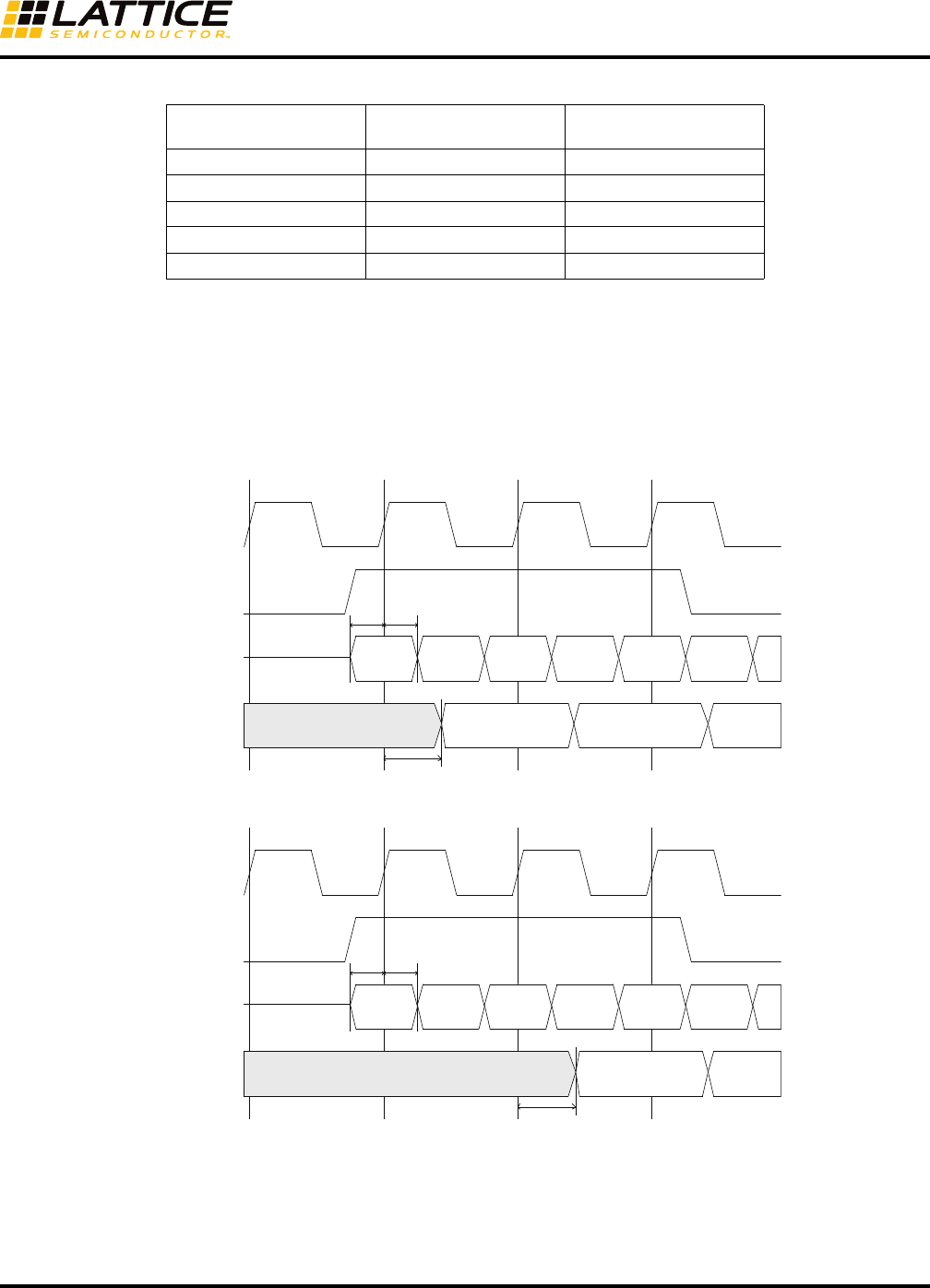
Figure 24. Pseudo-Dual Port RAM Timing Diagram – Without Output Registers
Figure 25. Pseudo-Dual Port RAM Timing Diagram – With Output Registers
Data_0 Data_1
Data_2
Invalid Data Data_0
WrClock
Data
Q
WrClockEn
t
SUDATA_EBR
t
HDATA_EBR
t
SUCE_EBR
t
HCE_EBR
t
CO_EBR
Data_1 Dat
a_2
Add_0 Add_1 Add_2
RdAddress
t
SUADDR_EBR
t
HADDR_EBR
RdClock
RdClockEn
t
SUCE_EBR
t
HCE_EBR
Add_0 Add_1 Add_2
WrAddress
t
SUADDR_EBR
t
HADDR_EBR
Data_0 Data_1 Data_2
Invalid Data Data_0
WrClock
Data
Q
WrClockEn
t
SUDATA_EBR
t
HDATA_EBR
t
SUCE_EBR
t
HCE_EBR
t
COO_EBR
Dat
a_1
Add_0 Add_1 Add_2
RdAddress
t
SUADDR_EBR
t
HADDR_EBR
RdClock
RdClockEn
t
SUCE_EBR
t
HCE_EBR
Add_0 Add_1 Add_2
WrAddress
t
SUADDR_EBR
t
HADDR_EBR
24
Memory Usage Guide for MachXO3 Devices
Read Only Memory (ROM) – EBR Based
The EBR blocks in the MachXO3L/LF devices can be configured as Read Only Memory (ROM). IPexpress allows
users to generate the Verilog-HDL or VHDL netlist for various memory sizes depending on design requirements.
Users are required to provide the ROM memory content in the form of an initialization file.
IPexpress generates the memory module as shown in Figure 26.
Figure 26. ROM – Read Only Memory Module Generated by IPexpress
Since the device has a number of EBR blocks, the generated module makes use of these EBR blocks, or primi-
tives, and cascades them to create the memory sizes specified by the user in the IPexpress GUI. For memory sizes
smaller than an EBR block, the module will be created in one EBR block. For memory sizes larger than one EBR
block, multiple EBR blocks can be cascaded in depth or width (as required to create these sizes).
The various ports and their definitions for the ROM are listed in Table 4.
Table 4. EBR-Based ROM Port Definitions
While generating the ROM using IPexpress, the user must provide the initialization file to pre-initialize the contents
of the ROM. These files are the *.mem files and they can be of Binary, Hex or the Addressed Hex formats. The ini-
tialization files are discussed in detail in the Initializing Memory section of this document.
IPexpress implements the MachXO3L/LF Read Only Memory (ROM) using an appropriately configured DP8KC
primitive with write-enables tied low.
Figures 27 and 28 show the internal timing waveforms for the Read Only Memory (ROM).
Port Name in
Generated Module Description Active State
Address Read Address —
OutClock Clock Rising Clock Edge
OutClockEn1Clock Enable Active High
Reset2Reset Active High
Q Read Data —
*ERROR Error Check Code Active High
*Denotes optional port
1. OutClockEn can be used as clock enable for the optional output registers.
2. Reset resets only the optional output registers of the ROM. It does not reset the contents of the
memory.
ROM
EBR-Based Read Only
Memory
OutClock
OutClockEn
Reset
Address
Q
25
Memory Usage Guide for MachXO3 Devices
Figure 27. ROM Timing Waveform – Without Output Registers
Figure 28. ROM Timing Waveform – With Output Registers
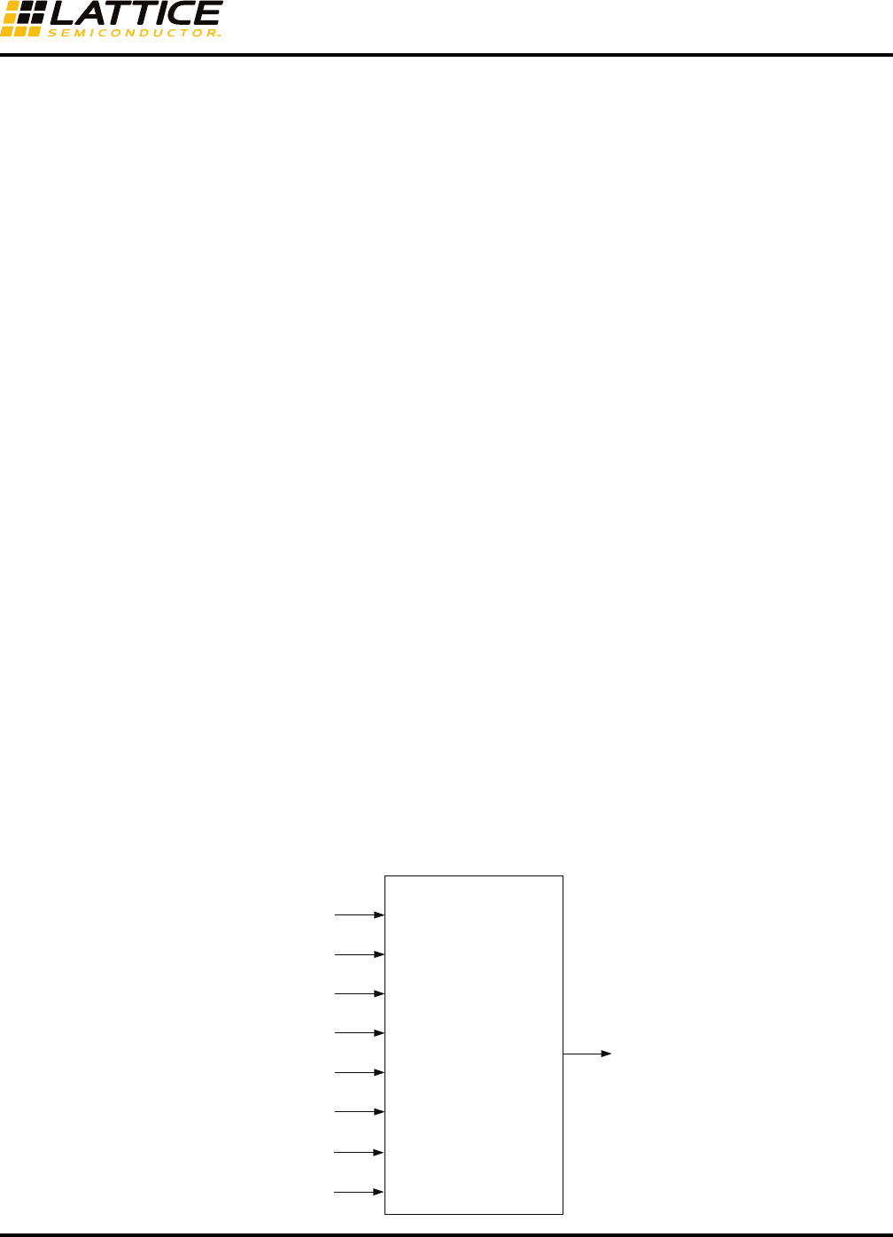
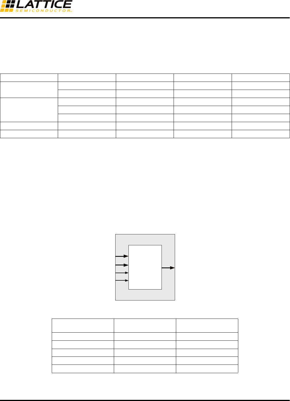
First In First Out (FIFO_DC) – EBR Based
The EBR blocks in MachXO devices can be configured as Dual-Clock First-In First-Out Memory (FIFO_DC). IPex-
press allows users to generate the Verilog-HDL or VHDL netlist for various memory sizes depending on design
requirements.
IPexpress generates the FIFO_DC memory module as shown in Figure 29.
Figure 29. FIFO Module Generated by IPexpress
Add_0 Add_1 Add_2 Add_3 Add_4
Invalid Data Data_0
OutClock
Address
Q
OutClockEn
t
SUADDR_EBR
t
HADDR_EBR
t
SUCE_EBR
t
HCE_EBR
t
CO_EBR
Data_1 Data_2 Data_3 Data_4
Add_0 Add_1 Add_2 Add_3 Add_4
Invalid Data Data_0
OutClock
Address
Q
OutClockEn
t
SUADDR_EBR
t
HADDR_EBR
t
SUCE_EBR
t
HCE_EBR
t
COO_EBR
Data_1 Data_2 Data_3
FIFO_DC
EBR-Based
First In First Out
Memory
Data
WrClock
WrEn
RdClock
AlmostFull
Q
Full
AlmostEmpty
Empty
RdEn
ORdEn
RPReset
Reset

26
Memory Usage Guide for MachXO3 Devices
Since the device has a number of EBR blocks, the generated module makes use of these EBR blocks, or primi-
tives, and cascades them to create the memory sizes specified by the user in the IPexpress GUI. For memory sizes
smaller than an EBR block, the module will be created in one EBR block. For memory sizes larger than one EBR
block, multiple EBR blocks can be cascaded in depth or width (as required to create these sizes).
In FIFO_DC mode, the input data is registered at the input of the memory array. The output data of the memory is
optionally registered at the output.
The various ports and their definitions for the FIFO_DC are listed in Table 5.
Table 5. EBR-Based FIFO_DC Memory Port Definitions
IPexpress implements the MachXO3L/LF Dual-Clock First-In First-Out Memory (FIFO_DC) using the FIFO8KB
primitive.
FIFO_DC Flags
The FIFO_DC have four flags available: Empty, Almost Empty, Almost Full and Full. Almost Empty and Almost Full
flags have a programmable range.
The program ranges for the four FIFO_DC flags are specified in Table 6.
Table 6. FIFO_DC Flag Settings
The value of Empty is fixed at 0. When coming out of reset, the active high flags Empty and Almost Empty are set
to high, since they are true.
Port Name in
Generated Module Description Active State
WrClock Write Port Clock Rising Clock Edge
RdClock Read Port Clock Rising Clock Edge
WrEn Write Enable Active High
RdEn Read Enable Active High
*ORdEn1Output Read Enable Active High
Reset2Reset Active High
RPReset3Read Pointer Reset Active High
Q Data Output —
Empty Empty Flag Active High
Full Full Flag Active High
AlmostEmpty Almost Empty Flag Active High
AlmostFull Almost Full Flag Active High
*ERROR Error Check Code Active High
*Denotes optional port
1. ORdEn can be used as clock enable for the optional output registers. This allows the full pipeline of
data to be output, including the last word.
2. Reset resets only the optional output registers, pointer circuitry and flags of the FIFO. It does not
reset the input registers or the contents of memory.
3. RPReset resets only the read pointer. See additional discussion below.
Module Flag Name Description Programming Range
Full Full flag setting 1 to (2N - 1)
AlmostFull Almost full setting 1 to (FULL -1)
AlmostEmpty Almost empty setting 1 to (FULL -1)
Empty Empty setting 0

27
Memory Usage Guide for MachXO3 Devices
The user should specify the absolute value of the address at which the Almost Empty and Almost Full flags will go
true. For example, if the Almost Full flag is required to go true at the address location 500 for a FIFO of depth 512,
the user should specify a value of 500 in IPexpress.
The Empty and Almost Empty flags are always registered to the read clock and the Full and Almost Full flags are
always registered to the write clock.
At reset both the write and read counters are pointing to address zero. After reset is de-asserted data can be writ-
ten into the FIFO_DC to the address pointed to by the write counter at the positive edge of the write clock when the
write enable is asserted
Similarly, data can be read from the FIFO_DC from the address pointed to by the read counter at the positive edge
of the read clock when read enable is asserted.
Read Pointer Reset (RPReset) is used to facilitate a retransmit operation and is more commonly used in “pack-
etized” communications. Asserting RPReset causes the internal read pointer to be reset to zero. It is typically used
in conjunction with the assertion of Reset prior to each new ‘packet’ which resets both read and write pointers to
zero. In this application, the user must keep careful track of when a packet is written into or read from the
FIFO_DC. To avoid the possible corruption of memory, RPReset should not be asserted until the prior read cycle is
complete (that is, RdEn deasserted for one clock period). Upon the deassertion of RPReset, the Empty and Almost
Empty flags assume their correct state after one read clock cycle – this is a regular condition known as boundary
cycle latency.
The data output of the FIFO_DC can be registered or non-registered through a selection in IPexpress. The output
registers are enabled by read enable.
FIFO_DC Dual and Dynamic Threshold Options
The optional Almost Full and Almost Empty flag thresholds may be individually set for single (default) or dual
threshold operation. In addition, the thresholds may be static at configuration (default) or dynamically set through
optional ports. The implementation of Dual or Dynamic thresholds automatically creates supporting LUT-based
logic.
Table 7. EBR-Based FIFO_DC Optional Dynamic Threshold Port Definitions
FIFO_DC Operation
If the output registers are not enabled it will take two clock cycles to read the first word out. The register for the flag
logic causes this extra clock latency. In the architecture of the emulated FIFO_DC, the internal read enables for
reading the data out is controlled not only by the read enable provided by the user but also the empty flag. When
the data is written into the FIFO, an internal empty flag is registered using write clock that is enabled by write
enable (WrEn). Another clock latency is added due to the clock domain transfer from write clock to read clock using
another register which is clocked by read clock that is enabled by read enable.
Internally, the output of this register is inverted and then ANDed with the user-provided read enable that becomes
the internal read enable to the RAM_DP which is at the core of the FIFO_DC.
Port Name in
Generated Module Description
AmEmptyThresh Almost Empty Single Threshold
AmFullThresh Almost Full Single Threshold
AmEmptySetThresh Almost Empty Set Threshold
AmEmptyClrThresh Almost Empty Clear Threshold
AmFullSetThresh Almost Full Set Threshold
AmFullClrThresh Almost Full Clear Threshold
28
Memory Usage Guide for MachXO3 Devices
Thus, the first read data takes two clock cycles to propagate through. During the first data out, read enable goes
high for one clock cycle, empty flag is de-asserted and is not propagated through the second register enabled by
the read enable. The first clock cycle brings the Empty Low and the second clock cycle brings the internal read
enable high (RdEn and !EF) and then the data is read out by the second clock cycle. Similarly, the first write data
after the full flag has a similar latency.
If the user has enabled the output registers, the output registers will cause an extra clock delay during the first data
out as they are clocked by the read clock and enabled by the read enable.
1. First RdEn and Clock Cycle to propagate the EF internally.
2. Second RdEn and Clock Cycle to generate internal Read Enable into the DPRAM.
3. Third RdEn and Clock Cycle to get the data out of the output registers.
Figures 30 and 31 show the internal timing waveforms for the Dual Clock FIFO (FIFO_DC).
Figure 30. FIFO_DC Without Output Registers (Non-Pipelined)
Invalid Data
Reset
Data
Q
t
SUDATA_EBR
t
HDATA_EBR
RPReset
WrClock
WrEn
RdClock
RdEn
Full
AlmostFull
Empty
AlmostEmpty
t
SUWREN_EBR
t
HWREN_EBR
t
CO_EBR
Data_4Data_3Data_2Data_1Data_0
Data_2Data_1 Data_4
Data_0 Data_3
29
Memory Usage Guide for MachXO3 Devices
Figure 31. FIFO_DC With Output Registers (Pipelined)
Distributed Single Port RAM (Distributed_SPRAM) – PFU Based
PFU-based Distributed Single Port RAM is created using the 4-input LUT (Look-Up Table) available in the PFU.
These LUTs can be cascaded to create a larger Distributed Memory sizes.
Figure 32 shows the Distributed Single Port RAM module as generated by IPexpress.
Figure 32. Distributed Single Port RAM Module Generated by IPexpress
The generated module makes use of the 4-input LUTs available in the PFU. Additional decode logic is generated
by utilizing the resources available in the PFU.
The various ports and their definitions for the Memory are as per Table 8.
Invalid Data
Reset
Data
Q
t
SUDATA_EBR
t
HDATA_EBR
RPReset
WrClock
WrEn
RdClock
RdEn
Full
AlmostFull
Empty
AlmostEmpty
t
SUWREN_EBR
t
HWREN_EBR
t
CO_EBR
Data_4Data_3Data_2Data_1Data_0
Data_2Data_1 Data_4Data_3
PFU-Based
Distributed Single Port
Memory
Clock
ClockEn
Reset
WE
Address
Q
Data
30
Memory Usage Guide for MachXO3 Devices
Table 8. PFU-Based Distributed Single Port RAM Port Definitions
Figures 33 and 34 show the internal timing waveforms for the Distributed Single Port RAM (Distributed_SPRAM).
Figure 33. PFU-Based Distributed Single Port RAM Timing Waveform – Without Output Registers
Port Name in
Generated Module Description Active State
Address Address —
Data Data In —
Clock Clock Rising Clock Edge
WE Write Enable Active High
ClockEn Clock Enable Active High
Reset1Reset Active High
Q Data Out —
1. Reset is available only when Output Registers are enabled.
Add_0 Add_1 Add_0 Add_1 Add_2
Data_0 Data_1
Invalid Data Data_0
Clock
WE
Address
Data
Q
ClockEn
t
HWREN_PFU
t
SUADDR_PFU
t
HADDR_PFU
t
SUDATA_PFU
t
HDATA_PFU
t
CORAM_PFU
Data_1 Data_2
t
SUWREN_PFU
31
Memory Usage Guide for MachXO3 Devices
Figure 34. PFU- Based Distributed Single Port RAM Timing Waveform – With Output Registers
Distributed Dual Port RAM (Distributed_DPRAM) – PFU Based
PFU-based Distributed Dual Port RAM is created using the 4-input LUT (Look-Up Table) available in the PFU.
These LUTs can be cascaded to create larger Distributed Memory sizes.
Figure 35 shows the Distributed Dual Port RAM module as generated by IPexpress.
Figure 35. Distributed Dual Port RAM Module Generated by IPexpress
The generated module makes use of the 4-input LUTs available in the PFU. Additional decode logic is generated
by utilizing the resources available in the PFU.
The various ports and their definitions are listed in Table 9.
Add_0 Add_1 Add_0 Add_1 Add_2
Data_0 Data_1
Invalid Data Data_0
Clock
WE
Address
Data
Q
ClockEn
t
HWREN_PFU
t
SUADDR_PFU
t
HADDR_PFU
t
SUDATA_PFU
t
HDATA_PFU
t
CO?
Data_1
t
SUWREN_PFU
PFU-Based
Distributed Dual Port
Memory
WrAddress
RdAddress
RdClock
RdClockEn
Reset
Q
WE
WrClock
WrClockEn
Data

32
Memory Usage Guide for MachXO3 Devices
Table 9. PFU-Based Distributed Dual Port RAM Port Definitions
The optional ports Read Clock (RdClock) and Read Clock Enable (RdClockEn) are not available in the hardware
primitive. These are generated by IPexpress when the user wants to enable the output registers in the IPexpress
configuration.
Figures 36 and 37 show the internal timing waveforms for the Distributed Dual Port RAM (Distributed_DPRAM).
Figure 36. PFU-Based Distributed Dual Port RAM Timing Waveform – Without Output Registers
Port Name in
Generated Module Description Active State
WrAddress Write Address —
Data Data Input —
WrClock Write Clock Rising Clock Edge
WE Write Enable Active High
WrClockEn Write Clock Enable Active High
RdAddress Read Address —
*RdClock Read Clock Rising Clock Edge
*RdClockEn Read Clock Enable Active High
Reset* Reset Active High
Q Data Out —
*Denotes optional port.
Data_0 Data_1 Data_2
Invalid Data Data_0
WrClock
Data
Q
WrClockEn
t
SUDATA_PFU
t
HDATA_PFU
t
SUCE_PFU
t
HCE_PFU
t
CORAM_PFU
Data_1 Dat
a_
2
Add_0 Add_1 Add_2RdAddress
t
SUADDR_PFU
t
HADDR_PFU
RdClock
RdClockEn
t
SUCE_PFU
t
HCE_PFU
Add_0 Add_1WrAddress
t
SUADDR_PFU
t
HADDR_PFU
WE
Add_2
33
Memory Usage Guide for MachXO3 Devices
Figure 37. PFU-Based Distributed Dual Port RAM Timing Waveform – With Output Registers
Distributed ROM (Distributed_ROM) – PFU-Based
PFU-based Distributed ROM is created using the 4-input LUT (Look-Up Table) available in the PFU. These LUTs
can be cascaded to create a larger Distributed Memory sizes.
Figure 38 shows the Distributed ROM module as generated by IPexpress.
Figure 38. Distributed ROM Generated by IPexpress
The generated module makes use of the 4-input LUTs available in the PFU. Additional decode logic is generated
by utilizing the resources available in the PFU.
The various ports and their definitions are listed in Table 10.
Data_0 Data_1 Data_2
Invalid Data Data_0
WrClock
Data
Q
WrClockEn
t
SUDATA_EBR
t
HDATA_EBR
t
SUCE_EBR
t
HCE_EBR
Dat
a_
1
Add_0 Add_1 Add_2RdAddress
t
SUADDR_EBR
t
HADDR_EBR
RdClock
RdClockEn
t
SUCE_EBR
t
HCE_EBR
Add_0 Add_1 Add_2WrAddress
t
SUADDR_EBR
t
HADDR_EBR
WE
PFU-Based
Distributed ROM
Address
OutClock
OutClockEn
Reset
Q
34
Memory Usage Guide for MachXO3 Devices
Table 10. PFU-Based Distributed ROM Port Definitions
The optional ports Out Clock (OutClock) and Out Clock Enable (OutClockEn) are not available in the hardware
primitive. These are generated by the IPexpress when the user wants to enable the output registers in the IPex-
press configuration.
Figures 39 and 40 show the internal timing waveforms for the Distributed ROM.
Figure 39. PFU-Based ROM Timing Waveform – Without Output Registers
Figure 40. PFU-Based ROM Timing Waveform – With Output Registers
Port Name in
Generated Module Description Active State
Address Address —
OutClock* Out Clock Rising Clock Edge
OutClockEn* Out Clock Enable Active High
Reset* Reset Active High
Q Data Out —
*Denotes optional port.
Add_0 Add_1 Add_2
Invalid Data Data_0
OutClock
Address
Q
OutClockEn
t
SUADDR_PFU
t
HADDR_PFU
t
CORAM_PFU
Data_1 Data_2
Add_0 Add_1 Add_2
Invalid Data Data_0
OutClock
Address
Q
OutClockEn
t
SUADDR_PFU
t
HADDR_PFU
Data_1
35
Memory Usage Guide for MachXO3 Devices
RAM-Based Shift Register
The Distributed SPRAM blocks in the MachXO3L/LF devices, in combination with LUT-based logic, can be config-
ured as a RAM-based Shift Register. IPexpress allows users to generate the Verilog-HDL or VHDL netlist for the
Shift Register length, as per design requirements.
IPexpress generates the Shift Register module as shown in Figure 41.
Figure 41. RAM-Based Shift Register Generated by IPexpress
The generated module makes use of the 4-input LUTs available in the PFU. Additional logic is generated by utiliz-
ing the resources available in the PFU.
The various ports and their definitions are listed in Table 11.
Table 11. RAM-Based Shift Register Port Definitions
The optional Addr port is available only when Variable Length type is selected. It is generated by IPexpress when
the user wants to enable the Variable Length operation in the IPexpress configuration. Figures 42 and 43 show the
internal timing waveforms for the RAM-Based Shift Register.
Port Name in
Generated Module Description Active State
Din Data In —
*Addr Address —
Clock Clock Rising Clock Edge
ClockEn Clock Enable Active High
Reset Reset Active High
Q Data Out —
*Denotes optional port.
RAM-Based
Shift Register
Addr
Clock
ClockEn
Reset
Q
Din
36
Memory Usage Guide for MachXO3 Devices
Figure 42. RAM-Based Shift Register Timing Waveform – Without Output Registers (Shift = 2)
Figure 43. RAM-Based Shift Register Timing Waveform – With Output Registers (Shift = 2)
Data_0 Data_1 Data_2 Data_3 Data_4
Invalid Data
Clock
Din
Q
ClockEn
tSUDATA_PFU tHDATA_PFU
tSUCE_PFU tHCE_PFU
tCO_RAM
Data_1 Data_2 Data_3Data_0
(SHIFT-1) Clock Periods
Delay
Data_0 Data_1 Data_2 Data_3 Data_4
Invalid Data
Clock
Din
Q
ClockEn
t
SUDATA_PFU
t
HDATA_PFU
t
SUCE_PFU
t
HCE_PFU
t
COREG
Data_0 Data_1 Data_2
(SHIFT) Clock Periods Delay
37
Memory Usage Guide for MachXO3 Devices
MachXO3L/LF Primitives
Single Port RAM (SP8KC) – EBR Based
The Single Port RAM primitive is shown below.
Figure 44. Single Port RAM (SP8KC)
Table 12. EBR-Based Single Port Memory Port Definitions
Each SP8KC primitive consists of 9,216 bits of RAM. The possible values for address depth and data width for the
SP8KC primitive are listed in Table 13.
Table 13. Single Port Memory Sizes for 9K Memories in MachXO3L/LF
Table 14 shows the various attributes available for the SP8KC. Some of these attributes are user selectable
through the IPexpress GUI. For detailed attribute definitions, refer to Appendix A. Attribute Definitions.
Port Name in the EBR
Block Primitive (SP8KC) Description Active State
AD Address Bus —
DI Data In —
CLK Clock Rising Clock Edge
CE Clock Enable Active High
OCE Output Clock Enable Active High
RST Reset Active High
WE Write Enable Active High
CS[2:0] Chip Select —
DO Data Out —
Single Port
Memory Size Input Data Output Data Address [MSB:LSB]
8K x 1 DI DO AD[12:0]
4K x 2 DI[1:0] DO[1:0] AD[12:1]
2K x 4 DI[3:0] DO[3:0] AD[12:2]
1K x 9 DI[8:0] DO[8:0] AD[12:3]
AD[12:0]
DI[8:0]
CLK
CE
RST
WE
DO[8:0]
CS[2:0]
EBR
OCE
38
Memory Usage Guide for MachXO3 Devices
Table 14. Single Port RAM Attributes for MachXO3L/LF (SP8KC)
True Dual Port RAM (DP8KC) – EBR-Based
The True Dual Port RAM primitive is shown below.
Figure 45. True Dual-Port RAM (DP8KC)
Attribute Description Values
Default
Value
User Selectable
through IPexpress
DATA_WIDTH Data Word Width 1, 2, 4, 9 9 Yes
REGMODE Register Mode (Pipelining) NOREG, OUTREG NOREG Yes
RESETMODE Selects Reset Type ASYNC, SYNC SYNC Yes
CSDECODE Chip Select Decode 0b000, 0b001, 0b010, 0b011,
0b100, 0b101, 0b110, 0b111
0b000
0b000 No
WRITEMODE Read/Write Behavior NORMAL, WRITE-
THROUGH, READBEFORE-
WRITE
NORMAL Yes
GSR Enable Global Set Reset ENABLED, DISABLED DISABLED No
INITVAL_00 .. INITVAL_1F Initialization Value 0x0000000000000000000000
000000000000000000000000
000000000000000000000000
0000000000
....
0xFFFFFFFFFFFFFFFFFFFF
FFFFFFFFFFFFFFFFFFFFFF
FFFFFFFFFFFFFFFFFFFFFF
FFFFFFFFFFFFFFFF
(80- character hex strings)
0x00000000000
0000000000000
0000000000000
0000000000000
0000000000000
0000000000000
0000
No
ASYNC_RESET_RELEASE Reset Release ASYNC, SYNC SYNC Yes
INIT_DATA (MachXO3LF
Only)
Init Values Status STATIC, DYNAMIC STATIC Yes
ADA[12:0]
DIA[8:0]
CLKA
CEA
RSTA
WEA
CSA[2:0]
EBR
DOA[8:0]
ADB[12:0]
DIB[8:0]
CLKB
CEB
RSTB
WEB
CSB[2:0]
DOB[8:0]
OCEA OCEB
39
Memory Usage Guide for MachXO3 Devices
Table 15. EBR-Based True Dual Port Memory Port Definitions
Each DP8KC primitive consists of 9,216 bits of RAM. The possible values for address depth and data width for the
DP8KC primitive are listed in Table 16.
Table 16. Dual Port Memory Sizes for 9K Memory in MachXO3L/LF
Table 17 shows the various attributes available for the True Dual Port Memory (RAM_DP_TRUE). Some of these
attributes are user-selectable through the IPexpress GUI. For detailed attribute definitions, refer to Appendix A.
Attribute Definitions.
Port Name in the EBR Block
Primitive (DP8KC) Description Active State
DIA, DIB Input Data port A and port B —
ADA, ADB Address Bus port A and port B —
CLKA, CLKB Clock for PortA and PortB Rising Clock Edge
CEA, CEB Clock Enables for Port CLKA and CLKB Active High
RSTA, RSTB Reset for PortA and PortB Active High
WEA, WEB Write enable port A and port B Active High
CSA[2:0], CSB[2:0] Chip Selects for each port —
OCEA, OCEB Output Clock Enables for PortA and PortB Active High
DOA, DOB Output Data port A and port B —
Dual Port
Memory Size
Input Data
Port A
Input Data
Port B
Output Data
Port A
Output Data
Port B
Address Port A
[MSB:LSB]
Address Port B
[MSB:LSB]
8K x 1 DIA DIB DOA DOB ADA[12:0] ADB[12:0]
4K x 2 DIA[1:0] DIB[1:0] DOA[1:0] DOB[1:0] ADA[12:1] ADB[12:1]
2K x 4 DIA[3:0] DIB[3:0] DOA[3:0] DOB[3:0] ADA[12:2] ADB[12:2]
1K x 9 DIA[8:0] DIB[8:0] DOA[8:0] DOB[8:0] ADA[12:3] ADB[12:3]

40
Memory Usage Guide for MachXO3 Devices
Table 17. Dual Port RAM Attributes for MachXO3L/LF (DP8KC)
Attribute Description Values
Default
Value
User Selectable
through IPexpress
DATA_WIDTH_A Data Word Width Port A 1, 2, 4, 9 9 Yes
DATA_WIDTH_B Data Word Width Port B 1, 2, 4, 9 9 Yes
REGMODE_A Register Mode (Pipelining)
for Port A
NOREG, OUTREG NOREG Yes
REGMODE_B Register Mode (Pipelining)
for Port B
NOREG, OUTREG NOREG Yes
RESETMODE Selects the Reset type ASYNC, SYNC SYNC Yes
CSDECODE_A Chip Select Decode
for Port A
0b000, 0b001, 0b010, 0b011,
0b100, 0b101, 0b110, 0b111
0b000 No
CSDECODE_B Chip Select Decode
for Port B
0b000, 0b001, 0b010, 0b011,
0b100, 0b101, 0b110, 0b111
0b000 No
WRITEMODE_A Read / Write Mode
for Port A
NORMAL, WRITE-
THROUGH, READBEFORE-
WRITE
NORMAL Yes
WRITEMODE_B Read / Write Mode
for Port B
NORMAL, WRITE-
THROUGH, READBEFORE-
WRITE
NORMAL Yes
GSR Enables Global Set Reset ENABLE, DISABLE DISABLED No
INITVAL_00 .. INITVAL_1F Initialization Value 0x0000000000000000000000
000000000000000000000000
000000000000000000000000
0000000000
....
0xFFFFFFFFFFFFFFFFFFFF
FFFFFFFFFFFFFFFFFFFFFF
FFFFFFFFFFFFFFFFFFFFFF
FFFFFFFFFFFFFFFF
(80-character hex strings)
0x00000000000
0000000000000
0000000000000
0000000000000
0000000000000
0000000000000
0000
No
ASYNC_RESET_RELEASE Reset Release ASYNC, SYNC SYNC Yes
INIT_DATA (MachXO3LF
Only)
Init Values Status STATIC, DYNAMIC STATIC Yes
41
Memory Usage Guide for MachXO3 Devices
Pseudo Dual Port RAM (PDPW8KC) – EBR-Based
The Pseudo Dual Port RAM primitive is shown below.
Figure 46. Pseudo Dual-Port RAM (PDPW8KC)
Table 18. EBR-Based Pseudo-Dual Port Memory Port Definitions
Each PDPW8KC primitive consists of 9,216 bits of RAM. The possible values for address depth and data width for
the PDPW8KC primitive are listed in Table 19.
Port Name in the EBR Block
Primitive (PDPW8KC) Description Active State
ADW Write Address —
DI Write Data —
BE Byte Enable Active High
CLKW Write Clock Rising Edge
CEW Write Clock Enable Active High
RST Reset Active High
CSW Write Chip Select —
ADR Read Address —
CLKR Read Clock Rising Edge
CER Read Clock Enable Active High
DO Read Data —
OCER Read Output Clock Enable Active High
CSR Read Chip Select —
ADW[8:0]
DI[17:0]
CLKW
CEW
RST
CSW[2:0]
ADR[12:0]
CLKR
CER
DO[17:0]
CSR[2:0]
OCER
BE[1:0]
EBR

42
Memory Usage Guide for MachXO3 Devices
Table 19. Pseudo-Dual Port Memory Sizes for 9K Memory in MachXO3L/LF
Table 20 shows the various attributes available for the Pseudo Dual Port Memory (RAM_DP). Some of these attri-
butes are user selectable through the IPexpress GUI. For detailed attribute definitions, refer to Appendix A. Attri-
bute Definitions.
Table 20. Pseudo-Dual Port RAM Attributes for MachXO3L/LF (PDPW8KC)
Pseudo-Dual Read
Port Memory Size Write Data Port Read Data Port
Read Address Port
[MSB:LSB]
Write Address Port
[MSB:LSB]
8K x 1 DI[17:0] DO ADR[12:0] ADW[8:0]
4K x 2 DI[17:0] DO[1:0] ADR[12:1] ADW[8:0]
2K x 4 DI[17:0] DO[3:0] ADR[12:2] ADW[8:0]
1K x 9 DI[17:0] DO[8:0] ADR[12:3] ADW[8:0]
512 x 18 DI[17:0] DO[17:0]* ADR[12:4] ADW[8:0]
Note: High and low bytes are swapped with regard to DI word.
Attribute Description Values Default Value
User Selectable
through IPexpress
DATA_WIDTH_W Write Data Word Width 18 18 Yes
DATA_WIDTH_R Read Data Word Width 1, 2, 4, 9, 18 9 Yes
REGMODE Register Mode (Pipelining) NOREG, OUTREG NOREG Yes
RESETMODE Selects the Reset type ASYNC, SYNC SYNC Yes
CSDECODE_W Chip Select Decode for
Write
0b000, 0b001, 0b010, 0b011,
0b100, 0b101, 0b110, 0b111
0b000 No
CSDECODE_R Chip Select Decode for
Read
0b000, 0b001, 0b010, 0b011,
0b100, 0b101, 0b110, 0b111
0b000 No
GSR Enables Global Set Reset ENABLE, DISABLE DISABLED No
INITVAL_00 .. INITVAL_1F Initialization Value 0x0000000000000000000000
000000000000000000000000
000000000000000000000000
0000000000
....
0xFFFFFFFFFFFFFFFFFFFF
FFFFFFFFFFFFFFFFFFFFFF
FFFFFFFFFFFFFFFFFFFFFF
FFFFFFFFF FFFFFFF
(80- character hex strings)
0x00000000000
0000000000000
0000000000000
0000000000000
0000000000000
0000000000000
0000
No
ASYNC_RESET_RELEASE Reset Release ASYNC, SYNC SYNC Yes
INIT_DATA (MachXO3LF
Only)
Init Values Status STATIC, DYNAMIC STATIC Yes
43
Memory Usage Guide for MachXO3 Devices
Dual-Clock FIFO (FIFO8KB) – EBR Based
The Dual-Clock FIFO RAM primitive is shown below.
Figure 47. FIFO_DC Primitive (FIFO8KB)
Table 21. EBR-Based FIFO_DC Memory Port Definitions
Each FIFO8KB primitive consists of 9,216 bits of RAM. The possible values for address depth and data width for
the FIFO8KB primitive are listed in Table 22.
Port Name in Primitive
(FIFO8KB) Description Active State
DI Data Input —
CLKW Write Port Clock Rising Clock Edge
WE Write Enable Active High
FULLI Write inhibit Active High
CSW Write Chip Select Active High
AFF Almost Full Flag Active High
FF Full Flag Active High
AEF Almost Empty Active High
EF Empty Flag Active High
DO Data Output —
ORE Output Read Enable Active High
CLKR Read Port Clock Rising Clock Edge
RE Read Enable Active High
EMPTYI Read inhibit Active High
CSR Read Chip Select Active High
RPRST Read Pointer Reset Active High
EBR
DI[17:0]
CLKW
WE DO[17:0]
RST
FULLI
AFF
FF
AEF
EF
CLKR
RE
CSR[1:0]
ORE
RPRST
CSW[1:0] EMPTYI

44
Memory Usage Guide for MachXO3 Devices
Table 22. MachXO3L/LF FIFO_DC Data Widths Sizes
Table 23 shows the various attributes available for the FIFO_DC. Some of these attributes are user-selectable
through the IPexpress GUI. For detailed attribute definitions, refer to Appendix A. Attribute Definitions.
Table 23. FIFO_DC Attributes for MachXO3L/LF (FIFO8KB)
FIFO Size Input Data Output Data
8K x 1 DI DO
4K x 2 DI[1:0] DO[1:0]
2K x 4 DI[3:0] DO[3:0]
1K x 9 DI[8:0] DO[8:0]
512 x 18 DI[17:0] DO[17:0]
Attribute Description Values Default Value
User Selectable
through IPexpress
DATA_WIDTH_W Data Width Write Mode 1, 2, 4, 9, 18 18 YES
DATA_WIDTH_R Data Width Read Mode 1, 2, 4, 9, 18 18 YES
REGMODE Register Mode NOREG, OUTREG NOREG YES
RESETMODE Select Reset Type ASYNC, SYNC ASYNC YES
CSDECODE_W Chip Select Decode for Write
Mode
0b00, 0b01, 0b10, 0b11 0b00 NO
CSDECODE_R Chip Select Decode for Read
Mode
0b00, 0b01, 0b10, 0b11 0b00 NO
GSR Enable Global Set Reset ENABLED, DISABLED DISABLED NO
AEPOINTER Almost Empty Pointer 0b00000000000000, .....,
0b01111111111111
—YES
AFPOINTER Almost Full Pointer 0b00000000000000, .....,
0b01111111111111
—YES
FULLPOINTER Full Pointer 0b00000000000000, .....,
0b10000000000000
—YES
FULLPOINTER1 Full Pointer minus 1 0b00000000000000, .....,
0b01111111111111
—NO
AFPOINTER1 Almost Full Pointer minus 1 0b00000000000000, .....,
0b01111111111110
—NO
AEPOINTER1 Almost Empty Pointer plus 1 0b00000000000000, .....,
0b10000000000000
—NO
ASYNC_RESET_RELEASE Reset Release ASYNC, SYNC SYNC Yes
INIT_DATA (MachXO3LF
Only)
Init Values Status STATIC, DYNAMIC STATIC Yes
45
Memory Usage Guide for MachXO3 Devices
FIFO_DC Flags
The FIFO_DC have four flags available: Empty, Almost Empty, Almost Full and Full. Almost Empty, Almost Full and
Full flags have a programmable range.
The program ranges for the four FIFO_DC flags are specified in Table 24.
Table 24. FIFO_DC Flag Settings
The value of Empty is fixed at 0. When coming out of reset, the active high flags Empty and Almost Empty are set
to high, since they are true.
Careful attention is required to set the Pointer attributes to match the desired behavior. Refer to Appendix B. Set-
ting FIFO_DC Pointer Attributes.
The Empty and Almost Empty flags are always registered to the read clock and the Full and Almost Full flags are
always registered to the write clock.
Distributed SPRAM (SPR16X4C) – PFU Based
The PFU based distributed single port RAM primitive is shown below.
Figure 48. Distributed_SPRAM Primitive (SPR16X4C)
Table 25. PFU based Distributed Single Port RAM Port Definitions
Module Flag Name FIFO Attribute Name Description Programming Range Program Bits
Full FULLPOINTER Full setting 1 to (2N - 1) 14
FULLPOINTER1 Full – 1 1 to (FULL-1) 14
AlmostFull
AFPOINTER Almost full setting 1 to (FULL -1) 14
AFPOINTER1 Almost full – 1 1 to (FULL -1) 14
AEPOINTER1 Almost empty + 1 1 to (FULL -1) 14
AlmostEmpty AEPOINTER Almost empty setting 1 to (FULL -1) 14
Empty — Empty setting 0 —
Port Name in the PFU
Primitive Description Active State
AD[3:0] Address —
DI[3:0] Data In —
CK Clock Rising Clock Edge
WRE Write Enable Active High
DO[3:0] Data Out —
AD[3:0]
CK
WRE
PFU
DO[3:0]
DI[3:0]
46
Memory Usage Guide for MachXO3 Devices
Distributed DPRAM (DPR16X4C) – PFU Based
The PFU based distributed Pseudo Dual-port RAM primitive is below.
Figure 49. Distributed DPRAM Primitive (DPR16X4C)
Table 26. PFU based Distributed Dual-Port RAM Port Definitions
Distributed ROM (ROMnnnX1A) – PFU Based
The PFU based distributed ROM primitives are shown below.
Figure 50. Distributed_ROM Primitive (ROM16X1A)
Figure 51. Distributed_ROM Primitive (ROM32X1A)
Port Name in the EBR
Block Primitive Description Active State
WAD[3:0] Write Address —
DI[3:0] Data Input —
WCK Write Clock Rising Clock Edge
WRE Write Enable Active High
RAD[3:0] Read Address —
DO[3:0] Data Out —
PFU
WAD[3:0]
WCK
WRE
DO[3:0]
DI[3:0]
RAD[3:0]
PFU
AD[3:0] DO
PFU
AD[4:0] DO
47
Memory Usage Guide for MachXO3 Devices
Figure 52. Distributed_ROM Primitive (ROM64X1A)
Figure 53. Distributed_ROM Primitive (ROM128X1A)
Figure 54. Distributed_ROM Primitive (ROM256X1A)
Table 27. PFU-Based Distributed ROM Port Definitions
Port Name in the PFU
Block Primitive Description
AD[n:0] Address
DO Data Out
PFU
AD[5:0] DO
PFU
AD[6:0] DO
PFU
AD[7:0] DO

48
Memory Usage Guide for MachXO3 Devices
Initializing Memory
In the EBR based ROM or RAM memory modes and the PFU-based ROM memory mode, it is possible to specify
the power-on state of each bit in the memory array. Each bit in the memory array can have one of two values: 0 or
1.
Initialization File Format
The initialization file is an ASCII file, which can be created or edited using any ASCII editor. IPexpress supports
three different types of memory file formats:
1. Binary file
2. Hex File
3. Addressed Hex
The file name for the memory initialization file is *.mem (<file_name>.mem). Each row depicts the value to be
stored in a particular memory location and the number of characters (or the number of columns) represents the
number of bits for each address (or the width of the memory module).
The initialization file is primarily used for configuring the ROMs. The EBR in RAM can also use the initialization file
to preload the memory contents.
Binary File
The file is a text file of 0’s and 1’s. The rows indicate the number of words and columns indicate the width of the
memory. In the example below, the memory size is 20x32; that is 20 addresses with each word of 32 bit length.
00100000010000000010000001000000
00000001000000010000000100000001
00000010000000100000001000000010
00000011000000110000001100000011
00000100000001000000010000000100
00000101000001010000010100000101
00000110000001100000011000000110
00000111000001110000011100000111
00001000010010000000100001001000
00001001010010010000100101001001
00001010010010100000101001001010
00001011010010110000101101001011
00001100000011000000110000001100
00001101001011010000110100101101
00001110001111100000111000111110
00001111001111110000111100111111
00010000000100000001000000010000
00010001000100010001000100010001
00010010000100100001001000010010
00010011000100110001001100010011

49
Memory Usage Guide for MachXO3 Devices
Hex File
The Hex file is a text file of hex characters arranged in a similar row-column arrangement. The number of rows in
the file is same as the number of address locations, with each row indicating the content of the memory location. In
the example below, the memory size is 8x16; that is 8 addresses with each word of 16 bit length.
A001
0B03
1004
CE06
0007
040A
0017
02A4
Addressed Hex
Addressed Hex consists of lines of address and data. Each line starts with an address, followed by a colon, and
any number of data. The format of memfile is address: data data data data ... where address and data are hexa-
decimal numbers.
–A0 : 03 F3 3E 4F
–B2 : 3B 9F
The first line puts 03 at address A0, F3 at address A1, 3E at address A2,and 4F at address A3. The second line
puts 3B at address B2 and 9F at address B3.
There is no limitation on the values of address and data. The value range is automatically checked based on the
values of addr_width and data_width. If there is an error in an address or data value, an error message is printed.
Users need not specify data at all address locations. If data is not specified at certain address, the data at that loca-
tion is initialized to 0. IPexpress makes memory initialization possible both through the synthesis and simulation
flows.

50
Memory Usage Guide for MachXO3 Devices
Technical Support Assistance
e-mail: techsupport@latticesemi.com
Internet: www.latticesemi.com
Revision History
Date Version Change Summary
March 2015 1.1 General updates:
— Product name/trademark adjustment.
— Added MachXO3LF support.
— Changed ispLEVER to Diamond.
Updated Introduction section.
— Added UFM information.
Updated Memories in MachXO3L/LF Devices section.
— Revised Figure 1, Top View of the MachXO3L-1300 Device and
Figure 2, Top View of the MachXO3L-4300 Device. Added UFM.
Updated IPexpress Flow section.
— Indicated MachXO3L in Figure 5, Example Generating Pseudo Dual
Port RAM (RAM_DP) Module Customization (MachXO3L).
— Added Figure 6, Example Generating Pseudo Dual Port RAM
(RAM_DP) Module Customization (MachXO3LF).
— Added information on storing memory initialization data in UFM.
Updated MachXO3L/LF Primitives section.
Revised the following tables to add INIT_DATA (MachXO3LF Only) attri-
bute:
— Table 14, Single Port RAM Attributes for MachXO3L/LF
— Table 17, Dual Port RAM Attributes for MachXO3L/LF (DP8KC)
— Table 20, Pseudo-Dual Port RAM Attributes for MachXO3L/LF
(PDPW8KC)
— Table 23, FIFO_DC Attributes for MachXO3L (FIFO8KB)
Updated Appendix A. Attribute Definitions section.
Added INIT_DATA (MachXO3LF Only)
April 2014 01.0 Initial release.

51
Memory Usage Guide for MachXO3 Devices
Appendix A. Attribute Definitions
DATA_WIDTH
Data width is associated with the RAM and FIFO elements. The DATA_WIDTH attribute defines the number of bits
in each word. It takes the values defined in the RAM size tables in each memory module.
REGMODE
REGMODE, or the Register mode attribute, is used to enable pipelining in the memory. This attribute is associated
with the RAM and FIFO elements. The REGMODE attribute takes the NOREG or OUTREG mode parameter that
disables and enables the output pipeline registers.
RESETMODE
The RESETMODE attribute allows users to select the mode of reset in the memory. This attribute is associated
with the block RAM elements. RESETMODE takes two parameters: SYNC and ASYNC. SYNC means that the
memory reset is synchronized with the clock. ASYNC means that the memory reset is asynchronous to clock.
CSDECODE
CSDECODE, or the Chip Select Decode attributes, are associated to block RAM elements. Chip Select (CS) is a
useful port when multiple cascaded EBR blocks are required by the memory. The CS signal forms the MSB for the
address when multiple EBR blocks are cascaded. CS is a 3-bit bus, so it can cascade eight memories easily.
CSDECODE takes the following parameters: “000”, “001”, “010”, “011”, “100”, “101”, “110”, and “111”. CSDECODE
values determine the decoding value of CS[2:0]. CSDECODE_W is chip select decode for write and
CSDECODE_R is chip select decode for read for Pseudo Dual Port RAM. CSDECODE_A and CSDECODE_B are
used for true dual port RAM elements and refer to the A and B ports.
WRITEMODE
The WRITEMODE attribute is associated with the block RAM elements. It takes the NORMAL, WRITETHROUGH,
and READBEFOREWRITE mode parameters.
In NORMAL mode, the output data does not change or get updated during the write operation. This mode is sup-
ported for all data widths.
In WRITETHROUGH mode, the output data is updated with the input data during the write cycle. This mode is sup-
ported for all data widths.
In READBEFOREWRITE mode, the output data port is updated with the existing data stored in the write address,
during a write cycle. This mode is supported for x9 and x18 data widths.
WRITEMODE_A and WRITEMODE_B are used for dual port RAM elements and refer to the A and B ports in case
of a True Dual Port RAM.
For all modes of the True Dual Port module, simultaneous read access from one port and write access from the
other port to the same memory address is not recommended. The read data may be unknown in this situation.
Also, simultaneous write access to the same address from both ports is not recommended. When this occurs, the
data stored in the address becomes undetermined when one port tries to write a 'H' and the other tries to write a
'L'.
It is recommended that users implement control logic to identify this situation if it occurs and then either:
1. Implement status signals to flag the read data as possibly invalid, or
2. Implement control logic to prevent the simultaneous access from both ports.
GSR
GSR, the Global Set/ Reset attribute, is used to enable or disable the global set/reset for the RAM element.

52
Memory Usage Guide for MachXO3 Devices
ASYNC_RESET_RELEASE
When RESETMODE is set to ASYNC, the ASYNC_RESET_RELEASE attribute allows users to select how the
reset is de-asserted/released: When set to SYNC, the reset is de-asserted synchronously to the clock. When set to
ASYNC, the memory reset is released asynchronously (without relation to the clock).
INIT_DATA (MachXO3LF Only)
The INIT_DATA attribute allows the user to specify how EBR initialization values are stored and accessed. When
set to STATIC, the EBR initialization values are compressed by the software and stored in a variable location in
UFM (User Flash Memory). When set to DYNAMIC, the initialization values are not compressed, and stored in a
user-accessible, fixed location in UFM.
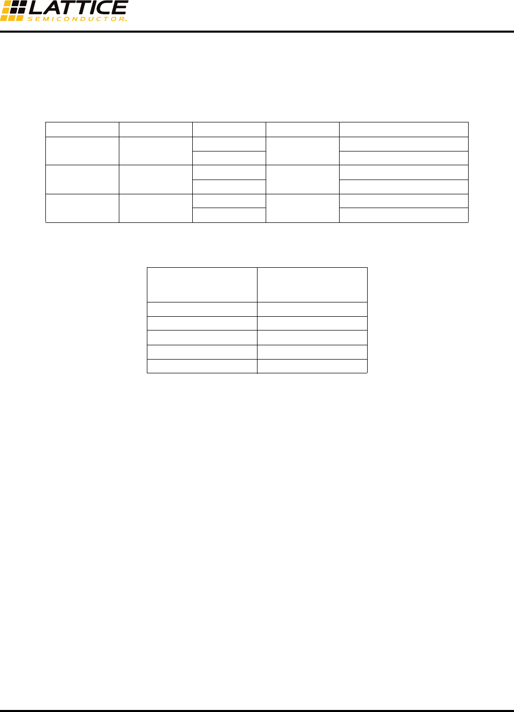
53
Memory Usage Guide for MachXO3 Devices
Appendix B. Setting FIFO_DC Pointer Attributes
The FIFO_DC uses pointer attributes to control the Full, Almost Full and Almost Empty flags.
The values for the pointer attributes are set according to the following table and equations:
Table 28. Pointer Attribute Setting Equations
Table 29. Port Width Values
The user should specify the absolute value of the address at which the Almost Empty and Almost Full flags will go
true. For example, if the Almost Full flag is required to go true at the address location 500 for a FIFO of depth 512,
the user should specify aff = 500.
Worked Example:
Write Data Width: 18 => use wrw=16
Read Data Width: 4 => use rdw = 4
Full: ff =16 ( (16) 18-bit words)
Almost Full: aff = 14
Almost Empty: aef = 8 ( (8) 4-bit words, which corresponds to (2) 16-bit writes)
Empty: 0 (always)
Flag Trip Value Attribute Port Width Equation
Full ff FULLPOINTER wrw1[(ff - 1) * wrw] + 1
FULLPOINTER1 [(ff - 2) * wrw] + 1
Almost Full aff AFPOINTER wrw1[(aff - 1) * wrw] + 1
AFPOINTER1 [(aff - 2) * wrw] + 1
Almost Empty aef AEPOINTER rdw1[(aef) * rdw] + rdw - 1
AEFOINTER1 [(aef + 1) * rdw] + rdw - 1
1. Set Write Port Width (wrw) and Read Port Width (rdw) per Table 29.
Attribute:
Data_width_w,
Data_width_r Port Width: wrw, rdw
11
22
44
98
18 16

54
Memory Usage Guide for MachXO3 Devices
Calculated Values:
FULLPOINTER = [(ff - 1) * wrw] + 1
= [(16 – 1) * 16] + 1
= (15 * 16) + 1
= 241
=> 14’ b00_0000_1111_0001
FULLPOINTER1 = [(ff - 2) * wrw] + 1
= [(16 – 2) * 16] + 1
= (14 * 16) + 1
= 225
=> 14’ b00_0000_1110_0001
AFPOINTER = [(aff - 1) * wrw] + 1
= [(14 – 1) * 16] + 1
= (13 * 16) + 1
= 209
=> 14’ b00_0000_1101_0001
AFPOINTER1 = [(aff - 2) * wrw] + 1
= [(14 – 2) * 16] + 1
= (12 * 16) + 1
= 193
=> 14’ b00_0000_1100_0001
AEPOINTER = [(aef) * rdw] + rdw - 1
= (8 * 4) + 4 - 1
= (8 * 4) + 3
= 35
=> 14’ b00_0000_0010_0011
AEFOINTER1 = [(aef + 1) * rdw] + rdw - 1
= [(8+1) * 4] + 4 - 1
= (9 * 4) + 3
= 39
=> 14’ b00_0000_0010_0111
