TN1294 Hardened Control Functions In MachXO3 Devices Reference Guide Using Mach XO3
User Manual:
Open the PDF directly: View PDF ![]() .
.
Page Count: 80
- Using Hardened Control Functions in MachXO3 Devices Reference Guide
- Introduction
- Hardened I2C IP Cores
- Typical I2C Transactions
- I2C Functional Waveforms
- I2C Timing Diagram
- I2C Simulation Model
- Hardened SPI IP Core
- SPI Registers
- Typical SPI Transactions
- SPI Functional Waveforms
- SPI Timing Diagrams
- SPI Simulation Model
- Hardened Timer/Counter PWM
- Timer Counter Simulation Model
- NVCM (MachXO3L)/Flash(MachXO3LF) Access
- Interface to NVCM/Flash
- Command Framing
- NVCM1/Flash Write and Read Examples
- NVCM/Flash Performance
- Erase/Program/Verify Time Calculation Example
- Technical Support Assistance
- Revision History

www.latticesemi.com 1TN1294_1.7
December 2016 Technical Note TN1294
© 2016 Lattice Semiconductor Corp. All Lattice trademarks, registered trademarks, patents, and disclaimers are as listed at www.latticesemi.com/legal. All other brand
or product names are trademarks or registered trademarks of their respective holders. The specifications and information herein are subject to change without notice.
Introduction
This reference guide supplements TN1293, Using Hardened Control Functions in MachXO3 Devices which
explains the software usage. In this document you will find:
• WISHBONE Protocol
• EFB Register Map
• Command Sequences
• Examples
As an overview, the MachXO3™ FPGA family combines a high-performance, low power, FPGA fabric with built-in,
hardened control functions. The hardened control functions ease design implementation and save general purpose
resources such as LUTs, registers, clocks and routing. The hardened control functions are physically located in the
Embedded Function Block (EFB). All MachXO3L/LF devices include an EFB module. The EFB block includes the
following control functions:
•Two I
2C Cores
• One SPI Core
• One 16-bit Timer/Counter
• (MachXO3L) Interface to NVCM memory
• (MachXO3LF) Interface to Flash memory which includes:
— User Flash Memory for MachXO3LF-640 and higher densities
— Configuration logic
• Interface to Dynamic PLL configuration settings
• Interface to On-chip Power Controller through I2C and SPI
Using Hardened Control Functions in
MachXO3 Devices Reference Guide
2
Using Hardened Control Functions
in MachXO3 Devices Reference Guide
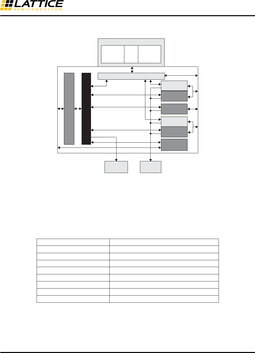
Figure 1 shows the EFB architecture and the interface to the FPGA core logic.
Figure 1. Embedded Function Block (EFB)
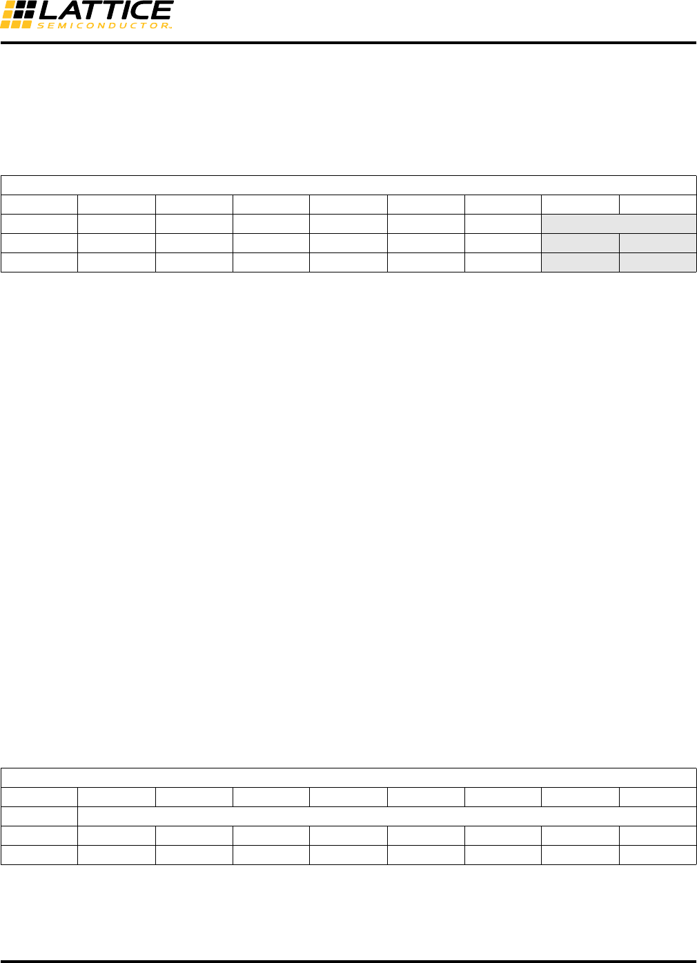
EFB Register Map
The EFB module has a Register Map to allow the service of the hardened functions through the WISHBONE bus
interface read/write operations. Each hardened function has dedicated 8-bit Data and Control registers, with the
exception of the NVCM/Flash, which are accessed through the same set of registers. Table 1 documents the regis-
ter map of the EFB module. The PLL registers are located in the NVCM/Flash in MachXO3L/LF devices PLL mod-
ules, but they are accessed through EFB WISHBONE read/write cycles.
Table 1. EFB Register Map1, 2, 3
Address spaces that are not defined in Table 1 are invalid and will result in non-deterministic results. It is the
responsibility of the designer to ensure valid addresses are presented to the EFB WISHBONE slave interface.
Address (Hex) Hardened Function
0x00-0x1F PLL0 Dynamic Access1
0x20-0x3F PLL1 Dynamic Access1
0x40-0x49 I2C Primary
0x4A-0x53 I2C Secondary
0x54-0x5D SPI
0x5E-0x6F Timer/Counter
0x70-0x75 NVCM/Flash
0x76-0x77 EFB Interrupt Source
1. There can be up to two PLLs in a MachXO3L/LF device. PLL0 has an address range from 0x00 to
0x1F. PLL1 (if present) has an address range from 0x20 to 0x3F. TN1282, MachXO3 sysCLOCK
PLL Design and Usage Guide, for details on PLL configuration registers and recommended usage.
2. NVCM in MachXO3L devices.
3. Flash in MachXO3LF devices.
Configuration
NVCM0/Flash
(including
USERCODE)
NVCM1/
UFM
NVCM/Flash Command Interface
NVCM/Flash
EFB Register Map
Configuration
Master/Slave
User
Master/Slave
SPI Port
WISHBONE Interface
EFB
Power
Controller
Secondary
I2C Port
Primary
I2C Port
PLL0/
PLL1
Timer/
Counter
Configuration
Slave
User
Master/Slave
User
Master/Slave
User Logic
User Logic
JTAG
OR
Feature Row
(including
TraceID)
Notes:
1. Only MachXO3L devices have NVCM.
2. Only MachXO3LF devices have Flash.
3
Using Hardened Control Functions
in MachXO3 Devices Reference Guide
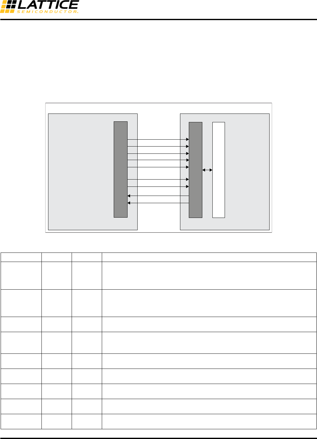
WISBONE Bus Interface
The WISHBONE Bus in the MachXO3L/LF is compliant with the WISHBONE standard from OpenCores. It pro-
vides connectivity between FPGA user logic and the EFB functional blocks. The user can implement a WISHBONE
Master interface to interact with the EFB WISHBONE slave interface or a LatticeMico8™ soft processor core can
be used to interact with the EFB WISHBONE.
The block diagram in Figure 2 shows the supported WISHBONE bus signals between the FPGA core and the EFB.
Table 2 provides a detailed definition of the supported signals.
Figure 2. WISHBONE Bus Interface Between the FPGA Core and the EFB Module
Table 2. WISHBONE Slave Interface Signals of the EFB Module
Signal Name I/O Width Description
wb_clk_i Input 1
Positive edge clock used by WISHBONE Interface registers and hardened functions
within the EFB module. Supports clock speeds up to 133 MHz. When used in con-
junction with the I2C User Slave or Configuration Slave ports, the clock speed must be
at least 7.5x the I2C bus speed (for example, >3.0 MHz when I2C rate = 400 kHz).
wb_rst_i Input 1
Active-high, synchronous reset signal that will only reset the WISHBONE interface
logic. This signal will not affect the contents of any registers. It will only affect ongoing
bus transactions. Wait 1us after de-assertion before starting any subsequent WISH-
BONE transactions.
wb_cyc_i Input 1 Active-high signal, asserted by the WISHBONE master, indicates a valid bus cycle is
present on the bus.
wb_stb_i Input 1
Active-high strobe, input signal, indicating the WISHBONE slave is the target for the
current transaction on the bus. The EFB module asserts an acknowledgment in
response to the assertion of the strobe.
wb_we_i Input 1 Level sensitive Write/Read control signal. Low indicates a Read operation, and High
indicates a Write operation.
wb_adr_i Input 8 8-bit wide address used to select a specific register from the register map of the EFB
module.
wb_dat_i Input 8 8-bit input data path used to write a byte of data to a specific register in the register
map of the EFB module.
wb_dat_o Output 8 8-bit output data path used to read a byte of data from a specific register in the regis-
ter map of the EFB module.
wb_ack_o Output 1 Active-high, transfer acknowledge signal asserted by the EFB module, indicating the
requested transfer is acknowledged.
EFB Register Map
WISHBONE Slave Interface
EFB
wb_clk_i
WISHBONE Master (User Logic)
wb_rst_i
wb_cyc_i
wb_stb_i
wb_we_i
wb_addr_i[7:0]
wb_dat_i[7:0]
wb_dat_o[7:0]
wb_ack_o
MachXO3
User Logic

4
Using Hardened Control Functions
in MachXO3 Devices Reference Guide
To interface to the EFB you must create a WISHBONE Master controller in the User Logic. In a multiple-Master
configuration, the WISHBONE Master outputs are multiplexed in a user-defined arbiter. A LatticeMico8 soft proces-
sor can also be utilized along with the Mico System Builder (MSB) platform which can implement multi-Master bus
configurations. If two Masters request the bus in the same cycle, only the outputs of the arbitration winner reach the
Slave interface.
The EFB WISHBONE bus supports the “Classic” version of the WISHBONE standard. Given that the WISHBONE
bus is an open source standard, not all features of the standard are implemented or required:
• Tags are not supported in the WISHBONE Slave interface of the EFB module. Given that the EFB is a hardened
block, these signals cannot be added by the user.
• The Slave WISHBONE bus interface of the EFB module does not require the byte select signals (sel_i or sel_o),
since the data bus is only a single byte wide.
• The EFB WISHBONE slave interface does not support the optional error and retry access termination signals. If
the slave receives an access to an invalid address, it will simply respond by asserting wb_ack_o signal. It is the
responsibility of the user to stay within the valid address range.
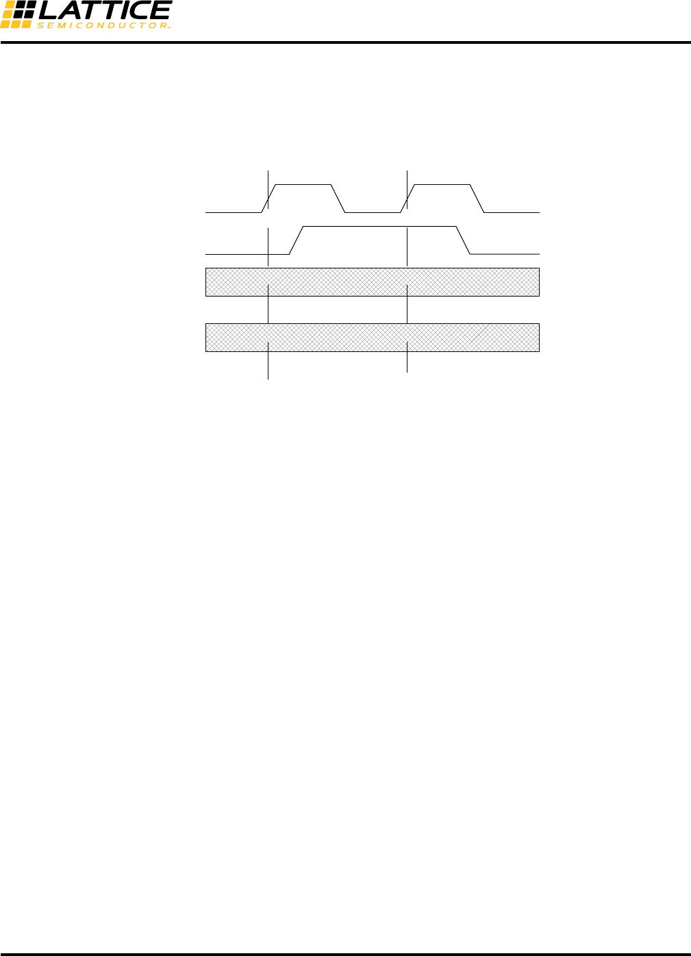
WISHBONE Write Cycle
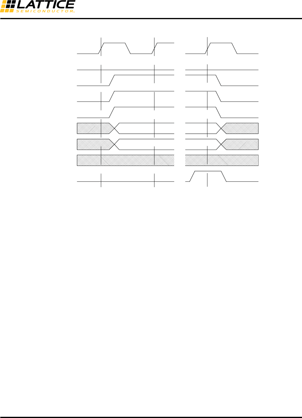
Figure 3 shows the waveform of a Write cycle from the perspective of the EFB WISHBONE Slave interface. During
a single Write cycle, only one byte of data is written to the EFB block from the WISHBONE Master. A Write opera-
tion requires a minimum three clock cycles.
On clock Edge 0, the Master updates the address, data and asserts control signals. During this cycle:
• The Master updates the address on the wb_adr_i[7:0] address lines
• Updates the data that will be written to the EFB block, wb_dat_i[7:0] data lines
• Asserts the write enable wb_we_i signal, indicating a write cycle
• Asserts the wb_cyc_i to indicate the start of the cycle
• Asserts the wb_stb_i, selecting a specific slave module
On clock Edge 1, the EFB WISHBONE Slave decodes the input signals presented by the master. During this cycle:
• The Slave decodes the address presented on the wb_adr_i[7:0] address lines
• The Slave prepares to latch the data presented on the wb_dat_i[7:0] data lines
• The Master waits for an active-high level on the wb_ack_o line and prepares to terminate the cycle on the next
clock edge, if an active-high level is detected on the wb_ack_o line
• The EFB may insert wait states before asserting wb_ack_o, thereby allowing it to throttle the cycle speed. Any
number of wait states may be added
• The Slave asserts wb_ack_o signal
The following occurs on clock Edge 2:
• The Slave latches the data presented on the wb_dat_i[7:0] data lines
• The Master de-asserts the strobe signal, wb_stb_i, the cycle signal, wb_cyc_i, and the write enable signal,
wb_we_i
• The Slave de-asserts the acknowledge signal, wb_ack_o, in response to the Master de-assertion of the strobe
signal
5
Using Hardened Control Functions
in MachXO3 Devices Reference Guide
Figure 3. WISHBONE Bus Write Operation
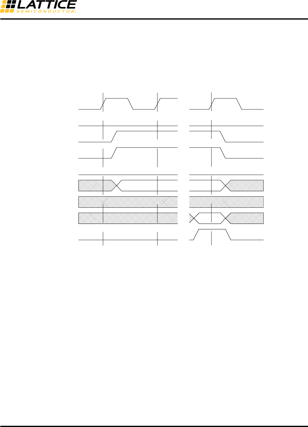
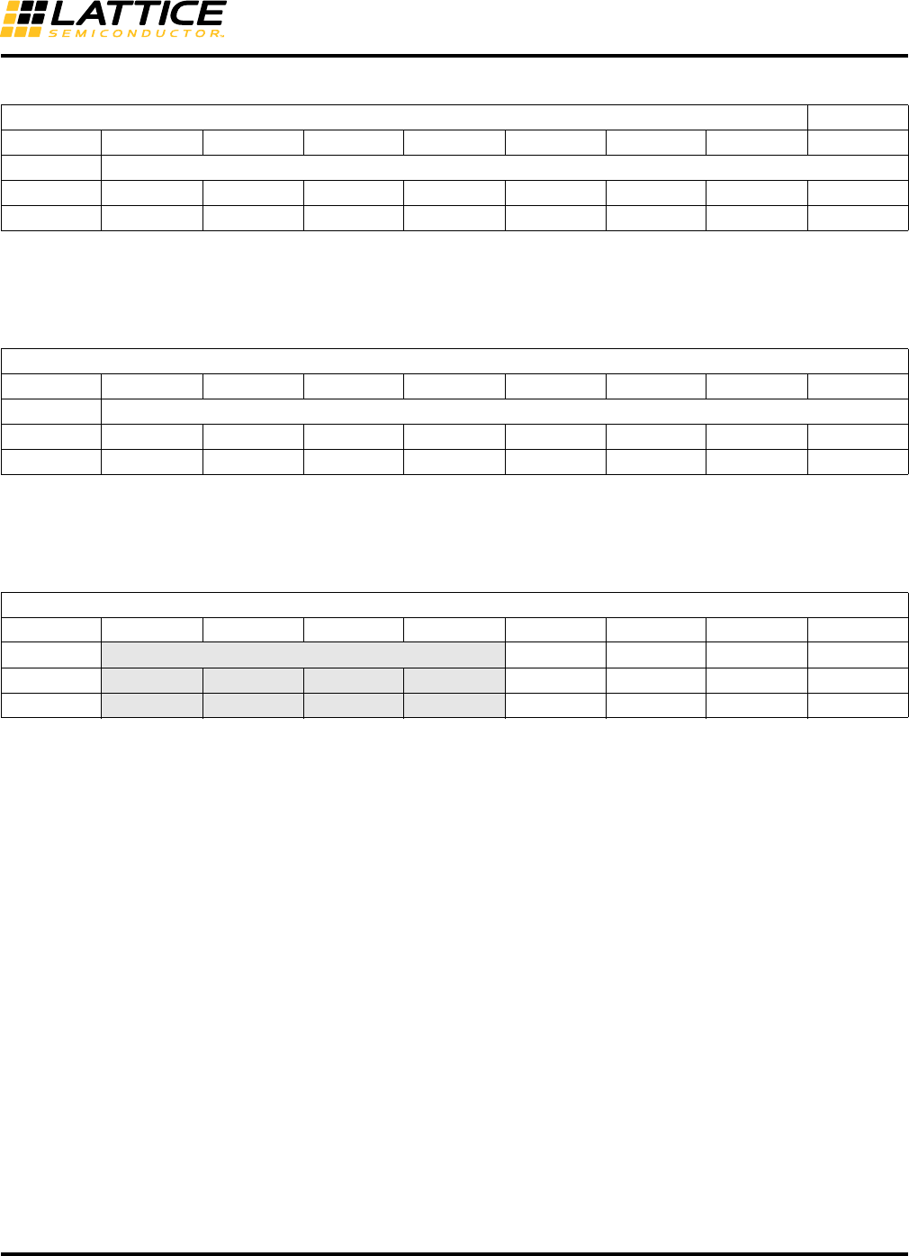
WISHBONE Read Cycle
Figure 4 shows the waveform of a Read cycle from the perspective of the EFB WISHBONE Slave interface. During
a single Read cycle, only one byte of data is read from the EFB block by the WISHBONE master. A Read operation
requires a minimum three clock cycles.
On clock Edge 0, the Master updates the address, data and asserts control signals. The following occurs during
this cycle:
• The Master updates the address on the wb_adr_i[7:0] address lines
• De-asserts the write enable wb_we_i signal, indicating a Read cycle
• Asserts the wb_cyc_i to indicate the start of the cycle
• Asserts the wb_stb_i, selecting a specific Slave module
On clock Edge 1, the EFB WISHBONE slave decodes the input signals presented by the master. The following
occurs during this cycle:
• The Slave decodes the address presented on the wb_adr_i[7:0] address lines
• The Master prepares to latch the data presented on wb_dat_o[7:0] data lines from the EFB WISHBONE slave on
the following clock edge
• The Master waits for an active-high level on the wb_ack_o line and prepares to terminate the cycle on the next
clock edge, if an active-high level is detected on the wb_ack_o line
• The EFB may insert wait states before asserting wb_ack_o, thereby allowing it to throttle the cycle speed. Any
number of wait states may be added.
• The Slave presents valid data on the wb_dat_o[7:0] data lines
• The Slave asserts wb_ack_o signal in response to the strobe, wb_stb_i signal
wb_clk_i
wb_rst_i
wb_cyc_i
wb_stb_i
wb_we_i
wb_adr_i [7:0]
wb_dat_i [7:0]
wb_dat_o [7:0]
wb_ack_o
VALID ADDRESS
VALID DATA
Edge 0 Edge 1 Edge 2
6
Using Hardened Control Functions
in MachXO3 Devices Reference Guide
The following occurs on clock Edge 2:
• The Master latches the data presented on the wb_dat_o[7:0] data lines
• The Master de-asserts the strobe signal, wb_stb_i, and the cycle signal, wb_cyc_i
• The Slave de-asserts the acknowledge signal, wb_ack_o, in response to the master de-assertion of the strobe
signal
Figure 4. WISHBONE Bus Read Operation
To avoid simulation mismatch in functional simulations, add a delay of 100ps to wb_cyc_i and wb_stb_i assertion
assignments. See the examples below. The examples assume the signal 'wb_cyc_i_gen' is generated elsewhere in
the design, for example from a synchronous state machine (SSM).
Verilog example: (assumes `timescale 1 ns / 100 ps)
assign wb_cyc_i = #0.100 wb_cyc_i_gen;
VHDL example:
wb_cyc_i <= wb_cyc_i_gen after 100ps;
Additionally, ensure your logic monitors for wb_ack_o, and deassert wb_cyc_i and wb_stb_i immediately.
wb_clk_i
wb_rst_i
wb_cyc_i
wb_stb_i
wb_we_i
wb_adr_i [7:0]
wb_dat_i [7:0]
wb_dat_o [7:0]
wb_ack_o
VALID ADDRESS
VALID DATA
Edge 0 Edge 1 Edge 2
7
Using Hardened Control Functions
in MachXO3 Devices Reference Guide
WISHBONE Reset Cycle
Figure 5 shows the waveform of the synchronous wb_rst_i signal. Asserting the reset signal will only reset the
WISHBONE interface logic. This signal will not affect the contents of any registers in the EFB register map. It will
only affect ongoing bus transactions.
Figure 5. EFB WISHBONE Interface Reset
The wb_rst_i signal can be asserted for any length of time.
Hardened I2C IP Cores
I2C is a widely used two-wire serial bus for communication between devices on the same board. Every
MachXO3L/LF device contains two hardened I2C IP cores designated as the “Primary” and “Secondary” I2C IP
cores. Either of the two cores can be operated as an I2C Master or as an I2C Slave. The difference between the two
cores is that the Primary core has pre-assigned I/O pins while the ports of the secondary core can be assigned by
designers to any general purpose I/O. In addition, the Primary I2C core can be used for accessing the NVCM/Flash.
However, the Primary I2C port cannot be used for both NVCM/Flash access and user functions in the same design.
When instantiating the Hardened I2C IP cores for Slave operations, the Embedded Function Block (EFB) 'wb_clk_i'
input must be connected to a valid clock source of at least 7.5x the I2C bus rate (for example, >3.0 MHz when I2C
rate = 400 kHz).
wb_clk_i
wb_rst_i
wb_cyc_i
wb_stb_i
Edge 0 Edge 1

8
Using Hardened Control Functions
in MachXO3 Devices Reference Guide
I2C Registers
Both I2C cores communicate with the EFB WISHBONE interface through a set of control, command, status and
data registers. Table 3 shows the register names and their functions. These registers are a subset of the EFB reg-
ister map.
Table 3. I2C Registers
Table 4. I2C Control (Primary/Secondary)
I2CEN I2C System Enable Bit – This bit enables the I2C core functions. If I2CEN is cleared,
the 2C core is disabled and forced into idle state.
0: I2C function is disabled
1: I2C function is enabled
GCEN Enable bit for General Call Response – Enables the general call response in slave
mode.
0: Disable
1: Enable
The General Call address is defined as 0000000 and works with either 7- or 10-bit
addressing
WKUPEN Wake-up from Standby/Sleep (by Slave Address matching) Enable Bit – When this bit
is enabled the, I2C core can send a wake-up signal to the on-chip power manager to
wake the device up from standby/sleep. The wake-up function is activated when the
MachXO3L/LF Slave Address is matched during standby/sleep mode.
0: Disable
1: Enable
I2C Primary
Register Name
I2C Secondary
Register Name
Register
Function
Address
I2C Primary
Address
I2C Secondary Access
I2C_1_CR I2C_2_CR Control 0x40 0x4A Read/Write
I2C_1_CMDR I2C_2_CMDR Command 0x41 0x4B Read/Write
I2C_1_BR0 I2C_2_BR0 Clock Pre-scale 0x42 0x4C Read/Write
I2C_1_BR1 I2C_2_BR1 Clock Pre-scale 0x43 0x4D Read/Write
I2C_1_TXDR I2C_2_TXDR Transmit Data 0x44 0x4E Write
I2C_1_SR I2C_2_SR Status 0x45 0x4F Read
I2C_1_GCDR I2C_2_GCDR General Call 0x46 0x50 Read
I2C_1_RXDR I2C_2_RXDR Receive Data 0x47 0x51 Read
I2C_1_IRQ I2C_2_IRQ IRQ 0x48 0x52 Read/Write
I2C_1_IRQEN I2C_2_IRQEN IRQ Enable 0x49 0x53 Read/Write
Note: Unless otherwise specified, all reserved bits in writable registers shall be written ‘0’.
I2C_1_CR / I2C_2_CR 0x40/0x4A
Bit 76543210
Name I2CEN GCEN WKUPEN (Reserved) SDA_DEL_SEL[1:0] (Reserved)
Default 0 0 0 0000 0
Access R/W R/W R/W —R/WR/W— —
Note: A write to this register will cause the I2C core to reset.
9
Using Hardened Control Functions
in MachXO3 Devices Reference Guide
SDA_DEL_SEL[1:0] SDA Output Delay (Tdel) Selection (see Figure 15)
00: 300 ns (min) 300 ns + 2000/[wb_clk_i frequency in MHz] (max)
01: 150 ns (min) 150 ns + 2000/[wb_clk_i frequency in MHz] (max)
10: 75 ns (min) 75 ns + 2000/[wb_clk_i frequency in MHz] (max)
11: 0 ns (min) 0 ns + 2000/[wb_clk_i frequency in MHz] (max)
Table 5. I2C Command (Pri/Sec)
STA Generate START (or Repeated START) condition (Master operation)
STO Generate STOP condition (Master operation)
RD Indicate Read from slave (Master operation)
WR Indicate Write to slave (Master operation)
ACK Acknowledge Option – when receiving, ACK transmission selection
0: Send ACK
1: Send NACK
CKSDIS Clock Stretching Disable. The I2C cores support a “wait state” or clock stretching from
the slave, meaning the slave can enforce a wait state if it needs time to finish the task.
Bit CKSDIS disables the clock stretching if desired by the user. In this case, the over-
flow flag must be monitored. For Master operations, set this bit to ‘0’. Clock stretching
will be used by the MachXO2 EFB I2C Slave during both ‘read’ and ‘write’ operations
(from the Master perspective) when I2C Command Register bit CKSDIS=0.
During a read operation (Slave transmitting), clock stretching occurs when TXDR is
empty (under-run condition). During a write operation (Slave receiving) clock stretch-
ing occurs when RXDR is full (over-run condition).
Translated into I2C Status register bits, the I2C clock-stretches if TRRDY=1. The deci-
sion to enable clock stretching is done on the 8TH SCL + 2 WISHBONE clocks.
0: Enabled
1: Disabled
Table 6. I2C Clock Prescale 0 (Primary/Secondary)
I2C_1_CMDR / I2C_2_CMDR 0x41/0x4B
Bit76543210
Name STA STO RD WR ACK CKSDIS (Reserved)
Default0000000 0
Access R/W R/W R/W R/W R/W R/W — —
I2C_1_BR0 / I2C_2_BR0 0x42/0x4C
Bit 76543210
Name I2C_PRESCALE[7:0]
Default100000000
Access R/W R/W R/W R/W R/W R/W R/W R/W
1. Hardware default value may be overridden by EFB component instantiation parameters. See discussion below.

10
Using Hardened Control Functions
in MachXO3 Devices Reference Guide
Table 7. I2C Register Clock Prescale 1 (Primary/Secondary)
I2C_PRESCALE[9:0] I2C Clock Prescale value. A write operation to I2CBR [9:8] will cause an I2C core reset.
The WISHBONE clock frequency is divided by (I2C_PRESCALE*4) to produce the
Master I2C clock frequency supported by the I2C bus (50 kHz, 100 kHz, 400 kHz).
Note: Different from transmitting a Master, the practical limit for Slave I2C bus speed support is (WISHBONE
clock)/2048. For example, the maximum WISHBONE clock frequency to support a 50 kHz Slave I2C operation is
102 MHz.
Note: The digital value is calculated by IPexpress™ when the I2C core is configured in the I2C tab of the EFB GUI.
The calculation is based on the WISHBONE Clock Frequency and the I2C Frequency, both entered by the user.
The digital value of the divider is programmed in the MachXO3L/LF device during device programming. After
power-up or device reconfiguration, the data is loaded onto the I2C_1_BR1/0 and I2C_2_BR1/0 registers.
Registers I2C_1_BR1/0 and I2C_2_BR1/0 have Read/Write access from the WISHBONE interface. Designers can
update these clock pre-scale registers dynamically during device operation; however, care must be taken to not
violate the I2C bus frequencies.
Table 8. I2C Transmit Data Register (Primary/Secondary)
I2C_Transmit_Data[7:0] I2C Transmit Data. This register holds the byte that will be transmitted on the I2C bus
during the Write Data phase. Bit 0 is the LSB and will be transmitted last. When trans-
mitting the slave address, Bit 0 represents the Read/Write bit.
Table 9. I2C Status (Primary/Secondary)
TIP Transmit In Progress. The current data byte is being transferred. Note that the TIP flag
will suffer one-half SCL cycle latency right after the START condition because of the
signal synchronization. Also note that this bit could be high after configuration wake-
up and before the first valid I2C transfer start (when BUSY is low), and it is not indicat-
ing byte in transfer, but an invalid indicator.
1: Byte transfer in progress
0: Byte transfer complete
I2C_1_BR1 / I2C_2_BR1 0x43/0x4D
Bit 76543210
Name (Reserved) I2C_PRESCALE[9:8]
Default100000000
Access ——————R/WR/W
1. Hardware default value may be overridden by EFB component instantiation parameters. See discussion below.
I2C_1_TXDR / I2C_2_TXDR 0x44/0x4E
Bit 76543210
Name I2C_Transmit_Data[7:0]
Default00000000
Access WWWWWWWW
I2C_1_SR / I2C_2_SR 0x45/0x4F
Bit 76543210
Name TIP BUSY RARC SRW ARBL TRRDY TROE HGC
Default ————————
AccessRRRRRRRR

11
Using Hardened Control Functions
in MachXO3 Devices Reference Guide
BUSY I2C Bus busy. The I2C bus is involved in transaction. This is set at START condition and
cleared at STOP. Note only when this bit is set should all other I2C SR bits be treated
as valid indicators for a valid transfer.
1: I2C bus busy
0: I2C bus not busy
RARC Received Acknowledge. An acknowledge response was received by the acknowledge
bit monitor. All ACK/NACK bits are monitored and reported, regardless of Mas-
ter/Slave source or Read/Write mode.
1: No acknowledge received
0: Acknowledge received
SRW Slave Read/Write. Indicates transmit or receive mode.
1: Master receiving / slave transmitting
0: Master transmitting / slave receiving
Note: SRW is valid after TRRDY=1 following a synchronization delay of up to four
WISHBONE clock cycles. Do not test both SRW and TRRDY in the same WISHBONE
transaction, but test SRW at least four WISHBONE clock cycles after TRRDY is tested
true. This delay is represented in Figure 14.
ARBL Arbitration Lost. The core has lost arbitration in Master mode. This bit is capable of
generating an interrupt.
1: Arbitration Lost
0: Normal
TRRDY Transmitter or Receiver Ready. The I2C Transmit Data register is ready to receive
transmit data, or the I2C Receive Data Register contains receive data (dependent
upon master/slave mode and SRW status). This bit is capable of generating an inter-
rupt.
1: Transmitter or Receiver is ready
0: Transmitter of Receiver is not ready
TROE Transmitter/Receiver Overrun Error. A transmit or receive overrun error has occurred
(dependent upon master/slave mode and SRW status).
Note: When acting as a transmitter (Master Write or Slave Read) a No Acknowledge
received will also assert TROE indicating a possible orphan data byte exists in TXDR.
This bit is capable of generating an interrupt.
1: Transmitter or Receiver Overrun detected or NACK received
0: Normal
HGC Hardware General Call Received. A hardware general call has been received in slave
mode. The corresponding command byte will be available in the General Call Data
Register. This bit is capable of generating an interrupt.
1: General Call Received in slave mode
0: Normal
12
Using Hardened Control Functions
in MachXO3 Devices Reference Guide
Table 10. I2C General Call Data Register (Primary/Secondary)
I2C_ GC _Data[7:0] I2C General Call Data. This register holds the second (command) byte of the General
Call transaction on the I2C bus.
Table 11. I2C Receive Data Register (Primary/Secondary)
I2C_ Receive _Data[7:0] I2C Receive Data. This register holds the byte captured from the I2C bus during the
Read Data phase. Bit 0 is LSB and was received last.
Table 12. I2C Interrupt Status (Primary/Secondary)
IRQARBL Interrupt Status for Arbitration Lost.
When enabled, indicates ARBL was asserted. Write a ‘1’ to this bit to clear the inter-
rupt.
1: Arbitration Lost Interrupt
0: No interrupt
IRQTRRDY Interrupt Status for Transmitter or Receiver Ready.
When enabled, indicates TRRDY was asserted. Write a ‘1’ to this bit to clear the inter-
rupt.
1: Transmitter or Receiver Ready Interrupt
0: No interrupt
IRQTROE Interrupt Status for Transmitter/Receiver Overrun or NACK received.
When enabled, indicates TROE was asserted. Write a ‘1’ to this bit to clear the inter-
rupt.
1: Transmitter or Receiver Overrun or NACK received Interrupt
0: No interrupt
IRQHGC Interrupt Status for Hardware General Call Received.
When enabled, indicates HGC was asserted. Write a ‘1’ to this bit to clear the inter-
rupt.
1: General Call Received in slave mode Interrupt
0: No interrupt
I2C_1_GCDR / I2C_2_GCDR 0x46/0x50
Bit 76543210
Name I2C_GC_Data[7:0]
Default ————————
AccessRRRRRRRR
I2C_1_RXDR / I2C_2_RXDR 0x47/0x51
Bit 76543210
Name I2C_Receive_Data[7:0]
Default ————————
AccessRRRRRRRR
I2C_1_IRQ / I2C_2_ IRQ 0x48/0x52
Bit 76543210
Name (Reserved) IRQARBL IRQTRRDY IRQTROE IRQHGC
Default ————————
Access ———— R/W R/W R/W R/W

13
Using Hardened Control Functions
in MachXO3 Devices Reference Guide
Table 13. I2C Interrupt Enable (Primary/Secondary)
IRQARBLEN Interrupt Enable for Arbitration Lost
1: Interrupt generation enabled
0: Interrupt generation disabled
IRQTRRDYEN Interrupt Enable for Transmitter or Receiver Ready
1: Interrupt generation enabled
0: Interrupt generation disabled
IRQTROEEN Interrupt Enable for Transmitter/Receiver Overrun or NACK Received
1: Interrupt generation enabled
0: Interrupt generation disabled
IRQHGCEN Interrupt Enable for Hardware General Call Received
1: Interrupt generation enabled
0: Interrupt generation disabled
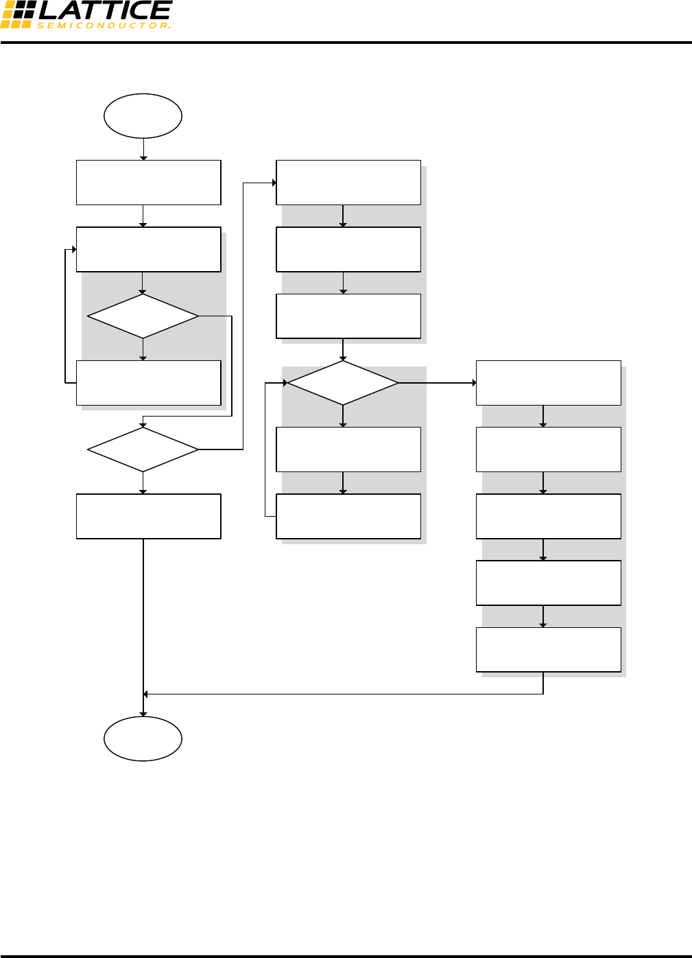
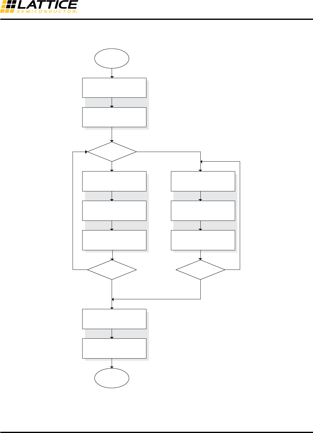
Figure 6 shows a flow diagram for controlling Master I2C reads and writes initiated via the WISHBONE interface.
The following sequence is for the Primary I2C but the same sequence applies to the Secondary I2C.
I2C_1_ IRQEN / I2C_2_IRQEN 0x49/0x53
Bit 76543 2 10
Name (Reserved) IRQARBLEN IRQTRRDYEN IRQTROEEN IRQHGCEN
Default 00000 0 00
Access ———— R/W R/W R/W R/W
14
Using Hardened Control Functions
in MachXO3 Devices Reference Guide
Figure 6. I2C Master Read/Write Example (via WISHBONE)
Start
TXDR <= I2C addr + ‘W’
CMDR <= 0x94 (STA+WR)
wait for TRRDY*
TXDR <= WRITE_DATA
CMDR <=0x14 (WR)
Write more data?
Read data?
CMDR <= 0x44 (STOP)
Done
TXDR <= I2C addr + ‘R’
CMDR <= 0x94 (STA+WR)
wait for SRW
CMDR <= 0x24 (RD)
Last Read?
wait for TRRDY
READ_DATA <= RXDR
wait **
CMDR <= 0x6C
(RD+NACK+STOP)
wait for TRRDY
READ_DATA <= RXDR
Y
N
Y
N
** Real-Time Read Delay Requirement
Read only 1 byte: min < wait < max
Read last of 2 bytes: 0 < wait < max
where
min = 2*tTCL_period
max = 7*tTCL_period
Y
N
CMDR <=0x04 (CKSDIS)***
*** Optional: Necessary only when
External I2C bus masters are present
* Real-Time Write Delay Requirement following TRRDY,
(when I2C_n_CMDR:CKSDIS = 1):
0 < wait < 6*tTCL_period
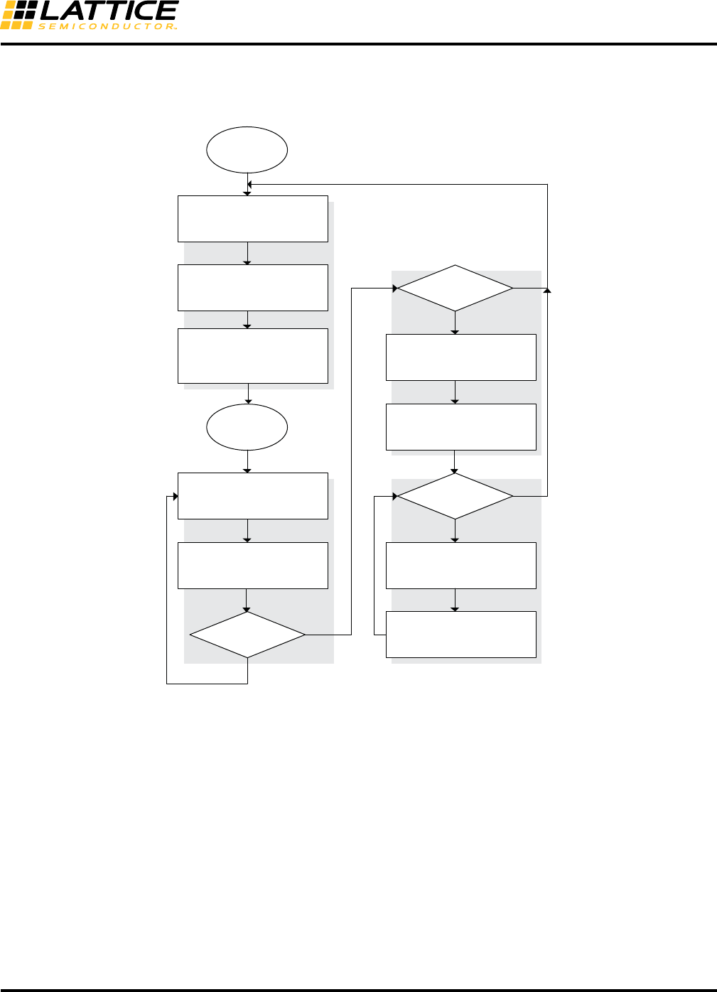
15
Using Hardened Control Functions
in MachXO3 Devices Reference Guide
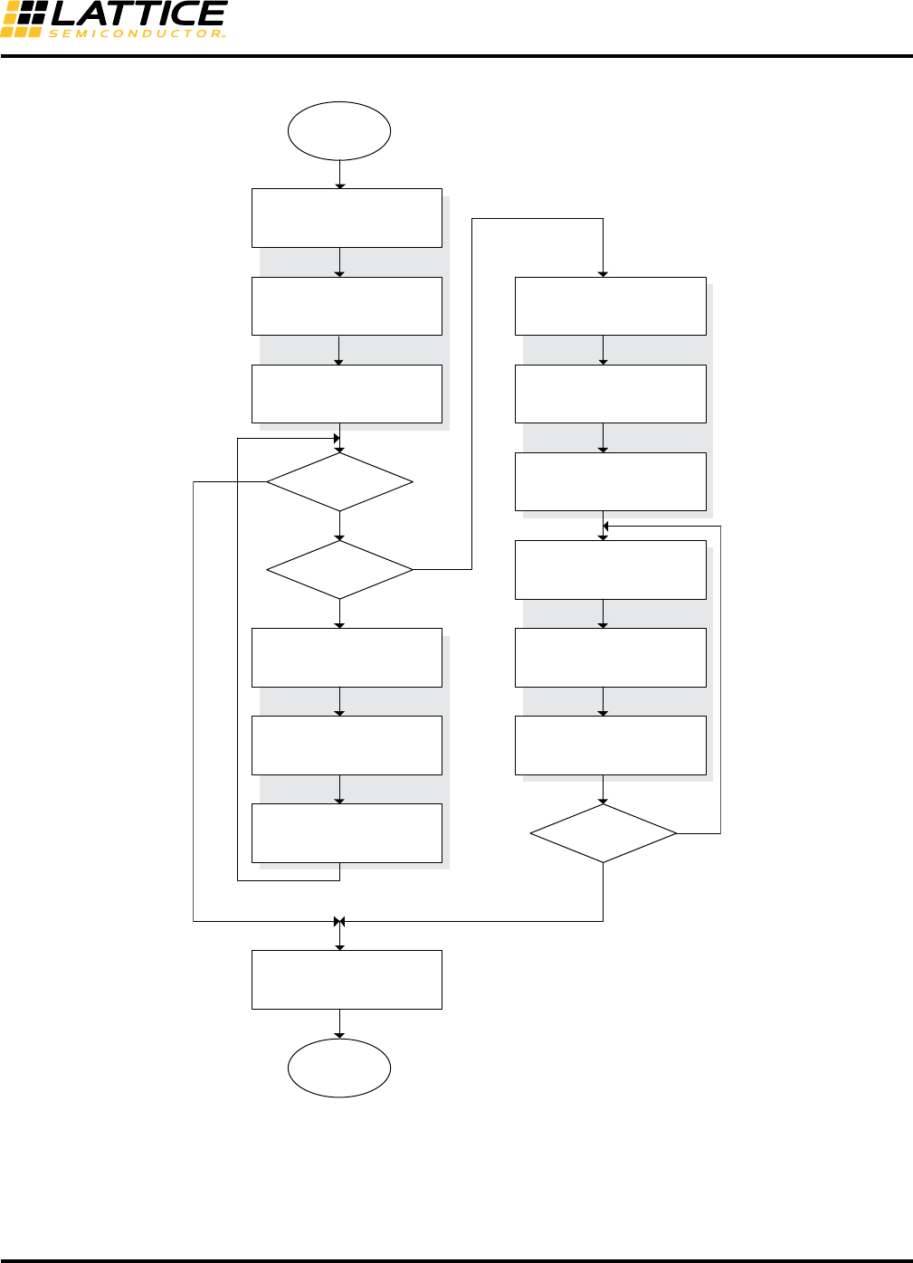
Figure 7 shows a flow diagram for reading and writing from an I2C Slave device via the WISHBONE interface. The
following sequence is for the Primary I2C but the same sequence applies to the Secondary I2C.
Figure 7. I2C Slave Read/Write Example (via WISHBONE)
Start
wait for not BUSY
CMDR <=0x04 (CKSDIS)
IRQEN <= 0x00
Read more data?
wait for SRW
Y
N
* Required only for IRQ
driven algorithms
discard <= RXDR
discard <= RXDR
IRQEN <= 0x04 (TRRDY)*
Idle
wait for TRRDY
IN_DATA <= RXDR
IRQ <= 0x04*
Write reply data?
TXDR <= OUT_DATA
wait for TRRDY
Write more data?
TXDR <= OUT_DATA
IRQ <= 0x04*
N
N
Y
Y
16
Using Hardened Control Functions
in MachXO3 Devices Reference Guide
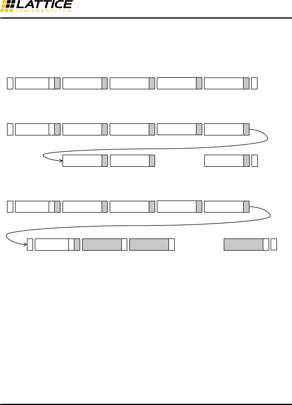
Figure 8, Figure 9, and Figure 10 illustrate typical User I2C bus protocol transactions that are supported by the
Master and Slave flows shown in Figure 6 and Figure 7. Additionally, the figures below reference typical sysConfig
Configuration commands structures.
Figure 8. Simple I2C Command (for example, ISC_ERASE)
Figure 9. I2C Command with Write Data (for example, LSC_PROG_INCR_NV)
Figure 10. I2C Command with Read Data (for example, LSC_READ_STATUS)
Start
Address
W
ACK
CMD OP1
ACK ACK
OP2
ACK
OP3
ACK
Stop
Start
Address
W
ACK
CMD OP1
ACK ACK
OP2
ACK
OP3
ACK
WDATA1 W DATA2
ACK ACK
…WDATAn
ACK
Stop
Start
Address
W
ACK
CMD OP1
ACK ACK
OP2
ACK
OP3
ACK
Restart
Address
R
ACK
RDATA1 RDATA2
ACK ACK …RDATAn
NACKStop
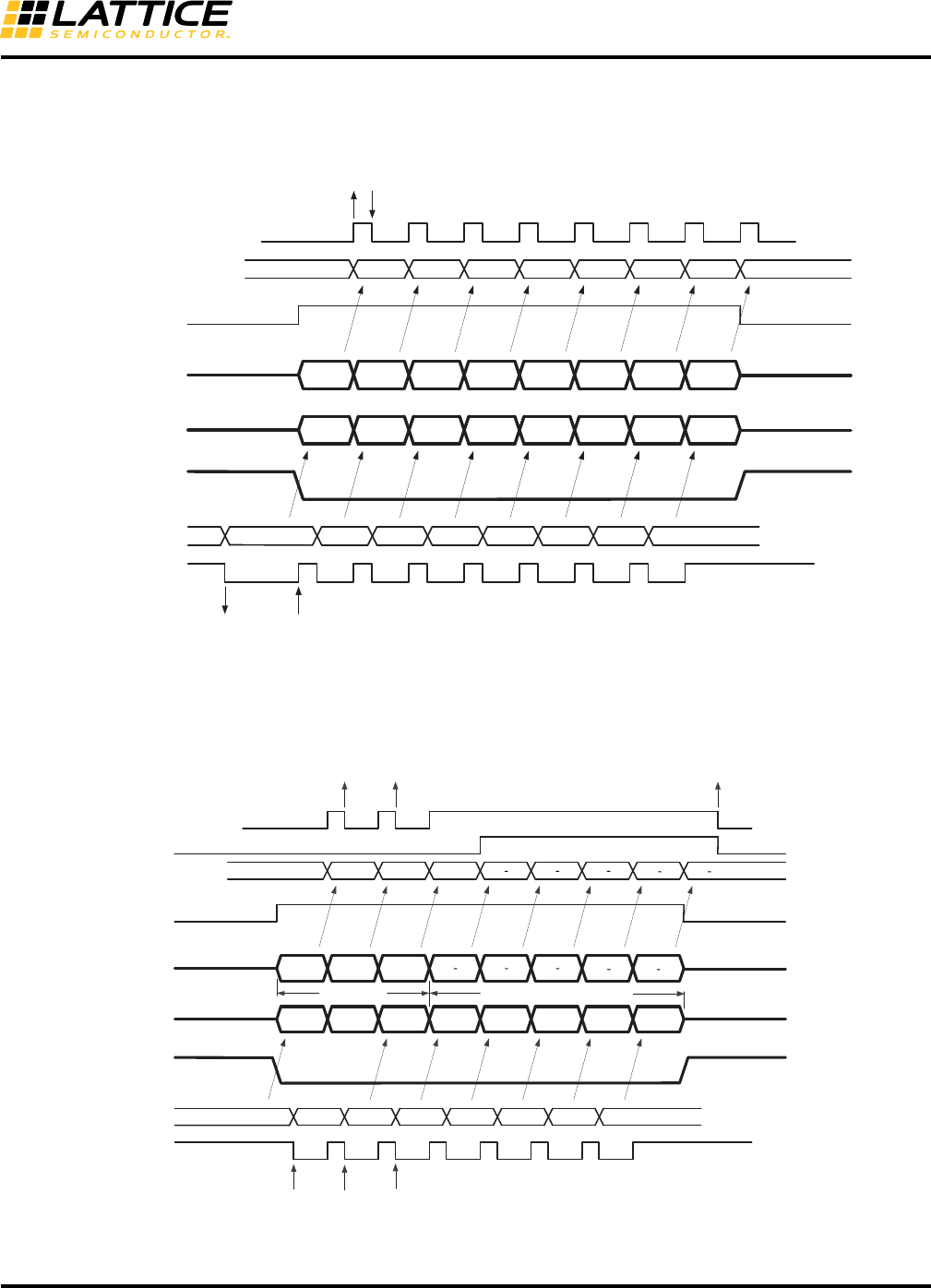
Typical I2C Transactions
17
Using Hardened Control Functions
in MachXO3 Devices Reference Guide
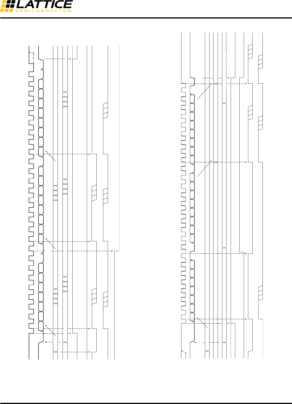
I2C Functional Waveforms
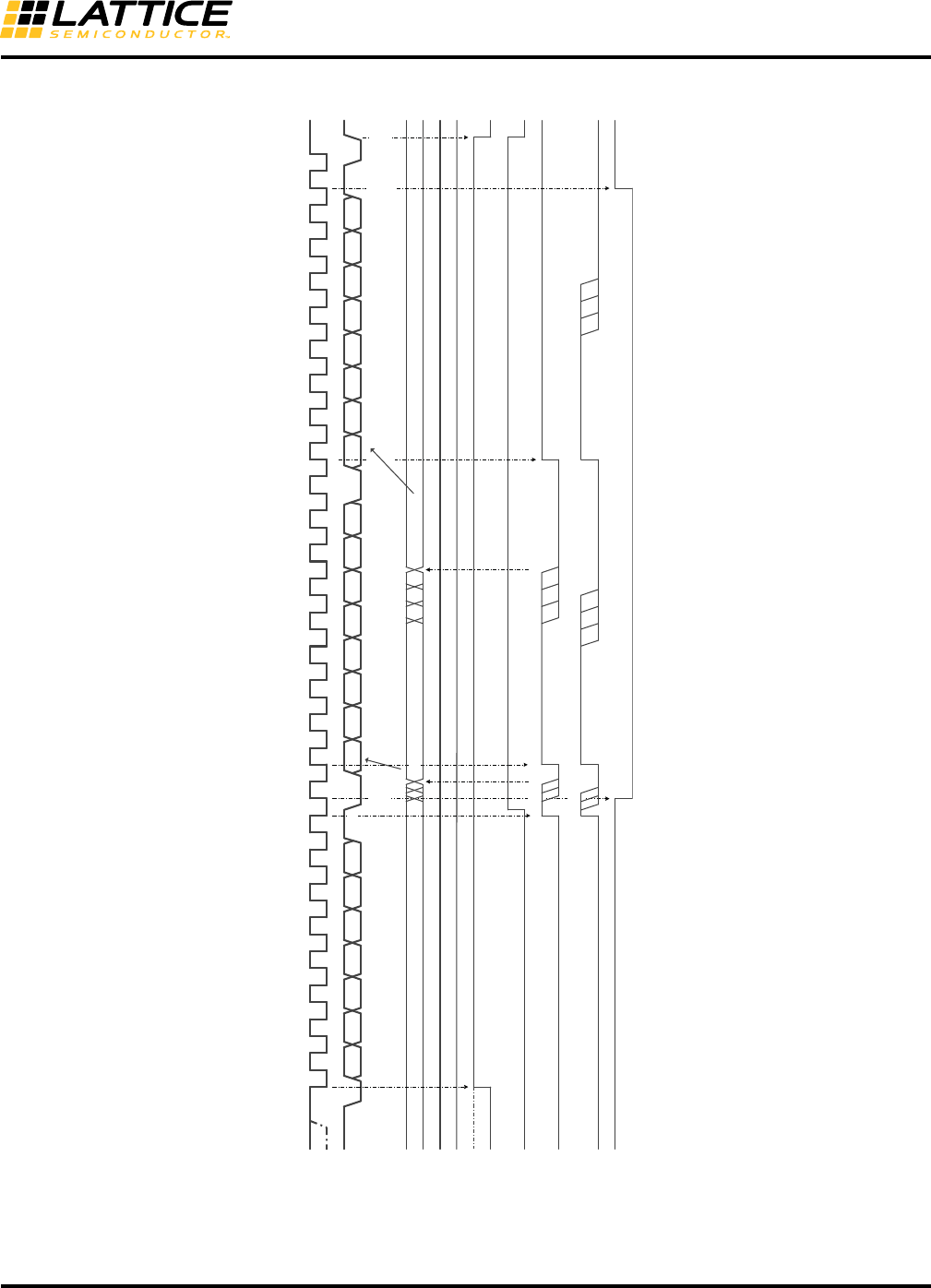
Figure 11. EFB Master – I2C Write
Figure 12. EFB Master – I2C Read
AD[(6:0),W]
AD6
SCL
AD5 AD4 AD3 AD2 AD1 AD0 Write
191 91 9
SDA D7 D6 D5 D4 D3 D2 D1 D0 D7 D6 D5 D4 D3 D2 D1 D0
Master Start
Ack from
Slave
Ack from
Slave
Ack from
Slave
Master Stop
I2C_1_SR[BUSY]
I2C_1_SR[SRW]
I2C_1_SR[TRRDY]
Write IRQTRRDY
I2C_1_IRQ[IRQTRRDY]
Write IRQTRRDY
Write I2C_1_TXDR Write I2C_1_TXDR
I2C_1_SR[RARC]
Write IRQTRRDY
I2C_1_CMDR 0x14(WR) 0x14(WR)
I2C_1_TXDR D[7:0] D[7:0]
0x94(Start+WR) 0x44(STOP)
Idle
AD[(6:0),W]
0x94 (START+WR)
D[7:0]
0x6C (RD+NACK+STOP)
Stop from
Master
SCL
AD6 AD5 AD4 AD3 AD2 AD1 AD0 Read
191 91 9
SDA D7 D6 D5 D4 D3 D2 D1 D0 D7 D6 D5 D4 D3 D2 D1 D0
Master Start/
Restart
Ack from
Slave
Ack from
Master
Nack from
Master
I2C_1_SR[BUSY]
I2C_1_SR[SRW]
I2C_1_SR[TRRDY]
Read I2C1_RXDR
Write IRQTRRDY
I2C_1_IRQ[IRQTRRDY]
Write IRQTRRDY
I2C_1_CMDR
I2C_1_TXDR
I2C_1_RXDR D[7:0]
0x24 (RD)
Write IRQTRRDY
Read I2C1_RXDR
18
Using Hardened Control Functions
in MachXO3 Devices Reference Guide
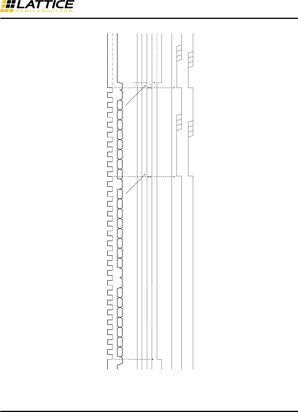
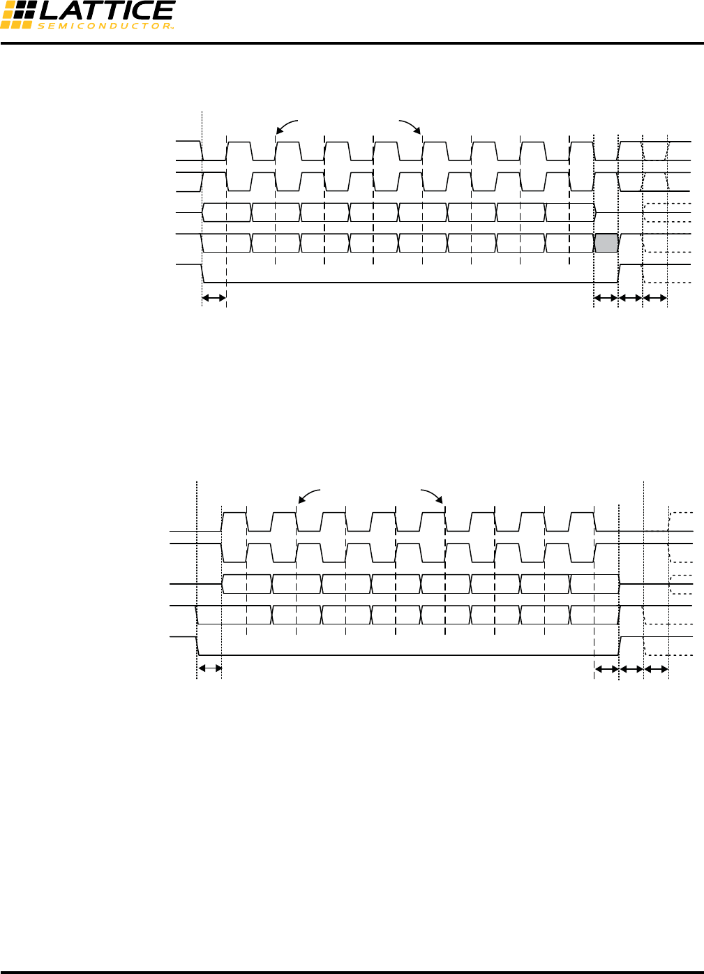
Figure 13. EFB Slave – I2C Write
SCL
AD6 AD5 AD4 AD3 AD2 AD1 AD0 Write
191 91 9
SDA D7 D6 D5 D4 D3 D2 D1 D0 D7 D6 D5 D4 D3 D2 D1 D0
Start from
Master
Ack from
Slave
Ack from
Slave
Ack from
Slave
Stop from
Master
I2C_1_SR[BUSY]
I2C_1_SR[SRW]
I2C_1_SR[TRRDY]
Write IRQTRRDY
I2C_1_IRQ[IRQTRRDY]
Read I2C_1_RXDR
Write IRQTRRDY
I2C_1_TXDR
I2C_1_RXDR
Read I2C_1_RXDR
D[7:0] D[7:0]
19
Using Hardened Control Functions
in MachXO3 Devices Reference Guide
Figure 14. EFB Slave – I2C Read
SCL
AD6 AD5 AD4 AD3 AD2 AD1 AD0
191 919
SDA D7 D6 D5 D4 D3 D2 D1 D0 D7 D6 D5 D4 D3 D2 D1 D0
Start from
Master
I2C_1_SR[BUSY]
I2C_1_SR[SRW]
I2C_1_SR[TRRDY]
Write IRQTRRDY
I2C_1_IRQ[IRQTRRDY]
Write IRQTRRDY
Write I2C_1_TXDR Write I2C_1_TXDR
I2C_1_SR[RARC]
I2C_1_TXDR
I2C_1_RXDR
D[7:0] D[7:0]
Write IRQTRRDY
Read
Ack from
Slave
Ack from
Master
No Ack from
Master
Stop from
Master

20
Using Hardened Control Functions
in MachXO3 Devices Reference Guide
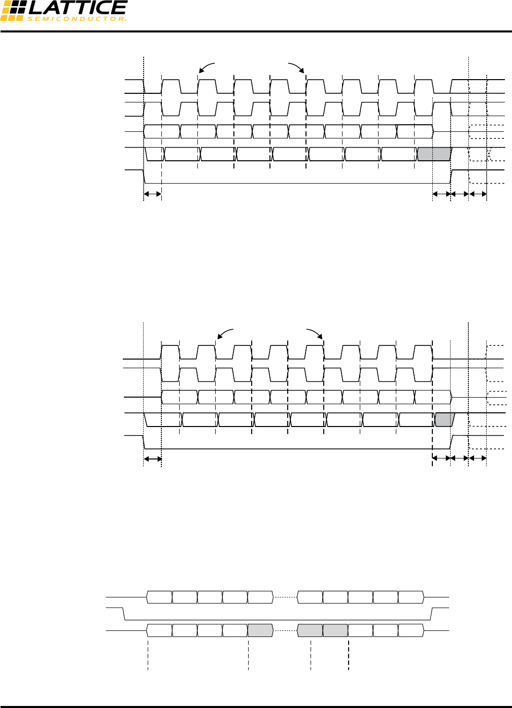
I2C Timing Diagram
Figure 15. I2C Bit Transfer Timing
I2C Simulation Model
The I2C EFB Register Map translation to the MachXO3L/LF EFB software simulation model is provided in below.
Table 14. I2C Primary Simulation Mode
I2C Primary
Register Name
Register
Size/Bit
Location
Register
Function
Address I2C
Primary Access
Simulation Model
Register Name Simulation Model Register Path
I2C_1_CR [7:0] Control 0x40 Read/Write i2ccr1[7:0] ../efb_top/config_plus_inst/config_core_inst/cfg_cdu/
njport_unit/i2c_1st/
I2CEN 7 i2c_en ../efb_top/config_plus_inst/config_core_inst/cfg_cdu/
njport_unit/i2c_1st/
GCEN 6 i2c_gcen ../efb_top/config_plus_inst/config_core_inst/cfg_cdu/
njport_unit/i2c_1st/
WKUPEN 5 i2c_wkupen ../efb_top/config_plus_inst/config_core_inst/cfg_cdu/
njport_unit/i2c_1st/
SDA_DEL_SEL[1:0] [3:2] sda_del_sel ../efb_top/config_plus_inst/config_core_inst/cfg_cdu/
njport_unit/i2c_1st/
I2C_1_CMDR [7:0] Command 0x41 Read/Write i2ccmdr[7:0] ../efb_top/config_plus_inst/config_core_inst/cfg_cdu/
njport_unit/i2c_1st/
STA 7 i2c_sta ../efb_top/config_plus_inst/config_core_inst/cfg_cdu/
njport_unit/i2c_1st/
STO 6 i2c_sto ../efb_top/config_plus_inst/config_core_inst/cfg_cdu/
njport_unit/i2c_1st/
RD 5 i2c_rd ../efb_top/config_plus_inst/config_core_inst/cfg_cdu/
njport_unit/i2c_1st/
WR 4 i2c_wt ../efb_top/config_plus_inst/config_core_inst/cfg_cdu/
njport_unit/i2c_1st/
ACK 3 i2c_nack ../efb_top/config_plus_inst/config_core_inst/cfg_cdu/
njport_unit/i2c_1st/
CKSDIS 2 i2c_cksdis ../efb_top/config_plus_inst/config_core_inst/cfg_cdu/
njport_unit/i2c_1st/
I2C_1_BR0 [7:0] Clock Pre-scale 0x42 Read/Write i2cbr[7:0] ../efb_top/config_plus_inst/config_core_inst/cfg_cdu/
njport_unit/i2c_1st/
I2C_PRESCALE[7:0] [7:0] i2cbr[7:0] ../efb_top/config_plus_inst/config_core_inst/cfg_cdu/
njport_unit/i2c_1st/
I2C_1_BR1 [7:0] Clock Pre-scale 0x43 Read/Write i2cbr[9:8] ../efb_top/config_plus_inst/config_core_inst/cfg_cdu/
njport_unit/i2c_1st/
I2C_PRESCALE[9:8] [1:0] i2cbr[9:8] ../efb_top/config_plus_inst/config_core_inst/cfg_cdu/
njport_unit/i2c_1st/
I2C_1_TXDR [7:0] Transmit Data 0x44 Write i2ctxdr[7:0] ../efb_top/config_plus_inst/config_core_inst/cfg_cdu/
njport_unit/i2c_1st/
I2C_Transmit_Data[7:0] [7:0] i2ctxdr[7:0] ../efb_top/config_plus_inst/config_core_inst/cfg_cdu/
njport_unit/i2c_1st/
I2C_1_SR [7:0] Status 0x45 Read i2csr[7:0] ../efb_top/config_plus_inst/config_core_inst/cfg_cdu/
njport_unit/i2c_1st/
data line
stable;
data valid
change
of data
allowed
t
SDA_DEL
SCL
SDA

21
Using Hardened Control Functions
in MachXO3 Devices Reference Guide
TIP 7 i2c_tip_sync ../efb_top/config_plus_inst/config_core_inst/cfg_cdu/
njport_unit/i2c_1st/
BUSY 6 i2c_busy_sync ../efb_top/config_plus_inst/config_core_inst/cfg_cdu/
njport_unit/i2c_1st/
RARC 5 i2c_rarc_sync ../efb_top/config_plus_inst/config_core_inst/cfg_cdu/
njport_unit/i2c_1st/
SRW 4 i2c_srw_sync ../efb_top/config_plus_inst/config_core_inst/cfg_cdu/
njport_unit/i2c_1st/
ARBL 3 i2c_arbl ../efb_top/config_plus_inst/config_core_inst/cfg_cdu/
njport_unit/i2c_1st/
TRRDY 2 i2c_trrdy ../efb_top/config_plus_inst/config_core_inst/cfg_cdu/
njport_unit/i2c_1st/
TROE 1 i2c_troe ../efb_top/config_plus_inst/config_core_inst/cfg_cdu/
njport_unit/i2c_1st/
HGC 0 i2c_hgc ../efb_top/config_plus_inst/config_core_inst/cfg_cdu/
njport_unit/i2c_1st/
I2C_1_GCDR [7:0] General Call 0x46 Read i2cgcdr[7:0] ../efb_top/config_plus_inst/config_core_inst/cfg_cdu/
njport_unit/i2c_1st/
I2C_GC_Data[7:0] [7:0] i2cgcdr[7:0] ../efb_top/config_plus_inst/config_core_inst/cfg_cdu/
njport_unit/i2c_1st/
I2C_1_RXDR [7:0] Receive Data 0x47 Read i2crxdr[7:0] ../efb_top/config_plus_inst/config_core_inst/cfg_cdu/
njport_unit/i2c_1st/
I2C_Receive_Data[7:0] [7:0] i2crxdr[7:0] ../efb_top/config_plus_inst/config_core_inst/cfg_cdu/
njport_unit/i2c_1st/
I2C_1_IRQ [7:0] IRQ 0x48 Read/Write
{1'b0, 1'b0, 1'b0, 1'b0,
i2csr_1st_irqsts_3,
i2csr_1st_irqsts_2,
i2csr_1st_irqsts_1,
i2csr_1st_irqsts_0}
../efb_top/efb_pll_sci_inst/u_efb_sci/
IRQARBL 3 i2csr_1st_irqsts_3 ../efb_top/efb_pll_sci_inst/u_efb_sci/
IRQTRRDY 2 i2csr_1st_irqsts_2 ../efb_top/efb_pll_sci_inst/u_efb_sci/
IRQTROE 1 i2csr_1st_irqsts_1 ../efb_top/efb_pll_sci_inst/u_efb_sci/
IRQHGC 0 i2csr_1st_irqsts_0 ../efb_top/efb_pll_sci_inst/u_efb_sci/
I2C_1_IRQEN [7:0] IRQ Enable 0x49 Read/Write
{1'b0, 1'b0, 1'b0, 1'b0,
i2csr_1st_irqena_3,
i2csr_1st_irqena_2,
i2csr_1st_irqena_1,
i2csr_1st_irqena_0}
../efb_top/efb_pll_sci_inst/u_efb_sci/
IRQARBLEN 3 i2csr_1st_irqena_3 ../efb_top/efb_pll_sci_inst/u_efb_sci/
IRQTRRDYEN 2 i2csr_1st_irqena_2 ../efb_top/efb_pll_sci_inst/u_efb_sci/
IRQTROEEN 1 i2csr_1st_irqena_1 ../efb_top/efb_pll_sci_inst/u_efb_sci/
IRQHGCEN 0 i2csr_1st_irqena_0 ../efb_top/efb_pll_sci_inst/u_efb_sci/
Table 14. I2C Primary Simulation Mode (Continued)
I2C Primary
Register Name
Register
Size/Bit
Location
Register
Function
Address I2C
Primary Access
Simulation Model
Register Name Simulation Model Register Path

22
Using Hardened Control Functions
in MachXO3 Devices Reference Guide
Table 15. I2C Secondary Simulation Model
I2C Secondary
Register Name
Register
Size/Bit
Location
Register
Function
Address I2C
Secondary Access
Simulation Model
Register Name Simulation Model Register Path
I2C_2_CR [7:0] Control 0x4A Read/Write i2ccr1[7:0] ../efb_top/config_plus_inst/config_core_inst/cfg_cdu/
njport_unit/i2c_2nd/
I2CEN 7 i2c_en ../efb_top/config_plus_inst/config_core_inst/cfg_cdu/
njport_unit/i2c_2nd/
GCEN 6 i2c_gcen ../efb_top/config_plus_inst/config_core_inst/cfg_cdu/
njport_unit/i2c_2nd/
WKUPEN 5 i2c_wkupen ../efb_top/config_plus_inst/config_core_inst/cfg_cdu/
njport_unit/i2c_2nd/
SDA_DEL_SEL[1:0] [3:2] sda_del_sel ../efb_top/config_plus_inst/config_core_inst/cfg_cdu/
njport_unit/i2c_2nd/
I2C_2_CMDR [7:0] Command 0x4B Read/Write i2ccmdr[7:0] ../efb_top/config_plus_inst/config_core_inst/cfg_cdu/
njport_unit/i2c_2nd/
STA 7 i2c_sta ../efb_top/config_plus_inst/config_core_inst/cfg_cdu/
njport_unit/i2c_2nd/
STO 6 i2c_sto ../efb_top/config_plus_inst/config_core_inst/cfg_cdu/
njport_unit/i2c_2nd/
RD 5 i2c_rd ../efb_top/config_plus_inst/config_core_inst/cfg_cdu/
njport_unit/i2c_2nd/
WR 4 i2c_wt ../efb_top/config_plus_inst/config_core_inst/cfg_cdu/
njport_unit/i2c_2nd/
ACK 3 i2c_nack ../efb_top/config_plus_inst/config_core_inst/cfg_cdu/
njport_unit/i2c_2nd/
CKSDIS 2 i2c_cksdis ../efb_top/config_plus_inst/config_core_inst/cfg_cdu/
njport_unit/i2c_2nd/
I2C_2_BR0 [7:0] Clock Pre-scale 0x4C Read/Write i2cbr[7:0] ../efb_top/config_plus_inst/config_core_inst/cfg_cdu/
njport_unit/i2c_2nd/
I2C_PRESCALE[7:0] [7:0] i2cbr[7:0] ../efb_top/config_plus_inst/config_core_inst/cfg_cdu/
njport_unit/i2c_2nd/
I2C_2_BR1 [7:0] Clock Pre-scale 0x4D Read/Write i2cbr[9:8] ../efb_top/config_plus_inst/config_core_inst/cfg_cdu/
njport_unit/i2c_2nd/
I2C_PRESCALE[9:8] [1:0] i2cbr[9:8] ../efb_top/config_plus_inst/config_core_inst/cfg_cdu/
njport_unit/i2c_2nd/
I2C_2_TXDR [7:0] Transmit Data 0x4E Write i2ctxdr[7:0] ../efb_top/config_plus_inst/config_core_inst/cfg_cdu/
njport_unit/i2c_2nd/
I2C_Transmit_Data[7:0] [7:0] i2ctxdr[7:0] ../efb_top/config_plus_inst/config_core_inst/cfg_cdu/
njport_unit/i2c_2nd/
I2C_2_SR [7:0] Status 0x4F Read i2csr[7:0] ../efb_top/config_plus_inst/config_core_inst/cfg_cdu/
njport_unit/i2c_2nd/
TIP 7 i2c_tip_sync ../efb_top/config_plus_inst/config_core_inst/cfg_cdu/
njport_unit/i2c_2nd/
BUSY 6 i2c_busy_sync ../efb_top/config_plus_inst/config_core_inst/cfg_cdu/
njport_unit/i2c_2nd/
RARC 5 i2c_rarc_sync ../efb_top/config_plus_inst/config_core_inst/cfg_cdu/
njport_unit/i2c_2nd/
SRW 4 i2c_srw_sync ../efb_top/config_plus_inst/config_core_inst/cfg_cdu/
njport_unit/i2c_2nd/
ARBL 3 i2c_arbl ../efb_top/config_plus_inst/config_core_inst/cfg_cdu/
njport_unit/i2c_2nd/
TRRDY 2 i2c_trrdy ../efb_top/config_plus_inst/config_core_inst/cfg_cdu/
njport_unit/i2c_2nd/
TROE 1 i2c_troe ../efb_top/config_plus_inst/config_core_inst/cfg_cdu/
njport_unit/i2c_2nd/
HGC 0 i2c_hgc ../efb_top/config_plus_inst/config_core_inst/cfg_cdu/
njport_unit/i2c_2nd/
I2C_2_GCDR [7:0] General Call 0x50 Read i2cgcdr[7:0] ../efb_top/config_plus_inst/config_core_inst/cfg_cdu/
njport_unit/i2c_2nd/
I2C_GC_Data[7:0] [7:0] i2cgcdr[7:0] ../efb_top/config_plus_inst/config_core_inst/cfg_cdu/
njport_unit/i2c_2nd/
I2C_2_RXDR [7:0] Receive Data 0x51 Read i2crxdr[7:0] ../efb_top/config_plus_inst/config_core_inst/cfg_cdu/
njport_unit/i2c_2nd/
I2C_Receive_Data[7:0] [7:0] i2crxdr[7:0] ../efb_top/config_plus_inst/config_core_inst/cfg_cdu/
njport_unit/i2c_2nd/

23
Using Hardened Control Functions
in MachXO3 Devices Reference Guide
Hardened SPI IP Core
The MachXO3L/LF contains a hard SPI IP core that can be configured as a SPI Master or Slave. When the SPI
core is configured as a Master it is able to control other devices with Slave SPI interfaces that are connected to the
SPI bus. When the SPI core is configured as a Slave, it is able to interface to an external SPI Master device.
SPI Registers
The SPI core communicates with the WISHBONE interface through a set of control, command, status and data
registers. Table 16 shows the register names and their functions. These registers are a subset of the EFB register
map.
Table 16. SPI Registers
I2C_2_IRQ [7:0] IRQ 0x52 Read/Write
{1'b0, 1'b0, 1'b0, 1'b0,
i2csr_2nd_irqsts_3,
i2csr_2nd_irqsts_2,
i2csr_2nd_irqsts_1,
i2csr_2nd_irqsts_0}
../efb_top/efb_pll_sci_inst/u_efb_sci/
IRQARBL 3 i2csr_2nd_irqsts_3 ../efb_top/efb_pll_sci_inst/u_efb_sci/
IRQTRRDY 2 i2csr_2nd_irqsts_2 ../efb_top/efb_pll_sci_inst/u_efb_sci/
IRQTROE 1 i2csr_2nd_irqsts_1 ../efb_top/efb_pll_sci_inst/u_efb_sci/
IRQHGC 0 i2csr_2nd_irqsts_0 ../efb_top/efb_pll_sci_inst/u_efb_sci/
I2C_2_IRQEN [7:0] IRQ Enable 0x53 Read/Write
{1'b0, 1'b0, 1'b0, 1'b0,
i2csr_2nd_irqena_3,
i2csr_2nd_irqena_2,
i2csr_2nd_irqena_1,
i2csr_2nd_irqena_0}
../efb_top/efb_pll_sci_inst/u_efb_sci/
IRQARBLEN 3 i2csr_2nd_irqena_3 ../efb_top/efb_pll_sci_inst/u_efb_sci/
IRQTRRDYEN 2 i2csr_2nd_irqena_2 ../efb_top/efb_pll_sci_inst/u_efb_sci/
IRQTROEEN 1 i2csr_2nd_irqena_1 ../efb_top/efb_pll_sci_inst/u_efb_sci/
IRQHGCEN 0 i2csr_2nd_irqena_0 ../efb_top/efb_pll_sci_inst/u_efb_sci/
SPI Register Name Register Function Address Access
SPICR0 Control Register 0 0x54 Read/Write
SPICR1 Control Register 1 0x55 Read/Write
SPICR2 Control Register 2 0x56 Read/Write
SPIBR Clock Pre-scale 0x57 Read/Write
SPICSR Master Chip Select 0x58 Read/Write
SPITXDR Transmit Data 0x59 Write
SPISR Status 0x5A Read
SPIRXDR Receive Data 0x5B Read
SPIIRQ Interrupt Request 0x5C Read/Write
SPIIRQEN Interrupt Request Enable 0x5D Read/Write
Note: Unless otherwise specified, all Reserved bits in writable registers shall be written ‘0’.
Table 15. I2C Secondary Simulation Model (Continued)
I2C Secondary
Register Name
Register
Size/Bit
Location
Register
Function
Address I2C
Secondary Access
Simulation Model
Register Name Simulation Model Register Path

24
Using Hardened Control Functions
in MachXO3 Devices Reference Guide
Table 17. SPI Control 0
TIdle_XCNT[1:0] Idle Delay Count. Specifies the minimum interval prior to the Master Chip Select low
assertion (Master Mode only), in SCK periods.
00: ½
01: 1
10: 1.5
11: 2
TTrail_XCNT[2:0] Trail Delay Count. Specifies the minimum interval between the last edge of SCK and
the high deassertion of Master Chip Select (Master Mode only), in SCK periods.
000: ½
001: 1
010: 1.5
…
111: 4
TLead_XCNT[2:0] Lead Delay Count. Specifies the minimum interval between the Master Chip Select
low assertion and the first edge of SCK (Master Mode only), in SCK periods.
000: ½
001: 1
010: 1.5
…
111: 4
Table 18. SPI Control 1
SPE This bit enables the SPI core functions. If SPE is cleared, SPI is disabled and forced
into idle state.
0: SPI disabled
1: SPI enabled, port pins are dedicated to SPI functions.
WKUPEN_USER Wake-up Enable via User. Enables the SPI core to send a wake-up signal to the on-
chip Power Controller to wake the part from Standby mode when the User slave SPI
chip select (spi_scsn) is driven low.
0: Wakeup disabled
1: Wakeup enabled.
SPICR0 0x54
Bit 76543210
Name TIdle_XCNT[1:0] TTrail_XCNT[2:0] TLead_XCNT[2:0]
Default00000000
Access R/W R/W R/W R/W R/W R/W R/W R/W
Note: A write to this register will cause the SPI core to reset.
SPICR1 0x55
Bit 7 6 5 4 3210
Name SPE WKUPEN_USER WKUPEN_CFG TXEDGE (Reserved)
Default 0 0 0 0 0000
Access R/W R/W R/W R/W — — — —
Note: A write to this register will cause the SPI core to reset.
25
Using Hardened Control Functions
in MachXO3 Devices Reference Guide
WKUPEN_CFG Wake-up Enable Configuration. Enables the SPI core to send a wake-up signal to the
on-chip power controller to wake the part from standby mode when the Configuration
slave SPI chip select (ufm_sn) is driven low.
0: Wakeup disabled
1: Wakeup enabled.
TXEDGE Data Transmit Edge. Enables Lattice proprietary extension to the SPI protocol. Selects
which clock edge to transmit SPI data. Refer to Figure 24 through Figure 27.
0: Transmit data on the MCLK/CCLK edge defined by SPICR2[CPOL] and
SPICR2[CPHA]
1: Transmit data ½ MCLK/CCLK earlier than defined by SPICR2[CPOL] and
SPICR2[CPHA]
Table 19. SPI Control 2
MSTR SPI Master/Slave Mode. Selects the Master/Slave operation mode of the SPI core.
Changing this bit forces the SPI system into idle state.
0: SPI is in Slave mode
1: SPI is in Master mode
MCSH SPI Master CSSPIN Hold. Holds the Master chip select active when the host is busy,
to halt the data transmission without de-asserting chip select.
Note: This mode must be used only when the WISHBONE clock has been divided by
a value greater than four (4).
0: Master running as normal
1: Master holds chip select low even if there is no data to be transmitted
SDBRE Slave Dummy Byte Response Enable. Enables Lattice proprietary extension to the
SPI protocol. For use when the internal support circuit (for example, WISHBONE host)
cannot respond with initial data within the time required, and to make the slave read
out data predictably available at high SPI clock rates.
When enabled, dummy 0xFF bytes will be transmitted in response to a SPI slave read
(while SPISR[TRDY]=1) until an initial write to SPITXDR. Once a byte is written into
SPITXDR by the WISHBONE host, a single byte of 0x00 will be transmitted then fol-
lowed immediately by the data in SPITXDR. In this mode, the external SPI master
should scan for the initial 0x00 byte when reading the SPI slave to indicate the begin-
ning of actual data. Refer to Figure 23.
0: Normal Slave SPI operation
1: Lattice proprietary Slave Dummy Byte Response Enabled
Note: This mechanism only applies for the initial data delay period. Once the initial
data is available, subsequent data must be supplied to SPITXDR at the required SPI
bus data rate.
SPICR2 0x56
Bit 76543210
Name MSTR MCSH SDBRE (Reserved) (Reserved) CPOL CPHA LSBF
Default 0 0 0 00000
Access R/W R/W R/W —— R/W R/W R/W
Note: A write to this register will cause the SPI core to reset.

26
Using Hardened Control Functions
in MachXO3 Devices Reference Guide
CPOL SPI Clock Polarity. Selects an inverted or non-inverted SPI clock. To transmit data
between SPI modules, the SPI modules must have identical SPICR2[CPOL] values. In
master mode, a change of this bit will abort a transmission in progress and force the
SPI system into idle state. Refer to Figure 24 through Figure 27.
0: Active-high clocks selected.
1: Active-low clocks selected.
CPHA SPI Clock Phase. Selects the SPI clock format. In master mode, a change of this bit
will abort a transmission in progress and force the SPI system into idle state. Refer to
Figure 24 through Figure 27.
0: Data is captured on a leading (first) clock edge, and propagated on the
opposite clock edge.
1: Data is captured on a trailing (second) clock edge, and propagated on the
opposite clock edge*.
Note: When CPHA=1, the user must explicitly place a pull-up or pull-down on SCK
pad corresponding to the value of CPOL (for example, when CPHA=1 and CPOL=0
place a pull-down on SCK). When CPHA=0, the pull direction may be set arbitrarily.
Slave SPI Configuration mode supports default setting only for CPOL, CPHA.
LSBF LSB-First. LSB appears first on the SPI interface. In master mode, a change of this bit
will abort a transmission in progress and force the SPI system into idle state. Refer to
Refer to Figure 24 through Figure 27.
Note: This bit does not affect the position of the MSB and LSB in the data register.
Reads and writes of the data register always have the MSB in bit 7.
0: Data is transferred most significant bit (MSB) first
1: Data is transferred least significant bit (LSB) first
Table 20. SPI Clock Prescale
DIVIDER[5:0] SPI Clock Prescale value. The WISHBONE clock frequency is divided by
(DIVIDER[5:0] + 1) to produce the desired SPI clock frequency. A write operation to
this register will cause a SPI core reset. DIVIDER must be >= 1.
Note: The digital value is calculated by IPexpress when the SPI core is configured in
the SPI tab of the EFB GUI. The calculation is based on the WISHBONE Clock Fre-
quency and the SPI Frequency, both entered by the user. The digital value of the
divider is programmed in the MachXO3L/LF device during device programming. After
power-up or device reconfiguration, the data is loaded onto the SPIBR register.
Register SPIBR has Read/Write access from the WISHBONE interface. Designers
can update the clock pre-scale register dynamically during device operation.
SPIBR 0x57
Bit 76543210
Name (Reserved) DIVIDER[5:0]
Default100000000
Access —— R/W R/W R/W R/W R/W R/W
1. Hardware default value may be overridden by EFB component instantiation parameters. See discussion below.

27
Using Hardened Control Functions
in MachXO3 Devices Reference Guide
Table 21. SPI Master Chip Select
CSN_[7:0] SPI Master Chip Selects. Used in master mode for asserting a specific Master Chip
Select (MCSN) line. The register has eight bits, enabling the SPI core to control up to
eight external SPI slave devices Each bit represents one master chip select line
(Active-Low). Bits [7:1] may be connected to any I/O pin via the FPGA fabric. Bit 0 has
a pre-assigned pin location. The register has Read/Write access from the WISHBONE
interface. A write operation on this register will cause the SPI core to reset.
Table 22. SPI Transmit Data Register
SPI_Transmit_Data[7:0] SPI Transmit Data. This register holds the byte that will be transmitted on the SPI bus.
Bit 0 in this register is LSB, and will be transmitted last when SPICR2[LSBF]=0 or first
when SPICR2[LSBF]=1.
Note: When operating as a Slave, SPITXDR must be written when SPISR[TRDY] is '1'
and at least 0.5 CCLKs before the first bit is to appear on SO. For example, when
CPOL = CPHA = TXEDGE = LSBF = 0, SPITXDR must be written prior to the CCLK
rising edge used to sample the LSB (bit 0) of the previous byte. See Figure 29. This
timing requires at least one protocol dummy byte be included for all slave SPI read
operations.
Table 23. SPI Status
TIP SPI Transmitting In Progress. Indicates the SPI port is actively transmitting/receiving
data.
0: SPI Transmitting complete
1: SPI Transmitting in progress*
TRDY SPI Transmit Ready. Indicates the SPI transmit data register (SPITXDR) is empty. This
bit is cleared by a write to SPITXDR. This bit is capable of generating an interrupt.
0: SPITXDR is not empty
1: SPITXDR is empty
SPICSR 0x58
Bit 76543210
Name CSN_7 CSN_6 CSN_5 CSN_4 CSN_3 CSN_2 CSN_1 CSN_0
Default00000000
Access R/W R/W R/W R/W R/W R/W R/W R/W
SPITXDR 0x59
Bit 76543210
Name SPI_Transmit_Data[7:0]
Default ————————
Access WWWWWWWW
SPISR 0x5A
Bit 76543210
Name TIP (Reserved) TRDY RRDY (Reserved) ROE MDF
Default 0 ——0 0—0 0
Access R ——R R—R R
28
Using Hardened Control Functions
in MachXO3 Devices Reference Guide
RRDY SPI Receive Ready. Indicates the receive data register (SPIRXDR) contains valid
receive data. This bit is cleared by a read access to SPIRXDR. This bit is capable of
generating an interrupt.
0: SPIRXDR does not contain data
1: SPIRXDR contains valid receive data
ROE Receive Overrun Error. Indicates SPIRXDR received new data before the previous
data was read. The previous data is lost. This bit is capable of generating an interrupt.
0: Normal
1: Receiver Overrun detected
MDF Mode Fault. Indicates the Slave SPI chip select (spi_scsn) was driven low while
SPICR2[MSTR]=1. This bit is cleared by any write to SPICR0, SPICR1 or SPICR2.
This bit is capable of generating an interrupt.
0: Normal
1: Mode Fault detected
Table 24. SPI Receive Data Register
SPI_Receive_Data[7:0] SPI Receive Data. This register holds the byte captured from the SPI bus. Bit 0 in this
register is LSB and was received last when LSBF=0 or first when LSBF=1.
Table 25. SPI Interrupt Status
IRQTRDY Interrupt Status for SPI Transmit Ready.
When enabled, indicates SPISR[TRDY] was asserted. Write a ‘1’ to this bit to clear the
interrupt.
1: SPI Transmit Ready Interrupt
0: No interrupt
IRQRRDY Interrupt Status for SPI Receive Ready.
When enabled, indicates SPISR[RRDY] was asserted. Write a ‘1’ to this bit to clear
the interrupt.
1: SPI Receive Ready Interrupt
0: No interrupt
SPIRXDR 0x5B
Bit 76543210
Name SPI_Receive_Data[7:0]
Default00000000
AccessRRRRRRRR
SPIIRQ 0x5C
Bit 76543210
Name (Reserved) IRQTRDY IRQRRDY (Reserved) IRQROE IRQMDF
Default — — —0 0—0 0
Access — — —R/WR/W—R/WR/W
29
Using Hardened Control Functions
in MachXO3 Devices Reference Guide
IRQROE Interrupt Status for Receive Overrun Error.
When enabled, indicates ROE was asserted. Write a ‘1’ to this bit to clear the inter-
rupt.
1: Receive Overrun Error Interrupt
0: No interrupt
IRQMDF Interrupt Status for Mode Fault.
When enabled, indicates MDF was asserted. Write a ‘1’ to this bit to clear the inter-
rupt.
1: Mode Fault Interrupt
0: No interrupt
Table 26. SPI Interrupt Enable
IRQTRDYEN Interrupt Enable for SPI Transmit Ready.
1: Interrupt generation enabled
0: Interrupt generation disabled
IRQRRDYEN Interrupt Enable for SPI Receive Ready
1: Interrupt generation enabled
0: Interrupt generation disabled
IRQROEEN Interrupt Enable for Receive Overrun Error
1: Interrupt generation enabled
0: Interrupt generation disabled
IRQMDFEN Interrupt Enable for Mode Fault
1: Interrupt generation enabled
0: Interrupt generation disabled
SPIIRQEN 0x5D
Bit 7654 3210
Name (Reserved) IRQTRDYEN IRQRRDYEN (Reserved) IRQROEEN IRQMDFEN
Default 0 0 000000
Access — — —R/WR/W—R/WR/W
30
Using Hardened Control Functions
in MachXO3 Devices Reference Guide
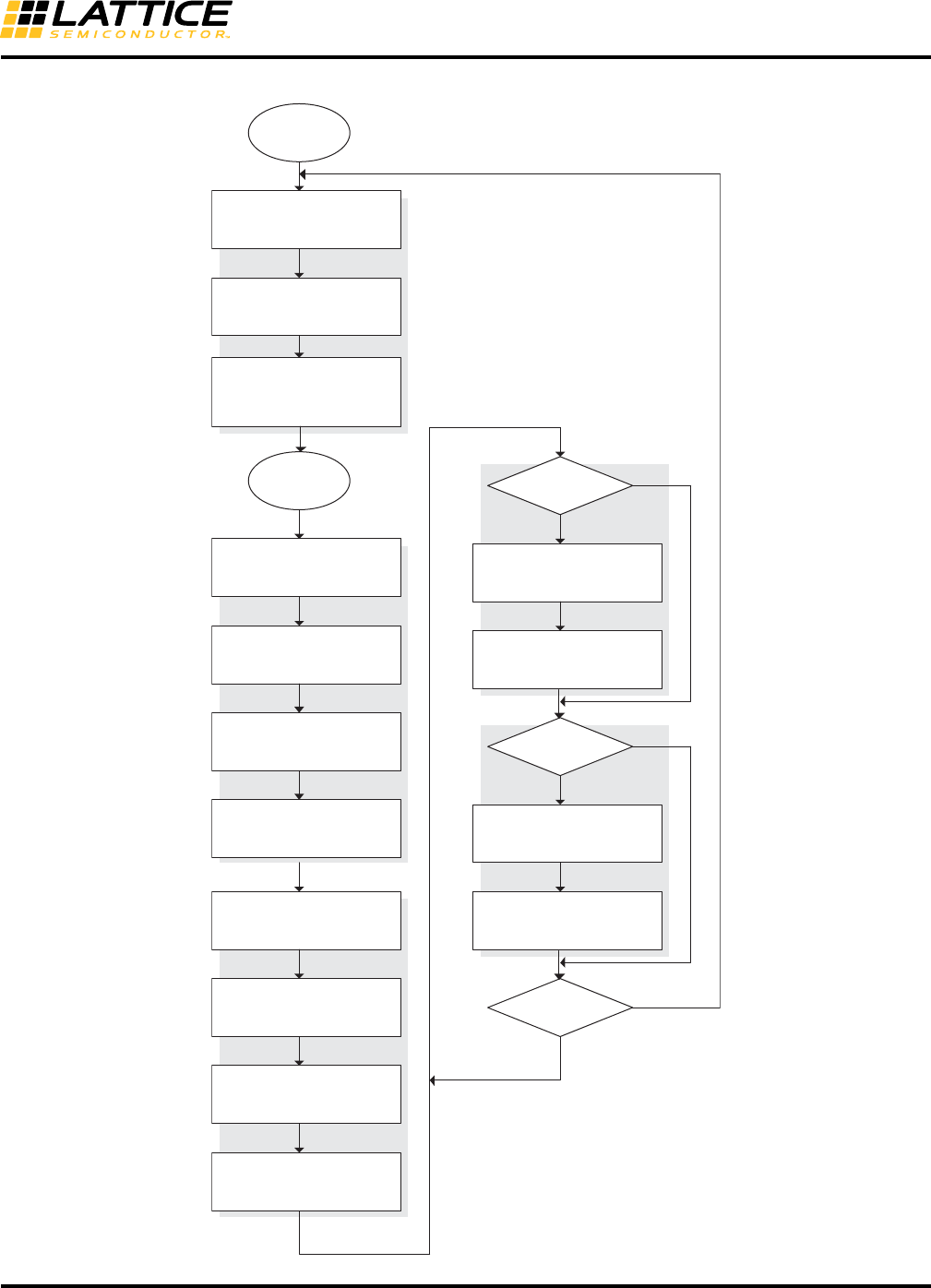
Figure 16 shows a flow diagram for controlling Master SPI reads and writes initiated via the WISHBONE interface.
Figure 16. SPI Master Read/Write Example (via WISHBONE) – Production Silicon
Note: Assumes CR2 register, MSCH = '1'. The algorithm when MSCH = '0' is application dependent and not pro-
vided. See Figure 22 for guidance.
Start
CR2 <= 0xC0
wait for TRDY
Done?
Read data?
TXDR <= SPI Write Data TXDR <= 0x00
wait for RRDY
SPI Read Data <= RXDR
Y
N
Y
N
wait for RRDY
Discard Data <= RXDR
Last Read?
CR2 <= 0x80
Y
N
wait for not TIP
Done
31
Using Hardened Control Functions
in MachXO3 Devices Reference Guide
Figure 17. SPI Master Read/Write Example (via WISHBONE) – R1 Silicon
Start
CR2 <= 0xC0
wait for TRDY
TXDR <= SPI Command Byte
Done?
Read data?
TXDR <= SPI Write Data
Done
Discard Data <= RXDR
TXDR <= 0x00
wait for RRDY
TXDR <= 0x00
wait for RRDY
SPI Read Data <= RXDR
Y
N
Y
N
Y
N
wait for RRDY
Discard Data <= RXDR Last Read?
CR2 <= 0x80
32
Using Hardened Control Functions
in MachXO3 Devices Reference Guide
Figure 18. SPI Slave Read/Write Example (via WISHBONE) - Production Silicon
Start
wait for not TIP
CR2 <=0x00 (Slave mode)
Transaction
Complete?
wait for TRDY
N
Y
discard <= RXDR
discard <= RXDR
TXDR <= T1 data (optional)*
Idle
wait for TIP
TXDR <= T2 data (dum1)*
Write reply data?
TXDR <= Tn+1 data
wait for RRDY
Read more data?
Rn data <= RXDR
N
N
Y
Y
wait for RRDY
R1 data <= RXDR
wait for TRDY
TXDR <= T3 data
wait for RRDY
R2 data <= RXDR
* If T1 data is not written, then
T2 data is dummy and 0xFF
will be transmitted on SO.
33
Using Hardened Control Functions
in MachXO3 Devices Reference Guide
Typical SPI Transactions
Figures 19, 20, and 21 illustrate typical User SPI bus protocol transactions that are supported by the Master and
Slave flows shown in Figures 16, 17, and 18. Additionally, the figures below reference typical sysConfig Configura-
tion commands structures.
Figure 19. Simple SPI Command (for example, ISC_ERASE)
Figure 20. SPI Command w/ Write Data (for example, LSC_PROG_INCR_NV)
Figure 21. SPI Command w/ Read Data (for example, LSC_READ_STATUS)
MOSI CMD
MISO
CSN
OP1 OP2 OP3
----
MOSI CMD
MISO
CSN
OP1 OP2 OP3 WDATA1 WDATA2 ... WDATAn
...
----
-- -
CMD OP1 OP2 OP3 ...
...
MOSI
MISO
CSN
RDATA1 RDATA2 RDATAn
----
-- -
34
Using Hardened Control Functions
in MachXO3 Devices Reference Guide
SPI Functional Waveforms
Figure 22. Fully Specified SPI Transaction (MachXO3L/LF as SPI Master or Slave)
Figure 23. Minimally Specified SPI Transaction Example (MachXO3L/LF as SPI Slave)
R1 from SI
to SPIRXDR
(auto)
T1 written to
SPITXDR via
WISHBONE
(user)
T1 from
SPITXDR to SO
(auto)
T1 T2 T3 T4 T5 T6 T7 T8
T1 T2 T3 T4 T5 T6 T7 T8
R1 R2 R3 R4 R5 R6 R7 R8
R1 R2 R3 R4 R5 R6 R7 R8
SPISR[RRDY]
SPIRXDR
SPISR[TIP]
SPISO or SI
SISPI or SO
CSSPIN or SCSN
SPITXDR
SPISR[TRDY]
R1 read from
SPIRXDR via
WISHBONE
(user)
Addr read from
SPIRXDR via
WISHBONE
(user)
Flush SPIRXDR
via WISHBONE
(user)
Quit reading SPIRXDR (data is “don’t care”)
CMD read from
SPIRXDR via
WISHBONE
(user)
0x08addr dum
0x08addr dum
old
old dum1 dum2 D1 D2 D3 D4 D5
FF* dum2 D1 D2 D3 D4 D5
Command Reply to Command
After SPISR[TIP] detected,
write dummy to SPITXDR
(user)
After CMD/Addr decode,
write good to SPITXDR
(user)
*Note: If SPITXDR is ‘empty’ at the start of a transaction,
the second byte will be ‘FF’ (silicon limitation).
Must write dummy byte in first byte period to get
good Tx data in third period (dummy data may be
overwritten in second period if necessary).
SPISR[RRDY]
SPISR[ROE]
SPIRXDR
SPISR[TIP]
SI
SO
SCSN
SPITXDR
SPISR[TRDY]
35
Using Hardened Control Functions
in MachXO3 Devices Reference Guide
SPI Timing Diagrams
Figure 24. SPI Control Timing (SPICR2[CPHA]=0, SPICR1[TXEDGE]=0)
Figure 25. SPI Control Timing (SPICR2[CPHA]=1, SPICR1[TXEDGE]=0)
MCLK/CCLK
(CPOL=0)
MCLK/CCLK
(CPOL=1)
SPISO/SI
SISPI/SO
CSSPIN/SCSN or SN
MSB first (LSBF=0):
LSB first (LSBF=1):
MSB
LSB
bit6
bit1
bit5
bit2
bit4
bit3
bit3
bit4
bit2
bit5
bit1
bit6 MSB
LSB
tL tT tI tL
tL = TLead_XCNT
tT = TTrail_XCNT
tL = TIdle_XCNT
sample instants
*Note : MachXO3L/LF SPI configuration modes only support
CPHA = CPOL = LSBF = TXEDGE = 0
Signal Name: MASTER/SLAVE
MSB first (LSBF=0):
LSB first (LSBF=1):
MSB
LSB
bit6
bit1
bit5
bit2
bit4
bit3
bit3
bit4
bit2
bit5
bit1
bit6 MSB
LSB
tL tT tI tL
tL = TLead_XCNT
tT = TTrail_XCNT
tL = TIdle_XCNT
sample instants
MCLK/CCLK
(CPOL=0)
MCLK/CCLK
(CPOL=1)
SPISO/SI
SISPI/SO
CSSPIN/SCSN
Signal Name: MASTER/SLAVE
36
Using Hardened Control Functions
in MachXO3 Devices Reference Guide
Figure 26. SPI Control Timing (SPICR2[CPHA]=0, SPICR1[TXEDGE]=1)
Figure 27. SPI Control Timing (SPICR2[CPHA]=1, SPICR1[TXEDGE]=1)
Figure 28. Slave SPI Dummy Byte Response (SPICR2[SDBRE]) Timing
MSB first (LSBF=0):
LSB first (LSBF=1):
MSB
LSB
bit6
bit1
bit5
bit2
bit4
bit3
bit3
bit4
bit2
bit5
bit1
bit6 MSB
LSB
tL tT tI tL
tL = TLead_XCNT
tT = TTrail_XCNT
tL = TIdle_XCNT
sample instants
CSSPIN/SCSN
MCLK/CCLK
(CPOL=0)
MCLK/CCLK
(CPOL=1)
SPISO/SI
SISPI/SO
Signal Name: MASTER/SLAVE
MSB first (LSBF=0):
LSB first (LSBF=1):
MSB
LSB
bit6
bit1
bit5
bit2
bit4
bit3
bit3
bit4
bit2
bit5
bit1
bit6 MSB
LSB
tL tT tI tL
tL = TLead_XCNT
tT = TTrail_XCNT
tL = TIdle_XCNT
sample instants
MCLK/CCLK
(CPOL=0)
MCLK/CCLK
(CPOL=1)
SPISO/SI
SISPI/SO
CSSPIN/SCSN
Signal Name: MASTER/SLAVE
SI(MOSI)
SO(MISO)
CS(SS)
FF FF FF FF FF
CMD OP1 OP2 OP3 FF FF FF FF FF FF
FF 00 D1 D2 D3
Receiving Read Command SPITXDR
NOT Ready
SPITXDR
Ready DATA Read Out

37
Using Hardened Control Functions
in MachXO3 Devices Reference Guide
SPI Simulation Model
The SPI EFB Register Map translation to the MachXO3L/LF EFB software simulation model is provided below.
Table 27. SPI Simulation Model
SPI Register Name
Register
Size/Bit
Location Register Function Address Access
Simulation
Model
Register Name Simulation Model Register Path
SPICR0 [7:0] Control Register 0 0x54 Read/Write spicr0[7:0] ../efb_top/config_plus_inst/config_core_inst/cfg_cdu/
njport_unit/spi_port/
TIdle_XCNT[1:0] [7:6] spicr0[7:6] ../efb_top/config_plus_inst/config_core_inst/cfg_cdu/
njport_unit/spi_port/
TTrail_XCNT[2:0] [5:3] spicr0[5:3] ../efb_top/config_plus_inst/config_core_inst/cfg_cdu/
njport_unit/spi_port/
TLead_XCNT[2:0] [2:0] spicr0[2:0] ../efb_top/config_plus_inst/config_core_inst/cfg_cdu/
njport_unit/spi_port/
SPICR1 [7:0] Control Register 1 0x55 Read/Write spicr1[7:0] ../efb_top/config_plus_inst/config_core_inst/cfg_cdu/
njport_unit/spi_port/
SPE 7 spi_en ../efb_top/config_plus_inst/config_core_inst/cfg_cdu/
njport_unit/spi_port/
WKUPEN_USER 6 spi_wkup_usr ../efb_top/config_plus_inst/config_core_inst/cfg_cdu/
njport_unit/spi_port/
WKUPEN_CFG 5 spi_wkup_cfg ../efb_top/config_plus_inst/config_core_inst/cfg_cdu/
njport_unit/spi_port/
TXEDGE 4 spi_tx_edge ../efb_top/config_plus_inst/config_core_inst/cfg_cdu/
njport_unit/spi_port/
SPICR2 [7:0] Control Register 2 0x56 Read/Write spicr2[7:0] ../efb_top/config_plus_inst/config_core_inst/cfg_cdu/
njport_unit/spi_port/
MSTR 7 spi_mstr ../efb_top/config_plus_inst/config_core_inst/cfg_cdu/
njport_unit/spi_port/
MCSH 6 spi_mcsh ../efb_top/config_plus_inst/config_core_inst/cfg_cdu/
njport_unit/spi_port/
SDBRE 5 spi_srme ../efb_top/config_plus_inst/config_core_inst/cfg_cdu/
njport_unit/spi_port/
CPOL 2 spi_cpol ../efb_top/config_plus_inst/config_core_inst/cfg_cdu/
njport_unit/spi_port/
CPHA 1 spi_cpha ../efb_top/config_plus_inst/config_core_inst/cfg_cdu/
njport_unit/spi_port/
LSBF 0 spi_lsbf ../efb_top/config_plus_inst/config_core_inst/cfg_cdu/
njport_unit/spi_port/
SPIBR [7:0] Clock Pre-scale 0x57 Read/Write spibr[7:0] ../efb_top/config_plus_inst/config_core_inst/cfg_cdu/
njport_unit/spi_port/
DIVIDER[5:0] [5:0] spibr[5:0] ../efb_top/config_plus_inst/config_core_inst/cfg_cdu/
njport_unit/spi_port/
SPICSR [7:0] Master Chip Select 0x58 Read/Write spicsr[7:0] ../efb_top/config_plus_inst/config_core_inst/cfg_cdu/
njport_unit/spi_port/
CSN_7 7 spicsr[7] ../efb_top/config_plus_inst/config_core_inst/cfg_cdu/
njport_unit/spi_port/
CSN_6 6 spicsr[6] ../efb_top/config_plus_inst/config_core_inst/cfg_cdu/
njport_unit/spi_port/
CSN_5 5 spicsr[5] ../efb_top/config_plus_inst/config_core_inst/cfg_cdu/
njport_unit/spi_port/
CSN_4 4 spicsr[4] ../efb_top/config_plus_inst/config_core_inst/cfg_cdu/
njport_unit/spi_port/
CSN_3 3 spicsr[3] ../efb_top/config_plus_inst/config_core_inst/cfg_cdu/
njport_unit/spi_port/
CSN_2 2 spicsr[2] ../efb_top/config_plus_inst/config_core_inst/cfg_cdu/
njport_unit/spi_port/
CSN_1 1 spicsr[1] ../efb_top/config_plus_inst/config_core_inst/cfg_cdu/
njport_unit/spi_port/
CSN_0 0 spicsr[0] ../efb_top/config_plus_inst/config_core_inst/cfg_cdu/
njport_unit/spi_port/
SPITXDR [7:0] Transmit Data 0x59 Write spitxdr[7:0] ../efb_top/config_plus_inst/config_core_inst/cfg_cdu/
njport_unit/spi_port/
SPI_Transmit_Data[7:0] [7:0] spitxdr[7:0] ../efb_top/config_plus_inst/config_core_inst/cfg_cdu/
njport_unit/spi_port/

38
Using Hardened Control Functions
in MachXO3 Devices Reference Guide
SPISR [7:0] Status 0x5A Read spisr[7:0] ../efb_top/config_plus_inst/config_core_inst/cfg_cdu/
njport_unit/spi_port/
TIP 7 spi_tip_sync ../efb_top/config_plus_inst/config_core_inst/cfg_cdu/
njport_unit/spi_port/
TRDY 4 spi_trdy ../efb_top/config_plus_inst/config_core_inst/cfg_cdu/
njport_unit/spi_port/
RRDY 3 spi_rrdy ../efb_top/config_plus_inst/config_core_inst/cfg_cdu/
njport_unit/spi_port/
ROE 1 spi_roe ../efb_top/config_plus_inst/config_core_inst/cfg_cdu/
njport_unit/spi_port/
MDF 0 spi_mdf ../efb_top/config_plus_inst/config_core_inst/cfg_cdu/
njport_unit/spi_port/
SPIRXDR [7:0] Receive Data 0x5B Read spirxdr[7:0] ../efb_top/config_plus_inst/config_core_inst/cfg_cdu/
njport_unit/spi_port/
SPI_Receive_Data[7:0] [7:0] spirxdr[7:0] ../efb_top/config_plus_inst/config_core_inst/cfg_cdu/
njport_unit/spi_port/
SPIIRQ [7:0] Interrupt Request 0x5C Read/Write
{1'b0, 1'b0, 1'b0,
spisr_irqsts_4,
spisr_irqsts_3,
spisr_irqsts_2,
spisr_irqsts_1,
spisr_irqsts_0}
../efb_top/efb_pll_sci_inst/u_efb_sci/
IRQTRDY 4 spisr_irqsts_4 ../efb_top/efb_pll_sci_inst/u_efb_sci/
IRQRRDY 3 spisr_irqsts_3 ../efb_top/efb_pll_sci_inst/u_efb_sci/
IRQROE 1 spisr_irqsts_1 ../efb_top/efb_pll_sci_inst/u_efb_sci/
IRQMDF 0 spisr_irqsts_0 ../efb_top/efb_pll_sci_inst/u_efb_sci/
SPIIRQEN [7:0] Interrupt Request Enable 0x5D Read/Write
{1'b0, 1'b0, 1'b0,
spisr_irqena_4,
spisr_irqena_3,
spisr_irqena_2,
spisr_irqena_1,
spisr_irqena_0}
../efb_top/efb_pll_sci_inst/u_efb_sci/
IRQTRDYEN 4 spisr_irqena_4 ../efb_top/efb_pll_sci_inst/u_efb_sci/
IRQRRDYEN 3 spisr_irqena_3 ../efb_top/efb_pll_sci_inst/u_efb_sci/
IRQROEEN 1 spisr_irqena_1 ../efb_top/efb_pll_sci_inst/u_efb_sci/
IRQMDFEN 0 spisr_irqena_0 ../efb_top/efb_pll_sci_inst/u_efb_sci/
Table 27. SPI Simulation Model (Continued)
SPI Register Name
Register
Size/Bit
Location Register Function Address Access
Simulation
Model
Register Name Simulation Model Register Path

39
Using Hardened Control Functions
in MachXO3 Devices Reference Guide
Hardened Timer/Counter PWM
The MachXO3L/LF EFB contains a hard Timer/Counter IP core. This Timer/Counter is a general purpose, bi-direc-
tional, 16-bit Timer/Counter module with independent output compare units and PWM support.
Timer/Counter Registers
The Timer/Counter communicates with the FPGA logic through the WISHBONE interface, by utilizing a set of con-
trol, status and data registers. Table 28 shows the register names and their functions. These registers are a subset
of the EFB register map. Refer to the EFB register map for specific addresses of each register.
Table 28. Timer/Counter Registers
Table 29. Timer/Counter Control 0
RSTEN Enables the reset signal (tc_rstn) to enter the Timer/Counter core from the PLD logic.
1: External reset enabled
0: External reset disabled
PRESCALE[2:0] Used to divide the clock input to the Timer/Counter
000: Static (clock disabled)
001: Divide by 1
010: Divide by 8
011: Divide by 64
100: Divide by 256
Timer/Counter
Register Name Register Function Address Access
TCCR0 Control Register 0 0x5E Read/Write
TCCR1 Control Register 1 0x5F Read/Write
TCTOPSET0 Set Top Counter Value [7:0] 0x60 Write
TCTOPSET1 Set Top Counter Value [15:8] 0x61 Write
TCOCRSET0 Set Compare Counter Value [7:0] 0x62 Write
TCOCRSET1 Set Compare Counter Value [15:8] 0x63 Write
TCCR2 Control Register 2 0x64 Read/Write
TCCNT0 Counter Value [7:0] 0x65 Read
TCCNT1 Counter Value [15:8] 0x66 Read
TCTOP0 Current Top Counter Value [7:0] 0x67 Read
TCTOP1 Current Top Counter Value [15:8] 0x68 Read
TCOCR0 Current Compare Counter Value [7:0] 0x69 Read
TCOCR1 Current Compare Top Counter Value [15:8] 0x6A Read
TCICR0 Current Capture Counter Value [7:0] 0x6B Read
TCICR1 Current Capture Counter Value [15:8] 0x6C Read
TCSR0 Status Register 0x6D Read/Write
TCIRQ Interrupt Request 0x6E Read/Write
TCIRQEN Interrupt Request Enable 0x6F Read/Write
Note: Unless otherwise specified, all Reserved bits in writable registers shall be written ‘0’.
TCCR0 0x5E
Bit 76 5 43210
Name RSTEN (Reserved) PRESCALE[2:0] CLKEDGE CLKSEL (Reserved)
Default 0 00000
Access R/W — R/W R/W R/W R/W
40
Using Hardened Control Functions
in MachXO3 Devices Reference Guide
101: Divide by 1024
110: (Reserved setting)
111: (Reserved setting)
CLKEDGE Used to select the edge of the input clock source. The Timer/Counter will update
states on the edge of the input clock source.
0: Rising Edge
1: Falling Edge
CLKSEL Defines the source of the input clock.
0: Clock Tree
1: On-chip Oscillator
Table 30. Timer/Counter Control 1
SOVFEN Enables the overflow flag to be used with the interrupt output signal. It is set when the
Timer/Counter is standalone, with no WISHBONE interface.
0: Disabled
1: Enabled
Note: When this bit is set, other flags such as the OCRF and ICRF will not be routed to
the interrupt output signal.
ICEN Enables the ability to perform a capture operation of the counter value. Users can
assert the “tc_ic” signal and load the counter value onto the TCICR0/1 registers. The
captured value can serve as a timer stamp for a specific event.
0: Disabled
1: Enabled
TSEL Enables the auto-load of the counter with the value from TCTOPSET0/1. When dis-
abled, the value 0xFFFF is auto-loaded.
0: Disabled
1: Enabled
OCM[1:0] Select the function of the output signal of the Timer/Counter. The available functions
are Static, Toggle, Set/Clear and Clear/Set.
All Timer/Counter modes:
00: The output is static low
In non-PWM modes:
01: Toggle on TOP match
In Fast PWM mode:
10: Clear on TOP match, Set on OCR match
11: Set on TOP match, Clear on OCR match
In Phase and Frequency Correct PWM mode:
10: Clear on OCR match when the counter is incrementing
TCCR1 0x5F
Bit 76543210
Name (Reserved) SOVFEN ICEN TSEL OCM[1:0] TCM[1:0]
Default 0000 0 0
Access — R/W R/W R/W R/W R/W

41
Using Hardened Control Functions
in MachXO3 Devices Reference Guide
Set on OCR match when counter is decrementing
11: Set on OCR match when the counter is incrementing
Clear on OCR match when the counter is decrementing
TCM[1:0] Timer Counter Mode. Defines the mode of operation for the Timer/Counter.
00: Watchdog Timer Mode
01: Clear Timer on Compare Match Mode
10: Fast PWM Mode
11: Phase and Frequency Correct PWM Mode
Table 31. Timer/Counter Set Top Counter Value 0
Table 32. Timer/Counter Set Top Counter Value 1
The value from TCTOPSET0/1 is loaded to the TCTOP0/1 registers once the counter has completed the current
counting cycle. Refer to the Timer/Counter Modes of Operation section for usage details.
TCTOPSET0 register holds the lower eight bits [7:0] of the top value. TCTOPSET1 register holds the upper eight
bits [15:8] of the top value.
Table 33. Timer/Counter Set Compare Counter Value 0
Table 34. Timer/Counter Set Compare Counter Value 1
TCTOPSET0 0x60
Bit 76543210
Name TCTOPSET[7:0]
Default111111111
Access R/W R/W R/W R/W R/W R/W R/W R/W
1. Hardware default value may be overridden by EFB component instantiation parameters.
TCTOPSET1 0x61
Bit 76543210
Name TCTOPSET[15:8]
Default111111111
Access R/W R/W R/W R/W R/W R/W R/W R/W
1. Hardware default value may be overridden by EFB component instantiation parameters.
TCOCRSET0 0x62
Bit 76543210
Name TCOCRSET[7:0]
Default111111111
Access R/W R/W R/W R/W R/W R/W R/W R/W
1. Hardware default value may be overridden by EFB component instantiation parameters.
TCOCRSET1 0x63
Bit 76543210
Name TCOCRSET[15:8]
Default111111111
Access R/W R/W R/W R/W R/W R/W R/W R/W
1. Hardware default value may be overridden by EFB component instantiation parameters.

42
Using Hardened Control Functions
in MachXO3 Devices Reference Guide
The value from TCOCRSET0/1 is loaded to the TCOCR0/1 registers once the counter has completed the current
counting cycle. Refer to the Timer/Counter Modes of Operation section for usage details.
TCOCRSET0 register holds the lower 8-bit value [7:0] of the compare value. TCOCRSET1 register holds the upper
8-bit value[15:8] of the compare value.
Table 35. Timer/Counter Control 2
WBFORCE In non-PWM modes, forces the output of the counter, as if the counter value matched
the compare (TCOCR) value or it matched the top value (TCTOP).
0: Disabled
1: Enabled
WBRESET Reset the counter from the WISHBONE interface by writing a '1' to this bit. Manually
reset to ‘0’. The rising edge is detected in the WISHBONE clock domain, and the
counter is reset synchronously on the next tc_clki. Due to the clock domain crossing,
there is a one-clock uncertainty when the reset is effective. This bit has higher priority
then WBPAUSE.
0: Disabled
1: Enabled
WBPAUSE Pause the 16-bit counter
1: Pause
0: Normal
Table 36. Timer/Counter Counter Value 0
Table 37. Timer/Counter Counter Value 1
Registers TCCNT0 and TCCNT1 are 8-bit registers, which combined, hold the counter value. The WISHBONE
host has read-only access to these registers.
TCCNT0 register holds the lower 8-bit value [7:0] of the counter value. TCCNT1 register holds the upper 8-bit value
[15:8] of the counter value.
TCCR2 0x64
Bit 76543210
Name (Reserved) WBFORCE WBRESET WBPAUSE
Default 0 0 0 0 0000
Access ————— R/W R/W R/W
TCCNT0 0x65
Bit 76543210
Name TCCNT[7:0]
Default00000000
AccessRRRRRRRR
TCCNT1 0x66
Bit 76543210
Name TCCNT[15:8]
Default00000000
AccessRRRRRRRR

43
Using Hardened Control Functions
in MachXO3 Devices Reference Guide
Table 38. Timer/Counter Current Top Counter Value 0
Table 39. Timer/Counter Current Top Counter Value 1
Registers TCTOP0 and TCTOP1 are 8-bit registers, which combined, receive a 16-bit value from the TCTOP-
SET0/1. The data stored in these registers represents the top value of the counter. The registers update once the
counter has completed the current counting cycle. The WISHBONE host has read-only access to these registers.
Refer to the Timer/Counter Modes of Operation section for usage details.
TCTOP0 register holds the lower 8-bit value [7:0] of the top value. TCTOP1 register holds the upper 8-bit value
[15:8] of the top value.
Table 40. Timer/Counter Current Compare Counter Value 0
Table 41. Timer/Counter Current Compare Counter Value 1
Registers TCOCR0 and TCOCR1 are 8-bit registers, which combined, receive a 16-bit value from the TCO-
CRSET0/1. The data stored in these registers represents the compare value of the counter. The registers update
once the counter has completed the current counting cycle. The WISHBONE host has read-only access to these
registers. Refer to the Timer/Counter Modes of Operation section for usage details.
TCOCR0 register holds the lower 8-bit value [7:0] of the compare value. TCOCR1 register holds the upper 8-bit
value [15:8] of the compare value.
TCTOP0 0x67
Bit 76543210
Name TCTOP[7:0]
Default11111111
AccessRRRRRRRR
TCTOP1 0x68
Bit 76543210
Name TCTOP[15:8]
Default11111111
AccessRRRRRRRR
TCOCR0 0x69
Bit 76543210
Name TCOCR[7:0]
Default11111111
AccessRRRRRRRR
TCOCR1 0x6A
Bit 76543210
Name TCOCR[15:8]
Default11111111
AccessRRRRRRRR
44
Using Hardened Control Functions
in MachXO3 Devices Reference Guide
Table 42. Timer/Counter Current Capture Counter Value 0
Table 43. Timer/Counter Current Capture Counter Value 1
Registers TCICR0 and TCICR1 are 8-bit registers, which combined, can hold the counter value. The counter value
is loaded onto these registers once a trigger event, tc_ic IP signal, is asserted. The capture value is commonly
used as a time-stamp for a specific system event. The WISHBONE host has read-only access to these registers.
TCICR0 register holds the lower 8-bit value [7:0] of the counter value. TCICR1 register holds the upper 8-bit value
[15:8] of the counter value.
Table 44. Timer/Counter Status Register
BTF Bottom Flag. Asserted when the counter reaches value zero. A write operation to this
register clears this flag.
1: Counter reached zero value
0: Counter has not reached zero
ICRF Capture Counter Flag. Asserted when the user asserts the TC_IC input signal. The
counter value is captured into the TCICR0/1 registers. A write operation to this register
clears this flag. This bit is capable of generating an interrupt.
1: TC_IC signal asserted.
0: Normal
OCRF Compare Match Flag. Asserted when counter matches the TCOCR0/1 register value.
A write operation to this register clears this flag. This bit is capable of generating an
interrupt.
1: Counter match
0: Normal
OVF Overflow Flag. Asserted when the counter matches the TCTOP0/1 register value. A
write operation to this register clears this flag. This bit is capable of generating an
interrupt.
1: Counter match
0: Normal
TCICR0 0x6B
Bit 76543210
Name TCICR[7:0]
Default00000000
AccessRRRRRRRR
TCICR1 0x6C
Bit 76543210
Name TCICR[15:8]
Default00000000
AccessRRRRRRRR
TCSR0 0x6D
Bit 76543210
Name (Reserved) BTF ICRF OCRF OVF
Default ————0000
Access ————RRRR
45
Using Hardened Control Functions
in MachXO3 Devices Reference Guide
Table 45. Timer/Counter Interrupt Status
IRQICRF Interrupt Status for Capture Counter Flag.
When enabled, indicates ICRF was asserted. Write a ‘1’ to this bit to clear the inter-
rupt.
1: Capture Counter Flag Interrupt
0: No interrupt
IRQOCRF Interrupt Status for Compare Match Flag.
When enabled, indicates OCRF was asserted. Write a ‘1’ to this bit to clear the inter-
rupt.
1: Compare Match Flag Interrupt
0: No interrupt
IRQOVF Interrupt Status for Overflow Flag.
When enabled, indicates OVF was asserted. Write a ‘1’ to this bit to clear the interrupt.
1: Overflow Flag Interrupt
0: No interrupt
Table 46. Timer/Counter Interrupt Enable
IRQICRFEN Interrupt Enable for Capture Counter Flag.
1: Interrupt generation enabled
0: Interrupt generation disabled
IRQOCRFEN Interrupt Enable for Compare Match Flag.
1: Interrupt generation enabled
0: Interrupt generation disabled
IRQOVFEN Interrupt Enable for Overflow Flag.
1: Interrupt generation enabled
0: Interrupt generation disabled
TCIRQ 0x6E
Bit 76543210
Name (Reserved) IRQICRF IRQOCRF IRQOVF
Default 0 0 0 0 0000
Access ————— R/W R/W R/W
TCIRQEN 0x6F
Bit 765432 1 0
Name (Reserved) IRQICRFEN IRQOCRFEN IRQOVFEN
Default 0 0 0 0 00 0 0
Access ————— R/W R/W R/W

46
Using Hardened Control Functions
in MachXO3 Devices Reference Guide
Timer Counter Simulation Model
The Timer Counter EFB Register Map translation to the MachXO3L/LF EFB software simulation model is provided
below.
Table 47. Timer/Counter Simulation Mode
Timer/Counter
Register Name
Register
Size/Bit
Location
Register
Function Address Access
Simulation Model Register
Name Simulation Model Register Path
TCCR0 [7:0] Control Register 0 0x5E Read/Write {tc_rstn_ena, tc_gsrn_dis,
tc_cclk_sel[2:0], tc_sclk_sel[2:0]} ../efb_top/efb_pll_sci_inst/u_efb_sci/
RSTEN 7 tc_rstn_ena ../efb_top/efb_pll_sci_inst/u_efb_sci/
PRESCALE[2:0] [5:3] tc_cclk_sel[2:0] ../efb_top/efb_pll_sci_inst/u_efb_sci/
CLKEDGE 2 tc_sclk_sel[2] ../efb_top/efb_pll_sci_inst/u_efb_sci/
CLKSEL 1 tc_sclk_sel[1] ../efb_top/efb_pll_sci_inst/u_efb_sci/
TCCR1 [7:0] Control Register 1 0x5F Read/Write
{1'b0, tc_ovf_ena, tc_ic_ena,
tc_top_sel, tc_oc_mode[1:0],
tc_mode[1:0]}
../efb_top/efb_pll_sci_inst/u_efb_sci/
SOVFEN 6 tc_ivf_ena ../efb_top/efb_pll_sci_inst/u_efb_sci/
ICEN 5 tc_ic_ena ../efb_top/efb_pll_sci_inst/u_efb_sci/
TSEL 4 tc_top_sel ../efb_top/efb_pll_sci_inst/u_efb_sci/
OCM[1:0] [3:2] tc_oc_mode[1:0] ../efb_top/efb_pll_sci_inst/u_efb_sci/
TCM[1:0] [1:0] tc_mode[1:0] ../efb_top/efb_pll_sci_inst/u_efb_sci/
TCTOPSET0 [7:0] Set Top Counter Value [7:0] 0x60 Write
{tc_top_set[7], tc_top_set[6],
tc_top_set[5], tc_top_set[4],
tc_top_set[3], tc_top_set[2],
tc_top_set[1], tc_top_set[0]}
../efb_top/efb_pll_sci_inst/u_efb_sci/
TCTOPSET[7:0] [7:0]
{tc_top_set[7], tc_top_set[6],
tc_top_set[5], tc_top_set[4],
tc_top_set[3], tc_top_set[2],
tc_top_set[1], tc_top_set[0]}
../efb_top/efb_pll_sci_inst/u_efb_sci/
TCTOPSET1 [7:0] Set Top Counter Value [15:8] 0x61 Write
{tc_top_set[15], tc_top_set[14],
tc_top_set[13], tc_top_set[12],
tc_top_set[11], tc_top_set[10],
tc_top_set[9], tc_top_set[8]}
../efb_top/efb_pll_sci_inst/u_efb_sci/
TCTOPSET[15:8] [7:0]
{tc_top_set[15], tc_top_set[14],
tc_top_set[13], tc_top_set[12],
tc_top_set[11], tc_top_set[10],
tc_top_set[9], tc_top_set[8]}
../efb_top/efb_pll_sci_inst/u_efb_sci/
TCOCRSET0 [7:0] Set Compare Counter Value [7:0] 0x62 Write
{tc_ocr_set[7], tc_ocr_set[6],
tc_ocr_set[5], tc_ocr_set[4],
tc_ocr_set[3], tc_ocr_set[2],
tc_ocr_set[1], tc_ocr_set[0]}
../efb_top/efb_pll_sci_inst/u_efb_sci/
TCOCRSET[7:0] [7:0]
{tc_ocr_set[7], tc_ocr_set[6],
tc_ocr_set[5], tc_ocr_set[4],
tc_ocr_set[3], tc_ocr_set[2],
tc_ocr_set[1], tc_ocr_set[0]}
../efb_top/efb_pll_sci_inst/u_efb_sci/
TCOCRSET1 [7:0] Set Compare Counter Value [15:8] 0x63 Write
{tc_ocr_set[15], tc_ocr_set[14],
tc_ocr_set[13], tc_ocr_set[12],
tc_ocr_set[11], tc_ocr_set[10],
tc_ocr_set[9], tc_ocr_set[8]}
../efb_top/efb_pll_sci_inst/u_efb_sci/
TCOCRSET[15:8] [7:0]
{tc_ocr_set[15], tc_ocr_set[14],
tc_ocr_set[13], tc_ocr_set[12],
tc_ocr_set[11], tc_ocr_set[10],
tc_ocr_set[9], tc_ocr_set[8]}
../efb_top/efb_pll_sci_inst/u_efb_sci/
TCCR2 [7:0] Control Register 2 0x64 Read/Write
{1'b0, 1'b0, 1'b0, 1'b0, 1'b0,
tc_oc_force, tc_cnt_reset,
tc_cnt_pause}
../efb_top/efb_pll_sci_inst/u_efb_sci/
WBFORCE 2 tc_oc_force ../efb_top/efb_pll_sci_inst/u_efb_sci/
WBRESET 1 tc_cnt_reset ../efb_top/efb_pll_sci_inst/u_efb_sci/
WBPAUSE 0 tc_cnt_pause ../efb_top/efb_pll_sci_inst/u_efb_sci/
TCCNT0 [7:0] Counter Value [7:0] 0x65 Read tc_cnt_sts[7:0] ../efb_top/efb_pll_sci_inst/u_efb_sci/
TCCNT[7:0] [7:0] tc_cnt_sts[7:0] ../efb_top/efb_pll_sci_inst/u_efb_sci/
TCCNT1 [7:0] Counter Value [15:8] 0x66 Read tc_cnt_sts[15:8] ../efb_top/efb_pll_sci_inst/u_efb_sci/
TCCNT[15:8] [7:0] tc_cnt_sts[15:8] ../efb_top/efb_pll_sci_inst/u_efb_sci/
TCTOP0 [7:0] Current Top Counter Value [7:0] 0x67 Read tc_top_sts[7:0] ../efb_top/efb_pll_sci_inst/u_efb_sci/
TCTOP[7:0] [7:0] tc_top_sts[7:0] ../efb_top/efb_pll_sci_inst/u_efb_sci/

47
Using Hardened Control Functions
in MachXO3 Devices Reference Guide
NVCM (MachXO3L)/Flash(MachXO3LF) Access
Designers can access the NVCM/Flash Logic interface using the JTAG, SPI, I2C, or WISHBONE interfaces. The
MachXO3L/LF NVCM/Flash consists of three sectors: Configuration NVCM0/Flash (includes USERCODE),
NVCM1/UFM, Feature Row.
The NVCM/Flash is organized in pages. The NVCM/Flash is not byte addressable. Each page has 128 bits (16
bytes).
NVCM/Flash Access Ports
Designers can access the NVCM/Flash via JTAG port (compliant with the IEEE 1149.1 and IEEE 1532 specifica-
tions), external Slave SPI port and external I2C Primary port and the internal WISHBONE interface of the EFB
module. Figure 29 illustrates the interfaces to the NVCM/Flash sectors.
TCTOP1 [7:0] Current Top Counter Value [15:8] 0x68 Read tc_top_sts[15:8] ../efb_top/efb_pll_sci_inst/u_efb_sci/
TCTOP[15:8] [7:0] tc_top_sts[15:8] ../efb_top/efb_pll_sci_inst/u_efb_sci/
TCOCR0 [7:0] Current Compare Counter Value
[7:0] 0x69 Read tc_ocr_sts[7:0] ../efb_top/efb_pll_sci_inst/u_efb_sci/
TCOCR[7:0] [7:0] tc_ocr_sts[7:0] ../efb_top/efb_pll_sci_inst/u_efb_sci/
TCOCR1 [7:0] Current Compare Top Counter
Value [15:8] 0x6A Read tc_ocr_sts[15:8] ../efb_top/efb_pll_sci_inst/u_efb_sci/
TCOCR[15:8] [7:0] tc_ocr_sts[15:8] ../efb_top/efb_pll_sci_inst/u_efb_sci/
TCICR0 [7:0] Current Capture Counter Value
[7:0] 0x6B Read tc_icr_sts[7:0] ../efb_top/efb_pll_sci_inst/u_efb_sci/
TCICR[7:0] [7:0] tc_icr_sts[7:0] ../efb_top/efb_pll_sci_inst/u_efb_sci/
TCICR1 [7:0] Current Capture Counter Value
[15:8] 0x6C Read tc_icr_sts[15:8] ../efb_top/efb_pll_sci_inst/u_efb_sci/
TCICR[15:8] [7:0] tc_icr_sts[15:8] ../efb_top/efb_pll_sci_inst/u_efb_sci/
TCSR0 [7:0] Status Register 0x6D Read {1'b0, 1'b0, 1'b0, 1'b0, tc_btf_sts,
tc_icrf_sts, tc_ocrf_sts, tc_ovf_sts} ../efb_top/efb_pll_sci_inst/u_efb_sci/
BTF 3 tc_btf_sts ../efb_top/efb_pll_sci_inst/u_efb_sci/
ICRF 2 tc_icrf_sts ../efb_top/efb_pll_sci_inst/u_efb_sci/
OCRF 1 tc_ocrf_sts ../efb_top/efb_pll_sci_inst/u_efb_sci/
OVF 0 tc_ovf_sts ../efb_top/efb_pll_sci_inst/u_efb_sci/
TCIRQ [7:0] Interrupt Request 0x6E Read/Write
{1'b0, 1'b0, 1'b0, 1'b0, 1'b0,
tc_icrf_irqsts, tc_ocrf_irqsts,
tc_ovf_irqsts}
../efb_top/efb_pll_sci_inst/u_efb_sci/
IRQICRF 2 tc_icrf_irqsts ../efb_top/efb_pll_sci_inst/u_efb_sci/
IRQOCRF 1 tc_ocrf_irqsts ../efb_top/efb_pll_sci_inst/u_efb_sci/
IRQOVF 0 tc_ovf_irqsts ../efb_top/efb_pll_sci_inst/u_efb_sci/
TCIRQEN [7:0] Interrupt Request Enable 0x6F Read/Write
{1'b0, 1'b0, 1'b0, 1'b0, 1'b0,
tc_icrf_irqena, tc_ocrf_irqena,
tc_ovf_irqena}
../efb_top/efb_pll_sci_inst/u_efb_sci/
IRQICRFEN 2 tc_icrf_irqena ../efb_top/efb_pll_sci_inst/u_efb_sci/
IRQOCRFEN 1 tc_ocrf_irqena ../efb_top/efb_pll_sci_inst/u_efb_sci/
IRQOVFEN 0 tc_ovf_irqena ../efb_top/efb_pll_sci_inst/u_efb_sci/
Table 47. Timer/Counter Simulation Mode (Continued)
Timer/Counter
Register Name
Register
Size/Bit
Location
Register
Function Address Access
Simulation Model Register
Name Simulation Model Register Path
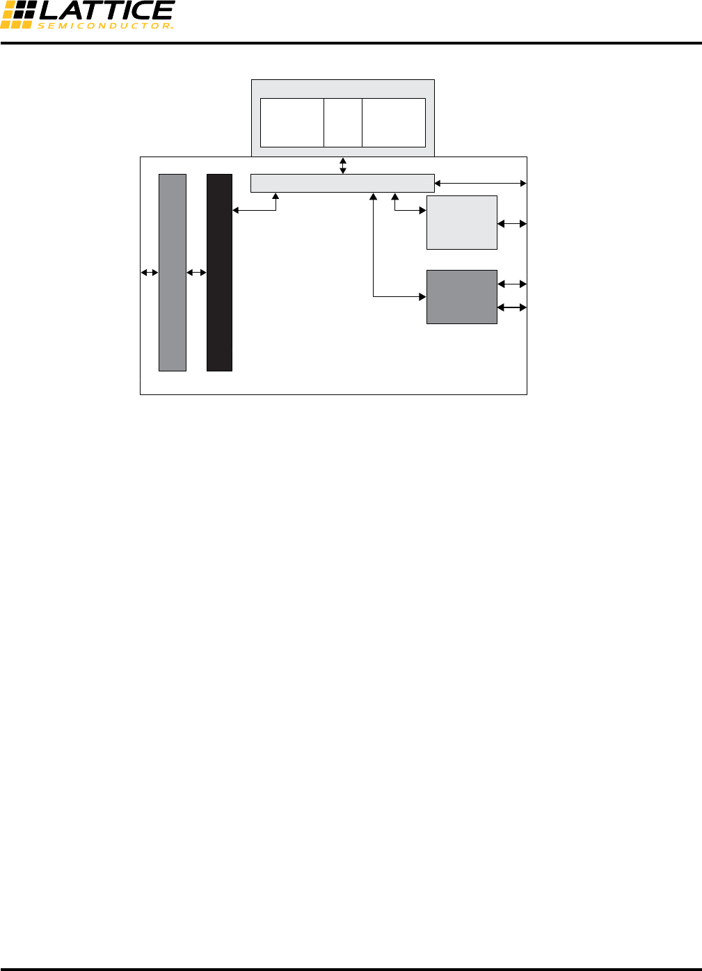
48
Using Hardened Control Functions
in MachXO3 Devices Reference Guide
Figure 29. Interfaces to the NVCM/Flash Sectors
The configuration logic arbitrates access from the interfaces by the following priority. When higher priority ports are
enabled NVCM/Flash access by lower priority ports will be blocked.
1. JTAG Port
2. Slave SPI Port
3. I2C Primary Port
4. WISHBONE Slave Interface
Note: Enabling NVCM/Flash Interface using Enable Configuration Interface command 0x74 Transparent Mode will
temporarily disable certain features of the device including:
• Power Controller
•GSR
• Hardened User SPI port
• Hardened User Primary I2C port
Functionality is restored after the NVCM/Flash Interface is disabled using Disable Configuration Interface com-
mand 0x26 followed by Bypass command 0xFF.
EFB Register Map
WISHBONE Interface
EFB
User Logic
Primary I2C Port
(Address yyyxxxxx00)
JTAG
Configuration
Slave
Configuration
Master/Slave
SPI Port
sn
Configuration
NVCM0/Flash
(including
USERCODE)
NVCM1/
UFM
NVCM/Flash Command Interface
NVCM/Flash
Feature Row
(including
TraceID)
Notes:
1. Only MachXO3L devices have NVCM.
2. Only MachXO3LF devices have Flash.

49
Using Hardened Control Functions
in MachXO3 Devices Reference Guide
NVCM/Flash Access through WISHBONE Slave Interface
The WISHBONE Slave interface of the EFB module enables designers to access the NVCM/Flash directly from the
FPGA core logic. The WISHBONE bus signals, described earlier in this document, are utilized by a WISHBONE
host that designers can implement using the general purpose FPGA resources.
The WISHBONE Interface communicates to the Configuration Logic through a set of data, control and status regis-
ters. Table 48 shows the register names and their functions. These registers are a subset of the EFB register map.
Refer to the EFB register map for specific addresses of each register.
Table 48. WISHBONE to NVCM/Flash Logic Registers
Table 49. NVCM/Flash Control
WBCE WISHBONE Connection Enable. Enables the WISHBONE to establish the read/write
connection to the NVCM/Flash logic. This bit must be set prior to executing any com-
mand through the WISHBONE port. Likewise, this bit must be cleared to terminate the
command. See Command and Data Transfers to NVCM/Flash Space for more infor-
mation on framing WISHBONE commands.
1: Enabled
0: Disabled
RSTE WISHBONE Connection Reset. Resets the input/output FIFO logic. The reset logic is
level sensitive. After setting this bit to '1' it must be cleared to '0' for normal operation.
1: Reset
0: Normal operation
Table 50. NVCM/Flash Transmit Data
CFG_Transmit_Data[7:0] CFG Transmit Data. This register holds the byte that will be written to the NVCM/Flash
logic. Bit 0 is LSB.
WISHBONE to CFG
Register Name Register Function Address Access
CFGCR Control 0x70 Read/Write
CFGTXDR Transmit Data 0x71 Write
CFGSR Status 0x72 Read
CFGRXDR Receive Data 0x73 Read
CFGIRQ Interrupt Request 0x74 Read/Write
CFGIRQEN Interrupt Request Enable 0x75 Read/Write
Note: Unless otherwise specified, all Reserved bits in writable registers shall be written ‘0’.
CFGCR 0x70
Bit 76543210
Name WBCE RSTE (Reserved)
Default 0 0 0 0 0 0 0 0
Access R/W R/W — — — — — —
CFGTXDR 0x71
Bit 76543210
Name CFG_Transmit_Data[7:0]
Default00000000
Access WWWWWWWW

50
Using Hardened Control Functions
in MachXO3 Devices Reference Guide
Table 51. NVCM/Flash Status
WBCACT WISHBONE Bus to Configuration Logic Active. Indicates that the WISHBONE to con-
figuration interface is active and the connection is established.
1: WISHBONE Active
0: WISHBONE not Active
TXFE Transmit FIFO Empty. Indicates that the Transmit Data register is empty. This bit is
capable of generating an interrupt.
1: FIFO empty
0: FIFO not empty
TXFF Transmit FIFO Full. Indicates that the Transmit Data register is full. This bit is capable
of generating an interrupt.
1: FIFO full
0: FIFO not full
RXFE Receive FIFO Empty. Indicates that the Receive Data register is empty. This bit is
capable of generating an interrupt.
1: FIFO empty
0: FIFO not empty
RXFF Receive FIFO Full. Indicates that the Transmit Data register is full. This bit is capable
of generating an interrupt.
1: FIFO full
0: FIFO not full
SSPIACT Slave SPI Active. Indicates the Slave SPI port has started actively communicating with
the Configuration Logic while WBCE was enabled. This port has priority over the I2C
and WISHBONE ports and will pre-empt any existing, and prohibit any new, lower pri-
ority transaction. This bit is capable of generating an interrupt.
1: Slave SPI port active
0: Slave SPI port not active
I2CACT I2C Active. Indicates the I2C port has started actively communicating with the Configu-
ration Logic while WBCE was enabled. This port has priority over the WISHBONE
ports and will pre-empt any existing, and prohibit any new WISHBONE transaction.
This bit is capable of generating an interrupt.
1: I2C port active
0: I2C port not active
CFGSR 0x72
Bit 7 6543210
Name WBCACT (Reserved) TXFE TXFF RXFE RXFF SSPIACT I2CACT
Default 0 0000000
Access R —RRRRRR
51
Using Hardened Control Functions
in MachXO3 Devices Reference Guide
Table 52. NVCM/Flash Receive Data
CFG_Receive_Data[7:0] CFG Receive Data. This register holds the byte read from the NVCM/Flash logic. Bit 0
in this register is LSB.
Table 53. NVCM/Flash Interrupt Status
IRQTXFE Interrupt Status for Transmit FIFO Empty.
When enabled, indicates TXFE was asserted. Write a ‘1’ to this bit to clear the inter-
rupt.
1: Transmit FIFO Empty Interrupt
0: No interrupt
IRQTXFF Interrupt Status for Transmit FIFO Full.
When enabled, indicates TXFF was asserted. Write a ‘1’ to this bit to clear the inter-
rupt.
1: Transmit FIFO Full Interrupt
0: No interrupt
IRQRXFE Interrupt Status for Receive FIFO Empty.
When enabled, indicates RXFE was asserted. Write a ‘1’ to this bit to clear the inter-
rupt.
1: Receive FIFO Empty Interrupt
0: No interrupt
IRQRXFF Interrupt Status for Receive FIFO Full.
When enabled, indicates RXFF was asserted. Write a ‘1’ to this bit to clear the inter-
rupt.
1: Receive FIFO Full Interrupt
0: No interrupt
IRQSSPIACT Interrupt Status for Slave SPI Active.
When enabled, indicates SSPIACT was asserted. Write a ‘1’ to this bit to clear the
interrupt.
1: Slave SPI Active Interrupt
0: No interrupt
IRQI2CACT Interrupt Status for I2C Active.
When enabled, indicates I2CACT was asserted. Write a ‘1’ to this bit to clear the inter-
rupt.
1: I2C Active Interrupt
0: No interrupt
CFGRXDR 0x73
Bit 76543210
Name CFG_Receive_Data[7:0]
Default00000000
AccessRRRRRRRR
CFGIRQ 0x74
Bit 765432 1 0
Name (Reserved) IRQTXFE IRQTXFF IRQRXFE IRQRXFF IRQSSPIACT IRQI2CACT
Default 000000 0 0
Access —— R/W R/W R/W R/W R/W R/W
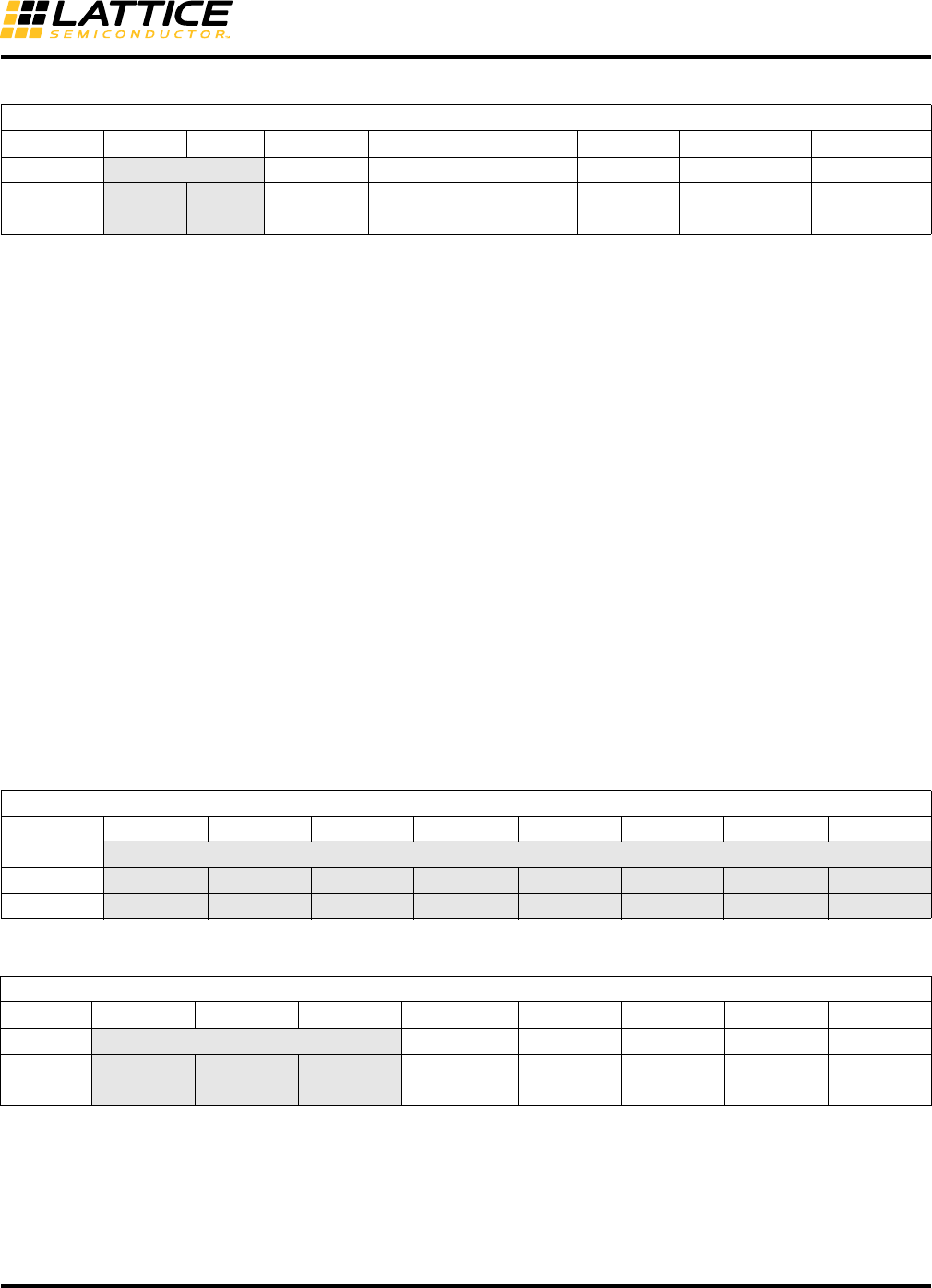
52
Using Hardened Control Functions
in MachXO3 Devices Reference Guide
Table 54. NVCM/Flash Interrupt Enable
IRQTXFEEN Interrupt Enable for Transmit FIFO Empty
1: Interrupt generation enabled
0: Interrupt generation disabled
IRQTXFFEN Interrupt Enable for Transmit FIFO Full
1: Interrupt generation enabled
0: Interrupt generation disabled
IRQRXFEEN Interrupt Enable for Receive FIFO Empty
1: Interrupt generation enabled
0: Interrupt generation disabled
IRQRXFFEN Interrupt Enable for Receive FIFO Full
1: Interrupt generation enabled
0: Interrupt generation disabled
IRQSSPIACTEN Interrupt Enable for Slave SPI Active
1: Interrupt generation enabled
0: Interrupt generation disabled
IRQI2CACTEN Interrupt Enable for I2C Active
1: Interrupt generation enabled
0: Interrupt generation disabled
Table 55. Unused (Reserved) Register
Table 56. EFB Interrupt Source
CFG_INT NVCM/Flash Interrupt Source. Indicates EFB interrupt source is from the NVCM/Flash
Block. Use CFGIRQ for further source resolution.
1: A bit is set in register CFGIRQ
0: No interrupt
CFGIRQEN 0x75
Bit 7 6 5 4 3 2 1 0
Name (Reserved) IRQTXFEEN IRQTXFFEN IRQRXFEEN IRQRXFFEN IRQSSPIACTEN IRQI2CACTEN
Default 000 0 0 0 0 0
Access —— R/W R/W R/W R/W R/W R/W
UNUSED 0x76
Bit 76543210
Name (Reserved)
Default 0 0 0 0 0 0 0 0
Access — — — — — — — —
EFBIRQ 0x77
Bit 76543210
Name (Reserved) CFG_INT TC_INT SPI_INT I2C2_INT I2C1_INT
Default 00000000
Access R R R R RRRR

53
Using Hardened Control Functions
in MachXO3 Devices Reference Guide
TC_INT Timer/Counter Interrupt Source. Indicates EFB interrupt source is from the
Timer/Counter Block. Use TCIRQ for further source resolution.
1: A bit is set in register TCIRQ
0: No interrupt
SPI_INT SPI Interrupt Source. Indicates EFB interrupt source is from the SPI Block. Use SPI-
IRQ for further source resolution.
1: A bit is set in register SPIIRQ
0: No interrupt
I2C2_INT I2C2 Interrupt Source. Indicates EFB interrupt source is from the Secondary I2C
Block. Use I2C_2_ IRQ for further source resolution.
1: A bit is set in register I2C_2_ IRQ
0: No interrupt
I2C1_INT I2C1 Interrupt Source. Indicates EFB interrupt source is from the Primary I2C Block.
Use I2C_1_ IRQ for further source resolution.
1: A bit is set in register I2C_1_ IRQ
0: No interrupt
Command and Data Transfers to NVCM/Flash Space
The command and data transfers to the NVCM/Flash are identical for all the access ports, regardless of their differ-
ent physical interfaces. The NVCM/Flash is organized in pages. Therefore, users address a specific page for Read
or Write operations to that page. Each page has 128 bits (16 bytes). The transfers are based on a set of instruc-
tions and page addresses. The NVCM/Flash is composed of three sectors, Configuration NVCM0/Flash (includes
USERCODE), NVCM1/UFM, Feature Row. The Erase operations are sector based.
Command Summary by Application
Table 57. NVCM (Sector 1)/UFM Commands
Command Name
Command
MSB LSB SVF Command Name Description
Read Status Register 0x3C LSC_READ_STATUS Read the 4-byte Configuration Status Register.
Check Busy Flag 0xF0 LSC_CHECK_BUSY Read the Configuration Busy Flag status.
Bypass 0xFF ISC_NOOP Null operation.
Enable Configuration Interface
(Transparent Mode) 0x74 ISC_ENABLE_X
Enable Transparent NVCM1/UFM access – All
user I/Os (except the hardened user SPI and
primary user I2C ports) are governed by the user
logic, the device remains in User mode. (The
subsequent commands in this table require the
interface to be enabled.)
Enable Configuration Interface
(Offline Mode) 0xC6 ISC_ENABLE
Enable Offline NVCM1 access – All user I/Os
(except persisted sysCONFIG ports) are tri-
stated. User logic ceases to function,
NVCM1/UFM remains accessible, and the device
enters 'Offline' access mode. (The subsequent
commands in this table require the interface to be
enabled.)
Disable Configuration Interface 0x26 ISC_DISABLE Disable the configuration (NVCM1/UFM)
access.
Set Address 0xB4 LSC_WRITE_ADDRESS Set the NVCM1/UFM sector 14-bit Address
Register.
Reset NVCM1/UFM Address 0x47 LSC_INIT_ADDR_NVCM1 Reset the address to point to Sector 1, Page 0
of the NVCM1/UFM.
Read NVCM1/UFM 0xCA LSC_READ_TAG
Read the NVCM1/UFM data. Operand specifies
number pages to read. Address Register is
post-incremented.

54
Using Hardened Control Functions
in MachXO3 Devices Reference Guide
Erase NVCM1/UFM 0xCB LSC_ERASE_TAG Erase the NVCM1/UFM sector only.
Program NVCM1/UFM Page 0xC9 LSC_PROG_TAG Write one page of data to the NVCM1/UFM.
Address Register is post-incremented.
Table 58. Configuration NVCM/Flash (Sector 0) Commands
Command Name
Command
MSB LSB SVF Command Name Description
Read Device ID 0xE0 IDCODE_PUB Read the 4-byte Device ID (0x01 2b 20 43).
Read USERCODE 0xC0 USERCODE Read 32-bit USERCODE.
Read Status Register 0x3C LSC_READ_STATUS Read the 4-byte Configuration Status Register.
Read Busy Flag 0xF0 LSC_CHECK_BUSY Read the Configuration Busy Flag status.
Refresh10x79 LSC_REFRESH Launch boot sequence (same as toggling PRO-
GRAMN pin).
STANDBY 0x7D LSC_DEVICE_CTRL Triggers the Power Controller to enter or wake
from standby mode.
Bypass 0xFF ISC_NOOP Null operation.
Enable Configuration Interface
(Transparent Mode) 0x74 ISC_ENABLE_X
Enable Transparent Configuration
NVCM0/Flash access – All user I/Os (except the
hardened user SPI and primary user I2C ports)
are governed by the user logic, the device
remains in User mode. (The subsequent com-
mands in this table require the interface to be
enabled.)
Enable Configuration Interface
(Offline Mode) 0xC6 ISC_ENABLE
Enable Offline Configuration NVCM0/Flash
access – All user I/Os (except persisted sys-
CONFIG ports) are tri-stated. User logic ceases
to function, and the device enters ‘Offline’
access mode. (The subsequent commands in
this table require the interface to be enabled.)
Disable Configuration Interface 0x26 ISC_DISABLE Exit access mode.
Set Configuration NVCM0/Flash
Address 0xB4 LSC_WRITE_ADDRESS Set the Configuration NVCM0/Flash 14-bit Page
Address.
Verify Device ID 0xE2 VERIFY_ID Verify device ID with 32-bit input, set Fail flag if
mismatched
Reset Configuration
NVCM0/Flash Address 0x46 LSC_INIT_ADDRESS Reset the address to point to Sector 0, Page 0
of the Configuration NVCM0/Flash.
Read NVCM0/Flash 0x73 LSC_READ_INCR_NV
Read the NVCM0/Flash data. Operand specifies
number pages to read. Address Register is
post-incremented.
Erase 0x0E ISC_ERASE
Erase the Config NVCM0/Flash, FEATURE
Row, FEABITs, Done bit, Security bits and
USERCODE.
Program Page 0x70 LSC_PROG_INCR_NV Write one page of data to the NVCM/Flash.
Address Register is post-incremented.
Program DONE 0x5E ISC_PROGRAM_DONE Program the Done bit.
Program SECURITY 0xCE ISC_PROGRAM_SECURITY Program the Security bit (Secures CFG
NVCM0/Flash sector).
Program SECURITY PLUS 0xCF ISC_PROGRAM_SECPLUS
Program the Security Plus bit (Secures CFG,
NVCM0/Flash and NVCM1/UFM Sectors). Note:
SECURITY and SECURITY PLUS commands
are mutually exclusive.
Program USERCODE 0xC2 ISC_PROGRAM_USERCODE Program 32-bit USERCODE.
Command Name
Command
MSB LSB SVF Command Name Description

55
Using Hardened Control Functions
in MachXO3 Devices Reference Guide
Table 59. Non-Volatile Register (NVR) Commands
When using the WISHBONE bus interface, the commands, operand and data are written to the CFGTXDR Regis-
ter. The Slave SPI or I2C interface shift the most significant bit (MSB) first into the MachXO3L/LF device. This is
required only when communicating with the configuration logic inside the MachXO3L/LF device.
In order to perform a Write, Read or Erase operation with the NVCM, it is required that the interface is enabled
using Command 0x74. Affected commands are noted in the Command Description as “EN Required.” Once the
modification operations are completed, the interface can be disabled using commands 0x26 and 0xFF.
Command Descriptions by Command Code
Table 60. Erase NVCM/Flash (0x0E)
Operand: 0000 ucfs 0000 0000 0000 0000(binary)
where: u: Erase NVCM1/UFM sector
0: No action
1: Erase
c: Erase CFG NVCM0/Flash sector (Config NVCM/Flash, DONE, security bits,
USERCODE)
0: No action
1: Erase
f: Erase Feature sector (Slave I2C address, sysCONFIG port persistence, Boot
mode, etc.)
0: No action
1: Erase
s: Erase SRAM
0: No action
1: Erase
Read Feature Row 0xE7 LSC_READ_FEATURE Read Feature Row.
Program Feature Row 0xE4 LSC_PROG_FEATURE Program Feature Row.
Read FEABITS 0xFB LSC_READ_FEABITS Read FEA bits.
Program FEABITs 0xF8 LSC_PROG_FEABITS Program the FEA bits.
1. The Refresh commands are not supported by the software simulation model.
Command Name
Command
msb lsb SVF Command Name Description
Read Trace ID code 0x19 UIDCODE_PUB Read 64-bit TraceID.
NVCM1/
UFM
CFG
NVCM0/
Flash NVR
EN
Required
CMD
(Hex)
Operands
(Hex) Data Mode Data Size
Data
Format
x x Y 0E See below — — —
Table 58. Configuration NVCM/Flash (Sector 0) Commands (Continued)
Command Name
Command
MSB LSB SVF Command Name Description

56
Using Hardened Control Functions
in MachXO3 Devices Reference Guide
Notes: Poll the BUSY bit (or wait, see Table 100) after issuing this command for erasure to
complete before issuing a subsequent command other than Read Status or Check
Busy.
Erased condition for NVCM/Flash bits = 0
Examples: 0x0E 04 00 00
Erase CFG NVCM0/Flash sector
0x0E 08 00 00
Erase NVCM1/UFM sector
0x0E 0C 00 00
Erase NVCM1/UFM and CFG NVCM0/Flash sectors
Table 61. Read TraceID Code (0x19)
Example: 0x19 00 00 00
Read 8-byte TraceID
Note: First byte read is user portion. Next seven bytes are unique to each silicon die.
Table 62. Disable Configuration Interface (0x26)
Example: 0x26 00 00
Disable NVCM/Flash interface for change access
Notes: Must have only two operands
The interface cannot be disabled while the Configuration Status Register Busy bit is
asserted. After commands (for example, Erase, Program) verify Busy is clear before
issuing the Disable command.
This command should be followed by Command 0xFF (BYPASS) to complete the Dis-
able operation. The BYPASS command is required to restore Power Controller, GSR,
Hardened User SPI and I2C port operation.
SRAM must be erased before exiting Offline (0xC6) Mode
NVCM1/
UFM
CFG
NVCM0/
Flash NVR
EN
Required CMD (Hex)
Operands
(Hex) Data Mode Data Size
Data
Format
x N 19 00 00 00 R 8B —
NVCM1/
UFM
CFG
NVCM0/
Flash NVR
EN
Required CMD (Hex)
Operands
(Hex) Data Mode Data Size
Data
Format
xx —2600 00———

57
Using Hardened Control Functions
in MachXO3 Devices Reference Guide
Table 63. Read Status Register (0x3C)
Data Format: Most significant byte of SR is received first, LSB last.
D bit 8 NVCM/Flash or SRAM Done Flag
When C = 0 SRAM Done bit has been programmed
• D = 1 Successful NVCM/Flash to SRAM transfer
• D = 0 Failure in the NVCM/Flash to SRAM transfer
When C=1 NVCM Done bit has been programed
• D = 1 Programmed
• D = 0 Not Programmed
C bit 9 Enable Configuration Interface (1=Enable, 0=Disable)
B bit 12: Busy Flag (1 = busy)
F bit 13: Fail Flag (1 = operation failed)
I I=0 Device verified correct, I=1 Device failed to verify
EEE bits[25:23]: Configuration Check Status
000: No Error
001: ID ERR
010: CMD ERR
011: CRC ERR
100: Preamble ERR
101: Abort ERR
110: Overflow ERR
111: SDM EOF
(all other bits reserved)
Usage: The BUSY bit should be checked following all Enable, Erase or Program operations.
Note: Wait at least 1us after power-up or asserting wb_rst_i before accessing the EFB.
Example: 0x3C 00 00 00
Read 4-byte Status Register for example, 0x00 00 20 00 (fail flag set)
Table 64. Reset CFG Address (0x46)
Example: 0x46 00 00 00
Set Address register to Configuration Sector 0, page 0
Table 65. Reset NVCM1 Address (0x47)
Example: 0x47 00 00 00
Set Address register to NVCM/Flash Sector 1, page 0
NVCM1/
UFM
CFG
NVCM0/
Flash NVR
EN
Required
CMD
(Hex)
Operands
(Hex)
Data
Mode
Data
Size Data Format (Binary)
x x N 3C 00 00 00 R 4B xxxx IxEE Exxx xxxx xxFB xxCD xxxx xxxx
NVCM1/
UFM
CFG NVCM0/
Flash NVR
EN
Required
CMD
(Hex)
Operands
(Hex) Data Mode Data Size
Data
Format
x Y 46 00 00 00 — — —
NVCM1/
UFM
CFG NVCM0/
Flash NVR
EN
Required CMD (Hex)
Operands
(Hex) Data Mode Data Size
Data
Format
x Y 47 00 00 00 — — —

58
Using Hardened Control Functions
in MachXO3 Devices Reference Guide
Table 66. Program DONE (0x5E)
Example: 0x5E 00 00 00
Set the DONE bit
Note: Poll the BUSY bit (or wait 200us) after issuing this command for programming to com-
plete before issuing a subsequent command other than Read Status or Check Busy.
Table 67. Program Configuration NVCM (0x70)
Example: 0x70 00 00 01 00 01 02 03 04 05 06 07 08 09 0A 0B 0C 0D 0E 0F
Write one page of data, pointed to by Address Register
Notes: 16 data bytes must be written following the command and operand bytes to ensure
proper data alignment. The Address Register is auto-incremented following the page
write.
Operands (0x00 00 00) are equivalent to (0x00 00 01).
Use 0x0E to erase CFG NVCM0 sector prior to executing this command.
Poll the BUSY bit (or wait 200us) after issuing this command for programming to com-
plete before issuing a subsequent command other than Read Status or Check Busy.
Table 68. Read Configuration NVCM/Flash (0x73) (SPI)
Note: This applies when Configuration NVCM/Flash is read through SPI
*Operand: 0001 0000 00pp pppp pppp pppp (binary)
pp..pp: num_pages Number of CFG NVCM0/Flash pages to read when num_pages = 1
Number of CFG NVCM0/Flash pages to read +1 when num_pages > 1
**Data Size: (num_pages * 16) bytes
Note: Read CFG NVCM0/Flash may be aborted at any time. Any data remaining in the read
FIFO will be discarded. Any read data beyond the prescribed read size will be indeter-
minate. The Address Register is auto-incremented after each page read.
***Examples: 0x73 10 00 01
0 bytes dummy followed by one page of CFG NVCM0/Flash data (16 bytes total)
0x73 10 00 04
Read 1 page dummy followed by three pages of CFG NVCM0/Flash data (four pages
total)
NVCM1/
UFM
CFG NVCM0/
Flash NVR
EN
Required
CMD
(Hex)
Operands
(Hex) Data Mode Data Size
Data
Format
x Y 5E 00 00 00 — — —
NVCM1/
UFM
CFG
NVCM0/
Flash NVR
EN
Required
CMD
(Hex)
Operands
(Hex)
Data
Mode Data Size Data Format
x Y 70 00 00 01 W 16B 16 bytes NVCM0 write data
NVCM1/
UFM
CFG NVCM0/
Flash NVR
EN
Required
CMD
(Hex)
Operands
(Hex) Data Mode Data Size
Data
Format
x Y 73 * (below) R ** (below) *** (below)

59
Using Hardened Control Functions
in MachXO3 Devices Reference Guide
Table 69. Read Configuration NVCM/Flash (0x73) (I2C/SPI)
Note: This applies when Configuration NVCM/Flash is read through I2C or SPI
*Operand: 0000 0000 00pp pppp pppp pppp (binary)
pp..pp: num_pages Number of CFG NVCM0/Flash pages to read when num_pages = 1
Number of CFG NVCM0/Flash pages to read +1 when num_pages > 1
**Data Size: (num_pages * 16) bytes when num_pages=1
32 bytes + (num_pages) * (16 + 4) bytes when num_pages>1
Note: Read CFG NVCM0/Flash may be aborted at any time. Any data remaining in the read
FIFO will be discarded. Any read data beyond the prescribed read size will be indeter-
minate. The Address Register is auto-incremented after each page read.
***Examples: 0x73 00 00 01
0 bytes dummy followed by one page CFG NVCM0/Flash data (16 bytes total)
0x73 00 00 04
Read 2 pages dummy, followed by three sets [1 page CFG NVCM0/Flash data, fol-
lowed by four bytes dummy] (five pages and 12 dummy bytes total)
Table 70. Read Configuration NVCM/Flash (0x73) (WISHBONE)
Note: This applies when Configuration NVCM/Flash is read through WISHBONE
*Operand: 0000 0000 00pp pppp pppp pppp (binary)
pp..pp: num_pages Number of CFG NVCM0/Flash pages to read when num_pages = 1
Number of CFG NVCM0/Flash pages to read +1 when
1 < num_pages ≤ 12
Set to 0x3FFF when num_pages > 12
**Data Size: (num_pages * 16) bytes when num_pages=1
32 bytes + (num_pages) * (16 + 4) bytes when num_pages>1
Note: When reading more than 12 pages, the num_pages argument is intentionally over-
sized. It is not necessary to read the extra pages. Read CFG NVCM0/Flash may be
aborted at any time. Any data remaining in the read FIFO will be discarded. Any read
data beyond the prescribed read size will be indeterminate. The Address Register is
auto-incremented after each page read.
***Examples: 0x73 00 00 01
0 bytes dummy followed by one page CFG NVCM0/Flash data (16 bytes total)
0x73 00 00 04
Read 2 pages dummy, followed by three sets [1 page CFG NVCM0/Flash data, fol-
lowed by four bytes dummy] (five pages and 12 dummy bytes total)
NVCM1/
UFM
CFG NVCM0/
Flash NVR
EN
Required
CMD
(Hex)
Operands
(Hex) Data Mode Data Size
Data
Format
x Y 73 * (below) R ** (below) *** (below)
NVCM1/
UFM
CFG NVCM0/
Flash NVR
EN
Required
CMD
(Hex)
Operands
(Hex) Data Mode Data Size
Data
Format
x Y 73 * (below) R ** (below) *** (below)

60
Using Hardened Control Functions
in MachXO3 Devices Reference Guide
Note: The maximum speed which one page of data (num_page=1) can be read using
WISHBONE and no wait states is 16.6 MHz. Faster WISHBONE clock speeds are
supported by inserting WB wait states to observe the retrieval delay timing require-
ment. For more information, refer to the Reading Flash Pages section of TN1204,
MachXO2 Programming and Configuration Usage Guide.
Table 71. Enable Configuration Interface (Transparent) (0x74)
Notes: The I2C interface uses only two operands all other interfaces use three operands. This
command is required to enable modification of the NVCM1/UFM, configuration CFG
NVCM0/Flash, or non-volatile registers (NVR). Terminate this command with command
0x26 followed by command 0xFF.
Exercising this command will temporarily disable certain features of the device, nota-
bly GSR, user SPI port, primary user I2C port and Power Controller. These features
are restored when the command is terminated.
Poll the BUSY bit (or wait 5us) after issuing this command for the NVCM/Flash pumps
to fully charge.
Example: 0x74 08 00 00
Enable NVCM/Flash interface for change access through a non-I2C interface.
Table 72. Refresh (0x79)
Example: 0x79 00 00
Issue Refresh command
Note: The Refresh command will Launch Boot sequence
Must have only two operands
After completing the Refresh command (for example, SPI SN deassertion or I2C stop),
further bus accesses are prohibited for the duration of tREFRESH. Violating this require-
ment will cause the Refresh process to abort and leave the MachXO3L/LF device in
an unprogrammed state.
Occasionally, following a device REFRESH or PROGRAMN pin toggle, the secondary
I2C port may be left in an undefined (non-idle) state. The likely hood of this condition is
design and route dependent. To positively return the Secondary I2C port to the idle
state, write a value of 0x44 to register I2C_2_CMDR via WISHBONE immediately
after device reset is released. This will cause a short low-pulse on SCK as the hard-
block signals a STOP on the bus then returns to the idle state. Failure to manually
return the Secondary I2C port to the idle state may result in an I2C bus lock-up condi-
tion. Normal I2C activity can be commenced without additional delay.
NVCM1/
UFM
CFG NVCM0/
Flash NVR
EN
Required
CMD
(Hex)
Operands
(Hex) Data Mode Data Size
Data
Format
xx —74
08 00 00 or
08 00 ———
NVCM1/
UFM
CFG
NVCM0/
Flash NVR
EN
Required
CMD
(Hex)
Operands
(Hex) Data Mode Data Size
Data
Format
(Binary)
79 00 00 — — —

61
Using Hardened Control Functions
in MachXO3 Devices Reference Guide
Table 73. STANDBY (0x7D)
Example: 0x7D 0y 00
y:2 Triggers the Power Controller to enter standby mode
y:8 Triggers the Power Controller to wakeup from standby mode
Notes: Must have only two operands.
The MachXO3L/LF Power Controller needs to be included in the design.
Additionally the following can be used to trigger the Power Controller to wakeup from
standby mode (if the user logic standby signal has not been enabled):
1. I2C has the following ways:
a. Primary I2C Configuration port – Address match to the I2C Configuration
address (No other settings required)
b. Primary or Secondary I2C User port – Address match the I2C User
address. Must have I2C_1_CR[WKUPEN] or I2C_1_CR[WKUPEN] set
c. General Call – Send the General Call Wakeup command (0xF3). Must
have General Calls enabled (I2C_1_CR[GCEN] or I2C_2_CR[GCEN] set)
and use the General Call address
2. SPI from the assertion of either Slave Configuration (sn) or User (spi_scsn)
chip select, as long as the appropriate control register bit is set:
a. Configuration: SPICR1[WKUPEN_CFG]
b. User: SPICR[WKUPEN_USER]
For more information on the Power Controller refer to TN1289, Power Estimation and
Management for MachXO3 Devices.
Table 74. Set Address (0xB4)
Data Format: s: sector
0: CFG NVCM0/Flash
1: NVCM1/UFM
aa..aa:address14-bit page address
Example: 0xB4 00 00 00 40 00 00 0A
Set Address register to NVCM1/UFM sector, page 10 decimal
Table 75. Read USERCODE (0xC0)
NVCM1/
UFM
CFG NVCM0/
Flash NVR
EN
Required
CMD
(Hex)
Operands
(Hex) Data Mode Data Size
Data Format
(Binary)
x N 7D 0y 00 — — —
NVCM1/
UFM
CFG
NVCM0/
Flash NVR
EN
Required
CMD
(Hex)
Operands
(Hex)
Data
Mode
Data
Size Data Format (Binary)
x x Y B4 00 00 00 W 4B 0s00 0000 0000 0000 00aa aaaa aaaa aaaa
NVCM1/
UFM
CFG NVCM0/
Flash NVR
EN
Required
CMD
(Hex)
Operands
(Hex) Data Mode Data Size
Data
Format
(Hex)
x Y/N C0 00 00 00 R 4B —

62
Using Hardened Control Functions
in MachXO3 Devices Reference Guide
Example: 0xC0 00 00 00
EN Required = Y Read 4-byte USERCODE from CFG NVCM0 sector
EN Required = N Read 4-byte USERCODE from SRAM
Table 76. Program USERCODE (0xC2)
Example: 0xC2 00 00 00 10 20 30 40
Sets USERCODE with 32-bit input 0x10 20 30 40
Note: Poll the BUSY bit (or wait 200us) after issuing this command for programming to com-
plete before issuing a subsequent command other than Read Status or Check Busy.
Table 77. Enable Configuration Interface (Offline) (0xC6)
Operand: 08 00 00 - Enable NVCM/Flash Normal mode. Normal edit mode for Offline configura-
tion. Used for all offline commands described in this document, including
Erase SRAM.
00 00 00 - Enable SRAM mode. Optional edit mode. Supports Erase SRAM com-
mand only.
Example: 0xC6 08 00 00 Enable NVCM/Flash interface for offline change access.
Notes: Use this command to enable offline modification of the NVCM/Flash, or non-volatile
registers (NVR). SRAM must be erased exiting Offline mode. When exiting Offline
mode follow the command 0x26 with the command 0xFF. Exercising this command
will tri-state all user I/Os (except persisted sysCONFIG ports). User logic ceases to
function. NVCM1/UFM remains accessible.
Poll the BUSY bit (or wait 5 µs) after issuing this command for the NVCM/Flash pumps
to fully charge.
Table 78. Program NVCM1/UFM (0xC9)
Example: 0xC9 00 00 01 00 01 02 03 04 05 06 07 08 09 0A 0B 0C 0D 0E 0F
Write one page of data, pointed to by Address Register
NVCM1/
UFM
CFG NVCM0/
Flash NVR
EN
Required
CMD
(Hex)
Operands
(Hex) Data Mode Data Size
Data
Format
(Hex)
x Y C2 00 00 00 W 4B —
NVCM1/
UFM
CFG NVCM0/
Flash NVR
EN
Required
CMD
(Hex)
Operands
(Hex) Data Mode Data Size
Data
Format
x C6 0y 00 00 — — —
NVCM1/
UFM
CFG
NVCM0/
Flash NVR
EN
Required CMD (Hex)
Operands
(Hex) Data Mode Data Size
Data
Format
x Y C9 00 00 01 W 16B 16 bytes NVCM0
write data

63
Using Hardened Control Functions
in MachXO3 Devices Reference Guide
Notes: 16 data bytes must be written following the command and operand bytes to ensure
proper data alignment. The Address Register is auto-incremented following the page
write.
Use 0x0E or 0xCB to erase NVCM1/UFM sector prior to executing this command.
Poll the BUSY bit (or wait 200us) after issuing this command for programming to com-
plete before issuing a subsequent command other than Read Status or Check Busy.
Table 79. Read NVCM1/UFM (0xCA) (SPI)
*Operand: 0001 0000 00pp pppp pppp pppp (binary)
where: pp..pp: num_pages Number of NVCM1/UFM pages to read when num_pages = 1
Number of NVCM1/UFM pages to read +1 when num_pages > 1
**Data Size (num_pages * 16) bytes
Note: Read NVCM1/UFM may be aborted at any time. Any data remaining in the read fifo
will be discarded. Any read data beyond the prescribed read size will be indetermi-
nate. The Address Register is auto-incremented after each page read.
***Examples: 0xCA 10 00 01
Read 0 bytes dummy followed by one page NVCM1/UFM data (16 bytes total)
0xCA 10 00 04
Read one page dummy followed by three pages NVCM1/UFM data (four pages total)
Table 80. Read NVCM1/UFM (0xCA) (SPI/I2C)
*Operand: 0000 0000 00pp pppp pppp pppp (binary)
where: pp..pp: num_pages Number of NVCM1/UFM pages to read when num_pages = 1
Number of NVCM1/UFM pages to read +1 when num_pages > 1
**Data Size: (num_pages * 16) bytes when num_pages=1
32 bytes + (num_pages * 16 + 4) bytes when num_pages>1
Note: Read NVCM1/UFM may be aborted at any time. Any data remaining in the read fifo
will be discarded. Any read data beyond the prescribed read size will be indetermi-
nate. The Address Register is auto-incremented after each page read.
***Examples: 0xCA 00 00 01
Read 0 bytes dummy followed by one page NVCM1/UFM data (16 bytes total)
0xCA 00 00 04
Read two pages dummy followed by three sets [one page NVCM1/UFM data, followed
by four bytes dummy] (five pages total and 12 dummy bytes)
NVCM1/
UFM
CFG NVCM0/
Flash NVR
EN
Required
CMD
(Hex)
Operands
(Hex) Data Mode Data Size
Data
Format
x Y CA *(below) R **(below) ***(below)
NVCM1/
UFM
CFG NVCM0/
Flash NVR
EN
Required
CMD
(Hex)
Operands
(Hex) Data Mode Data Size
Data
Format
x Y CA *(below) R **(below) ***(below)

64
Using Hardened Control Functions
in MachXO3 Devices Reference Guide
Table 81. Read NVCM1/UFM (0xCA) (WISHBONE)
*Operand: 0000 0000 00pp pppp pppp pppp (binary)
where: pp..pp: num_pages Number of NVCM1/UFM pages to read when num_pages = 1
Number of NVCM1/UFM pages to read +1 when
1 < num_pages ≤ 12
Set to 0x3FFF when num_pages > 12
**Data Size: (num_pages * 16) bytes when num_pages=1
32 bytes + (num_pages * 16 + 4) bytes when num_pages>1
Note: When reading more than 12 pages, the num_pages argument is intentionally over-
sized. It is not necessary to read the extra pages. Read NVCM1/UFM may be aborted
at any time. Any data remaining in the read fifo will be discarded. Any read data
beyond the prescribed read size will be indeterminate. The Address Register is auto-
incremented after each page read.
***Examples: 0xCA 00 00 01
Read 0 bytes dummy followed by one page NVCM1/UFM data (16 bytes total)
0xCA 00 00 04
Read two pages dummy followed by three sets [one page NVCM1/UFM data, followed
by four bytes dummy] (five pages total and 12 dummy bytes)
Note: The maximum WISHBONE clock speed with which one page of data (num_page=1)
can be read using WISHBONE and no wait states is 16.6 MHz. Faster WISHBONE
clock speeds are supported by inserting WB wait states to observe the retrieval delay
timing requirement. For more information, refer to the Reading Flash Pages section of
TN1204, MachXO2 Programming and Configuration Usage Guide.
Table 82. Erase NVCM1 (0xCB)
Notes: Erased condition for NVCM1 bits = ‘0’
Poll the BUSY bit (or wait, see Table 100) after issuing this command for erasure to
complete before issuing a subsequent command other than Read Status or Check
Busy.
Example: 0xCB 00 00 00
Erase NVCM1/UFM sector
Table 83. Program SECURITY (0xCE)
NVCM1/
UFM
CFG NVCM0/
Flash NVR
EN
Required
CMD
(Hex)
Operands
(Hex) Data Mode Data Size
Data
Format
x Y CA *(below) R **(below) ***(below)
NVCM1/
UFM
CFG NVCM0/
Flash NVR
EN
Required
CMD
(Hex)
Operands
(Hex) Data Mode Data Size
Data
Format
x Y CB 00 00 00 — — —
NVCM1/
UFM
CFG NVCM0/
Flash NVR
EN
Required
CMD
(Hex)
Operands
(Hex) Data Mode Data Size
Data
Format
x Y CE 00 00 00 — — —

65
Using Hardened Control Functions
in MachXO3 Devices Reference Guide
Example: 0xCE 00 00 00
Set the SECURITY bit
Note: Poll the BUSY bit (or wait 200us) after issuing this command for programming to com-
plete before issuing a subsequent command other than Read Status or Check Busy.
SECURITY and SECURITY PLUS commands are mutually exclusive.
Table 84. Program SECURITY PLUS (0xCF)
Example: 0xCF 00 00 00
Set the SECURITY PLUS bit
Note: Poll the BUSY bit (or wait 200us) after issuing this command for programming to com-
plete before issuing a subsequent command other than Read Status or Check Busy.
SECURITY and SECURITY PLUS commands are mutually exclusive.
Table 85. Read Device ID Code (0xE0)
Example: 0xE0 00 00 00
Read 4-byte device ID
NVCM1/
UFM
CFG NVCM0/
Flash NVR
EN
Required
CMD
(Hex)
Operands
(Hex) Data Mode Data Size
Data For-
mat
x Y CF 00 00 00 — — —
NVCM1/
UFM
CFG NVCM0/
Flash NVR
EN
Required
CMD
(Hex)
Operands
(Hex) Data Mode Data Size
Data Format
(Hex)
x N E0 00 00 00 R 4B See Table 86

66
Using Hardened Control Functions
in MachXO3 Devices Reference Guide
Table 86. Device ID
Example: 0xE0 00 00 00
Read 4-byte device ID
Table 87. Verify Device ID Code (0xE2)
Example: 0xE2 00 00 00 01 2B 20 43
Verify device ID with 32-bit input, sets ID Error bit 27 in SR if mismatched
Table 88. Program Feature Row (0xE4)
Data Format: ss: 8 bits for the user programmable I2C Slave Address
uu: 8 bits for the user programmable TraceID
cc cc cc cc: 32 bits of Custom ID code
Note: It is not recommended to reprogram the Feature Row in system as it should be pro-
grammed ideally once during manufacturing.
Device Name E Devices C Devices
MachXO3L-640E-MG121 0xC1 2B 20 43 —
MachXO3L-1300 0x41 2B 20 43 0xC1 2B B0 43
MachXO3L-1300E-MG256 0xC1 2B 30 43 —
MachXO3L-2100 0x41 2B 30 43 0x41 2B B0 43
MachXO3L-2100E-MG324 0xC1 2B 40 43 —
MachXO3L-2100C-BG324 — 0xC1 2B C0 43
MachXO3L-4300 0x41 2B 40 43 0x41 2B C0 43
MachXO3L-4300C-BG400 — 0xC1 2B D0 43
MachXO3L-6900 0x41 2B 50 43 0x41 2B D0 43
MachXO3L-9400 0x41 2B 60 43 0x41 2B E0 43
MachXO3LF-640E-MG121 0xE1 2B 20 43 —
MachXO3LF-1300 0x61 2B 20 43 0xE1 2B B0 43
MachXO3LF-1300E-MG256 0xE1 2B 30 43 —
MachXO3LF-2100 0x61 2B 30 43 0x61 2B B0 43
MachXO3LF-2100E-MG324 0xE1 2B 40 43 —
MachXO3LF-2100C-BG324 — 0xE1 2B C0 43
MachXO3LF-4300 0x61 2B 40 43 0x61 2B C0 43
MachXO3LF-4300C-BG400 — 0xE1 2B D0 43
MachXO3LF-6900 0x61 2B 50 43 0x61 2B D0 43
MachXO3LF-9400 0x61 2B 60 43 0x61 2B E0 43
NVCM1/
UFM
CFG NVCM0/
Flash NVR
EN
Required
CMD
(Hex)
Operands
(Hex) Data Mode Data Size
Data Format
(Hex)
x Y E2 00 00 00 W 4B See Table 86
NVCM1/
UFM
CFG NVCM0/
Flash NVR
EN
Required
CMD
(Hex)
Operands
(Hex) Data Mode Data Size
Data Format
(Hex)
Y E4 00 00 00 8B 00 00 ss uu cc
cc cc cc

67
Using Hardened Control Functions
in MachXO3 Devices Reference Guide
Example: 0xE4 00 00 00 00 00 01 00 00 00 12 34
Program Feature Row with User I2C address set to 1, default user TraceID string, Cus-
tom ID code of 12 34
Table 89. Read Feature Row (0xE7)
Data Format: ss: 8 bits for the user programmable I2C Slave Address
uu: 8 bits for the user programmable TraceID
cc cc cc cc: 32 bits of Custom ID code
Example: 0xE7 00 00 00
Reads the Feature Row
Table 90. Check Busy Flag (0xF0)
Data Format: B: bit 7: Busy Flag (1= busy)
(all other bits reserved)
Example: 0xF0 00 00 00
Read one byte, for example, 0x80 (busy flag set)
Table 91. Program FEABITs (0xF8)
Data Format: bb: Boot Sequence
1. If b=00 (Default) and m=0 then Single Boot from NVCM/Flash
2. If b=00 and m=1 then Dual Boot from NVCM/Flash then External if there
is a failure
3. If b=01 and m=1 then Single Boot from External Flash
m: Master SPI Port Persistence
0=Disabled (Default), 1=Enabled
i: I2C Port Persistence
0=Enabled (Default), 1=Disabled
s: Slave SPI Port Persistence
0=Enabled (Default), 1=Disabled
j: JTAG Port Persistence
0=Enabled (Default), 1=Disabled
NVCM1/
UFM
CFG NVCM0/
Flash NVR
EN
Required
CMD
(Hex)
Operands
(Hex) Data Mode Data Size
Data Format
(Hex)
x Y E7 00 00 00 R 8B 00 00 ss uu cc
cc cc cc
NVCM1/
UFM
CFG
NVCM0/
Flash NVR
EN
Required
CMD
(Hex)
Operands
(Hex) Data Mode Data Size
Data Format
(Binary)
x x N F0 00 00 00 R 1B Bxxx xxxx
NVCM1/
UFM
CFG
NVCM0/
Flash NVR
EN
Required
CMD
(Hex)
Operands
(Hex) Data Mode Data Size Data Format (Binary)
x Y F8 00 00 00 W 2B 00 bb mi sj di pa wv 00

68
Using Hardened Control Functions
in MachXO3 Devices Reference Guide
d: DONE Persistence
0=Disabled (Default), 1=Enabled
i: INITN Persistence
0=Disabled (Default), 1=Enabled
p: PROGRAMN Persistence
0=Enabled (Default), 1=Disabled
a: my_ASSP Enabled
0=Disabled (Default), 1=Enabled
w: Password (Flash Protect Key) Protect All Enabled
0=Disabled (Default), 1=Enabled
v: Password (Flash Protect Key) Enabled
0=Disabled (Default), 1=Enabled
Note: It is not recommended to reprogram the FEABITs in system as it should be pro-
grammed ideally once during manufacturing.
Example: 0xF8 00 00 00 0D 20
Programs the FEABITs
Table 92. Read FEABITs (0xFB)
Data Format: bb: Boot Sequence
1. If b=00 (Default) and m=0 then Single Boot from NVCM/Flash
2. If b=00 and m=1 then Dual Boot from NVCM/Flash then External if there
is a failure
3. If b=01 and m=1 then Single Boot from External Flash
m: Master SPI Port Persistence
0=Disabled (Default), 1=Enabled
i: I2C Port Persistence
0=Enabled (Default), 1=Disabled
s: Slave SPI Port Persistence
0=Enabled (Default), 1=Disabled
j: JTAG Port Persistence
0=Enabled (Default), 1=Disabled
d: DONE Persistence
0=Disabled (Default), 1=Enabled
i: INITN Persistence
0=Disabled (Default), 1=Enabled
p: PROGRAMN Persistence
0=Enabled (Default), 1=Disabled
NVCM1/
UFM
CFG
NVCM0/
Flash NVR
EN
Required
CMD
(Hex)
Operands
(Hex) Data Mode Data Size Data Format (Binary)
x Y FB 00 00 00 R 2B 00 bb mi sj di pa wv 00

69
Using Hardened Control Functions
in MachXO3 Devices Reference Guide
a: my_ASSP Enabled
0=Disabled (Default), 1=Enabled
w: Password (Flash Protect Key) Protect All Enabled
0=Disabled (Default), 1=Enabled
v: Password (Flash Protect Key) Enabled
0=Disabled (Default), 1=Enabled
Table 93. Bypass (Null Operation) (0xFF)
Note: Operands are optional
Example: 0xFF FF FF FF Bypass
NVCM1/
UFM
CFG
NVCM0/
Flash NVR
EN
Required
CMD
(Hex)
Operands
(Hex) Data Mode Data Size
Data Format
(Binary)
x x x N FF FF FF FF — — —

70
Using Hardened Control Functions
in MachXO3 Devices Reference Guide
Interface to NVCM/Flash
The WISHBONE interface of the EFB module allows a WISHBONE host to access the configuration resources of
the MachXO3L/LF devices. This can be particularly useful for reading data from configuration resources such as
USERCODE and TraceID. Most importantly, this feature allows users to update the NVCM/Flash array of the
devices while the device is in operation mode. This is a self-configuration operation. Upon power-up or a configura-
tion refresh operation, the new content of the NVCM is loaded into the Configuration SRAM and the device contin-
ues operation with a new configuration.
The data transfer and execution of operations is the same as the one documented in the NVCM1/UFM section of
this document. This is due to the fact that the NVCM1/UFM is also a NVCM/Flash resource and the communication
between the WISHBONE host and the configuration logic is performed through the same command, status and
data registers. Please see Tables 48 to 96 for information on these registers.
Figure 30 shows a basic flow diagram for implementing a NVCM/Flash Update initiated via any of the sysCONFIG
ports (I2C, SPI, or WISHBONE).
For detailed information on MachXO3L/LF programming and configuration, see TN1279, MachXO3 Programming
and Configuration Usage Guide.
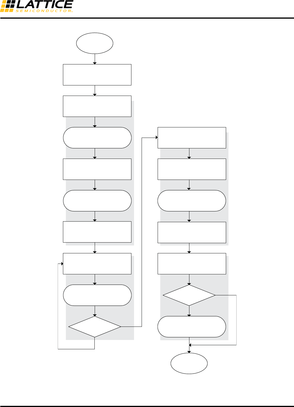
71
Using Hardened Control Functions
in MachXO3 Devices Reference Guide
Figure 30. Basic Configuration NVCM1/UFM Program Example
Start
Enable Transparent
Configuration (0x74)
Ensure unused Configuration
Ports are Inactive
Write more data?
Set NVCM DONE bit (0x5E)
Y
N
Write 1 Page Config Data
(0x70)
Wait for !BUSY (0xF0)
then verify !FAIL (0x3C)
(optional)
Set USERCODE (0xC2)
Set SECURITY (0xCE, 0xCF)
N
Y
Erase NVCM
Sector (0x0E)
Wait for !BUSY (0xF0)
then verify !FAIL (0x3C)
Set Address to 0 (0x46)
Wait for !BUSY (0xF0)
then verify !FAIL (0x3C)
Issue REFRESH (0x79)
Wait for tREFRESH
then verify DONE (0x3C)
Configure via
WISHBONE?
Done
N
Disable Configuration (0x26)
Wait for !BUSY (0xF0)
then verify !FAIL (0x3C)
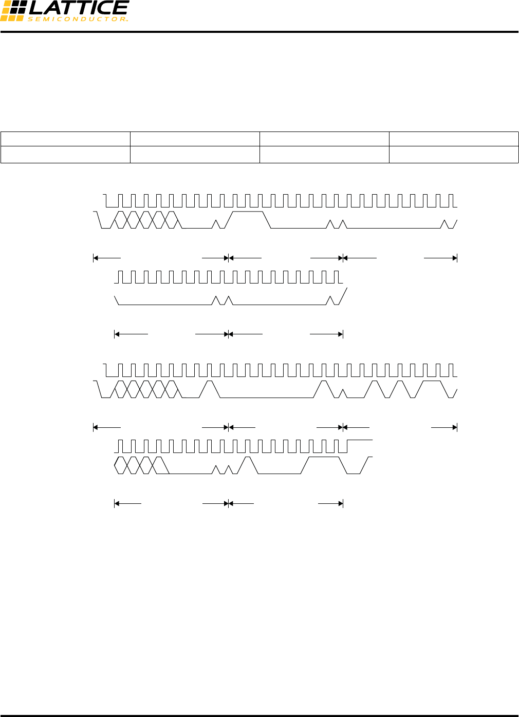
72
Using Hardened Control Functions
in MachXO3 Devices Reference Guide
Command Framing
I2C Framing
Each command string sent to the I2C EFB port must be correctly “framed” using the protocol defined for each inter-
face. In the case of I2C, the protocol is well known and defined by the industry as shown below.
Table 94. Command Framing Protocol, by Interface
Figure 31. I2C Read Device ID Example
Interface Pre-op (+) Command String Post-op (-)
I2CStart (Command/Operands/Data) Stop
SCL
A6 A5 A4 A3 A2 0 W11100000 00000000
SDA
SCL
(continued)
00000000
SDA
(continued)
00000000
0
...
...
...
...
Start By
Master
ACK By
MachXO3
ACK By ACK By
Frame 1 I
2
C Slave Address Byte Frame 2 CMD Byte Frame 3 Op Byte 1
Frame 4 Op Byte 2
ACK By
Frame 5 Op Byte 3
ACK By
A6 A5 A4 A3 A2 0 R 00000001 00101011
01000011
ID
0000
0
...
...
Restart
By Master
ACK By ACK By
Master
ACK By
Master
Frame 6 I
2
C Slave Address Byte Frame 7 Read ID Byte 1 Frame 8 Read ID Byte 2
Frame 9 Read ID Byte 3
ACK By
Master
Frame 10 Read ID Byte 4
NACK By
Master
Stop By
Master
SCL
(continued)
SDA
(continued)
SCL
(continued)
SDA
(continued)
ID ID ID
MachXO3 MachXO3
MachXO3 MachXO3
MachXO3
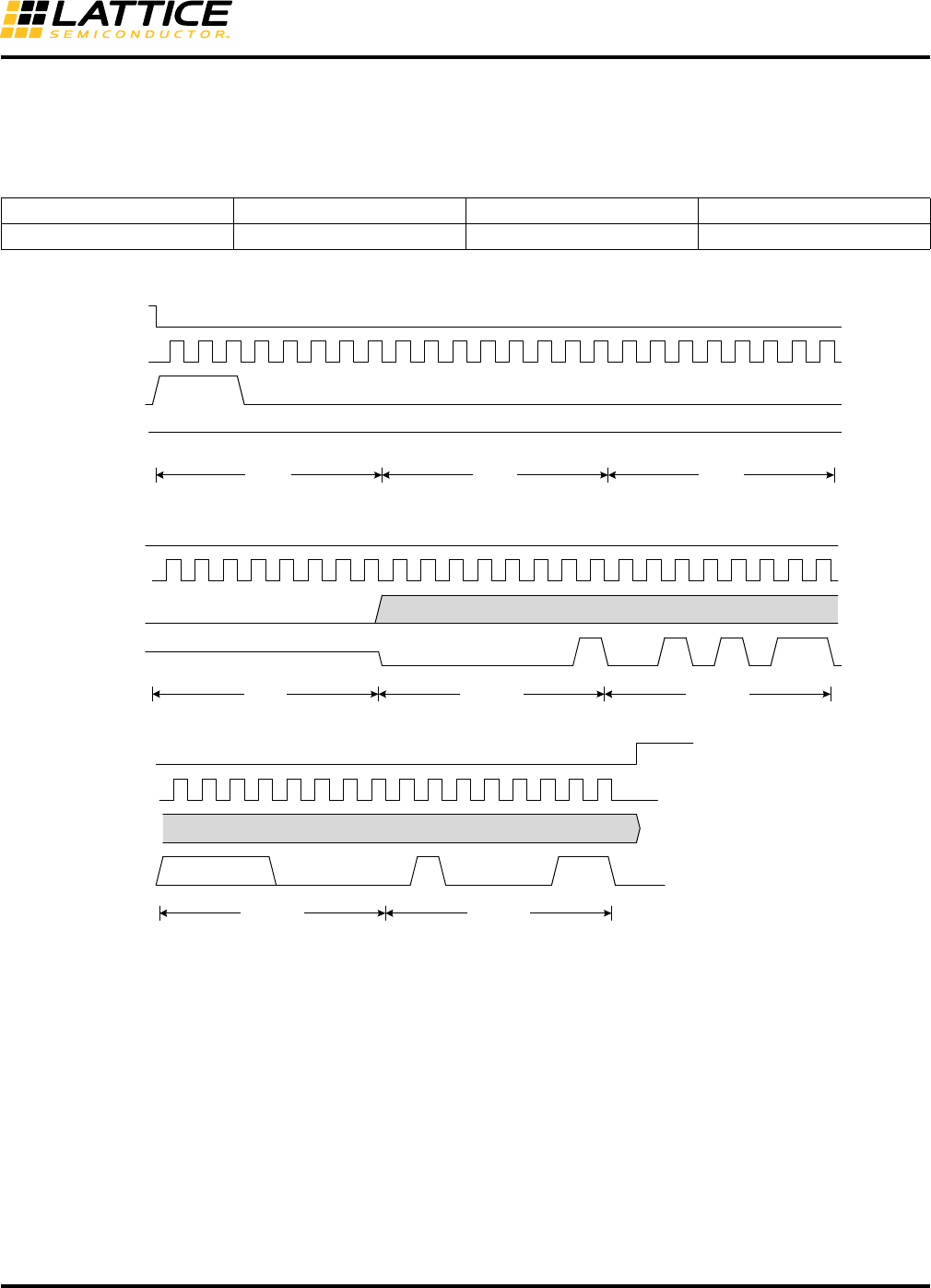
73
Using Hardened Control Functions
in MachXO3 Devices Reference Guide
SPI Framing
Each command string sent to the SPI EFB port must be correctly ‘framed’ using the protocol defined for each inter-
face. In the case of SSPI the protocol is well known and defined by the industry as shown below:
Table 95. Command Framing Protocol, by Interface
Figure 32. SSPI Read Device ID Example
Interface Pre-op (+) Command String Post-op (-)
SPI Assert CS (Command/Operands/Data) De-assert CS
111000000000000000000000
CMD Byte Op Byte 1 Op Byte 2
SCSN
SPI_SCK
MOSI
MISO
...
...
...
...
00000000
Op Byte 3 Read ID Byte 1 Read ID Byte 2
(continued)
(continued)
(continued)
(continued)
...
...
...
...
IDIDIDID000001000011
Read ID Byte 3 Read ID Byte 4
(continued)
(continued)
(continued)
(continued)
000000010010101 1
SCSN
SPI_SCK
MOSI
MISO
SCSN
SPI_SCK
MOSI
MISO
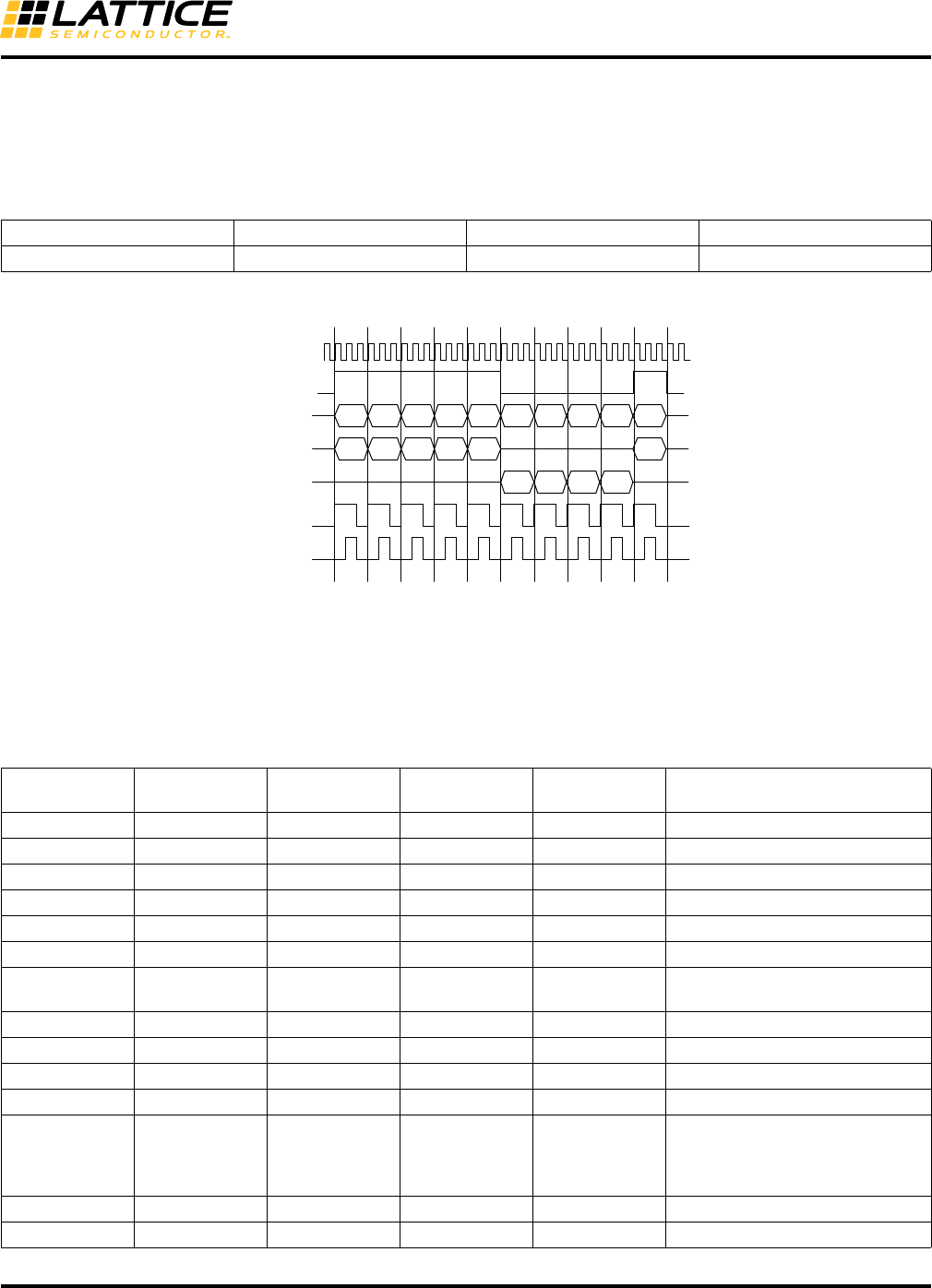
74
Using Hardened Control Functions
in MachXO3 Devices Reference Guide
WISHBONE Framing
To access the NVCM each command string sent to the WISHBONE EFB ports must be correctly ‘framed’ using the
protocol defined for each interface. In the case of the internal WISHBONE port, each command string is preceded
by setting CFGCR[WBCE]. Similarly, each command string is followed by clearing the CFGCR[WBCE] bit.
Table 96. Command Framing Protocol, by Interface
Figure 33. WISHBONE Read Device ID Example (-1200 HC Device)
NVCM1/Flash Write and Read Examples
The NVCM/Flash sectors support page-oriented read and write operations while erase operations are sector-
based. Consistent with many NVCM/Flash devices, byte-oriented operations are not supported.
Interface Pre-op (+) Command String Post-op (-)
WISHBONE Assert CFGCR[WBCE] (Command/Operands/Data) De-assert CFGCR[WBCE]
Table 97. Write Two NVCM1/UFM Pages
Instruction
Number R/W1 CMD2 Operand Data Comment
+ Open frame
1 W 74 08 00 00 — Enable Configuration Interface
– Close frame
+
2 W 3C 00 00 00 — Poll Configuration Status Register
R xx xx bx xx
–(Repeat until Busy Flag not set, or
wait 5us if not polling)
+
3 W 47 00 00 00 — Init NVCM1/UFM Address to 0000
–
+
4 W C9 00 00 01
00 01 02 03
04 05 06 07
08 09 0A 0B
0C 0D 0E 0F
Write NVCM1/UFM Page 0 Data
–
+
70 71 71 71 71 73 73 73 73 70
80 E0 00 00 00 00
wb_adr_i
wb_dat_i
C1 2B 20 43
wb_dat_o
wb_we_i
wb_str_i
wb_ack_o
wb_clk_i

75
Using Hardened Control Functions
in MachXO3 Devices Reference Guide
5 W 3C 00 00 00 — Poll Configuration Status Register
R xx xx bx xx
–(repeat until Busy Flag not set, or
wait 200 µs if not polling)
+
6 W C9 00 00 01
10 11 12 13
14 15 16 17
18 19 1A 1B
1C 1D 1E 1F
Write NVCM1/UFM Page 1 Data
(Note: Address automatically incre-
mented)
–
+
7 W 3C 00 00 00 — Poll Configuration Status Register
R xx xx bx xx
–(poll until Busy Flag clear, or wait
200us if not polling)
+
8 W 26 00 00 — Disable Configuration Interface
–
+
9 W FF — — Bypass (NOP)
–
1. When accessing NVCM/Flash via WISHBONE use CFGTXDR (0x71) to write data and CFDRXDR (0x73) to read data.
2. ‘+’ and ‘–’ refer to the command framing protocol appropriate for the interface, discussed in the Command Framing section.
Table 97. Write Two NVCM1/UFM Pages (Continued)
Instruction
Number R/W1 CMD2 Operand Data Comment

76
Using Hardened Control Functions
in MachXO3 Devices Reference Guide
Table 98. Read One NVCM1/UFM Page (All Devices, WISHBONE/SPI)
Instruction
Number R/W1 CMD2 Operand Data Comment
+ Open frame
1 W 74 08 00 00 — Enable Configuration Interface
– Close frame
+
2 W 3C 00 00 00 — Poll Configuration Status Register
R xx xx bx xx
–(Repeat until Busy Flag not set, or
wait 5us if not polling)
+
3 W B4 00 00 00 40 00 00 01 Set NVCM1/UFM Address to 0001
–
+
4 W CA 10 00 01 Read one page NVCM1/UFM
(page 1) data
R
10 11 12 13
14 15 16 17
18 19 1A 1B
1C 1D 1E 1F
–
+
5 W 26 00 00 — Disable Configuration Interface
–
+
6 W FF — — Bypass (NOP)
–
1. When accessing NVCM/Flash via WISHBONE use CFGTXDR (0x71) to write data and CFDRXDR (0x73) to read data.
2. ‘+’ and ‘–’ refer to the command framing protocol appropriate for the interface, discussed in Command Framing section.

77
Using Hardened Control Functions
in MachXO3 Devices Reference Guide
Table 99. Read Two NVCM1/UFM Pages (WISHBONE/SPI)
Instruction
Number R/W1 CMD2 Operand Data Comment
+ Open frame
1 W 74 08 00 00 — Enable Configuration Interface
– Close frame
+
2 W 3C 00 00 00 — Poll Configuration Status Register
R xx xx bx xx
–(Repeat until Busy Flag not set, or
wait 5 µs if not polling)
+
3 W 47 00 00 00 — Init NVCM1/UFM address to 0000
–
+
4 W CA 10 00 03
Read two pages of NVCM1/UFM
data, after one page of dummy
bytes.3
R
xx xx xx xx
xx xx xx xx
xx xx xx xx
xx xx xx xx
00 01 02 03
04 05 06 07
08 09 0A 0B
0C 0D 0E 0F
10 11 12 13
14 15 16 17
18 19 1A 1B
1C 1D 1E 1F
–
+
5 W 26 00 00 — Disable Configuration Interface
–
+
6 W FF — — Bypass (NOP)
–
1. When accessing NVCM/Flash via WISHBONE use CFGTXDR (0x71) to write data and CFDRXDR (0x73) to read data.
2. ‘+’ and ‘–’ refer to the command framing protocol appropriate for the interface
3. num_pages count must include dummy page.

78
Using Hardened Control Functions
in MachXO3 Devices Reference Guide
NVCM/Flash Performance
Table 100. NVCM/Flash Performance in MachXO3L/LF Device1
Erase/Program/Verify Time Calculation Example
Using the data above, it is possible to roughly calculate the time required to perform an Program/Verify operation.
The calculation assumes nearly 100% bus utilization. Overhead required by bus master processes, if any, is not
accounted for in the equation below.
E/P/V time (µs): tEraseProgramVerify = tErase + tProgram + tVerify
where: tErase = tEraseCFG + tEraseNVCM11
tProgram = 0.2 µs * number of Pages to program2
tVerify = (8 * number of Pages programmed) * BusEff * tBUSCLK
MachXO3L/LF
-640
MachXO3L/LF
-1300
MachXO3L/LF
-1300
256 Ball
Package
MachXO3L/LF
-2100
MachXO3L/LF
-2100
324 Ball
Package
MachXO3L/LF
-4300
MachXO3L/LF
-4300
400 Ball
Package
MachXO3L/LF
-6900
CFG Erase
(tEraseCFG)
Min. 800 800 1100 1100 1800 1800 2800 2800
Max. 1400 1400 1900 1900 3100 3100 4800 4800
CFG Program
(tProgramCFG)
All 500 500 740 740 1400 1400 2200 2200
1 page 0.2 0.2 0.2 0.2 0.2 0.2 0.2 0.2
NVCM1/UFM Erase
(tEraseNVCM1/UFM)
Min. 400 400 500 500 600 600 900 900
Max. 700 700 900 900 1000 1000 1600 1600
NVCM1/UFM Program
(tProgramNVCM1/UFM)
All 110 110 140 140 180 180 480 480
1 page 0.2 0.2 0.2 0.2 0.2 0.2 0.2 0.2
tErase (max) Note 2 12000 15000 15000 15000 15000 30000 30000 30000
1. All times are averages, in (ms). SRAM erase times are < 0.1 ms.
2. tErase (max) is recommended for algorithm based time-outs.
Table 101. E/P/V Calculation parameters
BusEff
(Single Page Read)
BusEff3
(Multi Page Read) tBUSCLK
I2C14 >12 2.5us min
SPI 12 > 8 0.015us min
WB 5.25 > 3 0.020us min
1. Sector erase times are additive. If a sector (for example, CFG) is not erased, its erase time is 0.
2. Data transfer time is insignificant to tProgram for high-speed data protocols. To account for slow bus speeds (for example, I2C) multiply tVer-
ify by 2.
3. Bus efficiency approaches this value as number of read pages increases.

79
Using Hardened Control Functions
in MachXO3 Devices Reference Guide
Technical Support Assistance
Submit a technical support case through www.latticesemi.com/techsupport.
Revision History
Date Version Change Summary
December 2016 1.7 Corrected Bit 2, Default value in Tabl e 5, I2C Command (Pri/Sec).
Updated document per Product Bulletin PB1381.
— Updated Table 68, Read Configuration NVCM/Flash (0x73)
(SPI).
— Updated Table 69, Read Configuration NVCM/Flash (0x73)
(I2C/SPI).
— Added Ta bl e 7 0 , Read Configuration NVCM/Flash (0x73)
(WISHBONE).
— Updated Table 79, Read NVCM1/UFM (0xCA) (SPI).
— Updated Table 80, Read NVCM1/UFM (0xCA) (I2C/SPI).
— Added Ta bl e 8 1 , Read NVCM1/UFM (0xCA) (WISHBONE).
April 2016 1.6 Updated I2C Registers section. Corrected reference to Figure 14 in
SRW definition under Table 9, I2C Status (Primary/Secondary).
Updated Command Descriptions by Command Code section.
— Modified Table 86, Device ID. Added MachXO3L-9400 and
MachXO3LF-9400.
— Modified Table 91, Program FEABITs (0xF8). Added wv in Data
Format (Binary).
— Modified Table 92, Read FEABITs (0xFB). Added wv in Data For-
mat (Binary).
March 2016 1.5 Updated I2C Registers section. Modified Figure 6, I2C Master
Read/Write Example (via WISHBONE).
Updated Command Descriptions by Command Code section. Cor-
rected Table 86, Device ID.
Updated NVCM/Flash Performance section. Added tErase (max)
values to Table 100, NVCM/Flash Performance in MachXO3L/LF
Device.
September 2015 1.4 Updated Hardened I2C IP Cores section. Modified description of
RARC and TROE.
Updated SPI Registers section. Modified description of TXEDGE
and CPOL.
Updated SPI Timing Diagrams section. Corrected the following dia-
grams:
— Figure 24, SPI Control Timing (SPICR2[CPHA]=0,
SPICR1[TXEDGE]=0)
— Figure 25, SPI Control Timing (SPICR2[CPHA]=1,
SPICR1[TXEDGE]=0)
— Figure 26, SPI Control Timing (SPICR2[CPHA]=0,
SPICR1[TXEDGE]=1)
— Figure 27, SPI Control Timing (SPICR2[CPHA]=1,
SPICR1[TXEDGE]=1)
Updated NVCM/Flash Access Ports section. Added disabled fea-
ture in Note.
Updated Command Framing section. Corrected device name in
Figure 31, I2C Read Device ID Example.
Updated Technical Support Assistance section.

80
Using Hardened Control Functions
in MachXO3 Devices Reference Guide
March 2015 1.3 General updates:
— Added MachXO3LF support.
— Added UFM support.
Updated WISBONE Bus Interface section. Revised In Table 2,
WISHBONE Slave Interface Signals of the EFB Module. Added
details to the wb_clk_i signal name description.
Updated Hardened I2C IP Cores section. Added new EFB instanti-
ation requirement for I2C configuration port access per Product
Bulletin PB1412.
Updated I2C Registers section.
— Changed Figure 6, I2C Master Read/Write Example (via WISH-
BONE).
— Revised SDA_DEL_SEL[1:0] description.
Updated SPI Registers section. Corrected CPOL description.
Updated SPI Timing Diagrams section. Changed the following fig-
ures:
— Figure 24, SPI Control Timing (SPICR2[CPHA]=0,
SPICR1[TXEDGE]=0)
— Figure 25, SPI Control Timing (SPICR2[CPHA]=1,
SPICR1[TXEDGE]=0)
— Figure 26, SPI Control Timing (SPICR2[CPHA]=0,
SPICR1[TXEDGE]=1)
— Figure 27, SPI Control Timing (SPICR2[CPHA]=1,
SPICR1[TXEDGE]=1)
October 2014 1.2 Updated I2C Registers section. Added note to SRW description
under Table 9, I2C Status (Primary/Secondary).
Updated Table 58, Configuration Flash (Sector 0) Commands.
Updated Erase command description.
Updated Command Descriptions by Command Code section.
Updated information on Erase Feature sector under Table 60,
Erase NVCM (0x0E).
Updated note under Table 24, Program FEABITs (0xF8).
July 2014 1.1 Product name/trademark adjustment.
Updated Figure 31, I2C Read Device ID Example. Change
iCE40LM to Slave.
General update to Table 98, NVCM Performance in MachXO3L
Device.
April 2014 01.0 Initial release.
Date Version Change Summary
