T_TSG601 T TSG601
User Manual: T_TSG601
Open the PDF directly: View PDF ![]() .
.
Page Count: 120 [warning: Documents this large are best viewed by clicking the View PDF Link!]
- Service Manual
- Warranty
- Contents
- List of Figures
- List of Tables
- General Safety Summary
- Service Safety Summary
- Specifications
- Operating Information
- Theory of Operation
- Performance Verification and Adjustment Procedures
- Maintenance
- Replaceable Electrical Parts
- Diagrams and Circuit Board Illustrations
- Replaceable Mechanical Parts

Service Manual
TSG 601
Serial Digital Generator
070-8911-02
Warning
The servicing instructions are for use by qualified
personnel only. To avoid personal injury, do not
perform any servicing unless you are qualified to
do so. Refer to the Safety Summary prior to
performing service
Copyright Tektronix, Inc., 1994. All rights reserved. Printed in U.S.A.
Tektronix products are covered by U.S. and foreign patents, issued and
pending.
Information in this publication supersedes that in all previously published
material. Specifications and price change privileges reserved. The fol-
lowing are registered trademarks: TEKTRONIX and TEK.
For further information, contact: Tektronix, Inc., Corporate Offices, P.O.
Box 1000, Wilsonville OR 97070–1000, USA. Phone: (503) 627–7111;
TLX: 192825; TWX: (910) 467–8708; Cable: TEKWSGT.
iiiTSG 601 Service Manual
Warranty
Tektronix warrants that the TSG 601 Serial Digital Generator will be free from
defects in materials and workmanship for a period of one (1) year from the date
of shipment. If this product proves defective during the warranty period, Tektro-
nix, at its option either will repair the defective product without charge for parts
and labor, or will provide a replacement in exchange for the defective product.
In order to obtain service under this warranty, Customer must notify Tektronix of
the defect before expiration of the warranty period and make suitable arrange-
ments for the performance of service. Customer shall be responsible for packag-
ing and shipping the defective product to the service center designated by
Tektronix, with shipping charges prepaid. Tektronix shall pay for the return of the
product to Customer if the shipment is to a location within the country in which
the Tektronix service center is located. Customer shall be responsible for paying
all shipping charges, duties, taxes, and any other charges for products returned to
any other locations.
This warranty shall not apply to any defect, failure or damage caused by improp-
er use or improper or inadequate maintenance and care. Tektronix shall not be
obligated to furnish service under this warranty a) to repair damage resulting
from attempts by personnel other than Tektronix representatives to install, repair
or service the product; b) to repair damage resulting from improper use or con-
nection to incompatible equipment; c) to repair any damage or malfunction
caused by the use of non-Tektronix supplies; or d) to service a product that has
been modified or integrated with other products when the effect of such modifi-
cation or integration increases the time or difficulty of servicing the product.
This warranty is given by Tektronix with respect to this product in lieu of
any other warranties, express or implied. Tektronix and its vendors disclaim
any implied warranties of merchantability or fitness for a particular pur-
pose. Tektronix’ responsibility to repair or replace defective products is the
sole and exclusive remedy provided to the customer for breach of this war-
ranty. Tektronix and its vendors will not be liable for any indirect, special,
incidental, or consequential damages irrespective of whether Tektronix or
the vendor has advance notice of the possibility of such damages.
iv TSG 601 Service Manual

TSG 601 Service Manual v
DECLARATION OF CONFORMITY
We
Tektronix, Inc.
Television Products Division
P.O. Box 500
Beaverton, Oregon U.S.A.
declare under our sole responsibility that the
TSG 601 Serial Digital Generator
to which this declaration relates is in conformity with the following standards:
EN50081-1, Generic Emission Standard
EN50082-1, Generic Immunity Standard
EN60555-2, Power Line Harmonics Standard
following the provisions of the Directive(s) of the Council of the European Union:
EMC Directive 89/366/EEC.
vi TSG 601 Service Manual

vii
TSG 601 Service Manual
Contents
Warranty iii. . . . . . . . . . . . . . . . . . . . . . . . . . . . . . . . . . . . . . . . . . . . . . . . .
List of Figures viii. . . . . . . . . . . . . . . . . . . . . . . . . . . . . . . . . . . . . . . . . . . . .
List of Tables ix. . . . . . . . . . . . . . . . . . . . . . . . . . . . . . . . . . . . . . . . . . . . . .
General Safety Summary xi. . . . . . . . . . . . . . . . . . . . . . . . . . . . . . . . . . .
Service Safety Summary xiii. . . . . . . . . . . . . . . . . . . . . . . . . . . . . . . . . . . .
Specifications 1–1. . . . . . . . . . . . . . . . . . . . . . . . . . . . . . . . . . . . . . . . . . . . .
Introduction 1–1. . . . . . . . . . . . . . . . . . . . . . . . . . . . . . . . . . . . . . . . . . . .
Reference Documentation 1–1. . . . . . . . . . . . . . . . . . . . . . . . . . . . . . . . .
Performance Conditions 1–2. . . . . . . . . . . . . . . . . . . . . . . . . . . . . . . . . .
Safety Standard Compliance 1–2. . . . . . . . . . . . . . . . . . . . . . . . . . . . . . .
EMI Compliance 1–2. . . . . . . . . . . . . . . . . . . . . . . . . . . . . . . . . . . . . . . .
Specification Tables 1–3. . . . . . . . . . . . . . . . . . . . . . . . . . . . . . . . . . . . . .
Waveform Diagrams 1–12. . . . . . . . . . . . . . . . . . . . . . . . . . . . . . . . . . . . .
Operating Information 2–1. . . . . . . . . . . . . . . . . . . . . . . . . . . . . . . . . . . . .
Powering the Instrument 2–1. . . . . . . . . . . . . . . . . . . . . . . . . . . . . . . . . .
Keypad and Display Conventions 2–2. . . . . . . . . . . . . . . . . . . . . . . . . . .
Using your TSG 601 2–3. . . . . . . . . . . . . . . . . . . . . . . . . . . . . . . . . . . . .
Outputting Serial Video Test Signals 2–4. . . . . . . . . . . . . . . . . . . . .
Adjusting the Output Amplitude 2–5. . . . . . . . . . . . . . . . . . . . . . . . .
Controlling the Video Component (Y, Cr, Cb) Channels 2–5. . . . . .
Specifying 8- or 10-bit Data Words 2–6. . . . . . . . . . . . . . . . . . . . . .
Specifying CRC Content of the Signal 2–6. . . . . . . . . . . . . . . . . . . .
Inserting ID Messages 2–7. . . . . . . . . . . . . . . . . . . . . . . . . . . . . . . . .
Editing ID Messages 2–7. . . . . . . . . . . . . . . . . . . . . . . . . . . . . . . . . .
Positioning ID Messages 2–7. . . . . . . . . . . . . . . . . . . . . . . . . . . . . . .
Setting up an ID Cycle 2–8. . . . . . . . . . . . . . . . . . . . . . . . . . . . . . . .
Cable Simulation 2–9. . . . . . . . . . . . . . . . . . . . . . . . . . . . . . . . . . . . .
Detecting Incorrect Termination 2–9. . . . . . . . . . . . . . . . . . . . . . . . .
Saving (Storing) Presets and IDs 2–9. . . . . . . . . . . . . . . . . . . . . . . .
Recalling Presets and IDs 2–10. . . . . . . . . . . . . . . . . . . . . . . . . . . . . .
Theory of Operation 3–1. . . . . . . . . . . . . . . . . . . . . . . . . . . . . . . . . . . . . . .
Block Diagram Description 3–1. . . . . . . . . . . . . . . . . . . . . . . . . . . . . . . .
Overview 3–1. . . . . . . . . . . . . . . . . . . . . . . . . . . . . . . . . . . . . . . . . . .
Keypad 3–4. . . . . . . . . . . . . . . . . . . . . . . . . . . . . . . . . . . . . . . . . . . .
RS-232 Port 3–4. . . . . . . . . . . . . . . . . . . . . . . . . . . . . . . . . . . . . . . . .
Microprocessor 3–4. . . . . . . . . . . . . . . . . . . . . . . . . . . . . . . . . . . . . .
Startup Sequence 3–5. . . . . . . . . . . . . . . . . . . . . . . . . . . . . . . . . . . . .
Operating Sequence 3–6. . . . . . . . . . . . . . . . . . . . . . . . . . . . . . . . . .
Watchdog 3–6. . . . . . . . . . . . . . . . . . . . . . . . . . . . . . . . . . . . . . . . . .
Serializer 3–6. . . . . . . . . . . . . . . . . . . . . . . . . . . . . . . . . . . . . . . . . . .
Return-Loss Detector 3–6. . . . . . . . . . . . . . . . . . . . . . . . . . . . . . . . .
LCD Display 3–7. . . . . . . . . . . . . . . . . . . . . . . . . . . . . . . . . . . . . . . .
Power Supply 3–7. . . . . . . . . . . . . . . . . . . . . . . . . . . . . . . . . . . . . . .

Contents
viii TSG 601 Service Manual
50 m Cable Simulator 3–7. . . . . . . . . . . . . . . . . . . . . . . . . . . . . . . . .
Performance Verification and Adjustment Procedures 4–1. . . . . . . . . . .
Required Test Equipment 4–1. . . . . . . . . . . . . . . . . . . . . . . . . . . . . . . . .
Performance Verification Checklist 4–2. . . . . . . . . . . . . . . . . . . . . . . . . .
Performance Verification Procedures 4–2. . . . . . . . . . . . . . . . . . . . . . . .
Preparation 4–2. . . . . . . . . . . . . . . . . . . . . . . . . . . . . . . . . . . . . . . . .
Procedures 4–3. . . . . . . . . . . . . . . . . . . . . . . . . . . . . . . . . . . . . . . . . .
Adjustment Procedures 4–6. . . . . . . . . . . . . . . . . . . . . . . . . . . . . . . . . . .
Maintenance 5–1. . . . . . . . . . . . . . . . . . . . . . . . . . . . . . . . . . . . . . . . . . . . . .
Battery Hints 5–1. . . . . . . . . . . . . . . . . . . . . . . . . . . . . . . . . . . . . . . . . . .
The BATTERY LOW Message 5–1. . . . . . . . . . . . . . . . . . . . . . . . .
Low Battery Shut Down 5–1. . . . . . . . . . . . . . . . . . . . . . . . . . . . . . .
Preventive Maintenance 5–2. . . . . . . . . . . . . . . . . . . . . . . . . . . . . . . . . .
Cleaning 5–2. . . . . . . . . . . . . . . . . . . . . . . . . . . . . . . . . . . . . . . . . . .
Static-Sensitive Components 5–2. . . . . . . . . . . . . . . . . . . . . . . . . . .
Troubleshooting Aids 5–3. . . . . . . . . . . . . . . . . . . . . . . . . . . . . . . . . . . .
Foldout Pages 5–3. . . . . . . . . . . . . . . . . . . . . . . . . . . . . . . . . . . . . . .
Diagrams 5–3. . . . . . . . . . . . . . . . . . . . . . . . . . . . . . . . . . . . . . . . . . .
Circuit Board Illustrations 5–4. . . . . . . . . . . . . . . . . . . . . . . . . . . . . .
Numbering 5–4. . . . . . . . . . . . . . . . . . . . . . . . . . . . . . . . . . . . . . . . .
Diagnostics 5–4. . . . . . . . . . . . . . . . . . . . . . . . . . . . . . . . . . . . . . . . . . . .
The Diagnostic Menu 5–4. . . . . . . . . . . . . . . . . . . . . . . . . . . . . . . . .
Corrective Maintenance 5–6. . . . . . . . . . . . . . . . . . . . . . . . . . . . . . . . . . .
Obtaining Replacement Parts 5–6. . . . . . . . . . . . . . . . . . . . . . . . . . .
Torque Specifications 5–7. . . . . . . . . . . . . . . . . . . . . . . . . . . . . . . . .
Replacing Assemblies 5–7. . . . . . . . . . . . . . . . . . . . . . . . . . . . . . . . . . . .
Back Cover Removal/Replacement 5–7. . . . . . . . . . . . . . . . . . . . . .
Connector Panel Removal/Replacement 5–7. . . . . . . . . . . . . . . . . . .
Main Board and LCD Removal/Replacement 5–8. . . . . . . . . . . . . .
Keypad Removal 5–8. . . . . . . . . . . . . . . . . . . . . . . . . . . . . . . . . . . . .
Keypad Replacement 5–8. . . . . . . . . . . . . . . . . . . . . . . . . . . . . . . . .
Replaceable Electrical Parts 6–1. . . . . . . . . . . . . . . . . . . . . . . . . . . . . . . . .
Diagrams 7–1. . . . . . . . . . . . . . . . . . . . . . . . . . . . . . . . . . . . . . . . . . . . . . . . .
Replaceable Mechanical Parts 8–1. . . . . . . . . . . . . . . . . . . . . . . . . . . . . . .
List of Figures
Figure 1–1: Analog/Digital Line Timing, 625/50 Systems 1–5. . . . . . . .
Figure 1–2: Analog/Digital Line Timing, 525/60 Systems 1–5. . . . . . . .
Figure 1–3: Analog/Digital Field Timing, 625-line Systems 1–6. . . . . .
Figure 1–4: Analog/Digital Field Timing, 525-line Systems 1–7. . . . . .
Figure 1–5: 75% Color Bars, Y 1–12. . . . . . . . . . . . . . . . . . . . . . . . . . . . .
Figure 1–6: 75% Color Bars, B–Y 1–13. . . . . . . . . . . . . . . . . . . . . . . . . .

Contents
ix
TSG 601 Service Manual
Figure 1–7: 75% Color Bars, R–Y 1–13. . . . . . . . . . . . . . . . . . . . . . . . . .
Figure 1–8: 100% Color Bars, Y 1–14. . . . . . . . . . . . . . . . . . . . . . . . . . . .
Figure 1–9: 100% Color Bars, B–Y 1–14. . . . . . . . . . . . . . . . . . . . . . . . .
Figure 1–10: 100% Color Bars, R–Y 1–15. . . . . . . . . . . . . . . . . . . . . . . .
Figure 1–11: Pluge 1, Y only 1–15. . . . . . . . . . . . . . . . . . . . . . . . . . . . . .
Figure 1–12: 625 Line Pluge 2, Y Channel Only 1–16. . . . . . . . . . . . . . .
Figure 1–13: 525 Line Pluge 2, Y Only 1–16. . . . . . . . . . . . . . . . . . . . . .
Figure 1–14: 5-Step Staircase and Modulated 5-Step, Y 1–17. . . . . . . . .
Figure 1–15: 5-Step Staircase, B–Y and R–Y 1–17. . . . . . . . . . . . . . . . . .
Figure 1–16: 625 Line Modulated 5-Step, B–Y and R–Y 1–18. . . . . . . .
Figure 1–17: 525 Line Modulated 5-Step, B–Y and R–Y 1–18. . . . . . . .
Figure 1–18: Limit Ramp, Y 1–19. . . . . . . . . . . . . . . . . . . . . . . . . . . . . . .
Figure 1–19: Limit Ramp, B–Y and R–Y 1–19. . . . . . . . . . . . . . . . . . . . .
Figure 1–20: Shallow Ramp, Y 1–20. . . . . . . . . . . . . . . . . . . . . . . . . . . . .
Figure 1–21: Shallow Ramp, B–Y and R–Y 1–20. . . . . . . . . . . . . . . . . . .
Figure 1–22: 625 Line Mod Pulse and Bar, Y 1–21. . . . . . . . . . . . . . . . . .
Figure 1–23: 625 Line Mod Pulse and Bar, B–Y 1–21. . . . . . . . . . . . . . .
Figure 1–24: 625 Line Mod Pulse and Bar, R–Y 1–21. . . . . . . . . . . . . . .
Figure 1–25: 525 Line Mod Pulse and Bar, Y 1–22. . . . . . . . . . . . . . . . . .
Figure 1–26: 525 Line Mod Pulse and Bar, B–Y 1–22. . . . . . . . . . . . . . .
Figure 1–27: 525 Line Mod Pulse and Bar, R–Y 1–22. . . . . . . . . . . . . . .
Figure 1–28: 60% Line Sweep with Markers, Y 1–23. . . . . . . . . . . . . . . .
Figure 1–29: 60% Line Sweep with Markers, B–Y and R–Y 1–23. . . . . .
Figure 1–30: 500 kHz Bowtie (reduced amplitude), Y 1–24. . . . . . . . . . .
Figure 1–31: 500 kHz Bowtie (reduced amplitude), B–Y and R–Y 1–24.
Figure 1–32: Bowtie Markers, Y Channel Only 1–25. . . . . . . . . . . . . . . .
Figure 1–33: Convergence, Vertical Lines; Y Channel Only 1–25. . . . . .
Figure 1–34: Convergence, Horizontal Lines; Y Only 1–26. . . . . . . . . . .
Figure 1–35: Active Picture Markers, Vertical Limits, Y Channel 1–26. .
Figure 1–36: Active Picture Markers, Horizontal Limits 1–27. . . . . . . . .
Figure 1–37: The Significance of the Active Picture Markers 1–27. . . . .
Figure 3–1: Block Diagram of the TSG 601 3–3. . . . . . . . . . . . . . . . . . .
List of Tables
Table 1–1: Encoding Parameters 1–3. . . . . . . . . . . . . . . . . . . . . . . . . . .
Table 1–2: Timing Relationships 1–4. . . . . . . . . . . . . . . . . . . . . . . . . . .
Table 1–3: Test Signal Characteristics 1–7. . . . . . . . . . . . . . . . . . . . . . .

Contents
xTSG 601 Service Manual
Table 1–4: Serial Digital Video Output 1–10. . . . . . . . . . . . . . . . . . . . . .
Table 1–5: Cable Simulator 1–10. . . . . . . . . . . . . . . . . . . . . . . . . . . . . . .
Table 1–6: Character Identification 1–11. . . . . . . . . . . . . . . . . . . . . . . . .
Table 1–7: Power Supply 1–11. . . . . . . . . . . . . . . . . . . . . . . . . . . . . . . . .
Table 1–8: Physical Characteristics 1–11. . . . . . . . . . . . . . . . . . . . . . . . .
Table 1–9: Environmental Characteristics 1–12. . . . . . . . . . . . . . . . . . . .
Table 1–10: 75% and 100% Color Bars Timing 1–13. . . . . . . . . . . . . . . .
Table 1–11: Pluge Timing 1–16. . . . . . . . . . . . . . . . . . . . . . . . . . . . . . . . .
Table 1–12: 5-Step Staircase and Modulated 5-Step Timing 1–17. . . . . .
Table 1–13: Active Picture Markers Timing 1–27. . . . . . . . . . . . . . . . . . .
Table 3–1: Circuit Addresses 3–2. . . . . . . . . . . . . . . . . . . . . . . . . . . . . .
Table 3–2: Low Battery Voltage Thresholds 3–4. . . . . . . . . . . . . . . . . .
Table 4–1: Required Equipment 4–1. . . . . . . . . . . . . . . . . . . . . . . . . . . .

xi
TSG 601 Service Manual
General Safety Summary
Review the following safety precautions to avoid injury and prevent damage to
this product or any products connected to it.
Only qualified personnel should perform service procedures.
Safety Terms and Symbols
These terms may appear in this manual:
WARNING. Warning statements identify conditions or practices that could result
in injury or loss of life.
CAUTION. Caution statements identify conditions or practices that could result in
damage to this product or other property.
These terms may appear on the product:
Danger indicates an injury hazard immediately accessible as you read the
marking.
Warning indicates an injury hazard not immediately accessible as you read the
marking.
Caution indicates a hazard to property including the product.
Terms in This Manual
Terms on the Product

General Safety Summary
xii TSG 601 Service Manual
The following symbols may appear on the product:
ATTENTION
Refer to Manual Double
Insulated
To Avoid Fire or Shock Hazards:
Use only the specified AC adapter provided with this product to connect it to the
mains (local AC) supply.
Do not operate this product from any power source that applies more than the
specified voltage.
For information on replacing and recharging batteries specific to this product,
refer to the detailed instructions provided in this manual.
Replace Batteries Properly
Before replacing batteries, turn the instrument off and disconnect the AC adapter.
Use only the size and type of batteries specified for this product. Be sure to
install the batteries in the proper polarity. Use care not to short battery terminals
together when replacing batteries.
When replacing alkaline batteries, all batteries should be replaced at the same
time.
Recharge Batteries Properly
Do not attempt to recharge alkaline batteries.
Recharge NiCad batteries only in accordance with the instructions provided in
this manual. Do not continue recharging for longer periods than recommended in
the instructions.
Replace the NiCad battery pack if the batteries do not recharge within the recom-
mended time, or if the operating time from a full charge seems significantly
shortened.
NOTE. Always discard batteries in accordance with all local regulations.
Symbols on the Product
Use the Proper AC
Adapter
Use an Appropriate
Power Source
Observe These Battery
Precautions

Service Safety Summary
xiii
TSG 601 Service Manual
This product contains a Nickel Cadmium (NiCd) battery, which must be recycled
or disposed of properly. For the location of a local battery recycler in the U.S. or
Canada, please contact:
RBRC (800) BATTERY
Rechargeable Battery Recycling Corp. (800) 227-7379
P.O. Box 141870 www.rbrc.com
Gainesville, Florida 32614
Observe and follow all ratings and markings on the product. Consult the product
manual(s) for further ratings information before making any connections to the
product.
This product is intended to be connected to electrical devices with their common
at ground potential. Do not connect to elevated or floating common voltages.
Do not operate this product in wet/damp conditions or locations.
This product is not designed for use in an explosive atmosphere.
Service Safety Summary
Only qualified personnel should perform service procedures. Read this Service
Safety Summary and the General Safety Summary before performing any service
procedures.
Use the Proper Fuse
Use only the type and rating fuse specified for this product.
Battery Recycling
Observe All Ratings
Use in a Suitable
Environment

xiv TSG 601 Service Manual

Specifications

TSG 601 Service Manual 1–1
Specifications
Introduction
The material in this section is organized into two main groupings: the specifica-
tion tables and the supporting figures. The specification tables include:
HGeneral signal characteristics and specifications.
HSignal level specifications.
HPower supply, physical, and environmental specifications.
The supporting figures (waveform diagrams and related data) follow the specifi-
cation tables.
Reference Documentation
The following documents were used as references in the preparation of this
section:
Product Classification Environmental Test Summary, 13 June 1977; Tektro-
nix Standard 062-2853-00
Electromagnetic Compatibility Environmental Test, 31 March 1977; Tektro-
nix Standard 062-2866-00
Recommendations and reports of the CCIR, 1978; Transmission of Sound
Broadcasting and Television Signals Over Long Distances (CMTT)
IEEE Standard Dictionary of Electrical Terms, Second Edition (1977); IEEE
Standard 100-1977
Safety Standard for Electrical and Electronic Test, Measuring Controlling
and Related Equipment, February 1988; ANSI/ISA-S82.01
International Electrotechnical Commission Standard “Safety Requirements
for Electronic Measuring Apparatus”; IEC 348
Canadian Standards Association Electrical Standard for Electrical and Elec-
tronic Measuring and Testing Equipment; CAN/CSA C22.2 No. 231
Standard for Electrical and Electronic Measuring and Testing Equipment,
Second Edition, July 21, 1980

Specifications
1–2 TSG 601 Service Manual
Performance Conditions
The Performance Requirements are valid if the instrument has been adjusted at
approximately 25° C, is being operated within environmental limits (see Table
1–9), and has had a minimum warm-up of 20 minutes.
Safety Standard Compliance
The following safety standards apply to the TSG 601:
HANSI S82 — Safety Standard for Electrical and Electronic Test, Measuring,
Controlling, and Related Equipment, 1988.
HCAN/CSA C22.2 No. 231 M89 — CSA Safety Requirements for Electrical
and Electronic Measuring and Test Equipment.
HIEC1010-1 — Safety Requirements for Electrical Equipment for Measure-
ment, Control, and Laboratory Use (1990).
HUL1244 — Standard for Electrical and Electronic Measuring and Testing
Equipment, Second Edition (1980).
EMI Compliance
The following electromagnetic interference (EMI) standards apply to the
TSG 601:
H47 CFR, Chapter 1 (FCC Rules), Part 15, Class A
HEN 50 081-1 Generic Emission Standard. Part 1: Residential, commercial
and light industry.
HEN 50 082-1 Generic Immunity Standard. Part 1: Residential, commercial
and light industry.
NOTE. Shielded cables were used in the certification of this instrument;
therefore, shielded cables are recommended to be used when operating. (EC 92)

Specifications
TSG 601 Service Manual 1–3
Specification Tables
Table 1–1: Encoding Parameters
Characteristic Performance Requirements Supplemental Information
Standards Conformance CCIR rec 601
Coded Signals Y, B–Y, and R–Y
Samples Per Complete Line
Luminance (Y)
Color Difference (B–Y & R–Y)
525/60 625/50
858 864
429 432
Sampling Structure Orthogonal, line, field, and picture repetitive.
R–Y and B–Y samples co-sited with odd (1st,
3rd, 5th, etc.) Y samples in each line.
Sampling Frequency
Luminance (Y)
B–Y and R–Y 13.5 MHz
6.75 MHz
Form of Coding Uniformly quantized PCM, 10 bits per sample,
for the luminance signal and each color differ-
ence signal.
Samples Per Digital Active Line
Luminance (Y)
B–Y and R–Y 720
360
Correspondence Between Video Signal
Levels and Quantization Levels
Luminance (Y) 877 quantization levels with the black level
(0 mV) corresponding to level 64 and the peak
white level (700 mV) corresponding to level 940.
B–Y and R–Y 897 quantization levels in the center of the quan-
tization scale (corresponding to ± 350 mV) with
zero signal (0 mV) corresponding to level 512.
Specifications
1–4 TSG 601 Service Manual
Table 1–2: Timing Relationships
Characteristics Supplemental Information
Standards Conformance ANSI/SMPTE 125M, CCIR Rec 656, and EBU Tech 3267–E
Line Timing
625/50
525/60 See Figure 1–1
See Figure 1–2
Field Timing
625/50
525/60 See Figure 1–3
See Figure 1–4
Timing Reference Signal
EAV / SAV Bit Preamble Signal
(* are protection bits) 9 1 0 0 1 Fixed
8 1 0 0 F F= 1 during field 2 (change state when H = 1 in EAV).
F = 0 during field 1.
71 0 0 V V = 1 during vertical blanking (change state when H = 1 in EAV).
V = 0 during active video.
61 0 0 H H = 1 at start of horizontal blanking. H = 1 EAV.
H = 0 SAV.
5* 1 0 0 P3
4* 1 0 0 P2 Hamming Code 6:3
3* 1 0 0 P1 Even parity bits 1 – 6
2* 1 0 0 P0
1* 0 0 0 0
0* 0 0 0 0
Protection Bit States 1 F V H P3 P2 P1 P0
9876543210
1000000000
1001110100
1010101100
1011011000
1100011100
1101101000
1110110000
1111000100
Specifications
TSG 601 Service Manual 1–5
Figure 1–1: Analog/Digital Line Timing, 625/50 Systems
Figure 1–2: Analog/Digital Line Timing, 525/60 Systems
Specifications
1–6 TSG 601 Service Manual
Figure 1–3: Analog/Digital Field Timing, 625-line Systems
Specifications
TSG 601 Service Manual 1–7
Figure 1–4: Analog/Digital Field Timing, 525-line Systems
Table 1–3: Test Signal Characteristics
Characteristic Supplemental Information
75% Color Bars See Figures 1–5, 1–6, and 1–7, and Table 1–10
100% Color Bars See Figures 1–8, 1–9, and 1–10, and Table 1–10
Pluge (BBC 1)
Field Timing, 625/50
700 mV
105 mV
Field Timing, 525/60
700 mV
105 mV
See Figure 1–11 and Table 1–11
Lines 83–166
Lines 167–250
Lines 72–142
Lines 143–212

Specifications
1–8 TSG 601 Service Manual
Table 1–3: Test Signal Characteristics (Cont.)
Supplemental InformationCharacteristic
Pluge (BBC 2)
Field Timing, 625/50
700 mV
450 mV
200 mV
110 mV
Field Timing, 525/60
700 mV
450 mV
200 mV
110 mV
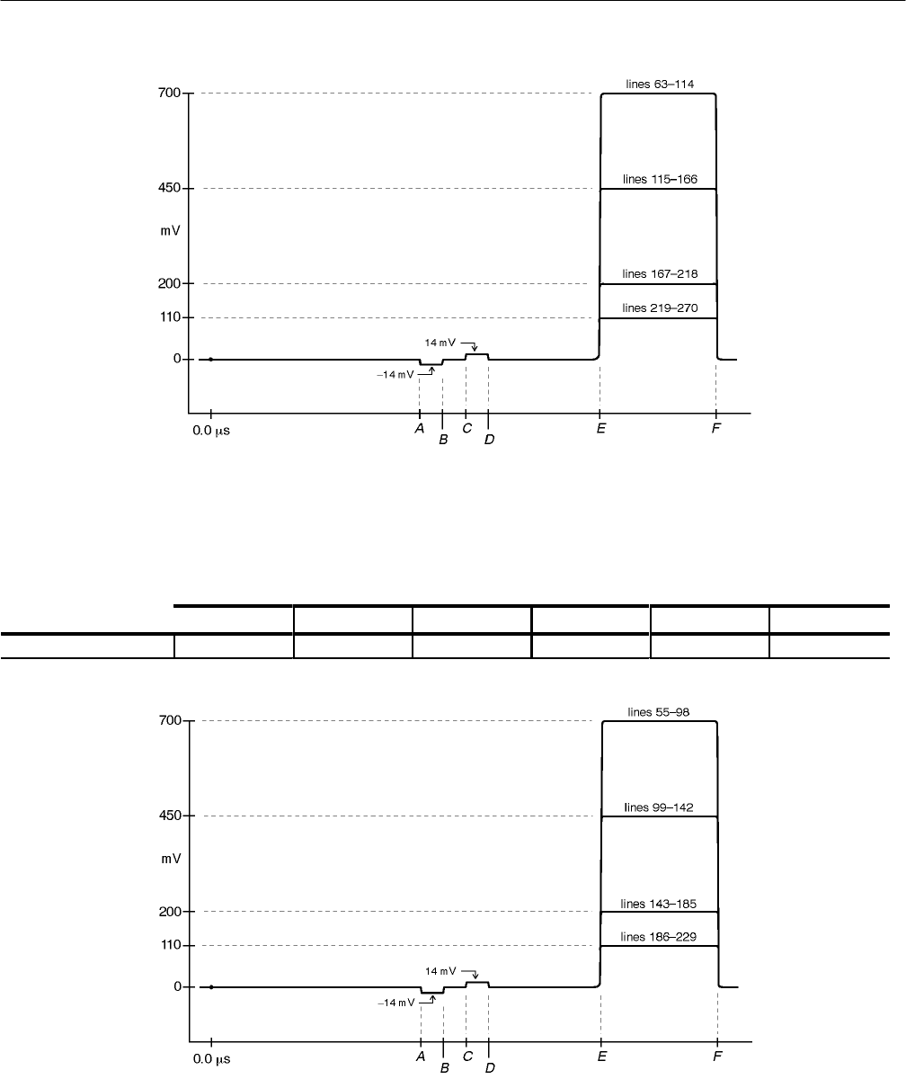
See Figures 1–12 and 1–13, and Table 1–11
Lines 63–114
Lines 115–166
Lines 167–218
Lines 219–270
Lines 55–98
Lines 99–142
Lines 143–185
Lines 186–229
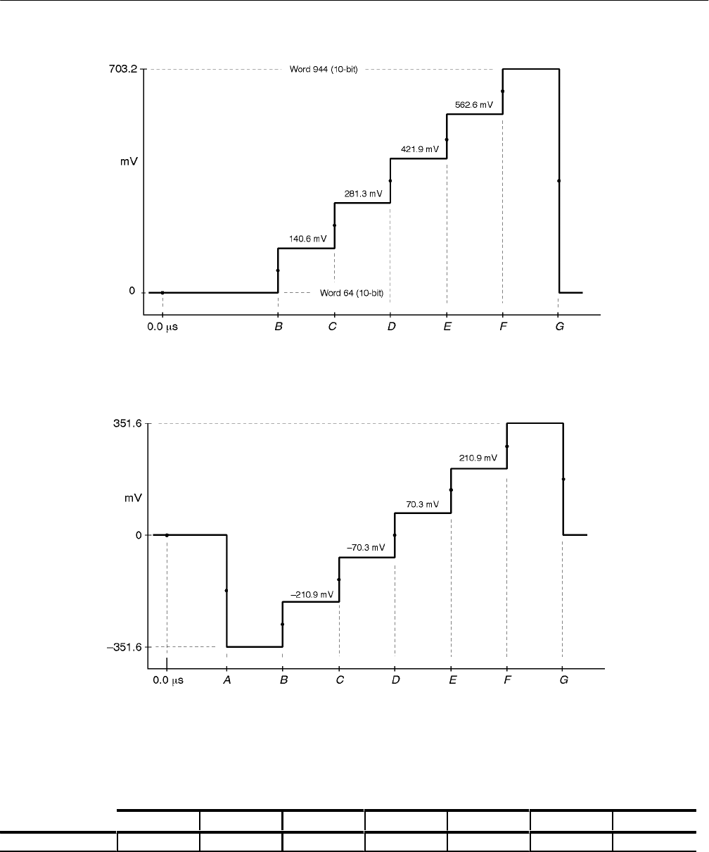
5-Step Staircase
AmplitudeY Channel
B–Y, R–Y
See Figures 1–14 and 1–15, and Table 1–12
0 to 702.4 mV in 176-word steps
–351.6 to +351.6 mV in 180-word steps
Mod 5-Step
AmplitudeY Channel
525 B–Y, R–Y
625 B–Y
625 R–Y
See Figures 1–14, 1–16, and 1–17; and Table 1–12
0 to 702.4 mV in 176-word steps
–157.3 mV
83.7 mV
94.4 mV
Limit Ramp See Figures 1–18 and 1–19
In 8-bit, extends from word 01 to 254;
in 10-bit, extends from word 04 to 1016.
Shallow Ramp
Amplitude
Pedestal (variable)
Y Channel
B–Y, R–Y
Rise Times
Y Channel
B–Y, R–Y
See Figures 1–20 and 1–21
80 mV
0 to 700 mV
–350 to +350 mV
200 ns
280 ns
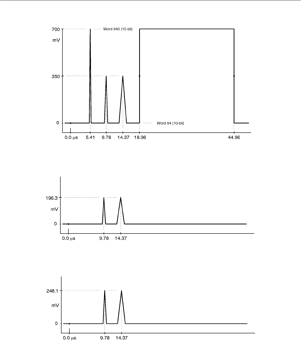
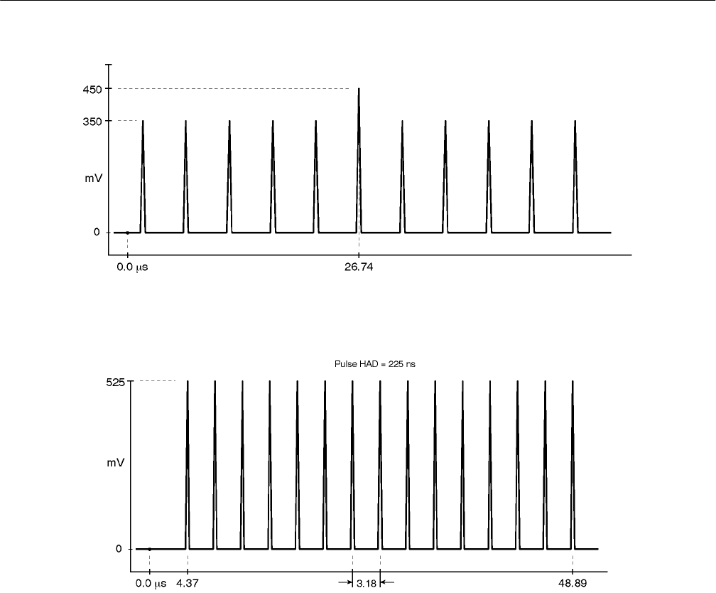
Mod Pulse and Bar (625 lines/50 Hz)
4T Pulse HAD
10T Pulse HAD
Pulse Amplitude
Y
B–Y
R–Y
2T Pulse HAD
See Figures 1–22, 1–23, and 1–24
400 ns
1000 ns (1.0 µs)
350.0 mV
196.3 mV
248.1 mV
200 ns (Y channel only)

Specifications
TSG 601 Service Manual 1–9
Table 1–3: Test Signal Characteristics (Cont.)
Supplemental InformationCharacteristic
Mod Pulse and Bar (525 lines/60 Hz)
12.5T Pulse HAD
Pulse Amplitude
Y Channel
B–Y
R–Y
2T Pulse HAD
See Figures 1–25, 1–26, and 1–27
1562.5 ns (in NTSC, encodes to 12.5T modulated pulse, ∅ = 60.7°)
350.0 mV
196.3 mV
248.1 mV
200 ns (Y channel only)
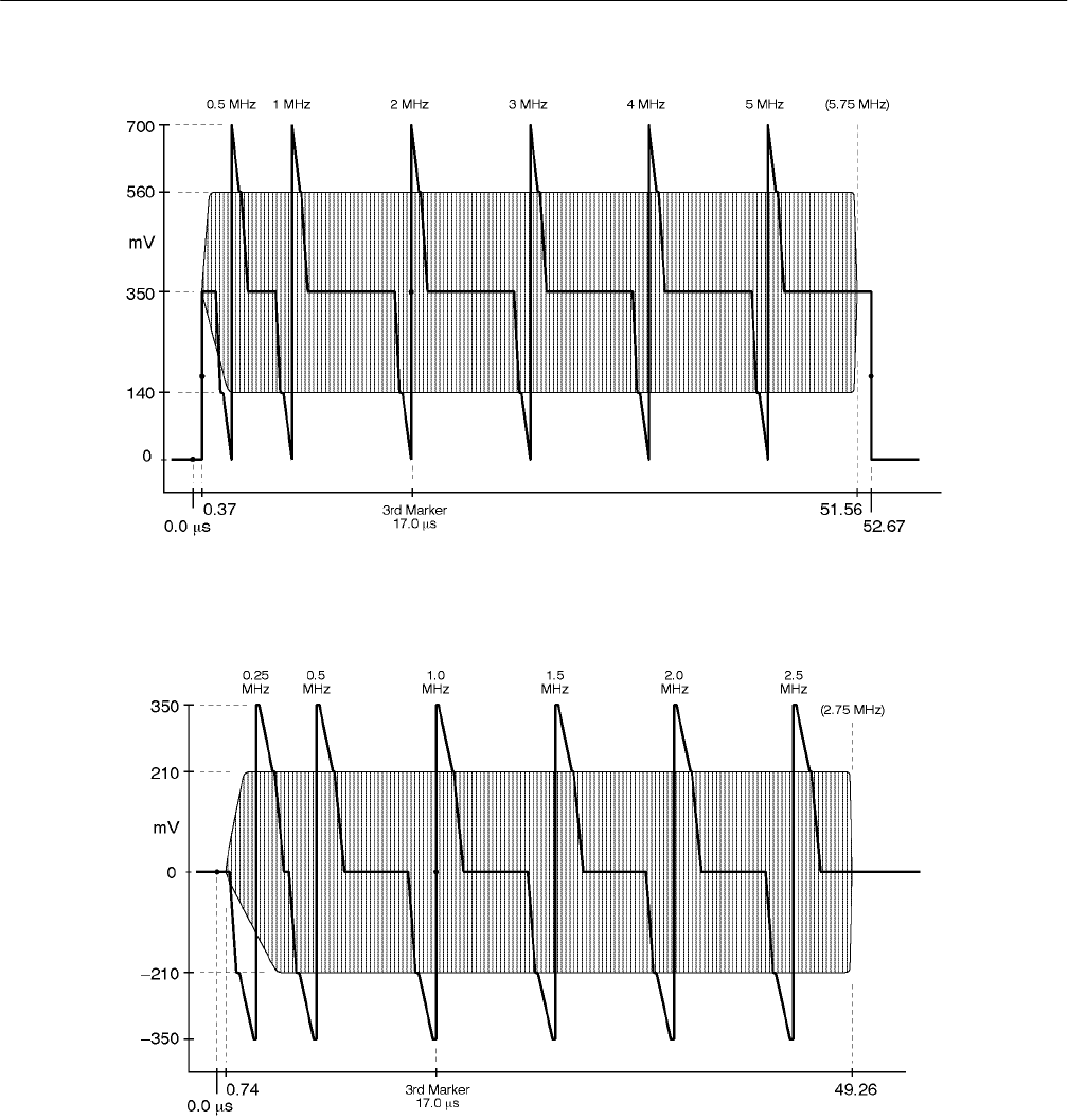
60% Line Sweep With Markers
Amplitude
Frequency Range
Y Channel
R–Y, B–Y
Marker Frequencies
Y Channel
R–Y, B–Y
See Figures 1–28 and 1–29
420 mV
250 kHz–5.75 MHz
125 kHz–2.75 MHz
0.5, 1, 2, 3, 4, and 5 MHz
0.25, 0.5, 1, 1.5, 2, and 2.5 MHz
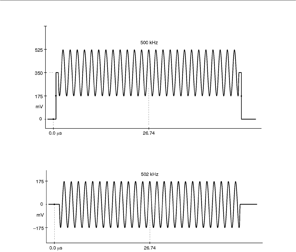
500 kHz Bowtie (half amplitude)
Y Channel
R–Y, B–Y
Amplitude
See Figures 1–30, 1–31, and 1–32
500 kHz sine wave
502 kHz sine wave
350 mV
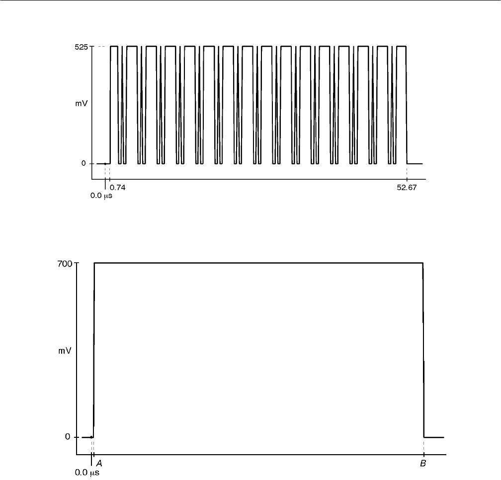
Convergence
Amplitude
Pattern
Pulse HAD
See Figures 1–33 and 1–34
525 mV (75%)
Crosshatch: 14 horiz./15 vert. lines
225 ± 25 ns
Equalizer SDI Checkfield Per SMPTE RP 178
PLL SDI Checkfield Per SMPTE RP 178
Matrix SDI Checkfield
Field Timing, 625/50
Equalizer
PLL
Field Timing, 525/60
Equalizer
PLL
Per SMPTE RP 178
Lines 24 through 166
Lines 167 through 310
Lines 21 through 141
Lines 142 through 262
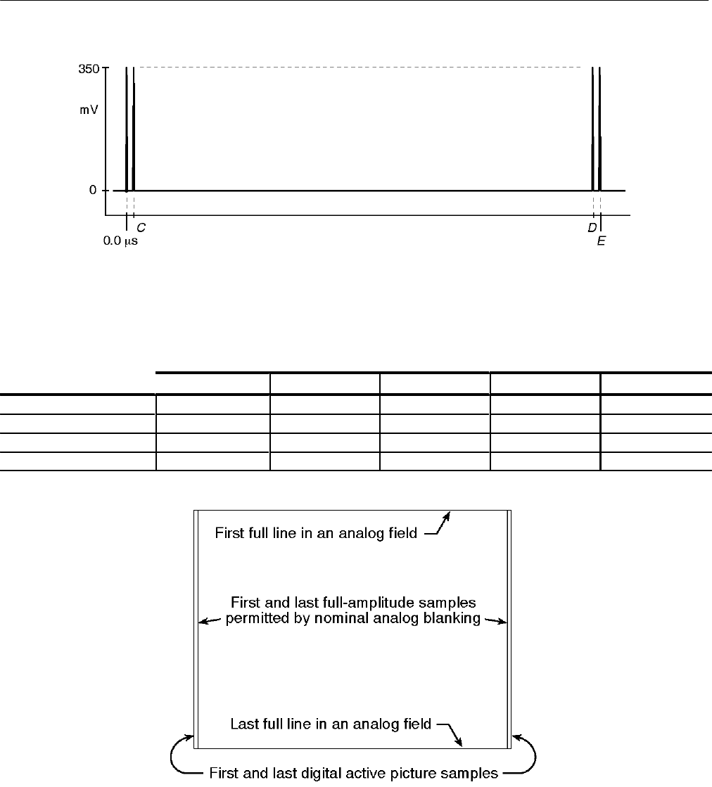
Active Picture Markers
Field Timing, 625/50
Vertical Limits
Horizontal Limits
Field Timing, 525/60
Vertical Limits
Horizontal Limits
See Figures 1–35, 1–36, and 1–37, and Table 1–13
Lines 24 and 310
Lines 25 through 309
Lines 21 and 262
Lines 22 through 261

Specifications
1–10 TSG 601 Service Manual
Table 1–4: Serial Digital Video Output
Characteristic Performance Requirements Supplemental Information
Connectors 3 BNCs, 75 Ω
Number of Outputs 1 component serial video
Digital Format CCIR 601 Component 525/625, 8 or 10 bits
data, Scrambled NRZI; complies with SMPTE
259M and CCIR 656.
Bit Rate 270 Mb/s
Source Impedance 75 Ω
Return Loss ≥ 15 dB from 5 MHz to 270 MHz
instrument switched on
Termination Detector Triggers display symbol when return loss of
the signal path is ≤10 dB (approximates ter-
mination impedance of ≤37.5 Ω and ≥150 Ω)
Signal Amplitude Variable from 600 mV to 1000 mV in the follow-
ing steps
Coarse: 100 mV on even 100 mV
increments
Fine: 20 mV increments
Absolute Accuracy
@ 800 mV setting 800 ± 20 mV
Relative Accuracy
Coarse increments 100 ± 8 mV From last 100 mV setting
Fine increments 20 ± 8 mV
DC Offset 0 ±0.5 Volts
Rise and Fall Times 400–1000 ps 20% to 80% amplitude points
Jitter less than ± 360 ps Over a period of one line.
Error Detection Ancillary Data Active picture CRC (0-AP-CRC, Tektronix propri-
etary) on lines 9 & 272 (525) or 5 & 318 (625).
EDH (SMPTE RP-165)
Table 1–5: Cable Simulator
Characteristic Performance Requirements Supplemental Information
Length –5.4 dB ±0.5 dB at 135 MHz (Approximates a
50 meter length of Belden 8281 coax cable)
Return Loss ≥ 20 dB from 5 MHz to 270 MHz

Specifications
TSG 601 Service Manual 1–11
Table 1–6: Character Identification
Characteristic Information
Number of Characters Displayed Two lines of up to 16 Characters per line.
Display Position Moveable over the Safe Action area of the field.
Character Amplitude Black, 70 mV equivalent
White, 630 mV equivalent
Table 1–7: Power Supply
Characteristic Performance Requirements Supplemental Information
DC Input Range 9 to 15 VDC
Supply Accuracy
+ 5 D
+ 5 A +5 V ±250 mV
+5 V ±250 mV
Hum
+ 5 D
+ 5 A ≤ 25 mV
≤ 25 mV
Noise
+ 5 D
+5 A ≤ 50 mV
≤ 20 mV ≤ 5 MHz Bandwidth
Fuse 4 A fast blow, 32 V min
Power Limit
Without adapter
With adapter 5.0 W
6.0 W
Power Consumption
Back light off
Back light on
Typical:
4.0 W
4.5 W
Table 1–8: Physical Characteristics
Characteristic Information
Height 5.6 cm (2.2 in)
Width 9.1 cm (3.6 in)
Depth 19.1 cm (7.5 in)
Net Weight
TSG 601
TSG 601 with battery pack 0.48 kg (1.06 lb)
0.68 kg (1.5 lb)
Shipping Weight (with AC adapter) 1.50 kg (3.31 lb)
Specifications
1–12 TSG 601 Service Manual
Table 1–9: Environmental Characteristics
Characteristic Information
Temperature
Operating
Storage 0°C to +35°C (32 to +95°F)
–30°C to +65°C (–22 to +149°F)
Altitude Operating
Storage to 15,000 feet (4572 m); IEC 1010-1 compliance to 2000 m
to 50,000 feet (15420 m)
Equipment Type Test
Equipment Class Class III (as defined in IEC 1010-1, Annex H)
Installation Category Category II (as defined in IEC 1010-1, Annex J)
Note: Rated for indoor use only.
Pollution Degree Pollution Degree 2 (as defined in IEC 1010-1)
Transportation Meets the requirements of NTSB Test Procedure 1A, category II (24 inch drop)
Waveform Diagrams
NOTE. The following diagrams represent the analog equivalents of the TSG 601
digital test signals. Horizontal axis units are microseconds after the start of Dig-
ital Active Video. Unless specified in the caption, each illustration represents
both 525 line/60 Hz and 625/50 Hz signals.
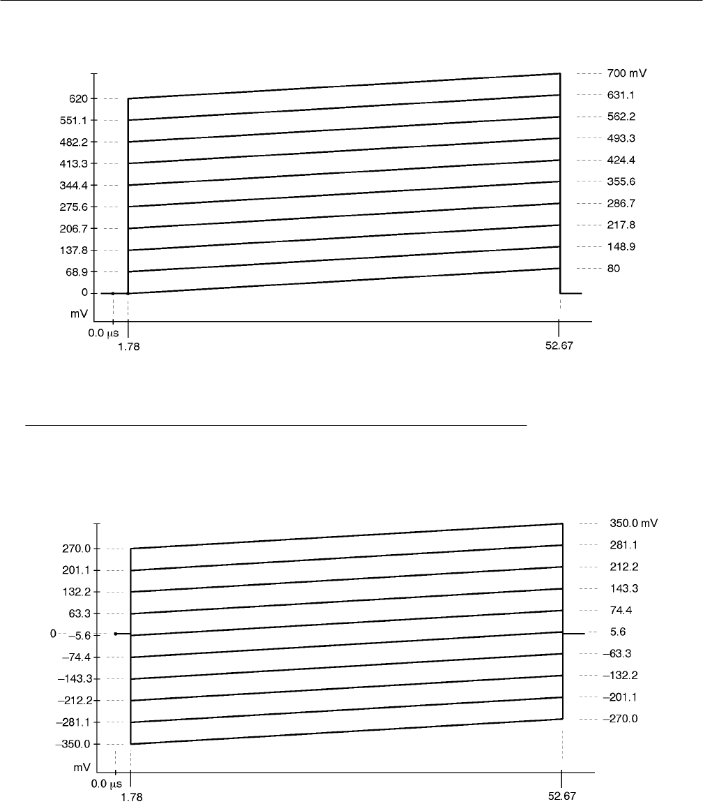
Figure 1–5: 75% Color Bars, Y
Specifications
TSG 601 Service Manual 1–13
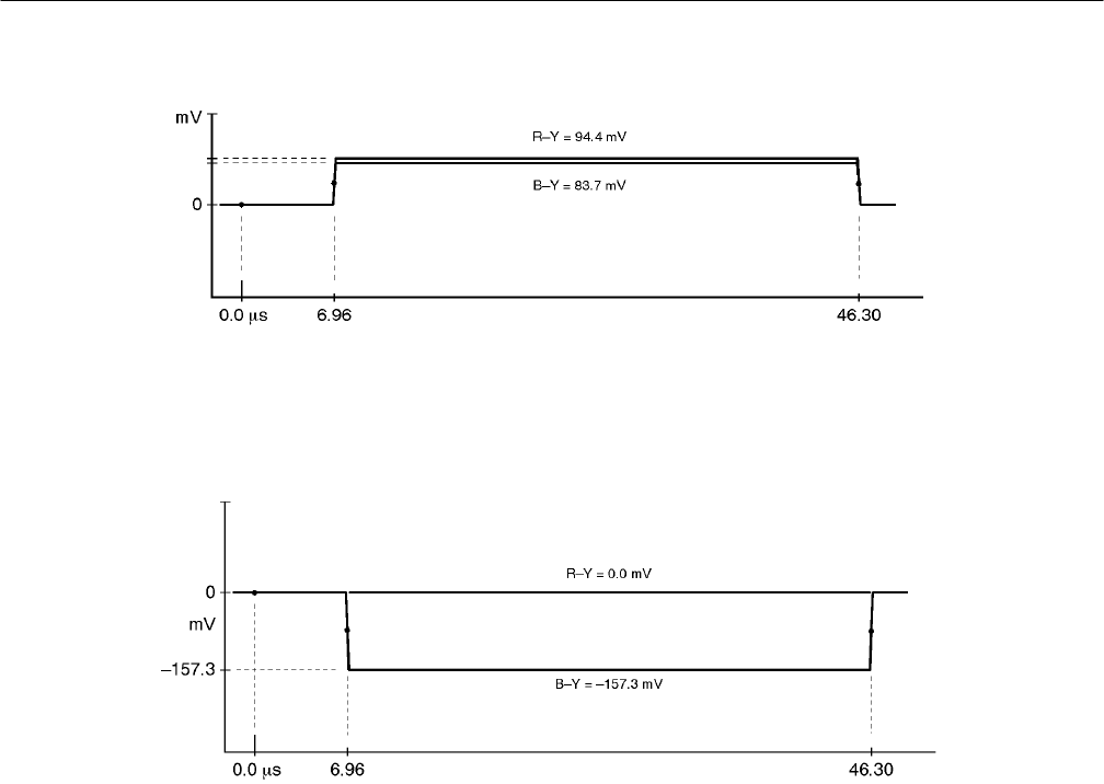
Figure 1–6: 75% Color Bars, B–Y
Figure 1–7: 75% Color Bars, R–Y
Table 1–10: 75% and 100% Color Bars Timing
A B C D E F G H
625/50 0.74 µs 7.26 13.70 20.22 26.74 33.18 39.70 46.15
525/60 0.37 6.96 13.56 20.07 26.67 33.26 39.85 46.37
Specifications
1–14 TSG 601 Service Manual
Figure 1–8: 100% Color Bars, Y
Figure 1–9: 100% Color Bars, B–Y
Specifications
TSG 601 Service Manual 1–15
Figure 1–10: 100% Color Bars, R–Y
Figure 1–11: Pluge 1, Y only
Specifications
1–16 TSG 601 Service Manual
Figure 1–12: 625 Line Pluge 2, Y Channel Only
Table 1–11: Pluge Timing
A B C D E F
625 & 525 21.57 µs 23.87 26.17 28.47 40.07 52.07
Figure 1–13: 525 Line Pluge 2, Y Only
Specifications
TSG 601 Service Manual 1–17
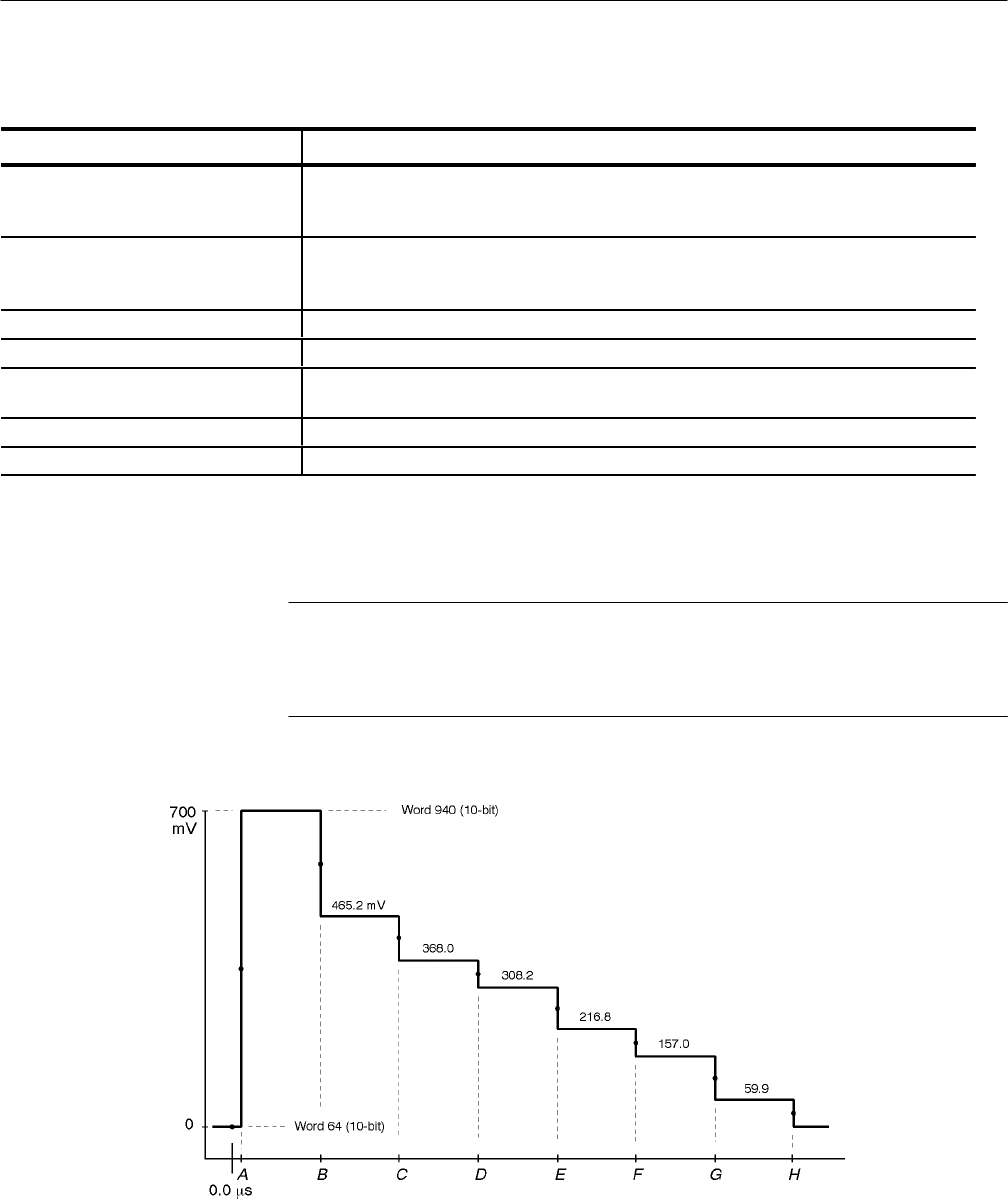
Figure 1–14: 5-Step Staircase and Modulated 5-Step, Y
Figure 1–15: 5-Step Staircase, B–Y and R–Y
Table 1–12: 5-Step Staircase and Modulated 5-Step Timing
A B C D E F G
625 & 525 6.96 µs 13.48 20.07 26.59 33.18 39.70 46.30
Specifications
1–18 TSG 601 Service Manual
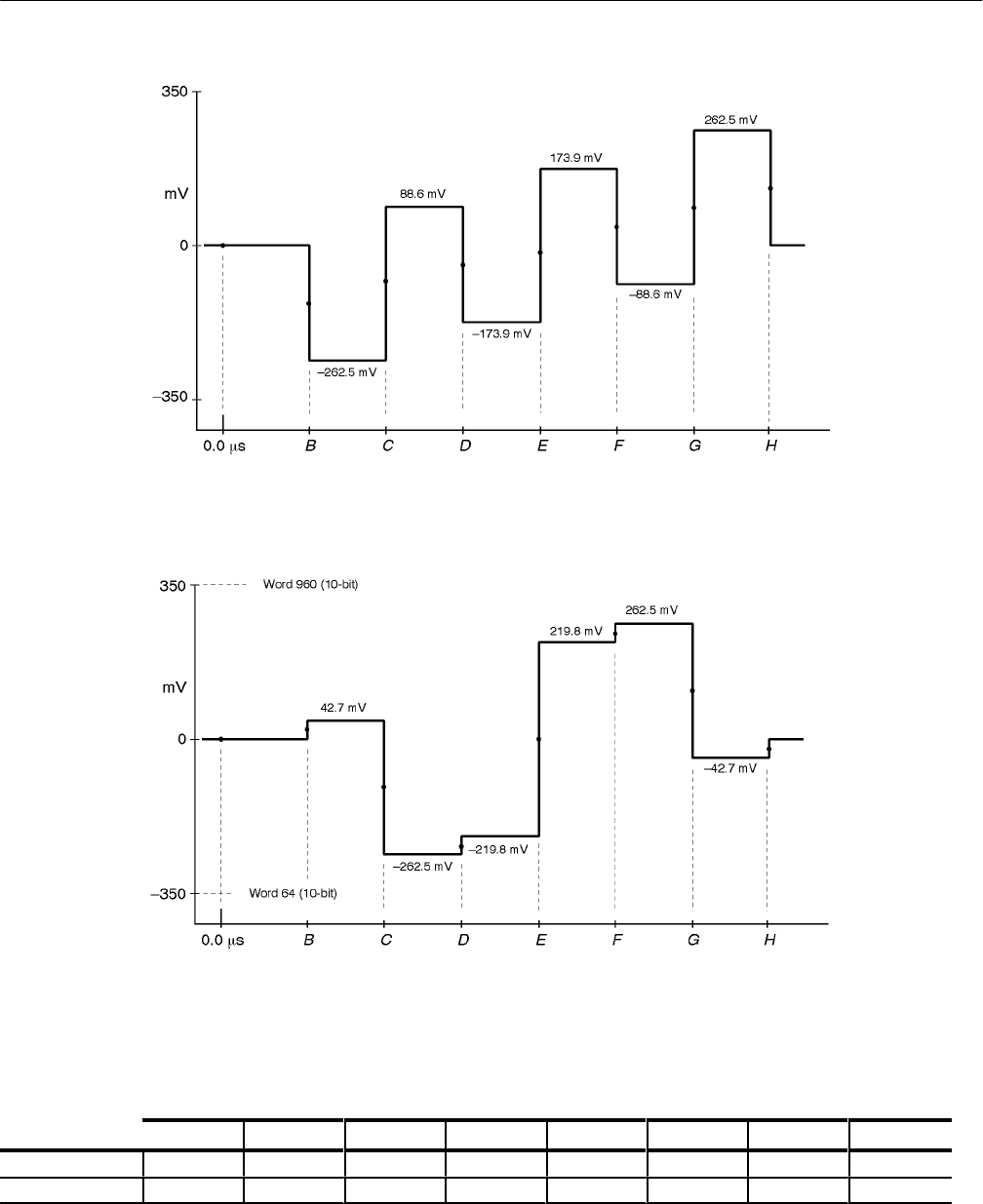
Figure 1–16: 625 Line Modulated 5-Step, B–Y and R–Y
Figure 1–17: 525 Line Modulated 5-Step, B–Y and R–Y
Specifications
TSG 601 Service Manual 1–19
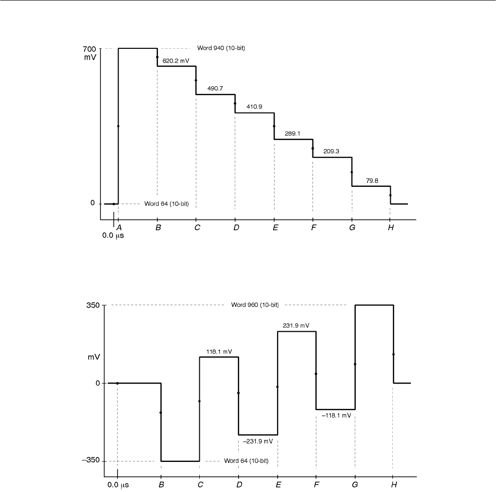
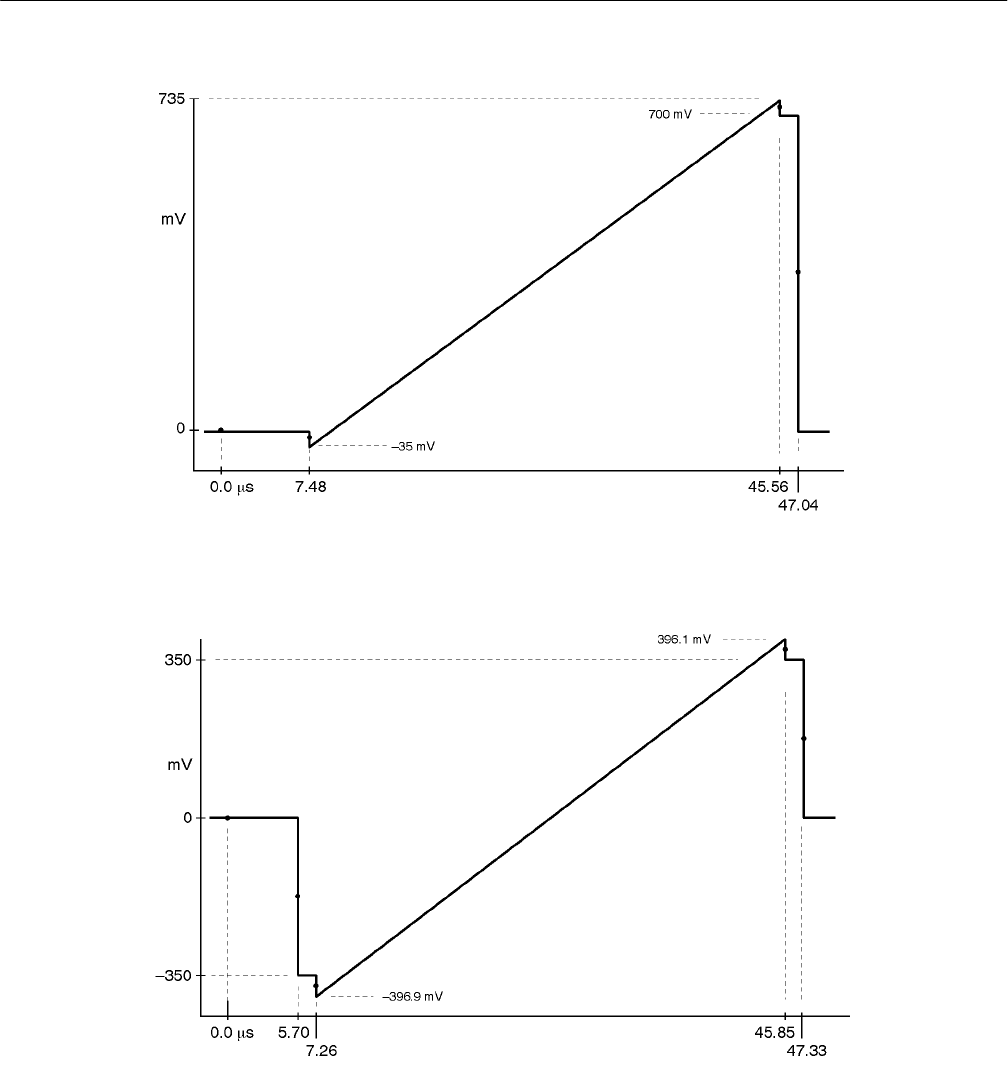
Figure 1–18: Limit Ramp, Y
Figure 1–19: Limit Ramp, B–Y and R–Y
Specifications
1–20 TSG 601 Service Manual
Figure 1–20: Shallow Ramp, Y
NOTE. You may set the shallow ramp pedestal to one of the ten levels shown. To do so, use the A and " keys
to select from levels 0 through 9 when the TSG 601 is in normal operation and the Shallow ramp is “active.”
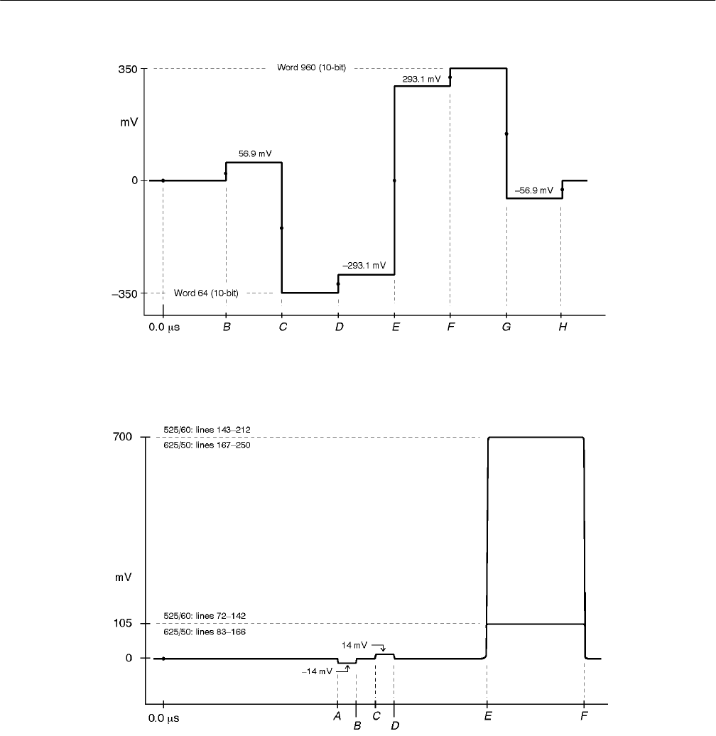
Figure 1–21: Shallow Ramp, B–Y and R–Y
Specifications
TSG 601 Service Manual 1–21
Figure 1–22: 625 Line Mod Pulse and Bar, Y
Figure 1–23: 625 Line Mod Pulse and Bar, B–Y
Figure 1–24: 625 Line Mod Pulse and Bar, R–Y
Specifications
1–22 TSG 601 Service Manual
Figure 1–25: 525 Line Mod Pulse and Bar, Y
Figure 1–26: 525 Line Mod Pulse and Bar, B–Y
Figure 1–27: 525 Line Mod Pulse and Bar, R–Y
Specifications
TSG 601 Service Manual 1–23
Figure 1–28: 60% Line Sweep with Markers, Y
Figure 1–29: 60% Line Sweep with Markers, B–Y and R–Y
Specifications
1–24 TSG 601 Service Manual
Figure 1–30: 500 kHz Bowtie (reduced amplitude), Y
Figure 1–31: 500 kHz Bowtie (reduced amplitude), B–Y and R–Y
Specifications
TSG 601 Service Manual 1–25
Figure 1–32: Bowtie Markers, Y Channel Only
Figure 1–33: Convergence, Vertical Lines; Y Channel Only
Specifications
1–26 TSG 601 Service Manual
Figure 1–34: Convergence, Horizontal Lines; Y Only
Figure 1–35: Active Picture Markers, Vertical Limits, Y Channel Only
Specifications
TSG 601 Service Manual 1–27
Figure 1–36: Active Picture Markers, Horizontal Limits, All Channels
Table 1–13: Active Picture Markers Timing
A B C D E
625/50: Y 0.72 µs 52.72 1.04 52.44 53.26
625/50: B–Y and R–Y — — 1.04 52.44 53.18
525/60: Y 0.16 53.02 0.29 52.89 53.26
525/60: B–Y and R–Y — — 0.29 52.89 53.18
Figure 1–37: The Significance of the Active Picture Markers

Specifications
1–28 TSG 601 Service Manual

Operating Information
TSG 601 Service Manual 2–1
Operating Information
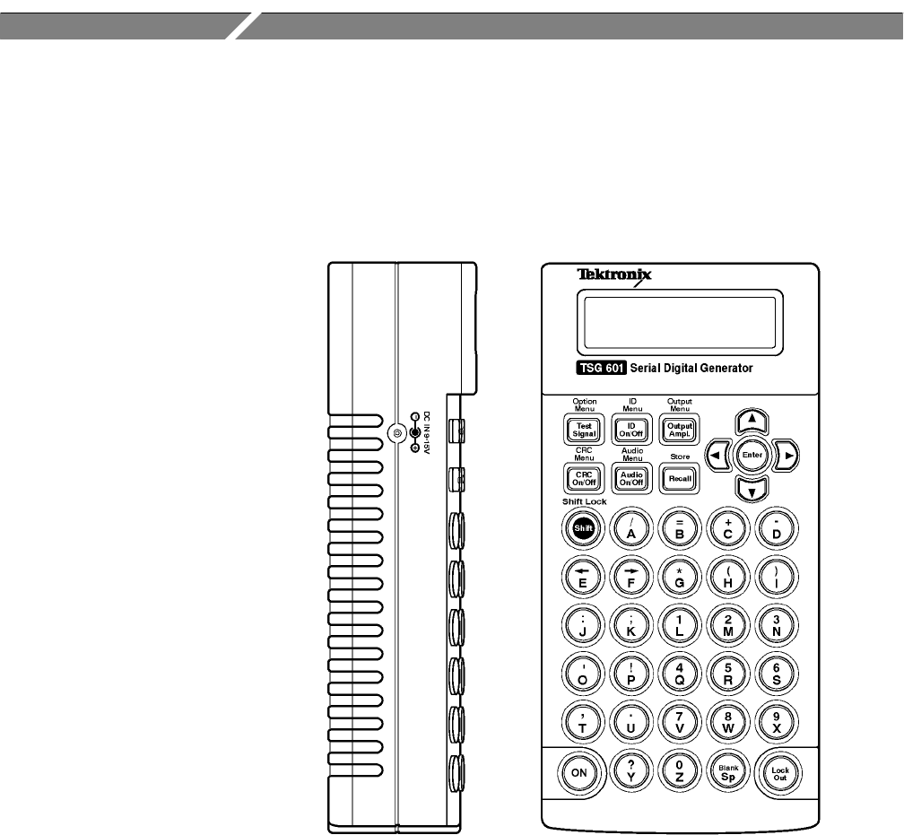
This section duplicates material contained in the TSG 601 User manual (Tektro-
nix p/n 070-8910-00). The material is included here for your convenience. Please
check the User manual whenever you need more information on any topic.
Powering the Instrument
The TSG 601 is DC powered. You may power it with the standard AC adapter,
the optional 9.6 V NiCad battery pack, eight standard AA batteries, or a “BP”
type battery pack with the correct voltage and polarity. The external DC power
connector is on the left side of the instrument (see the illustration above). Open
the battery compartment by sliding the compartment door in the direction of the
inscribed arrow until the door tabs line up with the slots in the case, then remove
the door. When selecting a power source for your TSG 601 please remember:
HAttempting to use an improper AC adapter can damage the instrument. USE
AN APPROPRIATE DC POWER SOURCE ONLY: Voltage must be be-

Operating Information
2–2 TSG 601 Service Manual
tween 9 and 15 VDC; the center contact of the connector must be NEG-
ATIVE polarity; and open-circuit voltage must not exceed 18 VDC. For best
results, use the adapter supplied with the instrument.
HThere is no need to remove the optional NiCad battery pack for recharging.
The TSG 601 will “trickle charge” the battery pack whenever the standard
AC adapter is used. It can take up to 16 hours to fully charge the battery
pack. Note that charging will occur only if the adapter supplies at least
12 V; make sure that the adapter you use is appropriate for the local AC
supply.
HAA batteries are not included with the instrument; buy them locally.
Rechargeable AA batteries may be used, but they are NOT recharged
automatically. To recharge AA batteries, remove them from the instrument
and use an appropriate battery charger. For safety, read and follow the battery
charger instructions. Do NOT attempt to recharge standard alkaline batteries.
HAfter a minute with no key press, the display back light will be dimmed to
conserve battery charge.
HTo guard against battery discharge if you forget to turn the TSG 601 off,
enable Auto Power Down through the Diagnostic menu (see page 5–4).
HThe TSG 601 can sense low battery voltage. It will warn you when the
charge is sufficient for approximately ten more minutes of operation. The
instrument will shut itself down when the battery voltage becomes too low
for reliable operation. See the Battery Hints in the Maintenance section of
this manual (page 5–1).
The ON key toggles instrument power On and Off.
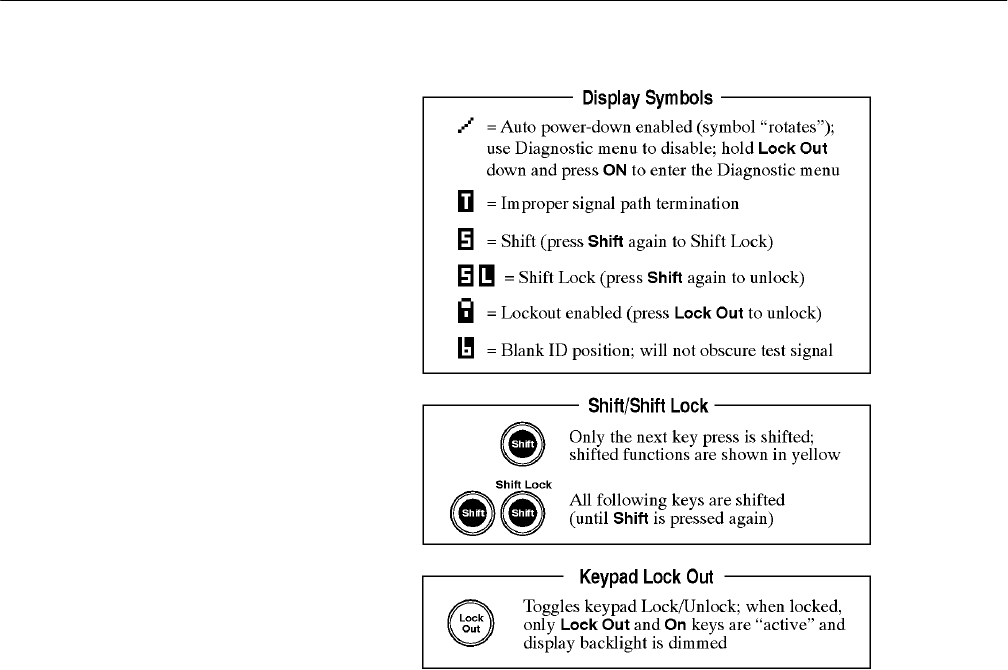
Keypad and Display Conventions
Please see the Instruction card (p/n 070-8909-00) supplied with the TSG 601 for
a “tour” of the keypad and an explanation of the display symbols. For your con-
venience, the following panels are taken from the card.
Operating Information
TSG 601 Service Manual 2–3
Using your TSG 601
Here’s a list of what you can do with your TSG 601. Simple instructions for each
operation begin on the indicated page. For more information on any subject, see
the User manual.
HOutput serial video test signals (page 2–4).
hSpecify the peak-to-peak amplitude of the serial output, from 600 to
1000 mV (page 2–5).
hChoose the video components (Y, Cr, Cb) to be included in the serial
output (page 2–5).
hSpecify 8- or 10-bit video sample words (page 2–6).
HEmbed CRC information (used for “Error Detection and Handling,” or EDH)
in the output to detect or simulate errors originating in the serial data path
(page 2–6).
HAdd an ID message to the video signal, and place it where you want in the
picture (page 2–7).
HStore up to eight ID messages for later use (pages 2–7, 2–9).
Operating Information
2–4 TSG 601 Service Manual
HCreate a sequence of (up to four) stored ID messages that will cycle
continuously in the output (page 2–8).
HSimulate the effect on your system of 50 m (164 ft.) of coaxial cable (page
2–9).
HDetect improper termination of the serial video signal path (page 2–9).
HSave all current instrument settings as a “Preset” for later recall (page 2–9).
1. Connect the Serial Video Output of the instrument to your system. Use 75 Ω
cable and be sure that the signal path is terminated properly.
2. Power the TSG 601 (page 2–1) and switch it on. By default, the instrument
will begin with most settings that were in effect when it was switched off.
Two exceptions: all video component channels will be ON (see page 2–5);
and the output amplitude will be 800 mV.
3. Select the appropriate serial video standard (625/50 or 525/60) through the
Diagnostic menu (pages 5–4, 5–6).
4. Return to normal operation by pressing the Test Signals key.
5. Select the desired test signal one of three ways:
hPress the Test Signals key repeatedly until the name of the signal you
want appears on the display. The signal will be output as soon as the
name is visible. Or...
hUse the Y and B keys to scroll through the list of signals until you get to
the desired signal. Or...
hPress the appropriate letter key (A through P) to “Direct-Select” the
signal. The available signals and their corresponding keys are listed in
the following table.
Outputting Serial Video
Test Signals

Operating Information
TSG 601 Service Manual 2–5
Test Signal Direct-Select Key
75% Color Bars A
100% Color Bars B
Pluge 1 (BBC 1) C
Pluge 2 (BBC 2) D
5-Step Staircase E
Limit Ramp F
Shallow Ramp G
Modulated 5-Step H
Modulated Pulse and Bar I
60% Line Sweep with Markers J
Bowtie K
Convergence L
Equalizer SDI Checkfield M
PLL SDI Checkfield N
Matrix SDI Checkfield O
Active Picture Markers P
1. Press the key marked “Output Ampl.”
2. Select the desired output level with the arrow keys. The Y / B keys change
the level to the next higher or lower 100 mV increment; A / " keys change it
in 20 mV increments. Holding an arrow key down will continually increase
or decrease the level until it reaches its minimum or maximum.
3. Press any rectangular key to exit the Output Amplitude Adjust function.
1. Enter the Output menu (press Shift, then Output Ampl.) and press ENTER to
reach “Channel Output Selection.” The display will look something like this:
Adjusting the Output
Amplitude
Controlling the Video
Component (Y, Cr, Cb)
Channels
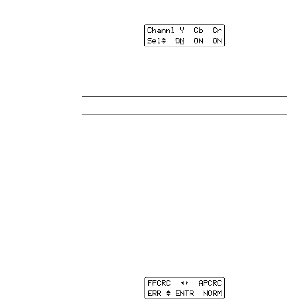
Operating Information
2–6 TSG 601 Service Manual
2. Use the A and " keys to position the flashing underline cursor to the status
(ON or OFF) of the channel you wish to change.
3. Toggle the status with the Y or B key. The channel status will change
instantly—you don’t have to press ENTER.
NOTE. All three component channels default to ON whenever the TSG 601 is
switched off and back on, regardless of prior “Channel Output” settings.
1. If necessary, enter the Output menu (press Shift, then Output Ampl.).
2. Scroll down to the “Video Data Word Length” item with the down arrow key
and press ENTER to reach the word length selection display.
3. Use the A or " key to toggle between 8 and 10 bits; press ENTER to confirm
the selection.
4. Press any rectangular key to exit the Output menu.
1. Enter the CRC menu (press Shift, then CRC On/Off). The display will resemble
the following illustration.
2. Use the A / " keys to select FFCRC (Full Field CRC) or APCRC (Active
Picture CRC). Notice that the up/down symbol on the second display line
will move to indicate the chosen type of CRC.
3. Use the Y / B keys to select the type of CRC to be encoded into the output.
The choices for the two types of CRCs are:
hFFCRC — NORM or ERR (Error)
hAPCRC — NORM, ZERO, or ERR (Error)
Specifying 8- or 10-bit
Data Words
Specifying CRC Content
of the Signal

Operating Information
TSG 601 Service Manual 2–7
See the User manual for an explanation of these options.
4. Once the desired CRC choices appear on the display, press ENTER to
accept/invoke the selections.
5. Press any rectangular key to exit the CRC menu.
6. Toggle the inclusion of CRC data or errors on and off by pressing the “CRC
On/Off” key. The CRC status will be reported on the second line of the
display, alternating with the ID status.
HToggle the ID message or cycle on and off with the “ID On/Off” key.
1. Enter the ID menu (press Shift, then ID On/Off).
2. Press the B key once to reach the “Edit ID #X” menu item. Note that the ID#
first shown on the display always indicates the current (most recently
recalled) ID.
3. Use the horizontal arrow keys to display the number of the ID you want to
edit, then press ENTER.
4. Use the arrow keys to move the character cursor. Specify the character with
the letter keys; press Shift to select symbols and numbers. The “Sp” key will
enter a space, blacking out the underlying test pattern. The test pattern will
show through a “Blank” (Shift-SP).
5. When you have made all the desired changes, press ENTER to save them.
(Note: pressing any rectangular key will abort the edit and exit the ID menu.)
If the ID message you started with in step 3 was “on-screen” when you
began the edit, the new message will take its place. If not, and you wish to
insert the new message, press the Y key to reach the “Recall ID #X” menu
item, select the ID number with the horizontal arrow keys, and press ENTER.
6. As usual, press any rectangular key to exit the ID menu.
NOTE. Only the position of the currently displayed ID may be changed. If you
wish to change the picture location of a message that is not displayed, you must
first recall it through the ID menu or the Recall menu.
Inserting ID Messages
Editing ID Messages
Positioning ID
Messages
Operating Information
2–8 TSG 601 Service Manual
1. Enter the ID menu (press Shift, then ID On/Off), if necessary.
2. With the Y and B keys, scroll to the “Position ID” menu item.
3. Press ENTER.
4. Use the arrow keys to move the message horizontally (H) and vertically (V)
in the picture.
5. When the ID occupies the desired position, press ENTER to save the new
location in memory and return to the ID menu. If you press any rectangular
key instead of ENTER, the ID will remain in its new position—but will revert
to the original location the next time it is recalled from memory.
6. As usual, press any rectangular key to exit the ID menu.
1. Edit and save the ID messages that you want to cycle (see “Editing ID
messages,” page 2–7). Note the numbers of the IDs, and the order in which
they should appear.
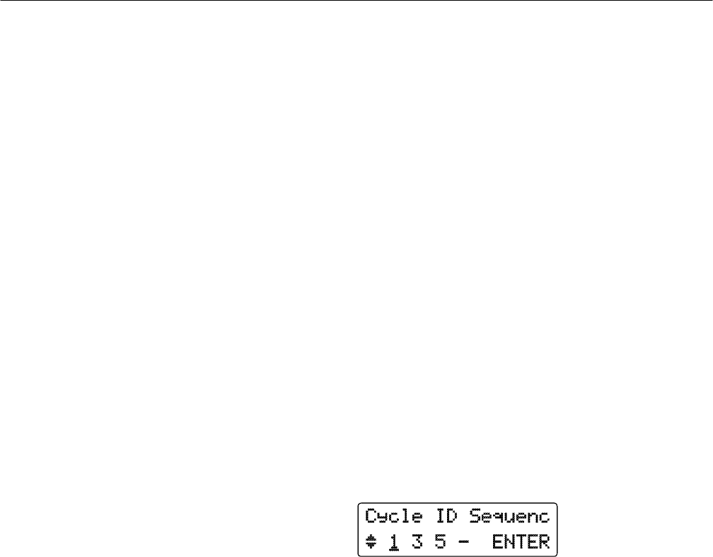
2. Scroll through the ID menu to reach the “ID Cycle Setup” item, then press
ENTER. The display will resemble the following illustration.
3. Use the A / " keys to move the underline cursor to one of the four sequence
“time intervals.” The IDs will appear in the order that their numbers appear
(from left to right) on the display.
4. Use the Y / B keys to select the number of the ID to appear during each
interval. Choose the hyphen (it’s below #1) to eliminate the interval. If you
want a blank interval (that is, a time gap between ID messages), you must
create an all-blank ID to put in that interval.
5. When the correct information is in all four time interval positions, press
ENTER to confirm the cycle setup. (Press any rectangular key to abort the
cycle edit.)
6. To set the duration of each cycle time interval, press the Y key to reach the
“ID Cycle time” menu item. Use the horizontal arrow keys to select the
duration between one and nine seconds. Press ENTER to confirm.
7. To replace the current ID with the ID cycle, scroll through the ID menu to
the “ID Cycle OFF” selection. Press a horizontal arrow key to change the
Setting up an ID Cycle

Operating Information
TSG 601 Service Manual 2–9
selection to “ID Cycle ON,” then press ENTER. The cycle will appear in the
picture if toggled on with the “ID On/Off” key.
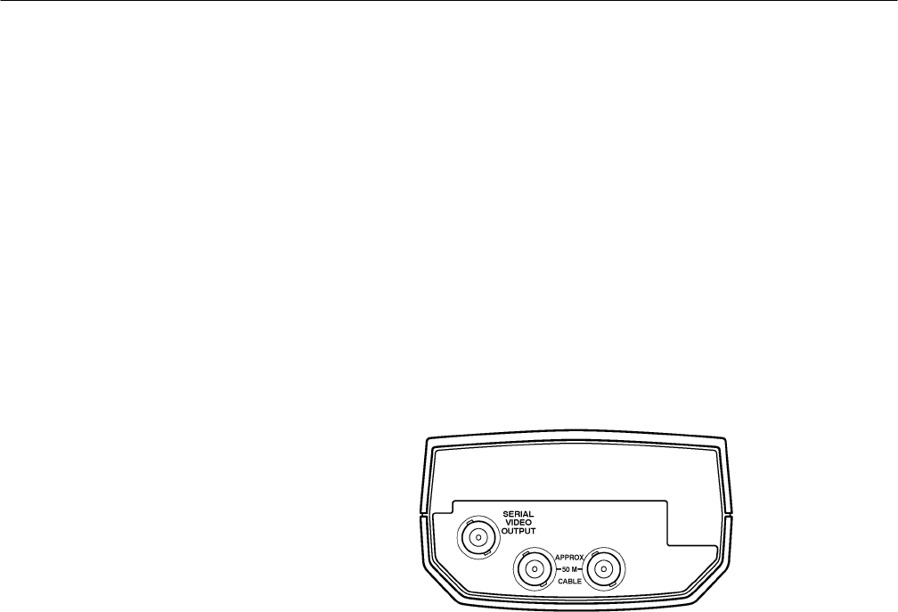
HTo simulate the addition of 50 meters of 75 Ω coaxial cable anywhere in
your system, connect the TSG 601 into the signal path with the two BNCs
marked “APPROX 50M CABLE.” The connectors are interchangeable, and
the circuit will simulate 50 m of Belden 8281 cable—which attenuates the
signal by approximately 5.4 dB at 135 MHz—whether the TSG 601 is
switched on or off.
HA special symbol will “flash” in the upper right corner of the TSG 601
display to indicate improper termination of the serial video signal path. The
symbol is displayed whenever the instrument detects return loss below
approximately 10 dB, which approximates termination impedance of less
than 37.5 or greater than 150
1. Press Shift and then Recall. Note that the ID# first shown on the display
always indicates the current (most recently recalled) ID.
2. Scroll through the “STORE ID” (#1 through #8) and “STO PRESET” (#1
through #4) locations with the left/right arrow keys. The first line of any ID
message already stored in the # location will be shown in the bottom line of
the display; use the B key to see the second message line. Remember that
storing the current settings or ID will overwrite the contents of the Preset or
ID # location.
3. When the desired storage number is displayed, press ENTER to save the
current ID or instrument settings. If you have stored an ID, it will replace the
old # contents on the bottom display line.
4. Press any rectangular key to exit the Store function.
Note that IDs are normally saved—when they are edited—through the ID menu
(see “Editing ID messages,” page 2–7). You may use the Recall/Store button,
however, if you wish to copy the current ID to another memory location. Re-
member that the “current” ID is the last message recalled through the ID menu or
Recall; the ID will be copied (and the previous contents of the ID# location over-
written) even when no message appears in the TSG 601 output (ID=Off).
Cable Simulation
Detecting Incorrect
Termination
Saving (Storing) Presets
and IDs
Operating Information
2–10 TSG 601 Service Manual
A preset includes all of the instrument settings in effect when the preset is saved,
including the current output format, test signal, ID#, and cycle setup. Note that
ID messages themselves are not stored. Thus, if a Preset “remembers” to display
ID#4 (for example), the latest message in ID#4 will appear whenever that Preset
is recalled. Remember, editing an ID message can have an affect on what you get
when you recall a preset.
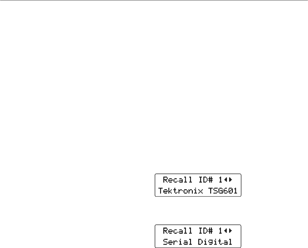
1. Press the Recall key. Note that the ID# first shown on the display always
indicates the current (most recently recalled) ID.
2. Scroll through the “RECALL ID” (#1 through #8) and “RCL PRESET” (#1
through #4) locations with the A / " keys. The first line of an ID message
will occupy the bottom line of the display; use the B key to see the second
line. For example, the “factory” ID#1 is “Tektronix TSG601 Serial Digital.”
The display will first look like this:
Pressing the B key will change it to this:
You may find this feature useful if you save two or more IDs with the same
first line of text.
3. When the desired storage number is displayed, press ENTER to recall the ID or
Preset.
4. Press any rectangular key to exit the Recall menu.
Recalling Presets and
IDs

Theory of Operation

TSG 601 Service Manual 3–1
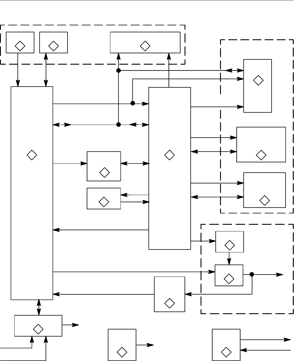
Theory of Operation
This section contains a description of the TSG 601 circuitry based on the block
diagram shown in Figure 3–1.
Block Diagram Description
The block diagram consists of the following major blocks:
Interface. The interface allows the user to control the operation of the instrument.
The TSG 601 has two standard methods of interfacing with the user. One method
is input through the instrument keypad, and the other method is output through
the liquid crystal display (LCD). The LCD consists of two lines with 16
characters per line. There is an alternate method of input through an internal
RS-232 port, but this is used for manufacturing purposes only.
Controller. The TSG 601 uses a microprocessor controller (A1U5) whose function
is to control the operation of the instrument. It does so by polling the different
inputs (keyboard or RS-232 port, battery low condition, and improper termina-
tion) and then responding accordingly.
Logic. The logic of the TSG 601 is contained in a FPGA (A1U2). The logic in
the FPGA can be blocked into three major groups:
HExtended memory access for the microprocessor to peripheral circuits
The FPGA decodes the upper address from the microprocessor and enables
the appropriate circuits to read or write data from/to the microprocessor.
Table 3–1 lists the memory addresses for the various circuits.
The eight lower address bits of the microprocessor are multiplexed on the
same lines as the data (AD(0–7)). The FPGA latches these bits with the
ASTB (address strobe) line and outputs them as A(0–7).
HHorizontal and Vertical Counters and Decoders
The H and V counter outputs, along with the output of the signal selection
register, are used in addressing the signal PROM and SRAMs to obtain the
appropriate signal information. The counter outputs are decoded for timing
information to enable the FPGA to process the signal before outputting it to
the serializer.
Overview

Theory of Operation
3–2 TSG 601 Service Manual
Table 3–1: Circuit Addresses
Hex Address Circuit
7FFFF–0 Flash PROM (A1U4)
9FFFF–8000 Video Flash PROM (A1U6)
A7FFF–A0000 SRAM LSB (A1U26)
C7FFF–C0000 SRAM MSB (A1U21)
E0000 LCD Instruction Code
E0001 LCD Data Code
FFFFF–E0002 FPGA Registers (A1U2)
HSignal Processing Circuit
The processing circuit receives the signal data (SD(0–9)) from the SRAMs,
then adds secondary information before scrambling the signal. The second-
ary information consists of EAV (end of active video) and SAV (start of ac-
tive video) timing, character ID (if any), and CRC ancillary data.
Memory. The TSG 601 has two flash PROMs (128KX8) and two SRAMs
(32KX8). The first flash PROM (A1U4) serves three functions: it contains the
microprocessor code in hex addresses 0 to FFFF, NVRAM for the microproces-
sor in hex addresses 10000 to 17FFF, and the configuration data for the
RAM-base FPGA in addresses 18000 to 1FFFF. The other flash PROM (A1U6)
and the two SRAMs are used to generate signal information.
Output. The FPGA outputs a 10-bit parallel signal stream with a 27 MHz clock
to a serializer (A1U11). The serializer multiplies the clock rate by 10 and outputs
the data in a serial stream at 270 MHz. The output of the serializer passes
through a buffer (A1U16) before being applied to the output connector. The
buffer amplitude is variable and is controlled by the DAC output (SIG_LEVEL)
of the microprocessor.
Termination Detector. The output signal line is monitored with a return-loss
bridge and signal-strength meter IC to determine if the output is properly
terminated.
Power Supply. The TSG 601 uses a switching power supply to generate the +5 V
supply. Input power can be supplied either through the DC input jack or by
batteries mounted in the instrument’s integral battery compartment.
Theory of Operation
TSG 601 Service Manual 3–3
Keypad
Microprocessor
Kernel
RS-232
Character ID
Generator
4000 Series
Xilinx FPGA
Test Signal
Frame/Line Data
(Flash PROM)
Video Test
Signal Data
(SRAM)
Serializer
1
14
Battery Input
DC Input
+5V
1
1
1
2
1
Upper Address Bus
Address/Data Bus
Driver
2
2
Termination
Detector
TCXO
27 MHz
1Board Clock 50 m
Cable
3
Interchangeable
Input/Output
Watchdog
1
Reset
LCD Display
1
INTERFACE
Power Supply
3
Launch
Amplitude Adjust
Cable Open/
Short Indicator
Flash
PROM
1
MEMORY
CONTROLLER LOGIC
Serial
Video
OUTPUT
Lower
Address Bus
Figure 3–1: Block Diagram of the TSG601

Theory of Operation
3–4 TSG 601 Service Manual
The keypad board (Assembly A2) is configured in a row and column format with
the signal lines sent to the main board (Assembly A1) through A1J2. The row
signal lines are inputs to the microprocessor (A1U5 ports 2X and 7X) and are
pulled up to +5 V by A1R5. When a key is pressed, the 100 resistance of
the key connects the row to the column of the pressed key.
The microprocessor (A1U5) drives the column lines low (0 V) one by one, read-
ing the row lines to decode a key press. The column lines are normally driven
high by the microprocessor (port 1X). When a column line is driven low, the oth-
er column lines are momentarily configured as inputs, leaving them floating.
This is done to avoid having two outputs driving each other, with different lev-
els, when two keys have been pressed. Only single key presses are decoded, with
multiple key presses being ignored. The microprocessor polls the keypad board
every 22 ms checking for key presses.
When the ON key is pressed, the regulated voltage (V_KEYBD) is connected to
the ON_KEY control line. If the instrument is off, the ON_KEY line will turn
the instrument on. When the instrument is on, the activation of the ON_KEY
line will be detected by port 23 (/ONKEY_SAFE) of the microprocessor. The
microprocessor will finish housekeeping details before shutting the instrument
off using the PWR_DWN signal of port 07.
A portion of port 3X on A1U5 is used to run the RS-232 interface (A1J13). This
interface is for manufacturing purposes only. A1U7 is the interface driver.
The microprocessor (A1U5) is used to gather data and control the operation of
the instrument based on this data. The microprocessor gathers data from several
sources: the keypad, the internal RS-232 port, the battery voltage level, the out-
put signal termination circuit, and the reset signal. The keypad and RS-232 in-
puts are discussed above.
The low battery condition is monitored on the BATT_LO line which is applied
to port 70, which is an analog-to-digital converter input. When the battery volt-
age level (VIN) goes below a set threshold, the instrument will indicate low bat-
teries on the LCD display. After going below another voltage threshold, the
instrument shuts itself off. These voltage thresholds are dependent on the battery
type and are listed in Table 3–2.
Table 3–2: Low Battery Voltage Thresholds
Battery Type Low Off
Alkaline 7.5 V 6.5 V
NiCad 9.3 V 8.6 V
Keypad
RS-232 Port
Microprocessor

Theory of Operation
TSG 601 Service Manual 3–5
The microprocessor exerts most of its control over the the instrument through
ports 4X, 5X, and 6X. Port 4X is a multiplex address (LSB) and data bus, while
ports 5X and 6X handle the upper address bus and the read, write, and wait con-
trol lines. With the extended memory capabilities of these ports, the micropro-
cessor can fetch instruction code from the flash PROM (A1U4), store and recall
users presets in NVRAM (also in A1U4), control the logic circuits in the FPGA,
and change the readout on the LCD display.
The microprocessor also controls other peripheral circuits through its I/O ports.
The lower LSB of port 0X and P34 of port 3X are used to communicate with the
Character ID chip (A1U23). P07 of port 0X shuts the power supply off when
either a low battery condition is detected or an Off condition is selected from the
keypad. P35 of port 3X is used to turn the backlight of the LCD on and off.
The microprocessor’s digital-to-analog outputs (ANO0 and ANO1) are used to
control the LCD display contrast level and the serial video output signal level
respectively.
When the instrument is first turned on, the FPGA (A1U2) goes into its configu-
ration routine. During this routine, the FPGA output signals LDC, INIT, and
DONE are held low, while HDC is held high. The FPGA is a RAM-base IC and
needs to read in the appropriate data in order to configure its internal logic. The
FPGA uses the address and data buses connecting to and from the flash PROM
(A1U4) to configure itself.
The FPGA starts at the MSB of A1U4 and decrements until all the configuration
data is read (by the FPGA). During the configuration routine, the remaining I/Os
of the FPGA are in a tri-state mode. The HDC signal is passed through an invert-
er (A1U22) and holds the microprocessor in the reset mode during this time.
This causes the outputs of the microprocessor to be placed in a tri-state mode,
removing contention from the address and data buses. After the configuration
routine is completed, the FPGA is ready for operation. It releases the micropro-
cessor to start setting up the instrument for operation by holding HDC low.
One of the tasks the microprocessor has during the instrument setup, is loading
the fast signal data from the signal flash PROM (A1U6) into the SRAMs
(A1U21 and A1U26). The microprocessor addresses the upper half of memory
and reads the data out of A1U6, and then turns around and writes the information
into the appropriate SRAM. Since the output of the PROM is only eight bits
wide and the signal data is ten bits, the data is stored in the PROM with the low-
er eight bits at one location, and the two MSBs at the next address. The micro-
processor loads the eight LSBs into A1U26 and the two MSBs into A1U21.
During this time, the FPGA is outputting a serial video signal at a blanking level
with EAV and SAV data. After the SRAMs are loaded, the microprocessor sets a
flag in the FPGA that causes the instrument to enter into the operating sequence
mode of operation, which is discussed below.
Startup Sequence

Theory of Operation
3–6 TSG 601 Service Manual
The normal operating sequence for the microprocessor is to poll the keypad ev-
ery 22 ms for user inputs and to check for a low battery condition. The FPGA
circuits are reading the signal data from the signal PROM and SRAMs, and pro-
cessing the data to add character ID, SAV and EAV, and CRC ancillary data.
Once the signal is complete, it is output to the serializer (A1U11), scrambled to
form the NRZI (non return to zero inverse) sequence using the following polyno-
mials:
G1(x) =x
9+x
4+1
G2(x) =x+1
(NRZI is a polarity-insensitive video data scrambling scheme in which 0 = no
change in logic, and 1 = a transition from one logic level to the other.)
The watchdog (A1U8) monitors the level of the +5 V supply, as well as the mi-
croprocessor and FPGA for a lockup condition. If the +5 V supply exceeds a
10% tolerance, the watchdog will pull its reset line low until the tolerance
condition is removed. When the reset line is pulled low, the FPGA is put into its
reconfigure mode, which in turn resets the microprocessor.
The watchdog also must receive a pulse at least every 250 ms on the AWAKE
line or it will reset the FPGA. The FPGA normally outputs the ASTB (address
strobe) line from the microprocessor as the AWAKE signal. During a write or
erase operation to the flash PROM (A1U4), the microprocessor is put into a
WAIT mode by the FPGA (the WAIT line is pulled low for a period of time that
may be longer than 250 ms). During the wait time, the FPGA outputs a field
pulse to keep the watchdog from resetting. The field pulse is a square wave with
a cycle time of 33.3 ms (40 ms PAL).
The serializer (A1U11) receives 10-bit data words and a 27 MHz clock from the
FPGA, and outputs a serial data stream at 270 MHz. A resonance tank of
540 MHz between pins 1 and 44 is used to convert the incoming 27 MHz clock
to 270 MHz. The voltage level at A1TP1 should be near +3 V when the AFC is
locked up. The serial data goes through the output driver (A1U16) which has a
variable amplitude capability and complimentary outputs. The output level is
controlled by the microprocessor through the SIG_LEVEL signal line.
The positive output of A1U11 goes through return-loss compensation before go-
ing to the output connector. The negative output goes through identical com-
pensation before it is internally terminated. The two outputs are connected
together at a summing point between A1R19 and A1R20. This summing point is
used to determine proper termination of the output signal. If the output is not
properly terminated in 75 , the summing point will activate the tank circuit
made up of A1L3, A1C30, and circuit board capacitance. The tank circuit drives
Operating Sequence
Watchdog
Serializer
Return-Loss Detector

Theory of Operation
TSG 601 Service Manual 3–7
the input to the signal strength meter (A1U13) which serves as a return-loss de-
tector. A1U13 signals the microprocessor when the output return loss is out of
specification, as set up by A1R31.
The microprocessor addresses the LCD display (Assembly A3) through the
FPGA. The display is enabled through the LCDE control line. The LCD contrast
is driven through A1Q4 from the microprocessor. The backlight is driven
through A1Q2.
The TSG 601 is DC powered either by batteries or by an AC adapter with a nega-
tive center lead orientation. When the adapter DC output is connected to A1J5,
power is not drawn from the batteries. A1L7 and A1C7 act as an EMI regulator,
and A1Q9 and A1VR1 protect the circuitry from a DC power adapter with a pos-
itive center lead. The +5 V regulator (A1U25) has very low quiescent power
draw for battery life extension. It supplies the keyboard with power. When the
ON key is pressed, the power is routed back to the power supply, using the flip-
flop A1U1 to activate the switching supply.
Once A1U1 pin 6 has gone low, the switching regulator (A1U3) is turned on.
Current output is enhanced by the driver made up of A1Q7, A1Q10, and A1Q8.
The switching transformer (A1L1A) outputs +5 V. A1L1B is used to clean up the
supply voltage for the analog circuitry.
The NiCad battery pack is charged through the circuit made up of A1Q12 and
A1CR2 when the supply voltage is at least +10.5 V. At supply voltages less than
that, the batteries will not charge.
The microprocessor shuts down the power supply using A1Q11 when a low bat-
tery state is detected.
The 50 m cable simulator has been characterized to closely emulate 50 m of Bel-
den 8281 coaxial cable. The simulator input and output are interchangeable.
LCD Display
Power Supply
50 m Cable Simulator

Theory of Operation
3–8 TSG 601 Service Manual

Performance Verification and
Adjustment Procedures
TSG 601 Service Manual 4–1
Performance Verification and Adjustment Procedures
This section consists of a detailed performance verification procedure to verify
the operation of the TSG 601, and an adjustment procedure to return the instru-
ment to in-spec operation.
A performance verification “Checklist” appears on page 4–2.
Step-by-step performance verification procedures begin on page 4–2.
Step-by-step instructions for adjustment procedures begin on page 4–6.
Required Test Equipment
The following list of equipment represents the minimum required for the Perfor-
mance Verification and Adjustment procedures. While alternate equipment may
be used, it is not recommended. Alternate equipment must meet the minimum
specifications for the listed equipment. Use of inadequate equipment may result
in faulty measurements or calibration.
Table 4–1: Required Equipment
Item Qty. Requirements Example
Oscilloscope 1 500 MHz bandwidth Tektronix 11403A
Digitizing Oscilloscope
with 11A72 Plug-in
Spectrum Analyzer 1 Freq. Range: 325 MHz
Sensitivity: up to 50 dB
Internal tracking generator
Tektronix 2712, Option 04
RF Bridge 1 At least 46 dB return loss
sensitivity, 50 kHz to
325 MHz
Wideband Engineering
Part No. A57TGACR, and
high-frequency terminator
A56T75B
50 W BNC cable 1 Tektronix p/n 012-0057-00
75/50 W minimum loss at-
tenuator, DC coupled 1Tektronix p/n 011-0057-01
(required for oscilloscope
plug–in with 50 Winput; at-
tenuates signal 2.3X)
75 W BNC termination 2 0.025% precision Tektronix p/n 011-0102-01
50 W BNC termination 1 Tektronix p/n 011-0123-00
AC adapter 1 Std. TSG 601 accessory
No. 1 Pozidrive, 4” screw-
driver 1

Performance Verification and Adjustment Procedures
4–2 TSG 601 Service Manual
Performance Verification Checklist
Use the following checklist if you are familiar with the operation of the TSG 601
and video performance verification techniques.
NOTE. Allow a 20-minute warm-up for the TSG 601 and the instruments used for
performance verification.
1. Serial Digital Output Amplitude, Absolute Accuracy and DC Offset
Absolute accuracy @ 800 mV setting: 800 20 mV
DC offset: 0.0 0.5 V
2. Serial Digital Output Amplitude, Relative Accuracy
Coarse increments: 100 8 mV
Fine increments: 20 8 mV
3. Serial Digital Output Rise and Fall Times
400–1000 ps @ 20% to 80% amplitude points
4. Serial Digital Output Jitter
Less than 360 ps
5. Cable Simulator Return Loss
At least 20 dB from 5 MHz to 270 MHz
Performance Verification Procedures
The order of these procedures has been chosen to minimize changes in equip-
ment setup.
Power up the test equipment and the TSG 601. Allow a 20-minute warm-up.
Connect the TSG 601 Serial Output to a 75/50 minimum loss attenuator. Con-
nect the other side of the pad to the 11403A through a 50 cable.
Configure the 11403A as follows:
WAVEFORM MENU
Vertical Desc. (L1*2.3). . . . . . . . . . . . . . . . . . . . . . . . . .
Horizontal Desc. Main @512 Points. . . . . . . . . . . . . . . . . . . . . . . .
Acquire Desc. Continuous. . . . . . . . . . . . . . . . . . . . . . . . . .
Vertical Mag: Wfm 200 mV. . . . . . . . . . . . . . . . . . . . . .
Vertical Pos: Wfm 0 V. . . . . . . . . . . . . . . . . . . . . . .
Main Size 1 ns. . . . . . . . . . . . . . . . . . . . . . . . . . . . .
Main Pos –4 ns. . . . . . . . . . . . . . . . . . . . . . . . . . . . . .
Impedance 50 . . . . . . . . . . . . . . . . . . . . . . . . . . . . .
Preparation

Performance Verification and Adjustment Procedures
TSG 601 Service Manual 4–3
Coupling DC. . . . . . . . . . . . . . . . . . . . . . . . . . . . . .
BW Limit 1 GHz. . . . . . . . . . . . . . . . . . . . . . . . . . . . .
NOTE. Multiplying the vertical scale by 2.3 compensates for the attenuation due
to the 75/50 minimum loss attenuator.
TRIGGER MENU
Trigger Main. . . . . . . . . . . . . . . . . . . . . . . . . . . . . . . .
Source Description L1. . . . . . . . . . . . . . . . . . . . . .
Level: M 0 V. . . . . . . . . . . . . . . . . . . . . . . . . . . . . .
Time Holdoff: M 510 ns. . . . . . . . . . . . . . . . . . . . . . . .
Mode Auto. . . . . . . . . . . . . . . . . . . . . . . . . . . . . . . . .
Coupling DC. . . . . . . . . . . . . . . . . . . . . . . . . . . . . .
Slope “+”. . . . . . . . . . . . . . . . . . . . . . . . . . . . . . . . .
MEASURE MENU
Amplitude (S)
Rise (S) 20% to 80% (Left Limit = 10%, Right Limit = 95%)
Fall (S) 20% to 80%
Overshoot (S)
Undershoot (S)
MID (DC Level)
1. Serial Digital Output, Absolute Amplitude Accuracy and DC Offset
Absolute amplitude accuracy specification: 800 mV 20 mV
DC offset specification: 0 V 0.5 V
a. Press the Output Ampl button on the TSG 601 and check for an 800 mV
output amplitude.
b. Use the 11403A to verify that the signal meets the above specifications.
2. Serial Digital Output Signal Amplitude, Relative Accuracy
Coarse increments specification: 100 8 mV
Fine increments specification: 20 8 mV
a. Press the TSG 601 B key until 700 mV appears on the LCD.
b. On the 11403A, verify that the signal amplitude is 700 8 mV.
c. Press " once so that 720 mV is displayed on the TSG 601 LCD.
d. On the 11403A, verify that the signal amplitude is 720 8 mV.
e. Press Y on the TSG 601 until 900 mV appears on the LCD.
Procedures

Performance Verification and Adjustment Procedures
4–4 TSG 601 Service Manual
f. On the 11403A, verify that the signal amplitude is 900 8 mV.
g. Press A so that 880 mV is displayed on the TSG 601 LCD.
h. On the 11403A, verify that the signal amplitude is 880 8 mV.
3. Serial Digital Output Rise and Fall Times
Specification: 400–1000 ps @ 20% to 80% amplitude points
a. Verify, on the 11403A, that the rise time is between 400 and 1000 ps.
b. Enter the 11403A TRIGGER menu and set the slope to “–”. Return to
the MEASURE menu.
c. Verify that the fall time is between 400 and 1000 ps.
4. Serial Digital Output Jitter
Specification: less than 360 ps
a. Configure the 11403A as follows:
WAVEFORM MENU
Vertical Desc. (L1*2.3). . . . . . . . . . . . . . . . . . . . . . . . . . .
Horizontal Desc. Main @512 Points. . . . . . . . . . . . . . . . . . . . . . . . .
Acquire Desc. Continuous. . . . . . . . . . . . . . . . . . . . . . . . . . .
Vert Mag: Wfm 200 mV. . . . . . . . . . . . . . . . . . . . . . . . . .
Vert Pos: Wfm 0 V. . . . . . . . . . . . . . . . . . . . . . . . . .
Main Size 10 ms. . . . . . . . . . . . . . . . . . . . . . . . . . . . . .
Main Pos 0 s. . . . . . . . . . . . . . . . . . . . . . . . . . . . . . .
Impedance 50 W. . . . . . . . . . . . . . . . . . . . . . . . . . . . .
Coupling DC. . . . . . . . . . . . . . . . . . . . . . . . . . . . . . .
BW Limit 1 GHz. . . . . . . . . . . . . . . . . . . . . . . . . . . . . .
TRIGGER MENU
Trigger Main. . . . . . . . . . . . . . . . . . . . . . . . . . . . . . . .
Source Description L1. . . . . . . . . . . . . . . . . . . . . . .
Level: M 0 V. . . . . . . . . . . . . . . . . . . . . . . . . . . . . . .
Time Holdoff: M 510 ns. . . . . . . . . . . . . . . . . . . . . . . .
Mode Auto. . . . . . . . . . . . . . . . . . . . . . . . . . . . . . . . . .
Coupling DC. . . . . . . . . . . . . . . . . . . . . . . . . . . . . . .
Slope “+”. . . . . . . . . . . . . . . . . . . . . . . . . . . . . . . . . .
WINDOW MENU
Vertical Mag: Wfm 100 mV. . . . . . . . . . . . . . . . . . . . . . .
Vertical Pos: Wfm 0 V. . . . . . . . . . . . . . . . . . . . . . .
Window Size 500 ps/div. . . . . . . . . . . . . . . . . . . . . . . . . . .
Window Position 40.001 ms. . . . . . . . . . . . . . . . . . . . . . . .

Performance Verification and Adjustment Procedures
TSG 601 Service Manual 4–5
CURSORS MENU
Vertical Bars
Cursor 1 40.00 ms. . . . . . . . . . . . . . . . . . . . . . . . . . . . . . .
Cursor 2 40.00 ms. . . . . . . . . . . . . . . . . . . . . . . . . . . . . . .
∆498.4 ps. . . . . . . . . . . . . . . . . . . . . . . . . . . . . . . . . . . . .
(cursors set so eye crossing is in the center)
b. Set the TSG 601 output amplitude to 800 mV.
c. Verify that the eye crossing stays within the cursors.
5. Cable Simulator Return Loss
Specification: w 20 dB from 5 MHz to 270 MHz
a. Connect a precision 50 W cable from the spectrum analyzer RF Input to
the RF Output on the high-frequency RF Bridge.
b. Connect a precision 50 W cable from the spectrum analyzer TG Output
to the RF Input on the RF Bridge.
c. Select Demod/TG on the spectrum analyzer. Turn on the Tracking
Generator and set the Tracking Generator Fixed Level to 0.00 dBm.
d. Set the spectrum analyzer Span/Div to 50 MHz, the Vertical Scale to
10 dB, Frequency range to 300 MHz, and the Resolution Bandwidth to
300 kHz.
e. Set the spectrum analyzer Reference Level to the first major division
down from the top on the analyzer display.
f. Remove one of the cables from the RF Bridge.
g. Set the spectrum analyzer Frequency Cursor to 250 MHz, and then set
the Marker to 270 MHz.
h. Reconnect the cable to the RF Bridge.
i. Note the Reference Level Readout.
j. In the Input Menu, adjust the spectrum analyzer External Attenuation
Amplitude by the amount noted in the previous step. Note: The
Reference Level Readout should now be 0.00 dBm.
k. Connect the precision high-frequency terminator to the Device Under
Test connector on the RF Bridge.
l. Verify that the frequency response from 5 MHz to 270 MHz is w20 dB.
This check verifies that you have a good terminator.
m. Return the spectrum analyzer frequency marker to 270 MHz if it was
moved.
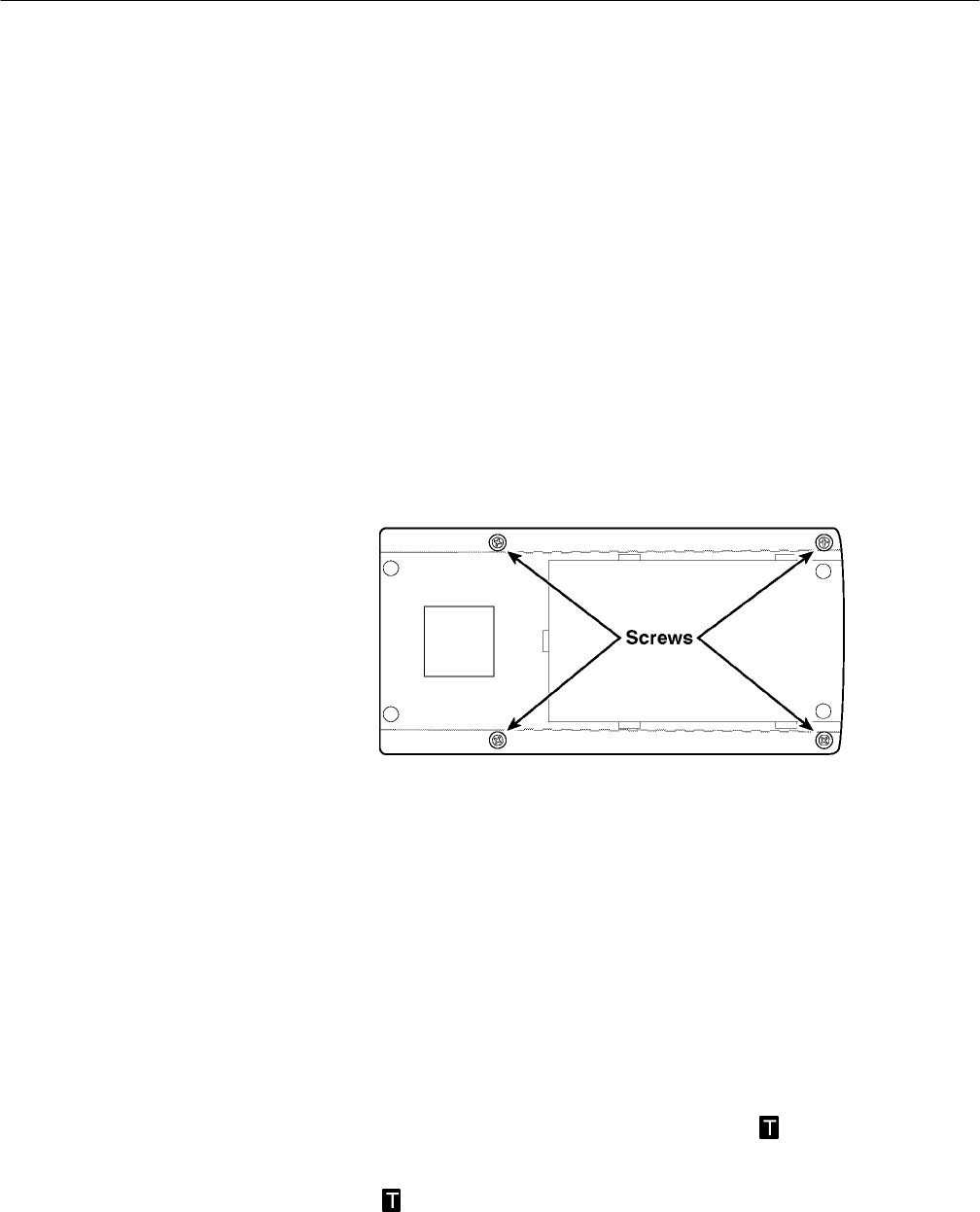
Performance Verification and Adjustment Procedures
4–6 TSG 601 Service Manual
n. Remove the precision high-frequency terminator from the RF Bridge.
o. Use a 75 male-to-male BNC connector to attach the Device Under
Test connector, on the RF Bridge, to one of the cable simulator BNCs.
Terminate the remaining side of the loopthrough with a 75 terminator.
p. Verify that the Reference Level Readout on the spectrum analyzer is
w25 dBm.
Adjustment Procedures
1. Termination Detection
a. Use a No. 1 Pozidrive screwdriver to remove the four screws found on
the back of the instrument.
b. Carefully pull the top and bottom halves of the instrument approximately
one inch apart, then disconnect the ribbon cable from the top (keypad)
half.
c. Connect two 75 Ω BNC terminators together. Place the terminators on
the TSG 601 Serial Video Output.
d. Connect the AC adapter and switch the TSG 601 on.
e. Place the instrument on its right-hand side (AC adapter plug pointing
up), with the display end of the instrument farthest away from you; you
will be making an adjustment on the main board while looking at the
instrument’s display.
f. Adjust R31 counterclockwise until the flashing symbol just appears.
g. Replace the two 75 Ω terminators with a 50 Ω terminator. Verify that
the symbol does not appear.

Performance Verification and Adjustment Procedures
TSG 601 Service Manual 4–7
h. To reassemble the instrument, reverse steps b and a. In step b, be sure to
install the ribbon cable with the brown wire leading to pin 1 of J10.
2. Output Amplitude
Allow a minimum 20 minute warm-up for the TSG 601 and the oscilloscope.
a. Configure the 11403A as follows:
WAVEFORM MENU
Vertical Desc. (L1*2.3). . . . . . . . . . . . . . . . . . . . . . . . . . .
Horizontal Desc. Main @512 Points. . . . . . . . . . . . . . . . . . . . . . . . .
Acquire Desc. Continuous. . . . . . . . . . . . . . . . . . . . . . . . . . .
Vertical Mag: Wfm 200 mV. . . . . . . . . . . . . . . . . . . . . . .
Vertical Pos: Wfm 0 V. . . . . . . . . . . . . . . . . . . . . . .
Main Size 1 ns. . . . . . . . . . . . . . . . . . . . . . . . . . . . . .
Main Pos –4 ns. . . . . . . . . . . . . . . . . . . . . . . . . . . . . . .
Impedance 50 . . . . . . . . . . . . . . . . . . . . . . . . . . . . .
Coupling DC. . . . . . . . . . . . . . . . . . . . . . . . . . . . . . .
BW Limit 1 GHz. . . . . . . . . . . . . . . . . . . . . . . . . . . . . .
TRIGGER MENU
Trigger Main. . . . . . . . . . . . . . . . . . . . . . . . . . . . . . . .
Source Description L1. . . . . . . . . . . . . . . . . . . . . . .
Level: M 0 V. . . . . . . . . . . . . . . . . . . . . . . . . . . . . . .
Time Holdoff: M 510 ns. . . . . . . . . . . . . . . . . . . . . . . .
Mode Auto. . . . . . . . . . . . . . . . . . . . . . . . . . . . . . . . . .
Coupling DC. . . . . . . . . . . . . . . . . . . . . . . . . . . . . . .
Slope “+”. . . . . . . . . . . . . . . . . . . . . . . . . . . . . . . . . .
MEASURE MENU
Amplitude (S)
Rise (S) 20% to 80% (Left limit = 10% Right limit = 95%)
Fall (S) 20% to 80%
Overshoot (S)
Undershoot (S)
MID (DC Level)
b. Connect the TSG 601 Serial Output to a 75/50 minimum loss pad.
Connect the other side of the pad to the 11403A through a 50 cable.
c. On the TSG 601 press and hold down the Lock Out button and then press
the ON button. You will now be in the Diagnostic Menu.
d. Press and hold the down arrow until “SIGNAL AMPL” appears on the
display, then press ENTER.
e. Use the left and right arrows to adjust the amplitude on the 11403A to
600 mV 5 mV.

Performance Verification and Adjustment Procedures
4–8 TSG 601 Service Manual
f. Press the up arrow. The display should now read “ADJ Signal Ampl.
800 mV.”
g. Use the left and right arrows to adjust the amplitude on the 11403A to
800 mV 5 mV.
h. Press the up arrow. The display should now read “ADJ Signal Ampl.
1000 mV.”
i. Use the left and right arrows to adjust the amplitude on the 11403A to
1 V 5 mV.
j. Press ENTER to store the new values in NVRAM.

Maintenance
TSG 601 Service Manual 5–1
Maintenance
Battery Hints
For optimal battery life and capacity, use the rechargeable NiCad battery pack
(Tektronix p/n 119-4488-00) in full charge/discharge cycles. In other words, fully
discharge the battery pack before recharging, and then charge the battery pack
until fully charged, approximately 16 hours. A new battery pack will take a few
charge/discharge cycles to reach full capacity.
WARNING. Install or replace batteries only with the instrument switched OFF
and the AC adapter disconnected.
Replace the batteries only with standard AA batteries (1.2–1.5 V, nominal), or
with a Tektronix rechargeable battery pack (p/n 119-4488-00).
Setting the Auto Power Down (page 5–5) and Battery Type (page 5–5) func-
tions in the diagnostic menu also have an impact on battery life. The battery
types are disposable (Alkaline) or rechargeable (NiCad). Setting the battery type
changes the voltage thresholds for both the BATTERY LOW display message
and low battery shut down.
The warning “BATTERY LOW” will appear on the second line of the TSG 601
display when the battery voltage drops below a predetermined level. The level
depends on the Battery Type set in the diagnostic menu (see page 5–5). The
TSG will operate for approximately ten minutes after the message first appears.
For best results, replace or recharge the batteries when you first see this warning.
To prevent erratic operation at very low power levels, the TSG 601 will shut it-
self down if the battery voltage drops below a second, lower threshold that also
depends on the Battery Type setting.
Low battery shut down can happen with little or no warning if, for instance, the
instrument has been left on by mistake with Auto Power Down disabled. In such
cases, the TSG 601 is likely to shut itself down almost immediately the next time
you switch it on. If this happens:
HInstall fresh batteries or operate the instrument with the AC adapter, and
HConfirm that the diagnostic menu Battery Type setting is appropriate.
The shut down threshold is higher for rechargeable batteries than for disposable.
Therefore, you will receive a false BATTERY LOW message and may experi-
ence premature shut down if using Alkaline batteries when the Battery Type is
The BATTERY LOW
Message
Low Battery Shut Down
Maintenance
5–2 TSG 601 Service Manual
set to “rechargeable.” On the other hand, NiCad batteries may be damaged—they
can lose their “rechargeability”—if they are discharged to the TSG 601 threshold
for disposable batteries. Be sure to select the correct Battery Type.
Preventive Maintenance
Under average conditions, the TSG 601 should have preventive maintenance per-
formed about every 2000 hours. This is approximately one year of operation.
Preventive maintenance includes cleaning, visual inspection, a performance veri-
fication and, if necessary, adjustment. See Section 4 for performance verification
and adjustment procedures.
Clean the instrument often enough to prevent dust and dirt from accumulating in
or on it. Dirt can provide high-resistance electrical leakage paths between con-
ductors or components in a humid environment.
CAUTION. The TSG 601 case is made of molded plastic. Do not allow water to
get inside of any enclosed assembly or component. Do not clean any plastic
materials with organic cleaning solvents, such as benzene, toluene, xylene,
acetone, or similar compounds, because they may damage the plastic.
The TSG 601 contains electrical components that are susceptible to damage from
static discharge. Static voltages of 1 kV to 30 kV are common in unprotected
environments.
CAUTION. Static discharge can damage any semiconductor component in this
instrument.
Observe the following precautions to avoid static damage:
HMinimize handling of static-sensitive components.
HTransport and store static-sensitive components or assemblies in their
original containers, on a metal rail, or on conductive foam. Label any
package that contains static-sensitive assemblies or components.
HDischarge the static voltage from your body by wearing a wrist strap while
handling these components. Servicing static-sensitive assemblies or
components should only be performed at a static-free workstation by
qualified personnel.
Cleaning
Static-Sensitive
Components

Maintenance
TSG 601 Service Manual 5–3
HNothing capable of generating or holding a static charge should be allowed
on the workstation surface.
HKeep the component leads shorted together whenever possible.
HPick up components by the body, never by the leads.
HDo not slide the components over any surface.
HAvoid handling components in areas that have a floor or work surface
covering capable of generating a static charge.
HUse a soldering iron that is connected to earth ground.
HUse only special antistatic, suction-type or wick-type desoldering tools.
Troubleshooting Aids
The following is miscellaneous information about schematics, circuit board il-
lustrations, component numbering, and assembly numbering.
NOTE. No repair should be attempted during the warranty period.
The foldout pages at the back of the manual contain schematic diagrams and cir-
cuit board illustrations.
The circuit number and electrical value of each component is shown on the sche-
matic diagrams. The first page in the Diagrams section explains the schematic
symbols and notations found on the diagrams. The Replaceable Electrical Parts
list gives a complete description of each component. Circuit boards and assem-
blies are shown with a heavy border, for identification. If the border does not
completely encircle the schematic then that schematic only portrays part of the
circuitry on that board or assembly. The name and assembly number of the cir-
cuit board are shown along the border as well as the serial number range that the
schematic represents (if applicable).
NOTE. Check for Change Information at the rear of the manual for inserts
describing corrections and modifications to the instrument and manual.
Foldout Pages
Diagrams

Maintenance
5–4 TSG 601 Service Manual
Electrical components, connectors, and test points are identified on circuit board
illustrations located on the inside fold of the corresponding circuit diagram or the
back of a preceding diagram.
The circuit board assemblies are assigned assembly numbers starting with A1.
Circuit boards have been assigned an assembly number so that they may be or-
dered from Tektronix, Inc. They are as follows:
A1 Main Board Assembly
A2 Keypad Board Assembly
A3 LCD Board Assembly
The part numbers for ordering these boards are listed first in the Replaceable
Electrical Parts list (EPL), in Section 6.
The EPL is arranged in assembly-by-assembly order, as designated in ANSI
Standard Y32.16-1975. Each component is assigned a circuit number, which is
shown in the parts list by combining the assembly number and the circuit num-
ber.
EXAMPLE: R123 on assembly A2 would be listed in the EPL as A2R123.
In the EPL, assemblies are listed first, followed by circuit board-mounted parts
in alphanumeric order. Parts mounted on the chassis are listed at the end of the
EPL.
NOTE. The complete part number shown in the parts list should be used when
ordering replacement parts.
Diagnostics
To enter the diagnostic menu, hold the Lock Out button down while pressing the
ON button. To exit the diagnostic menu and resume normal operation, press any
of the rectangular buttons at the top of the keypad.
The diagnostic menu items are listed below. Use the up (Y) and down (B) arrow
keys to scroll up and down the list.
Circuit Board
Illustrations
Numbering
The Diagnostic Menu
Maintenance
TSG 601 Service Manual 5–5
Y
B
'! A"
1. Auto power down; use the left (A) or right (") arrow key to toggle between
enabled and disabled.
The Auto Power Down function shuts the TSG 601 off when there has been
no key press for approximately 10 minutes, to conserve battery charge. The
Auto Power Down symbol (a rotating line) appears in the upper-right corner
of the display when the function is enabled.
((&* *%
Y
B
'%$'! A"
2. Battery type; use the A or " key to toggle between disposable or recharge-
able.
($&* '(
Y
B
&''
3. Factory Reset; press Enter to reset the instrument to the factory default
settings. WARNING: All user selections, ID messages, and Presets will be
lost.
Y
B
!!+#A"!!+
4. LCD Diagnostic; press the A key to turn all segments on, and press the " key
to turn all segments off. Exit this diagnostic with the Y and B keys as usual.
$#(&'(
Y
B
)) A"
5. LCD Contrast; use the A and " keys to adjust display contrast to compensate
for various viewing angles and ambient lighting.
#! "%!
Y
B
&''
6. Signal Amplitude Calibrate; instructions for the use of this diagnostic
function begin on page 4–7 (in the Verification and Adjustments section) of
this manual.
CAUTION. Changing this setting will affect the serial video output amplitude and
may give unexpected results. This utility should be used by Qualified Service
Personnel ONLY.

Maintenance
5–6 TSG 601 Service Manual
$%"' !'
Y
B
'#% A"
7. Format Set; use the A and " keys to select between 625 (625 lines/50 Hz)
and 525 (525 lines/60 Hz).
$'(% ))
Y
B
#!& ))
8. Software/Signal versions; note these numbers in any correspondence to
Tektronix about your TSG 601.
Y
B
9. Kernel Checksum; this information is used during manufacture and has no
pertinence to operation or adjustment of the TSG 601.
Y
B
10. Xilinx Checksum. This information is used during manufacture.
Corrective Maintenance
Corrective maintenance deals with obtaining replacement parts, torque specifica-
tions, and component replacement.
Replacement parts are available from or through the local Tektronix, Inc., field
office or representative.
When ordering parts be sure to include the following information in your order:
1. Instrument type (and option numbers, if any).
2. Instrument serial number.
3. Description of the part, as it appears in the electrical or mechanical parts list.
4. The Tektronix part number.
If a part that has been ordered is replaced with a new or improved part, the local
Tektronix field office or representative will contact you concerning any change in
the part number. After repair, the circuits may need readjustment.
Obtaining
Replacement Parts
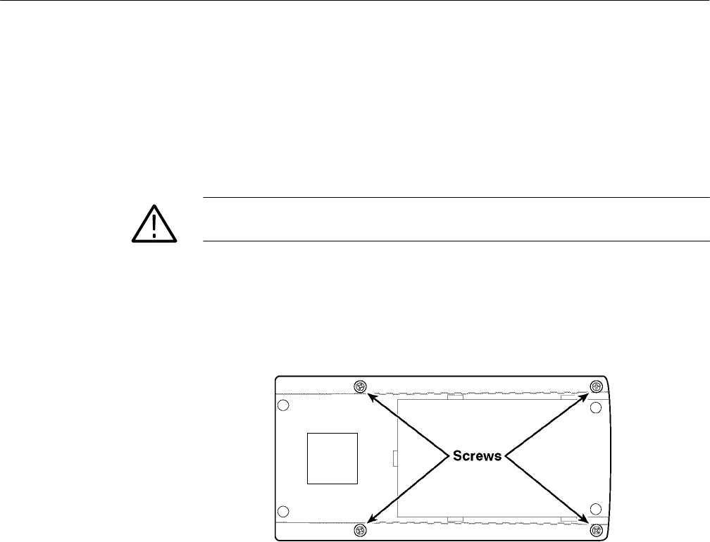
Maintenance
TSG 601 Service Manual 5–7
Only #4 screws are used in the TSG 601 to secure the case halves together. DO
NOT USE MORE THAN 3 INCH POUNDS OF TORQUE ON THESE
SCREWS.
Replacing Assemblies
WARNING. Disconnect the AC adapter and batteries before replacing any
components.
Follow this procedure to remove and replace the back cover of the TSG 601:
1. Remove the four screws securing the back cover to the front cover.
2. Gently separate the back cover about 1 inch from the instrument, taking care
to not pull the rear panel (connector panel) away with it.
3. Disconnect the battery cable from J10. Make sure to pull on the connector
housing to do this, not the wires. The back cover is now free and may be
moved away from the instrument.
4. Replacement is the reverse of removal. Be sure that the brown wire of the
battery cable assembly connects to pin 1 of J10.
Follow this procedure to remove and replace the connector (“rear”) panel of the
TSG 601:
1. With the back cover removed, disconnect the cable from J1 on the connector
panel. Again, pull on the connector housing, not on the wires.
2. Slide the assembly up away from the front panel.
3. Replacement is the reverse of removal.
Torque Specifications
Back Cover
Removal/Replacement
Connector Panel
Removal/Replacement

Maintenance
5–8 TSG 601 Service Manual
Follow this procedure to remove and replace the Main board and LCD of the
TSG 601:
1. After removing the connector panel, use a pair of needle-nose pliers to gently
pull the J2 housing up away from the instrument. Pull straight up, lifting the
Main board at the same time. Do NOT bend the connector housing.
2. When J2 pulls free, lift the Main board and the LCD display away from the
case.
3. To separate the Main board and LCD display module, disconnect the LCD
display cable from J6, and gently pull the two assemblies apart at J1. The
rubber board spacers should remain attached to the LCD display.
4. Replacement is the reverse of removal.
Follow this procedure to remove the TSG 601 keypad:
1. Once the Main board is out of the way, lift the plastic spacer board out of the
instrument. This is held in place only by a friction fit.
2. Lift the Keypad board out of the TSG 601. This too is held in place by a
friction fit.
3. Peel the rubber keypad out of the front panel.
Once the keypad has been removed from the front panel, follow this procedure to
replace the TSG 601 keypad:
1. Place the Keypad board with the pins of the connector towards the work-
bench.
2. Place the rubber keypad on top of the Keypad board, positioning it so that
the ON button is in the corner closest the connector.
3. Adjust the rubber keypad so that the fingers on its back side fit through the
corresponding holes in the Keypad board.
4. Holding the keypad and Keypad board with the buttons up, slide the front
case onto them, aligning the rubber buttons with the holes for them in the
front case as you do so. The Keypad board is a friction fit in the front case
half, so you must apply some slight pressure to fully seat the assemblies into
the case.
5. Place the assembled front case and keypad face down on the workbench and
press the plastic spacer board into place. Align the cutout in the spacer board
with the connector. The plastic fingers will be facing up.
6. Replace all assemblies by reversing the above procedures, as necessary.
Main Board and LCD
Removal/Replacement
Keypad Removal
Keypad Replacement

Replaceable Electrical Parts

TSG 601 Service Manual 6–1
Replaceable Electrical Parts
This section contains a list of the components that are replaceable for the
TSG 601. Use this list to identify and order replacement parts. There is a
separate Replaceable Electrical Parts list for each instrument.
Parts Ordering Information
Replacement parts are available from or through your local Tektronix, Inc., Field
Office or representative.
Changes to Tektronix instruments are sometimes made to accommodate
improved components as they become available and to give you the benefit of
the latest circuit improvements. Therefore, when ordering parts, it is important to
include the following information in your order.
HPart number
HInstrument type or model number
HInstrument serial number
HInstrument modification number, if applicable
If a part you have ordered has been replaced with a new or improved part, your
local Tektronix, Inc., Field Office or representative will contact you concerning
any change in part number.
Change information, if any, is located at the rear of this manual.
Using the Replaceable Electrical Parts List
The tabular information in the Replaceable Electrical Parts list is arranged for
quick retrieval. Understanding the structure and features of the list will help you
find all of the information you need for ordering replaceable parts.
The Mfg. Code Number to Manufacturer Cross Index for the electrical parts list
is located immediately after this page. The cross index provides codes, names,
and addresses of manufacturers of components listed in the electrical parts list.
Abbreviations conform to American National Standards Institute (ANSI)
standard Y1.1.
A list of assemblies can be found at the beginning of the electrical parts list. The
assemblies are listed in numerical order. When the complete component number
of a part is known, this list will identify the assembly in which the part is
located.
Cross Index–Mfr. Code
Number to Manufacturer
Abbreviations
List of Assemblies
Replaceable Electrical Parts
6–2 TSG 601 Service Manual
Column Descriptions
The component circuit number appears on the diagrams and circuit board
illustrations, located in the diagrams section. Assembly numbers are also marked
on each diagram and circuit board illustration, in the Diagram section and on the
mechanical exploded views, in the mechanical parts list. The component number
is obtained by adding the assembly number prefix to the circuit number.
Example a. Component Number
A23R1234 A23 R1234
Assembly Number Circuit Number
Read: Resistor 1234 of Assembl
y
23
Example b. Component Number
A23A2R1234 A23 R1234
Assembly Number
Circuit
Number
Read: Resistor 1234 of Subassembly 2 of Assembly 23
A2
Subassembly Number
The electrical parts list is arranged by assemblies in numerical sequence (A1,
with its subassemblies and parts, precedes A2, with its subassemblies and parts).
Mechanical subparts to the circuit boards are listed in the electrical parts list.
These mechanical subparts are listed with their associated electrical part (for
example, fuse holder follows fuse).
Chassis-mounted parts and cable assemblies have no assembly number prefix
and are located at the end of the electrical parts list.
Indicates part number to be used when ordering replacement part from
Tektronix.
Column three (3) indicates the serial or assembly number at which the part was
first used. Column four (4) indicates the serial or assembly number at which the
part was removed. No serial or assembly number entered indicates part is good
for all serial numbers.
An item name is separated from the description by a colon (:). Because of space
limitations, an item name may sometimes appear as incomplete. Use the U.S.
Federal Catalog handbook H6-1 for further item name identification.
The mechanical subparts are shown as *ATTACHED PARTS* / *END AT-
TACHED PARTS* or *MOUNTING PARTS* / *END MOUNTING PARTS* in
column five (5).
Indicates the code number of the actual manufacturer of the part. (Code to name
and address cross reference can be found immediately after this page.)
Indicates actual manufacturer’s part number.
Component No.
(Column 1)
Tektronix Part No.
(Column 2)
Serial/Assembly No.
(Column 3 and 4)
Name and Description
(Column 5)
Mfr. Code
(Column 6)
Mfr. Part No. (Column 7)

Replaceable Electrical Parts
TSG 601 Service Manual 6–3
CROSS INDEX – MFR. CODE NUMBER TO MANUFACTURER
Mfr.
Code. Manufacturer Address City, State, Zip Code
TK2058 TDK CORPORATION OF AMERICA 1600 FEEHANVILLE DRIVE MOUNT PROSPECT, IL 60056
TK2073 TOKYO AMERICA INC 565 W GULF ROAD ARLINGTON HEIGHTS IL 60005
TK2519 ALLIANCE SEMICONDUCTOR 1930 ZANKER ROAD SAN JOSE CA 95112
TK2598 MAXIM – ASIC 120 SAN GABRIEL DRIVE SUNNYVALE, CA 94086
0H1N5 TOSHIBA MARCON ELECTRONICS
AMERICA CORPORATION 998 FIRST EDGE DRIVE VERNON HILLS IL 60061
0JR03 ZMAN MAGNETICS INC 7633 S 180th KENT WA 98032
0JR04 TOSHIBA AMERICA INC
ELECTRONICS COMPONENTS DIV 9775 TOLEDO WAY IRVINE CA 92718
0LXM2 LZR ELECTRONICS INC 8051 CESSNA AVENUE GAITHERSBURG MD 20879
00779 AMP INC 2800 FULLING MILL
PO BOX 3608 HARRISBURG PA 17105
01295 TEXAS INSTRUMENTS INC
SEMICONDUCTOR GROUP 13500 N CENTRAL EXPY
PO BOX 655303 DALLAS TX 75262–5303
04222 AVX/KYOCERA
DIV OF AVX CORP 19TH AVE SOUTH
P O BOX 867 MYRTLE BEACH SC 29577
04713 MOTOROLA INC
SEMICONDUCTOR PRODUCTS SECTOR 5005 E MCDOWELL RD PHOENIX AZ 85008–4229
09969 DALE ELECTRONICS INC EAST HIGHWAY 50
P O BOX 180 YANKTON SD 57078
1ES66 MAXIM INTEGRATED PRODUCTS INC 120 SAN GABRIEL DRIVE SUNNYVALE CA 94086
1W344 UNITED CHEMI–CON INC
17856 SILICONIX INC 2201 LAURELWOOD RD SANTA CLARA CA 95054–1516
22526 BERG ELECTRONICS INC (DUPONT) 857 OLD TRAIL RD ETTERS PA 17319
24931 SPECIALTY CONNECTOR CO INC 2100 EARLYWOOD DR
PO BOX 547 FRANKLIN IN 46131
26364 COMPONENTS CORP 6 KINSEY PLACE DENVILLE NJ 07834–2611
27014 NATIONAL SEMICONDUCTOR CORP 2900 SEMICONDUCTOR DR SANTA CLARA CA 95051–0606
34335 ADVANCED MICRO DEVICES 901 THOMPSON PL
PO BOX 3453 SUNNYVALE CA 94086–3413
37964 GENNUM CORPORATION 970 FRASER DRIVE
PO BOX 489, STA A BURLINGTON, ONTARIO, CANADA L7R 3Y3
4T165 NEC ELECTRONICS USA INC
ELECTRON DIV 475 ELLIS ST
PO BOX 7241 MOUNTAIN VIEW CA 94039
50139 ALLEN–BRADLEY CO
ELECTRONIC COMPONENTS 1414 ALLEN BRADLEY DR EL PASO TX 79936
50434 HEWLETT–PACKARD CO
OPTOELECTRONICS DIV 370 W TRIMBLE RD SAN JOSE CA 95131–1008
53387 3M COMPANY
ELECTRONIC PRODUCTS DIV 3M AUSTIN CENTER AUSTIN TX 78769–2963
55322 SAMTEC INC 810 PROGRESS BLVD
PO BOX 1147 NEW ALBANY IN 47150–2257
55680 NICHICON /AMERICA/ CORP 927 E STATE PKY SCHAUMBURG IL 60195–4526
56845 DALE ELECTRONICS INC 2300 RIVERSIDE BLVD
PO BOX 74 NORFOLK NE 68701–2242
57668 ROHM CORPORATION 15375 BARRANCA PARKWAY
SUITE B207 IRVINE CA 92718
61429 FOX ELECTRONICS
DIV OF FOX ELECTRONICS INC 5842 CORPORATION CIRCLE FOR MEYERS FL 33905
62712 SEIKO INSTRUMENTS USA 2990 W LOMITA BLVD TORRANCE CA 90505–5102
68994 XILINX INC 2100 LOGIC DRIVE SAN JOSE CA 95124
75915 LITTELFUSE TRACOR INC
SUB OF TRACOR INC 800 E NORTHWEST HWY DES PLAINES IL 60016–3049
80009 TEKTRONIX INC 14150 SW KARL BRAUN DR
PO BOX 500 BEAVERTON OR 97077–0001

Replaceable Electrical Parts
6–4 TSG 601 Service Manual
Mfr.
Code. City, State, Zip CodeAddressManufacturer
82567 DYNAMICS CORP OF AMERICA
REEVES–HOFFMAN DIV 400 W NORTH ST CARLISLE PA 17013–2248
91637 DALE ELECTRONICS INC 2064 12TH AVE
PO BOX 609 COLUMBUS NE 68601–3632

Replaceable Electrical Parts
TSG 601 Service Manual 6–5
Component
Number Tektronix
Part Number Serial / Assembly Number
Effective Discontinued Name & Description Mfr.
Code Mfr. Part
Number
A1 671–2967–00 CIRCUIT BOARD:MAIN 80009 671296700
A2 671–2586–01 CIRCUIT BD ASSY:KEYBOARD 80009 671258601
A3 119–4506–00 DISPLAY,MODULE:,LCD;16 CHARACTERS X 2 LINES,5 X 7
DOT MATRIX,TRANSFLECTIVE,YEL/GRN LED 62712 M16327JY
A4 671–3227–00 CKT BD ASSY:REAR PANEL BOARD 80009 671322700
A1 671–2967–00 CIRCUIT BOARD:MAIN 80009 671296700
A1C1 283–5114–00 CAP,FXD,CER:MLC;0.1UF,10%,50V,X7R,1206 04222 12065C104KAT(1A
A1C2 290–5050–00 CAP,FXD,AL:47UF,20%,35V,6 H X 8 DIA MM;LOW IMP,SMD 1W344 MVF35VC47RM8TP
A1C3 283–5114–00 CAP,FXD,CER:MLC;0.1UF,10%,50V,X7R,1206 04222 12065C104KAT(1A
A1C4 283–5282–00 CAP,FXD,CER:MLC;2.2UF,+80–20%,16V,Y5V,0.120 X 0.060 04222 1206YG225ZAT2A
A1C5 283–5282–00 CAP,FXD,CER:MLC;2.2UF,+80–20%,16V,Y5V,0.120 X 0.060 04222 1206YG225ZAT2A
A1C6 283–5282–00 CAP,FXD,CER:MLC;2.2UF,+80–20%,16V,Y5V,0.120 X 0.060 04222 1206YG225ZAT2A
A1C7 283–5114–00 CAP,FXD,CER:MLC;0.1UF,10%,50V,X7R,1206 04222 12065C104KAT(1A
A1C8 283–5267–00 CAP,FXD,CER:MLC;1UF,+80%–20%,25V,Y5V,1206 04222 12063G105ZAT1A
A1C12 283–5283–00 CAP,FXD,CER:MLC;1.5PF,+/–.25PF,100V,NPO,.120X.060 04222 12061A1R5CAT*A
A1C14 283–5267–00 CAP,FXD,CER:MLC;1UF,+80%–20%,25V,Y5V,1206 04222 12063G105ZAT1A
A1C15 283–5283–00 CAP,FXD,CER:MLC;1.5PF,+/–.25PF,100V,NPO,.120X.060 04222 12061A1R5CAT*A
A1C16 283–5002–00 CAP,FXD,CER:MLC;1000PF,10%,50V,NPO,1206 TK2058 C3216COG1H102K–
A1C17 283–5113–00 CAP,FXD,CER:MLC;0.047UF,10%,50V,X7R,1206 04222 12065C473KAT1A
A1C18 283–5279–00 CAP,FXD,CER:MLC;0.47UF,10%,50V,X7R,.180X.250 04222 18255C474KAT1A
A1C19 283–5003–00 CAP,FXD,CER:MLC;0.01UF,10%,50V,X7R,1206 TK2058 C3216X7R1H103K–
A1C26 283–5003–00 CAP,FXD,CER:MLC;0.01UF,10%,50V,X7R,1206 TK2058 C3216X7R1H103K–
A1C27 283–5200–00 CAP,FXD,CER DI:0.47UF,+80–20%,50V 04222 18125E474ZAT1A
A1C28 283–5200–00 CAP,FXD,CER DI:0.47UF,+80–20%,50V 04222 18125E474ZAT1A
A1C29 283–5114–00 CAP,FXD,CER:MLC;0.1UF,10%,50V,X7R,1206 04222 12065C104KAT(1A
A1C30 283–5114–00 CAP,FXD,CER:MLC;0.1UF,10%,50V,X7R,1206 04222 12065C104KAT(1A
A1C31 283–5114–00 CAP,FXD,CER:MLC;0.1UF,10%,50V,X7R,1206 04222 12065C104KAT(1A
A1C33 283–5114–00 CAP,FXD,CER:MLC;0.1UF,10%,50V,X7R,1206 04222 12065C104KAT(1A
A1C34 283–5003–00 CAP,FXD,CER:MLC;0.01UF,10%,50V,X7R,1206 TK2058 C3216X7R1H103K–
A1C36 283–5114–00 CAP,FXD,CER:MLC;0.1UF,10%,50V,X7R,1206 04222 12065C104KAT(1A
A1C37 283–5114–00 CAP,FXD,CER:MLC;0.1UF,10%,50V,X7R,1206 04222 12065C104KAT(1A
A1C38 283–5114–00 CAP,FXD,CER:MLC;0.1UF,10%,50V,X7R,1206 04222 12065C104KAT(1A
A1C39 283–5114–00 CAP,FXD,CER:MLC;0.1UF,10%,50V,X7R,1206 04222 12065C104KAT(1A
A1C40 283–5203–00 CAP,FXD,CER:MLC;1000PF,10%,100V,X7R,1206 04222 12061C102KAT1A
A1C41 283–5203–00 CAP,FXD,CER:MLC;1000PF,10%,100V,X7R,1206 04222 12061C102KAT1A
A1C42 283–5203–00 CAP,FXD,CER:MLC;1000PF,10%,100V,X7R,1206 04222 12061C102KAT1A
A1C43 283–5114–00 CAP,FXD,CER:MLC;0.1UF,10%,50V,X7R,1206 04222 12065C104KAT(1A
A1C44 283–5114–00 CAP,FXD,CER:MLC;0.1UF,10%,50V,X7R,1206 04222 12065C104KAT(1A
A1C45 283–5114–00 CAP,FXD,CER:MLC;0.1UF,10%,50V,X7R,1206 04222 12065C104KAT(1A
A1C46 283–5114–00 CAP,FXD,CER:MLC;0.1UF,10%,50V,X7R,1206 04222 12065C104KAT(1A
A1C47 283–5114–00 CAP,FXD,CER:MLC;0.1UF,10%,50V,X7R,1206 04222 12065C104KAT(1A
A1C48 283–5114–00 CAP,FXD,CER:MLC;0.1UF,10%,50V,X7R,1206 04222 12065C104KAT(1A
A1C49 283–5114–00 CAP,FXD,CER:MLC;0.1UF,10%,50V,X7R,1206 04222 12065C104KAT(1A
A1C50 283–5114–00 CAP,FXD,CER:MLC;0.1UF,10%,50V,X7R,1206 04222 12065C104KAT(1A
A1C51 283–5114–00 CAP,FXD,CER:MLC;0.1UF,10%,50V,X7R,1206 04222 12065C104KAT(1A
A1C52 283–5114–00 CAP,FXD,CER:MLC;0.1UF,10%,50V,X7R,1206 04222 12065C104KAT(1A
A1C53 283–5114–00 CAP,FXD,CER:MLC;0.1UF,10%,50V,X7R,1206 04222 12065C104KAT(1A
A1C54 283–5114–00 CAP,FXD,CER:MLC;0.1UF,10%,50V,X7R,1206 04222 12065C104KAT(1A
A1C56 290–0943–00 CAP,FXD,ALUM:47UF,+50–20%,25V,6 X 11MM 0H1N5 CEUSM1E470–Q
A1C57 290–5034–01 CAP,FXD,ALUM:33UF,20%,10V,5.7MM(0.224) 1W344 MVK10VC33RME60T
A1C58 283–5114–00 CAP,FXD,CER:MLC;0.1UF,10%,50V,X7R,1206 04222 12065C104KAT(1A
A1C59 283–5203–00 CAP,FXD,CER:MLC;1000PF,10%,100V,X7R,1206 04222 12061C102KAT1A
A1C60 283–5203–00 CAP,FXD,CER:MLC;1000PF,10%,100V,X7R,1206 04222 12061C102KAT1A
A1C61 283–5114–00 CAP,FXD,CER:MLC;0.1UF,10%,50V,X7R,1206 04222 12065C104KAT(1A
A1C62 283–5114–00 CAP,FXD,CER:MLC;0.1UF,10%,50V,X7R,1206 04222 12065C104KAT(1A
A1C63 283–5114–00 CAP,FXD,CER:MLC;0.1UF,10%,50V,X7R,1206 04222 12065C104KAT(1A
A1C64 283–5114–00 CAP,FXD,CER:MLC;0.1UF,10%,50V,X7R,1206 04222 12065C104KAT(1A

Replaceable Electrical Parts
6–6 TSG 601 Service Manual
Component
Number Mfr. Part
Number
Mfr.
Code
Name & Description
Serial / Assembly Number
Effective Discontinued
Tektronix
Part Number
A1C65 283–5114–00 CAP,FXD,CER:MLC;0.1UF,10%,50V,X7R,1206 04222 12065C104KAT(1A
A1C66 283–5114–00 CAP,FXD,CER:MLC;0.1UF,10%,50V,X7R,1206 04222 12065C104KAT(1A
A1C67 283–5049–00 CAP,FXD,CER:MLC;180PF,5%,50V,NPO,1206 TK2058 C3216C0G1H181J–
A1C68 283–5114–00 CAP,FXD,CER:MLC;0.1UF,10%,50V,X7R,1206 04222 12065C104KAT(1A
A1C69 283–5203–00 CAP,FXD,CER:MLC;1000PF,10%,100V,X7R,1206 04222 12061C102KAT1A
A1C71 283–5203–00 CAP,FXD,CER:MLC;1000PF,10%,100V,X7R,1206 04222 12061C102KAT1A
A1C72 283–5114–00 CAP,FXD,CER:MLC;0.1UF,10%,50V,X7R,1206 04222 12065C104KAT(1A
A1C73 283–5003–00 CAP,FXD,CER:MLC;0.01UF,10%,50V,X7R,1206 TK2058 C3216X7R1H103K–
A1C74 283–5002–00 CAP,FXD,CER:MLC;1000PF,10%,50V,NPO,1206 TK2058 C3216COG1H102K–
A1C75 283–5113–00 CAP,FXD,CER:MLC;0.047UF,10%,50V,X7R,1206 04222 12065C473KAT1A
A1C76 283–5049–00 CAP,FXD,CER:MLC;180PF,5%,50V,NPO,1206 TK2058 C3216C0G1H181J–
A1C77 283–5003–00 CAP,FXD,CER:MLC;0.01UF,10%,50V,X7R,1206 TK2058 C3216X7R1H103K–
A1C78 283–5049–00 CAP,FXD,CER:MLC;180PF,5%,50V,NPO,1206 TK2058 C3216C0G1H181J–
A1C79 283–5049–00 CAP,FXD,CER:MLC;180PF,5%,50V,NPO,1206 TK2058 C3216C0G1H181J–
A1C81 283–5114–00 CAP,FXD,CER:MLC;0.1UF,10%,50V,X7R,1206 04222 12065C104KAT(1A
A1C82 290–5034–01 CAP,FXD,ALUM:33UF,20%,10V,5.7MM(0.224) 1W344 MVK10VC33RME60T
A1C83 283–5187–00 CAP,FXD,CER:MLC;15PF,5%,100V,NPO,1206 04222 12061A150JAT1A
A1C84 283–5187–00 CAP,FXD,CER:MLC;15PF,5%,100V,NPO,1206 04222 12061A150JAT1A
A1C85 283–5188–00 CAP,FXD,CER:MLC;100PF,5%,100V,NPO,1206 04222 12061A101JAT1A
A1C87 283–5188–00 CAP,FXD,CER:MLC;100PF,5%,100V,NPO,1206 04222 12061A101JAT1A
A1C88 283–5114–00 CAP,FXD,CER:MLC;0.1UF,10%,50V,X7R,1206 04222 12065C104KAT(1A
A1C89 283–5114–00 CAP,FXD,CER:MLC;0.1UF,10%,50V,X7R,1206 04222 12065C104KAT(1A
A1C90 283–5203–00 CAP,FXD,CER:MLC;1000PF,10%,100V,X7R,1206 04222 12061C102KAT1A
A1C91 283–5114–00 CAP,FXD,CER:MLC;0.1UF,10%,50V,X7R,1206 04222 12065C104KAT(1A
A1C92 283–5203–00 CAP,FXD,CER:MLC;1000PF,10%,100V,X7R,1206 04222 12061C102KAT1A
A1C93 283–5203–00 CAP,FXD,CER:MLC;1000PF,10%,100V,X7R,1206 04222 12061C102KAT1A
A1C98 283–5005–00 CAP,FXD,CER:MLC;4PF,+/–0.25PF,50V,NPO,1206 TK2058 C3216C0G1H040C–
A1C99 283–5005–00 CAP,FXD,CER:MLC;4PF,+/–0.25PF,50V,NPO,1206 TK2058 C3216C0G1H040C–
A1C100 290–0943–00 CAP,FXD,ALUM:47UF,+50–20%,25V,6 X 11MM 0H1N5 CEUSM1E470–Q
A1C101 283–5267–00 CAP,FXD,CER:MLC;1UF,+80%–20%,25V,Y5V,1206 04222 12063G105ZAT1A
A1C102 283–5267–00 CAP,FXD,CER:MLC;1UF,+80%–20%,25V,Y5V,1206 04222 12063G105ZAT1A
A1C103 283–5282–00 CAP,FXD,CER:MLC;2.2UF,+80–20%,16V,Y5V,0.120 X 0.060 04222 1206YG225ZAT2A
A1C105 283–5267–00 CAP,FXD,CER:MLC;1UF,+80%–20%,25V,Y5V,1206 04222 12063G105ZAT1A
A1C106 283–5188–00 CAP,FXD,CER:MLC;100PF,5%,100V,NPO,1206 04222 12061A101JAT1A
A1C107 283–5195–00 CAP,FXD,CER:MLC;10PF,5%,100V ,NPO,1206 04222 12061A100JAT1A
A1C108 283–5114–00 CAP,FXD,CER:MLC;0.1UF,10%,50V,X7R,1206 04222 12065C104KAT(1A
A1C109 283–5203–00 CAP,FXD,CER:MLC;1000PF,10%,100V,X7R,1206 04222 12061C102KAT1A
A1C110 283–5114–00 CAP,FXD,CER:MLC;0.1UF,10%,50V,X7R,1206 04222 12065C104KAT(1A
A1C111 290–1322–00 CAP,FXD,ALUM:470UF,20%,16V,ESR =
0.095OHM(20C,100KHZ),10 X 12.5MM,LS=5MM 55680 UPY1C471MPH
A1C112 283–5114–00 CAP,FXD,CER:MLC;0.1UF,10%,50V,X7R,1206 04222 12065C104KAT(1A
A1C113 283–5114–00 CAP,FXD,CER:MLC;0.1UF,10%,50V,X7R,1206 04222 12065C104KAT(1A
A1CR1 152–5027–00 DIODE,RECT:SCHTKY;40V,1A 04713 MBRS140T3
A1CR2 152–5018–00 DIODE,SIG:,ULTRA FAST;100V,0.74VF,4NS,2.0PF,SER–PAIR 27014 MMBD1203–HIGH
A1CR3 152–5027–00 DIODE,RECT:SCHTKY;40V,1A 04713 MBRS140T3
A1CR4 152–5086–00 DIODE,RECT:,ULTRA FAST;600V,1A,50NS 04713 MURS160T3
A1CR5 152–0843–00 DIODE,SIG:SCHTKY;SER–PAIR,20V,410MV,1.3PF 50434 HSMS–2812–T31
A1CR6 152–5045–00 DIODE,SIG:SCHTKY;20V,1.2PF,24 OHM 50434 HSMS–2810–T31
A1E1 108–5084–00 COIL,RF:FERRITE CHIP BEAD,52 OHM
+/–25%@100MHZ,DCR 0.3 OHM,IMAX 400 MA,8MM T&R TK2058 HF70ACB322513T
A1E2 108–5084–00 COIL,RF:FERRITE CHIP BEAD,52 OHM
+/–25%@100MHZ,DCR 0.3 OHM,IMAX 400 MA,8MM T&R TK2058 HF70ACB322513T
A1F1 159–0363–00 FUSE,WIRE LEAD:4A,125V,FAST BLOW,ULREC,CSACERT;, 75915 251004
A1J1 131–5542–01 CONN,BOX:PCB,BTM ENTRY;FEM,STR,2 X 7,0.1 CTR,0.235
H X 0.125 TAIL,30 GOLD,SLDR MASKPOSTS,DUAL ENTRY 53387 929842–01–07–30
A1J2 131–5543–01 CONN,BOX:PCB,BTM ENTRY;FEM,STR,2 X 10,0.1 CTR,0.23
H X 0.125 TAIL,30 GLD,SLDRMASK POST,DUAL ENTRY 53387 929842–01–10–30
A1J5 131–5527–00 JACK,PWR DC:PCB;MALE,RTANG,2MM PIN,11MMH(0.433) X
3.5MM(0.137) TAIL,9MM(0.354) W,TIN,W/SW,DC PWR JACK 0LXM2 DJ005A

Replaceable Electrical Parts
TSG 601 Service Manual 6–7
Component
Number Mfr. Part
Number
Mfr.
Code
Name & Description
Serial / Assembly Number
Effective Discontinued
Tektronix
Part Number
A1J6 131–4794–00 CONN,HDR::PCB;MALE,STR,1 X 2,0.1 CTR,0.235 53387 2402–6112 UB
A1J8 131–0391–00 CONN,RF JACK:SMB;50 OHM,STR,PCB,GOLD/GOLD,0.293
H X 0.155 TAIL,3/0.045 SQ TAIL 0.038DIA CTRCOND,0.2 SQ
PCB,0.312 HEX
24931 32JR105–1
A1J10 131–5240–00 CONN,HDR:PCB;MALE,STR,1 X 5,0.1 CTR,0.230MLG X
0.120 TAIL,30 GOLD 22526 68001–105
A1J13 131–5267–00 CONN,HDR:PCB;MALE,STR,2 X 40,0.1 CTR,0.235 00779 104326–4
A1J15 131–4794–00 CONN,HDR::PCB;MALE,STR,1 X 2,0.1 CTR,0.235 53387 2402–6112 UB
A1J21 131–0391–00 CONN,RF JACK:SMB;50 OHM,STR,PCB,GOLD/GOLD,0.293
H X 0.155 TAIL,3/0.045 SQ TAIL 0.038DIA CTRCOND,0.2 SQ
PCB,0.312 HEX
24931 32JR105–1
A1L1 108–1545–00 INDUCTOR,DUAL:TOROID,314UH,10%,157UH AT
1ADCMAX,0.25 OHMS,15 X 12MM 80009 108154500
A1L3 108–0598–00 COIL,RF:FIXED,200UH 0JR03 108–0598–00
A1L7 120–1939–00 TRANSFORMER:Z–92266 0JR03 Z–92266 (120–19
A1Q1 151–5066–00 TRANSISTOR,SIG:MOS,N–CH;60V,0.115A,7.5 OHM 04713 2N7002LT1
A1Q2 151–5066–00 TRANSISTOR,SIG:MOS,N–CH;60V,0.115A,7.5 OHM 04713 2N7002LT1
A1Q3 151–5000–00 TRANSISTOR,SIG:BIPOLAR,PNP;40V,200MA,250MHZ,AMPL 04713 MMBT3906LT1
A1Q4 151–5021–00 TRANSISTOR,SIG:BIPOLAR,NPN;40V,600MA,300MHZ,AMPL 04713 MMBT2222ALT1
A1Q5 151–5021–00 TRANSISTOR,SIG:BIPOLAR,NPN;40V,600MA,300MHZ,AMPL 04713 MMBT2222ALT1
A1Q6 151–5000–00 TRANSISTOR,SIG:BIPOLAR,PNP;40V,200MA,250MHZ,AMPL 04713 MMBT3906LT1
A1Q7 151–5066–00 TRANSISTOR,SIG:MOS,N–CH;60V,0.115A,7.5 OHM 04713 2N7002LT1
A1Q8 151–5088–00 TRANSISTOR,PWR:MOS,P–CH;30V,4.6A,0.07/0.135 17856 SI9435DY
A1Q9 151–5088–00 TRANSISTOR,PWR:MOS,P–CH;30V,4.6A,0.07/0.135 17856 SI9435DY
A1Q10 151–5001–00 TRANSISTOR,SIG:BIPOLAR,NPN;40V,200MA,300MHZ,AMPL 04713 MMBT3904LT1
A1Q11 151–5066–00 TRANSISTOR,SIG:MOS,N–CH;60V,0.115A,7.5 OHM 04713 2N7002LT1
A1Q12 151–5044–00 TRANSISTOR,PWR:BIPOLAR,PNP;100V,3.0A,3.0MHZ,AMPL 04713 MJD32CT4
A1Q13 151–5016–00 TRANSISTOR,SIG:BIPOLAR,PNP;20V,30MA,600MHZ,AMPL 04713 MMBTH81LT1
A1R1 321–5048–00 RES,FXD:THICK FILM;332K OHM,1%,0.125W,TC=100 PPM 57668 MCR18FXEA332K
A1R2 321–5047–00 RES,FXD:THICK FILM;100K OHM,1%,0.125W,TC=100 PPM 50139 BCK1003FT
A1R3 321–5030–00 RES,FXD:THICK FILM;10.0K OHM,1%,0.125W,TC=100 PPM 50139 BCK1002FT
A1R4 321–5000–00 RES,FXD:THICK FILM;10 OHM,1%,0.125W,TC=100PPM 91637 CRCW120610R0FT
A1R5 307–5041–01 RES,NTWK FXD:FILM;(15),4.7K OHM,2%,0.08W EA-
CH,50PPM 91637 SOMC–1601–472G–
A1R6 321–5001–00 RES,FXD:THICK FILM;12.1 OHM,1%,0.125W,TC=100 PPM 91637 CRCW120612R1FT
A1R8 321–5008–00 RES,FXD:THICK FILM;150 OHM,1%,0.125W,TC=100 50139 BCK1500FT
A1R11 321–5010–00 RES,FXD:THICK FILM;221 OHM,1%,0.125W,TC=100 50139 BCK221FT
A1R12 321–5010–00 RES,FXD:THICK FILM;221 OHM,1%,0.125W,TC=100 50139 BCK221FT
A1R13 321–5008–00 RES,FXD:THICK FILM;150 OHM,1%,0.125W,TC=100 50139 BCK1500FT
A1R14 321–5113–00 RES,FXD:THICK FILM;75 OHM,1%,0.125W,TC=100PPM 56845 CRCW1206–75ROFT
A1R17 321–5008–00 RES,FXD:THICK FILM;150 OHM,1%,0.125W,TC=100 50139 BCK1500FT
A1R19 321–5029–00 RES,FXD:THICK FILM;8.25K OHM,1%,0.125W,TC=100 PPM 50139 BCK8251FT
A1R20 321–5029–00 RES,FXD:THICK FILM;8.25K OHM,1%,0.125W,TC=100 PPM 50139 BCK8251FT
A1R22 321–5045–00 RES,FXD:THICK FILM;68.1 OHM,1%,0.125W,TC=100 PPM 50139 BCD68R1FT
A1R25 321–5045–00 RES,FXD:THICK FILM;68.1 OHM,1%,0.125W,TC=100 PPM 50139 BCD68R1FT
A1R30 321–5087–00 RES,FXD,FILM:620 OHM,5%,0.125W 50139 BCK6200JT
A1R31 311–5034–00 RES,VAR,TRMR:CERMET;2K OHM,25%,0.25W,4MM SQ,TOP
ADJ TK2073 G4DT202M
A1R32 321–5266–00 RES,FXD:THICK FILM;11K OHM,1%,0.125W,TC=100 91637 CRCW1206–1102FT
A1R33 321–5281–00 RES,FXD:THICK FILM;2K OHM,1%,0.125W,TC=100PPM 91637 CRCW1206–2001FT
A1R34 321–5051–00 RES,FXD:THICK FILM;0 OHM,1%,0.125W,TC=100 PPM 09969 CRCW1206 JUMPER
A1R35 321–5038–00 RES,FXD:THICK FILM;47.5K OHM,1%,0.125W,TC=100 PPM 50139 BCK4752FT
A1R36 321–5032–00 RES,FXD:THICK FILM;15.0K OHM,1%,0.125W,TC=100 PPM 50139 BCK1502FT
A1R37 321–5030–00 RES,FXD:THICK FILM;10.0K OHM,1%,0.125W,TC=100 PPM 50139 BCK1002FT
A1R38 321–5209–00 RES,FXD,FILM:243 OHM,1%,0.125WTAPE & REEL,SMD 91637 CRCW–1206–2430F
A1R39 321–5049–00 RES,FXD:THICK FILM;1M OHM,1%,0.125W,TC=100PPM 57668 MCR18FXEA1M
A1R40 311–5040–00 RES,VAR,TRMR:CERMET;10K OHM,25%,0.25W,4MM
SQ,TOP ADJ TK2073 G4DT103M
A1R42 321–5038–00 RES,FXD:THICK FILM;47.5K OHM,1%,0.125W,TC=100 PPM 50139 BCK4752FT

Replaceable Electrical Parts
6–8 TSG 601 Service Manual
Component
Number Mfr. Part
Number
Mfr.
Code
Name & Description
Serial / Assembly Number
Effective Discontinued
Tektronix
Part Number
A1R43 321–5041–00 RES,FXD:THICK FILM;82.5K OHM,1%,0.125W,TC=100 PPM 50139 BCK8252FT
A1R45 321–5028–00 RES,FXD:THICK FILM;6.81K OHM,1%,0.125W,TC=100 PPM 50139 BCK6811FT
A1R46 321–5016–00 RES,FXD:THICK FILM;681 OHM,1%,0.125W,TC=100 50139 BCK6810FT
A1R49 321–5027–00 RES,FXD:THICK FILM;5.62K OHM,1%,0.125W,TC=100 PPM 50139 BCK5621FT
A1R50 321–5025–00 RES,FXD:THICK FILM;3.92K OHM,1%,0.125W,TC=100 PPM 50139 BCK3921FT
A1R51 321–5090–00 RES,FXD:THICK FILM; 20K OHM,0.125W,100 PPM,1206,T&R 50139 BCK2002FT
A1R52 321–5030–00 RES,FXD:THICK FILM;10.0K OHM,1%,0.125W,TC=100 PPM 50139 BCK1002FT
A1R53 321–5030–00 RES,FXD:THICK FILM;10.0K OHM,1%,0.125W,TC=100 PPM 50139 BCK1002FT
A1R54 321–5018–00 RES,FXD:THICK FILM;1.0K OHM,1%,0.125W,TC=100 PPM 50139 BCK1001FT
A1R56 321–5030–00 RES,FXD:THICK FILM;10.0K OHM,1%,0.125W,TC=100 PPM 50139 BCK1002FT
A1R57 321–5030–00 RES,FXD:THICK FILM;10.0K OHM,1%,0.125W,TC=100 PPM 50139 BCK1002FT
A1R58 321–5015–00 RES,FXD:THICK FILM;562 OHM,1%,0.125W,TC=100 50139 BCK5620FT
A1R59 321–5000–00 RES,FXD:THICK FILM;10 OHM,1%,0.125W,TC=100PPM 91637 CRCW120610R0FT
A1R60 321–5007–00 RES,FXD:THICK FILM;121 OHM,1%,0.125W,TC=100 50139 BCK1210FT
A1R61 321–5006–00 RES,FXD:THICK FILM;100 OHM,1%,0.125W,TC=100 50139 BCK1000FT
A1R62 321–5006–00 RES,FXD:THICK FILM;100 OHM,1%,0.125W,TC=100 50139 BCK1000FT
A1R63 321–5006–00 RES,FXD:THICK FILM;100 OHM,1%,0.125W,TC=100 50139 BCK1000FT
A1R64 321–5006–00 RES,FXD:THICK FILM;100 OHM,1%,0.125W,TC=100 50139 BCK1000FT
A1R65 321–5006–00 RES,FXD:THICK FILM;100 OHM,1%,0.125W,TC=100 50139 BCK1000FT
A1R66 321–5006–00 RES,FXD:THICK FILM;100 OHM,1%,0.125W,TC=100 50139 BCK1000FT
A1R67 321–5006–00 RES,FXD:THICK FILM;100 OHM,1%,0.125W,TC=100 50139 BCK1000FT
A1R68 321–5006–00 RES,FXD:THICK FILM;100 OHM,1%,0.125W,TC=100 50139 BCK1000FT
A1R69 321–5006–00 RES,FXD:THICK FILM;100 OHM,1%,0.125W,TC=100 50139 BCK1000FT
A1R70 321–5006–00 RES,FXD:THICK FILM;100 OHM,1%,0.125W,TC=100 50139 BCK1000FT
A1R71 321–5018–00 RES,FXD:THICK FILM;1.0K OHM,1%,0.125W,TC=100 PPM 50139 BCK1001FT
A1R72 321–5030–00 RES,FXD:THICK FILM;10.0K OHM,1%,0.125W,TC=100 PPM 50139 BCK1002FT
A1R73 321–5030–00 RES,FXD:THICK FILM;10.0K OHM,1%,0.125W,TC=100 PPM 50139 BCK1002FT
A1R74 321–5047–00 RES,FXD:THICK FILM;100K OHM,1%,0.125W,TC=100 PPM 50139 BCK1003FT
A1R75 321–5166–00 RES,FXD:THICK FILM;150K OHM,1%,0.125W,TC=100 PPM 91637 CRCW1206–1503FT
A1R76 321–5048–00 RES,FXD:THICK FILM;332K OHM,1%,0.125W,TC=100 PPM 57668 MCR18FXEA332K
A1R77 321–5049–00 RES,FXD:THICK FILM;1M OHM,1%,0.125W,TC=100PPM 57668 MCR18FXEA1M
A1R78 321–5010–00 RES,FXD:THICK FILM;221 OHM,1%,0.125W,TC=100 50139 BCK221FT
A1R79 321–5045–00 RES,FXD:THICK FILM;68.1 OHM,1%,0.125W,TC=100 PPM 50139 BCD68R1FT
A1R80 321–5022–00 RES,FXD:THICK FILM;2.21K OHM,1%,0.125W,TC=100 PPM 50139 BCK2211FT
A1R81 321–5024–00 RES,FXD:THICK FILM;3.32K OHM,1%,0.125W,TC=100 PPM 50139 BCK3321FT
A1R82 321–5000–00 RES,FXD:THICK FILM;10 OHM,1%,0.125W,TC=100PPM 91637 CRCW120610R0FT
A1R83 321–5009–00 RES,FXD:THICK FILM;182 OHM,1%,0.125W,TC=100 50139 BCK1820FT
A1R84 321–5045–00 RES,FXD:THICK FILM;68.1 OHM,1%,0.125W,TC=100 PPM 50139 BCD68R1FT
A1TP3 214–4085–00 TERM,TEST POINT:0.070 ID,0.220 H,0.063 DIAPCB,0.015 X
0.032 BRASS,W/RED NYLON COLLAR 26364 104–01–02
A1TP4 214–4085–00 TERM,TEST POINT:0.070 ID,0.220 H,0.063 DIAPCB,0.015 X
0.032 BRASS,W/RED NYLON COLLAR 26364 104–01–02
A1U1 156–5074–02 IC,DIGITAL:HCMOS,FLIP FLOP;DUAL D–TYPE 01295 SN74HC74DR
A1U2 156–6871–00 IC,DIGITAL:CMOS,PLD;FPGA,XC4000 FAMILY,4013,576
CLBS,192 IOBS,160 I/O,5 NS 68994 XC4013–5MQ208C
A1U3 156–6714–00 IC,LINEAR:BIPOLAR,SW–REGULATOR;STEP–DOWN/BU-
CK,5.0V,500MA,4%,SHUTDOWN 27014 LM2574M–5.0
A1U4 156–6663–00 IC,MEMORY:CMOS,EPROM;128K X 8,120NS,5V PRGM 34335 AM29F010–120JC
A1U5 156–6661–00 IC,PROCESSOR:CMOS,MICRO COMPUTER;8–BIT,1K
RAM,A/D,D/A,12MHZ 4T165 UPD78237GC–3B9
A1U6 156–6663–00 IC,MEMORY:CMOS,EPROM;128K X 8,120NS,5V PRGM 34335 AM29F010–120JC
A1U7 156–6664–00 IC,MISC:CMOS,INTERFACE;DUAL RS–232DRIVER/RECEIV-
ER,+5V VCC,NEG INPUT THRESHOLD ON ONE RECEIVER 1ES66 MAX243CSE
A1U8 156–6665–00 IC,MISC:CMOS,PWR SUPPLY SUPERVISOR;MPU RESET
GEN,5V SUPPLY SENSING,MPU WATCHDOGTIMER 1ES66 MAX1232CSA (C74
A1U9 156–6491–00 IC,MEMORY:CMOS,ROM ;12 LINES X 24 COLUMN TV 80009 156649100
A1U10 156–5588–01 IC,LINEAR:BIPOLAR,V REF;POS,2.5V,1.0%,40PPM,SERIES 04713 MC1403DR2
A1U11 155–0416–00 IC,ASIC:BIPOLAR,VIDEO SERIALZER;FULL CUSTOM,M763 TK2598 155041600

Replaceable Electrical Parts
TSG 601 Service Manual 6–9
Component
Number Mfr. Part
Number
Mfr.
Code
Name & Description
Serial / Assembly Number
Effective Discontinued
Tektronix
Part Number
A1U13 156–6666–00 IC,LINEAR:BIPOLAR,AMPL;FM IF/DETECTOR,FSK DATA
SHAPER,W/RSSI 04713 MC13055D
A1U16 156–6668–00 IC,MISC:ECL,MISC;GENLINX CA DRVR W/TWO ADJUST
OUTPUTS 37964 GS9008
A1U18 156–6660–00 IC,ASIC:BIPOLAR,CUSTOM;DESERIALIZ-
ER,SC2307–00,PLCC44 80009 156–6660–00
A1U20 156–6669–00 IC,ASIC:GATE ARRAY;ENOLA VIDEO CO–PROCESSOR 27014 SCX6B21 AOD/V0
A1U21 156–6794–00 IC,MEMORY:CMOS,SRAM;32K X 8,15NS,5C2568,SOJ28.300 TK2519 AS7C256–15JC
A1U22 156–5081–01 IC,DIGITAL:HCTCMOS,GATE;HEX INVERTER 0JR04 TC74HCT04AFN(EL
A1U23 156–6867–00 IC,MEMORY:CMOS,ROM ;12 LINES X 24 COLUMN TV 80009 156686700
A1U25 156–5441–01 IC,LINEAR:BIPOLAR,VOLTAGE REGULATOR;POSITIVE,AD-
JUSTABLE,100MA,2%MICROPOWER 27014 LP2951CMX
A1U26 156–6794–00 IC,MEMORY:CMOS,SRAM;32K X 8,15NS,5C2568,SOJ28.300 TK2519 AS7C256–15JC
A1VR1 152–5046–00 DIODE,ZENER:;20V,5%,225MW 04713 MMBZ5250BLT1
A1VR2 152–5046–00 DIODE,ZENER:;20V,5%,225MW 04713 MMBZ5250BLT1
A1Y1 158–0449–00 OSCILLATOR:TCXO;27MHZ,1PPM,5PPM MIN ADJUSTIBIL-
ITY,3 PIN PACKAGE,DIP14 COMPATIBLE 82567 03–33336–001
A1Y2 158–5028–00 XTAL UNIT,QTZ:12.0 MHZ,+/–0.01%,PRL,CLH,TYPE FPX–SM 61429 FPX120 20
A2 671–2586–01 CIRCUIT BD ASSY:KEYBOARD 80009 671258601
A2J1 131–5781–00 CONN,HDR:PCB;MALE,STR,2 X 10,0.1 CTR,0.380 55322 MTLW–110–08–S–D
A3 119–4506–00 DISPLAY,MODULE:,LCD;16 CHARACTERS X 2 LINES,5 X 7
DOT MATRIX,TRANSFLECTIVE,YEL/GRN LED 62712 M16327JY
A4 671–3227–00 CKT BD ASSY:REAR PANEL BOARD 80009 671322700
A4J1 131–0391–00 CONN,RF JACK:SMB;50 OHM,STR,PCB,GOLD/GOLD,0.293
H X 0.155 TAIL,3/0.045 SQ TAIL 0.038DIA CTRCOND,0.2 SQ
PCB,0.312 HEX
24931 32JR105–1
A4J2 131–5436–00 CONN,RF JACK:BNC;50 OHM,FEMALE,STR,PCB,0.450 H X
(4)0.040 SQ,0.189 TAIL,ON 0.250 CTRPCB 24931 28JR299–3
A4J3 131–5436–00 CONN,RF JACK:BNC;50 OHM,FEMALE,STR,PCB,0.450 H X
(4)0.040 SQ,0.189 TAIL,ON 0.250 CTRPCB 24931 28JR299–3
A4J4 131–5436–00 CONN,RF JACK:BNC;50 OHM,FEMALE,STR,PCB,0.450 H X
(4)0.040 SQ,0.189 TAIL,ON 0.250 CTRPCB 24931 28JR299–3
W8 174–3183–00 CABLE ASSEMBLY:
(CONNECTED @ A1J8 & A4J1) 80009 174318300

Replaceable Electrical Parts
6–10 TSG 601 Service Manual

Diagrams and Circuit Board
Illustrations

TSG 601 Service Manual 7–1
Diagrams and Circuit Board Illustrations
Symbols
Graphic symbols and class designation letters are based on ANSI Standard
Y32.2–1975.
Logic symbology is based on ANSI Y32.14–1973 in terms of positive logic.
Logic symbols depict the logic function performed and may differ from the
manufacturer’s data.
Overline, parenthesis, or leading slash indicate a low asserting state.
Example: ID CONTROL, (ID CONTROL), or /ID CONTROL.
Abbreviations are based on ANSI Y1.1–1972.
Other ANSI standards that are used in the preparation of diagrams by Tektronix,
Inc. are:
Y14.15, 1966 — Drafting Practices.
Y14.2, 1973 — Line Conventions and Lettering.
Y10.5, 1968 — Letter Symbols for Quantities Used in Electrical
Science and Electrical Engineering.
American National Standard Institute
1430 Broadway, New York, New York 10018
Component Values
Electrical components shown on the diagrams are in the following units unless
noted otherwise:
Capacitors Values one or greater are in picofarads (pF).
Values less than one are in microfarads (mF).
Resistors Ohms ().
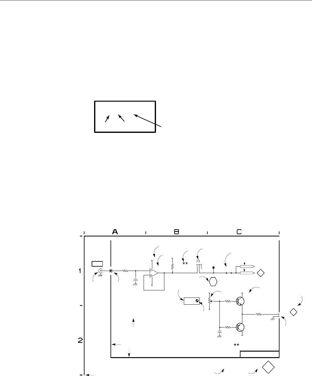
Diagrams and Circuit Board Illustrations
7–2 TSG 601 Service Manual
The following information and special symbols may appear in this manual.
Assembly Numbers Each assembly in the instrument is assigned an assembly number (e.g., A20).
The assembly number appears on the diagram (in circuit board outline), circuit
board illustration title, and lookup table for the schematic diagram.
The Replaceable Electrical Parts List is arranged by assembly number in numeri-
cal sequence; the components are listed by component number. Example:
Chassis–mounted components
have no Assembly No. prefix.
See end of Replaceable Electrical
Parts List
Assembly
Number
Component Number
Schematic Circuit
Number
Grid Coordinates
The schematic diagram and circuit board component location illustration have
grids. A lookup table with the grid coordinates is provided for ease of locating
the component. Only the components illustrated on the facing diagram are listed
in the lookup table.
When more than one schematic diagram is used to illustrate the circuitry on a
circuit board, the circuit board illustration will only appear opposite the first dia-
gram; the lookup table will list the diagram number of other diagrams that the
other circuitry appears on.
)$%&$"
!'
"'
" &(
"!$&%
&*"
"$&
(
!'"!$
&$(!&
$
(
$$
"
"'&
" $! &"
! &'$
'
'
(
$
$!&&
&%
$$&!
)(!$
$
#
)
!
( (
(
&"
(!
(!
$
!)%
'%& &
)
!
!$
%&
!$$
"$&
$
$
%
%"$&%%&
!$%&!
$&$
%#'$"
! &!$
"$&! !$
$
#
(
%"$&%%&!$
$$('%
%$ '$$ %
'
%$)$($
'%& &
$'&!$
!'&
% '$
%$(
&&
' &! !
%&$' &
%& '$ %%* '$
($& "'&
!"! & !&!$ $
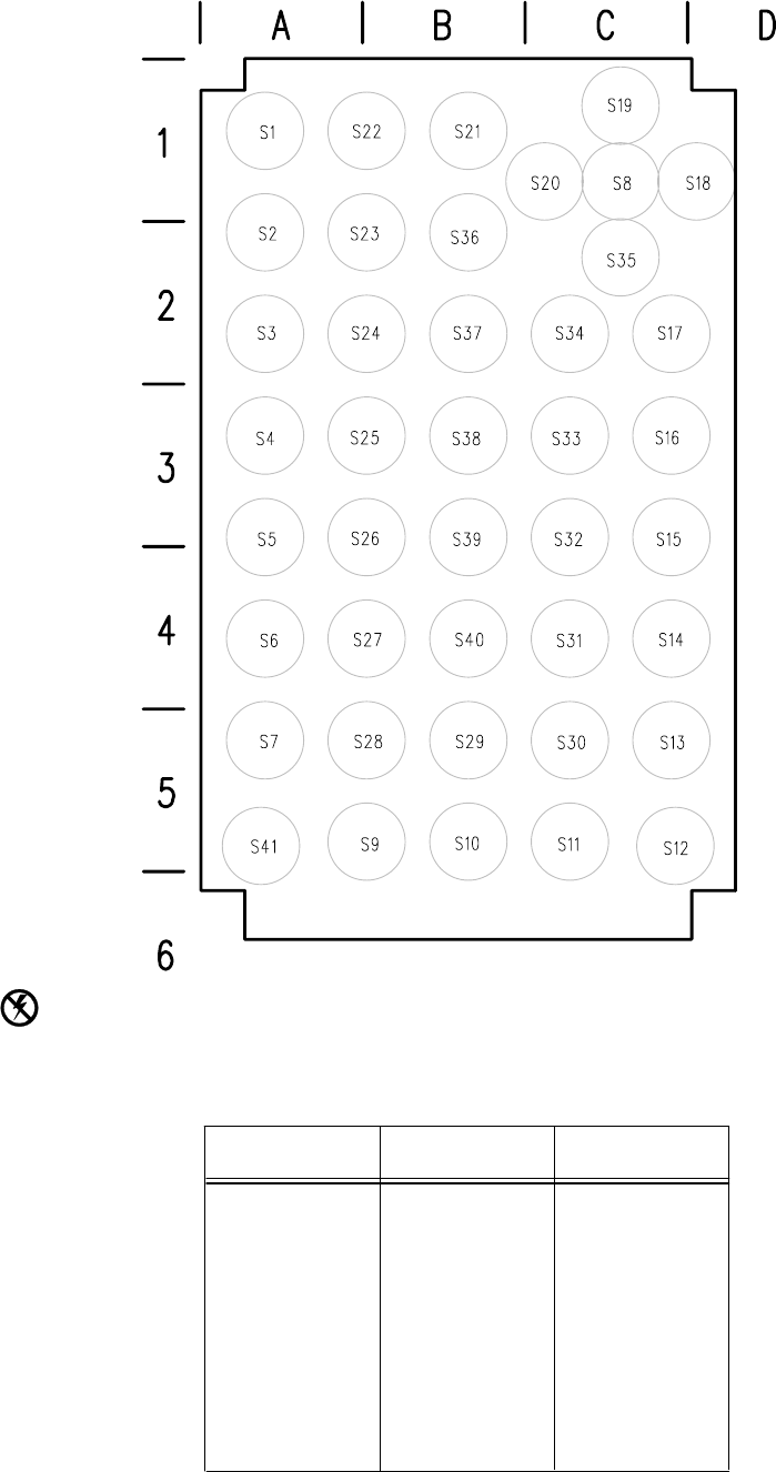
J1 H1 B6
S1 A1 A1
S2 A1 A1
S3 A2 A2
S4 A2 A3
S5 A3 A3
S6 A3 A4
S7 A4 A5
S8 A4 C1
S9 B4 A5
S10 C4 B5
S11 D4 C5
S12 D4 C5
S13 D4 C5
S14 D3 C4
S15 D3 C3
S16 D2 C3
S17 D2 C2
S18 D1 C1
S19 D1 C1
S20 D1 B1
S21 C1 B1
S22 B1 A1
S23 B1 A1
S24 B2 A2
S25 B2 A3
S26 B3 A3
S27 B3 A4
S28 B4 A5
S29 C4 B5
S30 D4 C5
S31 D3 C4
S32 D3 C3
S33 D2 C3
S34 D2 C2
S35 D1 C2
S36 C1 B1
S37 C2 B2
S38 C2 B3
S39 C3 B3
S40 C3 B4
S41 G2 A5
Schematic Diagram <1>
Component Locator Chart
Assembly A2.
A2 Key Board
TSG 601
Static Sensitive Devices
See Maintenance Section
#
+(0
+(0
+(0
"('(
,
,
,
"&'.
,
-,-," '%
()-"('&'.
,
,
(.-).-&)%
(.-).-&'.
,
,
+(0
+(0
,
,
+(0
+(0
+(0
+(0
+(0
(%
(%
(%
(%
(%
/"'
('4$2
#
&"'
(+
('4$2 /"'
('
,
+(0
,
,
+%%
,-(+
,
,!"-
, ,
+('(
+&'.
."(('(
."(&'.
,!"-%($
,
,
,
,
,
,
,
!
,
+(0
+(0
,
,
"
+(0
+(0
,
,
,
'
&
,
+
,
%
,
*
,
#
,
(
,
$
,
)
,
'-+
-
,
.
,
2
/
,
3
0
,
,)
+(0
%($
(.-
,
1
(%
(%
(%
(%
(%
%'$
TSG 601
$2(+
A2KEYPAD 1
C1 1 B5 A1
C2 3 D1 C1
C3 † 3 D1 C1
C4 1 H5 A1
C5 1 G5 A1
C6 1 G5 B1
C7 † 3 C1 C1
C8 2 E1 B4
C12 † 2 F1 B3
C14 2 E1 A3
C15 2 F1 A3
C16 2 A1 C3
C17 † 2 A2 C3
C18 † 2 A2 B4
C19 2 B2 C4
C26 † 2 F2 B3
C27 2 H2 A2
C28 2 G2 B2
C29 2 F2 A2
C30 2 G2 B3
C31 2 G2 A2
C33 2 E2 A4
C34 † 2 B2 C3
C36 3 G2 A3
C37 3 G2 B1
C38 3 G3 A3
C39 3 G3 A2
C40 † 3 G2 D2
C41 † 3 G2 D1
C42 † 3 H2 E2
C43 † 3 H2 D2
C44 † 3 H2 E2
C45 † 3 G3 D3
C46 † 3 G3 D3
C47 † 3 G3 E3
C48 † 3 G3 F2
C49 † 3 H3 G2
C50 † 3 H3 G2
C51 † 3 H3 F3
C52 3 G3 G3
C53 3 G3 G3
C54 † 3 G3 D3
C56 3 F2 F1
C57 3 G4 C4
C58 † 3 G4 C3
C59 † 3 G4 C3
C60 † 3 H4 C3
C61 † 3 H4 C3
C62 † 3 H4 C3
C63 † 3 G3 D1
C64 † 3 H3 E2
C65 † 3 H3 E2
C66 1 A2 G3
C68 † 3 G3 C2
C69 † 3 G3 C2
C71 † 3 H3 C2
C72 † 3 H3 C2
C81 † 3 H3 D1
C82 3 G3 C2
C83 † 1 A3 G2
C84 † 1 A3 F2
C85 † 1 A2 G3
C87 † 1 A3 G3
C88 1 A5 B1
C89 2 D1 A3
C90 † 3 G3 D4
C91 † 3 G3 E3
C92 † 3 G3 E4
C93 † 3 G3 F3
C98 2 B1 C3
C100 3 F3 F1
C101 † 3 F1 D1
C102 † 1 A5 F3
C103 1 H5 B1
C105 † 3 D1 E1
C106 † 1 A2 F3
C107 † 2 A1 B3
C108 2 D1 A3
C109 2 D1 A3
C110 2 G2 A2
C111 3 F2 E1
CR1 3 F2 E1
CR2 3 B2 C1
CR3 3 B1 C1
CR4 3 E2 E1
CR6 † 1 A2 F3
E1 3 G4 C3
E2 3 G3 C2
F1 3 B1 C1
J1 1 B5 A1
J2 1 A1 G2
J5 3 A1 C1
J6 1 B5 B4
J8 2 G1 B3
J10 3 A1 B1
J13 1 H5 B2
J15 1 B2 D4
J22 1 G1 D2
J23 1 E1 D3
J24 1 H1 D2
J25 1 H4 D2
J26 1 H2 F2
L1A 3 F2 F1
L1B 3 F3 F1
L3 2 G2 B3
L7 3 B1 C1
P6 1 B5
Q1 1 A2 G3
Q2 1 A5 G4
Q4 1 A5 B1
Q5 2 D1 A3
Q7 † 3 D2 D1
Q8 † 3 E2 E1
Q9 † 3 C1 C1
Q10 † 3 E2 E1
Q11 † 3 G1 D1
Q12 3 B2 C1
R1 1 A2 G3
R2 1 A2 G3
R3 1 A2 G4
R4 1 A5 F4
R5 1 C1 G3
R6 3 B2 C1
R8 † 2 C1 C3
R11 2 C1 B3
R12 2 C1 B3
R13 2 E1 B3
R14 2 F1 B3
R17 2 E1 A4
R19 † 2 F1 B3
R20 † 2 F1 B3
R22 † 2 F1 B4
R25 2 F1 B3
R30 2 F2 B3
R31 2 H2 A2
R32 2 E2 A3
R33 2 H2 A2
R45 1 B5 A1
R46 1 B5 A1
R49 2 E2 A3
R50 2 E2 A4
R52 † 3 C1 C1
R53 † 3 D2 E1
R54 † 3 D2 D1
R56 † 3 G1 C1
R57 † 3 F2 D1
R58 3 B2 C2
R59 3 B2 D1
R60 † 2 A2 C4
R61 † 1 H3 D3
R62 † 1 H3 D3
R63 † 1 H3 D3
R64 1 H3 D3
R65 1 H3 D3
R66 1 H3 D3
R67 1 H3 D3
R68 1 H3 E3
R69 † 1 H4 E4
R70 † 1 H4 E4
R71 † 1 G5 E3
R72 1 H2 F1
R73 1 G2 F1
R78 † 3 D2 D1
R79 2 G2 A2
TP1 2 B2 C4
TP3 3 F3 B3
TP4 3 F3 G1
U1A † 3 G1 D1
U1B † 3 G1 D1
U2 1 E2 D2
U3 † 3 C2 D1
U4 1 D1 E2
U5 1 B2 F2
U6 1 G1 E2
U7 1 G5 A1
U8 † 1 B2 D3
U10 1 A5 F3
U11 2 B1 C3
U13 2 G2 A3
U16 2 C1 A3
U21 1 G4 E4
U22A † 1 D2 E3
U22B † 1 C1 E3
U22C † 1 B3 E3
U23 1 C5 D1
U25 † 3 F1 C1
U26 1 G3 D4
VR1 † 3 C1 C1
VR2 † 3 E2 E1
Y1 1 C2 F3
Y2 1 A3 G2
A1 Main Board and Schematic <1> Component Locator Chart
(With crossĆreferences to schematic diagrams 1, 2, and 3.)
Comp
No
Diag
No
Diag
Loc
Bd
Loc
Comp
No
Diag
No
Diag
Loc
Bd
Loc
Comp
No
Diag
No
Diag
Loc
Bd
Loc
TSG 601
A1 Main Board (back)
Static Sensitive Devices
See Maintenance Section
Comp
No
Diag
No
Diag
Loc
Bd
Loc
A1 Main Board (front)
A3 LCD Board
(front)
A3 LCD Board
(back)
† = on back of board.
The schematic diagram has an alphanumeric grid to assist in locating parts within that diagram.
Use the lookup chart below for A3 Main Board Schematic <1>.
"
*
)
!
(
#
TEST SIGNAL
FLASH PROM
&$#&
"!
"
*
)
!
(
#
FLASH PROM
%"*
%"*
%"*
%"*
%"*
%"*
%"*
)
%
1
%"*
%"*
%"*
%"*
%"*
%"*
,
"%
)0,
"!0,
%"*
%"*
"
"
"
"
"
WATCHDOG
%"*
"!
"
"
%&'
"!,0&
(
'
!'
&0#(#0
"
*
)
""%
!'
#"
#"
#"
#"
&"
&"
&"
&"('"
"
#%"%
"!
%,(&,"
"
"
!'"
!"
"
"
"
"
"
"
"
&"
&"
%&"
*&"
"
"
"
"
"
"
"
"
"
"
"
"
"
'"
'"
' &"
'"
)
)
)
)
)
)
)
)
!
!
!
!
!
!
!
!
!
!
!
!
!
!
!
!
!
!
!
!
!
!
!
!
!
!
!
!
!
!
!
!
!
"
"
"
"
"
"
"
"
"
"
"
"
"
"
"
"
"
"
"
"
"
"
"
"
"
"
"
"
"
"
"
"
"
"
"
"
"
"
"
"
"
"
"
"
"
"
"
"
"
"
"
"
"
"
"
"
"
"
"
"
"
"
"
"
"
"
"
"
"
"
"
"
"
"
"
"
"
"
"
"
"
"
"
"
"
"
"
"
"
"
"
"
"
"
"
"
"
"
"
"
"
"
"
"
"
"
"
"
"
"
"
"
"
"
"
"
"
"
"
(
+
"%'&'
&#%"
((
*
"
&$#&
"!
""%
"
*
"%'&'
&$#&
"!
""%
)
"%'&'
&$#&
"!
""%
"
*
'
'
' &
'"
!0"
!0"
"%'&'
)
%
)
%
"
&,!
)&,!
%
*
!0"
!0"
0%*
%&'
"&0
"!
&
!'
"('
)
!
!
,
"&!
(
'
TCXO
%&'
)&'
#%&'
'
'"
%&'
%&'
!
)
(
+
#!
#!
#!
#!
#!
#!
#!
#!
)
)%
)&&
!"
!"
)%
)%
#!
#!'#
#!'#
#!'#
#!'#
#!'#&
#!'#
#&
+
+
"
%&'
#
#
#
#
#
#
#
#
#
#
#
#
#
#
#
#
#
#
#
#
#%
#*%
#*'
#%%$
&'
#"
#"
#"
#"
#"
#"
#"
#"
##*
##*
#
#
#
#
#
#%+
#'+
#&
#&$&
#'"
#'"
#'"
#'"
)&&
)&&
)
)
#
(
(#$#
*
)&'
)
%
$
%
#
''0"
)
"!,0&
MICROPROCESSOR
)!
)&'
%
%
(
&0)
%"*
%"*
%"*
%"*
%"*
%"*
%"*
%"*
0!&'
)
)
)
#
,
-
#
#
0&
"!,
%
*%
*'
(#
(
&
'
'
' &
'"
&%./
&%
&%0&
&%
&%
&%
&%
&%
&%
&%
&%./
&
&
&
&
&
&
&
&
&
"
*
)
!
(
'
VIDEO SRAMs
&
&
&
%
%
%
%
&
&
&
&
&
&
&
%
%
%
%
%
%
&
&
&
&
&
&
&
&
&
&
&
&
&
&
&
&*
)
"
*
)
!
(
'
&"
+!+
(
&%
&%
&
&
&
&
&
&
&
&
&
&
&
&
&
&
&
&
&
&%
&%
&%
)
#*%0*!
%0'
"
"
"
"
"
%+
'+
&
'
&'
&
&#%0
&#%0
!)0*'
!)*0*'
&'
"
#
(
'
)
%
(&,
&#%0
)
#
'&
%'&
%
*%
*'
&'
&
&
&
&
&
&
&*
&*
*
*
"
&#%0
&#%0
&#%0
!)0*'
!)*0*'
&
&
&
&
&
&
&*
&" )
&$#&
"!
""%
"%'&'
%&
!'%!
!'%
&0'+
&0'&
&0%+
&0%'&
&"
)
)
2
2
'+
%+
'&
%'&
)
(
+
2
2
%
"
FPGA
%
)
'
&'
(&,
&,!
)&,!
"
"&!
"&"('
)%
)
)
"!
)%
!
!
"('
!
)
!
(
(#
CHARACTER ID
GENERATOR
)&,!
&,!
&
'
&'
)
LCD
DISPLAY
0!&'
0%*
)
)
$
$
%
%
(
(
) )!
!
!
)"('
!
!
!
!
(
(
TSG 601
)
"%
(&,
)
CPU AND SERIAL DIGITAL GENERATION
!"' !'&" #"!!'& "(!'"!'"'"%
RS–232 DRIVER
1
#" !"%
A1 & A3
"

C8 E1 B4
C12 F1 B3
C14 E1 A3
C15 F1 A3
C16 A1 C3
C17 A2 C3
C18 A2 B4
C19 B2 C4
C26 F2 B3
C27 H2 A2
C28 G2 B2
C29 F2 A2
C30 G2 B3
C31 G2 A2
C33 E2 A4
C34 B2 C3
C89 D1 A3
C98 B1 C3
C107 A1 B3
C108 D1 A3
C109 D1 A3
C110 G2 A2
J8 G1 B3
L3 G2 B3
Q5 D1 A3
R8 C1 C3
R11 C1 B3
R12 C1 B3
R13 E1 B3
R14 F1 B3
R17 E1 A4
R19 F1 B3
R20 F1 B3
R22 F1 B4
R25 F1 B3
R30 F2 B3
R31 H2 A2
R32 E2 A3
R33 H2 A2
R49 E2 A3
R50 E2 A4
R60 A2 C4
R79 G2 A2
TP1 B2 C4
U11 B1 C3
U13 G2 A3
U16 C1 A3
Schematic Diagram <2>
Component Locator Chart
A1 Main Board. Partial assembly A1 also shown on
schematic diagrams 1 and 3.
SERIAL DRIVER
&
&
&
&
&
%$
#$%
#$%
&
&
&
&
&
&
&
&
&
&
%$
&%$
&%$
#&%$
#&%$
$
$
$#
$%'
$%'
&
&
"#$
%
&#"("
SERIALIZER
#")*
#"
#")*
#"
#"+#
#"
#"
#"
#"
#"
#"
#"
#"
#"
&#
%
#%$
&#
%
$
"
%
&#
"
"
"
#+&
#
#
#%$
#%$
&#$
&"
&
%
#
%
%
&
%
!
&
"
"
"
%
"
%
"
"
"
"
"
"
"+$
% "
"
#
#
%$
$
$"
$%$
$%$
!%
&
&
!%
%
%
"
%
%
TERMINATION DETECTOR
%
&
%
%
"
%
&#$
"
%
#"%
#"
#"
&#
%
%
&#
"$
TSG 601
$ $# $#%$$$"
SERIAL OUTPUT
"
2A1

C2 D1 C1
C3 D1 C1
C7 C1 C1
C36 G2 A3
C37 G2 B1
C38 G3 A3
C39 G3 A2
C40 G2 D2
C41 G2 D1
C42 H2 E2
C43 H2 D2
C44 H2 E2
C45 G3 D3
C46 G3 D3
C47 G3 E3
C48 G3 F2
C49 H3 G2
C50 H3 G2
C51 H3 F3
C52 G3 G3
C53 G3 G3
C54 G3 D3
C56 F2 F1
C57 G4 C4
C58 G4 C3
C59 G4 C3
C60 H4 C3
C61 H4 C3
C62 H4 C3
C63 G3 D1
C64 H3 E2
C65 H3 E2
C68 G3 C2
C69 G3 C2
C71 H3 C2
C72 H3 C2
C81 H3 D1
C82 G3 C2
C90 G3 D4
C91 G3 E3
C92 G3 E4
C93 G3 F3
C100 F3 F1
C101 F1 D1
C105 D1 E1
C111 F2 E1
CR1 F2 E1
CR2 B2 C1
CR3 B1 C1
CR4 E2 E1
E1 G4 C3
E2 G3 C2
F1 B1 C1
J5 A1 C1
J10 A1 B1
L1A F2 F1
L1B F3 F1
L7 B1 C1
Q7 D2 D1
Q8 E2 E1
Q9 C1 C1
Q10 E2 E1
Q11 G1 D1
Q12 B2 C1
R6 B2 C1
R52 C1 C1
R53 D2 E1
R54 D2 D1
R56 G1 C1
R57 F2 D1
R58 B2 C2
R59 B2 D1
R78 D2 D1
TP3 F3 B3
TP4 F3 G1
U1A G1 D1
U1B G1 D1
U3 C2 D1
U25 F1 C1
VR1 C1 C1
VR2 E2 E1
Schematic Diagram <3>
Component Locator Chart
A1 Main Board. Partial assembly A1 also shown
on schematic diagrams 1 and 2.
TSG 601
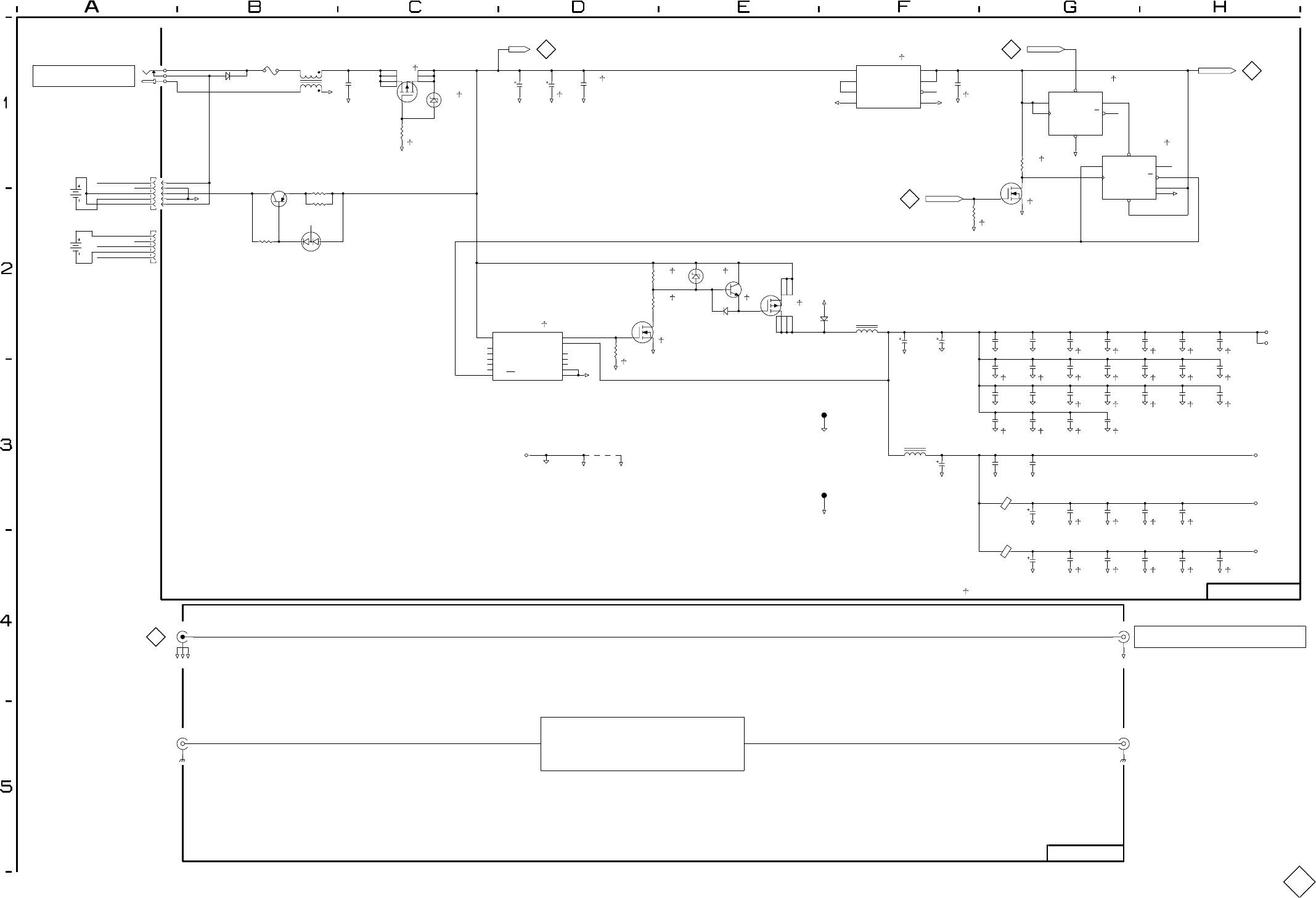
&*)
*)
%$
#
&$
#'
"""
%
%
&
&
+
+
%
!
%
POLARITY
PROTECTION
"
DC IN 9–15V
$
BATTERY
COMPARTMENT
&
"'
"
)'
"
&"
"
&"
&
! "
"
'"*'
"
SUPPLY CONTROL
!
"
!
!
"
&
%
!
!
"
%
&
"
+
!
"
"
&"
&
!
"
!
&
%$
#
'"
%
"
"'
"
)'
"
"
BATTERY CHARGER
$
(&
$$")
#
"
SWITCHING SUPPLY
+
%
%
%
%
%
%
$
%
%
%
%
%
%
%
%
%
%
%
%
%
%
%
&
&
%
%
%
%
%
%
%
&
%
&#
%
%
%
%
%
%
%
%
%
%
%
%
$
"
$ $# $#%$$$"
SERIAL VIDEO OUTPUT
"
APPROX 50 M CABLE50 M CABLE SIMULATOR
APPROX 50 M CABLE
TSG 601 POWER SUPPLY AND I/O PANEL
"
3A1 & A4

Replaceable Mechanical Parts

TSG 601 Service Manual 8–1
Replaceable Mechanical Parts
This section contains a list of the components that are replaceable for the
TSG 601. Use this list to identify and order replacement parts. There is a
separate Replaceable Mechanical Parts list for each instrument.
Parts Ordering Information
Replacement parts are available from or through your local Tektronix, Inc., Field
Office or representative.
Changes to Tektronix instruments are sometimes made to accommodate
improved components as they become available and to give you the benefit of
the latest circuit improvements. Therefore, when ordering parts, it is important to
include the following information in your order.
HPart number
HInstrument type or model number
HInstrument serial number
HInstrument modification number, if applicable
If a part you have ordered has been replaced with a new or improved part, your
local Tektronix, Inc., Field Office or representative will contact you concerning
any change in part number.
Change information, if any, is located at the rear of this manual.
Using the Replaceable Mechanical Parts List
The tabular information in the Replaceable Mechanical Parts list is arranged for
quick retrieval. Understanding the structure and features of the list will help you
find all of the information you need for ordering replaceable parts.
The Mfg. Code Number to Manufacturer Cross Index for the mechanical parts
list is located immediately after this page. The cross index provides codes,
names, and addresses of manufacturers of components listed in the mechanical
parts list.
Abbreviations conform to American National Standards Institute (ANSI)
standard Y1.1.
Chassis-mounted parts and cable assemblies are located at the end of the
Replaceable Electrical Parts list.
Cross Index–Mfr. Code
Number to Manufacturer
Abbreviations
Chassis Parts

Replaceable Mechanical Parts
8–2 TSG 601 Service Manual
Column Descriptions
Items in this section are referenced by figure and index numbers to the illustra-
tions.
Indicates part number to be used when ordering replacement part from
Tektronix.
Column three (3) indicates the serial number at which the part was first used.
Column four (4) indicates the serial number at which the part was removed. No
serial number entered indicates part is good for all serial numbers.
This indicates the quantity of mechanical parts used.
An item name is separated from the description by a colon (:). Because of space
limitations, an item name may sometimes appear as incomplete. Use the U.S.
Federal Catalog handbook H6-1 for further item name identification.
Following is an example of the indentation system used to indicate relationship.
1 2 3 4 5 Name & Description
Assembly and/or Component
Mounting parts for Assembly and/or Component
*MOUNTING PARTS*/*END MOUNTING PARTS*
Detail Part of Assembly and/or Component
Mounting parts for Detail Part
*MOUNTING PARTS*/*END MOUNTING PARTS*
Parts of Detail Part
Mounting parts for Parts of Detail Part
*MOUNTING PARTS*/*END MOUNTING PARTS*
Mounting Parts always appear in the same indentation as the Item it mounts,
while the detail parts are indented to the right. Indented items are part of and
included with, the next higher indentation. Mounting parts must be purchased
separately, unless otherwise specified.
Indicates the code number of the actual manufacturer of the part. (Code to name
and address cross reference can be found immediately after this page.)
Indicates actual manufacturer’s part number.
Figure & Index No.
(Column 1)
Tektronix Part No.
(Column 2)
Serial No.
(Column 3 and 4)
Qty (Column 5)
Name and Description
(Column 6)
Mfr. Code
(Column 7)
Mfr. Part Number
(Column 8)

Replaceable Mechanical Parts
TSG 601 Service Manual 8–3
CROSS INDEX – MFR. CODE NUMBER TO MANUFACTURER
Mfr.
Code Manufacturer Address City, State, Zip Code
TK0435 LEWIS SCREW CO 4300 S RACINE AVE CHICAGO IL 60609–3320
TK1155 QUALITY PLASTIC INJECTION MOLDING 3910 INDUSTRIAL AVE COEUR D’ALENE ID 83814
TK2548 XEROX BUSINESS SERVICES
DIV OF XEROX CORPORATION 14181 SW MILLIKAN WAY BEAVERTON OR 97077
0DWW6 MICRO POWER ELECTRONICS 7973 SW CIRRUS DRIVE
BLDG. #22 BEAVERTON OR 97005
0VG90 GLOBTEK INC 186 VETERANS DRIVE NORTHVALE, NJ 07647
62712 SEIKO INSTRUMENTS USA 2990 W LOMITA BLVD TORRANCE CA 90505–5102
80009 TEKTRONIX INC 14150 SW KARL BRAUN DR
PO BOX 500 BEAVERTON OR 97077–0001

Replaceable Mechanical Parts
8–4 TSG 601 Service Manual
Fig. &
Index
No. Tektronix
Part No. Serial Number
Effective Dscont Qty
12345 Name & Description Mfr.
Code Mfr. Part No.
1–1 614–0913–00 1 KIT ASSEMBLY:BATTERY HOLDER SUB ASSEMBLY
*MOUNTING PARTS* 80009 614091300
–2 211–0097–00 4 SCREW,MACHINE:4–40 X 0.312,PNH,STL
*END MOUNTING PARTS* TK0435 ORDER BY DESC
–3 348–1347–00 4 PAD,CUSHIONING:TSG90 80009 348134700
–4 200–4075–00 1 DOOR,BATTERY:POLYCARBONATE TK1155 200–4075–00
–5 333–4145–00 1 REAR,PANEL:PLASTIC,TSG601 80009 333414500
–6 ––––––––––– 1 CKT BD ASSY:REAR PANEL BOARD
(SEE A4 REPL)
*MOUNTING PARTS*
–7 211–0661–00 3 SCR,ASSEM WSHR:4–40 X 0.25,PNH,STL,CD PL,POZ,MACH TK0435 ORDER BY DESC
–8 214–4661–00 1 SPRING,EMI CNTC:SPRING,EMI CONTACT,0.004 CU–BE,
HEAT TREAT TO HARD,0.0003 INCH MIN TINMATE,TSG601
*END MOUNTING PARTS*
80009 214466100
–9 ––––––––––– 1 CIRCUIT BOARD:MAIN
(SEE A1 REPL)
–10 426–2408–00 1 SPACER,ECB:ABS,BLACK,TSG601 80009 426240800
–11 ––––––––––– 1 CIRCUIT BD ASSY:KEYBOARD
(SEE A2 REPL)
–12 119–4709–00 1 KEYPAD:TSG601 80009 119470900
–13 361–1636–00 2 SPACER:SANTOPREN 80009 361163600
–14 ––––––––––– 1 DISPLAY,MODULE:,LCD;16 CHARACTERS X 2 LINES,5 X 7
DOT MATRIX,TRANSFLECTIVE,YEL/GRN LEDBACK-
LIGHT,WIDE TEMP RANGE
(SEE A3 REPL)
–15 614–0920–00
016–1229–00
070–8909–00
1
1
1
KIT ASSEMBLY:378–2073–00,202–0230–03
STANDARD ACCESSORIES
CASE,CARRYING:TSG90
MANUAL,TECH:INSTRUCTION,CARD,TSG601
80009
80009T
K2548
61409200
0016122900
070890900
–16 119–4538–00
119–4539–00
1
1
POWER SUPPLY:12W; 12V 1A, 180CM CORD WITH 2.1MM
FEMALE RIGHT ANGLECONN, CN
(STANDARD ONLY)
OPTIONAL ACCESSORIES
POWER SUPPLY:12W; 12V 1A, 180CM CORD WITH 2.1MM
FEMALE RIGHT ANGLECONN, CN
(OPTION 1J ONLY)
0VG90
0VG90
WD1E1000CRA12CN
WD49E1000CRA12C
–17 119–4488–00
070–8910–00
070–8911–00
1
1
1
BAT PACK ASSY:
MANUAL,TECH:USER,TSG601
MANUAL,TECH:SERVICE,TSG601,DP
0DWW6
TK2548
TK2548
101–147–1
070891000
070891100
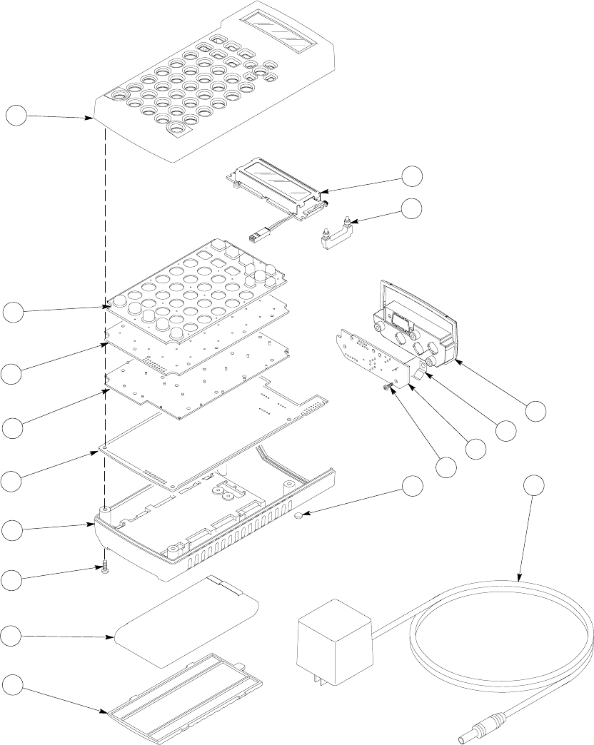
TSG 601 Service Manual 8–5
A1
A2
FIG. 1 EXPLODED VIEW
A3
A4
8–6 TSG 601 Service Manual
