TV 8888 25rd 42
User Manual: TV-8888-42
Open the PDF directly: View PDF ![]() .
.
Page Count: 45

1
HAIER
COLOUR TELEVISION
SERVICE MANUAL
PART # TV-8888-42
HAIER AMERICA TRADING, LLC
www.haieramerica.com

2
TABLE OF CONTENTS
Product Code Explanation and Series
Introduction
3
Features 4 – 5
Safety Precautions 6
Warning and Cautions 7 –8
General Servicing Precautions 9 – 13
Net Dimension 14
Parts and Functions 15
Remote Controller Functions 16
Program Diagram 17 – 22
Maintenance Service and Troubleshooting 23 – 27
Circuit Diagram 28 – 29
PCB Diagram 30
Circuit Explanation 31 –33
Service Mode and Adjusting Items and
Data
34 – 36
Circuit Signals Processing 37 - 40
Adjustment 41 - 42
Information of Resistors and Capacitors 43
Abbreviation of Part Name and
Description
44
Terminal View of Transistors 45

3
PRODUCT CODE EXPLANATION AND SERIES INTRODUCTION
BH 2004 D
Color television appearance
CRT cater corner 20inch
Appearance serial
BRAND
4
FEATURES
No FUNCTION
1 Main IC 76814
2 CRT Flat picture
3 Color system NTSC3.58
4 Audio system M
5 No. Of channels 181
6 OSD language ENGLISH、 FRENCH、 SPANISH
7
PIC
Multi-picture modes
8 AV stereo
9 Super woofer
10 Surrounding sound
11 Treble/bass boost
12 Left/right balancer
13 NICAM
14 Multi-audio modes
15 Tone adjuster
16 MTS/SAP
17
AUDIO
Auto-volume leveling
18 AV input Y
19 AV output
20 DVD terminal
21 S-video jack
22 Headphone socket Y
23
JIC
SCART socket
24 Digital curtain
25 Slow fading on & off
26 Semitransparent menu
27 Non-flashing channel changing
28 ZOOM
29 16:9 mode
30 Games
31 Calendar
32 Child-lock
33 Multi-functional lock Y
34 No-picture listening
35 Background light
36 Auto-timer on
37 CCD Y
38
SOFTWARE
V-CHIP Y
5
Continued:
FUNCTION
39 NO. Of built-in speakers 1
40 Audio output power (W) 3W
41 Total power input W 70W
42 Voltage range V 120V
43 Power frequency Hz 60HZ
44 Time of sleep timer (mins) 120MIN
45 Net weight (lbs) 46.2
46 Gross weight (lbs) 50.7
47 Net dimension (MM)
48 Packaged dimension (MM)
49 Quantity for 20' container
50 Quantity for 40' container
51
PARAMETER
Quantity for 40' high container
52 Acquired certificate
53
APPROVAL
Suitable market

6
SAFETY PRECAUTIONS
IMPORTANT SAFETY NOTICE
These parts identified by many electrical and mechanical parts in this chassis have
special safety-related characteristics.
It is essential that these special safety parts be replaced with the same components
as recommended in this manual to prevent X-RADIATION, Shock, Fire, or other
Hazards.
Do not modify the original design without permission of the manufacturer.
General Guidance
An Isolation Transformer should always be used during the servicing of a receiver
whose chassis is not isolated from the AC power line. Use a transformer of adequate
power rating as this protects the technician from accidents that might result in
personal injury caused by electrical shocks.
It will also protect the receiver and it’s components from being damaged by
accidental shorts of the circuitry that might be inadvertently introduced during the
service operation.
If any fuse (or Fusible Resistor) in this TV receiver is blown, replace it with a
specified one.
When replacing a high wattage resistor (Oxide Metal Film Resistor, over 1W), keep
the resistor 0.39inch away from PCB.
Keep wires away from high voltage or high temperature parts.
Due to the high vacuum and large surface area of the picture tube, extreme care
should be taken in handling the Picture Tube. Do not lift the Picture Tube by its Neck.
X-RAY Radiation
Warning:
The sources of X-RAY RADIATION in this TV receiver are the High Voltage Section
and the Picture Tube.
For continued X-RAY RADIATION protection, the replacement tube must be of the
same type as specified in the Replacement Parts List.
Before returning the receiver to the customer, always perform an AC leakage current
check on the exposed metallic parts of the cabinet, such as antennas, terminals, etc.,
to make sure that the set is safe to operate without any danger of electrical shock.
7
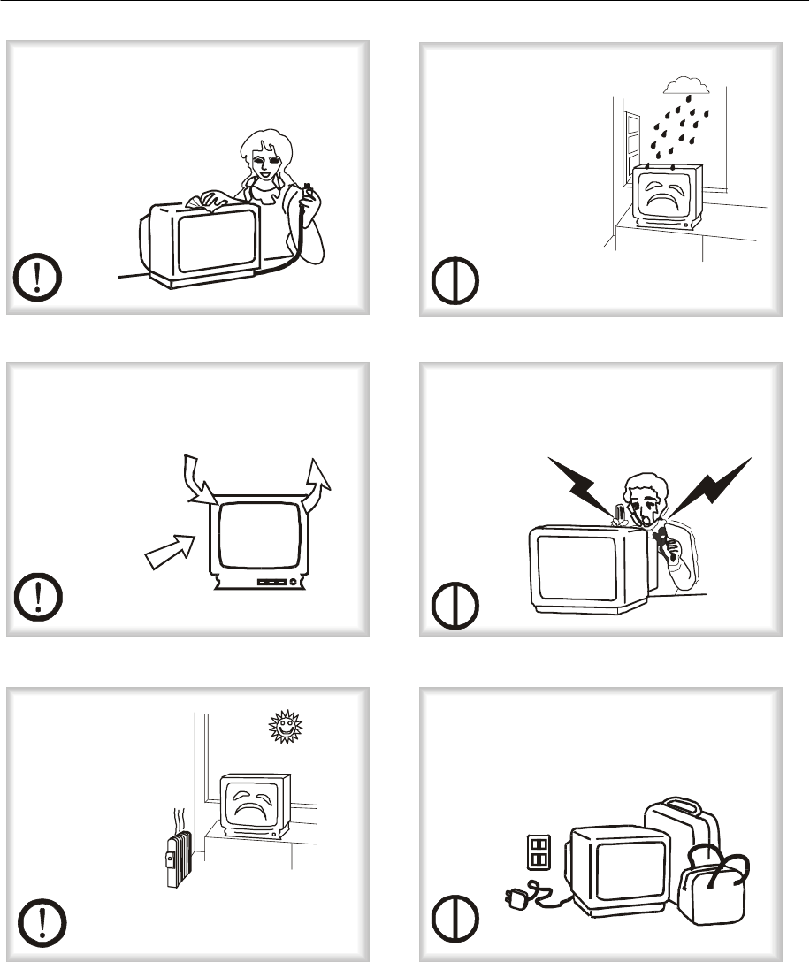
WARNING AND CAUTIONS
1. When you clean the TV set, please pull
out the power plug from AC outlet. Don't
clean the cabinet and the screen with
benzene, petrol and other chemicals.
4. To prevent the TV set from firing and
electric shock, don't
make the TV set rain
or moisture.
2.
In order to prolong the using life of the
TV set, please place it on a ventilated
place.
5. Don't open the back cover, otherwise it is
possible to damage the components in the
TV set and harm you.
3.
Don't place the
TV set in the
sunshine or near
heat source.
6. When the TV set isn't going to be used
for long time or it is in thunder and
lightening, please pull out the plug from AC
outlet and the antenna plug from the cover
of the TV set.
8
Explanation on the display tube
Generally, it is not required to clean the tube surface. However, if necessary, its
surface can be cleaned with a dry cotton cloth after putting off the power. Don’t use
any cleanser. Avoid using a hard cloth; the tube surface will be damaged.
CAUTION: Before servicing receivers covered by this service manual and its
supplements and addenda, read and follow the SAFETY PRECAUTIONS.
NOTE: If unforeseen circumstances create conflict between the following servicing
precautions and any of the safety precautions, always follow the safety precautions.
NB: Remember; Safety First.

9
GENERAL SERVICING PRECAUTIONS
1. Always unplug the receiver AC power cord from the AC power source before:
a. Removing or reinstalling any component, circuit board module or any other
assembly of the receiver.
b. Disconnecting or reconnecting any receiver electrical plug or other electrical
connection.
c. Connecting a test substitute in parallel with an electrolytic capacitor in the
receiver.
CAUTION: A wrong substitution part or incorrect installation polarity of electrolytic
capacitors may result in an explosion hazard.
d. Discharging the picture tube anode.
2. Test high voltage only by measuring it with an appropriate high voltage meter or
other voltage-measuring device (DVM, FETVOM, etc.) equipped with a suitable
high voltage probe. Do not test high voltage by “drawing an arc”.
3. Discharge the picture tube anode only by (a) first connecting one end of an
insulated clip lead to the degaussing or kine aquadag grounding system shield at
the point where the picture tube socket ground lead is connected, and then (b)
touch the other end of the insulated clip lead to the picture tube anode button,
using an insulating handle to avoid personal contact with high voltage.
4. Do not spray chemicals on or near this receiver or any of its assemblies.
5. Unless specified otherwise in this service manual, clean electrical contacts only by
applying the following mixture to the contacts with a pipe cleaner, cotton-tipped
stick or comparable nonabrasive applicator; 10% (by volume) Acetone and 90%
(by volume) isopropyl alcohol (90%-99% strength)
CAUTION: This is a flammable mixture.
Unless specified otherwise in this service manual, lubrication of contacts is not
required.
6. Do not defeat any plug / socket B+ voltage interlocks with which receivers
covered by this service manual might be equipped.
7. Do not apply AC power to this instrument and/or any of its electrical assemblies
unless all solid-state device heat sinks are correctly installed.
8. Always connect the test receiver ground lead to the receiver chassis ground
before connecting the test receiver positive lead.
Always remove the test receiver ground lead last.
9. Use with this receiver only the test fixtures specified in this service manual.
CAUTION: Do not connect the test fixture ground strap to any heat sink in this
receiver.
10
Electrostatically Sensitive (ES) Devices
Some semiconductor (solid state) devices can be damaged easily by static electricity.
Such components are usually called Electrostatically Sensitive (ES) Devices.
Examples of typical ES devices are integrated circuits and some field effect
transistors and semiconductor “chip” components. The following techniques should
be used to help reduce the incidence of component damage caused by static
electricity.
1. Immediately before handling any semiconductor component or semiconductor-
equipped assembly, drain off any electrostatic charge on your body by touching a
known earth ground. Alternatively, obtain and wear a commercially available
discharging wrist strap device, which should be removed to prevent potential
shock prior to applying power to the unit under test.
2. After removing an electrical assembly equipped with ES devices, place the
assembly on a conductive surface such as aluminum foil, to prevent electrostatic
charge buildup or exposure of the assembly.
3. Use only a grounded-tip soldering iron to solder or unsolder ES devices.
4. Use only an anti-static type folder removal device. Some solder removal devices
not classified as “anti-static” can generate electrical charges sufficient to damage
ES devices.
5. Do not use freon-propelled chemicals. These can generate electrical charges
sufficient to damage ES devices.
6. Do not remove a replacement ES device from its protective package until
immediately before you are ready to install it. (Most replacement ES devices are
packaged with leads electrically shorted together by conductive foam, aluminum
foil or comparable conductive material).
7. Immediately before removing the protective material from the leads of a
replacement ES device, touch the protective material to the chassis or circuit
assembly into which the device will be installed.
CAUTION: Be sure no power is applied to the chassis or circuit, and observe all
other safety precautions.
8. Minimize bodily motions when handling unpackaged replacement ES devices.
(Otherwise even some normally harmless motions such as mutual brushing of
your clothes’ fabric or lifting of your foot from a carpeted floor might generate
static electricity sufficient to damage an ES device.)
General Soldering Guidelines
1. Use a grounded-tip, low-wattage soldering iron and appropriate tip size and
shape that will maintain tip temperature within the range of 500 oF to 600 oF.
2. Use an appropriate gauge of RMA resin-core solder composed of 60 parts tin/40
parts lead.
3. Keep the soldering iron tip clean and well tinned.
4. Thoroughly clean the surfaces to be soldered. Use a small wire bristle (0.5 inch)
brush with a metal handle. Do not use freon-propelled spay-on cleaners.
11
5. Use the following unsoldering technique
a. Allow the soldering iron tip to reach normal temperature. (500 oF to 600oF)
b. Heating the component lead until the solder melts.
c. Quickly draw the melted solder with an anti-static, suction-type solder
removal device with solder braid.
CAUTION: Work quickly to avoid overheating the circuit board printed foil.
6. Use the following unsoldering technique
a. Allow the soldering iron tip to reach normal temperature. (500 o F to 600o F)
b. First, hold the soldering iron tip and solder the strand against the
component lead until the solder melts.
c. Quickly move the soldering iron tip to the junction of the component lead
and the printed circuit foil, and hold it there only until the solder flows onto
and around both the component lead and the foil.
CAUTION: Work quickly to avoid overheating the circuit board printed foil.
d. Closely inspect the solder area and remove any excess or splashed solder
with a small wire-bristle brush.
Removal /Replacement
Some chassis circuit boards have slotted holes (oblong) through which the IC leads
are inserted and then bent flat against the circuit foil. When holes are of slotted type,
the following technique should be used to remove and replace the IC. When working
with boards using the familiar round hole, use the standard technique as outlined.
Removal
De-solder and straighten each IC lead in one operation by gently prying up on the
lead with the soldering iron tip as the solder melts.
Draw away the melted solder with an anti-static suction-type solder removal device
(or with solder braid) before removing the IC.
Replacement
Carefully insert the replacement IC in the circuit board.
Carefully bend each IC lead against the circuit foil pad and solder it.
Clean the soldered areas with a small wire-bristle brush. (It is not necessary to
reapply acrylic coating to the areas).
12
“Small-Signal” Discrete Transistor
Removal/Replacement
Remove the defective transistor by clipping its leads as close as possible to the
component body.
Bend into a “U” shape the end of each of three leads remaining on the circuit board.
Bend into a “U” shape the replacement transistor leads.
Connect the replacement transistor leads to the corresponding leads extending from
the circuit board and crimp the “U” with long nose pliers to insure metal to metal
contact then solder each connection.
Power Output, Transistor Device
Removal/Replacement
Heat and remove all solder from around the transistor leads.
Remove the heat sink mounting screw (if so equipped).
Carefully remove the transistor from the heat sink of the circuit board.
Insert new transistor in the circuit board.
Solder each transistor lead, and clip off excess lead.
Replace heat sink.
Diode Removal/Replacement
Remove defective diode by clipping its leads as close as possible to diode body.
Bend the two remaining leads perpendicularly to the circuit board.
Observing diode polarity, wrap each lead of the new diode round the corresponding
lead on the circuit board.
Securely crimp each connection and solder it.
Inspect (on the circuit board copper side) the solder joints of the two “original” leads.
If they are not shiny, reheat them and if necessary, apply additional solder.
Fuse and Conventional Resistor
Removal/Replacement
1. Clip each fuse or resistor lead at top of the circuit board hollow stake.
2. Securely crimp the leads of replacement component around notch at stake top.
3. Solder the connections
13
CAUTION: Maintain original spacing between the replaced component and
adjacent components and the circuit board to prevent excessive component
temperatures.
Circuit Board Foil Repair
Excessive heat applied to the copper foil of any printed circuit board will weaken the
adhesive that bonds foil to the circuit board causing the foil to separate from or “lift-
off” the board. The following guidelines and procedures should be followed whenever
this condition is encountered.
At IC Connections
To repair a defective copper pattern at IC connections use the following procedure to
install a jumper wire on the copper pattern side of the circuit board. (Use this
technique only on IC connections).
1. Carefully remove the damaged copper pattern with a sharp knife. (Remove only as
much copper as absolutely necessary).
2. Carefully scratch away the solder resist and acrylic coating (if used) from the end
of the remaining copper pattern.
3. Bend a small “U” in one end of a small gauge jumper wire and carefully crimp it
around the IC pin. Solder the IC connection.
4. Route the jumper wire along the path of the out-away copper pattern and let it
overlap the previously scraped end of the good copper pattern. Solder the
overlapped area and clip off any excess jumper wire.
At other connections
Use the following technique to repair the defective copper pattern at connections
other than IC Pins. This technique involves the installation of a jumper wire on the
component side of the circuit board.
1. Remove the defective copper pattern with a sharp knife.
Remove at least 1/4 inch of copper, to insure that a hazardous condition will not
exist if the jumper wire opens.
2. Trace along the copper pattern from both sides of the pattern break and locate
the nearest component that is directly connected to the affected copper pattern.
3. Connect insulated 20-gauge jumper wire from the lead of the nearest component
on one side of the pattern break to the lead of the nearest component on the
other side.
Carefully crimp and solder the connections.
CAUTION: Be sure the insulated jumper wire is dressed so that it does not touch
components or sharp edges.
14
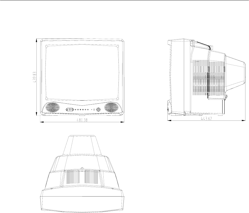
NET DIMENSION
15
PARTS AND FUNCTIONS
Front and side panel of TV Set
TV/AV MENU VOLUME CHANNEL
EARPHONE VIDEO AUDIO
POWER
• When using the S-terminal, please pull out the Video 1 input
terminal.
16
REMOTE CONTROLLER FUNCTIONS
1
6
789
23
45
0
RECALL
TV/ AV
RATI NG MUTE
P.ST D SLEEP
DISPLAY
M EN U CH +
VO L - VO L +
CH-
12
3
4
5
67
89
10
11 12

17
PROGRAM DIAGRAM
• Features
The HTN19R12 color TV set(s) (designed for the US market) incorporate the
monolithic integrated circuit LA76814K developed by SANYO in 1999 and the CPU
LC863432B-535A designed for LA76814K control.
LA76814K intergrates the sound accompany filter and trap filter in the chip,
resulting in minimized application of peripheric components, maximized integtration
and reliable performance.
The chip functions for picture intermediate frequency amplification, picture
detection, sound intermediate frequency amplification, sound frequency
discrimination, video amplification, choma decoding, line and field synchronized
scanning wave formation and output.
The circuits of picture detection, sound frequency discrimination and chroma
decoding incorporate PLL demodulation which is noted for significant stability and
reliability. In addition, this chip integrates the brightness and chroma retarding lines
and additional functions of black level extension, bus geometric figure adjustment,
I2C bu control on the basis of the 7687, resulting in test point free assembly,
reduced components of test point and peripheric components and improved picture
quality.
The CPU LC863424 uses SANYO LC863432B-535A series for reprogramming. In the
design, functions of CCD and V-CHIP as well as various function extensions are
added for the North American market. This chip also uses low frequency 32.7KHZ
crystal oscillator to reduce interferences to pictures and medium frequency signals.
• Technical properties and requirements
1. Main performance index
1. Screen diagonal: 20 inch
2. Receiving system: NTSC-M
3. Receiving channel: VHF-channel 2~13
UHF-channel 14~49
CATV-channel
1~125
4. Antenna input: 75ΩF plug
5. Picture limit noise sensibility: VHF≤51dBμV
UHF≤54dBμV
6. Color sensitivity: ≤40dB(μV
7. Two signal selectivity: -1.5MHZ≥45dB
+6MHZ≥50dB
8. Sound noise limit sensitivity: VHF≤39dBμV
UHF≤42dBμV
9. Sound output power: ≥2W
10. X-ray radiation value: <0.1mR/Hr
11. Voltage: AC 100 -130V
12. Energy consumption: ≤70W

18
13. Net dimensions: 22.8 X 21.2 X 20.8 inch
14. Net weight: 48.5 lbs
• User’s instructions
Note: This TV set has been installed together with a caption decoder and control to
US Federal Communications Commission.
Customized Power On setup
This TV set is designed for customized initiation. (For detailed information, see the
User’s Manual.) The TV set has been preset before delivery and can be reset by the
user.
Power on
1. When the TV set is connected with the power supply, the power indicator
illuminates. When the Power On/Off button on the TV set or the remote controller
is pressed, the TV set is started.
2. When the MENU button on the remote controller is pressed, the menu will appear
on the screen. The CH and VOL buttons are used for setup.
3. Press of CH+ or CH- button will result in moving the icon up or down for function
options. The designated item will turn green.
4. Pressing the VOL+ or VOL- button can change the designated item.
VIDEO setup
1. Press MENU button for VIDEO option.
2. Press CH+ or CH- button to designate desired item. (Move the icon to designated
item and the submenu will appear.)
3. The menu item under the icon will turn bright green. Press VOL+ or VOL- button
for options.
Options VOL+ VOL-
CONTRAST Contrast increase Contrast decrease
BRIGHT Brightness increase Brightness decrease
COLOR Color increase Color decrease
SHARP Sharpness increase Sharpness decrease
TINT Tint increase Tint decrease
4. Press MENU button again to quit the main MENU.
19
SETUP
1. Press SETUP button, the main menu will appear on the screen.
2. Press CH+ or CH- for LANGUAGE options. The designated LANGUAGE will turn
bright green.
3. Press VOL+ or VOL- for LANGUAGE options (such as English, Spanish and
French)
4. Receiving: Press VOL- button to move the icon to RECEPTION. The TV set is
preset AIR state before delivery (indicating that unlimited receiving of 0~63
channel signals). If the TV set is connected with the cable TV system, press
VOL+ button for CABLE option.
5. Automatic search: Press CH+ or CH- button for AUTO PROGRAM. When VOL or
+VOL- is pressed, the function of automatic channel search will be activated (if
signals are available, the channel will be fixed. If VOL+ button is pressed again,
the search can be resumed.)
6. Add/delete: Press CH+ or CH- button for option of ADD/DELETE. Press VOL+ or
VOL- button to add or delete some channel.
7. Input: Press CH+ or CH- button for option of INPUT. Press VOL+ or VOL- button,
or press AV/TV button on the remote controller for option of AV/TV.
8. Press MENU button again to quit the main menu.
TIME setup
1. Press MENU button and the main menu appear on the screen.
2. Press CH+ or CH- button to move the icon for TIME setup. The designated
CLOCK under the icon will turn bright green.
3. Press VOL+ or VOL- button for options of hour, minute and am/pm on the
CLOCK.
4. Press CH+ or CH- to adjust the figure until designed time value is reached. Set
ON TIME/OFF TIME with the same way.
5. Press CH+ or CH- for option of SLEEP. Press VOL+ or VOL- for option of set
clock. The clock display will turn bright green while SLEEP icon turns blue. Press
CH+ or CH- for sleep period adjustment.
0:15 / 0:30 / 0:45 / 1:00 / 1:15 / 1:30 / 1:45 / 2:00
6. When CHANNEL in TIME setup is designated, this option will be the preset
channel when the TV set is turned on or off.
7. Press MENU button again to quit the main menu.
20
SPECIAL
1. Press MENU button and the main menu appear on the screen.
2. Press CH+ or CH- button to move the icon to SPECIAL, and designate
C.CAPTION. Then icon of C.CAPTION turns to bright green. When OFF is
displayed, C.CAPTION is inactivated while when ON is displayed, C.CAPTION is
activated.
3. Press CH- to move the icon to CC ON MUTE and the icon will turn bright green.
Press VOL+ or VOL- button for adjustment of this function. When OFF is
displayed, the item cannot display its function regardless of the indication of
C.CAPTION. When this item displays C1 while C.CAPTION displays OFF, the
system will activate C.CAPTION function automatically.
4. Press CH- button to move the icon to POWER RESTORE. Press VOL+ or VOL- to
adjust power on and off.
5. When icon designates MENU OFFSET, the digital value of the designated item can
be adjusted by pressing VOL+ or VOL-. Function of this item is to change the
location of the menu.
6. Press MENU button again to quit the main menu.
V—CHIP setup
This function is designed for television program limitation. The TV set user is allowed
to control the usage of the TV set in accordance with the regulations of US Federal
Communications Commission. This function is also destined to prevent children from
watching the TV programs which are improper for juvenile.
1. Press MENU button, the menu will appear on the screen. Press RATING button,
V-CHIP displays the menu.
2. Press CH+ or CH- button to move the icon to another option, then the designated
item will turn bright red.
3. When an item is selected, press MENU button and the submenu of the designated
item will appear on the screen.
4. Press MENU button and return to V-CHIP.
5. Press RATING button to the main menu.
6. Press RATING button again to quit the main menu.

21
OPTION MENU
1. Press RATING button, and the RATING main menu will appear on the screen.
2. Designate OPTION MENU and then press MENU button, OPTION MENU will appear
on the screen.
3. Press CH+ or CH- button for item option, and the color of designated item will
change from yellow to bright green.
4. When HELP is selected, press MENU button and HELP menu will appear on the
screen. Press CH+ or CH- to search up and down for relative items. If MENU
button is pressed again, OPTION MENU will appear.
5. When NO-INFO RATING is selected, press MENU button for option of UNBLOCK or
BLOCK state.
6. When NO RATED is selected, press MENU button for option of UNBLOCK or
BLOCK state.
7. When ENTER PASSWARD is selected, press MENU button, then a dialog box will
appear at bottom left corner of the screen and then a 4 digit password can be
input. Press RATING button again to return to the main menu. The password
must be input when entering the V-CHIP submenu.
TV RATING
1. Press RATING button.
2. When TV RATING is selected, press MENU button and the submenu will appear
on the screen as follows:
TV RATING
TV-Y
TV-Y7
TV-G
TV-PG
TV-14
TV-MA
RATING FV V S L D
In the table, the blocks marked “” indicates the restrictive items. If all
restrictive items are to be selected, move the icon to the top left corner of the
table and then press MENU button.
1. If all restrictive items are to be released, move the icon to the bottom left
corner and press MENU button twice.
22
2. If one of the restrictive items is to be selected, press CH+ or CH- button
in an alternate way and press MENU button (for some line) and then
VOL+ or VOL- for option of desired line. Finally press MENU button.
Some item can be deleted by following the same process above.
1. Press RATING button again to quit V-CHIP menu.
MPAA RATING
1. Press RATING button, and the RATING main menu will appear on the screen.
2. When MPAA RATING turns bright red, press MENU button and MPAA RATING
submenu will appear on the screen.
3. If all items are to be selected, press CH+ or CH- button to move the icon to
the top left corner, and then press MENU button.
4. If all selective items are to be deleted, press CH+ or CH- button to move the
icon to the bottom left corner, and then press MENU button twice.
5. Items under or above the designated icon in the submenu can be selected.
6. Press RATING button again to quit V-CHIP menu.
BLOCK OFF
1. Press RATING button, and the RATING main menu will appear on the screen.
2. When BLOCK turns bright red and MENU button is pressed, BLOCK will display
BLOCK OFF and BLOCK ON.
Caution:
BLOCK OFF: Indicating lock on status. Regardless setup of TV RATING and MPAA
RATING, even V-CHIP signals are received during TV programs, this TV
set dos not have the V-CHIP function.
BLOCK ON: Indicating lock off status. When TV RATING and MPAA RATING are
selected, the TV set will have the V-CHIP function when V-CHIP signals
are received in the TV program.
Precautions:
1. Keep the TV set away from heat sources, such as stoves and radiators;
2. Place the TV set in a well ventilated area;
3. Place the TV set in an area free from dusts and corrosive gas;
4. Prevent the TV set from waterdrops, moisture and humidity;
5. Do not place magnetic materials on the TV set;
6. Disconnect the TV set when moving the TV set.
7. When the TV set is turn on during a rainy weather, disconnect the outdoor
antenna and use the indoor antenna attached to the TV set.
8. Disconnect the TV set from power supply source during a power interruption or
when going out on vacation.
23
MAINTENANCE SERVICE AND TROUBLESHOOTING
TROUBLESHOOTING PROCESS
1. No Light
Check to see if
Fuse3 is normal
No light and sound
Abnorma
Check VD504, C507,
V513, etc.
Check to see if the
collector voltage of
VD554 is 18V
Check N701, N101
etc
Check to see if,
9v,
5v is normal
Check the control
Voltage of V552 or
CPU power
The failure of
Horizontal unit
or
N101
Normal
Normal
Normal Abnormal
Check to see 103V etc.
Voltage is normal
Test to see all terminal
Resistance of load
Is normal
Check switch of
Power unit
Check to see if
rectifying tube
is normal
Change
rectifying tube
Check the
Loader
A
bnormal
Normal
Abnormal
Normal Abnormal
Normal Abnormal
24
Normal Normal Abnormal
Abnormal
Normal
Abnormal
Normal
2. No Raster
Abnormal
Check the voltage o
f
all pins of XP902 is
normal
Heater Resistor
open
Check to see if the
voltage of V433 is
existed?
Check the circuit from
pin13 of N201 to H-
drive
No raster
Whether G2 voltage is normal
Video amplifying
board is abnormal
V433 is not well
welded or open
T431, V433 Or C415,
C416. Care broken
Higher Lower
Inspect the circuit
from pin19, 20,
and 21 of N201 to
video amplifying
board
Check the voltage
of V433 collector is
normal
Inspect T431, R434
etc.
Normal Abnormal
Replace bad components
Check N201
Check N201 and H-Vibration Check +12V power circuit
25
3. Horizontal Bright Line
Make R451 open. Multimeter is at range RΧ1K. Red
probe connects to ground. Touch No.5 of N401 with
black probe. Bright line flashes for a moment
Horizontal bright line
Check if the vertical deflection
Deflection yoke plug
Inspect +24V
power circuit
Check N201
and N701
Replace components
There is trouble in V-circuit
T
here is trouble in V-output circuit
Yes No
Check 451R451 Check the voltage at Pin2 of N401
26
4. No of Redness in Color
Replace CRT,
66118618
Check circuit between
Pin19 of N201 and
XS202
No
Yes
Change V902 or
weld V902 again
Check to see if voltages of XP902
are normal
Lack of red
Check to see if V902 is open
or not well welded
27
5. Picture display but no sound
Cut of C601, connect red pen of multi-meter(R*1K) with ground,
and black pen tap Pin1 of N602 if there is snapping
Picture exists but no sound
Power amplifier is normal.
Check N101 and external SIF
circuit
Check muting circuit
and V601\V602
Check to see if +19V
exists
Check SIF circuit and speaker Inspect +19V
power supply
Cut off collection electrode of V602, use
black pen of multimeter tap Pin1 of
N601 if there is snapping sound
Yes No
28
CIRCUIT DIAGRAM
1. Pane Hint Picture
Picture/Sound IF
Amplifier, Video and
audio signal Processing,
RGB Output Circuits
and H &V Sync pulse
segregation
SA
W
Sound Power
Amplifier
Main Processor
Infrared Receiver Remote Controller
R
OM
Audio/Video In/Out
Horizontal
Scan Output
Vertical Scan
Output
CR
29
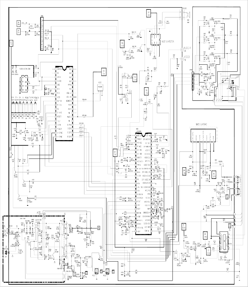
2. CIRCUIT DIAGRAM
RL551
SDT-SS-112LMR
T101
HA6019
30
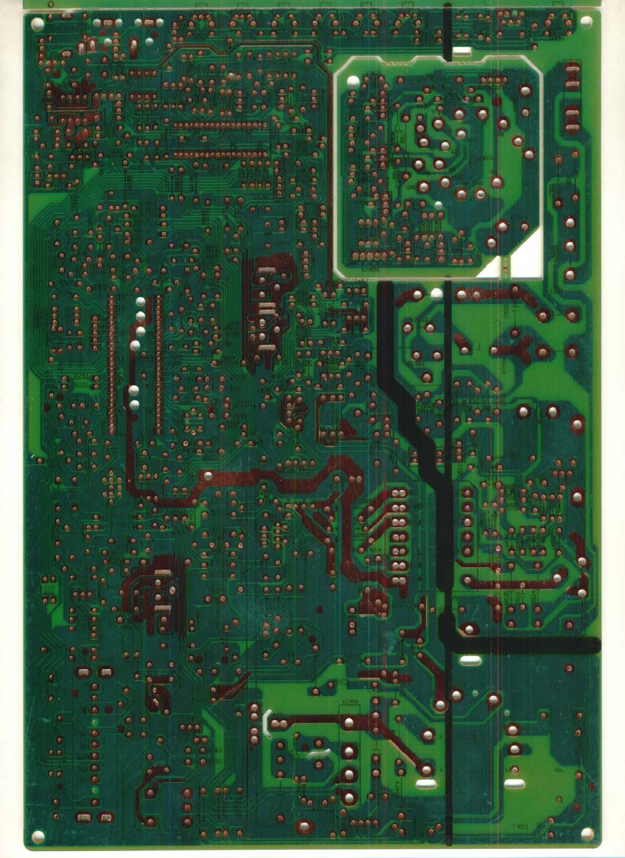
3. PCB Diagram

31
CIRCUIT EXPLANATION
1. Principle Integrated Circuits
A1. BH2004D color TV set composed of the following sections
(1) Small signal processing: super monolithic integrated circuits N204
(LA76814A), and memory N901 (AT24C08).
(2) Sound power amplifying: integrated circuits N701 (LA4225).
(3) Horizontal and Vertical scan output circuits: Vertical output integrated
circuits N402 (LA78040), Horizontal output transistor V411 (TT2140),
Horizontal flying back transformer T402 (JF0501-19810).
(4) Switch power supply: switch transformer T501 (BCK-01-90I), power
transistor V503 (2SD4460).
A2. Main integrated circuits:
(1) LA76814A Microprocessor
Picture IF/sound IF/video processing/H and V
Scan/color decoding
(2) LA78040 Vertical output integrated circuits
(3) LA4225 Sound power amplifying integrated circuits
A3. Electrical circuit analysis
1. Microprocessor and Small signal processing: super monolithic integrated
circuits, LA76814A.
LA76814A is super large integrated circuit decoder, containing intermediate
image amplifying, intermediate sound amplifying, horizontal and
vertical scan, small signal processing, color decoding, hi-pressure
tracing and over-load protection, I2C bus control.
Information introducing the functions and testing data for maintenance is listed in
Table 1.
1. N701 LC863424B
PIN Leads Function Voltage
(V) PIN Leads Function Voltage
(V)
1 Auto adjust Enable
Pin 5.1 19 OSD red signal output 0.09
2 Blank 20 OSD greem signal output 0.09
3 IIC data 4.6 21 OSD blue signal output 0.09
4 IIC clock 4.5 22 OSD blank signal output 0.01
32
5 Earth 0 23 Blank 5.1
6
CPU
Crystal oscillation
port
2.2 24 MUTE control 0.02
7
CPU
Crystal oscillation
port
2.75 25 Blank 5.07
8 Power (+5V) 5.1 26 AV option control 2 0.01
9 Plate control input 0.25 27 Av option control 1 0.01
10 AFT signal input 0.3 28 Control signal input 5.1
11 Blank 29
Right channel sound
volume PWM output port 0.01
12 S terminal input test 5.1 30 Left channel sound
volume PWM output port 0.01
13 CPU reset port 5.1 31 Blank
14 OSD filter 3.55 32 Demagnetize 0.007
15 Video signal input 3.2 33 Blank
16 POWER ON/OFF
control signal output 0.03 34 Blank
17 Field pulse input 4.8 35 Blank
18 Line pulse input 4.3 36 Blank
2. N101 LA76814K
PIN Leads Function
Working
Voltage
(V)
PIN Leads Function
Working
Voltage
(V)
1 Video output 2.23 28 Reciprocal pulse input 1.06
2 FM filter output 2.23 29 Reference current 1.69
3 AGC filter 2.22 30 Clock output 0.002
4 Hi AGC output 2.59 31 N.C. 0.002
5 MF input 1.30 32 OSD gain control 3.05

33
6 MF input 2.83 33 GND 0
7 GND 2.83 34 X ray protection 0.06
8 Power 0 35 ACC KILLER FILTER 0.39
9 FM filter 4.94 36 CHROMA AFC-F 3.49
10 AFT output 1.90 37 CW:3.58MHz OUT 0.54
11 Data bus 2.77 38 2.87
12 Clock bus 4.85 39 Auto color filter 3.2
13 Beam input 4.76 40 Video output option 2.43
14 R input 3.92 41 GND 0
15 G input 0.14 42 Outside video input 2.55
16 B input 0.15 43 Power 5
17 Beam limit 0.08 44 Inside video input 2.77
18 RGB Power 7.94 45 lack strech delay filter 2.6
19 R input 2.21 46 Video output 2.12
20 G input 2.36 47 Auto phase control filter 3.5
21 B input 2.28 48 VCO COLL 4.3
22 Line synchronized
output 0 49 VCO COLL 4.3
23 Field sawtooth
wave output 2.47 50 FILL FILTER 2.24
24 Field incline gain 2.65 51 Outer sound input 2.12
25 Power 5.10 52 SIF output 1.95
26 AFC filter 2.49 53 SIF auto phase control filter 2.38
27 Line output 0.63 54 SIF input 3.14
34
SERVICE MODE AND ADJUSTING ITEMS AND DATA
Method
a. Press PRO button to enter the adjustment or setup mode.
b. Press CH+ or CH- button to turn page up or down for desired item
options. If a special remote controller is used for options, part of
adjustment items can be selected directly by pressing buttons on the
remote controller.
c. Press VOL+ or VOL- button to alter the value of selected adjustment
items.
d. In the factory production process, the factory adjuster is used for
accelerated adjustment.
Notices for adjustment
OSD Range Ref.
B/W BALANCE
S-BRI 0-127 80
R-BIA 0-255 82
G-BIA 0-255 180
B-BIA 0-255 144
R-DRV 0-127 58
G-DRV 0-15 7
B-DRV 0-127 63
C. B/W 0-3 0
ADJUST
H. PHASE 0-31 17
H.BLK.LEFT 0-7 7
H.BLK.RIGHT 0-7 0
V. SIZE 0-127 39
V. LINE 0-31 10
V. POSE 0-63 56
V. SC 0-31 0
RF. AGC 0-63 20
OSD H.POSI 0-127 10
OSD V.POSI 0-31 3
VOLUME OUT 0-127 100
SETUP

35
STEREO OPTION 0-1 0
SUB.CONT 0-31 20
SUB.COLOR 0-63 25
SUB.SHARP 0-31 10
SUB.TINT
0-63 32
BLK.STR.DEF (0: On; 1: Off) 0-1 0
AFC GAIN (0: Low; 1: Hi) 0-1 1
V.SEPUP (0: Low; 1: Hi) 0-1 1
CD.MODE (LA76814: 0/1; LA76812: 0~7) 0-1 0
DIGITAL OSD (0: Simulation OSD input; 1: Digit OSD input) 0-1 0
OSD CONT. (0~127) / LA76814 (0~3) 0-3 2
GRAY MOD (0/1) 0-1 0
OSD Description Range Ref.
B.GAM.SEL (0~3)
0-3 3
RG.GAM.DEF (0/1)
0-1 0
FBPBLK.SW (0/1)
0-1 0
BRIGHT ABL.TH Bright. Abl. Threshold (0~7) 0-7 4
EMG.ABL.DEF Emg. Abl. Def (0/1) 0-1 1
BRT.ABL.DEF Brt. Abl. Def (0/1) 0-1 1
MID.STP.DEF Mid. Stp.Def (0/1) 0-1 1
R-Y/B-Y G.BL R-Y/B-Y Gain Balance (0~15)
LA76814, no this function 0-15 8
R-Y/B-Y ANG R-Y/B-Y Angle (0~15) 0-15 8
C.KILL.OFF C_Kill OFF (0/1) 0-1 0
SND.TRAP Sound Trap (0~7) 0-7 4
VOL.FIL “Volume Filter Defeat” 0-1 0
VIF.SYS.SW (0:45.75M; 1:58.75M) LA76814 0-1 0
VIDEO.LEVEL Video Level (0~7)
0-7 7
FM.LEVEL FM Level (0~31) 0-31 16
POWER OPTION 0: 2 starts; 1: memory; 2 or 3: 1 start 0-3 0
SEARCH CHECK 0: w/out start auto search;
1: w/ start auto search
0-1 0
SEARCH SPEED 0: search slow; 1: search fast 0-1 1
AV OPTION 0: w/out AV; 1: 1-way AV input; 2: 2-
way AV input; 3: 3-way AV input 0-3 1
POSITION L/R 0: top left corner; 1: top right corner 0-1 1
BLACK BACK 0: No black back; 1: Black back 0-1 1

36
BLACK TRANS 0-1 1
V.MUTE P.OFF 0: video output not cut before POWER
OFF;
1: video output cut before POWER OFF
0-1 0
CCD OPTION 0: CCD not used; 1: CCD used 0-1 1
V-CHIP OPTION 0: V-CHIP not used; 1: V-CHIP used 0-1 1
PASSWORD OPT. 0: V-CHIP not used; 1: V-CHIP used 0-1 1
TUNER OPTION 0:TDF-3M3 not used; 1: PHILIP
UV1336B used 0-1 1
SCREEN OPTION 0:w/out curtain; 1: w/ at start; 2: w/ at
close; 3: w/ at start/close 0-3 0
SCREEN TIME 0-7 6
SCREEN HDC 0-63 0
BAND SELECT 0-1 0

37
CIRCUIT SIGNALS PROCESSING
• MF amplifying circuit
Received by antenna and processed by the high frequency tuner, the television
signals will be transmitted by the tunner as 45.75MHZ signals to sound surface filter
through C112 coupling after being amplified by V102, and then the MF signals of
trapped wave in sound carrier wave from sound surface filter F45U will be sent to
pin 5 and 6 of LA76814.
The MF demodulation circuit of this TV set is completed through PLL carrier
wave generator and outside pressure control oscillator (T101) in LA76814. The MF
frequency is adjusted by T101 adjustment, and output of AFC is generated by a
numerical control IF-PLL circuit, and read and sent to CPU by I2C bus for correction
of MF signals frequency deviation.
The external capacitor of pin 3 decides the time constant of AGC,and high
frequency amplication AGC will be transmitted by I2C bus through Pin 4 for control
of high frequency tuner gain.
• Sound signals processing
The secondary sound MF signals are input via Pin 54 of LA76814, and then
demodulated in PLL tuner through lowpass and limit inside LA76814. After
demodulation, the sound signals will be amplified through inside lowpass and
transmitted via Pin1. Pin 2 is FM output, C121 is deaccentuation capacitor, Pin 9 is
FM detector’s DC filter connector and C117 is filter capacitor.
The external AUDIO signals are input via LA76814 pin 51, controlled by CPU.
A swith inside I2C bus control LA76814 can be used for options of internal and
external signals. The sound signals are transmitted via LA76814 pin 1 to LA4225A
pin 1 via C601 coupling and transmitted from its pin 4, after being amplified by
LA4225A, to the speaker. The mute circuit 1 is comprised of V601, V602 and other
components for Power On and Off mute. Circuit 2 is comprised of CPU mute pin
V603 and other components.
• Line sync processing circuit
The line oscillation circuit of the TV set is fully comprised of LA76814 internal
integrated components. The brightness signals containing compound sync signals
are transmitted to the internal sync seperation circuit for line and field sync pulse.
• Line output circuit
Standard line oscilation pulse is output via Pin 27 to V431 for line drive. T431 is H
(L) drive used to convert the low current and high pressure pulse signals from line
tube into low voltage and large current signals for line export needs. V432 is line
output, C435 and C436 are reciprocal capacitor, C441 is S calibration capacitor,
L441 is line linear indutance and T471 is line output transformer. 240V voltage
needed for field scanning is transmitted via winding 10 of the transformer and
gained after being rectified by VD472. In addition to anode high pressure, screen
grid and focus voltages, the transformer provides 180V video amplifier voltage by
winding 2. VD411, C411, R412, VD412, R414 and C412 form the X ray protection
circuit. R233, C231, R232, R403 and C408 form the beam restriction circuit. The
winding 9 of the transformer provides CRT filament voltage.
38
• Field sync and output circuit
Field sync seperator produces field sync signals from compound sync signals and
activates the field frequency splitting system. When a certain number field sync
pulse is detected, the field frequency spliting system will start operation for
frequency spliting of the multiple line frequency signals generated by the line
frequency oscilator. The field pulse gained from frequency spliting will be sent to
field sawtooth generator for sawtooth waves, and then transmitted by pin 23. The
output circuit of this TV set is mainly comprised of LA7840 and other components.
• CRT output circuit
The tricolor signals produced by LA76814 will be transmitted to CRT board and then
to the cathode of the TV tube after being amplified by videoamplifier which is
comprised of V902, V912 and V922.
• CCD performance
The CVBS signals produced by LA76814 pin 40 will be amplified and sent to N701
pin 19 via V821 and then processed by software and hardware inside CPU. The
decoded CCD signales will be transmitted to LA76814 pin 14, 15 and 16 via CPU pin
22, 23 and 24.
• V-CHIP performance
Performance of V-CHIP is mainly completed by CPU. The CPU receives grade signals
from the IC bus and executes relative performances and shields those programs of
relative grade.
Integrated circuit reference
1. All integrated circuit voltages
Following voltage data is achieved while the TV set is turned on, and the electric
resistance is achieved when the TV set is turned off. When the status changes, the
data should also be changed. So these data are used as references.

39
1. N701 LC863424B
PIN Leads Function Voltage
(V) PIN Leads Function Voltage
(V)
1 Auto adjust Enable
Pin 5.1 19 OSD red signal output 0.09
2 Blank 20 OSD greem signal output 0.09
3 IIC data 4.6 21 OSD blue signal output 0.09
4 IIC clock 4.5 22 OSD blank signal output 0.01
5 Earth 0 23 Blank 5.1
6
CPU
Crystal oscillation
port
2.2 24 MUTE control 0.02
7
CPU
Crystal oscillation
port
2.75 25 Blank 5.07
8 Power (+5V) 5.1 26 AV2 0.01
9 Plate control input 0.25 27 Av option control 1 0.01
10 AFT signal input 0.3 28 Control signal input 5.1
11 Blank 29
Right channel sound
volume PWM output port 0.01
12 S terminal input test 5.1 30 Left channel sound
volume PWM output port 0.01
13 CPU reset port 5.1 31 Blank
14 OSD filter 3.55 32 Demagnetize 0.007
15 Video signal input 3.2 33 Blank
16 POWER ON/OFF
control signal output 0.03 34 Blank
17 Field pulse input 4.8 35 Blank
18 Line pulse input 4.3 36 Blank

40
2. N101 LA76814K
PIN Leads Function Voltage
(V) PIN Leads Function
Voltage
(V)
1 Video output 2.23 28 Reciprocal pulse input 1.06
2 FM filter output 2.23 29 Reference current 1.69
3 AGC filter 2.22 30 Clock output 0.002
4 Hi AGC output 2.59 31 N.C. 0.002
5 MF input 1.30 32 OSD gain control 3.05
6 MF input 2.83 33 Earth 0
7 Earth 2.83 34 X ray protection 0.06
8 Power 0 35 ACC KILLER FILTER 0.39
9 FM filter 4.94 36 CHROMA AFC-F 3.49
10 AFT output 1.90 37
CW:3.58MHz OUT 0.54
11 Data bus 2.77 38 2.87
12 Clock bus 4.85 39 Auto color filter 3.2
13 Beam input 4.76 40 Video output option 2.43
14 R input 3.92 41 Earth 0
15 G input 0.14 42 Outside video input 2.55
16 B input 0.15 43 Power 5
17 Beam limit 0.08 44 Inside video input 2.77
18 RGB power 7.94 45 Black strech delay filter 2.6
19 R output 2.21 46 Video output 2.12
20 G output 2.36 47
Auto phase control
filter 3.5
21 B output 2.28 48 VCO COLL 4.3
22 Line synchronized
output 0 49 VCO COLL 4.3
23 Field sawtooth wave
output 2.47 50 FILL FILTER 2.24
24 Field incline gain 2.65 51 Outer sound input 2.12
25 Power 5.10 52 SIF output 1.95
26 AFC filter 2.49 53
SIF auto phase control
filter 2.38
27 Line output 0.63 54 SIF input 3.14

41
ADJUSTMENT
1. Safety Precautions
1. It is safe to adjust after using insulating transformer between the power supply
and chassis input to prevent the risk of electric shock and protect the
instrument.
2. Never disconnect leads while the TV receiver is on.
3. Don't short any portion of circuits while power is on.
4. The adjustment must be done on the correct appliances. But this is changeable in
view of productivity.
2. Adjustment procedure
The chassis of this TV set uses Sanyo IC with the latest digital bus processing
technology. The adjustment points are fewer and the adjustment is simpler. The
adjustment method is as follows:
• +B: 104± 1V adjustment
1) Switch on the power and connect NTSC circular signals to the tuner.
2) Adjust variable resistor RP551 until the voltage of the main power is 104±1V.
• Screen voltage adjustment
1) Switch on the power and receive NTSC system circular signal. Warm up the TV
set for 15 min.
2) Enter the adjustment state. Press the “MUTE” button, then a bright horizontal
line appears. Adjust screen potentiometer to let the horizontal line just appears.
• Focus adjustment
1) Receive electronic circular signal.
2) Set picture mode on standard mode.
3) Adjust focus potentiometer until the optimum picture is achieved.
• White balance adjustment
1) Set the picture mode on standard mode.
2) Enter the D state and adjust RCUT, GCUT, BCUT, GDRV and BDRV.
3) Coordinate of reference white color: (X=0.281, Y=0.311).
42
• Adjustment of horizontal and vertical position and size
1) Switch on the power and connect the signals to the tuner to receive NTSC
system circular signal.
2) Enter the D state. Adjust HPOS to change the horizontal position and V. POSE to
change the vertical position. Adjust V.SIZE to change the vertical size until the
vertical size is 90-92%. Horizontal size is related to the capacitor C436. Hold the
horizontal size is 90-92%.

43
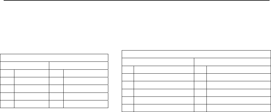
INFORMATION OF RESISTORS AND CAPACITORS
RESISTORS & CAPACITORS-PARTS NO.CODE
Notes: 1. Part numbers are indicated on most mechanical parts.
Please use this part number for parts orders.
2.The unit of resistance is Ω (ohm). K=1000Ω, M=1000KΩ
3.The unit of capacitance is µF (microfarad). P=10-6µF.
Numbering system of Capacitor
Example
CL42 ----- 17 ---- 50V ---- 2F4 ---- 104 * ---- Z
Type Voltage Value (PF) Tolerance
CL21X ---- 100V ---- 223 * ---- J
Type Voltage Value (PF) Tolerance
CL110X ---- 25V ---- 100µF ± 20%
Type Voltage Value Tolerance * 104 =10×104
223
=22×103
Numbering system of Capacitor
Example
RY17S ---- 2W ---- 390 ---- J ---- 05-E-A
Type Wattage Value(Ω) Tolerance
RS11 ---- 1/2W ---- 1.8K ---- K
Type Wattage Value Tolerance
44
ABBREVIATION OF PART NAME AND DESCRIPTION
RESISTOR CAPACITOR
PART NAME & DESCRIPTION
TYPE ALLOWANCE
T Carbon F ±1%
S Solid J ±5%
J Metal K ±10%
Y Oxide M ±20%
F Fuse G ±2%
PART NAME & DESCRIPTION
TYPE ALLOWANCE
C Ceramic J ±5%
T Ceramic K ±10%
L Film L ±15%
D Electro-analysis M ±20%
A Tantalum P +100%-0%
Z +80%-0%
45
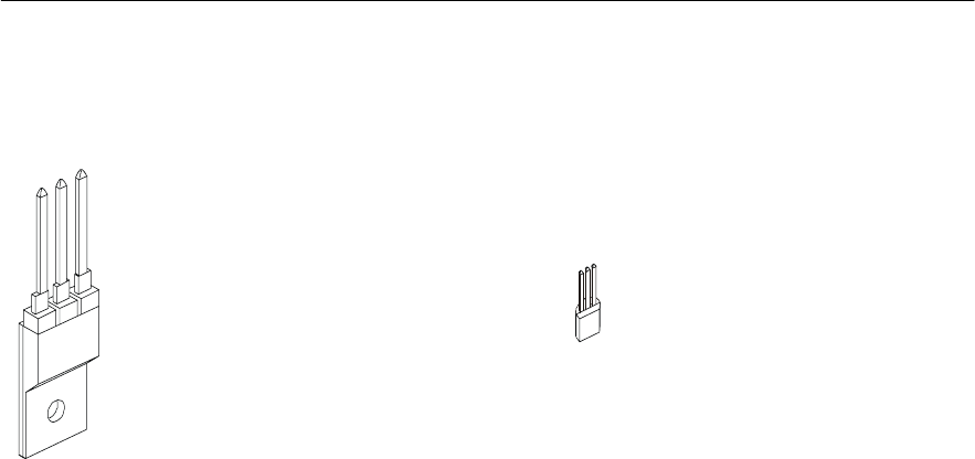
TERMINAL VIEW OF TRANSISTORS
BCE
KSR1010TA
KSR2010TA
E
CB
2SD18887YD
2SC4544----B-A
2SB1569A-E----B-A EXPORT
2SP2400A-E----B-A EXPORT
2SC3853(2SC3852)----E-A
3DD2553----B-A
3CA688----E-A
2SC3853(2SC3852)----B-A
2SC1815-Y------F
2SA1015-Y------F
2SC752GTM-Y------F EXPORT
2SC2878-A(TEM)------F EXPORT
RN1204(DTC144ESATP) EXPORT
2SA562TM-Y------F
2SC3355------F EXPORT
