Saeh560el Technics SAEH 560 Service Manual
User Manual: Technics-SAEH-560-Service-Manual
Open the PDF directly: View PDF ![]() .
.
Page Count: 81
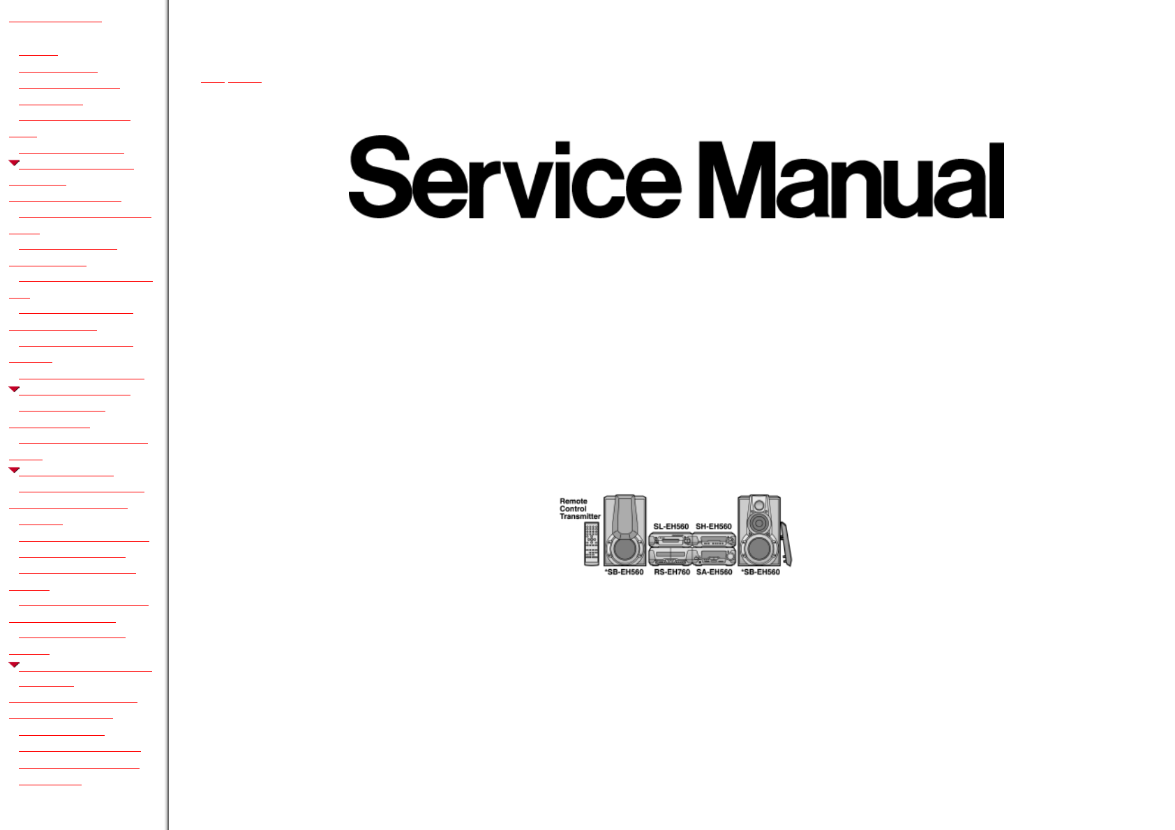
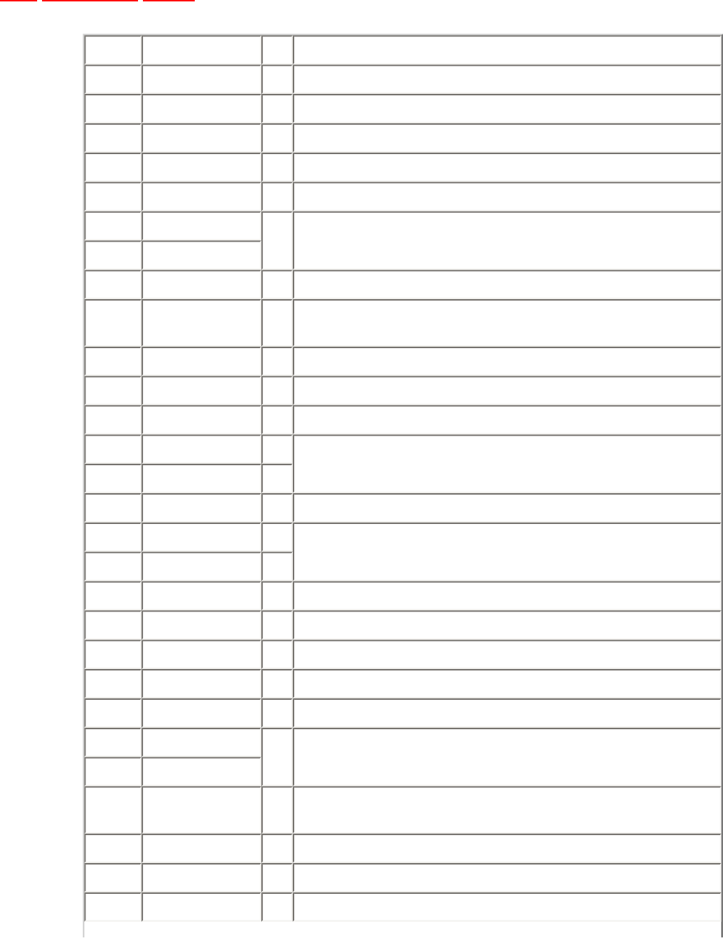
Table Of Contents
COVER
1 Before Repairs
2 Protection Circuitry
3 Accessories
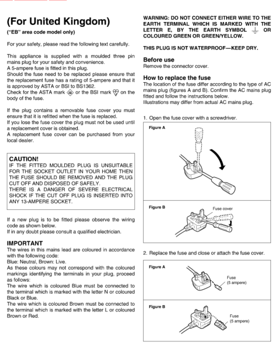
4 Caution for AC Main
Leads
5 Location of Controls
6 Operation Checks and
Component
ReplacementProcedures
6.1 Checking for the AC IN
P.C.B.
6.2 Checking for the
operation P.C.B.
6.3 Checking for the main P.
C.B.
6.4 Replacement for the
regulator transistor
6.5 Replacement for the
power IC
7 To Supply Power Source
8 Self-Diagnostic Mode
8.1 To display the
malfunction code
8.2 To return to the normal
display
8.3 Display contents
8.3.1 U70 CD, U70 DECK
(displayed automatically)
8.3.2 F61
9 Schematic Diagram Notes
10 Schematic Diagram
11 Printed Circuit Board
Diagram
12 Type Illustration of ICs,
Transistors and Diodes
13 Wiring Connection
Diagram
14 Terminal Function of ICs
14.1 IC901
(LC8A524A5N28):System
Control/FL Drive
15 Block Diagram
16 Replacement Parts List
17 Cabinet Parts Location
18 Packaging
Service Manual
TOP NEXT
AD0002043C2
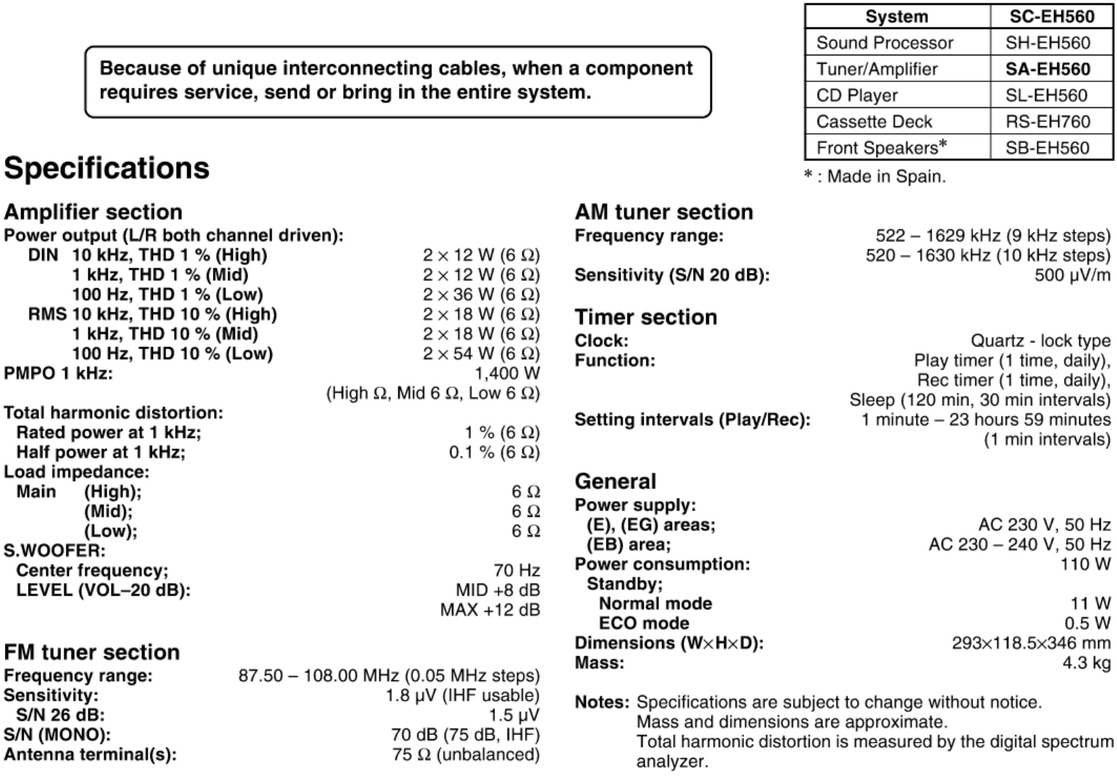
Tuner/Amplifier
SA-EH560
Colour
(S).....................Silver Type
Areas
(E).....................Europe.
(EB)..................Great Britain.
(EG)..................Germany, Italy, France, Netherlands and Denmark.
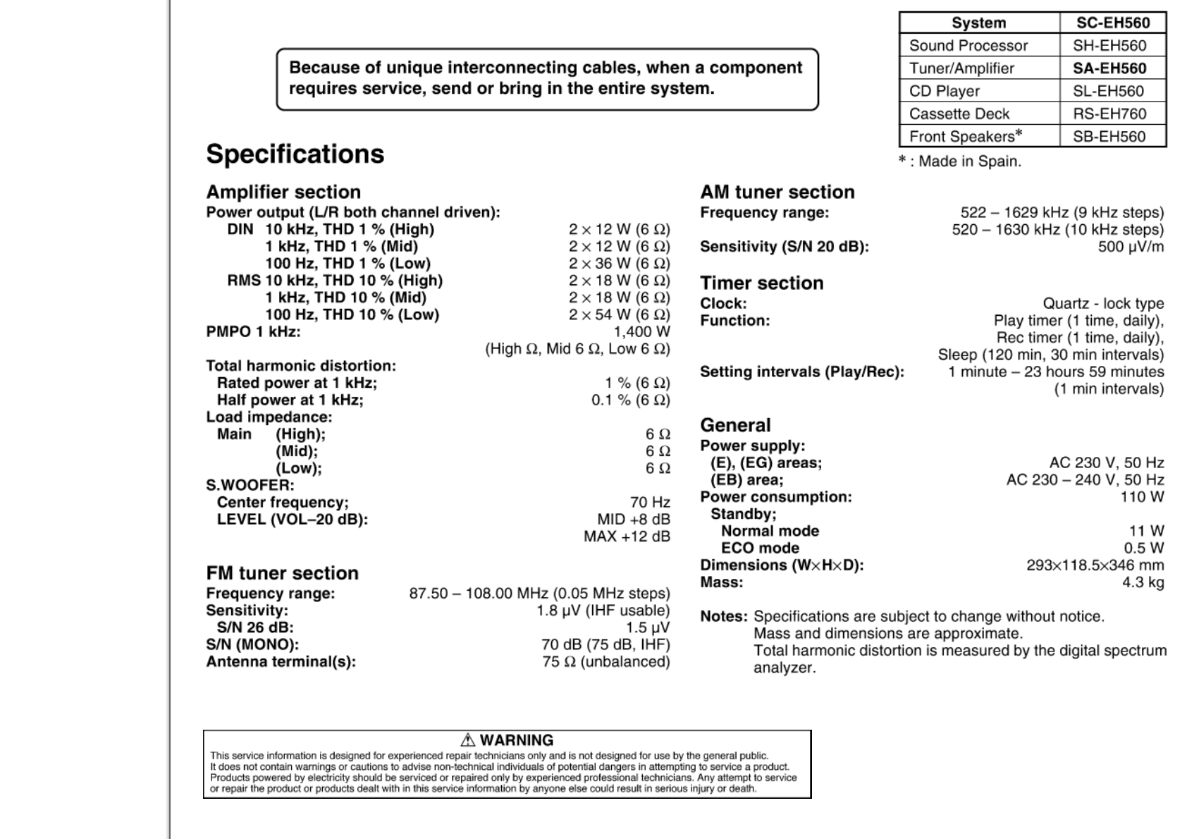
© 2000 Matsushita Electric Industrial Co., Ltd. All rights reserved. Unauthorized copying and distribution is a violation of law.

Table Of Contents
COVER
1 Before Repairs
2 Protection Circuitry
3 Accessories
4 Caution for AC Main Leads
5 Location of Controls
6 Operation Checks and Component ReplacementProcedures
6.1 Checking for the AC IN P.C.B.
6.2 Checking for the operation P.C.B.
6.3 Checking for the main P.C.B.
6.4 Replacement for the regulator transistor
6.5 Replacement for the power IC
7 To Supply Power Source
8 Self-Diagnostic Mode
8.1 To display the malfunction code
8.2 To return to the normal display
8.3 Display contents
8.3.1 U70 CD, U70 DECK(displayed automatically)
8.3.2 F61

9 Schematic Diagram Notes
10 Schematic Diagram
11 Printed Circuit Board Diagram
12 Type Illustration of ICs, Transistors and Diodes
13 Wiring Connection Diagram
14 Terminal Function of ICs
14.1 IC901 (LC8A524A5N28):System Control/FL Drive
15 Block Diagram
16 Replacement Parts List
17 Cabinet Parts Location
18 Packaging

© 2000 Matsushita Electric Industrial Co., Ltd. All rights reserved. Unauthorized copying and distribution is a violation of law.
1 Before Repairs
TOP PREVIOUS NEXT
1. Turn off the power supply. Using a 10Ω, 10 W resistor, connect both ends of power supply
capacitors (C701, C703 and C702, C704) in order to discharge the voltage.
2. Before turning the power supply on, after completion of repair, slowly apply the primary
voltage by using a power supply voltage controller to make sure that the consumed current at
50 Hz in NO SIGNAL mode should be shown below with respectto supply voltage 230/240 V.
Power supply voltage AC 230 V AC 240 V
Consumed current 50 Hz 70 ~ 250 mA
•@
TOP PREVIOUS NEXT

2 Protection Circuitry
TOP PREVIOUS NEXT
The protection circuitry may have operated if either of the following conditions is noticed:
No sound is heard when the power is switched ON.
Sound stops during a performance.
The functions of this circuitry is to prevent circuitry damage if, for example, the positive and negative
speaker connection wires are shorted, or if speaker system with an impedance less than the indicated
rated impedance of this unit are used.
If this occurs, follow the procedure outlined below.
1. Switch OFF the power.
2. Determine the cause of the problem and correct it.
3. Switch ON the power once again.
Note:
When the protection circuitry functions, the unit will not operate unless the power is first switched
OFF and then ON again.
•@
TOP PREVIOUS NEXT
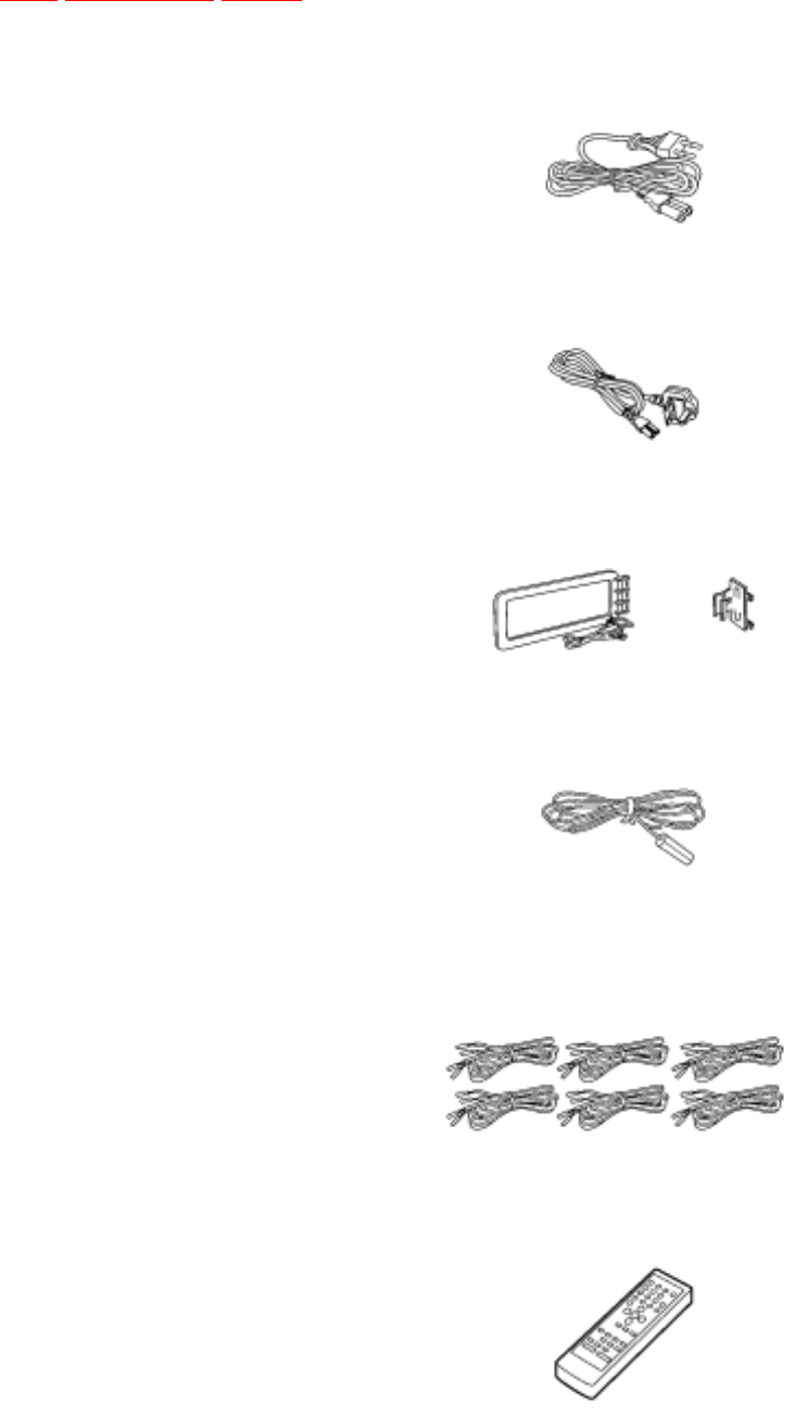
3 Accessories
TOP PREVIOUS NEXT
AC power supply cord for (E),(EG) areas/(RJA0019-X)...........................1 pc.
AC power supply cord for (EB) area/(RJA0053-2X).........................1 pc.
AM loop antenna set/(RSA0022-J)...........................1 pc.
FM indoor antenna/(RSA0007)..............................1 pc.
Speaker cords/(REE0499)..............................2 pcs./(REE0984)..............................2 pcs./
(REE0985)..............................2 pcs.
Remote control transmitter/(RAK-EHA29WH).....................1 pc.
Remote control batteries/(R6/LR6,“AA”, UM-3)............2 pcs.


6 Operation Checks and Component
Replacement/Procedures
TOP PREVIOUS NEXT
This section describes procedures for checking the operation of the major printed circuit boards and
replacing the main components.
For reassembly after operation checks or replacement, reverse the respective procedures. Special
reassembly procedures are described only when required.
/
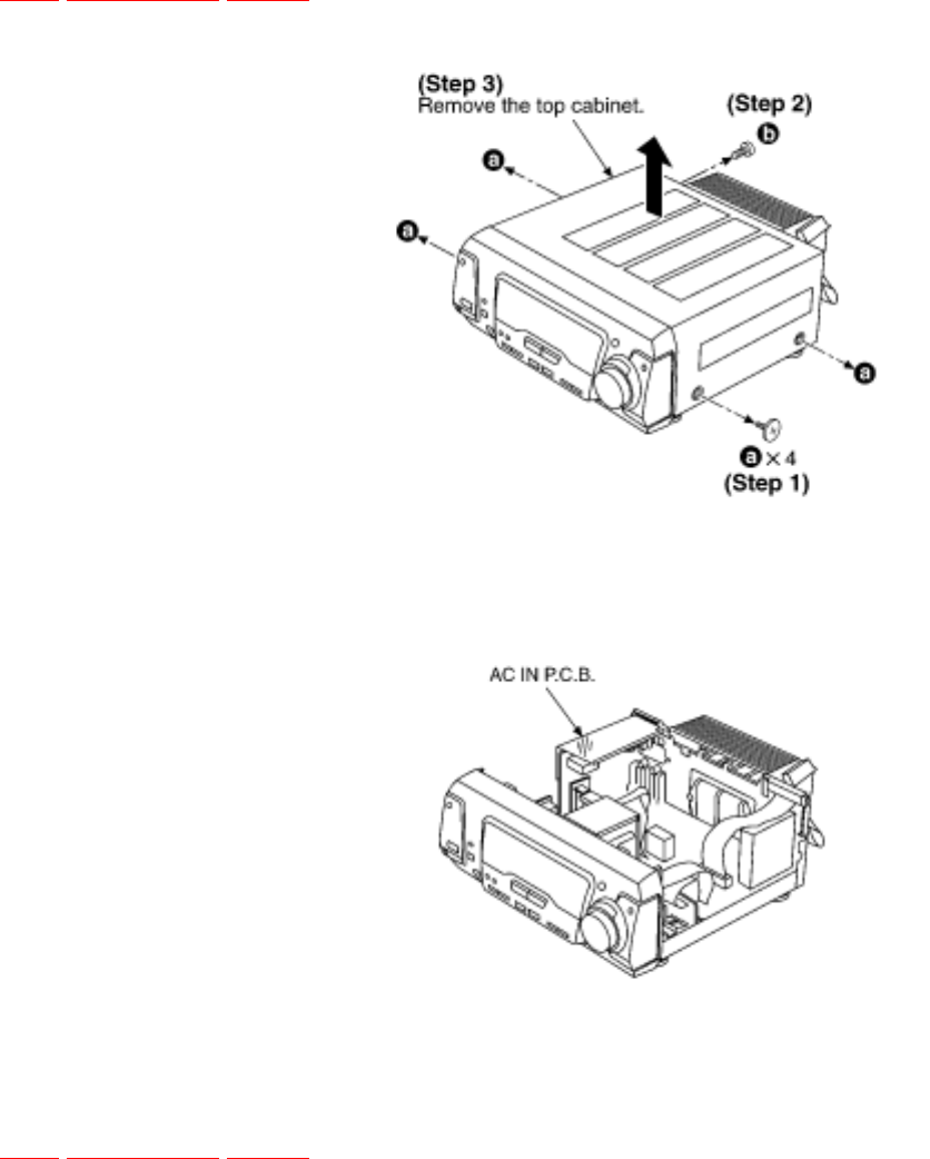
6.1 Checking for the AC IN P.C.B.
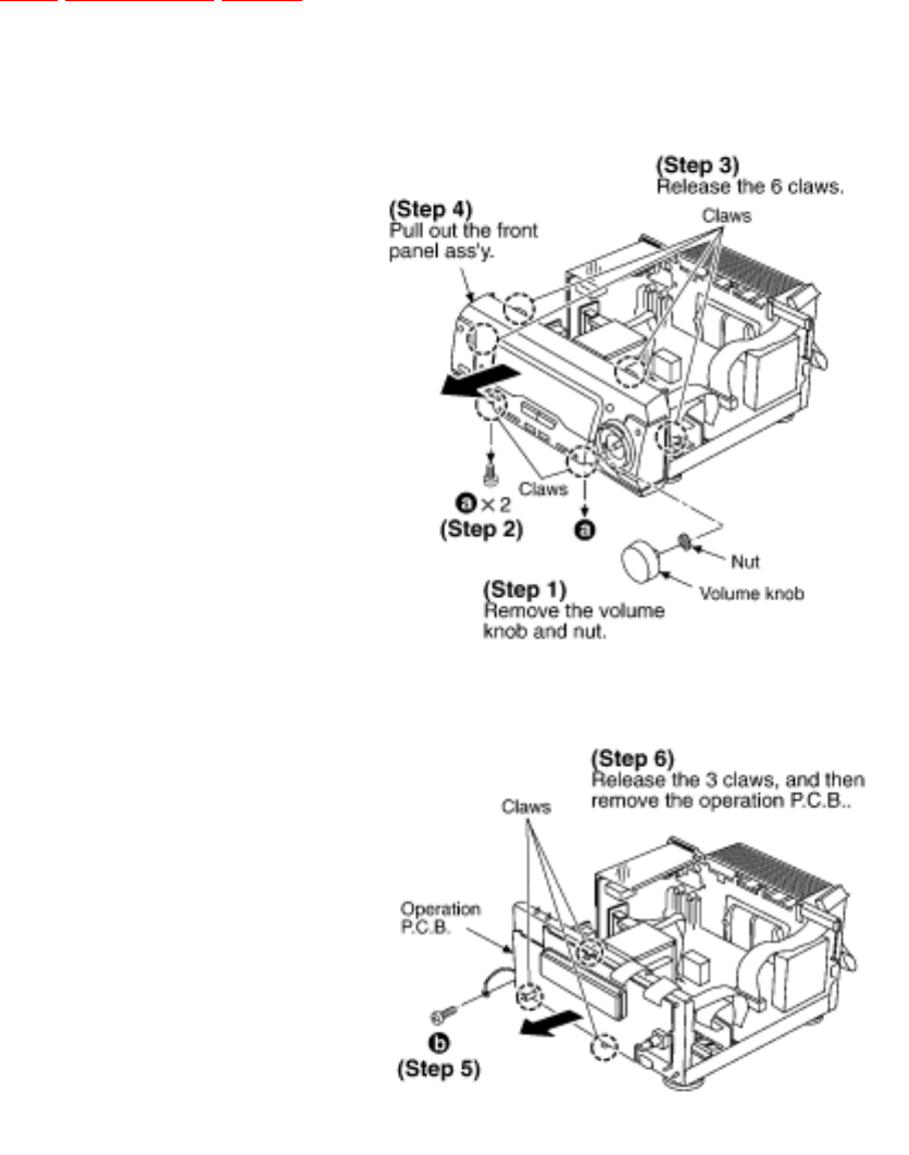
6.2 Checking for the operation P.C.B.
6.3 Checking for the main P.C.B.
6.4 Replacement for the regulator transistor
6.5 Replacement for the power IC
•@
TOP PREVIOUS NEXT
7 To Supply Power Source
TOP PREVIOUS NEXT
This unit SA-EH560 is designed to operate on power supplied form system connected./For system
connection, refer to Fig. 7-1.
Fig. 7-1.
When the unit SA-EH560 has to test and service alone, use the following method to supply power
source.
1. Short the section between W902A Pin 3 and C740 (-) (GND). (Refer to Fig. 7-2. )
2. Connect this unit to an AC power supply cord./(This unit come to stand-by mode.)
3. Turn the unit ON.
Fig. 7-2.

8 Self-Diagnostic Mode
TOP PREVIOUS NEXT
This unit is equipped with a self-diagnostic function which, in the event of a malfunction,
automatically displays a code indicating the nature of the malfunction.
Use this self-diagnostic function when servicing the unit.
8.1 To display the malfunction code
8.2 To return to the normal display
8.3 Display contents
8.3.1 U70 CD, U70 DECK(displayed automatically)
8.3.2 F61
•@
TOP PREVIOUS NEXT


8.2 To return to the normal display
TOP PREVIOUS NEXT
1. For U70 CD/U70 DECK
2. Press an any operation button on the tuner/amplifier.
3. To re-display the code, switch the power off (POWER STANDBY button), and then switch
power back on again
4. For F61
5. If F61 is displayed, the power will automatically be switched off and the standby indicator
will light up.
6. F61 will be displayed for 3 seconds, and then the clock will be displayed.
7. To re-display the code, switch the power on. F61 will be re-displayed, and then after 3
seconds the clock will be displayed and the power will automatically switch off.
•@
TOP PREVIOUS NEXT

8.3.1 U70 CD, U70 DECK/(displayed
automatically)
TOP PREVIOUS NEXT
Problem or condition
A bus-line communications error has occurred as a result of the flat cables being inserted incorrectly,
thus preventing the system from operating.
1. If U70 is displayed on the tuner/amplifier, the tape deck or CD Player cannot be operated by
remote control.
Correction Procedure
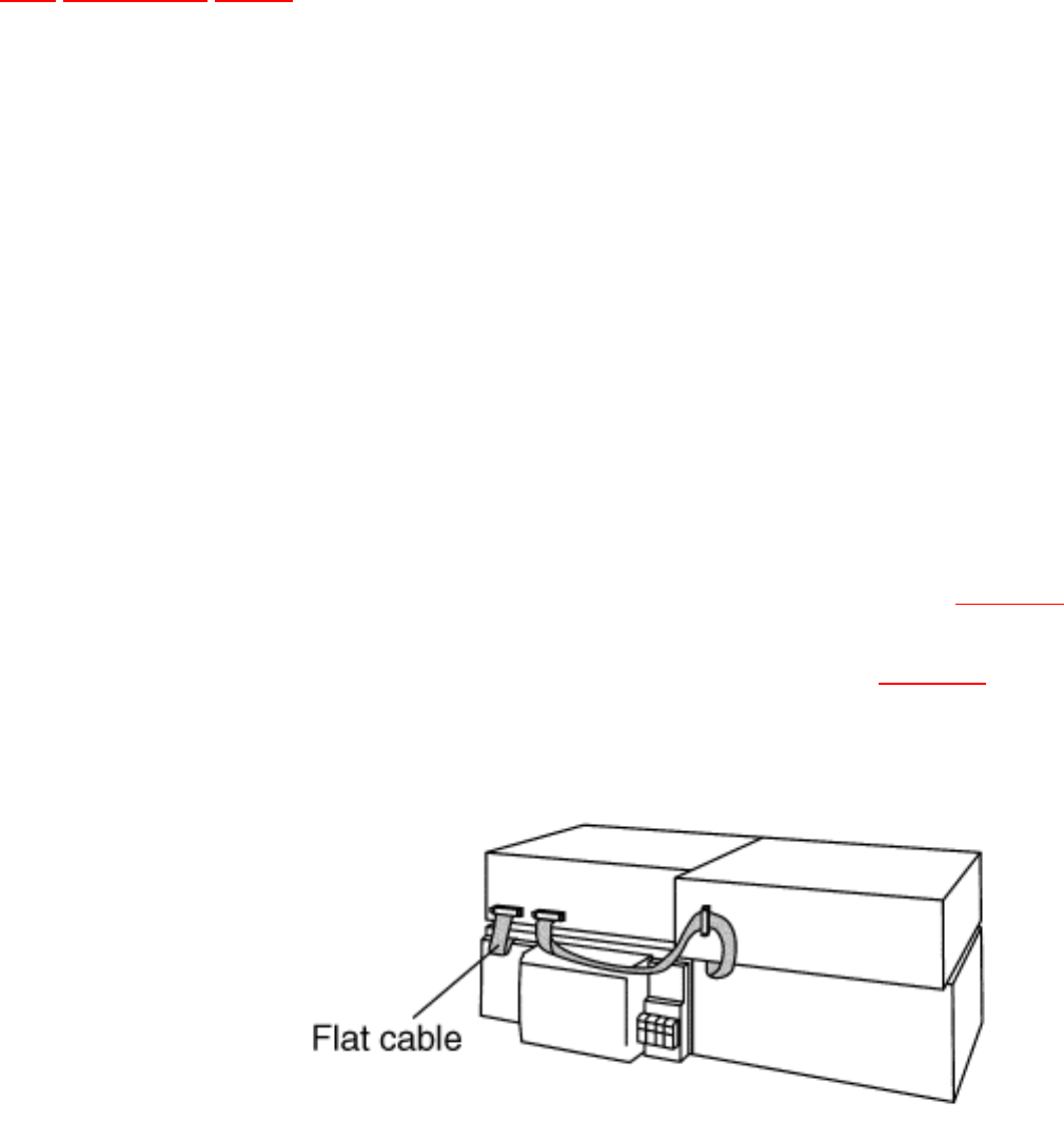
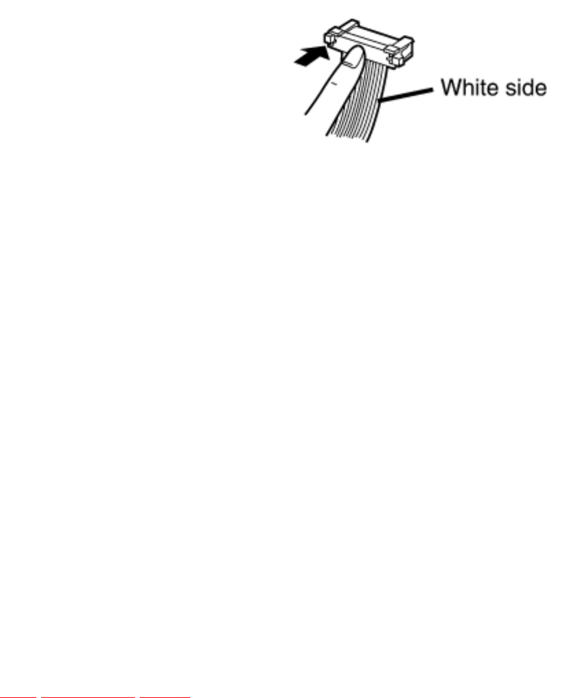
1. To check for correct insertion of flat cables.
2. Insert each connector until you hear a click.
3. Insert the flat cables at the back of the unit in the order indicated. Refer to Fig. 8-2.
Make sure the white side of the cable is on your right side. Refer to Fig. 8-3.
Fig. 8-2.
Fig. 8-3.

8.3.2 F61
TOP PREVIOUS NEXT
Problem or condition
When the power switch is switched on, it automatically switches back off, making it impossible to
switch power on.
Correction procedure
Faulty Tuner/Amplifier (SA-EH560) output IC (IC601). (When a DC voltage is applied to speaker
terminals.)
•@
TOP PREVIOUS NEXT

9 Schematic Diagram Notes
TOP PREVIOUS NEXT
This schematic diagram may be modified at any time with the development of new technology.
Notes:
S901:
Power Standby/on switch (
/I)
S902:
ECO mode switch (MODE)
S903:
Clock/timer, demo switch/(CLOCK/TIMER,
DEMO)
S904:
Play timer/record timer switch/(
PLAY/
REC)
S905:
FM mode switch (FM AUTO/MONO)
S906:
Tuning mode switch (TUNING MODE)

S907:
Set switch (SET)
S908:
Source input switch (INPUT SELECTOR)
S910:
Tuning down switch (TUNING,
)
S911:
Tuning up switch (TUNING,
)
S912:
Tuner/band switch (TUNER/BAND)
S913:
Super woofer switch (S.WOOFER)
S914:
RDS display mode PS switch/(RDS DISP MODE-PS)/ [For (E),(EG) areas]
S915:
RDS display mode PTY switch/(RDS DISP MODE-PTY)/ [For (E),(EG) areas]
VR901:
Volume control VR (VOLUME)
Indicated voltage values are the standard values for the unit measured by the DC electronic circuit
tester (high-impedance) with the chassis taken as standard. Therefore, there may exist some errors in
the voltage values, depending on theinternal impedance of the DC circuit tester.
No mark
: Power ON (FM or AM)
Important safety notice:
Components identified by mark have special characteristics important for safety.
Furthermore, special parts which have purposes of fire-retardant (resistors), high-quality sound
(capacitors), low-noise (resistors), etc. are used.
When replacing any of components, be sure to use only manufacturer’s specified parts shown in the
parts list.
Caution!
IC and LSI are sensitive to static electricity.
Secondary trouble can be prevented by taking care during repair.
Cover the parts boxes made of plastics with aluminum foil.
Ground the soldering iron.
Put a conductive mat on the work table.
Do not touch the legs of IC or LSI with the fingers directly.
Voltage and signal line
: Positive voltage line
: Negative voltage line
: FM signal line


14.1 IC901 (LC8A524A5N28):/System Control/FL
Drive
TOP PREVIOUS NEXT
Pin No. Terminal Name I/O Function
1 CHECK O Clock check signal output
2 LC72 DI O PLL data signal output
3 LC72 CE O Chip enable signal output
4 LC72 DO/ST I IF count data/stereo detect signal input
5 LC72 CK O Clock signal output
6 RL1 - Not used, open
7 RL2
8 ST/AV.6CH - Not used, open
9 SEL TUNER - Tuner select signal output
(Not used, open)
10 SEL/ TUNER O Tuner select signal output
11 AC IN I Power failure detect signal input
12 RESET I Reset signal input
13 X IN I Oscillator connected terminal (32.7 kHz)
14 X OUT O
15 VSS - GND terminal
16 XC IN I Oscillator connected terminal (6 MHz)
17 XC OUT O
18 VDD1 I Power supply terminal
19 KEY TU I Operation key signal input
20 KEY KARAOKE I Operation key signal input
21 SH REQ I Request signal input from Sound Processor
22 NC(GND) - Not used, connected to GND
23 VR JOGB I Volume control signal input
24 VR JOGA
25 MIC DET I Microphone connecting detect signal input
(Connected to VDD via resistor)
26 HP SW I Headphone connecting detect signal input
27 RDS CLK I RDS clock signal input
28 RDS DATA I RDS data signal input

29 REMOCON I Remote control signal input
30 NC - Not used, open
31
|
37
7G
|
1G
O Grid signal output
38 NC - Not used, open
39
40
|
45
P1
|
P6
O Segment signal output
46 VDD3 I Power supply terminal
47
|
50
P7
|
P10
O Segment signal output
51 -VP I Power supply terminal (negative)
52
|
71
P11
|
P30
O Segment signal output
72 VDD4 I Power supply terminal
73
|
77
P31
|
P35
O Segment signal output
78 REG IN0 I Area select signal input
79 REG IN1
80 STANDBY O LED (STANDBY) drive signal output
81 TIMER O LED (TIMER) drive signal output
82 S.W LED O LED (S.WOOFER) drive signal output
83 LOUNGE - LED (LOUNGE) drive signal output
(Not used, open)
84 CHORUS - LED (CHORUS) drive signal output
(Not used, open)
85 MUTE O Muting signal output
86 POWER O Power control signal output
87 /ECO O ECO signal output
88 MUTE2 O Muting signal output
89 VSS2 - GND terminal
90 VDD2 I Power supply terminal
91 NC - Not used, open
92
93 RL4 - Not used, open
94 SH CS O Chip select signal output for Sound Processor
95 SH DO O Serial communication signal to Sound Processor (Data signal output)
96 SH DI I Serial communication signal to Sound Processor (Data signal input)
97 SH CK I Serial communication signal to Sound Processor (Clock signal input)
98 E DET I Unusual condition detect signal input
99 CR TIMER I/O TIME CONSTANT terminal
100 SD I Station detector signal input from tuner circuit
•@
TOP PREVIOUS NEXT

16 Replacement Parts List
TOP PREVIOUS NEXT
Notes:
Important safety notice:
Components identified by mark have special characteristics important for safety.
Furthermore, special parts which have purposes of fire-retardant (resistors), high-quality sound
(capacitors), low-noise (resistors), etc. are used.
When replacing any of components, be sure to use only manufacture’s specified parts shown in the
parts list.
The<IA> <IB> <IC> <ID> marks in Remarks indicate language of instruction manual.
<IA>: Spanish, Swedish
<IB>: English
<IC>: German, French, Italian
<ID>: Netherlands, Danish
The parenthesized indications in the Remarks columns specify the areas. (Refer to the cover page for
area.)
The marking [RTL] indicates that Retention Time is Limited for this item. After the discontinuation
of this assembly in production, the item will continue to be available for a specific period of time.
The retention period of availabilityis dependent on the type of assembly, and in accordance with the
laws governing part and product retention. After the end of this period, the assembly will no longer
be available.
All parts are supplied by MESA.
Ref. No. Part No. Part Name& Description Pcs Remarks
1 RKM0395C-S CABINET 1
2 RHD30007-S SCREW 4
3 XTBS3+10JFZ1 SCREW 1
4 REX0967 WIRE ASS’Y 1
5 RMZ0339 ZENNER COVER 1
6 RGW0343-S KNOB,VOLUME 1
7 RHN90001 NUT 1
8 RKA0106-N FOOT RING 4
9 RKF0606A-K BACK GRILL 1
10 RKW0581-1V FL WINDOW 1
11 RMN0427 CABLE HOLDER 1
12 RYP0946B-S FRONT PANEL 1 (EB)
12 RYP0946G-S FRONT PANEL 1 (E,EG)
12-1 RGB0025-A TECHNICS BADGE 1
13 SHG1654 RUBBER 4
14 XTB3+10JFZ SCREW 10
15 XTB3+8JFZ SCREW 11
16 XTW3+15T SCREW 2
17 XTBS3+8JFZ1 SCREW 2
18 RLBT4001-N FERAITO COA 1
19 RMN0582 PT HOLDER 1
20 SHR9112 RIVET 1
21 XTB3+20JFZ SCREW 1
A1 RAK-EHA29WH REMOTE CONTROLLER 1
A1-1 RKK0123-H BATTERY COVER 1
A2 REE0499 SPEAKER CORD 2
A3 REE0984 SPEAKER CORD 2
A4 REE0985 SPEAKER CORD 2
A5 RJA0019-X AC POWER SUPPLY CORD 1 (E,EG)
A5 RJA0053-2X AC POWER SUPPLY CORD 1 (EB)
A6 RQA0117 WARRANTY CARD 1
A7 RQCB0169 SERVICE CENTER LIST 1
A8 RQT5354-E OPERATING INSTRUCTIONS 1 (E)<IA>
A8 RQT5355-B OPERATING INSTRUCTIONS 1 (EB)/<IB>

A8 RQT5352-D OPERATING INSTRUCTIONS 1 (EG)/<IC>
A8 RQT5353-H OPERATING INSTRUCTIONS 1 (EG)/<ID>
A9 RSA0007 FM INDOOR ANTENNA 1
A10 RSA0022-J AM LOOP ANTENNA 1
A11 SJP9009 ANT.ADAPTOR 1 (EB)
A12 RQCA0736 SETTING GUIDE 1 (EB)
C151 ECEA1CKS100 16V 10U 1 (E,EG)
C152 ECBT1H331KB5 50V 330P 1 (E,EG)
C153 ECBT1H102KB5 50V 1000P 1 (E,EG)
C154 ECBT1H561KB5 50V 560P 1 (E,EG)
C155 ECBT1H102KB5 50V 1000P 1 (E,EG)
C156,57 ECBT1H470J5 50V 47P 2 (E,EG)
C158,59 RCE0JKA470BG 6.3V 47U 2 (E,EG)
C160 ECBT1H102KB5 50V 1000P 1 (E,EG)
C395,96 ECBT1H473KB5 50V 0.047U 2
C509,10 ECBT1H103KB5 50V 0.01U 2
C550 ECBT1C103NS5 16V 0.01U 1
C551 ECA1HAK2R2XB 50V 2.2U 1
C552 ECBT1H103KB5 50V 0.01U 1
C553 ECEA1HKAR22B 50V 0.22U 1
C554 ECA1AAK221XH 10V 220U 1
C564 ECA1CAK100XB 16V 10U 1
C601,02 ECA1CAK100XB 16V 10U 2
C603,04 ECBT1H471KB5 50V 470P 2
C605,06 ECBT1H102KB5 50V 1000P 2
C607,08 ECBT1H471KB5 50V 470P 2
C609,10 ECBT1H470J5 50V 47P 2
C611,12 ECBT1H150JC5 50V 15P 2
C613,14 ECBT1H470J5 50V 47P 2
C616 ECEA1HKNR47B 50V 0.47U 1
C617,18 ECKR2H103ZU 500V 0.01U 2
C619 ECBT1H103KB5 50V 0.01U 1
C620,21 ECQV1H473JM3 50V 0.047U 2
C622 ECA1HM101 50V 100U 1
C624,25 ECQV1H473JM3 50V 0.047U 2
C626,27 ECQV1H104JM3 50V 0.1U 2
C631,32 ECBT1H473KB5 50V 0.047U 2
C635-37 ECBT1H473KB5 50V 0.047U 3
C639-42 ECBT1H102KB5 50V 1000P 4
C647-50 ECBT1H102KB5 50V 1000P 4
C655,56 ECA1CAK100XB 16V 10U 2
C659,60 ECA1CAK100XB 16V 10U 2
C666 ECBT1H473KB5 50V 0.047U 1
C701 ECA1VM472E 35V 4700U 1
C702,03 ECA1VM562E 35V 5600U 2
C704 ECA1VM472E 35V 4700U 1
C705 ECBT1H103KB5 50V 0.01U 1
C706 RCE1VKA100BG 35V 10U 1
C707,08 ECBT1H473KB5 50V 0.047U 2
C709 ECQV1H104JZ 50V 0.1U 1
C710 ECBT1H473KB5 50V 0.047U 1
C714 ECBT1H102KB5 50V 1000P 1
C715 ECA1EAM472XE 25V 4700U 1
C717 ECA1CAK330XB 16V 33U 1
C718 ECEA1CKS101 16V 100U 1
C719,20 ECBT1H473KB5 50V 0.047U 2
C721 RCE1AKA101BG 10V 100U 1
C722 ECEA1CKS101 16V 100U 1
C723,24 ECBT1H473KB5 50V 0.047U 2
C731 ECBT1H102KB5 50V 1000P 1
C732 ECBT1H223KB5 50V 0.022U 1
C733 ECBT1H473KB5 50V 0.047U 1
C734 RCE1HKA3R3BG 50V 3.3U 1
C735 ECBT1H473KB5 50V 0.047U 1
C737 ECA1HM101 50V 100U 1
C740 ECA1CAK100XB 16V 10U 1
C741 ECQE1104KF3 100V 0.1U 1
C753 ECKR1H103ZF5 50V 0.01U 1
C754 ECBT1H103KB5 50V 0.01U 1
C755 ECA1CAM102XB 16V 1000U 1
C758 ECBT1H103KB5 50V 0.01U 1
C759 RCE1AKA470BG 10V 47U 1
C761 ECQE1104KF3 100V 0.1U 1
C791 ECKWRS102MBC 1000P 1
C901 EEAFC0J101B 6.3V 100U 1
C902 RCE1AM102BV 10V 1000U 1
C903,04 ECBT1H103KB5 50V 0.01U 2
C905 ECBT1H102KB5 50V 1000P 1
C907,08 ECBT1H471KB5 50V 470P 2
C909 ECBT1H102KB5 50V 1000P 1
C910 ECBT1H200JC5 50V 20P 1
C911 ECBT1H180J5 50V 18P 1
C912 ECBT1H104KB5 50V 0.1U 1
C913 ECA1CAK100XB 16V 10U 1
C914 ECEA1HKS2R2 50V 2.2U 1
C915 ECBT1H103KB5 50V 0.01U 1
C916 EEAFC0J101B 6.3V 100U 1
C917 ECBT1H103KB5 50V 0.01U 1
C918 ECEA0JKS101 6.3V 100U 1
C919,20 RCE1HKA4R7BG 50V 4.7U 2
C921 ECBT1H102KB5 50V 1000P 1
C922 ECA1VAK330XB 35V 33U 1
C923,24 ECBT1H104KB5 50V 0.1U 2
C925,26 ECBT1H102KB5 50V 1000P 2
C927,28 RCE1HKA4R7BG 50V 4.7U 2
C931 ECA1CAK100XB 16V 10U 1
C961 ECEA1CKS100 16V 10U 1
CN602 RJU057W008 CONNECTOR(8P) 1
CN603 RJU057W004 CONNECTOR(4P) 1
CN701-13 RJS1A1101T1 CONNECTOR(1P) 13
CN781 RJS10T5ZA CONNECTOR(10P) 1
CP101 RJT100W11 CONNECTOR(11P) 1
CP602 RJT057W008-1 CONNECTOR(8P) 1
CP603 RJT057W004-1 CONNECTOR(4P) 1
D151 MA4051M DIODE 1
D306 SELS5223C LED 1
D500 MA165 DIODE 1
D551,52 MA165 DIODE 2
D555 MA4100M DIODE 1
D558 MA165 DIODE 1
D563 MA165 DIODE 1
D601,02 SB360L6508 DIODE 2
D607 1SS291TA DIODE 1
D657-59 MA165 DIODE 3
D701-04 1N5402BF DIODE 4
D705 RL1N4003N02 DIODE 1
D711 RL1N4003N02 DIODE 1
D715 MA165 DIODE 1
D717-20 RL1N4003N02 DIODE 4
D721 MA4300M DIODE 1
D723 MA4150M DIODE 1
D725 MA4082LTA DIODE 1
D730 MA4091H DIODE 1
D736 MA165 DIODE 1
D737 MA4082LTA DIODE 1
D738-40 MA165 DIODE 3
D741-44 RL1N4003N02 DIODE 4
D745 MA4051M DIODE 1
D746 RL1N4003N02 DIODE 1
D747 MA4068M DIODE 1
D749 MA165 DIODE 1
D751,52 1N5402BF DIODE 2
D753-55 RL1N4003N02 DIODE 3
D756,57 MA700 DIODE 2
D758 MA165 DIODE 1
D760 MA165 DIODE 1
D761 RL1N4003N02 DIODE 1
D901,02 1SS291TA DIODE 2
D903,04 MA165 DIODE 2
D905 1SS291TA DIODE 1
D906,07 MA165 DIODE 2
D915 1SS291TA DIODE 1
D933 MA165 DIODE 1 (E,EG)
D951 LNJ301MPUJAD LED 1
D954 SELS5923C LED 1
D956 SELS5923C LED 1
D961 MA4075M DIODE 1
D973 MA4030M DIODE 1
D974 MA165 DIODE 1
F1 XBA2C10TB0 FUSE 1
FL901 RSL0298-F FL 1
IC151 LC72721NMTLM IC 1 (E,EG)
IC601 RSN311W64A IC 1
IC901 LC8A524A5N28 IC 1
JK601 ,02 RJH5603-1J 6P SP TANSI 2
JK701 SJS9236 JACKAC INLET 1
JK903 RJJ37TN02-C JACK,HEADPHONE 1
L151,52 ELEXT101KA9 COIL 2 (E,EG)
L153 RLQA1R0JT1-Y COIL 1 (E,EG)
L601-06 RLQYR73MW1-0 COIL 6
L701 RLQZ371 COIL 1
L901 RLQA100JT1-Y COIL 1
L902 RLQA1R0JT1-Y COIL 1
P1 RPG4793 PACKING CASE(SYSTEM) 1 (E)
P1 RPG4795 PACKING CASE(SYSTEM) 1 (EB)
P1 RPG4794 PACKING CASE(SYSTEM) 1 (EG)
P2 RPQ0951 PAD(SYSTEM) 1
P3 RPG4397 PACKING CASE(RS) 1
P3 RPG4396 PACKING CASE(SA) 1
P3 RPG4398 PACKING CASE(SH) 1
P3 RPG4399 PACKING CASE(SL) 1
P4 RPN1195-2 PAD(RS) 1
P4 RPN1194 PAD(SA) 1
P4 RPN1196 PAD(SH) 1
P4 RPN1203 PAD(SL) 1
P5 SPP740-1 SHEET 4
P6 RPF0139 PROTECTION BAG(F.B.) 1
PCB1 REP2964D-M MAIN PCB 1 (E,EG)/[RTL]
PCB1 REP2964L-M MAIN PCB 1 (EB) [RTL]
PCB2 REP2966D-S SUB PCB 1 (E,EG)/[RTL]
PCB2 REP2966E-S SUB PCB 1 (EB) [RTL]
Q503 2SC3327A TRANSISTOR 1
Q551 2SA1995RSTA TRANSISTOR 1
Q554 2SA1995RSTA TRANSISTOR 1
Q555 2SC3327A TRANSISTOR 1
Q558 UN4211 TRANSISTOR 1
Q601,02 2SC5398RSTA TRANSISTOR 2
Q605,06 2SD2144STA TRANSISTOR 2
Q701 2SD2374PQAU TRANSISTOR 1
Q702 2SB1548PQAU TRANSISTOR 1
Q703 2SD2137PQTA TRANSISTOR 1
Q705 2SA1995RSTA TRANSISTOR 1
Q706 UN4211 TRANSISTOR 1
Q707 2SB1548PQAU TRANSISTOR 1
Q708 UN4211 TRANSISTOR 1
Q709 2SC3327A TRANSISTOR 1
Q711 2SB1548PQAU TRANSISTOR 1
Q723 2SC3940AQSTA TRANSISTOR 1
Q725 2SC5398RSTA TRANSISTOR 1
Q726 2SC3940AQSTA TRANSISTOR 1
Q791 2SC3327A TRANSISTOR 1
Q901 UN4212TA TRANSISTOR 1
Q902 UN411FTA TRANSISTOR 1
Q911,12 2SC3327A TRANSISTOR 2
Q961 UN4115 TRANSISTOR 1

R151,52 ERDS2FJ102 1/4W 1K 2 (E,EG)
R153,54 ERDS2FJ104 1/4W 100K 2 (E,EG)
R155 ERDS2FJ121 1/4W 120 1 (E,EG)
R158 ERDS2FJ102 1/4W 1K 1 (E,EG)
R229,30 ERDS2FJ102 1/4W 1K 2
R509-12 ERDS2FJ390 1/4W 39 4
R544 ERDS2FJ103 1/4W 10K 1
R546,47 ERDS2FJ392 1/4W 3.9K 2
R548 ERDS2FJ102 1/4W 1K 1
R551 ERDS2FJ183 1/4W 18K 1
R552 ERDS2FJ473 1/4W 47K 1
R553,54 ERDS2FJ392 1/4W 3.9K 2
R555 ERDS2FJ223 1/4W 22K 1
R556 ERDS2FJ104 1/4W 100K 1
R557 ERDS2FJ103 1/4W 10K 1
R558 ERDS2FJ222 1/4W 2.2K 1
R559 ERDS2FJ472 1/4W 4.7K 1
R561 ERDS2FJ104 1/4W 100K 1
R563,64 ERDS2FJ272 1/4W 2.7K 2
R570 ERDS2TJ225 1/4W 2.2M 1
R571 ERDS2FJ562 1/4W 5.6K 1
R572 ERDS2FJ153 1/4W 15K 1
R591 ERDS2FJ472 1/4W 4.7K 1
R597,98 ERDS2FJ122 1/4W 1.2K 2
R601,02 ERDS2FJ472 1/4W 4.7K 2
R603,04 ERDS2FJ332 1/4W 3.3K 2
R605,06 ERDS2FJ472 1/4W 4.7K 2
R607,08 ERDS2FJ563 1/4W 56K 2
R609,10 ERDS2FJ124 1/4W 120K 2
R611,12 ERDS2FJ563 1/4W 56K 2
R614,15 ERDS2FJ472 1/4W 4.7K 2
R617,18 ERDS2FJ472 1/4W 4.7K 2
R619,20 ERDS2FJ124 1/4W 120K 2
R621 ERDS2FJ154 1/4W 150K 1
R622,23 ERDS2FJ124 1/4W 120K 2
R624 ERDS2FJ154 1/4W 150K 1
R627 ERDS2FJ474 1/4W 470K 1
R628 ERDS2FJ223 1/4W 22K 1
R631,32 ERDS2FJ392 1/4W 3.9K 2
R635 ERDS2FJ222 1/4W 2.2K 1
R637 ERDS2FJ153 1/4W 15K 1
R638 ERDS2FJ683 1/4W 68K 1
R639,40 ERDS1FJ100 1/2W 10 2
R641,42 ERD2FCG100 1/4W 10 2
R643,44 ERDS1FJ100 1/2W 10 2
R645,46 ERD2FCG100 1/4W 10 2
R647,48 ERDS2FJ2R2 1/4W 2.2 2
R649,50 ERDS1FJ100 1/2W 10 2
R651,52 ERD2FCG100 1/4W 10 2
R683,84 ERDS2FJ102 1/4W 1K 2
R687,88 ERD16TJ000T 1/4W 0 2
R702 ERDS2FJ273 1/4W 27K 1
R703-05 ERG1SJ222 1W 2.2K 3
R707 ERD2FCJ4R7 1/4W 4.7 1
R708 ERDS2FJ472 1/4W 4.7K 1
R712 ERDS2FJ222 1/4W 2.2K 1
R719 ERDS2FJ332 1/4W 3.3K 1
R720 ERDS2FJ392 1/4W 3.9K 1
R721 ERD2FCJ4R7 1/4W 4.7 1
R722 ERQ16NKW2R2E 1/6W 2.2 1
R723 ERDS2FJ562 1/4W 5.6K 1
R724 ERDS2FJ392 1/4W 3.9K 1
R725 ERDS2FJ100 1/4W 10 1
R727 ERDS2FJ392 1/4W 3.9K 1
R729 ERDS2FJ221 1/4W 220 1
R738 ERDS2FJ392 1/4W 3.9K 1
R739 ERDS2FJ473 1/4W 47K 1
R749 ERDS2FJ102 1/4W 1K 1
R763 ERDS2FJ472 1/4W 4.7K 1
R764 ERDS2FJ331 1/4W 330 1
R765 ERDS1FJ221 1/2W 220 1
R766 ERDS1FJ470 1/2W 47 1
R767 ERD2FCJ4R7 1/4W 4.7 1
R768 ERDS2FJ101 1/4W 100 1
R770 ERDS2FJ104 1/4W 100K 1
R771 ERDS2FJ222 1/4W 2.2K 1
R772 ERDS2FJ223 1/4W 22K 1
R773,74 ERDS1FJ180 1/2W 18 2
R776 ERDS2FJ103 1/4W 10K 1
R777 ERDS2FJ102 1/4W 1K 1
R791,92 RSFMB40KT-L FUSE PROTECTOR 2
R793 ERDS2FJ1R0 1/4W 1 1
R794 ERDS2FJ473 1/4W 47K 1
R795 ERDS2FJ392 1/4W 3.9K 1
R797 ERD16TJ000T 1/4W 0 1
R901 ERDS2FJ821 1/4W 820 1
R902 ERDS2FJ102 1/4W 1K 1
R903 ERDS2FJ122 1/4W 1.2K 1
R904 ERDS2FJ152 1/4W 1.5K 1
R905 ERDS2FJ182 1/4W 1.8K 1
R906 ERDS2FJ222 1/4W 2.2K 1
R907 ERDS2FJ332 1/4W 3.3K 1
R908 ERDS2FJ472 1/4W 4.7K 1
R909 ERDS2FJ182 1/4W 1.8K 1
R910 ERDS2FJ222 1/4W 2.2K 1
R911 ERDS2FJ332 1/4W 3.3K 1
R912 ERDS2FJ472 1/4W 4.7K 1
R913 ERDS2FJ821 1/4W 820 1
R914 ERDS2FJ102 1/4W 1K 1
R915 ERDS2FJ122 1/4W 1.2K 1
R916 ERDS2FJ152 1/4W 1.5K 1
R918 ERDS2FJ103 1/4W 10K 1
R919 ERDS2FJ153 1/4W 15K 1
R921,22 ERDS2FJ103 1/4W 10K 2
R923 ERDS2FJ223 1/4W 22K 1
R924,25 ERDS2FJ102 1/4W 1K 2
R926 ERDS2FJ222 1/4W 2.2K 1
R928 ERDS2FJ473 1/4W 47K 1
R929-32 ERDS2FJ102 1/4W 1K 4
R933 ERDS2FJ471 1/4W 470 1
R934-36 ERDS2FJ101 1/4W 100 3
R937 ERDS2FJ103 1/4W 10K 1
R939 ERDS2FJ152 1/4W 1.5K 1
R943 ERDS2FJ101 1/4W 100 1
R944 ERDS2FJ222 1/4W 2.2K 1
R945 ERDS2FJ101 1/4W 100 1
R946 ERDS2FJ102 1/4W 1K 1
R947,48 ERDS2FJ104 1/4W 100K 2 (EB)
R949 ERDS2FJ472 1/4W 4.7K 1
R950 ERDS2FJ101 1/4W 100 1
R951 ERDS2FJ334 1/4W 330K 1
R952 ERDS2TJ106T 1/4W 10M 1
R953 ERDS2FJ101 1/4W 100 1
R954 ERDS2FJ104 1/4W 100K 1
R955 ERDS2FJ824 1/4W 820K 1
R956-58 ERDS2FJ102 1/4W 1K 3
R959 ERDS2FJ470 1/4W 47 1
R960 ERDS2FJ152 1/4W 1.5K 1
R961,62 ERDS2FJ223 1/4W 22K 2
R963,64 ERDS2FJ121 1/4W 120 2
R965,66 ERDS2FJ392 1/4W 3.9K 2
R967 ERDS2FJ222 1/4W 2.2K 1
R968 ERDS2FJ105 1/4W 1M 1
R969 ERDS2FJ272 1/4W 2.7K 1
R975 ERDS2FJ154 1/4W 150K 1
R976 ERDS2FJ104 1/4W 100K 1
R984 ERDS2FJ391 1/4W 390 1
R986 ERDS2FJ152 1/4W 1.5K 1
R987,88 ERDS2FJ102 1/4W 1K 2
R990 ERDS2FJ104 1/4W 100K 1
R991 ERDS2FJ473 1/4W 47K 1
R993 ERDS2FJ104 1/4W 100K 1
R995 ERDS2FJ221 1/4W 220 1
R996,97 ERDS2FJ151 1/4W 150 2
RL701 RSY0030M-0 RELAY 1
RL702 RSY0040M-0 RELAY 1
S901-08 EVQ11G05R SW 8
S910-13 EVQ11G05R SW 4
S914,15 EVQ11G05R SW 2 (E,EG)
T701 RTP2M5B018 POWER TRANSFORMER 1
T702 RTP1H3E001 POWER TRANSFORMER 1
VR901 EVQVBXFK124B V.R. 1
X151 RSXC4M33S02T OSCILLATOR 1
X901 EF0EC6004T4 OSCILLATOR 1
X902 RSXD32K7S02 OSCILLATOR 1
Z120 RAN0005EM-1 TUNER UNIT 1
Z701 ERZV10V511CS COMPONENT COMBINATION 1
Z901 RCDGP1U28XD REMOTE SENSOR 1
•@
TOP PREVIOUS NEXT


19202122 23
AM
MIX
12
LEVEL
DET
FM IF
S-
CURVE
2
3
REG
4
13
AGC
COMP
68 1110
AM
RF
AMP
AM
IF
AM/FM
IF
BUFFER
24
1
FM
DET
AM
OSC
BUFEER
ALC
TUNING
DRIVE
18
BUFFER
AMP
FM ANT
RF AMP
FM
MIXER
FM OSC
9
Vcc
+B(FM)
FM IF
AMP
+B2
AM
IFT
1
20
7.2MHz
XIN
XOUT
PHASE DET
CHARGE PUMP
CE 2
3
DI
4
CL
D0 5
98710
BO4
BO3
IO1
15
VDD
16 PD
IFIN
11
BO2
1/2 14
13
FM IN
AM IN
Power
supply
(FM:ON)
+B2
+B1
+B(FM)
SD
STEREO
SWITCH
17
FM / AM I F AMP,
DET / AM OSC,
MIX / FM MPX
(LA1833MN)
15
PILOT
CANCEL
PHASE
DET
16
VCO
FFFF
PILOT
DET
FF
AM
DET
DECODER
BO1 6
IO2
12
19 Vss Power
ON
RESET
PLL FREQUENCY
SYNTHESIZER
(LC72131M)
+B2
GND
57
ST
MONO
FM/AM
SD
FMDET
FM IF
IN
AM
OSC
OUT
AFC
AM
OSC
AM RF
IN
AGC
AM
OUT
DET
OUT
PILOT
IN
MPX
IN
PILOT
OUT
Lch
14
Rch
17
18
AIN
AOUT
AM
ANT
COIL
AM
OSC
COIL
AM ANT
+B2
STRQ
AM IF
IN
AM
MIX
OUT
Rch
IFT
+B(FM)
+B(FM)
+B(FM)
FM:ON DET
CE1
DATA1
CLK1
DATA IN
Z120 TUNER UNIT (RAN0005EM)
REFERENCE
DIVIDER
SWALLOW COUNTER
1/6,1/17 4BIT
12 BIT
PROGRAMMABLE
DIVIDER
DATA SHIFT
REGISTER LATCH
UNIVERSAL
COUNTER
From POWER
TRANSFORMER
1
8
W501
2
3
4
5
6
7
9
12
13
14
15
16
17
18
A.GND
DC 10V
TW Lch IN
TW Rch IN
19
11
10
CS.GND
SH FL1
DATA
D.GND
TUNER L/C
TUNER R
MID Lch IN
MID Rch IN
SW
MIC
-7.5V
V.GND
CS/REQ
CLK
SH FL2
20
SYNC
+B6
-B3
To SOUND PROCESSOR
BLOCK DIAGRAM
LC72 CE
LC72 DO/ST
LC72 CK
DATA1
CLK1
DATA IN
CE1
345
LC72 DI
2
LC8A524A5N28
IC901
SYSTEM CONTROL / FL DRIVE
94
SH CS
97
SH CK
9596
SH DO
SH DI SYNC
100
SD
21
SH REQ
SD
Rch
Rch
Rch
LC72721NMTLM
IC151
RDS SIGNAL
DEMODULATOR
VR901
(VOLUME)
24 23
VR JOGA
VR JOGB
LC8A524A5N28
IC901
SYSTEM CONTROL / FL DRIVE
29
REMO-
CON
Z901
(REMOTE
SENSOR) +B9
1~7G
31~37
P1~35
40~45,
47~50
52~71,
73~77
FL901 FL DISPLAY
D933
78
REGIN0
81
TIMER
82
S.W LED
D951
(S.WOOFER)
80
STANDBY
D954
( PLAY/REC) D306
()
DET
28
RDS DATA
RDS CLK
27
CLOCK
RECOVERY
(1187.5Hz)
RDDA
RDCL
PCL
RDS-ID
IDR
RDS-ID
DETECT
57kHz
BPF
(SCF)
PLL
(57kHz)
VREF
CINFLOUTVREF
VDD
Vss
MPX IN
T1
T2
T3
T4
TEST
XOUTXIN STDBY
OSC/DIVIDER
CLK(4.332MHz)
1011 20
14
19
8
7
2
4,12
3,13
+B2
156
16
17
9
15
18
X151
REGIN1
16 17
X901
(6MHz)
XC IN
XC OUT
13 14
X902
(32.7kHz)
XIN
X OUT
CR
TIMER
D903
99
ANTIALIASING
FILTER SMOOTHING
FILTER
REFERENCE
VOLTAGE
DATA
DECODER
79
MUTING
Q605
(Q606)
88
MUTE2
MUTE2
For [E,EG] areas.
SPEAKERS
(To SB-EH560)
HEADPHONES
KEY
SWITCH
(S901~915)
19 20
KEY TU
KEY
KARAOKE
Q901,
D904 RESET
12
RESET
+B9
15
Vss
89
Vss2
90
VDD2
+B10
VDD1
VDD3
VDD4
18 46 72
LC8A524A5N28
IC901
SYSTEM CONTROL / FL DRIVE
1621
GND
1047
1
(2)
6
3
20
15
19
(18)
26
(25)
24
RSN311W64A
IC601
POWER AMP
+B3
D601
-B1
D602
-B2
Q601,602
9
+B8
Q551,554,555
13
POWER
98
E DET
HP SW
26
AC IN
AC IN
8687
/ECO
/ECO
POWER
POWER
11
+B9
1
CHECK
TP
14
N
Q503,558+B4
51
-VP
-VP
85
MUTE
D906
SWITCH-
ING
D974
SWITCH-
ING
D907
23
(22) 5
(8)
11
(12)
HIGH
(6 )
MID
(6 )
LOW
(6 )
MUTING
CONT
Q911
(Q912)
Q902,961
-VP
MUTING
MUTE2
SIGNAL
LEVEL DET
POWER CONTROL
CIRCUIT
POWER CONTROL/
PROTECTION CIRCUIT
Rch
POWER TRANSFORMER
F1 AC IN
L701
T701
D702,704,
752,754,755
Q709
Q707
+B4
+B5
-B3
Q702,705
Z701RL702
Q791
POWER
TRANSFORMER
T702
D741~744
RL701
-B1
-B2
Q703,704
+B8 D701,703,
751,753
Q706
Q701
+B1
Q723
+B2
Q711,725 D717~720
+B6
D705
-VP
FL1
FL2
FL DISPLAY
(FL901)
Q708
+B3
POWER
SYNC
/ECHO
Q726
+B7
+B9
+B10
D902
D901
AC IN
D956
(TRI-AMPLIFIER)
D746
REGULATOR
REGULATOR
REGULATOR
REGULATOR SWITCH-
ING
SWITCH-
ING
REGULATOR
REGULATOR
REGULATOR
RELAY
DRIVE
RELAY
DRIVE
+B11
+B7
D711
NOTES : FM SIGNAL LINE
: AM SIGNAL LINE
: FM OSC SIGNAL LINE
: AM OSC SIGNAL LINE
: SOURCE SIGNAL LINE
: LOW SP. DRIVE SIGNAL LINE
( ) indicates pin No. Right channel.
U
V
OPERATION CIRCUIT
SCHEMATIC DIAGRAM-1
FL901 (RSL0298-F)
Y A A RQPONMLKJIHGFDCBBCDEFGHIJKLMNOPQRSTUVWX
S908
(INPUT SELECTOR)
S907
(SET)
S906
(TUNING MODE)
S905
(FM AUTO/MONO)
S903
(CLOCK/TIMER,
-
DEMO)
S902
(MODE)
S913
(S.WOOFER)
S912
(TUNER/BAND)
S915
(PTY)
S914
(PS)
JK903
HEADPHONES
R997
150
R996
150
D973
MA4030MTA
C921
1000P
C922
35V33
C920
50V4.7
R925
1K
C908
470P
R922
10K
R924
1K
C907
470P
R944
2.2K
C924
0.1
C904
0.01
D974
MA165TA
C395
0.047
C509
0.01
R511
39 R509
39
R512
39 R510
39
C396
0.047
C510
0.01
C923
0.1
R912
4.7K
R911
3.3K
R910
2.2K
R909
1.8K
R916
1.5K
R915
1.2K
R914
1K
R913
820
R908
4.7K
R907
3.3K
R906
2.2K
R905
1.8K
R904
1.5K
R903
1.2K
R902
1K
R901
820
C919
50V4.7
FL DISPLAY
1 6 8 10 11 12 13 14 15 16 17 18 19 20 21 22 23 24 25 26 27 28 29 30 31 32 33 34 35 36 37 38 39 40 41 42 43 44 45 46 47 48 49 50 53 542 5 7 9
W905
S901
(/)
S910
(TUNING, )
S911
(TUNING, )
(RDS DISP MODE)
S904
(PLAY/ REC)
C928
50V4.7
C927
50V4.7
R964
120
R963
120
Q912
Q911
R968
1M
10K
Q961
UN4115TA
MUTING CONT.
D961
MA4075MTA
C961
16V10
Q911,912
2SD2144STA
MUTING
R966
3.9K R965
3.9K
R967
2.2K
A
Q902
UN411FTA
MUTING CONT.
R975
150K
C931
16V10
8
7
2
4
3
5
1
P
Q
K
S
R921
10K
E
10K
4.7K
R969
2.7K
For [E,EG] areas.
NOTE:
The number which noted at the connectors on the schematic diagram as
"SCHEMATIC DIAGRAM-1" or "SCHEMATIC DIAGRAM-2"
indicates the schematic diagram serial number located on the left corner in the schematic diagram.
C
B
A
:NEGATIVE VOLTAGE LINE
:SOURCE SIGNAL LINE
-
27V
-
27V
0V0V
0V
-
6.1V
0V
-
6.1V
-
6.2V 0.1V
IC901
LC8A524A5N28
SYSTEM CONTROL/
FL DRIVE
A VBCD FGH I J K LMNOPQR U S
E
C
A
B
D
C
F
A
B
D
Y
A
B
C
D
E
F
G
H
I
J
K
L
M
N
O
P
Q
R
S
T
U
V
W
X
1
3
2
X901
(6MHz)
R960 1.5K
R958 1K
R959 47
R933 470
R937
10K
R988 1K
R987 1K
R934 100
R935 100
D915
1SS291TA
R936
100
C926
1000P
R918 10K
R928 47K
L902 1 H
R955
820K
D903
MA165TA
C913
16V10
C903
0.01
D902
1SS291TA D901
1SS291TA
C902
10V1000
D905 1SS291TA
R951
330K C910
20P
C911
18P
X902
(32.7kHz)
R952
10M
R930 1K
R932 1K
R931 1K
R956
1K R957
1K
C925
1000P
C915
0.01
D904
MA165TA
R923
22K
TP
R993
100K
R995
220
D306
SELS5223C
( )
D951
LNJ301MPUJAD
(S.WOOFER)
D906
MA165TA
D954
SELS5923C
(PLAY/ REC)R986
1.5K
R939
1.5K
D933
MA165TA
R990
100K
R949
4.7K
R950
100
R953
100
R954 100K
C912 0.1
D907
MA165TA
R919
15K
R991
47K
R926
2.2K
C901
6.3V100
C905
1000P
JMNHIGL OE
Q901
UN4212TA
RESET
22K
22K
R976
100K
L901
10 H
C914
50V2.2
1
11
21
2
12
22
3
13
23
4
14
24
5
15
25
6
16
26
7
17
27
8
18
28
9
19
29
10
20
30
3132333435363738394041424344454647484950
51
52
53
54
55
56
57
58
59
60
61
62
63
64
65
66
67
68
69
70
71
72
73
74
75
76
77
78
79
80
81 82 83 84 85 86 87 88 89 90 91 92 93 94 95 96 97 98 99
100
P10
P9
P8
P7
VDD3
P6
P5
P4
P3
P2
P1
NC
NC
1G
2G
3G
4G
5G
6G
7G
NC
REMOCON
RDS DATA
RDS CLK
HP SW
MIC DET
VR JOGA
VR JOGB
NC(GND)
SH REQ
KEY KARAOKE
KEY TU
VDD1
XC OUT
XC IN
VSS
X OUT
XIN
RESET
AC IN
SEL/ TUNER
SEL TUNER
ST/ AV6CH
RL2
RL1
LC72 CK
LC72 DO/ST
LC72 CE
LC72 DI
CHECK
TIMER
S.W LED
LOUNGE
CHORUS
MUTE
POWER
/ECO
MUTE2
VSS2
VDD2
NC
NC
RL4
SH CS
SH DO
SH DI
SH CK
E DET
CR TIMER
SD
-VP
P11
P12
P13
P14
P15
P16
P17
P18
P19
P20
P21
P22
P23
P24
P25
P26
P27
P28
P29
P30
VDD4
P31
P32
P33
P34
P35
REGIN0
REGIN1
STANDBY
SCHEMATIC DIAGRAM-2
R929
1K
E
For [E,EG] areas.
:NEGATIVE VOLTAGE LINE:POSITIVE VOLTAGE LINE
6.2V
5.2V
5.2V
5.2V
5.2V
-
27V
5.1V 0V
5.2V
2.6V
2.5V
0.5V
5.2V
5.2V
5.2V
1.3V
5.2V
5.2V
2.5V
2.2V
2.7V
1.7V
5.1V
2V
0V
5.2V
5.1V
0V
0V
2.6V
5.2V
5.2V
5.2V
4.4V
3.8V
3.8V
1.2V
0V
5.1V
5.1V
0V
0V
0V
0V
0V
1.5V
-
11.7V
-
4.8V
-
9.6V
-
12.4V
-
18V
-
12.2V
-
11.4V
-
11.4V
-
18V
-
18V
-
18V
-
6.8V
-
9.6V
-
16.8V
-
7.6V
-
12.6V
-
12V
-
21.7V
-
21.7V
-
17.1V
-
16.8V
-
11.8V
-
21.7V
-
21.8V
-
26.9V
5.2V
-
17.3V
-
12.5V
-
17.3V
-
22V
5.2V
-
12.7V
-
26.8V
-
26.8V
-
17.6V
-
17.3V
-
17.3V
-
17.3V
-
17.3V
-
17.3V
-
17.3V
-
17.3V
-
17.3V
-
17.3V
4V
-
25V
T 3.1ms.
0V
0V
4V
T 3.1ms.
-
25V
4.4V
P
-
P
F=6MHz
3.4V
P
-
P
F=6MHz
5.2V
P
-
P
F=32.7kHz
1.8V
P
-
P
F=32.7kHz
5V
0V
T16 ms.
5V
0V
2ms. 2V/DIV.
5V
0V
2ms. 2V/DIV.
0V
5V
T 10ms.
ABC
B
C
W901B
W902B
J
I
H
G
F
E
D
C
B
A
Q
K
L
M
N
O
P
IC151
LC72721NMTLM
RDS SIGNAL
DEMODULATOR
C917
0.01
C918
6.3V100
X151
C156
47P
C157
47P C154
560P C158
6.3V47
L151
100 H
C152
330P
C151
16V10
R158
1K
R151
1K
R152
1K
R154
100K
R153
100K
C155
1000P
C153
1000P
C160
1000P
C159
6.3V47
L152
100 H
R155
120
D151
MA4051MTA
VREF STDBY
1
2
3
4
5
6
7
8
9
10 11
12
13
14
15
16
17
18
19
20
MPX IN
VDD
VSS
FL OUT
CIN
T1
T2
PCL
X OUT
T3
IDR
RDCL
RDDA
RDS-ID
T4
VDD
VSS
XIN
R984
390
C916
6.3V100
1
2
15
3
4
5
6
7
8
9
10
11
12
13
14
1
15
3
4
6
7
8
9
10
11
13
14
12
2
5
D
E
A
VR901
EVQVBXFK124B
(VOLUME)
123
R945
100
R943
100
R962
22K
R961
22K
C909
1000P
R946
1K
Z901
RCDGP1U28XD
(REMOTE SENSOR)
BA COM
1
2
3
OPERATION CIRCUIT
A
SCHEMATIC DIAGRAM-3
L153
1H
For [E,EG] areas.
For [E,EG] areas.
R947
100K
R948
100K
For [EB] area.
D956
SELS5923C
(TRI-AMPLIFIER)
:SOURCE SIGNAL LINE:NEGATIVE VOLTAGE LINE:POSITIVE VOLTAGE LINE
5.2V
6.2V
-
27V
7.2V
5.1V
2.4V
3V
5.1V
2.5V2.6V
2.5V
2.5V
5.1V
2.5V
2.5V
B
SCHEMATIC DIAGRAM-4
MAIN CIRCUIT
DET
Rch IN
CE
Lch IN
DI
DO
CL
+B(2)
SD
+B(1)
T.GND
TUNER L/ Cch
TUNER Rch
TW Lch IN
TW Rch IN
A.GND
MID Lch IN
MIC
-7.5V
V.GND
D.GND
CS/REQ
CLK
DATA
CT.GND
SH FL1
SH FL2
SYNC
S.W
DC10V
To
MAIN CIRCUIT
of SOUND
PROCESSOR
To TUNER UNIT
on SCHEMATIC
DIAGRAM-9
R601
4.7K
R602
4.7K
R603
3.3K
R604
3.3K
R632
3.9K
R631
3.9K
R614
4.7K
R615
4.7K
R618
4.7K
R617
4.7K
R606
4.7K
C655
16V10
C656
16V10
C602
16V10
C659
16V10
C660
16V10
R564
2.7K
R563
2.7K
R597
1.2K
R598
1.2K
20
2
1
3
4
5
6
7
8
9
10
11
12
13
14
15
16
17
18
19
1
2
15
3
4
5
6
7
8
9
10
11
12
13
14
C601
16V10
R605
4.7K
2
1
3
4
5
6
7
8
9
10
11
2
15
3
4
5
6
7
9
11
12
13
8
10
14
1
W501
R712
2.2K
W902A
W901A
CP101
R230 1K
R229 1K
A
B
C
D
E
F
A
B
A
B
A
B
C
G
C
D
E
C
D
E
F
G
F
B
A
C
H
I
J
K
L
N
M
G
F
A
E
D
C
O
B
R683
1K
R684
1K
R688
0
R687
0
Q605,606
2SD2144STA
MUTING
Q605
Q606
MID Rch IN
:SOURCE SIGNAL LINE
:NEGATIVE VOLTAGE LINE
:POSITIVE VOLTAGE LINE :FM SIGNAL LINE
:AM SIGNAL LINE :LOW SP.DRIVE SIGNAL LINE
7.2V
14.8V
7.2V
6.2V
-
27V
7.5V
-
7.5V
10.4V
0V
0V
0V
0V
SCHEMATIC DIAGRAM-5
Q558
UN4211TA
SWITCHING
Q601 Q602
Q503
2SD2144STA
SWITCHING
C603 470P
C604 470P
C607 470P
C608 470P
C649 1000P
C650 1000P
C606 1000P
C605 1000P
C617
0.01
C618
0.01
R544
10K
D558
MA165TA
R637
15K
C619
0.01
R627
470K
C616
50V0.47
N
D601
SB360L6508
D602
SB360L6508
IC601
RSN311W64A
POWER AMP
123456789101112131415181920212223242526 1617
Q601,602
2SC5398RSTA
SWITCHING
D607
1SS291TA R635
2.2K
10K
10K
R572
15K R571
5.6K
D657
MA165TA
D659
MA165TA
D658
MA165TA
R648
1/4W2.2
A
B
C
D
E
F
I
H
R623 120K
R610 120K
C612 15P
R611 56K
C609 47P
R607 56K
C613 47P
R608 56K
C614 47P
R609 120K
C611 15P
R612 56K
C610 47P
R624 150K
R621 150K
R622 120K
R619 120K
R620 120K
R628
22K
C622
50V100
R647
1/4W2.2
OBALE JGNM
B
A
E
F
C
D
Q551
2SA1995RSTA
SIGNAL LEVEL DET.
Q554
2SA1995RSTA
SIGNAL LEVEL DET.
Q555
2SD2144STA
SIGNAL LEVEL
DET.
C552
0.01 R559
4.7K
R570
2.2M
R591
4.7K
R556
100K
C551
50V2.2
D551
MA165TA
R557
10K
R548
1K
R561
100K
D552
MA165TA
R558
2.2K
C554
10V220
D555
MA4100MTA
C550
0.01
D757
MA700ATA
D756
MA700ATA
C648
1000P
:SOURCE SIGNAL LINE
:NEGATIVE VOLTAGE LINE
:POSITIVE VOLTAGE LINE
:LOW SP.DRIVE SIGNAL LINE
-
7.5V
45.6V
14.8V
-
23.1V
-
46V
22.6V
-
7.5V
14.8V
10.4V
6.2V
7.5V
7.2V
-
27V
7.5V
-
7.5V
0V 5V
7.5V
7.1V
0V
7.5V
-
7.5V
-
7.5V
-
7.5V
0.3V
0V
0V0V
5.3V5.3V
0V
0V 0V 0V 0V 45.6V 0V 0V 22.6V 0V 0V 0V 0V 0V 22.2V 0V 45.6V 0V 0V
-
46V
-
22.5V
-
0.2V
-
23.1V
-
46V
SCHEMATIC DIAGRAM-6
RL701
Q709
2SD2144STA
RELAY DRIVE
Q703
2SD2137PQTA
REGULATOR
R719
3.3K
C721
10V100
D725
MA4082LTA
D749
MA165TA
R729
220
C723
0.047
R767
1/4W4.7
R727
3.9K
R766
1/2W47
D736
MA165TA
D563
MA165TA R738
3.9K
R739
47K
C564
16V10
D715
MA165TA
MAIN CIRCUIT
C724
0.047
R652
1/4W10
C626
0.1
C624
0.047 R646
1/4W10
L603
R643
1/2W10
R645
1/4W10
C625
0.047
L604
R644
1/2W10
R649
1/2W10
R651
1/4W10
C627
0.1
C635
0.047 C631
0.047
C637
0.047
C636
0.047 C666
0.047
C632
0.047
R642
1/4W10
C620
0.047
L602
C621
0.047 R641
1/4W10
L601
R639
1/2W10
R640
1/2W10
L605
L606
R650
1/2W10
10
2
1
3
4
5
6
7
8
9
2
1
3
4
JK602
JK601
Q706, 708
UN4211TA
SWITCHING
Q708 Q706
10K
10K
R797
0
B
34
12
6
5
A
E
C
B
F
D
C553
50V0.22
R555
22K
(Lch)
(Rch)
10K
10K
Q707
2SB1548PQAU
REGULATOR
Q723
2SC3940AQSTA
REGULATOR
D705
RL1N4003N02
D737
MA4082LTA
R763
4.7K
R764
330
C733
0.047
C740
16V10
D721
MA4300MTA R708
4.7K
C707
0.047
C706
35V10
C737
50V100
R707
1/4W4.7
C735
0.047
C708
0.047
C705
0.01
AB
AB
D
C
D701
D751
D703
C703
35V5600
C701
35V4700
D753
D753,761
RL1N4003N02
D761
R703
1W2.2K
R704
1W2.2K
R705
1W2.2K
C709
0.1
R638
68K
D701,703,751
1N5402BM21
C704
35V4700
C702
35V5600
D754D755
D704
D702
D752
C761
0.1
D702,704,752
1N5402BM21
D754,755
RL1N4003N02
R702
27K
C714
1000P
D719
D720
C741
0.1
C731
1000P
D717
D718
C715
25V4700
D717-720
RL1N4003N02
R552
47K
R546
3.9K
R554
3.9K
R551
18K
R547
3.9K
R553
3.9K
W722
W721
HIGH(6 )
MID(6 )
LOW(6 )
HIGH(6 )
MID(6 )
LOW(6 )
SPEAKERS
To SB-EH560
:SOURCE SIGNAL LINE
:NEGATIVE VOLTAGE LINE
:POSITIVE VOLTAGE LINE
:LOW SP.DRIVE SIGNAL LINE
0V
0.7V
-
27V
-
46V
7.2V 14.8V
45.6V
-
7.5V
6.2V
14.8V
10.4V
-
23.1V
22.6V
16.3V
10.2V2.1V 0V0V
22.1V7.5V
8V
14.8V7.2V
7.8V
-
38.2V
-
27V
-
27.5V
45.6V
AC IN CIRCUIT
SCHEMATIC DIAGRAM-7
W722
CN711 W1
CN712 W3
CN713 W2
T701
POWER TRANSFORMER(A)CIRCUIT POWER
TRANSFORMER(B)
CIRCUIT
CN701
CN702
CN703
CN704
CN705
CN706
CN707
CN708
CN709
CN710
CN602
CN603
AC IN
JK701
L701
F1 TA2
T702
Z701
C791
1000P
3 1
24
RL702
R795
3.9K
R794
47K
Q791
2SD2144STA
RELAY DRIVE
D740
MA165TA
D745
MA4051MTA
R772
22K
R771
2.2K
D741
D743
D744
D742
C753
0.01
C755
16V1000
Q726
2SC3940AQSTA
REGULATOR D746
RL1N4003N02
R777
1K
D747
MA4068LTA
C758
0.01
C759
10V47
C754
0.01
D500
MA165TA
W2/ W3
W1
2
1
3
4
2
1
3
4
5
6
7
8
9
10W721
R793
1
A
B
C
D
E
F
G
G
B
A
C
D
E
F
F
8
2
1
4
5
6
7
2
3
1
4
3
R774
1/2W18
R773
1/2W18
D711
RL1N4003N02
E
D
8
2
1
4
5
6
7
2
3
1
4
3
CP602
CP603
POWER SUPPLY CIRCUIT
Q702
2SB1548PQAU
REGULATOR
Q725
2SC5398RSTA
REGULATOR
Q711
2SB1548PQAU
REGULATOR
Q705
2SA1995RSTA
REGULATOR
Q701
2SD2374PQAU
REGULATOR
D738
MA165TA
D758
MA165TA
D730
MA4091HTA
R770
100K
D739
MA165TA
R765
1/2W220
R724
3.9K
C720
0.047
C718
16V100
C717
16V33
D723
MA4150HTA
R723
5.6K
C719
0.047
R725
10
D760
MA165TA
C710
0.047
R768
100
1
R749 1K
2
3
4
5
7
6
8
9
10
C734
50V3.3
C
C722
16V100
R720
3.9K
1
2
3
4
5
7
6
8
9
10 W701BCN781
K
F
C639
1000P
C640
1000P
C641
1000P
C642
1000P
C732
0.022
C647
1000P E602
E601
R721
1/4W4.7
R722 1/6W2.2
R776 10K
D741-744
RL1N4003N02
R792
RSFMB40KT-L
R791
RSFMB40KT-L
For [E,EG] areas.
For [EB] area.
230V 50Hz [E,EG]
230-240V 50Hz [EB]
H
H
:SOURCE SIGNAL LINE
:NEGATIVE VOLTAGE LINE
:POSITIVE VOLTAGE LINE
:LOW SP.DRIVE SIGNAL LINE
-
7.5V
14.8V
10.4V
16.3V
-
7.5V
-
22.6V
44.5V
14.8V
6.2V
44.5V14.8V
15.4V
-
22.6V
-
7.5V
-
8V
-
8V
-
0.6V
16.3V10.4V
15.8V
10.1V
9.6V
12.9V6.2V
6.8V
0.7V 0V
AC
13.5V
AC
4.8V
AC
13.5V
AC
17.8V
AC
17.8V
AC
30V

1 2 3 4 5 6 7 8 9 10
20 19 18 17 16 15 14 13 12 11
XIN
CE
DI
CL
DO
B01
B02
B03
B04
I01 IF IN
I02
AM IN
FM IN
VDD
PD
AIN
A OUT
Vss
X OUT
10K
0.047
100K
5 ~12P
1000P
A
B
C
D
0.58 H
390
220
27K
100P0.01
560
1K
4.7
DZS5.1B
10K
27P~ 33P
27P
7.2MHz
22K~100K
100
1000P
1000P
10K
1K
3.3K
10K
1K
1K
1K
470
ABCD
22
5.6K
0.01
A
B
C
D
E
F
LC72131M
PLL FREQUENCY
SYNTHESIZER
AM ANT
EXT
LOOP
FM ANT
(75 )
SCHEMATIC DIAGRAM-8
100
0.01
100
2SC2413
BUFFER AMP
2SK360
FM OSC
2SK360
RF AMP
22P 15P
22P0.022
2.7K47P
33K
100K
2P
8P
10K 10K 33K
33K
100K
0.022
100
27P
2P
4P
10K
220
0.022
0.022
150
5P
18P
27P
2SC2059
FM MIXER
0.47 H
0.47 H
10P ~ 33P
330P ~
580P
1P ~ 5P
680 ~
2.2K
0 ~ 220
1 H
820K ~ 2.2M
0.022
680
1000P
330
1P ~ 5P
6P ~ 10P
6 ~ 220
5P
5P ~ 12P
0~5P
100K
Z120 TUNER UNIT(RAN0005EM) :POSITIVE VOLTAGE LINE
:FM SIGNAL LINE
:FM OSC SIGNAL LINE
:AM SIGNAL LINE
:AM OSC SIGNAL LINE
C
B
24 23 22 21 20 19 18 17 16 15 14 13
1 2 3 4 5 6 7 8 9 10 11 12
FM IF IN
AM MIX OUT
REG
AM IF IN
GND
SD
ST
FM DET
Vcc
STRQ
FM/AM
MONO
AM OSC OUT
AM OSC
AFC
AM RF IN
AGC
AM OUT
DET OUT
PILOT IN
MPX IN
PILOT OUT
Rch OUT
Lch OUT
BADFC E
470
2.7K 1
68
0.1
1000P
470
0.01
5 ~ 150
AB
1
22
100
0.018
11K
100K
4700P
B
A
4700P
100K
1K1
0.018
1000P ~ 0.01
150P
68K 0.1
1022K4.7
4.7
47K
1000P
3.3
A
D
B
C
10K
0.01
330
1000P
LA1833MN
FM/AM IF AMP,
DET/AM OSC,MIX/FM MPX
A
B
B
A
D
A
2SC2712
SWITCHING
3.3K
2SC2413
FM IF AMP
2SC2413
FM IF AMP
330
SCHEMATIC DIAGRAM-9
11 13 245678910
1K ~ 10K
470
4.7K ~ 22K
0.022
0.1
DTA114
POWER SUPPLY
(FM:ON)
1K ~ 10K
100P ~ 1000P
0.01 ~ 0.068 10K ~ 100K
1K ~ 10K
270 ~ 680
270K ~ 680K 10P ~
39P 270K ~
680K
CL
DO
DI
Lch OUT
CE
Rch OUT
DET
+B(2)
SD
+B(1)
T.GND
To MAIN CIRCUIT(CP101)
on SCHEMATIC DIAGRAM-4
B
1
0.47
:POSITIVE VOLTAGE LINE :FM SIGNAL LINE :AM SIGNAL LINE :AM OSC SIGNAL LINE
ABCDEF
1
2
3
4
5
6
7
8
R929
R955
R988
R991
R937
R936
R926
R935
R987
R914
R910
R909
R953
R951
R943
R961
R155
R151
R152
R153
R154
R924
R925
R922 R921
R944
R906
R905
J
J
J
J
R915
R916
R954
R996
R990
R934
R930
R931
1
2
3
VR901
(VOLUME)
R923
R918
R957
R919
R969
R933
R967
R993
R986
R939
R960
R911
R976
R952
R928
R904
R903
R902
R511
R509
R510
R946
R908 R950
R948
R947
R945
R962 R949
R158
R907
R913 R959
R958
R975
R932
J
J
J
J
J
J
J
J
J
J
J
J
R956
R995
R968
R965
R997 R966
R984
R912
D956
(TRI-AMPLIFIER)
D951
S913
J
15
1413
1211
10 9
87
65
43
21
W902B
J
J
J
J
J
J
J
J
J
C902
C931
C915
C903
D903
C961
C901
C922
C920
C928
C913
D961
Q961
B
C
E
Q902
ECB
D906
D901
D902
C921
C926
C905
C912
C924
C917
C157
C152
C153
C160
C156
C510
C509 C395
C396
C923
C155
C154
C908
C907
C925
C909
C904
C911
C910
15
1413
1211
10 9
87
65
4
21
W901B
3
D973
D933
D915
D904
D974
D907
D905
J
L901
L902
L153
L151
L152
J
S915
(RDS
DISP MODE-PTY
)
S914
(RDS
DISP MODE-PS
)
S907
(SET)
S906
(TUNING
MODE)
S905
(FM AUTO/
MONO)
S903
(CLOCK/TIMER,
—DEMO)
S902
(MODE)
S904
( PLAY/
REC)
S908
(
INPUT SELECTOR
)
S912
(TUNER BAND)
J
J
J
J
J
J
J
J
J
J
J
J
151015202530 35
4045 50
55
60
31
51
65
7570
80
81
85
90
95
100
IC901
Q901
B
C
E
3
2
1X901
J
J
J
X902
1
2
5
6
7
8
9
10
11
12
13
14
15
16
17
18
19
20
21
22
23
24
25
26
27
28
29
30
31
32
33
34
35
36
37
38
39
40
41
42
43
44
45
46
47
48
49
50
53
54
FL901
C914
C916
C918
J
J
J
J
R901
R963
R964
R512
J
J
J
J
C158
C159
C151
C919 C927
Z901
(SENSOR)
3
2
1
X151
IC151
1510
11 15 20
D151
D954
Q912
ECB
Q911 ECB
JK903
(PHONES)
8
127
43
5
W905
TP
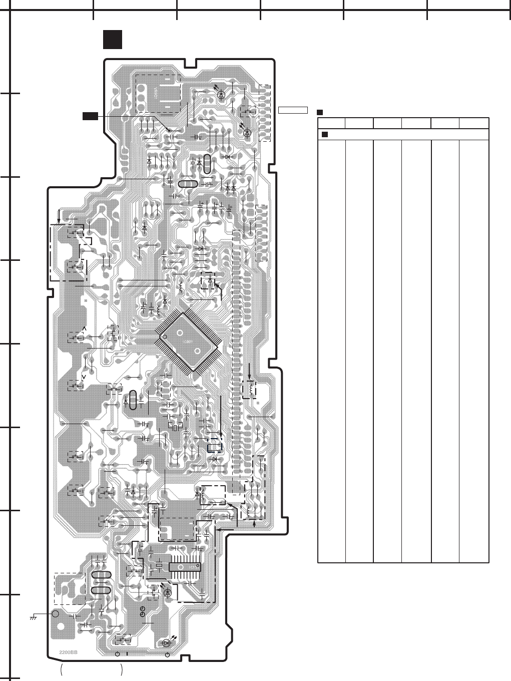
OPERATION P.C.B.
A
S.WOOFER
S911
(TUNING )
S910
(TUNING )
S901
( / ) D306
( )
REP2964D-M ..... [E,EG]
REP2964L-M ..... [EB]
For [E,EG]
areas.
For [E,EG]
areas.
For [E,EG]
areas.
For [EB] area.
For [E,EG] areas.
ELECTRICAL PARTS LOCATION
OPERATION P.C.B.
A
Ref. No. Lo. No. Ref. No. Lo. No. Ref. No. Lo. No.
IC151
IC901
Q901
Q902
Q911
Q912
Q961
D151
D306
D901
D902
D903
D904
D905
D906
D907
D915
D933
D951
D954
D956
D961
D973
D974
VR901
L151
L152
L153
L901
L902
Z901
X151
X901
X902
FL901
S901
S902
S903
S904
S905
S906
S907
S908
S910
S911
S912
S913
S914
S915
JK903
W901B
W902B
W905
R151
R152
R153
R154
R155
R158
R509
R510
R511
R512
R901
R902
R903
R904
R905
R906
R907
R908
R909
R910
R911
R912
R913
R914
R915
R916
R918
R919
R921
R922
R923
R924
R925
R926
R928
R929
R930
R931
R932
R933
R934
R935
R936
R937
R939
R943
R944
R945
R946
R947
R948
R949
R950
R951
R952
R953
R954
R955
R956
R957
R958
R959
R960
R961
R962
R963
R964
R965
R966
R967
R968
R969
R975
R976
R984
R986
R987
R988
R990
R991
R993
R995
R996
R997
C151
C152
C153
C154
C155
C156
C157
C158
C159
C160
C395
C396
C509
C510
C901
C902
C903
C904
C905
C907
C908
C909
C910
C911
C912
C913
C914
C915
C916
C917
C918
C919
C920
C921
C922
C923
C924
C925
C926
C927
C928
C931
C961
7C
4C
5B
3C
7B
7B
2C
6C
8B
3C
3C
2B
5B
3B
2C
6C
4B
4C
2C
7B
1C
2C
3C
6B
1B
6C
7C
5C
4C
4B
7C
7B
5B
6B
6C
8B
7B
7B
8B
6B
6A
6A
5B
5A
4A
4B
2C
4A
3A
7A
3D
2D
8A
6C
6C
7C
7C
6D
6C
8B
8A
7B
8A
7B
7B
7B
7B
6A
6A
5B
6B
5A
5A
4B
2C
3A
4B
4B
3A
2B
2B
6B
6B
1C
6C
6C
3B
6B
2B
2B
2B
2B
3C
2B
3B
3B
3B
4C
5C
6B
6C
6B
6C
6C
6C
6C
5C
5B
5B
3B
2B
2B
2B
3B
3C
4C
6C
6C
8B
8B
3C
3C
2C
2C
3C
3C
5B
1C
3C
3B
2B
3C
2B
3C
2C
3C
3C
7C
7C
7C
7C
7C
7B
7B
7B
7B
7C
7B
7B
8B
8A
4B
2C
3B
5C
4B
6C
5C
5C
5B
5B
5B
3B
5B
2B
6B
6B
6B
7C
3C
3C
3C
8A
6B
5B
3B
7C
3C
3C
2C
ABCDEF
1
2
3
4
5
6
7
8
10
9
8
7
6
5
4
3
2
1
CN781
D607
R635
R712
R707
R766
R702
J
J
J
J
R708
R719
R230
R598
R597
J
JJ
J
J
J
J
J
J
J
J
J
15
1413
1211
109
87
65
43
21
W902A
JJ
J
J
J
J
J
J
J
J
J
J
J
J
J
J
J
J
J
JJ
J
ECB
Q723 C740
C733
R764
R763
R564
R563
R558R570
R555
R687
R628 R604
R603
R605
R606
R617
R618
R684
R683
R688
R729
R553
R607
R572
R571
R544
R637
R767
R722
R721
R623
R548
R649
R650
R624
R608
R739
R704
R703
R638
R797
R738
R776 J
R556
R727
R621
R552
R551
R631
R632
R609
R611
R647
R640
R643
R705
R644
R652
R639
R645
R641 R651
R646
J
R642
R627
R610
R648
R619
R612
R620
R546
R547
R554
R614
J
J
R615
J
R601
R602
R622
R557
R559
R591
J
J
J
J
J
J
J
J
J
J
J
J
J
J
J
J
J
J
J
J
J
JJ
J
J
J
J
D737
D659
D657
C705 15
1413
1211
109
87
65
43
21
W901A
1514
1312
1110
98
76
54
32
1
W501
16
1718
1920
J
J
J
J
J
J
J
J
J
J
J
J
J
J
J
J
J
J
J
J
J
J
J
J
J
C737
C706
C564
D721
C708
C550
C552
C724
C709
C619
C613
C614
C723
C647
C608
C607
C611
C609
C616
C612
C617
C618
C648 C605
C606
C610
C604
C603
C649
C620
C632
C650
C707
C714
C731
C741
C761
BCE
Q707
C554
C656
C551
C553
C721
C660
C622
C659
C601
C655 C602
C735
1234567891011
CP101
R229
R561
D757
D555
D551
D558
D736
D753
D749
D756
D658
D563
D715
D718
D717
D755
D761
D705
D754 D719
D720
D552
ECB
Q555
ECB
Q554
ECB
Q558
ECB
Q708
ECB
Q709
ECB
Q706
ECB
Q503
D725
E
C
B
Q551
B
C
E
Q703
E602
E
C
B
Q602
E
C
B
Q601
E
C
B
Q606
E
C
B
Q605
26
25
24
23
22
21
20
19
18
17
16
15
14
13
12
11
10
9
8
7
6
5
4
3
2
1
IC601
J
J
J
J
J
J
J
J
J
J
J
J
J
J
J
J
J
J
J
J
J
J
J
J
J
J
J
J
J
J
J
J
J
J
D602
D601
E601
J
J
J
D703
D704
D702
D752
D701
D751
RL701
C715
1
2
3
4
5
6
7
8
9
10
1
2
3
4
W721 W722
65
21
43
C702
C703
C701
C704
J
J
J
J
J
J
J
C642
C641
C639
C732
C625 C627
C624 C626
C640
C621
1234
CP603
1234
CP602
5678
C631
C635
C637 C666 C636
JK601
JK602
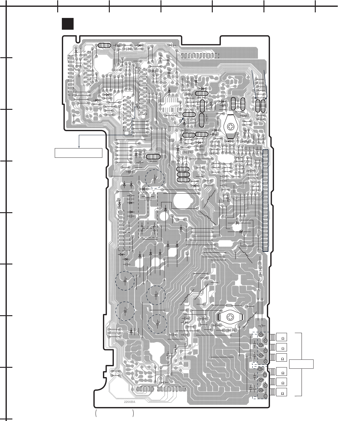
MAIN P.C.B.
B
SPEAKERS
To SB-EH560
To SOUND PROCESSOR
(R)
(R)
(L)
(L)
(R)
(L)
LOW
(6 )
MID
(6 )
HIGH
(6 )
LOW
(6 )
MID
(6 )
HIGH
(6 )
L601
L603
L604
L602
N
L605
L606
J
REP2964D-M ..... [E,EG]
REP2964L-M ..... [EB]
GHIJK
L
B
C
E
Q701
B
C
E
Q702
B
C
E
Q711 B
C
E
Q725
ECB
Q705
R725
R723
C719
C717
C710
C720
W701B
D723
10
9
8
7
6
5
4
3
2
1
C718
C722
C734 R720
R724
R768
R770
R749
R765
D760
D758
D739
D738
J
D730
J
POWER SUPPLY P.C.B.
C
REP2964D-M ..... [E,EG]
REP2964L-M ..... [EB]
ELECTRICAL PARTS LOCATION
Ref. No. Lo. No. Ref. No. Lo. No. Ref. No. Lo. No. Ref. No. Lo. No. Ref. No. Lo. No. Ref. No. Lo. No. Ref. No. Lo. No. Ref. No. Lo. No.
MAIN P.C.B.
B
POWER SUPPLY P.C.B.
C
Q701
Q702
Q705
Q711
IC601
Q503
Q551
Q554
Q555
Q558
Q601
Q602
Q605
Q606
Q703
Q706
Q707
Q708
Q709
Q723
D551
D552
D555
D558
D563
D601
D602
D607
D657
D658
D659
D701
D702
CP101
CP602
CP603
JK601
JK602
E601
E602
W501
W721
W722
W901A
W902A
R229
R230
R544
R546
R547
R548
R551
R552
R553
R554
R555
R556
R557
R558
R559
R561
R563
R627
R628
R631
R632
R635
R637
R638
R639
R640
R641
R642
R643
R644
R645
R646
R647
R648
R649
R650
R651
R652
R683
R684
R687
R688
R702
R703
R704
R705
C608
C609
C610
C611
C612
C613
C614
C616
C617
C618
C619
C620
C621
C622
C624
C625
C626
C627
C631
C632
C635
C636
C637
C639
C640
C641
C642
C647
C648
D703
D704
D705
D715
D717
D718
D719
D720
D721
D725
D736
D737
D749
D751
D752
D753
D754
D755
D756
D757
D761
L601
L602
L603
L604
L605
L606
RL701
CN781
R564
R570
R571
R572
R591
R597
R598
R601
R602
R603
R604
R605
R606
R607
R608
R609
R610
R611
R612
R614
R615
R617
R618
R619
R620
R621
R622
R623
R624
R707
R708
R712
R719
R721
R722
R727
R729
R738
R739
R763
R764
R766
R767
R776
R797
C550
C551
C552
C553
C554
C564
C601
C602
C603
C604
C605
C606
C607
C649
C650
C655
C656
C659
C660
C666
C701
C702
C703
C704
C705
C706
C707
C708
C709
C714
C715
C721
C723
C724
C731
C732
C733
C735
C737
C740
C741
C761
R749
R765
R768
R770
D739
D758
D760
W701B
Q725
D723
D730
D738
R720
R723
R724
R725
C710
C717
C718
C719
C720
C722
C734
5F
3D
2D
2D
3D
3D
2E
2E
2E
2E
3D
4D
3C
4D
4D
1B
2E
2D
2D
3D
3D
5E
5E
1B
2B
3D
2B
5D
5C
4D
5C
4C
4C
4C
4C
4C
4C
3C
3E
4D
1C
3E
5D
5C
5D
7C
5C
3D
2D
5C
7E
5E
6D
6D
5D
4D
5C
2B
1D
8D
8C
8E
7E
7E
3E
2C
5C
5C
3C
2B
2D
2C
3D
4E
4E
4E
3E
3E
3E
4E
3E
2E
2D
2D
2D
2D
2C
2C
2D
3D
3D
2D
2C
2C
3E
3E
3E
3E
2E
2E
3E
3E
4E
4E
4E
4E
3E
3E
2E
2E
4E
4E
3E
3E
4E
4E
4E
3E
3E
3E
2B
3D
3D
6E
5E
7D
5E
6D
6D
6D
7D
4E
4E
4D
4D
7D
7E
2E
2E
3E
3E
7C
5D
5D
5D
4C
4C
2B
2B
4D
4D
3E
3E
3D
4D
1C
1C
4C
3D
3D
3D
2D
2D
2D
2E
2D
3D
2C
2D
3E
3E
4E
4E
3E
3E
4E
4E
4E
3E
3E
3E
4E
4E
4E
3D
6E
7D
3E
7E
7D
7E
7D
8E
7E
8E
7E
8E
7D
7D
8D
7D
3E
4E
4E
4E
2D
2C
3E
3E
7E
7C
6C
6C
6C
2B
3C
4C
3C
3D
4C
4C
3E
3D
3D
4C
7D
1C
1D
4C
1C
5C
6C
2I
2I
2I
2I
2I
2I
3I
3I
2I
3I
2I
2I
2I
2I
2I
1I
2I
3I
2I
2I
2I
2I
2I
2I
2I
2I
2I
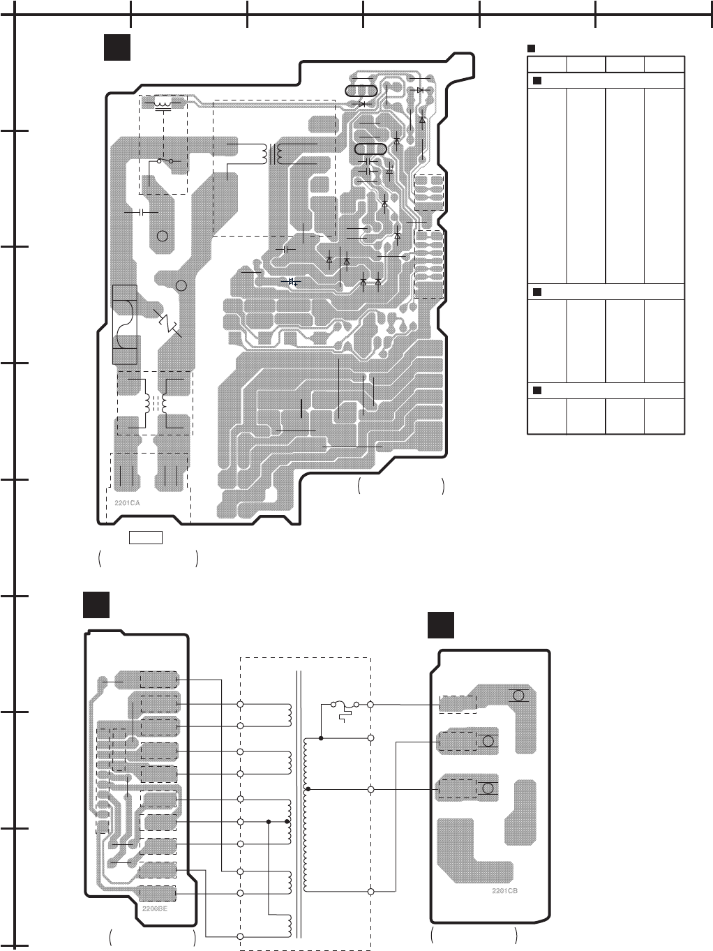
ABCDEF
1
2
3
4
5
6
7
8
J
RL702 T702(Power transformer)
R794
R773
R774
R777
R795
R771
R772
ECB
Q791
ECB
Q726
D500
D711
D746
D742
D744
D741
D743
D740
J
J
J
J
J
C754
C758
D745
D747
C759
1
2
3
4
CN603
1
2
3
4
CN602
5
6
7
8
J
J
J
J
J
J
J
J
J
C755
C753
JK701
J
J
J
J
L701
FC1 FC2
F1 T2A
Z701
W1
W2/W3
C791
AC IN P.C.B.
D
1
2
43
AC IN
230V 50Hz ..... [E,EG]
230-240V 50Hz ..... [EB]
REP2966D-S ..... [E,EG]
REP2966E-S ..... [EB]
CN710
CN709
CN708
CN707
CN706
CN705
CN704
CN703
CN702
CN701
R792
R791
R793
W722
W721
J
J
POWER TRANSFORMER
(B) P.C.B.
F
POWER TRANSFORMER
(A) P.C.B.
E
CN712
CN713
CN711
W3
W2
W1
J
J
J
J
J
J
1
2
3
4
5
6
7
8
9
10
1
2
3
4
T701(Power transformer)
REP2966D-S ..... [E,EG]
REP2966E-S ..... [EB]
REP2964D-M ..... [E,EG]
REP2964L-M ..... [EB]
ELECTRICAL PARTS LOCATION
POWER TRANSFORMER(A) P.C.B.
E
Ref. No. Lo. No. Ref. No. Lo. No.
POWER TRANSFORMER(B) P.C.B.
F
SPEAKER TERMINAL P.C.B.
D
Q726
Q791
D500
D711
D740
D741
D742
D743
D744
D745
D746
D747
L701
T702
Z701
F1
RL702
CN602
CN603
W1
W2
W3
CN709
CN710
W721
W722
R791
R792
R793
JK701
FC1
FC2
W1
W2/W3
R771
R772
R773
R774
R777
R794
R795
C753
C754
C755
C758
C759
C791
CN701
CN702
CN703
CN704
CN705
CN706
CN707
CN708
CN711
CN712
CN713
2D
1C
1C
2D
1D
3C
3D
3C
3D
1D
2D
2D
4B
2C
3B
3A
2B
3D
2D
5B
3A
3A
2B
3B
1D
2D
1D
2D
2C
1C
1D
3C
2D
3C
2D
2D
2B
6B
6B
7B
7B
7B
7B
7B
8B
8B
8B
7A
7A
8A
8A
6A
6D
7D
7D
6E
7E
7E
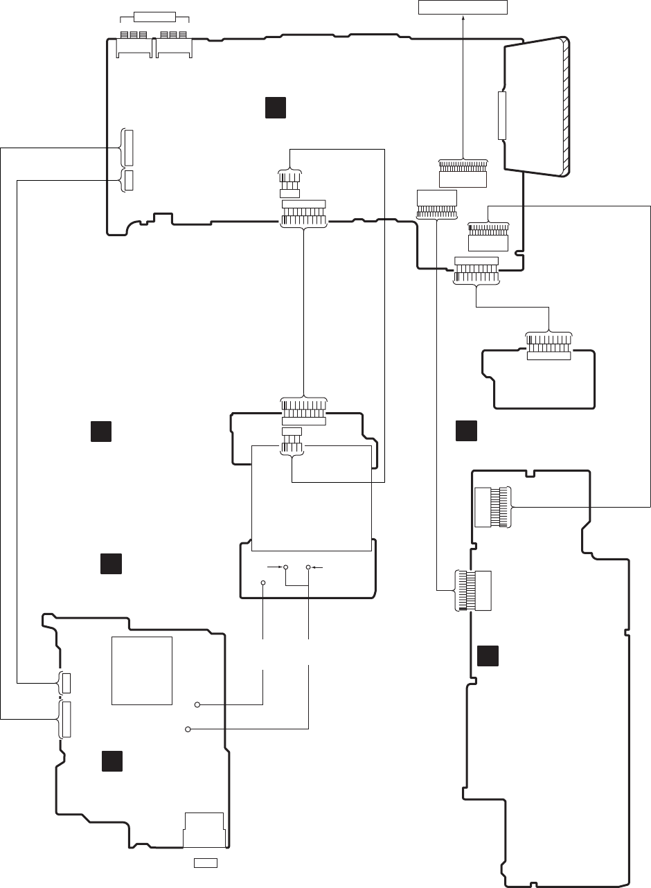
BMAIN P.C.B.
AOPERATION P.C.B.
W902B
14
.
.
.
.
.
2
15
.
.
.
.
.
.
1
W901B
14
.
.
.
.
.
2
15
.
.
.
.
.
.
1
W902A 1 . . . . . . 15
2 . . . . . 14
1. . . . . . . .10
CN781
2 . . . . . 14
1 . . . . . . 15
W901A
2 . . . . . . . . 20
1 . . . . . . . . 19
W501
To SOUND PROCESSOR
1 . . 4
W722
1. . . . . . . .10
W721
8
.
.
.
.
.
.
1
CP602
4
.
.
1CP603
SPEAKERS
CPOWER SUPPLY P.C.B.
W701B
1. . . . . . . .10
T702
(Power
transformer)
DAC IN P.C.B.
W1
W2/W3
1
.
.
4CN603
1
.
.
.
.
.
.
8
CN602
AC IN
EPOWER
TRANSFORMER
(A) P.C.B.
1 . . 4W722
1. . . . . . . .10
T701
(Power transformer)
W721
W3
W2
W1
For [E,EG]
areas.
For [EB]
area.
FPOWER
TRANSFORMER
(B) P.C.B.
1
.
.
.
.
.
.
.
.
.
11
CP101
Z120
TUNER
UNIT
BROWN
BLUE
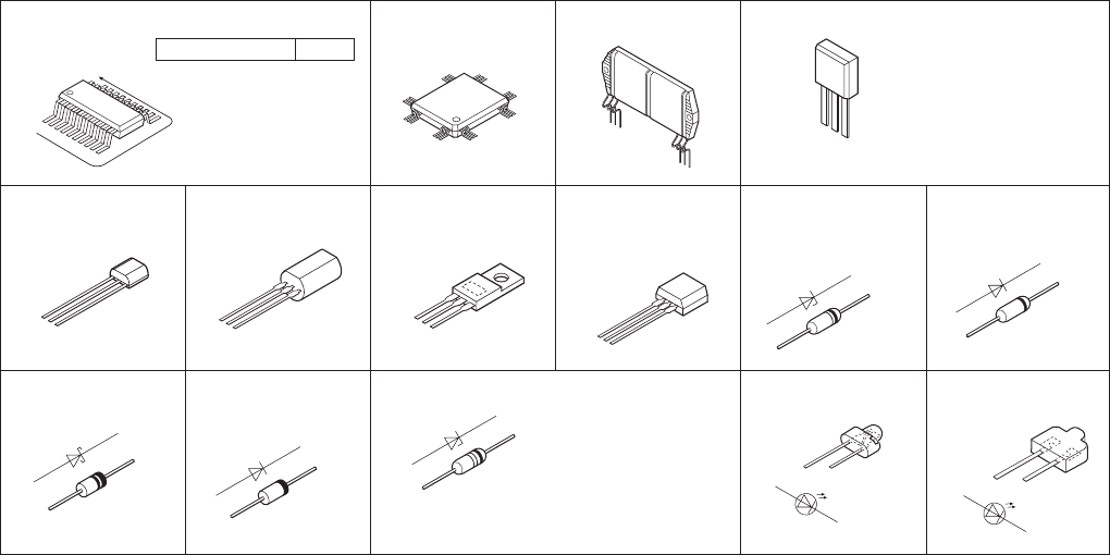
No.1
LC72721NMTLM 20PIN 2SD2137PQTA
UN411FTA
UN4115TA
UN4211TA
UN4212TA
ECB
MA4091HTA
MA4100MTA
MA4150HTA
MA4300MTA
LC8A524A5N28
.
.
.
.
.
.
.
.
.
.
.
50
51
1
............30
31
100
..
.
.
.
.
.
..
.
.
.
.
.
80
81
RSN311W64A
1
..................
26
2SC3940AQSTA
ECB
2SB1548PQAU
2SD2374PQAU
C
B
E
2SA1995RSTA
2SC5398RSTA
2SD2144STA
E
C
B
MA165TA
MA700ATA
1SS291TA Ca
A
Anode
Cathode
1N5402BM21
RL1N4003N02
Ca
A
Anode
Cathode
SB360L6508
Ca
A
Anode
Cathode
2SA1995RSTA
2SC5398RSTA
E
C
B
A
Anode
Cathode
Ca
Ca
A
Anode
Cathode MA4030MTA
MA4051MTA
MA4068LTA
MA4075MTA
MA4082LTA
LNJ301MPUJAD
A
Anode
Cathode
Ca
SELS5223C
SELS5923C
A
Ca
Anode
Cathode
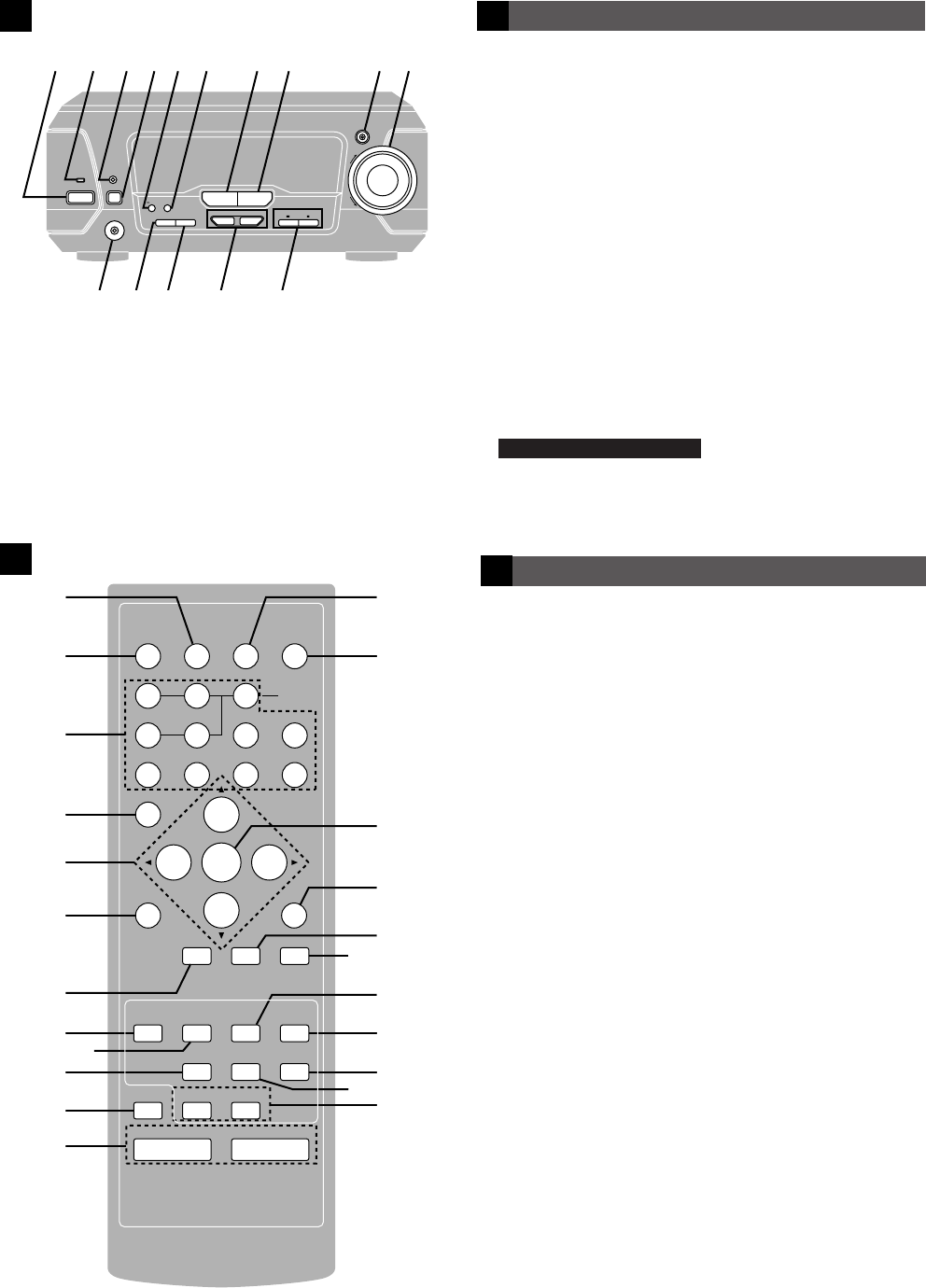
Tuner amplifier
1
A
A
B
l
r
1
]
m
o
q
z
y
|
:
9
{
}
t
;
s
n
u
v
x
H
AV EFFECT
SLEEP
CH SELECT
PROGRAM
123
456
7890
j/-/--
CANCEL
DISC
VCR/AUX/
6CH INPUT TAPE/
DECK 1/2
U
PRO LOGIC
S.WOOFER
TUNER/
BAND
⁄/g¤ ¤»
MUTING
MN
∂ VOLUME µ
CD
3D AI EQ/M.EQ BAND
EQ
Remote controls
Buttons 1, 9–;, and function in the same way as the
controls on the main unit.
lSleep timer button (SLEEP)
mNumbered buttons (1–9, 0, M)
nCursor buttons (2, 1, 3, 4)
qVCR button (VCR)
rTAPE select, deck 1/deck 2 select button
(TAPE/DECK 1/2)
sCD pause/Tape reverse playback button (2/;)
tMuting button (MUTING)
uProgram button (PROGRAM)
vCancel button (CANCEL)
xEQ button (EQ)
yAV effect button (AV EFFECT)
zCD button (CD)
{CD play/tape forward playback button (1)
|CD/tape stop button (∫)
}CD skip/search, tape fast forward/rewind buttons
(4, 5)
B
h
i
SIMULATED
STEREO
g–i
Standby/on switch (Í/I)
Press to switch the unit from on to standby mode or vice versa. In
standby mode, the unit is still consuming a small amount of
power.
2Standby indicator (Í)
When the unit is connected to the AC mains supply, this indicator
lights up in standby mode and goes out when the unit is turned on.
3Play timer/record timer button and indicator
(FPLAY/FREC)
4ECO mode button (MODE)
5Clock/timer, demo button
(CLOCK/TIMER, –DEMO)
6FM mode button (FM AUTO/MONO)
8Source input button (INPUT SELECTOR)
9Tuner/band button (TUNER/BAND)
:Super woofer button and indicator (S.WOOFER)
;Volume control (VOLUME)
<Headphone jack (PHONES)
=Tuning mode button (TUNING MODE)
>Set button (SET)
?Tuning buttons (X, W TUNING)
@
RDS display mode buttons
(RDS, PS–DISP MODE–PTY)
Except for United Kingdom
H
H/I
MODE
?
TUNING
@
PHONES
TUNING MODE SET
INPUT SELECTOR TUNER/BAND
VOLUME
UP
DOWN
FM AUTO/
MONO
œ
PLAY
/œ
REC
CLOCK/TIMER
DEMO
5 6 8 9 ;:3 41 2
< = > ?
S.WOOFER
DISP MODE
RDS
PTYPS
@
