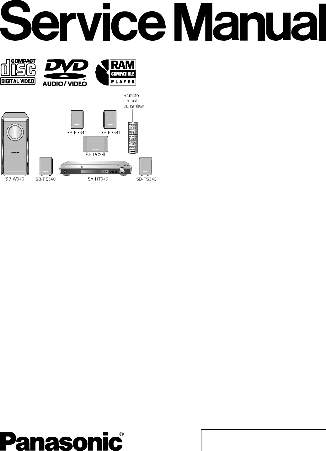
Technics SAHT 340 GC GS GCS Service Manual
User Manual: Technics-SAHT-340-GC-GS-GCS-Service-Manual
Open the PDF directly: View PDF ![]() .
.
Page Count: 98
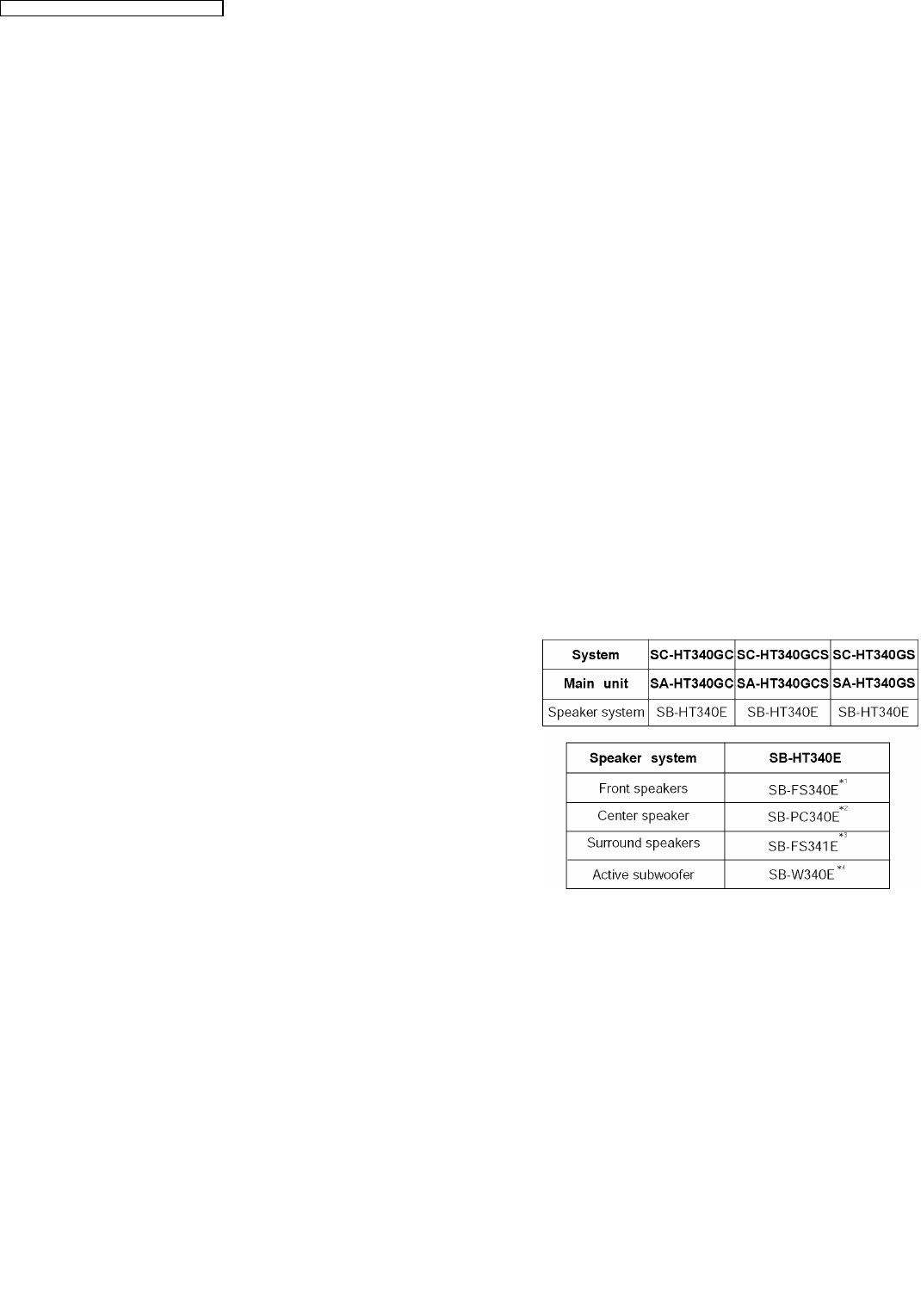
lGeneral
Power Source:
A
C 110V-240V, 50/ 60Hz
Power consumption: 90 W
Dimensions (W×H×D): 430×60×342 mm
Mass: 3kg
lAmplifier section
RMS Output Power: Dolby Digital Mode
lTotal RMS Dolby Digital
mode Power: 330 W
At 1kHz and total harmonic of 10%
lFront: 55 W/ Channel (5Ω)
lCenter: 55 W/ Channel (5Ω)
lSurround: 55 W/ Channel (5Ω)
At 100Hz and total harmonic of 10%
lActive subwoofers: 55 W/ Channel (5Ω)
PMPO Output Power: 2800W
DIN Output Power: Dolby Digital Mode:
lTotal DIN Dolby Digital mode Power:
150 W
At 1kHz and total harmonic of 1%
lFront: 25 W/ Channel (5Ω)
lCenter: 25 W/ Channel (5Ω)
lSurround: 25 W/ Channel (5Ω)
At 100Hz and total harmonic of 1%
©2006 Panasonic AVC Networks Singapore Pte.
Ltd. All rights reserved. Unauthorized copying and
distribution is a violation of law.
SA-HT340GC
SA-HT340GCS
SA-HT340GS
Colour
(S).......................Silver Type
lSubwoofer: 25 W/ Channel (5Ω)
lFM tuner section (FM)
Preset Memory: FM 15 stations
AM/MW 15 stations
Frequency Range: 87.5-108.00MHz
(50kHz step)
Sensitivity: 1.8µV (IHF)
S/N 26dB 1.4µV
Antenna Terminals: 75Ω(unbalanced)
lAM tuner section (AM/MW)
Frequency Range: 522-1629kHz (9kHz step)
520-1630kHz (10kHz step)
AM Sensitivity S/N 20dB at
999kHz: 560µV/m
lMic jack:
Sensitivity: 0.7mV (1.2kΩ)
Terminal: Mono 6.3mm jack (1 system)
lDisc section
Discs played (8 cm or 12 cm):
(1) DVD [DVD-Video, DivX(*6,7)]
(2) DVD-RAM [DVD-VR, MP3(*2,7), JPEG(*4,7), MPEG4(*5,7),
DivX(*6,7)]
(3) DVD-R [DVD-Video, DVD-VR, MP3(*2,7), JPEG(*4,7),
MPEG4(*5,7), DivX(*6,7)]
(4) DVD-R DL [DVD-Video, DVD-VR]
DVD Home Theater Sound System
Specifications
ORDER NO.MD0605178C3
(5) DVD-RW [DVD-Video, DVD-VR, MP3(*2,7), JPEG(*4,7),
MPEG4(*5,7), DivX(*6,7)]
(6) +R/RW [Video]
(7) +R DL [Video]
(8) CD, CD-R/RW [CD-DA, Video CD, SVCD(*1), MP3(*2,7),
WMA(*3,7), JPEG(*4,7), MPEG4(*5,7), DivX (*6,7), HighMAT
Level 2 (Audio and Image)]
*1 Conforming to IEC62107
*2 MPEG-1 Layer 3, MPEG-2 Layer 3
*3 Windows Media Audio Ver.9.0 L3
lNot compatible with Multiple Bit Rate (MBR)
*4 Exif Ver 2.1 JPEG Baseline files
lPicture resolution: between 160 x 120 and 6144 x 4096
pixels (Sub sampling is 4:0:0, 4:2:0, 4:2:2, 4:4:4). Extremely
long and narrow pictures may not be displayed.
*5 MPEG4 data recorded with Panasonic SD multi cameras or
DVD video recorders.
lConforming to SD VIDEO specifications (ASF standard)/
MPEG4 (Simple Profile) video system/G.726 audio system.
*6 Plays all versions of DivX® video (including DivX® 6) with
standard playback of DivX® media files. Certified to the DivX
Home Theater Profile.
lGMC (Global Motion Compensation) is not supported.
*7 The total combined maximum number of recognizable audio,
picture and video contents and groups: 4000 audio, picture
and video contents and 400 groups.
Pick up:
Wavelength:
lCD: 785nm
lDVD: 662nm
Laser power:
lCD: CLASS 1M
lDVD: CLASS 1
Audio output (DISC):
Number of channels: 5.1 ch (FL, FR, C, SL, SR,
SW)
Audio performance:
Frequency response:
DVD (linear audio): 4 Hz-22 kHz (48 kHz sampling)
4 Hz-44 kHz (96 kHz sampling)
CD-Audio: 4 Hz-20 kHz
S/N ratio:
CD-Audio: 105 dB
Dynamic range:
DVD (linear audio): 95 dB
CD-Audio: 95 dB
Total harmonic distortion:
CD-Audio: 0.005 %
lVideo section
V
ideo system:
Signal system: PAL 625/50, PAL 525/60,
NTSC
Composite video output:
Output level: 1 Vp-p (75 Ω)
Terminal: Pin jack (1 system)
S-video output:
Y
output level: 1 Vp-p (75 Ω)
C output level: PAL; 0.3Vp-p (75Ω)
NTSC; 0.286 Vp-p (75 Ω)
Terminal S terminal (1 system)
Component video output: [NTSC: 480p/480i, PAL:576p/576i]
Y
output level: 1.7 Vp-p (75 Ω)
PBoutput level: 0.7 Vp-p (75 Ω)
PRoutput level: 0.7 Vp-p (75 Ω)
Terminal: Pin jack (Y: green, PB: blue,
PR: red) (1 system)
Power consumption in standby mode:
approx 1W
Note:
1. Specifications are subject to change without notice.
Mass and dimensions are approximate.
2. Total harmonic distortion is measured by the digital spectrum
analyzer.
Solder:
This model uses lead free solder (PbF).
Mechanism:
This model uses DL2SU (Single tray) mechanism.
Power supply:
This model uses Switching Mode Power Supply (SMPS)
Module for power-up unit.
Refer to the original service manual for *1, *2, *3, *4.
2
SA-HT340GC / SA-HT340GCS / SA-HT340GS
3
SA-HT340GC / SA-HT340GCS / SA-HT340GS
1 Safety Precautions 6
1.1. GENERAL GUIDELINES 6
1.2. Before Repair and Adjustment (Using SMPS) 6
1.3. Protection Circuitry 6
1.4. Caution for AC Cord (For GS only) 7
2 Prevention of Electro Static Discharge (ESD) to
Electrostatically Sensitive (ES) Devices 8
3 Precaution of Laser Diode 9
4 About Lead Free Solder (PbF) 10
4.1. Service caution based on legal restrictions 10
5 Handling Precautions for Traverse Unit 11
5.1. Cautions to Be Taken in Handling the Optical Pickup Unit
11
5.2. Grounding for electrostatic breakdown prevention 11
6 Accessories 13
7 Operation Procedures 14
7.1. Remote Control Keys Operation 14
7.2. Main Unit Keys Operation 15
7.3. Disc information 16
7.4. About DivX VOD Content 18
8 Self-Diagnosis and special mode setting 19
8.1. Service Mode Summary Table 19
8.2. Service Mode Table 19
8.3. DVD Self Diagnostic Function-Error Code 24
8.4. Sales Demonstration Lock Function 26
8.5. Service Precautions 27
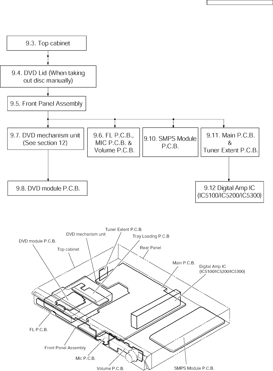
9 Assembling and Disassembling 28
9.1. Disassembly Flow Chart 29
9.2. Main Components and P.C.B. Locations 29
9.3. Disassembly of Top Cabinet 30
9.4. Disassembly of the DVD Lid (When taking out disc
manually) 30
9.5. Disassembly of Front Panel Assembly 31
9.6. Disassembly of FL P.C.B., Mic P.C.B. & Volume P.C.B.
31
9.7. Disassembly of DVD Mechanism Unit 32
9.8. Disassembly of DVD Module P.C.B. 32
9.9. Disassembly of Rear panel 33
9.10. Disassembly of SMPS Module P.C.B. 33
9.11. Disassembly of Main P.C.B. & Tuner Extent P.C.B. 33
9.12. Disassembly of Digital Amp IC (IC5100/IC5200/IC5300)
34
10 Service Position 35
10.1. Servicing position of the DVD Module P.C.B. 35
10.2. Servicing position of the Main P.C.B. 35
10.3. Servicing position of the SMPS Module P.C.B. 35
11 Assembly and disassembly of Mechanism Unit 36
11.1. Disassembly Procedure 36
12 Measurements and Adjustments 42
12.1. Service Tools and Equipment 42
12.2. Important points in adjustment 42
12.3. Storing and handling of test discs 42
12.4. Optical adjustment 43
13 Abbreviations 44
14 Voltage and Waveform Chart 46
14.1. DVD Module P.C.B. 46
14.2. Main P.C.B. 47
14.3. FL P.C.B., Mic P.C.B. & Tray Loading P.C.B. 48
14.4. SMPS Module P.C.B. 48
14.5. Waveform Chart 49
15 Illustration of IC's, Transistors and Diodes 51
16 Wiring Connection Diagram 52
17 Block Diagram 54
18 Schematic Notes 60
19 Schematic Diagram 62
19.1. (A) DVD Module (DV3.2) Circuit 62
19.2. (B) Main, FL, Volume & Mic Circuit 66
19.3. (C) Tray Loading & Tuner Extent Circuit 72
20 Printed Circuit Board 74
20.1. (A) DVD Module P.C.B. 74
20.2. (B) Main P.C.B. 75
20.3. (C) FL, Volume, Mic, Tray Loading & Tuner Extent P.C.B.
76
21 Basic Troubleshooting Guide 78
21.1. Basic Troubleshooting Guide for Traverse Unit (DVD
Module P.C.B.) 78
21.2. Troubleshooting Guide for Power section (Power circuit)
78
22 Overall Block (HT340) 79
22.1. HT340 DVD Unit Block 80
22.2. HT340 Block (Analog Signal : DVD 5.1ch Play Back
Mode) 81
22.3. HT340 Block (Analog Signal : 2ch Analog Input Mode) 82
22.4. HT340 Power Supply Block 83
22.5. HT340 Power (Main) Block 84
23 Terminal Function of ICs 85
23.1. IC2018 (C2CBYY000194): System Control
Microprocessor IC 85
24 Exploded Views 86
24.1. Cabinet Parts Location 86
24.2. Packaging 88
25 Replacement Parts List 89
25.1. Component Parts List 90
CONTENTS
Page Page
4
SA-HT340GC / SA-HT340GCS / SA-HT340GS

5
SA-HT340GC / SA-HT340GCS / SA-HT340GS
1 Safety Precautions
1.1. GENERAL GUIDELINES
1. When servicing, observe the original lead dress. If a short circuit is found, replace all parts which have been overheated or
damaged by the short circuit.
2. After servicing, see to it that all the protective devices such as insulation barriers, insulation papers shields are properly
installed.
3. After servicing, carry out the following leakage current checks to prevent the customer from being exposed to shock hazards.
1.1.1. LEAKAGE CURRENT COLD CHECK
1. Unplug the AC cord and connect a jumper between the two prongs on the plug.
2. Measure the resistance value, with an ohmmeter, between the jumpered AC plug and each exposed metallic cabinet part on
the equipment such as screwheads, connectors, control shafts, etc. When the exposed metallic part has a return path to the
chassis, the reading should be between 1MΩand 5.2MΩ.
When the exposed metal does not have a return path to the chassis, the reading must be .
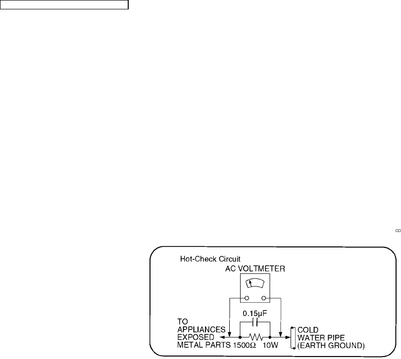
Figure 1
1.1.2. LEAKAGE CURRENT HOT CHECK (See Figure 1.)
1. Plug the AC cord directly into the AC outlet. Do not use an isolation transformer for this check.
2. Connect a 1.5kΩ, 10 watts resistor, in parallel with a 0.15µF capacitors, between each exposed metallic part on the set and a
good earth ground such as a water pipe, as shown in Figure 1.
3. Use an AC voltmeter, with 1000 ohms/volt or more sensitivity, to measure the potential across the resistor.
4. Check each exposed metallic part, and measure the voltage at each point.
5. Reverse the AC plug in the AC outlet and repeat each of the above measurements.
6. The potential at any point should not exceed 0.75 volts RMS. A leakage current tester (Simpson Model 229 or equivalent) may
be used to make the hot checks, leakage current must not exceed 1/2 milliamp. In case a measurement is outside of the limits
specified, there is a possibility of a shock hazard, and the equipment should be repaired and rechecked before it is returned to
the customer.
1.2. Before Repair and Adjustment (Using SMPS)
This model uses Switching Mode Power Supply (SMPS) Module to provide the neccessary voltages for the unit.
DO NOT SHORT-CIRCUIT DIRECTLY (with a screwdriver blade, for instance), as this may destroy solid state devices.
After repairs are completed, restore power gradually using a variac, to avoid overcurrent.
Current consumption at AC 100/ 110V, 50/ 60 Hz in NO SIGNAL mode volume minimal should be ~ 650 mA.
Current consumption at AC 230V~240V, 50 Hz in NO SIGNAL mode volume minimal should be ~ 650 mA.
1.3. Protection Circuitry
The protection circuitry may have operated if either of the following conditions are noticed:
·
No sound is heard when the power is turned on.
·
Sound stops during a performance.
The function of this circuitry is to prevent circuitry damage if, for example, the positive and negative speaker connection wires are
“shorted”, or if speaker systems with an impedance less than the indicated rated impedance of the amplifier are used.
6
SA-HT340GC / SA-HT340GCS / SA-HT340GS
If this occurs, follow the procedure outlines below:
1. Turn off the power.
2. Determine the cause of the problem and correct it.
3. Turn on the power once again after one minute.
Note:
When the protection circuitry functions, the unit will not operate unless the power is first turned off and then on again.
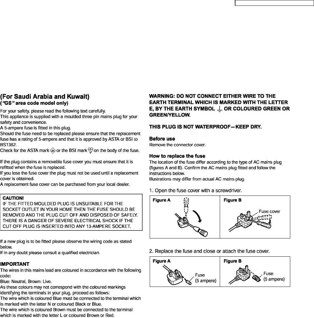
1.4. Caution for AC Cord (For GS only)
7
SA-HT340GC / SA-HT340GCS / SA-HT340GS
2 Prevention of Electro Static Discharge (ESD) to
Electrostatically Sensitive (ES) Devices
Some semiconductor (solid state) devices can be damaged easily by static electricity. Such components commonly are called
Electrostatically Sensitive (ES) Devices. Examples of typical ES devices are integrated circuits and some field-effect transistors and
semiconductor "chip" components. The following techniques should be used to help reduce the incidence of component damage
caused by electro static discharge (ESD).
1. Immediately before handling any semiconductor component or semiconductor-equipped assembly, drain off any ESD on your
body by touching a known earth ground. Alternatively, obtain and wear a commercially available discharging ESD wrist strap,
which should be removed for potential shock reasons prior to applying power to the unit under test.
2. After removing an electrical assembly equipped with ES devices, place the assembly on a conductive surface such as
aluminum foil, to prevent electrostatic charge buildup or exposure of the assembly.
3. Use only a grounded-tip soldering iron to solder or unsolder ES devices.
4. Use only an anti-static solder removal device. Some solder removal devices not classified as "anti-static (ESD protected)" can
generate electrical charge sufficient to damage ES devices.
5. Do not use freon-propelled chemicals. These can generate electrical charges sufficient to damage ES devices.
6. Do not remove a replacement ES device from its protective package until immediately before you are ready to install it. (Most
replacement ES devices are packaged with leads electrically shorted together by conductive foam, aluminum foil or comparable
conductive material).
7. Immediately before removing the protective material from the leads of a replacement ES device, touch the protective material
to the chassis or circuit assembly into which the device will be installed.
Caution
Be sure no power is applied to the chassis or circuit, and observe all other safety precautions.
8. Minimize bodily motions when handling unpackaged replacement ES devices. (Otherwise harmless motion such as the
brushing together of your clothes fabric or the lifting of your foot from a carpeted floor can generate static electricity (ESD)
sufficient to damage an ES device).
8
SA-HT340GC / SA-HT340GCS / SA-HT340GS
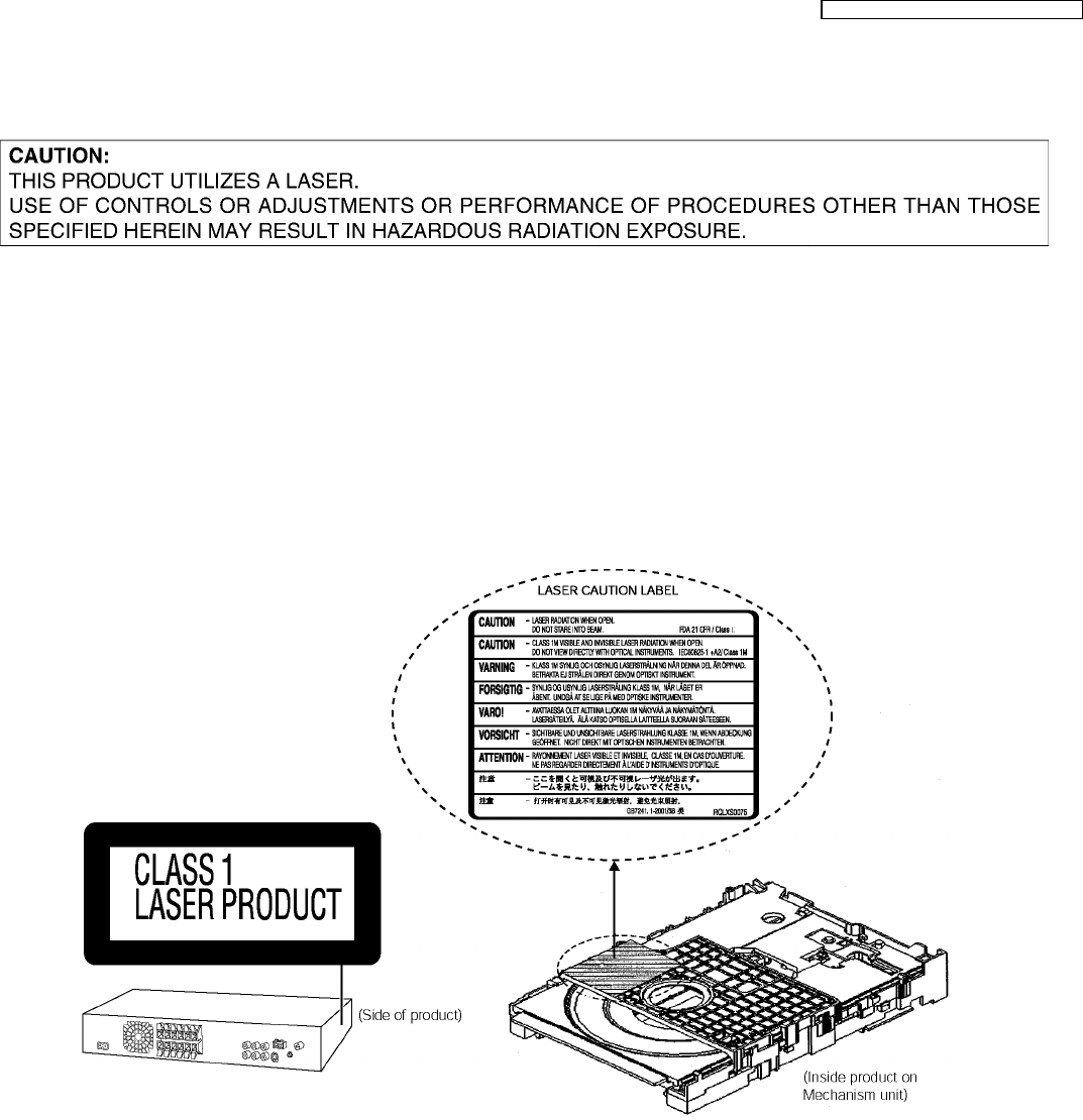
3 Precaution of Laser Diode
CAUTION :
This product utilizers a class 1 laser. Invisible laser radiation is emitted from the optical pick up lens.
When the unit is turned on:
Wavelength : 658nm/780nm
Maximum output radiation power from pick up : 100µW/VDE
Laser radiation from pick up unit is safety level, but be sure the followings:
1. Do not disassemble the optical pick up unit, since radiation from exposed laser diode is dangerous.
2. Do not adjust the variable resistor on the pick up unit. It was already adjusted.
3. Do not look at the focus lens using optical instruments.
4. Recommend not to look at pick up lens for a long time.
9
SA-HT340GC / SA-HT340GCS / SA-HT340GS

4 About Lead Free Solder (PbF)
4.1. Service caution based on legal restrictions
4.1.1. General description about Lead Free Solder (PbF)
The lead free solder has been used in the mounting process of all electrical components on the printed circuit boards used for this
equipment in considering the globally environmental conservation.
The normal solder is the alloy of tin (Sn) and lead (Pb). On the other hand, the lead free solder is the alloy mainly consists of tin
(Sn), silver (Ag) and Copper (Cu), and the melting point of the lead free solder is higher approx.30 degrees C (86°F) more than that
of the normal solder.
Definition of PCB Lead Free Solder being used
The letter of “PbF” is printed either foil side or components side on the PCB using the lead free solder.
(See right figure)
Service caution for repair work using Lead Free Solder (PbF)
·
The lead free solder has to be used when repairing the equipment for which the lead free solder is used.
(Definition: The letter of “PbF” is printed on the PCB using the lead free solder.)
·
To put lead free solder, it should be well molten and mixed with the original lead free solder.
·
Remove the remaining lead free solder on the PCB cleanly for soldering of the new IC.
·
Since the melting point of the lead free solder is higher than that of the normal lead solder, it takes the longer time to melt
the lead free solder.
·
Use the soldering iron (more than 70W) equipped with the temperature control after setting the temperature at 350±30
degrees C (662±86°F).
Recommended Lead Free Solder (Service Parts Route.)
·
The following 3 types of lead free solder are available through the service parts route.
RFKZ03D01K-----------(0.3mm 100g Reel)
RFKZ06D01K-----------(0.6mm 100g Reel)
RFKZ10D01K-----------(1.0mm 100g Reel)
Note
* Ingredient: tin (Sn), 96.5%, silver (Ag) 3.0%, Copper (Cu) 0.5%, Cobalt (Co) / Germanium (Ge) 0.1 to 0.3%
10
SA-HT340GC / SA-HT340GCS / SA-HT340GS
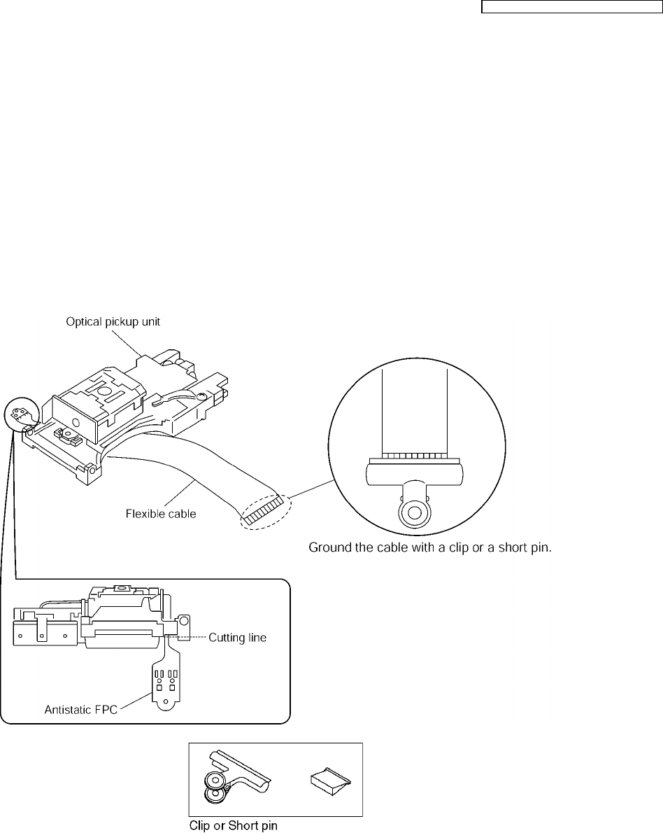
5 Handling Precautions for Traverse Unit
The laser diode in the optical pickup unit may break down due to static electricity of clothes or human body. Special care must be
taken avoid caution to electrostatic breakdown when servicing and handling the laser diode.
5.1. Cautions to Be Taken in Handling the Optical Pickup Unit
The laser diode in the optical pickup unit may be damaged due to electrostatic discharge generating from clothes or human body.
Special care must be taken avoid caution to electrostatic discharge damage when servicing the laser diode.
1. Do not give a considerable shock to the optical pickup unit as it has an extremely high-precise structure.
2. To prevent the laser diode from the electrostatic discharge damage, the flexible cable of the optical pickup unit removed should
be short-circuited with a short pin or a clip.
3. The flexible cable may be cut off if an excessive force is applied to it. Use caution when handling the flexible cable.
4. The antistatic FPC is connected to the new optical pickup unit. After replacing the optical pickup unit and connecting the flexible
cable, cut off the antistatic FPC.
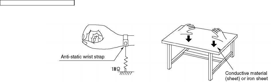
5.2. Grounding for electrostatic breakdown prevention
Some devices such as the DVD player use the optical pickup (laser diode) and the optical pickup will be damaged by static
electricity in the working environment. Proceed servicing works under the working environment where grounding works is
completed.
5.2.1. Worktable grounding
1. Put a conductive material (sheet) or iron sheet on the area where the optical pickup is placed, and ground the sheet.
5.2.2. Human body grounding
1. Use the anti-static wrist strap to discharge the static electricity form your body.
11
SA-HT340GC / SA-HT340GCS / SA-HT340GS
12
SA-HT340GC / SA-HT340GCS / SA-HT340GS
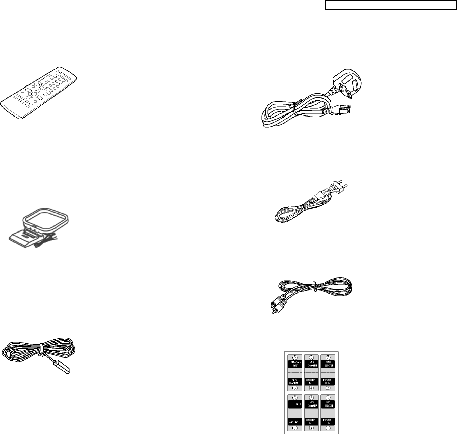
Remote control
AM loop antenna
FM indoor antenna
AC cord
(For GS only)
AC cord
(For GCS/GC)
Video cable
Speaker label
6 Accessories
13
SA-HT340GC / SA-HT340GCS / SA-HT340GS
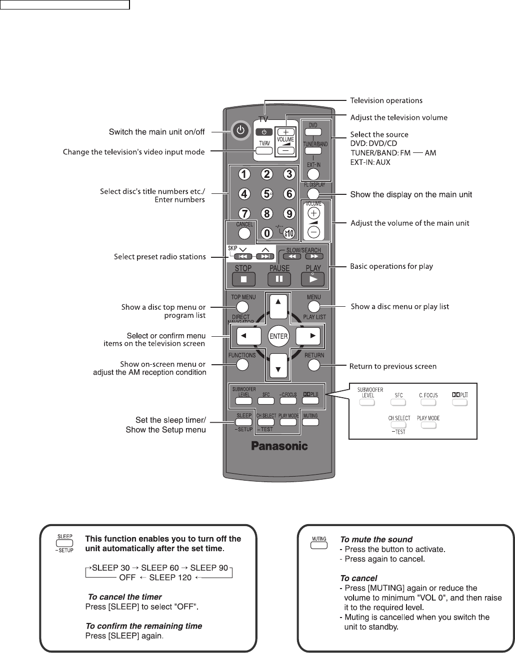
7 Operation Procedures
7.1. Remote Control Keys Operation
< >
14
SA-HT340GC / SA-HT340GCS / SA-HT340GS
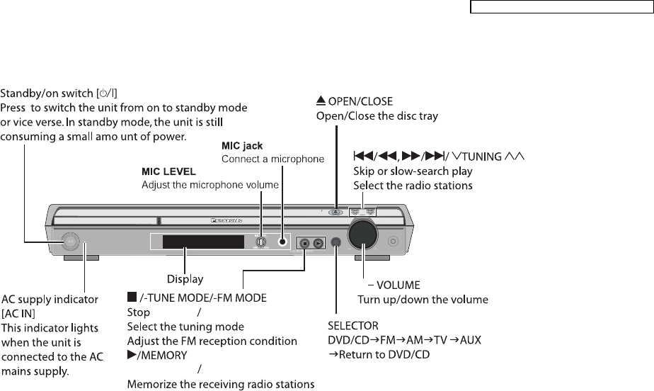
7.2. Main Unit Keys Operation
playback
Disc playback
Disc
playback
+,
SELECTOR
MEMORY
TUNING
VOLUME
AC IN
OPEN CLOSE
15
SA-HT340GC / SA-HT340GCS / SA-HT340GS
7.3. Disc information
7.3.1. DISC playability (Media)
16
SA-HT340GC / SA-HT340GCS / SA-HT340GS
7.3.2. File Extension Type Support (WMA/MP3/JPEG/MPEG4/DivX)
Tips for making data discs
DVD-RAM
Discs must conform to UDF 2.0.
DVD-R/RW
When there are more than eight groups, the eighth group onwards will be displayed on one vertical line in the menu
screen.
There may be differences in the display order on the menu screen and computer sc reen.
This unit cannot play les recorded using packet write.
fi
Discs must conform to UDF bridge (UDF 1.02/ISO9660).
This unit does not support multi-session. Only the default session is played.
CD-R/RW
Discs must conform to ISO9660 level 1 or 2 (except for extended formats).
This unit supports multi-session but if there are many sessions it takes more time for play to start. Keep the number of
sessions to a minimum to avoid this.
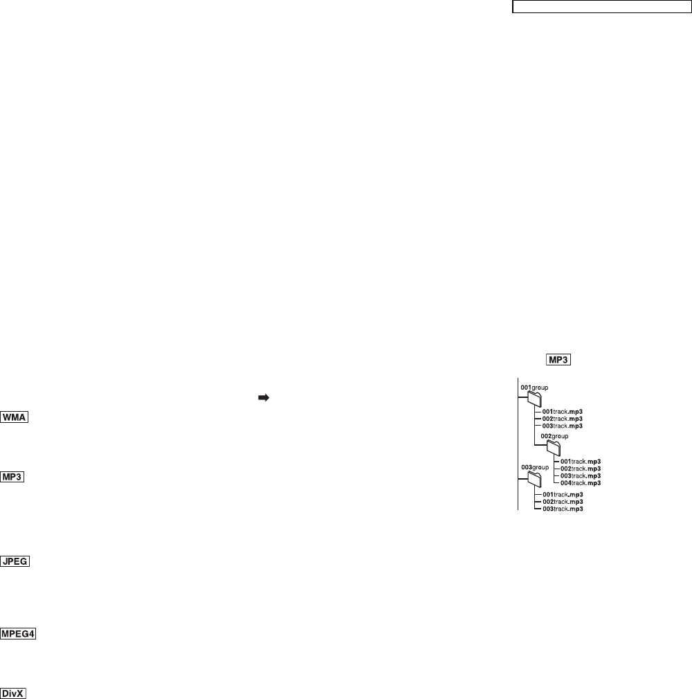
Naming folders and files
Files are treated as contents and folders are treated as groups on this unit.
(Extension: “.WMA” or “.wma”)
(Extension: “.MP3” or “.mp3”)
Example:
root
Compatible compression rate: between 32 kbps and 320 kbps.
This unit does not support ID3 tags.
Compatible sampling rates:
– DVD-RAM, DVD-R/RW: 11.02, 12, 22.05, 24, 44.1 and 48 kHz
– CD-R/RW: 8, 11.02, 12, 16, 22.05, 24, 32, 44.1 and 48 kHz
(Extension: “.JPG”, “.jpg”, “.JPEG” or “.jpeg”)
(Extension: “.ASF” or “.asf”)
(Extension: “.DIVX”, “.divx”, “.AVI” or “.avi”)
Compatible compression rate: between 48 kbps and 320 kbps.
You cannot play WMA les that are copy protected.
This unit does not support Multiple Bit Rate (MBR).
fi
JPEG
les taken on a digital camera that conform to DCF Standard (Design rule for Camera File system) Version 1.0 are
displayed. Files that have been altered, edited or saved with computer picture editing software may not be displayed.
This unit cannot display moving pictures, MOTION JPEG and other such formats, and still pictures other than JPEG
(Example: TIFF), or play pictures with attached audio.
fi
You can play all versions of DivX
®
video (including DivX
®
6) [DivX video system/MP3, Dolby Digital or MPEG audio
system] with standard playback of DivX
®
media les. Functions added with DivX Ultra are not supported.
GMC (Global Motion Compensation) is not supported.
DivX les greater than 2 GB or have no index may not be played properly on this unit.
This unit supports all resolutions up to maximum of 720 x 480 (NTSC)/720 x 576 (PAL).
You can select up to eight types of audio and subtitles on this unit.
fi
fi
You can play MPEG4 data [conforming to SD VIDEO speci cations (ASF standard)/MPEG4 (Simple Pro le) video
system/G.726 audio system] recorded with Panasonic SD multi cameras or DVD video recorders with this unit.
The recording date may differ from that of the actual date.
fi fi
At the time of recording, pre x folder and le names. This should be with numbers that have
an equal number of digits, and should be done in the order you want to play them (this may
not work at times). Files must have the extension ( see below).
fi fi
17
SA-HT340GC / SA-HT340GCS / SA-HT340GS
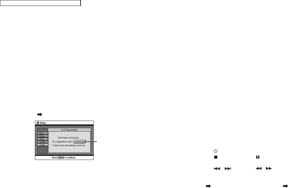
7.4. About DivX VOD Content
About DivX VOD content
DivX Video-on-Demand (VOD) content is encrypted for
copyright protection. In order to play DivX VOD content on
this unit, you rst need to register the unit.
Follow the online instructions f
fi
or purchasing DivX VOD
content to enter the unit’s registration code and register
the unit. For more information about DivX VOD, visit
www.divx.com/vod.
( Refer to OI page 23, “DivX Registration” in “Others” tab)
8 alphanumeric
characters
If you purchase DivX VOD content using a
registration code different from this unit’s code, you
will not be able to play this content. (“Authorization
Error” is displayed.)
Regarding DivX content that can only be
played a set number of times
Some DivX VOD content can only be played a set
number of times. When you play this content, the
remaining number of plays is displayed. You cannot
play this content when the number of remaining plays
is zero. (“Rented Movie Expired” or “Rental Expired” is
displayed.)
When playing this content
The number of remaining plays is reduced by one if
– you press [ ] or press and hold [–SETUP].
– you press [ , STOP]. (Press [ , PAUSE] to pause
play.)
– you press [
,
] (skip) or [
,
] (slow/search)
etc. and arrive at another content or the start of the
content being played.
Resume ( OI page 15, Stop) and Marker ( OI page 20,
Play Menu) functions do not work.
Display the unit’s registration code
We recommend that you make a note of this code for
future reference.
After playing DivX VOD content for the rst time,
another registration code is then displayed in “DivX
Registration”. Do not use this registration code to
purchase DivX VOD content. If you use this code
to purchase DivX VOD content, and then play the
content on this unit, you will no longer be able to play
any content that you purchased using the previous
code.
fi
18
SA-HT340GC / SA-HT340GCS / SA-HT340GS
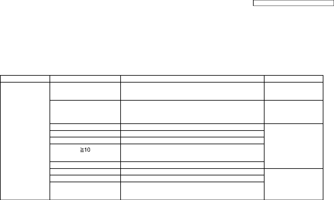
8 Self-Diagnosis and special mode setting
8.1. Service Mode Summary Table
The service modes can be activated by pressing various button combination on the player and remote control unit.
Below is the summary of major checking:
Player buttons Remote control unit buttons Application Note
STOP 0 Error code display (Refer to the section,
“8.3 DVD Self Diagnostic
Function-Error Code”).
5Jitter checking (Refer to the section
“8.2.1. Service Mode
Table 1” for more
information).
6Region display and mode (Refer to the section
“8.2.2. Service Mode
Table 2” for more
information).
7Micro-processor firmware version check
8DVD module firmware version check.
Initialization of the player (factory setting is restored.)
Used after replacement of micro-computer, FLASH ROM IC,
EEPROM and HDMI module.
ENTER DVD module reset (During initialisation)
FUNCTIONS DVD laser drive current check (Refer to the item “8.2.4.
Optical Pick-up Self-
Diagnosis”).
3 CD laser drive current check
PAUSE Writing of laser drive current value after replacement of optical
pickup (Do use this function only when optical pickup is
replaced.)
8.2. Service Mode Table
By pressing various button combinations on the player and remote control unit can activate the various service modes for checking.
Special Note:
Due to the limitations of the no. characters that can be shown on FL Display, the “FL Display” button on the remote control uni
is used to show the following page. (Display 1/Display 2).
19
SA-HT340GC / SA-HT340GCS / SA-HT340GS
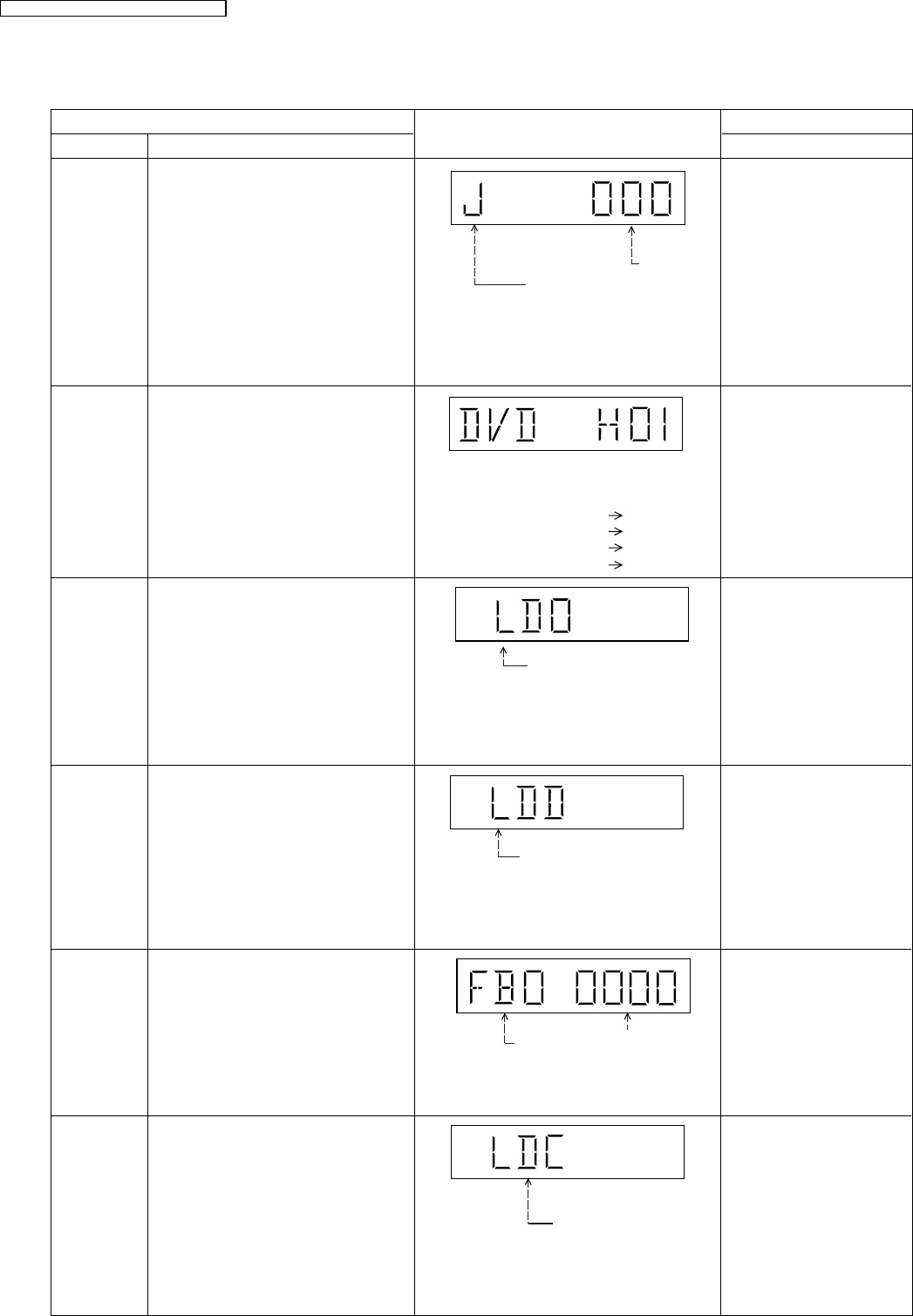
8.2.1. Service Mode Table 1
FL Display Key Operation
Front Key
Item
Jitter check mode
Press STOP or PLAY
button.
Jitter check
Description
Mode Name
Initial setting
of laser drive
current
DVD laser
drive current
measurement
ADSC internal
RAM data
check
Error code
check
Cancelled automatically
5 seconds later.
To exit, press [POWER]
button on main unit or
remote control.
Press "FL Display" on
remote control unit for next
page (FL Display) on values
of laser drive current.
Press "FL Display" on
remote control unit for next
page (FL Display) on values
of dvd drive current.
Press "FL Display" on
remote control unit for next
page. (FL Display)
Cancelled automatically
5 seconds later.
Cancelled automatically
5 seconds later.
Cancelled automatically
5 seconds later.
RAM data for
specified address
Address
CD laser drive
current
measurement
Press STOP or OPEN
button to exit.
In STOP (no disc) mode,
press STOP button on the
player, and "5" button on
the remote control unit.
Jitter check
Jitter rate is measured and displayed.
Measurement is repeatedly done in
the cycle of one second. Read error
counter starts from zero upon mode
setting. When target block data failed
to be read out, the counter advances
by one increment. When the failure is
caused by minor error, it may be
corrected when retried to enable
successful reading. In this case, the
counter advances by one. When the
error persists even after retry, the
counter may jump by two or more.
Jitter rate is shown in decimal notation to
one place of decimal.
Focus drive value is shown in hexadecimal
notation.
In STOP (no disc) mode,
press STOP button on the
player, and "0" button on the
remote control unit. * With
pointing of cursor up and
down on display.
Error code check
The latest error code stored in the
EEPROM IC is displayed.
Error code (play_err) is expressed in the
following convention.
Error code = 0 x DAXX is expressed: DVDnn UXX
Error code = 0 x DBXX is expressed: DVDnn HXX
Error code = 0 x DXXX is expressed: DVDnn FXXX
Error code = 0 x 0000 is expressed: DVDnn F---
* "xx" denotes the error code
In STOP (no disc) mode,
press STOP button on the
player, and PAUSE button
on the remote control unit.
Initial setting of laser drive current.
Initial current value for each of DVD
laser and CD laser is separately saved
in the EEPROM IC.
The value denotes the current in decimal
notation. The above example shows the
initial current is 34mA and 28mA for DVD
laser and CD laser respectively when the
laser is switched on.
In STOP (no disc) mode,
press STOP button on the
player, and FUNCTIONS
button on the remote
control unit.
DVD laser drive current measurement
·DVD laser drive current is measured
and the result is displayed together
with the initial value stored in the
EEPROM IC.
After the measurement, DVD laser
emission is kept on. It is turned off
when POWER key is switched off. (It
is also turned off when POWER button
on the player is switched off.)
In STOP (no disc) mode,
press STOP button on the
player, and "1" button on
the remote control unit.
ADSC internal RAM data check
·ADSC internal RAM data is read out
and displayed.
Laser current measurement
mode
DVD laser current
measurement mode
The value denotes the current in decimal
notation.
The above example shows the initial current
is 34mA and the measured value is 32mA.
The value is shown in hexadecimal
notation. The above example shows the
data in ADSC address OFAh is 6901h.
In STOP (no disc) mode,
press STOP button on the
player, and "3" button on
the remote control unit.
CD laser drive current measurement
CD laser drive current is measured
and the result is displayed together
with the initial value stored in the
EEPROM IC.
After the measurement, CD laser
emission is kept on. It is turned off
when POWER key is switched off. (It
is also turned off when POWER button
on the player is switched off.)
CD laser current
measurement mode
The value denotes the current in decimal
notation.
The above example shows the initial current
is 28mA and the measured value is 26mA.
Jitter rate Press "FL Display" on
remote control unit for next
page (FL Display).
20
SA-HT340GC / SA-HT340GCS / SA-HT340GS
8.2.2. Service Mode Table 2
Micro-processor firmware version
display & EEPROM checksum display.
EEPROM checksum is only available
due to existence of EEPROM IC.
(NO: NO EEPROM IC)
Micro-processor
firmware version
display &
EEPROM
checksum
display.
Initialization
Cancelled automatically
5 seconds later.
Cancelled automatically
5 seconds later.
In STOP (no disc)
mode, press STOP button
on the player, and "7"
button on the remote
control unit.
In STOP (no disc)
mode, press STOP button
on the player , and 10
button on the remote
control unit.
Initialization
User settings are cancelled and player
is initialized to factory setting.
Press "FL Display" button on
remote control unit for next
page. (FL Display)
Existence of
EEPROM
FL Display Key Operation
Front Key
Item
DescriptionMode Name
System controller
generation
Region
Region No.
N: noPAL / P: PAL
N: NTSC / 6: PAL60
Panel
controller
jumper
information
Cancelled automatically
5 seconds later.
Cancelled automatically
5 seconds later.
DVD module firmware version is
displayed on the FL Display.
Region display & mode
DVD module
firmware
version display
Region display In STOP (no disc)
mode, press STOP button
on the player, and "6"
button on the remote
control unit.
In STOP (no disc)
mode, press STOP button
on the player, and "8"
button on the remote
control unit.
Cancelled automatically
5 seconds later.
Displays frequency of communication
errors between system control IC and
mechanism control IC during DVD
module.
Communication
error display In STOP (no disc)
mode, press STOP button
on the player, and "MENU"
button on the remote
control unit.
Destination
System
controller
version
DVD Module
Reset To reset DVD Module.
Cancelled automatically
5 seconds later.
While in initialization
mode, press & hold STOP
button on player, follow by
"ENTER" button on the
remote control unit.
If EEPROM IC is present, the checksum
value will be displayed. It displays as
"NG" if the EEPROM IC installed is not
working properly.
The firmware version can be updated
using recovery disc.
This process is used when the DVD
module or flash ROM IC is replaced
with a new one.
(GC/GS)
(GCS)
(GC/GS)
(GCS)
21
SA-HT340GC / SA-HT340GCS / SA-HT340GS
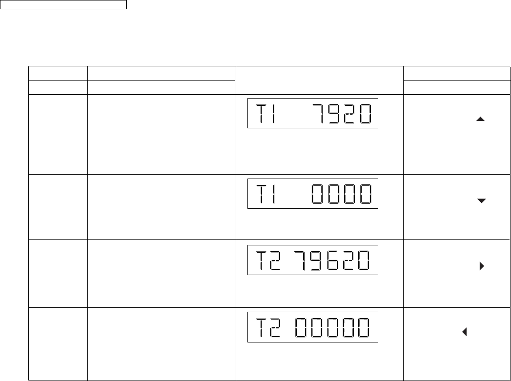
8.2.3. Service Mode Table 3
Timer 1 check
Cancelled automatically
5 seconds later.
Cancelled automatically
5 seconds later.
Cancelled automatically
5 seconds later.
Cancelled automatically
5 seconds later.
Timer 1 reset
Timer 2 check
Timer 2 reset
In STOP (no disc)
mode, press STOP button
on the player, and " "
button on the remote
control unit.
While displaying Timer 1
data, press STOP button
on the player, and " "
button on the remote
control unit.
In STOP (no disc)
mode, press STOP button
on the player, and " "
button on the remote
control unit.
While displaying Timer 2
data, press STOP button on
the player, and " " button
on the remote control unit.
Timer 1 check
Laser operation timer is measured
separately for DVD laser and CD laser.
Press "FL Display" button for next
page of FL Display
Press "FL Display" button for next
page of FL Display
Press "FL Display" button for next
page of FL Display
Timer 1 reset
Laser operation timer of both DVD
laser and CD laser is reset all at once.
Timer 2 check
Spindle motor operation timer
Timer 2 reset
Spindle motor operation timer
Shown to the left is DVD laser time, and to
the right is CD laser time.
Time is shown in 4 digits of decimal notation
in a unit of 10 hours.
"0000" will follow "9999".
Time is shown in 5 digits of decimal notation in
a unit of 10 hours.
"00000" will follow "99999".
FL Display Key Operation
Front Key
Item
Description
Mode Name
Shown to the left is DVD laser time, and to
the right is CD laser time.
It will clear to "0000" upon reset.
Time is shown in 5 digits of decimal notation in
a unit of 10 hours.
It will be cleared to "00000" upon activating
this.
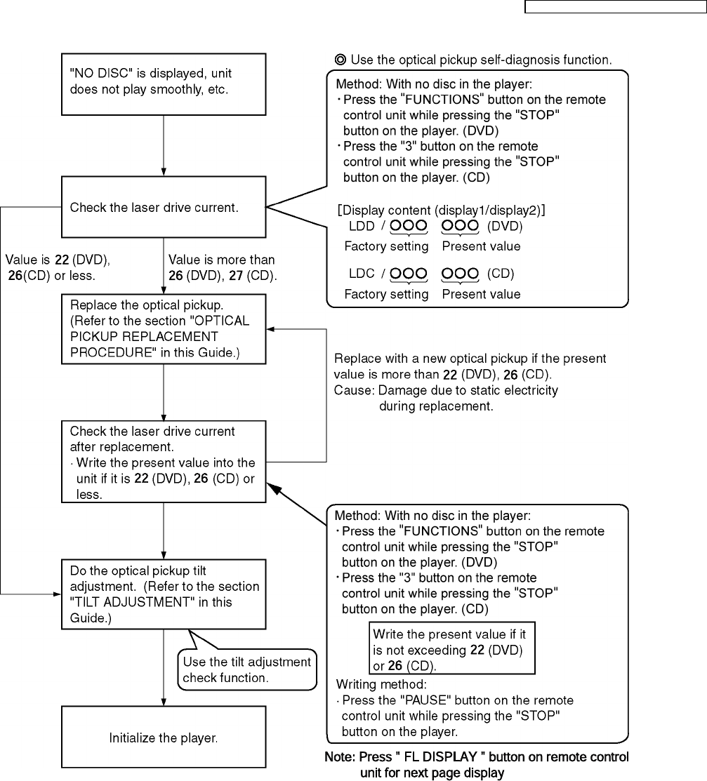
8.2.4. Optical Pick-up Self-Diagnosis
The optical pickup self-diagnosis function and tilt adjustment check function have been included in this unit. When repairing, use
the following procedure for effective self-diagnosis and tilt adjustment. Be sure to use the self-diagnosis function before replacing
the optical pickup when "NO DISC" is displayed. As a guideline, you should replace the optical pickup when the value of the laser
drive current is more than 55.
Note:
Press the power button to turn on the power, and check the value within three minutes before the unit warms up. (Otherwise,
the result will be incorrect.)
22
SA-HT340GC / SA-HT340GCS / SA-HT340GS
23
SA-HT340GC / SA-HT340GCS / SA-HT340GS
8.3. DVD Self Diagnostic Function-Error Code
8.3.1. Error Code Table 1
Error
Code
Diagnosis Contents Description of error Automatic FL Display Remarks
U11 Focus servo error Focus coil NG (OPU unit abnormal) Press [ nSTOP] on main
unit for next error.
H01 Tray loading error /
abnormality
The tray is not able to open Press [ nSTOP] on main
unit for next error
H02 Spindle servo error, DSC
disc motor error
(Spindle servo, DSC (IC8251) Spindle
motor, CLV servo error)
Press [ nSTOP] on main
unit for next error
H03 Traverse motor error (Traverse motor, IC8251) Press [ nSTOP] on main
unit for next error
H04 Tracking servo error Tracking coil NG (OPU unit abmormal) Press [ nSTOP] on main
unit for next error
H05 Seek timeout error Timeout of unit when seeking time is
reached
Press [ nSTOP] on main
unit for next error
H15 Disc tray open detection
switch (S9001) failure
The disc tray cannot be opened: it closes
spontaneously
Press [ nSTOP] on main
unit for next error
H16 Disc tray close detection
switch (S9001) failure
The disc tray cannot be closed: it opens
spontaneously
Press [ nSTOP] on main
unit for next error
F61 Power digital amp IC op &
DC output voltage
abnormal.
Upon power-on PCONT=High,
DCDET=Low
Press [ nSTOP] on main
unit for next error
F76 Power digital amp IC op &
DC output voltage
abnormal.
Speaker Jack shorted or amp circuit Press [ nSTOP] on main
unit for next error
F500 DSC error DSC (IC8251) stops in the occurrence of
servo error (startup, focus error, etc.)
Press [ nSTOP] on main
unit for next error
F501 DSC not Ready error DSC-system computer communication
error (Communication failure caused by
idling of DSC)
Press [ nSTOP] on main
unit for next error
F502 DSC Time out error Similar as F500 Press [ nSTOP] on main
unit for next error
F503 DSC communication
Failure
Communication error (result error
occurred although communication
command was sent)
Press [ nSTOP] on main
unit for next error
F504 Abnormal adjusting DSC
data slice offset
Press [ nSTOP] on main
unit for next error
F505 DSC Attention error Similar as F500 Press [ nSTOP] on main
unit for next error
24
SA-HT340GC / SA-HT340GCS / SA-HT340GS
8.3.2. Error Code Table 2
Error
Code
Diagnosis Contents Description of error Automatic FL Display Remarks
F506 Invalid media Disc is flipped over, TOC unreadable,
incompatible disc media
Press [ nSTOP] on main
unit for next error
F600 Access failure to
management information
caused by demodulation
error
Operation stopped because navigation
data is not accessible caused by the
demodulation defect
Press [ nSTOP] on main
unit for next error
F601 Indeterminate sector ID
requested
Operation stopped caused by the
request to access abnormal ID data
Press [ nSTOP] on main
unit for next error
F602 Access failure to LEAD-IN
caused by demodulation
error
LEAD IN data unreadable Press [ nSTOP] on main
unit for next error
F603 Access failure to KEYDET
caused by demodulation
error
Access failure to CSS data of disc Press [ nSTOP] on main
unit for next error
F610 ODC abnormality No permission for command execution Press [ nSTOP] on main
unit for next error
F611 No CRC OK for a specific
time (CD)
Access failure to seek address in CD
series
Press [ nSTOP] on main
unit for next error
F612 No CRC OK for a specific
time (DVD)
Access failure to ID data in DVD series Press [ nSTOP] on main
unit for next error
F620 Laser safeguard: high
temperature condition
High temperature of the laser guide unit
(OPU unit)
Press [ nSTOP] on main
unit for next error
F621 Laser safeguard: circuit
failure condition
Circuitry failure of the laser guide unit
(OPU unit)
Press [ nSTOP] on main
unit for next error
F103 Illegal highlight Position Big possibility of disc specification
violation during highlight display
Press [ nSTOP] on main
unit for next error
F4FF Force initialize failure (time
out)
Timeout when force initialization fails Press [ nSTOP] on main
unit for next error
F700 MBX overflow When replying message to disc manager Press [ nSTOP] on main
unit for next error
F701 Message command does
not end
Next message is sent before replying to
disc manager
Press [ nSTOP] on main
unit for next error
F702 Message command
changes
Message is changed before it is sent as
a reply to disc manager
Press [ nSTOP] on main
unit for next error
25
SA-HT340GC / SA-HT340GCS / SA-HT340GS
8.3.3. Error Code Table 3
Error
Code
Diagnosis Contents Description of error Automatic FL Display Remarks
F880 Task number is not
appropriate
Message coming from a non-existing
task
Press [ nSTOP] on main
unit for next error
F890 Sending message when
message is being sent to
AV task
Sending message to AV task Press [ nSTOP] on main
unit for next error
F891 Message couldn’t be sent
to AV task
Begin sending message to AV task Press [ nSTOP] on main
unit for next error
F893 FLASH ROM IC problem FLASH ROM IC installed is not operating
properly (Neccessary replacement of
FLASH ROM IC) or firmware problem
Press [ nSTOP] on main
unit for next error
F894 EEPROM abnormality EEPROM IC installed is not operating in
normal condition (EEPROM contains
neccessary data)
Press [ nSTOP] on main
unit for next error
F895 Region setting abnormality Firm version agreement check for factory
preset setting failure prevention. Check
region setting & re-initialize
Press [ nSTOP] on main
unit for next error
F896 No existence model Firm version agreement check for factory
preset setting failure prevention
Press [ nSTOP] on main
unit for next error
F897 Initialize is not completed Initialize completion check for factory
preset setting failure prevention
Press [ nSTOP] on main
unit for next error
F898 Disagreement of hardware
and software
Unsuitable combination of AV
DECORDER, SDRAM and FLASH ROM
(firmware)
Press [ nSTOP] on main
unit for next error
F8A0 Message command is not
appropriate
Begin sending message to AV task Press [ nSTOP] on main
unit for next error
Note:
An error code will be canceled if a power supply is turned OFF.
*1: CPPM is the copy guard function beforehand written in the disk for protection of copyrights.
*2: CEC is the consumer electronic control used for high-level user control of HDMI-connected devices.
*3: HDCP is the specification developed to control digital audio & video contents transmission for DVI or HDMI connections.
8.4. Sales Demonstration Lock Function
This function prevents discs from being lost when the unit is used for sales demonstrations by disabling the disc eject function.
"LOCKED" is displayed on the unit, and ordinary operation is disabled.
8.4.1. Setting
·
Prohibiting removal of disc
1. Select the DVD/CD function.
2. Press and hold down the button and the power button on the player for at least three seconds. (The message,
“___LOCKED_” appears when the function is activated.)
Note:
OPEN/CLOSE , DISC CHECK and DISC CHANGE buttons are invalid and the player displays “___LOCKED_” while
the lock function mode is entered.
·
Prohibiting operation of selector and disk
1. Select the DVD/CD function.
26
SA-HT340GC / SA-HT340GCS / SA-HT340GS

2. Press and hold down the button and the power button on the player for at least three seconds. (The message,
“___LOCKED_” appears when the function is activated.)
Note:
The following buttons are invalid and the player displays “___LOCKED_” while the lock function mode is entered.
Player , , , SELECTOR, , , VOLUME KNOB, DISC CHECK, DISC CHANGE, DISC1-DISC5
Remote
controller unit
SLEEP, REPEAT, 0~9, , RETURN, TOP MENU, , , , , , ,
POSITION MEMORY, TUNER/BAND, D.MIX, CH SELECT/ TEST, SET UP/ MUTING, DISPLAY, GROUP, TV, VCR/
AUX, QUICK REPLAY, SUBTITLE, FL DISPLAY, CH & VOLUME
8.4.2. Cancellation
The lock can be cancelled by the same procedure as used in setting. ("UNLOCK" is displayed on cancellation. Disconnecting the
power cable from power outlet does not cancel the lock.)
8.5. Service Precautions
8.5.1. Recovery after the DVD player is repaired
·
When the FLASH ROM IC or HDMI module P.C.B. is replaced, carry out the recovery processing to optimize the drive.
Playback the recovery disk to process the recovery automatically.
·
Recovery disc (Product number: RFKZD03R005) [SPG]
·
Performing recovery process
1. Load the recovery disc RFKZD03R005 on to the player and run it.
2. Recovery is performed automatically. When it is finished, a message appears on the screen.
3. Remove the recovery disc.
4. Turn off the power.
5. Initialize the player.
8.5.2. Firmware version-up of the DVD player
·
The firmware of the DVD player may be renewed to improve the quality including operability and playability to the substandard
discs.processing to optimize the drive.
The recovery disc has also firmware version-up.
·
After version-up, recovery processing is executed automatically.
·
Part number of the recovery disc for version-up will be noticed when it is supplied.
·
Updating firmware
1. Load the recovery disc on to the player and run it.
2. Firmware version of the player is automatically checked. Appropriate message appears whenever necessary.
3. Using remote controller´s cursor key, select whether version updating is to be done or not. (Selection of Yes/No)
4. a. If Yes is selected, version updating is performed.
b. If No is selected, only recovery is performed.
5. a. When updating is finished, remove the disc according to the message appearing on the screen.
b. Remove the disc according to the message appearing on the screen.
6. Turn off the power.
Note:
If the AC power supply is shut out during version-up due to a power failure, the version-up is improperly carried out.
In such a case, replace the FLASH ROM IC and carry out the version-up again.
8.5.3. DVD Module Reset
·
When after replacing Flash Rom IC or the DVD Module P.C.B., FL displays error code “ DVD F897”. This means the unit is not
initialized properly and the following process needs to be carry out.
·
Procedures:
1. Press on remote control while pressing “STOP” button on main unit. (To enter into initialization mode)
2. FL display show “INIT”
3. While still pressing “STOP” button on main unit, press “ENTER” on remote control. (To reset)
4. FL will display “RESET” before FL display will change to TOC reading again.
5. Power off unit. Unplug the AC cord.
6. Power on the unit. It should be no problem. If problem persist check on the DVD module P.C.B. or FLASH ROM IC.
27
SA-HT340GC / SA-HT340GCS / SA-HT340GS

Be careful when disassembling and servicing.
Some chassis components may have sharp edges.
Special Note:
lSMPS Module P.C.B. (SMPS) Replacement
9 Assembling and Disassembling
“ATTENTION SERVICER”
1. This section describes the disassembly procedures for all the major printed circuit boards and main components.
2. Before the disassembly process was carried out, do take special note that all safety precautions are to be carried out.
(Ensure that no AC power supply is connected during disassembling.)
3. For assembly after operation checks or replacement, reverse the respective procedures.
Special reassembly procedures are described only when required.
4. The Switch Regulator IC may have high temperature after prolonged use.
Use caution when removing the top cabinet and avoid touching heat sinks located in the unit.
5. Select items from the following index when checks or replacement are required.
·
Disassembly of Top Cabinet
·
Disassembly of DVD Lid (When taking out disc manually)
·
Disassembly of Front Panel
·
Disassembly of FL P.C.B., Mic P.C.B. & Volume P.C.B.
·
Disassembly of Mechanism Unit
·
Disassembly of DVD Module P.C.B.
·
Disassembly of Rear panel
·
Disassembly of SMPS Module P.C.B.
·
Disassembly of Main P.C.B. & Tuner Extent P.C.B.
·
Disassembly of Digital Amp IC (IC5100/IC5200/IC5300)
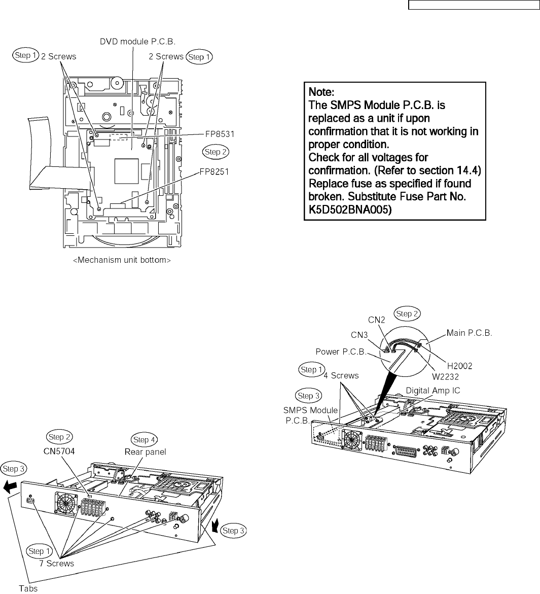
1. This model uses SMPS Module to provide the necessary voltages for the unit.
2. It is advisable to replace the SMPS Module once upon detecting of non-working conditions. Do not attempt to repair
or replace it by components.
3. Non-working conditions include:
lWith AC supply but no supply voltages after checking at CN2 and/or CN3 respectively.
lBroken fuse. (Substitute compatible part for fuse: K5D502BNA005)
lWire connection problem.
lNon-working parts in SMPS Module P.C.B. (Check components)
28
SA-HT340GC / SA-HT340GCS / SA-HT340GS
9.1. Disassembly Flow Chart
9.2. Main Components and P.C.B. Locations
29
SA-HT340GC / SA-HT340GCS / SA-HT340GS
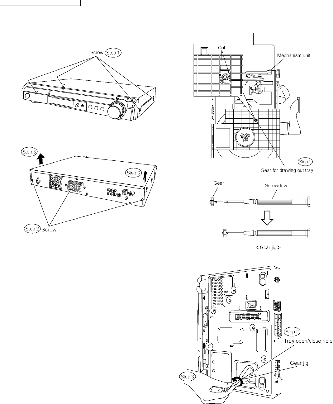
9.3. Disassembly of Top Cabinet
Step 1 Remove 4 screws.
Step 2 Remove 3 screws. (Rear view)
Step 3 Lift up and remove the top cabinet.
9.4. Disassembly of the DVD Lid
(When taking out disc
manually)
Step 1 Detach the gear for drawing out tray from the
mechanism unit. Inserts a screw driver into the gear. (The gear
jig)
Step 2 Insert the gear jig into the tray open/ close hole.
Step 3 Turn the gear jig counterclockwise to open the tray.
Note : Do not use force to push the tray backwards as it can
damage the mechanism unit.
Step 4 Turn the gear jig clockwise to return tray.
Step 5 Release the tabs and remove DVD lid.
30
SA-HT340GC / SA-HT340GCS / SA-HT340GS
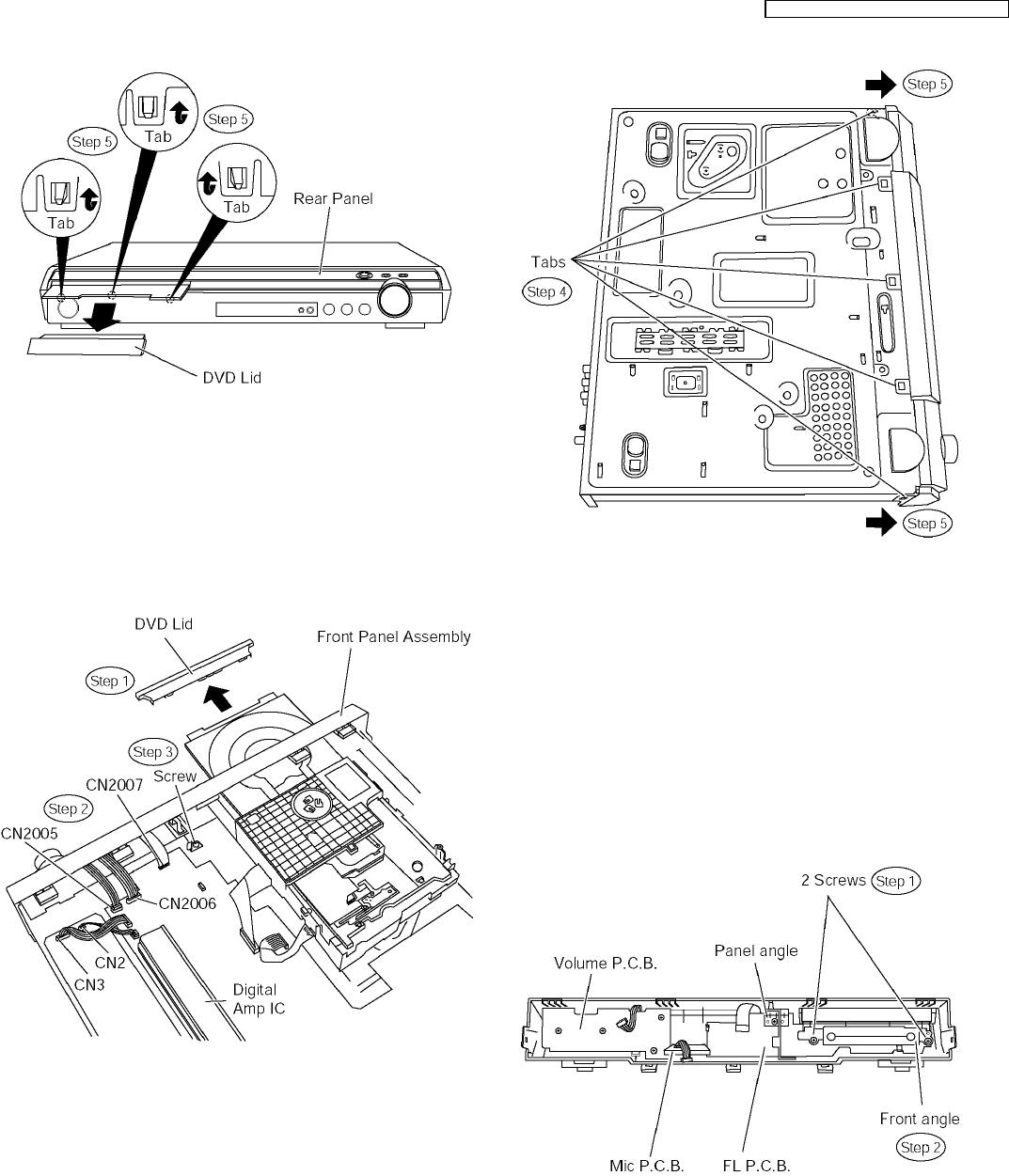
9.5. Disassembly of Front Panel
Assembly
·
Follow (Step 1) to (Step 3) of Item 9.3.
Step 1 Remove the DVD lid.
Step 2 Detach FFC cables at connectors. (CN2005, CN2006 &
CN2007)
Step 3 Remove 1 screw.
Step 4 Upset the unit and release the tabs.
Step 5 Detach the front panel assembly.
Special Note: Avoid placing the set in a position that might
cause damage to the jacks when removing the front panel
assembly.
9.6. Disassembly of FL P.C.B., Mic
P.C.B. & Volume P.C.B.
·
Follow the (Step 1) to (Step 5) of Item 9.5 for disassembly
of front panel.
·
Disassembly of FL P.C.B.
Step 1 Remove 2 screws.
Step 2 Remove the front angle.
Step 3 Remove 2 screws.
Step 4 Remove the panel angle.
Step 5 Remove FL P.C.B..
31
SA-HT340GC / SA-HT340GCS / SA-HT340GS
·
Disassembly of Volume P.C.B.
Step 6 Remove the volume knob.
Step 7 Remove 4 screws.
Step 8 Remove Volume P.C.B.
·
Disassembly of Mic P.C.B.
Step 9 Remove the mic knob.
Step 10 Remove Mic P.C.B.
9.7. Disassembly of DVD
Mechanism Unit
·
Follow (Step 1) to (Step 3) of Item 9.3.
·
Follow (Step 1) of Item 9.5.
Step 1 Remove 2 screws.
Step 2 Detach FFC cables at connectors. (CS901, CN2001).
Step 3 Lift up the mechanism unit vertically to remove it.
9.8. Disassembly of DVD Module
P.C.B.
·
Follow (Step 1) to (Step 3) of Item 9.7.
Step 1 Remove 4 screws.
Step 2 Detach FFC cables at the connectors.(FP8251,
FP8531)
32
SA-HT340GC / SA-HT340GCS / SA-HT340GS
Caution: Do not apply or exert excessive force when
detaching the FFC cables.
9.9. Disassembly of Rear panel
·
Follow (Step 1) to (Step 3) of Item 9.3.
Step 1 Remove 7 screws.
Step 2 Detach connector (CN5704) at fan unit.
Caution: Remember to attach the connector of fan unit
during assembly.
Step 3 Release the tabs.
Step 4 Remove the rear panel.
9.10. Disassembly of SMPS Module
P.C.B.
·
Follow (Step 1) to (Step 3) of Item 9.3.
·
Follow (Step 1) to (Step 4) of Item 9.9.
Step 1 Remove 1 screws.
Step 2 Detach cables at the connectors. (CN2, CN3)
Step 3 Remove SMPS Module P.C.B.
9.11. Disassembly of Main P.C.B. &
Tuner Extent P.C.B.
·
Follow (Step 1) to (Step 3) of Item 9.3.
·
Follow (Step 1) of Item 9.5 for disassembly of DVD lid.
·
Follow (Step 1) to (Step 3) of Item 9.7.
·
Follow (Step 1) to (Step 4) of Item 9.9.
Step 1 Remove 3 screws.
Step 2 Detach FFC cables at connector (CN2 & CN3).
Step 3 Lift up and remove Main P.C.B.
33
SA-HT340GC / SA-HT340GCS / SA-HT340GS
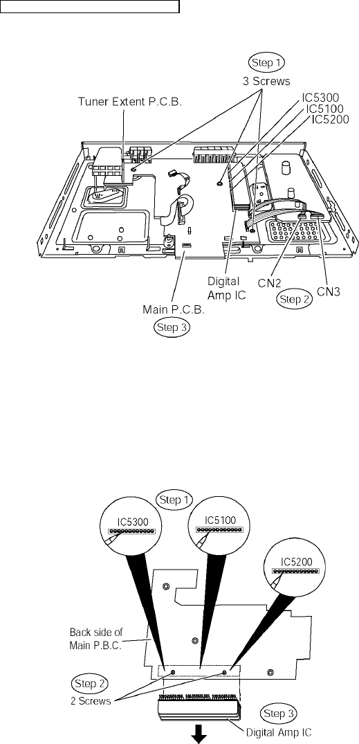
9.12. Disassembly of Digital Amp IC
(IC5100/IC5200/IC5300)
·
Follow (Step 1) to (Step 3) of Item 9.11.
Step 1 Desolder the pins of digital amp IC.
Step 2 Remove 2 screws.
Step 3 Remove the digital amp IC.
Note: Refer to the diagrams of Main P.C.B. (Section 19.2) for
location of the parts.
34
SA-HT340GC / SA-HT340GCS / SA-HT340GS
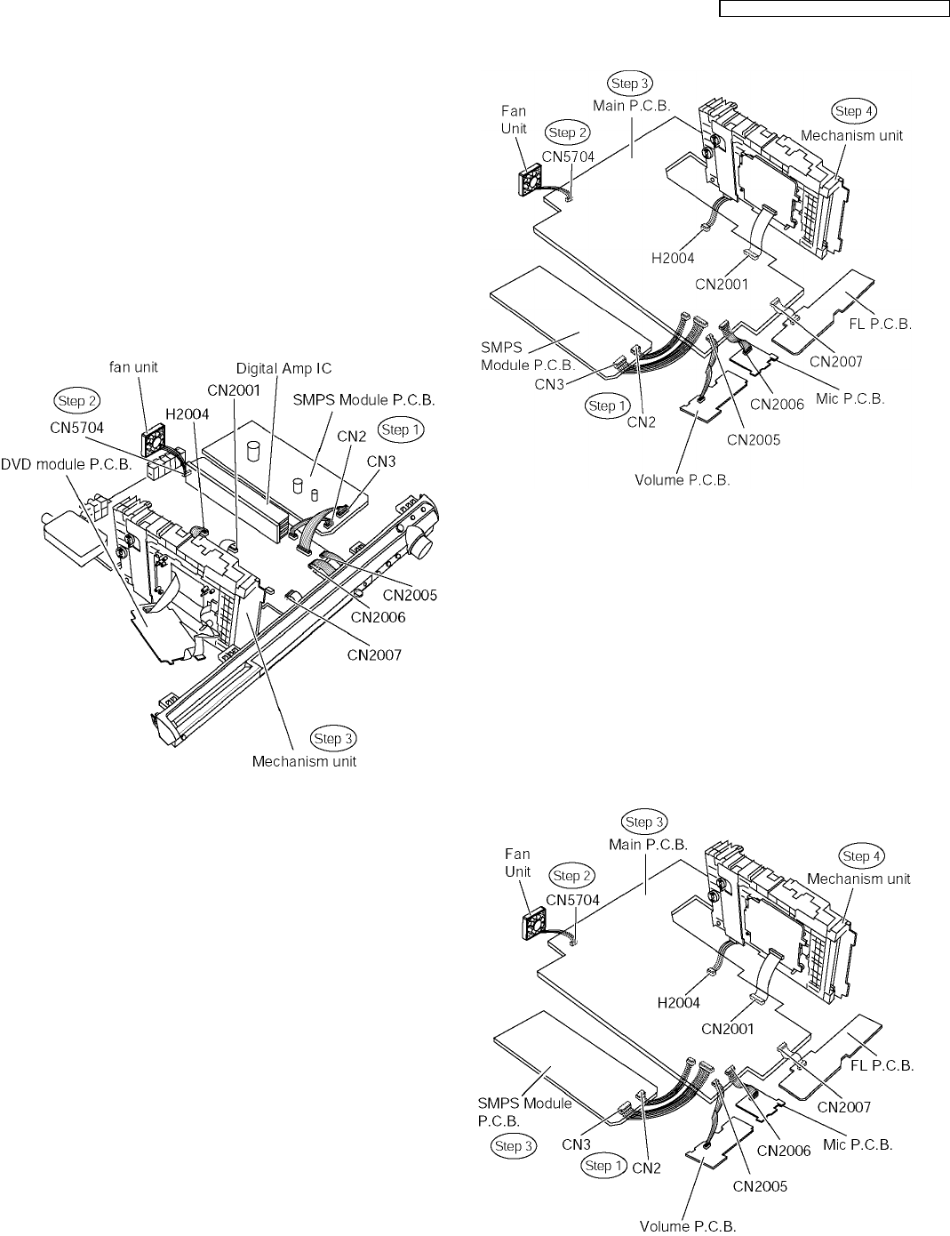
10 Service Position
10.1. Servicing position of the DVD
Module P.C.B.
·
Follow Item 9.7.
·
Follow (Step 1) of Item 9.8.
·
Follow (Step 1) of Item 9.9.
Step 1 Connect FFC cables at connectors. (CN2, CN3,
CN2001, CN2005, CN2006 & CN2007)
Step 2 Connect fan unit (CN5704).
Step 3 Turn mechanism unit to vertical position.
10.2. Servicing position of the Main
P.C.B.
·
Follow Item 9.7.
·
Follow (Step 1) of Item 9.9.
Step 1 Connect FFC cables at connectors. (CN2, CN3,
CN2001, CN2005, CN2006 & CN2007)
Step 2 Connect fan unit (CN5704).
Step 3 Turn over Main P.C.B.
Step 4 Turn mechanicm unit to vertical position (as show in
illustration) over Main P.C.B.
10.3. Servicing position of the
SMPS Module P.C.B.
·
Follow Item 9.7.
·
Follow Item 9.10.
·
Follow Item 9.11.
Step 1 Connect FFC cables at connectors. (CN2, CN3,
CN2001, CN2005, CN2006 & CN2007)
Step 2 Connect fan unit (CN5704).
Step 3 Turn over Main P.C.B. & SMPS Module P.C.B.
Step 4 Turn Mechanicm unit to vertical position (as show in
illustration) over Main P.C.B.
35
SA-HT340GC / SA-HT340GCS / SA-HT340GS
11 Assembly and
disassembly of
Mechanism Unit
11.1. Disassembly Procedure
11.1.1. Disassembly of Traverse Unit
Step 1 Slide the lever (A) in the arrow direction (to the opposite
side) till it stops.
Step 2 Slide the lever (A) further by bending the tab at the right
side of the lever A in the right direction. (The right groove opens
and the boss becomes seen.)
Step 3 Open the lever (B) to left. (The 2 grooves at the left side
open.).
Step 4 Remove the traverse unit.
11.1.2. Disassembly of Tray Unit
Step 1 Slide the guide tray unit while pressing the stopper in
the arrow direction, and remove the guide tray unit.
Step 2 Raise the loading unit.
Step 3 Slide the lever in the arrow direction till it stops and pull
the tray out.
36
SA-HT340GC / SA-HT340GCS / SA-HT340GS
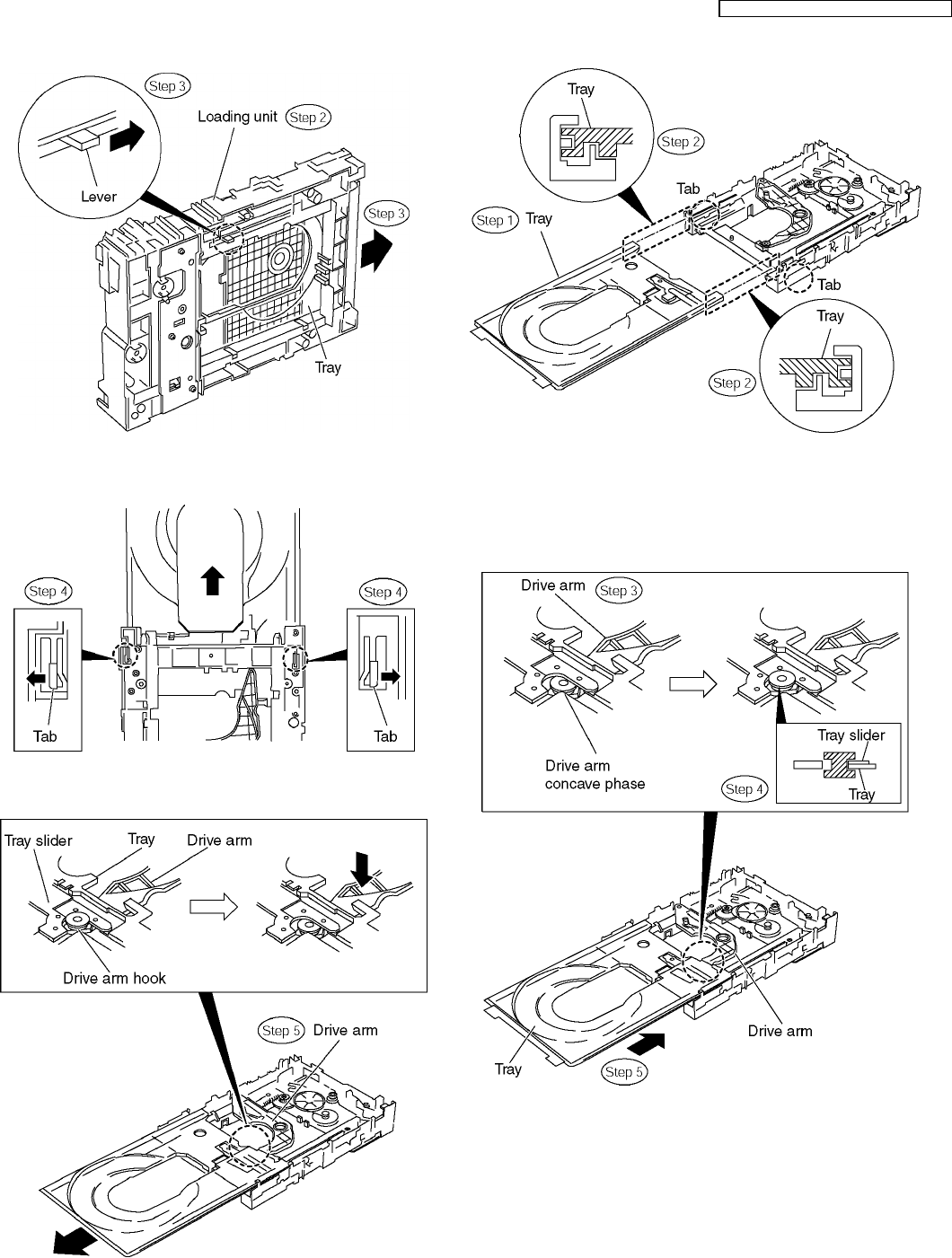
Step 4 Spread the tabs at the both sides and pull the tray out.
(The tray slides a little forword and stops.).
Step 5 Remove the drive arm concave phase from the tray
slider and tray.
l(Assembling the tray unit)
Step 1 Insert a part of the tray into the unit sliding over the
groove on the mechanical chassis unit.
Step 2 Insert the tray to the point before the tab of the
mechanical chassis unit.
Step 3 Hook the drive arm concave phase over the tray and
the tray slider.
Step 4 Press in the tray.
Step 5 Make sure that the tray and the drive arm move
smoothly.
11.1.3. Disassembly of Loading section
Step 1 Spread the tabs at the both sides and push out the drive
arm shaft.
37
SA-HT340GC / SA-HT340GCS / SA-HT340GS
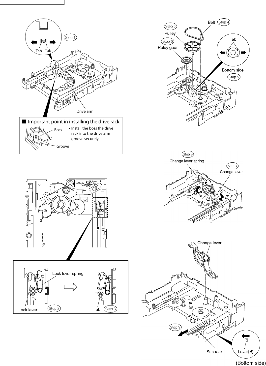
Step 2 Hook the lock lever spring on the lock lever projection
part temporarly.
Step 3 Unlock the tab and remove the lock lever.
Step 4 Remove the belt.
Step 5 Unlock the tab and remove the pulley.
Step 6 Remove the relay gear.
Step 7 Turn the change lever in the arrow direction till it stops.
Step 8 Hook the change lever spring on the change lever
project part temporarily.
Step 9 Pull the lever (B) in the bottom side to your side and
remove the change lever.
Step 10 Remove the drive rack, the sub rack and the drive
gear.
38
SA-HT340GC / SA-HT340GCS / SA-HT340GS
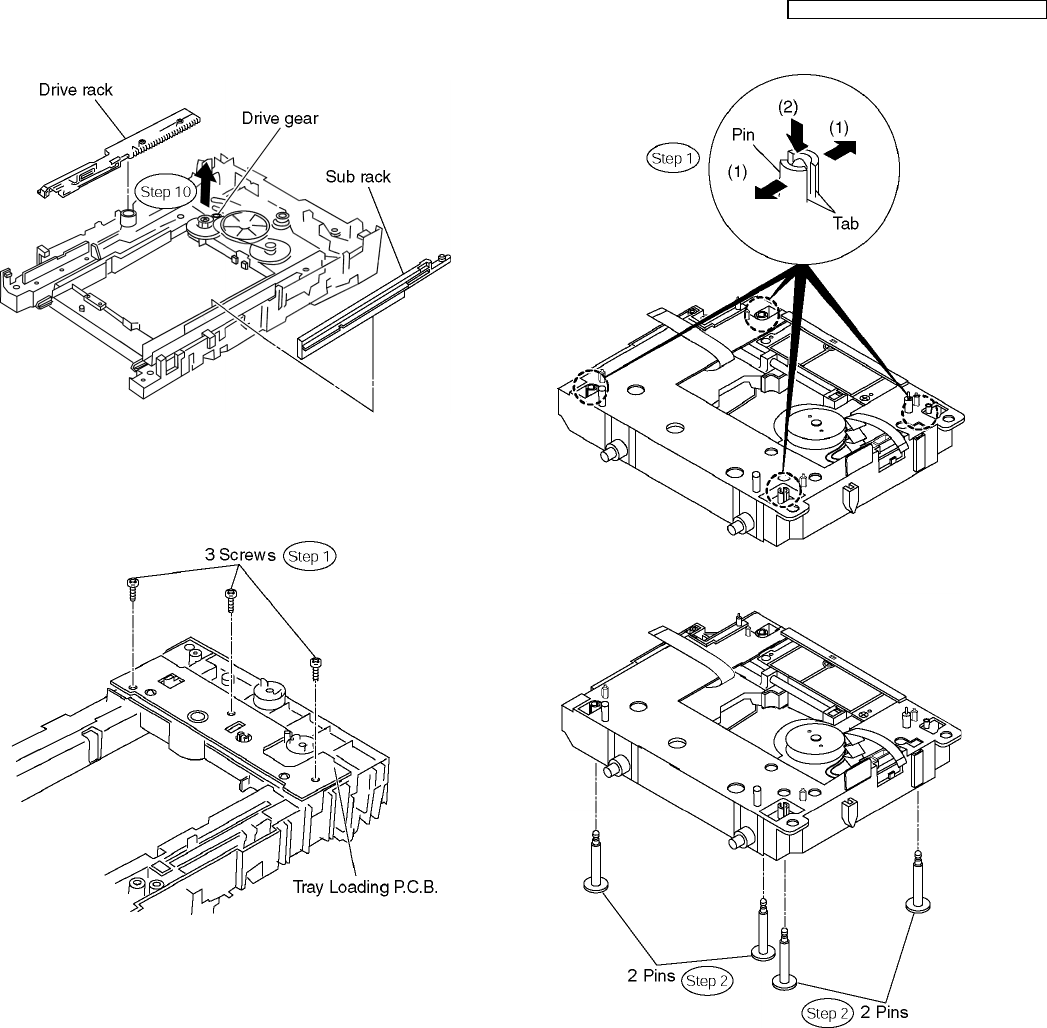
11.1.4. Disassembly of Tray Loading
P.C.B.
Step 1 Remove 3 screws
11.1.5. Disassembly of Optical Pickup
Unit
Special Note: Anti-static measures are necessary due to
handling of OPU unit .
Step 1 Spread the tabs to push in the pin.
Step 2 Remove 4 pins.
Step 3 Remove the middle chassis.
39
SA-HT340GC / SA-HT340GCS / SA-HT340GS
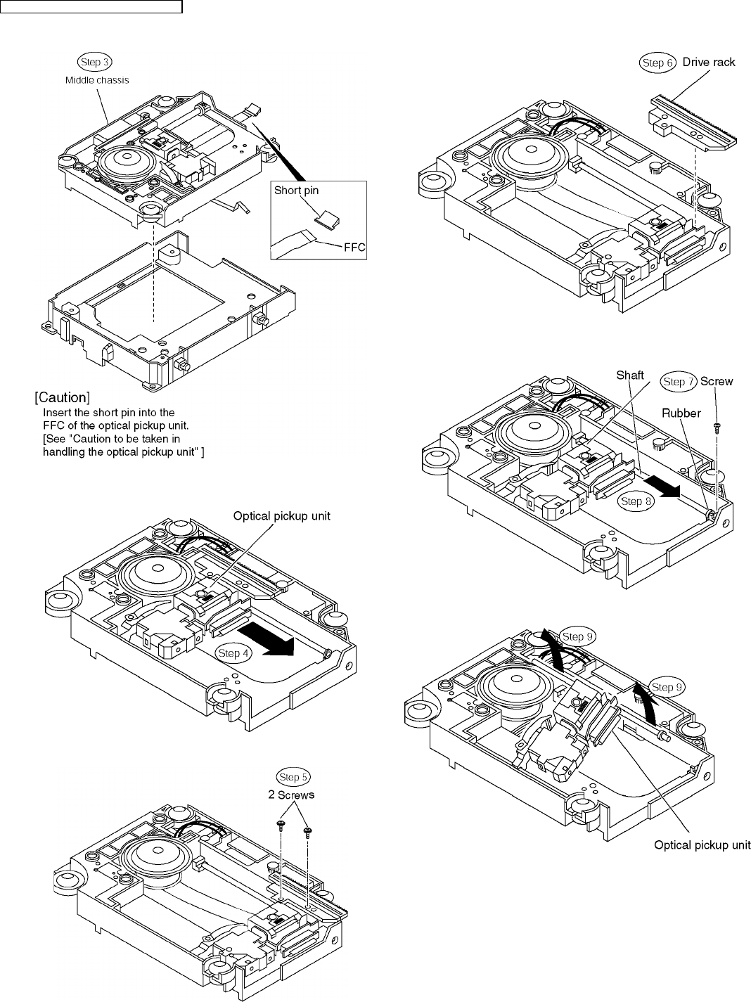
Step 4 Remove the optical pickup unit in the arrow direction till
it stops.
Step 5 Remove 2 screws.
Step 6 Remove the drive rack.
Step 7 Remove 1 screw.
Step 8 Slide the shaft in the arrow direction.
Step 9 Lift the optical pickup unit with the shaft.
Step 10 Remove the optical pickup unit.
40
SA-HT340GC / SA-HT340GCS / SA-HT340GS
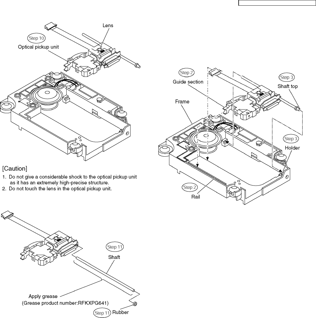
Step 11 Pull the shaft and the rubber out.
(Assembling the optical pickup unit)
Step 1 Pass the intermediate FPC through the frame hole.
Step 2 Align the guide section of the optical pickup unit with
the rail.
Step 3 Install the shaft top to the holder.
41
SA-HT340GC / SA-HT340GCS / SA-HT340GS

12 Measurements and Adjustments
12.1. Service Tools and Equipment
Application Name Number
Tilt adjustment DVD test disc DVDT-S20 [SPG]
TORX screw driver (T6) Available on sales route. (T6) or
RFKZ0185 [SPG]
Others Grease RFKXPG641 [SPG]
Confirmation CD test disc PVCD-K06 or any other commercially
available disc
VCD test disc PVCD-K06 or any other commercially
available disc
Recovery disc RFKZD03R005 [SPG]
12.2. Important points in adjustment
12.2.1. Important points in optical adjustment
·
Before starting optical adjustment, be sure to take anti-static measures.
·
Optical pickup tilt adjustment is needed after replacement of the following components.
1. Optical pickup unit
2. Spindle motor unit
3. Optical pickup peripheral parts
Notes
Adjustment is generally unnecessary after replacing other parts of the traverse unit. However, make adjustment if there is a
noticeable degradation in picture quality. Optical adjustments cannot be made inside the optical pickup. Adjustment is generally
unnecessary after replacing the traverse unit.
12.2.2. Important points in electrical adjustment
·
Follow the adjustment procedures described in this manual.
12.3. Storing and handling of test discs
·
Surface precision is vital for DVD test discs. Be sure to store and handle them carefully.
1. Do not place discs directly onto the workbench, etc., after use.
2. Handle discs carefully in order to maintain their flatness. Place them into their case after use and store them vertically. Store
discs in a cool place where they are not exposed to direct sunlight or air from air conditioners.
3. Accurate adjustment will not be possible if the disc is warped when placed on a surface made of glass, etc. If this happens, use
a new test disc to make optical adjustments.
4. If adjustment is done using a warped disc, the adjustment will be incorrect and some discs will not be playable.
42
SA-HT340GC / SA-HT340GCS / SA-HT340GS
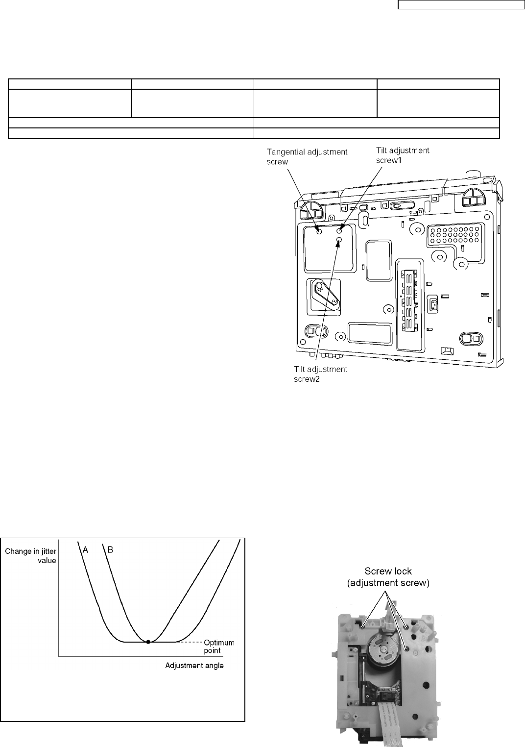
12.4.1.1. Adjustment procedure
1. While pressing STOP button on the main unit, press "5" on
the remote control unit.
2. Confirm that "J_xxx/yyy_zz" (display1/display2) is shown on
the front display.
For your information:
"yyy" and "zz" shown to the right have nothing to do with
the jitter value. "yyy" is the error counter, while "zz" is
the focus drive value.
Note:
Jitter value appears on the front display.
3. Play test disc T30 (center periphery).
4. Adjust tangential adjustment screw so that the jitter value is
minimized.
5. Play test disc T30 (center periphery).
6. Adjust tilt adjustment screw 1 so that the jitter value is
minimized.
7. Play test disc T30 (center periphery).
8. Adjust tilt adjustment screw 2 so that the jitter value is
minimized.
9. Repeat adjusting tilt adjustment screws 1 and 2 alternately
until the jitter value is minimized.
12.4.1.2. Important points
1. Make tangential adjustment first, and then make tilt
adjustment.
2. Repeat adjusting two or three times to find the optimum
point.
3. Finish the procedure with tilt adjustment.
Jitter value depends on the model:
1. If the jitter value changes like B, the optimum point is easy to
find.
2. If the jitter value changes like A, set the optimum point near the
middle.
12.4.1.3. Check after adjustment
Play test disc or any other disc to make sure there is no picture
degradation in the inner, middle and outer peripheries, and no
audio skipping. After adjustment is finished, lock each
adjustment screw in position using screw lock.
12.4.1.4. Procedure for screw lock
1. After adjustment, remove top cover, tray, clamper base and
traverse unit in this sequence.
2. Lay the traverse unit upside down, and fix adjustment screw
with screw lock.
3. After fixing, reassemble traverse unit, clamper base, tray
and top cover.
12.4. Optical adjustment
12.4.1. Optical pickup tilt adjustment
Measurement point Adjustment point Mode Disc
Tangential adjustment screw
Tilt adjustment screw
T01 (inner periphery) play
T30 (center periphery)
T43 (outer periphery) play
DVDT-S20 [SPG]
Measuring equipment Adjustment value
None (Main unit display for servicing is used.) Adjust to the minimum jitter value.
43
SA-HT340GC / SA-HT340GCS / SA-HT340GS

13 Abbreviations
INITIAL/LOGO ABBREVIATIONS
AA0~UP
ACLK
AD0~UP
ADATA
ALE
AMUTE
AREQ
ARF
ASI
ASO
ASYNC
ADDRESS
AUDIO CLOCK
ADDRESS BUS
AUDIO PES PACKET DATA
ADDRESS LATCH ENABLE
AUDIO MUTE
AUDIO PES PACKET REQUEST
AUDIO RF
SERVO AMP INVERTED INPUT
SERVO AMP OUTPUT
AUDIO WORD DISTINCTION SYNC
B BCK
BCKIN
BDO
BLKCK
BOTTOM
BYP
BYTCK
BIT CLOCK (PCM)
BIT CLOCK INPUT
BLACK DROP OUT
SUB CODE BLOCK CLOCK
CAP. FOR BOTTOM HOLD
BYPATH
BYTE CLOCK
C CAV
CBDO
CD
CDSCK
CDSRDATA
CDRF
CDV
CHNDATA
CKSL
CLV
COFTR
CPA
CPCS
CPDT
CPUADR
CPUADT
CPUIRQ
CPRD
CPWR
CS
CSYNCIN
CSYNCOUT
CONSTANT ANGULAR VELOCITY
CAP. BLACK DROP OUT
COMPACT DISC
CD SERIAL DATA CLOCK
CD SERIAL DATA
CD RF (EFM) SIGNAL
COMPACT DISC-VIDEO
CHANNEL DATA
SYSTEM CLOCK SELECT
CONSTANT LINEAR VELOCITY
CAP. OFF TRACK
CPU ADDRESS
CPU CHIP SELECT
CPU DATA
CPU ADDRESS LATCH
CPU ADDRESS DATA BUS
CPU INTERRUPT REQUEST
CPU READ ENABLE
CPU WRITE ENABLE
CHIP SELECT
COMPOSITE SYNC IN
COMPOSITE SYNC OUT
D DACCK
DEEMP
DEMPH
DIG0~UP
DIN
DMSRCK
DMUTE
DO
DOUT0~UP
DRF
DRPOUT
DREQ
DRESP
DSC
DSLF
DVD
D/A CONVERTER CLOCK
DEEMPHASIS BIT ON/OFF
DEEMPHASIS SWITCHING
FL DIGIT OUTPUT
DATA INPUT
DM SERIAL DATA READ CLOCK
DIGITAL MUTE CONTROL
DROP OUT
DATA OUTPUT
DATA SLICE RF (BIAS)
DROP OUT SIGNAL
DATA REQUEST
DATA RESPONSE
DIGITAL SERVO CONTROLLER
DATA SLICE LOOP FILTER
DIGITAL VIDEO DISC
INITIAL/LOGO ABBREVIATIONS
E EC
ECR
ENCSEL
ETMCLK
ETSCLK
ERROR TORQUE CONTROL
ERROR TORQUE CONTROL
REFERENCE
ENCODER SELECT
EXTERNAL M CLOCK (81MHz/40.5MHz)
EXTERNAL S CLOCK (54MHz)
F FBAL
FCLK
FE
FFI
FEO
FG
FSC
FSCK
FOCUS BALANCE
FRAME CLOCK
FOCUS ERROR
FOCUS ERROR AMP INVERTED INPUT
FOCUS ERROR AMP OUTPUT
FREQUENCY GENERATOR
FREQUENCY SUB CARRIER
FS (384 OVER SAMPLING) CLOCK
G GND COMMON GROUNDING (EARTH)
HHA0~UP
HD0~UP
HINT
HRXW
HOST ADDRESS
HOST DATA
HOST INTERRUPT
HOST READ/WRITE
I IECOUT
IPFRAG
IREF
ISEL
IEC958 FORMAT DATA OUTPUT
INTERPOLATION FLAG
I (CURRENT) REFERENCE
INTERFACE MODE SELECT
L LDON
LPC
LRCK
LASER DIODE CONTROL
LASER POWER CONTROL
L CH/R CH DISTINCTION CLOCK
MMA0~UP
MCK
MCKI
MCLK
MDATA
MDQ0~UP
MDQM
MLD
MPEG
MEMORY ADDRESS
MEMORY CLOCK
MEMORY CLOCK INPUT
MEMORY SERIAL COMMAND CLOCK
MEMORY SERIAL COMMAND DATA
MEMORY DATA INPUT/OUTPUT
MEMORY DATA I/O MASK
MEMORY SERIAL COMMAND LOAD
MOVING PICTURE EXPERTS GROUP
O ODC
OFTR
OSCI
OSCO
OSD
OPTICAL DISC CONTROLLER
OFF TRACKING
OSCILLATOR INPUT
OSCILLATOR OUTPUT
ON SCREEN DISPLAY
PP1~UP
PCD
PCK
PDVD
PEAK
PLLCLK
PLLOK
PWMCTL
PWMDA
PWMOA, B
PORT
CD TRACKING PHASE DIFFERENCE
PLL CLOCK
DVD TRACKING PHASE DIFFERENCE
CAP. FOR PEAK HOLD
CHANNEL PLL CLOCK
PLL LOCK
PWM OUTPUT CONTROL
PULSE WAVE MOTOR DRIVE A
PULSE WAVE MOTOR OUT A, B
44
SA-HT340GC / SA-HT340GCS / SA-HT340GS
INITIAL/LOGO ABBREVIATIONS
R RE
RFENV
RFO
RS
RSEL
RST
RSV
READ ENABLE
RF ENVELOPE
RF PHASE DIFFERENCE OUTPUT
(CD-ROM) REGISTER SELECT
RF POLARITY SELECT
RESET
RESERVE
S SBI0, 1
SBO0
SBT0, 1
SCK
SCKR
SCL
SCLK
SDA
SEG0~UP
SELCLK
SEN
SIN1, 2
SOUT1, 2
SPDI
SPDO
SPEN
SPRCLK
SPWCLK
SQCK
SQCX
SRDATA
SRMADR
SRMDT0~7
SS
STAT
STCLK
STD0~UP
STENABLE
STSEL
STVALID
SUBC
SBCK
SUBQ
SYSCLK
SERIAL DATA INPUT
SERIAL DATA OUTPUT
SERIAL CLOCK
SERIAL DATA CLOCK
AUDIO SERIAL CLOCK RECEIVER
SERIAL CLOCK
SERIAL CLOCK
SERIAL DATA
FL SEGMENT OUTPUT
SELECT CLOCK
SERIAL PORT ENABLE
SERIAL DATA IN
SERIAL DATA OUT
SERIAL PORT DATA INPUT
SERIAL PORT DATA OUTPUT
SERIAL PORT R/W ENABLE
SERIAL PORT READ CLOCK
SERIAL PORT WRITE CLOCK
SUB CODE Q CLOCK
SUB CODE Q DATA READ CLOCK
SERIAL DATA
SRAM ADDRESS BUS
SRAM DATA BUS 0~7
START/STOP
STATUS
STREAM DATA CLOCK
STREAM DATA
STREAM DATA INPUT ENABLE
STREAM DATA POLARITY SELECT
STREAM DATA VALIDITY
SUB CODE SERIAL
SUB CODE CLOCK
SUB CODE Q DATA
SYSTEM CLOCK
T TE
TIBAL
TID
TIN
TIP
TIS
TPSN
TPSO
TPSP
TRCRS
TRON
TRSON
TRACKING ERROR
BALANCE CONTROL
BALANCE OUTPUT 1
BALANCE INPUT
BALANCE INPUT
BALANCE OUTPUT 2
OP AMP INPUT
OP AMP OUTPUT
OP AMP INVERTED INPUT
TRACK CROSS SIGNAL
TRACKING ON
TRAVERSE SERVO ON
INITIAL/LOGO ABBREVIATIONS
V VBLANK
VCC
VCDCONT
VDD
VFB
VREF
VSS
V BLANKING
COLLECTOR POWER SUPPLY
VOLTAGE
VIDEO CD CONTROL (TRACKING
BALANCE)
DRAIN POWER SUPPLY VOLTAGE
VIDEO FEED BACK
VOLTAGE REFERENCE
SOURCE POWER SUPPLY VOLTAGE
WWAIT
WDCK
WEH
WSR
BUS CYCLE WAIT
WORD CLOCK
WRITE ENABLE HIGH
WORD SELECT RECEIVER
X X
XALE
XAREQ
XCDROM
XCS
XCSYNC
XDS
XHSYNCO
XHINT
XI
XINT
XMW
XO
XRE
XSRMCE
XSRMOE
XSRMWE
XVCS
XVDS
XVSYNCO
X´ TAL
X ADDRESS LATCH ENABLE
X AUDIO DATA REQUEST
X CD ROM CHIP SELECT
X CHIP SELECT
X COMPOSITE SYNC
X DATA STROBE
X HORIZONTAL SYNC OUTPUT
XH INTERRUPT REQUEST
X´ TAL OSCILLATOR INPUT
X INTERRUPT
X MEMORY WRITE ENABLE
X´ TAL OSCILLATOR OUTPUT
X READ ENABLE
X SRAM CHIP ENABLE
X SRAM OUTPUT ENABLE
X SRAM WRITE ENABLE
X V-DEC CHIP SELECT
X V-DEC CONTROL BUS STROBE
X VERTICAL SYNC OUTPUT
45
SA-HT340GC / SA-HT340GCS / SA-HT340GS

14 Voltage and Waveform Chart
14.1. DVD Module P.C.B.
Ref No.
MODE 1 2 3 4 5 6 7 8 9 10 11 12 13 14 15 16 17 18 19 20
CD PLAY 0.1 0.1 3.4 0.1 0.1 0.1 0.1 3.4 0.1 0.1 0.1 0.1 0.1 0.1 0.1 0.1 3.4 2.6 2.6 0.1
Ref No.
MODE 21 22 23 24 25 26 27 28 29 30 31 32 33 34 35 36 37 38 39 40
CD PLAY - 1.3 1.1 1.2 1.6 1.1 1.5 1.3 1.2 2.5 0.1 1.3 1.0 0.1 3.4 3.3 1.3 1.9 1.1 1.7
Ref No.
MODE 41 42 43 44 45 46 47 48 49 50 51 52 53 54 55 56 57 58 59 60
CD PLAY 1.3 0.7 1.2 0.1 1.3 1.3 1.3 1.5 1.5 2.2 1.3 0.1 - - 3.4 1.1 2.0 2.2 1.9 1.1
Ref No.
MODE 61 62 63 64 65 66 67 68 69 70 71 72 73 74 75 76 77 78 79 80
CD PLAY 2.2 2.0 2.4 2.7 0.1 3.4 3.4 0.1 3.4 0.1 0.1 0.1 0.1 0.1 0.1 0.1 0.1 0.1 0.1 0.1
Ref No.
MODE 81 82 83 84 85 86 87 88 89 90 91 92 93 94 95 96 97 98 99 100
CD PLAY 0.1 0.1 1.3 3.3 0.1 0.1 3.4 3.4 3.4 2.0 1.6 0.1 3.4 0.1 0.1 0.1 0.1 0.1 0.1 0.1
Ref No.
MODE 101 102 103 104 105 106 107 108 109 110 111 112 113 114 115 116 117 118 119 120
CD PLAY 0.1 3.3 1.0 0.1 2.4 1.9 0.3 0.1 1.8 3.3 3.3 1.3 1.9 1.9 1.9 1.7 1.7 1.7 1.7 2.0
Ref No.
MODE 121 122 123 124 125 126 127 128 129 130 131 132 133 134 135 136 137 138 139 140
CD PLAY 1.5 0.1 0.5 0.1 0.1 1.9 2.3 1.7 2.6 2.6 2.7 2.6 2.7 2.7 2.5 2.6 2.5 2.5 1.8 2.0
Ref No.
MODE 141 142 143 144 145 146 147 148 149 150 151 152 153 154 155 156 157 158 159 160
CD PLAY 1.7 1.7 0.1 1.7 1.7 3.4 0.9 0.9 0.4 3.4 2.0 1.0 1.0 2.0 0 0.4 3.3 3.4 0 3.4
Ref No.
MODE 161 162 163 164 165 166 167 168 169 170 171 172 173 174 175 176 177 178 179 180
CD PLAY 0 1.6 1.7 0.1 1.3 1.2 1.7 1.7 0.9 0.1 0.1 0.9 1.7 0.1 3.4 3.0 3.4 0.1 3.4 0.1
Ref No.
MODE 181 182 183 184 185 186 187 188 189 190 191 192 193 194 195 196 197 198 199 200
CD PLAY 3.0 0.2 2.8 3.4 0.1 0.1 3.4 3.4 0.1 0.1 0.1 0.1 0.1 0.1 0.1 0.1 3.4 3.0 3.0 2.9
Ref No.
MODE 201 202 203 204 205 206 207 208 209 210 211 212 213 214 215 216 217 218 219 220
CD PLAY 3.1 2.9 3.1 3.4 0.1 3.1 3.0 3.0 3.3 3.1 3.0 3.1 3.0 3.4 0.1 2.9 1.3 2.7 2.7 2.7
Ref No.
MODE 221 222 223 224 225 226 227 228 229 230 231 232 233 234 235 236 237 238 239 240
CD PLAY 3.3 0.1 1.7 3.4 1.7 0.1 3.3 3.3 3.2 0.1 2.0 0.1 0.1 1.3 1.7 0.1 0.1 0.1 3.4 1.6
Ref No.
MODE 241 242 243 244 245 246 247 248 249 250 251 252 253 254 255 256
CD PLAY 0.1 1.7 0.2 1.7 0.3 1.6 1.6 0.1 0 0.1 0.1 0.1 0.1 0.1 0.1 0.1
Ref No.
MODE 1 2 3 4 5 6 7 8 9 10 11 12 13 14 15 16 17 18 19 20
CD PLAY 3.4 3.0 3.4 3.1 3.1 0.1 3.1 3.3 3.4 3.0 3.0 0.1 2.9 3.4 2.7 3.3 3.3 3.3 3.2 2.0
Ref No.
MODE 21 22 23 24 25 26 27 28 29 30 31 32 33 34 35 36 37 38 39 40
CD PLAY 1.7 0.1 0.1 0.2 0.3 1.5 3.4 0.1 1.6 1.7 1.7 1.6 0.1 0.1 0.1 - 3.4 1.7 2.7 -
Ref No.
MODE 41 42 43 44 45 46 47 48 49 50 51 52 53 54 54
CD PLAY 0.1 3.0 3.4 3.1 3.0 0.1 3.0 3.2 3.4 2.9 2.9 0.1 3.0 0.1 0.1
Ref No.
MODE 12345678
CD PLAY 3.4 - 0.1 - 4.4 - - 4.7
Ref No.
MODE 12345
CD PLAY 3.0 3.0 0.1 1.3 0.9
Ref No.
MODE 1 2 3 4 5 6 7 8 9 10 11 12 13 14 15 16 17 18 19 20
CD PLAY 1.7 1.7 1.7 2.2 2.2 1.9 0.1 4.7 3.4 0.1 2.4 2.4 2.4 2.4 4.4 4.5 5.3 3.5 0.1 3.4
Ref No.
MODE 21 22 23 24 25 26 27 28 29 30
CD PLAY 9.2 9.1 1.8 1.7 1.7 1.7 3.4 4.3 0 0
Ref No.
MODE 1 2 3 4 5 6 7 8 9 10 11 12 13 14 15 16 17 18 19 20
CD PLAY 0 2.3 3.0 3.4 1.7 0.9 1.7 1.7 4.9 0 0.9 0.1 0.1 0 2.4 2.4 4.9 0 2.4 2.4
Ref No.
MODE 21 22 23 24 25 26 27 28
CD PLAY 2.4 2.4 4.9 0 2.5 2.4 2.4 4.8
Ref No.
MODE 1234
CD PLAY 3.3 1.3 0.1 0.1
Ref No.
MODE 12345
CD PLAY 3.3 3.4 0.1 0.1 -
Ref No.
MODE 12345678
CD PLAY 0.1 0.1 0.1 0.1 3.4 3.4 0.1 3.4
Ref No.
MODE 1 2 3 4 5 6 7 8 9 10 11 12 13 14 15 16 17 18 19 20
CD PLAY 0.7 1.1 2.3 1.3 1.9 1.4 2.2 1.3 1.1 0.1 3.4 3.4 3.4 3.4 - 1.2 2.1 2.2 1.9 1.1
Ref No.
MODE 21 22 23 24 25 26 27 28 29 30 31 32 33 34 35 36 37 38 39 40
CD PLAY 2.2 2.0 2.5 2.7 2.7 2.7 0.1 2.6 0.7 1.1 1.3 1.0 1.6 1.3 1.3 1.5 3.4 1.7 1.2 1.1
Ref No.
MODE 41 42 43 44 45 46 47 48
CD PLAY 1.0 1.1 1.8 1.1 1.7 0.1 3.4 1.4
Ref No.
MODE 12345 123445
CD PLAY 3.0 3.0 0.1 4.2 4.7 2.8 2.8 0.1 3.9 3.9 4.7
Ref No.
MODE E C B E C B E C B ECB
CD PLAY 0.1 4.6 0.1 0.1 4.6 4.6 1.9 3.5 1.3 3.5 4.1 4.1
Ref No.
MODE 1 2 3 456 ECB ECB
CD PLAY 0.1 0.1 1.4 0.1 0.1 4.4 0 0.1 4.0 3.4 3.3 0.1
Q8562
Q8561
Q8551
IC8001
IC8001
IC8051
IC8651
IC8001
IC8001
IC8001
IC8421
IC8651
IC8251
IC8001
IC8151
IC8051
IC8111
IC8001
IC8001
IC8611
IC8001
IC8001
IC8001
IC8001
IC8251
IC8051
IC8001
IC8695IC8691
IC8421
QR8111
IC8651
IC8606
IC8601
QR8420 QR8571
Q8552
46
SA-HT340GC / SA-HT340GCS / SA-HT340GS
14.2. Main P.C.B.
Ref No.
MODE 12345678
CD PLAY - 4.9 0 0 0 0 0 -
STANDBY - 4.8 0 0 0 0 0 -
Ref No.
MODE 1 2 3 4 5 6 7 8 9 10 11 12 13 14 15 16 17 18 19 20
CD PLAY 0.1 4.7 4.7 4.7 0 0 4.6 0 0 0 0 4.7 2.4 0 2.3 4.7 4.7 4.7 2.1 0
STANDBY 0 0 0 0.1 0 0 0 0 0 0 0 4.9 2.5 0 2.4 4.9 4.9 4.8 2.7 0
Ref No.
MODE 21 22 23 24 25 26 27 28 29 30 31 32 33 34 35 36 37 38 39 40
CD PLAY 0 4.7 0 0 0 0 4.7 4.7 4.7 4.7 0 0 0 4.6 0 4.0 4.4 4.6 0 4.6
STANDBY04.800000000000000.10.1000
Ref No.
MODE 41 42 43 44 45 46 47 48 49 50 51 52 53 54 55 56 57 58 59 60
CD PLAY 0 4.6 0 0.1 0 0 0 0 0 0 4.7 0 0 0 4.6 4.6 4.6 4.5 4.7 0
STANDBY00000000000000000000
Ref No.
MODE 61 62 63 64 65 66 67 68 69 70 71 72 73 74 75 76 77 78 79 80
CD PLAY 0 4.7 4.7 0 0 0 0 4.6 0 4.4 4.7 4.7 2.5 0 0 0 0 0 0 0
STANDBY04.90000000000.700000000
Ref No.
MODE 81 82 83 84 85 86 87 88 89 90 91 92 93 94 95 96 97 98 99 100
CD PLAY 0 0 0 4.7 0 0 4.7 0 0 0 4.7 0 0.7 1.2 0.4 0 1.6 4.8 4.7 4.7
STANDBY 0 0 0 0 0 0 0 0 0 0 4.8 0 0.7 1.2 0.4 0 1.6 4.9 4.9 0
Ref No.
MODE 1 2 3 4 5 6 7 8 9 10 11 12 13 14 15 16 17 18 19 20
CD PLAY00000000000000000000
STANDBY00000000000000000000
Ref No.
MODE 21 22 23 24 25 26 27 28 29 30 31 32 33 34 35 36 37 38 39 40
CD PLAY000000000000.100000000.1
STANDBY000000000000.100000000.1
Ref No.
MODE 41 42 43 44 45 46 47 48 49 50 51 52 53 54 55 56 57 58 59 60
CD PLAY0000000001.30000.1000000
STANDBY 000000001.40000.1000000
Ref No.
MODE 61 62 63 64 65 66 67 68 69 70 71 72 73 74 75 76 77 78 79 80
CD PLAY0-0.1004.805.60000000000000
STANDBY0-0.1004.805.60.1000000000000
Ref No.
MODE 81 82 83 84 85 86 87 88 89 90 91 92 93 94 95 96 97 98 99 100
CD PLAY0000-6.26.300000000000000
STANDBY0000-6.46.500000000000000
Ref No.
MODE 1 2 3 4 5 6 7 8 9 10 11 12 13 14 15 16 17 18 19 20
CD PLAY 4.9 0 0 2.1 4.7 1.6 0 1.6 2.1 0 1.6 0 2.1 4.7 2.1 4.9 2.2 2.2 0 2.2
STANDBY 4.9 0 0 2.1 4.7 1.5 0 1.5 2.1 0 1.6 0 2.1 4.7 2.1 4.9 2.2 2.2 0 2.2
Ref No.
MODE 21 22 23 24 25 26 27 28 29 30 31 32
CD PLAY 2.2 0 1.5 1.7 0 1.5 2.0 0 1.6 1.8 0 2.2
STANDBY 2.2 0 1.4 1.7 0 1.4 1.7 0 1.5 1.8 0 2.2
Ref No.
MODE 123456 1234567
CD PLAY 0 2.5 4.8 2.5 0 2.5 2.7 10.5 6.0 0 - 1.1 0.7
STANDBY 0 2.9 4.8 2.5 0 2.5 2.8 10.5 6.0 0 - 1.1 0.7
Ref No.
MODE ECB ECB ECB ECB ECB
CD PLAY 0 2.2 0 0 0 4.5 1.1 0 0.5 0 0 4.7 8.6 14.0 9.2
STANDBY00.10 000 000 004.6 000.5
Ref No.
MODE ECB ECB ECB ECB ECB
CD PLAY 4.3 5.4 4.9 6.3 6.3 6.9 6.2 9.2 6.9 0 5.2 0 -7.5 -23.3 -7.0
STANDBY 0 0 0 6.5 6.5 7.1 6.2 9.2 6.9 0 5.2 0 -7.5 -23.3 -7.0
Ref No.
MODE ECB ECB ECB ECB ECB
CD PLAY -6.3 -21.0 -6.8 12.9 21.2 13.5 9.2 11.1 9.8 3.2 3.5 3.7 4.7 4.9 4.7
STANDBY -6.9 -21.0 -6.4 12.9 21.2 13.5 9.2 11.2 9.8 3.2 3.2 3.8 4.6 4.8 4.7
Ref No.
MODE ECB ECB ECB ECB ECB
CD PLAY 0 2.7 0 2.9 0 0 5.1 5.7 5.7 -21.8 -25.4 -22.4 0 25.9 0
STANDBY 0 2.8 0 0 0 -2.9 5.1 5.7 5.7 -21.7 -25.3 -22.3 0 26.0 0
Q2913
Q2916 Q2917 Q2955
Q2910
IC2102
Q2915Q2914
Q2974
IC2801
IC2801
IC2802 IC2903
IC2102
Q2906
Q2980
Q2907
IC2004
IC2102
IC2102
IC2018
IC2018
IC2018
IC2018
IC2018
IC2102
Q2805
Q2804
Q2903 Q2905
Q2003 Q2006Q2004
Q2904
Q2030
47
SA-HT340GC / SA-HT340GCS / SA-HT340GS
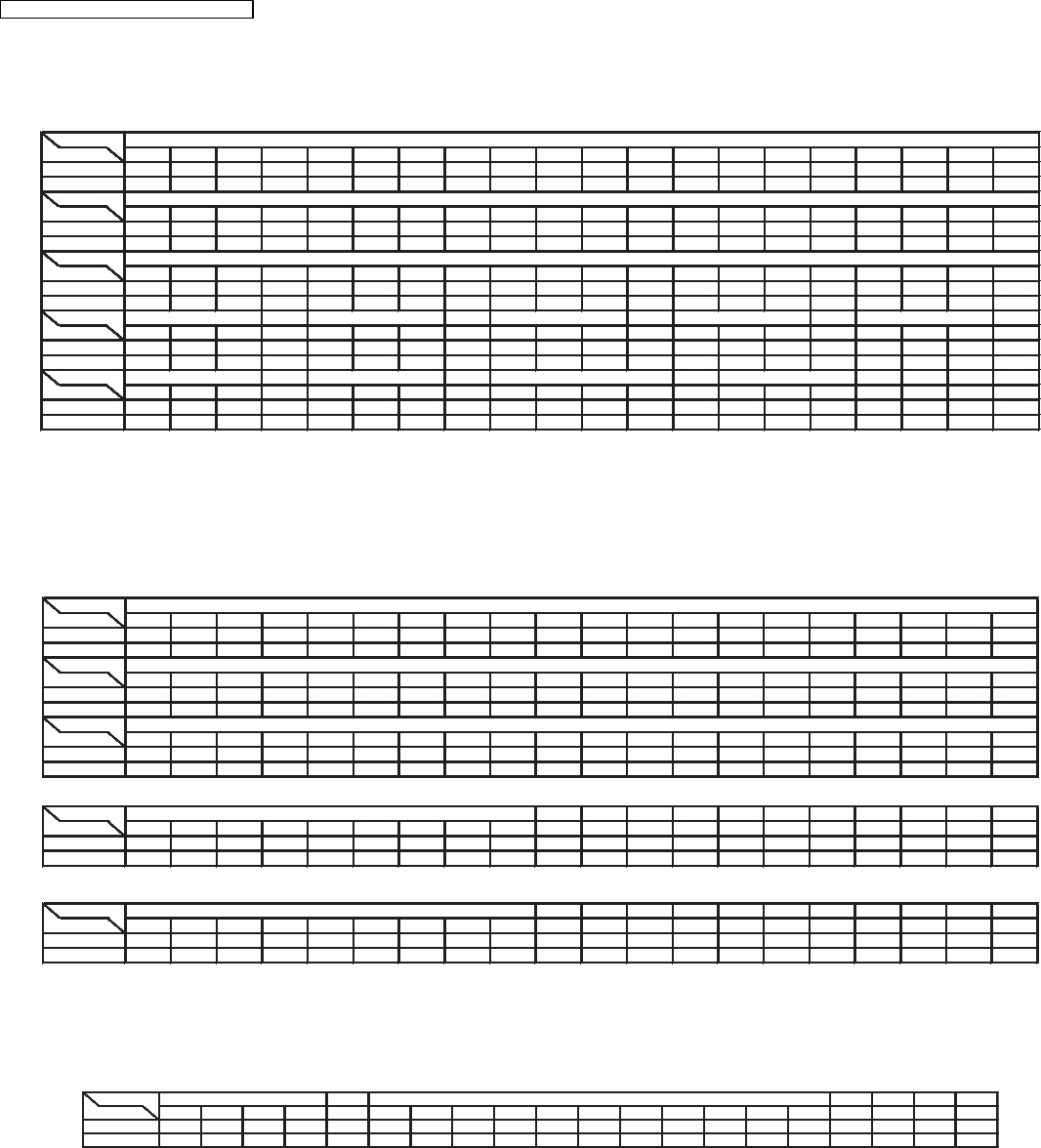
Ref No.
MODE 123456789101112
CD PLAY 25.9 12.7 0 12.6 4.7 0 0 0 0 12.7 0 12.7
STANDBY 26.0 12.8 0 12.7 4.7 0 0 0 3.0 12.8 0 12.8
Ref No.
MODE 123456789101112
CD PLAY 25.9 12.7 0 12.7 4.7 0 0 0 3.0 12.7 0 12.7
STANDBY 26.0 12.7 0 12.7 4.7 0 0 0 3.0 12.8 0 12.7
Ref No.
MODE 123456789101112
CD PLAY 25.9 12.7 0 13.0 4.7 0 0 0 0 12.7 0 12.8
STANDBY 25.6 12.7 0 12.7 4.6 0 0 0 3.0 12.7 0 12.8
Ref No.
MODE ECB ECB ECB ECB ECB
CD PLAY 1.6 1.6 0 0 0 0.6 0 0.2 0.2 8.9 17.1 9.5 0 4.9 0
STANDBY 1.6 1.6 0 0 0 0.6 0 0.1 0 8.9 17.1 9.5 0 4.9 0
Ref No.
MODE E C B E C B 1 2 3 4123
CD PLAY 0 0.1 0.7 0 4.6 0.1 5.6 4.4 0 0.4 00.14.8
STANDBY 0 0.1 0.7 0 4.6 0 5.6 4.4 1 0.4 10.14.8
IC5200
IC5300
Q5746
Q5745
IC5100
Q5740
Q5741
Q5742
Q5744
Q3003
Q3008 Q3009
14.3. FL P.C.B., Mic P.C.B. & Tray Loading P.C.B.
Ref No.
MODE 1234567891011121314151617181920
CD PLAY 4.9 0 0 -0.1 2.8 - 0.7 4.6 3.7 - - 0 4.8 -21.0 -21.0 -18.9 -18.8 -14.7 -18.9 -14.7
STANDBY 4.9 0 0 0 2.8 - 0.7 4.6 3.7 - - 0 4.9 -21.0 -21.0 -21.0 -18.9 -10.5 -8.4 -14.7
Ref No.
MODE 21 22 23 24 25 26 27 28 29 30 31 32 33 34 35 36 37 38 39 40
CD PLAY -12.9 -21.0 -21.0 -14.7 -14.7 -18.9 -21.0 -21.0 -16.8 -21.4 -14.9 -12.8 -19.1 -19.1 -19.1 -19.1 -19.1 -19.1 -19.1 -19.1
STANDBY -14.7 -21.0 -18.9 -10.5 -10.5 -16.8 -21.0 -18.9 -8.4 -21.4 -12.7 -10.6 -19.1 -19.1 -19.1 -19.1 -19.1 -19.1 -19.1-19.1
Ref No.
MODE 41 42 43 44
CD PLAY -19.1 -19.1 4.9 -0.1
STANDBY -19.1 -19.1 4.9 0
Ref No.
MODE 12345678
CD PLAY -4.9 -6.3 -5.9 -1.2 -5.7 -5.7 -0.1 0
STANDBY -5.0 -6.3 -5.9 -1.2 -5.7 -5.7 -0.1 0
Tray Loading P.C.B.
Ref No.
MODE 123456789
CD PLAY 4.7 8.0 0.6 8.0 0.1 8.0 0.6 2.7 4.7
STANDBY 0 1.8 0.8 1.8 0 2.1 0.9 4.9 0
IC904
FL P.C.B.
IC6901
IC6901
IC6901
MIC P.C.B.
IC2204
14.4. SMPS Module P.C.B.
SMPS Module P.C.B.
Ref No.
MODE 1234 1234567891011
CD PLAY 18.5 18.5 0 0 6 3.5 0 10.5 0 0 5 -12.3 -16.1 5.2 24.7
STANDBY 18.5 18.5 0 0 6 3.5 0 10.5 0 0 5 -12.2 -16.0 5.2 24.7
CN2 CN3
48
SA-HT340GC / SA-HT340GCS / SA-HT340GS
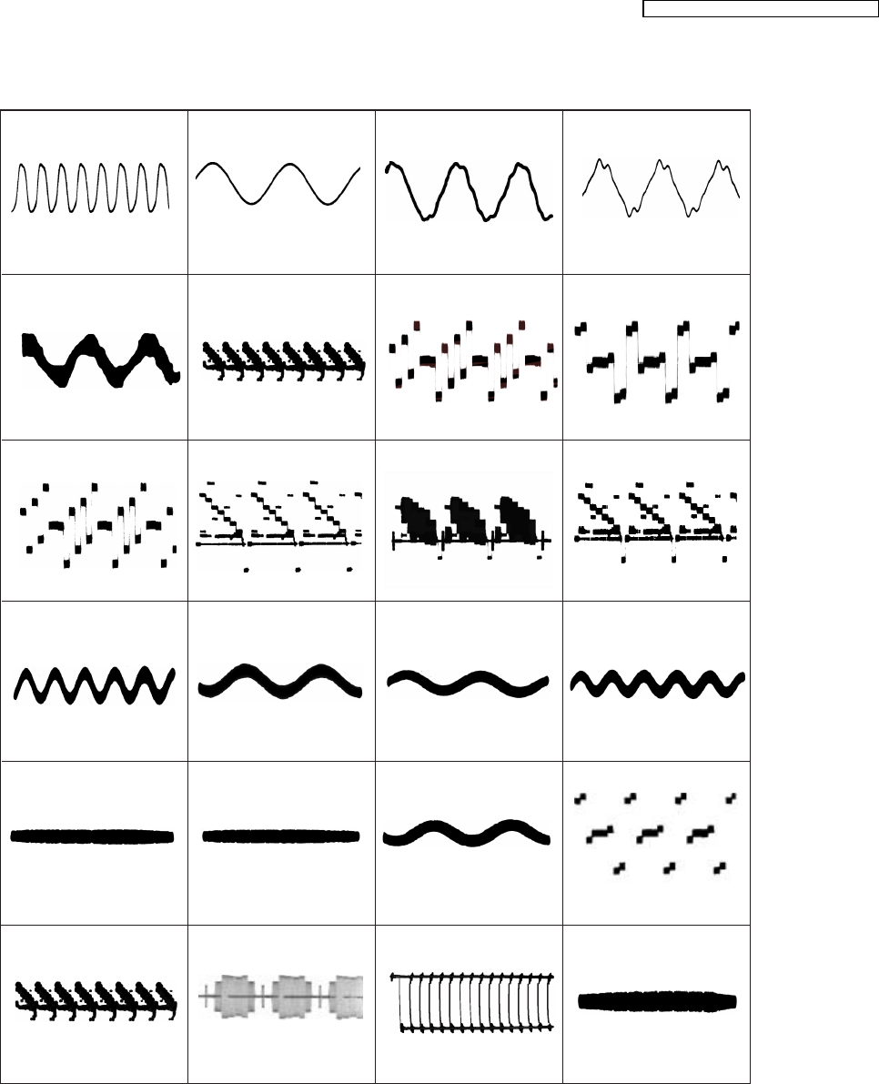
14.5. Waveform Chart
WF No. IC8001-147, 148 (PLAY)
0.64Vp-p(50usec/div)
WF No. IC8001-149, 156 (PLAY)
1.45Vp-p(50usec/div)
WF No. IC8001-157 (PLAY)
0.75Vp-p(50usec/div)
WF No. IC8001-169 (PLAY)
1.9Vp-p(200nsec/div)
WF No. IC8001-170, 171 (PLAY)
0.05Vp-p(50usec/div)
WF No. IC2801- 4 (PLAY)
1.2Vp-p(5msec/div)
WF No. IC2801- 8, 11 (PLAY)
1.4Vp-p(50usec/div)
WF No. IC2801- 13 (PLAY)
0.6Vp-p(50usec/div)
WF No. IC2801- 24, 27 (PLAY)
2.2Vp-p(50usec/div)
WF No. IC2801- 30 (PLAY)
2.3Vp-p(50usec/div)
WF No. IC2801- 32 (PLAY)
1.5Vp-p(20usec/div)
WF No. IC5100- 2, 4 (PLAY)
2Vp-p(50usec/div)
WF No. IC5200- 4 (PLAY)
0.6Vp-p(500usec/div)
WF No. IC5300- 4 (PLAY)
0.7Vp-p(500usec/div)
WF No. IC5300- 10, 12 (PLAY)
0.65Vp-p(200usec/div)
WF No. IC5300- 2 (PLAY)
1.1Vp-p(500usec/div)
WF No. IC5100- 10, 12 (PLAY)
0.9Vp-p(200usec/div)
WF No. IC5200- 2, 10, 12 (PLAY)
0.6Vp-p(200usec/div)
WF No. IC2801- 15 (PLAY)
0.6Vp-p(50usec/div)
WF No. IC2801- 18, 21 (PLAY)
1Vp-p(50usec/div)
WF No. IC2102-30 (PLAY)
4.4Vp-p(5msec/div)
WF No. IC2018-13 (PLAY)
5.4Vp-p(100nsec/div)
WF No. IC2102-20 (PLAY)
0.1Vp-p(500usec/div)
WF No. IC2102-17, 18, 28,
41,44 (PLAY)
76Vp-p(5msec/div)
49
SA-HT340GC / SA-HT340GCS / SA-HT340GS
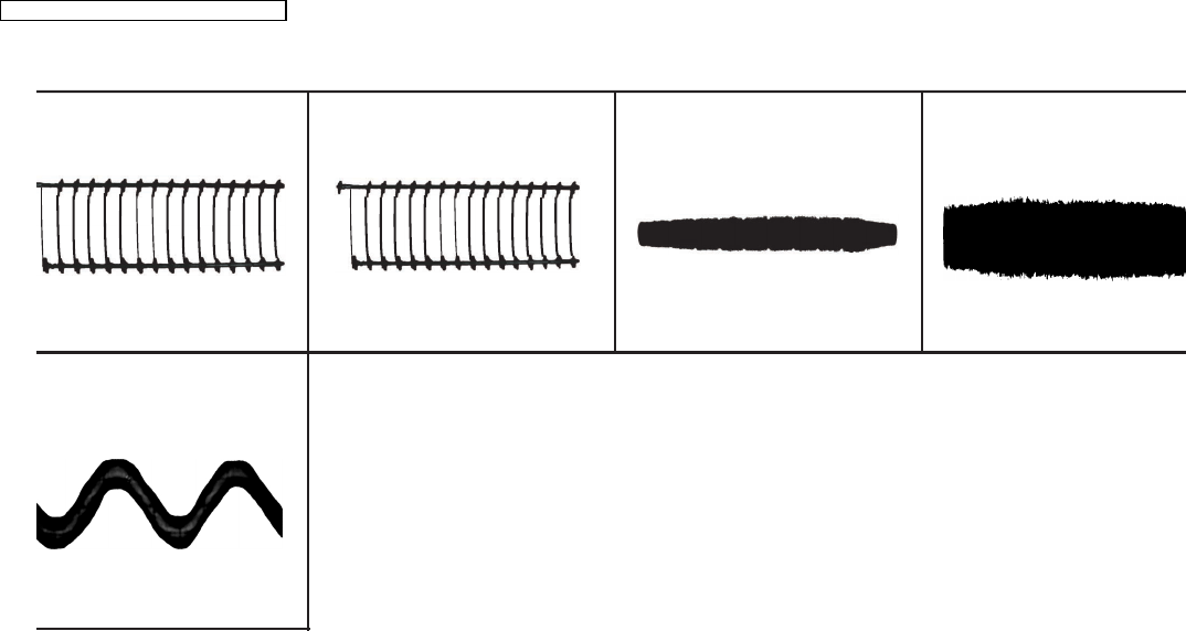
WF No. IC8421-11 (PLAY)
3.8Vp-p(500nsec/div)
WF No. IC8421-15, 16, 19
20, 22, 27
(PLAY)
F No. IC8421-21, 26 (PLAY)
0.22Vp-p(500usec/div)
0.72Vp-p(200usec/div)
WF No. IC8421-12, 13 (PLAY)
0.05Vp-p(200usec/div)
WF No. IC8001-172 (PLAY)
5Vp-p(200nsec/div)
50
SA-HT340GC / SA-HT340GCS / SA-HT340GS
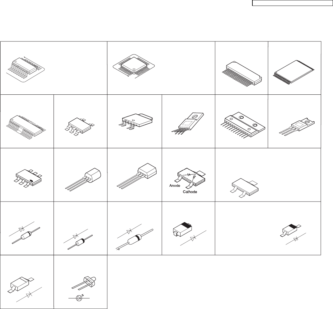
15 Illustration of IC's, Transistors and Diodes
No.1
No.1
1
28
15
14
7
21
22
8
1
4
5
2
C0EBE0000455
C0JBAA000346
E
C
B
B1BACD000018
E
C
B
B0BC5R600003
A
Ca
Cathode
Anode
B0BC7R500001
A
Ca
Cathode
Anode
B0EAKM000117
A
Ca
Cathode
Anode
C
B
E
B1GDCFJJ0047
B1GBCFJJ0051
B1ABGC000005
B1ADCF000001
B1ADCE000012
B1ADGB000008
2SD1819A0L
B1ABCF000176
C0CBCBD00018 (8p)
C0FBBK000050 (28p)
C1AB00001731 (6p)
C0EBA0000029 (4p)
C3EBGC000055 (8p)
C9ZB00000461 (32p)
C3EBEG000072 (8p)
C3ABPG000145 (54p)
C0HBB0000057 (44p)
C1AB00002463 (100p)
C2CBYY000194 (100p)
RFKWMHA0B160
XN0460100L
XP0621400L
B1BACG000023
B1BCCG000002
Anode
Cathode
Ca
A
A
Ca
Cathode
Anode
MN864701 (164p)
MN2DS0009VP (256p)
1
24
25
48
14
25
3
UNR511V00L
UNR521100L
B0ADCJ000020
B0ACCK000005 B0BC01200019
B0BC3R400001
B0BC5R000009
B0JCPD000025
B0BC01000014
B0BC013A0007
A
Ca
Cathode
Anode
Cathode
A
Ca
Anode
MA2J11100L
MAZ82200ML
MA2J72800L
1
23
C0GAY0000013
C0GBG0000048
B3AAA0000803
124
356
7
1
2
3
456
ECB
B1AAKD000012
B1ACKD000005
C0DBEHG00006 AN30070A AN17831A
3
1
12
51
SA-HT340GC / SA-HT340GCS / SA-HT340GS
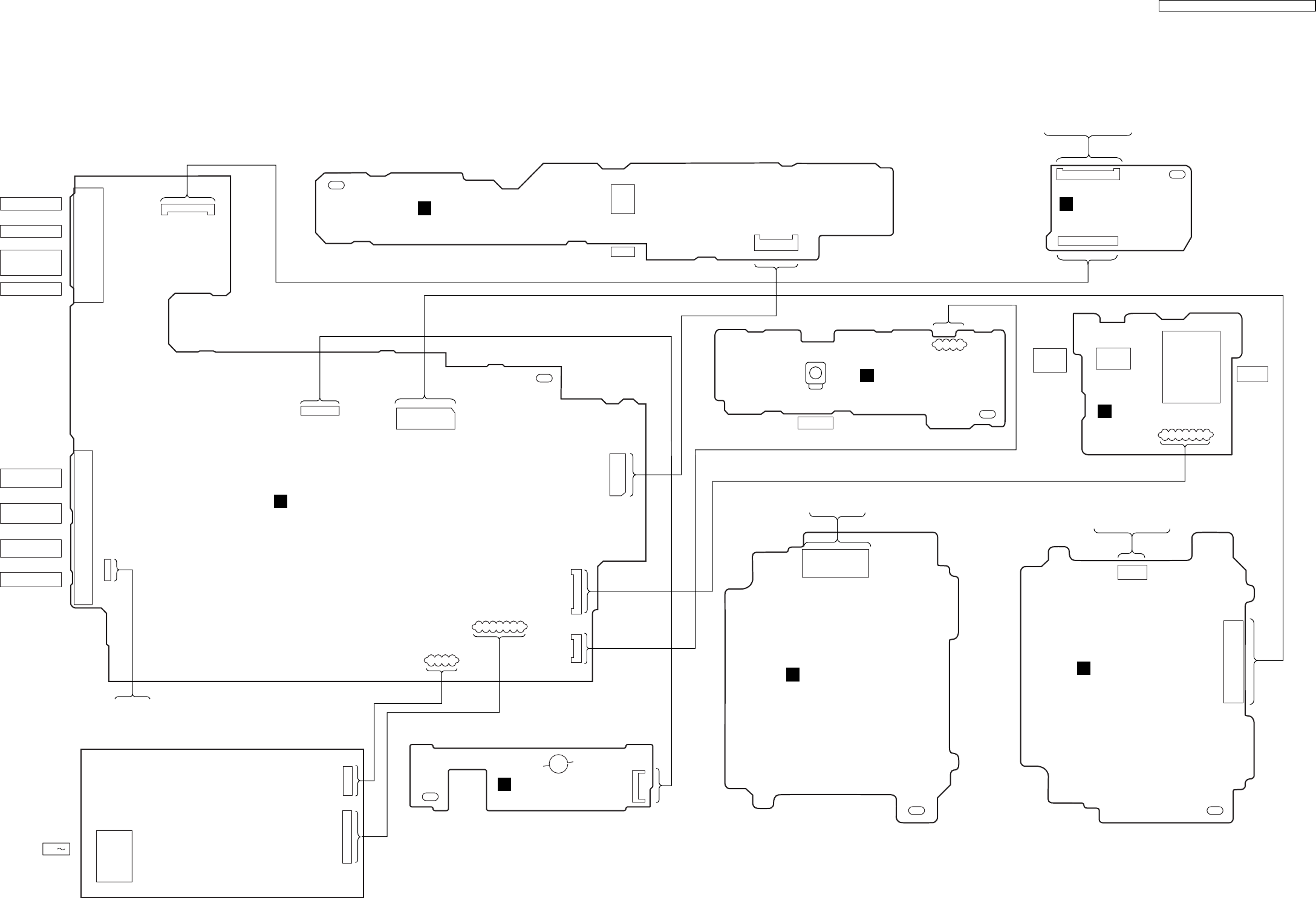
16 Wiring Connection Diagram
SA-HT340GC/GCS/GS WIRING CONNECTION
FP8101
FP8251
1
5
10
15
20
25
30
35
40
50
45
FP8531
25
201510
5
126
6
1
LOADING
MOTOR
+
-
MCS901
7
1
DVD MODULE P.C.B.
(SIDE:A)
A
PbF PbF
PbF
S-VIDEO OUT
VIDEO OUT
COMPONENT
VIDEO
OUT
AUX
SURROUND
SPEAKER
FRONT
SPEAKER
CENTER
SPEAKER
SUBWOOFER
14
13
12
11
10
9
8
7
6
5
4
3
2
1
1
2
3
17
1
4
12
12
13
50
49
48
47
4
3
2
1
10 1
5
4
2
14
13
12
11
10
9
8
6
3
1
7
JK5000
CN2001
H2004
CN5704
CN2007
CN2005
1
7
CN2006
CN2002
JK2001
13
2
1212
13
101
101
SENSOR
Z6900
CN6001
VR6800
14
H6004
CP2010
CN2010
VOLUME
PbF
PbF
PbF
PbF
TO FAN
UNIT
123
1
765432
875
4
32
1
VR6081
JK6802
H6903
MIC
VOLUME
MIC
14
111
1
11
H2001
1
4
CN2
CN1
110V-240V...50/60HZ
AC
CN3
H2002
SMPS MODULE P.C.B.
TRAY LOADING P.C.B.
F
(SOLDER SIDE)
TO TUNER PACK UNIT
MAIN P.C.B.
B
(SOLDER SIDE)
TUNER EXTENT P.C.B.
G
(SOLDER SIDE)
MIC P.C.B.
E
(SOLDER SIDE)
FL P.C.B.
C
(SOLDER SIDE)
VOLUME P.C.B.
D
(SOLDER SIDE)
TO OPU UNIT TO SPINDLE
MOTOR ASS'Y
DVD MODULE P.C.B.
(SIDE:B)
A
SA-HT340GC / SA-HT340GCS / SA-HT340GS
52

SA-HT340GC / SA-HT340GCS / SA-HT340GS
53
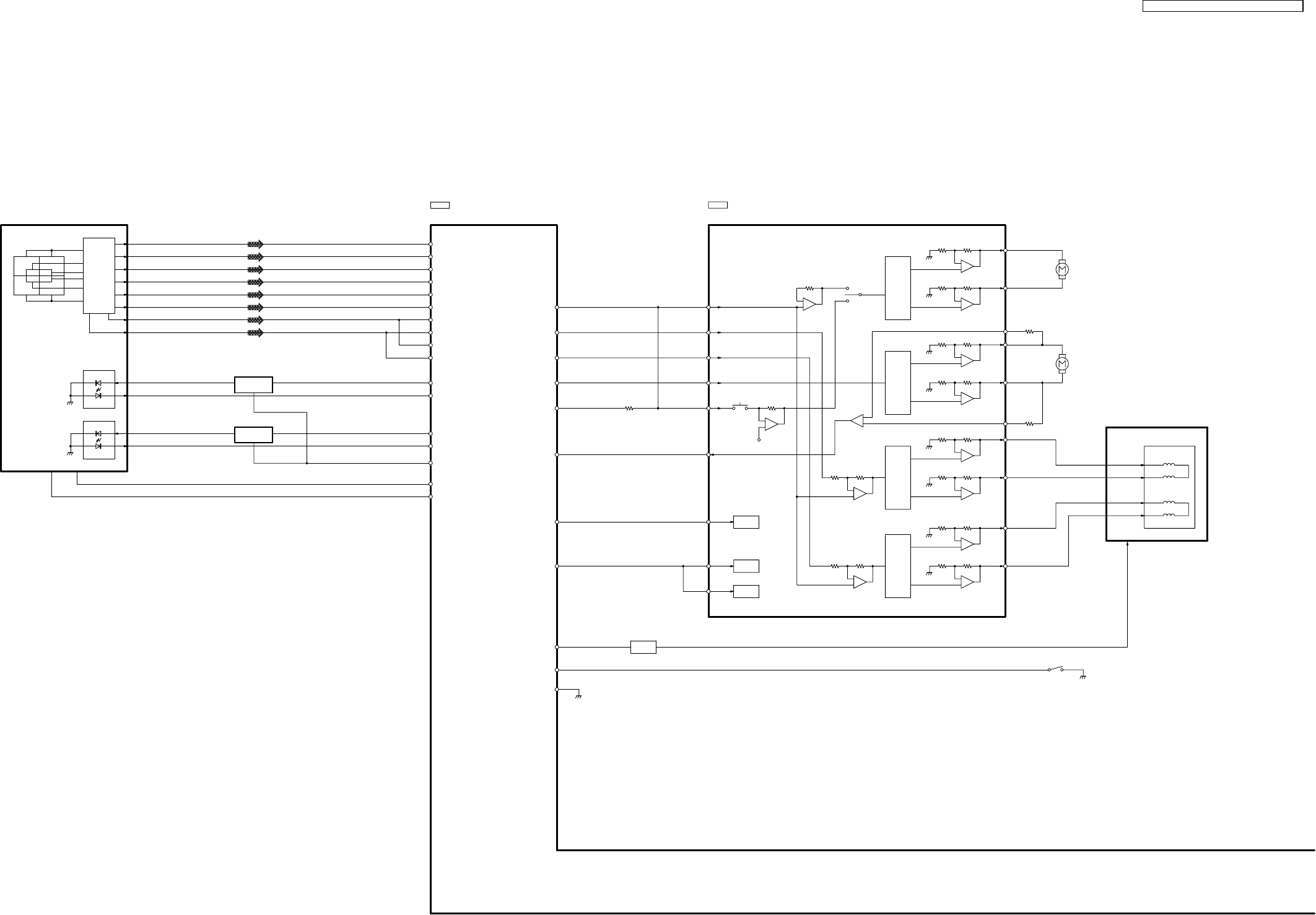
17 Block Diagram
BUFFER
QR8571
OPTICAL PICK UP UNIT
Q8551,8552
Q8561,8562
VOL4+
VOL4-
VOL3+
17
OPIN+
4
OPIN-
5
15
16
VOL3-
18
VOL1+
14
VOL1-
13
VOL2+
12
VOL2-
TRAVERSE INNER SW
11
MUTE
CH1,2
MUTE
CH3
24
BIAS1
1
VIN1
2
VIN2
3
23
VIN3
27
9
TRVFT MUTE
F0 DRV
PWM0
145
DRV1
90
TRS DRV
SPMUTE
DRV0
91
AD1
140
DRV4
87
DRV3
83
P14
81
89
DRV2
85
FG
114
113
125
139
126
RFINP
RFINN
LPC2
AD0
LPC02
LPC1
LPC01
VIN9
VIN10
VIN5
VIN6
VIN7
VIN8
VIN4
VIN3
VIN2
VIN1
MOTOR
SPINDLE
MOTOR
TRAVERSE
ACT F-
HFM
ACT F+
ACT T-
ACT T+
ACTUATOR
COIL
FOCUS
COIL
TRACKING
BIAS2
TRACKING COIL/FOCUS COIL/TRAVERSE/SPINDLE MOTOR DRIVE
C0GBG0000048
IC8251
PWM1
VHALF
TRV DRV
144
128
MUTE12
MUTE
CH4
20
MUTE4
MUTE3
LDIN
6
OPOUT
+
-
+
-
+
-
+
-
SHIFT
LEVEL
+
-
+
-
SHIFT
LEVEL
+
-
+
-
SHIFT
LEVEL
+
-
+
-
SHIFT
LEVEL
+
-
-
+
-
+
IC8001
MN2DS0009VP
DV3.2 LSI
LD DRIVE
LD DRIVE
130
129
131
132
133
134
136
135
137
138
123
124
LASER DIODE
B1 B2
B4
OPTICAL PICK UP UNIT
B3
A3
A2
PHOTO DETECTOR
A4
A1
LASER DIODE
AMP
HEAD
SA-HT340GC/GCS/GS BLOCK DIAGRAM
SA-HT340GC / SA-HT340GCS / SA-HT340GS
54
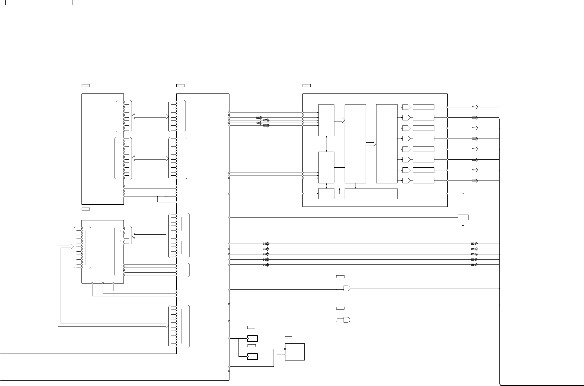
28
19
20
21
22
26
27
15
16
IC8421
AUDIO DAC
C0FBBK000050
OP CPU STAT
OP CPU CMD
OP CPU CLK
CR/PR/R
CB/PB/B
Y/PY/G
C
Y
A MUTE
SRCK
LRCK
AD OUT0
AD OUT1
AD OUT2
AD OUT3
P9
P10
P11
DACLK
P13
DAC4 OUT
DAC5 OUT
DAC1 OUT
DAC2 OUT
DAC3 OUT
P7
NRST
P6
P8
16bit
DATA
MEMORY
12bit
ADDRESS
MEMORY
12bit
ADDRESS
MEMORY
16bit
DATA
MEMORY
MCK
NWE
NCAS
NRAS
NCSM
MDQ15
MDQ14
MDQ13
MDQ12
MA11
MDQ11
MA10
MDQ10
MA9
MDQ9
MA8
MDQ8
MA7
MDQ7
MA6
MDQ6
MA5
MDQ5
MA4
MDQ4
MA3
MDQ3
MA2
MDQ2
MA1
MDQ1
MDQ0
MA0
CLK
NWE
NCAS
NRAS
CS
DQ15
DQ14
DQ13
DQ12
DQ11
DQ10
DQ9
DQ8
DQ7
DQ6
DQ5
DQ4
DQ3
DQ2
DQ1
DQ0
A11
A10
A9
A8
A7
A6
A5
A4
A3
A2
A1
A0
DVD STAT
DVD CMD
DVD CLK
CR/PR/R
CB/PB/B
Y/PY/G
C
Y
1
24
4
2
AND GATE
AND GATE
1
IC8695
IC8601
IC8606
C0JBAA000346
IC8691
C0JBAA000346
73
74
84
75
147
148
149
157
156
80
DVD MIX L
DVD MIX R
DVD FL
DVD FR
DVD SL
DVD SR
DVD CNT
SUBW
ZFLAG
QR8420
MUTING
SCK
MD
MC
MS
DATA1
DATA4
DATA3
DATA2
LRCK
MANAGER
CLOCK
SYSTEM
ZERO DETECT
OUT
OUT
ZFLAG
CLOCK
SYSTEM
5
166
BCK
I/F
CONTROL
FUNCTION
I/F
INPUT
SERIAL
CONTROLLER
FUNCTION
WITH
DIGITAL FILTER
OVERSAMPLING
4X/8X
LOW-PASS FILTER
OUTPUT AMP AND
DAC
V OUT6
LOW-PASS FILTER
OUTPUT AMP AND
DAC
V OUT5
LOW-PASS FILTER
OUTPUT AMP AND
DAC
V OUT4
LOW-PASS FILTER
OUTPUT AMP AND
DAC
V OUT3
LOW-PASS FILTER
OUTPUT AMP AND
DAC
V OUT2
LOW-PASS FILTER
OUTPUT AMP AND
DAC
V OUT1
LOW-PASS FILTER
OUTPUT AMP AND
DAC
V OUT8
MODULATOR
DELTA-SIGMA
MULTI-LEVEL
ENHANCED
V OUT7
LOW-PASS FILTER
OUTPUT AMP AND
DAC
4
3
78
77
76 2
6
169
13
12
11
7
170
171
172
167
168
8
DATA
IC8001
DV3.2 LSI
MN2DS0009VP
IC8051
64M SDRAM
C3ABPG000145
IC8651
RFKWMHA0B160 (GC/GS)
RFKWMHA0C160 (GCS)
16M FLASH ROM
40
38
36
32
30
28
26
24
EXDT0
EXDT15
39
37
33
31
29
27
25
23
NEXCE
18
55
NEXWE
NEXOE
20
281126
XOEXWEXCE
ADDRESS
ADDRESS
EXADR20
EXADR19
EXADR18
EXADR17
EXADR16
A20
A19
A18
A17
A16
A15
A8
A7
65
54
56
41
20
9
16
17
48
57
EXADT15
EXADT8
EXADT7
42
43
EXADT0
46
47
48
49
50
51
58
59
60
61
62
63
64
18
A0
1
8
18
25
DATA
DQ15
DQ0
45
43
41
39
36
34
32
30
44
42
40
35
38
33
31
29
223
221
227
228
229
38
16
17
18
19
208
210
212
216
217
213
211
209
207
203
201
199
206
202
198
230
237
232
238
240
242
244
246
247
245
200
243
241
53
51
50
48
47
45
44
42
13
11
10
8
7
5
4
2
35
22
34
33
32
31
30
29
26
25
24
23
SA-HT340GC/GCS/GS BLOCK DIAGRAM
MCK 1
225
1
1
RESET
C0EBA0000029
RESET
C0EBE0000455
P1
P2
5
6
66
67
(Not Supplied)
SDA
SCL
EEPROM
IC8611
SA-HT340GC / SA-HT340GCS / SA-HT340GS
55
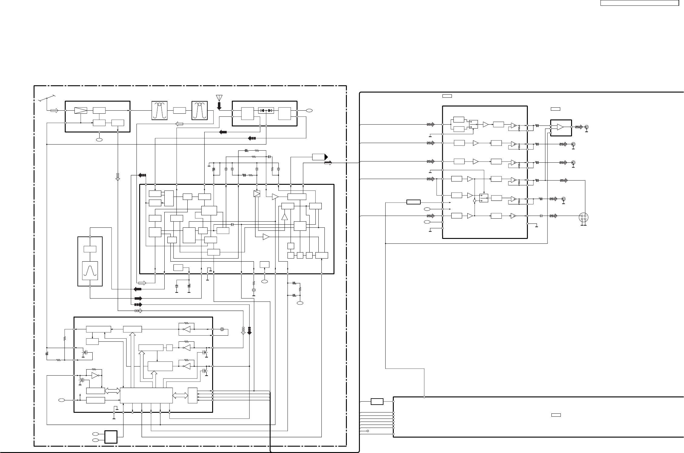
Q2804 MUTING
C
Y
CR/PR/R
CB/PB/B
Y/PY/G
12
1,16
4
8
6
14
5
15
7
13
11
10
19,22,25
32
C
Y
S-VIDEO OUT
JK2001
IC2801
VIDEO DRIVE
C9ZB00000461
+B
+B
VIDEO OUT
JK2001
30
29
27
26
CR(BLUE)
JK2001
18
17
CB(GREEN)
JK2001
21
20
24
23
62
4
1
Y(RED)
JK2001
VIDEO BUFFER
IC2802
C1AB00001731
IN1
IN2
SW
OUT
C IN
Y IN
MUTE 2
MUTE 1
CR IN
CB IN
CY IN
GND2
C OUT
GND
VCC 1
BIAS
6dB LPF
6 MHz
CLAMP
6dB LPF
6 MHz
LPF
6 MHz
BIAS
6dB LPF
12 MHz
BIAS
6dB LPF
12 MHz
6dB LPF
12 MHz
CLAMP
+
CY OUT
CY SAG
75
CR OUT
CR SAG
75
Y OUT
Y SAG
75
V OUT
V SAG
75
CB OUT
CB SAG
75
75
BIAS
CV IN CLAMP
6dB
L
H
SEL
SEL
L
H
42
DVD MUTE
MUTING
Q2006
ZFLAG
(FM)
ST
SD
DET OUT
(LC7213MDTRM)
(LA1833NMNTLM)
/FM MPX
DET/AM OSC MIX
FM/AM IF AMP,
TUNER PACK
SD
ST/DO
CE
DI
CLCL
DI
CE
DO
I/F
C2B
SHIFT REGISTER LATCH
DETECTOR
UNLOCK
15
11
17
18
16
1
20
14
13
4
3
2
5
896
12
7
1019
SYNTHESIZER
PLL FREQUENCY
AM IFT
121110
987654321
DET
PILOT
FFFFFF
VCO
CANCEL
PILOT
DET
PHASE
RF AMP
5
17
8
COIL
OSC
AM
COIL
ANT
AM
IF AMP
FM
AM ANT
FM ANT
SYSTEM CONTROL
IC2018
C2CBYY000194
TUN CLK
TUN SD
TUN DI
TUN DO
DVD STAT
DVD CMD
DVD CLK
36
35
38
37
29
30
28
CL
CE NC
SD
DI
ST/DO
DVD STAT
DVD CMD
DVD CLK
Rch
TUN L
(FM:ON)
SUPPLY
POWER
+B
+B
+B
X103
RESET
POWER ON
COUNTER
UNIVERSAL
1/2
1/6,1/17,4 BITS
SWALLOW COUNTER
DIVIDER
PROGRAMMABLE
12 BITS
CHARGE PUMP
PHASE DETECTOR
DIVIDER
REFERENCE
REG
REG
131415161718192021222324
+B
+B
SWITCH
STEREO
DECODER
FM IF
DET
LEVEL
S-CURVE
DET
FM
BUFFER
IF
AM/FM
DRIVE
TUNING
COMP
AM IF
AM DET
AGC
RM AMP
AM
MIX
AM
BUFFER
ALC
OSC
AM
+B
6
(FM)
+B
MIXER
OSC
BUFFER
SA-HT340GC/GCS/GS BLOCK DIAGRAM
81
RGB H
SA-HT340GC / SA-HT340GCS / SA-HT340GS
56
CLOCK
DATA
(36)
35
23 24
(37)
34
DVD-SUBW
DVD CNT
DVD SL(SR)
DVD MIX L(R)
TUNER L(R)
TV L(R) CH
LINOUT-L(R)
SYNC
RESET
12
X IN
15
X OUT
13
ASP CK
ASP DAT
83 84
VREF
98
JOG A
7677
JOG B
RMT
VCC
VCC
AVCC
18 16 62 99
(REMOTE SENSOR)
Z6900
(VOLUME)
VR6800
SUB IN
MIC IN
79
97
C IN
82
81(80)
VCC
VEE
86
85
84(83)
96(95)
90(89)
92(91)
94(93)
88(87)
100(99)
64 65
27
31
26
48
47
OP IN 1
OP IN 2 OP OUT 2
FLVOL OUT
(FRVOL OUT)
FLF IN
(FRF IN)
SL OUT
(SR OUT)
FL OUT
(FR OUT)
C OUT
FRONT L (R)
CENTER
SUBWOOFER
SUBOUT
OP OUT 1
46
45 44
32
(39) (40)
SYSTEM CONTROL
IC2018
C2CBYY000194
Q2004
19
D6900
15(20)
16(19)
17(18)
30(41)
28
X2001
Q2003
RESET
C1AB00002463
ASP(INPUT SELECT/DIGITAL SOUND PROCESSOR/ELECTRONIC VOLUME/TONE)
DVD FL(FR)
(FRIN)
FL IN
(SR IN)
SL IN
(INR1)
INL1
(INR2)
INL2
(INR3)
INL3
(INR4)
INL4
(INR5)
INL5
(RECOUTR)
RECOUTL
AUX
JK2002
SA-HT340GC/GCS/GS BLOCK DIAGRAM
FLSEL OUT
(FRSEL OUT) FLVOL IN
(FRVOL IN)
SLVOL IN
(SRVOL IN)
CVOL IN
SUBVOL IN
SLSEL OUT
(SRSEL OUT)
CSEL OUT
SUBSEL OUT
13
(22) 14
(21)
53 52
AMP
IC2102
VREF+
AMP
AMP
AMP
AMP
AMP
AMP
AMP
AGC
AMP
AMP
H BASS
MCU I/F
ASS
TONE
AMP
+B
-B
+B +B
+B
DRIVE
LED
MUTE C SW
67
SURROUND L (R)
AMP
Q3008
MUTING
Q3003
CONTROL
MUTING
Q3009
MUTING
MOTOR DRIVE(LOADING)
IC904
C0GAY0000013
DRIVE
LOADING
MOTOR
CONTROL
V REF
CONTROL
VREF+
V REF
GNDVCC
S902
S901
+B
Q2030
BRAKE H
TRY CW
TRY CCW
TRY CLOSE
TRY OPEN
1003214
8
9
52
1
IC2004
EEPROM
(Not Supplied)
ECS
EDA
ECK
23 25 24
4
36
5
SK
DO
CS
DI
97
KEY1
91
KEY2
(S6801-6806)
KEY SWITCH
(S6800)
KEY SWITCH
VREF+
+
_
+
_
MIC AMP
IC2204
C0ABBB000230
VR6081
JK6802
MIC
MIC SW
66
2
31
7
5
7
6
1
2
3
4
5
6
46
SA-HT340GC / SA-HT340GCS / SA-HT340GS
57
FL DISPLAY
C2CBYY000194
IC2018
SYSTEM CONTROL
5
X IN
X OUT
FL00
G1
P17
G10
P1
G1
P17
G10
P1
FL6901
DISPLAY DRIVER
IC6901
C0HBB0000057
SA-HT340GC/GCS/GS BLOCK DIAGRAM
966414
AVSS
VSSVSS
SPEAKERS
JK5000
1
7
12
6
9
3
4
10
40
P CONT
AM BP
20
FRONT +LOUT
FRONT +ROUT
SURROUND -LOUT
SURROUND +LOUT
SUBWOOFER-
SUBWOOFER+
FLD CLK
FLD OUT
FLD STB
87 85 86
304443987
-VP
GND
VCC
STB
CLK
D IN
+B -B
11
5
SURROUND -LOUT
SURROUND +LOUT
8
2
CENTER-
CENTER+
FL1
FL2
FRONT -LOUT
FRNOT -ROUT
70 72
DC DET
68
MUTE SURR
69
MUTE FRONT
71
STYB
DVD PCONT
FR0NT +L
FRONT L
FRONT R
FRONT -L
FRONT +R
FRONT -R
CH2 INPUT
CH1 INPUT
MUTE
STANDBY
6
8
IC5100
AN17831A
AUDIO POWER AMP
+
_
+
_
_
+
MUTE
REF
STANDBY CIRCUIT
+
_
+
_
_
+
VCC
8
9
5
CH2 +
OUTPUT
CH2 -
OUTPUT
CH1 +
OUTPUT
CH1 -
OUTPUT
+B
GND
7
12
10
2
4
SURROUND +L
SURROUND L
SURROUND R
SURROUND -L
SURROUND +R
SURROUND -R
CH2 INPUT
CH1 INPUT
MUTE
STANDBY
6
8
IC5200
AN17831A
AUDIO POWER AMP
+
_
+
_
_
+
MUTE
REF
STANDBY CIRCUIT
+
_
+
_
_
+
VCC
8
9
5
CH2 +
OUTPUT
CH2 -
OUTPUT
CH1 +
OUTPUT
CH1 -
OUTPUT
+B
GND
7
12
10
2
4
CENTER +
CENTER
SUBWOOFER
CENTER -
SUBWOOFER +
SUBWOOFER -
CH2 INPUT
CH1 INPUT
MUTE
STANDBY
6
8
IC5300
AN17831A
AUDIO POWER AMP
+
_
+
_
_
+
MUTE
REF
STANDBY CIRCUIT
+
_
+
_
_
+
VCC
8
9
5
CH2 +
OUTPUT
CH2 -
OUTPUT
CH1 +
OUTPUT
CH1 -
OUTPUT
+B
GND
7
12
10
2
4
AN30070A
POWER CONTROL
Q2916,2917
3
1
2
DC-DC CONVERTER
SS
VCCLX(OUT)
+B
Q2903
+9V
REGULATOR
Q5740-5742
Q5744-5746
FAN MOTOR
DRIVE
M
Q2910
Q2905
DC DETECTDC DETECT
DC DETECT
Q2915
DC DETECT
Q2980
SWITCHING
+B
Q2906,2907
-7V
REGULATOR
-B
Q2913
M +9V
REGULATOR
-B
Q2974
-VP
REGULATOR
+B
Q2904
SW +5V
REGULATOR
+B
+B
Q2955
DVD A+5V
REGULATOR
+B
Q2914, D2944
DVD 2.7V
REGULATOR
SIGNAL LINES
( ) Indicates the Pin No. of Right Channel.
: MAIN SIGNAL LINE
: FM SIGNAL LINE
: FM OSC SIGNA
: AUX SIGNAL LINE
L LINE
: AM SIGNAL LINE
: AM OSC SIGNAL LINE
: FM /AM SIGNAL LINE : CD-DA (AUDIO /VIDEO) SIGNAL LINE
NOTE : Signal Lines are applicable to the Left Channel only.
: DVD VIDEO SIGNAL LINE
: DVD AUDIO SIGNAL LINE
IC2903
POWER SUPPLY (TO SMPS MODULE)
H2001
2+26V (VCC)
1+26V (VCC)
9FL2 (FL-)
8FL1 (FL+)
11 -VP (-28V)
11 SYS6V
4+9.8V
H2002
-B
+B
VREF+
D2918
D2919
C0CBCBD00018
+B
POWER CONTROL
QR8111
1
5
8
+3.3V DC-DC CONVERTER
CONT
VIN
V0
IC8111
42
+1.2V REGULATOR
C0DBEHG00006
OUT VCC
+B
IC8151
SA-HT340GC / SA-HT340GCS / SA-HT340GS
58

SA-HT340GC / SA-HT340GCS / SA-HT340GS
59
18 Schematic Notes
·
This schematic diagram may be modified at any time
with the development of new technology.
Notes:
S901: Play detection switch.
S902: Open detection switch.
S6800: Tray open / close switch ( Open /
Close).
S6804: F. skip, search and Tuning switch
( / / TUNING ).
S6805: R. skip, search and Tuning switch
(// TUNING ).
S6801: Stop and TUNE mode /FM mode
switch ( TUNE MODE/FM MODE).
/
S6802: Play and memory switch (
Memory).
S6806: Standby / on switch (POWER ).
S6803: Source select switch (SELECTOR).
VR6081: VR Mic level.
VR6800: VR Volume jog.
·
Indicated voltage values are the standard values for the unit
measured by the DC electronic circuit tester (high-
impedance) with the chassis taken as standard. Therefore,
there may exist some errors in the voltage values,
depending on the internal impedance of the DC circuit
tester.
·
Important safety notice:
Components identified by mark have special
characteristics important for safety.
Furthermore, special parts which have purposes of fire-
retardant (resistors), high-quality sound (capacitors), low-
noise (resistors), etc. are used.
When replacing any of components, be sure to use only
manufacturer´s specified parts shown in the parts list.
·
The supply part number is described alone in the
replacement parts list.
·
Voltage and signal line
: +B Signal line
: CD-DA signal line
: Main signal line
: DVD (Video) signal line
: DVD (Audio) signal line
: FM/AM signal line
: -B Signal line
: AUX signal line
Caution!
IC and LSI are sensitive to static electricity.
Secondary trouble can be prevented by taking care during
repair.
Cover the parts boxes made of plastics with aluminum foil.
Ground the soldering iron.
Put a conductive mat on the work table.
Do not touch the legs of IC or LSI with the fingers directly.
60
SA-HT340GC / SA-HT340GCS / SA-HT340GS

61
SA-HT340GC / SA-HT340GCS / SA-HT340GS
19 Schematic Diagram
19.1. (A) DVD Module (DV3.2) Circuit
16
17
18
19
20
21
25
23
22
24
26
1
2
3
4
5
6
14
12
10
8
7
9
11
13
15
2
4
6
5
3
1
15
14
13
12
11
10
2
4
6
8
9
7
5
3
1
17
18
16
TO ACT
TO
HFM PCB
TO
LDU PCB
L1
J0JBC0000105
L2
J0JCC0000307
C6
22P
C8
0.1
C7
0.1
T+
F+
F-
T-
HFM
TA
TB
TD
TC
FE2
FE1
GND (IM)
GND (IM)
RF
VREF2(RF-)
PIN (DVD)
LD (CD)
LD GND
LD (DVD)
GND (OEIC)
VREF1
VCC
SUB2
SUB1
PIN(CD)
SUBSEL
GND
VCC
GND
GND
OUT
GND
GND
TB
TA
TC
TD
FE1
FE2
IM
RF
GND
VREF
VCC
SUB2
SUB1
SW
LD (CD)
LD (DVD)
LDGND
OPTICAL PICKUP UNIT CIRCUIT
C4
0.22
C5
22P
L3
J0JBC0000105
R2
0
R4
0
C2
0.1
C1
0.1
C3
0.1
R1
0
R3
0
R5
0
R6
0
R7
6.8K
VR2
6.8K
VR1
6.8K
L4
J0JBC0000105
: +B SIGNAL LINE : CD-DA SIGNAL LINE
3029
15
16
17
12
13
14
18
11
19
10
20
9
21
8
22
7
23
6
24
5
25
4
26
3
27
2
28
1
16
17
18
19
20
21
25
23
22
24
26
1
2
3
4
5
6
14
12
10
8
7
9
11
13
15
T+
F+
F-
T-
HFM
TA(DVD)
TB(DVD)
TD(DVD)
TC(DVD)
FE2(DVD/CD)
FE1(DVD/CD)
GND
RF
VREF2(RF-)
PIN(DVD)
LDCD
LDGND
LDDVD
GND(OEIC)
VREF1
VCC
SUB2
SUB1
PIN(CD)
SUBSEL
GND(VRCD)
FP8531
LDCNT
MUTE3
TRIN
BIAS2
LDIN
VIN3
PREVCC
FIN
VCC(CH3.4)
MUTE4
GND(CH3.4)
VO3-
VO3+
VO4-
VO4+
BIAS1
VIN1
VIN2
OPIN+
OPIN-
OPOUT
GND(PRE)
FIN
VCC(CH1.2)
MUTE12
GND(CH1.2)
VO2-
VO2+
VO1-
VO1+
VIN1
VIN2
VIN4
VIN3
RFINP
RFINN
LPC1
VREFH
VIN6
VIN5
LPC2
RAM_CD
LB8260 ERJ3GEY0R00V
LB8259 ERJ3GEY0R00V
LB8258 ERJ3GEY0R00V
LB8257 ERJ3GEY0R00V
LB8561 J0JBC0000042
LB8551 J0JBC0000042
LB8531 ERJ2GE0R00X
R8533 0
R8531 1.5K
C8533 0.1
C8256
0.1
C8253
0.1
R8251
6.8
RX8532
(56 x 4)
RX8533
(56 x 2)
C8531 100P
C8532
220P
RX8531
(56 x 2)
IC8251
C0GBG0000048
MOTOR DRIVER
TO
SPINDLE
TRAVERSE
MOTOR
ASS’Y
C8255
16V22
C8258
0.1
C8257
16V47
R8532 2.2K
TRVFTMUTE
C8262
0.1
C8261
0.1
R8262
15K
R8261
82k
R8263
82k
R8264
15K
R8231
22K
R8230
2.2K
C8231
0.1
DRV0
R8232
7.5K
C8232
0.1
DRV1
C8252
0.1
C8251
6.3V220
D+5V
2
4
6
5
3
1
FP8251
SPM-
SPM+
TRVM-
TRVM+
DGND
TRV_INNER_SW
M+9V
SPMUTE
AD1
TRDRV
FODRV
VHALF
TRV-I-SW
C8511 1
C8512 1
RX8534
(56 x 2)
VIN8
VIN7
SA-HT340GC/GCS/GS DVD MODULE (DV3.2)/ OPTICAL PICKUP UNIT CIRCUIT
K8251
A
B
C
D
E
F
G
H
1 2345678910111213
DVD MODULE (DV3.2) CIRCUIT
A
SCHEMATIC DIAGRAM-1
SA-HT340GC / SA-HT340GCS / SA-HT340GS
62
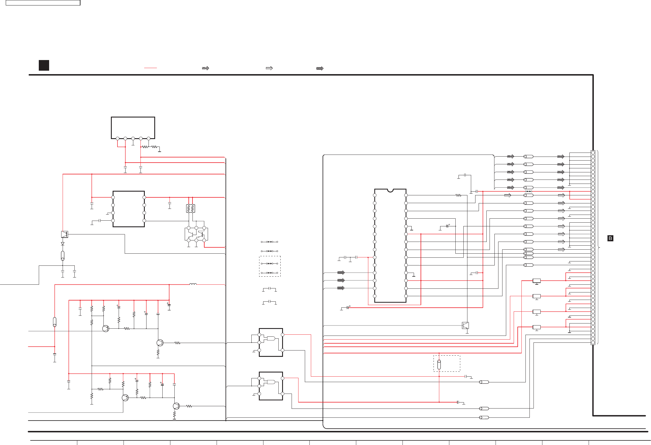
C8424
0.1
12345
1
2
36
7
8
45
D+5V
VO
NC
GND
CN
VIN
CTL VCC ADJ
R8153
620
R8154
1K
GND OUT
NC
NC
Cont
D+3.3V
HFMON
AD0
LPC02
LPC01
A+5V
VDD12
LB8530
J0JHC0000045
C8112
1
C8113
470P
C8111
0.1
C8152
1
C8151
4.7
L8550
G1C100KA0055
C8561
0.1
C8551
0.1
C8530
0.1
R8559
15K
R8558
47K
R8557
51 R8556
56
C8553
6.3V47
R8555
2.2
R8553
1K
R8552
1K
R8551
0
R8554
68
C8552
16V10
R8567
51
R8568
47K
R8566
56
C8563
6.3V47
R8565
2.2
R8563
1K
C8564
1
C8562
16V10
R8564
22
R8562
1K
R8561
0
C8550
6.3V33
C8554
1
Q8562
B1ADGB000008
SWITCH
Q8552
B1ADGB000008
SWITCH
Q8561
2SD1819A0L
Q8551
2SD1819A0L
SWITCH
SWITCH
C0CBCBD00018
3.3V REGULATOR IC
1.2V REGULATOR
IC8111
IC8151
C0DBEHG00006
2R7V
VDD12
QR8111
XP0621400L
SWITCH 123
4
5
6
RX8111
(22K x 2)
36
37
38
39
40
41
49
47
45
43
42
44
46
48
50
21
22
23
24
25
26
34
32
30
28
27
29
31
33
35
15
16
17
18
19
20
1
2
3
4
5
13
11
9
7
6
8
10
12
14
TO
MAIN CIRCUIT
(CN2001) ON
SCHEMATIC
DIAGRAM-5
FP8101
4
51
2
3
4
1
2
3
VGND
VGND
VGND
VGND
VGND
ADAC5V
ADAC5V
ADGND
ADGND
ADGND
ADGND
ADGND
ADGND
DGND
DGND
D+5V
D+5V
D+5V
A+5V
A+5V
A+5V
AGND
AGND
2R7V
2R7V
DGND
DGND
M+9V
M+9V
MGND
MGND
DGND
DGND
K8421
MIX-L
LB8421 ERJ2GE0R00X
MIX-R
LB8422 ERJ2GE0R00X
DOP_CPU-CLK
LB8691
ERJ2GEJ101X
FL
LB8425 ERJ2GE0R00X
FR
LB8426 ERJ2GE0R00X
A-REF
LB8423 ERJ2GE0R00X
ZFLAG&AMUTE
LB8424 ERJ2GE0R00X
AUDIODIGITAL
LB8491 ERJ2GE0R00X
DOP_CPU-CMD
LB8693
ERJ2GEJ101X
DOP_CPU-STAT
LB8692
ERJ2GEJ101X
FL8103
F1H0J1050022
VCC
GND
GND
VCC
OP_CPU_CLK
OP_CPU_CMD
OP_CPU_STAT
C8695
0.1
C8691
0.1
LB8690
(GC/GS)
J0JBC0000106
IC8691
C0JBAA000346
AND GATE LOGIC IC
QR8420
UNR521100L
AUDIO MUTING SWITCH
IC8695
C0JBAA000346
AND GATE LOGIC IC
M+9V
C8423
6.3V33
C8422
0.1
R8420
Y_PY_G
CB_PB_B
CR_PR_R
Y
C
2.2K
C8421
6.3V100
AUDIODIGITAL
P13
FL8104
F1J1E1040022
FL8102
F1H0J1050022
FL8101
F1H0J1050022
2R7V
SA-HT340GC/GCS/GS DVD MODULE (DV3.2) CIRCUIT
Y/PY/G
CB/PB/B
CR/PR/R
Y
C
LB8303 J0JBC0000042
LB8304 J0JBC0000042
LB8305 J0JBC0000042
LB8301 J0JBC0000042
LB8302 J0JBC0000042
C0FBBK000050
5-CH DAC IC
C8427
0.1
SW
LB8431 ERJ2GE0R00X
SR
CNT
LB8429 ERJ2GE0R00X
LB8428 ERJ2GE0R00X
SL
LB8427 ERJ2GE0R00X
C8428
0.1
C8426
0.1
AOUT0
AOUT1
AOUT2
IC8421
ZERO2
VOUT1
VOUT2
VCOM
AGND2
VCC2
VOUT3
VOUT4
VOUT5
VOUT6
AGND1
VCC1
VOUT7
VOUT8
ZERO1
MS
MC
MD
SCK
DATA1
BCK
LRCK
VDD
DGND
DATA2
DATA3
DATA4
MSEL
1
227
28
326
425
524
623
722
821
920
10 19
11 18
12 17
13 16
14 15
5
C8331
0.1
C8325
0.1
K8006
0
K8001
0
K8008
0
K8003
0
(GCS)
LB8571
J0JBC0000042
C8572
0.1 C8571
10
D8571
MA2J72800L
QR8571
UNR511V00L
BUFFER
: +B SIGNAL LINE : MAIN SIGNAL LINE
: DVD VIDEO SIGNAL LINE : DVD AUDIO SIGNAL LINE
DVD MODULE (DV3.2) CIRCUIT
A
SCHEMATIC DIAGRAM-2
15 16 17 18 19 20 21 22 23 24 25 2614
SA-HT340GC / SA-HT340GCS / SA-HT340GS
63
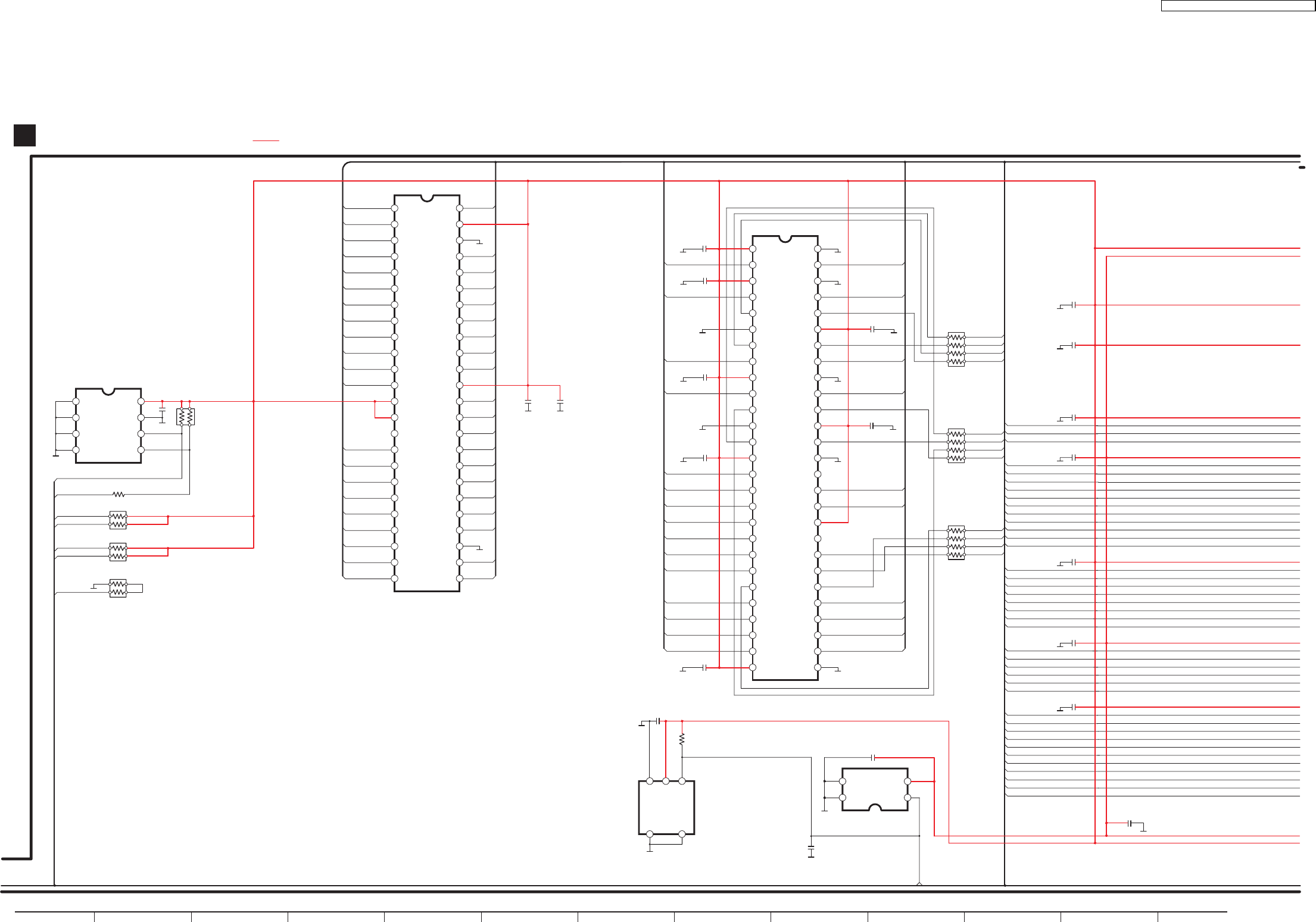
C8611
0.1
1
2
346
47
48
445
544
643
742
841
940
10 39
11 38
12 37
13 36
14 35
15 34
16 33
17 32
18 31
19 30
20 29
21 28
22 27
23 26
24 25
8
7
2
1
6
3
5
4
RX8611
(4.7K x 2)
R8611
100
RX8691
(10K x 2)
RX8001
(10K x 2)
RX8032
(4.7K x 2)
C8651
0.1
C8652
0.1
A0
A1
A2
GND
VCC
WP
SCL
SDA
A15
A14
A13
A12
A11
A10
A9
A19
A20
XWE
XRESET
NC
WP/ACC
RDY/XBSY
A18
A17
A7
A6
A5
A4
A3
A2
A1
A16
XBYTE
VSS
DQ15/A-1
DQ7
DQ14
DQ6
DQ13
DQ5
DQ12
DQ4
VDD
DQ11
DQ3
DQ10
DQ2
DQ9
DQ1
DQ8
DQ0
XOE
VSS
XCE
A0
EXDT0
EXADR15 EXADR16
EXADR14
EXADR13
EXADR12
EXADR11
EXADR10
EXADR9
EXADR8
EXADR19
EXADR20
NEXWE
EXADR18
EXADR17
EXADR7
EXADR6
EXADR5
EXADR4
EXADR3
EXADR2
EXADR1 EXADR0
PNRST
SCL
SDA
SBT3
OP_CPU_CLK
OP_CPU_CMD
IC8611
EEPROM
(NOT SUPPILED)
STBDAC
EXDT8
EXDT1
EXDT9
EXDT2
EXDT10
EXDT3
EXDT11
EXDT4
EXDT12
EXDT5
EXDT13
EXDT6
EXDT14
EXDT7
EXDT15
NEXCE
NEXOE
EXTRG0
A8
IC8651
RFKWMHA0B160(GC/GS)
RFKWMHA0C160(GCS)
16M FLASH ROM
: +B SIGNAL LINE
1
2
352
53
54
451
550
649
748
847
946
10 45
11 44
12 43
13 42
14 41
15 40
16 39
17 38
18 37
19 36
20 35
21 34
22 33
23 32
24 31
25 30
26 29
27 28
C8602
0.015
VDD
DQ0
VDDQ
DQ1
DQ2
VSSQ
DQ3
DQ4
VDDQ
DQ5
DQ6
VSSQ
DQ7
VDD
LDQM
/WE
/CAS
/RAS
/CS
BA0
BA1
A10/AP
A0
A1
A2
A3
VDD
VSS
DQ15
VSSQ
DQ14
DQ13
VDDQ
DQ12
DQ11
VSSQ
DQ10
DQ9
VDDQ
DQ8
VSS
NC
UDQM
CLK
CKE
NC
A11
A9
A8
A7
A6
A5
A4
VSS
EXADR1
EXADR2
EXADR3
MDQ15
MDQ14
MDQ11
MDQ10
DQM1
CLK
MA7
MA6
MA5
MA4
MDQ0
MDQ1
MDQ4
MDQ5
DQM0
NWE
NCAS
NRAS
NCSM
BA0
BA1
MA0
MA1
MA2
MA3
C8051
1
C8052
0.1
C8053
0.1
C8054
220P
C8055
1
C8056
2200P
C8057
1
C8007 0.1
C8019 0.1
C8018 0.1
C8008 0.1
IC8051
C3ABPG000145
64MB SDRAM
45
12
3
VSS
VDD
OUT
NC
CD
PNRST
C8606
0.1
R8601
100K C8601
0.1
IC8606
C0EBE0000455
RESET
IC8601
C0EBA0000029
RESET
C8020 0.1
C8021 0.1
C8022 0.1
C8006 0.1
EXADR4
EXADR5
EXADR6
EXADR7
EXADR17
EXADR18
EXADR19
EXADR8
EXADR9
EXADR10
EXADR11
EXADR12
EXADR13
EXADR14
EXADR15
EXADR16
EXDT15
EXDT7
EXDT14
EXDT5
EXDT12
EXDT4
EXDT6
EXDT13
EXDT11
EXDT3
EXDT10
EXDT2
EXDT9
EXDT1
EXDT8
EXDT0
NEXOE
NEXCE
EXADR0
OUT
VDDNIC
GND 1
2
3
4
NEXWE
MA10
MA8
MA9
MA11
MDQ7
MDQ8
MDQ6
MDQ9
MDQ3
MDQ12
MDQ2
RX8012
(82 x 4)
RX8014
(82 x 4)
RX8015
(82 x 4)
MDQ13
SA-HT340GC/GCS/GS DVD MODULE (DV3.2) CIRCUIT
DVD MODULE (DV3.2) CIRCUIT
A
SCHEMATIC DIAGRAM-3
28 29 30 31 32 33 34 35 36 37 38 3927
SA-HT340GC / SA-HT340GCS / SA-HT340GS
64
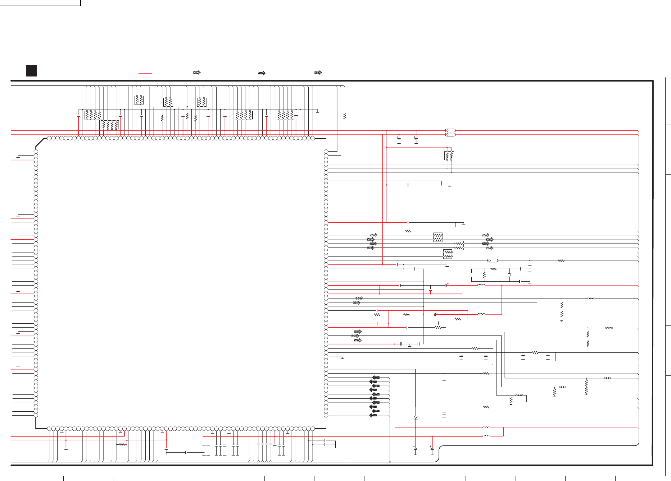
DVD MODULE (DV3.2) CIRCUIT
A
SCHEMATIC DIAGRAM-4
VHALF
VREFH
LPC02
LPC2
LPC01
LPC1
VIN3
VIN4
VIN2
VIN1
RFINP
RFINN
RAM_CD
TRV-I-SW
HFMON
OP_CPU_STAT
OP_CPU_CMD
OP_CPU_CLK
STBDAC
SBO3
SBT3
DRV1
DRV0
PNRST
MA3
MA4
MA2
MA5
NCSM
C8023
0.1
C8502 0.1
C8527 0.033
C8523 0.1
C8524 0.1
C8525 5600P
C8526 0.018
C8503 0.1
C8504 0.1
C8513 0.1
C8514 0.1
C8516 0.1
C8515 0.1
RX8017
RX8016
RX8020
RX8018
RX8019
RX8013
RX8011
(82 x 4)
R8013 22
C8013 0.1
C8014 0.1
C8015 0.1
TRVFTMUTE
SPMUTE
1
2
3
4
5
6
7
8
9
65 66 67 68 69 70 71 72 73
185
186
187
188
189
190
191
192
248249250251252
253
254
255
256
10
184
74
247
11
183
75
246
12
182
13
181
76
245
77
244
14
180
15
179
16
178
78
243
79
242
80
241
17
177
18
176
19
175
20
174
81
240
82
239
83
238
84
237
21
173
22
172
23
171
24
170
25
169
85
236
86
235
87
234
88
233
89
232
26
168
27
167
28
166
29
165
30
164
31
163
32
162
90
231
91
230
92
229
93
228
94
227
95
226
96
225
33
161
34
35
159
36
158
97
224
98
223
99
222
100
221
37
157
38
156
39
155
40
154
41
153
42
152
43
151
44
150
101
220
102
219
103
218
104
217
105
216
106
215
107
214
108
213
160
45
149
46
148
47
147
48
146
49
145
50
144
51
143
52
142
109
212
110
211
111
210
112
209
113
208
114
207
115
206
116
205
53
141
54
140
55
138
56
137
57
136
58
135
59
134
60
133
61
132
62
131
63
130
64
129
117
204
118
203
119
202
120
201
121
200
122
199
123
198
124
197
125
196
126
195
127
194
128
193
139
MDQ18
VSS
VDD33
MDQ28
MDQ19
MDQ27
MDQ20
VDD33
VSS
MDQ26
MDQ21
MDQ25
MDQ22
MDQ24
MDQ23
VSS
VDD33
EXADT0
NEXCE
NEXOE
VSS
VDD12
EXDT0
EXDT8
EXDT1
EXDT9
EXTD2
EXDT10
EXDT3
EXDT11
EXDT4
EXDT12
EXDT5
VSS
VDD33
EXDT13
EXDT6
EXDT14
EXDT7
EXDT15
EXADR16
EXADT15
EXADT14
VSS
VDD12
EXADT13
EXADT12
EXADT11
EXADT10
EXADT9
EXADT8
VSS
VDD33
EXADR19
NEXWE
EXADR18
EXADR17
EXADT7
EXADT6
EXADT5
EXADT4
EXADT3
EXADT2
EXADT1
TRCDATA1
TRCDATA0
TRCCLK
EXTRG0
SDATA
SCLOCK
EXTRG1
VSS
VDD33
VDIO0
VDIO1
VDIO2
VDIO3
VDIO4
VDIO5
VDIO6
VDIO7
VDD33
VSS
IECOUT
ADOUT0
ADOUT1
ADOUT2
ADOUT3
SRCK
LRCK
DACCK
VDD12
VSS
OSCO
OSCI
AVSSG
AVDDG
AVSSE
AVDDE
DAC5OUT
DAC4OUT
AVSSF
COMP2
IREF1
VREF
COMP1
AVDDF
DAC1OUT
DAC2OUT
DAC3OUT
AVDDH
PWM0
PWM1
AVSSH
AD4
AD2
AD1
AD0
VIN1
VIN2
VIN4
VIN3
VIN8
VIN7
VIN6
VIN5
VIN9
VIN10
P0
P1
P2
VSS
VDD33
P3
P4
P5
P6
P7
P8
P9
P10
P11
P12
P13
P13
P14
VSS
VDD12
NRST
FG
DRV5
DRV4
DRV3
DRV2
DRV1
DRV0
VSS
VDD33
MONI7
MONI6
MONI5
MONI4
MONI3
MONI2
MONI1
MONI0
AVDDD
PLFIL1
AVSSD
VREFH7
VREFL7
CCAPA
AVSSC
CDATA
AVDDC
ANAMONI1
ANAMONI2
RFINN
RFINP
VIN1RF
VIN2RF
VIN4RF
VIN3RF
AVDDB
VREFH5
VREFL5
AVSSB
LPC1
LPC01
LPC2
LPC02
VREFH
VHALF
MDQ29
MDQ17
MDQ30
MDQ16
MDQ31
DQM3
DQM2
VDD33
VSS
MA3
MA4
MA2
MA5
MA1
MA6
MA0
MA7
VDD33
VSS
MA10
MA8
BA1
VDD12
VSS
MA9
BA0
MA11
NCSM
NRAS
NCAS
VSS
MCKI
VDD33
MCK
VSS
NWE
DQM1
DQM0
VDD12
MDQ7
MDQ8
VSS
VDD33
MDQ6
MDQ9
MDQ5
MDQ10
MDQ4
MDQ11
MDQ3
MDQ12
VSS
VDD33
MDQ2
MDQ13
MDQ1
MDQ14
MDQ0
MDQ15
VDD33
VSS
TRCST
TRCDATA3
TRC
DATA2
IC8001
MN2DS0009VP
DV3.2 LSI
C8012 0.1
C8016 0.1
C8017 0.1
C8004 0.1
C8003 0.1
R8003
47K
C8024
0.1
C8521 0.1
C8522 0.1
SCL
SDA
EXADR20
MA1
MA6
MA0
MA7
(82 x 4)
MA10
MA8
MA9
MA11
BA1
BA0
(22 x 2)
NRAS
NCAS
(22 x 2)
CLK
R8011 22
NWE
R8012 22
DQM1
DQM0
(22 x 2)
MDQ5
MDQ10
MDQ4
MDQ11
MDQ1
MDQ14
MDQ0
MDQ15
MDQ7
MDQ8
MDQ6
MDQ9
MDQ3
MDQ12
MDQ2
MDQ13
(82 x 4)
(82 x 4)
TRCST
TRCDATA3
TRCDATA2
C8505 0.1
D8211
MA2J11100L
: +B SIGNAL LINE : CD-DA SIGNAL LINE
: DVD AUDIO SIGNAL LINE : DVD VIDEO SIGNAL LINE
VDD12
AUDIODIGITAL
DMIXOUT
SRCK
LRCK
ADAC-CLK
FODRV
TRDRV
AD0
Y_PY_G
AD1
CB_PB_B
CR_PR_R
RX8031
(4.7K x 2)
L8302
G1C100K00019
VIN1
VIN2
VIN4
VIN3
VIN8
VIN7
VIN6
VIN5
VIN5
VIN6
C8528 1
C8529 1
C8501
6.3V100
C8201
6.3V100
L8501
G1C100K00019
L8201
G1C100K00019
R8211
10K
C8541
4700P
C8211
1200P
C8221
1000P
C8222
820P
C8226
1000P
C8225
1000P
R8541
15K
R8221
8.2K
R8225
8.2K
C8312 1
LB8401 J0JBC0000042
C8401
15P
R8621
1M
R8622 1K
C8622
12P
C8621
12P
X8621
H0J270500085
C8305 0.1
(100 x 2)
R8401 100
C8025 0.1
C8001
4V330
C8011
6.3V100
LB8001
J0JHC0000045
LB8011
J0JHC0000045
D+3.3V
D+3.3V
C
Y
D+3.3V
R8421
K8325
K8321
R8325
68
R8326
0
R8321
68
R8322
0
K8331
R8331
68
R8335
68
R8332
0
0
AOUT2
(100 x 2)
AOUT0
AOUT1
TRCDATA1
TRCDATA0
TRCCLK
SCLOCK
SDATA
EXTRGO
R8041
33
C8026 0.1
C8005 0.1
C8306 0.1
C8304
0.1
C8303 0.1
C8302
6.3V33
C8313 1
R8313 9.1K R8314 0
C8301 6.3V220
L8301
G1C100K00019
R8311
2.4K
C8311 0.1
R8312 1K
C8202 0.1 C8203 0.1
SA-HT340GC/GCS/GS DVD MODULE (DV3.2) CIRCUIT
RX8402
RX8403
RX8401
(100 x 2)
K8335
R8341
68
K8341
A
B
C
D
E
F
G
H
41 42 43 44 45 46 47 48 49 50 51 5240
SA-HT340GC / SA-HT340GCS / SA-HT340GS
65
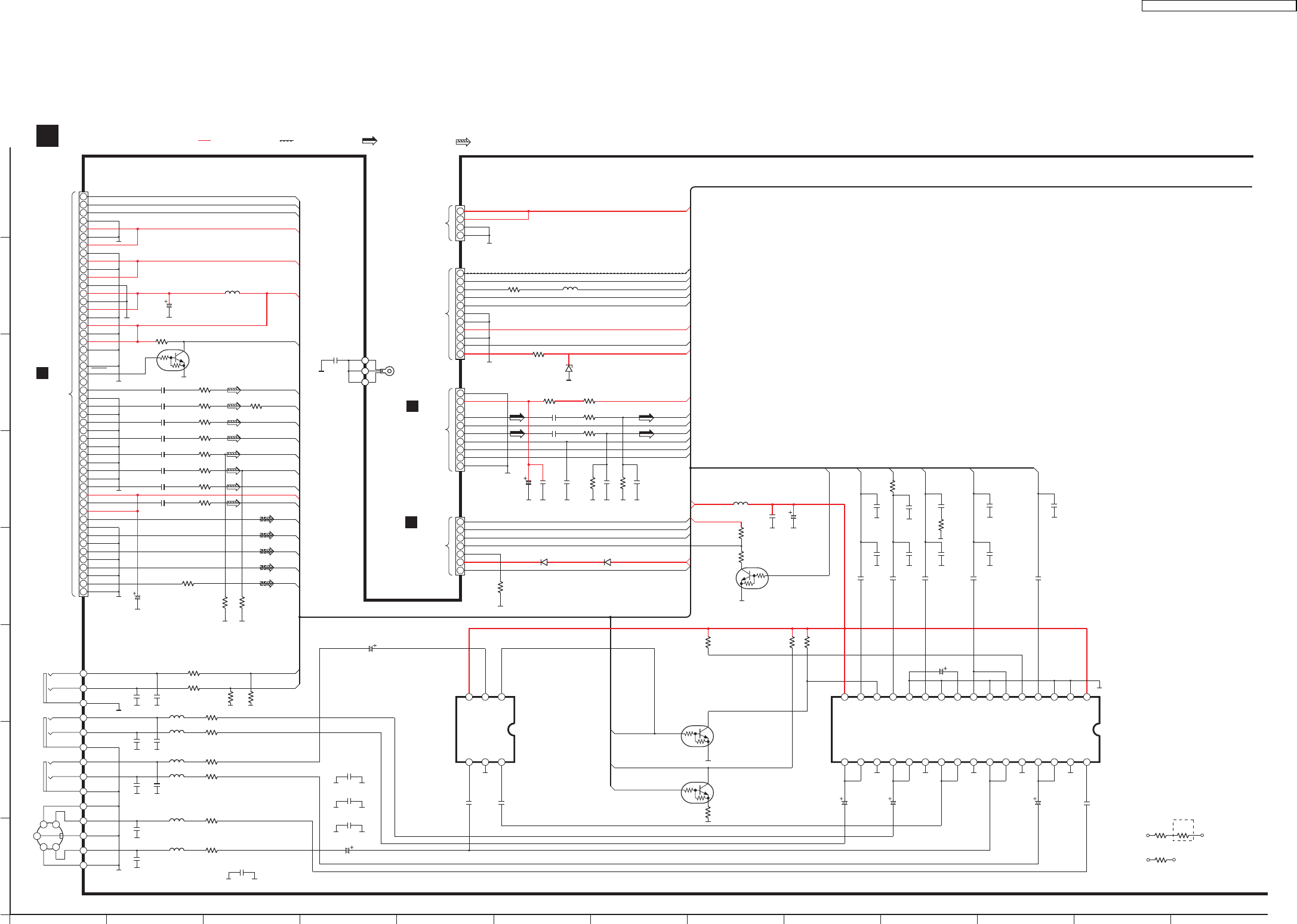
19.2. (B) Main, FL, Volume & Mic Circuit
10
2
4
6
8
9
7
5
3
1
A
B
C
D
E
F
G
H
1 2345678910111213
15
14
13
12
11
10
2
4
6
8
9
7
5
3
1DVD_STA
CN2001
CN2002
5
3
1
2
4
6
7
H2004
30
29
28
27
26
25
17
19
21
23
24
22
20
18
16
36
35
34
33
32
31
50
49
48
47
46
38
40
42
44
45
43
41
39
37
DVD_CMD
DVD_CK
M+9V
DVD+_2.7
DVD_D+5V
MUTE_DVD
R2006 1.8K
DVD-SUBW
Q2006
B1GBCFJJ0051
DVD-CNT
DVD-SR
DVD-SL
DVD-FR
DVD-FL
MIXR
DVD_A+5V
MIXL
C
Y
CR
CB
PY
STATUS
CMD
DSPCLK
MGND
M+9V
MGND
M+9V
DGND
2.7V
DGND
2.7V
AGND
A+5V
AGND
A+5V
DGND
D+5V
DGND
D+5V
DGND
DGND
ZFLAG
SUBW
ADACGND
CENTER
ADACGND
SR
ADACGND
SL
ADACGND
FR
ADACGND
FL
ADACGND
MIXR
ADAC5V
MIXL
ADAC5V
C
VGND
Y
VGND
CR/PR/R
VGND
CB/PB/B
VGND
PY/Y/G
VGND
TUNERGND
TUNER CLK
TUNER DI
TUNER SD
TUNER LCH
TUNER DO/ST
TUNER RCH
T+9V
PORT_SEL
R2600 1KC2600 1
R2260 56KC2261 0.018
R2952 8.2
R2900 1
R2160 56KC2161 0.018
R2500 22KC2500 1
R2400 22KC2400 1
R2300 22KC2300 1
R2201 12KC2201 1
R2101 12KC2101 1
R2111 12KC2111 1
R2291 6.8K
R2191 6.8K
R2211 12KC2211 1
C2021
10V220
L2009
G0C220JA0055
DVD_A+5V
CR
CB
PY
Y
AUX-LCH
AUX-RCH
+9V
TU_DI
TU_SD
TUN_LCH
TU_ST
TUN_RCH
TU_CLK
10
11
2
4
6
8
9
7
5
3
1
H2002
VCC_CTRL
SYNC
GND
+9.8V
GND
GND
PCONT
FL1
FL2
SYS6V
-VP
VCC_CTRL
SYNC
+9.8V
PCONT
FL1
FL2
SYS6V
-28V
3
1
2
4
H2001
GND
+26V/18V(VCC)
+26V/18V(VCC)
GND
VCC
TRAY_OPEN
TRAY_CLOSE
TRAY_CCW
M+9V
TRAY_CW
TRAY_OPEN
TRAY_CLOSE
TRAY_CCW
GND(MGND)
C+7.5V
TRAY_CW
C2022 16V100
C2169 0.01
R2161 47K
D2936
B0EAKM000117
D2935
B0EAKM000117
R2261 47K
C2162 680P
C2262 680P
C2026 1
BRAKE_H
R2264 10K
C2264
220P
R2164 10K
C2164
220P
R2265
3.3K
R2165
3.3K
R2943
2.7K
R2942
2.2K
W2503
0
R2807
1K
VREF
C2819
100P
C2821
100P
C2820
100P
C2822
100P
L2801
G0C220JA0055
Q2030
B1GBCFJJ0051
WIDE
Q2805
B1GBCFJJ0051
D2900
B0BC7R500001
L2800 G0C220JA0055
C2833
16V10
1
2
3
E2900
K4CZ01000027
C2904
0
TO
DVD MODULE
CIRCUIT
(FP8101) ON
SCHEMATIC
DIAGRAM- 2
A
TO
TRAY LOADING
CIRCUIT
(CS901) ON
SCHEMATIC
DIAGRAM- 11
F
TO
TUNER EXTENT
CIRCUIT
(CP2010) ON
SCHEMATIC
DIAGRAM- 11
G
TO
SMPS MODULE
SA-HT340GC/GCS/GS MAIN CIRCUIT
WIDE_OUT
:+B SIGNAL LINE :-B SIGNAL LINE
V REF CONTROL
MUTING
INVERTER
: FM /AM SIGNAL
TO
SMPS MODULE
2
12
13
14
8
6
10
9
1
3
5
4
11
7
S-VIDEO
COMPOSITE CB CR AUX
Y
YOUT
COUT
JK2001
R-CH
L-CH
C2830
1000P
C2823
100P
C2825
100P
C2826
100P
C2827
100P
C2828
100P
C2829
100P
R2809 75
L2802
J0JBC0000015
R2812 75
L2803
J0JBC0000015
R2813 75
L2804
J0JBC0000015
R2816 75
L2805
J0JBC0000015
R2817 75
L2806
J0JBC0000015
R2818 75
L2807
J0JBC0000015
IC2802
C1AB00001731
VIDEO BUFFER
OUT
SW
GND
IN1
VCCIN2
C2804
1
C2800
1
C2851
220P
C2852
1000P
1
2
56
3
4
C2803
6.3V1000
C2841
6.3V1000
RGB
Q2804
B1GBCFJJ0051
R2804
1K
R2803
1K
C2808
10V220
C2807
0.01
C2818 1
C2838
100P
C2817 1
C2837
100P
C2811 0.1
C2836
100P
C2835
100P
C2812 0.1
C
C2810 0.01
C2834
100P
IC2801
C9ZB00000461
CBIN
GND
CYIN
SEL
CBSAG
CBOUT
GND2
CYSAG
BIASCYOUT
SEL
CVIN
MUTE1
CIN
S2
S1
YSAG
YOUT
GND2
VSAG
VOUT
SDCOUT
YIN
VCC1
GND2
COUT
C2801 0.1
12
31 32
3
30
4
29
5
28
6
27
7
26
8
25
9
24
10
23
11
22
12
21
13
20
14
19
15
18
16
17
C2809
10V220
C2805
6.3V330
C2802
6.3V1000
CRIN
MUTE2
CROUT
GND2
VCC2CRSAG
C2806
6.3V330
C2853
100P
MAIN CIRCUIT
B
SCHEMATIC DIAGRAM-5
: MAIN SIGNAL LINE
VIDEO DRIVE
W2524 0
W2504 0
W2553 0
W2561 0
W2539 0
W2554
0
W2514
0
W2512
0
(GC/GS)
W2509
0
W2595
0
SA-HT340GC / SA-HT340GCS / SA-HT340GS
66
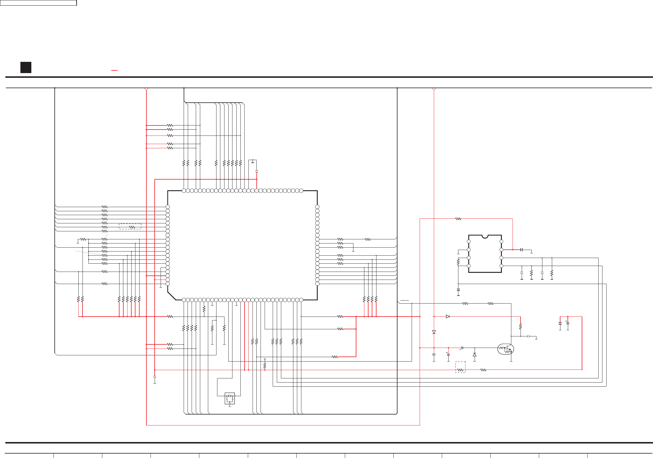
15 16 17 18 19 20 21 22 23 24 25 2614
R2085
4.7K
R2086
22K
SYS6V
RESET
VREF
2
1
3
4
8
7
6
5
C2010
330P
C2004
0.01
C2011
330P
R2084
47K
C2013
0.022
NC
DI
DO
GND
NC
SK
CS
VCC
R2087
22K
C2012
330P
IC2004
Q2003
B1GBCFJJ0051
C2006
50V3.3
C2003
50V22
D2008
B0ACCK000005
D2005
B0ACCK000005
D2007
B0ACCK000005
C2009
0.1
C2007
0.1
C2008
6.3V100
123456789
31
32
33
34
35
36
37
38
39
72
73
74
75
76
77
78
79
80
92
93
94
95
96
97
98
99
100
10
71
40
91
11
70
41
90
12
69
13
68
42
89
43
88
14
67
15
66
16
65
44
87
45
86
46
85
17
64
18
63
19
62
20
61
47
84
48
83
49
82
50
81
21
60
22
59
23
58
24
57
25
56
26
55
27
54
28
53
29
52
30
51
NC
RF_PCON
RF_DET
RF_LINK
RF_DATA
TUN_SD
TUN_CLK
TUN_DO
TUN_DI
PCONT
EPM
DVD_MUTE
NC
NC
NC
NC
NC
RF_PCONT
RF_DET
RF_LINK
RF_DATA
TU_SD
TU_CLK
TU_ST
TU_DI
PCONT
MUTE_DVD
NC
NC
NC
RGB_H
AVCC
BRAKE_H
VREF
KEY1
AVSS
DES1
DES2
DES3
MD1
KEY2
MD2
MD3
RDS_DAT
FLD_OUT
FLD_STB
FLD_CLK
ASP_DAT
ASP_CLK
YC_H
RGB
BRAKE_H
KEY1
KEY2
FLD_OUT
FLD_STB
FLD_CLK
ASP_DA
ASP_CK
YC_H
TRAY_CLOSE
SYNC
AM_BP
MIC_EN
DVD_CMD
RMT
NMI
VCC
XIN
VSS
XOUT
DVD_CLK
DVD_STAT
NC
NC
ECS
ECK
EDA
NC
SYNC
BEATPROOF
DVD_CMD
RMT
DVD_CK
DVD_STA
RESET
NC
NC
NC
CNVSS
BYTE
SINE_FL
SINE_SW
TRAY_OPEN
TRAY_CW
TRAY_CCW
TRAY_CLOSE
TRAY_OPEN
TRAY_CW
TRAY_CCW
WIDE
VCC
NC
NC
NC
VCC_CTRL
VSS
MIC_SW
MUTE_C
MUTE_SURR
NC
NC
NC
NC
NC
NC
NC
NC
NC
MUTE_FRONT_SW
DC_DET
DVD_PCONT
JOG_A
JOG_B
SCART_MUTE
WIDE1
MIC_SW
MUTE_C
MUTE_SURR
MUTE_F_SW
DC_DET
STYB
DVD_PCNT
NC
NC
NC
JOG_A
JOG_B
NC
SCART_MUTE
IC2018
C2CBYY000194
R2019 27K
R2017 27K
R2032 47K
R2095 4.7K
R2001 100K
R2096 10K
R2069 220
R2068 220
R2067 220
R2066 2.2K
R2072 220
R2071 220
R2070 220
R2062 220
R2064 220
R2065 220
R2060 220
R2073 220
R2046 220
R2052 220
R5312 1K
R5212 1K
R5112 1K
R2078
R2075 220
820 (GC/GS)
820
6.8K
10K (GC/GS)
0
4.7K
R2077
3.3K (GCS)
R2093
4.7K (GCS)
R2089
R2082
R2080
R2041 10K
R2039 10K
R2045 10K
R2043 47K
R2063 47K
R2061 47K
R2053 10K
R2012 10K
R2079 10K
R2081 10K
R2088 10K
R2076 10K
R2091 10K
R2002 10K
R2094 10K
R2031 220
R2030 220
R2029 220
R2005 220
R2097 470K
R2004 220
R2003 220
R2000 220
R2016 220
R2015 1K
R2010 220
R2024 220
R2023 220
R2022 220
R2047 220
R2048 220
R2049 220
R2040 220
R2042 220
R2044 220
SINE_FR
SINE_FL
X2001
H2B100500004
10MHz
13
2
GND
IN OUT
R2092 220
CNVSS
R2090 220
R2999 22K
R2998 22K
VCC_CTRL
C2000
50V0.1
C2001
0.1
SA-HT340GC/GCS/GS MAIN CIRCUIT
:+B SIGNAL LINE
MICRO-PROCESSOR
EEPROM
(NOT SUPPLIED)
RESET
STYB
MAIN CIRCUIT
B
SCHEMATIC DIAGRAM-6
W2596 0
W2585
0W2580 0
W2523
0
W2593
0
W2587
0
W2583
0
W2586
0
W2537
0
W2588
0
(GC/GS)
(GC/GS)
SA-HT340GC / SA-HT340GCS / SA-HT340GS
67
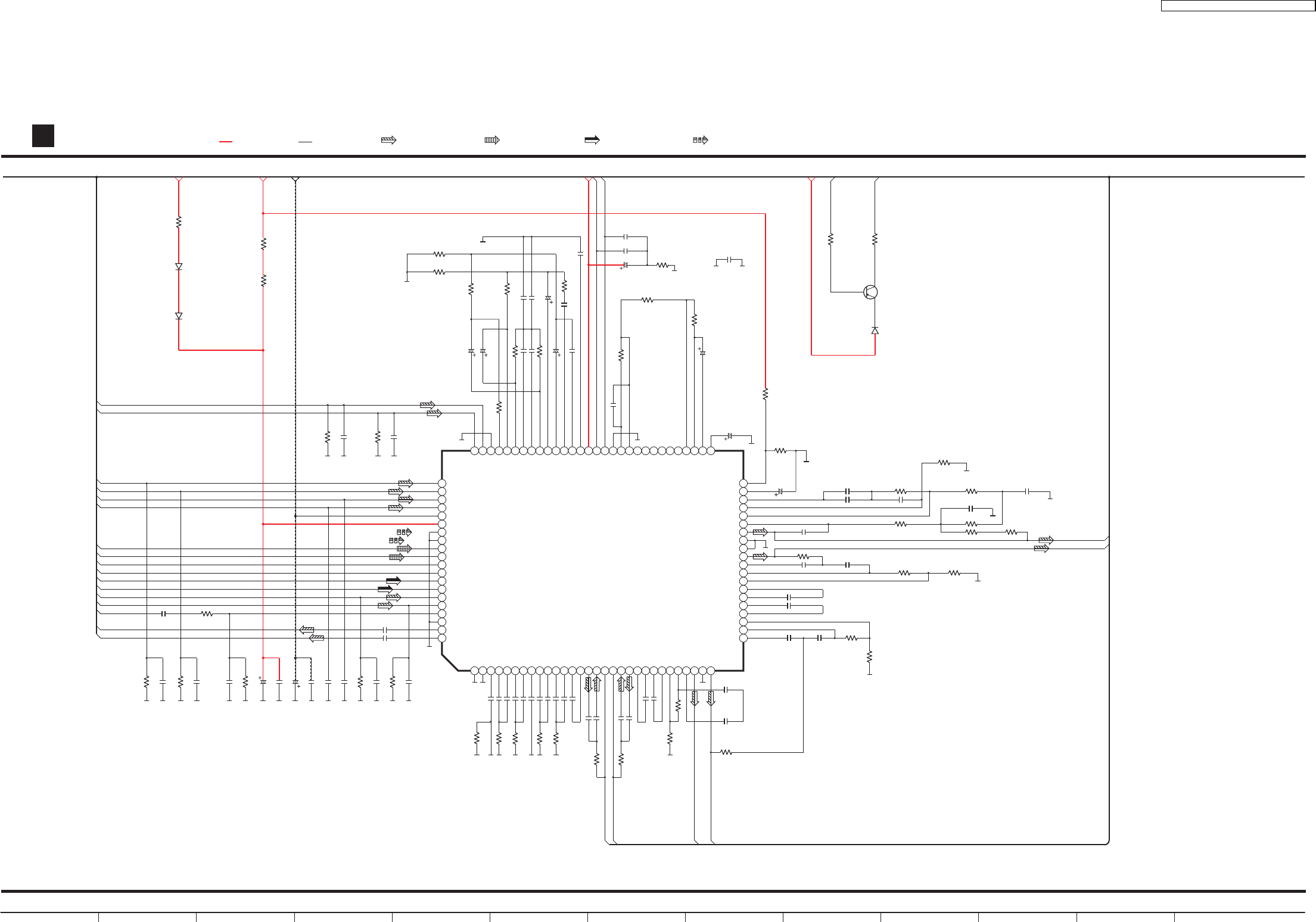
28 29 30 31 32 33 34 35 36 37 38 3927
123456789
31
32
33
34
35
36
37
38
39
72
73
74
75
76
77
78
79
80
92
93
94
95
96
97
98
99
100
10
71
40
91
11
70
41
90
12
69
13
68
42
89
43
88
14
67
15
66
16
65
44
87
45
86
46
85
17
64
18
63
19
62
20
61
47
84
48
83
49
82
50
81
21
60
22
59
23
58
24
57
25
56
26
55
27
54
28
53
29
52
30
51
AGC1
SLVOLOUT
SLFIN
SLNFIN
SLVOLIN
SLSELOUT
SRSELOUT
SRVOLIN
SR_OUT
SUBW
SRNFIN
SRVOLOUT
SRFIN
SROUT
AGND
AGND
OPOUT2
OPIN2
OPOUT1
OPIN1
SUBOUT
SUBC
SLIN
RECOUTR
RECOUTL
AGND
MICIN
INL1
INR1
INL2
INR2
INL3
INR3
INL4
INR4
INL5
INR5
AVCC
AVEE
FLIN
FRIN
CIN
DVD-SL
MIXL
MIXR
TUN-LCH
TUN-RCH
TV-LCH
TV-RCH
AUX-LCH
AUX-RCH
DVD-FL
DVD-FR
DVD-CNT
DVD-SUBW
DVD-SR
AGND
FRFIN
FRVOLOUT
FRVOLIN
SLOUT
FROUT
FLOUT
FLFIN
FLVOLOUT
FLVOLIN
FLSELOUT
COUT
AGND
CFIN
CVOLOUT
CNFIN
CVOLIN
CSELOUT
FRSELOUT
SL_OUT
FROUT
FLOUT
CENTER
TBR2
TBR1
TMR2
TMR1
TTR
TBL2
TBL1
TML2
TML1
TTL
CLPF
SRIN
HBASS1
HBASS2
HBASS3
AGC2
DGND
DATA
CLOCK
DVDD
ASP_CK
ASP_DA
SW+5V
+7V
SF
LSIN
SUBSELOUT
SUBVOLIN
HBASS9
HBASS8
HBASS7
HBASS6
HBASS5
HBASS4
RSIN
LCIN
RCIN
LIN
LF
RF
RIN
EXTOUTR
EXTOUTL
AGND
SUBIN
R2112 12K
C2272 100P
C2112 470P
C2212 470P
C2172 100P
R2212 12K
R2113 4.7K
C2115 0.015
C2116 0.0047
C2507 470P
R2511 12K
C2323 100P
R2336 12K
C2423 50V100P
R2436 12K
C2615 50V2200P
R2619 20K
C2295 1
C2195 1
C2018 16V47
C2017 0.01
C2020 0.01
C2019 16V47
R2114 4.7K
C2117 0.047
C2118 0.22
C2214 0.022
R2218 4.7K
C2215 0.015
R2115 10K
R2215 10K
R2502 10K
R2302
10K
R2501 6.8K
R2303
10K
R2301
1.8K
R2401 1.8K
R2611 1.2K
R2610 56K
R2402 10K
C2301 1
C2401 1
C2216 0.0047
R2214 4.7K
C2217 0.047
C2218 0.22
C2119 1
C2121 0.047
C2120 0.039
C2221 50V0.047
C2220 16V0.039
C2219 1
C2503
0.047
C2502
0.047
R2403 10K
R2612 56K
R2609 1.5K
R2621
39K
R2601 47K
R2404 12K
R2405
5.6K
R2406
5.6K
R2304 12K
R2620
12K
R2627 68K
R2608 56K
C2303
0.047
C2403 0.047
C2612 3300P
C2402 0.033
C2609 0.22
C2605 0.047
C2610 0.47
C2611 0.012
C2302
0.033
C2501 1
C2608
16V10
C2607 50V22
C2606
16V10
R2607
10K
C2023 220P
C2024 220P
R2606
10K
C2410 16V100
R2407 1.8K
R2307 1.8K
C2407 16V10
C2304 16V10
C2404 16V10
C2308 0.022 C2408
0.022
C2617 0.15
D2929
B0ACCK000005
IC2102
C1AB00002463
C2601 0.022
C2307 16V10
C2406 1
C2306 1
C2405 3300P
C2305 3300P
C2309 0.082
LINEOUT-R
LINEOUT-L
-7V
+9V
SYS6V
SYNC
STBLED
R2950
1K
R2944
4.7K
Q2004
B1ADCE000012
C2411
0.1
R2960
15
D2001
B0ACCK000005
D2002
B0ACCK000005
SA-HT340GC/GCS/GS MAIN CIRCUIT
:+B SIGNAL LINE
:-B SIGNAL LINE
: MAIN SIGNAL LINE : MUSIC PORT SIGNAL LINE: AUX SIGNAL LINE : FM /AM SIGNAL LINE
ASP
LED DRIVE
C2114 0.022
R6920
100
R6921 1.5K
C6921 220P
C6920
1
ASP_MICIN
MAIN CIRCUIT
B
SCHEMATIC DIAGRAM-7
W2559
0
W2563
0
W2562
0
W2525 0
W2541
0
W2577
0
W2575
0
SA-HT340GC / SA-HT340GCS / SA-HT340GS
68
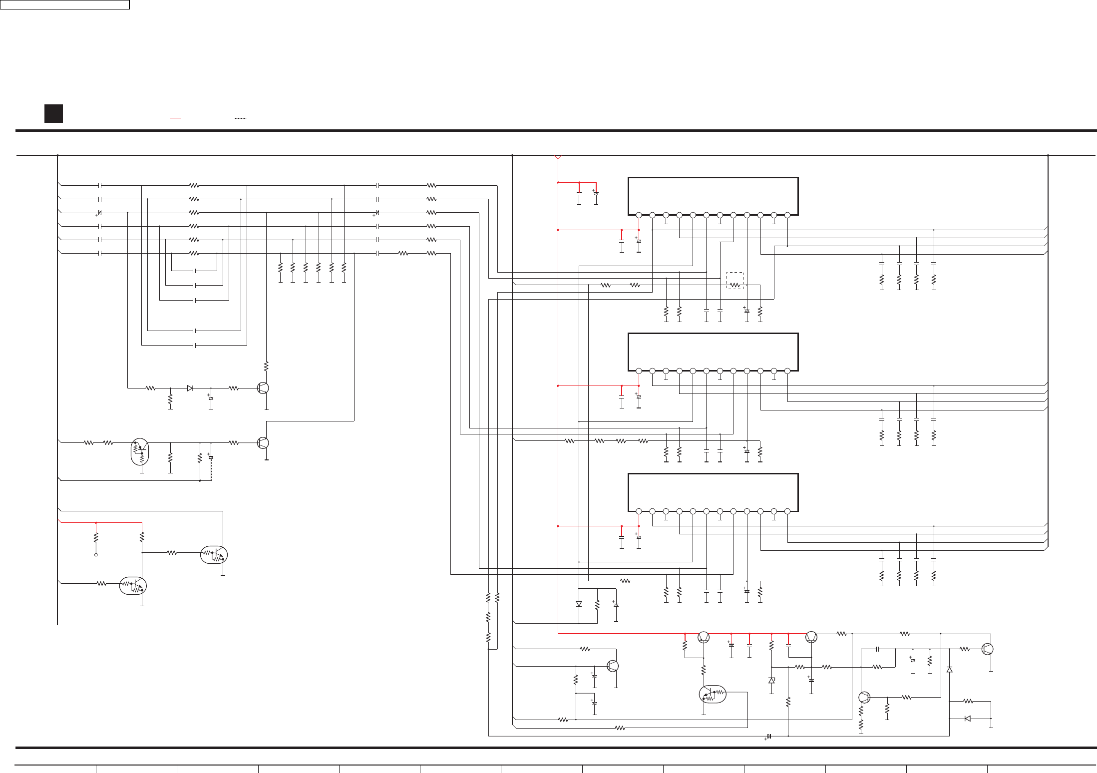
41 42 43 44 45 46 47 48 49 50 51 5240
CENTER
SL_OUT
SR_OUT
-7V
MUTE_C
DVD_PCONT
STYB
MUTE_SURR
MUTE_FRONT_SW
SUBW
FLOUT
FROUT
C2424 2200P
C2324 2200P
C2524 6800P
C2724 1800P
C2624 6800P
R2194 27K
R3007
27K
R3009
1K
R3008
1.8K
R3003
8.2K
R2936
0
R2938
10K
R3006
1K
VCC
OUT+_R
GND_R
OUT-_R
STBY
IN_R
GND
IN_L
MUTE
OUT-_L
GND_L
OUT+_L
R2294 27K
R2626 100K
R2339 100K
R2439 100K
R2512 100K
C2183 1
C2283 1
C2619 50V10
C2312 1
C2412 1
C2506 1
C3001 1
C3002 1
C3006 50V10
C3003 1
C3004 1
C3005 1
R2185 10K
R2285 10K
R2617 22K
R2312 10K
R2412 10K
R2510 15K
R5101 4.7K
R5102 4.7K
R5301 22K
R5201 15K
R5202 15K
R5302 15K
123456 7 8 9 10 11 12
C5124
0.1
R5111
10K
R5104
27K
R5108
27K
R5110
1.2K
C5101
50V10
C5104
470P
C5105
470P
C5108
16V22
FR+
FR-
FL+
FL-
C5107
0.22
R5109
1.2K
C5106
0.22
R5106
1.2K
C5103
0.22
R5105
1.2K
C5102
0.22
C5505
470P
C5503
35V1000
VCC
IC5100
AN17831A
VCC
OUT+_R
GND_R
OUT-_R
STBY
IN_R
GND
IN_L
MUTE
OUT-_L
GND_L
OUT+_L
123456 7 8 9 10 11 12
C5224
0.1
R5211
10K
R5204
27K
R5208
27K
R5210
1.2K
C5201
50V10
C5204
470P
C5205
470P
C5208
16V22
C5207
0.22
R5209
1.2K
C5206
0.22
R5206
1.2K
C5203
0.22
R5205
1.2K
C5202
0.22
IC5200
AN17831A
VCC
OUT+_R
GND_R
OUT-_R
STBY
IN_R
GND
IN_L
MUTE
OUT-_L
GND_L
OUT+_L
123456 7 8 9 10 11 12
C5324
0.1
R5311
10K
R5304
5.6K
R5308
27K
R5765
10K
R5759
100K
R5755
10K
R5736
2.2K
R5763
2.7K
R5764
3.9K
R5758
3.3M
R5756
10K
R5760
10K
R5757
10K
R5754
56K
W2502
0
R5766
10K
D5745
B0BC013A0007
R5313
47K
R5310
1.2K
C5301
50V10
C5304
470P
C5305
470P
C5799
0.1
C5790
1000P
C5308
16V22
C5795
0.1
C5307
0.22
R5309
1.2K
C5306
0.22
R5306
1.2K
C5303
0.22
R5305
1.2K
C5302
0.22
C5792
6.3V220
C5794
16V33
C5798
50V100
C5797
50V1
C5796
50V2.2
C5791
16V100
R5762
150K
R5761
2.2M
IC5300
AN17831A
SR+
SR-
SL+
SL-
SW+
SW-
C+
C-
Q3009
B1ABCF000176
Q3003
B1GDCFJJ0047
Q3008
B1ABGC000005
D3001
B0ACCK000005
D5302
B0ACCK000005
C3007
50V10
C3009
50V10
R3005
22K
R3014
56K
R2941
47K
R5534
18K
R5533
22K
R3015
56K
SS
SW+5V
Q2917
B1GBCFJJ0051
DC_DET
FANLOCK
Q2916
B1GBCFJJ0051
D5744
B0ACCK000005
D5743
B0ACCK000005
Q5741
B1ABCF000176
Q5745
B1ACKD000005
Q5740
B1BACG000023
Q5742
B1ABCF000176
Q5744
B1ABCF000176
Q5746
B1GBCFJJ0051
FANDCOUT(+)
PCONT
SA-HT340GC/GCS/GS MAIN CIRCUIT
AUDIO POWER
AUDIO POWER
AUDIO POWER
FAN MOTOR DRIVE
FAN MOTOR DRIVE
FAN MOTOR DRIVE
FAN MOTOR DRIVE
FAN MOTOR DRIVE
FAN MOTOR DRIVE
DC-DC CONVERTER
DC-DC CONVERTER
CONTROL
MUTING
MUTING
MUTING CONTROL
CONTROL
:+B SIGNAL LINE :-B SIGNAL LINE
C5313
50V10
MAIN CIRCUIT
B
SCHEMATIC DIAGRAM-8
W2556 0
W2530
0
W2516
0
W2520
0
W2522 0
W2521
0
W2517 0
W2532
0
W2536
0
W2533
0
W2534
0
W2531
0
W2571
0
W2527 0
W2552
0
W2501
0
W2505
0
W2572
0
(GC/GS)
SA-HT340GC / SA-HT340GCS / SA-HT340GS
69
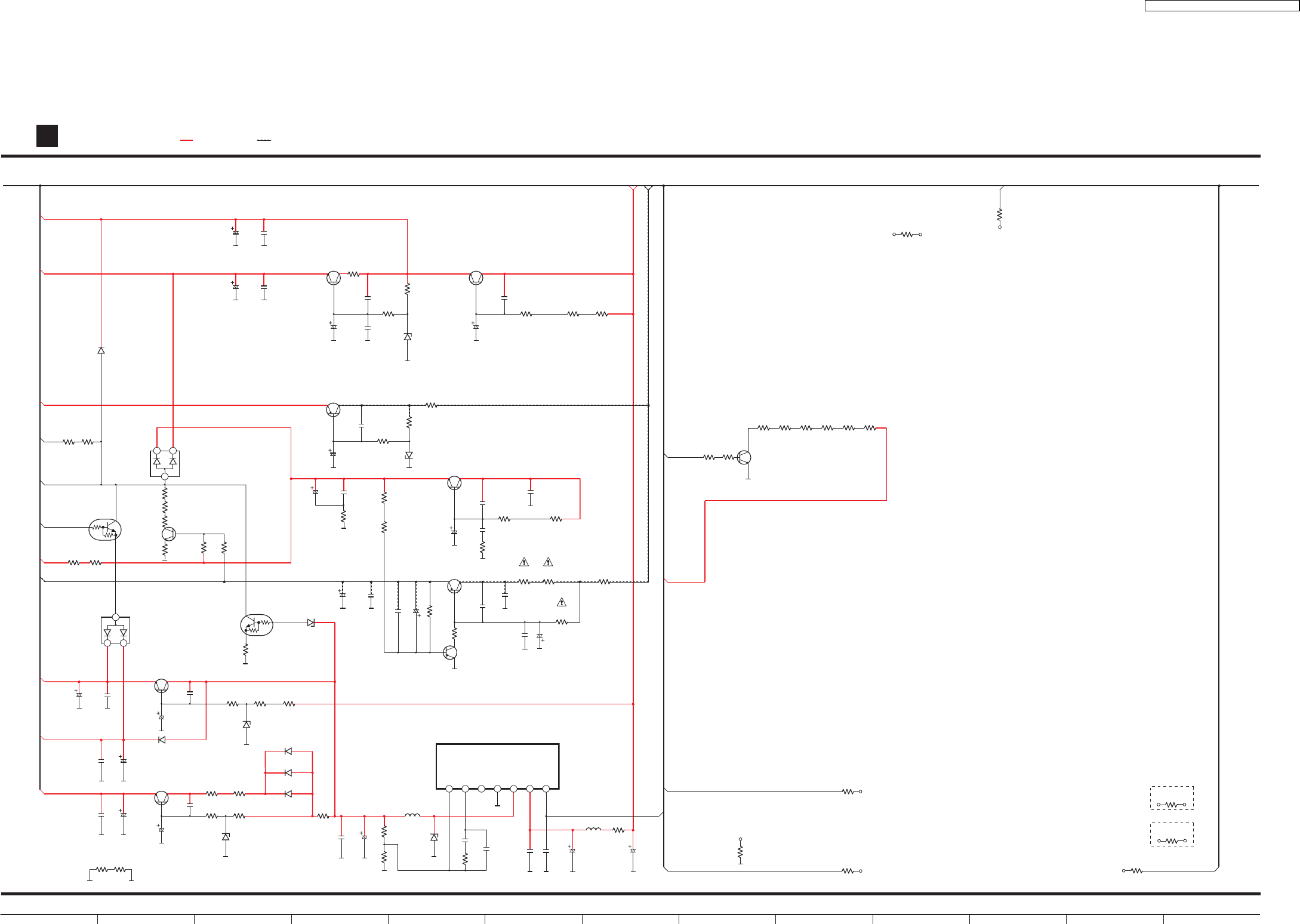
54 55 56 57 58 59 60 61 62 63 64 6553
R2934
820
R2933
150
D2915
B0BC5R600003
R2905 220
IC2903
AN30070A
Q2904
B1AAKD000012
C2945
0.1
C2959
1
C2922
16V470
C2946
16V47
C2978
0.1
C2977
16V100
C2902
0.01
R2919
270K
R2921
27K
R2926
1.5
R2973
150
R2972
22
R2971
1.5
AMPO
ANPN
VCC
SS
LX(OUT)
GND
NC
C2919
10P
C2920
8200P
R2920
3.9K
R2907
3.9K
R2908
390
C2976
0.1
C2975
16V100
L2902
G0A101G00022
C2924
0.1
C2970
0.1
C2969
0.1
C2952
0.1
C2921
16V470
C2901
16V470
C2965
0.1
C2967
10V220
L2909
G0A200D00002
R2970
22
R2969
150
R2968
150
Q2913
B1BACD000018
C2940
0.01
C2941
16V100
D2938
B0EAKM000117
C2984
0.1
C2983
16V100
C2925
6.3V220
D2939
B0EAKM000117
D2937
B0EAKM000117
D2907
B0EAKM000117
Q2903
B1BACD000018
Q2915
B1GBCFJJ0051 Q2910
B1ABCF000176
C2906
0.01
C2963
1
C2908
16V100
C2913
16V100
C2964 1
R2904
100
R2975
4.7K
R2974 4.7
Q2974
B1ACKD000005
C2985
0.01
C2986
50V100
R2976
150
D2974
MAZ82200ML
D2904
B0JCPD000025
R2913
47
R2912
47 R2911 47
R2914
2.7K
R2915 2.7K
W2544
0
C2903
0.01
Q2906
B1BCCG000002
Q2907
B1ADCF000001
Q2914
B1BACG000023
C2910
0.01
C2961 1
D2944
B0BC3R400001
C2914 10V33
R2929
1.8K
R2963
2.2K
R2964
22
C2966
0.1
C2968
16V100
Q2955
B1BACD000018
Q2905
B1GBCFJJ0051
D2941
B0BC5R600003
D2905
B0BC7R500001
D2919
B0ADCJ000020
12
3
D2918
B0ADCJ000020
DC_DET
DVD_PCONT
VREF
+9V
-7V
DVD_A+5V
DVD_+2.7V
DVD_D5V
+12V
M+9V
SW+5V
21
3
D2906
B0ACCK000005
R2924
68K
R2940
39K
+9.8V
-28V
1
2
3
4
56
7
SS
BEATPROOF
VCC
R2980
1K
LINEOUT-R
LINEOUT-L
C2974
0.1
C2973
16V100
C2972
0.1
C2971
16V100
C2982
0.1
C2981
16V100
SA-HT340GC/GCS/GS MAIN CIRCUIT
M +9V REGULATOR
+9V REGULATOR
DC DETECT
DC DETECT CONTROL
DC DETECT
DVD A+5V REGULATOR
DVD 2.7V REGULATOR
-7V REGULATOR
-7V REGULATOR
DC-DC CONVERTER
SW +5V REGULATOR
-VP REGULATOR
:+B SIGNAL LINE
:-B SIGNAL LINE
R2007
10K
W2578
0
W2576
0
LCH_OUT
R1200
470
R1100
470
R2986
22
R2985
22
R2984
22
R2983
22
R2982
22
R2981
22
Q2980
B1BACD000018
SWITCHING
W2904
0
W2903
0
W2506
0Y
R2503
W2529
0
MAIN CIRCUIT
B
SCHEMATIC DIAGRAM-9
W2564
0
W2566
0
W2540
0
W2567
0
W2573
0
W2538
0
W2545
0
W2574
0
W2543
0
W2542
0
W2550
0
W2579
0
W2560
0
W2558
0
W2590
0
(GC/GS)
(GCS)
SA-HT340GC / SA-HT340GCS / SA-HT340GS
70
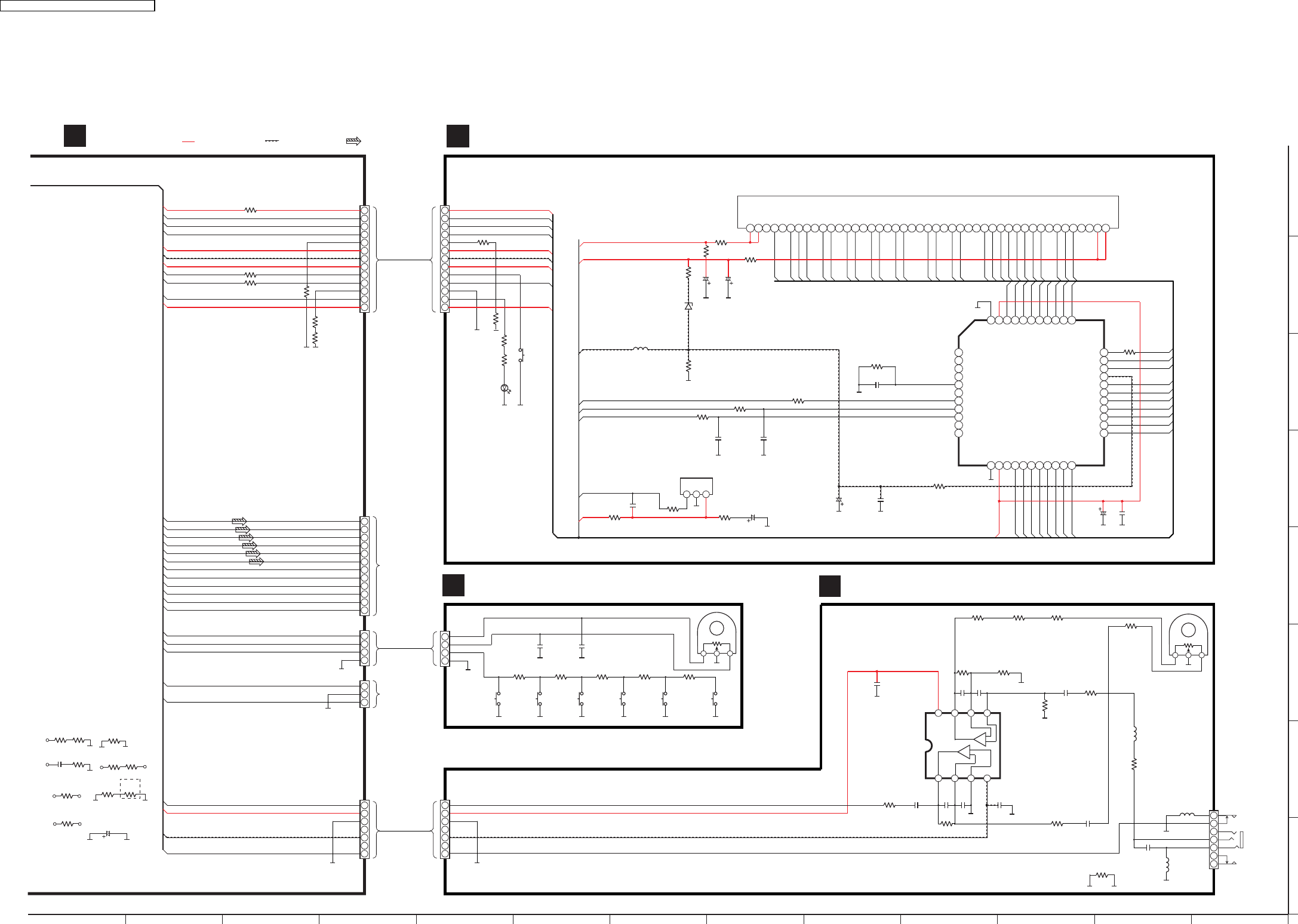
12
11
10
2
4
6
8
9
7
5
3
1
FR+_OUT
SW+_OUT
SR-_OUT
C-_OUT
FR-_OUT
SL+_OUT
SW-_OUT
FL+_OUT
SR+_OUT
C+_OUT
JK5000
FL-_OUT
SL-_OUT
FR+
SW+
SR-
C-
FR-
SL+
SW-
FL+
SR+
C+
FL-
SL-
S6800
POWER
R6939
0
FL6901
A2BD00000160
P1
F1
F1
NP
P1
NP
P2
P3
P4
NP
P5
P6
NP
P7
P8
NP
P9
P10
NP
P11
P12
NP
NP
P13
P14
NP
P15
P16
NP
NP
P17
G1
G3
G9
G8
G2
G7
G6
NP
G5
G4
G1
NP
NP
F2
F2
P2
P3
P4
P5
P6
FL1
FL2
-VP
FLD_OUT1
VREF
RMT
FLD_CLK1
FLD_STB1
P7
P8
P9
P10
P11
P12
P13
G10
G9
G8
G7
G6
G5
G4
G3
G2
G1
P1
P2
P3
P4
P5
P6
P7
P8
P9
P14
P15
P16
P17
G10
G3
G9
G8
G2
G7
G6
G5
G4
G1
P17
SW+5V
P16
P15
P14
P13
P12
P11
P10
R6936
150
W6545
0
C6904
1000P
C6909
0.01
C6806
100P
C6906
100P
GND
VCC
P18
P17
P16
P15
P14
P13
P12
P11
P10
G1
P1
P2
-VP
OSC P3
P4
DIN P5
CLK P6
STB P7
P8
P9
GND
VCC
G10
G9
G8
G7
G6
G5
G4
G3
G2
R6918
22K
R6919 68
R6916 68
R6917 1K
C6905
50V22
C6903
50V22
C6918
10V47
D6910
B0BC5R000009
L6903
J0JBC0000041
R6940
0
R6914
82K
R6934
47
Z6900
B3RAB0000025
C6911
0.01
C6917
100P
C6916
100P
C6910
6.3V100
C6913
50V3.3
IC6901
C0HBB0000057
12345678910
11 14
13
12 15 16 17 18 19 23
22
21
20 26
25
24 292827 3631 33 35 38
30 32 34 37 41 42 43 45
40
39 44
1
2
3
4
5
6
7
8
925
26
27
28
29
30
31
32
33
363738394041424344
10
11
24
35
23
12 13 14 15 16 17 18 19 20 21 22
34
3
2
1
4
3
12
10
8
6
5
2
1
7
9
11
13
CN6001
H6004
FLD_STB
FLD_OUT
FLD_CLK
FLGND
FL1
-VP
FL2
KEY1
RMT
SW+5V SW+5V
FLD_STB1
FLD_OUT2
FLD_CLK1
FL1
-VP
FL2
DGND
STBLED
VREF
RMT
VREF
4
3
12
10
8
6
5
2
1
7
9
11
13
CN2007
FLD_STB
FLD_OUT
FLD_CLK
FLGND
FL1
-VP
FL2
KEY1
RMT
SW+5V
DGND
STBLED
VREF
FLD_STB
FLD_OUT
FLD_CLK
FL1
-VP
FL2
KEY1
RMT
SW+5V
STBLED
VREF
D6900
B3AAA0000803
R6905
1.5K
C6805
100P
S6805
PLAY
S6806
SELECTOR
STOP
REVERSE/
TUNE DOWN
FORWARD/
TUNE UP
OPEN/CLOSE
R6804
1.8K
R6805
2.2K
S6804
S6803
R6802
1K
R6803
1.2K
S6802
S6801
R6801
1K
3
1
2
4
JOG_A
JOG_B
KEY2
DGND
CN2005
3
1
2
4
JOG_A
JOG_B
KEY2
JOG_A
JOG_B
KEY2
DGND
CN5704
3
1
2
FANDCOUT(+)
GND
FANLOCK
FANDCOUT(+)
FANLOCK
A
B
C
D
E
F
G
H
67 68 69 70 71 72 73 74 75 76 77 7866
C2900
16V470P
FL CIRCUIT
C
SA-HT340GC/GCS/GS MAIN/FL/VOLUME/MIC CIRCUIT
TO SPEAKERS
TO FAN
DISPLAY DRIVE
:+B SIGNAL LINE : MAIN SIGNAL LINE
:-B SIGNAL LINE
IC2204
C0ABBB000230
OP-AMP
V-
V+
R6702
47K
R6706
0
W6514
0
W6517
0W6515
0
R6705
1K
R6701
0
JK6802
MIC
5
4
3
2
1
6
7
87
21
6
3
5
4
L6083
J0JBC0000019
L6082
J0JBC0000030
L6081
ERJ3GEY0R00V
C6708
47P
C6702
330P
C6703
47P
C6701
1
C6711
1
R6709
0C6710
0
C6093
0.047
C6706
0.1
R6703
680
R6081
0
C6709
0.1
ASP_MICIN
H6903
+7V
MIC_AGND
-7V
MIC_SW
7
6
5
4
3
2
1
ASP_MICIN
CN2006
+7V
MIC_AGND
-7V
MIC_SW
ASP_MICIN
+7V
-7V
MIC_SW 7
6
5
4
3
2
1
W6516
0
R6708
18K
C6707
47P
R6707
10K
(GC/GS)
MAIN CIRCUIT
B
SCHEMATIC DIAGRAM-10
VR6800
VOLUME JOG
123
AB
VOLUME CIRCUIT
D MIC CIRCUIT
E
123
AB
VR6801
MIC VOLUME
+
-
+
-
W2584 0
W2591 0
W2582
0
W2592
0
W2589
0
W2548
0
W2546
0
W2597
0
W2513
0
W2508
0
W2570
0
W6501 0
W6509
0
W6511
0
W6512
0W6513
0
W6504 0
W6502 0
C2832
220P
W2581 0
W2515
0W2519
0
W2528
0
W2547
0
SA-HT340GC / SA-HT340GCS / SA-HT340GS
71
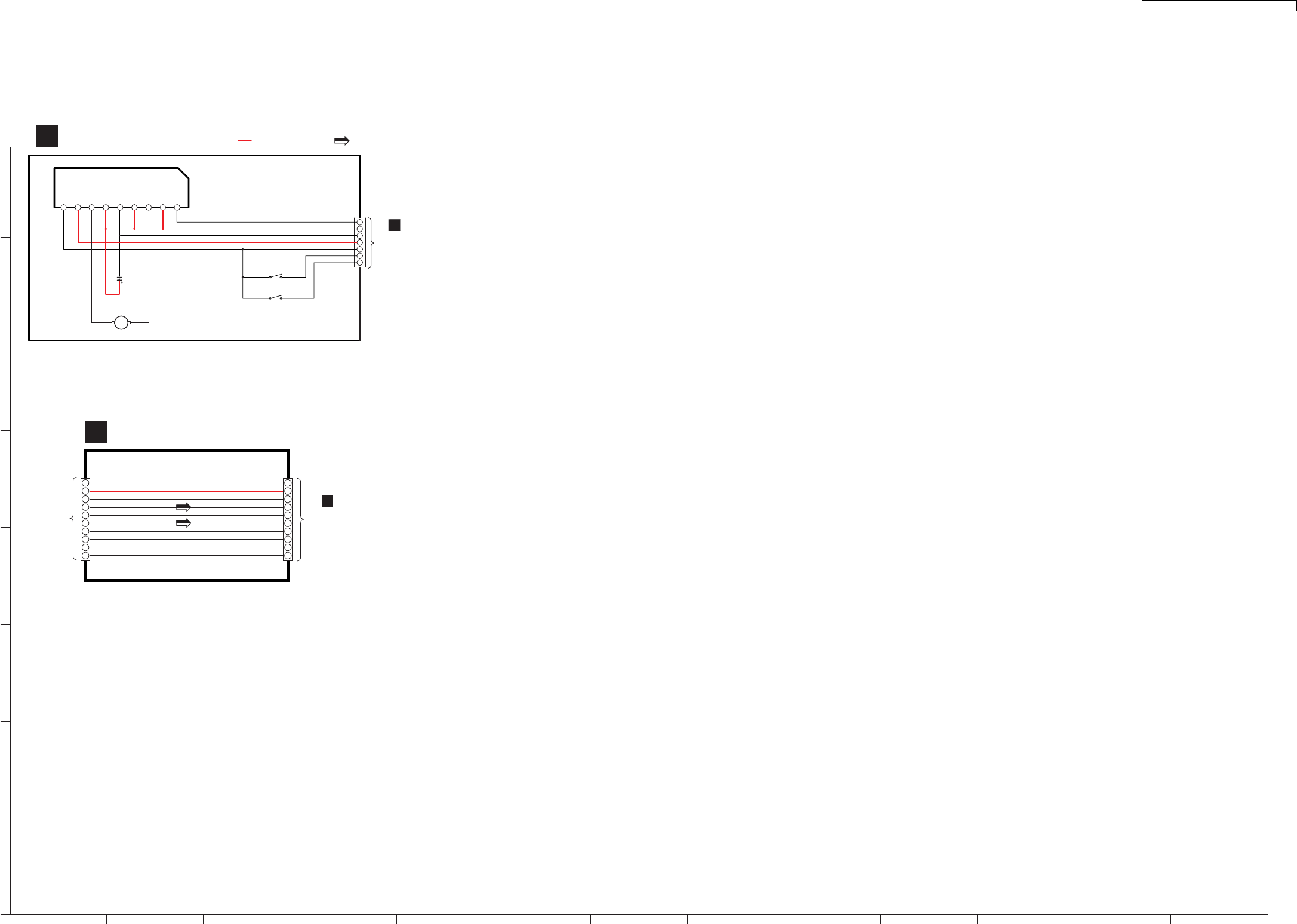
19.3. (C) Tray Loading & Tuner Extent Circuit
A
B
C
D
E
F
G
H
1 2345678910111213
SA-HT340GC/GCS/GS TUNER EXTENT/TRAY LOADING CIRCUIT
:+B SIGNAL LINE
: FM /AM SIGNAL
VCC
OUT2
NC
GND
VS
OUT1
VREF
IC904
C0GAY0000013
MOTOR DRIVER
S901
PLAY
C984
25V10 S902
OPEN
B
M
CS901
TRAY CW
M+9V
GND1
VREF+
TRAY CCW
TRY CLOSE
TRY OPEN 1
2
3
4
7
123456789
5
6
LOADING MOTOR
TO
MAIN CIRCUIT
(H2004)on
SCHEMATIC
DIAGRAM-5
CP2010CN2010
2
6
8
9
7
5
3
110
2
4
6
8
9
7
5
3
1
10
2
4
6
8
9
7
5
3
1
TO
MAIN CIRCUIT
(CN2002) on
SCHEMATIC
DIAGRAM-5
B
TO TUNER
PACK
(J3CCBB000007)
TUNERGND
TUNER CLK
TUNER DI
TUNER SD
TUNER LCH
TUNER DO/ST
TUNER RCH
RDS DETECT
T+9V
PORT_SEL
TUNERGND
TUNER CLK
TUNER DI
TUNER SD
TUNER LCH
TUNER DO/ST
TUNER RCH
RDS DETECT
T+9V
PORT_SEL
GTUNER EXTENT CIRCUIT
TRAY LOADING CIRCUIT
F
SCHEMATIC DIAGRAM-11
SA-HT340GC / SA-HT340GCS / SA-HT340GS
72

SA-HT340GC / SA-HT340GCS / SA-HT340GS
73
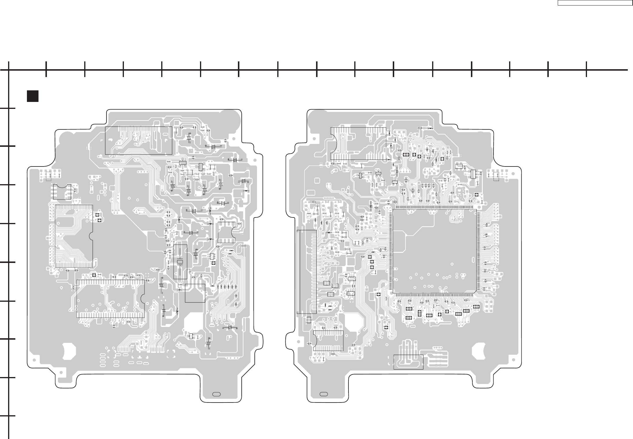
20 Printed Circuit Board
20.1. (A) DVD Module P.C.B.
B
CE
B
C
E
B
CE
B
C
E
B
CE
B
C
E
DVD MODULE P.C.B. (REP4012B...GC/GS, REP4012H...GCS)
A
(SIDE A) (SIDE B)
3118A
3118A 3118A
3118A
ABCDEFG
1
2
3
4
5
6
7
8
9
HI J KL MNO P
SA-HT340GC/GCS/GS DVD MODULE P.C.B.
PbF PbF
C8261
C8422
C8571
C8572
D8571
FL8101
FL8102
FL8103
FL8104
LB8691
LB8692
LB8693
Q8551
Q8561
QR8571
R8262
R8264
R8421
R8551
R8552
R8561
R8562
LB8257
LB8260
LB8259
LB8258
C8426
RX8532
RX8534 RX8533
RX8531
R8531
R8532
R8533
LB8531
LB8530
C8531
C8532
C8533
C8530
C8424 C8428
C8427
K8341
R8341
K8335
R8335
C8331
R8332
R8331
K8331
C8325
K8325 R8325
R8326
K8321
R8321
R8322
C8528
C8504
C8522
C8521
C8511
C8526
C8512
C8525
C8523
C8527
C8505
C8524
C8502
C8503
C8231
R8230
C8024
C8232
R8232
R8231
C8008
C8602
C8606
IC8601
IC8606
C8601
R8601
R8003
C8023
RX8611
R8611
C8529
R8211
C8211
D8211
C8541
R8541
C8226
C8225
R8225
C8222
C8221
R8221
C8304
C8305
LB8401
RX8401
C8022
C8021 C8007
C8006
C8020
RX8403
R8401
RX8402
C8017
C8019
C8018
IC8001
C8005
C8313
R8314
R8313
C8312
C8015
IC8421
LB8301
LB8302
LB8303
LB8304
LB8305
LB8561
LB8551
LB8571
C8401
RX8031
R8041
C8016
RX8016
RX8017
RX8015
C8004
RX8018
R8011
C8012
RX8019
R8012
C8003
RX8014
RX8013
C8013
C8014
RX8012
RX8011
RX8032
IC8691
IC8695
C8691
C8695
K8251
IC8251
K8001
(GCS)
FP8101
FP8251
1
64
129
192
65
128
193 256
1
5
10
15
20
25
30
35
40
50
45
C8111
C8112
C8113
C8257
C8258 C8256
C8253
C8262
C8421
C8423
C8550
C8551
C8552
C8553
C8554
C8561
C8562
C8563
C8564
IC8111
K8421
L8550
LB8421
LB8422
LB8423
LB8424
LB8425LB8426 LB8427
LB8428
LB8429
LB8431
LB8491
Q8552
Q8562
QR8420
R8261
R8263
R8420
R8553
R8554
R8555
R8556
R8557
R8558
R8559 R8563
R8564
R8565
R8566
R8567
R8568
FP8531
QR8111
RX8111
C8252
L8302
L8301
C8301
C8201
C8302
C8501
L8501
L8201
C8514
C8513
C8515
C8516
C8203
C8621
C8311
R8311
R8312
C8306
R8621
R8622
C8026
C8622
C8025
C8652
C8651
C8303
LB8001
LB8011
C8251
IC8651
LB8690
C8001
C8611
C8011
C8202
C8057
C8056
C8052
C8051
C8053
C8054
C8055
R8013
RX8020
RX8001 RX8691
IC8151
C8151
C8152
R8153
R8154
IC8051
IC8611
K8006
(GCS)
R8251
C8255
X8621
1234
5678
(TO SPINDLE/
TRAVERSE
MOTOR)
(NOT
SUPPLIED)
(TO OPTICAL PICKUP UNIT)
K8008
K8003
28 2726 2524 2322 2120 1918 1716 15
1413121110987654321
30
29
25
201510
5
126
1
2
4
3
5
6
7
8
34251
3
2
1
4
5
6
1510152027
28 35 40 45 50 5430
25
1
5
10
15
24 20
25 35 40 48
30 45
12
34
5
4
1
2
3
123
45
123
45
345621
28 15
145110
2025
SA-HT340GC / SA-HT340GCS / SA-HT340GS
74
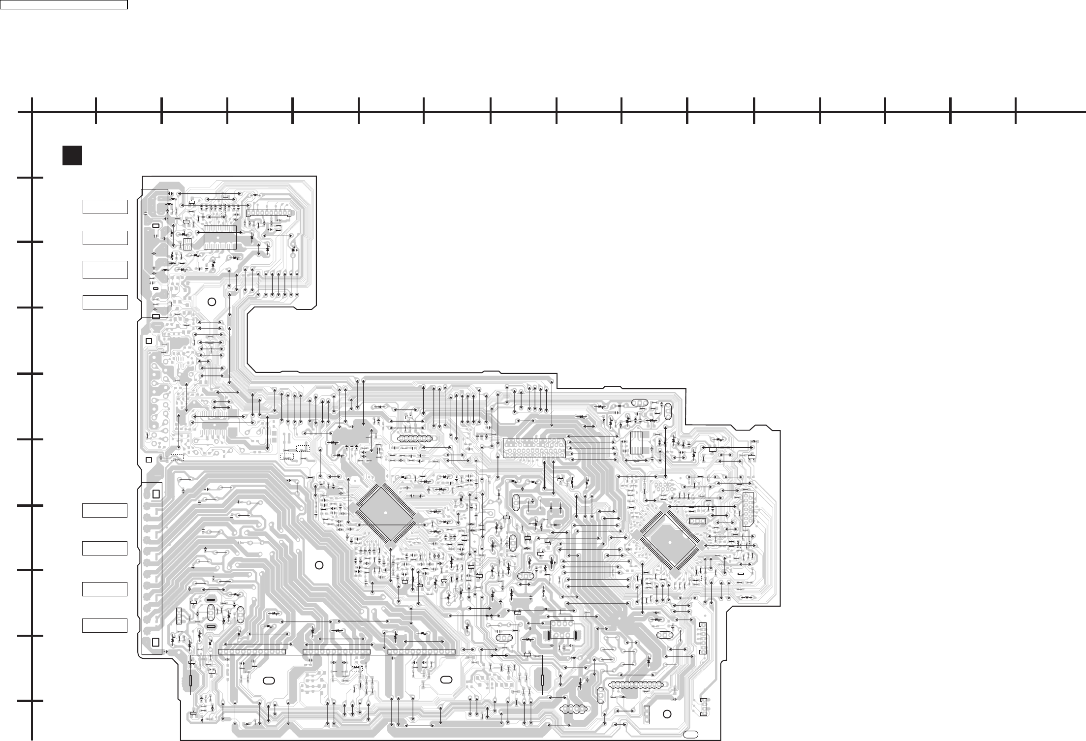
20.2. (B) Main P.C.B.
B
C
E
B
C
E
B
C
E
B
C
E
B
C
E
B
C
E
B
C
E
B
C
E
B
C
E
E
C
B
B
C
E
B
C
E
B
C
EB
C
E
ABCDEFG
1
2
3
4
5
6
7
8
9
HI J KL MNO P
BMAIN P.C.B. (REPX0531E...GC/GS, REPX0531D...GCS)
SA-HT340GC/GCS/GS MAIN P.C.B.
S-VIDEO OUT
VIDEO OUT
COMPONENT
VIDEO
OUT
AUX
SURROUND
SPEAKER
FRONT
SPEAKER
CENTER
SPEAKER
SUBWOOFER
B
C
E
B
C
E
B
C
E
B
C
E
B
C
E
B
C
E
B
C
E
B
C
E
B
C
E
B
C
E
46
13
5
4
2
14
13
12
11
10
9
8
6
14
13
12
11
10
9
8
7
6
5
4
3
2
1
1
2
3
112111098765432 123456789 1210 11
1
30 31
50
51
80
81
100
1234567
1 2 3 4 5 6 7 8 9 10 11 12
7
6
5
4
3
2
1
1234
123456789 1110
3
1
21
4
3
2
7
1
2
3
4
5
6
1
30
31
50
51
80 81
100
12
10
5
3
7
9
6
4
8
11 12
13
14
58
50
49
48
47
46
45
44
43
42
41
40
39
38
37
36
35
34
33
32
31
30
29
28
27
26
25
24
23
22
21
20
19
18
17
16
15
14
13
12
11
10
9
8
7
6
5
4
3
2
1
3
1
7
10 9 8 7 6 5 4 3 2 1
1
2
3
116
17 32
IC2102
R2214
C2611
C2115
C2215
R2336
R2621
C2024
C2114
C2214
C2601
C2502
R2501
C2309
C2305
C2306
C2406
C2405
R2404
C2408
C2302
C2308
C2610
C2118
C2218
C2112
C2216
C2116
C2117
C2217
C2119
R2436
R2402
R2301
C2219
R2609
R2619
R2303
C2272
C2403
C2503
C2507
C2612
R2607
C2221
R2304
C2020
C2402
C2423
C2323
R2608
R2403
R2503
C2303
R2112
R2610 C2617
C2609
C2212
C2401
R2302
R2606
R2511
R2401
C2615
C2121
R2212
C2172
R2215
R2218
R2502
R2627
R2113
C2301
C2120
R2612
R2114
C2220
R2611
R2620
C2023
C2017
R2115
Q2006
R2191
C2600
C2201
R2006
R2600
C2821
R2500
C2211
R2211
C2111
R2201
R2101
R2291
C2101
R2111
IC2018
IC2004
C2012
R2043
R2086
R2045
R2085
R2002
R2015
R2001
R2044
R2094
R2081
R2082
R2029
R2060
R2047
R2040
R2041
R2061
R2087
R2003
C2007
R2049
C2011
R2095
R2019
R2022
R2023
R2030
R2062
R2077
R2039
R2000
R2042
C2013
R2004
R2005
R2010
R2012
R2053
R2016
R2024
R2017
R2093
R2072
R2032
R2071
R2089
R2075
R2048
R2092
C2010
R2052
C2000
C2001
R2091
R2090
R2073
R2070
R2078
W2524
R2400
W2541
C2295
W2586
W2583
R2067
R2066
R2064
R2065
R2068
R2069
R2300 C2500
C2400
C2300
C2501
R2046
C5302
C5303
C5306
C5307
C5202
C5203
C5206
C5207
C5102
C5103
C5106
C5107
R5304 R5104
R5204
R5301
R5302
C5795
C5790
R5754
R5757
R5755
R5756
R5760
R5759
R5758
Q5741
Q5744
Q5742
D5743
D5744
R5763
R5764
C3001
C3002
C3003
C3004
C3005
R5101
R5102
R5201
R5202
R2185
R2285
R2312
R2412
R2510
R2617
C2183
C2283
C2312
C2412
C2506
R5533
R5534
R2626
R2512
R2439
R2339
R2294
R2194
Q3009
Q3008
R3008
R3009
R3014
R3015
W2529
R2919
R2920 R2921
C2919
C2920
C2970
D2904
C2969
C2952
R2915
C2903
C2902
C2910
Q2907
C2964
R2914
C2961
C2972
C2963 R2907
R2908
C2974
R2904
R2905
R2975
R2976
C2985
C2965
C2924
C2984
R2972 R2973
D2944
R2929
R2963
D2941
R2964
C2966
C2982
D2919
Q2915
R2968
R2969
R2970
C2940
C2976
R2934
D2915
C2945
R2933
C2959
C2978
R1200
R1100
IC2802
Q2805
C2811
C2818
C2807
C2812
C2817
C2801
R2818
C2826
C2827
C2828
C2810
C2830
C2825
R2817
C2829
L2804
R2803
R2804
R2807
C2832
R2265
C2823
R2816
L2802
L2803
L2807
L2805
L2806
R2812
R2813
R2809
C2169
R2261
R2260
C2262
C2162
C2161
R2161
R2160
C2261
Q2804
IC2801
W2512
W2509
W2513
C2026
R2264
R2164
C2164
C2264
R2165
W2506
W2503
W2504
R5108
R5111
R5112
R5212
R5211
R5208
R5308
R5311
R5312
R5313
C5305 C5104 C5105
(GC/GS)
C5204 C5205
C5304
C2195
R2601
R2960
R2031
R2063
R2076
R2079 R2080
R2084
R2088
C2004
C2009
C2906
D2906
D2918
R2007
D2005
D2007
D2008
Q2003
W2591
D2001
D2002
R2942
R2943
R2944
R2950
R2952
C2819
C2820
C2822
C5505
D2929
Q2030
Q2004
W2587
W2588
W2530
W2590
W2547
W2539
D2974
W2545
W2525
W2553
W2508
W2580
W2559
W2562
W2561
W2585
W2574
W2519
W2566
W2531
W2567
W2543
W2544 W2542
W2502
W2584
W2582
W2581
R2998
R2999
W2514
R5762
W2563
W2517
R2936
R2941
R2938
Q2917
Q2916
W2516
W2520
W2528
W2515
W2533
W2536 W2532
W2570
W2573
W2571
R2940
R2924
Q2910
W2592
W2589
C2800
W2501
C5799
W2593
R5761
C2424
C2324
W2540
W2538
W2552
W2556
W2572
R5736
C2804
W2902
W2903
W2904
W2905
(GC/GS)
(GC/GS)
C2411
W2537
W2554
W2560
W2564
R2980
W2595
Q5746
R5765
R5766
(TO FAN)
W2575
W2576
W2577
W2578
D5745
W2596
W2597
(GC/GS)
R2405
R2407
R2307
R2406
C5324
C5124
C5224
Q2905
D2905
W2579
W2558
Q3003
R3003
D3001
R3005
C2524
C2624
C2724
R3007
C2834
C2835
C2836
C2837
C2838
R3006
D5302
C2904
W2527
R2096
W2521
R2097
(GC/GS)
(GC/GS)
W2523
W2522
W2534
C6921
R6921
R6920
C6920
C2852
C2851
W2505
W2546
W2548
W2550
C2853
C2605
R2900 D2900
H2001
H2002
IC5100
JK5000
IC5300 IC5200
C5301
CN2001
L2009
X2001
W2275
W2129
W2108
W2158
W2138
W2148
W2162
W2131
H2004
C2021
C5503
C5308
C5313
W2103
W2145
C5101
C5108 C5208
W2151 W2150
C5201
W2105 W2104
W2110
W2160
W2159
W2109
W2200
W2161
W2189
CN5704
C5794
C5797
C5792
C5791
Q5740
W2244
W2226
C3006
C2619
W2198
W2199
W2107
W2157
W2176
W2247
W2231
W2183
W2165
W2153
C3009
W2235
L2909
C2922
C2921
E2900
C2901
C2913
C2914
Q2906
Q2903
R2913
C2971
C2908
C2973
R2974
C2986
Q2974
D2937
D2938
D2939
R2926
R2971
D2907
C2967
C2925
C2983
C2968
Q2955
C2981
CN2007
CN2006
CN2005
C2941
Q2913
C2975
C2946
Q2904
C2977
W2122
W2134
W2118
W2126
L2801
CN2002
C2022
W2259
W2258
W2268
W2267
C2803
C2805 C2802
C2806
JK2001
C2808
C2809
W2125
W2140
W2141
W2144
W2146
W2123
W2135
W2180
W2127
W2128
C2606
C2607
C2407
C2018
C2608
C2304
C2307
C2019
C2404
C2003
W2186
IC2903
C5796
D2935
D2936
W2254
W2261
W2255
W2219
W2197
W2264
W2217
W2214
W2215
W2223
W2224
W2218
W2230
W2192
W2256
W2202
W2262
W2248
W2185
W2201
W2184
W2191
W2171
W2170
W2249
W2269
W2272
W2221
W2225
W2216
W2101
W2172
W2206
W2239
W2188
W2232
W2142
W2147
W2168
W2222
W2169
W2181
W2139
W2257
W2179
W2207
W2211
W2193
W2209
W2210
W2281
W2277
W2253
W2280
W2276
W2234
W2136
W2265
W2163
W2196
L2902
W2236
W2252
W2251
W2220
W2241
W2212
W2250
W2271
W2155
W2260
W2154
W2106
W2246
W2149
W2229
W2273
W2194
W2205
W2178
W2213
W2187
W2233
W2156
W2208
W2240
W2203
C2410
W2152
Q2980
W2245
W2274
W2242
W2237
W2270
W2278
W2228
W2266
W2137
W2120
W2121
W2119
R2983
R2984
R2985
W2124
W2190
W2204
W2238
W2243
C5798
W2263
W2279
W2132
W2133
W2173
W2174
W2195
W2182
W2282
W2283
W2284
W2285
W2286
W2287
W2288
W2289
W2290
W2291
W2292
W2293
W2294
W2295
W2297
W2296
W2298
W2299
W2301
W2302
W2303
W2304
W2305
W2306
W2307
W2308
W2309
W2310
W2311
W2312
W2313
W2314
W2315
W2316
W2317
W2318
W2319
Q2914
R2986
C2006
K2910
K2913
K2912
W2143
W2300
W2320
W2321
W2322
W2323
C2841
C2008
Q5745
W2324
W2326
W2327 (GC/GS)
W2325
C3007
C2833
R5209
R5206
R5205 R5110
R5109
R5106
R5105
R5310
R5309
R5306
R5305
R5210
W2350
W2351
W2352
W2353
W2354
W2329
W2330
W2331
R2912
R2911
C2900
W2332
W2333
W2227
W2334
L2800
R2982
R2981
B
C
E
B
C
E
B
C
E
B
C
E
CA
A
CA
E
C
B
E
C
B
0490A-2
0490A-2
PbF
HEATSINK
(NOT SUPPLIED)
(TO SMPS MODULE)
(TO SMPS MODULE)
SA-HT340GC / SA-HT340GCS / SA-HT340GS
75
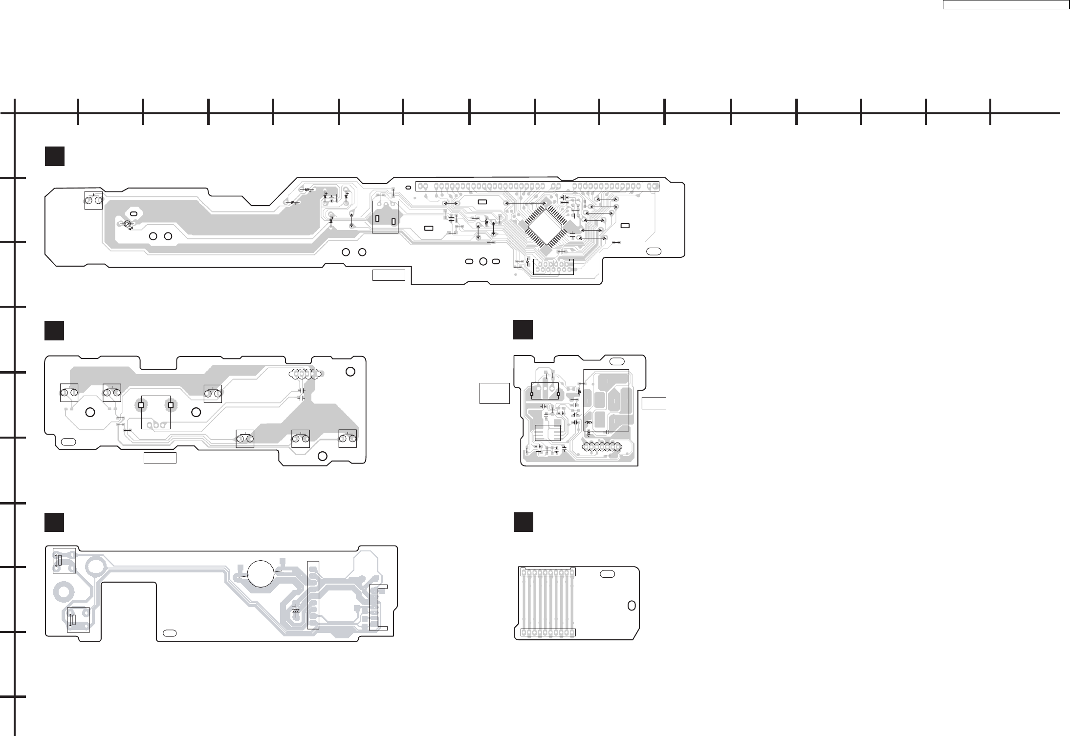
20.3. (C) FL, Volume, Mic, Tray Loading & Tuner Extent P.C.B.
13
2
1357911
2468 1210
13
44
31241711 12 15 18
89764 5
21 42 45
41403937 3830272623201916141310 32 33 34 35 36
1
11
12
22
23
33 34
44
1234
123
1
4
123
5
8
1765432
875
4
32
1
10123456789
10123456789
7
6
5
4
3
2
1
1
2
3
4
5
6
7
8
9
R6905
R6914
R6916
R6917
R6918
R6919
C6904
R6934
R6936
R6939
R6940
IC6901
D6910
L6903
W6504
W6502
W6511
W6512
W6509
C6911
C6909
C6906
C6916
C6917
W6513
W6545
W6501
Z6900
C6903
C6905
D6900
FL6901
W6002
W6001
W6003
W6004
W6006
W6005
W6008
W6010
CN6001
W6009
C6913
C6910
C6918
W6012
W6011
S6800
(POWER)
C6806
C6805
R6805
R6804
R6803
R6802
R6801
H6004
S6801
S6802 S6803
S6804
S6805
S6806
VR6800
(FORWARD/
TUNE UP)
W6516
C6701
C6711
C6710
C6708
W6515
C6707
R6708R6707
C6709
C6706
C6703
C6702
R6709
R6706
R6705
R6703
R6702
R6701
W6514
W6517
L6083
L6082
L6081
R6081
IC2204
C6093
VR6081
JK6802
H6903
CP2010
CN2010
(TO TUNER PACK)
0490A-2
0490A-2
PbF
0490A-2
0490A-2
PbF
LOADING
MOTOR
CS901
IC904
C984
S902
(OPEN SW)
S901
(PLAY SW)
ABCDEFG
1
2
3
4
5
6
7
8
9
HI J KL MNO P
C
FL P.C.B. (REPX0531E...GC/GS, REPX0531D...GCS)
D
VOLUME P.C.B. (REPX0531E...GC/GS, REPX0531D...GCS)
E
MIC P.C.B.(REPX0531E...GC/GS,
REPX0531D...GCS)
G
TUNER EXTENT P.C.B.
(REPX0531E...GC/GS,
REPX0531D...GCS)
SA-HT340GC/GCS/GS FL/VOLUME/MIC/TRAY LOADING/TUNER EXTENT P.C.B.
0490A-2
0490A-2
PbF
0490A-2
0490A-2
PbF
2462A
2462A
PbF
TRAY LOADING P.C.B. (REP3288B)
F
SENSOR
(REVERSE/
TUNE DOWN) (OPEN/CLOSE)
(SELECTOR) (PLAY) (STOP)
M
+
-
VOLUME
MIC
VOLUME MIC
SA-HT340GC / SA-HT340GCS / SA-HT340GS
76

SA-HT340GC / SA-HT340GCS / SA-HT340GS
77

21 Basic Troubleshooting Guide
21.1. Basic Troubleshooting Guide for Traverse Unit (DVD Module P.C.B.)
*Compare the above with OK condition Module
*Compare
the
above
with
OK
condition
Module
Checking components
a) Check LD current OPU unit (FFC connection)
Checking Points
8) Jitter out of specification
Problems
b) Check OPU (change to other unit and confirm)
*Check for solder short and/or component
*Check
for
solder
short
and/or
component
damaged
IC8051
Q8550, Q8560, Q8561, Q8562
Q8550, Q8551, Q8552, Q8560
*Check for solder short and/or component
*Check
for
solder
short
and/or
component
missing/damaged
*Check for solder short and/or component
*Check
for
solder
short
and/or
component
damaged
Q8550, Q8551, Q8552, Q8560, Q8561, Q8562
FP8201
IC8251
IC8251
Q8550, Q8551, Q8552, Q8560, Q8561, Q8562
IC8001
*Check for solder short and/or component
*Check
for
solder
short
and/or
component
missing/damaged
LB8301, R8321, R8322, LB8302, R8325, R8326
IC8421
*Check for solder short and/or component
*Check
for
solder
short
and/or
component
missing/damaged
a) Check laser drive circuitry (voltages and current)
- Check CD laser drive
*Compare the above with OK condition Module
*Compare
the
above
with
OK
condition
Module
- Check DVD laser drive
*Check voltages and LD current and compare with
*Check
voltages
and
LD
current
and
compare
with
OK Module
OK
Module
a) Check SDRAM address and data bus signal
b) Check video signals
c) Check audio DAC circuitry
signals
Traverse unit
b) Check laser drive circuitry (voltages and current)
c) Check LSI connection to motor drive circuitry
*Compare the above with OK condition Module
*Compare
the
above
with
OK
condition
Module
a) Check connection from Backend Module to
b) Check motor driver circuitry on voltages and control
*Compare the above with OK condition Module
*Compare
the
above
with
OK
condition
Module
a) Check motor driver circuitry (voltages)
7) Block noise during play
spinning
- Cannot read CD
- Cannot read DVD
movement
6) Cannot read disc but spindle is
3) Disc not spinning
4) Traverse not moving
5) Traverse and spindle abnormal
2) No TOC/Long TOC
Checking components
1) Distorted picture or abnormal
sound is heard during initialisation
Problems Checking Points
a) Check SDRAM address, data bus, CLK and
other control signals waveform
IC8051
21.2. Troubleshooting Guide for Power section (Power circuit)
Refer to the follow-up supplements for this model. This is due to the information not available at the time of issue for this service
manual.
78
SA-HT340GC / SA-HT340GCS / SA-HT340GS
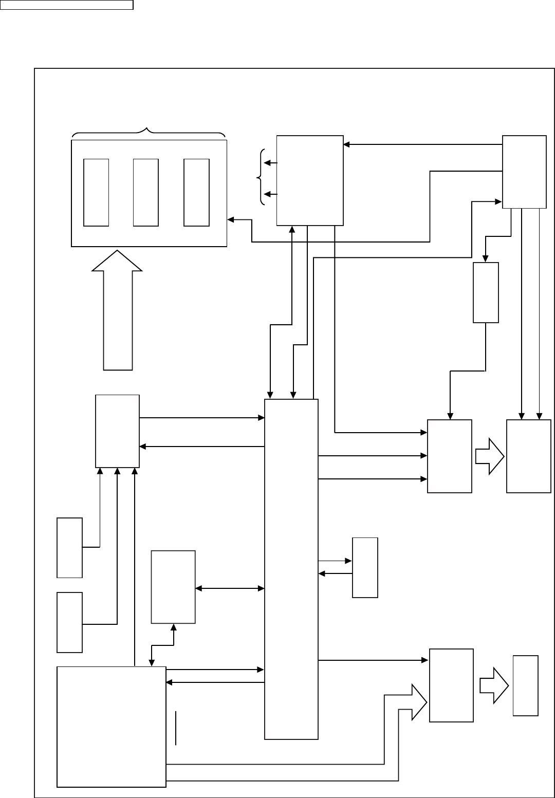
22 Overall Block (HT340)
ASP
AUX
REG
EEPROM
TUNER AMPLITIER BLOCK(MAIN)
IC5100
IC5200
IC5300
IC2102
DCDET
+26/+18V
HT340 OVERALL BLOCK
+9.8V
DVD PCONT/
PCONT
SUPPLY
VOLTAGES
VREF
Loading
Drive
VIDEO
DRIVER
IC904
IC2004
Q2974/
D2974
FL+(FL1)
FL-(FL2)
-VP
SW+5V
IC1101 IC6901
FL6901
JK1001
(AV)
C/Y/CR/CB/PY
SYSTEM CONTROL
IC2018
FR+/FR-
FL+/FL-
TRAY_OPEN
TRAY_CLOSE
TRAY_CCW
ZFLAG
MUTE_DVD
DVD_CM
DVD_STA
DVD_CK
AUDIO/
VIDEO
SL+/SL-
SR+/SR-
SW+/SW-
C+/C-
TO
SPEAKERS
DVD MODULE
(DV 3.2)
FL
DRIVER
POWER
BLOCK
(MAIN)
FL
DISPLAY
SMPS
MODULE
SA-HT340GC / SA-HT340GCS / SA-HT340GS
79
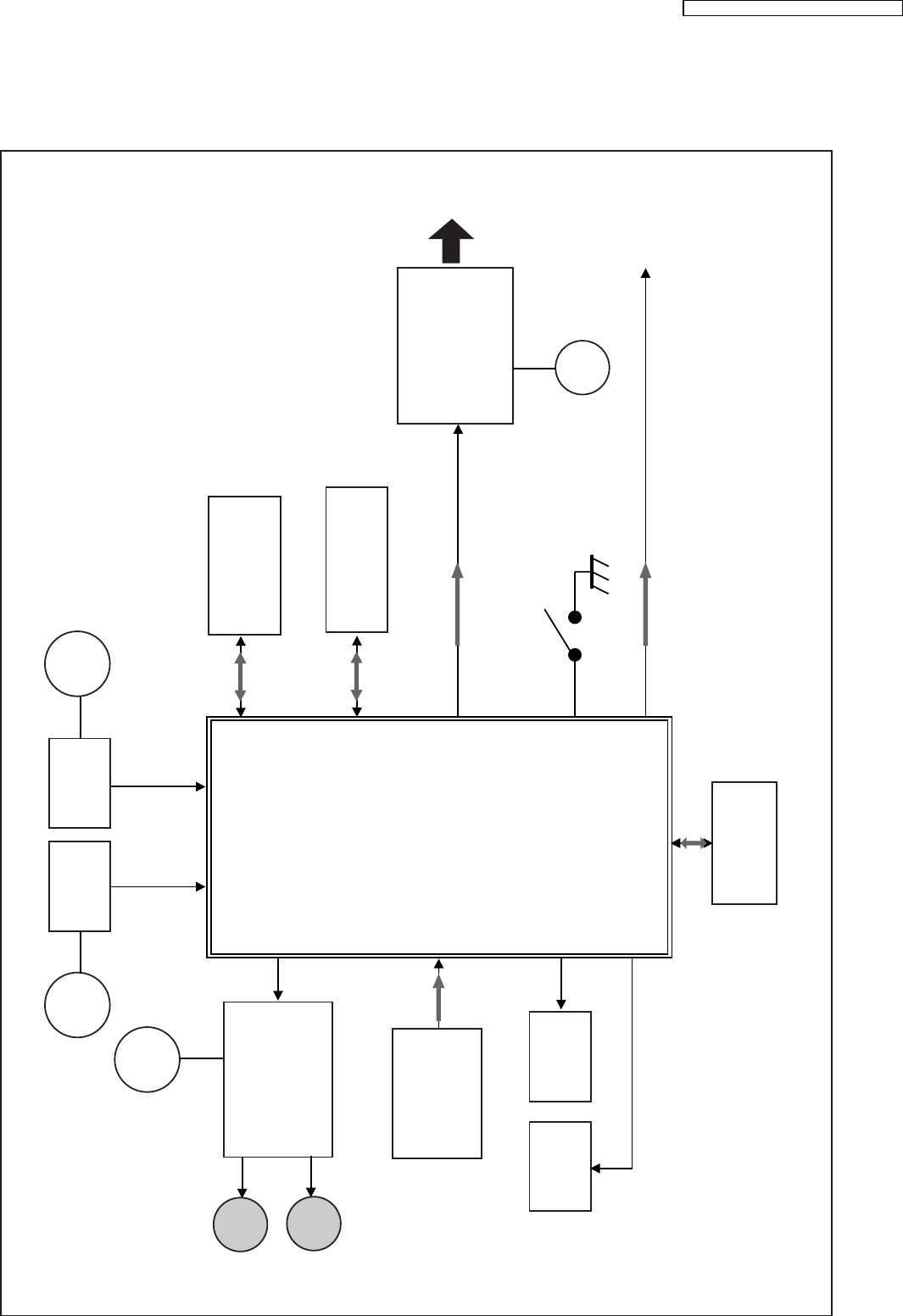
22.1. HT340 DVD Unit Block
DV3.2
Audio
output
Video output
(Y, C, CR/PR/R, CB/PB/B, Y/PY/G)
DVD System
DVD
System
LSI
<FEP>
EFM+
Demodulate
ECC
<BEP>
MPEG2
Decode
SP Motor
TRV Motor
IC8611
TRV sw
CD DVD
IC8251 IC8001
IC8151 IC8111
D+3.3V
VDD
1.2V IC8051
IC8421
IC8651
Driver
FO/TR Act
TRV/SP Motor
OPU
UNIT
LD
Drive
REG REG
LD
Drive
EEPROM
M
M
M+9V
+2.7V D+5V
SD RAM
SD
RAM
Flash ROM
Flash
ROM
Audio
DAC
+5V
SA-HT340GC / SA-HT340GCS / SA-HT340GS
80
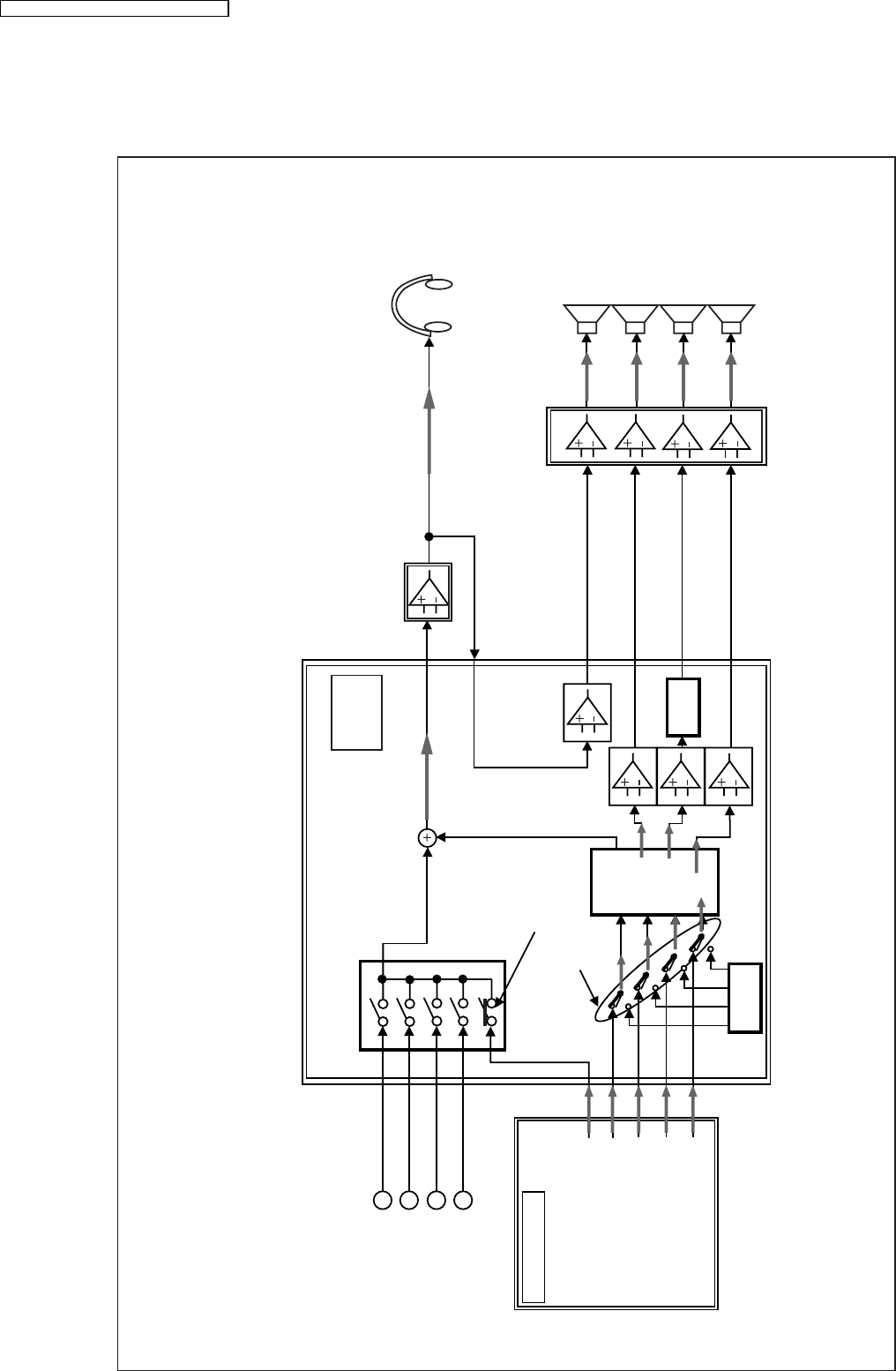
22.2. HT340 Block (Analog Signal : DVD 5.1ch Play Back Mode)
TV/VCR In
MUSIC PORT In
AUX In
TUNER In
DVD Module
ON
ON
DVD Mix(L/R)
DVD Front(L/R)
Volume
DVD Center
DVD Sub-Woofer
DVD Surround(L/R) AGC
ASS
DVD 5.1ch Play Back Mode
IC2102
Head Phone
Front(L/R)
Center
Sub-Woofer
Surround(L/R)
IC5100/IC5200
IC5300
HIC
ASP
SA-HT340GC / SA-HT340GCS / SA-HT340GS
81
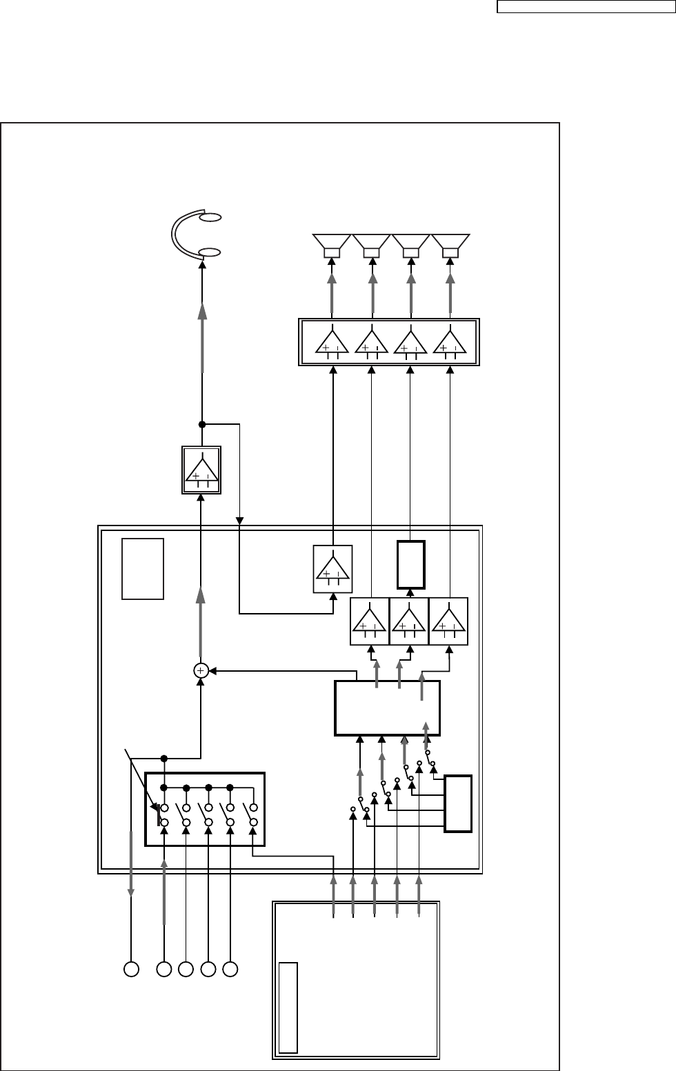
22.3. HT340 Block (Analog Signal : 2ch Analog Input Mode)
TV In
Line Out
TCR In
AUX In
TUNER In
DVD Module
ON
DVD Mix(L/R)
DVD Front(L/R)
Volume
DVD Center
DVD Sub-Woofer
DVD Surround(L/R) AGC
ASS
2ch Analog input Mode
IC2102
Head Phone
ASP
Front(L/R)
Center
Sub-Woofer
Surround(L/R)
IC5100/IC5200
IC5300
HIC
SA-HT340GC / SA-HT340GCS / SA-HT340GS
82
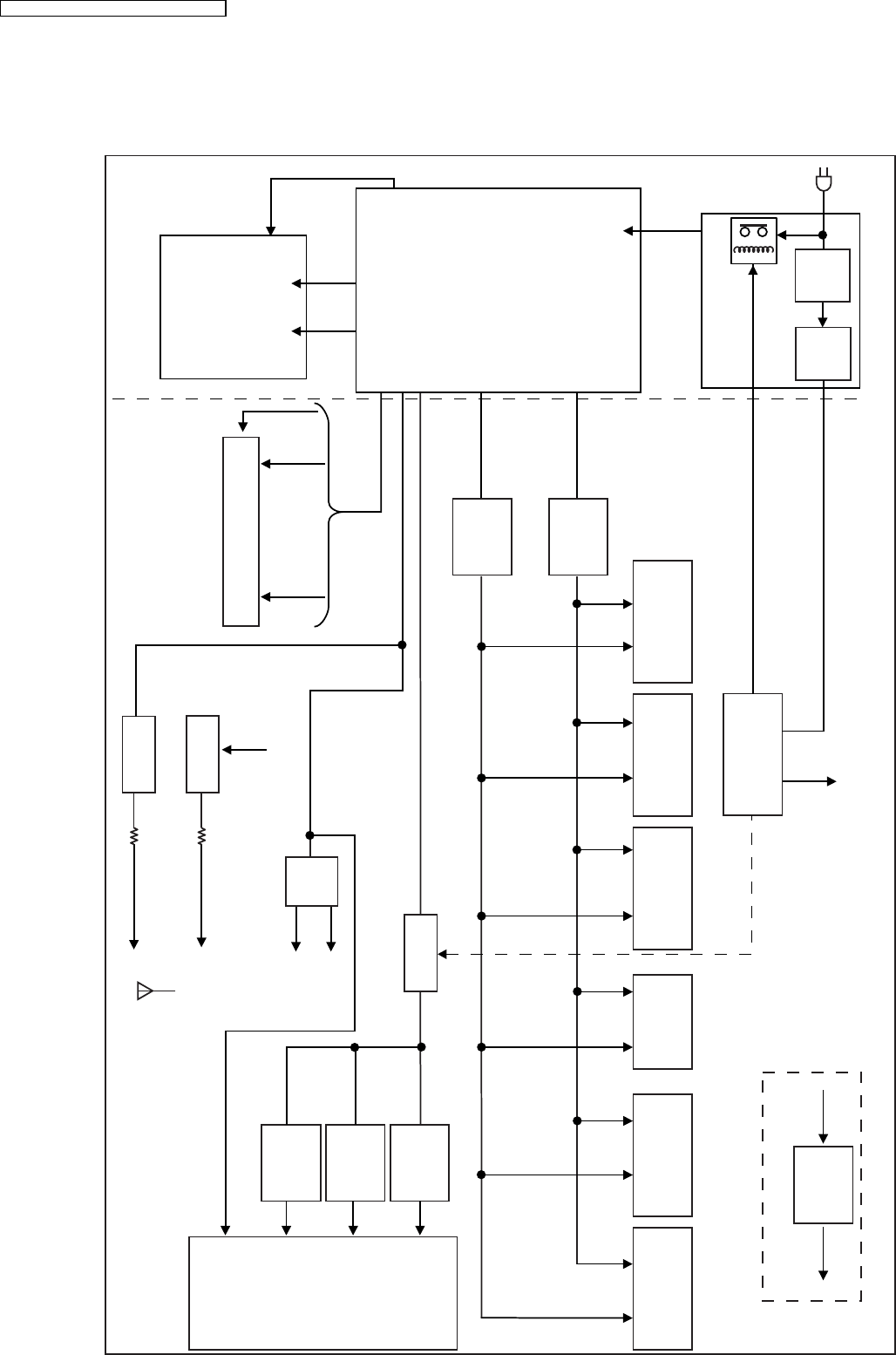
22.4. HT340 Power Supply Block
POWER
BLOCK
(SMPS)
SUB-TRANSFORMER BLOCK
+7V
REG
A+5V
REG
D+5V
REG
D+2.7
REG
REG
REG
+5V
REG 6V
REG SUB
HEADPHONE
AMP
ASPVIDEO
U-COM
OP-AMP
LOGIC
SWITCH
IC5100/IC5200
IC5300
Q2906/Q2907
Q2903/D2902
-30V
+30V
+30V
FL+ FL-
-VP +5V
-7V
REG
IC2903
Q2935/
D2941
Q2912
Q2910/D2917
Q2914/
D2944
Q2904/
D2915
SYS 6V
IC2301 IC2103/IC2600
IC2104/IC2205 IC2801
Q2902/D2914
FOR WIRELESS MODELS ONLY
DVD
MODULE
IC2102
DC_13V
RF+5V
IC2103
REG
SCART
DRIVER
IC1101
-30V
T+9V
+12V
MUTING
DVD PCONT
POWER
HIC
SECTION
SW+5V +30V
DAMP+5V
+18V DC_13V
M+9V
TUNER
FL DISPLAY
<POWER ON MODE>
AC
INPUT
ON
(DAMP
+5V)
SA-HT340GC / SA-HT340GCS / SA-HT340GS
83
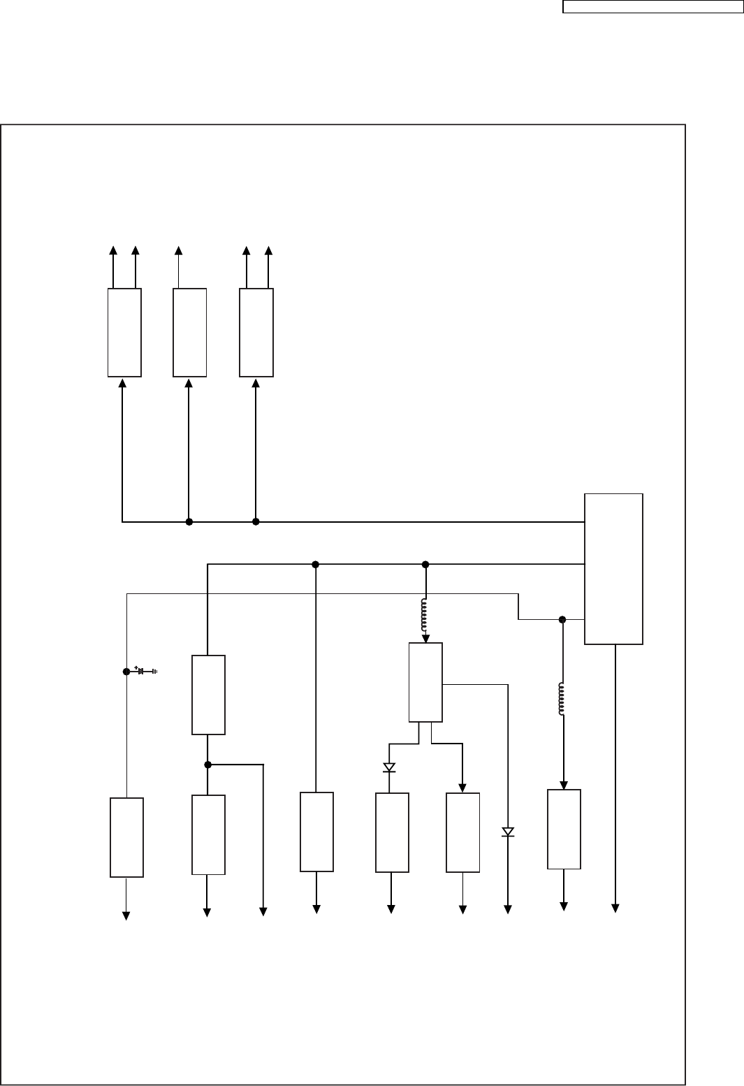
22.5. HT340 Power (Main) Block
SMPS
REG IC5100
IC5200
IC5300
FR+/FL+
FR-/FL-
HT340 POWER(MAIN) BLOCK
Q2906/Q2907
REG
Q2904/D2915
REG
Q2914/D2944
REG
Q2955/D2941
REG
IC2903
Q2903
REG
Q2913/D2943/D2942
+26/18V
SR+/SL+
SL-/SR-
SW+/SW-
C+/C-
-7V
SW+5V
+9V
DVD2.7V
A+5V
REG
Q2974/D2974 -28V
R
-VP
D+5V
SYS6V
M+9V
SA-HT340GC / SA-HT340GCS / SA-HT340GS
84

23.1. IC2018 (C2CBYY000194):
System Control
Microprocessor IC
Pin
No.
Terminal Name I/O Function
1TRAY_
CLOSE
ILoading mechanism close SW ( L: SW
ON )
2TRAY_CCW OTerminal for tray control 1
3TRAY_CW OTerminal for tray control 2
4TRY_OPEN ILoading Mechanism open SW ( L: SW
ON )
5SINE_SW IDetect of square wave 1
6 N.C - No connection
7 SINE_FL I Detect of square wave 2
8BYTE - VSS (GND)
9 CNVSS - VSS (GND)
10 N.C - No connection
11 N.C - No connection
12 RESET I System Reset Input
13 XOUT - Main Clock Output (10.0 MHZ)
14 VSS - GND (0V)
15 XIN - Main Clock Input (10.0 MHZ)
16 VCC - Power supply (5V)
17 NMI I Connect to VCC, External Interrupt I/P
18 RMT I Remote control input
19 SYNC IAC failure detection input
20 AM_BP O AM beat proof
21 MIC_EN - No connection
22 N.C - No connection
23 EDA I/O DATA signal for the EEPROM
24 ECK O CLOCK signal for the EEPROM
25 ECS O LAT signal for the EEPROM
26 N.C - No connection
27 N.C - No connection
28 DVD_CLK ICLK signal for the DVD Module
29 DVD_STAT I STATUS signal from DVD Module
30 DVD_CMD OCMD signal for the DVD Module
31 RF_DET I RF module detection - wireless ready
32 RF_PCON - RF power control
33 RF_LINK I RF link control - wireless ready
34 RF_DATA O RF change direction -wireless ready
35 TUN_SD I CMD signal for the DVD Module
36 TUN_CLK O I2C Clock Data Tuner
37 TUN_DO I Stereo Detection
38 TUN_DI O I2C Data for Tuner
39 N.C - No connection
40 PCONT O Control Signal for the Power Control
Relay
41 EPM - Connect to Flash
42 DVD_MUTE I Signal from DVD module control mute
circuit
43 N.C - No connection
44 N.C - No connection
45 N.C - No connection
46 N.C - No connection
Pin
No.
Terminal Name I/O Function
47 N.C - No connection
48 N.C - No connection
49 N.C - No connection
50 N.C - No connection
51 N.C - No connection
52 N.C - No connection
53 N.C - No connection
54 N.C - No connection
55 N.C - No connection
56 N.C - No connection
57 N.C - No connection
58 N.C - No connection
59 N.C - No connection
60 N.C - No connection
61 N.C - No connection
62 N.C. - No connection
63 N.C - No connection
64 VSS - GND (0V)
65 VCC_CTRL O Power suppply control
66 MIC_SW OMic surround
67 MUTE_C O Center mute
68 MUTE_SURR O Surround mute
69 MUTE_F_SW O Front and subwoofer mute
70 DC_DET I Signal from the DC Detection circuit
71 STBY ODigital amplifier standby control
72 DVD_PCNT OControl signal for the power for the
DVD Module
73 N.C - No connection
74 N.C - No connection
75 N.C - No connection
76 JOG_A I Signal A from Volume JOG
77 JOG_B I Signal B from Volume JOG
78 N.C - No connection
79 SCART_ MUTE O Line out for SCART terminal
80 WIDE1 OControl signal for the WIDE function
81 RGB_H O Mute signal 1 for video output
82 YC-H OControl signal for the video signal Mix
83 ASP_CLK O ASP clock
84 ASP_DAT O ASP data
85 FLD_CLK OClock signal for the FL driver
86 FLD_STB O FL driver strobe
87 FLD_OUT O FL data out
88 RDS_DAT I Data signal from the RDS decoder
89 MD3 I Model code 3
90 MD2 I Model code 2
91 KEY 2 IKey 2 line input
92 MD1 I Model code 1
93 DES3 I Region setting for DVD
94 DES2 I Model code Digit 1
95 DES1 I Region setting for Tuner
96 AVSS - Analog power supply input
97 KEY1 IKey 1 line input
98 VREF - Reference voltage input
99 AVCC - Analog power supply input
100 BRAKE_H O Terminal for tray control 3
23 Terminal Function of ICs
85
SA-HT340GC / SA-HT340GCS / SA-HT340GS
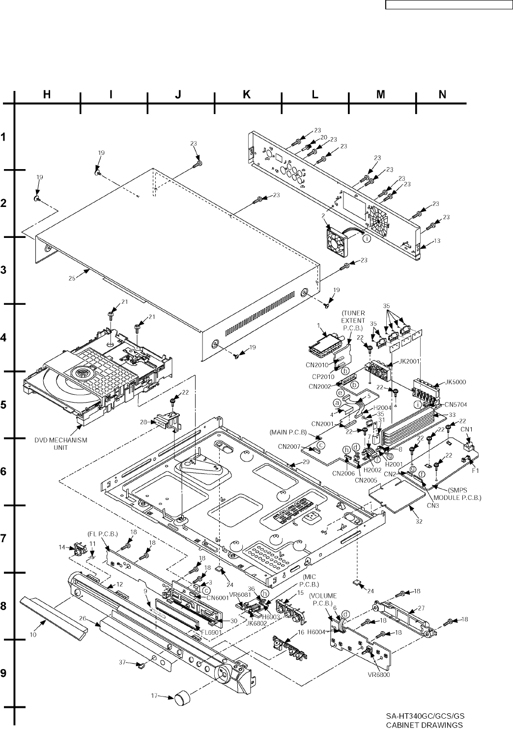
24 Exploded Views
24.1. Cabinet Parts Location
86
SA-HT340GC / SA-HT340GCS / SA-HT340GS
87
SA-HT340GC / SA-HT340GCS / SA-HT340GS
24.2. Packaging
88
SA-HT340GC / SA-HT340GCS / SA-HT340GS
25 Replacement Parts List
Notes:
*Important safety notice:
Components identified by mark have special characteristics important for safety purpose.
Furthermore, special parts which have purposes of fire-retardant (resistors), high-quality sound (capacitors), low-noise
(resistors), etc. are used.
When replacing any of components, be sure to use only manufacture’s specified parts shown in the parts list.
*Warning: This product uses a laser diode. Refer to caution statements.
*Capacity values are in microfarads (µF) unless specified otherwise, P=Pico-farads (pF), F=Farads (F).
*Resistance values are in ohms, unless specified otherwise, 1K=1,000 (OHM), 1M=1,000K (OHM).
*The parenthesized indications in the Remarks columns specify the model names and areas. (Refer to the cover page)
*The marking (RTL) indicates the retention time is limited for this item. After the discontinuation of this assembly in production,
it will no longer be available.
*Reference for O/I book languages are as follows:
[En: English, Cn: Chinese Ar: Arabic]
*[M] indicates in the Remarks columns indicates parts supplied by PAVCSG.
*[SPG] indicates in the Remarks columns indicates parts supplied by SPG [PAVC].
89
SA-HT340GC / SA-HT340GCS / SA-HT340GS
25.1. Component Parts List
Ref.
No.
Part No. Part Name & Description Remarks
CABINET AND CHASSIS
1J3CCBB000007 TUNER PACK [M]
2L6FAJCCH0007 FAN MOTOR [M]
3REEX0612 13P FFC CABLE [M]
4REEX0613 50P FFC CABLE [M]
5REXX0384 7P FLAT WIRE [M]
6REXX0519 4P FLAT WIRE [M]
7REXX0520 11P FLAT WIRE [M]
8REXX0521 4P FLAT WIRE [M]
9RGB0164-S PANA BADGE [M]
10 RGKX0325-S DVD LID [M]
11 RGLX0128-Q LIGHTING CHIP [M]
12 RGPX0208-S FRONT PANEL [M]
13 RGRX0058B-B REAR PANEL [M]GCS
13 RGRX0058B-C REAR PANEL [M]GC/
GS
14 RGUX0665-S POWER BUTTON [M]
15 RGUX0666-S FUNCTION BUTTON [M]
16 RGUX0676-S OPEN CLOSE BUTTON [M]
17 RGWX0076-S VOLUME KNOB [M]
18 RHD26046 SCREW [M]
19 RHD30007-1SJ SCREW [M]
20 RHD30070 EARTH TERMINAL [M]
21 RHD30102-1 SCREW [M]
22 RHD30111-3 SCREW [M]
23 RHD30119-S SCREW [M]
24 RKA0059-K LEG RUBBER [M]
25 RKMX0107-1S2 TOP CABINET [M]
26 RKWX0258B-K FL WINDOW [M]
27 RMAX0071-2 MECHA HOLDER [M]
28 RMAX0086 PANEL ANGLE [M]
29 RMKX0117 BOTTOM CHASSIS [M]
30 RMNX0149 FL HOLDER [M]
31 RMYX0164 SMALL HEATSINK [M]
32 RMZX0029 MAIN PCB INSULATOR [M]
33 RXXX0076 HEATSINK UNIT [M]
35 XTB3+8JFJ SCREW [M]
36 REXX0531 7P FLAT WIRE [M]
37 RGW0352A-K MIC KNOB [M]
DVD MECHANISM UNIT
310 RHM0003-J MAGNET [M]
311 RDG0547 PULLEY GEAR [M]
312 RDG0548-1 RELAY GEAR [M]
313 RDG0549 DRIVE GEAR [M]
314 RDV0070 BELT [M]
315 REM0102 MOTOR UNIT [M]
316 RGQ0395-K1 TRAY [M]
317 RME0350 CHANGE LEVER SPRING [M]
318 RME0351 LOCK LEVER SPRING [M]
319 RME0353 TRAY SLIDER SPRING [M]
320 RMK0591 MECHA CHASSIS [M]
321 RML0627-2 DRIVE ARM [M]
322 RML0628 CHANGE LEVER [M]
323 RML0629 LOCK LEVER [M]
324 RML0631 TRAY SLIDER [M]
325 RMM0247 DRIVE RACK [M]
326 RMM0248 SUB RACK [M]
327 RMC0387 SUPPORT SPRING [M]
329 RMR1446-X CLAMPER [M]
330 XTN26+6GFJ SCREW [M]
331 XTV2+6GFJ SCREW [M]
333 XWG6FFY WASHER [M]
334 RMR1447-X MAGNET HOLDER [M]
335 RMR1468-K CLAMP PLATE [M]
350 RAE2018W-S TRAVERSE UNIT [M]
351 RMG0598-A FLOATING RUBBER [M]
352 RMG0617-H CUSHION RUBBER A [M]
353 RMG0618-H CUSHION RUBBER B [M]
Ref.
No.
Part No. Part Name & Description Remarks
354 RMR1596-X2 MIDDLE CHASSIS [M]
355 RMS0789 FIXED PIN [M]
356 RXQ0946 TRAVERSE MOTOR ASS’Y [M]
357 RXQ1389 DVD OPU SUB ASS’Y [M]
PRINTED CIRCUIT BOARDS
REP4012B DVD MODULE P.C.B. [M]
(RTL)GC
/GS
REP4012H DVD MODULE P.C.B. [M]
(RTL)GC
S
REPX0531E MAIN P.C.B. [M]
(RTL)GC
/GS
REPX0531D MAIN P.C.B. [M]
(RTL)GC
S
REPX0531E VOLUME P.C.B. [M]
(RTL)GC
/GS
REPX0531D VOLUME P.C.B. [M]
(RTL)GC
S
REPX0531E FL P.C.B. [M]
(RTL)GC
/GS
REPX0531D FL P.C.B. [M]
(RTL)GC
S
REPX0531E MIC P.C.B. [M]
(RTL)GC
/GS
REPX0531D MIC P.C.B. [M]
(RTL)GC
S
REPX0531E TUNER EXTENT P.C.B. [M]
(RTL)GC
/GS
REPX0531D TUNER EXTENT P.C.B. [M]
(RTL)GC
S
REP3288B LOADING P.C.B. [M]
(RTL)
N0AZ6GE00004 SWITCHING MODE POWER SUPPLY [M]
(RTL)
INTEGRATED CIRCUITS
IC904 C0GAY0000013 IC MOTOR DRIVER [M]
IC2018 C2CBYY000194 IC MICRO-PROCESSOR [M]
IC2102 C1AB00002463 IC ASP [M]
IC2204 C0ABBB000230 IC OP-AMP [M]
IC2801 C9ZB00000461 IC VIDEO BUFFER [M]
IC2802 C1AB00001731 IC VIDEO BUFFER [M]
IC2903 AN30070A IC DC-DC CONVERTER [M]
IC5100 AN17831A IC POWER [M]
IC5200 AN17831A IC POWER [M]
IC5300 AN17831A IC POWER [M]
IC6901 C0HBB0000057 IC DISPLAY DRIVER [M]
IC8001 MN2DS0009VP IC DV3.2 LSI [M]
IC8051 C3ABPG000145 IC SDRAM [M]
IC8111 C0CBCBD00018 IC 3.3V REGULATOR [M]
IC8151 C0DBEHG00006 IC 1.2V REGULATOR [M]
IC8251 C0GBG0000048 IC MOTOR DRIVER [M]
IC8421 C0FBBK000050 IC AUDIO DAC [M]
IC8601 C0EBA0000029 IC RESET [M]
IC8606 C0EBE0000455 IC RESET [M]
IC8651 RFKWMHA0B160 IC FLASH ROM [SPG]GC
/GS
IC8651 RFKWMHA0C160 IC FLASH ROM [SPG]GC
S
IC8691 C0JBAA000346 IC AND GATE [M]
IC8695 C0JBAA000346 IC AND GATE [M]
TRANSISTORS
90
SA-HT340GC / SA-HT340GCS / SA-HT340GS

Ref.
No.
Part No. Part Name & Description Remarks
Q2003 B1GBCFJJ0051 TRANSISTOR [M]
Q2004 B1ADCE000012 TRANSISTOR [M]
Q2006 B1GBCFJJ0051 TRANSISTOR [M]
Q2030 B1GBCFJJ0051 TRANSISTOR [M]
Q2804 B1GBCFJJ0051 TRANSISTOR [M]
Q2805 B1GBCFJJ0051 TRANSISTOR [M]
Q2903 B1BACD000018 TRANSISTOR [M]
Q2904 B1AAKD000012 TRANSISTOR [M]
Q2905 B1GBCFJJ0051 TRANSISTOR [M]
Q2906 B1BCCG000002 TRANSISTOR [M]
Q2907 B1ADCF000001 TRANSISTOR [M]
Q2910 B1ABCF000176 TRANSISTOR [M]
Q2913 B1BACD000018 TRANSISTOR [M]
Q2914 B1BACG000023 TRANSISTOR [M]
Q2915 B1GBCFJJ0051 TRANSISTOR [M]
Q2916 B1GBCFJJ0051 TRANSISTOR [M]
Q2917 B1GBCFJJ0051 TRANSISTOR [M]
Q2955 B1BACD000018 TRANSISTOR [M]
Q2974 B1ACKD000005 TRANSISTOR [M]
Q2980 B1BACD000018 TRANSISTOR [M]
Q3003 B1GDCFJJ0047 TRANSISTOR [M]
Q3008 B1ABGC000005 TRANSISTOR [M]
Q3009 B1ABCF000176 TRANSISTOR [M]
Q5740 B1BACG000023 TRANSISTOR [M]
Q5741 B1ABCF000176 TRANSISTOR [M]
Q5742 B1ABCF000176 TRANSISTOR [M]
Q5744 B1ABCF000176 TRANSISTOR [M]
Q5745 B1ACKD000005 TRANSISTOR [M]
Q5746 B1GBCFJJ0051 TRANSISTOR [M]
Q8551 2SD1819A0L TRANSISTOR [M]
Q8552 B1ADGB000008 TRANSISTOR [M]
Q8561 2SD1819A0L TRANSISTOR [M]
Q8562 B1ADGB000008 TRANSISTOR [M]
QR8111 XP0621400L CHIP TRANSISTOR [M]
QR8420 UNR521100L CHIP TRANSISTOR [M]
QR8571 UNR511V00L CHIP TRANSISTOR [M]
DIODES
D2001 B0ACCK000005 DIODE [M]
D2002 B0ACCK000005 DIODE [M]
D2005 B0ACCK000005 DIODE [M]
D2007 B0ACCK000005 DIODE [M]
D2008 B0ACCK000005 DIODE [M]
D2900 B0BC7R500001 DIODE [M]
D2904 B0JCPD000025 DIODE [M]
D2905 B0BC7R500001 DIODE [M]
D2906 B0ACCK000005 DIODE [M]
D2907 B0EAKM000117 DIODE [M]
D2915 B0BC5R600003 DIODE [M]
D2918 B0ADCJ000020 DIODE [M]
D2919 B0ADCJ000020 DIODE [M]
D2929 B0ACCK000005 DIODE [M]
D2935 B0EAKM000117 DIODE [M]
D2936 B0EAKM000117 DIODE [M]
D2937 B0EAKM000117 DIODE [M]
D2938 B0EAKM000117 DIODE [M]
D2939 B0EAKM000117 DIODE [M]
D2941 B0BC5R600003 DIODE [M]
D2944 B0BC3R400001 DIODE [M]
D2974 MAZ82200ML DIODE [M]
D3001 B0ACCK000005 DIODE [M]
D5302 B0ACCK000005 DIODE [M]
D5743 B0ACCK000005 DIODE [M]
D5744 B0ACCK000005 DIODE [M]
D5745 B0BC013A0007 DIODE [M]
D6900 B3AAA0000803 DIODE [M]
D6910 B0BC5R000009 DIODE [M]
D8211 MA2J11100L DIODE [M]
D8571 MA2J72800L DIODE [M]
CHIP INDUCTORS
Ref.
No.
Part No. Part Name & Description Remarks
LB8001 J0JHC0000045 CHIP INDUCTOR [M]
LB8011 J0JHC0000045 CHIP INDUCTOR [M]
LB8257 ERJ3GEY0R00V CHIP RESISTOR [M]
LB8258 ERJ3GEY0R00V CHIP RESISTOR [M]
LB8259 ERJ3GEY0R00V CHIP RESISTOR [M]
LB8260 ERJ3GEY0R00V CHIP RESISTOR [M]
LB8301 J0JBC0000042 CHIP INDUCTOR [M]
LB8302 J0JBC0000042 CHIP INDUCTOR [M]
LB8303 J0JBC0000042 CHIP INDUCTOR [M]
LB8304 J0JBC0000042 CHIP INDUCTOR [M]
LB8305 J0JBC0000042 CHIP INDUCTOR [M]
LB8401 J0JBC0000042 CHIP INDUCTOR [M]
LB8421 ERJ2GE0R00X CHIP RESISTOR [M]
LB8422 ERJ2GE0R00X CHIP RESISTOR [M]
LB8423 ERJ2GE0R00X CHIP RESISTOR [M]
LB8424 ERJ2GE0R00X CHIP RESISTOR [M]
LB8425 ERJ2GE0R00X CHIP RESISTOR [M]
LB8426 ERJ2GE0R00X CHIP RESISTOR [M]
LB8427 ERJ2GE0R00X CHIP RESISTOR [M]
LB8428 ERJ2GE0R00X CHIP RESISTOR [M]
LB8429 ERJ2GE0R00X CHIP RESISTOR [M]
LB8431 ERJ2GE0R00X CHIP RESISTOR [M]
LB8491 ERJ2GE0R00X CHIP RESISTOR [M]
LB8530 J0JHC0000045 CHIP INDUCTOR [M]
LB8531 ERJ2GE0R00X CHIP RESISTOR [M]
LB8551 J0JBC0000042 CHIP INDUCTOR [M]
LB8561 J0JBC0000042 CHIP INDUCTOR [M]
LB8571 J0JBC0000042 CHIP INDUCTOR [M]
LB8690 J0JBC0000106 CHIP INDUCTOR [M]GC/
GS
LB8691 ERJ2GEJ101X CHIP RESISTOR [M]
LB8692 ERJ2GEJ101X CHIP RESISTOR [M]
LB8693 ERJ2GEJ101X CHIP RESISTOR [M]
VARIABLE RESISTORS
VR6081 EVUE27FK3B53 VR MIC LEVEL [M]
VR6800 EVEKE2F2524M VR VOLUME JOG [M]
SWITCHES
S901 RSH1A044-1A SW PLAY [M]
S902 RSH1A044-1A SW OPEN [M]
S6800 EVQ21405R SW POWER [M]
S6801 EVQ21405R SW OPEN/CLOSE [M]
S6802 EVQ21405R SW TUNE UP/FORWARD [M]
S6803 EVQ21405R SW TUNE DOWN/REVERSE [M]
S6804 EVQ21405R SW STOP [M]
S6805 EVQ21405R SW PLAY [M]
S6806 EVQ21405R SW SELECTOR [M]
CONNECTORS
CN2001 K1MY50AA0029 50P CONNECTOR [M]
CN2002 K1KA10AA0031 10P CONNECTOR [M]
CN2005 K1KA04AA0193 4P CONNECTOR [M]
CN2006 K1KA07AA0193 7P CONNECTOR [M]
CN2007 K1MN13AA0003 16P CONNECTOR [M]
CN2010 K1KA10AA0031 10P CONNECTOR [M]
CN5704 K1KA03AA0301 3P CONNECTOR [M]
CN6001 K1MN13BA0004 13P CONNECTOR [M]
CP2010 K1KB10B00042 10P CONNECTOR [M]
CS901 K1KA07BA0061 7P CONNECTOR [M]
FP8101 K1MN50BA0173 50P CONNECTOR [M]
FP8251 K1MN06BA0148 6P CONNECTOR [M]
FP8531 K1MY26BA0025 26P CONNECTOR [M]
COILS & TRANSFORMERS
L2009 G0C220JA0055 COIL [M]
91
SA-HT340GC / SA-HT340GCS / SA-HT340GS

Ref.
No.
Part No. Part Name & Description Remarks
L2800 G0C220JA0055 COIL [M]
L2801 G0C220JA0055 COIL [M]
L2802 J0JBC0000015 CHIP INDUCTOR [M]
L2803 J0JBC0000015 CHIP INDUCTOR [M]
L2804 J0JBC0000015 CHIP INDUCTOR [M]
L2805 J0JBC0000015 CHIP INDUCTOR [M]
L2806 J0JBC0000015 CHIP INDUCTOR [M]
L2807 J0JBC0000015 CHIP INDUCTOR [M]
L2902 G0A101G00022 COIL [M]
L2909 G0A200D00002 COIL [M]
L6081 ERJ3GEY0R00V CHIP JUMPER [M]
L6082 J0JBC0000030 CHIP BEEZ [M]
L6083 J0JBC0000019 CHIP INDUCTOR [M]
L6903 J0JBC0000041 CHIP INDUCTOR [M]
L8201 G1C100K00019 CHIP COIL [M]
L8301 G1C100K00019 CHIP COIL [M]
L8302 G1C100K00019 CHIP COIL [M]
L8501 G1C100K00019 CHIP COIL [M]
L8550 G1C100KA0055 CHIP INDUCTOR [M]
COMPONENT COMBINATION
Z6900 B3RAB0000025 REMOTE SENSOR [M]
OSCILLATORS
X2001 H2B100500004 CERAMIC RESONATORS [M]
X8621 H0J270500085 CRYSTAL [M]
DISPLAY TUBE
FL6901 A2BD00000160 FL DISPLAY [M]
FL8101 F1H0J1050022 CHIP CAPACITOR [M]
FL8102 F1H0J1050022 CHIP CAPACITOR [M]
FL8103 F1H0J1050022 CHIP CAPACITOR [M]
FL8104 F1J1E1040022 CHIP CAPACITOR [M]
HOLDERS
H2001 K1YF04000001 CABLE HOLDER [M]
H2002 K1YZ11000002 11P CABLE HOLDER [M]
H2004 K1YZ07000001 7P WIRE HOLDER [M]
H6004 K1YZ04000002 4P CABLE HOLDER [M]
H6903 K1YZ07000001 7P WIRE HOLDER [M]
FUSE
F1 K5D502BNA005 FUSE [M]
JACKS
JK2001 K1U717B00004 JK COMBO [M]
JK5000 K4AC12B00003 JK SPEAKER [M]
JK6802 K2HB102J0038 JK [M]
EARTH TERMINAL
E2900 K4CZ01000027 TERMINAL [M]
PACKING MATERIALS
P1 RPGX1557 PACKING CASE [M]GC
P1 RPGX1558 PACKING CASE [M]GS
P1 RPGX1559 PACKING CASE [M]GCS
P2 RPNX0369-1 POLYFOAM [M]
P3 RPFX0058-1J MIRAMAT [M]
ACCESSORIES
A1 N2QAYZ000006 REMOTE CONTROL [M]
A1-1 RKK-HTR0051K R/C BATTERY COVER [M]
A2 K2CQ2CA00002 AC CORD [M]
Ref.
No.
Part No. Part Name & Description Remarks
A2 K2CT3CA00004 AC CORD [M]
GS
A3 RQT8589-B O/I BOOK (EN) [M]
A3 RQT8735-F O/I BOOK (AR, PE) [M]GC/
GS
A3 RQT8734-1C O/I BOOK (CN) [M]GCS
A4 N1DAAAA00002 AM LOOP ANTENNA [M]
A5 RSA0007-L FM ANTENNA [M]
A6 RQCA0968 SPEAKER LABEL [M]
A7 K2KA2BA00001 VIDEO CABLE [M]
RESISTORS
R1100 ERJ3GEYJ471V 470 1/16W [M]
R1200 ERJ3GEYJ471V 470 1/16W [M]
R2000 ERJ3GEYJ221V 220 1/16W [M]
R2001 ERJ3GEYJ104V 100K 1/16W [M]
R2002 ERJ3GEYJ103V 10K 1/16W [M]
R2003 ERJ3GEYJ221V 220 1/16W [M]
R2004 ERJ3GEYJ221V 220 1/16W [M]
R2005 ERJ3GEYJ221V 220 1/16W [M]
R2006 ERJ3GEYJ182V 1.8K 1/16W [M]
R2007 ERJ3GEYJ103V 10K 1/16W [M]
R2010 ERJ3GEYJ221V 220 1/16W [M]
R2012 ERJ3GEYJ103V 10K 1/16W [M]
R2015 ERJ3GEYJ102V 1K 1/16W [M]
R2016 ERJ3GEYJ221V 220 1/16W [M]
R2017 ERJ3GEYJ273V 27K 1/16W [M]
R2019 ERJ3GEYJ273V 27K 1/16W [M]
R2022 ERJ3GEYJ221V 220 1/16W [M]
R2023 ERJ3GEYJ221V 220 1/16W [M]
R2024 ERJ3GEYJ221V 220 1/16W [M]
R2029 ERJ3GEYJ221V 220 1/16W [M]
R2030 ERJ3GEYJ221V 220 1/16W [M]
R2031 ERJ3GEYJ221V 220 1/16W [M]
R2032 ERJ3GEYJ473V 47K 1/16W [M]
R2039 ERJ3GEYJ103V 10K 1/16W [M]
R2040 ERJ3GEYJ221V 220 1/16W [M]
R2041 ERJ3GEYJ103V 10K 1/16W [M]
R2042 ERJ3GEYJ221V 220 1/16W [M]
R2043 ERJ3GEYJ473V 47K 1/16W [M]
R2044 ERJ3GEYJ221V 220 1/16W [M]
R2045 ERJ3GEYJ103V 10K 1/16W [M]
R2046 ERJ3GEYJ221V 220 1/16W [M]
R2047 ERJ3GEYJ221V 220 1/16W [M]
R2048 ERJ3GEYJ221V 220 1/16W [M]
R2049 ERJ3GEYJ221V 220 1/16W [M]
R2052 ERJ3GEYJ221V 220 1/16W [M]
R2053 ERJ3GEYJ103V 10K 1/16W [M]
R2060 ERJ3GEYJ221V 220 1/16W [M]
R2061 ERJ3GEYJ473V 47K 1/16W [M]
R2062 ERJ3GEYJ221V 220 1/16W [M]
R2063 ERJ3GEYJ473V 47K 1/16W [M]
R2064 ERJ3GEYJ221V 220 1/16W [M]
R2065 ERJ3GEYJ221V 220 1/16W [M]
R2066 ERJ3GEYJ222V 2.2K 1/16W [M]
R2067 ERJ3GEYJ221V 220 1/16W [M]
R2068 ERJ3GEYJ221V 220 1/16W [M]
R2069 ERJ3GEYJ221V 220 1/16W [M]
R2070 ERJ3GEYJ221V 220 1/16W [M]
R2071 ERJ3GEYJ221V 220 1/16W [M]
R2072 ERJ3GEYJ221V 220 1/16W [M]
R2073 ERJ3GEYJ221V 220 1/16W [M]
R2075 ERJ3GEYJ221V 220 1/16W [M]
R2076 ERJ3GEYJ103V 10K 1/16W [M]
R2077 ERJ3GEYJ821V 820 1/16W [M]
R2078 ERJ3GEYJ682V 6.8K 1/16W [M]
R2079 ERJ3GEYJ103V 10K 1/16W [M]
R2080 ERJ3GEYJ103V 10K 1/16W [M]GC/
GS
R2080 ERJ3GEYJ332V 3.3K 1/16W [M]GCS
R2081 ERJ3GEYJ103V 10K 1/16W [M]
R2082 ERJ3GEY0R00V 0 1/16W [M]
R2084 ERJ3GEYJ473V 47K 1/16W [M]
92
SA-HT340GC / SA-HT340GCS / SA-HT340GS
Ref.
No.
Part No. Part Name & Description Remarks
R2085 ERJ3GEYJ472V 4.7K 1/16W [M]
R2086 ERJ3GEYJ223V 22K 1/16W [M]
R2087 ERJ3GEYJ223V 22K 1/16W [M]
R2088 ERJ3GEYJ103V 10K 1/16W [M]
R2089 ERJ3GEYJ472V 4.7K 1/16W [M]
R2090 ERJ3GEYJ221V 220 1/16W [M]
R2091 ERJ3GEYJ103V 10K 1/16W [M]
R2092 ERJ3GEYJ221V 220 1/16W [M]
R2093 ERJ3GEYJ472V 4.7K 1/16W [M]GCS
R2093 ERJ3GEYJ821V 820 1/16W [M]GC/
GS
R2094 ERJ3GEYJ103V 10K 1/16W [M]
R2095 ERJ3GEYJ472V 4.7K 1/16W [M]
R2096 ERJ3GEYJ103V 10K 1/16W [M]
R2097 ERJ3GEYJ474V 470K 1/16W [M]
R2101 ERJ3GEYJ123V 12K 1/16W [M]
R2111 ERJ3GEYJ123V 12K 1/16W [M]
R2112 ERJ3GEYJ123V 12K 1/16W [M]
R2113 ERJ3GEYJ472V 4.7K 1/16W [M]
R2114 ERJ3GEYJ472V 4.7K 1/16W [M]
R2115 ERJ3GEYJ103V 10K 1/16W [M]
R2160 ERJ3GEYJ563V 56K 1/16W [M]
R2161 ERJ3GEYJ473V 47K 1/16W [M]
R2164 ERJ3GEYJ103V 10K 1/16W [M]
R2165 ERJ3GEYJ332V 3.3K 1/16W [M]
R2185 ERJ3GEYJ103V 10K 1/16W [M]
R2191 ERJ3GEYJ682V 6.8K 1/16W [M]
R2194 ERJ3GEYJ273V 27K 1/16W [M]
R2201 ERJ3GEYJ123V 12K 1/16W [M]
R2211 ERJ3GEYJ123V 12K 1/16W [M]
R2212 ERJ3GEYJ123V 12K 1/16W [M]
R2214 ERJ3GEYJ472V 4.7K 1/16W [M]
R2215 ERJ3GEYJ103V 10K 1/16W [M]
R2218 ERJ3GEYJ472V 4.7K 1/16W [M]
R2260 ERJ3GEYJ563V 56K 1/16W [M]
R2261 ERJ3GEYJ473V 47K 1/16W [M]
R2264 ERJ3GEYJ103V 10K 1/16W [M]
R2265 ERJ3GEYJ332V 3.3K 1/16W [M]
R2285 ERJ3GEYJ103V 10K 1/16W [M]
R2291 ERJ3GEYJ682V 6.8K 1/16W [M]
R2294 ERJ3GEYJ273V 27K 1/16W [M]
R2300 ERJ3GEYJ223V 22K 1/16W [M]
R2301 ERJ3GEYJ182V 1.8K 1/16W [M]
R2302 ERJ3GEYJ103V 10K 1/16W [M]
R2303 ERJ3GEYJ103V 10K 1/16W [M]
R2304 ERJ3GEYJ123V 12K 1/16W [M]
R2307 ERJ3GEYJ182V 1.8K 1/16W [M]
R2312 ERJ3GEYJ103V 10K 1/16W [M]
R2336 ERJ3GEYJ123V 12K 1/16W [M]
R2339 ERJ3GEYJ104V 100K 1/16W [M]
R2400 ERJ3GEYJ223V 22K 1/16W [M]
R2401 ERJ3GEYJ182V 1.8K 1/16W [M]
R2402 ERJ3GEYJ103V 10K 1/16W [M]
R2403 ERJ3GEYJ103V 10K 1/16W [M]
R2404 ERJ3GEYJ123V 12K 1/16W [M]
R2405 ERJ3GEYJ562V 5.6K 1/16W [M]
R2406 ERJ3GEYJ562V 5.6K 1/16W [M]
R2407 ERJ3GEYJ182V 1.8K 1/16W [M]
R2412 ERJ3GEYJ103V 10K 1/16W [M]
R2436 ERJ3GEYJ123V 12K 1/16W [M]
R2439 ERJ3GEYJ104V 100K 1/16W [M]
R2500 ERJ3GEYJ223V 22K 1/16W [M]
R2501 ERJ3GEYJ682V 6.8K 1/16W [M]
R2502 ERJ3GEYJ103V 10K 1/16W [M]
R2503 ERJ3GEYJ682V 6.8K 1/16W [M]
R2510 ERJ3GEYJ153V 15K 1/16W [M]
R2511 ERJ3GEYJ123V 12K 1/16W [M]
R2512 ERJ3GEYJ104V 100K 1/16W [M]
R2600 ERJ3GEYJ102V 1K 1/16W [M]
R2601 ERJ3GEYJ473V 47K 1/16W [M]
R2606 ERJ3GEYJ103V 10K 1/16W [M]
R2607 ERJ3GEYJ103V 10K 1/16W [M]
R2608 ERJ3GEYJ563V 56K 1/16W [M]
Ref.
No.
Part No. Part Name & Description Remarks
R2609 ERJ3GEYJ152V 1.5K 1/16W [M]
R2610 ERJ3GEYJ563V 56K 1/16W [M]
R2611 ERJ3GEYJ122V 1.2K 1/16W [M]
R2612 ERJ3GEYJ563V 56K 1/16W [M]
R2617 ERJ3GEYJ223V 22K 1/16W [M]
R2619 ERJ3GEYJ203V 20K 1/16W [M]
R2620 ERJ3GEYJ123V 12K 1/16W [M]
R2621 ERJ3GEYJ393V 39K 1/16W [M]
R2626 ERJ3GEYJ104V 100K 1/16W [M]
R2627 ERJ3GEYJ683V 68K 1/16W [M]
R2803 ERJ3GEYJ102V 1K 1/16W [M]
R2804 ERJ3GEYJ102V 1K 1/16W [M]
R2807 ERJ3GEYJ102V 1K 1/16W [M]
R2809 ERJ3GEYF750V 75 1/16W [M]
R2812 ERJ3GEYF750V 75 1/16W [M]
R2813 ERJ3GEYF750V 75 1/16W [M]
R2816 ERJ3GEYF750V 75 1/16W [M]
R2817 ERJ3GEYF750V 75 1/16W [M]
R2818 ERJ3GEYF750V 75 1/16W [M]
R2900 ERJ3GEYJ1R0V 1 1/16W [M]
R2904 ERJ3GEYJ101V 100 1/16W [M]
R2905 ERJ3GEYJ221V 220 1/16W [M]
R2907 ERJ3GEYJ392V 3.9K 1/16W [M]
R2908 ERJ3GEYJ391V 390 1/16W [M]
R2911 ERG2SJ470E 47 2W [M]
R2912 ERG2SJ470E 47 2W [M]
R2913 ERG2SJ470E 47 2W [M]
R2914 ERJ3GEYJ272V 2.7K 1/16W [M]
R2915 ERJ3GEYJ272V 2.7K 1/16W [M]
R2919 ERJ3GEYJ274V 270K 1/16W [M]
R2920 ERJ3GEYF392V 3.9K 1/16W [M]
R2921 ERJ3GEYF273V 27K 1/16W [M]
R2924 ERJ3GEYJ683V 68K 1/16W [M]
R2926 ERX2SJ1R5E 1.5 2W [M]
R2929 ERJ3GEYJ182V 1.8K 1/16W [M]
R2933 ERJ3GEYJ151V 150 1/16W [M]
R2934 ERJ3GEYJ821V 820 1/16W [M]
R2936 ERJ3GEY0R00V 0 1/16W [M]
R2938 ERJ3GEYJ103V 10K 1/16W [M]
R2940 ERJ3GEYJ393V 39K 1/16W [M]
R2941 ERJ3GEYJ473V 47K 1/16W [M]
R2942 ERJ3GEYJ222V 2.2K 1/16W [M]
R2943 ERJ3GEYJ272V 2.7K 1/16W [M]
R2944 ERJ3GEYJ472V 4.7K 1/16W [M]
R2950 ERJ3GEYJ102V 1K 1/16W [M]
R2952 ERJ3GEYJ8R2V 8.2 1/16W [M]
R2960 ERJ3GEYJ150V 15 1/16W [M]
R2963 ERJ3GEYJ222V 2.2K 1/16W [M]
R2964 ERJ3GEYJ220V 22 1/16W [M]
R2968 ERJ6GEYJ151V 150 1/10W [M]
R2969 ERJ6GEYJ151V 150 1/10W [M]
R2970 ERJ3GEYJ220V 22 1/16W [M]
R2971 ERX2SJ1R5E 1.5 2W [M]
R2972 ERJ3GEYJ220V 22 1/16W [M]
R2973 ERJ3GEYJ151V 150 1/16W [M]
R2974 ERD2FCVJ4R7T 4.7 1/4W [M]
R2975 ERJ3GEYJ472V 4.7K 1/16W [M]
R2976 ERJ3GEYJ151V 150 1/16W [M]
R2980 ERJ3GEYJ102V 1K 1/16W [M]
R2981 ERG2SJ220E 22 2W [M]
R2982 ERG2SJ220E 22 2W [M]
R2983 ERG2SJ220E 22 2W [M]
R2984 ERG2SJ220E 22 2W [M]
R2985 ERG2SJ220E 22 2W [M]
R2986 ERG2SJ220E 22 2W [M]
R2998 ERJ3GEYJ223V 22K 1/16W [M]
R2999 ERJ3GEYJ223V 22K 1/16W [M]
R3003 ERJ3GEYJ822V 8.2K 1/16W [M]
R3005 ERJ3GEYJ223V 22K 1/16W [M]
R3006 ERJ3GEYJ102V 1K 1/16W [M]
R3007 ERJ3GEYJ273V 27K 1/16W [M]
R3008 ERJ3GEYJ103V 10K 1/16W [M]
R3009 ERJ3GEYJ102V 1K 1/16W [M]
93
SA-HT340GC / SA-HT340GCS / SA-HT340GS

Ref.
No.
Part No. Part Name & Description Remarks
R3014 ERJ3GEYJ563V 56K 1/16W [M]
R3015 ERJ3GEYJ563V 56K 1/16W [M]
R5101 ERJ3GEYJ472V 4.7K 1/16W [M]
R5102 ERJ3GEYJ472V 4.7K 1/16W [M]
R5104 ERJ3GEYJ273V 27K 1/16W [M]
R5105 D0C1220JA020 1.2K 1W [M]
R5106 D0C1220JA020 1.2K 1W [M]
R5108 ERJ3GEYJ273V 27K 1/16W [M]
R5109 D0C1220JA020 1.2K 1W [M]
R5110 D0C1220JA020 1.2K 1W [M]
R5111 ERJ3GEYJ103V 10K 1/16W [M]
R5112 ERJ3GEYJ102V 1K 1/16W [M]
R5201 ERJ3GEYJ153V 15K 1/16W [M]
R5202 ERJ3GEYJ153V 15K 1/16W [M]
R5204 ERJ3GEYJ273V 27K 1/16W [M]
R5205 D0C1220JA020 1.2K 1W [M]
R5206 D0C1220JA020 1.2K 1W [M]
R5208 ERJ3GEYJ273V 27K 1/16W [M]
R5209 D0C1220JA020 1.2K 1W [M]
R5210 D0C1220JA020 1.2K 1W [M]
R5211 ERJ3GEYJ103V 10K 1/16W [M]
R5212 ERJ3GEYJ102V 1K 1/16W [M]
R5301 ERJ3GEYJ223V 22K 1/16W [M]
R5302 ERJ3GEYJ153V 15K 1/16W [M]
R5304 ERJ3GEYJ562V 5.6K 1/16W [M]
R5305 D0C1220JA020 1.2K 1W [M]
R5306 D0C1220JA020 1.2K 1W [M]
R5308 ERJ3GEYJ273V 27K 1/16W [M]
R5309 D0C1220JA020 1.2K 1W [M]
R5310 D0C1220JA020 1.2K 1W [M]
R5311 ERJ3GEYJ103V 10K 1/16W [M]
R5312 ERJ3GEYJ102V 1K 1/16W [M]
R5313 ERJ3GEYJ473V 47K 1/16W [M]
R5533 ERJ3GEYJ223V 22K 1/16W [M]
R5534 ERJ3GEYJ183V 18K 1/16W [M]
R5736 ERJ3GEYJ222V 2.2K 1/16W [M]
R5754 ERJ3GEYJ563V 56K 1/16W [M]
R5755 ERJ3GEYJ103V 10K 1/16W [M]
R5756 ERJ3GEYJ103V 10K 1/16W [M]
R5757 ERJ3GEYJ103V 10K 1/16W [M]
R5758 ERJ3GEYJ335V 3.3M 1/16W [M]
R5759 ERJ3GEYJ104V 100K 1/16W [M]
R5760 ERJ3GEYJ103V 10K 1/16W [M]
R5761 ERJ3GEYJ225V 2.2M 1/16W [M]
R5762 ERJ3GEYJ154V 150K 1/16W [M]
R5763 ERJ3GEYJ272V 2.7K 1/16W [M]
R5764 ERJ3GEYJ392V 3.9K 1/16W [M]
R5765 ERJ3GEYJ103V 10K 1/16W [M]
R5766 ERJ3GEYJ103V 10K 1/16W [M]
R6081 ERJ3GEY0R00V 0 1/16W [M]
R6701 ERJ3GEY0R00V 0 1/16W [M]
R6702 ERJ3GEYJ473V 47K 1/16W [M]
R6703 ERJ3GEYJ681V 680 1/16W [M]
R6705 ERJ3GEYJ102V 1K 1/16W [M]
R6706 ERJ3GEY0R00V 0 1/16W [M]
R6707 ERJ3GEYJ103V 10K 1/16W [M]
R6708 ERJ3GEYJ183V 18K 1/16W [M]
R6709 ERJ3GEY0R00V 0 1/16W [M]
R6801 ERJ3GEYJ102V 1K 1/16W [M]
R6802 ERJ3GEYJ102V 1K 1/16W [M]
R6803 ERJ3GEYJ122V 1.2K 1/16W [M]
R6804 ERJ3GEYJ182V 1.8K 1/16W [M]
R6805 ERJ3GEYJ222V 2.2K 1/16W [M]
R6905 ERJ3GEYJ152V 1.5K 1/16W [M]
R6914 ERJ3GEYJ823V 82K 1/16W [M]
R6916 ERJ3GEYJ680V 68 1/16W [M]
R6917 ERJ3GEYJ102V 1K 1/16W [M]
R6918 ERJ3GEYJ223V 22K 1/16W [M]
R6919 ERJ3GEYJ680V 68 1/16W [M]
R6920 ERJ3GEYJ101V 100 1/16W [M]
R6921 ERJ3GEYJ152V 1.5K 1/16W [M]
R6934 ERJ3GEYJ470V 47 1/16W [M]
R6936 ERJ3GEYJ151V 150 1/16W [M]
Ref.
No.
Part No. Part Name & Description Remarks
R6939 ERJ3GEY0R00V 0 1/16W [M]
R6940 ERJ3GEY0R00V 0 1/16W [M]
R8003 ERJ2GEJ473X 47K 2W [M]
R8011 ERJ2GEJ220X 22 2W [M]
R8012 ERJ2GEJ220X 22 2W [M]
R8013 ERJ2GEJ220X 22 2W [M]
R8041 ERJ2GEJ330X 33 2W [M]
R8153 ERJ2RHD621X 620 2W [M]
R8154 ERJ2RHD102X 1K 2W [M]
R8211 ERJ2GEJ103X 10K 2W [M]
R8221 ERJ2GEJ822X 8.2K 2W [M]
R8225 ERJ2GEJ822X 8.2K 2W [M]
R8230 ERJ2GEJ222X 2.2K 2W [M]
R8231 ERJ2GEJ223X 22K 2W [M]
R8232 ERJ2GEJ752X 7.5K 2W [M]
R8251 ERJ6GEYJ6R8V 6.8 1/10W [M]
R8261 ERJ2GEJ823X 82K 2W [M]
R8262 ERJ2GEJ153X 15K 2W [M]
R8263 ERJ2GEJ823X 82K 2W [M]
R8264 ERJ2GEJ153X 15K 2W [M]
R8311 ERJ2RHD242X 2.4K 2W [M]
R8312 ERJ2RHD102X 1K 2W [M]
R8313 ERJ2RHD912X 9.1K 2W [M]
R8314 ERJ2GE0R00X 02W [M]
R8321 ERJ3RED680V 68 3W [M]
R8322 ERJ3GEY0R00V 0 1/16W [M]
R8325 ERJ3RED680V 68 3W [M]
R8326 ERJ3GEY0R00V 0 1/16W [M]
R8331 ERJ3RED680V 68 3W [M]
R8332 ERJ3GEY0R00V 0 1/16W [M]
R8335 ERJ3RED680V 68 3W [M]
R8341 ERJ3RED680V 68 3W [M]
R8401 ERJ2GEJ101X 100 2W [M]
R8420 ERJ2GEJ222X 2.2K 2W [M]
R8421 ERJ2GE0R00X 02W [M]
R8531 ERJ2GEJ152X 1.5K 2W [M]
R8532 ERJ2GEJ222X 2.2K 2W [M]
R8533 ERJ2GE0R00X 02W [M]
R8541 ERJ2GEJ153X 15K 2W [M]
R8551 ERJ2GE0R00X 02W [M]
R8552 ERJ2GEJ102X 1K 2W [M]
R8553 ERJ2GEJ102X 1K 2W [M]
R8554 ERJ2GEJ680X 68 2W [M]
R8555 ERJ2GEJ2R2X 2.2 2W [M]
R8556 ERJ3GEYJ560V 56 1/16W [M]
R8557 ERJ3GEYJ510V 51 1/16W [M]
R8558 ERJ2GEJ473X 47K 2W [M]
R8559 ERJ2GEJ153X 15K 2W [M]
R8561 ERJ2GE0R00X 02W [M]
R8562 ERJ2GEJ102X 1K 2W [M]
R8563 ERJ2GEJ102X 1K 2W [M]
R8564 ERJ2GEJ220X 22 2W [M]
R8565 ERJ2GEJ2R2X 2.2 2W [M]
R8566 ERJ3GEYJ560V 56 1/16W [M]
R8567 ERJ3GEYJ510V 51 1/16W [M]
R8568 ERJ2GEJ473X 47K 2W [M]
R8601 ERJ2GEJ104X 100K 2W [M]
R8611 ERJ2GEJ101X 100 2W [M]
R8621 ERJ2GEJ105X 1M 2W [M]
R8622 ERJ2RHD102X 1K 2W [M]
RX8001 D1H410320002 CHIP RESISTOR [M]
RX8011 D1H88204A024 CHIP RESISTOR [M]
RX8012 D1H88204A024 CHIP RESISTOR [M]
RX8013 D1H88204A024 CHIP RESISTOR [M]
RX8014 D1H88204A024 CHIP RESISTOR [M]
RX8015 D1H88204A024 CHIP RESISTOR [M]
RX8016 D1H88204A024 CHIP RESISTOR [M]
RX8017 D1H88204A024 CHIP RESISTOR [M]
RX8018 D1H422020001 CHIP RESISTOR [M]
RX8019 D1H422020001 CHIP RESISTOR [M]
RX8020 D1H422020001 CHIP RESISTOR [M]
RX8031 D1H447220001 CHIP RESISTOR [M]
94
SA-HT340GC / SA-HT340GCS / SA-HT340GS

Ref.
No.
Part No. Part Name & Description Remarks
RX8032 D1H447220001 CHIP RESISTOR [M]
RX8111 D1H422320002 CHIP RESISTOR [M]
RX8401 D1H410120001 CHIP RESISTOR [M]
RX8402 D1H410120001 CHIP RESISTOR [M]
RX8403 D1H410120001 CHIP RESISTOR [M]
RX8531 D1H456020001 CHIP RESISTOR [M]
RX8532 D1H85604A024 CHIP RESISTOR [M]
RX8533 D1H456020001 CHIP RESISTOR [M]
RX8534 D1H456020001 CHIP RESISTOR [M]
RX8611 D1H447220001 CHIP RESISTOR [M]
RX8691 D1H410320002 CHIP RESISTOR [M]
W2501 ERJ6GEY0R00V CHIP RESISTOR [M]
W2502 ERJ3GEY0R00V CHIP JUMPER [M]
W2503 ERJ6GEY0R00V CHIP RESISTOR [M]
W2504 ERJ6GEY0R00V CHIP RESISTOR [M]
W2505 ERJ3GEY0R00V CHIP JUMPER [M]
W2506 ERJ3GEY0R00V CHIP JUMPER [M]
W2508 ERJ6GEY0R00V CHIP RESISTOR [M]
W2509 ERJ6GEY0R00V CHIP RESISTOR [M]
W2512 ERJ3GEY0R00V CHIP JUMPER [M]GC/
GS
W2513 ERJ6GEY0R00V CHIP RESISTOR [M]
W2514 ERJ6GEY0R00V CHIP RESISTOR [M]
W2515 ERJ6GEY0R00V CHIP RESISTOR [M]
W2516 ERJ6GEY0R00V CHIP RESISTOR [M]
W2517 ERJ6GEY0R00V CHIP RESISTOR [M]
W2519 ERJ6GEY0R00V CHIP RESISTOR [M]
W2520 ERJ6GEY0R00V CHIP RESISTOR [M]
W2521 ERJ3GEY0R00V CHIP JUMPER [M]GC/
GS
W2522 ERJ6GEY0R00V CHIP RESISTOR [M]
W2523 ERJ3GEY0R00V CHIP JUMPER [M]
W2524 ERJ3GEY0R00V CHIP JUMPER [M]
W2525 ERJ6GEY0R00V CHIP RESISTOR [M]
W2527 ERJ6GEY0R00V CHIP RESISTOR [M]
W2528 ERJ6GEY0R00V CHIP RESISTOR [M]
W2529 ERJ3GEY0R00V CHIP JUMPER [M]
W2530 ERJ6GEY0R00V CHIP RESISTOR [M]
W2531 ERJ6GEY0R00V CHIP RESISTOR [M]
W2532 ERJ3GEY0R00V CHIP JUMPER [M]
W2533 ERJ6GEY0R00V CHIP RESISTOR [M]
W2534 ERJ6GEY0R00V CHIP RESISTOR [M]
W2536 ERJ6GEY0R00V CHIP RESISTOR [M]
W2537 ERJ6GEY0R00V CHIP RESISTOR [M]
W2538 ERJ3GEY0R00V CHIP JUMPER [M]
W2539 ERJ3GEY0R00V CHIP JUMPER [M]
W2540 ERJ3GEY0R00V CHIP JUMPER [M]
W2541 ERJ3GEY0R00V CHIP JUMPER [M]
W2542 ERJ6GEY0R00V CHIP RESISTOR [M]
W2543 ERJ3GEY0R00V CHIP JUMPER [M]
W2544 ERJ3GEY0R00V CHIP JUMPER [M]
W2545 ERJ3GEY0R00V CHIP JUMPER [M]
W2546 ERJ6GEY0R00V CHIP RESISTOR [M]
W2547 ERJ6GEY0R00V CHIP RESISTOR [M]
W2548 ERJ6GEY0R00V CHIP RESISTOR [M]
W2550 ERJ6GEY0R00V CHIP RESISTOR [M]
W2552 ERJ6GEY0R00V CHIP RESISTOR [M]
W2553 ERJ6GEY0R00V CHIP RESISTOR [M]
W2554 ERJ6GEY0R00V CHIP RESISTOR [M]
W2556 ERJ3GEY0R00V CHIP JUMPER [M]
W2558 ERJ6GEY0R00V CHIP RESISTOR [M]
W2559 ERJ6GEY0R00V CHIP RESISTOR [M]
W2560 ERJ3GEY0R00V CHIP JUMPER [M]
W2561 ERJ6GEY0R00V CHIP RESISTOR [M]
W2562 ERJ3GEY0R00V CHIP JUMPER [M]
W2563 ERJ6GEY0R00V CHIP RESISTOR [M]
W2564 ERJ3GEY0R00V CHIP JUMPER [M]
W2566 ERJ3GEY0R00V CHIP JUMPER [M]
W2567 ERJ6GEY0R00V CHIP RESISTOR [M]
W2570 ERJ6GEY0R00V CHIP RESISTOR [M]
W2571 ERJ6GEY0R00V CHIP RESISTOR [M]
W2572 ERJ6GEY0R00V CHIP RESISTOR [M]
Ref.
No.
Part No. Part Name & Description Remarks
W2573 ERJ6GEY0R00V CHIP RESISTOR [M]
W2574 ERJ3GEY0R00V CHIP JUMPER [M]
W2575 ERJ6GEY0R00V CHIP RESISTOR [M]
W2576 ERJ6GEY0R00V CHIP RESISTOR [M]
W2577 ERJ6GEY0R00V CHIP RESISTOR [M]
W2578 ERJ6GEY0R00V CHIP RESISTOR [M]
W2579 ERJ6GEY0R00V CHIP RESISTOR [M]
W2580 ERJ6GEY0R00V CHIP RESISTOR [M]
W2581 ERJ3GEY0R00V CHIP JUMPER [M]
W2582 ERJ3GEY0R00V CHIP JUMPER [M]
W2583 ERJ3GEY0R00V CHIP JUMPER [M]
W2584 ERJ6GEY0R00V CHIP RESISTOR [M]
W2585 ERJ3GEY0R00V CHIP JUMPER [M]
W2586 ERJ3GEY0R00V CHIP JUMPER [M]GC/
GS
W2587 ERJ6GEY0R00V CHIP RESISTOR [M]
W2588 ERJ6GEY0R00V CHIP RESISTOR [M]
W2589 ERJ6GEY0R00V CHIP RESISTOR [M]
W2590 ERJ3GEY0R00V CHIP JUMPER [M]
W2591 ERJ6GEY0R00V CHIP RESISTOR [M]
W2592 ERJ6GEY0R00V CHIP RESISTOR [M]
W2593 ERJ6GEY0R00V CHIP RESISTOR [M]
W2595 ERJ6GEY0R00V CHIP RESISTOR [M]
W2596 ERJ3GEY0R00V CHIP JUMPER [M]GC/
GS
W2597 ERJ3GEY0R00V CHIP JUMPER [M]GC/
GS
W2903 ERJ3GEY0R00V CHIP JUMPER [M]GC/
GS
W2904 ERJ3GEY0R00V CHIP JUMPER [M]GCS
W6501 ERJ3GEY0R00V CHIP JUMPER [M]
W6502 ERJ6GEY0R00V CHIP RESISTOR [M]
W6504 ERJ6GEY0R00V CHIP RESISTOR [M]
W6509 ERJ3GEY0R00V CHIP JUMPER [M]
W6511 ERJ6GEY0R00V CHIP RESISTOR [M]
W6512 ERJ6GEY0R00V CHIP RESISTOR [M]
W6513 ERJ3GEY0R00V CHIP JUMPER [M]
W6514 ERJ3GEY0R00V CHIP JUMPER [M]
W6515 ERJ6GEY0R00V CHIP RESISTOR [M]
W6516 ERJ6GEY0R00V CHIP RESISTOR [M]
W6517 ERJ6GEY0R00V CHIP RESISTOR [M]
W6545 ERJ6GEY0R00V CHIP RESISTOR [M]
CHIP JUMPERS
K8001 ERJ2GE0R00X CHIP JUMPER [M]
K8003 ERJ2GE0R00X CHIP JUMPER [M]GCS
K8006 ERJ2GE0R00X CHIP JUMPER [M]
K8008 ERJ2GE0R00X CHIP JUMPER [M]GCS
K8251 ERJ3GEY0R00V CHIP JUMPER [M]
K8321 ERJ2GE0R00X CHIP JUMPER [M]
K8325 ERJ2GE0R00X CHIP JUMPER [M]
K8331 ERJ2GE0R00X CHIP JUMPER [M]
K8335 ERJ2GE0R00X CHIP JUMPER [M]
K8341 ERJ2GE0R00X CHIP JUMPER [M]
K8421 ERJ3GEY0R00V CHIP JUMPER [M]
CAPACITORS
C984 ECA1EAK100XE 10 25V [M]
C2000 ECJ1VB1H104K 0.1 50V [M]
C2001 ECJ1VB1H104K 0.1 50V [M]
C2003 ECA1HM220B 22 50V [M]
C2004 ECJ1VB1H103K 0.01 50V [M]
C2006 ECA1HM3R3B 3.3 50V [M]
C2007 ECJ1VB1C104K 0.1 16V [M]
C2008 ECA0JM101B 100 6.3V [M]
C2009 ECJ1VB1H104K 0.1 50V [M]
C2010 ECJ1VB1H331K 330P 50V [M]
C2011 ECJ1VB1H331K 330P 50V [M]
C2012 ECJ1VB1H331K 330P 50V [M]
C2013 ECJ1VB1H223K 0.022 50V [M]
C2017 ECJ1VB1H103K 0.01 50V [M]
C2018 ECA1CM470B 47 16V [M]
95
SA-HT340GC / SA-HT340GCS / SA-HT340GS

Ref.
No.
Part No. Part Name & Description Remarks
C2019 ECA1CM470B 47 16V [M]
C2020 ECJ1VB1H103K 0.01 50V [M]
C2021 ECA1AM221B 220 10V [M]
C2022 ECA1CM101B 100 16V [M]
C2023 ECJ1VB1H221K 220P 50V [M]
C2024 ECJ1VB1H221K 220P 50V [M]
C2026 ECJ1VB1A105K 1 10V [M]
C2101 ECJ1VB1C105K 1 16V [M]
C2111 ECJ1VB1C105K 1 16V [M]
C2112 ECJ1VB1H471K 470P 50V [M]
C2114 ECJ1VB1H223K 0.022 50V [M]
C2115 ECJ1VB1H153K 0.015 50V [M]
C2116 ECJ1VB1H472K 4700P 50V [M]
C2117 ECJ1VB1H473K 0.047 50V [M]
C2118 ECJ1VB1C224K 0.22 16V [M]
C2119 ECJ1VB1C105K 1 16V [M]
C2120 ECJ1VB1C393K 0.039 16V [M]
C2121 ECJ1VB1H473K 0.047 50V [M]
C2161 ECJ1VB1C183K 0.018 16V [M]
C2162 ECJ1VB1H681K 680P 50V [M]
C2164 ECJ1VB1H221K 220P 50V [M]
C2169 ECJ1VB1H103K 0.01 50V [M]
C2172 ECJ1VC1H101J 100P 50V [M]
C2183 ECJ1VB1A105K 1 10V [M]
C2195 ECJ1VB1A105K 1 10V [M]
C2201 ECJ1VB1C105K 1 16V [M]
C2211 ECJ1VB1C105K 1 16V [M]
C2212 ECJ1VB1H471K 470P 50V [M]
C2214 ECJ1VB1H223K 0.022 50V [M]
C2215 ECJ1VB1H153K 0.015 50V [M]
C2216 ECJ1VB1H472K 4700P 50V [M]
C2217 ECJ1VB1H473K 0.047 50V [M]
C2218 ECJ1VB1C224K 0.22 16V [M]
C2219 ECJ1VB1C105K 1 16V [M]
C2220 ECJ1VB1C393K 0.039 16V [M]
C2221 ECJ1VB1H473K 0.047 50V [M]
C2261 ECJ1VB1C183K 0.018 16V [M]
C2262 ECJ1VB1H681K 680P 50V [M]
C2264 ECJ1VB1H221K 220P 50V [M]
C2272 ECJ1VC1H101J 100P 50V [M]
C2283 ECJ1VB1A105K 1 10V [M]
C2295 ECJ1VB1A105K 1 10V [M]
C2300 ECJ1VB1A105K 1 10V [M]
C2301 ECJ1VB1A105K 1 10V [M]
C2302 ECJ1VB1C333K 0.033 16V [M]
C2303 ECJ1VB1H473K 0.047 50V [M]
C2304 ECA1CM100B 10 16V [M]
C2305 ECJ1VB1H332K 3300P 50V [M]
C2306 ECJ1VB1A105K 1 10V [M]
C2307 ECA1CM100B 10 16V [M]
C2308 ECJ1VB1H223K 0.022 50V [M]
C2309 ECJ1VB1C823K 0.082 16V [M]
C2312 ECJ1VB1A105K 1 10V [M]
C2323 ECJ1VC1H101J 100P 50V [M]
C2324 ECJ1VB1H222K 2200P 50V [M]
C2400 ECJ1VB1A105K 1 10V [M]
C2401 ECJ1VB1A105K 1 10V [M]
C2402 ECJ1VB1C333K 0.033 16V [M]
C2403 ECJ1VB1H473K 0.047 50V [M]
C2404 ECA1CM100B 10 16V [M]
C2405 ECJ1VB1H332K 3300P 50V [M]
C2406 ECJ1VB1A105K 1 10V [M]
C2407 ECA1CM100B 10 16V [M]
C2408 ECJ1VB1H223K 0.022 50V [M]
C2410 ECA1CM101B 100 16V [M]
C2411 ECJ1VB1H104K 0.1 50V [M]
C2412 ECJ1VB1A105K 1 10V [M]
C2423 ECJ1VC1H101J 100P 50V [M]
C2424 ECJ1VB1H222K 2200P 50V [M]
C2500 ECJ1VB1A105K 1 10V [M]
C2501 ECJ1VB1C105K 1 16V [M]
C2502 ECJ1VB1H473K 0.047 50V [M]
C2503 ECJ1VB1H473K 0.047 50V [M]
Ref.
No.
Part No. Part Name & Description Remarks
C2506 ECJ1VB1A105K 1 10V [M]
C2507 ECJ1VB1H471K 470P 50V [M]
C2524 ECJ1VB1H682K 6800P 50V [M]
C2600 ECJ1VB1A105K 1 10V [M]
C2601 ECJ1VB1H223K 0.022 50V [M]
C2605 ECJ1VB1H473K 0.047 50V [M]
C2606 ECA1CM100B 10 16V [M]
C2607 ECA1HM220B 22 50V [M]
C2608 ECA1CM100B 10 16V [M]
C2609 ECJ1VB1C224K 0.22 16V [M]
C2610 ECJ1VB1A474K 0.47 10V [M]
C2611 ECJ1VB1H123K 0.012 50V [M]
C2612 ECJ1VB1H332K 3300P 50V [M]
C2615 ECJ1VB1H222K 2200P 50V [M]
C2617 ECJ1VB1A154K 0.15 10V [M]
C2619 ECA1HM100B 10 50V [M]
C2624 ECJ1VB1H682K 6800P 50V [M]
C2724 ECJ1VB1H182K 1800P 50V [M]
C2800 ECJ1VB1C105K 1 16V [M]
C2801 ECJ1VB1H104K 0.1 50V [M]
C2802 ECA0JM102B 1000 6.3V [M]
C2803 ECA0JM102B 1000 6.3V [M]
C2804 ECJ1VB1C105K 1 16V [M]
C2805 ECA0JM331B 330 6.3V [M]
C2806 ECA0JM331B 330 6.3V [M]
C2807 ECJ1VB1H103K 0.01 50V [M]
C2808 ECA1AM221B 220 10V [M]
C2809 ECA1AM221B 220 10V [M]
C2810 ECJ1VB1H103K 0.01 50V [M]
C2811 ECJ1VB1H104K 0.1 50V [M]
C2812 ECJ1VB1H104K 0.1 50V [M]
C2817 ECJ1VB1C105K 1 16V [M]
C2818 ECJ1VB1C105K 1 16V [M]
C2819 ECJ1VC1H101J 100P 50V [M]
C2820 ECJ1VC1H101J 100P 50V [M]
C2821 ECJ1VC1H101J 100P 50V [M]
C2822 ECJ1VC1H101J 100P 50V [M]
C2823 ECJ1VC1H101J 100P 50V [M]
C2825 ECJ1VC1H101J 100P 50V [M]
C2826 ECJ1VC1H101J 100P 50V [M]
C2827 ECJ1VC1H101J 100P 50V [M]
C2828 ECJ1VC1H101J 100P 50V [M]
C2829 ECJ1VC1H101J 100P 50V [M]
C2830 ECJ1VB1H102K 1000P 50V [M]
C2832 ECJ1VB1H221K 220P 50V [M]
C2833 ECA1CM100B 10 16V [M]
C2834 ECJ1VC1H101J 100P 50V [M]
C2835 ECJ1VC1H101J 100P 50V [M]
C2836 ECJ1VC1H101J 100P 50V [M]
C2837 ECJ1VC1H101J 100P 50V [M]
C2838 ECJ1VC1H101J 100P 50V [M]
C2841 ECA0JM102B 1000 6.3V [M]
C2851 ECJ1VB1H221K 220P 50V [M]
C2852 ECJ1VB1H102K 1000P 50V [M]
C2853 ECJ1VC1H101J 100P 50V [M]
C2900 EEUFC1C471B 470P 16V [M]
C2901 ECA1CM471B 470 16V [M]
C2902 ECJ1VB1H103K 0.01 50V [M]
C2903 ECJ1VB1H103K 0.01 50V [M]
C2904 ERJ3GEY0R00V 0 1/16W [M]
C2906 ECJ1VB1H103K 0.01 50V [M]
C2908 ECA1CM101B 100 16V [M]
C2910 ECJ1VB1H103K 0.01 50V [M]
C2913 ECA1CM101B 100 16V [M]
C2914 ECA1AM330B 33 10V [M]
C2919 ECJ1VC1H100D 10P 50V [M]
C2920 ECJ1VB1H822K 8200P 50V [M]
C2921 ECA1CM471B 470 16V [M]
C2922 EEUFC1C471B 470P 16V [M]
C2924 ECJ1VB1H104K 0.1 50V [M]
C2925 ECA0JM221B 220 6.3V [M]
C2940 ECJ1VB1H103K 0.01 50V [M]
C2941 ECA1CM101B 100 16V [M]
96
SA-HT340GC / SA-HT340GCS / SA-HT340GS

Ref.
No.
Part No. Part Name & Description Remarks
C2945 ECJ1VB1H104K 0.1 50V [M]
C2946 ECA1CM470B 47 16V [M]
C2952 ECJ1VB1H104K 0.1 50V [M]
C2959 ECJ1VB1A105K 1 10V [M]
C2961 ECJ1VB1A105K 1 10V [M]
C2963 ECJ1VB1A105K 1 10V [M]
C2964 ECJ1VB1A105K 1 10V [M]
C2965 ECJ1VB1C104K 0.1 16V [M]
C2966 ECJ1VB1H104K 0.1 50V [M]
C2967 ECA1AM221B 220 10V [M]
C2968 ECA1CM101B 100 16V [M]
C2969 ECJ1VB1H104K 0.1 50V [M]
C2970 ECJ1VB1H104K 0.1 50V [M]
C2971 ECA1CM101B 100 16V [M]
C2972 ECJ1VB1H104K 0.1 50V [M]
C2973 ECA1CM101B 100 16V [M]
C2974 ECJ1VB1H104K 0.1 50V [M]
C2975 ECA1CM101B 100 16V [M]
C2976 ECJ1VB1H104K 0.1 50V [M]
C2977 ECA1CM101B 100 16V [M]
C2978 ECJ1VB1H104K 0.1 50V [M]
C2981 ECA1CM101B 100 16V [M]
C2982 ECJ1VB1H104K 0.1 50V [M]
C2983 ECA1CM101B 100 16V [M]
C2984 ECJ1VB1H104K 0.1 50V [M]
C2985 ECJ1VB1H103K 0.01 50V [M]
C2986 ECA1HM101B 100 50V [M]
C3001 ECJ1VB1A105K 1 10V [M]
C3002 ECJ1VB1A105K 1 10V [M]
C3003 ECJ1VB1A105K 1 10V [M]
C3004 ECJ1VB1A105K 1 10V [M]
C3005 ECJ1VB1A105K 1 10V [M]
C3006 ECA1HM100B 10 50V [M]
C3007 ECA1HM100B 10 50V [M]
C3009 ECA1HM100B 10 50V [M]
C5101 ECA1HM100B 10 50V [M]
C5102 ECJ1VB1C224K 0.22 16V [M]
C5103 ECJ1VB1C224K 0.22 16V [M]
C5104 ECJ1VB1H471K 470P 50V [M]
C5105 ECJ1VB1H471K 470P 50V [M]
C5106 ECJ1VB1C224K 0.22 16V [M]
C5107 ECJ1VB1C224K 0.22 16V [M]
C5108 ECA1CM220B 22 16V [M]
C5124 ECJ1VB1H104K 0.1 50V [M]
C5201 ECA1HM100B 10 50V [M]
C5202 ECJ1VB1C224K 0.22 16V [M]
C5203 ECJ1VB1C224K 0.22 16V [M]
C5204 ECJ1VB1H471K 470P 50V [M]
C5205 ECJ1VB1H471K 470P 50V [M]
C5206 ECJ1VB1C224K 0.22 16V [M]
C5207 ECJ1VB1C224K 0.22 16V [M]
C5208 ECA1CM220B 22 16V [M]
C5224 ECJ1VB1H104K 0.1 50V [M]
C5301 ECA1HM100B 10 50V [M]
C5302 ECJ1VB1C224K 0.22 16V [M]
C5303 ECJ1VB1C224K 0.22 16V [M]
C5304 ECJ1VB1H471K 470P 50V [M]
C5305 ECJ1VB1H471K 470P 50V [M]
C5306 ECJ1VB1C224K 0.22 16V [M]
C5307 ECJ1VB1C224K 0.22 16V [M]
C5308 ECA1CM220B 22 16V [M]
C5313 ECA1HM100B 10 50V [M]
C5324 ECJ1VB1H104K 0.1 50V [M]
C5503 ECA1VM102B 1000 35V [M]
C5505 ECJ1VB1H471K 470P 50V [M]
C5790 ECJ1VB1H102K 1000P 50V [M]
C5791 ECA1CM101B 100 16V [M]
C5792 ECA0JM221B 220 6.3V [M]
C5794 ECA1CM330B 33 16V [M]
C5795 ECJ1VB1H104K 0.1 50V [M]
C5796 ECA1HM2R2B 2.2 50V [M]
C5797 ECEA1HKA010B 1 50V [M]
C5798 ECA1HM101B 100 50V [M]
Ref.
No.
Part No. Part Name & Description Remarks
C5799 ECJ1VB1H104K 0.1 50V [M]
C6093 ECJ1VB1H473K 0.047 50V [M]
C6701 ECJ1VB1C105K 1 16V [M]
C6702 ECJ1VC1H331J 330P 50V [M]
C6703 ECJ1VC1H470J 47P 50V [M]
C6706 ECJ1VB1H104K 0.1 50V [M]
C6707 ECJ1VC1H470J 47P 50V [M]
C6708 ECJ1VC1H470J 47P 50V [M]
C6709 ECJ1VB1H104K 0.1 50V [M]
C6710 ERJ3GEY0R00V 0 1/16W [M]
C6711 ECJ1VB1C105K 1 16V [M]
C6805 ECJ1VC1H101K 100P 50V [M]
C6806 ECJ1VC1H101K 100P 50V [M]
C6903 ECA1HM220B 22 50V [M]
C6904 ECJ1VB1H102K 1000P 50V [M]
C6905 ECA1HM220B 22 50V [M]
C6906 ECJ1VC1H101K 100P 50V [M]
C6909 ECJ1VB1H103K 0.01 50V [M]
C6910 ECA0JM101B 100 6.3V [M]
C6911 ECJ1VB1H103K 0.01 50V [M]
C6913 ECA1HM3R3B 3.3 50V [M]
C6916 ECJ1VC1H101K 100P 50V [M]
C6917 ECJ1VC1H101K 100P 50V [M]
C6918 ECA1AM470B 47 10V [M]
C6920 ECJ1VB1C105K 1 16V [M]
C6921 ECJ1VB1H221K 220P 50V [M]
C8001 EEE0GA331WP 330 4V [M]
C8003 ECJ0EF1C104Z 0.1 16V [M]
C8004 ECJ0EF1C104Z 0.1 16V [M]
C8005 ECJ0EF1C104Z 0.1 16V [M]
C8006 ECJ0EF1C104Z 0.1 16V [M]
C8007 ECJ0EF1C104Z 0.1 16V [M]
C8008 ECJ0EF1C104Z 0.1 16V [M]
C8011 F2G0J101A066 100 6.3V [M]
C8012 ECJ0EF1C104Z 0.1 16V [M]
C8013 ECJ0EF1C104Z 0.1 16V [M]
C8014 ECJ0EF1C104Z 0.1 16V [M]
C8015 ECJ0EF1C104Z 0.1 16V [M]
C8016 ECJ0EF1C104Z 0.1 16V [M]
C8017 ECJ0EF1C104Z 0.1 16V [M]
C8018 ECJ0EF1C104Z 0.1 16V [M]
C8019 ECJ0EF1C104Z 0.1 16V [M]
C8020 ECJ0EF1C104Z 0.1 16V [M]
C8021 ECJ0EF1C104Z 0.1 16V [M]
C8022 ECJ0EF1C104Z 0.1 16V [M]
C8023 ECJ0EF1C104Z 0.1 16V [M]
C8024 ECJ0EF1C104Z 0.1 16V [M]
C8025 ECJ0EF1C104Z 0.1 16V [M]
C8026 ECJ0EF1C104Z 0.1 16V [M]
C8051 ECJ1VB0J105K 1 6.3V [M]
C8052 ECJ0EF1C104Z 0.1 16V [M]
C8053 ECJ0EF1C104Z 0.1 16V [M]
C8054 ECJ0EC1H221J 220P 50V [M]
C8055 ECJ1VB0J105K 1 6.3V [M]
C8056 ECJ0EB1E222K 2200P 25V [M]
C8057 ECJ1VB0J105K 1 6.3V [M]
C8111 ECJ0EB1A104K 0.1 10V [M]
C8112 ECJ1VB0J105K 1 6.3V [M]
C8113 ECJ0EB1E471K 470P 25V [M]
C8151 ECJ1VB0J475K 4.7 6.3V [M]
C8152 ECJ1VB1C105K 1 16V [M]
C8201 F2G0J101A066 100 6.3V [M]
C8202 ECJ0EB1A104K 0.1 10V [M]
C8203 ECJ0EB1A104K 0.1 10V [M]
C8211 ECJ0EB1E122K 1200P 25V [M]
C8221 ECJ0EB1E102K 1000P 25V [M]
C8222 ECJ0EB1E821K 820P 25V [M]
C8225 ECJ0EB1E102K 1000P 25V [M]
C8226 ECJ0EB1E102K 1000P 25V [M]
C8231 ECJ0EB1A104K 0.1 10V [M]
C8232 ECJ0EB1A104K 0.1 10V [M]
C8251 F2G0J221A065 220 6.3V [M]
C8252 ECJ0EF1C104Z 0.1 16V [M]
97
SA-HT340GC / SA-HT340GCS / SA-HT340GS

Ref.
No.
Part No. Part Name & Description Remarks
C8253 ECJ0EF1C104Z 0.1 16V [M]
C8255 F2G1C220A037 22 16V [M]
C8256 ECJ0EF1C104Z 0.1 16V [M]
C8257 F2G1C470A076 47 16V [M]
C8258 ECJ0EF1C104Z 0.1 16V [M]
C8261 ECJ0EF1C104Z 0.1 16V [M]
C8262 ECJ0EF1C104Z 0.1 16V [M]
C8301 F2G0J221A031 220 6.3V [M]
C8302 F2G0J330A031 33 6.3V [M]
C8303 ECJ0EB1A104K 0.1 10V [M]
C8304 ECJ0EB1A104K 0.1 10V [M]
C8305 ECJ0EB1A104K 0.1 10V [M]
C8306 ECJ0EB1A104K 0.1 10V [M]
C8311 ECJ0EB1A104K 0.1 10V [M]
C8312 ECJ1VB0J105K 1 6.3V [M]
C8313 ECJ1VB0J105K 1 6.3V [M]
C8325 ECJ0EF1C104Z 0.1 16V [M]
C8331 ECJ0EF1C104Z 0.1 16V [M]
C8401 ECJ0EC1H150J 15P 50V [M]
C8421 F2G0J101A083 100 6.3V [M]
C8422 ECJ0EF1C104Z 0.1 16V [M]
C8423 F2G0J330A083 33 6.3V [M]
C8424 ECJ0EF1C104Z 0.1 16V [M]
C8426 ECJ0EF1C104Z 0.1 16V [M]
C8427 ECJ0EF1C104Z 0.1 16V [M]
C8428 ECJ0EF1C104Z 0.1 16V [M]
C8501 F2G0J101A031 100 6.3V [M]
C8502 ECJ0EF1C104Z 0.1 16V [M]
C8503 ECJ0EF1C104Z 0.1 16V [M]
C8504 ECJ0EF1C104Z 0.1 16V [M]
C8505 ECJ0EF1C104Z 0.1 16V [M]
C8511 ECJ1VB0J105K 1 6.3V [M]
C8512 ECJ1VB0J105K 1 6.3V [M]
C8513 ECJ0EB1A104K 0.1 10V [M]
C8514 ECJ0EB1A104K 0.1 10V [M]
C8515 ECJ0EB1A104K 0.1 10V [M]
C8516 ECJ0EB1A104K 0.1 10V [M]
C8521 ECJ0EB1A104K 0.1 10V [M]
C8522 ECJ0EB1A104K 0.1 10V [M]
C8523 ECJ0EF1C104Z 0.1 16V [M]
C8524 ECJ0EF1C104Z 0.1 16V [M]
C8525 ECJ0EB1C562K 5600P 16V [M]
C8526 ECJ0EB1C183K 0.018 16V [M]
C8527 ECJ0EB1A333K 0.033 10V [M]
C8528 ECJ1VB0J105K 1 6.3V [M]
C8529 ECJ1VB0J105K 1 6.3V [M]
C8530 ECJ0EF1C104Z 0.1 16V [M]
C8531 ECJ0EC1H101J 100P 50V [M]
C8532 ECJ0EC1H221J 220P 50V [M]
C8533 ECJ0EF1C104Z 0.1 16V [M]
C8541 ECJ0EB1E472K 4700P 25V [M]
C8550 F2G0J330A031 33 6.3V [M]
C8551 ECJ0EF1C104Z 0.1 16V [M]
C8552 F2G1C100A072 10 16V [M]
C8553 F2G0J470A031 47 6.3V [M]
C8554 ECJ1VB0J105K 1 6.3V [M]
C8561 ECJ0EF1C104Z 0.1 16V [M]
C8562 F2G1C100A072 10 16V [M]
C8563 F2G0J470A031 47 6.3V [M]
C8564 ECJ1VB0J105K 1 6.3V [M]
C8571 ECJ3YB1A106M 10 10V [M]
C8572 ECJ0EF1C104Z 0.1 16V [M]
C8601 ECJ0EF1C104Z 0.1 16V [M]
C8602 ECJ0EB1C153K 0.015 16V [M]
C8606 ECJ0EF1C104Z 0.1 16V [M]
C8611 ECJ0EF1C104Z 0.1 16V [M]
C8621 ECJ0EC1H120J 12P 50V [M]
C8622 ECJ0EC1H120J 12P 50V [M]
C8651 ECJ0EF1C104Z 0.1 16V [M]
C8652 ECJ0EF1C104Z 0.1 16V [M]
C8691 ECJ0EF1C104Z 0.1 16V [M]
C8695 ECJ0EF1C104Z 0.1 16V [M]
98
SA-HT340GC / SA-HT340GCS / SA-HT340GS
