Technics SLEH 570 Service Manual
User Manual: Technics-SLEH-570-Service-Manual
Open the PDF directly: View PDF ![]() .
.
Page Count: 76

file:///C|/Documents%20and%20Settings/Administrator/Plocha/SL-EH570/s0000000000.htm
Service Manual
TOP NEXT
AD0102032C2
Compact Disc Player
● SL-EH570
Traverse Deck: RAE0152Z Mechanism series
Colour
(S)..........Silver Type
Area
(E)..........Europe.
file:///C|/Documents%20and%20Settings/Administrator/Plocha/SL-EH570/s0000000000.htm (1 of 2) [25.4.2003 20:50:06]
file:///C|/Documents%20and%20Settings/Administrator/Plocha/SL-EH570/s0000000000.htm
© 2001 Matsushita Electric Industrial Co., Ltd. All rights reserved. Unauthorized copying and distribution is a violation of law.
•@
TOP NEXT
file:///C|/Documents%20and%20Settings/Administrator/Plocha/SL-EH570/s0000000000.htm (2 of 2) [25.4.2003 20:50:06]

file:///C|/Documents%20and%20Settings/Administrator/Plocha/SL-EH570/s0100000000x.htm
1 Note
TOP PREVIOUS NEXT
Refer to the service manual for Model No. SA-EH570 (Order No. AD0102030C2) for information on
Accessories and Packaging.
•@
TOP PREVIOUS NEXT
file:///C|/Documents%20and%20Settings/Administrator/Plocha/SL-EH570/s0100000000x.htm [25.4.2003 20:50:39]

file:///C|/Documents%20and%20Settings/Administrator/Plocha/SL-EH570/s0200000000x.htm
2 Handling Precautions for Traverse
Deck
TOP PREVIOUS NEXT
The laser diode in the traverse deck (optical pickup) may break down due to potential difference caused
by static electricity of clothes or human body.
So be careful of electrostatic breakdown during repair of the traverse deck (optical pickup).
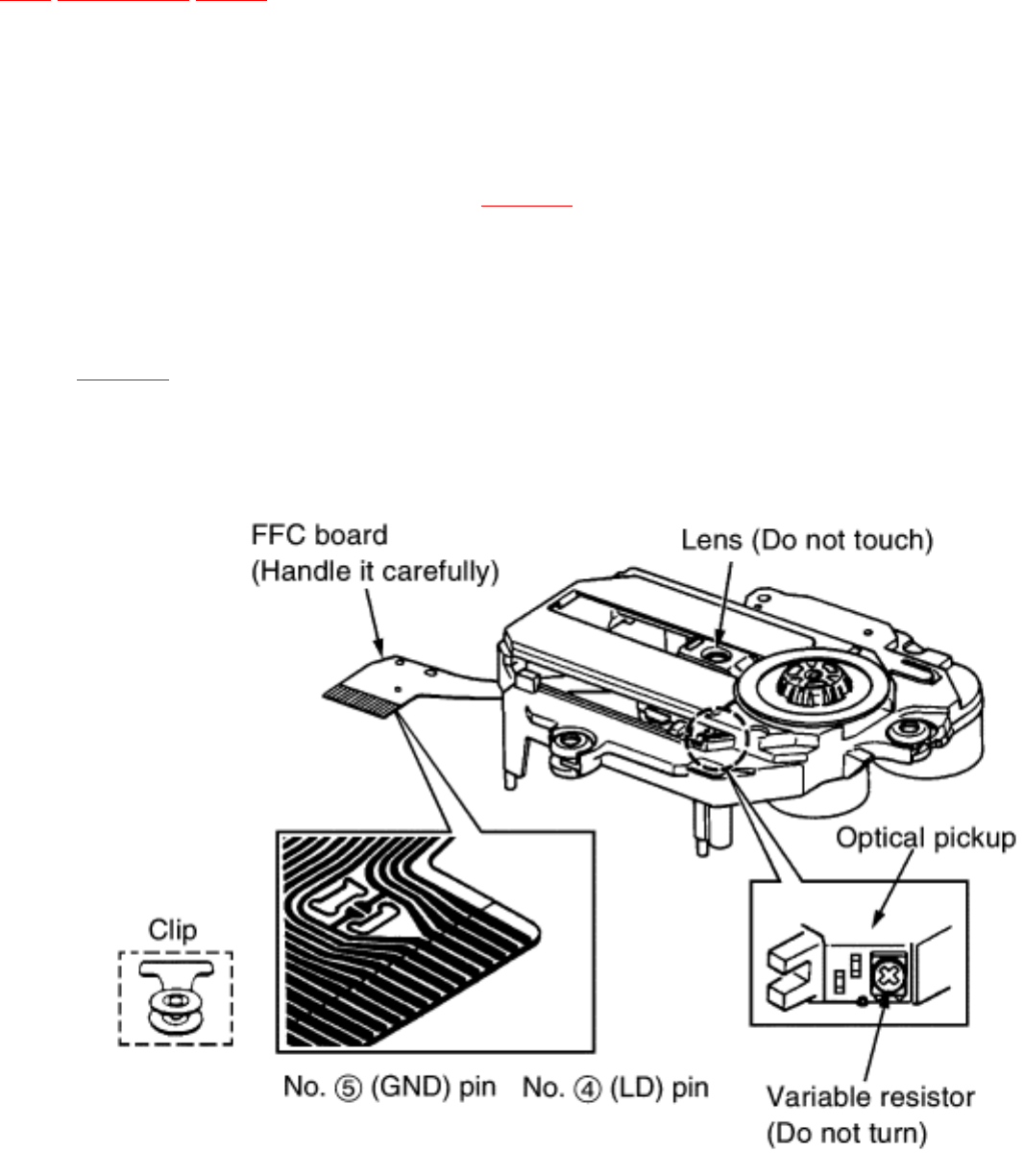
2.1 Handling of traverse deck (optical pickup)
2.2 Grounding for electrostatic breakdown prevention
2.2.1 Human body grounding
2.2.2 Work table grounding
•@
TOP PREVIOUS NEXT
file:///C|/Documents%20and%20Settings/Administrator/Plocha/SL-EH570/s0200000000x.htm [25.4.2003 20:50:58]
file:///C|/Documents%20and%20Settings/Administrator/Plocha/SL-EH570/s0201000000.htm
2.1 Handling of traverse deck (optical
pickup)
TOP PREVIOUS NEXT
1. Do not subject the traverse deck (optical pickup) to static electricity as it is extremely sensitive to
electrical shock.
2. To protect the laser diode against electrostatic breakdown, short the flexible board (FFC board)
with a clip or similar object. Refer to Fig. 2-1.
3. Take care not to apply excessive stress to the flexible board (FFC board).
4. Do not turn the variable resistor (laser power adjustment). It has already been adjusted. Refer to
Fig. 2-1.
Fig. 2-1.
file:///C|/Documents%20and%20Settings/Administrator/Plocha/SL-EH570/s0201000000.htm (1 of 2) [25.4.2003 20:51:15]

file:///C|/Documents%20and%20Settings/Administrator/Plocha/SL-EH570/s0202000000.htm
2.2 Grounding for electrostatic
breakdown prevention
TOP PREVIOUS NEXT
2.2.1 Human body grounding
2.2.2 Work table grounding
•@
TOP PREVIOUS NEXT
file:///C|/Documents%20and%20Settings/Administrator/Plocha/SL-EH570/s0202000000.htm [25.4.2003 20:51:36]

file:///C|/Documents%20and%20Settings/Administrator/Plocha/SL-EH570/s0202010000.htm
2.2.1 Human body grounding
TOP PREVIOUS NEXT
Use the anti-static wrist strap to discharge the static electricity from your body. Refer to Fig. 2-2.
Fig. 2-2.
•@
TOP PREVIOUS NEXT
file:///C|/Documents%20and%20Settings/Administrator/Plocha/SL-EH570/s0202010000.htm [25.4.2003 20:51:53]
file:///C|/Documents%20and%20Settings/Administrator/Plocha/SL-EH570/s0202020000.htm
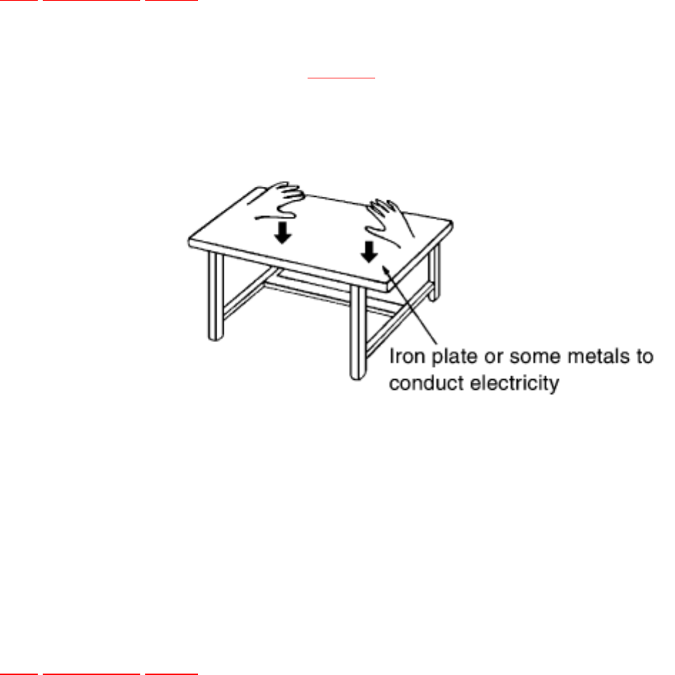
2.2.2 Work table grounding
TOP PREVIOUS NEXT
Put a conductive material (sheet) or steel sheet on the area where the traverse deck (optical pickup) is
placed, and ground the sheet. Refer to Fig. 2-3.
Fig. 2-3.
Caution:
The static electricity of your clothes will not be grounded through the wrist strap.
So take care not to let your clothes touch the traverse deck (optical pickup).
•@
TOP PREVIOUS NEXT
file:///C|/Documents%20and%20Settings/Administrator/Plocha/SL-EH570/s0202020000.htm [25.4.2003 20:52:10]
file:///C|/Documents%20and%20Settings/Administrator/Plocha/SL-EH570/s0300000000x.htm
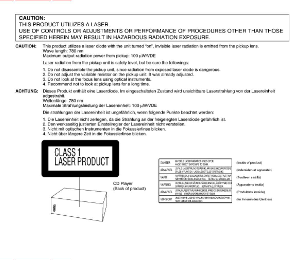
3 Precaution of Laser Diode
TOP PREVIOUS NEXT
•@
TOP PREVIOUS NEXT
file:///C|/Documents%20and%20Settings/Administrator/Plocha/SL-EH570/s0300000000x.htm [25.4.2003 20:52:28]

file:///C|/Documents%20and%20Settings/Administrator/Plocha/SL-EH570/s0400000000x.htm
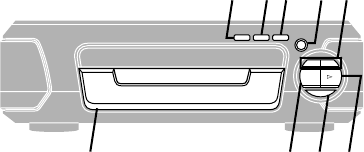
4 Location of Controls
TOP PREVIOUS NEXT
•@
TOP PREVIOUS NEXT
file:///C|/Documents%20and%20Settings/Administrator/Plocha/SL-EH570/s0400000000x.htm [25.4.2003 20:52:47]

file:///C|/Documents%20and%20Settings/Administrator/Plocha/SL-EH570/s0500000000x.htm
5 Operation Checks and Component
Replacement/ Procedures
TOP PREVIOUS NEXT
● This section describes procedures for checking the operation of the major printed circuit boards
and replacing the main components.
● For reassembly after operation checks or replacement, reverse the respective procedures. Special
reassembly procedures are described only when required.
/
5.1 Checking for the main P.C.B.
5.2 Checking for the CD servo P.C.B.
5.3 Replacement for the traverse deck ass’y
5.4 Replacement for the belt, loading motor ass’y and loading switch
•@
TOP PREVIOUS NEXT
file:///C|/Documents%20and%20Settings/Administrator/Plocha/SL-EH570/s0500000000x.htm [25.4.2003 20:53:43]
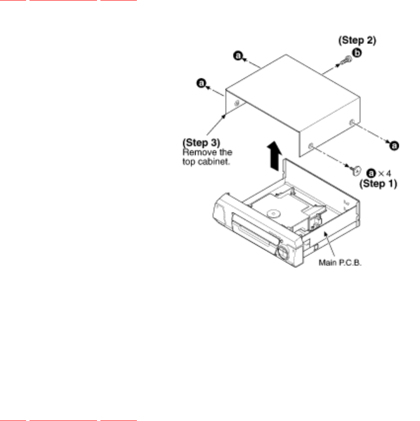
file:///C|/Documents%20and%20Settings/Administrator/Plocha/SL-EH570/s0501000000.htm
5.1 Checking for the main P.C.B.
TOP PREVIOUS NEXT
● Check the main P.C.B. as shown above.
/
•@
TOP PREVIOUS NEXT
file:///C|/Documents%20and%20Settings/Administrator/Plocha/SL-EH570/s0501000000.htm [25.4.2003 20:54:02]
file:///C|/Documents%20and%20Settings/Administrator/Plocha/SL-EH570/s0502000000.htm
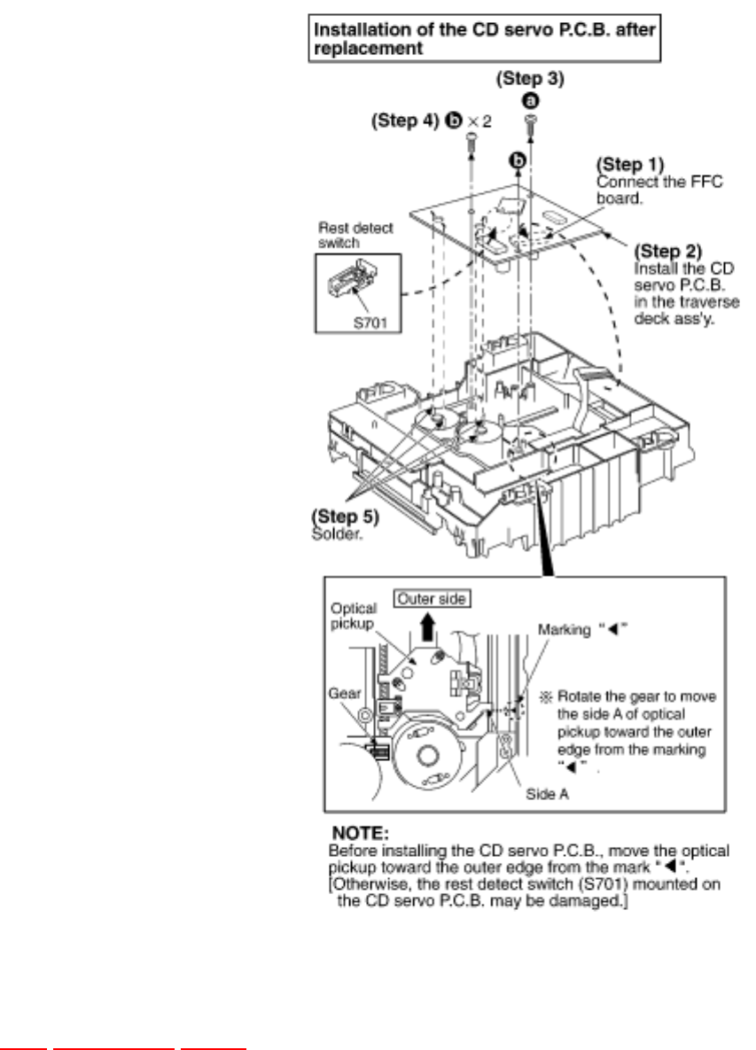
5.2 Checking for the CD servo P.C.B.
TOP PREVIOUS NEXT
● Follow the (Step 1) - (Step 3) of item 5.1.
file:///C|/Documents%20and%20Settings/Administrator/Plocha/SL-EH570/s0502000000.htm (1 of 2) [25.4.2003 20:54:21]
file:///C|/Documents%20and%20Settings/Administrator/Plocha/SL-EH570/s0502000000.htm
● Check the CD servo P.C.B. as shown below.
•@
TOP PREVIOUS NEXT
file:///C|/Documents%20and%20Settings/Administrator/Plocha/SL-EH570/s0502000000.htm (2 of 2) [25.4.2003 20:54:21]
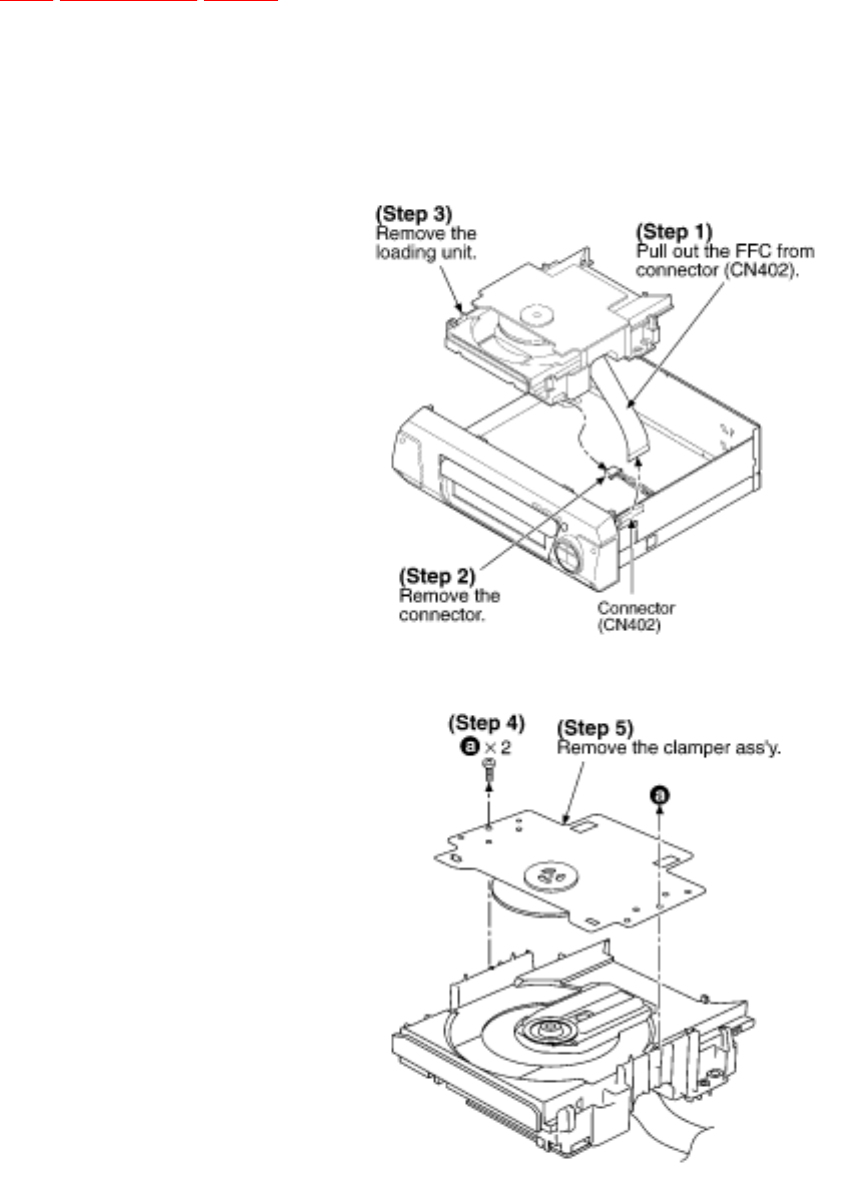
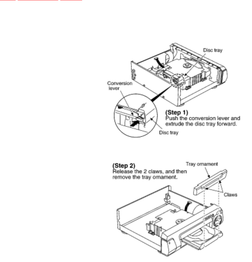
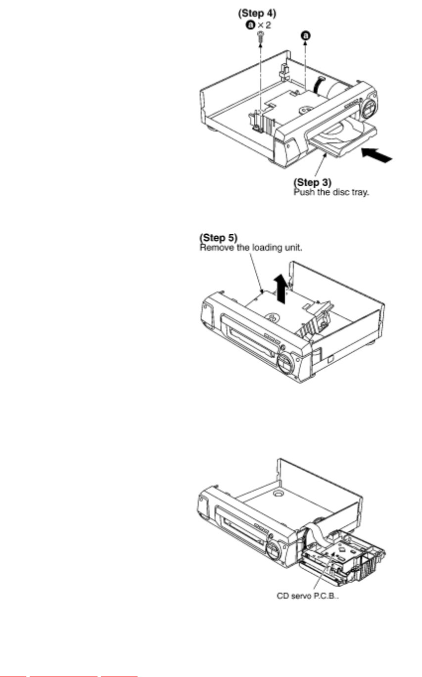
file:///C|/Documents%20and%20Settings/Administrator/Plocha/SL-EH570/s0503000000.htm
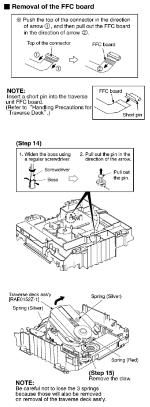
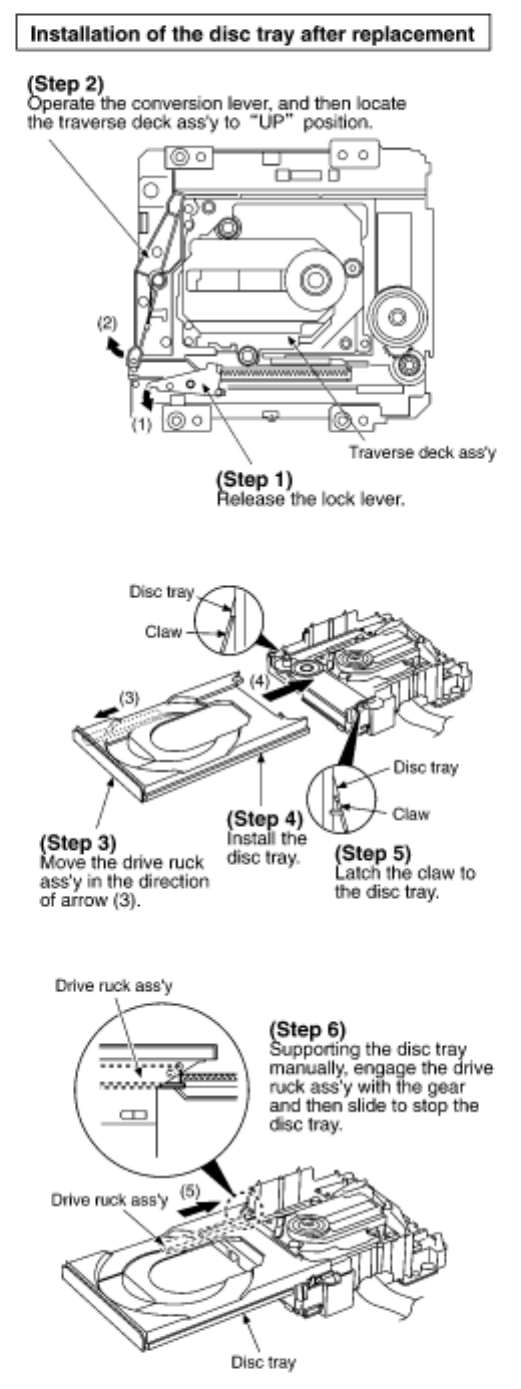
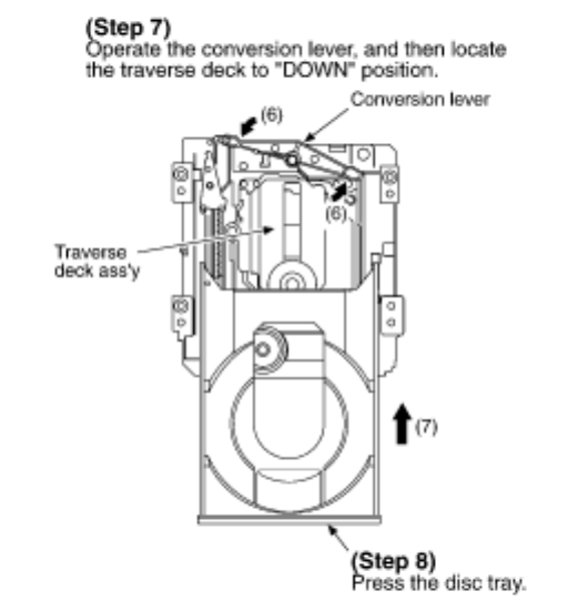
5.3 Replacement for the traverse deck
ass’y
TOP PREVIOUS NEXT
● Follow the (Step 1) - (Step 3) of item 5.1.
● Follow the (Step 1) - (Step 5) of item 5.2.
file:///C|/Documents%20and%20Settings/Administrator/Plocha/SL-EH570/s0503000000.htm (1 of 6) [25.4.2003 20:54:39]

file:///C|/Documents%20and%20Settings/Administrator/Plocha/SL-EH570/s0503000000.htm
file:///C|/Documents%20and%20Settings/Administrator/Plocha/SL-EH570/s0503000000.htm (2 of 6) [25.4.2003 20:54:39]
file:///C|/Documents%20and%20Settings/Administrator/Plocha/SL-EH570/s0503000000.htm
file:///C|/Documents%20and%20Settings/Administrator/Plocha/SL-EH570/s0503000000.htm (3 of 6) [25.4.2003 20:54:39]
file:///C|/Documents%20and%20Settings/Administrator/Plocha/SL-EH570/s0503000000.htm
file:///C|/Documents%20and%20Settings/Administrator/Plocha/SL-EH570/s0503000000.htm (4 of 6) [25.4.2003 20:54:39]
file:///C|/Documents%20and%20Settings/Administrator/Plocha/SL-EH570/s0503000000.htm
file:///C|/Documents%20and%20Settings/Administrator/Plocha/SL-EH570/s0503000000.htm (5 of 6) [25.4.2003 20:54:39]
file:///C|/Documents%20and%20Settings/Administrator/Plocha/SL-EH570/s0503000000.htm
•@
TOP PREVIOUS NEXT
file:///C|/Documents%20and%20Settings/Administrator/Plocha/SL-EH570/s0503000000.htm (6 of 6) [25.4.2003 20:54:39]
file:///C|/Documents%20and%20Settings/Administrator/Plocha/SL-EH570/s0504000000.htm
5.4 Replacement for the belt, loading
motor ass’y and loading switch
TOP PREVIOUS NEXT
● Follow the (Step 1) - (Step 3) of item 5.1.
● Follow the (Step 1) - (Step 5) of item 5.2.
● Follow the (Step 1) - (Step 9) of item 5.3.
file:///C|/Documents%20and%20Settings/Administrator/Plocha/SL-EH570/s0504000000.htm (1 of 2) [25.4.2003 20:54:58]
file:///C|/Documents%20and%20Settings/Administrator/Plocha/SL-EH570/s0504000000.htm
•@
TOP PREVIOUS NEXT
file:///C|/Documents%20and%20Settings/Administrator/Plocha/SL-EH570/s0504000000.htm (2 of 2) [25.4.2003 20:54:58]

file:///C|/Documents%20and%20Settings/Administrator/Plocha/SL-EH570/s0600000000x.htm
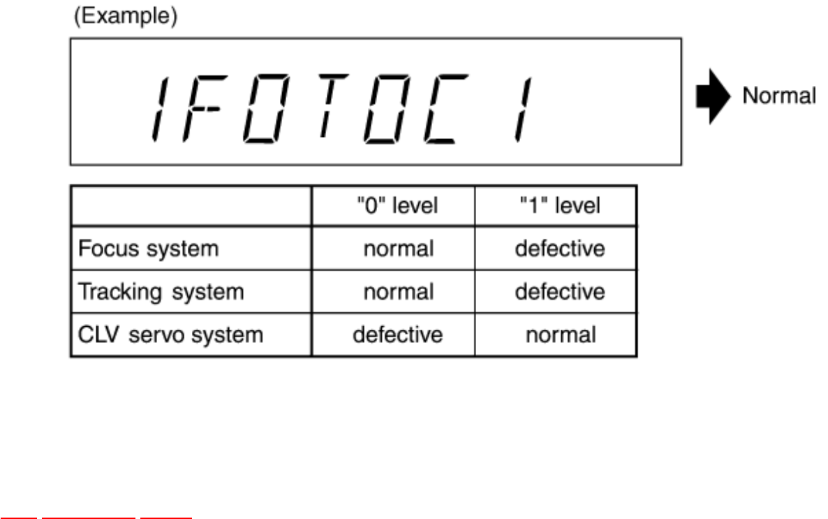
6 Error Code Display and Servo
Adjustment Function
TOP PREVIOUS NEXT
This unit has an error code display function, so that if the unit operates incorrectly, the fault is displayed
using an error code on the FL display of the Tuner/Amplifier (SA-EH570). It also has a servo adjustment
function for displayingthe status of servo system functions (Focus, Tracking, CLV servo) on the FL
display of the Tuner/Amplifier. The system control IC and FL display are part of the Tuner/Amplifier so
make sure the system has been connected properly beforeusing these functions. Use these two functions
for guidance during fault diagnosis and repair.
Note:
Check beforehand for scratching or soiling of the test disc (SZZP1054C), and soiling or other problems
with the pickup lens.
6.1 Error code display procedure
6.1.1 Automatic adjustment results
6.1.2 Checking the mechanism switches
6.2 Servo adjustment procedure
6.3 Error code based on troubleshooting
•@
TOP PREVIOUS NEXT
file:///C|/Documents%20and%20Settings/Administrator/Plocha/SL-EH570/s0600000000x.htm [25.4.2003 20:55:16]

file:///C|/Documents%20and%20Settings/Administrator/Plocha/SL-EH570/s0601000000.htm
6.1 Error code display procedure
TOP PREVIOUS NEXT
6.1.1 Automatic adjustment results
6.1.2 Checking the mechanism switches
•@
TOP PREVIOUS NEXT
file:///C|/Documents%20and%20Settings/Administrator/Plocha/SL-EH570/s0601000000.htm [25.4.2003 20:55:51]

file:///C|/Documents%20and%20Settings/Administrator/Plocha/SL-EH570/s0601010000.htm
6.1.1 Automatic adjustment results
TOP PREVIOUS NEXT
1. Turn on the power.
2. Load the test disc (SZZP1054C).
3. Hold down the REPEAT button for at least 2 seconds, and then press the STOP button for at least
2 seconds while continuing to hold down the REPEAT button.
4. A servo section error code is displayed. Refer to Error code based on troubleshooting. Use this
error code display as a guideline for finding the malfunction point in the servo circuitry. If the
error code E00 is displayed, the unit isOK.
•@
TOP PREVIOUS NEXT
file:///C|/Documents%20and%20Settings/Administrator/Plocha/SL-EH570/s0601010000.htm [25.4.2003 20:56:10]
file:///C|/Documents%20and%20Settings/Administrator/Plocha/SL-EH570/s0601020000.htm
6.1.2 Checking the mechanism switches
TOP PREVIOUS NEXT
1. After a servo section error code is displayed, press the F.SKIP button.
2. A mechanism OK/NG error code is displayed. Refer to Table 6-1. This error code can be used
diagnose whether the mechanism is OK or not. If there are multiple errors, these can be displayed
successively by pressing the F.SKIP button.
3. Press the STOP button, then remove the disc and turn off the power. (The error code display mode
is canceled.)
Table 6-1.
FL display Symptom Cause
H15 When CD tray opens, it closes by itself. Tray open detect switch (S790) fault.
H16 When CD tray closes, it opens by itself. Tray close detect switch (S791) fault.
F15 Does not play even if the PLAY button is pressed. Pickup rest position detect switch (S701) fault.
F26 Disc not move even if the PLAY button is pressed. System control and servo processor IC (IC451, IC702) fault.
•@
TOP PREVIOUS NEXT
file:///C|/Documents%20and%20Settings/Administrator/Plocha/SL-EH570/s0601020000.htm [25.4.2003 20:56:27]
file:///C|/Documents%20and%20Settings/Administrator/Plocha/SL-EH570/s0602000000.htm
6.2 Servo adjustment procedure
TOP PREVIOUS NEXT
1. Turn on the power.
2. Load the test disc (SZZP1054C).
3. Hold down the REPEAT button for at least 2 seconds, and then press the PAUSE button for at least
2 seconds while continuing to hold down the REPEAT button.
4. Press the PLAY button, and play for 10 seconds.
5. Servo adjustment results are displayed. Refer to Fig. 6-2. For further information about servo
adjustment results, refer to Fig. 6-3.
Fig. 6-2.
Fig. 6-3.
file:///C|/Documents%20and%20Settings/Administrator/Plocha/SL-EH570/s0602000000.htm (1 of 2) [25.4.2003 20:56:44]
file:///C|/Documents%20and%20Settings/Administrator/Plocha/SL-EH570/s0602000000.htm
6. Remove the disc and turn off the power.
•@
TOP PREVIOUS NEXT
file:///C|/Documents%20and%20Settings/Administrator/Plocha/SL-EH570/s0602000000.htm (2 of 2) [25.4.2003 20:56:44]
file:///C|/Documents%20and%20Settings/Administrator/Plocha/SL-EH570/s0603000000.htm
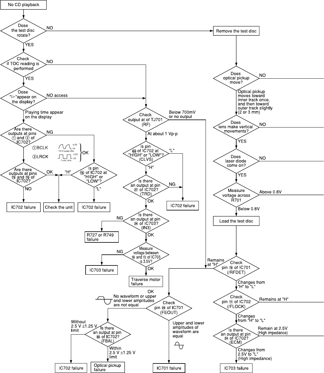
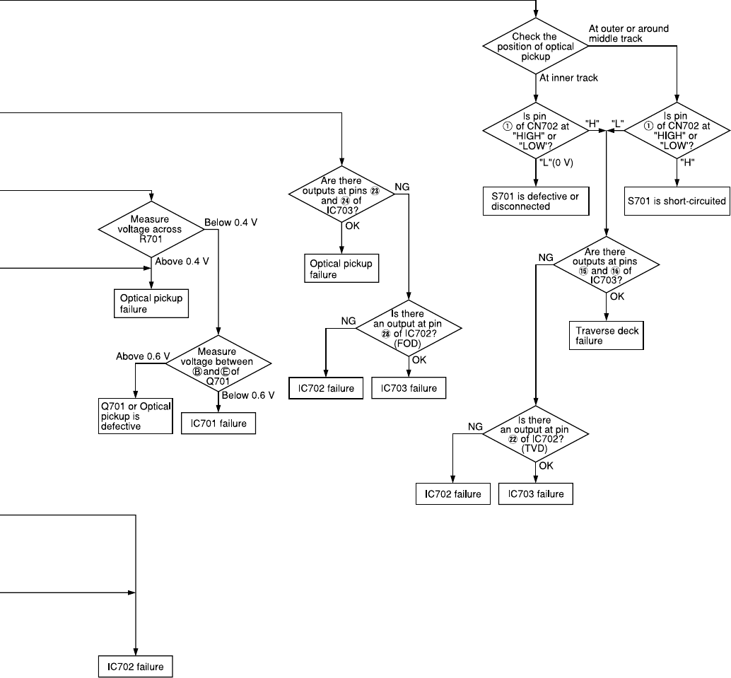
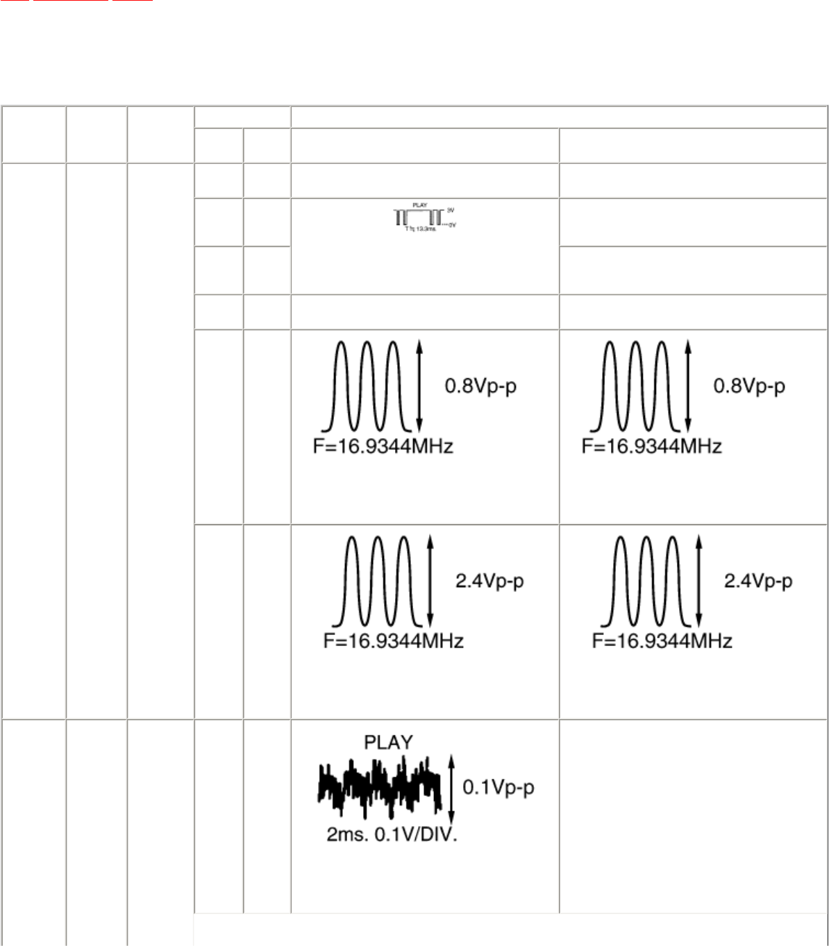
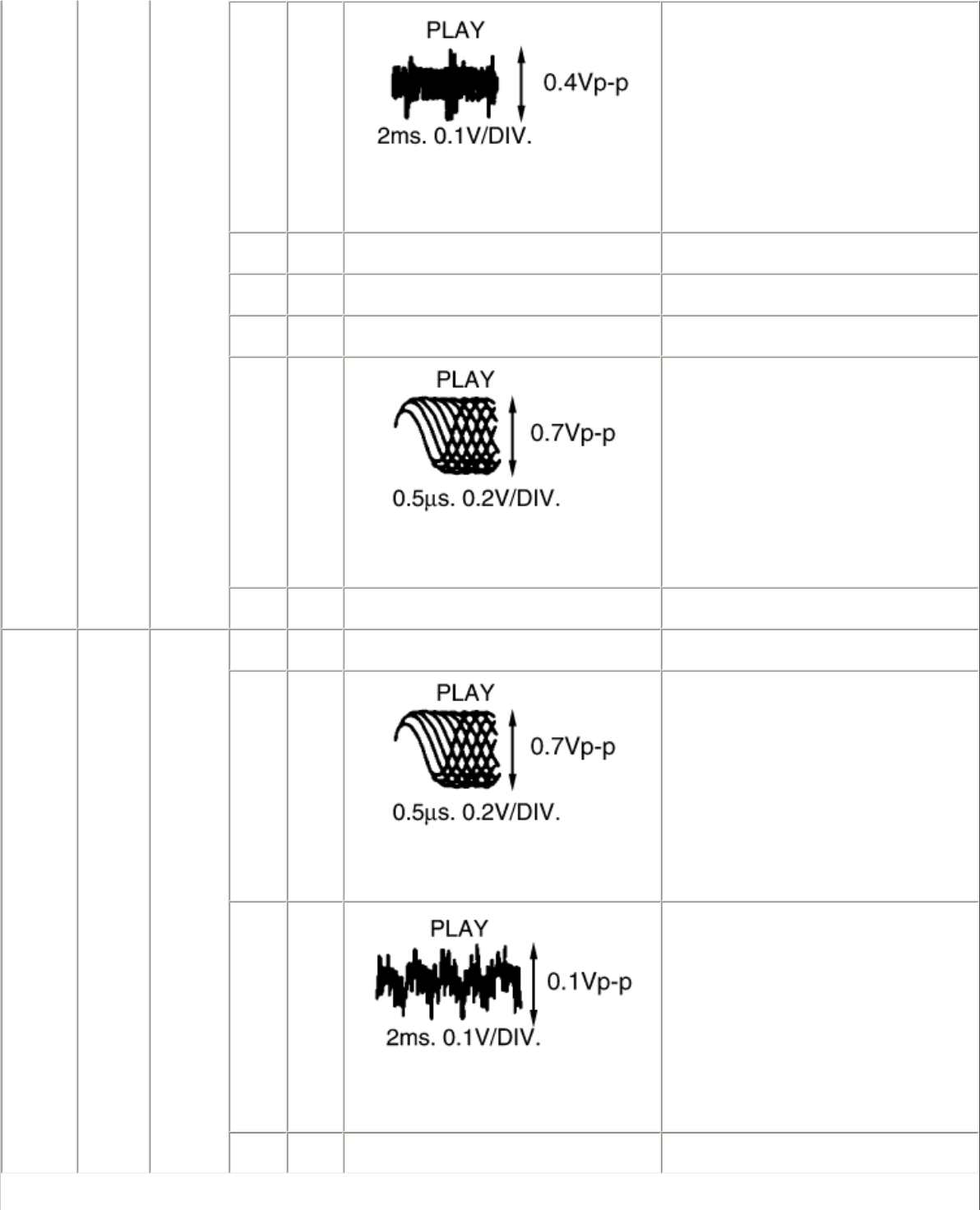
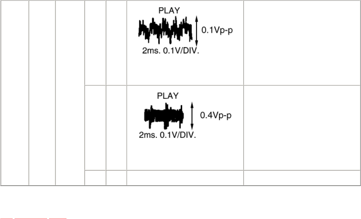
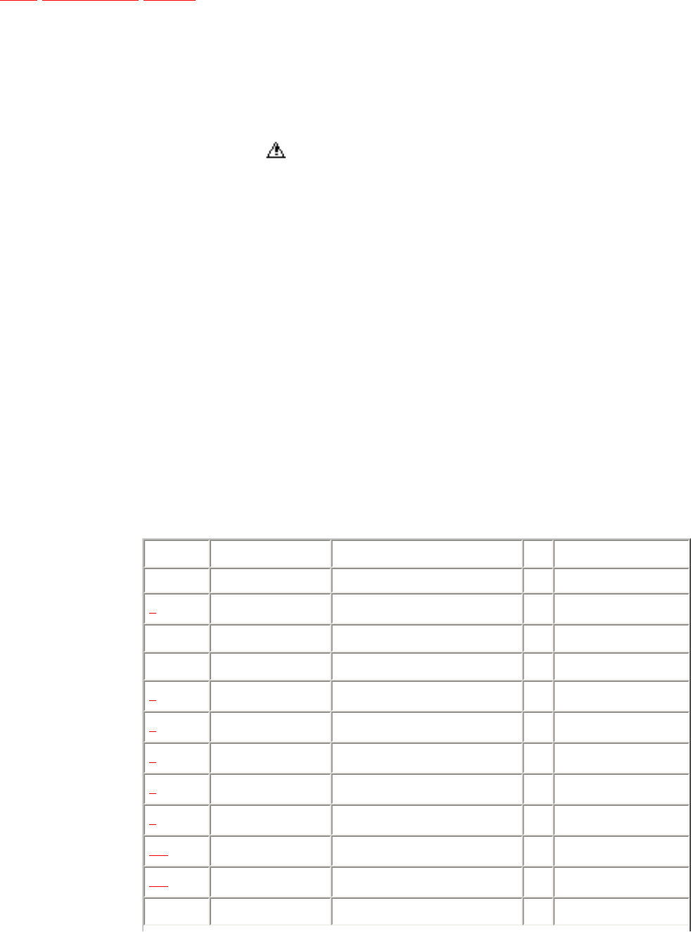
6.3 Error code based on troubleshooting
TOP PREVIOUS NEXT
● This unit is satisfactory if the error code is E00 and E02 .
● Before testing, check that the test disc is free of scratches and optical pickup is clean.
FL error
code/display Symptom Probable
cause Signal to check Normal voltage and waveform values
Signal
name Location PLAY STOP
E01 Focus and
tracking
offset
adjustments
not
completed
in the
specified
time
period.
Clocks X1
IN and X2
OUT, power
supply VDD
and
reset/RST,
all on IC702.
MDATA,
MCLK,
MLD and
SENSE
signals
to/from
mechanism
controller.
MDATA IC702-8
pin 0.3 V 0 V
MCLK IC702-7
pin 2.9 V
MLD IC702-9
pin 2.9 V
/RST IC702-
18 pin 2.9 V 2.9 V
X1 IN IC702-
58 pin
X2 OUT IC702-
59 pin
E03, E05,
E07, E09,
E0B, E0D,
E0F
Disc play
unstable. Scratches or
contaminants
on disc
surface.
Focus and
Tracking
servo circuit
(check
waveforms,
voltages and
part values.)
Spindle
driver
circuit.
Optical
pickup.
FE IC702-
32 pin 1.7 V
file:///C|/Documents%20and%20Settings/Administrator/Plocha/SL-EH570/s0603000000.htm (1 of 3) [25.4.2003 20:57:01]
file:///C|/Documents%20and%20Settings/Administrator/Plocha/SL-EH570/s0603000000.htm
TE IC702-
33 pin 1.7 V
FOD IC702-
28 pin 1.7 V 1.7 V
TRD IC702-
27 pin 1.7 V 1.7 V
/RFDET IC702-
38 pin 0 V 3.3 V
RF TJ701 1.0 V
STAT IC702-
17 pin 3.3 V 0 V
E04, E06,
E0C, E0E, Best Eye
(PD
balance)
adjustment
not
completed
in the
specified
time
period.
Scratches or
contaminants
on disc
surface.
Focus and
Tracking
servo circuit
(check
waveforms,
voltages and
part values.)
Optical
pickup.
FBAL IC702-
30 pin 1.7 V 1.7 V
RF IC701-8
pin 1.0 V
FE IC702-
32 pin 1.7 V
OFT IC702-
36 pin 0 V 0 V
file:///C|/Documents%20and%20Settings/Administrator/Plocha/SL-EH570/s0603000000.htm (2 of 3) [25.4.2003 20:57:01]
file:///C|/Documents%20and%20Settings/Administrator/Plocha/SL-EH570/s0603000000.htm
E08, E0A Focus and
Tracking
gain
adjustment
not
completed
in specified
time
period.
Scratches or
contaminants
on disc
surface.
Focus and
Tracking
servo circuit
(check
waveforms,
voltages and
part values.)
Optical
pickup.
FE IC702-
32 pin 1.7 V
TE IC702-
33 pin 1.7 V
OFT IC702-
36 pin 0 V 0 V
•@
TOP PREVIOUS NEXT
file:///C|/Documents%20and%20Settings/Administrator/Plocha/SL-EH570/s0603000000.htm (3 of 3) [25.4.2003 20:57:01]
file:///C|/Documents%20and%20Settings/Administrator/Plocha/SL-EH570/s0700000000x.htm
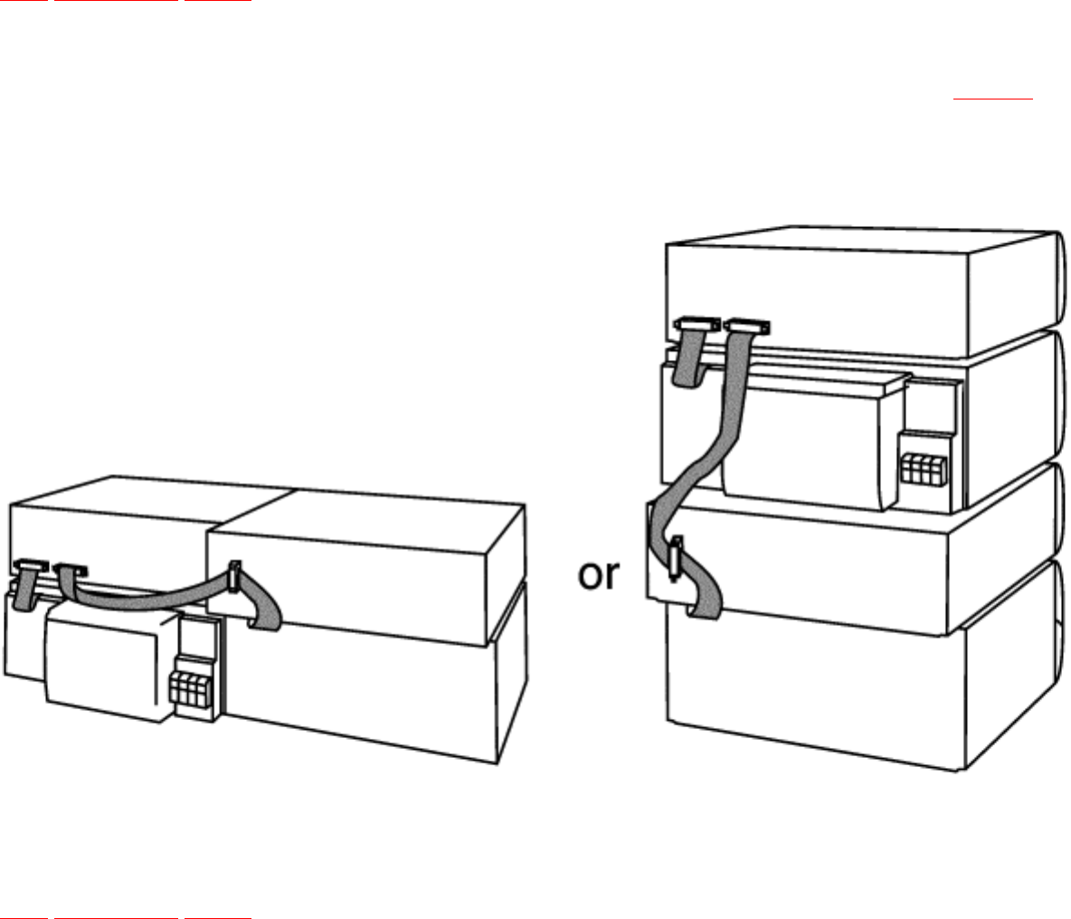
7 To Supply Power Source
TOP PREVIOUS NEXT
This unit is designed to operate on power supplied from system connected./When a component requires
service, use the system connections to supply power source. /For system connections, refer to Fig.7-1.
Fig. 7-1.
•@
TOP PREVIOUS NEXT
file:///C|/Documents%20and%20Settings/Administrator/Plocha/SL-EH570/s0700000000x.htm [25.4.2003 20:57:21]

file:///C|/Documents%20and%20Settings/Administrator/Plocha/SL-EH570/s0800000000x.htm
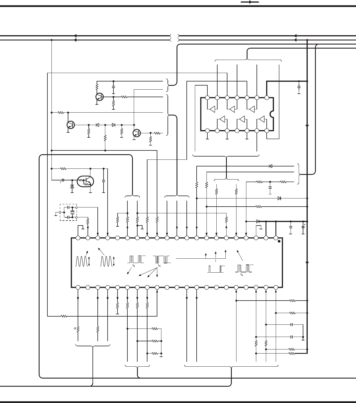
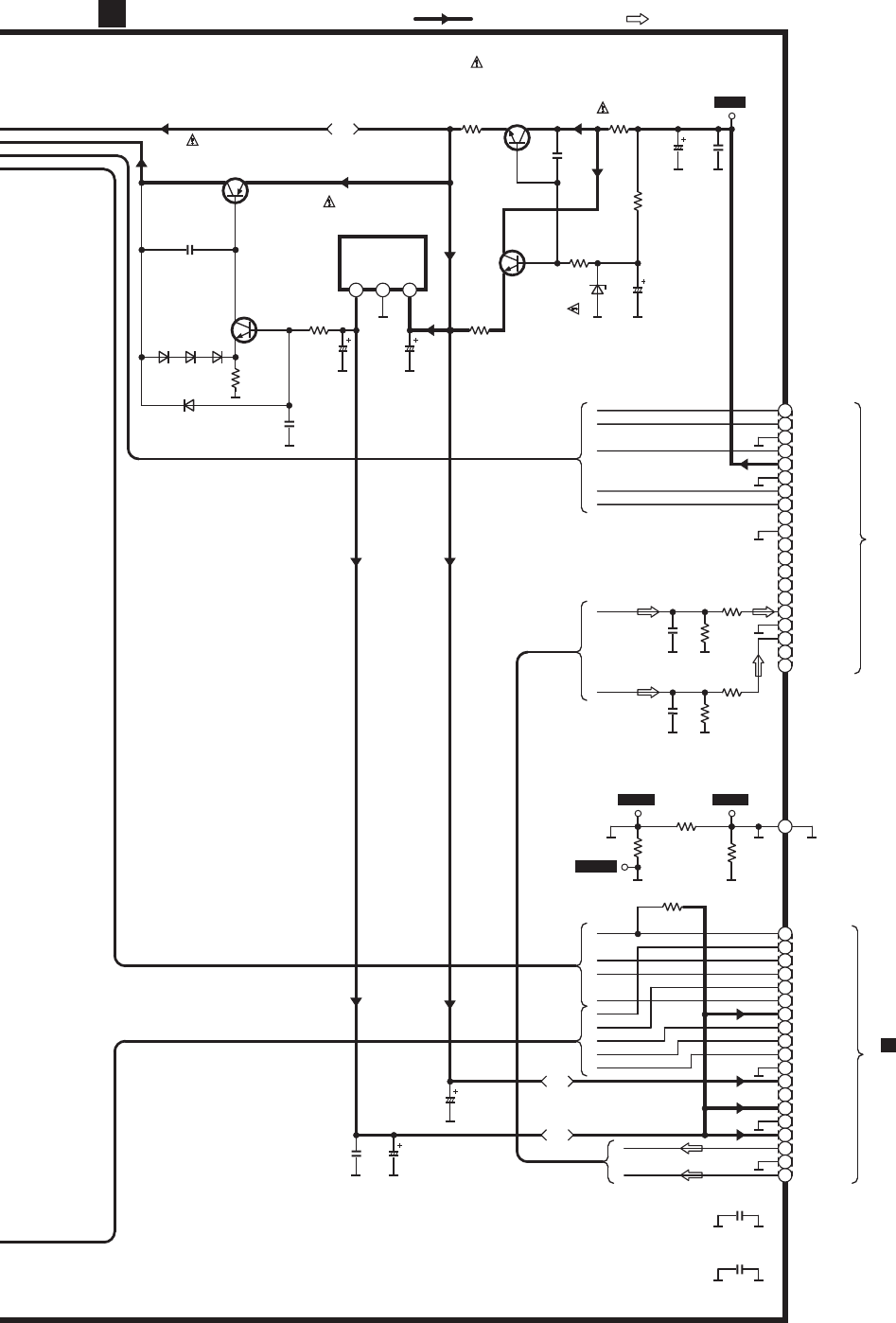
8 Schematic Diagram Notes
TOP PREVIOUS NEXT
● This schematic diagram may be modified at any time with the development of new technology.
Notes:
● S601:
CD edit switch (EDIT)
● S602:
Repeat switch (REPEAT)
● S603:
Random play switch (RANDOM)
● S611:
Disc tray open/close switch/(
OPEN/CLOSE)
● S612:
Pause switch (
)
● S613:
F.Skip/search switch (
)
file:///C|/Documents%20and%20Settings/Administrator/Plocha/SL-EH570/s0800000000x.htm (1 of 4) [25.4.2003 20:57:39]

file:///C|/Documents%20and%20Settings/Administrator/Plocha/SL-EH570/s0800000000x.htm
● S614:
Play switch (
)
● S615:
Stop switch (
)
● S616:
R.Skip/search switch (
)
● S701:
Rest detect switch in OFF position
● S790:
Tray open detect switch in OFF position
● S791:
Tray close detect switch in OFF position
● Indicated voltage values are the standard values for the unit measured by the DC electronic circuit
tester (high-impedance) with the chassis taken as standard. Therefore, there may exist some errors
in the voltage values, depending on theinternal impedance of the DC circuit tester.
❍ No mark
: CD Stop
❍ ( )
file:///C|/Documents%20and%20Settings/Administrator/Plocha/SL-EH570/s0800000000x.htm (2 of 4) [25.4.2003 20:57:39]
file:///C|/Documents%20and%20Settings/Administrator/Plocha/SL-EH570/s0800000000x.htm
: CD Play [1 kHz, L+R, 0 dB]
● Important safety notice:
Components identified by mark have special characteristics important for safety.
Furthermore, special parts which have purposes of fire-retardant (resistors), high-quality sound
(capacitors), low-noise (resistors), etc. are used.
When replacing any of components, be sure to use only manufacturer’s specified parts shown in
the parts list.
● The supply part number is described alone in the replacement parts list.
● Caution!
IC and LSI are sensitive to static electricity.
Secondary trouble can be prevented by taking care during repair.
Cover the parts boxes made of plastics with aluminum foil.
Ground the soldering iron.
Put a conductive mat on the work table.
Do not touch the legs of IC or LSI with the fingers directly.
● Voltage and signal line
❍
: Positive voltage line
❍
file:///C|/Documents%20and%20Settings/Administrator/Plocha/SL-EH570/s0800000000x.htm (3 of 4) [25.4.2003 20:57:39]

file:///C|/Documents%20and%20Settings/Administrator/Plocha/SL-EH570/s0900000000x.htm
9 Schematic Diagram
TOP PREVIOUS NEXT
•@
TOP PREVIOUS NEXT
file:///C|/Documents%20and%20Settings/Administrator/Plocha/SL-EH570/s0900000000x.htm [25.4.2003 20:58:19]

file:///C|/Documents%20and%20Settings/Administrator/Plocha/SL-EH570/s1000000000x.htm
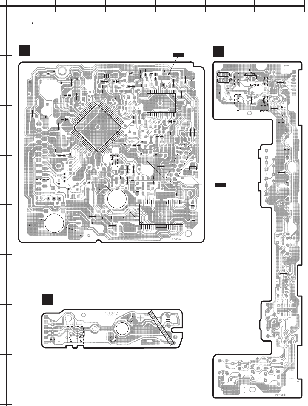
10 Printed Circuit Board Diagram
TOP PREVIOUS NEXT
•@
TOP PREVIOUS NEXT
file:///C|/Documents%20and%20Settings/Administrator/Plocha/SL-EH570/s1000000000x.htm [25.4.2003 20:58:38]

file:///C|/Documents%20and%20Settings/Administrator/Plocha/SL-EH570/s1100000000x.htm
11 Type Illustration of ICs, Transistors
and Diodes
TOP PREVIOUS NEXT
•@
TOP PREVIOUS NEXT
file:///C|/Documents%20and%20Settings/Administrator/Plocha/SL-EH570/s1100000000x.htm [25.4.2003 20:58:58]

file:///C|/Documents%20and%20Settings/Administrator/Plocha/SL-EH570/s1200000000x.htm
12 Wiring Connection Diagram
TOP PREVIOUS NEXT
•@
TOP PREVIOUS NEXT
file:///C|/Documents%20and%20Settings/Administrator/Plocha/SL-EH570/s1200000000x.htm [25.4.2003 20:59:15]

file:///C|/Documents%20and%20Settings/Administrator/Plocha/SL-EH570/s1300000000x.htm
13 Block Diagram
TOP PREVIOUS NEXT
•@
TOP PREVIOUS NEXT
file:///C|/Documents%20and%20Settings/Administrator/Plocha/SL-EH570/s1300000000x.htm [25.4.2003 20:59:33]

file:///C|/Documents%20and%20Settings/Administrator/Plocha/SL-EH570/s1400000000x.htm
14 Troubleshooting Guide
TOP PREVIOUS NEXT
•@
TOP PREVIOUS NEXT
file:///C|/Documents%20and%20Settings/Administrator/Plocha/SL-EH570/s1400000000x.htm [25.4.2003 21:00:04]

file:///C|/Documents%20and%20Settings/Administrator/Plocha/SL-EH570/s1500000000x.htm
15 Terminal Function of ICs
TOP PREVIOUS NEXT
15.1 IC451 (M38504E6255F):System Control
15.2 IC701 (AN8885SBE1V):Servo Amp
15.3 IC702 (MN662790RSC):Servo Processor/Digital Signal Processor/Digital Filter/ D/A converter
15.4 IC703 (AN8739SBE2):Focus Coil/Tracking Coil/ Traverse Motor/Spindle Motor Drive
•@
TOP PREVIOUS NEXT
file:///C|/Documents%20and%20Settings/Administrator/Plocha/SL-EH570/s1500000000x.htm [25.4.2003 21:00:23]
file:///C|/Documents%20and%20Settings/Administrator/Plocha/SL-EH570/s1501000000.htm
15.1 IC451 (M38504E6255F):/System
Control
TOP PREVIOUS NEXT
Pin No. Terminal Name I/O Function
1 Vcc I Power supply terminal
2 VREF I Reference voltage input
3 AVSS - GND terminal
4 SYNC I Power failure detect signal input
5 SUBQ I Sub-code Q data signal input
6 SQCK O Sub code Q resistor clock signal output
7 BLKCK I Block clock signal input
8 CD REQ I Serial communication signal to Sound Processor (Request signal input)
9 B CS O Serial communication signal to Sound Processor (Chip select signal output)
10 B CLK O Serial communication signal to Sound Processor (Clock signal output)
11 DATA O O Serial communication signal to Sound Processor (Data signal output)
12 DATA I I Serial communication signal to Sound Processor (Data signal input)
13 TEST I Test mode select signal input/(Connected to VCC via resistor)
14 RESTSW I Rest switch signal input
15 CNVSS - Connected to VSS
16 SERVO RST O Reset signal output for CD servo IC
17 E-CS - EEPROM serial communication signal
(Not used, open)
18 RESET I Reset signal input
19 X IN I Oscillator connected terminal (8 MHz)
20 X OUT O
21 VSS - GND terminal
22 LED ORG O Orange LED control signal output
23 LED CLK - Not used, open
24 LED DATA O LED data signal output
25 LED GRN O Green LED control signal output
26 MSEL O Function select signal output/(Connected to VSS via resistor)
27 MDATA O Command data output for CD servo IC
28 MCLK O Command clock output for CD servo IC
file:///C|/Documents%20and%20Settings/Administrator/Plocha/SL-EH570/s1501000000.htm (1 of 2) [25.4.2003 21:00:41]
file:///C|/Documents%20and%20Settings/Administrator/Plocha/SL-EH570/s1501000000.htm
29 MLD O Command load output
30 STAT I Status signal input
31 HALH - CD mechanism motor speed control signal output (Not used, open)
32 PL - Not used, open
33 CW O CD mechanism motor control signal output (forward direction)
34 CCW O CD mechanism motor control signal output (reverse direction)
35 PSTN - Not used, open
36 SW1 - Not used, open
37 SW2 - Not used, open
38 SW3 I Disc tray open detect signal input
39 SW5 - Not used, open
40 KEY2 I Operation key signal input
41 KEY1 I Operation key signal input
42 SW4 I Disc tray close detect switch signal input
•@
TOP PREVIOUS NEXT
file:///C|/Documents%20and%20Settings/Administrator/Plocha/SL-EH570/s1501000000.htm (2 of 2) [25.4.2003 21:00:41]
file:///C|/Documents%20and%20Settings/Administrator/Plocha/SL-EH570/s1502000000.htm
15.2 IC701 (AN8885SBE1V):/Servo Amp
TOP PREVIOUS NEXT
Pin No. Terminal Name I/O Function
1 PDE I Tracking signal input terminal 1 (E ch)
2 PDF I Tracking signal input terminal 2 (F ch)
3 Vcc I Power supply terminal
4 PDA I Focus signal input terminal 1 (A ch)
5 PDB I Focus signal input terminal 2 (B ch)
6 LPD I Laser PD signal
7 LD O Laser power auto control output
8 RF O RF amp terminal
9 RFIN I AGC input terminal
10 CSBRT I OFTR capacitor connection terminal
11 CEA I HPF-AMP capacitor connection terminal
12 BDO O Dropout detection control
13 LDON I LD APC ON/OFF (H: ON)
14 GND - GND terminal
15 /RFDET O RF detect signal output (L: detect)
16 PDOWN - Power down terminal
17 OFTR O Off track detection (H: detect)
18 DEFLVL - Not used, connected to GND
19 ENV O Envelope signal output
20 GCTL I Sub-code frame clock signal input
21 EQ SW - Not used, connected to GND
22 TEN I Tracking error signal input
23 TEOUT O Tracking error signal output
24 FEOUT O Focus error signal output
25 FEN I Focus error signal input
26 VREF O Reference voltage output
27 TBAL I Tracking balance adj. input
28 FBAL I Focus balance adj. input
•@
file:///C|/Documents%20and%20Settings/Administrator/Plocha/SL-EH570/s1502000000.htm (1 of 2) [25.4.2003 21:00:58]

file:///C|/Documents%20and%20Settings/Administrator/Plocha/SL-EH570/s1503000000.htm
15.3 IC702 (MN662790RSC):/Servo
Processor/Digital Signal
Processor/Digital Filter/ /D/A converter
TOP PREVIOUS NEXT
Pin No. Terminal Name I/O Function
1 BCLK - Serial bit clock output (Not used, open)
2 LRCK - L/R discriminating signal output
(Not used, open)
3 SRDATA - Serial data signal output (Not used, open)
4 DVDD1 I Power supply terminal
5 DVSS1 - GND terminal
6 TX O Digital audio interface signal output
7 MCLK I Command clock signal input
8 MDATA I Command data signal input
9 MLD I Command load signal input
10 SENSE - Sense signal (Not used, open)
11 /FLOCK - Optical servo condition (focus)
(Not used, open)
12 /TLOCK - Optical servo condition (tracking)
(Not used, open)
13 BLKCK O Sub-code block clock signal output
(f=75 Hz)
14 SQCK I Sub-code Q resistor clock signal input
15 SUBQ O Sub-code Q data signal output
16 DMUTE - Muting input (Not used, connected to GND)
17 STAT O Status signal output
18 /RST I Reset signal input (L: reset)
19 SMCK - System clock (f=4.2336 MHz)
(Not used, open)
20 CSEL - Frequency control terminal of crystal oscillator (Not used, connected to GND)
21 TRV - Traverse servo control signal output
(Not used, open)
22 TVD O Traverse drive signal output
23 PC O Turntable motor drive signal output (L: ON)
file:///C|/Documents%20and%20Settings/Administrator/Plocha/SL-EH570/s1503000000.htm (1 of 3) [25.4.2003 21:01:17]

file:///C|/Documents%20and%20Settings/Administrator/Plocha/SL-EH570/s1503000000.htm
24 ECM O Turntable motor drive signal output
(Forced mode)
25 ECS O Turntable motor drive signal output
(Servo error signal)
26 KICK - Kick pulse output (Not used, open)
27 TRD O Tracking drive signal output
28 FOD O Focus drive signal output
29 VREF I D/A drive output normal voltage input
30 FBAL O Focus balance adj. output
31 TBAL O Tracking balance adj. output
32 FE I Focus error signal input
33 TE I Tracking error signal input
34 RFENV I RF envelope signal input
35 VDET I Oscillator detect signal input (H: detect)
36 OFT I Off track signal input (H: Off track)
37 TRCRS I Track cross signal input
38 /RFDET I RF detect signal input (L: detect)
39 BDO I Dropout detection signal input (H: dropout)
40 LDON O Laser power control signal output (H: ON)
41 PLLF2 - PLL loop filter terminal (Not used, open)
42 DSLF2 I/O DSL loop filter terminal
43 WVEL - Double velocity status signal output
(Not used, open)
44 ARF I RF signal input
45 IREF I Reference current input
46 DRF I DSL bias terminal
47 DSLF I/O DSL loop filter terminal
48 PLLF I/O PLL loop filter terminal
49 VCOF - VCO loop filter terminal
(Not used, connected to GND)
50 AVDD2 I Power supply terminal
51 AVSS2 - GND terminal
52 EFM - EFM signal (Not used, open)
53 PCK - PLL extract clock (Not used, open)
54 VCOF2 - VCO loop filter terminal
(Not used, connected to GND)
55 SUBC - Sub-code serial output clock
(Not used, open)
file:///C|/Documents%20and%20Settings/Administrator/Plocha/SL-EH570/s1503000000.htm (2 of 3) [25.4.2003 21:01:17]
file:///C|/Documents%20and%20Settings/Administrator/Plocha/SL-EH570/s1503000000.htm
56 SBCK - Sub-code serial input data
(Not used, connected to GND)
57 VSS - GND terminal
58 X1 IN I Crystal oscillator terminal (f=16.9344 MHz)
59 X2 OUT O
60 VDD I Power supply terminal
61 BYTCK - Byte clock signal (Not used, open)
62 /CLDCK - Sub-code frame clock signal
(Not used, open)
63 FCLK O Crystal frame clock
64 IPFLAG - Interpolation flag terminal (Not used, open)
65 FLAG - Flag terminal (Not used, open)
66 CLVS - Turntable servo phase synchro signal
(Not used, open)
67 CRC - Sub-code CRC check terminal
(Not used, open)
68 DEMPH - De-emphasis ON signal (Not used, open)
69 RESY - Re-synchronizing signal of frame sync.
(Not used, open)
70 IOSEL I I/O select signal input (Connected to VDD)
71 /TEST I Test terminal
(Not used, connected to power supply)
72 AVDD1 I Power supply terminal
73 OUTL O L ch audio signal output
74 AVSS1 - GND terminal
75 OUTR O R ch audio signal output
76 RSEL I Polarity direction control terminal of RF signal (Not used, connected to power supply)
77 IOVDD I Power supply terminal
78 PSEL - Test terminal (Connected to GND)
79 MSEL - Output frequency select signal input
(Not used, connected to GND)
80 SSEL I SUBQ output mode select signal input
(Not used, connected to VDD)
•@
TOP PREVIOUS NEXT
file:///C|/Documents%20and%20Settings/Administrator/Plocha/SL-EH570/s1503000000.htm (3 of 3) [25.4.2003 21:01:17]
file:///C|/Documents%20and%20Settings/Administrator/Plocha/SL-EH570/s1504000000.htm
15.4 IC703 (AN8739SBE2):/Focus
Coil/Tracking Coil/ /Traverse
Motor/Spindle /Motor Drive
TOP PREVIOUS NEXT
Pin No. Terminal Name I/O Function
1 /RST - Not used, open
2 NC - Not used
3 IN2 I Motor driver 2 input
4 PC2 I Turntable motor drive signal input (L: ON)
5 NC - Not used
6 IN1 I Motor driver 1 input
7 NC - Not used, open
8 PVCC1 I Driver power supply terminal 1
9 PGND1 - Driver GND terminal 1
10 NC - Not used, connected to GND
11 D1- O Motor driver 1 output terminal (-)
12 D1+ O Motor driver 1 output terminal (+)
13 D2- O Motor driver 2 output terminal (-)
14 D2+ O Motor driver 2 output terminal (+)
15 D3- O Motor driver 3 output terminal (-)
16 D3+ O Motor driver 3 output terminal (+)
17 D4- O Motor driver 4 output terminal (-)
18 D4+ O Motor driver 4 output terminal (+)
19 NC - Not used
20 PGND2 - Driver GND terminal 2
21 PVCC2 I Driver power supply terminal 2
22 NC - Not used, open
23 VCC I Power supply terminal
24 VREF I Reference voltage input terminal
25 IN4 I Motor driver 4 input
26 IN3 I Motor driver 3 input
file:///C|/Documents%20and%20Settings/Administrator/Plocha/SL-EH570/s1504000000.htm (1 of 2) [25.4.2003 21:01:52]

file:///C|/Documents%20and%20Settings/Administrator/Plocha/SL-EH570/s1504000000.htm
27 RSTIN I Reset terminal
(Not used, connected to GND)
28 NC - Not used, connected to GND
•@
TOP PREVIOUS NEXT
file:///C|/Documents%20and%20Settings/Administrator/Plocha/SL-EH570/s1504000000.htm (2 of 2) [25.4.2003 21:01:52]
file:///C|/Documents%20and%20Settings/Administrator/Plocha/SL-EH570/s1600000000x.htm
16 Replacement Parts List
TOP PREVIOUS NEXT
Notes:
● Important safety notice:
Components identified by mark have special characteristics important for safety.
Furthermore, special parts which have purposes of fire-retardant (resistors), high-quality sound
(capacitors), low-noise (resistors), etc. are used.
When replacing any of components, be sure to use only manufactures specified parts shown in the
parts list.
● The marking [RTL] indicates that Retention Time is Limited for this item. After the
discontinuation of this assembly in production, the item will continue to be available for a specific
period of time. The retention period of availability is dependenton the type of assembly, and in
accordance with the laws governing part and product retention. After the end of this period, the
assembly will no longer be available.
● All parts are supplied by MESA.
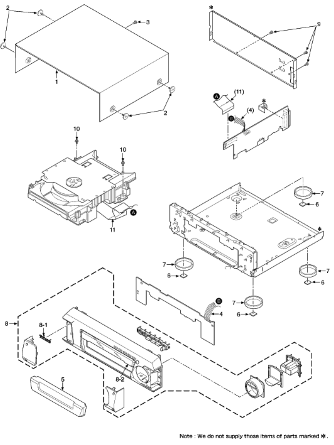
Ref. No. Part No. Part Name & Description Pcs Remarks
1 RKM0400-1S TOP CABINET 1
2 RHD30007-1S SCREW 4
3 XTBS3+8JFZ1 SCREW 1
4 REX0976 CONNECTOR ASS´Y(6P) 1
5 RGK1136-1S CD LID 1
6 RKA0105-K RUBBER 4
7 RKA0106-N FOOT RING 4
8 RYP1007-S FRONT PANEL ASS´Y 1
8-1 RGB0025-A TECHNICS BADGE 1
8-2 RKW0579-1Q PANEL LID 1
9 XTBS3+8JFZ1 SCREW 3
file:///C|/Documents%20and%20Settings/Administrator/Plocha/SL-EH570/s1600000000x.htm (1 of 8) [25.4.2003 21:02:10]
file:///C|/Documents%20and%20Settings/Administrator/Plocha/SL-EH570/s1600000000x.htm
10 XTB3+8FFZ SCREW 2
11 REZ1362 FFC 1
101 RFKJXDT07-K LOADING CHASSIS /ASS´Y 1
101-1 RDG0142 GEAR 1
101-2 RDG0193 GEAR 1
101-3 RDP0065 PULLEY 1
102 REM0019 MOTOR ASS´Y 1
103 RMK0255 BELT COVER 1
104 RGQ0144-K DISC TRAY 1
105 RAE0152Z-1 TRAVERSE DECK ASS´Y 1
105-1 SHGD113-1 FLOATING RUBBER 3
105-2 SNSD38 SCREW 2
105-3 RAF0150A-1 OPTICAL PICKUP 1
105-4 RDG0247 DRIVE GEAR 1
105-5 RDG0248 INTERMEDIATE GEAR 1
105-6 RXQ0339 TRAVERSE MOTOR /ASS´Y 1
105-7 RXQ0304-1 PLATE 1
105-8 XQN17+CG5 SCREW 1
105-9 XQN2+CQ5 SCREW 1
105-10 XQS17+A35FZ SCREW 2
106 RMS0350-1 PIN(B) 1
107 RMS0627 PIN(A) 1
108 RME0109 FLOATING SPRING(1) 2
109 RME0142 FLOATING SPRING(2) 1
110 RMR0698-K1 TRAVERSE CHASSIS 1
111 XTV2+6G SCREW 2
112 RME0063 SPRING 1
113 RMM0079A-1 SLIDE PLATE(1) 1
114 RML0178-1 LEVER 1
115 RFKNLPG440-K GEAR ASS´Y 1
116 RHD20009-1 SCREW 1
117 RME0087A-1 SPRING 1
118 RML0349 LEVER 1
file:///C|/Documents%20and%20Settings/Administrator/Plocha/SL-EH570/s1600000000x.htm (2 of 8) [25.4.2003 21:02:10]
file:///C|/Documents%20and%20Settings/Administrator/Plocha/SL-EH570/s1600000000x.htm
119 RMM0059A-1 SLIDE PLATE(2) 1
120 RMR0334 HOLDER 1
121 RHM245ZA MAGNET 1
122 RXQ0380 HOLDER 1
123 XTN26+6G SCREW 3
124 RMA0793-1 DISC CLAMPER ASS´Y 1
125 XYN2+F6FZ SCREW 2
126 RMG0158 BELT 1
127 XTN2+6G SCREW 1
C4 ECBT1C103MS5 16V 0.01U 1 F1D1C103A004
C5 RCE1AKA101BG 10V 100U 1 F2A1A1010020
C6 ECA1CM471 16V 470U 1
C7 ECBT1C103MS5 16V 0.01U 1 F1D1C103A004
C9 ECEA1AKS221 10V 220U 1
C10 F2A0J221A143 6.3V 220U 1
C11 ECBT1H102KB5 50V 1000P 1 F1D1H102A012
C12 ECBT1C103MS5 16V 0.01U 1 F1D1C103A004
C151,52 ECBT1H102KB5 50V 1000P 2 F1D1H102A012
C401 RCE1HKA3R3BG 50V 3.3U 1 F2A1H3R3A015
C402 ECBT1C103MS5 16V 0.01U 1 F1D1C103A004
C403 ECBT1H102KB5 50V 1000P 1 F1D1H102A012
C404,05 ECBT1C103MS5 16V 0.01U 2 F1D1C103A004
C406 F2A0J221A143 6.3V 220U 1
C407 ECEA1AKS221 10V 220U 1
C408 ECBT1H101KB5 50V 100P 1 F1D1H101A012
C410 EEAFC0J101B 6.3V 100U 1
C411 ECBT1H104KB5 50V 0.1U 1
C413,14 ECBT1H471KB5 50V 470P 2 F1D1H471A012
C415,16 ECBT1C103MS5 16V 0.01U 2 F1D1C103A004
C452 ECBT1C103MS5 16V 0.01U 1 F1D1C103A004
C701 ECEA0JKA330I 6.3V 33U 1
C702 ECUVNE104MBN 16V 0.1U 1 F1J1C104A065
C703 ECEA0JKS101 6.3V 100U 1
C704 ECUVNE104MBN 16V 0.1U 1 F1J1C104A065
C706 ECUV1H272KBN 50V 2700P 1 F1J1H272A592
file:///C|/Documents%20and%20Settings/Administrator/Plocha/SL-EH570/s1600000000x.htm (3 of 8) [25.4.2003 21:02:10]

file:///C|/Documents%20and%20Settings/Administrator/Plocha/SL-EH570/s1600000000x.htm
C707 ECUV1E273KBN 25V 0.027U 1
C710 ECUV1H121KCN 50V 120P 1 F1J1H121A507
C711,12 ECUVNE104ZFN 25V 0.1U 2 F1J1E1040017
C713 ECUVNE104MBN 16V 0.1U 1 F1J1C104A065
C714 ECEA0JKS101 6.3V 100U 1
C715 ECUV1H272KBN 50V 2700P 1 F1J1H272A592
C716 ECUV1H821KBN 50V 820P 1
C717 ECUVNE104ZFN 25V 0.1U 1 F1J1E1040017
C718 ECUV1A224KBV 10V 0.22U 1 F1H1A224A001
C721,22 ECUV1H100DCV 50V 10P 2
C723 ECEA1AKS221 10V 220U 1
C724 ECUVNE104MBN 16V 0.1U 1 F1J1C104A065
C725,26 ECUV1H102KBN 50V 1000P 2
C727,28 ECEA1HKS010 50V 1U 2
C730 ECUVNE104ZFN 25V 0.1U 1 F1J1E1040017
C731,32 ECEA1AKS221 10V 220U 2
C733 ECUVNE104MBN 16V 0.1U 1 F1J1C104A065
C734 ECEA1AKS221 10V 220U 1
C735-37 ECUVNE104ZFN 25V 0.1U 3 F1J1E1040017
C738 ECUV1H103KBN 50V 0.01U 1
C739 ECUV1H152KBN 50V 1500P 1
C742 ECUV1E273KBN 25V 0.027U 1
C743 ECUVNE104ZFN 25V 0.1U 1 F1J1E1040017
C744 ECUV1E562KBV 25V 5600P 1
C745 ECUV1H102KBV 50V 1000P 1
C747 ECUV1H181JCG 50V 180P 1
C749 ECUV1H222KBN 50V 2200P 1
C750,51 ECUVNE104MBN 16V 0.1U 2 F1J1C104A065
C752 ECUV1H102KBN 50V 1000P 1
C753 ECUV1H471KBM 50V 470P 1
C754 ECUV1H471KBN 50V 470P 1
C790 ECA1AKF820 10V 82U 1
CN402 K1MN19B00035 CONNECTOR(19P) 1
CN405 RJP6G18ZA CONNECTOR(6P) 1 K1KA06A00220
CN701 K1MN16B00080 CONNECTOR(16P) 1
file:///C|/Documents%20and%20Settings/Administrator/Plocha/SL-EH570/s1600000000x.htm (4 of 8) [25.4.2003 21:02:10]
file:///C|/Documents%20and%20Settings/Administrator/Plocha/SL-EH570/s1600000000x.htm
CN702 RJS1A6719-1Q CONNECTOR(19P) 1
CP790 RJP6G17ZA CONNECTOR(6P) 1 K1KA06B00117
D3 MA4082LTA DIODE 1 MAZ40820LF/
D10 MA165 DIODE 1 MA2C165
D12-14 MA165 DIODE 3 MA2C165
D401-04 MA165 DIODE 4 MA2C165
D406,07 MA165 DIODE 2 MA2C165
D606 SML79455C LED 1
D801 MA165 DIODE 1 MA2C165
IC2 UPC29M33HB IC 1 C0CAABE00005
IC451 M38504E6225F IC 1
IC452 TC74HCT7007A IC 1 C0JBAZ001229
IC701 AN8885SBE1V IC 1
IC702 MN662790RSC IC 1
IC703 AN8739SBE2 IC 1 AN8739SBTE2
IC790 TA7291S IC 1 C0GAL0000001
JK401 RJT065K20 SYSTEM CONNECTOR/(20P) 1 K1FA220B0006
PCB1 REP1960A P.C.B. ASS´Y 1 [RTL]
PCB2 REP3140A-M P.C.B. ASS´Y 1 [RTL]
PCB3 REP3118A-N P.C.B. ASS´Y 1 [RTL]
Q2,Q3 2SD1862QRTV6 TRANSISTOR 2 B1BACD000012/
Q4 2SB621A-R TRANSISTOR 1 2SB0621AH/
Q5 2SC3311ATA TRANSISTOR 1 2SC3311A0A
Q401 UN4214TA TRANSISTOR 1 UNR421400A
Q402-04 2SC3311ATA TRANSISTOR 3 2SC3311A0A
Q701 2SB709S TRANSISTOR 1 2SB07090S
Q801,02 UN411FTA TRANSISTOR 2 UNR411F00A
R5 ERDS2FJ271 1/4W 270 1
R6 ERDS2FJ6R8 1/4W 6.8 1
file:///C|/Documents%20and%20Settings/Administrator/Plocha/SL-EH570/s1600000000x.htm (5 of 8) [25.4.2003 21:02:10]
file:///C|/Documents%20and%20Settings/Administrator/Plocha/SL-EH570/s1600000000x.htm
R7,R8 ERDS2FJ1R2 1/4W 1.2 2
R9 ERQ16NKWR33E 0.33 1
R10 ERDS2FJ471 1/4W 470 1
R11 ERDS2FJ222 1/4W 2.2K 1
R21,22 ERDS2FJ100 1/4W 10 2
R31 ERDS2FJ100 1/4W 10 1
R155,56 ERDS2FJ473 1/4W 47K 2
R157,58 ERDS2FJ221 1/4W 220 2
R401 ERDS2FJ681 1/4W 680 1
R402 ERDS2FJ104 1/4W 100K 1
R403 ERDS2FJ472 1/4W 4.7K 1
R404 ERDS2FJ222 1/4W 2.2K 1
R405 ERDS2FJ104 1/4W 100K 1
R406 ERDS2FJ101 1/4W 100 1
R407 ERDS2FJ471 1/4W 470 1
R408 ERDS2FJ222 1/4W 2.2K 1
R409 ERDS2FJ471 1/4W 470 1
R411 ERDS2T0T 1/4W 0 1
R413 ERDS2FJ101 1/4W 100 1
R414-16 ERDS2FJ222 1/4W 2.2K 3
R419,20 ERDS2FJ102 1/4W 1K 2
R421,22 ERDS2FJ103 1/4W 10K 2
R424 ERDS2FJ472 1/4W 4.7K 1
R426 ERDS2FJ472 1/4W 4.7K 1
R429 ERDS2FJ103 1/4W 10K 1
R432 ERDS2FJ472 1/4W 4.7K 1
R433 ERDS2FJ103 1/4W 10K 1
R434,35 ERDS2FJ101 1/4W 100 2
R436,37 ERDS2FJ472 1/4W 4.7K 2
R438 ERDS2FJ102 1/4W 1K 1
R439 ERDS2FJ223 1/4W 22K 1
R440 ERDS2FJ473 1/4W 47K 1
R441 ERDS2FJ472 1/4W 4.7K 1
R442 ERDS2FJ103 1/4W 10K 1
R444 ERDS2FJ472 1/4W 4.7K 1
R445 ERDS2FJ473 1/4W 47K 1
file:///C|/Documents%20and%20Settings/Administrator/Plocha/SL-EH570/s1600000000x.htm (6 of 8) [25.4.2003 21:02:10]

file:///C|/Documents%20and%20Settings/Administrator/Plocha/SL-EH570/s1600000000x.htm
R448,49 ERDS2FJ102 1/4W 1K 2
R451-55 ERDS2FJ332 1/4W 3.3K 5
R610 ERDS2FJ151 1/4W 150 1
R611 ERDS2FJ821 1/4W 820 1
R612 ERDS2FJ102 1/4W 1K 1
R620 ERDS2FJ821 1/4W 820 1
R621 ERDS2FJ102 1/4W 1K 1
R622 ERDS2FJ122 1/4W 1.2K 1
R623 ERDS2FJ152 1/4W 1.5K 1
R624 ERDS2FJ182 1/4W 1.8K 1
R701 ERJ6GEYJ4R7V 1/10W 4.7 1
R702 ERJ6GEYJ103V 1/10W 10K 1
R704 ERJ6GEYJ102V 1/10W 1K 1
R705 ERJ6GEYJ154V 1/10W 150K 1
R706 ERJ6GEYJ102V 1/10W 1K 1
R707 ERJ6GEYJ393V 1/10W 39K 1
R708 ERJ6GEYJ223V 1/10W 22K 1
R709 ERJ3GEYJ473V 1/16W 47K 1 D0GB473JA002
R711 ERJ6GEYJ823 1/10W 82K 1 ERJ6GEYJ823V
R712 ERJ8GEYJ221V 1/8W 220 1
R714 ERJ3GEY0R00V CHIP JUMPER 1
R715 ERJ6GEYJ102V 1/10W 1K 1
R717,18 ERJ6GEYJ102V 1/10W 1K 2
R721 ERJ6GEYJ101V 1/10W 100 1
R723 ERJ6GEYJ682V 1/10W 6.8K 1
R724 ERJ6GEYJ183V 1/10W 18K 1
R725 ERJ6GEYJ391V 1/10W 390 1 D0GD391JA003
R727 ERJ3GEYJ392V 1/16W 3.9K 1
R728,29 ERJ6GEYJ392V 1/10W 3.9K 2
R731 ERJ6GEYJ682V 1/10W 6.8K 1
R735,36 ERJ6GEYJ101V 1/10W 100 2
R741 ERJ6GEYJ473V 1/10W 47K 1
R742 ERJ6GEYJ224V 1/10W 220K 1
R744 ERJ6GEYJ124V 1/10W 120K 1
R749 ERJ6GEYJ472V 1/10W 4.7K 1
R750 ERJ6GEYJ4R7V 1/10W 4.7 1
file:///C|/Documents%20and%20Settings/Administrator/Plocha/SL-EH570/s1600000000x.htm (7 of 8) [25.4.2003 21:02:10]
file:///C|/Documents%20and%20Settings/Administrator/Plocha/SL-EH570/s1600000000x.htm
R753 ERJ6GEYJ100 1/10W 10 1
R802 ERDS2FJ103 1/4W 10K 1
RJ701,02 ERJ6GEY0R00V CHIP JUMPER 2
RJ704 ERJ6GEY0R00V CHIP JUMPER 1
RJ710 ERJ6GEY0R00V CHIP JUMPER 1
RJ712-14 ERJ6GEY0R00V CHIP JUMPER 3
RJ721-42 ERJ3GEY0R00V CHIP JUMPER 22
S601-03 EVQ11G05R SW,PUSH 3
S611-16 EVQ11G05R SW,PUSH 6
S701 RSH1A043-U SW,REST 1 K0J1BB000022
S790,91 RSH1A005 SW,OPEN/CLOSE DET. 2 K0J1BB000010
X401 RSXY8M00D01T OSCILLATOR 1 H2B800400005
X701 RSXZ16M9M01T OSCILLATOR 1 H2A169500005
•@
TOP PREVIOUS NEXT
file:///C|/Documents%20and%20Settings/Administrator/Plocha/SL-EH570/s1600000000x.htm (8 of 8) [25.4.2003 21:02:10]

file:///C|/Documents%20and%20Settings/Administrator/Plocha/SL-EH570/s1700000000x.htm
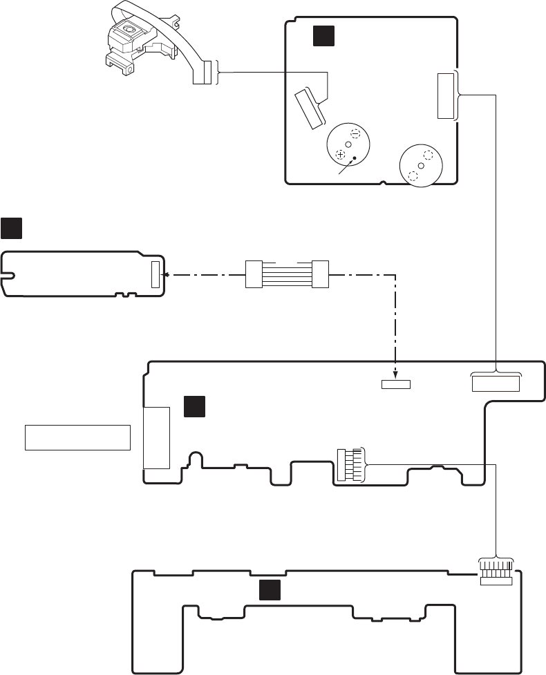
17 Cabinet Parts Location
TOP PREVIOUS NEXT
•@
TOP PREVIOUS NEXT
file:///C|/Documents%20and%20Settings/Administrator/Plocha/SL-EH570/s1700000000x.htm [25.4.2003 21:02:29]

file:///C|/Documents%20and%20Settings/Administrator/Plocha/SL-EH570/s1800000000x.htm
18 Loading Unit Parts Location
TOP PREVIOUS
•@
TOP PREVIOUS
file:///C|/Documents%20and%20Settings/Administrator/Plocha/SL-EH570/s1800000000x.htm [25.4.2003 21:02:50]
RANDOM REPEAT EDIT
OPEN
/
CLOSE
∫
45
<
;
DEFGH
IJKL
DRandom play button (RANDOM)
ERepeat play button (REPEAT)
FCD edit button (EDIT)
GDisc tray open/close button ( <, OPEN/CLOSE)
HSkip/search buttons (4, 5)
IDisc tray
JStop button (
∫
)
KPause button ( ;)
LPlay button and indicator ( !)
The colour of the indicator depends on the operation taking place.
If stopped: orange
If playing: green
If paused: flashes
8 7 6 5
1 2 3 4
NBOUT
GND
NAOUT
VREF
GND
Vcc
BIN
AIN
M
M
A
B
C
D
E
F
G
15
14
13
1616
15
14
13
1212
11
8
7
6
5
4
3
2
1
11
10
9
8
7
6
5
4
3
2
1
10
9
1516171819202122232425262728
1413121110987654321
PDE
PDF
Vcc
PDA
PDB
LPD
LD
RF
RFIN
CSBRT
CEA
BDO
LDON
GND
FBAL
TBAL
VREF
FEN
FEOUT
TEOUT
TEN
EQSW
GCTL
ENV
DEFLVL
OFTR
PDOWN
/RFDET
A
B
C
D
TP35
TP38
C737
0.1 C736
0.1
TP37
TP36
M702
SPINDLE
MOTOR
M701
TRAVERSE
MOTOR AB DC
C735
0.1
C734
10V220
BADC
BA
AB
R729
3.9K
R728
3.9K
C739
1500P
R727
3.9K
R749
4.7K
C752
1000P
C738
0.01
R724
18K
R735
100
R723
6.8K
R731 6.8K
R715
1K
C715
2700P
R725
390
C714
6.3V100
C712
0.1
C711
0.1
R708
22K
R707
39K
TP42 TP40
C749
2200P
R702
10K
C747
180P
R744
120K
C710
120P
R705
150K
TP33 TP32
R704
1K
R706
1K
ABCDKE G
C742
0.027
H
I
R701
4.7
C701
6.3V33
CN701
(RF)
TP30 C716
820P
TJ701
A
B
C
D
E
D
E
C
A
B
DCB A
C750
0.1
C751
0.1
VREF
C702
0.1
C706
2700P
C707
0.027
C704
0.1
C703
6.3V100
Q701
2SB709STX
LASER POWER
DRIVE
IC701
AN8885SBE1V
SERVO AMP
IC703
AN8739SBE2
FOCUS COIL/
TRACKING COIL/
TRAVERSE MOTOR/
SPINDLE MOTOR DRIVE
TRACKING
COIL
FOCUS
COIL
0.1
2
12
11
3
8
10
5
4
9
680P
680P
1K
0.1
0.047
6
Vcc
PDF
PDE
LD
LD
GND
NB
GND
GND
NA
VREF
LPD
GND
T+
T-
F+
F-
A
LD
15 16 17 18 19 20 21
14 13 12 11 10 9 8
23 24 25 26 27 28
654321
NC
RST IN
IN3
IN4
NC
GND
NC
PGND2
PVcc2
D4+
D4-
D3+
D3-
/ RST
NC
IN2
PC2
NC
IN1
NC
GND
PVcc1
PGND1
NC
D1-
D1+
D2-
D2+
7
22
Vcc
VREF
R736
100
C713
0.1
CD SERVO CIRCUIT
OPTICAL PICKUP
SCHEMATIC DIAGRAM-1
NOTE:
The number which noted at the connectors on the schematic diagram as
"SCHEMATIC DIAGRAM-1" or "SCHEMATIC DIAGRAM-2"
indicates the schematic diagram serial number located on the left corner in the schematic diagram.
R750
4.7
F
J
TP29
1.7V 3.4V1.7V 1.7V 1.7V (0.2V)
0V (2.5V)
2.8V (1.5V)
1V 0.7V 2.1V 1.8V 0V (3.3V)
0V
1.7V 1.7V 1.7V 1.7V 1.7V 1.7V 1.7V 0V 1.7V 0V 3.3V
(0V)
(0.4V) (0.3V)
0V 0V 0V 0V 7.3V 7.3V 1.7V
1.7V3.3V
(0V)
0V 0V 0V
(0.7V) 7.3V
PLAY
0.1V
P-P
2ms. 0.1V/DIV.
PLAY
2ms. 0.1V/DIV.
0.4V
P-P
3.4V
7.3V
1V(2V)
3.3V (2.5V)2.8V
PLAY
0.7V
P-P
0.5 s. 0.2V/DIV.
3.4V
0V
0V 1.7V 1.7V
:CD SIGNAL LINE:POSITIVE VOLTAGE LINE
1.7V1.7V1.7V
(0.5V) (0.3V)

61
60
59
58
57
56
55
54
53
52
51
50
49
48
47
46
45
44
43
42
41
62 63 64 65 66 67 68 69 70 71 72 73 74 75 76 77 78 79 80
1
2
3
4
5
6
7
8
9
10
11
12
13
14
15
16
17
18
19
20
2122232425262728293031323334353637383940
BCLK
LRCK
SRDATA
DVDD1
DVss1
TX
MCLK
MDATA
MLD
SENSE
/FLOCK
/TLOCK
BLKCK
SQCK
SUBQ
DMUTE
STAT
/RST
SMCK
CSEL
TRV
TVD
PC
ECM
ECS
KICK
TRD
FOD
VREF
FBAL
TBAL
FE
TE
RFENV
VDET
OFT
TRCRS
/RFDET
BDO
LDON
PLLF2
DSLF2
WVEL
ARF
IREF
DRF
DSLF
PLLF
VCOF
AVDD2
AVss2
EFM
PCK
VCOF2
SUBC
SBCK
Vss
X1 IN
X2 OUT
VDD
BYTCK
/CLDCK
FCLK
IPFLAG
FLAG
CLVS
CRC
DEMPH
RESY
IOSEL
/TEST
AVDD1
OUTL
AVss1
OUTR
RSEL
IOVDD
PSEL
MSEL
SSEL
191817161514
132 4 5 6 7 8 9 10 11 12 13
TP22
A
B
TP23
TP21
C727
50V1
C728
50V1
C725
1000P
C726
1000P
R718
1K
R717
1K
C754
470P
C730
0.1
C731
6.3V220
R721
100
C732
6.3V220
C733
0.1
TP20
C753
470P
A
B
CN702
C743
0.1
TP14TP13TP8 TP12TP6 TP7TP4TP3
IHGFEDCB
S701
(REST SW)
TP16
C745
1000P
A
B
C
D
E
F
G
H
I
GFEDCBAIHG F EDCBA
R712
220
C718
0.22
C717
0.1
C744
5600P
R709
47K
R741 47K
R711
82K
C722
10P
X701
(16.9344MHz)
C721
10P
C724
0.1
C723
10V220
IC702
MN662790RSCAQ-P
SERVO PROCESSOR/
DIGITAL SIGNAL PROCESSOR/
DIGITAL FILTER/
D/A CONVERTER
+B(2)
Rch OUT
/RST
STAT
SUBQ
SQCK
BLKCK
P.GND
MLD
MDATA
MCLK
TX
LD SW
D.GND
A.GND
Lch OUT
REST SW
SPEED
R753
10
TP15
TP1
R742
220K
SCHEMATIC DIAGRAM-2
To MAIN CIRCUIT(CN402)
on SCHEMATICDIAGRAM-5
KJ
+B(1)
A
TP17
C
TP19
R714
0
7.3V
3.4V
3.4V
3.4V
3.4V
1.6V
(2.7V)
(0.3V)
2.9V
0V
2.9V
0V
2.9V
3.3V (3V)
0V (3.3V)
2.9V
1.7V
3.3V(0V)
1.7V
1.7V
1.7V
1.7V
1.7V
1.7V
1.7V
1.7V
1.7V
1.7V
3.3V(0V)
0V(3.3V)
0V
0V
1.7V
1V
1.7V
0V
3.4V
1.6V
1.6V
3.4V
3.4V
3V
1.5V
3.4V
1.5V
3V
PLAY
1kHz, 0dB
2.2V
P-P
0.8V
P-P
F=16.9344MHz
PLAY
0.7V
P-P
PLAY
2ms. 0.1V/DIV.
0.4V
P-P
PLAY
0.1V
P-P
2ms. 0.1V/DIV.
PLAY
0V
3V
T 13.3ms.
PLAY
0V
3V
T 13.3ms.
PLAY
0V
3V
T 13.3ms.
0.5 s. 0.2V/DIV.
3.4V
2.4V
P-P
F=16.9344MHz
3.4V
3.4V
1.5V
1.7V
3.4V
:CD SIGNAL LINE:POSITIVE VOLTAGE LINE
0V
PLAY
0V
3.3V
F=75Hz
PLAY
0V
3.3V
T 13.3ms.
SCHEMATIC DIAGRAM-3
2
4
7
1
5
6
3
2
4
7
1
5
6
3
W401B
A
B
S612
()
S614
()
S615
()
S611
( OPEN/
CLOSE)
S613
(/)
S616
(/)
R620
820 R621
1K R622
1.2K R623
1.5K R624
1.8K
R611
820 R612
1K
S601
(EDIT)
S602
(REPEAT)
S603
(RANDOM)
B
A
D606
SML79455C
()
R610
150
DOPERATION CIRCUIT
CN405
W401A
A
B
C
D
E
F
G
H
I
Q802
UN411FTA
LED DRIVE
Q801
UN411FTA
LED DRIVE
D801
MA165TA R802
10K
IC790
TA7291S
MOTOR DRIVE
123456789
2
1
3
4
5
6
M
C790
10V82
CP790
LOADING
MOTOR
S790
(OPEN DET.)
S791
(CLOSE DET.)
LOADING MOTOR CIRCUIT
B
2
1
3
4
5
6
C415
0.01
MAIN CIRCUIT
C
4.8V
:POSITIVE VOLTAGE LINE
(4.8V)
4.7V(1.7V) 4.8V
0V
4.8V 7.3V 0.6V 7.3V 7.3V 0.6V 7.3V 4.8V
(3V)
0V(4.7V) 4.8V
4.8V
7.3V
IC451
C2BBFD000256
SYSTEM CONTROL
IC452
TC74HCT7007A
3.3V TO 5V
CONVERTER
ABC
A
B
C14131211109
7654321
Y5 A5Y4 A4Y3 A3 Vcc
Y0 A0Y1 A1Y2 A2GND
8
A
B
B
A
Q401
UN4214TA
RESET
AB
CDE
ABC D
A
B
C
D
E
X401
(8MHz)
R401
680
D401
MA165TA
C401
50V3.3
R429
10K
R402
100K
C402
0.01
R404
2.2K
R451
3.3K
R408
2.2K
R455
3.3K
D407
MA165TA
C411
0.1
C410
6.3V100
R403
4.7K
R405
100K
R439
22K
R440
47K
R442
10K
D403
MA165TA D404
MA165TA
R445
47K
R444
4.7K
R441
4.7K
Q404
2SC3311ATA
INTERFACE
Q403
2SC3311ATA
INTERFACE
Q402
2SC3311ATA
INTERFACE
R436
4.7K
R437
4.7K
R438
1K
C408
100P
R449
1K
C416
0.01
R448
1K
R433
10K
R434
100
D406
MA165TA
R435
100
D402
MA165TA
R409
470
R407
470
R406
100
AD C BFE
R424
4.7K
R432
4.7K
C414
470P
R419
1K
R422
10K
C413
470P
R420
1K
R421
10K
R413
100
IG
R414
2.2K
R415
2.2K
R416
2.2K
R452
3.3K
R453
3.3K
R454
3.3K
C452
0.01
SCHEMATIC DIAGRAM-4
2
1
3
R411
0
H
:POSITIVE VOLTAGE LINE
4.8V
7.3V
0.2V
1V
0.5V 0V
0.5V
1V
0V 4.8V
2.1V 2.1V 4.8V 4.8V 4.8V 4.8V 1V 0.4V 1.2V 3.3V 3.3V 0V 4.8V 4.8V
(4.5V) 2.1V 4.8V 4.8V
4.8V 0V 0V 0V 4.8V 4.8V 0V 4.8V 4.8V 4.8V 4.8V 4.8V 4.8V
4.8V
(4.5V) 3.3V
(3V) 0V
(4.8V) 0V
(3.3V) 4.8V 3.3V 4.8V
0V 0V
PLAY
0V
4.8V
F=75Hz
PLAY
0V
4.8V
T 13.3ms.
1.7V
P-P
F=8MHz
1.8V
P-P
F=8MHz
(4.8V)(4.4V)(0.3V)
PLAY
0V
4.8V
T 13.3ms. PLAY
0V
4.8V
T 13.3ms.
0V
(4.8V)(3V)
20 19 18 17 16 15 14 13 12 11 10 987654321
22 23 24 25 26 27 28 29 30 31 32 33 34 35 36 37 38 39 40 41 42
21
Vss
X OUT
XIN
RESET
E-CS
SERVORST
CNVss
RESTSW
TEST
DATA I
DATA O
B CLK
BCS
CD REQ
BLKCK
SQCK
SUBQ
SYNC
AVss
VREF
Vcc
LED ORG
LED CLK
LED DTA
MSEL
MDATA
MLD
STAT
HALH
PL
CW
CCW
PSTN
SW1
SW2
SW3
SW5
KEY2
KEY1
SW4
MCLK
LED GRN
IC2
UPC29M33HB
REGULATOR
231
INGNDOUT
20
2
1
3
4
5
6
7
8
9
10
11
12
13
14
15
16
17
18
19
Q4
2SB621ARSTA
REGULATOR
Q2,3
2SD1862QRTV6
REGULATOR
Q5
2SC3311ATA
STABILIZER
19
2
1
3
4
5
6
7
8
9
10
11
12
13
14
15
16
17
18
E
D
C
A
B
A
B
C
B
A
D
A
B
E
C
D
A
B
C407
10V220
C9
10V220
C11
1000P
D10
MA165TA
D12 D13 D14
D12-14
MA165TA
R10
470
C12
0.01
R11
2.2K
C10
6.3V220
C405
0.01
C403
1000P
R426
4.7K
R158
220
R156
47K
R155
47K
R157
220
C152
1000P
C151
1000P
CN402
C404
0.01
E1
R22
10
JK401
C7
0.01
C6
16V470
R5
270
C5
10V100
D3
MA4082LTA
R6
6.8
R8
1.2
C4
0.01
SYNC
CD REQ
CT.GND
CS
+B(10V)
D.GND
SCLK
DATA
NC
V.GND
NC
NC
NC
NC
NC
A.GND
NC
NC
REST SW
/ RST
STAT
SUBQ
SQCK
BLKCK
SPEED
MLD
MDATA
MCLK
P.GND
+B(1)
TX
LD SW
D.GND
+B(2)
Rch IN
A.GND
Lch IN
CD Lch OUT
CD Rch OUT
A
To CD SERVO CIRCUIT(CN702)
on SCHEMATIC DIAGRAM-2
To SOUND PROCESSOR
(SE-EH570) &
CASSETTE DECK
(RS-DV250)
SCHEMATIC DIAGRAM-5
+10V
R21
10
R31
10
CT.GND
A.GNDD.GND
C406
6.3V220
MAIN CIRCUIT
C
Q2
R9
0.33
Q3
R7
1.2
7.3V
3.4V
10.1V
8.1V
7.3V
8.1V
10.1V
7.3V
7.3V3.4V
6.7V 3.3V
2.7V
6.7V
4.8V 7.3V
7.3V
:POSITIVE VOLTAGE LINE :CD SIGNAL LINE
ABCDEF
1
2
3
4
5
6
7
8
R621
R624
R611
R623
R622
R610
J
R620
J
J
J
J
J
R802
R612
S612
( )
S614
( )
S615
( ) S616
( )
S611
( OPEN/
CLOSE)
S601
(EDIT)
S602
(REPEAT)
D606
( ) W401B
2
1
3
4
5
6
7
J
OPERATION P.C.B.
D
(REP3140A-M)
S603
(RANDOM)
S613
( )
ECB
Q801
ECB
Q802
D801
CD SERVO P.C.B.
A
18
16
14
12
10
8
6
4
2
19
17
15
13
11
9
7
5
3
1
CN702
IC702
1
5
10
15
20 21
25
30
35
40
41
45
50
55
6061
65
70
75
80
IC703
156 810 14
2021
23
2528
C
BE
Q701
1
3
5
7
9
11
13
15
2
4
6
8
10
12
14
16
CN701
IC701
1
5
10
14
15 20 25 28
M
M
M701
(TRAVERSE MOTOR)
M702
(SPINDLE
MOTOR)
C728
C727
X701
C703
C701
C734
C714
C731
C732
C723
C750
C751
C735
C752
R736
R727
R729 R728
R749
R725
C739
C715
RJ
RJ
RJ RJ
RJ
C737
C736
RJ
C753
C743
C733
C754
C725
C730
R718
R717 C726
RJ
C724
C722
C721
R714
C744
C717
R741
C704
RJ
C707
C706
C702
R701
RJ
RJ
RJ
RJ
RJ
RJ
RJ
RJ
C712 RJ
C711
RJ
RJ
RJ
RJ
C713 R750
R744
R704
R705
R702
C710
C718
C747
RJ
R708
R707
R706
C749
C742
C716
R709
R712 RJ
R742
RJ
RJ
R715
R724
R735
R731
RJ
R753
RJ
RJ
R723
C738
C745
TP20
TP23
TP21
TP22
TP19
TP30
TP29
(RF)
TJ701
TP40
TP33
TP32
TP42
S701
(REST SW)
TP1
TP3
TP4
TP7
TP6
TP8
TP17
TP13 TP12
TP14
TP38
TP15
TP16
TP36
TP35
TP37
VREF
(REP3118A-N)
15
R711
R721
This printed circuit board diagram may be modified at any time with the development of new technology.
1
2
3
4
5
6
CP790
S790 S791
M
1
234
56789
IC790
C790
LOADING
MOTOR
LOADING MOTOR P.C.B.
B
(REP1960A)

No.1
1
26
14
13
6
20
21
71
7
8
14
1
............
.
.
.
.
.
.
.
.
.
.
.
............
.
.
.
.
.
.
.
.
.
.
.
20
21
40
41
60
61
80
3
12E
C
B
ECB
ECB
Ca
A
A
AN8885SBE1V
C2BBFD000256 28PIN
42PIN
AN8739SBE2 TC74HCT7007A MN662790RSCAQ-P TA7291S
UPC29M33HB 2SB709STX 2SC3311ATA
UN411FTA
UN4214TA
2SB621ARSTA 2SD1862QRTV6
MA4082LTA SML79455C
Anode
Cathode Anode
Anode
Cathode
A
Ca
MA165TA
Anode
Cathode
Ca
9
1
E
C
B
1
15
2
16
CN701
M701
(TRAVERSE
MOTOR)
M702
(SPINDLE
MOTOR)
ACD SERVO P.C.B.
CMAIN P.C.B.
BLOADING MOTOR P.C.B.
OPTICAL PICKUP
RED MARK
CN702
W401A
CN405
To SOUND PROCESSOR&
CASSETTE DECK
1
.
.
.
.
.
7
1
.
.
.
.
6
1
.
.
.
.
6
1
.
.
.
.
6
.
.
.
.
.
.
.
.
.
.
.
.
19
.
.
.
.
.
.
.
.
1
18
.
.
.
.
.
.
.
2
18 . . . . . . . 2
19 . . . . . . . . 1
1 . . . . 6
DOPERATION P.C.B. W401B
7 . . . . . 1
CN402
WHITE
CP790
AN8739SBE2
IC703
FOCUS COIL / TRACKING
COIL / TRAVERSE MOTOR /
SPINDLE MOTOR DRIVE
F-
F+
T-
T+
M702
SPINDLE
MOTOR
M701
TRAVERSE
MOTOR
VREF 22
17
18
D4-
D4+
12
11
D1+
D1-
14
13
D2+
D2-
M
1
IN4 25
IN3 26
15
14
D3-
D3+
/RST
PGND1
PGND2
9
20
+B1
8
21
PVcc1
PVcc2
IN1 6
IN2 3
PC2 4
FOD
TRD
TVD
ECS
ECM
PC
M
20 27
6
FCLK
TBAL
28
1
21
AN8885SBE1V
IC701
SERVO AMP
4
5
13
LDON
NRF
DET.
89
+B2
7
OFTR
10
+B2
SUBTRA-
CTOR
RFENV
/RFDET
3
+B2
25
24 FE
15
12 BDO
17 OFT
19
26
BDO
11
3TENV
+B2
ENV
OFTR
BDO
/RFDET
FEN
FE OUT
VCC
VREF
FBAL
TBAL
2
EE
F F
GCTL
PDF
PDE
PDB
PDA
LD
LPD
RF RF IN CSBRT CEA
C
A
D
D
B
C
LDON
FBAL
VREF
SEMICONDUCTOR
LASER
PHOTO DETECTOR
OPTICAL PICKUP
RFEQ1
RFEQ2
AMP GCA BCA
AMP GCA BCA
SUBTRA-
CTOR
AMP GCA
VREF
BCA
AMP GCA BCA
22
23 TE
TEN
TE OUT
EQSW
Vcc
VREF
14
GND
18
DEFLVL
BAND
GAP
16
PDOWN
LASER
POWER
DRIVE
Q701
FOCUS
COIL
DRIVE
SPINDLE
MOTOR
DRIVE
TRAVERSE
MOTOR
DRIVE
TRACKING
COIL
DRIVE
RESET
SIGNAL
GENERATOR
FOCUS COIL
TRACKING COIL
+B2
VREF
TJ701
76 RSEL
44 ARF
46 DRF
47
41
52
PLLF
48
EFM
53 PCK
14 SQCK
80 SSEL
73
9MLD
68
75
OUTR
OUTL
MLD
MN662790RSCAQ-P
IC702
SERVO PROCESSOR / DIGITAL SIGNAL PROCESSOR
DIGITAL FILTER / D/A CONVERTER
Rch
PSEL
78
7
450 60
DVDD1
AVDD2
VDD
69
RESY
IOSEL
CLVS
CRC
BLKCK
/CLDCK
SBCK
SUBC
DEMPH
DSL / PLL VCO
5745157
DVss1
AVss1
AVss2
Vss
70
66
67
13
62
56
55
BLKCK
SQCK
SUBQ
15
SUBQ
PLLF2
DSLF
MCLK MCLK
MDATA
8
MDATA
STAT
17
STAT
VCOF2
54
VCOF
49
BYTCK
61
SMCK
19
FCLK
63
CSEL
20
MSEL
79
X2 OUT
59 58
X1 IN
FE
TE
RFENV
32 33 34
FE
TE
RFENV
TRCRS
VDET
BDO
37 35 39
BDO
/RFDET
OFT
38 36
/RFDET
OFT
10 43 40
SENSE
WVEL
LDONLDON
/FLOCK
/TLOCK
FBAL FBAL
TBAL TBAL
FOD FOD
TRD TRD
TVD TVD
VREF VREF
TRV
KICK
DSLF2 DSLF2
DMUTE
BCLK
SRDATA
LRCK
PC PC
ECS ECS
ECM ECM
IPFLAG
FLAG
11
12
30
31
28
27
22
29
21
26
42
16
1
3
2
23
25
24
64
65
6
TX
AVDD1
72
VCC5V
77 71
/TEST
18
/RST
+B2
+B2
DSLF2
45 IREF
+B2
+B2
X701
(16.9344MHZ)
/RST
+B2
1 BIT DAC
PWM LOGIC
PWM
(R)
PWM
(L)
16k
SRAM
8 TIMES OVERSAMPLING/
DIGITAL FILTER
DIGITAL DEEMPHASIS
DIGITAL AUDIO
INTERFACE
DIGITAL AUDIO
INTERFACE
INTERPORATION/
SOFT MUTING/
DIGITAL
ATTENUATION
CIRC ERROR
CORRECTION/
DEINTERLEAVE
SUBCODE
BUFFER
EFM DEMODULATION/
SYNC INTERPOLATION
SUBCODE DEMODULATION
CD-TEXT
BUFFER
A/D
CONVERTER
DSL / PLL VCO
VCO
OUTPUT
PORT
D/A
CONVERTER
SERVO CPU
SERVO TIMING
GENERATOR
INPUT PORT
TIMING
GENERATOR
PITCH
CONTROL
MICRO COMPUTER
INTERFACE
FCLK
13
S701
(REST
SW)
REST
SW
C2BBFD000256
IC451
SYSTEM CONTROL
TC74HCT7007A
IC452
CONVERTER
(3.3V To 5V)
SERVORST
BLKCK
SQCK
6
MDATA
MCLK
STAT
8
CD REQ
9
BCS D402
Q402
B CLK
10
DATA O
11
DATA I
12
Q403,
404
Q2,3
+B1
+B2
SYNC1
CS
8
JK401
2
3
4
5
6
7
9
12
13
14
15
16
17
18
CD REQ
CT.GND
+B(10V)
D.GND
SCLK
DATA
11
10
NC
Rch
A.GND
CD Lch OUT
NC
To SOUND
PROCESSOR
(SH-EH570)/
CASSETTE
DECK(RS-DV250)
BLOCK DIAGRAM
CD Rch OUT
NC
BLKCK
5
SUBQ
SUBQ
STAT
1
MLD
V.GND
NC
NC
NC
NC
+B3
MLD
MDATA
MCLK
/RST 16
7
29
27
1430
28
SQCK
19
20 NC
4
SYNC
Q4,5
D10,12~14
UPC29M33HB
IC2
D7
+B4
26
MSEL
KEY SWITCH
(S601~603,611~616)
KEY2
40
KEY1
41
+B3
Q401
18
RESET
1
VCC
+B3
VREF
2
38
SW3
S790
(OPEN DET.)
42
SW4
S791
(CLOSE DET.)
89
11
2
10
12
Y3A3
Y0A0
Y4A4
Y5A5
7
GND
+B3
Vcc
21 315
AVSS
CNVSS
VSS
14
RESET
INTER-
FACE
INTER-
FACE
13
TEST
+B3
REGULATOR
REGULATOR
REGULATOR
+10V
A.GNDD.GNDCT.GND
CW
33
CCW
34 22
LED ORG
LED GRN
25
Q801,
802
LED
DRIVE
D606
()
M
LOADING
MOTOR
5
2,4,6,8
+B4
3
7
1
9
TA7291S
IC790
MOTOR DRIVE
XOUT
XIN
20
19
X401
(8MHz)
Note:
: CD SIGNAL LINE