Differential Video Amplifiers UA733C UA733
User Manual: UA733C
Open the PDF directly: View PDF ![]() .
.
Page Count: 10
uA733C, uA733M
DIFFERENTIAL VIDEO AMPLIFIERS
SLFS027A – NOVEMBER 1970 – REVISED MARCH 1993
1
POST OFFICE BOX 655303 • DALLAS, TEXAS 75265
200-MHz Bandwidth
250-kΩ Input Resistance
Selectable Nominal Amplification of 10,
100, or 400
No Frequency Compensation Required
Designed to be Interchangeable With
Fairchild uA733C and uA733M
description
The uA733 is a monolithic two-stage video
amplifier with differential inputs and differential
outputs.
Internal series-shunt feedback provides wide
bandwidth, low phase distortion, and excellent
gain stability. Emitter-follower outputs enable the
device to drive capacitive loads, and all stages are
current-source biased to obtain high common-
mode and supply-voltage rejection ratios.
Fixed differential amplification of 10 V/V, 100 V/V,
or 400 V/V may be selected without external
components, or amplification may be adjusted
from 10 V/V to 400 V/V by the use of a
single external resistor connected between 1A
and 1B. No external frequency-compensating
components are required for any gain option.
The device is particularly useful in magnetic-tape
or disc-file systems using phase or NRZ encoding
and in high-speed thin-film or plated-wire
memories. Other applications include general-
purpose video and pulse amplifiers where wide
bandwidth, low phase shift, and excellent gain
stability are required.
The uA733C is characterized for operation from 0°C to 70°C; the uA733M is characterized for operation over
the full military temperature range of – 55°C to 125°C.
Copyright 1993, Texas Instruments Incorporated
PRODUCTION DATA information is current as of publication date.
Products conform to specifications per the terms of Texas Instruments
standard warranty. Production processing does not necessarily include
testing of all parameters.
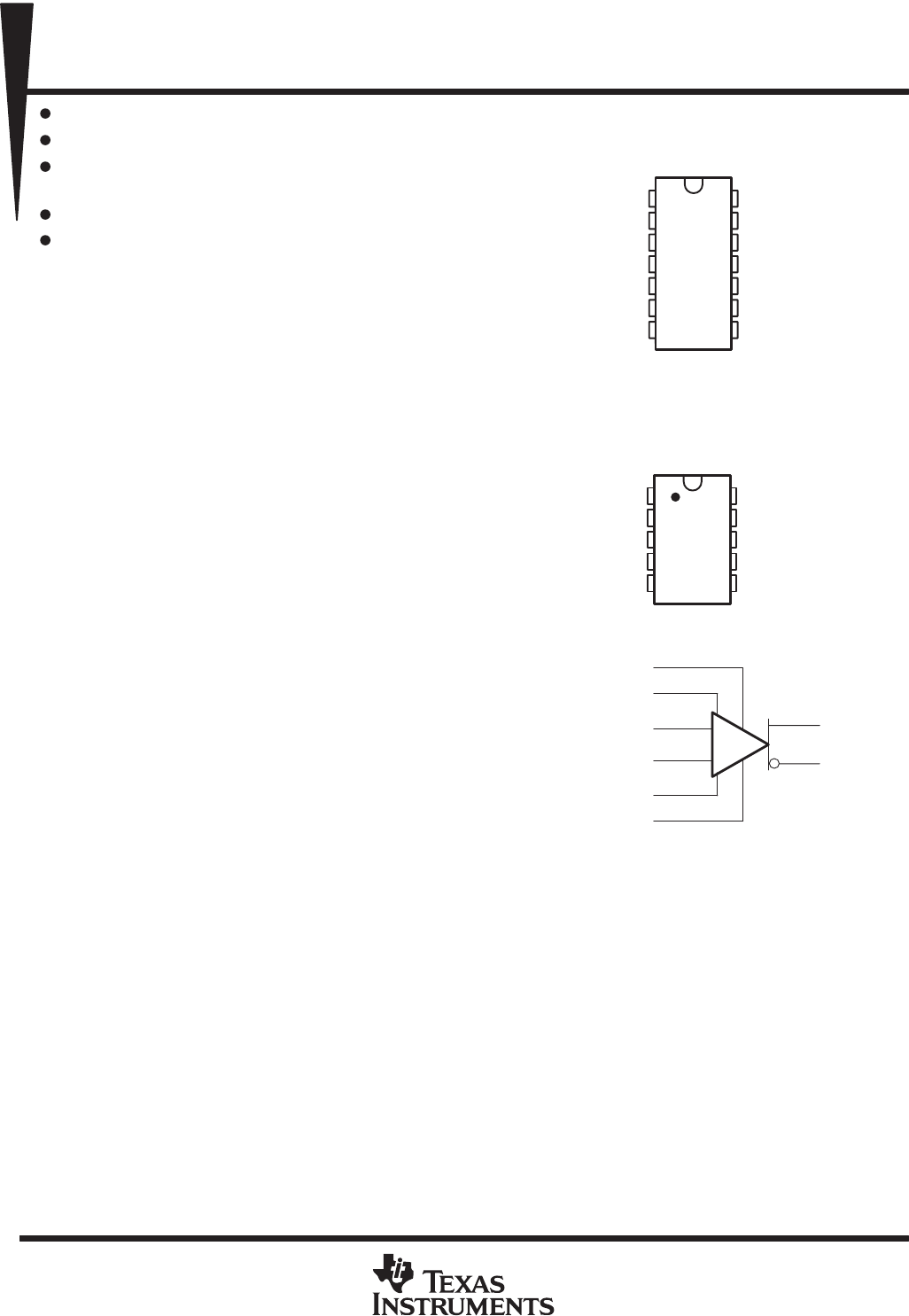
1
2
3
4
5
6
7
14
13
12
11
10
9
8
IN+
NC
GAIN ADJ 2A
GAIN ADJ 1A
VCC –
NC
OUT+
IN –
NC
GAIN ADJ 2B
GAIN ADJ 1B
VCC+
NC
OUT–
uA733C ...D OR N PACKAGE
uA733M ...J PACKAGE
(TOP VIEW)
1
2
3
4
5
10
9
8
7
6
IN+
GAIN ADJ 2A
GAIN ADJ 1A
VCC–
OUT+
IN–
GAIN ADJ 2B
GAIN ADJ 1B
VCC+
OUT–
uA733M ...U PACKAGE
(TOP VIEW)
NC No internal connection
+
_
GAIN ADJ 1A
GAIN ADJ 2A
IN+
IN–
GAIN ADJ 1B
GAIN ADJ 2B
OUT+
OUT–
symbol
uA733C, uA733M
DIFFERENTIAL VIDEO AMPLIFIERS
SLFS027A – NOVEMBER 1970 – REVISED MARCH 1993
2POST OFFICE BOX 655303 • DALLAS, TEXAS 75265
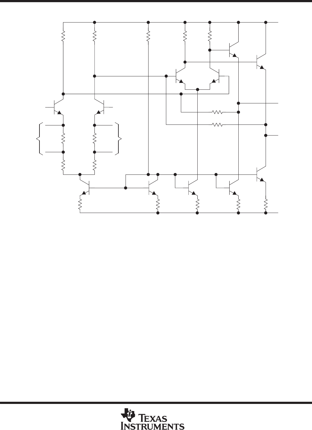
schematic
1A
2A
GAIN
ADJ
IN+ IN–
1B
2B
GAIN
ADJ
590 Ω590 Ω
300 Ω
2.4 kΩ2.4 kΩ10 kΩ1.1 kΩ1.1 kΩ
50 Ω50 Ω
1.4 kΩ300 Ω400 Ω400 Ω
VCC+
OUT+
OUT–
VCC–
7 kΩ
7 kΩ
Component values shown are nominal.
Component values shown are nominal.
uA733C, uA733M
DIFFERENTIAL VIDEO AMPLIFIERS
SLFS027A – NOVEMBER 1970 – REVISED MARCH 1993
3
POST OFFICE BOX 655303 • DALLAS, TEXAS 75265
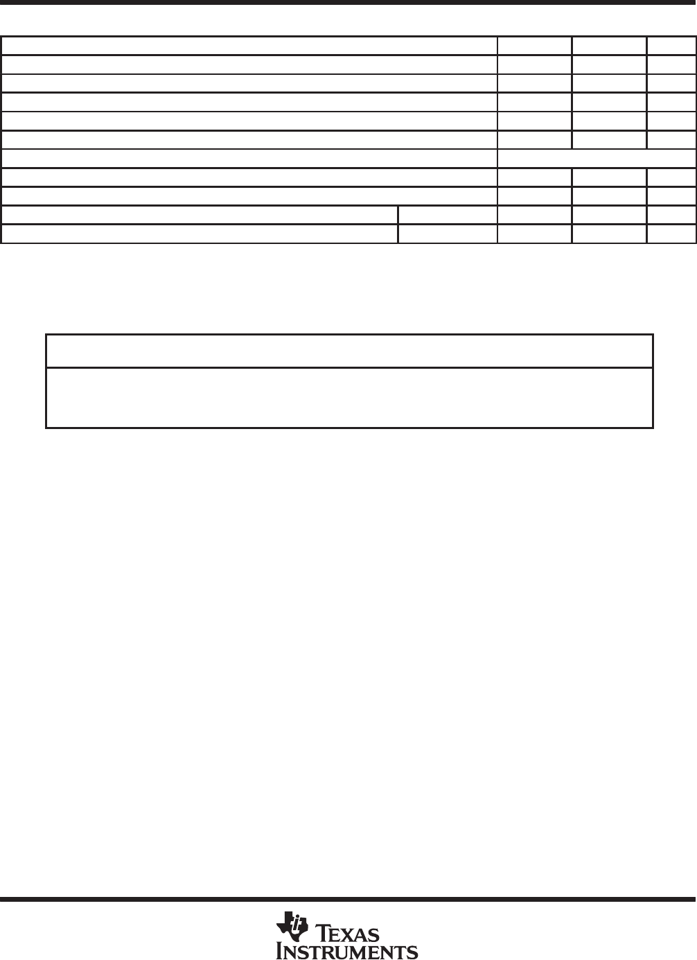
absolute maximum ratings over operating free-air temperature range (unless otherwise noted)†
uA733C uA733M UNIT
Supply voltage VCC+ (see Note 1) 8 8 V
Supply voltage VCC – (see Note 1) – 8 – 8 V
Differential input voltage ± 5 ± 5 V
Common-mode input voltage ± 6 ± 6 V
Output current 10 10 mA
Continuous total power dissipation See Dissipation Rating Table
Operating free-air temperature range 0 to 70 – 55 to 125 °C
Storage temperature range – 65 to 150 – 65 to 150 °C
Lead temperature 1,6 mm (1/16 inch) from case for 60 seconds J or U package 300 °C
Lead temperature 1,6 mm (1/16 inch) from case for 10 seconds D or N package 260 °C
†Stresses beyond those listed under absolute maximum ratings may cause permanent damage to the device. This is a stress rating only, and
functional operation of the device at these or any other conditions beyond those indicated in the recommended operating conditions section of
this specification is not implied. Exposure to absolute-maximum-rated conditions for extended periods may affect device reliability.
NOTE 1: All voltage values, except differential input voltages, are with respect to the midpoint between VCC+ and VCC –.
DISSIPATION RATING TABLE
PACKAGE TA ≤ 25°C
POWER RATING DERATING
FACTOR DERATE
ABOVE TA
TA = 70°C
POWER RATING TA = 125°C
POWER RATING
D
J (uA733M)
N
U
500 mW
500 mW
500 mW
500 mW
N/A
11.0 mW/°C
N/A
5.4 mW/°C
N/A
104°C
N/A
57°C
500 mW
500 mW
500 mW
430 mW
N/A
269 mW
N/A
133 mW
uA733C, uA733M
DIFFERENTIAL VIDEO AMPLIFIERS
SLFS027A – NOVEMBER 1970 – REVISED MARCH 1993
4POST OFFICE BOX 655303 • DALLAS, TEXAS 75265
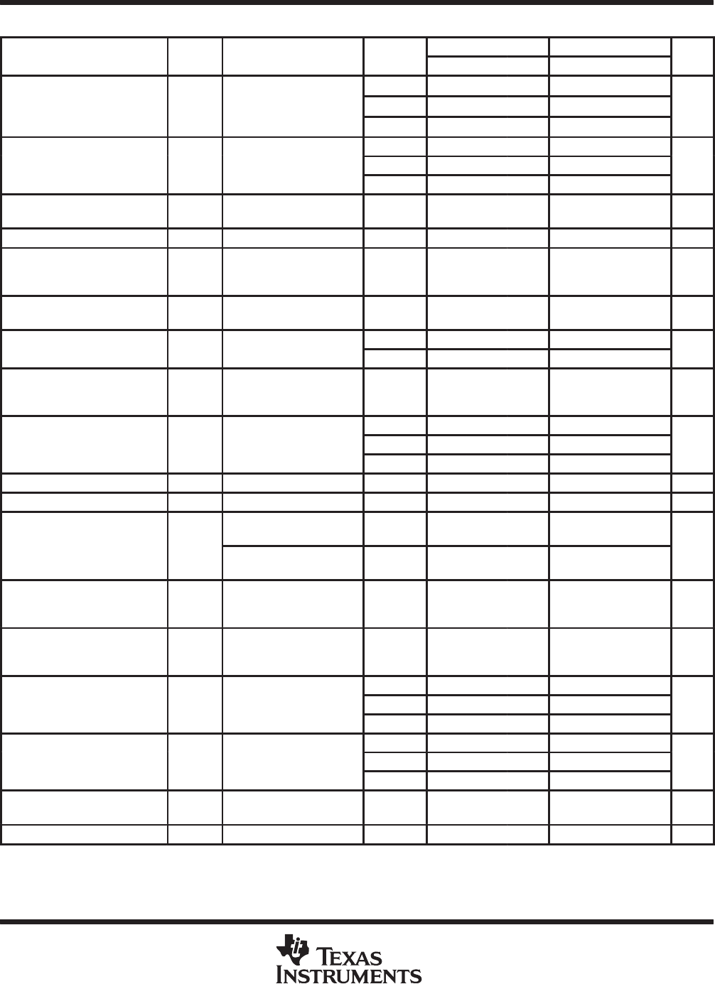
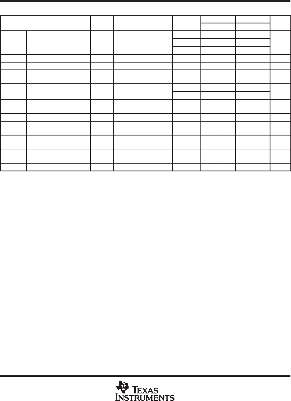
electrical characteristics, VCC± = ±6 V, TA = 25°C
PARAMETER
FIGURE
TEST CONDITIONS
GAIN uA733C uA733M
UNIT
PARAMETER
FIGURE
TEST
CONDITIONS
OPTION†MIN TYP MAX MIN TYP MAX
UNIT
Large-signal
diff ti l
1 250 400 600 300 400 500
AVD differential
voltage
1 VOD = 1 V 2 80 100 120 90 100 110 V/V
voltage
amplification 3 8 10 12 9 10 11
1 50 50
BW Bandwidth 2 RS = 50 Ω2 90 90 MHz
3 200 200
IIO Input offset
current Any 0.4 5 0.4 3 µA
IIB Input bias current Any 9 30 9 20 µA
VICR
Common-mode
input voltage
range
1 Any ±1±1 V
VOC Common-mode
output voltage 1 Any 2.4 2.9 3.4 2.4 2.9 3.4 V
VOO
Output offset
1
1 0.6 1.5 0.6 1.5
V
V
OO voltage
1
2 & 3 0.35 1.5 0.35 1
V
VOPP
Maximum peak-
to-peak output
voltage swing
1 Any 3 4.7 3 4.7 V
1 4 4
riInput resistance 3 VOD ≤ 1 V 2 10 24 20 24 kΩ
3 250 250
roOutput resistance 20 20 Ω
CiInput capacitance 3 VOD ≤ 1 V 2 2 2 pF
CMRR
Common-mode
4
VIC = ± 1 V,
f ≤ 100 kHz 2 60 86 60 86
dB
CMRR
rejection ration
4
VIC = ± 1 V,
f = 5 MHz 2 70 70
dB
kSVR
Supply voltage
rejection ratio
(∆VCC/(∆VIO)
1∆VCC± = ± 0.5 V 2 50 70 50 70 dB
Vn
Broadband
equivalent input
noise voltage
5BW = 1 kHz to 10 MHz Any 12 12 µV
Pti
R50Ω
1 7.5 7.5
tpd Propagation
delay time
2RS = 50 Ω,
Our
p
ut voltage ste
p
=1V
2 6.0 10 6.0 10 ns
delay
time
Our ut
voltage
ste
=
1
V
3 3.6 3.6
R50Ω
1 10.5 10.5
trRise time 2 RS = 50 Ω,
Our
p
ut voltage ste
p
=1V
2 4.5 12 4.5 10 ns
Our ut
voltage
ste
=
1
V
3 2.5 2.5
Isink(max) Maximum output
sink current Any 2.5 3.6 2.5 3.6 mA
ICC Supply current No load, No signal Any 16 24 16 24 mA
†The gain option is selected as follows:
Gain Option 1 . . . Gain-adjust pin 1A is connected to pin 1B, and pins 2A and 2B are open.
Gain Option 2 . . . Gain-adjust pin 1A and pin 1B are open, pin 2A is connected to pin 2B.
Gain Option 3 . . . All four gain-adjust pins are open.
uA733C, uA733M
DIFFERENTIAL VIDEO AMPLIFIERS
SLFS027A – NOVEMBER 1970 – REVISED MARCH 1993
5
POST OFFICE BOX 655303 • DALLAS, TEXAS 75265
electrical characteristics, VCC± = ±6 V, TA = 0°C to 70°C for uA733C, – 55°C to 125°C for uA733M
PARAMETER
FIGURE
TEST CONDITIONS
GAIN uA733C uA733M
UNIT
PARAMETER
FIGURE
TEST
CONDITIONS
OPTION†MIN MAX MIN MAX
UNIT
L i l diff ti l
1 250 600 200 600
AVD Large-signal differential
voltage am
p
lification
1 VOD = 1 V 2 80 120 80 120 V/V
voltage
am lification
3 8 12 8 12
IIO Input offset current Any 6 5 µA
IIB Input bias current Any 40 40 µA
VICR Common-mode input
voltage range 1 Any ±1± 1 V
VOO
Out
p
ut offset voltage
1
1 1.5 1.5
V
V
OO
O
u
tp
u
t
offset
v
oltage
1
2 & 3 1.5 1.2
V
VOPP Maximum peak-to-peak
output voltage swing 1 Any 2.8 2.5 V
riInput resistance 3 VOD ≤ 1 V 2 8 8 kΩ
CMRR Common-mode rejection
ratio 4 VIC = +1 V, f ≤ 100 kHz 2 50 50 dB
kSVR Supply voltage rejection
ratio (∆VCC/(∆VIO)1∆VCC± = ±0.5 V 2 50 50 dB
Isink(max) Maximum output sink
current Any 2.5 2.2 mA
ICC Supply current No load, No signal Any 27 27 mA
†The gain option is selected as follows:
Gain Option 1 . . . Gain-adjust pin 1A is connected to pin 1B, and pins 2A and 2B are open.
Gain Option 2 . . . Gain-adjust pin 1A and pin 1B are open, pin 2A is connected to pin 2B.
Gain Option 3 . . . All four gain-adjust pins are open.
uA733C, uA733M
DIFFERENTIAL VIDEO AMPLIFIERS
SLFS027A – NOVEMBER 1970 – REVISED MARCH 1993
6POST OFFICE BOX 655303 • DALLAS, TEXAS 75265
PARAMETER MEASUREMENT INFORMATION
test circuits
Figure 1
2 kΩ
50 Ω50 Ω
VOD
VID
+
–
Figure 2
50 Ω50 Ω
VID
+
–
1 kΩ
1 kΩ
0.2 µF
0.2 µF
Figure 3
2 kΩ
VOD
+
–
Figure 4
0.2 µF
0.2 µF
1 kΩ
50 Ω
50 Ω
1 kΩ
VIC
+
–
Figure 5
2 kΩ
VOD
+
–
Figure 6
50 Ω50 Ω
0.2 µF
0.2 µF
1 kΩ
2B 1B
2A 1A
Radj
1 kΩ
VOLTAGE AMPLIFICATION ADJUSTMENT
+
–
uA733C, uA733M
DIFFERENTIAL VIDEO AMPLIFIERS
SLFS027A – NOVEMBER 1970 – REVISED MARCH 1993
7
POST OFFICE BOX 655303 • DALLAS, TEXAS 75265
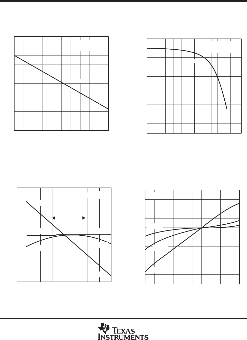
TYPICAL CHARACTERISTICS
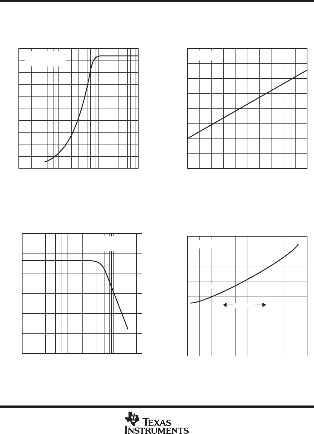
Figure 7
PHASE SHIFT
vs
FREQUENCY
GAIN 2
5
0
–5
–10
–15
–20
Phase Shift – Degrees
012345678910
f – Frequency – MHz
VCC± = ±6 V
TA = 25°C
Figure 8
PHASE SHIFT
vs
FREQUENCY
GAIN 2
50
0
–50
–100
–150
–200
–250
–300
–350
–400
–450
Phase Shift – Degrees
f – Frequency – MHz
1 4 10 40 100 400
VCC± = ±6 V
TA = 25°C
Figure 9
1.2
1.1
1.0
0.9
0.8
–75 – 50 – 25 0 25 50 75 100 125
uA733C
GAIN 1
GAIN 2
GAIN 3
GAIN 1
GAIN 3
GAIN 2
Voltage Amplification Relative to Value at T = 25 C
Ao
TA – Free-Air Temperature – °C
VOLTAGE AMPLIFICATION
(SINGLE-ENDED OR DIFFERENTIAL)
vs
TEMPERATURE
VCC± = ±6 V
Figure 10
1.4
1.2
1.0
0.8
0.6
0.4 345678
|VCC±| – Supply Voltage – V
VOLTAGE AMPLIFICATION
(SINGLE-ENDED OR DIFFERENTIAL)
vs
SUPPLY VOLTAGE
TA = 25°C
Voltage Amplification Relative to Value at V +_
CC = 6 V
+_
GAIN 1
GAIN 2
GAIN 3
uA733C, uA733M
DIFFERENTIAL VIDEO AMPLIFIERS
SLFS027A – NOVEMBER 1970 – REVISED MARCH 1993
8POST OFFICE BOX 655303 • DALLAS, TEXAS 75265
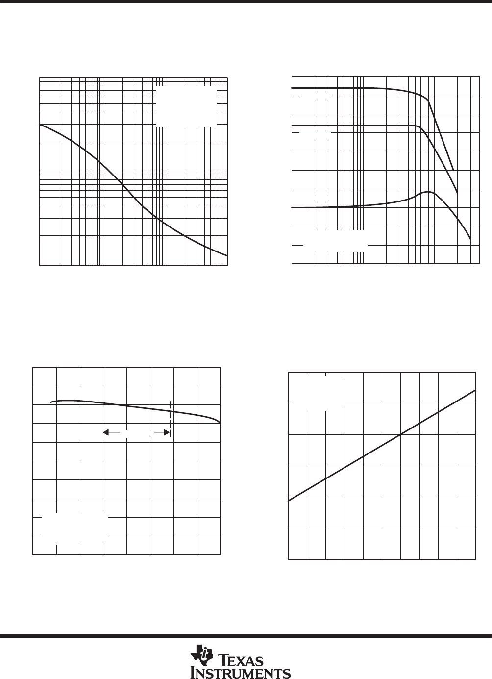
TYPICAL CHARACTERISTICS
Figure 11
DIFFERENTIAL VOLTAGE AMPLIFICATION
vs
RESISTANCE BETWEEN G1A AND G1B
10 40 100 400 1 k 4 k 10 k
1000
700
400
200
100
70
40
20
10
Radj – Resistance Between G1A and G1B – Ω
VCC± = ±6 V
VOD = 1 V
TA = 25°C
See Figure 6
AVD
– Differential Voltage Amplification
Figure 12
SINGLE-ENDED VOLTAGE AMPLIFICATION
vs
FREQUENCY
A
f – Frequency – MHz
1 4 10 40 100 400
GAIN 1
GAIN 2
GAIN 3
VCC± = ±6 V
TA = 25°C
VS – Single-ended Voltage Amplification – dB
50
40
30
20
10
0
Figure 13
SUPPLY CURRENT
vs
FREE-AIR TEMPERATURE
uA733C
20
18
16
14
12
10
8
6
4
2
0
–75 – 50 – 25 0 25 50 75 100 125
TA – Free-Air Temperature – °C
I – Supply Current – mA
CC
VCC± = ±6 V
No Load
No Signal
Figure 14
345678
24
20
16
12
8
4
0
|VCC±| – Supply Voltage – V
SUPPLY CURRENT
vs
SUPPLY VOLTAGE
No Load
No Signal
TA = 25°C
I – Supply Current – mA
CC
uA733C, uA733M
DIFFERENTIAL VIDEO AMPLIFIERS
SLFS027A – NOVEMBER 1970 – REVISED MARCH 1993
9
POST OFFICE BOX 655303 • DALLAS, TEXAS 75265
TYPICAL CHARACTERISTICS
Figure 15
MAXIMUM PEAK-TO-PEAK OUTPUT VOLTAGE
vs
LOAD RESISTANCE
10 40 100 400 1 k 4 k 10 k
5
4
3
2
1
0
RL – Load Resistance – Ω
VCC± = ±6 V
TA = 25°C
V – Maximum Peak-to-Peak Output Voltage – V
OPP
Figure 16
345678
MAXIMUM PEAK-TO-PEAK OUTPUT VOLTAGE
vs
SUPPLY VOLTAGE
V – Maximum Peak-to-Peak Output Voltage – V
OPP
8
7
6
5
4
3
2
1
0
|VCC±| – Supply Voltage – V
TA = 25°C
Figure 17
MAXIMUM PEAK-TO-PEAK OUTPUT VOLTAGE
vs
FREQUENCY
f – Frequency – MHz
1 4 10 40 100 400
2 7 20 70 200
VCC± = ±6 V
TA = 25°C
V – Maximum Peak-to-Peak Output Voltage – V
OPP
6
5
4
3
2
1
0
Figure 18
– 60 – 40 –20 0 20 40 60 80 100 120 140
INPUT RESISTANCE
vs
FREE-AIR TEMPERATURE
40
35
30
25
20
15
10
5
0
TA – Free-Air Temperature – °C
r
uA733C
GAIN 2
VCC± = ±6 V
Ω
i – Input Resistance – k
IMPORTANT NOTICE
Texas Instruments and its subsidiaries (TI) reserve the right to make changes to their products or to discontinue
any product or service without notice, and advise customers to obtain the latest version of relevant information
to verify, before placing orders, that information being relied on is current and complete. All products are sold
subject to the terms and conditions of sale supplied at the time of order acknowledgement, including those
pertaining to warranty, patent infringement, and limitation of liability.
TI warrants performance of its semiconductor products to the specifications applicable at the time of sale in
accordance with TI’s standard warranty. Testing and other quality control techniques are utilized to the extent
TI deems necessary to support this warranty. Specific testing of all parameters of each device is not necessarily
performed, except those mandated by government requirements.
CERTAIN APPLICATIONS USING SEMICONDUCTOR PRODUCTS MAY INVOLVE POTENTIAL RISKS OF
DEATH, PERSONAL INJURY, OR SEVERE PROPERTY OR ENVIRONMENTAL DAMAGE (“CRITICAL
APPLICATIONS”). TI SEMICONDUCTOR PRODUCTS ARE NOT DESIGNED, AUTHORIZED, OR
WARRANTED TO BE SUITABLE FOR USE IN LIFE-SUPPORT DEVICES OR SYSTEMS OR OTHER
CRITICAL APPLICATIONS. INCLUSION OF TI PRODUCTS IN SUCH APPLICATIONS IS UNDERSTOOD TO
BE FULLY AT THE CUSTOMER’S RISK.
In order to minimize risks associated with the customer’s applications, adequate design and operating
safeguards must be provided by the customer to minimize inherent or procedural hazards.
TI assumes no liability for applications assistance or customer product design. TI does not warrant or represent
that any license, either express or implied, is granted under any patent right, copyright, mask work right, or other
intellectual property right of TI covering or relating to any combination, machine, or process in which such
semiconductor products or services might be or are used. TI’s publication of information regarding any third
party’s products or services does not constitute TI’s approval, warranty or endorsement thereof.
Copyright 1998, Texas Instruments Incorporated
