UF585
User Manual: UF585
Open the PDF directly: View PDF ![]() .
.
Page Count: 290 [warning: Documents this large are best viewed by clicking the View PDF Link!]
Order Number : MGCS990301C1
H13
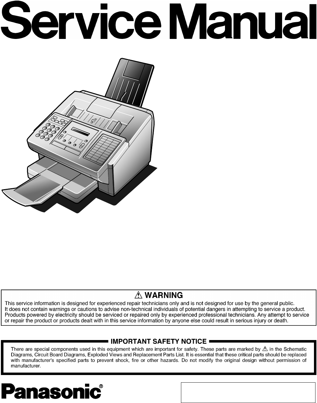
Facsimile
UF-585 / 595
© 1999 Matsushita Graphic Communication Systems, Inc.
All rights reserved. Unauthorized copying and distribution is
a violation of law.
Table of Contents
3
General Description...................................6
1.1 Overview...................................................6
1.2 General Features and Functions ..............6
1.3 General Specifications..............................8
1.4 Scanner Specifications ...........................10
1.5 Printer Specifications ..............................11
1.6 Power......................................................12
1.7 Environment............................................12
1.8 Construction............................................12
1.9 Specification Table .................................15
1.10 Function Table........................................17
Disassembly Instruction...........................20
2.1 General Disassembly Flowchart.............20
2.2 Power Cord (1008),
Telephone Line Cable (1009),
Lithium Battery (234),
Recording Paper Tray Assembly (1007),
Paper Cassette.......................................21
2.3 Left Cover (103), Right Cover (102),
Front Cover (104), Speaker (117),
Separation Rubber (207) ........................22
2.4 Control Panel Unit,
PNL1 PC Board (231),
LCD Unit (233)........................................24
2.5 Transmit Guide (301) Assembly,
Scanning Glass (308) .............................26
2.6 Stamp Assembly, Stamp Solenoid (327) 27
2.7 Eject Roller (303)....................................28
2.8 Transmit Motor (324) ..............................30
2.9 Scanner Block (321), Mirror 1 (334),
Mirror 2 (335), Mirror 3 (336),
ADF Roller (331).....................................31
2.10 A4 LED Array (329), Feed Roller (302) ..32
2.11 LPC PC Board (401),
SCA/SCB PC Board (422),
ILS PC Board (425),
SNS4 PC Board (729) ............................33
2.12 High Voltage Power Supply Unit (424),
Paper Feed Solenoid (531),
Clutch Gear Assembly (530),
Paper Feed Roller (518) .........................34
2.13 Printer Cover (106), Rear Cover (105),
Printer Motor (626)..................................36
2.14 LCU PC Board (402),
Low Voltage Power Supply Unit (423) ...37
2.15 Fuser Unit (701),
Thermistor Assembly (728).....................38
2.16 Fuser Lamp (732), Exit Roller (719),
Fuser Roller (709),
Pressure Roller (706)..............................39
2.17 Rear Chassis (505),
PRTA PC Board (536),
SNS1 PC Board (615)............................ 42
2.18 Transfer Guide (601) Assembly,
Feed Roller (526) ................................... 44
2.19 Toner Sensor (513),
Laser Unit [LSU] (512),
SNS3 PC Board (535)............................ 45
2.20 Bias Transfer Roller (604) ...................... 47
2.21 SNS2 PC Board (534)............................ 48
2.22 Printer Grease Points............................. 49
2.23 Screw Identification Template ................ 50
Maintenance, Adjustments and
Check Points ........................................... 52
3.1 Required Tools....................................... 52
3.2 Periodic Maintenance Points.................. 52
3.3 Periodic Maintenance Check List........... 53
3.4 Updating the Firmware........................... 54
3.5 ADF Pressure......................................... 56
3.6 Printer Unit Test ..................................... 56
3.7 General Circuit Diagram......................... 57
3.8 SCA / SCB PCB (UF-595, UF-585)........ 59
3.9 LPC PCB................................................ 77
3.10 LCU PCB................................................ 84
3.11 SRU PCB (Optional) .............................. 86
3.12 Low Voltage Power Supply PCB (POW) 87
3.13 High Voltage Power Supply PCB (HVPS)88
3.14 SNS3...................................................... 89
3.15 SNS4...................................................... 90
3.16 SNS1...................................................... 91
3.17 Parallel Interface PCB (Option).............. 91
3.18 CCD Alignment ...................................... 92
Troubleshooting....................................... 96
4.1 Initial Troubleshooting Flowchart ........... 96
4.2 Improper LCD Display............................ 97
4.3 Information Codes (INFO. CODES) ....... 98
4.4 Printed Copy Quality Problems ............ 111
4.5 Document Feeder (ADF)...................... 127
4.6 Communications .................................. 130
4.7 Information Code Table........................ 136
4.8 Diagnostic Codes ................................. 140
Table of Contents
4
Service Modes.......................................146
5.1 Service Mode Table..............................146
5.2 Service Mode 1
(Function Parameter Setting)................147
5.3 Service Mode 3 (Printout of Lists,
Reports and Test Results) ...................153
5.4 Service Mode 4 (Modem Test) .............166
5.5 Service Mode 5 (Diagnostic).................171
5.6 Service Mode 6 (RAM Initialization)......173
5.7 Service Mode 7 (LBP Service Mode)....174
5.8 Service Mode 8 (Check & Call).............175
5.9 Service Mode 9 (System Maintenance)180
System Description................................186
6.1 Mechanical Operation...........................186
6.2 Electrical Circuit Explanation ................195
Exploded View & Parts List....................222
7.1 Cover Assembly....................................222
7.2 Control Panel........................................224
7.3 Transmitter Assembly...........................226
7.4 Electrical Parts......................................228
7.5 Base Unit ..............................................230
7.6 Paper Transportation............................232
7.7 Fuser Unit .............................................234
7.8 Cassette................................................236
7.9 Option Cassette....................................238
7.10 Packing and Accessories......................240
Installation..............................................245
8.1 Function Key.........................................245
8.2 Main Unit and Accessories ...................246
8.3 Installing the Accessories .....................247
8.4 Installing the Toner Cartridge ...............248
8.5 Loading the Recording Paper...............250
8.6 Adjusting the Paper Cassette for
the Paper Length .................................252
8.7 Adjusting the Paper Cassette for
the Paper Width....................................253
8.8 Connecting the Telephone
Line Cable and Power Cord..................254
8.9 Customizing Your Machine...................256
Options and Supplies ............................ 262
9.1 Options and Supplies ........................... 262
9.2 Installing Optional 250 Sheet Paper
Cassette (UE-409070) ......................... 263
9.3 Installing Handset Kit (UE-403117)...... 265
9.4 Installing Parallel Port Interface Kit
(UE-404071)......................................... 266

Panasonic UF-585 / 595
6
1 General Description
1.1 Overview
This section covers the features and specifications of the plain paper facsimile transceiver "Panasonic UF-585/595". This fax
machine can transmit and receive on the Public Switched Telephone Network (PSTN) in modes conforming to ITU-T Group 3
recommendations.
1.2 General Features and Functions
1. Laser Printing
Clear picture quality is obtained by employing a Laser printing method on plain paper. The machine can print onto A4, Letter
or Legal size paper.
2. Quick Scan
Quick Scan speeds up the fax process by scanning the documents into memory at a rate of approximately 6* seconds per
page.
(*Standard Resolution, based on ITU-T Image No. 1 Test Chart. The scanning speed applies to the feeding process from the
leading to the lagging edge of a single page test chart. The time for the storing process is not applied for this definition.)
3. Easy Maintenance
This laser printing mechanism only requires changing the toner cartridge, housing the drum and toner.
Unlike other machines with removable EPROM (Erasable Programmable ROM), this machine is equipped with a F-ROM
(Flash ROM). F-ROM offers the flexibility of quick and easy firmware updates, creation of a master firmware card, backup
and restore of firmware and machine parameters.
4. Panasonic Super Smoothing
The machine incorporates a new sophisticated image processing technology to enhance print quality of ordinary received fax
images by smoothing the curved edges of the character.
5. A4 size Scanning
A4 size is the maximum document width that can be scanned and transmitted.
(Note: 10.1 in (257 mm) is the maximum document width that can be loaded into the ADF, however only A4 width will be
scanned.)
6. Automatic Document Feeder
An Automatic Document Feeder feeds originals from the document tray automatically, starting with the bottom page.
Capacity: 30 documents of average thickness and of the same size.
7. Speedy Transmission
Short Protocol reduces hand-shake time by shortening Phase B and D.
8. Error Correction Mode (ECM)
An Error Correction Mode, which conforms to ITU-T Recommendations, allows error-free data transmission. ECM with MMR
Coding also conforms to ITU-T Recommendations.
9. Automatic Dialing Function
Up to 100 stations can be easily dialed by One-Touch Dialing or Abbreviated Dialing Function. Any other stations can be
dialed directly from the keypad by entering the full telephone number (up to 12 stations).
10. Memory Transmission
The contents of a document can be stored into the document memory first, then transmitted from memory. Operator
attendance until transmission ends is not necessary.
11. Multi-station Transmission
Using the document memory, the document can be transmitted to multiple destinations.
Max. Document Size Document Thickness
Up to 20 pages A4 / Letter / Legal 12 to 20 lb (0.0024 to 0.0048 in)
Up to 30 pages A4 / Letter Size 12 to 16 lb (0.0024 to 0.0039 in)

General Description
7
12. Deferred Communication
The 10 built-in 24-hour timers allow the operator to set deferred transmissions or deferred polling. Using the document
memory, documents can also be transmitted to multiple stations.
13. Substitute Reception
The contents of a document will be received into the document memory if the recording paper or toner runs out, or a recording
paper jam occurs during reception. The stored documents can be printed after replacing the recording paper or toner cartridge
or correcting a paper jam.
14. Multiple Task Operation
Multiple Task Access operations can store documents and their destinations even during reception or memory transmission. It
can also receive during document storage.
15. Halftone (Photo)
For transmission or copying, this function ensures high quality reproduction of gray-shaded or photographic documents. This
machine uses 64 levels of error diffusion to create halftones with Quality mode.
16. Copy Function
The Copy function allows the machine to be used as a copier. Using the document memory, up to 99 copies can be made of a
single original.
17. 32 Transaction Journal
The 32 Transaction Journal provides transaction information - number of pages transmitted or received, start date and time,
communication results, identification, etc. It is automatically printed after every 32 transactions, or it can be printed manually
at anytime.
18. Latest Individual Transmission Journal
The latest Individual Transmission Journal provides information on the last transmission - number of pages transmitted, start
date and time, communication results, identification, etc. It can be printed manually at anytime after communications.
19. Communication Journal
A communication journal is a result report of a communication which can be printed automatically after communication is
completed. Printout conditions can be selected for each communication to 1) not print, 2) always print, or 3) print when
communication has failed.
20. Multi-purpose LCD Display
The 20 x 2 Alphanumeric LCD display shows the operation mode, date and time, remote ID number, and pages transmitted or
received. In case of an error, the LCD display shows an information code and error message indicating the exact cause of
trouble.
21. Verification Stamp
The Verification Stamp is automatically stamped on the original document when the document is transmitted or stored in
memory successfully. The "X" mark appears at the bottom of each page.
22. Password Transmission
A password transmitted from the other party is checked to prevent the transmission of documents to an unauthorized station.
23. Password Reception
A password transmitted from the other party is checked to prevent the reception of documents by an unauthorized station.
The reception of a junk mail, etc., is preventable.
24. Access Code
The Access Code can be registered into the machine to prevent operation by an unauthorized user.
25. Selective Reception
To prevent unwanted faxes from being received, the machine compares the ID Number of the transmitting machine with the
telephone number stored in the built-in automatic telephone dialer.

Panasonic UF-585 / 595
8
26. Receive to Memory
Users can set the unit to store incoming documents into its available memory. Later, using a 4-digit password, stored
documents can be printed when the user is present. This function helps ensure that important documents are not read or lost
while they are sitting unattended in the fax tray.
27. Relay Transmission Request
By setting the machine as an initial sending station, the unit is capable of setting up a relay request to a central hub machine
with a network password. Documents can then be automatically transmitted to the end receiving stations. This model is
designed to operate as an initial sending station.
28. Confidential Mailbox
When the received message is stored into the memory with a 4-digit confidential code, the message can be printed on
recording paper or polled by a remote station. A maximum of 10 mailboxes can be used. A remote confirmation report such as
Confidential Memory Report and/or Confidential XMT Report is not transmitted to the source station and/or the remote station
after Confidential Mailbox reception or polling transmission.
29. Remote Diagnostic Function
The remote Diagnostic Function can be used to diagnose the unit remotely over the PSTN or equivalent. A new host system
is required for high speed remote diagnostics to be available.
30. Distinctive Ring Detector (DRD)
This feature supports an optional telephone service, “Distinctive Ring Service”, provided by local telephone companies. This
service allows up to 4 different telephone numbers to be assigned on a single telephone line, each with a distinctive ring
pattern. By programming a fax parameter to select the appropriate ring pattern associated with the telephone number
assigned to the fax machine, the unit will differentiate and answer incoming calls on the fax telephone line only. All other
telephone calls will not be answered. Check with your local telephone company on the availability of this optional service in
your area.
31. Check and Call Function
This feature enables the Authorized Servicing Dealers to manage and improve the Fax machine maintenance to their
customers by alerting them of equipment problems. It also can be used as a Supply Sales Tool by alerting the Dealer that the
unit is running Low on Toner. The function overview is as follows:
a. The machine’s printer error information is stored in the Printer Report.
b. The printer report can be manually printed when required.
c. When printer errors occur, the unit can automatically transmit the Service Alert Report to the pre-registered telephone
number.
d. When the unit detects Low Toner, it can automatically transmit the Maintenance Alert Report to the pre-registered
telephone number.
e. When the unit detects Low Toner, it can automatically print out the Toner Order Form with pre-registered order information.
32. Continuous Polling (Station Mode)
This feature allows you to store or add documents into a polled file in memory.
To enable the Continuous Polling feature set Function Parameter No. 003 to "2:Station". The Program Key [P4] will be
assigned with the "Store-4-Polling" name automatically and cannot be changed.
To prepare the document(s) to be polled, simply place the document(s) on the ADF and then press the Program Key [P4] to
store or add the document(s) into a polled file.
(Note: If a regular polled file ([FUNCTION][3][2]) is stored in memory, the Program Key [P4] for Continuous Polling will not be
accepted.)
1.3 General Specifications
1. Communication Facility
Public Switched Telephone Network (PSTN)
2. Line Coupling
Direct Coupling
3. Input Level
-5 to -43 dbm

General Description
9
4. Output Level
0 to -15 dbm
5. Control Procedure
ITU-T Rec.T.30
MGCS Proprietary short protocol
6. Modem Speed
7. Coding Scheme
MH (Modified Huffman), MR (Modified Read), MMR (Modified Modified Read)
8. Communication Resolution
<Transmission>
<Reception>
9. Halftone (Photo)
64 Levels, Error Diffusion
10. Error Correction Mode
ITU-T Rec. T.30 ECM
11. Image Memory Capacity (Flash Memory)
12. Transmission Speed
UF-585 : 6 Seconds using ITU-T Image No. 1 in Standard Resolution, memory to memory communication.
UF-595 : 3 Seconds using ITU-T Image No. 1 in Standard Resolution, memory to memory communication.
V.34 (UF-595 only) : 33600 - 2400 bps @2400 step (QAM with TCM)
V.17 : 14400, 12000, TC9600, TC7200 bps (QAM with TCM)
V.29 : 9600, 7200 bps (QAM)
V.27ter : 4800, 2400 bps (PhM)
Standard : 203 dpi x 98 lpi (8 pels/mm x 3.85 lines/mm)
Fine : 203 dpi x 196 lpi (8 pels/mm x 7.70 lines/mm)
S-Fine : 203 dpi x 391 lpi (8 pels/mm x 15.4 lines/mm)
[UF-585] : 203 dpi x 391 lpi (8 pels/mm x 15.4 lines/mm)
[UF-595] :
:
203 dpi x 391 lpi (8 pels/mm x 15.4 lines/mm)
406 dpi x 391 lpi (16 pels/mm x 15.4 lines/mm)
Standard (Base) : 60 pages
Optional (Adtional) : + 80 pages (1 MB : UE-410045)
+ 160 pages (2 MB : UE-410046)
+ 320 pages (4 MB : UE-410047)
(using ITU-T Image No.1 in Standard Resolution)

Panasonic UF-585 / 595
10
13. Automatic Dialing
14. Print Reduction Ratio
15. Clock Backup Battery
This unit uses a lithium battely to save the clock and calendar. The service life is approximately 1 year during power failure.
1.4 Scanner Specifications
1. Document Dimensions
Note
With operator’s assistance, a maximum of 78.7 in (2000 mm) length document can be sent (one page at a time) through the
ADF.
2. Automatic Document Feeder
The Automatic Document Feeder feeds the originals from the document tray automatically, starting with the bottom page.
Dialing Signal : 10 PPS/DTMF
Dialing Method
One-Touch Dialing
Abbreviated Dialing
Manual Number Dialing
(Direct Dialing)
:
:
:
Up to 28 keys (including 4 programmable keys)
Up to 72 stations
Up to 12 stations
(Up to 36 digits including pauses)
Programmable Dialing : Up to 4 programmable keys
Combination Dialing : Combination of One-Touch, Abbreviated and Manual Number
Dialing
Multi-Station Dialing : Multi-Station Transmission/Polling
[Up to 112 stations]
Deferred Multi-Station Transmission//Polling
[Up to 112 stations]
Registration Memory Capacity in One-Touch and Abbreviated Dialing
Number of Stations : Up to 100 stations
Telephone number of
each station : Up to 36 digits (Including pauses and spaces)
Station name for each
station : Up to 15 characters
Redialing
Automatic
Manual
:
:
Up to 15 times with 0 to 15 minute intervals
By pressing the Redial button (last number dialed)
A4 / Letter : 70 to 100% in 1% steps
Legal : 80 to 100% in 1% steps (according to the received document length)
Width : Minimum 5.83 in (148 mm)
Maximum 10.1 in (257 mm)
Length : Minimum 5.04 in (128 mm)
Maximum 14.0 in (356 mm)
Paper thickness : Single-page : 0.0024 to 0.0060 in (0.06 to 0.15 mm)
: Multi-page : 0.0024 to 0.0048 in (0.06 to 0.12 mm)
Capacity : 20 documents (Legal Size - 20 lb)
: 30 documents (Letter / A4 Size - 16 lb)
denotes hazards that could result in minor injury or damage to the machine.
CAUTION
!
• THIS PRODUCT CONTAINS A LITHIUM BATTERY. DANGER OF EXPLOSION IF BATTERY IS INCORRECTLY
REPLACED.
REPLACE ONLY WITH THE SAME OR EQUIVALENT TYPE. DISPOSE OF USED BATTERIES ACCORDING TO
THE INSTRUCTIONS OF YOUR LOCAL SOLID WASTE OFFICIALS.

General Description
11
3. Scanning Method
4. Effective Scanning Width
5. Scanning Resolution
6. Contrast Selection
3 steps (Normal / Lighter / Darker)
1.5 Printer Specifications
1. Recording Paper Size (W x L)
2. Recommended Recording Paper Weight
16 to 24 lb (60 to 90 g/m2)
3. Paper Capacity with standard cassette
250 sheets (20 lb, 75 g/m2)
The paper does not exceed the Maximum Paper Capacity Mark.
4. Printing Resolution
5. Non Printable Margin
The shaded areas represent the unprintable area on the recording paper.
Horizontal : Sheet Feeding with CCD type image sensor
Vertical : Stepper Motor feeding
Letter : 8.3 in (212 mm)
Standard : 203 dpi x 98 lpi (8 pels/mm 3.85 lines/mm)
Fine : 203 dpi x 196 lpi (8 pels/mm 7.7 lines/mm)
S-Fine
[UF-585] : 203 dpi x 391 lpi (8 pels/mm x 15.4 lines/mm)
[UF-595] : 406 dpi x 391 lpi (16 pels/mm x 15.4 lines/mm) (Interpolated)
Letter : 8.5 x 11 in (216 x 279 mm)
Legal : 8.5 x 14 in (216 x 356 mm)
A4 : 8.3 x 11.7 in (210 x 297 mm)
(Fax or Copy) : 406 x 391 dpi
(PC Printing)
[UF-585] : 300 x 300 dpi
[UF-595] : 300 x 300 dpi
600 x 600 dpi
0.16 in
(4 mm) 0.16 in
(4 mm)
0.16 in
(4 mm)
0.16 in
(4 mm)

Panasonic UF-585 / 595
12
6. Printing Speed
5 ppm (12 seconds/page)
7. Fuser Warm Up Time
8. Document Tray Capacity
100 sheets
1.6 Power
1. Power Requirement
99~140 VAC, 47~63Hz, Single Phase
2. Power Consumption
1.7 Environment
1. Operating Environment
2. Storage Environment (Carton Box Condition)
Note
The machine should be stored upright.
3. Transportation Environment (Max. 480 hours, Carton Box Condition)
1.8 Construction
Within 30 seconds after turning the power on. [Room Temperature: 68 to 95°F (20 to 35°C)]
[Power Voltage: Minimum 115 VAC]
UF-585 UF-595
Standby (Sleep Mode: On) : Approx. Less than 0.7 W/H ←
Standby (Power Save Mode: On) : Approx. 6.0 W/H Approx. 7.0 W/H
Standby (Power Save Mode: Off) : Approx. 21 W/H Approx. 23 W/H
[Room temperature: 77°F (25°C)]
Transmission : Approx. 16 W Approx. 17 W
Reception : Approx. 450 W ←
Copy : Approx. 450 W ←
Max : Approx. 470 W ←
Temperature : 50 to 95°F (10 to 35°C)
Relative Humidity : 15 to 70% RH
Tilt : The unit must be kept on an even, level surface.
Temperature : -4 to 104°F (-20 to 40°C)
Relative Humidity : 5 to 85% RH
Temperature : -4 to 122°F (-20 to 50°C)
Relative Humidity : 15 to 85% RH
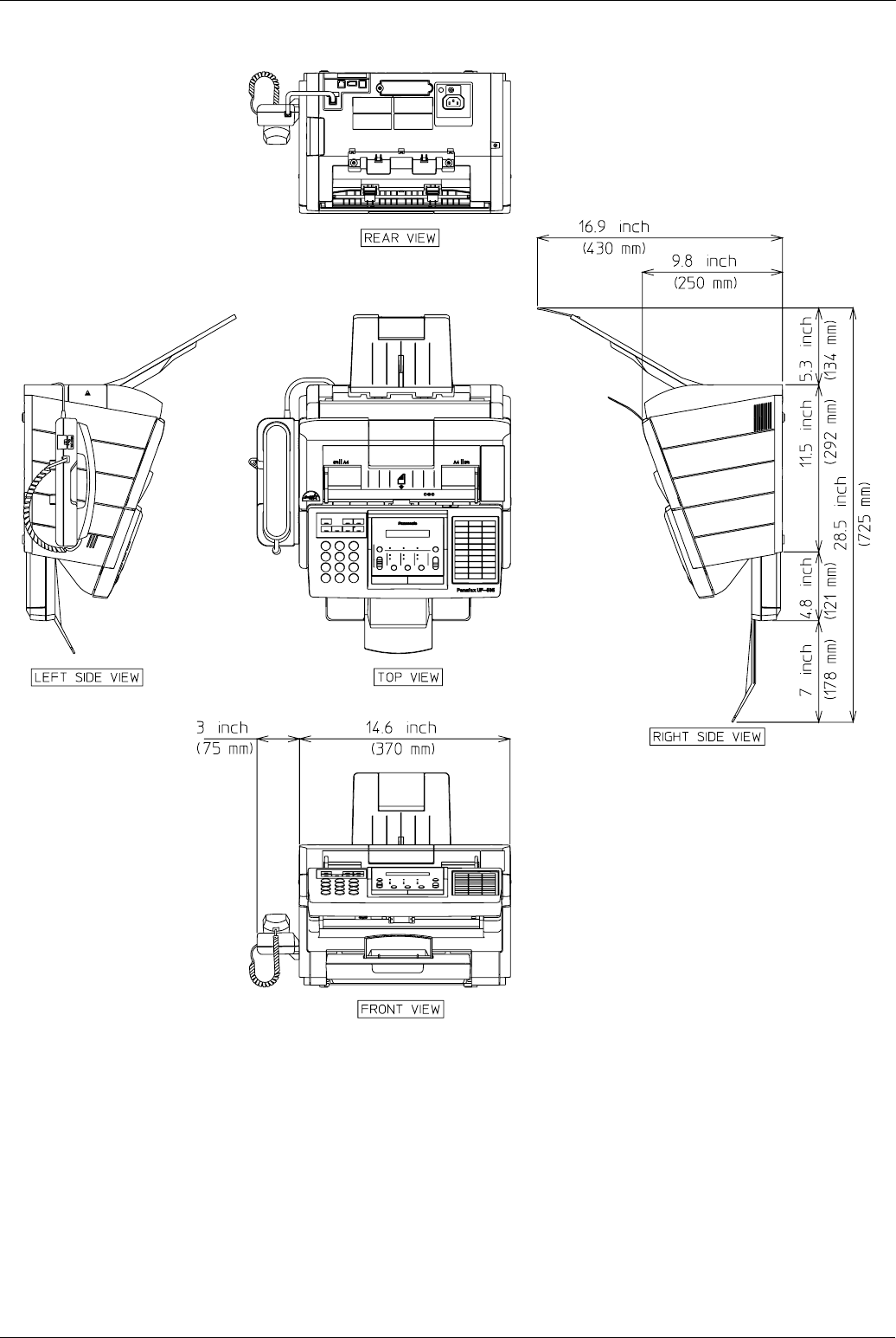
Dimensions (W x D x H) 14.6 x 16.3 x 9.8 in (370 x 413 x 250 mm)
Weight (excluding paper) Approximately 19 lb (8.5 Kg)
General Description
13
1.8.1 External View
Panasonic UF-585 / 595
14
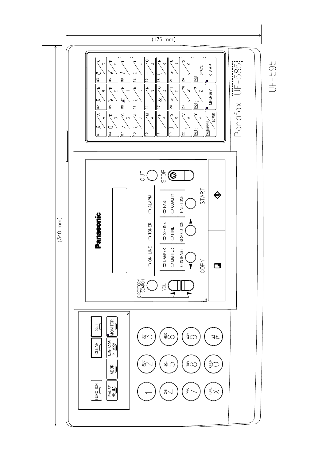
1.8.2 Control Panel
6.9 inch
13.4 inch
General Description
15
1.9 Specification Table
Item UF-585 UF-595
Main Specification
Compatibility G3 ←
PSTN Line Port Yes ←
Modem Speed (kbps) 14.4 - 2.4 33.6 - 2.4
Coding Scheme MH/MR/MMR ←
ECM (Conforms to ITU-T) Yes(MMR) ←
Short Protocol Yes (B) Yes (B,D)
Transmission Speed
(ITU-T Image No.1)
Approx. 6 Seconds Approx. 3 Seconds
Communication Resolution (dpi x lpi)
(Conforms to ITU-T)
Transmission
Std 203 x 98
Fine 203 x 196
S-fine 203 x 391
Reception
Std 203 x 98
Fine 203 x 196
S-fine 203 x 391
Transmission
Std 203 x 98
Fine 203 x 196
S-fine 203 x 391
406 x 391
Reception
Std 203 x 98
Fine 203 x 196
S-fine 203 x 391
406 x 391
Scanner Mechanism
ADF Capacity 30 sheets ←
Max. Document Size 10.1 x 78.7 in
(257 x 2000 mm)
←
Min. Document Size 5.8 x 5.0 in
(148 x 128 mm)
←
Effective Scanning Width 8.3 in (212 mm) (Letter) ←
Scanning Device CCD ←
Scanning Resolution
(dpi x lpi)
Std : 203 x 98 (8 pels x 3.85 lines/mm)
Fine : 203 x 196 (8 pels x 7.7 lines/mm)
S-Fine : 203 x 391 (8 pels x 15.4 lines/mm)
Std : 203 x 98 (8 pels x 3.85 lines/mm)
Fine : 203 x 196 (8 pels x 7.7 lines/mm)
S-Fine : 203 x 391 (8 pels x 15.4 lines/mm)
: 406 x 391 (16 pels x 15.4 lines/mm)
Scanning Speed
(A4 size document, standard resolution)
Approx. 6 seconds ←
Reduction XMT No ←
Collation Stack Yes ←
Printer Mechanism
Recording Method Laser Printing ←
Recording Paper Size A4 / Letter / Legal ←
Recording Paper Capacity 250 sheets ←
Effective Printing Width 202 mm ←
Recording Resolution
(Fax, Copy)
(PC Printing)
406 x 391
300 x 300
406 x 391
300 x 300
600 x 600
Recording Speed 5 ppm ←
Collation Stack Yes ←
Document Memory
Document Memory Capacity 60 pages (1 MB) 1 MB
Optional Document Memory
(Flash Memory Card)
Yes
1 MB : + 80 pages
2 MB : + 160 pages
4 MB : + 320 pages
←
Document Memory Backup Yes (Permanent) ←
Copy Quality
Halftone (Photo) Yes ←
Super Fine (dpi x lpi)
(Tx and Rx)
203 x 391 203 x 391
406 x 391
Contrast Selection (Tx) Yes ←
Smoothing
Yes (Fax, Copy)
No (PC printing)
←
←
Consumable
3 % Black Chart (ITU-T No. 1 chart) Approx, 7500 pages ←
Multiple copy mode
operation environment
20°C, 50%RH ←
Panasonic UF-585 / 595
16
Note:
1. Paper Cassette Configuration
Options
Leased Line Port No ←
V.24 Line Port No ←
Cassette with Feeder Unit
(250 sheets)
No Yes
Document Memory Yes (Flash Memory Card)
(1MB/2MB/4MB)
←
Page Memory No ←
Battery Backup 72 hours No ←
G3 Optional Communication Port No ←
Handset Yes ←
V.24/Encryption Interface No ←
PDL No ←
Parallel Port Interface
Printer Interface (GDI)
Scanner Interface
PC Interface (CFP)
Yes
Yes
Yes
←
←
←
Item UF-585 UF-595
Main Unit
A4/LTR/LGL
250 sheets
Standard
A4:
Letter:
Legal:
8.3 x 11.7 in (210 x 297 mm)
8.5 x 11 in (216 x 279 mm)
8.5 x 14 in (216 x 356 mm)
[13 in Legal (8.5 x 13 in) is not supported]
A4/LTR/LGL
250 sheets
A4/LTR/LGL
250 sheets
With optional 250 sheet Cassette
Main Unit

General Description
17
1.10 Function Table
Item UF-585 UF-595
Dual Operation
Multi-Task Operation Yes ←
Direct XMT Reserve Yes ←
Memory XMT Reserve Yes ←
Max. Number of Memory Job Files 10 files ←
Dialing/Telephone Features
One-Touch keys 24 ←
One-Touch/Program keys 4 ←
One-Touch Auto Dialers 28 ←
Abbreviated Auto Dialers 72 ←
Max. Auto Dialing Locations 100 ←
Max. Tel Number Digits 36 ←
Max. Station Name Digits 15 ←
Directory Search Dialing Yes ←
Full Number Dialing (Buffered Dialing) Yes (Up to 12 stations) ←
Direct Dialing (Monitor Dialing)
(see Note)
Yes ←
Automatic Redialing Yes ←
Manual Redialing Yes ←
Chain Dialing Yes ←
Line Monitor Speaker Yes ←
Pulse/Tone Dialing Yes ←
Pulse to Tone change Yes ←
Flash key Yes ←
Transmission Features
Direct Transmission Yes ←
Memory Transmission Yes ←
Multi-station Transmission Yes (112 stations) ←
Multifile Transmission No ←
Direct Deferred Transmission Yes (10 timers) ←
Deferred Transmission Yes (10 timers / 112 stations) ←
Deferred Multi-station Transmission Yes ←
Priority Direct Transmission Yes ←
Priority Memory Transmission No ←
Batch Transmission No ←
Reception Features
Substitute Reception Yes ←
Fixed Reduction Yes ←
Auto Reduction Yes ←
Overlapping Print Yes ←
Receive to Memory Yes ←
DRD Yes ←
Receive Control
Fax/Tel Auto Switch Yes ←
Silent Reception No ←
External TAM Interface Yes ←
Remote Reception Yes (DTMF) ←
Polling Features
Polling Yes ←
Continuous Polling (Station Mode) Yes ←
Turnaround Polling No ←
Multi-station Polling Yes (112 stations) ←
Deferred Polling Yes (10 timers) ←
Deferred Multi-station Polling Yes (10 timers / 112 stations) ←
Memory Polling Tx Yes (1 file) ←
Preset Polling Password Yes ←
Temporary Polling Password Yes ←
Convenience
Panel Display Yes (20 x 2 Alphanumeric LCD) ←
Voice Contact No ←
Edit File Mode Yes ←
Incomplete File Save Yes ←
Automatic Cover Sheet Yes ←
Copy Features

Panasonic UF-585 / 595
18
Note:
During Monitor Dialing Mode, the START button must be pressed to initiate fax communication. During this mode automatic
Redialing is not available.
Single Copy Yes ←
Multiple Copy Yes ←
Reduction Copy Yes ←
Certainty
Verification Stamp Yes ←
Header/Total Page Print Yes ←
Transaction Journal Yes (32 transactions) ←
Comm. Journal Yes ←
Last Ind. XMT Journal Yes ←
Power Failure Report No ←
List Printouts
One-Touch List Yes ←
Abbr. No. List Yes ←
Program List Yes ←
Directory Search List Yes ←
Fax Parameter List Yes ←
File List Yes ←
Character Code List No ←
Directory Sheet Yes ←
Identification
Logo Yes (25 characters) ←
Multiple Logo No ←
Character ID Yes (16 characters) ←
Numeric ID Yes (20 digits) ←
Special Communication
Password XMT/RCV Yes ←
Select Reception Yes ←
Relay XMT Request Yes ←
Relay XMT Center No ←
Confidential XMT/Polling No ←
Confidential Center No ←
Mailbox XMT/Poling Yes ←
Mailbox Center Yes ←
File XMT No ←
Fax Forward Yes ←
Sub-address XMT Yes ←
Sub-address RCV Yes ←
OMR-XMT No ←
Others
Access Code Yes ←
Department Code No ←
Energy Saver Mode
(Energy Star Compliant)
Yes ←
Day Light Time Save Yes ←
Self Diagnostic Function Yes ←
Remote Diagnostic Function Yes ←
Check & Call Function Yes ←
Item UF-585 UF-595
Panasonic UF-585 / 595
20
2 Disassembly Instruction
2.1 General Disassembly Flowchart
Paper Cassette
2.2
Lithium Battery
(234)
2.2
Open Control
Panel Unit
Open Printer Cover
(XXX)
X.X
NCU PC Board
(402)
2.14
NCU PC Board
(402)
2.14
Low Voltage PSU
(423)
2.14
Fuser Unit
(701)
2.15
Fuser Lamp
(732)
2.16
Exit Roller
(719)
2.16
Fuser Roller
(709)
2.16
Pressure Roller
(706)
2.16
Rear Cover
(XXX)
X.X
Front Cover
(104)
2.3
Scanner Block
(321)
2.9
A4 LED Array
(329)
2.10
Feed Roller
(302)
2.10
ADF Roller
(331)
2.9
Toner Sensor
(513)
2.19
Bias Transfer Roller
(604)
2.20
PRTA PC Board
(536)
2.17
SNS1 PC Board
(615)
2.17
Rear Chassis
(505) Assy
2.17
Feed Roller
(526)
2.18
Transfer Guide
(601)
2.18
Laser Unit
(512)
2.19
SNS3 PC Board
(535)
2.19
Transmit Motor
(324)
2.8
Eject Roller
(303)
2.7
Stamp Solenoid
(327)
2.6
Scanning Glass
(308)
2.5
Open Control
Panel Unit
Transmit Guide
(301) Assy
2.5
Left Cover
(103)
2.3
Right Cover
(102)
2.3
High Voltage PSU
(424)
2.12
Paper Feed Solenoid
(531)
2.12
Printer Motor
(626)
2.13 Clutch Gear Assy
(530)
2.12
Paper Feed Roller
(518)
2.12
Printer Grease Points
2.22
Thermistor Assy
(728)
2.15
Recording Paper Tray
Assy (1007)
2.2
SNS2 PC Board
(534)
2.21
Printer Cover
(106)
2.13
Rear Cover
(105)
2.13
LPC PC Board
(401)
2.11
SCA/SCB PC Board
(422)
2.11
ILS PC Board
(425)
2.11
Control Panel Chassis
(201)
2.4
PNL1 PC Board
(231)
2.4
LCU PC Board
(402)
2.14
LCD Unit
(233)
2.4
SNS4 PC Board
(729)
2.11
Disassembly Instruction
21
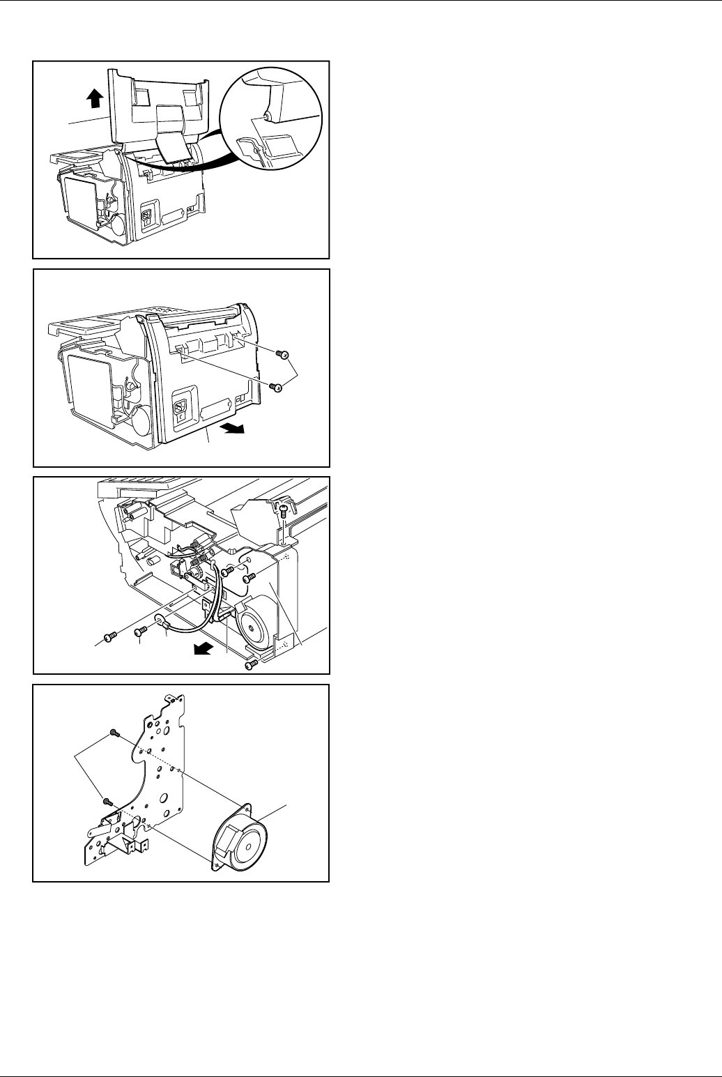
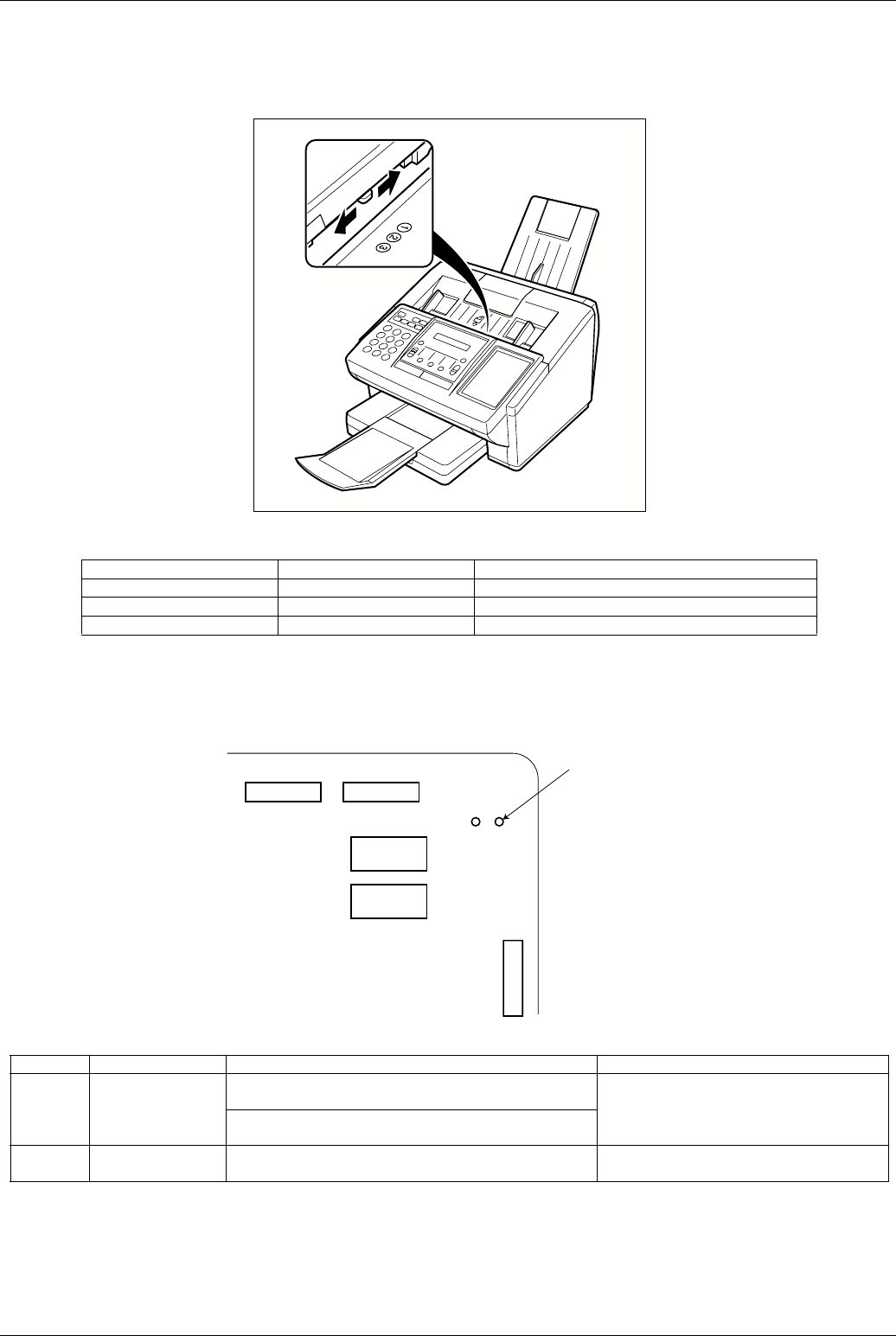
2.2 Power Cord (1008), Telephone Line Cable (1009), Lithium Battery (234),
Recording Paper Tray Assembly (1007), Paper Cassette
(1) Remove the Battery Holder (230).
(2) Release 2 Latch Hooks.
(3) Remove the Lithium Battery (234).
(4) Replace with a new Battery.
Caution:
Dispose of the Lithium Battery properly and keep it away from
small children. When replacing the battery make sure to
obserse the polarity to avoid damage to the machine.
(5) Disconnect the Power Cord (1008).
(6) Disconnect the Telephone Line Cable (1009).
(7) Remove the Recording Paper Tray Assembly (1007).
(8) Remove the Paper Cassette.
(1)
(2)
(3)
(5)
(6)
(7)
(8)
Panasonic UF-585 / 595
22
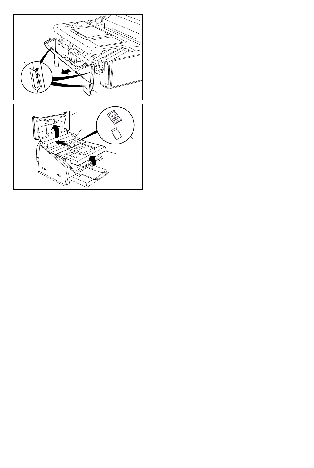
2.3 Left Cover (103), Right Cover (102), Front Cover (104), Speaker (117),
Separation Rubber (207)
(1) Open the Printer Cover (106).
(2) Open the Control Panel Unit.
(3) Remove the Memory Card Cover (110).
(Remove the Memory Card, if installed.)
(4) 2 Screws (B1).
(5) Remove the Left Cover (103).
(6) Disconnect CN9 on the SCA/SCB PC Board (422).
(7) 2 Screws (C2) and 1 Screw (1Y).
(8) Remove the Speaker (117).
(9) 2 Screws (B1).
(10) Remove the Right Cover (102).
(1)
(2)
(3)
(4)
(6)
(5)
(7)
(8)
(9)
(10)
Disassembly Instruction
23
(11) Release 3 Latch Hooks.
(12) Remove the Front Cover (104).
Replacing & Cleaning Separation Rubber
(1) Open the Control Panel Unit.
(2) Open the Printer Cover (106).
(3) Remove the Separation Rubber Holder Assy (202).
(4) Replace with a new Separation Rubber (207).
(5) Clean the Separation Rubber (207) with a soft cloth, soaked
with isopropyl alcohol.
(11)
(12)
(1)
(2)
(3)
(4)
Panasonic UF-585 / 595
24
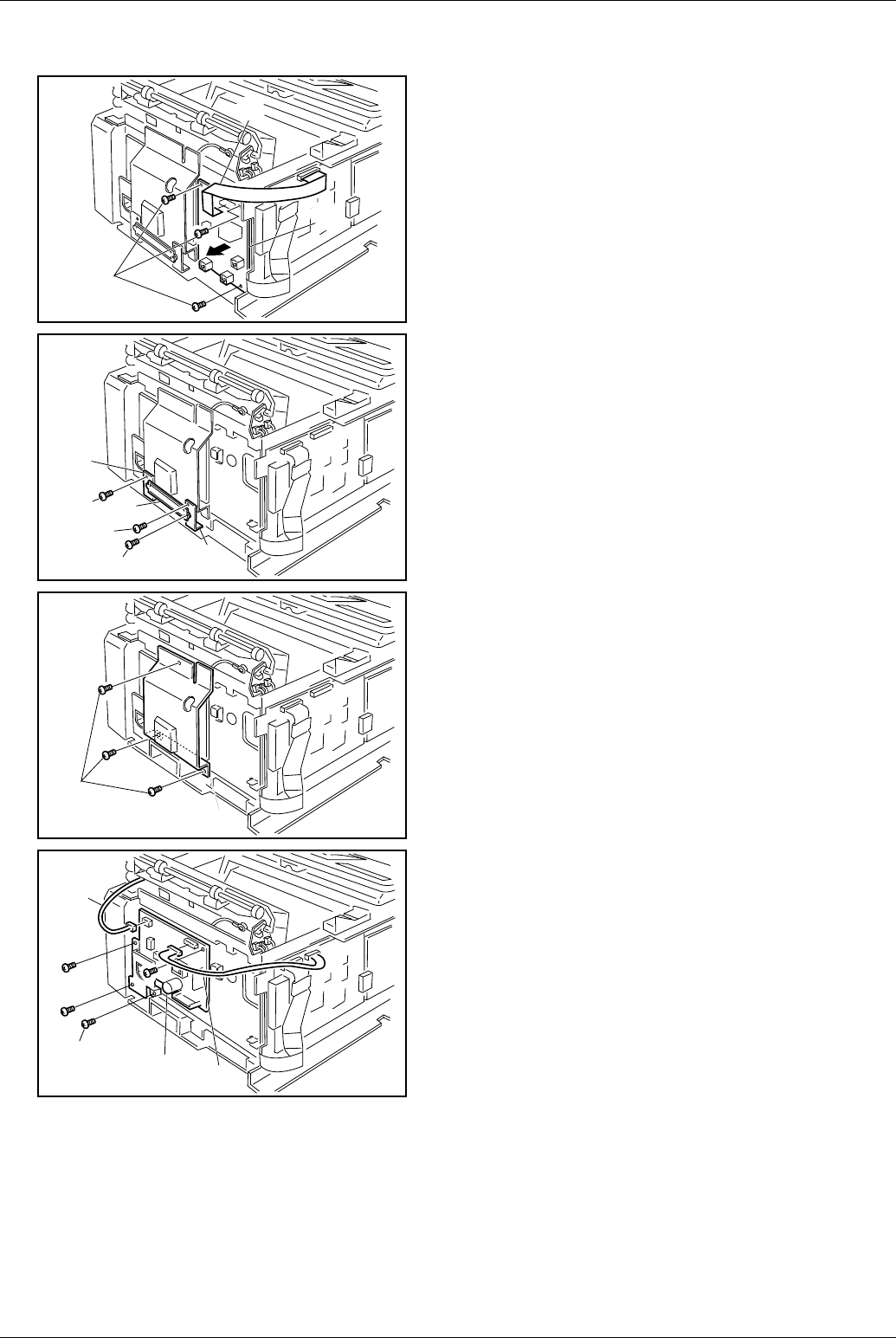
2.4 Control Panel Unit, PNL1 PC Board (231), LCD Unit (233)
(1) Open the Printer Cover (106)
(2) Slightly open the Control Panel Unit.
(3) Remove the Left Cover (103) and the Right Cover (102).
(Refer to 2.3)
(4) Disconnect Connector CN4 on the SCA/SCB PC Board.
(5) Release the Stopper Latch (210) and open the Control
Panel Unit.
(6) Remove the Control Panel Unit.
(7) 2 Screws (19).
(8) Remove the Control Panel Chassis (201) Assembly.
Note:
If noise occurs while scanning, clean the Roller Shaft 2 (235)
and the Feed Pinch Roller (236) shaft hole with isopropyl
alcohol.
(9) 16 Screws (7B).
(10) Disconnect Connector CN40 on the PNL1 PC Board.
(11) Release 1 Latch Hook.
(12) Remove the PNL1 PC Board (231).
(1)
(2)
(5)(5)
(6)
(4)
(5)
(7)
(8)
(9)
(10)
(12)
(11)
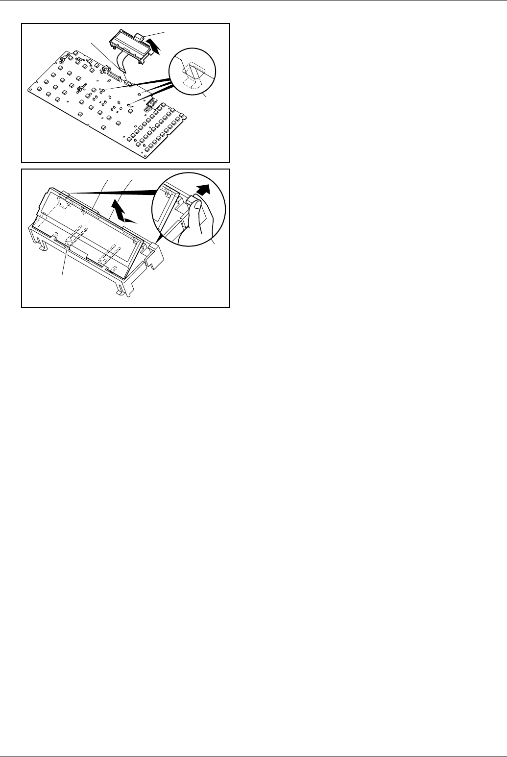
Disassembly Instruction
25
(13) Disconnect the Flat Cable from the Connector CN41 on
the PNL1 PC Board.
(14) Release 3 Latch Hooks.
(15) Remove the LCD Holder (223).
(16) Release 2 Latch Hooks.
(17) Remove the LCD Unit (233).
(13)
(14)
(15)
(16)
(17)
Panasonic UF-585 / 595
26
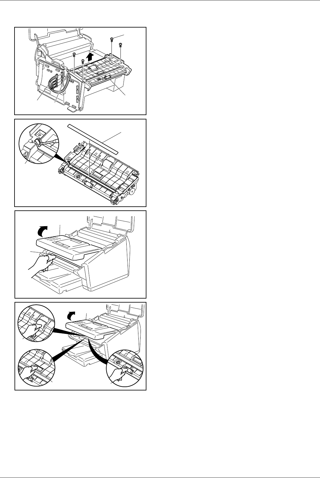
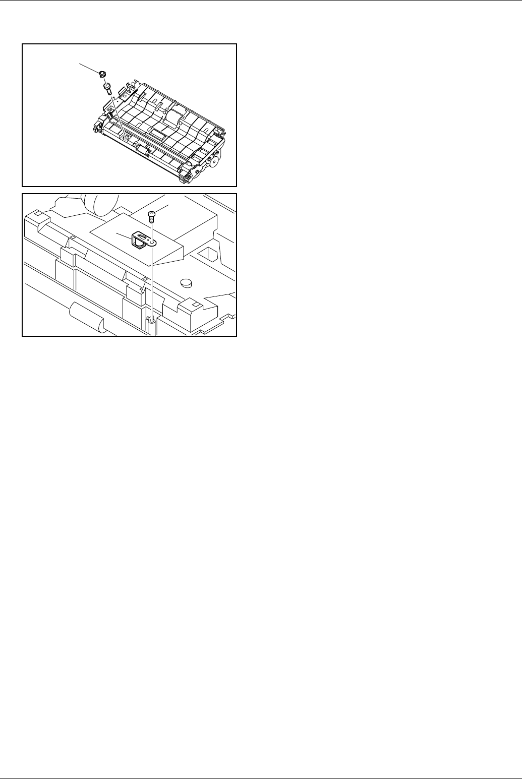
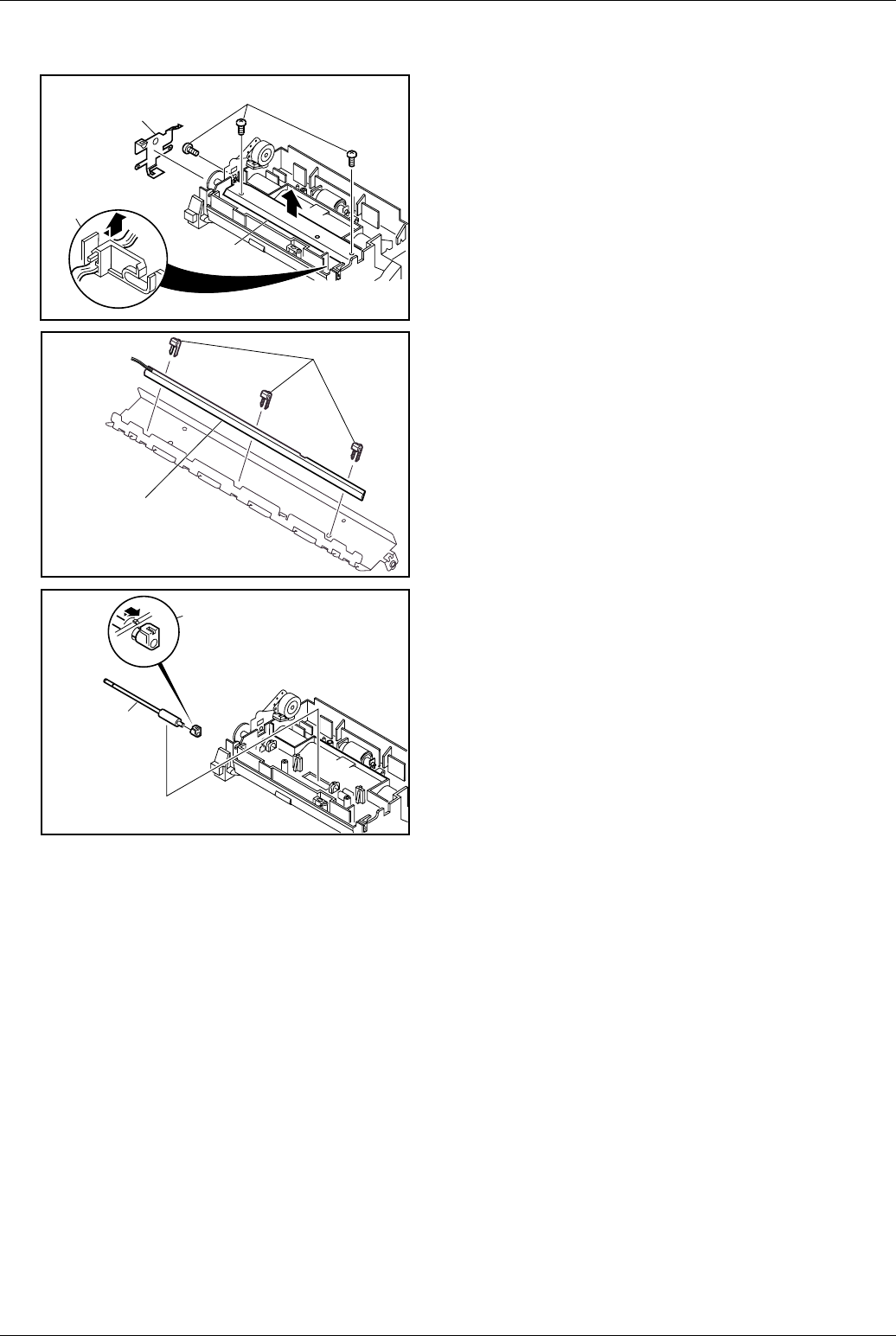
2.5 Transmit Guide (301) Assembly, Scanning Glass (308)
(1) Remove the Left Cover (103), Right Cover (102), and
Front Cover (104) (Refer to 2.3).
(2) Remove the Control Panel Unit (Refer to 2.4).
(3) Release the Harnesses from the clamps.
(4) 4 Screws (19).
(5) Disconnect 4 Connectors (CN1, 3, 5 and 7).
(6) Remove the Transmit Guide (301) Assembly.
(7) Carefully release the Latch Hook using a Blade-tip
Screwdriver.
(8) Remove the Scanning Glass (308).
Cleaning Scanning Glass (308)
(1) Open the Control Panel Unit.
(2) Clean the Scanning Glass (308) with a soft cloth, soaked
with isopropyl alcohol.
Cleaning Feed Roller (302), Eject Roller (303), ADF Roller
(331)
(1) Open the Control Panel Unit.
(2) Clean the Feed Roller (302), Eject Roller (303) and ADF
Roller (331) with a soft cloth, soaked with isopropyl alcohol.
(4)x4
(6)
(5) (3)
(7)
(8)
(1)
(2)
(1)
(2) (2)
(2)
Disassembly Instruction
27
2.6 Stamp Assembly, Stamp Solenoid (327)
(1) Remove the Transmit Guide (301) Assembly
(Refer to 2.5).
(2) Remove the Stamp Assembly (325, 326).
(3) 1 Screw (19).
(4) Remove the Stamp Solenoid (327).
(2)
(3)
(4)
Panasonic UF-585 / 595
28
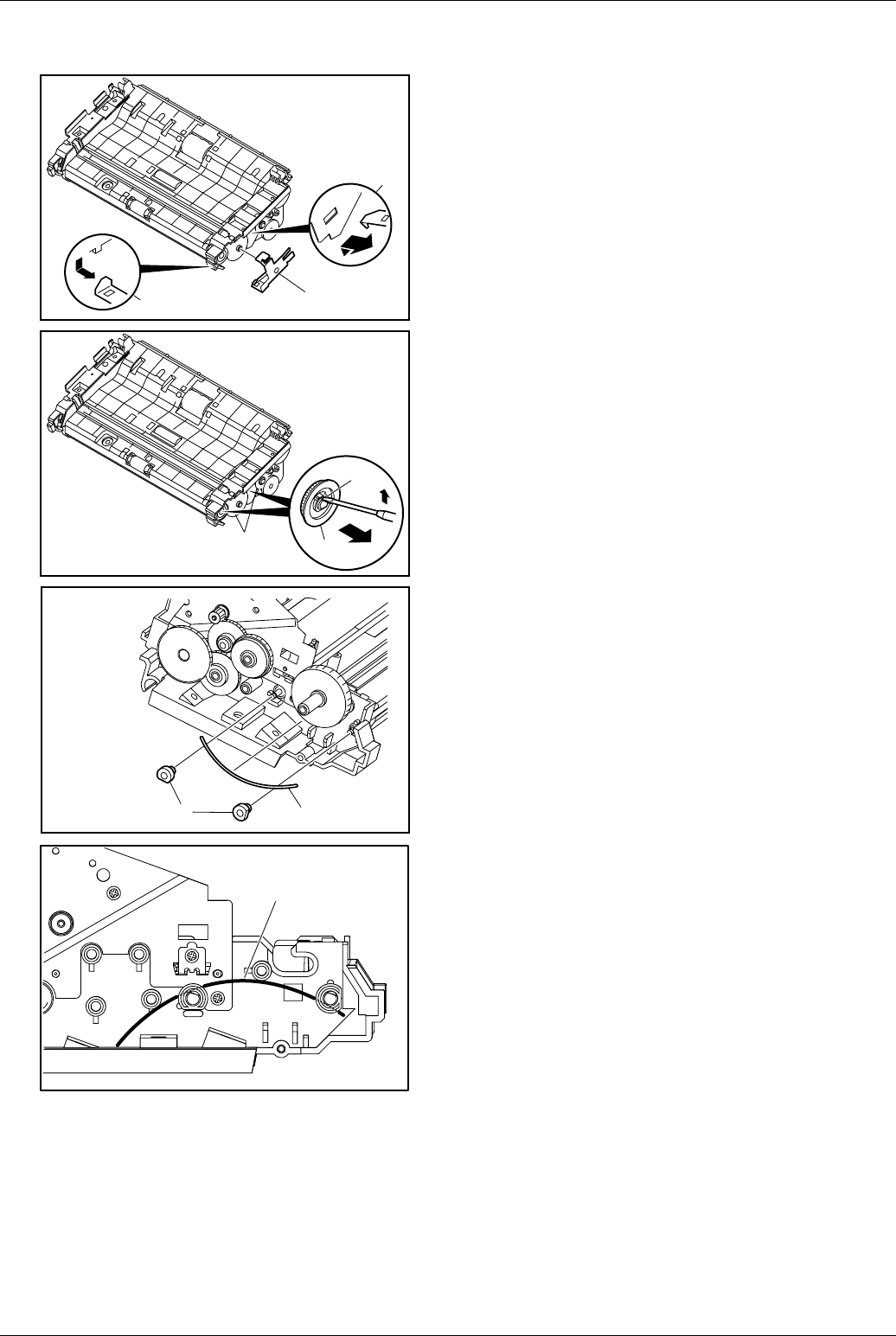
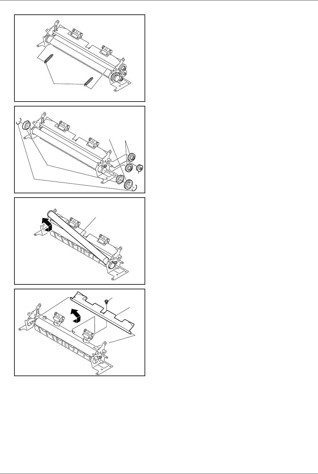
2.7 Eject Roller (303)
(1) Remove the Transmit Guide (301) Assembly
(Refer to 2.5).
(2) Remove the Stamp Assembly (325, 326) (Refer to 2.6).
(3) Release 2 Latch Hooks.
(4) Remove the Ground Plate (317).
(5) Release the Latch Hook by using a small Blade-tip
Screwdriver.
(6) Remove 2 D25F Drive Gears (332).
(7) Remove D17 Gear (313) and D50 Gear (314).
(8) Remove 2 P6C Bushings (342).
(9) Remove the Roller Wire Spring (343).
Caution:
Reinstall the Roller Wire Spring (343) according to the
illustration.
(3)
(3) (4)
(5)
(6)
(7)
(8) (9)
Roller Spring

Disassembly Instruction
29
(10) Remove 2 P6A Bushings (316).
(11) Remove the Eject Roller (303).
(10)
(11)
Panasonic UF-585 / 595
30
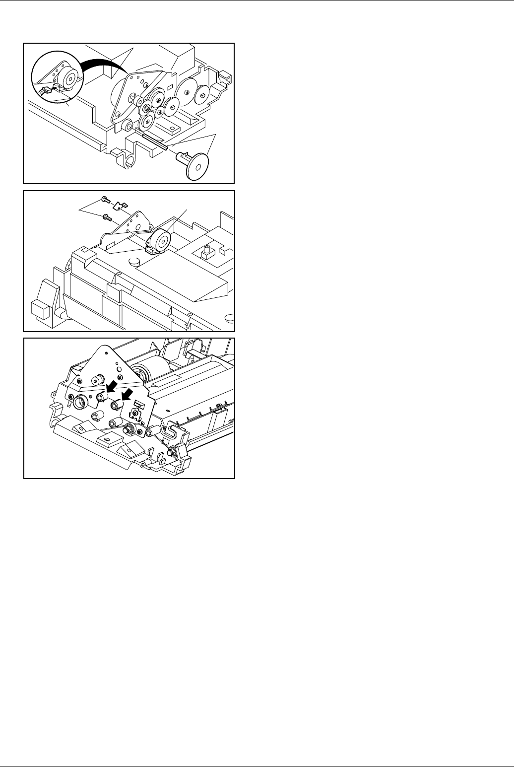
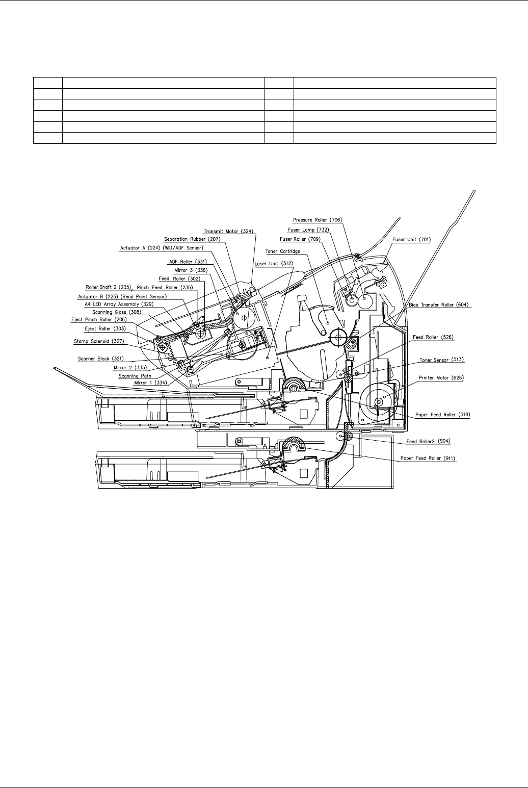
2.8 Transmit Motor (324)
(1) Remove the Transmit Guide (301) Assembly
(Refer to 2.5).
(2) Remove the Stamp Assembly (325, 326) (Refer to 2.6).
(3) Disconnect the Harness (340) from the Transmit Motor.
(4) Remove the ADF Gear (305) and ADF Angular
Shaft (338).
Caution:
When removing the ADF Gear, rotate the Transmit Motor
Gear by hand until the Gear Latch Hook can be seen from the
inside, under the Transmit Motor. Push down on the Latch
Hook to release the ADF Gear.
(5) 2 Screws (19).
(6) Remove the Transmit Motor (324).
Caution:
Reinstall the Transmit Motor (324) according to the direction
shown in the illustration.
Caution:
Before reassembling, apply EM-50L Grease to the Gear Posts
shown by the arrows in the illustration.
(3)
(4)
(5) (6)
Disassembly Instruction
31
2.9 Scanner Block (321), Mirror 1 (334), Mirror 2 (335), Mirror 3 (336), ADF
Roller (331)
(1) Remove the Transmit Guide (301) Assembly (Refer to
2.5).
(2) Remove the Stamp Assembly (325, 326) (Refer to 2.6).
(3) 1 Screw (19).
(4) Remove the Harnesses from the hook.
(5) Remove the Scanner Block (321).
(6) Remove P10 and P6B Bushings (315, 318) by using
Blade-tip Screwdriver.
(7) Remove the ADF Roller (331).
Cleaning Mirror 1 (334), Mirror 2 (335) and Mirror 3 (336)
Clean Mirror 1 (334), Mirror 2 (335) and Mirror 3 (336) with a
soft cloth, soaked with isopropyl alcohol.
(3)
(4)
(5)
(6) (7)
Mirror 1
Mirror 2
Mirror 3
Panasonic UF-585 / 595
32
2.10 A4 LED Array (329), Feed Roller (302)
(1) Remove the Scanner Block (321) (Refer to 2.9).
(2) Remove the Ground Plate (317).
(3) 3 Screws (19).
(4) Release the Harness from the hook.
(5) Remove the LED Bracket (306) Assembly.
(6) Remove 3 LED Clips (307).
(7) Remove the A4 LED Array (329).
Caution:
When reinstalling the A4 LED Array, position the 3 LED Clips
at the appropriate locations.
(8) Remove the Gears, Bushings and the Roller Wire Spring
(Refer to 2.7).
(9) Remove 2 P6A Bushings (316).
(10) Remove the Feed Roller (302).
(2) (3)
(4)
(5)
(6)
(7)
(10)
(9)
Disassembly Instruction
33
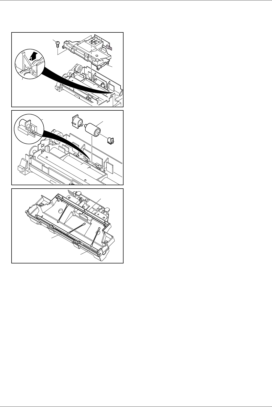
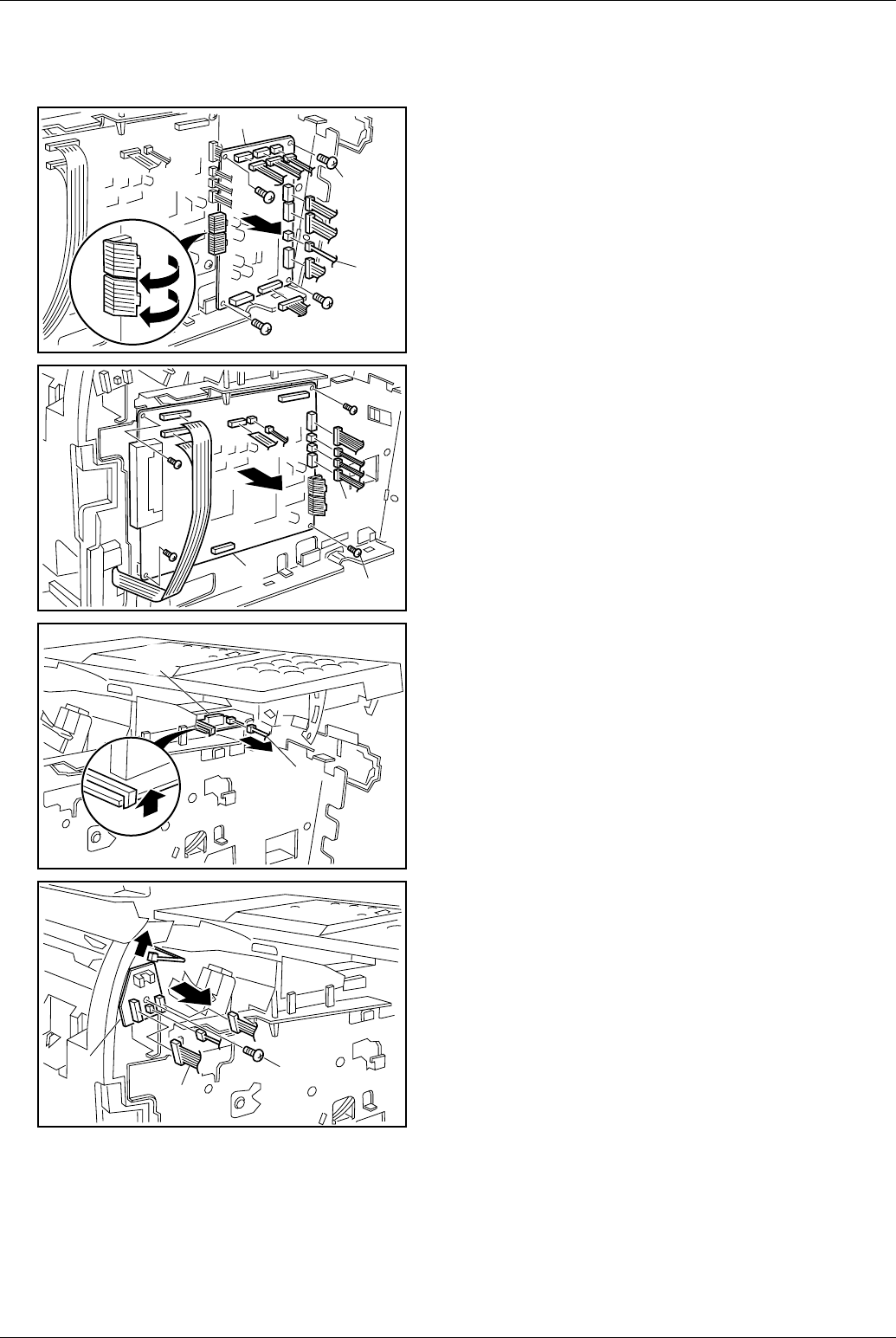
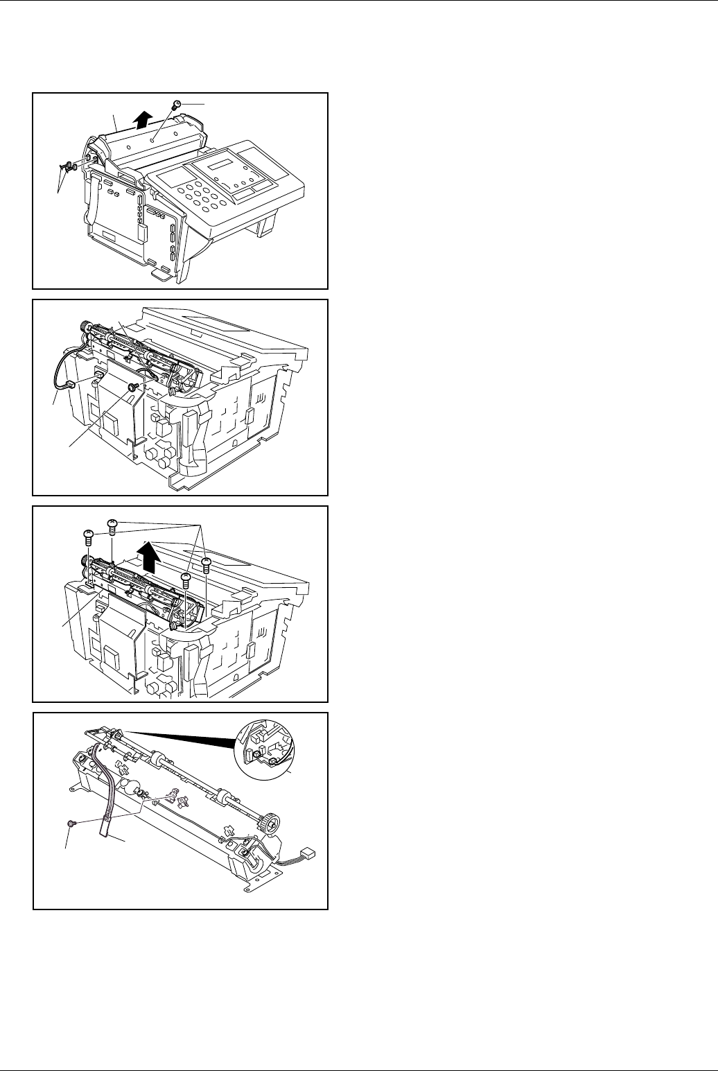
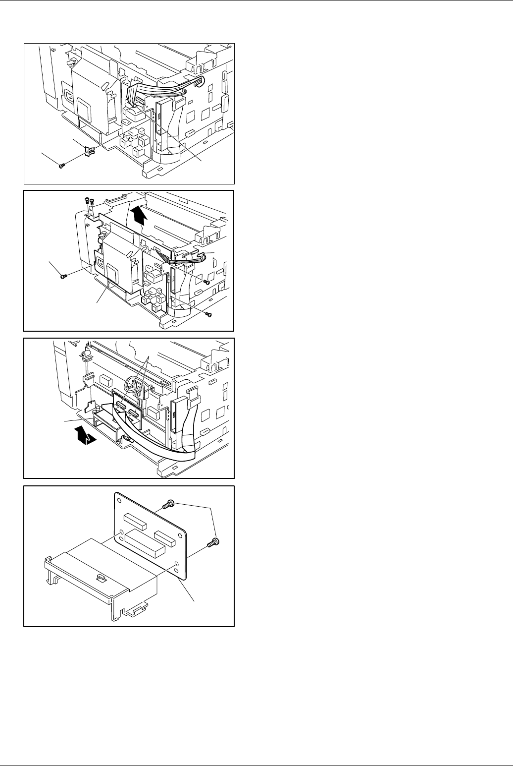
2.11 LPC PC Board (401), SCA/SCB PC Board (422), ILS PC Board (425),
SNS4 PC Board (729)
(1) Remove the Left Cover (Refer to 2.3).
(2) Disconnect all Connectors on LPC PC Board (401).
(3) Release Connectors CN50 and CN67 with your finger as
shown in the illustration.
(4) 4 Screws (19).
(5) Remove the LPC PC Board (401),
(6) Disconnect all Connectors and the Flat Cables on SCA/
SCB PC Board.
(7) 4 Screws (19).
(8) Remove the SCA/SCB PC Board (422).
(9) Move all Harnesses away from the front of the Door Sensor.
(10) Release the Latch Hook and remove the ILS PC Board
(425).
(11) Disconnect Connector CN73 on the ILS PC Board.
(12) Disconnect Connectors CN85, 86 and 87 on the SNS4 PC
Board.
(13) 1 Screw (19).
(14) Lift up the Paper Exit Actuator (730) and remove the
SNS4 PC Board (729).
(4)x4
(5)
(2)
(3)
(7)x4
(8)
(6)
(11)
(11)(11)
(10)
(13)
(12)
(14)
Panasonic UF-585 / 595
34
2.12 High Voltage Power Supply Unit (424), Paper Feed Solenoid (531),
Clutch Gear Assembly (530), Paper Feed Roller (518)
(1) Remove the Right Cover (102) (Refer to 2.3).
(2) Remove the HVPS Sheet (408).
(3) 4 Screws (19).
(4) Disconnect Connector CN39 on the the HVPS Unit.
(5) Remove the HVPS Unit (424).
(6) 1 Screw (19).
(7) Remove the Paper Feed Solenoid (531).
Note:
If the Paper Feed Solenoid does not work properly due to
dust, etc. remove the spring to disassemble and clean the
magnet and plate as shown in the illustration.
(8) 1 Screw (19).
(9) Remove the Feed Roller Ground Spring (628).
(10) Remove the E-Ring (524).
(11) Remove the Clutch Gear Assembly.
(12) Place the machine on its Rear side.
(13) 2 Screws (19).
(14) Remove the Feed Roller Assembly.
(2)
(4)
(5)
(3)x5
(6) (7)
(8)
(9)
(10)
(11)
(13)
(14)
Disassembly Instruction
35
Clean the Paper Feed Rollers (518) with a soft cloth, soaked
with isopropyl alcohol.
(15) 2 Screws (4N).
(16) Remove the Paper Feed Rollers (518).
(15)
(16)
Panasonic UF-585 / 595
36
2.13 Printer Cover (106), Rear Cover (105), Printer Motor (626)
(1) Remove the Left Cover and the Right Cover (Refer to
2.3).
(2) Release the hooks and remove the Printer Cover (106).
(3) 2 Screws (B1).
(4) Remove the Rear Cover (105).
(5) Remove the HVPS Unit (424) (Refer to 2.12)
(6) 1 Screw (19).
(7) Remove the Ground Wire (542).
(8) Remove the Feed Roller Ground Spring (628).
(9) Remove the Connector on the Printer Motor.
(10) 5 Screws (19).
(11) Remove the Motor Bracket (616) Assembly.
Caution:
The Gears underneath may dislodge when the Motor Bracket
is removed.
(12) 2 Screws (4N).
(13) Remove the Printer Motor (626).
(2)
(3)
(4)
(6) (7)
(8)
(9)x5 (10)
(11)
(12)
Disassembly Instruction
37
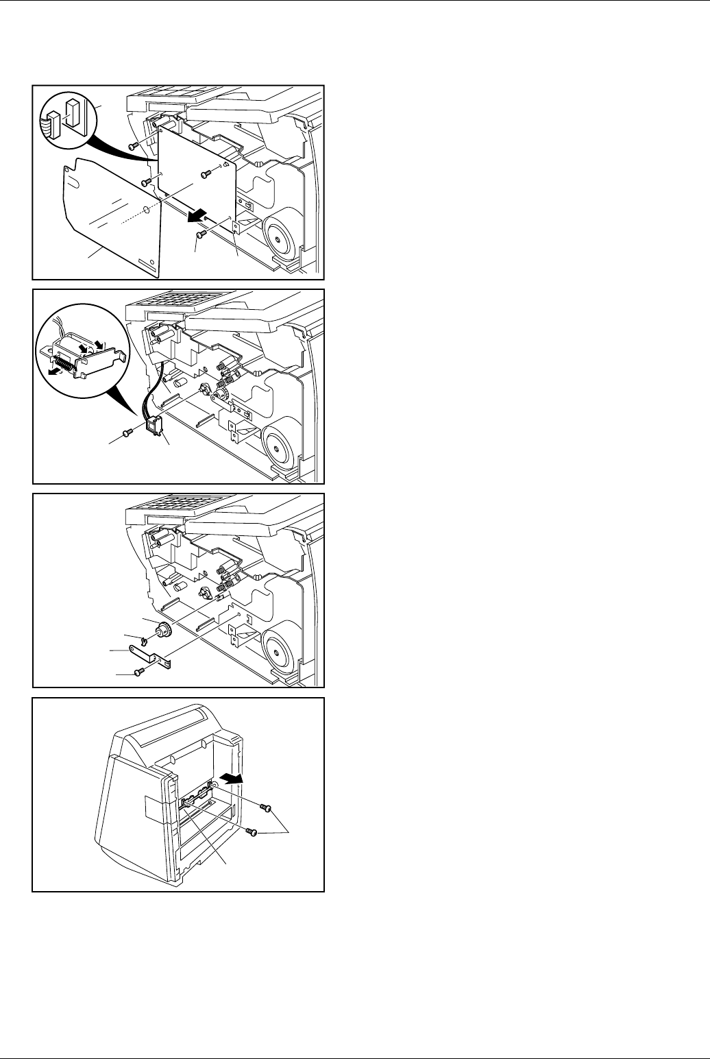
2.14 LCU PC Board (402), Low Voltage Power Supply Unit (423)
(1) Remove the Rear Cover (105) (Refer to 2.13).
(2) Remove the Flat Cable from the Connector CN25 on the
LCU PC Board.
(3) 3 Screws (B5).
(4) Remove the LCU PC Board (402).
(5) 1 Screw (B1).
(6) Remove the Parallel Port I/F Cover (113).
(7) 1 Screw (19).
(8) Remove the Right Printer I/F Bracket (406).
(9) 1 Screw (19).
(10) Remove the Left Printer I/F Bracket (405).
(11) 3 Screws (19).
(12) Remove the LVPS Protection Cover (404).
(13) Disconnect Connectors CN31 and CN33 on the LVPS Unit.
(14) 4 Screws (19).
(15) Remove the LVPS Unit (423).
(2)
(4)
(2)
(3)
(4)
(2)
(4)
(2)
(4)
(8)
(5)
(7)
(6)
(9)
(10)
(11)
(12)
(15)
(13)
(13)
(14)x4
Panasonic UF-585 / 595
38
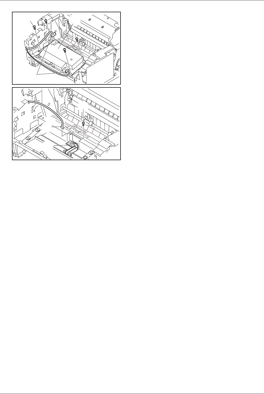
2.15 Fuser Unit (701), Thermistor Assembly (728)
CAUTION:
To prevent getting burned, do not install, remove, clean or adjust when the Fuser Unit is hot.
(1) Remove the Rear Cover (Refer to 2.13).
(2) 1 Screw (19).
(3) Remove the Fuser Top Cover (733).
(4) Disconnect Connectors CN85 and CN87 on the SNS4 PC
Board (729).
(5) Disconnect Connector CN31 on LVPS Unit (423).
(6) 1 Screw (4N).
(7) Remove the FG1 Harness (629).
(8) 4 Screws (19).
(9) Remove the Fuser Unit (701).
(10) Disconnect Connector CN86 on the SNS4 PC Board (729).
(11) 1 Screw (1Q).
(12) Remove the Thermistor Assembly (728).
Caution:
The Thermostat and Thermal Fuse are not available as Spare
Parts. If they become defective, replace the entire Fuser Unit.
(2)
(3)
(4)
(5)
(6)
(7)
(8)
(9)
(10)
(11) (12)
Disassembly Instruction
39
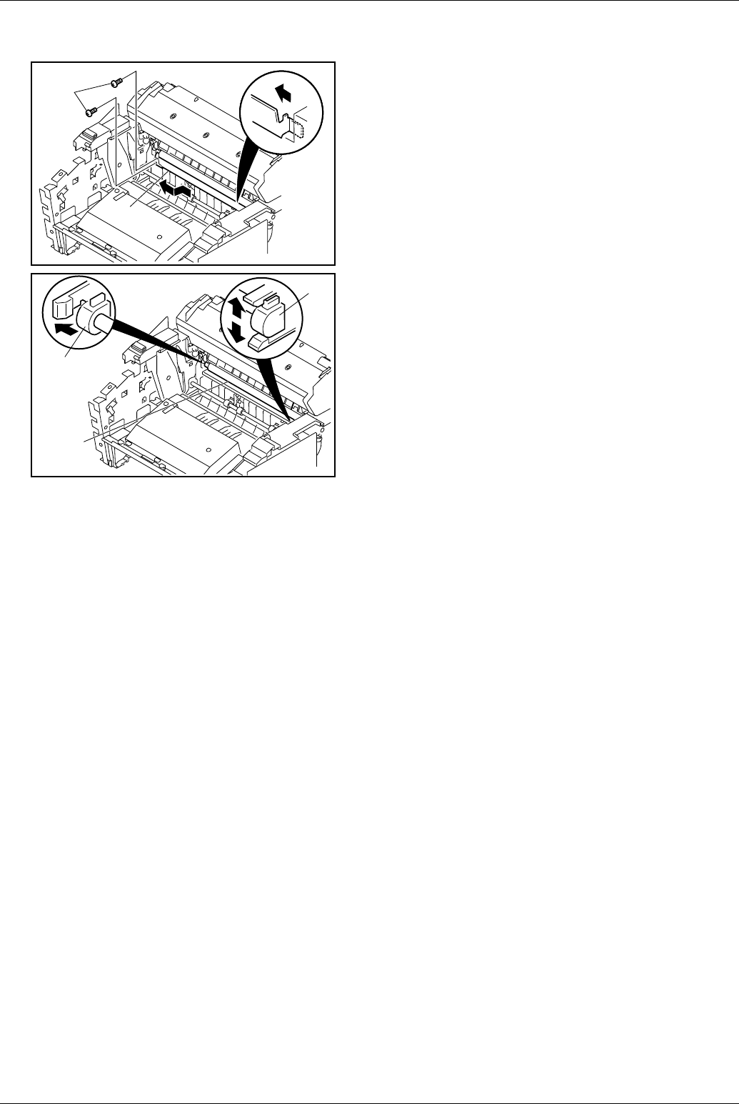
2.16 Fuser Lamp (732), Exit Roller (719), Fuser Roller (709),
Pressure Roller (706)
(1) Remove the Rear Cover (Refer to 2.13) and the Fuser Unit
(Refer to 2.15).
(2) 1 Screw (4N).
(3) Remove the LVPS-Fuser Harness (727) and Fuser Lamp
Terminal B (731).
(4) Remove the Fuser Lamp (732).
Caution:
When reinstalling the Fuser Lamp, make sure that the Fuser
Lamp is inserted into the Fuser Unit as illustrated. Do not
touch the glass portion of the Fuser Lamp with bare hands.
Grease from fingerprints will shorten its life cycle, use isopro-
pyl alcohol to clean fingerprints.
Caution:
When reinstalling the Fuser Lamp, make sure that both ends
of the Fuser Lamp fits into the projected area of the Fuser
Lamp Terminal A (724) and the Fuser Lamp Terminal B
(731).
(5) Remove the E22 Gear (722).
Caution:
You may need to use force to pull out the Gear.
(6) Remove the Right and Left P3.5L11.2 Bushings (720 and
721).
(7) Remove the Exit Roller (719).
(8) 2 Screws (4N).
(9) Remove the Fuser Cover (723).
(2)
(3) (4)
White
Black (6)
(7)
(5)
(8)
(9)
Panasonic UF-585 / 595
40
(10) Remove 2 Pressure Springs (708).
(11) Remove the E14 Gear (714).
Caution:
You may need to use force to pull out the Gear.
(12) Remove the 2 E18 Gears (713).
(13) Remove 2 C-Rings (712).
(14) Remove the E24 Drive Gear (711).
(15) Remove 2 P17L6.8 Bushings (710).
(16) Remove the Fusert Roller (709).
Caution:
Do not scratch the surface of the Fuser Roller when removing
or reinstalling it.
(17) 1 Screw (4N).
(18) Remove the Lower Paper Exit Guide (703).
(10)
(13)
(15) (11)
(12)
(14)
(16)
(17)
(18)

Disassembly Instruction
41
(19) Remove 2 P6L5.5 Bushings (707).
(20) Remove the Pressure Roller (706).
Caution:
Do not scratch the surface of the Pressure Roller when
removing or reinstalling it.
(19)
(20)
Panasonic UF-585 / 595
42
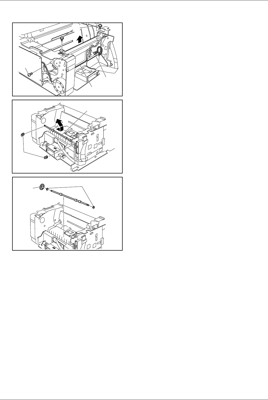
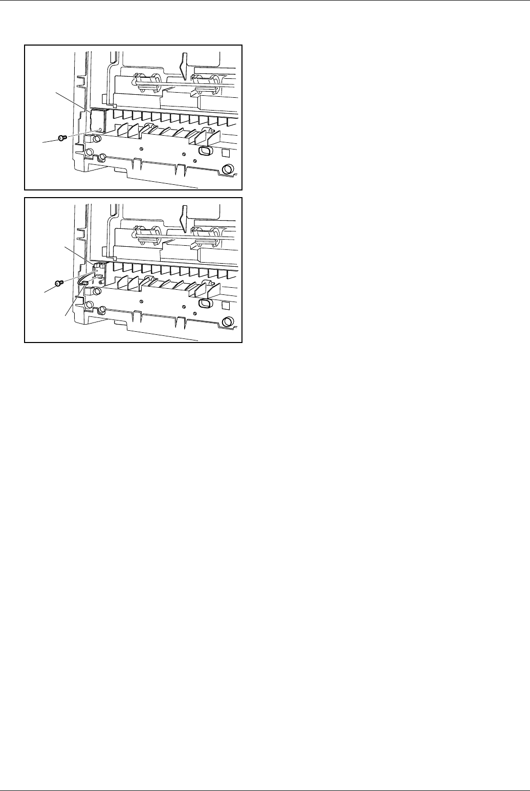
2.17 Rear Chassis (505), PRTA PC Board (536), SNS1 PC Board (615)
(1) Remove the Fuser Unit (701) (Refer to 2.15).
(2) 1 Screw (19).
(3) Remove the Memory Card Ground Plate (516).
(4) Remove the Parallel Port I/F Cover (113), Left and Right
Printer I/F Brackets (405, 406) (Refer to 2.14).
(5) Disconnect Connector CN25 on the LCU PC Board (402).
(6) Disconnect Connector CN6 on the SCA/SCB PC Board
(422).
(7) 5 Screws (19).
(8) Remove the Rear Chassis (505) Assembly.
(9) Disconnect SCA/SCB-PRTA Flat Cables (421) on the
PRTA PC Board (536).
(10) Release the Latch Hooks and remove the Printer I/F PCB
Guide (532) Assembly.
(11) 2 Screws (19).
(12) Remove the PRTA PC Board (536).
(2)
(3)
(5)
(7)x5
(8)
(6)(6)(6)
(9)(9)
(10)
(9)
(11)
(12)

Disassembly Instruction
43
(13) Disconnect Connectors CN80 and CN81on the SNS1 PC
Board (615).
(14) 1 Screw (19).
(15) Remove the SNS1 PC Board (615).
(15)
(14)
(13)
Panasonic UF-585 / 595
44
2.18 Transfer Guide (601) Assembly, Feed Roller (526)
(1) Remove the Rear Chassis (Refer to 2.17).
(2) 2 Screws ( C8).
(3) 1 Screw (19).
(4) Disconnect Connector CN80 on the SNS1 PC Board (615).
(5) Remove the Transfer Guide (601) Assembly.
(6) Remove the 2 E-Rings. (524).
(7) Remove the Feed Roller (526).
(8) Remove the Roller Gear (529).
(9) Remove 2 P6L5 Bushings (527, 528).
(2)(2)
(3)
(5)
(4)
(2)
(6)
(7)
(8) (9)
White
Black
Disassembly Instruction
45
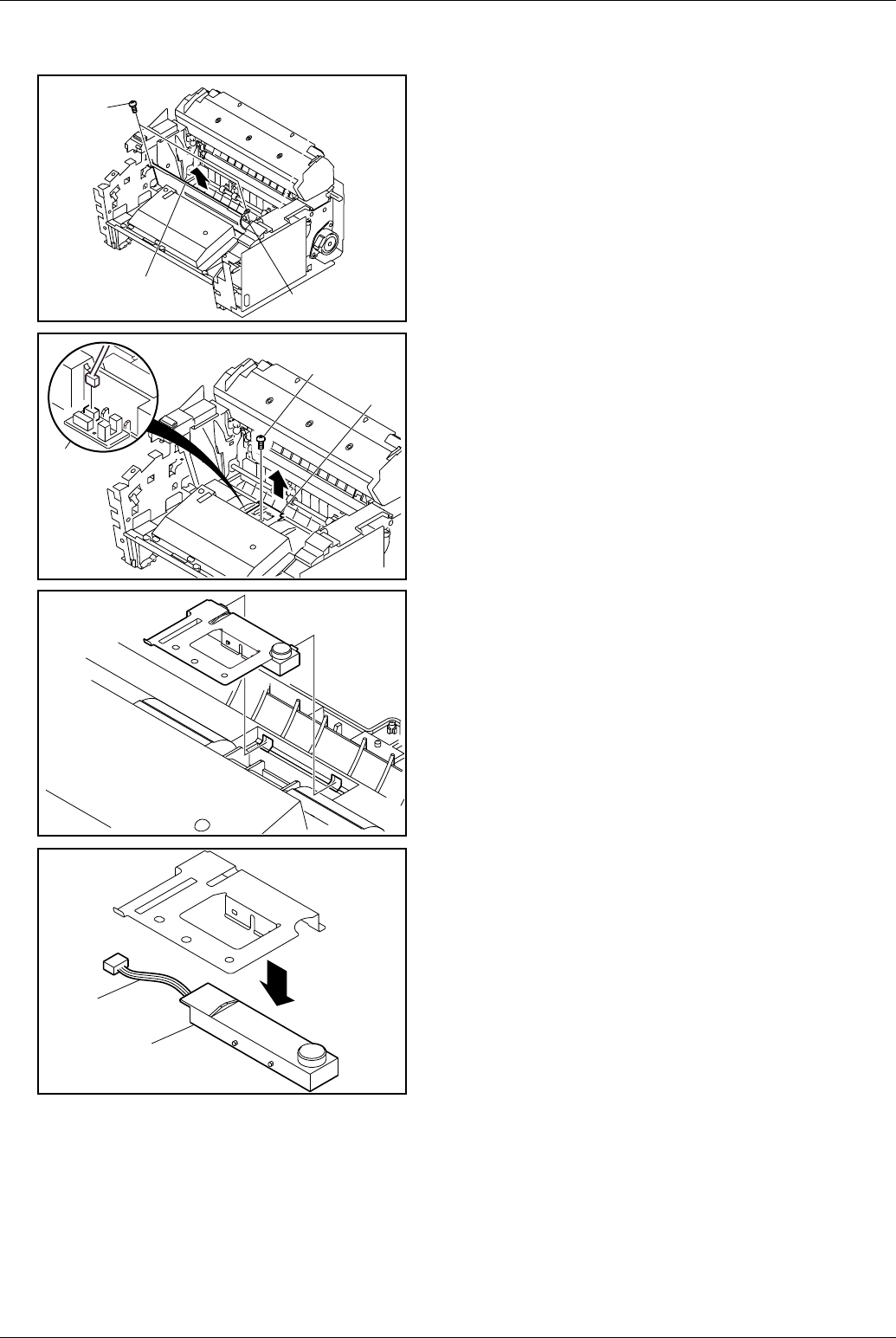
2.19 Toner Sensor (513), Laser Unit [LSU] (512), SNS3 PC Board (535)
(1) Remove the Transmit Guide Assembly (Refer to 2.5).
(2) 2 Screws (19).
(3) Remove Ground Wire (542).
(4) Remove the CCD Shield Plate (533).
(5) 1 Screw (19).
(6) Disconnect Connector CN84 on the SNS3 PC Board.
(7) Remove the Toner Sensor Spring Plate (506) Assembly.
Note:
When reinstalling, make sure that the Toner Sensor Spring
Plate is inserted into the 2 notches in the main frame as
shown in the illustration.
(8) Remove the Toner Sensor (513).
(9) Disconnect the Connector on the Toner Sensor.
(2)
(4) (3)
(6)
(5)
(7)
(8)
(9)
Panasonic UF-585 / 595
46
(10) Disconnect 2 Connectors on the Laser Unit (512).
(11) 4 Screws (1Y).
(12) Remove the Laser Unit (512).
(13) Disconnect Connectors CN83 and CN84 on the SNS3 PC
Board (535).
(14) 1 Screw (19).
(15) Lift up the No Paper Actuator (525) and Remove the SNS3
PC Board (535).
(10)
(11)(11)
(11)x4 (12)
(14)(14)
(13)
(13)(13)
(14)
(15)
Disassembly Instruction
47
2.20 Bias Transfer Roller (604)
(1) Remove the CCD Shield Plate (Refer to 2.19).
(2) 2 Screws (19).
(3) Remove the BTR Guide (602).
(4) Release the Latch Hook on the Transfer Guide (601)
Assembly as illustrated and remove the Bias Transfer
Roller (604).
Caution:
• Do not touch the surface of the Bias Transfer Roller. Clean
the Bias Transfer Roller only with a dry cloth.
• When cleanning or replacing the Bias Transfer Roller,
clean both sides of the Transfer Guide with isopropyl alco-
hol.
(2)
(3)
(4)
White
Black
Panasonic UF-585 / 595
48
2.21 SNS2 PC Board (534)
(1) Place the machine on its rear side.
(2) 1 Screw (19).
(3) Remove the Plate A (507).
(4) 1 Screw (19).
(5) Remove the SNS2 PC Board (534).
(6) Disconnect Connector CN82 (538) on the SNS2 PC Board.
(3)
(2)
(5)
(4)
(6)

Disassembly Instruction
49
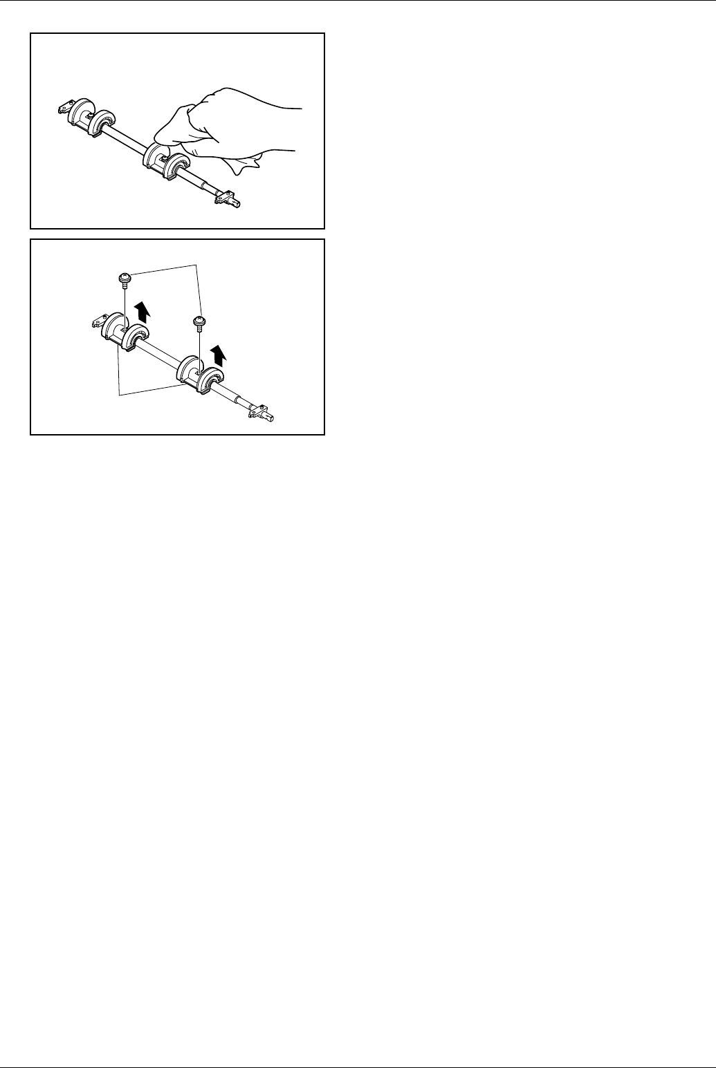
2.22 Printer Grease Points
Before reassembling, apply EM-50L Grease to the parts shown
in the illustration.
(1) Gear G, B83D22 (622) : Gear surface
(2) Gear B, D60D20 (621) : Rib surface
(3) Gear F, D55 (619) : Gear surface
(4) Gear F, D55 (619) : Gear Side surface
(1)
(2)
(3)
(4)
Panasonic UF-585 / 595
50
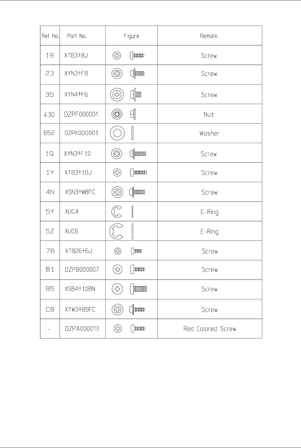
2.23 Screw Identification Template
Panasonic UF-585 / 595
52
3 Maintenance, Adjustments and Check Points
3.1 Required Tools
3.2 Periodic Maintenance Points
No.ToolNo.Tool
1 Soft Cloth 6 Tweezer
2 Isopropyl Alcohol 7 Pliers
3 Phillips Screwdriver (#2) 8 Cotton Swab
4 Stubby Phillips Screwdriver (#2) 9 Brush
5 Blade-tip Screwdriver (3/32 in) 10 Molykote EM-50L Grease (Dow Corning)
Maintenance, Adjustments and Check Points
53
3.3 Periodic Maintenance Check List
The chart outlined below is a general guideline for maintenance. The example list is for an average usage of 50 transmitted and
received documents per day. Needless to say, the environmental conditions and actual use will vary these factors.
The chart below is for reference only.
Note:
The number of pages is based on the ITU-T Image No. 1 test chart at Multi-Copy mode.
Operation environment 20°C, 50%RH.
Parts Description Cleaning Replacement / Adjustment
Cycle Method Cycle Method
Receiver Unit
Printer Motor (626) - 100,000 documents Page 36
Toner Cartridge - - approx 7,500 pages
(See Note)
Paper Feed Roller (518)(911) 12 months or 10,000 documents Page 34 30,000 documents Page 34
Feed Roller (526) (904) 12 months or 10,000 documents Page 44 -
Bias Transfer Roller (604) 12 months or 10,000 documents Page 47 30,000 documents Page 47
Fuser Unit (701) When replacing Print Cartridge Cleaning chart 50,000 documents Page 38
Fuser Roller (709) When the Recording Paper wraps
itself around the roller.
Page 39 (Included as part of
the Fuser Unit)
Page 39
Pressure Roller (706) When the Recording Paper wraps
itself around the roller.
Page 39 (Included as part of
the Fuser Unit)
Page 39
Transmitter Unit
Roller Shaft 2 (235) 30,000 documents Page 24 -
Feed Pinch Roller (236)
* Shaft Hole
30,000 documents Page 24 -
ADF Roller (331) 12 months or 10,000 documents Page 26 30,000 documents Page 31
Separation Rubber (207) 12 months or 10,000 documents Page 23 30,000 documents Page 23
Feed Roller (302) 12 months or 10,000 documents Page 26 30,000 documents Page 32
Eject Roller (303) 12 months or 10,000 documents Page 26 30,000 documents Page 28
Scanning Glass (308) 12 months or 10,000 documents Page 26 -
Mirrors (334, 335, 336) 12 months or 10,000 documents Page 31 -
Transmit Motor (324) - 100,000 documents Page 30
"x" Stamp Head (325) - 5,000 documents Page 27

Panasonic UF-585 / 595
54
3.4 Updating the Firmware
Unlike other machines with removable EPROM (Erasable Programmable ROM), this machine is equipped with an F-ROM (Flash
ROM). F-ROM offers the flexibility of quick and easy firmware updates, creation of a master firmware card, backup and restore of
firmware and machine parameters.
The following is the basic procedure to update the firmware of the machine. The details are described in the Firmware Update Kit
User’s Guide.
3.4.1 Creating a Master Firmware Card
A. Utilizing the Firmware Update Kit.
1. Install the Firmware Update Kit. (Order No.: UE-406052)
2. Install a Flash Memory Card (2 MB or higher) into the machine.
3. Follow the instructions included in the Firmware Update Kit User’s Guide.
B. Copy the Firmware from an Existing Machine
1. Unplug the Power Cord to turn the machine OFF.
2. Install a Flash Memory Card (2 MB or higher) into the machine with the Panasonic Logo facing outwards.
3. Plug in the Power Cord to turn the machine ON.
4. Perform the Service Mode 9-2 (Firmware Backup).
5. The firmware is copied into the Flash Memory Card.
6. After the backup is completed, press "STOP" to return to standby.
7. Unplug the Power Cord to turn the machine OFF.
8. Remove the Master Firmware Card that you just created from the machine.
9. Plug in the Power Cord to turn the machine ON.
10. Use this Master Firmware Card to update the firmware on other machines.
3.4.2 Updating the Firmware using the Master Firmware Card
1. Before starting, print the Fax and Function Parameter Lists.
2. Unplug the Power Cord to turn the machine OFF.
3. Install the appropriate Master Firmware Card into the machine with the Panasonic Logo facing outwards.
4. Plug in the Power Cord to turn the machine ON.
5. Perform the Service Mode 9-1 (Firmware Update).
6. The firmware is copied into the machine.
7. After the update is completed, the machine reboots itself and returns to standby.
8. Perform the Service Mode 6 (Parameter Initialization).
9. Unplug the Power Cord to turn the machine OFF.
10. Remove the Master Firmware Card from the machine.
11. Plug in the Power Cord to turn the machine ON.
12. Reprogram the Fax and/or Function Parameters according to the lists printed in Step 1 above if the settings
are other than factory default.
3.4.3 Erasing the Master Firmware Card
1. Unplug the Power Cord to turn the machine OFF.
2. Install the Master Firmware Card into the machine with the Panasonic Logo facing outwards.
3. Plug in the Power Cord to turn the machine ON.
4. Perform the Service Mode 9-5 (PC → Flash Card).
5. The firmware is erased from the card and the following message is shown on the display:
6. Press "STOP" twice to return to standby.
7. Unplug the Power Cord to turn the machine OFF.
8. Remove the blank Flash Memory Card from the machine.
9. Plug in the Power Cord to turn the machine ON.
PRESS SET TO START
READY TO PROGRAM

Maintenance, Adjustments and Check Points
55
3.4.4 Firmware Version
UF-585 A A V10000 AU
Country Code
AU : USA
AC : Canada
Firmware Version
Language
A: US English, C-French & Spanish
Firmware Type
A : Standard
B : Optional
Model Number
Panasonic UF-585 / 595
56
3.5 ADF Pressure
• When documents multi-feed, move the pressure Adjusting Lever to the 3 (H) position.
• When documents do not feed properly, move the Pressure Adjusting Lever to the 1 (L) position.
3.6 Printer Unit Test
1. Short the Test Pattern Print Switch (SW1) solder connection points on the LPC PCB as shown below.
2. The Test Pattern prints. Check the print Quality.
Note:
When the unit is in Sleep Mode, Fax Parameter No. 34 (Power Saver Timer) is ON, the unit will not print the test pattern.
Press any key on the control panel to wake up the unit, then complete the procedure.
Position Pressure of separator Situation
1 (L) Low When the documents misfeed
2 (M) Medium Normal Position (Factory set position)
3 (H) High When the documents multi-feed
Pattern Selection method Stop method
Pattern 0 1-dot Horizontal line Short SW1 solder connection points for less than 2 seconds
(400 dpi printing)
Short SW1 solder connection points again for
less than 2 seconds
Short SW1 solder connection points for 2 seconds or more
(600 dpi printing)
Pattern 1 Blank page Short SW1 solder connection points for 2 seconds or more
while the Pattern 0 is printing
Short SW1 solder connection points again for
less than 2 seconds
LPC PCB
CN59 CN57
SW1
Test Pattern Switch Solder
Connection Points
IC3
Q19
CN69
Maintenance, Adjustments and Check Points
57
3.7 General Circuit Diagram
3.7.1 Fax Circuit
PRTA
(Printer
Terminal
Board)
(536)
STAMP
SOLENOID (327)
LED ARRAY (329)
SPEAKER
(117)
Parallel
Port
(Centronics)
36 pin
*CONTINUED ON NEXT PAGE
TRANSMIT
MOTOR
(324)
(231)
SENSORS:
ADF Sensor
RP Sensor
B4 Sensor
ADF Door
Sensor
KEYS:
Ten keys
One-touch keys
Program keys
etc...
(337)
(402)
(124)
Panasonic UF-585 / 595
58
3.7.2 Printer Circuit
PRINTER
MOTOR
(626)
(422)
(401)
PAPER FEED
SOLENOID
(531)
* OPTIONAL 2ND CASSETTE
(512)
(921) (923)
(535)
(729)
(424) (423)
(615)
(534)
PAPER FEED
SOLENOID
(908)
(513)
FUSER LAMP (732)
FUSER UNIT
(701)
THERMISTOR (728)
THERMOSTAT THERMAL
FUSE
Maintenance, Adjustments and Check Points
59
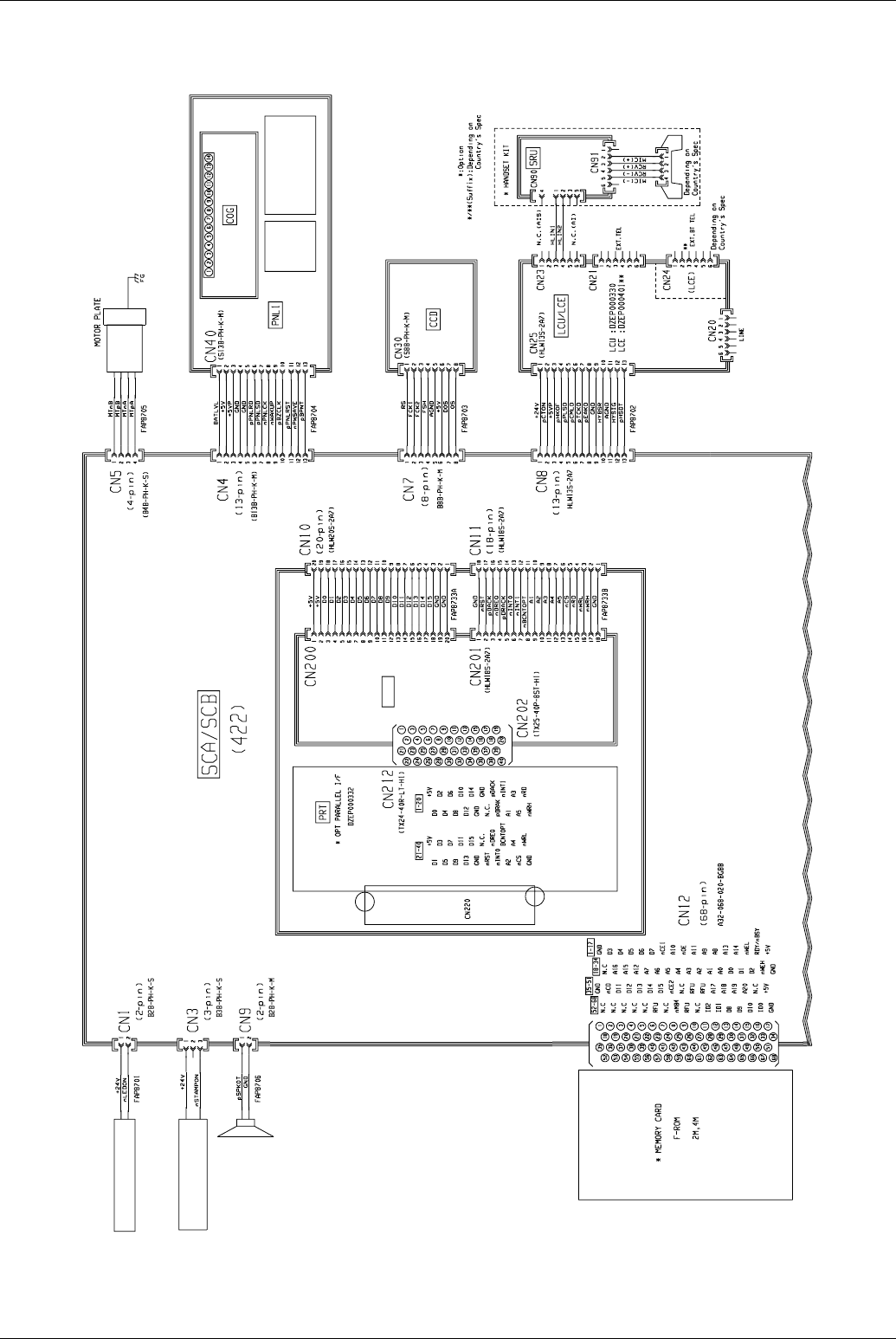
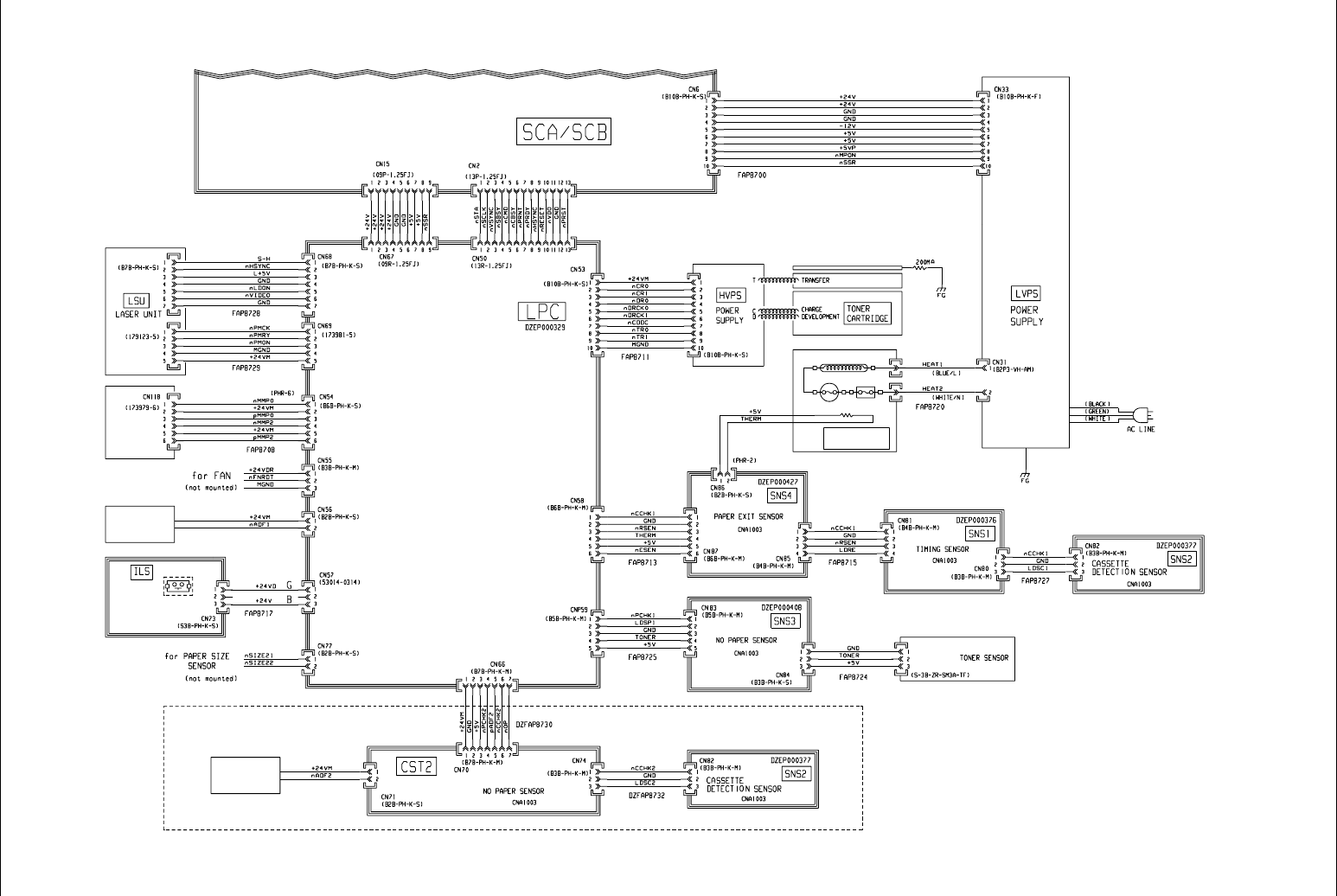
3.8 SCA / SCB PCB (UF-595, UF-585)
CN1
CN2
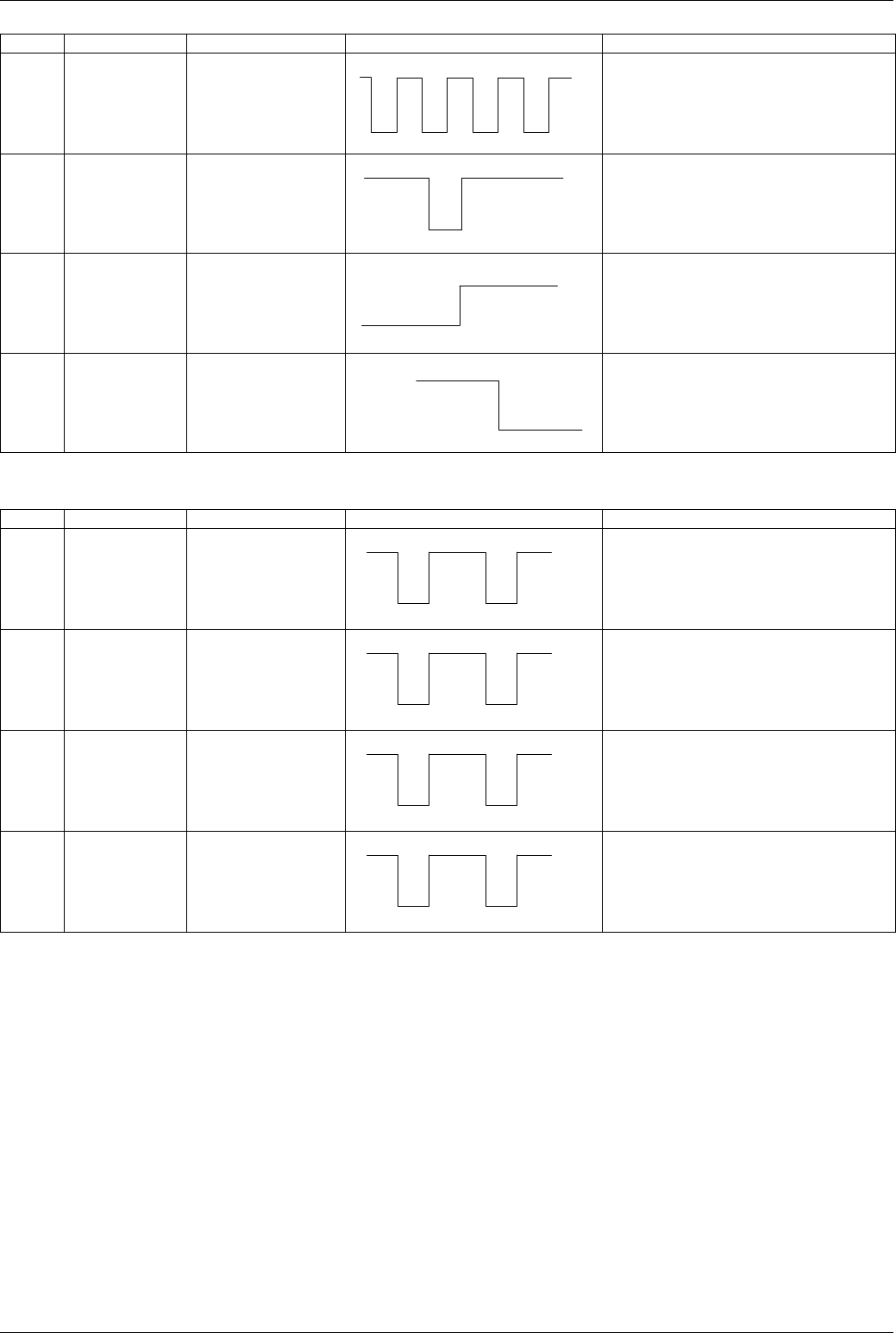
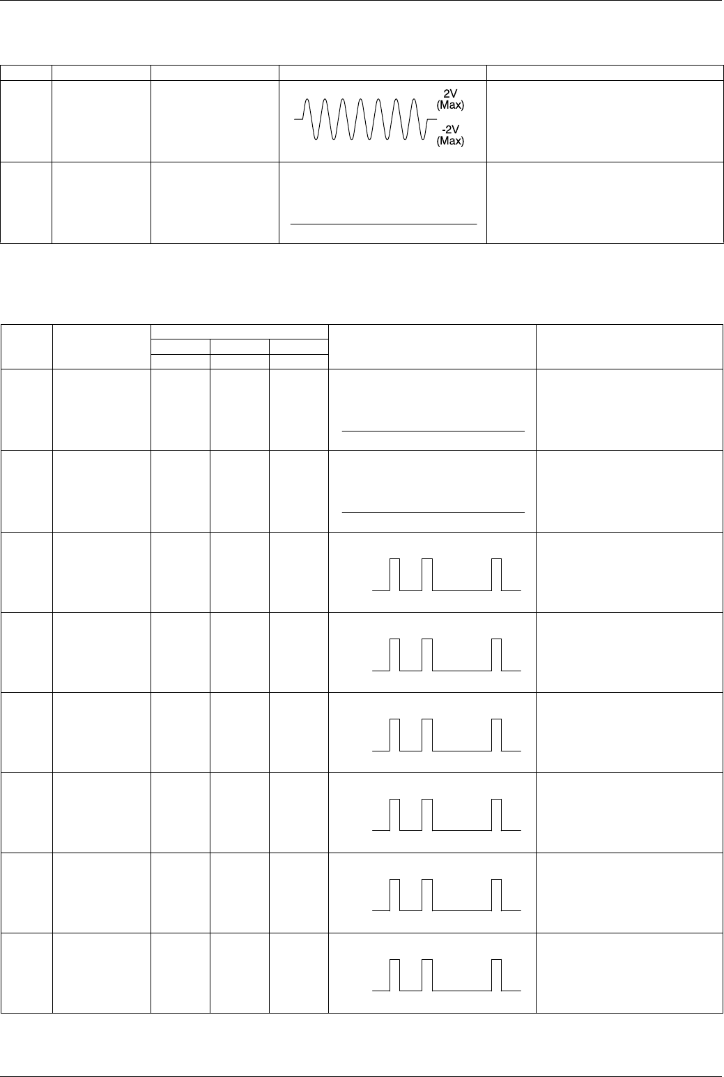
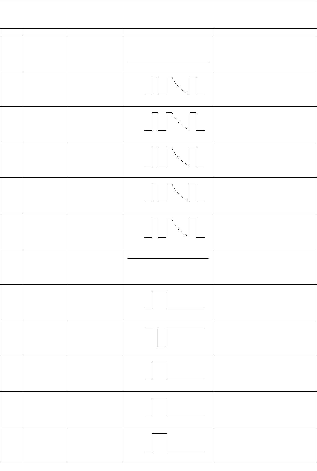
Pin No. Signal Name Destination Signal Waveform Function
CN1-1 +24V LED Array +24 VDC Power Supply
CN1-2 nLEDON LED Array LED Enable Signal
Pin No. Signal Name Destination Signal Waveform Function
CN2-1 nSTA LPC PCB CN 50-1 Serial Interface Data Signal
CN2-2 nSCLK LPC PCB CN 50-2 Serial Interface Synchronization Clock
CN2-3 nSYNC LPC PCB CN 50-3 V - SYNC for Video Signal
CN8
13
1
CN4
13
1
CN9
2
1
CN12
CN10
20
1
CN6
10
1
CN11
18
1
F-ROM
IC4
CN7
18
CN1
12
CN3
13
CN5
14
CN2
13 1
CN15
91
1
68
+24V
Approx.+13V(H)
0V(L)
LED Off
LED On
+5V(H)
0V(H)
5V
0V
+5V(H)
0V(L)
Panasonic UF-585 / 595
60
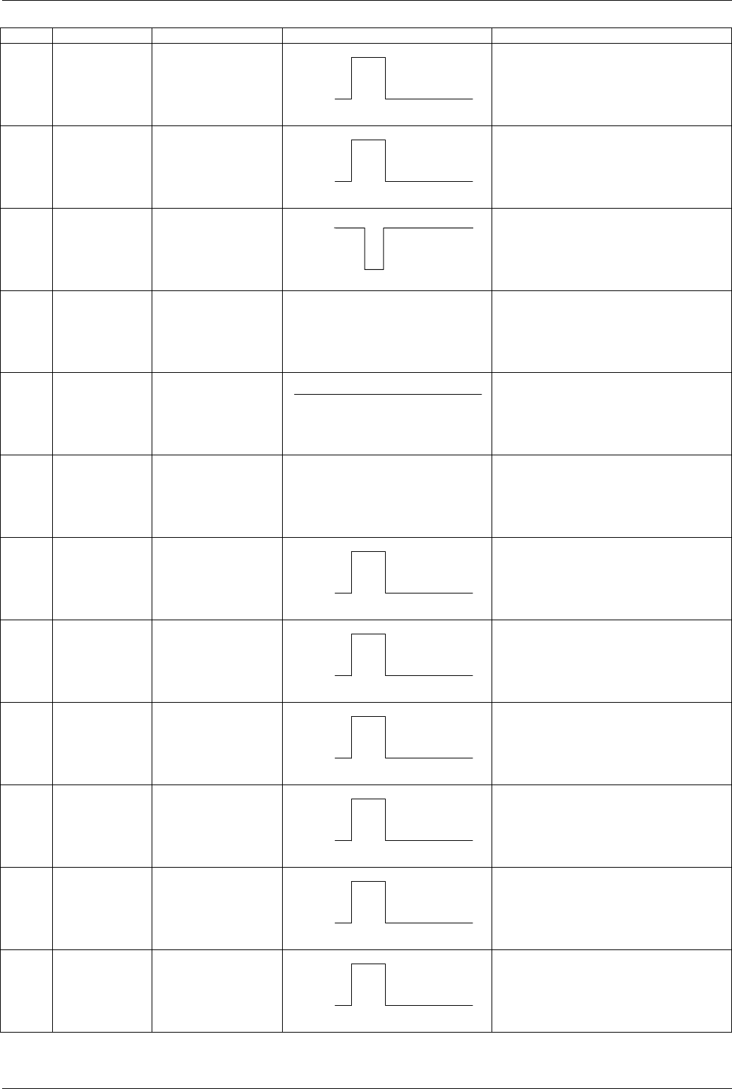
CN2-4 nSBSY LPC PCB CN 50-4 Serial Interface Enable Signal
CN2-5 nCMD LPC PCB CN 50-5 Serial Interface Command Data Signal
CN2-6 nCBSY LPC PCB CN 50-6 Serial Interface Enable Signal
CN2-7 nPRNT LPC PCB CN 50-7 Print Request Signal
CN2-8 nPRDY LPC PCB CN 50-8 Printer Ready Signal
CN2-9 nHSYNC LPC PCB CN 50-9 H - SYNC for Video Signal
CN2-10 nRESET LPC PCB CN 50-10 Not Used
CN2-11 nVDO LPC PCB CN 50-11 Laser Drive Print Data Signal
CN2-12 GND LPC PCB CN 50-12 Ground
CN2-13 nPRST LPC PCB CN 50-13 Printer External Reset Signal
Pin No. Signal Name Destination Signal Waveform Function
+5V(H)
0V(L)
+5V(H)
0V(H)
+5V(H)
0V(L)
5V(H)
0V(L)
+5V(H)
0V(L)
+5V(H)
0V(H)
5V
0V
0V
5V(H)
0V(L)
Maintenance, Adjustments and Check Points
61
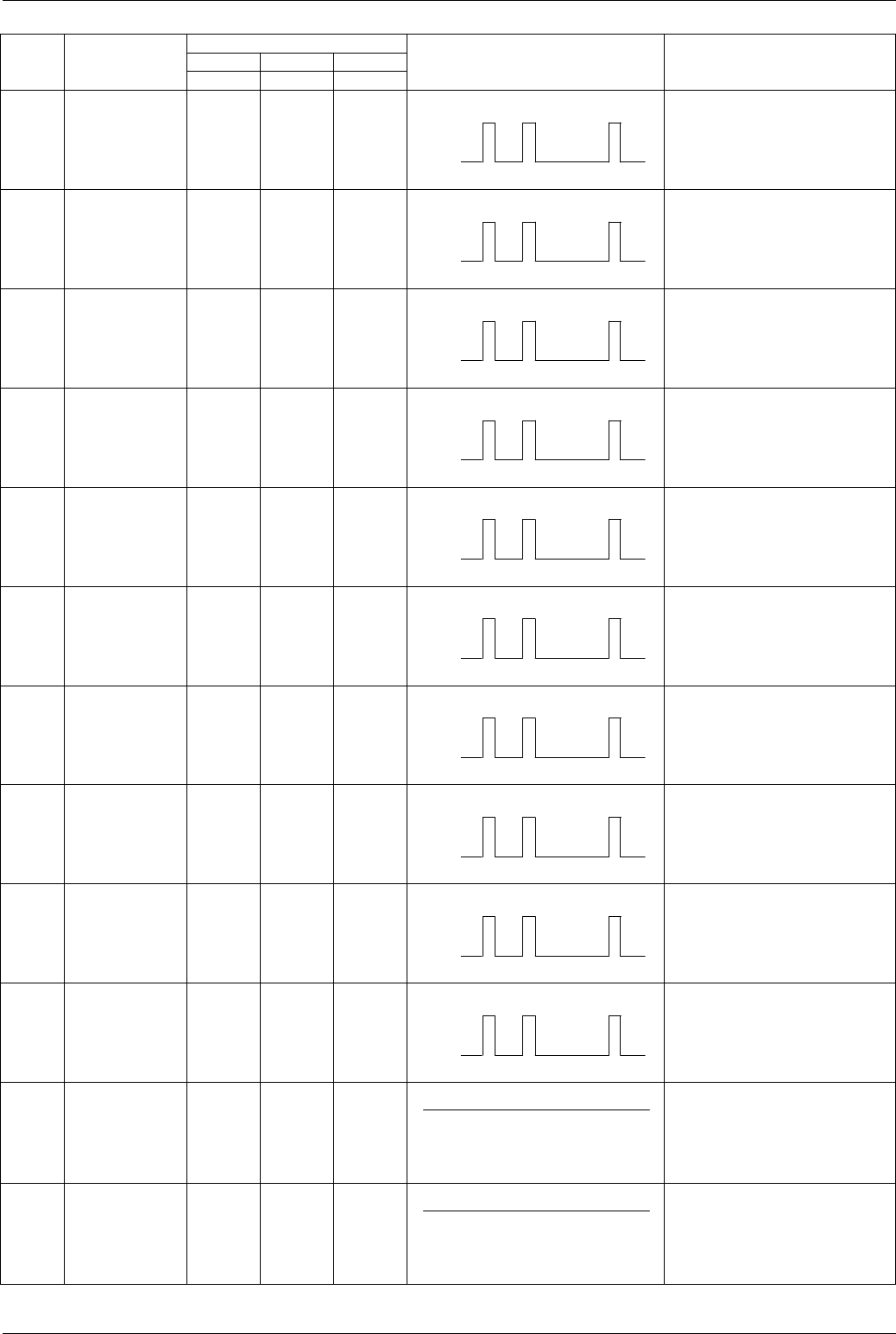
CN3
CN4
Pin No. Signal Name Destination Signal Waveform Function
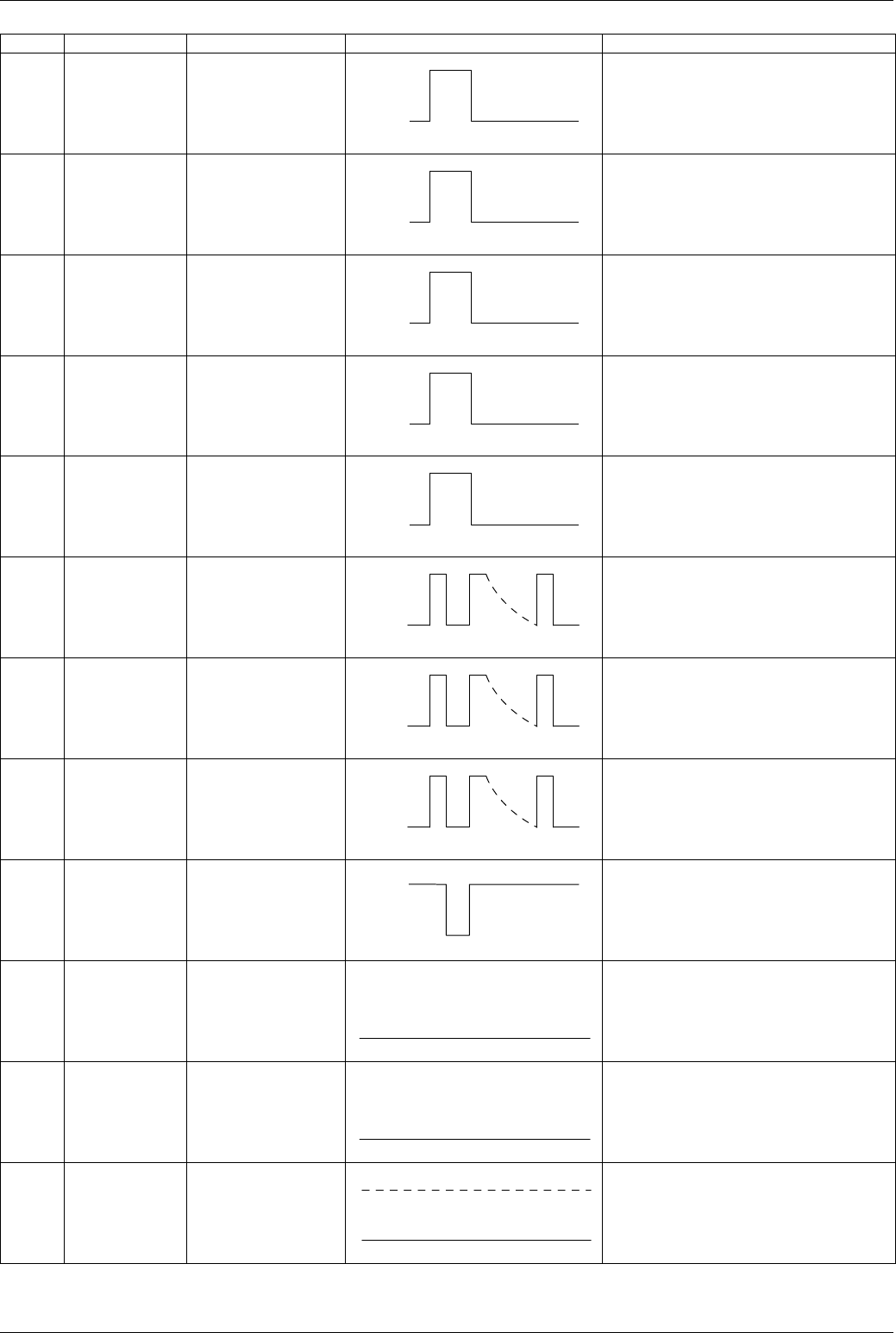
CN3-1 +24V Stamp Solenoid +24 VDC Power Supply
CN3-2 NC Not Used
CN3-3 nSTAMPON Stamp Solenoid Stamp Driver Signal
Pin No. Signal Name Destination Signal Waveform Function
CN4-1 BATLVL PNL PCB CN40-1 Battery Backup Power Supply
CN4-2 +5V PNL PCB CN40-2 +5 VDC Power Supply
CN4-3 +5VP PNL PCB CN40-3 +5 VDC Power Supply
CN4-4 GND PNL PCB CN40-4 Ground
CN4-5 GND PNL PCB CN40-5 Ground
CN4-6 pPNLRD PNL PCB CN40-6 Reception Data
CN4-7 pPNLTD PNL PCB CN40-7 Transmission Data
CN4-8 pPNLCK PNL PCB CN40-8 Serial Data Transfer Clock
CN4-9 pPNLRST PNL PCB CN40-9 Panel Reset Signal (Reset by 5V)
+24V
+24V
Stamp Off
Stamp On
0V
+5V
+5V
0V
0V
+5V(H)
0V(L)
5V
0V
5V(H)
0V(L)
Panasonic UF-585 / 595
62
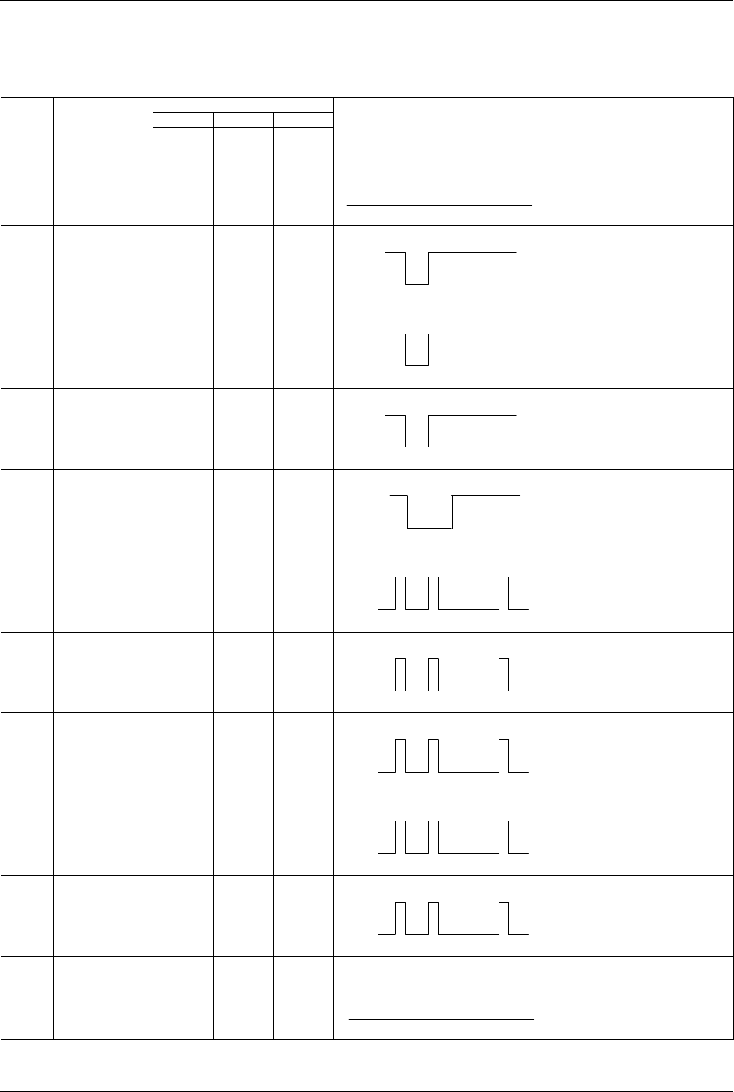
CN5
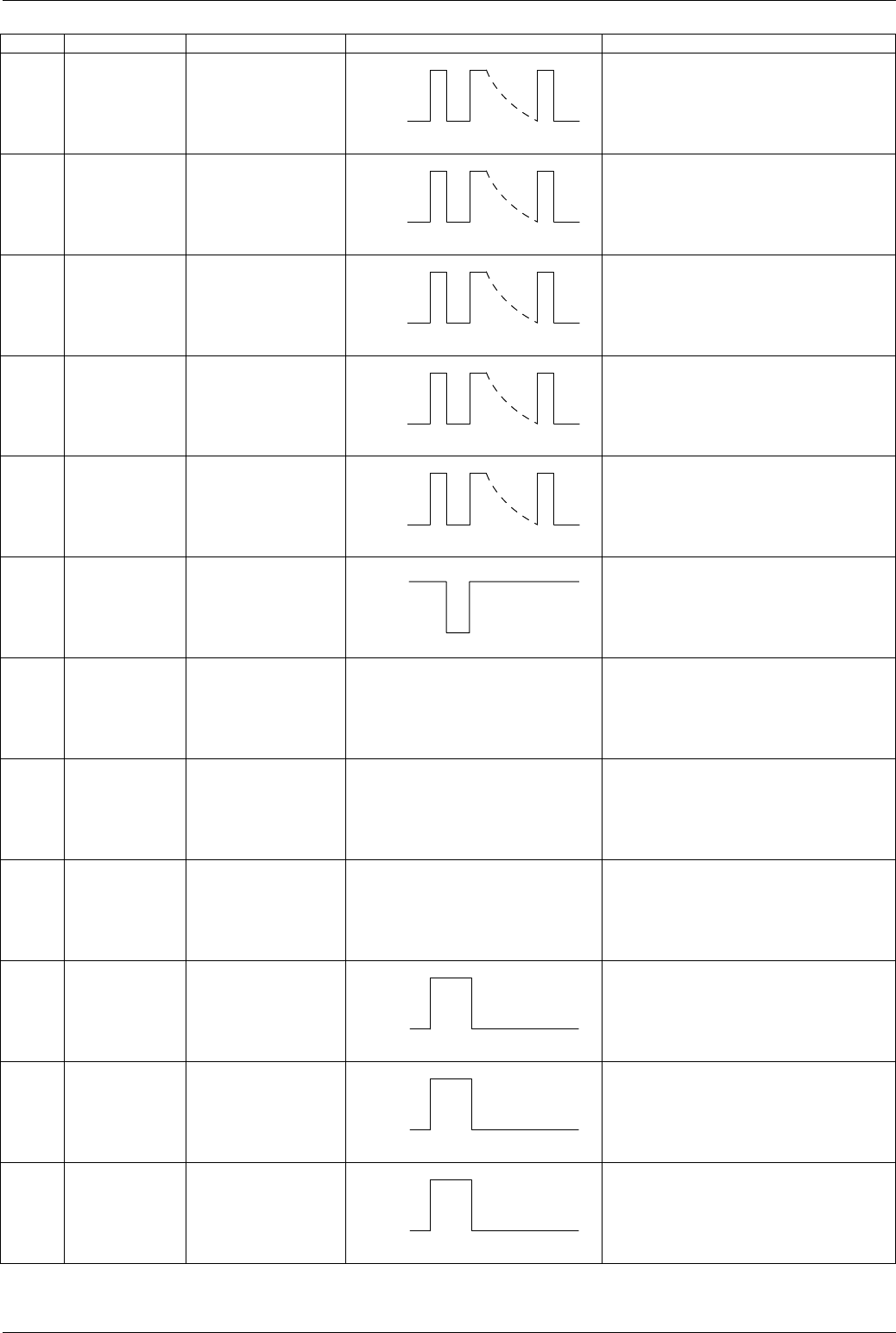
CN4-10 pBZCLK PNL PCB CN40-10 Buzzer Clock
CN4-11 nWAKUP PNL PCB CN40-11 Power Saver Reset Signal
CN4-12 nPWSAVE PNL PCB CN40-12 Power Saver Enable
CN4-13 nBPNT PNL PCB CN40-13 Read Point Sensor Signal
Pin No. Signal Name Destination Signal Waveform Function
CN5-1 MTpA Transmit Motor Stepping Signal
CN5-2 MTnA Transmit Motor Stepping Signal
CN5-3 MTpB Transmit Motor Stepping Signal
CN5-4 MTnB Transmit Motor Stepping Signal
Pin No. Signal Name Destination Signal Waveform Function
5V
0V
5V
0V
+5V(H)
0V(L)
+5V(H)
0V(L)
+24V
0V
+24V
0V
+24V
0V
+24V
0V
Maintenance, Adjustments and Check Points
63
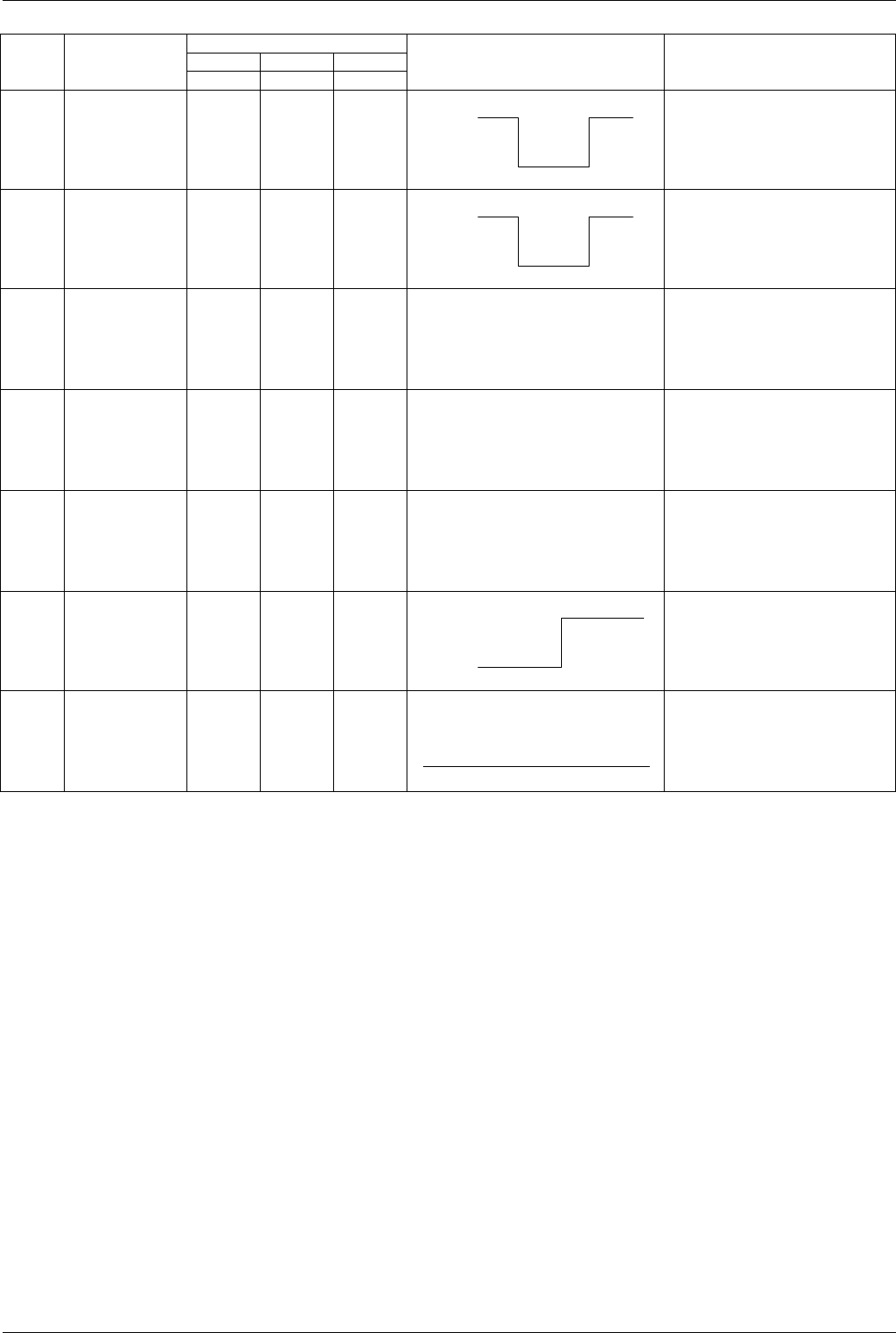
CN6
Pin No. Signal Name Destination Signal Waveform Function
CN6-1 +24V LVPS CN33-1 +24 VDC Power Supply
CN6-2 +24V LVPS CN33-2 +24 VDC Power Supply
CN6-3 GND LVPS CN33-3 Ground
CN6-4 GND LVPS CN33-4 Ground
CN6-5 -12V LVPS CN33-5 -12 VDC Power Supply
CN6-6 +5V LVPS CN33-6 +5 VDC Power Supply
CN6-7 +5V LVPS CN33-7 +5 VDC Power Supply
CN6-8 +5VP LVPS CN33-8 +5 VDC Sleep Mode Power Supply
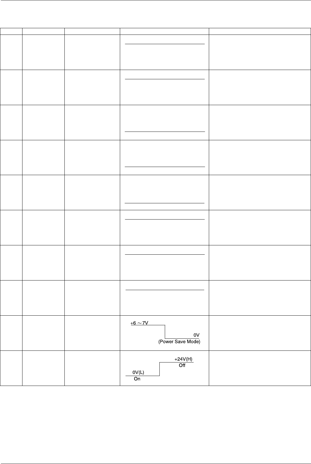
CN6-9 nMPON LVPS CN33-9 Power Saver Mode Control Signal
CN6-10 nSSR LVPS CN33-10 Fuser Lamp Control Signal
+24V
+24V
0V
0V
-12V
+5V
+5V
+5V
Panasonic UF-585 / 595
64
CN7
CN8
Pin No. Signal Name Destination Signal Waveform Function
CN7-1 FR CCD PCB CN30-1 Reset Signal
CN7-2 FCK1 CCD PCB CN30-2 Shift Register Clock 1
CN7-3 FCK2 CCD PCB CN30-3 Shift Register Clock 2
CN7-4 FSG CCD PCB CN30-4 Data Transfer Enable Signal
CN7-5 AGND CCD PCB CN30-5 Ground
CN7-6 +5V CCD PCB CN30-6 +5 VDC Power Supply
CN7-7 DOS CCD PCB CN30-7 Differential Output Signal
CN7-8 OS CCD PCB CN30-8 Output Signal
Pin No. Signal Name Destination Signal Waveform Function
CN8-1 +24V LCU PCB CN25-1 +24 VDC Power Supply
CN8-2 pCTON LCU PCB CN25-2 Ring Detection Signal
H : Ring Detected
L : Ring Not Detected
CN8-3 +5V LCU PCB CN25-3 +5Vp
+5V(H)
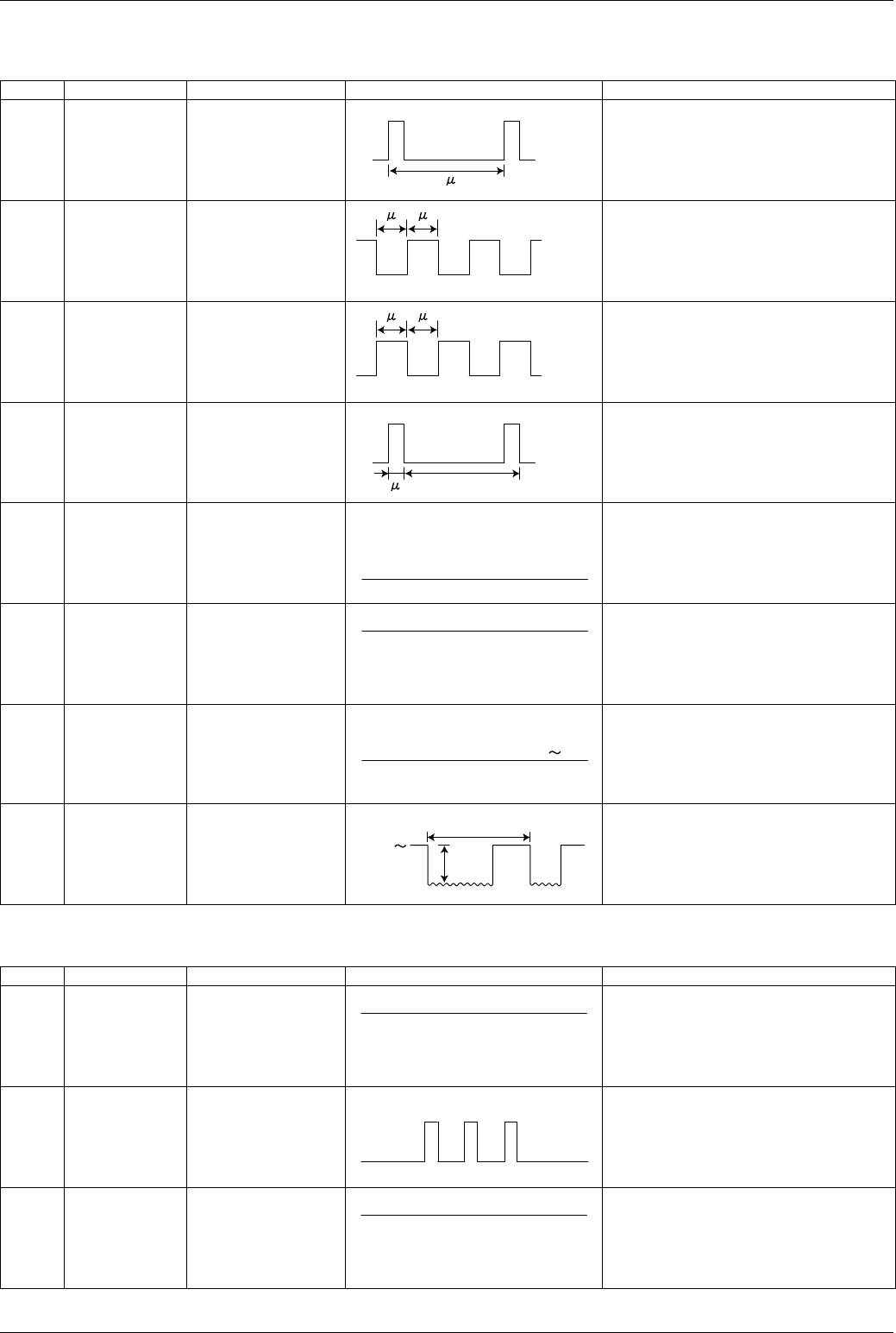
0V(L)
1 s
+5V(H)
0V(H)
1 s 1 s
+5V(H)
0V(H)
1 s 1 s
+5V(H)
0V(L)
1 s 2.4ms
0V
+5V
+3.0V 4.5V
3.5V
4.5V
2.4ms
Max.1.0V
+24V
above +3V(H) Ring Detected
0V
+5V
Maintenance, Adjustments and Check Points
65
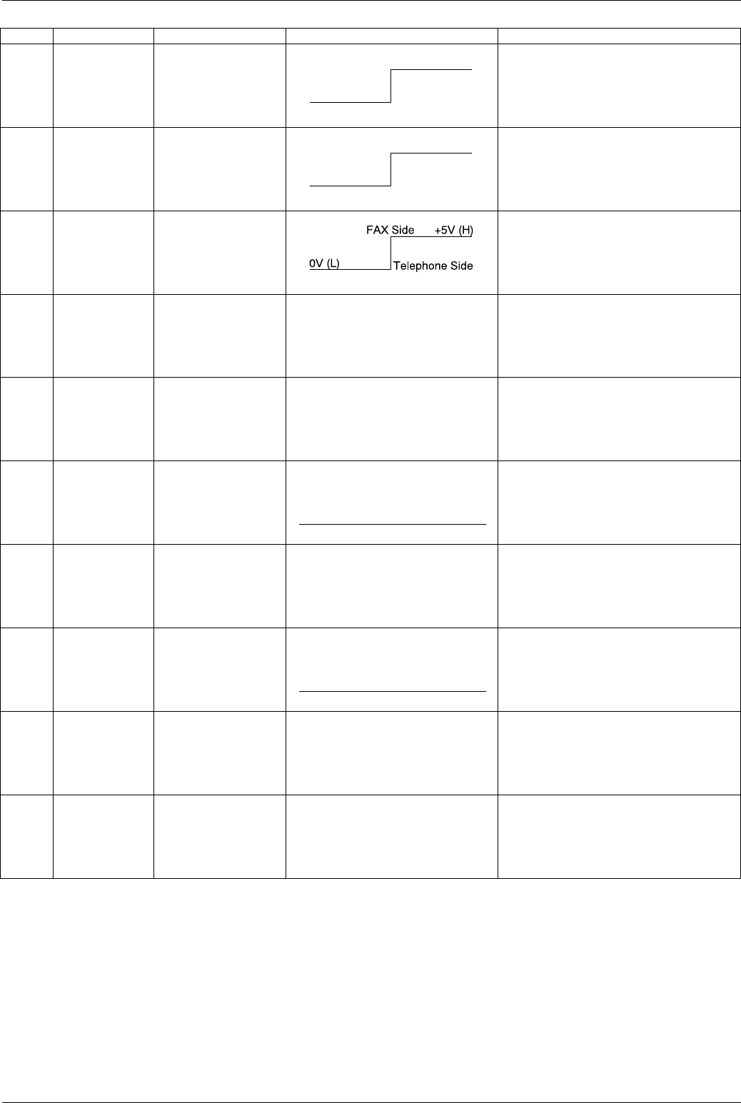
CN8-4 pHKOF LCU PCB CN25-4 External Phone Off-Hook Detection Signal
(Phone Line must be connected)
H : Off Hook
L : On Hook
CN8-5 pPLSD LCU PCB CN25-5 Pulse Dial Relay Drive Signal
H : Make
L : Break
CN8-6 pCMLD LCU PCB CN25-6. Line Switching Relay Drive Signal
H : CML On
L : CML Off
CN8-7 pTCKD LCU PCB CN25-7 Not Used
CN8-8 pEAKD LCU PCB CN25-8 Not Used
CN8-9 GND LCU PCB CN25-9 Ground
CN8-10 HYBSR LCU PCB CN25-10 Line Transformer Input Signal
CN8-11 AGND LCU PCB CN25-11 Ground
CN8-12 HYSIG LCU PCB CN25-12 FAX Off Line Signal
CN8-13 NC LCU PCB CN25-13 Not Used
Pin No. Signal Name Destination Signal Waveform Function
+5V (H)OFF Hook
ON Hook
0V (L)
+5V (H)Make
Break
0V (L)
0V
0V
Panasonic UF-585 / 595
66
CN9
CN10
Note:
CN212 is available when the Optional Parallel I/F is installed.
Pin No. Signal Name Destination Signal Waveform Function
CN9-1 pSPKOT Speaker Line Signal, Key Tone, Ringer
CN9-2 GND Speaker Ground
Pin No. Signal Name Destination Signal Waveform Function
PRTA PRTA PRT
CN200 CN202 CN212
CN10-1 GND 20 30 30 Ground
CN10-2 GND 19 10 10 Ground
CN10-3 D15 18 29 29 Data Signal (15)
CN10-4 D14 17 9 9 Data Signal (14)
CN10-5 D13 16 28 28 Data Signal (13)
CN10-6 D12 15 8 8 Data Signal (12)
CN10-7 D11 14 27 27 Data Signal (11)
CN10-8 D10 13 7 7 Data Signal (10)
0V
0V
0V
+5V(H)
0V(L)
+5V(H)
0V(L)
+5V(H)
0V(L)
+5V(H)
0V(L)
+5V(H)
0V(L)
+5V(H)
0V(L)
Maintenance, Adjustments and Check Points
67
CN10-9 D9 12 26 26 Data Signal (9)
CN10-10 D8 11 6 6 Data Signal (8)
CN10-11 D7 10 25 25 Data Signal (7)
CN10-12 D6 9 5 5 Data Signal (6)
CN10-13 D5 8 24 24 Data Signal (5)
CN10-14 D4 7 4 4 Data Signal (4)
CN10-15 D3 6 23 23 Data Signal (3)
CN10-16 D2 5 3 3 Data Signal (2)
CN10-17 D1 4 22 22 Data Signal (1)
CN10-18 D0 3 2 2 Data Signal (0)
CN10-19 +5V 2 21 21 +5 VDC Power Supply
CN10-20 +5V 1 1 1 +5 VDC Power Supply
Pin No. Signal Name Destination Signal Waveform Function
PRTA PRTA PRT
CN200 CN202 CN212
+5V(H)
0V(L)
+5V(H)
0V(L)
+5V(H)
0V(L)
+5V(H)
0V(L)
+5V(H)
0V(L)
+5V(H)
0V(L)
+5V(H)
0V(L)
+5V(H)
0V(L)
+5V(H)
0V(L)
+5V(H)
0V(L)
+5V
+5V
Panasonic UF-585 / 595
68
CN11
Note:
CN212 is available when the Optional Parallel I/F is installed.
Pin No. Signal Name Destination Signal Waveform Function
PRTA PRTA PRT
CN201 CN202 CN212
CN11-1 GND 18 40 40 Ground
CN11-2 nWRH 17 20 20 Write H Signal - Low Enable
CN11-3 nWRL 16 39 39 Write L Signal - Low Enable
CN11-4 nRD 15 19 19 Read Signal - Low Enable
CN11-5 nCS 14 38 38 FPGA (Field Programmed Gate
Array) Chip Select - Low Enable
CN11-6 A5 13 18 18 Address Signal (5)
CN11-7 A4 12 37 37 Address Signal (4)
CN11-8 A3 11 17 17 Address Signal (3)
CN11-9 A2 10 36 36 Address Signal (2)
CN11-10 A1 9 16 16 Address Signal (1)
CN11-11 nBCNOPT 8 35 35 Detection Signal
H : Option Board Not Installed
L : Option Board Installed
0V
+5V(H)
0V(L)
+5V(H)
0V(L)
+5V(H)
0V(L)
+5V(H)
0V(L)
+5V(H)
0V(L)
+5V(H)
0V(L)
+5V(H)
0V(L)
+5V(H)
0V(L)
+5V(H)
0V(L)
0V(L)
+5V(H)
Maintenance, Adjustments and Check Points
69
CN11-12 nINT1 7 15 15 Data Transfer Interrupt Signal
CN11-13 nINT0 6 34 34 Signal Detect Interrupt Signal
CN11-14 pDRACK 5 14 14 Not Used
CN11-15 nDREQ 4 33 33 Not Used
CN11-16 pDACK 3 13 13 Not Used
CN11-17 nRST 2 32 32 FPGA (Field Programmed Gate
Array) Reset Signal
CN11-18 GND 1 11 11 Ground
Pin No. Signal Name Destination Signal Waveform Function
PRTA PRTA PRT
CN201 CN202 CN212
+5V(H)
0V(L)
+5V(H)
0V(L)
+5V(H)
0V(L)
0V
Panasonic UF-585 / 595
70
CN12
Pin No. Signal Name Destination Signal Waveform Function
CN12-1 GND Flash Memory Card Ground
CN12-2 D3 Flash Memory Card Data Signal (3)
CN12-3 D4 Flash Memory Card Data Signal (4)
CN12-4 D5 Flash Memory Card Data Signal (5)
CN12-5 D6 Flash Memory Card Data Signal (6)
CN12-6 D7 Flash Memory Card Data Signal (7)
CN12-7 +5V(*CE1) Flash Memory Card +5 VDC Power Supply
CN12-8 A11 Flash Memory Card Address Signal (11)
CN12-9 nRD Flash Memory Card Read Signal - Low Enable
CN12-10 A12 Flash Memory Card Address Signal (12)
CN12-11 A10 Flash Memory Card Address Signal (10)
CN12-12 A9 Flash Memory Card Address Signal (9)
0V
5V(H)
0V(L)
5V(H)
0V(L)
5V(H)
0V(L)
5V(H)
0V(L)
5V(H)
0V(L)
+5V
5V(H)
0V(L)
5V(H)
0V(L)
5V(H)
0V(L)
5V(H)
0V(L)
5V(H)
0V(L)
Maintenance, Adjustments and Check Points
71
CN12-13 A14 Flash Memory Card Address Signal (14)
CN12-14 A15 Flash Memory Card Address Signal (15)
CN12-15 nWRL Flash Memory Card Write L Signal - Low Enable
CN12-16 RDY / *BSY Flash Memory Card Not Used
CN12-17 +5V Flash Memory Card +5 VDC Power Supply
CN12-18 NC Flash Memory Card Not Used
CN12-19 A17 Flash Memory Card Address Signal (17)
CN12-20 A16 Flash Memory Card Address Signal (16)
CN12-21 A13 Flash Memory Card Address Signal (13)
CN12-22 A8 Flash Memory Card Address Signal (8)
CN12-23 A7 Flash Memory Card Address Signal (7)
CN12-24 A6 Flash Memory Card Address Signal (6)
Pin No. Signal Name Destination Signal Waveform Function
5V(H)
0V(L)
5V(H)
0V(L)
5V(H)
0V(L)
+5V
5V(H)
0V(L)
5V(H)
0V(L)
5V(H)
0V(L)
5V(H)
0V(L)
5V(H)
0V(L)
5V(H)
0V(L)
Panasonic UF-585 / 595
72
CN12-25 A5 Flash Memory Card Address Signal (5)
CN12-26 A4 Flash Memory Card Address Signal (4)
CN12-27 A3 Flash Memory Card Address Signal (3)
CN12-28 A2 Flash Memory Card Address Signal (2)
CN12-29 A1 Flash Memory Card Address Signal (1)
CN12-30 D0 Flash Memory Card Data Signal (0)
CN12-31 D1 Flash Memory Card Data Signal (1)
CN12-32 D2 Flash Memory Card Data Signal (2)
CN12-33 nWRH Flash Memory Card Write H Signal - Low Enable
CN12-34 GND Flash Memory Card Ground
CN12-35 GND Flash Memory Card Ground
CN12-36 nCD Flash Memory Card Flash Memory Card Detection Signal
H : Card Not Installed
L : Card Installed
Pin No. Signal Name Destination Signal Waveform Function
5V(H)
0V(L)
5V(H)
0V(L)
5V(H)
0V(L)
5V(H)
0V(L)
5V(H)
0V(L)
5V(H)
0V(L)
5V(H)
0V(L)
5V(H)
0V(L)
5V(H)
0V(L)
0V
0V
0V(L)
+5V(H)
Maintenance, Adjustments and Check Points
73
CN12-37 D11 Flash Memory Card Data Signal (11)
CN12-38 D12 Flash Memory Card Data Signal (12)
CN12-39 D13 Flash Memory Card Data Signal (13)
CN12-40 D14 Flash Memory Card Data Signal (14)
CN12-41 D15 Flash Memory Card Data Signal (15)
CN12-42 nCE2 Flash Memory Card Low Enable
CN12-43 NC Not Used
CN12-44 RSV Flash Memory Card Not Used
CN12-45 RSV Flash Memory Card Not Used
CN12-46 A18 Flash Memory Card Address Signal (18)
CN12-47 A19 Flash Memory Card Address Signal (19)
CN12-48 A20 Flash Memory Card Address Signal (20)
Pin No. Signal Name Destination Signal Waveform Function
5V(H)
0V(L)
5V(H)
0V(L)
5V(H)
0V(L)
5V(H)
0V(L)
5V(H)
0V(L)
5V(H)
0V(L)
5V(H)
0V(L)
5V(H)
0V(L)
5V(H)
0V(L)
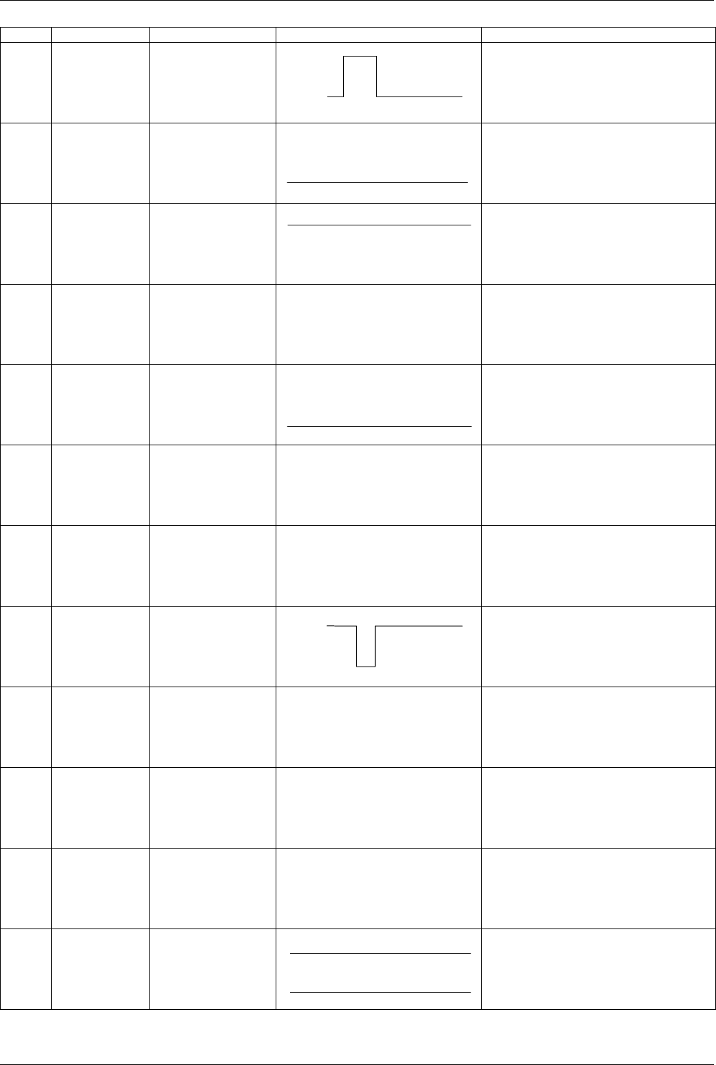
Panasonic UF-585 / 595
74
CN12-49 A21 Flash Memory Card Address Signal (21)
CN12-50 GND Flash Memory Card Ground
CN12-51 +5V Flash Memory Card +5 VDC Power Supply
CN12-52 NC Flash Memory Card Not Used
CN12-53 GND(A22) Flash Memory Card Ground
CN12-
54-56
NC Flash Memory Card Not Used
CN12-57 RFU Flash Memory Card Not Used
CN12-58 NC Flash Memory Card Low Enable
CN12-59 nMB4 Flash Memory Card Not Used
CN12-60 RFU Flash Memory Card Not Used
CN12-61 NC Flash Memory Card Not Used
CN12-62 ID2 Flash Memory Card Flash Memory Card ID
Pin No. Signal Name Destination Signal Waveform Function
5V(H)
0V(L)
0V
+5V
0V
5V(H)
0V(L)
0V
5V
or
Maintenance, Adjustments and Check Points
75
CN12-63 ID1 Flash Memory Card Flash Memory Card ID
CN12-64 D8 Flash Memory Card Data Signal (8)
CN12-65 D9 Flash Memory Card Data Signal (9)
CN12-66 D10 Flash Memory Card Data Signal (10)
CN12-67 ID0 Flash Memory Card Flash Memory Card ID
CN12-68 GND Flash Memory Card Ground
Pin No. Signal Name Destination Signal Waveform Function
0V
5V
or
5V(H)
0V(L)
5V(H)
0V(L)
5V(H)
0V(L)
0V
5V
or
0V

Panasonic UF-585 / 595
76
CN15
Pin No. Signal Name Destination Signal Waveform Function
CN15-1 +24V LPC PCB CN15-1 +24 VDC Power Supply
CN15-2 +24V LPC PCB CN15-2 +24 VDC Power Supply
CN15-3 +24V LPC PCB CN15-3 +24 VDC Power Supply
CN15-4 +24V LPC PCB CN15-4 +24 VDC Power Supply
CN15-5 GND LPC PCB CN15-5 Ground
CN15-6 GND LPC PCB CN15-6 Ground
CN15-7 +5V LPC PCB CN15-7 +5 VDC Power Supply
CN15-8 +5V LPC PCB CN15-8 +5 VDC Power Supply
CN15-9 nSSR LPC PCB CN15-9 Fuser Lamp Control Signal
+24V
+24V
+24V
+24V
0V
0V
+5V
+5V
+24V(H)
0V(L)
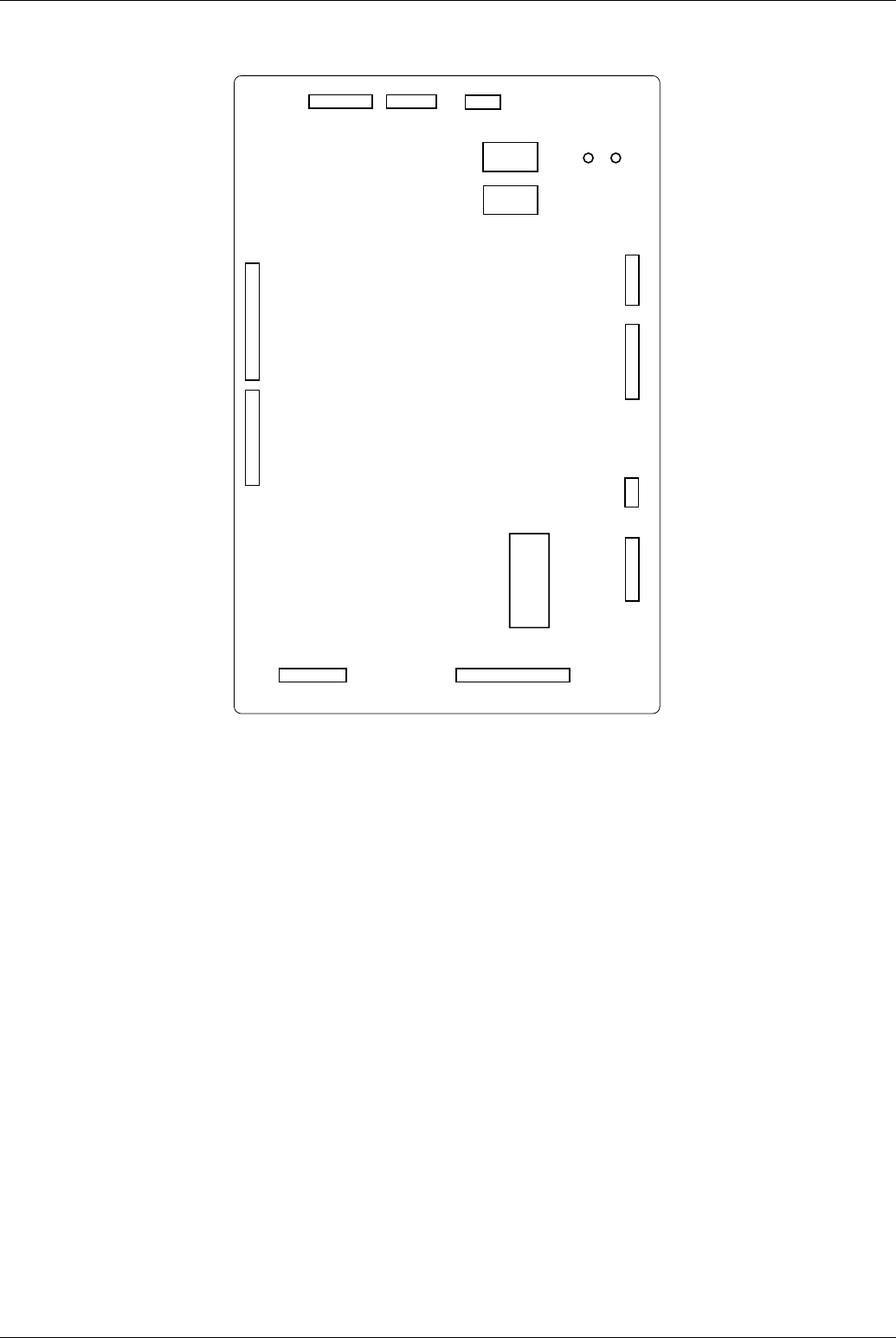
Maintenance, Adjustments and Check Points
77
3.9 LPC PCB
CN56
21
CN54
61
CN69
51
CN59
51
CN58
61
CN68
71
CN66
71
CN53
101
IC6
sw1
CN57
31
CN50
113
CN67
19
IC3
Q19
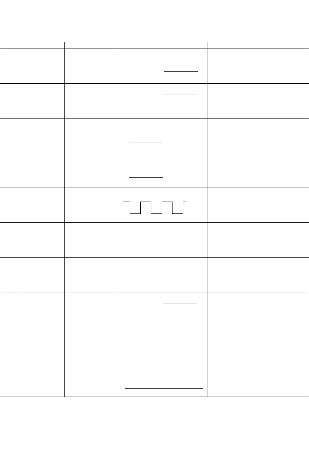
Panasonic UF-585 / 595
78
CN50
Refer to SCA / SCB PCB CN2.
CN53
Pin No. Signal Name Destination Signal Waveform Function
CN53-1 +24VM HVPS
CN39-1
+24 VDC Power Supply
CN53-2 nCR0 HVPS
CN39-2
Charge Control AC Output
CN53-3 nCR1 HVPS
CN39-3
Charge Control DC Output
CN53-4 nDR0 HVPS
CN39-4
Development Control AC+DC Output
CN53-5 nDRCK0 HVPS
CN39-5
Development AC Clock
(F = 1.875 kHz)
CN53-6 nDRCK1 HVPS
CN39-6
Not Used
CN53-7 nCDDC HVPS
CN39-7
Not Used
CN53-8 nTR0 HVPS
CN39-8
Transfer Control Transfer Output
CN53-9 nTR1 HVPS
CN39-9
Not Used
CN53-10 MGND HVPS
CN39-10
Ground
0V
+24V
+24V (H)
0V (L) ON
+24V (H)
0V (L) ON
+24V (H)
0V (L) ON
+24V(H)
0V(H)
+24V (H)
0V (L) ON
0V
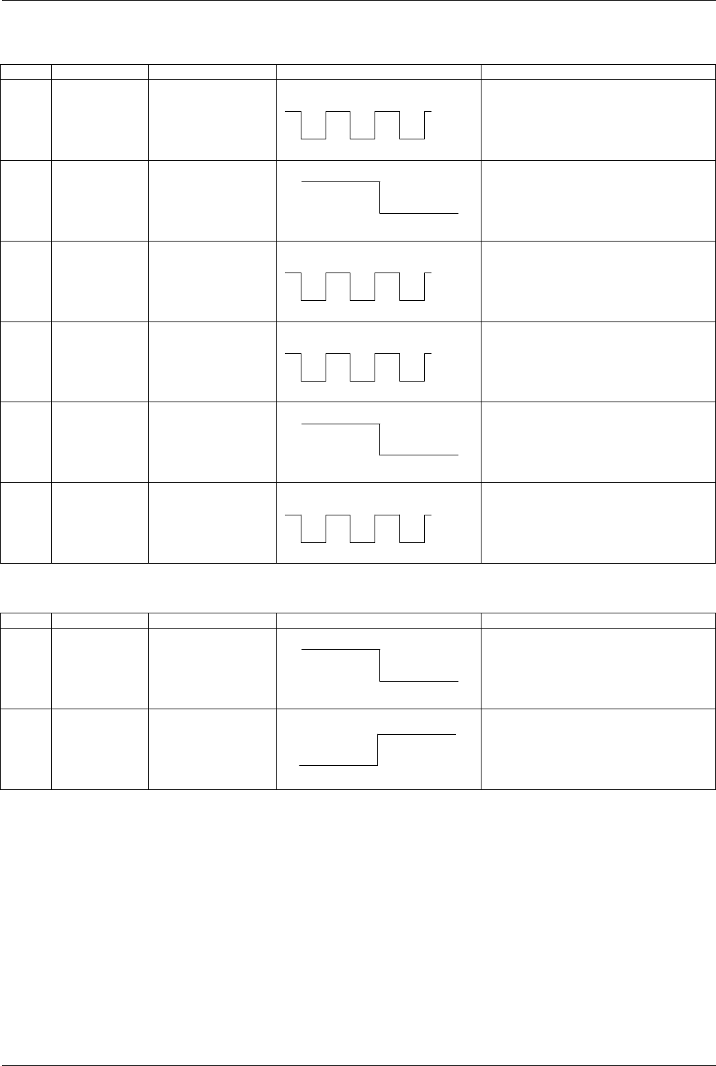
Maintenance, Adjustments and Check Points
79
CN54
CN56
Pin No. Signal Name Destination Signal Waveform Function
CN54-1 nMMP0a Printer Motor
CN118-1
Printer Motor Phase 1 Output Signal
CN54-2 +24VM Printer Motor
CN118-2
+24 VDC Power Supply
CN54-3 pMMP0a Printer Motor
CN118-3
Printer Motor Phase 0 Output Signal
CN54-4 nMMP2a Printer Motor
CN118-4
Printer Motor Phase 3 Output Signal
CN54-5 +24VM Printer Motor
CN118-5
+24 VDC Power Supply
CN54-6 pMMP2a Printer Motor
CN118-6
Printer Motor Phase 2 Output Signal
Pin No. Signal Name Destination Signal Waveform Function
CN56-1 +24VM Paper Feed Solenoid +24 VDC Power Supply
CN56-2 nADF1 Paper Feed Solenoid Paper Feed Roller Solenoid Control Signal
+24V(H)
0V(H)
0V
+24V
+24V(H)
0V(H)
+24V(H)
0V(H)
0V
+24V
+24V(H)
0V(H)
0V
+24V
+24V (H)
0V (L) ON
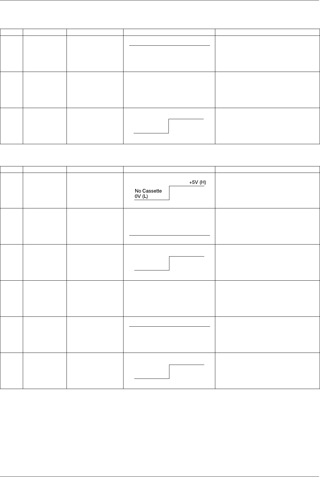
Panasonic UF-585 / 595
80
CN57
CN58
Pin No. Signal Name Destination Signal Waveform Function
CN57-1 +24V ILS PCB
CN73-1
+24 VDC Power Supply
CN57-2 NC
CN57-3 +24VD ILS PCB
CN73-3
Printer Cover Detection Signal
Pin No. Signal Name Destination Signal Waveform Function
CN58-1 nCCHK1 SNS4
CN87-1
No Cassette Detection Signal
CN58-2 GND SNS4
CN87-2
Ground
CN58-3 nRSEN SNS4
CN87-3
Timing Sensor Detection Signal
CN58-4 THERM SNS4
CN87-4
Fuser Thermistor Voltage Level Signal
CN58-5 +5V SNS4
CN87-5
+5 VDC Power Supply
CN58-6 nESEN SNS4
CN87-6
Paper Exit Sensor Detection Signal
+24V
+24V (H)
0V (L)
Cover Open Cover Closed
0V
+5V (H)
0V (L)
Detect Paper
Approx. +2 VDC
+5V
+5V (H)
0V (L)
Detect Paper
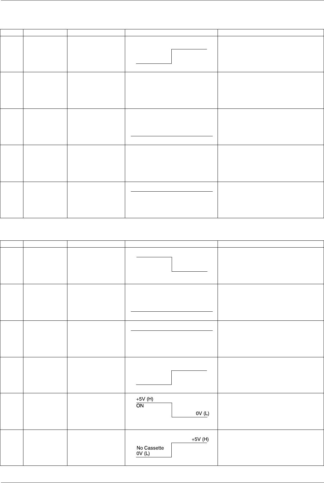
Maintenance, Adjustments and Check Points
81
CN59
CN66
Pin No. Signal Name Destination Signal Waveform Function
CN59-1 nPCHK1 SNS1
CN83-1
No Paper Sensor Detection Signal
CN59-2 LDSP1 SNS1
CN83-2
No Paper Sensor LED Drive Current
CN59-3 GND SNS1
CN83-3
Ground
CN59-4 TONER SNS1
CN83-4
Remaining Toner Level Signal
CN59-5 +5V SNS1
CN83-5
+5 VDC Power Supply
Pin No. Signal Name Destination Signal Waveform Function
CN66-1 +24VM CST2
CN70-1
+24 VDC Power Supply
CN66-2 GND CST2
CN70-2
Ground
CN66-3 +5V CST2
CN70-3
+5 VDC Power Supply
CN66-4 nPCHK2 CST2
CN70-4
No Paper Detection Signal
(2nd Cassette)
CN66-5 pADF2 CST2
CN70-5
Feed Roller Drive Clutch Control Signal
(2nd Cassette)
CN66-6 nCCHK2 CST2
CN70-6
No Cassette Detection Signal
(2nd Cassette)
+5V (H)
0V (L)
Paper No Paper
Approx. +1 VDC
0V
Approx. +2 VDC
+5V
0V
+24V
0V
+5V
+5V (H)
0V (L)
Paper No Paper
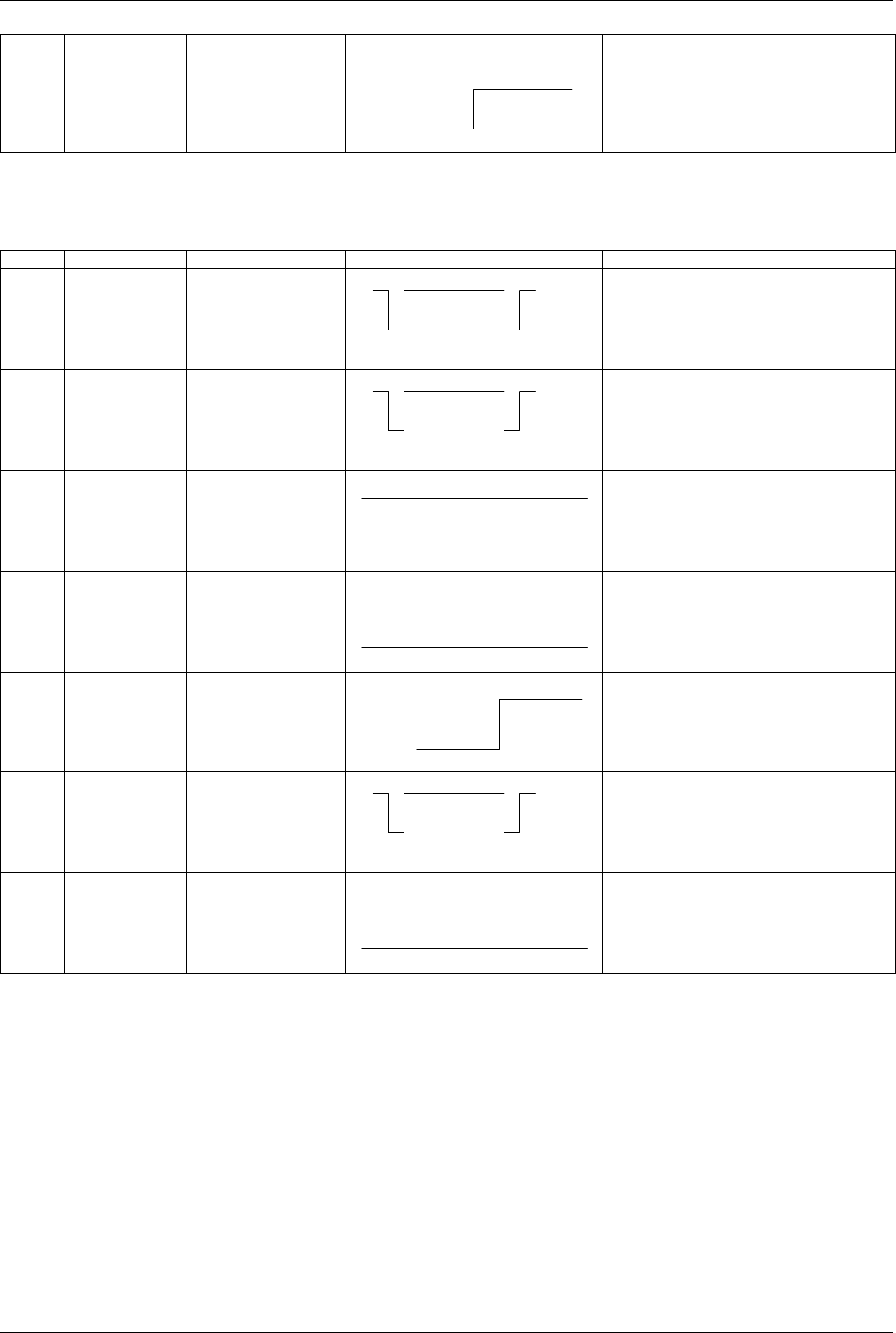
Panasonic UF-585 / 595
82
CN67
Refer to SCA / SCB CN15.
CN68
CN66-7 nOP CST2
CN70-7
2nd Feeder Unit Detection Signal
Pin No. Signal Name Destination Signal Waveform Function
CN68-1 S-H LSU
CN1-1
Laser Power Sample/Hold Timing Signal
L : Sampling
H : Holding
CN68-2 nHSYNC LSU
CN1-2
H-SYNC Video Signal
2.136 ms (400 dpi)
1.393 ms (600 dpi)
CN68-3 L+5V LSU
CN1-3
+5 VDC Power Supply for Laser Drive Circuit
(Supplied only while the LP is operating)
CN68-4 GND LSU
CN1-4
Ground
CN68-5 nLDON LSU
CN1-5
Laser Control Signal
CN68-6 nVIDEO LSU
CN1-6
Video Data
L=Black, H=White
CN68-7 GND LSU
CN1-7
Ground
Pin No. Signal Name Destination Signal Waveform Function
+5V (H)
0V (L)
No Feeder Unit
+5V(H)
0V(L)
+5V(H)
0V(L)
+5V
0V
+5V(H)
0V(L)
+5V(H)
0V(L)
0V
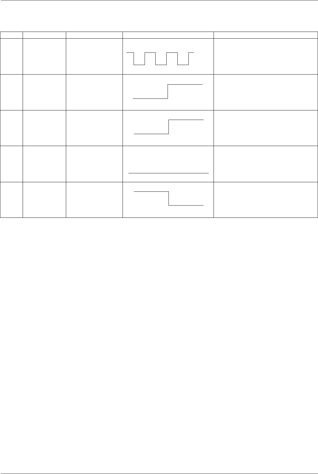
Maintenance, Adjustments and Check Points
83
CN69
Pin No. Signal Name Destination Signal Waveform Function
CN69-1 nPMCK LSU
CN15-1
Tetragon Motor Clock
0.702 kHz (400 dpi)
1.076 kHz (600 dpi)
CN69-2 nPMRY LSU
CN15-2
Tetragon Motor Ready Signal
CN69-3 nPMON LSU
CN15-3
Tetragon Motor Control Signal
CN69-4 MGND LSU
CN15-4
Frame Ground
CN69-5 +24VM LSU
CN15-5
+24 VDC Power Supply
+5V(H)
0V(H)
Ready
0V (L)
+5V (H)
Not Ready
0V (L)
+5V (H)
OFF
ON
0V
0V
+24V

Panasonic UF-585 / 595
84
3.10 LCU PCB
CN20
CN25
13 1
CN23
TEL LINE
HANDSET
CN21

Maintenance, Adjustments and Check Points
85
CN20
CN21
CN23
CN25
Refer to SCA / SCB PCB CN8.
Pin No. Signal Name Destination Signal Waveform Function
CN20-3 LT2(T) Telephone Line Line Signal
CN20-4 LT1(R) Telephone Line Line Signal
Pin No. Signal Name Destination Signal Waveform Function
CN21-3 T1 External Telephone External Telephone Line Signal
CN21-4 T2 External Telephone External Telephone Line Signal
Pin No. Signal Name Destination Signal Waveform Function
CN23-1 NC Not Used
CN23-2 NC Not Used
CN23-3 HLIN1 SRU PCB CN90-1 Fax Handset Line Signal
CN23-4 HLIN2 SRU PCB CN90-2 Fax Handset Line Signal
CN23-5 NC Not Used
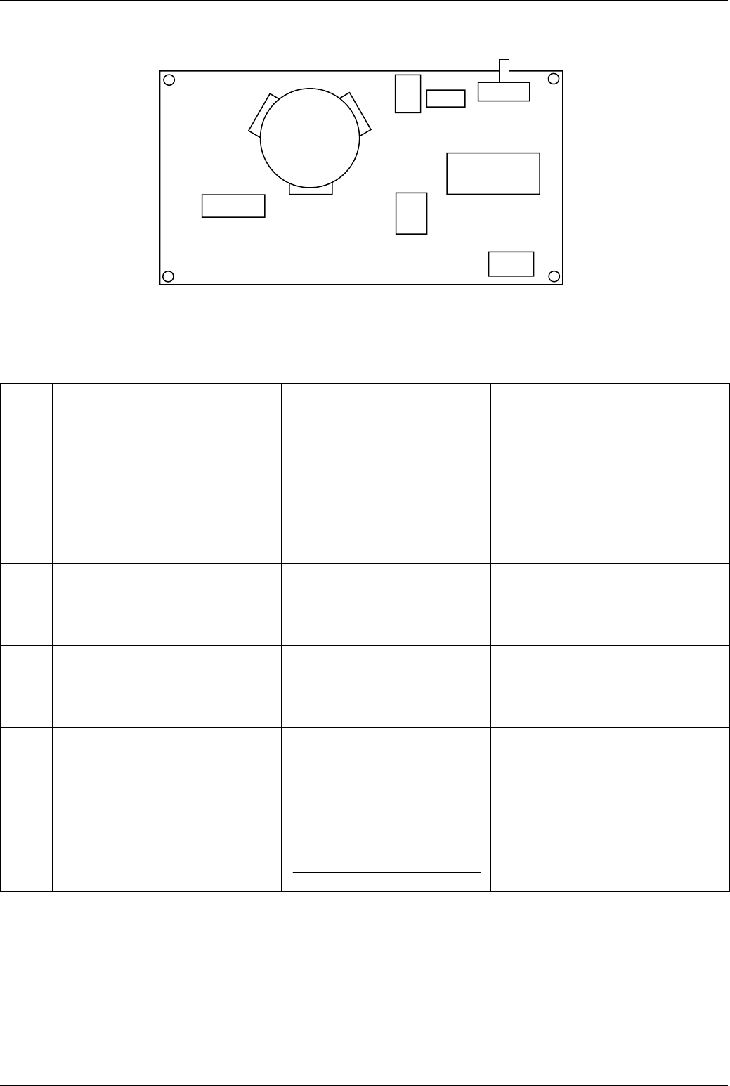
Panasonic UF-585 / 595
86
3.11 SRU PCB (Optional)
CN90
Refer to LCU PCB CN23.
CN91
Pin No. Signal Name Destination Signal Waveform Function
CN91-1 NC Not Used
CN91-2 MIC (+) Telephone Handset CN Handset Microphone
CN91-3 RCV (+) Telephone Handset CN Handset Receiver
CN91-4 RCV (-) Telephone Handset CN Handset Receiver
CN91-5 MIC (-) Telephone Handset CN Handset Microphone
CN91-6 TGND Ground
TEL Cradle Cord
CN91
Handset
15
0V
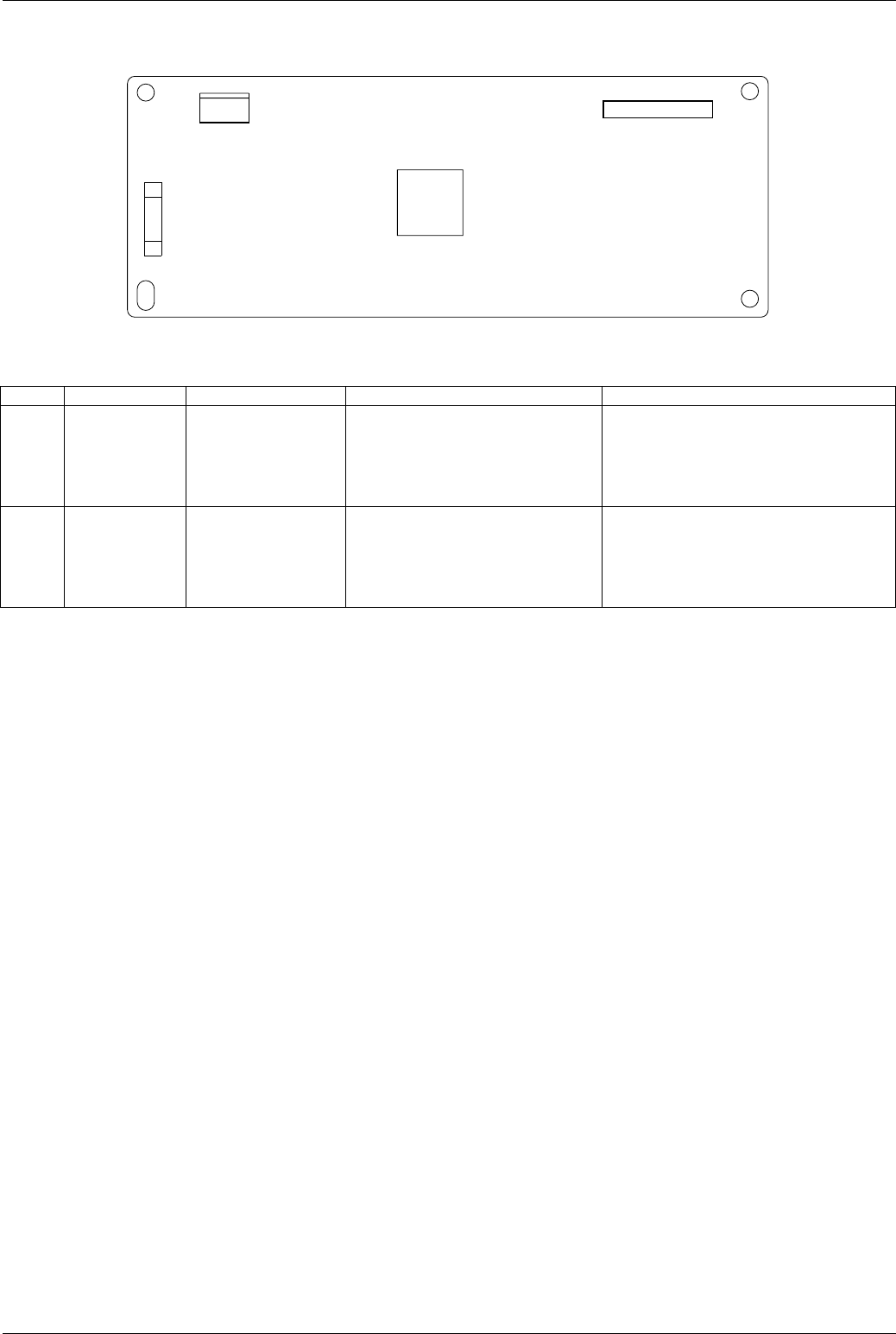
Maintenance, Adjustments and Check Points
87
3.12 Low Voltage Power Supply PCB (POW)
CN31
CN33
Refer to SCA / SCB PCB CN6.
Pin No. Signal Name Destination Signal Waveform Function
CN31-1 HEAT 1 Fuser Unit CN116 Fuser Lamp AC (Black-Live)
CN31-2 HEAT 2 Fuser Unit CN116 Fuser Lamp AC (White-Neutral)
L102
CN33
110
FUSE
CN31
12
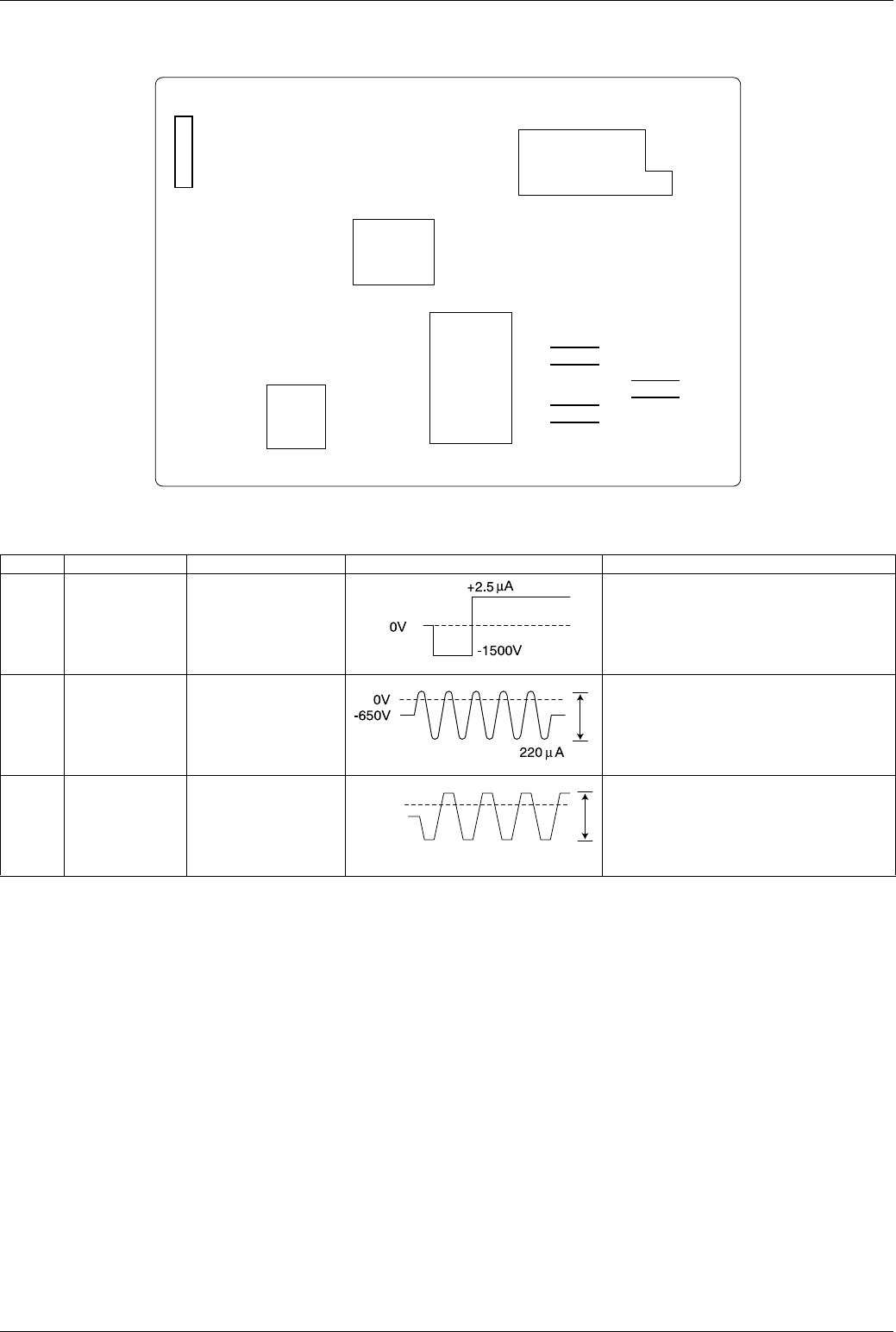
Panasonic UF-585 / 595
88
3.13 High Voltage Power Supply PCB (HVPS)
High Voltage Output
CN39
Refer to LPC PCB CN53.
Pin No. Signal Name Destination Signal Waveform Function
T Transfer Bias Transfer Roller (1) Transfer Current: (+2.5 µA)
(2) Cleaning Voltage: (-1500 V)
C Charge Bias Charge Roller Charge Current: 220 µA
(AC 220 Hz Sine Wave)
& DC Charge Voltage
D Development Development Roller Development Voltage
(AC 1.875 kHz Square Wave)
& DC Voltage
CN39
T201 T101
T301
T401
110
C
D
T
1500Vp-p
-300V
0V

Maintenance, Adjustments and Check Points
89
3.14 SNS3
CN83
Refer to LPC PCB CN59.
CN84
Pin No. Signal Name Destination Signal Waveform Function
CN84-1 GND Toner Sensor Ground
CN84-2 TONER Toner Sensor Remaining Toner Level Signal
CN84-3 +5V Toner Sensor +5 VDC Power Supply
CN84
1
3
CN83
1
5
0V
Approx. +2 VDC
+5V
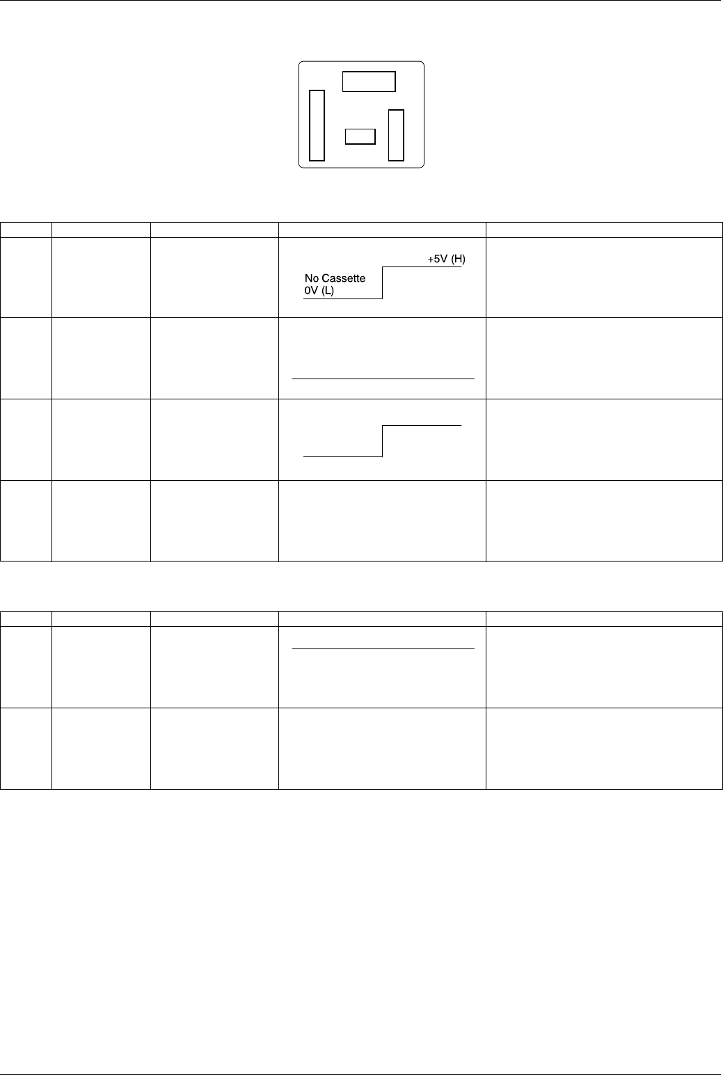
Panasonic UF-585 / 595
90
3.15 SNS4
CN85
CN86
CN87
Refer to LPC PCB CN58.
Pin No. Signal Name Destination Signal Waveform Function
CN85-1 nCCHK1 SNS1
CN81-1
No Cassette Detection Signal
CN85-2 GND SNS1
CN81-2
Ground
CN85-3 nRSEN SNS1
CN81-3
Timing Sensor Detection Signal
CN85-4 LDRE SNS1
CN81-4
Timing Sensor and No Cassette Sensor LED
Drive Current
Pin No. Signal Name Destination Signal Waveform Function
CN86-1 +5V Thermistor +5 VDC Power Supply
CN86-2 THERM Thermistor Fuser Thermistor Voltage Level Signal
CN85
4
1
CN86
2
1
CN87
6
1
0V
+5V (H)
0V (L)
Detect Paper
Approx. +2 VDC
+5V
Approx. +2 VDC
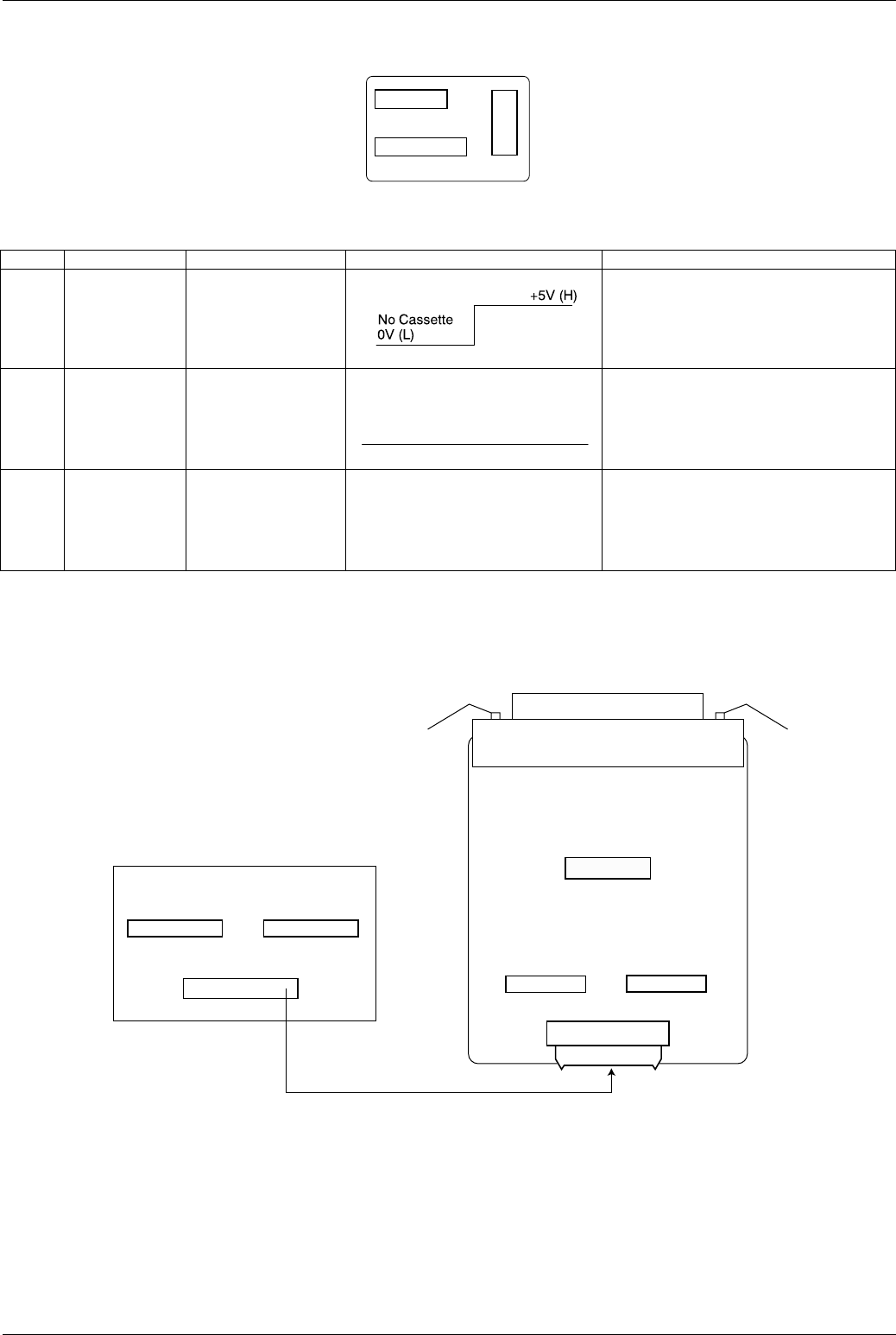
Maintenance, Adjustments and Check Points
91
3.16 SNS1
CN80
CN81
Refer to SNS4 PCB CN85.
3.17 Parallel Interface PCB (Option)
CN200
Refer to SCA / SCB PCB CN10.
CN201
Refer to SCA / SCB PCB CN11.
CN202 and CN212
Refer to SCA / SCB PCB CN10 and CN11.
Pin No. Signal Name Destination Signal Waveform Function
CN80-1 nCCHK1 SNS2
CN82-1
No Cassette Detection Signal
CN80-2 GND SNS2
CN82-2
Ground
CN80-3 LDSC1 SNS2
CN82-3
No Cassette Sensor LED Drive Current
CN81
4
1
CN80
3
1
0V
Approx. +1 VDC
Parallel I/F
CN212
CN202
CN201CN200
140
PRT PCB
CN211
1 18
CN210
1 20
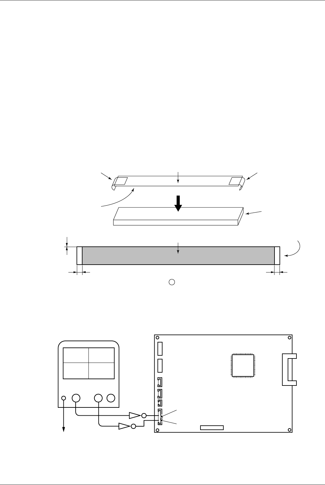
Panasonic UF-585 / 595
92
3.18 CCD Alignment
The CCD PC Board (337) is factory adjusted using special precision equipment and normally should not be replaced in the field. It
is recommended that the entire Scanner Block (321) be replaced. This will insure that the CCD PC Board (337) is aligned
properly.
If the CCD PC Board (337) is replaced, it can temporarily be aligned by following the procedure given below.
Note: The picture quality may not be the same as a unit that has been factory set.
• TOOLS REQUIRED
1. A 2 channel Oscilloscope
2. CCD Test Pattern
a copy can be made from the pattern shown in the Appendix. It must be reproduced to the same size as the sample
pattern in the Appendix (1:1 ratio).
• PROCEDURE
1. Remove Covers (see chapter 2).
2. Remove the Transmitter Unit with the Control Panel Assembly (see Section 2.4).
3. Position the CCD Test Pattern as follows.
a. Remove the Scanning Glass (308).
b. Using scotch tape, position the CCD Test Pattern on the Scanning Glass (308) as shown below. The CCD Test
Pattern must be faced down and centered on the Scanning Glass (308).
c. Set the Scanning Glass (308) with the CCD Test Pattern.
4. Connecting the Oscilloscope
• Carefully solder 2 probe wires to the components shown below on the SCA / SCB PC Board as shown below.
a. CN7 pin 4 (Trigger)
b. CN7 pin 8 (CCD out)
Tape
Printed side
Aligh the edge
CCD Test Pattern Tape
Scanning glass
Scanning glass
B
CCD Test Pattern
2 A=B
A
Frame Ground
CH1
CPU
SCA / SCB
CN7 - 8
CN7 - 4
CH2TRGG
Oscilloscope

Maintenance, Adjustments and Check Points
93
5. Adjusting the CCD PC Board
a. Enter Service Mode No. 5-1 (see Section 5.5.1 [CCD Test]).
b. Monitoring the Oscilloscope, carefully adjust the position of the CCD Board until the output is obtained as shown
below. Make sure that the ADF Door is closed.
c. Carefully tighten both mounting screws on the CCD PC Board.
6. Disconnect the Oscilloscope and reassemble the machine.
7. Run a test in Copy Mode to ensure the until is working properly.
Approx.
300mv
CCD out

Panasonic UF-585 / 595
94
APPENDIX
CCD TEST PATTERN
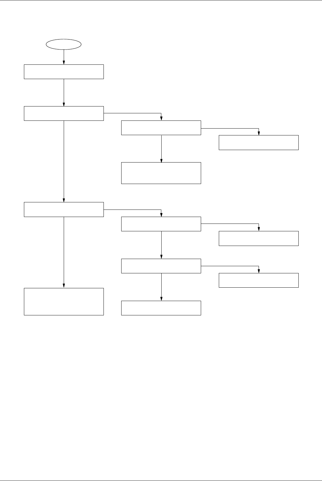
Panasonic UF-585 / 595
96
4 Troubleshooting
4.1 Initial Troubleshooting Flowchart
START
Plug the Power Cord in to turn
ON the unit.
Does the LCD display function
correctly?
Does the original document feed
through correctly?
Does the recording paper exit the
unit?
Troubleshoot printed copy quality
problems (Sect. 4.4).
Troubleshoot the Document
Feeder (Sect. 4.5).
Check for recording paper path
problems.
Troubleshoot Improper LCD
Display (Sect. 4.2).
Troubleshoot any 3-digit
INFO. CODE displayed
(Sect. 4.3).
Does the unit produce normal
copies?
Troubleshoot communication
problems (transmission, reception,
dialing, polling, information codes,
or diagnostic codes.) (Sect. 4.6-4.8)
Does the unit power up normally?
Yes
Yes
Yes
Yes
No
No
No
No
Yes
No
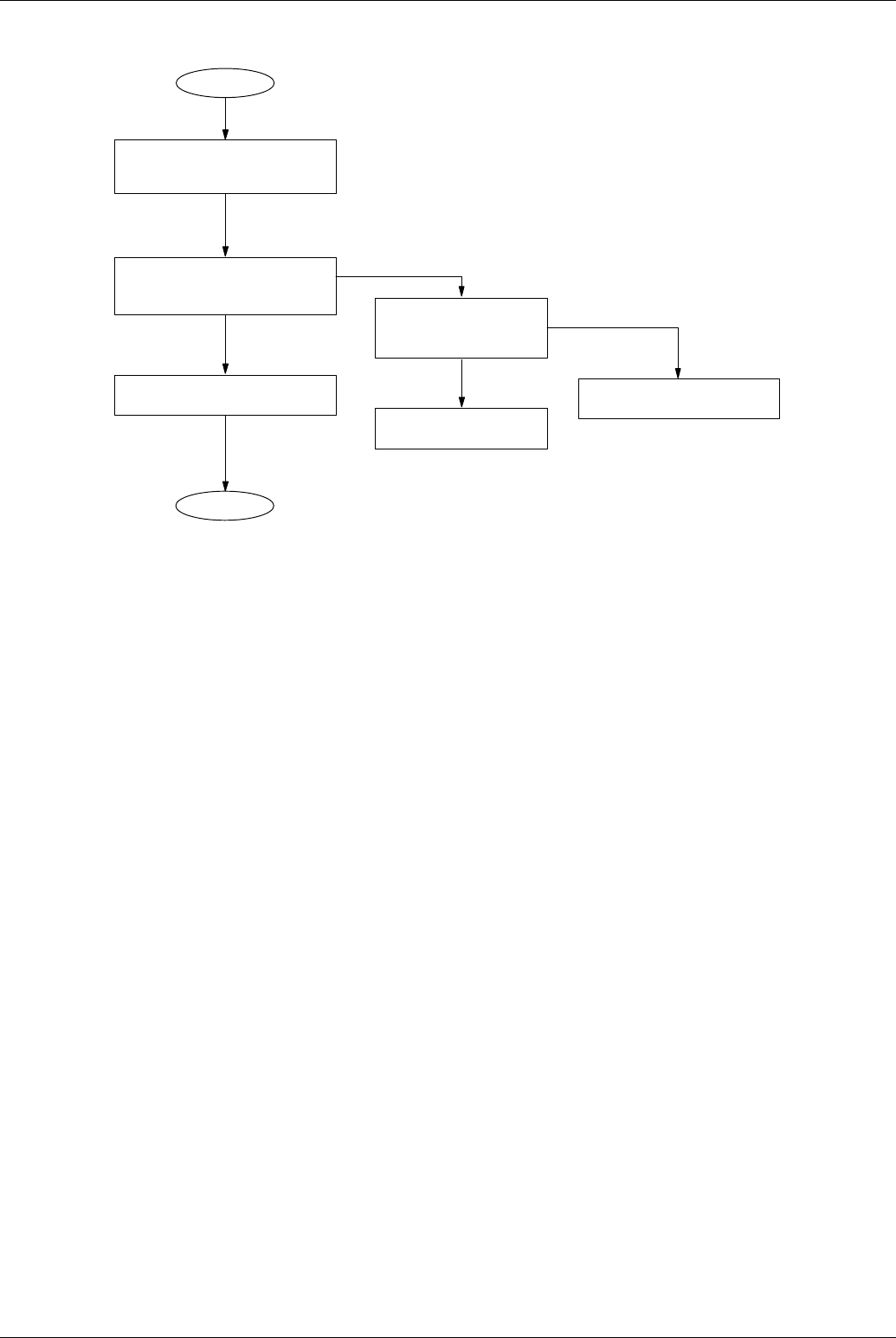
Troubleshooting
97
4.2 Improper LCD Display
Check connectors: CN4
(SCA/SCB PCB) and CN40
When pressing any key,
do you hear the 'Pi-' sound from
the Speaker? Does CN4, pin 2 and pin 3
on the SCA/SCB PCB
measure +5VDC?
Replace the SCA/SCB PCB.
Replace the PNL1 PCB.
Reinstall the firmware.
Yes
Yes
No
No
START
END
(PNL1 PCB).
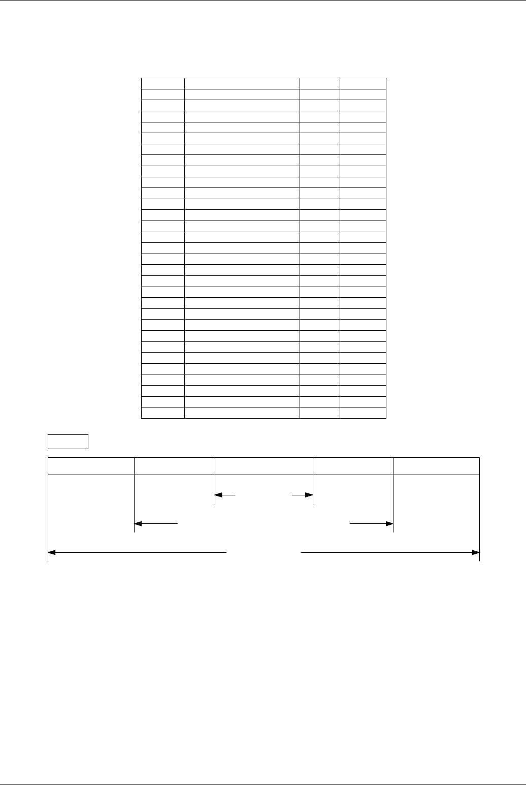
Panasonic UF-585 / 595
98
4.3 Information Codes (INFO. CODES)
The 3-digit information codes display to show the unit’s status. These codes also print on the journal. The following table indicates
appropriate sections for troubleshooting.
Phase A: Call establishment
Phase B: Pre-message procedure
Phase C: Message transmission
Phase D: Post-message procedure
Phase E: Call release
Code Explanation Phase Section
001 Recording paper jam C 4.3.8
002 Recording paper jam C,D 4.3.8
007 Recording paper jam C,D 4.3.8
010 No recording paper B,C 4.3.9
030 Document misfeeding B 4.3.10
031 Document too long C 4.3.10
400 Transmission error B 4.3.1
401 Transmission error B 4.3.2
402 Transmission error B 4.3.2
403 Polling reception error B 4.3.12
404 Transmission error B 4.3.3
405 Transmission error B 4.3.3
407 Transmission error D 4.3.3
408 Transmission error D 4.3.5
409 Transmission error D 4.3.5
411 Polling reception error B 4.3.12
414 Polling reception error B 4.3.12
415 Remote side mis-operation B 4.3.12
416 Reception error D 4.3.4
417 Reception error C 4.3.5
418 Reception error C 4.3.5
420 Reception error B 4.3.1
422 Transmission error B 4.3.2
434 Signal noise level too high B 4.3.6
459 Reception error C 4.3.7
490 Reception error C 4.3.5
494 Reception error C 4.3.7
495 Reception error C 4.3.7
630 Remote unit busy B 4.3.11
634 No busy tone detected B -
Phase A Phase B Phase C Phase D Phase E
Message
Transmission
Facsimile Communication Procedure
Facsimile Call
Phase
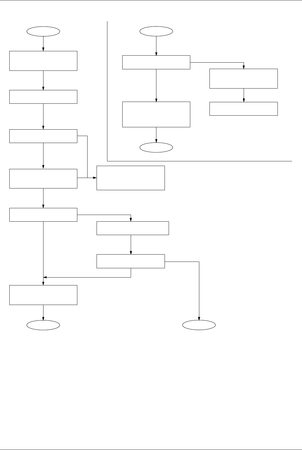
Troubleshooting
99
4.3.1 Information Codes: 400, 420
START
400
END END
Enable the monitor speaker.
(Refer to Sect. 5.2 Parameter
No. 008)
Does the remote unit repeat
the 300 bps signal every 3
sec.?
1. Refer to Sect. 4.6.
2. Check the remote unit.
(Remote unit is defective)
(Remote unit is defective)
2. Check the telephone
1. Check the remote unit.
number to the remote unit.
Perform a transmission test to
the remote unit in question.
Does the remote unit send the
CED and 300 bps Fax signal ?
Is transmission to the
reference unit successful?
1. Replace the LCU PCB.
2. Replace the SCA/SCB PCB.
Does the trouble still occur?
Yes
Yes
Yes
No
No
No
Yes
No
START
420
END
2. Check the remote unit.
1. Misdialed call.
(Remote unit is defective)
3. Refer to Sect. 4.6.
Check the line connection
from the wall jack to the "Line"
on the LCU PCB.
Is reception from a reference
unit successful?
Replace the SCA/SCB PCB.
Yes
No
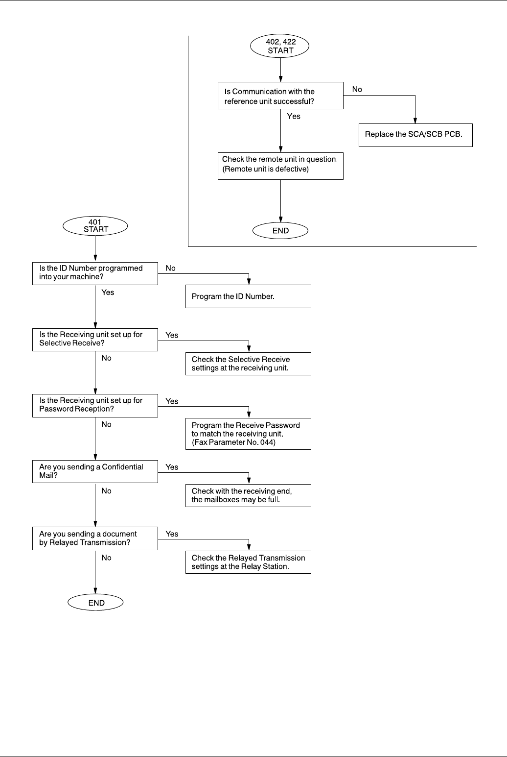
Panasonic UF-585 / 595
100
4.3.2 Information Codes: 401, 402, 422
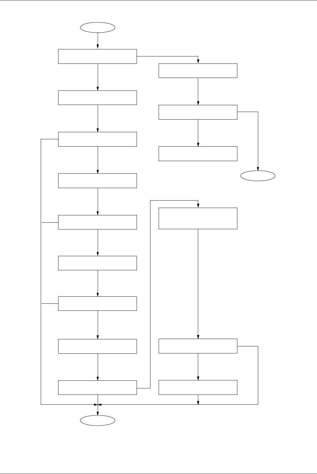
Troubleshooting
101
4.3.3 Information Codes: 404, 405, 407
START
END
Is communication with reference
unit successful?
Change Function Parameter #010:
Reduce Tx Attenuation Level
Yes
No
Yes
No
Change Function Parameter #017:
Reduce Tx Modem Speed
Does the problem still occur?
1. Replace the LCU PCB.
2. Replace the SCA/SCB PCB.
Does the problem still occur?
Change Function Parameter #025:
Communication Startup to 2nd
Does the problem still occur?
Change Funciotn Parameter #014:
Increase G3 Tx Equalization
Does the problem still occur?
END
Does the problem still occur?
Check the telephone line condition.
Does the problem still occur?
(Recording paper may have run
Check the remote unit.
out or paper may have jammed.)
Refer to Sect. 4.6.
Yes
No
Yes
No
Yes
Yes
No
No
Yes
No
Panasonic UF-585 / 595
102
4.3.4 Information Code: 416
START
END
Is communication with the
reference unit successful?
Change Function Parameter #011:
Reduce Rx Sensitivity Level
Yes
No
Yes
No
Change Function Parameter #023:
Increase Training Check Period
Does the problem still occur?
1. Replace the LCU PCB.
Refer to Sect. 4.6.
2. Replace the SCA/SCB PCB.
Does the problem still occur?
Change Function Parameter #013:
Increase G3 Rx Equalization
Does the problem still occur?
END
Does the problem still occur?
Yes
No
No
Yes
No
Yes
Check the telephone line condition.
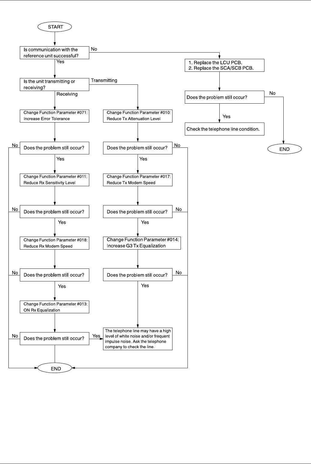
Troubleshooting
103
4.3.5 Information Codes: 408, 409, 417, 418, 490
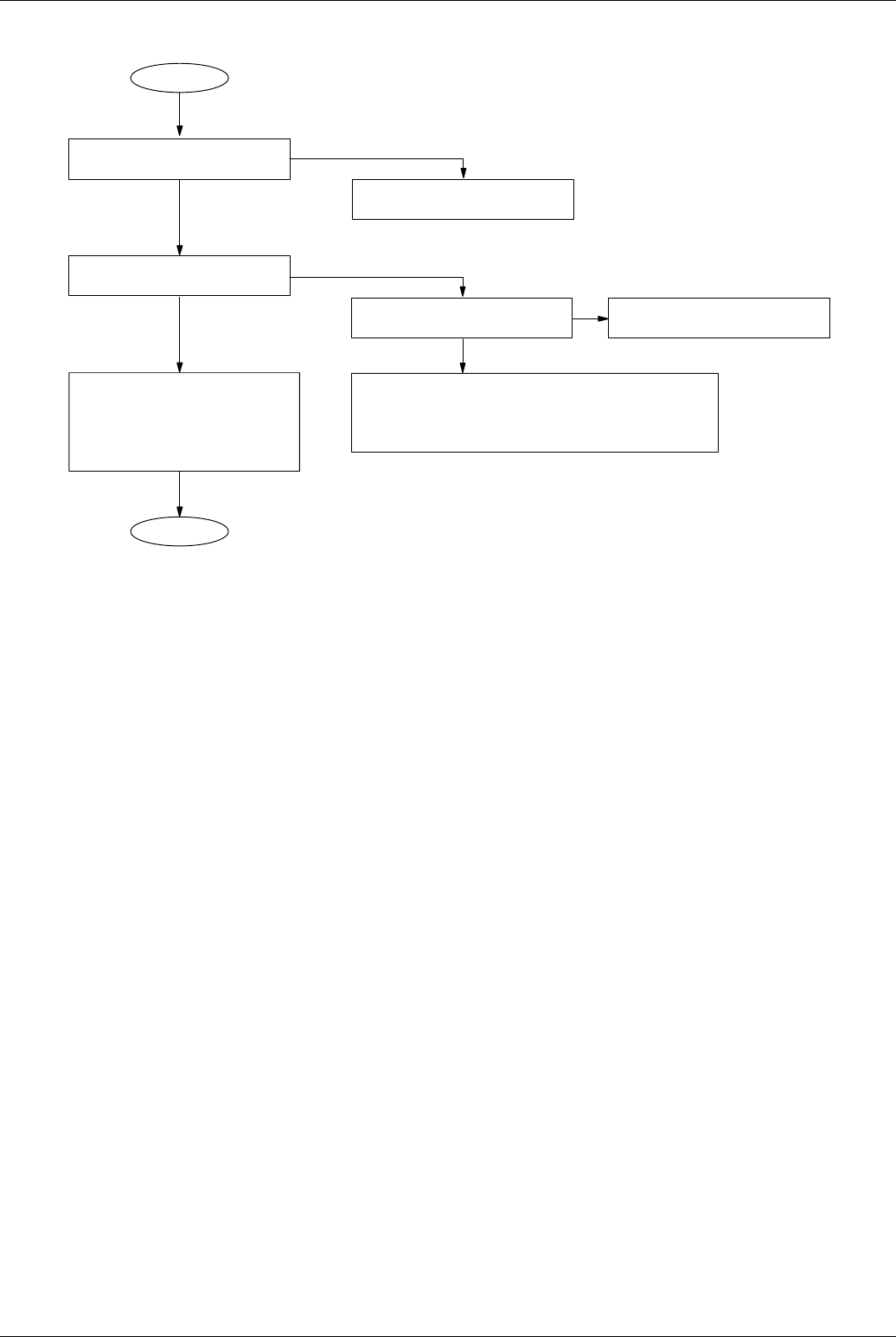
Panasonic UF-585 / 595
104
4.3.6 Information Code: 434
START
END
Is communication with the
reference unit successful?
Does the trouble occur
regardless of the remote unit?
Yes
No
Yes Yes
Replace the SCA/SCB PCB.
No
Can the transmitter in question
transmit to the other units?
Check the remote unit in question.
(Remote unit is defective)
Change the parameter in Service Mode 1.
(Refer to Sect. 5.2.)
for transmitter
for receiver
: #010
: #011
: Increase Tx Level
: Reduce Rx Sensitivity Level
The telephone line may have a high
level of white noise and/or
frequent impulse noise.
Ask the telephone company to
check the line.
No
Troubleshooting
105
4.3.7 Information Codes: 459, 494, 495
START
END
between the telephone jack on
Check the line connection
the wall and the LCU PCB.
Is communication with the
reference unit successful?
Yes
No
Yes
No
Does the problem still occur?
1. Replace the LCU PCB.
No
1. Check the remote unit in
question. (Remote unit is defective)
2. Refer to Sect. 4.6.
2. Replace the SCA/SCB PCB.
If the telephone line frequently
disconnects at the beginning of each
communication, ask the telephone
company to check the line.
Does the trouble occur
regardless of the remote unit?
END
Yes
Check the telephone line condition.
Panasonic UF-585 / 595
106
4.3.8 Information Codes: 001, 002, 007 (Recording Paper Jam)
START
Yes
No
Is the recording paper size and
thickness within specification?
Replace with correct paper.
Yes
No
Is the recording paper loaded in
the Cassette properly?
Load the paper correctly.
END
Check the Paper Feed Solenoid.
Is the paper cassette functional?
Yes
No
Replace the paper cassette.
Check the Paper Feed Roller
Assembly.
Check all Sensors and Actuators
(No Paper Sensor, Timing
Sensor, Paper Exit Sensor).
Troubleshooting
107
4.3.9 Information Code: 010 (No Recording Paper)
START
Yes
No
Is the Paper Cassette seated
properly
Reseat the cassette.
Yes
No
No
Is the recording paper loaded in
the cassette?
Load the paper.
Yes
No
Is the No Paper Actuator
operational?
Replace the Actuator.
Yes
Is the No Paper Sensor
operational?
Replace the No Paper Sensor.
Yes
No
Does the Paper Feed Roller turn?
Overhaul the Clutch Gear
Assembly.
END
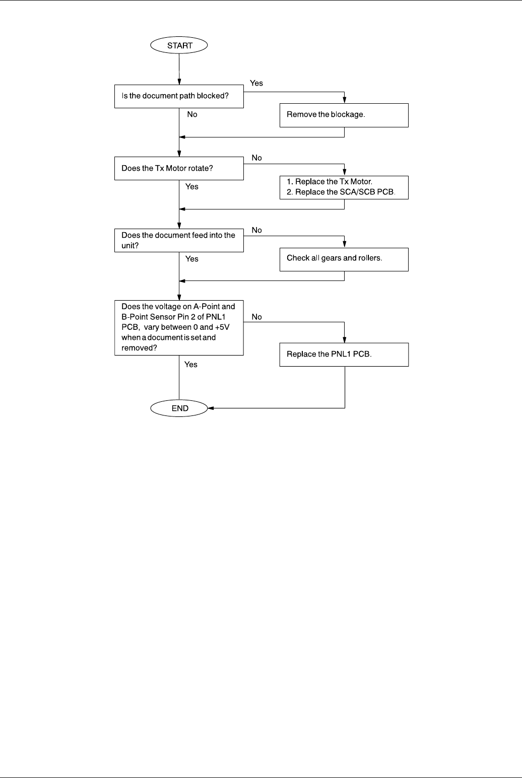
Panasonic UF-585 / 595
108
4.3.10 Information Codes: 030, 031 (Document Jam)
Troubleshooting
109
4.3.11 Information Code: 630 (Dialing Error)
START
END END
Yes
No
Is there a dial tone when
MONITOR button is pressed? 1. Connect the telephone line
correctly.
2. Check the telephone line.
Yes
No
Is the remote machine busy?
Can the unit dial the reference
unit? No
1. Check all connectors.
2. Replace the SCA/SCB PCB.
1. The remote machine is defective.
2. Telephone line quality is poor.
(Refer to Sect. 4.6.)
Press the REDIAL button to retry
connection.
Yes
Panasonic UF-585 / 595
110
4.3.12 Information Codes: 403, 411, 414, 415 (Polling Operator Trouble)
Troubleshooting
111
4.4 Printed Copy Quality Problems
4.4.1 Black Copy
START
No
Yes
Is the printout in Service Mode 3
normal?
Check the Scanner mechanism.
Is the HVPS normal?
Yes
Is the SCA/SCB PCB normal?
Is the Toner Cartridge
operational?
Replace the Toner Cartridge.
1. Check all connectors and
voltages on the HVPS.
2. Check the contacts between
HVPS and Toner Cartridge.
3. Replace the HVPS.
Yes
No
Yes
No
No
1. Check all connectors and
voltages on the SCA/SCB PCB.
2. Replace the SCA/SCB PCB.
END
Paper Travel
Panasonic UF-585 / 595
112
4.4.2 Blank Copy
START
END
Is the printout in Test Mode 3
normal?
Check the Scanner mechanism.
Are there any foreign particles or
stains on the BTR?
Is the Toner Cartridge operational?
Is the HVPS normal?
Yes
No
Replace the Toner Cartridge.
Yes
No
1. Clean the BTR with a soft, dry
cloth.
2. Replace the BTR.
1. Check all connectors and
voltages on the HVPS.
2. Check the Spring Connector
and voltage on the HVPS.
3. Replace the HVPS.
Are there any foreign particles or
stains blocking the Laser Beam
path?
Yes
No
Is the SCA/SCB PCB normal?
1. Remove the particles from the
laser beam path or clean the
stains.
2. Replace the LSU.
1. Check all connectors and
voltages on the SCA/SCB PCB.
2. Replace the SCA/SCB PCB.
Yes
No
No
Yes
Yes
No
Paper Travel
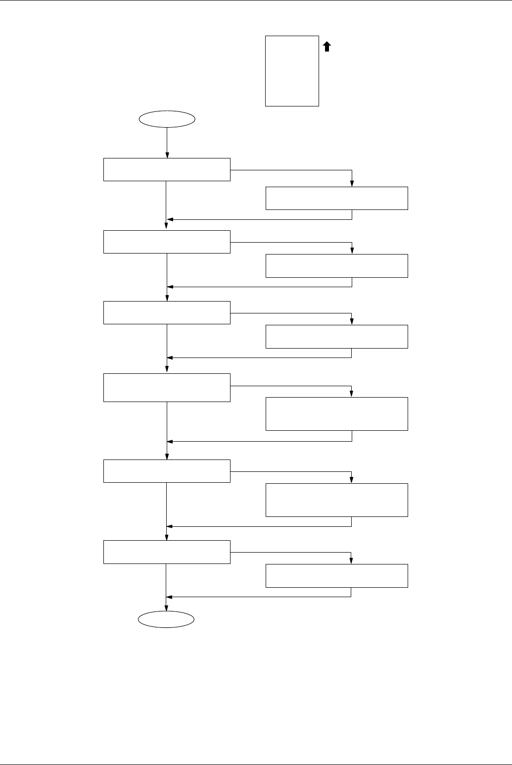
Troubleshooting
113
4.4.3 Vertical White Lines
START
END
Is the printout in Service Mode 3
normal?
Replace the paper.
Yes
No
Replace the Toner Cartridge.
Are there any foreign particles or
stains blocking the Laser Beam
path?
Yes
No
1. Clean the BTR with a soft, dry
cloth.
2. Replace the BTR.
Yes
No
Clean or replace the rollers.
No
Yes
Check the Scanner mechanism.
No
Yes
Is the recording paper damp?
Is the Toner Cartridge operational?
1. Remove the particles from the laser
beam path or clean the stains.
2. Replace the LSU.
Are there any foreign particles or
No
Yes
Are the Fuser and Pressure
Roller surfaces clean?
Paper Travel
P
stains on the BTR?
Panasonic UF-585 / 595
114
4.4.4 Ghost Images
START
END
No
YesIs the printout in Service Mode 3
normal?
Check the Scanner mechanism.
Is the Toner Cartridge operational?
No
Yes
Are the Fuser and Pressure
Roller surfaces clean?
No
Yes
Is the recording paper damp?
Are there any foreign particles or
stains on the BTR?
No
Yes
Yes
No
Replace the paper.
Replace the Toner Cartridge.
1. Clean the BTR with a soft, dry
cloth.
2. Replace the BTR.
Clean or replace the rollers.
Paper Travel
A
AAAA
Troubleshooting
115
4.4.5 Vertical Dark Lines
START
No
YesIs the printout in Service Mode 3
normal?
Check the Scanner mechanism.
Is the Toner Cartridge operational?
No
Yes
Are there any foreign particles or
stains on the BTR?
Yes
No
Replace the Toner Cartridge.
1. Clean the BTR with a soft, dry
cloth.
2. Replace the BTR.
Is the LSU normal? No
Yes Replace the LSU.
END
Are the Fuser and Pressure
Roller surfaces clean?
No
Yes Clean or replace the rollers.
Paper Travel
P
Panasonic UF-585 / 595
116
4.4.6 Horizontal Dark Lines
START
Is the printout in Service Mode 3
normal?
Yes
No
Replace the Toner Cartridge.
1. Clean the BTR with a soft, dry
cloth.
2. Replace the BTR.
No
Yes
Check the Scanner mechanism.
Is the Toner Cartridge operational?
No
Yes
Is the LSU normal? No
Yes Replace the LSU.
Is the HVPS normal?
1. Check all connectors and
voltages on the HVPS.
2. Check the Spring Connector
and voltage on the HVPS.
3. Replace the HVPS.
Yes
No
END
Are the Fuser and Pressure
Roller surfaces clean?
No
Yes Clean or replace the rollers.
Paper Travel
P
Are there any foreign particles or
stains on the BTR?
Troubleshooting
117
4.4.7 Dark Background
Is the LSU normal? No
Yes Replace the LSU.
START
No
YesIs the printout in Service Mode 3
normal?
Check the Scanner mechanism.
Is the Toner Cartridge operational?
No
Yes
Is the recording paper damp?
Yes
No
Replace the paper.
Replace the Toner Cartridge.
Is the HVPS normal?
1. Check all connectors and
voltages on the HVPS.
2. Check the Spring Connector
and voltage on the HVPS.
3. Replace the HVPS.
Yes
No
END
Are the Fuser and Pressure
Roller surfaces clean?
No
Yes Clean or replace the rollers.
Paper Travel
P
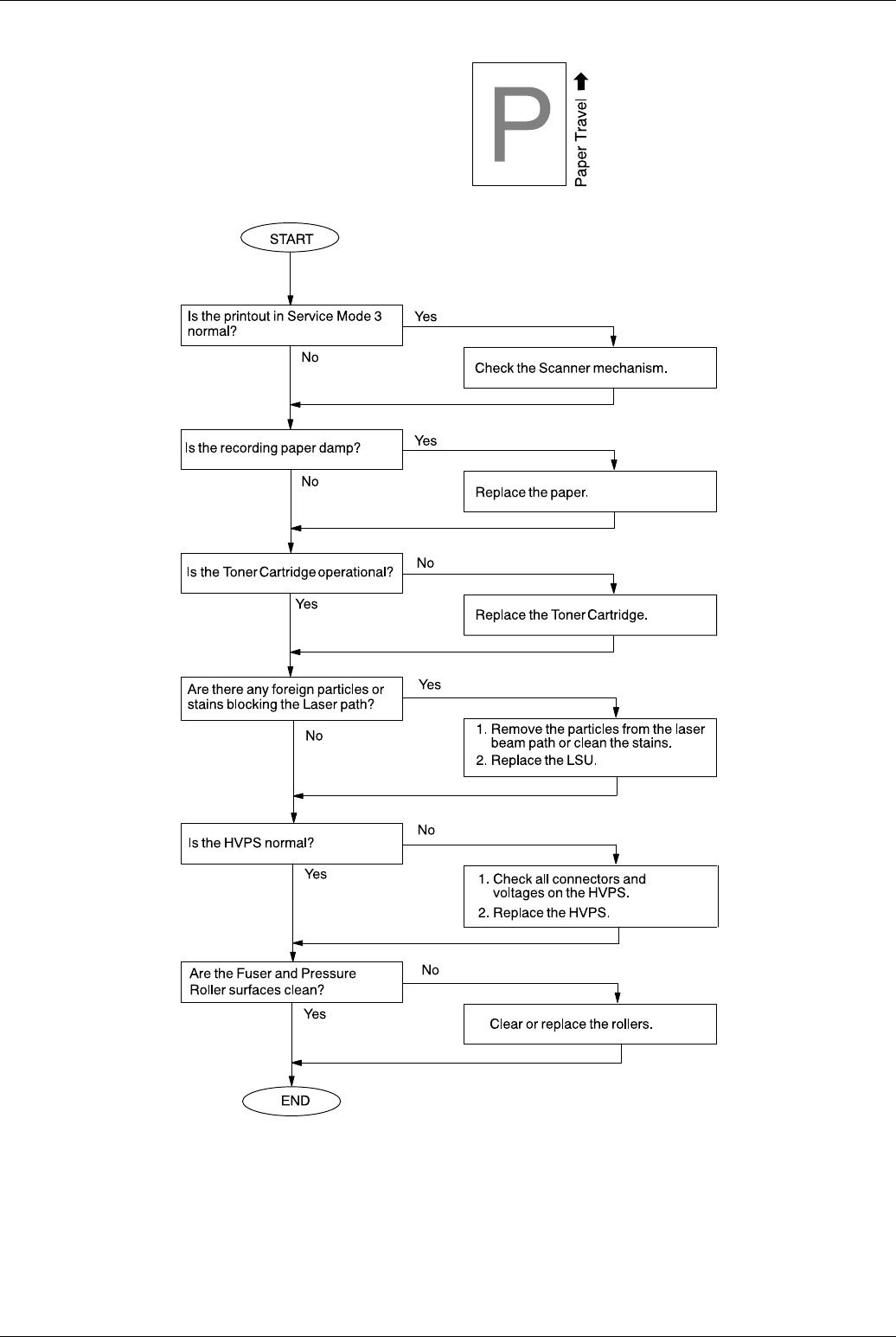
Panasonic UF-585 / 595
118
4.4.8 Light Print
Troubleshooting
119
4.4.9 Horizontal White Lines
END
Are the Fuser and Pressure
Roller surfaces clean?
No
Yes Clean or replace the rollers.
START
No
YesIs the printout in Service Mode 3
normal?
Check the Scanner mechanism.
Is the Toner Cartridge operational?
No
Yes
Is the recording paper damp?
Yes
No
Replace the paper.
Replace the Toner Cartridge.
Is the HVPS normal?
1. Check all connectors and
voltages on the HVPS.
2. Replace the HVPS.
Yes
No
1. Clean the BTR with a soft, dry
cloth.
2. Replace the BTR.
Are there any foreign particles or
stains on the BTR?
No
Yes
Paper Travel
P
Panasonic UF-585 / 595
120
4.4.10 Improper Fusing (Printed image does not bond to the paper)
Note
Replace the entire Unit when the Thermostat or the Thermal Fuse becomes open-circuit.
END
Is the Fuser Unit normal? No
Yes Replace the Fuser Unit. (See Note)
START
No
Yes
Is the recording paper damp?
Replace the paper.
P
Troubleshooting
121
4.4.11 Voids in Solid Areas
END
Are the Fuser and Pressure
Roller surfaces clean?
No
Yes Clean or replace the rollers.
START
No
Yes
Is the recording paper damp?
Replace the recording paper.
Is the Toner Cartridge operational?
Yes
No
Replace the Toner Cartridge.
P
Paper Travel
Panasonic UF-585 / 595
122
4.4.12 Black Dots
END
Are the Fuser and Pressure
Roller surfaces clean?
No
Yes Clean or replace the rollers.
START
Is the Toner Cartridge operational?
Yes
No
Replace the Toner Cartridge.
P
Paper Travel
Troubleshooting
123
4.4.13 Recording Paper Creases
START
No
Yes
Is the recording paper damp?
Replace the recording paper.
END
Are there any foreign particles or
stains in the Fuser Unit?
1. Clean or replace the rollers.
Are there any foreign particles or
stains in the paper path?
Yes
No Remove any obstructions and
clean the paper path.
No
Yes
Is the recording paper skewing?
Ensure the paper is set under the
Paper Separation Clips in the cassette.
No
Yes
2. Replace the Fuser Unit.
Paper Travel
Panasonic UF-585 / 595
124
4.4.14 Poor Printed Copy Quality
START
Is the printout in Service Mode 3
normal?
1. Replace the LPC PCB.
2. Replace the LSU.
3. Replace the HVPS.
4. Replace the Toner Cartridge.
END
Perform a receiving test with the
reference fax unit.
Is the printed copy correct?
Yes
No
Make a local copy.
No
Yes Check the Transmission Block
(CN30 on the CCD PCB and
CN4 on the SCA/SCB PCB).
Is the received copy correct?
1. Check CN8 on the SCA/SCB PCB.
2. Check CN25 on the LCU PCB.
3. Check the Telephone Line Cable.
4. Replace the SCA/SCB PCB.
Yes
No
Is a poor copy printed when
receiving from a specific
transmitter?
Yes
No
Telephone line quality is poor.
(Refer to Sect. 4.6.)
The transmitting machine may be
defective.
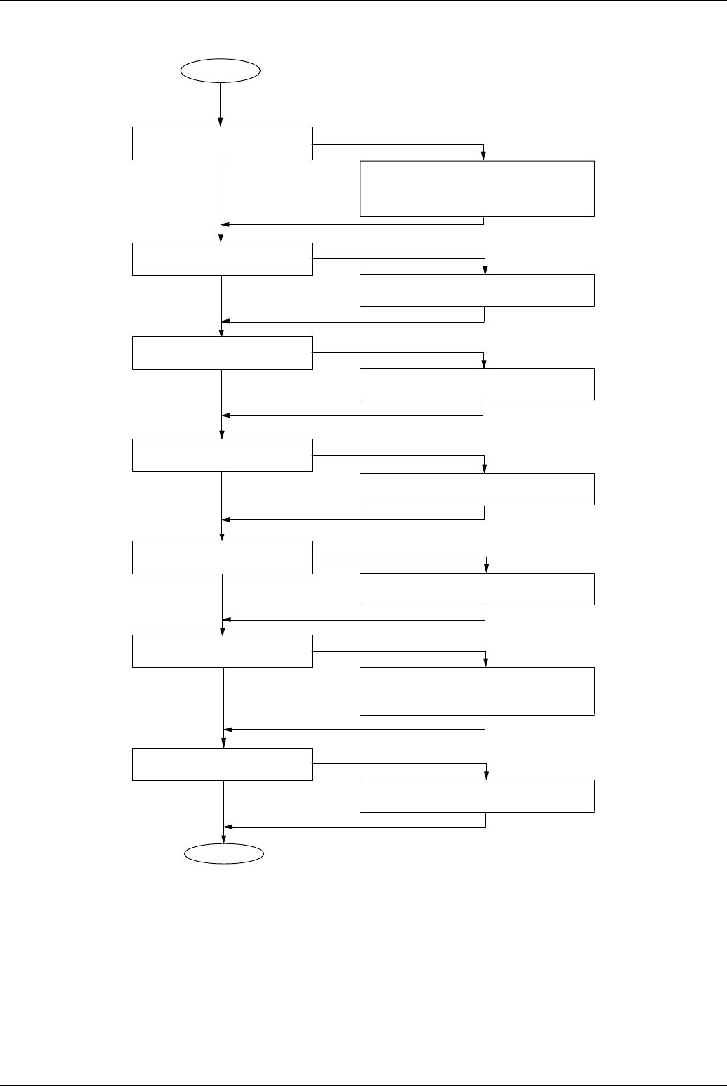
Troubleshooting
125
4.4.15 Abnormal Printing
START
Is the recording paper loaded in
the cassette properly?
1. Adjust the Paper Width Guide (Sect. 8.5).
2. Adjust the Paper Length Guide.
3. Ensure the paper is under the Paper
Separation Clips.
Is the Panasonic Toner Cartridge
being used?
Yes
No
Is the recording paper size and
thickness within specification?
Yes
No
Yes
No
Replace with correct paper (Sect. 1.5).
Replace with the Panasonic Toner Cartridge.
Are all switches and sensors
operating properly?
Do the rollers rotate properly?
Yes
No
Are there any foreign particles or
paper pieces in the receiver unit?
Yes
No
Remove the foreign particles or paper pieces
from the receiver unit.
1. Check all rollers, gears, drive clutches and
springs.
2. Adjust or replace any defective parts.
Adjust, clean or replace.
Yes
No
Is the receiving mechanism
operating correctly?
Yes
No
Adjust or replace any defective parts.
END
Panasonic UF-585 / 595
126
4.4.16 Scanned Copy Quality Problems
START
No
Yes
Is the LED Array abnormal?
Replace the LED Array.
END
Are the Transmitting Rollers
dirty?
Are there any foreign particles or
paper pieces in the scanning area?
Yes
No Remove the foreign particles or paper
pieces from the scanning area.
No
Yes
Is the scanning area dirty?
1. Clean the Scanning Glass (Sect. 2.5).
2. Clean Mirrors 1, 2 and 3 (Sect. 2.9).
No
Yes
Clean the rollers (Sect. 2.10).
Is the Scanner Assembly abnormal?
1. Check CN7 (SCA/SCB PCB).
2. Check CN30 (CCD PCB).
3. Replace the Scanner Block (321) (Sect. 2.10).
4. Replace the SCA/SCB PCB (Sect. 2.11).
Yes
No
Troubleshooting
127
4.5 Document Feeder (ADF)
4.5.1 No Document Feed
START
END
Yes
No
Is the document set properly?
Set the document properly.
Yes
No
Is the document thickness or size
within specification? Make a copy or cut the document
to the specification size.
Yes
No
the document is set?
Is the "Pi.." tone generated when
Does the ADF Sensor actuator
move smoothly?
Replace the PNL1 PCB.
No
Adjust or replace the actuator.
No
Yes
Yes
Replace the PNL1 PCB.
Yes
Yes
No
Does the ADF Roller rotate?
Replace the Transmit Motor.
Is the trouble solved?
No
Replace the ADF Roller or
Separation Rubber or both.
Yes
No
Is the ADF Roller surface dirty?
Clean the ADF Roller surface.
Adjust the separator pressure.
Is the trouble solved?
END
Panasonic UF-585 / 595
128
4.5.2 Document does not feed or Multiple feeds
START
END
No
Is the Control Panel Unit locked?
Close the Control Panel Unit firmly.
Yes
No
Is the ADF Roller clean?
Clean the surface of the roller
with isopropyl alcohol (Sect. 2.5).
Yes
No
Is the ADF Roller worn out?
Replace the ADF Roller
(Sect. 2.5).
Yes
No
Does the ADF Roller drive
properly?
Does the ADF Roller's gear
system function properly?
Yes
No
Separation Rubber normal?
Is the adjustment of the
Is the Separation Rubber worn
out?
Replace the Separation Rubber.
No
Clean or adjust the Separation
Rubber Pressure (Sect. 2.3).
No
Yes Adjust the gear system or replace
defective parts.
Yes
Yes
Troubleshooting
129
4.5.3 Document Jam (030) or Skewing
START
END
Yes
No
Is the Control Panel Unit closed?
Close the Control Panel Unit firmly.
Do all sensors on the PNL1 PCB
operate normally?
Does the Feed Roller have drive
and sufficient friction?
Yes
No
Clean or replace the PNL1 PCB.
Is the document path clear of
foreign particles or paper?
Yes
No
Clean the surface of the roller
Is the Transmitting mechanism
operating properly?
Yes
No
Remove the foreign particles or
with isopropyl alcohol (Sect. 2.5).
paper from the document path.
Yes
No
Adjust or replace any defective
parts.
Panasonic UF-585 / 595
130
4.6 Communications
This section explains general troubleshooting procedures for the 400 series of Information Codes. These errors are primarily
caused by poor telephone line quality (loss, noise, echo, etc.). This unit is furnished with Service Mode 1 to assist in troubleshooting
line quality problems.
It is suggested that both the transmitting unit and receiving unit be adjusted. This section gives relevant parameters in Service
Mode 1 for the transmitting and receiving sides. If no improvement is realized after the parameters are adjusted, it is recommended
that the parameters be returned to the default settings.
4.6.1 Communication Trouble
Troubleshooting
131
4.6.2 Poor Transmitted Copy Quality
START
Yes
Make a copy.
No
No
Yes
Is the printed copy normal?
Perform a transmission test
to a reference fax unit.
Is the LED Array lit?
Does CN1, pin 1 on
the
SCA/SCB PCB measure
+24 VDC?
Yes
No
Yes
No
Are CN7 (
SCA/SCB
PCB)
and CN30 (CCD PCB)
connected properly? Connect them correctly.
Replace the LVPS.
Does nLEDON go Low
when the scan starts?
Check CN1 on the
SCA/
SCB
PCB and the LED
harness.
Does the problem still
occur?
Replace the LED Array.
The receiving unit may be
defective.
1. Replace the Scanner
Block.
2. Replace the
SCA/SCB
PCB.
Replace the
SCA/SCB
PCB.
Is the transmitted copy
normal?
No
Yes
No
No
1. Check CN8 (
SCA/SCB
PCB)
and CN25 (LCU PCB).
2. Check the telephone line cable.
Replace if necessary.
Does poor transmitted copy
appear when transmitting to
a specific receiver? Telephone line quality is
poor.
END
Yes
Yes
Panasonic UF-585 / 595
132
4.6.3 Dialing Problems
START
END
No
Yes
Does the unit proceed to
Phase B?
1. Set documents on the ADF correctly.
4. Refer to Sect. 4.6.
3. The called party is busy.
2. Check the telephone line connection.
Are you using One-Touch dialing
or ABBR. dialing?
Are you using direct dialing?
No
Yes
Check the registered telephone number.
Is the Monitor Volume too loud or
too low?
No
Yes
Check the dialed telephone number.
No
Yes
Adjust the monitor volume.
Troubleshooting
133
4.6.4 Transmission Problems
START
END
Yes
No
Does the ID display?
1. No ID function at the remote unit.
2. The ID is not set for the remote unit.
Does the Verification Stamp
operate?
Is the copy quality OK?
Yes
No
1. Set "STAMP=ON"
2. Check CN3 (SCA/SCB PCB).
3. Replace the Stamp Solenoid.
4. Replace the SCA/SCB PCB.
Any other problems?
Yes
No
Make a copy and refer to Sect. 4.4.16
Yes
No See Sect. 4.3 (Troubleshooting using
information codes).
Panasonic UF-585 / 595
134
4.6.5 Reception Problems
START
END
Yes
No
Does the machine answer the
Ringing signal?
1. Set "RCV = AUTO".
2. Check that all covers are closed firmly.
3. Check the telephone line connection.
4. Check the Ringer Timing or DRD setting.
5. Check the recording paper path.
6. Check CN8 (SCA/SCB PCB) and CN25 (LCU PCB).
7. Replace the LCU PCB.
8. Replace the SCA/SCB PCB.
Is the received copy OK?
Any other problems?
Yes
No
Make a copy and refer to Sect. 4.4.14.
Yes
No See Sect. 4.3 (Troubleshooting using
information codes).
Troubleshooting
135
4.6.6 Polling Problems
Note:
No-check Mode means that password is not set.
START
END
Yes
No
Is Polling reception OK?
1. Set the same polling password as the other party is using.
2. Check the password of the remote unit.
Is Polling transmission OK?
Any other problems?
Yes
No
1. Set the polling password or no - check mode.*
2. Check the password of the remote unit.
Yes
No See Sect. 4.3 (Troubleshooting using information codes).

Panasonic UF-585 / 595
136
4.7 Information Code Table
Information Codes
Code Mode Phase Description of Problem Cause
001 RCV
COPY
C,D Leading edge of the recording paper fails to
reach the Timing Sensor. (1st cassette)
Recording paper jam.
Timing Sensor abnormal.
002 RCV
COPY
C,D Leading edge of the recording paper fails to
reach the Timing Sensor. (2nd cassette)
Recording paper jam.
Timing Sensor abnormal.
007 RCV
COPY
C,D 1.Leading edge of the recording paper fails to
reach the Paper Exit Sensor.
2.Recording paper has not completely passed
the Paper Exit Sensor.
Recording paper jam.
Paper Exit Sensor abnormal.
008 RCV
COPY
C,D Paper Cassette was opened while the recording
paper was feeding.
Recording paper jam.
010 RCV
COPY
B,C No recording paper. No recording paper or paper is not set
properly.
No Paper Sensor is defective.
011 STANDBY B,C Paper Cassette is not installed properly.
012 RCV C,D The length of the received document is over 2m.
021 STANDBY
RX
COPY
B,C,D Thermister is abnormal.
Fuser Control is abnormal.
Defective LPC PCB.
Defective Fuser Unit, LVPS.
026 - - The backup battery is getting weak.
030 XMT B Read Point Sensor does not go ON within 10
seconds after the document starts feeding.
Document is not set properly.
Defective Read Point Sensor.
031 XMT
COPY
C Transmitting document was longer than
2,000mm (or 78.7 in).
The document may jam.
Defective Read Point Sensor.
033 - - Sub CPU system error. Defective SCA/SCB PCB.
041 STANDBY
RX
COPY
B,C,D Out of toner. No toner.
Defective Toner Sensor.
043 STANDBY
RX
COPY
B,C,D Low toner. Toner is getting low.
Defective Toner Sensor.
045 STANDBY - No Toner Cartridge. Toner cartridge has not been installed.
Defective Toner Sensor (Cartridge Sensor).
051 RCV
COPY
- Printer Motor abnormal. Connector not properly connected.
Defective Printer Motor.
Defective LPC PCB.
054 STANDBY
RX
COPY
- HSYNC abnormal.
Laser motor abnormal.
Defective Laser Unit.
055 STANDBY
RX
COPY
- No response of LBP CPU on LPC. Defective LPC PCB.
Defective SCA/SCB PCB.
059 RCV
COPY
C Interface error occurred between SCA/SCB
PCB and LPC PCB.
Defective LPC PCB.
Defective SCA/SCB PCB.
060 - A Printer Cover is open. Cover is not firmly closed.
Connectors are not firmly connected.
061 - A ADF Door is open. Cover is not firmly closed.
Connectors are not firmly connected.
200 RCV C Decoding process is not completed at the end of
phase C.
Defective SCA/SCB PCB.
212 XMT
RCV
A-E Interface error occurred between the CPU and
modem.
Modem is defective. (SCA/SCB PCB)
Software problem occurred. (SCA/SCB PCB)
301 XMT
RCV
System fault. Software problem occurred. (SCA/SCB PCB)
331 XMT C 8-minutes timer error. (Germany only)
400 XMT B T1 timer (35±5 sec) elapsed without detecting
300 bps signal.
Wrong number is dialed and the START button
is pushed.
Telephone line is disconnected while dialing.
SCA/SCB PCB (Modem) or LCU PCB is
defective.
Receiver is defective. (It may only be
transmitting CED)
401 XMT B DCN was returned from receiver while
transmitter is waiting for CFR or FTT.
Your machine’s ID Number is not programmed.
Possible incompatibility or incorrect Password
(Password Reception, Selective Receive).
Mailbox is full.

Troubleshooting
137
402 XMT B DCN was returned from receiver while
transmitter is waiting for NSF/DIS.
Receiver working in non-CCITT mode only.
(Possible incompatibility)
403 RCV(Polling) B Transmitter had no polling function. "POLLED=ON" (polling XMT ready) is not set
at the transmitter.
Document to be transmitted is not placed at the
transmitter.
404 XMT B Transmitter sent NSS (or DCS) followed by TCF
three times, but the receiver did not respond.
(CFR or FTT is usually returned)
Receiver is defective. (Modem, LCU PCB, etc.)
SCA/SCB PCB or LCU PCB is defective.
Receiver disconnects line during first NSS (or
DCS) is transmitted.
405 XMT B Transmitter received FTT after it transmitted
TCF at 2400bps.
Received RTN after communicating at 2400
bps.
Line quality is poor. (TCF is damaged due to
line noise)
Receiver is defective. (Modem, LCU PCB, etc.)
SCA/SCB PCB or LCU PCB is defective.
406 RCV(Pass-
word Comm.)
B XMT-Password mismatched.
RCV-Password mismatched.
Selective RCV incomplete.
XMT, RCV password does not match.
Last 4 digits of TSI does not match with the last
4 digits of ONE-TOUCH, ABBR telephone
number.
407 XMT D Transmitter received no response after it
transmitted post message, such as EOP, MPS,
EOM, etc...or received DCN.
Receiver is defective. (No paper, paper
jamming, etc.)
Receiver ceased receiving because of
excessive error. (Line quality is poor)
SCA/SCB PCB (Modem) or LCU PCB is defec-
tive.
408 XMT D Transmitter received RTN after it transmitted
EOP, MPS, or EOM.
Receiver receives data with error. (Line quality
is poor)
Receiver is defective. (Modem, LCU, etc.)
SCA/SCB PCB or LCU PCB are defective.
409 XMT D Transmitter receives PIN after it transmitted a
post message, such as EOP, MPS, EOM, etc.
Receiver receives data with error due to poor
line quality, and receiving operator requests
voice contact.
Receiver is defective. (Modem, LCU, etc.)
SCA/SCB PCB or LCU PCB are defective.
410 RCV D Received DCN while waiting for post command.
(EOP, MPS, EOM, etc.)
Interface or line is faulty.Transmitter is
defective.
411 RCV(Polling) B Received DCN after transmitting NSC. Transmitter is not ready for polling
communication.
Password does not match between transmitter
and receiver.
412 G3 RX B,D No response within 12 seconds in NSS/DCS/
MPS wait state. (After transmitting FTT)
Transmitter is defective.
SCA/SCB PCB is defective.
414 RCV(Polling) B No response received after transmitting 3rd
NSC.
Password does not match between transmitter
and receiver.
Transmitter is defective. (No document,
document jam, etc.)
415 XMT(Polling) B Remote side attempted to receive message
from your machine in polling
communication.
Inform the remote side that your machine does
not have the polling transmission feature.
416 RCV D Receiver did not detect post command, such as
EOP, MPS, EOM, etc.
Transmitter is defective.Line quality is poor.
(RTC signal is distorted due to line noise)
SCA/SCB PCB or LCU PCB are defective.
417 RCV C Receiver returned RTN in response to post
message.
Line quality is poor. (There are excessive errors
in received data)
SCA/SCB PCB or LCU PCB are defective.
418 RCV C Receiver transmitted PIN in response to PRI-Q
from transmitter. (Transmitting operator
requests voice contact)
Line quality is poor. (There are excessive errors
in received data)
SCA/SCB PCB or LCU PCB are defective.
420 RCV B T1 timer (35 sec.) elapsed without detecting 300
bps signal.
There is wrong incoming call.(non-facsimile
communication)
Transmitter is defective.
SCA/SCB PCB or LCU PCB is defective.
421 RCV B Busy Tone is detected after sending NSF Signal. Remote station disconnectes the line.
Wrong number is dialed.
422 XMT B Content of NSF (or DIS) or NSC (or DTC) was
invalid.
There is an incompatibility.
427 G3 RCV B DCN received to NSF/CSI/DIS transmitted. The interface is incompatible.
433 XMT
RCV
B,D T.30 Protocol abnormal. Defective remote station.
Information Codes
Code Mode Phase Description of Problem Cause

Panasonic UF-585 / 595
138
434 XMT or RCV B CD (response from Modem) did not turn OFF
within 180 sec. after receiver detected FLAG
signal.
Remote unit is defective.
SCA/SCB PCB or LCU PCB is defective.
436 G3 RX C DCN received after transmitting FTT. Transmitter is defective or incompatible.
Line quality is poor.
456 RCV B Received relay transfer request or confidential
document to distribute to a end receiving station
or all confidential mailboxes are used.
457 RELAYXMT
CONF.XMT/
POLL
B Remote unit does not have Relayed XMT or
Confidential Comm. capability.
459 RCV C Failed training in Phase C. Line quality is poor. (Training signal is distorted
due to line noise)
SCA/SCB PCB or LCU PCB are defective.
490 RCV C Sum of error line exceeded the limit (Parameter
70) by 64 lines.
Line quality is poor.
SCA/SCB PCB or LCU PCB are defective.
494 RCV C Interval between two EOLs was more than 10
sec. when receiver received message data.
Transmitter is defective.
Line quality is poor. (EOL is damaged due to
line noise)
SCA/SCB PCB or LCU PCB are defective.
495 XMT/RCV C During reception, CD turned OFF or continued
ON for long time.
During communication, lost loop - current.
Line is disconnected.
Transmitter is defective.
SCA/SCB PCB or LCU PCB are defective.
496 XMT C CS of modem is not able to turn ON. SCA/SCB PCB is defective.
501 XMT/
RCV(V.34)
B Remote unit does not have Modem
compatibility.
502 XMT/
RCV(V.34)
B,C,D During reception, CD turned OFF or continued
ON for long time.
During communication, lost loop - current.
Line is disconnected.
Transmitter is defective.
SCA/SCB PCB or LCU PCB are defective.
503 XMT/
RCV(V.34)
B,C,D CS of modem is not able to turn ON during
training.
SCA/SCB PCB is defective.
Line is disconnected.
504 RCV/V.34
(Polling)
B Polling is rejected from the remote station. No polling document is set.
505 XMT/V.34
(Polling)
B Polling XMT is rejected. No polling document is set.
540 XMT ECM B No response after transmitting 3rd CTC or DCN
received.
Incompatible interface.
541 XMT ECM D No response after transmitting 3rd EOR or
received DCN.
Line is faulty.
LCU PCB abnormal.
542 XMT ECM D No response to the 3rd RR transmitted or
received DCN.
Remote unit is abnormal.
543 XMT ECM D T5 timer (60 sec.) elapsed without MCF. Remote unit is abnormal.
544 XMT ECM D Stopped Transmission after EOR Transmission. Line is faulty.
LCU PCB abnormal.
550 RCV ECM C Timer between frames in phase C has elapsed. Defective remote station.
554 RCV ECM D Transmitted ERR after receiving EOR. Faulty line.
555 RCV ECM D Transmitted PIN after receiving EOR. Faulty line and Operator Call requested by RX
side.
570 RCV B Password or machine code did not match during
remote diagnostic communication.
571 XMT B Remote unit did not have the remote diagnostic
function.
580 XMT B Sub-address transmission to a unit that has their
DIS bit 49 (NSF bit 155) OFF.
Sub-address transmission to a unit that has no
Sub-address function.
581 XMT B Sub-address Password transmission to a unit
that has their DIS bit 50 (NSF bit 156) OFF.
Sub-address transmission to a unit that has no
Sub-address function.
601 XMT ADF Door was opened during ADF
transmission.
623 XMT A No document was in the ADF. (Built-in dialer
engaged)
Operator removed the document from the ADF
after dialing was completed.
Document is not set properly in the ADF.
630 XMT or
RCV(Polling)
B Redial count over. No dial tone detected.
Sensor dial tone is not detected. (country
dependent)
Busy tone is detected. (country dependent)
T1 timer (35±5 sec) elapsed without a signal
from the receiver.
631 XMT A "STOP" button was pressed during Auto Dialing.
Information Codes
Code Mode Phase Description of Problem Cause

Troubleshooting
139
634 XMT Redial count over with no response from the
called station or busy tone was not detected.
Note: If busy tone is not detected, the machine
will only redial once.
638 XMT Power turned off with applicable data in memory
or during communication.
Power cord unplugged.
Power failure occurred.
800 Conf. XMT
Conf. Polling
Relay XMT
The machine was requested to relay a
document but has no Relay Hub capability.
814 The remote station does not have Relay XMT
nor Confidential Communication capability.
815 Mailbox is full.
816 The received Polling Password did not match.
825 Parameter settings of the initial sending station
are not properly set.
870 MEM XMT
Multi-Copy
Memory overflow occurred while storing
documents into memory for transmission.
File register is full.
880 Someone try to poll a Confidential Document
whil your machine is storing a same
Confidential Code Document.
884 File Access Error.
Information Codes
Code Mode Phase Description of Problem Cause
Panasonic UF-585 / 595
140
4.8 Diagnostic Codes
The 13-digit Diagnostic Code is provided for the service engineer to analyze how the communication was performed. The code is
recorded on the Journal.
Journal Example
1st Digit: Manufacturer Code
-: Not used/defined
2nd Digit
-: Not used/defined
Data Definition
Manufacture Code
0
1 Casio
2 Canon
3 Sanyo
4 Sharp
5 Tamura
6 Toshiba
7NEC
8Oki
9 Hitachi
A Xerox
B Fujitsu
C Matsushita
D Mitsubishi
E Murata
F Ricoh
Data Definition
ID (TSI, CSI, CIG) RTN DCN STOP Button
0----
1 Received - - -
2 - Received - -
3 Received Received - -
4 - - Received -
5 Received - Received -
6 - Received Received -
7 Received Received Received -
8 - - - Pressed
9 Received - - Pressed
A - Received - Pressed
B Received Received - Pressed
C - - Received Pressed
D Received - Received Pressed
E - Received Received Pressed
F Received Received Received Pressed
************* -JOURNAL- ************************* DATE MAR-12-1999 ***** TIME 09:39********
NO. COM PAGES FILE DURATION X/R IDENTIFICATION DATE TIME DIAGNOSTIC
01 OK 001 129 00:00'42 XMT 123 456 789 MAR-12 01:55 C8649003C0000
********************************** - PANAFAX UF -585- ***** -12345678901234567890- *******
-PANASONIC -
1st digit 13th digit
Troubleshooting
141
3rd Digit
-: Not used/defined
4th Digit
-: Not used/defined
5th Digit
-: Not used/defined
Data Definition
Resolution Paper Width
0- A4
1 S-Fine A4
2 400 x 400 A4
3 300 x 300 A4
4- -
5- -
6- -
7- -
8- -
9- -
A- -
B- -
C- -
D- -
E- -
F- -
Data Definition
Scanning Rate Resolution
0 20 ms/line Std
1 5 ms/line Std
2 10 ms/line Std
3- Std
4 40 ms/line Std
5- Std
6- Std
7 0 ms/line Std
8 20 ms/line Fine
9 5 ms/line Fine
A 10 ms/line Fine
B - Fine
C 40 ms/line Fine
D - Fine
E - Fine
F 0 ms/line Fine
Data Definition
Deferred Comm. Dialing/RCV Memory/Non-Memory
0 - Manual Communication Non-Memory
1 Used Manual Communication Non-Memory
2 - Auto Dialing Non-Memory
3 Used Auto Dialing Non-Memory
4 - Auto RCV Non-Memory
5 Used Auto RCV Non-Memory
6 - Remote RCV Non-Memory
7 Used Remote RCV Non-Memory
8 - Manual Communication Memory
9 Used Manual Communication Memory
A - Auto Dialing Memory
B Used Auto Dialing Memory
C - Auto RCV Memory
D Used Auto RCV Memory
E - Remote RCV Memory
F Used Remote RCV Memory
Panasonic UF-585 / 595
142
6th Digit
-: Not used/defined
7th Digit
-: Not used/defined
8th Digit
-: Not used/defined
Data Definition
Polling XMT/RCV Selective Comm. Password Comm.
0 - RCV Off Off
1 Yes RCV Off Off
2 - XMT Off Off
3 Yes XMT Off Off
4 - RCV On Off
5 Yes RCV On Off
6- XMT On Off
7Yes XMT On Off
8 - RCV Off On
9 Yes RCV Off On
A- XMT Off On
BYes XMT Off On
C - RCV On On
D Yes RCV On On
E - XMT On On
F Yes XMT On On
Data Definition
Sub-address Comm. Confidential Comm. Relayed Comm. Turnaround Polling
0----
1Yes---
2- Yes - -
3Yes Yes - -
4- - Yes -
5Yes-Yes-
6- Yes Yes -
7 Yes Yes Yes -
8---Yes
9Yes - - Yes
A-Yes-Yes
B Yes Yes - Yes
C- - Yes Yes
DYes-YesYes
E - Yes Yes Yes
F Yes Yes Yes Yes
Data Definition
Advanced Comm. Cover Sheet XMT
0- -
1 Report XMT -
2 Check & Call -
3- -
4 Memory Transfer -
5- -
6- -
7- -
8- Yes
9 Report XMT Yes
A Check & Call Yes
B- Yes
C Memory Transfer Yes
D- Yes
E- Yes
F- Yes
Troubleshooting
143
9th Digit
-: Not used/defined
10th Digit
-: Not used/defined
11th Digit
-: Not used/defined
Data Definition
Short Protocol Standard /
Non-Standard
0 - Standard
1 - Standard
2 - Standard
3 - Standard
4 - Standard
5 - Standard
6 - Standard
7 - Standard
8 - Non-Standard
9 B Non-Standard
A - Non-Standard
B D Non-Standard
C - Non-Standard
D - Non-Standard
E - Non-Standard
F - Non-Standard
Data Definition
Coding ECM
0MH -
1MR -
2MMR -
3- -
4- -
5- -
6- -
7- -
8MH Yes
9MR Yes
AMMR Yes
B- -
C- -
D- -
E- -
F- -
Data Definition
Symbol Rate (V.34) V.34
0- -
1- -
2- -
3- -
4- -
5- -
6- -
7- -
8 2400 sr Yes
9- -
A 2800 sr Yes
B 3000 sr Yes
C 3200 sr Yes
D 3429 sr Yes
E- -
F- -
Panasonic UF-585 / 595
144
12th Digit
-: Not used/defined
13th Digit
-: Not used/defined
Data Definition
Modem Speed Modem Speed (V.34)
0 2400 bps -
1 4800 bps 2400 bps
2 7200 bps 4800 bps
3 9600 bps 7200 bps
4 TC 7200 bps 9600 bps
5 TC 9600 bps 12000 bps
6 12000 bps 14400 bps
7 14400 bps 16800 bps
8 - 19200 bps
9 - 21600 bps
A - 24000 bps
B - 26400 bps
C - 28800 bps
D - 31200 bps
E - 33600 bps
F- -
Data Definition
Line status
0-
1 Private Line
2-
3-
4-
5-
6-
7-
8-
9-
A-
B-
C-
D-
E-
F-

Panasonic UF-585 / 595
146
5 Service Modes
5.1 Service Mode Table
The following Service Modes are provided to assist you in setting operational functions of the unit and determining the condition of
the unit.
No. Service Mode Description
1 Function Parameter Setting Allows changes to the function parameters (the home position, etc...).
2 Not used
3 Print Parameter List / Reports Prints the Function Parameter List, Page Memory Test, Printer Report,
All Document Files, Protocol Trace and Toner Order Form.
4 Modem Tests Generates various binary tonal or DTMF signals, by the modem.
5 Diagnostic Performs various hardware tests.
6 RAM Initialization Initialize RAM and restore the default value of the function parameters.
7 LBP Service Mode Changes the Printer Parameters (the home position, etc.).
8 Check & Call Enters information for Service Alert Report, Maintenance Alert Report
and Toner Order Form.
9 System Maintenance Update the firmware, backup the parameter settings.
Service Modes
147
5.2 Service Mode 1 (Function Parameter Setting)
Use the following procedure to change the function parameters.
Note
The following buttons provide these functions in the service mode:
"START" : The new setting value is stored in the machine.
"\/" : Scroll the function parameter number down.
"/\" : Scroll the function parameter number up.
Step Operation or Unit Condition LCD Display
1 Standby
2 Press “FUNCTION” and then “7”.
3 Press “MONITOR” four times, then press “*”.
4 Press “1”.
5 Enter the Function Parameter Number.
Ex: Changing the "ALARM STATUS" -- Enter "001" and press [SET].
6 Press “START”.
7 Enter the new setting value.
Ex: Enter "3" for Constant.
8 Press “START”. The new value will be stored and the next parameter will be
displayed.
9 Repeat steps 4 through 7 to change other Function Parameters or Press
“STOP” twice to return to standby.
MAR-12-1999 15:0000%
SET MODE (1-6)
ENTER NO. OR
SERVICE MODE
ENTER NO. OR
PARAMETER (000-199)
ENTER PARAMETER #_
PARAMETER #001
ALARM STATUS?
ALARM STATUS:Timer
1:OFF 2:Tmr 3:CONST
ALARM STATUS:Const.
1:OFF 2:Tmr 3:CONST
PARAMETER #002
STOP COMM.JRNL?
MAR-12-1999 15:0000%

Panasonic UF-585 / 595
148
Function Parameter Table
No. Parameter (see Note 3) Selections Function
000 MON/TEL DIAL 1 = Monitor
2 = TEL/DIAL
Selects whether the machine starts to TX
automatically during On-Hook dialing.
(Monitor: Start to TX after pressing START)
(TEL/DIAL: Start to TX automatically)
001 ALARM STATUS 1 = Off
2 = Timer (6 sec.)
3 = Constant
Selects the operation of the alarm status.
OFF : Alarm is disabled.
Timer : Alarm will shut off after 6 seconds.
Constant : Alarm will not stop until "STOP" is
pressed or the error is cleared/corrected.
002 STOP COMM. JRNL 1 = Off
2 = On
Selects whether the machine prompts to print the
COMM. Journal when the printout condition is set
to INC and STOP is pressed during
communication.
003 CONTINUOUS POLL 1 = Off
2 = Stn (Tx only)
Selects whether the Continuous Polling feature is
enabled.
Stn:
Place the document(s) on the ADF then press the
Program Key [P4] to store or add the document(s)
into a polled file. (See Note 4)
004 NUMERIC ID SET 1 = Off (will not accept)
2 = On (accepts)
Selects whether the machine accepts and allows to
set or change the Numeric ID.
005 Not Used
006 ID DISPLAY 1 = Number (Numeric ID)
2 = Chara (Character ID)
Selects the priority of displaying the ID.
007 JNL COLUMN 1 = Preset station name
2 = Received ID
Selects the contents of the ID to display on the
Journal.
008 MONITOR 1 = Off
2 = On
Selects whether the Monitor is ON/OFF for monitor-
ing fax signals.
(FOR SERVICE USE ONLY)
009 DC LOOP 1 = Off (Normal)
2 = On (Off Hook)
Selects a false Off Hook state for back to back
communication test.
010 TX LEVEL 00 = 0 dBm
~
15 = -15 dBm
Selects the TX signal output level, 0 to -15 dBm in 1
dBm steps. (Refer to Chapter 4.3)
011 RX LEVEL 1 = -43 dBm
2 = -38 dBm
3 = -33 dBm
4 = -48 dBm
Selects the receiving sensitivity of -33/-38/-43/-48
dBm.
(Refer to Chapter 4.3)
012 DTMF LEVEL 00 = 0 dBm
~
15 = -15 dBm
Selects the DTMF output level, 0 to -15 dBm in 1
dBm steps.
013 G3 RX EQL [UF-595]
1 = 0dB
2 = 4dB
3 = 8dB
4 = 12dB
Selects the cable equalizer for G3 reception mode.
UF-595: 1:0dB
2:4dB
3:8dB
4:12dB
UF-585: 1:Off
2:On (7.2 Km)
[UF-585]
1 = Off
2 = On
014 G3 TX EQL [UF-595]
1 = 0dB
2 = 4dB
3 = 8dB
4 = 12dB
Selects the cable equalizer for G3 transmission
mode.
UF-595 : 1:0dB
2:4dB
3:8dB
4:12dB
UF-585 : 1:Off
2:On (7.2 Km)
[UF-585]
1 = Off
2 = On
015
~
016
Not Used

Service Modes
149
017 TX START ● 2400 bps
● 4800 bps
● 7200 bps
● 9600 bps
● TC7200 bps
● TC9600 bps
● 12000 bps
● 14400 bps
Selects the transmission modem start speed,
14400/12000/TC9600/TC7200/9600/7200/4800/
2400 bps.
Note:
This parameter is applicable only when communi-
cating with regular G3 machines. When commu-
nicating with Super G3 (V.34) machines, use
Parameter #32.
018 RX START ● 2400 bps
● 4800 bps
● 7200 bps
● 9600 bps
● TC7200 bps
● TC9600 bps
● 12000 bps
● 14400 bps
Selects the reception modem start speed, 14400/
12000/TC9600/TC7200/9600/7200/4800/2400 bps.
Note:
This parameter is applicable only when communi-
cating with regular G3 machines. When commu-
nicating with Super G3 (V.34) machines, use
Parameter #33.
019 ITU-T V.34
(UF-595 only)
1 = Off
2 = On
3 = Select
Selects whether the ITU-T V.34 is Off, On or Select.
(Select: Select whether the ITU-T V.34 is Off or On,
when entering One-Touch/Abbreviated Dialing
Numbers or Manual Number Dialing.)
020 ITU-T ECM 1 = Off (Invalid)
2 = On (Valid)
Select the ECM mode.
021 EP TONE 1 = Off (without EP Tone)
2 = On (with EP Tone)
Selects the echo protect tone on V.29 mode, On
(Add) or Off (Not add).
(Used when Echo Suppression is disabled.)
022 SIGNAL. INTERVAL 1 = 100 ms
2 = 200 ms
3 = 500 ms
Selects the time interval between the receiving
signal and the transmitting signal.
023 TCF CHECK 1 = Normal (Short)
2 = Long
Selects the TCF check interval Long/Short
024 CED FREQUENCY. 1 = 1080 Hz (non CCITT)
2 = 2100 Hz
Selects the CED frequency 2100/1080 Hz
025 COMM. START-UP 1 = 1’st response
2 = 2’nd response
Selects the communication start-up condition (XMT
and Polling).
(Used when Echo Suppression is disabled.)
026 NON-STANDARD 1 = Off (Invalid)
2 = On (Valid)
Selects own mode (Panafax mode).
027 SHORT PROTOCOL B 1 = Off (Invalid)
2 = On (Valid)
Selects the short protocol (TYPE B) mode.
028 SHORT PROTOCOL D
(UF-595 only)
1 = Off (Invalid)
2 = On (Valid)
Selects the short protocol (TYPE D) mode.
029 REMOTE DIAGNOSTICS. 1 = Off (will not accept)
2 = On (accepts)
Selects whether the machine accepts the Remote
Diagnostics from the service station.
030 CED & 300 bps 1 = 75 ms
2 = 1 sec
Selects the pause interval between the CED and
the 300 bps signal.(Used when Echo Suppression
is disabled.)
031 RTC = EOLx12 1 = Off (EOLx6)
2 = On (EOLx12)
Selects the RTC signal, EOLx6 or EOLx12.
032 V.34 TX START
(UF-595 only)
2400-33600bps Selects the transmission modem start speed in
V.34 communication, 33600-2400bps.
033 V.34 RX START
(UF-595 only)
2400-33600bps Selects the receiving modem start speed in V.34
communication, 33600-2400bps.
034 V.34 TX Symbol Rate
(UF-595 only)
2400-3429sr Selects the transmission symbol rate for V.34,
3429/3200/3000/2800/2400 sr.
Press “V“ or “/\“ to select the symbol rate.
035 V.34 RX Symbol Rate
(UF-595 only)
2400-3429sr Selects the receiving symbol rate for V.34,
3429/3200/3000/2800/2400 sr.
Press “V“ or “/\“ to select the symbol rate.
036 Not Used
037 PROTOCOL DISPLAY 1 = Off (not displayed)
2 = On (displayed)
Selects whether to display the modem speed
during communication. (Press "\/" or "/\" to display)
038 Not used
039 FLASH TIME 5 = 50 ms
~
100 = 1000 ms
Selects the pause interval before activating the
Flash key.
040 E/F TIME (For Germany,
Austria and Switzerland only)
5 = 50 ms
~
100 = 1000 ms
Selects the pause interval before activating the
Flash key.
Function Parameter Table
No. Parameter (see Note 3) Selections Function

Panasonic UF-585 / 595
150
041 PAUSE TIME 1 = 1 sec.
~
10 = 10 sec.
Selects the pause interval from 1 sec. ~ 10 sec. for
dialing through a switchboard or for international
calls.
042 Not used
043 REDIAL INTERVAL 0 = no waiting
~
15 = 15 minutes
Selects the redial interval from 0 to 15 minutes in 1
minute steps.
044 REDIAL COUNT 0 = no redial
~
15 = 15 times
Selects the redial count from 0 to 15 times in 1 step
intervals.
045 RING DETECT COUNT 1 = 1 ring
~
9 = 9 rings
Selects the ring detection count from 1 to 9 rings in
1 ring step intervals.
046 ON-HOOK TIME 0 = 0 sec.
~
90 = 90 sec.
Selects the on-hook time between sequential
communication calls in 1 second step intervals.
047 RESPONSE WAIT 1 = 1 sec.
~
90 = 90 sec.
Selects the waiting interval for the response after
completing the dialing.
048
049
Not used
050 RING DETECT MODE 1 = Normal
2 = Rough
Selects the quality of ringer detection. Use if the
line signal is out of regulation, set to "Rough" so
that the unit may detect the ringing signals.
051 Not used
052 PULSE RATE 1 = 10 pps
2 = 20 pps
Selects the dial pulse rate 10/20 pps.
053
054
Not used
055 BUSY TONE CHECK 1 = Off
2 = On
Selects whether to detect the Busy Tone.
056 DIAL TONE CHECK
(Except for USA and Canada
version)
1 = Off
2 = On
Selects whether to detect dial tone before dialing
the telephone number.
057 DC LOOP CHECK
(Except for USA and Canada
version)
1 = Off (will not check)
2 = On (checks)
Selects whether the unit checks the DC Loop
during communication.
058 COMM.JRNL +IMAGE 1: Off (without image)
2: On (with image)
Selects whether the machine prints the COMM.
Journal with image.
059 CONFIDENTIAL RCV
REPORT
1 = Off (does not print out)
2 = On (prints out)
Selects whether the machine prints the
CONFIDENTIAL RCV REPORT.
060 VERSION Displays the ROM version.
061 TX/RX//PRT/CPY COUNTER TX/RX/PRT/CPY Displays the transmitted, received, total printed and
copied document count.
062 PRINT COUNTER 1 = Off
2 = On
Selects whether to print in the Fax Parameter List,
the counter information that is displayed in the
Function Parameter No. 61.
063 Not used
064 SILENT DETECTION TIME
OUT
01 = 1 sec.
~
60 = 60 sec.
Selects silent detection timeout time (TAM I/F).
065 SILENT INTEGRATION TIME 01 = 1 sec.
~
10 = 10 sec.
Selects ring detection integration time (TAM I/F).
066 RING COUNT (TAM) 1 = 1 ring
~
99 = 99 ring
Selects ring detection count 1 to 99 times in one
step intervals on TAM I/F mode.
067 SELF-LEARNING 1 = A4
2 = LETTER
Selects the default paper size to be used when the Legal
Size recording paper is replaced with either Letter/A4
size paper without setting the corresponding Recording
Paper Size in the Fax Parameter No. 23.
068 NYSE FAX FORWARD
(For USA and Canada only)
1 = Off
2 = On
Selects whether the machine will forward the
incoming and outgoing faxes to a specified ABBR
or One-Touch station.
069 NYSE LOCAL PRINT
(For USA and Canada only)
1 = Incomplete
2 = On (Always)
Selects the printing condition for the incoming faxes
after FAX Forwarding.
INC.: Prints only if FAX Forwarding fails.
ON : Always prints.
Function Parameter Table
No. Parameter (see Note 3) Selections Function
Service Modes
151
070 LINE ERROR ● 128 lines
● 256 lines
● 512 lines
● 1024 lines
● 2048 lines
● Off (Unlimited)
1. Selects the line disconnect condition during
reception. If the number of line errors exceed this
setting, the unit will disconnect the line.
2. Selects the transmit condition of RTP/PIP or
RTN/PIN.
(Available if No.73 ERROR DETECT is set to
"LINES") (See Note 1)
071 TOTAL ERROR 1 = 5%
2 = 10%
3 = 15%
4 = 20%
Selects the transmit condition of RTP/PIP or RTN/
PIN.
(Available if No.73 ERROR DETECT is set to
"RATE") (See Note 2)
072 CONTINUOUS ERROR 1 = Off (unlimited)
2 = 3 lines/STD
3 = 6 lines/STD
4 = 12 lines/STD
Selects the continuous total error criteria of Off/3/6
or 12 lines in Standard mode. If continuous total
error exceeds this setting, the unit will transmit
RTN/PIN. (Available if No.73 ERROR DETECT is
set to "RATE")
073 ERROR DETECT 1 = Lines
2 = Rate
Selects the error detect condition Lines/Rate.
074 RTN RECEIVE 1 = Disconnect
2 = Continue
Selects whether to disconnect the phone line or
continue when "RTN" is received.
075 CODING 1 = MH (MH only)
2 = MR (MH or MR)
3 = MMR (MH or MR or MMR)
Selects the coding scheme.
076 Not used
077 RX JAM LENGTH 1 = Off (unlimited)
2 = 2 m
3 = 8 m
Selects the maximum length of a document that
can be received per page before disconnecting the
telephone line.
078
079
Not used
080 DOC TOP FEED -5.0 mm
~
+5.0 mm
Adjusts the distance between the scanning sensor
ON position and the scanning start position.
081 DOC END FEED -5.0 mm
~
+5.0 mm
Adjusts the distance between the scanning sensor
OFF position and the scanning end position.
082 JAM LENGTH 1 = 1 m
2 = 2 m
3 = 8 m
4 = Unlimited
Selects the maximum length of the document that
can be scanned.
083 Not used
084 LINE AS NO PAPER 1 = Ring (ring)
2 = Busy (keep line busy)
Selects whether to ring or send a busy tone to the
remote station when the recording paper runs out
or the unit cannot receive because of any trouble.
085 Not used
086 Not used
087 DARKER LEVEL 0 = Darkest Contrast
~
15 = Lightest Contrast
Selects the scanning contrast level.
0 ← → 15
Darkest ←→ Lightest
088 NORMAL LEVEL
089 LIGHTER LEVEL
090 Not used
091 Not used
092 SMOOTHING 1 = Off
2 = On
Selects whether the smoothing function is
available.
093
~
129
Not used
130 BUSY-ACK TIMING 1 = In Busy
2 = While Busy
3 = After Busy
Selecting the Printer Interface Busy-to-Ack timing
variations.
131 CMD RCV GRD TIMER 1 min
~
15 min
Selects the Guard Timer between the Commands
(GDI).
132 PRT DATA TIMER 1 min
~
15 min
Selects the Guard Timer for the Data Frame.
133 COLLATION (PRT) 1 = Off
2 = On
3 = Auto
Selects the Print Collation mode when activating
the GDI Printer Driver.
(Fax Parameter #65 is carried out when “3 = Auto”
is selecting)
Function Parameter Table
No. Parameter (see Note 3) Selections Function
Panasonic UF-585 / 595
152
Note 1:
No. 070 LINE ERROR-Transmit condition of RTP/PIP or RTN/PIN
Note 2:
No. 071 TOTAL ERROR-Transmit condition of RTP/PIP or RTN/PIN
Note 3:
The default setting of parameters depends on the country’s specifications or regulations. Print the Function Parameter List to
confirm the default settings.
Note 4:
Continuous Polling (Station Mode)
This feature allows you to store or add documents into a polled file in memory.
To enable the Continuous Polling feature set Function Parameter No. 003 to "2:Station". The Program Key [P4] will be
assigned with the "Store-4-Polling" name automatically and cannot be changed.
To prepare the document(s) to be polled, simply place the document(s) on the ADF and then press the Program Key [P4] to
store or add the document(s) into a polled file.
(Note: If a regular polled file ([FUNCTION][3][2]) is stored in memory, the Program Key [P4] for Continuous Polling will not be
accepted.)
134 COLLATION (PC) 1 = Off
2 = On
3 = Auto
Selects the Print Collation mode when activating
the CFP Protocol.
(Fax Parameter #65 is carried out when “3 = Auto”
is selecting)
135
~
199
Not used
Signal Setting
1:128 2:256 3:512 4:1024 5:2048 6:Off
MCF/PIP 0-31 0-63 0-127 0-255 0-511 Always
RTP/PIP 32-63 64-127 128-255 256-511 512-1023 -
RTN/PIN 64-127 128-255 256-511 512-1023 1024-2047 -
Signal Setting
1:5% 2:10% 3:15% 4:20%
MCF/PIP 0-2 0-4 0-7 0-9
RTP/PIP 3-4 5-9 8-14 10-19
RTN/PIN 5- 10- 15- 20-
Function Parameter Table
No. Parameter (see Note 3) Selections Function
Service Modes
153
5.3 Service Mode 3 (Printout of Lists, Reports and Test Results)
From this Service Mode you can print the Function Parameter List, Page Memory Test, Printer Report, All Document File, Protocol
Trace and the Toner Order Form.
5.3.1 Function Parameter List
A list of all Function Parameters can be printed by the following procedure.
Step Operation or Unit Condition LCD Display
1 Standby
2 Press “FUNCTION” and then “7”.
3 Press “MONITOR” four times, then press “*”.
4 Press “3”.
5 Press “START”.
6 After printing is completed, the unit returns to the display in step 3.
7 Press “STOP” to return to standby.
MAR-12-1999 15:0000%
SET MODE (1-6)
ENTER NO. OR
SERVICE MODE
ENTER NO. OR
PRINTOUT (1-7)
1:FUNC. PARAM. LIST
FUNC. PARAMETER LIST
* PRINTING *
SERVICE MODE
ENTER NO. OR
MAR-12-1999 15:0000%

Panasonic UF-585 / 595
154
Note:
1. [ ] - Factory Default
2. The contents of the Funcion Parameter List may vary depending on the country’s regulations.
3. “*” mark will be shown on the left side of number when setting was changed from default.
Function Parameter List (Sample)
*************** -FUNCTION PARAMETER- ************** DATE MAR-12-1999 ***** TIME 12:07 *** P.01
000 MON/TEL DIAL:[Monitor] Monitor 050 RING DET MODE:[Normal] Normal
001 ALARM STATUS:[Timer] Timer 051 ----------
002 STOP COMM.JRNL:[On] On 052 PULSE RATE:[10pps] 10pps
003 CONTINUOUS POLL:[Off] Off 053 ----------
004 NUMERIC ID SET:[On] On 054 ----------
005 --------- 055 BUSY TONE CHECK:[On] On
006 ID DISPLAY:[Chara] Chara 056 ----------
007 JNL COLUMN:[Station] Station 057 ----------
008 MONITOR:[Off] Off 058 COMM. JRNL +IMAGE:[Off] Off
009 DC LOOP:[Off] Off 059 CONF.RCV REPORT:[On] On
010 TX LEVEL:[-9dBm] -9dBm 060 VERSION: UF-595 AAV10000AU
011 RX LEVEL:[-43dBm] -43dBm 061 TX/RX/PRT/CPY:000050/000058/000074/000001
012 DTMF LEVEL:[-5dBm] -5dBm 062 PRINT COUNTER:[Off] Off
013 G3 RX EQL:[Off] Off 063 ----------
014 G3 TX EQL:[Off] Off 064 SILENT DET.T.OUT:[60] 60
015 --------- 065 SILENT INT. TIME:[5sec] 5sec
016 --------- 066 RING COUNT(TAM):[5] 5
017 TX START:[14400bps ] 14400bps 067 SELF-LEARNING:[Letter] Letter
018 RX START:[14400bps ] 14400bps 068 ----------
019 ITU-T V34:[On] On 069 ----------
020 ITU-T ECM:[On] On 070 LINE ERROR:[128] 128
021 EP TONE:[Off] Off 071 TOTAL ERROR:[ 10] 10
022 SIG. INTERVAL:[500ms] 500ms 072 CONTI. ERROR:[Off] Off
023 TCF CHECK:[Normal] Normal 073 ERROR DETECT:[Rate] Rate
024 CED FREQ.:[2100Hz] 2100Hz 074 RTN RECEIVE:[Discon] Discon
025 COMM. START-UP:[1’st] 1’st 075 MH/MR/MMR:[MMR] MMR
026 NON-STANDARD:[On] On 076 ----------
027 SHORT PROTOCOL B:[On] On 077 RX JAM LENGTH:[Off] Off
028 SHORT PROTOCOL D:[On] On 078 ----------
029 REMOTE DIAG.:[On] On 079 ----------
030 CED & 300bps:[75ms] 75ms 080 ----------
031 RTC=EQL x 12:[Off] Off 081 DOC END FEED:[0.0mm] 0.0mm
032 V34 TX START:[33600bps] 33600bps 082 JAM LENGTH:[ 2 m] 2 m
033 V34 RX START:[33600bps] 33600bps 083 ----------
034 V34 TX SR:[3429sr] 3429sr 084 LINE AS NOPAPER:[Ring] Ring
035 V34 RX SR:[3429sr] 3429sr 085 ----------
036 --------- 086 ----------
037 PROTOCOL DISPLAY:[Off] Off 087 DARKER LEVEL:[4] 4
038 --------- 088 NORMAL LEVEL:[8] 8
039 FLASH TIME:[50] 500ms 089 LIGHTER LEVEL:[12] 12
040 --------- 090 ----------
041 PAUSE TIME:[3] 3 sec 091 ----------
042 --------- 092 SMOOTHING:[On] On
043 REDIAL INTERVAL:[3] 3 min 093 ----------
044 REDIAL COUNT:[5] 5 094 ----------
045 RING DET. COUNT:[2] 2 095 ----------
046 ON-HOOK TIME:[5] 5 sec 096 ----------
047 RESPONSE WAIT:[60] 60 sec 097 ----------
048 --------- 098 ----------
049 --------- 099 ----------
Note:The power must be reset for the new parameter settings to take effect.
- PANASONIC -
******************************** - PANAFAX UF-595 - ******* - 123456789012345678 -***********

Service Modes
155
5.3.2 Printer Report
All printer errors are logged on the Printer Report which can be printed by the following procedure.
Step Operation or Unit Condition LCD Display
1 Standby
2 Press “FUNCTION” and then “7”.
3 Press “MONITOR” four times, then press “*”.
4 Press “3”.
5 Press “4” and “START”.
6 After printing is completed, the unit returns to the display in step 3.
7 Press “STOP” to return to standby.
MAR-12-1999 15:0000%
SET MODE (1-6)
ENTER NO. OR
SERVICE MODE
ENTER NO. OR
PRINTOUT (1-7)
1:FUNC. PARAM. LIST
PRINTER REPORT
* PRINTING *
SERVICE MODE
ENTER NO. OR
MAR-12-1999 15:0000%
**************-PRINTER REPORT-********************* DATE MAR-12-1999 ***** TIME 19:02********
************************************ - PANAFAX - ***** - 12345678901234567890 - ********
LAST PRINT ERROR : MAR-12 15:38 NO. 001-12
CUSTOMER ID : 1234567890123456
LBP ROM VERSION : 300102
TRANSMIT COUNTER : 000475
RECEIVE COUNTER : 000398
COPY COUNTER : 001083
PRINT COUNTER : 001575
PRINT ERROR : 1.MAR-11-1999 15:38 NO.001-12
2.MAR-10-1999 10:48 NO.001-11
3.MAR-09-1999 15:23 NO.004-36
- PANASONIC -
FAX ROM VERSION : UF-595 AAV10000AU
Panasonic UF-585 / 595
156
5.3.3 Page Memory Test
A test pattern prints out for cheking the page memory (IC6 on the SCB PCB/ IC6 and 7 on the SCA PCB) and printer mechanism
using the following procedure.
Step Operation or Unit Condition LCD Display
1 Standby
2 Press “FUNCTION” and then “7”.
3 Press “MONITOR” four times, then press “*”.
4 Press “3”.
5 Press “3” and “START”.
6 After printing is completed, the unit returns to the display in step 3.
7 Press “STOP” to return to standby.
MAR-12-1999 15:0000%
SET MODE (1-6)
ENTER NO. OR
SERVICE MODE
ENTER NO. OR
PRINTOUT (1-7)
1:FUNC. PARAM. LIST
PAGE MEMORY TEST
* PRINTING *
SERVICE MODE
ENTER NO. OR
MAR-12-1999 15:0000%
MAR-12-1999 15:00
VERSION: UF-595 AAV10000AU
LBP ROM VERSION : 300102
MEMORY SIZE: (1MB)
TX/RX/PRT/CPY:000123/000456/000789/000333
SHIPMENT SET

Service Modes
157
1. Printer Error Code Table
Note:
If an 021 series Error Code occurs, 021-25 (Thermistor Open) or 021-26 (Thermistor detected temperarure over 200 °C), a
pre-programmed recovery safety software is activated to protect the unit and the service personnel during abnormal increase in
temperature.
Once activated, this program is downloaded into the LPC PC Board’s SRAM, disabling the Fuser Lamp and preventing it from
turning ON again.
In order to reset this circuit, please follow the procedure below.
1) Reset the LBP Fuser by using Service Mode 7-1-2 (Section 5.7) and Power OFF/ON.
2) Replace the Thermistor or Fuser Unit. If the problem persists.
3) Replace the LPC PCB.
Error
Code Description of Problems Cause
00 No problem detected
10 The Timing Sensor turned OFF before a certain period of
time.
1. Recording Paper Jam.
2. Timing Sensor defective
3. Incorrect paper size setting.
11 Timing Sensor did not turn ON within a certain period of time.
(Original Cassette Feeder)
1. Recording Paper misfeeding, Paper Feed Roller defective.
2. Drive Clutch defective.
3. Timing Sensor defective.
12 Timing Sensor did not turn ON within a certain period of time.
(250 sheet Optional Cassette Feeder)
1. Recording Paper misfeeding, Paper Feed Roller defective.
2. Drive Clutch defective.
3. Timing Sensor defective.
14 Timing Sensor did not turn OFF within a certain period of time. 1. Recording Paper Jam.
2. Timing Sensor defective
3. Incorrect paper size setting.
15 Paper Eject Sensor did not turn ON within a certain period of
time.
1. Recording Paper Jam.
2. Paper Exit Sensor defective.
16 Paper Eject Sensor did not turn OFF within a certain period of
time.
1. Recording Paper Jam.
2. Paper Exit Sensor defective.
17 Timing Sensor detected paper while initializing the unit. 1. Recording Paper jammed in the unit.
2. Timing Sensor defective.
18 Paper Exit Sensor detected paper while initializing the unit. 1. Recording Paper jammed in the unit.
2. Paper Exit Sensor defective.
22 The temperature of the Fuser Roller remained low even after
the circuit was activated.
1. Fuser Unit defective.
2. LPC PCB defective.
3. LVPS defective.
23 Abnormally high Fuser Roller temperature after the circuit was
de-activated.
1. Fuser Unit defective.
2. LPC PCB defective.
3. LVPS defective.
24 The temperature of the Fuser Roller was not controlled within
a certain margin.
1. Fuser Unit defective.
2. LPC PCB defective.
3. LVPS defective.
25 Thermistor open. 1. Thermistor defective (Fuser Unit).
2. LPC PCB defective.
26 Thermistor detected temperature over 200°C. 1. Thermistor defective (Fuser Unit).
2. LPC PCB defective.
3. LVPS defective.
31 The Tetragon Motor did not reach a constant speed of 7018
rpm (400dpi)/10762 rpm (600dpi) within a certain period of
time.
1. LSU defective.
32 The Tetragon Motor did not maintain a constant speed of 7018
rpm (400dpi)/10762 rpm (600dpi).
1. LSU defective.
36 HSYNC signal abnormal. 1. LSU defective.
2. LPC PCB defective.
54 A/D Converter error. 1. LPC PCB defective.
61 Unit detected “No Toner Cartridge”. 1. Toner Cartridge not installed.
2. Toner Sensor defective.
63 Unit detected “Printer Door Open”. 1. Printer door is not closed.
2. ILS PCB defective.
64 Unit detected “No Cassette”. 1. Cassette not installed or partially open.
2. Cassette Sensor defective.
65 Unit detected “Out of Paper”. 1. Cassette(s) ran out of receiving paper.
2. Paper Detect Sensor defective.
81 No response from LP controller. 1. LPC PCB defective
82 Illegal response from LP controller 1. LPC PCB defective
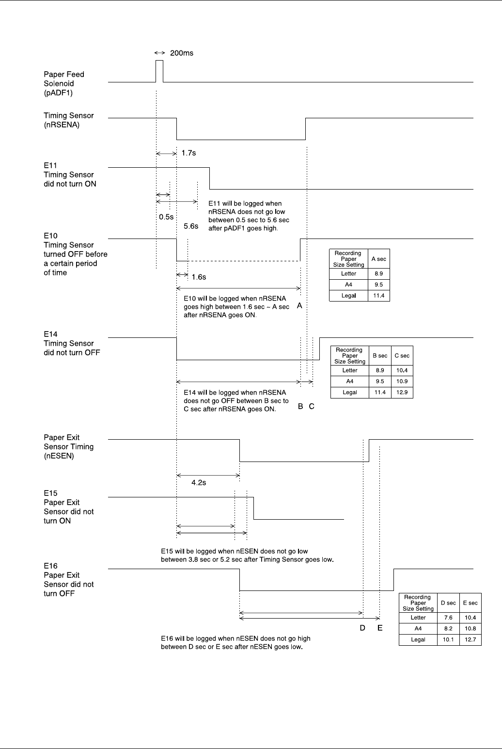
Panasonic UF-585 / 595
158
2. Printer Error Detail Explanation
Recording Paper Jam Detection
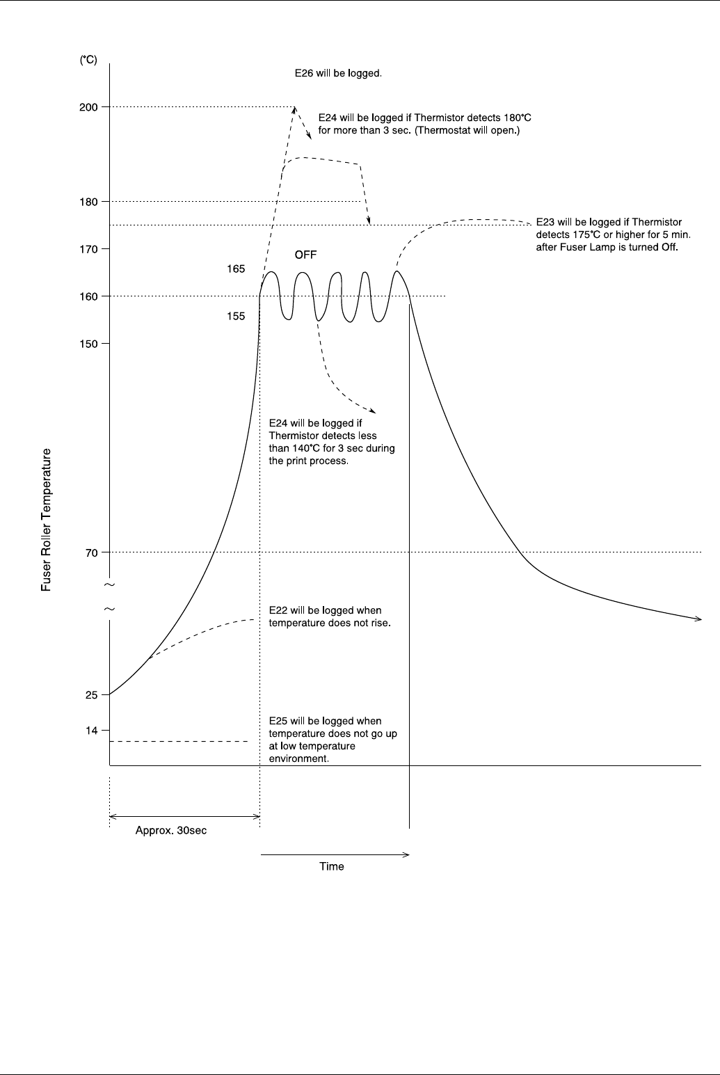
Service Modes
159
Fuser Error Detection
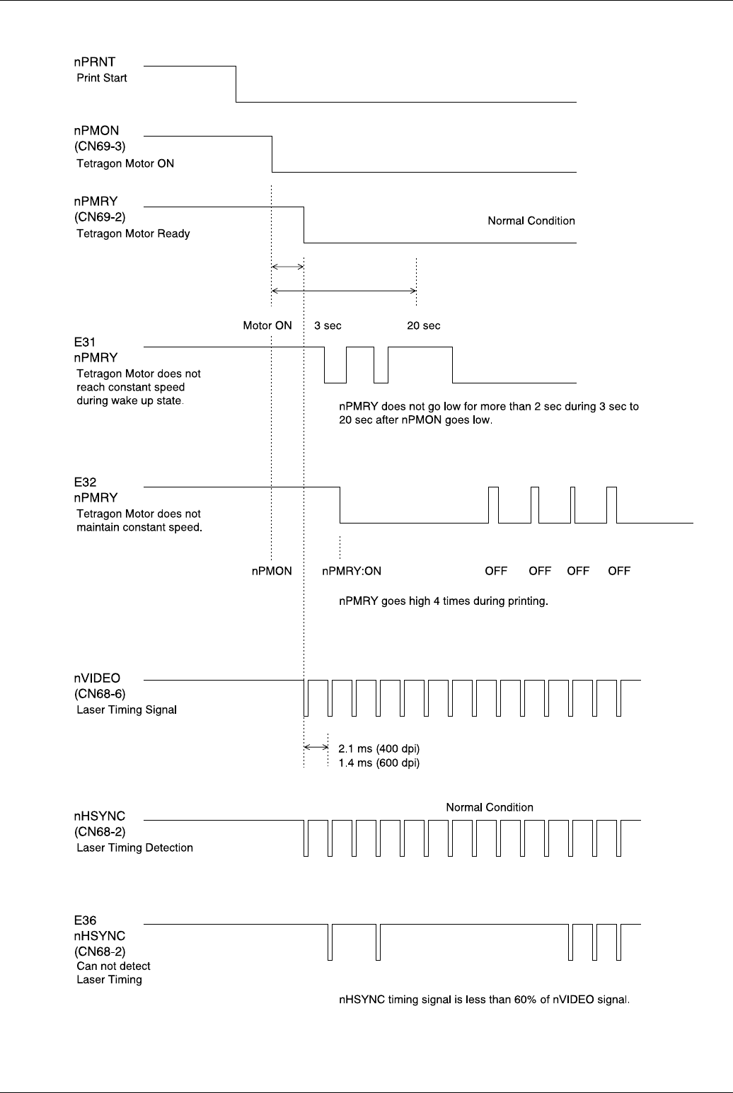
Panasonic UF-585 / 595
160
LSU Error Detection
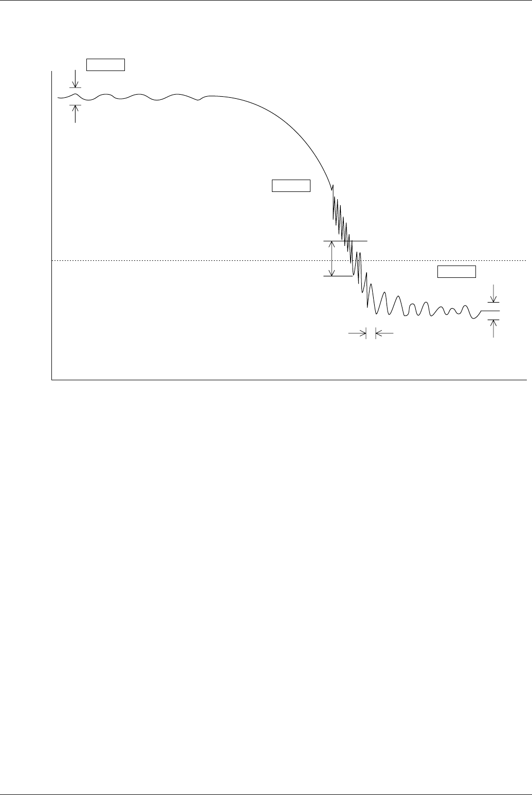
Service Modes
161
Out of Toner Detection
Toner Sensor output may change when the mixing blade passes above the Toner Sensor. Therefore the output signal has a
max. voltage and min. voltage during mixing blade rotation cycle (4.6 sec).
E043
If the unit detects Status B 10 times during printing, the machine recognizes that the remaining toner is low and the display
shows "REPLACE TONER CARTRIDGE".
E041
After detecting E043 and the LBP Print Available Counter Value reaches "0", the unit logs E041 (OUT OF TONER).
E45
If the unit detects Status C when power is On, the unit logs E045 and displays "NO CARTRIDGE". The unit will recover when
detecting Status A after a new toner cartridge is installed.
1.4V
2V
3V
1V
0V
Status A
Status B
(Enough toner in the cartridge)
(Remaining toner
is getting low)
Status C
(Almost no toner)
Max. - min. voltage is less than 1.0V
Min. voltage is more than 1.4V
Max. - min. voltage is less than 0.25V
Min. voltage is less than 1.4V
Max. - min. voltage is less than 0.08V
Min. voltage is less than 1.4V
Mixing blade
rotating cycle
Toner Sensor Output Signal
Panasonic UF-585 / 595
162
5.3.4 Print All Document Files
Prints all the document files from the Flash Memory.
(This function will be available as a running change in the future)
Step Operation or Unit Condition LCD Display
1 Standby
2 Press “FUNCTION” and then “7”.
3 Press “MONITOR” four times, then press “*”.
4 Press “3”.
5 Press “5” and “START”.
6 After printing is completed, the unit returns to the display in step 3.
7 Press “STOP” to return to standby.
MAR-12-1999 15:0000%
SET MODE (1-6)
ENTER NO. OR
SERVICE MODE
ENTER NO. OR
PRINTOUT (1-7)
1:FUNC. PARAM. LIST
ALL DOCUMENT FILES
* PRINTING *
SERVICE MODE
ENTER NO. OR
MAR-12-1999 15:0000%
Service Modes
163
5.3.5 Protocol Trace
Prints a Protocol Trace Report for the previous communication.
Step Operation or Unit Condition LCD Display
1 Standby
2 Press “FUNCTION” and then “7”.
3 Press “MONITOR” four times, then press “*”.
4 Press “3”.
5 Press “6” and “START”.
6 After printing is completed, the unit returns to the display in step 3.
7 Press “STOP” to return to standby.
MAR-12-1999 15:0000%
SET MODE (1-6)
ENTER NO. OR
SERVICE MODE
ENTER NO. OR
PRINTOUT (1-7)
1:FUNC. PARAM. LIST
PROTOCOL TRACE
* PRINTING *
SERVICE MODE
ENTER NO. OR
MAR-12-1999 15:0000%
*************** PROTOCOL LOG REPORT ****************** DATE MAR-12-1999 ***** TIME 16:56 ***P.01
STATUS : OK
MODE : ECM-TX (STANDARD)
SPEED : 9600bps 00MS/L
REMOTE CAPA. : DIS 00 CE B9 C4 80 12
LOCAL CAPA. : TSI 2B 20 20 20 38 37 2B 2B 2B 2B
39 38 36 36 35 34 37 38 38 30
DCS 00 C6 F8 44
REMOTE : NSF CSI DIS CFR
COMMAND LOG.
LOCAL : TSI DCS PIX PPS-EOP
REMOTE : MCF
LOCAL : DCN
-PANASONIC-
************************************ -PANAFAX UF-595- ***********-12345678901234567890-******
------------------------------------------------------------------
Panasonic UF-585 / 595
164
5.3.6 Toner Cartridge Order Form
The Toner Cartridge Order Form can be printed out manually by the following procedure.
Step Operation or Unit Condition LCD Display
1 Standby
2 Press “FUNCTION” and then “7”.
3 Press “MONITOR” four times, then press “*”.
4 Press “3”.
5 Press “7” and “START”.
6 After printing is completed, the unit returns to the display in step 3.
7 Press “STOP” to return to standby.
MAR-12-1999 15:0000%
SET MODE (1-6)
ENTER NO. OR
SERVICE MODE
ENTER NO. OR
PRINTOUT (1-7)
1:FUNC. PARAM. LIST
TONER ORDER FORM
* PRINTING *
SERVICE MODE
ENTER NO. OR
MAR-12-1999 15:0000%
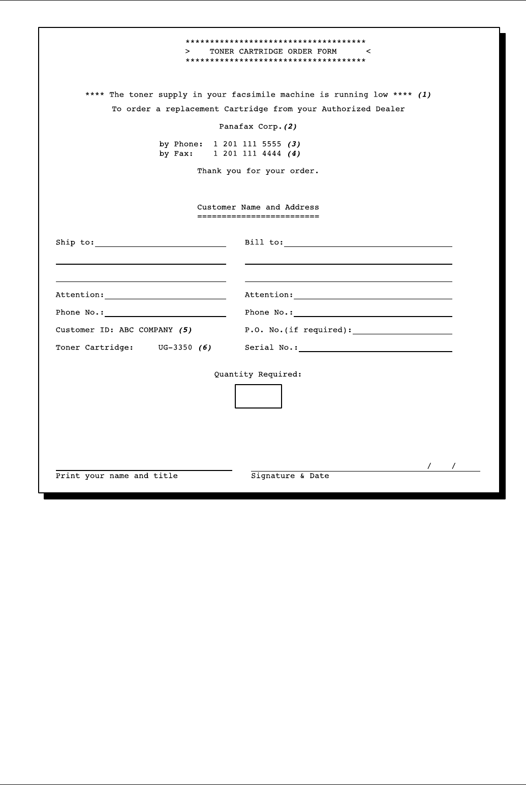
Service Modes
165
Explanation of Contents
(1) Low Toner Message (Fixed) “The toner supply in your facsimile machine is running low”
(2) Dealer Name Up to 25 digits
(3) Toner Order Tel # Up to 36 digits
(4) Toner Order Fax # Up to 36 digits
(5) Customer ID Up to 16 characters (User Identification Code)
(6) Toner Cartridge No. UG-3350
Panasonic UF-585 / 595
166
5.4 Service Mode 4 (Modem Test)
5.4.1 Binary Signal
This Service Mode is used to check the binary signal output. Signals can be output to the line using the following procedure.
Binary Signal Table
Step Operation or Unit Condition LCD Display
1 Standby
2 Press “FUNCTION” and then “7”.
3 Press “MONITOR” four times, then press “*”.
4 Press “4”.
5 Press “START”.
6 Enter the signal number (1-9) to select the binary signal.
7 Press "CLEAR" to end the signal generation. To select another signal,
repeat step 6.
8 Press “STOP” twice to return to standby.
Number Signals
1 V21 300bps
2 V27ter 2400bps
3 V27ter 4800bps
4 V29 7200bps
5 V29 9600bps
6 V17 TC7200bps
7 V17 TC9600bps
8 V33 12000bps
9 V33 14400bps
MAR-12-1999 15:0000%
SET MODE (1-6)
ENTER NO. OR
SERVICE MODE
ENTER NO. OR
MODEM TEST (1-5)
1:SIGNAL TEST
SIGNAL TEST
IDLE (ENTER 1-9)
SIGNAL TEST
300bps
SIGNAL TEST
IDLE (ENTER 1-9)
MAR-12-1999 15:0000%
Service Modes
167
5.4.2 Tonal Signal
This Service Mode is used to check the tonal signal output. Signals can be output to the line using the following procedure.
Tonal Signal Table
Step Operation or Unit Condition LCD Display
1 Standby
2 Press “FUNCTION” and then “7”.
3 Press “MONITOR” four times, then press “*”.
4 Press “4”.
5 Press “2” and “START”.
6 Enter the signal number (1-7) to select the binary signal.
7 Press "CLEAR" to end the signal generation. To select another signal,
repeat step 6.
8 Press “STOP” twice to return to standby.
Number Signals
1 462 Hz
2 1080 Hz
3 1100 Hz
4 1300 Hz
5 1650 Hz
6 1850 Hz
7 2100 Hz
MAR-12-1999 15:0000%
SET MODE (1-6)
ENTER NO. OR
SERVICE MODE
ENTER NO. OR
MODEM TEST (1-5)
1:SIGNAL TEST
TONAL TEST
IDLE (ENTER 1-7)
TONAL TEST
1080Hz
TONAL TEST
IDLE (ENTER 1-7)
MAR-12-1999 15:0000%
Panasonic UF-585 / 595
168
5.4.3 DTMF Signal
This Service Mode is used to check the DTMF (Dual Tone Multi Frequency) signal output.
The DTMF signal can be generated using the following procedure.
Step Operation or Unit Condition LCD Display
1 Standby
2 Press “FUNCTION” and then “7”.
3 Press “MONITOR” four times, then press “*”.
4 Press “4”.
5 Press “3” and “START”.
6a Press “START” for DTMF Single Tone Generation.
7a Enter the signal number (1-8) to select the DTMF signal.
6b Press “2” and “START” for Dual Tone Generation.
7b Enter the signal number (0-#) to select the DTMF Dual tone.
8 Press "CLEAR" to end the signal generation. To select another signal,
repeat step 7a or 7b.
9 Press “STOP” twice to return to standby.
MAR-12-1999 15:0000%
SET MODE (1-6)
ENTER NO. OR
SERVICE MODE
ENTER NO. OR
MODEM TEST (1-5)
1:SIGNAL TEST
DTMF TEST (1-2)
1.SINGLE
SINGLE TONE
ENTER (1-8)
SINGLE TONE
697Hz
DUAL TONE
ENTER (0-#)
DUAL TONE
(0)
SINGLE TONE
ENTER (1-8)
MAR-12-1999 15:0000%

Service Modes
169
DTMF Single Tone Table
DTMF Dual Tone Table
Number DTMF Signal Tones
1 697 Hz
2 770 Hz
3 852 Hz
4 941 Hz
5 1209 Hz
6 1336 Hz
7 1477 Hz
8 1633 Hz
Number DTMF Dual Tones
0 941 Hz + 1336 Hz
1 697 Hz + 1209 Hz
2 697 Hz + 1336 Hz
3 697 Hz + 1477 Hz
4 770 Hz + 1209 Hz
5 770 Hz + 1336 Hz
6 770 Hz + 1477 Hz
7 852 Hz + 1209 Hz
8 852 Hz + 1336 Hz
9 852 Hz + 1477 Hz
* 941 Hz + 1209 Hz
# 941 Hz + 1477 Hz
Panasonic UF-585 / 595
170
5.4.4 Binary Signal (V.34) (UF-595 only)
This Service Mode is used to check the binary V.34 Signals output. Signals can be output to the line using the folowing procedure.
Binary Signal Table
Step Operation or Unit Condition LCD Display
1 Standby
2 Press “FUNCTION” and then “7”.
3 Press “MONITOR” four times, then press “*”.
4 Press “4”.
5 Press “5” and “START”.
6 Enter the signal number (01-61) and “START” to select the binary signal.
7 Press "CLEAR" to end the signal generation. To select another signal,
repeat step 6.
8 Press “STOP” twice to return to standby.
Number Signals Number Signals Number Signals
01 V34 2400 sr 2400 bps 22 V34 3000 sr 9600 bps 43 V34 3429 sr 4800 bps
02 V34 2400 sr 4800 bps 23 V34 3000 sr 12000 bps 44 V34 3429 sr 7200 bps
03 V34 2400 sr 7200 bps 24 V34 3000 sr 14400 bps 45 V34 3429 sr 9600 bps
04 V34 2400 sr 9600 bps 25 V34 3000 sr 16800 bps 46 V34 3429 sr 12000 bps
05 V34 2400 sr 12000 bps 26 V34 3000 sr 19200 bps 47 V34 3429 sr 14400 bps
06 V34 2400 sr 14400 bps 27 V34 3000 sr 21600 bps 48 V34 3429 sr 16800 bps
07 V34 2400 sr 16800 bps 28 V34 3000 sr 24000 bps 49 V34 3429 sr 19200 bps
08 V34 2400 sr 19200 bps 29 V34 3000 sr 26400 bps 50 V34 3429 sr 21600 bps
09 V34 2400 sr 21600 bps 30 V34 3000 sr 28800 bps 51 V34 3429 sr 24000 bps
10 V34 2800 sr 4800 bps 31 V34 3200 sr 4800 bps 52 V34 3429 sr 26400 bps
11 V34 2800 sr 7200 bps 32 V34 3200 sr 7200 bps 53 V34 3429 sr 28800 bps
12 V34 2800 sr 9600 bps 33 V34 3200 sr 9600 bps 54 V34 3429 sr 31200 bps
13 V34 2800 sr 12000 bps 34 V34 3200 sr 12000 bps 55 V34 3429 sr 33600 bps
14 V34 2800 sr 14400 bps 35 V34 3200 sr 14400 bps 56 ANSam
15 V34 2800 sr 16800 bps 36 V34 3200 sr 16800 bps 57 CM
16 V34 2800 sr 19200 bps 37 V34 3200 sr 19200 bps 58 JM
17 V34 2800 sr 21600 bps 38 V34 3200 sr 21600 bps 59 INFO0c & TONEB
18 V34 2800 sr 24000 bps 39 V34 3200 sr 24000 bps 60 INFO0c & TONEA
19 V34 2800 sr 26400 bps 40 V34 3200 sr 26400 bps 61 PPh & AC & ALT
20 V34 3000 sr 4800 bps 41 V34 3200 sr 28800 bps
21 V34 3000 sr 7200 bps 42 V34 3200 sr 31200 bps
MAR-12-1999 15:0000%
SET MODE (1-6)
ENTER NO. OR
SERVICE MODE
ENTER NO. OR
MODEM TEST (1-5)
1:SIGNAL TEST
V.34 MODEM TEST
ENTER NO.
V.34 MODEM TEST
V34 2400sr 2400bps
V.34 MODEM TEST
ENTER NO.
MAR-12-1999 15:0000%
Service Modes
171
5.5 Service Mode 5 (Diagnostic)
5.5.1 CCD Test
This Service Mode is used to check the CCD.
Use the following procedure to initiate the test.
Step Operation or Unit Condition LCD Display
1 Standby
2 Press “FUNCTION” and then “7”.
3 Press “MONITOR” four times, then press “*”.
4 Press “5”.
5 Press “START”.
The scanner will be active.
6 Press “STOP” twice to return to standby.
MAR-12-1999 15:0000%
SET MODE (1-6)
ENTER NO. OR
SERVICE MODE
ENTER NO. OR
DIAGNOSTIC (1-3)
1:CCD TEST
1:CCD TEST
* CHECK NOW *
MAR-12-1999 15:0000%
Panasonic UF-585 / 595
172
5.5.2 LCD / LED Test
This Service Mode is used to check the LCD and LEDs.
Use the following procedure to initiate the test.
Step Operation or Unit Condition LCD Display
1 Standby
2 Press “FUNCTION” and then “7”.
3 Press “MONITOR” four times, then press “*”.
4 Press “5” .
5 Press “2” and “START”.
1) LCDs display as shown at right.
2) All LEDs will light.
6 Press “STOP” twice to return to standby.
MAR-12-1999 15:0000%
SET MODE (1-6)
ENTER NO. OR
SERVICE MODE
ENTER NO. OR
DIAGNOSTIC (1-3)
1:CCD TEST
2:LCD/LED TEST
* CHECK NOW *
MAR-12-1999 15:0000%
Service Modes
173
5.6 Service Mode 6 (RAM Initialization)
Initializes RAM and restores the Function Parameters to their default values.
Note:
This operation should be performed when the unit is first installed.
RAM Initialization Table
Step Operation or Unit Condition LCD Display
1 Standby
2 Press “FUNCTION” and then “7”.
3 Press “MONITOR” four times, then press “*”.
4 Press “6”.
5Press "\/" or “/\“ to select the initialization mode. (See Table)
6 Press “START”.
7 Returns to step 3 and press “STOP” to return to standby.
No. Initialize Mode Description
99 SHIPMENT SET (A) Deletes all setting information, except parameter number 80 and 81, then
set default values.
98 SHIPMENT SET (B) Deletes all setting information, except parameter number 61, 80 and 81,
then set default values.
97 FLASH MEMORY CLEAR Deletes all information in the Flash Memory.
16 LBP ERROR LOG CLEAR Clears the Printer Error Log.
15 LOGO/ID/PSWD CLEAR Clears the Logo, ID, Polling Password.
14 ALL JOB CLEAR Clears all Jobs stored in Flash Memory.
13 PROGRAM DIAL CLEAR Clears the Program keys.
12 ABBR DIAL CLEAR Clears the One-touch and ABBR Numbers.
11 JOURNAL CLEAR Clears the Journal contents.
* PARAMETER INITIALIZE Restores the Fax and Function Parameters to default values.
MAR-12-1999 15:0000%
SET MODE (1-6)
ENTER NO. OR
SERVICE MODE
ENTER NO. OR
* RAM INITIALIZE *
ENTER NO. OR
* RAM INITIALIZE *
LOGO/ID/PSWD CLEAR
* COMPLETED *
LOGO/ID/PSWD CLEAR
MAR-12-1999 15:0000%
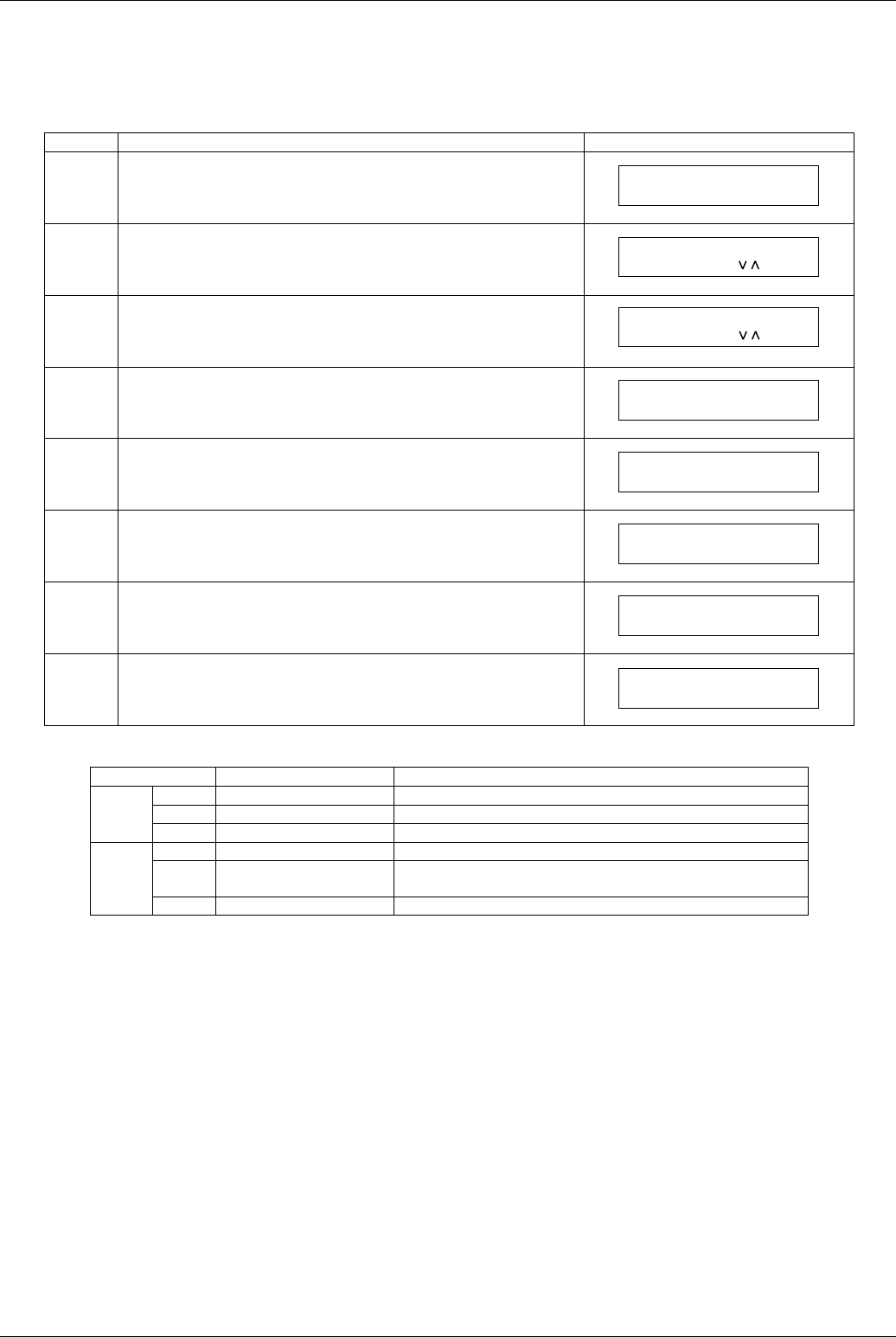
Panasonic UF-585 / 595
174
5.7 Service Mode 7 (LBP Service Mode)
This Service Mode is used to change printer parameters and verify printer information.
Use the following procedure to change printer parameter.
Step Operation or Unit Condition LCD Display
1 Standby
2 Press “FUNCTION” and then “7”.
3 Press “MONITOR” four times, then press “*”.
4 Press “7”.
5 1) Press “START” for printer parameter settings.
2) Press “2” and “START” to get the printer information.
Ex: Enter "START" for printer parameter settings.
6 Press "3" and "START".
Then enter the number of pages.
Ex: Enter "50" and press "START".
7 Press "\/" or "/\" to select another Parameter Name (See Table)
or press "CLEAR" to return to step 4.
6 Repeat step 5 through 7 to request operation, or press "STOP" twice to
return to standby.
Sub-Code Parameter Name Description
1 1 Printer Counter Displays and resets the printer and cassette(s) counters.
2 LBP Fuser Reset Clears the LBP fuser error.
3 Out of Toner Sets the number of pages to print after low toner is detected.
2 \//\ LBP ROM Version Shows the LBP ROM Version.
\//\ LBP Print Available Shows the remaining number of allowable printable pages after low
toner has been detected (Counter Only).
\//\ LBP MEMORY CAPACITY Shows the page memory capacity.
MAR-12-1999 15:0000%
SET MODE (1-6)
ENTER NO. OR
SERVICE MODE
ENTER NO. OR
1:LBP PARAMETER SET
LP SERVICE MODE (1-2)
1.PRINTER COUNTER
LBP PARAMETER SET
3.OUT OF TONER
LBP PARAMETER SET
1.LBP PARAMETER SET
LP SERVICE MODE (1-2)
MAR-12-1999 15:0000%

Service Modes
175
5.8 Service Mode 8 (Check & Call)
5.8.1 Overview
This feature enables the Authorized Servicing Dealers to manage and improve the Fax machine maintenance to their customers by
alerting them of equipment problems. It also can be used as a Supply Sales Tool by alerting the Dealer that the unit is running Low
on Toner. The function overview is as follows:
1. The machine’s printer error information is stored in the Printer Report.
2. The printer report can be manually printed when required.
3. When printer errors occurs, the unit can automatically transmit the Service Alert Report to the pre-registered telephone
number.
4. When the unit detects Low Toner, it can automatically transmit the Maintenance Alert Report to the pre-registered telephone
number.
5. When the unit detects Low Toner, it can automatically print out the Toner Order Form with pre-registered order information.
5.8.2 Printer Reports
• Conditions under which a report can be printed or transmitted
1. Manual print
The Printer Report can be printed by Service Mode 3 (See Section 5.3.2).
2. Automatic transmission/printout
3. Service Alert Report
When the unit detects an Emergency Printer Error, the unit will immediately transmit the Service Alert Report to the
pre-registered telephone number. However, the unit will not transmit the Service Alert Report if it finds the same error within
the same date in the error log.
4. Maintenance Alert Report
When the unit detects Low Toner, the unit can automatically transmit the Maintenance Alert Report to the pre-registered
telephone number. Refer to the Printer Error Code Table.
5. Toner Order Form
When the unit detects Low Toner, the unit can automatically print the Toner Order Form with the pre-registered order
information.
Note:
The Service and Maintenance Alert Reports are managed in the same manner as the normal memory transmission (Retry,
Incomplete, File List, Display while it is transmitting, Journal).
• Printer Error Code Table
Note:
1. Transmission Report: o = Service Alert Report,, x = Maintenance Alert Report
2. Condition: R = Receive Mode, C = Copy Mode, S = Standby Mode, T = Transmit Mode
Into.
Code Printer
Error Code LED/LCD Log
only Tx Report Condition Content of Error
001 11 JAM o R/C Paper Jam 1st Cassette.
002 12 JAM o R/C Paper Jam 2nd Cassette.
007 14-18 JAM o R/C Paper Exit Error.
010 00 NO PAPER R/C No Paper in 1st or 2nd Cassette.
011 64,65 NO Cassette S No 1st or 2nd Cassette.
021 22-26 o o R/C Fuser Problem / LP Thermistor disconnected
Problem.
041 00 TONER o S/R/C No Toner
043 00 TONER o x S/R/C Low Toner Warning
045 61 TONER o S No Toner Cartridge
051 54 o o S/R/C Printer Error
054 31,32,36 o o R/C LSU Problem
055 81,82 o o S/R/C No response from LP Controller
060 Rx Door Open
Panasonic UF-585 / 595
176
5.8.3 Setting Operation
8:CHECK & CALL
PRESS SET TO SELECT
CHECK & CALL (1-7)
1:SVC. ALERT FAX #
SERVICE ALERT FAX #
SET or START
SET or START
SET or START
CLEAR
CLEAR
Enter a destination fax number for the Service Alert Report.
When it is entered, the automatic transmission of the Service
Alert Report becomes effective.
Max. 36 digits (i.e. 201 111 2222)
CHECK & CALL (1-7)
2:MAINT. ALERT FAX #
MAINT. ALERT FAX #
SET or START
SET or START
CLEAR
CLEAR
Enter a destination fax number for the Maintenance Alert
Report. When it is entered, the automatic transmission of the
Maintenance Alert Report becomes effective.
Max. 36 digits (i.e. 201 111 3333)
CHECK & CALL (1-7)
3:TONER ORDER FAX #
TONER ORDER FAX #
SET or START
SET or START
CLEAR
CLEAR
Enter the supply fax number to be printed on the Toner Order
Form. When it is entered, the automatic print of the Toner
Order Form becomes effective.
Max. 36 digits (i.e. 201 111 4444)
CHECK & CALL (1-7)
4:TONER ORDER TEL #
TONER ORDER TEL #
SET or START
SET or START
CLEAR
CLEAR
Enter the supply telephone number to be printed on the Toner
Order Form.
Max. 36 digits (i.e. 201 111 5555)
CHECK & CALL (1-7)
5:DEALER NAME
DEALER NAME
SET or START
SET or START
CLEAR
CLEAR
Enter the Dealer’s Name to be printed on the Toner Order
Form.
Max. 25 digits (i.e. Panafax Corp.)
CHECK & CALL (1-7)
6:CUSTOMER ID
CUSTOMER ID
SET or START
SET or START
CLEAR
CLEAR
Enter a Customer ID code to be printed on the Service Alert
Report, Maintenance Alert Report and Toner Order Form.
Max. 16 characters (i.e. ABC Company)
6
CHECK & CALL (1-7)
7:PRINTER REPORT XMT
PRINTER REP. XMT:Off
1:OFF 2:ON
SERVICE MODE
ENTER NO. OR V
* DIALING *
555 1234
SET or START
CLEAR
7
5
4
3
2
1
21
After the Service Alert Report is faxed to
the pre-registered FAX #, the machine
returns to standby mode.

Service Modes
177
Note
1. Service Alert Report
To enable the automatic transmission of Service Alert Report, enter the destination fax telephone number in the “SERVICE
ALERT FAX #" field. When a printer error occurs, the Service Alert Report is transmitted to the designated number
automatically. A blank entry in this field, disables the Automatic transmission of the Service Alert Report.
2. Maintenance Alert Report
To enable the automatic transmission of Maintenance Alert Report, enter the destination fax telephone number in the “MAINT.
ALERT FAX #" field. When a printer error occurs, the Maintenance Alert Report is transmitted to the designated number
automatically. A blank entry in this field, disables the Automatic transmission of the Maintenance Alert Report.
3. Toner Order Form
To enable the automatic printout of the Toner Order Form, enter the destination fax telephone numbers in the “Toner Order
FAX #” field. When a low toner error occurs, the Toner Order Form is printed automatically. A blank entry in this field, disables
the automatic printout of the Toner Order Form.
4. SERVICE ALERT FAX #, this would be the fax telephone number for the Dealer’s Service Department.
MAINT. ALERT FAX #, this could be the fax telephone number for the Dealer’s Supply Sales Desk.
TONER ORDER FAX #, this could be the fax telephone number for the Dealer’s Supply Sales Desk.
TONER ORDER TEL #, this could be the voice telephone number for the Dealer’s Supply Sales Desk.
DEALER NAME, this name is printed on the Toner Order Form.
CUSTOMER ID, to identify your customer, enter up to 16 characters user code in this field. This name will be printed on the
Service Alert Report, Maintenance Alert Report and Toner Order Form.
5. Printer Report XMT
To manually transmit the Service Alert Report to the pre-registered SERVICE ALERT REPORT FAX #, set the Printer Report
XMT to "2:ON".
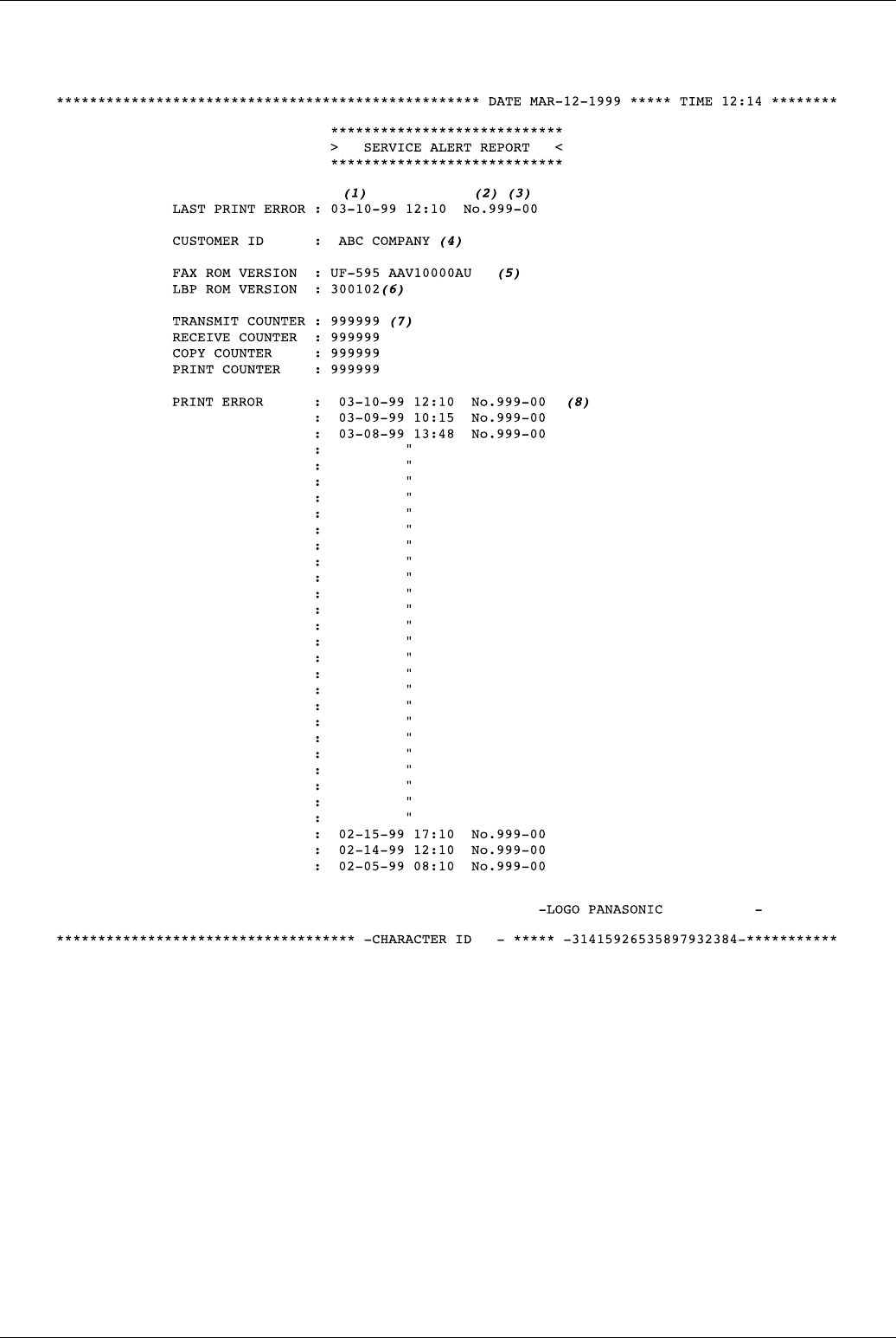
Panasonic UF-585 / 595
178
5.8.4 SERVICE ALERT REPORT FORMAT
Explanation of Contents
(1) Date & Time when a problem occurred
(2) Information Code
(3) Printer Error Code Refer to Service Manual
(4) Customer ID Up to 16 characters (User Identification Code)
(5) Fax ROM Version
(6) LBP ROM Version
(7) Transmission / Reception / Copy / Print Counters
(8) Print Error Last 30 records (Latest on top)

Service Modes
179
5.8.5 MAINTENANCE ALERT REPORT FORMAT
Explanation of Contents
(1) Low Toner Message (Fixed) “MACHINE IS RUNNING OUT TONER”
(4) Customer ID Up to 16 characters (User IdentificationCode)
(5) Fax ROM Version
(6) LBP ROM Version
(7) Transmission / Reception / Copy / Print Counters
*************************************************** DATE MAR-12-1999 ***** TIME 12:14 ********
****************************
> MAINTENANCE ALERT REPORT <
****************************
LAST PRINT ERROR : MACHINE IS RUNNING OUT OF TONER
(1)
CUSTOMER ID : ABC COMPANY
(4)
FAX ROM VERSION : UF-595 AAV10000AU
(5)
LBP ROM VERSION : 300102
(6)
TRANSMIT COUNTER : 999999
(7)
RECEIVE COUNTER : 999999
COPY COUNTER : 999999
PRINT COUNTER : 999999
-LOGO PANASONIC -
************************************ -CHARACTER ID - ***** -31415926535897932384-***********
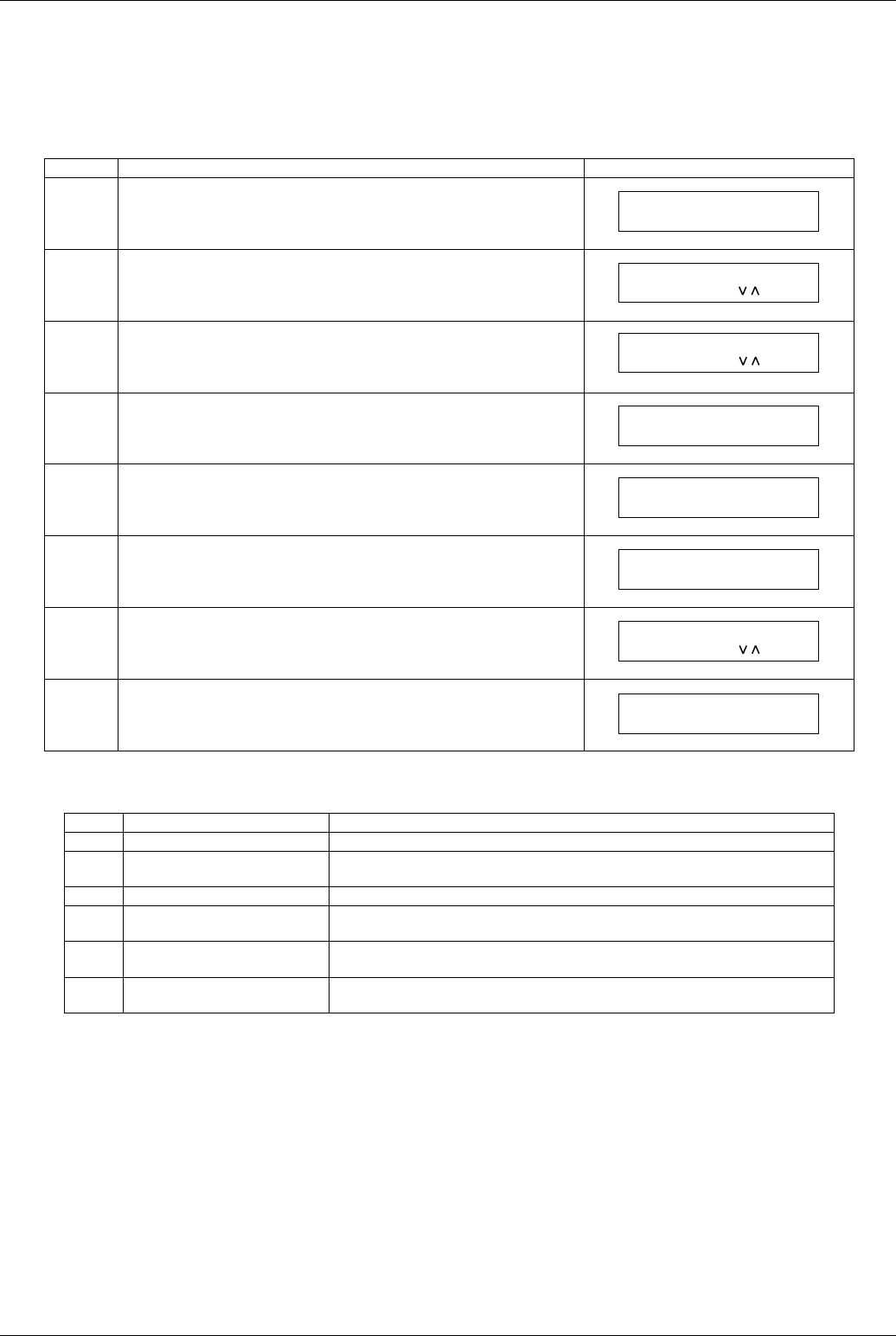
Panasonic UF-585 / 595
180
5.9 Service Mode 9 (System Maintenance)
5.9.1 Overview
This Service Mode is used to maintain and/or update the firmware of the machine.
Use the following procedure for System Maintenance.
System Maintenance Table
Note:
The created Backup Card must be removed from the machine.
Step Operation or Unit Condition LCD Display
1 Standby
2 Press “FUNCTION” and then “7”.
3 Press “MONITOR” four times, then press “*”.
4 Press “9”.
5 Press “START” to update the firmware.
Enter No. or press ”∨” or “∧“ to select the maintenance to be performed.
Ex: Enter “2”.
6 Press “START” and “SET”.
7 After the backup is completed, repeat step 4 through 6
to request an operation.
8 Press “STOP” to return to standby.
No. Maintenance Mode Description
1 FIRMWARE UPDATE Updates the firmware in the machine with the Master Firmware Card.
2 FIRMWARE BACKUP Creates a Backup Card of the machine’s firmware.
(A 2 MB or higher Flash Memory Card is required)
3 PARAMETER RESTORE Restores the parameters from the Backup Card into the machine.
4 PARAMETER BACKUP Creates a Backup Card of the machine’s parameters.
(A 1 MB or higher Flash Memory Card is required)
5PC
→ FLASH CARD Creates a Master Firmware Card using the Firmware Update Kit.
(A 2 MB or higher Flash Memory Card is required)
8 SEND RECEIVED FILE Transfers documents from memory to another fax machine during a fatal printer
error.
MAR-12-1999 15:0000%
SET MODE (1-6)
ENTER NO. OR
SERVICE MODE
ENTER NO. OR
SYSTEM MAINT. (1-8)
1:FIRMWARE UPDATE
SYSTEM MAINT. (1-8)
2:FIRMWARE BACKUP
FIRMWARE BACKUP
* IN PROGRESS *
SERVICE MODE
ENTER NO. OR
MAR-12-1999 15:0000%
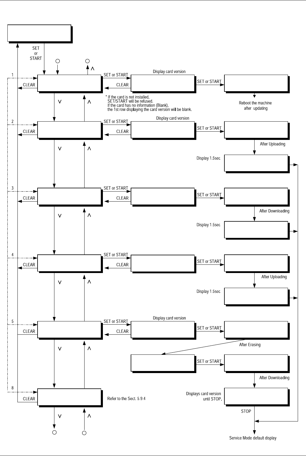
Service Modes
181
5.9.2 Operation
9:SYSTEM MAINTENANCE
PRESS SET TO SELECT
SYSTEM MAINT.(1-8)
1:FIRMWARE UPDATE
FIRMWARE UPDATE
* IN PROGRESS *
SYSTEM MAINT.(1-8)
2:FIRMWARE BACKUP
UF-XXX AAV12300AU
PRESS SET TO START
FIRMWARE BACKUP
* IN PROGRESS *
SYSTEM MAINT.(1-8)
3:PARAMETER RESTORE
PARAMETER RESTORE
PRESS SET TO START
PARAMETER RESTORE
* IN PROGRESS *
SYSTEM MAINT.(1-8)
4:PARAMETER BACKUP
PARAMETER BACKUP
PRESS SET TO START
PARAMETER BACKUP
* IN PROGRESS *
SYSTEM MAINT.(1-8)
5:PC --> FLASH CARD
UF-XXX AAV12300AU
PRESS SET TO START
PC --> FLASH CARD
* ERASING NOW *
UF-XXXAAV12300AU
PRESS SET TO START
FIRMWARE BACKUP
* COMPLETED *
PARAMETER RESTORE
* COMPLETED *
PARAMETER BACKUP
* COMPLETED *
PC --> FLASH CARD
* PROGRAMMING NOW *
READY TO PROGRAM
PRESS SET TO START
UF-XXX AAV12300AU
* COMPLETED *
1 2
1 2
SYSTEM MAINT.(1-8)
8:SEND RCV’D FILE
12
*
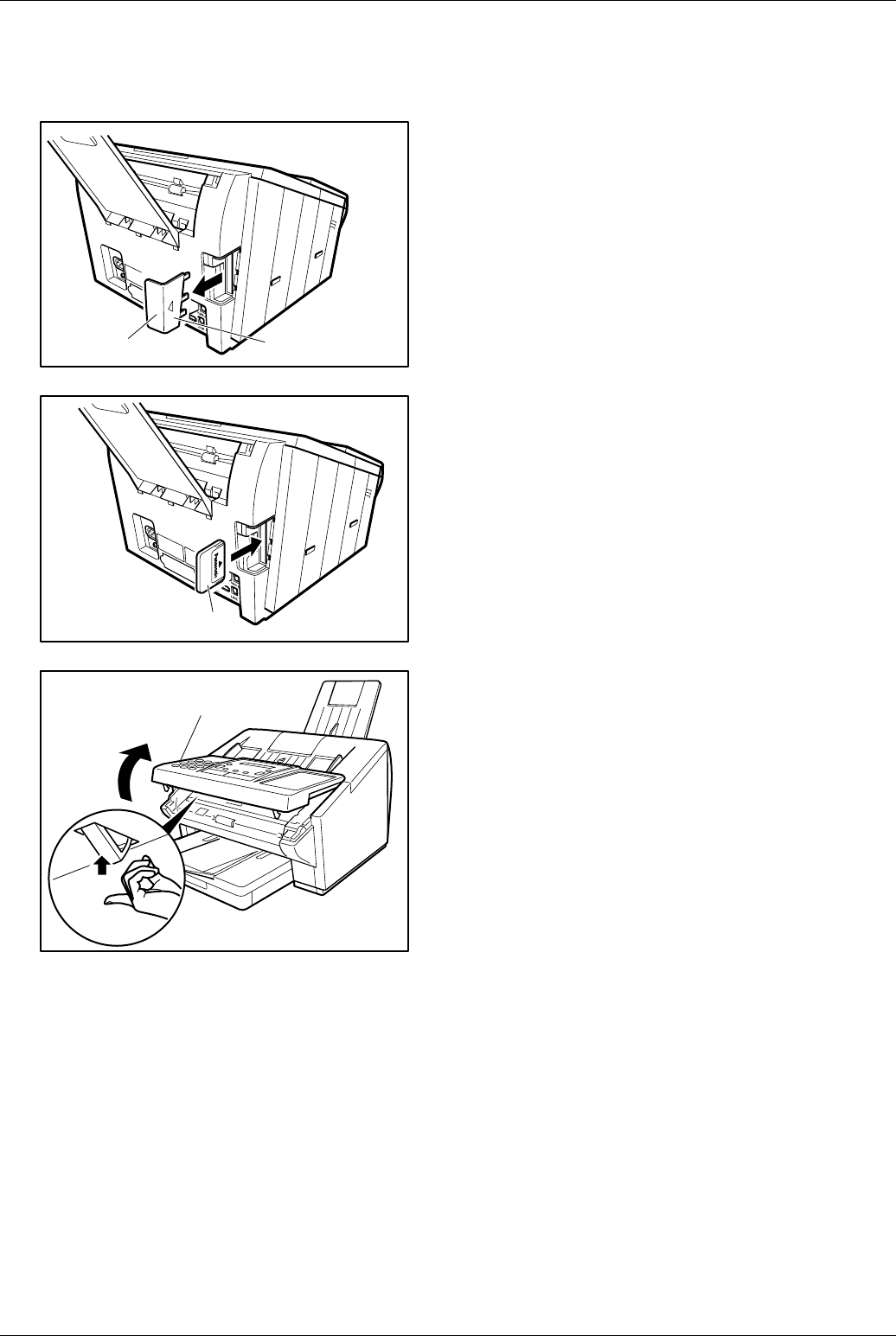
Panasonic UF-585 / 595
182
5.9.3 Recovering F-ROM Firmware Update Failure
If the Firmware Update is interrupted before completion, the machine will not be able to progress into the Standby Mode and the
LCD display will remain Blank. If this happens, please follow the steps described below to recover from a failed firmware update.
(1) Unplug the Power Cord.
(2) Remove the Memory Card Cover.
(3) Insert the Flash Memory Card gently into the card slot with
the Panasonic logo facing to the outside of the machine.
Caution:
Installing the Flash Memory Card in the wrong direction may
damage the connecting pins inside the machine.
(4) Open the Control Panel Unit.
(5) Activate the Read Point Sensor with your finger and plug
in the Power Cord.
(6) Wait approximately 10 seconds, release the Read Point
Sensor and close the Control Panel Unit (ADF).
(7) Allow the unit to complete the Firmware Update (approx.
1-minute). When completed, the unit will reboot and
progress to the Standby Mode.
(8) Unplug the Power Cord.
(9) Remove the Flash Memory Card.
(10) Re-install the Memory Card Cover.
(11) Plug in the Power Cord.
(12) Perform Parameter Initialization (see page 173).
Memory Card Cover
(2)
(3)
Control Panel Unit
(4)
(5)
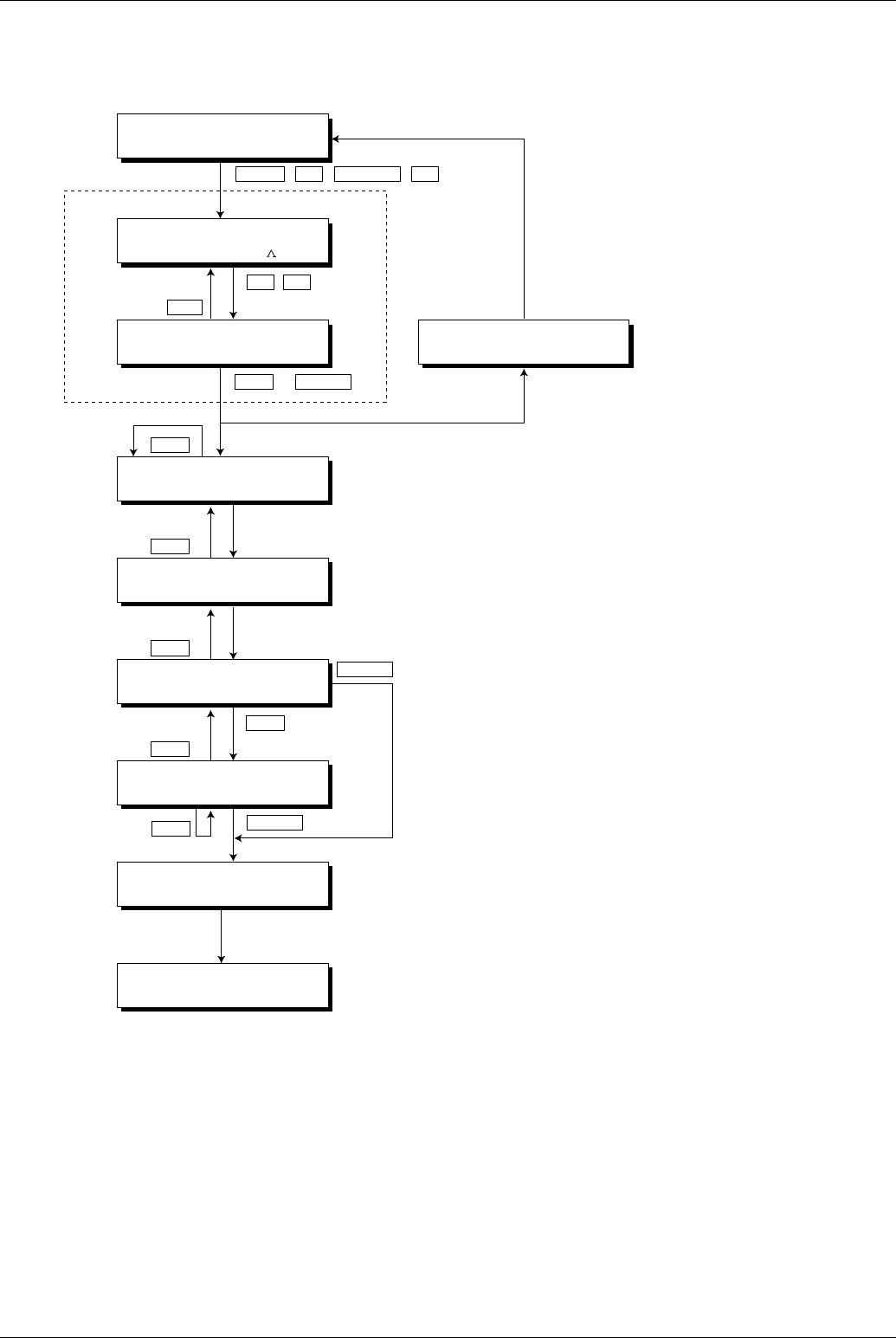
Service Modes
183
5.9.4 Send Received File
This function is the relief mode which makes it possible to retrieve memory received documents during a fatal
printer error by transferring the documents to another fax machine.
MAR-12-1999 15:00
nn%
SERVICE MODE
ENTER NO. OR v
SYSTEM MAINT.(1-8)
8:SEND RCV FAX
FILE DOES NOT EXIST
ENTER STATION(S)
THEN PRESS START
<01> NEW YORK OFFICE
212 555 1234
<02> LONDON OFFICE
011 44 123 4567
2 STN(S) ARE SET
ADD MORE OR START
MAR-12-1999 15:00
nn%
* DIALING * NO.nnn
212 555 1234
FUNC 7
9
CLR
8
Pi-pi-pi
*MON X 4
START
START
Note:
1. After the received document file is successfully transmitted, unit will
NOT delete the file automatically.
2. Under certain conditions there could be two (2) received files stored
separately. In this case, transmission will be made separately.
3. Only normal received document will be transmitted.
Document received with a confidential code will NOT be transmitted by
this operation.
4. Documents received with a confidential code, can be retrieved by using
Confidential Polling from a remote station.
START
If no file was received
Enter station
Enter another station
SET
SET
SET
CLR
CLR
CLR
CLR
Pi-pi-pi
or
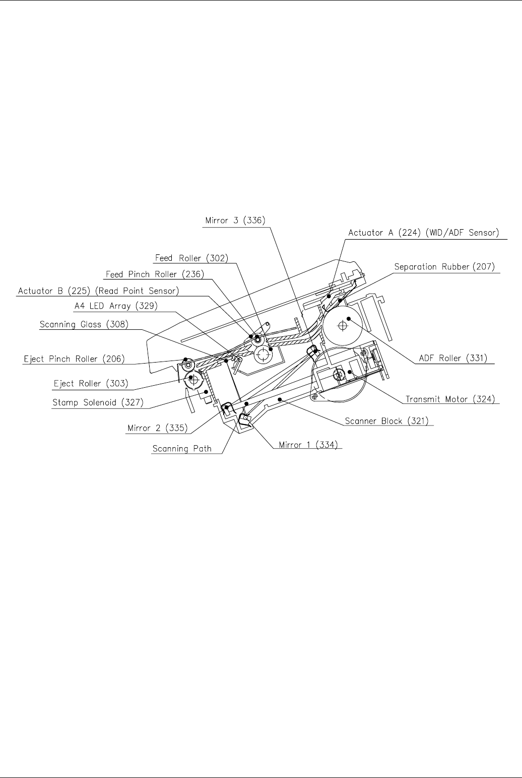
Panasonic UF-585 / 595
186
6 System Description
6.1 Mechanical Operation
The mechanical units are installed in a single unit body. The mechanical block consists of the following mechanisms:
Transmit Mechanism
Control Panel
Receive Mechanism
Printing Process Operation
Covers and Enclosures
6.1.1 Transmit Mechanism
The Transmit Mechanism consists of components which feed, scan and eject documents, as well as send signals. These
components and their functions are as follows:

System Description
187
ADF Mechanism
The ADF (Automatic Document Feeder) automatically feeds paper into the unit, and consists of ADF Roller and Separation
Rubber. Each document is placed face-down on the Printer Cover (106) before being fed into the unit.
● The ADF Roller (331) feeds individual pages into the scanning area.
● The Separation Rubber (207) separates documents placed on the ADF, preventing multiple feeding.
A4 LED Array (329)
The UF-585/595 has one LED Array, used as a light source to illuminate the document. The LED Array turns ON when the Read
Point Sensor is activated by the document leading edge.
Transmit Guide Unit
The Transmit Guide Unit is an auxiliary part used for feeding and ejecting documents. It consists of the Transmit Guide (301),
Control Panel Chassis (201), Feed Roller (302), Eject Roller (303), and Eject Pinch Roller (206) and Feed Pinch Roller
(236). This unit also provides the white scanning area and serves as a base for electronic white reference.
Transmit Mechanism Drive System
This system feeds documents through the transmitting mechanism, and consists of rollers, gears and a stepper motor.
● The Transmit Motor (324), a stepper motor, controlled by the CPU, drives the ADF Roller, Feed Roller and Eject Roller, with
the speed based on the density of the picture information.
● The Feed Roller (302) feeds the document to the scanning point.
● The Eject Roller (303) feeds and ejects the document out of the machine.
Transmit Mechanism Sensors
The ADF Sensor (PC1), activated by Actuator A (224), detects the presence of documents on the ADF Tray and multiple
pages.
The RP (Read Point) Sensor (PC3), activated by Actuator B (225), detects the lead and trail edges of the document,
controlling the reading position. The CPU determines that a document is jammed if Actuator B is not tripped within a
specified time after the ADF Roller starts feeding, and disengages the ADF Roller by reversing the Transmit Motor direction.
The ADF Door Sensor (PC2), activated by ADF Door Actuator (226), halts all scanning operations when the Control Panel
Unit is opened.
Verification Stamp Unit
The Verification Stamp Unit stamps an “X” mark on the front of the document after the document is successfully transmitted or
stored. It consists of the Stamp Head (325), Stamp Holder (326) and Stamp Solenoid (327).
Scanner Block (321)
The Scanner Block consists of three mirrors, a Lens, and a CCD PC Board (337).
● The mirrors, Mirror 1 (334), Mirror 2 (335) and Mirror 3 (336) reflect image information, in the form of light, through the Lens.
● The Lens focuses the image information and passes it to the CCD.
● The CCD, mounted on the CCD PC Board, converts the image information into an electronic signal.
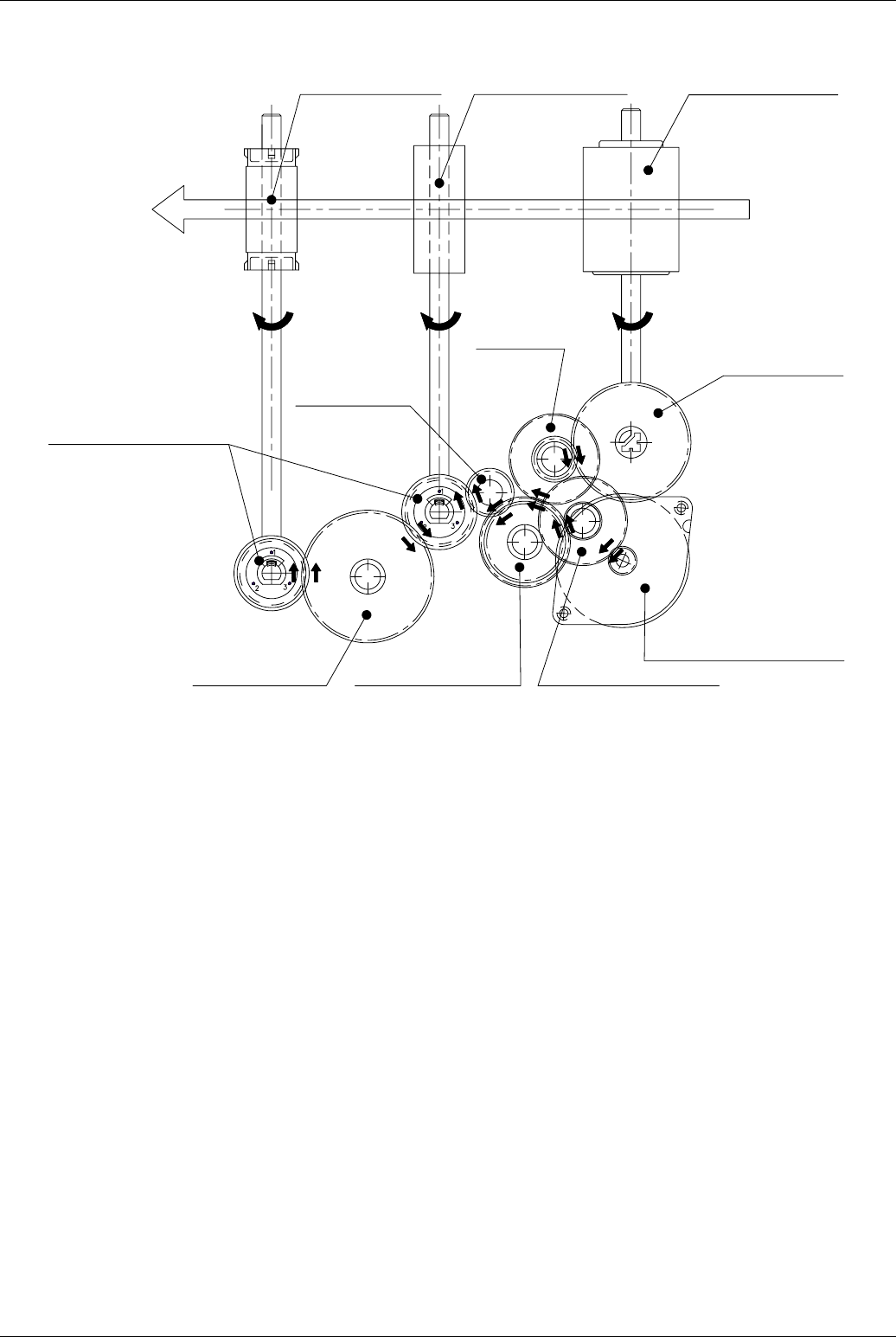
Panasonic UF-585 / 595
188
Drive System
6.1.2 Control Panel
The Control Panel consists of the PNL1 PC Board (231) and LCD Unit (233), which displays the various status messages, and a
membrane-type panel.
D50 Gear (314) B55D30 Gear (311) B54B22 Gear (310)
Transmit Motor (324)
ADF Gear (305)
D17 Gear (313)
Eject Roller (303) Feed Roller (302) ADF Roller (331)
Document
D25F Drive Gear (332)
B55D16
Gear (312)
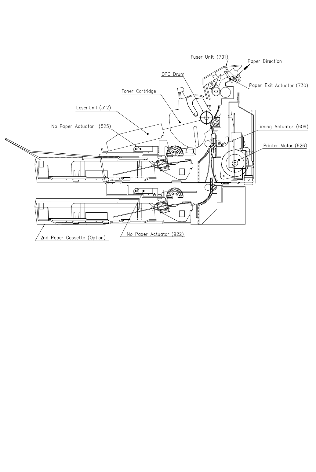
System Description
189
6.1.3 Receive Mechanism
The Receive Mechanism consists of the Laser Unit (LSU), OPC (Organic Photo Conductor) Drum, and various other parts which
ensure the normal feeding of recording paper. These components and their functions are as follows:
Paper Feed Units No.1 and 2
UF-585: Paper Feeder Unit No. 2 is not available.
UF-595: Paper Feeder Unit No. 2 is available as an option.
Paper Feed Unit No.1 Operation
1. The printing operation begins when the nPRNT (Print Request) output signal level goes Low. The Printer Motor (626) is
initialized.
2. The Paper Feed Solenoid (531) is energized for a specified period of time and turned ON. This activates the Paper Feed
Roller (518), which rotates one revolution. The paper is separated into individual sheets by the L and R Paper Separation
Clips (809 and 811) and transported to the Feed Roller (526).
3. After one revolution the Paper Feed Roller (518) stops, releasing the paper. The Feed Roller (526) transports the paper to
the drum area.
4. The actual printing process starts at a specified time after the Timing Actuator (609) is activated and stops at a a specified
period of time after the trailing edge clears the Timing Actuator (609).
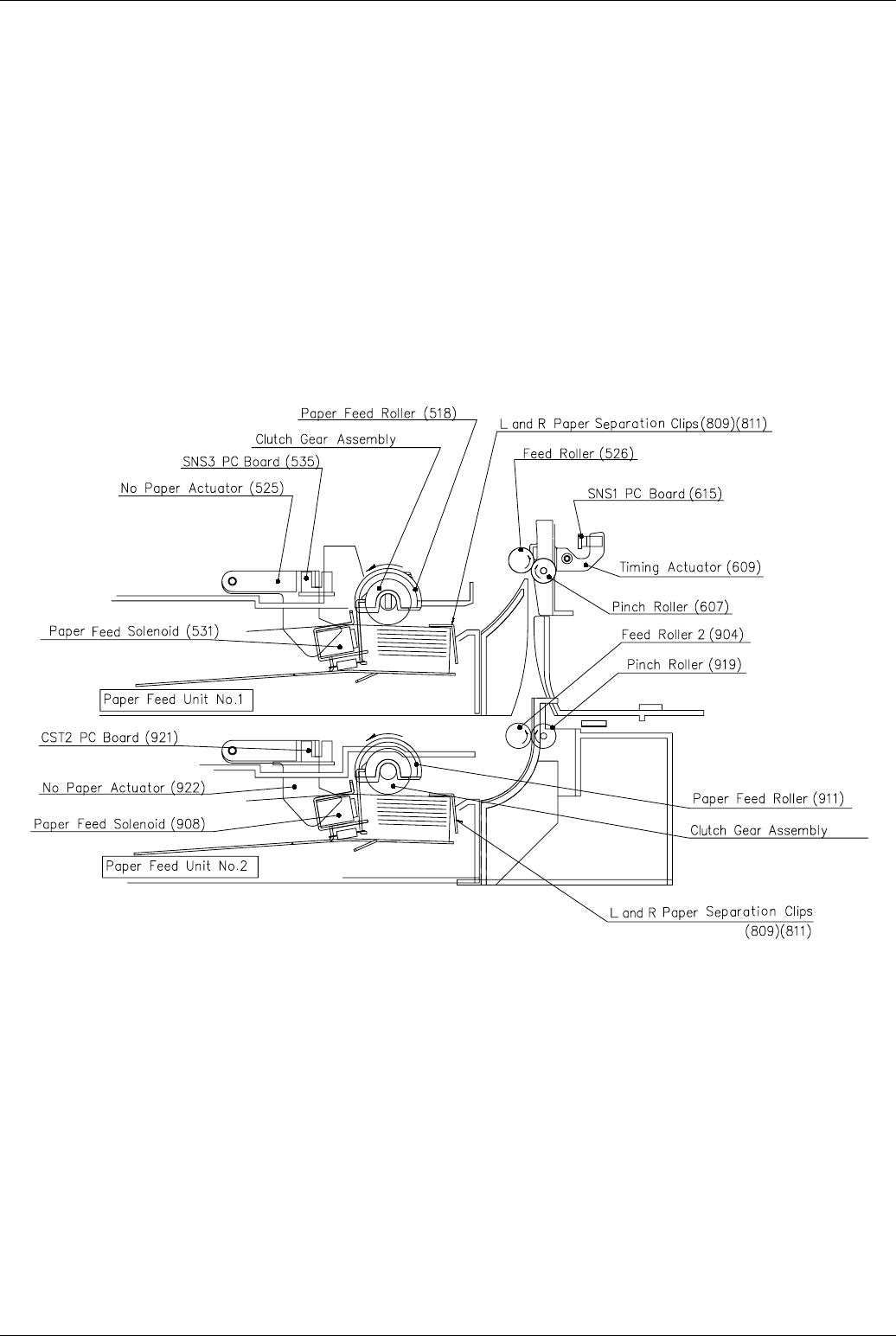
Panasonic UF-585 / 595
190
Paper Feed Unit No. 2 (Optional) Operation
The Paper Feed Unit No.1 always takes priority. The Paper Feed Unit No. 2 becomes operational only when the cassette No.1
runs out of paper and the NP Sensor is deactivated, causing the nPCHK1 output signal level to go High.
1. The printing operation begins when the nPRNT (Print Request) output signal level goes Low. The Printer Motor (626) is
initialized.
2. The Paper Feed Solenoid (908) is energized for a specified period of time and is turned ON. This activates the Paper Feed
Roller (911), which rotates one revolution. The paper is separated into individual sheets by the L and R Paper Separation
Clips (809) (811) and transported to the Feed Roller 2 (904).
3. After one revolution the Paper Feed Roller (911) stops, releasing the paper. The Feed Roller 2 (904) and the Feed Roller
(526) transports the paper to the drum area.
4. The actual printing process starts at a specified time after the Timing Actuator (609) is activated and stops at a a specified
period of time after the trailing edge clears the Timing Actuator (609).
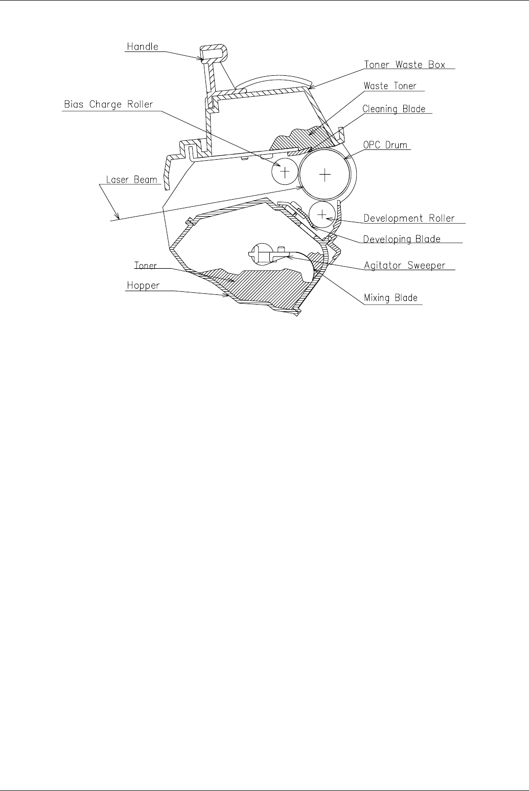
System Description
191
6.1.4 Printing Process Operation
Charge
In the dark, the Bias Charge Roller (BCR) applies a high, uniform negative charge to the surface of the OPC Drum. The surface
potential is approximately -650 VDC and remains because the drum has a high electric resistance in the dark.
Exposure
A portion of the laser beam is deflected to the timing sensor [Beam Detection (BD) Sensor], which controls the start timing of
scanning on the OPC Drum. The CPU also uses the timing sensor to detect abnormal signals. The light beam from the laser
diode is modulated by the digital signal (nVIDEO) and converted to parallel light waves by the collimator lens. The beam is then
directed to the rotating tetragon mirror, where it is reflected to the f-θ lens and then focused onto the OPC Drum surface. The
laser beam moves across the surface of the OPC Drum in the scanning direction. Where the laser beam is applied, the negative
charge on the drum dissipates, and where the laser is not applied, the negative charge remains. This action forms a latent,
electrostatic image on the OPC Drum, corresponding to the original image.
Development
This development process uses a conventional method, where toner coats a Development Roller and transfers to the latent
image on the OPC Drum. In the Toner Cartridge, the (mono-component) toner is negatively charged by the friction between the
rotating Development Roller (Mag Roller) and the Developing Blade. This combination and the rotation of the Mixing Blade
transfers the toner from the reservoir and forms a brush effect on the Mag roller. Where the magnetic brush lightly touches the
OPC Drum, the negatively charged toner is attracted to the latent image on the drum, forming a mirror image of the original on
the drum. Any remaining toner is removed from the Mag Roller by the Developing Blade and is recycled back into the toner
reservoir. A bias voltage of approximately 1.5 kVACp-p at 1.87 kHz, riding on a -300 VDC bias is applied to the magnetic brush
to achieve maximum print quality.
The Toner Sensor (513), a magnetic sensor, detects the remaining quantity of toner in the Toner Cartridge. When the “TONER”
lamp starts to blink, there is still enough toner left in the cartridge to print 100 pages (based on ITU-T Image No.1). When the
toner runs out, the display will show: “OUT OF TONER & INFO CODE 041” and the machine is disabled from
printing any copies.
The Toner Cartridge consists of OPC Drum, Bias Charge Roller, Development Roller, Developing Blade, Cleaning Blade,
Mixing Blades and Toner Waste Box. The OPC Drum is an aluminum cylinder coated with an OPC (Organic Photo Conductor)
sensitive material. This surface is photoelectric (retains the charge in the dark and releases the charge in the light). The
potential differences on the surface (a static latent image) form a printed image. The Bias Charge Roller provides a uniform
charge on the OPC Drum surface. The Development Roller supplies toner to the drum by rotating over the magnet. The
Developing Blade evens the toner on the Development Roller surface and also charges the toner by friction. The Cleaning
Blade cleans by scraping the remaining toner off the OPC Drum surface after transfer.
Panasonic UF-585 / 595
192
Transfer and Separation
As the paper is fed between the OPC Drum and the Bias Transfer Roller (BTR) (604), a positive charge of approximately
+2.5 µA steady current is applied to the backside of the paper by the BTR. The toner particles are attracted away from the drum
towards the surface of the paper. During cleaning, the BTR is charged to approximately -1500 VDC to repel toner on the OPC
Drum and prevent toner from being attracted to the BTR. After transfer has occurred, the paper passes over the Discharge
Plate (612) in the Transfer Guide (601), reducing the difference of potential between the OPC Drum and the paper. The
stiffness of the paper causes the paper to separate from the drum.
Cleaning
After transfer, some toner may remain on the surface of the OPC Drum. A Cleaning Blade scrapes the OPC Drum surface, and
the removed toner is moved into the Toner Waste Box, inside the Toner Cartridge.
Laser Unit
Laser
A 5 mW Laser Diode, with a wave length of 780 nm (±20 nm), provides a modulated beam controlled by nVIDEO. The beam
power on the drum surface is approximately 0.15 mW, and is controlled by the monitor circuit.
Collimator Lens
This lens converges and focuses the laser beam, converting it to parallel light.
Aperture
This controls the size of the laser beam.
Tetragon Mirror and Motor
The tetragon scanner consists of a 4-sided mirror, directly driven by a tetragon motor, revolving at 7,018 rpm (400 dpi) or
10,762 rpm (600 dpi). Scanning speed for 400 dpi and 600 dpi are controled by motor clock supplied from LPC PCB. Motor
clock for 400 dpi is 702 Hz and 600 dpi is 1,076 Hz. The laser beam is reflected against these mirrors and swept over the
recorded width in the scanning direction. This unit features a stable line scanning speed, a precision mirror reflection angle, a
reflection free surface, and instant start.
LD PCB Beam Detection
Sensor Bean Detection Lens F Lens Laser Housing
Tetragon Mirror
Tetragon Motor
Cylindrical LensApertureCollimator LensLaser Diode
System Description
193
Beam Detection (BD) Lens and Beam Detection (BD) Sensor
The BD Lens receives the reflected light from the Polygon Mirror and redirects it into the BD Sensor, which converts the laser
beam into electrical signals and sets the start timing for the scanning line.
f-θ Lens
This amorphous plastic, molded lens is designed to provide parallel laser light across the surface of the drum, providing a
constant scanning speed.
Fusing and Paper Exit
Fuser Unit (701)
The Fuser Unit, consisting of the Fuser Lamp, Fuser Roller, Pressure Roller, Thermistor, and Thermostat, bonds the toner into
the paper using heat and pressure.
Fuser Lamp (732)
Located in the Fuser Roller is a Halogen lamp that serves as the heat source for the Fuser Roller.
Fuser Roller (709)
A Teflon coated roller supplies the heat for bonding the toner to the paper. The temperature of the surface is kept constant at
approximately 160°C (±5°C) or (320°F).
Pressure Roller (706)
This converted PFA tube Silicon Rubber Roller applies pressure to the Fuser Roller, assisting in bonding the toner to the paper.
Thermistor Assembly (728)
The Thermistor, a heat sensitive resistor, in contact with the Fuser Roller, monitors the surface temperature. The temperature
detected is used to control the ON/OFF switching of the Fuser Lamp. It also acts as the primary overheat prevention device. A
comparator circuit on the FCB PC Board acts as a secondary overheat protection and becomes active at approximately 185°C
(365°F).
Thermostat (725)
A Thermostatic Fuse, part of the power line for the Fuser Lamp, provides an extra overheat protection by opening when the
Fuser Roller surface temperature reaches approximately 200°C (392°F) and remains there for 1 minute. If the primary and
secondary overheat protection does not halt the rise in temperature, the thermostat opens, removing power from the Fuser
Lamp. When the Thermostat opens, it must be replaced.
Fuser Unit (701)
Exit Roller (719)
Paper Exit Actuator (730)
Pressure Roller (706)
Fuser Lamp (732)
Fuser Roller (709)
Thermostat (725)
Thermal Fuse (726)
Thermistor Assembly (728)

Panasonic UF-585 / 595
194
SNS4 PC Board (729) [Paper Exit Sensor]
This sensor detects the presence of printed paper at the exit. If no paper passes, or if paper is over the sensor too long, a
“RECORDING PAPER JAM” message is displayed. When paper passes over the sensor, the output is Low (Low Active).
Thermal Fuse (726)
It is placed in series with the Thermostat on the power line of the Fuser Lamp and performs the tertiary overheating prevention
(in case the Thermostat fails) by opening when the surrounding temperature reaches approximately 216°C (420.8°F).
6.1.5 Covers and Enclosures
The Printer Cover (106) contains the R and L Document Guides (107 and 108), which adjust to the paper width to properly feed
the original documents. The Left Cover (103) has a Speaker (117) mounted inside and shields the circuit boards. It also contains
the Memory Card Cover (110) that provides access to the Flash Memory Card. The Rear Cover (105) contains the Recording
Paper Tray and Sub Tray (1007), used to support legal size documents.
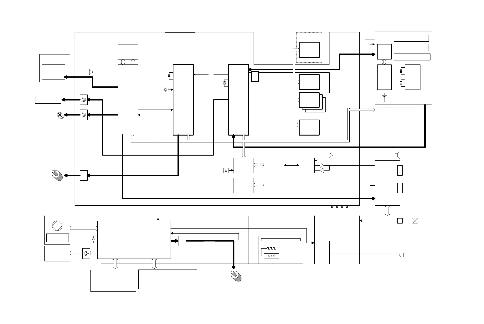
System Description
195
6.2 Electrical Circuit Explanation
6.2.1 Fax Block Diagram
6.2.1.1 Fax Block Diagram (UF-595)
CLK
CCD
TCD1208AP-1
FRIP5
(MN86075)
L mord
SRAM
32KB
Program
F-ROM
2MB
WorkMemory
PageMemory
DRAM
2MBx3
F-ROM
1/2/4MB
Asic
144pin
MN195004 TR88017
MASK ROM
512kB
SRAM
128kB
MOT
DRV
CCD PCB
(337)
TX MOTOR
(324)
BAT
CIR
SCA PCB
(422)
analog
LCU PCB
(402)
Flash
MEMORY
CARD
LINE
7.16MHz(X)
24.576MHz(X)
uPD78012
LASER UNIT
(512)
HV PSU
(424)
7.68MHz(X)
2nd CASSETTE
CST2 PCB (921)
SNS2 PCB (923)
[Paper Detect Sensor]
PAPER FEED SOLENOID (908)
MOT
DRV
PRINTER MOTOR
(626)
THERMISTOR ASSY (728)
FUSER LAMP (732)
THERMOSTAT (725)
AC
(HandSet)
PNL1 PCB
(231)
LCD UNIT
(233)
TEL
PARALLEL PORT I/F
Key
Matrix
and
LED
Image
F-ROM
1MB
WID/ADF SENSOR
[Actuator A] (224)
RP SENSOR
[Actuator B] (225)
ADF DOOR SENSOR
[ADF Door Actuator] (226)
STAMP SOLENOID
(327)
SRU PCB
(124)
(Option)
A4 LED Array
(329)
CPU
(SH7041)
600dpi
400dpi
16MHz(X)
36.2335MHz(X)
HTC
Low Voltage
Power Supply Unit
(423)
+24V
+5V
-12V
LPC PCB
(401)
CPU
8MHz(X)
32768KHz(X)
+5VP
SNS1 PCB (615) [Timing Sensor]
SNS3 PCB (535) [Paper Detect Sensor]
SNS4 PCB (729) [Paper Exit Sensor]
TONER SENSOR (513)
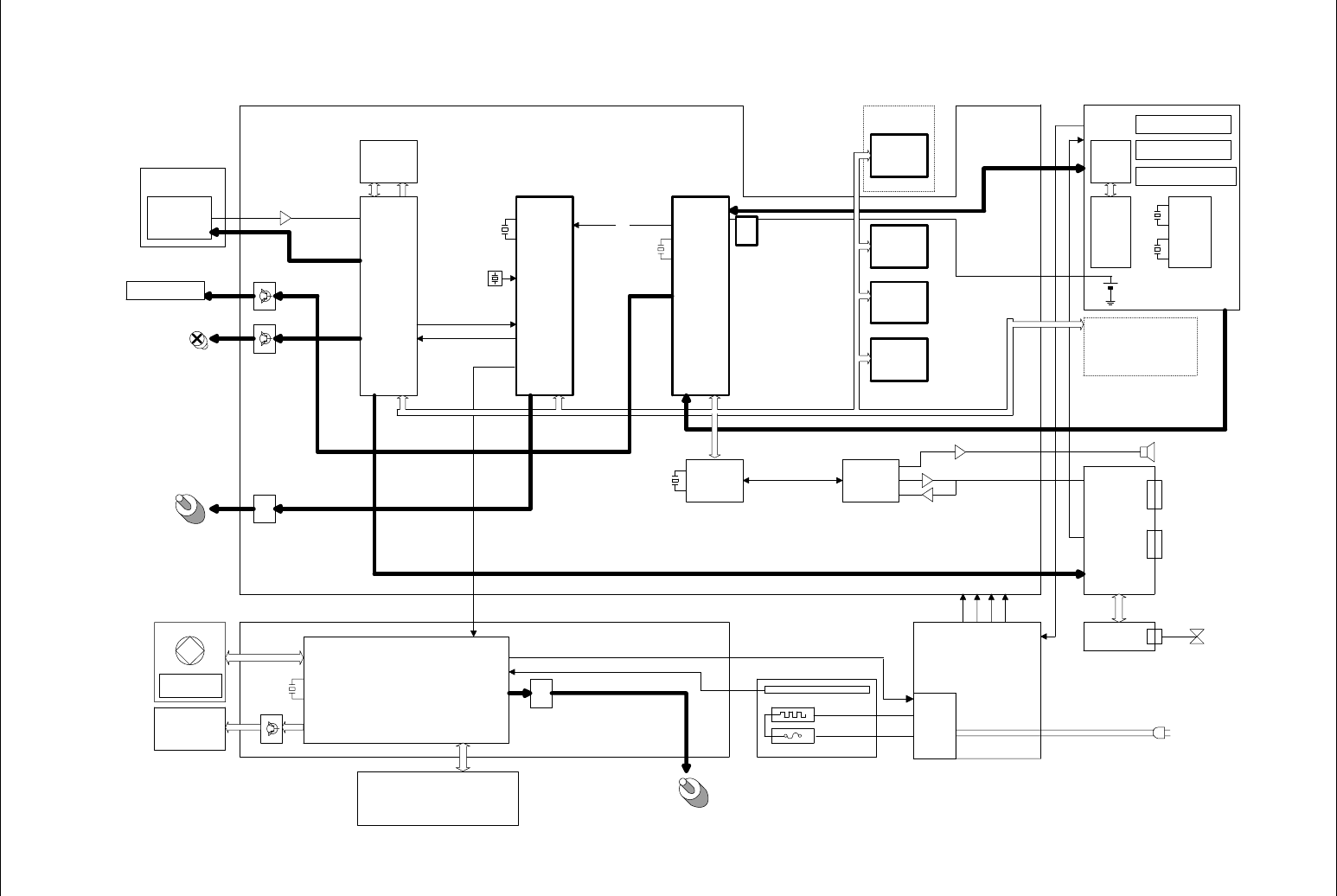
Panasonic UF-585 / 595
196
6.2.1.2 Fax Block Diagram (UF-585)
CLK
CCD
TCD1208AP-1
FRIP4
(MN86074)
SRAM
32KB
Program
F-ROM
2MB
WorkMemory
PageMemory
DRAM
2MB
F-RAM
1/2/4MB
Asic
144pin
FM214
MOT
DRV
BAT
CIR
Flash
MEMORY
CARD
LINE
7.16MHz(X)
32.256MHz(X)
uPD78012
7.68MHz(X)
MOT
DRV
HTC
+24V
+5V
-12V
AC
(HandSet)
TEL
Key
Matrix
and
LED
Image
F-ROM
1MB
CPU
(SH7041)
400dpi
16MHz(X)
analog
300dpi
36.2335MHz(X)
CPU
8MHz(X)
32768KHz(X)
+5VP
PNL1 PCB
(231) WID/ADF SENSOR
[Actuator A] (224)
RP SENSOR
[Actuator B] (225)
ADF DOOR SENSOR
[ADF Door Actuator] (226)
LCD UNIT
(233)
PARALLEL PORT I/F
LCU PCB
(402)
SRU PCB
(124)
(Option)
Low Voltage
Power Supply Unit
(423)
PRINTER MOTOR
(626)
THERMISTOR ASSY (728)
FUSER LAMP (732)
THERMOSTAT (725)
LPC PCB
(401)
SNS1 PCB (615) [Timing Sensor]
SNS3 PCB (535) [Paper Detect Sensor]
SNS4 PCB (729) [Paper Exit Sensor]
TONER SENSOR (513)
TX MOTOR
(324)
LASER UNIT
(512)
HV PSU
(424)
CCD PCB
(337)
SCB PCB
(422)
STAMP SOLENOID
(327)
A4 LED Array
(329)
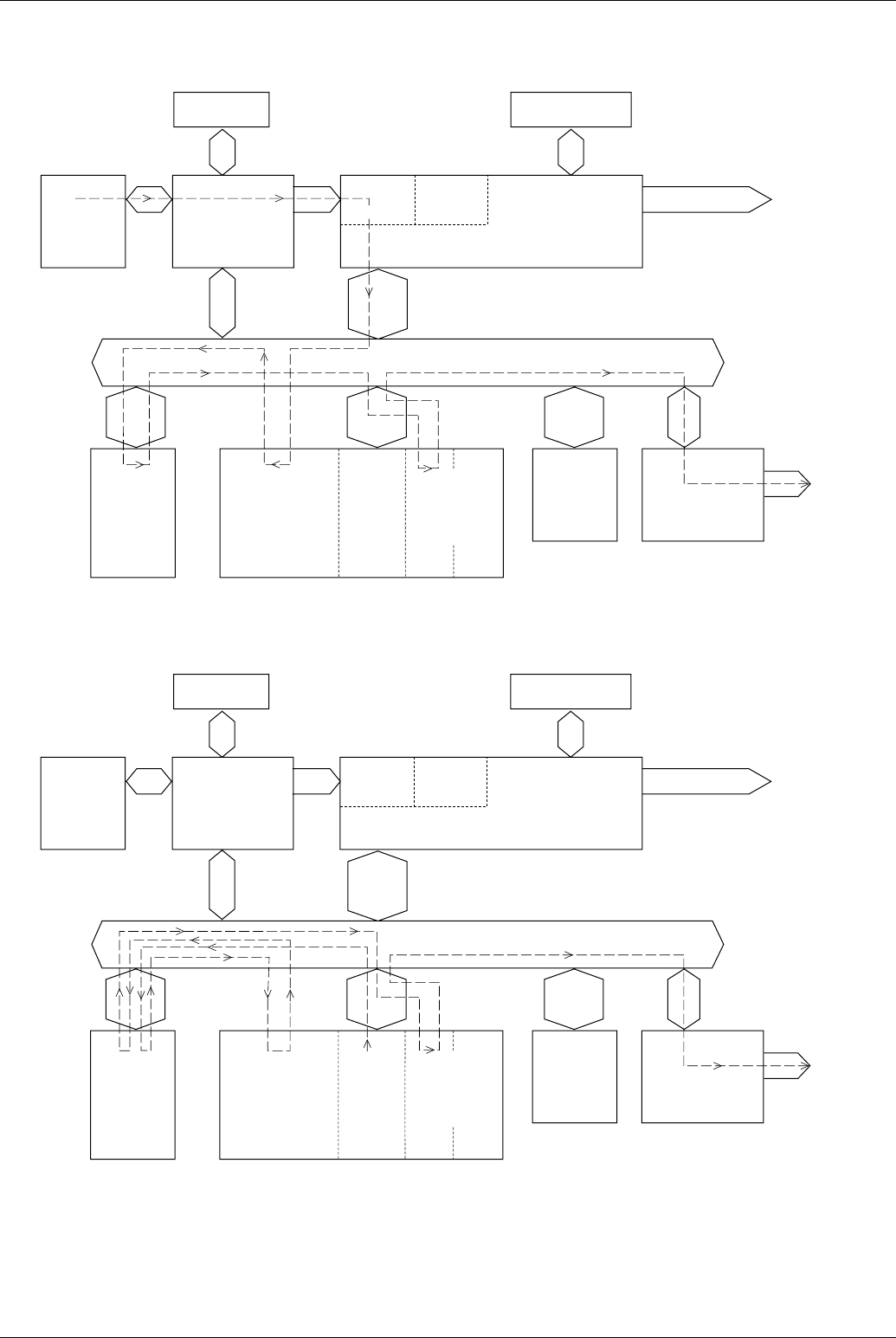
System Description
197
6.2.2 Signal Routing
CCD PCB
UF-595:
FRIP5 (IC17)
UF-585:
FRIP4 (IC7)
PEGASUS
(IC2)
Converter
S/P P/S
Converter
SRAM Smoothing ROM
Laser Printer
Line
F-ROM
Program
(IC4 or IC21)
DRAM
[UF-595: IC6,7,20]
[UF-585: IC6]
F-ROM
(IC5) DRAM
[UF-595:
IC6,7,20]
[UF-585: IC6]
CPU
(IC1)
MODEM
[UF-595: IC10,11]
[UF-585: IC8]
Data Bus (16 bit)
Page
Memory ECM
Buffer
Line
Memory
Work
Area
Image
Memory PEGASUS SH I/F & LP Image Processor
ADF Transmission
Memory Transmission
CCD PCB
UF-595:
FRIP5 (IC17)
UF-585:
FRIP4 (IC7)
PEGASUS
(IC2)
Converter
S/P P/S
Converter
SRAM Smoothing ROM
Laser Printer
Line
F-ROM
Program
(IC4 or IC21)
DRAM
[UF-595: IC6,7,20]
[UF-585: IC6]
F-ROM
(IC5) DRAM
[UF-595:
IC6,7,20]
[UF-585: IC6]
CPU
(IC1)
MODEM
[UF-595: IC10,11]
[UF-585: IC8]
Data Bus (16 bit)
Page
Memory ECM
Buffer
Line
Memory
Work
Area
Image
Memory PEGASUS SH I/F & LP Image Processor
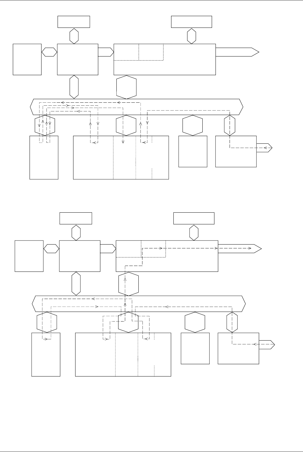
Panasonic UF-585 / 595
198
Memory Reception
CCD PCB
UF-595:
FRIP5 (IC17)
UF-585:
FRIP4 (IC7)
PEGASUS
(IC2)
Converter
S/P P/S
Converter
SRAM Smoothing ROM
Laser Printer
Line
F-ROM
Program
(IC4 or IC21)
DRAM
[UF-595: IC6,7,20]
[UF-585: IC6]
F-ROM
(IC5) DRAM
[UF-595:
IC6,7,20]
[UF-585: IC6]
CPU
(IC1)
MODEM
[UF-595: IC10,11]
[UF-585: IC8]
Data Bus (16 bit)
Page
Memory ECM
Buffer
Line
Memory
Work
Area
Image
Memory
PEGASUS SH I/F & LP Image Processor
Direct Reception
CCD PCB
UF-595:
FRIP5 (IC17)
UF-585:
FRIP4 (IC7)
PEGASUS
(IC2)
Converter
S/P P/S
Converter
SRAM Smoothing ROM
Laser Printer
Line
F-ROM
Program
(IC4 or IC21)
DRAM
[UF-595: IC6,7,20]
[UF-585: IC6]
F-ROM
(IC5) DRAM
[UF-595:
IC6,7,20]
[UF-585: IC6]
CPU
(IC1)
MODEM
[UF-595: IC10,11]
[UF-585: IC8]
Data Bus (16 bit)
Page
Memory ECM
Buffer
Line
Memory
Work
Area
Image
Memory PEGASUS SH I/F & LP Image Processor
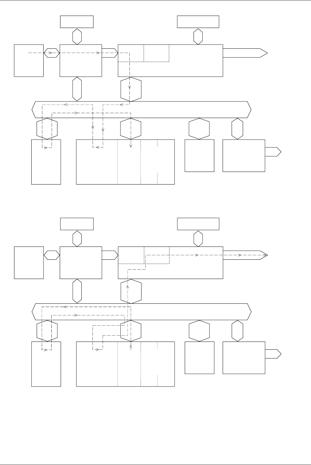
System Description
199
Scan into Memory
CCD PCB
UF-595:
FRIP5 (IC17)
UF-585:
FRIP4 (IC7)
PEGASUS
(IC2)
Converter
S/P P/S
Converter
SRAM Smoothing ROM
Laser Printer
Line
F-ROM
Program
(IC4 or IC21)
DRAM
[UF-595: IC6,7,20]
[UF-585: IC6]
F-ROM
(IC5) DRAM
[UF-595:
IC6,7,20]
[UF-585: IC6]
CPU
(IC1)
MODEM
[UF-595: IC10,11]
[UF-585: IC8]
Data Bus (16 bit)
Page
Memory ECM
Buffer
Line
Memory
Work
Area
Image
Memory PEGASUS SH I/F & LP Image Processor
File Print from Memory
CCD PCB
UF-595:
FRIP5 (IC17)
UF-585:
FRIP4 (IC7)
PEGASUS
(IC2)
Converter
S/P P/S
Converter
SRAM Smoothing ROM
Laser Printer
Line
F-ROM
Program
(IC4 or IC21)
DRAM
[UF-595: IC6,7,20]
[UF-585: IC6]
F-ROM
(IC5) DRAM
[UF-595:
IC6,7,20]
[UF-585: IC6]
CPU
(IC1)
MODEM
[UF-595: IC10,11]
[UF-585: IC8]
Data Bus (16 bit)
Page
Memory ECM
Buffer
Line
Memory
Work
Area
Image
Memory PEGASUS SH I/F & LP Image Processor
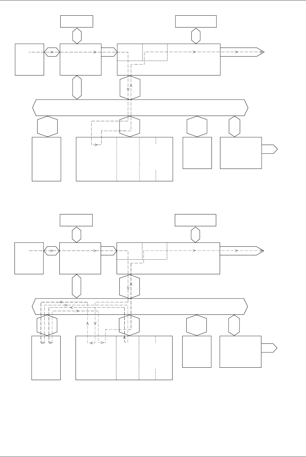
Panasonic UF-585 / 595
200
Single Copy
CCD PCB
UF-595:
FRIP5 (IC17)
UF-585:
FRIP4 (IC7)
PEGASUS
(IC2)
Converter
S/P P/S
Converter
SRAM Smoothing ROM
Laser Printer
Line
F-ROM
Program
(IC4 or IC21)
DRAM
[UF-595: IC6,7,20]
[UF-585: IC6]
F-ROM
(IC5) DRAM
[UF-595:
IC6,7,20]
[UF-585: IC6]
CPU
(IC1)
MODEM
[UF-595: IC10,11]
[UF-585: IC8]
Data Bus (16 bit)
Page
Memory ECM
Buffer
Line
Memory
Work
Area
Image
Memory PEGASUS SH I/F & LP Image Processor
Multiple Copies
CCD PCB
UF-595:
FRIP5 (IC17)
UF-585:
FRIP4 (IC7)
PEGASUS
(IC2)
Converter
S/P P/S
Converter
SRAM Smoothing ROM
Laser Printer
Line
F-ROM
Program
(IC4 or IC21)
DRAM
[UF-595: IC6,7,20]
[UF-585: IC6]
F-ROM
(IC5) DRAM
[UF-595:
IC6,7,20]
[UF-585: IC6]
CPU
(IC1)
MODEM
[UF-595: IC10,11]
[UF-585: IC8]
Data Bus (16 bit)
Page
Memory ECM
Buffer
Line
Memory
Work
Area
Image
Memory PEGASUS SH I/F & LP Image Processor
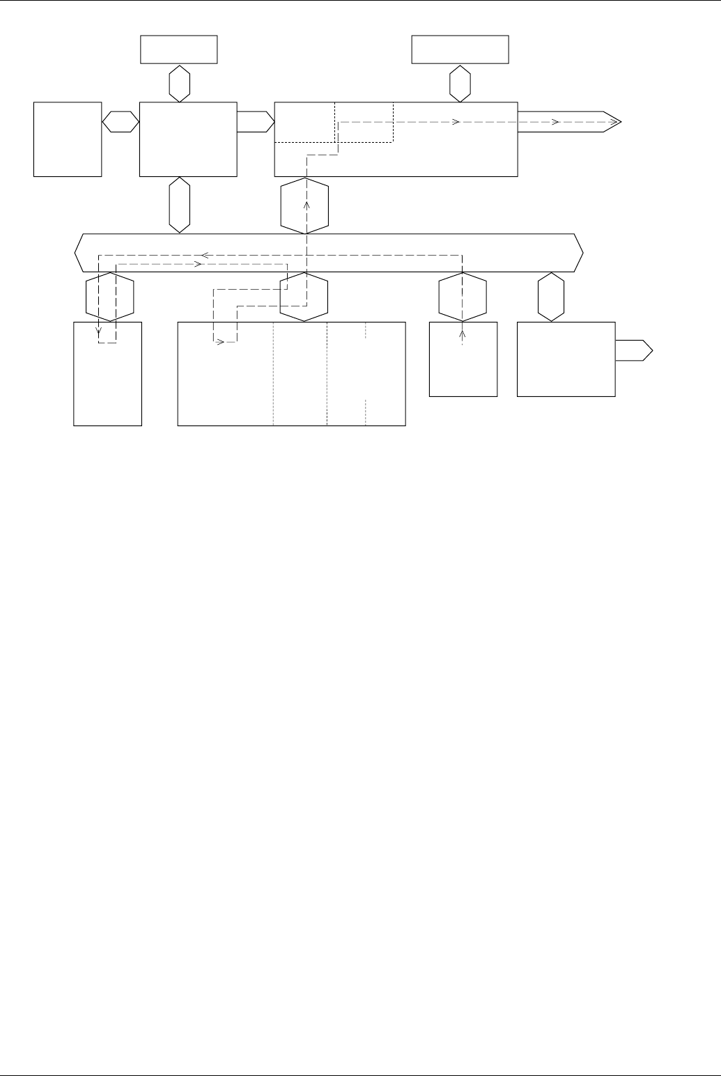
System Description
201
Report / List Printing
CCD PCB
UF-595:
FRIP5 (IC17)
UF-585:
FRIP4 (IC7)
PEGASUS
(IC2)
Converter
S/P P/S
Converter
SRAM Smoothing ROM
Laser Printer
Line
F-ROM
Program
(IC4 or IC21)
DRAM
[UF-595: IC6,7,20]
[UF-585: IC6]
F-ROM
(IC5) DRAM
[UF-595:
IC6,7,20]
[UF-585: IC6]
CPU
(IC1)
MODEM
[UF-595: IC10,11]
[UF-585: IC8]
Data Bus (16 bit)
Page
Memory ECM
Buffer
Line
Memory
Work
Area
Image
Memory PEGASUS SH I/F & LP Image Processor
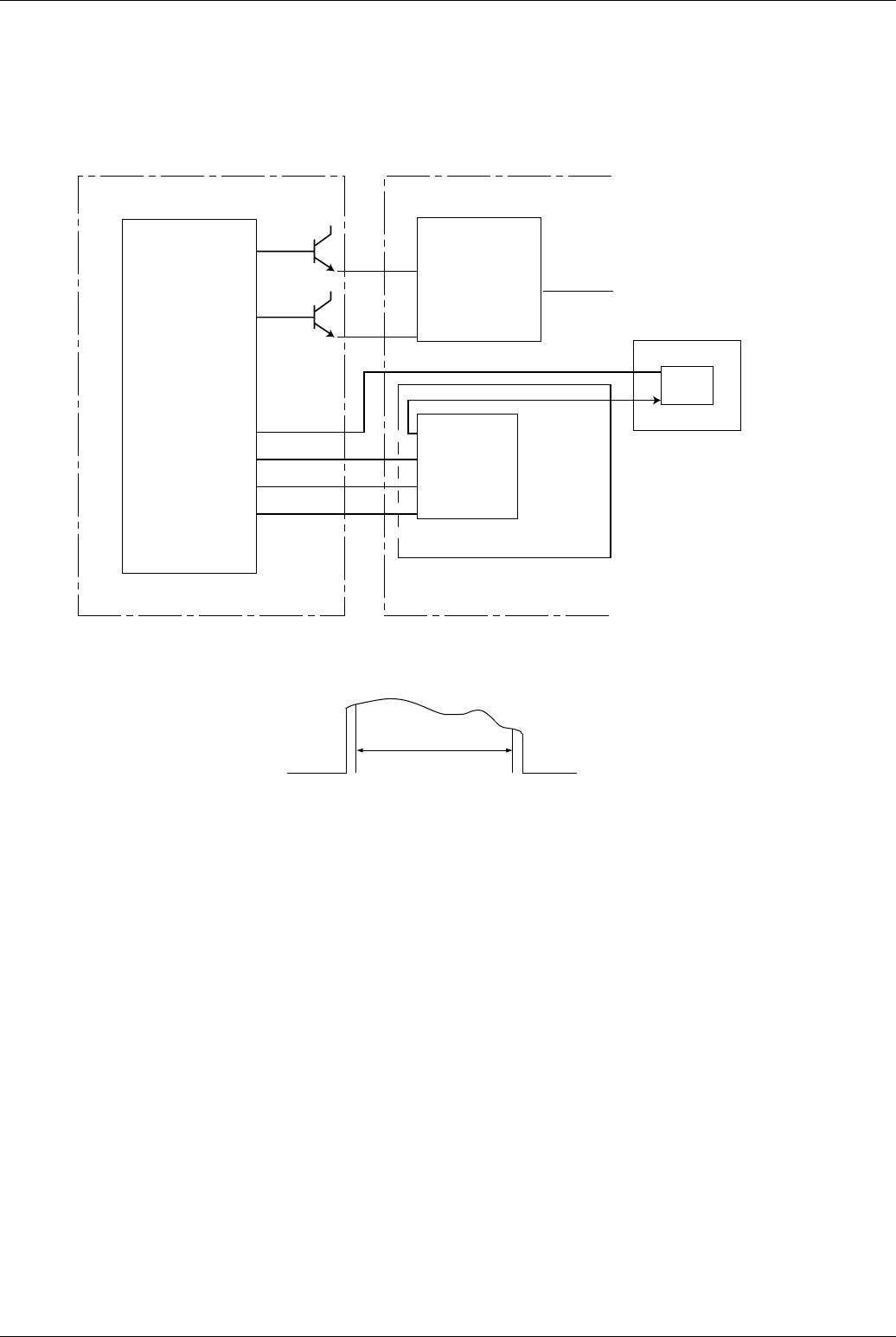
Panasonic UF-585 / 595
202
6.2.3 Picture Signal Scanning Block
The image data read by the optical unit is input to the CCD mounted on the CCD PC Board, then transferred to the SCA/SCB PC
Board after the optical information is converted into an electrical signal by the CCD. The following shows a block diagram of the
picture signal scanning circuit. This picture signal scanning circuit consists of (1) ABC circuit, (2) shading correction circuit, (3) offset
control circuit, (4) picture signal binary coding correction circuit and (5) reducing circuit.
ABC Circuit
This circuit consists of IC19, IC17, C187, R109 and R320 (UF-585: IC19, IC7, C113, R146 and R250). Its function is to prevent
deterioration of picture quality due to dirt on the document or degrading of the luminous energy of the Xenon Lamp light source.
The picture signal from the CCD is amplified in IC19 and input to IC17 (UF-585: IC7), where it is converted from analog to digital
and the shading is corrected. When the signal exceeds +5V as the result of this amplification and correction, capacitor C187
(UF-585: C113) is charged through R109 (UF-585: R146). This charging voltage lowers the level of the picture signal input to
IC19. When the picture signal voltage rises, this charge voltage becomes higher. When the picture signal level lowers due to the
background color, etc., of a transmitting document, the voltage of the charged capacitor C187 (UF-585: C113) is discharged
through R320 (UF-585: R250). Consequently, the output of the ABC circuit is kept constant to maintain the picture quality,
regardless of changes in the CCD output level.
W
B
1728 bit
Effective Scan Width
CCD
TCD 1208P
Differencial
Amplifier
CCD PC Board SCA/SCB Board
CCD
Drive
Circuit
Relay
[SCA]
IC17
MN86075
IC2
DZAC000157
(PEGASUS)
[SCB]
IC7
MN86074
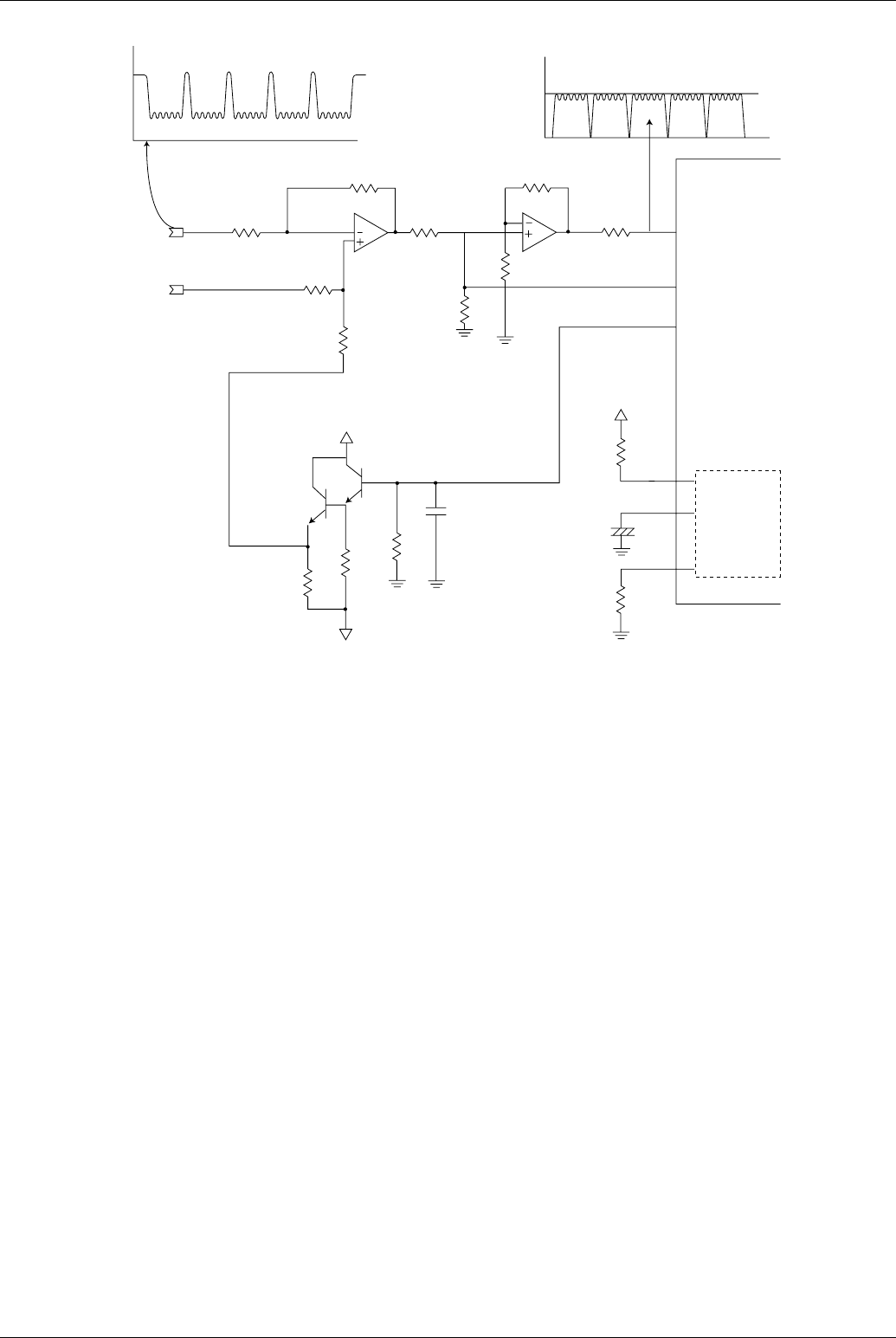
System Description
203
Shading Correction Circuit
The Shading Correction Circuit, included in IC17 (UF-585: IC7), is provided to correct for reduction in LED lamp intensity around
the optical lens and LED lamp intensity distortion due to shading of each bit. This circuit scans the reference white on the
transmitting document plate immediately before the document reaches the scanning position and writes a compensation value
according to the distortion of the waveform, at the time, into the S-RAM (IC18).When the actual picture signal is input, the circuit
corrects the picture signal shading, according to this compensation value. This shading is carried out for each page during
transmission or copy.
Offset Control Circuit
The Offset Control Circuit consists of Q5, Q4, IC17 and IC19 (UF-585: Q4, Q5, IC7 and IC19), and controls the black level of
the CCD output to be at 0V by using the input.
Picture Signal Binary Coding Correction Circuit
The Picture Signal Binary Coding Correction Circuit is included in IC17 (UF-585: IC7). It is used to obtain a binary coding signal
which is a corrected picture and error diffused signal of a false halftone signal, which is detected from a shaded picture signal.
CCD Output ABC Circuit Output
R109
(R146)
C187
(C113)
R320
(R250)
IC19, 1
IC19, 2
32
(24)
37
(20)
19
(26)
41
(15)
39
(18)
40
(17)
IC17
(IC7)
Control
Circuit
OS
DOS
0V
3V
0V
UF-595 (UF-585)
-12V
+12V
Q5
(Q4)
Q4
(Q5)
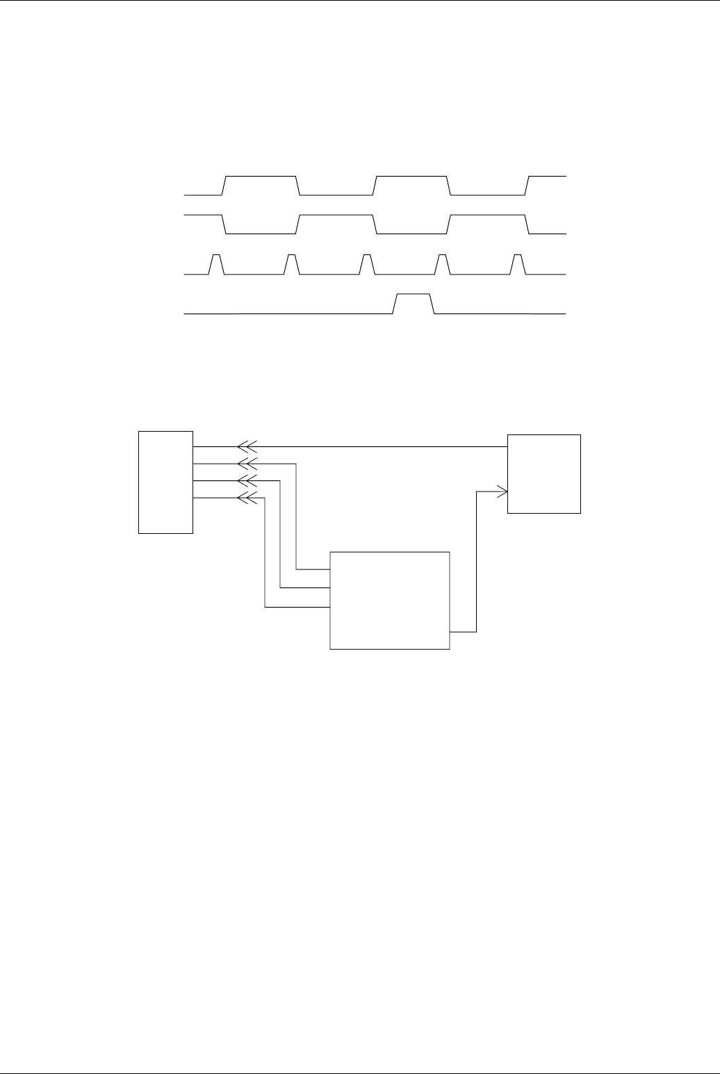
Panasonic UF-585 / 595
204
6.2.4 CCD Drive Clock Generator Circuit
This circuit is also contained in IC17 (UF-585: IC7). Its function is to generate FSG, FCK1, FCK2 and RS clock signals, which are
required for driving the CCD. These clock signals are generated by the system clock generator circuit derived from the 4 MHz clock
signal that is input to IC9 (UF-585: IC7). Its timing chart is shown below.The FR clock supplied to the CCD is output from the RS of
IC2 (PEGASUS). The RS clock of IC2 is derived from the FR clock of IC17 [MN86075] (UF-595: IC7 [MN86074]) generates the
timing of the RS clock to drive the CCD.
FCK1
FCK2
RS
FSG
CCD
FR RS
FCK1
FCK2
FSG
IC2
(PEGASUS)
IC17 (IC7)
86075 (86074)
FR
UF-595 (UF-585)
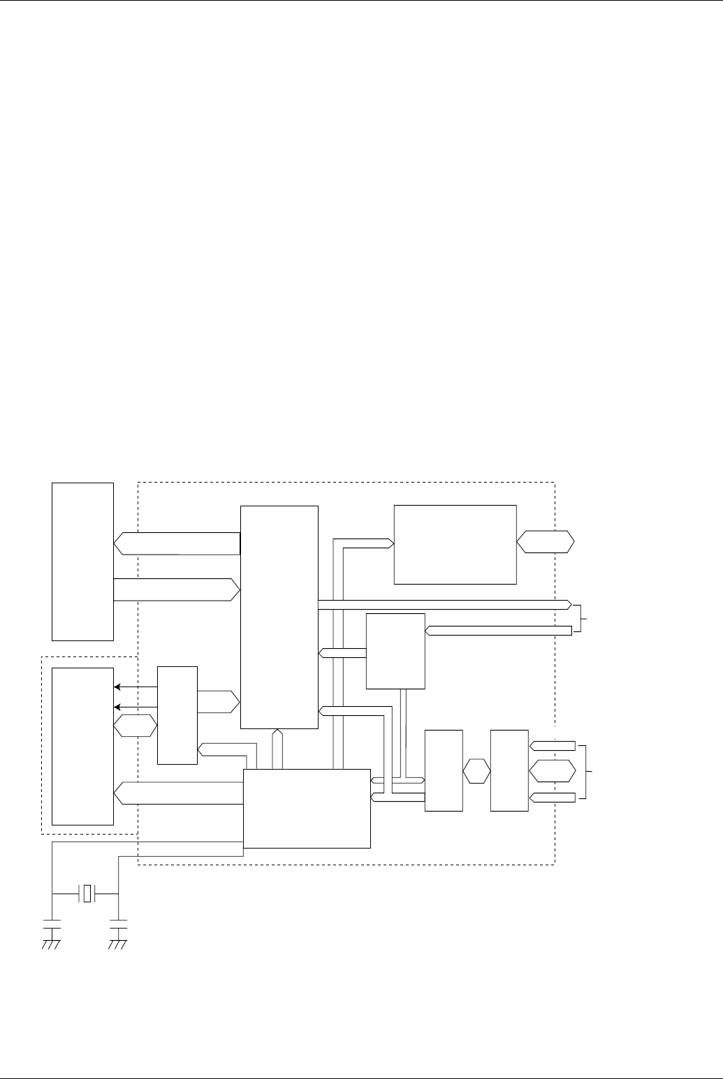
System Description
205
6.2.5 Picture Quality Control Circuit
This circuit consists of a recording picture control standard cell IC2 [DZAC000157 or ”PEGASUS”] , an interpolation table ROM
(IC3), line memory for interpolating (SRAM) and its peripheral circuitry.
The recording picture control standard cell (IC2) inputs the parallel data from the system bus, conducts picture quality correction
(smoothing), reduction, synchronization control, etc., then sends this data to the printer. These functions are as follows:
Picture quality correction circuit (smoothing)
Compares the picture element with 15 surrounding picture elements, determines the interpolation data from the interpolation
data ROM, and smooths out diagonal lines, etc., on the recorded picture.
Image range isolation circuit
Identifies the halftone picture range and controls smoothing to eliminate blotching of the recording picture which has undergone
error diffusion or other processing.
Reduction circuit
This circuit is used to process the received data so that it fits on the recording paper, according to the Fax Parameter settings.
Synchronization control circuit
This circuit is used to synchronize the output recorded data with the horizontal synchronizing output signal from the printer for
each line. Within a line, it is synchronized with the dot clock signal. The dot clock signal is provided by dividing the crystal
oscillator frequency from the Extend Generator Circuit (16 MHz) by 5.
Smoothing
Process
Circuit
Timing
Generator
Circuit
Scanning LSI
[IC17 (IC7)]
Laser Printer I/F
CPU Bus
Horizontal
Sync
Circuit
Scanning
Synchronization
Circuit
Register
(IC2)
AddressAddress
Control SignalControl Signal
System
Bus
I/F
RAM
I/F
Line
Memory
16 MHz
Crystal
Oscillator
Smoothing
Data
ROM
[IC3]
Recording Picture Process Circuit
Block Diagram
UF-595 (UF-585)
Control Signal
Address
Address Address
Data
Data
Data Bus
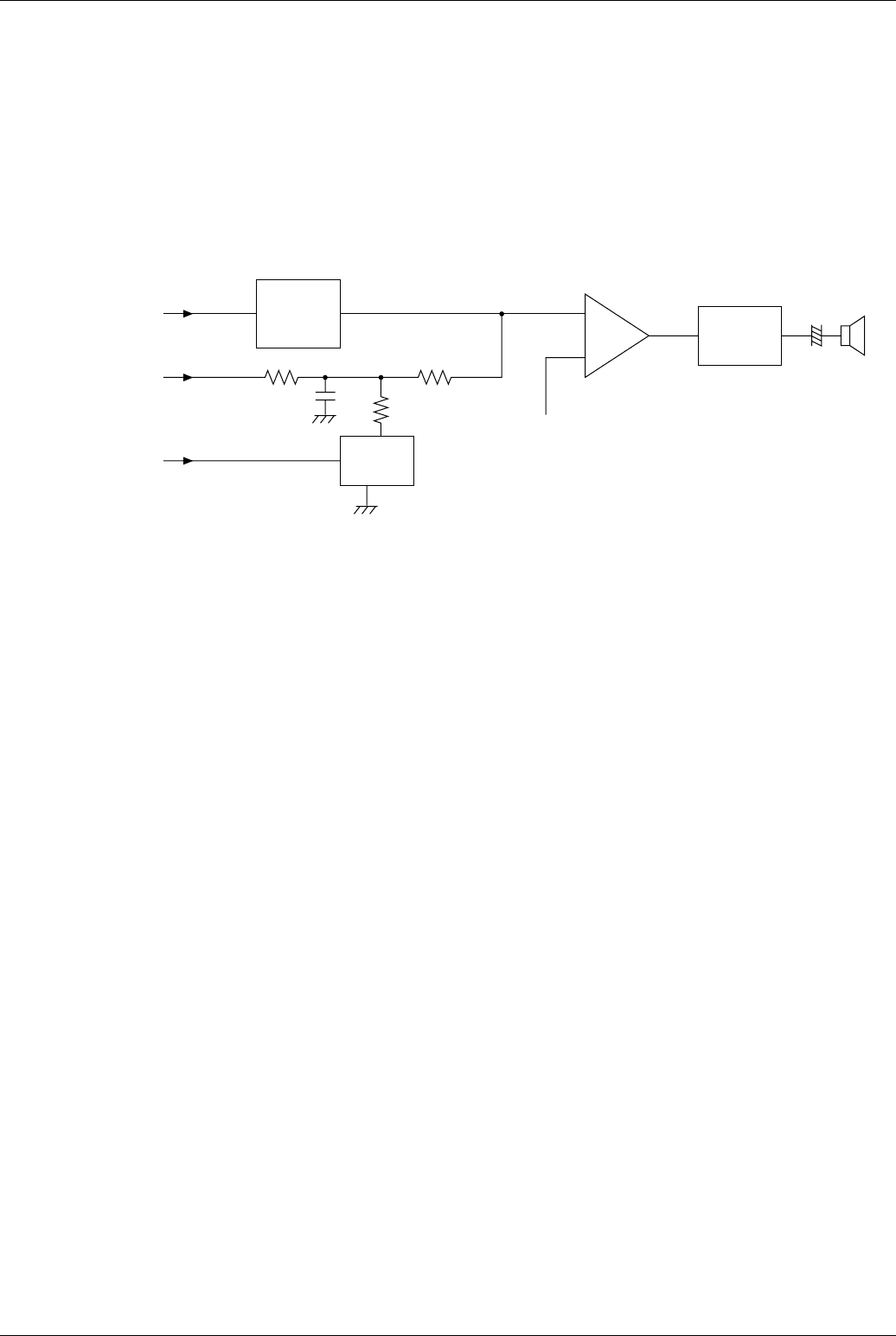
Panasonic UF-585 / 595
206
6.2.6 Line Monitor Circuit
The Line Monitor Circuit consists of an operational amplifier (IC14, 2), analog switch (IC13), speaker amplifier (Q18, 19) and its
peripheral circuits. Its function is to monitor the dial tone, DTMF tone, response signals, etc. over the speaker. It also sounds the
output of the key touch tones, alarm tones, etc. from the panel CPU over the speaker. The received signal from the LCU PCB
passese through an AGC circuit (IC14, 1, Q7, Q6) and is then input to the analog switch for volume control. It passes through the
operational amplifier (IC14, 2) and is then input to the speaker amplifier (Q18, 19), where it is amplified to a level sufficient to drive
the speaker. The volume can be set in 9 steps (including OFF) from the panel.
Key touch tone, etc. from the panel are mixed by the operational amplifier (IC14, 2) and input to the speaker amplifier. The key
touch tones and alarm tones can be set to one of three levels, High, Low, or Off, with analog switch Q17.
Volume
Control
Circuit
(IC13)
Level Control
Circuit
(Q17)
(IC14, 2) Speaker
Amplifier
(Q18,19)
Speaker
AGD
(+2.5VDC)
Line Monitor Signal
(from AGC Circuit)
Buzzer Clock
(from Control Panel Unit)
Buzzer Tone Switch
(from Output Port)
+
-
Line Monitor Circuit
Block Diagram
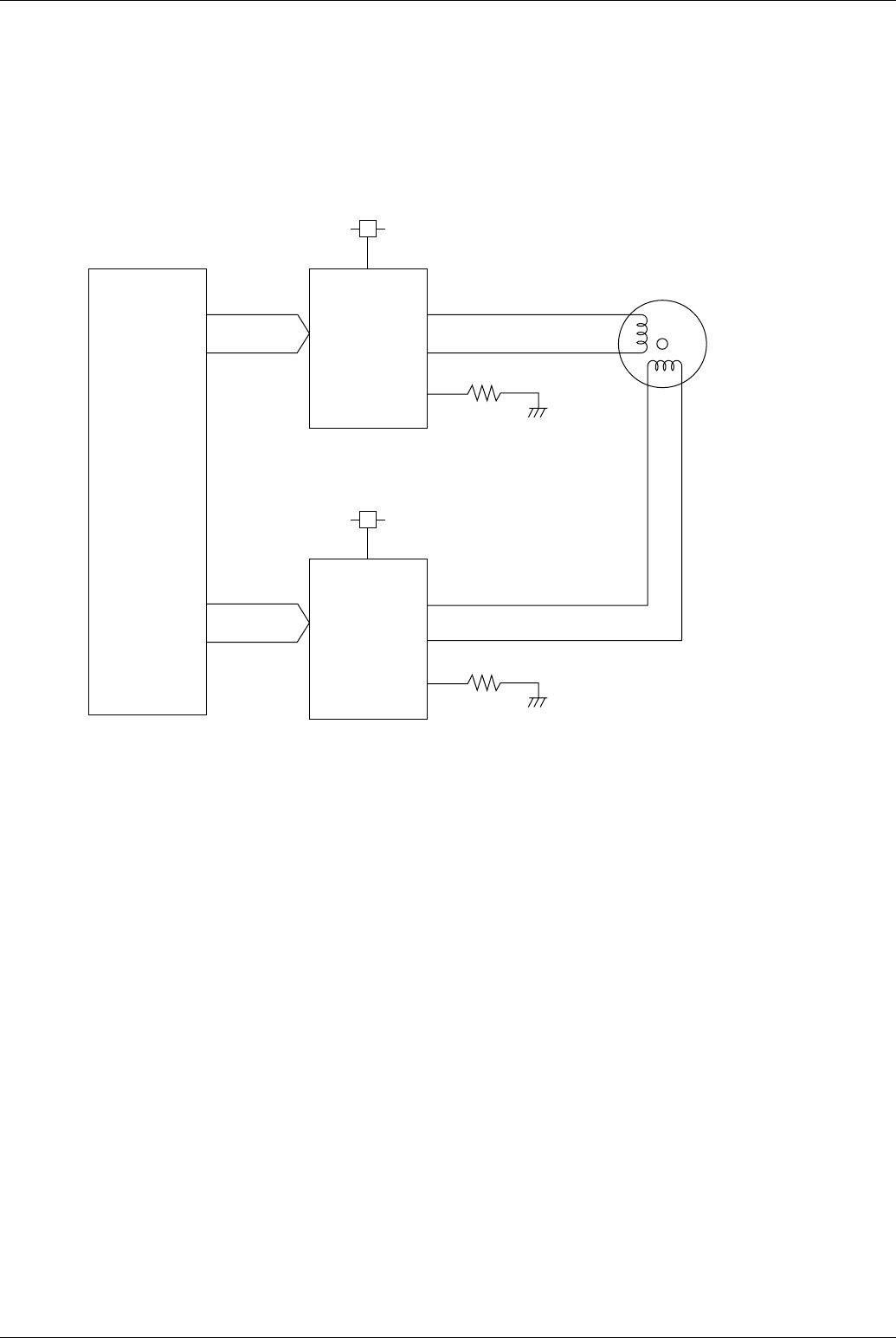
System Description
207
6.2.7 Transmit Motor Control Circuit
The transmit motor is a PM type, two-phase bi-polar motor. The stepping signal and chopping current control signals (pTAPH,
pTBPH, pTA10, pTA11, pTB10 and pTB11) are sent to the chopper drive circuit, comprised of IC26, IC27 (UF-585: IC9, IC10) and
its peripheral circuitry, from IC2 PEGASUS (Panasonic Engine for Graphic Adaptation System Under the SH: DZAC000157) output
port. The motor is powered by +24 VDC and is driven by a 1/2-phase excitation, and greater step division is provided by controlling
the phase circuit in steps (micro-step control).
Tx Stepper
Motor
Tx Motor Driver Circuit Block Diagram
PEGASUS
IC2
Motor
Driver
IC26
(IC9)
+24V
Motor
Driver
IC27
(IC10)
+24V
R26
R25
UF-595 (UF-585)
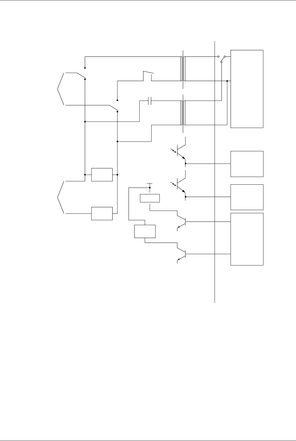
Panasonic UF-585 / 595
208
6.2.8 Line Control Board
The following shows a block diagram of the Line Control Board.
The Ring Detector consists of a photocoupler, PC1, and its peripheral circuits. The ringing signal is half-wave rectifier in the Ring
Detector, and transferred through the nCTON signal line to the CPU on the SCA/SCB PC Board. The CPU observes the signal to
distinguish from signals caused by chattering.
The Off-Hook Detector (External Telephone) circuit consists of the photocoupler, PC2, and its peripheral circuits. When PC2
detects loop current flow, it emits a Low active output signal (nHKOF) to the CPU which monitors it for a specified time. If the CPU
detects no change in the Low signal level, it determines that the External Telephone is Off-Hook.
PC1
PC2
CML
PLS
CML
Line
PC1
PC2
Telephone
Off-Hook
Detector
Ring
Detector
CML
PLS
HYBSR
HYSIG
Modem
IC 11
(IC 8)
Port
IC17
(IC 7)
SCA/(SCB) PCBLCU PCB
+24V
CPU
IC 1
CPU
IC 1
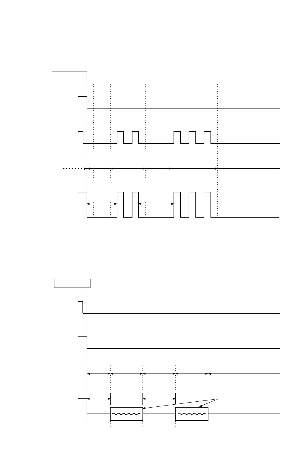
System Description
209
Dial Pulse Generator
The circuit consists of the CML relay, PLS relay and their peripheral circuits. This circuit generates dial pulses. The CPU on the
SCA/SCB PC Board controls all dial pulse generation sequences. It turns relay CML and PLS ON and OFF through the
MN86075 [IC17] (UF-585: MN86074 [IC7]). The status of the relays during dialing is shown below. When the absence of the
terminating message is confirmed by the Off-Hook detector, the CPU turns CML relay ON to develop loop status (DC loop).
After a few seconds, the CPU turns the PLS relay On and Off to generate dial pulses, making and breaking the loop.
DTMF Tone Generator
The circuit is incorporated in the MODEM on the SCA/SCB PC Board. The DTMF tone is conveyed to the telephone line using
the same route as the facsimile signal. The DTMF tone selection is controlled by the CPU. The relay status during dialing is
shown below.
CML Relay
PLS Relay
Line release
Line status
make
break
Speech
condition
Dial pulses Dial pulses
First
digit Second
digit
Prepause Inter-digit
pause
make
break
make
break
Speech
condition Speech
condition
Dial Pulse
PLS Relay
CML Relay
Line release
Line status
make
break
Speech
condition
First
digit Second
digit
Prepause Inter-digit
pause
make
break
make
break
Speech
condition Speech
condition
DTMF signal
DTMF Tone
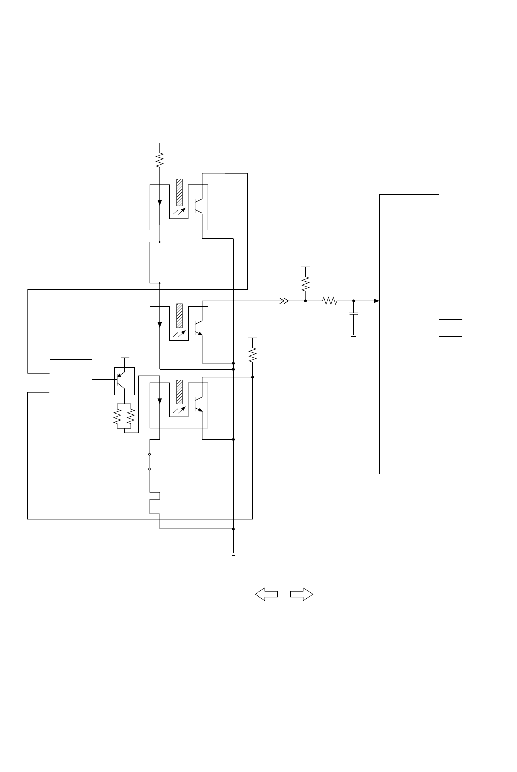
Panasonic UF-585 / 595
210
6.2.9 SNS PC Board
Each sensor consists of an LED and phototransistor. When documents are placed on the ADF tray or are moving, a shutter in the
document sensor opens. The light from the LED turns the phototransistor “ON”, and the output voltage from the sensor becomes a
“Low” level. With no document on the ADF tray, the shutter interrupts the light path, and output from the sensor is kept at a “High”
level. Operation of the RP Sensor is exactly the same as the ADF Sensor. The Printer Cover Sensor (ILS PC Board) operation is
similar, except that the output from the sensor is kept at a “Low” level when the cover is closed and becomes a “High” level when
the Printer Cover is opened.
Read Point
Sensor
GND
+5V
+5V
nBPNT
PC3
Shutter
A
K
Printer Cover Sensor
(ILS PC Board)
MPU
CPU
(IC1)
Shutter
PC2
A
K
ADF
Sensor
GND
PC1
Shutter
A
K
SCA/SCB PC BoardPNL1 PC Board
+5VP
+5VP
PNL CPU
IC1
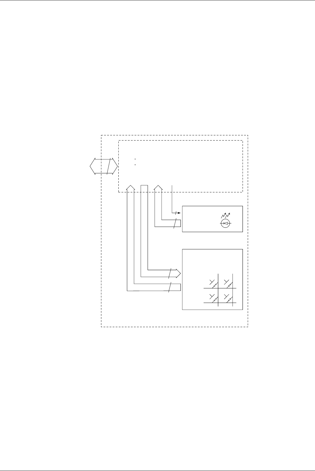
System Description
211
6.2.10 Control Panel
The Control Panel consists of the Display PCB and Panel Unit, which display various status information.It is normally interfaced to
the main CPU. Keyed input signals are received by the Panel CPU and the data is transferred to the main CPU on the SCA/SCB
PC Board.
The Control Panel performs the following processes simultaneously:
• Key inputting
• LED, LCD display
• Data transmission / reception
Interface to main CPU
The interfacing between the main CPU and the panel CPU are all executed with commands and responses in the following two
formats:
• Command / response (1 byte) + number of data + check sum
• Command / response (1 byte) + number of data + data 1 + data 2 ........................ + data n + check sum.
PNLCK
PNLRD
PNLSD
PNLRST
BZCLK
+5V
+5VP
GND
GND
nPWSAVE
nWAKEUP
nBPNT
BATLVL
20 characters, 2 lines, 5x7 dots control
LED, KEY scanning
2
8
10
8
SCN (9:0)
KIN (7:0)
LED
Key matrix
(59 keys)
PNL1 PC Board
13
LED (7:0)
LEDCT (1:0)
From
/to
SCA/SCB
PCB
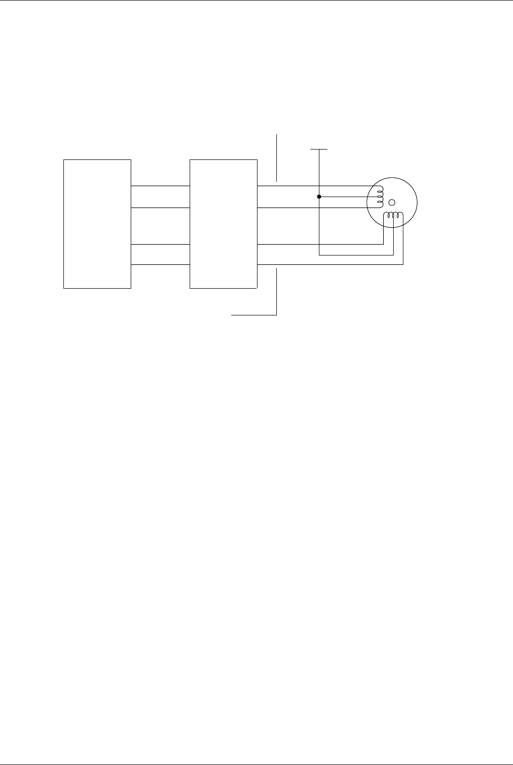
Panasonic UF-585 / 595
212
6.2.11 Printer Motor Drive Circuit
Motor Drive Circuit
The Printer Motor is a 4-phase uni-polar PM-type step motor. The step signals (pMMP0A to pMMP3A) are transmitted to IC6
(the Chopper Drive Circuit) by means of a CPU with real-time output function. The chopper current is determined by the voltage
at IC6, Pin3 and Pin13. The Printer Motor has two speeds, Slow and Constant. The Printer Motor is powered by a +24 VDC sup-
ply. When the interlocks are open, the +24 VDC supply is cut off and the Printer Motor stops rotating.
Pulse
Motor
Laser Printer Motor Drive Circuit Block Diagram
CPU
IC1
+24 VM
3
1
6
4
pMMP0a
nMMP0a
pMMP2a
CN53
nMMP2a
Motor
Driver
IC6
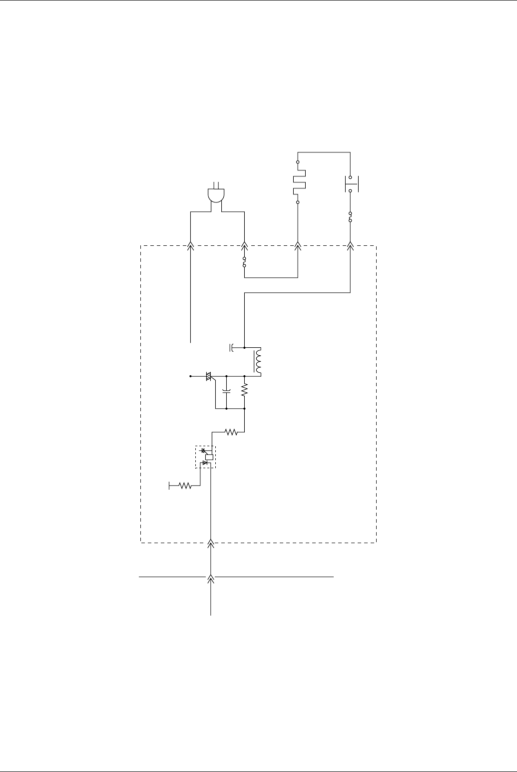
System Description
213
Fuser Lamp Drive Circuit
The Fuser Lamp is powered by 115 VAC. It is driven by the LVPS and controlled by the nSSR signal from the SCA/SCB PC
Board. When the CN33, Pin10 (nSSR) on the LVPS goes LOW, the Fuser Lamp turns ON. This lights up the PC301 LED and
activates the CR301 photo-triac, and VAC 115 VAC is sent to the Fuser Lamp. The time at which CR301 is actually activated
depends on the VAC 115 VAC sine wave. When the cross-voltage for Pin 6 and Pin 4 of PC301 is other than 0 Volts (sine wave
exceeds 0 volts), PC301 inhibits the activation of the triac and turns ON the Fuser Lamp.
99
CN33
+24V
R304
4
2
1PC301
nSSR
R303
CR301
2
1
2
1
C302
R302
C301
2
1
CN31 H
CN31
Fuser Lamp
Fuse
Thermostat
Thermal Fuse
3
SCA/SCB PCB
6
LVPS
Fuser Lamp Drive Circuit Diagram
L301
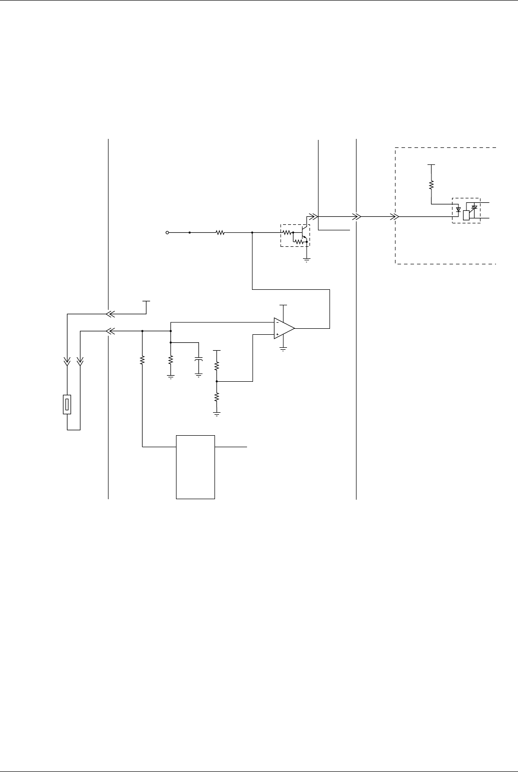
Panasonic UF-585 / 595
214
Fuser Temperature Control Circuit
The fuser temperature is controlled by IC1 on the LPC PC Board, which contains A/D (Analog/Digital) converters ANI0 and
ANI7. The Fuser Temperature Control Circuit uses A/D converter, ANI0. When thePC301 drive current is transmitted from the
LPC PC Board to the LVPS, the Fuser Lamp turns ON. IC4 is a conparator with open output at pins 1 and 7 and is used as an
abnormal temperature detection circuit. IC4, pin 1, has a high impedance when Q10 is activated, turning ON the Fuser Lamp.
An abnormal temperature is detected when the VTH voltage level becomes higher than V+, forcing IC4, 1, pin 1 Low and deac-
tivating Q10.
Abnormally low and high temperatures, as well as Thermistor release status, are detected by IC1 (CPU) programming.
GND
Q10
3
2
R78
2
IC4.1
4
1
3
GND GND
C13
R77
GND
R76
R88
+5v
+24V
GND
PC301
1
2
6
4
+24v
R304
+5v
Thermistor
LVPS
pSSRA
pSSRA
8
1
47
LPC PCB
6
7
CN
10
99
CN6
CN67 CN15
10
CN33
Fuser Temperature Control Circuit Diagram
(ANI0)
IC1
CPU
R89
SCA (SCB)
PCB
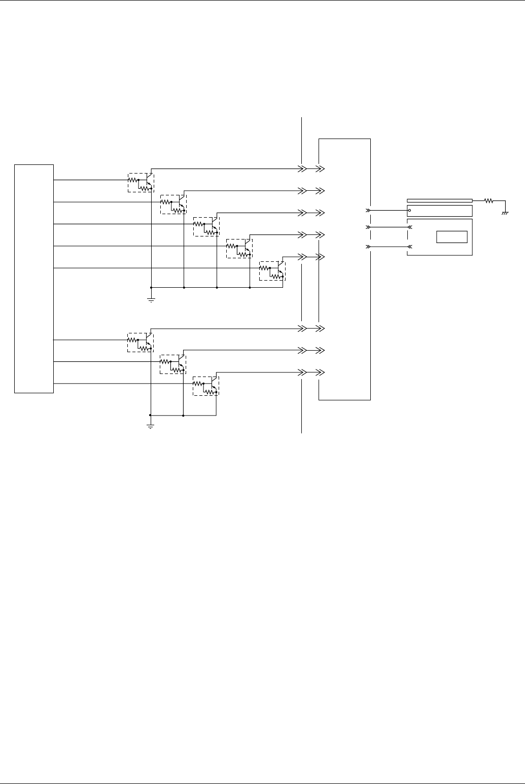
System Description
215
High Voltage Drive Circuit (Charging, Development and Transfer)
High Voltage is provided through a DC to DC converter, which changes the +24 VDC supply voltage to -650 VDC, and output
approximately 0.64 KVAC (Steady current: 220 µA) for the Charging Block. The Developer Circuit converts the +24 VDC to
between -300 VDC for the development bias, and outputs 1,500 VAC(p-p) at a frequency of 1.875 kHz to charge the toner. The
Transfer Circuit changes the +24 VDC supply voltage to approximately +280 VDC (MAX) (steady current: 2.5 µA/-1500 VDC
steady voltage).
3
GND
Q6
2
1
3
Q2
2
1
FG
Discharge Plate
Bias Transfer Roller
Bias Charge Roller
Development Roller
3
Q5
2
13
Q4
2
13
Q3
2
1
HVPS
CPU
pCR0
pCR1
pDR0
pTR0
pTR1
CN53
2
3
3
GND
Q13
2
13
Q14
2
1
pDRCK0
pCDDC
5
7
4T
C
D
8
9
PCB
Toner
Cartridge
High Voltage Drive Circuit
3
Q12
2
1
pDRCK1
6
nCDDC
nDRCK0
nDRCK1
nTR1
nTR0
NDR0
nPCR1
nPCR0
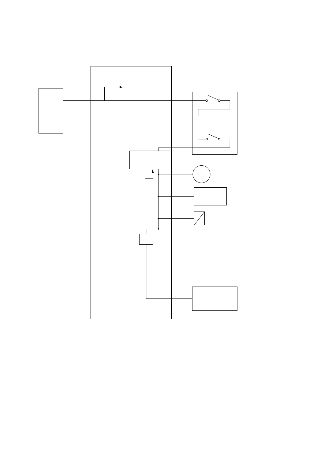
Panasonic UF-585 / 595
216
6.2.12 Interlock Safety Circuit
This safety circuit turns OFF the +24 VDC supply voltages when the Printer Cover is opened. When the Printer Cover is opened,
the microswitch(es) on the ILS PC Board are de-actuated, turning OFF +24 VDC to the Printer Drive Circuit, the High Voltage
Power Supply, and the Paper Feed Solenoid Circuits, turning OFF the +5 VDC supply voltage for the Laser Driver circuits, on the
Laser Unit.
+24V
LVPS
+24V
+24V Printer
Cover
+24VD
ILS PCB
Paper Feed Solenoid
Laser Unit
DC/DC
Converter
Rush Current
Protection Circuit
pMPOW
High Voltage
Power Supply Unit
Printer Motor
(LPC PCB)
+24VM
+24VM
+24VM
+24VM
L+5V
Interlock Safety Circuit Block Diagram
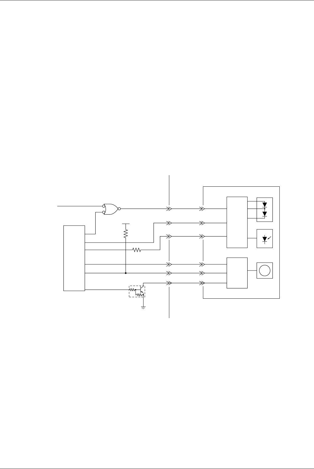
System Description
217
6.2.13 Laser Unit (LSU) Control Circuit
The laser control signals are described below.
nLDON
The LSU is activated when this output signal is LOW. If an error occurs, the nLDON output signal level goes High and the LSU
is deactivated.
nVIDEO
This is the actual Data Signal. The Laser is ON when the nVIDEO output signal level is LOW.
nHSYNC
This horizontal synchronization signal transmitted from the Beam Detection Sensor sets the horizontal position of the laser
beam as it crosses the OPC Drum.
nPMON
This is the Scanner Motor Control Signal. The Scanner Motor rotates when the nPMON output signal level is LOW.
nPMRDY
A Phased-Lock Loop (PLL) circuit keeps the Scanner Motor speed constant when the nPMRDY is at a Low output signal level.
nPMCK
This is the Scanner Motor Clock.
Laser
Timing
Sensor
Scanner
Motor
Laser
Drive
Circuit
Scanner
Motor
Drive
Circuit
IC1
CPU
VDO Signal nVIDEO
nLDON
nHSYNC
nPMON
LSU
+5V
R4
LPC PCB
6
5
2
3
CN68
20
nPMRY
nPMCK
CN69
2
1
61
36
2
3
1
4
53
IC2
Laser Unit Control Circuit Block Diagram
R10
3
Q1
2
1
GND
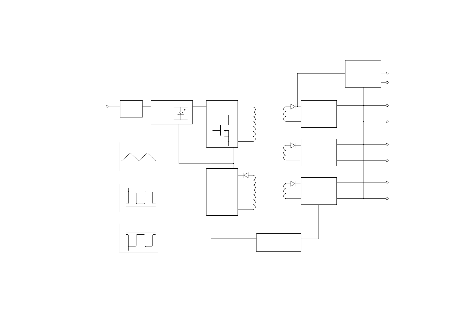
Panasonic UF-585 / 595
218
6.2.14 Power Supply Unit (LVPS)
Block Diagram of ETXDN200A4D
INPUT INPUT
CIRCUIT
RECTIFIER
CIRCUIT CONVERTER
CIRCUIT
(Q101)
+5 VP OUTPUT
-12 VDC OUTPUT
+24 VDC OUTPUT
GND
GND
G
E
0
A-B Voltage
C
A
B
D
F
HGND
CONTROL
CIRCUIT
OVER CURRENT
LIMITTER
ERROR DETECTION
CIRCUIT
+5 VDC
OUTPUT
CIRCUIT
+5 VP OUTPUT
GND
+5 VP OUTPUT
CIRCUIT
-12 VDC
OUTPUT
CIRCUIT
+24 VDC
OUTPUT
CIRCUIT
C105
0
C-D Voltage
0
E-F, G-H Voltage
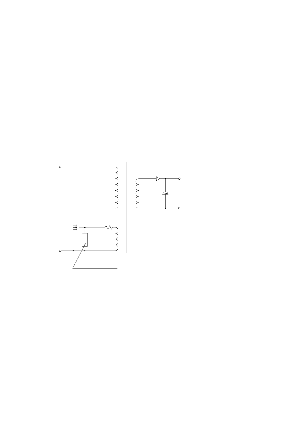
System Description
219
ETXDN200A4D (115V)
Input Circuit
AC line voltage travels to the rectifying circuit through the line filter. The line filter eliminates RFI noise which may otherwise pass
to the AC line from the power supply unit. It also protects the power supply unit from transient noise which may pass into the unit
from the AC line.
Rectifying Circuit
AC power is rectified by D101 and charges C105 to make high DC voltage, then supply power to converter circuit.
Kick-on voltage for control IC (IC101) is supplied AC power through R103 and R110.
Inrush current is limited by TH101.
Converter Circuit
A hybrid IC (IC101), in combination with transformer T1, form a switching power supply circuit using the RCC (Ringing Choke
Converter) system.
As soon as power is applied to the Power Supply Unit, AC line voltage is rectified by D101 and is smoothed by capacitor C105.
The protection circuit at the time of start-up is controlled by an IC (IC101) and resistors R103 and R110.
Main Switching Circuit
In the above circuit, when the main switching transistor, Q101, is turned On, input voltage, Ei, is supplied to the primary winding of
transformer T101. However, no current will flow through diode D201 of the secondary side, due to reverse polarity of the
secondary winding causing no current flow within T1. But the transformer charges with energy. When Q101 is turned Off,
the supply voltage to the primary winding shuts off and the windings of T101 change polarity, allowing D201 to conduct, releasing
the energy accumulated in T101 to the circuit. When the energy is discharged through D201, Q101 turns on, once again
reversing the polarity on T101 windings, creating a self-oscillation circuit.
Ei
Eo
D203
P --- Primary Winding
S --- Secondary Winding
B --- Control Winding
T101
Q101
P
B
Control Circuit
S+
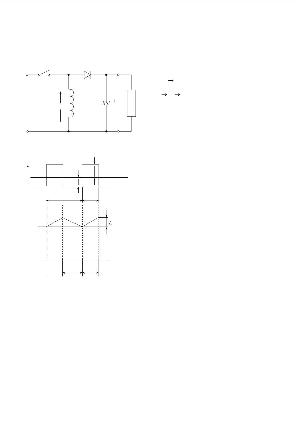
Panasonic UF-585 / 595
220
In the actual circuit, the fixed output voltages are obtained by changing the winding ratio of transformer T101. In this converter
circuit, the output voltages are stabilized by controlling the duty cycle of the ON and OFF timing of the transistor. In this power
supply, the bias winding is built into the transformer. The power supply has four outputs, +24 VDC, -12 VDC, +5 VP and +5
VDC. The +24 VDC output is protected by the Error Detection Circuit, and the +5 VP and -12 VDC outputs are protected by the
circuitry inside of the voltage regulator IC, +5 VDC is protected by ZD251.
Control Circuit and Error Detection Circuit
The control circuit amplifies the output of the duty cycle according to the error voltage detected by the Error Detection Circuit,
and drives the main transistor Q101. The method used to change the duty cycle is to change the ON time period. When the
output voltage of the +24 VDC circuit rises, the current of photocoupler PC101 increases, the output pulse width of the control
circuit decreases and the ON time period of Q101 decreases. This control circuit decides the minimum OFF time period by itself.
When the oscillation frequency becomes higher and the OFF time period becomes minimum, the OFF time period remains
unchanged and only the ON time period decreases. This way, there is a upper limit of the oscillation frequency and the duty
cycle is expanded.
Over Current Limiter (O.C.L)
The +24 VDC output is limited by Ton MAX Limiter (ON time period of transistor Q101) which is part of the control circuit. The +5
VP, -12 VDC and +5 VDC outputs have over current limiters provided inside the voltage regulator and IC251.
The value of output voltage is
Eo=d/(1-d)*Ei
d=Ton/Ts
Equivalent circuit model for the RCC.
Ton : ON time of Q102
In the equivalent circuit ; When SW is ON, current
flows
SW L
When SW is OFF, current flows
L D RL
The value of inductance increase current between
ON period. (d*Ts)
IL=Ei/L*d*Ts . . . . . . . . . . . . . . . . . .(1)
The value of inductance decrease current between
OFF period. ((1-d)*Ts) . . . . . . . . . . . . . . . .(2)
From equation (1) and (2),
E0=d/(1-d)*Ei
Ts : Period of oscillation
VL
VL LC
T101
D(D203)
Eo
Eo
Ts dTs
RL
Ei
SW
(Q101)
T
IL
Ei
(1-d)Ts dTs

Panasonic UF-585 / 595
222
7 Exploded View & Parts List
7.1 Cover Assembly
AU=U.S.A. AC=Canada
Ref
No. Safety
Mark Part No. Part Name AU AC
UF-585 UF-595 UF-585 UF-595 Location
101 - DZKP000166 Spring Plate, Doc. Guide 11114I
102 - DZMC000525 Cover, Right 11117J
103 - DZMC000527 Cover, Left (UF-585) 1 - 1 - 6C
- DZMC000566 Cover, Left (UF-595) - 1 - 1 6C
104 - DZMC000529 Cover, Front 11117E
105 - DZMC000531 Cover, Rear 11115J
106 - DZML000289 Cover, Printer 11113G
107 - DZML000291 Document Guide, Right 11111I
108 - DZML000293 Document Guide, Left 11111G
109 - DZML000295 Sub Tray, Document 11111I
110 - DZMC000533 Cover, Memory Card 11114E
111 - DZML000297 Tray, Recording Paper 11113K
112 - DZML000299 Sub Tray, Recording Paper 11111J
113 - DZMC000563 Cover, Parallel Port I/F 11115J
114 - DZMC000567 Cover, Connector Access - 1 - 1 5B
115 - DZFP000723 Harness, SCA/SCB-SPK 11115E
116 - DZNK001918 Label, Function 11111J
117 - DZDR000014 Speaker 11115D
118 - DZNK000550 Label, Energy Star 11111G
119 - DZLF000180 Gear, B14 11114H
120 - DZDU000025 Handset 11111A
121 - DZFN000066 Cord, Handset 11111A
122 - DZJE000165 Cradle, Upper 11112A
123 - DZFN000061 Cord, Cradle 11112C
124 - DZEC100422 PC Board, SRU 11113B
125 - DZJE000166 Cradle, Lower 11114A
126 - DZML000132 Cradle Assembly 11111B
B1 - DZPB000007 Screw 11115B, 3E, 4H, 4J,
6J, 8I
C2 - DZPB000020 Screw 11115E
1Y-XTB3+10JScrew 11115E
19-XTB3+8JScrew 11114B
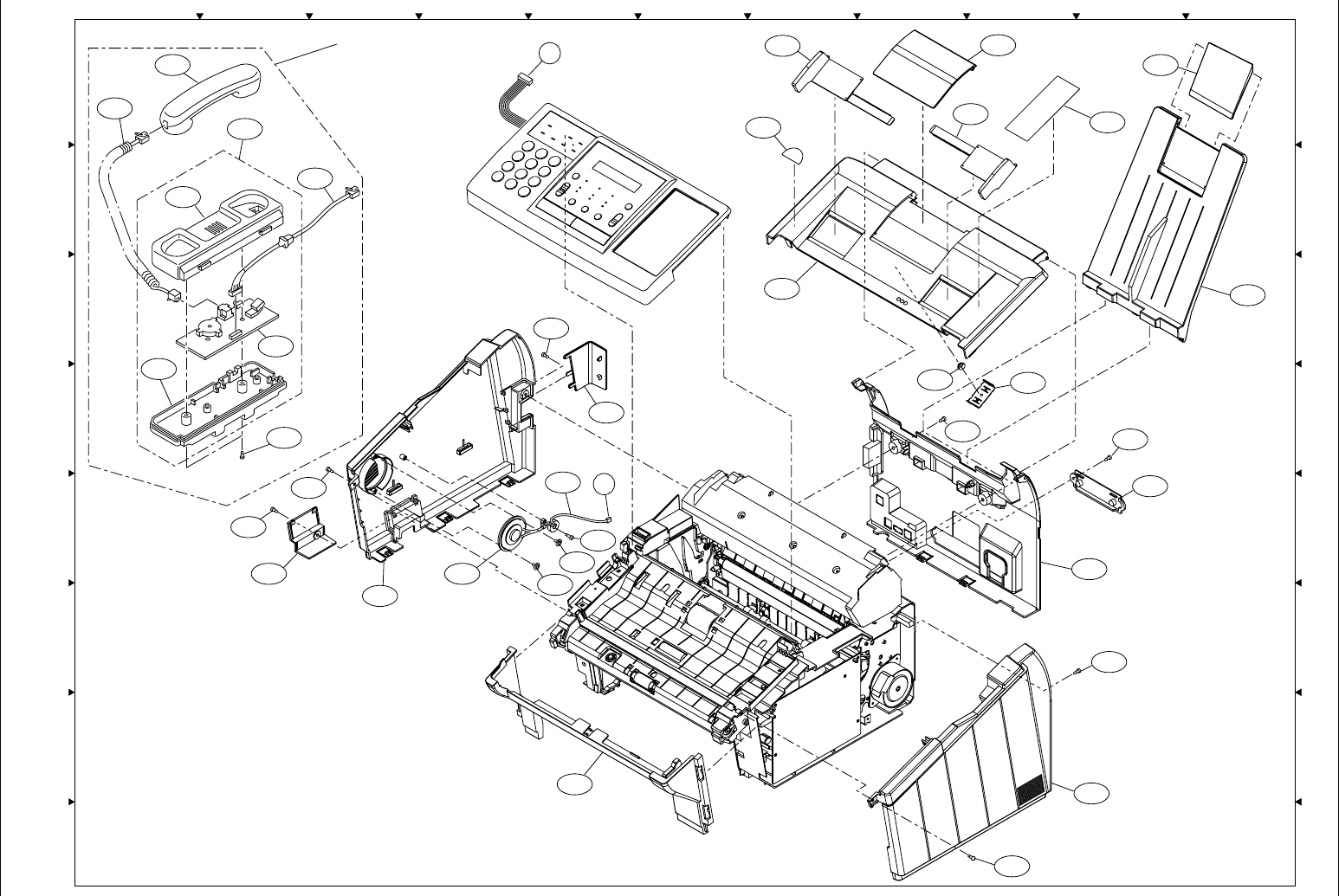
Exploded View & Parts List
223
KA CDEFGHI JB
8
1
3
4
5
6
7
222
Fig. 1: Cover Assembly
19
B1
114
B1
120
121
122
123
125
124
126
(OPTIONAL)
103
117 C2
C2
1Y
110
115
B1
104
B1
102
B1
105
113
B1
B1
101
119
106
118
108 109
116
112
111
107
A
to Fig.4
I
to Fig.4
L5_H11/3/19

Panasonic UF-585 / 595
224
7.2 Control Panel
AU=U.S.A. AC=Canada
Ref
No. Safety
Mark Part No. Part Name AU AC
UF-585 UF-595 UF-585 UF-595 Location
201 - DZJB000106 Chassis, Control Panel 11116K
202 - DZJC000216 Holder, Separation Rubber 11113K
203 - DZKL000023 Lever, ADF Adjustment 11115K
204 - DZKP000164 Spring, Plate 11113J, 3K
205 - DZKR000016 Spring, Wire 11114G, 6G, 8J
206 - DZLA000176 Roller, Eject Pinch 11117I
207 - DZJN000001 Rubber, Separation 11114K
208 - DZKP000179 Ground Plate, Control Panel 11117K
209 - DZGT000023 Brush, Antistatic 11118J
210 - DZMG000025 Latch, Stopper 11113H
211 - DZMC000523 Cover, Control Panel (UF-585) 1 - 1 - 3F
- DZMC000569 Cover, Control Panel (UF-595) - 1 - 1 3F
212 - DZKB000521 Key, Start 11115A
213 - DZKB000522 Key, Copy 11115A
214 - DZKB000523 Key, Stop 11114B
215 - DZKB000524 Key, A 11114A
216 - DZKB000525 Key, B 11113A
217 - DZKB000526 Key, C 11114A
218 - DZKB000527 Key, D 11114A
219 - DZNA000522 Plate, LCD Window 11111E
220 - DZNA000523 Sheet, Panel 11111C
221 - DZNA000524 Cover, Directory Sheet 11111G
222 - DZNA000525 Sheet, One-Touch 11112H
223 - DZJC000229 Holder, LCD 11116F
224 - DZHC000091 Actuator A (ADF Sensor) 11117B
225 - DZHC000092 Actuator B (Read Point Sensor) 11118C
226 - DZHC000093 Actuator, ADF Door 11117A
227 - DZJC000230 Holder, Actuator A 11117B
228 - DZJC000231 Holder, Actuator B 11117C
229 - DZJC000232 Holder, ADF Door Actuator 11116A
230 - DZJC000234 Holder, Battery 11112F
231 - DZEC101103 PC Board, PNL1 11118D
232 - DZFP000721 Harness, SCA/SCB-PNL 11115D
233 - DZDA000025 LCD Unit 11115F
234 - CR2032 Battery, Lithium 11112E
235 - DZKG000018 Shaft 2, Roller 11115F
236 - DZLA000058 Roller, Feed Pinch 11114F
237 - DZJC000113 Plate, Separator Pressure 11114I
238 - DZJM000104 White Seal 11118I
239 - DZMG000018 Latch 11116G, 8J
240 - DZKB000145 Ten Key 11111A
241 - DZKR000015 Wire Spring, Pressure Plate 11113I
242 - DKKR000018 Wire Spring, Latch 11116G, 7J
19-XTB3+8JScrew 11118K
7B-XTB26+6JScrew 11118E
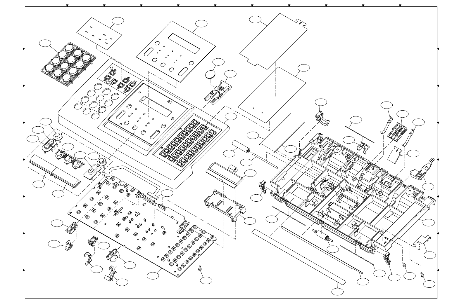
Exploded View & Parts List
225
KA CDEFGHI JB
8
1
3
4
5
6
7
222
Fig. 2: Control Panel
220
240
219
230
211
221
222
210
241
237
204
202
204
207
203
201
208
19
239
242
209
238
223 242
239
233
235
236
205
205
232
7B
231
228
225
227
224
229
226
212
213
216
215
214 216
217
218
206
19
234
L5_H11/3/19

Panasonic UF-585 / 595
226
7.3 Transmitter Assembly
AU=U.S.A. AC=Canada
Ref
No. Safety
Mark Part No. Part Name AU AC
UF-585 UF-595 UF-585 UF-595 Location
301 - DZJB000105 Guide, Transmit 11112E
302 - DZLA000163 Roller, Feed 11115H
303 - DZLA000164 Roller, Eject 11114E
304 - DZKG000094 Shaft, Clutch 11111J
305 - DZLF000270 Gear, ADF 11115K
306 - DZJA000584 Bracket, LED 11117G
307 - DZJA000585 Clip, LED 11115E, 6F, 7H
308 - DZTE000021 Glass, Scanning 11111F
309 - DZJA000586 Bracket, Motor 11113I
310 - DZLF000271 Gear, B54B22 11114I
311 - DZLF000272 Gear, B55D30 11115H
312 - DZLF000273 Gear, B55D16 11115J
313 - DZLF000274 Gear, D17 11115I
314 - DZLF000275 Gear, D50 11115H
315 - DZLM000082 Bushing, P10 11112K
316 - DZLM000083 Bushing, P6A 11114E, 5F, 6G, 6I
317 - DZKP000163 Plate, Ground 11116I
318 - DZLM000084 Bushing, P6B 11111H
319 - DZLD000009 Clutch, Drum 11112I
320 - DZKP000178 Spring Plate, EMI 11113K
321 - DZHP002384 Scanner Block 11113B
322 - DZJB000108 Chassis, Scanner 11115A
324 - 42S1S15DCNB Motor, Transmit 11112I
325 - DZHT000027 Stamp Head (Blue) 11113D
326 - DZJC000072 Stamp Holder 11114D
327 - DZHP002353 Stamp Solenoid 11114D
328 - DZFP000719 Harness, SCA/SCB-LED 11117H
329 - LNR304713 LED Array, (A4) 11116G
330 - DZKP000001 Spring Plate, Mirror 11113B, 4A, 4B, 4C,
7A, 8C
331 - DZLA000096 Roller, ADF 11111H
332 - DZLF000165 Gear, D25F Drive 11116H, 6I
333 - DZKQ000004 Spring 1, Clutch 11111J
334 - DZTC000020 Mirror 1 11117B
335 - DZTC000021 Mirror 2 11114A
336 - DZTC000022 Mirror 3 11114B
337 - DZEC100264 PC Board, CCD 11115D
338 - DZJC000192 Shaft, ADF Angular 11114J
339 - DZFP000720 Harness, SCA/SCB-CCD 11115C
340 - DZFP000722 Harness, SCA/SCB-TX Motor 11112I
341 - DZJM000301 Film, ADF 11111G
342 - DZLM000092 Bushing, P6C 11116G, 6I
343 - DZKR000017 Wire Spring, Roller 11116H
344 - DZMH000009 Bracket, Eject Roller 11118E
19-XTB3+8JScrew 11114D, 4K, 5D, 7F,
8H, 8I
4N-XSN3+W8FCScrew 11115E
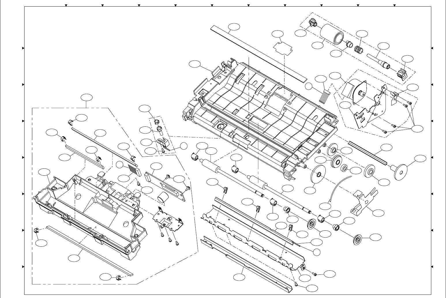
Exploded View & Parts List
227
KA CDEFGHI JB
8
1
3
4
5
6
7
222
Fig. 3: Transmitter Assembly
308
301
318
331
319
333
304
315
320
19
324
340
309
305
338
312
310
311
313
317
314
332
316
302
316
316
303
307
307
307
342
332
316
329
19
19
306
344
325
326
327
19
330
330
336
330
330
335
4N
337
339
19
330
330
334
322
341
343
342
328
321
E
to Fig.4
D
to Fig.4
B
to Fig.4
C
to Fig.4
L5_H11/3/19
Panasonic UF-585 / 595
228
7.4 Electrical Parts
AU=U.S.A. AC=Canada
IMPORTANT SAFETY NOTICE:
Components identified by the sign have special characteristics important for safety. When replacing any of these
components, use only the specified parts.
Ref
No. Safety
Mark Part No. Part Name AU AC
UF-585 UF-595 UF-585 UF-595 Location
401 - DZEC101039 PC Board, LPC 11114B
402 DZEC101038 PC Board, LCU 11113G
403 - DZMC000515 Bracket, AC Inlet 11114J
404 - DZMC000517 Cover, LVPS Protection 11112I
405 - DZMC000518 Bracket, Left Printer I/F 11112J
406 - DZMC000519 Bracket, Right Printer I/F 11113K
407 - DZJC000228 Holder, Printer Cover Sensor 11111C
408 - DZHA000115 Sheet, HVPS 11117I
409 - DZFP000718 Harness, SCA/SCB-LVPS 11113H
411 - DZFP000740 Flat Cable, SCA/SCB-LCU 11112H
415 - DZFP000725 Harness, LPC-HVPS 11117F
417 - DZFP000729 Harness, LPC-ILS 11112B
421 - DZFP000738 Flat Cable, SCA/SCB-PRTA 11115B
422 DZEC101235 PC Board, SCB (UF-585AU) 1 - - - 3D
DZEC101240 PC Board, SCA (UF-595AU) - 1 - - 3D
DZEC101237 PC Board, SCB (UF-585AC) - - 1 - 3D
DZEC101241 PC Board, SCA (UF-595AC) - - - 1 3D
423 ETXDN200A4D PSU, Low Voltage (100V) 11114H
424 - EUKMBN731HA PSU, High Voltage 11117G
425 - DZEC100262 PC Board, ILS 11111B
426 - DZJF000350 Guide 2, Memory Card 11113D
427 - DZJK000005 Clamp, Harness 11113F, 4D, 5C,
428 - DZEC101464 PC Board, Printer I/F 11111K
19-XTB3+8JScrew 11111F, 2J, 2K, 3A,
3B, 3H, 4J, 6H,
B5-XSB4+10BNScrew 11113I
4N-XSN3+W8FCScrew 11113J
B1 - DZPB000007 Screw 11111K, 2K
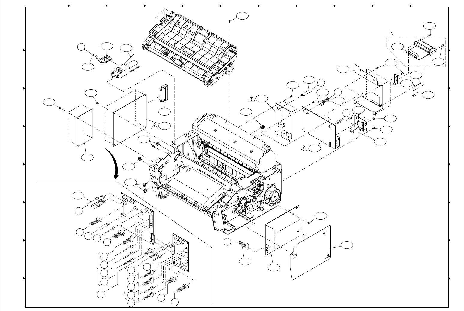
Exploded View & Parts List
229
KA CDEFGHI JB
8
1
3
4
5
6
7
222
Fig. 4: Electrical Parts
19
19
402
427
19
409
423
403
19
4N
B5
406
405
19
B1
B1
428
19
404
407
425
417
19
19
401
427
F
to Fig.5
to Fig.7
to Fig.1
427
427
422
426
19
408
424
421
415
411
AB
J
to Fig.7 AA
to Fig.9
G
Q
AB
HI
to Fig.1
to Fig.3
A
C
D
B
E
K
M
N
O
P
to Fig.5
to Fig.6
Q
W
G
H
L5_H11/3/19
(OPTIONAL)

Panasonic UF-585 / 595
230
7.5 Base Unit
AU=U.S.A. AC=Canada
Ref
No. Safety
Mark Part No. Part Name AU AC
UF-585 UF-595 UF-585 UF-595 Location
501 - DZJA000587 Chassis, Bottom 11115E
502 - DZJA000588 Chassis, Right 11117G
503 - DZJF000356 Chassis, Left Sub 11113C
504 - DZMC000535 Chassis, Left 11113C
505 - DZMC000536 Chassis, Rear 11111J
506 - DZKP000162 Spring Plate, Toner Sensor 11112G
507 - DZJE000547 Plate, A 11117F
508 - DZKN000161 Spring, A Coil 11116J, 7J
509 - DZKN000162 Spring, B Coil 11117K
510 - DZKQ000021 Spring, Right Cartridge Locking 11116J
511 - DZKQ000022 Spring, Left Cartridge Locking 11111A
512 - LPA1602F02 Laser Unit 11116B
513 - DZAN000002 Sensor, Toner 11112G
514 - DZMM000016 Leg, Rubber 11115G, 6E
515 - DZKP000009 Plate, Ground 11112A
516 - DZJL000023 Ground Plate, Memory Card 11111D
517 - DZKG000095 Shaft, Feed Roller 11117E
518 - DZLA000081 Roller, Paper Feed 11116D, 6E
519 - DZLM000050 Bushing, P6L8 11117D, 7G
520 - DZLF000131 Gear, E34 11117I
521 - DZKN000073 Spring, Clutch Coil 11117I
522 - DZJB000024 Case, Clutch 11117J
523 - DZJM000300 Drum, Clutch 11117J
524 - DZJM000171 E-Ring 11113F, 4H, 7I, 7K
525 - DZHC000089 Actuator, No Paper 11114C
526 - DZLA000175 Roller, Feed 11113G
527 - DZLM000052 Bushing, P6L5 Conductive
(Black)
11112F
528 - DZLM000006 Bushing, P6L5 (White) 11114H
529 - DZLF000268 Gear, Feed Roller 11114H
531 - DZGB000019 Solenoid, Paper Feed 11117K
532 - DZJC000235 Guide, Printer I/F PCB 11113J
533 - DZMC000520 Plate, CCD Shield 11114G
534 - DZEC101076 PC Board, SNS2 11116E
535 - DZEC101163 PC Board, SNS3 11114D
536 - DZEC101210 PC Board, PRTA 11113H
537 - DZFP000730 Harness, SNS3-TNR 11112F
538 - DZFP000732 Harness, SNS1-SNS2 11116F
539 - DZFP000731 Harness, LPC-SNS3 11114D
540 - DZFP000733 Harness, LPC-LSU1 11114B
541 - DZFP000734 Harness, LPC-LSU2 11116C
542 - DZFP000764 Ground Wire (CCD) 11114G
1Y-XTB3+10JScrew 11114B, 5D, 6C
4N-XSN3+W8FCScrew 11116D, 6E
19-XTB3+8JScrew 11111A, 1B, 1D, 1F,
1J, 1K, 2A, 2E,
3A, 3G, 3H, 4D,
4E, 6E, 6K, 7D,
7F, 7I, 7K, 8G,
8K
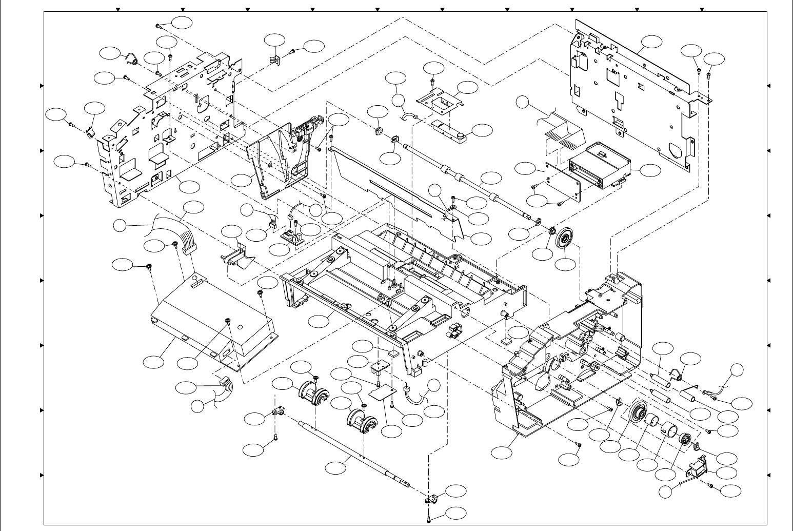
Exploded View & Parts List
231
KA CDEFGHI JB
8
1
3
2
4
5
6
7
Fig. 5: Base Unit
505
19 19
532
508
508
510
509
19
531
524
524
523
522
521
520
19
19
19
536
19
529
528
514
524
526
19
542
533
513
506
19
524
527
19
19
19
535
539
503
19
516
19
19
19
511
19
515
19
19
504
540
525
1Y
1Y
1Y
512 1Y
19
519
4N
518 4N
518
507
534
19
514
517
519
19
19
502
501
19 538
537
541
F
to Fig.4
L
R
to Fig.6
L
K
to Fig.4
N
to Fig.4
M
to Fig.4
S
to Fig.6
O
to Fig.4
T
to Fig.6
L5_H11/4/5

Panasonic UF-585 / 595
232
7.6 Paper Transportation
AU=U.S.A. AC=Canada
Ref
No. Safety
Mark Part No. Part Name AU AC
UF-585 UF-595 UF-585 UF-595 Location
601 - DZJF000353 Guide, Transfer 11114J
602 - DZJF000355 Guide, BTR 11114H
603 - DZHA000114 Sheet, Mylar 11114H
604 - DZLA000174 Roller, Bias Transfer 11113G
605 - DZLM000085 Bushing, Left BTR (White) 11112F
606 - DZKN000025 Spring, BTR 11112G, 4I
607 - DZLA000080 Roller, Pinch 11113H
608 - DZKR000014 Spring, Wire 11113H, 4I
609 - DZHC000088 Actuator, Timing 11113H
610 - DZLM000081 Bushing, Right BTR (Black) 11114I
611 - DZLF000269 Gear, BTR 11114I
612 - DZJL000092 Plate, Discharge 11112J
613 - DZFP000747 Resistor, 200MΩ, 1/2 Watt 11111H
614 - DZKP000160 Plate Spring, Ground Transfer 11111I
615 - DZEP000376 PC Board, SNS1 11112J
616 - DZJA000590 Bracket, Printer Motor 11116H
617 - DZLF000281 Gear D, E24 11115F
618 - DZLF000279 Gear A, D31 11115F
619 - DZLF000278 Gear F, D55 11115F
620 - DZLF000280 Gear E, D25E29 11115F
621 - DZLF000277 Gear B, D60D20 11116F
622 - DZLF000276 Gear G, B83D22 11116F
623 - DZLF000282 Gear C, D62E18 11116E
624 - DZLF000283 Gear I, E29 11117F
625 - DZLF000284 Gear H, E23 11117E
626 - 55SPM25D7NA2 Motor, Printer 11117H
627 - DZJD000023 Bracket, HVPS Support 11118G
628 - DZKP000161 Ground Spring, Feed Roller 11117I
629 - DZFP000737 Harness, FG1 (Fuser) 11111H
630 - DZFP000736 Harness, HV 11113J
631 - DZFP000728 Harness, SNS1-SNS4 11111K
632 - DZFP000724 Harness, LPC-RXMOT 11118H
19-XTB3+8JScrew 11111I, 1J, 3F, 4F,
6H, 7H, 8F, 8G,
8I
C8-XTW3+8SFCScrew 11111H, 3J
4N-XSN3+W8FCScrew 11115G, 8F
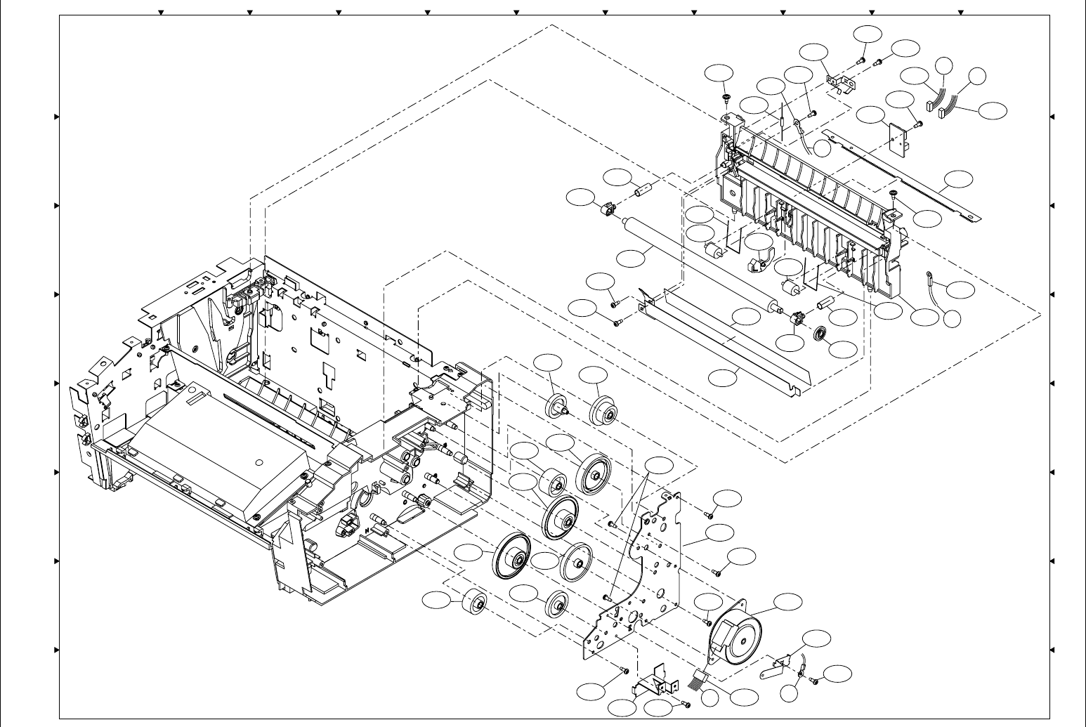
Exploded View & Parts List
233
KA CDEFGHI JB
8
1
3
4
5
6
7
222
Fig. 6: Paper Transportation
19
19
614
19
629
613
C8
606
605
19
19
604
608
607
603
602
618
617
619
620
621
622
623
624
625
19
627 19
19
19
19
4N
628
19
609
608
607
606
611
610
630
601
C8
612
19
538
615 631
616
626
632
L5_H11/3/19
S
to Fig.5
U
to Fig.7
X
to Fig.7
T
to Fig.5
P
to Fig.4
R
to Fig.5

Panasonic UF-585 / 595
234
7.7 Fuser Unit
AU=U.S.A. AC=Canada
Note:
The Thermostat and Thermal Fuse is not available as individual replacement part. It is recomended to replace the entire Fuser
Unit (Ref. No. 701) when either part is defective.
Ref
No. Safety
Mark Part No. Part Name AU AC
UF-585 UF-595 UF-585 UF-595 Location
701 - DZHP002455 Fuser Unit 11112H
702 - DZJB000112 Frame, Fuser 11116G
703 - DZJF000354 Guide, Lower Paper Exit 11114I
704 - DZGT000021 Brush, Discharge 11115K
705 - DZKK000039 Plate, Pressure Roller Arm 11114H, 6J
706 - DZLA000088 Roller, Pressure 11116H
707 - DZLM000041 Bushing, P6L5.5 11115H, 5J
708 - DZKN000160 Spring, Pressure 11114H, 6J
709 - DZLA000072 Roller, Fuser 11116F
710 - DZLM000047 Bushing, P17L6.8 11115F, 7I
711 - DZLF000147 Gear, E24 Drive 11117J
712 - DZPJ000002 C-Ring 11115F, 7J
713 - DZLF000263 Gear, E18 11116I, 7I
714 - DZLF000264 Gear, E14 11117I
715 - DZKP000159 Spring, Pinch Roller 11114J, 4K
716 - DZJA000583 Holder, Pinch Roller 11113I, 4J
717 - DZLA000172 Pinch Roller 1, Exit 11113I, 4J
718 - DZLA000188 Pinch Roller 2, Exit 11113I, 3J
719 - DZLA000173 Roller, Exit 11113H
720 - DZLM000039 Bushing, Right P3.5L11.2 11114I
721 - DZLM000040 Bushing, Left P3.5L11.2 11112G
722 - DZLF000265 Gear, E22 11114I
723-DZJB000111Cover, Fuser 11113G
724 - DZJC000222 Terminal A, Fuser Lamp 11114E
725-(See Note)Thermostat 11114E
726-(See Note)Thermal Fuse 11114F
727 - DZFP000735 Harness, LVPS-Fuser 11113G
728 - DZGT000022 Thermistor Assembly 11113F
729 - DZEC101263 PC Board, SNS4 11112E
730 - DZKK000038 Actuator, Paper Exit 11112E
731 - DZJC000223 Terminal B, Fuser Lamp 11113G
732 - DZGN000006 Lamp, Fuser (100V) 11114E
733 - DZJE000544 Cover, Fuser Top 11112C
734 - DZNK000036 Caution Label, High Temperature 11112A
735 - DZNK002185 Instruction Label, Print Cartridge 11111B
736 - DZFP000727 Harness, LPC-SNS4 11111E
737 DZJM000327 Sheet, Mylar 11113B
19-XTB3+8JScrew 11111C, 2D, 5F, 6I,
7H
1Q-XYN3+F10Screw 11112F
23-XYN3+F8Screw 11114E, 4F
4N-XSN3+W8FCScrew 11112D, 2E, 3F, 4G,
5G, 5J
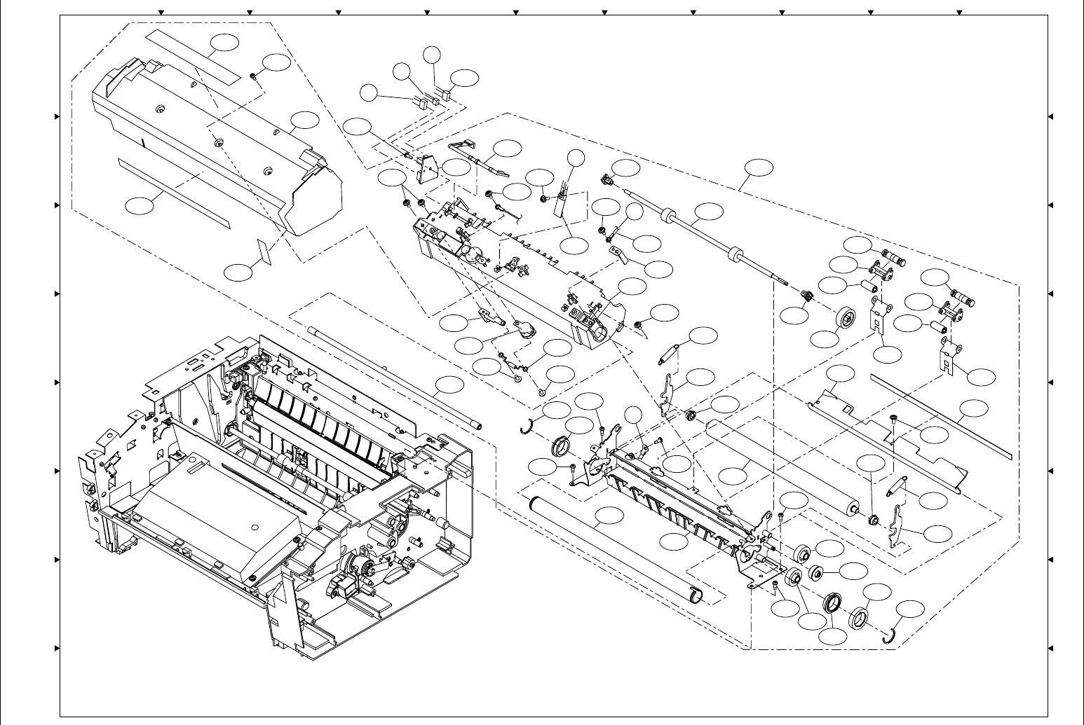
Exploded View & Parts List
235
KA CDEFGHI JB
8
1
3
4
5
6
7
222
Fig. 7: Fuser Unit
701
717
722
720
716
718
717
716
718
715
715
719
721
1Q
730
19
4N 729
724
726
23
23
725
19
710
712
19
732
733
19
735
734
4N
4N
731
728
723
4N
708
707
705
4N
706
703
704
4N
708
705
712
711
713
714
710
713
19
709
702
19
707
737
736
727
U
to Fig.6
J
to Fig.4
V
W
to Fig.4
V
L5_H11/3/19
X
to Fig.6

Panasonic UF-585 / 595
236
7.8 Cassette
AU=U.S.A. AC=Canada
Ref
No. Safety
Mark Part No. Part Name AU AC
UF-585 UF-595 UF-585 UF-595 Location
801 - DZJF000359 Base Frame, Cassette 11117I
802 - DZJF000360 Guide, Paper Length 11118D
803 - DZJF000364 Guide, Paper Width 11113F
804 - DZJF000362 Cover, Cassette 11116B
805 - DZJF000365 Tray, Document Return 11113B
806 - DZKM000018 Plate, Pressure 11113J
807 - DZJP000005 Pad, Pressure Plate 11111H, 1I
808 - DZNK002122 Label, Cassette 11111E
809 - DZJC000226 Paper Separation Clip, Left 11113H
810 - DZKN000163 Spring, Pressure 11113I, 4J
811 - DZJC000227 Paper Separation Clip, Right 11115J
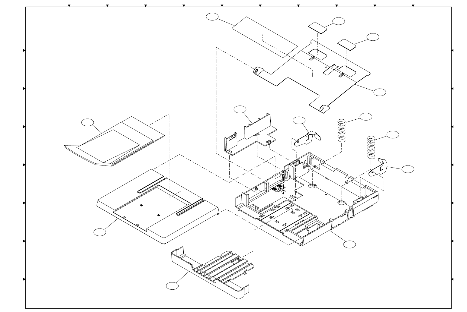
Exploded View & Parts List
237
KA CDEFGHI JB
8
1
3
4
5
6
7
222
Fig. 8: Cassette
807
807
808
805
804
802
801
811
810
810
809
803
806
L5_H11/3/19
Panasonic UF-585 / 595
238
7.9 Option Cassette
AU=U.S.A. AC=Canada
Ref
No. Safety
Mark Part No. Part Name AU AC
UF-585 UF-595 UF-585 UF-595 Location
901 - DZJB000119 Frame, Option Cassette Base - 1 - 1 5D
902 - DZMC000514 Plate, Base Frame - 1 - 1 1D
903 - DZJA000593 Bracket, Gear - 1 - 1 5K
904 - DZLA000187 Roller 2, Feed - 1 - 1 2I
905 - DZLF000282 Gear, D62E18 - 1 - 1 5I
906 - DZLF000283 Gear, E29 - 1 - 1 6I
907 - DZLF000284 Gear, E23 - 1 - 1 5J
908 - DZGB000019 Solenoid, Paper Feed - 1 - 1 7K
909 - DZKP000161 Ground Spring, Feed Roller - 1 - 1 6K
910 - DZKG000095 Shaft, Feed Roller - 1 - 1 3I
911 - DZLA000081 Roller, Paper Feed - 1 - 1 1G, 2H
912 - DZLM000050 Bushing, P6L8 - 1 - 1 1H, 2F, 3H, 3J,
913 - DZJM000171 E-Ring - 1 - 1 3I, 4J
914 - DZLF000131 Gear, E34 - 1 - 1 3I
915 - DZKN000073 Spring, Clutch Coil - 1 - 1 4I
916 - DZJB000024 Case, Clutch - 1 - 1 4J
917 - DZJM000300 Drum, Clutch - 1 - 1 4J
918 - DZLF000268 Gear, Feed - 1 - 1 3K
919 - DZLA000080 Roller, Pinch - 1 - 1 2I, 2J
920 - DZKP000118 Spring, Pinch Roller - 1 - 1 1I, 2J
921 - DZEP000406 PC Board, CST2 - 1 - 1 3D
922 - DZHC000089 Actuator, No Paper - 1 - 1 3F
923 - DZEC101076 PC Board, SNS2 - 1 - 1 7F
924 - DZJE000547 Plate A - 1 - 1 8F
925 - DZMM000016 Leg, Rubber - 1 - 1 6F, 7H
926 - DZJF000371 Tray, Paper Cassette 2 - 1 - 1 6B
927 - DZFP000717 Harness, CST2-CSTSNS2 - 1 - 1 7G
928 - DZFP000716 Cover 2, Cassette - 1 - 1 3D
930 - DZJF000380 Sub Guide, Recording Paper 11114C
5Y - XUC4 E-Ring - 1 - 1 5I, 6I
4N - XSN3+W8FC Screw - 1 - 1 1G, 2H
19 - XTB3+8J Screw - 1 - 1 1A, 1B, 1H, 1I,
2C, 2E, 2F, 2J,
3B, 3D, 3E, 5J,
6K, 7F, 7J, 8G
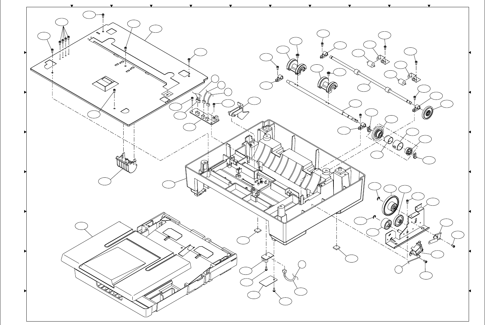
Exploded View & Parts List
239
KA CDEFGHI JB
8
1
3
4
5
6
7
222
Fig. 9: Option Cassette
19
19
19
19
19
902
19
19
927
921
922
19
912
4N
911
19
912
919
920
19
919
920
19
19
912
918
911 4N
904
910
912
913
914
915
916
917
913
5Y 905
19
907
903
909
19
908
19
906
5Y
925
927
19
924
19
923
925
901
930
926
19
AA
to Fig.4
Y
Z
YZ
L5_H11/3/19

Panasonic UF-585 / 595
240
7.10 Packing and Accessories
AU=U.S.A. AC=Canada
IMPORTANT SAFETY NOTICE:
Components identified by the sign have special characteristics important for safety. When replacing any of these
components, use only the specified parts.
Ref
No. Safety
Mark Part No. Part Name AU AC
UF-585 UF-595 UF-585 UF-595 Location
1001 - DZRB000398 Carton (UF-585) 1 - 1 - 6E
- DZRB000407 Carton (UF-595) - 1 - 1 6E
1002 - DZRH000288 Assembly, Cushion 11112D, 2E, 5C, 6E
1003 - DZRK000016 Cassette Sheet 11114C
1005 - DZRD000008 Box, Accessories 11116A
1106 - DZSD000868 User’s Guide (English) 11115A
- DZSD000869 Quick Guide (English) 11115A
- DZSD000871 User’s Guide (Canadian French) - - 1 1 5A
- DZSD000872 Quick Guide (Canadian French) - - 1 1 5A
1007 - N/A (See Ref. No. 111 and 112) 11114A
1008 DZFM000027 Power Cord 11113A
1009 - DZFN000050 Telephone Line Cable 11113A
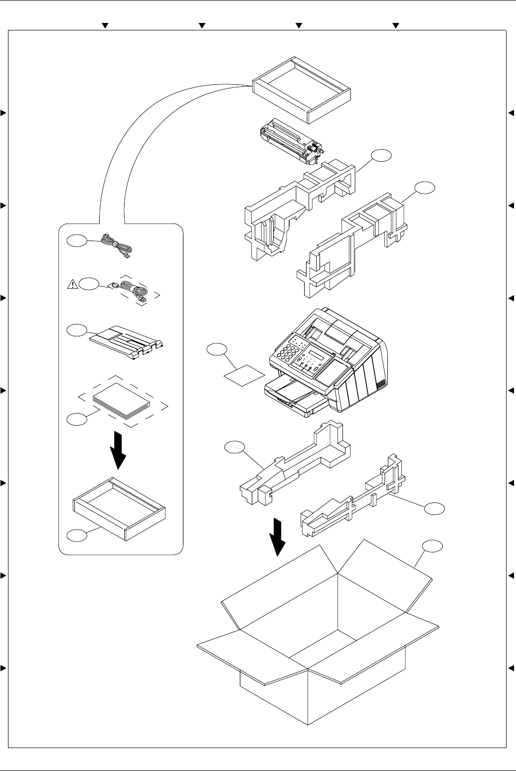
Exploded View & Parts List
241
EACDB
1
8
2
3
4
5
6
7
Fig. 10: Packing and Accessories
1009
1008
1006
1005
1002
1002
1003
1002
1002
1001
1007
L5_H11/3/19
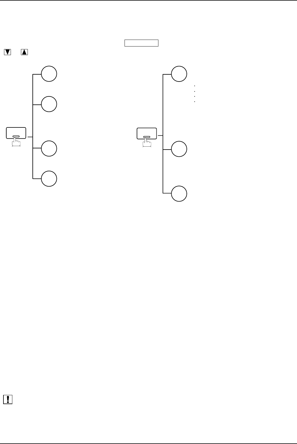
Installation
245
8 Installation
8.1 Function Key
Any function can be started by first pressing and then enter the function number, or by pressing
or scroll key repeatedly until the desired function appears on the display.
(see Note 1)
1. If Fax Parameter is not preset to a Valid position, which enables you to use the function, the display will not show
the function.
FUNCTION
2
1
3
6
FUNCTION
7
8
9
FUNCTION
Advanced Communication
1 = Relayed Transmission
(See Note 1)
2 = Confidential Communication
Polling
1 = Polling
2 = Polled
Printout
1 = Journal (Print/View)
2 = One-Touch/Abbreviated/
Directory Search List
3 = Program List
4 = Fax Parameter List
5 = Not used
6 = Individual XMT Journal
7 = Directory Sheet
Deferred Communication
1 = XMT
2 = Polling
Set Mode
1 = User Parameters
Date & Time
Logo
Character ID
ID Number (Fax Telephone Number)
2 = One-Touch/Abbreviated Numbers
3 = Program Keys
4 = Fax Parameters
5 = Relayed XMT & Conf. Comm. Parameters
(See Note 1)
6 = Cleaning Printer Roller
Select Mode
1 = Communication Journal = OFF/ON/INC
2 = Not Used
3 = Cover Sheet = OFF/ON
4 = Password-XMT = OFF/ON (See Note 1)
5 = RCV to Memory = OFF/ON/PRINT
Edit File Mode
1 = File List (Print/View)
2 = Change Time/Station
3 = Delete File
4 = Print File
5 = Add Document
6 = Retry Incomplete File
Note:
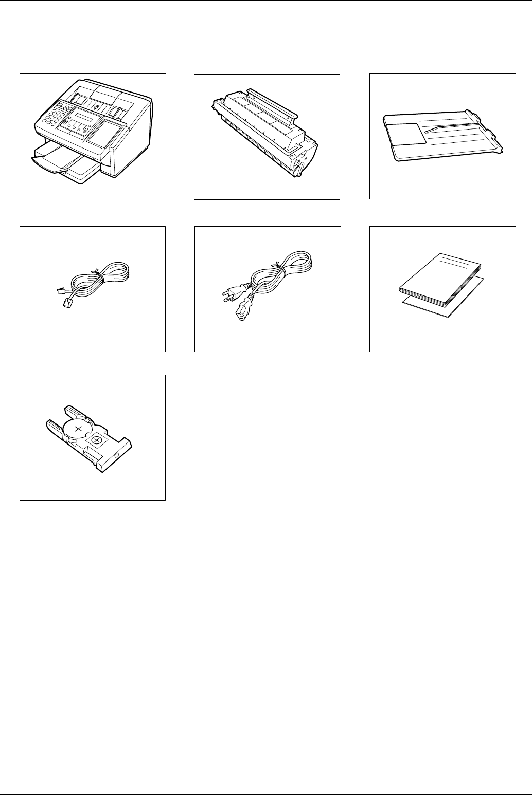
Panasonic UF-585 / 595
246
8.2 Main Unit and Accessories
Unpack the carton and check that you have all the accessories illustrated.
Machine Toner Cartridge Recording Paper Tray
Telephone Line Cable Power Cord User’s Guide / Quick Guide
Lithium Battery and Holder
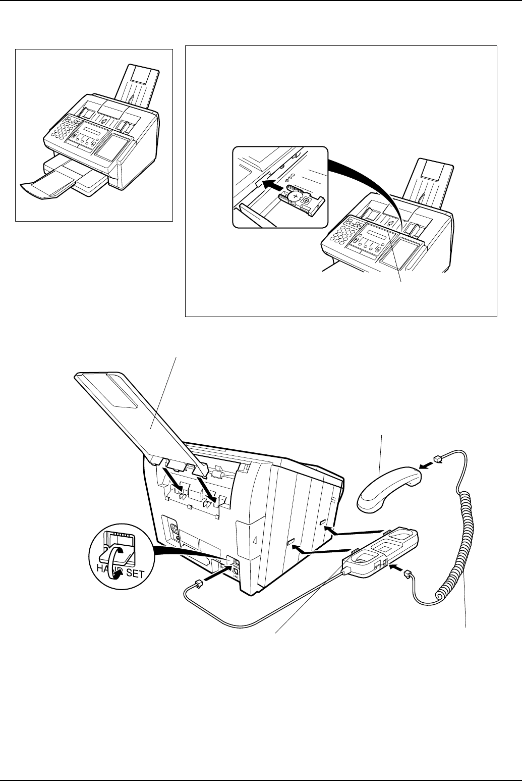
Installation
247
8.3 Installing the Accessories
Final Installed View
Handset Cradle
[Available as an Option
]
Hook the projections into the square holes on
the machine.
Connect the cable into the HANDSET jack on
the machine.
Handset Cord
[Available as an Option]
Recording Paper Tray
Hook the projections into the
square holes on the machine.
Handset
[Available as an Option]
Installing the Lithium Battery (This battery is used to
backup the clock during power failures, see page 149 of the
User’s Guide)
Install the Battery into the Holder and slide it into the slot on the
ADF Door as shown.
ADF Door
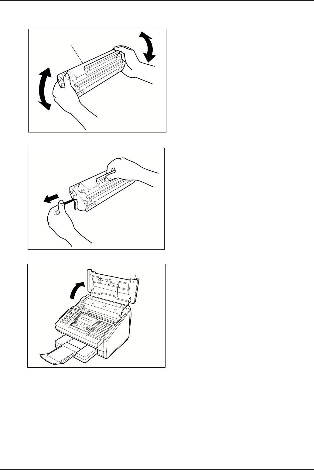
Panasonic UF-585 / 595
248
8.4 Installing the Toner Cartridge
1Unpack the Toner Cartridge and rock it back
and forth as shown for 5 or 6 times to even the
toner inside.
2Remove the protective seal.
Note: Pull on the seal slowly and straight out.
3Open the Printer Cover.
Continued on the next page.
Toner Cartridge
Printer Cover
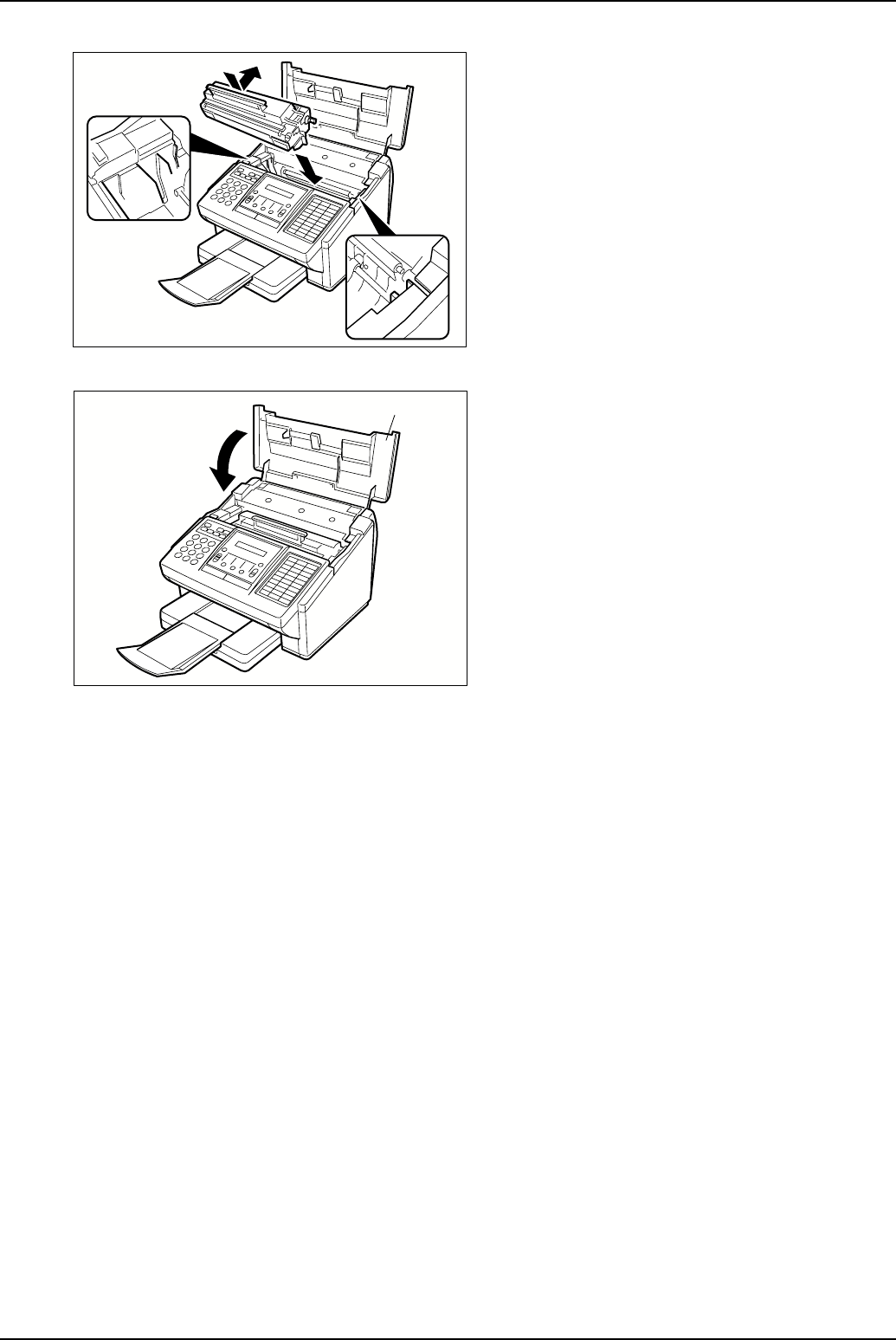
Installation
249
4Align the projections on both sides of the
Toner Cartridge with the grooves in the
machine as shown and insert the Toner
Cartridge into the machine.
Note : Lock the Toner Cartridge into place by
pressing the handle down and then
pushing towards the rear of the
machine.
5Close the Printer Cover.
6If you are replacing the Toner Cartridge, it is recommended to clean the Printer Roller to maintain good
printing quality. To clean the Printer Roller, follow the procedure on page 146 of the User's Guide.
Printer Cover
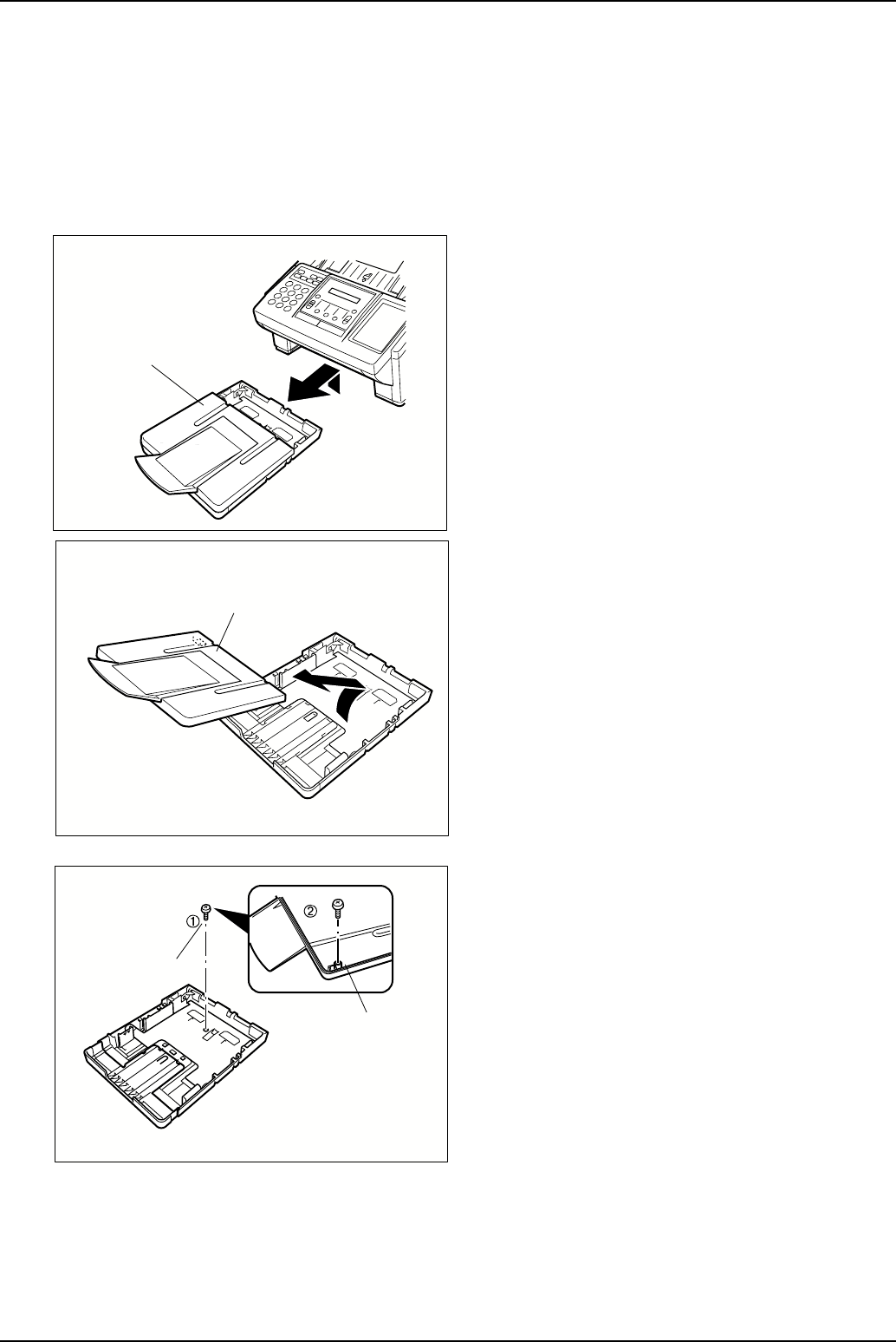
Panasonic UF-585 / 595
250
8.5 Loading the Recording Paper
Paper Specifications
In general, most bond papers will produce excellent results. Most photocopy papers will also work very well.
There are many "name" and "generic" brands of paper available. We recommend that you test various papers
until you obtain the results you are looking for. For detailed recommended paper specifications, see page 154
of the User’s Guide.
How to Load the Recording Paper
1Lift up the Paper Cassette slightly
and slide it out from the machine.
2Remove the Paper Cassette Cover.
3(1) Remove the Shipping Screw securing the
Pressure Plate.
(2) Store the screw by attaching it to the post
provided under the Paper Cassette Cover
for future use.
Paper Cassette
Cassette Cover
Cassette Cover
Shipping Screw

Installation
251
4(1) Load the paper into the Paper Cassette.
Slide the paper width guide to the left until it
lightly touches the stack of paper without
bending the paper. The paper must fit
squarely and firmly between the Paper
Width Guide and the right side of tray. If it
does not, the paper may feed into the
printer incorrectly resulting in a paper jam.
Caution: Make sure that the paper is set
under the metal Paper Separation
Clips and that it does not exceed
the Maximum Paper Capacity Mark.
You can load about 250 sheets (20
lb weight). For paper specification,
see page 154 of the User’s Guide.
(2) Re-install the Paper Cassette Cover.
(3) Slide the Paper Cassette into the machine.
Paper
Width Guide
Max. Paper
Capacity Mark
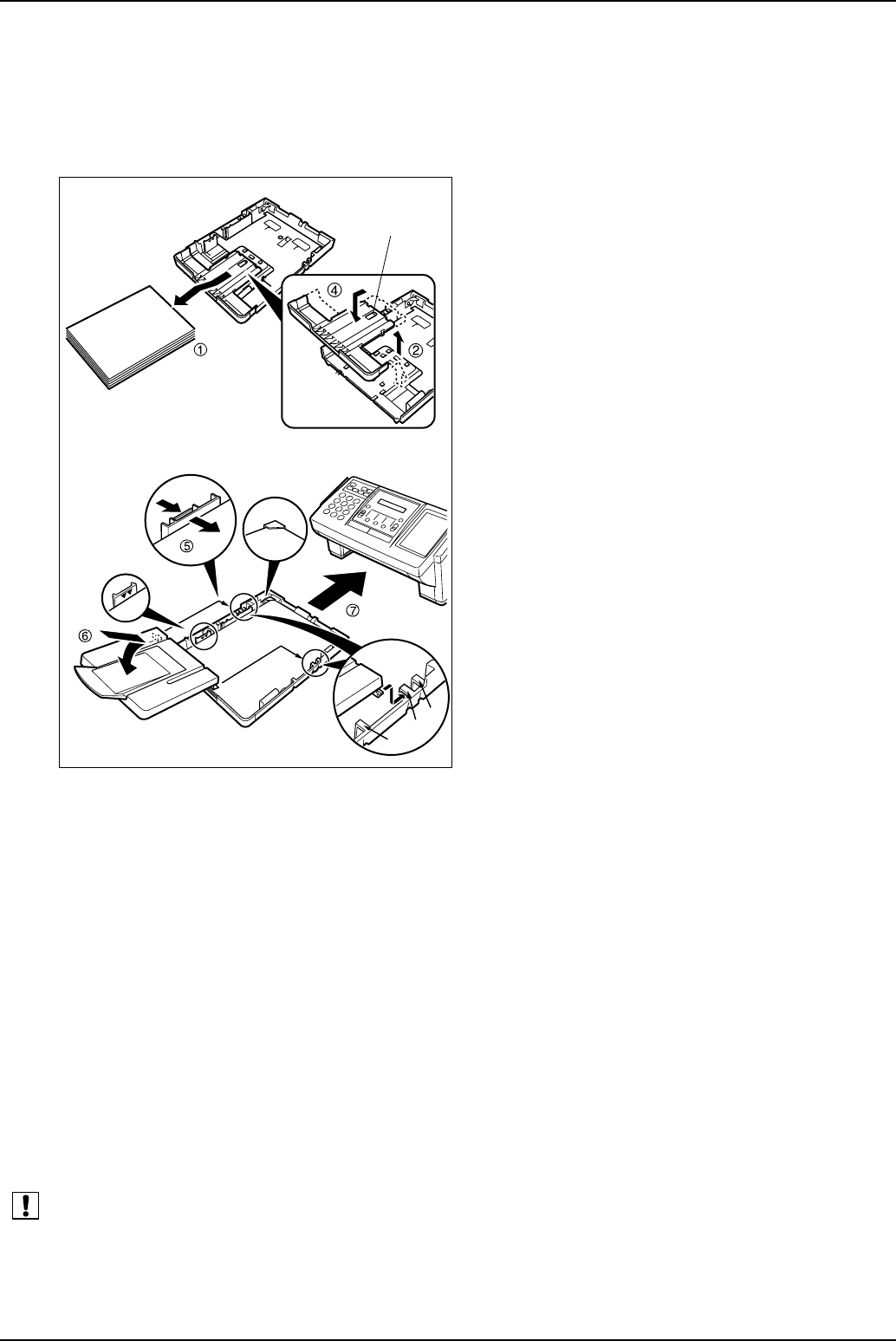
Panasonic UF-585 / 595
252
8.6 Adjusting the Paper Cassette for the Paper Length
How to Adjust the Paper Cassette for the Paper Length
The factory default Paper Length setting for the Paper Cassette is on Letter size. To change the paper length to
A4 or Legal size, follow the steps below.
1(1) Remove the paper from the Paper
Cassette and place the cassette upside
down on a flat surface.
(2) While pushing down on the release latch,
pull out the Paper Length Guide.
(3) Turn the Paper Cassette upright.
(4) Insert the Paper Length Guide hooks into
the appropriate paper length slots (A4 or
Legal) and slide the guide towards the
back of the cassette until it locks in place.
(5) Load the paper into the Paper cassette.
Slide the paper width guide to the left until it
lightly touches the stack of paper without
bending the paper. The paper must fit
squarely and firmly between the Paper
Width Guide and the right side of tray. If it
does not, the paper may feed into the
printer incorrectly resulting in a paper jam.
Caution: Make sure that the paper is set
under the metal Paper Separation
Clips and that it does not exceed
the Maximum Paper Capacity Mark.
You can load about 250 sheets (20
lb weight). For paper specification,
see page 154 of the User’s Guide.
(6) Replace the Paper Cassette Cover to the
appropriate paper position (LTR, A4 or
LGL).
(7) Slide the Paper Cassette into the machine.
Paper Width Guide
Max. Paper
Capacity Mark
LGL A4
LTR
Paper Length Guide
Release Latch
2The Recording Paper Size setting of the Fax Parameter No. 23 must match the paper loaded in the cassette.
If you change the Recording Paper Size, please change the setting accordingly. (See page 38 of the User’s
Guide)
Note:
If you forget to change the Recording Paper Size setting in Fax Parameter No. 23 when different paper is installed
in the cassette, the unit will Stop printing after the 1st page of an Incoming Fax and display a " PAPER SIZE
MISMATCH" error. Then, the Recording Paper size setting automatically adjusts to the proper size and the unit
resumes printing the Incoming Fax from the 1st page.
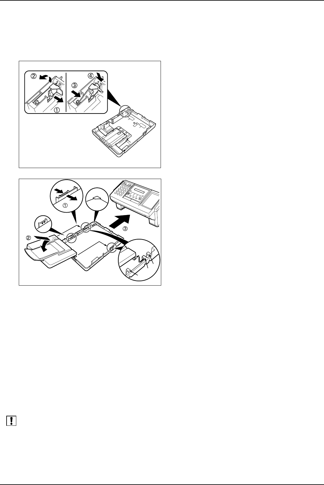
Installation
253
8.7 Adjusting the Paper Cassette for the Paper Width
How to Adjust the Paper Cassette for the Paper Width
The factory default Paper Width setting for the Paper Cassette is on Letter/Legal size. To change the paper width
to A4 size, follow the steps below.
1(1) Release the left Paper Separation Clip
latch.
(2) Pull up the Paper Separation Clip to
remove it.
(3) Reposition the Paper Separation Clip into
the A(A4) slot.
(4) Swing the Paper Separation Clip
downward to latch it in place.
2(1) Load the paper into the Paper Cassette.
Slide the paper width guide to the left until it
lightly touches the stack of paper without
bending the paper. The paper must fit
squarely and firmly between the Paper
Width Guide and the right side of tray. If it
does not, the paper may feed into the
printer incorrectly resulting in a paper jam.
Caution: Make sure that the paper is set
under the metal Paper Separation
Clips and that it does not exceed
the Maximum Paper Capacity Mark.
You can load about 250 sheets (20
lb weight). For paper specification,
see page 154 of the User’s Guide.
(2) Replace the Paper Cassette Cover to the
appropriate paper position (LTR, A4 or
LGL).
(3) Slide the Paper Cassette into the machine.
Paper Separation Clip
Paper
Width Guide
Max. Paper
Capacity Mark
LGL A4
LTR
Note:
3The Recording Paper Size setting of the Fax Parameter No. 23 must match the paper loaded in the cassette.
If you change the Recording Paper Size, please change the setting accordingly. (See page 38 of the User’s
Guide)
If you forget to change the Recording Paper Size setting in Fax Parameter No. 23 when different paper is installed
in the cassette, the unit will Stop printing after the 1st page of an Incoming Fax and display a " PAPER SIZE
MISMATCH" error. Then, the Recording Paper size setting automatically adjusts to the proper size and the unit
resumes printing the Incoming Fax from the 1st page.
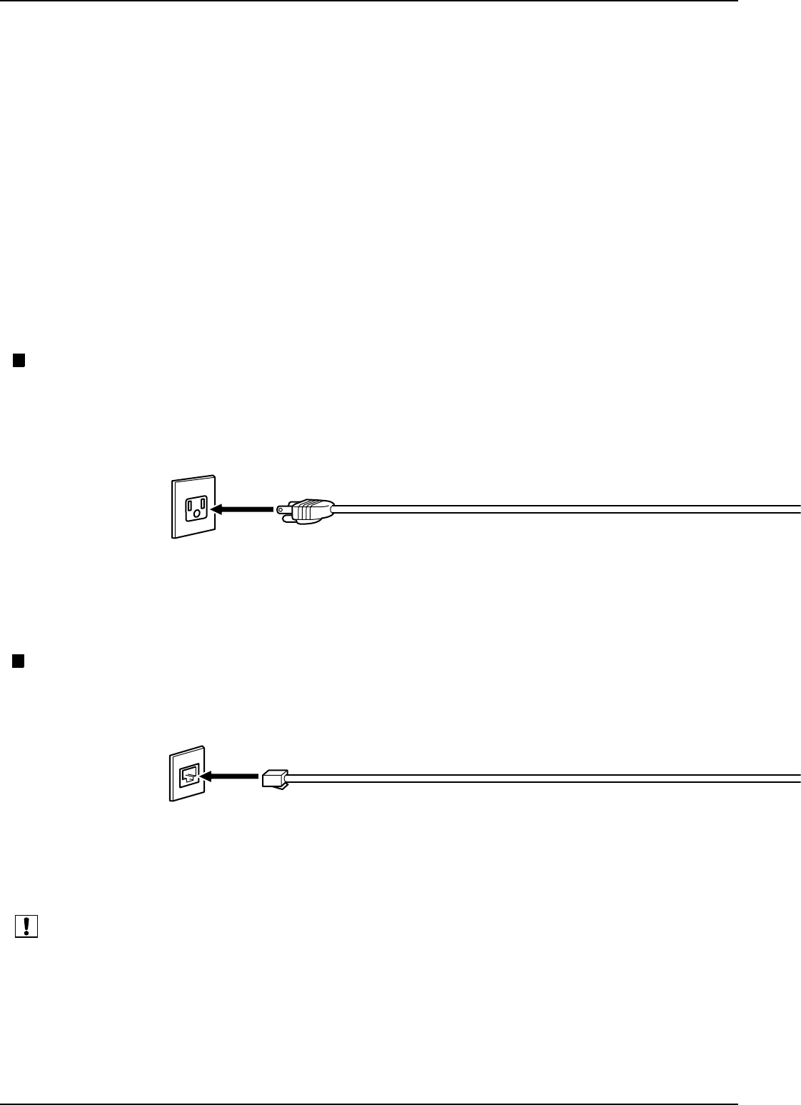
Panasonic UF-585 / 595
254
8.8 Connecting the Telephone Line Cable and Power Cord
Power Cord
Plug one end of the power cord into an ordinary 3 prong AC outlet and the other end into the receptacle on the
rear of the machine.
Warning : This apparatus must be properly grounded through an ordinary 3 prong AC outlet.
Do not break off the earth (ground) prong to fit a 2 prong outlet.
(see Note 1).
1. Your machine uses little power and you should keep it ON at all times. If the power is turned OFF for too long, the
clock contents may be lost.
Power Cord (Included)
Telephone Line Cable
Plug one end of the telephone line cable into the "RJ-11C" telephone jack supplied by the telephone company
and the other end into the LINE jack on the Rear side of the machine
RJ-11C Telephone Jack
Telephone Line Cable (Included)
Note:
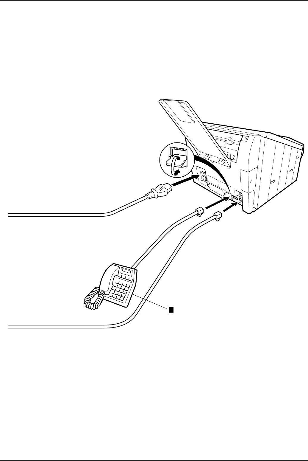
Installation
255
External Telephone (Optional)
You can connect an additional standard
single line telephone to the machine.
To connect the telephone, break off the
protective tab on the TEL jack.
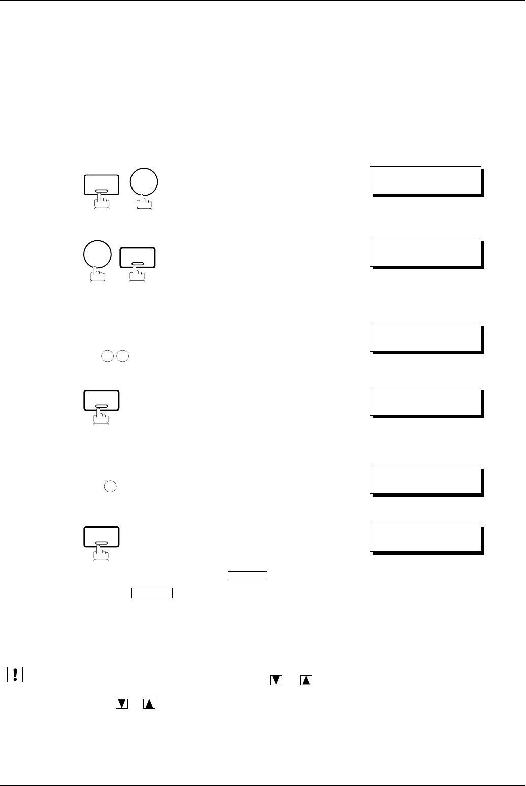
Panasonic UF-585 / 595
256
8.9 Customizing Your Machine
Your facsimile machine has a variety of adjustable Fax Parameters. These parameters, listed in the Parameter
Table, are preset for you and do not need to be changed. If you do want to make a change, read the table carefully.
Some parameters, such as the Resolution, Contrast, and Verification Stamp parameters, can be temporarily
changed by simple key operation just before a transmission is made. When the transmission ends, however, these
parameters return to their preset values (Home position). Other parameters can only be changed by the procedure
described below.
Setting the Fax Parameters
(see Note 1) (see Note 2) (see Note 3)
1
2
3Enter Fax Parameter number from the Parameter Table.
(See pages 257 to 260)
Ex: for CONTRAST
4
5Enter the new setting value.
Ex: for LIGHTER
6
To set another parameter, press to return to step
3 or press to return to standby.
1. To scroll the Fax Parameters in Step 2 or 4, press or .
2. To print out a Fax Parameter List, see page 135 of the User’s Guide.
3. If you press or in step 5, the new setting will be canceled.
FUNCTION
7SET MODE (1-6)
ENTER NO. OR ∨ ∧
4SET
FAX PARAMETER(01-99)
NO.=
❚
0 1
FAX PARAMETER(01-99)
NO.=01
SET 01 CONTRAST
1:NORMAL
2
01 CONTRAST
2:LIGHTER
SET
CLEAR
STOP
02 RESOLUTION
1:STANDARD
Note:
Installation
257
Fax Parameter Table
No. Parameter Setting
Number Setting Comments
01 CONTRAST *1 Normal Setting the home position of the CONTRAST key.
2 Lighter
3 Darker
02 RESOLUTION 1 Standard Setting the home position of the RESOLUTION key.
2 Fine
3 S-Fine
04 STAMP *1 Off Setting the home position of the STAMP key.
To select the stamp function when document is stored in memory,
see Fax Parameter No. 28.
2On
05 MEMORY 1 Off Setting the home position of the MEMORY key.
*2 On
06 DIALING METHOD 1 Pulse Selecting the Dialing method.
*2 Tone
07 HEADER PRINT *1 Inside Selecting the printing position of the header.
Inside : Inside TX copy area.
Outside : Outside TX copy area.
No print : Header is not printed.
2 Outside
3 No print
08 HEADER FORMAT *1 Logo, ID No. Selecting the header format.
2 From To
09 RCV’D TIME PRINT *1 Invalid Selecting whether the machine prints the received date & time,
remote ID, percentage of reduction and page number on the
bottom of each received page.
2 Valid
10 KEY/BUZZER VOLUME 1 Off Selecting the volume of the Key/Buzzer tone.
*2 Soft
3 Loud
12 COMM. JOURNAL 1 Off Selecting the home position of printout mode for COMM. Journal
Off/Always/INC.
Off : No printout
Always : Always prints out
Inc. only: Printout when communication has failed.
2Always
*3 Inc. only
13 AUTO JOURNAL PRINT 1 Invalid Selecting whether the machine prints the journal automatically
after every 32 transactions.
*2 Valid
15 IN MODE *1 Tel Selecting IN (attended) mode as either Telephone Mode or
Fax / Tel Auto Switching Mode.
2 Fax/Tel SW
16 OUT MODE *1 Fax Selecting OUT (unattended) mode as either Fax Mode or TAM
interface Mode.
2TAM
Continued on the next page.
*
I/F
Panasonic UF-585 / 595
258
18 OPERATOR
CALL TIMER incoming voice call in Fax/Tel Auto Switching mode.
(See page 64 of the User’s Guide)
19 OGM LENGTH (TAM I/F) 1 1 sec. Setting for the OGM length of your TAM from 1 to 60 seconds.
The machine will not start to detect SILENCE until the time
setting has lapsed. (Default = 20 sec.)
--- ---
60 60 sec.
20 SILENT DET. (TAM I/F) 1 Invalid Selecting the Silent Detection Mode.
*2 Valid
22 SUBSTITUTE RCV 1 Invalid Selecting whether the machine receives to memory when
recording paper runs out, toner runs out or recording paper is
jammed.
*2 Valid
23 RECORDING PAPER
SIZE
1 A4 Selecting the recording paper size installed in your machine.
*2 Letter
3 Legal
24 PRINT REDUCTION 1 Fixed Selecting print reduction mode.
Fixed : Reduce received document according to setting of
Parameter No. 25.
Auto : Reduce received document according to the length of
received documents.
*2 Auto
25 REDUCTION RATIO 70 70% Selecting fixed print reduction ratio from 70% to 100%. This
parameter functions only when fixed print reduction is selected on
Fax Parameter No. 24.
---- ----
100 100%
26 POLLING PASSWORD (----) Setting a 4-digit password for secured polling. (See page 73 of
27 POLLED FILE SAVE *1 Invalid Selecting whether the machine retains the polled document in
memory even after the document is polled once.
2 Valid
28 STAMP AT MEM. XMT 1 Invalid Selecting whether the machine stamps the original documents
when storing the documents into memory.
(depending on the Stamp setting on the Control Panel)
*2 Valid
31 INCOMPLETE FILE
SAVE
*1 Invalid Selecting whether the machine retains the document in memory if
the document is not successfully transmitted.
2 Valid
32 COPY REDUCTION 1Manual Selecting whether the machine performs the copy reduction ratio
automatically or manually.
Manual :The machine will prompt you for the Zoom ratio (100% to
70%) when making copies.
Auto : The machine will automatically determine the reduction
ratio according to the length of the original document.
*2 Auto
Continued on the next page.
No. Parameter Setting
Number Setting Comments
4 50 sec.
2 30 sec.
3 40 sec.
the User’s Guide)
*1 20 sec. Selecting the length of time that your machine signals (rings) for an
Installation
259
34 ENERGY SAVER MODE
1Off
To reduce the power consumption in standby, select either Energy-
Saver or Sleep mode and specify the Delay Time (1 to 120
minutes) for the machine to enter into the selected mode.
The Delay Timer setting is only available in the Energy-Saver or
Sleep Modes.
Off : The unit will remain in standby mode and
consume more energy than when in Energy-
Saver or Sleep modes.
Energy-Saver Mode :Saves energy by consuming less power than
when in standby mode by turning off the
fuser unit after the specified time.
Sleep Mode : This is the lowest power state that the
machine enters after the specified time
without actually turning off.
2 Energy-Saver
*3 Sleep
35 DAYLIGHT TIME 1 Invalid Selecting whether the clock adjusts for Daylight Saving Time
automatically. The built-in clock will advance 1 hour at 2:00 am on
the first Sunday in April and fallback 1 hour at 2:00 am on the last
Sunday in October.
*2 Valid
36 RING PATTERN
DETECT (DRD)
(See Note 2)
*1 Invalid All ring patterns.
2 Valid
Select a ring pattern for automatic answering.
1: A Standard ring pattern.
2: B Double ring pattern.
3: C Triple ring pattern (Short-Short-Long).
4: D All other triple ring pattern, except the type C
described above.
37 RCV TO MEMORY
(----)
Enter a 4-digit password used to print out the received document
in memory by using F8-5 (RCV TO MEMORY). When F8-5 is set
to On, this parameter will not be shown on the LCD display. (See
page 92 of the User’s Guide)
38 ACCESS CODE (----) Enter a 4-digit Access Code to secure the machine from
unauthorized use. (See page 90 of the User’s Guide)
40 RELAY XMT REQUEST *1 Invalid Selecting whether the machine accepts and performs Relay XMT
Request. (See page 115 of the User’s Guide)
2 Valid
42 CONF. POLLED FILE
SAVE
*1 Invalid Selecting whether the machine saves the confidential polled file
even after the file is polled once.
2 Valid
43 PASSWORD-XMT *1 Off Setting a 4-digit XMT-Password and selecting whether the
machine performs and checks the XMT-Password of the receiving
station when transmitting. (See page 101 of the User’s Guide)
2On
44 PASSWORD-RCV *1 Off Setting a 4-digit RCV-Password and selecting whether the
machine performs and checks the RCV-Password of the
transmitting station when receiving. (See page 102 of the
2On
46 SELECT RCV *1 Invalid Selecting whether the machine performs selective reception. (See
page 99 of the User’s Guide)
2 Valid
47 REMOTE RECEPTION 1 Invalid Selecting whether or not the machine accepts remote reception
command. (See page 63 of the User’s Guide)
*2 Valid
52 DIAGNOSTIC
PAS S WO RD (----) Setting the password for Remote Diagnostic Mode. Please ask
your Panasonic Authorized Dealer for details.
53 SUB-ADDRESS
PAS S WO RD (----) Setting a 20-digit password for secured sub-address
communication.
Continued on the next page.
No. Parameter Setting
Number Setting Comments
User’s Guide)

Panasonic UF-585 / 595
260
(see Note 1)
(see Note 2)
54 FAX FORWARD *1 Invalid Selecting whether the machine performs Fax Forwarding to the
specified destination . (See page 97 of the User’s Guide)
2 Valid
56 COVER SHEET *1 Off Setting the home position of the Cover Sheet parameter in the
Select Mode. (See page 95 of the User’s Guide)
2On
58 LANGUAGE *1 A-English Selecting the language to be shown on the display and reports.
2 C-French
3 Spanish
65 PRINT COLLATION 1 Invalid Selecting whether the machine prints out documents in sequence.
(See page 69 of the User’s Guide)
*2 Valid
99 MEMORY SIZE
(Flash Memory)
- - Displays the amount of base and optional memory installed.
(Base Memory + Optional Memory)
1. Setting number marked with an asterisk (*) indicates the factory standard setting.
2. This parameter supports an optional telephone service "Distinctive Ring Service" provided by your local telephone
company. It allows up to 4 different telephone numbers to be assigned on a single telephone line with a distinctive
ring for each telephone number. By selecting the appropriate ring pattern associated with the telephone number
assigned for your fax machine. It can differentiate and answer the incoming call on the fax number. All other calls
on the other telephone numbers will not be answered. This optional service from your local phone company is also
called Custom Ringing, Distinctive Ringing, Ident-a-call, Ident-a-ring, Personalized Ringing, RingMaster, RingMate,
Selective Ringing, Smart Ring or something similar. Check with your local telephone company on the availability of
this service in your area.
No. Parameter Setting
Number Setting Comments
Note:
Panasonic UF-585 / 595
262
9 Options and Supplies
9.1 Options and Supplies
Please contact your local Panasonic dealer for availability.
1. Options
2. Supplies
Order No. Picture Description Available Models
UE-403117 Handset Kit UF-585
UF-595
UE-409070 250 Sheet Letter / Legal / A4 Size Paper
Cassette with the Feeder Unit UF-595
UE-404071 Pararellel Port Interface Kit
(used for Printer, Scanner or PC Interface)
UF-585
UF-595
UE-410045 Expansion Flash Memory Card, 1 MB
UF-585
UF-595
UE-410046 Expansion Flash Memory Card, 2 MB
UE-410047 Expansion Flash Memory Card, 4 MB
Order No. Picture Description Available Models
DZHT000027 Verification Stamp UF-585
UF-595
UG-3350 Toner Cartridge UF-585
UF-595
Options and Supplies
263
9.2 Installing Optional 250 Sheet Paper Cassette (UE-409070)
1. Contents
2. Installation
Note:
Install this Feeder Unit as the 2nd Feeder Unit only.
Qty. Description Part No. Remarks
1 250 Sheet Paper Cassette with Feeder Unit UE-409070
(1) Disconnect the Telephone Line Cable and the Power
Cord.
(2) Remove the Recording Paper Tray Assembly.
(3) Open the Printer Cover.
(4) Remove the Paper Cassette from the machine.
(5) Remove the Toner Cartridge from the machine.
(6) Remove 1 Screw (B1).
(7) Remove the Connector Access Cover (114).
(8) Place the machine on its Rear side over a clean cloth to
prevent damaging the Rear Cover.
(9) Break off the protective tab on the machine.
(10) Remove 4 Screws from the top of the 250 Sheet Paper
Cassette.
(11) Remove the shipping tape and place the CST2-CSTSNS2
Harness (927) to the outside of the cassette.
(12) Insert the 250 Sheet Paper Cassette into the machine.
(1)
(2)
(5)
(3)
(4)
(6)
(7)
(10)
(9)
(8)
(11)
(12)

Panasonic UF-585 / 595
264
(13) Secure the 250 Sheet Paper Cassette with the 4 screws
removed in step 10.
(14) Place the machine upright.
(15) Connect the CST2-CSTSNS2 Harness (927) into the
Connector CN66 on the LPC PC Board.
(16) Re-install the Connector Access Cover.
(17) Re-install the Recording Paper Tray Assembly, Paper
Cassettes and the Toner Cartridge.
(18) Re-connect the Telephone Line Cable and the Power
Cord.
(19) Print some pages from the Optional Paper Cassette to
confirm its operation.
(15)
(13)x4
(16)
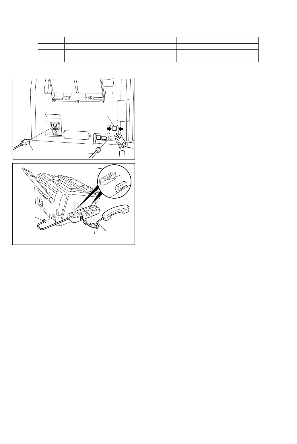
Options and Supplies
265
9.3 Installing Handset Kit (UE-403117)
1. Contents
2. Installation
Qty. Description Part No. Remarks
1 Handset DZDU000031
1 Handset Cord DZFN000066
1 Cradle Assembly DZML000132
(1) Disconnect the Power Cord and the Telephone Line
Cable.
(2) Break off the protective tab on the HANDSET Jack on the
machine.
(3) Hook the projections of the Cradle Assembly into the
holes on the Left Cover.
(4) Connect the Cradle Assembly Cable to the
HANDSET Jack on the rear of the machine.
(5) Connect the Handset Cord.
(6) Re-connect the Telephone Line Cable and the Power
Cord.
(1) (1)
(2)
(3)
(4)
(5)
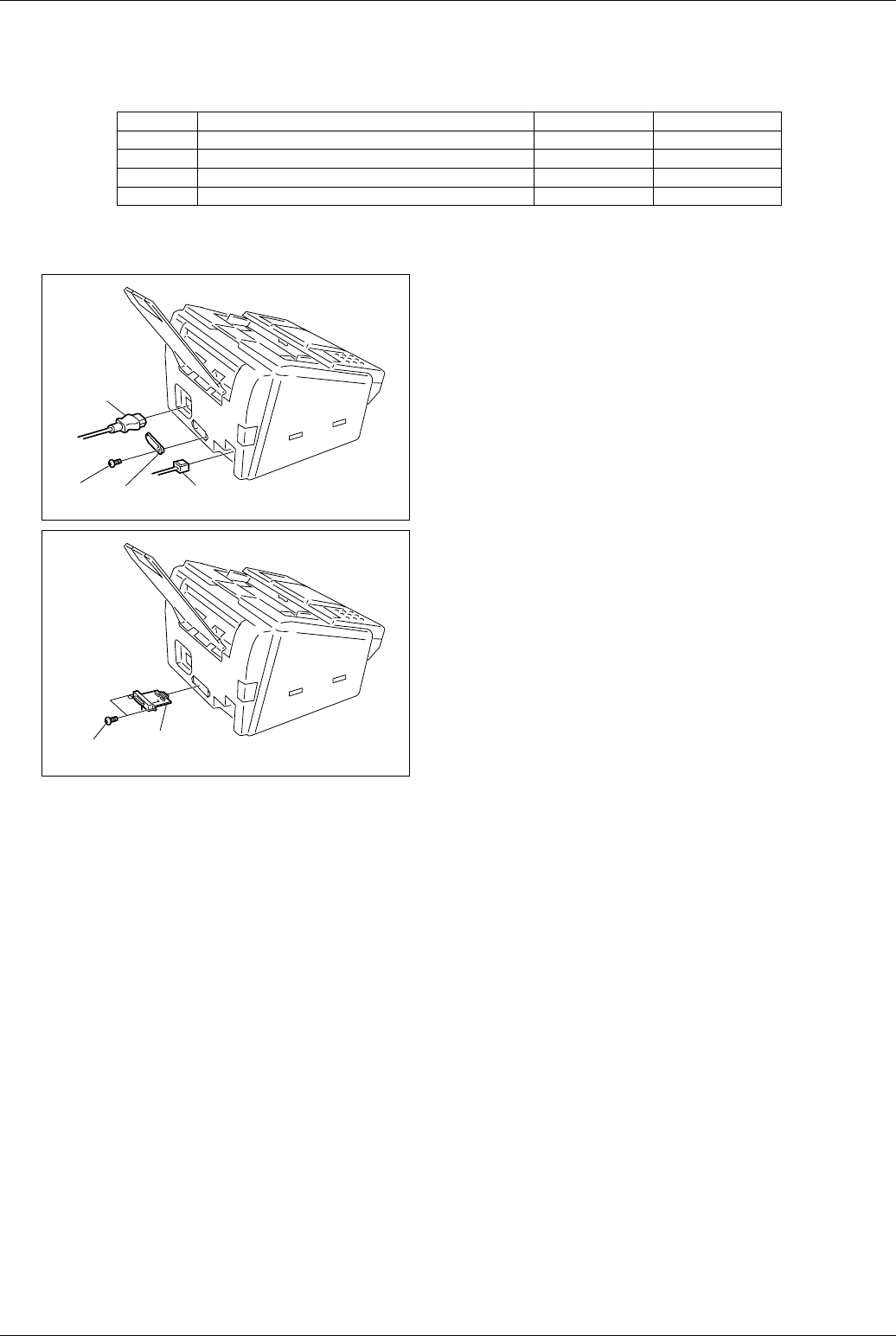
Panasonic UF-585 / 595
266
9.4 Installing Parallel Port Interface Kit (UE-404071)
1. Contents
2. Installation
Qty. Description Part No. Remarks
1 Parallel Port Interface Assembly DZHP002990
1 Screw DZPB000007
1 Printer Driver (Floppy Disk 2HD) DZQW000113 1 disk
1 set Scanner Driver (Floppy Disk 2HD) DZQW000114 4 disks
(1) Disconnect the Power Cord and the Telephone Line
Cable.
(2) Remove 1 Screw.
(3) Remove the Parallel Port Interface Cover.
(Save it for future use if the Parallel Port Interface Assembly
is removed)
(4) Install the Parallel Port Interface Assembly.
(5) Install 2 Screws.
(One screw is included with the kit and the other was
removed in Step 2 above)
(6) Re-connect the Telephone Line Cable and the Power
Cord.
(2) (3) (1)
(1)
(5) (4)
271
10Schematic Diagram
10.1 SCA PC Board (UF-595)
Model Drawing Name
UF-595 SCA PC Board (1/9)
272
Model Drawing Name
UF-595 SCA PC Board (2/9)
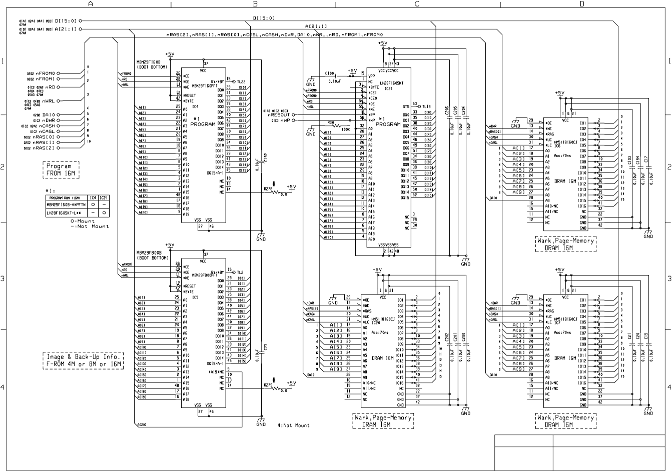
273
Model Drawing Name
UF-595 SCA PC Board (3/9)
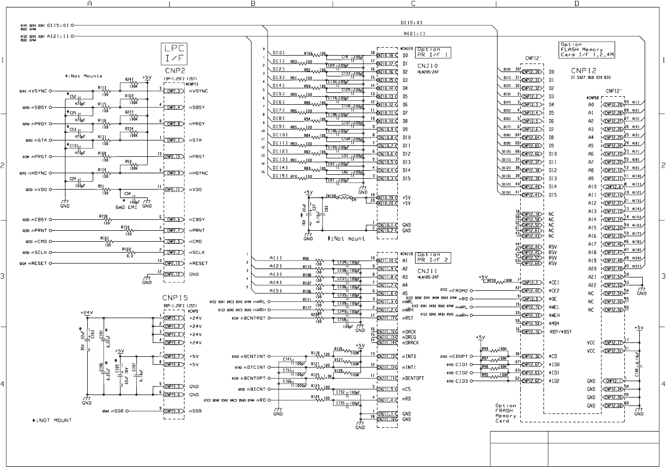
274
Model Drawing Name
UF-595 SCA PC Board (4/9)
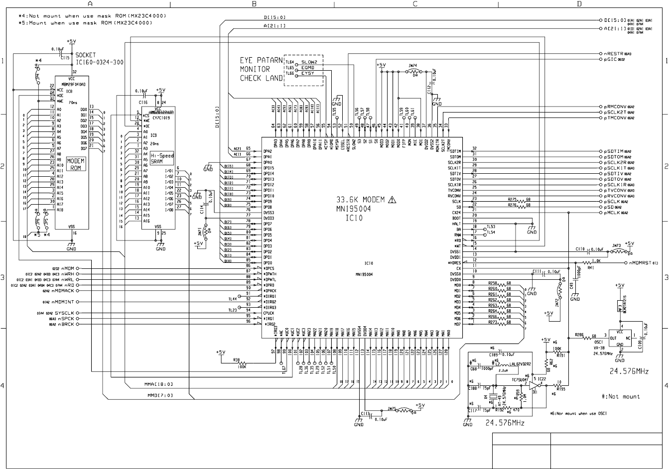
275
Model Drawing Name
UF-595 SCA PC Board (5/9)
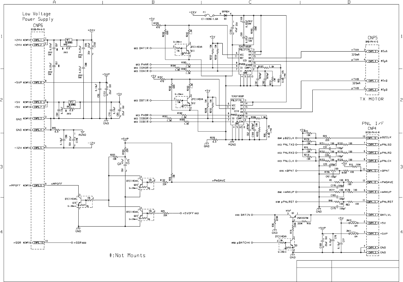
276
Model Drawing Name
UF-585 SCB PC Board (6/6)
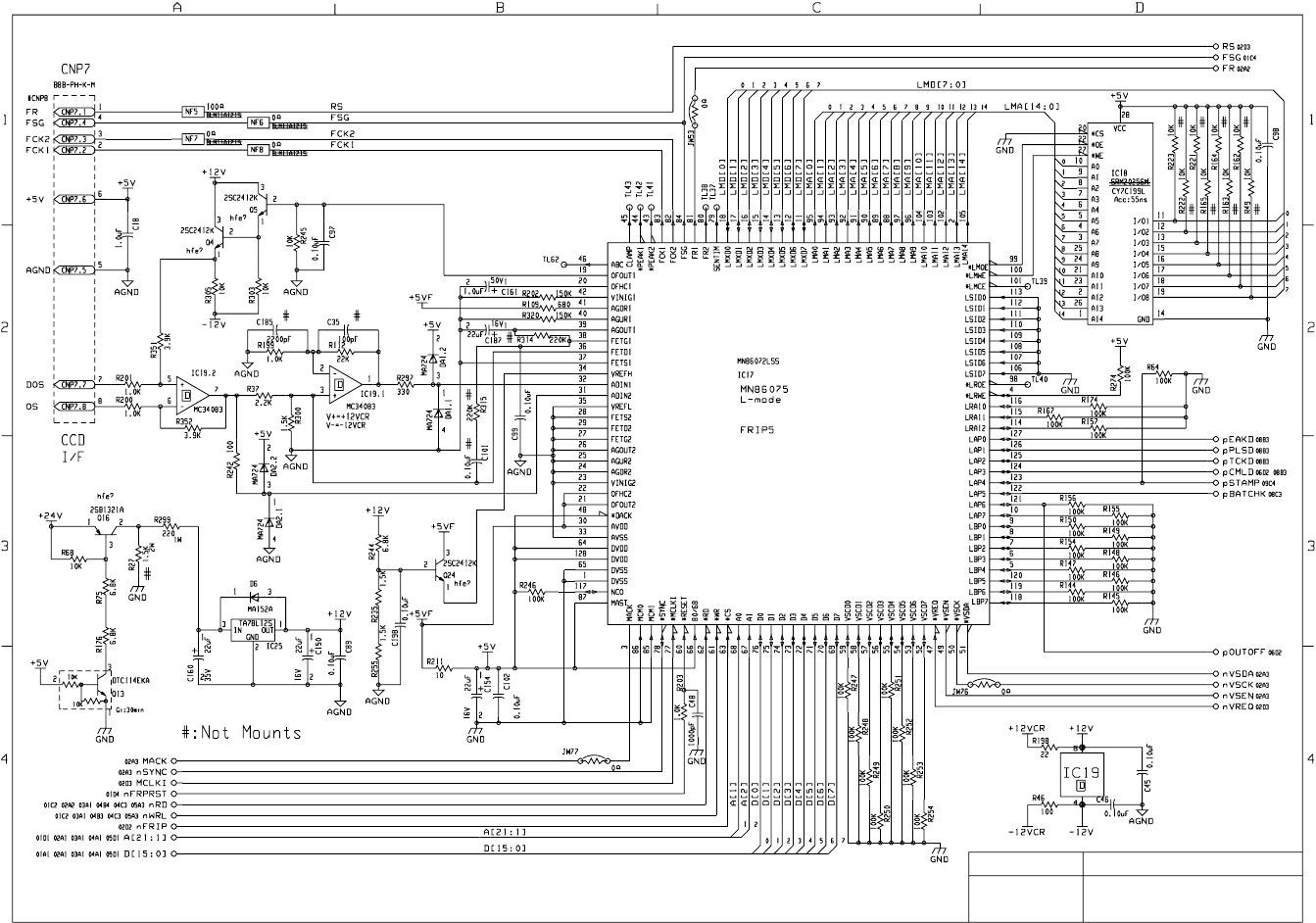
277
Model Drawing Name
UF-595 SCA PC Board (7/9)
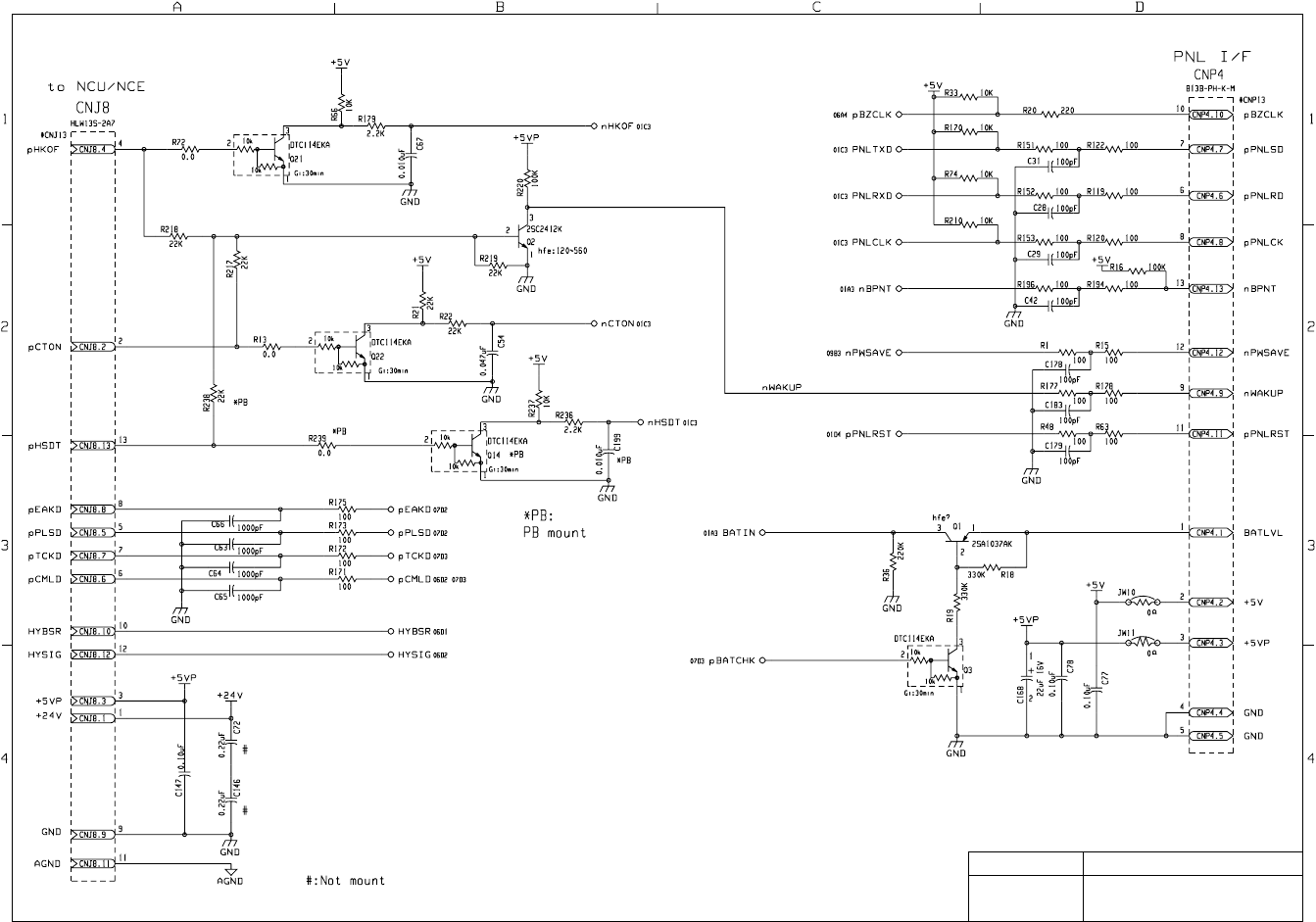
278
Model Drawing Name
UF-595 SCA PC Board (8/9)
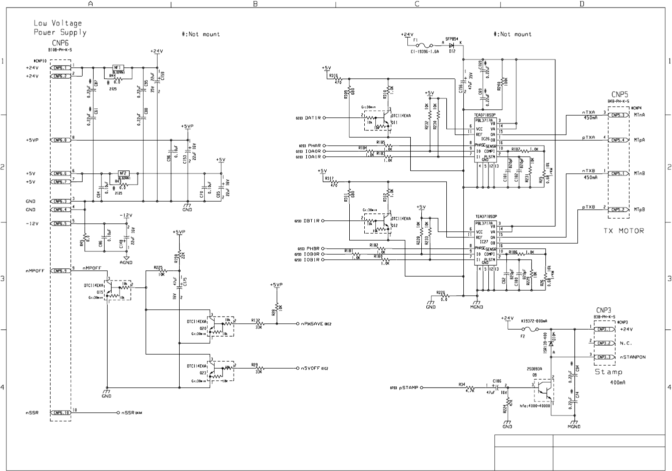
279
Model Drawing Name
UF-595 SCA PC Board (9/9)
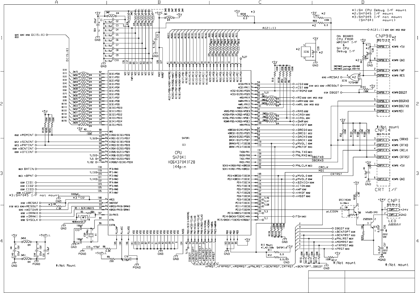
280
10.2 SCB PC Board (UF-585)
Model Drawing Name
UF-585 SCB PC Board (1/6)
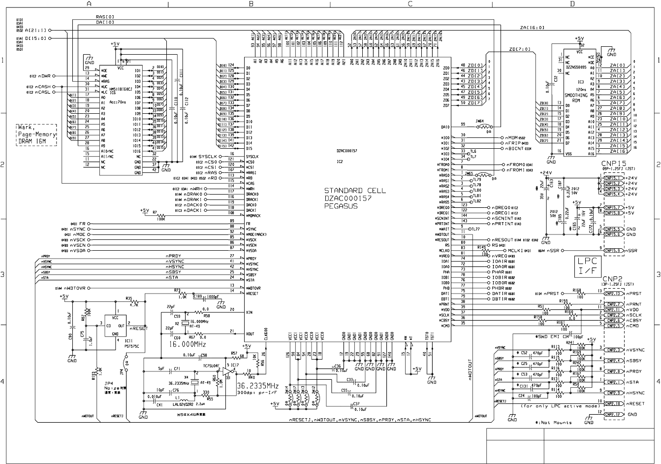
281
Model Drawing Name
UF-585 SCB PC Board (2/6)
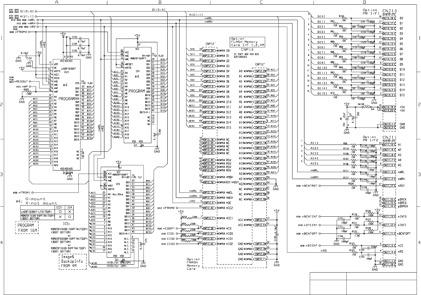
282
Model Drawing Name
UF-585 SCB PC Board (3/6)
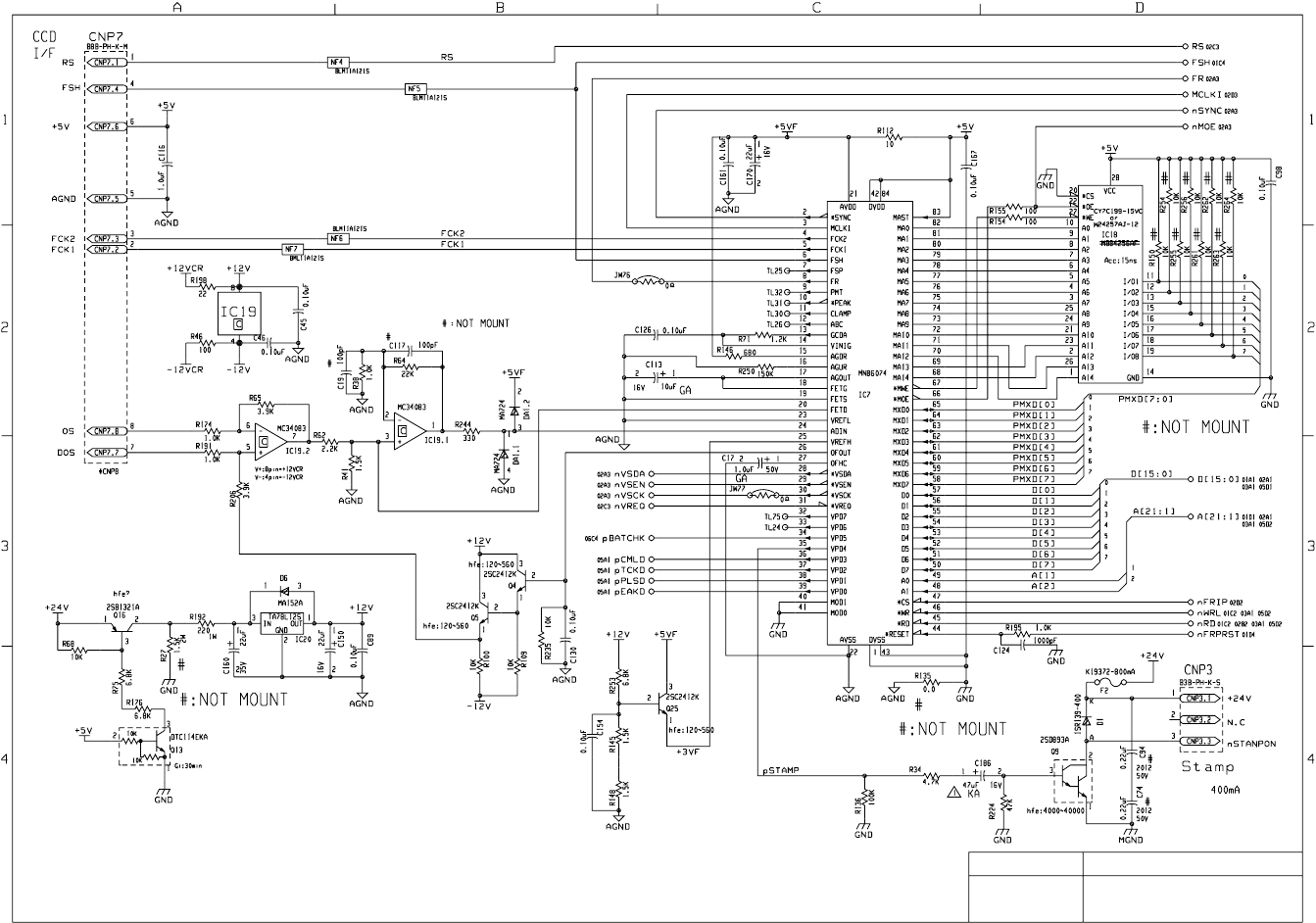
283
Model Drawing Name
UF-585 SCB PC Board (4/6)
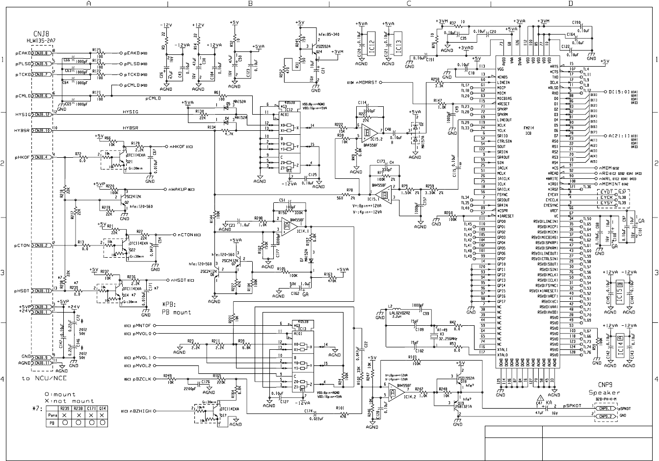
284
Model Drawing Name
UF-585
Not Mounted
Not
Mounted
SCB PC Board (5/6)
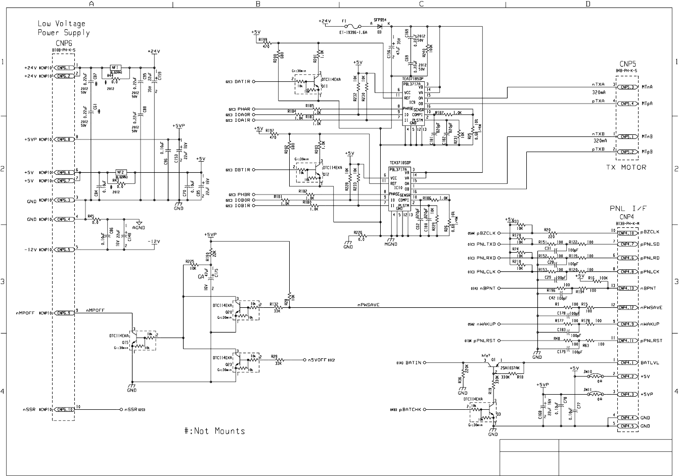
285
Model Drawing Name
UF-585 SCB PC Board (6/6)
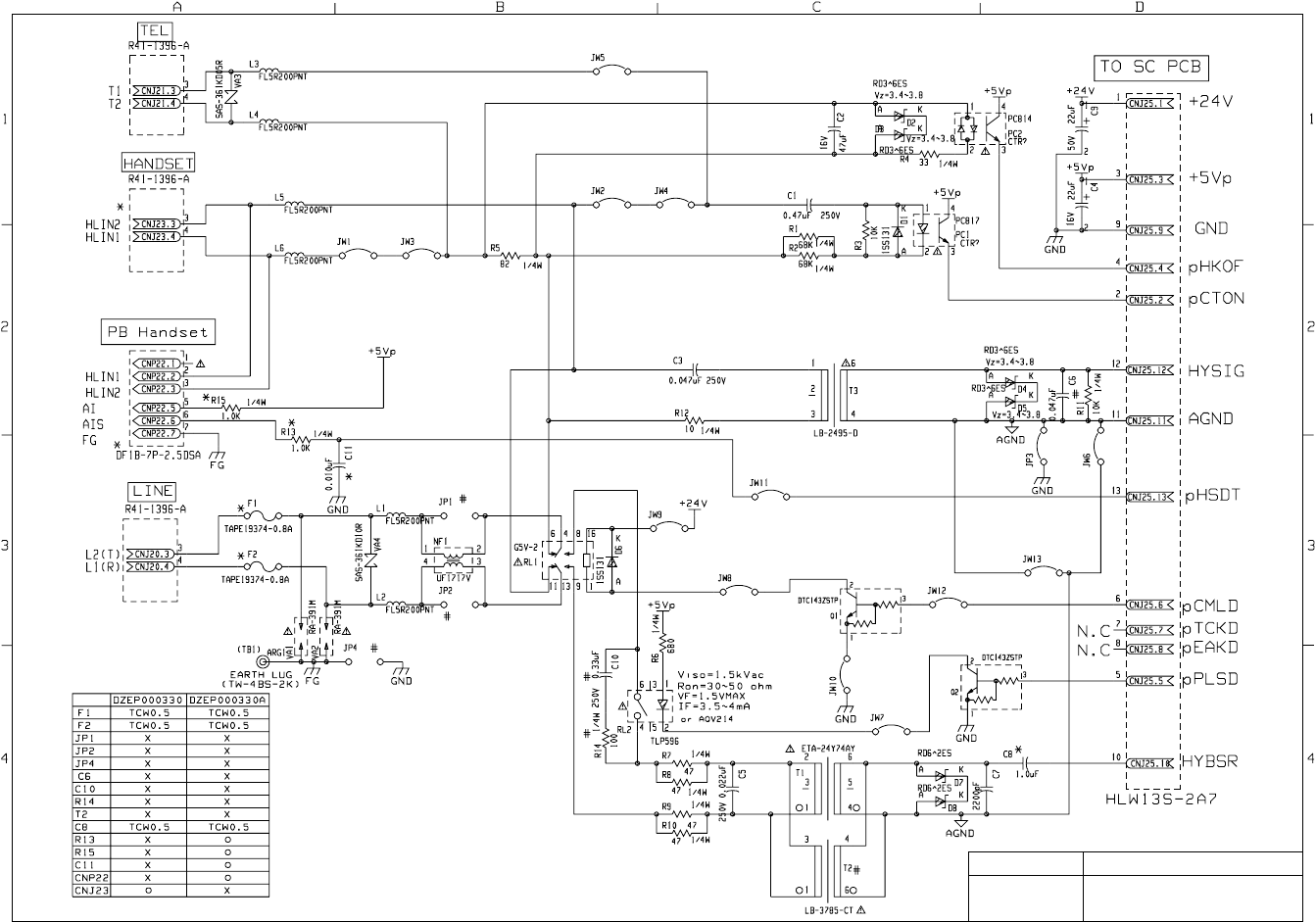
286
10.3 LCU,LCE PC Board
Model Drawing Name
LCU PC Board (1/1)
UF-585/595
NOT
Mounted
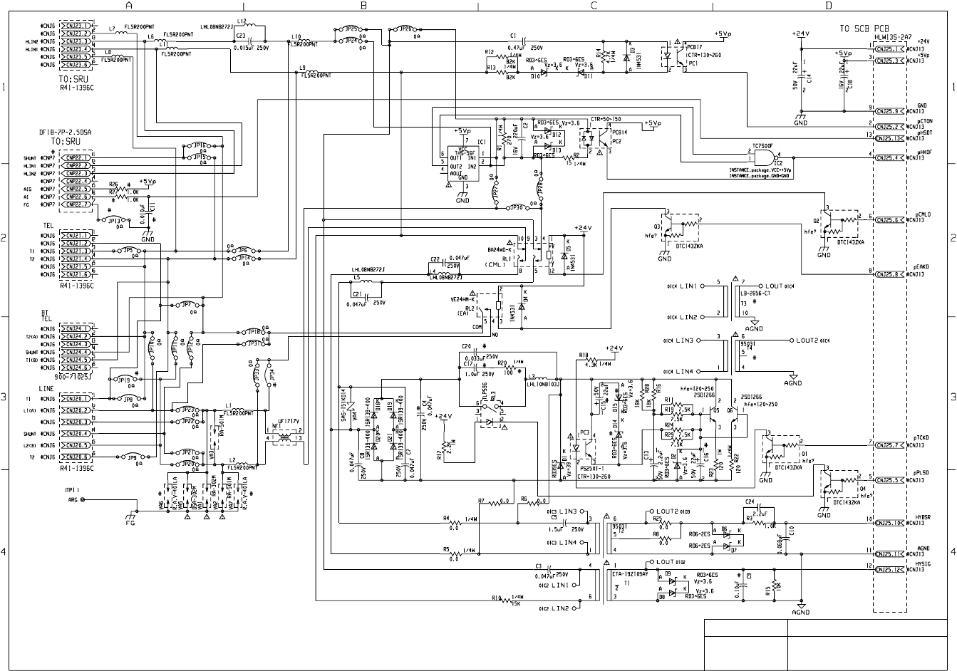
287
Model Drawing Name
LCE PC Board (1/1)
UF-585/595
NOT
Mounted
NOT
Mounted
NOT
Mounted
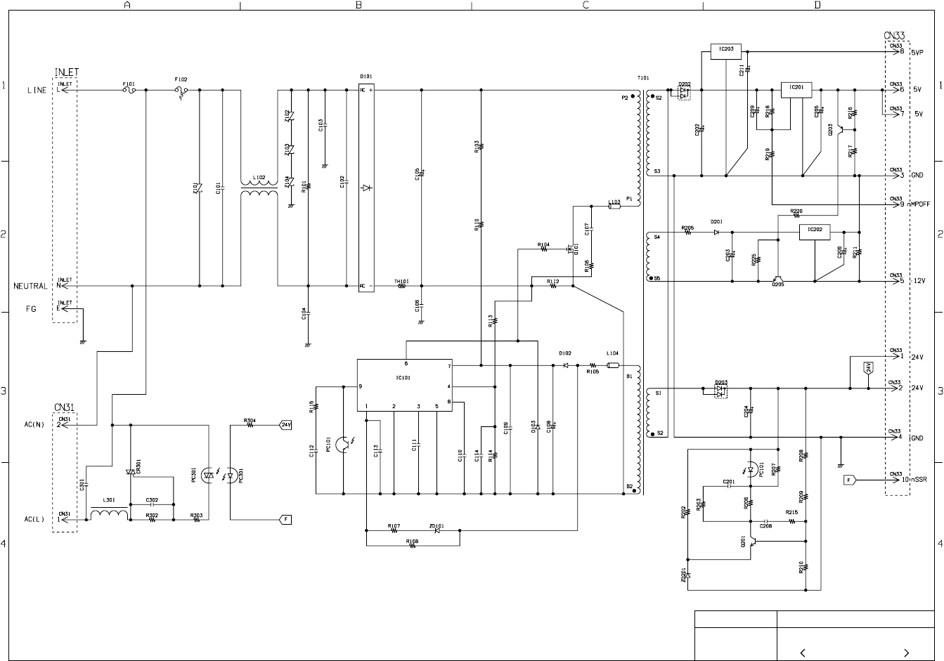
288
10.4 Low Voltage Power Supply PC Board
ETXDN200A4D
Model Drawing Name
Power Supply PC Board (100V)
UF-585/595
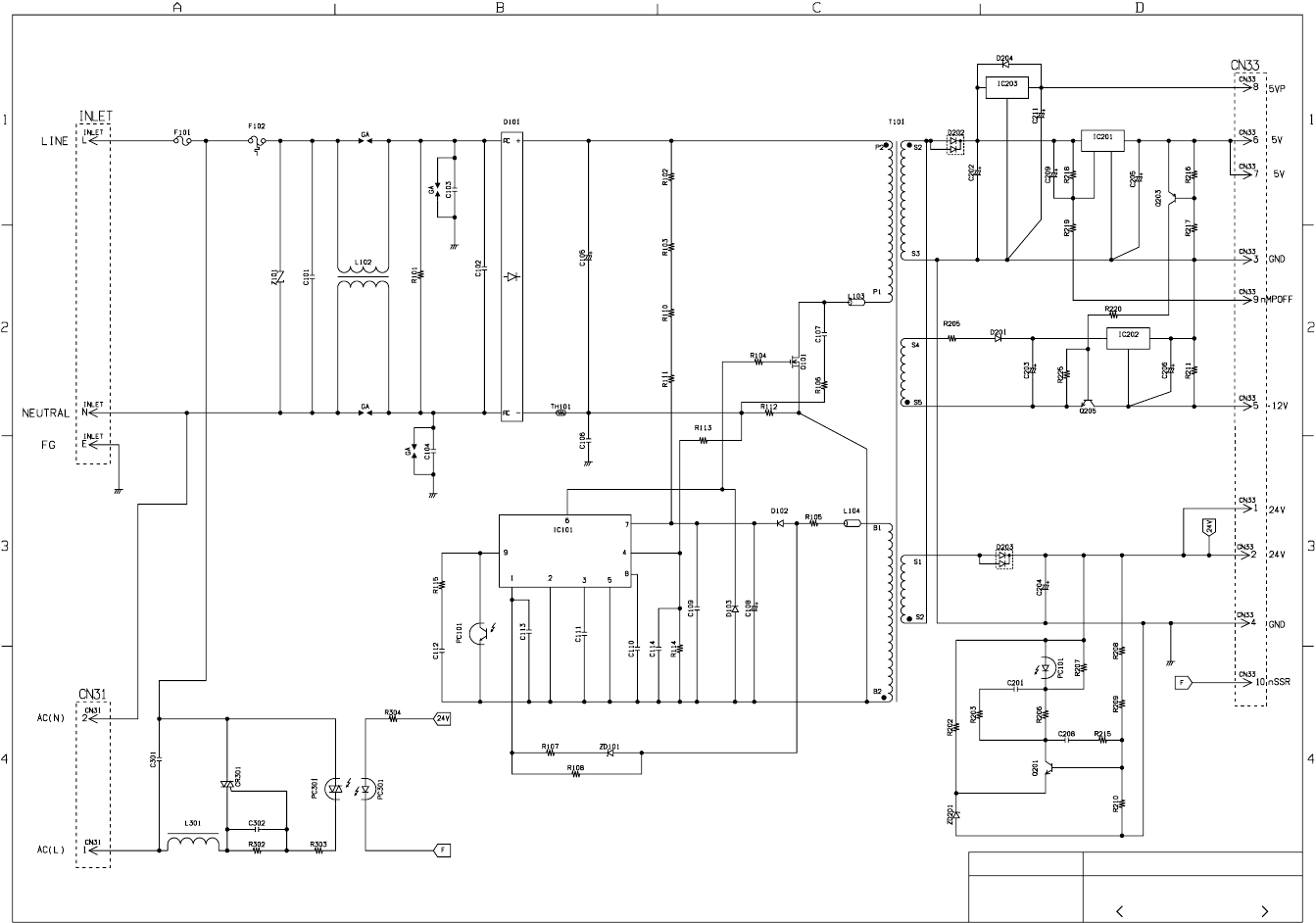
289
ETXDN200E4D
Model Drawing Name
Power Supply PC Board (200V)
UF-585/595
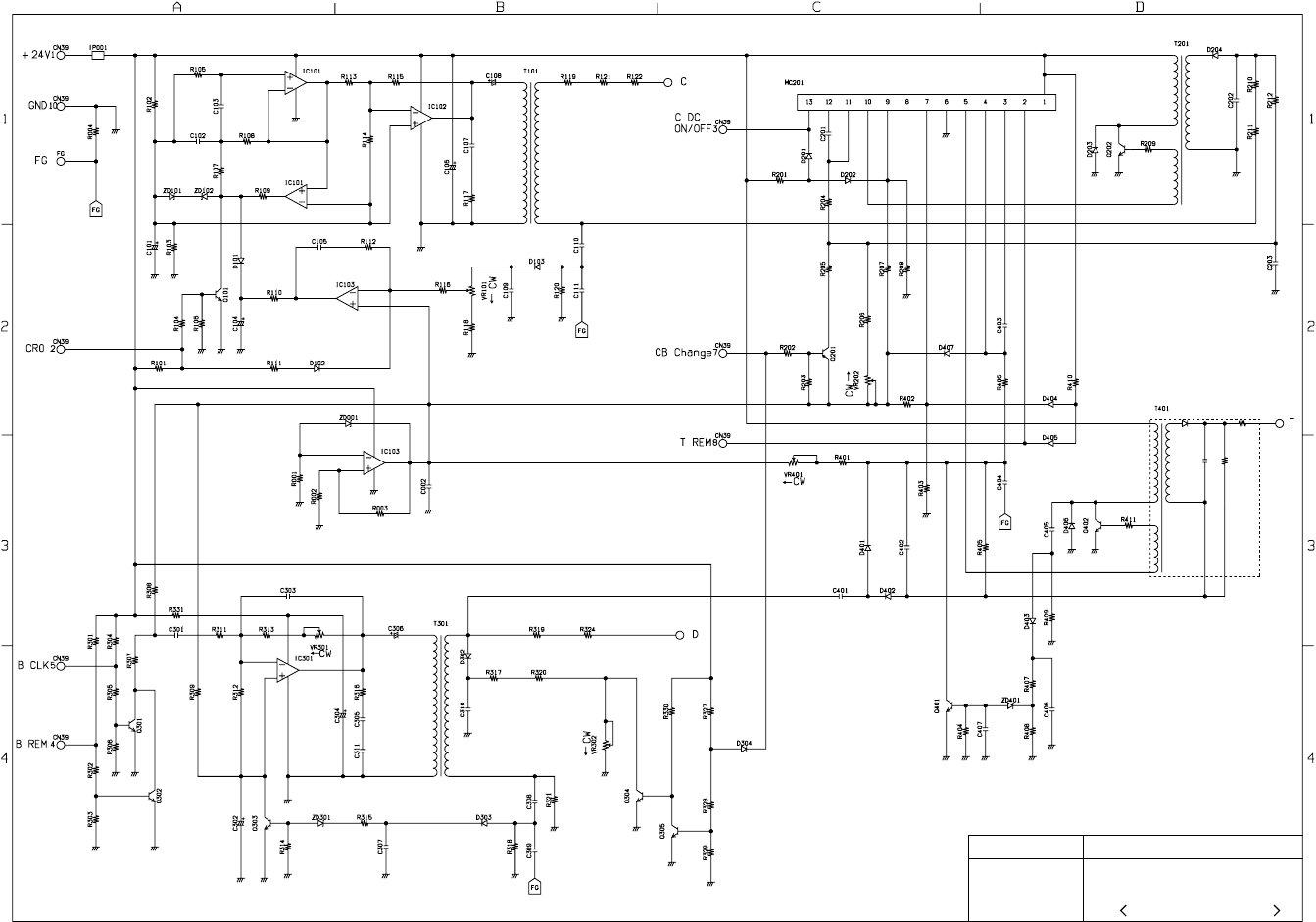
290
10.5 High Voltage Power Supply PC Board
EUKMBN731HA
Model Drawing Name
High Voltage Power Supply
PC Board (1/1)
UF-585/595
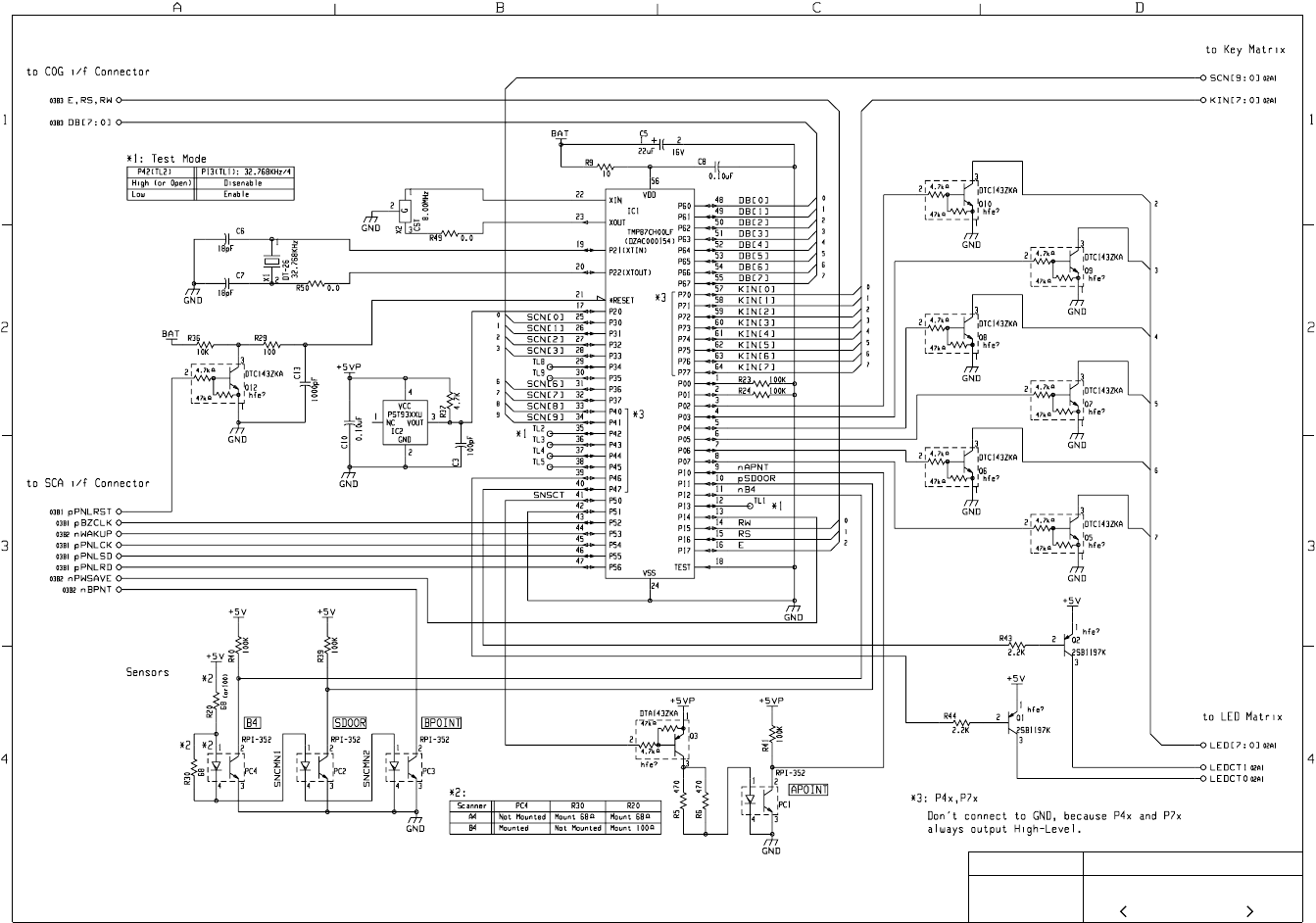
291
10.6 PANEL PC Board
DZEC101103
Model Drawing Name
PANEL PC Board 1
UF-585/595
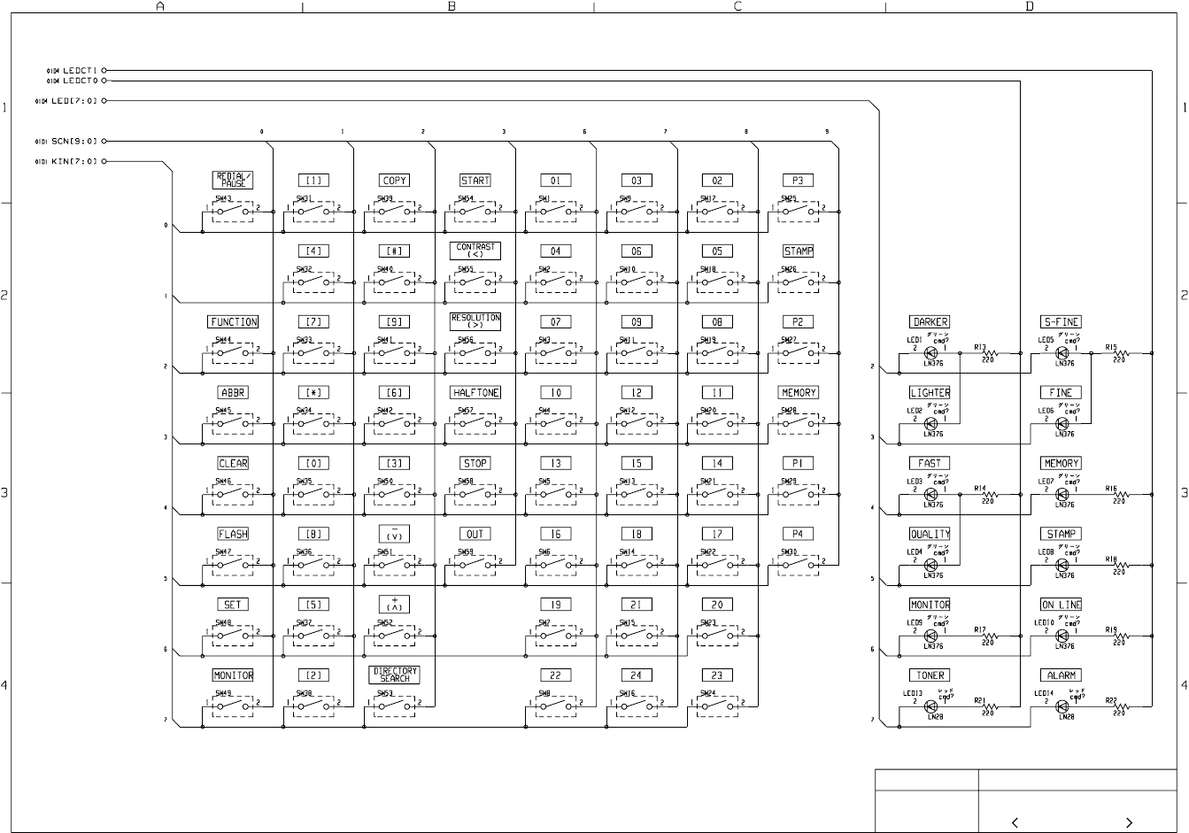
292
Model Drawing Name
UF-585/595 DZEC101103
PANEL PC Board 2
293
Model Drawing Name
UF-585/595 DZEC101103
PANEL PC Board 3
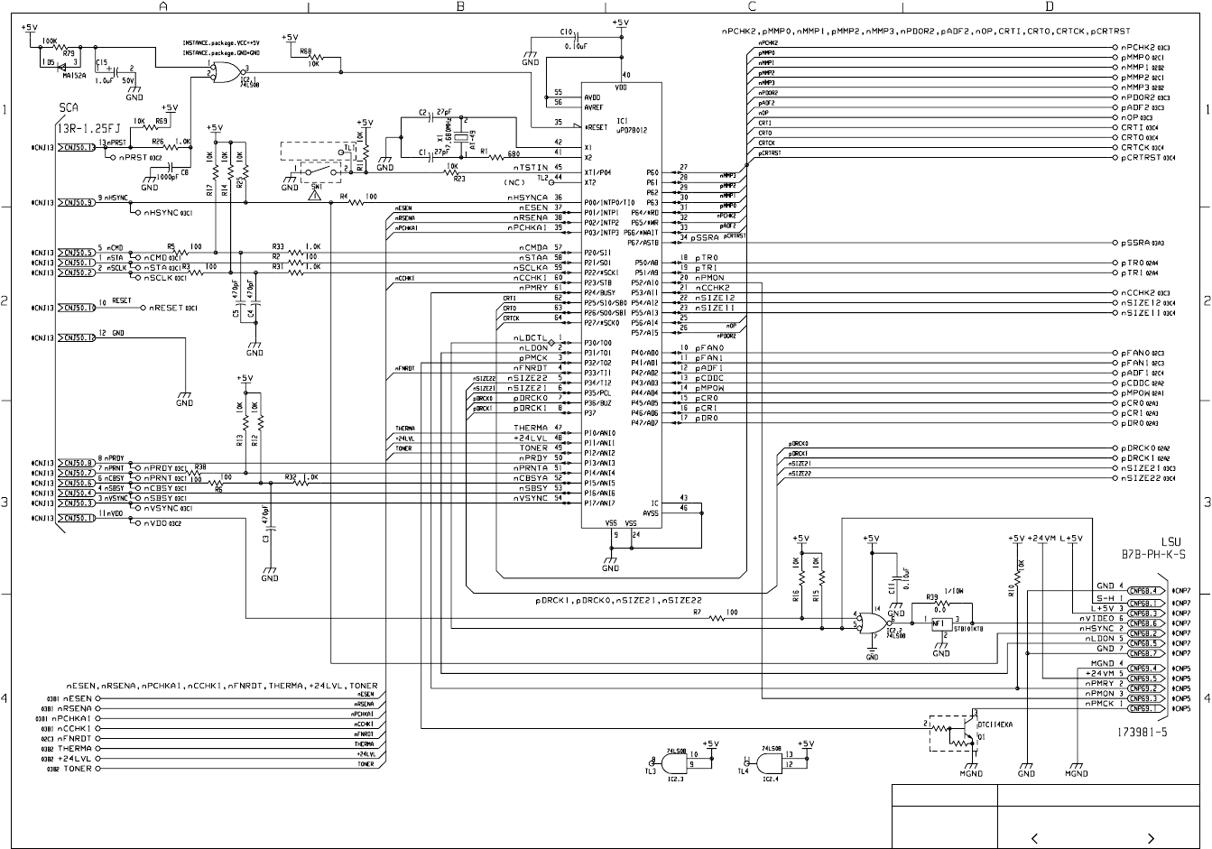
294
10.7 LPC PC Board
DZEC101039
Model Drawing Name
LPC PC Board (1/3)
UF-585/595
Not
Mounted
Not
Mounted
Pad Switch
295
DZEC101039
Model Drawing Name
LPC PC Board (2/3)
UF-585/595
HVPS
Not
Mounted
Not
Mounted
Not
Mounted
Pulse
Motor
Paper Feed
Clutch
Fan
296
DZEC101039
Model Drawing Name
LPC PC Board (3/3)
UF-585/595
Not
Mounted
Not
Mounted
Not
Mounted
Not
Mounted
Not
Mounted
Not
Mounted
Not
Mounted
Not
Mounted Not
Mounted
Option
Cassette
Not
Mounted
Not
Mounted
Door
Sensor
Timing
Thermistor
No Paper
Sensor
Toner
Cassette
Sensor
Feed
Sensor
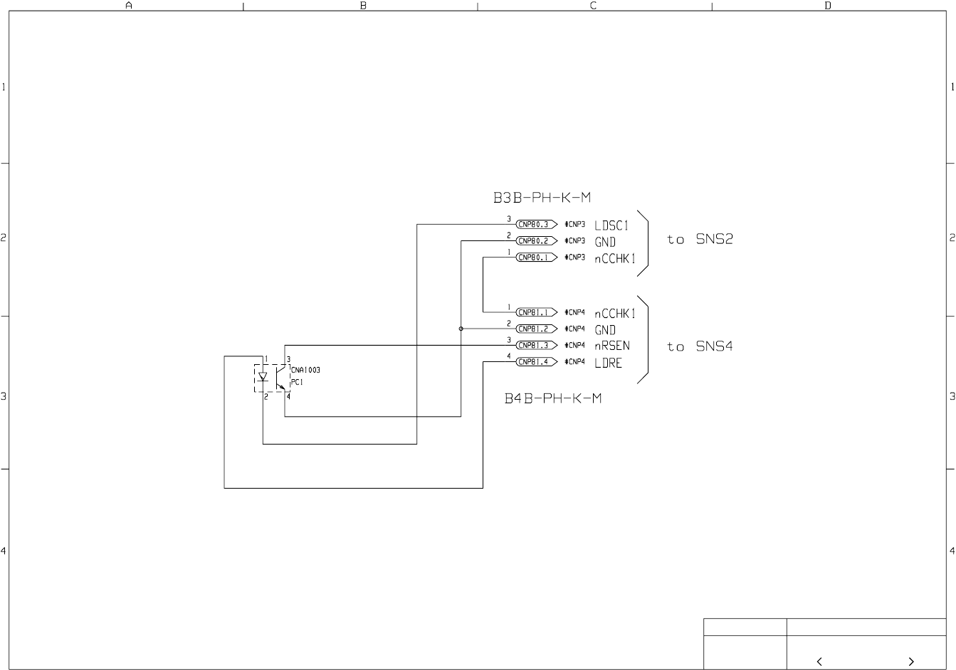
297
10.8 SNS PC Board
Model Drawing Name
UF-585/595 DZEP000376
SNS PC Board 1
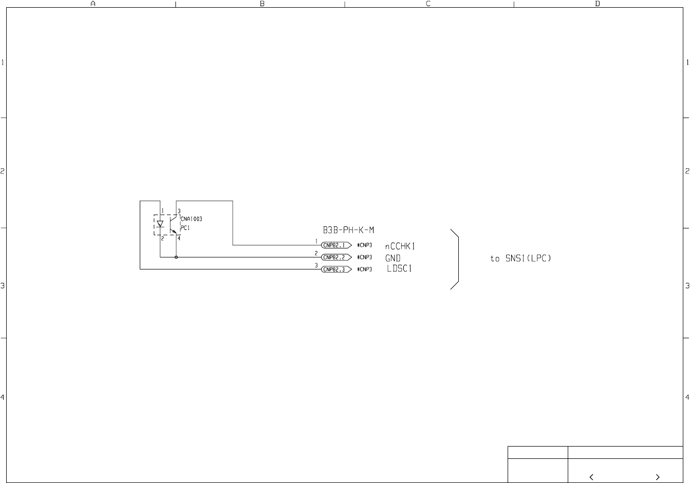
298
Model Drawing Name
UF-585/595 DZEC101076
SNS PC Board 2
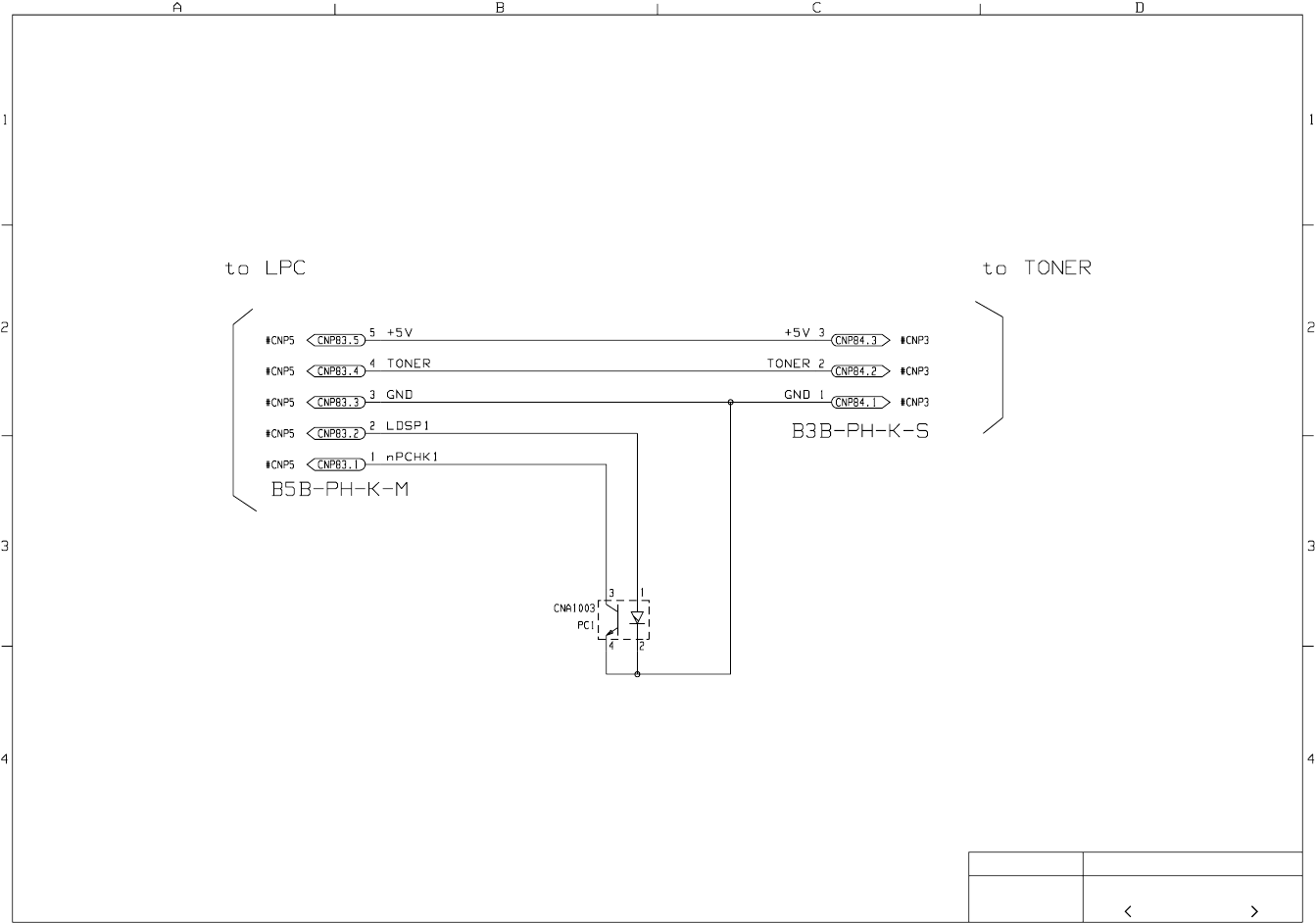
299
Model Drawing Name
UF-585/595 DZEC101163
SNS PC Board 3
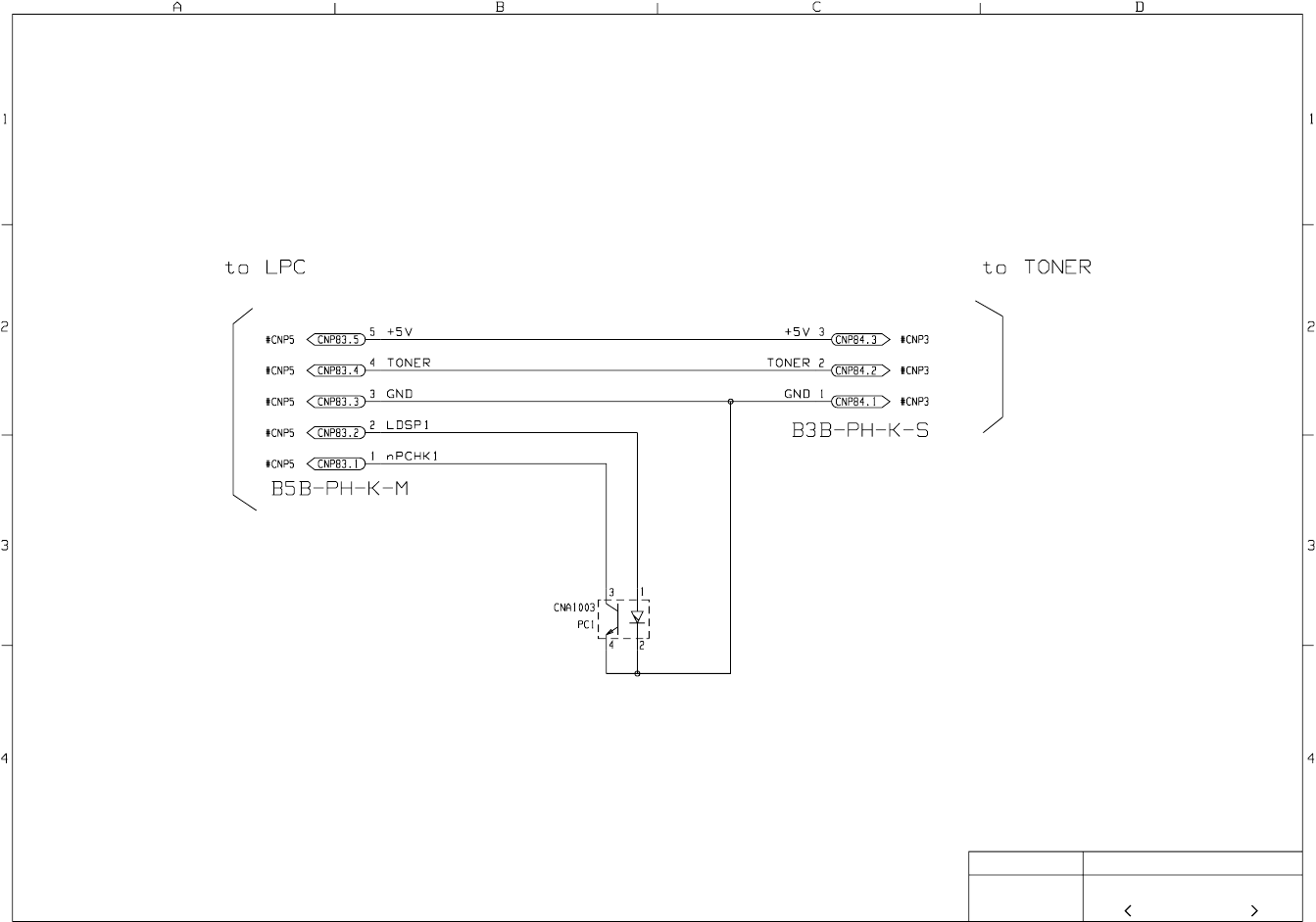
300
Model Drawing Name
UF-585/595 DZEC101263
SNS PC Board 4
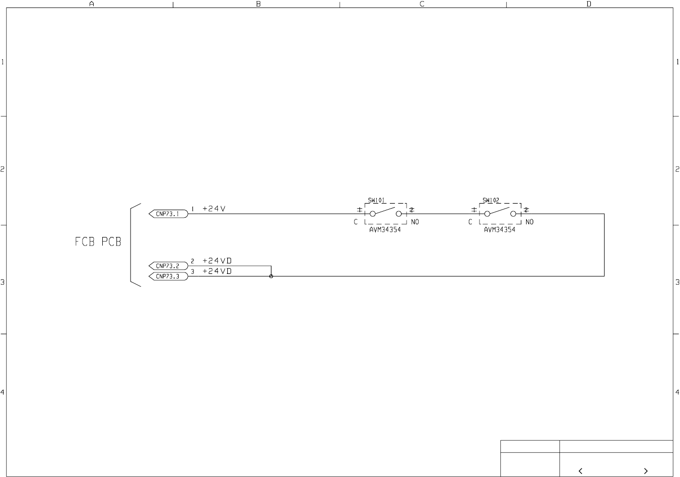
301
10.9 ILS PC Board
DZEC100262
Model Drawing Name
ILS PC Board (1/1)
UF-585/595
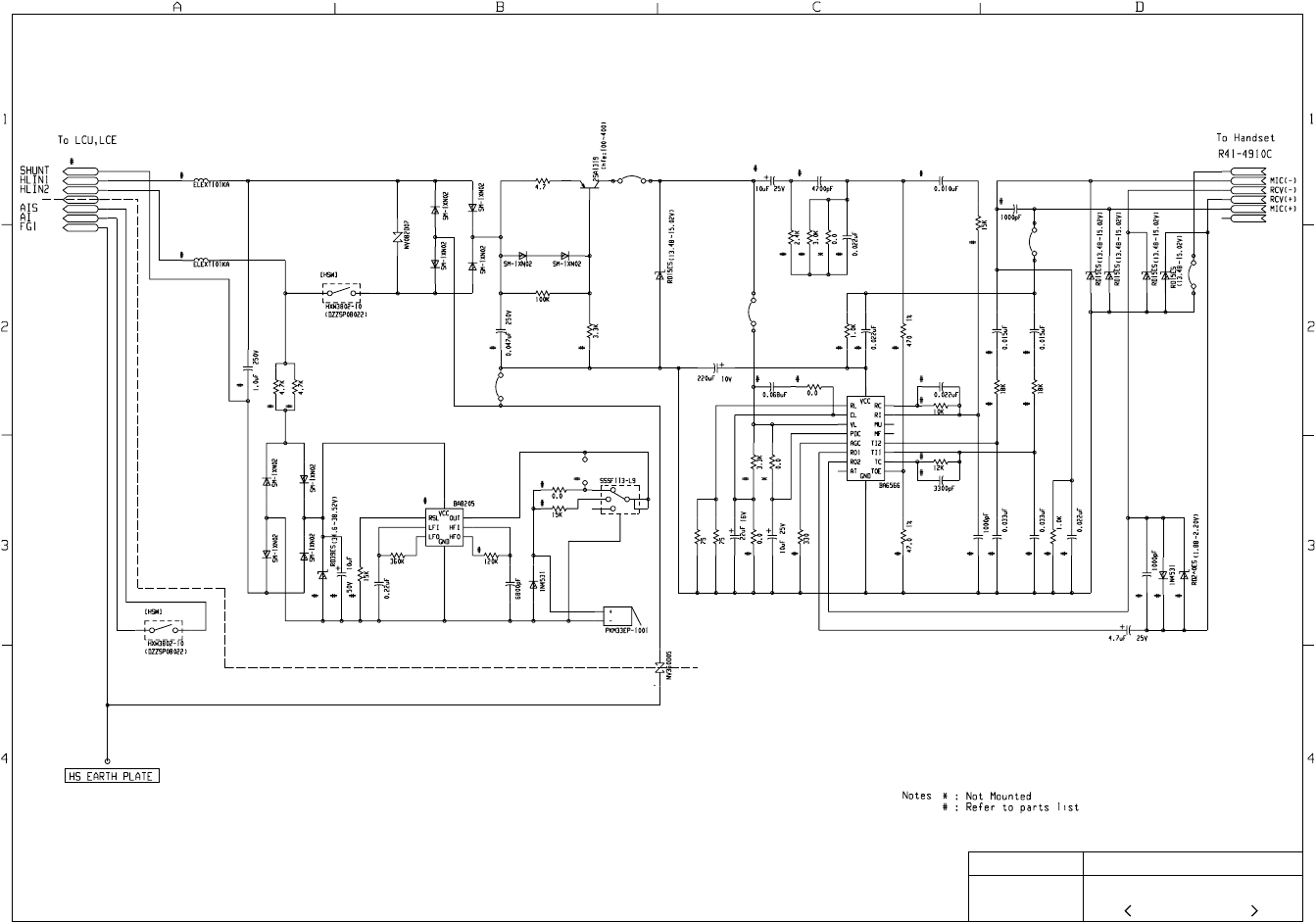
302
10.10 SRU PC Board
Model Drawing Name
UF-585/595 DZEC100422
SRU PC Board
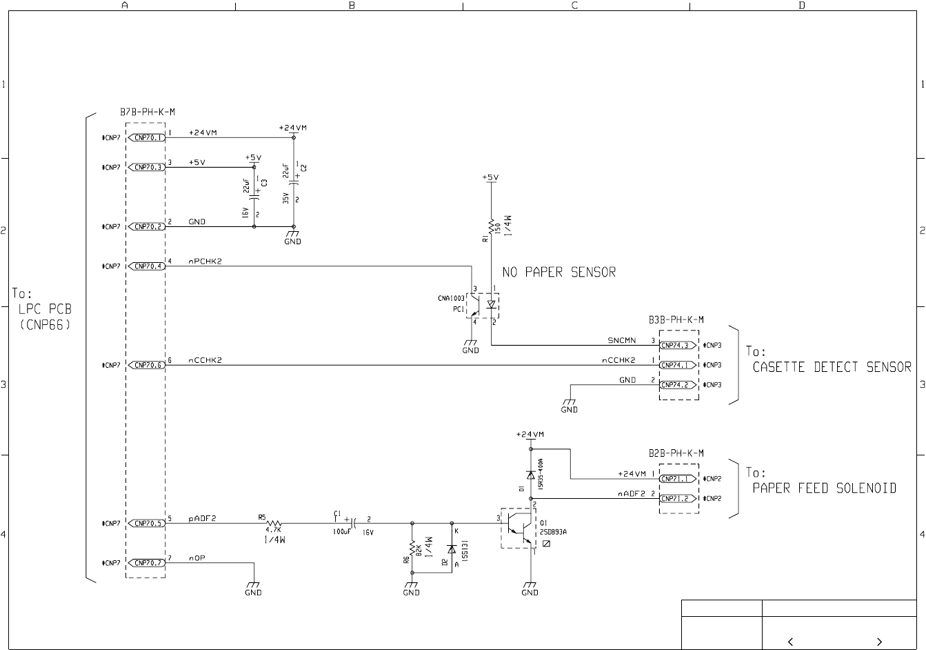
303
10.11 CST2 PC Board
DZEC101076
Model Drawing Name
CST2 PC Board (1/1)
UF-585/595
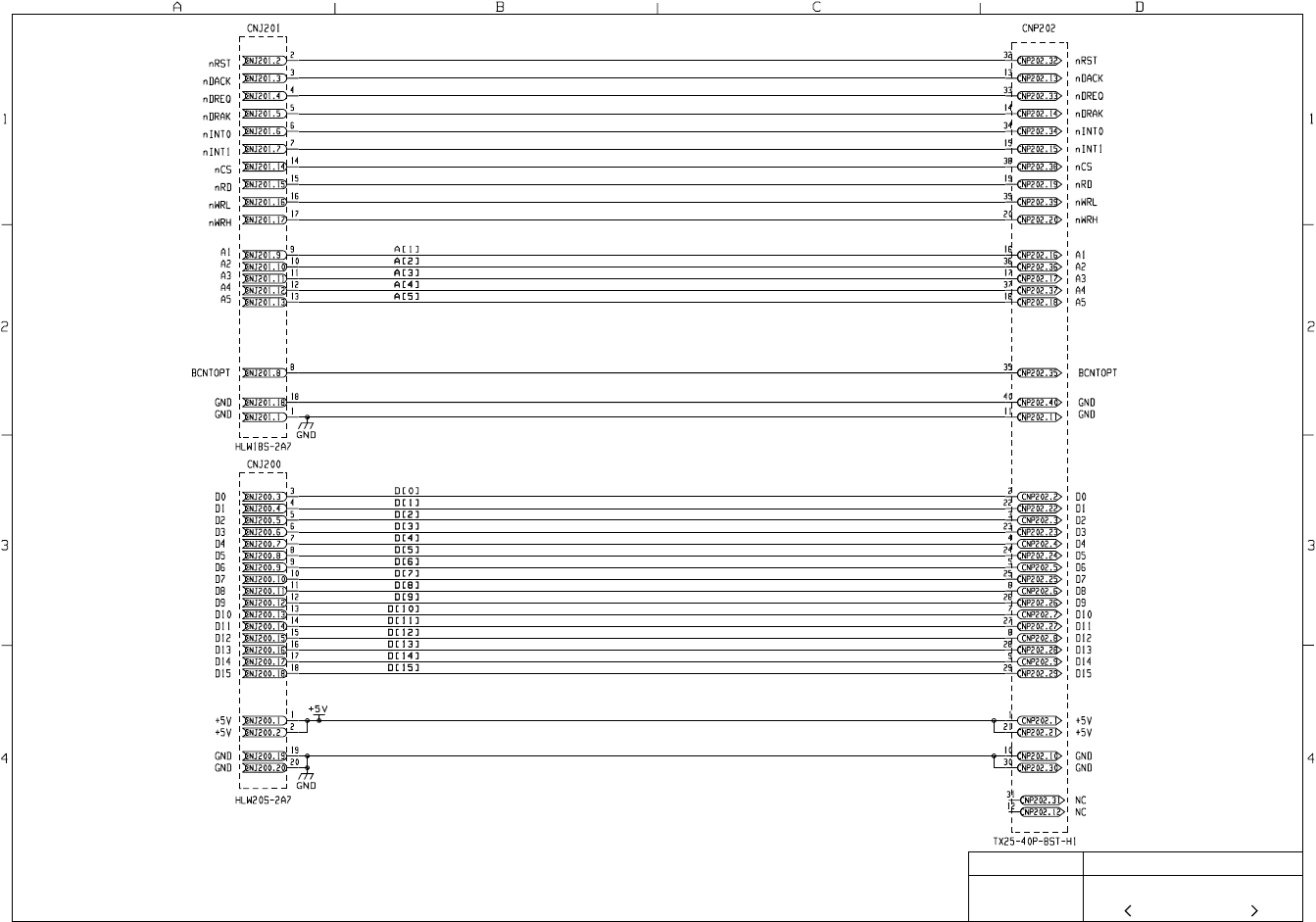
304
10.12 CRTA PC Board
Model Drawing Name
UF-585/595 DZEC101210
PRTA PC Board
305
10.13 PRT PC Board
Model Drawing Name
UF-585/595 DZEC101464
PRT 1 PC Board
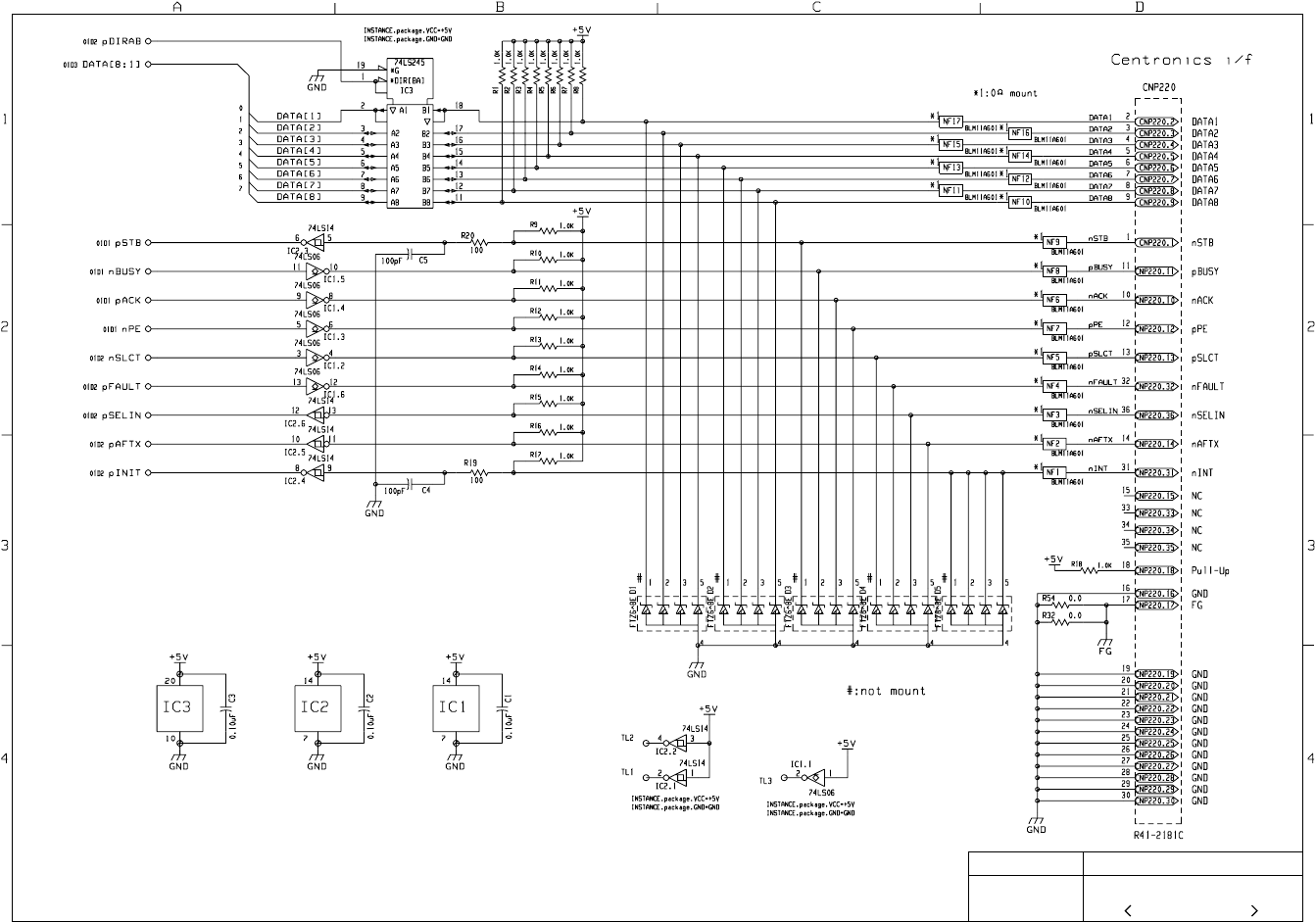
306
Model Drawing Name
UF-585/595 DZEC101464
PRT 2 PC Board
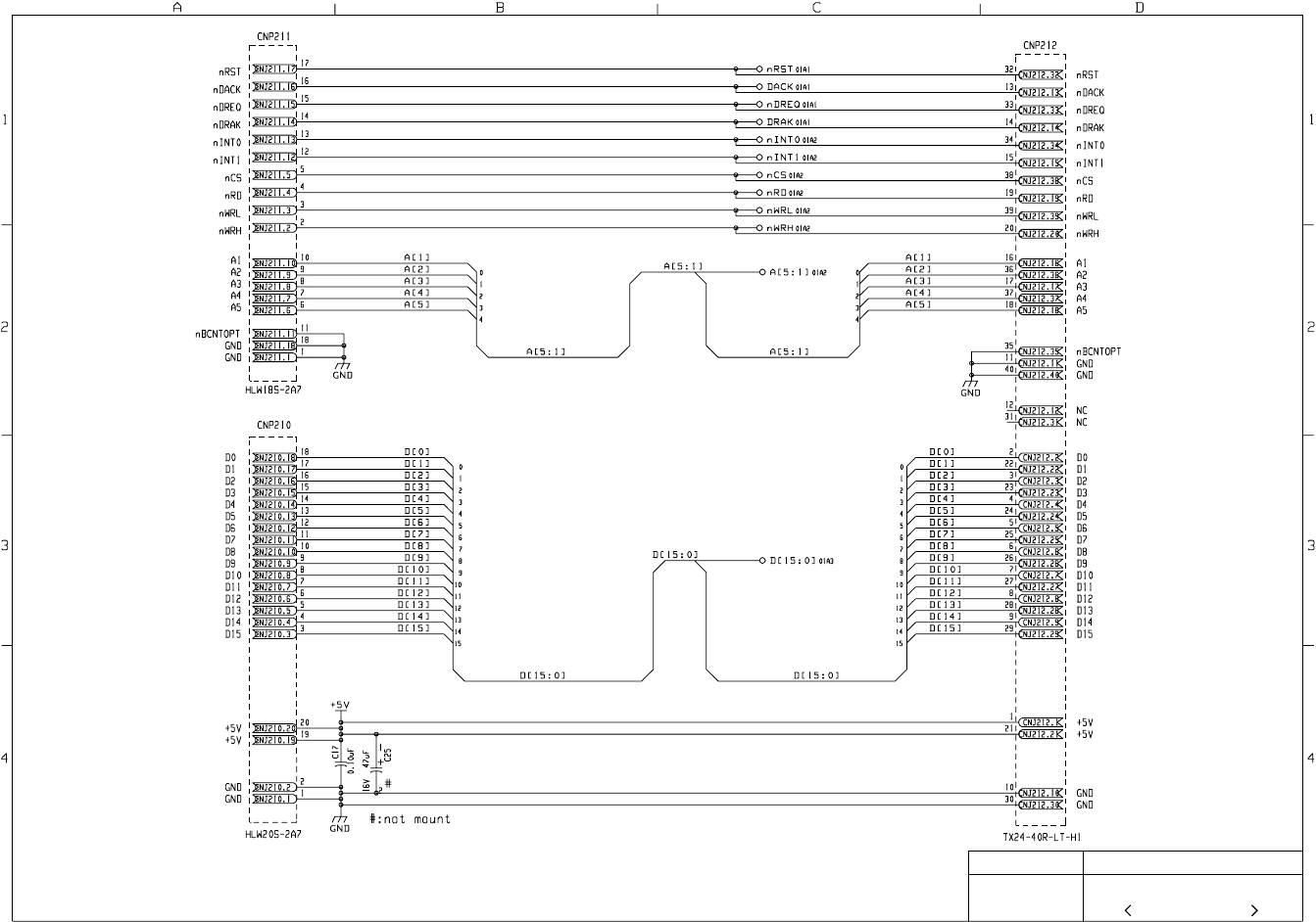
307
Model Drawing Name
UF-585/595 DZEC101464
PRT 3 PC Board
