Discovery Kit With STM8S001J3M3, STM8L001J3M3 And STM8L050J3M3 MCUs UM2339 STM8 SO8 DISCO User Manual
User Manual:
Open the PDF directly: View PDF ![]() .
.
Page Count: 26
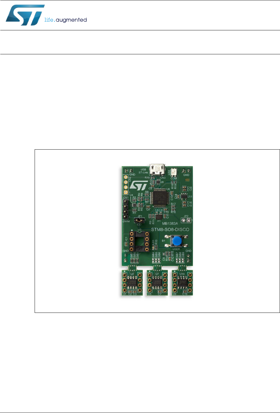
- Figure 1. STM8-SO8-DISCO (Top view)
- 1 Features
- 2 Product marking
- 3 System requirements
- 4 Development toolchains
- 5 Demonstration software
- 6 Ordering information
- 7 Hardware layout and configuration
- Figure 2. Top layout
- 7.1 Mechanical drawing
- 7.2 Embedded ST-LINK/V2
- 7.3 Power supply (CN3)
- 7.4 LEDs (LD1 and LD2)
- 7.5 Push-button (B1)
- 7.6 IDD measurement (JP1)
- Appendix A STM8S001J3M3 DIL8 module
- Appendix B STM8L001J3M3 DIL8 module
- Appendix C STM8L050J3M3 DIL8 module
- Appendix D Electrical schematics
- Appendix E Federal Communications Commission (FCC) and Industry Canada (IC) Compliance
- Revision history
March 2018 UM2339 Rev 1 1/26
1
UM2339
User manual
Discovery kit with STM8S001J3M3,
STM8L001J3M3 and STM8L050J3M3 MCUs
Introduction
The STM8-SO8-DISCO helps to discover features of STM8S Value Line and STM8L Value
Line devices available in SO8 packages. This discovery kit offers three SO8 to DIL8
modules designed with STM8S001J3M3, STM8L001J3M3 and STM8L050J3M3
microcontrollers, and allows the user to easily develop and share applications. It includes an
on-board ST-LINK/V2 to debug and program any of the embedded STM8 microcontrollers,
or even an external target by means of a SWIM connector. The STM8-SO8-DISCO is
operated by simply plugging it into a PC through a standard USB Type-A to Micro-B cable.
Figure 1. STM8-SO8-DISCO (Top view)
1. Picture is not contractual.
www.st.com

Contents UM2339
2/26 UM2339 Rev 1
Contents
1 Features . . . . . . . . . . . . . . . . . . . . . . . . . . . . . . . . . . . . . . . . . . . . . . . . . . . 6
2 Product marking . . . . . . . . . . . . . . . . . . . . . . . . . . . . . . . . . . . . . . . . . . . . 6
3 System requirements . . . . . . . . . . . . . . . . . . . . . . . . . . . . . . . . . . . . . . . . 6
4 Development toolchains . . . . . . . . . . . . . . . . . . . . . . . . . . . . . . . . . . . . . . 7
5 Demonstration software . . . . . . . . . . . . . . . . . . . . . . . . . . . . . . . . . . . . . . 7
6 Ordering information . . . . . . . . . . . . . . . . . . . . . . . . . . . . . . . . . . . . . . . . 7
7 Hardware layout and configuration . . . . . . . . . . . . . . . . . . . . . . . . . . . . . 8
7.1 Mechanical drawing . . . . . . . . . . . . . . . . . . . . . . . . . . . . . . . . . . . . . . . . . . 9
7.2 Embedded ST-LINK/V2 . . . . . . . . . . . . . . . . . . . . . . . . . . . . . . . . . . . . . . 10
7.2.1 Using the ST-LINK/V2 to program/debug one on-board STM8 device . 10
7.2.2 Using the ST-LINK/V2 to program/debug a STM8 device on a DIL8
module . . . . . . . . . . . . . . . . . . . . . . . . . . . . . . . . . . . . . . . . . . . . . . . . . . 10
7.2.3 Using the ST-LINK/V2 to program/debug an external STM8 device . . . 11
7.2.4 Driver . . . . . . . . . . . . . . . . . . . . . . . . . . . . . . . . . . . . . . . . . . . . . . . . . . . 11
7.2.5 ST-LINK/V2 firmware upgrade . . . . . . . . . . . . . . . . . . . . . . . . . . . . . . . . 11
7.3 Power supply (CN3) . . . . . . . . . . . . . . . . . . . . . . . . . . . . . . . . . . . . . . . . . 12
7.4 LEDs (LD1 and LD2) . . . . . . . . . . . . . . . . . . . . . . . . . . . . . . . . . . . . . . . . 12
7.5 Push-button (B1) . . . . . . . . . . . . . . . . . . . . . . . . . . . . . . . . . . . . . . . . . . . 12
7.6 IDD measurement (JP1) . . . . . . . . . . . . . . . . . . . . . . . . . . . . . . . . . . . . . . 13
Appendix A STM8S001J3M3 DIL8 module . . . . . . . . . . . . . . . . . . . . . . . . . . . . . . 14
Appendix B STM8L001J3M3 DIL8 module . . . . . . . . . . . . . . . . . . . . . . . . . . . . . . 15
Appendix C STM8L050J3M3 DIL8 module . . . . . . . . . . . . . . . . . . . . . . . . . . . . . . 16
Appendix D Electrical schematics . . . . . . . . . . . . . . . . . . . . . . . . . . . . . . . . . . . . 17

List of tables UM2339
4/26 UM2339 Rev 1
List of tables
Table 1. Ordering information . . . . . . . . . . . . . . . . . . . . . . . . . . . . . . . . . . . . . . . . . . . . . . . . . . . . . . . 7
Table 2. Selecting one on-board STM8 . . . . . . . . . . . . . . . . . . . . . . . . . . . . . . . . . . . . . . . . . . . . . . 10
Table 3. DIL8 socket (U3) pinout . . . . . . . . . . . . . . . . . . . . . . . . . . . . . . . . . . . . . . . . . . . . . . . . . . . 10
Table 4. External SWIM connector (CN1) pinout . . . . . . . . . . . . . . . . . . . . . . . . . . . . . . . . . . . . . . . 11
Table 5. User LED port assignment . . . . . . . . . . . . . . . . . . . . . . . . . . . . . . . . . . . . . . . . . . . . . . . . . 12
Table 6. User push-button port assignment . . . . . . . . . . . . . . . . . . . . . . . . . . . . . . . . . . . . . . . . . . . 12
Table 7. STM8S001J3M3 DIL8 module . . . . . . . . . . . . . . . . . . . . . . . . . . . . . . . . . . . . . . . . . . . . . . 14
Table 8. STM8L001J3M3 DIL8 module . . . . . . . . . . . . . . . . . . . . . . . . . . . . . . . . . . . . . . . . . . . . . . 15
Table 9. STM8L050J3M3 DIL8 module . . . . . . . . . . . . . . . . . . . . . . . . . . . . . . . . . . . . . . . . . . . . . . 16
Table 10. Document revision history . . . . . . . . . . . . . . . . . . . . . . . . . . . . . . . . . . . . . . . . . . . . . . . . . 25

UM2339 Rev 1 5/26
UM2339 List of figures
5
List of figures
Figure 1. STM8-SO8-DISCO (Top view) . . . . . . . . . . . . . . . . . . . . . . . . . . . . . . . . . . . . . . . . . . . . . . . 1
Figure 2. Top layout . . . . . . . . . . . . . . . . . . . . . . . . . . . . . . . . . . . . . . . . . . . . . . . . . . . . . . . . . . . . . . . 8
Figure 3. Mechanical drawing . . . . . . . . . . . . . . . . . . . . . . . . . . . . . . . . . . . . . . . . . . . . . . . . . . . . . . . 9
Figure 4. STM8-SO8-DISCO board interconnections . . . . . . . . . . . . . . . . . . . . . . . . . . . . . . . . . . . . 18
Figure 5. STM8S001J3M3 module . . . . . . . . . . . . . . . . . . . . . . . . . . . . . . . . . . . . . . . . . . . . . . . . . . 19
Figure 6. STM8L001J3M3 module. . . . . . . . . . . . . . . . . . . . . . . . . . . . . . . . . . . . . . . . . . . . . . . . . . . 20
Figure 7. STM8L050J3M3 module. . . . . . . . . . . . . . . . . . . . . . . . . . . . . . . . . . . . . . . . . . . . . . . . . . . 21
Figure 8. Button, LED and programming socket . . . . . . . . . . . . . . . . . . . . . . . . . . . . . . . . . . . . . . . . 22
Figure 9. ST-LINK/V2. . . . . . . . . . . . . . . . . . . . . . . . . . . . . . . . . . . . . . . . . . . . . . . . . . . . . . . . . . . . . 23

Features UM2339
6/26 UM2339 Rev 1
1 Features
•STM8S001J3M3 microcontroller featuring 8 Kbytes of Flash memory, 1 Kbyte of RAM
and 128 bytes of Data EEPROM in an SO8 package
•STM8L001J3M3 microcontroller featuring 8 Kbytes of Flash memory including up to
2 Kbytes of Data EEPROM and 1.5 Kbytes of RAM in an SO8 package
•STM8L050J3M3 microcontroller featuring 8 Kbytes of Flash memory, 1 Kbyte of RAM
and 256 bytes of Data EEPROM in an SO8 package
•1 user Led
•1 user push-button
•Individual and breakable STM8 SO8 to DIL8 module
•DIL8 socket to ease programming of the STM8 MCU
•On-board ST-LINK/V2 debugger/programmer
•Comprehensive free software libraries and examples
•Support of a wide choice of Integrated Development Environments (IDEs) including
Cosmic, IAR™, Raisonance, iSYSTEM and STMicroelectronics
2 Product marking
Evaluation tools marked as ‘ES’ or ‘E’ are not yet qualified and therefore they are not ready
to be used as reference design or in production. Any consequences deriving from such
usage will not be at ST charge. In no event, ST will be liable for any customer usage of
these engineering sample tools as reference design or in production.
‘E’ or ‘ES’ marking examples of location:
•On the targeted STM8 that is soldered on the board (for illustration of STM8 marking,
refer to the section ‘Package information’ of the STM8 datasheet at www.st.com).
•Next to the evaluation tool ordering part number, that is stuck or silkscreen printed on
the board
3 System requirements
•Windows® OS (7, 8 and 10)
•USB Type-A to Micro-B cable
UM2339 Rev 1 7/26
UM2339 Development toolchains
25
4 Development toolchains
•STMicroelectronics: free STVD-STM8 (using Cosmic toolchain)
•IAR™: IAR-EWSTM8
•Cosmic: free IDEA
•Raisonance: RIDE-STM8
•iSYSTEM: winIDEA-STM8
5 Demonstration software
The demonstration software, included in the corresponding STM8 standard peripheral
library package, is preloaded in the STM8S001J3M3 Flash memory for easy demonstration
of the device peripherals in standalone mode. The latest versions of the demonstration
source code and associated documentation can be downloaded from the
www.st.com/stm8-discovery web page.
6 Ordering information
To order the STM8-SO8-DISCO kit, refer to Table 1.
Table 1. Ordering information
Order code Target STM8
STM8-SO8-DISCO
STM8S001J3M3
STM8L001J3M3
STM8L050J3M3
Hardware layout and configuration UM2339
8/26 UM2339 Rev 1
7 Hardware layout and configuration
The STM8-SO8-DISCO has been designed around three STM8 microcontrollers available
in SO8 package: STM8S001J3M3, STM8L001J3M3 and STM8L050J3M3. To ease the
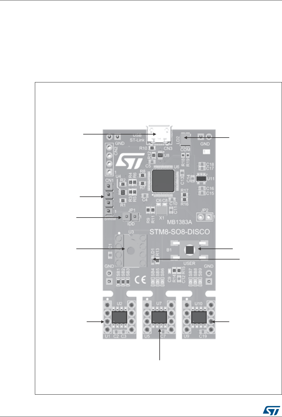
evaluation, each STM8 device is mounted on individual and breakable SO8 to DIL8 module.
Figure 2 helps users to locate the different features of the STM8-SO8-DISCO board.
Figure 2. Top layout
06Y9
67/,1.0LFUR%
86%FRQQHFWRU
6:,0H[WHUQDO
FRQQHFWRU
,''MXPSHU
',/VRFNHW
6706-0',/
PRGXOH
670/-0',/
PRGXOH
8VHU/('
8VHUSXVKEXWWRQ
670/-0',/
PRGXOH
67/,1.
FRPPXQLFDWLRQ/('
UM2339 Rev 1 9/26
UM2339 Hardware layout and configuration
25
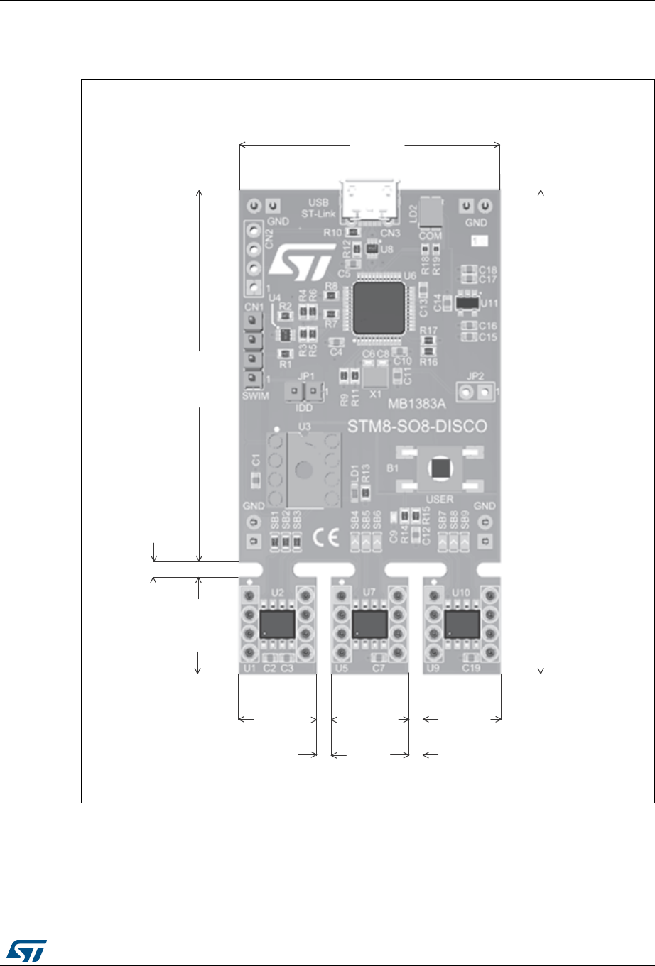
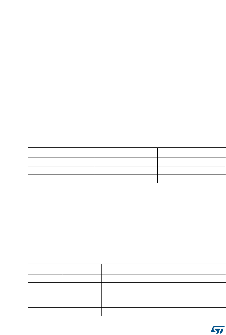
7.1 Mechanical drawing
Figure 3. Mechanical drawing
06Y9
PP
PP PP
PP
PP
PP
PP
PP
PP
PP
Hardware layout and configuration UM2339
10/26 UM2339 Rev 1
7.2 Embedded ST-LINK/V2
The ST-LINK/V2 programming and debugging tool is integrated on the STM8-SO8-DISCO
board.
The embedded ST-LINK/V2 can be used in 3 different ways:
•Program/debug one on-board STM8 device by selecting it using the corresponding
solder bridges
•Program/debug a STM8 device mounted on a DIL8 module plugged to the socket U3
•Program/debug an external STM8 device mounted on a user application board using a
cable connected to SWIM connector (CN1)
The embedded ST-LINK/V2 supports only SWIM for STM8 devices. For information about
debugging and programming features refer to ST-LINK/V2 in-circuit debugger/programmer
for STM8 and STM32 User manual (UM1075), which describes in details all the ST-LINK/V2
features.
7.2.1 Using the ST-LINK/V2 to program/debug one on-board STM8 device
To program/debug one of the on-board STM8 device, solder bridges must be configured as
detailed in below table. In addition, no DIL8 module must be present on the socket U3 and
no external target must be connected to CN1.
Note: Practically, only SB1, SB4 and SB7 are used to redirect the SWIM signal to the selected
STM8 device. But to prevent conflict on GPIOs used for the user push-button and LED, it is
preferable to also configure others solder bridges.
7.2.2 Using the ST-LINK/V2 to program/debug a STM8 device on a DIL8
module
To program/debug a STM8 device mounted on a DIL8 module plugged to the socket U3, it is
required to set all solder bridges OFF (SB1 to SB9) and no external target must be
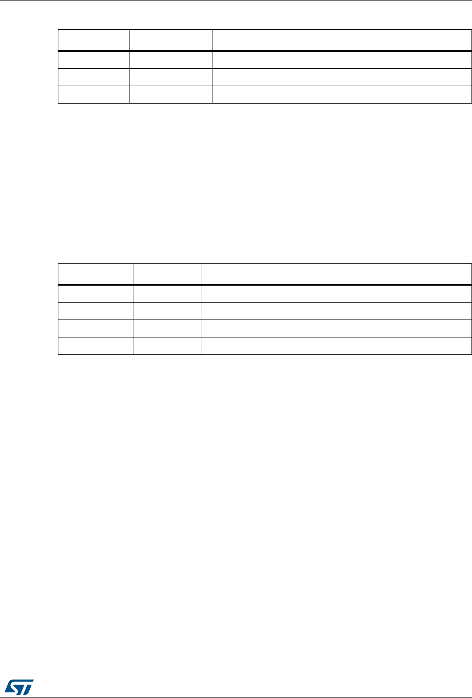
connected to CN1. The DIL8 socket pinout is detailedTable 3.
Table 2. Selecting one on-board STM8
Selected STM8 device Solder Bridge ON Solder Bridge OFF
STM8S001J3M3 (U2) SB1, SB2, SB3 SB4, SB5, SB6, SB7, SB8, SB9
STM8L001J3M3 (U7) SB4, SB5, SB6 SB1, SB2, SB3, SB7, SB8, SB9
STM8L050J3M3 (U10) SB7, SB8, SB9 SB1, SB2, SB3, SB4, SB5, SB6
Table 3. DIL8 socket (U3) pinout
Pin number Pin name Description
1 GPIO1/SWIM Serial wire interface module (SWIM)
2 GPIO2 Not connected
3 GND Ground
4 VDD Power supply (+3.3 V)
5 GPIO3/LED User LED
UM2339 Rev 1 11/26
UM2339 Hardware layout and configuration
25
Note: When plugging the DIL8 module to the socket, please pay attention to the pin 1.
7.2.3 Using the ST-LINK/V2 to program/debug an external STM8 device
To program/debug an external STM8 device mounted on a user application, it is required to
set all solder bridges OFF (SB1 to SB9) and to remove any DIL8 module from the socket
U3.
The user application must be connected to the STM8-SO8-DISCO using the SWIM
connector (CN1).
Note: This program/debug connector is only 3.3 V compliant.
7.2.4 Driver
Before connecting the STM8-SO8-DISCO board to a Windows PC via USB, a driver for the
ST-LINK/V2 must be installed. It can be downloaded from the www.st.com website.
In case the STM8-SO8-DISCO board is connected to the PC before installing the driver, the
PC device manager may report the interface as ‘Unknown’.
To recover from this situation, after installing the dedicated driver, the association of the
‘Unknown’ USB device found on the STM8-SO8-DISCO board to this dedicated driver, must
be updated in the device manager manually.
7.2.5 ST-LINK/V2 firmware upgrade
The ST-LINK/V2 embeds a firmware upgrade mechanism for in-situ upgrade through the
USB port. As the firmware may evolve during the life time of the ST-LINK/V2 product (for
example new functionality, bug fixes, support for new microcontroller families), it is
recommended to visit www.st.com website before starting to use the STM8-SO8-DISCO
board and periodically, in order to stay up-to-date with the latest firmware version.
6 GPIO4 Not connected
7 GPIO5/BP User push-button
8 GPIO6 Not connected
Table 3. DIL8 socket (U3) pinout (continued)
Pin number Pin name Description
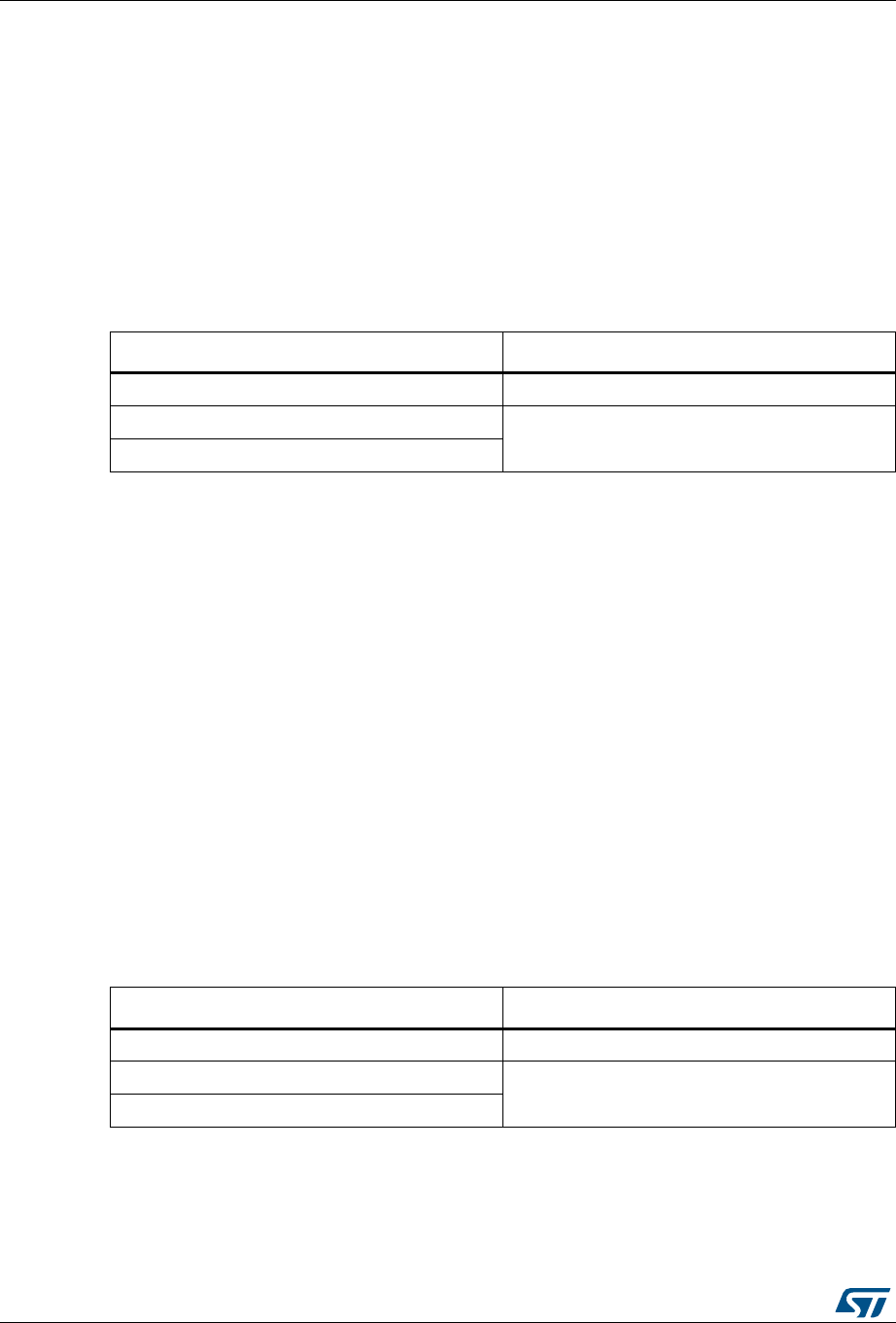
Table 4. External SWIM connector (CN1) pinout
Pin number Pin name Description
1 NC Not connected
2 SWIM Serial wire interface module
3 VSS Ground
4 NRST Reset of STM8 device
Hardware layout and configuration UM2339
12/26 UM2339 Rev 1
7.3 Power supply (CN3)
The STM8-SO8-DISCO is designed to be powered using the ST-LINK/V2 USB connector
CN3.
7.4 LEDs (LD1 and LD2)
The STM8-SO8-DISCO features a user LED (LD1) connected to the pin 5 of the DIL8
module. To light on this LED, a high logic state must be output on the corresponding STM8
GPIO.
The tricolor LED (green, orange, red) LD2 (COM) provides information about ST-LINK
communication status:
•Slow blinking Red/Off: at power-on before USB initialization
•Fast blinking Red/Off: after the first correct communication between the PC and
ST-LINK/V2 (enumeration)
•Red LED On: when the initialization between the PC and ST-LINK/V2-1 is complete
•Green LED On: after a successful target communication initialization
•Blinking Red/Green: during communication with target
•Green On: communication finished and successful
•Orange On: Communication failure
7.5 Push-button (B1)
The STM8-SO8-DISCO offers a user push-button (B1) connected to pin 7 of the DIL8
module. To retrieve the push-button state, the firmware must read the corresponding STM8
GPIO.
The use of the push-button depends on the STM8 device firmware.
Table 5. User LED port assignment
Selected STM8 device GPIO assigned to user LED
STM8S001J3M3 (U2) PA3/PB5
STM8L001J3M3 (U7)
PB3/PB5/PD0
STM8L050J3M3 (U10)
Table 6. User push-button port assignment
Selected STM8 device GPIO assigned to user push-button
STM8S001J3M3 (U2) PC3/PC4/PC5
STM8L001J3M3 (U7)
PB7/PC0
STM8L050J3M3 (U10)

UM2339 Rev 1 13/26
UM2339 Hardware layout and configuration
25
7.6 IDD measurement (JP1)
Jumper IDD (JP1) allows to measure the consumption of a STM8 device by removing the
jumper and by connecting an ammeter:
•Jumper ON: STM8 device(s) is (are) powered (default).
•Jumper OFF: an ammeter must be connected to measure the STM8 device(s) current.
If there is no ammeter, STM8 device(s) is (are) not powered.
Note: By default all STM8 devices are powered. To isolate the power consumption of only one
STM8 device, it is required to either cutout the non-required DIL8 modules or to cut all of
them and insert the required DIL8 module in the socket U3.
STM8S001J3M3 DIL8 module UM2339
14/26 UM2339 Rev 1
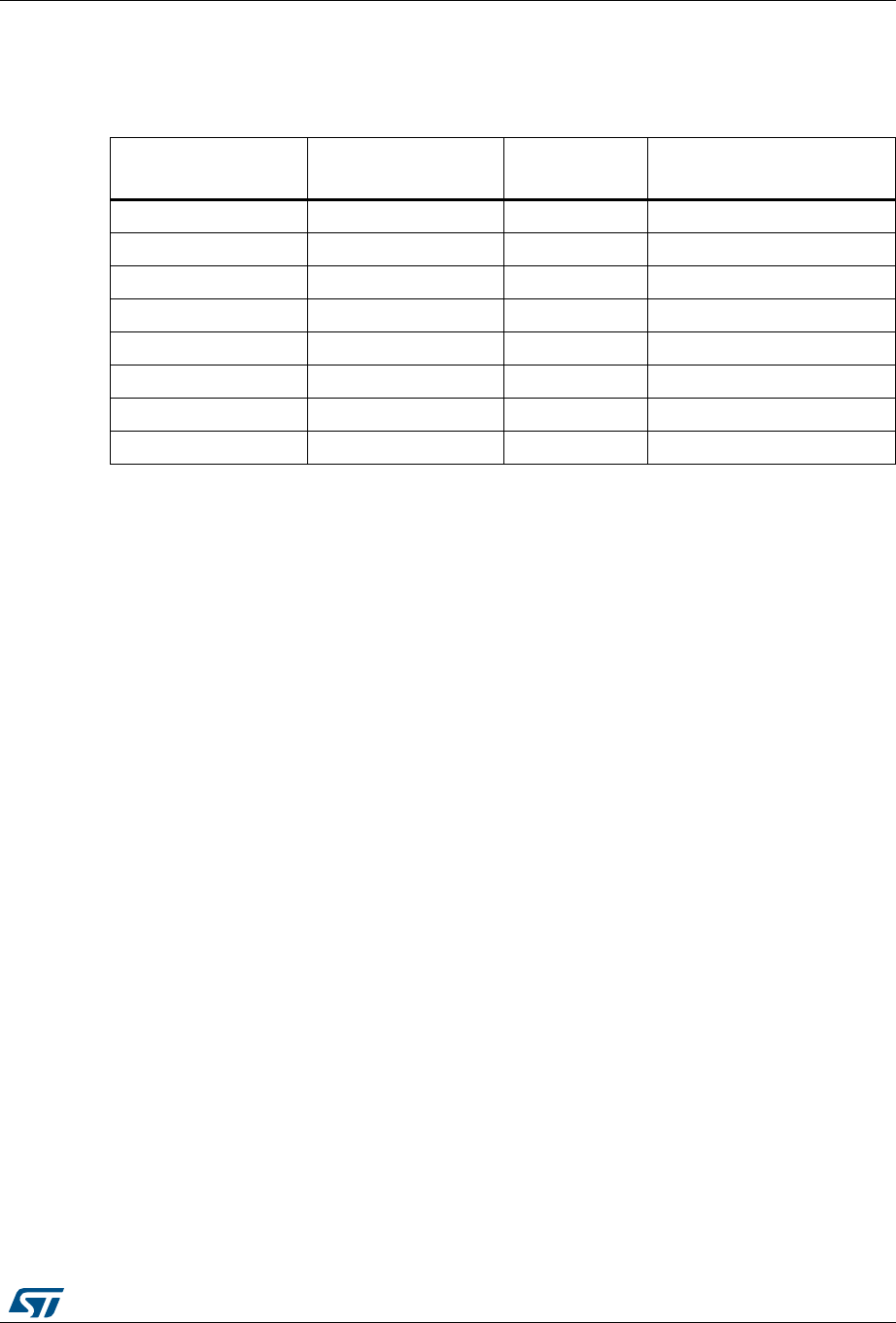
Appendix A STM8S001J3M3 DIL8 module
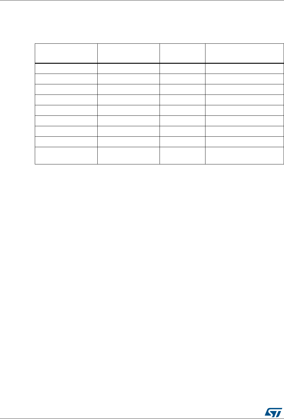
Table 7. STM8S001J3M3 DIL8 module
DIL8 module pin
number DIL8 module pin name STM8 SO8 pin
number Description
1 GPIO1/SWIM 8 PC6/PD1/PD3/PD5
2GPIO2 1PA1/PD6
3GND 2Ground
4VDD 4 Power supply
5GPIO3 5 PA3/PB5
6GPIO4 6 PB4
7GPIO5 7 PC3/PC4/PC5
8GPIO6 NC Not connected
N/A N/A 31.8 V voltage regulator
decoupling capacitor
UM2339 Rev 1 15/26
UM2339 STM8L001J3M3 DIL8 module
25
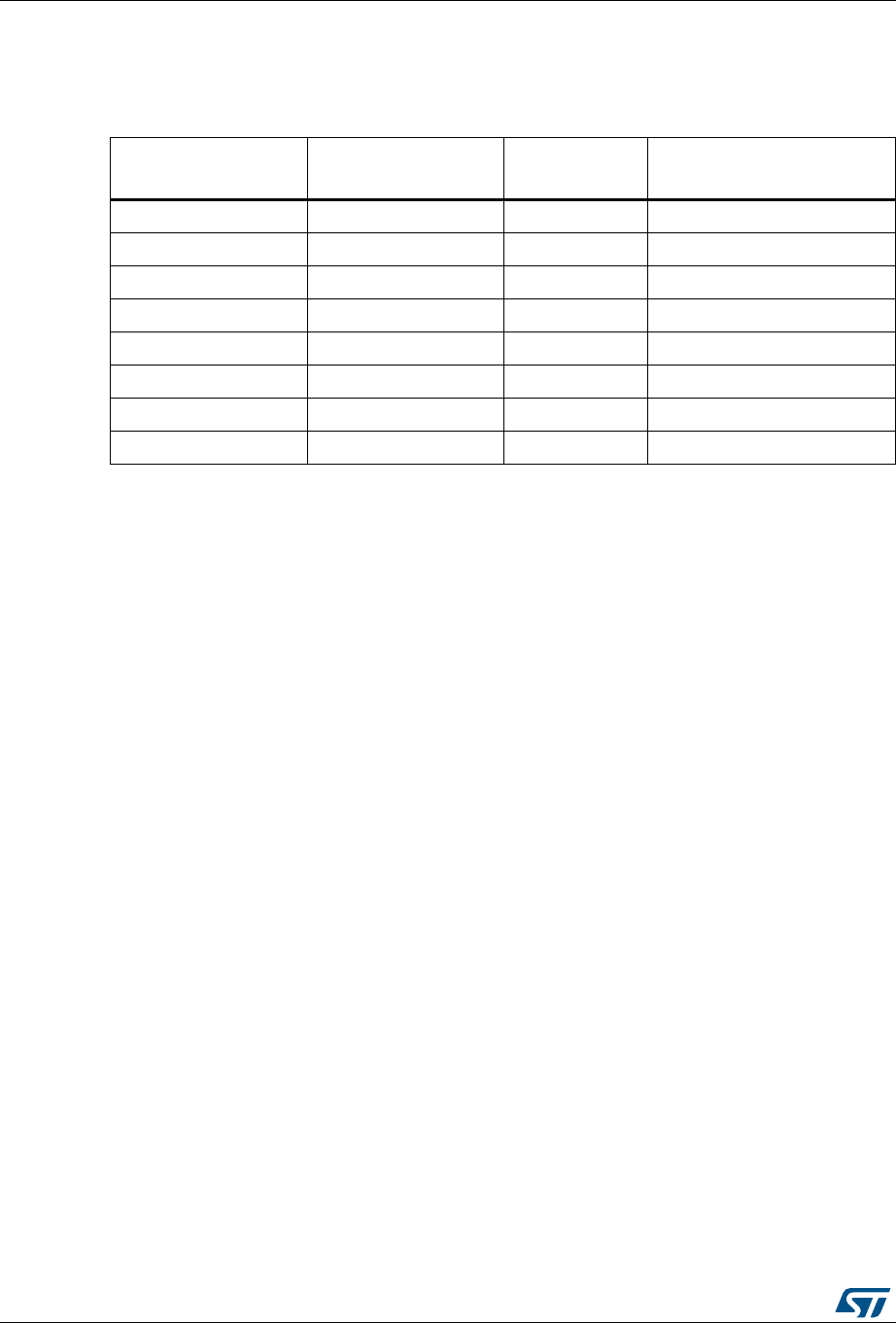
Appendix B STM8L001J3M3 DIL8 module
Table 8. STM8L001J3M3 DIL8 module
DIL8 module pin
number DIL8 module pin name STM8 SO8 pin
number Description
1 GPIO1/SWIM 1 PA0/PC3/PC4
2GPIO2 2 PA2/PA4/PA6
3GND 3Ground
4VDD 4 Power supply
5GPIO3 5 PB3/PB5/PD0
6GPIO4 6 PB6
7GPIO5 7 PB7/PC0
8GPIO6 8 PC1/PC2
STM8L050J3M3 DIL8 module UM2339
16/26 UM2339 Rev 1
Appendix C STM8L050J3M3 DIL8 module
Table 9. STM8L050J3M3 DIL8 module
DIL8 module pin
number DIL8 module pin name STM8 SO8 pin
number Description
1 GPIO1/SWIM 1 PA0/PA2/PC6
2GPIO2 2PA3
3GND 3Ground
4VDD 4 Power supply
5GPIO3 5 PB3/PB5/PD0
6GPIO4 6 PB6
7GPIO5 7 PB7/PC0
8GPIO6 8 PC1/PC4/PC5

UM2339 Rev 1 17/26
UM2339 Electrical schematics
25
Appendix D Electrical schematics
This section provides design schematics of the STM8-SO8-DISCO discovery board:
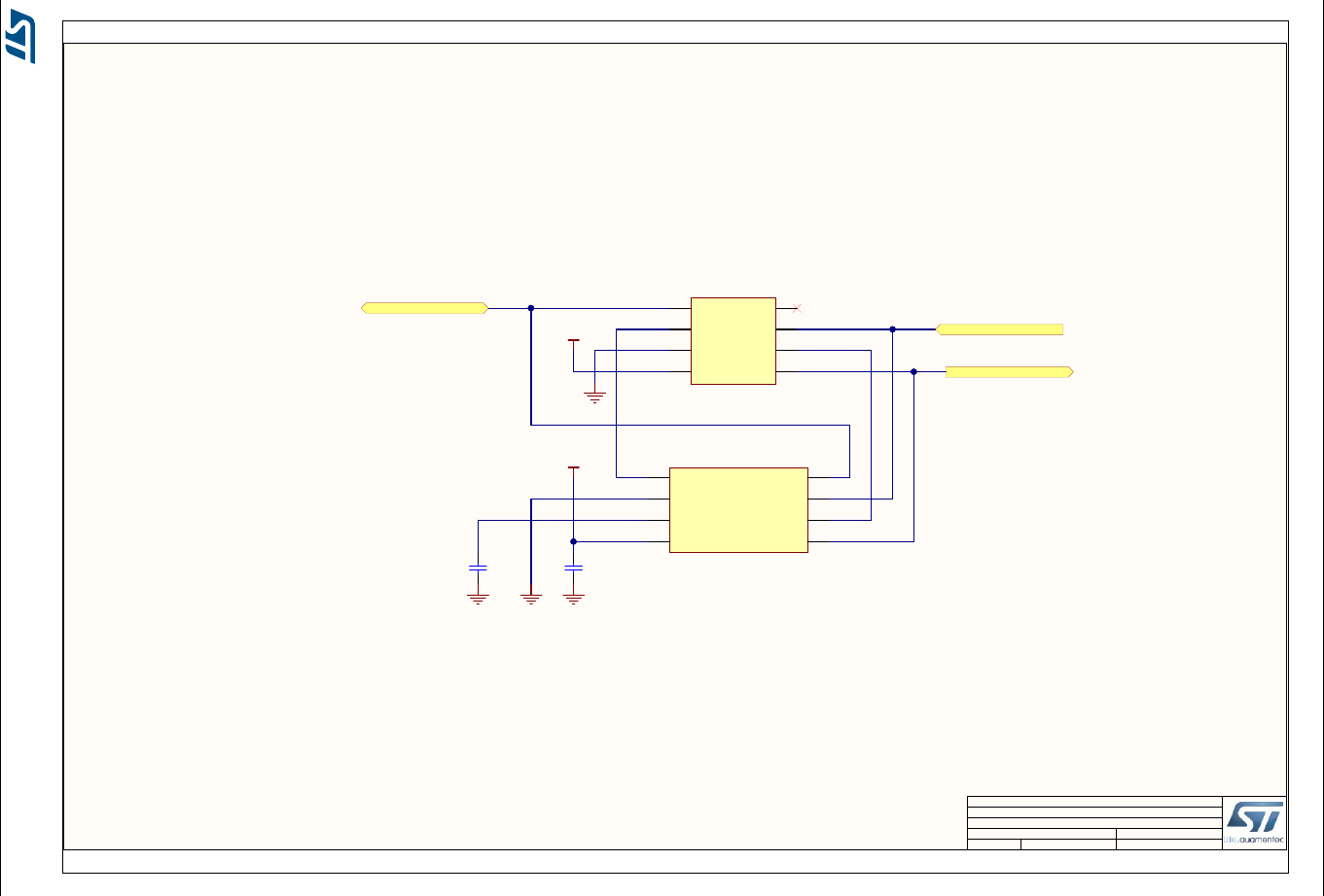
•Figure 4: STM8-SO8-DISCO board interconnections
•Figure 5: STM8S001J3M3 module
•Figure 6: STM8L001J3M3 module
•Figure 7: STM8L050J3M3 module
•Figure 8: Button, LED and programming socket
•Figure 9: ST-LINK/V2
Electrical schematics UM2339
18/26 UM2339 Rev 1
Figure 4. STM8-SO8-DISCO board interconnections
11
Top
Title:
Size:
Reference:
Sheet: ofA4
Revision:
Project: STM8 SO8 Discovery
MB1383A02
11-DEC-17
Default
Date:
-
Variant:
T_SWIM
U_ST-LinkV2_SWIM
ST-LinkV2_SWIM.SchDoc
U_Mechanical
Mechanical.SchDoc
STM8S001J3_USER_B
STM8S001J3_USER_LED
STM8S001J3_T_SWIM
STM8L001J3_USER_B
STM8L001J3_USER_LED
STM8L001J3_T_SWIM
STM8L050J3_USER_B
STM8L050J3_USER_LED
STM8L050J3_T_SWIM
T_SWIM
U_Button-Led-ProgSocket
Button-Led-ProgSocket.SchDoc
STM8L001J3_USER_B
STM8L001J3_USER_LED
STM8L001J3_T_SWIM
U_STM8L001J3_Module
STM8L001J3_Module.SchDoc
STM8S001J3_USER_B
STM8S001J3_USER_LED
STM8S001J3_T_SWIM
U_STM8S001J3_Module
STM8S001J3_Module.SchDoc
STM8L050J3_USER_B
STM8L050J3_USER_LED
STM8L050J3_T_SWIM
U_STM8L050J3_Module
STM8L050J3_Module.SchDoc
UM2339 Electrical schematics
UM2339 Rev 1 19/26
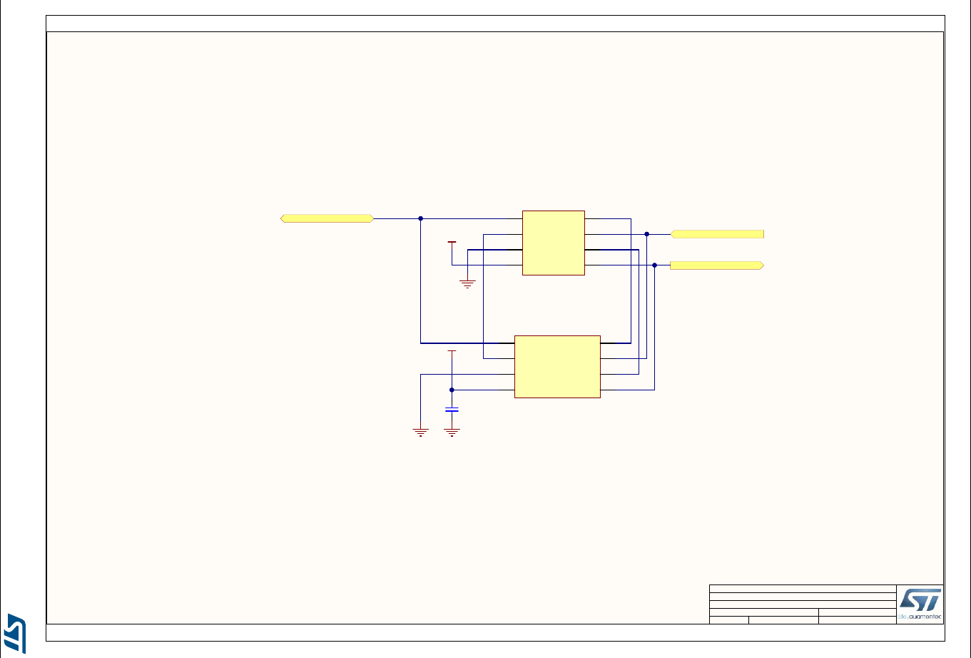
Figure 5. STM8S001J3M3 module
38
STM8S001J3 module
Title:
Size:
Reference:
Sheet: ofA4
Revision:
Project: STM8 SO8 Discovery
MB1383A02
11-DEC-17
Default
Date:
-
Variant:
VDD STM8S001J3_USER_B
STM8S001J3_USER_LED
STM8S001J3_T_SWIM
VDD
1uF
C2
100nF
C3
STM8S001J3M3
PA1/PD6
1
VSS/VSSA
2
VCAP
3
VDD/VDDA
4PA3/PB5 5
PB4 6
PC3/PC4/PC5 7
PC6/PD1/PD3/PD5 8
U2
DIL8-LYCONN--7.40X1.83
1
1
2
2
3
3
4
455
66
77
88
U1
Electrical schematics UM2339
20/26 UM2339 Rev 1
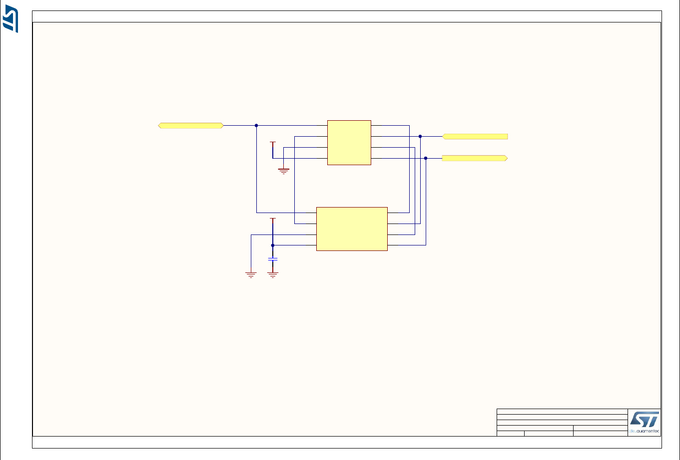
Figure 6. STM8L001J3M3 module
48
STM8L001J3 module
Title:
Size:
Reference:
Sheet: ofA4
Revision:
Project: STM8 SO8 Discovery
MB1383A02
11-DEC-17
Default
Date:
-
Variant:
VDD
VDD
100nF
C7
STM8L001J3_USER_B
STM8L001J3_USER_LED
STM8L001J3_T_SWIM
STM8L001J3M3
PA0/PC3/PC4
1
PA2/PA4/PA6
2
VSS
3
VDD
4PB3/PB5/PD0 5
PB6 6
PB7/PC0 7
PC1/PC2 8
U7
DIL8-LYCONN--7.40X1.83
1
1
2
2
3
3
4
455
66
77
88
U5
UM2339 Electrical schematics
UM2339 Rev 1 21/26
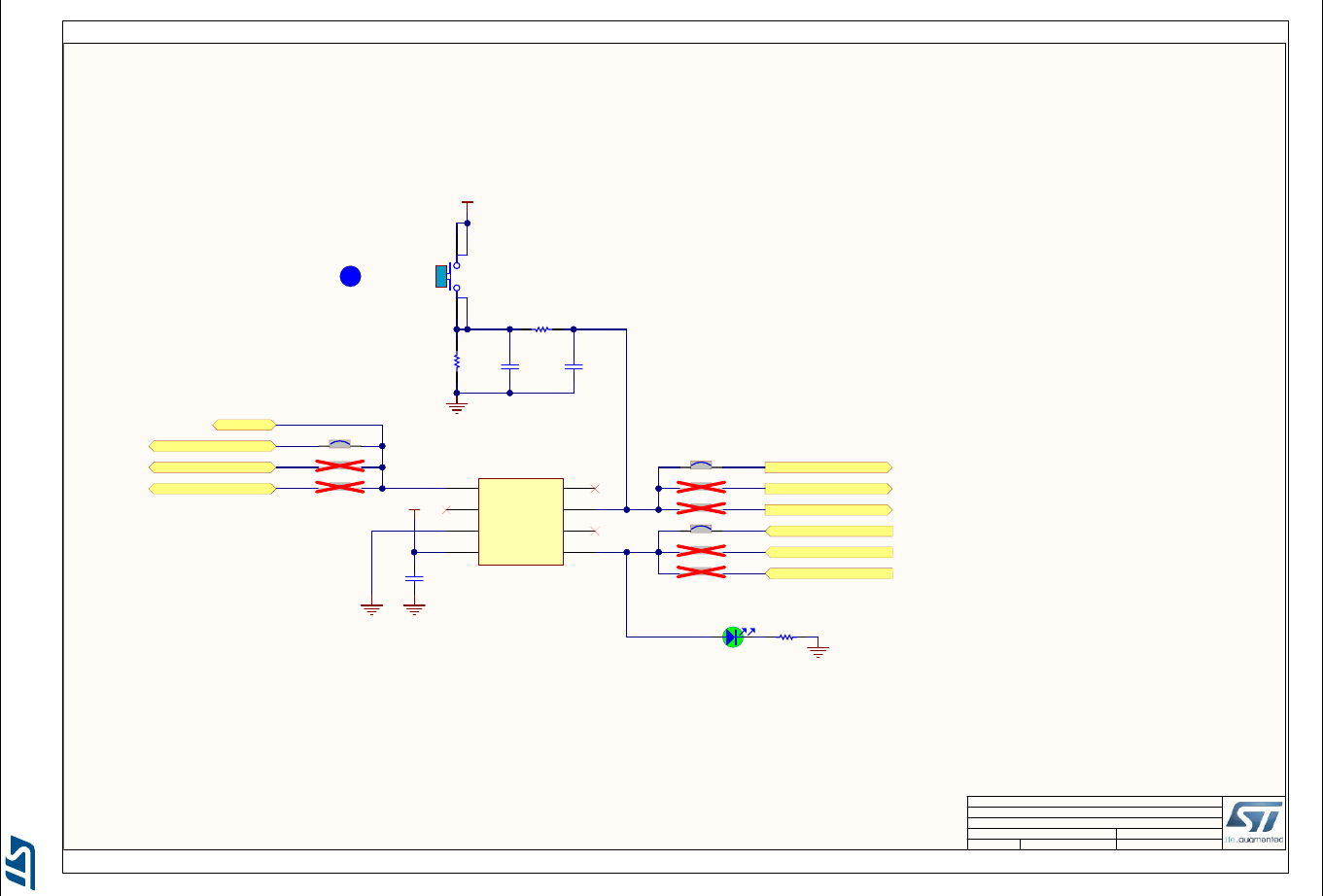
Figure 7. STM8L050J3M3 module
58
STM8L050J3 module
Title:
Size:
Reference:
Sheet: ofA4
Revision:
Project: STM8 SO8 Discovery
MB1383A02
11-DEC-17
Default
Date:
-
Variant:
VDD
VDD
100nF
C19
STM8L050J3_USER_B
STM8L050J3_USER_LED
STM8L050J3_T_SWIM
STM8L050J3M3
PA0/PA2/PC6
1
PA3
2
VSS/VSSA
3
VDD/VDDA
4PB3/PB5/PD0 5
PB6 6
PB7/PC0 7
PC1/PC4/PC5 8
U10
DIL8-LYCONN--7.40X1.83
1
1
2
2
3
3
4
455
66
77
88
U9
Electrical schematics UM2339
22/26 UM2339 Rev 1
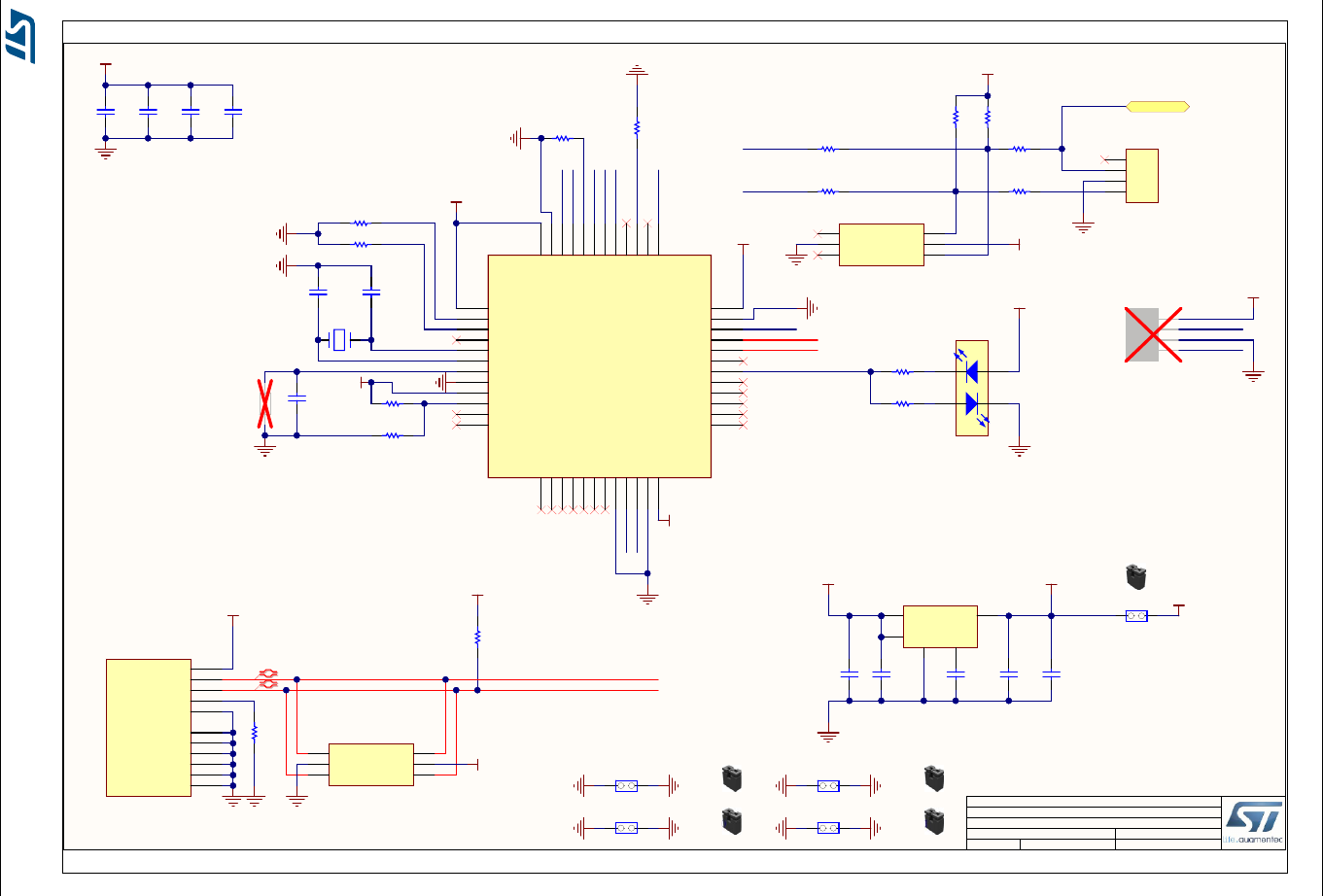
Figure 8. Button, LED and programming socket
68
Button, LED and programming socket
Title:
Size:
Reference:
Sheet: ofA4
Revision:
Project: STM8 SO8 Discovery
MB1383A02
11-DEC-17
Default
Date:
-
Variant:
510R
R13
GREEN
LD1
3V3_STLINK
1K
R15
100K
R14
10pF
C9
SW_BLUE
13
4 2
B1
1
1
2
2
3
3
4
455
66
77
88
U3
STM8-MODULE-DIL8-SOCKET
VDD
GND
100nF
C12
1uF
C1
STM8S001J3_USER_B
STM8S001J3_USER_LED
STM8S001J3_T_SWIM
USER
STM8L001J3_USER_B
STM8L001J3_USER_LED
STM8L001J3_T_SWIM
STM8L050J3_USER_B
STM8L050J3_USER_LED
STM8L050J3_T_SWIM
T_SWIM
BLUE HAT
HW1
SB7
SB1
SB4
SB8
SB2
SB5
SB9
SB3
SB6
UM2339 Electrical schematics
UM2339 Rev 1 23/26
Figure 9. ST-LINK/V2
78
ST-Link/V2 SWIM mode
Title:
Size:
Reference:
Sheet: ofA4
Revision:
Project: STM8 SO8 Discovery
MB1383A02
11-DEC-17
Default
Date:
-
Variant:
STLINK_USB_D_N
STLINK_USB_D_P
STLK_RST
STLK_OSC_IN
STLK_OSC_OUT
AIN_1
Board Ident: PC13=0
LED_STLINK
3V3_STLINK
3V3_STLINK
3V3_STLINK
3V3_STLINK
PWR_EXT
3V3_STLINK
4K7
R8
100K
R7
10KR9
10K
R11
NX3225GD-8.00M
X1
10pF
C8
10pF
C6
100nF
C11
4K7
R17
4K7
R16
STM32F103CBT6
VBAT
1
PA7
17
PC13
2
PA12 33
PC14
3
PB0
18
PC15
4JTMS/SWDIO 34
OSCIN
5
PB1
19
OSCOUT
6
VSS_2 35
NRST
7
PB2/BOOT1
20
VSSA
8
VDD_2 36
VDDA
9
PB10
21
PA0
10
JTCK/SWCLK 37
PA1
11
PB11
22
PA2
12
PA15/JTDI 38
PA3
13
VSS_1
23
PA4
14
PB3/JTDO 39
PA5
15
VDD_1
24
PA6
16
PB4/JNTRST 40
PB12 25
PB5 41
PB13 26
PB6 42
PB14 27
PB7 43
PB15 28
BOOT0 44
PA8 29
PB8 45
PA9 30
PB9 46
PA10 31
VSS_3 47
PA11 32
VDD_3 48
U6
JP2
SWIM_IN
SWIM
SWIM_IN
SWIM
SWIM_IN
SWIM_RST
SWIM_RST_IN
STLINK_SWDIO
STLINK_SWCLK
5V_STLINK
STLINK_USB_D_N
STLINK_USB_D_P
3V3_STLINK
USB_uB_105017-0001
VBUS 1
DM 2
DP 3
ID 4
GND 5
Shield 6
USB_Micro-B receptacle
Shield 7
Shield 8
Shield 9
EXP 10
EXP 11
CN3
1K5
R12
100K
R10
USBLC6-2P6
IO2
3GND
2IO1
1IO_1 6
VBUS 5
IO_2 4
U8
5V_STLINK
5V_STLINK 3V3_STLINK
1uF
C18
100nF
C17
10nF
C14
LD3985M33R
51
2
GND
3
4
BYPASS
INH
Vin Vout
U11
3V3_STLINK
LD_BICOLOR_CMS
2 1
43
Red
Green
LD2
1
2
3
4
CN2
STLINK_SWDIO
STLINK_SWCLK
3V3_STLINK
T_SWIM
SWIM
SWIM_RST
SWIM_IN
SWIM_RST_IN
220R
R4
220R
R5
47R
R2
47R
R1
680R
R3
3V3_STLINK
SWIM
COM
USB STLink
1
2
3
4
CN1
VDD
HW7
JP1
IDD
680R
R6
USBLC6-2P6
IO2
3GND
2IO1
1IO_1 6
VBUS 5
IO_2 4
U4
3V3_STLINK
100nF
C16
100nF
C4
100nF
C13
100nF
C5
100nF
C10
1uF
C15
SWIM
NC
VSS
NRST
SWDIO
VSS
SWCLK
3V3
RESERVED
HW9
HW11HW10
HW8
CN6
CN5
CN7
CN4
330R
R18
330R
R19

Federal Communications Commission (FCC) and Industry Canada (IC) Compliance UM2339
24/26 UM2339 Rev 1
Appendix E Federal Communications Commission (FCC)
and Industry Canada (IC) Compliance
This kit is designed to allow:
1. Product developers to evaluate electronic components, circuitry, or software associated
with the kit to determine whether to incorporate such items in a finished product and
2. Software developers to write software applications for use with the end product. This kit
is not a finished product and when assembled may not be resold or otherwise
marketed unless all required FCC equipment authorizations are first obtained.
Operation is subject to the condition that this product not cause harmful interference to
licensed radio stations and that this product accept harmful interference. Unless the
assembled kit is designed to operate under part 15, part 18 or part 95 of 47 CFR,
Chapter I (‘FCC Rules’), the operator of the kit must operate under the authority of an
FCC license holder or must secure an experimental authorization under part 5 of this
chapter.
UM2339 Rev 1 25/26
UM2339 Revision history
25
Revision history
Table 10. Document revision history
Date Revision Changes
19-Mar-2018 1 Initial version

UM2339
26/26 UM2339 Rev 1
IMPORTANT NOTICE – PLEASE READ CAREFULLY
STMicroelectronics NV and its subsidiaries (“ST”) reserve the right to make changes, corrections, enhancements, modifications, and
improvements to ST products and/or to this document at any time without notice. Purchasers should obtain the latest relevant information on
ST products before placing orders. ST products are sold pursuant to ST’s terms and conditions of sale in place at the time of order
acknowledgement.
Purchasers are solely responsible for the choice, selection, and use of ST products and ST assumes no liability for application assistance or
the design of Purchasers’ products.
No license, express or implied, to any intellectual property right is granted by ST herein.
Resale of ST products with provisions different from the information set forth herein shall void any warranty granted by ST for such product.
ST and the ST logo are trademarks of ST. All other product or service names are the property of their respective owners.
Information in this document supersedes and replaces information previously supplied in any prior versions of this document.
© 2018 STMicroelectronics – All rights reserved
