VA1616
VSXXXXX 13021210552936
User Manual: VA1616
Open the PDF directly: View PDF ![]() .
.
Page Count: 72
ViewSonic 381 Brea Canyon Road, Walnut, California 91789 USA - (800) 888-8583
(VA1616w-8 SM Rev. 1a Feb. 2009)
Service Manual
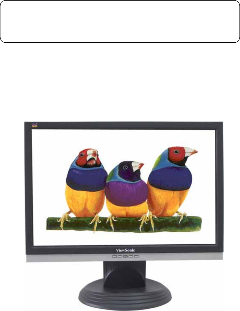
ViewSonic VA1616w-8
Model No VSXXXXX
16” Color TFT LCD Display

- 2 –
Copyright
Copyright © 2008 by ViewSonic Corporation. All rights reserved. No part of this
publication may be reproduced, transmitted, transcribed, stored in a retrieval system, or
translated into any language or computer language, in any form or by any means,
electronic, mechanical, magnetic, optical, chemical, manual or otherwise, without the prior
written permission of ViewSonic Corporation.
Disclaimer
ViewSonic makes no representations or warranties, either expressed or implied, with
respect to the contents hereof and specifically disclaims any warranty of merchantability or
fitness for any particular purpose. Further, ViewSonic reserves the right to revise this
publication and to make changes from time to time in the contents hereof without obligation
of ViewSonic to notify any person of such revision or changes.
Trademarks
Optiquest is a registered trademark of ViewSonic Corporation. ViewSonic is a registered
trademark of ViewSonic Corporation. All other trademarks used within this document are
the property of their respective owners.
Product disposal at end of product life
The lamp in this product contains mercury. Please dispose of in accordance with local,
state or federal laws.
Revision History
Revision SM Editing
Date
ECR
Number Description of changes TPV Model Approval
1a Feb-3-09 Initial Release T69MM5DY9WVSNN

- 3 –
TABLE OF CONTENTS
1. Precautions And Safety Notices 4
2. Specification 7
3. Front Panel Control And Indicators 9
4. Circuit Description 15
5. Adjustment Procedure 24
6. Troubleshooting Flow Chart 43
7. Block Diagram 44
8. Schematic Diagram 45
9. PCB Layout Diagram 53
10. Exploded Diagram And Spare Parts List 57
11. Recommended Spare Parts List 61
- 4 –
1. Precautions And Safety Notices
1.1 SAFETY PRECAUTIONS
This monitor is manufactured and tested on a ground principle that a user’s safety comes
first. However, improper use or installation may cause damage to the monitor as well as
the user. Carefully go over the following WARNINGS before installing and keep this guide
handy.
WARNINGS
.This monitor should be operated only at the correct power sources indicated on the label
on the rear end of the monitor. If you’re unsure of the power supply in your residence,
consult you local dealer or power company.
.Use only the special power adapter that comes with this monitor for power input.
.Do not try to repair the monitor your self as it contains no user-serviceable parts. This
monitor should only be repaired by a qualified technician.
.Do not remove the monitor cabinet. There is high-voltage parts inside that may cause
electric shock to human bodies, even when the power cord is unplugged.
.Stop using the monitor if the cabinet is damaged. Have it checked by a service technician.
.Put your monitor only in a clean, dry environment. If it gets wet, unplug the power cable
immediately and consult your service technician.
.Always unplug the monitor before cleaning it .Clean the cabinet with a clean, dry cloth.
Apply non-ammonia based cleaner onto the cloth, not directly onto the glass screen.
.Keep the monitor away from magnetic objects, motors, TV sets, and transformer.
.Do not place heavy objects on the monitor or power cord.
1.2 PRODUCT SAFETY NOTICE
Many electrical and mechanical parts in this chassis have special safety visual inspections
and the protection afforded by them cannot necessarily be obtained by using replacement
components rated for higher voltages, wattage, etc. Before replacing any of these
components read the parts list in this manual carefully. The use of substitute replacement
parts which do not have the same safety characteristics as specified in the parts list may
create shock, fire ,or other hazards.
1.3 SERVICE NOTES
1. When replacing parts or circuit boards, clamp the lead wires around terminals before
soldering.
2. When replacing a high wattage resistor(more than 1W of metal oxide film resistor) in
circuit board, keep the resistor about 5mm away from circuit board.
3. Keep wires away from high voltage, high temperature components and sharp edges.
4. Keep wires in their original position so as to reduce interference.
5. Usage of this product please refer to also user’s manual.
- 5 –
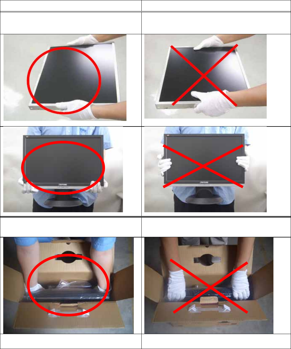
1.4 HANDING AND PLACING METHODS
Correct Methods: Incorrect Methods:
Only touch the metal frame of the LCD panel or
the front cover of the monitor. Do not touch the
surface of the polarizer.
Surface of the LCD panel is pressed by fingers and
that may cause “Mura.”
Take out the monitor with cushions Taking out the monitor by grasping the LCD panel.
That may cause “Mura.”
Place the monitor on a clean and soft foam pad. Placing the monitor on foreign objects. That could
scratch the surface of the panel or cause “Mura.”
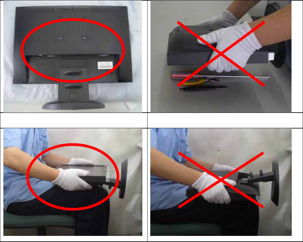
- 6 –
Place the monitor on the lap, the panel surface
must be upwards.
The panel is placed facedown on the lap. That may
cause “Mura.”
- 7 –
2. Specification
2.1 PRODUCT SPECIFICATIONS
Type 16.0” (full 15.6” wide viewable diagonal area),
TFT(Thin Film Transistor), Active Matrix WXGA lcd,
0.252mm pixel pitch
Color Filter RGB vertical stripe
LCD
Glass Surface Anti-Glare
Input Signal Video Sync RGB analog(0.7/1.0 Vp-p, 75ohms)
Separate Sync, Fh:24-82 kHz, Fv:50-75 Hz
Compatibility PC
Macintosh Up to 1366 x 768 Non-interlaced
Power Macintosh up to 1366 x 768
Resolution Recommended
and supported 1366 x 768 @ 60 Hz
1280 x 1024 @ 60 Hz
1024 x768 @ 60, 70, 72, 75 Hz
800 x 600 @ 56, 60, 72, 75 Hz
640 x 480 @ 60, 75 Hz
720 x 400 @ 70 Hz
Power Voltage 100V~240 VAC, 50/60Hz (auto switch)
Display area Full Scan 347.5mm(H) x 196.8mm(V) 13.7”(H) x 7.7”(V)
Operating
conditions
Temperature
Humidity
Altitude
32°F to + 104°F( 0°C to + 40°C)
20%C to + 80%(non-condensing)
To 10,000 feet
Storage conditions
Temperature
Humidity
Altitude
-4°F to + 140°F( -20°C to + 60°C)
5%C to + 90%(non-condensing)
To 40,000 feet
Dimensions Physical 376.23mm(W) x 327.42mm(H) x165mm(D)
14.8”(W) x 12.8”(H) x 5.6”(D)
Weight Physical 5.84 Ib(2.65 kg)
Regulations
BSMI, CCC, PSB, C-Tick, CE, GS, MIC, VCCI,
Ergo, Gost-R/Hygienic, SASO, TCO’03, Ukraine,
UL/cUL, FCC-B, ICES-B, ENERGY STAR®
TUV-S/IRAM/UL-AR S Mark,
Power saving
modes
On
Off 16W (Typical) (blue LED)
<1W
Preset Timing Mode (pre-adjusted to VESA® 1366 x 768 @ 60 Hz)
Warning: Do not set the graphics card in your computer to exceed these refresh rates; doing so may
result in permanent damage to the LCD display.
1 Macintosh computers older than G3 require a ViewSonic® Macintosh adapter. To order an adapter,
contact ViewSonic.
- 8 –
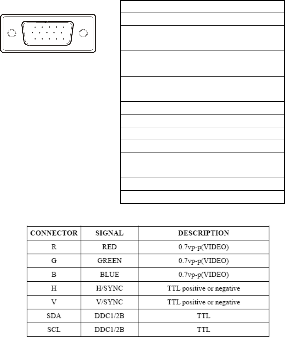
2.2 INTERFACE DESCRIPTION
D-SUB 15 PIN CONNECTOR
15
610
11 15
SIGNAL LEVEL
Pin Number Pin Function
1 Red video input
2 Green video input
3 Blue video input
4 No Connection
5 Ground
6 Red video ground
7 Green video ground
8 Blue video ground
9 +5V
10 H/V sync ground
11 No connection
12 (SDA)
13 Horizontal sync (Composite sync)
14 Vertical sync
15 (SCL)
- 9 –
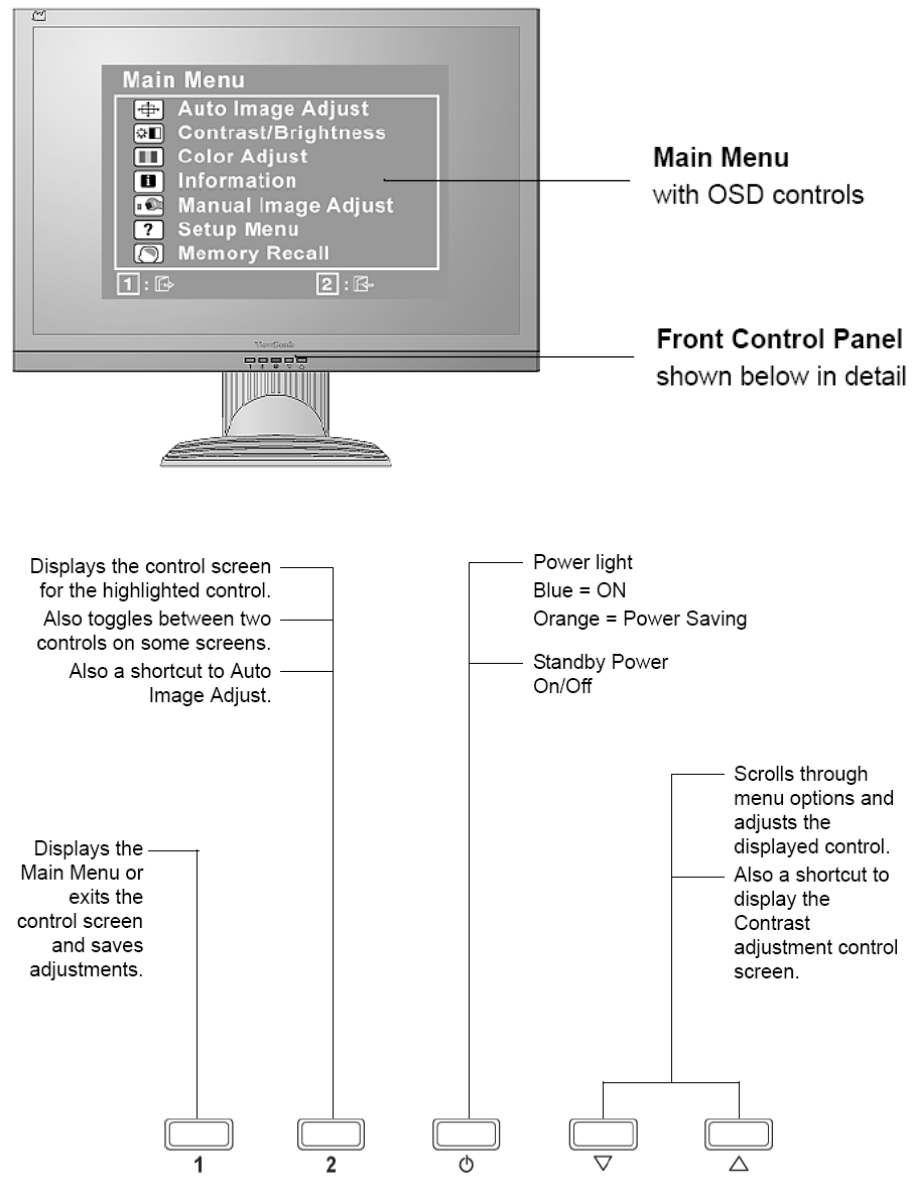
3.Front Panel Function Controls And Indicators
- 10 –
Do the following to adjust the display setting:
1. To display the Main Menu, press button [1].
NOTE: All OSD menus and adjustment screens disappear automatically after about 15
seconds. This is adjustable through the OSD timeout setting in the setup menu.
2. To select a control to adjust, press ▲or ▼ to scroll up or down in the Main Menu.
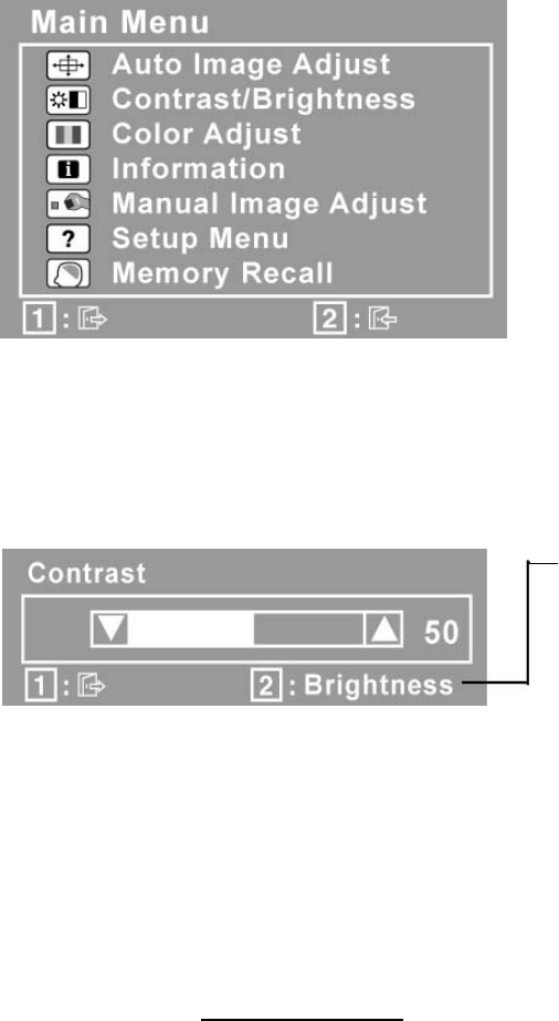
3. After the desired control is selected, press button [2]. A control screen like the one
shown below appears.
The line at the bottom of the screen
shows the current functions of
buttons 1 and 2: Exit or select the
Brightness control.
4. To adjust the control, press the up ▲ or▼ down buttons.
5. To save the adjustments and exit the menu, press button [1] twice.
The following tips may help you optimize your display:
• Adjust the computer's graphics card so that it outputs a 1366 x 768 @ 60Hz video
signal to the LCD display. (Look for instructions on “changing the refresh rate” in the
graphics card's user guide.)
• If necessary, make small adjustments using H. POSITION and V. POSITION until the
screen image is completely visible. (The black border around the edge of the screen
should barely touch the illuminated “active area” of the LCD display.)

- 11 –
Main Menu Controls
Adjust the menu items shown below by using the up and down buttons.
Control Explanation
Auto Image Adjust automatically sizes, centers, and fine tunes the video
signal to eliminate waviness and distortion. Press the [2] button to obtain a
sharper image.
NOTE: Auto Image Adjust works with most common video cards. If this
function does not work on your LCD display, then lower the video refresh rate
to 60 Hz and set the resolution to its pre-set value.
Contrast adjusts the difference between the image background (black level)
and the foreground (white level).
Brightness adjusts background black level of the screen image.
Color Adjust provides several color adjustment modes, including preset color
temperatures and a User Color mode which allows independent adjustment of
red (R), green (G), and blue (B). The factory setting for this product is 6500K
(6500 Kelvin).
sRGB-This is quickly becoming the industry standard for color management,
with support being included in many of the latest applications. Enabling this
setting allows the LCD display to more accurately display colors the way they
were originally intended. Enabling the intended. Enabling the sRGB setting
will cause Contrast and Brightness adjustments to be disabled.
9300K-Adds blue to the screen image for cooler white (used in most office
settings with fluorescent lighting).
6500K-Adds red to the screen image for warmer white and richer red.
5400K-Adds green to the screen image for a darker color.
User Color Individual adjustments for red (R), green (G), and blue (B).
1. To select color (R, G or B) press button [2].
2. To adjust selected color, press ▲ and▼.
Important: If you select RECALL from the Main Menu when the product is
- 12 –
set to a Preset Timing Mode, colors return to the 6500K factory preset.
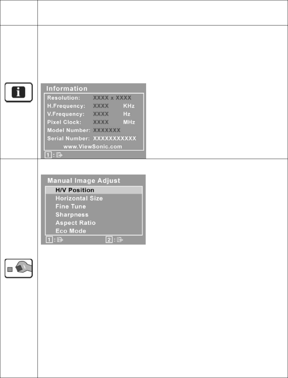
Information displays the timing mode (video signal input) coming from the
graphics card in the computer, the LCD model number, the serial number, and
the ViewSonic® website URL. See your graphics card’s user guide for
instructions on changing the resolution and refresh rate (vertical frequency).
NOTE: VESA 1366 x 768 @ 60Hz (recommended) means that the resolution
is 1366 x 768 and the refresh rate is 60 Hertz.
Manual Image Adjust display the Manual Image Adjust menu
H./V. Position (Horizontal/Vertical Position) moves the screen image left or
right and up or down.
H./Size (Horizontal Size) adjusts the width of the screen image.
Fine Tune sharpens the focus by aligning text and/or graphics with pixel
boundaries.
NOTE: Try Auto Image Adjust first.
Sharpness adjusts the clarity and focus of the screen image.
Aspect ratio Selects the image size for 4:3 and full screen.
ECO Mode provides the lower power consumption by reducing the
brightness.
Standard: The default brightness setting.
Optimize: Decreases the brightness by 25%.
- 13 –
Conserve: Decreases the brightness by 50%.
NOTE: When the ECO Mode is set to “Optimize” or “Conserve”, the
Brightness, Contrast, and Dynamic Contrast cannot be adjusted.
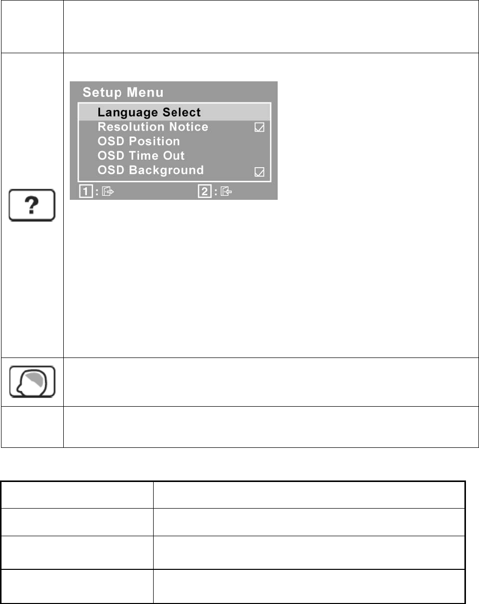
Setup Menu displays the menu shown below:
Language Select allows the user to choose the language used in the menus
and control screens.
Resolution Notice advises the optimal resolution to use.
OSD Position allows the user to move the OSD menus and control screens.
OSD Timeout sets the length of time the OSD screen is displayed. For
example, with a “15 second” setting, if a control is not pushed within 15
seconds, the display screen disappears.
OSD Background allows the user to turn the OSD background On or Off.
Memory Recall returns the adjustments back to factory settings if the display
is operating in a factory Preset Timing Mode listed in the Specifications of this
manual.
Exception: This control does not affect changes made with the User Color
control, Language Select or Power Lock setting.
SHORT CUTS FUNCTION FROM THE BUTTONS
[1] Main Menu
[2] Auto Image Adjust
[▼] To immediately activate Brightness and menu. It should
be change to Contrast OSD by push button[2]
[▲] To immediately activate Contrast menu. It should be
change to Brightness OSD by push button[2]
- 14 –
[▼] + [▲] Recall both of Contrast and Brightness to default without
OSD message.
[1] + [2] Toggle 720x400 and 640x400 mode when input 720x400
or 640x400 mode
[1] + [▼] + [▲]
(Keep pushing 5 sec)
White Balance
1. It will not shown on user’s guide
2. OSD message as below,
(Image = no blanking)
[1] + [▲] OSD Lock
[1] + [▼] Power Lock
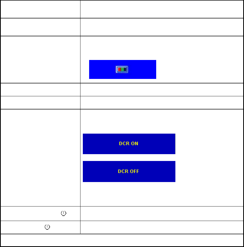
[▲]
1.Long Press [up] key 3 seconds to switch DCR On/Off,
2. Loop: DCR On <=> DCR Off
When switch to DCR ON
When switch to DCR OFF
3. DCR Off in Factory mode.
4. Reset to default when re-power on/off
5. Message will appear only after Hot Key is pressed
No signal + [1] + [ ] Burning mode
[1] + [ ] Factory Mode
Remark : All the short cuts function are only available while OSD off
- 15 –
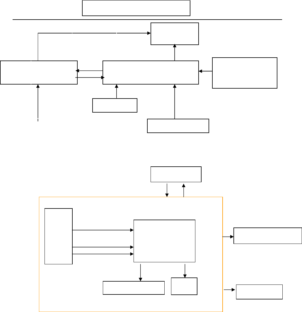
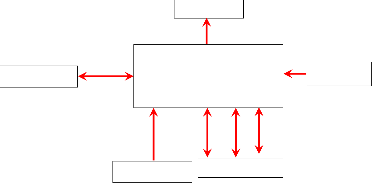
4. Circuit Description
4.1 LCD MONITOR DESCRIPTION
The LCD MONITOR will contain a Main Board, an Power Board, Key Board which
house the flat panel control logic, brightness control logic and DDC.
4.2 MAIN BOARD BLOCK FUNCTION DESCRIPTION
The main board contains panel control logic, brightness control logic, DDC and DC convert
DC circuit and so on.
Power Board
(Include: adapter, inverter)
Flat Panel and
CCFL backlight
Main Board
Key Board
RS232 Connector
For white balance
adjustment in factory
mode
HOST Computer
CCFL Drive.
AC-IN
100V-240V
Video signal, DDC
Monitor Block Diagram
R
G
B
H
V
SDA
SCL
OSC
Backlight and Panel
PWPC board
Flash memory Keyboard
TSUM1PFR-LF
- 16 –
4.3 PWPC BOARD BLOCK FUNCTION DESCRIPTION
PWPC board combines to adapter and inverter, Adapter which commonly consists of
bridge rectifier and filter, start circuit, PWM control circuit, protection circuits and convert
to 12V, 5V DC voltage by input 90V-240V AC voltage that provide power supply for each
chips in the main board and inverter. Inverter is DC TO AC circuit. It changes the 12v
DC of power supply to about 600-800v AC that drives the backlight. It mostly consists of
starting circuit, PWM controller, DC changing circuit, LC surging circuit, output circuit
and protection circuit etc.
AC input EMI filter
Bridge
Rectifier
and Filter
Start Circuit
R904, R932, R933
PWM
Control IC
Over
Voltage
Protect
Rectifier
CMOS
ON/OFF
Control
PWM
Control IC
Feedback
Circuit
OSC and
Output
Circuit
DC Convert
Circuit
MOSFET
Q802
Over
Voltage
CN902
Transformer
Lamp
5V
12V
ON/OF
DIM
- 17 –
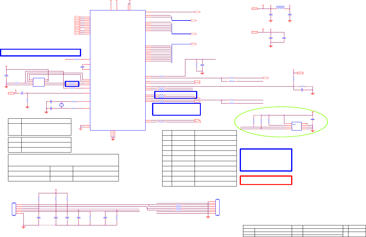
4.4 INTRODUCTION OF IC
TSUM1PFR-LF(U401): integrate ADC, OSD, SCALER, MCU, LVDS, convert analog
RGB into digital and room and shrink scaling output to LCD panel.
PIN Function:
Pin Symbol Description
21 SDO SPI flash serial data output
22 CSZ SPI flash chip select
23 SCK SPI flash serial select
24 SDI SPI flash serial data input
18 DDCA_SDA/RS232_TX DDC Data for analog interface/
UART Ttransmitter /
General Purpose Input/Output; 4mA driving strength
19 DDCA_SCL/RS232_RX DDC Clock for analog interface/
UART Receiver /
General Purpose Input/Output; 4mA driving strength
54 RST Chip reset; High reset
52 VCTRL Regulator control
16 HSYNCO Analog HSYNC input
17 VSYNCO Analog VSYNC input
15 REFP Internal ADC top de-coupling pin
14 REFM Internal ADC bottom de-coupling pin
4 REXT External resistor 390 ohm to AVDD_33
Chip Configuration Input
MODE[1:0] Chip Operation
32、31 MODE[1:0] Input
00 Normal Operation
1 XIN Xin; Crystal Oscillator Input
2 XOUT Xout; Crystal Oscillator Output
6 AVDD_33 ADC Power 3.3V
51 VDDP Digital Output Power 3.3V
30、53 VDDC Digital Core Power 1.8V
3、5、29 GND Ground

- 18 –
- 19 –
AP1117D33LA(U404): DC power convert, convert to 3.3v.
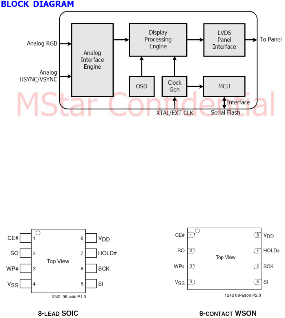
SST25LF020A-33-4C-SAE(U403): SST’s serial flash family features a four-wire,
SPI-com-patible interface that allows for a low pin-count package occupying less board
space and ultimately lowering total system costs. The SST25LF020A/040A devices
significantly improve performance, while lowering power consumption. The total energy
consumed is a function of the applied voltage, current, and time of application. The
SST25LF020A/040A devices operate with a single 3.0-3.6V power supply. The
SST25LF020A devices are offered in an 8-lead SOIC 150 mil body width (SA) package.
Pin Diagram:
PIN Descriptions:
- 20 –
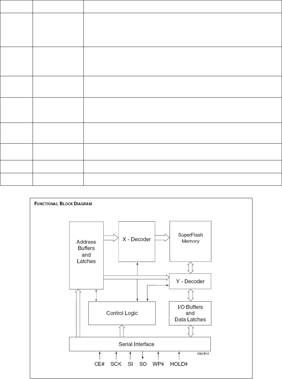
Circuit Diagram
Symbol Pin Name Functions
SCK Serial Clock
To provide the timing of the serial interface.
Commands, addresses, or input data are latched on the
rising edge of the clock input, while output data is shifted out
on the falling edge of the clock input.
SI
Serial Data
Input
To transfer commands, addresses, or data serially into the
device.
Inputs are latched on the rising edge of the serial clock.
SO Serial Data
Output
To transfer data serially out of the device.
Data is shifted out on the falling edge of the serial clock.
CE# Chip Enable
The device is enabled by a high to low transition on CE#.
CE# must remain low for the duration of any command
sequence.
WP# Write Protect
The Write Protect (WP#) pin is used to enable/disable BPL
bit in the status register.
HOLD# Hold To temporarily stop serial communication with SPI flash
memory without resetting the device.
VDD Power Supply To provide power supply(3.0-3.6V)
VSS Ground
- 21 –
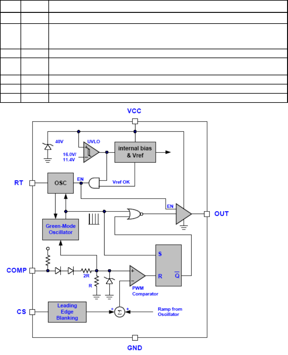
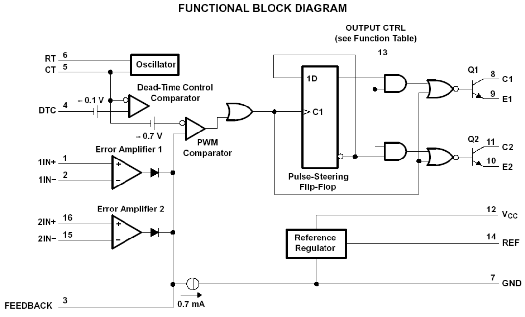
LD7552BPS (IC901): PWM control, high-voltage startup current. The circuit unit has
functions such as over-current protection, over-voltage protection, output short-circuit
protection and etc. The function of each pin and the inside circuit diagram are as follows:
Pin Name Function
1 GND Ground
2 COMP
Voltage feedback pin (same as the COMP pin in UC384X), By
connecting a photo-coupler to close the control loop and achieve the
regulation
3 VCC Supply voltage pin
4 RT
This pin is to program the switching frequency. By connecting a resistor
to ground to set the switching frequency.
6 NC Unconnected pin
7 VCC Supply voltage pin
8 OUT Gate drive output to drive the external MOSFET

- 22 –
TL494(IC801): The TL494 incorporates all the functions required in the construction of a
pulse-width-modulation (PWM) control circuit on a single chip. Designed
primarily for power-supply control, this device offers the flexibility to tailor the
power-supply control circuitry to a specific application.
PIN Descriptions:
- 23 –
- 24 –
5. Adjustment Procedure
5.1 ADJUSTMENT CONDITIONS AND PRECAUTIONS
1. Approximately 30 minutes should be allowed for warm up before proceeding.
2. Adjustments should be undertaken only on those necessary elements since most of them
have been carefully preset at the factory.
3. ESD protection is needed before adjustment.
5.2 MAIN ADJUSTMENTS
NO. FUNCTIONS DESIGNATION
1. White Balance Function Key
2. Geometry Function Key
5.3 ALIGNMENT PROCEDURES
Approximately 30 minutes should be allowed for warm up before proceeding
White-Balance adjustment.
1. Adjust of White Balance
1.) How to do the CA-210 MEM .Channel setting
A、Reference to CA-210 user guide
B、Use “ MODE” key to modify x、y、Lv value and use “MEMORY CH” key to modify the
TEXT description Following is the procedure to do white-balance adjust
2.) Setting the color temp. You want
A、MEM.CHANNEL1 ( 9300 color):
9300 color temp. parameter is x = 0.283 ±0.003; y = 0.298 ±0.003;
Lv ≥ 147 cd/m2 ,
B、MEM.CHANNEL1 ( 6500 color):
6500 color temp. parameter is x = 0.313±0.003; y = 0.329 ±0.003;
Lv ≥ 179cd/m2,
C、MEM.CHANNEL 1 ( 5400 color):
5400 color temp. parameter is x = 0.335±0.003; y = 0.350 ±0.003;
Lv ≥ 168cd/m2,
D、MEM.CHANNEL1 ( SRGB color):
SRGB color temp. parameter is x=0.313±0.003; y=0.329±0.003; Lv≥179cd/m2,
3.) Into factory mode of VA1616:
First Power off, then press Switch 1 button along with press Power button will activate the
factory mode, then MCU will do AUTO LEVEL automatically. Meanwhile press MENU
the OSD screen will located at LEFT TOP OF PANEL.
4.) Bias adjustment :
- 25 –
Set the Contrast to 70,Adjust the Brightness to 100.
5.) Gain adjustment :
Move cursor to “-F-” and press MENU key
A、Adjust 9300 color-temperature
(1)、Switch the CA-210 to x、y、Lv -Mode (with press “MODE” button )
(2)、Switch the MEM. channel to Channel 1 ( with up or down arrow on CA-210 )
(3) 、The LCD-indicator on CA-210 will show x=0.283±0.003, y=0.298±0.003,
Lv≥147cd/m2
(4) Adjust the R G B of color3 on factory window until CA210 indicator reached
x=0.283±0.003, y=0.298±0.003, Lv≥147cd/m2
B、Adjust 6500 color-temperature
(1)、Switch the CA-210 to x、y、Lv -Mode (with press “MODE” button )
(2)、Switch the MEM .channel to Channel 1 ( with up or down arrow on CA-210 )
(3) 、The LCD-indicator on CA-210 will show x=0.313±0.003, y=0.329±0.003,
Lv≥179cd/m2
(4) Adjust the R G B of color3 on factory window until CA210 indicator reached
x=0.313±0.003, y=0.329±0.003, Lv≥179 cd/m2
C、Adjust 5400 color-temperature
(1)、Switch the CA-210 to x、y、Lv -Mode (with press “MODE” button )
(2)、Switch the MEM .channel to Channel 1( with up or down arrow on CA-210 )
(3) 、The LCD-indicator on CA-210 will show x=0.335±0.003, y=0.350±0.003,
Lv≥168 cd/m2
(4)、Adjust the R G B of color3 on factory window until CA210 indicator reached
x = 0.335±0.003; y = 0.350±0.003; Lv≥168 cd/m2
D、Adjust SRGB color-temperature
(1)、Switch the CA-210 to x、y、Lv -Mode (with press “MODE” button )
(2)、Switch the MEM .channel to Channel 1 ( with up or down arrow on CA-210 )
(3) 、The LCD-indicator on CA-210 will show x=0.313±0.003, y=0.329±0.003,
Lv≥179 cd/m2
(4)、Adjust the R G B of color3 on factory window until CA210 indicator reached
x=0.313±0.003, y=0.329±0.003, Lv≥179 cd/m2
F、Press reset key and Turn the Power-button “off to on” to quit from factory mode。
2. Geometry
1).Set cross-hatch pattern and preset timing as timing table listed.
2).Change to each mode in turn and wait for the monitor finish auto-alignment and save
press before change to next mode.
3).Until all of modes are adjusted, exit OSD menu and press POWER OFF to exit factory
mode.
- 26 –
5.4 Factory Defaults
Item Defaults Item Defaults
Contrast 70% Input Priority N/A
Brightness 100% Resolution Notice On
Color Temperature 6500K Volume N/A
Sharpness 100% Balance N/A
OSD H. Position 50% Treble N/A
OSD V. Position 50% Bass N/A
OSD Time Out 15 720x400 / 640x400 720x400
OSD Background On DCR ON : For Region code =
E/G/P/A/S/K/U/J units only
OFF: For Region code = M
units only
5.5 Function Test
1 Product: 16” LCD Monitor
2 Test Equipment: Color Video Signal & Pattern (or PC with SXGA resolution)
3 Test Condition: Before function test and alignment, each LCD Monitor should be
warmed up for at least 30 minutes with the following conditions:
(a)In room temperature,
(b) With full-white screen, RGB, and Black
(c) With cycled display modes,
640*480 (H=43.27kHz, V=75Hz)
800*600 (H=53.7kHz, V=75Hz)
1024*768 (H=68.67kHz, V=60Hz)
1280*1024 (H=79.97kHz, V=60Hz)
1366*768 (H=55.9kHz, V=60Hz)
4 Test Display Modes & Pattern
Compatible Modes
Item Timing Analog
1 640 x 480 @ 60Hz, 31.5kHz Yes
2 640 x 480 @ 75Hz, 31.5kHz Yes
3 720 x 400 @ 70Hz, 31.5kHz Yes
4 800 x 600 @ 56Hz, 35.1kHz Yes
5 800 x 600 @ 60Hz, 37.9kHz Yes
6 800 x 600 @ 72Hz, 48.1kHz Yes
7 800 x 600 @ 75Hz, 46.9kHz Yes
8 1024 x 768 @ 60Hz, 48.4kHz Yes
9 1024 x 768 @ 70Hz, 56.5kHz Yes
10 1024 x 768 @ 72Hz, 58.1kHz Yes
11 1024 x 768 @ 75Hz, 60.0kHz Yes
12 1280 x 1024 @ 60Hz, 48.4kHz Yes
13 1366 x 768 @ 60Hz, 60.0kHz Yes
- 27 –
Function Test Display Pattern
Item Test Content Pattern Specification Remark
1 Frequency &
Tracking Fine Line Moire Eliminate visual wavy
noise. Figure 1
2 Contrast/Bright
ness 16 Gray Scale 16 gray levels sh should
be distinguishable. Figure 2
3 Boundary Horizontal & Vertical
Thickness
Horizontal and Vertical
position of video should
be adjustable to be
within the screen frame.
Figure 3
4 RGB Color
Performance RGB Color Intensities
Contrast of each R, G,
B, color should be
normal.
Figure
4,5,6
5
Screen
Uniformity &
Flicker
Full White Should be compliant
with the spec. Figure 7
6 Dead
Pixel/Line
White Screen & Dark
Screen
The numbers of dead
pixels should be
compliant with the spec.
Figure 7,8
7 White Balance White & Black Pattern
The screen must have
the pure white and black
pattern, no other color.
Figure 9
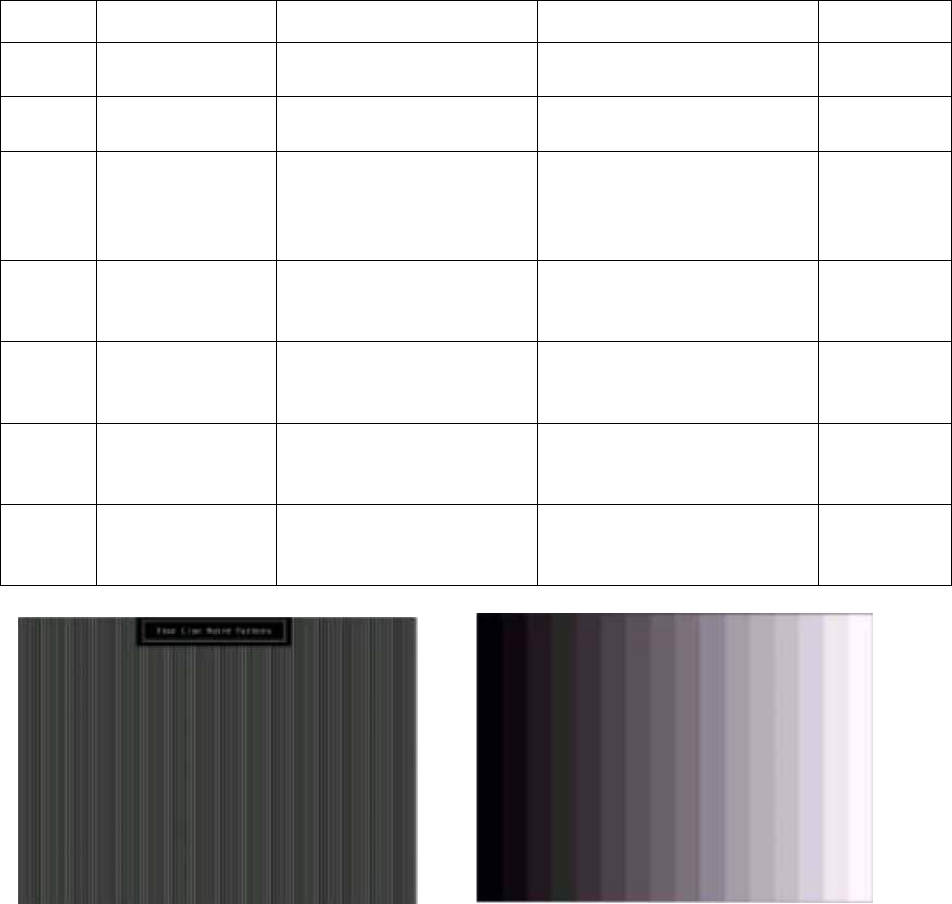
Fine Line Morie Pattern (Figure1) Gray Scale Pattern (Figure2)

- 28 –
Horizontal & Vertical Thickness Pattern R. Color Pattern (Figure 4)
(Figure 3)
G. Color Pattern (Figure 5) B. Color Pattern (Figure 6)
Full White Pattern (Figure 7) Dark Screen Pattern (Figure 8)

- 29 –
Black-White Pattern (Figure 9)
4.3 Function Test and Alignment Procedure
All Modes Reset
You should do “All Mode Reset” (Refer to Chapter III-3. Hot Keys for Function
Controls) first. This action will allow you to erase all end-user’s settings and restore
the factory defaults.
Auto Image Adjust
Please select and enter “Auto Image Adjust” function on Main Menu to see if it is
workable. The “Auto Image Adjust” function is aimed to offer a better screen quality
by built-in ASIC. For optimum screen quality, the user has to adjust each function
manually.
Firmware
Test Pattern: Burn In Mode (Refer to Chapter III-3. Hot Keys for Function Controls)
- Make sure the F/W is the latest version.
DDC
Test Pattern: EDID program
Make sure it can pass test program.
Fine Tune and Sharpness
Test Signal: 1366*768@60Hz
Test Pattern: Line Moire Pattern
Check and see if the image has noise and focus performs well. Eliminate visual
line bar.
If not, readjust by the following steps:
(a)Select and enter “Fine Tune” function on “Manual Image Adjust” to adjust the
image to eliminate visual wavy noise.
(b)Then, select and enter “Sharpness” function to adjust the clarity and focus of the
screen image.
Boundary
Test Signal: 1366*768@60Hz
Test Pattern: Horizontal & Vertical Line Thickness Pattern
Check and see if the image boundary is within the screen frame.
If not, readjust by the following steps:
(a)Select and enter “Manual Image Adjust” function on OSD Main Menu.
- 30 –
(b)Then, select and enter “Horizontal Size” or “Horizontal/Vertical Position” function
to adjust the video boundary to be full scanned and within screen frame.
White Balance
Test Signal: 1366*768@60Hz
Test Pattern: White and Black Pattern
1.5.8 R, G, B, Colors Contrast
Test Signal: 1366*768@60Hz
Test Pattern: R, G, B, Color Intensities Pattern and 16 Gray Scale Pattern
- Check and see if each color is normal and distinguishable.
- If not, please return the unit to repair area.
Screen Uniformity and Flicker
Test Signal: 1366*768@60Hz
Test Pattern: Full White Pattern
- Check and see if it is in normal condition.
1.5.10 Dead Pixel and Line
Test Signal: 1366*768@60Hz
Test Pattern: Dark and White Screen Pattern
- Check and see if there are dead pixels on LCD panel with shadow gauge and
filter film.
- The total numbers and distance of dead pixels should be compliant with the
spec.
Mura
Test Pattern: White, RGB, Black, & Grey
Test Tool: 10% ND Filter
- Check if the Mura can pass 10% ND Filter.
Audio
Test Signal: Voice signal (optional, depend on model)
Test Pattern: liberty
- Make sure there is audio output.
- Make sure that audio function (volume 80%) is working without noise and
resonance.
- Make sure that the sound of right and left speakers are in balance.
Check for Secondary Display Modes
Test Signal:
Analog: 640*480@60/75Hz;
720*400@70Hz; 800*600@56/60/72/75Hz;
1024*768@60/70/72/75Hz; 1280*1024@60Hz
1366*768@60Hz
- Normally when the primary mode 1366*768@60Hz is well adjusted and
compliant with the specification, the secondary display modes will also be
compliant with the spec. But we still have to check with the general test pattern to
make sure every secondary is compliant with the specification.
All Modes Reset
After final QC step, we have to erase all saved changes again and restore the
factory defaults. You should do “All Mode Reset” again.
Power Off Monitor
- 31 –
Turn off the monitor by pressing “Power” button.
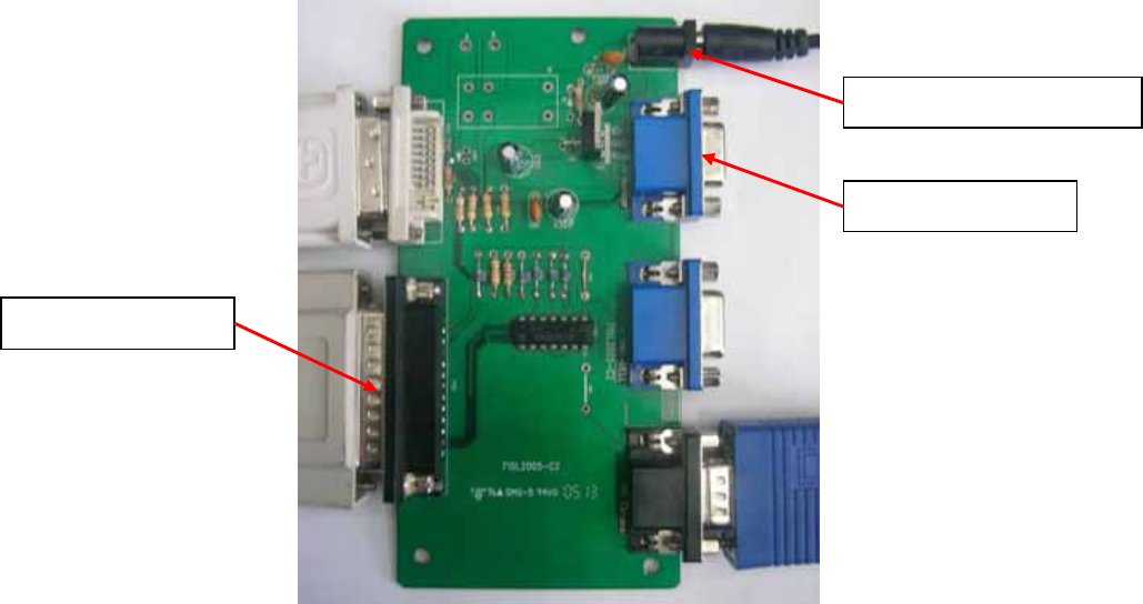
5.6 Firmware Upgrade Procedure
When you receive the returned monitor, please check whether the firmware version is
the latest. If not, please do the following procedures to upgrade it to the latest version.
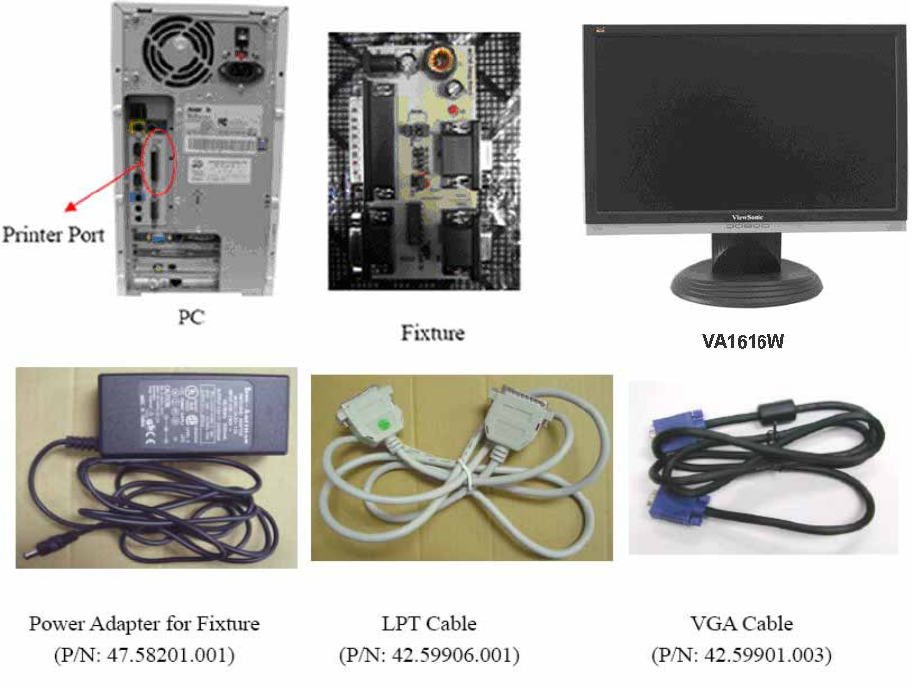
1 Equipment Needed
- Monitor( TSUM Series )
- Fixture for Firmware Upgrade
- Power Adapter (P/N: 47.58201.001) *1 for Fixture
- VGA Cable (P/N: 42.59901.003) *1(Pin 4, 11 should be connected to GND)
- PC (Personal Computer)
- LPT Cable (P/N: 42.59906.001) *1
- Firmware Upgrade Program
- One additional monitor for checking the program execution
2 Setup Procedure
2.1 Connect P2 of Fixture with printer port of PC by LPT Cable.
2.2 Connect P1 of Fixture with Monitor(TSUM series) by VGA Cable.
2.3 Plug Power Adapter to Fixture.
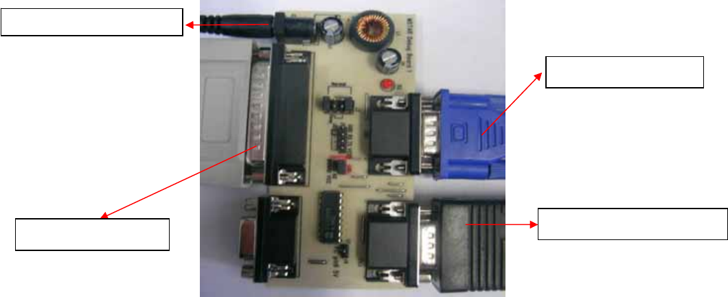
- 32 –
2.4 Connect Power Cord to Monitor(TSUM series).
2.5 Connect P3 to the Signal Generator (eg.Chroma2326) for verifying it after the
operation being completed.
2.6 Connect PC to the additional monitor.
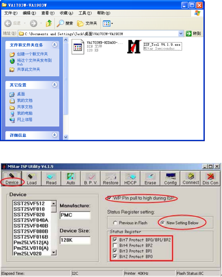
3 Firmware Upgrade Procedure
Step 1. Let Monitor(TSUM series) set to be connected with AC cable and VGA cable.
Step 2.Execute the MSstar ISP tool.
P2:to LPT Cable
JP1
:
to Power Ada
p
ter
P1:to VGA Cable
P3:to Signal Generator
- 33 –
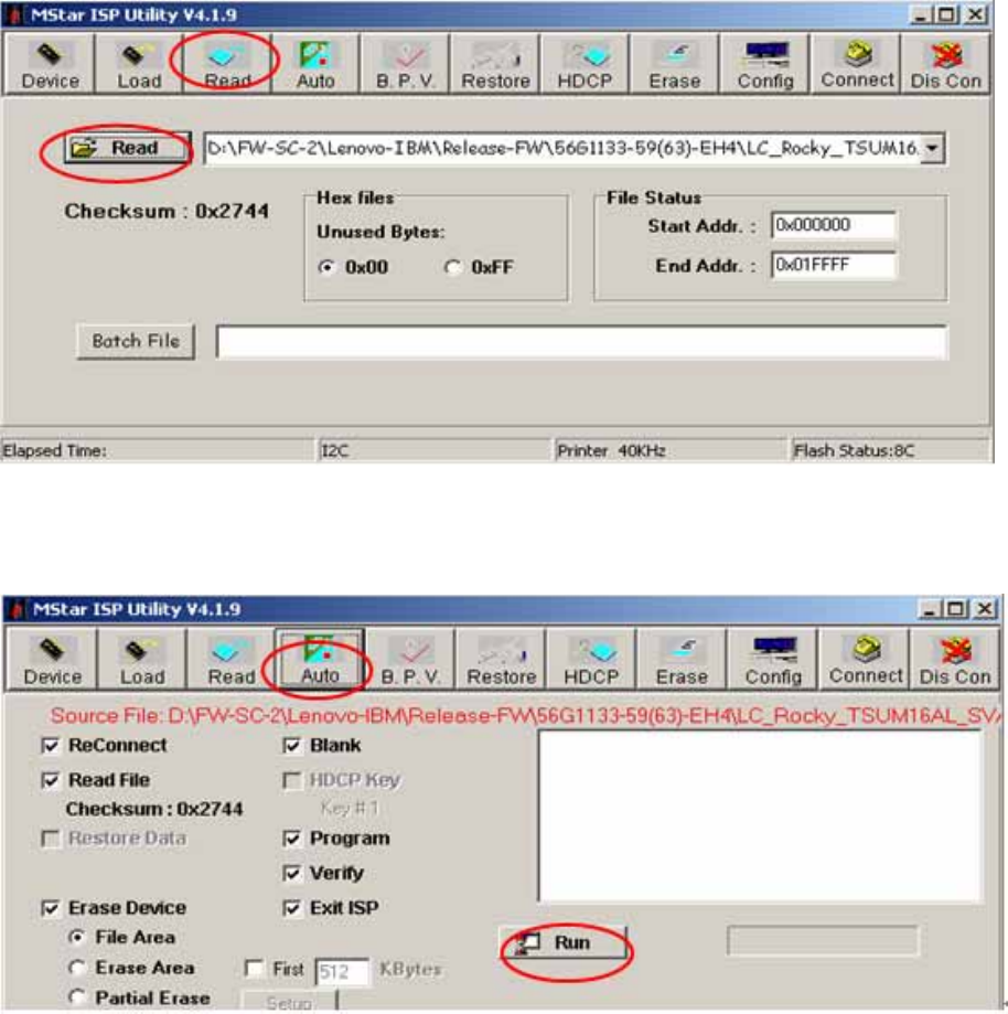
Step 3. Click “Device” button . Make sure that parameters relative to WP# is followed
bellow.
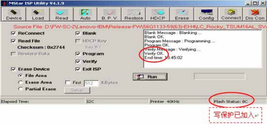
Step 4. Click “Read” button. Select the object bincode on your corresponding directory.
- 34 –
Step 5. Click “Auto” button. Be sure that function of Erase Device (File Area), Blank,
Program and Verify is selected, then execute the flashing action by clicking the “Run”
button.
Step 6. If the flashing F/W has been completed, “Verify Ok” message will be shown on
the right TextBox and Flash Status will be “8C” in the right-bottom of window.
- 35 –
Step 7. Unplug and replug power cord of Monitor(TSUM series) set and then check the
OSD operation and image on srceen.
Step 8. At last, do “Memory Recall.”
3.2 Setup Procedure
3.2.1 Connect P2 and monitor of Fixture with VGA ports of Monitor (TSUM Series) by
VGA Cable.
3.2.2 Connect P1 of Fixture with Printer port of PC by LPT Cable.
3.2.3 Plug Power Adapter to Fixture.
3.2.4 Connect Power Cord to Monitor (TSUM Series).
3.2.5 Connect PC to the additional monitor.
- 36 –
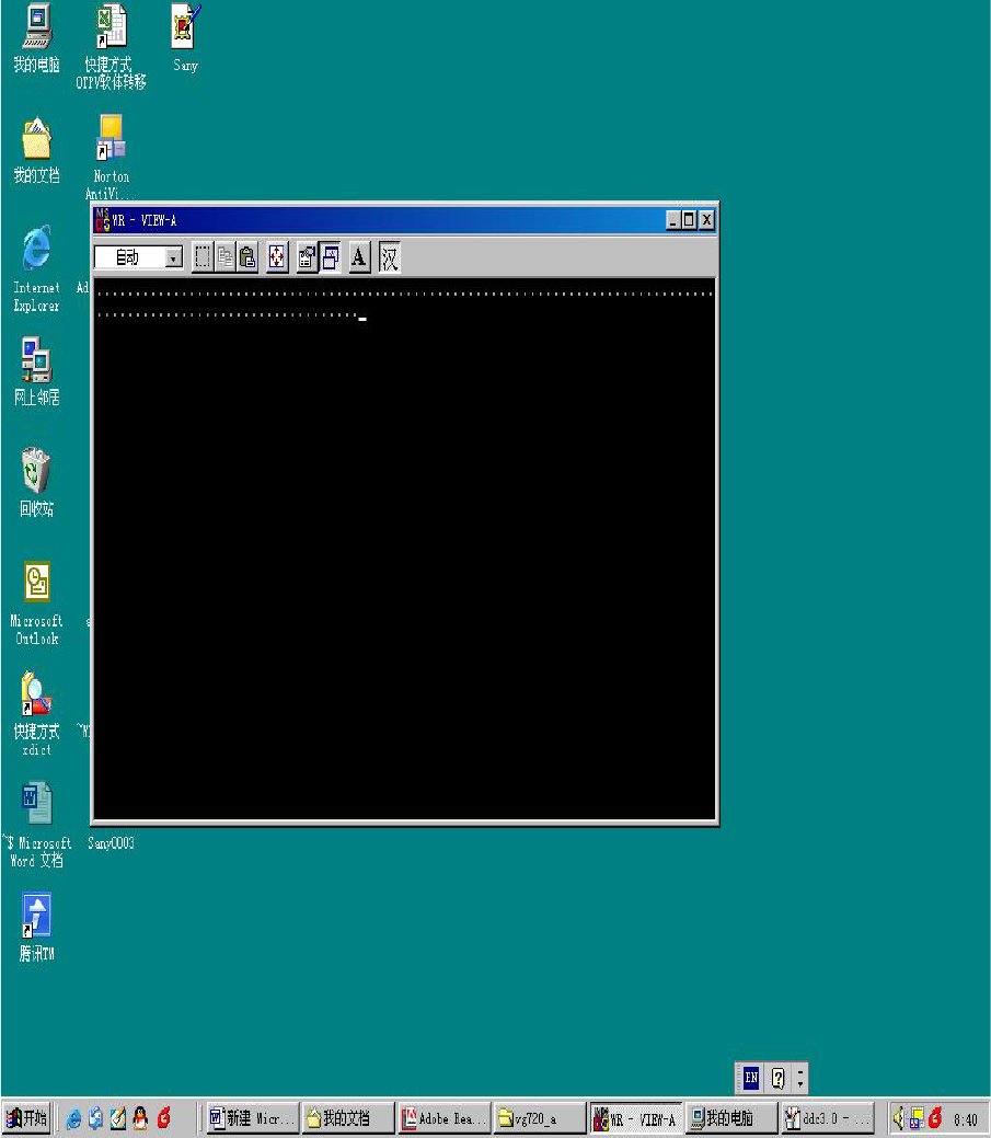
3.3 DDC Key In Procedure
Sep1.Select and execute DDC Key In program
JP1: Power Adapter
P2: VGA Cable
P1:to LTP Cable
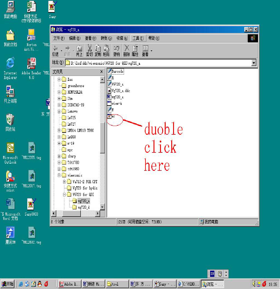
- 37 –
- 38 –
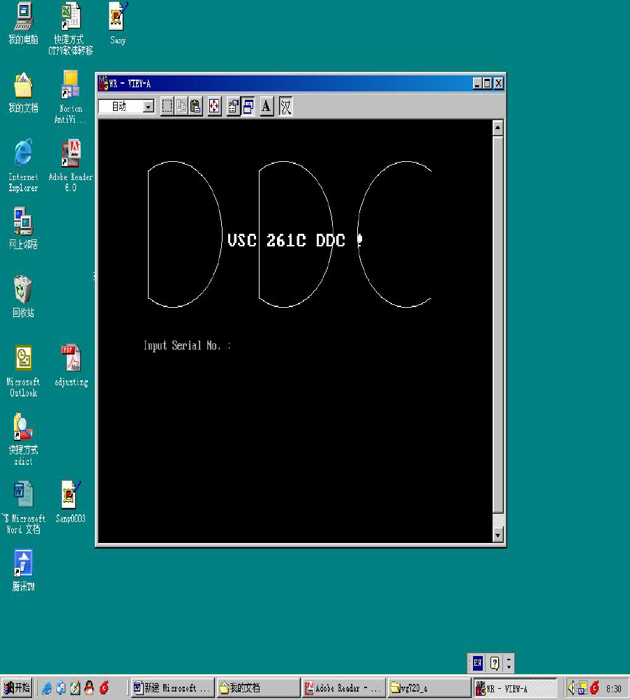
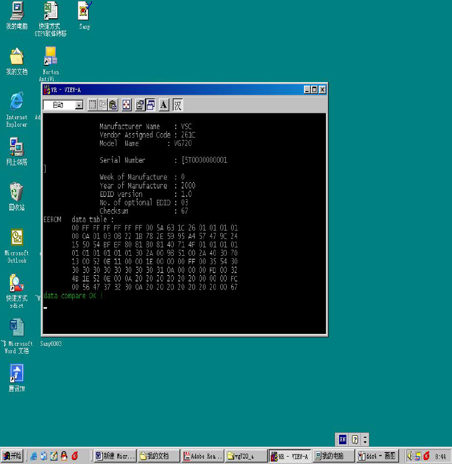
Sep2:Inpute the S/N and execute “Enter”
- 39 –
- 40 –
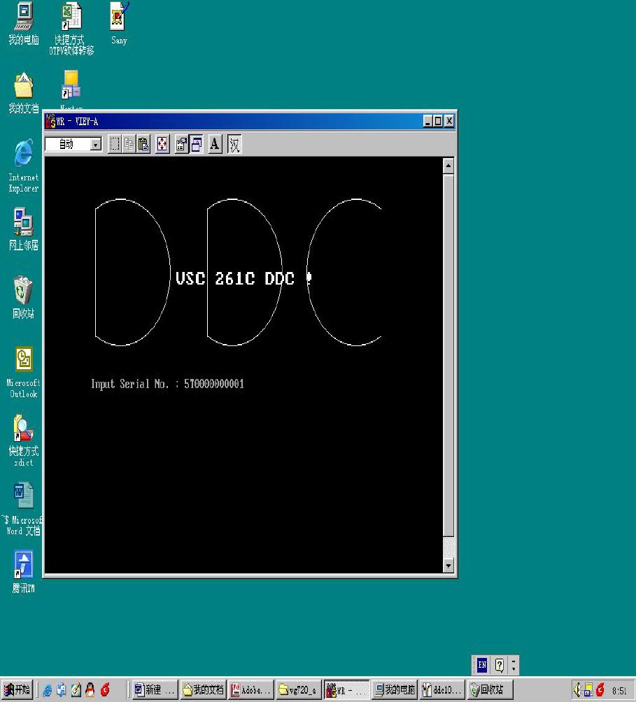
Sep3:Key the “Enter” and write the data
- 41 –
Sep4:If ddc program OK and show “data compare ok”
- 42 –
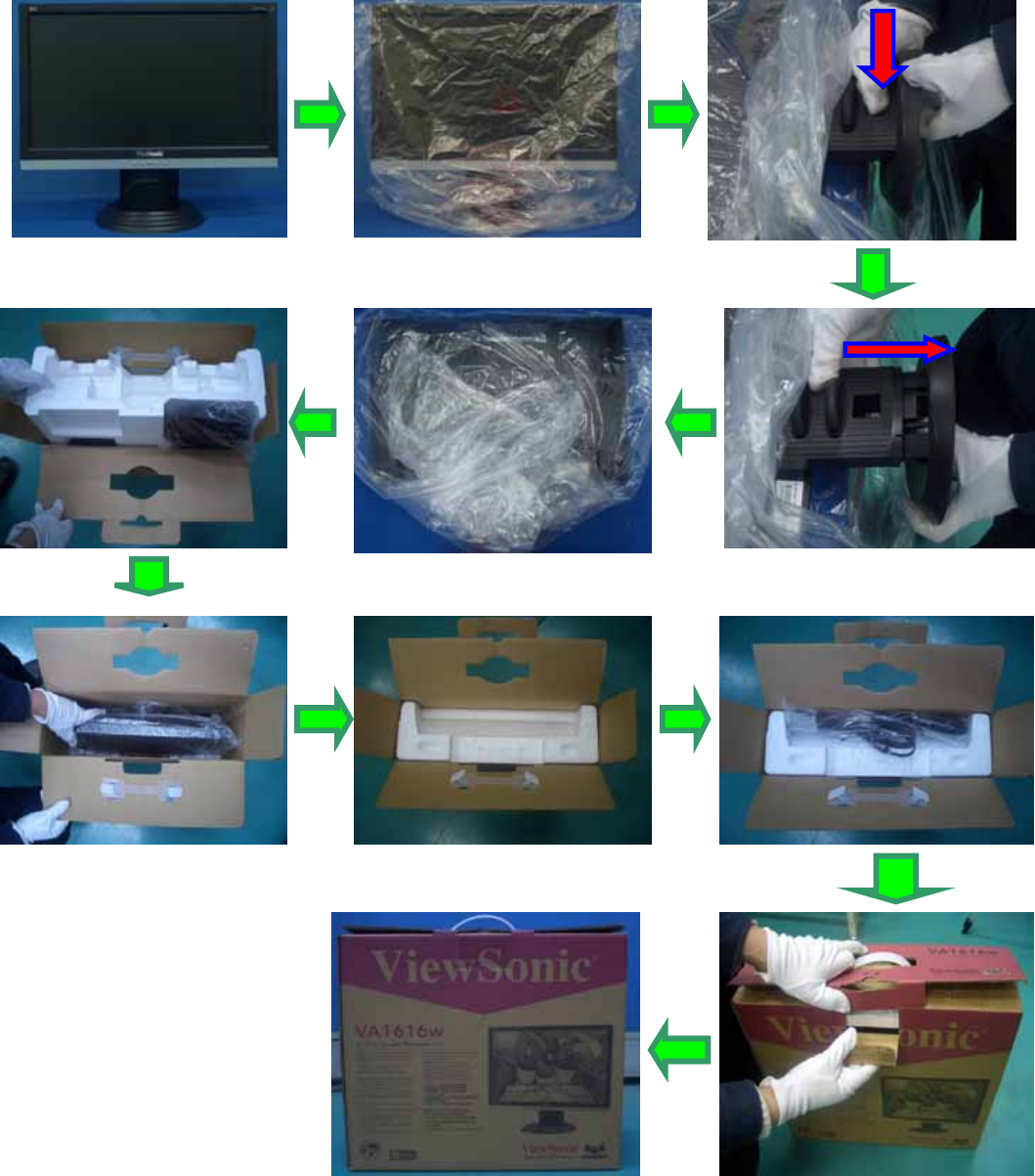
5.7 Packing Procedure
- 43 –
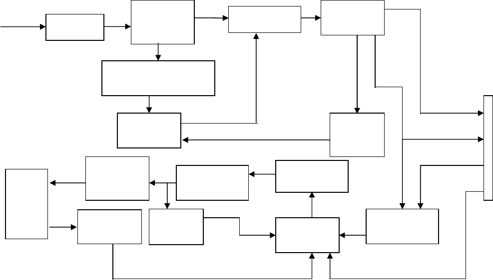
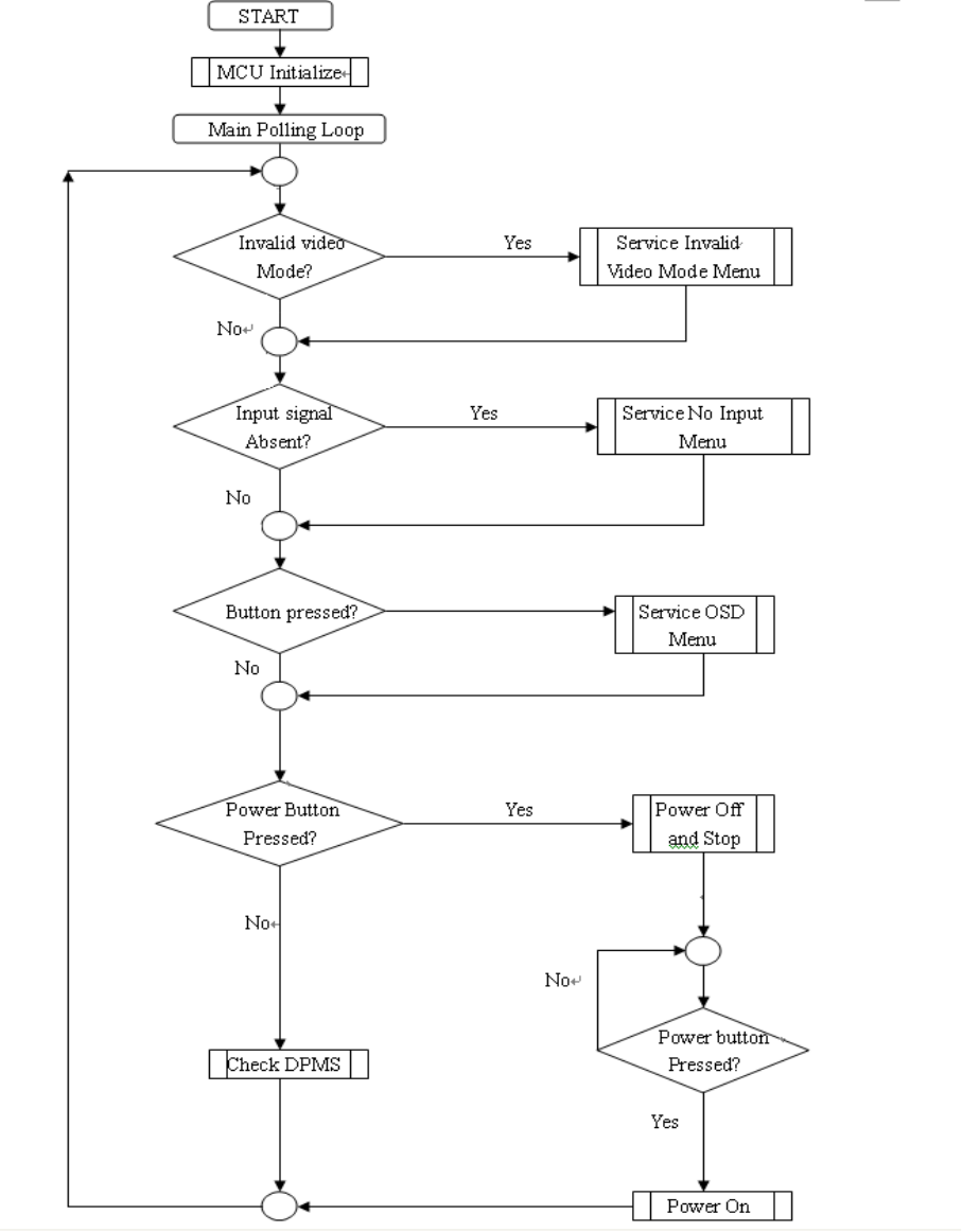
6.Troubleshooting Flow Chart
- 44 –
7.Block Diagram
Scalar TSUM1PFR-LF
(Include:MCU,ADC,OSD)
LCD Interface
Flash Memory
(User data /WB /EDID)
OSD Control Interface
(Key pad)
Crystal
14.31818MHz
EPR_SDA
EPR
_
SCL
H-SYNC
V-SYNC
RXD
TXD RGB
D-Sub Connector

- 45 –
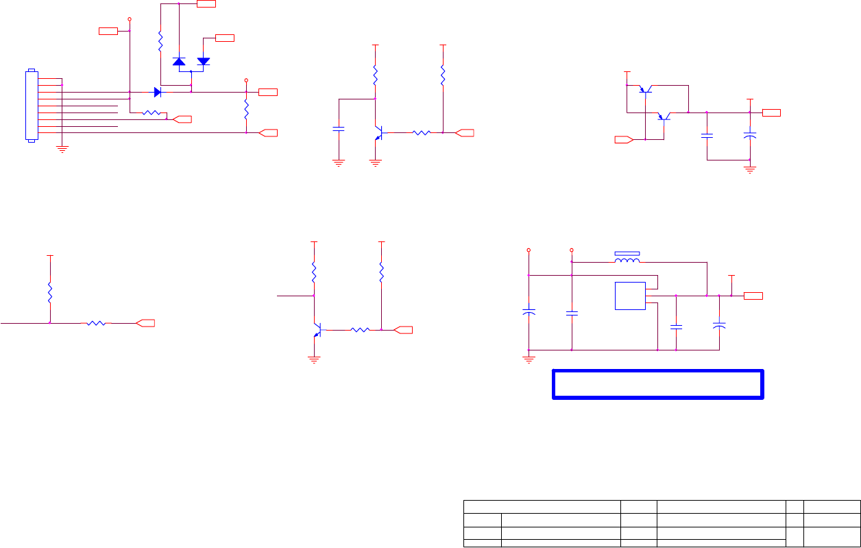
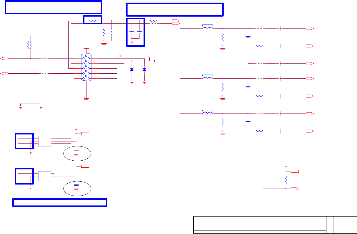
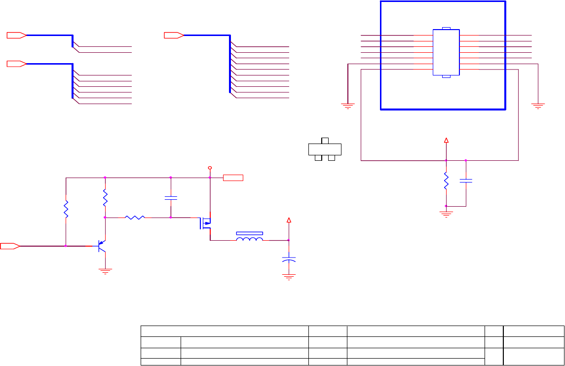
8. Schematic Diagram
8.1 Main Board
02.Input
DSUB_R+
DSUB_G+
DSUB_B+
DSUB_V
DSUB_R-
DSUB_G-
DSUB_B-
DET_CABLE
DSUB_H
DSUB_SOG
DDC1_SDA
DDC1_SCL
DSUB_5V
CMVCC1
VCC3.3
ESD_VCC
ESD_VCC
CBPC7MM5VSQ1 C
VSC VA1616W A
37Thursday , January 24, 2008
715G2904-C-2 <
称爹
>
01.TOP
G2904-C-2-VSC-1-071218
OEM MODEL Size
Rev
Date Sheet of
TPV MODEL
PCB NAME
称爹
T P V ( Top Victory Electronics Co . , Ltd. )
Key Component
絬
隔
瓜
絪
腹
CMVCC1
CMVCC
VCC3.3
CMVCC
ESD_VCC
PA[4..9]
DSUB_5V
PA[0..1]
PB[0..9]
CMVCC1
XGA/SXGA
VCC1.8
VCC3.3
VCC3.3
TSUM16FWR SCHEMATIC
VCC1.8
LVDS OUTPUT
03.Scalar
DSUB_R+
DSUB_G+
DSUB_SOG
DSUB_B+
DSUB_R-
DSUB_G-
DSUB_B-
DSUB_H
DSUB_V
Adj_BACKLIGHT
VCC1.8
VCC3.3
PA[0..1]
PB[0..9]
DDC1_SDA
DDC1_SCL
DET_CABLE
on_BACKLIGHT
PPWR_ON#
PANEL_ID#
Volume#
Mut e
CMVCC
PA[4..9]
CMVCC1
VCTRL
DSUB_5V
04.Output
CMVCC
PB[0..9]
PA[0..1]
PPWR_ON#
PA[4..9]
CMVCC
CMVCC1
05.Pow er
on_BACKLIGHT
Adj_BACKLIGHT
VCC1.8
CMVCC
VCC3.3
Mute
Volume#
PANEL_ID#DSUB_5V
CMVCC1
VCTRL
ESD_VCC
- 46 –
DSUB_5V 4
R450 NC
NC
D401
BAV99
3
1
2
CBPC7MM5VSQ1 D
VSC VA1616W B
77Thursday , January 24, 2008
715G2904-D-2 <
称爹
>
05.power
G2904-D-2-VSC-1-080124
OEM MODEL Size
Rev
Date Sheet of
TPV MOD EL
PCB NAME
称爹
T P V ( Top Vict ory Electronics Co . , Ltd. )
Key Component
絬
隔
瓜
絪
腹
R440
4K7 1/16W 5%
VCC3.3
R458
NC
FB403 NC
R439
10K 1/16W 5%
VCC3.3
U404 can use package 232 or 252.
CMVCC
VCC3.3 4,5
R448
4K7 1/16W 5%
Q409
KN2907AS
ESD_VCC 4
CMVCC1
C432
0.1uF/16V
+
C427
100uF25V
CMVCC1
VCC3.3
U404
AP1117D33LA
1
2
3
ADJ(GND)
VOUT
VIN
CMVCC
Q406
2N3904S-RTK/PS
CN404
CONN
1
2
3
4
5
6
7
8
9Mut e
Volume
CMVCC1 5
R447
10K 1/16W 5%
+
C426
100uF25V
CMVCC5,6
VCC3.3
+
C423
100uF25V
C_PANEL_INDEX
VCC3.3
Volume# 5
Q410
KN2907AS
R437
10K 1/16W 5%
Volume
VCC3.3
VCTRL5
CMVCC
PANEL_ID# 5
R441
1K 1/16W 5%
BKLT-VBRI
BKLT-VBRI
C428
0.1uF/16V
BKLT-EN
adj_BACKLIGHT 5
D402
SM340A
R449
NC
MVCC
R446
NC
VCC3.3
C422
0.1uF/16V
Q408
2N3904S-RTK/PS
C425
NC
VCC1.8 5
R442
100R 1/16W 5%
on_BACKLIGHT 5
VCC1.8
BKLT-EN
Mut e 5
- 47 –
VGA_G+ DSUB_G+ 5
R120
10K 1/16W 5%
FB103
BEAD
1 2
DDC1_SCL5
C101
0.047uF
DSUB_V 5
VGA_G+
C113
0.047uF
CBPC7MM5VSQ1 D
VSC VA1616W B
47Thursday , January 24, 2008
715G2904-D-2 <
称爹
>
02.input
G2904-D-2-VSC-1-080124
OEM MODEL Size
Rev
Date Sheet of
TPV MODEL
PCB NAME
称爹
T P V ( Top Victory Electronics Co . , Ltd. )
Key Component
絬
隔
瓜
絪
腹
VGA_G-
DSUB_SOG 5
C103
22pF
DSUB_5V 7
R101 0R05 1/10W 5%
R116
75R 1/ 16W 5%
DSUB_5V
DSUB_R- 5
H_Sy nc
DSUB_5V
R117
100R 1/16W 5%
R102 100R 1/16W 5%
FB101
BEAD
1 2
DET_CABLE 5
VGA_B-
R106
2K2 1/16W 5%
DSUB_G- 5
R105
2K2 1/16W 5%
VGA_B+
CN101
DB15
1
6
2
7
3
8
4
9
5
11
12
13
14
15
10
17 16
VGA_R+
ESD_VCC 7
ESD_VCC
DSUB_B+ 5
VCC3.3
VGA_PLUG
C102
22pF
VGA_B-
FB102
BEAD
1 2
R118
1K 1/16W 5%
R115
100R 1/16W 5%
R107
75R 1/ 16W 5%
VGA_PLUG
DDC1_SCL
R111
100R 1/16W 5%
VCC3.3
C104
5pF/50V
V_Sy nc
VGA_B+
R109
390 OHM 1/16W
R110
100R 1/ 16W 5%
C109
0.047uF
VGA_R+
VGA_B+
R114
100R 1/16W 5%
C110
0.047uF
DGND
DSUB_SDA
VGA_R-
Swap VGA G+ abd VGA R+ for ESD GND.
VGA_G+
R112
75R 1/ 16W 5%
R104
100R 1/16W 5%
R113
100R 1/ 16W 5%
According to NDS's request to move
the capacitors(C102, C103).
VGA_G-
VCC3.3 5,7
C111
5pF/50V
GND POWER
According to NDS's request to change
type of R101 from 0402 to 0603.
C107
0.047uF
C105
0.047uF
DDC1_SDA5
候綼
U101
C114
NC
V_Sy nc
C108
5pF/50V
H_Sy nc
R103 100R 1/16W 5%
ZD103
UDZSNP5.6B
1 2
候綼
U103
DDC1_SDA
DSUB_H 5
U102
AZC099-04S
1
2
3 4
5
6
I/O1
GND
I/O2 I/O3
VDD
I/O4
ZD104
UDZSNP5.6B
1 2
DSUB_SDA
DSUB_B- 5
DSUB_SCL
R108
100R 1/16W 5%
ESD_VCC 7
R121
10K 1/16W 5%
C106
0.047uF
DSUB_SCL
DSUB_R+ 5
VGA_R-
U103
AZC099-04S
1
2
3 4
5
6
I/O1
GND
I/O2 I/O3
VDD
I/O4
C115
NC
VGA_R+
- 48 –
KEY_LEFT
C412 22pF
R452 NC
DSUB_B-4
R453
AVDD
PB7
R420 100R 1/16W 5%
U403
DDC1_SCL4
32 pF
C417
0.1uF/ 16V
VCC3.34,7
R456 0R 05 1/16W
C404
0.1uF/ 16V
Without NVRAM
R411 100R 1/16W 5%
VCTRL 7
LED_OR AN GE
CBPC7MM5VSQ1 D
VSC VA1616W C
57Thursday , J anuary 24, 2008
715G2904-D-2 <
称爹
>
03.Scalar
G2904-D-2-VSC-1-080124
OEM MODEL Size
Rev
Date Sheet of
TPV MOD EL
PCB NAME
称爹
T P V ( Top Victory Electronics Co . , Ltd. )
Key Component
絬
隔
瓜
絪
腹
LED_GRN/BLUE
R452
NC
PB0
For ID2008
EMI request to add a resister R456, R457
CMVCC1
U403
NC / M24C04-WMN6TP
1
2
3
45
6
7
8NC
E1
E2
VSSSDA
SCL
WC
VCC
R427
3.9K OHM 1/16W
C429
NC
on_BACKLIGHT 7
蔼
(93G 22-53B-H)
NC
AVDD
10K 1/16W 5%
R420
VCC3.3
MSC L
KEY_RI GHT
R424 NC
PA5
R426 100R 1/16W 5%
R409
20K OHM 1/16W
R430 NC
27 pF
X401
14.31818MHz
1 2
C416
0.1uF/ 16V
For user data, WB, EDID,
HDCP are saved in
Flash.
NC
PB5
DSUB_B+4
For NVRAM
R432 NC
Befor AOC ID2007 OSD
MSD A
LED_OR AN GE
C401
0.1uF/ 16V
VCC3.3
PB2
DSUB_R-4
DSUB_G+4
R424
0.22uF16V
R421
10K 1/16W 5%
C414
0.1uF/ 16V
R407
10K 1/16W 5%
EE_WP
100R 1/16W 5%
NC
POWER_KEY #
PB8
PA[4. .9]
VCC3.3
adj_BACKLIGHT 7
R410 120R 1/16W 5%
R451 NC
R454
NC
C415
0.1uF/ 16V
DDC1_SDA4
NC
MSC L
PB[0. .9] 6
PA1
R455
PA4
NC
R455
NC
R417
10K 1/ 16W 5%
56 pF
AVDD
MSD A
VDDC
PB4
NC
KEY2
R419 100R 1/16W 5%
VCC1.8
DSUB_SOG4
DET_CABLE 4
R406
10K 1/16W 5%
Volume# 7
U402
Normal Function : CL = Cs + ((Cg*Cd)/(Cg+Cd))
R454
NC
POWER _KEY #
U402
SST25LF020A-33-4C-SAE
1
2
3
4 5
6
7
8
CE#
SO
WP#
VSS SI
SCK
HOLD#
VDD
CMVCC
PA8
C408
0.22uF16V
Mut e 7
LVDS
CMVCC17
X'TAL
PANEL_ID# and POWER_KEY#
could be optional.
R412 100R 1/16W 5%
LED_OR AN GE
C413
0.1uF/ 16V
瑉红
(93G 22-53-J)
PA6
KEY1
C409 0.1uF /16V
VDDC
X401
NC or 100R 1/16W 5%
PB6
C418
NC
POWER_KEY #
R418 100R 1/16W 5%
DSUB_G-4
SST
NC
DSUB_H4
R451
PB9
U402
C406
0.1uF/ 16V
When NVRAM is used,
POWER_KEY# and PANEL_ID#
will not be used at same
time.
100R 1/16W 5%
NC or 100R 1/16W 5%
PA[0. .1]
18 pF
EE_WP
R431 NC
PA0
VCC1.87
VDDP
CN402
NC \ CONN
1
2
3
4
5
6
7
8
R404
10K 1/16W 5%
WP
C407
0.1uF/ 16V
PPWR_ON# 6
020A
C419
KEY2
Max condition for LED:
1. Vcc = 3.3 V
2. Current = 12 mA
FW need to be
modified.
R403 390 OHM 1/16W
R428
3.9K OHM 1/16W
PB1
Cs and Cd (C411, C412)
10K 1/16W 5%
DSUB_V4
CMVCC 6,7
PA[0..1]
R453
NC
VCC3.3
LED_GRN /BLUE
R457 0R 05 1/16W
PA9
PANEL_ID# 7
100R 1/16W 5%
P.S : Assume Cs = 4 pF
10K 1/16W 5%
M24C04-WMN6TP
R425
NC
R405 100R 1/16W 5%
PA[4..9]
R402
0R05 1/16W
CL of SPEC
KEY1
PA7
R408
10K 1/16W 5%
NC
C411 22pF
C403
0.1uF/ 16V
R414 120R 1/16W 5%
PB[0..9]
KEY_AUTO
+
C410
10uF/50V
PB3
TSUM1PFR-LF
U401
13
10
11
8
12
9
7
16
17
4
15
14
21
23
22
24
27
56
1
2
35
36
37
38
39
40
41
42
43
44
45
46
47
48
49
50
34
33
5
6
32
31
52
30
18
19
62
20
28
55
58
59
60
61
63
64
25
26
54
51
53
29
57
3
RIN0P
GIN 0P
SOGIN 0
BIN0P
RIN0M
GIN 0M
BIN0M
HSYNC0
VSYNC 0
REXT
REFP
REFM
SDO
SCK
SCZ
SDI
PWM2/GPIO_P24
PWM1/GPIO_P25
XI N
XO U T
LVA2P
LVA2M
LVA1P
LVA1M
LVA0P
LVA0M
LVB3P
LVB3M
LVBCKP
LVBCKM
LVB2P
LVB2M
LVB1P
LVB1M
LVB0P
LVB0M
LVA3M
LVA3P
GND
AVDD_ADC
MOD E [ 1]
MOD E [ 0]
VCTRL
VDDC
DDC A_SDA/RS232_TX
DDC A_SCL/ rs232_RX
PWM0/GPIO_P26
GPIO_P15/PWM0
GPIO_P27/PWM1
GPIO_P12
GPIO_P00/SAR1
GPIO_P01/SAR2
GPIO_P06
GPIO_P07
GPIO_P13
GPIO_P14
GPIO_P11/I2C_MDA
GPIO_P10/I2C_MCL
RST
VDDP
VDDC
GND
RSTN
GND
R401
0R05 1/16W
R425, C418 depend on
case.
CN401
CONN
1
2
3
4
5
6
R413 100R 1/16W 5%
DSUB_R+4
Near to Connect
R426
VDDP
LED_GRN/BLUE
R429 NC
FB401
300OHM
010A
- 49 –
PB0
2006-11-7 Add pull up 4K7 to MVCC
LVB3M
CBPC7MM5VSQ1 D
VSC VA1616W A
67Thursday , January 24, 2008
715G2904-D-2 <
称爹
>
04.output
G2904-D-2-VSC-1-080124
OEM MODEL Size
Rev
Date Sheet of
TPV MOD EL
PCB NAME
称爹
T P V ( Top Victory Electronics Co . , Ltd. )
Key Component
絬
隔
瓜
絪
腹
PA0
FB402
120OHM
PB8 PB9
R434
330 OHM 1/4W
PB4
R433
10K 1/16W 5%
PB9
LVB0M
PA4
CN403
CONN
2
4
6
8
10
12
14
1
3
5
7
9
11
13
C419
0.1uF/16V
PB7
PA[4..9]
LVB1M
PB5
LVB0P
1
PB3PA1
AO3401L
C420
0.1uF/16V
LVBCKM
PA[0..1]
PANEL_VCC
CMVCC
3
PPWR_ON#
PA9
LVB2P
PB2
PB[0..9]
2
R436
100K 1/16W 5%
PB6
R434 has to be changed
from 0805 to 1206
PB[0..9]5
PB2
LVBCKP
D
LVB1P
PB8
Q405
AO3401
PB0
+
C421
100uF25V
G
PA5
PA[4..9]5
PA6
LVB3P
PB7
PB4
PB3
CN403 change to 14P Dip connector
based on 715G2904-D
PPWR_ON#5
PB5
PA7
S
PB6
Q404
PMBS3906
R435
4K7 1/16W 5%
LVB2M
PB1
PA8
PANEL_VCC
PA[0..1]5
PB1
CMVCC 5,7
- 50 –
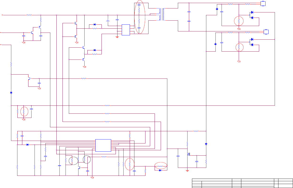
8.2 Power Board
R835
1M 1/10W 5%
Q809
RK7002
C822
1uF/ 25V
R821
1K 1/8W
R820
10K 1/10W 1%
R802
10K 1/10W 1%
D802
BAV99
3
1
2
C845
2.2uF/ 16V
C819
0.0022uF
Q807
N.C
R839
22R 1/8W
D807
LL4148
Q801
PMBS3904
CN802
CONN
1
2
ON/ OF F
R862
1M 1/10W 5%
D806
LL4148
D805
LL4148
穝糤
PWPC7521MYA1 H
Custom
33Friday , Dec ember 21, 2007
715G2852-H ODM MOD EL
3.I NVERTER
G2852-H-X-X-7-071221
OEM MODEL Size
Rev
Date Sheet of
TPV MOD EL
PCB NAME
称爹
T P V ( Top Victory Elect ronics Co . , Ltd. )
Key Component
絬
隔
瓜
絪
腹
DIM
R828
10K 1/10W 1%
C807
0.1uF/ 25V
R827
1K 1/10W 1%
C817
NC
R856
15R 1/ 4W
Q811
PMBS3904
Q812
PMBS3906
1
23
C834
0.1uF/ 25V
R865
NC
C824
0.1uF
Q806
PMBS3904
R804
100R 1/8W
D801
BAV99
3
1
2
R818
1K 1/10W 1%
R837
47K 1/8W
R822
1K 1/8W
F801
0 OHM 1/4W
R829
22R 1/8W
R861
NC
+12V
D811
NC
C838
1500PF/50V
R826
1K 1/8W
D814
LL4148
C823
0.0022uF
R841
68K OHM 1% 1/10W
R831
1K 1/8W
R864
NC
R801
1K5 1/10W 1%
D810
NC
R817
10K 1/10W 1%
R830
NC
AOC 519Fwx
R807
10K 1/10W 1%
C825
0.1uF/ 25V
R814
1K5 1/10W 1%
R854
NC
R851
6K8 1/10W
CN801
CONN
1
2
C839
1500PF/50V
R810
51K OHM 1% 1/8W
R853
68K 1/10W
新增
Q804
PMBS3906
1
23
R855
15R 1/ 4W
R808
10K 1/10W 1%
Q802
AM9945N-T1-PF
1
2
3
4
8
7
6
5
S
G
S
G
D
D
D
D
D812
LL4148
C801
30pF/3KV
R863
10K 1/10W 1%
R825
22R 1/8W
C842
0.01uF
C821
0.1uF/ 25V
C820
220pF50V
C835
NC
+
C802
470UF/25V
T801
POWER X'FMR
6
3
7
4
81
R850
22R 1/8W
Q808
PDTA144WK
R803
680K 1/10W
D817
LL4148
R823
0R05 1/10W 5%
C803
30pF/3KV
Q805
PDTC144WK
IC801 TL494IDR
1
2
3
4
5
6
7
8 9
10
11
12
13
14
15
16
1IN +
1IN -
FEED BACK
DTC
CT
RT
GND
C1 E1
E2
C2
VCC
OUTPUT CTRL
REF
2IN -
2IN +
C846
NC
R824
1K 1/10W 1%
R832
10K 1/10W 1%
- 51 –
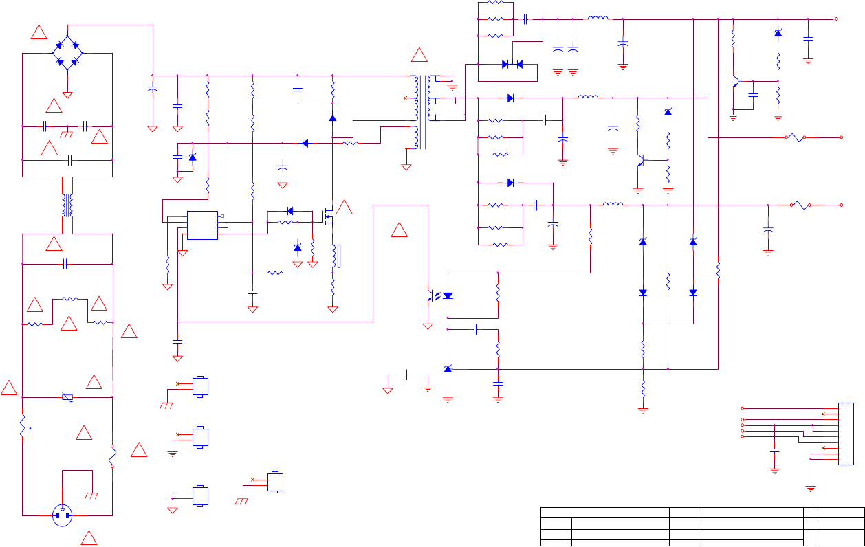
HS2
HEAT SINK(D906_Q90G6263-3)
1
2
ZD906
RLZ22B
1 2
!
R909
5.1 OH M 1/4W
+5V
F903
FUSE
R921 NC
+
C918
680uF/25V
GND 1
GND
1
2
R907
NC
C938
NC
R910
10R 1/4W
!
D915
LL4148
!
+12V
VOL
!
R915
100K OHM 1% 1/8W
R935 100 OHM 1/4W
R918
100 OHM 1/4W
R926
1K 1/10W 1%
R942
1K 1/10W 1%
D903
LL4148
IC902
PC 123X2Y F ZOF
12
43
R932
300K OHM 1/4W
R924
150R 1/8W
C924
0.1uF
F901
FUSE
D916
LL4148
+
C940
1000uF25V
!
PWPC7521MYA1 H
Custom
23Friday , December 21, 2007
715G2852-H OD M MOD EL
2.POWER
G2852-H-X-X-7-071221
OEM MODEL Size
Rev
Date Sheet of
TPV MODEL
PCB NAME
称爹
T P V ( Top Victory Electronics Co . , Ltd. )
Key Component
絬
隔
瓜
絪
腹
R902
680K OHM 1/4W
R912
220 OHM 1/4W
+
C917
680uF/25V
R920
100 OHM 1/4W
Q901
2SK2645-54MR
CN902
CONN
1
2
3
4
5
6
7
8
9
10
CN901
87G 501 32 S
SOCKET
12
3
!
R961 100 OHM 1/4W
DIM
R901
680K OHM 1/4W
VAR901
Varistor
R905
NC
IC 903
AZ431AZ-AE1
D900
FR107
C902
1000pF
+
C921
NC
D901
FR103
+
C907
100uF450V
R919
100 OHM 1/4W
ZD 922
RLZ5.1B
1 2
!
C930
0.1uF
R914
0.47 OHM +-5% 2WS
!
R922 NC
R947
NC
R938
10K 1/8W
FB901
BEAD
12
C928
0.01uF
R925
1K 1/8W
ZD902
RLZ13B
1 2
R943
470R 1/8W
HS5
SHIELD(H85G0002-1)
1
2
R927
3.6K OHM 1% 1/10W
t
NR901
NTCR
+
C915
470uF/16V
+5V1
+
C903
22uF/50V
R904
300K OHM 1/4W
C925
NC
R906
NC
+
C939
NC
ZD905
RLZ18B
1 2
MUTE
N.C
R908
100KOHM +-5% 2WS
C906
1500pF2KV
T901
POWER X'FMR
7
8
9
10
11
12
4
5
6
1
2
!
R948
NC
D905 31DQ06FC3
D907 NC
C911
0.1uF
+
C922
470UF/25V
F902
NC
C910
NC
!
-+
BD901
KBP208G
2
1
3
4
ZD921
RLZ13B
1 2
!
C931
0.1uF
!
C909
470pF/25V
Q903
PMBS3904
HS3
HEAT SINK(Q901_Q90G6263-3)
1
2
C929
0.001uF
C901
1000pF
R952
NC
C908
0.22UF
C912
0.001uF
ON/OFF
C932
0.001uF
!
C900
3300pF 250V
R939
1K 1/8W
!
AOC 519Fwx
IC901
LD7552BPS
1
2
3
4 5
6
7
8
GND
COMP
VCC
RT NC
CS
VCC
OUT
ZD923
NC
1 2
Q904
NC
R933
300K OHM 1/4W
+5V
L901
27mH
1
4
2
3
L905
NC
!
R962 100 OHM 1/4W
R930
2.43K OHM 1% 1/10W
!
L903
1.0uH
R946
150 OHM 2W
R923 NC
R940
33K 1/10W
C904
0.22UF
D906
FCH10U10
1
2
3
!
L904
1.0uH
R900
680K OHM 1/4W
- 52 –
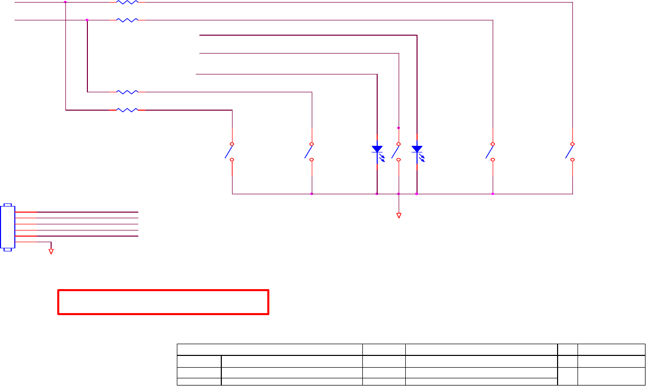
8.3 Key Board
R001
3K 1/10W
POWER
POWER
SW001
SW
GND
KEPC7QH5 2
VSC VA1616W A
22Thursday , December 13, 2007
715G2622-2B N/A
1. Key board
G2622-2B-VSC-X-1-071213
OEM MODEL Size
Rev
Date Sheet of
TPV MODEL
PCB NAME
称爹
T P V ( Top Victory Electronics Co . , Ltd. )
Key Component
絬
隔
瓜
絪
腹
SW002
SW
SW005
SW
KEY2
BLUE
SW004
SW
UP
LED001
BLUE
12
ORANGE
ORANGE
KEY1
R003
2K OHM 1% 1/10W
DOWN
CN101 use wire harness dip.
GND
R002
3K 1/10W
DOWN UP
BLUE
CN001
wireharness/CONN
1
2
3
4
5
6
SW003
SW
R004
2K OHM 1% 1/10W
ON/OFF
KEY 2
LED002
ORANGE
12
KEY1
KEY 1
KEY2
- 53 –
ViewSonic Corporation Confidential - Do Not Cop VA1616w
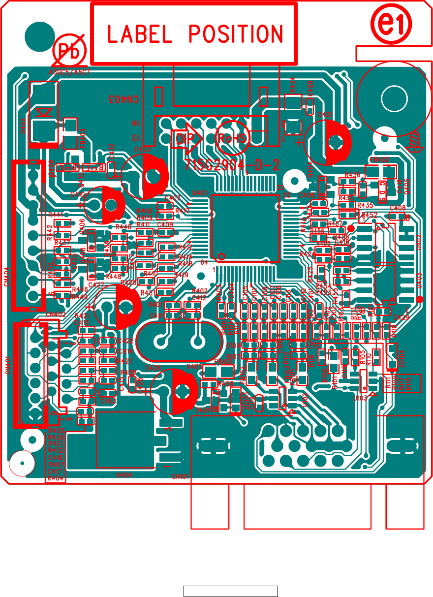
9. PCB Layout Diagram
9.1 MAIN BOARD PCB TOP VIEW
- 54 –
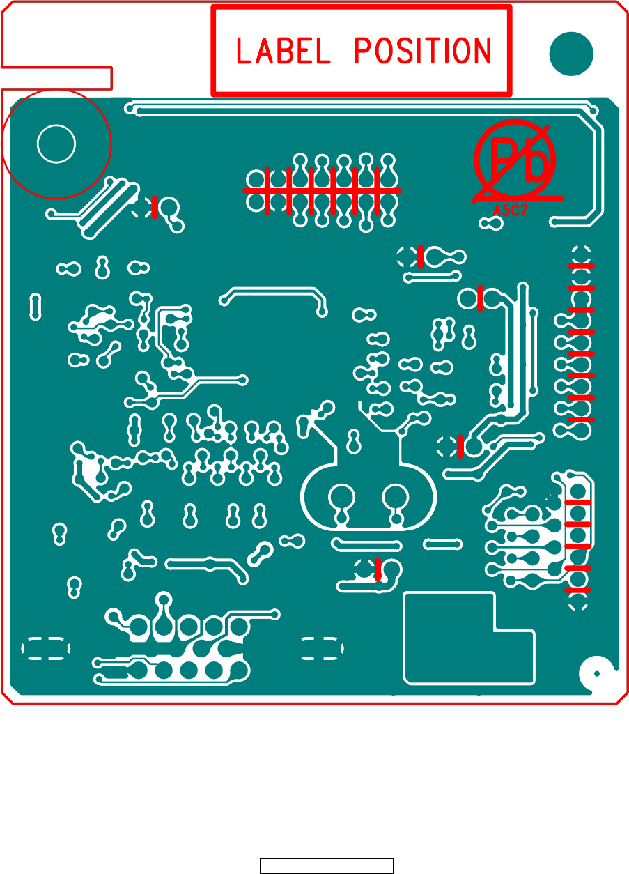
ViewSonic Corporation Confidential - Do Not Cop VA1616w
MAIN BOARD PCB BUTTON VIEW
- 55 –
ViewSonic Corporation Confidential - Do Not Cop VA1616w
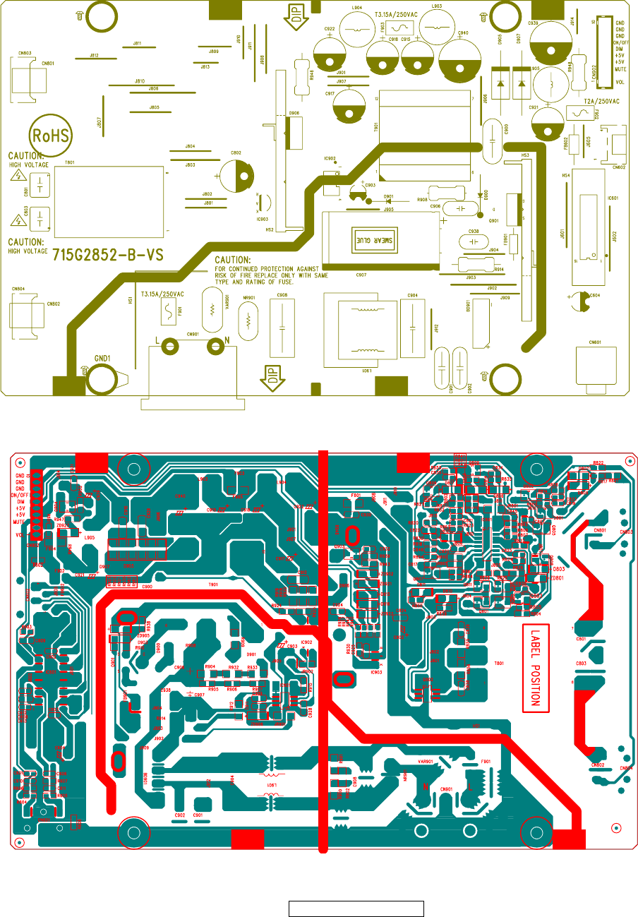
9.2 POWER BOARD TOP VIEW
POWER BOARD BUTTON VIEW
- 56 –
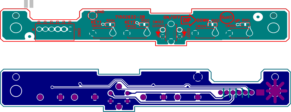
9.3 KEY BOARD TOP VIEW
KEY BOARD BUTTON VIEW
- 57 –
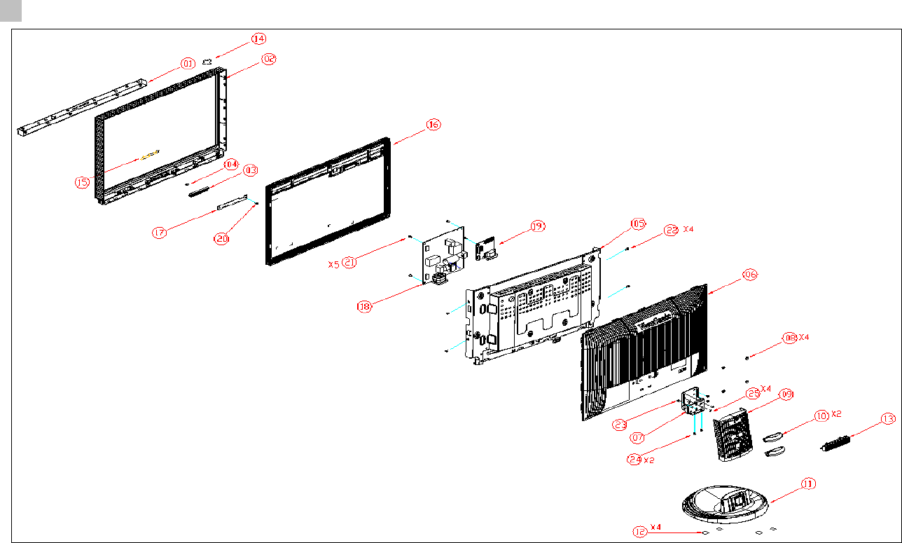
10.Exploded Diagram And Spare Parts List

- 58 –
Item Description Part Number Q'ty
1 DECORATION Q34G0332EB7 1
2 BEZEL Q34G0330 KSA1L0130 1
3 KEY_PAD A33G0216EB7 2B 1
4 LENS_POWER A33G0217 2 1
5 MAINFRAME J15G8B15 1 1
6 REAR COVER Q34G0331 KR 1L 1
7 HINGE Q37G0073011 1
8 RUBBER VESA J12G 808 1 4
9 STAND Q34G0333 KR 1L 1
10 CABLE CLIP A33G0246 KR 1B 2
11 BASE Q34G0334 KR 1L0133 1
12 FOOT Q12G6600 6 4
13 COVER-HINGE Q34G0335 KR 1L 1
14 VSC17-LCD FRONT LOGO 023G3178709 3A 1
15 VSC17-LCD FRONT LOGO 023G3178709 4A 1
16 PANEL M156B1-L01 NB CMO 750GLM56B1112N 1
17 KEY BOARD KEPC8QH8 1
18 POWER BOARD PWPC8521MQW1 1
19 MAIN BOARD 756GQ8CB VV067 1
20 SCREW 3X8MM 0Q1G 330 8120 1
21 SCREW,42-D020523 0M1G1730 6120 5
22 SCREW 0M1G 130 5120 4
23 SCREW 0Q1G1740 10120 1
24 SCREW FOR GROUND 42-D000649 0M1G1740 8 47 CR3 2
25 SCREW FOR GROUND 42-D000649 0M1G1740 8 47 CR3 4
- 59 –
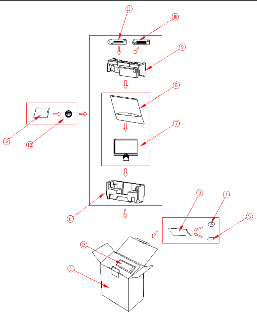
Packing For Shipping

- 60 –
Item Description Part Number Q'ty
1 CARTON Q44G5021709 1A 1
2 HANDLE1/ HANDLE2 050G 600 2/050G 600 3 1
3 PE BAG FOR MANUAL Q45G 76 28 RN R 1
4 CD MANUAL Q70G5000709 2A 1
5 QSG Q41G5000709 3A 1
6 EPS Q44G5021201 1
7 MONITOR T69* 1
8 PE BAG FOR MONITOR Q45G 88607 R 1
9 EPS Q44G5021101 1
10 D-SUB CABLE 089G 728HAA DB 1
11 POWER CORD 089G414A18N YH 1
12 PE BAG FOR BASE Q45G 88606 R 1
13 BASE Q34G0334 KR 1L0133 1

- 61 –
11.Recommended Spare Part List
VA1616W-8 BOM list—T69MM5DY9WVSNN
Item ViewSonic
P/N Ref. P/N Description Universal
number# Q'ty
1 019G6014 1 TIE FOR STRAP 0.1
2 023G3178709 3A LOGO 1
3 023G3178709 4A VSC17-LCD FRONT LOGO 1
4 041G 68508 A CONTROL CARD 0.1
5 050G 600 2 HANDLE1 1
6 050G 600 3 HANDLE2 1
7 052G 1185 24 VSC TAPE 51
8 052G 1186 SMALL TAPE 8
9 052G 1211 B Conductive Tape 85mm *40mm *0.09mm 1
10 089G 728CAA DB D-SUB CABLE---2ND SOURCE 1
11 089G 728GAA DB D-SUB CABLE---2ND SOURCE 1
12 089G 728HAA DB D-SUB CABLE 1
13 095G8018B3X516 LVDS CABLE 1
14 0M1G 130 5120 SCREW 4
15 0M1G1730 6120 SCREW,42-D020523 5
16 0M1G1740 8 47
CR3 SCREW FOR GROUND 42-D000649 4
17 0Q1G 330 8120 SCREW 3X8MM 42A9930017/ 42-D002093 1
18 705GQ834613 15.6"STAND/BASE ASS'Y 1
19 0M1G1740 8 47
CR3 SCREW FOR GROUND 42-D000649 2
20 0Q1G1740 10120 SCREW 1
21 A33G0246 KR 1B CABLE CLIP 2
22 Q12G6600 6 FOOT 4
23 Q34G0333 KR 1L STAND 1
24 Q34G0334 KR
1L0133 BASE 1
25 Q37G0073011 HINGE 1
26 750GLM56B1112N PANEL M156B1-L01 NB CMO 1
27 756GQ8CB VV067 MAIN BOARD-CBPCRM5VSQ1 1
28 100GVMM6001N11 MCU ASS'Y-056G1133 81 1
29 056G1133 81 SST25LF020A-33-4C-SAE 1
30 A33G0216EB7 2B KEY_PAD 1
31 A33G0217 2 LENS_POWER 1
32 040G 45762412B CBPC LABEL 1
33 033G3802 6 WAFER 1
34 033G3802 9 WAFER 9P RIGHT ANELE PITCH 1
35 033G8027 14 H WAFER 14P 2.0MM DIP 1
36 067G 3151014KV EC 105℃ CAP 100UF M 25V 1
37 067G 3151014KV EC 105℃ CAP 100UF M 25V 1

- 62 –
38 067G 3151014KV EC 105℃ CAP 100UF M 25V 1
39 067G 3151014KV EC 105℃ CAP 100UF M 25V 1
40 067G215V100 7R LOW E.S.R 10UF M 50V 1
41 088G 35315F HD D-SUB CONN F ATTACHED SCREW 1
42 093G 22 53 H 14.31818MHZ/30PF/49US 1
43 056G 562557 IC TSUM1PFR-LF 1
44 056G 563 52 IC AP1117D33L-13 TO252-3L DIODES 1
45 056G 662 13 IC AZC099-04S SOT23-6L 1
46 056G 662 13 IC AZC099-04S SOT23-6L 1
47 056G1133 81 SST25LF020A-33-4C-SAE 1
48 057G 417 22 T TRA KN2907AS -60V/-0.6A SOT-23 1
49 057G 417 22 T TRA KN2907AS -60V/-0.6A SOT-23 1
50 057G 417511 MMBT3904 1
51 057G 417512 MMBT3906 1
52 057G 763 1 A03401 SOT23 BY AOS(A1) 1
53 061G0402000 RST CHIP MAX 0R05 1/16W 1
54 061G0402000 RST CHIP MAX 0R05 1/16W 1
55 061G0402000 RST CHIP MAX 0R05 1/16W 1
56 061G0402000 RST CHIP MAX 0R05 1/16W 1
57 061G0402101 RST CHIPR 100 OHM +-5% 1/16W 1
58 061G0402101 RST CHIPR 100 OHM +-5% 1/16W 1
59 061G0402101 RST CHIPR 100 OHM +-5% 1/16W 1
60 061G0402101 RST CHIPR 100 OHM +-5% 1/16W 1
61 061G0402101 RST CHIPR 100 OHM +-5% 1/16W 1
62 061G0402101 RST CHIPR 100 OHM +-5% 1/16W 1
63 061G0402101 RST CHIPR 100 OHM +-5% 1/16W 1
64 061G0402101 RST CHIPR 100 OHM +-5% 1/16W 1
65 061G0402101 RST CHIPR 100 OHM +-5% 1/16W 1
66 061G0402101 RST CHIPR 100 OHM +-5% 1/16W 1
67 061G0402101 RST CHIPR 100 OHM +-5% 1/16W 1
68 061G0402101 RST CHIPR 100 OHM +-5% 1/16W 1
69 061G0402101 RST CHIPR 100 OHM +-5% 1/16W 1
70 061G0402101 RST CHIPR 100 OHM +-5% 1/16W 1
71 061G0402101 RST CHIPR 100 OHM +-5% 1/16W 1
72 061G0402101 RST CHIPR 100 OHM +-5% 1/16W 1
73 061G0402102 RST CHIPR 1 KOHM +-5% 1/16W 1
74 061G0402102 RST CHIPR 1 KOHM +-5% 1/16W 1
75 061G0402103 RST CHIPR 10 KOHM +-5% 1/16W 1
76 061G0402103 RST CHIPR 10 KOHM +-5% 1/16W 1
77 061G0402103 RST CHIPR 10 KOHM +-5% 1/16W 1
78 061G0402103 RST CHIPR 10 KOHM +-5% 1/16W 1
79 061G0402103 RST CHIPR 10 KOHM +-5% 1/16W 1
80 061G0402103 RST CHIPR 10 KOHM +-5% 1/16W 1

- 63 –
81 061G0402103 RST CHIPR 10 KOHM +-5% 1/16W 1
82 061G0402103 RST CHIPR 10 KOHM +-5% 1/16W 1
83 061G0402103 RST CHIPR 10 KOHM +-5% 1/16W 1
84 061G0402103 RST CHIPR 10 KOHM +-5% 1/16W 1
85 061G0402103 RST CHIPR 10 KOHM +-5% 1/16W 1
86 061G0402104 RST CHIPR 100 KOHM +-5% 1/16W 1
87 061G0402121 RST CHIP 120R 1/16W 5% 1
88 061G0402203 RST CHIP 20K 1/16W 5% 1
89 061G0402220 RST CHIPR 22 OHM +-5% 1/16W 1
90 061G0402222 RST CHIPR 2.2 KOHM +-5% 1/16W 1
91 061G0402222 RST CHIPR 2.2 KOHM +-5% 1/16W 1
92 061G0402390 0F RST CHIP 390R 1/16W 1% 1
93 061G0402390 0F RST CHIP 390R 1/16W 1% 1
94 061G0402390 1F RST CHIPR 3.9KOHM +-1% 1/16W 1
95 061G0402390 1F RST CHIPR 3.9KOHM +-1% 1/16W 1
96 061G0402472 RST CHIPR 4.7 KOHM +-5% 1/16W 1
97 061G0402472 RST CHIPR 4.7 KOHM +-5% 1/16W 1
98 061G0402750 RST CHIPR 75 OHM +-5% 1/16W 1
99 061G0402750 RST CHIPR 75 OHM +-5% 1/16W 1
100 061G0402750 RST CHIPR 75 OHM +-5% 1/16W 1
101 061G0603000 RST CHIP MAX 0R05 1/10W 1
102 061G1206331 RST CHIPR 330 OHM +-5% 1/4W 1
103 065G0402104 15 MLCC 0402 0.1UF K 16V X5R 1
104 065G0402104 15 MLCC 0402 0.1UF K 16V X5R 1
105 065G0402104 15 MLCC 0402 0.1UF K 16V X5R 1
106 065G0402104 15 MLCC 0402 0.1UF K 16V X5R 1
107 065G0402104 15 MLCC 0402 0.1UF K 16V X5R 1
108 065G0402104 15 MLCC 0402 0.1UF K 16V X5R 1
109 065G0402104 15 MLCC 0402 0.1UF K 16V X5R 1
110 065G0402104 15 MLCC 0402 0.1UF K 16V X5R 1
111 065G0402104 15 MLCC 0402 0.1UF K 16V X5R 1
112 065G0402104 15 MLCC 0402 0.1UF K 16V X5R 1
113 065G0402104 15 MLCC 0402 0.1UF K 16V X5R 1
114 065G0402104 15 MLCC 0402 0.1UF K 16V X5R 1
115 065G0402104 15 MLCC 0402 0.1UF K 16V X5R 1
116 065G0402104 15 MLCC 0402 0.1UF K 16V X5R 1
117 065G0402104 15 MLCC 0402 0.1UF K 16V X5R 1
118 065G0402104 15 MLCC 0402 0.1UF K 16V X5R 1
119 065G0402220 31 CHIP 22PF 50V NPO 1
120 065G0402220 31 CHIP 22PF 50V NPO 1
121 065G0402220 31 CHIP 22PF 50V NPO 1
122 065G0402220 31 CHIP 22PF 50V NPO 1
123 065G0402224 17 CAP CER 0.22UF -20%-80% 1

- 64 –
124 065G0402473 12 CHIP 0.047UF 16V X7R 1
125 065G0402473 12 CHIP 0.047UF 16V X7R 1
126 065G0402473 12 CHIP 0.047UF 16V X7R 1
127 065G0402473 12 CHIP 0.047UF 16V X7R 1
128 065G0402473 12 CHIP 0.047UF 16V X7R 1
129 065G0402473 12 CHIP 0.047UF 16V X7R 1
130 065G0402473 12 CHIP 0.047UF 16V X7R 1
131 065G0402509 31 CHIP 5PF 50V NPO 1
132 065G0402509 31 CHIP 5PF 50V NPO 1
133 065G0402509 31 CHIP 5PF 50V NPO 1
134 071G 56K121 M
GP 120 OHM 6A 1
135 071G 56V301 M CHIP BEAD 2012 300 OHM 1
136 071G 59K190 B 19 OHM BEAD 1
137 071G 59K190 B 19 OHM BEAD 1
138 071G 59K190 B 19 OHM BEAD 1
139 093G 64 33 DIO SIG SM BAV99 (PHSE)R 1
140 093G 39S 34 T UDZSNP5.6B ROHM 1
141 093G 39S 34 T UDZSNP5.6B ROHM 1
142 093G3004 3 SM340A 1
143 715G2904 1 2 MAIN PCB FR-4 57X64X1.6MM DS 1
144 056G 563916 IC LD1117DT33TR DPAK 1
145 709G2904 QS001 CONSUMPTIVE ASS'Y 1
146 052G 2191 A PAPER TAPE 3.562
147 052G6026 3 MESH PRINTTING PAPER 3.352
148 055G 23520 IPA 0.314
149 055G 100610 TIN CREAM W/O PB 0.265
150 Q05G6054 1 SHEET 0.042
151 Q09G6012 1 PIN 0.008
152 709G2904 QM001 CONSUMPTIVE ASS'Y 1
153 049G 51 1A ERADICATOR 0.116
154 052G 2191 A PAPER TAPE 0.140
155 055G 2 ALCOHOL 1.161
156 055G 23524 WELDING FLUX WITHOUT PB 1.077
157 Q55G 100622 TIN STICK(SAC0507) 0.013
158 Q55G 100625 TIN STICK_LOW ARGENTUM 1.363
159 J12G 808 1 RUBBER VESA 4
160 J15G8B15 1 MAINFRAME 1
161 KEPC8QH8 KEY BOARD 1
162 077G 603 2C TO TACT SWITCH 1
163 077G 603 2C TO TACT SWITCH 1
164 077G 603 2C TO TACT SWITCH 1
165 077G 603 2C TO TACT SWITCH 1

- 65 –
166 077G 603 2C TO TACT SWITCH 1
167 081G 13 B GH LED GHB713A GUANGHONG 1
168 081G 13 Y GH LED GHY713C GUANGHONG 1
169 095G820H 6D506 WIRE HARNESS 6P(SANW)-6P(PH)
100MM 1
170 061G0603200 1F RST CHIPR 2 KOHM +-1% 1/10W 1
171 061G0603200 1F RST CHIPR 2 KOHM +-1% 1/10W 1
172 061G0603300 1F RST CHIPR 3 KOHM +-1% 1/10W 1
173 061G0603300 1F RST CHIPR 3 KOHM +-1% 1/10W 1
174 715G2622 3 KEPC PCB 1
175 PWPC8521MQW1 POWER BOARD 1
176 040G 45762412B CBPC LABEL
177 033G8021 2E F WAFER 1
178 033G8021 2E F WAFER 1
179 033G8021 2E U INVERT CONNECTOR 1
180 033G8021 2E U INVERT CONNECTOR 1
181 056G 139 7 1 IC EL817MA M-TYPE 1
182 056G 139 3A IC PC123Y22FZ0F 1
183 061G 58120 WT NTCR 12OHM 20% 2A SCK-122 1
184 063G 10722410S CAP 0.22UF 275VAC 1
185 063G107K104 6 0.1UF +-10% 1
186 063G107K104 U 0.1UF/275V 1
187 063G107K2246S1 X2 CAP 0.22UF K 275VAC 1
188 065G 3J3006ET 30PF 5% SL 3KV TDK 1
189 065G 3J3006ET 30PF 5% SL 3KV TDK 1
190 065G305M1022BP Y2 1000PF M 250VAC Y5P 1
191 065G305M1022BP Y2 1000PF M 250VAC Y5P 1
192 065G306M2222BP 2200PF +-20% 250VAC 1
193 067G 40Z10115K CAP 105℃ 100UF M 450V 1
194 067G215D4714KV E.C 105℃ CAP 470UF M 25V ED SERIES 1
195 067G215D4714KV E.C 105℃ CAP 470UF M 25V ED SERIES 1
196 067G215D6814KV CAP 105℃ 680UF M 25V 1
197 067G215D6814KV CAP 105℃ 680UF M 25V 1
198 067G215S1024KV EC 105℃ CAP 1000UF M 25V 1
199 067G215Y4714HV EC 105℃ CAP 470UF M 25V 1
200 067G215Y4714HV EC 105℃ CAP 470UF M 25V 1
201 073G 253 91 H CHOKE COIL 1
202 073G 253 91 H CHOKE COIL 1
203 073G 253191 H IND CHOKE 1.1UH DADON 1
204 073G 253191 H IND CHOKE 1.1UH DADON 1
205 073L 174 26H2G INE FILTER 27MH 1
206 073L 174 26S2G LINE FILTER 27MH 1
207 080GL17T 40 H XFMR INVERTER DADON 1

- 66 –
208 080GL17T 40 DN X'FMR TK.2001U.101 1
209 080GL19T 26 T X'FMR 610UH SRW24LQL-T15H016 1
210 087G 501 32 S AC SOCKET 1
211 087G 501 32 S AC SOCKET 1
212 087G 501 32 DL AC SOCKET DIP 3PIN+2PIN GROUND 1
213 093G 50460 28 BRIDGE DIODE KBP208G LITEON 1
214 093G3006 1 1 31DQ06FC3 NIHON INTER 1
215 095G 82010D508 WIRE HARNESS 10P(SAN)-9P(PH) 100MM 1
216 095G 82010E508 WIRE HARNESS 10P(SAN)-9P(PH) 100MM 1
217 095G 82010X508 WIRE HARNESS 10P(SAN)-9P(PH) 100MM 1
218 705GQ757011 Q901 ASS'Y 1
219 057G 667 30 2SK2645 1
220 057G 724 11 STP9NK65ZFP 1
221 0M1G1730 8120 SCREW 1
222 Q90G6263 3 HEAT SINK 1
223 705GQ793053 D906 ASS'Y 1
224 093G 60250 FCH10U10 1
225 093G 60267 SP10100 1
226 0M1G1730 8120 SCREW 1
227 Q90G6263 3 HEAT SINK 1
228 056G 379 22 IC TL494IDR SOIC-16 1
229 056G 379 76 IC LD7552BPS SOP-8 1
230 057G 417 4 PMBS3904/PHILIPS-SMT(04) 1
231 057G 417 4 PMBS3904/PHILIPS-SMT(04) 1
232 057G 417 4 PMBS3904/PHILIPS-SMT(04) 1
233 057G 417 4 PMBS3904/PHILIPS-SMT(04) 1
234 057G 417 6 PMBS3906/PHILIPS-SMT(06) 1
235 057G 417 6 PMBS3906/PHILIPS-SMT(06) 1
236 057G 417 12 T KEC 2N3904S-RTK/PS 1
237 057G 600 55 P5506 HVG SO-8 1
238 057G 759 2 RK7002FD5T116 SOT-23 BY ROHM 1
239 057G 760 4B PDTA144WK SOT346 1
240 057G 760 5B PDTC144WK SOT346 1
241 061G0603000 RST CHIP MAX 0R05 1/10W 1
242 061G0603100 1F RST CHIPR 1 KOHM +-1% 1/10W 1
243 061G0603100 1F RST CHIPR 1 KOHM +-1% 1/10W 1
244 061G0603100 1F RST CHIPR 1 KOHM +-1% 1/10W 1
245 061G0603100 1F RST CHIPR 1 KOHM +-1% 1/10W 1
246 061G0603100 1F RST CHIPR 1 KOHM +-1% 1/10W 1
247 061G0603100 2F RST CHIPR 10K OHM +-1% 1/10W 1
248 061G0603100 2F RST CHIPR 10K OHM +-1% 1/10W 1
249 061G0603100 2F RST CHIPR 10K OHM +-1% 1/10W 1
250 061G0603100 2F RST CHIPR 10K OHM +-1% 1/10W 1

- 67 –
251 061G0603100 2F RST CHIPR 10K OHM +-1% 1/10W 1
252 061G0603100 2F RST CHIPR 10K OHM +-1% 1/10W 1
253 061G0603100 2F RST CHIPR 10K OHM +-1% 1/10W 1
254 061G0603100 2F RST CHIPR 10K OHM +-1% 1/10W 1
255 061G0603105 RST CHIPR 1M OHM +-5% 1/10W 1
256 061G0603105 RST CHIPR 1M OHM +-5% 1/10W 1
257 061G0603150 1F RST CHIPR 1.5 KOHM +-1% 1/10W 1
258 061G0603150 1F RST CHIPR 1.5 KOHM +-1% 1/10W 1
259 061G0603243 1F RST CHIPR 2.43K OHM +-1% 1/10W 1
260 061G0603330 2F RST CHIPR 33K OHM +-1% 1/10W 1
261 061G0603360 1F RST CHIPR 3.6K OHM +-1% 1/10W 1
262 061G0603680 1F RST CHIPR 6.8 KOHM +-1% 1/10W 1
263 061G0603680 2F RST CHIPR 68K OHM +-1% 1/10W 1
264 061G0603683 RST CHIPR 68K OHM +-5% 1/10W 1
265 061G0603684 RST CHIPR 680 KOHM +-5% 1/10W 1
266 061G0805000 RST CHIP MAX 0R05 1/8W 1
267 061G0805100 1F RST CHIPR 1K OHM +-1% 1/8W 1
268 061G0805100 1F RST CHIPR 1K OHM +-1% 1/8W 1
269 061G0805100 1F RST CHIPR 1K OHM +-1% 1/8W 1
270 061G0805100 3F RST CHIPR 100KOHM +-1% 1/8W 1
271 061G0805101 1ST CHIPR 100 OHM +-5% 1/8W 1
272 061G0805102 RST CHIPR 1K OHM +-5% 1/8W 1
273 061G0805102 RST CHIPR 1K OHM +-5% 1/8W 1
274 061G0805102 RST CHIPR 1K OHM +-5% 1/8W 1
275 061G0805103 RST CHIPR 10K OHM +-5% 1/8W 1
276 061G0805151 RST CHIPR 150 OHM +-5% 1/8W 1
277 061G0805220 RST CHIPR 22 OHM +-5% 1/8W 1
278 061G0805220 RST CHIPR 22 OHM +-5% 1/8W 1
279 061G0805220 RST CHIPR 22 OHM +-5% 1/8W 1
280 061G0805220 RST CHIPR 22 OHM +-5% 1/8W 1
281 061G0805471 RST CHIPR 470 OHM +-5% 1/8W 1
282 061G0805473 RST CHIPR 47K OHM +-5% 1/8W 1
283 061G0805510 2F RST CHIPR 51K OHM +-1% 1/8W 1
284 061G1206000 RST CHIP MAX 0R05 1/4W 1
285 061G1206000 RST CHIP MAX 0R05 1/4W 1
286 061G1206000 4 RST CHIP MAX 0R05 1/4W 1
287 061G1206100 RST CHIPR 10 OHM +-5% 1/4W 1
288 061G1206101 RST CHIPR 100 OHM +-5% 1/4W 1
289 061G1206101 RST CHIPR 100 OHM +-5% 1/4W 1
290 061G1206101 RST CHIPR 100 OHM +-5% 1/4W 1
291 061G1206101 RST CHIPR 100 OHM +-5% 1/4W 1
292 061G1206101 RST CHIPR 100 OHM +-5% 1/4W 1
293 061G1206101 RST CHIPR 100 OHM +-5% 1/4W 1

- 68 –
294 061G1206150 RST CHIPR 15 OHM +-5% 1/4W 1
295 061G1206150 RST CHIPR 15 OHM +-5% 1/4W 1
296 061G1206221 RST CHIPR 220 OHM +-5% 1/4W 1
297 061G1206304 RST CHIPR 300K OHM +-5% 1/4W 1
298 061G1206304 RST CHIPR 300K OHM +-5% 1/4W 1
299 061G1206304 RST CHIPR 300K OHM +-5% 1/4W 1
300 061G1206519 RST CHIPR 5.1 OHM +-5% 1/4W 1
301 061G1206684 RST CHIPR 680K OHM +-5% 1/4W 1
302 061G1206684 RST CHIPR 680K OHM +-5% 1/4W 1
303 061G1206684 RST CHIPR 680K OHM +-5% 1/4W 1
304 065G0603102 32 1000PF +-10% 50V X7R 1
305 065G0603103 32 CAP CHIP 0603 0.01UF K 50V X7R 1
306 065G0603104 22 CAP CHIP 0603 0.1UF K 25V X7R 1
307 065G0603104 22 CAP CHIP 0603 0.1UF K 25V X7R 1
308 065G0603104 22 CAP CHIP 0603 0.1UF K 25V X7R 1
309 065G0603104 22 CAP CHIP 0603 0.1UF K 25V X7R 1
310 065G0603222 22 CHIP 2200PF 25V X7R 1
311 065G0603222 22 CHIP 2200PF 25V X7R 1
312 065G0805103 32 CAP CHIP 0805 10NF K 50V X7R 1
313 065G0805104 32 CAP CHIP 0805 0.1UF K 50V X7R 1
314 065G0805104 32 CAP CHIP 0805 0.1UF K 50V X7R 1
315 065G0805104 32 CAP CHIP 0805 0.1UF K 50V X7R 1
316 065G0805104 32 CAP CHIP 0805 0.1UF K 50V X7R 1
317 065G0805104 32 CAP CHIP 0805 0.1UF K 50V X7R 1
318 065G080510522K
T CAP CHIP 0805 1UF K 25V X7R 1
319 065G0805152 31 1.5NF/50V 1
320 065G0805152 31 1.5NF/50V 1
321 065G080522131G CAP CHIP 0805 220PF G 50V NPO 1
322 065G0805225 12 CAP CHIP 0805 2.2UF K 16V X7R 1
323 065G0805471 21 CAP CHIP 0805 470PF J 25V NPO 1
324 065G1206102 72 CAP CHIP 1206 1000PF K 500V X7R 1
325 065G1206102 72 CAP CHIP 1206 1000PF K 500V X7R 1
326 093G 6432P LL4148 1
327 093G 6432P LL4148 1
328 093G 6432P LL4148 1
329 093G 6432P LL4148 1
330 093G 6432P LL4148 1
331 093G 6432P LL4148 1
332 093G 6432P LL4148 1
333 093G 6432P LL4148 1
334 093G 6432P LL4148 1
335 093G 6433P BAV99 1

- 69 –
336 093G 6433P BAV99 1
337 093G 39S 20 T RLZ22B LLDS 1
338 093G 39S 25 T RLZ5.1B LLDS 1
339 093G 39S 40 T RLZ 13B LLDS 1
340 093G 39S 40 T RLZ 13B LLDS 1
341 093G 39S 44 T RLZ18B LLDS 1
342 006G 31500 EYELET 2
343 056G 158 10 T IC AS431AZTR-E1 TO-92 1
344 061G152M10452T RST MOFR 100KOHM +-5% 2WS 1
345 061G152M15152T RST MOFR 150 OHM +-5% 2WS 1
346 061G152M47852T RST MOFR 0.47 OHM +-5% 2WS 1
347 065G 2K152
1T6213 CAP CER 1500PF K 2KV 1
348 067G 2152207NT KY50VB22M-TP5 5*11 1
349 067G215S4713KT 470UF 16V 1
350 071G 55 29 FERRITE BEAD 1
351 084G 56 3W FUSE 1
352 093G 6026T52T RECTIFIER DIODE FR107 1
353 093G 6038T52T FR103 1
354 095G 90 23 JUMPER 1
355 095G 90 23 JUMPER 1
356 095G 90 23 JUMPER 1
357 095G 90 23 JUMPER 1
358 095G 90 23 JUMPER 1
359 095G 90 23 JUMPER 1
360 095G 90 23 JUMPER 1
361 095G 90 23 JUMPER 1
362 095G 90 23 JUMPER 1
363 095G 90 23 JUMPER 1
364 095G 90 23 JUMPER 1
365 095G 90 23 JUMPER 1
366 095G 90 23 JUMPER 1
367 095G 90 23 JUMPER 1
368 095G 90 23 JUMPER 1
369 095G 90 23 JUMPER 1
370 095G 90 23 JUMPER 1
371 095G 90 23 JUMPER 1
372 095G 90 23 JUMPER 1
373 095G 90 23 JUMPER 1
374 095G 90 23 JUMPER 1
375 095G 90 23 JUMPER 1
376 095G 90 23 JUMPER 1
377 095G 90 23 JUMPER 1

- 70 –
378 095G 90 23 JUMPER 1
379 715G2852 1 VS POWER-PCB FR-1 193X122X1.6MM SS 1
380 067G215Y2207KT CAP 105℃ 22UF M 50V KINGNICHI 1
381 084G 56 3 B FUSE 3.15A 250V 1
382 056G 158 12 KIA431A-AT/P TO-92 1
383 084G 56 3 B FUSE 3.15A 250V 1
384 709G2852 QA001 CONSUMPTIVE ASS'Y 1
385 052G 2191 A PAPER TAPE 0.335
386 095G 90 23 JUMPER 1.255
387 057G 417 12 T KEC 2N3904S-RTK/PS 1
388 057G 417 12 T KEC 2N3904S-RTK/PS 1
389 057G 417 12 T KEC 2N3904S-RTK/PS 1
390 057G 417 13 T KEC 2N3906S-RTK/PS 1
391 057G 417 13 T KEC 2N3906S-RTK/PS 1
392 057G 763 14 AM9945N 1
393 093G 6433S DIODE BAV99 SEMTECH 1
394 093G 6433S DIODE BAV99 SEMTECH 1
395 093G 64S522SEM LL4148 1
396 093G 64S522SEM LL4148 1
397 093G 64S522SEM LL4148 1
398 093G 64S522SEM LL4148 1
399 093G 64S522SEM LL4148 1
400 093G 64S522SEM LL4148 1
401 093G 64S522SEM LL4148 1
402 093G 64S522SEM LL4148 1
403 093G 64S522SEM LL4148 1
404 709G2852 QS001 CONSUMPTIVE ASS'Y 1
405 052G 2191 A PAPER TAPE 2.244
406 Q05G6054 1 SHEET 0.026
407 Q09G6012 1 PIN 0.005
408 Q51G 100502 GLUE_RED_MALER 0.045
409 S80GL19T26V1 TRANSFORMER ASS'Y 1
410 071FPL24108 04 PC47 LQ2425 A315 1
411 709G2852 QM001 CONSUMPTIVE ASS'Y 1
412 049G 51 1A ERADICATOR 0.164
413 052G 2191 A PAPER TAPE 0.140
414 055G 2 ALCOHOL 1.675
415 055G 23524 WELDING FLUX WITHOUT PB 2.142
416 Q51G 6 4509 GLUE_RTV 0.500
417 Q55G 100622 TIN STICK(SAC0507) 0.037
418 Q55G 100625 TIN STICK_LOW ARGENTUM 4.334
419 705GQ851002 OIL FOR DISAPPEAR ASS'Y 1
420 051G 200 1 OIL FOR DISAPPEAR 0.020

- 71 –
421 Q07G 1 5V60 WOODEN PALLET 0.011
422 Q34G0330
KSA1L0130 BEZEL L156W-7VSC3 1
423 Q34G0331 KR 1L REAR COVER 1
424 Q34G0332EB7 1L DECORATION 1
425 Q34G0335 KR 1L COVER-HINGE 1
426 Q40G 15N709 2A RATING LABEL 1
427 Q40G 58170931A HT POT LABEL 1
428 Q40G0001624 4A PALLET LABEL 0.050
429 Q40G0001709 2A SN LANEL 1
430 Q40G000270927A EPA LABEL 1
431 Q44G5021101 EPS 1
432 Q44G5021201 EPS 1
433 Q44G5021709 1A 15 LCD VSC CARTON 1
434 Q44G6000 213A EMPTY CARTON FOR LOADING 0.011
435 Q44G6000 214A EMPTY CARTON FOR LOADING 0.011
436 Q44G6002112 94 PAPER BOARD 0.022
437 Q44G6002CP1A24 PAPER CAP 0.011
438 Q44G9003208 CORNER PAPER 0.045
439 Q45G 88606 R PE BAG FOR BASE 1
440 Q45G 88607 R PE BAG FOR MONITOR 1
441 Q52G6020114 PROTECT FILM 1
442 Q41G2401709 4A WARRANTY CARD 1
443 Q41G5000709 3A VA1616 QSG FOR CHINA 1
444 Q45G 76 28 RN
R PE BAG FOR MANUAL 1
445 Q70G5000709 2A VA1616W CD MANUAL 1
446 040G 581 26704 SHIPPING LABEL 0.010
447 040G 58162435A P/N LABEL FOR MANUAL PE BAG 1
448 Q40G 581709 1B CARTON LABEL 1
449 Q50G 4 10 TIE 30.000
450 045G 77501 BARCODE RIBBON 0.350
451 Q40G 58170930A LABEL 1
452 Q40G000270938A CARTON STICK+CEL LABEL FOR
VA1616W 1
453 Q40G000270926A MANUFACTURE ADDRESS STICKER 1
454 089G414A18N YH POWER CORD(32E1818021) 1
455 089G414A18N IS POWER CORD 32E1818021---2ND
SOURCE 1
456 Q41G5000709 4A ROHS CARD 1
457 052G6019 1 INSULATING TAPE 30.000
458 052G 2191 A PAPER TAPE 10.000
459 052G 1185 MIDDLE TAPE 20.000
460 Q45G2007C0103A PE BAG FOR CARTON 1
- 72 –
* Reader’s Response*
Dear Readers:
Thank you in advance for you feedback on our Service Manual, which allows continuous
improvement of our products. We would appreciate your completion of the Assessment Matrix
below, for return to ViewSonic Corporation.
Assessment
A. What do you think about the content after reading VA1616w-8 Service Manual?
Unit Excellent Good Fair Bad
1. Precautions And Safety Notice
2. Specification
3. Front Panel Control and Indicators
4. Circuit Description
5. Adjustment Procedure
6. Troubleshooting Flow Chart
7. Block Diagram
8. Schematic Diagram
9. PCB Layout Diagram
10. Exploded Diagram And Spare Parts List
11. Recommended Spare Parts List
B. Are you satisfied with the VA1616w-8 Service Manual?
Item Excellent Good Fair Bad
1. Service Manual Content
2. Service Manual Layout
3. The form and listing
C. Do you have any opinion and suggestion about this Service Manual?
Reader’s Basic Data:
Name: Title:
Company:
Add:
Tel: F a x :
E-Mail:
After completing this form, please return it to ViewSonic Quality Assurance in the USA at
facsimile 1-909-839-7943. You may also e-mail any suggestion to the Director, Quality System
& Process (marc.maupin@viewsonic.com)
