VLSI LAB MANUAL
User Manual:
Open the PDF directly: View PDF ![]() .
.
Page Count: 120 [warning: Documents this large are best viewed by clicking the View PDF Link!]
MUFFAKHAM JAH COLLEGE OF ENGINEERING
AND TECHNOLOGY
(Affliated to Osmania University)
Banjara Hills, Hyderabad, Telangana
DEPARTMENT
OF
INFORMATION TECHNOLOGY

VLSI DESIGN LAB MANUAL
TABLE OF CONTENTS
S.No.
Content
Page No.
1.
Institute Vision
i
2.
Institute Mission
i
3.
Department Vision
ii
4.
Department Mission
ii
5.
PEOs
iii
6.
POs
iv
7.
PSOs
v
8.
General Guidelines and safety instructions
vi
9.
Introduction to VLSI DESIGN laboratory
vii
List of Programs
Program No.
Page. No
1
SWITCH LEVEL MODELLING
1.1
OBTAIN LOGIC GATE DESIGN OF NOT , NAND , NOR IN
CMOS
1,2,3
1,3,5
1.2
OBTAIN OAI AND AOI LOGIC GATES OF THE FUNCTION
1.2.1
F=[ab+ac+bd ]‘-----AOI
4
7
1.2.2
F=[(a+b)(a+c)(b+d)]‘---OAI
5
9
1.3
TRANSMISSION GATE DESIGN
1.3.1
2:1 MUX
6
12
1.3.2
XOR GATE
7
14
1.3.3
X-NOR GATE
8
16
1.3.4
OR GATE
9
18
1.4
COMPLEX LOGIC GATES USING CMOS
1.4.1
F=[a+b(c+d)]‘
10
21

VLSI DESIGN LAB MANUAL
1.4.2
S-R LATCH
11
23
2
STRUCTURAL GATE LEVEL MODELLING (WITH AND WITHOUT
DELAYS)
2.1
OBTAIN FUNCTION F=[a+b+ac+bd]‘ using gate level modeling
12
25
2.2
DESIGN HALF ADDER
13
28
2.3
DESIGN FULL ADDER USING 2 HALF ADDER & AN OR
GATE
14
31
2.4
IMPLEMENT 2:1 MUX USING TRI STATE BUFFERS
15
34
2.5
IMPLEMENT 4:1 MUX USING 2:1 MULTIPLEXERS
16
37
2.6
SR LATCH
17
40
2.7
D LATCH
18
43
3
HIERARCHICAL MODELING
3.1
CONSTRUCT A 4 INPUT AND GATE USING 2-INPUT NAND
& NOR GATES
19
46
3.2
CONSTRUCT AN 2:4 ACTIVE HIGH DECODER USING
CMOS 2-INPUT NOR & NOT GATES
20
48
3.3
SR LATCH
21
50
3.4
D LATCH
22
52
4
RTL & BEHAVIORAL MODELING
4.1
DESIGN A 4:1 MULTIPLEXER USING RTL &
BEHAVIOURAL MODELLING
23
57
14.2
DESIGN A 2:4 ACTIVE HIGN DECODER USING RTL &
BEHAVIOURSL MODELLING
24
60
4.3
DESIGN A 4 BIT PRIORITY ENCODER USING RTL &
BEHAVIOURSL MODELLING
25
63
4.4
DESIGN A 4 BIT NEGATIVE EDGE TRIGGERED MASTER
SLAVE JK FLIP FLOP USING RTL
26
67
4.5
DESIGN A 4 BIT POSTIVE EDGE TRIGGERED MASTER
SLAVE D FLIP FLOP USING RTL
27
70

VLSI DESIGN LAB MANUAL
4.6
DESIGN A 4 BIT POSTIVE EDGE TRIGGERED MASTER
SLAVE T FLIP FLOP USING RTL
28
72
4.7
DESIGN A 4-BIT LOADABLE SISO/PIPO SHIFT REGISTER
USING RTL
29
74
4.8
IMPLEMENT RIPPLE CARRY ADDER USING RTL AND
BEHAVIORAL MODELING
30
77
4.9
IMPLEMENT CARRY LOOK AHEAD ADDER USING RTL
AND BEHAVIORAL MODELING
31
80
4.10
IMPLEMENT REGISTER MULTIPLIER USING RTL AND
BEHAVIORAL MODELING
32
83
4.11
IMPLEMENT ARRAY MULTIPLIER USING RTL
MODELING
33
85
5
LAYOUT DESIGNING [DSCH2 & MICROWIND2]
5.1
OBTAIN LAYOUT DESIGN OF NOT GATE IN CMOS
34
88
5.2
OBTAIN LAYOUT DESIGN OF NAND GATE IN CMOS
35
91
5.3
OBTAIN LAYOUT DESIGN OF NOR GATE IN CMOS
36
93
ANNEXURE –I OU PRESCRIBED SYLLABUS
95
ANNEXURE – II PROGRAMMING LAB EVALUATION
RUBRIC
96

VLSI DESIGN LAB MANUAL
INFORMATION TECHNOLOGY DEPARTMENT, MJCET i
1. Vision of the Institution:
To be part of universal human quest for development and progress by
contributing high calibre, ethical and socially responsible engineers who
meet the global challenge of building modern society in harmony with
nature.
2. Mission of the Institution
To attain excellence in imparting technical education from the
undergraduate through doctorate levels by adopting coherent and
judiciously coordinated curricular and co-curricular programs
To foster partnership with industry and government agencies through
collaborative research and consultancy
To nurture and strengthen auxiliary soft skills for overall development
and improved employability in a multi-cultural work space
To develop scientific temper and spirit of enquiry in order to harness the
latent innovative talents
To develop constructive attitude in students towards the task of nation
building and empower them to become future leaders
To nourish the entrepreneurial instincts of the students and hone their
business acumen.
To involve the students and the faculty in solving local community
problems through economical and sustainable solutions.

VLSI DESIGN LAB MANUAL
INFORMATION TECHNOLOGY DEPARTMENT, MJCET ii
3. Department Vision
Fostering a bright technological future by enabling the students to
function as leaders in software industry and serve as means of
transformation to empower society through ITeS.
4. Department Mission
To create an ambience of academic excellence through state of art
infrastructure and learner-centric pedagogy leading to employability in
multi-disciplinary fields.

VLSI DESIGN LAB MANUAL
INFORMATION TECHNOLOGY DEPARTMENT, MJCET iii
5. Programme Education Objectives
1. Graduates will demonstrate technical competence and leadership in their
chosen fields of employment by identifying, formulating, analyzing and
creating efficient IT solutions.
2. Graduates will communicate effectively as individuals or team members
and be successful in varied working environment.
3. Graduates will demonstrate lifelong learning through continuing
education and professional development.
4. Graduates will be successful in providing viable and sustainable solutions
within societal, professional, environmental and ethical context

VLSI DESIGN LAB MANUAL
INFORMATION TECHNOLOGY DEPARTMENT, MJCET iv
6. Programme Outcomes
1.
Engineering knowledge
: Apply the knowledge of mathematics, science,
engineering fundamentals and an engineering specialization to the solution of
complex engineering problems.
2.
Problem analysis
: Identify, formulate, review research literature, and analyze
complex engineering problems reaching substantiated conclusions using first
principles of mathematics, natural sciences, and engineering sciences.
3.
Design/development of solutions
: Design solutions for complex engineering
problems and design system components or processes that meet the specified needs
with appropriate consideration for the public health and safety, and the cultural,
societal, and environmental considerations.
4.
Conduct investigations of complex problems:
Use research-based knowledge
and research methods including design of experiments, analysis and interpretation
of data, and synthesis of the information to provide valid conclusions.
5.
Modern tool usage
: Create, select, and apply appropriate techniques, resources,
and modern engineering and IT tools including prediction and modeling to
complex
e
ngineering activities with an understanding of the limitations.
6.
The engineer and society
: Apply reasoning informed by the contextual knowledge
to assess societal, health, safety, legal and cultural issues and the consequent
responsibilities relevant to the professional engineering practice.
7.
Environment and sustainability
: Understand the impact of the professional
engineering solutions in societal and environmental contexts, and demonstrate the
knowledge of, and need for sustainable development.
8.
Ethics
: Apply ethical principles and commit to professional ethics and
responsibilities and norms of the engineering practice.
9.
Individual and team work
: Function effectively as an individual, and as a
member or leader in diverse teams, and in multidisciplinary settings.
10.
Communication
: Communicate effectively on complex engineering activities with
the engineering community and with society at large, such as, being able to
comprehend and write effective reports and design documentation, make effective
presentations, and give and receive clear instructions.
11.
Project management and finance
: Demonstrate knowledge and understanding of
the engineering and management principles and apply these to one‘s own work, as
a member and leader in a team, to manage projects and in multidisciplinary
environments.
12.
Lifelong learning
: Recognize the need for, and have the preparation and ability to
engage in independent and lifelong learning in the broadest context of
technological change.

VLSI DESIGN LAB MANUAL
INFORMATION TECHNOLOGY DEPARTMENT, MJCET v
7. Programme Specific Outcomes:
PSO1: The IT graduates will work as software engineers for providing
solutions to real world problems using structured and object oriented
programming languages and open source software.
PSO2: The IT graduates will work as System engineer, Software analyst and
Tester for IT and ITes.

VLSI DESIGN LAB MANUAL
INFORMATION TECHNOLOGY DEPARTMENT, MJCET vi
MUFFAKHAM JAH COLLEGE OF ENGINEERING AND
TECHNOLOGY
DEPARTMENT OF INFORMATION TECHNOLOGY
VLSI DESIN LAB
GENERAL GUIDELINES AND SAFETY INSTRUCTIONS
1. Sign in the log register as soon as you enter the lab.
2. Strictly observe lab timings.
3. Strictly follow the written and verbal instructions given by the teacher / Lab Instructor
4. It is mandatory to come to lab in a formal dress and wear your ID cards.
5. Do not wear loose-fitting clothing or jewelry in the lab.
6. Mobile phones should be switched off in the lab.
7. Keep the labs clean at all times, no food and drinks allowed inside the lab.
8. Do not tamper with computer configurations
9. Playing games on the computers is strictly prohibited.
10. Use of Internet during laboratory timings is prohibited
11. Shut down the computer and switch off the monitor before leaving your table.
12. Handle the Trainer kits with care.
13. Don't plug any external devices / Pen drives without permission from lab staff.
14. Don't install any software without the permission of the Lab Incharge.
15. Observation book and lab record should be carried to each lab.
16. Be sure of location of fire extinguishers and first aid kits in the laboratory.
17. Please take care of your personal belongings. Lab Incharges /Staff are not responsible for
any loss of your belongings.

VLSI DESIGN LAB MANUAL
INFORMATION TECHNOLOGY DEPARTMENT, MJCET vii
8. Introduction TO VLSI DESIGN Laboratory
Verilog Theory:
Verilog is a HARDWARE DESCRIPTION LANGUAGE (HDL). A hardware
description language is a language used to describe a digital system: for example, a network
switches, a microprocessor or a memory or a simple flip-flop. This just means that, by using a
HDL, one can describe any (digital) hardware at any level. Verilog HDL is case sensitive
Design Styles:
The traditional method of electronic design is bottom-up. Each design is performed at
the gate-level using the standard gates. With the increasing complexity of new designs this
approach is nearly impossible to maintain. New systems consist of ASIC or microprocessors
with a complexity of thousands of transistors. These traditional bottom-up designs have to
give way to new structural, hierarchical design methods. Without these new practices it
would be impossible to handle the new complexity.
Bottom-Up Design:
The desired design-style of all designers is the top-down one. A real top-down design
allows early testing, easy change of different technologies, a structured system design and
offers many other advantages. But it is very difficult to follow a pure top-down design. Due
to this fact most designs are a mix of both methods, implementing some key elements of both
design styles.
History of Verilog:
When Cadence gave OVI the LRM, several companies began working on Verilog
simulators. In 1992, the first of these were announced, and by 1993 there were several
Verilog simulators available from companies other than Cadence. The most successful of
these was VCS, the Verilog Compiled Simulator, from Chronologic Simulation. This was a
true compiler as opposed to an interpreter, which is what Verilog-XL was. As a result,
compile time was substantial, but simulation execution speed was much faster.

VLSI DESIGN LAB MANUAL
INFORMATION TECHNOLOGY DEPARTMENT, MJCET viii
Various stages of ASIC/ FPGA IC design flow.
Specification
High Level Design
Micro Design/Low level design
RTL Coding
Simulation
Synthesis
Place & Route
Post Silicon Validation
Simulation:
It is the process of verifying the functional characteristics of models at any level of
abstraction. We use simulators to simulate the Hardware models, to test if the RTL code
meets the functional requirements of the specification. To achieve this we need to write a test
bench, which generates clk, reset and the required test vectors. A sample test bench for a
counter is shown below. Normally we spend 60-70% of time in design verification.
Synthesis:
It is the process in which synthesis tools like design compiler take RTL in Verilog or VHDL,
target technology, and constrains as input and maps the RTL to target technology primitives.
Synthesis tool, after mapping the RTL to gates, also do the minimal amount of timing
analysis to see if the mapped design is meeting the timing requirements. (Important thing to
note is, synthesis tools are not aware of wire delays, they only know of gate delays). After the
synthesis there are a couple of things that are normally done before passing the netlist to
backend (Place and Route).
Place and Route:
The gate level netlist from the synthesis tool is taken and imported into place and
route tool in Verilog netlist format. All the gates and flip-flops are placed; clock tree
synthesis and reset is routed. After this each block is routed. The PAR tool output is a GDS
file, used by foundry for fabricating the ASIC. Backend team normally dumps out SPEF
(standard parasitic exchange format) /RSPF (reduced parasitic exchange format)/DSPF

VLSI DESIGN LAB MANUAL
INFORMATION TECHNOLOGY DEPARTMENT, MJCET ix
(detailed parasitic exchange format) from layout tools like ASTRO to the frontend team, who
then use the read_parasitic command in tools like Prime Time to write out SDF (standard
delay format) for gate level simulation purposes.
Module:
In Verilog, we call our "black boxes" module. This is a reserved word within the program
used to refer to things with inputs, outputs, and internal logic workings.
wire data type is used for connecting two points.
reg data type is used for storing values
Here we have only two types of ports, input and output. In real life, we can have bi-
directional ports as well. Verilog allows us to define bi-directional ports as "inout."
Operators:
Nearly all operators are exactly the same as their counterparts in the C programming
language.
Control Statements:
If-else statements check a condition to decide whether or not to execute a portion of
code. If a condition is satisfied, the code is executed. Else, it runs this other portion of code.
One could use any operator in the condition checking, as in the case of C language. If
needed we can have nested if else statements; statements without else are also ok, but they
have their own problem, when modeling combinational logic, in case they result in a Latch
(this is not always true).
Case statements are used where we have one variable which needs to be checked for
multiple values. like an address decoder, where the input is an address and it needs to be
checked for all the values that it can take. Instead of using multiple nested if-else statements,
one for each value we're looking for, we use a single case statement: this is similar to switch
statements in languages like C++.

VLSI DESIGN LAB MANUAL
INFORMATION TECHNOLOGY DEPARTMENT, MJCET x
A while statement executes the code within it repeatedly if the condition it is assigned
to check returns true. While loops are not normally used for models in real life, but they are
used in test benches. As with other statement blocks, they are delimited by begin and end.
For loops in Verilog are almost exactly like for loops in C or C++. The only
difference is that the ++ and -- operators are not supported in Verilog.
Repeat is similar to the for loop. Instead of explicitly specifying a variable and
incrementing it when we declare the for loop, we tell the program how many times to run
through the code, and no variables are incremented.
While, if-else, case (switch) statements are the same as in C language.
If-else and case statements require all the cases to be covered for combinational logic.
For-loop is the same as in C, but no ++ and -- operators.
Repeat is the same as the for-loop but without the incrementing variable.
Combinational elements can be modeled using assign and always statements.
Sequential elements can be modeled using only always statement.
There is a third block, which is used in test benches only: it is called Initial statement.
An initial block, as the name suggests, is executed only once when simulation starts.
This is useful in writing test benches. If we have multiple initial blocks, then all of
them are executed at the beginning of simulation.
always: As the name suggests, an always block executes always, unlike initial blocks
which execute only once (at the beginning of simulation). A second difference is that
an always block should have a sensitive list or a delay associated with it.
The sensitive list is the one which tells the always block when to execute the block of
code. The @ symbol after reserved word ' always', indicates that the block will be
triggered "at" the condition in parenthesis after symbol @.
One important note about always block: it cannot drive wire data type, but can drive
reg and integer data types.
An assign statement is used for modeling only combinational logic and it is executed
continuously. So the assign statement is called 'continuous assignment statement' as
there is no sensitive list.

VLSI DESIGN LAB MANUAL
INFORMATION TECHNOLOGY DEPARTMENT, MJCET xi
Tasks and Functions:
When repeating the same old things again and again, Verilog, like any other
programming language, provides means to address repeated used code, these are called Tasks
and Functions.
Functions and tasks have the same syntax; one difference is that tasks can have
delays, whereas functions can not have any delay. This means that function can be used for
modeling combinational logic.
A second difference is that functions can return a value, whereas tasks cannot.
Module Instantiation
Modules are the building blocks of Verilog designs
You create the design hierarchy by instantiating modules in other modules.
You instance a module when you use that module in another, higher-level module
Ports: Ports allow communication between a module and its environment.
All but the top-level modules in a hierarchy have ports.
Ports can be associated by order or by name.
Registers: store the last value assigned to them until another assignment statement
changes their value.
Registers represent data storage constructs.
We can create regs arrays called memories.
Register data types are used as variables in procedural blocks.
Register data type is required if a signal is assigned a value within a procedural block
Procedural blocks begin with keyword initial and always.
Gate level primitives:
Verilog has built in primitives like gates, transmission gates, and switches. These are
rarely used in design (RTL Coding), but are used in post synthesis step for modeling
the ASIC/FPGA cells; these cells are then used for gate level simulation, or what is
called as SDF simulation. Also the output netlist format from the synthesis tool,
which is imported into the place and route tool, is also in Verilog gate level
primitives. Ex: and , or etc:

VLSI DESIGN LAB MANUAL
INFORMATION TECHNOLOGY DEPARTMENT, MJCET xii
There are six different switch primitives (transistor models) used in Verilog, nmos,
pmos and cmos and the corresponding three resistive versions rnmos, rpmos and
rcmos. The cmos types of switches have two gates and so have two control signals.
Transmission gates tran and rtran are permanently on and do not have a control line.
Tran can be used to interface two wires with separate drives, and rtran can be used to
weaken signals. Resistive devices reduce the signal strength which appears on the
output by one level. All the switches only pass signals from source to drain; incorrect
wiring of the devices will result in high impedance outputs.
Delays:
In real circuits, logic gates have delays associated with them. Verilog provides the
mechanism to associate delays with gates
Rise, Fall and Turn-off delays.
Minimal, Typical, and Maximum delays.
In Verilog delays can be introduced with #'num' as in the examples below, where # is
a special character to introduce delay, and 'num' is the number of ticks simulator
should delay current statement execution
The rise delay is associated with a gate output transition to 1 from another value (0, x,
z).
The fall delay is associated with a gate output transition to 0 from another value (1, x,
z).
The Turn-off delay is associated with a gate output transition to z from another value
(0, 1, x).
The min value is the minimum delay value that the gate is expected to have.
The typ value is the typical delay value that the gate is expected to have.
The max value is the maximum delay value that the gate is expected to have.
User Defined Primitives (UDP):
Verilog has built-in primitives like gates, transmission gates, and switches. This is a
rather small number of primitives; if we need more complex primitives, then Verilog
provides UDP, or simply User Defined Primitives. Using UDP we can model.

VLSI DESIGN LAB MANUAL
INFORMATION TECHNOLOGY DEPARTMENT, MJCET xiii
Combinational Logic
Sequential Logic
UDP begins with reserve word primitive and ends with endprimitive. Ports/terminals of
primitive should follow. This is similar to what we do for module definition. UDPs should be
defined outside module and endmodule.
UDP port rules:
An UDP can contain only one output and up to 10 inputs.
Output port should be the first port followed by one or more input ports.
All UDP ports are scalar, i.e. Vector ports are not allowed.
UDPs cannot have bidirectional ports.
The output terminal of a sequential UDP requires an additional declaration as type
reg.
It is illegal to declare a reg for the output terminal of a combinational UDP.
Functionality of primitive (both combinational and sequential) is described inside a
table, and it ends with reserved word 'endtable'. For sequential UDP, we can use
initial to assign an initial value to output.
Note: An UDP cannot use 'z' in the input table
table: It is used for describing the function of UDP. Verilog reserved word table
marks the start of table and reserved word endtable marks the end of table. Each line inside a
table is one condition; when an input changes, the input condition is matched and the output
is evaluated to reflect the new change in input.
initial: This statement is used for initialization of sequential UDPs. This statement
begins with the keyword 'initial'. The statement that follows must be an assignment statement
that assigns a single bit literal value to the output terminal reg.
Concatenations: are expressed using the brace characters { & }, with commas
separating the expressions within.
o Example: + {a, b[3:0], c, 4'b1001} // if a and c are 8-bit numbers, the results
has 24 bits
Unsized constant numbers are not allowed in concatenations.

VLSI DESIGN LAB MANUAL
INFORMATION TECHNOLOGY DEPARTMENT, MJCET xiv
Abstraction Levels:
Behavioral Models: Higher level of modeling where behavior of logic is modeled.
RTL Models : Logic is modeled at register level
Structural Models: Logic is modeled at both register level and gate level.
Procedural Blocks:
Verilog behavioral code is inside procedure blocks, but there is an exception: some
behavioral code also exist outside procedure blocks.
initial: initial blocks execute only once at time zero (start execution at time zero).
always: always blocks loop to execute over and over again; in other words, as the
name suggests, it executes always.
Procedural Assignment Statements:
Procedural assignment statements assign values to reg, integer, real, or time variables
and cannot assign values to nets (wire data types)
Procedural Group Statements:
If a procedure block contains more than one statement, those statements must be enclosed
within
Sequential begin - end block
Parallel fork - join block
When using begin-end, we can give name to that group. This is called named blocks
begin - end
Group several statements together.
Cause the statements to be evaluated sequentially (one at a time)
Any timing within the sequential groups is relative to the previous statement.
Delays in the sequence accumulate (each delay is added to the previous delay)
Block finishes after the last statement in the block
fork - join

VLSI DESIGN LAB MANUAL
INFORMATION TECHNOLOGY DEPARTMENT, MJCET xv
Group several statements together.
Cause the statements to be evaluated in parallel (all at the same time).
Timing within parallel group is absolute to the beginning of the group.
Block finishes after the last statement completes (Statement with highest delay, it can
be the first statement in the block).
Blocking and Nonblocking Assignment Statements:
Blocking assignments are executed in the order they are coded, hence they are
sequential. Since they block the execution of next statement, till the current statement
is executed, they are called blocking assignments. Assignment are made with "="
symbol.
Example a = b;
Nonblocking assignments are executed in parallel. Since the execution of next
statement is not blocked due to execution of current statement, they are called
nonblocking statement. Assignments are made with "<=" symbol. Example a <= b;
assign and deassign:
The assign and deassign procedural assignment statements allow continuous
assignments to be placed onto registers for controlled periods of time. The assign
procedural statement overrides procedural assignments to a register. The deassign
procedural statement ends a continuous assignment to a register.
force and release:
Another form of procedural continuous assignment is provided by the force and
release procedural statements. These statements have a similar effect on the assign-
deassign pair, but a force can be applied to nets as well as to registers. One can use force
and release while doing gate level simulation to work around reset connectivity problems.
Also can be used insert single and double bit errors on data read from memory.

VLSI DESIGN LAB MANUAL
INFORMATION TECHNOLOGY DEPARTMENT, MJCET xvi
Casex and casez:
Special versions of the case statement allow the x ad z logic values to be used as
"don't care".
Looping statements:
Appear inside procedural blocks only; Verilog has four looping statements like any
other programming language.
The forever loop executes continually, the loop never ends. Normally we use forever
statements in initial blocks.
The repeat loop executes < statement > a fixed < number > of times
The while loop executes as long as an < expression > evaluates as true. This is the
same as in any other programming language.
The for loop is the same as the for loop used in any other programming language.
Continuous assignment statements drive nets (wire data type). They represent
structural connections.
VLSI DESIGN LAB MANUAL
INFORMATION TECHNOLOGY DEPARTMENT, MJCET 1
1. SWITCH LEVEL MODELLING
Program 1
1.1 OBTAIN LOGIC GATE DESIGN OF NOT, NAND, NOR IN CMOS
Aim:-
Design a logic gate in CMOS
Software Requirements:
Synthesis tool:
Xilinx Project
navigator – ISE
14.7
Simulation tool:
ModelSim
Simulator
Description: Digital logic circuits are non linear networks that use transistors as electronic
switches to divert one of the supply voltages VDD or 0V to the output. This corresponds to a logic
result of f-1 or f=0.
An important characteristic of a CMOS circuit is the duality that exists between its PMOS
transistors and NMOS transistors. According to the De Morgan's laws based logic, the PMOS
transistors in parallel have corresponding NMOS transistors in series while the PMOS transistors
in series have corresponding NMOS transistors in parallel.
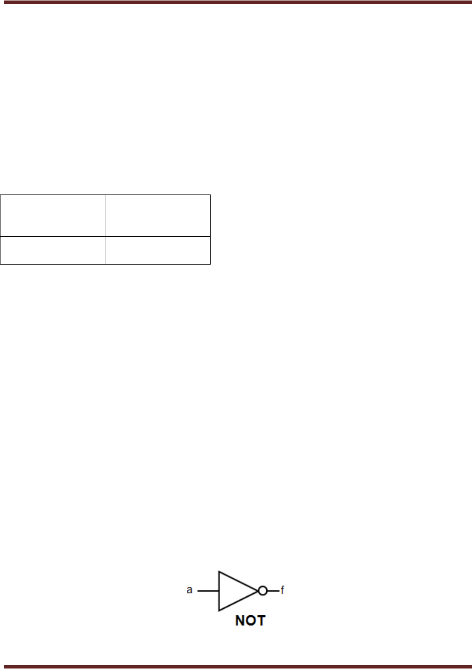
The NOT or the INVERT function is the simplest Boolean operation. It has an input ‗a‘ and
produces output f(a) i.e. it implements logical negation.
An important feature of CMOS is the manner in which complementary FET pair ensures that
always a path from the output to either the power source VDD or ground. To accomplish this, the
set of all paths to the voltage source must be the complement of the set of all paths to ground.
This can be easily accomplished by defining one in terms of the NOT of the other.
LOGIC SYMBOL
VLSI DESIGN LAB MANUAL
INFORMATION TECHNOLOGY DEPARTMENT, MJCET 2
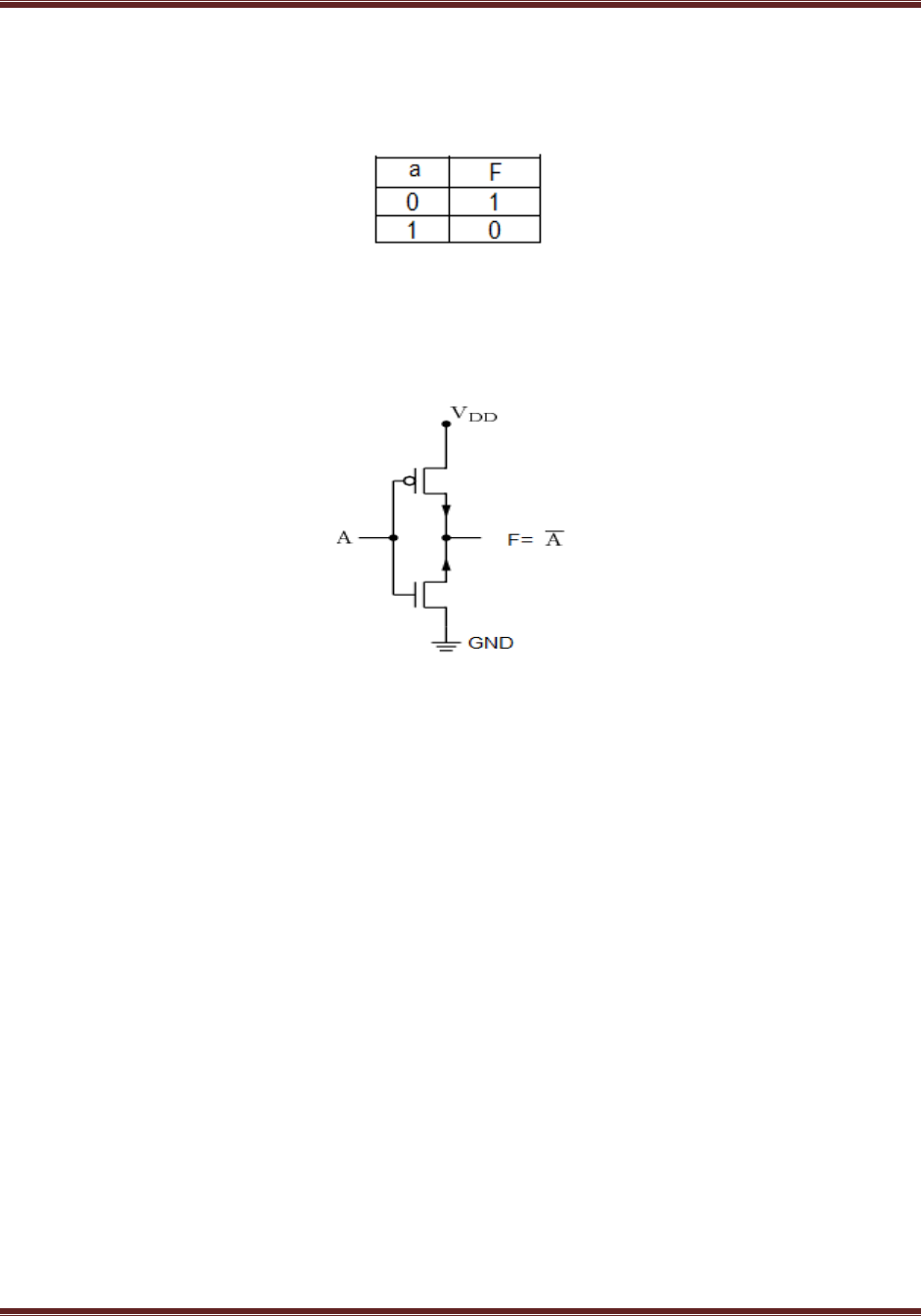
TRUTH TABLE
LOGIC DIAGRAM
VERILOG CODE
module not1(a,f);
input a;
output f;
supply1 vdd;
supply0 gnd;
pmos p(f,vdd,a);
nmos n(f,gnd,a);
endmodule
OUTPUT
The Truth Table of not gate is verified.
VLSI DESIGN LAB MANUAL
INFORMATION TECHNOLOGY DEPARTMENT, MJCET 3
Program 2
OBTAIN LOGIC GATE DESIGN OF NAND IN CMOS
Aim:-
Write Verilog code for two input logic gates
Software Requirements:
Synthesis tool:
Xilinx Project
navigator – ISE
14.7
Simulation tool:
ModelSim
Simulator
Description: Digital logic circuits are non linear networks that use transistors as electronic
switches to divert one of the supply voltages VDD or 0V to the output. This corresponds to a logic
result of f=1 or f=0.
An important characteristic of a CMOS circuit is the duality that exists between its PMOS
transistors and NMOS transistors. According to the De Morgan's laws based logic, the PMOS
transistors in parallel have corresponding NMOS transistors in series while the PMOS transistors
in series have corresponding NMOS transistors in parallel.
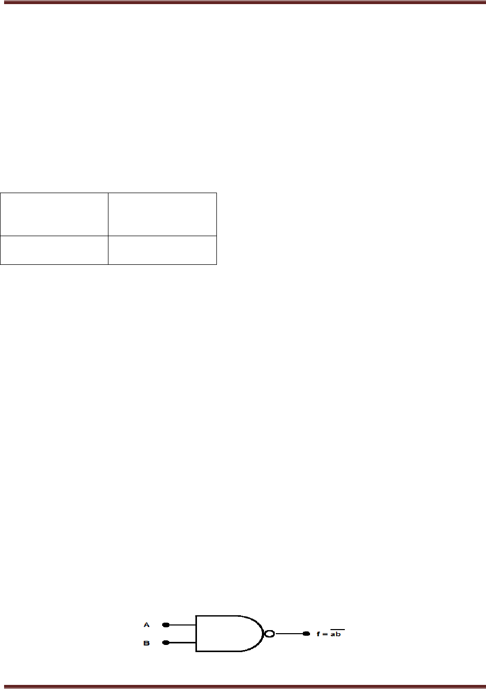
A NAND2 gate is that it uses two parallel connected pFET‘s while the nFET‘s are in series. The
NAND gate is characterized by an output that is 0 unless both of the inputs are 1.
In a two-input CMOS NAND (NAND2) gate the two series connected nMOS transistors creates
a conducting path between output node and the ground only if both input voltages are set to
VOH i.e. both the parallel pMOS transistors will be off. For all other input combinations, either
one or both of the pMOS transistors will be turned on, while the path of the nMOS transistors
will be cut-off, thus creating a current path between the output node and the power supply
voltage.
LOGIC SYMBOL
VLSI DESIGN LAB MANUAL
INFORMATION TECHNOLOGY DEPARTMENT, MJCET 4
TRUTH TABLE
LOGIC DIAGRAM
VERILOG CODE
module cmosnand(f,a,b);
input a;
input b;
output f;
wire w1;
supply1 vdd;
supply0 gnd;
pmos p1(f,vdd,a);
pmos p2(f,vdd,b);
nmos n1(f,w1,a);
nmos n2(w1,gnd,b);
endmodule
OUTPUT:
The Truth Table of NAND gate is verified.
VLSI DESIGN LAB MANUAL
INFORMATION TECHNOLOGY DEPARTMENT, MJCET 5
Program 3
OBTAIN LOGIC GATE DESIGN OF NOR IN CMOS
Aim:-
a) Write Verilog code for two input logic gates
Software Requirements:
Synthesis tool:
Xilinx Project
navigator – ISE
14.7
Simulation tool:
ModelSim
Simulator
Description: An important characteristic of a CMOS circuit is the duality that exists between its
PMOS transistors and NMOS transistors. According to the De Morgan's laws based logic, the
PMOS transistors in parallel have corresponding NMOS transistors in series while the PMOS
transistors in series have corresponding NMOS transistors in parallel.
The NOR gate has 2 PMOS and 2 NMOS transistors. It uses two parallel connected nFET‘s
while the pFET‘s are in series. The NOR gate is characterized by an output 1 only if both of the
inputs are 1.
When either one or both inputs are high, the nMOS transistor(s) creates a conducting path
between the output node and ground, and the pMOS transistors are cut-off i.e f =0v.. When both
input voltages are low, the nMOS transistors are cut-off and the pMOS transistors create a
conducting path between the output node and the supply voltage VDD thus giving output high.
LOGIC SYMBOL
TRUTH TABLE
VLSI DESIGN LAB MANUAL
INFORMATION TECHNOLOGY DEPARTMENT, MJCET 6
LOGIC DIAGRAM
VERILOG CODE
module cmosnor(x,a,b);
input a;
input b;
output f;
wire w1;
supply1 vdd;
supply0 gnd;
pmos p1(w1,vdd,a);
pmos p2(f,w1,b);
nmos n1(f,gnd,a);
nmos n2(f,gnd,b);
endmodule
OUTPUT:
The Truth Table of NOR gate is verified.
VLSI DESIGN LAB MANUAL
INFORMATION TECHNOLOGY DEPARTMENT, MJCET 7
Program 4
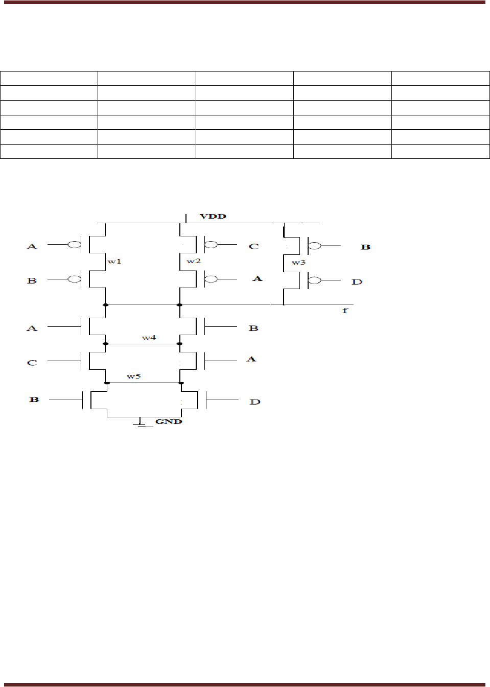
1.2 OBTAIN OAI AND AOI LOGIC GATES OF THE FUNCTION
12.1 F=[ab+ac+bd ]’-----AOI
Aim:-
Write Verilog code for AOI F=[ab+ac+bd ]‘
Software Requirements:
Synthesis tool:
Xilinx Project
navigator – ISE
14.7
Simulation tool:
ModelSim
Simulator
Description: An important characteristic of a CMOS circuit is its inverting nature which allows
it to construct logic circuits for AOI logic expression using a structured approach.
AOI gates perform one or more AND operations followed by an OR operation and then an
inversion. AOI function is an inverted sum of products ISOP
Construction of AOI cells is particularly efficient using CMOS technology where the total
number of transistor gates can be compared to the same construction using NAND logic or NOR
logic. The complement of AOI Logic is OR-AND-Invert (OAI) logic where the OR gates
precede a NAND gate.
LOGIC SYMBOL
TRUTH TABLE
A
B
C
D
F
0
0
0
0
1
0
1
0
1
0
1
0
1
0
0
1
1
0
0
0
1
1
1
1
0
VLSI DESIGN LAB MANUAL
INFORMATION TECHNOLOGY DEPARTMENT, MJCET 8
LOGIC DIAGRAM
VERILOG CODE
module aoi(a,b,c,d,f);
input a;
input b;
input c;
input d;
output f;
supply1 vdd;
supply0 gnd;
wire w1,w2,w3,w4,w5;
pmos p1(w1,vdd,a);
pmos p2(w1,vdd,b);
pmos p3(w2,w1,a);
pmos p4(w2,w1,c);
pmos p5(f,w2,b);
pmos p6(f,w2,d);
nmos n1(w3,gnd,b);
nmos n2(f,w3,a);
nmos n3(w4,gnd,c);
nmos n4(f,w4,a);
nmos n5(w5,gnd,d);
nmos n6(f,w5,b);
endmodule
OUTPUT:
The Truth Table of AOI is verified.
VLSI DESIGN LAB MANUAL
INFORMATION TECHNOLOGY DEPARTMENT, MJCET 9
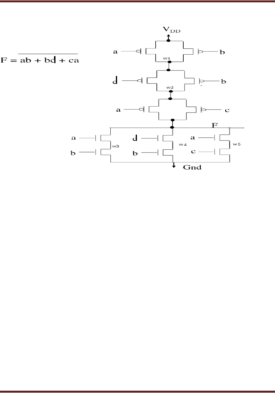
Program 5
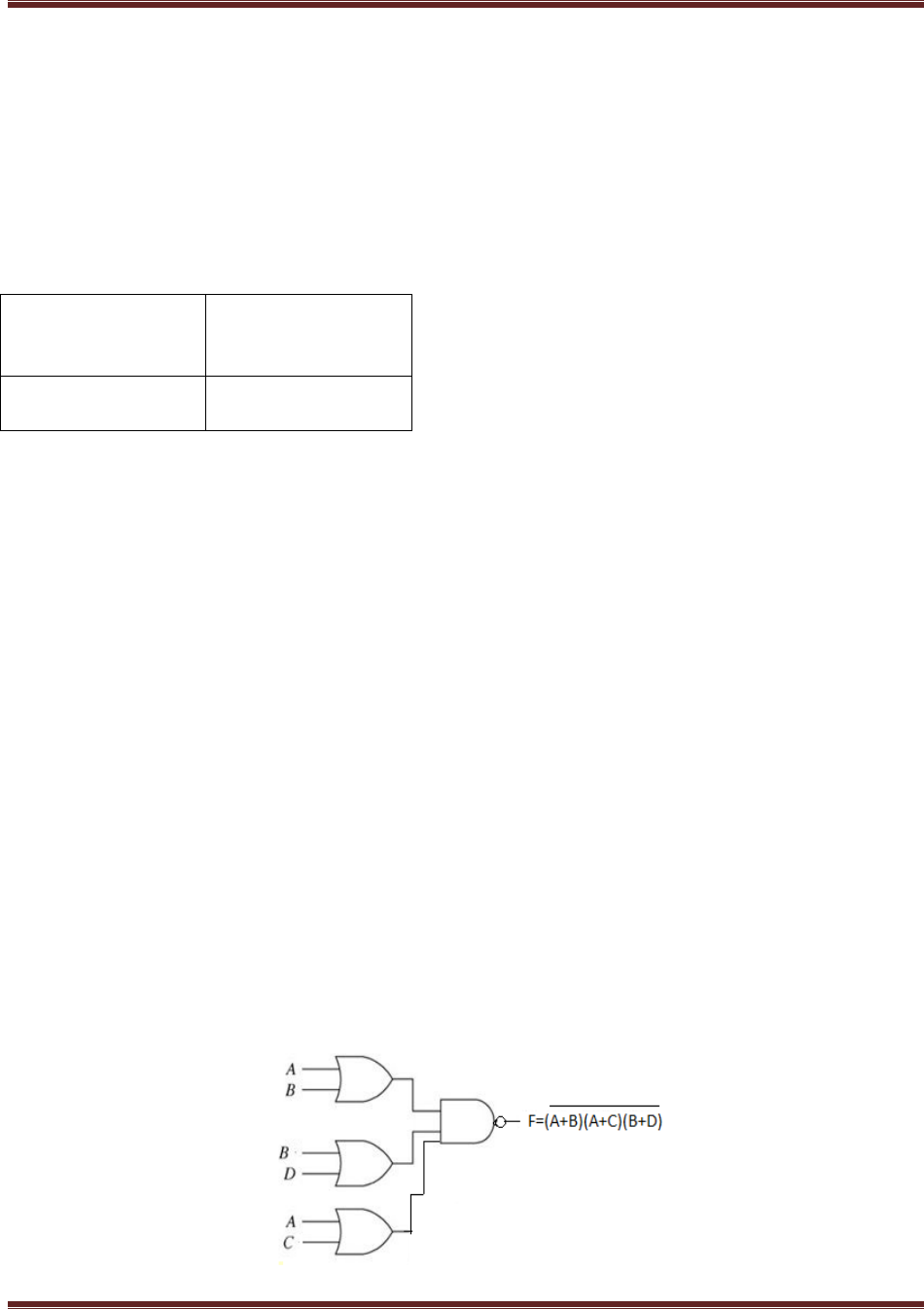
1.2.2 F=[(a+b)(a+c)(b+d)]’---OAI
AIM:-
Write Verilog code for AOI F=[(a+b)(a+c)(b+d)]‘
SOFTWARE REQUIREMENTS:
Synthesis tool:
Xilinx Project
navigator – ISE
14.7
Simulation tool:
ModelSim
Simulator
DESCRIPTION: CMOS logic gates are intrinsically inverting. The output always produces a
NOT operation acting on the input variables. The inverting nature of CMOS logic circuits allows
us to construct logic circuits for AOI and OAI expressions using a structured approach.
OAI logic function implements the operations in the order OR then AND then NOT. An Or-And-
Invert (OAI) CMOS gate is similar to the AOI gate except that it is an implementation of
product-of-sums realization of a function
Behaviors of nMOS and pMOS groups are Parallel-connected nMOS gives OR-NOT operations
whereas Parallel-connected pMOS gives AND-NOT operations Series-connected nMOS results
AND-NOT operations whereas Series-connected pMOS gives OR-NOT.
The OAI are implemented in the following way:
• The N-tree is implemented as follows:
– Each product term is a set of parallel transistors for each input in the term
– All product terms (parallel groups) are put in series
– The complete function is again assumed to be an inverted representation
• The P-tree can be implemented as the dual of the N-tree
LOGIC SYMBOL
VLSI DESIGN LAB MANUAL
INFORMATION TECHNOLOGY DEPARTMENT, MJCET 10
TRUTH TABLE
A
B
C
D
F
0
0
0
0
1
0
1
0
1
1
0
1
1
1
0
1
1
0
0
1
1
1
1
1
0
LOGIC DIAGRAM
VERILOG CODE
module oai(a,b,c,d,f);
input a;
input b;
input c;
input d;
output f;
supply1 vdd;
supply0 gnd;
wire w1,w2,w3,w4,w5;
pmos p1(w3,vdd,a);
pmos p2(f,w3,b);
pmos p3(w4,vdd,a);
pmos p4(f,w4,c);
pmos p5(w5,vdd,b);
pmos p6(f,w5,d);
nmos n1(w1,gnd,b);

VLSI DESIGN LAB MANUAL
INFORMATION TECHNOLOGY DEPARTMENT, MJCET 11
nmos n2(w1,gnd,d);
nmos n3(w2,w1,a);
nmos n4(w2,w1,c);
nmos n5(f,w2,a);
nmos n6(f,w2,b);
endmodule
OUTPUT:
The Truth Table of OAI is verified.
VLSI DESIGN LAB MANUAL
INFORMATION TECHNOLOGY DEPARTMENT, MJCET 12
Program 6
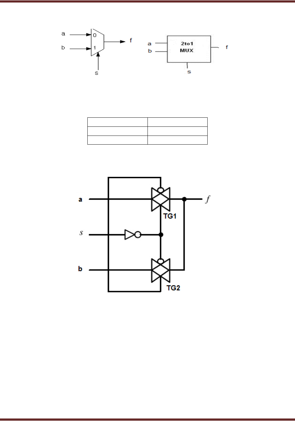
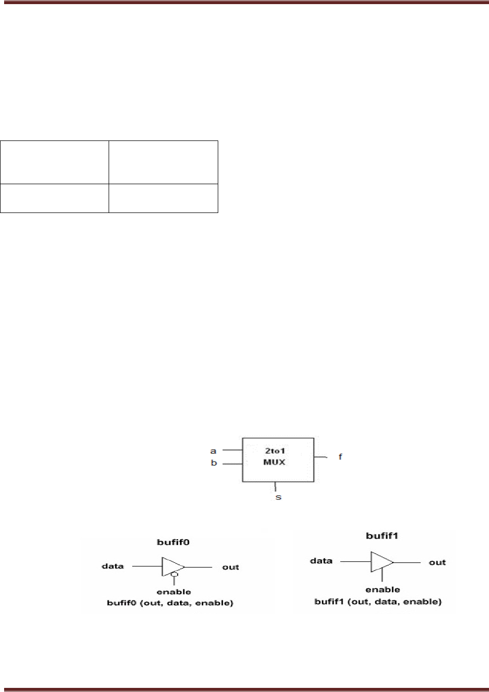
1.3 TRANSMISSION GATE DESIGN
1.3.1 Design a 2:1 MUX using TRANSMISSION GATE
Aim:-
Write Verilog code for 2:1 mux using Transmission gates.
Software Requirements:
Synthesis tool:
Xilinx Project
navigator – ISE
14.7
Simulation tool:
ModelSim
Simulator
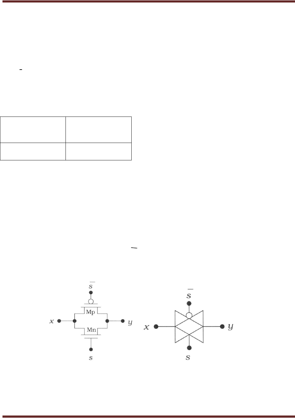
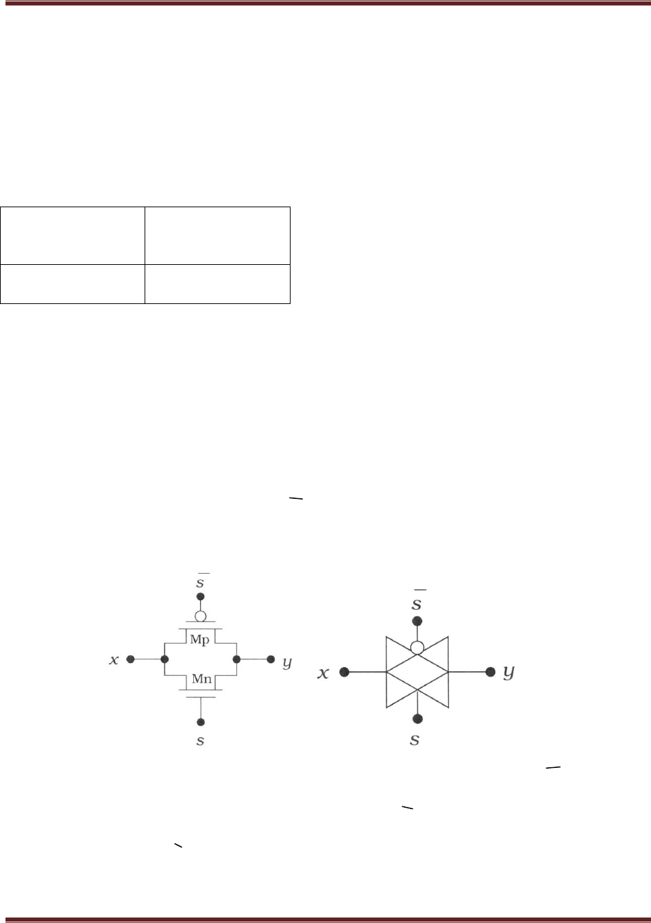
Description: A CMOS Transmission gate is created by connecting an nFET and pFET in
parallel. It has the following characteristics.
» It is a Bi-directional switch
» It Transmit the entire voltage range [0, VDD]
» Both transistors are ON or OFF simultaneously.
» The NMOS switch passes a good zero but a poor 1.
» The PMOS switch passes a good one but a poor 0.
Controlled by gate select signals, s and s
--if s = 1, y = x, switch is closed, transistors are on
– if s = 0, y = unknown (high impedance), switch open, transistors are off
In 2:1 mux when the select signal has a value s=0, one pair of Transmission gate is closed while
other is open giving the first input as output but if s=1 the second input goes as output.
VLSI DESIGN LAB MANUAL
INFORMATION TECHNOLOGY DEPARTMENT, MJCET 13
LOGIC SYMBOL
TRUTH TABLE
s
F
0
A
1
B
LOGIC DIAGRAM
VERILOG CODE
module mux(a,b,s,f);
input a;
input b;
input s;
output f;
wire sb;
not(sb,s);
cmos tg1(f,a,sb,s);
cmos tg2(f,b,s,sb);
endmodule
OUTPUT: The Truth Table of TRANSMISSION GATE is verified.

VLSI DESIGN LAB MANUAL
INFORMATION TECHNOLOGY DEPARTMENT, MJCET 14
Program 7
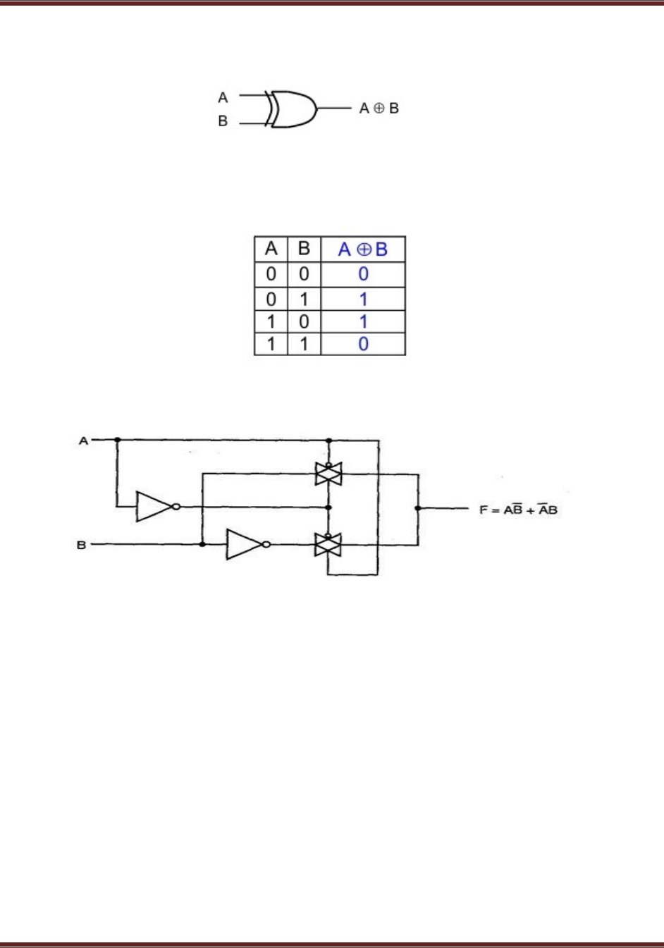
1.3.2 Design a XOR using TRANSMISSION GATE
Aim:-
Write Verilog code for XOR using transmission gate
Software Requirements:
Synthesis tool:
Xilinx Project
navigator – ISE
14.7
Simulation tool:
ModelSim
Simulator
Description: A CMOS Transmission gate is created by connecting an nFET and pFET in
parallel. It has the following characteristics.
» It is a Bi-directional switch
» It Transmit the entire voltage range [0, VDD]
» Both transistors are ON or OFF simultaneously.
» The NMOS switch passes a good zero but a poor 1.
» The PMOS switch passes a good one but a poor 0.
Controlled by gate select signals, s and s
--if s = 1, y = x, switch is closed, transistors are on
– if s = 0, y = unknown (high impedance), switch open, transistors are off
In XOR gate implementation of transmission gate the input to the top transmission gate is b, this
is inverted and given as input to the second TG2.The input ‗a‘ and its compliment are used to
control the TGs. When a=0 the upper TG is closed and ‗b‘ is passed to the output while a=1
closes the lower TG is closed and ‗b‘ compliment is passed to the output.
VLSI DESIGN LAB MANUAL
INFORMATION TECHNOLOGY DEPARTMENT, MJCET 15
LOGIC SYMBOL
TRUTH TABLE
LOGIC DIAGRAM
VERILOG CODE
module xortg(a,b,f);
input a;
input b;
output f;
wire ab,bb;
not(ab,a);
not(bb,b);
cmos tg1(f,b,ab,a);
cmos tg2(f,bb,a,ab);
endmodule
OUTPUT:
The Truth Table of XOR TRANSMISSION GATE is verified.
VLSI DESIGN LAB MANUAL
INFORMATION TECHNOLOGY DEPARTMENT, MJCET 16
Program 8
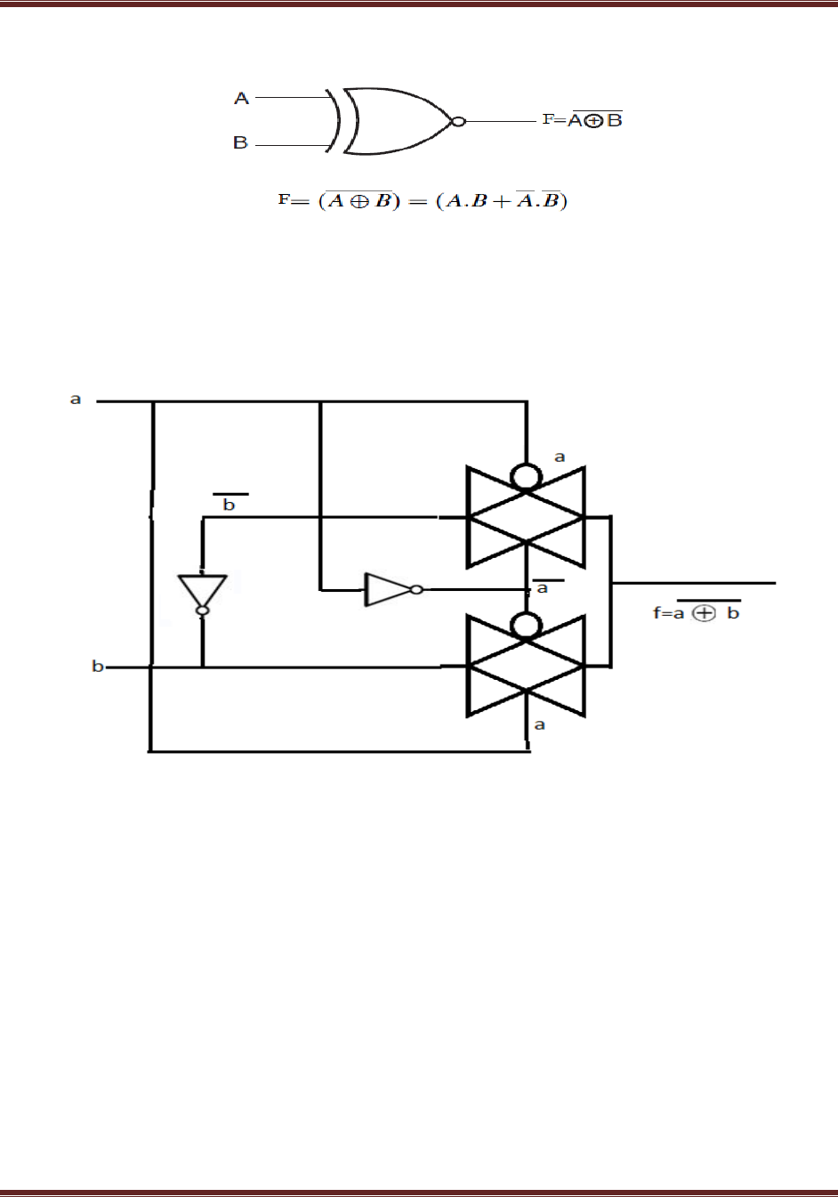
1.3.3 Design a XNOR gate using TRANSMISSION GATE
Aim:-
a) Write Verilog code for XNOR using transmission gate
Software Requirements:
Synthesis tool:
Xilinx Project
navigator – ISE
14.7
Simulation tool:
ModelSim
Simulator
Description: A CMOS Transmission gate is created by connecting an nFET and pFET in
parallel. It has the following characteristics.
» It is a Bi-directional switch
» It Transmit the entire voltage range [0, VDD]
» Both transistors are ON or OFF simultaneously.
» The NMOS switch passes a good zero but a poor 1.
» The PMOS switch passes a good one but a poor 0.
Controlled by gate select signals, s and s
--if s = 1, y = x, switch is closed, transistors are on
– if s = 0, y = unknown (high impedance), switch open, transistors are off
An XNOR gate function is obtained by interchanging ‗b‘ and its compliment ‗b‘ from XOR
functions. The output of an XNOR gate is 1 iff the inputs are equal. In XNOR implementation of
transmission gate the input to the top transmission gate is ‗b ,‘ this is inverted and given as input
to the second TG2.The input ‗a‘ and its compliment are used to control the TGs. When a=0 the
upper TG is closed and ‗b‘ is passed to the output while a=1 closes the lower TG is closed and
‗b‘ is passed to the output.
VLSI DESIGN LAB MANUAL
INFORMATION TECHNOLOGY DEPARTMENT, MJCET 17
LOGIC SYMBOL
TRUTH TABLE
LOGIC DIAGRAM
VERILOG CODE
module xnor1(a,b,f);
input a;
input b;
output f;
wire aa,bb;
not(ab,a);
not(bb,b);
cmos tg1(f,b,a,ab);
cmos tg2(f,bb,ab,a);
endmodule
OUTPUT: The Truth Table of XNOR TRANSMISSION GATE is verified.
VLSI DESIGN LAB MANUAL
INFORMATION TECHNOLOGY DEPARTMENT, MJCET 18
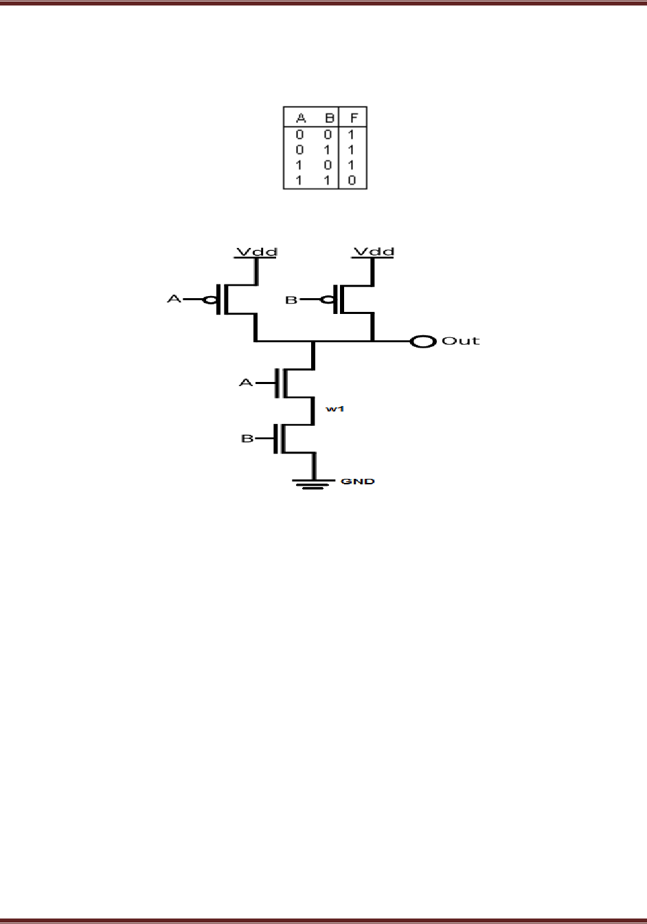
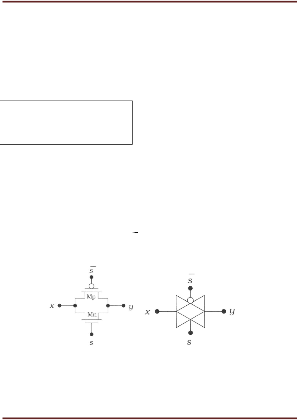
Program 9
1.3.4 Design a OR gate using TRANSMISSION GATE
Aim:-
b) Write Verilog code for OR using transmission gate
Software Requirements:
Synthesis tool:
Xilinx Project
navigator – ISE
14.7
Simulation tool:
ModelSim
Simulator
Description: A CMOS Transmission gate is created by connecting an nFET and pFET in
parallel. It has the following characteristics.
» It is a Bi-directional switch
» It Transmit the entire voltage range [0, VDD]
» Both transistors are ON or OFF simultaneously.
» The NMOS switch passes a good zero but a poor 1.
» The PMOS switch passes a good one but a poor 0.
Controlled by gate select signals, s and s
--if s = 1, y = x, switch is closed, transistors are on
– if s = 0, y = unknown (high impedance), switch open, transistors are off
In OR implementation of transmission gate the input to the top transmission gate is ‗b ,‘ and to
the second TG2 is ‗a‘ .The input ‗a‘ and its compliment are used to control the TGs. When a=0
the upper TG is closed and ‗b‘ is passed to the output while a=1 closes the lower TG and ‗a‘ is
passed to the output.
VLSI DESIGN LAB MANUAL
INFORMATION TECHNOLOGY DEPARTMENT, MJCET 19
LOGIC SYMBOL
TRUTH TABLE
LOGIC DIAGRAM

VLSI DESIGN LAB MANUAL
INFORMATION TECHNOLOGY DEPARTMENT, MJCET 20
VERILOG CODE
module or1(a,b,f);
input a;
input b;
output f;
wire ab;
not(ab,a);
cmos tg1(f,b,ab,a);
cmos tg2(f,a,a,ab);
endmodule
OUTPUT:
The Truth Table of OR TRANSMISSION GATE is verified.
VLSI DESIGN LAB MANUAL
INFORMATION TECHNOLOGY DEPARTMENT, MJCET 21
Program 10
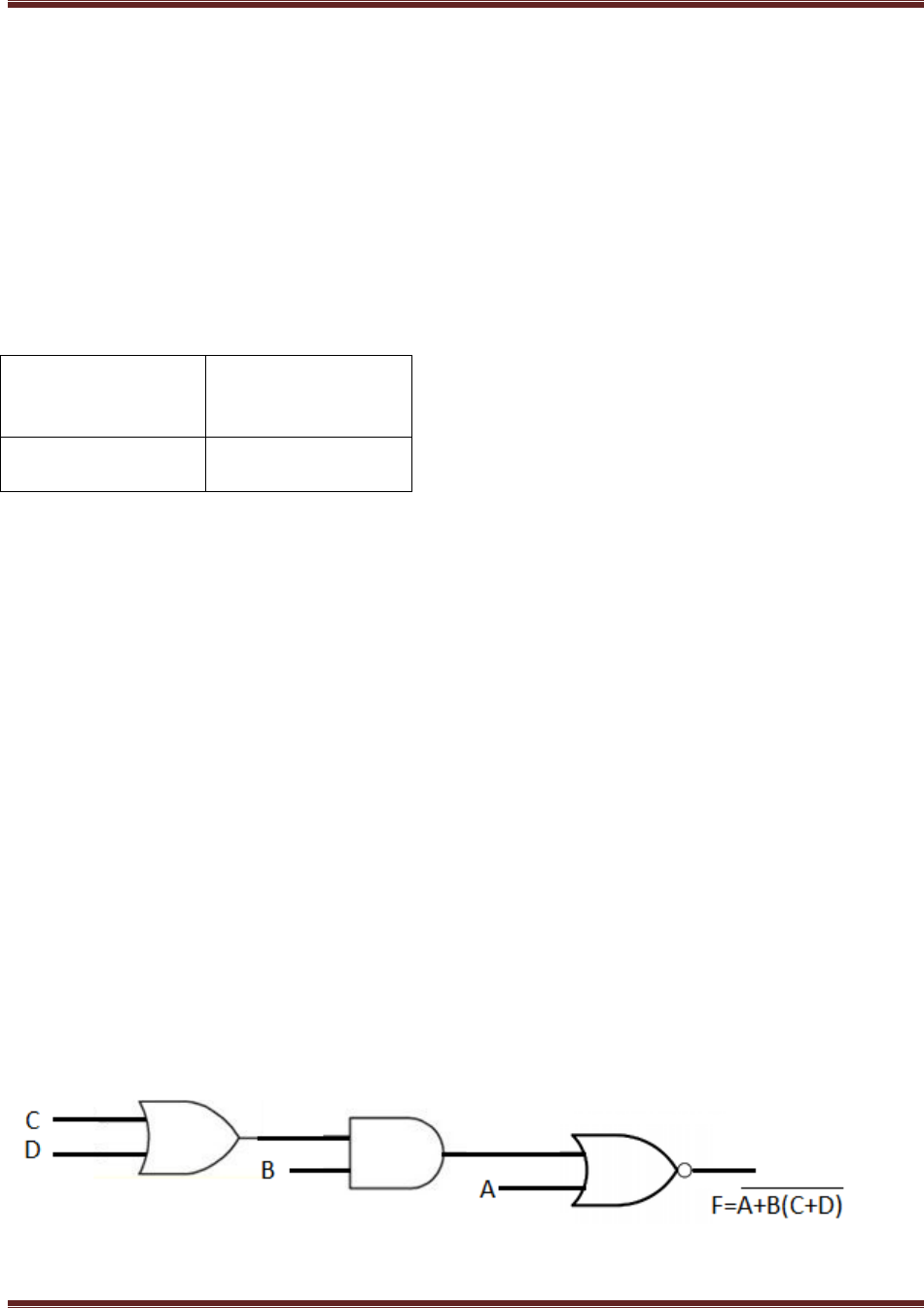
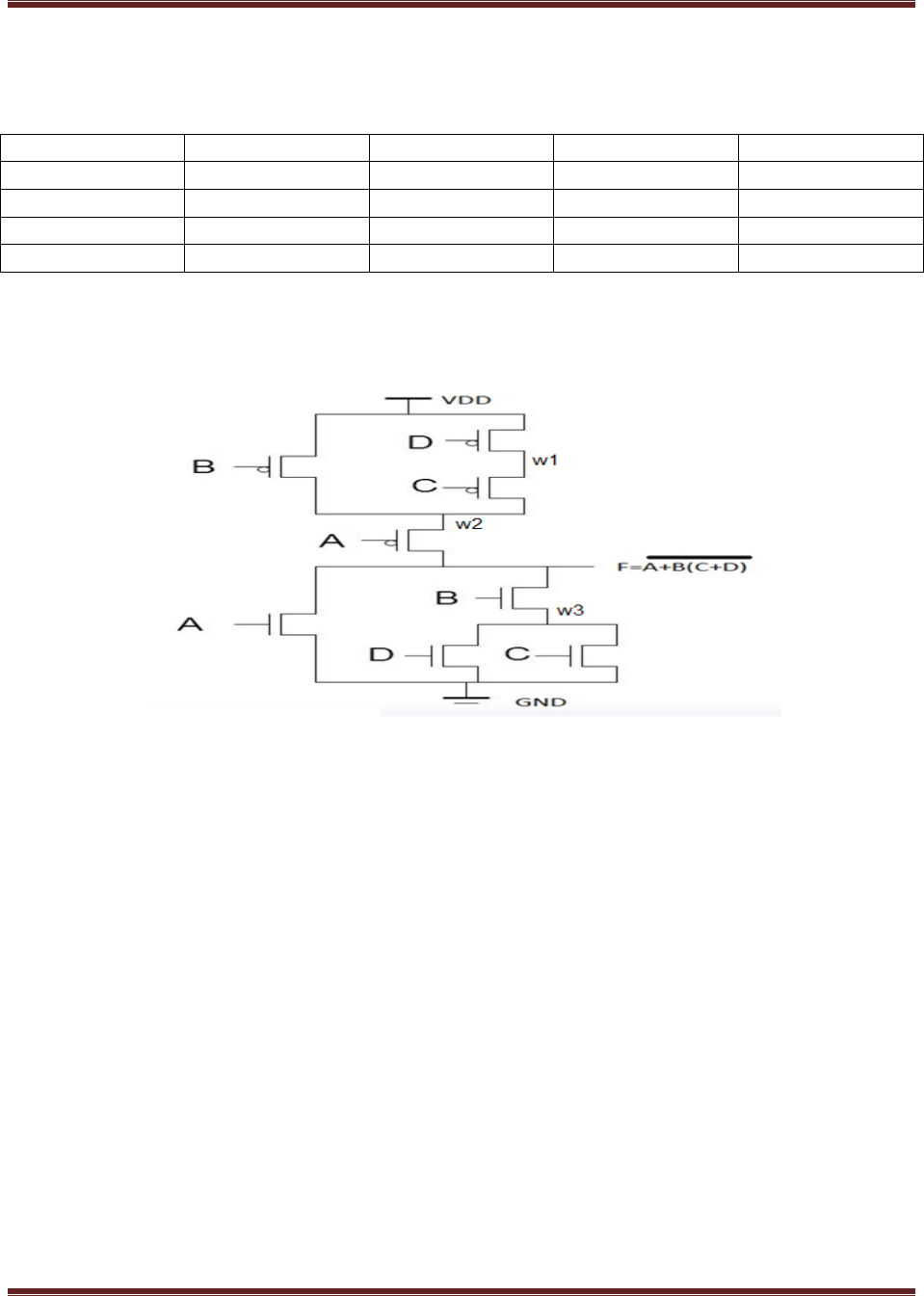
1.4 COMPLEX LOGIC GATES USING CMOS
1.4.1 F=[a+b(c+d)]‘
Aim:-
Design F=[a+b(c+d)]‘ using CMOS
Software Requirements:
Synthesis tool:
Xilinx Project
navigator – ISE
14.7
Simulation tool:
ModelSim
Simulator
Description: Complex or combinational logic gates are useful in VLSI system-level design.
Complex gates can be realized at transistor level – which is advantageous as the gate delay is
smaller for one complex gate than for the series connection of several simple gates realizing the
same function.
The realized logic function can be any combination of the NOT, AND, OR functions and there is
always an inversion at the output
Simplest way to construct is to use the PDN and PUN .First the pull-down network (PDN) is
created. The OR function is realized by n-type FETs connected in parallel. The AND function is
realized by n-type FETs connected in series.
Next the pull-up network (PUN) is designed with p-type transistors. The PUN has to create a
current path between the supply rail and the output for every logic 1 of the logic function. This
can be done by creating the dual network of the PDN. In the dual network every series
connection is turned into a parallel connection and vica versa.
LOGIC SYMBOL
VLSI DESIGN LAB MANUAL
INFORMATION TECHNOLOGY DEPARTMENT, MJCET 22
TRUTH TABLE
A
B
C
D
F
0
0
0
0
1
0
1
0
0
0
1
0
1
0
0
1
1
1
1
0
LOGIC DIAGRAM
VERILOG CODE
module complex(a,b,c,d,f);
input a;
input b;
input c;
input d;
output f;
wire w1,w2,w3;
supply0 gnd;
supply1 vdd;
pmos p1(w2,vdd,b);
pmos p2(w1,vdd,c);
pmos p3(w2,w1,d);
pmos p4(f,w2,a);
nmos n1(w3,gnd,c);
nmos n2(w3,gnd,d);
nmos n3(f,w3,b);
nmos n4(f,gnd,a);
endmodule
OUTPUT: The Truth Table of COMS complex logic is verified.
VLSI DESIGN LAB MANUAL
INFORMATION TECHNOLOGY DEPARTMENT, MJCET 23
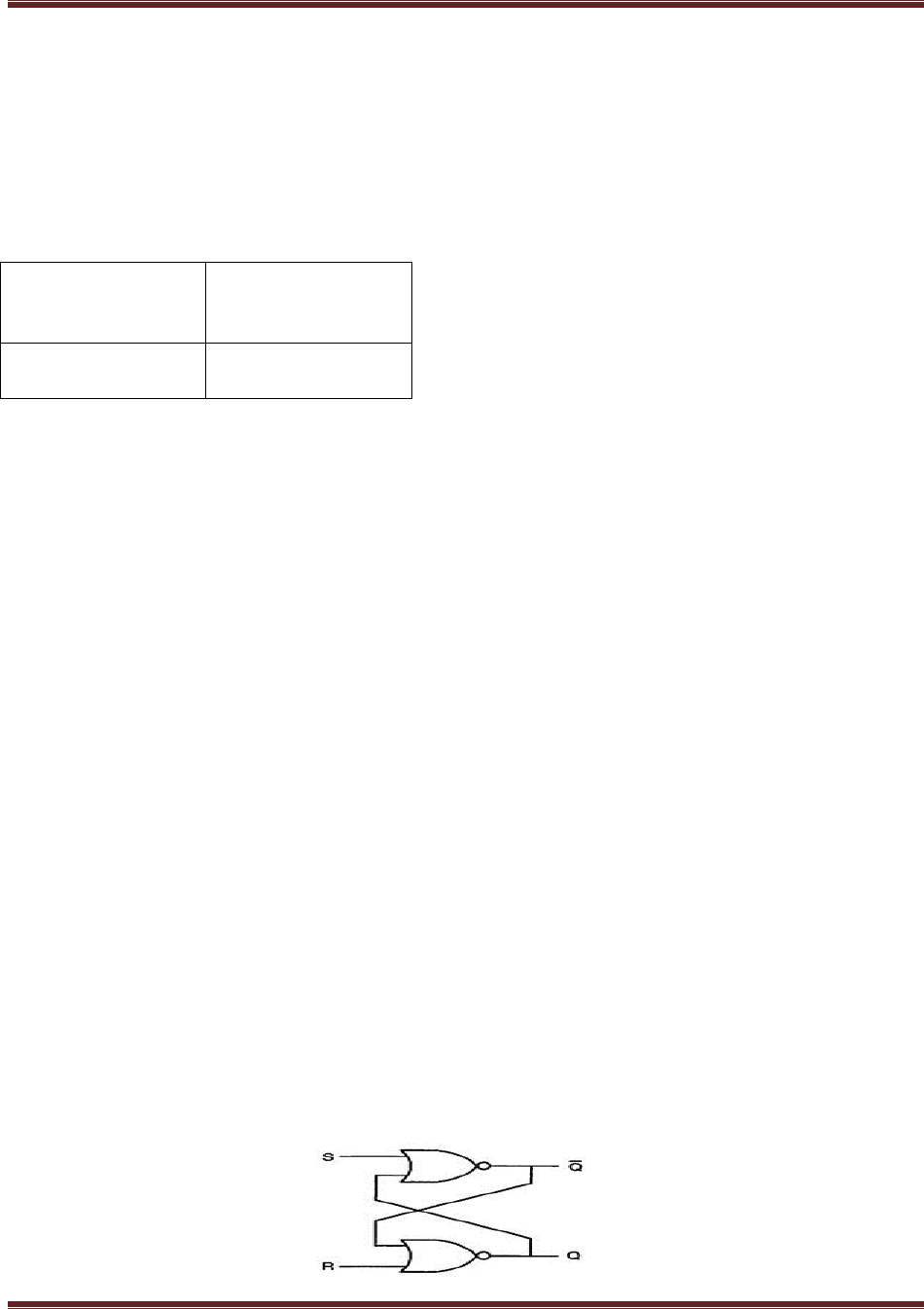
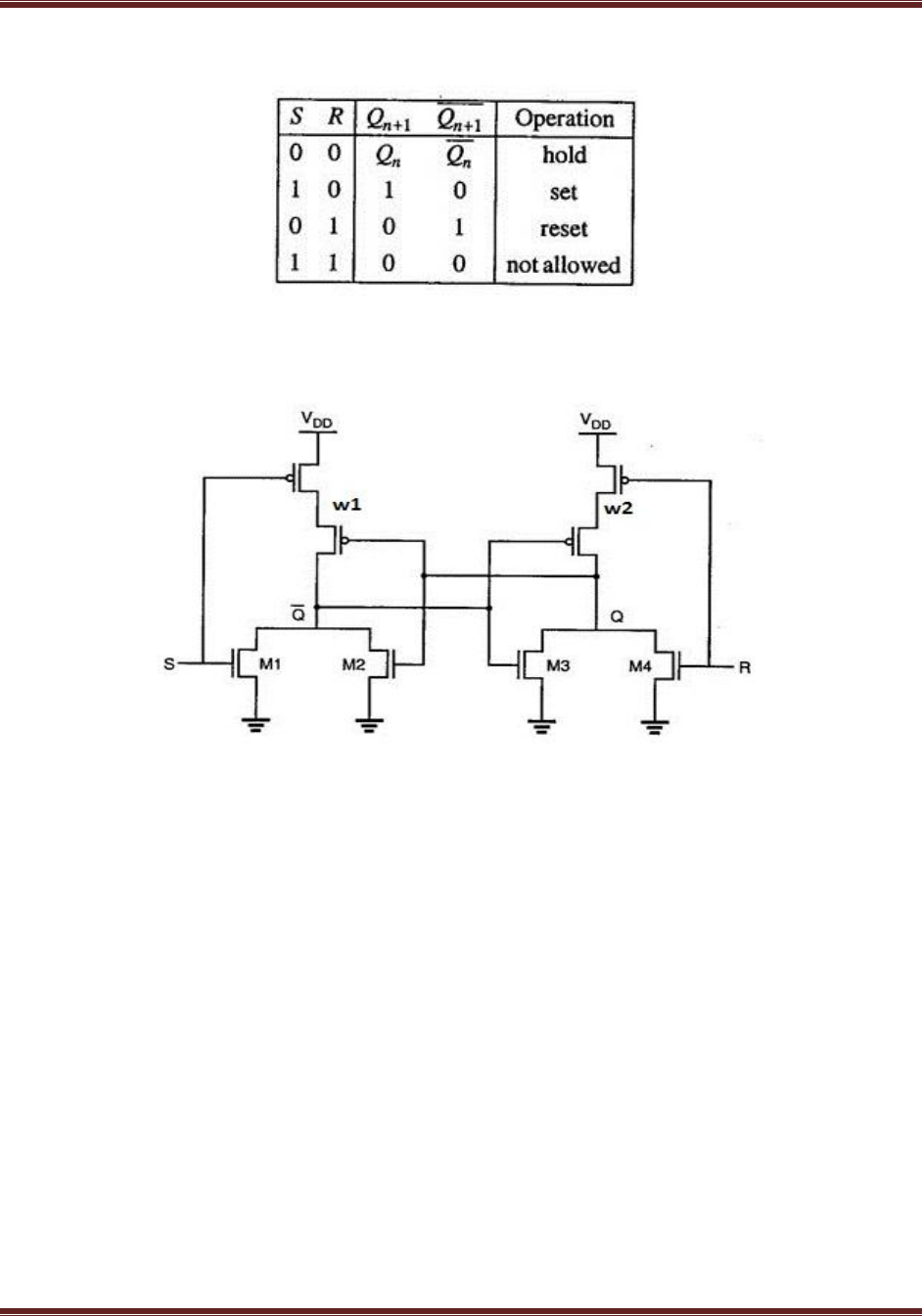
Program 11
1.4.2 Write Verilog code for SR Latch using CMOS
Aim:-
Design SR Latch using CMOS
Software Requirements:
Synthesis tool:
Xilinx Project
navigator – ISE
14.7
Simulation tool:
ModelSim
Simulator
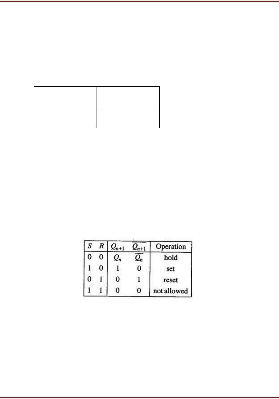
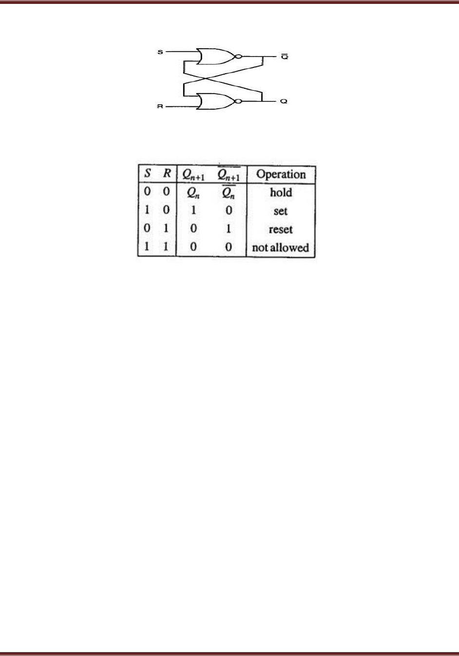
Description: A latch (also called a flip-flop) is a fundamental component of data storage. A
single latch can hold 1-bit of data, increase that number by many orders of magnitude and you
can create kilo-, mega-, giga-, even tera-bytes of memory
The logic diagram for SR latch can be obtained by using two NOR2 gates. The two NOR gates
each have their output flow into the input of the other. There are two controllable inputs: reset
(R) and set (S), which produce the two outputs: Q and Q(―Q-not‖). That‘s where the SR latch
gets its name – it‘s a set/reset latch.
Steady: When S and R are both 0, then Q remains steady. It keeps the value it had before.
If it was 0 it‘ll remain 0, if it was 1 it will still be 1.
Set: Changing S to 1 has the potential to ―set‖ the output of Q. If Q was 0, changing S to
1 will change Q to 1 as well. If Q was already 1, making S=1 will have no effect.
Reset: Moving the R input from 0 to 1 can ―reset‖ Q. As long as Q was 1, setting R to 1
will change Q to 0. If Q was already 0, though, R won‘t have any effect on it.
Restricted: When both S and R are 1, we enter restricted territory: our rule that Q
and Q must be complements is broken, as they both go to 0. So we call S=1/R=1 a
restricted combination. In most latch circuits precautions are taken to keep those inputs
from both being 1.
LOGIC SYMBOL
VLSI DESIGN LAB MANUAL
INFORMATION TECHNOLOGY DEPARTMENT, MJCET 24
TRUTH TABLE
LOGIC DIAGRAM
VERILOG CODE
module srlatch(s,r,q,qb);
input s;
input r;
inout q;
inout qb;
wire w1,w2;
supply0 gnd;
supply1 vdd;
pmos p1(w1,vdd,s);
pmos p2(qb,w1,q);
pmos p3(q,w2,qb);
pmos p4(w2,vdd,r);
nmos n1(qb,gnd,s);
nmos n2(qb,gnd,q);
nmos n3(q,gnd,qb);
nmos n4(q,gnd,q);
endmodule
OUTPUT: The Truth Table of SRLATCH is verified.
VLSI DESIGN LAB MANUAL
INFORMATION TECHNOLOGY DEPARTMENT, MJCET 25
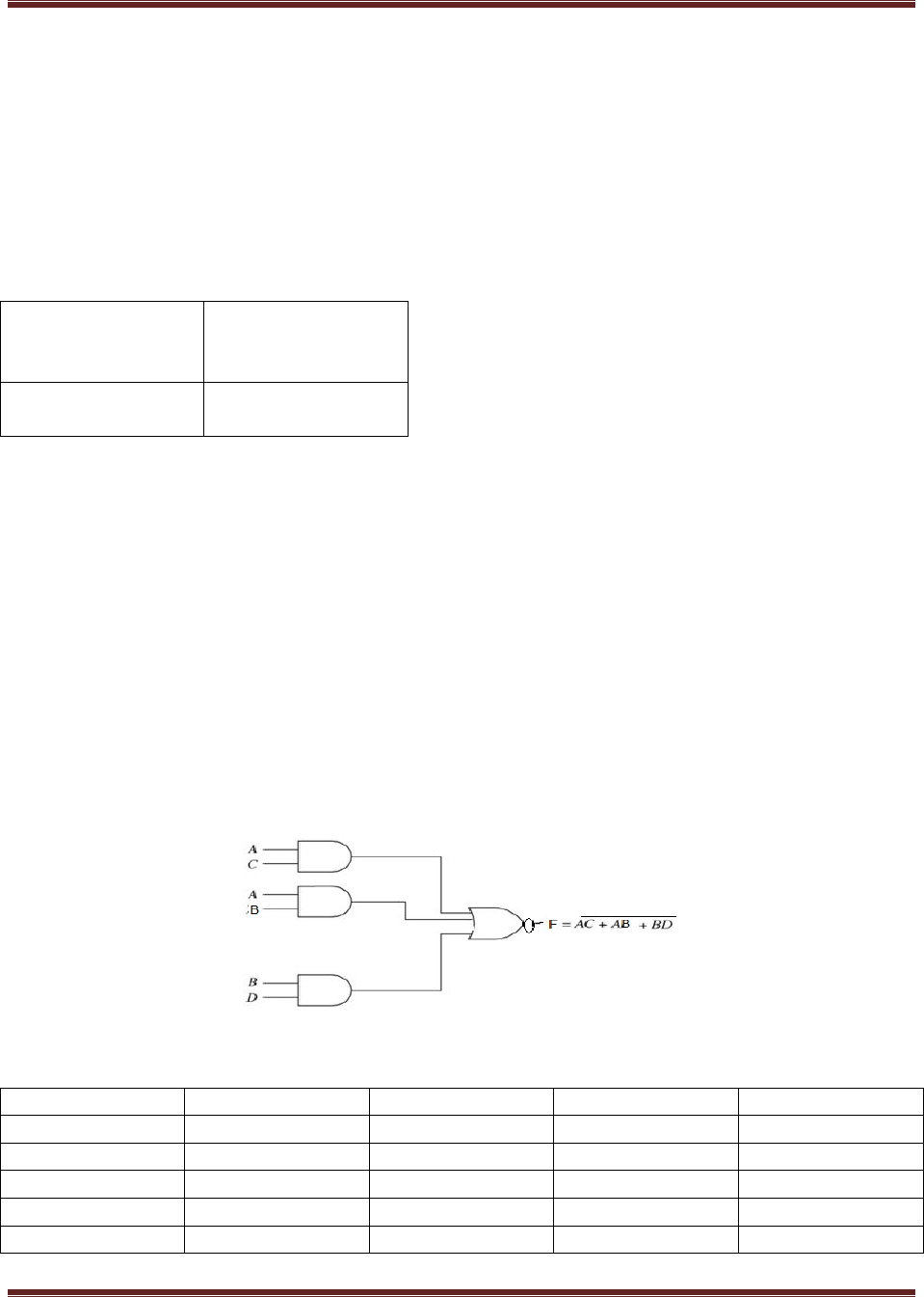
Program 12
2. STRUCTURAL GATE LEVEL MODELLING
2.1 OBTAIN FUNCTION F=[a+b+ac+bd]’ using gate level modeling
Aim:-
Design a structural gate level modeling for the AOI F=[a+b+ac+bd]’
Software Requirements:
Synthesis tool:
Xilinx Project
navigator – ISE
14.7
Simulation tool:
ModelSim
Simulator
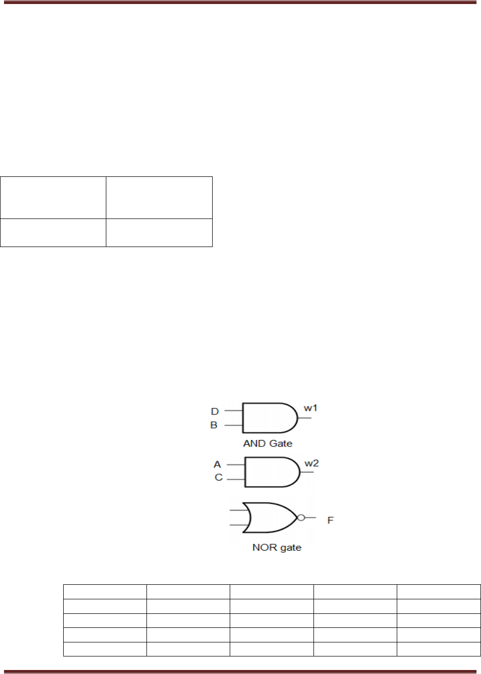
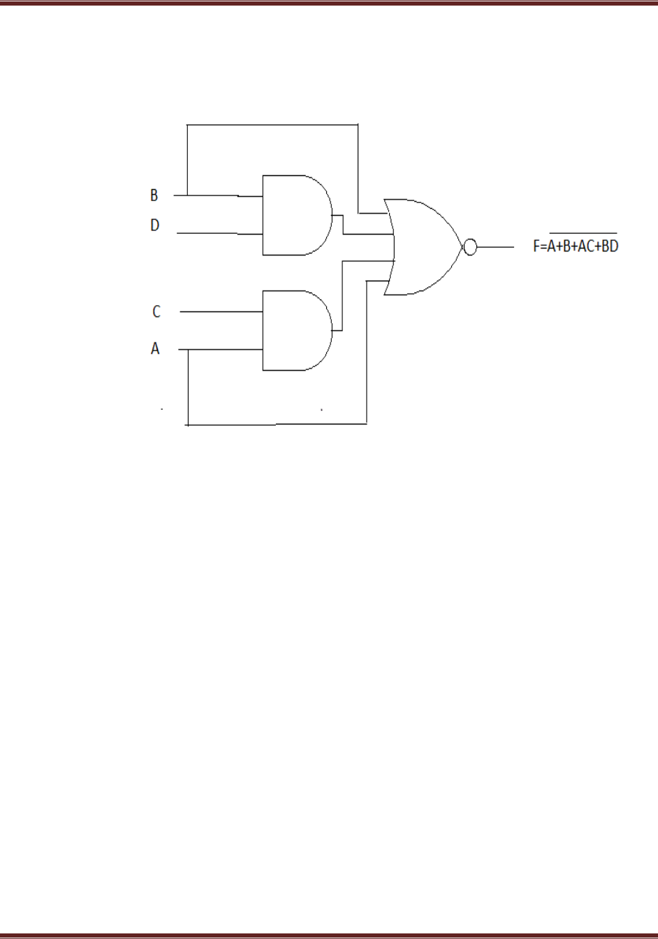
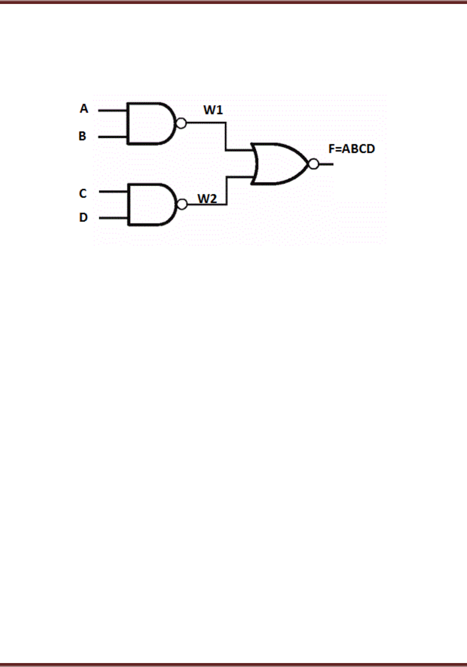
Description: Structural modeling describes a digital logic network in terms of the components
that make up the system. Gate level modeling is based on using primitive logic gates and
specifying how they are wired together.
This logic is constructed using primitive AND and NOR gates that takes the input a, b, c, d and
produce an output of F=[a+b+ac+bd]‘. W1 and w2 are the outputs of AND two gates which inturn
are determined by the input values.
LOGIC SYMBOL
TRUTH TABLE
A
B
C
D
F
0
0
0
0
1
0
1
0
1
1
1
0
1
0
0
1
1
1
1
0
VLSI DESIGN LAB MANUAL
INFORMATION TECHNOLOGY DEPARTMENT, MJCET 26
LOGIC DIAGRAM
VERILOG CODE
module func(a,b,c,d,f);
input a;
input b;
input c;
input d;
output f;
wire w1,w2;
and a1(w1,a,c);
and a2(w2,b,d);
nor n(f,w1,w2,a,b);
endmodule
OUTPUT: The Truth Table of OAI is verified.

VLSI DESIGN LAB MANUAL
INFORMATION TECHNOLOGY DEPARTMENT, MJCET 27
2.1 OBTAIN FUNCTION F=[a+b+ac+bd]’ using gate level modeling with delay
VERILOG CODE
module func1(a,b,c,d,f);
input a;
input b;
input c;
input d;
input f;
wire w1,w2;
and #(100,200) a1(w1,a,c);
and #(100,200) a2(w2,b,d);
nor #(100,200) n(f,w1,w2,a,b);
endmodule
OUTPUT:
The Truth Table of OAI WITH DELAY is verified.
VLSI DESIGN LAB MANUAL
INFORMATION TECHNOLOGY DEPARTMENT, MJCET 28
Program 13
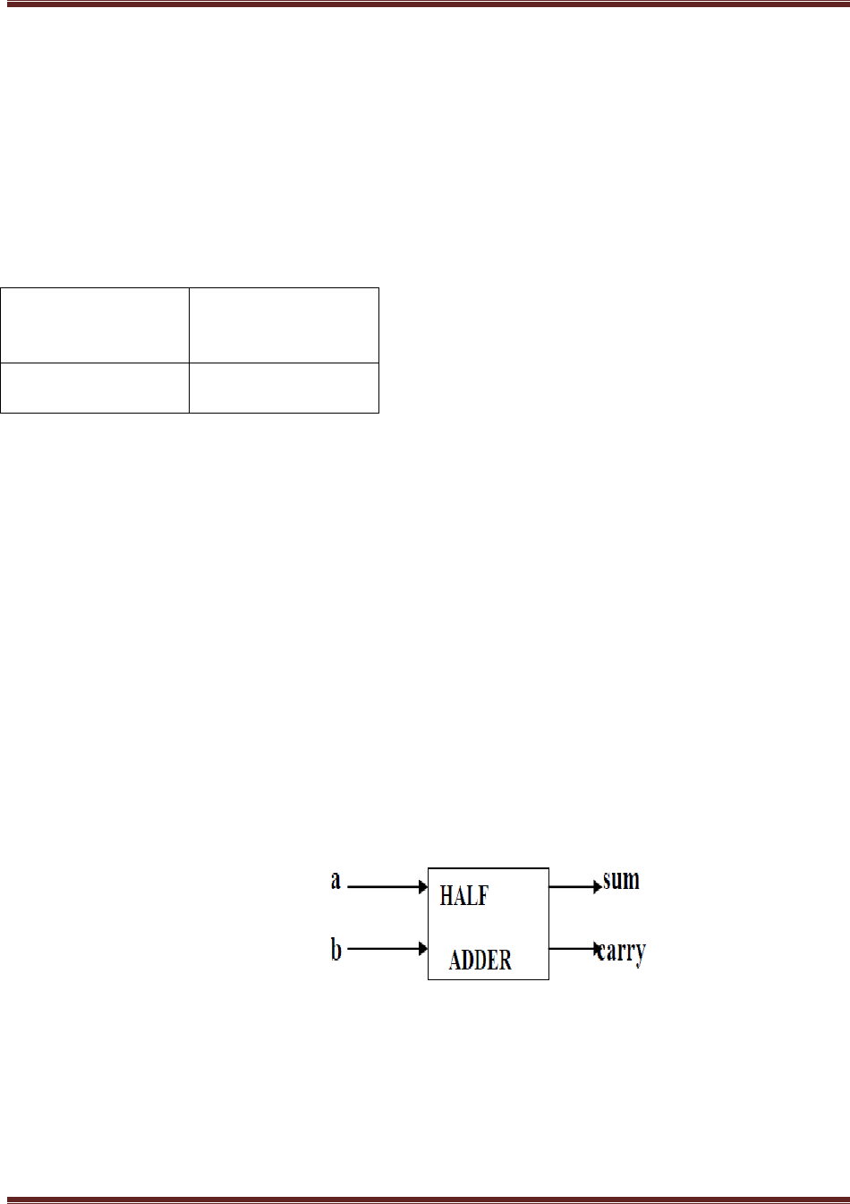
2.2 DESIGN HALF ADDER
Aim:-
Design a structural gate level modeling for the half adder
Software Requirements:
Synthesis tool:
Xilinx Project
navigator – ISE
14.7
Simulation tool:
ModelSim
Simulator
Description: Structural modeling describes a digital logic network in terms of the components
that make up the system. Gate level modeling is based on using primitive logic gates and
specifying how they are wired together.
A combinational circuit that performs the addition of two bits is called a half-adder. This circuit
needs two binary inputs and produces two binary outputs. One of the input variables designates
the augend and other designates the addend bits; the output variables designate sum and carry.
sum= ab.
carry = ab.
A combination of XOR gate and AND gate can be used to develop the circuit. Output of XOR
gate is sum bit and that of AND gate is carry bit.
LOGIC SYMBOL
VLSI DESIGN LAB MANUAL
INFORMATION TECHNOLOGY DEPARTMENT, MJCET 29
TRUTH TABLE
LOGIC DIAGRAM
VERILOG CODE
module half(a,b,s,c);
input a;
input b;
output s;
output c;
xor x(s,a,b);
and a1(c,a,b);
endmodule
OUTPUT:
The Truth Table of HALF ADDER is verified.

VLSI DESIGN LAB MANUAL
INFORMATION TECHNOLOGY DEPARTMENT, MJCET 30
2.2 DESIGN HALF ADDER with delay
VERILOG CODE
module half(a,b,s,c);
input a;
input b;
output s;
output c;
xor #(100,200) x(s,a,b);
and #(100,200) a1(c,a,b);
endmodule
OUTPUT:
The Truth Table of HALF ADDER WITH DELAY is verified.
VLSI DESIGN LAB MANUAL
INFORMATION TECHNOLOGY DEPARTMENT, MJCET 31
Program 14
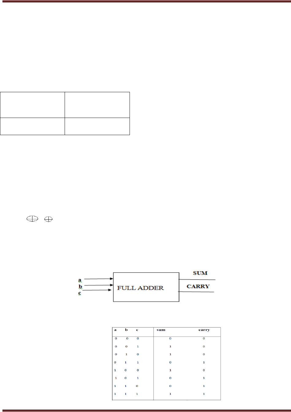
2.3 DESIGN FULL ADDER
Aim:-
Design a structural gate level modeling for the full adder using two half adders and OR
gate
Software Requirements:
Synthesis tool:
Xilinx Project
navigator – ISE
14.7
Simulation tool:
ModelSim
Simulator
Description: Structural modeling describes a digital logic network in terms of the components
that make up the system. Gate level modeling is based on using primitive logic gates and
specifying how they are wired together.
A combinational circuit that performs the addition of 3 bits is called a full adder. This circuit
accepts 3 binary inputs and produces two binary outputs. The two outputs are denoted by sum
and carry.
sum= a b c
carry = ab + bc+ca
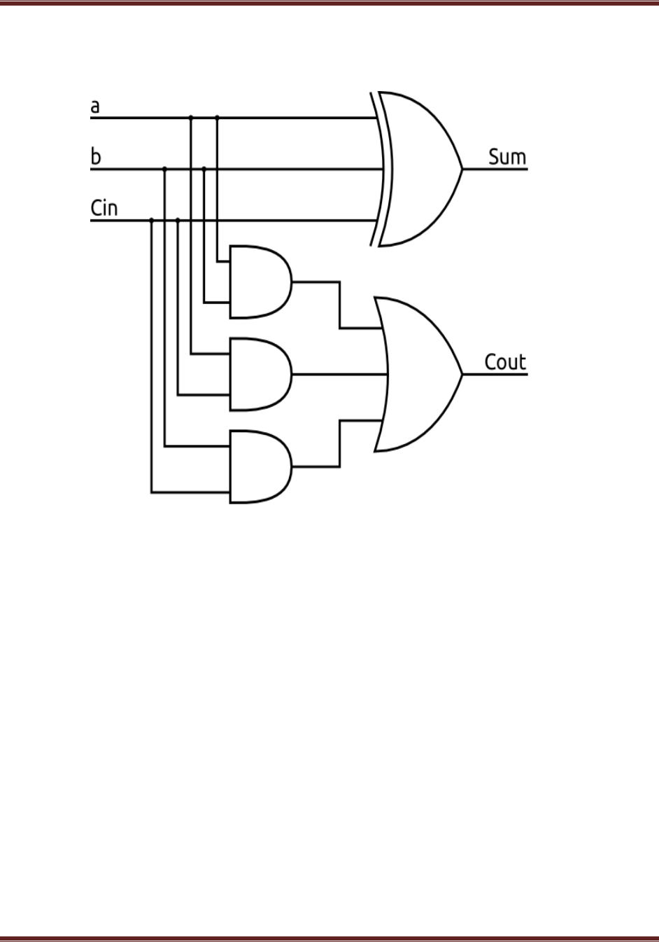
A full can also be built from two half adders and an OR gate..
LOGIC SYMBOL
TRUTH TABLE
VLSI DESIGN LAB MANUAL
INFORMATION TECHNOLOGY DEPARTMENT, MJCET 32
LOGIC DIAGRAM
VERILOG CODE
module fa(a,b,cin,s,c);
input a;
input b;
input cin;
output s;
output c;
wire w1,w2,w3;
half h1(a,b,w1,w2);
half h2(w1,cin,s,w3);
or r(c,w3,w2);
endmodule
OUTPUT:
The Truth Table of FULL ADDER is verified.

VLSI DESIGN LAB MANUAL
INFORMATION TECHNOLOGY DEPARTMENT, MJCET 33
2.3 DESIGN FULL ADDER WITH DELAY
VERILOG CODE
module fa(a,b,cin,s,c);
input a;
input b;
input cin;
output s;
output c;
wire w1,w2,w3;
half #(100,200) h1(a,b,w1,w2);
half #(100,200) h2(w1,cin,s,w3);
or #(100,200) r(c,w3,w2);
endmodule
OUTPUT:
The Truth Table of FULL ADDER WITH DELAY is verified.
VLSI DESIGN LAB MANUAL
INFORMATION TECHNOLOGY DEPARTMENT, MJCET 34
Program 15
2.4 IMPLEMENT 2:1 MUX USING TRI STATE BUFFERS
Aim:-
Design a structural gate level modeling for 2:1 MUX using tri state buffer.
Software Requirements:
Synthesis tool:
Xilinx Project
navigator – ISE
14.7
Simulation tool:
ModelSim
Simulator
Description: Structural modeling describes a digital logic network in terms of the components
that make up the system. Gate level modeling is based on using primitive logic gates and
specifying how they are wired together.
A tri-state buffer is similar to a buffer, but it adds an additional "enable" input that controls
whether the primary input is passed to its output or not. If the "enable" inputs signal is true, the
tri-state buffer behaves like a normal buffer. If the "enable" input signal is false, the tri-state
buffer passes a high impedance (orhi-Z) signal, which effectively disconnects its output from the
circuit.
LOGIC SYMBOL
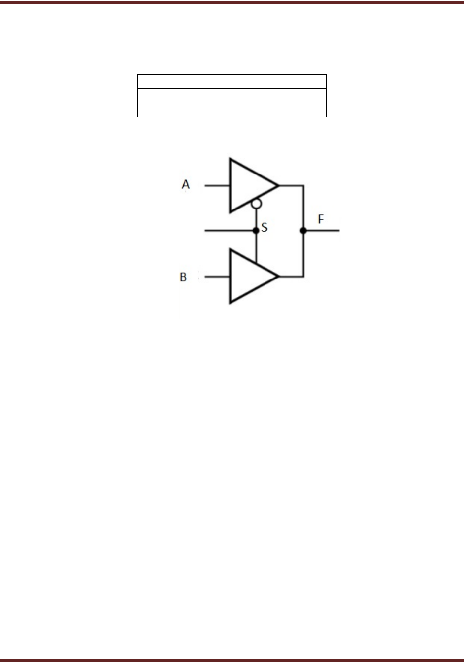
VLSI DESIGN LAB MANUAL
INFORMATION TECHNOLOGY DEPARTMENT, MJCET 35
TRUTH TABLE
S
F
0
A
1
B
LOGIC DIAGRAM
VERILOG CODE
module trimux(a,b,en,f);
input a;
input b;
input en;
output f;
bufif0(f,a,en);
bufif1(f,b,en);
endmodule
OUTPUT:
The Truth Table of 2:1 Mux Using Tri State Buffer Is verified.

VLSI DESIGN LAB MANUAL
INFORMATION TECHNOLOGY DEPARTMENT, MJCET 36
2.4 IMPLEMENT 2:1 MUX USING TRI STATE BUFFERS WITH DELAY
VERILOG CODE
module trimux(a,b,en,f);
input a;
input b;
input en;
output f;
bufif0 #(100,200) (f,a,en);
bufif1 #(100,200) (f,b,en);
endmodule
OUTPUT:
The Truth Table of 2:1 Mux Using Tri State Buffer with delay is verified
VLSI DESIGN LAB MANUAL
INFORMATION TECHNOLOGY DEPARTMENT, MJCET 37
Program 16
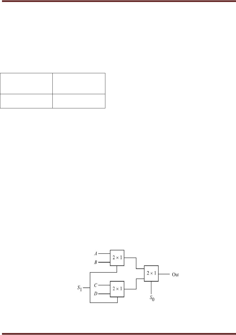
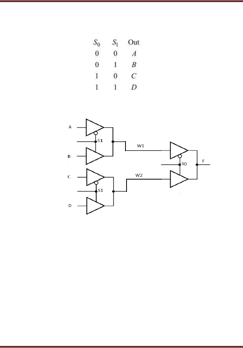
2.5 IMPLEMENT 4:1 MUX USING 2:1 MULTIPLEXERS
Aim:-
Design a structural gate level modeling for 4:1 MUX using 2:1 MUX and tri state buffer.
Software Requirements:
Synthesis tool:
Xilinx Project
navigator – ISE
14.7
Simulation tool:
ModelSim
Simulator
Description: Structural modeling describes a digital logic network in terms of the components
that make up the system. Gate level modeling is based on using primitive logic gates and
specifying how they are wired together.
A tri-state buffer is similar to a buffer, but it adds an additional "enable" input that controls
whether the primary input is passed to its output or not. If the "enable" inputs signal is true, the
tri-state buffer behaves like a normal buffer. If the "enable" input signal is false, the tri-state
buffer passes a high impedance (orhi-Z) signal, which effectively disconnects its output from the
circuit.
A 4-to-1 Multiplexers has 4-data input lines ,two select lines and single output line. Three 2:1
Mux can be used to make a 4:1 mux. The first and second mux uses s1 as the select line and third
uses s0 as the select line.
LOGIC SYMBOL
VLSI DESIGN LAB MANUAL
INFORMATION TECHNOLOGY DEPARTMENT, MJCET 38
TRUTH TABLE
LOGIC DIAGRAM
VERILOG CODE
module trimux4(a,b,c,d,s0,s1,f);
input a;
input b;
input c;
input d;
input s0;
input s1;
output f;
wire w1,w2;
trimux t1(a,b,s0,w1);
trimux t2(c,d,s0,w2);
trimux t3(w1,w2,s1,f);
endmodule
OUTPUT: The Truth Table of 4:1 MUX USING 2:1 MULTIPLEXER is verified

VLSI DESIGN LAB MANUAL
INFORMATION TECHNOLOGY DEPARTMENT, MJCET 39
2.5 IMPLEMENT 4:1 MUX USING 2:1 MULTIPLEXERS WITH DELAY
VERILOG CODE
module trimux4(a,b,c,d,s0,s1,f);
input a;
input b;
input c;
input d;
input s0;
input s1;
output f;
wire w1,w2;
trimux #(100,200) t1(a,b,s0,w1);
trimux #(100,200) t2(c,d,s0,w2);
trimux #(100,200) t3(w1,w2,s1,f);
endmodule
OUTPUT: The Truth Table of 4:1 Mux Using 2:1 Multiplexer with delay is verified
VLSI DESIGN LAB MANUAL
INFORMATION TECHNOLOGY DEPARTMENT, MJCET 40
Program 17
2.6 SR LATCH
Aim:-
Design a structural gate level modeling for SR Latch.
Software Requirements:
Synthesis tool:
Xilinx Project
navigator – ISE
14.7
Simulation tool:
ModelSim
Simulator
Description: Structural modeling describes a digital logic network in terms of the components
that make up the system. Gate level modeling is based on using primitive logic gates and
specifying how they are wired together.
The logic diagram for SR latch can be obtained by using two NOR2 gates.The two NOR gates
each have their output flow into the input of the other. There are two controllable inputs: reset
(R) and set (S), which produce the two outputs: Q and Q(―Q-not‖). That‘s where the SR latch
gets its name – it‘s a set/reset latch
TRUTH TABLE

VLSI DESIGN LAB MANUAL
INFORMATION TECHNOLOGY DEPARTMENT, MJCET 41
LOGIC DIAGRAM
VERILOG CODE
module srg(s,r,q,qb);
input s;
input r;
inout q;
inout qb;
nor n1(qb,s,q);
nor n2(q,r,qb);
endmodule
OUTPUT: The Truth table of SR latch is verified

VLSI DESIGN LAB MANUAL
INFORMATION TECHNOLOGY DEPARTMENT, MJCET 42
2.6 IMPLEMENT SR LATCH WITH DELAY
VERILOG CODE
module srg(s,r,q,qb);
input s;
input r;
inout q;
inout qb;
nor #(100,200) n1(qb,s,q);
nor #(100,200) n2(q,r,qb);
endmodule
OUTPUT: The Truth Table of SR latch with delay is verified
VLSI DESIGN LAB MANUAL
INFORMATION TECHNOLOGY DEPARTMENT, MJCET 43
Program 18
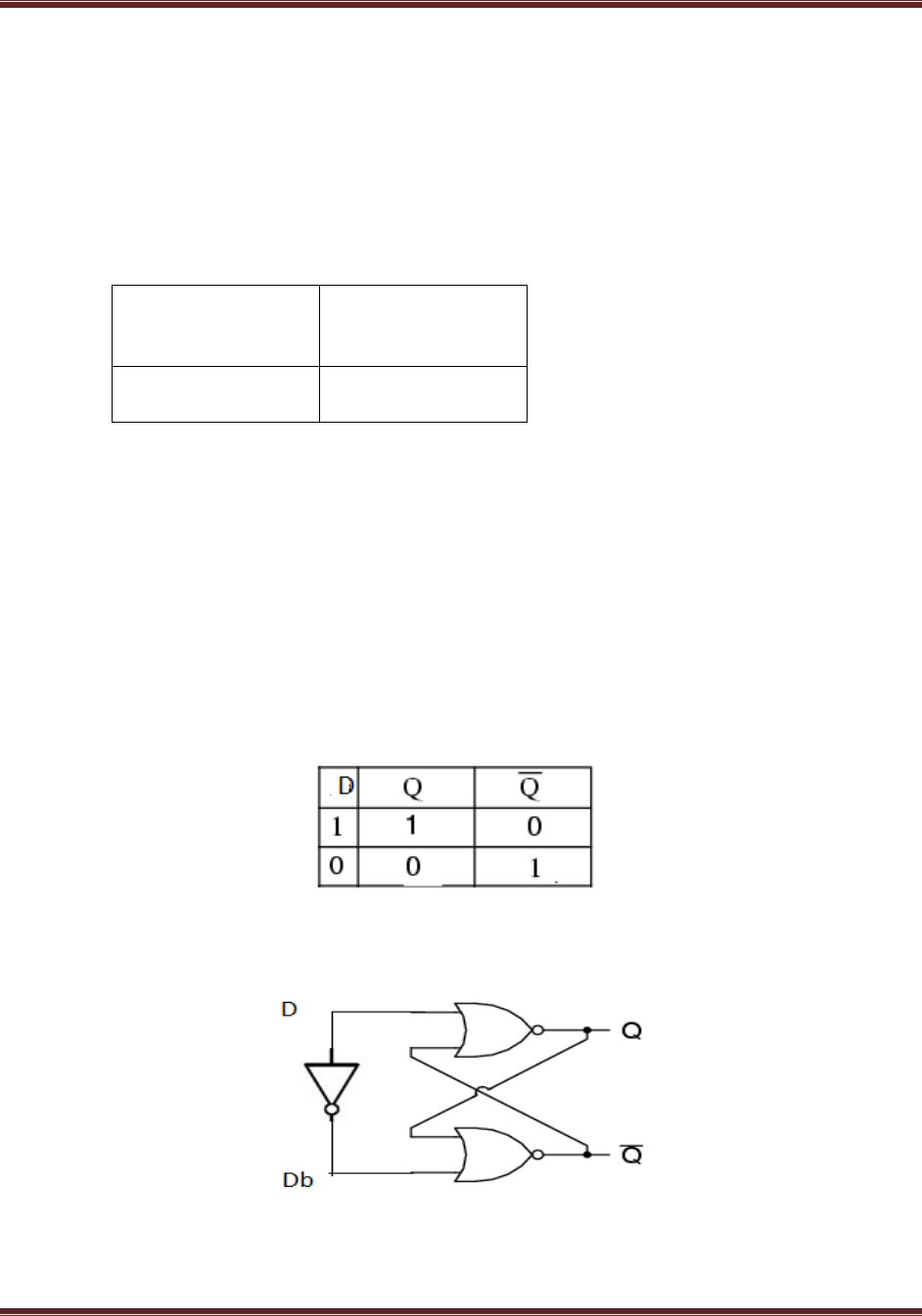
2.7 IMPLEMENT D – LATCH
Aim:-
Design a structural gate level modeling for D Latch.
Software Requirements:
Synthesis tool:
Xilinx Project
navigator – ISE
14.7
Simulation tool:
ModelSim
Simulator
Description: Structural modeling describes a digital logic network in terms of the components
that make up the system. Gate level modeling is based on using primitive logic gates and
specifying how they are wired together.
A latch (also called a flip-flop) is a fundamental component of data storage. A single latch can
hold 1-bit of data, increase that number by many orders of magnitude and you can create kilo-,
mega-, giga-, even tera-bytes of memory
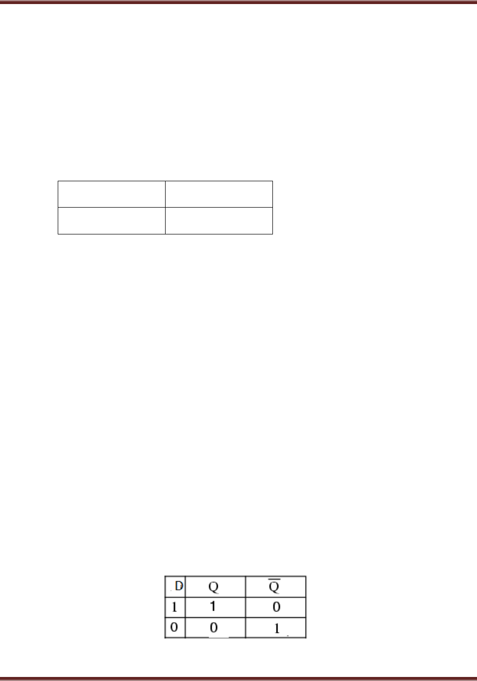
TRUTH TABLE
LOGIC DIAGRAM

VLSI DESIGN LAB MANUAL
INFORMATION TECHNOLOGY DEPARTMENT, MJCET 44
VERILOG CODE
module dlatch(d,db,q,qb);
input d;
input db;
inout q;
inout qb;
not (db,d);
nor n1(qb,d,q);
nor n2(q,db,qb);
endmodule
OUTPUT:
The Truth Table of D-latch is verified

VLSI DESIGN LAB MANUAL
INFORMATION TECHNOLOGY DEPARTMENT, MJCET 45
2.7 IMPLEMENT D – LATCH WITH DELAY
VERILOG CODE
module dlatch(d,db,q,qb);
input d;
input db;
inout q;
inout qb;
not #(100,200) (db,d);
nor #(100,200) n1(qb,d,q);
nor #(100,200) n2(q,db,qb);
endmodule
OUTPUT: The Truth Table of D-latch with delay is verified

VLSI DESIGN LAB MANUAL
INFORMATION TECHNOLOGY DEPARTMENT, MJCET 46
Program 19
3. HIERARCHICAL MODELING
3.1 CONSTRUCT A 4 INPUT AND-GATE USING 2-INPUT NAND & NOR GATES
Aim:-
Design a 4 input and gate using 2-input nand & nor gates.
Software Requirements:
Synthesis tool:
Xilinx Project
navigator – ISE
14.7
Simulation tool:
ModelSim
Simulator
Description:
The concept of primitive, modules and instancing provides the basis for hierarchical design in
Verilog. Complex systems can be described in Verilog HDL using mixed-design style modeling.
This modeling style supports hierarchical description
Direct instantiation and connection of models from a separate calling model to form structural
hierarchy in a design. A module may be declared anywhere in a design relative to where it is
called.
The gate level and switch can be used separately or intermixed within a single module.
An AND gate can be created using already created switch level modules for NAND2 and NOR2.
These gates can be instantiated to create the hierarchical design..
TRUTH TABLE
A
B
C
D
F
0
0
0
0
0
0
1
0
1
0
1
0
1
0
0
1
1
1
1
1
VLSI DESIGN LAB MANUAL
INFORMATION TECHNOLOGY DEPARTMENT, MJCET 47
LOGIC DIAGRAM
VERILOG CODE
module and4(a,b,c,d,f);
input a;
input b;
input c;
input d;
output f;
wire w1,w2;
nand1 n1(a,b,w1);// Instantiation of switch level NAND
nand1 n2(c,d,w2);
nor1 n3(w1,w2,f);
endmodule
OUTPUT: The Truth Table of 4 Input And-Gate Using 2-Input Nand & Nor Gate is verified.
VLSI DESIGN LAB MANUAL
INFORMATION TECHNOLOGY DEPARTMENT, MJCET 48
Program 20
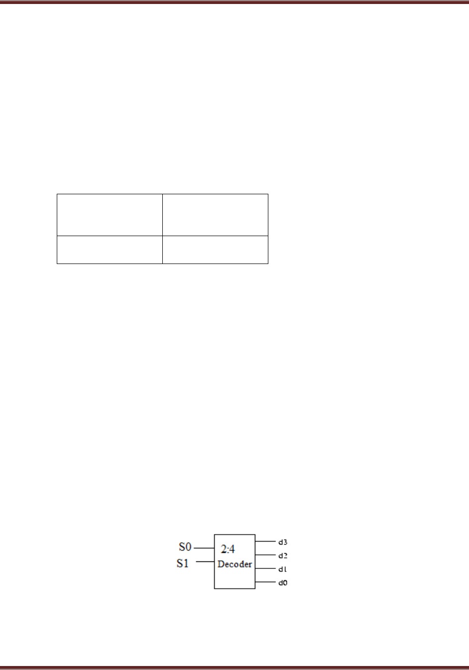
3.2 CONSTRUCT AN 2:4 ACTIVE HIGH DECODER USING CMOS 2-INPUT NOR
& NOT GATES
Aim:-
Design an 2:4 active high decoder using CMOS 2-input nor & not gates
Software Requirements:
Synthesis tool:
Xilinx Project
navigator – ISE
14.7
Simulation tool:
ModelSim
Simulator
Description:
The concept of primitive, modules and instancing provides the basis for hierarchical design in
Verilog. Complex systems can be described in Verilog HDL using mixed-design style modeling.
This modeling style supports hierarchical description
Direct instantiation and connection of models from a separate calling model to form structural
hierarchy in a design. A module may be declared anywhere in a design relative to where it is
called.
The gate level and switch can be used separately or intermixed within a single module.
A decoder is a circuit which has n inputs and 2n outputs, and outputs 1 on the wire corresponding
to the binary number represented by the inputs
LOGIC SYMBOL
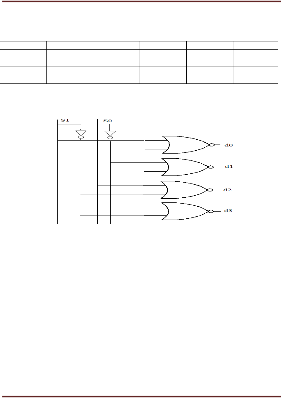
VLSI DESIGN LAB MANUAL
INFORMATION TECHNOLOGY DEPARTMENT, MJCET 49
TRUTH TABLE
S1
S0
D0
D1
D2
D3
0
0
1
0
0
0
0
1
0
1
0
0
1
0
0
0
1
0
1
1
0
0
0
1
LOGIC DIAGRAM
VERILOG CODE
module decode24(s0,s1,d0,d1,d2,d3);
input s0;
input s1;
output d0;
output d1;
output d2;
output d3;
wire s0b,s1b;
not1 n1(s0,s0b);
not1 n2(s1,s1b);
nor1 n3(s1,s0,d0);
nor1 n4(s1b,s0,d1);
nor1 n5(s1,s0b,d2);
nor1 n6(s1b,s0b,d3);
endmodule
OUTPUT: The Truth Table of 2:4 active high decoder using CMOS 2-input nor & not gates is
verified.

VLSI DESIGN LAB MANUAL
INFORMATION TECHNOLOGY DEPARTMENT, MJCET 50
Program 21
3.2 CONSTRUCT SR LATCH USING HIERARCHICAL MODELING
Aim:-
Design a SR Latch
.
Software Requirements:
Synthesis tool:
Xilinx Project
navigator – ISE
14.7
Simulation tool:
ModelSim
Simulator
Description:
The concept of primitive, modules and instancing provides the basis for hierarchical design in
Verilog. Complex systems can be described in Verilog HDL using mixed-design style modeling.
This modeling style supports hierarchical description
Direct instantiation and connection of models from a separate calling model to form structural
hierarchy in a design. A module may be declared anywhere in a design relative to where it is
called.
The gate level and switch can be used separately or intermixed within a single module.
A latch (also called a flip-flop) is a fundamental component of data storage. A single latch can
hold 1-bit of data, increase that number by many orders of magnitude and you can create kilo-,
mega-, giga-, even tera-bytes of memory
The logic diagram for SR latch can be obtained by using two NOR2 gates.The two NOR gates
each have their output flow into the input of the other. There are two controllable inputs: reset
(R) and set (S), which produce the two outputs: Q and Q(―Q-not‖). That‘s where the SR latch
gets its name – it‘s a set/reset latch.
VLSI DESIGN LAB MANUAL
INFORMATION TECHNOLOGY DEPARTMENT, MJCET 51
LOGIC SYMBOL
TRUTH TABLE
VERILOG CODE
module srh(s,r,q,qb);
input s;
input r;
inout q;
inout qb;
nor1 n1(s,q,qb);
nor1 n2(r,qb,q);
endmodule.
OUTPUT: The Truth Table of SR Latch Using Hierarchical Modeling is verified
VLSI DESIGN LAB MANUAL
INFORMATION TECHNOLOGY DEPARTMENT, MJCET 52
Program 22
3.2 CONSTRUCT D LATCH USING HIERARCHICAL MODELING
Aim:-
Design a D Latch
Software Requirements:
Synthesis tool:
Xilinx Project
navigator – ISE 14.7
Simulation tool:
ModelSim
Simulator
Description:
The concept of primitive, modules and instancing provides the basis for hierarchical design in
Verilog. Complex systems can be described in Verilog HDL using mixed-design style modeling.
This modeling style supports hierarchical description
Direct instantiation and connection of models from a separate calling model to form structural
hierarchy in a design. A module may be declared anywhere in a design relative to where it is
called.
The gate level and switch can be used separately or intermixed within a single module.
A latch (also called a flip-flop) is a fundamental component of data storage. A single latch can
hold 1-bit of data, increase that number by many orders of magnitude and you can create kilo-,
mega-, giga-, even tera-bytes of memory
In the verilog code not gate is called using switch level and nor gates are called using gate level.
TRUTH TABLE
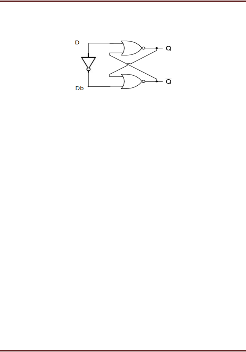
VLSI DESIGN LAB MANUAL
INFORMATION TECHNOLOGY DEPARTMENT, MJCET 53
LOGIC DIAGRAM
VERILOG CODE
module dh(d,db,q,qb);
input d;
input db;
inout q;
inout qb;
not1 n(d,db);
nor1 n1(d,q,qb);
nor1 n2(db,qb,q);
endmodule
OUTPUT: The Truth Table of D Latch using hierarchical modeling is verified.
VLSI DESIGN LAB MANUAL
INFORMATION TECHNOLOGY DEPARTMENT, MJCET 54
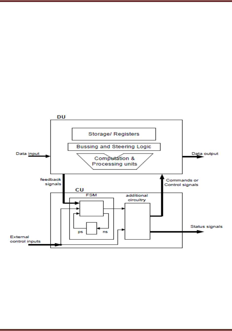
3. REGISTER TRANSFER LEVEL (RTL) MODELING
REGISTER TRANSFER LEVEL (RTL) MODELING
At RTL digital design abstraction, registers are the basic components (primitives).
Data paths are defined by their registers and the operations performed on the data stored
in the registers.
An elementary operation performed on data stored in a register is called micro operation
Copying the contents of one register into another
Adding the contents of two registers
Storing result into a register
Shift and count
Incrementing the contents of a register.
The movement and processing of the data stored in registers are termed register transfer
operations or RTL operations
An RTL operation can be considered as a combination of the elementary micro
operations.

VLSI DESIGN LAB MANUAL
INFORMATION TECHNOLOGY DEPARTMENT, MJCET 55
It is a fact that almost all synchronous sequential digital systems can be viewed as a set
of registers and operations that transfer data.
These RTL operations of a digital system are completely specified by three basic
elements:
The register set,
The operations that are performed on data in registers
The sequence of the operations.
In other words, the digital system can be described and modeled by a RTL Control Sequence
(RTLCS for short) or RTL code/program.
This RTL code uses an associated notational system, called Register
Transfer Notation (RTN).
Operations in RTN are almost always of the form:
regA ← ƒ( reg1, reg2, …., regn )
BEHAVIORALMODELING
Behavioral modeling is the highest level of abstraction in the Verilog HDL. The other modeling
techniques are relatively detailed. They require some knowledge of how hardware or hardware
signals work. The abstraction in this modeling is as simple as writing the logic in C language.
This is a very powerful abstraction technique. All that the designer needs is the algorithm of the
design, which is the basic information for any design.
Most of the behavioral modeling is done using two important constructs: initial and always. All
the other behavioral statements appear only inside these two structured procedure constructs.
initial Construct
Statements which come under the initial construct constitute the initial block. The initial block is
executed only once in the simulation, at time 0. If there is more than one initial block, then all the
initial blocks are executed concurrently. The initial construct is used as follows:
Initial initial
begin or
reset = 1'b0; clk = 1'b1;
clk = 1'b1;
end
In the first initial block there is more than one statement hence they are written between begin
and end. If there is only one statement then there is no needs to put begin and end.
always Construct
Statements which come under the always construct constitute the always block. The always

VLSI DESIGN LAB MANUAL
INFORMATION TECHNOLOGY DEPARTMENT, MJCET 56
block starts at time 0, and keeps on executing all the simulation time. It works like a infinite
loop. It is generally used to model a functionality that is continuously repeated.
Always initial
clk = 1'b0; #5 clk = ~clk;
The above code generates a clock signal clk, with a time period of 10 units. The initial blocks
initiates the clk value to 0 at time 0. Then after every 5 units of time it toggled, hence we get a
time period of 10 units.
VLSI DESIGN LAB MANUAL
INFORMATION TECHNOLOGY DEPARTMENT, MJCET 57
Program 23
4.1 Write Verilog code to implement 4:1 multiplexer using RTL and Behavioral modeling.
Aim :- Design 4:1 multiplexer using RTL and Behavioral modeling.
Software Requirements:
Synthesis tool:
Xilinx Project
navigator – ISE
14.7
Simulation tool:
ModelSim
Simulator
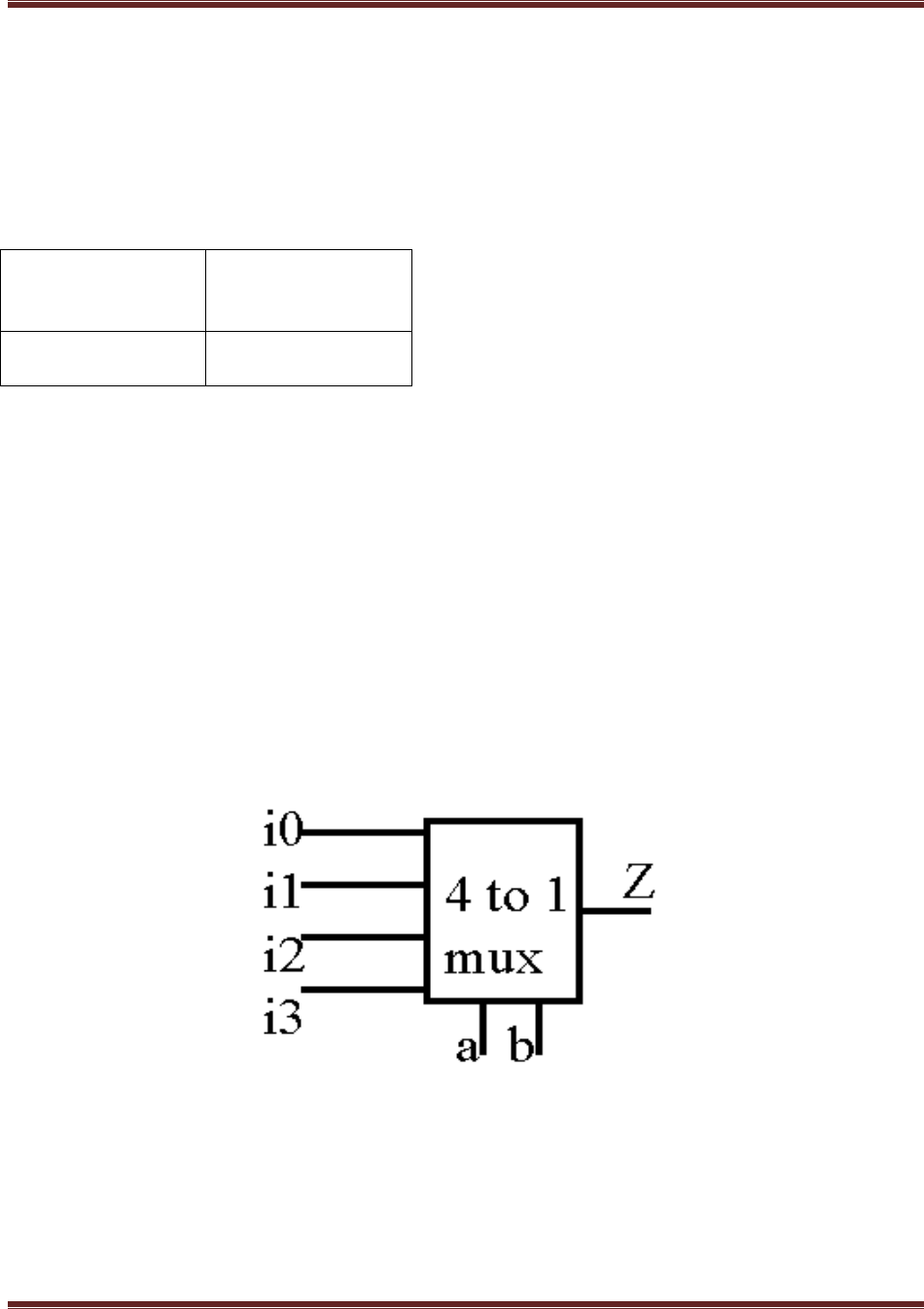
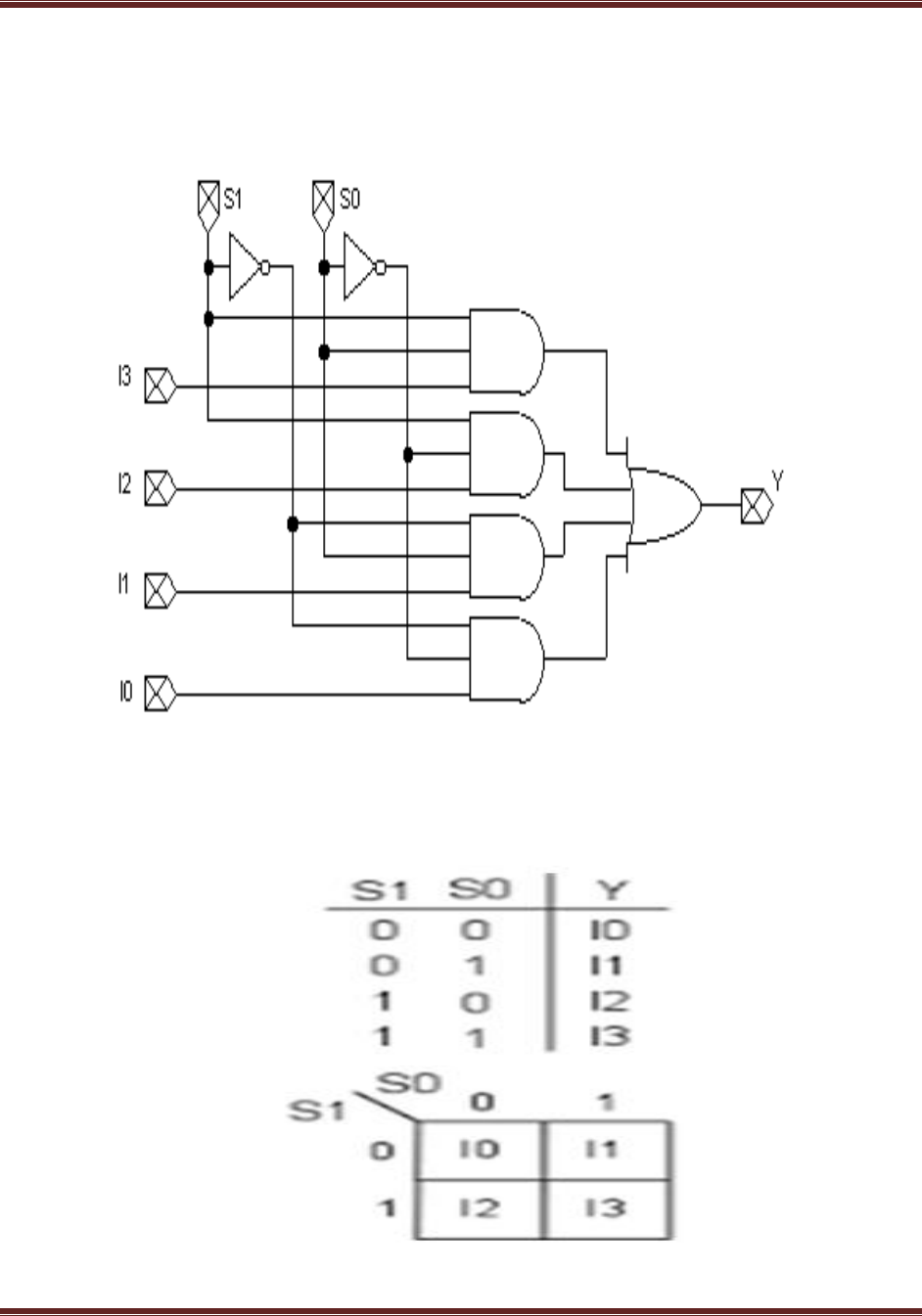
Description: 4:1 mux has four inputs lines I0 to I3 and one output F. It consists of two select
lines s0 and s1. It is implemented using three 2:1 mux.
RTL (Register transfer level) is step by step process which uses low level keywords, it uses
assign as a keyword, Behavioral modeling is architectural modeling .It is module based or object
based.
LOGIC SYMBOL
VLSI DESIGN LAB MANUAL
INFORMATION TECHNOLOGY DEPARTMENT, MJCET 58
LOGICAL DIAGRAM
TRUTH TABLE

VLSI DESIGN LAB MANUAL
INFORMATION TECHNOLOGY DEPARTMENT, MJCET 59
RTL CODE
module rtl41(s,i,f);
input [1:0]s;
input [3:0]i;
output f;
assign f=(~s[0]& ~s[1]& i[0]|~s[0]& s[1]& i[1]|
s[0]& ~s[1]& i[2]|s[0]& s[1]& i[3]);
endmodule
BEHAVIOURAL CODE
module b41(s,i,f);
input [0:0] s;
input [3:0] i;
output f;
reg f;
always @(s)
case(s)
0:f=i[0];
1:f=i[1];
2:f=i[2];
3:f=i[3];
endcase
endmodule
OUT PUT: The Truth Table of 4:1 mux is verified
VLSI DESIGN LAB MANUAL
INFORMATION TECHNOLOGY DEPARTMENT, MJCET 60
Program 24
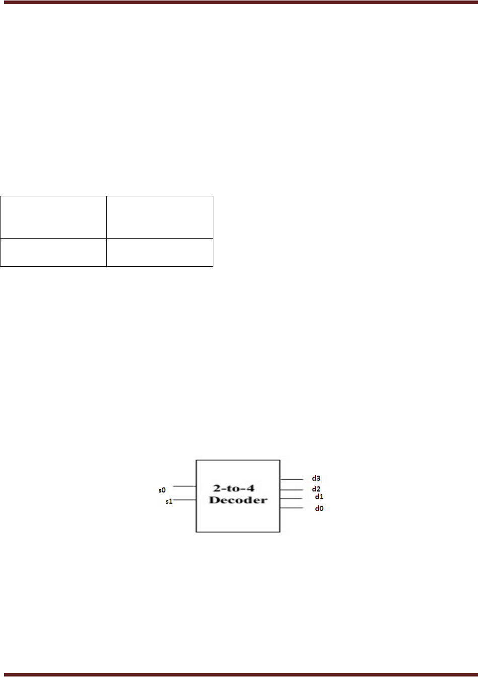
4.2 Write Verilog code to implement 2:4 Active High Decoder using RTL and
Behavioral modeling
Aim Design 2:4 Active High Decoder using RTL and Behavioral modeling.
Software Requirements:
Synthesis tool:
Xilinx Project
navigator – ISE
14.7
Simulation tool:
ModelSim
Simulator
Description: Decoder is quite similar to demux 2:4 decoder take 2 inputs (s0 & s1) and 4
outputs (d0,d1,d2,d3)
RTL (Register transfer level) is step by step process which uses low level keywords, it uses
assign as a keyword , Behavioral modeling is a architectural modeling .It is module based or
object based.
LOGIC SYMBOL
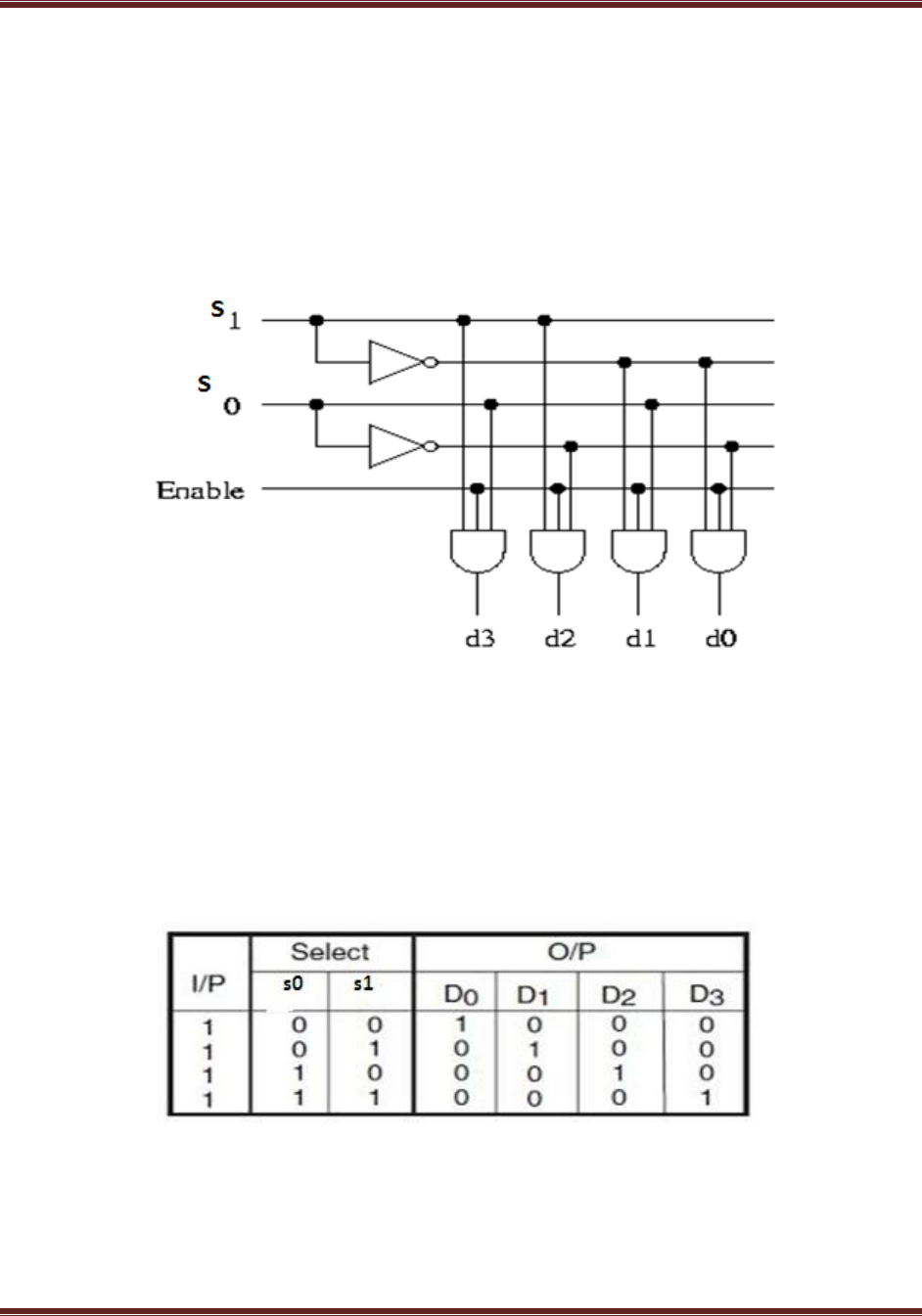
VLSI DESIGN LAB MANUAL
INFORMATION TECHNOLOGY DEPARTMENT, MJCET 61
LOGIC DIAGRAM
TRUTH TABLE

VLSI DESIGN LAB MANUAL
INFORMATION TECHNOLOGY DEPARTMENT, MJCET 62
RTL CODE:
module rtl24(s,d0,d1,d2,d3);
input [1:0] s;
output d0;
output d1;
output d2;
output d3;
assign d0=(~s[0]&~s[1]);
assign d1=(s[0]&~s[1]);
assign d2=(~s[0]&s[1]);
assign d3=(s[0]&s[1]);
endmodule
Behavioral code
module b24(s,d,f);
input [1:0]s;
output [3:0]d;
output f;
reg f;
always @(s)
case(s)
8:f=d[0];
4:f=d[1];
2:f=d[2];
1:f=d[3];
endcase
endmodule
OUT PUT: The Truth Table of 2:4 active high decoder is verified
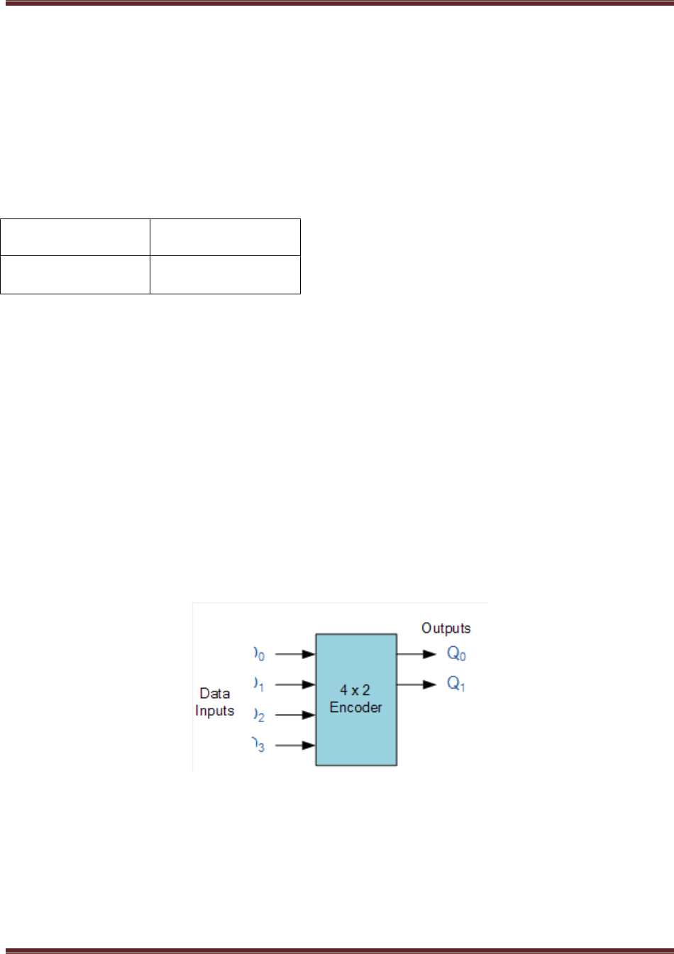
VLSI DESIGN LAB MANUAL
INFORMATION TECHNOLOGY DEPARTMENT, MJCET 63
Program 25
4.3 Write Verilog code to implement 4-BIT Priority encoder using RTL and Behavioral
modeling
AIM: Design a 4-BIT Priority encoder using RTL and Behavioral modeling
SOFTWARE REQUIREMENTS:
Synthesis tool:
Xilinx Project
navigator – ISE 14.7
Simulation tool:
ModelSim
Simulator
DESCRIPTION: A 4-bit priority encoder basically converts the 4 bit input into a binary
representation. A common user of priority encoder is for interrupt controller to select the most
critical of the multiple interrupt requests
RTL (Register transfer level) is step by step process which uses low level keywords, it uses
assign as a keyword, Behavioral modeling is a architectural modeling .It is module based or
object based.
LOGIC SYMBOL
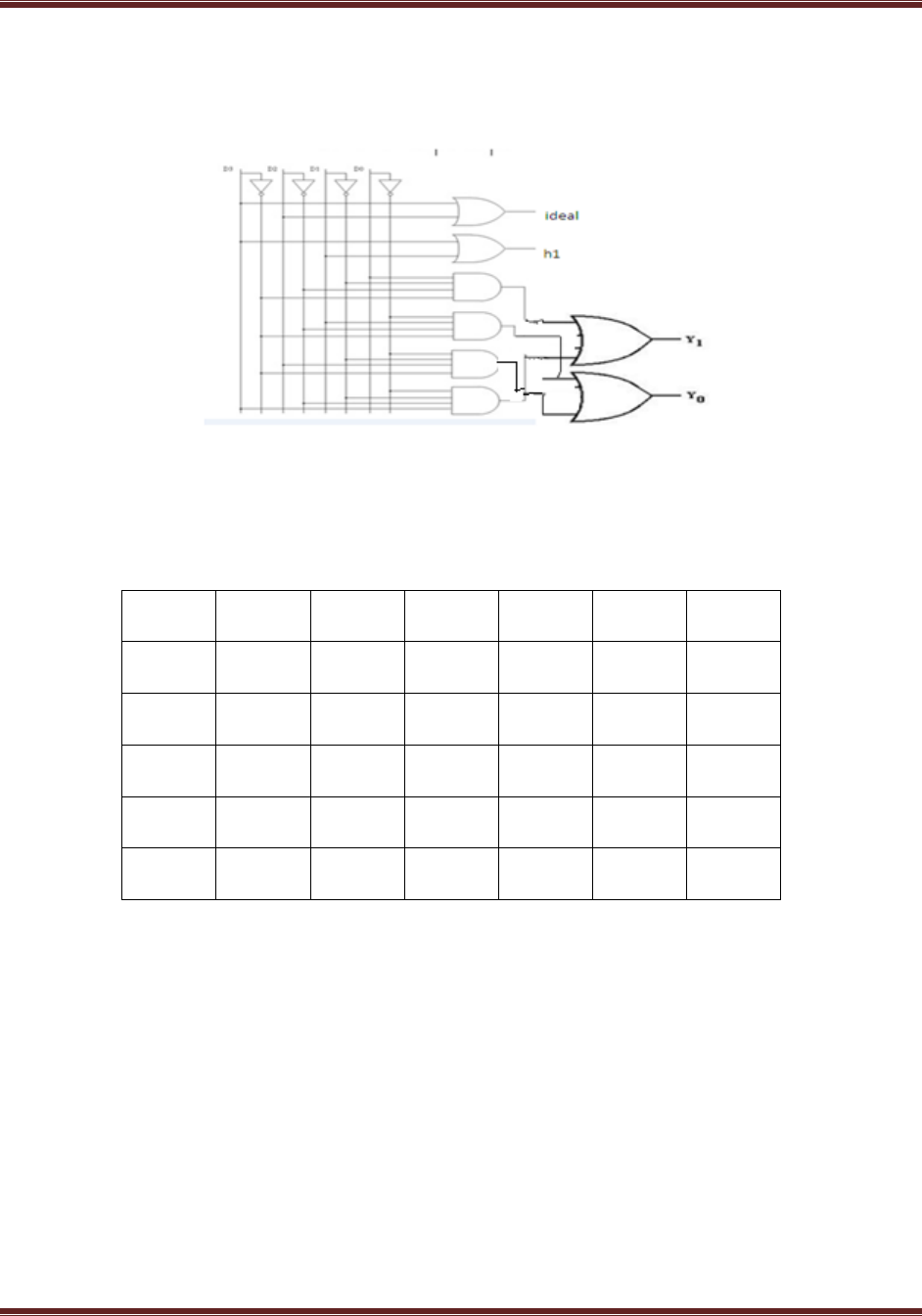
VLSI DESIGN LAB MANUAL
INFORMATION TECHNOLOGY DEPARTMENT, MJCET 64
LOGIC DIAGRAM
TRUTH TABLE
i3
i2
i1
i0
ideal
y0
y1
0
0
0
0
1
0
0
0
0
0
1
0
0
0
0
0
1
X
0
0
1
0
1
X
X
0
1
0
1
x
X
X
0
1
1

VLSI DESIGN LAB MANUAL
INFORMATION TECHNOLOGY DEPARTMENT, MJCET 65
RTL CODE
module priorityb(i0,i1,i2,i3,y0,y1,idle);
input [3:0] i;
output [1:0] y;
output idle;
output y0;
outputy1;
wire h1,h2,h3,h4;
assign h1=~(i3)&~(i2)&(i1)&(i0);
assign h2=~(i3)&~(i2)&(i1);
assign h3=~(i3)&(i2);
assign h4=(i3);
assign idle=~(i3)&~(i2)&~(i1)&~(i0);
assign y1=h2|h4;
assign y0=h3|h4;
endmodule
BEHAVIORAL MODELING
module priorityb(i,y,idle);
input [3:0] i;
output [1:0] y;
output idle;
reg[1:0]y;
reg idle;
always @ (i)
if(i==0)
begin
idle=1;
y[0]=0;
y[1]=0;
end
else if(i[3]==1)
begin
idle=0;
y[0]=1;
y[1]=1;
end
else if(i[2]==1)
begin
idle=0;
y[0]=1;
y[1]=0;
end
else if(i[1]==1)
begin
idle=0;
y[0]=0;

VLSI DESIGN LAB MANUAL
INFORMATION TECHNOLOGY DEPARTMENT, MJCET 66
y[1]=1;
end
else if(i[0]==1)
begin
idle=0;
y[0]=0;
y[1]=0;
end
endmodule
OUT PUT: The Truth Table of 4 bit priority encoder is verified
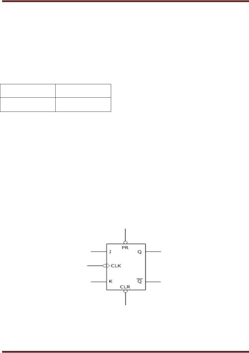
VLSI DESIGN LAB MANUAL
INFORMATION TECHNOLOGY DEPARTMENT, MJCET 67
Program 26
4.4 Write Verilog code to implement JK Flip Flop for negative edge triggered using
RTL and Behavioral modeling
AIM: Design JK FILP FLOP for –ve edge triggered using RTL and Behavioral modeling
SOFTWARE REQUIREMENTS:
Synthesis tool:
Xilinx Project
navigator – ISE 14.7
Simulation tool:
ModelSim
Simulator
DESCRIPTION: JK filpflop is the most versatile of the basic flip-flops. It has the input
following characters of the clocked D-flip-flop, but has two inputs labeled J and K . If J and K
are different then the output Q takes the value of J at the nest clock edge.
RTL (Register transfer level) is step by step process which uses low level keywords, it uses
assign as a keyword , Behavioral modeling is a architectural modeling .It is module based or
object based.
LOGIC SYMBOL
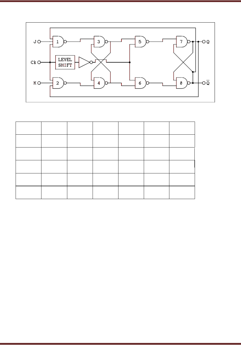
VLSI DESIGN LAB MANUAL
INFORMATION TECHNOLOGY DEPARTMENT, MJCET 68
LOGIC DIAGRAM
TRUTH TABLE
CLK
PRESET
clear
J
K
q
Qb
1
1
0
X
X
0
1
1
1
1
0
0
qp
qbp
1
1
1
0
1
0
1
1
1
1
1
0
1
0
1
1
1
1
1
1/0
1/0
RTL CODE
module jk(j,k,pr,clr,clk,q,qb);
input j;
input k;
input pr;
input clr;
input clk;
output q;
output qb;
wire w1,w2,w3,w4,w5,w6;
assign w1=~(j&qb&clk);
assign w2=~(k&q&clk);
assign w3=~(w1&pr&w4);
assign w4=~(w2&clr&w3);
assign w5=~(w3&(~clk));
assign w6=~(w4&(~clk));
assign q=~(w5&qb);

VLSI DESIGN LAB MANUAL
INFORMATION TECHNOLOGY DEPARTMENT, MJCET 69
assign qb=~(w6&q);
endmodule
OUT PUT: The Truth Table of negative edge triggered JK flipflop is verified
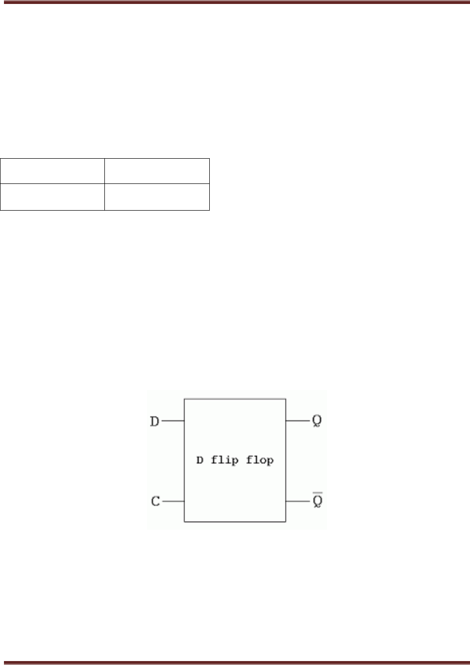
VLSI DESIGN LAB MANUAL
INFORMATION TECHNOLOGY DEPARTMENT, MJCET 70
Program 27
4.5 Write Verilog code to implement D FILP FLOP using RTL
AIM: Design D FILP FLOP using RTL modeling
SOFTWARE REQUIREMENTS:
Synthesis tool:
Xilinx Project
navigator – ISE 14.7
Simulation tool:
ModelSim
Simulator
DESCRIPTION: D flip-flop is also known as data or delay flip-flop. This flip-flop captures the
value of the D-input at the definite portion of the clock cycle. That captured value of the D
becomes the output Q. IT can be viewed as a memory cell, a zero order hold or delay line. D flip-
flop forms the basis for the shift register which are an essential part of many electronic devices.
RTL (Register transfer level) is step by step process which uses low level keywords, it uses
assign as a keyword, Behavioral modeling is a architectural modeling .It is module based or
object based.
LOGIC SYMBOL
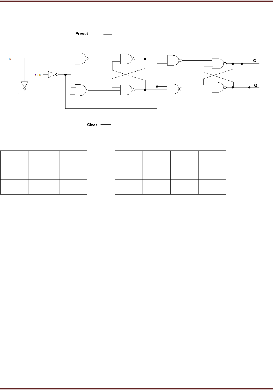
VLSI DESIGN LAB MANUAL
INFORMATION TECHNOLOGY DEPARTMENT, MJCET 71
LOGIC DIAGRAM
TRUTH TABLE
CLK
PRESET
clear
d
db
q
qb
1
1
0
0
1
0
1
1
1
1
1
0
1
0
RTL CODE
module dp(d,db,pr,clr,clk,q,qb);
input d;
input db;
input pr;
input clr;
input clk;
output q;
output qb;
wire w1,w2,w3,w4,w5,w6;
assign db=~(d);
assign w1=~(d&qb&(~clk));
assign w2=~(db&q&(~clk));
assign w3=~(w1&pr&w4);
assign w4=~(w2&clr&w3);
assign w5=~(w3&clk);
assign w6=~(w4& clk);
assign q=~(w5&qb);
assign qb=~(w6&q);
endmodule
OUT PUT: The Truth Table of D Flip Flop is verified
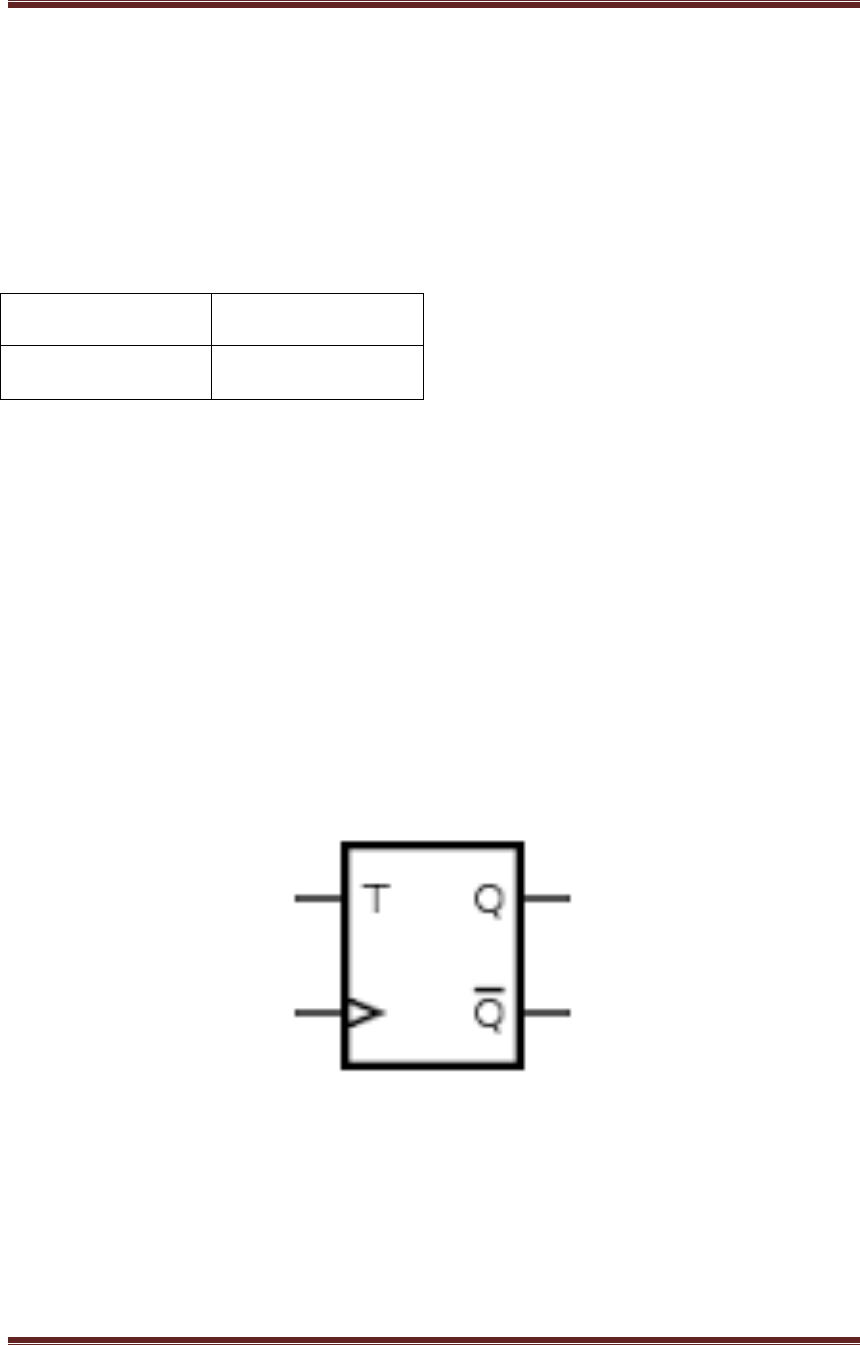
VLSI DESIGN LAB MANUAL
INFORMATION TECHNOLOGY DEPARTMENT, MJCET 72
Program 28
4.6 Write Verilog code to implement T FILP FLOP using RTL modeling
AIM: Design T FILP FLOP using RTL modeling
SOFTWARE REQUIREMENTS:
Synthesis tool:
Xilinx Project
navigator – ISE
Simulation tool:
ModelSim
Simulator
DESCRIPTION: T – Flip flop is similar to D-ff to some extent. The only difference is
that D-flip flop is uses a delay line while T-flipflop uses a toggle. If the T –input is high
the flipflop changes the state (toggles).Whenever the clock input is high if the T input is
low the ff holds the previous value.
RTL (Register transfer level) is step by step process which uses low level keywords, it
uses assign as a keyword, Behavioral modeling is a architectural modeling .It is module
based or object based.
LOGIC SYMBOL
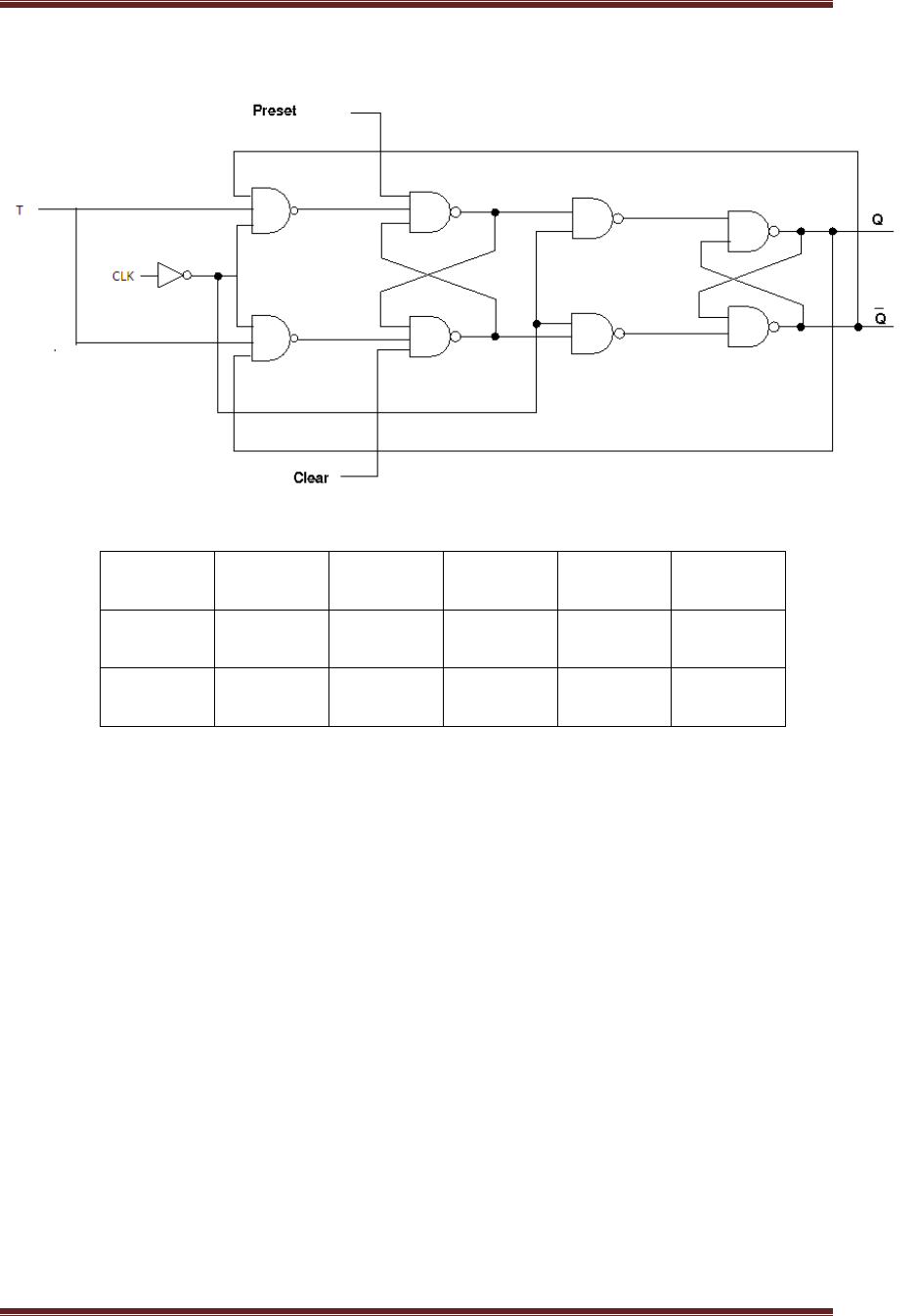
VLSI DESIGN LAB MANUAL
INFORMATION TECHNOLOGY DEPARTMENT, MJCET 73
LOGIC DIAGRAM
TRUTH TABLE
RTL CODE
module tff(t,pr,clr,clk,q,qb);
input t;
input pr;
input clr;
input clk;
output q;
output qb;
wire w1,w2,w3,w4,w5,w6;
assign w1=~(t&qb&(~clk));
assign w2=~(t&q&(~clk));
assign w3=~(w1&pr&w4);
assign w4=~(w2&clr&w3);
assign w5=~(w3&clk);
assign w6=~(w4& clk);
assign q=~(w5&qb);
assign qb=~(w6&q);
endmodule
OUT PUT: The Truth Table of T Flip Flop is verified
pr
clr
clk
T
q
qb
1
0
1
0
0
1
1
1
1
1
1
1

VLSI DESIGN LAB MANUAL
INFORMATION TECHNOLOGY DEPARTMENT, MJCET 74
Program 29
4.7 Write Verilog code to implement 4 BIT LOADABLE SISO/PIPO shift
register using RTL modeling
AIM: Design 4 BIT LOADABLE SISO/PIPO shift register using RTL modeling
SOFTWARE REQUIREMENTS:
Synthesis tool:
Xilinx Project
navigator – ISE 14.7
Simulation tool:
ModelSim
Simulator
DESCRIPTION: Shift register can have both parallel and serial inputs and outputs.
These are often configured as ―serial in‖ & ―serial out‖ (SISO) OR ― parallel in , serial
out ‖(PIPO).
A basic four-bit shift register can be constructed using four D flip-flops. Serial-in,
serial-out shift registers delay data by one clock time for each stage. They will store a
bit of data for each register. The operation of the circuit is as follows. If load =0 the
register is first cleared, forcing all four outputs to zero. The input data is then applied
sequentially to the D input of the first flip-flop on the left. During each clock pulse,
one bit is transmitted from left to right
If load =1 the circuit behaves as PIPO. For parallel in - parallel out shift registers, all
data bits appear on the parallel outputs immediately following the simultaneous entry of
the data bits.
RTL (Register transfer level) is step by step process which uses low level keywords, it
uses assign as a keyword, Behavioral modeling is a architectural modeling .It is module
based or object based.
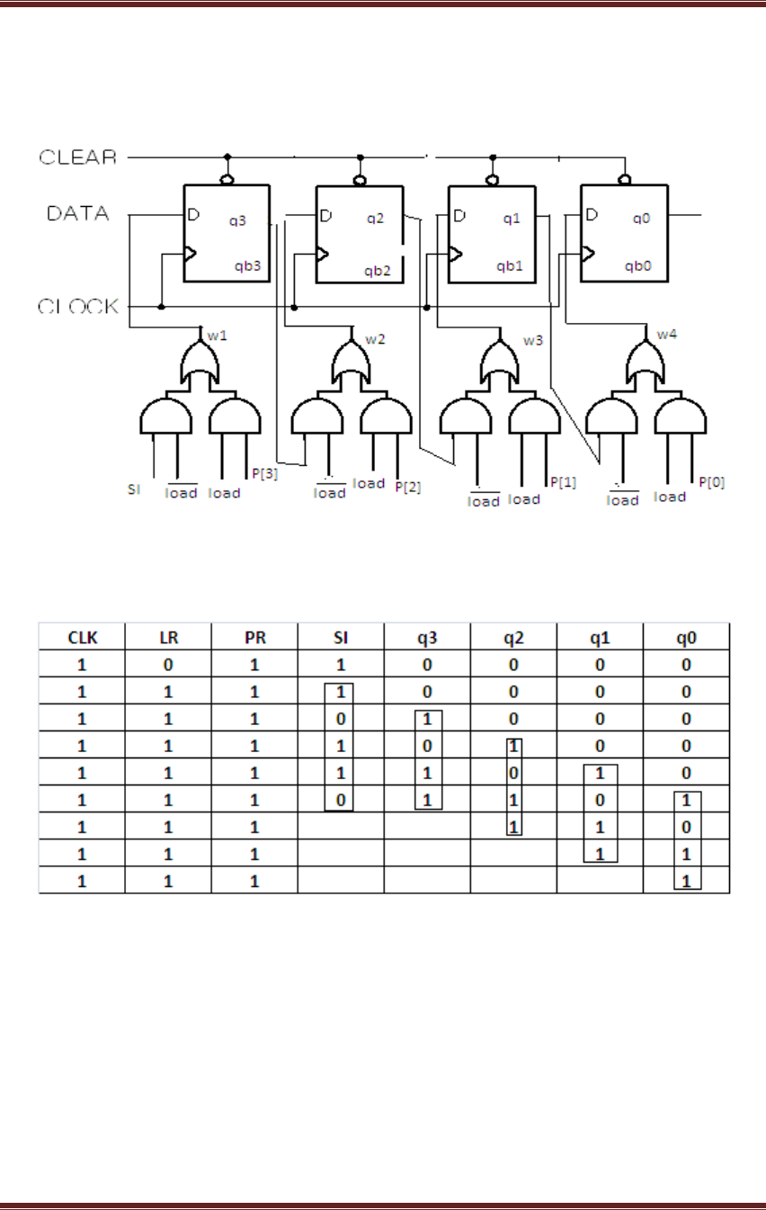
VLSI DESIGN LAB MANUAL
INFORMATION TECHNOLOGY DEPARTMENT, MJCET 75
LOGIC DIAGRAM
TRUTH TABLE

VLSI DESIGN LAB MANUAL
INFORMATION TECHNOLOGY DEPARTMENT, MJCET 76
RTL CODE
module siso(si,pr,clr,clk,p,load,q);
input si;
input pr;
input clr;
input clk;
input [3:0] p;
input load;
output [3:0] q;
wire w1,w2,w3,w4;
assign w1=((si&(~load))||(load&p[3]));
assign w2=((q[3]&(~load))||(load & p[2]));
assign w3=((q[2] & (~load))||(load & p[1]));
assign w4=((q[1] & (~load))||(load & p[0]));
dp d1(w1,pr,clr,clk,q[3],qb[3]);
dp d2(w2,pr,clr,clk,q[2],qb[2]);
dp d3(w3,pr,clr,clk,q[1],qb[1]);
dp d4(w4,pr,clr,clk,q[0],qb[0]);
endmodule
NOTE: For PIPO output is same as input.
OUTPUT: The truth table of SISO/PIPO is verified
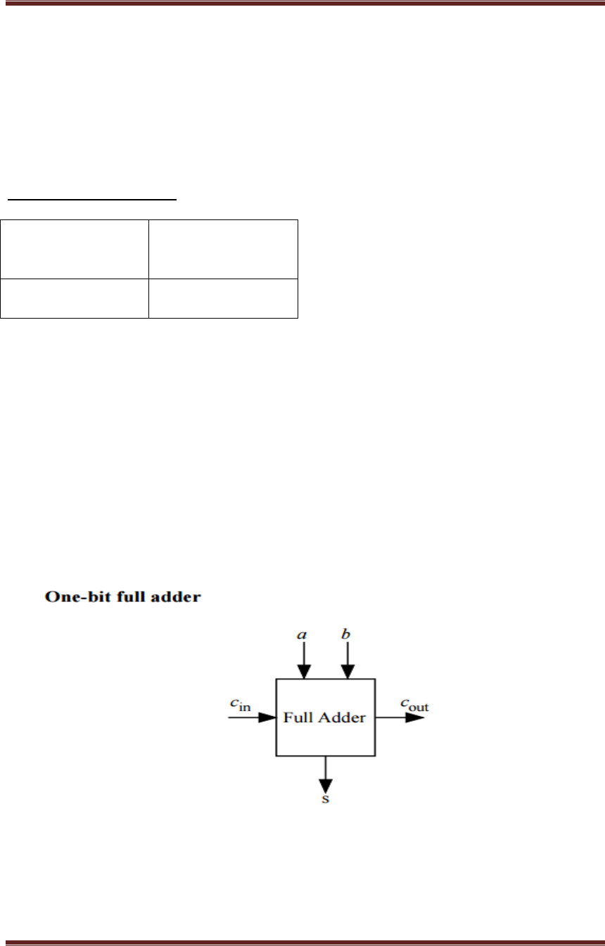
VLSI DESIGN LAB MANUAL
INFORMATION TECHNOLOGY DEPARTMENT, MJCET 77
Program 30
4.9 Implement Ripple Carry Adder using RTL and Behavioral Modeling
Aim : Write Verilog code to implement Ripple Carry Adder using RTL and Behavioral
modeling
Software Requirements:
Synthesis tool:
Xilinx Project
navigator – ISE
14.7
Simulation tool:
ModelSim
Simulator
Description: Ripple carry adder A ripple carry adder is a digital circuit that produces
the arithmetic sum of two binary numbers. It can be constructed with full adders
connected in cascaded (see section 2.1), with the carry output from each full adder
connected to the carry input of the next full adder in the chain. Below figure shows the
inter connection of four full adder (FA) circuits to provide a 4-bit ripple carry adder.
From that the input is from the right side because the first cell traditionally
represents the least significant bit (LSB). Bits a0and b0 in the figure represent the least
significant bits of the numbers to be added. The sum output is represented by the bits
s0-s3
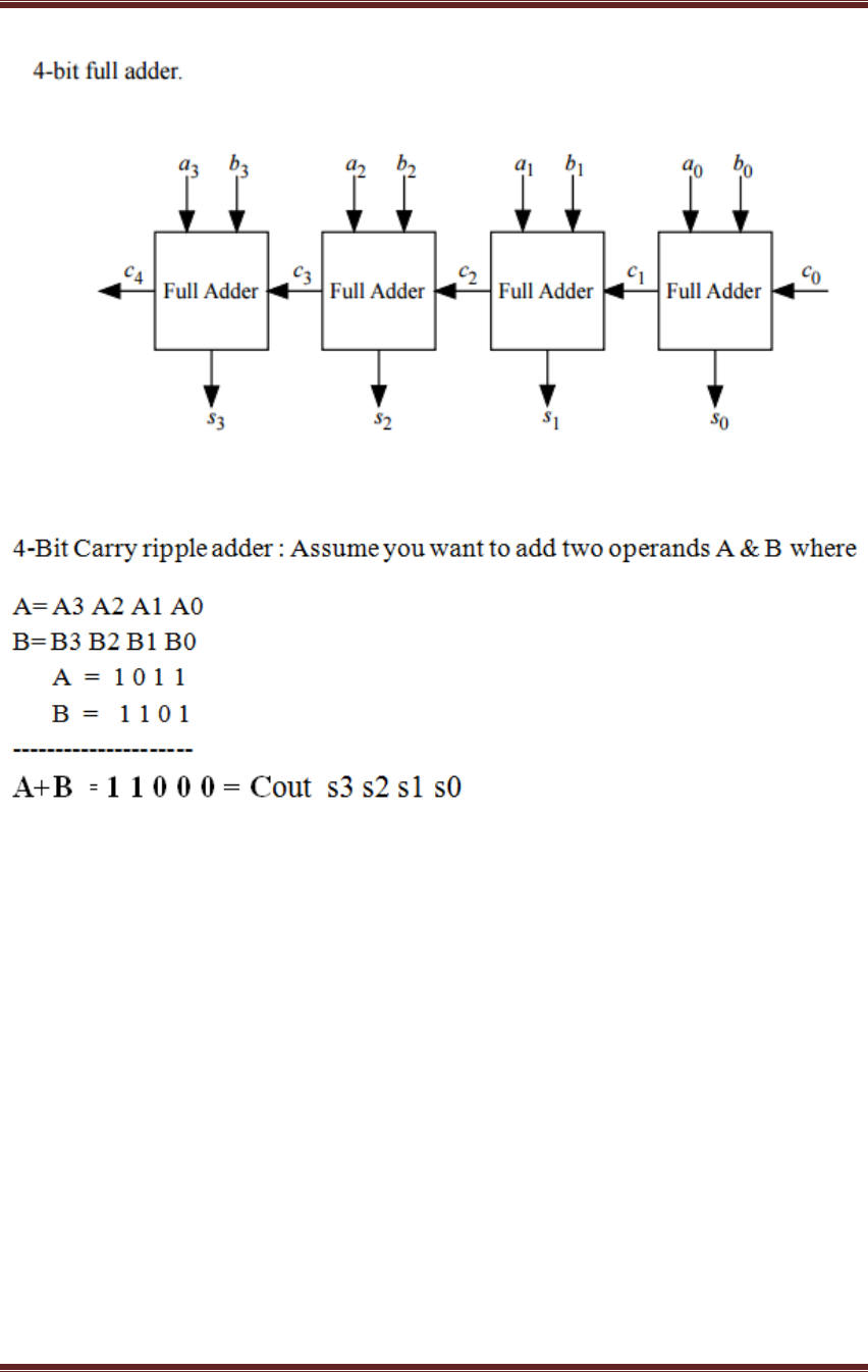
VLSI DESIGN LAB MANUAL
INFORMATION TECHNOLOGY DEPARTMENT, MJCET 78
RTL CODE:
Module rtl rc(c,c4,a,b,c0)
input[3:0]a,b;
input c0;
output[3:0]s,c4;
assign{c4,s}=a+b+c0;
endmodule
Behavioural modelling
module rip(a,b,c0,s,c4)
input[3:0]a,b;
input c0;
output[3:0]s,c4;
regc4;

VLSI DESIGN LAB MANUAL
INFORMATION TECHNOLOGY DEPARTMENT, MJCET 79
regs;
always @ (a:b:c0);
begin
(s,c4)= a+b+c0;
end
endmodule

VLSI DESIGN LAB MANUAL
INFORMATION TECHNOLOGY DEPARTMENT, MJCET 80
Program 31
4.8 Write Verilog code to implement 4 bit carry look ahead (CLA) using RTL
and Behavioral modeling
AIM: Design a 4bit carry look ahead (CLA) using RTL and Behavioral modeling
SOFTWARE REQUIREMENTS:
Synthesis tool:
Xilinx Project
navigator – ISE
14.7
Simulation tool:
ModelSim
Simulator
DESCRIPTION: The carry look ahead adder (CLA) solves the carry delay problem by
calculating the carry signal in advance based on the inputs signals Or It is used to
decrease calculation time in adder units.
Ci+1=Gi +Pi-Ci
Si = PiΘCi
Gi =aibi
Pi =ai Θbi
Ci+1=aibi+Ci(aiΘbi)
Where Gi---carry generate then
Pi ----carry propagate
RTL (Register transfer level) is step by step process which uses low level keywords, it
uses assign as a keyword, Behavioral modeling is a architectural modeling .It is module
based or object based.
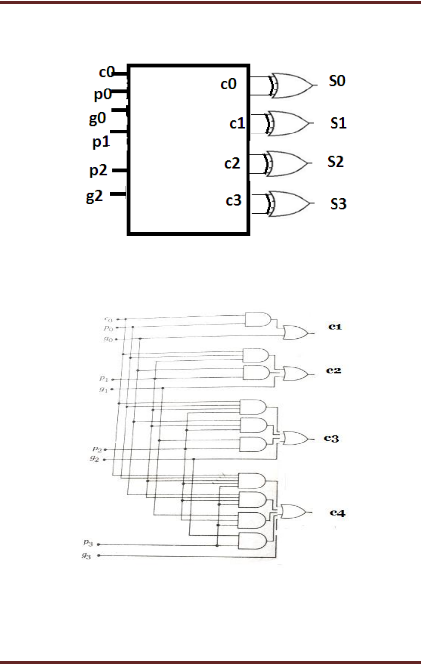
VLSI DESIGN LAB MANUAL
INFORMATION TECHNOLOGY DEPARTMENT, MJCET 81
LOGIC SYMBOL
LOGIC DIAGRAM

VLSI DESIGN LAB MANUAL
INFORMATION TECHNOLOGY DEPARTMENT, MJCET 82
TRUTH TABLE
a
b
c0
s
c4
1
1
0
0
1
0
0
0
0
0
1
0
0
1
0
0
1
0
0
1
RTL CODE
module CLA _4b(sum ,c4, a,b,c0);
input [3:0] a,b;
input c0;
output [3:0] sum;
output_4;
wire p0, p1,p2,p3,g0,g1,g2,g3,c1,c2,c3,c4;
assign
p0=a[0]^b[0];
p1=a[1]^b[1];
p2=a[2]^b[02];
p3=a[3]^b[3];
g0=a[0]&b[0];
g1=a[1]&b[1];
g2=a[2]&b[02];
g3=a[3]&b[3];
assign
c1=g0|(p0&c0);
c2=g1|(p1&g0)|(p1&p0&c0);
c3=g2|(p2&g1)|(p2&p1&g0)|(p2&p1&p0&c0);
assign
sum[0]=p0^c0;
sum[1]=p1^c1;
sum[2]=p2^c2;
sum[3]=p3^c3;
c_4=c4
endmodule
OUTPUT: The Truth Table of CLA is verified
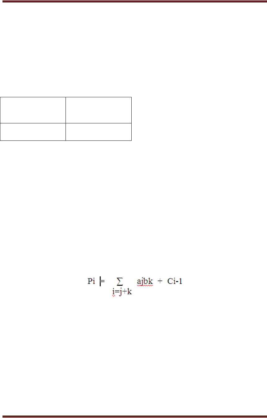
VLSI DESIGN LAB MANUAL
INFORMATION TECHNOLOGY DEPARTMENT, MJCET 83
Program 32
4.10 Write Verilog code to implement 4X4 Register Based Multiplier using RTL
and Behavioral modeling
Aim: Design 4X4 register based multiplier using RTL and Behavioral modeling
Software Requirements:
Synthesis tool:
Xilinx Project
navigator – ISE
14.7
Simulation tool:
ModelSim
Simulator
Description: Binary multiplication is based on the basic operations 0 x 0 =0 ; 0 x 1=0;
1x0=0; 1x1=1. Multiplication is by a factor of 2m can be accomplished using a ShL-m
operations on a register.
While multipliying ‗n‘ bits we specify a word of length of n=4 with input values
a=a3a2a1a0 and b=b3b2b1b0. The product axb is given by 8 bit result
P= p7p6p5p4p3p2p1p0
Each bit ‗bi‘ multiplies the multiplicand ‗a‘ on a bit by bit basis.
RTL (Register transfer level) is step by step process which uses low level keywords, it
uses assign as a keyword, Behavioral modeling is a architectural modeling .It is module
based or object based.
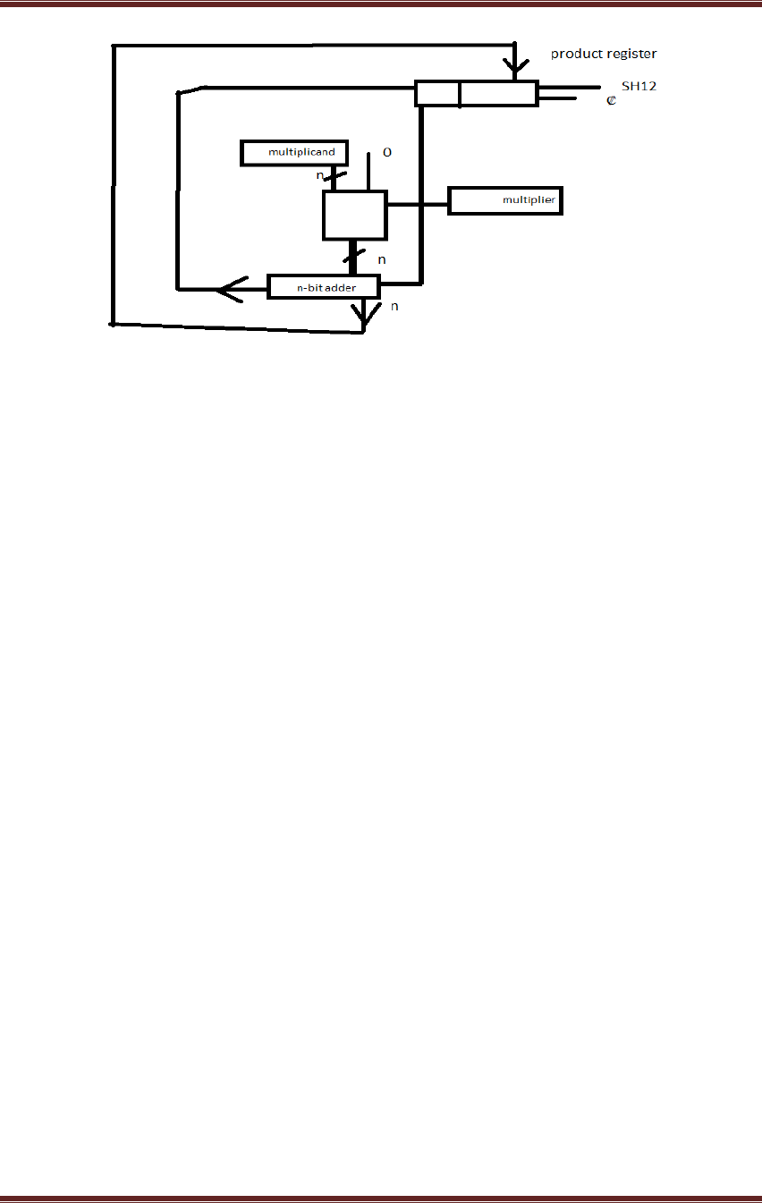
VLSI DESIGN LAB MANUAL
INFORMATION TECHNOLOGY DEPARTMENT, MJCET 84
RTL CODE
module regmul(a,b,p)
input[3:0] a,b ;
output[7:0 ] p;
Wire[7:0] w1,w2,w3,w4;
assign w1= a*b[0]*1;
assign w2= a*b[1]*2;
assign w3= a*b[2]*4;
assign w4= a*b[3]*8;
assign p= w1|w2|w3|w4;
endmodule
BEHAVIOURAL CODE
module regmul(a,b,p)
input[3:0] a,b ;
output[7:0 ] p;
Wire[7:0] w1,w2,w3,w4;
Always @ (a & b )
begin
w1= a*b[0]*1;
w2= a*b[1]*2;
w3= a*b[2]*4;
w4= a*b[3]*8;
p= w1|w2|w3|w4;
end
endmodule
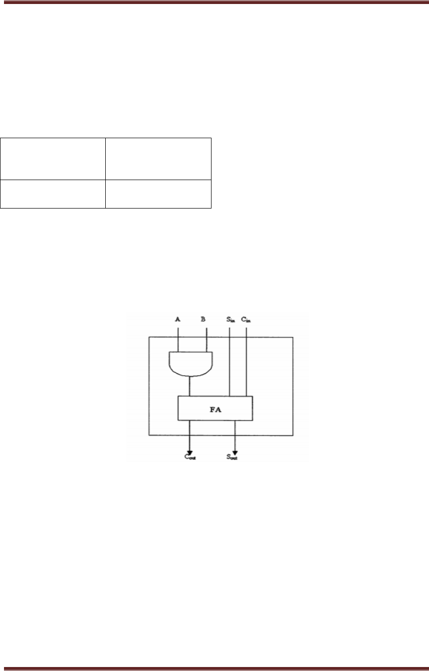
VLSI DESIGN LAB MANUAL
INFORMATION TECHNOLOGY DEPARTMENT, MJCET 85
Program 33
Array Multiplier
4.11 Aim : implement Array multiplier Using RTL modeling
Software Requirements:
Synthesis tool:
Xilinx Project
navigator – ISE
14.7
Simulation tool:
ModelSim
Simulator
Description: An array multiplier accepts the multiplier and multiplicand which uses an
array of cells to calculate the bit products of aj bk individually in parallel manner.
LOGIC SYMBOL
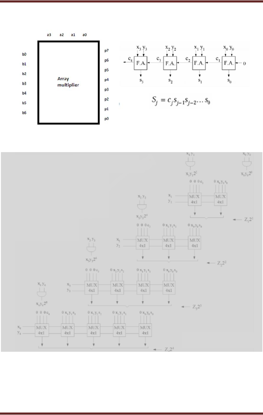
VLSI DESIGN LAB MANUAL
INFORMATION TECHNOLOGY DEPARTMENT, MJCET 86
LOGIC DIAGRAM
RTL CODE
Modue artl(a,b,p);
Input [3:0]a;
Input [3:0]b;

VLSI DESIGN LAB MANUAL
INFORMATION TECHNOLOGY DEPARTMENT, MJCET 87
Output [7:0] p;
Wire w0,w1,w2,w3,w4,w5;
Wire[11:0] c;
Assign p[0]=a[0]&b[0];
Half n1 ((a[0]&b[1]),(a[1]&b[0]),p[1],c[0]);
Half n2 ((a[1]&b[1]),(a[2]&b[0]),w0,c[1]);
Assign{c[3],p[2]}=w0 + (a[0]&b[2]) +c[0];
Half n3 ((a[2]&b[1]),(a[3]&b[0]),w1,c[3]);
Assign{c[4],w2}=w1 + (a[1]&b[2]) +c[1];
Assign{c[5],p[3]}=w2 + (a[0]&b[3]) +c[2];
Assign{c[6],w3}= (a[3]&b[1]) +(a[2]&b[2]+c[3]);
Assign{c[7],w4}=w3 + c[4]+(a[1]&b[3]);
Half n4 (w4,c[5],p[4],c[8]);
Assign{c[10],p[5]}=w5+c[7]+c[8];
Assign{c[11],p[6]}=(a[3]&b[3])+c[9]+c[10];
Assign p[7]=c[11];
endmodule
Behavioural Code
module abm(a,b,p)
input [3:0] a,b;
output[7:0] p; reg[7:0] p;
wire[7:0]w, reg wire [7:0] w;
always @ ( a & b)
begin
w1 = a * b [0] *1 ;
w1 = a * b [0] *1 ;
w2 = a * b [1] *2 ;
w1 = a * b [2] *4 ;
w1 = a * b [3] *8 ;
end
endmodule

VLSI DESIGN LAB MANUAL
INFORMATION TECHNOLOGY DEPARTMENT, MJCET 88
Program 34
LAYOUT DESIGNING [DSCH2 & MICROWIND2]
Obtain Layout Design Of Not Gate In CMOS
Aim: Implement Layout Design Of Not Gate In CMOS
Software Requirements:
Synthesis tool:
Dsch 2
Simulation tool:
microwind 2
PROCEDURE:
1. Click on open tab of Dsch2, ), inside the library create a New file name (Ex:
xxx.sch).
2. Design the CMOs equivalent of an Inverter by dragging and dropping required
symbol.
3. Click on file---> Make Verilog file .
4. Click on simulate tab ---Start Simulate.
5. Open Microwind
6. Click on File---xxx.sch file(created using DSch2)
7. Click on Compile tab ----compile verilog file
8. Compile and close
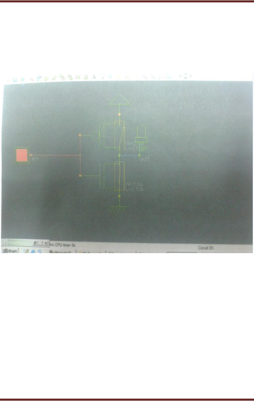
VLSI DESIGN LAB MANUAL
INFORMATION TECHNOLOGY DEPARTMENT, MJCET 89
Program 34
Inverter(NOT)
CMOS DIAGRAM OF Inverter(NOT)
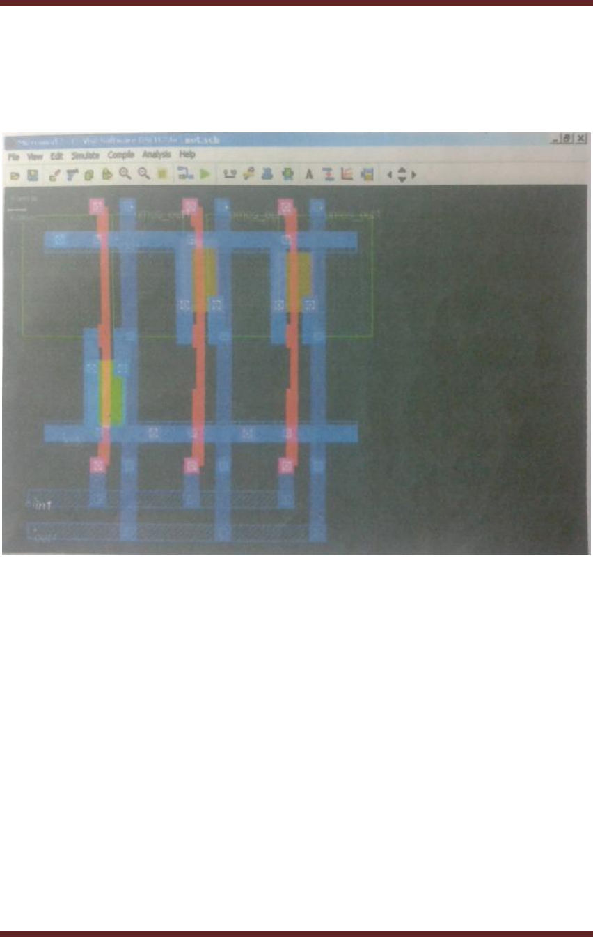
VLSI DESIGN LAB MANUAL
INFORMATION TECHNOLOGY DEPARTMENT, MJCET 90
LAYOUT OF NOT GATE
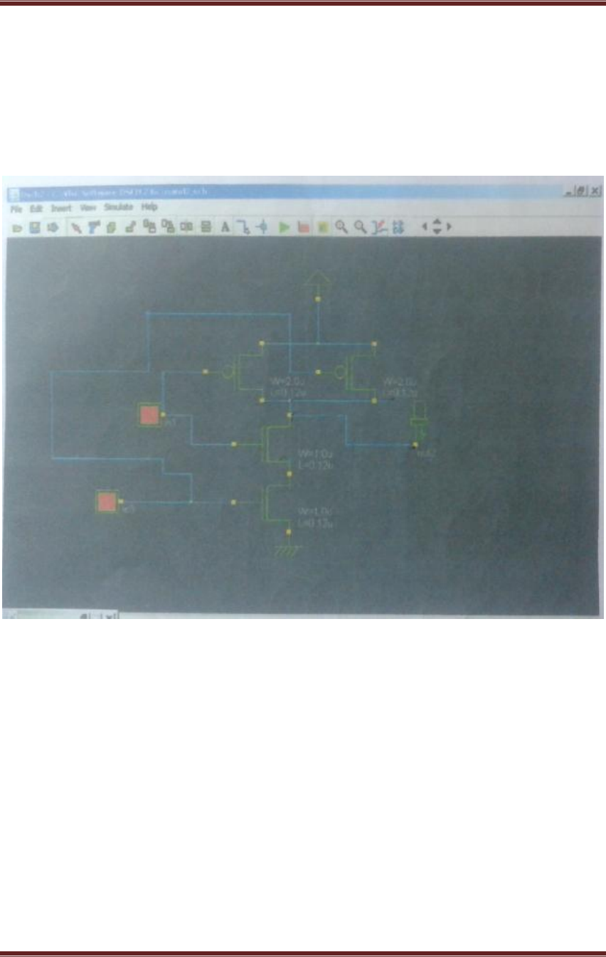
VLSI DESIGN LAB MANUAL
INFORMATION TECHNOLOGY DEPARTMENT, MJCET 91
Program 35
CMOS DIAGRAM FOR 2 INPUT NAND GATE
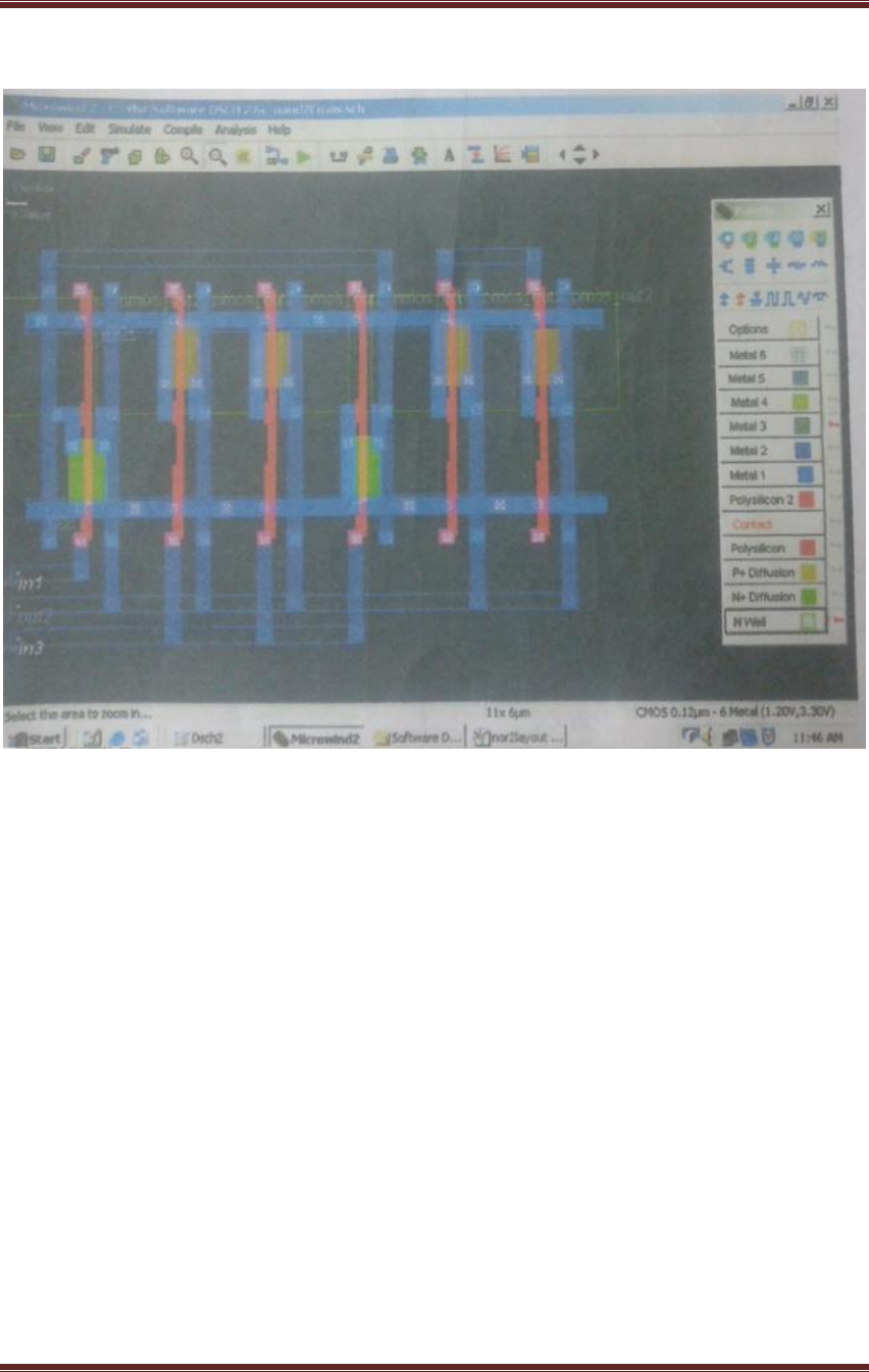
VLSI DESIGN LAB MANUAL
INFORMATION TECHNOLOGY DEPARTMENT, MJCET 92
LAYOUT OF NAND GATE
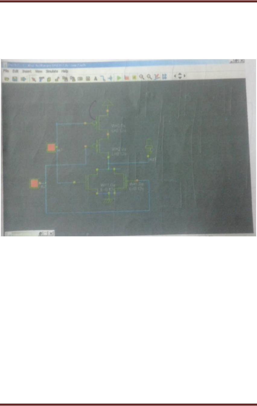
VLSI DESIGN LAB MANUAL
INFORMATION TECHNOLOGY DEPARTMENT, MJCET 93
Program 36
CMOS DIAGRAM OF NOR GATE
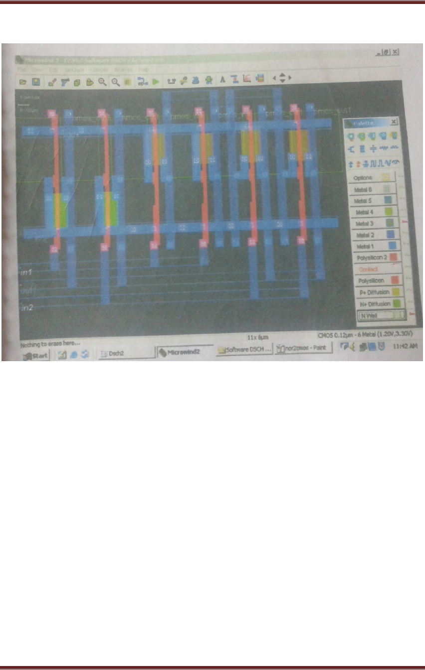
VLSI DESIGN LAB MANUAL
INFORMATION TECHNOLOGY DEPARTMENT, MJCET 94
LAYOUT OF 2 INPUT NOR GATE

VLSI DESIGN LAB MANUAL
INFORMATION TECHNOLOGY DEPARTMENT, MJCET 95
Annexure – I
List of programs according to O.U. curriculum
With Effect From the Academic Year 2013-14
BIT 431
VLSI DESIGN LAB
Instruction 4 Periods
per week
Duration of University Examination 3Hours
University Examination 75Marks
Sessional 25 Marks
1. Switch level modeling using Verilog
a) Logic gates b) AOl and OAI gates
c) Transmission gate d) Complex logic gates using CMOS
2. Structural Gate-level Modeling [With and without delay]— Digital circuits using
gate primitives—using Verilog.
a) AOl gate b) Half adder and full adders
c) MUX using buffers d) S-R latch etc.
3. Mixed gate —level and Switch-level modeling using Verilog-usage of primitives,
modules and instancing and understanding the hierarchical design.
a) Constructing a 4-input AND gate using CMOS 2-input NAND and NOR
gates.
b) Constructing a decoder using CMOS 2-input AND gates and NOT gates etc.
4. RTL Modeling of general VLSI system components.
a) MUXes b) Decoders c) Priority encodes d) Flip-flops e) Registers.
5. Synthesis of Digital Circuits
a) Ripple carry adder and carry look-ahead adder
b) array multiplier
6. Verilog code for finite state machine
7. Modeling of MOSFET
8. Stick diagram representations. Simple layout of Inverter. Understanding the
concepts of Design Rule checking.
9. Fault Modeling for Stuck-at-O and Stuck-at-I faults.
10. Clock generation circuits (study)

VLSI DESIGN LAB MANUAL
INFORMATION TECHNOLOGY DEPARTMENT, MJCET 96
ANNEXURE -II
MUFFAKHAM JAH COLLEGE OF ENGINEERING AND TECHNOLOGY
LABORATORY COURSE EVALUATION SYSTEM
PROGRAMMING LABORATORY COURSES
i. The number of experiments/programs/sessions in each laboratory course shall
be as per the curriculum in the scheme of instructions provided by OU.
ii. The students will maintain a separate note book for each laboratory course in
which all the related work would be done.
iii. In each session the students will complete the assigned tasks of process
development, coding, compiling, debugging, linking and executing the
programs.
iv. The students will then execute the programme and validate it by obtaining the
correct output for the provided input. The course coordinator will certify the
validation in the same session.
v. The students will submit the record in the next class. The evaluation will be
continuous and not cycle-wise or at semester end.
vi. The internal marks of 25 are awarded in the following manner:
a. Laboratory record - Maximum Marks 15
b. Test and Viva Voce - Maximum Marks 10
vii. Laboratory Record: Each experimental record is evaluated for a score of 50.
The rubric parameters are as follows:
a. Write up format - Maximum Score 20
b. Process development and coding - Maximum Score 10
c. Compile, debug, link and execute program - Maximum Score 15
d. Process validation through input-output - Maximum Score 5
While (a) is assessed at the time of record submission, (b), (c) and (d) are
assessed during the session based on the performance of the student in the
laboratory session. Hence if a student is absent for any laboratory session but
completes the program in another session and subsequently submits the record,
it shall be evaluated for a score of 20 and not 50.

VLSI DESIGN LAB MANUAL
INFORMATION TECHNOLOGY DEPARTMENT, MJCET 97
viii. The experiment evaluation rubric is therefore as follows :
Parameter
Max Score
Outstanding
Accomplished
Developing
Beginner
Points
Process
Development
and Coding
10
Compilation,
Debugging,
Linking and
Executing
15
Process
Validation
5
Write up format
20
ix. The first page of the record will contain the following title sheet:

VLSI DESIGN LAB MANUAL
INFORMATION TECHNOLOGY DEPARTMENT, MJCET 98
MUFFAKHAM JAH COLLEGE OF ENGINEERING AND TECHNOLOGHY
LABORATORY EXPERIMENT ASSESSMENT SHEET
INFORMATION TECHNOLOGY DEPARTMENT
B.E. IV/IV I SEM
VLSI DESIGN LABORATORY (BIT 431)
NAME: ROLL NO.
Exp.
No.
Title of the Program
Date
conducted
Date
Submitted
Process
Development
and Coding
(Max 10)
Compilation
, Debugging,
Linking and
Executing
(Max 15)
Process
Validation
(Max 5)
Write up
format
(Max 20)
Total
Score
(Max 50)
1
2
3
4
5
6
7
8
9
10
11
12
TOTAL
Date: Signature of Course
Coordinator

VLSI DESIGN LAB MANUAL
INFORMATION TECHNOLOGY DEPARTMENT, MJCET 99
x. The 15 marks of laboratory record will be scaled down from the TOTAL of the
assessment sheet.
xi. The test and viva voce will be scored for 10 marks as follows:
Internal Test - 6 marks
Viva Voce / Quiz - 4 marks
xii. Each laboratory course shall have 5 course outcomes.
The proposed course outcomes would be as follows:
On successful completion of the course, the student will acquire the ability to:
1. Apply the design concepts for development of a process and interpret data
2. Demonstrate knowledge of programming environment, compiling, debugging,
linking and executing variety of programs.
3. Demonstrate documentation and presentation of the algorithms / flowcharts /
programs in a record form.
4. Validate the process using known input-output parameters.
5. Employ analytical and logical skills to solve real world problem and
demonstrate oral communication skills.
xiii. The Course coordinators would prepare the assessment matrix in accordance
with the guidelines provided above for the five course outcomes. The scores to
be entered against each of the course outcome would be the sum of the
following as obtained from the assessment sheet in the record:
a. Course Outcome 1: Sum of the scores under ‗Process Development and
Coding‘.
b. Course Outcome 2: Sum of the scores under
‗Compilation/Debugging/Linking and Executing‘.
c. Course Outcome 3: Sum of the scores under ‗Write up format‘.
d. Course Outcome 4: Sum of the scores under ‗Process validation‘.
e. Course Outcome 5: Marks for ‗Internal Test and Viva voce‘.
xiv. Soft copy of the assessment matrix would be provided to the course
coordinators.

VLSI DESIGN LAB MANUAL
INFORMATION TECHNOLOGY DEPARTMENT, MJCET 100
LABORATORY EXPERIMENT EVALUATION RUBRIC
CATEGORY
OUTSTANDING
(Up to 100%)
ACCOMPLISHED
(Up to 75%)
DEVELOPING
(Up to 50%)
BEGINNER (Up to
25%)
Write up
format
Aim, Apparatus,
material requirement,
theoretical basis,
procedure of
experiment, sketch of
the experimental
setup etc. is
demarcated and
presented in clearly
labeled and neatly
organized sections.
The write up follows
the specified format
but a couple of the
specified parameters
are missing.
The report follows
the specified format
but a few of the
formats are missing
and the experimental
sketch is not
included in the
report
The write up does not
follow the specified
format and the
presentation is shabby.
Observations
and
Calculations
The experimental
observations and
calculations are
recorded in neatly
prepared table with
correct units and
significant figures.
One sample
calculation is
explained by
substitution of values
The experimental
observations and
calculations are
recorded in neatly
prepared table with
correct units and
significant figures
but sample
calculation is not
shown
The experimental
observations and
calculations are
recorded neatly but
correct units and
significant figures
are not used. Sample
calculation is also
not shown
The experimental
observations and results
are recorded carelessly.
Correct units significant
figures are not followed
and sample calculations
not shown
Results and
Graphs
Results obtained are
correct within
reasonable limits.
Graphs are drawn
neatly with labeling
of the axes. Relevant
calculations are
performed from the
graphs. Equations are
obtained by
regression analysis or
curve fitting if
relevant
Results obtained are
correct within
reasonable limits.
Graphs are drawn
neatly with labeling
of the axes. Relevant
calculations from the
graphs are
incomplete and
equations are not
obtained by
regression analysis or
curve fitting
Results obtained are
correct within
reasonable limits.
Graphs are not
drawn neatly and or
labeling is not
proper. No
calculations are
done from the
graphs and
equations are not
obtained by
regression analysis
or curve fitting
Results obtained are not
correct within reasonable
limits. Graphs are not
drawn neatly and or
labeling is not proper. No
calculations are done from
the graphs and equations
are not obtained by
regression analysis or
curve fitting
Discussion of
results
All relevant points of
the result are
discussed and
justified in light of
theoretical
expectations.
Reasons for divergent
results are identified
and corrective
measures discussed.
Results are discussed
but no theoretical
reference is
mentioned. Divergent
results are identified
but no satisfactory
reasoning is given for
the same.
Discussion of results
is incomplete and
divergent results are
not identified.
Neither relevant points of
the results are discussed
nor divergent results
identified
