Assist VPLPX20
User Manual: VPLPX20
Open the PDF directly: View PDF ![]() .
.
Page Count: 177 [warning: Documents this large are best viewed by clicking the View PDF Link!]
- Front Page
- Operating Instructions
- Service Notes
- Circuit Board Location
- Disassembly
- Cabinet assy removal
- Front block assy removal
- NF board removal
- BA and Y boards removal
- Power block removal
- G block assy (GA, GB, GC and GD board) removal
- C board removal
- Optics unit assy removal
- BC and KS boards removal
- Connector block assy removal
- BB, QA, QB, QC and QD boards removal
- F, K board and AC inlet removal
- Lens assy removal
- Prism block and polarizer removal
- Adjustment - general
- Semiconductor Pin Layouts
- Exploded Views
- Block Diagrams
- Circuit Diagrams
- Frame (1/3)
- Frame (2/3)
- Frame (3/3)
- QA board (1/3)
- QA board (2/3)
- QA board (3/3)
- QB board (1/2)
- QB board (2/2)
- QC board (1/2)
- QC board (2/2)
- QD board
- BA board (1/2)
- BA board (2/2)
- BB board
- BB board (1/4)
- BB board (2/4)
- BB board (3/4)
- BB board (4/4)
- BC board (1/2)
- BC board (2/2)
- C board (1/3)
- C board (2/3)
- C board (3/3)
- Y (1/3), S, NF and NR board
- Y board (2/3)
- Y board (3/3)
- H board
- K board
- KS board
- GA (1/2) and F board
- GA board (2/2)
- GB and GC board
- GD board
- MCB Layouts
WORLD
WORLD
SERVICE MANUAL
MODEL ..........
VPL-PX20
VPL-PX30
R
LCD DATA PROJECTOR
...............
MODEL
RM-PJM610
............... DEST.
WORLD
..........
DEST.
WARNING!!
AN INSULATED TRANSFORMER SHOULD BE USED DURING
ANY SERVICE TO AVOID POSSIBLE SHOCK HAZARD, BE-
CAUSE OF LIVE CHASSIS.
THE CHASSIS OF THIS RECEIVER IS DIRECTLY CONNECTED
TO THE AC POWER LINE.
SAFETY-RELATED COMPONENT WARNING !!
COMPONENTS IDENTIFIED BY A ! MARK ON THE SCHEMATIC
DIAGRAMS, EXPLODED VIEWS AND IN THE PARTS LIST ARE
CRITICAL TO SAFE OPERATION. REPLACE THESE COMPO-
NENTS WITH SONY PARTS WHOSE PART NUMBERS APPEAR
AS SHOWN IN THIS MANUAL OR IN SUPPLEMENTS PUB-
LISHED BY SONY.
ATTENTION!!
AFIN D’ÉVITER TOUT RISQUE D’ÉLECTROCUTION
PROVENANT D’UN CHÂSSIS SOUS TENSION, UN
TRANSFORMATEUR D’ISOLEMENT DOIT ETRE UTILISÉ LORS
DE TOUT DÉPANNAGE.
LE CHÂSSIS DE CE RÉCEPTEUR EST DIRECTEMENT
RACCORDÉ Á L’ALIMENTATION SECTEUR.
ATTENTION AUX COMPOSANTS RELATIFS Á LA
SÉCURITÉ!!
LES COMPOSANTS IDENTIFIÉS PAR UNE MAPQUE ! SUR
LES SCHÉMAS DE PRINCIPE, LES VUES EXPLOSÉES ET LES
LISTES DE PIECES SONT D’UNE IMPORTANCE CRITIQUE
POUR LA SÉCURITÉ DU FONCTIONNEMENT. NE LES
REMPLACER QUE PAR DES COMPOSANTS SONY DONT LE
NUMÉRO DE PIÈCE EST INDIQUÉ DANS LE PRÉSENT MANUEL
OU DANS DES SUPPLÉMENTS PUBLIÉS PAR SONY.
! WARNING
This manual is intended for qualified service personnel only.
To reduce the risk of electric shock, fire or injury, do not perform any servicing other than that
contained in the operating instructions unless you are qualified to do so. Refer all servicing to
qualified service personnel.
! WARNUNG
Die Anleitung ist nur für qualifiziertes Fachpersonal bestimmt.
Alle Wartungsarbeiten dürfen nur von qualifiziertem Fachpersonal ausgeführt werden. Um die
Gefahr eines elektrischen Schlages, Feuergefahr und Verletzungen zu vermeiden, sind bei
Wartungsarbeiten strikt die Angaben in der Anleitung zu befolgen. Andere als die angegeben
Wartungsarbeiten dürfen nur von Personen ausgeführt werden, die eine spezielle Befähigung
dazu besitzen.
! AVERTISSEMENT
Ce manual est destiné uniquement aux personnes compétentes en charge de l’entretien. Afin
de réduire les risques de décharge électrique, d’incendie ou de blessure n’effectuer que les
réparations indiquées dans le mode d’emploi à moins d’être qualifié pour en effectuer d’autres.
Pour toute réparation faire appel à une personne compétente uniquement.
1
VPL-PX20/PX30
TABLE OF CONTENTS
1. Operating Instructions
Operating Instructions...............................................................................1-1
Installation Manual for Dealers ..............................................................1-23
Quick Reference Card .............................................................................1-36
2. Service Informations
2-1. Circuit Boards Location ..............................................................................2-1
2-2. Servicing Tools ...........................................................................................2-1
2-2-1. XA, XAA Extension Boards (70P) ............................................ 2-1
2-2-2. XB, XBB Extension Boards (50P) ............................................. 2-1
2-3. Cabinet Assy Removal ................................................................................ 2-2
2-4. Front Block Assy Removal .........................................................................2-2
2-5. NF Board Removal .....................................................................................2-3
2-6. BA and Y Boards Removal......................................................................... 2-3
2-7. Power Block Removal.................................................................................2-4
2-8. G Block Assy (GA, GB, GC and GD Board) Removal ..............................2-4
2-9. C Board Removal ........................................................................................ 2-5
2-10. Optics Unit Assy Removal.......................................................................... 2-5
2-11. BC and KS Boards Removal....................................................................... 2-6
2-12. Connector Block Assy Removal .................................................................2-6
2-13. BB, QA, QB, QC and QD Boards Removal ............................................... 2-7
2-14. F, K Board and AC Inlet Removal .............................................................. 2-7
2-15. Lens Assy Removal..................................................................................... 2-8
2-16. Prism Block and Polarizer Removal ........................................................... 2-8
2-17. Note on Lamp Breakage.............................................................................. 2-9
3. Theory of Operation
3-1. BA Board ....................................................................................................3-1
3-1-1. Main IC Functions...................................................................... 3-1
3-1-2. Signal Path ................................................................................. 3-1
3-1-3. Path of SYNC Processing .......................................................... 3-2
3-1-4. Clamp Pulse Generation Circuit................................................. 3-2
3-2. BB Board.....................................................................................................3-3
3-3. BC Board.....................................................................................................3-4
3-4. C Board ....................................................................................................... 3-5
3-4-1. Timing Generator .......................................................................3-5
3-4-2. LCD Driver Control Pulse ......................................................... 3-5
3-5. Y Board .......................................................................................................3-6
2VPL-PX20/PX30
3-5-1. Microprocessor peripheral circuit ..............................................3-6
3-5-2. USB Circuit ................................................................................3-7
3-5-3. Memory ......................................................................................3-8
3-6. Description of QA Board Operations ........................................................3-10
3-6-1. Switching of Video Signals ...................................................... 3-10
3-6-2. Switching of Audio Signals .....................................................3-11
3-6-3. Monitoring of the USB Power Supply ..................................... 3-11
3-7. Description of QB Board Circuit Operations ............................................ 3-12
3-7-1. INPUT A Input ......................................................................... 3-12
3-7-2. DDC Memory........................................................................... 3-12
3-7-3. INPUT A Mouse Driver ...........................................................3-12
3-8. Description of QC Board Circuit Operations ............................................ 3-13
3-8-1. INPUT B Inputs ....................................................................... 3-13
3-8-2. DDC Memory........................................................................... 3-13
3-8-3. INPUT A Mouse Driver ...........................................................3-13
3-9. Description of QD Board Circuit Operations............................................3-14
3-9-1. RS-232C Communication ........................................................3-14
3-9-2. Reception of Remote Control Signals ......................................3-14
3-9-3. Video Input............................................................................... 3-14
3-10. Description of K Board Circuit Operations .............................................. 3-14
3-11. Description of KS Board Circuit Operations ............................................ 3-14
3-12. Voltage Map of F, GA, GB, GC, GD Board .............................................3-15
3-12-1. Voltages Map of F, GA, GB, GC and GD Board .................... 3-15
3-12-2. F Board ..................................................................................... 3-15
3-12-3. GA Board ................................................................................. 3-16
3-12-4. Main Converter ........................................................................3-19
3-12-5. Basic Operations of Sub-Converter ......................................... 3-20
3-12-6. Details of Parts ......................................................................... 3-21
3-12-7. GB, GC, and GD Boards .......................................................... 3-22
4. Electrical Adjustments
4-1. Equipment Required....................................................................................4-1
4-2. Preparations .................................................................................................4-1
4-2-1. Turning on the Power .................................................................4-1
4-2-2. Setting the Factory Mode ........................................................... 4-1
4-3. C Board Adjustments .................................................................................. 4-1
4-3-1. R VCOM Adjustments ...............................................................4-1
4-3-2. G VCOM Adjustments ............................................................... 4-1
4-3-3. B VCOM Adjustments ...............................................................4-1
4-4. Signal Level Adjustments ........................................................................... 4-1
4-4-1. Component Level Adjustments ..................................................4-1
4-4-2. VIDEO NTSC Level Adjustments .............................................4-2
4-4-3. VIDEO PAL Level Adjustments ...............................................4-2
4-4-4. Y/PB/PR Level Adjustments...................................................... 4-2
3
VPL-PX20/PX30
4-4-5. 15KRGB Level Adjustments ..................................................... 4-3
4-4-6. W/B HIGH Adjustments ............................................................4-3
4-4-7. W/B LOW Adjustments .............................................................4-4
4-4-8. Component Y Level Adjustment ............................................... 4-4
4-5. VIDEO W/B Low Mode Adjustment .........................................................4-5
4-5-1. High Mode ................................................................................. 4-5
4-5-2. Low Mode .................................................................................. 4-5
4-6. Adjustments in Replacement of Prism and Optical Unit ............................ 4-6
4-6-1. VCOM Adjustment .................................................................... 4-6
4-6-2. Polarization Plate Adjustment .................................................... 4-6
4-6-3. 3Dγ Adjustment (Outline) .........................................................4-6
4-6-4. 3Dγ Adjustments ....................................................................... 4-6
4-7. Adjustment Item Intialize Data ...................................................................4-7
5. Semiconductors
6. Exploded Views
6-1. Cabinet ........................................................................................................6-1
6-2. Chassis Block ..............................................................................................6-2
6-3. Optics Unit .................................................................................................. 6-3
6-4. Base Block ..................................................................................................6-4
6-5. Optical Unit ................................................................................................. 6-5
7. Electrical Parts List
8. Block Diagrams
Overall ....................................................................................................................8-1
QA ..........................................................................................................................8-4
QB........................................................................................................................... 8-2
QC........................................................................................................................... 8-2
QD ..........................................................................................................................8-3
BA........................................................................................................................... 8-3
BB ........................................................................................................................... 8-6
BC ........................................................................................................................... 8-8
C .............................................................................................................................8-9
NF .........................................................................................................................8-10
NR......................................................................................................................... 8-10
S ............................................................................................................................8-10
4VPL-PX20/PX30
Y ...........................................................................................................................8-10
K ...........................................................................................................................8-11
KS .........................................................................................................................8-11
H ...........................................................................................................................8-11
F ............................................................................................................................8-12
GA (1/2)................................................................................................................ 8-12
GA (2/2)................................................................................................................ 8-13
GB......................................................................................................................... 8-13
GC......................................................................................................................... 8-13
GD ........................................................................................................................8-13
9. Diagrams
9-1. Frame Schematic Diagram .......................................................................... 9-1
9-2. Schematic Diagrams and Printed Wiring Boards........................................9-4
Schematic Diagrams
QA (1/3) .................................................................................................... 9-6
QA (2/3) .................................................................................................... 9-7
QA (3/3) .................................................................................................... 9-8
QB (1/2) .................................................................................................. 9-10
QB (2/2) .................................................................................................. 9-11
QC (1/2) .................................................................................................. 9-12
QC (2/2) .................................................................................................. 9-13
QD ........................................................................................................... 9-15
BA (1/2) .................................................................................................. 9-17
BA (2/2) .................................................................................................. 9-18
BB (1/4) ..................................................................................................9-21
BB (2/4) ..................................................................................................9-22
BB (3/4) ..................................................................................................9-23
BB (4/4) ..................................................................................................9-24
BC (1/2) ..................................................................................................9-26
BC (2/2) ..................................................................................................9-27
C (1/3) ..................................................................................................9-29
C (2/3) ..................................................................................................9-30
C (3/3) ..................................................................................................9-31
NF ...........................................................................................................9-33
NR ...........................................................................................................9-33
S ..............................................................................................................9-33
Y (1/3) ..................................................................................................9-33
Y (2/3) ..................................................................................................9-34
Y (3/3) ..................................................................................................9-35
H..............................................................................................................9-36
K..............................................................................................................9-37
KS ...........................................................................................................9-37
F ..............................................................................................................9-39
5
VPL-PX20/PX30
GA (1/2) .................................................................................................. 9-39
GA (2/2) .................................................................................................. 9-40
GB ...........................................................................................................9-41
GC ...........................................................................................................9-41
GD ........................................................................................................... 9-42
Printed Wiring Boards
QA ............................................................................................................. 9-5
QB ...........................................................................................................9-10
QC ...........................................................................................................9-12
QD ........................................................................................................... 9-14
BA ...........................................................................................................9-16
BB ...........................................................................................................9-20
BC ...........................................................................................................9-25
C ..............................................................................................................9-28
NF ...........................................................................................................9-32
NR ...........................................................................................................9-32
S ..............................................................................................................9-32
Y..............................................................................................................9-32
H..............................................................................................................9-36
K..............................................................................................................9-37
KS ...........................................................................................................9-37
F ..............................................................................................................9-38
GA ........................................................................................................... 9-38
GB ...........................................................................................................9-41
GC ...........................................................................................................9-41
GD ........................................................................................................... 9-42
1-1
VPL-PX20/PX30
Section 1
Operating Instructions This section is extracted
from operation manual.
1999 Sony Corporation
4-073-984-11(1)
VPL-PX20
VPL-PX30
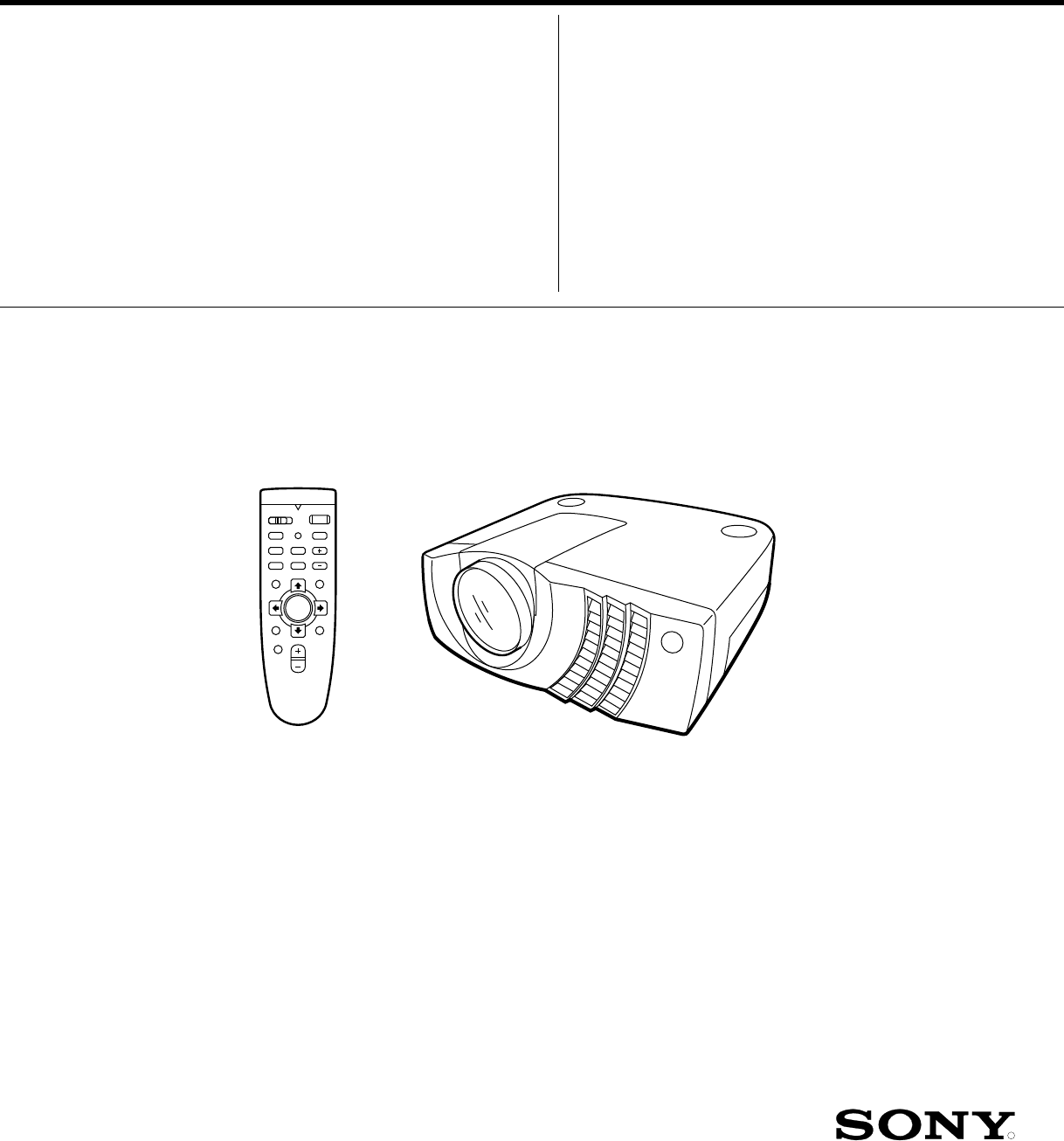
Operating Instructions
Mode d’emploi
Manual de instrucciones
FR
ES
LCD Data Projector
GB
VPL-PX20/PX30
1-2 VPL-PX20/PX30
2
(GB)
To prevent fire or shock hazard, do not
expose the unit to rain or moisture.
To avoid electrical shock, do not open the
cabinet. Refer servicing to qualified
personnel only.
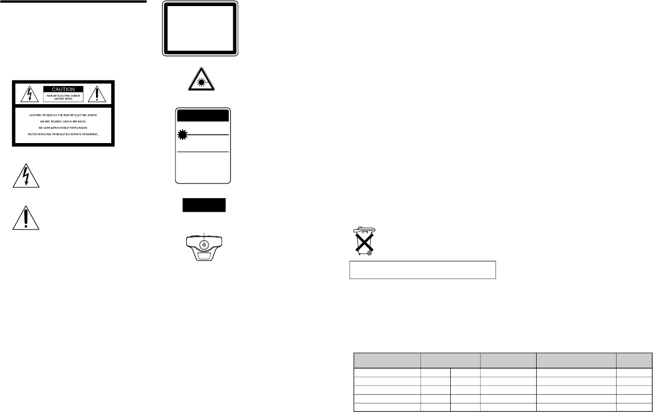
This symbol is intended to alert the
user to the presence of uninsulated
“dangerous voltage” within the
product’s enclosure that may be of
sufficient magnitude to constitute a risk
of electric shock to persons.
This symbol is intended to alert the
user to the presence of important
operating and maintenance (servicing)
instructions in the literature
accompanying the appliance.
WARNING
This label is located on
the rear of the Remote
Commander.
This label is located on the
rear of the Remote
Commander.
Caution
use of controls or adjustments or performance of
procedures other than those specified herein may result in
hazardous radiation exposure.
Notes
• Do not aim the laser at people or not look into the laser
transmitter.
• When the Remote Commander causes malfunction,
consult with qualified Sony personnel. We change the
Remote Commander as new one according to the
guarantee.
This label is located on the
rear of the Remote
Commander.
Laser light shines out of this window.
For the customers in the USA
This equipment has been tested and found to comply with
the limits for a Class A digital device, pursuant to Part 15 of
the FCC Rules. These limits are designed to provide
reasonable protection against harmful interference when the
equipment is operated in a commercial environment. This
equipment generates, uses, and can radiate radio frequency
energy and, if not installed and used in accordance with the
instruction manual, may cause harmful interference to radio
communications. Operation of this equipment in a
residential area is likely to cause harmful interference in
which case the user will be required to correct the
interference at his own expense.
You are cautioned that any changes or modifications not
expressly approved in this manual could void your authority
to operate this equipment.
This label is located on
the side of the Remote
Commander.
LASER RADIATION
DO NOT STARE INTO BEAM
CLASS 2 LASER PRODUCT
RAYONNEMENT LASER
NE PAS REGARDER DANS LE FAISCEAU
APPAREIL A LASER DE CLASSE 2
LASER–STRAHLING
NIGHT IN DEN STRAHL BLICKEN
LASER KLASSE 2
MAX OUTPUT:1mW
WAVE LENGTH:645nm
LASER RADIATION
DO NOT STARE INTO BEAM
WAVE LENGTH:645nm
MAX OUTPUT:1mW
CLASS II LASER PRODUCT
COMPLIES WITH DHHS 21 CFR
SUBCHAPTER J
SONY CORPORATION
6-7-35 KITASHINAGAWA
SHINAGAWA-KU,TOKYO,JAPAN
A
MANUFACTURED;
CAUTION
AVOID EXPOSURE-
LASER
RADIATION IS EMITTED
FROM THIS APERTURE.
3
(GB)
For the customers in Canada
This Class A digital apparatus complies with Canadian
ICES-003.
For the customers in the United Kingdom
WARNING
THIS APPARATUS MUST BE EARTHED
IMPORTANT
The wires in this mains lead are coloured in accordance with
the following code:
Green-and-Yellow: Earth
Blue: Neutral
Brown: Live
As the colours of the wires in the mains lead of this
apparatus may not correspond with the coloured markings
identifying the terminals in your plug proceed as follows:
The wire which is coloured green-and-yellow must be
connected to the terminal in the plug which is marked by the
letter E or by the safety earth symbol I or coloured green
or green-and-yellow.
The wire which is coloured blue must be connected to the
terminal which is marked with the letter N or coloured black.
The wire which is coloured brown must be connected to the
terminal which is marked with the letter L or coloured red.
Voor de klanten in Nederland
Bij dit product zijn batterijen geleverd.
Wanneer deze leeg zijn, moet u ze niet
weggooien maar inleveren als KCA.
The socket-outlet should be installed near the equipment
and be easily accessible.
Warning on power connection
Use a proper power cord for your local power supply.
The United States, Continental UK, Ireland, Japan
Canada Europe Australia, New Zealand
Plug type VM0233 290B YP-12A —
1)
VM1296
Female end VM0089 386A YC-13B VM0310B VM10505
Cord type SJT SJT H05VV-F N13237/CO-228 HVCTF
Rated Voltage & Current 10A/125V 10A/125V 10A/250V 10A/250V 13A/125V
Safety approval UL/CSA UL/CSA VDE VDE DENTORI
.........................................................................................................................................................................................................
1) Use the correct plug for your country.

1-3
VPL-PX20/PX30
5
(GB)
English
GB
Table of Contents
Overview
Precautions ............................................................... 7 (GB)
Features..................................................................... 8 (GB)
Location and Function of Controls ......................... 9 (GB)
Front/Left Side ......................................................... 9 (GB)
Rear/Right Side/Bottom........................................... 9 (GB)
Control panel.......................................................... 11 (GB)
Connector panel ..................................................... 12 (GB)
Remote Commander .............................................. 13 (GB)
Setting up and projecting
Installing the Projector........................................... 14 (GB)
Connecting .............................................................. 15 (GB)
Connecting with a Computer ................................. 15 (GB)
Connecting with a VCR/15k RGB/Component
Equipment ......................................................... 17 (GB)
Selecting the Menu Language ............................... 18 (GB)
Projecting ................................................................ 19 (GB)
Effective tools for your presentation ..................... 21 (GB)
Adjustments and settings using the menu
Using the MENU...................................................... 22 (GB)
The PICTURE CTRL Menu ..................................... 22 (GB)
The INPUT SETTING Menu .................................... 24 (GB)
The SET SETTING Menu ........................................ 26 (GB)
The INSTALL SETTING Menu ................................ 27 (GB)
Installation
Installation Examples ............................................. 28 (GB)
Floor Installation .................................................... 28 (GB)
Ceiling Installation................................................. 29 (GB)
Tips for Installation ................................................ 30 (GB)
Unsuitable Installation ........................................... 30 (GB)
Notes on Installation .............................................. 30 (GB)

1-4 VPL-PX20/PX30
6
(GB)
Maintenance
Maintenance ............................................................ 32 (GB)
Replacing the Lamp ............................................... 32 (GB)
Cleaning the Air Filter ........................................... 33 (GB)
Troubleshooting ..................................................... 34 (GB)
Other
Specifications ......................................................... 36 (GB)
Index ........................................................................ 42 (GB)
7
(GB)
Precautions
On safety
• Check that the operating voltage of your unit is
identical with the voltage of your local power
supply.
• Should any liquid or solid object fall into the cabinet,
unplug the unit and have it checked by qualified
personnel before operating it further.
• Unplug the unit from the wall outlet if it is not to be
used for several days.
• To disconnect the cord, pull it out by the plug. Never
pull the cord itself.
• The wall outlet should be near the unit and easily
accessible.
• The unit is not disconnected to the AC power source
(mains) as long as it is connected to the wall outlet,
even if the unit itself has been turned off.
• Do not look into the lens while the lamp is on.
• Do not aim the laser at people or not look into the
laser transmitter.
• Do not place your hand or objects near the
ventilation holes — the air coming out is hot.
• Be careful not to catch your fingers by the adjuster
when you lift up the projector. Do not push hard on
the top of the projector with the adjuster out.
On illumination
• To obtain the best picture, the front of the screen
should not be exposed to direct lighting or sunlight.
• Ceiling-mounted spot lighting is recommended. Use
a cover over fluorescent lamps to avoid lowering the
contrast ratio.
• Cover any windows that face the screen with opaque
draperies.
• It is desirable to install the projector in a room where
floor and walls are not of light-reflecting material. If
the floor and walls are of reflecting material, it is
recommended that the carpet and wall paper be
changed to a dark color.
On preventing internal heat build-up
After you turn off the power with the I /
1
key on the
Remote Commander or on the control panel, do not
disconnect the unit from the wall outlet while the
cooling fan is still running.
Caution
The projector is equipped with ventilation holes
(intake) on the bottom and ventilation holes (exhaust)
on rear. Do not block or place anything near these
holes, or internal heat build-up may occur, causing
picture degradation or damage to the projector.
On cleaning
• To keep the cabinet looking new, periodically clean
it with a soft cloth. Stubborn stains may be removed
with a cloth lightly dampened with a mild detergent
solution. Never use strong solvents, such as thinner,
benzene, or abrasive cleansers, since these will
damage the cabinet.
• Avoid touching the lens. To remove dust on the lens,
use a soft dry cloth. Do not use a damp cloth,
detergent solution, or thinner.
• Clean the filter at regular intervals every 300 hours.
On repacking
• Save the original shipping carton and packing
material; they will come in handy if you ever have to
ship your unit. For maximum protection, repack your
unit as it was originally packed at the factory.
Precautions
Overview
1-5
VPL-PX20/PX30
8
(GB)
Features
High brightness, high picture quality
• High brightness
The LCD panel with microlens and the 200 W UHP
lamp allow high brightness (light output 1400 ANSI
lumen for VPL-PX20, and 2400 ANSI lumen for
VPL-PX30) and excellent uniformity on the picture.
•High resolution
By adopting three 1.3-inch, approximately 790,000-
pixels XGA panels, this projector can project sharp
picture with the resolutions of 1024 × 768 pixels for
RGB input and 750 horizontal TV lines for video
input.
•High picture performance
This projector utilizes 3D Digital Gamma correction
for good picture uniformity. And the internal RGB
enhancer provides sharper RGB images.
Simple setup
•Sony original high performance APA (Auto Pixel
Alignment) function
You can get the clearest picture automatically by
simply pressing the APA key when the signal is
input from a computer.
•Simple setup with external equipment
This projector has 44 kinds of preset data for input
signals. You can get a suitable picture by connecting
an equipment with supplied cable and pressing the
APA key.
•USB, Digital RGB and 5BNC connectors
USB equipment (e.g., USB mouse) allows you to
expand your system. Using the application software
supplied with the projector allows you to control the
projector from your computer operated with
Windows
1)
98 operating system . The Digital RGB
connector allows you to connect the projector to a
Digital RGB equipment. The 5BNC input connector
allows you to connect the projector to a workstation
output high-resolution signals and to connect the
projector to a computer from a long distance.
Easy presentation
•Remote Commander with mouse control and
laser pointer functions
With the built-in mouse receiver, you can operate a
computer with the Remote Commander. For
presentations, you can use the laser pointer built into
the Remote Commander.
•Digital ZOOM, FUNCTION and HELP keys on
the Remote Commander
The Digital ZOOM allows you to enhance your
presentation by zoooming in on the image.
You can allocate a presentation file to the
FUNCTION keys by using the application software
(CD-ROM) supplied with the projector. Just pressing
the FUNCTION key opens the file immediately.
The HELP key will be helpful if you encounter a
problem during operation.
•High portability
This projector is compact-7.2kg (15lb 14oz),
portable size. With such a feature, a carrying handle
contributes to a convenient carrying, and you can
carry it everywhere you want.
Multi scan compatibility
•Scan converter built-in
This projector has a built-in scan converter which
converts the input signal within 1024 × 768 pixels.
•Accept various input signals
This projector accepts video signals of the
composite, S video, and component as well as the
15k RGB, VGA
2)
, SVGA
2)
, XGA
2)
and SXGA
2)
signals, which all can be displayed.
•Compatible with six color systems
NTSC
3.58
, PAL, SECAM, NTSC
4.433)
, PAL-M or
PAL-N color system can be selected automatically or
manually.
Other functions
Plug & Play
This projector complies with DDC1 and DDC2B.
(DDC1 and DDC2B are the Display Data Channel
(DDC
TM
)
4)
standard in the VESA standard.)
When connecting a DDC1 host system, the projector
synchronizes with V.CLK that follows the VESA
standard and outputs EDID (Extended Display
Identification Data) to the data line.
When connecting a DDC2B host system, the projector
automatically switches to the appropriate
communication mode.
Features
.........................................................................................................................................................................................................
1) Windows is a registered trademark of Microsoft Corporation (U.S.A and other countries).
2) VGA, SVGA, XGA and SXGA are registered trademarks of the International Business Machines Corporation, U.S.A.
3) NTSC
4.43
is the color system used when playing back a video recorded on NTSC on an NTSC
4.43
system VCR.
4) DDC
TM
is a registered trademark of the Video Electronics Standard Association.
9
(GB)
Location and Function of
Controls
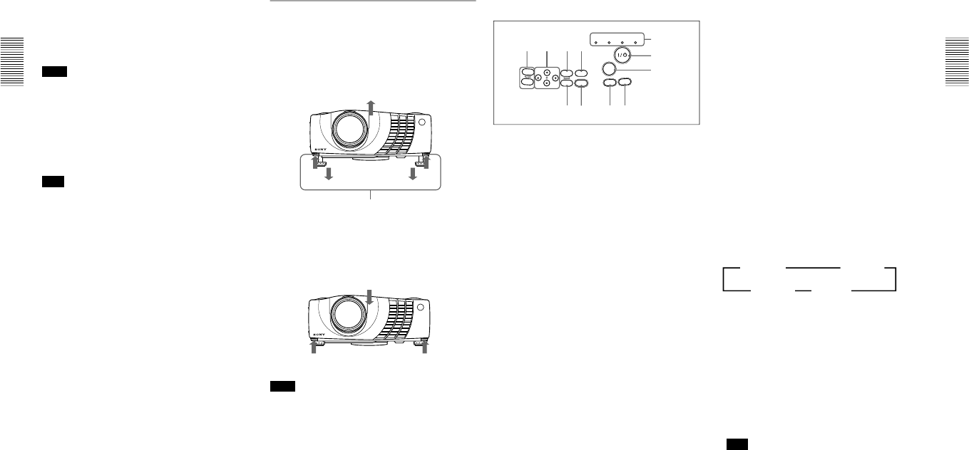
Front/Left Side
1 Zoom ring
Adjusts the size of the picture.
2 Focus ring
Adjusts the picture focus.
3 Lens
Open the lens cap before projection.
4 Ventilation holes (exhaust)
5Front remote control detector (SIRCS receiver)
6 Adjuster
When a picture is projected on the out of the screen,
adjust the picture using this adjuster.
For details on how to use the adjusters, see “How to use
the adjuster” on page 10 (GB).
7 Security lock
Connects to an optional security cable (Kensington’s).
The security lock corresponds to Kensington’s
MicroSaver Security System.
If you have any comment, contact
Kensington
2853 Campus Drive, San Mates, CA 94403
U.S.A.
Tel: 800-535-4242: extension 3348
Home page address:
http://www.kensington.com/
8 Carrying handle
Pull up the handle from the projector for carrying.
9 Left speaker
0 Control panel
For details, see “Control panel” on page 11 (GB).
qa Right speaker
qs Lens hood
qd Rear remote control detector (SIRCS receiver)
qf AC IN socket
Connects the supplied AC power cord.
Rear/Right Side/Bottom
Location and Function of Controls
2
3
6
45 7
8
9
1qa
qs 0
w;
qg qj
qh
ql
qk
qd
qf
1-6 VPL-PX20/PX30
10
(GB)
qg Rear speaker
qh Lamp cover
qj Ventilation holes (intake)/air filter cover
Notes
• Do not place anything near the ventilation holes as it
may cause internal heat build-up.
• Do not place your hand or objects near the
ventilation holes — the air coming out is hot.
qk Air filter cover button
Used to remove the air filter cover.
For details, see “Cleaning the Air Filter” on page 33 (GB).
Note
Clean the air filter every 300 hours to ensure
optimal performance.
ql Adjuster buttons
w; Connector panel
For details, see page 12 (GB).
How to use the adjuster
To adjust the height
Adjust the height of the projector as follows:
1
Lift the projector and press the adjuster buttons.
The adjusters will extend from the projector.
2
While pressing the buttons, lower the projector.
Then, release the buttons.
For fine adjustment, turn the adjusters to the right
and the left.
Notes
• Be careful not to let the projector down on your
fingers.
• Do not push hard on the top of the projector with the
adjusters out.
Location and Function of Controls
Adjuster buttons
11
(GB)
Location and Function of Controls
Control panel
1 VOL +/– keys
Adjust the volume of the built-in speakers and output
level of the AUDIO jack.
+ : Increases the volume.
– : Decreases the volume.
2 Arrow keys (M/m/</,)
Used to select the menu or to make various adjustments.
3 MENU key
Displays the on-screen menu. Press again to clear the
menu.
4 HELP key
If you need help information during an operation, press
this key to display help messages. The Help menu lists
error recoveries depending on problem type.
5 Indicators
LAMP/COVER: Lights up or flashes under the
following conditions:
• Lights up when the lamp has reached the end of
its life or becomes a high temperature.
• Flashes when the lamp cover or air filter cover
is not secured firmly.
TEMP (Temperature)/FAN: Lights up or flashes
under the following conditions:
• Lights up when temperature inside the projector
becomes unusually high.
• Flashes when the fan is broken.
POWER SAVING: Lights up when the projector is
in the power saving mode. When POWER
SAVING in the SET SETTING menu is set to
ON, the projector goes into the power saving
mode if no signal is input for 10 minutes.
Although the lamp goes out, the cooling fan
keeps running. In the power saving mode, any
key does not function for the first 40 seconds.
The power saving mode is canceled when a signal
is input or any key is pressed.
ON/STANDBY: Lights up or flashes under the
following conditions:
• Lights in red when the AC power cord is
plugged into the wall outlet. Once in the
standby mode, you can turn on the projector
with the
I / 1
key.
• Lights in green when the power is turned on.
• Flashes in green while the cooling fan runs after
turning off the power with the
I / 1
key. The
fan runs for about 120 seconds after turning off
the power.
The ON/STANDBY indicator flashes quickly
for the first 40 seconds.
During this time, you cannot turn the power
back on with the
I / 1
key.
For details on the LAMP/COVER and the TEMP/FAN
indicators, see page 35 (GB).
6
I
/
1
(
on / standby
)
key
Turns on and off the projector when the projector is in
the standby mode. The ON/STANDBY indicator
lights in green when the power is turned on.
When turning off the power, press the I /
1
key
twice following the message on the screen, or press
and hold the key for about one second.
For details on steps for turning off the power, see “To turn
off the power” on page 20 (GB).
7 INPUT key
Selects the input signal. Each time you press the key,
the input signal switches as follows:
The audio signals are common to the VIDEO and
S-VIDEO.
8 LIGHT key
If you press this key while the power is on, the keys
on the control panel will be displayed in orange.
Press this key to turn off the light.
9 APA (Auto Pixel Alignment) key
Adjusts a picture to be projected clearest
automatically while a signal from the computer is
input. Adjust the shift (up/down and left/right) at the
same time automatically.
Note
Press the APA key when the full image is displayed
on the screen. If there are black edges around the
image, the APA function will not function properly
and the image may extend beyond the screen.
q; RESET key
Resets the value of an item back to its factory preset
value. This key functions when the menu or a setting
item is displayed on the screen.
qa ENTER key
Enters the settings of items in the menu system.
INPUT
HELP
MENU
ENTER
RESET
APA
LIGHT
VOL +
VOL -
LAMP/
COVER TEMP/
FAN POWER
SAVING ON/
STANDBY
1234 5
6
7
890qa
B INPUT-A B INPUT-B
S-VIDEO bVIDEO b
1-7
VPL-PX20/PX30
12
(GB)
Connector panel
1 INPUT A connectors
1DIGITAL RGB/5BNC/RGB switch: Selects
DIGITAL RGB, 5BNC or RGB on INPUT A
connectors. Select the appropriate position
depending on the input signal.
DIGITAL RGB: Signal input from DIGITAL
RGB connector.
5BNC: Signal input from the 5BNC connector.
RGB: Signal input from the RGB connector.
2RGB input connector (HD D-sub 15-pin,
female): Connects to the monitor output on a
computer using the supplied cable. This
connector only accepts signals from a computer.
35BNC input connectors (R/R-Y/P
R
, G/Y, B/B-
Y/P
B
, SYNC/HD, VD connectors) (BNC type):
Connect to a high-resolution computer or VCR
where signals are transmitted long distances; for
example, when the projector has been hung from
the ceiling.
According to the connected equipment, computer,
component (R-Y/Y/B-Y), HDTV or DTV (DTV
GBR, DTV YP
B
P
R
) signal is selected.
Right side
Location and Function of Controls
4DIGITAL RGB input connector (DFP 20-pin,
TMDS): Connects to a digital RGB output
connector on external equipment.
5USB connector: Connects your computer or
USB equipment.
A plug: (Right, for downstream, 4-pin):
Connects to USB
equipment
.
B plug: (Left, for upstream, 4-pin):
Connects to
a computer. If you connect the projector and a
computer, the projector automatically assumes
that a USB mouse is connected; this allows you
to control the mouse from the Remote
Commander. The application software supplied
with the projector allows you to control the
projector from your computer.
6MOUSE (13-pin) connector: Connects to the
mouse port on a computer to control the mouse
function using the supplied mouse cable.
7AUDIO (stereo mini-jack) jack: Connects to the
audio output on a computer.
2 INPUT B connectors
Connect to external equipment such as a computer.
You can control the mouse signal with the Remote
Commander.
RGB input (HD D-sub 15-pin, female): Connects
to the monitor output on a computer using the
supplied cable. This connector only accepts
signals from a computer.
AUDIO (stereo mini-jack): Connects to the audio
output on a computer.
MOUSE (13-pin): Connects to the mouse port on a
computer to control the mouse function using the
supplied mouse cable.
3 VIDEO IN jacks
Connect to external video equipment such as a VCR.
S VIDEO (mini DIN 4-pin):
Connects to the S video
output (Y/C video output) on video equipment.
VIDEO (phono type): Connects to the composite
video output.
AUDIO input L (MONO)/R (phono type): Connect
to the audio output of equipment. For stereo
equipment, use both the L and R jacks; for monaural
equipment, use the L (MONO) jack only.
The audio signals are common to the VIDEO and
S VIDEO.
4 CONTROL S IN/PLUG IN POWER (DC 5V
output) jack
Connects to the control S out jacks of the Sony equipment.
Connects to the CONTROL S OUT jack on the supplied
Remote Commander when using it as a wired Remote
Commander. In this case, you do not need to install the
batteries in the Remote Commander, since the power is
supplied from this jack.
5 RS-232C connector (D-sub 9-pin, female)
Connects to a computer to operate the projector from
the computer.
RS-232C
IN
PLUG IN POWER
OUTPUT
INPUT A
INPUT B
VIDEO IN
CONTROL S
REMOTE
DIGITAL RGB
USB
R/R-Y/PRB/B-Y/PBSYNC/HD VDG/Y
MOUSEAUDIORGB
MOUSEAUDIOAUDIO RGB
MONITOR
S VIDEO VIDEO AUDIO
LR
(MONO)
DIGITAL
RGB RGB
5BNC
RS-232C
IN
PLUG IN POWER
OUTPUT
INPUT A
INPUT B
VIDEO IN
CONTROL S
REMOTE
DIGITAL RGB
USB
R/R-Y/PRB/B-Y/PBSYNC/HD VDG/Y
MOUUSEAUDIORGB
MOUUSEAUDIOAUDIO RGB
MONITOR
S VIDEO VIDEO AUDIO
LR
(MONO)
DIGITAL
RGB RGB
5BNC
34
2
1
6
5
INPUT A
DIGITAL RGB
USB
R/R-Y/P
R
B/B-Y/P
B
SYNC/HD VDG/Y
MOUSEAUDIORGB
DIGITAL
RGB RGB
5BNC
76
2
1
5
3
4
13
(GB)
.........................................................................................................................................................................................................
1) Macintosh is a registered trademark of Apple Computer, Inc.
Remote Commander
The keys which have the same names as on the
control panel function identically.
You can control a connected computer using the
Remote Commander.
For details, see “Connecting with a Computer” on page
15 (GB).
Notes on laser beam
• Do not look into the laser transmitter.
• Do not aim the laser at people.
1
I
/
1
key
2 INPUT key
3 APA (Auto Pixel Alignment) key
4 VOLUME +/– keys
5 LASER key
Emits laser beam from the laser transmitter when you
press this key.
Location and Function of Controls
COMMAND
MUTING
VOLUME
HELP
/
INPUTAPA
FUNCTION
MENU LASER
ENTER
RESET D ZOOM
+
–
+
–
R CLICK
PIC
AUDIO
ONOFF
12
6
7
9
qd
qa,qs
qf
qg
qh
qj
qk
ql
w;
wa ws
0
8
5
4
2
1
3
6 OUTPUT connectors
MONITOR (HD D-sub 15-pin, female): Connects
to the video input connector on the monitor.
Outputs signals from the selected channel in the
INPUT A (RGB or 5BNC) or INPUT B (RGB)
connector. This connector does not output any
signals from the DIGITAL RGB connector.
AUDIO (phono type): Connects to external active
speakers.
The volume of the speakers can be controlled by the
VOLUME +/– keys on the Remote Commander or
the VOL +/– keys on the control panel.
6 Joy stick
Functions as a mouse of a computer connected to the
unit.
7 Arrow keys (M/m/</,)
8 L CLICK key
Functions as a left button on a mouse. When
connected to a Macintosh
1)
computer, the L CLICK
key functions as a mouse button.
9 R CLICK key
Functions as a right button on a mouse. When
connected to a Macintosh computer, the R CLICK key
functions as a mouse button.
0 D ZOOM +/– key
Enlarges the image at a desired location on the screen.
+: Pressing the + key once displays the icon. This
icon indicates the point you want to enlarge. Use
an arrow key (M/m/</,) to move the icon to
the point to be enlarged. Press the + key
repeatedly until the image is enlarged to your
requirements.
–: Pressing the – key reduces an image that has been
enlarged with the D ZOOM + key.
qa Strap holder
Attaches the supplied strap.
qs CONTROL S OUT jack (stereo minijack)
Connects to the CONTROL S IN jack on the projector
with the connecting cable (not supplied) when using
the Remote Commander as a wired one. In this case,
you do not need to install the batteries since the power
is supplied via the CONTROL S IN jack on the
projector.
qd RESET key
qf ENTER key
qg MENU key
qh FUNCTION 1/2 keys
When you connect the projector with a computer, you
can open a file on the screen by just pressing the
FUNCTION key. This will enhance your presentation.
To use this function, allocate a file to the FUNCTION
key by using the application software. For details on
how to allocate a file to the FUNCTION key, refer to
the help file of the application software.
1-8 VPL-PX20/PX30
14
(GB)
Location and Function of Controls / Installing the Projector
Be sure to
install the
battery from
the # side.
qj MUTING keys
Cut off the picture and sound.
PIC: Cuts off the picture. Press again to restore the
picture.
AUDIO: Cuts off the sound from speakers and
AUDIO jack. Press again or press the VOLUME
+ key to restore the sound.
qk HELP key
If you need help information during an operation,
press this key to display help messages.
ql COMMAND ON/OFF switch
When this switch is set to OFF, no key on the Remote
Commander function. This saves the battery power.
w; Transmission indicator
Lights up when you press a key on the Remote
Commander.
This indicator does not light up when you use the laser
pointer.
wa Infrared transmitter
ws Laser transmitter
Battery installation
1
Push and slide to open the lid, then install the two
size AA (R6) batteries (supplied) with the correct
polarity.
2
Replace the lid.
Notes on batteries
• Make sure that the battery orientation is correct when
inserting batteries.
• Do not mix an old battery with a new one, or
different types of batteries.
• If you will not use the Remote Commander for a
long time, remove the batteries to avoid damage
from battery leakage. If batteries have leaked,
remove them, wipe the battery compartment dry and
replace the batteries with new ones.
Notes on Remote Commander operation
• Make sure that there is nothing to obstruct the
infrared beam between the Remote Commander and
the remote control detector on the projector.
• The operation range is limited. The shorter the
distance between the Remote Commander and the
projector is, the wider the angle within which the
commander can control the projector.
Installing the Projector
This section describes the installation arrangements
for installing the projector.
Horizontal center
of the screen
The distance between the lens and the screen varies
depending on the size of the screen. Use the following table
as a guide.
Unit: m (feet)
Screen
size 40 60 80 100 120 150 200 300
(inches)
Minimum 1.5 2.3 3.1 3.9 4.6 5.8 7.8 11.7
Distance (4.9) (7.5) (10.0) (12.6) (15.2) (19.1) (25.5) (38.4)
Maximum 1.8 2.8 3.7 4.7 5.7 7.1 9.5 14.3
Distance (6.0) (9.1) (12.3) (15.4) (18.6) (23.3) (31.2) (46.9)
Distance between the screen
and the center of the lens
15
(GB)
RS-232C
IN
PLUG IN POWER
OUTPUT
INPUT A
INPUT B
VIDEO IN
CONTROL S
REMOTE
DIGITAL RGB
USB
R/R-Y/P
R
B/B-Y/P
B
SYNC/HD VDG/Y
MOUSEAUDIORGB
MOUSEAUDIOAUDIO RGB
MONITOR
S VIDEO VIDEO AUDIO
LR
(MONO)
DIGITAL
RGB RGB
5BNC
DIGITAL
RGB RGB
5BNC
• insert the plugs of the cables properly; plugs that are
not fully inserted often generate noise. When pulling
out a cable, be sure to pull it out from the plug, not
the cable itself.
Notes
• Connect all the connecting cables to the INPUT A
connector when you input a signal from the INPUT
A connector.
Connect all the cables to the INPUT B connector
when you input a signal from the INPUT B
connector as well.
• Supplied mouse cables may not work properly
according to your computer.
When connecting with an IBM PC/AT
compatible computer
Right side
to serial
port or
to mouse
port
Monitor
SIC-S21 (for
serial)/S22
(for PS/2)
Mouse cable
(supplied)
to
monitor
out
Stereo audio
connecting
cable (not
supplied)
to
audio
out
HD D-sub
15-pin
cable
(supplied)
Connecting
Connecting with a Computer
This section describes how to connect the projector to
a computer.
You can control the projector from your computer by
using the application software supplied with the projector,
and/or you can use USB equipment. For details, see
“Using USB equipment (e.g., USB mouse)”.
When the projector is connected to a computer, you
can control the mouse of a computer by the Remote
Commander.
The R/L CLICK keys and joy stick function as follows.
Note
Make sure that there is nothing to obstruct the infrared
beam between the Remote Commander and the
remoter control detector on the projector.
Function
Key and IBM PC/AT
1)
Macintosh
joy stick compatible, Serial
R CLICK
(front) Right button Mouse button
L CLICK
(rear) Left button Mouse button
Joy stick Corresponds with the movements of the mouse
Also refer to the instruction manual of equipment to
be connected.
Notes
• This unit accepts the VGA, SVGA, XGA or SXGA
signals. However, we recommend you to set the
output signal of your computer to the XGA.
• If you set your computer, such as a notebook type
IBM PC/AT compatible, to output the signal to both
the display of your computer and the external
monitor, the picture of the external monitor may not
appear properly. In such cases, set the output mode
of your computer to output the signal to only the
external monitor.
For details, refer to the operating instructions supplied
with your computer.
• The RGB input connectors of the INPUT A/B and
DIGITAL RGB connector of the INPUT A comply
with the VESA DDC2B. If your computer or
graphics board is compatible with DDC, turn on the
power of the equipment as follows:
1Connect the projector to the computer with the HD
D-sub 15-pin cable.
2Turn on the power of the projector.
3Boot up the computer.
When making connections, be sure to:
•
turn off all equipment before making any connections.
• use the proper cables for each connection.
Connecting
.........................................................................................................................................................................................................
1) IBM and PC/AT are a trademark and a registered trademark of International Business Machines Corporation, U.S.A.
Computer
Monitor
cable
SMF-410
(not
supplied)
Speaker
Note
Set the DIGITAL RGB/5BNC/RGB switch to RGB
(right) when you connect the computer to the
INPUT A connector.
Setting up and projecting
to INPUT A
or INPUT B
1-9
VPL-PX20/PX30
16
(GB)
When connecting with a Macintosh
computer
Right side
SIC-S20
Mouse
cable (not
supplied)
to mouse
port
to audio out
to
monitor
out
Connecting
Signal
adapter
(not
supplied)
RS-232C
IN
PLUG IN POWER
OUTPUT
INPUT A
INPUT B
VIDEO IN
CONTROL S
REMOTE
DIGITAL RGB
USB
R/R-Y/P
R
B/B-Y/P
B
SYNC/HD VDG/Y
MOUSEAUDIORGB
MOUSEAUDIOAUDIO RGB
MONITOR
S VIDEO VIDEO AUDIO
LR
(MONO)
DIGITAL
RGB RGB
5BNC
DIGITAL
RGB RGB
5BNC
Stereo audio
connecting
cable (not
supplied)
Computer
Monitor
Monitor
cable
SMF-410
(not
supplied)
HD D-sub
15-pin
cable
(supplied)
Speaker
Notes
• Set the DIGITAL RGB/5BNC/RGB switch to
RGB (right) when you connect the computer to
the INPUT A connector.
• When you connect with a Macintosh computer,
you need the optional signal adapter.
Right side
Using the DIGITAL RGB (TMDS)
connector
Connect the computer to the DIGITAL RGB (TMDS)
connector on the connector panel.
Note
If you use the DIGITAL RGB (TMDS) connector, the
MONITOR connector will not output image signals.
Notes
• Use the proper mouse cable for your computer.
• You can use a USB mouse. For details, see
“Using USB equipment (e.g., USB mouse)”.
• Set the DIGITAL RGB/5BNC/RGB switch to
DIGITAL RGB (left).
• To connect digital RGB equipment, use the digital
signal cable (SMF-D102 or SMF-D110) (not
supplied). Do not use other cables — noise may
appear on the image.
to INPUT A
or INPUT B
Mouse cable
Stereo audio
connecting
cable (not
supplied)
Digital signal
cable
SMF-D102
(not supplied)
or
SMF-D110
(not supplied)
RS-232C
IN
PLUG IN POWER
OUTPUT
INPUT A
INPUT B
VIDEO IN
CONTROL S
REMOTE
DIGITAL RGB
USB
R/R-Y/PRB/B-Y/PBSYNC/HD VDG/Y
MOUSEAUDIORGB
MOUSEAUDIOAUDIO RGB
MONITOR
S VIDEO VIDEO AUDIO
LR
(MONO)
DIGITAL
RGB RGB
5BNC
DIGITAL
RGB RGB
5BNC
to mouse
port
to digital
RGB out to audio
out
Computer
Computer
Remote
cable
to
RS-232C
port
17
(GB)
Connecting
Using USB equipment (e.g., USB mouse)
Connect the USB equipment to the USB connector on
the connector panel.
You can connect your computer to the projector via
the RGB connector, 5BNC connector or DIGITAL
RGB connector. (The example below uses the RGB
connector.)
Notes
• Your computer may not start correctly when it has
been connected to the USB connector on the
projector via the USB cable. In this case, first
disconnect the USB cable, restart the computer, then
connect the computer to the projector using the USB
cable supplied with the projector.
• The USB connector on this projector will function
only with a computer operated with Windows 98.
• When you connect the mouse to your computer via
the USB connector, do not connect another mouse to
the MOUSE port. The projector automatically
assumes that a USB mouse is connected.
Note
Set the DIGITAL RGB/5BNC/RGB switch to the
suitable position depending on the connection.
RS-232C
IN
PLUG IN POWER
OUTPUT
INPUT A
INPUT B
VIDEO IN
CONTROL S
REMOTE
DIGITAL RGB
USB
R/R-Y/PRB/B-Y/PBSYNC/HD VDG/Y
MOUSEAUDIORGB
MOUSEAUDIOAUDIO RGB
MONITOR
S VIDEO VIDEO AUDIO
LR
(MONO)
DIGITAL
RGB RGB
5BNC
DIGITAL
RGB RGB
5BNC
Right side
HD D-sub
15-pin
cable
(supplied)
Stereo audio
connecting
cable (not
supplied)
to
monitor
out
to USB
port to audio
out
Other USB
equipment
USB
cable A
type-B
type
(sup-
plied)
Computer
USB hub function
If you connect the projector and your computer using
the USB cable for the first time, the following devices
will be recognized.
1General purpose USB hub
2USB human interface device (for wireless mouse
function)
3USB human interface device (for projector control
function)
Any other devices connected to the downstream
connector of a projector are recognized by your
computer.
Connecting with a VCR/15k RGB/
Component Equipment
This section describes how to connect the projector
with a VCR, external active speakers, and 15k RGB/
component equipment.
Also refer to the instruction manuals of the equipment
to be connected.
When making connections, be sure to:
• turn off all equipment before making any
connections.
• use the proper cables for each connection.
• insert the plugs of the cables properly; plugs that are
not fully inserted often generate noise. When pulling
out a cable, be sure to pull it out from the plug, not
the cable itself.
S-Video cable
(not supplied) Audio/video
cable
(supplied)
Active speakers
to audio/video
outputs
to S video
output
VCR
Right side
RS-232C
IN
PLUG IN POWER
OUTPUT
INPUT A
INPUT B
VIDEO IN
CONTROL S
REMOTE
DIGITAL RGB
USB
R/R-Y/P
R
B/B-Y/P
B
SYNC/HD VDG/Y
MOUSEAUDIORGB
MOUSEAUDIOAUDIO RGB
MONITOR
S VIDEO VIDEO AUDIO
LR
(MONO)
DIGITAL
RGB RGB
5BNC
1-10 VPL-PX20/PX30
18
(GB)
RS-232C
IN
PLUG IN POWER
OUTPUT
INPUT A
INPUT B
VIDEO IN
CONTROL S
REMOTE
DIGITAL RGB
USB
R/R-Y/P
R
B/B-Y/P
B
SYNC/HD VDG/Y
MOUSEAUDIORGB
MOUSEAUDIOAUDIO RGB
MONITOR
S VIDEO VIDEO AUDIO
LR
(MONO)
DIGITAL
RGB RGB
5BNC
DIGITAL
RGB RGB
5BNC
Notes
• Set the aspect ratio using ASPECT in the INPUT
SETTING menu according to the input signal.
• To connect a 15k RGB/Component equipment,
select the COMPUTER/COMPONENT/DTV
YP
B
P
R
/DTV GBR in the INPUT-A in the SET
SETTING menu according to the input signal.
• Use the composite sync signal when you input the
external sync signal from 15k RGB/component
equipment.
Connecting to a HDTV 1035/60i
Since the screen ratio of a high definition image is
16:9 and 576 lines are displayed in the vertical
direction, the image displayed is not a high-
definition image.
Right side
15k RGB/Component equipment
to RGB/
component
output
BNC Cable
(not supplied) Stereo audio
connecting
cable
(not
supplied)
to
audio
output
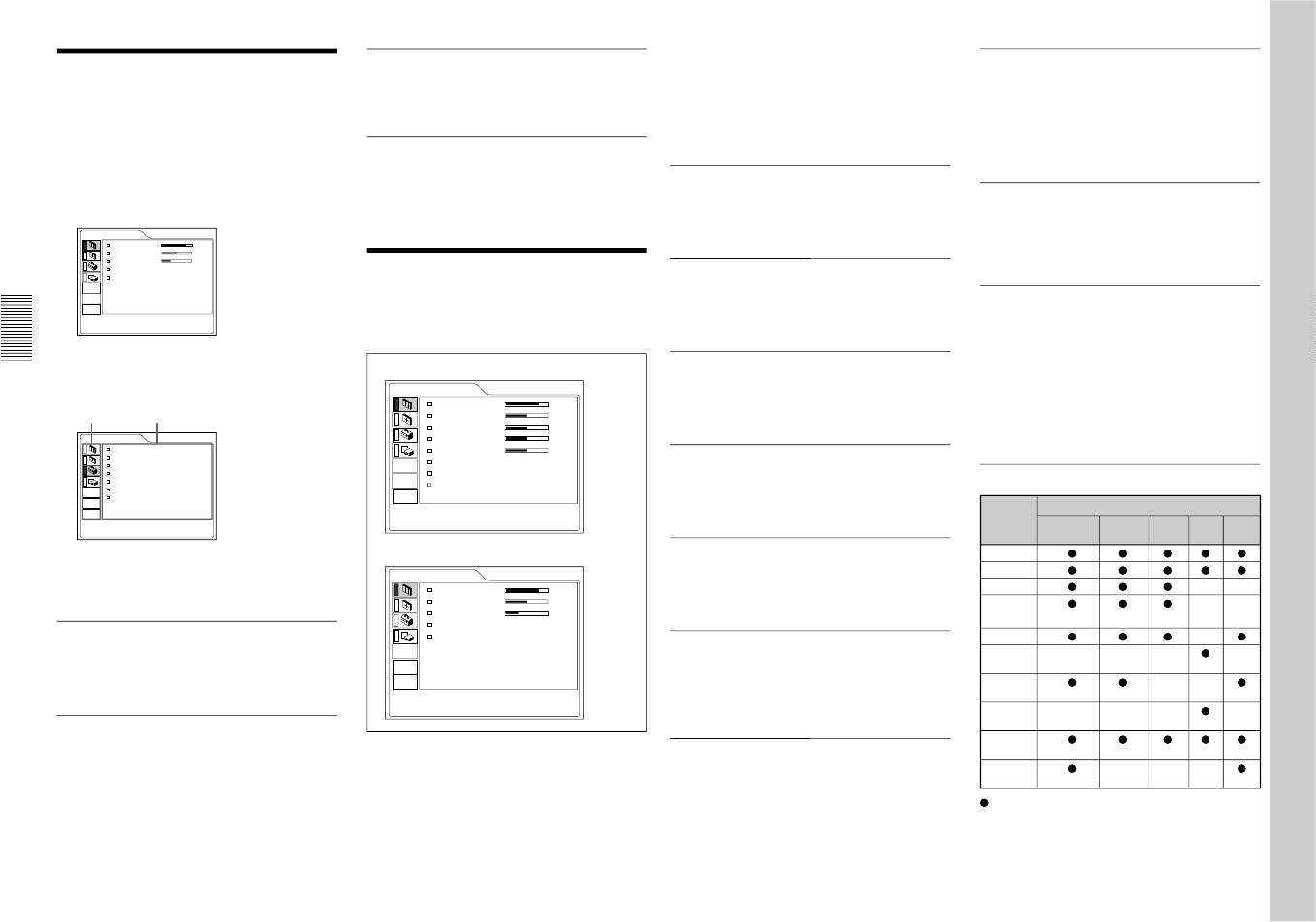
Connecting / Selecting the Menu Language
Selecting the Menu Language
You can select the language for displaying in the
menu and other on screen displays. The factory setting
is ENGLISH.
1
Plug the AC power cord into the wall outlet.
2
Press the I /
1
key to turn on the power.
3
Press the MENU key.
The menu display appears.
4
Select the icon of SET SETTING Menu, the third
one, with the M or m key, then press the , or
ENTER key.
The SET SETTING Menu appears.
5
Select LANGUAGE with the M or m key, then
press the , or ENTER key.
6
Select the language desired with the M or m key,
then press the < or ENTER key.
The menu changes into the selected language .
To clear the menu display
Press the MENU key.
The menu display disappears automatically if no key
is pressed for one minute.
INPUT
HELP
MENU
ENTER
RESET
APA
LIGHT
VOL +
VOL -
LAMP/
COVER TEMP/
FAN POWER
SAVING ON/
STANDBY
2
4, 5, 6 3
1
SET SETTING
STATUS: ON
INPUT-A: COMPUTER
AUTO INPUT SEL:
OFF
LANGUAGE: ENGLISH
SPEAKER: ON
POWER SAVING:
OFF
SIRCS RECEIVER:
FRONT&REAR
INPUT-A
19
(GB)
INPUT-B: Selects audio and video signals input
from the INPUT B connector.
VIDEO: Selects audio and video signals input
from the AUDIO/VIDEO (VIDEO IN)
jacks.
S-VIDEO:Selects audio and video signals input
from the AUDIO/S VIDEO (VIDEO
IN) jacks.
Note
The AUDIO (VIDEO IN) jacks are used as audio
outputs of both VIDEO and S-VIDEO.
4
Turn the zoom ring to adjust the size of the
picture.
5
Turn the focus ring to adjust the focus.
Note
Looking into the lens when projecting may cause
injury to your eyes.
To Press
Adjust the volume
the VOL +/– keys on the control panel or
the VOLUME +/– keys on the Remoter
Commander.
Cut off the sound
the AUDIO MUTING key on the Remote
Commander. To restore the sound, press
the AUDIO MUTING key again or press
the VOL + key on the control panel or the
VOLUME + key on the Remote
Commander.
Cut off the picture
the PIC MUTING key on the Remote
Commander. To restore the picture, press the
PIC MUTING key again.
To get the clearest picture
You can get the suitable picture when a signal from
the computer is input. Press the APA key.
The picture is automatically adjusted to be projected
clearest.
Notes
• Adjust the signal when the still picture is displayed
on the screen.
• Press the APA key when the full image is displayed
on the screen. If there are black edges around the
image, the APA function will not function properly
and the image may extend beyond the screen.
• If you switch the input signal or re-connect a
computer, press the APA key again to get the
suitable picture.
Projecting
1
After all equipment is connected completely, plug
the AC power cord into the wall outlet.
The ON/STANDBY indicator lights in red and the
projector goes into the standby mode.
2
Press the I /
1
key.
The ON/STANDBY indicator lights in green.
3
Turn on equipment connected to the projector.
Press the INPUT key to select the input source.
INPUT-A:Selects audio and video signals input
from the INPUT A connector.
Projecting
Rear
remote
control
detector
ON/STANDBY
indicator
INPUT
HELP
MENU
ENTER
RESET
APA
LIGHT
VOL +
VOL -
LAMP/
COVER TEMP/
FAN POWER
SAVING ON/
STANDBY
COMMAND
MUTING
VOLUME
HELP
/
INPUTAPA
FUNCTION
MENU LASER
ENTER
RESET D ZOOM
+
–
+
–
R CLICK
PIC
AUDIO
ONOFF
12
2
3
1
4
5
2
3
(Front)
APA key
APS key
1-11
VPL-PX20/PX30
20
(GB)
Projecting
• “ADJUSTING” appears on the screen. Press the
APA key again during the adjustment to restore the
original screen.
• “Complete!” appears on the screen when the picture
is adjusted properly. The picture may not be adjusted
properly depending on the kinds of input signals.
• Adjust the items in the INPUT SETTING menu
when you adjust the picture manually.
For details, see page 24 (GB).
To correct the trapezoid
When the projecting image is a trapezoid, change the
projector’s position/height by moving the adjuster.
For details on “How to use the adjuster”, see page 10
(GB).
If the image is still a trapezoid, correct it in DIGIT
KEYSTONE in the INSTALL SETTING menu.
When the base edge is longer than the upper
edge as shown in the figure below:
When the upper edge is longer than the base
edge as shown in the figure below:
For details on “DIGIT KEYSTONE”, see page 27 (GB).
To turn off the power
1
Press the I /
1
key.
“Power OFF?” appears on the screen.
Note
The message will disappear if you press any key
except the I /
1
key, or if you do not press any
key for five seconds.
2
Press the I /
1
key.
The ON/STANDBY indicator flashes in green and
the fan continues to run for about 120 seconds to
reduce the internal heat. Also, the ON/STANDBY
indicator flashes quickly for the first 40 seconds.
During this time, you will not be able to turn the
power back on with the I /
1
key.
3
Unplug the AC power cord from the wall outlet
after the fan stops running and the ON/STANDBY
indicator lights in red.
When you cannot confirm the on-screen
message
When you cannot confirm the on-screen message in a
certain condition, you can turn off the power by
holding the I /
1
key for about one second.
Note
Do not unplug the AC power cord while the
fan is still running; otherwise, the fan will
stop although the internal heat is still high,
leading to breakdown of the projector.
About the air filter cleaning
Clean the air filter every 300 hours to ensure
optimal performance.
Set the value to negative.
Set the value to positive.
21
(GB)
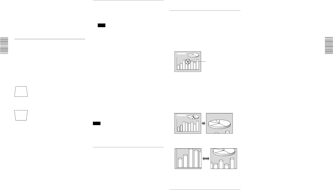
Effective tools for your presentation
To enlarge the image (Digital Zoom
function)
You can select a point in the image to enlarge.
1
Press the D ZOOM + key on the Remote
Commander.
The Digital Zoom icon appears at the center of the
image.
2
Move the icon to the point on the image you want
to enlarge. Use the arrow keys (M/m/</,) to
move the icon.
3
Press the D ZOOM + key again.
The image where the icon is located is enlarged.
By pressing the + key repeatedly, the image size
increases. (ratio of enlargement: max. 4 times)
Use the arrow keys(M/m/</,) to scroll the
enlarged image.
To return the image back to its original size
Press the D ZOOM – key on the Remote Commander.
To use the Laser Pointer function
Press the LASER key on the Remote Commander.
The laser pointer appears. The pointer is helpful in
indicating a particular point on the screen.
Projecting
Digital Zoom icon
1-12 VPL-PX20/PX30
22
(GB)
Using the MENU
The projector is equipped with an on-screen menu for
making various adjustments and settings.
To select the language used in the menu, see page
26 (GB).
1
Press the MENU key.
The menu display appears.
The bar on the icon of the currently selected menu
is highlighted in yellow.
PICTURE CTRL
CONTRAST: 80
BRIGHT: 50
RGB ENHANCER:
30
GAMMA MODE:
GRAPHICS
COLOR TEMP:LOW
INPUT-A
2
Use the M or m key to select a menu, then press
the , or ENTER key.
The selected menu appears.
SET SETTING
STATUS: ON
INPUT-A: COMPUTER
AUTO INPUT SEL:
OFF
LANGUAGE: ENGLISH
SPEAKER: ON
POWER SAVING:
OFF
SIRCS RECEIVER:
FRONT&REAR
INPUT-A
3
Make setting or adjustment on an item.
For details on setting individual items, see the relevant
menu pages.
To clear the menu display
Press the MENU key.
The menu display disappears automatically if no key
is pressed for one minute.
To reset items that have been adjusted
Press the RESET key.
“Complete!” appears on the screen and the settings
appearing on the screen will be reset to their factory
preset values.
Items which can be reset are:
• “CONTRAST”, “BRIGHT”, “COLOR”, “HUE”,
“SHARP” and “RGB ENHANCER” in the
PICTURE CTRL menu.
• “DOT PHASE”, “SIZE H” and “SHIFT” in the
INPUT SETTING menu.
Menus Setting items
About the memory of the settings
The settings are automatically stored in the projector
memory.
When no signal is input
When there is no input signal, “NO INPUT–Cannot
adjust this item.” appears on the screen, and each item
cannot be adjusted.
The PICTURE CTRL Menu
The PICTURE CTRL (control) menu is used for
adjusting the picture.
Unadjustable items depending on the input signal are
not displayed in the menu.
Operation
1. Select an item
Use the M or m key to select the item, then press the
, or ENTER key.
2. Adjust an item
• When changing the adjustment level:
To increase the number, press the M or , key.
When the video signal is input
When the RGB signal is input
PICTURE CTRL
CONTRAST: 80
BRIGHT: 50
COLOR: 50
HUE: 50
SHARP: 50
D.PICTURE: ON
COLOR TEMP:LOW
COLOR SYS: AUTO
VIDEO
PICTURE CTRL
CONTRAST: 80
BRIGHT: 50
RGB ENHANCER:
30
GAMMA MODE:
GRAPHICS
COLOR TEMP:LOW
INPUT-A
Using the MENU / The PICTURE CTRL Menu
23
(GB)
To decrease the number, press the m or < key.
Press the ENTER key to restore the original screen.
• When changing the setting:
Press the M or m key to change the setting.
Press the ENTER or < key to restore the original
screen.
CONTRAST
Adjusts the picture contrast.
The higher the setting, the greater the contrast.
The lower the setting, the lower the contrast.
BRIGHT
Adjusts the picture brightness.
The higher the setting, the brighter the picture.
The lower the setting, the darker the picture.
COLOR
Adjusts color intensity.
The higher the setting, the greater the intensity.
The lower the setting, the lower the intensity.
HUE
Adjusts color tones.
The higher the setting, the picture becomes greenish.
The lower the setting, the picture becomes purplish.
SHARP
Adjusts the picture sharpness.
The higher the setting, the sharper the picture.
The lower the setting, the softer the picture.
RGB ENHANCER
Adjusts the picture sharpness when the RGB signals
are input.
The higher the setting, the sharper the picture.
The lower the setting, the softer the picture.
D. (Dynamic) PICTURE
Emphasizes the black color.
ON: Emphasizes the black color to produce a bolder
“dynamic” picture.
OFF: Reproduces the dark portions of the picture
accurately, in accordance with the source signal.
GAMMA MODE
Selects a gamma correction curve.
GRAPHICS: Improves the reproduction of half
tones. Photos can be reproduced in natural tones.
TEXT: Contrasts black and white. Suitable for
images that contain lots of text.
COLOR TEMP
Adjusts the color temperature.
HIGH: Makes the white color bluish.
LOW: Makes the white color reddish.
COLOR SYS (System)
Selects the color system of the input signal.
AUTO: Automatically selects one of the following
signals: NTSC
3.58
, PAL, SECAM, NTSC
4.43
.
PAL-M/N: Automatically selects one of the
following signals: PAL-M/PAL-N, NTSC
3.58
.
Normally, set to AUTO.
If the picture is distorted or colorless, select the color
system according to the input signal.
Input signals and adjustable/setting items
Item Input signal
Video or Compo- HDTV RGB
1)
B&W
S video (Y/C) nent
CONTRAST
BRIGHT
COLOR ––
HUE ––
SHARP –
RGB
––– –
ENHANCER
D. PICTURE
––
GAMMA – – – –
MODE
COLOR
TEMP
COLOR –––
SYS
: Adjustable/can be set
– : Not adjustable/can not be set
The PICTURE CTRL Menu
(15k 60/50 only)
(NTSC3.58/
4.43 only)
.........................................................................................................................................................................................................
1) The RGB signals of a computer
Adjustments and settings using the menu
1-13
VPL-PX20/PX30
24
(GB)
The INPUT SETTING Menu
The INPUT SETTING menu is used to adjust the
input signal.
Unadjustable items depending on the input signal are
not displayed in the menu.
Operation
1. Select an item
Use the M or m key to select the item, then press the
, or ENTER key.
2. Adjust an item
• When changing the adjustment level:
To increase the number, press the M or , key.
To decrease the number, press the m or < key.
Press the ENTER key to restore the original screen.
• When changing the setting:
Press the M or m key to change the setting.
Press the ENTER or < key to restore the original
screen.
DOT PHASE
Adjusts the dot phase of the LCD panel and the signal
input from the INPUT A/B connector. Adjust the
picture further for finer picture after the picture is
adjusted with pressing the APA key.
Adjust the picture to where it looks clearest.
When the video signal is input
When the RGB signal is input
Memory No.
Signal type
Memory No.
Signal type
SIZE H
Adjusts the horizontal size of picture input from the
INPUT A/B connector.
The higher the setting, the larger the horizontal size of
the picture.
The lower the setting, the smaller the horizontal size
of the picture. Adjust the setting according to the dots
of the input signal. For details on the suitable value
for the preset signals, see page 25 (GB).
SHIFT
Adjusts the position of the picture input from the
INPUT A/B connectors or VIDEO IN jacks.
H adjusts the horizontal position of the picture.
V adjusts the vertical position of the picture.
As the setting for H increases, the picture moves to
the right, and as the setting decreases, the picture
moves to the left.
As the setting for V increases, the picture moves up,
and as the setting decreases, the picture moves down.
Use the < or the , key to adjust the horizontal
position and the M and m key for the vertical position.
ASPECT
Sets the aspect ratio of the picture.
When inputting 16:9 (squeezed) signal from
equipment such as a DVD player, set to 16:9.
4:3 : When the picture with ratio 4:3 is input.
16:9 : When the picture with ratio 16:9 (squeezed) is
input.
SCAN CONV (Scan converter)
Converts the signal to display the picture according to
the screen size.
ON: Displays the picture according to the screen
size. The picture will lose some clarity.
OFF: Displays the picture while matching one pixel
of input picture element to that of the LCD. The
picture will be clear but the picture size will be
smaller.
Note
When the XGA or SXGA signal is input, this item
will not be displayed.
INPUT SETTING
ASPECT: 16:9
SHIFT H: 200 V: 30
NO.01
VIDEO/60
VIDEO
INPUT SETTING
DOT PHASE: 0
SIZE H: 1056
SHIFT H: 200 V: 30
SCAN CONV: ON
NO.17
800x600
INPUT-A
The INPUT SETTING Menu
25
(GB)
Preset signals
Memory Preset signal
fH fV Sync
SIZE
No.
(kHz) (Hz)
H
1 Video 60 Hz
15.734 59.940 H-neg V-neg
2 Video 50 Hz
15.625 50.000 H-neg V-neg
3
15k RGB/Component 60 Hz 15.734 59.940 H-neg V-neg
4
15k RGB/Component 50 Hz 15.625 50.000 H-neg V-neg
5
HDTV 33.750 60.000 H-neg V-neg
6
640 × 350
VGA mode 1
31.469 70.086 H-pos V-neg 800
7
VGA VESA
2)
85 Hz
37.861 85.080 H-pos V-neg 832
8
640 × 400
PC-9801
3)
Normal
24.823 56.416 H-neg V-neg 848
9
VGA mode 2
31.469 70.086 H-neg V-pos 800
10
VGA VESA 85 Hz
37.861 85.080 H-neg V-pos 832
11
640 × 480
VGA mode 3
31.469 59.940 H-neg V-neg 800
12
Macintosh 13”
35.000 66.667 H-neg V-neg 864
13
VGA VESA 72 Hz
37.861 72.809 H-neg V-neg 832
14
VGA VESA 75 Hz
37.500 75.000 H-neg V-neg 840
15
VGA VESA 85 Hz
43.269 85.008 H-neg V-neg 832
16
800 × 600
SVGA VESA 56 Hz
35.156 56.250 H-pos V-pos 1024
17
SVGA VESA 60 Hz
37.879 60.317 H-pos V-pos 1056
18
SVGA VESA 72 Hz
48.077 72.188 H-pos V-pos 1040
19
SVGA VESA 75 Hz
46.875 75.000 H-pos V-pos 1056
20
SVGA VESA 85 Hz
53.674 85.061 H-pos V-pos 1048
21
832 × 624
Macintosh 16”
49.724 74.550 H-neg V-neg 1152
22
1024 × 768
XGA VESA 43 Hz
35.524 43.479 H-pos V-pos 1264
23
XGA VESA 60 Hz
48.363 60.004 H-neg V-neg 1344
24
XGA VESA 70 Hz
56.476 69.955 H-neg V-neg 1328
25
XGA VESA 75 Hz
60.023 75.029 H-pos V-pos 1312
26
XGA VESA 85 Hz
68.677 84.997 H-pos V-pos 1376
27
1152
× 864 SXGA VESA 70 Hz
63.995 70.016 H-pos V-pos 1472
28
SXGA VESA 75 Hz
67.500 75.000 H-pos V-pos 1600
29
SXGA VESA 85 Hz
77.487 85.057 H-pos V-pos 1568
30
1152 × 900
Sunmicro LO 61.795 65.960 H-neg V-neg 1504
31
Sunmicro HI 71.713 76.047 H-neg V-neg 1472
32
1280 × 960 SXGA VESA 60 Hz
60.000 60.000 H-pos V-pos 1800
33
SXGA VESA 75 Hz
75.000 75.000 H-pos V-pos 1728
34
1280 × 1024 SXGA VESA 43 Hz
46.433 43.436 H-pos V-pos 1696
35
SGI-5
53.316 50.062 H-neg V-neg 1680
36
SXGA VESA 60 Hz
63.974 60.013 H-pos V-pos 1696
37
SXGA VESA 75 Hz
79.976 75.025 H-pos V-pos 1688
38
SXGA VESA 85 Hz
91.146 85.024 H-pos V-pos 1728
43
PC Component
480/60P
480/60P ( ) 31.470 60.000 SonG
44
575/50P 575/50P
( ) 31.250 50.000 SonG
45
1080/50I 1080/50I
28.130 50.000
46
1080&
1080/50I-2
31.250 50.000
1152/60
47
720/60P 720/60P
45.000 60.000
48
720/50P 720/50P
37.500 50.000
Input signals and adjustable/setting items
Item Input signal
Video or 15k RGB/
HDTV RGB
1)
B&W
S video (Y/C) Component
DOT – – –
PHASE
SIZE H – – –
SHIFT
ASPECT ––
SCAN – – – –
CONV
(lower
than
SVGA
only)
: Adjustable/can be set
– : Not adjustable/can not be set
About the preset memory No.
This projector has 44 kinds of preset data for input
signals (the preset memory). The memory number of
the current input signal and the signal type are
displayed when the preset signal is input. This
projector automatically detects the signal type. When
the signal is registered to the preset memory, a
suitable picture is displayed on the screen according to
the signal type. You can adjust the picture through the
INPUT SETTING menu.
This projector also has 20 kinds of user memories for
each INPUT-A/B. When an unpreset signal is input
for the first time, memory number is displayed as 0. If
the input signal is adjusted in the INPUT SETTING
menu, the setting via INPUT-A/B is stored. When
more than 20 user memories are registered for each
INPUT-A/B, the newest memory is automatically
stored over the oldest one.
The INPUT SETTING Menu
.........................................................................................................................................................................................................
1) The RGB signals of a computer
2) VESA is a registered trademark of Video Electronics Standard Association.
3) PC-98 is a registered trademark of NEC Corporation.
D
ouble frequency
NTSC
D
ouble frequency
PAL
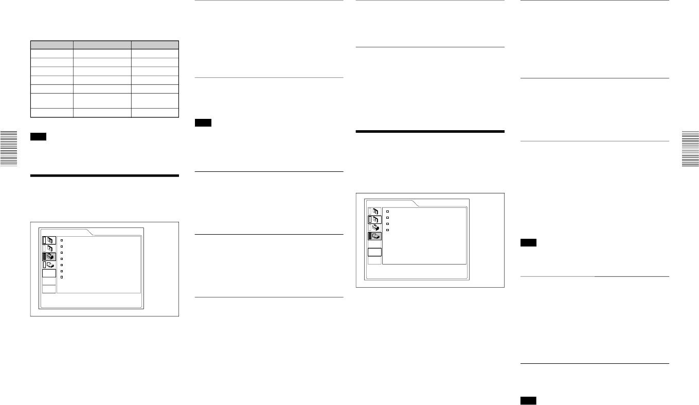
1-14 VPL-PX20/PX30
26
(GB)
Since the data is recalled from the preset memory
about the following signals, you can use these preset
data by adjusting SIZE H. Make fine adjustment by
adjusting SHIFT.
Signal Memory No. SIZE H
Super Mac-2 23 1312
SGI-1 23 1320
Macintosh 19” 25 1328
Macintosh 21” 28 1456
Sony News 36 1708
PC-9821 36 1600
1280 × 1024
WS Sunmicro 37 1664
Note
When the aspect ratio of input signal is other than 4:3,
a part of the screen is displayed in black.
The SET SETTING Menu
The SET SETTING menu is used for changing the
settings of the projector.
Operation
1. Select an item
Use the M or m key to select the item, then press the
, or ENTER key.
2. Change the setting
Press the M or m key to change the setting.
To restore the original screen, press the ENTER or
<
key.
STATUS (on-screen display)
Sets up the on-screen display.
ON: Shows all of the on-screen displays.
OFF: Turns off the on-screen displays except for the
menus, a message when turning off the power,
and warning messages.
For details on the warning messages, see page 35 (GB).
INPUT-A
Selects the computer, component, DTV YP
B
P
R
or
DTV GBR signal input from the 5BNC connector.
Note
If the setting is not correct, “Please check INPUT-A
setting.” appears on the screen and the color of the
picture becomes strange or the picture is not
displayed.
AUTO INPUT SEL
When set to ON, the projector detects input signals in
the following order: INPUT-A/INPUT-B/VIDEO/S-
VIDEO. It indicates the input channel when the power
is turned on or the INPUT key is pressed.
LANGUAGE
Selects the language used in the menu and on-screen
displays.
Available languages are: English, French, German,
Italian, Spanish, Japanese and Chinese.
SPEAKER
Set to OFF to cut off the sound of the internal
speakers. When set to OFF, “SPEAKER OFF”
appears on the screen when you turn on the power.
SET SETTING
STATUS: ON
INPUT-A: COMPUTER
AUTO INPUT SEL:
OFF
LANGUAGE: ENGLISH
SPEAKER: ON
POWER SAVING:
OFF
SIRCS RECEIVER:
FRONT&REAR
INPUT-A
The INPUT SETTING Menu / The SET SETTING Menu
27
(GB)
POWER SAVING
When set to ON, the projector goes into the power
saving mode if no signal is input for 10 minutes.
SIRCS RECEIVER
Selects the remote control detectors (SIRCS receiver)
on the front and rear of the projector.
FRONT & REAR: Activates both the front and rear
detectors.
FRONT: Activates the front detector only.
REAR: Activates the rear detector only.
The INSTALL SETTING
Menu
The INSTALL SETTING menu is used for changing
the settings of the projector.
Operation
1. Select an item
Use the M or m key to select the item, then press the
, or ENTER key.
2. Adjust an item
• When changing the adjustment level:
To increase the number, press the M or , key.
To decrease the number, press the m or < key.
Press the ENTER key to restore the original screen.
• When changing the setting:
Press the M or m key to change the setting.
Press the ENTER or < key to restore the original
screen.
KEYSTONE MEM
ON: DIGIT KEYSTONE setting is stored.
The data is retrieved when the projector power is
turned on. The setting will remain the same every
time.
OFF: DIGIT KEYSTONE is reset to 0 when the
power is turned on next time.
DIGIT KEYSTONE
Corrects the trapezoid caused by the projection angle.
If the base edge is longer, set a negative value; if the
upper edge is longer, set a positive value to square the
image.
INSTALLATION
Sets to reverse the picture horizontally or vertically.
FLOOR-FRONT: The picture is not reversed.
CEILING-FRONT: The picture is reversed
horizontally and vertically.
FLOOR-REAR: The picture is reversed
horizontally.
CEILING-REAR: The picture is reversed
vertically.
Note
In case of using a mirror, be careful of installation
since the picture may be reversed.
LAMP MODE
Sets the lamp brightness in the projection.
STANDARD: Illuminates with normal brightness.
LOW: Reduces fan noise and power consumption.
Compared with the STANDARD setting, the
brightness of an image projecting under the LOW
setting will be low.
LAMP TIMER
Indicates how long the lamp has been turned on.
Note
This only displays the time. You cannot alter the
display.
INSTALL SETTING
KEYSTONE MEM:
ON
DIGIT KEYSTONE:
0
INSTALLATION:
CEILING-FRONT
LAMP MODE: STANDARD
LAMP TIMER: 234h
INPUT-A
The SET SETTING Menu/The INSTALL SETTING Menu
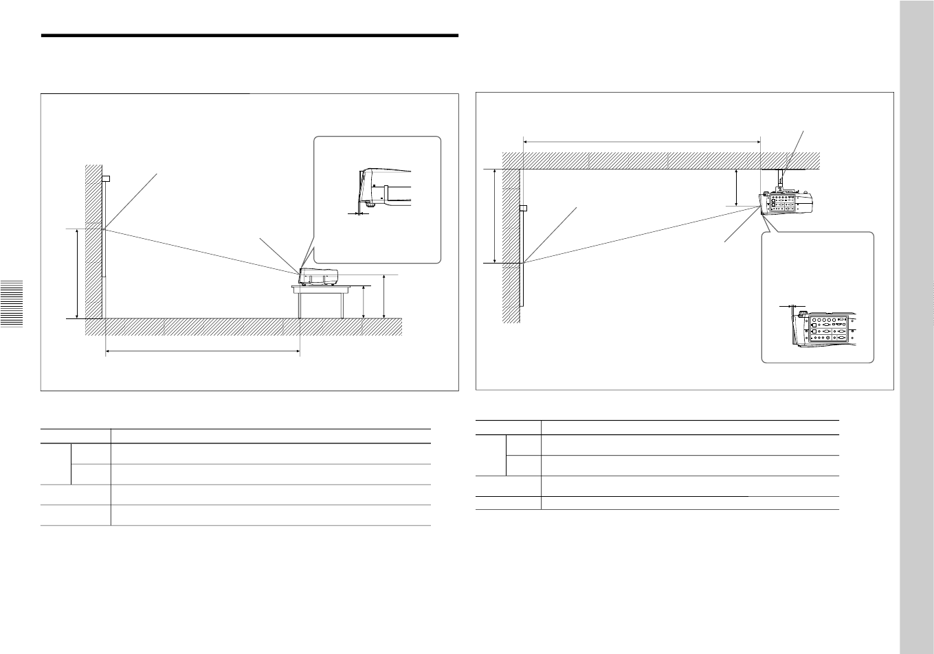
1-15
VPL-PX20/PX30
28
(GB)
a
x
b
c
a: Distance between the screen and the center of the lens
b: Distance from the floor to the center of the lens
c: Distance from the floor to the foot of the projector
x: Free
Screen size (inches) 40 60 80 100 120 150 180 200 250 300
Minimum 1490 2280 3060 3850 4630 5810 6990 7770 9740 11700
a(58
3
/
4
) (89
7
/
8
) (120
1
/
2
) (151
5
/
8
) (182
3
/
8
) (228
7
/
8
) (275
1
/
4
) (306) (383
5
/
8
) (460
3
/
4
)
Maximum 1820 2780 3740 4700 5660 7100 8540 9500 11900 14300
(71
3
/
4
) (109
1
/
2
) (147
3
/
8
) (185
1
/
8
) (222
7
/
8
) (279
5
/
8
) (336
3
/
8
) (374
1
/
8
) (468
5
/
8
) (563
1
/
8
)
bx–305 x–457 x–610 x–762 x–914 x–1143 x–1372 x–1524 x–1905 x–2286
(12) (18) (24) (30) (36) (45) (54) (60) (75
1
/
8
) (90
1
/
8
)
cx–394 x–546 x–699 x–851 x–1003 x–1232 x–1461 x–1613 x–1994 x–2375
(15
5
/
8
) (21
5
/
8
) (27
5
/
8
) (33
5
/
8
) (39
5
/
8
) (48
5
/
8
) (57
5
/
8
) (63
5
/
8
) (78
5
/
8
) (93
5
/
8
)
Unit: mm (inches)
Center of the lens
Center of the screen
Wall
Floor
To calculate the installation measurement (unit: mm)
SS: screen size diagonal (inches)
a (minimum) = {(SS × 50.18/1.3102) – 75.10104} × 1.025
a (maximum) = {(SS × 64.518746/1.3102) – 107.8977} × 0.975
b = x – (SS/1.3102 × 9.984)
c = x – (SS/1.3102 × 9.984 + 89)
Distance from the front of
the cabinet and the center
of the lens
Standard lens: 10 mm (
13
/
32
inches)
Installation Examples
Floor Installation
Installation Examples
29
(GB)
a
x
b
Ceiling Installation
When installing the projector on the ceiling, use the
PSS-610 Projector Suspension Support.
a: Distance between the screen and the center of the lens
b: Distance between the ceiling and the center of the lens
x: Distance between the ceiling and the center of the screen
Center of the lens
Screen size (inches) 80 100 120 150 180 200 250 300
Minimum 3060 3850 4630 5810 6990 7770 9740 11700
a(120
1
/
2
) (151
5
/
8
) (182
3
/
8
) (228
7
/
8
) (275
1
/
4
) (306) (383
5
/
8
) (460
3
/
4
)
Maximum 3740 4700 5660 7100 8540 9500 11900 14300
(147
3
/
8
) (185
1
/
8
) (222
7
/
8
) (279
5
/
8
) (336
3
/
8
) (374
1
/
8
) (468
5
/
8
) (563
1
/
8
)
x
b+610 b+762 b+914 b+1143 b+1372 b+1524 b+1905 b+2286
(24) (30) (36) (45) (54) (60) (75
1
/
8
) (90
1
/
8
)
b
231/256/281/331/356/381 mm (9
1
/
8
/10
1
/
8
/11
1
/
8
/13
1
/
8
/14
1
/
8
/15 inches) adjustable when using PSS-610
Wall
PSS-610 Projector Suspension Support
(not supplied)
Ceiling
Unit: mm (inches)
Center of the screen
For ceiling installation, consult with qualified Sony
personnel.
To calculate the installation measurement (unit: mm)
SS: screen size diagonal (inches)
a (minimum) = {(SS × 50.18/1.3102) – 75.10104} × 1.025
a (maximum) = {(SS × 64.518746/1.3102) – 107.8977} × 0.975
x = b + (SS/1.3102 × 9.984)
Distance from the front of
the cabinet and the center
of the lens
Installation Examples
Installation
Standard lens:
10 mm (
13
/
32
inches)
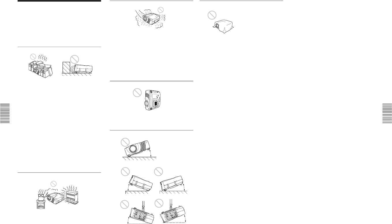
1-16 VPL-PX20/PX30
30
(GB)
Tips for Installation
Tips for Installation
Unsuitable Installation
Do not install the projector in the following situations.
These installations may cause malfunction or damage
to the projector.
Poorly ventilated
• Allow adequate air circulation to prevent internal
heat build-up. Do not place the unit on surfaces
(rugs, blankets, etc.) or near materials (curtains,
draperies) that may block the ventilation holes.
When the internal heat builds up due to the block-up,
the temperature sensor will function with the
message “High temp.! Lamp off in 1 min.” The
power will be turned off automatically after one
minute.
• Leave space of more than 30 cm (11
7
/
8
inches)
around the unit.
• Be careful that the ventilation holes may inhale
tininess such as a piece of paper.
• If you put something in front of the front ventilation
holes, the exhaust may be inhaled into the projector
through the ventilation holes at the bottom, causing
the internal temperature to rise, which activates the
protection circuit. Install the projector so that the
exhaust is not blocked.
Highly heated and humid
• Avoid installing the unit in a location where the
temperature or humidity is very high, or temperature
is very low.
• To avoid moisture condensation, do not install the
unit in a location where the temperature may rise
rapidly.
Very dusty
Avoid installing the unit in a location where there is a
lot of dust; otherwise, the air filter will be obstructed.
The dust blocking the air through the filter may cause
raising the internal heat of the projector. Clean it up
periodically.
Notes on Installation
Carry out the followings.
No toppling of the unit
Avoid using as the unit topples over on its side. It may
cause malfunction.
Use to be level
Avoid using as the unit tilts more than 20 degrees. Do
not install the unit other than on the floor or ceiling.
These installation may cause malfunction.
20°
20°
20°
20°
20°
31
(GB)
Tips for Installation
No blocking the ventilation holes
Avoid using something to cover over the ventilation
holes; otherwise, the internal heat may build up.
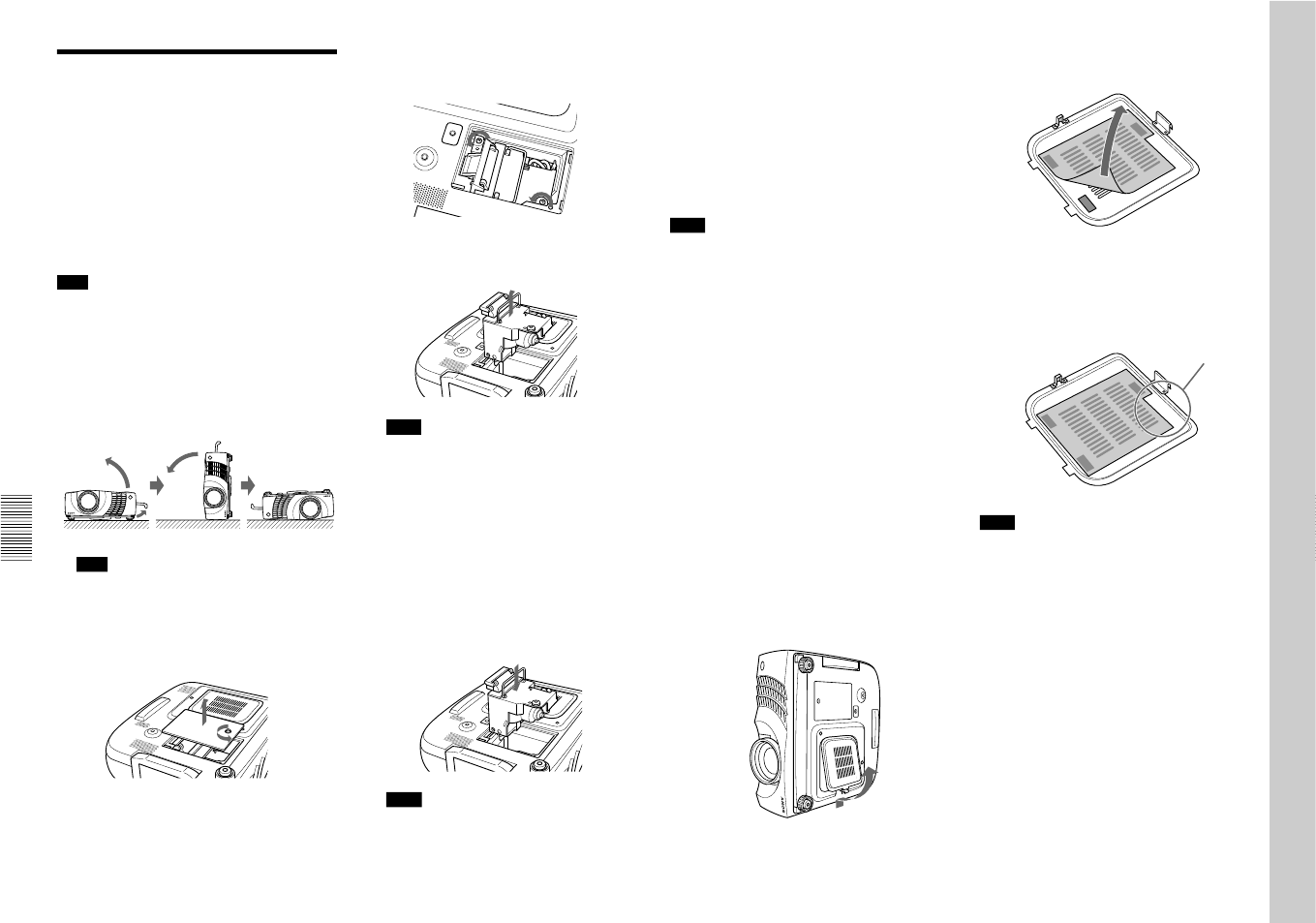
1-17
VPL-PX20/PX30
32
(GB)
Maintenance
Replacing the Lamp
When it is time to replace the lamp, replace the lamp
promptly with a new LMP-P200 Projector Lamp.
The lamp reaches the end of its life after about 1000
hours for the STANDARD setting, or about 2000
hours for the LOW setting in the LAMP MODE.
When replacing the lamp after using the
projector
Turn off the projector, then unplug the power cord.
Wait for at least an hour for the lamp to cool.
Note
The lamp becomes a high temperature after turning
off the projector with the I / 1 key. If you touch the
lamp, you may scald your finger. When you replace
the lamp, wait for at least an hour for the lamp to cool.
1
Place a protective sheet (cloth) beneath the
projector.
Hold the projector handle and turn the projector
toward the control panel as shown below.
Note
When replacing the lamp, be sure it is on a flat
and stable surface.
2
Open the lamp cover by loosening one screw with
the Philips screwdriver (supplied with the LMP-
P200 Projector Lamp).
3
Loosen two screws on the lamp unit with the
Philips screwdriver.
4
While holding the handle and keeping the lamp
unit horizontal, pull straight up.
Notes
• Pull out the lamp unit by holding the handle. If
you touch the lamp unit, you may be burned or
injured.
• When removing the lamp unit, make sure it
remains horizontal, then pull straight up. Do not
tilt the lamp unit. If you pull out the lamp unit
while tilted and if the lamp breaks, the pieces
may scatter, causing injury.
• If the lamp breaks, consult with qualified Sony
personnel.
5
Insert the new lamp all the way in until it is
securely in place. Tighten the screws. Fold down
the handle.
Notes
• Be careful not to touch the glass surface of the
lamp.
• The power will not turn on if the lamp is not
secured properly.
Maintenance
33
(GB)
6
Close the lamp cover and tighten the screw.
7
Turn the projector back over.
8
Connect the power cord and turn the projector to
the standby mode.
9
Press the following keys on the control panel in
the following order for less than in five seconds
each: RESET, <, ,, ENTER.
Notes
• Be sure to use the LMP-P200 Projector Lamp for
replacement. If you use lamps other than LMP-P200,
the projector may cause a malfunction.
• Be sure to turn off the projector and unplug the
power cord before replacing the lamp.
• Do not put your hands into the lamp replacement
spot, or not fall any liquid or object into it to avoid
electrical shock or fire.
Disposal of used projector lamp
As the materials used in this lamp are similar to those
of a fluorescent lamp, you should dispose of a used
projector lamp in the same way as a fluorescent lamp.
Cleaning the Air Filter
The air filter should be cleaned every 300 hours.
When it becomes difficult to remove the dust from the
filter, replace the filter with a new one.
To clean the air filter, follow the steps below:
1
Turn off the power and unplug the power cord.
2
Remove the air filter cover while holding down
the air filter cover button on the filter cover.
3
Peel off the air filter. (The air filter is secured
with Velcro tape (3).)
4
Remove the dust from the filter with a vacuum
cleaner.
5
Install the air filter as shown in the figure. Install
the air filter cover on the projector.
Notes
• Just placing the air filter on the Velcro tapes will not
lock the air filter in place. When installing the air
filter, place it on the air filter cover and attach by
pressing down hard on the three Velcro tapes. Make
sure that the air filter is not bent.
• Set the air filter correctly (straight) in the air filter
cover. If the air filter is not straight, the filter may
malfunction.
• If the air filter is excessively dirty, wash it with a
mild detergent solution and dry it in a shaded place.
If the dust cannot be removed, replace the air filter
with the supplied new one.
• The air filter has front and back sides. Make sure
you install the air filter in the right direction. Check
the notch on the filter as shown in the figure above
and install properly.
• Be sure to attach the air filter cover firmly; the power
will not be turned on if it is not closed securely.
Maintenance
Notch
Maintenance
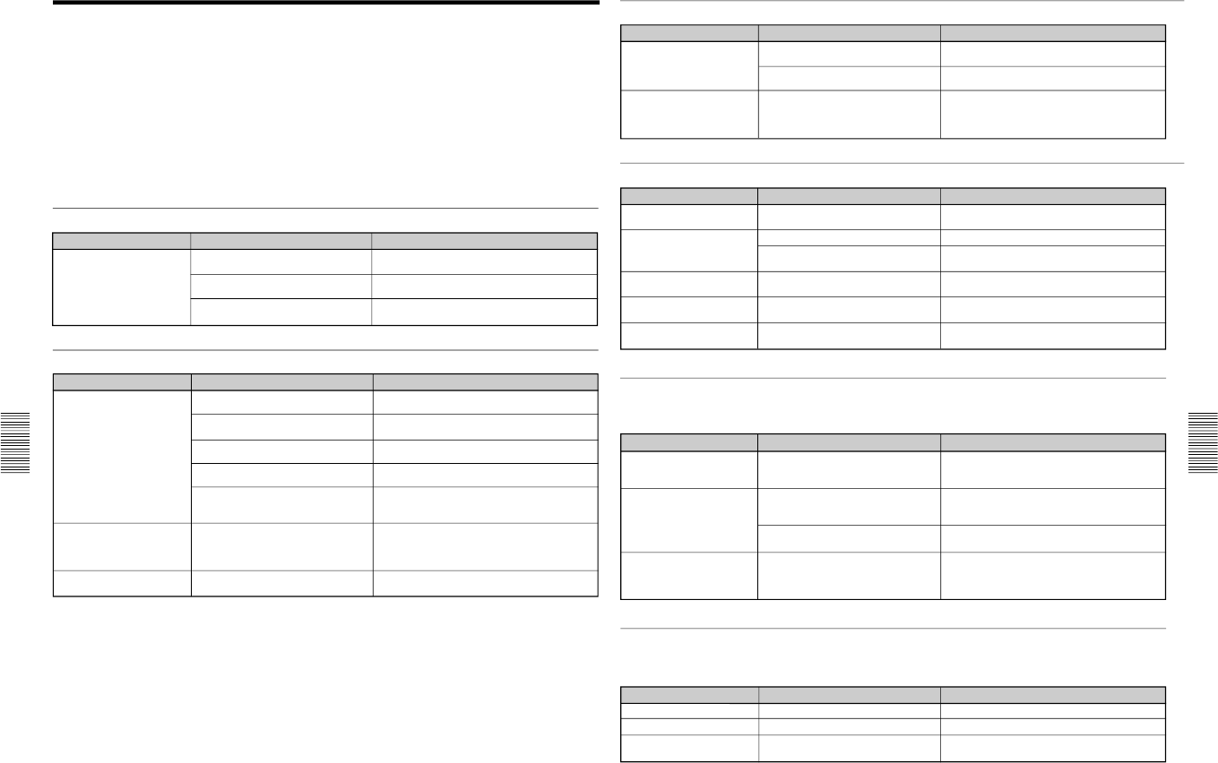
1-18 VPL-PX20/PX30
34
(GB)
Troubleshooting
Troubleshooting
If you encounter a problem during operation, press the HELP key to display the help messages.
You can get these kinds of help messages:
• Image: A menu is not displayed. Colors are not correct.
• Sound: Sound is not output correctly.
• Other: The indicator lights up/flashes.
If you still have a problem after consulting the help messages, please check the following. If the problem persists,
contact your Sony dealer.
Power
Image
Symptom Cause Remedy
The power is not turned on. The power has been turned off and on
with the I / 1 key at a short interval. Wait for about 120 seconds before turning on the
power
(see page 19 (GB))
.
The lamp cover is detached. Close the lamp cover securely
(see page
32 (GB))
.
The air filter cover is detached. Close the air filter cover securely
(see page
33 (GB))
.
Symptom Cause Remedy
No picture.
The computer signal is not set to output
to external monitor. Set the computer signal to output to external
monitor
(see page 15 (GB))
.
The computer signal is set to output to
both the LCD of the computer and
external monitor.
Set the computer signal to output only to external
monitor
(see page 15 (GB))
.
The picture is noisy. Noise may appear on the background
depending on the combination of the
numbers of dot input from the connector
and numbers of pixel on the LCD panel.
Change the desktop pattern on the connected
computer.
Cable is disconnected or not connected
properly. Check that the proper connections have been
made
(see pages 15 (GB) to 18 (GB))
.
Input selection is incorrect. Select the input source correctly using the INPUT
key
(see page 19 (GB))
.
The picture is cut off. Press the PIC MUTING key to release the muting
function
(see page 19 (GB))
.
On-screen display does not
appear. STATUS in the SET SETTING menu has
been set to OFF. Set STATUS in the SET SETTING menu to ON
(see page 26 (GB))
.
35
(GB)
Troubleshooting
Sound
Symptom Cause Remedy
No Sound. Cable is disconnected or not connected
properly. Check that the proper connections have been
made
(see pages 15 (GB) to 18 (GB))
.
The sound is cut off. Press the AUDIO MUTING key to release the
muting function
(see page 19 (GB))
.
When inputting sound through
AUDIO jack, sound comes
through one channel only.
Monaural sound is being input through
the AUDIO jack. Input stereo sound.
Others
Symptom Cause Remedy
The LAMP/COVER indicator
flashes. The lamp cover or the air filter cover is
detached. Attach the cover securely
(see pages 32 (GB) and
33 (GB)).
The LAMP/COVER indicator
lights up. The lamp has reached the end of its life. Replace the lamp
(see page 32 (GB)).
The lamp becomes a high temperature. Wait for 120 seconds to cool down the lamp and
turn on the power again
(see page 19 (GB))
.
The TEMP/FAN indicator
flashes. The fan is broken. Consult with qualified Sony personnel.
The TEMP/FAN indicator
lights up. The internal temperature is unusually
high. Check to see if nothing is blocking the ventilation
holes.
Warning messages
Use the list below to check the meaning of the messages displayed on the screen.
Message
Caution messages
Use the list below to check the meaning of the messages displayed on the screen.
Message
Meaning Remedy
High temp.!
Lamp off in 1 min. Internal temperature is too high. Turn off the power.
Check to see if nothing is blocking the ventilation
holes.
Frequency is out of range! This input signal cannot be projected as
the frequency is out of the acceptable
range of the projector.
Input a signal that is within the range of the
frequency.
The resolution setting of the output
signal of a computer is too high. Set the setting of output to the XGA
(see page 15
(GB)).
NO INPUT No input signal Check connections
(see page 15 (GB) to 18 (GB))
.
Not applicable! You have pressed the wrong key. Press the appropriate key.
Please check INPUT-A
setting. You have input RGB signal from the
computer when INPUT-A in the SET
SETTING menu is set to COMPONENT,
DTV YP
B
P
R
or DTV GBR.
Set INPUT-A correctly
(see page 26 (GB))
.
Meaning Remedy
SPEAKER OFF SPEAKER in the SET SETTING menu
has been set to OFF. Set SPEAKER to ON if necessary
(see page 26
(GB))
.
Both LAMP/COVER and
TEMP/FAN indicators light up. The electric system failed. Consult with qualified Sony personnel.

1-19
VPL-PX20/PX30
36
(GB)
Specifications
Specifications
Optical characteristics
Projection system 3 LCD panels, 1 lens, projection
system
LCD panel VPL-PX20: 1.3-inch TFT SONY
LCD panel
VPL-PX30: 1.3-inch TFT SONY
LCD panel with micro-lens
array,
2,359,296 pixels
(786,432 pixels × 3)
Lens Approx. 1.3 times zoom lens
f 36.7 to 47.8 mm/F 1.7 to 2.0
Lamp 200 W UHP
Projection picture size
Range: 40 to 300 inches (diagonal
measure)
Light output VPL-PX20: ANSI lumen
1)
1400 lm
VPL-PX30: ANSI lumen
1)
2400 lm
Throwing distance 40-inch: 1490 to 1820 mm
(58
3
/
4
to 71
3
/
4
inches)
60-inch: 2280 to 2780 mm
(89
7
/
8
to 109
1
/
2
inches)
80-inch: 3060 to 3740 mm
(120
1
/
2
to 147
3
/
8
inches)
100-inch: 3850 to 4700 mm
(151
5
/
8
to 185
1
/
8
inches)
120-inch: 4630 to 5660 mm
(182
3
/
8
to 222
7
/
8
inches)
150-inch: 5810 to 7100 mm
(228
7
/
8
to 279
5
/
8
inches)
180-inch: 6990 to 8540 mm
(275
1
/
4
to 336
3
/
8
inches)
200-inch: 7770 to 9500 mm
(306 to 374
1
/
8
inches)
250-inch: 9740 to 11900 mm
(383
5
/
8
to 468
5
/
8
inches)
300-inch: 11700 to 14300 mm
(460
3
/
4
to 563
1
/
8
inches)
Electrical characteristics
Color system NTSC
3.58
/PAL/SECAM/NTSC
4.43
/
PAL-M/PAL-N system,
switched automatically/manually
Resolution 750 horizontal TV lines (Video
input)
1024 × 768 pixels (RGB input)
Acceptable computer signals
fH: 15 to 91 kHz
fV: 43 to 85 Hz
.........................................................................................................................................................................................................
1) ANSI lumen is a measuring method of American National Standard IT 7.228.
Speaker Wide frequency range 3 speakers
system,
Woofer: 65 mm (2
5
/
8
inches)
diameter, max. 3 W
Tweeter: 45 mm (1
3
/
16
inches)
diameter, max. 1 W × 2
(stereo)
Input/Output
Video/audio input VIDEO: phono type
Composite video: 1 Vp-p ±2 dB
sync negative (75 ohms
terminated)
S VIDEO: Y/C mini DIN 4-pin
type (male)
Y (luminance): 1 Vp-p ±2 dB
sync negative (75 ohms
terminated)
C (chrominance): burst
0.286 Vp-p ±2 dB (NTSC)
(75 ohms terminated),
burst 0.3 Vp-p ±2 dB (PAL)
(75 ohms terminated)
AUDIO: Phono type × 2
500 mVrms, impedance more
than 47 kilohms
INPUT A HD D-sub15-pin (female)/ 5BNC
(female)/ Digital Interface
Switched
Analog RGB:HD D-sub15-pin
(female)
R: 0.7 Vp-p ±2 dB (75 ohms
terminated)
G: 0.7 Vp-p ±2 dB (75 ohms
terminated)
G with sync: 1 Vp-p ±2 dB sync
negative (75 ohms terminated)
B: 0.7 Vp-p ±2 dB (75 ohms
terminated)
SYNC/HD:
Composite sync input: 1-5 Vp-p
high impedance, positive/
negative
Horizontal sync input: 1-5 Vp-p
high impedance, positive/
negative
VD:
Vertical sync input: 1-5 Vp-p
high impedance, positive/
negative
Analog RGB/component: 5BNC
(female)
R/R-Y: 0.7 Vp-p ±2 dB (75
ohms terminated)
37
(GB)
Specifications
R/R-Y,G/Y,B/B-Y: Gain
Unity,75ohms
SYNC/HD,VD: 4Vp-p (open),
1Vp-p (75ohms)
* DIGITAL RGB signal is not
output from MONITOR OUT
terminal.
AUDIO OUT (variable out):
Stereo minijack
max. 1 Vrms, When an input
signal is 500 mVrms, impedance
less than 5 kilohms
REMOTE RS-232C: D-sub 9-pin (female)
CONTROL S IN/PLUG IN POWER
Stereo minijack 5Vp-p, plug in
power, DC5V
Safety regulations: UL1950, CSA No.950, DHHS
(Laser), DNHW (Laser), FCC
Class A, IC Class A,
EN60 950 (NEMKO), CE, C-
Tick, CCIB, EN60 825-1
(Laser), VCCI class B, JEIDA
Laser beam
Laser type Class 2
Wavelength 645 nm
Output 1 mW
General
Dimensions 339 × 142 × 335 mm (13
3
/
8
× 5
5
/
8
× 13
1
/
4
inches) (w/h/d)
Mass Approx. 7.2 kg (15 lb 14 oz)
Power requirements
AC 100 to 240 V, 50/60 Hz
Power consumption
Max. 290 W (Standby mode:
5 W)
Heat dissipation 989.6 BTU
Operating temperature
0°C to 40°C (32°F to 104°F)
Operating humidity35% to 85% (no condensation)
Storage temperature
–20°C to 60°C (32°F to 140°F)
Storage humidity 10% to 90%
Supplied accessories
Remote Commander RM-PJM610
(1)
Size AA (R6) batteries (2)
HD D-sub 15-pin Cable SMF-410
(1)
G: 0.7 Vp-p ±2 dB (75 ohms
terminated)
G with sync/Y: 1 Vp-p ±2 dB
sync negative (75 ohms
terminated)
B/B-Y: 0.7 Vp-p ±2 dB (75
ohms terminated)
SYNC/HD:
Composite sync input: 1-5 Vp-p
high impedance, positive/
negative
Horizontal sync input: 1-5 Vp-p
high impedance, positive/
negative
VD:
Vertical sync input: 1-5 Vp-p
high impedance, positive/
negative
DIGITAL RGB: DFP 20-pin
(TMDS)
USB HUB: Up (B type: female)
× 1, Down (A type: female) × 1
MOUSE (output): 13-pin (female)
(For details, see “Pin assignment” on
page 38 (GB).)
AUDIO: Stereo minijack
500 mVrms, impedance more
than 47 kilohms
INPUT B Analog RGB: HD D-sub15-pin
(female)
R: 0.7 Vp-p ±2 dB (75 ohms
terminated)
G: 0.7 Vp-p ±2 dB (75 ohms
terminated)
G with sync: 1 Vp-p ±2 dB sync
negative (75 ohms terminated)
B: 0.7 Vp-p ±2 dB (75 ohms
terminated)
SYNC/HD:
Composite sync input: 1-5 Vp-p
high impedance, positive/
negative
Horizontal sync input: 1-5 Vp-p
high impedance, positive/
negative
VD:
Vertical sync input: 1-5 Vp-p
high impedance, positive/
negative
MOUSE (output): 13-pin (female)
(For details, see “Pin assignment” on
page 38 (GB).)
AUDIO: Stereo minijack
500 mVrms, impedance more
than 47 kilohms
OUTPUT MONITOR OUT: HD D-sub
15-pin (female) (Continued)
Other
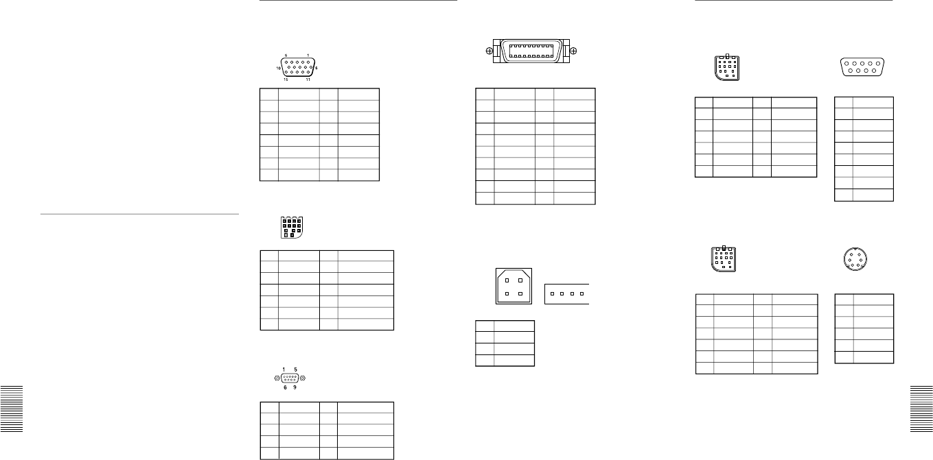
1-20 VPL-PX20/PX30
38
(GB)
Mouse Cable
SIC-S21 (for Serial)
(2 m) (1)
SIC-S22 (for PS/2) (2 m) (1)
Audio/video cable
(1.5 m)
(1)
USB Cable A type – B type (2 m)
(1)
Application software, Projector
Station (1)
Lens Cap (1)
Strap for Remote Commander (1)
AC power cord (1)
Air filter (for replacement) (1)
Operating Instructions (1)
Installation Manual for Dealers (1)
Quick Reference Card (1)
Warranty Card (1)
Design and specifications are subject to change
without notice.
Optional accessories
Projector Lamp LMP-P200 (for replacement)
Projector Suspension Support PSS-610
Carrying Case VLC-600
1)
Signal Selector IFU-SC50
Monitor Cable
SMF-400 (HD D-sub 15-pin (male) y 5 × BNC
(male))
SMF-410 (HD D-sub 15-pin (male) y HD D-sub
15-pin (male))
Signal cable
SMF-401 (HD D-sub 15-pin (male) y HD D-sub
15-pin (male))
Signal Interface Cable
SIC-10 (5 × BNC (male) y 5 × BNC (male))
Digital Signal Cable
SMF-D102 (DFP 20-pin y DFP 20-pin)
SMF-D110 (DFP 20-pin y DFP 20-pin)
Mouse Cable
SIC-S20 (for Macintosh)
(2 m)
SIC-S21 (for Serial)
(2 m)
SIC-S22 (for PS/2)
(2 m)
Signal Adapter
ADP-20 (Macintosh y HD D-sub 15-pin)
Projection Lens
Long Focus Zoom Lens VPLL-ZM101
Short Focus Zoom Lens VPLL-ZM31
Fixed Short Focus Lens VPLL-FM21
Screens
50-inch Portable VPS-50C
1)
Some of the items may not be available in some areas. For
details, please consult your nearest Sony office.
.........................................................................................................................................................................................................
1) VLC-600 and VPS-50C may not be available in some areas. For details, please consult your nearest Sony office.
Specifications
Pin assignment
RGB input connector (HD D-sub 15-pin,
female)
1 R/R-Y 9 N.C.
2 G/Y 10 GND
3 B/B-Y 11 GND
4 N.C. 12 N.C.
5 GND 13 HD/C.Sync
6 GND (R) 14 VD
7 GND (G) 15 N.C.
8 GND (B)
MOUSE connector (13-pin, female)
1 RTS 8 R
2 GND 9 98/AT/TXD
3 XA 10 +5V/DTR
4 XB 11 CLOCK
5 YA 12 DATA
6 YB 13 RXD
7 L/PS
RS-232C connector (D-sub 9-pin, female)
1 DCD 6 DSR
2 RX DA 7 RTS
3 TX DA 8 CTS
4 DTR 9 RI
5 GND
12 35 69 1013
39
(GB)
DIGITAL RGB input connector (DFP 20-pin,
female)
1 TX0– 11 TXC–
2 TX0+ 12 TXC+
3
TX0 SHIELD
13
TXC SHIELD
4
TX2 SHIELD
14
TX1 SHIELD
5 TX2– 15 TX1–
6 TX2+ 16 TX1+
7 DDC/SCL 17 NC
8 DDC/SDA 18 SENSE
9 NC 19 +5V DC
10 NC 20 GND
USB connector
Mouse cable pin assignment
SIC-S22
13-pin mini DIN 6-pin
1 RTS 8 R
2 GND 9 98/AT/TXD
3 XA 10 +5V/DTR
4 XB 11 CLOCK
5 YA 12 DATA
6 YB 13 RXD
7 L/PS
1 DATA
2NC
3 GND
4 +5V
5 CLOCK
6NC
13-pin D-sub 9-pin
1 RTS 8 R
2 GND 9 98/AT/TXD
3 XA 10 +5V/DTR
4 XB 11 CLOCK
5 YA 12 DATA
6 YB 13 RXD
7 L/PS
1 DCD
2 RXD
3 TXD
4 DTR
5 GND
6 DSR
7 RTS
8 CTS
9RI
SIC-S21
Specifications
3
12
56
4
21 53 96 1310
1
69
5
21 53 96 1310
2
3
114
4
Plug B
(female) Plug A
110
1120
1 +5V
2D–
3D+
4 GND
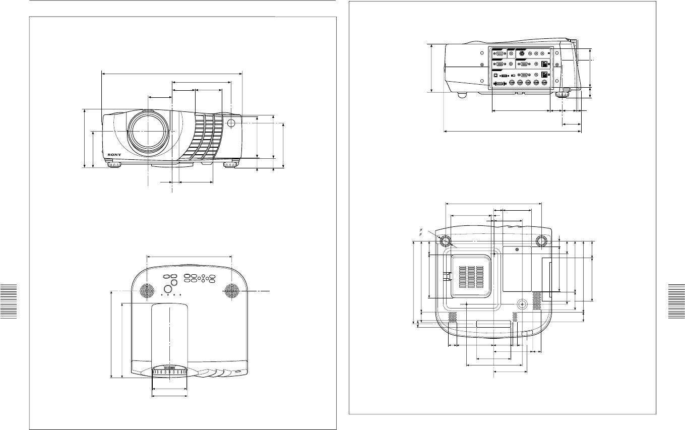
1-21
VPL-PX20/PX30
40
(GB)
Specifications
Dimensions
Unit: mm (inches)
Front
339 (13
11
/
32
)
142 (5
19
/
32
)
55 (2
5
/
32
) 64.3 (2
9
/
16
)
58 (2
9
/
32
)
82 (3
7
/
32
)
16.6(
21
/
32
)
142.6 (5
5
/
8
)
106.2 (4
3
/
16
)
100.7 (3
31
/
32
)
109.4 (4
5
/
16
)
89 (3
1
/
2
)
24.5
(
31
/
32
)
22.4
(
7
/
8
)
Top
248 (9
3
/
4
)
99 (3
29
/
32
)
105 (4
1
/
8
)
257 (10
1
/
8
)
220 (8
21
/
32
)
Center of the lens
Center of the unit
41
(GB)
Specifications
Unit: mm (inches)
Bottom
Side
335.5 (13
7
/
32
)
146 (5
3
/
4
)
95 (3
3
/
4
)
45.4
(1
25
/
32
)
23.8
(
15
/
16
)
28.4
(1
1
/
8
)
35.4
(1
13
/
32
)
0 – 2.1 (0 –
3
/
32
)
116.8 (4
19
/
32
)
279
(10
31
/
32
)
246
(9
11
/
16
)
134
(5
9
/
32
)
150.8
(5
15
/
16
)
38.4
(1
1
/
2
)
16.8
(
21
/
32
)
152.3
(6)
211.2
(8
5
/
16
)
127(5) 51.5 (
2
1
/
32
)
29
(1
5
/
32
)
210.4
(8
9
/
32
)
128
(5
1
/
32
)
40
(1
9
/
16
)
29
(1
5
/
32
)
20
(
25
/
32
)
117.2
(4
5
/
8
)
26.5
(1
1
/
32
)
1.8
(
1
/
16
)
32
23
(
29
/
32
)
108.8
(4
9
/
32
)54.5 (2
5
/
32
)
113.5
(4
15
/
32
)
100
(3
15
/
16
)
96 (3
25
/
32
)
163
(6
13
/
32
)
14
(
9
/
16
)
23
(
29
/
32
)
82.5
(3
1
/
4
)
81.5
(3
7
/
32
)
( 1
1
/
4
)
7.2
(
9
/
32
)
53
(2
3
/
32
)
Center of the unit

1-22 VPL-PX20/PX30
42
(GB)
Index
A
Adjuster 10 (GB)
Adjusting
memory of the settings 22 (GB)
the picture 22 (GB)
the picture size/shift 24 (GB)
Air filter 33 (GB)
APA function 11 (GB), 19 (GB)
ASPECT 24 (GB)
AUTO INPUT SEL 26 (GB)
B
Battery
installation 14 (GB)
notes 14 (GB)
BRIGHT 23 (GB)
C
Carrying handle 9 (GB)
COLOR 23 (GB)
COLOR SYS (System) 23 (GB)
COLOR TEMP 23 (GB)
Condensation 30 (GB)
Connections
component equipment 18 (GB)
computer 15 (GB)
VCR 17 (GB)
CONTRAST 23 (GB)
Cut off
the picture 19 (GB)
the sound 19 (GB)
D, E, F
DIGIT KEYSTONE 27 (GB)
DIGITAL RGB input connector 12 (GB)
pin assignment 39 (GB)
DIGITAL RGB/5BNC/RGB switch
12 (GB)
Dimensions 40 (GB)
D. (Dynamic) PICTURE 23 (GB)
DOT PHASE 24 (GB)
5BNC input connectors 12 (GB)
G
GAMMA MODE 23 (GB)
H
HUE 23 (GB)
I, J, K
INPUT-A 26 (GB)
INPUT SETTING menu 24 (GB)
INSTALL SETTING menu 27 (GB)
INSTALLATION 27 (GB)
Installation examples 28 (GB)
on a ceiling 29 (GB)
on a floor 28 (GB)
KEYSTONE MEM 27 (GB)
L
LAMP MODE 27 (GB)
Lamp replacement 32 (GB)
LAMP TIMER 27 (GB)
LANGUAGE 26 (GB)
Location and function of controls
connector panel 12 (GB)
control panel 11 (GB)
front/left side 9 (GB)
rear/right side/bottom 9 (GB)
Remote Commander 13 (GB)
M, N
Menu
clearing the menu display 22 (GB)
INPUT SETTING menu 24 (GB)
INSTALL SETTING menu 27 (GB)
PICTURE CTRL menu 22 (GB)
SET SETTING menu 26 (GB)
using the menu 22 (GB)
Messages
cautions 35 (GB)
warnings 35 (GB)
Mouse cable
connection 15 (GB)
pin assignment 39 (GB)
Mouse connector 12 (GB)
pin assignment 38 (GB)
O
Optional accessories 38 (GB)
P, Q
PICTURE CTRL menu 22 (GB)
Pin assignment 38 (GB)
Power
turn off 20 (GB)
turn on 19 (GB)
POWER SAVING 11 (GB), 27 (GB)
Precautions 7 (GB)
Projecting 19 (GB)
PSS-610 Projector Suspension Support
29 (GB)
R
Remote Commander
battery installation 14 (GB)
D ZOOM key 13 (GB), 21 (GB)
FUNCTION key 13 (GB)
HELP key 14 (GB)
laser pointer function 13 (GB), 21 (GB)
location and function of controls
13 (GB)
Remote control detector
front 9 (GB)
rear 9 (GB)
setting 27 (GB)
Reset
resettable items 22 (GB)
resetting the item 22 (GB)
RGB ENHANCER 23 (GB)
RGB input connector 12 (GB)
pin assignment 38 (GB)
RS-232C connector 12 (GB)
pin assingment 38 (GB)
S
SCAN CONV (Scan converter) 24 (GB)
Screen size 14 (GB), 25 (GB), 36 (GB)
SET SETTING menu 26 (GB)
SHARP 23 (GB)
SHIFT 24 (GB)
SIRCS RECEIVER 9 (GB), 27 (GB)
SIZE H 24 (GB)
SPEAKER 26 (GB)
Specifications 36 (GB)
STATUS (on-screen display) 26 (GB)
Supplied accessories 37 (GB)
T, U
Tips for installation 30 (GB)
notes 30 (GB)
unsuitable places 30 (GB)
Troubleshooting 34 (GB)
USB connector 12 (GB)
pin assignment 39 (GB)
V, W, X, Y, Z
Ventilation holes
exhaust 9 (GB)
intake 10 (GB)
Index
1-23
VPL-PX20/PX30
4-073-987-01 (1)
VPL-PX20
VPL-PX30
1999 Sony Corporation
LCD Data Projector
Installation Manual for Dealers
Pages 3, 11 to 16 and 46 to 59
This installation Manual for Dealers explains how to install the projector. For example, it explains
lens replacement, installation measurements when using the optional lens and hanging the
projector from the ceiling.
Manuel d’installation pour les revendeurs
Pages 3, 17 à 22 et 46 à 59
Le manuel d’installation pour les revendeurs explique comment installer le projecteur. Par
exemple, il explique la procédure de remplacement de l’objectif, les dimensions d’installation
lorsque vous employez l’objectif en option et comment suspendre le projecteur au plafond.
Manual de instalación para proveedores
Páginas 3, 23 a 28 y 46 a 59
En este manual de instalación para proveedores se describe cómo instalar el proyector. Por
ejemplo, se describe cómo sustituir el objetivo, las medidas de instalación cuando se utiliza el
objetivo opcional y cómo colgar el proyector en el techo.
Installationsanleitung für Händler
Seite 3, 29 bis 34 und 46 bis 59
In dieser Installationsanleitung für Händler wird erläutert, wie Sie den Projektor installieren.
Beispielsweise werden das Austauschen des Objektivs, die Installationsabmessungen beim
Verwenden des gesondert erhältlichen Objektivs und das Installieren des Projektors an der Decke
beschrieben.
Manuale d’installazione per i rivenditori
Pagine 3, 35 a 40 e 46 a 59
Il presente manuale contiene le istruzioni relative all’installazione del proiettore. Vengono riportate
ad esempio le istruzioni su come sostituire l’obiettivo, le misure di installazione quando si utilizza
l’obiettivo opzionale e le procedure dell’installazione al soffitto.
Installation Manual for Dealers
Pages 3, 41 to 45 and 60 to 64
This installation Manual for Dealers explains how to install the projector. For example, it explains
lens replacement, installation measurements when using the optional lens and hanging the
projector from the ceiling.
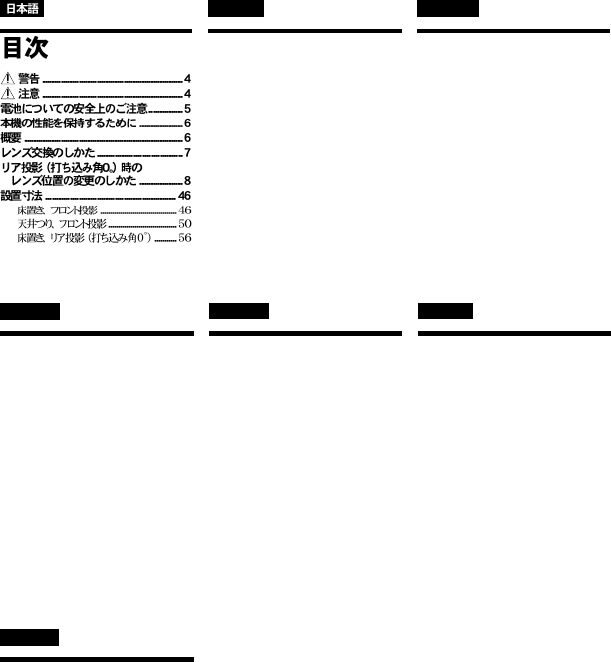
1-24 VPL-PX20/PX30
3
English
Table of Contents
Precautions................................... 11
Overview ....................................... 12
Replacing the Lens ...................... 13
Changing the Lens Position for
Rear Projection (Optical Axis
Angle: 0 degree)...................... 14
Installation Diagram ..................... 46
Floor Installation (Front
Projection) ..................................... 46
Ceiling Installation (Front
Projection) ..................................... 50
Floor Installation (Rear Projection:
Optical Axis Angle 0 Degree) ....... 56
Français
Table des matières
Précautions................................... 17
Aperçu ........................................... 18
Remplacement de l’objectif......... 19
Changement de la position de
l’objectif pour la rétroprojection
(angle d’axe optique :
0 degré) .................................... 20
Schéma d’installation .................. 46
Installation au sol (projection
frontale) ......................................... 46
Installation au platfond (projection
frontale) ......................................... 50
Installation au sol (Rétroprojection:
angle d’axe optique de 0 degré) .... 56
Español
Indice
Precauciones ................................ 23
Introducción ................................. 24
Sustitución del objetivo............... 25
Cambio de la posición del objetivo
para la proyección posterior
(ángulo de eje óptico:
0 grados).................................. 26
Diagrama de instalación .............. 46
Instalación en el suelo (proyección
frontal) ........................................... 46
Instalación en el techo (proyección
frontal) ........................................... 50
Instalación en el suelo (proyección
posterior: ángulo de eje óptico de 0
grados) ........................................... 56
Deutsch
Inhalt
Sicherheitsmaßnahmen............... 29
Übersicht....................................... 30
Austauschen des Objektivs ........ 31
Ändern der Objektivposition für die
Rückprojektion (Winkel der
optischen Achse: 0 Grad) ...... 32
Installationsdiagramm ................. 46
Installation am Boden
(Frontprojektion) ........................... 46
Installation an der Decke
(Frontprojektion) ........................... 50
Installation am Boden (Rückprojektion:
Winkel der optischen Achse =
0 Grad).......................................... 56
Italiano
Indice
Precauzioni ................................... 35
Presentazione ............................... 36
Sostituzione dell’obiettivo........... 37
Cambiamento di posizione
dell’obiettivo per la proiezione
posteriore (angolo di asse
ottico: 0 gradi) ......................... 38
Diagramma di installazione ......... 46
Installazione sul pavimento (proiezione
frontale) ......................................... 46
Installazione sul soffitto (proiezione
frontale) ......................................... 50
Installazione sul pavimento (proiezione
posteriore: grado zero dell’angolo di
asse ottico) ..................................... 56
Chinese
Table of Contents
Precautions................................... 41
Overview ....................................... 42
Replacing the Lens ...................... 42
Changing the Lens Position for
Rear Projection (Optical Axis
Angle: 0 degree)...................... 43
Installation Diagram ..................... 60
Floor Installation (Front
Projection) ..................................... 61
Ceiling Installation (Front
Projection) ..................................... 64
Floor Installation (Rear Projection:
Optical Axis Angle 0 Degree) ....... 67

1-25
VPL-PX20/PX30
11
Precautions
On safety
• Check that the operating voltage of your unit is
identical with the voltage of your local power
supply. If voltage adaptation is required, consult with
qualified Sony personnel.
• Should any liquid or solid object fall into the cabinet,
unplug the unit and have it checked by qualified
Sony personnel before operating it further.
• Unplug the unit from the wall outlet if it is not to be
used for several days.
• To disconnect the cord, pull it out by the plug. Never
pull the cord itself.
• The wall outlet should be near the unit and easily
accessible.
• The unit is not disconnected from the AC power
source (mains) as long as it is connected to the wall
outlet, even if the unit itself has been turned off.
• Do not look into the lens while the lamp is on.
• Do not place your hand or objects near the
ventilation holes — the air coming out is hot.
• Avoid using an extension cord with a low voltage
limited since it may cause the short-circuit and
physical incidents.
• To carry the projector, be sure to use the carrying
handle. Do not hold other parts of the projector,
especially the lens, nor catch your finger between the
handle, floor, and the projector.
• Do not catch your finger between the unit and
surface of the floor when moving the projector
installed on the floor.
• Be careful not to catch your finger in the cooling fan.
• Do not carry the projector with the cabinet on and
with its cover open.
On installation
• When the projector is mounted on the ceiling, the
Sony PSS-610 Projector Suspension Support must be
used for installation.
• Allow adequate air circulation to prevent internal
heat build-up. Do not place the unit on surfaces
(rugs, blankets, etc.) or near materials (curtains,
draperies) that may block the ventilation holes.
Leave space of more than 30 cm (11
7
/
8
inches)
between the wall and the projector. Be aware that
room heat rises to the ceiling; check that the
temperature near the installation location is not
excessive.
• Install the projector on the floor or ceiling. Any other
installation causes a mulfunction such as color
irregularity or shortening lamp life.
• Do not install the unit in a location near heat sources
such as radiators or air ducts, or in a place subject to
direct sunlight, excessive dust or humidity,
mechanical vibration or shock.
• To avoid moisture condensation, do not install the
unit in a location where the temperature may rise
rapidly.
• Be sure to secure the cabinet cover firmly when
installing to the ceiling firmly.
On illumination
• To obtain the best picture, the front of the screen
should not be exposed to direct lighting or sunlight.
• Ceiling-mounted spot lighting is recommended. Use
a cover over fluorescent lamps to avoid lowering the
contrast ratio.
• Cover any windows that face the screen with opaque
draperies.
• It is desirable to install the projector in a room where
floor and walls are not of light-reflecting material. If
the floor and walls are of reflecting material, it is
recommended that the carpet and wall paper be
changed to a dark color.
On preventing internal heat build-up
• After you turn off the power with the I / 1 key on
the control panel or on the Remote Commander, do
not disconnect the unit from the wall outlet while the
cooling fan is still running.
• Do not disconnect the AC power cord from the wall
outlet while the fan is still running.
Caution
The projector is equipped with ventilation holes
(intake) at the bottom and ventilation holes (exhaust)
at the front. Do not block or place anything near these
holes, or internal heat build-up may occur, causing
picture degradation or damage to the projector.
English
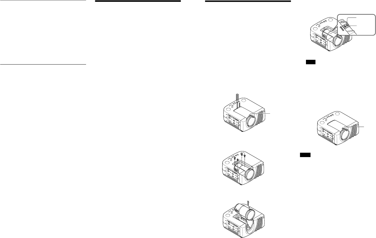
1-26 VPL-PX20/PX30
12
On cleaning
• To keep the cabinet looking new, periodically clean
it with a soft cloth. Stubborn stains may be removed
with a cloth lightly dampened with a mild detergent
solution. Never use strong solvents, such as thinner,
benzene, or abrasive cleansers, since these will
damage the cabinet.
• Avoid touching the lens. To remove dust on the lens,
use a soft dry cloth. Do not use a damp cloth,
detergent solution, or thinner.
• Clean the filter at regular intervals.
On repacking
• Save the original shipping carton and packing
material; they will come in handy if you ever have to
ship your unit. For maximum protection, repack your
unit as it was originally packed at the factory.
Overview
This manual describes how to install the Sony LCD
Data Projector VPL-PX20/PX30, how to replace the
lens, how to change the lens position for rear
projection (optical axis angle: 0 degree), and
installation diagrams. When you replace the lens or
change the lens position, also refer to the Operating
Instructions.
13
Replacing the Lens
You can install the following two types of lenses in
the projector.
• VPLL-ZM101 Long Focus Zoom Lens
• VPLL-ZM31 Short Focus Zoom Lens
Follow the steps below to replace the lens.
For details on replacing the lens, also refer to the
installation manual supplied with the lens.
1
Turn off the power and disconnect the power
cable.
2
Remove the lens hood. To remove the lens hood,
insert a screwdriver into the lens hood slit then
lightly push down on the hood with the
screwdriver and slide the lens hood forward.
3
Remove the four screws (M4×12, with washers)
locking the lens by using a Philips screwdriver.
4
Lift and remove the lens.
5
Install the lens with the lens stopper and the
projector stopper met at their edges.
Note
For ease in identification when you install the
lens, make sure that the label on the lens is facing
up.
6
Tighten the four screws to secure the replacement
lens firmly.
7
Install the lens hood by sliding it from front to
back until it snaps into the lock position.
Notes
• The lens scratches easily, so when handling it,
always place it gently on a stable and level surface in
a horizontal position.
• Avoid touching the lens surface.
Stopper
(Projector)
Stopper
(Lens)
Lens hood
Lens hood
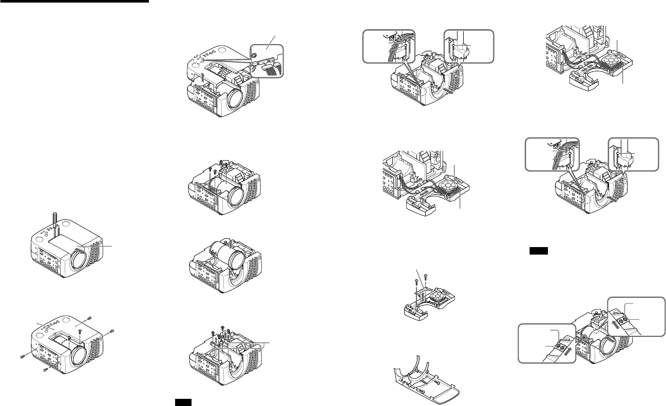
1-27
VPL-PX20/PX30
14
Changing the Lens
Position for Rear
Projection (Optical Axis
Angle: 0 degree)
For rear projection, you can set the optical axis angle
to 0 (zero). In this case, you will need to set the lens
position as follows.
You can install the following types of lenses for a zero
optical axis angle.
• Standard lens
• VPLL-ZM101 Long Focus Zoom Lens
• VPLL-ZM31 Short Focus Zoom Lens
• VPLL-FM21 Fixed Short Focus Lens
1
Turn off the power and disconnect the power
cable.
2
Remove the lens hood. To remove the lens hood,
insert a screwdriver into the lens hood slit then
lightly push down on the hood with the
screwdriver and slide the lens hood forward.
3
Remove the four silver screws (M3×8) on the both
sides and two silver screws (M3×8) on the top
locking the hood.
4
Disconnect the 12-pin connector and 4-pin
connector (connected to the PC board H) from the
hood. Lift the hood and set it behind the unit.
5
Remove the lens hood locking the lens by
loosening the four screws (M4×12, with washers)
with a Philips screwdriver.
6
Lift and remove the lens.
7
Remove the left and right spacers by loosening the
four screws (M4×12, with washers).
Note
The spacer and the screws may be needed later on.
Store them.
Lens hood
Hood
PC board H
Spacers
15
8
Remove two screws (M3×6, with washers) that
lock the front panel. Free the wires from the
clamp.
9
Disconnect the two connectors on the back of the
front panel, one for cooling fan and the other for
remote control detector, and then remove the front
panel.
10
Remove the two screws (M3×6, with washers)
from the front panel. Remove the lens bottom
cover.
11
Install the lens bottom cover on the lens hood
(removed in Step 2) with the two screws.
12
Connect the connector for remote control detector
and the connector for cooling fan.
13
Install the front panel on the unit with the two
screws (M3×6, with washers). Fasten the wires
with the clamp.
14
Install the lens with the lens stopper and the
projector stopper met at their edges.
Notes
• Make sure that lens stoppers and projector
stoppers are met on both sides.
• For ease in identification when you install the
lens, make sure that the lens stopper is facing up.
Screw
Screw
Clamp
Cooling fan
Remote control
detector
Lens bottom cover
Cooling fan
Remote control
detector
Screw
Screw
Clamp
Stopper
(Projector)
Stopper
(Lens)
Stopper
(Projector)
Stopper
(Lens)
(continued)
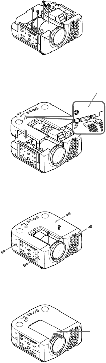
1-28 VPL-PX20/PX30
16
15
Lock the lens by tightening the four screws
(M4×12, with washers).
16
Connect the 12-pin connector and 4-pin connector
to the PC board H (disconnected in Step 4).
17
Install the hood and lock with the six screws
(M3×8).
18
Install the lens hood by sliding it from front to
back until it snaps into position.
Lens hood
PC board H
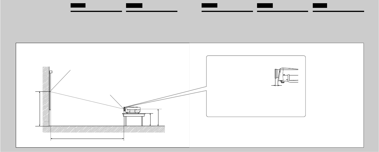
1-29
VPL-PX20/PX30
46
a
x
b
c
English
Installation
Diagram
Floor Installation (Front
Projection)
Français
Schéma
d’installation
Installation au sol
(projection frontale)
Floor / Sol / Suelo /
Boden / Pavimento
Wall
Mur
Pared
Wand
Parete
A
Center of the screen
Centre de l’écran
Centro de la pantalla
Mitte des Projektionsschirms
Centro dello schermo
Center of the lens / Centre de
l’objectif / Centro del objetivo /
Mitte des Objektivs / Centro
dell’obiettivo
This section describes the examples for
installing the projector on the desk, etc.
A
See the charts on pages 48 and 49
concerning the installation
measurements.
The alphabetical letters in the
illustration indicate the distances
below.
a : distance between the screen and the
center of the lens
b : distance between the floor and the
center of the lens
c : distance between the floor and the
bottom of the adjusters of the
projector
x : free
Cette section décrit des exemples
d'installation du projecteur sur un
bureau, etc. A
Reportez-vous aux tableaux des pages
48 à 49 sur les mesures d’installation.
Les caractères alphabétiques dans
l'illustration indiquent les distances ci-
dessous.
a : distance entre l’écran et le centre de
l’objectif
b : distance entre le sol et le centre de
l’objectif
c : distance entre le sol et la base des
pieds réglables du projecteur
x : libre
47
Español
Diagrama de
instalación
Instalación en el suelo
(proyección frontal)
Deutsch
Installations-
diagramm
Installation am Boden
(Frontprojektion)
Italiano
Diagramma di
installazione
Installazione sul pavimento
(proiezione frontale)
Distance between the front of the
cabinet and the center of the lens
Distance entre l’avant du châssis et le
centre de l’objectif
Distancia entre la parte frontal de la
unidad y el centro del objetivo
Abstand zwischen der
Gehäusevorderseite und der
Objektivmitte
Distanza tra la parte anteriore
dell’apparecchio e il centro
dell’obiettivo
Unit: mm (inches) / Unité: mm (pouces) /
Unidad: mm (pulgadas) / Einheit: mm (Zoll) /
Unità: mm (pollici)
Questa sezione descrive gli esempi di
installazione del proiettore su un
tavolo, ecc. A
Vedere i diagrammi da pagina 48 a
pagina 49 relativi alle misure di
installazione.
Le lettere nell'illustrazione indicano le
distanze descritte di seguito.
a : distanza fra lo schermo e il centro
dell’obiettivo
b : distanza tra il pavimento e il centro
dell’obiettivo
c : distanza fra il pavimento e la base
dei dispositivi di regolazione del
proiettore
x : libero
En esta sección se muestran ejemplos
para instalar el proyector sobre una
mesa, etc. A
Consulte las tablas de las páginas 48 a
49 en relación con las medidas de
instalación.
Las letras alfabéticas de la ilustración
indican las distancias mostradas a
continuación.
a : distancia entre la pantalla y el
centro del objetivo
b : distancia entre el suelo y el centro
del objetivo
c : distancia entre el suelo y la base de
los ajustadores del proyector
x : libre
In diesem Abschnitt finden Sie
Beispiele für das Installieren des
Projektors auf einem Tisch usw. A
In den Tabellen auf Seite 48 bis 49
finden Sie die
Installationsabmessungen.
Die Buchstaben in der Abbildung
beziehen sich auf die unten
beschriebenen Abstände.
a : Abstand zwischen dem
Projektionsschirm und der Mitte des
Objektivs
b : Abstand zwischen dem Boden und
der Mitte des Objektivs
c : Abstand zwischen dem Boden und
der Unterseite der Ausgleichsfüße
des Projektors
x : frei
VPLL-ZM101: 28.9 (1
1
/
8
)
VPLL-ZM31: 54.3 (2
1
/
8
)

1-30 VPL-PX20/PX30
48
English
Installation Diagram
Floor Installation (Front
Projection)
Français
Schéma d’installation
Installation au sol (projection
frontale)
Unit: mm (inches) / Unité: mm (pouces) / Unidad: mm (pulgadas) / Einheit: mm (Zoll) / Unità: mm (pollici)
The installation measurements and their
calculation method for each lens are shown
above.
The alphabetical letters in the charts and
calculation methods indicate the following.
SS : screen size measured diagonally
(inches)
a : distance between the screen and the
center of the lens
b : distance between the floor and the
center of the lens
c : distance between the floor and the
bottom of the adjusters of the projector
x : free
N : minimum
M : maximum
Les mesures d’installation et leur méthode
de calcul pour chaque objectif sont indiquées
ci-dessus.
Les caractères alphabétiques dans
l’illustration indiquent ce qui suit.
SS : dimension de l’écran en diagonale
(pouces)
a : distance entre l’écran et le centre de
l’objectif
b : distance entre le sol et le centre de
l’objectif
c : distance entre le sol et la base des pieds
réglables du projecteur
x : libre
N : minimum
M : maximum
■ VPLL-ZM101
SS 40 60 80 100 120 150 180 200 250 300
N2600 4000 5410 6810 8220 10330 12430 13840 17350 20870
a(102
3
/
8
) (157
1
/
2
) (213
1
/
8
) (268
1
/
4
) (323
3
/
4
) (406
3
/
4
) (489
1
/
2
) (545) (683
1
/
4
) (821
7
/
8
)
M3890 5940 7980 10030 12080 15150 18220 20270 25380 30500
(153
1
/
4
) (234) (314
1
/
4
) (394
15
/
16
) (475
3
/
4
) (596
5
/
8
) (717
1
/
2
) (798
1
/
4
) (999
3
/
8
) (1201)
bx–305 x–457 x–610 x–762 x–914 x–1143 x–1372 x–1524 x–1905 x–2286
(12) (18) (24) (30) (36) (45) (54) (60) (75
1
/
8
) (90
1
/
8
)
cx–394 x–546 x–699 x–851 x–1003 x–1232 x–1461 x–1613 x–1994 x–2375
(15
5
/
8
) (21
5
/
8
) (27
5
/
8
) (33
5
/
8
) (39
5
/
8
) (48
5
/
8
) (57
5
/
8
) (63
5
/
8
) (78
5
/
8
) (93
5
/
8
)
a (N) = {(SS × 89.82/1.3102) – 209.2626} × 1.025
a (M) = {(SS × 137.56012/1.3102) – 211.5915} × 0.975
b = x – (SS/1.3102 × 9.984)
c = x – (SS/1.3102 × 9.984 + 89)
49
Español
Diagrama de instalación
Instalación en el suelo
(proyección frontal)
Deutsch
Installations-diagramm
Installation am Boden
(Frontprojektion)
Italiano
Diagramma di installazione
Installazione sul pavimento
(proiezione frontale)
Las medidas de instalación y sus métodos de
cálculo para cada objetivo se muestran
anteriormente.
Las letras alfabéticas de las tablas y los
métodos de cálculo indican lo siguiente.
SS : tamaño de pantalla medida
diagonalmente (pulgadas)
a : distancia entre la pantalla y el centro
del objetivo
b : distancia entre el suelo y el centro del
objetivo
c : distancia entre el suelo y la base de los
ajustadores del proyector
x : libre
N : mínimo
M : máximo
Die Installationsabmessungen und das
jeweilige Berechnungsverfahren für die
einzelnen Objektive sind oben angegeben.
Die Buchstaben in den Tabellen und den
Berechnungsverfahren haben folgende
Bedeutung:
SS : Projektionsschirmgröße in Zoll,
diagonal gemessen
a : Abstand zwischen dem
Projektionsschirm und der Mitte des
Objektivs
b : Abstand zwischen dem Boden und der
Mitte des Objektivs
c : Abstand zwischen dem Boden und der
Unterseite der Ausgleichsfüße des
Projektors
x : frei
N : Mindestens
M : Höchstenss
Le misure di installazione e il loro metodo
di calcolo per ogni obiettivo sono mostrati
qui sopra.
Le lettere nei diagrammi e i metodi di
calcolo indicano quanto segue.
SS : dimensione schermo misurata
diagonalmente (pollici)
a : distanza fra lo schermo e il centro
dell’obiettivo
b : distanza tra il pavimento e il centro
dell’obiettivo
c : distanza fra il pavimento e la base dei
dispositivi di regolazione del
proiettore
x : libero
N : Minima
M : Massima
Unit: mm (inches) / Unité: mm (pouces) / Unidad: mm (pulgadas) / Einheit: mm (Zoll) / Unità: mm (pollici)
■ VPLL-ZM31
a (N) = {(SS × 41.75/1.3102) – 116.2604} × 1.025
a (M) = {(SS × 45.821033/1.3102) – 112.9154} × 0.975
b = x – (SS/1.3102 × 9.984)
c = x – (SS/1.3102 × 9.984 + 89)
SS 40 60 80 100 120 150 180 200 250 300
N1190 1840 2490 3150 3800 4780 5760 6410 8050 9680
a(46
7
/
8
) (72
1
/
2
) (98
1
/
8
) (124
1
/
8
) (149
5
/
8
) (188
1
/
4
) (226
7
/
8
) (252
1
/
2
) (317) (381
1
/
4
)
M1250 1940 2620 3300 3980 5000 6030 6710 8410 10120
(49
1
/
4
) (76
1
/
2
) (103
1
/
4
) (130) (156
3
/
4
) (196
7
/
8
) (237
7
/
16
) (264
1
/
4
) (331
1
/
4
) (398
1
/
2
)
bx–305 x–457 x–610 x–762 x–914 x–1143 x–1372 x–1524 x–1905 x–2286
(12) (18) (24) (30) (36) (45) (54) (60) (75
1
/
8
) (90
1
/
8
)
cx–394 x–546 x–699 x–851 x–1003 x–1232 x–1461 x–1613 x–1994 x–2375
(15
5
/
8
) (21
5
/
8
) (27
5
/
8
) (33
5
/
8
) (39
5
/
8
) (48
5
/
8
) (57
5
/
8
) (63
5
/
8
) (78
5
/
8
) (93
5
/
8
)
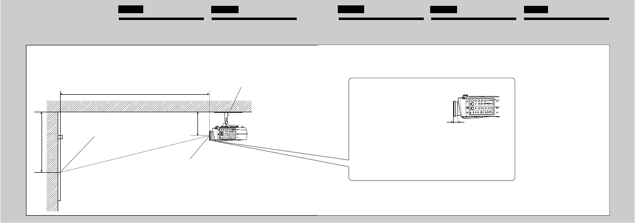
1-31
VPL-PX20/PX30
50
a
x
b
English
Ceiling Installation
(Front Projection)
Français
Installation au platfond
(projection frontale)
Ceiling
Plafond
Techo
Decke
Soffitto
Wall
Mur
Pared
Wand
Parete
B
Center of the screen
Centre de l’écran
Centro de la pantalla
Mitte des Projektionsschirms
Centro dello schermo
Center of the lens /
Centre de l’objectif / Centro del objetivo /
Mitte des Objektivs / Centro dell’obiettivo
PSS-610 Projector Suspension Support (not supplied)
Support de suspension pour projecteur PSS-610 (non fourni)
Soporte de suspensión para proyector PSS-610 (no suministrado)
Projektoraufhängung PSS-610 (nicht mitgeliefert)
Supporto di sospensione del proiettore PSS-610 (non in dotazione)
This section describes the examples for
installing the projector on the ceiling.
B
When installing the projector on the
ceiling, use the PSS-610 Projector
Suspension Support.
For ceiling installation, ask for qualified
Sony personnel only.
See the charts on pages 52 to 53
concerning the installation measurements.
The alphabetical letters in the
illustration indicate the distances below.
a : Distance between the screen and the
center of the lens
b : Distance between the ceiling and the
center of the lens
x : Distance between the ceiling and the
center of the screen
Cette section décrit des exemples
d’installation du projecteur au plafond.
B
Lorsque vous installez le projecteur au
plafond, utilisez le support de
suspension pour projecteur PSS-610.
Pour une installation au plafond,
adressez-vous uniquement à un
personnel qualifié Sony.
Reportez-vous aux tableaux des pages
52 à 53 sur les mesures d’installation.
Les caractères alphabétiques dans
l’illustration indiquent les distances ci-
dessous.
a : distance entre l’écran et le centre de
l’objectif
b : distance entre le plafond et le centre
de l’objectif
x : distance entre le plafond et le centre
de l’écran
51
Español
Instalación en el techo
(proyección frontal)
Deutsch
Installation an der
Decke (Frontprojektion)
Italiano
I
nstallazione sul soffitto
(proiezione frontale)
Distance between the front of the cabinet
and the center of the lens
Distance entre l’avant du châssis et le
centre de l’objectif
Distancia entre la parte frontal de la unidad
y el centro del objetivo
Abstand zwischen der Gehäusevorderseite
und der Objektivmitte
Distanza tra la parte anteriore
dell’apparecchio e il centro dell’obiettivo
Unit: mm (inches) / Unité: mm (pouces) /
Unidad: mm (pulgadas) / Einheit: mm (Zoll) /
Unità: mm (pollici)
En esta sección se muestran ejemplos
para instalar el proyector en el techo. B
Para instalar el proyector en el techo,
utilice el soporte de suspensión para
proyector PSS-610.
Para realizar la instalación en el techo,
solicite asistencia técnica únicamente a
personal especializado de Sony.
Consulte las tablas de las páginas 52 a
53 en relación con las medidas de
instalación.
Las letras alfabéticas de la ilustración
indican las distancias mostradas a
continuación.
a : distancia entre la pantalla y el centro
del objetivo
b : distancia entre el techo y el centro
del objetivo
x : distancia entre el techo y el centro de
la pantalla
In diesem Abschnitt finden Sie
Beispiele für das Installieren des
Projektors an der Decke. B
Zur Installation des Projektors an der
Decke benötigen Sie die
Projektoraufhängung PSS-610.
Wenn Sie das Gerät an der Decke
montieren wollen, wenden Sie sich bitte
an qualifiziertes Sony-Personal.
In den Tabellen auf Seite 52 bis 53
finden Sie die
Installationsabmessungen.
Die Buchstaben in der Abbildung
beziehen sich auf die unten
beschriebenen Abstände.
a : Abstand zwischen dem
Projektionsschirm und der Mitte des
Objektivs
b : Abstand zwischen der Decke und
der Mitte des Objektivs
x : Abstand zwischen der Decke und
der Mitte des Projektionsschirms
Questa sezione descrive gli esempi di
installazione al soffitto del proiettore.
B
Quando viene installato il proiettore sul
soffitto utilizzare il supporto di
sospensione del proiettore PSS-610.
Per l’installazione al soffitto, rivolgersi
esclusivamente a personale qualificato
Sony.
Vedere i diagrammi da pagina 52 a
pagina 53 relative alle misure di
installazione.
Le lettere nell'illustrazione indicano le
distanze descritte di seguito.
a : distanza tra lo schermo e il centro
dell’obiettivo
b : distanza tra il soffitto e il centro
dell’obiettivo
x : distanza tra il soffitto e il centro
dello schermo
VPLL-ZM101: 28.9 (1
1
/
8
)
VPLL-ZM31: 54.3 (2
1
/
8
)

1-32 VPL-PX20/PX30
52
English Français
Unit: mm (inches) / Unité: mm (pouces) / Unidad: mm (pulgadas) / Einheit: mm (Zoll) / Unità: mm (pollici)
SS 80 100 120 150 180 200 250 300
N5410 6810 8220 10330 12430 13840 17350 20870
a(213
1
/
8
) (268
1
/
4
) (323
3
/
4
) (406
3
/
4
) (489
1
/
2
) (545) (683
1
/
4
) (821
7
/
8
)
M7980 10030 12080 15150 18220 20270 25380 30500
(314
1
/
4
) (394
15
/
16
) (475
3
/
4
) (596
5
/
8
) (717
1
/
2
) (798
1
/
4
) (999
3
/
8
) (1201)
xb+610 b+762 b+914 b+1143 b+1372 b+1524 b+1905 b+2286
(24) (30) (36) (45) (54) (60) (75
1
/
8
) (90
1
/
8
)
bP
The installation measurements and their
calculation method for each lens are
shown above.
The alphabetical letters in the charts and
calculation methods indicate the
following.
SS : screen size measured diagonally
(inches)
a : Distance between the screen and
the center of the lens
b : Distance between the ceiling and
the center of the lens
x : Distance between the ceiling and
the center of the screen
N : minimum
M : maximum
P : 231, 256, 281, 331, 356, 381 mm
(9
1
/
8
, 10
1
/
8
, 11
1
/
8
, 13
1
/
8
, 14
1
/
8
, 15
inches) adjustable when using
PSS-610
Les mesures d’installation et leur
méthode de calcul pour chaque objectif
sont indiquées ci-dessus.
Les caractères alphabétiques dans
l’illustration indiquent ce qui suit.
SS : dimension de l’écran en diagonale
(pouces)
a : distance entre l’écran et le centre
de l’objectif
b : distance entre le plafond et le
centre de l’objectif
x : distance entre le plafond et le
centre de l’écran
N : minimum
M : maximum
P : Si vous utilisez le PSS-610, la
hauteur peut être réglée à 231,
256, 281, 331, 356, 381 mm (9
1
/
8
,
10
1
/
8
, 11
1
/
8
, 13
1
/
8
, 14
1
/
8
, 15
pouces).
■ VPLL-ZM101
a (N) = {(SS × 89.82/1.3102) – 209.2626} × 1.025
a (M) = {(SS × 137.56012/1.3102) – 211.5915} × 0.975
x = b + (SS/1.3102 × 9.984)
Ceiling Installation (Front
Projection) Installation au platfond
(projection frontale)
53
Español Deutsch Italiano
Unit: mm (inches) / Unité: mm (pouces) / Unidad: mm (pulgadas) / Einheit: mm (Zoll) / Unità: mm (pollici)
Las medidas de instalación y sus
métodos de cálculo para cada objetivo
se muestran anteriormente.
Las letras alfabéticas de las tablas y los
métodos de cálculo indican lo
siguiente.
SS : tamaño de pantalla medida
diagonalmente (pulgadas)
a : distancia entre la pantalla y el
centro del objetivo
b : distancia entre el techo y el centro
del objetivo
x : distancia entre el techo y el centro
de la pantalla
N : mínimo
M : máximo
P : Si utiliza la unidad PSS-610, la
altura podrá ajustarse en 231, 256,
281, 331, 356, 381 mm (9
1
/
8
,
10
1
/
8
, 11
1
/
8
, 13
1
/
8
, 14
1
/
8
, 15
pulgadas).
Die Installationsabmessungen und das
jeweilige Berechnungsverfahren für die
einzelnen Objektive sind oben
angegeben.
Die Buchstaben in den Tabellen und
den Berechnungsverfahren haben
folgende Bedeutung:
SS : Projektionsschirmgröße in Zoll,
diagonal gemessen
a : Abstand zwischen dem
Projektionsschirm und der Mitte
des Objektivs
b : Abstand zwischen der Decke und
der Mitte des Objektivs
x : Abstand zwischen der Decke und
der Mitte des Projektionsschirms
N : Mindestens
M : Höchstens
P : Wenn Sie die PSS-610 verwenden,
kann die Höhe auf die folgenden
Zahlenwerte eingestellt werden
231, 256, 281, 331, 356, 381 mm.
Le misure di installazione e il loro
metodo di calcolo per ogni obiettivo
sono mostrati qui sopra.
Le lettere nei diagrammi e i metodi di
calcolo indicano quanto segue.
SS : dimensione schermo misurata
diagonalmente (pollici)
a : distanza tra lo schermo e il centro
dell’obiettivo
b : distanza tra il soffitto e il centro
dell’obiettivo
x : distanza tra il soffitto e il centro
dello schermo
N : Minima
M : Massima
P : Quando si usa il PSS-610, l’altezza
può essere regolata su 231, 256,
281, 331, 356, 381 mm.
■ VPLL-ZM31
SS 80 100 120 150 180 200 250 300
N2490 3150 3800 4780 5760 6410 8050 9680
a(98
1
/
8
) (124
1
/
8
) (149
5
/
8
) (188
1
/
4
) (226
7
/
8
) (252
1
/
2
) (317) (381
1
/
4
)
M2620 3300 3980 5000 6030 6710 8410 10120
(103
1
/
4
) (130) (156
3
/
4
) (196
7
/
8
) (237
7
/
16
) (264
1
/
4
) (331
1
/
4
) (398
1
/
2
)
xb+610 b+762 b+914 b+1143 b+1372 b+1524 b+1905 b+2286
(24) (30) (36) (45) (54) (60) (75
1
/
8
) (90
1
/
8
)
bP
a (N) = {(SS × 41.75/1.3102) – 116.2604} × 1.025
a (M) = {(SS × 45.821033/1.3102) – 112.9154} × 0.975
x = b + (SS/1.3102 × 9.984)
Instalación en el techo
(proyección frontal) Installation an der Decke
(Frontprojektion) Installazione sul soffitto
(proiezione frontale)
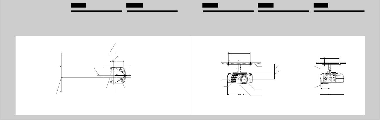
1-33
VPL-PX20/PX30
54
English Français
C
a
133.4 (5 3/8)
169.5 (6 3/4)
58 (2 3/8)
67.8 (2 3/4)
61.3 (2 1/2)
216.6 (8 5/8)
159.7 (6 3/8)
6
5
4
3
1
2
•
When using the standard lens equipped with the VPL-PX20/PX30 / Si vous utilisez l’objectif standard qui équipe le VPL-PX20/
PX30 / Installation mit dem Standardobjektiv des VPL-PX20/PX30 / Al emplear el objetivo estándar equipado con el VPL-PX20/
PX30 / Quando si utilizza l’obiettivo standard in dotazione con il VPL-PX20/PX30
Attaching the projector
suspension support PSS-610 Fixation du support de
suspension de projecteur
PSS-610
For more details on the ceiling installation,
refer to the Installation manual for Dealers of
the PSS-610. The installation measurements
are shown above when you install the
projector on the ceiling.
Top view C
Align the center of the lens with the center of
the screen.
Front view D
The lens is offset 67.8 mm (2
3
/
4
inches) to the
right from the center of the supporting pole.
When mounting, take care to align the center
of the lens with the center of the screen; not
the center of the supporting pole.
Side view E
a) Distance between the screen and the center
of the lens
1Center of the screen
2Center of the unit
3Front of the cabinet
4Upper ceiling mount bracket
5Center of the supporting pole (The center
of the supporting pole is different from that
of the unit.)
6Center of the lens
7Ceiling
8The bottom surface of the mounting
bracket
9Distance between the ceiling and the
surface of the mounting bracket
Using adjustment pipe (b):
150/175/200 mm (6/7/7
7
/
8
inches)
Using adjustment pipe (c):
250/275/300 mm (9
7
/
8
/10
7
/
8
/11
7
/
8
inches)
0Front of the lens
Pour plus de détails sur l'installation au
plafond, reportez-vous au manuel
d'installation pour les revendeurs du PSS-610.
Les dimensions d'installation pour le montage
au plafond sont indiquées ci-dessus.
Vue du dessus C
Alignez le centre de l’objectif sur le centre de
l’écran.
Vue frontal D
L’objectif est décalé de 67,8 mm (2
3
/
4
pouces)
vers la droite du centre du pivot de support.
Au moment du montage, veillez à aligner
correctement le centre de l’objectif sur le
centre de l’écran; pas le centre du pivot de
support.
Vue latérale E
a) Distance entre l’écran et le centre de
l’objectif
1Centre de l’écran
2Centre de l’appareil
3Avant du meuble
4Support de montage de plafond supérieur
5Centre du pivot de support (Le centre du
pivot de support est différent de celui de
l’appareil.)
6Centre de I’objectif
7Plafond
8Le dessous du support de montage
9Distance entre le plafond et la surface du
supprt de montage
Utilisation du tube de réglage (b):
150/175/200 mm (6/7/7
7
/
8
pouces)
Utilisation du tube de réglage (c):
250/275/300 mm (9
7
/
8
/10
7
/
8
/11
7
/
8
pouces)
0Avant de I’objectif
55
Español Deutsch Italiano
Unit: mm (inches) / Unité: mm (pouces) / Unidad: mm (pulgadas) / Einheit: mm (Zoll) / Unità: mm (pollici)
250 (9
7
/
8
)
125 (5)
169.5 (6
3
/
4
)
81 (3
3
/
16
)
58
(2
3
/
8
)
6
2
5
79
8
61.3
(2
1
/
2
)216.6 (8
5
/
8
)
125.4 (5)
133.4 (5
3
/
8
) 202 (8)
3
0
Instalación del soporte de
suspensión del proyector
PSS-610
Anbringen der
Projektoraufhängung PSS-610 Applicazione del supporto di
sospensione del proiettore
PSS-610
DE
Para más información sobre la instalación en
el techo, consulte el manual de instalación
para proveedores de la unidad PSS-610. Las
medidas de instalación se muestran
anteriormente para cuando instale el proyector
en el techo.
Vista superior C
Alinee el centro del objetivo con el centro de
la pantalla.
Vista frontal D
El objetivo está desplazado 67,8 mm (2
3
/
4
pulgadas) a la derecha del centro de la
columna de soporte. Al realizar el montaje,
alinee el centro del objetivo con el centro de la
pantalla y no con el centro de la columna de
soporte.
Vista lateral E
a) Distancia entre la pantalla y el centro del
objetivo
1Centro de la pantalla
2Centro de la unidad
3Parte frontal de la caja
4Soporte de montaje superior para techo
5Centro de la columna de soporte (El centro
de la columna de soporte no es el mismo
que el de la unidad.)
6Centro del objetivo
7Techo
8La base del la superficie del soporte de
montaje
9Distancia entre el techo y la base del
proyector
Uso del tubo de ajuste (b):
150/175/200 mm (6/7/7
7
/
8
pulgadas)
Uso del tubo de ajuste (c):
250/275/300 mm (9
7
/
8
/10
7
/
8
/11
7
/
8
pulgadas)
0Parte frontal del objetivo
Näheres zur Deckenmontage finden Sie in der
Installationsanleitung zur PSS-610 für
Händler. Die Installationsabmessungen für das
Montieren des Projektors an der Decke sind
oben angegeben.
Draufsicht C
Richten Sie die Mitte des Objektivs an der
Mitte des Projektionsschirms aus.
Vorderansicht D
Das Objektiv am Projektor ist 67,8 mm nach
rechts von der Mitte des Ständers versetzt.
Achten Sie beim Installieren darauf, die Mitte
des Objektivs, nicht die Mitte des Ständers, an
der Mitte des Projektionsschirms auszurichten.
Seitenansicht E
a) Abstand zwischen dem Projektionsschirm
und der Mitte des Objektivs
1Mitte des Projektionsschirms
2Mitte des Geräts
3Vorderseite des Gehäuses
4Deckenmontagehalterung
5Mitte des Ständers (Die Mitte des Ständers
entspricht nicht der des Geräts.)
6Mitte des Objektivs
7Decke
8Die Unterseite der Halterung
9Abstand zwischen der Decke und der
Oberlfäche der Hlaterung
Mit Einstellrohr (b): 150/175/200 mm
Mit Einstellrohr (c): 250/275/300 mm
0Vorderseite des Objektivs
Per ulteriori informazioni sull'installazione al
soffitto, fare riferimento al manuale di
installazione per rivenditori relativo al
supporto di sospensione PSS-610. Le misure
di installazione per l'installazione al soffitto
sono indicate di seguito.
Vista dall’alto C
Allineare il centro della lente con il centro
dello schermo.
Vista frontale D
Rispetto al centro per l’asta di supporto, la
lente del proiettore è spostata verso destra di
67,8 mm. Durante il montaggio, assicurarsi di
allineare il centro della lente del proiettore e
non il centro per l’asta di supporto con il
centro dello schermo.
Vista laterale E
a) Distanza fra lo schermo e il centro
dell’obiettivo
1Centro dello schermo
2Centro dell’apparecchio
3Parte anteriore dell’apparecchio
4Staffa di montaggio al soffitto
5Centro per l’asta di supporto (Il centro per
l’asta di supporto è diverso da quello
dell’apparecchio.)
6Centro della lente
7Soffitto
8La superficie inferiore della staffa di
montaggio
9Distanza fra il soffitto e la superficie della
staffa di montaggio
Utilizzando il tubo di regolazione (b):
150/175/200 mm
Utilizzando il tubo di regolazione (c):
250/275/300 mm
0Parte anteriore della lente
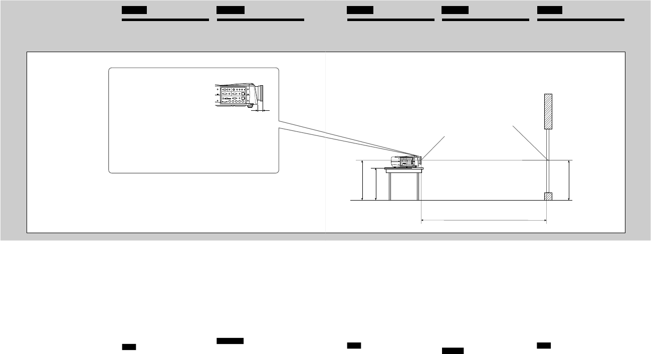
1-34 VPL-PX20/PX30
56
English Français
F
Distance between the front of the cabinet
and the center of the lens
Distance entre l’avant du châssis et le
centre de l’objectif
Distancia entre la parte frontal de la unidad
y el centro del objetivo
Abstand zwischen der Gehäusevorderseite
und der Objektivmitte
Distanza tra la parte anteriore
dell’apparecchio e il centro dell’obiettivo
Floor Installation (Rear
Projection: Optical Axis
Angle 0 Degree)
I
nstallation au sol
(Rétroprojection: angle
d’axe optique de 0 degré)
This section describes the examples for
installing the projector behind the screen, etc.
F
See the charts on pages 58 and 59 concerning
the installation measurements.
The alphabetical letters in the illustration
indicate the distances below.
a : distance between the screen and the center
of the lens
b : distance between the floor and the center
of the lens
c : distance between the floor and the bottom
of the adjusters of the projector
x : free
Note
If the projector has been set at the factory and
if you project a picture from the rear, the
picture will be upside down. If you use a
mirror, the picture may be reversed. In these
cases, change the INSTALLATION in the
INSTALL SETTING menu.
For details, refer to the “INSTALL SETTING”
menu in the Operating Instructions for your LCD
data projector.
Cette section décrit les exemples d'installation
du projecteur derrière l'écran, etc. F
Reportez-vous aux tableaux des pages 58 à 59
sur les mesures d’installation.
Les caractères alphabétiques dans l'illustration
indiquent les distances ci-dessous.
a : distance entre l’écran et le centre de
l’objectif
b : distance entre le sol et le centre de
l’objectif
c : distance entre le sol et la base des pieds
réglables du projecteur
x : libre
Remarque
Si le projecteur est réglé par défaut et si vous
rétroprojetez une image, l’image sera
retournée. Vous pouvez redresser l’image en
utilisant un miroir. Dans ces cas, changez
INSTALLATION dans le menu REGL.
INSTAL.
Pour plus de détails, voir le menu “REGL.
INSTAL.” dans le mode d’emploi de votre
projecteur de données LCD.
Standard: 10 (
13
/
32
)
VPLL-ZM101: 28.9 (1
1
/
8
)
VPLL-ZM31: 54.3 (2
1
/
8
)
VPLL-FM21: 35.7 (1
13
/
32
)
57
Español Deutsch Italiano
Unit: mm (inches) / Unité: mm (pouces) /
Unidad: mm (pulgadas) / Einheit: mm (Zoll) /
Unità: mm (pollici)
a
x
bc
Wall
Mur
Pared
Wand
Parete
Center of the screen
Centre de l’écran
Centro de la pantalla
Mitte des Projektionsschirms
Centro dello schermo
Center of the lens / Centre de l’objectif /
Centro del objetivo / Mitte des Objektivs /
Centro dell’obiettivo
Instalación en el suelo
(proyección posterior: ángulo
de eje óptico de 0 grados)
Installation am Boden
(Rückprojektion: Winkel der
optischen Achse = 0 Grad)
Installazione sul pavimento
(proiezione posteriore: grado zero
dell’angolo di asse ottico)
Questa sezione descrive gli esempi di
installazione del proiettore dietro allo
schermo, ecc. F
Vedere i diagrammi da pagina 58 a pagina 59
relativi alle misure di installazione.
Le lettere nell'illustrazione indicano le
distanze descritte di seguito.
a : distanza fra lo schermo e il centro
dell’obiettivo
b : distanza tra il pavimento e il centro
dell’obiettivo
c : distanza fra il pavimento e la base dei
dispositivi di regolazione del proiettore
x : libero
Nota
Se il proiettore è stato impostato in fabbrica e si
proietta un’immagine dalla parte posteriore,
l’immagine risulterà capovolta. Se si utilizza uno
specchio, l’immagine potrebbe risultare invertita. In
questi casi, modificare INSTALLAZIONE nel
menu IMPOST.INST.
Per informazioni dettagliate, fare riferimento a al
menu “IMPOST.INST” nelle istruzioni per l’uso de
vostro proiettore di dati con schermo a cristalli liquidi.
En esta sección se muestran ejemplos para
instalar el proyector detrás de la pantalla, etc.
F
Consulte las tablas de las páginas 58 a 59 en
relación con las medidas de instalación.
Las letras alfabéticas de la ilustración indican
las distancias mostradas a continuación.
a : distancia entre la pantalla y el centro del
objetivo
b : distancia entre el suelo y el centro del
objetivo
c : distancia entre el suelo y la base de los
ajustadores del proyector
x : libre
Nota
Si el proyector se ha ajustado en fábrica y
proyecta una imagen desde la parte posterior,
la imagen aparecerá invertida. Si utiliza un
espejo, es posible que aparezca al revés. En
estos casos, cambie la opción INSTALACION
del menú AJUSTE INST.
Para obtener información más detallada,
consulte el menú “AJUSTE INST” en las
instrucciones de uso de vuestro proyector LCD
de datos.
In diesem Abschnitt finden Sie Beispiele für
das Installieren des Porjektors hinter dem
Projektionsschirm usw. F
In den Tabellen auf Seite 58 bis 59 finden Sie
die Installationsabmessungen.
Die Buchstaben in der Abbildung beziehen
sich auf die unten beschriebenen Abstände.
a : Abstand zwischen dem Projektionsschirm
und der Mitte des Objektivs
b : Abstand zwischen dem Boden und der
Mitte des Objektivs
c : Abstand zwischen dem Boden und der
Unterseite der Ausgleichsfüße des
Projektors
x : frei
Hinweis
Wenn der Projektor werkseitig eingestellt wurde
und Sie ein Bild mit dem Rückprojektionsverfahren
projizieren, erscheint das Bild auf dem Kopf. Wenn
Sie einen Spiegel verwenden, erscheint das Bild
möglicherweise seitenverkehrt. Ändern Sie in
diesem Fall die Einstellung für INSTALLATION
im Menü ANFANGSWERTE.
Näheres können Sie im Abschnitt zum Menü
“ANFANGSWERTE” in der Bedienungsanleitung
Ihres LCD-Datenprojektors nachlesen.
1-35
VPL-PX20/PX30
58
English Français
Unit: mm (inches) / Unité: mm (pouces) / Unidad: mm (pulgadas) / Einheit: mm (Zoll) / Unità: mm (pollici)
■
Standard lens / Objectif standard / Objetivo estándar / Standardobjektiv / Uso Obiettivo standard
Floor Installation (Rear
Projection: Optical Axis Angle
0 Degree)
Installation au sol
(Rétroprojection: angle d’axe
optique de 0 degré)
SS 40 60 80 100 120 150 180 200 250 300
N1490 2280 3060 3850 4630 5810 6990 7770 9740 11700
a(58
3
/
4
) (89
7
/
8
) (120
1
/
2
) (151
5
/
8
) (182
3
/
8
) (228
7
/
8
) (275
1
/
4
) (306) (383
5
/
8
) (460
3
/
4
)
M1820 2780 3740 4700 5660 7100 8540 9500 11900 14300
(71
3
/
4
) (109
1
/
2
) (147
3
/
8
) (185
1
/
8
) (222
7
/
8
) (279
5
/
8
) (336
3
/
8
) (374
1
/
8
) (468
5
/
8
) (563
1
/
8
)
bx
(x)
cx–79
(x–3
1
/
8
)
a (N) = {(SS × 50.18/1.3102) – 75.10104} × 1.025
a (M) = {(SS × 64.518746/1.3102) – 107.8977} × 0.975
b = x
c = x – 79
■ VPLL-ZM101
SS 40 60 80 100 120 150 180 200 250 300
N2600 4000 5410 6810 8220 10330 12430 13840 17350 20870
a(102
3
/
8
) (157
1
/
2
) (213
1
/
8
) (268
1
/
4
) (323
3
/
4
) (408
3
/
4
) (489
1
/
2
) (545) (683
1
/
4
) (821
7
/
8
)
M3890 5940 7980 10030 12080 15150 18220 20270 25380 30500
(153
1
/
4
) (234) (314
1
/
4
) (394
15
/
16
) (475
3
/
4
) (596
5
/
8
) (717
1
/
2
) (798
1
/
4
) (999
3
/
8
) (1201)
bx
(x)
cx–79
(x–3
1
/
8
)
a (N) = {(SS × 89.82/1.3102) – 209.2626} × 1.025
a (M) = {(SS × 137.56012/1.3102) – 211.5915} × 0.975
b = x
c = x – 79
Unit: mm (inches) / Unité: mm (pouces) / Unidad: mm (pulgadas) / Einheit: mm (Zoll) / Unità: mm (pollici)
The installation measurements and their
calculation method for each lens are shown
above.
The alphabetical letters in the charts and
calculation methods indicate the following.
SS : screen size measured diagonally
(inches)
a : distance between the screen and the
center of the lens
b : distance between the floor and the
center of the lens
c : distance between the floor and the
bottom of the adjusters of the projector
x : free
N : minimum
M : maximum
Les mesures d’installation et leur méthode
de calcul pour chaque objectif sont indiquées
ci-dessus.
Les caractères alphabétiques dans
l’illustration indiquent ce qui suit.
SS : dimension de l’écran en diagonale
(pouces)
a : distance entre l’écran et le centre de
l’objectif
b : distance entre le sol et le centre de
l’objectif
c : distance entre le sol et la base des pieds
réglables du projecteur
x : libre
N : minimum
M : maximum
59
Español Deutsch Italiano
Instalación en el suelo
(proyección posterior: ángulo
de eje óptico de 0 grados)
Installation am Boden
(Rückprojektion: Winkel der
optischen Achse = 0 Grad)
Installazione sul pavimento
(proiezione posteriore: grado
zero dell’angolo di asse ottico)
Unit: mm (inches) / Unité: mm (pouces) / Unidad: mm (pulgadas) / Einheit: mm (Zoll) / Unità: mm (pollici)
a = {(SS × 24.71/1.3102) – 81.86279} × 1.0
b = x
c = x – 79
SS 40 60 80 100 120 150 180 200 250 300
a670 1050 1430 1800 2180 2750 3310 3690 4630 5580
(26
1
/
2
) (41
3
/
8
) (56
3
/
8
) (70
7
/
8
) (85
7
/
8
) (108
3
/
8
) (130
3
/
8
) (145
3
/
8
) (182
3
/
8
) (219
3
/
4
)
bx
(x)
cx–79
(x–3
1
/
8
)
■ VPLL-FM21
■ VPLL-ZM31
Unit: mm (inches) / Unité: mm (pouces) / Unidad: mm (pulgadas) / Einheit: mm (Zoll) / Unità: mm (pollici)
a (N) = {(SS × 41.75/1.3102) – 116.2604} × 1.025
a (M) = {(SS × 45.821033/1.3102) – 112.9154} × 0.975
b = x
c = x – 79
SS 40 60 80 100 120 150 180 200 250 300
N1190 1840 2490 3150 3800 4780 5760 6410 8050 9680
a(46
7
/
8
) (72
1
/
2
) (98
1
/
8
) (124
1
/
8
) (149
5
/
8
) (188
1
/
4
) (226
7
/
8
) (252
1
/
2
) (317) (381
1
/
4
)
M1250 1940 2620 3300 3980 5000 6030 6710 8410 10120
(49
1
/
4
) (76
1
/
2
) (103
1
/
4
) (130) (156
3
/
4
) (196
7
/
8
) (237
7
/
16
) (264
1
/
4
) (331
1
/
4
) (398
1
/
2
)
bx
(x)
cx–79
(x–3
1
/
8
)
Las medidas de instalación y sus métodos de
cálculo para cada objetivo se muestran
anteriormente.
Las letras alfabéticas de las tablas y los
métodos de cálculo indican lo siguiente.
SS : tamaño de pantalla medida
diagonalmente (pulgadas)
a : distancia entre la pantalla y el centro
del objetivo
b : distancia entre el suelo y el centro del
objetivo
c : distancia entre el suelo y la base de los
ajustadores del proyector
x : libre
N : mínimo
M : máximo
Die Installationsabmessungen und das
jeweilige Berechnungsverfahren für die
einzelnen Objektive sind oben angegeben.
Die Buchstaben in den Tabellen und den
Berechnungsverfahren haben folgende
Bedeutung:
SS : Projektionsschirmgröße in Zoll,
diagonal gemessen
a : Abstand zwischen dem
Projektionsschirm und der Mitte des
Objektivs
b : Abstand zwischen dem Boden und der
Mitte des Objektivs
c : Abstand zwischen dem Boden und der
Unterseite der Ausgleichsfüße des
Projektors
x : frei
N : Mindestens
M : Höchstenss
Le misure di installazione e il loro metodo
di calcolo per ogni obiettivo sono mostrati
qui sopra.
Le lettere nei diagrammi e i metodi di
calcolo indicano quanto segue.
SS : dimensione schermo misurata
diagonalmente (pollici)
a : distanza fra lo schermo e il centro
dell’obiettivo
b : distanza tra il pavimento e il centro
dell’obiettivo
c : distanza fra il pavimento e la base dei
dispositivi di regolazione del
proiettore
x : libero
N : Minima
M : Massima
1-36 VPL-PX20/PX30
When using other type of mouse / Si vous utilisez un autre type de souris / Si utiliza otro tipo
de ratón / Wenn Sie einen anderen Maustyp verwenden /
Quando si utilizzano altri tipi di mouse
4-073-992-01 (1)
Connections / Connexions / Conexiones / Anschlüsse /
Collegamenti
A
HD D-sub 15-pin cable / Câble HD D-sub à 15 broches / Cable HD D-sub 15 pines / 15poliges D-
Sub-HD-Kabel / Cavo HD D-sub a 15 piedini
B
Signal adapter / Adaptateur de signal / Adaptador de señales / Signaladapter / Adattatore del
segnale
C
Stereo audio connecting cable / Câble de connexion audio stéréo / Cable de conexión de audio
estéreo / Stereo-Audioverbindungskabel / Cavo audio stereo
D
USB cable / Câble USB / Cable USB / USB-Kabel / Cavo USB
E
S-video cable / Câble S-vidéo / Cable de vídeo S / S-Videokabel /
Cavo S-Video
F
Audio/video cable / Câble audio/vidéo / Cable de audio/vídeo / Audio-/Videokabel / Cavo audio/
video
Quick Reference Card
/
Carte de référence rapide
/
Tarjeta de
referencia rápida
/
Kurzreferenz / Scheda di riferimento rapido
VPL-PX20/VPL-PX30
AUDIO OUT
MONITOR OUT
MOUSE/SERIAL
Sony Corporation © 1999 Printed in Japan
Connecting with a computer / Raccordement à un ordinateur / Conexión
con ordenador / Anschließen an einen Computer / Collegamento a un
computer
SIC-S20
1)
/S21/S22/S23
1)
C
1)
B
1), 2)
A
Using a USB equipment (e.g., USB mouse) / Utilisation d’un appareil USB (p.ex., souris
USB) / Empleo de un equipo USB (p. ej., un ratón USB) / Verwenden eines USB-Geräts (z.
B. einer USB-Maus) / Uso di un dispositivo USB (ad esempio un mouse USB)
RS-232C
IN
PLUG IN POWER
OUTPUT
INPUT A
INPUT B
VIDEO IN
CONTROL S
REMOTE
DIGITAL RGB
USB
R/R-Y/P
R
B/B-Y/P
B
SYNC/HD VDG/Y
MOUSEAUDIORGB
MOUSEAUDIOAUDIO RGB
MONITOR
S VIDEO VIDEO AUDIO
LR
(MONO)
DIGITAL
RGB RGB
5BNC
DIGITAL
RGB RGB
5BNC
AUDIO OUT
DOWNSTREAM
MONITOR OUT
A
C
1)
D
B
1), 2)
Other USB equipment /
Autre appareil USB / Otro equipo USB /
Anderes USB-Gerät / Altro apparecchio USB
RS-232C
IN
PLUG IN POWER
OUTPUT
INPUT A
INPUT B
VIDEO IN
CONTROL S
REMOTE
DIGITAL RGB
USB
R/R-Y/PRB/B-Y/PBSYNC/HD VDG/Y
MOUSEAUDIORGB
MOUSEAUDIOAUDIO RGB
MONITOR
S VIDEO VIDEO AUDIO
LR
(MONO)
DIGITAL
RGB RGB
5BNC
DIGITAL
RGB RGB
5BNC
Connecting with a VCR / Raccordement à un magnétoscope / Conexión
con una vídeograbadora / Anschließen an einen Videorecorder /
Collegamento a un videoregistratore
RS-232C
IN
PLUG IN POWER
OUTPUT
INPUT A
INPUT B
VIDEO IN
CONTROL S
REMOTE
DIGITAL RGB
USB
R/R-Y/P
R
B/B-Y/P
B
SYNC/HD VDG/Y
MOUSEAUDIORGB
MOUSEAUDIOAUDIO RGB
MONITOR
S VIDEO VIDEO AUDIO
LR
(MONO)
DIGITAL
RGB RGB
5BNC
AUDIO/VIDEO OUT S VIDEO OUT
E
1)
F
1)
not supplied / non fourni / no suministrado / nicht mitgeliefert / non in dotazione
2)
Only connecting to the Macintosh /
Raccordement au Macintosh uniquement
/ Conexión
únicamente al sistema Macintosh / Nur zum Anschließen an den Macintosh / Collegamento solo al
Macintosh
Projection Distances / Distances de projection / Distancias de
proyección / Projektionsentfernungen / Distanze di proiezione
Distance (m (feet)) / Distance (m (pieds)) / Distancia (m
(pies)) / Abstand (m) /Distanza (m)
1490–1820 (58
3
/
4
–71
3
/
4
)
2280–2780 (89
7
/
8
–109
1
/
2
)
3060–3740 (120
1
/
2
–147
3
/
8
)
3850–4700 (151
5
/
8
–185
1
/
8
)
4630–5660 (182
3
/
8
–222
7
/
8
)
5810–7100 (228
7
/
8
–279
5
/
8
)
6990–8540 (275
1
/
4
–336
3
/
8
)
7770–9500 (306
–374
1
/
8
)
9740–11900 (383
5
/
8
–468
5
/
8
)
11700–14300 (460
3
/
4
–563
1
/
8
)
Screen size(inchies) / Taille de l’écran (pouces) / Tamaño de la
pantalla (pulgadas) / Projektionsschirmgröße (Zoll) /
Dimensione
schermo (pollici)
40
60
80
100
120
150
180
200
250
300
System Requirement / Configuration requise
/
Requisito de sistema
/
Systemvoraussetzung
/
Requisiti di sistema
1-37
VPL-PX20/PX30
English
1
After all equipment is connected completely, plug the
AC power cord into the wall outlet.
2
Press the ? / 1 key to turn on the projector.
3
Turn on equipment connected to the projector. Press
the INPUT key to select “INPUT-A”, “INPUT-B”,
“S-VIDEO” or “VIDEO”.
4
Turn the zoom ring to adjust the size of the picture,
and turn the focus ring to adjust the focus.
To adjust the picture of computer automatically
Press the APA (Auto Pixel Alignment) key.
To
correct the trapezoid
Correct the trapezoid of the picture by changing the
DIGIT KEYSTONE value in the INSTALL SETTING
menu.
To enlarge the image
Press the D ZOOM + key. Using an arrow key (M/m/
</,), move the icon to the point you want to
enlarge. Press the D ZOOM + key again.
Français
1
Après que tous les appareils ont été complètement
raccordés, branchez le câble d’alimentation sur une
prise murale.
2
Appuyez sur la touche ? / 1 pour mettre le projecteur
sous tension.
3
Mettez sous tension l’appareil raccordé au projecteur.
Appuyez sur la touche INPUT pour sélectionner
“ENT.A”, “ENT.B”, “S-VIDEO” ou “VIDEO”.
4
Tournez la bague de zoom pour ajuster la taille de
l’image et tournez la bague de mise au point pour
ajuster la mise au point.
Pour régler automatiquement l’image de
l’ordinateur
Appuyez sur la touche APA (alignement automatique
des pixels).
Pour corriger la distorsion trapézoïdale
Corrigez la distorsion trapézoïdale en changeant la
valeur TRAPEZE NUMER dans le menu REGL.
INSTAL.
Pour agrandir l’image
Appuyez sur la touche D ZOOM +. A l’aide d'une
touche fléchée (M/m/</,), déplacez l’icône à
l’endroit que vous voulez agrandir. Appuyez de
nouveau sur la touche D ZOOM +.
Basic Operation / Opération de base / Operación básica /
Grundfunktion / Operazione di base
Español
1
Una vez conectados todos los equipos por
completo, enchufe el cable de alimentación de CA
en la toma mural.
2
Pulse la tecla ? / 1 para encender el proyector.
3
Encienda el equipo conectado al proyector. Pulse la
tecla INPUT para seleccionar “ENTRAD A”,
“ENTRAD B”, “S-VIDEO” o “VIDEO”.
4
Gire el anillo de zoom para ajustar el tamaño de la
imagen, y gire el anillo de enfoque para ajustar el
enfoque.
Para ajustar la imagen del ordenador
automáticamente
Pulse la tecla APA (Alineación automática de píxeles).
Para corregir la distorsión trapezoidal
Corrija la distorsión trapezoidal de la imagen cambiando
el valor de DIST TRAP DIG del menú AJUSTE INST.
Para ampliar la imagen
Pulse la tecla D ZOOM +. Mediante una tecla de flecha
(
M/m/</,
), desplace el icono hasta el punto que
desee aumentar. Vuelva a pulsar la tecla D ZOOM +.
Deutsch
1
Wenn alle Geräte vollständig angeschlossen sind,
stecken Sie den Stecker des Netzkabels in die
Netzsteckdose.
2
Schalten Sie den Projektor mit der Taste ? / 1 ein.
3
Schalten Sie die an den Projektor angeschlossenen
Geräte ein. Wählen Sie mit der Taste INPUT
“EING.A”, “EING.B”, “S-VIDEO” oder “VIDEO”
aus.
4
Stellen Sie durch Drehen des Zoom-Rings die Größe
des Bildes und durch Drehen des Fokussierrings den
Fokus ein.
So lassen Sie das Bild des Computers
automatisch einstellen
Drücken Sie die Taste APA (automatische
Pixelausrichtung).
So korrigieren Sie die Trapezverzerrung
Korrigieren Sie die Trapezverzerrung des Bildes,
indem Sie den Wert für TRAPEZ DIGITAL im Menü
ANFANGSWERTE ändern.
So vergrößern Sie das Bild
Drücken Sie die Taste D ZOOM +. Stellen Sie das
Symbol mit einer der Pfeiltasten (M/m/</,) auf die
zu vergrößernde Stelle. Drücken Sie die Taste D
ZOOM + erneut.
Italiano
1
Dopo avere collegato saldamente tutti gli apparecchi,
inserire l’alimentatore CA nella presa di rete.
2
Per accendere il proiettore, premere il tasto ? / 1.
3
Accendere l’apparecchiatura collegata al proiettore.
Premere il tasto INPUT per selezionare “INGRE A”,
“INGRE B”, “S-VIDEO” o “VIDEO”.
4
Per regolare le dimensioni dell’immagine, ruotare il
regolatore dello zoom, per regolare la messa a fuoco,
ruotare il regolatore della focalizzazione.
Per regolare automaticamente l’immagine del
computer
Premere il tasto APA (Allineamento automatico dei
pixel).
Per correggere la distorsione dell’immagine
Correggere l’immagine distorta modificando il valore
di KEYST. DIGIT. nel menu IMPOST. INST.
Per ingrandire l’immagine
Premere il tasto D ZOOM +. Utilizzando uno dei tasti
direzionali, (M/m/</,), spostare l’icona sul punto
che si desidera ingrandire, quindi premere di nuovo il
tasto D ZOOM +.
APA
APA
D ZOOM
INPUT
HELP
MENU
ENTER
RESET
APA
LIGHT
VOL +
VOL -
LAMP/
COVER TEMP/
FAN POWER
SAVING ON/
STANDBY
COMMAND
MUTING
VOLUME
HELP
/
INPUTAPA
FUNCTION
MENU LASER
ENTER
RESET D ZOOM
+
–
+
–
R CLICK
PIC
AUDIO
ONOFF
12
2
3
1
4
2
3
2-1
VPL-PX20/PX30
Section 2
Service Informations
2-1. Circuit Boards Location
2-2. Servicing Tools
2-2-1. XA, XAA Extension Boards (70P)
•For Y board and QA board
(QA board use 2 pieces of XA and XAA board.)
2-2-2. XB, XBB Extension Boards (50P)
•For BA board.
XBB (A-1391-006-A)
XB (A-1391-007-A)
XA (A-1391-005-A)
XAA (A-1391-004-A)
QD
Y
BA
QA
C
BC
H
NR
K
F
GC
GB
GD
GA
S
KS
QC
QB
BB
NF
POWER BLOCK
2-2 VPL-PX20/PX30
2-3. Cabinet Assy Removal
2 Lens cover(TP)
3 Two screws(+B3 x 8)
4 Two screws(+B3 x 8)
5 Two screws(+B3 x 8)
6 Cabinet assy
1 Push in claw
Driver_
CN3500
CN3501
2-4. Front Block Assy Removal
1 Two screws
(+PWH3 x 6)
Connector(black) 3P
Connector(white) 3P
2 Front block assy
2-3
VPL-PX20/PX30
2-5. NF Board Removal
• Remove the Front Block Assy (Refer to 2-4.)..
5 Screw
(+PWH3 x 6)
1 Screw
(+BVTP3 x 12)
3 Four screws
(+BVTP3 x 12)
2 Holder(FBHR)
4 Ajuster assy
6 NF board
CN3600
2-6. BA and Y Boards Removal
1 Screw
(+PWH3 x 6)
2 PWB holder
4 BA board
3 Y board
2-4 VPL-PX20/PX30
2-7. Power Block Removal
3 Two screws
(+PWH3 x 6)
5 Four screws
(+PWH3 x 6)
CP501
1 Two screws
(+PWH3 x 6)
2 Connector(2P)
4 Holder(L)
6 Power block
A
A
7 screw
(+PWH3 x 6)
2-8. G Block Assy (GA, GB, GC and GD Board) Removal
3 Screw
(+PWH3 x 6)
1 Three screws
(+PWH3 x 6)
5 Three claws
8 GC board
2 G block assy
7 GB board
9 GD board
6 GA board
Earth plate(G)
Connector(3P)
CN2701
CN2502
CN2103
CN2104
CN2105
CN2301
4 Screw
(+PWH3 x 6)
CN2110
CN2111
2-5
VPL-PX20/PX30
2-9. C Board Removal
2 Screw
(Terminal M3 x 8)
3 Spacer(C)
Connector(CN605)
1 Two screws
(+PWH3 x 6)
4 C board
CN600
CN601
CN602
CN603
2-10. Optics Unit Assy Removal
• Remove the C Board (Refer to 2-9.).
2 Two screws
(+PWH3 x 6)
3 Connector(2P)
1 Five screws
(+PSW4 x 12)
4 Optics unit assy
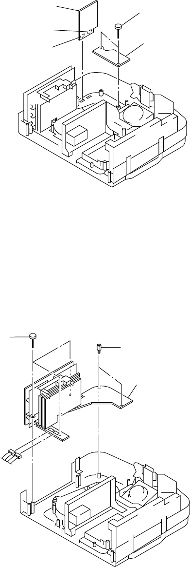
2-6 VPL-PX20/PX30
2-11. BC and KS Boards Removal
• Remove the Optics Unit (Refer to 2-10.).
2 Two screws
(+PWH3 x 6)
1 BC board
3 KS board
Connector(CN500)
Connector(CN502)
• Remove the KS Board (Refer to 2-11.).
2-12. Connector Block Assy Removal
1 Three screws
(+PWH3 x 6) 2 Two spacers
3 Connector block assy
CN308
CN310
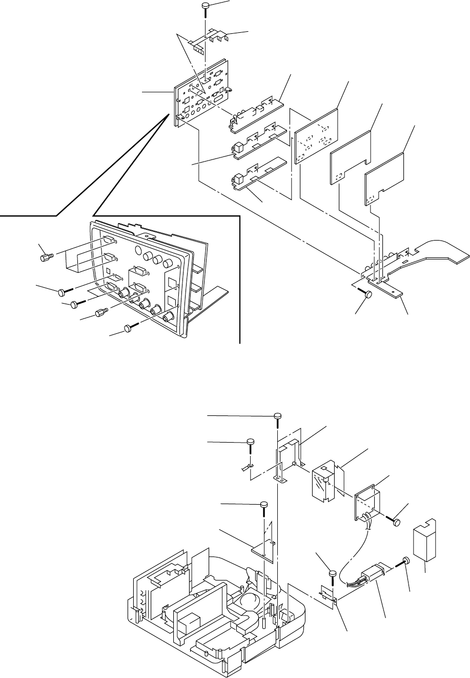
2-7
VPL-PX20/PX30
2-13. BB, QA, QB, QC and QD Boards Removal
1 Screw
(+PWH3 x 6)
8 Screw
(+PWH3 x 6)
3 Four screws
5 Two screws
(+BM2 x 6)
6 Two screws
(+PM2 x 6)
4 Four screws
7 Three screws
(+PWH3 x 8)
2 PWB holder
!; QD board ![ QA board
!= BA board
!- Y board
!/ BB board
!] QB board
!\ QC board
9 Connector panel
• Remove the G Block Assy (Refer to 2-8.).
• Remove the Optics Unit (Refer to 2-8.).
2-14. F, K Board and AC Inlet Removal
2 Screw
(+PSW4 x 12)
GND
1 Two screws
(+PWH3 x 6) 3 Holder(F)
4 Shield cover(F)
6 F board
Insulator sheet(F)
9 Two screws
(+PWH3 x 6)
!- Two screws
(+K3 x 5)
!= AC inlet(3P)
!/ Holder(AC)
5 Four screws
(+PWH3 x 6)
7 Two screws
(+PWH3 x 6)
8 K board
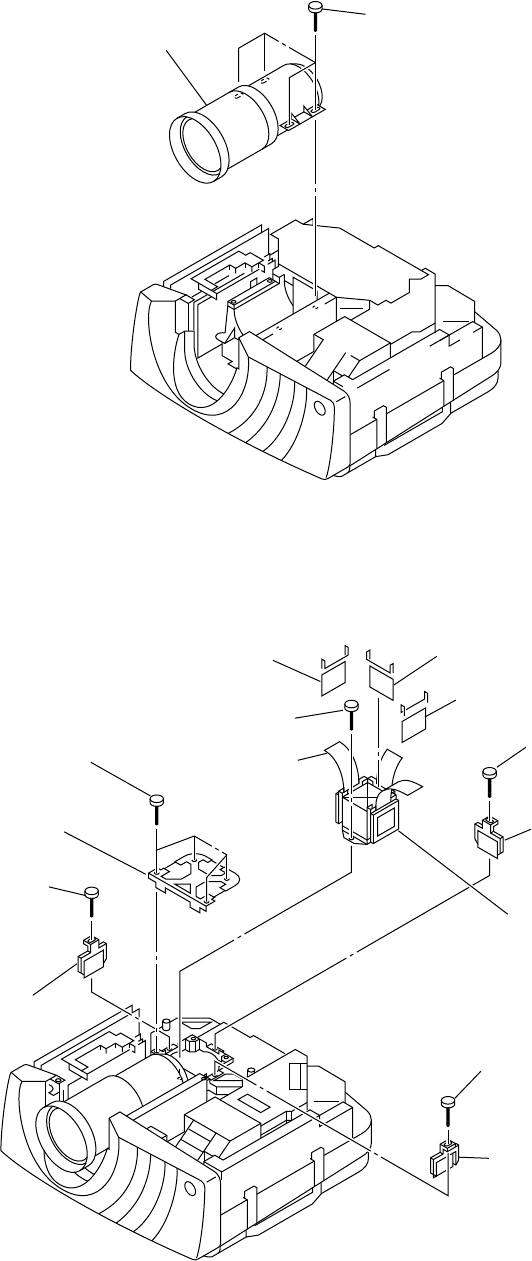
2-8 VPL-PX20/PX30
• Remove the C Board (Refer to 2-9.).
2-16. Prism Block and Polarizer Removal
2-15. Lens Assy Removal
1 Four screws
(+PSW4 x 12)
2 Lens assy
1 Four screws
(+P3 x 5)
3 Screw
(+PSW3 x 8)
8 Screw
(+PSW3 x 8)
2 Cover
9 Rch-in polarizer

2-9
VPL-PX20/PX30
2-17. Note on Lamp Breakage
Note 1
Ehen the lamp broken, its broken pieces may remain inside the unit.
Take off all the pices with gloves using care about a hand cut, before replacing.
Then, the fly-eye lens may be cloudy at the lamp breakage, at that time wipe the suface of the lens with an
authorized lens cleaner kit.
. Cleaner (4-075-337-01)
. Wiper (4-075-338-01)
Note 2
Under the consideration of lamp’s reliability, set the lamp mode to “LOW” during repairing the unit with
the cabinet opening and the lamp on.
3-1
VPL-PX20/PX30
3-1. BA Board
This circuit mainly performs the following processes.
a. VIDEO (C-VIDEO, Y/C, component), HDTV (Y PB PR) image processing
b. Sync separation processing
3-1-1. Main IC Functions
1. CXD2064 (IC221), digital comb filter
Performs NTSC3.58, PAL443 3-line applicable digital Y/C separation.
The operating clock (fsc) output from Pin 46 of CXA2123 (IC101) is input to Pin 37. The VIDEO
signal input from Pin 2 is digitally processed by this clock. The Y signal is then output from Pin 9
and the C signal from Pin 7.
2. CXA2123 (IC101), chroma decoder and sync processing
Chroma decoder/sync processing IC controlled by the I2C bus. It can process C-VIDEO signals and
Y/C signals. The C-VIDEO signal is input to Pin 1, the Y signal to Pin 44, and the C signal to Pin 43
to automatically differentiate between NTSC3.58, NTSC4.43, PAL, PAL-M, PAL-N, SECAM, and
B/W. When identified as NTSC3.58 or PAL, it supplies a clock to IC221 (CXD2084) to perform Y/C
separation. Y/C separation is performed in this IC when other systems are identified. The signals are
then converted to the Y/U/V signals, and the Y signal is output from Pin 21, the Cb signal from Pin
22, and the Cr signal from Pin 23.
In sync processing, the C-VIDEO/Y signal input is separated into H and V, and the H-sync signal is
output from Pin 9 while the V-sync signal is output from Pin 4. (For the 15 kHz COMPONENT and
RGB signals, only C.SYNC is input from Pin 19.)
3. CXA2101 (IC1601), HD interface
The HD interface is controlled by the I2C bus. It turns ON/OFF user-controlled COLOR, HUE,
SHARPNESS, and DYNAMIC PICTURE functions for signals input, performs detection axis
settings, and improves chroma transient, and converts signals to R, G, and B signals then outputs
them.
When the DTV (YpbPr, GBR) is input, the Y/Pb/Pr signal G/B/R are input to Pins 11, 10, and 9
respectively. COMPONENT is input to Pin 5 (Y), 4 (Cb), and 3 (Cr). The Video signal is decoded by
IC101, and then input to Pins 69 (Y), 68 (Cb), and 67 (Cr).
They are then subject to various controls, converted to R, G, and B signals, and output from Pins 35
(R), 37 (G), and 39 (B).
3-1-2. Signal Path
1. Path of VIDEO signal
The VIDEO and Y/C signals input from CN102 are input to Pins 1, 44, and 43 of IC101 via buffers
Q107 (composite video), Q109 (Y), and Q101 (C).
For PAL and NTSC3.58, the signal amplified by two times by IC101 is output from Pin 3, passed
through the low pass filter composed of Q120, L111, L110, C211, C210, and C143, input to Pin 2 of
IC221 (comb filter), Y/C separated, output from Pins 9, Y, 7, and C, passed through the low pass
filter composed of L112, C215, L113, and C219, after which the Y signal is input to Pin 5 of IC101
and the C signal is input to Pin 7. All other signals are processed in IC101, converted to the Y, U, and
V signals, and output from Pins 21 (Y), 22 (B-Y), and 23 (R-Y). They are then input to Pins 69, 68,
and 67 of IC102 for the above processing by CXA2101, and output.
Section 3
Theory of Operation
3-2 VPL-PX20/PX30
2. Path of component (Y/R-Y/B-Y) signal, 15kRGB signal
The component video signal input from CN101 is passed through the buffer Q116/ Q115/Q117, and
input to Pins 5 (Y), 4 (Cb), and 3 (Cr). The 15kRGB signal is passed through the same path as the
component signal, input to Pins 5 (G), 4 (B), and 3 (R) of IC102 for the above processing by
CXA2101, and output.
3. Path of HDTV (Y, PB, PR) signal
The Y/Pb/Pr video signal input from CN101 is input to Pins 11 (Y), 10 (Pb), and 9 (Pr) of IC102 via
the buffer Q116/115/117 for the above processing by CXA2101, and output.
3-1-3. Path of SYNC Processing
1. When the VIDEO signal is selected
The signal input to IC101 is sync separated internally, and the H and V SYNC from Pins 9 and 4 are
output.
The equivalent pulse of the signal output from Pin 9 is eliminated as it is imposed with PLL. After
this, it is input to Pins 65 and 66 of IC102, selected, and output from Pins 29 and 28. The H sync
output is reversed by IC259, input to IC256, noise-eliminated, output from Pin 7, waveform-rectified
by IC257, and output from CN101.
2. For component signal (15K) and 15kRGB signals
The C SYNC signal rectified by the QA board is input to Pin 19 of IC101. The signal output from
Pins 9 and 4 are input to Pin 2 of IC1021. The rest is the same process as for Video signals.
3. When HDTV (YPbPr, GBR), components signals other than 15K are input
The signal input from CN101 is input to Pins 11, 7, and 8 of IC102 in the order of Y/G, H, and V.
IC102 automatically determines if the signal is SonG, C.SYNC, or HV separate, and outputs the
signal from Pins 29 and 28. The rest is the same process as for Video signals.
3-1-4. Clamp Pulse Generation Circuit
1. Path of VIDEO, component (Y/R-Y/B-Y) signal, and 15 kRGB signal
The SGP output from Pin 10 of IC101 is waveform-rectified by IC263, input to IC251, subject to
selection with the HDTV signal input, output from Pin 1, reversed by IC252, and output from
CN101.
2. When HDTV (YPbPr, GBR), component signals other than 15K are input
The H.sync output from Pin 29 of IC102 is reversed by IC259, and then input to IC256.
Clamp pulses are generated by this IC, output from Pin 5, waveform-rectified by IC259 and IC257,
input to IC251, selected, and output from CN101.
3-3
VPL-PX20/PX30
3-2. BB Board
The BB board inputs the analog RGB signal from the QA board or digital RGB signal (TMSD:Panel
Link) from CN300, converts to the VESA60 equivalent XGA signals, superimposes the OSD signal, and
outputs to the BC board.
1. Scan Converter
PW*64 (IC303) is used as the scan converter.
This IC incorporates the X86 base CPU core and frame memory SDRAM.
The 4 Mbits (512 KBytes) flash ROM (IC314) is equipped externally as the PROM and 1 Mbit (128
KBytes) SRAM (IC315) as the CPU RAM.
2. The External Data Bus
The external data bus is 16 bits. The CPU operates on 43.333 MHz which is obtained by dividing the
130 MHz memory clock by 3.
3. The External Flash RCM
The program of the external flash ROM can be rewritten by connecting a board for converting the
RS232C level to CN312. In this case, the EXTSW must be connected to GND to switch the
communication line, and the WDEN must be connected to GND to stop the operations of the watch
dog timer.
4. PW**
**
*64
PW*64 normally operates as a sub CPU according to the commands from the main CPU on the Y
board. The commands are sent by asynchronous serial communication using TXD/RXD.
The OSD data itself is stored in IC314 which is the PW*64 memory. Based on the commands from
the main CPU, the PW*64 selects the contents displayed and superimposes.
To realize high-speed signal switching operations, the MUTE signal is directly sent to PW264.
The INTERLACE detection signal is directly sent from PW264 to Y.
5. PW264
Since PW264 is a X86 based CPU, the RESET signal must be input at a HIGH level.
For this reason, the open drain RESET signal of IC306 is reversed by the Schmidt inverter (IC317).
6. Memory Clock
The 130 MHz memory clock is obtained by multiplying the X300 21.667 MHz by six times.
The internal SDRAM operates on this frequency.
7. Internal Core
As the internal core operates on 2.5V, D3.3V is stepped down to 2.5V and supplied by IC312.
3-4 VPL-PX20/PX30
3-3. BC Board
The BC board controls the contrast, bias, W/B, etc. of the linear digital signals from the BBC board, then
performs gamma correction by LUT (Look Up Table) and 3D gamma correction which corrects in planes
according to the gradation, converts the signals from digital to analog before outputting them.
1. IC502 (CXD9512Q)
IC502 (CXD9512Q) has a 48 bit 2-pixel series input and 30 bit (10bit/pixel) straight output.
Therefore a 2 clock whose phase matches the input clock is required.
2. IC501
IC501 is an IC generating 2 clock corresponding to the frequency diffusion. It outputs the same clock
as the input to CLKB and the 2 clock to CLKA according to the phase of the input clock.
IC 500 (Pin 1 of IC501) is incorporated to match the timings of the data and clock.
3. IC503
IC503 is a 64 Kbits (8 Kbytes) EEPROM memorizing LUT (Look Up Table) and the 3D gamma
data. It exchanges data with IC502 using I2C signals (slave address is A2).
4. IC511
IC511 generates RESET signals for IC503.
5. IC505
IC505 is a switching buffer for OSD display of PW264 when outputting the internal signals of IC502
in gamma adjustments, etc.
When PW OSD ENA is LOW, DG07 and DGE7 are sent to ODD_YS and EVEN_ YS respectively
to control the ON/OFF of the OSD. DR07 and DRE7 are also sent to ODD_YM and EVEN_YM
respectively to control the OSD half tone.
When PW OSD ENA is HIGH, both YM and YS are pulled-down to the LOW level by the
resistance, and the OSD of this route goes off.
6. IC506
IC506 is a 10-bit D/A converter. It converts gamma corrected digital data to analog signals.
The output when the full-scale (3FFHEX) is input becomes approximately 0.75 Vp-p after
termination at 75 Z of the C board.
7. D500
D500 is an external reference voltage source to improve accuracy. It generates 1.25±2% voltage.
To avoid the effects of the digital circuit and input signal, IC506, D500 receives the supply of analog
5V from the C board.
Other circuits operate on digital 3.3V from the BB board.
8. S500
S500 switches the I2C signal, writes the LUT data using the I2C signal from the external tool
connected to CN503 so that the operations of IC502 (CXD9512) can be controlled directly.
During normal operations, IC502 is connected to the I2C line from the Y board and is controlled from
the main microprocessor.
The slave address of I2C of IC502 is 76 Hex.
3-5
VPL-PX20/PX30
3-4. C Board
3-4-1. Timing Generator
The following timing pulses are generated from the HSO, VSO, and CLOCK by the CXD9512Q of the
BC board and supplied to the C board.
In the C board, all signals are level shifted to 5V and sent via the buffer as well.
HCK1, HCK2: Clock for the H shift register drive of the panel
HST: Start pulse for the H shift register drive of the panel
VCK: Clock for the V shift register drive of the panel
VST: Start pulse for the V shift register drive of the panel
ENB: Enable signal of the gate selection pulse
FRP: Reverses the top and bottom of video signals centering around the reversal pulse and SIG
CENT voltage
PRG: Pulse which regulates the width of the first SID level
PCG: Pulse which improves uniformity
RGT: Reverses the left and right of the screen, controls the drive direction of the H shift register
DWN: Reverses the left and right of the screen, controls the drive direction of the V shift register
3-4-2. LCD Driver Control Pulse
INV CONT: Reverses the polarity of the CLK for MCLK
DLY CONT: Adjusts the phase of the CLK for the MCLK in the 180d range
These pulses optimize the sampling phase of the video signal.
POSCONT1, 2: Adjusts the position of the 12 outputs for the video input signal.
Sets the optimum timing for inputting signals to the LCD panel through 16 different combinations of
the output.
3-6 VPL-PX20/PX30
3-5. Y Board
The main circuits of the Y board include the microprocessor peripheral circuit, USB circuit, and IrDA
circuit.
3-5-1. Microprocessor peripheral circuit
The controller of the projector is mainly composed of the Main MPU, EEPROM, and power supply
monitoring IC.
MainCPU
Sync Sep
Flash Memory Write
V Line COUNTING
SIRCS
fH.fV COUNTING
Serial
Communication
RS-232C Communication
V Blanking INTERRUPTION
Key (ADC)
PW:Scan Converter(BB)
(Sub CPU)
AD9884A:
ADC/PLL
Device Controller
1) CXA1946:Audio (QA)
Device Controller
1) M24C64:EEPROM (Y)
2) CXA9812:3D Gamma (BC)
3) M24C64:EEPROM for 3D Gamma (BC)
UART
SCI
12C Bus
400kbps
Device Controller
1) CXA1875 (DAC) x 2:Switch/Amp (QA)
2) CXA2123:Chroma Dec (BA)
3) CXA2101:RGB Mtrx (BA)
4) CXA1875 (DAC):Comb/Others (BA)
5) M62399 (DAC):Panel (C)
6) M52749 (DAC):V AMP (C)
12C Bus
100kbps
12C Bus
ST7:USB Controller(Y)
(Sub CPU)
12C Bus
19,200bps
100kbps
3-7
VPL-PX20/PX30
1. Main MPU: IC3204 (HD64F2633TE)
16-bit, 1-chip microcomputer.
The operating frequency is =24.576 MHz which is the 12.288 MHz frequency supplied from the
external crystal oscillator (X3200) multiplied by two times in the internal PLL.
The memories incorporated are the 256 Kbytes FLASH-ROM and 16 Kbytes RAM.
The Table Main MPU Terminal Functions list the terminal functions of the main MPU and details of
the external device control.
2. EEPROM: IC3203 (M24C64-WMN)
64 Kbits EEPROM controlled by the 400 kHz IC.
Stores the adjustment values of the projector.
3. Power supply monitoring ICs: IC3201, IC3202 (S-80842, S-80828)
The main CPU operates on the Sub+5V and Sub+3.3V power supply.
IC3201#1 monitors the Sub+5V while IC3202#1 monitors sub+3.3V using their respective threshold
values of 4.2V and 2.8V.
When below these threshold values, the reset signal (active = low) is output from #2 of the
monitoring IC, and input to the main MPU reset input terminal (IC3204 #71).
The CPU is reset by this external reset signal, or the internal reset signal by the WDT (watch dog
timer) in the MPU.
3-5-2. USB Circuit
VPL-PX30 corresponds to the USB communication as an interface of the personal computer.
The USB circuit mounts the USB hub controller IC and USB projector controller IC in the Y board.
The USB has a tree structure as shown in the figure below.
USB Block
1. USB Hub Controller IC:IC3303 (uPD72012)
The USB communication (US+, US_) from the personal computer is an IC relaying to the USB
device connected to the lower level.
When connected to the personal computer with a USB cable, +5V (VBUS) is supplied from the
personal computer, the Q3307 base becomes high, Q3307 turns ON, the Q3306 base becomes low,
Q3306 turns ON, and the Q3306 collector voltage=3.3V is supplied as the Vcc of IC3303.
When this IC operates normally, the enable signal (active; low) is output to the device in the lower
level connected by the down stream (DS) 1, 2, and 3 from #40, #41, and #42.
USB Hub
Controler
Mouse
Driver
(QB M’t)
USB
Projector
Controler
Main
MPU
Power
Controler
(QA M’t)
USB_Cable
Host P.C.
USB
Products
3-8 VPL-PX20/PX30
2. USB Projector Controller IC: IC3304 ST72T36
In the USB communication between the personal computer and main MPU of the projector, the
enable signal: Low (IC3303;#42) of the microprocessor cable hub for performing protocol conversion
(USB-IC) is input to the Q3310 base, Q3310 goes OFF, this IC#8 becomes high, and reset is
canceled.
The projector control signal executed by the application projector station for the projector on the
personal computer is input to IC31 and IC32 via the HUB (IV3303). This signal is analyzed and sent
to the main MPU by IIC (#24, #28).
Basically, this IC is the master while the main MPU is the salve.
To send the projector information (input signals, etc.) to the personal computer, the main MPU
converts the signal line USB REQ to Low. When this signal is input to #7, this IC requests for
projector information using IIC to the main MPU.
3. IrDA Circuit
The remote control signal (IrDA) received by the infrared photo-sending unit (NF/NR M’t) in front
and at the back of the projector is input to the IrDA filter IC (IC3301) (NF;#2, NR;#3). In IC3301, the
photo-sensing unit effective signal (NF;#7, NR;#6) by the main MPU is enabled = low, and the signal
determined as a useful IrDA signal is output from #5. While it is input as the SIRCS signal to the
main MPU via the SIRCS circuit (QD), it is input to #1 of IC3302 (#2 is fixed at low), the reverse
signal is output from #7, input to #2 and 6 of IC3002, and #7:IrDA, #3:IrDB are output to the QB
board and QC board,
If INPUT-A is selected, the control signal mouse A/B becomes high by the main MPU, and
consequently, #1 of IC3002 becomes high (#5:Low), the IrDA signal is output only from #7, and #3
is prohibited.
3-5-3. Memory
Memory structure of VPL-PX20/30 series is based on the 600 series, and it is composed of the following
five memory blocks.
1. Set memory
2. Status memory
3. Channel memory
4. Chroma memory
5. W/B memory
The 600 series is equipped with the gamma memory, but the current VPL-PX20/30 series is no gamma
memory. The gamma mode function is realized by applying the offset to the output value of the contrast
and the brightness of the devices as X2000 series.
When the power plug is connected to the power line (Standby status), all data inside the internal ROM are
written into the NVM (Nonvolatile Memory). When the power is turned on, required data for the current
picture, such as status memory data, etc., are selected, and they are written into the internal RAM.
When adjustment is carried out, adjustment data are written into the NVM automatically (items on the
user mode) or by the trigger of memory operation (items on the service mode and special service mode).
Adjustable items (W/B and Device Adjust) of the service mode and special service mode are memorized
into the NVM by the memory operation. At the same time, the factory preset (adjusted) data are all
eliminated from the memory.
3-9
VPL-PX20/PX30
Set Memory
Status
Memory
No.01
No.02
No.03
INPUT-A Preset INPUT-B Preset
...
...
No.50
No.03
...
...
No.50
W/B
Memory
Computer Others
HIGH
LOW
HIGH
LOW
Set Memory
Status
Memory
No.01
No.02
No.03
INPUT-A Preset INPUT-B Preset INPUT-A
User INPUT-B
Preset
...
...
No.50
No.03
...
...
No.50
No.71
...
No.90
No.91
...
No.110
Set Memory
Status Memory
Channel
Memory
Video
S Video
Input-A
Input-B
Chroma
Memory
NT358/443/BW60
PAL/PAL-M/N/
SECAM/BW50
15k RGB
15k Component
Other Component
HDVTV YPbPr
HDTV GBR
W/B
Memory
Computer Others
HIGH
LOW
HIGH
LOW
CPU ROM External NVM CPU RAM
Active memory copy
MemoryInitialize
W/B
Memory
HIGH
LOW
Channel
Memory
Video
S Video
Input-A
Input-B
Chroma
Memory
NT358/443/BW60
PAL/PAL-M/N/
SECAM/BW50
15k RGB
15k Component
Other Component
HDVTV YPbPr
HDTV GBR
Channel Memory
Chroma Memory
CPU Internal ROM : 256 kbyte Flash Memory
CPU Internal RAM : 16 kbyte
External NVM Memory: 256 kbyte Flash Memory
3-10 VPL-PX20/PX30
3-6. Description of QA Board Operations
The QA board mainly switches between video signals and audio signals, and performs sync separation.
3-6-1. Switching of Video Signals
This model has the following signal input.
INPUT A DSUB15 pin analog signal 5BNC analog signal
Digital signal
INPUT B DSUB15-pin analog signal
VIDEO COMPOSITE
Y/C
These signals are switched as shown in the following figure.
BA
COMPOSITE VIDEO
Y/C VIDEO
QA
BB
INPUT A DSUB15
INPUT B DSUB15
INPUT A 5BNC
INPUT A DIGITAL
3-11
VPL-PX20/PX30
As shown in the figure, the QA board first switches between INPUT A (DSUB15), INPUT A (5BNC),
and INPUT B. The switching is performed by IC823 (RED), 824 (GREEN), and 825 (BLUE). SYNC is
performed by IC811. These ICs are controlled by the output of IC806 and IC807 (both DAC) controlled
by the CPU using the IIC bus.
Next the video signals input from the BA board and the RGB signals described above are switched by
IC801. This IC amplifies the signal switched by two times, terminates the signal at 75 Z in the later stage
board, and outputs it. This IC is also controlled by IC806.
As described earlier, SYNC is switched by IC811, but the H SYNC input from 5BNC has additional
conditions. When the signal input from 5BNC is 15 kHz, it is sync separated by IC805, and input to
IC811 in the later stage. If it is not 15 kHz, it is input directly to IC811.
The SYNC selected by IC811 is waveform-rectified by Q821 to Q826, IC812, and IC813.
It is then branched in three ways, output to the BA board, input to IC814 for monitor-out, and input to
IC802 for sync separation. After sync separation in IC802, it is switched with the SYNC from the video
block by IC803, converted to 3.3V, and output to the BB board. IC804 fixes the video clamp pulse to a
fixed pulse width.
The monitor-out outputs only signals projected to the screen from INPUT A (DSUB, 5BNC) and INPUT
B. IC808 to IC810 are amplifiers for monitor-out. IC814 functions as an output buffer for SYNC.
3-6-2. Switching of Audio Signals
Audio signals input are switched by IC819, and volume-controlled. The output of IC819 is separated into
that for the monitor-out and that for the speaker-out. The one for monitor-out is input to IC821, and
output from CN806 to the QC board. That for the speaker-out is converted to 3 channels by Q836 to
Q838. The L and R channel signals are then output to the KS board from CN810 while the mixed L and R
signals are output from CN809 to the K board. Q831 to Q835 compose the mute circuit.
3-6-3. Monitoring of the USB Power Supply
The USB download side must be supplied up to 500 mA at 5V. IC822 monitors this current amount. 5V
power is supplied to the download side from Pin 8 of IC822. When this exceeds 900 mA, the power is
stopped, and at the same time, the High signal is supplied from Pin 2 to the USB control IC (IC3303) in
the Y board.
IC822 also supplies power to the mouse driver (IC1201) for INPUT A on the QB board.
When a connector is connected to the upload side of the USB, a Low signal is input from the USB control
IC (IC3303) on the Y board to Pin 4 of IC822, and a 5V power is supplied from Pin 5.
3-12 VPL-PX20/PX30
3-7. Description of QB Board Circuit Operations
The QB board is composed of the INPUT A input terminal, DDC memory, INPUT A mouse driver, and
USB terminal.
3-7-1. INPUT A Input
Three signals are input to INPUT A; analog signal of DSUB15 pin, analog signal of 5 BNC, and digital
signal. These signals are switched by SW1201. The analog signal of DSUB15 pin is input from CN1202
and output from CN1203 to the QA board. (An input terminal is provided for the 5BNC analog signal and
digital signal in the BB board. These signals are output from this input terminal to the QA board.)
3-7-2. DDC Memory
IC1202 is a DDC memory for INPUT A. This IC is written with EDID data for DDC. When a computer
is connected to CN1202, power is supplied to the IC. If the computer connected is DDC compatible, DDC
communication is performed.
3-7-3. INPUT A Mouse Driver
IC1201 is a mouse driver for INPUT A. This IC functions when connected to PS/2 and the serial port of
the computer, or connected to a Macintosh or NEC 98 series computer by USB. Identification of the
mouse of these computers is performed when power is supplied to IC1201. As power is supplied from the
computer except when connected by USB, connections can be identified even if AC is not supplied to the
unit. When connected by USB, the mouse cannot be identified if no power is supplied to the unit.
The mouse code input from CN1203"A1" is decided by IC1201, and output from CN1201 or I1202 to the
computer.
3-13
VPL-PX20/PX30
3-8. Description of QC Board Circuit Operations
The QC board is composed of the INPUT B input terminal, DCC memory, INPUT B mouse driver, and
monitor-out terminal.
3-8-1. INPUT B Inputs
Unlike INPUT A , only analog signals of DSUB15 pin are accepted. The signal is input from CN1802,
and output from CN1804 to the QA board.
3-8-2. DDC Memory
IC1802 is the DDC memory of INPUT B. This IC is written with EDID data for DDC.
When a computer is connected to CN1802, power is supplied to the IC. If the computer connected is
DDC compatible, DDC communication will be performed.
3-8-3. INPUT A Mouse Driver
IC1201 is the mouse driver for INPUT A. The operations are basically the same as INPUT A. The only
difference is that INPUT B has no USB connection.
The mouse code input from CN1804"A1 and B2" is decoded by IC1801, and output from CN1801 to the
computer.
3-14 VPL-PX20/PX30
3-9. Description of QD Board Circuit Operations
The functions of this board include buffer of RS232C communication, reception of remote control signals
(CIRCS signal), and video input.
3-9-1. RS232C Communication
In RS232C communication, IC1901 is used as the buffer. Signals are connected to the computer by
CN1904, and passed through IC1901, CN1903, BB board, and then the Y board for communication with
the CPU on the Y board.
3-9-2. Reception of Remote Control Signals
Signals from the remote controller connected by cable are input from I1902.
They are then inverted by Q1904, and output from Pin 5 of CN1903 to the Y board.
If not connected by remote control cable, signals received by the NF and NR boards are input from Pin 6
of CN1903, passed through J1902, and output from Pin 5 of CN1903 to the Y board again.
3-9-3. Video Input
Video signals are input from J1901, and output from CN1901 to the BA board.
The video audio signals are output from CN1902 to the QA board.
3-10. Description of K Board Circuit Operations
This board amplifies audio signals and outputs them to the main speaker.
Signals input from Pin 1 of CN2900 are amplified by IC2900 and output to the main speaker from
CN2903.
Pin 3 of CN2900 inputs mute signals. When this line is High (about 4.5V), no more signals are output to
the speaker.
3-11. Description of KS Board Circuit Operations
This board amplifies audio signals and outputs them to the sub speaker.
Signals input from Pins 3 and 5 of CN2951 are amplified in IC2950, passed through the H board from
CN2952, and output to the sub speakers.
Pin 7 of CN2951 inputs mute signals. When this line is High (about 4.5V), no more signals are output to
the speaker.
3-15
VPL-PX20/PX30
3-12. Voltage Map of F, GA, GB, GC, GD Board
3-12-1. Voltages Map of F, GA, GB, GC and GD Board
3-12-2. F Board
The EMI filter is composed of the one level of LFT.
The F2000 is the same regardless of whether it is 100V or 200V (6.3A/250V).
AC
INLET
Filter
EMI
filter
Bridge
Rectifier Active Filter
IC2100
DC359 10V
SUB+5
17.5V
-7V
A6V
D3.3V
10.7V
FAN+B2
FAN+B1
18.5 0.5V
10.7 1.0V
POWER SUPPLY
BLOCK(for LAMP) LAMP
DC-DC CONVERTER
GC BOARD / IC2500
DC-DC CONVERTER
GB BOARD / IC2300
DC-DC
CONVERTER
IC2700 REG. IC2701
REG. IC2702 FAN 2
FAN 1
MAIN CONVERTER
IC2101 CPU
A/D CON
D/A CON
etc...
AUDIO
CIRCUIT
K BOARD
GC BOARD
C BOARD,
BB BOARD
F BOARD
GA BOARD
AC100~240V
9.0 2.0V
17.5 0.4V
5.9 0.3V
-7.4 1.0V
SUB CONVERTER
IC2102
Fig. 1 Voltages Map
3-16 VPL-PX20/PX30
3-12-3.GA Board
1. Structure
•Active Filter
The active filter improves the power factor of the AC voltage after bridge rectification, and at the
same time, serves as a step-up converter and supplies DC358V±10V to the lamp power supply in the
later stage, sub converter, and main converter. However, when the maximum AC voltage exceeds the
output voltage of the active filter, the power factor will not be improved correctly.
•Inrush Current Limit Circuit
When the AC voltage is supplied with the electric load of the smoothing capacitors C2112 and C2113
fully discharged, the inrush current flows to the capacitor, and as a result, damage the fuse in the
input stage. To prevent this, immediately after inputting the AC voltage, the inrush current is limited
by R2101. After the operations of the standby converter start, the thyristor D2102 turns ON and
short-circuits the two edges of R2101. (The VPL-X600 series and VPL-SC50 series turn ON the
thyristor after the operations of the main converter start.)
•Sub converter
The DC voltage obtained by completely rectifying the AC voltage or the output voltage of the active
filter is stepped-down to the GC board input voltage and the VCC for the active filter control IC.
These operations are controlled by IC2102.
.VCC (18.5V±0.5V)
.GC board input voltage (9.0V±2.0V)
( ) shows the potential of the connector.
•Main converter
The output voltage of the active filter is stepped-down to the following signal circuits and AUDIO
circuit. These operations are controlled by IC2101.
However, when no load, the voltage is clamped to about 17.8V by the diode.
•Power protector
Normally, when the main converter is operating, GA/Q2107 turn ON, and the microprocessor port of
the Y board is kept “Low”. When the output voltage lines and GND line of the main converter are
short-circuited, GA/Q2107 goes OFF, and the microprocessor port of the Y board is set to “High”.
Furthermore, the microprocessor sets the POWER ON signal to “Low”, and stops the operations of
the main converter. (At this time, both the TEMP and LAMP LEDs of the control panel light up.)
2. Operations of the Active Filter
•ON/OFF operations
The active filter starts operations at the same time as the main converter in the later stage. At standby,
Q2106 maintains Pin 8 of IC2100 at “Low”, and the active filter does not operate. When the “High”
signal is received from the microprocessor of the Y board, Pin 7 of CN2106 becomes “High”, Q2106
goes OFF, Q2104 turns ON, and Q2105 also turns ON. As a result, VCC is supplied to IC2100 and
IC2100 starts operating.

3-17
VPL-PX20/PX30
3. Basic Operations
In conventional rectification circuits which do not use the active filter, peak recharge current is generated in a part of the
AC voltage waveform due to the capacity components of the smoothing capacitor. This causes such problems of the
effective power such as later phase power consumption, high frequency, etc., and may cause subsequent problems in other
equipment. To prevent this, this power supply circuit is equipped with a step-up DC-DC converter in the smoothing
circuit and adopts an active filter which compares the input current waveform with the input voltage waveform by
appropriate control.
Fig. 2 shows the principle of the active filter circuit. When MOS-FET Q2100 turns ON, energy is accumulated in the
choke coil L2100. When it goes OFF, energy is discharged, and current flows to the load side.
Fig. 3 shows the relation between the voltage and current. The average input current for each switching period of the
MOS-FET Q2100 is half of the peak current flowing to the choke coil L2100. Since these peak values can be placed on the
curve proportionate to half the AC voltage input, they appear like resistance load on the AC voltage from the input side of
the active filter.
-V
+V
C2112&C2113
Q2100
L2100 D2108
D2100
+
Control Circuit
D2100 : Bridge rectifier
L2100 : Smoothing choke coil
C2112,C2113 : Smoothing capacitor
Q2100 : MOS-FET
D2108 : Smoothing diode
IC2100 : Control IC
IC2100
Pulse Voltage
Maximum Switching current
Switching Current
Inductor Current
Fig. 2 Princple of Active Filter
Fig. 3 Puls Voltage and current
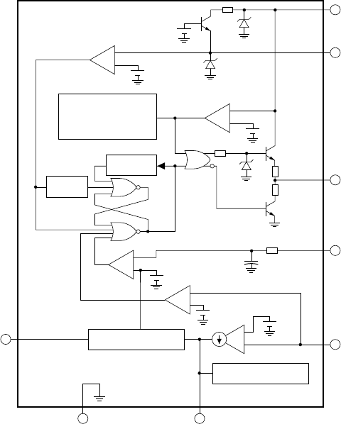
3-18 VPL-PX20/PX30
Fig. 4 show a simple block diagram of the active filter control IC2100. The current flowing to MOS-
FET Q2100 is detected by the sense resistor R2106. When this current reaches the threshold value
corresponding to the peak current flowing to the choke coil L2100, the comparator turns OFF the
MOS-FET Q2100. The threshold value is sent to the comparator as the product of the AC voltage
waveform and control amplifier output voltage V0. The MOS-FET Q2100 maintains the OFF state
until the choke coil L2100 and diode S2108 current becomes zero. The output is maintained at
358±10V by the PWM control of the switching. This output setting is performed by the R2127 to
R2133 voltage-dividing resistor.
4. Timer function
As a watchdog timer function is equipped inside the IC2100, no external oscillator is required. When
the current flowing to the choke coil L2100 reaches zero and the drive output becomes OFF for more
than 620 us, the timer automatically starts or restarts the pre-converter.
5. Internal over-voltage comparator
To prevent abnormal output voltages, the control ICIC2100 is equipped with an over-voltage
comparator. This comparator turns ON at initial startup, when the load changes suddenly, and when
the output ripple increases. The over-voltage comparator monitors the peak output voltage of the
converter, and turns OFF the MOS-FET Q2100 immediately when the reference value is exceeded.
The threshold value of the comparator is set to 1.08V in the control IC IC2100.
Multiplier Input
GND
Vref
1.8V
1.5V
Multiplier
Delay
Timer R 16V
13V
UVLO
2.5V
Reference Voltage
Source
RS Latch
Current Sence Comparator
Over Voltage Comparator
Differential
Amplifier
Voltage Feedback
Input
Compensation
Current Sence
Input
Drive Output
Zero Current
Detector IN/OUT
VCC
Quick Stert
6.7V
1.2V
1.6V
Zero Current
Detector
Fig. 4 Simple Block Diagram of IC2100

3-19
VPL-PX20/PX30
6. External over-voltage protection circuit
In case the internal over-voltage comparator does not function when the control IC2100 performs
abnormal operations, an over-voltage protection circuit composed of the shunt regulator IC2105 has
been equipped externally. The output voltage is monitored by the voltages of the two ends of R2177.
When this potential reaches 2.495 (428V output voltage), IC2105 turns ON, to turn OFF the control
IC IC2100 operating the latch circuit composed of Q2106 and Q2102.
7. External pre-drive circuit
The control ICIC2100 is equipped with a totem pole output stage, but due to the selection of a surface
mounted device, strong heat is generated when a large input MOS-FET is driven. To suppress this
heat, the pre-drive circuit composed of Q2109 and Q2110 has been added in front of the MOS-FET
Q2100.
8. Details of parts
L2000 Choke coil for eliminating the noise components of the common mode.
D2100 Bridge rectification diode rectifying the AC voltage to both waveforms. Taking into
account the voltage changes in the market, the 800V voltage resistor was used.
R2101 Resistor limiting the bridge current when AC voltage is input.
D2101 Thyristor short-circuiting R2101 when the main converter is operating.
Q2100 MOS-FET for switching the active filter. Performs switching by the PWM control of
IC2100. Taking into account the heat generated by power loss, the current capacity
of 16A is driven in series.
L2100 Choke coil for the active filter. Accumulates energy when Q2100 is ON and supplies
current to the later stage when OFF.
D2108 Rectification diode for the active filter. A fast recovery diode is used for high
voltage tolerance and high speed ON/OFF.
C2112, C2113 Smoothing capacitor for the active filter. Rectifies the half waveform after bridge
rectification during standby. DC voltage is supplied to the sub-converter in the later
stage. Recharges and discharges the step-up converter when the active filter is
operating.
IC2100 Controls the operations of the active filter.
R2101 Current detection resistor. The current flowing to the active filter is input to IC2106
by the voltage of the two ends of this resistor.
3-12-4. Main Converter
1. ON/OFF Operations of the Main Converter
The main converter control IC is IC2101. During standby, Q2103 maintains the ON state. As the
IC2101/CONTROL pin is Low, the main converter does not operate. When the “High” signal is
received from the microprocessor at power ON of Pin 7 of CN2106, Q2103 goes OFF, and the main
converter starts operating.
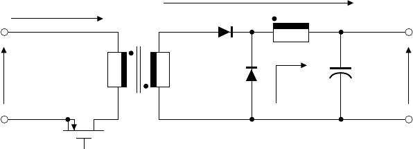
3-20 VPL-PX20/PX30
2. Basic operations of the main converter
The main converter is composed of the self-excited forward converter operating on the DC voltage
received from the active filter.
The switching and control are performed by IC2101. The oscillating frequency is fixed to about 100
kHz by the internal oscillator for PWM control.
.Transformer secondary operations
When Q1 (built-in FET of IC2101 in this case) turns ON, the output voltage of the active filter is
supplied to the primary line T1 of the transformer. At the same time, voltage is induced according to
the number of coils in the secondary coiled line T2.
As the secondary side rectification diode D1 is biased in the normal direction, the current i2 is
supplied. This current flows along the path for recharging the smoothing capacitor C1 in the order of
D1, L1, and C1. The inductance L1 at this time is accumulated with PL energy.
Next, when Q1 goes OFF, no voltage Vin is transmitted from the primary side. Based on the PL
energy accumulated when Q1 is ON, reverse power is generated in the L1 inductor. The current i3
from the L1 inductor flows from L1 to C1, and then to D2, and while Q1 is OFF according to the PL
energy above.
3-12-5.Basic Operations of Sub-Converter
Composed of the RCC (Ringing Choke Converter) which can operate by the DC voltage obtained by
completely rectifying the AC voltage or the output voltage of the active filter. This switching and control
are performed by IC2102. The oscillating frequency is fixed at about 100 kHz by the internal oscillator
for PWM control. During standby, voltage is supplied to the GC board generating the SUB5V for the
microprocessor, and the VCC of the control ICs are also supplied when the main converter and active
filter are operating (POWER ON).
When DC voltage is supplied between Pins 5 and 7 of the transformer T2101, a voltage corresponding to
the number of coils is induced between Pins 8 and 9 of the transformer. IC2102 controls PWM so that the
CONTROL terminal is always 5.7 V (TYP).
17.5V
AUDIO+B
A6V
-7V
V in C1
i 3
i 2
i 1 D1
D2
L1
T2T1
Q1
+
Fig. 5 Principle of Operations of Main Converter

3-21
VPL-PX20/PX30
3-12-6. Details of Parts
R2139, R2140 Resistors for protecting the main and standby converters. When a problem occurs in
the later stage circuit, the line is opened to protect other parts.
IC2102 Control IC of the sub converter. Comes in the same package as the PWM control IC
and 700V MOS-FET.
T2102 Switching regulator transformer for the sub-converter. As it is of the flyback type,
the secondary side goes OFF when the primary side is ON, and vice versa.
D2118, D2121 Snubber circuit of the sub converter. The noise is suppressed by the switching pulse
of the sub converter.
IC2101 PWM control IC of the main converter.
T2100 Switching regulator transformer for the main converter. As it is of the forward type,
when the primary side is ON, the secondary side also turns ON, and when the
primary side is OFF, the secondary side also goes OFF.
R2145, R2146, R2147, C2121, D2119
Reset circuit of the main converter. Snubber circuit which consumes the exciting
current accumulated in the primary coil of T2100 for every switching pulse.
D2124, D2134, S2135, D2136, D2137, D2138, D2139, D2127, D2129, D2132, D2128, D2130, D2131
Diode for the secondary rectification of the main converter.
L2105, L2106, L2107, L2108, L2101, L2109, L2102, L2103
Choke coil for the main converter.
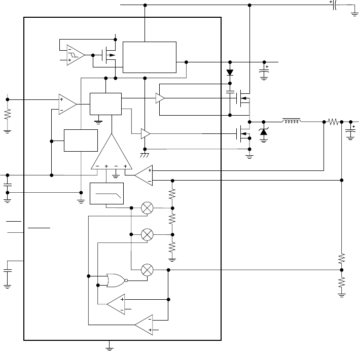
3-22 VPL-PX20/PX30
3-12-7.GB, GC, and GD Boards
1. Structure
The GB, GC, and GD boards are each composed of the DC-DC converter for step-down voltage as
shown below.
GB board : 5.9V±0.3V→3.3V±0.3V
GC board : 9.0V±2.0V→5.0V±0.3V
GD board : 17.5V±0.4V→10.6V±0.3V
2. Operations of the DC-DC Converter
As the structure of each DC-DC converter is more or less the same, the basic circuit operations are
described here.
Fig. 6 shows the DC-DC converter control circuit structure. This converter adopts the step-down
chopper method in which the input voltage is directly switched by two MOS-FETs.
In moderate loads, the DC-DC converter sets into the idling mode and skips most of the internal
oscillator pulses to decrease the switching frequency and reduce MOS-FET switching losses.
In heavy loads, the converter controls the MOS-FET pulse width used for switching, and turns ON
the High side MOS-FET only for the time determined by the duty ratio.
When the MOS-FET at the High side goes OFF, the Low side MOS-FET turns ON after 60 ns. The
Low side MOS-FET maintains the ON state until the current flowing to the L inductor zero-crosses.
The aim of these operations is to attain high efficiency in both moderate and heavy loads.
+5V LIHEAR
REGULATOR
SHDH
V+
OUT
PW
LOGIC
TO
CSL
4.5V
SECF B
REF
+5V AT 5mA
MAIN
OUTPUTL
C
GND
SHDN
SS
1V
4V
+2.505V
AT 100 A
ON/OFF
SYNC
ADJ FB FB
CSL
CSH
P GND
DL
LX
DH
BST
VL
5V FB
3.3V FB
BATTERY VOLTAGE
High side MOS-FET
Low side MOS-FET
+2.505V
REF
LPF
60kHz
PWN
CONPARATOR
Fig. 6 DC-DC Converter Control Circuit
3-23
VPL-PX20/PX30
When the potential difference between Pin 8 (CSH) and Pin 9 (CSL) of the control IC exceeds
100 mV due to shorting of the load, etc., the control IC internal current restriction circuit stops PWM
LOGIC and turns OFF the High side MOD-FET.
3. GC Board (SUB5V DC-DC converter)
The GC board is input with the secondary side output voltage (9.0V±2.0V) of T2101 from when the
power supply voltage is input. It steps down the standby voltage 5.0V±0.3V supplied to the micro-
processor by the DC-DC converter IC2500 and outputs it.
The GB board receives and transmits the POWER ON signal, and POWER PROT signal.
4. GB Board (D3.3V DC-DC Converter)
The GB board is input with the secondary side output voltage A6V (5.9V±0.3V) of T2100 when the
power is turned ON. It steps-down the D3.3V (3.3V±0.3V) supplied to the signal circuit using the
DC-DC converter IC2300, and outputs it.
5. GC Board 10.7V DC-DC Converter and FAN+B1, 2 Regulator
The GD board is input with the secondary side output voltage 17.5V (17.5V±0.4V) of T2100 when
the power is turned ON. It steps-down the 10.7V (10.6V±0.3V) supplied to the signal circuit using
the DC-DC converter IC2700, and outputs it.
The GD board is mounted with a regulator (IC2701, IC2702) which inputs the above 10.7V and
steps-down the voltage FAN+B1, 2 for the suction and exhaust FAN. The microprocessor of the Y
board reads the resistance value of the thermistor TH2020 (resistance value changes according to the
temperature) mounted on the S board and outputs the 0 to 5V voltage from the port to Pins 7 and 9 of
CN2701 of the GD board.
By adding the current based on the voltage to the ADJ terminal of the regulators IC2701 and IC2702,
the suction FAN controls the 10.2V to 6V (FAN+B1) while the exhaust FAN controls the 10.2V to
7V (FAN+B2) voltage. The thermistor TH2020 mainly monitors the external temperature of the unit.
When the LAMP MODE STANDARD mode is selected on the menu, both fans are set to the
minimum voltage of FAN 7V for the suction FAN and 8V for the exhaust Fan. When the LAMP
MODE LOW mode is set, the fans are set to the minimum voltage of FAN 6V for the suction FAN
and 7V for the exhaust Fan.
4-1
VPL-PX20/PX30
Section 4
Electrical Adjustments
4-1. Equipment Required
.Oscilloscope
Tektronix 2465 or equivalent
(bandwidth: 350 MHz or more)
.NTSC, PAL, SECAM component signal generator
Tektronix TG2000 + AVG1 (optional module)
+AWVG1 (optional module) or equivalent
.VG (Programmable video signal generator)
VG814 or equivalent
.Digital voltmeter
Advantest TR6845 or equivalent
.Luminance meter
Note: Perform the following adjustments at least 5
minutes after turning on the power.
4-2. Preparations
4-2-1. Turning on the Power
1. Connect the power cord and supply the power to the
unit.
2. Check that the STANDBY LED of the control panel
lights up in red.
4-2-2. Setting the Factory Mode
1. Check that the STATUS in the menu is ON.
2. Exit the Menu.
3. Press the keys in the following order:
“ENTER” → “ENTER” → “LEFT” → “ENTER”.
The message “Do you with to enter into the FACTORY
MODE?” will be displayed.
Select YES on the menu to set the unit into the factory
mode.
4-3. C Board Adjustments
4-3-1. R VCOM Adjustments
Turn off the menu using the STATUS OFF during adjustments.
(No shield is required.)
1. Enter the R DRV of the device adjust by the factory
mode and check the 1 line ON/OFF signal.
2. Adjust the ← and → keys to minimize the flicker.
4-3-2. G VCOM Adjustments
1. Enter the G DRV of the device adjust by the factory
mode and check the 1 line ON/OFF signal.
2. Adjust the ← and → keys to minimize the flicker.
4-3-3. B VCOM Adjustments
1. Enter the B DRV of the device adjust by the factory
mode and check the 1 line ON/OFF signal.
2. Adjust the ← and → keys to minimize the flicker.
4-4. Signal Level Adjustments
4-4-1. Component Level Adjustments
1. Connect the component signal to INPUT-A (5BNC),
and select COMPONENT with SIGNAL SELECT.
(15K Component color bar Chroma ON)
2. Set the COLOR to 40.
3. Connect the oscilloscope to TP612 (B OUT) on the C
board.
4. Enter the OTHER of the device adjust of the menu.
5. Set 06 3D GAMMA/THROUGH: 0 to 06 3D
GAMMA/THROUGH: 1.
6. Set 07 3D GAMMA/SW: 1 to 07 3D GAMMA/SW: 0
7. Adjust the cursor at the top of the oscilloscope to the
bar on the left side (white section).
8. Adjust GND level to the bottom edge in the DC 0.5 V
range.
9. Set the input signal to component color bar.
10. Select 12 YUV COL. Adjust the ← and → keys so
that the levels of the right bar and the left bar become
the same.
11. Select 05 SUB HUE. Adjust the ← and → keys so that
the two bars at the center become flat.
4-2 VPL-PX20/PX30
12. Press the ENTER key to select the SAVE TO
MEMORY of the menu, and press the ENTER key
again to save the data.
4-4-2. VIDEO NTSC Level Adjustments
1. Set the Color to 40. Input the NTSC 100% Color bar
signal to the VIDEO input, and switch the input to
VIDEO.
The RGB MATRIX of device adjust of the menu is
set.
2. Connect the oscilloscope to TP612 on the C board.
3. Select 12 YUV COL, and adjust the ← and → keys so
that the levels of the right bar and left bar become the
same.
4. Select 05 SUB HUE, and adjust the ← and → keys so
that the two bars at the center become flat.
5. Press the ENTER key to select the SAVE TO
MEMORY of the menu, and press the ENTER key
again to save the data.
4-4-3. VIDEO PAL Level Adjustments
1. Set the Color to 40. Input the PAL 100% Color bar signal
to the VIDEO input.
BA MATRIX of device adjust on the menu is set.
2. Connect the oscilloscope to TP612 on the C board.
3. Select 12 YUV COL, and adjust the ← and → keys so
that the levels of the right bar and left bar become the
same.
4. Select 04 SUB HUE, and adjust the ← and → keys so
that the two bars at the center become flat.
5. Press the ENTER key to select the SAVE TO
MEMORY of the menu, and press the ENTER key
again to save the data.
4-4-4. Y/PB/PR Level Adjustments
1. Input the HDVS (1080/60i) 100% Color bar (YPbPr)
signal to INPUT-A, select INPUT-A, and select Y/PB/
PR using SIGNAL SELECT.
2. Set RGB MATRIX of Device adjust on the menu.
3. Select 11 YUV COM, and adjust using the ← and →
keys so that the level of the left bar becomes the same
as the level of the cursor at the top.
4. Select 12 YUV COL, and adjust using the ← and →
keys so that the levels of the right bar and left bar
become the same.
5. Select 04 SUB HUE, and adjust using the ← and →
keys so that the two bars at the center become flat.
6. Press the ENTER key to select the SAVE TO
MEMORY of the menu, and press the ENTER key
again to save the data.
15k Component
color bar
chroma ON
NTSC 100%
color bar
PAL 100%
color bar
1080/60i 100%
color bar
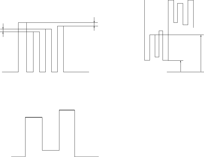
4-3
VPL-PX20/PX30
4-4-5. 15KRGB Level Adjustments
1. Input the 15K RGB 100% Color bar signal to INPUT-
A, select INPUT-A, and select RGB using SIGNAL
SELECT.
2. Set RGB MATRIX of Device adjust on the menu.
3. Connect the oscilloscope to TP612 on the C board.
4. Select 12 YUV COL, and adjust using the ← and →
keys so that the levels of the right bar and left bar
become the same.
5. Select 05 SUB HUE, and adjust using the ← and →
keys so that the two bars at the center become flat.
6. Press the ENTER key to select the SAVE TO
MEMORY of the menu, and press the ENTER key
again to save the data.
4-4-6. W/B HIGH Adjustments
1. Input the W/B HIGH adjustment signal to INPUT-A,
and connect the oscilloscope to TP605 on the C board.
2. Set the CONTRAST control to maximum position.
3. Enter the OTHER of the device adjust of the menu.
4. Set 06 3D GAMMA/THROUGH: 0 to 06 3D
GAMMA/THROUGH: 1.
5. Set 07 3D GAMMA/SW: 1
6. Set 07 3D GAMMA/SW: 0.
7. Enter the P DRV of the device adjust of the menu.
8. Adjust the lower side of the 100 IRE section of the
signal for 2.5 ± 0.05 Vdc with 11.VAMP/SUB CON
R.
9. Adjust the lower side of the 100 IRE section of the
signal for 6.5 ± 0.05 Vdc with 13.VAMP/SUB CON
B.
10. Input the W/B HIGH adjustment signal to INPUT-A,
and connect the oscilloscope to TP602 on the C board.
11. Adjust the lower side of the 100 IRE section of the
signal for 6.5 ± 0.05 Vdc with 12.VAMP/SUB CON
G.
12. Input the W/B HIGH adjustment signal to INPUT-A,
and connect the oscilloscope to TP608 on the C board.
13. Adjust the lower side of the 100 IRE section of the
signal for 6.5 ± 0.05 Vdc with 11.VAMP/SUB CON
R.
14. Select the SAVE TO MEMORY of the device adjust
of the menu, and press the ENTER key to save the
data.
15k Component
color bar
chroma ON
0 IRE
(0)
86.27 IRE
(220)
12.5 IRE
(32)
100 IRE
(225)
( ): SG ROM data
6.5 0.05Vdc
0V
2.5 0.05Vdc
4-4 VPL-PX20/PX30
15. Rest the CONTRAST to 80.
16. Connect the oscilloscope to TP605 on the C board.
17. Enter the WB ADJUST HIGH by the menu.
18. Adjust the DC level of signal’s 87.5 IRE section for 6.0
± 0.05 Vdc with GAIN B .
19. Connect the oscilloscope to TP602 on the C board.
20. Adjust the DC level of signal’s 87.5 IRE section for
6.0 ± 0.05 Vdc with GAIN G.
21. Connect the oscilloscope to TP608 on the C board.
22. Adjust the DC level of signal’s 87.5 IRE section for
6.0 ± 0.05 Vdc with GAIN G and adjust the lower side
of the 12.5 IRE section of the signal for 3.0 ± 0.05Vdc
with 13.VAMP/SUB CON B.
23. Connect the oscilloscope to TP608 on the C board.
24. Adjust the DC level of signal’s 87.5 IRE section for
6.0 ± 0.05 Vdc with GAIN R and adjust the DC level
of signal’s 12.5 IRE section for 3.0 ± 0.05 Vdc with
BIAS R.
25. Select the SAVE TO MEMORY from the W/B
ADJUST page of the menu, and press the ENTER key
to save the data.
4-4-7. W/B LOW Adjustments
1. Enter the RGB WB LOW by the menu.
2. Copy the adjusted value of the HIGH mode to the
R/G/B BIAS.
3. Enter the following value in the R/G/B GAIN.
R GAIN: HIGH mode + 5
G GAIN: HIGH mode _ 5
B GAIN: HIGH mode _ 15
4. Select the SAVE TO MEMORY from the W/B
ADJUST page of the menu, and press the ENTER key
to save the data.
5. Enter the OTHER of the device adjust of the menu.
6. Reset 06 3D GAMMA/THROUGH: 1 to 06 3D
GAMMA/THROUGH: 0.
7. Reset 07 3D GAMMA/SW: 0 to 07 3D GAMMA/SW:
1.
8. Select the SAVE TO MEMORY from the Device
adjust page of the menu, and press the ENTER key to
save the data.
4-4-8. Component Y Level Adjustment
1. Input the Component Y signal to INPUT-A (5BNC),
and select the COMPONENT by INPUT-A of the SET
SETTING.
2. Connect the oscilloscope to TP605 on the C board.
3. Enter the OTHER of the device adjust of the menu.
4. Set 06 3D GAMMA/THROUGH: 0 to 06 3D
GAMMA/THROUGH: 1.
5. Set 07 3D GAMMA/SW: 1 to 07 3D GAMMA/SW: 0.
6. Enter the WB ADJUST HIGN from the menu.
7. Adjust the 100 IRE section of the signal for 6.1 ± 0.05
Vdc with GAIN B and adjust the 12.5 IRE section of
the signal for 6.1 ± 0.05 Vdc with BIAS B.
8. Connect the oscilloscope to TP602 on the C board.
9. Adjust the 100 IRE section of the signal for 6.1 ± 0.05
Vdc with GAIN G and adjust the 100 IRE section of
the signal for 3.0 ± 0.05 Vdc with BIAS G
10. Connect the oscilloscope to TP608 on the C board.
6.0 0.05Vdc
0V
3.0 0.05Vdc
0
100 IRE
12.5 IRE
4-5
VPL-PX20/PX30
11. Adjust the 100 IRE section of the signal for 6.1 ± 0.05
Vdc with GAIN R and adjust the 100 IRE section of
the signal for 3.0 ± 0.05 Vdc with BAIS R.
12. Select the SAVE TO MEMORY from the W/B
ADJUST page of the menu, and press the ENTER key
to save the data.
13. Enter the OTHER of the device adjust of the menu.
14. Reset 06 3D GAMMA/THROUGH: 1 to 06 3D
GAMMA/THROUGH: 0.
15. Reset 07 3D GAMMA/SW: 0 to 07 3D GAMMA/SW: 1.
16. Select the SAVE TO MEMORY from the Device
adjust page of the menu, and press the ENTER key to
save the data.
4-5. VIDEO W/B Low Mode Adjustment
1. Input the component flat field signal to INPUT-A.
2. Select the INPUT-A, then select the COMPONENT
with INPUT-A of SET SETTING.
3. Set the D.PICTURE of PICTURE CONTROL to off.
4. Set the “06 3D GAMMA/THROUGH” to “0” (LUT ON).
5. Set the “07 3D GAMMA/SW” to “1” (3D GAMMA ON).
4-5-1. High Mode
1. Enter the HIGH MODE.
2. Make sure that the R/G/B GAIN and BIAS are
adjusted properly.
3. Input the 80 IRE component flat field signal to
INPUT-A.
4. Adjust the y value by the G GAIN of W/B HIGH.
When the x value after the y value adjustment is
greater than the specification, use the Blue as reference
color. If it is smaller than the specification, use the Red
as reference color. Adjust the color as shown below
with the GAIN other than the reference color.
5. Input the 30 IRE component flat field signal to INPUT-
A.
6. Adjust the color as shown below with the BIAS other
than the reference color.
7. Perform the 80 IRE and the 30 IRE adjustments above
repeatedly until the specifications are met.
8. Select the SAVE TO MEMORY from the W/B
ADJUST page of the menu, and press the ENTER key
to save the data.
HIGH MODE color specifications:
(x, y)=(0.275, 0.312) ± 0.005 (80 IRE)
(x, y)=(0.275, 0.312) ± 0.007 (30 IRE)
4-5-2. Low Mode
1. Enter the LOW MODE.
2. Make sure that the same data as W/B HIGH are
written in the R/G/B GAIN and BIAS.
3. Input the 80 IRE component flat field signal to
INPUT-A.
4. Adjust the Y value by the G GAIN. When the X value
after the Y value adjustment is greater than the
specification, use the Blue as reference color. If it is
smaller than the specification, use the Red as reference
color. Adjust the color as shown below with the GAIN
other than the reference color.
5. Input the 30 IRE component flat field signal to
INPUT-A.
6. Adjust the color as shown below with the BIAS other
than the reference color.
7. Perform the 80 IRE and the 30 IRE adjustments above
repeatedly until the specifications are met.
8. Select the SAVE TO MEMORY from the W/B
ADJUST page of the menu, and press the ENTER key
to save the data.
LOW MODE color specifications:
(x, y)=(0.283, 0.331) ± 0.005(80 IRE)
(x, y)=(0.283, 0.331) ± 0.007 (30 IRE)

4-6 VPL-PX20/PX30
4-6. Adjustments in Replacement of Prism
and Optical Unit
After replacement of the prism, set the factory mode, and
perform the following adjustment.
4-6-1. VCOM Adjustment
The bottom most menu item on the main menu is the
Device Adjustment Menu. Set this menu and select
“P. DRV.” Perform V COM adjustments for each of the
item “V COM/R,” “V COM/G,” and “V COM/B.”
In the above mode, as the built-in test pattern will be
output, adjust so that flicker is minimum throughout the
whole screen.
4-6-2. Polarization Plate Adjustment
Select “BB-GAMMA” on the device adjustment menu.
Press the “PIC MUTING” button and the whole screen will
become black. In this state, adjust the respective
polarization plate until the black becomes the darkest.
4-6-3. 3Dγ Adjustment (Outline)
The principle of 3Dγ is described before the adjustment of
3Dγ.
3Dγ is like a function which can individually adjust W/B at
a total of 180 points brightness 8 levels, horizontal
direction 6 points, vertical direction 5 points (8*6*5=160
points).
So altogether 540 adjustments (160*3 (RGB)=480) will be
required, which is in practice not possible. The following
describes a simpler method.
First the “GAMMA” menu consists of the following
hierarchy.
GAMMA LEVEL 0 POSITION 1
POSITION 2 R
:G
:B
POSITION 20
LEVEL 1
:
:
LEVEL 7
When adjusting a certain LEVEL, automatically the
internal signal (flat field) of that level will be displayed.
4-6-4. 3Dγ Adjustments
1. First input “GAMMA.”
2. Set LEVEL to 1.
3. Study the uniformity of the whole screen, and locate
the areas where uniformity is poor.
4. Changing “POSITION” to 1, 2, or 3 will display the
cursor. The position of the cursor is the position which
will be adjusted.
Move the cursor to the area with poor uniformity.
5. Move “R” and “B” up and down, and adjust so that the
uniformity is the same as the other areas.
6. Set LEVEL 2.
7. Like steps 3, 4, and 5, adjust the areas with poor
uniformity.
8. Adjust up to LEVEL 6.
9. Study the test pattern from LEVEL 1 to LEVEL 6, and
if no problems, return to the first hierarchy, adjust the
device, and save the data in SAVE TO MEMORY.
Precautions:
1. Basically adjust RED and BLUE only without
changing GREEN.
2. Do not adjust LEVEL 0 and LEVEL 7.
3. To set back factory settings should adjustments fail,
skip “SAVE TO MEMORY,” press the STANDBY
key, and turn off the power. All the adjusted data will
be set back to factory settings.
Factory settings cannot be set back however if “SAVE
TO MEMORY” has already been implemented. So
check the picture quality carefully prior to
implementing “SAVE TO MEMORY.”
4. For zoom lens, the uniformity will change slightly
according to the zoom position.
As uniformity will change slightly according to the F
number of the lens, perform the adjustments on the
projection system under the normal using conditions.
5. Do not change other items in the Device Adjust Menu.
The device adjust menu contains important parameters
for machine operations.
Unnecessary operations will result in “no image” and
“abnormal image.”
“Factory reset” cannot be performed on device adjust
menu items.
(Implementing SAVE TO MEMORY will completely
overwrite the data.)
Do not change data unnecessarily.

4-7
VPL-PX20/PX30
4-7. Adjustment Item Intialize Data
Memory Name
Device Name Item Name SET CHROMA MEMORY Remark
MEMORY NT358/NT443 Pal/Pal-M/N 15kRGB YCbCr YCbCr YPbPr HD
/BW60 /Secam/BW50 (15k) (Exc. 15k) -GBR
RGB MTRX/ CONTRAST 8 Fixed value
R DRIVE 30 30 30 30 30 30 30 Fixed value
G DRIVE 30 30 30 30 30 30 30 Fixed value
B DRIVE 30 30 30 30 30 30 30 Fixed value
SUB HUE 7 7 7 7 7 7 7
SUB BRT 54 Fixed value
R-Y/R 6 13 13 13 13 13 13 Fixed value
R-Y/B 12 15 15 15 15 15 15 Fixed value
G-Y/R 10 8 8 8 8 8 8 Fixed value
G-Y/B 5 4 4 4 4 4 4 Fixed value
YUV CON 7 7 11 11 11 11 11
YUV COL 12 12 12 12 12 12 12
SUB SHP 1 1 3 3 3 3 3 Fixed value
SHPFO 1 1 1 1 1 1 1 Fixed value
PRE OVER 0 0 0 0 0 0 0 Fixed value
DMIC PIC 3 Fixed value
CTI LVL 2 2 1 1 1 1 1 Fixed value
LTI LVL 1 1 1 1 0 0 0 Fixed value
D. COM/ VENH 5 Fixed value
CHROMA/ Y-OUT LVL 13 Fixed value
C-PUT LVL 18 Fixed value
Y-DL 5 Fixed value
S B-Y ADJ 7 Fixed value
S R-Y ADJ 7 Fixed value
S-INHBT 0 Fixed value
S-ID 0 Fixed value
S GP 0 Fixed value
S V-ID 0 Fixed value
BELL FO 0 Fixed value
HPF 0 Fixed value
SHP GAIN 8 8 8 8 8 8 8 Fixed value
SHP EQ 0 0 0 0 0 0 0 Fixed value
SHP FO 2 2 2 2 2 2 2 Fixed value
P. DRV/ VCOM G 40
VCOM R 37
VCOM B 40
SIG CEN 148 Fixed value
Note: There are nonadjustable items in accordance with the input signal.

4-8 VPL-PX20/PX30
Memory Name
Device Name Item Name SET CHROMA MEMORY Remarks
MEMORY NT358/NT443 Pal/Pal-M/N 15kRGB YCbCr YCbCr YPbPr HD
/BW60 /Secam/BW50 (15k) (Exc. 15) -GBR
P. DRV/ SID LVL 206 Fixed value
PRG LVL 86 Fixed value
INV CONT 0 Fixed value
SH/ SH1 10 Fixed value
SH2 200 Fixed value
VAMP CONT 190 Fixed value
SUB CON R 180
SUB CON G 180
SUB CON B 180
BRT 212 Fixed value
3D GAMMA/ SUB CONT 0 Fixed value
SUB BRT 0 Fixed valuel
R OSD LVL 16 Fixed value
G OSD LVL 16 Fixed value
B OSD LVL 16 Fixed value
THROUGH 0 Fixed value
SW 1 Fixed value
APC THRES 25 Fixed value
APC LIMIT 32 Fixed value
OTHER/ H START 143 Fixed value
V START 22 Fixed value
TEMP LAMP Nonadjustable Fixed value
TEMP PANEL Nonadjustable Fixed valuel
LAMP FAN1 Nonadjustable Fixed value
PANEL FAN1 Nonadjustable Fixed value
LAMP FAN2 Nonadjustable Fixed value
PANEL FAN2 Nonadjustable Fixed value
GAMMA Indication only
Note: There are nonadjustable items in accordance with the input signal.

4-9
VPL-PX20/PX30
Memory Name
Menu Title Item Name SET CH MEMORY
MEMORY VIDEO S Video INPUT-A INPUT-B
PICTURE CTRL CONTRAST 80 80 80 80
BRI GHT 50 50 50 50
COLOR 50 50 50 _
HUE 50 50 50 _
SHARP 50 50 50 _
RGB ENHANCER __30 30
D.PICTURE OFF OFF OFF _
GAMMA MODE __GRAPHICS GRAPHICS
COLOR TEMP LOW LOW HIGH HIGH
COLOR SYS AUTO AUTO AUTO AUTO
INPUT SETTING DOT PHASE
SIZE H
SHIFT
SCAN CONV
ASPECT
BLANKING
SET SETTING STATUS ON
INPUT-A COMPUTER
AUTO INPUT SEL OFF
LANGUAGE ENGLSH
SPEAKER ON
POWER SAVING OFF
SIRCS RECEIVER FRONT&REAR
INSTALL SETTING KEYSTONE MEM. ON
DIGIT KEYSTONE 0
INSTALLATION FLOOR-FRONT
LAMP MODE STANDARD
LAMP TIMER Indication only
INFORMATION fH Indication only
fV Indication only
ROM Ver Indication only
OPERATION TIMER Indication only
PREVIOUS LAMP TIMER Indication only
W/B ADJUST GAIN R
GAIN G
GAIN B
BIAS R
BIAS G
BIAS B
* : DOT PHASE, SIZE H, SHIFT H/V, SCAN CONV, ASPECT, and BLANKING in the “INPUT SETTING” menu have an
initial value respectively in accordance with the input signal (PRESET MEMORY No.).
Note :There are nonadjustable items in accordance with the input signal.

4-10 VPL-PX20/PX30
Menu Title Item Name Memory Name
STATUS W/B MEMORY
MEMORY VIDEO VIDEO RGB RGB
-HIGH -LOW -HIGH -LOW
PICTURE CTRL CONTRAST
BRI GHT
COLOR
HUE
SHARP
RGB ENHANCER
D.PICTURE
GAMMA MODE
COLOR TEMP
COLOR SYS
INPUT SETTING DOT PHASE 24(*)
SIZE H *
SHIFT *
SCAN CONV ON (*)
ASPECT 4 :3 (*)
BLANKING 0 (*)
SET SETTING STATUS
INPUT-A
AUTO INPUT SEL
LANGUAGE
SPEAKER
POWER SAVING
SIRCS RECEIVER
INSTALL SETTING KEYSTONE MEM.
DIGIT KEYSTONE
INSTALLATION
LAMP MODE
LAMP TIMER
INFORMATION FH
FV
ROM Ver
OPERATION TIMER
PREVIOUS LAMP TIMER
W/B ADJUST GAIN R 170 175 170 175
GAIN G 170 165 170 165
GAIN B 170 160 170 160
BIAS R 80 80 80 80
BIAS G 80 80 80 80
BIAS B 80 80 80 80
* : DOT PHASE, SIZE H, SHIFT H/V, SCAN CONV, ASPECT, and BLANKING in the “INPUT SETTING” menu have an
initial value respectively in accordance with the input signal (PRESET MEMORY No.).
Note :There are nonadjustable items in accordance with the input signal.
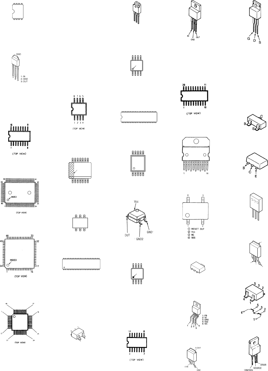
5-1
VPL-PX20/PX30
2SA1037K-T-146-R
2SA1162-YG-TE85L
2SA1213Y-TE12L
2SA1462
2SA1611T1-M5M6
2SC2412K-T-146-R
2SC2712-YG-TE85L
2SC3326N
2SC3545
DTC114EKA-T146
DTC144EKA-T146
2SC2873Y-TE12L
2SK2198
2SK2281-4061
FMS1-T-148
TOP223Y-BB
TA7812F
TEA2025D
TC74VHC244F
IMISM530AYB-D
M62399FP-TE2
TC74VHCT541AFT
TDA2009A
S-80828ANNP-EDR-T2
S-80840ANUP-ED4-T2
PQ20VZ1U
PQ20VZ5U
PQ05SZ1U
Section 5
Semiconductors
24LC21AT/SN
BA09FP-E2
BA12FP-E2
CXA1875AM-T4
EL4332CS
TC74HC4052AFT
MAX202CSE-T
CXA2101AQ
CXA2112R-T6
CXD2064Q-T6
CXA1946AR
1
8
4
5
INDEX
8
1
5
4
V
SS
V
OO
OUT
GS1881-CTA
TC7W14FU (TE12R)
TC7W02FU (TE12R)
BA033FP-E2
TC4W53F
GS4981CTA
LM358P
SN75157
TC7W08FU
TL082CPS-E20
TL431BCDR2
UPC393G2-E2
MC100ELT20DR2
NJM082BM
TC7W14F (TE12R)
SN75453BPSR
ST49C101ACF8-05-TR
HA4314BCB-E2
HN1D03FU-TE85R
IDT71V016S15PH-TL
LP29851M5X-3.5
LM7131BCM5X
TC7S04FU
TC7S66FU
TC75S56F (TE85R)
TC7SH14FU (TE85R)
1
14
7
8
INDEX
AREA
64
13
44
1
23
22
123
1:OUT
2:IN
3:GND
LM2990SX
MAX4223ESA-TG08
M24C64-WMN6T
M52749FP-TP
M62438FP-600C
RS-140-T
TC7WH04FU (TE12R)
TC74VHC86FT (EL)
TC74HC02AF (EL)
TC74LCX04FT
TC74VHC14FT
TC74LCX125FT
42
1
22
21
10
1
6
5
GDS
D
1
8
4
5
(TOP VIEW)
INDEX
S
D
G
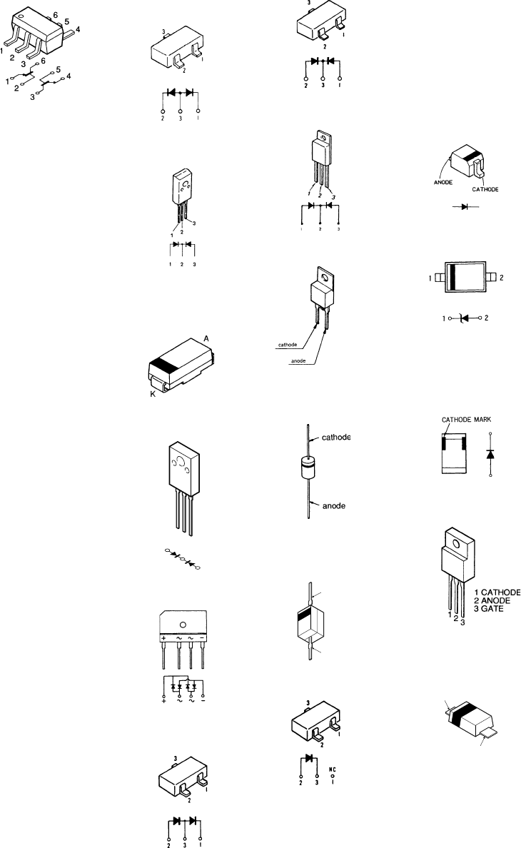
5-2 VPL-PX20/PX30
HN1B01FU-TE85R 1S2836-T1
DAP202K-T-146
FMG-G2CS
D10SC9M
D1FL20U-TA
D1FS4A-TA
D2FL20U
D5LC20U
D6SB80
DA204K-T-146
MA157-TX
3
3
2
2
1
1
ANODE
CATHODE
DAN202K-T-146
FCQ20A06
FSF10A60
P6KE350A
RM11A
P6KE200AG23
P6KE300A
P6KE350A
RD12M-T1B2
ANODE
CATHODE
RD4.7SB-T1
UDZ-TE-17-3.3B
1SS355TE-17
MA111
RB501V-40TE-17
RD3.3SB2-T1
RD9.1SB2-T1
UDZ-TE-17-3.9B
D2FS6-TA
RD5.6SB-T1
RD27SB-T1
RD5.6SB2-T1
SEC1401C
SEC1801C
SEC1901C
SEC2422C
TF861S
UDZ-TE-17-2.2B
UDZ-TE-17-27B
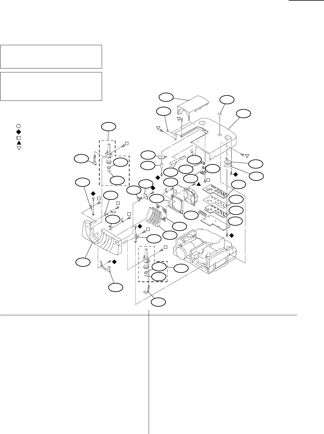
VPL-PX20/PX30 6-1
REF NO. PART NO. DESCRIPTION REMARK
6-1. Cabinet
REF NO. PART NO. DESCRIPTION REMARK
: 7-682-148-01 +P3x8
: 7-682-903-11 +PWH3x6
: 7-685-648-79 +PVTP3x12
: 7-682-663-09 +BSWP4x12
: 7-682-548-04 +PWH3x8
1
2
3
4
5
6
7
8
9
7
8
9
10
11
12
13
14
15
17
16
18
19 20
21
22
23
24 25
26
27
28
27
28
29
30
31
32
33
Section 6
Exploded Views
• Items marked “ * ” are not stocked since they are seldom required
for routine service. Some delay should be anticipated when order-
ing these items.
• Items with no part number and no description are not stocked be-
cause they are seldom required for routine service.
• The construction parts of an assembled part are indicated with a
collation number in the remarks column.
The components identified marked ! are
critical for safety.
Replace only with the part number specified.
Les composants identifiés par la marque !
sont critiques pour la sécurité.
Ne les remplacer que par une pièce portant
le numéro spécifié.
NOTE :
Cabinet
1 * X-4037-378-1 COVER ASSY, FRONT
2 4-073-765-01 COVER (BT), LENS
3 * 4-073-760-01 HOLDER (FBHL)
4 * 4-073-759-01 HOLDER (FBHR)
5 * 4-073-763-01 HOLDER (FHL)
6 * 4-073-762-01 HOLDER (FHR)
7 X-4037-376-1 ADJUSTER ASSY 8, 9
8 4-073-784-01 SHAFT, ADJUSTABLE
9 4-073-783-01 SHEET, UR
10 4-073-767-01 LEVER (L), ADJUSTER
11 4-073-766-01 LEVER (R), ADJUSTER
12 * 4-073-758-01 RM (FR)
13 * 1-675-457-11 NF BOARD
14 * 4-073-772-01 DUCT, FAN
15 * 4-073-771-01 NET, FAN
16 * 4-073-770-01 HOLDER, FAN
17 1-763-422-11 FAN, DC
18 * 4-073-768-01 HOOD
19 * 4-073-764-01 COVER (TP), LENS
20 * 4-073-773-01 EMBLEM (PX30)
21 * 4-063-685-01 FOOT
22 * 4-073-774-01 GUARD (H1), LIGHTING
23 * 4-073-775-01 SPACER (H)
24 * 4-063-672-01 STOPPER (LCT)
25 * 4-063-686-01 SPRING, COMPRESSION
26 * 4-063-673-01 HOLDER (LCT)
27 1-529-499-11 SPEAKER (4.5CM)
28 * 4-073-777-01 HOLDER (T), SP
29 4-073-747-01 BUTTON, CONTROL
30 * 4-073-748-01 GUIDE, BUTTON
31 * A-1375-193-A H COMPL
32 * 4-073-746-01 GUIDE, LED
33 * 4-074-574-01 GUID (H2), LIGHTING
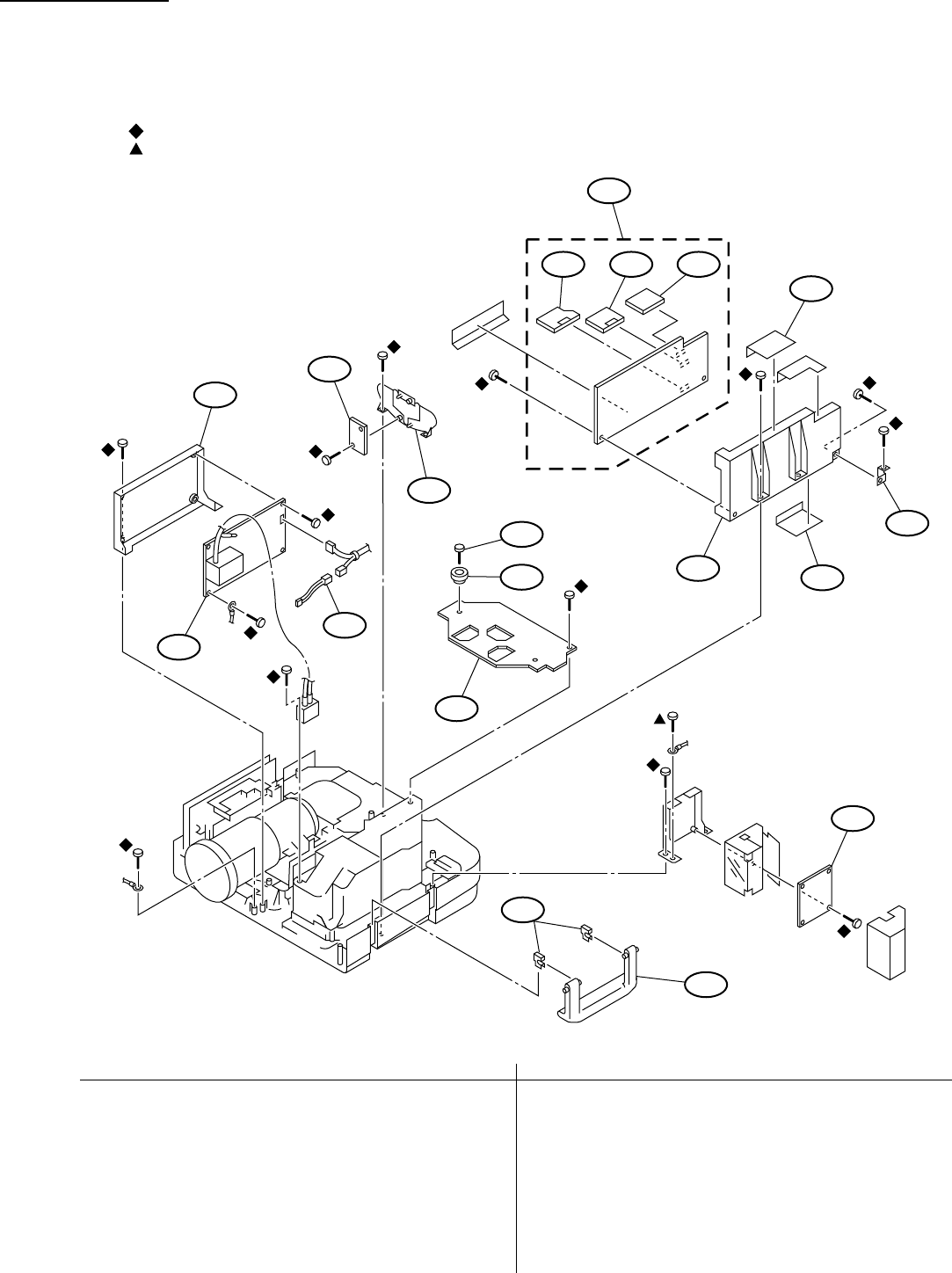
VPL-PX20/PX30
6-2
REF NO. PART NO. DESCRIPTION REMARK
6-2. Chassis Block
REF NO. PART NO. DESCRIPTION REMARK
Chassis Block
REF NO. PART NO. DESCRIPTION REMARK
51 * 4-073-731-01 HOLDER (L)
52 !1-468-445-11 POWER BLOCK
53 1-900-249-68 CONNECTOR ASSY, FUSE 2P
54 * A-1335-121-A C COMPL
55 * A-1390-974-A NR MOUNT
56 * X-4037-377-1 RM (ER) ASSY
57 * 4-073-752-01 BUSH, HANDLE
58 4-073-753-01 HANDLE
59 * A-1241-395-A F MOUNT
60 * 4-073-730-01 HOLDER (G)
61 * A-1316-486-A GA COMPL 62-64
62 * A-1316-485-A GD COMPL
63 * A-1316-484-A GC COMPL
64 * A-1316-487-A GB COMPL
65 * 4-073-735-01 PLATE (G), EARTH
66 * 4-073-990-01 SHEET (G2), INSULATOR
67 4-074-968-01 SPACER (C)
68 3-701-809-31 SCREW, TERMINAL (M3X8)
51
52
53
54
55
56
57
58
59
60
61
62 64 63
65
66
66
67
68
: 7-682-903-01 +PWH3x6
: 7-685-663-09 +PSW4x12
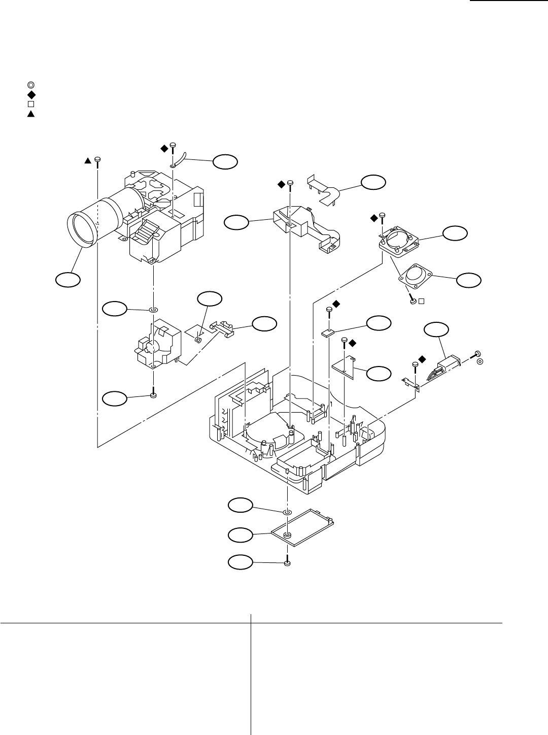
VPL-PX20/PX30 6-3
6-3. Optics Unit
REF NO. PART NO. DESCRIPTION REMARK REF NO. PART NO. DESCRIPTION REMARK
Optics Unit
101 1-758-440-11 OPTICAL UNIT (VPL-PX30)
1-758-452-11 OPTICAL UNIT (VPL-PX20)
102 * 4-073-740-01 HOLDER (L), SPEAKER
103 1-505-600-11 SPEAKER (065W004)
104 3-701-822-01 HOLDER, WIRE
105 * 3-715-526-01 WASHER (M3)
106 4-066-202-01 SCREW, M3
107 * 4-073-788-01 SPRING, DOOR
108 * 4-073-787-01 DOOR, DUCT
109 * 4-073-729-01 DUCT
110 * 4-073-728-01 COVER, DUCT
111 * A-1390-975-A S MOUNT
112 * A-1385-189-A K COMPL
113 !1-526-813-12 INLET, AC (3P)
115 * 4-073-750-01 LAMP COVER
116 4-073-989-01 SCREW (+B M3X12), PREVENTION
68 663 09 S
101
102
103
104
105
106
107
108
109
110
111
112
113
114
115
116
: 7-682-246-09 +K3x5
: 7-682-903-11 +BWH3x6
: 7-685-648-79 +BVTP3x12
: 7-682-663-09 +PSW4x12
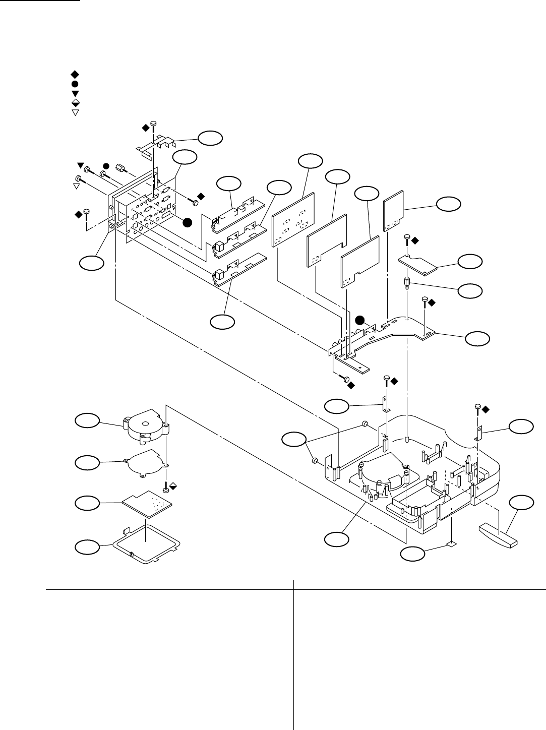
VPL-PX20/PX30
6-4
REF NO. PART NO. DESCRIPTION REMARK
6-4. Base Block
REF NO. PART NO. DESCRIPTION REMARK
Base Block
151 * A-1136-039-A BB COMPL
152 4-066-549-11 SPACER
153 * A-1385-190-A KS COMPL
154 * A-1136-040-A BC COMPL
155 * A-1394-958-A Y COMPL
156 * A-1136-038-A BA COMPL
157 * A-1275-178-A QA COMPL
158 * A-1275-180-A QB COMPL
159 * A-1275-179-A QC COMPL
160 * A-1275-181-A QD COMPL
161 * 4-073-744-01 PANEL, CONNECTOR
162 * 4-073-745-01 HOLDER, CONNECTOR PANEL
163 * 4-073-749-01 HOLDER, PWB
164 * 4-073-761-01 HOLDER (BH)
165 * 4-063-685-01 FOOT
166 * 4-073-751-01 CUSHION, HANDLE
167 * 4-073-741-01 FOOT (RE)
168 1-763-417-11 FAN, DC
169 * 4-073-739-01 GUARD, FAN
170 4-073-737-01 FILTER
171 * 4-073-738-01 COVER, FILTER
172 * X-4037-413-1 BASE ASSY
: 7-682-903-11 +PWH3x6
: 7-621-259-52 +P2.6x8
: 7-621-772-38 +B2x6
: 7-682-568-09 +B4x13
: 7-682-548-04 +PWH3x8
A
A
151
152
153
154
155
156
157
158
159
160
161
162
163
164
164
165
166
167
168
169
170
171 172
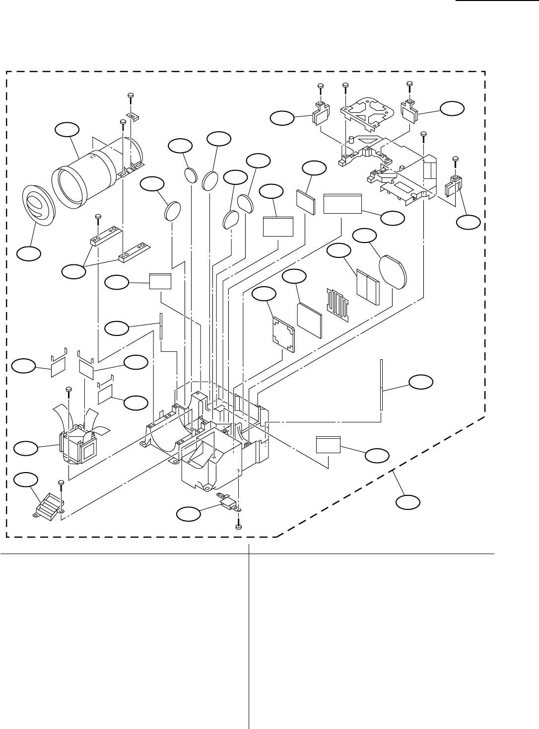
VPL-PX20/PX30 6-5
REF NO. PART NO. DESCRIPTION REMARK
Optical Unit
6-5. Optical unit
REF NO. PART NO. DESCRIPTION REMARK
201 1-758-440-11 OPTICAL UNIT (VPL-PX30) 202-229
1-758-452-11 OPTICAL UNIT (VPL-PX20) 202-229
202 9-885-000-52 PROJECTION LENS
203 9-885-000-65 SPACER
204 1-758-459-11 PRISM BLOCK
205 9-885-000-76 POLORIZER, G-OUT PLATE
206 9-885-000-72 POLORIZER, G-OUT PLATE
207 9-885-000-74 POLORIZER, G-OUT PLATE
208 * 9-885-000-63 MIRROR C
209 * 9-885-000-62 MIRROR B
210 * 9-885-000-64 MIRROR D
211 * 9-885-000-61 MIRROR A
212 * 9-885-000-69 UV PROOF GLASS
213 * 9-885-000-60 G REFLECTION DICHROIC MIRROR
214 * 9-885-000-59 B REFLECTION DICHROIC MIRROR
215 9-885-000-53 LENS A, FLYEYE
216 * 9-885-000-54 LENS B, FLYEYE
217 9-885-000-55 FLYEYE/PS CONVERTER LENS
218 * 9-885-000-66 MAIN CONDENSER LENS
219 * 9-885-000-68 LENS B, RELAY
220 9-885-000-58 POLARIZER, R/CONDENSER LENS
221 9-885-000-57 POLARIZER, B/CONDENSER LENS
222 9-885-000-56 POLARIZER, G/CONDENSER LENS
223 * 9-885-000-67 LENS A, RELAY
224 9-885-000-75 POLORIZER, R-IN PLATE
225 9-885-000-71 POLORIZER, G-IN PLATE
226 9-885-000-73 POLORIZER, B-IN PLATE
227 4-073-776-01 GUARD (L), LIGHTING
228 4-073-785-01 DUCT (F)
229 9-885-000-70 CAP, LENS
201
202
203
204
205 206
207
208
209
210
211
213
212
214
215
216
217
218
219
220 221
222
223
224
225
226
227
228
229

7-1
VPL-PX20/PX30
Ref.No. Part No. Description RemarkRef.No. Part No. Description Remark
*A-1136-038-A BA COMPL
**********************
<CAPACITOR>
C101 1-131-998-21 TANTALUM 82µF 20% 6.3V
C102 1-128-065-11 ELECT CHIP 68µF 20% 10V
C103 1-164-004-11 CERAMIC CHIP 0.1µF 10% 25V
C104 1-163-021-91 CERAMIC CHIP 0.01µF 10% 50V
C105 1-163-227-11 CERAMIC CHIP 10PF 0.5PF 50V
C106 1-128-004-11 ELECT CHIP 10µF 20% 16V
C107 1-165-319-11 CERAMIC CHIP 0.1µF 50V
C108 1-164-004-11 CERAMIC CHIP 0.1µF 10% 25V
C109 1-164-004-11 CERAMIC CHIP 0.1µF 10% 25V
C110 1-163-021-91 CERAMIC CHIP 0.01µF 10% 50V
C111 1-163-275-11 CERAMIC CHIP 0.001µF 5% 50V
C112 1-107-823-11 CERAMIC CHIP 0.47µF 10% 16V
C114 1-163-021-91 CERAMIC CHIP 0.01µF 10% 50V
C115 1-131-998-21 TANTALUM 82µF 20% 6.3V
C116 1-107-682-11 CERAMIC CHIP 1µF 10% 16V
C117 1-163-021-91 CERAMIC CHIP 0.01µF 10% 50V
C118 1-127-820-91 CERAMIC 4.7µF 0 16V
C119 1-165-319-11 CERAMIC CHIP 0.1µF 50V
C120 1-164-004-11 CERAMIC CHIP 0.1µF 10% 25V
C121 1-107-682-11 CERAMIC CHIP 1µF 10% 16V
C122 1-164-004-11 CERAMIC CHIP 0.1µF 10% 25V
C123 1-164-004-11 CERAMIC CHIP 0.1µF 10% 25V
C124 1-164-004-11 CERAMIC CHIP 0.1µF 10% 25V
C125 1-164-004-11 CERAMIC CHIP 0.1µF 10% 25V
C126 1-164-004-11 CERAMIC CHIP 0.1µF 10% 25V
C127 1-164-004-11 CERAMIC CHIP 0.1µF 10% 25V
C128 1-164-004-11 CERAMIC CHIP 0.1µF 10% 25V
C131 1-115-565-11 CERAMIC CHIP 2.2µF 10% 10V
C133 1-163-037-11 CERAMIC CHIP 0.022µF 10% 50V
C136 1-163-021-91 CERAMIC CHIP 0.01µF 10% 50V
C137 1-107-682-11 CERAMIC CHIP 1µF 10% 16V
C138 1-164-004-11 CERAMIC CHIP 0.1µF 10% 25V
C139 1-163-021-91 CERAMIC CHIP 0.01µF 10% 50V
C140 1-107-682-11 CERAMIC CHIP 1µF 10% 16V
C141 1-163-021-91 CERAMIC CHIP 0.01µF 10% 50V
C142 1-128-004-11 ELECT CHIP 10µF 20% 16V
C143 1-163-235-11 CERAMIC CHIP 22PF 5% 50V
C144 1-128-065-11 ELECT CHIP 68µF 20% 10V
C145 1-163-021-91 CERAMIC CHIP 0.01µF 10% 50V
C146 1-128-065-11 ELECT CHIP 68µF 20% 10V
C147 1-163-021-91 CERAMIC CHIP 0.01µF 10% 50V
C149 1-126-204-11 ELECT CHIP 47µF 20% 16V
C150 1-164-004-11 CERAMIC CHIP 0.1µF 10% 25V
C151 1-128-004-11 ELECT CHIP 10µF 20% 16V
C152 1-164-004-11 CERAMIC CHIP 0.1µF 10% 25V
C153 1-126-204-11 ELECT CHIP 47µF 20% 16V
C154 1-107-823-11 CERAMIC CHIP 0.47µF 10% 16V
C155 1-107-823-11 CERAMIC CHIP 0.47µF 10% 16V
C156 1-107-823-11 CERAMIC CHIP 0.47µF 10% 16V
C157 1-107-823-11 CERAMIC CHIP 0.47µF 10% 16V
C158 1-107-823-11 CERAMIC CHIP 0.47µF 10% 16V
C159 1-107-823-11 CERAMIC CHIP 0.47µF 10% 16V
C160 1-107-823-11 CERAMIC CHIP 0.47µF 10% 16V
C161 1-107-823-11 CERAMIC CHIP 0.47µF 10% 16V
C162 1-107-823-11 CERAMIC CHIP 0.47µF 10% 16V
C163 1-107-823-11 CERAMIC CHIP 0.47µF 10% 16V
C164 1-107-823-11 CERAMIC CHIP 0.47µF 10% 16V
C165 1-128-004-11 ELECT CHIP 10µF 20% 16V
C166 1-128-004-11 ELECT CHIP 10µF 20% 16V
C167 1-164-004-11 CERAMIC CHIP 0.1µF 10% 25V
C168 1-164-004-11 CERAMIC CHIP 0.1µF 10% 25V
C169 1-128-065-11 ELECT CHIP 68µF 20% 10V
C170 1-164-161-11 CERAMIC CHIP 0.0022µF 10% 50V
C171 1-164-004-11 CERAMIC CHIP 0.1µF 10% 25V
C172 1-107-823-11 CERAMIC CHIP 0.47µF 10% 16V
C173 1-164-004-11 CERAMIC CHIP 0.1µF 10% 25V
C174 1-107-823-11 CERAMIC CHIP 0.47µF 10% 16V
C175 1-107-823-11 CERAMIC CHIP 0.47µF 10% 16V
C176 1-164-004-11 CERAMIC CHIP 0.1µF 10% 25V
C177 1-128-004-11 ELECT CHIP 10µF 20% 16V
C178 1-164-004-11 CERAMIC CHIP 0.1µF 10% 25V
C179 1-107-823-11 CERAMIC CHIP 0.47µF 10% 16V
C180 1-128-004-11 ELECT CHIP 10µF 20% 16V
C181 1-163-021-91 CERAMIC CHIP 0.01µF 10% 50V
C182 1-107-823-11 CERAMIC CHIP 0.47µF 10% 16V
C183 1-126-205-11 ELECT CHIP 47µF 20% 6.3V
C184 1-107-823-11 CERAMIC CHIP 0.47µF 10% 16V
C185 1-109-982-11 CERAMIC CHIP 1µF 10% 10V
C186 1-126-205-11 ELECT CHIP 47µF 20% 6.3V
C187 1-126-204-11 ELECT CHIP 47µF 20% 16V
C188 1-164-004-11 CERAMIC CHIP 0.1µF 10% 25V
C189 1-107-823-11 CERAMIC CHIP 0.47µF 10% 16V
C190 1-107-823-11 CERAMIC CHIP 0.47µF 10% 16V
C191 1-107-823-11 CERAMIC CHIP 0.47µF 10% 16V
C192 1-107-823-11 CERAMIC CHIP 0.47µF 10% 16V
BA
The components identified marked ! are
critical for safety.
Replace only with the part number specified.
Les composants identifiés par la marque !
sont critiques pour la sécurité.
Ne les remplacer que par une pièce portant
le numéro spécifié.
NOTE :
• Items marked “ * ” are not stocked since they are seldom required
for routine service. Some delay should be anticipated when order-
ing these items.
• Due to standardization, replacements in the parts list may be dif-
ferent from the parts specified in the diagrams or the components
used on the set.
RESISTORS
• All resistors are in ohms.
• F: nonflammable
• METAL: Metal-film resistor
• METAL OXIDE: Metal oxide-film resistor
Section 7
Electrical Parts List

7-2 VPL-PX20/PX30
Ref.No. Part No. Description RemarkRef.No. Part No. Description Remark
C193 1-107-823-11 CERAMIC CHIP 0.47µF 10% 16V
C194 1-107-823-11 CERAMIC CHIP 0.47µF 10% 16V
C195 1-107-823-11 CERAMIC CHIP 0.47µF 10% 16V
C196 1-107-823-11 CERAMIC CHIP 0.47µF 10% 16V
C197 1-107-823-11 CERAMIC CHIP 0.47µF 10% 16V
C198 1-128-013-11 ELECT CHIP 1µF 20% 50V
C199 1-107-823-11 CERAMIC CHIP 0.47µF 10% 16V
C200 1-107-823-11 CERAMIC CHIP 0.47µF 10% 16V
C201 1-107-823-11 CERAMIC CHIP 0.47µF 10% 16V
C202 1-107-823-11 CERAMIC CHIP 0.47µF 10% 16V
C203 1-163-021-91 CERAMIC CHIP 0.01µF 10% 50V
C204 1-128-013-11 ELECT CHIP 1µF 20% 50V
C205 1-107-823-11 CERAMIC CHIP 0.47µF 10% 16V
C206 1-107-823-11 CERAMIC CHIP 0.47µF 10% 16V
C207 1-126-205-11 ELECT CHIP 47µF 20% 6.3V
C208 1-107-823-11 CERAMIC CHIP 0.47µF 10% 16V
C209 1-107-823-11 CERAMIC CHIP 0.47µF 10% 16V
C210 1-163-245-11 CERAMIC CHIP 56PF 5% 50V
C211 1-163-235-11 CERAMIC CHIP 22PF 5% 50V
C212 1-126-206-11 ELECT CHIP 100µF 20% 6.3V
C213 1-165-319-11 CERAMIC CHIP 0.1µF 50V
C214 1-163-237-11 CERAMIC CHIP 27PF 5% 50V
C215 1-163-245-11 CERAMIC CHIP 56PF 5% 50V
C216 1-128-004-11 ELECT CHIP 10µF 20% 16V
C218 1-163-237-11 CERAMIC CHIP 27PF 5% 50V
C219 1-163-245-11 CERAMIC CHIP 56PF 5% 50V
C220 1-163-021-91 CERAMIC CHIP 0.01µF 10% 50V
C221 1-126-204-11 ELECT CHIP 47µF 20% 16V
C222 1-126-204-11 ELECT CHIP 47µF 20% 16V
C223 1-164-004-11 CERAMIC CHIP 0.1µF 10% 25V
C224 1-163-021-91 CERAMIC CHIP 0.01µF 10% 50V
C225 1-107-823-11 CERAMIC CHIP 0.47µF 10% 16V
C226 1-107-823-11 CERAMIC CHIP 0.47µF 10% 16V
C227 1-107-823-11 CERAMIC CHIP 0.47µF 10% 16V
C239 1-164-004-11 CERAMIC CHIP 0.1µF 10% 25V
C240 1-164-004-11 CERAMIC CHIP 0.1µF 10% 25V
C241 1-164-004-11 CERAMIC CHIP 0.1µF 10% 25V
C242 1-164-004-11 CERAMIC CHIP 0.1µF 10% 25V
C243 1-163-037-11 CERAMIC CHIP 0.022µF 10% 50V
C244 1-163-009-11 CERAMIC CHIP 0.001µF 10% 50V
C250 1-164-004-11 CERAMIC CHIP 0.1µF 10% 25V
C251 1-164-004-11 CERAMIC CHIP 0.1µF 10% 25V
C252 1-126-204-11 ELECT CHIP 47µF 20% 16V
C253 1-164-004-11 CERAMIC CHIP 0.1µF 10% 25V
C254 1-164-004-11 CERAMIC CHIP 0.1µF 10% 25V
C256 1-163-131-00 CERAMIC CHIP 390PF 5% 50V
C257 1-164-004-11 CERAMIC CHIP 0.1µF 10% 25V
C258 1-135-346-21 TANTALUM 39µF 20% 16V
C259 1-126-204-11 ELECT CHIP 47µF 20% 16V
C260 1-164-004-11 CERAMIC CHIP 0.1µF 10% 25V
C261 1-164-004-11 CERAMIC CHIP 0.1µF 10% 25V
C263 1-128-065-11 ELECT CHIP 68µF 20% 10V
C264 1-128-065-11 ELECT CHIP 68µF 20% 10V
C265 1-164-004-11 CERAMIC CHIP 0.1µF 10% 25V
C266 1-163-251-11 CERAMIC CHIP 100PF 5% 50V
C267 1-117-681-11 ELECT CHIP 100µF 20% 16V
<CONNECTOR>
CN101 *1-793-797-21 CONNECTOR, BOARD TO BOARD
CN102 *1-580-789-21 PIN, CONNECTOR (SMD) 6P
<DIODE>
D101 8-719-988-61 DIODE 1SS355TE-17
<FILTER>
FL100 1-233-736-21 FILTER, EMI
FL101 1-233-736-21 FILTER, EMI
FL102 1-233-736-21 FILTER, EMI
FL106 1-233-736-21 FILTER, EMI
FL107 1-233-736-21 FILTER, EMI
FL251 1-239-466-21 FILTER, EMI
<IC>
IC101 8-752-094-47 IC CXA2123AQ-T6
IC102 8-752-086-33 IC CXA2101AQ-TL
IC103 8-759-242-64 IC TC4W53F
IC105 8-759-031-84 IC SC7S04F
IC106 8-759-031-84 IC SC7S04F
IC221 8-752-390-37 IC CXD2064Q-T6
IC250 8-752-072-94 IC CXA1875AM-T4
IC251 8-759-242-64 IC TC4W53F
IC252 8-759-031-84 IC SC7S04F
IC253 8-759-494-88 IC TC75S56F(TE85R)
IC254 8-759-084-79 IC TC7S14F
IC255 8-759-460-79 IC BA09FP-E2
IC256 8-759-344-12 IC GS4981CTA
IC257 8-759-038-15 IC MC74HC4538AF
IC258 8-759-157-17 IC PQ05SZ1U
IC259 8-759-433-92 IC TC7W14F-TE12L
<COIL>
L100 1-412-058-11 INDUCTOR CHIP 10µH
L101 1-412-058-11 INDUCTOR CHIP 10µH
L102 1-412-058-11 INDUCTOR CHIP 10µH
L103 1-412-058-11 INDUCTOR CHIP 10µH
L104 1-412-058-11 INDUCTOR CHIP 10µH
L105 1-412-058-11 INDUCTOR CHIP 10µH
L106 1-412-363-21 FERRITE 0µH
L108 1-412-363-21 FERRITE 0µH
L109 1-412-363-21 FERRITE 0µH
L110 1-410-389-31 INDUCTOR CHIP 47µH
L111 1-410-385-11 INDUCTOR CHIP 22µH
L112 1-410-383-31 INDUCTOR CHIP 15µH
L113 1-410-383-31 INDUCTOR CHIP 15µH
L251 1-409-556-11 INDUCTOR 47µH
<TRANSISTOR>
Q101 8-729-120-28 TRANSISTOR 2SC1623-L5L6
Q103 8-729-230-49 TRANSISTOR 2SC2712-YG
Q107 8-729-120-28 TRANSISTOR 2SC1623-L5L6
Q108 8-729-230-49 TRANSISTOR 2SC2712-YG
Q109 8-729-120-28 TRANSISTOR 2SC1623-L5L6
Q110 8-729-230-49 TRANSISTOR 2SC2712-YG
Q111 8-729-230-49 TRANSISTOR 2SC2712-YG
Q112 8-729-902-96 TRANSISTOR FMS1
Q113 8-729-902-96 TRANSISTOR FMS1
Q114 8-729-902-96 TRANSISTOR FMS1
Q115 8-729-107-31 TRANSISTOR 2SC3545-T43
Q116 8-729-107-31 TRANSISTOR 2SC3545-T43
Q117 8-729-107-31 TRANSISTOR 2SC3545-T43
Q118 8-729-216-22 TRANSISTOR 2SA1162-G
Q119 1-801-806-11 TRANSISTOR DTC144EKA-T146
Q120 8-729-230-49 TRANSISTOR 2SC2712-YG
Q121 8-729-216-22 TRANSISTOR 2SA1162-G
Q122 8-729-230-49 TRANSISTOR 2SC2712-YG
Q123 8-729-216-22 TRANSISTOR 2SA1162-G
Q124 8-729-230-49 TRANSISTOR 2SC2712-YG
BA

7-3
VPL-PX20/PX30
Ref.No. Part No. Description RemarkRef.No. Part No. Description Remark
Q125 8-729-216-22 TRANSISTOR 2SA1162-G
Q126 8-729-230-49 TRANSISTOR 2SC2712-YG
Q127 8-729-216-22 TRANSISTOR 2SA1162-G
Q128 8-729-230-49 TRANSISTOR 2SC2712-YG
Q129 8-729-230-49 TRANSISTOR 2SC2712-YG
Q130 8-729-216-22 TRANSISTOR 2SA1162-G
<RESISTOR>
R102 1-216-077-91 RES,CHIP 15K 5% 1/10W
R104 1-216-049-91 RES,CHIP 1K 5% 1/10W
R105 1-216-678-11 METAL CHIP 13K 0.50% 1/10W
R106 1-216-631-11 METAL CHIP 150 0.50% 1/10W
R107 1-216-049-91 RES,CHIP 1K 5% 1/10W
R108 1-216-651-11 METAL CHIP 1K 0.50% 1/10W
R109 1-216-639-11 METAL CHIP 330 0.50% 1/10W
R110 1-216-685-11 METAL CHIP 27K 0.50% 1/10W
R111 1-216-631-11 METAL CHIP 150 0.50% 1/10W
R112 1-216-619-11 METAL CHIP 47 0.50% 1/10W
R113 1-216-081-00 RES,CHIP 22K 5% 1/10W
R114 1-216-081-00 RES,CHIP 22K 5% 1/10W
R115 1-216-061-00 RES,CHIP 3.3K 5% 1/10W
R116 1-216-295-91 SHORT 0
R118 1-216-683-11 METAL CHIP 22K 0.50% 1/10W
R119 1-208-796-11 METAL CHIP 3.9K 0.50% 1/10W
R120 1-216-025-91 RES,CHIP 100 5% 1/10W
R121 1-216-017-91 RES,CHIP 47 5% 1/10W
R122 1-216-644-11 METAL CHIP 510 0.50% 1/10W
R123 1-216-639-11 METAL CHIP 330 0.50% 1/10W
R124 1-216-683-11 METAL CHIP 22K 0.50% 1/10W
R125 1-216-047-91 RES,CHIP 820 5% 1/10W
R126 1-216-061-00 RES,CHIP 3.3K 5% 1/10W
R127 1-216-649-11 METAL CHIP 820 0.50% 1/10W
R130 1-216-025-91 RES,CHIP 100 5% 1/10W
R131 1-216-057-00 RES,CHIP 2.2K 5% 1/10W
R132 1-216-025-91 RES,CHIP 100 5% 1/10W
R133 1-216-631-11 METAL CHIP 150 0.50% 1/10W
R134 1-216-025-91 RES,CHIP 100 5% 1/10W
R136 1-216-631-11 METAL CHIP 150 0.50% 1/10W
R137 1-216-049-91 RES,CHIP 1K 5% 1/10W
R138 1-216-295-91 SHORT 0
R139 1-216-295-91 SHORT 0
R140 1-216-081-00 RES,CHIP 22K 5% 1/10W
R141 1-216-081-00 RES,CHIP 22K 5% 1/10W
R142 1-216-295-91 SHORT 0
R143 1-216-129-00 RES,CHIP 2.2M 5% 1/10W
R147 1-216-049-91 RES,CHIP 1K 5% 1/10W
R148 1-216-025-91 RES,CHIP 100 5% 1/10W
R149 1-216-295-91 SHORT 0
R150 1-216-025-91 RES,CHIP 100 5% 1/10W
R151 1-216-017-91 RES,CHIP 47 5% 1/10W
R152 1-216-047-91 RES,CHIP 820 5% 1/10W
R153 1-216-631-11 METAL CHIP 150 0.50% 1/10W
R154 1-216-631-11 METAL CHIP 150 0.50% 1/10W
R155 1-216-049-91 RES,CHIP 1K 5% 1/10W
R156 1-216-049-91 RES,CHIP 1K 5% 1/10W
R157 1-216-049-91 RES,CHIP 1K 5% 1/10W
R158 1-216-083-00 RES,CHIP 27K 5% 1/10W
R159 1-216-089-91 RES,CHIP 47K 5% 1/10W
R160 1-216-017-91 RES,CHIP 47 5% 1/10W
R161 1-216-025-91 RES,CHIP 100 5% 1/10W
R162 1-216-025-91 RES,CHIP 100 5% 1/10W
R163 1-216-133-00 RES,CHIP 3.3M 5% 1/10W
R164 1-216-039-00 RES,CHIP 390 5% 1/10W
R165 1-216-295-91 SHORT 0
R166 1-216-039-00 RES,CHIP 390 5% 1/10W
R167 1-216-295-91 SHORT 0
R168 1-216-017-91 RES,CHIP 47 5% 1/10W
R169 1-216-017-91 RES,CHIP 47 5% 1/10W
R170 1-216-041-00 RES,CHIP 470 5% 1/10W
R172 1-216-041-00 RES,CHIP 470 5% 1/10W
R174 1-216-041-00 RES,CHIP 470 5% 1/10W
R176 1-216-017-91 RES,CHIP 47 5% 1/10W
R177 1-216-017-91 RES,CHIP 47 5% 1/10W
R178 1-216-017-91 RES,CHIP 47 5% 1/10W
R179 1-216-017-91 RES,CHIP 47 5% 1/10W
R180 1-216-683-11 METAL CHIP 22K 0.50% 1/10W
R181 1-216-069-00 RES,CHIP 6.8K 5% 1/10W
R182 1-216-070-00 RES,CHIP 7.5K 5% 1/10W
R183 1-216-017-91 RES,CHIP 47 5% 1/10W
R184 1-216-017-91 RES,CHIP 47 5% 1/10W
R185 1-216-017-91 RES,CHIP 47 5% 1/10W
R186 1-216-077-91 RES,CHIP 15K 5% 1/10W
R187 1-216-017-91 RES,CHIP 47 5% 1/10W
R188 1-216-017-91 RES,CHIP 47 5% 1/10W
R189 1-216-073-00 RES,CHIP 10K 5% 1/10W
R190 1-216-037-00 RES,CHIP 330 5% 1/10W
R191 1-216-017-91 RES,CHIP 47 5% 1/10W
R192 1-216-017-91 RES,CHIP 47 5% 1/10W
R193 1-216-691-11 METAL CHIP 47K 0.50% 1/10W
R194 1-216-073-00 RES,CHIP 10K 5% 1/10W
R195 1-216-017-91 RES,CHIP 47 5% 1/10W
R196 1-216-073-00 RES,CHIP 10K 5% 1/10W
R197 1-216-037-00 RES,CHIP 330 5% 1/10W
R198 1-216-017-91 RES,CHIP 47 5% 1/10W
R202 1-216-017-91 RES,CHIP 47 5% 1/10W
R203 1-216-017-91 RES,CHIP 47 5% 1/10W
R204 1-216-017-91 RES,CHIP 47 5% 1/10W
R205 1-216-667-11 METAL CHIP 4.7K 0.50% 1/10W
R206 1-216-667-11 METAL CHIP 4.7K 0.50% 1/10W
R207 1-216-017-91 RES,CHIP 47 5% 1/10W
R208 1-216-081-00 RES,CHIP 22K 5% 1/10W
R209 1-216-017-91 RES,CHIP 47 5% 1/10W
R210 1-216-017-91 RES,CHIP 47 5% 1/10W
R211 1-216-017-91 RES,CHIP 47 5% 1/10W
R212 1-216-017-91 RES,CHIP 47 5% 1/10W
R213 1-216-081-00 RES,CHIP 22K 5% 1/10W
R214 1-216-037-00 RES,CHIP 330 5% 1/10W
R215 1-216-629-11 METAL CHIP 120 0.50% 1/10W
R216 1-216-629-11 METAL CHIP 120 0.50% 1/10W
R217 1-216-627-11 METAL CHIP 100 0.50% 1/10W
R224 1-216-025-91 RES,CHIP 100 5% 1/10W
R225 1-216-627-11 METAL CHIP 100 0.50% 1/10W
R226 1-216-644-11 METAL CHIP 510 0.50% 1/10W
R227 1-216-682-11 METAL CHIP 20K 0.50% 1/10W
R228 1-216-035-00 RES,CHIP 270 5% 1/10W
R229 1-216-649-11 METAL CHIP 820 0.50% 1/10W
R230 1-216-047-91 RES,CHIP 820 5% 1/10W
R231 1-216-025-91 RES,CHIP 100 5% 1/10W
R232 1-216-682-11 METAL CHIP 20K 0.50% 1/10W
R233 1-216-035-00 RES,CHIP 270 5% 1/10W
R234 1-216-017-91 RES,CHIP 47 5% 1/10W
R235 1-216-047-91 RES,CHIP 820 5% 1/10W
R236 1-216-667-11 METAL CHIP 4.7K 0.50% 1/10W
R238 1-216-017-91 RES,CHIP 47 5% 1/10W
R250 1-216-073-00 RES,CHIP 10K 5% 1/10W
R251 1-216-073-00 RES,CHIP 10K 5% 1/10W
R252 1-216-073-00 RES,CHIP 10K 5% 1/10W
R253 1-216-073-00 RES,CHIP 10K 5% 1/10W
R254 1-216-025-91 RES,CHIP 100 5% 1/10W
R255 1-216-025-91 RES,CHIP 100 5% 1/10W
R256 1-216-025-91 RES,CHIP 100 5% 1/10W
R257 1-216-025-91 RES,CHIP 100 5% 1/10W
R258 1-216-025-91 RES,CHIP 100 5% 1/10W
BA

7-4 VPL-PX20/PX30
Ref.No. Part No. Description RemarkRef.No. Part No. Description Remark
R259 1-216-017-91 RES,CHIP 47 5% 1/10W
R260 1-216-025-91 RES,CHIP 100 5% 1/10W
R261 1-216-017-91 RES,CHIP 47 5% 1/10W
R262 1-216-017-91 RES,CHIP 47 5% 1/10W
R263 1-216-017-91 RES,CHIP 47 5% 1/10W
R264 1-216-017-91 RES,CHIP 47 5% 1/10W
R265 1-216-017-91 RES,CHIP 47 5% 1/10W
R266 1-216-017-91 RES,CHIP 47 5% 1/10W
R267 1-216-667-11 METAL CHIP 4.7K 0.50% 1/10W
R268 1-218-762-11 METAL CHIP 270K 0.50% 1/10W
R269 1-216-065-91 RES,CHIP 4.7K 5% 1/10W
R270 1-216-017-91 RES,CHIP 47 5% 1/10W
R271 1-216-057-00 RES,CHIP 2.2K 5% 1/10W
R272 1-216-041-00 RES,CHIP 470 5% 1/10W
R273 1-216-667-11 METAL CHIP 4.7K 0.50% 1/10W
R274 1-216-017-91 RES,CHIP 47 5% 1/10W
R275 1-216-017-91 RES,CHIP 47 5% 1/10W
R276 1-216-073-00 RES,CHIP 10K 5% 1/10W
R277 1-216-025-91 RES,CHIP 100 5% 1/10W
R278 1-216-017-91 RES,CHIP 47 5% 1/10W
R279 1-216-017-91 RES,CHIP 47 5% 1/10W
R280 1-216-667-11 METAL CHIP 4.7K 0.50% 1/10W
R281 1-216-041-00 RES,CHIP 470 5% 1/10W
R282 1-216-035-00 RES,CHIP 270 5% 1/10W
R283 1-216-047-91 RES,CHIP 820 5% 1/10W
R284 1-216-017-91 RES,CHIP 47 5% 1/10W
R285 1-216-017-91 RES,CHIP 47 5% 1/10W
R288 1-216-295-91 SHORT 0
R289 1-216-295-91 SHORT 0
R290 1-216-053-00 RES,CHIP 1.5K 5% 1/10W
R291 1-216-061-00 RES,CHIP 3.3K 5% 1/10W
R292 1-216-295-91 SHORT 0
R294 1-216-057-00 RES,CHIP 2.2K 5% 1/10W
R295 1-216-091-00 RES,CHIP 56K 5% 1/10W
R296 1-216-043-91 RES,CHIP 560 5% 1/10W
<TEST PIN>
TP100 1-535-757-11 CHIP, CHECKER
TP101 1-535-757-11 CHIP, CHECKER
TP102 1-535-757-11 CHIP, CHECKER
TP103 1-535-757-11 CHIP, CHECKER
TP104 1-535-757-11 CHIP, CHECKER
TP105 1-535-757-11 CHIP, CHECKER
TP106 1-535-757-11 CHIP, CHECKER
TP107 1-535-757-11 CHIP, CHECKER
TP108 1-535-757-11 CHIP, CHECKER
TP109 1-535-757-11 CHIP, CHECKER
TP110 1-535-757-11 CHIP, CHECKER
TP111 1-535-757-11 CHIP, CHECKER
TP112 1-535-757-11 CHIP, CHECKER
TP113 1-535-757-11 CHIP, CHECKER
TP114 1-535-757-11 CHIP, CHECKER
TP115 1-535-757-11 CHIP, CHECKER
TP116 1-535-757-11 CHIP, CHECKER
<CRYSTAL>
X100 1-781-730-21 VIBRATOR, CRYSTAL (16.2MHz)
*************************************************************
*A-1136-039-A BB COMPL
**********************
<CAPACITOR>
C301 1-164-505-11 CERAMIC CHIP 2.2µF 16V
C302 1-107-826-91 CERAMIC CHIP 0.1µF 10% 16V
C303 1-162-970-11 CERAMIC CHIP 0.01µF 10% 25V
C304 1-162-970-11 CERAMIC CHIP 0.01µF 10% 25V
C305 1-162-970-11 CERAMIC CHIP 0.01µF 10% 25V
C306 1-162-970-11 CERAMIC CHIP 0.01µF 10% 25V
C307 1-162-970-11 CERAMIC CHIP 0.01µF 10% 25V
C308 1-162-970-11 CERAMIC CHIP 0.01µF 10% 25V
C309 1-162-970-11 CERAMIC CHIP 0.01µF 10% 25V
C310 1-162-970-11 CERAMIC CHIP 0.01µF 10% 25V
C311 1-162-970-11 CERAMIC CHIP 0.01µF 10% 25V
C313 1-162-970-11 CERAMIC CHIP 0.01µF 10% 25V
C314 1-119-667-11 CERAMIC CHIP 22µF 10V
C316 1-164-505-11 CERAMIC CHIP 2.2µF 16V
C317 1-162-970-11 CERAMIC CHIP 0.01µF 10% 25V
C318 1-162-970-11 CERAMIC CHIP 0.01µF 10% 25V
C319 1-107-826-91 CERAMIC CHIP 0.1µF 10% 16V
C320 1-162-970-11 CERAMIC CHIP 0.01µF 10% 25V
C321 1-165-176-11 CERAMIC CHIP 0.047µF 10% 16V
C322 1-107-826-91 CERAMIC CHIP 0.1µF 10% 16V
C323 1-165-176-11 CERAMIC CHIP 0.047µF 10% 16V
C324 1-162-970-11 CERAMIC CHIP 0.01µF 10% 25V
C325 1-107-826-91 CERAMIC CHIP 0.1µF 10% 16V
C326 1-107-826-91 CERAMIC CHIP 0.1µF 10% 16V
C327 1-165-176-11 CERAMIC CHIP 0.047µF 10% 16V
C328 1-162-970-11 CERAMIC CHIP 0.01µF 10% 25V
C329 1-107-826-91 CERAMIC CHIP 0.1µF 10% 16V
C330 1-107-826-91 CERAMIC CHIP 0.1µF 10% 16V
C331 1-107-826-91 CERAMIC CHIP 0.1µF 10% 16V
C332 1-162-970-11 CERAMIC CHIP 0.01µF 10% 25V
C333 1-107-826-91 CERAMIC CHIP 0.1µF 10% 16V
C334 1-164-505-11 CERAMIC CHIP 2.2µF 16V
C335 1-107-826-91 CERAMIC CHIP 0.1µF 10% 16V
C336 1-162-970-11 CERAMIC CHIP 0.01µF 10% 25V
C337 1-107-826-91 CERAMIC CHIP 0.1µF 10% 16V
C338 1-162-970-11 CERAMIC CHIP 0.01µF 10% 25V
C339 1-107-826-91 CERAMIC CHIP 0.1µF 10% 16V
C340 1-107-826-91 CERAMIC CHIP 0.1µF 10% 16V
C341 1-107-826-91 CERAMIC CHIP 0.1µF 10% 16V
C342 1-162-970-11 CERAMIC CHIP 0.01µF 10% 25V
C343 1-162-970-11 CERAMIC CHIP 0.01µF 10% 25V
C344 1-162-970-11 CERAMIC CHIP 0.01µF 10% 25V
C345 1-107-826-91 CERAMIC CHIP 0.1µF 10% 16V
C346 1-107-826-91 CERAMIC CHIP 0.1µF 10% 16V
C347 1-162-970-11 CERAMIC CHIP 0.01µF 10% 25V
C348 1-107-826-91 CERAMIC CHIP 0.1µF 10% 16V
C349 1-162-970-11 CERAMIC CHIP 0.01µF 10% 25V
C350 1-107-826-91 CERAMIC CHIP 0.1µF 10% 16V
C351 1-164-505-11 CERAMIC CHIP 2.2µF 16V
C352 1-119-667-11 CERAMIC CHIP 22µF 10V
C353 1-107-826-91 CERAMIC CHIP 0.1µF 10% 16V
C354 1-107-826-91 CERAMIC CHIP 0.1µF 10% 16V
C355 1-107-826-91 CERAMIC CHIP 0.1µF 10% 16V
C356 1-107-826-91 CERAMIC CHIP 0.1µF 10% 16V
C357 1-162-970-11 CERAMIC CHIP 0.01µF 10% 25V
C358 1-162-920-11 CERAMIC CHIP 27PF 5% 50V
C359 1-164-677-11 CERAMIC CHIP 0.033µF 10% 16V
C360 1-107-826-91 CERAMIC CHIP 0.1µF 10% 16V
C361 1-115-416-11 CERAMIC CHIP 1000PF 5% 25V
C362 1-162-920-11 CERAMIC CHIP 27PF 5% 50V
BA BB

7-5
VPL-PX20/PX30
Ref.No. Part No. Description RemarkRef.No. Part No. Description Remark
C363 1-107-826-91 CERAMIC CHIP 0.1µF 10% 16V
C365 1-107-823-11 CERAMIC CHIP 0.47µF 10% 16V
C366 1-107-826-91 CERAMIC CHIP 0.1µF 10% 16V
C367 1-107-826-91 CERAMIC CHIP 0.1µF 10% 16V
C368 1-126-205-11 ELECT CHIP 47µF 20% 6.3V
C369 1-126-205-11 ELECT CHIP 47µF 20% 6.3V
C370 1-117-681-11 ELECT CHIP 100µF 20% 16V
C371 1-126-205-11 ELECT CHIP 47µF 20% 6.3V
C372 1-128-391-11 ELECT CHIP 330µF 20% 6.3V
C373 1-107-826-91 CERAMIC CHIP 0.1µF 10% 16V
C374 1-107-826-91 CERAMIC CHIP 0.1µF 10% 16V
C375 1-107-826-91 CERAMIC CHIP 0.1µF 10% 16V
C376 1-107-826-91 CERAMIC CHIP 0.1µF 10% 16V
C377 1-107-826-91 CERAMIC CHIP 0.1µF 10% 16V
C378 1-107-826-91 CERAMIC CHIP 0.1µF 10% 16V
C379 1-107-826-91 CERAMIC CHIP 0.1µF 10% 16V
C380 1-107-826-91 CERAMIC CHIP 0.1µF 10% 16V
C381 1-107-826-91 CERAMIC CHIP 0.1µF 10% 16V
C382 1-107-826-91 CERAMIC CHIP 0.1µF 10% 16V
C383 1-107-826-91 CERAMIC CHIP 0.1µF 10% 16V
C384 1-119-667-11 CERAMIC CHIP 22µF 10V
C385 1-107-826-91 CERAMIC CHIP 0.1µF 10% 16V
C386 1-107-826-91 CERAMIC CHIP 0.1µF 10% 16V
C387 1-107-826-91 CERAMIC CHIP 0.1µF 10% 16V
C388 1-107-826-91 CERAMIC CHIP 0.1µF 10% 16V
C389 1-107-826-91 CERAMIC CHIP 0.1µF 10% 16V
C391 1-107-826-91 CERAMIC CHIP 0.1µF 10% 16V
C392 1-107-826-91 CERAMIC CHIP 0.1µF 10% 16V
C393 1-107-826-91 CERAMIC CHIP 0.1µF 10% 16V
C394 1-119-667-11 CERAMIC CHIP 22µF 10V
C395 1-107-826-91 CERAMIC CHIP 0.1µF 10% 16V
C396 1-107-826-91 CERAMIC CHIP 0.1µF 10% 16V
C397 1-107-826-91 CERAMIC CHIP 0.1µF 10% 16V
C399 1-107-826-91 CERAMIC CHIP 0.1µF 10% 16V
C400 1-107-826-91 CERAMIC CHIP 0.1µF 10% 16V
C401 1-107-826-91 CERAMIC CHIP 0.1µF 10% 16V
C402 1-107-826-91 CERAMIC CHIP 0.1µF 10% 16V
C403 1-107-826-91 CERAMIC CHIP 0.1µF 10% 16V
C404 1-107-826-91 CERAMIC CHIP 0.1µF 10% 16V
C405 1-107-826-91 CERAMIC CHIP 0.1µF 10% 16V
C406 1-164-505-11 CERAMIC CHIP 2.2µF 16V
C408 1-107-826-91 CERAMIC CHIP 0.1µF 10% 16V
C409 1-165-176-11 CERAMIC CHIP 0.047µF 10% 16V
C412 1-125-837-91 CERAMIC CHIP 1µF 10% 6.3V
C413 1-107-826-91 CERAMIC CHIP 0.1µF 10% 16V
C421 1-164-505-11 CERAMIC CHIP 2.2µF 16V
C422 1-162-970-11 CERAMIC CHIP 0.01µF 10% 25V
C423 1-117-681-11 ELECT CHIP 100µF 20% 16V
<CONNECTOR>
CN300 1-778-465-11 SOCKET, CONNECTOR 20P
CN301 *1-785-306-21 CONNECTOR, BOARD TO BOARD70P
CN303 *1-785-306-21 CONNECTOR, BOARD TO BOARD70P
CN304 1-694-649-11 TERMINAL BOARD ASSY, INPUT/OUT
CN305 *1-785-306-21 CONNECTOR, BOARD TO BOARD70P
CN306 *1-793-798-21 CONNECTOR, BOARD TO BOARD
CN307 *1-785-306-21 CONNECTOR, BOARD TO BOARD70P
CN308 *1-764-007-11 PIN, CONNECTOR (SMD) 12P
CN309 *1-793-798-21 CONNECTOR, BOARD TO BOARD
CN310 *1-695-223-21 PIN, CONNECTOR (SMD) 10P
CN311 *1-793-798-21 CONNECTOR, BOARD TO BOARD
CN312 *1-764-177-11 PIN, CONNECTOR (SMD)(1.5MM) 7P
<DIODE>
D300 8-719-024-77 DIODE HN1D03FU-TE85L
D301 8-719-024-77 DIODE HN1D03FU-TE85L
D302 8-719-024-77 DIODE HN1D03FU-TE85L
D303 8-719-024-77 DIODE HN1D03FU-TE85L
D314 8-719-024-77 DIODE HN1D03FU-TE85L
D315 8-719-024-77 DIODE HN1D03FU-TE85L
D316 8-719-073-01 DIODE MA111-(K8).S0
D317 8-719-073-01 DIODE MA111-(K8).S0
D318 8-719-977-95 DIODE DTZ-TT11-2.4B
<FERRITE BEAD>
FB300 1-414-921-11 INDUCTOR CHIP 0µH
FB301 1-414-921-11 INDUCTOR CHIP 0µH
FB302 1-414-921-11 INDUCTOR CHIP 0µH
FB304 1-414-921-11 INDUCTOR CHIP 0µH
FB307 1-414-921-11 INDUCTOR CHIP 0µH
FB308 1-414-921-11 INDUCTOR CHIP 0µH
FB311 1-414-921-11 INDUCTOR CHIP 0µH
FB313 1-414-921-11 INDUCTOR CHIP 0µH
FB314 1-414-921-11 INDUCTOR CHIP 0µH
FB315 1-414-921-11 INDUCTOR CHIP 0µH
FB316 1-414-921-11 INDUCTOR CHIP 0µH
FB317 1-414-921-11 INDUCTOR CHIP 0µH
FB318 1-414-921-11 INDUCTOR CHIP 0µH
FB319 1-414-921-11 INDUCTOR CHIP 0µH
FB320 1-414-921-11 INDUCTOR CHIP 0µH
FB321 1-414-921-11 INDUCTOR CHIP 0µH
FB322 1-414-921-11 INDUCTOR CHIP 0µH
FB323 1-414-921-11 INDUCTOR CHIP 0µH
<FILTER>
FL302 1-239-899-21 FILTER, CHIP EMI
<IC>
IC300 8-759-645-78 IC SII151
IC301 8-759-523-96 IC TC74VHC86FT(EL)
IC302 8-759-475-43 IC TC74LCX125FT(EL)
IC304 8-759-645-12 IC AD9884AKS-140
IC305 8-759-531-92 IC TC7WH04FU(TE12R)
IC306 8-759-544-01 IC S-80828ANNP-EDR-T2
IC307 8-759-475-43 IC TC74LCX125FT(EL)
IC308 8-759-646-15 IC ST49C101ACF8-05-TR
IC309 8-759-647-53 IC IMISM530AYB-D REV.T
IC311 8-759-460-72 IC BA033FP-E2
IC312 8-759-388-31 IC PQ20VZ1U
IC313 8-759-598-12 IC LP2985IM5X-3.5
IC314 *8-759-655-74 IC MBM29LV400TC-70PFTN-SX1696
IC315 8-759-645-48 IC IDT71V016S15PH-TL
IC316 8-759-442-20 IC 24LC21AT/SN
IC317 8-759-594-71 IC TC7SH14FU-TE85R
IC318 8-759-523-79 IC TC74VHC02FT(EL)
<COIL>
L300 1-410-992-11 INDUCTOR CHIP 0.82µH
L301 1-409-529-21 INDUCTOR 10µH
L302 1-410-989-11 INDUCTOR CHIP 0.47µH
L303 1-410-989-11 INDUCTOR CHIP 0.47µH
<TRANSISTOR>
Q302 8-729-230-49 TRANSISTOR 2SC2712-YG
Q303 8-729-230-49 TRANSISTOR 2SC2712-YG
BB

7-6 VPL-PX20/PX30
Ref.No. Part No. Description RemarkRef.No. Part No. Description Remark
<RESISTOR>
R300 1-216-864-11 SHORT 0
R301 1-216-864-11 SHORT 0
R302 1-216-864-11 SHORT 0
R303 1-216-864-11 SHORT 0
R304 1-216-864-11 SHORT 0
R305 1-216-864-11 SHORT 0
R306 1-216-864-11 SHORT 0
R307 1-216-864-11 SHORT 0
R309 1-216-805-11 RES,CHIP 47 5% 1/16W
R310 1-216-801-11 RES,CHIP 22 5% 1/16W
R311 1-216-817-11 RES,CHIP 470 5% 1/16W
R313 1-216-833-91 RES,CHIP 10K 5% 1/16W
R314 1-216-805-11 RES,CHIP 47 5% 1/16W
R320 1-216-864-11 SHORT 0
R322 1-216-864-11 SHORT 0
R323 1-216-864-11 SHORT 0
R325 1-216-864-11 SHORT 0
R327 1-216-833-91 RES,CHIP 10K 5% 1/16W
R328 1-216-864-11 SHORT 0
R329 1-216-864-11 SHORT 0
R330 1-216-864-11 SHORT 0
R331 1-218-285-11 RES,CHIP 75 5% 1/16W
R332 1-218-285-11 RES,CHIP 75 5% 1/16W
R333 1-218-285-11 RES,CHIP 75 5% 1/16W
R334 1-216-801-11 RES,CHIP 22 5% 1/16W
R335 1-216-801-11 RES,CHIP 22 5% 1/16W
R338 1-216-809-11 RES,CHIP 100 5% 1/16W
R339 1-216-833-91 RES,CHIP 10K 5% 1/16W
R340 1-218-696-11 METAL CHIP 1.5K 0.50% 1/16W
R341 1-216-805-11 RES,CHIP 47 5% 1/16W
R342 1-216-805-11 RES,CHIP 47 5% 1/16W
R343 1-216-801-11 RES,CHIP 22 5% 1/16W
R344 1-216-833-91 RES,CHIP 10K 5% 1/16W
R346 1-216-809-11 RES,CHIP 100 5% 1/16W
R347 1-216-809-11 RES,CHIP 100 5% 1/16W
R348 1-216-809-11 RES,CHIP 100 5% 1/16W
R349 1-216-809-11 RES,CHIP 100 5% 1/16W
R350 1-216-809-11 RES,CHIP 100 5% 1/16W
R353 1-216-833-91 RES,CHIP 10K 5% 1/16W
R354 1-216-827-11 RES,CHIP 3.3K 5% 1/16W
R355 1-216-827-11 RES,CHIP 3.3K 5% 1/16W
R356 1-216-833-91 RES,CHIP 10K 5% 1/16W
R357 1-216-833-91 RES,CHIP 10K 5% 1/16W
R358 1-216-833-91 RES,CHIP 10K 5% 1/16W
R359 1-216-833-91 RES,CHIP 10K 5% 1/16W
R360 1-216-821-11 RES,CHIP 1K 5% 1/16W
R362 1-216-864-11 SHORT 0
R371 1-216-805-11 RES,CHIP 47 5% 1/16W
R372 1-216-805-11 RES,CHIP 47 5% 1/16W
R373 1-216-805-11 RES,CHIP 47 5% 1/16W
R387 1-216-864-11 SHORT 0
R392 1-216-805-11 RES,CHIP 47 5% 1/16W
R393 1-216-805-11 RES,CHIP 47 5% 1/16W
R394 1-216-821-11 RES,CHIP 1K 5% 1/16W
R395 1-216-821-11 RES,CHIP 1K 5% 1/16W
R396 1-216-821-11 RES,CHIP 1K 5% 1/16W
R397 1-216-821-11 RES,CHIP 1K 5% 1/16W
R398 1-216-809-11 RES,CHIP 100 5% 1/16W
R399 1-216-809-11 RES,CHIP 100 5% 1/16W
R411 1-216-837-11 RES,CHIP 22K 5% 1/16W
R412 1-216-833-91 RES,CHIP 10K 5% 1/16W
R413 1-216-805-11 RES,CHIP 47 5% 1/16W
R414 1-216-805-11 RES,CHIP 47 5% 1/16W
R421 1-216-809-11 RES,CHIP 100 5% 1/16W
R423 1-216-833-91 RES,CHIP 10K 5% 1/16W
R424 1-216-821-11 RES,CHIP 1K 5% 1/16W
R425 1-216-825-11 RES,CHIP 2.2K 5% 1/16W
R426 1-216-809-11 RES,CHIP 100 5% 1/16W
R427 1-216-809-11 RES,CHIP 100 5% 1/16W
R428 1-216-833-91 RES,CHIP 10K 5% 1/16W
R429 1-216-833-91 RES,CHIP 10K 5% 1/16W
R430 1-216-805-11 RES,CHIP 47 5% 1/16W
R433 1-216-801-11 RES,CHIP 22 5% 1/16W
R434 1-216-801-11 RES,CHIP 22 5% 1/16W
R435 1-216-833-91 RES,CHIP 10K 5% 1/16W
R436 1-216-833-91 RES,CHIP 10K 5% 1/16W
R438 1-216-801-11 RES,CHIP 22 5% 1/16W
R439 1-216-801-11 RES,CHIP 22 5% 1/16W
R441 1-216-851-11 RES,CHIP 330K 5% 1/16W
R442 1-216-845-11 RES,CHIP 100K 5% 1/16W
R443 1-216-805-11 RES,CHIP 47 5% 1/16W
R445 1-216-809-11 RES,CHIP 100 5% 1/16W
R446 1-216-809-11 RES,CHIP 100 5% 1/16W
R450 1-216-833-91 RES,CHIP 10K 5% 1/16W
R451 1-216-833-91 RES,CHIP 10K 5% 1/16W
R452 1-216-809-11 RES,CHIP 100 5% 1/16W
R454 1-216-833-91 RES,CHIP 10K 5% 1/16W
<NETWORK>
RB301 1-239-409-11 RES, CHIP NETWORK 47 (3216)
RB324 1-239-409-11 RES, CHIP NETWORK 47 (3216)
RB325 1-239-409-11 RES, CHIP NETWORK 47 (3216)
RB326 1-239-409-11 RES, CHIP NETWORK 47 (3216)
RB327 1-239-409-11 RES, CHIP NETWORK 47 (3216)
RB328 1-239-409-11 RES, CHIP NETWORK 47 (3216)
RB329 1-239-409-11 RES, CHIP NETWORK 47 (3216)
RB330 1-239-409-11 RES, CHIP NETWORK 47 (3216)
RB331 1-239-409-11 RES, CHIP NETWORK 47 (3216)
RB332 1-239-409-11 RES, CHIP NETWORK 47 (3216)
RB333 1-239-409-11 RES, CHIP NETWORK 47 (3216)
RB334 1-239-409-11 RES, CHIP NETWORK 47 (3216)
RB335 1-239-409-11 RES, CHIP NETWORK 47 (3216)
<SWITCH>
S300 1-570-245-11 SWITCH, MICRO (FILTER COVER)
<TEST PIN>
TP303 1-535-757-11 CHIP, CHECKER
TP321 1-535-757-11 CHIP, CHECKER
TP322 1-535-757-11 CHIP, CHECKER
TP323 1-535-757-11 CHIP, CHECKER
TP324 1-535-757-11 CHIP, CHECKER
TP325 1-535-757-11 CHIP, CHECKER
TP326 1-535-757-11 CHIP, CHECKER
<CRYSTAL>
X300 1-781-774-21 VIBRATOR, CRYSTAL (18.0MHz)
X301 1-781-665-21 VIBRATOR, CRYSTAL (34.0MHz)
BB

7-7
VPL-PX20/PX30
Ref.No. Part No. Description RemarkRef.No. Part No. Description Remark
*************************************************************
*A-1136-040-A BC COMPL
**********************
<CAPACITOR>
C500 1-162-927-11 CERAMIC CHIP 100PF 5% 50V
C501 1-162-970-11 CERAMIC CHIP 0.01µF 10% 25V
C505 1-107-826-91 CERAMIC CHIP 0.1µF 10% 16V
C506 1-107-826-91 CERAMIC CHIP 0.1µF 10% 16V
C507 1-107-823-11 CERAMIC CHIP 0.47µF 10% 16V
C510 1-162-970-11 CERAMIC CHIP 0.01µF 10% 25V
C511 1-162-927-11 CERAMIC CHIP 100PF 5% 50V
C514 1-107-826-91 CERAMIC CHIP 0.1µF 10% 16V
C515 1-107-826-91 CERAMIC CHIP 0.1µF 10% 16V
C516 1-107-826-91 CERAMIC CHIP 0.1µF 10% 16V
C517 1-107-826-91 CERAMIC CHIP 0.1µF 10% 16V
C518 1-107-826-91 CERAMIC CHIP 0.1µF 10% 16V
C519 1-162-970-11 CERAMIC CHIP 0.01µF 10% 25V
C521 1-107-826-91 CERAMIC CHIP 0.1µF 10% 16V
C522 1-107-826-91 CERAMIC CHIP 0.1µF 10% 16V
C523 1-107-826-91 CERAMIC CHIP 0.1µF 10% 16V
C524 1-107-826-91 CERAMIC CHIP 0.1µF 10% 16V
C525 1-107-826-91 CERAMIC CHIP 0.1µF 10% 16V
C526 1-107-826-91 CERAMIC CHIP 0.1µF 10% 16V
C528 1-107-826-91 CERAMIC CHIP 0.1µF 10% 16V
C529 1-107-826-91 CERAMIC CHIP 0.1µF 10% 16V
C533 1-126-205-11 ELECT CHIP 47µF 20% 6.3V
C534 1-107-826-91 CERAMIC CHIP 0.1µF 10% 16V
C535 1-107-826-91 CERAMIC CHIP 0.1µF 10% 16V
C536 1-107-826-91 CERAMIC CHIP 0.1µF 10% 16V
C537 1-107-826-91 CERAMIC CHIP 0.1µF 10% 16V
C545 1-107-826-91 CERAMIC CHIP 0.1µF 10% 16V
C546 1-125-837-91 CERAMIC CHIP 1µF 10% 6.3V
C548 1-107-826-91 CERAMIC CHIP 0.1µF 10% 16V
<CONNECTOR>
CN500 *1-793-797-21 CONNECTOR, BOARD TO BOARD
CN501 *1-785-305-21 CONNECTOR, BOARD TO BOARD 70P
CN502 *1-793-797-21 CONNECTOR, BOARD TO BOARD
CN503 1-573-806-21 PIN, CONNECTOR (1.5MM) (SMD)6P
<DIODE>
D500 8-719-985-01 DIODE LM385M-1.2
D501 8-719-073-01 DIODE MA111-(K8).S0
<FERRITE BEAD>
FB500 1-414-921-11 INDUCTOR CHIP 0µH
FB501 1-414-921-11 INDUCTOR CHIP 0µH
FB502 1-414-921-11 INDUCTOR CHIP 0µH
FB504 1-414-921-11 INDUCTOR CHIP 0µH
FB505 1-414-921-11 INDUCTOR CHIP 0µH
<FILTER>
FL501 1-234-011-11 FILTER, EMI
FL502 1-234-011-11 FILTER, EMI
FL503 1-234-011-11 FILTER, EMI
FL507 1-239-899-21 FILTER, CHIP EMI
<IC>
IC500 8-759-475-35 IC TC74LCX04FT(EL)
IC501 8-759-649-90 IC W152-2G-E2
IC502 8-759-592-38 IC CXD9512Q
IC503 8-759-492-55 IC M24C64-WMN6T
IC505 8-759-475-43 IC TC74LCX125FT(EL)
IC506 8-759-645-13 IC ADV7123KST140
IC511 8-759-544-01 IC S-80828ANNP-EDR-T2
<TRANSISTOR>
Q500 8-729-230-49 TRANSISTOR 2SC2712-YG
Q501 8-729-140-63 TRANSISTOR 2SA1611-M5M6
<RESISTOR>
R500 1-216-805-11 RES,CHIP 47 5% 1/16W
R501 1-216-805-11 RES,CHIP 47 5% 1/16W
R503 1-216-805-11 RES,CHIP 47 5% 1/16W
R504 1-216-841-11 RES,CHIP 47K 5% 1/16W
R505 1-216-864-11 SHORT 0
R506 1-216-841-11 RES,CHIP 47K 5% 1/16W
R507 1-216-864-11 SHORT 0
R508 1-216-833-91 RES,CHIP 10K 5% 1/16W
R509 1-216-805-11 RES,CHIP 47 5% 1/16W
R510 1-216-805-11 RES,CHIP 47 5% 1/16W
R511 1-216-805-11 RES,CHIP 47 5% 1/16W
R512 1-216-805-11 RES,CHIP 47 5% 1/16W
R513 1-216-809-11 RES,CHIP 100 5% 1/16W
R514 1-216-809-11 RES,CHIP 100 5% 1/16W
R517 1-216-841-11 RES,CHIP 47K 5% 1/16W
R518 1-216-821-11 RES,CHIP 1K 5% 1/16W
R519 1-216-827-11 RES,CHIP 3.3K 5% 1/16W
R520 1-216-827-11 RES,CHIP 3.3K 5% 1/16W
R521 1-216-864-11 SHORT 0
R526 1-216-831-11 RES,CHIP 6.8K 5% 1/16W
R527 1-216-831-11 RES,CHIP 6.8K 5% 1/16W
R528 1-216-821-11 RES,CHIP 1K 5% 1/16W
R529 1-216-864-11 SHORT 0
R530 1-216-805-11 RES,CHIP 47 5% 1/16W
R531 1-216-805-11 RES,CHIP 47 5% 1/16W
R534 1-216-805-11 RES,CHIP 47 5% 1/16W
R537 1-216-827-11 RES,CHIP 3.3K 5% 1/16W
R540 1-216-817-11 RES,CHIP 470 5% 1/16W
R541 1-218-285-11 RES,CHIP 75 5% 1/16W
R542 1-218-285-11 RES,CHIP 75 5% 1/16W
R543 1-218-285-11 RES,CHIP 75 5% 1/16W
R548 1-216-827-11 RES,CHIP 3.3K 5% 1/16W
R560 1-216-864-11 SHORT 0
R561 1-216-864-11 SHORT 0
R562 1-216-833-91 RES,CHIP 10K 5% 1/16W
R563 1-216-831-11 RES,CHIP 6.8K 5% 1/16W
R565 1-216-833-91 RES,CHIP 10K 5% 1/16W
R568 1-216-831-11 RES,CHIP 6.8K 5% 1/16W
R569 1-216-831-11 RES,CHIP 6.8K 5% 1/16W
<NETWORK>
RB501 1-239-409-11 RES, CHIP NETWORK 47 (3216)
RB502 1-239-409-11 RES, CHIP NETWORK 47 (3216)
RB503 1-239-409-11 RES, CHIP NETWORK 47 (3216)
RB504 1-239-409-11 RES, CHIP NETWORK 47 (3216)
RB505 1-239-409-11 RES, CHIP NETWORK 47 (3216)
RB506 1-239-409-11 RES, CHIP NETWORK 47 (3216)
RB507 1-239-409-11 RES, CHIP NETWORK 47 (3216)
<SWITCH>
S500 1-571-674-11 SWITCH, SLIDE
BC

7-8 VPL-PX20/PX30
Ref.No. Part No. Description RemarkRef.No. Part No. Description Remark
<TEST PIN>
TP501 1-535-757-11 CHIP, CHECKER
TP502 1-535-757-11 CHIP, CHECKER
TP503 1-535-757-11 CHIP, CHECKER
TP504 1-535-757-11 CHIP, CHECKER
TP505 1-535-757-11 CHIP, CHECKER
TP506 1-535-757-11 CHIP, CHECKER
*************************************************************
*A-1241-395-A F MOUNT
**********************
1-533-223-11 HOLDER, FUSE
*4-374-846-01 COVER, CAPACITOR, CAP TYPE
<CAPACITOR>
C2002 !1-107-533-11 FILM 1µF 20% 275V
C2003 !1-115-166-11 FILM 0.22µF 20% 275V
<CONNECTOR>
CN2000 *1-900-249-66 TERMINL ASSY, FASTEN
CN2002 *1-900-249-67 CONNECTOR ASSY, RELAY (F) 3P
<FUSE>
F2000 !1-576-233-11 FUSE (H.B.C.) (6.3A/250V)
<COIL>
L2000 !1-415-967-11 INDUCTOR 5mmH
<RESISTOR>
R2000 !1-202-847-00 SOLID 560K 20% 1/2W
<VARISTOR>
VD2000 !1-801-073-41 VARISTOR ERZV14D471
*************************************************************
*A-1275-178-A QA COMPL
**********************
<CAPACITOR>
C801 1-124-778-00 ELECT CHIP 22µF 20% 6.3V
C802 1-110-666-11 ELECT CHIP 22µF 20% 6.3V
C803 1-164-004-11 CERAMIC CHIP 0.1µF 10% 25V
C804 1-128-453-21 ELECT CHIP 47µF 20% 6.3V
C805 1-164-004-11 CERAMIC CHIP 0.1µF 10% 25V
C806 1-113-701-21 ELECT CHIP 22µF 20% 16V
C807 1-164-004-11 CERAMIC CHIP 0.1µF 10% 25V
C808 1-126-204-11 ELECT CHIP 47µF 20% 16V
C809 1-164-004-11 CERAMIC CHIP 0.1µF 10% 25V
C810 1-126-205-11 ELECT CHIP 47µF 20% 6.3V
C811 1-164-004-11 CERAMIC CHIP 0.1µF 10% 25V
C812 1-126-205-11 ELECT CHIP 47µF 20% 6.3V
C813 1-164-004-11 CERAMIC CHIP 0.1µF 10% 25V
C816 1-125-817-11 CERAMIC CHIP 10µF 10% 6.3V
C817 1-125-817-11 CERAMIC CHIP 10µF 10% 6.3V
C820 1-109-982-11 CERAMIC CHIP 1µF 10% 10V
C821 1-164-344-11 CERAMIC CHIP 0.068µF 10% 25V
C822 1-128-004-11 ELECT CHIP 10µF 20% 16V
C824 1-163-259-91 CERAMIC CHIP 220PF 5% 50V
C825 1-126-205-11 ELECT CHIP 47µF 20% 6.3V
C826 1-164-004-11 CERAMIC CHIP 0.1µF 10% 25V
C827 1-163-251-11 CERAMIC CHIP 100PF 5% 50V
C828 1-163-251-11 CERAMIC CHIP 100PF 5% 50V
C829 1-124-778-00 ELECT CHIP 22µF 20% 6.3V
C830 1-164-004-11 CERAMIC CHIP 0.1µF 10% 25V
C831 1-163-245-11 CERAMIC CHIP 56PF 5% 50V
C832 1-164-004-11 CERAMIC CHIP 0.1µF 10% 25V
C833 1-164-004-11 CERAMIC CHIP 0.1µF 10% 25V
C834 1-164-004-11 CERAMIC CHIP 0.1µF 10% 25V
C835 1-164-004-11 CERAMIC CHIP 0.1µF 10% 25V
C836 1-164-004-11 CERAMIC CHIP 0.1µF 10% 25V
C837 1-164-004-11 CERAMIC CHIP 0.1µF 10% 25V
C838 1-164-004-11 CERAMIC CHIP 0.1µF 10% 25V
C839 1-163-009-11 CERAMIC CHIP 0.001µF 10% 50V
C840 1-124-778-00 ELECT CHIP 22µF 20% 6.3V
C841 1-163-021-91 CERAMIC CHIP 0.01µF 10% 50V
C842 1-163-251-11 CERAMIC CHIP 100PF 5% 50V
C843 1-126-204-11 ELECT CHIP 47µF 20% 16V
C844 1-164-004-11 CERAMIC CHIP 0.1µF 10% 25V
C845 1-126-204-11 ELECT CHIP 47µF 20% 16V
C846 1-126-204-11 ELECT CHIP 47µF 20% 16V
C847 1-126-204-11 ELECT CHIP 47µF 20% 16V
C848 1-126-205-11 ELECT CHIP 47µF 20% 6.3V
C849 1-124-778-00 ELECT CHIP 22µF 20% 6.3V
C850 1-124-778-00 ELECT CHIP 22µF 20% 6.3V
C851 1-128-453-21 ELECT CHIP 47µF 20% 6.3V
C852 1-128-453-21 ELECT CHIP 47µF 20% 6.3V
C853 1-128-453-21 ELECT CHIP 47µF 20% 6.3V
C854 1-164-004-11 CERAMIC CHIP 0.1µF 10% 25V
C855 1-128-004-11 ELECT CHIP 10µF 20% 16V
C856 1-163-217-11 CERAMIC CHIP 1PF 0.25PF 50V
C857 1-164-004-11 CERAMIC CHIP 0.1µF 10% 25V
C858 1-128-004-11 ELECT CHIP 10µF 20% 16V
C859 1-164-004-11 CERAMIC CHIP 0.1µF 10% 25V
C860 1-128-004-11 ELECT CHIP 10µF 20% 16V
C861 1-163-217-11 CERAMIC CHIP 1PF 0.25PF 50V
C862 1-164-004-11 CERAMIC CHIP 0.1µF 10% 25V
C863 1-128-004-11 ELECT CHIP 10µF 20% 16V
C864 1-164-004-11 CERAMIC CHIP 0.1µF 10% 25V
C865 1-128-004-11 ELECT CHIP 10µF 20% 16V
C866 1-163-217-11 CERAMIC CHIP 1PF 0.25PF 50V
C867 1-164-004-11 CERAMIC CHIP 0.1µF 10% 25V
C868 1-128-004-11 ELECT CHIP 10µF 20% 16V
C869 1-128-004-11 ELECT CHIP 10µF 20% 16V
C870 1-128-004-11 ELECT CHIP 10µF 20% 16V
C871 1-128-399-11 ELECT CHIP 330µF 20% 16V
C872 1-128-399-11 ELECT CHIP 330µF 20% 16V
C873 1-128-399-11 ELECT CHIP 330µF 20% 16V
C874 1-164-004-11 CERAMIC CHIP 0.1µF 10% 25V
C875 1-128-004-11 ELECT CHIP 10µF 20% 16V
C876 1-128-004-11 ELECT CHIP 10µF 20% 16V
C877 1-128-004-11 ELECT CHIP 10µF 20% 16V
C878 1-128-013-11 ELECT CHIP 1µF 20% 50V
C879 1-164-004-11 CERAMIC CHIP 0.1µF 10% 25V
C880 1-126-395-11 ELECT CHIP 22µF 20% 16V
C881 1-126-395-11 ELECT CHIP 22µF 20% 16V
C882 1-126-395-11 ELECT CHIP 22µF 20% 16V
C883 1-128-004-11 ELECT CHIP 10µF 20% 16V
C884 1-164-004-11 CERAMIC CHIP 0.1µF 10% 25V
C885 1-128-013-11 ELECT CHIP 1µF 20% 50V
C886 1-164-004-11 CERAMIC CHIP 0.1µF 10% 25V
C887 1-126-204-11 ELECT CHIP 47µF 20% 16V
BC F QA

7-9
VPL-PX20/PX30
Ref.No. Part No. Description RemarkRef.No. Part No. Description Remark
C888 1-164-004-11 CERAMIC CHIP 0.1µF 10% 25V
C891 1-124-778-00 ELECT CHIP 22µF 20% 6.3V
C892 1-124-778-00 ELECT CHIP 22µF 20% 6.3V
C893 1-110-666-11 ELECT CHIP 22µF 20% 6.3V
C894 1-110-666-11 ELECT CHIP 22µF 20% 6.3V
C895 1-110-666-11 ELECT CHIP 22µF 20% 6.3V
C896 1-126-603-11 ELECT CHIP 4.7µF 20% 35V
C897 1-126-603-11 ELECT CHIP 4.7µF 20% 35V
C898 1-110-666-11 ELECT CHIP 22µF 20% 6.3V
C899 1-110-666-11 ELECT CHIP 22µF 20% 6.3V
C900 1-124-778-00 ELECT CHIP 22µF 20% 6.3V
C901 1-164-004-11 CERAMIC CHIP 0.1µF 10% 25V
C902 1-126-206-11 ELECT CHIP 100µF 20% 6.3V
C903 1-126-603-11 ELECT CHIP 4.7µF 20% 35V
C904 1-126-603-11 ELECT CHIP 4.7µF 20% 35V
C905 1-126-603-11 ELECT CHIP 4.7µF 20% 35V
C906 1-126-603-11 ELECT CHIP 4.7µF 20% 35V
C907 1-126-603-11 ELECT CHIP 4.7µF 20% 35V
C908 1-126-603-11 ELECT CHIP 4.7µF 20% 35V
C909 1-164-004-11 CERAMIC CHIP 0.1µF 10% 25V
C911 1-164-161-11 CERAMIC CHIP 0.0022µF 10% 50V
C912 1-107-682-11 CERAMIC CHIP 1µF 10% 16V
C914 1-128-004-11 ELECT CHIP 10µF 20% 16V
C915 1-128-004-11 ELECT CHIP 10µF 20% 16V
C916 1-128-004-11 ELECT CHIP 10µF 20% 16V
C917 1-128-004-11 ELECT CHIP 10µF 20% 16V
C920 1-164-161-11 CERAMIC CHIP 0.0022µF 10% 50V
C921 1-107-682-11 CERAMIC CHIP 1µF 10% 16V
C922 1-128-004-11 ELECT CHIP 10µF 20% 16V
C923 1-128-004-11 ELECT CHIP 10µF 20% 16V
C924 1-128-004-11 ELECT CHIP 10µF 20% 16V
C925 1-163-021-91 CERAMIC CHIP 0.01µF 10% 50V
C926 1-117-681-11 ELECT CHIP 100µF 20% 16V
C927 1-164-004-11 CERAMIC CHIP 0.1µF 10% 25V
C928 1-107-682-11 CERAMIC CHIP 1µF 10% 16V
C929 1-107-682-11 CERAMIC CHIP 1µF 10% 16V
C930 1-107-682-11 CERAMIC CHIP 1µF 10% 16V
C931 1-107-682-11 CERAMIC CHIP 1µF 10% 16V
C936 1-126-395-11 ELECT CHIP 22µF 20% 16V
C937 1-163-023-00 CERAMIC CHIP 0.015µF 10% 50V
C938 1-107-682-11 CERAMIC CHIP 1µF 10% 16V
C939 1-128-004-11 ELECT CHIP 10µF 20% 16V
C940 1-107-682-11 CERAMIC CHIP 1µF 10% 16V
C941 1-107-682-11 CERAMIC CHIP 1µF 10% 16V
C942 1-164-004-11 CERAMIC CHIP 0.1µF 10% 25V
C943 1-164-004-11 CERAMIC CHIP 0.1µF 10% 25V
C944 1-126-395-11 ELECT CHIP 22µF 20% 16V
C945 1-126-395-11 ELECT CHIP 22µF 20% 16V
C946 1-164-004-11 CERAMIC CHIP 0.1µF 10% 25V
C947 1-126-395-11 ELECT CHIP 22µF 20% 16V
C948 1-107-682-11 CERAMIC CHIP 1µF 10% 16V
C949 1-110-666-11 ELECT CHIP 22µF 20% 6.3V
C950 1-128-004-11 ELECT CHIP 10µF 20% 16V
C951 1-126-204-11 ELECT CHIP 47µF 20% 16V
C952 1-128-004-11 ELECT CHIP 10µF 20% 16V
C953 1-128-065-11 ELECT CHIP 68µF 20% 10V
C954 1-128-004-11 ELECT CHIP 10µF 20% 16V
C955 1-128-065-11 ELECT CHIP 68µF 20% 10V
C958 1-110-666-11 ELECT CHIP 22µF 20% 6.3V
C959 1-110-666-11 ELECT CHIP 22µF 20% 6.3V
C960 1-128-453-21 ELECT CHIP 47µF 20% 6.3V
C961 1-164-004-11 CERAMIC CHIP 0.1µF 10% 25V
C962 1-164-004-11 CERAMIC CHIP 0.1µF 10% 25V
C963 1-164-004-11 CERAMIC CHIP 0.1µF 10% 25V
C964 1-164-004-11 CERAMIC CHIP 0.1µF 10% 25V
C965 1-164-004-11 CERAMIC CHIP 0.1µF 10% 25V
C966 1-164-004-11 CERAMIC CHIP 0.1µF 10% 25V
C967 1-164-004-11 CERAMIC CHIP 0.1µF 10% 25V
C968 1-164-004-11 CERAMIC CHIP 0.1µF 10% 25V
C969 1-164-004-11 CERAMIC CHIP 0.1µF 10% 25V
C970 1-164-004-11 CERAMIC CHIP 0.1µF 10% 25V
C971 1-164-004-11 CERAMIC CHIP 0.1µF 10% 25V
C972 1-164-004-11 CERAMIC CHIP 0.1µF 10% 25V
C973 1-164-004-11 CERAMIC CHIP 0.1µF 10% 25V
C974 1-164-004-11 CERAMIC CHIP 0.1µF 10% 25V
C975 1-164-004-11 CERAMIC CHIP 0.1µF 10% 25V
C976 1-164-506-11 CERAMIC CHIP 4.7µF 16V
C977 1-164-506-11 CERAMIC CHIP 4.7µF 16V
C978 1-113-701-21 ELECT CHIP 22µF 20% 16V
C979 1-164-506-11 CERAMIC CHIP 4.7µF 16V
C980 1-128-453-21 ELECT CHIP 47µF 20% 6.3V
C981 1-113-701-21 ELECT CHIP 22µF 20% 16V
C982 1-128-004-11 ELECT CHIP 10µF 20% 16V
C983 1-128-004-11 ELECT CHIP 10µF 20% 16V
C984 1-128-004-11 ELECT CHIP 10µF 20% 16V
<CONNECTOR>
CN801 *1-785-305-21 CONNECTOR, BOARD TO BOARD 70P
CN802 *1-785-305-21 CONNECTOR, BOARD TO BOARD 70P
CN803 *1-793-798-21 CONNECTOR, BOARD TO BOARD
CN804 *1-793-798-21 CONNECTOR, BOARD TO BOARD
CN805 *1-793-798-21 CONNECTOR, BOARD TO BOARD
CN806 *1-793-798-21 CONNECTOR, BOARD TO BOARD
CN807 *1-580-057-11 PIN, CONNECTOR (SMD) 4P
CN808 *1-580-055-21 PIN, CONNECTOR (SMD) 2P
CN809 *1-580-056-21 PIN, CONNECTOR (SMD) 3P
CN810 *1-760-388-11 CONNECTOR PIN (SMD) 9 PIN
<DIODE>
D801 8-719-800-76 DIODE 1SS226
D802 8-719-800-76 DIODE 1SS226
D803 8-719-800-76 DIODE 1SS226
D804 8-719-800-76 DIODE 1SS226
D805 8-719-800-76 DIODE 1SS226
D807 8-719-800-76 DIODE 1SS226
D808 8-719-800-76 DIODE 1SS226
D809 8-719-800-76 DIODE 1SS226
D810 8-719-800-76 DIODE 1SS226
D811 8-719-800-76 DIODE 1SS226
D812 8-719-800-76 DIODE 1SS226
D813 8-719-914-43 DIODE DAN202K
D814 8-719-800-76 DIODE 1SS226
D815 8-719-914-43 DIODE DAN202K
D816 8-719-800-76 DIODE 1SS226
D817 8-719-800-76 DIODE 1SS226
D818 8-719-800-76 DIODE 1SS226
D819 8-719-800-76 DIODE 1SS226
D820 8-719-800-76 DIODE 1SS226
D821 8-719-800-76 DIODE 1SS226
D822 8-719-800-76 DIODE 1SS226
D823 8-719-800-76 DIODE 1SS226
D824 8-719-158-37 DIODE RD9.1SB2
D825 8-719-158-37 DIODE RD9.1SB2
D826 8-719-988-61 DIODE 1SS355TE-17
D827 8-719-988-61 DIODE 1SS355TE-17
D831 8-719-422-12 DIODE MA8039
D832 8-719-422-12 DIODE MA8039
D833 8-719-158-15 DIODE RD5.6SB
D834 8-719-422-12 DIODE MA8039
D835 8-719-422-12 DIODE MA8039
D836 8-719-158-37 DIODE RD9.1SB2
QA

7-10 VPL-PX20/PX30
Ref.No. Part No. Description RemarkRef.No. Part No. Description Remark
D837 8-719-158-37 DIODE RD9.1SB2
D838 8-719-158-37 DIODE RD9.1SB2
D839 8-719-158-37 DIODE RD9.1SB2
D840 8-719-158-37 DIODE RD9.1SB2
D841 8-719-158-37 DIODE RD9.1SB2
D842 8-719-036-76 DIODE RD3.3SB2-T1
D843 8-719-914-43 DIODE DAN202K
D844 8-719-914-43 DIODE DAN202K
D845 8-719-036-76 DIODE RD3.3SB2-T1
D846 8-719-158-37 DIODE RD9.1SB2
D847 8-719-158-37 DIODE RD9.1SB2
D848 8-719-158-37 DIODE RD9.1SB2
D871 8-719-058-24 DIODE RB501V-40TE-17
D872 8-719-058-24 DIODE RB501V-40TE-17
<FERRITE BEAD>
FB801 1-414-234-22 INDUCTOR CHIP 0µH
FB802 1-414-234-22 INDUCTOR CHIP 0µH
FB803 1-414-234-22 INDUCTOR CHIP 0µH
FB804 1-414-234-22 INDUCTOR CHIP 0µH
<FILTER>
FL802 1-239-466-21 FILTER, EMI
FL803 1-239-466-21 FILTER, EMI
FL804 1-469-577-21 INDUCTOR 0µH
<IC>
IC801 8-759-491-93 IC EL4332CS-TE2
IC802 8-759-646-02 IC M52347FP-TE
IC803 8-759-174-16 IC TC74VHC244F
IC804 8-759-186-43 IC TC74VHC123AF
IC805 8-759-457-53 IC GS1881-CTA
IC806 8-752-072-94 IC CXA1875AM-T4
IC807 8-752-072-94 IC CXA1875AM-T4
IC808 8-759-542-11 IC MAX4223ESA-TG068
IC809 8-759-542-11 IC MAX4223ESA-TG068
IC810 8-759-542-11 IC MAX4223ESA-TG068
IC811 8-759-523-01 IC TC74HC4052AFT(EL)
IC812 8-759-700-78 IC NJM082M
IC813 8-759-092-82 IC SN75157PS-ELL2000
IC814 8-759-090-19 IC SN75453BPS
IC816 8-759-460-79 IC BA09FP-E2
IC817 8-759-157-17 IC PQ05SZ1U
IC818 8-759-539-89 IC LM2990SX-5.0
IC819 8-752-074-42 IC CXA1946AR
IC821 8-759-983-69 IC LM358PS
IC822 8-759-655-59 IC UPD16875G-E2
IC823 8-759-422-82 IC HA4314BCB-E2
IC824 8-759-422-82 IC HA4314BCB-E2
IC825 8-759-422-82 IC HA4314BCB-E2
<COIL>
L801 1-414-235-22 INDUCTOR CHIP 0µH
L802 1-412-058-11 INDUCTOR CHIP 10µH
L803 1-412-058-11 INDUCTOR CHIP 10µH
L804 1-412-058-11 INDUCTOR CHIP 10µH
L805 1-412-058-11 INDUCTOR CHIP 10µH
L808 1-412-363-21 FERRITE 0µH
L809 1-412-363-21 FERRITE 0µH
L810 1-412-363-21 FERRITE 0µH
L811 1-412-363-21 FERRITE 0µH
L812 1-412-363-21 FERRITE 0µH
L813 1-412-363-21 FERRITE 0µH
L814 1-412-363-21 FERRITE 0µH
L815 1-412-363-21 FERRITE 0µH
L816 1-414-235-22 INDUCTOR CHIP 0µH
L817 1-412-060-11 INDUCTOR CHIP 22µH
<TRANSISTOR>
Q802 8-729-900-53 TRANSISTOR DTC114EK
Q805 8-729-112-65 TRANSISTOR 2SA1462-Y33
Q808 8-729-900-53 TRANSISTOR DTC114EK
Q809 8-729-216-22 TRANSISTOR 2SA1162-G
Q810 8-729-900-53 TRANSISTOR DTC114EK
Q811 8-729-107-31 TRANSISTOR 2SC3545-T1T44
Q812 8-729-107-31 TRANSISTOR 2SC3545-T1T44
Q813 8-729-107-31 TRANSISTOR 2SC3545-T1T44
Q821 8-729-230-49 TRANSISTOR 2SC2712-YG
Q822 8-729-230-49 TRANSISTOR 2SC2712-YG
Q823 8-729-216-22 TRANSISTOR 2SA1162-G
Q824 8-729-230-49 TRANSISTOR 2SC2712-YG
Q825 8-729-230-49 TRANSISTOR 2SC2712-YG
Q826 8-729-216-22 TRANSISTOR 2SA1162-G
Q831 8-729-230-49 TRANSISTOR 2SC2712-YG
Q832 8-729-230-49 TRANSISTOR 2SC2712-YG
Q833 8-729-216-22 TRANSISTOR 2SA1162-G
Q834 8-729-230-49 TRANSISTOR 2SC2712-YG
Q835 8-729-230-49 TRANSISTOR 2SC2712-YG
Q836 8-729-230-49 TRANSISTOR 2SC2712-YG
Q837 8-729-230-49 TRANSISTOR 2SC2712-YG
Q838 8-729-230-49 TRANSISTOR 2SC2712-YG
<RESISTOR>
R801 1-216-631-11 METAL CHIP 150 0.50% 1/10W
R802 1-216-631-11 METAL CHIP 150 0.50% 1/10W
R803 1-216-049-91 RES,CHIP 1K 5% 1/10W
R804 1-216-631-11 METAL CHIP 150 0.50% 1/10W
R805 1-216-631-11 METAL CHIP 150 0.50% 1/10W
R806 1-216-631-11 METAL CHIP 150 0.50% 1/10W
R807 1-216-631-11 METAL CHIP 150 0.50% 1/10W
R808 1-216-013-00 RES,CHIP 33 5% 1/10W
R809 1-216-043-91 RES,CHIP 560 5% 1/10W
R810 1-216-631-11 METAL CHIP 150 0.50% 1/10W
R811 1-216-631-11 METAL CHIP 150 0.50% 1/10W
R812 1-216-631-11 METAL CHIP 150 0.50% 1/10W
R813 1-216-631-11 METAL CHIP 150 0.50% 1/10W
R814 1-216-631-11 METAL CHIP 150 0.50% 1/10W
R815 1-216-631-11 METAL CHIP 150 0.50% 1/10W
R816 1-216-013-00 RES,CHIP 33 5% 1/10W
R817 1-216-043-91 RES,CHIP 560 5% 1/10W
R818 1-216-049-91 RES,CHIP 1K 5% 1/10W
R819 1-216-025-91 RES,CHIP 100 5% 1/10W
R821 1-216-025-91 RES,CHIP 100 5% 1/10W
R822 1-216-095-00 RES,CHIP 82K 5% 1/10W
R823 1-216-089-91 RES,CHIP 47K 5% 1/10W
R824 1-216-025-91 RES,CHIP 100 5% 1/10W
R825 1-216-025-91 RES,CHIP 100 5% 1/10W
R826 1-216-089-91 RES,CHIP 47K 5% 1/10W
R827 1-216-079-00 RES,CHIP 18K 5% 1/10W
R828 1-216-071-00 RES,CHIP 8.2K 5% 1/10W
R829 1-216-625-11 METAL CHIP 82 0.50% 1/10W
R830 1-216-059-00 RES,CHIP 2.7K 5% 1/10W
R831 1-216-057-00 RES,CHIP 2.2K 5% 1/10W
R832 1-216-057-00 RES,CHIP 2.2K 5% 1/10W
R833 1-216-025-91 RES,CHIP 100 5% 1/10W
R834 1-216-095-00 RES,CHIP 82K 5% 1/10W
R835 1-216-089-91 RES,CHIP 47K 5% 1/10W
R836 1-216-089-91 RES,CHIP 47K 5% 1/10W
QA

7-11
VPL-PX20/PX30
Ref.No. Part No. Description RemarkRef.No. Part No. Description Remark
R837 1-216-095-00 RES,CHIP 82K 5% 1/10W
R838 1-216-653-11 METAL CHIP 1.2K 0.50% 1/10W
R839 1-216-095-00 RES,CHIP 82K 5% 1/10W
R840 1-216-639-11 METAL CHIP 330 0.50% 1/10W
R841 1-216-639-11 METAL CHIP 330 0.50% 1/10W
R842 1-216-653-11 METAL CHIP 1.2K 0.50% 1/10W
R843 1-216-065-91 RES,CHIP 4.7K 5% 1/10W
R845 1-216-091-00 RES,CHIP 56K 5% 1/10W
R846 1-216-666-11 METAL CHIP 4.3K 0.50% 1/10W
R847 1-216-073-00 RES,CHIP 10K 5% 1/10W
R848 1-216-073-00 RES,CHIP 10K 5% 1/10W
R849 1-216-073-00 RES,CHIP 10K 5% 1/10W
R850 1-216-690-11 METAL CHIP 43K 0.50% 1/10W
R851 1-216-073-00 RES,CHIP 10K 5% 1/10W
R853 1-216-631-11 METAL CHIP 150 0.50% 1/10W
R854 1-216-629-11 METAL CHIP 120 0.50% 1/10W
R855 1-216-057-00 RES,CHIP 2.2K 5% 1/10W
R856 1-216-651-11 METAL CHIP 1K 0.50% 1/10W
R857 1-216-025-91 RES,CHIP 100 5% 1/10W
R858 1-216-025-91 RES,CHIP 100 5% 1/10W
R859 1-216-624-11 METAL CHIP 75 0.50% 1/10W
R860 1-216-624-11 METAL CHIP 75 0.50% 1/10W
R861 1-216-624-11 METAL CHIP 75 0.50% 1/10W
R862 1-216-025-91 RES,CHIP 100 5% 1/10W
R863 1-216-049-91 RES,CHIP 1K 5% 1/10W
R864 1-216-049-91 RES,CHIP 1K 5% 1/10W
R865 1-216-025-91 RES,CHIP 100 5% 1/10W
R866 1-218-767-11 METAL CHIP 430K 0.50% 1/10W
R867 1-216-025-91 RES,CHIP 100 5% 1/10W
R868 1-216-025-91 RES,CHIP 100 5% 1/10W
R869 1-216-025-91 RES,CHIP 100 5% 1/10W
R870 1-216-025-91 RES,CHIP 100 5% 1/10W
R871 1-216-025-91 RES,CHIP 100 5% 1/10W
R872 1-216-025-91 RES,CHIP 100 5% 1/10W
R873 1-216-025-91 RES,CHIP 100 5% 1/10W
R874 1-216-057-00 RES,CHIP 2.2K 5% 1/10W
R875 1-216-025-91 RES,CHIP 100 5% 1/10W
R876 1-216-025-91 RES,CHIP 100 5% 1/10W
R877 1-216-025-91 RES,CHIP 100 5% 1/10W
R878 1-216-073-00 RES,CHIP 10K 5% 1/10W
R879 1-216-073-00 RES,CHIP 10K 5% 1/10W
R880 1-216-073-00 RES,CHIP 10K 5% 1/10W
R881 1-216-073-00 RES,CHIP 10K 5% 1/10W
R882 1-216-073-00 RES,CHIP 10K 5% 1/10W
R883 1-216-025-91 RES,CHIP 100 5% 1/10W
R884 1-216-025-91 RES,CHIP 100 5% 1/10W
R885 1-216-025-91 RES,CHIP 100 5% 1/10W
R886 1-216-025-91 RES,CHIP 100 5% 1/10W
R887 1-216-025-91 RES,CHIP 100 5% 1/10W
R888 1-216-025-91 RES,CHIP 100 5% 1/10W
R889 1-216-073-00 RES,CHIP 10K 5% 1/10W
R890 1-216-073-00 RES,CHIP 10K 5% 1/10W
R891 1-216-073-00 RES,CHIP 10K 5% 1/10W
R894 1-216-659-11 METAL CHIP 2.2K 0.50% 1/10W
R895 1-216-663-11 METAL CHIP 3.3K 0.50% 1/10W
R897 1-216-295-91 SHORT 0
R899 1-216-063-91 RES,CHIP 3.9K 5% 1/10W
R900 1-216-017-91 RES,CHIP 47 5% 1/10W
R901 1-216-065-91 RES,CHIP 4.7K 5% 1/10W
R902 1-216-065-91 RES,CHIP 4.7K 5% 1/10W
R903 1-216-025-91 RES,CHIP 100 5% 1/10W
R904 1-216-063-91 RES,CHIP 3.9K 5% 1/10W
R905 1-216-017-91 RES,CHIP 47 5% 1/10W
R906 1-216-065-91 RES,CHIP 4.7K 5% 1/10W
R907 1-216-065-91 RES,CHIP 4.7K 5% 1/10W
R908 1-216-025-91 RES,CHIP 100 5% 1/10W
R909 1-216-063-91 RES,CHIP 3.9K 5% 1/10W
R910 1-216-017-91 RES,CHIP 47 5% 1/10W
R911 1-216-065-91 RES,CHIP 4.7K 5% 1/10W
R912 1-216-065-91 RES,CHIP 4.7K 5% 1/10W
R913 1-216-025-91 RES,CHIP 100 5% 1/10W
R914 1-216-049-91 RES,CHIP 1K 5% 1/10W
R915 1-216-013-00 RES,CHIP 33 5% 1/10W
R916 1-216-043-91 RES,CHIP 560 5% 1/10W
R917 1-216-029-00 RES,CHIP 150 5% 1/10W
R918 1-216-029-00 RES,CHIP 150 5% 1/10W
R919 1-216-029-00 RES,CHIP 150 5% 1/10W
R920 1-216-029-00 RES,CHIP 150 5% 1/10W
R921 1-216-029-00 RES,CHIP 150 5% 1/10W
R922 1-216-029-00 RES,CHIP 150 5% 1/10W
R923 1-216-025-91 RES,CHIP 100 5% 1/10W
R924 1-216-025-91 RES,CHIP 100 5% 1/10W
R925 1-216-095-00 RES,CHIP 82K 5% 1/10W
R926 1-216-095-00 RES,CHIP 82K 5% 1/10W
R927 1-216-025-91 RES,CHIP 100 5% 1/10W
R928 1-216-095-00 RES,CHIP 82K 5% 1/10W
R929 1-216-095-00 RES,CHIP 82K 5% 1/10W
R930 1-216-025-91 RES,CHIP 100 5% 1/10W
R931 1-216-025-91 RES,CHIP 100 5% 1/10W
R932 1-216-025-91 RES,CHIP 100 5% 1/10W
R941 1-216-025-91 RES,CHIP 100 5% 1/10W
R942 1-216-089-91 RES,CHIP 47K 5% 1/10W
R943 1-216-089-91 RES,CHIP 47K 5% 1/10W
R944 1-216-001-00 RES,CHIP 10 5% 1/10W
R945 1-216-295-91 SHORT 0
R946 1-216-635-11 METAL CHIP 220 0.50% 1/10W
R947 1-216-635-11 METAL CHIP 220 0.50% 1/10W
R948 1-216-001-00 RES,CHIP 10 5% 1/10W
R949 1-216-295-91 SHORT 0
R950 1-216-635-11 METAL CHIP 220 0.50% 1/10W
R951 1-216-635-11 METAL CHIP 220 0.50% 1/10W
R952 1-216-001-00 RES,CHIP 10 5% 1/10W
R953 1-216-295-91 SHORT 0
R954 1-216-635-11 METAL CHIP 220 0.50% 1/10W
R955 1-216-635-11 METAL CHIP 220 0.50% 1/10W
R956 1-216-631-11 METAL CHIP 150 0.50% 1/10W
R957 1-216-631-11 METAL CHIP 150 0.50% 1/10W
R958 1-216-631-11 METAL CHIP 150 0.50% 1/10W
R959 1-216-631-11 METAL CHIP 150 0.50% 1/10W
R960 1-216-631-11 METAL CHIP 150 0.50% 1/10W
R961 1-216-631-11 METAL CHIP 150 0.50% 1/10W
R962 1-216-049-91 RES,CHIP 1K 5% 1/10W
R963 1-216-089-91 RES,CHIP 47K 5% 1/10W
R964 1-216-089-91 RES,CHIP 47K 5% 1/10W
R965 1-216-089-91 RES,CHIP 47K 5% 1/10W
R966 1-216-095-00 RES,CHIP 82K 5% 1/10W
R967 1-216-073-00 RES,CHIP 10K 5% 1/10W
R968 1-216-073-00 RES,CHIP 10K 5% 1/10W
R969 1-216-025-91 RES,CHIP 100 5% 1/10W
R970 1-216-041-00 RES,CHIP 470 5% 1/10W
R971 1-216-097-91 RES,CHIP 100K 5% 1/10W
R972 1-216-095-00 RES,CHIP 82K 5% 1/10W
R973 1-216-089-91 RES,CHIP 47K 5% 1/10W
R974 1-216-089-91 RES,CHIP 47K 5% 1/10W
R975 1-216-017-91 RES,CHIP 47 5% 1/10W
R976 1-216-081-00 RES,CHIP 22K 5% 1/10W
R977 1-216-081-00 RES,CHIP 22K 5% 1/10W
R978 1-216-025-91 RES,CHIP 100 5% 1/10W
R979 1-216-049-91 RES,CHIP 1K 5% 1/10W
R980 1-216-095-00 RES,CHIP 82K 5% 1/10W
R981 1-216-101-00 RES,CHIP 150K 5% 1/10W
R982 1-216-099-00 RES,CHIP 120K 5% 1/10W
R983 1-216-095-00 RES,CHIP 82K 5% 1/10W
QA

7-12 VPL-PX20/PX30
Ref.No. Part No. Description RemarkRef.No. Part No. Description Remark
R984 1-216-013-00 RES,CHIP 33 5% 1/10W
R985 1-216-013-00 RES,CHIP 33 5% 1/10W
R987 1-216-001-00 RES,CHIP 10 5% 1/10W
R988 1-216-186-00 RES,CHIP 330 5% 1/8W
R989 1-216-186-00 RES,CHIP 330 5% 1/8W
R990 1-216-017-91 RES,CHIP 47 5% 1/10W
R991 1-216-186-00 RES,CHIP 330 5% 1/8W
R992 1-216-186-00 RES,CHIP 330 5% 1/8W
R993 1-216-017-91 RES,CHIP 47 5% 1/10W
R994 1-216-017-91 RES,CHIP 47 5% 1/10W
R995 1-216-017-91 RES,CHIP 47 5% 1/10W
R997 1-216-025-91 RES,CHIP 100 5% 1/10W
R998 1-216-025-91 RES,CHIP 100 5% 1/10W
R999 1-216-025-91 RES,CHIP 100 5% 1/10W
R1000 1-216-089-91 RES,CHIP 47K 5% 1/10W
R1001 1-216-025-91 RES,CHIP 100 5% 1/10W
R1002 1-216-025-91 RES,CHIP 100 5% 1/10W
R1003 1-216-025-91 RES,CHIP 100 5% 1/10W
R1004 1-216-025-91 RES,CHIP 100 5% 1/10W
R1005 1-216-025-91 RES,CHIP 100 5% 1/10W
R1006 1-216-095-00 RES,CHIP 82K 5% 1/10W
R1007 1-216-025-91 RES,CHIP 100 5% 1/10W
R1008 1-216-095-00 RES,CHIP 82K 5% 1/10W
R1009 1-216-095-00 RES,CHIP 82K 5% 1/10W
R1010 1-216-095-00 RES,CHIP 82K 5% 1/10W
R1011 1-216-017-91 RES,CHIP 47 5% 1/10W
R1013 1-216-095-00 RES,CHIP 82K 5% 1/10W
R1014 1-216-025-91 RES,CHIP 100 5% 1/10W
R1015 1-216-113-00 RES,CHIP 470K 5% 1/10W
R1016 1-216-113-00 RES,CHIP 470K 5% 1/10W
R1017 1-216-025-91 RES,CHIP 100 5% 1/10W
R1018 1-216-025-91 RES,CHIP 100 5% 1/10W
R1019 1-216-049-91 RES,CHIP 1K 5% 1/10W
R1021 1-216-295-91 SHORT 0
R1022 1-216-295-91 SHORT 0
R1031 1-216-077-91 RES,CHIP 15K 5% 1/10W
R1032 1-216-077-91 RES,CHIP 15K 5% 1/10W
R1033 1-216-077-91 RES,CHIP 15K 5% 1/10W
R1034 1-216-077-91 RES,CHIP 15K 5% 1/10W
R1035 1-216-113-00 RES,CHIP 470K 5% 1/10W
R1036 1-216-113-00 RES,CHIP 470K 5% 1/10W
R1037 1-216-113-00 RES,CHIP 470K 5% 1/10W
R1038 1-216-113-00 RES,CHIP 470K 5% 1/10W
R1039 1-216-113-00 RES,CHIP 470K 5% 1/10W
R1040 1-216-113-00 RES,CHIP 470K 5% 1/10W
R1042 1-216-295-91 SHORT 0
R1043 1-216-295-91 SHORT 0
R1044 1-216-295-91 SHORT 0
R1046 1-216-295-91 SHORT 0
R1047 1-216-295-91 SHORT 0
R1048 1-216-295-91 SHORT 0
R1049 1-216-073-00 RES,CHIP 10K 5% 1/10W
R1050 1-216-025-91 RES,CHIP 100 5% 1/10W
R1051 1-216-025-91 RES,CHIP 100 5% 1/10W
R1052 1-216-073-00 RES,CHIP 10K 5% 1/10W
R1053 1-216-025-91 RES,CHIP 100 5% 1/10W
R1061 1-216-049-91 RES,CHIP 1K 5% 1/10W
R1064 1-216-025-91 RES,CHIP 100 5% 1/10W
R1065 1-216-049-91 RES,CHIP 1K 5% 1/10W
R1068 1-216-025-91 RES,CHIP 100 5% 1/10W
R1069 1-216-049-91 RES,CHIP 1K 5% 1/10W
R1070 1-216-049-91 RES,CHIP 1K 5% 1/10W
R1071 1-216-049-91 RES,CHIP 1K 5% 1/10W
R1072 1-216-049-91 RES,CHIP 1K 5% 1/10W
R1073 1-216-049-91 RES,CHIP 1K 5% 1/10W
R1074 1-216-049-91 RES,CHIP 1K 5% 1/10W
R1075 1-216-049-91 RES,CHIP 1K 5% 1/10W
R1076 1-216-049-91 RES,CHIP 1K 5% 1/10W
R1077 1-216-049-91 RES,CHIP 1K 5% 1/10W
R1078 1-216-049-91 RES,CHIP 1K 5% 1/10W
R1079 1-216-097-91 RES,CHIP 100K 5% 1/10W
R1080 1-216-097-91 RES,CHIP 100K 5% 1/10W
R1081 1-216-097-91 RES,CHIP 100K 5% 1/10W
R1082 1-216-097-91 RES,CHIP 100K 5% 1/10W
R1083 1-216-097-91 RES,CHIP 100K 5% 1/10W
R1084 1-216-097-91 RES,CHIP 100K 5% 1/10W
R1085 1-216-025-91 RES,CHIP 100 5% 1/10W
R1086 1-216-059-00 RES,CHIP 2.7K 5% 1/10W
R1087 1-216-668-11 METAL CHIP 5.1K 0.50% 1/10W
R1088 1-216-025-91 RES,CHIP 100 5% 1/10W
R1089 1-216-668-11 METAL CHIP 5.1K 0.50% 1/10W
R1090 1-216-059-00 RES,CHIP 2.7K 5% 1/10W
R1091 1-216-049-91 RES,CHIP 1K 5% 1/10W
R1092 1-216-049-91 RES,CHIP 1K 5% 1/10W
R1093 1-216-049-91 RES,CHIP 1K 5% 1/10W
R1094 1-216-049-91 RES,CHIP 1K 5% 1/10W
R1095 1-216-049-91 RES,CHIP 1K 5% 1/10W
R1096 1-216-033-00 RES,CHIP 220 5% 1/10W
R1097 1-216-033-00 RES,CHIP 220 5% 1/10W
R1100 1-216-057-00 RES,CHIP 2.2K 5% 1/10W
<THERMISTOR>
TH801 1-809-020-11 THERMISTOR
*************************************************************
*A-1275-179-A QC COMPL
**********************
<CAPACITOR>
C1801 1-126-204-11 ELECT CHIP 47µF 20% 16V
C1802 1-164-004-11 CERAMIC CHIP 0.1µF 10% 25V
C1803 1-164-004-11 CERAMIC CHIP 0.1µF 10% 25V
C1804 1-163-251-11 CERAMIC CHIP 100PF 5% 50V
C1805 1-163-251-11 CERAMIC CHIP 100PF 5% 50V
C1806 1-163-251-11 CERAMIC CHIP 100PF 5% 50V
C1807 1-163-251-11 CERAMIC CHIP 100PF 5% 50V
C1808 1-164-004-11 CERAMIC CHIP 0.1µF 10% 25V
C1810 1-163-231-11 CERAMIC CHIP 15PF 5% 50V
C1811 1-163-231-11 CERAMIC CHIP 15PF 5% 50V
<CONNECTOR>
CN1801 1-778-830-21 CONNECTOR (BUS) (INPUT B MOUS)
CN1802 1-784-828-11 CONNECTOR, D SUB (RGB)
CN1803 1-784-828-11 CONNECTOR, D SUB (MONITOR OUT)
CN1804 *1-793-797-21 CONNECTOR, BOARD TO BOARD
CN1805 *1-793-797-21 CONNECTOR, BOARD TO BOARD
<DIODE>
D1801 8-719-158-15 DIODE RD5.6SB
D1802 8-719-058-24 DIODE RB501V-40TE-17
D1803 8-719-158-15 DIODE RD5.6SB
D1804 8-719-158-15 DIODE RD5.6SB
D1805 8-719-158-15 DIODE RD5.6SB
D1806 8-719-158-15 DIODE RD5.6SB
D1807 8-719-158-15 DIODE RD5.6SB
D1808 8-719-158-15 DIODE RD5.6SB
D1809 8-719-988-61 DIODE 1SS355TE-17
D1811 8-719-158-15 DIODE RD5.6SB
QA QC

7-13
VPL-PX20/PX30
Ref.No. Part No. Description RemarkRef.No. Part No. Description Remark
D1812 8-719-988-61 DIODE 1SS355TE-17
D1815 8-719-988-61 DIODE 1SS355TE-17
D1816 8-719-158-37 DIODE RD9.1SB2
D1817 8-719-158-15 DIODE RD5.6SB
D1818 8-719-058-24 DIODE RB501V-40TE-17
D1819 8-719-158-15 DIODE RD5.6SB
D1820 8-719-158-15 DIODE RD5.6SB
D1821 8-719-158-15 DIODE RD5.6SB
D1822 8-719-158-15 DIODE RD5.6SB
D1823 8-719-158-15 DIODE RD5.6SB
D1824 8-719-158-15 DIODE RD5.6SB
D1825 8-719-158-15 DIODE RD5.6SB
D1826 8-719-158-15 DIODE RD5.6SB
<IC>
IC1801 8-759-654-25 IC RCV4-A1S-OTP
IC1802 8-759-442-20 IC 24LC21AT/SN
IC1803 8-759-925-72 IC SN74HC02ANS
IC1804 8-759-542-91 IC S-80840ANUP-ED4-T2
<JACK>
J1801 1-566-822-21 JACK (AUDIO IN)
J1802 1-566-822-21 JACK (AUDIO OUT)
<TRANSISTOR>
Q1801 1-801-806-11 TRANSISTOR DTC144EKA-T146
Q1802 8-729-216-22 TRANSISTOR 2SA1162-G
Q1803 8-729-216-22 TRANSISTOR 2SA1162-G
Q1804 8-729-216-22 TRANSISTOR 2SA1162-G
<RESISTOR>
R1801 1-216-083-00 RES,CHIP 27K 5% 1/10W
R1802 1-216-091-00 RES,CHIP 56K 5% 1/10W
R1803 1-216-083-00 RES,CHIP 27K 5% 1/10W
R1804 1-216-085-00 RES,CHIP 33K 5% 1/10W
R1805 1-216-121-91 RES,CHIP 1M 5% 1/10W
R1806 1-216-067-00 RES,CHIP 5.6K 5% 1/10W
R1807 1-216-067-00 RES,CHIP 5.6K 5% 1/10W
R1808 1-216-025-91 RES,CHIP 100 5% 1/10W
R1809 1-216-025-91 RES,CHIP 100 5% 1/10W
R1810 1-216-049-91 RES,CHIP 1K 5% 1/10W
R1811 1-216-059-00 RES,CHIP 2.7K 5% 1/10W
R1812 1-216-065-91 RES,CHIP 4.7K 5% 1/10W
R1813 1-216-017-91 RES,CHIP 47 5% 1/10W
R1814 1-216-017-91 RES,CHIP 47 5% 1/10W
R1815 1-216-067-00 RES,CHIP 5.6K 5% 1/10W
R1816 1-216-025-91 RES,CHIP 100 5% 1/10W
R1817 1-216-083-00 RES,CHIP 27K 5% 1/10W
R1818 1-216-091-00 RES,CHIP 56K 5% 1/10W
R1819 1-216-083-00 RES,CHIP 27K 5% 1/10W
R1820 1-216-083-00 RES,CHIP 27K 5% 1/10W
R1821 1-216-073-00 RES,CHIP 10K 5% 1/10W
R1822 1-216-097-91 RES,CHIP 100K 5% 1/10W
R1823 1-216-085-00 RES,CHIP 33K 5% 1/10W
R1824 1-216-017-91 RES,CHIP 47 5% 1/10W
R1825 1-216-017-91 RES,CHIP 47 5% 1/10W
R1826 1-216-295-91 SHORT 0
R1827 1-216-295-91 SHORT 0
R1828 1-216-033-00 RES,CHIP 220 5% 1/10W
R1829 1-216-295-91 SHORT 0
R1830 1-216-295-91 SHORT 0
R1831 1-216-053-00 RES,CHIP 1.5K 5% 1/10W
R1832 1-216-121-91 RES,CHIP 1M 5% 1/10W
R1833 1-216-025-91 RES,CHIP 100 5% 1/10W
R1834 1-216-033-00 RES,CHIP 220 5% 1/10W
R1835 1-216-077-91 RES,CHIP 15K 5% 1/10W
R1836 1-216-077-91 RES,CHIP 15K 5% 1/10W
R1837 1-216-091-00 RES,CHIP 56K 5% 1/10W
R1838 1-216-091-00 RES,CHIP 56K 5% 1/10W
R1839 1-216-091-00 RES,CHIP 56K 5% 1/10W
R1840 1-216-091-00 RES,CHIP 56K 5% 1/10W
R1841 1-216-073-00 RES,CHIP 10K 5% 1/10W
R1842 1-216-091-00 RES,CHIP 56K 5% 1/10W
R1843 1-216-073-00 RES,CHIP 10K 5% 1/10W
<NETWORK>
RB1801 1-233-576-11 RES, CHIP NETWORK 100
<CRYSTAL>
X1801 1-781-163-11 VIBRATOR, OSCILLATOR (24.0MHz)
X1802 1-781-170-21 VIBRATOR, CERAMIC (6.0MHz)
*************************************************************
*A-1275-180-A QB COMPL
**********************
<CAPACITOR>
C1201 1-126-204-11 ELECT CHIP 47µF 20% 16V
C1202 1-164-004-11 CERAMIC CHIP 0.1µF 10% 25V
C1203 1-164-004-11 CERAMIC CHIP 0.1µF 10% 25V
C1204 1-163-251-11 CERAMIC CHIP 100PF 5% 50V
C1205 1-163-251-11 CERAMIC CHIP 100PF 5% 50V
C1206 1-163-251-11 CERAMIC CHIP 100PF 5% 50V
C1207 1-163-251-11 CERAMIC CHIP 100PF 5% 50V
C1208 1-164-004-11 CERAMIC CHIP 0.1µF 10% 25V
C1209 1-164-004-11 CERAMIC CHIP 0.1µF 10% 25V
C1210 1-163-231-11 CERAMIC CHIP 15PF 5% 50V
C1211 1-163-231-11 CERAMIC CHIP 15PF 5% 50V
<CONNECTOR>
CN1201 1-778-830-21 CONNECTOR (BUS)
CN1202 1-784-828-11 CONNECTOR, D SUB (RGB)
CN1203 *1-793-797-21 CONNECTOR, BOARD TO BOARD
CN1204 *1-793-797-21 CONNECTOR, BOARD TO BOARD
<DIODE>
D1201 8-719-158-15 DIODE RD5.6SB
D1202 8-719-058-24 DIODE RB501V-40TE-17
D1203 8-719-158-15 DIODE RD5.6SB
D1204 8-719-158-15 DIODE RD5.6SB
D1205 8-719-158-15 DIODE RD5.6SB
D1206 8-719-158-15 DIODE RD5.6SB
D1207 8-719-158-15 DIODE RD5.6SB
D1208 8-719-158-15 DIODE RD5.6SB
D1209 8-719-988-61 DIODE 1SS355TE-17
D1210 8-719-058-24 DIODE RB501V-40TE-17
D1211 8-719-158-15 DIODE RD5.6SB
D1212 8-719-988-61 DIODE 1SS355TE-17
D1214 8-719-988-61 DIODE 1SS355TE-17
D1215 8-719-988-61 DIODE 1SS355TE-17
D1216 8-719-158-37 DIODE RD9.1SB2
D1217 8-719-158-15 DIODE RD5.6SB
D1218 8-719-058-24 DIODE RB501V-40TE-17
D1219 8-719-158-15 DIODE RD5.6SB
QBQC

7-14 VPL-PX20/PX30
Ref.No. Part No. Description RemarkRef.No. Part No. Description Remark
D1220 8-719-158-15 DIODE RD5.6SB
D1221 8-719-158-15 DIODE RD5.6SB
D1222 8-719-158-15 DIODE RD5.6SB
D1223 8-719-158-15 DIODE RD5.6SB
D1224 8-719-158-15 DIODE RD5.6SB
D1225 8-719-158-15 DIODE RD5.6SB
D1226 8-719-158-15 DIODE RD5.6SB
D1227 8-719-158-15 DIODE RD5.6SB
<IC>
IC1201 8-759-654-25 IC RCV4-A1S-OTP
IC1202 8-759-442-20 IC 24LC21AT/SN
IC1203 8-759-925-72 IC SN74HC02ANS
IC1204 8-759-542-91 IC S-80840ANUP-ED4-T2
<JACK>
J1201 1-793-994-21 CONNECTOR, USB
J1202 1-779-677-11 CONNECTOR, USB (B)
J1203 1-566-822-21 JACK (AUDIO)
<TRANSISTOR>
Q1201 1-801-806-11 TRANSISTOR DTC144EKA-T146
Q1202 8-729-216-22 TRANSISTOR 2SA1162-G
Q1203 8-729-216-22 TRANSISTOR 2SA1162-G
Q1204 8-729-216-22 TRANSISTOR 2SA1162-G
<RESISTOR>
R1201 1-216-083-00 RES,CHIP 27K 5% 1/10W
R1202 1-216-091-00 RES,CHIP 56K 5% 1/10W
R1203 1-216-083-00 RES,CHIP 27K 5% 1/10W
R1204 1-216-067-00 RES,CHIP 5.6K 5% 1/10W
R1205 1-216-067-00 RES,CHIP 5.6K 5% 1/10W
R1206 1-216-025-91 RES,CHIP 100 5% 1/10W
R1207 1-216-025-91 RES,CHIP 100 5% 1/10W
R1208 1-216-049-91 RES,CHIP 1K 5% 1/10W
R1209 1-216-059-00 RES,CHIP 2.7K 5% 1/10W
R1210 1-216-065-91 RES,CHIP 4.7K 5% 1/10W
R1211 1-216-017-91 RES,CHIP 47 5% 1/10W
R1212 1-216-017-91 RES,CHIP 47 5% 1/10W
R1213 1-216-067-00 RES,CHIP 5.6K 5% 1/10W
R1214 1-216-025-91 RES,CHIP 100 5% 1/10W
R1215 1-216-083-00 RES,CHIP 27K 5% 1/10W
R1216 1-216-091-00 RES,CHIP 56K 5% 1/10W
R1217 1-216-083-00 RES,CHIP 27K 5% 1/10W
R1218 1-216-083-00 RES,CHIP 27K 5% 1/10W
R1219 1-216-073-00 RES,CHIP 10K 5% 1/10W
R1220 1-216-097-91 RES,CHIP 100K 5% 1/10W
R1221 1-216-017-91 RES,CHIP 47 5% 1/10W
R1222 1-216-017-91 RES,CHIP 47 5% 1/10W
R1223 1-216-085-00 RES,CHIP 33K 5% 1/10W
R1224 1-216-033-00 RES,CHIP 220 5% 1/10W
R1225 1-216-295-91 SHORT 0
R1226 1-216-295-91 SHORT 0
R1227 1-216-017-91 RES,CHIP 47 5% 1/10W
R1228 1-216-017-91 RES,CHIP 47 5% 1/10W
R1229 1-216-053-00 RES,CHIP 1.5K 5% 1/10W
R1230 1-216-121-91 RES,CHIP 1M 5% 1/10W
R1231 1-216-085-00 RES,CHIP 33K 5% 1/10W
R1232 1-216-121-91 RES,CHIP 1M 5% 1/10W
R1233 1-216-025-91 RES,CHIP 100 5% 1/10W
R1234 1-216-033-00 RES,CHIP 220 5% 1/10W
R1235 1-216-077-91 RES,CHIP 15K 5% 1/10W
R1236 1-216-077-91 RES,CHIP 15K 5% 1/10W
R1237 1-216-091-00 RES,CHIP 56K 5% 1/10W
R1238 1-216-091-00 RES,CHIP 56K 5% 1/10W
R1239 1-216-091-00 RES,CHIP 56K 5% 1/10W
R1240 1-216-091-00 RES,CHIP 56K 5% 1/10W
R1241 1-216-091-00 RES,CHIP 56K 5% 1/10W
R1242 1-216-073-00 RES,CHIP 10K 5% 1/10W
R1243 1-216-091-00 RES,CHIP 56K 5% 1/10W
R1244 1-216-073-00 RES,CHIP 10K 5% 1/10W
<NETWORK>
RB1201 1-233-576-11 RES, CHIP NETWORK 100
<SWITCH>
SW1201 1-571-589-11 SWITCH, SLIDE
(DIGITAL RGB/5BN/RGB)
<CRYSTAL>
X1201 1-781-163-11 VIBRATOR, OSCILLATOR (24.0MHz)
X1202 1-781-170-21 VIBRATOR, CERAMIC (6.0MHz)
*************************************************************
*A-1275-181-A QD COMPL
**********************
<CAPACITOR>
C1901 1-164-004-11 CERAMIC CHIP 0.1µF 10% 25V
C1902 1-164-004-11 CERAMIC CHIP 0.1µF 10% 25V
C1903 1-164-004-11 CERAMIC CHIP 0.1µF 10% 25V
C1904 1-164-004-11 CERAMIC CHIP 0.1µF 10% 25V
C1905 1-164-004-11 CERAMIC CHIP 0.1µF 10% 25V
C1906 1-163-009-11 CERAMIC CHIP 0.001µF 10% 50V
C1908 1-163-009-11 CERAMIC CHIP 0.001µF 10% 50V
C1909 1-163-009-11 CERAMIC CHIP 0.001µF 10% 50V
C1910 1-163-009-11 CERAMIC CHIP 0.001µF 10% 50V
C1911 1-163-009-11 CERAMIC CHIP 0.001µF 10% 50V
C1912 1-163-009-11 CERAMIC CHIP 0.001µF 10% 50V
C1915 1-109-994-11 CERAMIC CHIP 2.2µF 10% 10V
C1916 1-124-779-00 ELECT CHIP 10µF 20% 16V
C1917 1-164-004-11 CERAMIC CHIP 0.1µF 10% 25V
C1918 1-109-994-11 CERAMIC CHIP 2.2µF 10% 10V
C1919 1-163-133-00 CERAMIC CHIP 470PF 5% 50V
<CONNECTOR>
CN1901 1-573-806-21 PIN, CONNECTOR (1.5MM) (SMD)6P
CN1902 1-573-290-21 PIN, CONNECTOR (1.5MM) (SMD)4P
CN1903 *1-764-177-11 PIN, CONNECTOR (SMD)(1.5MM) 7P
CN1904 1-565-269-11 SOCKET, CONNECTOR (D-DUB,L) 9P
(RS-232C/422)
<DIODE>
D1901 8-719-037-53 DIODE RD27SB-T1
D1902 8-719-037-53 DIODE RD27SB-T1
D1903 8-719-914-42 DIODE DA204K
D1904 8-719-037-53 DIODE RD27SB-T1
D1905 8-719-037-53 DIODE RD27SB-T1
D1906 8-719-914-42 DIODE DA204K
D1907 8-719-914-43 DIODE DAN202K
D1908 8-719-914-44 DIODE DAP202K
QB QD

7-15
VPL-PX20/PX30
Ref.No. Part No. Description RemarkRef.No. Part No. Description Remark
D1909 8-719-158-37 DIODE RD9.1SB2
D1910 8-719-158-37 DIODE RD9.1SB2
D1911 8-719-158-37 DIODE RD9.1SB2
D1912 8-719-158-37 DIODE RD9.1SB2
D1913 8-719-158-37 DIODE RD9.1SB2
D1914 8-719-158-37 DIODE RD9.1SB2
<IC>
IC1901 8-759-252-59 IC MAX202CSE
IC1902 8-759-285-61 IC PC74HC123D-T
<JACK>
J1901 1-770-053-11 TERMINAL BLOCK, S(LIGHT ANGLE)
J1902 1-695-473-11 JACK (CONTROLS-IN)
<COIL>
L1901 1-412-363-21 FERRITE 0µH
L1902 1-412-363-21 FERRITE 0µH
L1903 1-412-363-21 FERRITE 0µH
<TRANSISTOR>
Q1901 8-729-216-22 TRANSISTOR 2SA1162-G
Q1902 8-729-216-22 TRANSISTOR 2SA1162-G
Q1903 1-801-806-11 TRANSISTOR DTC144EKA-T146
Q1904 1-801-806-11 TRANSISTOR DTC144EKA-T146
<RESISTOR>
R1901 1-216-295-91 SHORT 0
R1902 1-216-295-91 SHORT 0
R1903 1-216-295-91 SHORT 0
R1904 1-216-295-91 SHORT 0
R1914 1-216-049-91 RES,CHIP 1K 5% 1/10W
R1915 1-216-148-00 RES,CHIP 8.2 5% 1/8W
R1916 1-216-089-91 RES,CHIP 47K 5% 1/10W
R1917 1-216-081-00 RES,CHIP 22K 5% 1/10W
R1918 1-216-097-91 RES,CHIP 100K 5% 1/10W
R1919 1-216-057-00 RES,CHIP 2.2K 5% 1/10W
R1920 1-216-065-91 RES,CHIP 4.7K 5% 1/10W
R1921 1-216-025-91 RES,CHIP 100 5% 1/10W
R1922 1-216-049-91 RES,CHIP 1K 5% 1/10W
R1923 1-216-025-91 RES,CHIP 100 5% 1/10W
R1924 1-216-308-00 RES,CHIP 4.7 5% 1/10W
R1925 1-216-025-91 RES,CHIP 100 5% 1/10W
R1926 1-216-113-00 RES,CHIP 470K 5% 1/10W
<NETWORK>
RB1901 1-233-576-11 RES, CHIP NETWORK 100
<TEST PIN>
TP1901 1-535-757-11 CHIP, CHECKER
TP1902 1-535-757-11 CHIP, CHECKER
*************************************************************
*A-1316-484-A GC COMPL
**********************
<CAPACITOR>
C2500 1-126-400-11 ELECT CHIP 22µF 20% 35V
C2501 1-110-501-11 CERAMIC CHIP 0.33µF 10% 16V
C2502 1-163-021-91 CERAMIC CHIP 0.01µF 10% 50V
C2503 1-115-339-11 CERAMIC CHIP 0.1µF 10% 50V
C2504 1-164-506-11 CERAMIC CHIP 4.7µF 16V
C2507 1-115-737-11 ELECT 0.001F 20% 10V
C2510 1-115-339-11 CERAMIC CHIP 0.1µF 10% 50V
C2511 1-115-339-11 CERAMIC CHIP 0.1µF 10% 50V
<CONNECTOR>
CN2500 *1-774-245-11 CONNECTOR, BOARD TO BOARD 8P
CN2502 *1-564-509-11 PLUG, CONNECTOR 6P
<DIODE>
D2500 8-719-056-97 DIODE UDZ-TE-17-27B
D2501 8-719-104-34 DIODE 1S2836
D2502 8-719-055-30 DIODE D1FS4A-TA
<IC>
IC2500 8-759-389-95 IC MAX797ESE-TE2
<COIL>
L2500 1-416-606-11 INDUCTOR 47µH
<TRANSISTOR>
Q2500 8-729-048-98 TRANSISTOR 2SK2281-4061
Q2501 8-729-048-98 TRANSISTOR 2SK2281-4061
<RESISTOR>
R2502 1-216-295-91 SHORT 0
R2504 1-216-295-91 SHORT 0
R2505 1-216-295-91 SHORT 0
R2506 1-240-182-91 REGISTER 0
R2508 1-216-295-91 SHORT 0
R2509 1-216-295-91 SHORT 0
*************************************************************
*A-1316-485-A GD COMPL
**********************
<CAPACITOR>
C2700 1-126-400-11 ELECT CHIP 22µF 20% 35V
C2701 1-110-501-11 CERAMIC CHIP 0.33µF 10% 16V
C2702 1-115-339-11 CERAMIC CHIP 0.1µF 10% 50V
C2703 1-115-339-11 CERAMIC CHIP 0.1µF 10% 50V
C2704 1-164-506-11 CERAMIC CHIP 4.7µF 16V
C2705 1-115-339-11 CERAMIC CHIP 0.1µF 10% 50V
C2706 1-126-397-11 ELECT CHIP 33µF 20% 25V
C2707 1-163-021-91 CERAMIC CHIP 0.01µF 10% 50V
C2708 1-163-021-91 CERAMIC CHIP 0.01µF 10% 50V
C2709 1-111-066-11 ELECT 820µF 20% 25V
GDGCQD

7-16 VPL-PX20/PX30
Ref.No. Part No. Description RemarkRef.No. Part No. Description Remark
C2710 1-115-339-11 CERAMIC CHIP 0.1µF 10% 50V
C2711 1-126-397-11 ELECT CHIP 33µF 20% 25V
C2713 1-115-339-11 CERAMIC CHIP 0.1µF 10% 50V
C2726 1-164-505-11 CERAMIC CHIP 2.2µF 16V
<CONNECTOR>
CN2700 *1-774-245-11 CONNECTOR, BOARD TO BOARD 8P
CN2701 *1-564-714-11 PIN, CONNECTOR (SMALL TYPE)12P
<DIODE>
D2700 8-719-056-97 DIODE UDZ-TE-17-27B
D2701 8-719-104-34 DIODE 1S2836
D2702 8-719-055-30 DIODE D1FS4A-TA
<IC>
IC2700 8-759-389-95 IC MAX797ESE-TE2
IC2701 8-759-388-31 IC PQ20VZ1U
IC2702 8-759-388-31 IC PQ20VZ1U
<COIL>
L2700 1-416-606-11 INDUCTOR 47µH
<TRANSISTOR>
Q2700 8-729-048-98 TRANSISTOR 2SK2281-4061
Q2701 8-729-048-98 TRANSISTOR 2SK2281-4061
<RESISTOR>
R2701 1-216-085-00 RES,CHIP 33K 5% 1/10W
R2702 1-216-085-00 RES,CHIP 33K 5% 1/10W
R2703 1-216-667-11 METAL CHIP 4.7K 0.50% 1/10W
R2704 1-216-643-11 METAL CHIP 470 0.50% 1/10W
R2705 1-216-687-11 METAL CHIP 33K 0.50% 1/10W
R2706 1-216-659-11 METAL CHIP 2.2K 0.50% 1/10W
R2707 1-216-642-11 METAL CHIP 430 0.50% 1/10W
R2708 1-216-671-11 METAL CHIP 6.8K 0.50% 1/10W
R2709 1-240-216-91 REGISTER 0
R2710 1-216-659-11 METAL CHIP 2.2K 0.50% 1/10W
R2711 1-216-642-11 METAL CHIP 430 0.50% 1/10W
R2712 1-216-671-11 METAL CHIP 6.8K 0.50% 1/10W
R2713 1-216-085-00 RES,CHIP 33K 5% 1/10W
R2714 1-216-085-00 RES,CHIP 33K 5% 1/10W
R2715 1-216-667-11 METAL CHIP 4.7K 0.50% 1/10W
R2716 1-216-643-11 METAL CHIP 470 0.50% 1/10W
R2717 1-216-687-11 METAL CHIP 33K 0.50% 1/10W
R2718 1-216-025-91 RES,CHIP 100 5% 1/10W
R2719 1-216-689-11 METAL CHIP 39K 0.50% 1/10W
R2720 1-216-025-91 RES,CHIP 100 5% 1/10W
R2722 1-216-686-11 METAL CHIP 30K 0.50% 1/10W
*************************************************************
*A-1316-486-A GA COMPL
**********************
4-034-094-01 SHEET, INSULATOR
7-682-648-09 SCREW +PS 3X8
<CAPACITOR>
C2100 1-137-477-61 MYLAR 0.47µF 10% 400V
C2101 1-164-346-11 CERAMIC CHIP 1µF 16V
C2102 1-163-021-91 CERAMIC CHIP 0.01µF 10% 50V
C2103 1-115-339-11 CERAMIC CHIP 0.1µF 10% 50V
C2104 1-115-340-11 CERAMIC CHIP 0.22µF 10% 25V
C2105 1-163-021-91 CERAMIC CHIP 0.01µF 10% 50V
C2106 1-163-009-11 CERAMIC CHIP 0.001µF 10% 50V
C2107 1-101-821-00 CERAMIC 0.0022µF500V
C2110 1-115-339-11 CERAMIC CHIP 0.1µF 10% 50V
C2112 1-117-751-11 ELECT(BLOCK) 220µF 20% 450V
C2113 1-117-751-11 ELECT(BLOCK) 220µF 20% 450V
C2114 1-109-892-11 ELECT CHIP 47µF 20% 25V
C2115 1-115-339-11 CERAMIC CHIP 0.1µF 10% 50V
C2116 1-107-888-11 ELECT 47µF 20% 25V
C2117 1-107-889-11 ELECT 220µF 20% 25V
C2119 1-115-339-11 CERAMIC CHIP 0.1µF 10% 50V
C2121 1-130-202-00 FILM 0.022µF5% 400V
C2122 1-115-339-11 CERAMIC CHIP 0.1µF 10% 50V
C2124 1-164-506-11 CERAMIC CHIP 4.7µF 16V
C2125 1-163-021-91 CERAMIC CHIP 0.01µF 10% 50V
C2126 1-115-339-11 CERAMIC CHIP 0.1µF 10% 50V
C2127 1-115-805-11 ELECT 180µF 20% 35V
C2128 1-115-798-11 ELECT 0.0039F 20% 25V
C2129 1-115-785-11 ELECT 470µF 20% 25V
C2131 1-115-818-11 ELECT 0.0018F 20% 35V
C2132 1-115-818-11 ELECT 0.0018F 20% 35V
C2135 1-163-021-91 CERAMIC CHIP 01µF 10% 50V
C2141 1-163-009-11 CERAMIC CHIP 001µF 10% 50V
C2165 1-163-021-91 CERAMIC CHIP 01µF 10% 50V
C2170 1-115-730-11 ELECT 180µF 20% 10V
C2171 1-115-339-11 CERAMIC CHIP 0.1µF 10% 50V
C2172 1-117-228-11 MYLAR 2.2µF 10% 450V
C2173 1-163-009-11 CERAMIC CHIP 0.001µF 10% 50V
C2174 1-107-910-11 ELECT 100µF 20% 50V
C2175 1-164-506-11 CERAMIC CHIP 4.7µF 16V
C2176 1-115-810-11 ELECT 390µF 20% 35V
<CONNECTOR>
CN2101 *1-774-248-11 CONNECTOR, BOARD TO BOARD 8P
CN2102 *1-774-248-11 CONNECTOR, BOARD TO BOARD 8P
CN2103 *1-564-508-11 PLUG, CONNECTOR 5P
CN2104 *1-564-511-11 PLUG, CONNECTOR 8P
CN2105 *1-564-507-11 PLUG, CONNECTOR 4P
CN2106 *1-774-248-11 CONNECTOR, BOARD TO BOARD 8P
CN2110 *1-900-249-69 CONNECTOR ASSY, RELAY (GA) 3P
CN2111 *1-900-249-70 CONNECTOR ASSY, VH 3P
<DIODE>
D2100 !8-719-066-75 DIODE D6SB80
D2102 8-719-066-76 DIODE TF861S
D2103 8-719-055-30 DIODE D1FS4A-TA
D2105 8-719-056-97 DIODE UDZ-TE-17-27B
D2106 8-719-304-63 DIODE RM11C
D2107 8-719-056-97 DIODE UDZ-TE-17-27B
D2108 8-719-060-06 DIODE FSF10A60
GD GA

7-17
VPL-PX20/PX30
Ref.No. Part No. Description RemarkRef.No. Part No. Description Remark
D2110 8-719-073-01 DIODE MA111-(K8).S0
D2111 8-719-104-34 DIODE 1S2836
D2112 8-719-056-85 DIODE UDZ-TE-17-8.2B
D2113 8-719-106-71 DIODE RD12M-B2
D2114 8-719-071-96 DIODE P6KE350A
D2115 8-719-073-36 DIODE P6KE300A
D2116 8-719-056-85 DIODE UDZ-TE-17-8.2B
D2117 8-719-510-30 DIODE D2FL20
D2118 8-719-059-23 DIODE P6KE200AG23
D2119 8-719-051-96 DIODE FMG-G2CS
D2120 8-719-073-36 DIODE P6KE300A
D2121 8-719-051-96 DIODE FMG-G2CS
D2122 8-719-071-96 DIODE P6KE350A
D2123 8-719-073-36 DIODE P6KE300A
D2124 8-719-055-33 DIODE D1FL40
D2125 8-719-510-30 DIODE D2FL20
D2126 8-719-510-30 DIODE D2FL20
D2127 8-719-053-50 DIODE FCQ20A06
D2128 8-719-073-52 DIODE D2FS6-TA
D2129 8-719-510-41 DIODE D10SC9M
D2130 8-719-510-30 DIODE D2FL20
D2131 8-719-510-30 DIODE D2FL20
D2132 8-719-510-41 DIODE D10SC9M
D2133 8-719-056-97 DIODE UDZ-TE-17-27B
D2134 8-719-510-37 DIODE D5LC20U
D2135 8-719-510-37 DIODE D5LC20U
D2136 8-719-510-37 DIODE D5LC20U
D2137 8-719-510-37 DIODE D5LC20U
D2138 8-719-510-37 DIODE D5LC20U
D2139 8-719-510-37 DIODE D5LC20U
D2140 8-719-073-52 DIODE D2FS6-TA
D2141 8-719-073-52 DIODE D2FS6-TA
D2142 8-719-073-01 DIODE MA111-(K8).S0
D2143 8-719-073-01 DIODE MA111-(K8).S0
D2144 8-719-073-01 DIODE MA111-(K8).S0
D2145 8-719-073-01 DIODE MA111-(K8).S0
D2146 8-719-073-01 DIODE MA111-(K8).S0
D2147 8-719-045-99 DIODE RD2.2M-T1B
D2148 8-719-978-04 DIODE DTZ-TT11-3.3B
D2149 8-719-045-99 DIODE RD2.2M-T1B
<IC>
IC2100 8-759-641-00 IC MC33262DR2
IC2101 8-759-490-02 IC TOP224Y-BB
IC2102 8-759-470-64 IC TOP223Y-BB
IC2103 8-759-388-23 IC TL431BCDR2
IC2104 8-759-100-93 IC UPC393G2
IC2105 8-759-388-23 IC TL431BCDR2
<COIL>
L2100 1-419-302-11 INDUCTOR 250µH
L2101 1-406-971-51 INDUCTOR 10µH
L2102 1-406-665-11 INDUCTOR 100µH
L2103 1-406-665-11 INDUCTOR 100µH
L2105 1-406-975-21 INDUCTOR 47µH
L2106 1-406-975-21 INDUCTOR 47µH
L2107 1-406-663-21 INDUCTOR 47µH
L2108 1-406-663-21 INDUCTOR 47µH
L2109 1-406-971-51 INDUCTOR 10µH
L2110 1-419-350-11 INDUCTOR 690µH
L2120 1-416-758-21 INDUCTOR 22µH
<PHOTO COUPLER>
PH2100 8-749-010-64 PHOTO COUPLER PC123F2
PH2101 8-749-010-64 PHOTO COUPLER PC123F2
<TRANSISTOR>
Q2100 8-729-041-01 TRANSISTOR 2SK2198
Q2101 8-729-216-22 TRANSISTOR 2SA1162-G
Q2102 8-729-230-49 TRANSISTOR 2SC2712-YG
Q2103 8-729-230-49 TRANSISTOR 2SC2712-YG
Q2104 8-729-230-49 TRANSISTOR 2SC2712-YG
Q2105 8-729-101-07 TRANSISTOR 2SB798-DL
Q2106 8-729-230-49 TRANSISTOR 2SC2712-YG
Q2107 8-729-230-49 TRANSISTOR 2SC2712-YG
Q2108 8-729-230-49 TRANSISTOR 2SC2712-YG
Q2109 8-729-807-51 TRANSISTOR 2SD1623-S
Q2110 8-729-101-07 TRANSISTOR 2SB798-DL
Q2111 8-729-216-22 TRANSISTOR 2SA1162-G
<RESISTOR>
R2079 1-218-369-11 RES,CHIP 2.2K 5% 1/2W
R2085 1-216-039-00 RES,CHIP 390 5% 1/10W
R2088 1-249-393-11 CARBON 10 5% 1/4W F
R2089 1-216-073-00 RES,CHIP 10K 5% 1/10W
R2090 1-216-049-91 RES,CHIP 1K 5% 1/10W
R2091 1-216-073-00 RES,CHIP 10K 5% 1/10W
R2092 1-216-025-91 RES,CHIP 100 5% 1/10W
R2093 1-216-099-00 RES,CHIP 120K 5% 1/10W
R2094 1-216-099-00 RES,CHIP 120K 5% 1/10W
R2095 1-216-099-00 RES,CHIP 120K 5% 1/10W
R2097 1-216-095-00 RES,CHIP 82K 5% 1/10W
R2098 1-216-073-00 RES,CHIP 10K 5% 1/10W
R2100 1-216-041-00 RES,CHIP 470 5% 1/10W
R2101 1-219-363-11 FUSIBLE 5.6 5% 5W F
R2102 1-216-089-91 RES,CHIP 47K 5% 1/10W
R2104 1-216-073-00 RES,CHIP 10K 5% 1/10W
R2105 1-216-073-00 RES,CHIP 10K 5% 1/10W
R2106 1-219-738-11 METAL 0.08 10% 5W
R2107 1-216-073-00 RES,CHIP 10K 5% 1/10W
R2108 1-216-041-00 RES,CHIP 470 5% 1/10W
R2109 1-216-073-00 RES,CHIP 10K 5% 1/10W
R2110 1-249-393-11 CARBON 10 5% 1/4W F
R2111 1-216-073-00 RES,CHIP 10K 5% 1/10W
R2112 1-216-073-00 RES,CHIP 10K 5% 1/10W
R2113 1-218-756-11 METAL CHIP 150K 0.50% 1/10W
R2114 1-218-756-11 METAL CHIP 150K 0.50% 1/10W
R2115 1-218-756-11 METAL CHIP 150K 0.50% 1/10W
R2116 1-218-759-11 METAL CHIP 200K 0.50% 1/10W
R2117 1-218-759-11 METAL CHIP 200K 0.50% 1/10W
R2118 1-218-760-11 METAL CHIP 220K 0.50% 1/10W
R2119 1-218-760-11 METAL CHIP 220K 0.50% 1/10W
R2120 1-218-369-11 RES,CHIP 2.2K 5% 1/2W
R2121 1-216-681-11 METAL CHIP 18K 0.50% 1/10W
R2122 1-216-295-91 SHORT 0
R2124 1-216-295-91 SHORT 0
R2125 1-216-081-00 RES,CHIP 22K 5% 1/10W
R2126 1-216-025-91 RES,CHIP 100 5% 1/10W
R2127 1-218-764-11 METAL CHIP 330K 0.50% 1/10W
R2128 1-218-760-11 METAL CHIP 220K 0.50% 1/10W
R2129 1-218-760-11 METAL CHIP 220K 0.50% 1/10W
R2130 1-218-760-11 METAL CHIP 220K 0.50% 1/10W
R2131 1-218-760-11 METAL CHIP 220K 0.50% 1/10W
R2132 1-218-760-11 METAL CHIP 220K 0.50% 1/10W
R2133 1-216-675-91 METAL CHIP 10K 0.50% 1/10W
R2134 1-220-337-11 RES,CHIP 270K 5% 1/2W
GA

7-18 VPL-PX20/PX30
Ref.No. Part No. Description RemarkRef.No. Part No. Description Remark
R2135 1-220-337-11 RES,CHIP 270K 5% 1/2W
R2136 1-216-089-91 RES,CHIP 47K 5% 1/10W
R2138 1-216-025-91 RES,CHIP 100 5% 1/10W
R2139 1-249-385-11 CARBON 2.2 5% 1/4W F
R2140 1-249-389-11 CARBON 4.7 5% 1/4W F
R2141 1-216-311-00 RES,CHIP 6.8 5% 1/10W
R2142 1-216-033-00 RES,CHIP 220 5% 1/10W
R2143 1-216-311-00 RES,CHIP 6.8 5% 1/10W
R2144 1-216-009-91 RES,CHIP 22 5% 1/10W
R2145 1-216-492-21 METAL OXIDE 82K 5% 3W F
R2146 1-216-492-21 METAL OXIDE 82K 5% 3W F
R2147 1-216-492-21 METAL OXIDE 82K 5% 3W F
R2148 1-216-049-91 RES,CHIP 1K 5% 1/10W
R2149 1-216-039-00 RES,CHIP 390 5% 1/10W
R2150 1-216-039-00 RES,CHIP 390 5% 1/10W
R2151 1-216-089-91 RES,CHIP 47K 5% 1/10W
R2152 1-216-049-91 RES,CHIP 1K 5% 1/10W
R2153 1-216-025-91 RES,CHIP 100 5% 1/10W
R2154 1-215-871-11 METAL OXIDE 2.2K 5% 1W F
R2155 1-215-871-11 METAL OXIDE 2.2K 5% 1W F
R2156 1-216-667-11 METAL CHIP 4.7K 0.50% 1/10W
R2157 1-216-667-11 METAL CHIP 4.7K 0.50% 1/10W
R2158 1-216-683-11 METAL CHIP 22K 0.50% 1/10W
R2159 1-216-667-11 METAL CHIP 4.7K 0.50% 1/10W
R2160 1-216-687-11 METAL CHIP 33K 0.50% 1/10W
R2161 1-216-029-00 RES,CHIP 150 5% 1/10W
R2162 1-215-871-11 METAL OXIDE 2.2K 5% 1W F
R2163 1-215-871-11 METAL OXIDE 2.2K 5% 1W F
R2164 1-216-099-00 RES,CHIP 120K 5% 1/10W
R2165 1-216-025-91 RES,CHIP 100 5% 1/10W
R2166 1-216-089-91 RES,CHIP 47K 5% 1/10W
R2170 1-218-756-11 METAL CHIP 150K 0.50% 1/10W
R2171 1-218-756-11 METAL CHIP 150K 0.50% 1/10W
R2172 1-218-760-11 METAL CHIP 220K 0.50% 1/10W
R2173 1-218-760-11 METAL CHIP 220K 0.50% 1/10W
R2174 1-218-760-11 METAL CHIP 220K 0.50% 1/10W
R2175 1-218-760-11 METAL CHIP 220K 0.50% 1/10W
R2176 1-218-760-11 METAL CHIP 220K 0.50% 1/10W
R2177 1-216-673-11 METAL CHIP 8.2K 0.50% 1/10W
R2179 1-216-097-91 RES,CHIP 100K 5% 1/10W
R2180 1-216-025-91 RES,CHIP 100 5% 1/10W
R2181 1-216-025-91 RES,CHIP 100 5% 1/10W
R2182 1-216-089-91 RES,CHIP 47K 5% 1/10W
R2183 1-216-073-00 RES,CHIP 10K 5% 1/10W
R2184 1-216-073-00 RES,CHIP 10K 5% 1/10W
R2185 1-216-073-00 RES,CHIP 10K 5% 1/10W
R2186 1-216-057-00 RES,CHIP 2.2K 5% 1/10W
R2187 1-216-065-91 RES,CHIP 4.7K 5% 1/10W
R2188 1-216-041-00 RES,CHIP 470 5% 1/10W
R2189 1-216-077-91 RES,CHIP 15K 5% 1/10W
R2190 1-216-057-00 RES,CHIP 2.2K 5% 1/10W
R2191 1-216-097-91 RES,CHIP 100K 5% 1/10W
R2192 1-216-097-91 RES,CHIP 100K 5% 1/10W
R2193 1-216-073-00 RES,CHIP 10K 5% 1/10W
R2194 1-216-073-00 RES,CHIP 10K 5% 1/10W
R2195 1-216-067-00 RES,CHIP 5.6K 5% 1/10W
R2196 1-216-081-00 RES,CHIP 22K 5% 1/10W
R2197 1-216-049-91 RES,CHIP 1K 5% 1/10W
R2198 1-216-073-00 RES,CHIP 10K 5% 1/10W
<TRANSFORMER>
T2100 1-435-145-11 TRANSFORMER, CONVERTER (SRT)
T2101 1-435-144-11 TRANSFORMER, CONVERTER (SRT)
*************************************************************
*A-1316-487-A GB COMPL
**********************
<CAPACITOR>
C2300 1-126-397-11 ELECT CHIP 33µF 20% 25V
C2301 1-110-501-11 CERAMIC CHIP 0.33µF 10% 16V
C2302 1-163-021-91 CERAMIC CHIP 0.01µF 10% 50V
C2303 1-164-506-11 CERAMIC CHIP 4.7µF 16V
C2304 1-115-339-11 CERAMIC CHIP 0.1µF 10% 50V
C2305 1-163-021-91 CERAMIC CHIP 0.01µF 10% 50V
C2306 1-163-021-91 CERAMIC CHIP 0.01µF 10% 50V
C2307 1-115-781-11 ELECT 220µF 20% 10V
C2308 1-115-734-11 ELECT 680µF 20% 10V
C2310 1-115-339-11 CERAMIC CHIP 0.1µF 10% 50V
C2311 1-115-339-11 CERAMIC CHIP 0.1µF 10% 50V
<CONNECTOR>
CN2300 *1-774-245-11 CONNECTOR, BOARD TO BOARD 8P
CN2301 *1-564-508-11 PLUG, CONNECTOR 5P
<DIODE>
D2300 8-719-056-97 DIODE UDZ-TE-17-27B
D2301 8-719-104-34 DIODE 1S2836
D2302 8-719-055-30 DIODE D1FS4A-TA
<IC>
IC2300 8-759-389-95 IC MAX797ESE-TE2
<COIL>
L2300 1-406-974-61 INDUCTOR 33µH
L2301 1-416-949-21 INDUCTOR 15µH
<TRANSISTOR>
Q2300 8-729-048-98 TRANSISTOR 2SK2281-4061
Q2301 8-729-048-98 TRANSISTOR 2SK2281-4061
<RESISTOR>
R2301 1-216-295-91 SHORT 0
R2303 1-216-667-11 METAL CHIP 4.7K 0.50% 1/10W
R2304 1-216-639-11 METAL CHIP 330 0.50% 1/10W
R2305 1-216-655-11 METAL CHIP 1.5K 0.50% 1/10W
R2306 1-240-216-91 REGISTER 0
R2307 1-216-667-11 METAL CHIP 4.7K 0.50% 1/10W
R2308 1-216-639-11 METAL CHIP 330 0.50% 1/10W
R2309 1-216-655-11 METAL CHIP 1.5K 0.50% 1/10W
GA GB

7-19
VPL-PX20/PX30
Ref.No. Part No. Description RemarkRef.No. Part No. Description Remark
*************************************************************
*A-1335-121-A C COMPL
**********************
<CAPACITOR>
C600 1-115-339-11 CERAMIC CHIP 0.1µF 10% 50V
C601 1-115-339-11 CERAMIC CHIP 0.1µF 10% 50V
C602 1-115-339-11 CERAMIC CHIP 0.1µF 10% 50V
C604 1-164-004-11 CERAMIC CHIP 0.1µF 10% 25V
C605 1-115-340-11 CERAMIC CHIP 0.22µF 10% 25V
C606 1-164-004-11 CERAMIC CHIP 0.1µF 10% 25V
C607 1-115-340-11 CERAMIC CHIP 0.22µF 10% 25V
C608 1-164-004-11 CERAMIC CHIP 0.1µF 10% 25V
C609 1-115-340-11 CERAMIC CHIP 0.22µF 10% 25V
C610 1-115-340-11 CERAMIC CHIP 0.22µF 10% 25V
C616 1-124-779-00 ELECT CHIP 10µF 20% 16V
C617 1-115-340-11 CERAMIC CHIP 0.22µF 10% 25V
C619 1-115-340-11 CERAMIC CHIP 0.22µF 10% 25V
C626 1-162-964-11 CERAMIC CHIP 0.001µF 10% 50V
C627 1-164-004-11 CERAMIC CHIP 0.1µF 10% 25V
C628 1-162-964-11 CERAMIC CHIP 0.001µF 10% 50V
C629 1-124-778-00 ELECT CHIP 22µF 20% 6.3V
C630 1-107-826-91 CERAMIC CHIP 0.1µF 10% 16V
C631 1-107-826-91 CERAMIC CHIP 0.1µF 10% 16V
C633 1-107-826-91 CERAMIC CHIP 0.1µF 10% 16V
C634 1-115-339-11 CERAMIC CHIP 0.1µF 10% 50V
C635 1-115-339-11 CERAMIC CHIP 0.1µF 10% 50V
C636 1-107-826-91 CERAMIC CHIP 0.1µF 10% 16V
C637 1-128-401-11 ELECT CHIP 100µF 20% 25V
C639 1-115-339-11 CERAMIC CHIP 0.1µF 10% 50V
C640 1-162-970-11 CERAMIC CHIP 0.01µF 10% 25V
C643 1-164-004-11 CERAMIC CHIP 0.1µF 10% 25V
C644 1-164-004-11 CERAMIC CHIP 0.1µF 10% 25V
C645 1-115-339-11 CERAMIC CHIP 0.1µF 10% 50V
C646 1-115-339-11 CERAMIC CHIP 0.1µF 10% 50V
C647 1-115-339-11 CERAMIC CHIP 0.1µF 10% 50V
C648 1-117-681-11 ELECT CHIP 100µF 20% 16V
C649 1-117-681-11 ELECT CHIP 100µF 20% 16V
C650 1-117-681-11 ELECT CHIP 100µF 20% 16V
C651 1-164-004-11 CERAMIC CHIP 0.1µF 10% 25V
C652 1-117-681-11 ELECT CHIP 100µF 20% 16V
C653 1-117-681-11 ELECT CHIP 100µF 20% 16V
C654 1-128-401-11 ELECT CHIP 100µF 20% 25V
C657 1-128-400-11 ELECT CHIP 47µF 20% 25V
C658 1-115-339-11 CERAMIC CHIP 0.1µF 10% 50V
C660 1-115-339-11 CERAMIC CHIP 0.1µF 10% 50V
C662 1-128-401-11 ELECT CHIP 100µF 20% 25V
C663 1-124-778-00 ELECT CHIP 22µF 20% 6.3V
C664 1-107-826-91 CERAMIC CHIP 0.1µF 10% 16V
C665 1-107-826-91 CERAMIC CHIP 0.1µF 10% 16V
C666 1-107-826-91 CERAMIC CHIP 0.1µF 10% 16V
C667 1-115-339-11 CERAMIC CHIP 0.1µF 10% 50V
C668 1-115-339-11 CERAMIC CHIP 0.1µF 10% 50V
C670 1-128-401-11 ELECT CHIP 100µF 20% 25V
C672 1-115-339-11 CERAMIC CHIP 0.1µF 10% 50V
C675 1-164-004-11 CERAMIC CHIP 0.1µMF 10% 25V
C676 1-164-004-11 CERAMIC CHIP 0.1µF 10% 25V
C677 1-115-339-11 CERAMIC CHIP 0.1µF 10% 50V
C678 1-115-339-11 CERAMIC CHIP 0.1µF 10% 50V
C679 1-115-339-11 CERAMIC CHIP 0.1µF 10% 50V
C680 1-117-681-11 ELECT CHIP 100µF 20% 16V
C681 1-164-004-11 CERAMIC CHIP 0.1µF 10% 25V
C683 1-115-339-11 CERAMIC CHIP 0.1µF 10% 50V
C685 1-115-339-11 CERAMIC CHIP 0.1µF 10% 50V
C686 1-124-778-00 ELECT CHIP 22µF 20% 6.3V
C687 1-107-826-91 CERAMIC CHIP 0.1µF 10% 16V
C689 1-107-826-91 CERAMIC CHIP 0.1µF 10% 16V
C690 1-115-339-11 CERAMIC CHIP 0.1µF 10% 50V
C691 1-115-339-11 CERAMIC CHIP 0.1µF 10% 50V
C693 1-128-401-11 ELECT CHIP 100µF 20% 25V
C695 1-115-339-11 CERAMIC CHIP 0.1µF 10% 50V
C698 1-164-004-11 CERAMIC CHIP 0.1µF 10% 25V
C699 1-164-004-11 CERAMIC CHIP 0.1µF 10% 25V
C700 1-115-339-11 CERAMIC CHIP 0.1µF 10% 50V
C701 1-115-339-11 CERAMIC CHIP 0.1µF 10% 50V
C702 1-115-339-11 CERAMIC CHIP 0.1µF 10% 50V
C703 1-117-681-11 ELECT CHIP 100µF 20% 16V
C704 1-164-004-11 CERAMIC CHIP 0.1µF 10% 25V
C706 1-115-339-11 CERAMIC CHIP 0.1µF 10% 50V
C708 1-115-339-11 CERAMIC CHIP 0.1µF 10% 50V
C711 1-107-826-91 CERAMIC CHIP 0.1µF 10% 16V
C719 1-107-826-91 CERAMIC CHIP 0.1µF 10% 16V
C724 1-128-401-11 ELECT CHIP 100µF 20% 25V
C725 1-117-681-11 ELECT CHIP 100µF 20% 16V
C754 1-107-826-91 CERAMIC CHIP 0.1µF 10% 16V
C755 1-107-826-91 CERAMIC CHIP 0.1µF 10% 16V
C757 1-107-826-91 CERAMIC CHIP 0.1µF 10% 16V
C759 1-162-910-11 CERAMIC CHIP 5PF 0.25PF 50V
C762 1-107-826-91 CERAMIC CHIP 0.1µF 10% 16V
C763 1-126-602-11 ELECT CHIP 3.3µF 20% 50V
C764 1-126-602-11 ELECT CHIP 3.3µF 20% 50V
C765 1-126-602-11 ELECT CHIP 3.3µF 20% 50V
C769 1-107-826-91 CERAMIC CHIP 0.1µF 10% 16V
C772 1-115-340-11 CERAMIC CHIP 0.22µF 10% 25V
C773 1-115-340-11 CERAMIC CHIP 0.22µF 10% 25V
C774 1-115-340-11 CERAMIC CHIP 0.22µF 10% 25V
C778 1-117-681-11 ELECT CHIP 100µF 20% 16V
C779 1-117-681-11 ELECT CHIP 100µF 20% 16V
C780 1-107-826-91 CERAMIC CHIP 0.1µF 10% 16V
C781 1-107-826-91 CERAMIC CHIP 0.1µF 10% 16V
C782 1-107-826-91 CERAMIC CHIP 0.1µF 10% 16V
C789 1-107-826-91 CERAMIC CHIP 0.1µF 10% 16V
<CONNECTOR>
CN600 *1-691-591-11 PIN, CONNECTOR (1.5MM) (SMD)8P
CN601 1-774-932-21 CONNECTOR, FFC/FPC (ZIF) 32P
CN602 1-774-932-21 CONNECTOR, FFC/FPC (ZIF) 32P
CN603 1-774-932-21 CONNECTOR, FFC/FPC (ZIF) 32P
CN605 *1-785-306-21 CONNECTOR, BOARD TO BOARD70P
<DIODE>
D601 8-719-159-06 DIODE RD4.7SB-T2
D606 8-719-977-95 DIODE DTZ-TT11-2.4B
<FERRITE BEAD>
FB600 1-414-921-11 INDUCTOR CHIP 0µH
FB602 1-414-921-11 INDUCTOR CHIP 0µH
FB603 1-414-921-11 INDUCTOR CHIP 0µH
FB604 1-414-921-11 INDUCTOR CHIP 0µH
FB605 1-414-921-11 INDUCTOR CHIP 0µH
FB607 1-414-921-11 INDUCTOR CHIP 0µH
FB608 1-414-921-11 INDUCTOR CHIP 0µH
FB609 1-414-921-11 INDUCTOR CHIP 0µH
FB611 1-414-921-11 INDUCTOR CHIP 0µH
FB613 1-414-921-11 INDUCTOR CHIP 0µH
FB614 1-414-921-11 INDUCTOR CHIP 0µH
FB615 1-414-921-11 INDUCTOR CHIP 0µH
FB616 1-414-921-11 INDUCTOR CHIP 0µH
FB618 1-414-921-11 INDUCTOR CHIP 0µH
FB619 1-414-921-11 INDUCTOR CHIP 0µH
C

7-20 VPL-PX20/PX30
Ref.No. Part No. Description RemarkRef.No. Part No. Description Remark
FB620 1-414-921-11 INDUCTOR CHIP 0µH
FB622 1-414-921-11 INDUCTOR CHIP 0µH
FB624 1-414-921-11 INDUCTOR CHIP 0µH
FB625 1-414-921-11 INDUCTOR CHIP 0µH
FB626 1-414-921-11 INDUCTOR CHIP 0µH
FB627 1-414-921-11 INDUCTOR CHIP 0µH
FB629 1-414-921-11 INDUCTOR CHIP 0µH
FB630 1-414-921-11 INDUCTOR CHIP 0µH
FB631 1-414-921-11 INDUCTOR CHIP 0µH
FB633 1-414-921-11 INDUCTOR CHIP 0µH
FB634 1-414-921-11 INDUCTOR CHIP 0µH
FB635 1-414-921-11 INDUCTOR CHIP 0µH
FB636 1-414-921-11 INDUCTOR CHIP 0µH
FB637 1-414-921-11 INDUCTOR CHIP 0µH
FB638 1-414-921-11 INDUCTOR CHIP 0µH
FB639 1-414-748-11 FERRITE 0µH
FB640 1-414-748-11 FERRITE 0µH
FB641 1-414-921-11 INDUCTOR CHIP 0µH
FB642 1-414-921-11 INDUCTOR CHIP 0µH
FB643 1-414-921-11 INDUCTOR CHIP 0µH
FB644 1-414-921-11 INDUCTOR CHIP 0µH
FB645 1-414-921-11 INDUCTOR CHIP 0µH
<IC>
IC600 8-759-584-86 IC M52749FP-TP
IC602 8-759-482-47 IC M62399FP-TE2
IC603 8-752-080-99 IC CXA2112R
IC604 8-752-080-99 IC CXA2112R
IC605 8-759-157-17 IC PQ05SZ1U
IC606 8-759-157-17 IC PQ05SZ1U
IC608 8-759-259-77 IC PQ20VZ5U
IC609 8-752-080-99 IC CXA2112R
IC610 8-752-080-99 IC CXA2112R
IC611 8-752-080-99 IC CXA2112R
IC612 8-752-080-99 IC CXA2112R
IC613 8-759-351-63 IC TA7812F(TE16L)
IC614 8-759-490-41 IC TC74VHCT541AFT(EL)
IC615 8-759-490-41 IC TC74VHCT541AFT(EL)
IC624 8-759-449-58 IC LM7131BCM5X
IC625 8-759-482-35 IC MC100ELT20DR2
IC626 8-759-523-84 IC TC74VHC14FT(EL)
<COIL>
L601 1-410-393-11 INDUCTOR CHIP 100µH
L602 1-410-369-11 INDUCTOR CHIP 1µH
L603 1-410-369-11 INDUCTOR CHIP 1µH
L604 1-410-369-11 INDUCTOR CHIP 1µH
L605 1-410-369-11 INDUCTOR CHIP 1µH
L606 1-410-369-11 INDUCTOR CHIP 1µH
L607 1-410-369-11 INDUCTOR CHIP 1µH
L609 1-410-381-11 INDUCTOR CHIP 10µH
L611 1-409-556-11 INDUCTOR 47µH
L612 1-409-556-11 INDUCTOR 47µH
<TRANSISTOR>
Q600 8-729-013-28 TRANSISTOR HN1B01FU-TE85R
Q601 8-729-013-28 TRANSISTOR HN1B01FU-TE85R
Q602 8-729-013-28 TRANSISTOR HN1B01FU-TE85R
Q603 8-729-013-28 TRANSISTOR HN1B01FU-TE85R
Q604 8-729-013-28 TRANSISTOR HN1B01FU-TE85R
Q605 8-729-013-28 TRANSISTOR HN1B01FU-TE85R
Q606 8-729-112-65 TRANSISTOR 2SA1462-Y33
Q607 8-729-112-65 TRANSISTOR 2SA1462-Y33
Q608 8-729-112-65 TRANSISTOR 2SA1462-Y33
Q612 8-729-112-65 TRANSISTOR 2SA1462-Y33
<RESISTOR>
R470 1-216-805-11 RES,CHIP 47 5% 1/16W
R471 1-216-805-11 RES,CHIP 47 5% 1/16W
R472 1-216-805-11 RES,CHIP 47 5% 1/16W
R474 1-216-805-11 RES,CHIP 47 5% 1/16W
R475 1-216-805-11 RES,CHIP 47 5% 1/16W
R476 1-216-805-11 RES,CHIP 47 5% 1/16W
R477 1-216-805-11 RES,CHIP 47 5% 1/16W
R478 1-216-805-11 RES,CHIP 47 5% 1/16W
R479 1-216-805-11 RES,CHIP 47 5% 1/16W
R480 1-216-805-11 RES,CHIP 47 5% 1/16W
R482 1-216-814-11 RES,CHIP 270 5% 1/16W
R483 1-216-805-11 RES,CHIP 47 5% 1/16W
R484 1-216-817-11 RES,CHIP 470 5% 1/16W
R485 1-216-864-11 SHORT 0
R486 1-216-864-11 SHORT 0
R487 1-216-815-11 RES,CHIP 330 5% 1/16W
R488 1-216-815-11 RES,CHIP 330 5% 1/16W
R600 1-216-809-11 RES,CHIP 100 5% 1/16W
R601 1-216-809-11 RES,CHIP 100 5% 1/16W
R602 1-216-809-11 RES,CHIP 100 5% 1/16W
R603 1-216-825-11 RES,CHIP 2.2K 5% 1/16W
R604 1-216-825-11 RES,CHIP 2.2K 5% 1/16W
R605 1-216-825-11 RES,CHIP 2.2K 5% 1/16W
R606 1-216-809-11 RES,CHIP 100 5% 1/16W
R607 1-216-809-11 RES,CHIP 100 5% 1/16W
R608 1-216-816-11 RES,CHIP 390 5% 1/16W
R609 1-220-373-11 RES,CHIP 620 5% 1/16W
R611 1-216-816-11 RES,CHIP 390 5% 1/16W
R613 1-216-825-11 RES,CHIP 2.2K 5% 1/16W
R615 1-216-825-11 RES,CHIP 2.2K 5% 1/16W
R617 1-216-825-11 RES,CHIP 2.2K 5% 1/16W
R618 1-216-789-11 RES,CHIP 2.2 5% 1/16W
R619 1-216-789-11 RES,CHIP 2.2 5% 1/16W
R620 1-216-789-11 RES,CHIP 2.2 5% 1/16W
R621 1-216-789-11 RES,CHIP 2.2 5% 1/16W
R622 1-216-789-11 RES,CHIP 2.2 5% 1/16W
R623 1-216-789-11 RES,CHIP 2.2 5% 1/16W
R624 1-216-864-11 SHORT 0
R625 1-216-864-11 SHORT 0
R626 1-216-864-11 SHORT 0
R629 1-216-805-11 RES,CHIP 47 5% 1/16W
R631 1-220-373-11 RES,CHIP 620 5% 1/16W
R634 1-216-833-91 RES,CHIP 10K 5% 1/16W
R635 1-216-822-11 RES,CHIP 1.2K 5% 1/16W
R636 1-220-158-11 RES,CHIP 3.6K 5% 1/16W
R638 1-216-809-11 RES,CHIP 100 5% 1/16W
R639 1-216-809-11 RES,CHIP 100 5% 1/16W
R640 1-216-829-11 RES,CHIP 4.7K 5% 1/16W
R641 1-216-809-11 RES,CHIP 100 5% 1/16W
R644 1-216-821-11 RES,CHIP 1K 5% 1/16W
R645 1-216-805-11 RES,CHIP 47 5% 1/16W
R646 1-216-805-11 RES,CHIP 47 5% 1/16W
R647 1-216-809-11 RES,CHIP 100 5% 1/16W
R648 1-216-809-11 RES,CHIP 100 5% 1/16W
R649 1-216-809-11 RES,CHIP 100 5% 1/16W
R650 1-216-809-11 RES,CHIP 100 5% 1/16W
R652 1-216-816-11 RES,CHIP 390 5% 1/16W
R653 1-220-373-11 RES,CHIP 620 5% 1/16W
R656 1-216-864-11 SHORT 0
R657 1-216-864-11 SHORT 0
R658 1-216-864-11 SHORT 0
R661 1-216-864-11 SHORT 0
R662 1-216-864-11 SHORT 0
R663 1-216-864-11 SHORT 0
R665 1-216-845-11 RES,CHIP 100K 5% 1/16W
C

7-21
VPL-PX20/PX30
Ref.No. Part No. Description RemarkRef.No. Part No. Description Remark
R666 1-216-805-11 RES,CHIP 47 5% 1/16W
R670 1-216-833-91 RES,CHIP 10K 5% 1/16W
R671 1-216-864-11 SHORT 0
R672 1-216-864-11 SHORT 0
R674 1-216-864-11 SHORT 0
R676 1-216-864-11 SHORT 0
R677 1-216-845-11 RES,CHIP 100K 5% 1/16W
R678 1-216-864-11 SHORT 0
R682 1-216-864-11 SHORT 0
R683 1-218-726-11 METAL CHIP 27K 0.50% 1/16W
R684 1-218-726-11 METAL CHIP 27K 0.50% 1/16W
R685 1-216-864-11 SHORT 0
R686 1-216-805-11 RES,CHIP 47 5% 1/16W
R687 1-216-805-11 RES,CHIP 47 5% 1/16W
R688 1-216-805-11 RES,CHIP 47 5% 1/16W
R689 1-216-805-11 RES,CHIP 47 5% 1/16W
R690 1-216-805-11 RES,CHIP 47 5% 1/16W
R691 1-216-805-11 RES,CHIP 47 5% 1/16W
R692 1-216-805-11 RES,CHIP 47 5% 1/16W
R693 1-216-805-11 RES,CHIP 47 5% 1/16W
R694 1-216-805-11 RES,CHIP 47 5% 1/16W
R695 1-216-805-11 RES,CHIP 47 5% 1/16W
R696 1-216-805-11 RES,CHIP 47 5% 1/16W
R697 1-216-805-11 RES,CHIP 47 5% 1/16W
R698 1-216-864-11 SHORT 0
R699 1-216-833-91 RES,CHIP 10K 5% 1/16W
R701 1-216-833-91 RES,CHIP 10K 5% 1/16W
R703 1-216-673-11 METAL CHIP 8.2K 0.50% 1/10W
R704 1-216-644-11 METAL CHIP 510 0.50% 1/10W
R705 1-216-682-11 METAL CHIP 20K 0.50% 1/10W
R706 1-216-833-91 RES,CHIP 10K 5% 1/16W
R708 1-216-833-91 RES,CHIP 10K 5% 1/16W
R709 1-216-829-11 RES,CHIP 4.7K 5% 1/16W
R710 1-216-864-11 SHORT 0
R711 1-216-864-11 SHORT 0
R715 1-216-864-11 SHORT 0
R716 1-216-864-11 SHORT 0
R717 1-216-864-11 SHORT 0
R718 1-216-845-11 RES,CHIP 100K 5% 1/16W
R719 1-216-805-11 RES,CHIP 47 5% 1/16W
R723 1-216-833-91 RES,CHIP 10K 5% 1/16W
R724 1-216-864-11 SHORT 0
R725 1-216-864-11 SHORT 0
R727 1-216-864-11 SHORT 0
R729 1-216-864-11 SHORT 0
R730 1-216-845-11 RES,CHIP 100K 5% 1/16W
R731 1-216-864-11 SHORT 0
R735 1-218-726-11 METAL CHIP 27K 0.50% 1/16W
R736 1-218-726-11 METAL CHIP 27K 0.50% 1/16W
R737 1-216-864-11 SHORT 0
R738 1-216-805-11 RES,CHIP 47 5% 1/16W
R739 1-216-805-11 RES,CHIP 47 5% 1/16W
R740 1-216-805-11 RES,CHIP 47 5% 1/16W
R741 1-216-805-11 RES,CHIP 47 5% 1/16W
R742 1-216-805-11 RES,CHIP 47 5% 1/16W
R743 1-216-805-11 RES,CHIP 47 5% 1/16W
R744 1-216-805-11 RES,CHIP 47 5% 1/16W
R745 1-216-805-11 RES,CHIP 47 5% 1/16W
R746 1-216-805-11 RES,CHIP 47 5% 1/16W
R747 1-216-805-11 RES,CHIP 47 5% 1/16W
R748 1-216-805-11 RES,CHIP 47 5% 1/16W
R749 1-216-805-11 RES,CHIP 47 5% 1/16W
R750 1-216-864-11 SHORT 0
R751 1-216-864-11 SHORT 0
R753 1-216-864-11 SHORT 0
R754 1-216-864-11 SHORT 0
R755 1-216-864-11 SHORT 0
R757 1-216-864-11 SHORT 0
R758 1-216-864-11 SHORT 0
R762 1-216-864-11 SHORT 0
R763 1-216-864-11 SHORT 0
R764 1-216-864-11 SHORT 0
R765 1-216-845-11 RES,CHIP 100K 5% 1/16W
R766 1-216-797-11 RES,CHIP 10 5% 1/16W
R770 1-216-833-91 RES,CHIP 10K 5% 1/16W
R771 1-216-864-11 SHORT 0
R772 1-216-864-11 SHORT 0
R774 1-216-864-11 SHORT 0
R776 1-216-864-11 SHORT 0
R777 1-216-845-11 RES,CHIP 100K 5% 1/16W
R778 1-216-864-11 SHORT 0
R782 1-218-726-11 METAL CHIP 27K 0.50% 1/16W
R783 1-218-726-11 METAL CHIP 27K 0.50% 1/16W
R784 1-216-864-11 SHORT 0
R785 1-216-805-11 RES,CHIP 47 5% 1/16W
R786 1-216-805-11 RES,CHIP 47 5% 1/16W
R787 1-216-805-11 RES,CHIP 47 5% 1/16W
R788 1-216-805-11 RES,CHIP 47 5% 1/16W
R789 1-216-805-11 RES,CHIP 47 5% 1/16W
R790 1-216-805-11 RES,CHIP 47 5% 1/16W
R791 1-216-805-11 RES,CHIP 47 5% 1/16W
R792 1-216-805-11 RES,CHIP 47 5% 1/16W
R793 1-216-805-11 RES,CHIP 47 5% 1/16W
R794 1-216-805-11 RES,CHIP 47 5% 1/16W
R795 1-216-805-11 RES,CHIP 47 5% 1/16W
R796 1-216-805-11 RES,CHIP 47 5% 1/16W
R797 1-216-864-11 SHORT 0
R798 1-216-864-11 SHORT 0
R799 1-216-864-11 SHORT 0
R1601 1-216-864-11 SHORT 0
R1603 1-216-841-11 RES,CHIP 47K 5% 1/16W
R1604 1-216-809-11 RES,CHIP 100 5% 1/16W
R1605 1-216-809-11 RES,CHIP 100 5% 1/16W
R1607 1-216-864-11 SHORT 0
R1610 1-216-864-11 SHORT 0
R1615 1-216-864-11 SHORT 0
R1624 1-216-809-11 RES,CHIP 100 5% 1/16W
R1631 1-218-285-11 RES,CHIP 75 5% 1/16W
R1632 1-218-285-11 RES,CHIP 75 5% 1/16W
R1633 1-218-285-11 RES,CHIP 75 5% 1/16W
R1638 1-216-864-11 SHORT 0
R1641 1-216-864-11 SHORT 0
R1647 1-216-041-00 RES,CHIP 470 5% 1/10W
R1648 1-216-041-00 RES,CHIP 470 5% 1/10W
R1649 1-216-041-00 RES,CHIP 470 5% 1/10W
R1656 1-216-864-11 SHORT 0
R1657 1-216-864-11 SHORT 0
R1658 1-216-864-11 SHORT 0
R1659 1-216-805-11 RES,CHIP 47 5% 1/16W
R1660 1-216-805-11 RES,CHIP 47 5% 1/16W
R1661 1-216-805-11 RES,CHIP 47 5% 1/16W
R1662 1-216-864-11 SHORT 0
R1663 1-216-864-11 SHORT 0
R1664 1-216-864-11 SHORT 0
R1666 1-216-821-11 RES,CHIP 1K 5% 1/16W
<THERMISTOR>
TH600 1-808-656-11 THERMISTOR
C

7-22 VPL-PX20/PX30
Ref.No. Part No. Description RemarkRef.No. Part No. Description Remark
<TEST PIN>
TP600 1-535-757-11 CHIP, CHECKER
TP601 1-535-757-11 CHIP, CHECKER
TP602 1-535-757-11 CHIP, CHECKER
TP603 1-535-757-11 CHIP, CHECKER
TP604 1-535-757-11 CHIP, CHECKER
TP605 1-535-757-11 CHIP, CHECKER
TP606 1-535-757-11 CHIP, CHECKER
TP607 1-535-757-11 CHIP, CHECKER
TP608 1-535-757-11 CHIP, CHECKER
TP609 1-535-757-11 CHIP, CHECKER
TP610 1-535-757-11 CHIP, CHECKER
TP611 1-535-757-11 CHIP, CHECKER
TP612 1-535-757-11 CHIP, CHECKER
TP616 1-535-757-11 CHIP, CHECKER
TP617 1-535-757-11 CHIP, CHECKER
TP618 1-535-757-11 CHIP, CHECKER
TP619 1-535-757-11 CHIP, CHECKER
TP620 1-535-757-11 CHIP, CHECKER
TP621 1-535-757-11 CHIP, CHECKER
TP625 1-535-757-11 CHIP, CHECKER
TP626 1-535-757-11 CHIP, CHECKER
TP627 1-535-757-11 CHIP, CHECKER
*************************************************************
*A-1375-193-A H COMPL
**********************
<CONNECTOR>
CN3500 *1-766-383-11 PIN, CONNECTOR (1.5MM)(SMD)12P
CN3501 1-573-290-21 PIN, CONNECTOR (1.5MM) (SMD)4P
CN3502 *1-580-055-21 PIN, CONNECTOR (SMD) 2P
CN3503 *1-580-055-21 PIN, CONNECTOR (SMD) 2P
<DIODE>
D3500 8-719-045-53 DIODE SEC1801C
D3501 8-719-045-53 DIODE SEC1801C
D3502 8-719-045-53 DIODE SEC1801C
D3503 8-719-045-53 DIODE SEC1801C
D3504 8-719-045-53 DIODE SEC1801C
D3505 8-719-045-53 DIODE SEC1801C
D3506 8-719-045-53 DIODE SEC1801C
D3507 8-719-045-60 DIODE SEC1401C
D3508 8-719-045-53 DIODE SEC1801C
D3509 8-719-045-53 DIODE SEC1801C
D3510 8-719-045-53 DIODE SEC1801C
D3511 8-719-045-53 DIODE SEC1801C
D3512 8-719-045-53 DIODE SEC1801C
D3513 8-719-045-53 DIODE SEC1801C
D3514 8-719-045-53 DIODE SEC1801C
D3515 8-719-045-53 DIODE SEC1801C
D3520 8-719-045-53 DIODE SEC1801C
D3523 8-719-045-53 DIODE SEC1801C
D3525 8-719-045-53 DIODE SEC1801C
D3526 8-719-045-53 DIODE SEC1801C
D3527 8-719-045-60 DIODE SEC1401C
D3528 8-719-045-53 DIODE SEC1801C
D3529 8-719-045-53 DIODE SEC1801C
D3532 8-719-045-53 DIODE SEC1801C
D3540 8-719-045-61 DIODE SEC1901C (LAMP-LED)
D3541 8-719-045-61 DIODE SEC1901C (TEMP-LED)
D3543 8-719-045-53 DIODE SEC1801C (POWER-SAVE)
D3544 8-719-045-51 DIODE SEC2422C (ON/STBY)
D3550 8-719-914-43 DIODE DAN202K
D3551 8-719-914-43 DIODE DAN202K
D3552 8-719-914-43 DIODE DAN202K
D3553 8-719-914-43 DIODE DAN202K
D3554 8-719-914-44 DIODE DAP202K
D3555 8-719-914-44 DIODE DAP202K
D3556 8-719-914-44 DIODE DAP202K
D3557 8-719-914-44 DIODE DAP202K
<TRANSISTOR>
Q3540 8-729-230-49 TRANSISTOR 2SC2712-YG
Q3541 8-729-230-49 TRANSISTOR 2SC2712-YG
Q3542 8-729-027-38 TRANSISTOR DTA144EKA-T146
<RESISTOR>
R3500 1-216-083-00 RES,CHIP 27K 5% 1/10W
R3501 1-216-075-00 RES,CHIP 12K 5% 1/10W
R3502 1-216-069-00 RES,CHIP 6.8K 5% 1/10W
R3503 1-216-063-91 RES,CHIP 3.9K 5% 1/10W
R3504 1-216-059-00 RES,CHIP 2.7K 5% 1/10W
R3505 1-216-057-00 RES,CHIP 2.2K 5% 1/10W
R3506 1-216-053-00 RES,CHIP 1.5K 5% 1/10W
R3507 1-216-055-00 RES,CHIP 1.8K 5% 1/10W
R3508 1-216-083-00 RES,CHIP 27K 5% 1/10W
R3509 1-216-075-00 RES,CHIP 12K 5% 1/10W
R3510 1-216-069-00 RES,CHIP 6.8K 5% 1/10W
R3511 1-216-063-91 RES,CHIP 3.9K 5% 1/10W
R3512 1-216-059-00 RES,CHIP 2.7K 5% 1/10W
R3513 1-216-057-00 RES,CHIP 2.2K 5% 1/10W
R3514 1-216-053-00 RES,CHIP 1.5K 5% 1/10W
R3515 1-216-055-00 RES,CHIP 1.8K 5% 1/10W
R3516 1-216-041-00 RES,CHIP 470 5% 1/10W
R3517 1-216-041-00 RES,CHIP 470 5% 1/10W
R3520 1-216-041-00 RES,CHIP 470 5% 1/10W
R3522 1-216-041-00 RES,CHIP 470 5% 1/10W
R3523 1-216-041-00 RES,CHIP 470 5% 1/10W
R3524 1-216-041-00 RES,CHIP 470 5% 1/10W
R3525 1-216-041-00 RES,CHIP 470 5% 1/10W
R3526 1-216-041-00 RES,CHIP 470 5% 1/10W
R3527 1-216-033-00 RES,CHIP 220 5% 1/10W
R3529 1-216-041-00 RES,CHIP 470 5% 1/10W
R3532 1-216-041-00 RES,CHIP 470 5% 1/10W
R3533 1-216-041-00 RES,CHIP 470 5% 1/10W
R3534 1-216-041-00 RES,CHIP 470 5% 1/10W
R3540 1-216-061-00 RES,CHIP 3.3K 5% 1/10W
R3541 1-216-061-00 RES,CHIP 3.3K 5% 1/10W
R3542 1-216-049-91 RES,CHIP 1K 5% 1/10W
R3544 1-216-037-00 RES,CHIP 330 5% 1/10W
R3545 1-216-073-00 RES,CHIP 10K 5% 1/10W
R3546 1-216-073-00 RES,CHIP 10K 5% 1/10W
R3550 1-216-041-00 RES,CHIP 470 5% 1/10W
R3552 1-216-041-00 RES,CHIP 470 5% 1/10W
R3553 1-216-041-00 RES,CHIP 470 5% 1/10W
R3554 1-216-041-00 RES,CHIP 470 5% 1/10W
R3555 1-216-041-00 RES,CHIP 470 5% 1/10W
R3556 1-216-041-00 RES,CHIP 470 5% 1/10W
R3557 1-216-033-00 RES,CHIP 220 5% 1/10W
R3559 1-216-041-00 RES,CHIP 470 5% 1/10W
R3562 1-216-041-00 RES,CHIP 470 5% 1/10W
R3563 1-216-041-00 RES,CHIP 470 5% 1/10W
R3564 1-216-041-00 RES,CHIP 470 5% 1/10W
HC

7-23
VPL-PX20/PX30
Ref.No. Part No. Description RemarkRef.No. Part No. Description Remark
<SWITCH>
S3500 1-692-453-11 SWITCH, KEY BOARD (LEFT)
S3501 1-692-453-11 SWITCH, KEY BOARD (RIGHT)
S3502 1-692-453-11 SWITCH, KEY BOARD (DOWN)
S3503 1-692-453-11 SWITCH, KEY BOARD (UP)
S3504 1-692-453-11 SWITCH, KEY BOARD (ENTER)
S3505 1-692-453-11 SWITCH, KEY BOARD (MENU)
S3506 1-692-453-11 SWITCH, KEY BOARD (INPUT)
S3507 1-692-453-11 SWITCH, KEY BOARD (POWER)
S3508 1-692-453-11 SWITCH, KEY BOARD (HELP)
S3509 1-692-453-11 SWITCH, KEY BOARD (LIGHT)
S3512 1-692-453-11 SWITCH, KEY BOARD (ALITO)
S3513 1-692-453-11 SWITCH, KEY BOARD (VOL–)
S3514 1-692-453-11 SWITCH, KEY BOARD (VOL+)
S3515 1-692-453-11 SWITCH, KEY BOARD (RESET)
*************************************************************
*A-1385-189-A K COMPL
**********************
*4-032-770-81 HEAT SINK, V-OUT
7-682-648-09 SCREW +PS 3X8
<CAPACITOR>
C2900 1-126-200-11 ELECT CHIP 10µF 20% 35V
C2901 1-164-505-11 CERAMIC CHIP 2.2µF 16V
C2902 1-128-401-11 ELECT CHIP 100µF 20% 25V
C2903 1-164-505-11 CERAMIC CHIP 2.2µF 16V
C2904 1-128-401-11 ELECT CHIP 100µF 20% 25V
C2905 1-128-401-11 ELECT CHIP 100µF 20% 25V
C2906 1-164-004-11 CERAMIC CHIP 0.1µF 10% 25V
C2907 1-164-004-11 CERAMIC CHIP 0.1µF 10% 25V
C2908 1-128-401-11 ELECT CHIP 100µF 20% 25V
<CONNECTOR>
CN2900 *1-580-056-21 PIN, CONNECTOR (SMD) 3P
CN2901 *1-580-055-21 PIN, CONNECTOR (SMD) 2P
CN2903 *1-580-055-21 PIN, CONNECTOR (SMD) 2P
<FILTER>
FL2001 1-233-736-21 FILTER, EMI
<IC>
IC2900 8-759-980-43 IC TDA2009A
<TRANSISTOR>
Q2900 8-729-216-22 TRANSISTOR 2SA1162-G
Q2901 8-729-230-49 TRANSISTOR 2SC2712-YG
<RESISTOR>
R2900 1-216-075-00 RES,CHIP 12K 5% 1/10W
R2901 1-216-075-00 RES,CHIP 12K 5% 1/10W
R2902 1-216-097-91 RES,CHIP 100K 5% 1/10W
R2903 1-216-061-00 RES,CHIP 3.3K 5% 1/10W
R2904 1-216-041-00 RES,CHIP 470 5% 1/10W
R2905 1-216-643-11 METAL CHIP 470 0.50% 1/10W
R2906 1-216-651-11 METAL CHIP 1K 0.50% 1/10W
R2907 1-216-073-00 RES,CHIP 10K 5% 1/10W
R2908 1-216-021-00 RES,CHIP 68 5% 1/10W
R2909 1-216-059-00 RES,CHIP 2.7K 5% 1/10W
R2910 1-216-021-00 RES,CHIP 68 5% 1/10W
R2911 1-216-059-00 RES,CHIP 2.7K 5% 1/10W
R2912 1-249-385-11 CARBON 2.2 5% 1/4W F
R2913 1-249-385-11 CARBON 2.2 5% 1/4W F
R2914 1-216-637-11 METAL CHIP 270 0.50% 1/10W
*************************************************************
*A-1385-190-A KS COMPL
**********************
<CAPACITOR>
C2950 1-107-682-11 CERAMIC CHIP 1µF 10% 16V
C2951 1-164-489-11 CERAMIC CHIP 0.22µF 10% 16V
C2952 1-163-023-00 CERAMIC CHIP 0.015µF 10% 50V
C2953 1-107-682-11 CERAMIC CHIP 1µF 10% 16V
C2954 1-117-681-11 ELECT CHIP 100µF 20% 16V
C2955 1-117-681-11 ELECT CHIP 100µF 20% 16V
C2956 1-117-681-11 ELECT CHIP 100µF 20% 16V
C2957 1-107-682-11 CERAMIC CHIP 1µF 10% 16V
C2958 1-117-681-11 ELECT CHIP 100µF 20% 16V
C2959 1-117-681-11 ELECT CHIP 100µF 20% 16V
C2960 1-107-682-11 CERAMIC CHIP 1µF 10% 16V
C2961 1-164-004-11 CERAMIC CHIP 0.1µF 10% 25V
C2962 1-164-489-11 CERAMIC CHIP 0.22µF 10% 16V
C2963 1-117-681-11 ELECT CHIP 100µF 20% 16V
C2964 1-163-023-00 CERAMIC CHIP 0.015µF 10% 50V
C2965 1-126-200-11 ELECT CHIP 10µF 20% 35V
C2966 1-128-401-11 ELECT CHIP 100µF 20% 25V
C2967 1-128-401-11 ELECT CHIP 100µF 20% 25V
<CONNECTOR>
CN2951 *1-766-376-11 PIN, CONNECTOR (1.5MM)(SMD) 9P
CN2952 *1-580-057-11 PIN, CONNECTOR (SMD) 4P
<IC>
IC2950 8-759-524-84 IC TEA2025D-013TR
IC2951 8-759-460-81 IC BA12FP-E2
<TRANSISTOR>
Q2950 8-729-216-22 TRANSISTOR 2SA1162-G
Q2951 8-729-230-49 TRANSISTOR 2SC2712-YG
<RESISTOR>
R2950 1-216-665-11 METAL CHIP 3.9K 0.50% 1/10W
R2951 1-216-646-11 METAL CHIP 620 0.50% 1/10W
R2952 1-216-025-91 RES,CHIP 100 5% 1/10W
R2953 1-216-665-11 METAL CHIP 3.9K 0.50% 1/10W
R2954 1-216-025-91 RES,CHIP 100 5% 1/10W
R2955 1-216-075-00 RES,CHIP 12K 5% 1/10W
R2956 1-216-075-00 RES,CHIP 12K 5% 1/10W
R2957 1-216-041-00 RES,CHIP 470 5% 1/10W
R2958 1-216-061-00 RES,CHIP 3.3K 5% 1/10W
R2959 1-216-646-11 METAL CHIP 620 0.50% 1/10W
R2960 1-216-097-91 RES,CHIP 100K 5% 1/10W
R2961 1-216-073-00 RES,CHIP 10K 5% 1/10W
KKSH

7-24 VPL-PX20/PX30
Ref.No. Part No. Description RemarkRef.No. Part No. Description Remark
*************************************************************
*A-1390-974-A NR MOUNT
**********************
<CAPACITOR>
C3700 1-113-985-11 TANTAL. CHIP 10µF 20% 20V
<CONNECTOR>
CN3700 *1-580-056-21 PIN, CONNECTOR (SMD) 3P
<IC>
IC3700 8-749-012-17 IC RS-140-T
<RESISTOR>
R3700 1-216-025-91 RES,CHIP 100 5% 1/10W
R3701 1-216-017-91 RES,CHIP 47 5% 1/10W
*************************************************************
*A-1390-975-A S MOUNT
**********************
<CONNECTOR>
CN2020 *1-580-056-21 PIN, CONNECTOR (SMD) 3P
<SWITCH>
S2020 1-570-245-11 SWITCH, MICRO
<THERMISTOR>
TH2020 1-808-656-11 THERMISTOR
*************************************************************
*1-675-457-11 PWB, NF
**********************
<CAPACITOR>
C3600 1-113-985-11 TANTAL. CHIP 10µF 20% 20V
<CONNECTOR>
CN3600 1-691-550-11 PIN, CONNECTOR (1.5MM)(SMD) 3P
<IC>
IC3600 8-749-012-17 IC RS-140-T
<RESISTOR>
R3600 1-216-025-91 RES,CHIP 100 5% 1/10W
R3601 1-216-017-91 RES,CHIP 47 5% 1/10W
*************************************************************
*A-1394-958-A Y COMPL
*4-073-897-01 GUIDE, PWB
**********************
<CAPACITOR>
C3001 1-109-982-11 CERAMIC CHIP 1µF 10% 10V
C3006 1-164-004-11 CERAMIC CHIP 0.1µF 10% 25V
C3007 1-164-004-11 CERAMIC CHIP 0.1µF 10% 25V
C3008 1-126-395-11 ELECT CHIP 22µF 20% 16V
C3009 1-126-205-11 ELECT CHIP 47µF 20% 6.3V
C3012 1-164-004-11 CERAMIC CHIP 0.1µF 10% 25V
C3013 1-126-395-11 ELECT CHIP 22µF 20% 16V
C3014 1-126-205-11 ELECT CHIP 47µF 20% 6.3V
C3200 1-164-004-11 CERAMIC CHIP 0.1µF 10% 25V
C3202 1-109-982-11 CERAMIC CHIP 1µF 10% 10V
C3203 1-164-004-11 CERAMIC CHIP 0.1µF 10% 25V
C3204 1-109-982-11 CERAMIC CHIP 1µF 10% 10V
C3205 1-164-004-11 CERAMIC CHIP 0.1µF 10% 25V
C3206 1-164-004-11 CERAMIC CHIP 0.1µF 10% 25V
C3207 1-164-004-11 CERAMIC CHIP 0.1µF 10% 25V
C3208 1-163-133-00 CERAMIC CHIP 470PF 5% 50V
C3209 1-163-227-11 CERAMIC CHIP 10PF 0.5PF 50V
C3210 1-163-227-11 CERAMIC CHIP 10PF 0.5PF 50V
C3211 1-124-778-00 ELECT CHIP 22µF 20% 6.3V
C3212 1-164-004-11 CERAMIC CHIP 0.1µF 10% 25V
C3213 1-124-778-00 ELECT CHIP 22µF 20% 6.3V
C3214 1-164-004-11 CERAMIC CHIP 0.1µF 10% 25V
C3215 1-124-778-00 ELECT CHIP 22µF 20% 6.3V
C3216 1-163-021-91 CERAMIC CHIP 0.01µF 10% 50V
C3217 1-164-004-11 CERAMIC CHIP 0.1µF 10% 25V
C3218 1-164-004-11 CERAMIC CHIP 0.1µF 10% 25V
C3219 1-164-004-11 CERAMIC CHIP 0.1µF 10% 25V
C3220 1-164-004-11 CERAMIC CHIP 0.1µF 10% 25V
C3301 1-163-021-91 CERAMIC CHIP 0.01µF 10% 50V
C3302 1-163-021-91 CERAMIC CHIP 0.01µF 10% 50V
C3303 1-163-021-91 CERAMIC CHIP 0.01µF 10% 50V
C3304 1-163-021-91 CERAMIC CHIP 0.01µF 10% 50V
C3305 1-164-004-11 CERAMIC CHIP 0.1µF 10% 25V
C3306 1-163-021-91 CERAMIC CHIP 0.01µF 10% 50V
C3307 1-163-021-91 CERAMIC CHIP 0.01µF 10% 50V
C3308 1-163-021-91 CERAMIC CHIP 0.01µF 10% 50V
C3309 1-163-251-11 CERAMIC CHIP 100PF 5% 50V
C3310 1-163-251-11 CERAMIC CHIP 100PF 5% 50V
C3311 1-126-205-11 ELECT CHIP 47µF 20% 6.3V
C3312 1-164-004-11 CERAMIC CHIP 0.1µF 10% 25V
C3313 1-164-004-11 CERAMIC CHIP 0.1µF 10% 25V
C3314 1-164-004-11 CERAMIC CHIP 0.1µF 10% 25V
C3315 1-164-004-11 CERAMIC CHIP 0.1µF 10% 25V
C3316 1-164-004-11 CERAMIC CHIP 0.1µF 10% 25V
C3317 1-164-004-11 CERAMIC CHIP 0.1µF 10% 25V
C3318 1-164-004-11 CERAMIC CHIP 0.1µF 10% 25V
C3319 1-163-227-11 CERAMIC CHIP 10PF 0.5PF 50V
C3320 1-163-227-11 CERAMIC CHIP 10PF 0.5PF 50V
C3321 1-163-239-11 CERAMIC CHIP 33PF 5% 50V
C3322 1-163-239-11 CERAMIC CHIP 33PF 5% 50V
C3323 1-164-004-11 CERAMIC CHIP 0.1µF 10% 25V
C3324 1-164-004-11 CERAMIC CHIP 0.1µF 10% 25V
C3325 1-164-004-11 CERAMIC CHIP 0.1µF 10% 25V
C3326 1-109-982-11 CERAMIC CHIP 1µF 10% 10V
C3327 1-164-004-11 CERAMIC CHIP 0.1µF 10% 25V
C3328 1-163-021-91 CERAMIC CHIP 0.01µF 10% 50V
C3330 1-163-021-91 CERAMIC CHIP 0.01µF 10% 50V
C3332 1-117-720-11 CERAMIC CHIP 4.7µF 10V
C3334 1-117-720-11 CERAMIC CHIP 4.7µF 10V
C3401 1-164-004-11 CERAMIC CHIP 0.1µF 10% 25V
NR S YNF

7-25
VPL-PX20/PX30
Ref.No. Part No. Description RemarkRef.No. Part No. Description Remark
C3402 1-125-817-11 CERAMIC CHIP 10µF 10% 6.3V
C3403 1-164-004-11 CERAMIC CHIP 0.1µF 10% 25V
<CONNECTOR>
CN3000 *1-785-305-21 CONNECTOR, BOARD TO BOARD 70P
CN3001 *1-764-007-11 PIN, CONNECTOR (SMD) 12P
CN3002 *1-580-057-11 PIN, CONNECTOR (SMD) 4P
CN3003 *1-580-756-21 PIN, CONNECTOR (SMD) 7P
CN3005 *1-760-388-11 CONNECTOR PIN (SMD) 9 PIN
CN3010 *1-691-551-11 PIN, CONNECTOR (SMD) 8P
<DIODE>
D3200 8-719-914-43 DIODE DAN202K
D3201 8-719-914-43 DIODE DAN202K
D3301 8-719-158-19 DIODE RD6.2SB
D3302 8-719-158-19 DIODE RD6.2SB
D3303 8-719-158-19 DIODE RD6.2SB
D3304 8-719-158-19 DIODE RD6.2SB
D3305 8-719-158-19 DIODE RD6.2SB
D3306 8-719-158-19 DIODE RD6.2SB
D3307 8-719-158-19 DIODE RD6.2SB
D3308 8-719-158-19 DIODE RD6.2SB
D3309 8-719-158-19 DIODE RD6.2SB
D3310 8-719-158-19 DIODE RD6.2SB
D3311 8-719-158-19 DIODE RD6.2SB
D3312 8-719-158-19 DIODE RD6.2SB
D3313 8-719-158-19 DIODE RD6.2SB
D3314 8-719-158-19 DIODE RD6.2SB
D3315 8-719-158-19 DIODE RD6.2SB
D3316 8-719-158-19 DIODE RD6.2SB
D3317 8-719-914-43 DIODE DAN202K
D3318 8-719-914-43 DIODE DAN202K
<FERRITE BEAD>
FB3200 1-414-234-22 INDUCTOR CHIP 0µH
FB3201 1-414-234-22 INDUCTOR CHIP 0µH
<FILTER>
FL3000 1-239-899-21 FILTER, CHIP EMI
FL3001 1-239-899-21 FILTER, CHIP EMI
FL3002 1-239-899-21 FILTER, CHIP EMI
<IC>
IC3002 8-759-082-58 IC TC7W08FU
IC3003 8-759-058-58 IC TC7S04FU(TE85R)
IC3004 8-759-460-72 IC BA033FP-E2
IC3007 8-759-157-17 IC PQ05SZ1U
IC3200 8-759-082-58 IC TC7W08FU
IC3201 8-759-582-91 IC S-80842ANNP-ED6-T2
IC3202 8-759-544-01 IC S-80828ANNP-EDR-T2
IC3203 8-759-492-55 IC M24C64-WMN6T
IC3204 8-759-648-10 IC HD64F2633TE
IC3301 8-759-653-02 IC IRMF
IC3302 8-759-242-78 IC TC7W02F
IC3303 8-759-655-55 IC UPD72012GB-003-3B4
IC3304 8-759-655-54 IC ST72T631L4M1
IC3401 8-759-082-60 IC TC7S66FU
IC3402 8-759-277-63 IC TC7W14FU(TE12R)
<TRANSISTOR>
Q3000 8-729-202-38 TRANSISTOR 2SC3326N-A
Q3001 8-729-202-38 TRANSISTOR 2SC3326N-A
Q3002 8-729-230-49 TRANSISTOR 2SC2712-YG
Q3003 8-729-230-49 TRANSISTOR 2SC2712-YG
Q3200 8-729-101-07 TRANSISTOR 2SB798-DL
Q3201 8-729-230-49 TRANSISTOR 2SC2712-YG
Q3301 8-729-202-38 TRANSISTOR 2SC3326N-A
Q3302 8-729-202-38 TRANSISTOR 2SC3326N-A
Q3303 8-729-230-49 TRANSISTOR 2SC2712-YG
Q3306 8-729-216-22 TRANSISTOR 2SA1162-G
Q3307 1-801-806-11 TRANSISTOR DTC144EKA-T146
Q3310 1-801-806-11 TRANSISTOR DTC144EKA-T146
<RESISTOR>
R3002 1-216-025-91 RES,CHIP 100 5% 1/10W
R3004 1-216-025-91 RES,CHIP 100 5% 1/10W
R3005 1-216-089-91 RES,CHIP 47K 5% 1/10W
R3007 1-216-025-91 RES,CHIP 100 5% 1/10W
R3008 1-216-025-91 RES,CHIP 100 5% 1/10W
R3009 1-216-089-91 RES,CHIP 47K 5% 1/10W
R3012 1-216-025-91 RES,CHIP 100 5% 1/10W
R3014 1-216-025-91 RES,CHIP 100 5% 1/10W
R3015 1-216-057-00 RES,CHIP 2.2K 5% 1/10W
R3016 1-216-025-91 RES,CHIP 100 5% 1/10W
R3017 1-216-065-91 RES,CHIP 4.7K 5% 1/10W
R3019 1-216-057-00 RES,CHIP 2.2K 5% 1/10W
R3020 1-216-025-91 RES,CHIP 100 5% 1/10W
R3021 1-216-065-91 RES,CHIP 4.7K 5% 1/10W
R3030 1-216-017-91 RES,CHIP 47 5% 1/10W
R3031 1-216-057-00 RES,CHIP 2.2K 5% 1/10W
R3032 1-216-073-00 RES,CHIP 10K 5% 1/10W
R3033 1-216-033-00 RES,CHIP 220 5% 1/10W
R3201 1-216-073-00 RES,CHIP 10K 5% 1/10W
R3202 1-216-085-00 RES,CHIP 33K 5% 1/10W
R3203 1-216-085-00 RES,CHIP 33K 5% 1/10W
R3204 1-216-049-91 RES,CHIP 1K 5% 1/10W
R3205 1-216-089-91 RES,CHIP 47K 5% 1/10W
R3206 1-216-634-11 METAL CHIP 200 0.50% 1/10W
R3207 1-216-073-00 RES,CHIP 10K 5% 1/10W
R3208 1-216-025-91 RES,CHIP 100 5% 1/10W
R3211 1-216-025-91 RES,CHIP 100 5% 1/10W
R3212 1-216-025-91 RES,CHIP 100 5% 1/10W
R3213 1-216-025-91 RES,CHIP 100 5% 1/10W
R3214 1-216-662-11 METAL CHIP 3K 0.50% 1/10W
R3215 1-216-025-91 RES,CHIP 100 5% 1/10W
R3216 1-216-057-00 RES,CHIP 2.2K 5% 1/10W
R3217 1-216-057-00 RES,CHIP 2.2K 5% 1/10W
R3220 1-216-073-00 RES,CHIP 10K 5% 1/10W
R3221 1-216-073-00 RES,CHIP 10K 5% 1/10W
R3222 1-216-073-00 RES,CHIP 10K 5% 1/10W
R3223 1-216-073-00 RES,CHIP 10K 5% 1/10W
R3224 1-216-295-91 SHORT 0
R3227 1-216-025-91 RES,CHIP 100 5% 1/10W
R3228 1-216-025-91 RES,CHIP 100 5% 1/10W
R3231 1-216-025-91 RES,CHIP 100 5% 1/10W
R3232 1-216-025-91 RES,CHIP 100 5% 1/10W
R3234 1-216-025-91 RES,CHIP 100 5% 1/10W
R3235 1-216-049-91 RES,CHIP 1K 5% 1/10W
R3237 1-216-073-00 RES,CHIP 10K 5% 1/10W
R3239 1-216-025-91 RES,CHIP 100 5% 1/10W
R3243 1-216-025-91 RES,CHIP 100 5% 1/10W
R3245 1-216-025-91 RES,CHIP 100 5% 1/10W
R3246 1-216-073-00 RES,CHIP 10K 5% 1/10W
R3247 1-216-073-00 RES,CHIP 10K 5% 1/10W
R3248 1-216-073-00 RES,CHIP 10K 5% 1/10W
R3249 1-216-073-00 RES,CHIP 10K 5% 1/10W
R3250 1-216-073-00 RES,CHIP 10K 5% 1/10W
Y

7-26 VPL-PX20/PX30
Ref.No. Part No. Description RemarkRef.No. Part No. Description Remark
R3251 1-216-025-91 RES,CHIP 100 5% 1/10W
R3252 1-216-025-91 RES,CHIP 100 5% 1/10W
R3253 1-216-025-91 RES,CHIP 100 5% 1/10W
R3254 1-216-025-91 RES,CHIP 100 5% 1/10W
R3255 1-216-025-91 RES,CHIP 100 5% 1/10W
R3256 1-216-025-91 RES,CHIP 100 5% 1/10W
R3257 1-216-025-91 RES,CHIP 100 5% 1/10W
R3258 1-216-025-91 RES,CHIP 100 5% 1/10W
R3259 1-216-025-91 RES,CHIP 100 5% 1/10W
R3260 1-216-025-91 RES,CHIP 100 5% 1/10W
R3261 1-216-025-91 RES,CHIP 100 5% 1/10W
R3262 1-216-057-00 RES,CHIP 2.2K 5% 1/10W
R3263 1-216-057-00 RES,CHIP 2.2K 5% 1/10W
R3264 1-216-025-91 RES,CHIP 100 5% 1/10W
R3265 1-216-025-91 RES,CHIP 100 5% 1/10W
R3267 1-216-073-00 RES,CHIP 10K 5% 1/10W
R3268 1-216-073-00 RES,CHIP 10K 5% 1/10W
R3271 1-216-025-91 RES,CHIP 100 5% 1/10W
R3274 1-216-073-00 RES,CHIP 10K 5% 1/10W
R3275 1-216-073-00 RES,CHIP 10K 5% 1/10W
R3276 1-216-651-11 METAL CHIP 1K 0.50% 1/10W
R3277 1-216-661-11 METAL CHIP 2.7K 0.50% 1/10W
R3301 1-216-049-91 RES,CHIP 1K 5% 1/10W
R3302 1-216-049-91 RES,CHIP 1K 5% 1/10W
R3303 1-216-037-00 RES,CHIP 330 5% 1/10W
R3304 1-216-037-00 RES,CHIP 330 5% 1/10W
R3305 1-216-037-00 RES,CHIP 330 5% 1/10W
R3306 1-216-037-00 RES,CHIP 330 5% 1/10W
R3307 1-216-025-91 RES,CHIP 100 5% 1/10W
R3308 1-216-057-00 RES,CHIP 2.2K 5% 1/10W
R3309 1-216-065-91 RES,CHIP 4.7K 5% 1/10W
R3310 1-216-057-00 RES,CHIP 2.2K 5% 1/10W
R3311 1-216-065-91 RES,CHIP 4.7K 5% 1/10W
R3312 1-216-025-91 RES,CHIP 100 5% 1/10W
R3313 1-216-025-91 RES,CHIP 100 5% 1/10W
R3314 1-216-025-91 RES,CHIP 100 5% 1/10W
R3315 1-216-295-91 SHORT 0
R3316 1-216-295-91 SHORT 0
R3317 1-216-025-91 RES,CHIP 100 5% 1/10W
R3318 1-216-025-91 RES,CHIP 100 5% 1/10W
R3319 1-216-017-91 RES,CHIP 47 5% 1/10W
R3320 1-216-073-00 RES,CHIP 10K 5% 1/10W
R3321 1-216-057-00 RES,CHIP 2.2K 5% 1/10W
R3322 1-216-025-91 RES,CHIP 100 5% 1/10W
R3323 1-216-025-91 RES,CHIP 100 5% 1/10W
R3324 1-216-025-91 RES,CHIP 100 5% 1/10W
R3325 1-216-025-91 RES,CHIP 100 5% 1/10W
R3326 1-216-025-91 RES,CHIP 100 5% 1/10W
R3327 1-216-025-91 RES,CHIP 100 5% 1/10W
R3328 1-216-025-91 RES,CHIP 100 5% 1/10W
R3329 1-216-025-91 RES,CHIP 100 5% 1/10W
R3330 1-216-057-00 RES,CHIP 2.2K 5% 1/10W
R3331 1-216-057-00 RES,CHIP 2.2K 5% 1/10W
R3332 1-216-025-91 RES,CHIP 100 5% 1/10W
R3333 1-216-025-91 RES,CHIP 100 5% 1/10W
R3334 1-216-025-91 RES,CHIP 100 5% 1/10W
R3335 1-216-025-91 RES,CHIP 100 5% 1/10W
R3336 1-216-025-91 RES,CHIP 100 5% 1/10W
R3337 1-216-025-91 RES,CHIP 100 5% 1/10W
R3338 1-216-025-91 RES,CHIP 100 5% 1/10W
R3339 1-216-025-91 RES,CHIP 100 5% 1/10W
R3340 1-216-025-91 RES,CHIP 100 5% 1/10W
R3341 1-216-001-00 RES,CHIP 10 5% 1/10W
R3342 1-216-067-00 RES,CHIP 5.6K 5% 1/10W
R3343 1-216-121-91 RES,CHIP 1M 5% 1/10W
R3344 1-216-053-00 RES,CHIP 1.5K 5% 1/10W
R3345 1-216-005-00 RES,CHIP 15 5% 1/10W
R3346 1-216-005-00 RES,CHIP 15 5% 1/10W
R3347 1-216-005-00 RES,CHIP 15 5% 1/10W
R3348 1-216-005-00 RES,CHIP 15 5% 1/10W
R3349 1-216-005-00 RES,CHIP 15 5% 1/10W
R3350 1-216-005-00 RES,CHIP 15 5% 1/10W
R3351 1-216-005-00 RES,CHIP 15 5% 1/10W
R3352 1-216-005-00 RES,CHIP 15 5% 1/10W
R3353 1-216-005-00 RES,CHIP 15 5% 1/10W
R3354 1-216-005-00 RES,CHIP 15 5% 1/10W
R3355 1-216-005-00 RES,CHIP 15 5% 1/10W
R3356 1-216-005-00 RES,CHIP 15 5% 1/10W
R3357 1-216-077-91 RES,CHIP 15K 5% 1/10W
R3358 1-216-077-91 RES,CHIP 15K 5% 1/10W
R3359 1-216-077-91 RES,CHIP 15K 5% 1/10W
R3360 1-216-077-91 RES,CHIP 15K 5% 1/10W
R3361 1-216-077-91 RES,CHIP 15K 5% 1/10W
R3362 1-216-077-91 RES,CHIP 15K 5% 1/10W
R3363 1-216-025-91 RES,CHIP 100 5% 1/10W
R3364 1-216-662-11 METAL CHIP 3K 0.50% 1/10W
R3365 1-218-769-11 METAL CHIP 510K 0.50% 1/10W
R3366 1-216-097-91 RES,CHIP 100K 5% 1/10W
R3367 1-216-097-91 RES,CHIP 100K 5% 1/10W
R3368 1-218-769-11 METAL CHIP 510K 0.50% 1/10W
R3369 1-216-295-91 SHORT 0
R3370 1-216-073-00 RES,CHIP 10K 5% 1/10W
R3371 1-216-053-00 RES,CHIP 1.5K 5% 1/10W
R3372 1-216-025-91 RES,CHIP 100 5% 1/10W
R3378 1-216-662-11 METAL CHIP 3K 0.50% 1/10W
R3382 1-216-295-91 SHORT 0
R3383 1-216-295-91 SHORT 0
R3384 1-216-025-91 RES,CHIP 100 5% 1/10W
R3386 1-216-057-00 RES,CHIP 2.2K 5% 1/10W
R3389 1-216-049-91 RES,CHIP 1K 5% 1/10W
R3390 1-216-073-00 RES,CHIP 10K 5% 1/10W
R3401 1-216-295-91 SHORT 0
R3402 1-216-295-91 SHORT 0
R3403 1-216-025-91 RES,CHIP 100 5% 1/10W
R3404 1-216-025-91 RES,CHIP 100 5% 1/10W
R3405 1-216-103-00 RES,CHIP 180K 5% 1/10W
R3406 1-216-073-00 RES,CHIP 10K 5% 1/10W
<NETWORK>
RB3003 1-233-576-11 RES, CHIP NETWORK 100
<TEST PIN>
TP3000 1-535-757-11 CHIP, CHECKER
TP3001 1-535-757-11 CHIP, CHECKER
TP3002 1-535-757-11 CHIP, CHECKER
TP3003 1-535-757-11 CHIP, CHECKER
TP3004 1-535-757-11 CHIP, CHECKER
TP3005 1-535-757-11 CHIP, CHECKER
TP3006 1-535-757-11 CHIP, CHECKER
TP3007 1-535-757-11 CHIP, CHECKER
TP3008 1-535-757-11 CHIP, CHECKER
TP3009 1-535-757-11 CHIP, CHECKER
TP3200 1-535-757-11 CHIP, CHECKER
TP3201 1-535-757-11 CHIP, CHECKER
TP3202 1-535-757-11 CHIP, CHECKER
TP3203 1-535-757-11 CHIP, CHECKER
TP3204 1-535-757-11 CHIP, CHECKER
TP3205 1-535-757-11 CHIP, CHECKER
TP3206 1-535-757-11 CHIP, CHECKER
TP3301 1-535-757-11 CHIP, CHECKER
Y

7-27
VPL-PX20/PX30
Ref.No. Part No. Description RemarkRef.No. Part No. Description Remark
TP3302 1-535-757-11 CHIP, CHECKER
TP3303 1-535-757-11 CHIP, CHECKER
TP3304 1-535-757-11 CHIP, CHECKER
TP3305 1-535-757-11 CHIP, CHECKER
TP3306 1-535-757-11 CHIP, CHECKER
TP3307 1-535-757-11 CHIP, CHECKER
TP3308 1-535-757-11 CHIP, CHECKER
TP3309 1-535-757-11 CHIP, CHECKER
<CRYSTAL>
X3200 1-781-659-21 VIBRATOR, CRYSTAL (12.288 MHz)
X3301 1-767-340-11 VIBRATOR, CRYSTAL (4.0 MHz)
X3302 1-781-163-11 VIBRATOR, OSCILLATOR (24.0 MHz)
*************************************************************
MISCELLANOUS
**********************
1-529-499-11 SPEAKER (4.5CM)
1-763-422-11 FAN, DC
1-758-440-11 OPTICAL UNIT
!1-468-445-11 POWER BLOCK
1-500-278-11 FILTER, CLAMP (FERRITE CORE)
1-505-600-11 SPEAKER (065W004)
!1-526-813-12 INLET, AC (3P)
1-763-417-11 FAN, DC
1-900-249-68 CONNECTOR ASSY, FUSE 2P
*************************************************************
ACCESSORIES
**********************
1-575-334-11 CORD, CONNECTION
!1-534-827-14 CORD, POWER (7A/125V)
!1-777-649-11 CORD, POWER (10A/250V)
!1-782-929-11 CORD, POWER SUPPLY (BS 3P)
(10A/250V)
1-790-081-21 CABLE, USB
4-073-737-01 FILTER
4-073-984-11 OPERATING INSTRUCTIONS (ENGLISH/
FRANCH/SPANISH)
4-073-984-21 OPERATING INSTRUCTIONS (GERMAN/
ITALIAN)
4-073-987-01 INSTRUCTION MANUAL FOR DEALERS
(JAPANESE/ENGLISH/FRENCH/
SPANISH/GERMAN/ITALIAN/CHINESE)
4-073-992-01 QUICK REFERENCE CARD (JAPANESE/
ENGLISH/FRENCH/SPANISH/GERMAN/
ITALIAN/CHINESE)
9-885-000-17 COVER, BATTERY (RM-PJM610)
Y
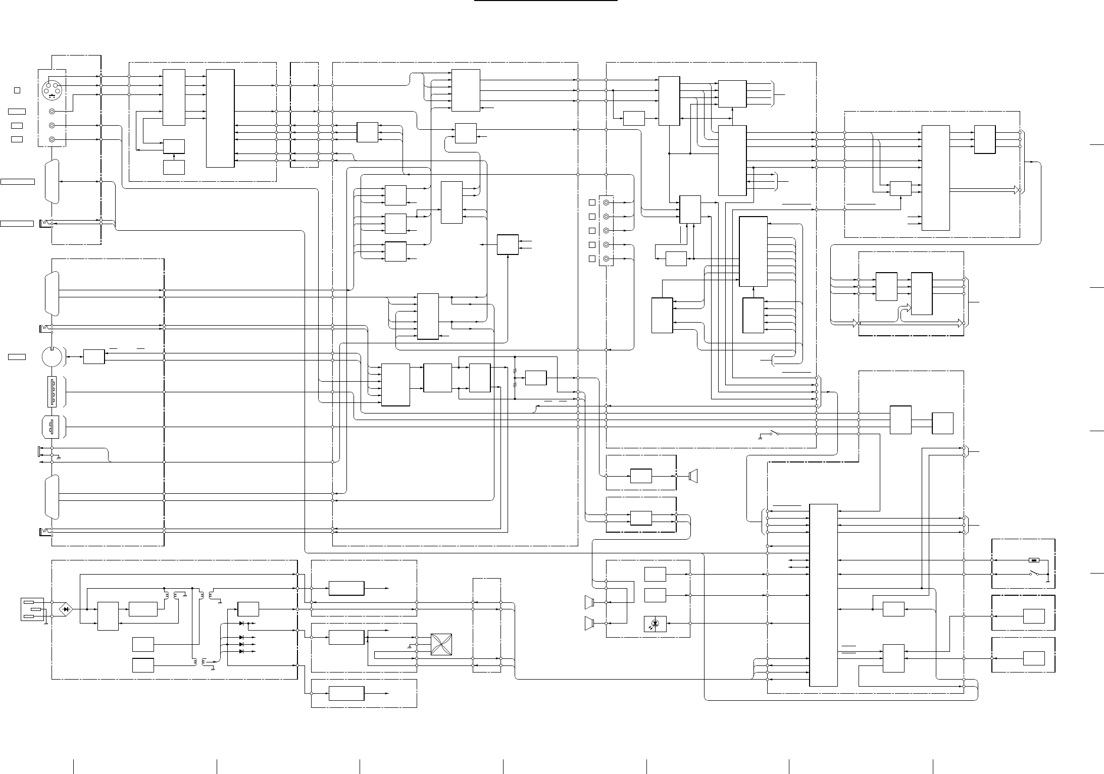
8-1 8-1
A B C D E F GH
1
2
3
4
5
VPL-PX20/PX30
Section 8
Block Diagrams
OVERALL BLOCK
OVERALL OVERALL
SP
S
VIDEO
L-V
R-V
3
1
4
2
J1901
CN1904
RS-232C/422
CONTROLS-IN
Y
C
C-VIDEO
L-V
L-R
Y
C
C-V COLER
DECODER
IC101
V.B-Y
V.R-Y
V-Y
HS
VS
IC102
INTERFACE
RGB
D.COMB
DAC
IC221
IC250
CVBS
COMB Y/C
V-R,V-G,V-B
V-HD,V-VD
R/R-Y
B/B-Y
BB
(1/3)
BA
QD
R/R-Y
B/B-Y
V
H
G/Y
V
H
G/Y
V-HD,V-VD
V-R,V-G,V-B
Q811-813
BUFF
BNC R
BNC B
BNC G
SIRCS S
SIRCS
RD,TD
CN1802(QC)
QB,QC
CN1202(QB)
J1203(QB)
J1801(QC)
AH,AV(QB),BH,BV(QC)
AR,AG,AB(QB),BR,BG,BB(QC)
AL(QB),BK(QC)
AR(QB),BR(QC)
MOUSE
CN1201(QB)
CN1801(QC)
MOUSE
DRIVER
IC1801(QC)
IC1201(QB)
1-13
DS2-,DS+(QB)
IRD A(QB), B(QC)IRD
USB DS-,USB DS+
CN1803(QC)
OUT R,G,B
OUT H,V
USB DS+,USB DS-
CN1201(QB)
CN1202(QB)
CN1201(QB)
INPUTA SW1
INPUTA SW2
AUDIO OR
AUDIO OL
J1802(QC)
INPUTA SW1,SW2
QA
R
SELECT
IC823
AR
BR
BNC R SW
R
CONV.
OUT R,G,B
G
SW
SELECT
G
BNC G
BG
AG IC824
B
SW
SELECT
B
BNC B
BB
AB IC825
SYNC
SW
IC811
AH
BH
BNC H
AV
BV
BNC V
SYNC
PROCESS
IC802
BUFF
IC803
W/SW SW
REF H
REF V
HD
VD
H
OUT H
OUT V
V
SW
VIDEO SW
AMP
IC803
V-R
R
V-G
G
V-B
B
G
R
B
A/B D/A CONV.
D/A
CONV.
IC807
IC806
D/A
D/A
CONV.
CONV.
D/A
D/A
CONV.
D/A
CONV.
SDA
SCD
DAC OUT
OUT H,V
AUDIO OR
AUDIO OL
OUT R,G,B
GA
AC
INLET PFC
CONT.
SWITCHING
IC2100 Q2100
PWM
CONT.
IC2102
IC2101
CONT.
PWM
L2100 T2101
T2100
POWER
PROT
IC2104
17.5V
AUDIO +B
A-6V
A-7V
POWER PROT
POWER ON
6V
SUB SUB5V
DC-DC CONV.
IC2500
SUB 5V
POWER ON
POWER PROT
GC
IC2700
DC-DC CONV.
10.7V FAN+B1,2
10.7V
FAN PROT1,2
FAN CONT1,2
18V
SUB
GD
6V D+3.3V
IC2300
DC-DC CONV. D3.3V
GB
(2/3)
BB
FAN1,2
AUDIO
SW
PROCESSOR
IC819
BL
AL
L-V
BR
AR
R-V
SOUND
PROCESSOR
IC820
L
R
VAR
AMP
IC821
R
L
MIX
Q838
L
R
N,V
BNC R,G,B
L/R
L
R
BNC H,V
DS2-,DS2+
USB DS-,USB DS+
USB US-,USB US+
IRD BA,IRD
BB(3/3)
SYNC
DET
Q302,303
R
G
B
V
H
D/A
CONV.
IC304
R
G
B
H
V
R
G
B
INPUT A SW1,SW2
HS OUT
TMDS
RECEIVER
IC823
GRE0-7
GGE0-7
GBE0-7
RX0-,+
RX2-,+
RXC-,+
RX1-,+ CN300
TO
SCAN
CONVERTER
IC303(1/5),(3/5)
SW
IC302
H
V
HD
VD
GHDREN
CHDREN
INV
IC305(3/3)
DRE0-7
DGE0-7
DBE0-7
DHS
DVS
CONT.
MEMORY
IC303(2/5)
BHENN
ROMOEN
ROMWEN
CS2
A0-19
CS3
NM1
BOOTWE
TXD
RXD
WDTEN
TO
CN312
PW OSD ENA
RAM
RAMOEN
A0-17
BHENN
RAMWEN
D0-15
ROM
D0-15
IC314
CN301
TO
PW OSD ENA
BNC H,V
IC315
DS2-,DS2+
DS1-,DS1+
US1-,US1+
FIL COVER
VSO
HD
VD
IRDA,IRDB
BC
PW OSD ENA
DVS
DHS
DBE0-7
DGE0-7
DRE0-7
BUFF
W/SW
(1/4),(4/4)
IC505
DGE7
DRE7
SDA
SCL
IC502
PROCESS,
LCD CONT.
IC506
R,G,B
RE0-9
GE0-9
BE0-9
EVEN R
EVEN G
EVEN B
EVN
DEC
OSD
OSD YM
OSD YS
LCD CONT.
C
EVEN R
EVEN G
EVEN B
IC600
AMP
R
G
BROM
B IC609,610
G IC603,604
R IC611,612
R VID1-12
G VID1-12
B VID1-12
LCD CONT.CONT.
LCD
TO
R,G,B
LCD PANEL
K
AUDIO
AMP
IC2900
L/R MAIN
MAIN
SP
Y
DS2-,DS2+
DS1-,DS1+
US1-,US1+
USB,HUB
CNTL
IC3303
DS3-
US3+
USB
MONITOR
CTRL
IC3304
FIL COVER
KS
IC2950
AMP
AUDIO
RR SP
L L SP
KS
L SP
R SP
L
R
SP
KEY
MATRIX
KEY0
KEY1
MATRIX
KEY
MAIN CPU
IC3204
SDAT
SCLK
POWER PROT
FAN CONT1,2
FAN PROT1,2
P.SAVE LED,
KEY1
KEY0
SIRCS
IRDA,IRDB
VD
HD
VSO
PW OSD ENA
LAMP LED,
TEMP LED,
POWER LED,
LIGHT ON
POWER ON
TXD
RXD FLASH
TO
LAMP MODE
LAMP PROT
LAMP ON
TO
BALAST
S
LAMP TEMP
LAMP COVER
IC3600
NF
SIRCS-NF SIRCS
SIRCS
SIRCS-NR
NR
IC3700
SIRCS S
RD,TD
LAMP TEMP
LAMP COVER
TXD RD
ANALOG
SW
IRDA
FILTER
IC3301
IC3401
NF ON
NR ON
IROUT
RXD RS RD
J1902
TD
S300
FCEN
BOOTWE
ROMWEN
ROMOEN
A0-19
BNC R,G,B
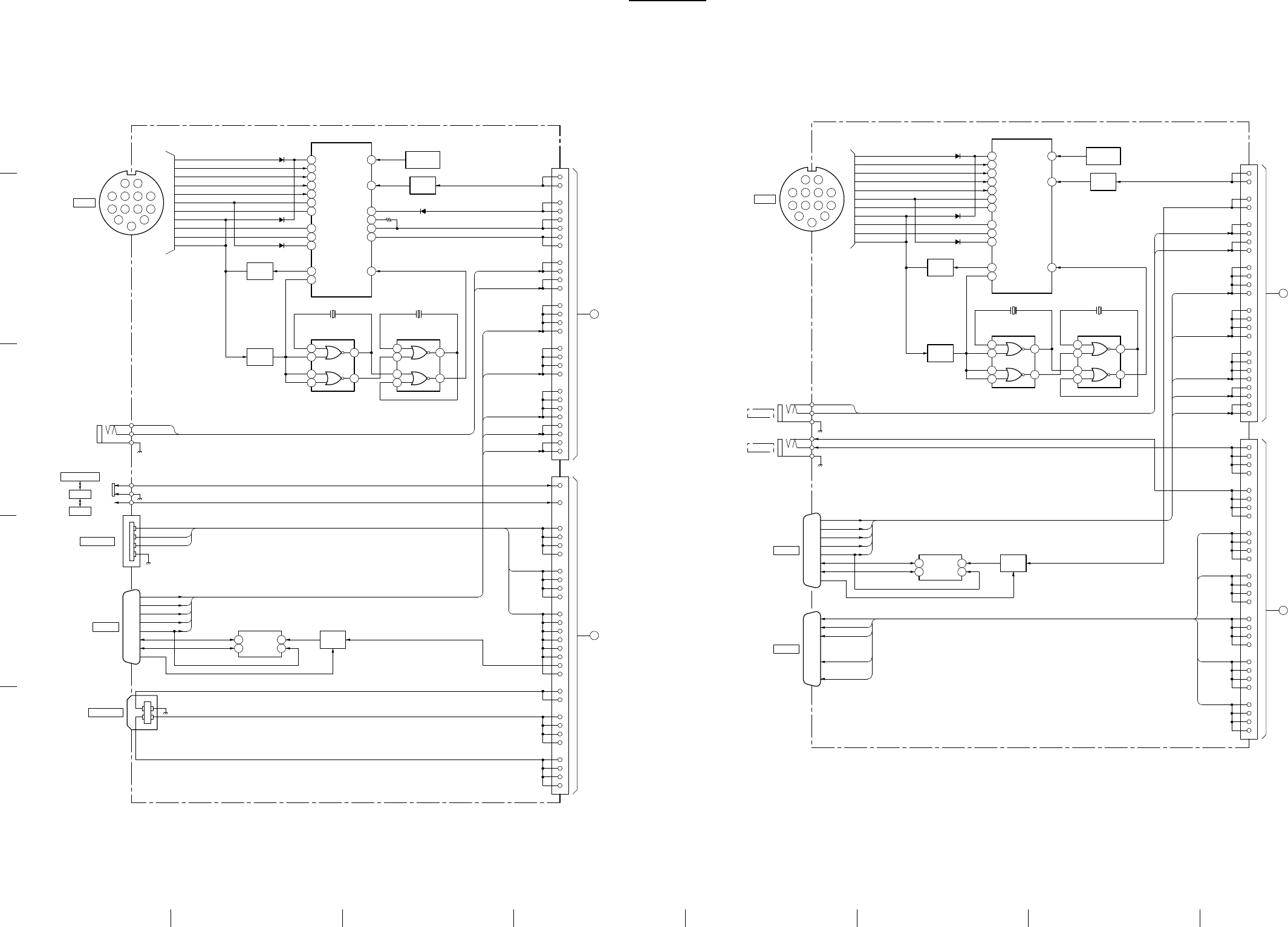
8-2 8-2
A B C D E F GH
1
2
3
4
5
VPL-PX20/PX30
QC BLOCK
QB QC
11 12
10 7 8 13
6459
32
1
CN1201
MOUSE
1 RTS
XA
XB
YA
YB
L/PS
R
98/AT/TXD
CLK
DAT/RI
RXD
20
16
15
14
13
17
18
24
19
6
7
28
D1215
SELECT SW
SELECT SW
D1212
SELECT SW
D1209
SW
Q1202
BUFF
Q1204
XA
XB
YA
YB
L/PS
R
CLK
DAT/RI
L/PS
8
10
5
33
32
31
3
RESET
IRDA
DS2-
DS2+
DSC IN
IC1201 MOUSE DRIVE
8
910
4
5
6
DSC,INV
IC1203(2/2)
X1202 6MHz
IC1203(1/2)
DSC,SELECT
12
11 13
1
2
3
X1201 24MHz
3
4
5
6
7
8
9
11
12
13
OUT
IC1204
RESET
Q1201
INV
D1214
SELECT SW
A1
B1
A2
B2
A3
B3
A4
B4
A6
B6
A9
B9
A12
B12
A13
B13
A16
B16
A17
B17
A20
B20
A21
B21
A23
B23
A25
B25
CN1203
TO
QA BOARD
CN803
IRD A
MS 5V
DS 2-
DS 2+
AUDIO AL
AUDIO AR
AR
AG
AB
AH
AV
AUDIO AR
AUDIO AL
J1203
1
2
3
13
14
12
15
5
AR
AG
AB
AH
AV
SDA
SCL
INPUT A
CN1202
5
6
8
7
SDA
SCL
VCC
VCLK
IC1202 Q1203
+5V SW
DIGITAL RGB
S BNC
RGB
1
2
3
USB 5V
USBD D-
USBD D+
USB INPUT
J1201
SW1201
A20
B20
A21
B21
A24
B24
A25
B25
A1
A2
A4
B4
A5
B5
A8
B8
A9
B9
A12
B12
A13
B13
A14
B14
A15
B15
A17
B17
INPUTA SW1
INPUTA SW2
USBD D+
USBD D-
USB 5V
IN 5V
USBU D+
USBU D-
J1202
USB INPUT
QB(INPUT TERMINAL)
CN804
QA BOARD
TO
CN1204
1
2
4
11 12
10 7 8 13
6459
32
1
CN1801
MOUSE
1 RTS
XA
XB
YA
YB
L/PS
R
98/AT/TXD
CLK
DAT/RI
RXD
20
16
15
14
13
17
18
24
19
6
7
28
D1815
SELECT SW
SELECT SW
D1812
SELECT SW
D1809
SW
Q1812
BUFF
Q1804
XA
XB
YA
YB
L/PS
R
CLK
DAT/RI
L/PS
8
10
3
RESET
IRDB
DSC IN
IC1801 MOUSE DRIVE
8
910
4
5
6
DSC,INV
IC1803(2/2)
X1802 6MHz
IC1803(1/2)
DSC,SELECT
12
11 13
1
2
3
X1801 24MHz
3
4
5
6
7
8
9
11
12
13
OUT
IC1804
RESET
Q1801
INV
A1
B1
A2
B2
A6
B6
A9
B9
A12
B12
A13
B13
A16
B16
A17
B17
A20
B20
A21
B21
A23
B23
A25
B25
CN1804
TO
QA BOARD
CN805
IRD B
SUB 5V
AUDIO BL
AUDIO BR
BR
BG
BB
BH
BV
AUDIO BR
AUDIO BL
J1801
1
2
3
13
14
12
15
5
BR
BG
BB
BH
BV
SDA
SCL
INPUT B
CN1802
5
6
8
7
SDA
SCL
VCC
VCLK
IC1802 Q1803
+5V SW
A1
A9
B9
A10
B10
A13
B13
A14
B14
AUDIO OL
OUT R
OUT G
QC(IN/OUT TERMINAL)
CN806
QA BOARD
TO
J1802
AUDIO
AUDIO
B2
A2
B1
CN1805
CN1803
INPUT A
OUT B
OUT G
OUT R
3
2
1
13 OUT H
14 OUT V
OUT B
B18
A18
B17
A17
OUT H
B22
A22
B21
A21
A24
B24
A25
B25
OUT V
3
4
B6
A6
B5
A5
AUDIO OR
QB BLOCK
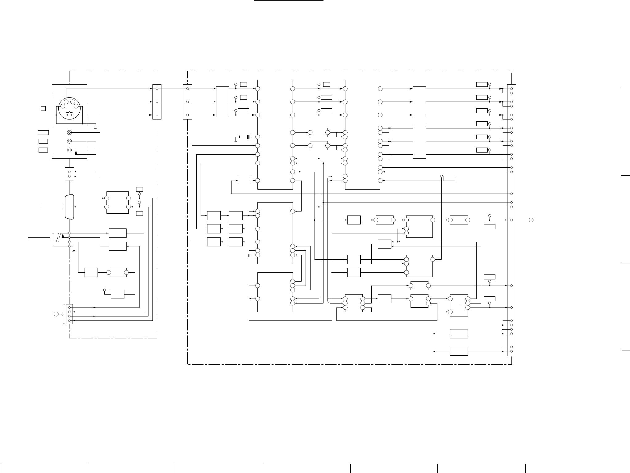
8-3 8-3
A B C D E F GH
1
2
3
4
5
VPL-PX20/PX30
BA, QD BA, QD
BA, QD BLOCK
3
1
4
2
J1901
S
VIDEO
L-V
R-V
Y
C
V
L
R
1
3
TO
QA BOARD
CN807
1
3
5
Y
C
C-VIDEO
CN1901
L-VIDEO
R-VIDEO
RS-232C/422
CN1904
8
710
9
R1
T20
R20
T21
IC1901
RS-232C DRIVE
2 RD
3 TD
TP1902
RXD
TXD
TP1901
CONTROLS-IN
J1902
INV.BUFF
Q1904
Q1903
INV.BUFF
2B2Q 105
IC1902
TIMER
SW
Q1902
Q1901
SW
+5V
5
6
1
2
CN1903
CN1902
CN3003
Y BOARD
TO
SIRCS S
SIRCS
TXD RD
RXD RS
CN102
5
3
1
Y(SVIDEO)
CV
C(SVIDEO) Y/C/CV
BUFF
Q107,109,101 Y
TP101
44
43
1
TP102
C
TP100
VIDEO
CVBS/Y2
C2
CVBS/Y1
XTAL
38
X100
16.2MHz
19 Y1
CVBS OUT
COMB C
COMB Y
3
7
5
BUFF
Q111
COMB OUT
9HS
CR OUT
CB OUT
Y OUT
23
22
21
VS 4
13
SCL
14
SDA
10
SCP
46
SFC OUT
IC101 COLOR DECODER
Q108
BUFFEQ
Q120
ADIN2
1CLP0
Q128
BUFF EQ,AMP
Q125-127
7 AC0
Q124
BUFF EQ,AMP
Q121-123
9 AY0
PNR23
26 NTPL1
FIN 37
VEH3 20
VEH2 21
VEH1 22
IC221 D.COMB
1 SW1
9SW2
7
VEH3
6
VEH2
5
VEH1
SCL 15
SDA 14
IC250 DAC
V.R-Y
TP103
V.B-Y
TP104
TP105
V.Y
R-Y1
B-Y1
Y1
67
68
69
IC106 INV
2 4IN OUT
OUTIN 42
IC105 INV
HS166
1HS2
VS2
2
65 VS1
HS OUT29
28 VS OUT
SDA
56
55 SCL
HS
VS
35
37
39
R OUT
G OUT
B OUT
R-Y2 3
9
PR3
4
B-Y2
10
PB3
5
Y2
11
Y3
7
HS3
8
VS3
31
SCP IN
IC102 RGB INTERFACE
Q112-114
BUFF
R/G/B
R OUT
TP108
TP109
G OUT
TP110
B OUT VG
VG
VR
CN101
A11
B11
A13
B13
A15
B15
BUFF
Q115-117
B5
A5
B3
A3
B1
A1R/R-Y
G/Y
B/B-Y
B-Y/B
TP112
Y/G
TP107
TP106
R-Y/R
B6
B7
H
V
TP113
SCP IN
RGB SYNC B8
SDA A20
SCL B20
BUFF
Q103 IC253
3 4IN OUT 6 CH1
CH07
A5
COMMON 1
2-CH MULTIPLEXER
IC251
OUTIN 42
IC252 INV.
B9
TP114
CLAMP
V-CLP
IC103
2-CH MULTIPLEXER
1COMMON
5A
6 CH1
CH07
Q118
BUFF
INV
Q119
53
IC259 INV
17
62
HS
VS BUFF
Q130
IC254 INV
2 4IN OUT
5
IC256
2 7 B211
4A1
Q2 10
Q2 9
Q1 6
MONO. MULTI.
IC257
V-HD
H.SYNC
TP115
B17
B18
TP116
V.SYNC
V-VD
BUFF
Q110,129
A22
B22
A23
B23
A24
A25
IO
IC258 +5V REG
+5V
+9V
IC255 +9V REG
OI
TO
BB BOARD
CN306
QD(SIRCS/VIDEO IN)
BA(CHROMA DECODER)
23
5

8-4 8-4
A B C D E F GH
1
2
3
4
5
VPL-PX20/PX30
QA QA
3
SHDN 7
6
IC808
R DRV R
A14
B14
B4
B6
A4
B10
B27
A1
B1
A6
B29
A27
A29
B33
B31
A31
B35
A33
A35
B8
A8
B12
A10
A12
QA(INPUT SELECT)
CN801
G
B
BNC R
BNC B
BNC G
BNC V
BNC H
CLP
H
V
BUFF W/SW
IC803(2/2)
3
5
7
9
19
11
13
17
15
2G
1
8
1G
4
12
16
IC803(1/2)
BUFF W/SW
2
6
18
14
V-CLP 1A11Q13
V-HD
V-VD
Q810
INV
G IN4 CLP 17
G
15
REH
IN
6-OUT
13
REV 8 V IN
V POL19
18 H POL
COMP/H HD
+OUT
VD
A15
B15
A17
B17
A18
B18
B19
A20
B20
A21
B21
B22
A23
AUDIO MUTE
SCLK
SDAT
AUDIO CE
US+
US-
USB P.FLG
DS1+
DS1-
MS P.ENA
US VBUS
USB P.ENA
SUB 5V
B/B-Y
G/Y
R/R-Y
V-CLP
V-HD
V-VD
A11
B11
B9
A9
B7
A7
B28
A28
B26
A25
A26
B25
B23
V-R
V-B
V-G
A19
B21
A23
A21
B19
CN802
A17
B17
RGB SYNC
H
V
A13
A15
B15
B13
SDA100K A30
SCL100K B30
YC/OTHER A5
CV/OTHER B5
DS2-
DS2+
A4
B4
A3
B3
B1
A1
A34
A32
B34
IC802
SYNC PROCESS
3
4
6
7DAC0
DAC1
DAC4 1SW1
D/A CON.
IC806
DAC25
SW2 2
SW3 3
SW4 4
SCL
SDA
15
14
A/B
MON OUT OFF INPUTA SW1
INPUTA SW2
BUFF
Q813
Q812
BUFF Q811
BUFF
BNC-R
BNC-G
BNC-B
D/A CON.
5 DAC2
SW02
DAC16
3 DAC4
4
SDA
SCL
IC807
14
15
SRS ON
SPEAKER MUTE
CV/OTHER
YC/OTHER
DAC3
I
IC817 +5V REG
O
IC818 -5V REG
IO
OI
IC816 +9V REG
+5V
-5V
+9V
MS 5V
SUB 5V
IRD B
IRD A
+6V
+10V
-6V
USP P.FLG,MS P.ENA,USB P.ENA,SUB5V,MS5V
US+/-,DS1+/- US VBUS,SUB5V
AUDIO MUTE,SCLK,SDAT,AUDIO CE
INPUTA AW1/SW2
SRSON,SPEAKER MUTE
AUDIO OL/OR
AUDIO AL/AR,BL/BR
TO QC BOARD
CN1805
CN303
TO BB BOARD
B10
A9
A10
B9
CN806
OUT R
OUT G A13
B13
B14
A14
OUT B A17
B17
B18
A18
OUT H A21
B21
B22
A22
OUT V A24
B24
B25
A25
AUDIO OL A1
B1
B2
A2
AUDIO OR A5
B5
B6
A6
SHDN
3
7
6
G DRV
IC809
IC810
B DRV
SHDN
3
7
6
R,G,B
BNC R/G/B
BNC H/V
3
4
6
5
11
B2
B3
A2
10
A1
8
1OUT1
VIDEO SW,AMP
IC801
12 A3
OUT2
OUT3
A/B 16
MON OUT OFF
R
G
B
V-R
V-G
V-G
BNC R7
BR
5
1
IC823
RGB SELECT
12
SW1
13SW2
11
10
SW3
OUT
AR
BR
AG SW3 115
7 BNC G
SW2
SW1
13
12
RGB SELECT
IC824
BG BG1 OUT 10
AB SW3 115
7 BNC B
SW2
SW1
13
12
RGB SELECT
IC825
BB BB1 OUT 10
IC811
SYNC SW
14 X1
15 X2
2X0 OUTX 13
BNC R
BNC G
BNC B
TO QB BOARD
CN1203
CN803
B9
A9
B6
A6
A4
B4
B3
A3
A17
A2
B2
B1
A1
A25
B25
B23
A23
A21
B21
B20
A20
B17
B16
A16
B12
A13
A12
B13
AUDIO AR
AUDIO AL
CS OUT
IC805
1CV 2
CS
OUT IN
X311
BH
AH
CS
BNCH
4
2
5
BNCV
Y3
Y2
Y1
AV Y01
BV
SW3
SW2
SW1
6
9
10
OUTY 3
BUFF
Q809
H
V
Q821
Q824
Q822,823
PEAK
HOLD
H
BUFF
V
BUFF
Q825,826
HOLD
PEAK
IC813
COMP
6
5 IN2-
IN2+
OUT2 3
1 IN1+
IN1-7 OUT1 2
IC814
BUFF
2A6
1A1
2Y 5
1Y 3
BUFF
G
Q805
BNC R/G/B
V-R,V-G,V-B
A/B
R,G,B
G
H
V
B2
B9
A9
A6
B6
B1
A2
A1
B16
TO QC BOARD
CN1804
B25
A25
B23
B21
A23
A20
B20
A21
B17
A17
CN805
A16
B13
B12
A13
A12
AUDIO BL
AUDIO BR
DS2+
DS2-
MS5V
IRDA
AV
AH
AB
AG
AR
BR
BG
BB
BH
BV
IRDB
SUB5V
Q802
G
BNC H/V
RE H
RE V
V-R,V-G,V-B
SW
SW
Q808
D872
D871
V
H
IRDA,IRDB,DS2-,DS2+
R
G
B
R/G/B MON
B1
BNCH
IC804
V-CLP OUT
DAC3
CN305
TO BB BOARD
BNC,R/G/B
R,G,B
R MON
G MON
B MON
7
6
4
1
3
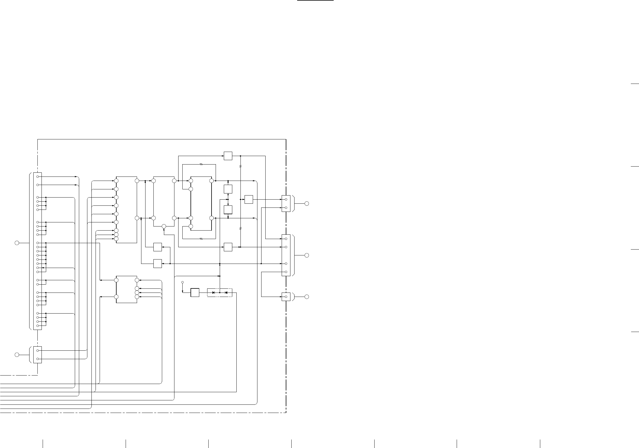
8-5 8-5
A B C D E F GH
1
2
3
4
5
VPL-PX20/PX30
QA BLOCK
TO QB BOARD
B17
A17
B15
A15
A14
B14
CN1204
B12
A13
A12
B13
SWB 5V
USB 5V
B9
A8
B8
A9
B5
A5
A4
B4
USB DS-
USB DS+
A2
A1
CN804
41
40
44
43
14
AUDIO SW1,PROCESSOR
42 IN11
IC819
23RE01
MUTE
Q835
RE02
22 CE
16 DATA
21 CLK
Q831
SW
SW
Q832
45
MUTE
Q834
2 INR OUTR 5
SOUND PROCESSOR
IC820
9 INL OUTL 8
VAR AMP
IN1+
IN2+
5
3
7OUT2
1OUT1
IC821
6 IN2-7
2 IN1-
BUFF
Q836
BUFF
Q837
MIX
Q838
AUDIO OLAUDIO BL
AUDIO AL
L-VIDEO
AUDIO BR
AUDIO AR
R-VIDEO
SCLK
SDAT
AUDIO CE
IN12
IN13
IN21
IN22
IN23 CNTL
TO KS BOARD
CN2951
4
7
CN810
1
3
CN809
TO K BOARD
CN2900
B21
A20
B20
A21
USB US+
B25
A25
B24
A24 USB US-
DSI+
DSI-
US-
US+
1 L-VIDEO
3 R-VIDEO
TO QD BOARD
CN1902
CN807
INPUTA SW2
INPUTA SW1
QA(AUDIO PROCESS)
7IN8 OUTA
USB 5V/MS 5V CONTROL
IC822
OUTB5 USBP.ENA
1
2USBP.FLG
4MSP.ENA
ENB
FLGA
ENA
SUB 5V
MS 5V
AUDIO MUTE
SRS ON
Q833
MUTE
MUTE MIX
D844
+9V
1
1
CN808
TO K BOARD
CN2901
AUDIO +B
AUDIO +B
SP-MUTE
R
L
SP-MUTE
L/R
9
AUDIO OR
US VBUS
SP MUTE
9
10
11
8
2
QA QA
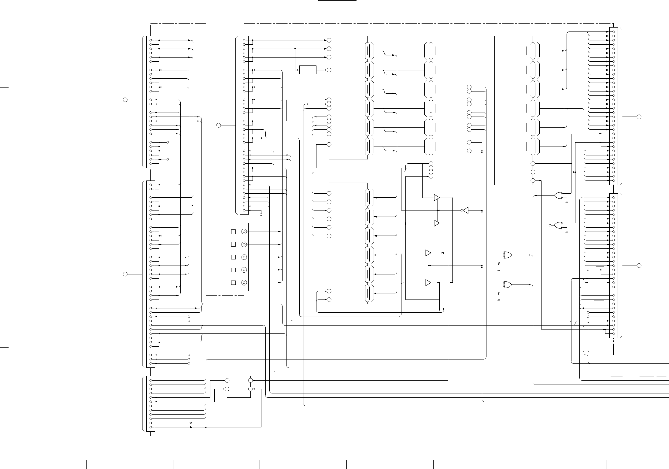
8-6 8-6
A B C D E F GH
1
2
3
4
5
VPL-PX20/PX30
BB(SCAN CONVERTER)
SCLK,SDAT,SCL400K,SDA400K,SCL100K,SDA100K
DS2-,DS2+,DS1-,DS1+,US-,US+
AUDIO MUTE,AUDIO CE
PANELTEMP,OSD RES,BUSY,DIS,PW-OSDENA,OSD CS
VSO,VD,HD
USBP.FLG,USBP.ENA,MSP.ENA,US VBUS
IRDA,IRDB
GHDREN
SCL,SDA
B15
A13
B13
A15
CN306
A11
B11
V-R
DRA0
DRA7
IC304 A/D CONV.
DATACK
CKINV27
115
HSOUT
R IN
117
7
PWRONB
125
GRE0-GRE7
105
112
G IN15
B IN27
14 SOG IN
28 CLAMP
29 SDA
30 SCL
41 COAST
SOGOUT
118
SYNC DET
Q302,303 DGA0
DGA7
GGE0-GGE7
92
85
DBA0
DBA7
GBE0-GBE7
72
65
GRO0-GRO7
DRB7
DRB0
95
DGB0
DGB7
GGO0-GGO7
82
75
GBO0-GBO7
DBB0
DBB7 55
62
A8
B8
CN303
B12
A12
B10
A10
R
G
B
A33
B33
B35
B31
A31
A35 BNC R
BNC G
BNC B
B29
A27
B27
BNC V
A29
B6
A4
B4
V
A1
B1
A6 H
CLP
A14
B17
A15
B14
A17
B15
A20
B20
A21
B18
B19
A18
A23
B22
B21
BNC H
US-
US+
CN304
AUDIO CE
SDAT
SCLK
AUDIO MUTE
USBP.FLG
DS1+
DS1-
MSP.ENA
US VBUS
USBP.ENA
SUB 5V
BNC R
R
SUB+5V-3
GBNC G
BBNC B
HBNC H
VBNC V
GRE7
GRE0
GGE7
GGE0
GBE7
GBE0
GRO7
GRO0
GGO7
GGO0
GBO7
GBO0
GVS
159
158
GCLK
IC303(1/5) SCAN CONV.
142
151
GCOAST
GSOG
136
GFBK
24
GGO0-GGO7
GBO0-GBO7
120
99
207
117
133
GGE0-GGE7
GRO0-GRO7
GBE0-GBE7
110
190
189
51
GRE0-GRE7
221
208
TO QA BOARD
CN801
69
85
86
49
56
59
66
77
17
10
27
20
IC300 TMDS RECEIVER
37
30 Q16
Q23
Q8
Q15
Q0
Q7
Q40
Q47
Q32
Q39
Q24
Q31
RX1+
RX1-
RXC-
RXC+
93
94
RX2+
RX2-
80
81
RXO+ 90
RXO- 91
PD 2
PDO 8
IC303(3/5) D PROT
DBE7
DBE0
DGE7
DGE0
DRE7
DRE0
DBO0
DBO7
DGO0
DGO7
DRO7
DRO0
339
307
303
336
333
310
317
323
350
245
231
273
CN309
B21
B22
B24
B14
B17
B18
A24
B9
B10
B13
A21
A22
A23
A15
A16
A17
A18
A5
A11
A12
A10
A6
A7
A8
A9
A2
A1
A13
A14
A4
A3
A19
A20
B19
B20
B23
DBE4
DBE3
DBE2
DBE1
DBE0
DGE7
DGE6
DGE5
DGE4
DGE3
DGE2
DGE1
DGE0
DRE7
DRE6
DRE5
DRE4
DRE3
DRE2
DBE5
DVS
DHS
DRO7
DRO6
DRO5
DRO4
DRO3
DRO2
DRO1
DRO0
DBE6
DBE7
DRE0-DRE7
DGE0-DGE7
DBE0-DBE7
DRO0-DRO7
DGO0-DGO7
DBO0-DBO7
289
DVS
263
DHS
287
DCLK
A19
A2
A1
B24
B23
B21
A21
B19
B18
A18
A16
A24
A23
B14
B13
B11
B10
B9
B8
B7
B6
B5
B4
A11
A6
A10
A9
A8
A7
A5
A4
B17
CN311
DGO0
DGO1
DGO2
DGO3
DGO4
DGO5
DGO6
DGO7
DBO0
DBO1
DBO2
DBO3
DBO4
DBO5
DBO6
DBO7
RESET
SCL400K
SDA400K
OSDCS
DISP
BUSY
OSDRES
PANEL TEMP
NC
NC
SCL100K
SDA100K
DCLK
IC301(4/4)
VSO 13
11
10
9
8
IC301(3/4)
12
IC301(2/4)
46
5VD
2
13
IC301(1/4)
HD
IC302(2/4)
9
10
8
1112
13
IC302(1/4)
71
IC305(3/3)
HSYHC48
ODCK44
DE46
YSYNC47
GVS
GPEN
GCLK
GFBK
65
1
IC302(3/4)
23
4
IC302(4/4)
H
V
GHS
144
GPEN
152
GHSFOUT
166
GHSFOUT
GCLK
GSOG
GCOAST
GFBK
SDA
EEPROM
SCL
6
5
7VCLK
V-G
V-B
B/B-Y
G/Y
R/R-Y
A3
B3
B1
B5
A5
A1
B6
B7
B8
B9
B18
B17
A20 SDA100K
B20
RGBSYNC
V
H
SCL100K
V-CLP
V-VD
V-HD
+6VA22
B22
A23
B23
+10VA24
A25
+6V
+10V
TO BA BOARD
CN101
TO QA BOARD
CN802
B5
A1
B1
CV/OTHER
IRDA
IRDB
B28
A28
A30
B30
A5
SAD100K
SCL100K
YC/OTHER
V-CLP
A23
B23
B21
A21
B25
A26
B26
A25 V-HD
V-VD
V-G
V-B
B19
A19 V-R
CN305
B17
A17 RGBSYNC
G/Y
B/B-Y
R/R-Y
B9
A9
A11
B11
B7
A7
V
H
B15
A15
A13
B13
15
16
11
5
6
12
2
1 TXO-
CN300
DS2-
DS2+
B3
A3
A4
B4
+6VA32
A34 +10V
-7VB34
+6V
+10V
-7V
TXO+
TX2-
TX2+
TXC-
TXC+
TX1-
TX1+
DDC CLK7
DDC DAT8
19
18 HPD
+5V
VCC 8
IC316
RXO-
RXO+
RX2-
RX2+
RXC-
RXC+
RX1-
RX1+
TO BC BOARD
CN500
TO BC BOARD
CN502
75
SCL100K
SDA100K
GHS
GVS
SCLK,SDAT
DRE1
DRE0
PW OSD ENA
5
7
NC
6
102
15
16
BB BB

8-7 8-7
A B C D E F GH
1
2
3
4
5
VPL-PX20/PX30
BB BLOCK
341
IC303(2/5) MEMORY CONT.
DCKEXT
105
315
302
A19
A0
RESET
MCKEXT
RAMOEN
RAMWEN
A35
B35
B34
A34
B33
A33
B32
A32
B30
B28
A28
B27
A27
B26
A26
B25
A25
B24
A24
B23
A23
A22
B21
A21
B20
B19
A19
B18
A18
B17
A17
B15
A15
A14
B12
A12
TO Y BOARD
CN3000
CN307
IC312 +2.5V REG
IC313
+3.3V REG
VOUT
VIN1 5
202
A0-A19
B1
B2
CN301
B4
B3
B5
A5
B6
A6
A8
B7
A9
B8
A10
B9
B11
A11
A12
B12
B13
B19
B20
B21
B22
B23
B24
B25
A25
B26
A26
B27
A27
B28
A28
B29
A29
-7V
D3.3V8
9
10
4
6
10V
6V
3
1
CN308
+10V
+6V
-7V
A+3.3V
+2.5V
9
8
6
5
7
1
2
CN310
10
D+3.3V-2
SUB+5V-3
SUB 5V
POWER ON
POWER PROT
FAN PROT1
FAN CONT1
FAN PROT2
FAN CONT2
CN2701 1
TO GD BOARD
TO GA BOARD
CN2103
TO GB BOARD
CN2301
SUB+5V SU+5V-3
+6V +6V
B10
A10
A9
B8
A8
B6
A6
B4
A4
B2
A2
B9
B14
OSCIN1 FOUT 15
DCK OUT
IC309
2OSCOUT
IC306
RESET
IC308
MCK OUT
1 OSC
8 OSC
2 VDD
5OUT
OUT 1
X301
34.0MHz
D+3.3V-2
18MHz
X300
A30
S/C RES
DSD RES
BUSY
DI SP
PW-DSD ENA
DSD CS
VSO
VD
HD
RXD S/C
TXD S/C
SCL400K
SDA400K
USB P.FLG
USB P.ENA
DS2-
DS1-
DS1+
US-
US+
MSP.ENA
US VBUS
PANEL LINK
INTERLACE
PIC MUTE
SCLK
AUDIO CE
AUDIO MUTE
PANEL TEMP
IRDA
IRDB
FIL COVER
POWER ON
FAN PROT1
FAN CONT1
FAN PROT2
FAN CONT2
POWER PROT
SCL100K
SDA100K
S301
S300
RXD
TXD
IC318(1/4)
IC318(2/4)
4
5
6
1
2
3
IC314 ROM
OE
A1
24
25
A19 16
17
48
29
45
28
WDTEN
116
TXD80
RXD79
INTERLACE29
PIC MUTE
2
GHDREN
31
SCL
SDA
54
53
RAMOE
RAMWE
178
177
D0-D15
D0
131
D15
172
201
186
185
193
194
113
27
106
107
BHENN
ROMOEN
ROMWEN
CS2
CS3
NM1
BOOTWE
D0-D15
SDA
SCL
VPPEN3
B10
A7
A18
A17
A16
A15
A14
A13
A12
A11
A10
A9
A8
A7
A6
A5
A4
A3
A2
A1
A0
B15
B14
B17
B16
B18
A32
B32
A30
B30
A31
B31
D13
D11
D10
D9
D8
D7
D6
D5
D4
D3
D2
D1
D0
D14
D15
VPPEN
BOOTWE
FCEN
NM1
RESETN
CS3
CS2
ROMWEN
ROMOEN
BHENN
1
2
CN302
CN312
3
2
6
5
1
8
18
38
36
WE11
NC
14
26CE
ROMOEN
ROMWEN
BOOTWE
D0-D15
A1-A19
A0-A17
RAMWEM
RAMOEN
BHENN
D0-D15
17 WE
40
41
UB
OE A0
21
24
27
42
IC315 RAM
38
35
16
A17
44
23
29
32
13
10
7
32
1
11
13
12
56
4
IC307(1/4)
IC307(2/4)
IC307(3/4)
IC307(4/4)
10
89
62
IC305(2/3)
RXD
TXD
EXT SW
WDTEN
TXD
RXD
D+3.3V-2
TO GC BOARD
CN2502
BB(SCAN CONVERTER)
TO GD BOARD
CN2701 6 - 9
IO
IC317
42
SDAT
DS2+
BHEN
ROMOE
ROMWE
CS2
CS3
NM1
BOOTWE
IRRCVR1
IPRCVR0
A19
D12
IRRCVR
VCC
A0-A19
A0-A19
17
18
19
20
21
22
18
5
1
39
DIGITAL
RGB
TERMINAL
NC
NC
BB BB
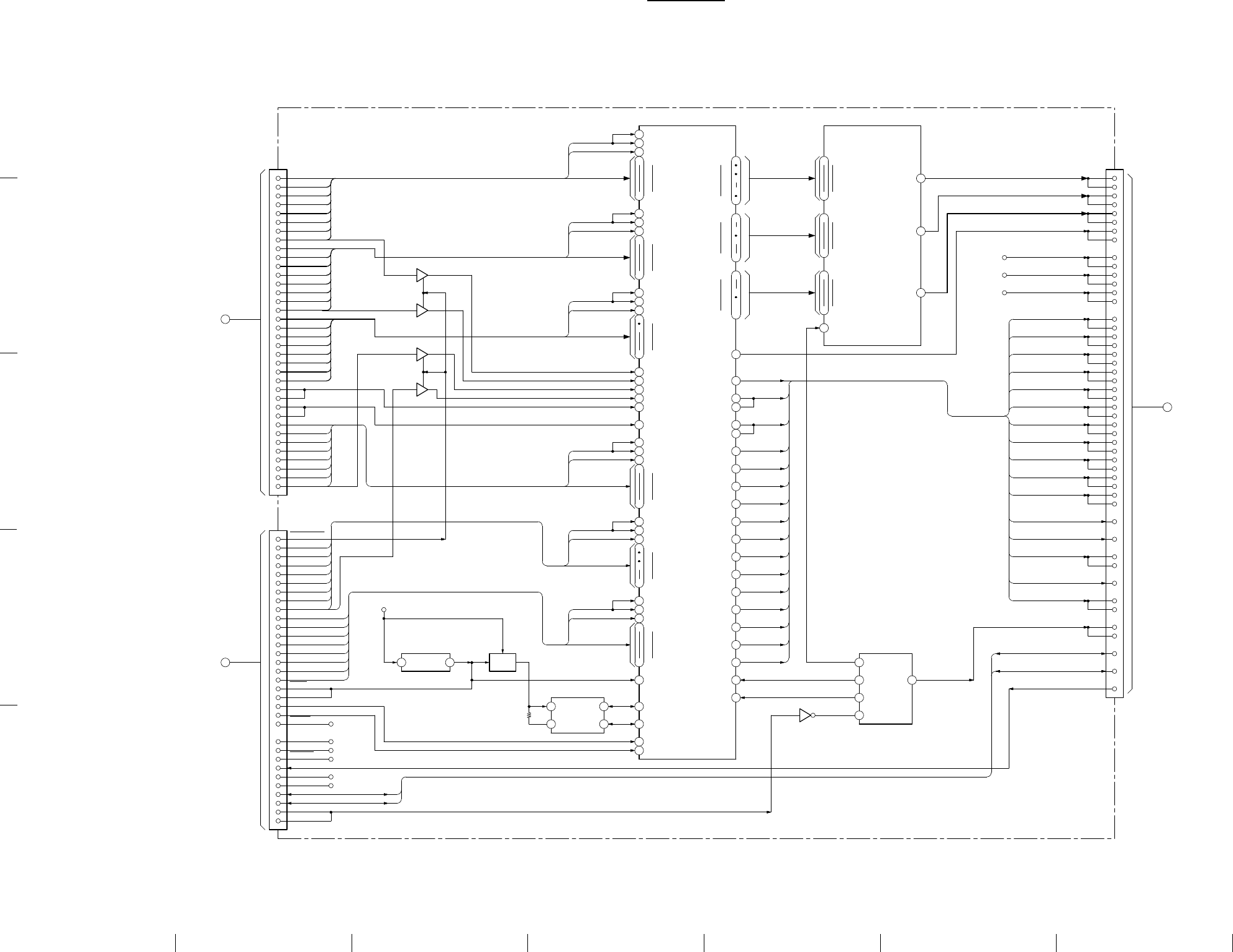
8-8 8-8
A B C D E F GH
1
2
3
4
5
VPL-PX20/PX30
BC BLOCK
IC502
114
OSD PROCESS,LCD CONT
IOR
EVN OSD R0
34
113
112
EVN IN R034
41 EVN IN R7
193
EVN OUT R0
EVN OUT R9
EVN OSD R1
EVN OSD R2
EVN IN G749
EVN OSD G2
EVN OSD G1
EVN OSD G0
EVN IN G0
110
109
42
111
EVN IN B760
EVN OSD B2
EVN OSD B1
EVN OSD B0
EVN IN B0
107
103
50
108
54
EVN YM
EVN YS
ODD YM
129
117
116
VSYNC IN
ODD YS
128
63
HSYN IN62
ODD IN R0
ODD OSD R2
ODD IN R7
75
68
124
ODD OSD R0
ODD OSD R1
126
125
DRE0
DRE1
DRE0-DRE7
DGE0-DGE7
DGE1
DGE0
DBE1
DBE0-DBE7
DBE0
DR00
DR00-DR07
DR01
122
ODD OSD G1
DG01
DG00-DG07
ODD IN G7
ODD OSD G2
ODD IN G0
121
DG00 ODD OSD G0
123
119
ODD OSD B1
DB01
DB00-DB07
ODD IN B7
ODD OSD B2
ODD IN B0
93
118
86
DB00 ODD OSD B0
120
EO1
5
VCC8 SDA
SCL 6 97 RSCL
RSDA
98
RESET
95
EEPROM
IC503
HSDA
101
HSCL
100
A2
BC(LCD R,G,B,DEC,LCD CONT.)
A1
A3
A4
A5
A6
A7
A8
A9
A10
A11
A12
A13
A14
A15
A16
A17
A18
A19
A20
A21
A22
A23
A24
B9
B10
DRE0
DRE1
DRE2
DRE3
DRE4
DRE5
DRE6
DRE7
DGE6
DGE7
DGE5
DGE4
DGE3
DGE2
DGE1
DGE0
B13
B14
B17
B18
B19
B20
B21
B22
DBE5
DBE7
DBE6
DBE1
DBE2
DBE3
DBE4
DBE0
DRO6
DRO7
DRO5
DRO0
DRO4
DRO3
DRO2
DRO1
B23
B24
DVH
DVS
1112
21
13
3
DRE7
DGE7
IC505(4/4)
IC505(1/4)
IC505(2/4)
54
6
10
IC505(3/4)
98
TO BB BOARD
CN309
CN500
SW
Q500,501
IC511
RESET
OUT
VDD2 1
OSD RES
PANEL TEMP
SDATOSD
SCLKOSD
BUSY
SCL100K
DCLK
SDA100K
SCL400K
SDA400K
A1
D24
B23
B21
A21
B19
A19
B18
A18
A16
A24
A23
DBO5
RESET
DBO7
DBO6
DGO7
DBO0
DBO1
DBO2
DBO4
DBO3
DGO6
DGO5
DGO4
DGO3
DGO2
DGO1
DGO0
PW OSD ENA
TO BB BOARD
CN311
B14
B13
B11
B10
B9
B8
B7
B6
B5
B4
A11
A10
A9
A8
A7
A6
CN502
A5
A4
B17
OSD CS
DR07
DG07
192
190
184
181
EVN OUT G9
158
164
166
EVN OUT G0
168
EVN OUT B0
EVN OUT B9
132
142
140
138
RE0-RE9
GE0-GE9
BE0-BE9
R9
R0
48
39
EVN R,G,B,DEC
IC506
G9
G0
10
1
B014
23 B9
IOG 32
IOB 28
CLOCK
24
A30
A31
CN501
EVENR
EVENG
B28
B27
EVENB
A28
A27
CLP
A13
A12
ODDR
B34
B33
ODDG
A34
A33
ODDB
B31
B30
B22
SID B21
POSCONT1 A21
A22
POSCONT2 A19
A20
INVCNT B19
B20
FRP B16
B17
HST A16
A17
VCK
B15
B14
VST
A15
A14
PRG
B13
B12
PCG
B10
B9
ENB
A10
A9
RGT B8
DWN A8
HCK2 B6
B7
HCK1
BLK
B5
B4
A7
SCL100K B2
ECLK
A5
A4
SDA100K A2
PANEL TEMP A1
17LCD CLR/CLP
30SID
24CNT1B
25CNT1A
22CNT2B
23CNT2A
32INV CNT
7LCD FRP
20LCD HST
13LCD VCK
11LCD VST
8LCD PRG
9LCD PCG
14LCD ENB
21LCD RGT
10LCD DWN
19LCD HCK2
16LCD BLK
18LCD HCK1
64CLOCK
66CLOCK2X
HCK1
BLK
HCK2
DWN
RGT
ENB
PCG
PRG
VST
VCK
HST
FRP
INV CNT
POSCONT2
POSCONT1
SID
CLK GEN
IC501
10
15
CLKB3
CLKA4
CLKA1 2
14 CLKA3
1 REF
12
IC500(1/6)
TO C BOARD
CN605
DISP
D+3.3V
76
77
80
85
A2
13
15
16
BC BC
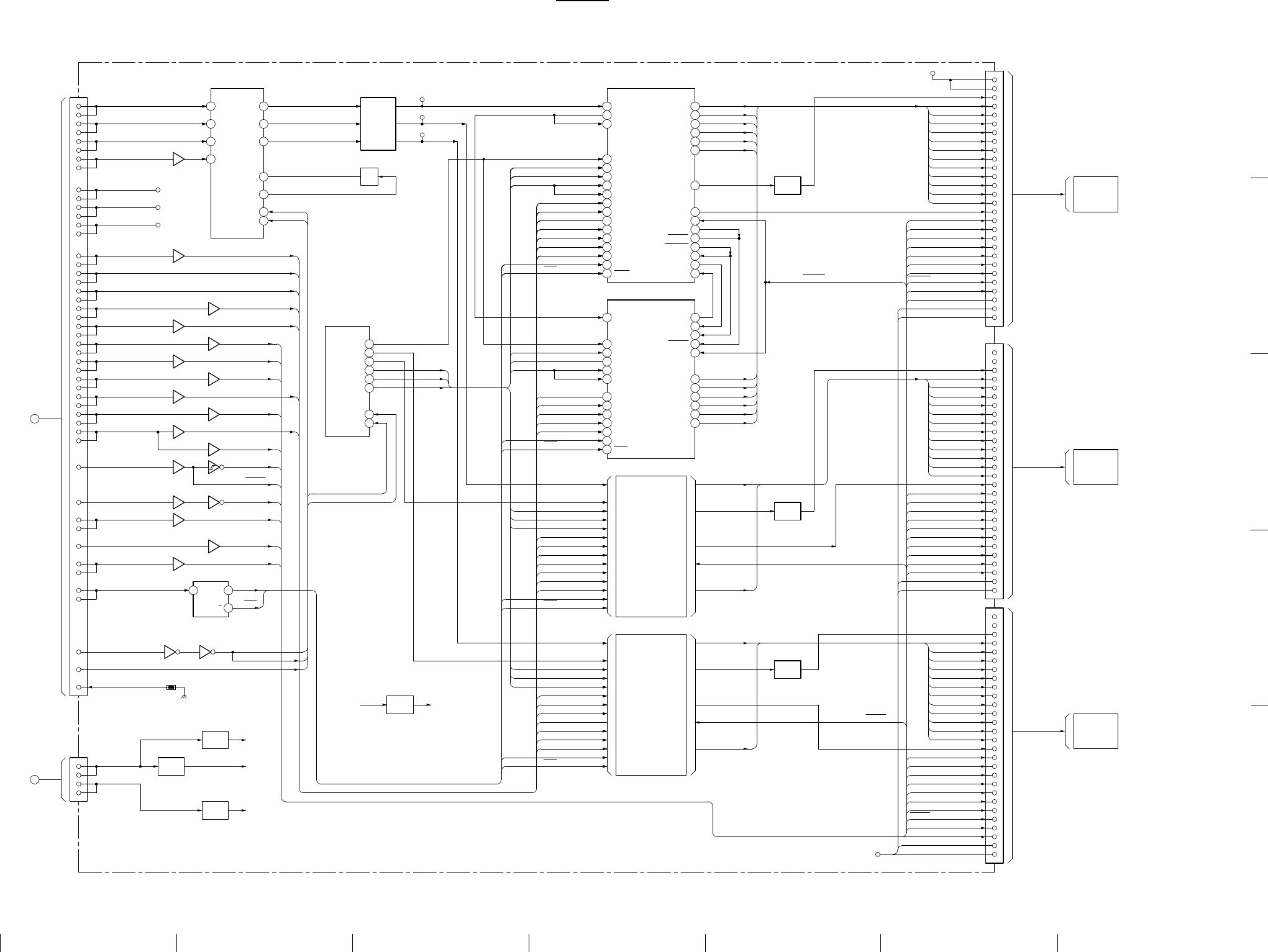
8-9 8-9
A B C D E F GH
1
2
3
4
5
VPL-PX20/PX30
C BLOCK
A30
A31
EVENR R IN R OUT
B26
B27 EVENG G IN G OUT
A28 G IN B OUT
EVENBA27
A13 CLP
CLPA12
IC615(1/8)
BUFF
R/G/B
Q606-608
D/AI
MAIN
SCLD
SDA 23
22
34
29
33
38
412
6
11
21
31SH-OUT1
SH-OUT2 29
47 VIDEO IN
46 INV-OUT
45 SH-IN
34
VID2
VID1
VID3
VID4
21SH-OUT4
27SH-OUT3
VID6
VID5
19
17
SH-OUT5
SH-OUT6
CLK-OUT 55
59CLK-IN
54
61
CLK-OUT
CLK-IN
13
33VCOM OUT
DIR-CNT
4
3
NEXT-IN
NEXT-OUT
38SID-OUT
R LCD DRIVER
IC611
TP612
TP611
TP610
SW
Q612
31SH-OUT1
MCLK
MCLK
ENB
51
50
12
POS-CON1
PRG
POS-CON2
INV-CNT
62
52
1
2
SH-OUT6 17
SH-OUT2
SH-OUT3
SH-OUT5
SH-OUT4 VID10
19
21 VID11
VID12
29
27 VID9
VID8
R LCD DRIVER
IC612
OFFSET
SID-OFST
DLY-CNT
SIG CEN
42
48
49
35
VCOM OFST
34
SH-IN
45
61
CLK-IN
VID7
DIR-CNT 13
NEXT-OUT
CLK-IN
NEXT-IN
59
4
3
6
7
4
5
1
3
30
15
+15.5V
BUFF
Q601,604
R-SID
8
9
10
11
12
13
14
31
17
18
19
23
24
25
29
16
26
22
27
28
HVDD
VVDD
PS2G
VSIG1VID1
VID2 VSIG2
VID3 VSIG3
VID4 VSIG4
VID5 VSIG5
VID6 VSIG6
VID7 VSIG7
VID8 VSIG8
VID9 VSIG9
VID10 VSIG10
VID11 VSIG11
VID12 VSIG12
COM
HST
HCK2
HCK1
ENB
VCK
VST
PCG
RGT
DWN
BLK
HB
VB
ENB1
PB DIR
VB2
VB1
BLK1
LCD PANEL
(R)
A06
A05
5
4
A02
A01
A03
A04 15
14
13
12
IC602
DAC
3SDA
2
SCL
IC626(1/6)
IC624
SID
B22
B21
B34
B33 ODDR
A33
A34
ODDG
B31
B30 ODDB
A21
A22
POSCONT1
A20
POSCONT2A19
INVCNT
IC615(6/8)
B19
B20
B16
B17
FRP
IC614(1/8)
B15
B14
A17
VCK
IC614(6/8)
IC615(4/8)
HSTA16
A15
B12
B13
PRG
IC614(2/8)
IC614(5/8)
VSTA14
B10
A9
A10
ENB
IC614(7/8)
IC614(3/8)
PCGB9
IC615(7/8)
IC615(5/8)
RGTB8
IC626(2/6)
DWNA8
IC614(4/8)
IC615(3/8)
HCK2B6
B7
IC614(8/8)
BLKA7
IC615(2/8)
HCK1B4
B5
D7
Q
Q
3
2
ECLK
A5
A4
IC625
PECLDRV
MCLK
MCLK
SCL100KB2
IC626(6/6)
18
1
13
18
15
13
14
17
12
12
214
15 4
16
11
17
12
IC626(5/6)
10
A2 SDA100K
A1 PANEL TEMP TH600
IO
1
2
6V
6
5 17V
IO
IC605
A+5V REG
I O +15.5V
D5V-2
A+5V
IC600
EVEN R/G/B AMP
CN600
1113
SCLO
SDA100K
SID-OUT
POS-CON1
POS-CON2
INV-CNT
FRP
HST
VCK
VST
PRG
2
3
2
7
5
7
6
3
8
6
5
4
3
1
8
9
3
PCG
ENB1
ENB
RGT
PB DIR
DWN
HCK2
BLK1
HCK1
SCL
SCLO
SDA100K
CN605
VCOM OFST
SIG CEN
DLY-CNT
SID-OFST
OFFSET
FRP
SID-IN
PDS-CON1
POS-CON2
INV-CNT
PRG
ENB
MCLK
MCLK
R VCOM
SCEN
DRY-CON
V33
FRP
SID-OUT
POS-CON1
POS-CON2
INV-CNT
PRG
ENB
MCLK
MCLK
SCEN
DRY-CON
V33
POS-CON1
POS-CON2
INV-CNT
PRG
ENB
MCLK
MCLK
G
G VCOM
SCEN
DLY-CON
V33
FRP
SID-OUT
POS-CON1
POS-CON2
INV-CNT
MCLK
MCLK
PRG
ENB
IC603,604
G LCD DRIVER
(SAME AS R PROCESS)
B LCD DRIVER
(SAME AS R PROCESS)
INV-CNT
POS-CON2
POS-CON1
SID-OUT
PRG
MCLK
MCLK
ENB
IC609,610
DLY-CON
B VCOM
FRP
V33
SCEN
B
BLK1
VB1
VB2
RGT
ENB1
G-SID
BUFF
22BLK
VB
HB
28
27
DWN
RGT
PCG
VST
HCK1
VCK
ENB
HCK2
HST
26
16
29
25
19
24
23
18
17
VSIG9VID9
VID12
VID11
VID10
VSIG12
COM
VSIG11
VSIG10
VID8
VID7
VID6
VID5
VSIG8
VSIG7
VSIG6
VSIG5
11
31
14
13
12
10
9
8
7
VID2
VID4
VID3
VID1
VSIG2
VSIG4
VSIG3
VSIG1
PS2G
4
6
5
3
1
30
15
LCD PANEL
(G)
Q600,603
VID1-VID6
SID-OUT
VCOM OUT
DIR-CNT
VID7-VID12
PB DIR
ENB1
PB DIR
VB2
VB1
BLK1
B-SID
Q602,605
BUFF
HB
VB
DWN
BLK
PCG
RGT
27
28
26
22
29
16
3VSIG1VID1
HCK2
ENB
VCK
VST
HCK1
VID11
VID12
COM
HST
VSIG11
VSIG12
18
23
24
25
19
31
17
13
14
VID8
VID10
VID9
VID6
VID7
VSIG8
VSIG10
VSIG9
VSIG6
VSIG7
VID4
VID5
VID3
VID2
VSIG4
VSIG5
VSIG3
VSIG2
10
12
11
8
9
6
7
5
4
(B)
LCD PANEL
PS2G
30
1
15
VCOM OUT
VID7-VID12
DIR-CNT
SID-OUT
VID1-VID6
C(LCD DRIVER)
CN602
CN601
CN603
+15.5V REG
IC608
D5V REG
IC606
TO BC BOARD
CN501
BR/GHTNESS
R
G
B
SCEN
DLY-CON
V33
SDA100K
SCL
+12VOI
+12V REG
IC613
+17V
R
35
49
42
48
44
39
1
2
52
62
12
50
51
PB DIR
13
416
14
CN2104
TO GA BOARD
C C
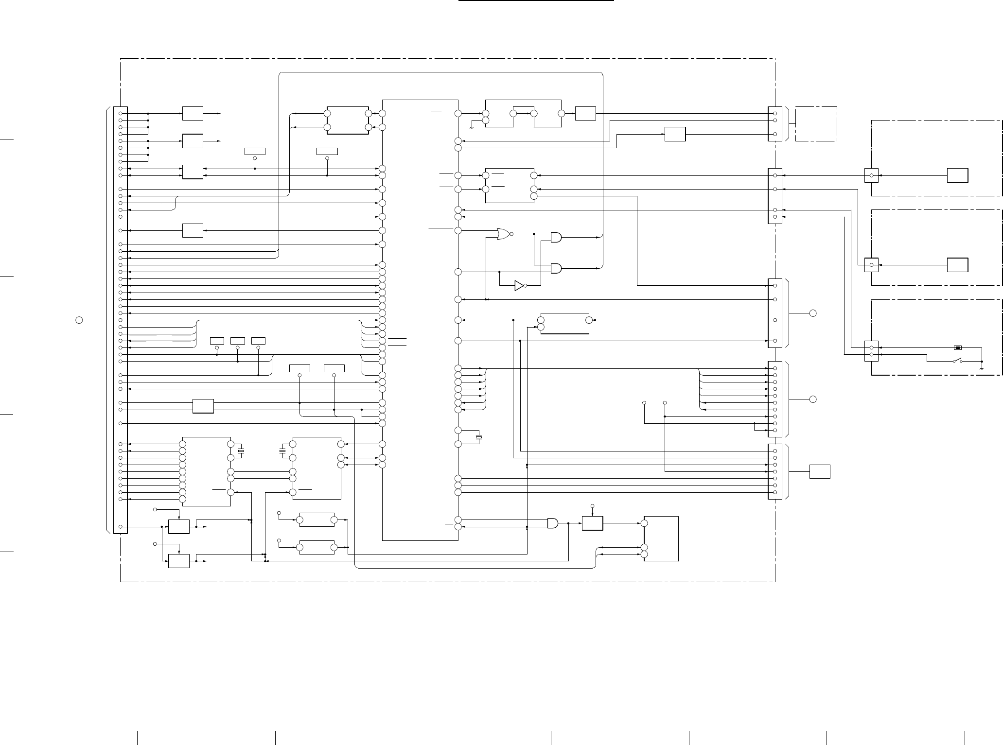
8-10 8-10
A B C D E F GH
1
2
3
4
5
VPL-PX20/PX30
Y, S, NF, NR BLOCK
IC3204
MAIN CPU
FAN CONT2
OUT17
3
OUT21 IN2
IN1 5
BUFF
IC3006
A35
B35 I
TO BB BOARD
CN307
CN3000 IC3004 +3.3V REG
O4
3
CN3002
1
9LAMP NORM/ECOSUB+3.3V
B34
A34
SUB+5V
D+5V
POWER PROT
A32
B32
A33
B33 +6V I O
SCL1100KB30
A30 SDA1100K
IC3007 +5V REG
Q3301,3302
FAN CONT199
BUS SW SDA100K
SCL100K 4 SCL100K
SDA100K6
TP3302
SDA100K
TP3301
SCL100K
2 4
IC3003
LAMP PROT 97
39LAMP ON
POWER PROT
FAN PROT2
FAN PROT198
POWER ON40
FIL COVER
PANEL TEMP96
AUDIO MUTE50
AUDIO CE49
SCLK
SDAT
PIC MUTE27
INTERLACE26
PANEL LINK41
P94
P97
P96
OSD CS366
OSD CS0
43
VSO30
VD30
HD31
RXD S/C60
TXD S/C61
SCL400K1
SDA400K2
3
S/C RES
110
TP3205
SDA400KSCL400K
TP3204
B28
FAN CONT2A28
FAN PROT2B27
FAN CONT1A27
FAN PROT1B26
BUFF
Q3003
A26
A24
B23
A23
A22
B21
A21
B20
B19
A19
B18
A18
B17
A17
A25 IRDB
B24 IRDA
B25 FIL COVER
PANEL TEMP
AUDIO MUTE
AUDIO CE
SCLK
SDAT
PIC MUTE
INTERLACE
PANEL LINK
P94
P97
P96
PW-OSD ENA
OSD CS
OSD CS3
OSD CSO
B15
A15
A14
B12
A12
B10
A10
A9
BUS SW
Q3000,3001
TP3206
VSO VD
TP3203 TP3202
HD
USB HUB CNTL
IC3303
D2113
USB P.FLG32
X2
X1
25
26
USB P.ENA40
B8
A8
B6
A6
B4
A4
B2
A2
B9
D2012
D1110
D109
UD18
UD07
MS P.ENA41
D31 15
D30 14
RESET 6
VSD
VD
HD
RXD S/C
TXD S/C
SCL 400K
SDA 400K
S/C RES
USB P.FLG
USB P.ENA
DS2-
DS2+
DS1-
DS1+
US-
US+
MS P.ENA 8
31
32
2
3
OSC OUT
OSC IN
USBDM
USBDP
RESET
PCO 7
SCL USB 24
SDA USB 28
Q3306,3307
SW
B14 DVDD,AVDD
(IC3303)
+3.3V
+5V
Q3309,3310
SW
(IC3304)
VDD
US VBUS
DS3-
DS3+
4MHz
X3301 X3302
24MHz
55
57
45 USB REQ
SCL USB
SDA USB
107
108
105
117
115
100
104
114
100
OUT
IC3201
RESET
VDD21
+5V
+3.3V
VDD2 1OUT
IC3202
RESET
3Y
IC3402
1A
2A
SCMTINV
3
1 27 3A1Y 6 BUFF
Q3303
IR1N1
IR1N2
IC3301
IREN1
IREN2
IRDA FILTER
6
7
3
2NF ON 14
NR ON 15
IROUT 5
LAMP COVER
LAMP TEMP 95
102
6
5
3IRDB
1
27 IRDA
63MOUSE A/B
MOUSE ENA 62
IC3002(1/2)
IC3002(2/2)
IC3302
1
27
TXD RD
RXD RS
ANALOG SW
IC3401
23
22
2 O/I I/O 1
SIRCS 12
COND4
LIGHT ON 34
P.SAVE LED 35
LAMP LED 36
TEMP LED 37
POWER LED 38
KEY0 93
KEY1 94
X3200
12.288MHz
75XTAL
EXTAL 77
FWE 74
MD1
119
MD2
120
WDTOVF 67
RES 71 RES SW
Q3200,3201
IC3200
6
53
+5V-1
VCC
5
8
6
IC3203
EEPROM
Y(MPU)
BUFF
Q3002
3
5
8
CN3005
1
TO QD BOARD
CN1903
1
2
5
6
CN3003
LAMP MODE
LAMP PROT
LAMP ON
SIRCS-NF
SIRCS-NR
LAMP TEMP
LAMP COVER
SIRCS-S
SIR CS
RXD RS
TXD RD
D+5V
LAMP LED
P.SAVE LED
LIGHT ON 1
CN3500
TO H BOARD
10
3
2
CN3001
4TEMP LED
5
POWER LED
6
KEY0
7
KEY1
9
SUB+5V
12
+5V-1+5V-2
CN3010
7
8
6
5
4
3
1
TXD
RXD
RES
VIN
FWR
MD1
MD2
FLASH
IC3600IR-RX
OUT
2
CN3600
SIRCS-NF
NF(SIRCS RECEIVE FRONT)
CN3700
SIRCS-NR
NR(STRCS RECEIVE REAR)
2
IC3700 IR-RX
OUT
S(LAMP TEMP/COVER SW)
LAMP COVER
CN2020
1
LAMP TEMP3 TH2020
POWER ON
IC3304
USB MONITOR CTRL
FAN CONT1
FAN CONT2
SCL40OK,SDA400K
SCL400K
SDA400K
22
23
12
BALAST
Y, S, NF, NR Y, S, NF, NR

8-11 8-11
A B C D E F GH
1
2
3
4
5
VPL-PX20/PX30
K, KS, H K, KS, H
K, KS, H BLOCK
1
3
CN2900
Q2900,2901
1
CN2901
L/R
SP-MUTE
AUDIO +B
4 INV.INL
IC2900
R OUT
L OUT
AUDIO AMP
1
2 INV.INR
R IN
8
10
SP-MUTE
MAIN+
MAIN-
K(AUDIO AMP)
TO
CN809
QA BOARD
CN2105
GA BOARD
TO
MAIN
AUDIO AMP
R-OUT
L-OUT
12 IN-R
CN810
QA BOARD
TO SP-MUTE
Q2950,2951 FB13
KS(SUB AUDIO AMP)
CN2951
R
L
7
4IN-L9
IC2950
19
2L SP-
L SP+ 1
2
CN2952
3R SP+
R SP- 4
FB8
1
9 SP-MUTE
AUDIO+B
IC2951
VCCVCC
H(CONTROL PANEL)
1
4
3
2
1
2
CN3502
L
R
1
2
CN3503
L SP+
L SP-
R SP+
R SP-
L SP+
L SP-
R SP+
R SP-
1
4
3
2
SW
Q3541
D3500,3501
D3541
D3540
D3543
D3506,3508
D3510,3515
D3520,3523
D3525,3526,3528
D3532
S3500-3507
KEY MATRIX
KEY MATRIX
S3512-3515
Q3540
SW
CN3500
P.SAVE LED
LAMP LED
TEMP LED
POWER LED 5
KEY0 6
KEY1 7
SUB+5V 9
D+5V 10
12
D3509
D3529 D3527
D3507
SW
Q3542
ON/STBY
D3544
GR
Y BOARD
TO
CN3001
S3508,3509
D+5V
LIGHT ON
9
11
10
12
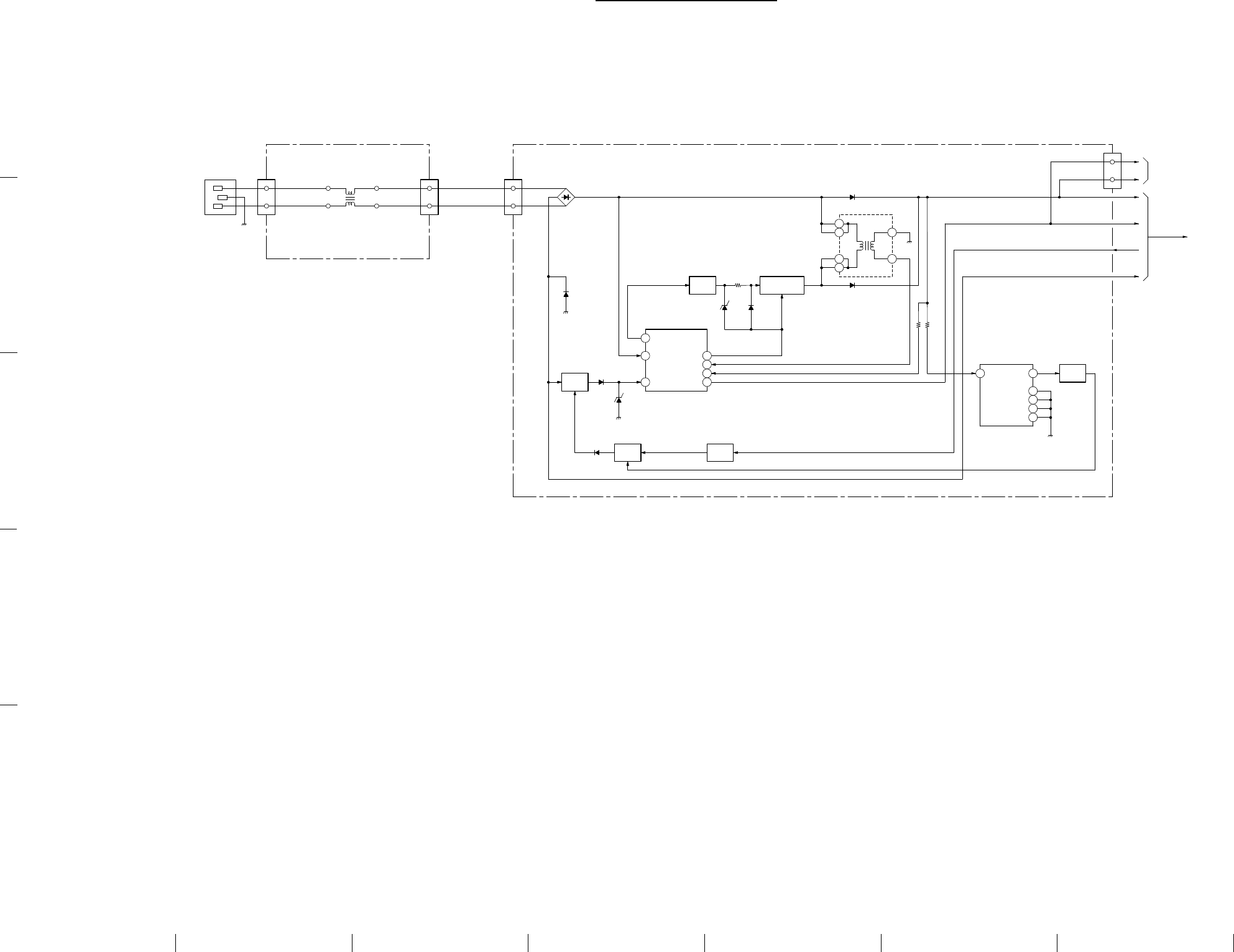
8-12 8-12
A B C D E F GH
1
2
3
4
5
VPL-PX20/PX30
F, GA (1/2) F, GA (1/2)
F BLOCK
GA BLOCK (1/2)
CN2000
AC(L)
AC(N)
1 2
4 3
CN2002
CONTROL
VCC
DRIVE
INDET
8
1
3
GND
ISENSE
6
4
IC2100
Q2109,2110
DRIVE
PRI
Q2100
SWITCHING
Q2104,2105
POWER
CONT
Q2101,2102
PFC
OVP
CLAMP
D2107
Q2106
CONT
POWER
1VDET
5ZERODET
SWITCH(SCR)
D2102
7
13
L2100
8
11
2
3
RECT
D2108
D2106
PROTECT
D2141
CLAMP
D2105
CLAMP
D2100
MAIN RECT
C
D
B
A
POWER SUPPLY
TO LAMP
+V(W)
-V(B)
CN2111
F(EMI FILTER) GA(1/2)(ACTIVE FILTER)
AC(N)
AC(L)
CN2110
SHUNT REGULATOR
8 REF
A
A
A
7
6
3
K1
IC2105
A2
OVP
Q2111
PFC
AC(N)
AC
INLET LFT
L2000
AC(L)
D2110
CLAMP
D2103
CLAMP
TO GA(2/2)
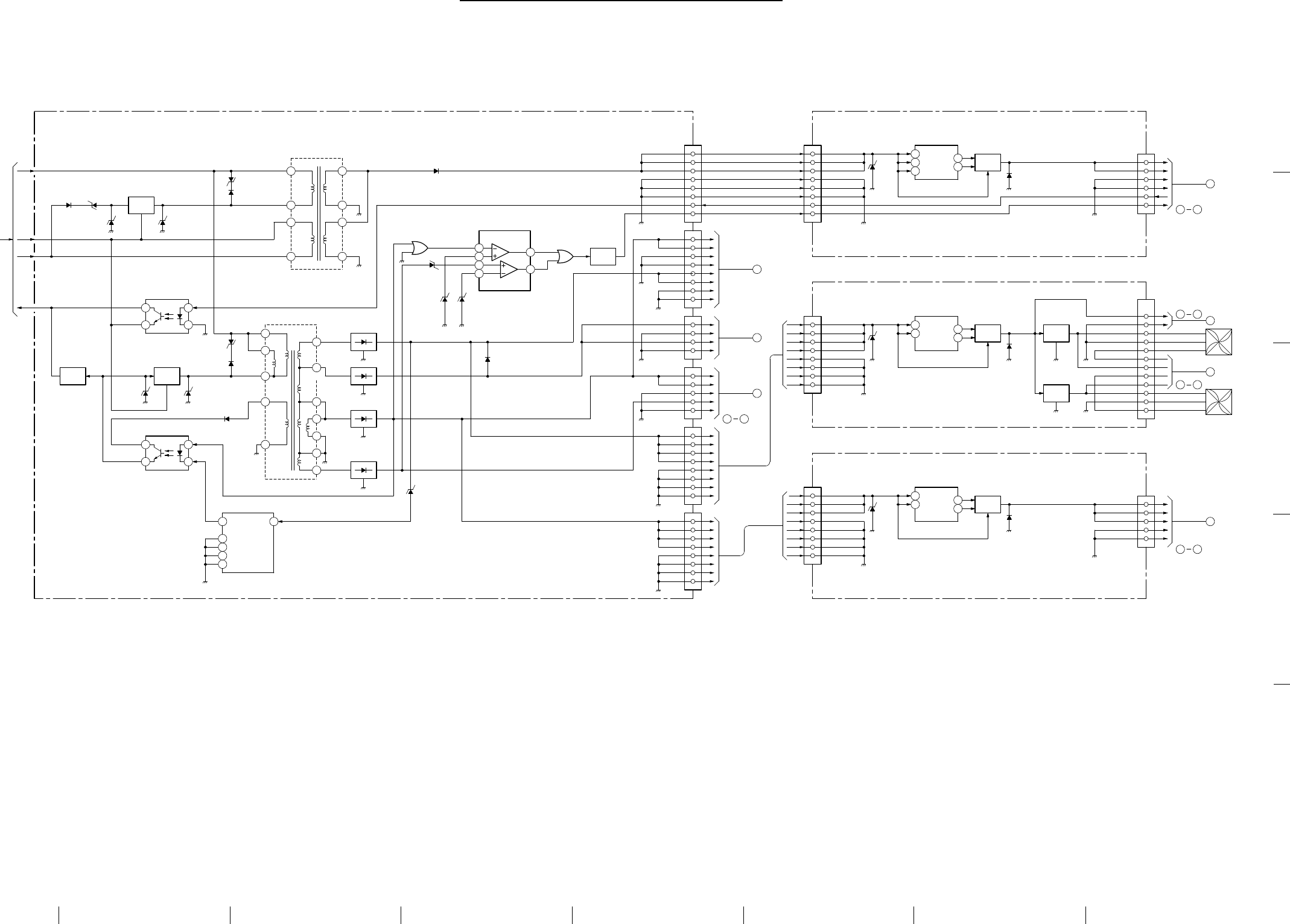
8-13 8-13
A B C D E F GH
1
2
3
4
5
VPL-PX20/PX30
GA (2/2), GB, GC, GD GA (2/2), GB, GC, GD
GA BLOCK (2/2)
GB, GC, GD BLOCK
C BOARD
TO
7
POWER PORT
IC2104
1
Q2107,2108
PROT
POWER
CN2106
SUB
SUB
1
2
SUB
GND2
GND2
GND2
POWER ON
POWER PROT
3
4
5
6
7
8
GND
GND
17.5V
17.5V
GND
GND
A6V
A6V
7
8
6
5
4
3
2
1
CN2104
3
6
8
7
4
5
1
2
CN2102
3
6
8
7
4
5
1
2
CN2101
CN2105
GND
AUDIO+B
GND
AUDIO+B
4
3
2
1
4A-7V
GND 5
GND
A6V
A6V 1
3
2
CN2103
GND
6V
K BOARD
TO
BB BOARD
TO
ON
Q2103
POWER
6
5
3
2
D2147
CLAMP
D2148
CLAMP
Q2142,2143
D2144,2145
RECT
D2134,2135,2136
4
3
2
14
15
13
12
11
10
9
6
7
2
3
IC2103
SHUNT REGULATOR
81
D2127,2129,2132
RECT
RECT
D2128,2130,2131
D2137,2138,2139
RECT
6
7
OVP
D2133
K
A
A
A
A
REF
9
8
4
2
7
5
3
1
4
32
I SOLATER
PH2101
1
D2120
CLAMP
D2119
NOISE FILTER
NOIS
D2121
NOISE
FILTER
FILTER
D2118 D2125,2126
RECT
D2111
Q2113
CLAMP
D2122,2123
CLAMP
CLAMP
D2114,2115
S
CD
D
S
C
D2112
CLAMP
D2116
CLAMP
GA(2/2)(CONVERTER)
3
4
2
1
ISOLATER
PH2100
D2124
D2149
CLAMP
GND
GND
GND
6V
6V
6V
18V
GND
GND
GND
GND
18V
18V
18V
7
8
5
6
2
3
4
16
7
10
16
SUB5V DC-DC CONV
IC2500
CLAMP
D2500 13
SHD
FB
V+ DL
DH SWITCH
Q2500,2501
SUB
SUB
SUB
GND2
GND2
GND2
POWER ON
POWER PROT
D2502
RECT
6
5
4
3
2
1SUB5V
SUB5V
GND2
GND2
POWER ON
POWER PROT
BB BOARD
TO
CN2502
GC(SUB5V REG)
CN2500
6 SHD
GND
GND7
8
6
5
4
3
2
GND
GND
6V
6V
6V SWITCH10
CLAMP
D2300 DL
DH
V+ 16
13
D2302
RECT
D3.3V
4
5
1
2
3
BB BOARD
TO
GB(D3.3V REG)
CN2300
1 6V Q2300,2301
D3.3V DC-DC CONV
IC2300
CN2301
GND
7
8
GND
GD(FAN+B AND 10.7V REG)
18V1
5
4
6
2
3
GND
18V
GND
18V
18V
CN2700
SWITCH
Q2700,2701
6
10
10.7V DC-DC CONV
CLAMP
D2700 DL
DH
SHD
V+ 16
13
IC2700
D2702
RECT
8
CN2701
FAN PRO(1)
FAN+B(1)
GND
6
5
7
3
4
FAN 1
IGO
2GND
110.7V
9
10
11
12
FAN PRO(1)
FAN CON(1)
FAN PRO(2)
FAN CON(2)
FAN+B(2)
GND
FAN PRO(2)
IO
G
IC2701
IC2702
FAN+B(2)REG
FAN+B(1)REG
D3.3V
D3.3V
GND
GND
A
B
C
D
IC2102
PWN CONTROL
SRT
T2101
T2100
SRT
D2140
CLAMP
IC2101
PWN CONTROL
GA(1/2)
CN600
CN2901
CN308
TO QA BOARD
CN808
14
11
18
6 8
61
CN310
20
19
CN308
89
17
CN310
12
TO
BB BOARD
FAN 2
21
BB BOARD
TO
107
CN308
FROM
9-1 9-1
A B C D E F GH
1
2
3
4
5
VPL-PX20/PX30
Section 9
Diagrams
9-1. Frame Schematic Diagram
FRAME (1/3) FRAME (1/3)
CN301
70P
CN311CN309 CN307
BA
CN101
70P
CN502CN500
CN501
70P
CN605
CN305
CN303
CN3000
CN310
10P
50P
50P
CN600
8P
8P
32P
32P
32P
32P
32P
32P
CN601 CN602 CN603
70P
70P
70P
70P
50P
50P
50P
50P
70P
70P
70P
70P
3P
CN3600
3P
3P
3P
CN3700
12P
12P
CN3010
3P
CN3002
4P
4P
CN3500
H
NF
NR
BALAST
QD
CN3005
S
7P
7P
CN3003
CN3001
CN306
CN102
CN1901
6P
6P
QA
5P
5P
CN1902
CN807
CN801
CN802
QB
50P
50P
50P
50P
CN803 CN971
CN804 CN972
QC
50P
50P
50P
50P
K
3P
KS
4P
4P
CN3501
CN2952
CN810
CN2951
3P
3P
CN3502 CN3503
LSP RSP
GB GA
GC
GD
BB
BC
C
Y
2P
2P
CN2903
MSP
CN2900
CN808
2P
4P
CN2105
CN2901
8P
8P
8P
CN308
CN2301
12P
5P
8P
8P
8P
F
3P
3P
9P
LCD LCD LCD
9P
9P
3P
CN809
2P
8P
6P
CN2502
5P
CN2103
CN2701
12P
3P
FAN
3P
FAN
CN805 CN806
CN2102
CN2500
CN2700 CN2106
CN2104
CN2101
CN2300
(EMI FILTER)
(AUDIO AMP)
(INPUT TERMINAL)
ACTIVE FILTER
CONVERTER
(SUB 5V REG)
(D+3.3V REG)
FAN +B AND
10.7V REG
INPUT SELECT
AUDIO PROCESS
(SIRCS/VIDEO IN)
DECORDER
CHROMA
(SCAN CONVERTOR)
CN1805CN1804
(IN/OUT TERMINAL)
(SUB AUDIO AMP)
(CONTROL PANEL)
(CPU)
(LCD DRIVER)
(G) (B) (R)
(SW AND TH)
(THREE DIMENSIONS)
(FRONT RECIVER)
(REAR RECIVER)
B-SS1696<08.>-KESSENZU-P1
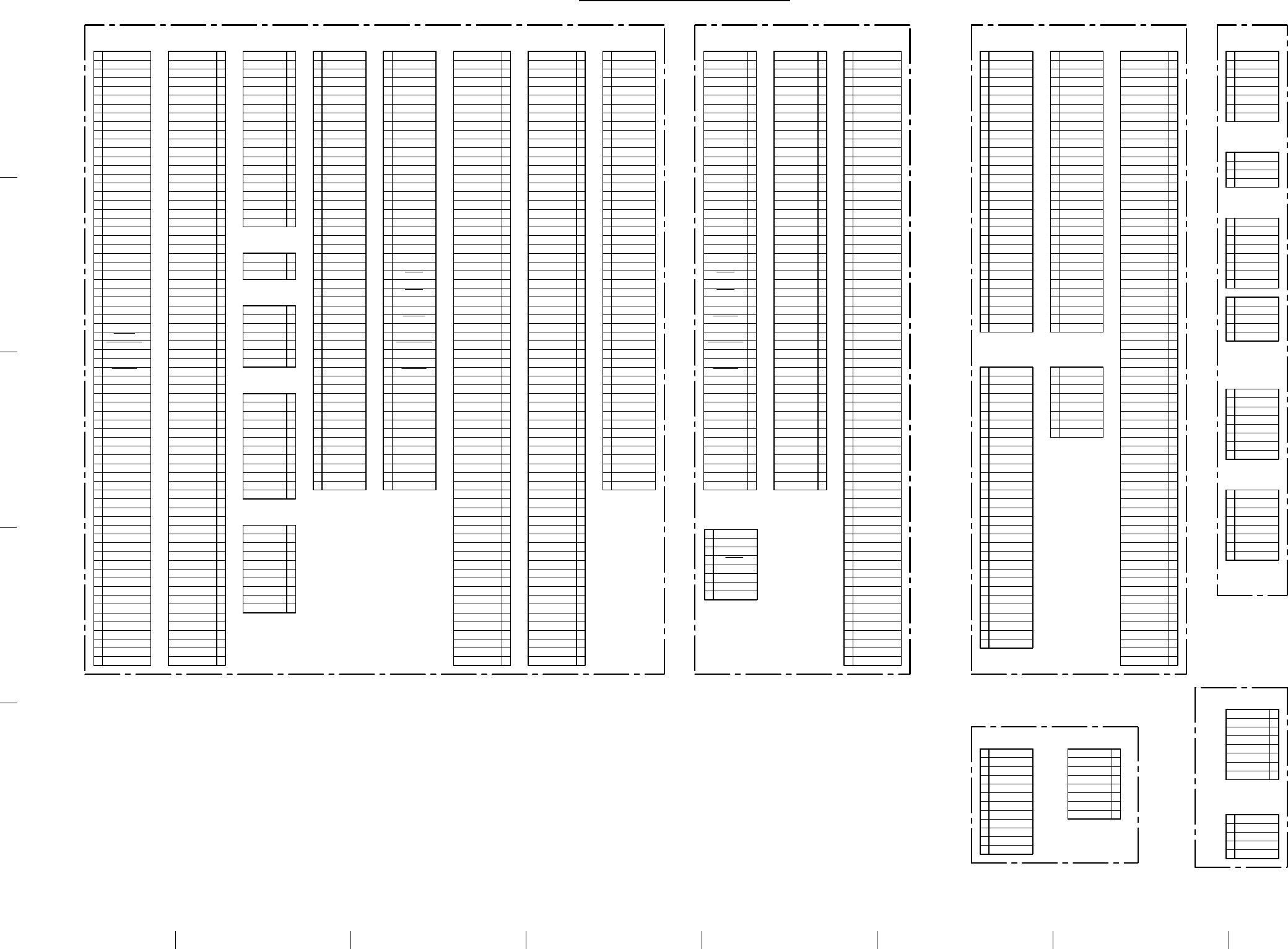
9-2 9-2
A B C D E F GH
1
2
3
4
5
VPL-PX20/PX30
FRAME (2/3) FRAME (2/3)
1
2
3
1
2
3
4
5
6
7
1
2
3
4
5
6
7
8
9
10
11
12
1
2
3
4
5
6
7
8
1
2
3
4
5
6
7
8
9
10
11
12
13
14
15
16
17
18
19
20
21
22
23
24
25
26
27
28
29
30
31
32
1
2
3
4
5
6
7
8
9
10
11
12
13
14
15
16
17
18
19
20
21
22
23
24
25
26
27
28
29
30
31
32
1
2
3
4
5
6
7
8
9
10
11
12
13
14
15
16
17
18
19
20
21
22
23
24
25
26
27
28
29
30
31
32
1
2
3
4
5
6
7
8
1
2
3
4
5
6
7
8
1
2
3
4
5
6
7
8
1
2
3
4
5
6
7
8
1
2
3
4
5
6
7
8
1
2
3
4
5
6
7
8
1
2
3
4
5
6
7
8
1
2
3
4
5
6
7
8
9
10
11
12
A1
A2
A3
A4
A5
A6
A7
A8
A9
A10
A11
A12
A13
A14
A15
A16
A17
A18
A19
A20
A21
A22
A23
A24
A25
A26
A27
A28
A29
A30
A31
A32
A33
A34
B1
B2
B3
B4
B5
B6
B7
B8
B9
B10
B11
B12
B13
B14
B15
B16
B17
B18
B19
B20
B21
B22
B23
B24
B25
B26
B27
B28
B29
B30
B31
B32
B33
B34
A35
B35
A1
A2
A3
A4
A5
A6
A7
A8
A9
A10
A11
A12
A13
A14
A15
A16
A17
A18
A19
A20
A21
A22
A23
A24
A25
A26
A27
A28
A29
A30
A31
A32
A33
A34
B1
B2
B3
B4
B5
B6
B7
B8
B9
B10
B11
B12
B13
B14
B15
B16
B17
B18
B19
B20
B21
B22
B23
B24
B25
B26
B27
B28
B29
B30
B31
B32
B33
B34
A35
B35
1
2
3
4
5
6
7
8
9
10
11
12
13
14
15
16
17
18
19
20
1
2
3
4
5
6
7
8
9
10
1
2
3
4
1
2
3
4
5
1
2
3
4
5
A1
A2
A3
A4
A5
A6
A7
A8
A9
A10
A11
A12
A13
A14
A15
A16
A17
A18
A19
A20
A21
A22
A23
A24
A25
A26
A27
A28
A29
A30
A31
A32
A33
A34
B1
B2
B3
B4
B5
B6
B7
B8
B9
B10
B11
B12
B13
B14
B15
B16
B17
B18
B19
B20
B21
B22
B23
B24
B25
B26
B27
B28
B29
B30
B31
B32
B33
B34
A35
B35
A1
A2
A3
A4
A5
A6
A7
A8
A9
A10
A11
A12
A13
A14
A15
A16
A17
A18
A19
A20
A21
A22
A23
A24
A25
A26
A27
A28
A29
A30
A31
A32
A33
A34
B1
B2
B3
B4
B5
B6
B7
B8
B9
B10
B11
B12
B13
B14
B15
B16
B17
B18
B19
B20
B21
B22
B23
B24
B25
B26
B27
B28
B29
B30
B31
B32
B33
B34
A35
B35
A1
B1
A2
B2
A3
B3
A4
B4
A5
B5
A6
B6
A7
B7
A8
B8
A9
B9
A10
B10
A11
B11
A12
B12
A13
B13
A14
B14
A15
B15
A16
B16
A17
B17
A18
B18
A19
B19
A20
B20
A21
B21
A22
B22
A23
B23
A24
B24
A25
B25
A1
B1
A2
B2
A3
B3
A4
B4
A5
B5
A6
B6
A7
B7
A8
B8
A9
B9
A10
B10
A11
B11
A12
B12
A13
B13
A14
B14
A15
B15
A16
B16
A17
B17
A18
B18
A19
B19
A20
B20
A21
B21
A22
B22
A23
B23
A24
B24
A25
B25
A1
B1
A2
B2
A3
B3
A4
B4
A5
B5
A6
B6
A7
B7
A8
B8
A9
B9
A10
B10
A11
B11
A12
B12
A13
B13
A14
B14
A15
B15
A16
B16
A17
B17
A18
B18
A19
B19
A20
B20
A21
B21
A22
B22
A23
B23
A24
B24
A25
B25
A1
B1
A2
B2
A3
B3
A4
B4
A5
B5
A6
B6
A7
B7
A8
B8
A9
B9
A10
B10
A11
B11
A12
B12
A13
B13
A14
B14
A15
B15
A16
B16
A17
B17
A18
B18
A19
B19
A20
B20
A21
B21
A22
B22
A23
B23
A24
B24
A25
B25
A1
A2
A3
A4
A5
A6
A7
A8
A9
A10
A11
A12
A13
A14
A15
A16
A17
A18
A19
A20
A21
A22
A23
A24
A25
A26
A27
A28
A29
A30
A31
A32
A33
A34
B1
B2
B3
B4
B5
B6
B7
B8
B9
B10
B11
B12
B13
B14
B15
B16
B17
B18
B19
B20
B21
B22
B23
B24
B25
B26
B27
B28
B29
B30
B31
B32
B33
B34
A35
B35
A1
A2
A3
A4
A5
A6
A7
A8
A9
A10
A11
A12
A13
A14
A15
A16
A17
A18
A19
A20
A21
A22
A23
A24
A25
A26
A27
A28
A29
A30
A31
A32
A33
A34
B1
B2
B3
B4
B5
B6
B7
B8
B9
B10
B11
B12
B13
B14
B15
B16
B17
B18
B19
B20
B21
B22
B23
B24
B25
B26
B27
B28
B29
B30
B31
B32
B33
B34
A35
B35
A1
B1
A2
B2
A3
B3
A4
B4
A5
B5
A6
B6
A7
B7
A8
B8
A9
B9
A10
B10
A11
B11
A12
B12
A13
B13
A14
B14
A15
B15
A16
B16
A17
B17
A18
B18
A19
B19
A20
B20
A21
B21
A22
B22
A23
B23
A24
B24
A25
B25
CN300
CN2106
CN2101
CN2102
CN2104
CN2103
CN2300
CN2301
CN2700
CN2701
CN500
CN502
CN2105
CN605
CN501 CN603
CN601
CN600CN602
CN503
CN302
CN308
CN310
CN309 CN301 CN303 CN306CN305CN307 CN311
CN312
20P
8P
:B-TO-B
8P
:B-TO-B
8P
:B-TO-B
8P
WHT
:S-MICRO
5P
BLK
:S-MICRO
8P
:B-TO-B
5P
WHT
:S-MICRO
8P
:B-TO-B
12P
WHT
50P
50P
4P
RED
:S-MICRO
70P
70P 32P
FPC
32P
FPC
8P
:SMD
32P
FPC
8P
WHT
:SMD
3P
:SMD
12P
10P
50P 70P 70P 50P70P70P 50P
7P
:SMD
BB
BC CGA
GB
GD
GND
GND
US+
US-
GND
GND
DS1+
DS1-
GND
GND
USBP.ENA
USBP.FLG
SDA400K
SCL400K
TXDS/C
RXDS/C
GND
GND
HD
GND
GND
VD
VSO
DISP
BUSY
GND
PANEL LINK
GND
AUDIO CE
AUDIO MUTE
OSD_RES
PANEL TEMP
FILTER COVER
POWER ON
FAN PROT1
FAN CONT1
FAN PROT2
FAN CONT2
GND
GND
SDA100K
SCL100K
GND
GND
+6V
+6V
+6V
+6V
POWER PROT
SUB+5V
SUB+5V
SUB+5V
SUB+5V
DS2+
DS2-
PW-OSD ENA
IRDA
IRDB
OSD CS
SDAT
SCLK
GND
GND
GND
GND
US VBUS
S/C RES
MSP.ENA
INTERLACE
PIC MUTE
GND
GND
GND
GND
R/R-Y
R/R-Y
GND
GND
G/Y
G/Y
GND
GND
B/B-Y
B/B-Y
GND
GND
H
H
GND
GND
V
V
GND
GND
RGBSYNC
RGBSYNC
GND
GND
V-R
V-R
GND
GND
V-G
V-G
GND
GND
V-B
V-B
GND
GND
V-HD
V-HD
GND
GND
V-CLP
V-CLP
GND
GND
SDA100K
SCL100K
GND
GND
+6V
+6V
+6V
+6V
V-VD
V-VD
10V
10V
-7V
-7V
DS2+
DS2+
IRDA
IRDB
DS2-
DS2-
YC/OTHER
CV/OTHER
TX1+
TX1-
TXC+
TXC-
GND
TX2+
TX2-
TX0+
TX0-
SHLD1
SHLDC
+5V
RESERVED
RESERVED
SHLD2
SHLD0
RESERVED
HPD
DDC_DAT
DDC_CLK
VCC
IRRCVR
GND
VCC
RXD
TXD
GND
EXTSW
WDTEN
GND
GND
6V
6V
GND
GND
GND
GND
10V
-7V
D3.3V
D3.3V
D3.3V
GND
GND
POWER ON
FANPROT1
FANCONT1
FANPROT2
FANCONT2
POWER PROT
SUB 5V
SUB 5V
GND
ROMOEN
3.3V
ROMWEN
3.3V
ROMWEN
3.3V
CS2
3.3V
CS3
GND
FCEN
GND
BOOTWE
GND
VPPEN
D15
D14
D13
D12
D11
D10
D9
D8
D7
D6
D5
D4
D3
D2
D1
D0
NC
NC
GND
RESETN
GND
NMI
6V
6V
6V
6V
PANEL TEMP
GND
GND
DISP
BUSY
GND
GND
GND
GND
SCL400K
GND
SDA400K
GND
OSD_RES
SCL100K
SDA100K
PW OSD ENA
OSD_CS
NC
NC
NC
NC
DRE0
GND
DRE1
GND
DRE2
DRE3
DRE4
DRE5
DRE6
GND
DRE7
GND
DGE0
DVS
DGE1
DVS
DGE2
GND
DGE3
GND
DGE4
DHS
DGE5
DHS
DGE6
GND
DGE7
GND
DBE0
DRO0
DBE1
DRO1
DBE2
DRO2
DBE3
DRO3
DBE4
DRO4
DBE5
DRO5
DBE6
DBE7
DRO7
GND
GND
DRO6
D3.3V
D3.3V
D3.3V
D3.3V
SDAT
AUDIO CE
GND
GND
US+
US-
GND
DS1+
GND
GND
BNC V
BNC V
GND
GND
GND
GND
GND
GND
GND
GND
BNC H
BNC H
BNC B
BNC B
BNC G
BNC G
BNC R
BNC R
US+
US-
GND
USBP.FLG
USBP.ENA
SUB 5V
SUB 5V
SUB 5V
SUB 5V
SUB 5V
SUB 5V
DS1-
MSP.ENA
US VBUS
V-B
V-B
GND
CV/OTHER
GND
V-HD
GND
V-VD
GND
GND
SDA100K
SCL100K
GND
GND
+6V
+6V
+6V
+6V
+10V
GND
+10V
GND
SCLK
GND
MODE
PLUG
SDI
SDO
VCC
ISPEN
PS2G
VSIG1
VSIG2
VSIG3
VSIG4
VSIG5
VSIG6
VSIG7
VSIG8
VSIG9
VSIG10
VSIG11
VSIG12
HVDD
RGT
HST
VSS
BLK
ENB
VCK
VST
DWN
PCG
VVDD
VSSGR
HCK2
HCK1
VSSGL
HB
VB
COM
SOUT
PS2G
VSIG1
VSIG2
VSIG3
VSIG4
VSIG5
VSIG6
VSIG7
VSIG8
VSIG9
VSIG10
VSIG11
VSIG12
HVDD
RGT
HST
VSS
BLK
ENB
VCK
VST
DWN
PCG
VVDD
VSSGR
HCK2
HCK1
VSSGL
HB
VB
COM
SOUT
PS2G
VSIG1
VSIG2
VSIG3
VSIG4
VSIG5
VSIG6
VSIG7
VSIG8
VSIG9
VSIG10
VSIG11
VSIG12
HVDD
RGT
HST
VSSGR
HCK2
HCK1
17V
GND 2
GND 2
GND 2
TO GC
SUB
SUB
SUB
POWER ON
POWER PROT
AUDIO+B
AUDIO+B
A6V
A6V
17.5V
17.5V
18V
18V
18V
18V
TO GD
TO K
TO C
GND
GND
TO BB
PANEL TEMP
GND
GND
GND
GND
GND
GND
GND
ECLK
HCK1
HCK2
ENB
PCG
DWN
RGT
CLP
PRG
VCK
FRP
VST
HST
BLK
ODDB
ODDG
ODDR
ECLK
TO BC CN501
SDA100K
SCL100K
HCK1
HCK2
ENB
PCG
GND
CLP
PRG
VST
VCK
HST
FRP
GND
GND
PANEL TEMP
GND
GND
GND
GND
A5V
GND
ECLK
HCK1
ENB
PCG
DWN
RGT
CLP
PRG
VCK
FRP
VST
HST
INVCNT
BLK
POSCONT1
POSCONT2
A5V
EVENB
EVENG
EVENB
EVENG
EVENR
ODDB
EVENR
ODDB
GND
GND
ODDG
ODDR
ODDG
ODDR
ECLK
SDA100K
SCL100K
HCK1
HCK2
HCK2
ENB
PCG
GND
GND
CLP
PRG
VST
VCK
HST
FRP
GND
POSCONT2
INVCNT
SID
POSCONT1
SID
A5V
A5V
GND
GND
GND
GND
GND
GND
GND
GND
DRE0
GND
DRE1
GND
DRE2
DRE3
DRE4
DRE5
DRE6
GND
DRE7
GND
DGE0
DVS
DGE1
DVS
DGE2
GND
DGE3
GND
DGE4
DHS
DGE5
DHS
DGE6
GND
DGE7
GND
DBE0
DRO0
DBE1
DRO1
DBE2
DRO2
DBE3
DRO3
DBE4
DRO4
DBE5
DRO5
DBE6
DBE7
DRO7
GND
GND
D3.3V
D3.3V
D3.3V
D3.3V
DR06
PANEL TEMP
DCLK
GND
DCLK
GND
GND
GND
DGO0
DBO0
DGO1
DBO1
DGO2
DBO2
DGO3
DBO3
DGO4
DBO4
DGO5
DBO5
DGO6
DBO6
DGO7
DBO7
GND
GND
GND
GND
DISP
BUSY
GND
GND
GND
GND
SCL400K
GND
SDA400K
GND
D3.3V
D3.3V
SCL100K
SDA100K
RESET
RESET
OSD_CS0
OSD_RES
NC
NC
PW OSD ENA
NC
NC
GND
GND
GND
GND
A6V
A6V
GND
A-7V
GND
GND
GND
GND
GND
6V
6V
6V
6V
GND
GND
GND
GND
POSCONT2
INVCNT
POSCONT2
INVCNT
POSCONT1
SID
POSCONT1
SID
GND
GND
A5V
A5V
A5V
A5V
GND
GND
VSS
VSSGL
BLK
ENB
VCK
VST
DWN
HB
VB
PCG
VVDD
COM
SOUT
6V
6V
GND
GND
17V
GND
GND
EVENB
EVENG
EVENB
EVENG
GND
GND
EVENR
ODDB
EVENR
GND
GND
ODDG
ODDR
TO BB
6V
6V
6V
6V
GND
GND
GND
GND
D3.3V
D3.3V
D3.3V
GND
GND
18V
18V
18V
18V
GND
GND
GND
GND
10.7V
GND
FAN+B(1)
GND
FAN PRO(1)
FAN PRO(1)
FAN CON(1)
FAN PRO(2)
FAN CON(2)
FAN+B(2)
GND
FAN PRO(2)
GND
A19
GND
A18
GND
A17
GND
A16
A15
A14
A13
A12
A11
A10
A9
A8
A7
A6
A5
A4
A3
A2
A1
A0
GND
BHENN
GND
ROMOEN
DCLK
GND
DCLK
GND
GND
GND
DGO0
DBO0
DGO1
DBO1
DGO2
DBO2
DGO3
DBO3
DGO4
DBO4
DGO5
DBO5
DGO6
DBO6
DGO7
DBO7
GND
GND
RESET
RESET
D3.3V
D3.3V
CLP
CLP
GND
GND
A3.3V
A3.3V
V
V
GND
GND
H
H
GND
GND
B
B
GND
GND
G
G
GND
GND
R
R
GND
GND
AUDIO MUTE
SCLK
R/R-Y
R/R-Y
GND
GND
G/Y
G/Y
GND
GND
B/B-Y
B/B-Y
GND
H
GND
V
GND
RGBSYNC
GND
V-CLP
GND
V-R
V-R
GND
GND
V-G
V-G
GND
GND
Y/C OTHER
B-SS1696<08.>-KESSENZU-P2
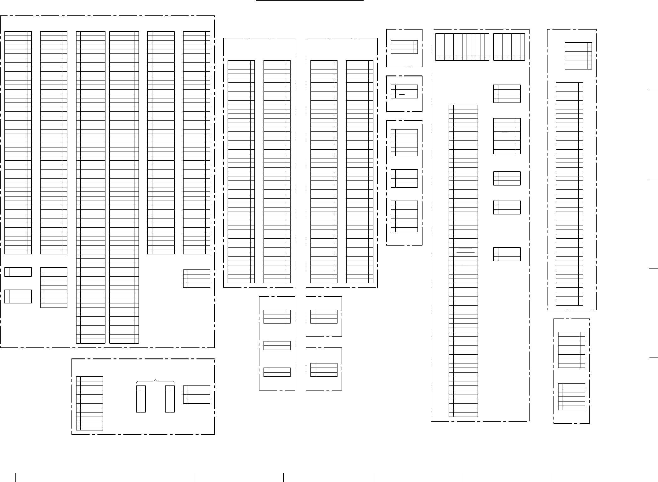
9-3 9-3
A B C D E F GH
1
2
3
4
5
VPL-PX20/PX30
1
2
3
1
2
3
1
2
3
1
2
3
1
2
3
4
5
6
7
8
9
1
2
3
4
5
6
1
2
3
4
1
2
3
1
2
3
4
5
6
7
8
9
10
11
12
1
2
3
4
5
6
7
A1
A2
A3
A4
A5
A6
A7
A8
A9
A10
A11
A12
A13
A14
A15
A16
A17
A18
A19
A20
A21
A22
A23
A24
A25
A26
A27
A28
A29
A30
A31
A32
A33
A34
B1
B2
B3
B4
B5
B6
B7
B8
B9
B10
B11
B12
B13
B14
B15
B16
B17
B18
B19
B20
B21
B22
B23
B24
B25
B26
B27
B28
B29
B30
B31
B32
B33
B34
A35
B35
A1
B1
A2
B2
A3
B3
A4
B4
A5
B5
A6
B6
A7
B7
A8
B8
A9
B9
A10
B10
A11
B11
A12
B12
A13
B13
A14
B14
A15
B15
A16
B16
A17
B17
A18
B18
A19
B19
A20
B20
A21
B21
A22
B22
A23
B23
A24
B24
A25
B25
A1
B1
A2
B2
A3
B3
A4
B4
A5
B5
A6
B6
A7
B7
A8
B8
A9
B9
A10
B10
A11
B11
A12
B12
A13
B13
A14
B14
A15
B15
A16
B16
A17
B17
A18
B18
A19
B19
A20
B20
A21
B21
A22
B22
A23
B23
A24
B24
A25
B25
A1
B1
A2
B2
A3
B3
A4
B4
A5
B5
A6
B6
A7
B7
A8
B8
A9
B9
A10
B10
A11
B11
A12
B12
A13
B13
A14
B14
A15
B15
A16
B16
A17
B17
A18
B18
A19
B19
A20
B20
A21
B21
A22
B22
A23
B23
A24
B24
A25
B25
A1
B1
A2
B2
A3
B3
A4
B4
A5
B5
A6
B6
A7
B7
A8
B8
A9
B9
A10
B10
A11
B11
A12
B12
A13
B13
A14
B14
A15
B15
A16
B16
A17
B17
A18
B18
A19
B19
A20
B20
A21
B21
A22
B22
A23
B23
A24
B24
A25
B25
A1
B1
A2
B2
A3
B3
A4
B4
A5
B5
A6
B6
A7
B7
A8
B8
A9
B9
A10
B10
A11
B11
A12
B12
A13
B13
A14
B14
A15
B15
A16
B16
A17
B17
A18
B18
A19
B19
A20
B20
A21
B21
A22
B22
A23
B23
A24
B24
A25
B25
A1
B1
A2
B2
A3
B3
A4
B4
A5
B5
A6
B6
A7
B7
A8
B8
A9
B9
A10
B10
A11
B11
A12
B12
A13
B13
A14
B14
A15
B15
A16
B16
A17
B17
A18
B18
A19
B19
A20
B20
A21
B21
A22
B22
A23
B23
A24
B24
A25
B25
A1
A2
A3
A4
A5
A6
A7
A8
A9
A10
A11
A12
A13
A14
A15
A16
A17
A18
A19
A20
A21
A22
A23
A24
A25
A26
A27
A28
A29
A30
A31
A32
A33
A34
B1
B2
B3
B4
B5
B6
B7
B8
B9
B10
B11
B12
B13
B14
B15
B16
B17
B18
B19
B20
B21
B22
B23
B24
B25
B26
B27
B28
B29
B30
B31
B32
B33
B34
A35
B35
A1
A2
A3
A4
A5
A6
A7
A8
A9
A10
A11
A12
A13
A14
A15
A16
A17
A18
A19
A20
A21
A22
A23
A24
A25
A26
A27
A28
A29
A30
A31
A32
A33
A34
B1
B2
B3
B4
B5
B6
B7
B8
B9
B10
B11
B12
B13
B14
B15
B16
B17
B18
B19
B20
B21
B22
B23
B24
B25
B26
B27
B28
B29
B30
B31
B32
B33
B34
A35
B35
A1
B1
A2
B2
A3
B3
A4
B4
A5
B5
A6
B6
A7
B7
A8
B8
A9
B9
A10
B10
A11
B11
A12
B12
A13
B13
A14
B14
A15
B15
A16
B16
A17
B17
A18
B18
A19
B19
A20
B20
A21
B21
A22
B22
A23
B23
A24
B24
A25
B25
A1
B1
A2
B2
A3
B3
A4
B4
A5
B5
A6
B6
A7
B7
A8
B8
A9
B9
A10
B10
A11
B11
A12
B12
A13
B13
A14
B14
A15
B15
A16
B16
A17
B17
A18
B18
A19
B19
A20
B20
A21
B21
A22
B22
A23
B23
A24
B24
A25
B25
A1
B1
A2
B2
A3
B3
A4
B4
A5
B5
A6
B6
A7
B7
A8
B8
A9
B9
A10
B10
A11
B11
A12
B12
A13
B13
A14
B14
A15
B15
A16
B16
A17
B17
A18
B18
A19
B19
A20
B20
A21
B21
A22
B22
A23
B23
A24
B24
A25
B25
1
2
3
4
5
6
7
8
1
2
3
4
1
2
1
2
1
2
3
4
1
2
1
2
3
4
5
6
7
1
2
3
1
2
3
4
1
2
3
1
2
3
1
2
3
1
2
3
4
5
6
7
8
1
2
3
4
5
6
1
2
3
4
5
6
1
2
3
4
5
6
7
8
9
10
11
12
1
2
1
2
CN807
CN2020
CN1203 CN1204 CN1804 CN1805
CN2500
CN2502
CN102
CN101
CN3003CN3001
CN3000
CN3002
CN3010
CN3005
CN3006
CN3007
CN1903
CN1901
CN1902
CN1991
CN2900
CN2903
CN2901
CN3700
CN3600
CN3501
CN3503CN3502
CN3500
CN804CN806CN805CN803
CN810
CN808
CN809
CN802CN801
4P
WHT-L
3P
:SMD
50P
WHT 50P
WHT 50P
WHT
50P
WHT
8P
:B-TO-B
6P
WHT
:S-MICRO
6P
:SMD
50P
7P
WHT
:SMD
12P
WHT
:SMD
70P
4P
WHT
:SMD
8P
WHT
:SMD
3P
WHT
:SMD
3P
RED
:SMD
3P
WHT
:SMD
7P
WHT
6P
4P
3P
3P
WHT-L
:SMD
2P
WHT-L
:SMD
2P
RED-L
:SMD
3P
RED
:SMD
3P
WHT-I
:SMD
4P
WHT
:SMD
2P
WHT-L
:SMD
2P
WHT-L
:SMD
12P
WHT
:SMD
50P
WHT
50P
WHT
50P
WHT
50P
WHT
9P
WHT-L
2P
WHT-L
:SMD
3P
WHT-L
:SMD
70P70P
KS
NF
NR
QA
QB
QD
S
U
QC
Y
BA
GC
H
SP-MUTE
L/R
GND
AUD GND
AUDIO+B
MAIN+
MAIN-
SUB+5V
GND
SIRCS-NF
SUB+5V
GND
SIRCS-NF
S-SEL
GND
R-VIDEO
GND
L-VIDEO
R
SP-MUTE
L/R
GND
AUDIO+BAUDIO+B
GND
GND
SP-MUTE
L
AU GND AU GND
NC
NC
GND
GND
TXD_RD
RXD_RS
SUB+5V
SIRCS
SIRCS_S
GND
GND
C-VIDEO
GND
S-SEL
GND
GND
R-VIDEO
L-VIDEO
GND
LAMP COVER
LAMP TEMP
GND
ECO /NOR
SW COVER
GND
SUB+5V
SIRCS
SIRCS-S
GND
TXD RS
RXD RS
GND
GND
KEY1
KEY0
LIGHT ON
P.SAVE LED
LAMP LED
TEMP LED
POWER LED
SUB+5V
D+5V
D+5V
TO NF(CN3600)
TO NR(CN3700)
SUB+5V
GND
GND
SIRCS-NF
SUB+5V
SIRCS-NR
GND
LAMP PROT
LAMP ON
GND
LAMP COVER
LAMP TEMP
LAMP MODE
TXD
RXD
VIN
GND
RES
FWR
MD1
MD2
GND
GND
US+
US-
GND
GND
DS1+
DS1-
GND
GND
SDA400K
SCL400K
GND
GND
GND
HD
VD
VSO
GND
GND
GND
SDAT
SCLK
GND
GND
GND
SDA100K
SCL100K
USB P.ENA
USB P.FLG
TXD S/C
RXD S/C
GND
PANEL LINK
AUDIO CE
AUDIO MUTE
GND
GND
+6V
+6V
+6V
+6V
PANEL TEMP
POWER ON
FAN PROT1
FAN CONT1
FAN CONT2
FAN PROT2
GND
DS2+
DS2-
GND
FIL. COVER
POWER PROT
OSDC CS
PW-OSD ENA
S/C RES
IRDA
IRDB
SUB+5V
SUB+5V
SUB+5V
SUB+5V
MS P.ENA
US VBUS
INTERLACE
PIC MUTE
P96
P97
P94
GND
GND
GND
GND
GND
GND
GND
GND
GND
GND
GND
GND
GND
GND
GND
GND
GND
GND
GND
GND
AV
AV
AH
AH
AB
AB
AB
AB
AG
AG
AG
AG
AR
AR
AR
AR
AUDIO AR
AUDIO AR
AUDIO AL
AUDIO AL
GND
GND
DS2+
DS2+
DS2-
DS2-
IRD A
IRD A
MS5V
MS5V
GND
GND
GND
GND
GND
GND
GND
GND
GND
GND
GND
GND
GND
GND
GND
GND
GND
GND
GND
GND
GND
GND
USBU D-
USBU D-
USBU D-
USBU D-
USBU D+
USBU D+
USBU D+
USBU D+
SUB 5V
USBD D-
USBD D-
USBD D-
USBD D-
USBD D+
USBD D+
USBD D+
USBD D+
IN 5V
IN 5V
INPUTA SW2
INPUTA SW1
USB 5V
USB 5V
USB 5V
USB 5V
USB 5V
USB 5V
USB 5V
GND
GND
GND
GND
GND
GND
GND
GND
GND
GND
GND
GND
GND
GND
GND
GND
GND
GND
GND
GND
AUDIO BL
AUDIO BL
AUDIO BR
AUDIO BR
BR
BR
BR
BR
BG
BG
BG
BG
BB
BB
BB
BB
BH
BH
BV
BV
GND
GND
IRD B
IRD B
SUB5V
SUB5V
GND
GND
GND
GND
GND
GND
GND
GND
GND
GND
GND
GND
GND
GND
GND
GND
GND
GND
GND
GND
GND
GND
AUDIO OL
AUDIO OL
AUDIO OL
AUDIO OL
AUDIO OR
AUDIO OR
AUDIO OR
AUDIO OR
OUT R
OUT R
OUT R
OUT R
OUT G
OUT G
OUT G
OUT G
OUT B
OUT B
OUT B
OUT B
OUT H
OUT H
OUT H
OUT H
OUT V
OUT V
OUT V
OUT V
GND
GND
GND
GND
GND
GND
GND
GND
GND
GND
GND
GND
GND
GND
GND
GND
GND
GND
GND
GND
GND
GND
GND
GND
AUDIO AL
AUDIO AL
AR
AR
AR
AR
AG
AG
AG
AG
AB
AB
AB
AB
AH
AH
AV
AV
AUDIO AR
AUDIO AR
GND
IRD A
IRD A
DS2-
DS2-
DS2+
DS2+
GND
MS5V
MS5V
GND
GND
GND
GND
GND
GND
GND
GND
GND
GND
GND
GND
GND
GND
GND
GND
GND
GND
GND
GND
AUDIO BL
AUDIO BL
AUDIO BR
AUDIO BR
BR
BR
BR
BR
BG
BG
BG
BG
BB
BB
BB
BB
BH
BH
BV
BV
GND
GND
IRD B
IRD B
SUB5V
SUB5V
GND
GND
GND
GND
CN801 TO BB
GND
GND
GND
GND
GND
GND
AUDIO CE
SDAT
BNC R
BNC R
GND
GND
GND
GND
GND
GND
GND
GND
GND
GND
GND
GND
GND
GND
GND
GND
GND
GND
GND
CLP
CLP
R
R
G
G
B
B
H
V
V
BNC G
BNC G
BNC B
BNC B
BNC H
BNC H
BNC V
BNC V
A3.3V
A3.3V
H
AUDIO MUTE
US+
US+
US-
US-
GND
DS1+
USB P.ENA
USB P.FLG
SCLK
SUB 5V
SUB 5V
SUB 5V
SUB 5V
SUB 5V
SUB 5V
US VBUS
MS P.ENA
DS1-
GND
GND
R/R-Y
R/R-Y
G/Y
G/Y
GND
GND
B/B-Y
B/B-Y
GND
GND
H
H
GND
GND
V
V
GND
GND
GND
GND
GND
GND
GND
GND
GND
GND
GND
GND
GND
GND
GND
GND
RGBSYNC
RGBSYNC
V-R
V-R
V-G
V-G
V-B
V-B
V-HD
V-HD
V-VD
V-VD
V-CLP
V-CLP
SDA100K
SCL100K
GND
GND
+6V
+6V
+6V
+6V
-6V
-6V
IRD A
IRD B
GND
GND
DS2+
DS2+
DS2-
DS2-
YC/OTHER
CV/OTHER
+10V
+10V
GND
GND
GND
GND
GND
GND
GND
GND
GND
GND
GND
GND
GND
GND
GND
GND
GND
GND
AUDIO OL
AUDIO OL
AUDIO OL
AUDIO OL
AUDIO OR
AUDIO OR
AUDIO OR
AUDIO OR
OUT R
OUT R
OUT R
OUT R
OUT G
OUT G
OUT G
OUT G
OUT B
OUT B
OUT B
OUT B
OUT H
OUT H
OUT H
OUT H
OUT V
OUT V
OUT V
OUT V
GND
GND
GND
GND
GND
GND
GND
GND
GND
GND
GND
GND
GND
GND
GND
GND
GND
GND
GND
GND
GND
GND
GND
GND
GND
GND
SUB 5V
INPUTA SW1
USB DS+
USB DS+
USB DS+
USB DS+
USB DS-
USB DS-
USB DS-
USB DS-
USB US+
USB US+
USB US+
USB US+
USB US-
USB US-
USB US-
USB US-
INPUTA SW2
US VBUS
US VBUS
USB 5V
USB 5V
USB 5V
USB 5V
USB 5V
USB 5V
USB 5V
CV
GND
Y(SVIDEO)
C(SVIDEO)
GND
GND
+6V
+6V
+6V
+6V
R/R-Y
R/R-Y
GND
GND
G/Y
G/Y
GND
GND
GND
B/B-Y
B/B-Y
H
GND
GND
GND
GND
V
RGBSYNC
GND
GND
GND
GND
VR
VR
VG
VG
VB
VB
GND
V-HD
GND
GND
V-VD
V-CLP
GND
GND
SDA
SCL
GND
GND
GND
GND
+10V
+10V
YC/OTHER
CV/OTHER
TO GA
SUB
SUB
SUB
POWER ON
GND
GND
GND
POWER PROT
GND 2
GND 2
SUB5V
SUB5V
POWER ON
TO BB
POWER PROT
GND
GND
KEY1
KEY0
L SP+
L SP-
R SP+
R SP-
LIGHT ON
P.SAVE LED
LAMP LED
TEMP LED
POWER LED
SUB+5V
D+5V
D+5V
L SP-
L SP+
R SP-
R SP+
TO SP
TO KS CN2952
TO Y CN3001
B-SS1696<08.>-KESSENZU-P3
FRAME (3/3) FRAME (3/3)

9-4 9-4
A B C D E F GH
1
2
3
4
5
VPL-PX20/PX30
9-2. Schematic Diagrams and
Printed Wiring Boards
Note:
• Parts marked “ * ” differ according to the model/destination. Refer
to the mount table for each function.
• The parts marked “ # ” on schematic diagrams are not mounted.
• All capacitors are in µF unless otherwise noted. pF: µµF 50WV or
less are not indicated except for electrolytics.
• All electrolytics are in 50 V unless otherwise specified.
• : fusible resistor
• : nonflammable resistor
• : panel designation and adjustment for repair
• Caution when replacing chip parts
New parts must be attached after removal of the chip.
Be careful not to heat the minus side of a tantalum capacitor,
because it is easily damaged by the heat.
Reference information
RESISTOR RN : METAL FILM
RC : SOLID
FPRD : NONFLAMMABLE CARBON
FUSE : NONFLAMMABLE FUSIBLE
RS : NONFLAMMABLE METAL OXIDE
RB : NONFLAMMABLE CEMENT
RW : NONFLAMMABLE WIREWOUND
: ADJUSTMENT RESISTOR
COIL LF-8L : MICRO INDUCTOR
CAPACITOR TA : TANTALUM
PS : STYROL
PP : POLYPROPYLENE
PT : MYLAR
MPS : METALIZED POLYESTER
MPP : METALIZED POLYPROPYLENE
ALB : BIPOLAR
ALT : HIGH TEMPERATURE
ALR : HIGH RIPPLE
[Measuring conditions, voltage and waveform]
• A voltage value is the reference value between the measurement
point and the earth, when the NTSC color bar signal is received
from the color bar generator (digital multi-meter used: 10 M ohms/
V DC).
• A voltage value is the reference value between the measurement
point and the earth, when the NTSC color bar signal and RGB
color bar signal are received from the color bar generator (digital
multi-meter used: 10 M ohms/V DC).
• Unit of voltage is V (volt).
•: B+line
: B– line
• Voltage variations may occur due to normal production tolerances.
• No mark : NTSC (3.58 MHz) color bar signal.
• [ ] : RGB color bar signal is received.
• : Measurement disabled.
• Circled numbers indicate the reference waveform.
•: Signal path.
Les composants identifiés par la marque !
sont critiques pour la sécurité.
Ne les remplacer que par une pièce portant
le numéro spécifié.
The components identified marked ! are
critical for safety.
Replace only with the part number specified.
ƒ
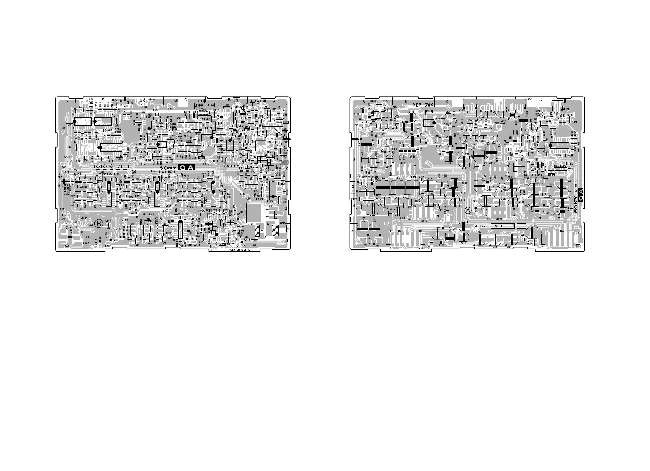
9-5 9-5
A B C D E F GH
1
2
3
4
5
VPL-PX20/PX30
QA QA
QA – B SIDE –
SUFFIX ; -11
QA – A SIDE –
SUFFIX ; -11
—
QA
—
1-675-450-11
IC801 * C-4
IC802 * E-2
IC803 * F-2
IC804 E-2
IC805 * D-1
IC806 * F-1
IC807 * E-1
IC808 * E-2
IC809 * D-2
IC810 * B-3
IC811 * C-2
IC812 * B-1
IC813 B-1
IC814 * B-2
IC816 * A-4
IC817 * A-4
IC818 * A-3
IC819 * A-2
IC820 * B-1
IC821 * A-3
IC822 * B-4
IC823 * E-3
IC824 * D-3
IC825 * B-3
Q802 E-2
Q804 E-2
Q805 E-2
Q808 E-2
Q809 * C-1
Q810 E-2
Q811 * C-4
Q812 * D-3
Q813 * D-4
Q821 * C-1
Q822 * C-1
Q823 * C-1
Q824 * C-2
Q825 * C-2
Q826 * C-2
Q831 * A-1
Q832 * A-1
Q833 * A-1
Q834 A-1
Q835 A-1
Q836 * B-1
Q837 * A-1
Q838 * B-1
*:B Side mount
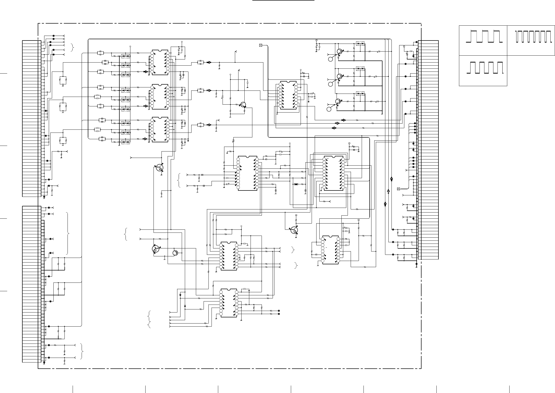
9-6 9-6
A B C D E F GH
1
2
3
4
5
VPL-PX20/PX30
QA (1/3) QA (1/3)
• Refer to page 9-5 for Printed Wiring Board
• Refer to page 9-9 for IC Block Diagrams
0
1
2
3
0
0
0
0
0
0
0
0
0.2 0.4
0.3
0.2
-5.0
1.72.4
0
0
0
0
0
0
0.2
5.0
5.0
0.4
-5.0
0
0
0.2
5.0
5.0
0.4
-5.0
0
0
0
0
0.2
5.0
5.0
0.4
-5.0
0.4
0
0
4.2
0
0
0
0
0
0
0
0
0.2
0.2
0.2
3.0
0.4
2.9
2.4
2.6
0
0
0
0
0
0
0
0
0
0
3.3
0.2
5.0
3.2
3.3
0.4
3.2
4.9
3.2
0
0.4
0
0
0
0
0
0
4.9
3.2
3.3
3.3
3.2
0
0
0
0
0
0
0.4
0.4
0.4
0.4
0.4
0.4
0.4
0.4
4.2
0.5
4.9
4.8
5.0
5.0
4.9
4.9
4.8
5.0
5.0
4.4
3.7
4.4
3.7
4.4
3.7
3.3
B
G
R
B
G
R
B
G
R
R
G
B
12345678
9 10 11 12 13 14 15 16
12345678
9 10 11 12 13 14 15 16
12345678
9 10 11 12 13 14 15 16 12345678910
11 12 13 14 15 16 17 18 19 20
12345678910
11 12 13 14 15 16 17 18 19 20
A1
B1
A2
B2
A3
B3
A4
B4
A5
B5
A6
B6
A7
B7
A8
B8
A9
B9
A10
B10
A11
B11
A12
B12
A13
B13
A14
B14
A15
B15
A16
B16
A17
B17
A18
B18
A19
B19
A20
B20
A21
B21
A22
B22
A23
B23
A24
B24
A25
B25
A1
B1
A2
B2
A3
B3
A4
B4
A5
B5
A6
B6
A7
B7
A8
B8
A9
B9
A10
B10
A11
B11
A12
B12
A13
B13
A14
B14
A15
B15
A16
B16
A17
B17
A18
B18
A19
B19
A20
B20
A21
B21
A22
B22
A23
B23
A24
B24
A25
B25
A1
A2
A3
A4
A5
A6
A7
A8
A9
A10
A11
A12
A13
A14
A15
A16
A17
A18
A19
A20
A21
A22
A23
A24
A25
A26
A27
A28
A29
A30
A31
A32
A33
A34
B1
B2
B3
B4
B5
B6
B7
B8
B9
B10
B11
B12
B13
B14
B15
B16
B17
B18
B19
B20
B21
B22
B23
B24
B25
B26
B27
B28
B29
B30
B31
B32
B33
B34
A35
B35
12345678
9 10 11 12 13 14 15 16
1234567
8 9 10 11 12 13 14
1234567
8 9 10 11 12 13 14
1234567
8 9 10 11 12 13 14
TH801
CN803
CN801
C805
C804
C807
C808
C809
C810
C811
C812
C813
Q802
Q808
Q810
D801
D802
D803
D804
D805
D807
D808
D809
D810
R826
R827
R828
R829
R830
R835
R845 R846
R847
R849
R850
R851 R852
R853
R854
R855
R856
R857 R858
R859 R860
R861 R862
R867
R868
R875
R878
R879
R880
R881 R882
R883
R884
R887
R888
R889
R890 R891
R896
R899
R922
R921
R920
R919
R918
R917
R914
R913
R912
R911
R910
R909
R908
R907
R906
R905
R904
R903
R902
R901
R900
C821
C824
C826
C825
C830
C828
C827
C837
C838
C842
C844
C843 C845
C846
C847
C848
R801 R802
R803
R804
R805
R806 R807
R831
R832
R810 R811
R812 R813
R814 R815
R818
CN805
Q805
Q811
Q812
Q813
R923
C803
R848
C801
C802
R821
R876 R877
R869
R870
R871
R872
R873
R885
R886
C822
C849
C850
C891
C892
C893
C894
C895
C898
C899
C900
C949
C958
C959
C960
C961
C962
C963
C964
C965
C966
C967
C968
C969
C970
C971
C972
C973
C974
C975
C980
D811
D812
D821
R822
R823
R824
R825
R833
R834
R836
R837
R839
R924
R925
R926
R927
R928
R929
R930
R931
R932
C839
R894
R874
R893
R892
R819
R898
R843
R844
JL874
JL807
JL808
JL809
JL810
JL811
JL812
JL813
JL814
JL815
JL816
JL817
JL818
JL819
JL906
JL905
JL822
JL823
JL824
JL825
JL826
JL827
JL828
JL829
JL830
JL831
JL832
JL833
JL834
JL835
JL836
JL837
JL838
JL897
JL839
JL841
JL842
JL843
JL844
JL845
JL846
D871
D872
JL873
R838
R842
R840
R841
R1100
Q804
R816
R817
R808
R809
R915
R916
JL801
JL898
JL805
JL803
JL804
JL806
IC801
IC803
C829
C840
C841
R895
IC804
IC806
IC807
IC823
IC824
IC825
L801
R897
C816
C817
C820
IC802
70P
0.1
25V
B:CHIP
0.1
25V
B:CHIP
47
16V
:AL-CP
0.1
25V
B:CHIP
0.1
25V
B:CHIP
0.1
25V
B:CHIP
DTC114EKA
SW
DTC114EKA
SW
DTC114EKA
SW
MA157-TX
PROTECT
MA157-TX
PROTECT
MA157-TX
PROTECT
MA157-TX
PROTECT
MA157-TX
PROTECT
MA157-TX
PROTECT
MA157-TX
PROTECT
MA157-TX
PROTECT
MA157-TX
PROTECT
82
:RN-CP
0.068
25V
B:CHIP
0.1
25V
B:CHIP
100p
CH:CHIP
100p
CH:CHIP
0.1
25V
B:CHIP
0.1
25V
B:CHIP
100p
CH:CHIP
0.1
25V
B:CHIP
47
16V
:AL-CP
47
16V
:AL-CP
47
16V
:AL-CP
150
:RN-CP 150
:RN-CP
1k
:CHIP
150
:RN-CP 150
:RN-CP
150
:RN-CP 150
:RN-CP
2.2k
:CHIP
2.2k
:CHIP
150
:RN-CP 150
:RN-CP
150
:RN-CP 150
:RN-CP
150
:RN-CP 150
:RN-CP
1k
:CHIP
#
#
47
6.3V
:ALB-CP
47
6.3V
:AL-CP
47
6.3V
:AL-CP
47
6.3V
:AL-CP
0.1
25V
B:CHIP
47
6.3V
:AL-CP
47k
:CHIP
4.7k
:CHIP
4.7k
:CHIP 2.2k
:CHIP
47k
:CHIP
56k
:CHIP 4.3k
:RN-CP
10k
:CHIP
10k :CHIP
43k
:RN-CP
10k
:CHIP
150 :RN-CP
120
:RN-CP
2.2k
:CHIP
1k
:RN-CP
100
:CHIP 100
:CHIP
75
:RN-CP 75
:RN-CP
75
:RN-CP 100
:CHIP
100
:CHIP
100
:CHIP
100
:CHIP
10k
:CHIP
10k :CHIP
10k :CHIP
10k
:CHIP
10k
:CHIP
100
:CHIP
100
:CHIP
100
:CHIP
100
:CHIP
10k
:CHIP
10k
:CHIP 10k
:CHIP
3.9k
:CHIP
47
:CHIP
4.7k
:CHIP
4.7k
:CHIP
100
:CHIP
3.9k
:CHIP
47
:CHIP
4.7k
:CHIP
4.7k
:CHIP
100
:CHIP
3.9k
:CHIP
47
:CHIP
4.7k
:CHIP
4.7k
:CHIP
100
:CHIP
1k
:CHIP
150
:CHIP 150
:CHIP
150
:CHIP 150
:CHIP
150
:CHIP 150
:CHIP
2SC3545
C BUFF
2SC3545
C BUFF
2SC3545
C BUFF
2SC3545
C BUFF
100
:CHIP
0.1
25V
B:CHIP
10k
:CHIP
100
:CHIP
100
:CHIP
100
:CHIP
100
:CHIP
100
:CHIP
100
:CHIP
100
:CHIP
47
6.3
:ALB-CP
0.1
25V
B:CHIP
0.1
25V
B:CHIP
0.1
25V
B:CHIP
0.1
25V
B:CHIP
0.1
25V
B:CHIP
0.1
25V
B:CHIP
0.1
25V
B:CHIP
0.1
25V
B:CHIP
0.1
25V
B:CHIP
0.1
25V
B:CHIP
0.1
25V
B:CHIP
0.1
25V
B:CHIP
0.1
25V
B:CHIP
0.1
25V
B:CHIP
0.1
25V
B:CHIP
47
6.3V
:ALB-CP
MA157-TX
PROTECT
MA157-TX
PROTECT
MA157-TX
PROTECT
82k
:CHIP
47k
:CHIP
100
:CHIP
100
:CHIP
100
:CHIP
82k
:CHIP
47k
:CHIP
82k
:CHIP
82k
:CHIP
100
:CHIP
82k
:CHIP
82k
:CHIP
100
:CHIP
82k
:CHIP
82k
:CHIP
100
:CHIP
100
:CHIP
100
:CHIP
22
6.3V
:AL-CP
22
6.3V
:ALB-CP
10
16V
:AL-CP
220p
CH:CHIP
47
16V
:AL-CP
22
6.3V
:AL-CP
22
6.3V
:AL-CP
22
6.3V
:AL-CP
22
6.3V
:AL-CP
22
6.3V
:ALB-CP
22
6.3V
:ALB-CP
22
6.3V
:ALB-CP
22
6.3V
:ALB-CP
22
6.3V
:ALB-CP
22
6.3V
:AL-CP
22
6.3V
:ALB-CP
22
6.3V
:ALB-CP
22
6.3V
:ALB-CP
100
:CHIP
100
:CHIP 100
:CHIP
0.001
B:CHIP
2.2k
:RN-CP
2.2k
:CHIP
#
#
100
:CHIP
#
4.7k
:CHIP
#
:CHIP
#
50P
WHT
50P
WHT
#
RB501V
RB501V
1.2k
:RN-CP
330
:RN-CP
330
:RN-CP
1.2k
:RN-CP
2.2k
:CHIP
#
33
:CHIP 560
:CHIP
33
:CHIP
560
:CHIP
33
:CHIP
560
:CHIP
#
#
#
#
#
#
#
#
#
#
#
#
#
#
#
#
#
#
#
#
#
#
#
#
#
#
#
#
#
#
#
#
#
#
#
#
#
#
#
#
#
#
#
#
#
#
EL4332C
SELECT
TC74VHC244F
SELECT
22
6.3V
:AL-CP
22
6.3V
:AL-CP
0.01
B:CHIP
12k
:RN-CP
TC74VHC123AF
V CLP OUT
CXA1875AX
DAC
CXA1875AX
DAC
HA4314BCB
SELECT
HA4314BCB
SELECT
HA4314BCB
SELECT
OUH
:CHIP
SHORT
:CHIP
10
6.3V
:ALB-CP
10
6.3V
:ALB-CP
1mF
10V
:AL-CP
M52347FP
SYNC SEP
5V
5V
5V
5V
5V
SDA100K
SCL100K
A
B
MON OUT OFF
INPUTA SW2
INPUTA SW1
CV/OTHER
YC/OTHER
SRS ON
SPEAKER MUTE
RGBSYNC
R MON
G MON
B MON
RE V
RE H
G/Y
B/B-Y
R/R-Y
-5V
9V
3.3V
3.3V
3.3V
3.3V
AUDIO AL
AUDIO AR
AUDIO BL
AUDIO BR
5V
BH
BV
SYNC SW1
SYNC SW2
SYNC SW3
AV
BNC V
BNC H
AH
-5V
SUB5V
IRD B
IRD A
DS2+
DS2-
SUB5V
US VBUS
MS5V
BNC R
BNC G
BNC B
BNC R
BNC G
BNC B
1
2
3
4
5
6
7
8
V-R
V-G
V-B
V-H
V-V
V-CLP
BR
BG
BB
BR
BG
BB
9
10
11
12
OUT3
B3
A3
A1
B1
B2
A2
OUT2
OUT1
GND1
GND2 GND3
A/B
VCC
VCC
VEE
GND
GND
GND
GND
GND
GND
GND
GND
GND
GND
GND
GND
GND
GND
GND
GND
GND
GND
GND
GND
GND
GND
GND
GND
GND
GND
GND
GND
GND
GND
GND
GND
GND
GND
GND
GND
GND
GND
GND
GND
GND
GND
GND
GND
GND
GND
AUDIO CE
SDAT
BNC R
BNC R
GND
GND
GND
GND
GND
GND
GND
GND
GND
GND
GND
GND
GND
GND
GND
GND
GND
GND
GND
CLP
CLP
R
R
G
G
B
B
H
V
V
BNC G
BNC G
BNC B
BNC B
BNC H
BNC H
BNC V
BNC V
A3.3V
A3.3V
H
AUDIO MUTE
US+
US+
US-
US-
GND
DS1+
USB P.ENA
USB P.FLG
AUDIO AL
AUDIO AL
AR
AR
AR
AR
AG
AG
AG
AG
AB
AB
AB
AB
AH
AH
AV
AV
AUDIO BL
AUDIO BL
AUDIO BR
AUDIO BR
BR
BR
BR
BR
BG
BG
BG
BG
BB
BB
BB
BB
BH
BH
BV
BV
AUDIO AR
AUDIO AR
GND
IRD A
IRD A
DS2-
DS2-
DS2+
DS2+
GND
GND
GND
IRD B
IRD B
SUB5V
SUB5V
GND
GND
GND
GND
SCLK
SUB 5V
SUB 5V
SUB 5V
SUB 5V
SUB 5V
SUB 5V
MS5V
MS5V
US VBUS
MS P.ENA
DS1-
TO QB CN1203
TO QC CN1804
B-SS1696<08.>-QA.-P1
(INPUT SW)
QA(1/3)
TO BB CN303
(P3)
(P3)
(P3)
(P2)
(P2)
(P2)
(P2)
(P2)
(P2)
(P2)
(P2)
(P3)
(P2)
(P2)
(P2)
(P2)
(P2)
(P2)
(P2)
(P3)
(P2)
(P3)
(P1)
(P2)
(P3)
(P2)
(P2)
(P2)
(P3)
(P2)
1G
1A1
2Y4
1A2
2Y3
1A3
2Y2
1A4
2Y1
GND
VCC
2G
1Y1
2A4
1Y2
2A3
1Y3
2A2
1Y4
2A1
GND
V DET
V.POL
H.POL
VCC
G IN
V IN
CLP
CLP SW
HD+OUT
CLP TH.STATE
V.STATE
V T
GATE SW
HD-OUT
VD+OUT
V S OUT
V S IN
COMP/H
IN
COMP/H
DET
1A
1B
1CLR
1
Q
Q
2CLR
2B
2A
VCC
1R/C
1C
1Q
GND
2R/C
2C
2Q 2
SW1
SW0
DAC4
DAC3
DAC2
DAC1
DAC0
GND
VCC
SCL
SDA
SW3
SW2
SW1
SW0
DAC4
DAC3
DAC2
DAC1
DAC0
GND
VCC
SCL
SDA
SW3
SW2
SAD2
SAD1
SAD0
SAD2
SAD1
SAD0
QA Board Waveforms
12
3
0.6 Vp-p
B/B-Y
0.6 Vp-p
G/Y
0.6 Vp-p
R/R-Y
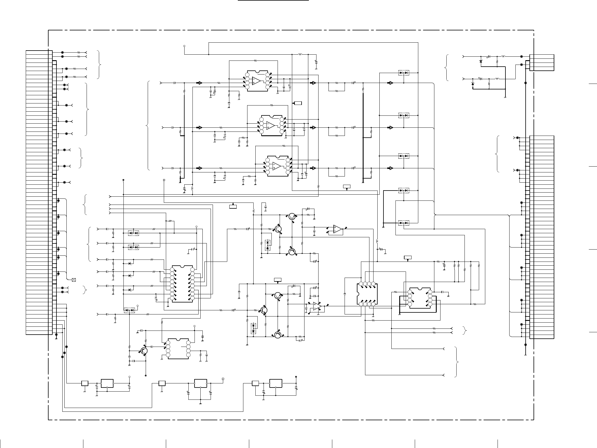
9-7 9-7
A B C D E F GH
1
2
3
4
5
VPL-PX20/PX30
QA (2/3) QA (2/3)
• Refer to page 9-5 for Printed Wiring Board
• Refer to page 9-9 for IC Block Diagrams
0
+5V
+5V
0
0
0
00
0
4.9
4.9
3.7
3.7
3.6
3.7
0.2
3.7
8.9
3.7
3.7
+9V
0
0
8.9
8.9 3.7
3.7
4.3
3.7
4.2
0
0.2
1.5
0.7
-5.0
0
0
0
0
0
0
0
0.2
0.2
0
0
0
0
0
5.0
+9V
00
3.7
3.7
3.7
3.6
3.6
4.3
8.9
8.9 3.1
3.6
+5V
0
0
0.4
5.0
-5.0
0
0
0
0
-5.0
0
0
-5.0
0.4
5.0
0
0
0.4
5.0
0
0
B
R
G
B
R
G
B
R
G
1 2 3 4
5678
1234
5678
1234
5678
1234
5678
A1
A2
A3
A4
A5
A6
A7
A8
A9
A10
A11
A12
A13
A14
A15
A16
A17
A18
A19
A20
A21
A22
A23
A24
A25
A26
A27
A28
A29
A30
A31
A32
A33
A34
B1
B2
B3
B4
B5
B6
B7
B8
B9
B10
B11
B12
B13
B14
B15
B16
B17
B18
B19
B20
B21
B22
B23
B24
B25
B26
B27
B28
B29
B30
B31
B32
B33
B34
A35
B35
A1
B1
A2
B2
A3
B3
A4
B4
A5
B5
A6
B6
A7
B7
A8
B8
A9
B9
A10
B10
A11
B11
A12
B12
A13
B13
A14
B14
A15
B15
A16
B16
A17
B17
A18
B18
A19
B19
A20
B20
A21
B21
A22
B22
A23
B23
A24
B24
A25
B25
EMIEMI
IO
G
EMI
1234
5678
IO
G
IO
G
12345678
910 11 12 13 14 15 16
1234
5678
1
2
3
4
IC808
IC809
IC813
CN806
CN802
IC810
IC814
IC818
IC812(1/2)
IC812(2/2)
C851
C852
C853
C854 C855
C856
C857
C858
C859
C860 C861
C862
C863
C864
C865
C866
C867
C868
C869
C872
C873
C874
C876
C877
C878
C879
C883
C884
C885
C886
C887
C888
C951
C953
C955
Q821
Q822
Q823
Q824
Q825
Q826
D813
D815
D816
D817
D818
D819
D820
R942
R943
R944
R945 R946
R947
R948
R949 R950
R951
R952
R953 R954
R955
R956
R957
R958
R959
R960
R961
R962
R963
R964
R965
R967
R968
R969
R970
R971
R972
R973
R974
R978
R979 R984
R985
R987
R988
R989
R990
R991 R992
R993
R1015
R1016
L802
L804
FL801 FL802
FL803
C896
C897
C882
C881
R980
R983
R981
R982
L803
C870
C836
Q809
R863
C831
C834
C832
C835
C833 R865
D814
C875
R864
C952
C950
C954
C880
R994
R995
C806
R976
R977
R975
R966
R941
C978
C981
C982
C983
C984
D822
D823
D846
D847
D848
L805
R997
R998
R999
R1000
R1001
R1002
R1003
R1004
R1005
R1006
R1007
R1008
R1009
R1010
R1011
R1013
D824
D825
C979
C977
C976
R866
JL849
JL850
JL851
JL852
JL853
JL854
JL855
JL856
JL857
JL858
JL859
JL860
JL861
JL862
JL863
JL864
JL865
JL866
JL870 JL867
JL868
JL869
JL871
JL872
JL875
JL903
JL904
JL878
JL879
JL880
JL881
JL882
JL883
C871
CN807
R1012
IC816
IC817
IC805
IC811
JL848
JL847 L808
L809
MAX4223ESA
R DRV
MAX4223ESA
G DRV
SN75157
COMP
70P
MAX4223ESA
B DRV
SN75453BPS
BUFF
47
6.3V
:ALB-CP
47
6.3V
:ALB-CP
47
6.3V
:ALB-CP
0.1
25V
B:CHIP
10
16V
:AL-CP
1p
CK:CHIP
0.1
25V
B:CHIP
10
16V
:AL-CP
0.1
25V
B:CHIP
10
16V
:AL-CP
1p
CK:CHIP
0.1
25V
B:CHIP
10
16V
:AL-CP
0.1
25V
B:CHIP
10
16V
:AL-CP
1p
CK:CHIP 0.1
25V
B:CHIP
10
16V
:AL-CP
10
16V
:AL-CP
0.1
25V
B:CHIP
10
16V
:AL-CP
10
16V
:AL-CP
1
:AL-CP
0.1
25V
B:CHIP
10
16V
:AL-CP
0.1
25V
B:CHIP
1
:AL-CP
0.1
25V
B:CHIP
47
16V
:AL-CP
0.1
25V
B:CHIP
47
16V
:AL-CP
68
10V
:AL-CP 68
10V
:AL-CP
2SC2712
BUFF
2SC2712
PEAK HOLD
2SA1162
PEAK HOLD
2SC2712
BUFF
2SC2712
PEAK HOLD
2SA1162
PEAK HOLD
DAN202K
PROTECT
DAN202K
PROTECT
MA157-TX
PROTECT
MA157-TX
PROTECT
MA157-TX
PROTECT
MA157-TX
PROTECT
MA157-TX
PROTECT
47k
:CHIP
47k
:CHIP
10
:CHIP
0
:CHIP 220
:RN-CP
220 :RN-CP
10
:CHIP
0
:CHIP 220
:RN-CP
220 :RN-CP
10
:CHIP
0
:CHIP
220
:RN-CP
220 :RN-CP
1k
:CHIP
47k
:CHIP
47k
:CHIP
47k
:CHIP
10k
:CHIP
10k
:CHIP
100
:CHIP
470
:CHIP
100k
:CHIP
47k
:CHIP
47k
:CHIP
100
:CHIP
1k
:CHIP 33
:CHIP
33
:CHIP
10
:CHIP
330
1/8W
:CHIP
330
1/8W
:CHIP
47
:CHIP
330
1/8W
:CHIP
330
1/8W
:CHIP
47
:CHIP
470k
:CHIP
470k
:CHIP
10µH
:CHIP
10µH
:CHIP
TL082CPS
BUFF
TL082CPS
BUFF
LM2990SX-5.0
150
:RN-CP
150
:RN-CP
150
:RN-CP
150
:RN-CP
150
:RN-CP
150
:RN-CP
82k
:CHIP
4.7
35V
:AL-CP
4.7
35V
:AL-CP
82k
:CHIP
82k
:CHIP
150k
:CHIP
120k
:CHIP
22
16V
:AL-CP
22
16V
:AL-CP
10µH
:CHIP
10
16V
:AL-CP
0.1
25V
B:CHIP
2SA1162
C BUFF
1k
:CHIP
56p
CH:CHIP
0.1
25V
B:CHIP
0.1
25V
B:CHIP
0.1
25V
B:CHIP
0.1
25V
B:CHIP
100
:CHIP
MA157-TX
PROTECT
10
16V
:AL-CP
47
:CHIP
47
:CHIP
22k
:CHIP
22k
:CHIP
47
:CHIP
82k
:CHIP
100
:CHIP
10
16V
:AL-CP
10
16V
:AL-CP
10
16V
:AL-CP
MA157-TX
PROTECT
MA157-TX
PROTECT
RD9.1SB2
PROTECT
RD9.1SB2
PROTECT
RD9.1SB2
PROTECT
10µH
:CHIP
100
:CHIP
100
:CHIP
100
:CHIP
47k
:CHIP
100
:CHIP
100
:CHIP
100
:CHIP
100
:CHIP
100
:CHIP
82k
:CHIP
100
:CHIP
82k
:CHIP
82k
:CHIP
82k
:CHIP
47
:CHIP
82k
:CHIP
22
16V
:ALB-CP
22
16V
:AL-CP
10
16V
:AL-CP
10
16V
:AL-CP
10
16V
:AL-CP
22
16V
:ALB-CP
22
16V
:ALB-CP
1k
:CHIP
RD9.1SB2
PROTECT
RD9.1SB2
PROTECT
430k
:RN-CP
50P
WHT
4.7
16V
F:CHIP
4.7
16V
F:CHIP
4.7
16V
F:CHIP
4P
WHT-L
#
330
16V
:AL-CP
330
16V
:AL-CP
330
16V
:AL-CP
#
#
#
#
#
#
#
#
#
#
#
#
#
#
#
#
#
#
#
#
#
#
#
#
#
#
#
#
#
#
#
#
#
BA09EP-E2
9V REG
PQ05SZ1U
5V REG
GS1881-CTA
SYNC SEP
TC74HC4052AFT
SYNC SEP
#
#
OUH
OUH
B/B-Y
G/Y
R/R-Y
R MON
G MON
B MON
5V
MON OUT OFF
AUDIO OR
AUDIO OL
VIDEO L
VIDEO R
5V
A
SDA100K
SCL100K
RGBSYNC
RE H
RE V
BA H
BA V
BA V
BA H
-5V
-5V
9V
9V
BV
AH
BNC V
AV
5V
-5V
BH
BNC H
5V
SYNC SW1
SYNC SW2
SYNC SW3
CV/OTHER
YC/OTHER
DS2-
DS2+
IRD A
IRD B
5V 5
67
8
4
3
21
OUT R
OUT H
OUT G
OUT B
V-R
V-G
V-B
V-H
V-V
V-CLP
OUT G
OUT B
OUT H
OUT V
OUT V
OUT R
VCC
NC
SHDN
NC
VEE
SHDN
SHDN
VCC
VCC
NC
NC
NC
NC
VEE
VEE
GND
GND
R/R-Y
R/R-Y
G/Y
G/Y
GND
GND
B/B-Y
B/B-Y
GND
GND
H
H
GND
GND
V
V
GND
GND
GND
GND
GND
GND
GND
GND
GND
GND
GND
GND
GND
GND
GND
GND
RGBSYNC
RGBSYNC
GND
GND
GND
GND
GND
GND
GND
GND
GND
GND
GND
GND
GND
GND
GND
GND
GND
GND
AUDIO OL
AUDIO OL
AUDIO OL
AUDIO OL
AUDIO OR
AUDIO OR
AUDIO OR
AUDIO OR
OUT R
OUT R
OUT R
OUT R
OUT G
OUT G
OUT G
OUT G
OUT B
OUT B
OUT B
OUT B
OUT H
OUT H
OUT H
OUT H
OUT V
OUT V
OUT V
OUT V
GND
GND
GND
GND
V-R
V-R
V-G
V-G
V-B
V-B
V-HD
V-HD
V-VD
V-VD
V-CLP
V-CLP
SDA100K
SCL100K
GND
GND
+6V
+6V
+6V
+6V
-6V
-6V
S-SEL
GND
R-VIDEO
GND
L-VIDEO
CS OUT
CV IN
VS OUT
GND
VCC
ODD/
EVEN
RESET
BACK PCH
IRD A
IRD B
GND
GND
DS2+
DS2+
DS2-
DS2-
YC/OTHER
CV/OTHER
+10V
+10V
(INPUT SW)
B-SS1696<08.>-QA.-P2
QA(2/3)
TO QC CN1805
TO QD CN1902
(P3)
(P3)
(P2)
(P1)
(P1)
(P1)
(P1)
TO BB CN305
(P1)
(P1)
(P1)
(P1)
(P1)
(P1)
(P1)
(P1)
VCC
IN1-
IN1+
OUT1
IN2+
IN2-
OUT2
GND
1A
1B
1Y
GND 2Y
2A
2B
VCC
(P2)
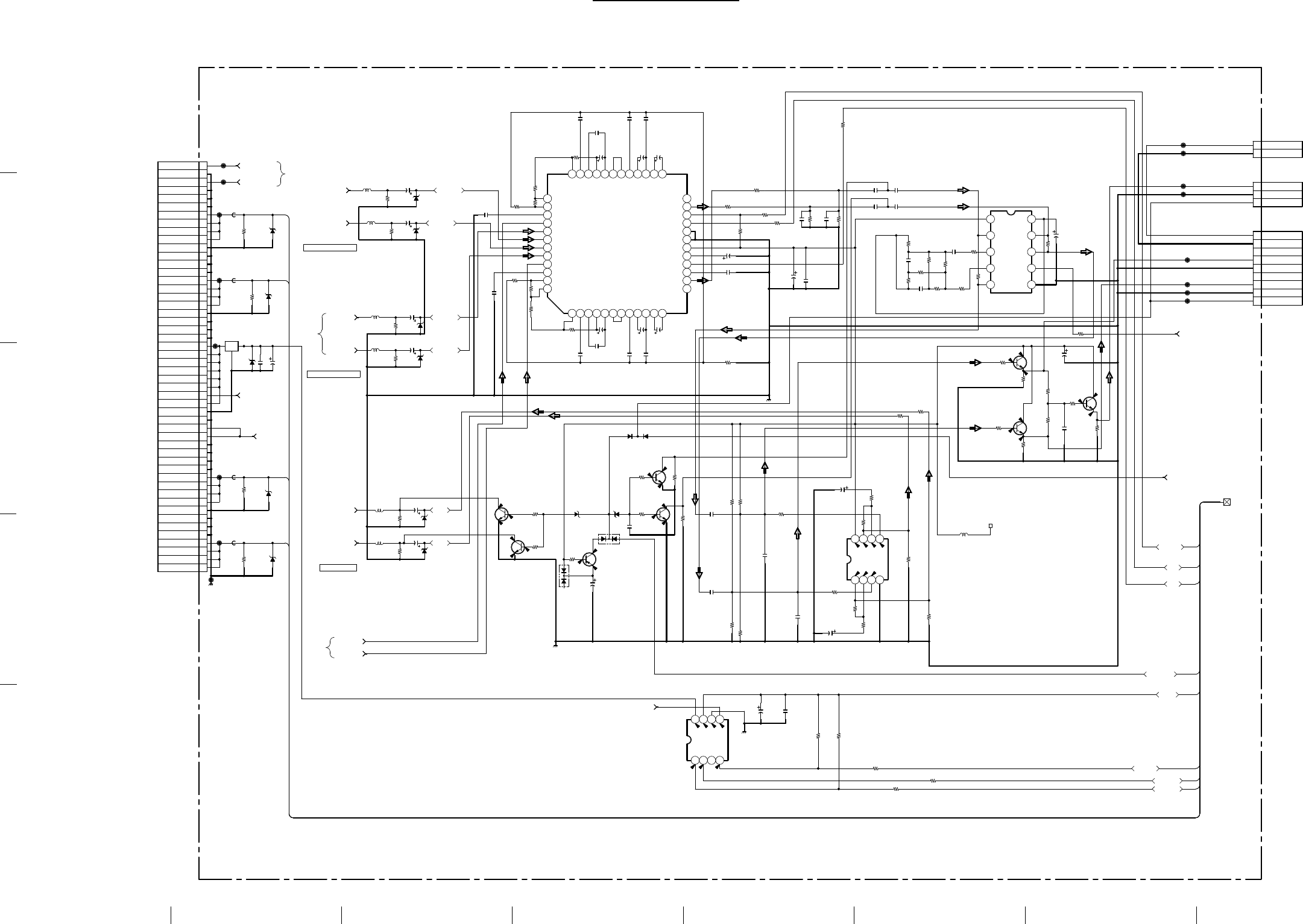
9-8 9-8
A B C D E F GH
1
2
3
4
5
VPL-PX20/PX30
QA (3/3) QA (3/3)
• Refer to page 9-5 for Printed Wiring Board
• Refer to page 9-9 for IC Block Diagrams
0
8.9
8.9
8.9
3.2
3.9
3.8
3.2
2.5
3.2
8.9
3.8
3.8
3.8
3.9
3.9
3.9
0
0
0
0
00
0
0
0
0
0
0
-0.4
8.8
00
0
5.0
4.9
5.0
0.3
R
L
L
R
L/R
L
R
R
L
R
L
L
R
R
L
RL
R
L
R
L
R
R
L
L
12345
6 7 8 9 10
A1
B1
A2
B2
A3
B3
A4
B4
A5
B5
A6
B6
A7
B7
A8
B8
A9
B9
A10
B10
A11
B11
A12
B12
A13
B13
A14
B14
A15
B15
A16
B16
A17
B17
A18
B18
A19
B19
A20
B20
A21
B21
A22
B22
A23
B23
A24
B24
A25
B25
EMI
1
2
3
1
2
3
4
5
6
7
8
9
1234
5678
1 2 3 4 5 6 7 8 9 10 11 12
13
14
15
16
17
18
19
20
21
22
23
24
252627282930313233343536
37
38
39
40
41
42
43
44
45
46
47
48
1234
5678
1
2
CN804
IC819
C901
C902
C909
C910 C911 C912
C913
C918
C919 C920
C921
C925
C926 C927
C928
C929
C937
C938 C940
C941
C942
C943
C944
C945
C946
C947 C948
Q831
Q832
Q833
Q834
Q835
Q836
Q837
Q838
D831
D832
D833
D834
D835
D836
D837
D838
D839
D840
D841
D842
D843
D844
D845
R1033
R1031
R1032
R1034
R1035
R1036
R1037
R1038
R1039
R1040
R1041
R1042
R1043
R1044
R1045
R1046
R1047
R1048
R1049
R1050
R1051
R1052
R1053
R1061
R1065
R1069
R1070
R1071
R1072
R1073
R1074
R1075
R1076
R1077
R1078
R1079
R1080
R1081 R1082
R1083
R1084
R1085
R1086
R1087
R1088
R1089
R1090
R1091 R1092
R1093
R1094
R1095
FB801
FB802
FB803
FB804
C936
C931
C930
C908
C907
C906
C905
C904
C903
C914 C915 C916
C917
C922
C923
C924
R1098
C956 C957
R1099
C939
R1096
R1097
R1014 R1017
R1018
R1019
FL804
CN808
CN809
IC821
JL884
JL885
JL886
JL887
JL888
JL889
JL890
JL891
R1064
R1068
CN810
D826 D827
JL900
JL899
JL894
JL907
JL892
JL893
JL896
JL895
IC822
L816
C932
C933
C934
C935
IC820
R1020
R1021
R1022
L810
L811
L812
L813
L814
L815
R1060R1057R1054
R1056
R1055 R1058
R1059
BK2125HM601
BK2125HM601
BK2125HM601
BK2125HM601
CXA1946AR
AUDIO SW1
PROCESSOR
0.1
25V
B:CHIP
100
6.3V
:AL-CP
0.1
25V
B:CHIP
#0.0022
B:CHIP 1
16V
B:CHIP
#
#
#0.0022
B:CHIP
1
16V
B:CHIP
0.01
B:CHIP
100
16V
:AL-CP
0.1
25V
B:CHIP
1
16V
B:CHIP 1
16V
B:CHIP
1
16V
B:CHIP
1
16V
B:CHIP
22
16V
:AL-CP
22
16V
:AL-CP
0.1
25V
B:CHIP
22
16V
:AL-CP
2SC2712
SW
2SC2712
SW
2SA1162
MUTE
2SC2712
2SC2712
2SC2712
UDZ-TE-17-3.9B
UDZ-TE-17-3.9B
RD5.6SB
UDZ-TE-17-3.9B
UDZ-TE-17-3.9B
RD9.1SB2
PROTECT
RD9.1SB2
PROTECT
RD9.1SB2
PROTECT
RD9.1SB2
PROTECT
RD9.1SB2
PROTECT
RD9.1SB2
PROTECT
RD3.3SB2
MUTE
DAN202K
MUTE
DAN202K
MUTE MIX
15k
:CHIP
15k
:CHIP
15k
:CHIP
15k
:CHIP
470k
:CHIP
470k
:CHIP
470k
:CHIP
470k
:CHIP
470k
:CHIP
470k
:CHIP
#
0
:CHIP
0
:CHIP
0
:CHIP
#
0
:CHIP
0
:CHIP
0
:CHIP
10k
:CHIP
100
:CHIP
100
:CHIP
100
:CHIP
1k
:CHIP
1k
:CHIP
1k
:CHIP
1k
:CHIP
1k
:CHIP
1k
:CHIP
1k
:CHIP
1k
:CHIP 1k
:CHIP
100k
:CHIP 100k
:CHIP
100k
:CHIP 100k
:CHIP
100
:CHIP
2.7k
:CHIP
3.3k
:CHIP
100
:CHIP
3.3k
:CHIP
2.7k
:CHIP
1k
:CHIP 1k
:CHIP
1k
:CHIP
1k
:CHIP
1k
:CHIP
1 16V B:CHIP
1 16V B:CHIP
22
16V
:AL-CP
0.015
B:CHIP
1
16V
B:CHIP
0.1
25V
B:CHIP
0.1
25V
B:CHIP
1
16V
B:CHIP
RD3.3SB2
MUTE
2SC2712
MUTE
2SC2712
MUTE
10k
:CHIP
1k
:CHIP
1k
:CHIP
1k
:CHIP
100k
:CHIP
100k
:CHIP
4.7
35V
:AL-CP
4.7
35V
:AL-CP
4.7
35V
:AL-CP
4.7
35V
:AL-CP
4.7
35V
:AL-CP
4.7
35V
:AL-CP
#
:CHIP
#
B:CHIP #
B:CHIP
#
:CHIP
10
16V
:AL-CP
10
16V
:AL-CP
10
16V
:AL-CP
10
16V
:AL-CP 10
16V
:AL-CP
10
16V
:AL-CP
10
16V
:AL-CP
10
16V
:AL-CP
1k
:CHIP
1k
:CHIP
100
:CHIP
100
:CHIP
100
:CHIP
1k
:CHIP
LM358PSR
VAR AMP
50P
WHT
100
:CHIP
100
:CHIP
2P
WHT-L
:SMD
3P
WHT-L
:SMD
9P
WHT-L
1SS355 1SS355
STS104B
#
#
#
#
#
#
#
#
#
#
#
#
#
#
#
#
µPD16875G
POWER SUP
OUH
:CHIP
#
#
#
#
#
#
SHORT
SHORT
OUH
OUH
OUH
OUH
OUH
OUH
###
#
##
#
L-OUT
R-OUT AUDIO CE
SDAT
AUDIO MUTE
USB P.FLG
USB P.ENA
SUB 5V
L-INPUT-B
R-INPUT-B
L-INPUT-A
R-INPUT-A
SCLK
MS P.ENA
VIDEO L
VIDEO R
AUDIO OL
AUDIO OR
INPUTA SW1
INPUTA SW2
B
SPEAKER MUTE
SRS ON
9V
AUDIO BL
AUDIO BR
AUDIO AL
AUDIO AR
US VBUS
MS5V
SUB 5V
7
8
9
5
64
2
3
1
10
11
12
AUDIO OUT
AUDIO-INPUT-B
VCC
DIFF
REFIN
INR INL
OUTL
CNTL
GNDOUTR
FIL
R
GND
GND
GND
GND
GND
GND
GND
GND
GND
GND
GND
GND
GND
GND
GND
GND
GND
GND
GND
GND
GND
GND
SUB 5V
INPUTA SW1
USB DS+
USB DS+
USB DS+
USB DS+
USB DS-
USB DS-
USB DS-
USB DS-
USB US+
USB US+
USB US+
USB US+
USB US-
USB US-
USB US-
USB US-
INPUTA SW2
AUDIO-INPUT-B
US VBUS
US VBUS
SP-MUTE
L/R
GND
AUDIO+B
AUDIO+B
GND
GND
SP-MUTE
L
AU GND
AU GND
R
L
NC
NC
USB 5V
USB 5V
USB 5V
USB 5V
USB 5V
USB 5V
USB 5V
(INPUT SW)
B-SS1696<08.>-QA.-P3
QA(3/3)
(P1)
(P1)
TO KS CN2951
TO K CN2900
TO GA CN2105
(P1)
(P2)
(P2)
(P2)
TO QB CN1204
(P1)
(P1)
(P1)
(P1)
(P1)
(P1)
VCC
OUT2
IN2-
IN2+
OUT1
IN1-
IN1+
GND
ENA
FLGA
FLGB
ENB
OUTA
IN
GND
OUTB
LDLC2
LDHC2
INAO2
VRIN2
VOUT2
TIN2
TCHC2
TCLC22
TCO2
FDIN2
FNTO1
REO1
CE
CLK
DGND
GND
VCC
VCT
DATA
TIMER
REO2
FNTO2
LDLC1
LDHC1
INAO1
VRIN1
VOUT1
TIN1
TCHC1
TCO1
FDIN1
TCLC12
TCLC11TCLC21
IN14
GAIN11
GAIN21
GAIN134
GAIN12
GAIN234
GAIN22
IN13
IN12
IN11
IN21
IN22
IN23
IN24
(P1)
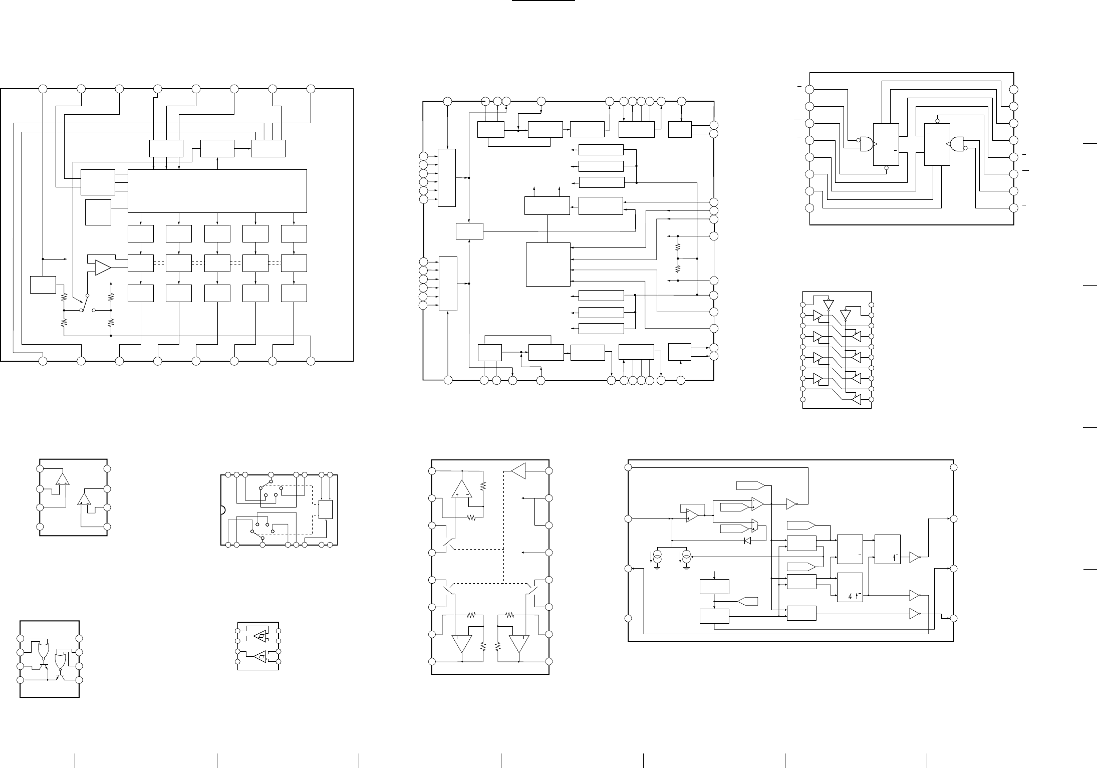
9-9 9-9
A B C D E F GH
1
2
3
4
5
VPL-PX20/PX30
LATCH
DAC
AMP
LATCH
DAC
AMP
LATCH
DAC
AMP
LATCH
DAC
AMP
LATCH
DAC
AMP
+
—
VCC
REG
I2C DECODER
LEVEL
CONVERTER
LEVEL
CONVERTER LEVEL
CONVERTER
LATCH
POWER
ON
RESET
OPEN COLLECTOR
3 6
25 81 4 7
SW1
SW0
DAC4
DAC3
DAC2
DAC1
DAC0
GND
14 11
15 12 916 13 10
VCC
SCL
SDA
SAD2
SAD1
SAD0
SW3
SW2
CXA1875AM-T4 (IC806, IC807)
36 35 34 33 31 30 25
26
27
28
29
32
1234 56
7
8
910 11 12
13
14
15
16
17
18
19
20
21
22
23
24
37
38
39
40
41
42
43
44
45
46
47
48
GAIN12
GAIN11
IN11
IN12
IN13
IN14
IN21
IN22
IN23
IN24
GAIN21
GAIN22
FNTO1
REO1
CE
CLK
DGND
GND
VCC
VCT
DATA
TIMER
REO2
FNTO2
GAIN134
LDLC1
LDHC1
INAO1
VRIN1
VOUT1
TIN1
TCLC1
TCLC11
TCLC12
TCO1
FDIN1
GAIN234
LDLC2
LDHC2
INAO2
VRIN2
VOUT2
TIN2
TCHC2
TCLC21
TCLC22
TCO2
FDIN2
LOUD VOLUME
8dB STEP VOLUME
1dB STEP
VCTBUFF
VCTBUFF
VCTBUFF
TONE FADER
INPUT SW
LATCH LATCH
CONTROL
ZCDET
SHIFT
REGISTER
45k
45k
VCTBUFF
VCTBUFF
VCTBUFF
VOLUME
1dB STEP
LOUD
INPUT SW
TONE FADER
VOLUME
8dB STEP
CXA1946AR (IC819)
1
2
3
4
5
6
7
16
15
14
13
12
11
10
8
A
RD
C
Q
B
GND
Q
R
9
VDD
R
C
RD
Q
B
Q
A
Q
Q
D
RD
Q
Q
RD
TC74VHC123AF (EL) (IC804)
1
2
3
4
5
6
7
8
9
10
20
19
18
17
16
15
14
13
12
11
VCC
OEB
YA1
B4
YA2
B3
YA3
B2
YA4
B1
OEA
A1
YB4
A2
YB3
A3
YB2
A4
YB1
GND
TC74VHC244F (EL) (IC803)
1A
1B
1Y
1
2
3
GND 4
VCC
2B
2A
8
7
6
2Y
5
SN75453BPSR (IC814)
VCC
8
OUTPUT 2
7
INPUT 2 (
-
)
INPUT 2 (+)
6
5
OUTPUT 1 1
INPUT 1 (
-
)2
INPUT 1 (+) 3
GND 4
LM358PSR (IC821)
8
7
6
5
1
2
3
4
NON INV IN1
OUT1
OUT2
GND
VCC
INV IN2
NON INV IN2
INV IN2
SN75157PS-ELL2000 (IC813)
141516 13 12 11 10 9
0
2
COMMON
3
1
INHIBIT
VEE
VSS
VDD
2
1
COMMON
3
0
SEL.A
SEL.B
DECODER
12 3 456 78
MC75HC4052AFT (EL) (IC811)
QA QA
VCC
8
ODD/EVEN
OUT
7
R SET
6
BACK PORCH
OUT
5
C SYNC OUT 1
VIDEO IN 2
V SYNC OUT 3
GND 4
V SLICE
V CLAMP
C SYNC
NOSYNC
VOLTAGE
REGULATOR
VCC
85
BACK PORCH
DETECTOR
D
CLK( )
Q
Q
TIMING
CURRENT
12V
VERTICAL
DETECTOR
HORIZONTAL
D
G
Q D
CLK
Q
Q
WINDOW
CIRCUIT
11 Q
GS1881-CTA (IC805)
OUT1 1A/B
16
GND1 2VCC
15
A1 3VCC
14
B1 4VEE
13
B2 5A3
12
A2 6B3
11
GND2 7GND3
10
OUT2 8OUT3
9
EL4332CS-TE2 (IC801)
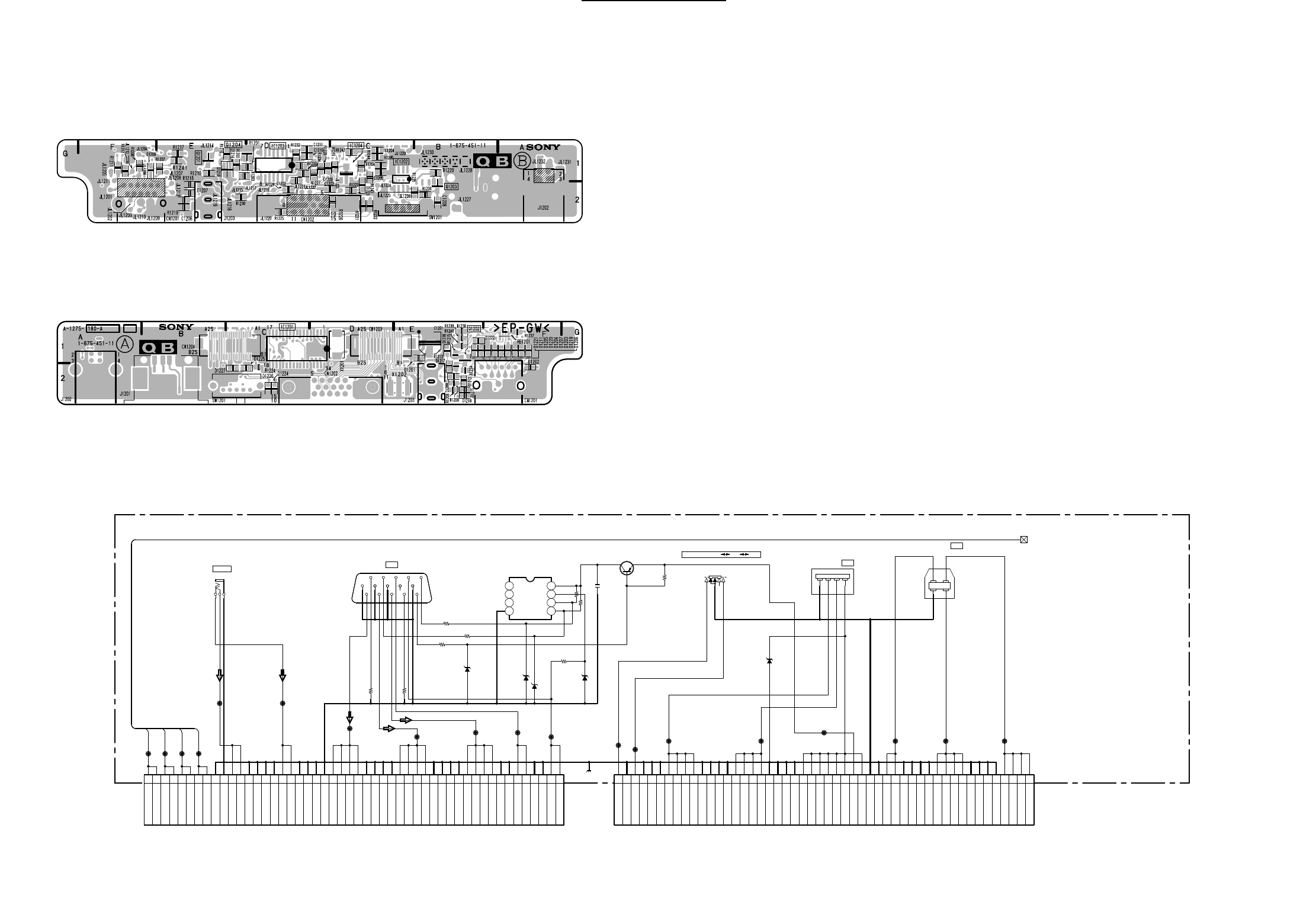
9-10 9-10
A B C D E F GH
1
2
3
4
5
VPL-PX20/PX30
QB – B SIDE –
SUFFIX ; -11
QB – A SIDE –
SUFFIX ; -11
B
G
R
RL
1234
A1
B1
A2
B2
A3
B3
A4
B4
A5
B5
A6
B6
A7
B7
A8
B8
A9
B9
A10
B10
A11
B11
A12
B12
A13
B13
A14
B14
A15
B15
A16
B16
A17
B17
A18
B18
A19
B19
A20
B20
A21
B21
A22
B22
A23
B23
A24
B24
A25
B25
A1
B1
A2
B2
A3
B3
A4
B4
A5
B5
A6
B6
A7
B7
A8
B8
A9
B9
A10
B10
A11
B11
A12
B12
A13
B13
A14
B14
A15
B15
A16
B16
A17
B17
A18
B18
A19
B19
A20
B20
A21
B21
A22
B22
A23
B23
A24
B24
A25
B25
1234
5 6 7 8
J1203
CN1202
Q1203
D1223 D1224
D1225
D1226
R1225 R1226
JL1214 JL1215JL1216 JL1217
JL1218 JL1219
JL1220
JL1221 JL1222 JL1223 JL1224
JL1225 JL1226 JL1227 JL1228
JL1229
JL1230 JL1231 JL1232
D1227
C1208
R1220
R1221 R1222
R1223 R1224
SW1201
CN1203 CN1204
R1235
R1236
J1201
J1202
IC1202
0
:CHIP 0
:CHIP
2SA1162
BUFF
RD5.6SB
5V-REG RD5.6SB
5V-REG
RD5.6SB
5V-REG
RD5.6SB
5V-REG
### #
##
#
#
##
#
#
## #
#
## #
RD5.6SB
5V-REG
0.1
B:CHIP
100k
:CHIP
47
:CHIP 47
:CHIP
33k
:CHIP 220
:CHIP
50P
WHT 50P
WHT
15k
:CHIP 15k
:CHIP
24LC21AT
DDC MEN
A
231 12345
678910
11 12 13 14 15
231
MS5V
IRD A
DS2-
DS2+
GND
GND
GND
GND
GND
GND
GND
GND
GND
GND
GND
GND
GND
GND
GND
GND
GND
GND
GND
GND
GND
GND
GND
GND
GND
GND
GND
GND
GND
GND
GND
GND
GND
GND
GND
GND
GND
GND
GND
GND
GND
GND
USBU D-
USBU D-
USBU D-
USBU D-
USBU D+
USBU D+
USBU D+
USBU D+
SUB 5V
USBD D-
USBD D-
USBD D-
USBD D-
USBD D+
USBD D+
USBD D+
USBD D+
IN 5V
IN 5V
INPUTA SW2
INPUTA SW1
AV
AV
AH
AH
AB
AB
AB
AB
AG
AG
AG
AG
AR
AR
AR
AR
AUDIO AR
AUDIO AR
AUDIO AL
AUDIO AL
GND
GND
DS2+
DS2+
DS2-
DS2-
IRD A
IRD A
MS5V
MS5V
NC
NC
NC
VCC
VSS
VCLK
SCL
SDA
USB 5V
USB 5V
USB 5V
USB 5V
USB 5V
USB 5V
USB 5V
B-SS1696<08.>-QB.-P1
(INPUT A TERMINAL)
QB(1/2)
TO QA CN803 TO QA CN804
(P2)
USB
USB
DIGITAL RGB 5BN RGB
RGB
AUDIO
QB (1/2) QB (1/2)
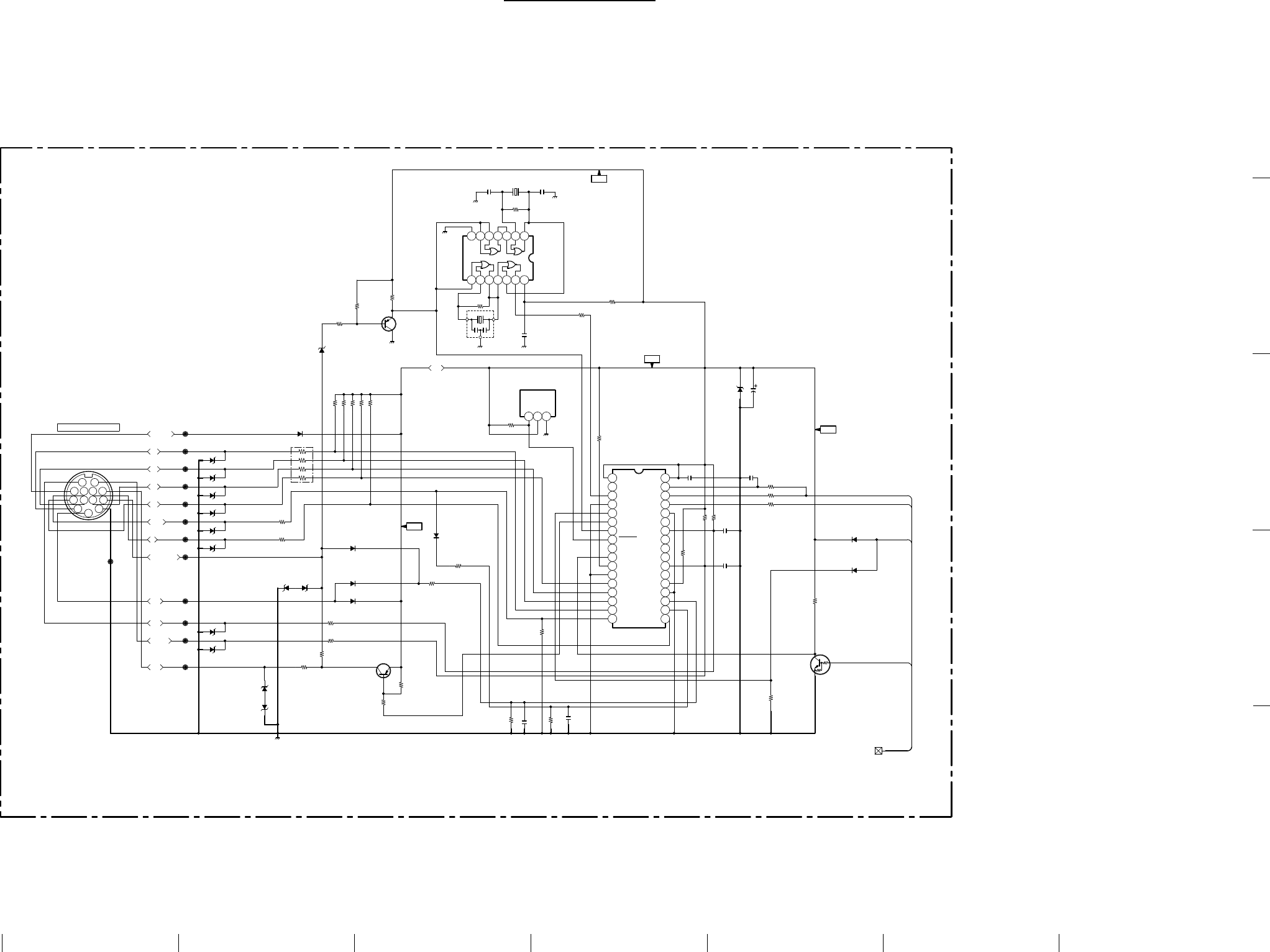
9-11 9-11
A B C D E F GH
1
2
3
4
5
VPL-PX20/PX30
• Refer to page 9-10 for Printed Wiring Board
+5V
+5V
+5V
+5V
11 12
10 13
69
78
5
2
1
4
3
1234567
8 9 10 11 12 13 14
1 2 3
1234567891011121314151617
18 19 20 21 22 23 24 25 26 27 28 29 30 31 32 33 34
CN1201
JL1210
JL1202
JL1203
JL1204
JL1205
JL1206
JL1207
JL1208
JL1201
JL1211
JL1212
JL1213
JL1209
RB1201
Q1202
R1216
C1204
C1205
C1207 C1206
C1203
D1201
C1209
R1211
R1212
R1206
R1207
D1203
D1204
D1205
D1206
D1207
D1211
D1217
D1219
D1220
D1221
R1214
D1222
D1216
R1215
R1217
Q1201
R1210
D1214
D1215
D1212
D1209
R1227
R1228
Q1204
R1202
R1201 R1230
R1233
R1232
C1211 C1210
C1202
R1204 R1205
C1201
D1202
D1210
D1218
R1234
X1201
R1203
D1208
R1237
R1238
R1239
R1240
R1241
R1208
R1242
R1243
R1244
R1209
R1218 R1219
R1213
R1229
IC1204
X1202
R1231
IC1203
IC1201
#
#
#
#
#
#
#
#
#
#
#
#
#
2SA1162
BUFF
56k
:CHIP
100p
CH:CHIP
100p
CH:CHIP
100p
CH:CHIP 100p
CH:CHIP
0.1
16V
B:CHIP
RD5.6SB
5V REG
0.1
16V
B:CHIP
47 :CHIP
47 :CHIP
100 :CHIP
100 :CHIP
RD5.6SB-T1
PROTECT
RD5.6SB-T1
PROTECT
RD5.6SB-T1
PROTECT
RD5.6SB-T1
PROTECT
RD5.6SB-T1
PROTECT
RD5.6SB-T1
PROTECT
RD5.6SB-T1
PROTECT
RD5.6SB-T1
PROTECT
RD5.6SB-T1
PROTECT
RD5.6SB-T1
PROTECT
100
:CHIP
RD5.6SB-T1
PROTECT
RD9.1SB2-T1
PROTECT
27k
:CHIP
27k
:CHIP
DTC144EKA
INV
4.7k
:CHIP
1SS355
SELECT SW
1SS355
SELECT SW
1SS355
SELECT SW
1SS355
SELECT SW
47 :CHIP
47 :CHIP
2SA1162
BUFF
56k
:CHIP
27k
:CHIP 1M
:CHIP
100
:CHIP
1M
:CHIP
15p
CH:CHIP 15p
CH:CHIP
0.1
16V
B:CHIP
13P
BUS
100
10k
:CHIP
10k
:CHIP
47
16V
:AL-CP
RB501V
SELECT SW
RB501V
SELECT SW
RB501V
SELECT SW
220
:CHIP
27k
:CHIP
RD5.6SB-T1
PROTECT
56k
:CHIP
56k
:CHIP
56k
:CHIP
56k
:CHIP
56k
:CHIP
1k :CHIP
10k
:CHIP
56k
:CHIP
10k
:CHIP
2.7k :CHIP
27k
:CHIP 10k
:CHIP
5.6k :CHIP
1.5k :CHIP
24MHz
S-80840ANUP
RESET
6MHz
33k
:CHIP
TC74HC02AF
SELECT
ST72633
RCV4
MOUSE DRV
XA
XB
YA
YB
L/PS
R
CLK
DAT/RI
RXD
RTS
+5V/DTR
98/AT/TXD
VCC
A
IRD A
MS5V
DS2-
DS2+
B-SS1696<08.>-QB.-P2
(INPUT A MOUS TERMINAL,MOUS DRV.)
(P1)
INPUT A MOUSE
QB(2/2)
VCC
VSS
OUT
VCC
GND
VDD
X2
X1
VSS
PC2
PC1
PC0
RESET
N.C.
PB7
PB6
PB5
PB4
PB3
PB2
PB1
VPP
VDDA
USBVCC
USB-
USB+
VSSA
PA0
PA1
N.C.
N.C.
N.C.
PA2
PA3
PA4
PA5
PA6
PA7
PB0
QB (2/2) QB (2/2)
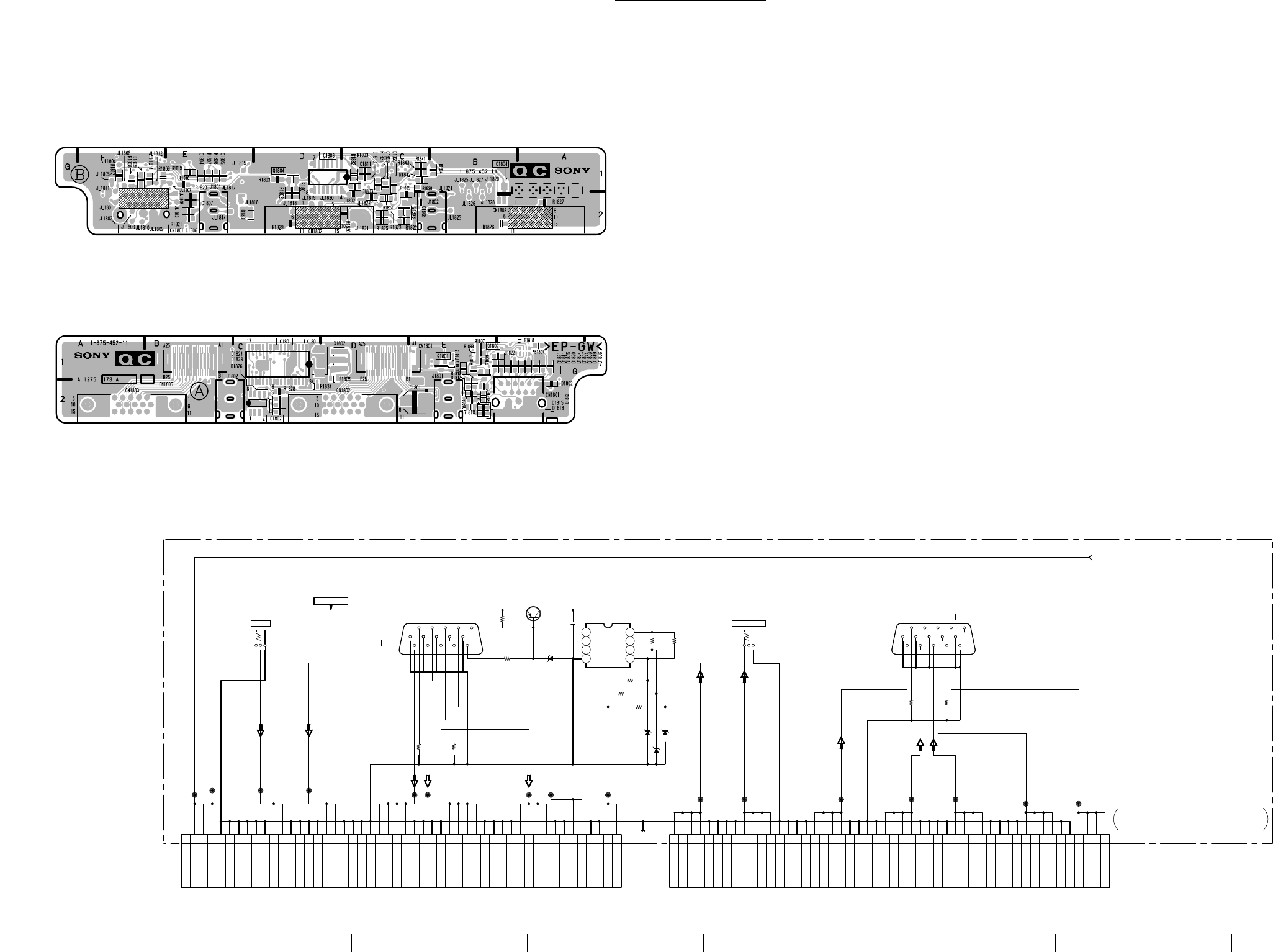
9-12 9-12
A B C D E F GH
1
2
3
4
5
VPL-PX20/PX30
QC – B SIDE –
SUFFIX ; -11
QC – A SIDE –
SUFFIX ; -11
SUB +5V
LR
RG B
LR
RGB
A1
B1
A2
B2
A3
B3
A4
B4
A5
B5
A6
B6
A7
B7
A8
B8
A9
B9
A10
B10
A11
B11
A12
B12
A13
B13
A14
B14
A15
B15
A16
B16
A17
B17
A18
B18
A19
B19
A20
B20
A21
B21
A22
B22
A23
B23
A24
B24
A25
B25
A1
B1
A2
B2
A3
B3
A4
B4
A5
B5
A6
B6
A7
B7
A8
B8
A9
B9
A10
B10
A11
B11
A12
B12
A13
B13
A14
B14
A15
B15
A16
B16
A17
B17
A18
B18
A19
B19
A20
B20
A21
B21
A22
B22
A23
B23
A24
B24
A25
B25
1234
5 6 7 8
J1801
CN1802
J1802
CN1803
R1826 R1827
JL1814
Q1803
D1823
D1824 D1825
R1829 R1830
D1826
R1824
R1825
R1828
C1808
R1822
R1823
JL1815 JL1816 JL1817 JL1818 JL1819 JL1820 JL1821 JL1822 JL1823 JL1824 JL1825 JL1826 JL1827 JL1828 JL1829
CN1804
CN1805
R1836
R1835
IC1802
0
:CHIP 0
:CHIP
0
:CHIP 0
:CHIP
2SA1162
BUFF
RD5.6SB
5V-REG
RD5.6SB
5V-REG
RD5.6SB
5V-REG
RD5.6SB
5V-REG
#
0.1
B:CHIP
###
#
#
## # ## # ## ##
100k
:CHIP
33k
:CHIP 47
:CHIP
47
:CHIP
220
:CHIP
15k
:CHIP
15k
:CHIP
50P
WHT
50P
WHT
24LC21AT
DDC MEN
A
12345
678910
11 12 13 14 15
12345
678910
11 12 13 14 15
GND
GND
GND
GND
GND
GND
GND
GND
GND
GND
GND
GND
GND
GND
GND
GND
GND
GND
AUDIO OL
AUDIO OL
AUDIO OL
AUDIO OL
AUDIO OR
AUDIO OR
AUDIO OR
AUDIO OR
OUT R
OUT R
OUT R
OUT R
OUT G
OUT G
OUT G
OUT G
OUT B
OUT B
OUT B
OUT B
OUT H
OUT H
OUT H
OUT H
OUT V
OUT V
OUT V
OUT V
GND
GND
GND
GND
GND
GND
GND
GND
GND
GND
GND
GND
GND
GND
GND
GND
GND
GND
GND
GND
GND
GND
GND
GND
AUDIO BL
AUDIO BL
AUDIO BR
AUDIO BR
BR
BR
BR
BR
BG
BG
BG
BG
BB
BB
BB
BB
BH
BH
BV
BV
GND
GND
IRD B
IRD B
SUB5V
SUB5V
GND
GND
GND
GND
NC
NC
NC
VCC
VSS
VCLK
SCL
SDA
B-SS1696<08.>-QC.-P1
INPUT B TERMINAL,
OUTPUT TERMINAL
QC(1/2)
TO QA CN806
MONITOR OUT
AUDIO OUT
RGB
AUDIO
TO QA CN805
(P2)
QC (1/2) QC (1/2)
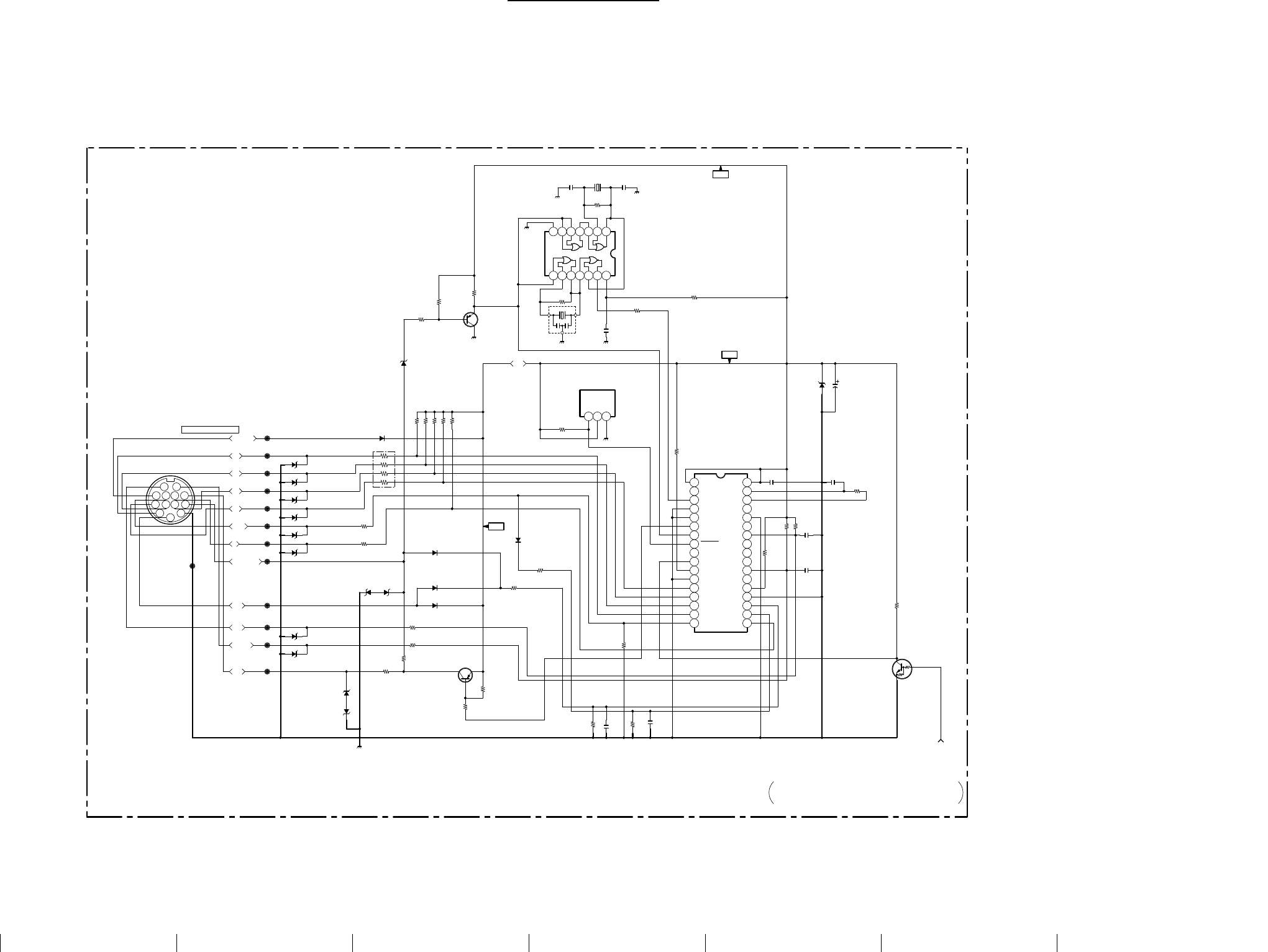
9-13 9-13
A B C D E F GH
1
2
3
4
5
VPL-PX20/PX30
+5V
+5V
+5V
11 12
10 13
69
78
5
2
1
4
3
1234567
8 9 10 11 12 13 14
1234567891011121314151617
18 19 20 21 22 23 24 25 26 27 28 29 30 31 32 33 34
1 2 3
CN1801
JL1810
JL1802
JL1803
JL1804
JL1805
JL1806
JL1807
JL1808
JL1801
JL1811
JL1812
JL1813
JL1809
RB1801
Q1802
R1807R1806
C1804
C1805
C1807 C1806
C1803
C1801
D1801
C1809
R1813
R1814
R1808
R1809
D1803
D1804
D1805
D1806
D1807
D1811
D1817
D1819
D1820
D1821
R1816
D1822
D1816 D1818
D1802
R1817
R1819
Q1801
R1812
D1815
D1812
D1809
R1802
R1801
C1811 X1801
C1802
R1832
C1810
R1833
R1834
R1805
D1808
R1803
R1818
R1837
R1838
R1839
R1840
R1810
R1841
R1842
R1843
R1811
R1820 R1821
R1815
R1831
IC1803
Q1804
IC1804
R1804
X1802
IC1801
13P
BUS
#
#
#
#
#
#
#
#
#
#
#
#
#
100
2SA1162
BUFF
10k
:CHIP
10k
:CHIP
100p
CH:CHIP
100p
CH:CHIP
100p
CH:CHIP 100p
CH:CHIP
0.1
16V
B:CHIP
47
16V
:AL-CP
RD5.6SB
5V REG
#
B:CHIP
47 :CHIP
47 :CHIP
100 :CHIP
100 :CHIP
RD5.6SB-T1
PROTECT
RD5.6SB-T1
PROTECT
RD5.6SB-T1
PROTECT
RD5.6SB-T1
PROTECT
RD5.6SB-T1
PROTECT
RD5.6SB-T1
PROTECT
RD5.6SB-T1
PROTECT
RD5.6SB-T1
PROTECT
RD5.6SB-T1
PROTECT
RD5.6SB-T1
PROTECT
100
:CHIP
RD5.6SB-T1
PROTECT
RD9.1SB2-T1
PROTECT
27k
:CHIP
27k
:CHIP
DTC144EKA
INV
4.7k
:CHIP
1SS355
SELECT SW
1SS355
SELECT SW
1SS355
SELECT SW
0.1
16V
B:CHIP
15p
CH:CHIP
15p
CH:CHIP
1M
:CHIP
100
:CHIP
56k
:CHIP
27k
:CHIP 1M
:CHIP
RB501V
SELECT SW
RB501V
SELECT SW
220
:CHIP
24MHz
RD5.6SB-T1
PROTECT
27k
:CHIP
56k
:CHIP
56k
:CHIP
56k
:CHIP
56k
:CHIP
56k
:CHIP
1k :CHIP
10k
:CHIP
56k
:CHIP
10k
:CHIP
2.7k :CHIP
27k
:CHIP 10k
:CHIP
5.6k :CHIP
1.5k
:CHIP
2SA1162
SW
33k
:CHIP
TC74HC02AF
SELECT
S-80840ANUP
RESET
6MHz
ST72633
RCV4
MOUSE DRV
XA
XB
YA
YB
L/PS
R
CLK
DAT/RI
RXD
RTS
+5V/DTR
98/AT/TXD
VCC
A
B-SS1696<08.>-QC.-P2
QC(2/2)
INPUT B MOUS TERMINAL,
MOUSE DRV.
(P1)
INPUT B MOUS
VDD
X2
X1
VSS
PC2
PC1
PC0
RESET
N.C.
PB7
PB6
PB5
PB4
PB3
PB2
PB1
VPP
VDDA
USBVCC
USB-
USB+
VSSA
PA0
PA1
N.C.
N.C.
N.C.
PA2
PA3
PA4
PA5
PA6
PA7
PB0
OUT
VCC
VCC
VSS
VSS
• Refer to page 9-12 for Printed Wiring Board
QC (2/2) QC (2/2)
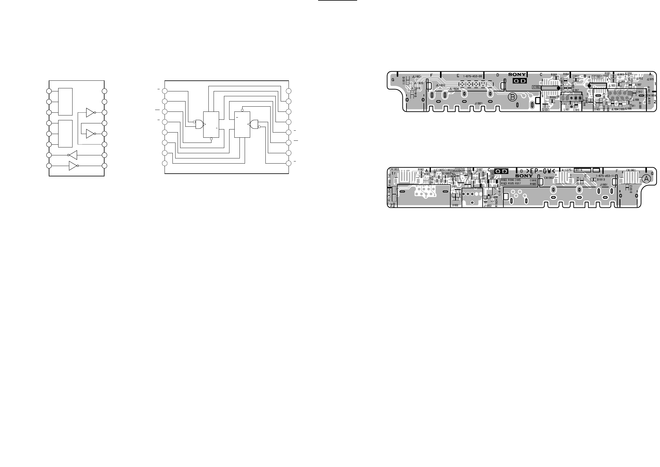
9-14 9-14
A B C D E F GH
1
2
3
4
5
VPL-PX20/PX30
QD – B SIDE –
SUFFIX ; -11
QD – A SIDE –
SUFFIX ; -11
C1+ 116
215
314
413
512
611
710
89
V+
C1-
C2+
C2-
V-
T2OUT
R2IN
Vcc
GND
T1OUT
R1IN
R1OUT
T1IN
T2IN
R2OUT
VOLTAGE
DOUBLER
VOLTAGE
INVERTER
MAX202 (IC1901)
QD QD
1
2
3
4
5
6
7
16
15
14
13
12
11
10
8
A
RD
C
Q
B
GND
Q
R
9
VDD
R
C
RD
Q
B
Q
A
Q
Q
D
RD
Q
Q
RD
PC74HC123D (IC1902)
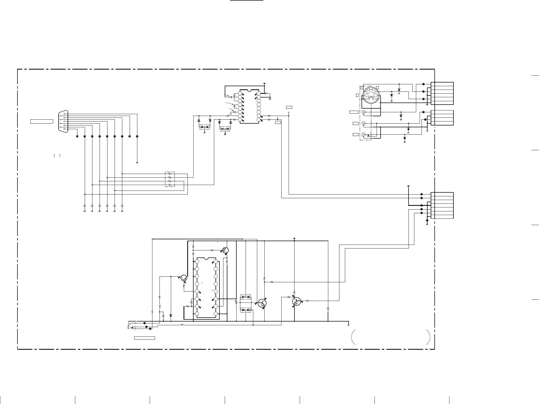
9-15 9-15
A B C D E F GH
1
2
3
4
5
VPL-PX20/PX30
• Refer to page 9-14 for Printed Wiring Board
• Refer to page 9-14 for IC Block Diagrams
0
7.7
0
5.3
5.0
5.0
9.5
2.9
4.4
-4.9
-9.3
-9.3
0
5.0
5.0
5.0
5.0
5.0
0
0
0
4.3
0
0
0
0
5.0
5.0
12
34
V
L
R
1
2
3
4
5
6
12345678
910 11 12 13 14 15 16
1
2
3
4
12345678
9 10 11 12 13 14 15 16
1
2
3
4
5
6
7
JL1901 JL1902 JL1903 JL1904 JL1905 JL1906 JL1907 JL1908 JL1909
IC1902
JL1910
JL1911
JL1912
JL1913
JL1914
JL1915
R1901
D1901
J1901
D1902
D1903
TP1901
TP1902
R1902
R1903
D1904
R1904
D1905
C1901
D1906
C1902
C1903
C1904
C1905
CN1903
C1908 C1909 C1910 C1911 C1912
R1914
R1915
C1915
R1916 R1917
Q1901
R1918
Q1902
R1919
R1920
R1921
R1922
D1907
R1923
C1916
R1924
Q1903
R1925
Q1904
C1917
R1926
C1918
D1908
C1919
D1909
J1902
JL1916
JL1917 JL1918
C1906
JL1919
JL1920
JL1921
JL1922
JL1924
CN1901
IC1901
RB1901
CN1904
CN1902
D1910
D1911
D1912
D1913
D1914
L1903
L1901
L1902
0.1
25V
B:CHIP
0.1
25V
B:CHIP
0.1
25V
B:CHIP
0
:CHIP
0
:CHIP
0
:CHIP
D204K
D204K
0
:CHIP
0.001
B:CHIP
0.001
B:CHIP
0.001
B:CHIP
0.001
B:CHIP
0.001
B:CHIP
0.1
25V
B:CHIP
0.1
25V
B:CHIP
RD27SB
RD27SB
RD27SBRD27SB
1k
:CHIP
100
:CHIP
4.7k
:CHIP
100
:CHIP
100
:CHIP
RD9.1SB2
PROTECT
10
16V
:AL-CP 0.1
25V
B:CHIP
DAP202K
PROTECT
470p
CH:CHIP
2SA1162
DTC144EKA
INV.BUFF
2SA1162
SW
8.2
:CHIP
4.7
:CHIP
47k
:CHIP 22k
:CHIP
2.2k
:CHIP
1k
:CHIP
DTC144EKA
INV.BUFF
DAN202K
PROTECT
PC74HC123D
TIMER
470k
:CHIP
100k
:CHIP
# ########
#
#
#
#
#
#
#
##
2.2
10V
B:CHIP
2.2
10V
B:CHIP
7P
WHT
0.001
B:CHIP
#
#
#
#
#
6P
MAX202CSE
100
4P
D-SUB 9PIN
RS-232C/422A
RD9.1SB2-T1
RD9.1SB2-T1
RD9.1SB2-T1
RD9.1SB2-T1
RD9.1SB2-T1
OUH
OUH
OUH
5V-4
5V-4
5V-4
1
2
3
4
5
6
7
8
9
RS-232C/422
TX
RX
TX0
CONTROLS-IN
GND
GND
TXD_RD
RXD_RS
SUB+5V
SIRCS
SIRCS_S
Y
GND
C
GND
C-VIDEO
GND
S-SEL
GND
GND
C
Y
S
VIDEO
L-V
R-V
R-VIDEO
L-VIDEO
8 CTS
2 RD
1 NC
6 DSR
7 RTS
3 TD
4 DTR
8 CTS
2 RD
9 NC
5 GND
RXO
TO Y CN3003
TO QA CN807
TO BA CN102
RS-232C DRIVE
(DC+5V)
B-SS1696<08.>-QD.-P1
REMOTE TERMINAL,
VIDEO INPUTTERMINAL,
TIMER
QD
V-
C2-
C2+
GND
VCCC1+
V+
C1-
R21
T20
T10
T11
T21
R20
R1I
R1O
2CLR
VCC
1R/C
1C
1Q
2B
1A
1B
1CLR
2Q
2C
2R/C
GND 2A
1
2
Q
Q
QD QD
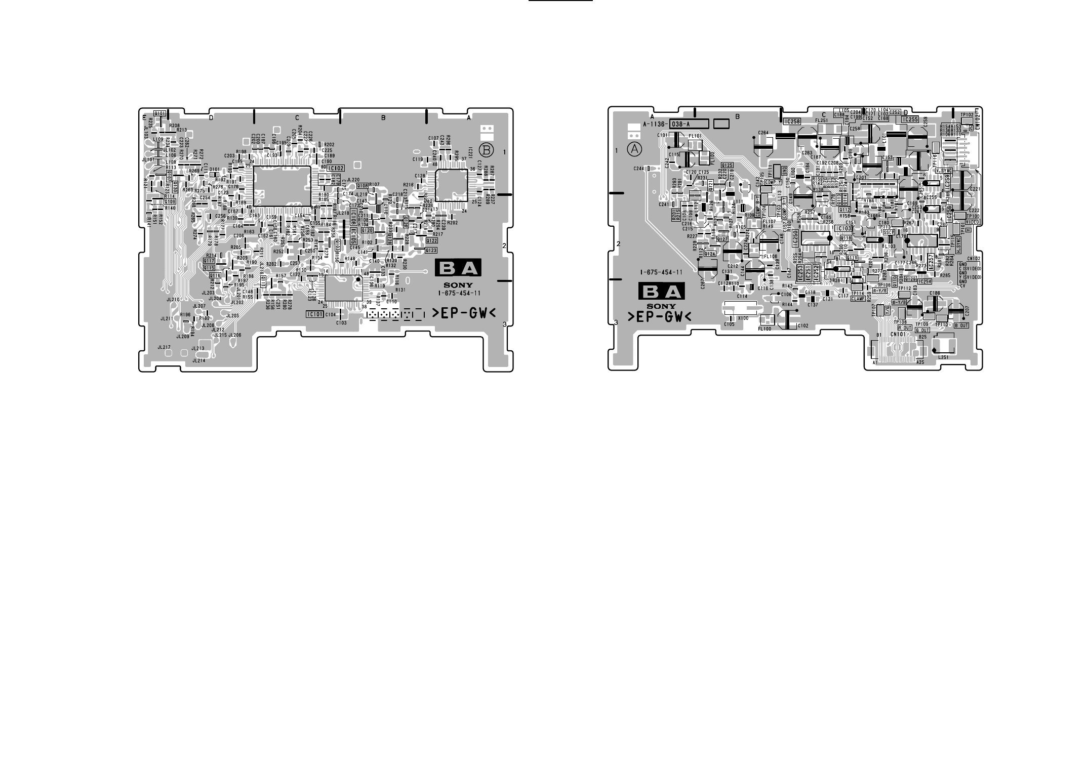
9-16 9-16
A B C D E F GH
1
2
3
4
5
VPL-PX20/PX30
BA – B SIDE –
SUFFIX ; -11
BA– A SIDE –
SUFFIX ; -11
——
BA
——
1-675-454-11
IC101 ∗C-3
IC102 ∗C-1
IC103 C-2
IC105 ∗B-2
IC106 ∗B-2
IC250 C-2
IC251 C-2
IC252 C-2
IC253 C-2
IC254 D-3
IC255 D-1
IC256 D-2
IC257 D-2
IC258 C-1
IC259 D-1
Q101 ∗E-1
Q103 ∗C-2
Q107 ∗D-1
Q108 ∗B-1
Q109 ∗E-2
Q110 D-3
Q111 ∗C-3
Q112 C-2
Q113 C-2
Q114 C-2
Q115 ∗D-2
Q116 ∗D-2
Q117 ∗D-2
Q118 C-2
Q119 C-2
Q120 ∗B-2
Q121 B-1
Q122 ∗A-2
Q123 ∗A-2
Q124 B-2
Q125 B-1
Q126 ∗B-2
Q127 B-2
Q128 ∗B-2
Q129 D-3
Q130 ∗D-1
R201 A-2
R215 A-2
TP100 E-2
TP101 E-2
TP102 E-1
TP103 B-2
TP104 B-2
TP106 D-3
TP107 D-3
TP108 D-3
TP109 D-3
TP110 D-3
TP112 D-3
TP113 D-2
TP114 C-3
TP115 E-2
∗:B Side mount
BA BA
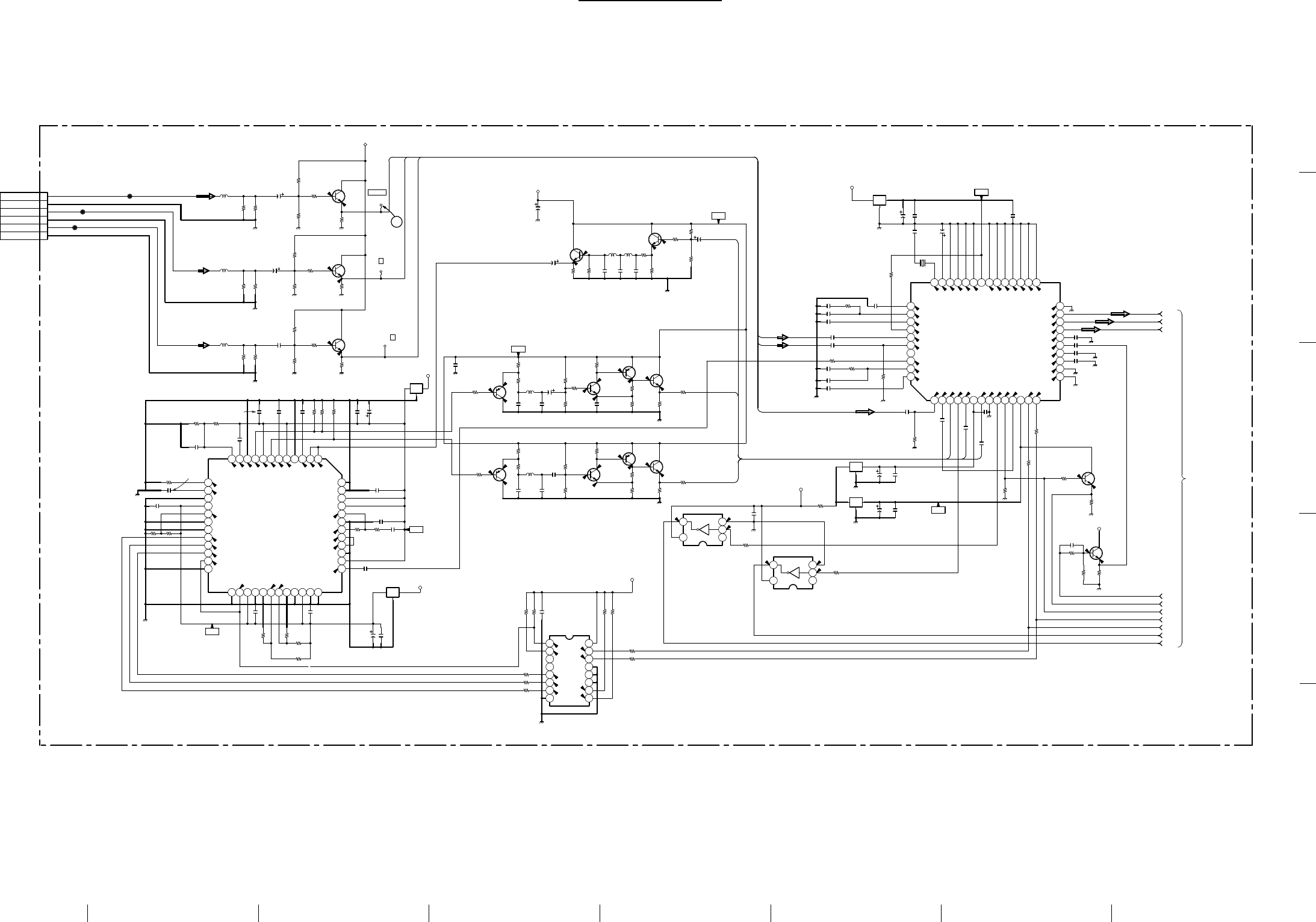
9-17 9-17
A B C D E F GH
1
2
3
4
5
VPL-PX20/PX30
BA (1/2) BA (1/2)
• Refer to page 9-16 for Printed Wiring Board
• Refer to page 9-19 for Waveforms
• Refer to page 9-19 for IC Block Diagrams
0
+5V
*
1.7
1.7
3.2
4.9
1.7
1.8
3.7
*
0
0
0
0
0
0
0
0
0
0
0
0
0
0
0
0
0
0
2.2
1.2
2.5
0.3
0.9
2.4
4.9
4.8
1.8
1.8
1.6
2.3
2.5
2.6
1.1
0.8
0.4
1.5
0.9
+5V
0
0
4.8
0
0.3
4.6
+9V
+9V
4.6
4.0
2.9
2.3
0
3.0
3.6
3.6
8.3
8.3
3.5
4.2
1.2
0.5
8.3
3.5
4.2
0
4.2
4.2
8.3
1.3
0.7
+5V
+5V
0
0
0
0
0
0
0
0
0
*
0.4
0.4
2.3
2.3
2.4
2.4
1.5
2.6
0.5
0
0.7
2.5
0.5
1.4
1.4
1
3.6
4.3
3.6
4.3
3.6
0
1.4
3.6
1.0
0
0.3
0.4
0.3
5.0
4.2
4.8
4.85.0
R-Y
B-Y
Y
VIDEO
C
Y
VIDEO
C
Y
1 2 3 4 5 6 7 8 9 10 11 12 13 14
15
16
17
18
19
20
21
22
23
24
2526272829303132333435363738
39
40
41
42
43
44
45
46
47
48
EMI
EMI
EMI
EMI
EMI
12345678
9 10 11 12 13 14 15 16
1
2
3
4
5
6
1 2 3
45
1 2 3
45
123456789101112
13
14
15
16
17
18
19
20
21
22
23
24
25 26 27 28 29 30 31 32 33 34 35 36
37
38
39
40
41
42
43
44
45
46
47
48
TP100
R116
R119
R130
R134
R147
R148
R149
R150
R156 R157
C103 C104
C105
C110
C112
C114
C116
C117
C121
C123
C126
C133
C138
C139
C140
C141
C147
TP101
TP102
R155
R110
C106
C118
C122
C107
C119
C124
R107
C143
L110
C210
L111
C211
R104
R102
R105
C213 R115
R226
C214
L112
C215
C216
R227
R228
C217 R120
R231
R126
R122
C218
L113
C219
C220
R232
R233
R131 R132
FL101
FL102
FL100
FL106
FL107
R137
C137
R182
C131
CN102
C148
C136
X100
C145
R106 R111
R113
R114
R121
R133 R136
C221
C222 R140
R141
R151
R153 R154
C223 R208
R213
R234
C224 R238
R230
R125
R152
R235
IC101
C212
R225
C101
C115
R143
C102
C144
C146
C267
R144
C239
C241
IC221
C242
C240
C243
C244
C127
R237
R287
R288
R289
R290 R291
R292
R293
R294
R295 R296
C120
C128C125
C108C109
C142
R224
R108
R112
R118
R124
R127
R229
Q103
Q111
IC105
IC106
Q120
Q108
Q121
Q125
Q123
Q122
Q124
Q128
Q127Q126
Q107
Q109
Q101
JL102
JL103
JL101
R109
R123
R201 R215 R216
L106
L108
L109
IC250
R256
R258
R257
R255
R254
R251
R252
R253
R250
C250
0.01 B:CHIP
0.01
B:CHIP
0.1
25V
B:CHIP
0.1
25V
B:CHIP
0.01
B:CHIP
0.1
25V
B:CHIP
0.1
25V
B:CHIP
0
:CHIP
0 :CHIP
3.9k :CHIP
0.01
B:CHIP
100
:CHIP
100
:CHIP
0.01
B:CHIP
10p
CH:CHIP
0.01
B:CHIP
1 16V B:CHIP
0.01 B:CHIP
1 16V B:CHIP
0.47
16V
B:CHIP
1 16V B:CHIP
100
:CHIP
100
:CHIP
1k
:CHIP1k
:CHIP
1k
:CHIP
0.022 B:CHIP
1k
:CHIP
27k
:RN-CP
10
16V
:AL-CP
0.1 25V B:CHIP
0.1
F:CHIP
0.1
F:CHIP
0.1
25V
B:CHIP
1k
:CHIP 22p
CH:CHIP
47µH
:CHIP
56p
CH:CHIP
47µH
:CHIP
22p
CH:CHIP
1k
:CHIP
15k
:CHIP
13k
:RN-CP
0.1
F:CHIP
3.3k
:CHIP
510
:RN-CP
27p
CH:CHIP
15µH
:CHIP
56p
CH:CHIP
10
16V
:AL-CP
20k
:RN-CP
270
:CHIP
33p
CH:CHIP
100
:CHIP
100
:CHIP
3.3k
:CHIP
510
:RN-CP
27p
CH:CHIP
15µH
:CHIP
56p
CH:CHIP
0.01
B:CHIP
20k
:RN-CP
270
:CHIP
2.2k
:CHIP 100
:CHIP
EMI
EMI
1k
:CHIP
1
16V
B:CHIP
4.7 16V :CHIP
EMI
EMI
EMI 7.5k
:CHIP
2.2
10V
B:CHIP
6P
:SMD
#
0.01 B:CHIP
0.01
B:CHIP
150
:RN-CP 150
:RN-CP
22k
:CHIP
22k
:CHIP
47
:CHIP
150
:RN-CP
150
:RN-CP
47
16V
:AL-CP
47
16V
:AL-CP
22k
:CHIP
22k
:CHIP
47
:CHIP
150
:RN-CP
150
:RN-CP
0.1
25V
B:CHIP
22k
:CHIP
22k
:CHIP
47
:CHIP
0.01
B:CHIP
47
:CHIP
820
:RN-CP
820
:RN-CP
820
:RN-CP
820
:RN-CP
CXA2123AQ
MAIN
COLOR DECODER
100
6.3V
:AL-CP
100
:RN-CP
680k
:CHIP
82
6.3V
:AL-CP
68
10V
:AL-CP
82
6.3V
:AL-CP
68
10V
:AL-CP
68
10V
:AL-CP
100
16V
:AL-CP
#
0.1
25V
B:CHIP
0.1
25V
B:CHIP
CXD2064Q-T6
D.COMB
0.1
25V
B:CHIP
0.1
25V
B:CHIP
0.022
B:CHIP
0.001
B:CHIP
0.1
25V
B:CHIP
#
#
0
:CHIP
0
:CHIP
1.5k
:CHIP
3.3k
:CHIP
0
:CHIP
#
2.2k
:CHIP
56k
:CHIP 560
:CHIP
0.1
25V
B:CHIP
0.1
25V
B:CHIP
0.1
25V
B:CHIP
0.1
25V
B:CHIP
0.1
25V
B:CHIP
10
16V
:AL-CP
100
:CHIP
47
:RN-CP
1k
:RN-CP
22k
:RN-CP
22k
:RN-CP
820
:RN-CP
820
:RN-CP
16.2MHz
2SC2712
SCP.BUFF
2SC2712
RGB SYNC.BUFF
TC7S04F
VS.INV
TC7S04F
HS.INV
2SC2712
COMB. V.BUFF
2SC2712
COMB.V.BUFF
2SA1162
COMB.Y.BUFF
2SA1162
COMB.C.BUFF
2SA1162
COMB.Y.AMP
2SC2712
COMB.Y.AMP
2SC2712
COMB.Y.BUFF
2SC2712
COMB.C.BUFF
2SA1162
COMB.C.AMP
2SC2712
COMB.C.AMP
2SC2412K
V.BUFF
2SC2412K
Y.BUFF
2SC2412K
C.BUFF
#
#
#
330
:RN-CP
330
:RN-CP
#120
:RN-CP 120
:RN-CP
OUH
OUH
OUH
CXA1875AM
DAC
100
:CHIP
100
:CHIP
100
:CHIP
100
:CHIP
100
:CHIP
10k
:CHIP
10k
:CHIP
10k
:CHIP
10k
:CHIP
0.1
25V
B:CHIP
9V
5V
5V
5V
5V
9V
5V
5V
R-Y
B-Y
Y
SYNC
CLP
SDA
SCL
VS
HS
SCP
COMB.OUT
COMB.Y
COMB.OUT
C
Y
VIDEO
VIDEO
Y
C
COMB.Y
COMB.C
COMB.C
CV
GND
VIDEO
Y
C
Y(SVIDEO)
C(SVIDEO)
GND
GND
VRF
VG
DAVS
AYO
DAVD
ACO
RT
ADVD
ADVS
RB
ADIN
CLPO
DTR
PNR
VEH1
VEH2
VEH3
MOD1
DVSS
MOD2
DVDD
TEST
VB
IRF
NTPL2
NTPL1
DVDD
TEST
DVSS
APCN
TRAP
TEST
TEST
DVDD
TEST
DVSS
FIN
CKSL
PLSL
MCKO
ADCK
CPO
PLVS
VCV
PLVD
CLVD
CLPEN
CLVS
TO QD CN1901
C3
APC-Fil
CVBS/Y3
C2
CVBS/Y2
COMB SYS
SFC OUT
AFC.Fi
C1
CVBS/Y1
SYNC IN
CVBS OUT(2VPpp)
VS
COMB Y
COMB C/FORCED S
D-GND
HS
SCP
Y FOR SYNC
SYNC-Vcc
SYNC-GND
Cr1
Cb1
Y1
Y OUT
Cb out
Cr out
YS1
B1
G1
R1
Y/C GND
Cr2
Cb2
Y2
Y/C Vcc
B2
G2
BPH-Fil
Xtal
D-VDD
SCL
SDA
YS3
APL FIL
R2
YS/YM
ADD(8EH)
(CHROMA DECODER)
VCC
SCL
SDA
SDA2
SDA1
SDA0
SW3
SW2
SW1
SW0
DAC4
DAC3
GND
VEH1
VEH2
VEH3
B-SS1696<08.>-BA.-P1
BA(1/2)
(2/2)
R217
100
:RN-CP

9-18 9-18
A B C D E F GH
1
2
3
4
5
VPL-PX20/PX30
BA (2/2) BA (2/2)
11
12
+5V
0
0
0
0
0
0
0
00
0
0.4
2.5
4.2
4.9
5
6
+5V
0
4.9
0
4.9
4.9
0
4.7
4.9
4.7
0
2.3
1.4
0.8
0
0
0
0
0
0.5
0
0
4.9
4.6
0.5
0.7
3.7
3.0
3.7
3.0
3.7
3.0
7
98
2
3
4
+5V
0
0
1.3 1.3
0
0
0
0.7
1.3
4.2
10
13
0
0
0
0
0
0
1.3
4.8
4.6
4.9
4.9
5.1
2.5
2.4
2.4
2.4
4.5
4.5
4.5
7.2
2.9
2.9
2.9
2.4
2.4
2.9
2.9
2.9
2.4
2.4
2.9
2.9
2.9
8.0
2.4
2.4
2.9
2.9
2.9
2.6
0.5
0.7
2.2
3.3
2.3
3.3
2.2
3.3
8.8
3.3
4.8
4.8
4.8
4.8
4.8
4.8
4.1
4.9
4.9
4.6
4.8
4.8
4.8
00
2.2
3.4
2.9
00
2.9
3.4 00
2.2
3.4
2.8
2.3
R-Y
Y
B-Y
R
G
B
1 2 3 4 5 6 7 8 9 10 11 12 13 14 15 16 17 18 19 20 21 22 23 24
25
26
27
28
29
30
31
32
33
34
35
36
37
38
39
40
414243444546474849505152535455565758596061626364
65
66
67
68
69
70
71
72
73
74
75
76
77
78
79
80
1 2 3 4
5678
1 2 3 4 5 6 7 8
910111213141516
EMI
A1
B1
A2
B2
A3
B3
A4
B4
A5
B5
A6
B6
A7
B7
A8
B8
A9
B9
A10
B10
A11
B11
A12
B12
A13
B13
A14
B14
A15
B15
A16
B16
A17
B17
A18
B18
A19
B19
A20
B20
A21
B21
A22
B22
A23
B23
A24
B24
A25
B25
IO
G
IO
G
1234
5678
1234
5678
1234
5678
123
45
123
45
123
45
R161
R162
Q117
Q115
Q116
R214
R190
R197
L103
R164 R166
Q114
Q113
Q112
R168
R169
R176
R184
R185
R183
R170 R172 R174
R171
R173 R175 R179R178R177
R181
R186
C181
L102
TP113
TP106
TP107
TP112
C168
C204
TP111
IC102
C167
C173
C176
C172
C174
C175
C189
C190
C191
C192
C200
C201
C202
C185
C149
C187
C153
C152
C188
C150
C179
C182
C184
C198
C151
C166
C164
C163
C162
C161
C160
C159
C158
C156
C155
C154
C157
C193
C194
C165
R165
R167
C178
R198
C195
C196
C197
C171C170
IC256
Q130
R271
R269
R272
C260
R268
C254
R188
R195
R212
C253
R207
R209
C206 R211
IC257
R265
R267C256
R274
C261
R275
C262
R270
C265
Q118
R210
R266
C255
L104
C252
R264
C259 C258
C263
C264
R279
R261
C257 R262
R263
R260
R259
FL251
R273
C266
R277
C177
TP108
TP109
TP110
CN101
R236
R280 C251
R278
C225
C226
C227
C205
C208
C209
R284
R281
R282
R138
R139
R142
JL217
C183
C186
C207
C111
R285
IC255
IC258
C199
TP103
TP104
TP105
C180
R193
R187
L100
L105
L101
R180
R158
R159
R163
R160
C203
R191
R192
IC103
R205
IC259
R206
C169
IC251
IC252
IC253
Q119
R189 R194 R196
R202
R203
R204
TP114
TP115
TP116
Q110 Q129
R283
JL201
JL202
JL203
JL204
JL206
JL207
JL208
JL209
JL210
JL211
JL212
JL215
JL216
JL205
JL218
JL219
JL220
D101
R276
IC254
JL213
JL214
100 :CHIP
100 :CHIP
2SC3545
BUFF
2SC3545
BUFF
2SC3545
BUFF
330
:CHIP
330
:CHIP
330
:CHIP
10µH
:CHIP
390
:CHIP 390
:CHIP
FMS1
BUFF
FMS1
BUFF
FMS1
BUFF
47 :CHIP
47 :CHIP
47 :CHIP
47
:CHIP
47
:CHIP
47
:CHIP
470
:CHIP 470
:CHIP 470
:CHIP
#
##47
:CHIP
47
:CHIP
47
:CHIP
6.8k
:CHIP
15k
:CHIP
0.01
B:CHIP
10µH
:CHIP
0.1
25V
B:CHIP
1 :AL-CP
CXA2101AQ
RGB INTERFACE
0.1
25V
B:CHIP
0.1
25V
B:CHIP
0.1
25V
B:CHIP
0.47 16V B:CHIP
0.47 16V B:CHIP
0.47 16V B:CHIP
0.47 16V B:CHIP
0.47 16V B:CHIP
0.47 16V B:CHIP
0.47 16V B:CHIP
0.47 16V B:CHIP
0.47 16V B:CHIP
0.47 16V B:CHIP
1
10V
B:CHIP
47
16V
:AL-CP
47
16V
:AL-CP
47 16V :AL-CP
0.1 25V B:CHIP
0.1
25V
B:CHIP
0.1
25V
B:CHIP
0.47 16V B:CHIP
0.47 16V B:CHIP
0.47 16V B:CHIP
1 :AL-CP
10 16V :AL-CP
10 16V :AL-CP
0.47 16V B:CHIP
0.47 16V B:CHIP
0.47 16V B:CHIP
0.47 16V B:CHIP
0.47 16V B:CHIP
0.47 16V B:CHIP
0.47 16V B:CHIP
0.47 16V B:CHIP
0.47 16V B:CHIP
0.47 16V B:CHIP
0.47 16V B:CHIP
0.47 16V B:CHIP
0.47 16V B:CHIP
10 16V :AL-CP
0 :CHIP
0 :CHIP
0.1
25V
B:CHIP
47 :CHIP
0.47 16V B:CHIP
0.47 16V B:CHIP
0.47 16V B:CHIP
0.1
25V
B:CHIP
0.0022
B:CHIP
GS4981
SYNC.SEP.
2SA1037K
2.2k
:CHIP
4.7k
:CHIP
470
:CHIP
0.1
25V
B:CHIP
270k
:RN-CP
0.1
25V
B:CHIP
47
:CHIP
47
:CHIP
47
:CHIP
0.1
25V
B:CHIP
47
:CHIP
47
:CHIP
0.47
16V
B:CHIP
47
:CHIP
MC74HC4538
P.WIDTH.ADJ
47
:CHIP
4.7k
:RN-CP
390p
CH:CHIP
47
:CHIP
0.1
25V
B:CHIP
47
:CHIP
#
47
:CHIP
0.1
25V
B:CHIP
2SA1037K
47
:CHIP
47
:CHIP
#
10µH
:CHIP
47
16V
:AL-CP
47
:CHIP
47
16V
:AL-CP
39
16V
:AL-CP
68
10V
:AL-CP
68
10V
:AL-CP
47
:CHIP47
:CHIP
0.1
25V
B:CHIP
47
:CHIP
47
:CHIP
100
:CHIP
47
:CHIP
4.7k
:RN-CP
100p
CH:CHIP
100
:CHIP
10
16V
:AL-CP
50P
4.7k
:RN-CP
4.7k
:RN-CP
0.1
25V
B:CHIP
47
:CHIP
0.47 16V B:CHIP
0.47 16V B:CHIP
0.47 16V B:CHIP
0.47 16V B:CHIP
0.47 16V B:CHIP
0.47 16V B:CHIP
47
:CHIP
470
:CHIP
270
:CHIP
0 :CHIP
0 :CHIP
0 :CHIP
#
47
6.3V
:AL-CP
47
6.3V
:AL-CP 47
6.3V
:AL-CP
1000p
CH:CHIP
47
:CHIP
BA09FP
9V REG
PQ05SZ1U
5V REG
0.47 16V B:CHIP
10
16V
:AL-CP
47k
:RN-CP
47
:CHIP
10µH
:CHIP
10µH
:CHIP
10µH
:CHIP
22k :RN-CP
27k :CHIP
47k :CHIP
3.3M :CHIP
47 :CHIP
0.01 B:CHIP
47
:CHIP
47
:CHIP
TC4W53
SCP.SW
4.7k
:RN-CP
TC7W14F
INV.
4.7k
:RN-CP
68
10V
:AL-CP
TC4W53F
CLAMP SW
TC7S04F
CLAMP BUFF
TC75S56F
HS.GEN.
DTC144EKA
INV
10k
:CHIP 10k
:CHIP 10k
:CHIP
47 :CHIP
47 :CHIP
47 :CHIP
2SC2712
CLAMP P.ADD 2SC2712
HS ADD
820
:RN-CP
#
#
#
#
#
#
#
#
#
#
#
#
#
#
#
#
#
1SS355
SPEED UP
10k
:CHIP
TC7S04F
VS.INV
#
#
5V
9V
9V
9V
9V
9V
9V
5V
5V 5V
SCP
SW2
CLP
CLP
SCL
SDA
HS
VS
R-Y
B-Y
Y
SYNC
R OUT
G OUT
R OUT
R OUT
G OUT
B OUT
GND
R OUT
G OUT
B OUT
+6V
Y/G
R-Y/R
B-Y/B
+6V
+6V
+6V
R/R-Y
R/R-Y
GND
GND
G/Y
G/Y
GND
GND
GND
B/B-Y
B/B-Y
H
GND
GND
GND
GND
V
RGBSYNC
GND
GND
GND
GND
VR
VR
VG
VG
VB
VB
GND
V-HD
GND
GND
V-VD
V-CLP
GND
GND
SDA
SCL
GND
GND
GND
GND
+10V
+10V
YC/OTHER
CV/OTHER
CLAMP
H.SYNC
V.SYNC
V.R-Y
V.B-Y
V.Y
SCP IN
C
INH
VEE
GND
+VCC
CH0
CH1
A
TO BB CN306
HS2
VS2
R-Y2
B-Y2
Y2
HS3
VS3
PR3
PB3
Y3
HS4
VS4
R4
G4
B4
2HS5
2VS5
2R-Y5
2B-Y5
2Y5
HS1
R-Y1
B-Y1
Y1
VCC MAT
GND MAT
V PH
H PH
SDA
SCL
R OUT
G OUT
B OUT
SCP IN
VBLK IN
HP IN
VS OUT
HS OUT
SELV OUT
SELH OUT
SELCR OUT
SELCB OUT
SELY OUT
SELY IN
SELCB IN
VCC SIG
IREF YC
GND SIG
BS/H
GS/H
RS/H
GND OUT
VCC OUT
IREF SYNC
YG IN
YG OUT
EY IN
ECB IN
ECR IN
YCBCR SW
VM/SHP/COFF
VM OUT
CLP C
DPIC MUTE
DPIC C
ADDRESS
LB2 IN
LG2 IN
LR2 IN
YS/YM2
LB1 IN
LG1 IN
LR1 IN
YS/YM1
ABL IN
ABL FIL
PABL FIL
IK IN
SELCR IN
VS1
(CHROMA DECODER)
BA(2/2)
(1/2)
B-SS1696<08.>-BA.-P2
L251
47µH
• Refer to page 9-16 for Printed Wiring Board
• Refer to page 9-19 for Waveforms
• Refer to page 9-19 for IC Block Diagrams
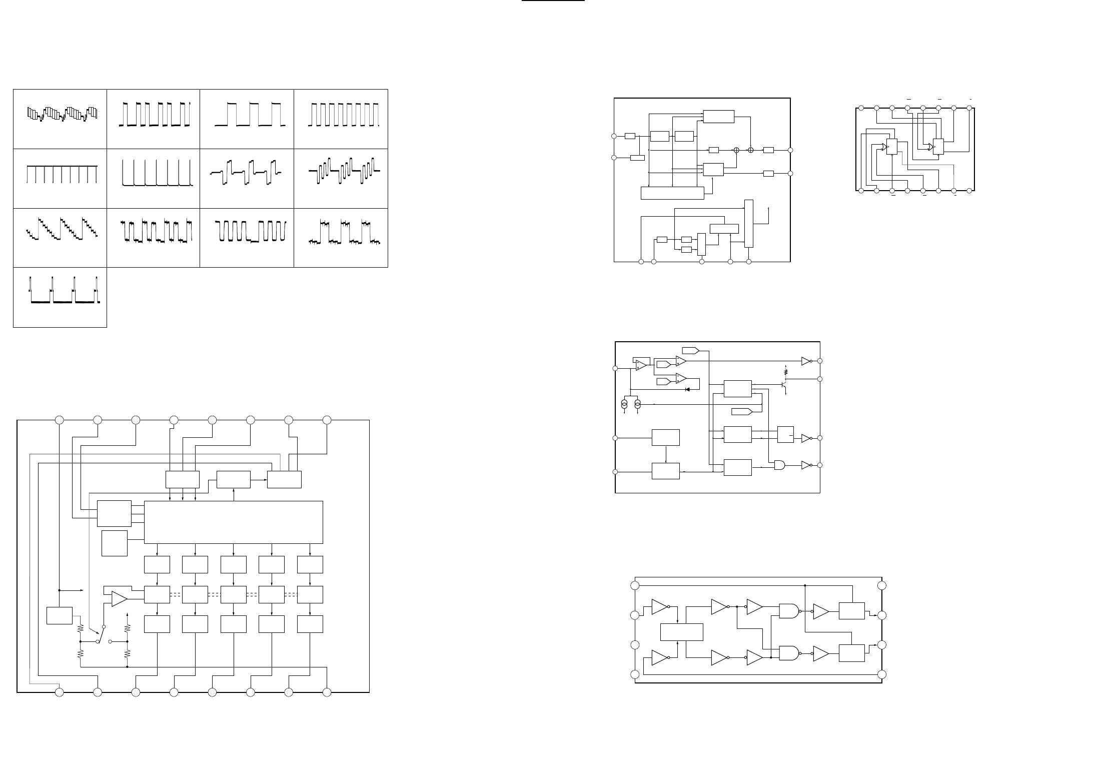
9-19 9-19
A B C D E F GH
1
2
3
4
5
VPL-PX20/PX30
BA Board Waveforms
1234
5678
9 0 !- !=
![
1.0 Vp-p
TP100 [VIDEO]
0.7 Vp-p
TP106 [R-Y/R]
0.7 Vp-p
TP107 [Y/G]
0.7 Vp-p
TP112 [B-Y/B]
5.0 Vp-p
TP115 [H.SYNC]
3.8 Vp-p
TP116 [V.SYNC]
0.7 Vp-p
TP103 [R-Y]
0.7 Vp-p
TP104 [B-Y]
0.6 Vp-p
TP105 [Y]
0.6 Vp-p
TP108 [R|OUT]
0.6 Vp-p
TP110 [B|OUT]
0.6 Vp-p
TP109 [G|OUT]
3.8 Vp-p
TP113 [SCP|IN]
16 15 14 13 12 11 10 9
1 2 3 4 5 6 7 8
1-C 1-CR 1-RD 1-CK 1-CK 1-Q 1-Q GND
VDD 2-C 2-CR 2-RD 2-CK 2-CR 2-Q 2-Q
MC74HC4538AFEL (IC257)
VIDEO
INPUT
VCC
BACK PORCH
DETECTOR
2
COMPOSITE
SYNC OUTPUT
1
BACK PORCH
OUTPUT
5
VERTICAL SYNC
OUTPUT
3
HORIZONTAL
OUTPUT
7
8
RESET 6
VOLTAGE
REGULATOR
TIMING
CURRENTS
D
NO SYNC
V1
V2
C SYNC
Q
Q
CLK
VERTICAL
DETECTOR
GS4981 (IC256)
LATCH
DAC
AMP
LATCH
DAC
AMP
LATCH
DAC
AMP
LATCH
DAC
AMP
LATCH
DAC
AMP
+
—
VCC
REG
I2C DECODER
LEVEL
CONVERTER
LEVEL
CONVERTER LEVEL
CONVERTER
LATCH
POWER
ON
RESET
OPEN COLLECTOR
3 6
25 81 4 7
SW1
SW0
DAC4
DAC3
DAC2
DAC1
DAC0
GND
14 11
15 12 916 13 10
VCC
SCL
SDA
SAD2
SAD1
SAD0
SW3
SW2
CXA1875AM-T4 (IC250)
2
1
9
42
CPO VCV PLSL FIN CKSL
44 39 37 38
ADIN
AYO
7 ACO
CLPO
A/D
VCO 1/4
1/2
DL D/A
D/A
NTSC:1H
PAL :2H NTSC:1H
PAL :2H
CLAMP
+
-
+
-
SW
SW
4fsc
VERTICAL
BORDER EMPHA
ADAPTIVE
FILTER OP
LOGICAL OPERATION
PHASE
COMPARATOR
CXD2064Q-T6 (IC221)
1
2
3
4 5
6
7
8
COMMON
INH
VEE CH1
A
CH0
VDD
VSS
LOGIC LEVEL
CONVERTOR
OUT IN
C
OUT IN
C
TC4W53F (TE12R) (IC251, 103)
BA BA
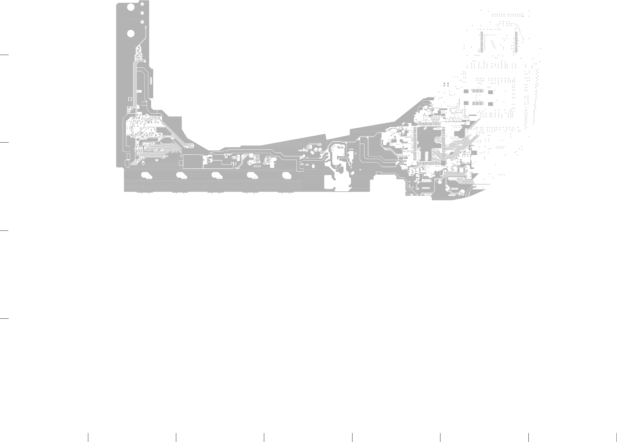
9-20 9-20
A B C D E F GH
1
2
3
4
5
VPL-PX20/PX30
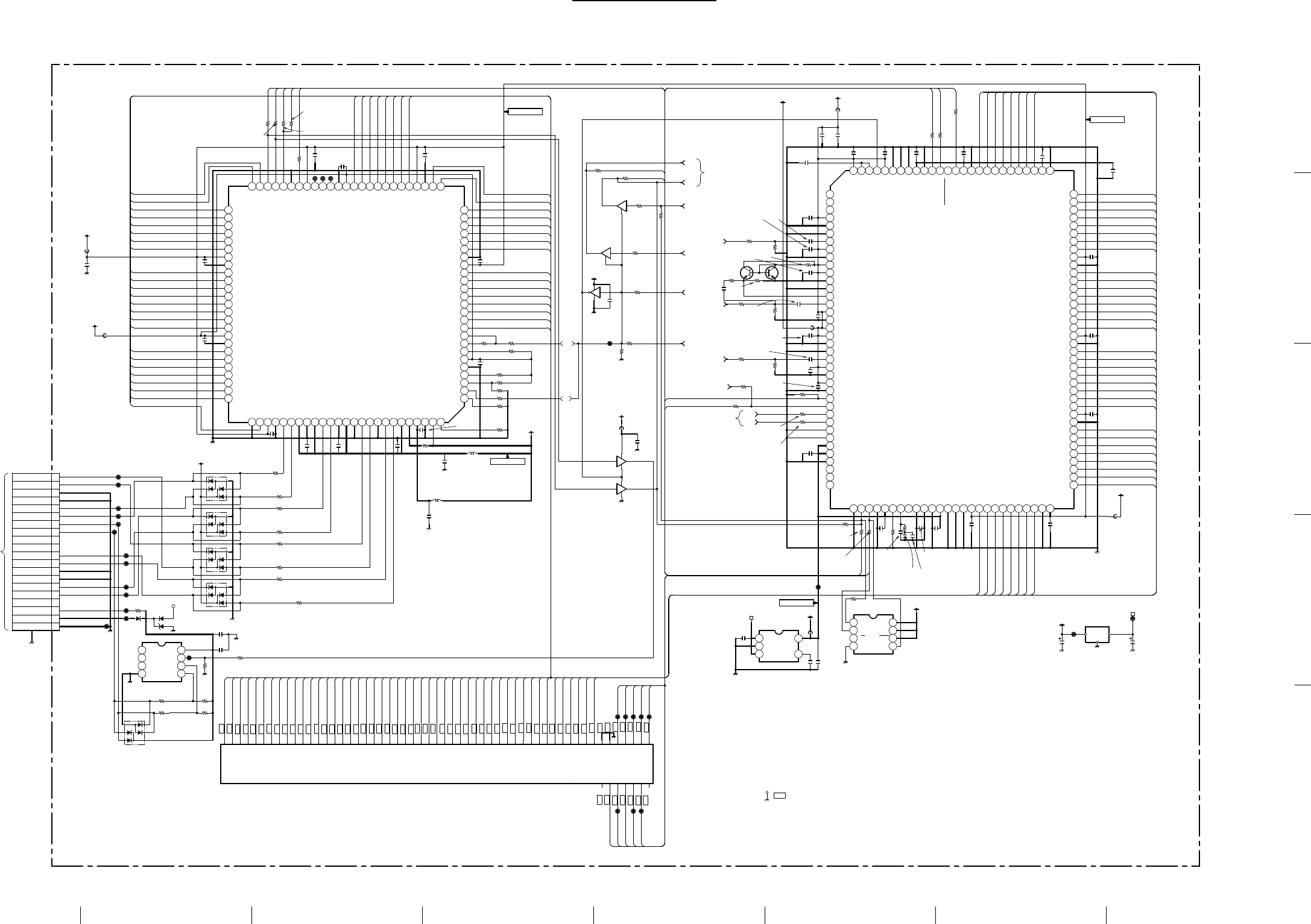
9-21 9-21
A B C D E F GH
1
2
3
4
5
VPL-PX20/PX30
BB (1/4) BB (1/4)
• Refer to page 9-20 for Printed Wiring Board
D+3.3V-2
D+3.3V-2
D+3.3V-2
D+3.3V-2
1 2 3 4 5 6 7 8 9 10 11 12 13 14 15 16 17 18 19 20 21 22 23 24 25 26 27 28 29 30
103
104
105
106
107
108
109
110
111
112
113
114
115
116
117
118
119
120
31 32
121
122
123
124
125
126
127
128
33 34 35 36 37 38
39
40
41
42
43
44
45
46
47
48
49
50
51
52
53
54
55
56
57
58
59
60
61
62
63
64
6566676869707172737475767778798081828384858687888990919293949596979899
100101102
1 2 3 4 5 6 7 8 9 10 11 12 13 14 15 16 17 18 19 20 21 22 23 24 25
26
27
28
29
30
31
32
33
34
35
36
37
38
39
40
41
42
43
44
45
46
47
48
49
50
51525354555657585960616263646566676869707172737475
76
77
78
79
80
81
82
83
84
85
86
87
88
89
90
91
92
93
94
95
96
97
98
99
100
IO G
123
4 5
1234
5 6 7 8
1
2
3
4
5
6
7
8
9
10
11
12
13
14
15
16
17
18
19
20
1234
5 6 7 8
FB300
C301
FB301
CN300
C303
D300
D301
D302
D303
R309
R310
C306
C307
JL300
JL301
JL302
C309 C310
C313
C316
C317
C318
R322
FB304
R327
R328
R329
R330
C322
C324
C325
FB307
C326
C328
C330
C331
C332
C333
FB308
C334 C335
C336
C337
R339
C338
C340
C342
R343
C344
C345
C346
C351
R331
R332
R333
R387
R392
R393
R386
R338
R341 R342
TP303
R413 R414
C343
C368
D315
R426
R427
C405
R428
R429
JL311
JL312
JL313
R430
JL314
JL315
JL316
JL317
JL318
JL327
JL328
JL329
C339 C408
R340
R431
R432
R433
R434
FB302
C319
R437
R441
R442
C421
C341
C422
FB310
C409
C321
C327
C352
C311
C406
D317
R326
R443
R314
D318
JL308
JL364
JL365
JL366
JL367
D316
R313
IC316
C356
C370
JL447
JL448
JL453
JL458
JL457 JL452
JL459
JL456
JL455
JL454
C308
R452
IC319
C348
C347
C349
FB311
R453
IC313
IC311
R335
R334
R316
C329
C323
IC302(3/4)
IC302(2/4)
IC302(1/4)
IC302(4/4)
Q302
Q303
IC305(3/3)
R323
R311
C305
R300
R301
R302
R303
R304
R305
R306
R307
C304
IC304
IC300
R315
R324
R325
R320
R319
R317
R312
FB303
R444
IC303(1/5)
C314
10k
1/16W
:CHIP
0.1
16V
B:CHIP
HN1D03FU
HN1D03FU
HN1D03FU
HN1D03FU
2.2
16V
F:CHIP
0.01
25V
B:CHIP
2.2
16V
F:CHIP
2.2
16V
F:CHIP
2.2
16V
F:CHIP
0.01
25V
B:CHIP
0.01
25V
B:CHIP
0.01
25V
B:CHIP
22
1/16W
:CHIP
20P
10k
1/16W
:CHIP
47
1/16W
:CHIP
47
1/16W
:CHIP
#
22
1/16W
:CHIP
75
1/16W
:CHIP
75
1/16W
:CHIP
75
1/16W
:CHIP
100
1/16W
:CHIP
0.1
16V
B:CHIP
0.1
16V
B:CHIP
0.1
16V
B:CHIP
0.1
16V
B:CHIP
0.1
16V
B:CHIP
0.1
16V
B:CHIP
0.1
16V
B:CHIP
0.1
16V
B:CHIP
0.1
16V
B:CHIP
0.1
16V
B:CHIP
47
1/16W
:CHIP
47
1/16W
:CHIP
0.01
25V
B:CHIP
0.01
25V
B:CHIP
0.01
25V
B:CHIP
0.01
25V
B:CHIP
0.01
25V
B:CHIP
0.01
25V
B:CHIP
0.01
25V
B:CHIP
0.01
25V
B:CHIP
0.01
25V
B:CHIP
0.01
25V
B:CHIP
0
1/16W
:CHIP
0
1/16W
:CHIP
0
1/16W
:CHIP
0
1/16W
:CHIP
0
1/16W
:CHIP
0.01
25V
B:CHIP
0.1
16V
B:CHIP
47
6.3V
:AL-CP
0.1
16V
B:CHIP
HNID03FU
100
1/16W
:CHIP
100
1/16W
:CHIP
10k
1/16W
:CHIP
10k
1/16W
:CHIP
47
1/16W
:CHIP
#
22
1/16W
:CHIP
22
1/16W
:CHIP
330k
1/16W
:CHIP
100k
1/16W
:CHIP
0.1
16V
B:CHIP
2.2
16V
F:CHIP
0.01
25V
B:CHIP
22
10V
F:CHIP
0.047
16V
B:CHIP
0.047
16V
B:CHIP
0.047
16V
B:CHIP
0.01
25V
B:CHIP
#
47
1/16W
:CHIP
2.2
16V
F:CHIP
#
RD5.6SB2
BKM1608TS601
BKM1608TS601
BKM1608TS601
BKM1608TS601
BKM1608TS601
BKM1608TS601
#
MA111
24LC21AT
EDID
#
#
#
#
#
#
#
#
#
#
#
#
#
#
#
#
#
#
#
10k
1/16W
:CHIP
47
1/16W
:CHIP
47
1/16W
:CHIP
47
1/16W
:CHIP
47
1/16W
:CHIP
0.01
25V
B:CHIP
0.1
16V
B:CHIP
0.1
16V
B:CHIP
1.5k
1/16W
:RN-CP
#
#
0.1
16V
B:CHIP
100
16V
:AL-CP
#
#
#
#
##
#
#
#
#
0.01
25V
B:CHIP
#
100
1/16W
:CHIP
0.1
16V
B:CHIP
0.01
25V
B:CHIP
0.01
25V
B:CHIP
BKM1608TS601
#
LP2985IM5X-3.5
3.5V REG
BA033FP-E2
3.3V REG
22
1/16W
:CHIP
22
1/16W
:CHIP
#
0.1
16V
B:CHIP
0.047
16V
B:CHIP
TC74LCX125FT
SYNC SW
TC74LCX125FT
SYNC SW
TC74LCX125FT
SYNC SW
TC74LCX125FT
SYNC SW
2SC2712
SOG CLAMP
2SC2712
SOG CLAMP
TC7WH04FU
INVERTER
0 1/16W :CHIP
470
1/16W
:CHIP
0.01
25V
B:CHIP
0 1/16W :CHIP
0 1/16W :CHIP
0 1/16W :CHIP
0 1/16W :CHIP
0 1/16W :CHIP
0 1/16W :CHIP
0 1/16W :CHIP
0 1/16W :CHIP
0.01 25V B:CHIP
AD9884AKS-140
A/D CONVERTER
SII151
TMDS RECEIVER
#
#
SHORT
SHORT
#
#
#
#
#
PW264P
SCAN CONVERTER
10V
F:CHIP
PDO
PD
R
G
B
SDA
SCL
A 3.3V
H
V
PANEL LINK
CLP
D3.3V-2
D 3.3V-2
D3.3V-2
D3.3V-2
A 3.3V
V1
H1
D 3.3V-2
A
6V
3.3V
6V A 3.3V
GHDREN
SUB 5V-3
D 3.3V-2
D 3.3V-2
D 3.3V-2
158
152
159
144
151
160
157
208
214
213
215
216
223
222
221
133
128
135
181
182
183
184
189
51
26
102
109
77
52
78
110
190
191
192
197
198
199
200
207
117
103
104
118
111
112
119
120
99
48
74
23
49
100
75
24
167
136
143
141
142
166
168
12 11
14
13
98
7
10
23
1
56
4
17
4
8
GRE4
GRE5
GRE6
GRE7
GGE2
GGE3
GGE4
GGE5
GGE6
GGE7
GGO4
GGO5
GGO6
GGO7
GBO2
GBO3
GBO4
GBO5
GBO6
GBO7
GBE1
GBE2
GBE3
GBE4
GBE5
GBE6
GBE7
GGE0
GGE1
GGE2
GGE3
GGE4
GGE5
GRE0
GRE1
GRE2
GRE3
GRE4
GRE5
GRE6
GRE7
GRE0
GRE1
GRE2
GRE3
GRE4
GRE5
GRE6
GRE7
GRO0
GRO1
GRO2
GRO3
GRO4
GRO5
GRO6
GRO7
GGE6
GGE7
GVS
GCLK
GFBK
GSOG
GBLKSPL
GHSFOUT
GHSFOUT
GCOAST
GBLKSPL
GREF
GFBK
GCOAST
GREF
GCLK
GBE0
GCLK
GSOG
GGE0
GGE1
GGE2
GGE3
GGE4
GGE5
GGE6
GGE7
GGO0
GGO1
GGO2
GGO3
GGO4
GGO5
GGO6
GGO7
GBE0
GBE1
GBE2
GBE3
GBE4
GBE5
GBE6
GBE7
GBO0
GBO1
GBO2
GBO3
GBO4
GBO5
GBO6
GBO7
GGE0
GGE1
GRE0
GRE1
GRE2
GRO6
GGO3
GGO2
GRO7
GRO5
GRO4
GRO2
GRO3
GBE0
GBE1
GBE2
GBE3
GBE4
GBE5
GBE6
GBE7
GFBK
GPEN
GPEN
GRE3
GGO1
GRO1
GHS
GVS
GBO1
GHS
GVS
GSOG
GBO0
GGO0
GRO0
GRO7
GBO0
GBO1
GBO2
GBO3
GBO4
GBO5
GBO6
GBO7
GGO0
GGO1
GGO2
GGO3
GGO4
GGO5
GGO6
GGO7
GRO0
GRO1
GRO2
GRO3
GRO4
GRO5
GRO6
NC
NC
NC
NC
VD
GND
GND
VD
GND
VD
VD
GND
GND
VD
GND
VD
VD
GND
GND
VD
GND
VD
GND
CKINV
CLAMP
SDA
SCL
A0
A1
PVD
PVD
GND
NC
NC
VDD
GND
DBB0
DBB1
DBB2
DBB3
DBB4
DBB5
DBB6
DBB7
VDD
GND
GND
GND
PVD
GND
PVD
GND
NC
FILT
CKEXT
PVD
GND
COAST
HSYNC
GND
DRB0
DRB1
DRB2
DRB3
DRB4
DRB5
DRB6
DRB7
VDD
GND
DGA0
DGA1
DGA2
DGA3
DGA4
DGA5
DGA6
DGA7
VDD
GND
DGB0
DGB1
DGB2
DGB3
DGB4
DGB5
DGB6
DGB7
VDD
GND
DBA0
DBA1
DBA2
DBA3
DBA4
DBA5
DBA6
DBA7
VD
REFIN
REFOUT
PWRDNB
VD
GND
GND
GND
VDD
GND
HSOUT
DATACK
VDD
GND
DRA0
DRA1
DRA2
DRA3
DRA4
DRA5
DRA6
DRA7
VDD
GND
R IN
G IN
B IN
Q26
Q27
Q28
Q29
Q30
Q31
0VCC
0GND
Q32
Q33
Q34
Q35
Q36
Q37
Q38
Q39
GND
Q40
Q41
Q42
Q43
Q44
Q45
Q46
Q13
Q12
Q11
Q10
Q9
Q8
0GND
0VCC
Q7
Q6
Q5
Q4
Q3
Q2
Q1
Q0
PD0
SCDT
STAG OUT
GND
PIXS
ST
PD
DF0
0GND
Q47
0VCC
RX2+
RX2-
AVCC
AGND
AVCC
RX1+
RX1-
AGND
AVCC
AGND
RX0+
RX0-
AGND
RXC+
RXC-
AVCC
EXT RES
PVCC
PGND
RSVD
OCK INV
AGND
Q25
Q24
HSYNC
VSYNC
DE
0GND
0DCK
0VCC
CTL3
CTL2
CTL1
GND
Q23
Q22
Q21
Q20
Q19
Q18
Q17
Q16
0VCC
0GND
Q15
Q14
TX1+
TX1-
TXC+
TXC-
GND
TX2+
TX2-
TX0+
TX0-
SHLD1
SHLDC
+5V
RESERVED
RESERVED
SHLD2
SHLD0
RESERVED
HPD
DDC_DAT
DDC_CLK
VCC
VCC
VCC
DATACK/
SOGOUT
GND
GRE0
GRE1
GRE2
GRE3
GRE4
GRE5
GRE6
GRE7
GGE0
GGE1
GGE2
GGE3
GGE4
GGE5
GGE6
GGE7
GBE0
GBE1
GBE2
GBE3
GBE4
GBE5
GBE6
GBE7
GRO0
GRO1
GRO2
GRO3
GRO4
GRO5
GRO6
GRO7
GGO0
GGO1
GGO2
GGO3
GGO4
GGO5
GGO6
GGO7
GBO0
GBO1
GBO2
GBO3
GBO4
GBO5
GBO6
GBO7
NC1
NC2
NC3
GND
VCC
VCLK
SCL
SDA
GFBK
GREF
GCOAST
GCLK
GVS
GHS
GBLKSPL
NC(GPEN)
GPENSOG(SOG)
NC(GFIELD)
NC(PLLCLK)
NC(GCLKOUT)
NC(GHSFOUT)
NC(GADCCLK)
A24
C23
D22
B23
A23
C22
B22
D21
F26
F25
E26
E25
F24
D26
D25
F23
U25
T26
T25
T24
T23
R26
R25
R24
E24
C26
B26
C25
E23
D24
A26
B25
R23
P26
P25
P24
P23
H25
G26
H23
W23
W24
W25
V26
V25
V23
V24
U26
L23
L26
K25
J26
L25
K26
L24
M26
M24
J24
J23
J25
H26
M25
SOGIN
VIN
GND
ON/OFF
VOUT
BYPASS
D
GND
Q
PR
VCC
Q
CLR
CK
(P3)
(P4)
(P4)
(P4)
(P4)
(P4)
(P2)
(P4)
(P4)
(P2)
B-SS1696<08.>-BB.-P1
BB(1/4)
(SCAN CONVERTER)
NC
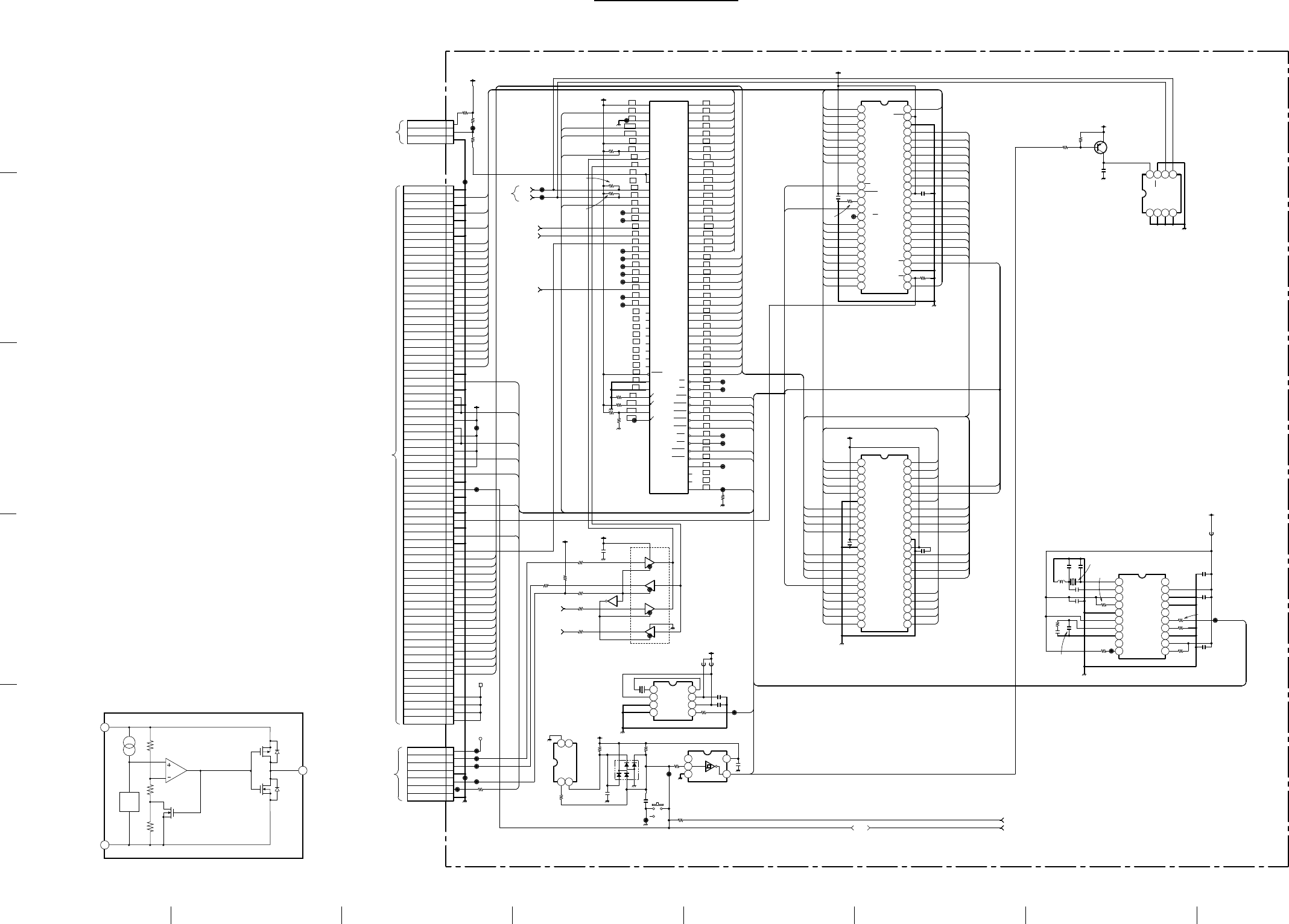
9-22 9-22
A B C D E F GH
1
2
3
4
5
VPL-PX20/PX30
• Refer to page 9-20 for Printed Wiring Board
12345678910
11 12 13 14 15 16 17 18 19 20
A1
A2
A3
A4
A5
A6
A7
A8
A9
A10
A11
A12
A13
A14
A15
A16
A17
A18
A19
A20
A21
A22
A23
A24
A25
A26
A27
A28
A29
A30
A31
A32
A33
A34
B1
B2
B3
B4
B5
B6
B7
B8
B9
B10
B11
B12
B13
B14
B15
B16
B17
B18
B19
B20
B21
B22
B23
B24
B25
B26
B27
B28
B29
B30
B31
B32
B33
B34
A35
B35
1 2
34
1
2
3
4
5
6
7
1
2
3
12345678910111213141516171819202122
23 24 25 26 27 28 29 30 31 32 33 34 35 36 37 38 39 40 41 42 43 44
1234
5678
1234
5678
123456789101112131415161718192021222324
25 26 27 28 29 30 31 32 33 34 35 36 37 38 39 40 41 42 43 44 45 46 47 48
123
4 5
R354
R355
R356
R357
R358
JL303
JL304
JL305
JL306
JL307
JL309
JL310
JL319
JL320
JL321
JL322
JL323
JL324
R359
JL325
FB313 FB314
R360
C357
C358
C359
C360
C362
C365
C366
FB315
C367
JL326
CN301
JL360
JL361
C354
C355
R349
R350
R347
R346
R344
C404
IC308
JL372
JL371
R412
R398
R410
R421
CN302
CN312
R424
JL401
C302 C350
R425
C353
C373
JL330
JL331
JL332
JL333
JL334
JL335
L300
JL370
R353
R439
D314
JL374
R399
R308
JL368 JL375
JL376
JL377
JL378
JL379
JL380
C412
C413
R411
C363
S301
R448
R449
X300
IC310
R447
R365
Q301
C361
R362
X301
IC314
IC315
IC305(2/3)
R348
IC307(1/4)
IC307(4/4)
IC307(3/4)
IC307(2/4)
R438
IC306
IC317
C364
R366
R361
IC309
IC303(2/5)
R423
R422
27p
CH:CHIP 27p
CH:CHIP
0.47
16V
B:CHIP
0.01
25V
B:CHIP
1k
1/16W
:CHIP
3.3k
1/16W
:CHIP
3.3k
1/16W
:CHIP
10k
1/16W
:CHIP
10k
1/16W
:CHIP
10k
1/16W
:CHIP
10k
1/16W
:CHIP
100
1/16W
:CHIP
100
1/16W
:CHIP
100
1/16W
:CHIP
100
1/16W
:CHIP
10k
1/16W
:CHIP
0.1
16V
B:CHIP 0.1
16V
B:CHIP
0.1
16V
B:CHIP
70P
0.033
16V
B:CHIP
0.1
16V
B:CHIP
0.1
16V
B:CHIP
0.1
16V
B:CHIP
10k
1/16W
:CHIP
100
1/16W
:CHIP
#
2.2k
1/16W
:CHIP
0.47µH
0.1
16V
B:CHIP
0.1
16V
B:CHIP
0.1
16V
B:CHIP
0.1
16V
B:CHIP
3P
:SMD
100
1/16W
:CHIP
1k
1/16W
:CHIP
10k
1/16W
:CHIP
7P
:SMD
HNID03FU
100
1/16W
:CHIP
22
1/16W
:CHIP
BKM1608TS601 BKM1608TS601
BKM1608TS601
#
0.1
16V
B:CHIP
0.1
16V
B:CHIP
#
#
#
#
#
#
#
#
#
#
#
#
#
#
#
#
#
#
#
#
#
#
#
#
#
#
#
#
#
#
#
#
#
#
#
22k
1/16W
:CHIP
1
6.3V
B:CHIP
#
#
#
E2PROM
18MHz
#
#
ST49C101ACF8-05-
TR
2SA1611T1-M5M6
POWER SW
0.001
25V
CH:CHIP
0
1/16W
:CHIP
34.0MHz
MBM29LV400TC-90P
FTN-
4M FLASH ROM
IDT71V016S15PH
IM SRAM
TC7WH04FU
INVERTER
100
1/16W
:CHIP
TC74LCX125FT
COM SW
TC74LCX125FT
COM SW
TC74LCX125FT
COM SW
TC74LCX125FT
COM SW
22 1/16W :CHIP
S80828ANNP-EDR
RESET
TC7SH14FU-TE85R
SCHMITT INVERTER
#
#
#
IMISM530AYB-D
SPECTRUM SPREAD
PW264P
SCAN CONVERTER
#
#
RESET
≠≠≠≠≠≠≠≠≠
SDA
SCL
RESET≠≠≠≠≠≠≠≠≠
D 3.3V-2
D3.3V-2
D 3.3V-2
D 3.3V-2
D 3.3V-2
D 3.3V-2
TXD
RXD
D3.3V-2
D 3.3V-2
SC3 RESET
D 3.3V-3
D 3.3V-3
GHDREN
6V
SUB 5V-3
D 3.3V-3
PIC MUTE
INTERLACE
23
14
1
56
4
12 11
13
98
7
10
114
105
226
315
341
115
116
79
80
107
106
53
54
27
28
83
29
2
3
57
84
30
4
58
31
5
32
6
86
60
33
7
34
87
61
8
35
81
108
304
253
328
202
209
210
217
211
212
219
220
233
242
235
249
243
275
301
276
244
251
327
302
131
130
140
139
145
146
153
154
155
156
163
164
169
170
171
172
195
196
201
186
185
178
177
187
188
193
194
122
121
129
113
62
A0
A1
A2
A3
A4
A5
A6
A7
A8
A9
A10
A11
A12
A13
A14
A15
A16
A17
A18
A19
D2
D3
D4
D5
D6
D7
D8
D9
D10
D11
D12
D13
D14
D15
D1
BHENN
ROMOEN
ROMWEN
RAMOEN
RAMWEN
RESET
MCKEXT
DCKEXT
BOOTWE
MCKEXT
D0
WDTEN
A19
A0
A1
A2
A3
A4
A5
A6
A7
A8
A9
A10
A11
A12
A13
A14
A15
A16
A17
A18
D0
D1
D2
D3
D4
D5
D6
D7
D8
D9
D10
D11
D12
D13
D14
D15
BHENN
ROMOEN
ROMWEN
CS2
CS3
BOOTWE
CS2
CS3
A2
A3
A4
A5
A6
A7
A8
A9
A10
A11
A12
A13
A14
A15
A16 A17
A18
D0
D1
D2
D3
D4
D5
D6
D7
D8
D9
D10
D11
D12
D13
D14
D15
A0
A1
A2
A3
A4
A5
A6
A7
A8
A9 A10
A11
A12
A13
A14
A15
A16
A16 A17
D0
D1
D2
D3
D4
D5
D6
D7 D8
D9
D10
D11
D12
D13
D14
D15
A1
ROMWEN
RAMOEN
BHENN
ROMOEN
DCKEXT
RAMWEN
NMI
NMI
RESET
WDTEN
BOOTWE
A19
SCL
SDA
NCVSS
OUT VDD
RESET
MCKEXT
DCKEXT
RXD
TXD
IRRCVR0
IRRCVR1
PORTA0
PORTA1
PORTA2
PORTA3
PORTA4
PORTA5
PORTA6
PORTA7
PORTB0
PORTB1
PORTB2
PORTB3
PORTB4
PORTB5
PORTB6
PORTB7
DTMB
DTCLK
A0
A1
A2
A3
A4
A5
A6
A7
A8
A9
A10
A11
A12
A13
A14
A15
A16
A17
A18
A19
D0
D1
D2
D3
D4
D5
D6
D7
D8
D9
D10
D11
D12
D13
D14
D15
RD
WR
BHEN
ROMOE
ROMWE
RAMWE
RAMOE
CS0
CS1
NMI
GND
A19
GND
A18
GND
A17
GND
A16
A15
A14
A13
A12
A11
A10
A9
A8
A7
A6
A5
A4
A3
A2
A1
A0
GND
BHENN
GND
ROMOEN
GND
ROMOEN
3.3V
ROMWEN
3.3V
ROMWEN
3.3V
CS2
3.3V
CS3
GND
FCEN
GND
BOOTWE
GND
VPPEN
D15
D14
D13
D12
D11
D10
D9
D8
D7
D6
D5
D4
D3
D2
D1
D0
NC
NC
VCC
RXD
TXD
GND
EXTSW
WDTEN
GND
VCC
IRRCVR
GND
A0
A1
A2
A3
A4
CS
I/O1
I/O2
I/03
I/O4
VCC
VSS
I/O5
I/O6
I/O7
I/O8
WE
A5
A6
A7
A8
NC
A15
A14
A13
OE
UB
LB
I/O16
I/O15
I/O14
I/O13
VSS
VCC
I/O12
I/O11
I/O10
I/O9
NC
A12
A11
A10
A9
NC
A15
A14
A13
A12
A11
A10
A9
A8
NC
NC
NC
A17
A7
A6
A5
A4
A3
A2
A1
A16
VSS
DQ15/A-1
DQ7
DQ14
DQ6
DQ13
DQ5
DQ12
DQ4
VCC
DQ11
DQ3
DQ10
DQ2
DQ9
DQ1
DQ8
DQ0
VSS
AQ
BYTE
WE
RESET
NC
NC
RY/BY
OE
CE
NC(CPUEN)
NC(CLKIN)
NC(UCSRC)
NC(WDTEN)
NC(PORTC1)
NC(PORTC0)
NC(PORTC2)
NC(PORTC3)
NC(PORTC4)
NC(PORTC5)
NC(PORTC6)
NC(PORTC7)
NC(SCANEN)
NC(SCANMOD)
NC(PTSTIN0)
PTSTEN
(PTSTIN1)
NC(PTSTOUT)
NC
NC
(CS2)
(CS3)
NC(EXTINT1)
EXTINT0
NC(EXTINT2)
F2
E1
Y2
AE15
AF15
F3
F4
D1
D2
E3
E2
C1
C2
B1
B2
D5
B3
A2
A3
C5
D6
B4
A4
C6
B5
A5
B6
A6
D8
C8
B7
A7
B8
D9
C9
A8
B9
D3
E4
AE4
AC5
AF2
U2
V1
V2
W1
V3
V4
W3
W4
AA1
AB2
AA3
AC1
AB3
AD1
AD2
AB4
AC3
AF1
H3
H2
J4
J3
K1
K2
L1
L2
L3
L4
M3
M4
N1
N2
N3
N4
T3
T4
U1
R2
R1
P2
P1
R3
R4
T1
T2
G2
G1
H1
F1
GND
RESETN
GND
NMI
6V
6V
6V
6V
VCC
WC
E0
E1
E2
VSS
AE1
AE2
(SCAN CONVERTER)
B-SS1696<08.>-BB.-P2
BB(2/4)
OSCIN
OSCOUT
AVDD
D-C
STOP
LF
AVSS
S1
SSON
REFOUR
OVDD
OVSS
R0
R1
FOUT
S2
DVSS
DVDD
S3
S0
(P1)
(P4)
(P4)
(P1)
DIGITAL
RGB
TERMINAL
(P4)
(P4)
(MICRO PROCESSOR)
NC
X1
OE
A.GND
D.GND
X2
A.VCC
D.VCC
CLK
NC
BB (2/4) BB (2/4)
VOO 2
VSS 4
OUT
1
VREF
S-80828ANNP-ED4-T2 (IC306)
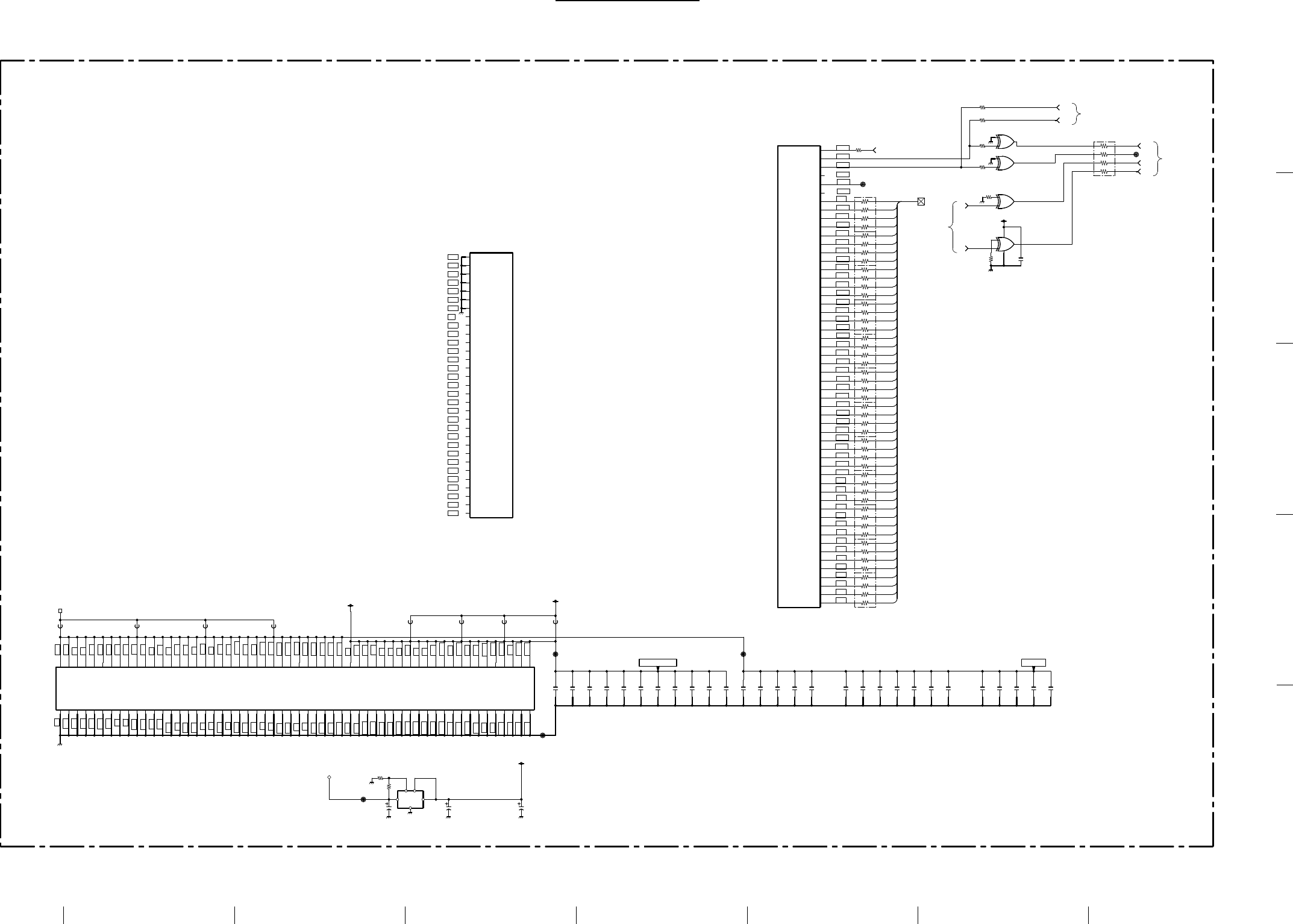
9-23 9-23
A B C D E F GH
1
2
3
4
5
VPL-PX20/PX30
• Refer to page 9-20 for Printed Wiring Board
+2.5VD+3.3V-2
GI
O
ON/OFFADJ
C374 C375 C376 C377 C378
C379 C380 C381 C382 C383 C385 C386
C387 C388 C389
R371
R372
RB324
RB325
RB326
RB327
RB328
RB329
RB330
RB331
RB332
RB333
RB334
RB335
C391 C392 C393 C395 C396 C397 C399 C400 C401 C402 C403
JL358
R373
FB316 FB317 FB318 FB319 FB320 FB321 FB322 FB323
R394
R395
C369
R396
R397
C371
C320
R435
R436
RB301
C384 C394
JL381 JL382
JL383
JL384
JL417
IC301(4/4)
IC301(2/4)
IC301(1/4)
IC301(3/4)
IC303(3/5)
IC303(5/5)
IC303(4/5)
IC312
C372
47
1/16W
:CHIP 1k
1/16W
:CHIP
1k
1/16W
:CHIP
0.1
16V
B:CHIP
0.1
16V
B:CHIP
0.1
16V
B:CHIP
0.1
16V
B:CHIP
0.1
16V
B:CHIP
0.1
16V
B:CHIP
0.1
16V
B:CHIP
0.1
16V
B:CHIP 0.1
16V
B:CHIP 0.1
16V
B:CHIP
0.1
16V
B:CHIP
0.1
16V
B:CHIP
0.1
16V
B:CHIP
0.1
16V
B:CHIP
0.1
16V
B:CHIP 0.1
16V
B:CHIP
0.1
16V
B:CHIP
0.1
16V
B:CHIP
0.1
16V
B:CHIP
0.1
16V
B:CHIP
0.1
16V
B:CHIP
0.1
16V
B:CHIP
0.1
16V
B:CHIP
0.1
16V
B:CHIP
0.1
16V
B:CHIP
0.1
16V
B:CHIP
1k
1/16W
:CHIP
1k
1/16W
:CHIP
0.01
25V
B:CHIP
47
6.3V
:AL-CP
47
6.3V
:AL-CP
10k
1/16W
:CHIP
10k
1/16W
:CHIP
47
47
47
47
47
47
47
47
47
47
47
47
47
22
10V
F:CHIP
22
10V
F:CHIP
BKM1608TS601 BKM1608TS601 BKM1608TS601 BKM1608TS601 BKM1608TS601 BKM1608TS601 BKM1608TS601 BKM1608TS601
#
##
#
#
#
47
1/16W
:CHIP
47
1/16W
:CHIP
TC74VHC86FT
SYNC BUF
TC74VHC86FT
SYNC BUF
TC74VHC86FT
SYNC BUF
TC74VHC86FT
SYNC BUF
PW264P
SCAN CONVERTER
PW264P
SCAN CONVERTER
PW264P
SCAN CONVERTER
PQ20VZ1U
3.3V REG
330
6.3V
:AL-CP
DCLK
DVS
DHS
2.5V
D 3.3V-2
VSO
D
2.5V
3.3V-2
D 3.3V-3
D
HD
VD
3.3V-2
H1
V1
D PORT
287
289
263
343
264
290
231
240
239
248
238
237
274
273
245
272
300
297
270
324
351
350
323
349
295
322
319
318
292
317
339
260
286
312
338
311
337
310
336
283
257
309
282
256
334
333
307
332
306
254
305
279
330
303
42
43
44
21
47
22
73
9
36
10
89
63
37
11
90
64
38
12
39
13
92
66
40
14
93
67
41
15
94
68
16
1
17
18
19
45
46
50
82
85
88
91
95
98
101
124
125
134
138
148
149
162
165
173
175
180
204
205
224
225
228
229
236
241
247
252
255
258
259
261
262
265
266
268
271
296
314
320
325
326
329
331
335
342
346
347
348
20
25
56
59
62
69
70
71
72
96
97
123
126
147
150
176
203
206
227
230
234
267
278
281
284
291
293
294
299
321
340
344
345
352
55
65
76
127
132
137
161
174
179
218
232
246
250
269
277
280
285
288
298
308
313
316
1
23
4
56
14
7
10
98
13
12 11
DRE0
DRE1
DRE2
DRE3
DRE4
DRE5
DRE6
DRE7
DGE1
DGE2
DGE3
DGE4
DGE5
DGE6
DGE7
DBE1
DBE2
DBE3
DRO1
DRO2
DRO3
DBO4
DBO5
DBO6
DBO7
DBE4
DBE5
DBE6
DBE7
DRO4
DRO5
DRO6
DRO7
DGO1
DGO2
DGO3
DGO4
DGO5
DGO6
DGO7
DBO1
DBO2
DBO3
DGE0
DBE0
DRO0
DGO0
DBO0
VCLK
VPEN
VVS
VHS
VFIELD
VG0
VG1
VG2
VG3
VVG4
VG5
VG6
VG7
VB0
VB1
VB3
VB4
VB5
VB6
VB7
VB2
DCLK
DVS
DHS
DRE0
DRE1
DRE2
DRE3
DRE4
DRE5
DRE6
DRE7
DGE3
DGE4
DGE0
DGE1
DGE2
DGE5
DGE6
DGE7
DBE0
DBE1
DBE2
DBE3
DBE4
DBE5
DBE6
DBE7
DGE0
DRO0
DRO1
DRO2
DRO3
DRO5
DRO4
DRO6
DRO7
DGO1
DGO2
DGO3
DGO4
DGO5
DGO7
DGO6
DBO1
DBO0
DBO2
DBO4
DBO3
DBO5
DBO6
DBO7
NC(DENR)
DEN(DENG)
NC(DENB)
VCLKEN
NC(VLAN)
NC(VR0)
NC(VR1)
NC(VR2)
NC(VR3)
NC(VR4)
NC(VR5)
NC(VR6)
NC(VR7)
VDD3
VDD5
VDD6
VDD9
VDD10
VDD13
VDD14
VDD16
VDD17
VDD19
VDD20
VDD23
VDD24
VDD25
VDD28
VDD31
VCC1
VCC3
VCC9
VCC12
VCC14
VCC15
VCC16
VCC17
VCC18
VCC19
GND1 NC(VDD1)
NC(VDD2)
NC(VDD4)
NC(VDD7)
NC(VDD8)
NC(VDD12)
NC(VDD21)
NC(VDD22)
NC(VDD26)
NC(VDD27)
NC(VDD29)
NC(VDD30)
NC(VDD32)
NC(VDD33)
NC(VDD34)
NC(VCC2)
NC(VCC4)
NC(VCC5)
NC(VCC6)
NC(VCC7)
NC(VCC8)
NC(VCC10)
NC(VCC11)
NC(VCC13)
NC(VCC20)
NC(VCC21)
NC(VCC22)
NC(GND2)
GND3
GND8
GND10
GND12
GND13
GND14
GND16
GND19
GND24
GND25
GND26
GND30
GND31
GND34
GND35
GND36
GND37
GND38
GND40
GND43
GND44
GND45
GND46
GND50
GND51
GND56
NC(GND5)
NC(GND6)
NC(GND7)
NC(GND9)
NC(GND17)
NC(GND20)
NC(GND21)
NC(GND22)
NC(GND23)
NC(GND27)
NC(GND28)
NC(GND29)
NC(GND32)
NC(GND33)
NC(GND39)
NC(GND41)
NC(GND42)
NC(GND47)
NC(GND48)
NC(GND49)
NC(GND52)
NC(GND53)
NC(GND54)
NC(GND55)
NC(VDD18)
NC(GND18)
NC(VDD11)
NC(GND11)
NC(VDD15)
NC(GND15)
SOANMOD(GND4)
B16
B17
B18
A21
B21
A22
C21
A9
B10
A10
D11
C11
B11
A11
D12
C12
B12
A12
B13
A13
D14
C14
B14
A14
D15
C15
B15
A15
D16
C16
A16
AD13
AD15
AC15
AF17
AC16
AD16
Y25
AA26
AA25
AB26
AA24
AA23
AC26
AC25
AB23
AC24
AD26
AD23
AC22
AF25
AF24
AE23
AF23
AD21
AE22
AE19
AE18
AD18
AE17
AF13
AC12
AD12
AE12
AF12
AE11
AF11
AE10
AF10
AD9
AC9
AE9
AD8
AC8
AF8
AF7
AE7
AF6
AE6
AC6
AE5
AD5
AF4
AE3
A1
A17
A18
A19
B19
B20
B24
D4
D7
D10
D13
D17
D20
D23
G4
G23
H24
J2
K4
K23
M2
M23
N23
N25
P4
U4
U23
W26
Y1
Y4
Y23
AA4
AB1
AB25
AC4
AC7
AC10
AC13
AC14
AC17
AC18
AC20
AC23
AD22
AC11
AE14
AE20
AE25
AE26
AF3
AF5
AF9
AF16
AF20
AF21
AF22
A20
A25
C4
C7
C10
C17
C18
C19
C20
D18
D19
G3
G24
K3
K24
N26
U3
U24
Y3
Y24
AA2
AC19
AD4
AD7
AD10
AD17
AD19
AD20
AD25
AE21
AF14
AF15
AF19
AF26
C3
C13
C24
G25
H4
J1
M1
N24
P3
W2
Y26
AB24
AC2
AC21
AD3
AD6
AD11
AD14
AD24
AE8
AE13
AE16
AE24
(SCAN CONVERTER)
BB(3/4)
B-SS1696<08.>-BB.-P3
(P1)
(P4)
(DISPLAY PORT)
(P4)
(P4)
(VIDEO PORT)
BB (3/4) BB (3/4)
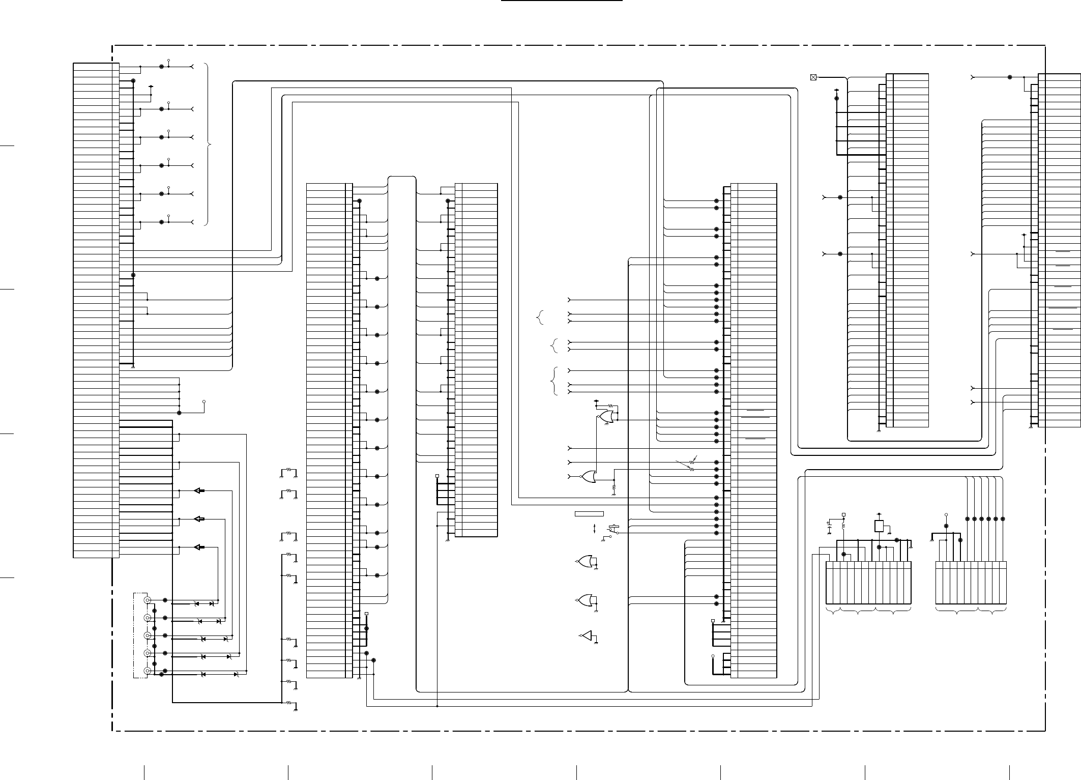
9-24 9-24
A B C D E F GH
1
2
3
4
5
VPL-PX20/PX30
• Refer to page 9-20 for Printed Wiring Board
B
G
R
A1
A2
A3
A4
A5
A6
A7
A8
A9
A10
A11
A12
A13
A14
A15
A16
A17
A18
A19
A20
A21
A22
A23
A24
A25
A26
A27
A28
A29
A30
A31
A32
A33
A34
B1
B2
B3
B4
B5
B6
B7
B8
B9
B10
B11
B12
B13
B14
B15
B16
B17
B18
B19
B20
B21
B22
B23
B24
B25
B26
B27
B28
B29
B30
B31
B32
B33
B34
A35
B35
1
2
3
4
5
6
7
8
9
10
11
12
EMI
A1
B1
A2
B2
A3
B3
A4
B4
A5
B5
A6
B6
A7
B7
A8
B8
A9
B9
A10
B10
A11
B11
A12
B12
A13
B13
A14
B14
A15
B15
A16
B16
A17
B17
A18
B18
A19
B19
A20
B20
A21
B21
A22
B22
A23
B23
A24
B24
A25
B25
A1
B1
A2
B2
A3
B3
A4
B4
A5
B5
A6
B6
A7
B7
A8
B8
A9
B9
A10
B10
A11
B11
A12
B12
A13
B13
A14
B14
A15
B15
A16
B16
A17
B17
A18
B18
A19
B19
A20
B20
A21
B21
A22
B22
A23
B23
A24
B24
A25
B25
A1
A2
A3
A4
A5
A6
A7
A8
A9
A10
A11
A12
A13
A14
A15
A16
A17
A18
A19
A20
A21
A22
A23
A24
A25
A26
A27
A28
A29
A30
A31
A32
A33
A34
B1
B2
B3
B4
B5
B6
B7
B8
B9
B10
B11
B12
B13
B14
B15
B16
B17
B18
B19
B20
B21
B22
B23
B24
B25
B26
B27
B28
B29
B30
B31
B32
B33
B34
A35
B35
A1
A2
A3
A4
A5
A6
A7
A8
A9
A10
A11
A12
A13
A14
A15
A16
A17
A18
A19
A20
A21
A22
A23
A24
A25
A26
A27
A28
A29
A30
A31
A32
A33
A34
B1
B2
B3
B4
B5
B6
B7
B8
B9
B10
B11
B12
B13
B14
B15
B16
B17
B18
B19
B20
B21
B22
B23
B24
B25
B26
B27
B28
B29
B30
B31
B32
B33
B34
A35
B35
1
2
3
4
5
6
7
8
9
10
A1
B1
A2
B2
A3
B3
A4
B4
A5
B5
A6
B6
A7
B7
A8
B8
A9
B9
A10
B10
A11
B11
A12
B12
A13
B13
A14
B14
A15
B15
A16
B16
A17
B17
A18
B18
A19
B19
A20
B20
A21
B21
A22
B22
A23
B23
A24
B24
A25
B25
CN303
CN305
CN309 CN311
CN308
CN307
FL302
CN310
CN304
S300
D304
D305
D306
D307
D308
D309
D310
D311
D312
D313
TP321
TP322
TP323
TP324
TP325
TP326
JL336
JL337
JL338
JL339
JL340
JL341
JL342
JL343
JL344
JL345
JL346
JL359
CN306
JL385
JL386
JL387
JL388
JL389
JL390
JL391
JL392
JL393
JL394
JL395
JL396
JL397
JL398
JL399
JL400
JL402
JL403
JL404
JL405
JL406
JL407
JL408
JL409
JL433
JL434
JL442
L301
C423
JL449
JL450
JL451
R451
R450
IC305(1/3)
JL439
JL440
JL441
JL438
JL436
JL437
JL435
JL357
JL356
JL411
JL410
JL412
JL413
JL420
JL421
JL414
JL415
JL347
JL349
JL348
JL445
JL350
JL351
JL416
JL446
JL418
JL419
JL422
JL423
JL424
JL425
JL426
JL353
JL443
JL444
JL352
JL427
JL428
JL429
JL430
JL431
JL432
JL354
JL355
R445
R446
IC318(1/4)
IC318(2/4)
IC318(3/4)
IC318(4/4)
R374
R375
R377
R378
R379
R382
R383
R384
R385
70P
70P 70P
12P 10P
#
#
#
#
#
#
#
#
#
#
#
#
#
#
#
#
#
#
#
#
#
#
#
#
#
#
#
#
#
#
#
#
#
#
#
#
#
#
#
#
#
#
#
#
#
#
#
#
#
100
16V
:AL-CP
#
#
#
50P
50P 50P
10µH
10k
1/16W
:CHIP
10k
1/16W
:CHIP
TC7WH04FU
INVERTER
#
#
#
#
#
#
#
#
#
#
#
#
#
#
#
#
#
#
#
#
#
#
#
#
#
#
#
#
#
#
#
#
#
#
#
#
#
#
#
#
#
#
#
#
100 1/16W :CHIP
100 1/16W :CHIP
TC74VHC02FT(EL)
NOR GATE
TC74VHC02FT(EL)
NOR GATE
TC74VHC02FT(EL)
NOR GATE
TC74VHC02FT(EL)
NOR GATE
#
#
#
#
#
#
#
#
#
CLP
V
H
B
G
R
6V
6V
VSO
RXD
TXD
6V
DCLK
DVS
DHS
PANEL LINK
A 3.3V
RESET
D3.3V-2
D3.3V-2
D 3.3V-2
SDA400K
SCL400K
SCL400K
SDA400K
HD
VD
SC3 RESET
SUB 5V-3
SUB 5V-3
D PORT
SUB 5V-3
6V
INTERLACE
PIC MUTE
D3.3V-2
35
6
5
4
14
7
2
3
1
9
8
10
12
11
13
SDA100K
SCL100K
V-CLP
V-VD
V-HD
V-B
V-G
V-R
RGBSYNC
V
H
B/B-Y
R/R-Y
POWER ON
FANPROT1
FANPROT2
FANCONT1
FANCONT2
OSD_RES
OSD_RES
PANEL TEMP
SCLK
SDAT
DRE0
DRE1
DRE2
DRE3
DRE4
DRE5
DRE6
DRE7
DGE0
DGE1
DGE2
DGE3
DGE4
DGE5
DGE6
DGE7
DBE0
DBE1
DBE2
DBE3
DBE4
DBE5
DBE6
DBE7
DGO0
DGO1
DGO2
DGO3
DGO4
DGO5
DGO6
DGO7
POWER ON
FANPROT1
FANCONT1
FANPROT2
FANCONT2
PANEL TEMP
SCLK
SDAT
DS1+
US-
US+
DS1-
DS1+
US-
US+
USBP.FLG
USBP.ENA
DISP
BUSY
BUSY
DISP
POWER PROT
POWER PROT
SCL100K
SDA100K
DRO0
DRO1
DRO2
DRO3
DRO4
DRO5
DRO6
DRO7
DBO0
DBO1
DBO2
DBO3
DBO4
DBO5
DBO6
DBO7
DS2+
IRDB
IRDA
DS2-
YC/OTHER
CV/OTHER
PW OSD ENA
IRDA
IRDB
R/R-Y
G/Y
B/B-Y
H
V
RGBSYNC
V-CLP
V-R
V-G
V-B
CV/OTHER
V-HD
V-VD
SDA100K
SCL100K
YC/OTHER
G/Y
OSD CS
OSD CS
DS1-
USBP.ENA
USBP.FLG
DS2+
DS2-
MSP.ENA
US VBUS
SDA100K
SCL100K
US VBUS
MSP.ENA
PW OSD ENA
PANEL TEMP
CLP
CLP
GND
GND
A3.3V
A3.3V
V
V
GND
GND
H
H
GND
GND
B
B
GND
GND
G
G
GND
GND
R
R
GND
GND
AUDIO MUTE
SDAT
AUDIO CE
GND
GND
US+
US-
GND
DS1+
GND
GND
BNC V
BNC V
GND
GND
GND
GND
GND
GND
GND
GND
BNC H
BNC H
BNC B
BNC B
BNC G
BNC G
BNC R
BNC R
GND
GND
GND
GND
R/R-Y
R/R-Y
GND
GND
G/Y
G/Y
GND
GND
B/B-Y
B/B-Y
GND
GND
H
H
GND
GND
V
V
GND
GND
RGBSYNC
RGBSYNC
GND
GND
V-R
V-R
GND
GND
V-G
V-G
GND
GND
V-B
V-B
GND
GND
V-HD
V-HD
GND
GND
V-CLP
V-CLP
GND
GND
SDA100K
SCL100K
GND
GND
+6V
+6V
+6V
+6V
GND
GND
US+
US-
GND
GND
DS1+
DS1-
GND
GND
USBP.ENA
USBP.FLG
SDA400K
SCL400K
TXDS/C
RXDS/C
GND
GND
HD
GND
GND
VD
VSO
DISP
BUSY
GND
PANEL LINK
GND
AUDIO CE
AUDIO MUTE
GND
6V
6V
GND
GND
GND
GND
POWER ON
FANPROT1
FANCONT1
FANPROT2
FANCONT2
R
G
B
H
V
DRE0
GND
DRE1
GND
DRE2
DRE3
DRE4
DRE5
DRE6
GND
DRE7
GND
DGE0
DVS
DGE1
DVS
DGE2
GND
DGE3
GND
DGE4
DHS
DGE5
DHS
DGE6
GND
DGE7
GND
DBE0
DRO0
DBE1
DRO1
DBE2
DRO2
DBE3
DRO3
DBE4
DRO4
DBE5
DRO5
DBE6
DBE7
DRO7
GND
GND
DCLK
GND
DCLK
GND
GND
GND
DGO0
DBO0
DGO1
DBO1
DGO2
DBO2
DGO3
DBO3
DGO4
DBO4
DGO5
DBO5
DGO6
DBO6
DGO7
DBO7
GND
GND
GND
GND
DISP
BUSY
GND
GND
GND
GND
SCL400K
GND
SDA400K
GND
V-VD
V-VD
OSD_RES
US+
US-
GND
PANEL TEMP
FILTER COVER
POWER ON
FAN PROT1
FAN CONT1
FAN PROT2
FAN CONT2
GND
GND
SDA100K
SCL100K
GND
GND
+6V
+6V
+6V
+6V
GND
GND
DRO6
RESET
RESET
OSD_RES
SCLK
D3.3V
D3.3V
D3.3V
D3.3V
D3.3V
D3.3V
10V
-7V
10V
10V
-7V
-7V
USBP.FLG
USBP.ENA
D3.3V
D3.3V
D3.3V
POWER PROT
POWER PROT
SCL100K
SDA100K
SUB+5V
SUB+5V
SUB+5V
SUB+5V
DS2+
DS2+
IRDA
IRDB
DS2-
DS2-
YC/OTHER
CV/OTHER
DS2+
DS2-
PW-OSD ENA
PW OSD ENA
IRDA
IRDB
SUB 5V
SUB 5V
SUB 5V
SUB 5V
SUB 5V
SUB 5V
SUB 5V
SUB 5V
R/R-Y
R/R-Y
GND
GND
G/Y
G/Y
GND
GND
B/B-Y
B/B-Y
GND
H
GND
V
GND
RGBSYNC
GND
V-CLP
GND
Y/C OTHER
V-R
V-R
GND
GND
V-G
V-G
GND
GND
V-B
V-B
GND
CV/OTHER
GND
V-HD
GND
V-VD
GND
GND
SDA100K
SCL100K
GND
GND
+6V
+6V
+6V
+6V
+10V
GND
+10V
GND
OSD_CS
NC
NC
OSD CS
SDAT
SCLK
DS1-
GND
GND
GND
GND
MSP.ENA
US VBUS
US VBUS
S/C RES
MSP.ENA
INTERLACE
PIC MUTE
NC
NC
(SCAN CONVERTER)
B-SS1696<08.>-BB.-P4
BB(4/4)
TO BC CN502TO BC CN500
(P3)
(P4)
(P4)
(P3)
(P3)
TO GD CN2701TO GA CN2103 TO GB CN2301
TO Y CN3000
ON
OFF
FILTER COVER
(P4)
(P2)
(P3)
(P1)
(P2)
(P2)
TO BA CN101TO QA CN802
TO QA CN801
(P1)
TO GC CN2502
TO GD CN2701
BB (4/4) BB (4/4)
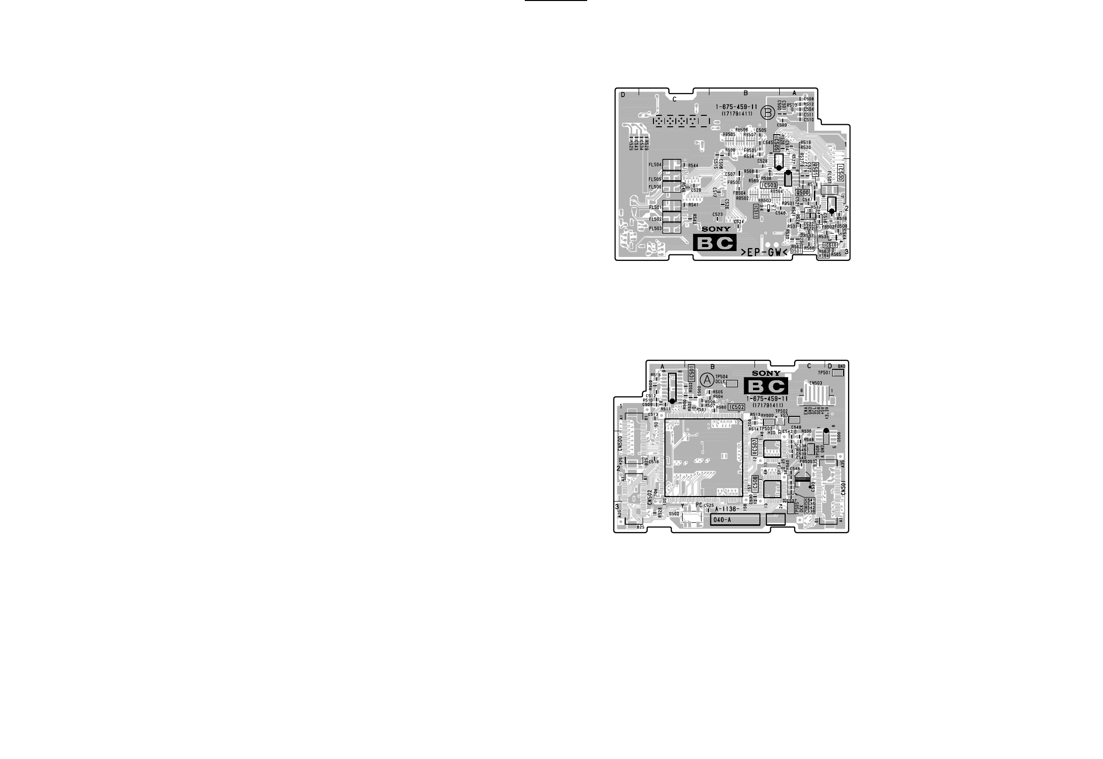
9-25 9-25
A B C D E F GH
1
2
3
4
5
VPL-PX20/PX30
——
BC
——
1-675-459-11
IC500 ∗A-2
IC501 B-1
IC502 B-1
IC503 ∗B-2
IC505 ∗B-1
IC506 C-2
IC507 C-2
IC510 ∗A-3
IC511 ∗B-2
Q500 ∗A-2
Q501 ∗A-2
TP501 D-1
TP502 C-1
TP503 C-1
TP504 C-1
TP506 C-2
TP505 C-3
∗:B Side mount
BC BC
BC – B SIDE –
SUFFIX ; -11
BC – A SIDE –
SUFFIX ; -11
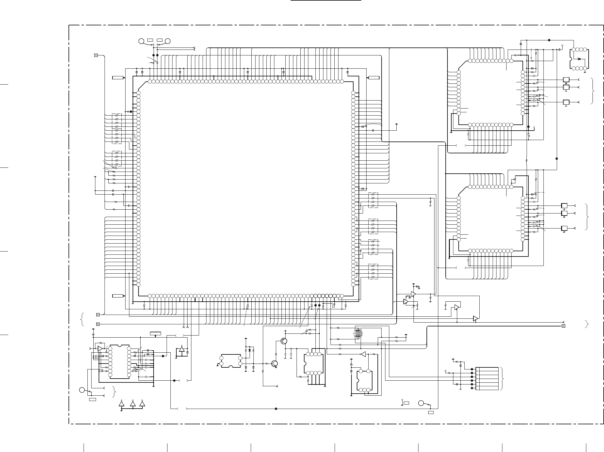
9-26 9-26
A B C D E F GH
1
2
3
4
5
VPL-PX20/PX30
D3.3VD3.3V
D3.3V
D3.3V
4
3
12
12345678910111213141516171819202122232425262728293031323334353637383940414243444546474849505152
53
54
55
56
57
58
59
60
61
62
63
64
65
66
67
68
69
70
71
72
73
74
75
76
77
78
79
80
81
82
83
84
85
86
87
88
89
90
91
92
93
94
95
96
97
98
99
100
101
102
103
104
105106107 108 109 110 111 112113 114115 116117 118 119120 121122 123124 125126 127128 129130 131132 133 134135 136137 138139 140141 142143 144145 146 147148 149150 151152 153154 155156
157
158
159
160
161
162
163
164
165
166
167
168
169
170
171
172
173
174
175
176
177
178
179
180
181
182
183
184
185
186
187
188
189
190
191
192
193
194
195
196
197
198
199
200
201
202
203
204
205
206
207
208
1234
5678
-2
-2
-2
-2
-2
-2
-2
-2
-2
123
45
1 2
34
1
2
3
4
5
6
1234
5678
123456789101112
13
14
15
16
17
18
19
20
21
22
23
24
25 26 27 28 29 30 31 32 33 34 35 36
37
38
39
40
41
42
43
44
45
46
47
48
12345678
9 10 11 12 13 14 15 16
123456789101112
13
14
15
16
17
18
19
20
21
22
23
24
25 26 27 28 29 30 31 32 33 34 35 36
37
38
39
40
41
42
43
44
45
46
47
48
EMI
EMI
EMI
EMI
EMI
EMI
C500
C501 C502
R501
R502
R504
R505
R506
R507
R510 R511
R512
C510
C511
JL500
JL501
C516
R517
R518
C519
R520
R524
R541
R542
R543
R549
R551
FL501
FL502
FL503
FL504
FL505
FL506
R515
RB505
RB506
RB507
R560
R561
D500
IC506
R516
RV500
IC507
C526
R500
C529
C530
C535
C536
C537
C538
C539
C540
C541
C542
C545
C503
C504
C508
C509
C512
C520
C514
C518
C522
C523
R540
TP501
C525
R509
TP502 TP503
TP504
TP505
FB500 C505
FB501
FB502
FB504
C524
FB505
JL505 JL506
R534
R503
TP506
JL507
JL508
JL509
JL513
C533
R537
R538
IC503
IC511
R564
R562
D501
C546 C547
JL561
R508
FB508
C544
IC510
R565
R519
R526
R527
R563
C528
R568
R569
RB500
RB501
RB504
RB503
IC505(1/4)
IC505(2/4)
IC505(3/4)
IC505(4/4)
IC502
C517
C515C506 C507 R513
R514
Q501
Q500
IC500(2/6)IC500(1/6)
IC500(3/6)
IC500(4/6)
IC500(5/6) IC500(6/6)
C513
R547
R548
R536
R550
R544
R545
R546
IC501
R521
C521
JL502
JL503
R522
R523
R535
R530
R531
JL544
JL545
JL546
JL547
JL548
JL549
CN503
A
R567
R566
#
#
#
#
0.01
25V
B:CHIP
#
47
1/16W
:CHIP
47
1/16W
:CHIP
47
1/16W
:CHIP
47k
1/16W
:CHIP
1k
1/16W
:CHIP
75
1/16W
:CHIP
75
1/16W
:CHIP
75
1/16W
:CHIP
47k
1/16W
:CHIP
47k
1/16W
:CHIP
47
1/16W
:CHIP
100p
CH:CHIP
0.01
25V
B:CHIP
0.01
25V
B:CHIP
47
47
47
100p
CH:CHIP
#
#
0.1
16V
B:CHIP
0
1/16W
:CHIP
0
1/16W
:CHIP
0
1/16W
:CHIP
0
1/16W
:CHIP
#
47
1/16W
:CHIP
0.1
16V
B:CHIP
0.1
16V
B:CHIP
0.1
16V
B:CHIP
0.1
16V
B:CHIP
#
#
#
#
#
#
0.1
16V
B:CHIP
0.1
16V
B:CHIP
0.1
16V
B:CHIP
0.1
16V
B:CHIP
0.1
16V
B:CHIP
0.1
16V
B:CHIP
0.1
16V
B:CHIP
0.1
16V
B:CHIP
0.1
16V
B:CHIP
0.1
16V
B:CHIP
0.1
16V
B:CHIP
0.1
16V
B:CHIP
#
470
1/16W
:CHIP
0.1
16V
B:CHIP
47
1/16W
:CHIP
3.3k
1/16W
:CHIP
0.1
16V
B:CHIP
0.1
16V
B:CHIP
47
1/16W
:CHIP
47
6.3V
:AL-CP
BK1608TS601
BK1608TS601
BK1608TS601
BK1608TS601
BK1608TS601
47
1/16W
:CHIP
M24C64
E2PROM
#
10k
1/16W
:CHIP
#
MA111
S80828ANNP-EDR
RESET
#
#
##
#
#
#
#
3.3k
1/16W
:CHIP
#
10k
1/16W
:CHIP
#
#
#
#
3.3k
1/16W
:CHIP
1
6.3V
B:CHIP
10k
1/16W
:CHIP
0.1
16V
B:CHIP
6.8k
1/16W
:CHIP
6.8k
1/16W
:CHIP
6.8k
1/16W
:CHIP
6.8k
1/16W
:CHIP
6.8k
1/16W
:CHIP
#
47
47
47
ADV7123KST140
#
TC74LCX125FT
OSD SW
TC74LCX125FT
OSD SW
TC74LCX125FT
OSD SW
TC74LCX125FT
OSD SW
CXD9512Q
3D GAMMA
0.1
16V
B:CHIP
0.1
16V
B:CHIP
0.1
16V
B:CHIP
0.47
16V
B:CHIP
100
1/16W
:CHIP
100
1/16W
:CHIP
2SA1611T1-M5M6
POWER SW
2SC2712
POWER SW
TC74LCX04FTTC74LCX04FT
TC74LCX04FT
TC74LCX04FT
TC74LCX04FTTC74LCX04FT
#
#
3.3k
1/16W
RES CHIP
#
#
#
#
#
W152-2G
CLOCK BUF
SHORT
0.1
16V
B:CHIP
#
#
#
#
#
47 1/16W :CHIP
47 1/16W :CHIP
#
#
#
#
#
#
6P
:SMD
5V
#
#
CLK2X
CLOCK
DOUTCK
DOUTCK
DOUTCK
LCD CONT
I2C
RESET≠≠≠≠≠≠≠≠≠
EVN_IN
ODD_IN
DCLK
D3.3V D3.3V
A5V
D 3.3V
D 3.3V
ECLK
VSO
HSO
EVEN R
EVEN G
EVEN B
ODD R
ODD G
ODD B
OCLK
DVS
DHS
D
3.3V
PW OSD ENA≠≠≠≠≠≠≠≠≠≠
≠≠≠≠≠≠≠≠≠
D3.3V
D3.3V
D3.3V
D3.3V
12
3
4
714
5
6
98
11
10
13
12
23
1
56
4
98
10
14
12 11
13
7
FRP
PRG
PCG
DWN
VST
VCK
ENB
CLP
HCK1
HCK2
HST
RGT
RE0
RE1
RE2
RE3
RE4
RE5
RE6
RE7
RE8
RE9
BO0
BO1
BO2
BO3
BO4
BO5
BO6
BO7
BO8
BO9
GE0
GE1
GE2
GE3
GE4
GE5
GE6
GE7
GE8
GE9
BE0
BE1
BE2
BE3
BE4
BE5
BE6
BE7
BE8
BE9
GO0
GO1
GO2
GO3
GO4
GO5
GO6
GO7
GO8
GO9
RO0
RO1
RO2
RO3
RO4
RO5
RO6
RO7
RO8
RO9
BE0
BE1
BE2
BE3
BE4
BE5
BE6
BE7
BE8
BE9
GE0
GE1
GE2
GE3
GE4
GE5
GE6
GE7
GE8
GE9
RE0
RE1
RE2
RE3
RE4
RE5
RE6
RE7
RE8
RE9
RO0
RO1
RO2
RO3
RO4
RO5
RO6
RO7
RO8
RO9
GO0
GO1
GO2
GO3
GO4
GO5
GO6
GO7
GO8
GO9
BO0
BO1
BO2
BO3
BO4
BO5
BO6
BO7
BO8
BO9
DRE0
DRE1
DRE2
DRE3
DRE4
DRE5
DRE6
DRE7
DGE0
DGE1
DGE2
DGE3
DGE4
DGE5
DGE6
DGE7
DBE0
DBE1
DBE2
DBE3
DBE4
DBE5
DBE6
DBE7
DRO0
DRO1
DRO2
DRO3
DRO4
DRO5
DRO6
DRO7
DGO0
DGO1
DGO2
DGO3
DGO4
DGO5
DGO6
DGO7
DBO0
DBO1
DBO2
DBO3
DBO4
DBO5
DBO6
DBO7
BLK
DRO0
DRO1
DGO0
DGO1
DBO0
DBO1
DRE1
DGE0
DGE1
DBE0
DBE1
SCL
POSCONT2
POSCONT1
SID
INVCNT
SDA
DRE7
DRE0
DRO7
GND
GND
AGCSHP
IFHIZ
GND
SCAN_AMC
SCAN_SMC
LCD_FRP
LCD_PRG
LCD_PCG
LCD_DWN
LCD_VST
LCD_VSTI
LCD_VCK
LCD_ENB
LCD_BLK
LCD_CLR/CLP
LCD_HCK1
LCD_HCK2
LCD_HST
LCD_RGT
CNT2B
CNT2A
CNT1B
CNT1A
GND
VDD
AVDD
NC
SID
AGND
INV_CNT
TMC1
EVN_IN_R_0
EVN_IN_R_1
EVN_IN_R_2
EVN_IN_R_3
EVN_IN_R_4
EVN_IN_R_5
EVN_IN_R_6
EVN_IN_R_7
EVN_IN_G_0
EVN_IN_G_1
EVN_IN_G_2
EVN_IN_G_3
EVN_IN_G_4
EVN_IN_G_5
EVN_IN_G_6
EVN_IN_G_7
EVN_IN_B_0
GND
GND
EVN_IN_B_1
VDD
EVN_IN_B_2
EVN_IN_B_3
EVN_IN_B_4
EVN_IN_B_5
EVN_IN_B_6
EVN_IN_B_7
TMC2
HSYNC_IN
VSYNC_IN
CLOCK
GND
CLK2X
GND
ODD_IN_R_0
ODD_IN_R_1
ODD_IN_R_2
ODD_IN_R_3
ODD_IN_R_4
ODD_IN_R_5
ODD_IN_R_6
ODD_IN_R_7
ODD_IN_G_0
ODD_IN_G_1
VDD
GND
ODD_IN_G_2
ODD_IN_G_3
ODD_IN_G_4
ODD_IN_G_5
ODD_IN_G_6
ODD_IN_G_7
ODD_IN_B_0
ODD_IN_B_1
ODD_IN_B_2
ODD_IN_B_3
ODD_IN_B_4
ODD_IN_B_5
ODD_IN_B_6
ODD_IN_B_7
VDD
RESET
DEBUG
RSCL
RSDA
CS
HSCL
HSDA
BUNRI
EVN_OSD_B_2
VDD
GND
GND
EVN_OSD_B_1
EVN_OSD_B_0
EVN_OSD_G_0
EVN_OSD_G_2
EVN_OSD_G_1
EVN_OSD_R_0
EVN_OSD_R_2
EVN_OSD_R_1
EVN_I
EVN_YS
EVN_YM
ODD_OSD_B_0
ODD_OSD_B_2
ODD_OSD_B_1
ODD_OSD_G_2
ODD_OSD_G_1
ODD_OSD_G_0
ODD_OSD_R_2
ODD_OSD_R_0
ODD_OSD_R_1
ODD_1
ODD_YS
ODD_YM
VDD
GND
EVN_OUTB_9
EVN_OUTB_8
EVN_OUTB_7
EVN_OUTB_6
EVN_OUTB_5
EVN_OUTB_4
EVN_OUTB_3
GND
EVN_OUTB_2
EVN_OUTB_1
EVN_OUTB_0
ODD_OUTB_9
ODD_OUTB_8
ODD_OUTB_7
VDD
GND
ODD_OUTB_6
ODD_OUTB_5
ODD_OUTB_4
ODD_OUTB_3
ODD_OUTB_2
ODD_OUTB_1
ODD_OUTB_0
GND
GND
VDD
EVN_OUTG_9
EVN_OUTG_8
EVN_OUTG_7
EVN_OUTG_6
EVN_OUTG_5
EVN_OUTG_4
EVN_OUTG_3
EVN_OUTG_2
EVN_OUTG_1
EVN_OUTG_0
GND
ODD_OUTG_9
ODD_OUTG_8
ODD_OUTG_7
ODD_OUTG_6
VDD(ADDITIONAL)
GND(ADDITIONAL)
ODD_OUTG_5
ODD_OUTG_4
ODD_OUTG_3
ODD_OUTG_2
ODD_OUTG_1
ODD_OUTG_0
EVN_OUTR_9
GND
VDD
EVN_OUTR_8
EVN_OUTR_7
EVN_OUTR_6
EVN_OUTR_5
EVN_OUTR_4
EVN_OUTR_3
EVN_OUTR_2
GND
EVN_OUTR_1
EVN_OUTR_0
ODD_OUTR_9
ODD_OUTR_8
ODD_OUTR_7
ODD_OUTR_6
ODD_OUTR_5
ODD_OUTR_4
ODD_OUTR_3
ODD_OUTR_2
ODD_OUTR_1
ODD_OUTR_0
GND
VDD
VDD
HSYNC_OUT
VSYNC_OUT
G0
G1
G2
G3
G4
G5
G6
G7
G8
G9
BLANK
SYNC
VAA
B0
B1
B2
B3
B4
B5
B6
B7
B8
B9
CLOCK
GND
GND
IOB
VAA
VAA
IOG
IOR
COMP
VREF
IOR
IOG
IOB
RSET
R0
R1
R2
R3
R4
R5
R6
R7
R8
R9
PSAVE
REF
CLKA1
CLKA2
VDD
GND
CLKB1
CLKB2
S2
FBK
CLKA4
CLKA3
VDD
GND
CLKB4
CLKB3
S1
EVEN
G0
G1
G2
G3
G4
G5
G6
G7
G8
G9
BLANK
SYNC
VAA
B0
B1
B2
B3
B4
B5
B6
B7
B8
B9
CLOCK
GND
GND
IOB
VAA
VAA
IOG
IOR
COMP
VREF
IOR
IOG
IOB
RSET
R0
R1
R2
R3
R4
R5
R6
R7
R8
R9
PSAVE
ODD
GND
VSO HSO
DCK
OCLK
E0
E1
E2
VSS
VCC
WC
SCL
SDA
NC
VSS
VDD
OUT
B-SS1696<08.>-BC.-P1
(P2)
(P2)
(P2)
(P2)
OSD SW
INVERTER
(P2)
(P2)
(P2)
INVERTER
BC(1/2)
(P2)
(P2)
(P2)
(THREE DIMENSIONS ©)
NC
+3.3V
+5V
SDA
SCL
GND
ENA
C548
0.1
16V
B:CHIP
S500
BC (1/2) BC (1/2)
• Refer to page 9-25 for Printed Wiring Board
• Refer to page 9-27 for Waveforms
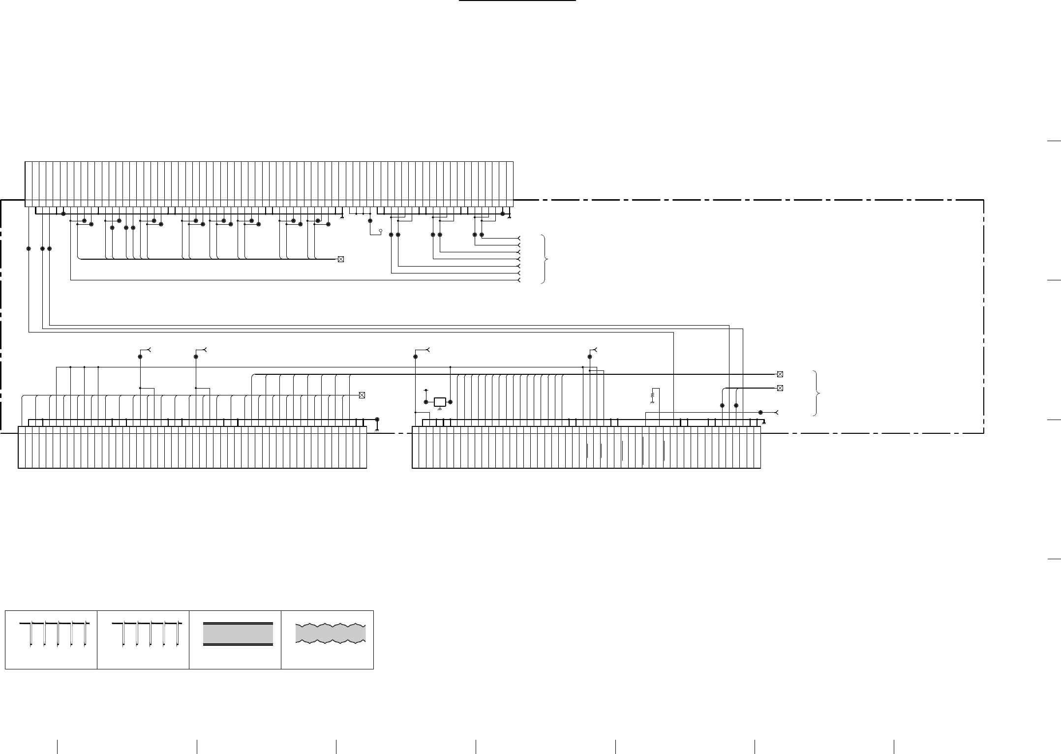
9-27 9-27
A B C D E F GH
1
2
3
4
5
VPL-PX20/PX30
-2
A1
B1
A2
B2
A3
B3
A4
B4
A5
B5
A6
B6
A7
B7
A8
B8
A9
B9
A10
B10
A11
B11
A12
B12
A13
B13
A14
B14
A15
B15
A16
B16
A17
B17
A18
B18
A19
B19
A20
B20
A21
B21
A22
B22
A23
B23
A24
B24
A25
B25
A1
B1
A2
B2
A3
B3
A4
B4
A5
B5
A6
B6
A7
B7
A8
B8
A9
B9
A10
B10
A11
B11
A12
B12
A13
B13
A14
B14
A15
B15
A16
B16
A17
B17
A18
B18
A19
B19
A20
B20
A21
B21
A22
B22
A23
B23
A24
B24
A25
B25
EMI
A1
A2
A3
A4
A5
A6
A7
A8
A9
A10
A11
A12
A13
A14
A15
A16
A17
A18
A19
A20
A21
A22
A23
A24
A25
A26
A27
A28
A29
A30
A31
A32
A33
A34
B1
B2
B3
B4
B5
B6
B7
B8
B9
B10
B11
B12
B13
B14
B15
B16
B17
B18
B19
B20
B21
B22
B23
B24
B25
B26
B27
B28
B29
B30
B31
B32
B33
B34
A35
B35
CN500 CN502
FL507
CN501
R528
JL514 JL515 JL516
JL517
JL518 JL519
JL520
JL521
JL522 JL523 JL524 JL525 JL526
JL527 JL528
JL529
JL530 JL531 JL532
JL533
JL534
JL535
JL536
JL537
JL538 JL539 JL540 JL541 JL542
JL543
JL551 JL552
JL553
JL554
JL555 JL556
JL557
JL558 JL559 JL560
70P
1k
1/16W
:CHIP
###
#
##
#
#
########
###
#
##
#
#
#####
#
##
#
#
##
#
###
50P 50P
EVEN R
EVEN B
EVEN G
ODD R
ODD B
ODD G
ECLK
LCD CONT
EVN_IN
ODD_IN
I2C
RESET≠≠≠≠≠
≠≠≠≠
DCLK
DVS DHS
A5V
D3.3V
PW OSD ENA≠≠≠≠≠≠≠≠≠≠
≠≠≠≠≠≠≠≠≠
DWN
HCK1
RGT
DRE0
DRE1
DRE2
DRE3
DRE4
DRE5
DRE6
DRE7
DGE0
DGE1
DGE2
DGE3
DGE4
DGE5
DGE6
DGE7
DBE0
DBE1
DBE2
DBE3
DBE4
DBE5
DBE6
DBE7
DRO0
DRO1
DRO2
DRO3
DRO4
DRO5
DRO6
DRO7
DGO0
DGO1
DGO2
DGO3
DGO4
DGO5
DGO6
DGO7
DBO0
DBO1
DBO2
DBO3
DBO4
DBO5
DBO6
DBO7
SDA
SCL
BLK
ENB
PCG
CLP
PRG
VST
VCK
HST
FRP
POSCONT2
INVCNT
POSCONT1
SID
HCK2
PANEL TEMP
GND
GND
GND
GND
A5V
GND
ECLK
HCK1
ENB
PCG
DWN
RGT
CLP
PRG
VCK
FRP
VST
HST
INVCNT
BLK
POSCONT1
POSCONT2
A5V
EVENB
EVENG
EVENB
EVENG
EVENR
ODDB
EVENR
ODDB
GND
GND
ODDG
ODDR
ODDG
ODDR
ECLK
DRE0
GND
DRE1
GND
DRE2
DRE3
DRE4
DRE5
DRE6
GND
DRE7
GND
DGE0
DVS
DGE1
DVS
DGE2
GND
DGE3
GND
DGE4
DHS
DGE5
DHS
DGE6
GND
DGE7
GND
DBE0
DRO0
DBE1
DRO1
DBE2
DRO2
DBE3
DRO3
DBE4
DRO4
DBE5
DRO5
DBE6
DBE7
DRO7
GND
GND
PANEL TEMP
DCLK
GND
DCLK
GND
GND
GND
DGO0
DBO0
DGO1
DBO1
DGO2
DBO2
DGO3
DBO3
DGO4
DBO4
DGO5
DBO5
DGO6
DBO6
DGO7
DBO7
GND
GND
GND
GND
DISP
BUSY
GND
GND
GND
GND
SCL400K
GND
SDA400K
GND
D3.3V
D3.3V
D3.3V
D3.3V
D3.3V
D3.3V
SCL100K
SDA100K
SDA100K
SCL100K
DR06
RESET
RESET
OSD_CS0
OSD_RES
NC
NC
PW OSD ENA
HCK1
HCK2
HCK2
ENB
PCG
GND
GND
CLP
PRG
VST
VCK
HST
FRP
GND
POSCONT2
INVCNT
SID
POSCONT1
SID
A5V
A5V
GND
GND
GND
GND
GND
GND
GND
GND
B-SS1696<08.>-BC.-P2
BC(2/2)
(P1)
(P1)(P1)
(P1)
(P1)(P1)
TO BB CN309
(P1)
TO C CN605
(THREE DIMENSIONS
©
)
NC
NC
(P1)
PANEL TEMP
PANEL TEMP
BC (2/2) BC (2/2)
BC Board Waveforms
1234
3.2 Vp-p
TP502 [VSO]
3.2 Vp-p
TP503 [HSO]
3.2 Vp-p
TP504 [0|CLK]
1.6 Vp-p
TP505 [DCK]
• Refer to page 9-25 for Printed Wiring Board
• Refer to page 9-27 for Waveforms
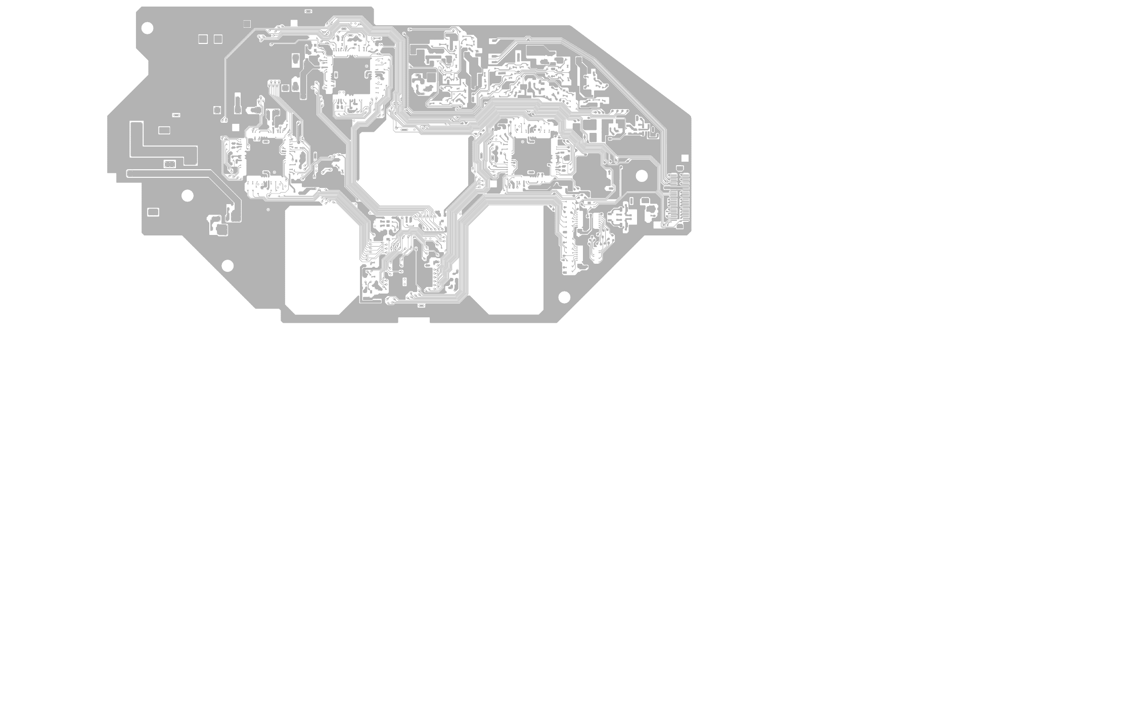
9-28 9-28
A B C D E F GH
1
2
3
4
5
VPL-PX20/PX30
C – B SIDE –
SUFFIX ; -11
C – A SIDE –
SUFFIX ; -11
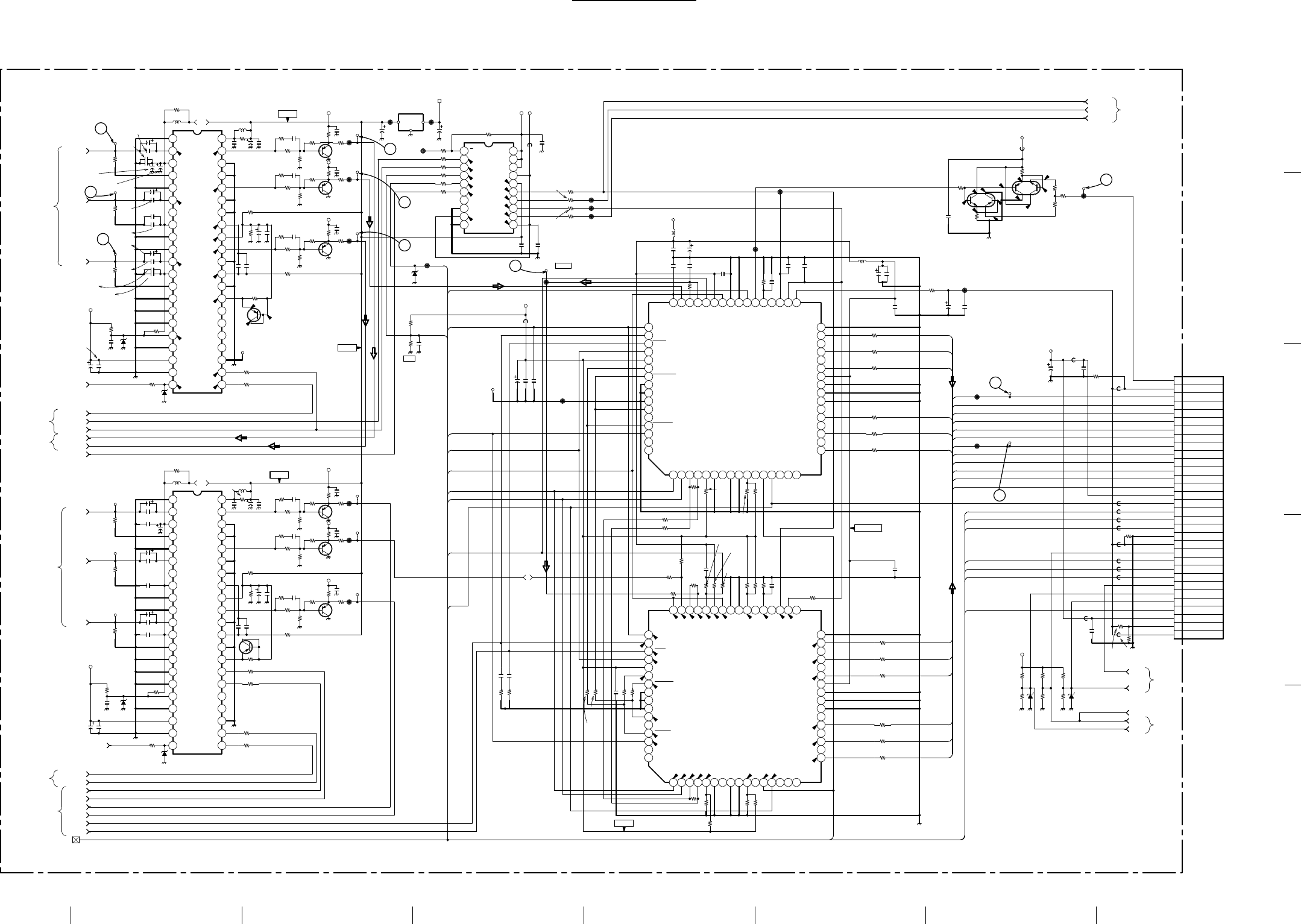
9-29 9-29
A B C D E F GH
1
2
3
4
5
VPL-PX20/PX30
C (1/3) C (1/3)
0
15.6
6.5
7.1
6.5
7.1
10
+15.5V
0
15.6
7.1
7.1
7.7
7.7
2
3
D+5V
1
0
0
0
0
0
0
4.6
3.7
3.7
5.0
3.5
3.5
3.5
3.5
0.3
1.9
1.9
4.1
4.1
7.1
7.1
7.1
7.1
7.1
7.1
3.3
5.3
11.2
7.1
15.6
3.3
9.1
1.3
7.1
0
4.9
4.9
9.4
3.3
5.0
11.7
7.1
1.9
1.7
1.8
5.0
+12V
+12V
7
8
9
4
5
6
0
0
4.6
4.8
2.6
4.5
3.4
4.5
4.6
2.6
4.1
4.9
4.90.3
4.1
3.4
3.4
+12V
G
G
G
G
G
G
B
R
B
R
1 2 3 4 5 6 7 8 9 10 11 12 13 14 15 16
17
18
19
20
21
22
23
24
25
26
27
28
29
30
31
32
33343536373839404142434445464748
49
50
51
52
53
54
55
56
57
58
59
60
61
62
63
64
1 2 3 4 5 6 7 8 9 10 11 12 13 14 15 16
17
18
19
20
21
22
23
24
25
26
27
28
29
30
31
32
33343536373839404142434445464748
49
50
51
52
53
54
55
56
57
58
59
60
61
62
63
64
1
2
3
4
5
6
7
8
9
10
11
12
13
14
15
16
17
18
19
20
21
22
23
24
25
26
27
28
29
30
31
32
123456789101112131415161718192021
22 23 24 25 26 27 28 29 30 31 32 33 34 35 36 37 38 39 40 41 42
123456789101112131415161718192021
22 23 24 25 26 27 28 29 30 31 32 33 34 35 36 37 38 39 40 41 42
IO G
12345678910
11 12 13 14 15 16 17 18 19 20
R600
R603
Q600
Q603
R613
R618
R619 R624 JL600
D601
R637
R638
R639
R640
R641
R642
TP600
IC602
R644
C626
R645
C628
R646
FB600
TP601
JL613
C632
C634
L602
C635
C636
IC603
IC604
R665
C638
R668
R669
R670
R673
C639
R677
R679
R681
R683
R684
C641
C642
JL614
C643 C644
R685
L603
R686
R687
R688
R689
R690
R691
R692
R693
R694
R695
R696
R697
C646
C647
C650
JL615
C651
JL616
JL617
TP602
TP603
R699
R700
D602
R701
R702
R706
R707
D603
C658
C660
FB602
FB603
FB604
FB605
FB607
FB608
FB609
JL636
FB606
R656
FB601
FB610
R752
R666
C603
C606
C608
R606
C613
C614
R632
C615
R633
C617
C618 C619
R654 C620
R1604
R1605
IC622
C621
C622
C623
C624
C709
C710
C712
R1606 L608
C713 C714 C715
R1608
R1609 C716
R1611
R1612
C717
R1613
C718
R1614 C720
R1616
C721
C722
R1617 C723
R1618
R1620
R1621
R1622
R655
TP610
TP611
TP612
TP613
TP614
TP615
TP618
CN601
JL645
JL646
JL650
R635
R636
FB633
FB634
IC613
C627
D604
D605
L610
TP619
TP620
TP621
R1631
R1633
TP622
TP623
TP624
R1634
R1635
R1636
JL653
JL654
JL655
JL656
JL657
JL658
C762
FB642
C629 C631
JL659
JL662
JL663
JL664
FB643
C645
C633
C600
R1640
C612
JL665
C605
C768
C767
C766
C764
C763
C761
C610
R631
C725
C724
C637
C770
R610
C657
Q609
Q610
Q611
R1650
R1651
R1652
R1647
R1648
R1649
R1653
R1654
R1655
R1659
R1660
R1661
C604
C778 C779
R1632
C765
C609
C786
C783
C784
C785
C611
C780
C781
C782
R1639
R607
L609
L601
R1665
R1666
C789
C771
D607
C790
R1668
R1667
Q612
R1603
Q613
R634
D606
C772
C773
C607
C774
C616
TP627
R675
IC600
Q608
Q607
Q606
R647R648
R650R649
C630
R660
R659
R609 R608
R611
R653
R652
R682
R698
R751
R662
R663
R676
R674
R671
R661
R680
R667
R678
R672
R664
R658
R657
R1656
R1662
R1607
R1657
R1610
R1658
R1664
R1615
R1619
R1643
R1644
R1663
100k
:CHIP
1/16W 100k
:CHIP
1/16W
27k
:RN-CP
1/16W
10k
:CHIP
1/16W
100
16V
:AL-CP
1µH
10k
1/16W
:CHIP
27k
:RN-CP
1/16W
47
:CHIP
1/16W
47
:CHIP
1/16W
47
:CHIP
1/16W
47
:CHIP
1/16W
47
:CHIP
1/16W
47
:CHIP
1/16W
47
:CHIP
1/16W
47
:CHIP
1/16W
47
:CHIP
1/16W
47
:CHIP
1/16W
47
:CHIP
1/16W
47
:CHIP
1/16W
100 1/16W :CHIP
100 1/16W :CHIP
1µH
#
#
#
4.7k 1/16W :CHIP
47
1/16W
:CHIP
47
1/16W
:CHIP
1000p
B:CHIP
1000p
B:CHIP
M62399FP
DAC
#
0.1
16V
B:CHIP
CXA2112R
LCD DRIVER
CXA2112R
LCD DRIVER
1k
1/16W
:CHIP
#
10k
1/16W
:CHIP
10k
1/16W
:CHIP
#
#
#
#
#
#
#
#
HN1B01FU-T
BUFF
HN1B01FU-T
BUFF
2.2
:CHIP
1/16W
2.2
:CHIP
1/16W
2.2k
:CHIP
1/16W
100
:CHIP
1/16W
2.2k
:CHIP
1/16W
RD4.7SB
#
#
#
0
1/16W
:CHIP
100 1/16W :CHIP
0
1/16W
:CHIP
#
#
#
0
1/16W
:CHIP
#
0.1
B:CHIP
0.1
B:CHIP
0.1
B:CHIP
0.1
B:CHIP
0.1
B:CHIP
0.1
B:CHIP
0.1
B:CHIP
47
1/16W
:CHIP
#
0.1
25V
B:CHIP
0.1
25V
B:CHIP
#
#
0.22
25V
B:CHIP
#0.22
25V
B:CHIP
#
#
#
#
#
#
#
###
#
#
#
#
#
#
#
#
100
1/16W
:CHIP
#
#
#
100
1/16W
:CHIP
100
1/16W
:CHIP
#
#
#
#
#
#
#
#
#
#
#
#
#
#
#
#
1.2k
1/16W
:CHIP
3.6k
1/16W
:CHIP
#
#
#
BKM1608TS601
BKM1608TS601
BKM1608TS601
BKM1608TS601
BKM1608TS601
BKM1608TS601
BKM1608TS601
BKM1608TS601
0.1
16V
B:CHIP
0.1
25V
B:CHIP
22
6.3V
:AL-CP
0.1
16V
B:CHIP
32P
FPC
#
#
BKM1608TS601
BKM1608TS601
BKM1608TS601
TA7812F
75
1/16W
:CHIP
75
1/16W
:CHIP
#
#
#
#
#
#
0.1
B:CHIP
0.1
16V
B:CHIP
0.1
B:CHIP
0.1
25V
B:CHIP
0.1
25V
B:CHIP
0.1
25V
B:CHIP
#
#
#
#
#
#
#
#
#
#
#
#
#
#
#
#
#
#
#
#
#
#
#
#
100
16V
:AL-CP
#
0.1
25V
B:CHIP
75
1/16W
:CHIP
47
25V
:AL-CP
470
1/16W
:CHIP
#
#
10µH
100µH
100
1/16W
:CHIP
10k
#
:CHIP
47k
1/16W
:CHIP
0.22
25V
B:CHIP
0.22
25V
B:CHIP
0.22
25V
B:CHIP
100
25V
:AL-CP
100
25V
:AL-CP
#
3.3
50V
:CHIP
3.3
50V
:CHIP
3.3
50V
:CHIP
#
#
#
#
#
100
16V
:AL-CP 100
16V
:AL-CP
0.1
16V
B:CHIP
0.1
16V
B:CHIP
0.1
16V
B:CHIP
#
#
#
#
0.1
16V
B:CHIP
#
#
#
#
#
470
1/10W
:CHIP
470
1/10W
:CHIP
470
1/10W
:CHIP
#
#
#
#
#
#
47
1/16W
:CHIP
47
1/16W
:CHIP
47
1/16W
:CHIP
#
1k :CHIP
#
# :CHIP
0.22
25V
B:CHIP
0.22
25V
B:CHIP
0.22
25V
B:CHIP
0.22
25V
B:CHIP
10
16V
RD5.6SB2
2SA1462
#
#
M52749FP-TP
RGB AMP
2SA1462
BUFF
2SA1462
BUFF
2SA1462
BUFF
100
1/16W
:CHIP
100
1/16W
:CHIP
100
1/16W
:CHIP
100
1/16W
:CHIP
0.1
16V
B:CHIP
#
#
620
1/16W
:CHIP
390
1/16W
:CHIP
390
1/16W
:CHIP
620
1/16W
:CHIP 390
1/16W
:CHIP
0
SHORT
0
SHORT
0
SHORT
0 SHORT
0 SHORT
0
SHORT
0
SHORT
0
SHORT
0
SHORT
#
#
0
SHORT
0
SHORT
#
0
SHORT
0
SHORT
0
SHORT
0
SHORT
0
SHORT
0
SHORT
0
SHORT
0
SHORT
0
SHORT
0
SHORT
#
#
#
0
1/16W
:CHIP
12V
12V
G
SCEN
B VCOM
R VCOM
MCLK
MCLK
LCD DRIVE
DWN
VB2
VB1
CLP
BLKI
BLK
D
5V-2
D5V-2
D5V-2
15.5V
EVEN R
EVEN G
EVEN B
R OUT
B OUT
CLP
17V
SCL1
SDA100K
SDA100K
ODD R
ODD G
ODD B
R
B
15.5V
15.5V
PANEL CONT
VB1
VB2
SCL0
SCL
A5V
A5V
A5V
A5V
A5V
A5V
A5V
A5V
A5V
32
31
30
29
28
27
26
25
24
23
22
21
20
19
18
17
16
15
14
13
12
11
10
9
8
7
6
5
4
3
2
1
6
2
1
3
5
4
6
2
1
3
5
4
VID1
VID2
VID3
VID4
VID5
VID6
VID7
VID8
VID9
VID10
VID11
VID12
ENB
SID-OUT
DLY-CON
POS-CON1
POS-CON2
V33
VID1
VID2
VID3
VID4
VID5
VID6
VID7
VID8
VID9
VID10
VID11
VID12
HST
VCK
VST
PCG
V33
FRP
DLY-CON
PRG
RGT
HCK1
HCK2
ENB1
INV-CNT
POS-CNT1
POS-CNT2
NEXT-OUT
NEXT-IN
F/R-CNT
GND
S-12-CNT
ENB
DIR-CNT
SH-OUT6
SH-OUT5
SH-OUT4
PGND
PVCC
SH-OUT3
SH-OUT2
SH-OUT1
SIG CEN
ISET
SID-OUT
SID-IN
SID-OFST
VCC
FRP
SH-IN
INV-OUT
VIDEO IN
DLY-CNT
MCLK
INV-CNT
VDD
CLK-OUT
DGND
CLK-IN
PRG
MCLK
CLK-OUT
CLK-IN
OFFSET
VCOM OFST
VCOM OUT
NC
NC
NC
NC
NC
NC
NC
NC
NC
NC
NC
NC
NC
NC
NC
NC
NCNC
NC
NC
NC
NC
SCL
SDA
VREFL
GND
A07
A08
R CS0
CS1
CS2
VDD
VCCA06
A05
A04
A03
A02
A01
GINV
PS2G
VSIG1
VSIG2
VSIG3
VSIG4
VSIG5
VSIG6
VSIG7
VSIG8
VSIG9
VSIG10
VSIG11
VSIG12
HVDD
RGT
HST
VSS
BLK
ENB
VCK
VST
DWN
PCG
VVDD
VREF1
VREF2
GND
GND2
VSSGR
HCK2
HCK1
VSSGL
HB
VB
COM
SOUT
GND1(R)
G_IN
OSD_BLK
R_IN
VCC1(R)
OSD_R
SOG_IN
VCC1(G)
OSD_G
GND1(G)
B-IN
VCC1(B)
OSD_B
GND
NC
GND1(B)
ABL_IN
NC
SOG_OUT
CLP
VCC2
R_OUT
NC
GND2
G_OUT
NC
GND
CONT_REF
B_OUT
GND
CONT_DAC
BLK
D/A_1
D/A_2
D/A_3
D/A_4
D/A_5
GND
SDA
GND1(R)
G_IN
OSD_BLK
R_IN
VCC1(R)
OSD_R
SOG_IN
VCC1(G)
OSD_G
GND1(G)
B-IN
VCC1(B)
OSD_B
GND
NC
GND1(B)
ABL_IN
NC
SOG_OUT
CLP
VCC2
R_OUT
NC
GND2
G_OUT
NC
GND
CONT_REF
B_OUT
GND
CONT_DAC
BLK
D/A_1
D/A_2
D/A_3
D/A_4
D/A_5
GND
SDA
SCL
MAIN BRIGHTNESS
VCC_5V
MAIN BRIGHTNESS
VCC_5V
SCL0
B-SS1696<08.>-C..-P1
(LCD DRIVER)
(P2)
TO LCD PANEL(G)
(P2,3)
(P2)
(P3)
(G)
(G)
(P3)
(P2)
(P3)
(P3)
(P3)
(P2)
(P3)
(P3)
(P3)
SIG CEN
SID-OFST
VCC
FRP
SH-IN
INV-OUT
VIDEO IN
VCOM OFST
ISET
SID-OUT
SID-IN
NC
NC
NC
MCLK
VDD
DGND
CLK-IN
PRG
MCLK
CLK-OUT
CLK-IN
NC
NC
NC
NC
DLY-CNT
INV-CNT
CLK-OUT
OFFSET
POS-CNT2
NEXT-OUT
NEXT-IN
F/R-CNT
GND
S-12-CNT
ENB
DIR-CNT
NC
NC
NC
NC
NC
NC
NC
POS-CNT1
SH-OUT5
SH-OUT4
PGND
PVCC
NC
NC
NC
NC
NC
SH-OUT3
SH-OUT2
SH-OUT1
VCOM OUT
NC
NC
GND2
SH-OUT6
C(1/3)
• Refer to page 9-28 for Printed Wiring Board
• Refer to page 9-28 for Waveforms
• Refer to page 9-31 for IC Block Diagrams
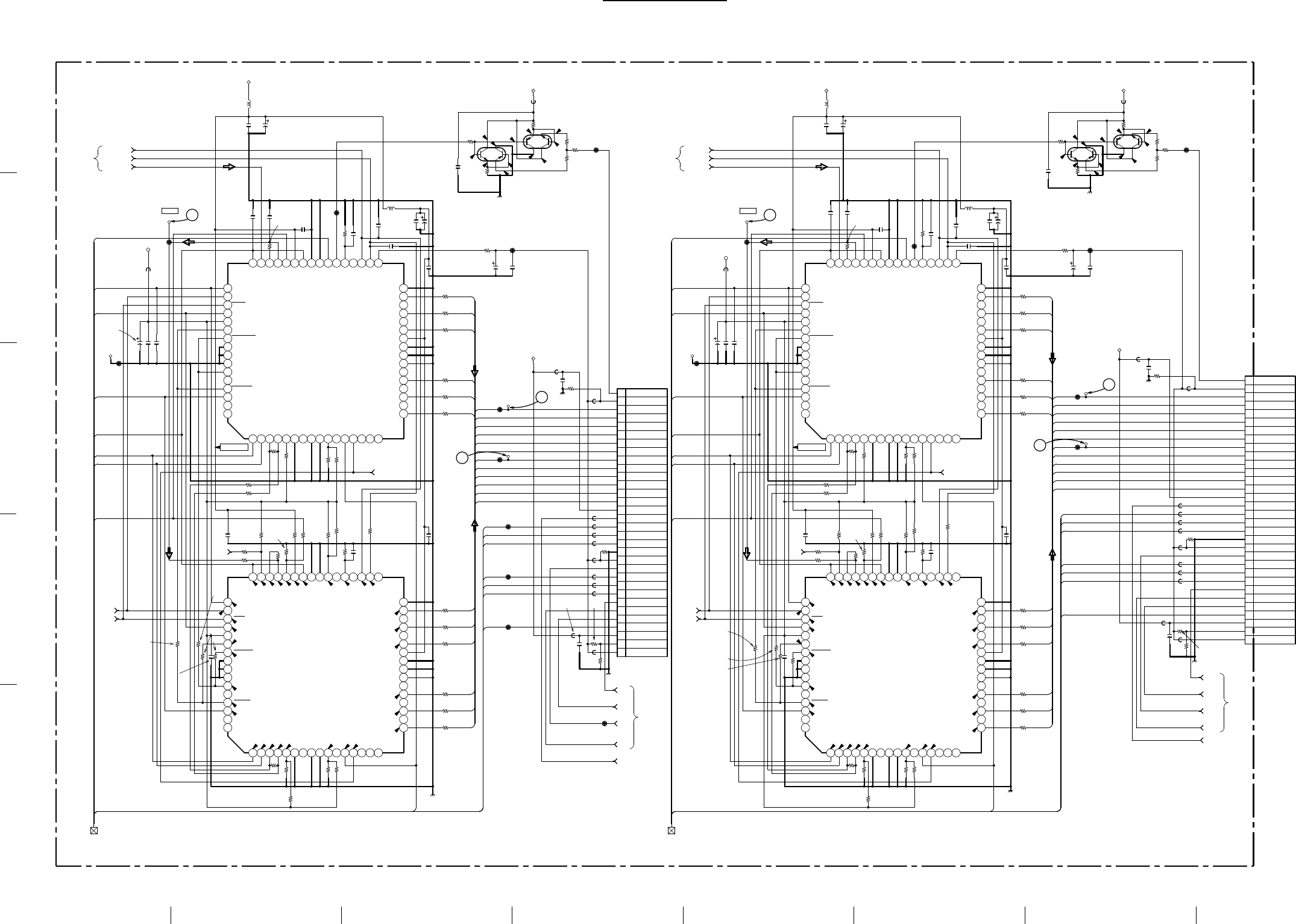
9-30 9-30
A B C D E F GH
1
2
3
4
5
VPL-PX20/PX30
015.6
7.1
+15.5V
15
16
7.7
7.1
7.7
7.1
7.1
15.6
0
6.56.5
14
0
0
0
0
0
015.6
7.1
7.7
7.1
7.7
7.1
7.1
15.6
0
6.56.5
11
12
13
+15.5V
4.6
3.7
3.7
5.0
3.5
3.5
3.5
3.5
0.3
1.9
1.9
4.4
5.0
7.1
7.1
7.1
7.1
7.1
7.1
3.3
5.3
11.3
7.1
15.6
3.3
9.1
1.3
7.1
1.9
0
0
0
0
0
4.6
3.7
3.7
5.0
3.5
3.5
3.5
3.5
0.3
1.9
1.9
4.4
5.0
7.1
7.1
7.1
7.1
7.1
7.1
3.3
5.3
11.3
7.1
15.6
3.3
9.1
1.3
7.1
1.9
R
R
R
R
R
B
B
B
B
B
1 2 3 4 5 6 7 8 9 10 11 12 13 14 15 16
17
18
19
20
21
22
23
24
25
26
27
28
29
30
31
32
33343536373839404142434445464748
49
50
51
52
53
54
55
56
57
58
59
60
61
62
63
64
1 2 3 4 5 6 7 8 9 10 11 12 13 14 15 16
17
18
19
20
21
22
23
24
25
26
27
28
29
30
31
32
33343536373839404142434445464748
49
50
51
52
53
54
55
56
57
58
59
60
61
62
63
64
1 2 3 4 5 6 7 8 9 10 11 12 13 14 15 16
17
18
19
20
21
22
23
24
25
26
27
28
29
30
31
32
33343536373839404142434445464748
49
50
51
52
53
54
55
56
57
58
59
60
61
62
63
64
1 2 3 4 5 6 7 8 9 10 11 12 13 14 15 16
17
18
19
20
21
22
23
24
25
26
27
28
29
30
31
32
33343536373839404142434445464748
49
50
51
52
53
54
55
56
57
58
59
60
61
62
63
64
1
2
3
4
5
6
7
8
9
10
11
12
13
14
15
16
17
18
19
20
21
22
23
24
25
26
27
28
29
30
31
32
1
2
3
4
5
6
7
8
9
10
11
12
13
14
15
16
17
18
19
20
21
22
23
24
25
26
27
28
29
30
31
32
FB611
TP604
JL619
R712
R713
C667
L604
C668
C669
IC609
IC610
R718
C671
R719
R723
R726
C672
R730
R734
R735
R736
C673
R737
C675
L605
C676
C678
C679
R738
R739
R740
R741
R742
R743
R744
R745
R746
R747
R748
R749
C680
JL620
JL621
TP605
TP606
JL622
C681
C683
FB613
FB614
FB615
FB616
FB618
FB619
FB620
FB622
TP607
JL623
R759
C690
R761
L606
C691
C692
IC611
IC612
R765
C694
R766
R767
R768
R770
R773
C695
R777
R779
R781
R782
R783
C696
C698
L607
C699
C701
C702
R785
R786
R787
R788
R789
R790
R791
R792
R793
R794
R795
R796
C703
JL624
JL625
TP608
TP609
JL626
C704
C706
C708
FB624
FB625
FB626
FB627
FB629
FB630
FB631
FB612
FB617
FB621
R756
FB623
FB628
FB632
R1602
Q604
Q601
R620
R621 JL601
R615
R625
R601
R604
Q605
Q602
R622
R623 JL602
R617
R626
R602
R605
JL633
JL637
JL638
JL639
CN602
CN603
JL649
JL651
FB635
FB637
FB638
C685
FB636
C663
C686
C664 C687
C688
C665
TP625
JL660
TP626
JL661
FB645
C677 C700
FB644
C689
C666
C601
C602
C693C670
C787
C788
R760
R720
R728
R714 R722
R733
C674
R721
R732
R797
R798
R799
R1601
R763
R764
R776
R784
R780
R775
R769
R771 R774
R762
C697
R757
R758
R778
R772
R750
R753
R754
R755
R731R725
R711
R710
R716
R717
R715
R724 R727
R729
100k
:CHIP
1/16W 100k
:CHIP
1/16W
27k
:RN-CP
1/16W
10k
:CHIP
1/16W
100k
:CHIP
1/16W 100k
:CHIP
1/16W
27k
:RN-CP
1/16W
10k
:CHIP
1/16W
100
16V
:AL-CP
100
16V
:AL-CP
1µH 1µH
27k
:RN-CP
1/16W
47
:CHIP
1/16W
47 :CHIP1/16W
47
:CHIP
1/16W
47
:CHIP
1/16W
47 :CHIP1/16W
47
:CHIP
1/16W
47
:CHIP
1/16W
47 :CHIP1/16W
47
:CHIP
1/16W
47
:CHIP
1/16W
47 :CHIP1/16W
47
:CHIP
1/16W
27k
:RN-CP
1/16W
47
:CHIP
1/16W
47 :CHIP1/16W
47
:CHIP
1/16W
47
:CHIP
1/16W
47 :CHIP1/16W
47
:CHIP
1/16W
47
:CHIP
1/16W
47 :CHIP1/16W
47
:CHIP
1/16W
47
:CHIP
1/16W
47 :CHIP1/16W
47
:CHIP
1/16W
1µH 1µH
# #
##
##
CXA2112R
LCD DRIVER
CXA2112R
LCD DRIVER
CXA2112R
LCD DRIVER
CXA2112R
LCD DRIVER
47
1/16W
:CHIP
10
1/16W
:CHIP
#
#
#
#
##
#
#
#
#
#
0
1/16W
:CHIP
#
#
#
#
#
#
#
#
0.1
B:CHIP
0.1
B:CHIP
0.1
B:CHIP
0.1
B:CHIP
0.1
B:CHIP
0.1
B:CHIP
0.1
B:CHIP
0.1
B:CHIP
0.1
B:CHIP
0.1
B:CHIP
0.1
B:CHIP
0.1
B:CHIP
0.1
B:CHIP
HN1B01FU-T
BUFF
HN1B01FU-T
BUFF
2.2
:CHIP
1/16W
2.2
:CHIP
1/16W
2.2k
:CHIP
1/16W
0
1/16W
:CHIP
100
:CHIP
1/16W
2.2k
:CHIP
1/16W
HN1B01FU-T
BUFF
HN1B01FU-T
BUFF
2.2
:CHIP
1/16W
2.2
:CHIP
1/16W
2.2k
:CHIP
1/16W
0
1/16W
:CHIP
100
:CHIP
1/16W
2.2k
:CHIP
1/16W
BKM1608TS601
BKM1608TS601
BKM1608TS601
BKM1608TS601
BKM1608TS601
BKM1608TS601
BKM1608TS601
BKM1608TS601
BKM1608TS601
BKM1608TS601
BKM1608TS601
BKM1608TS601
BKM1608TS601
BKM1608TS601
BKM1608TS601
BKM1608TS601
0.1
16V
B:CHIP
0.1
16V
B:CHIP
#
0.1
16V
B:CHIP
22
6.3V
:AL-CP
0.1
B:CHIP
22
6.3V
:AL-CP
32P
FPC
32P
FPC
BKM1608TS601
BKM1608TS601
BKM1608TS601
BKM1608TS601
0.1
B:CHIP
0.1
B:CHIP
0.1
16V
B:CHIP
0.1 16V B:CHIP
0.1
B:CHIP
0.1
B:CHIP
0.1
25V
B:CHIP
0.1 25V B:CHIP
0.1
25V
B:CHIP
0.1
25V
B:CHIP
0.1 25V B:CHIP
0.1
25V
B:CHIP
##
#
#
#
##
#
#
#
#
#
#
#
#
#
##
100
25V
:AL-CP
100
25V
:AL-CP
#
#
#
#
#
##
#
#
#
#
0
SHORT
0
SHORT
0
SHORT
0
SHORT
0 SHORT
0 SHORT
0
SHORT
0
SHORT
#
#
#
0
SHORT
0
SHORT
0 SHORT
#
0
SHORT
0
SHORT
0
SHORT
0
SHORT
0
SHORT
0
SHORT
0
SHORT
0
SHORT
0
SHORT
0
SHORT
0
SHORT
0
SHORT
0 SHORT
0 SHORT
0 SHORT
0
SHORT
0
SHORT
0
SHORT
15.5V
MCLK
MCLK
B OUT
B VCOM
SCEN
RB DIR
15.5V
MCLK
MCLK
R OUT
R VCOM
SCEN
RB DIR
RB DIR
RB DIR
BR
DWN
VB2
VB1
DWN
VB2
VB1
LCD DRIVE
LCD DRIVE
BLK
BLK
D5V-2
D 5V-2
15.5V
15.5V
15.5V 15.5V
32
31
30
29
28
27
26
25
24
23
22
21
20
19
18
17
16
15
14
13
12
11
10
9
8
7
6
5
4
3
2
1
32
31
30
29
28
27
26
25
24
23
22
21
20
19
18
17
16
15
14
13
12
11
10
9
8
7
6
5
4
3
2
1
6
2
1
3
5
4
6
2
1
3
5
4
6
2
1
3
5
4
6
2
1
3
5
4
VID1
VID2
VID3
VID4
VID5
VID6
SID-OUT
DLY-CON
POS-CON1
POS-CON2
V33
VID8
VID9
VID10
VID11
VID12
VID7
VID1
VID2
VID3
VID4
VID5
VID6
ENB
DLY-CON
POS-CON1
POS-CON2
V33
VID8
VID9
VID10
VID11
VID12
VID7
VID1
VID2
VID3
VID4
VID5
VID6
VID7
VID8
VID9
VID10
VID11
VID12
HST
VCK
VST
PCG
VID1
VID2
VID3
VID4
VID5
VID6
VID7
VID8
VID9
VID10
VID11
VID12
HST
VCK
VST
PCG
FRP FRP
PRG PRG
HCK2
HCK1
HCK2
HCK1
INV-CNT
ENB1
ENB
ENB1
SID-OUT
INV-CNT
POS-CNT1
POS-CNT2
NEXT-OUT
NEXT-IN
F/R-CNT
GND
S-12-CNT
ENB
DIR-CNT
SH-OUT6
SH-OUT5
SH-OUT4
PGND
PVCC
SH-OUT3
SH-OUT2
SH-OUT1
SIG CEN
ISET
SID-OUT
SID-IN
SID-OFST
VCC
FRP
SH-IN
INV-OUT
VIDEO IN
DLY-CNT
MCLK
INV-CNT
VDD
CLK-OUT
DGND
CLK-IN
PRG
MCLK
CLK-OUT
CLK-IN
OFFSET
VCOM OFST
VCOM OUT
NC
NC
NC
NC
NC
NC
NC
NC
NC
NC
NC
NC
NC
NC
NC
NC
NCNC
NC
NC
NC
NC
RINVBINV
GND2 GND2
PS2G
VSIG1
VSIG2
VSIG3
VSIG4
VSIG5
VSIG6
VSIG7
VSIG8
VSIG9
VSIG10
VSIG11
VSIG12
HVDD
RGT
HST
VSS
BLK
ENB
VCK
VST
DWN
PCG
VVDD
PS2G
VSIG1
VSIG2
VSIG3
VSIG4
VSIG5
VSIG6
VSIG7
VSIG8
VSIG9
VSIG10
VSIG11
VSIG12
HVDD
RGT
HST
VSS
BLK
ENB
VCK
VST
DWN
PCG
VVDD
VSSGR
HCK2
HCK1
VSSGL
HB
VB
COM
SOUT
VSSGR
HCK2
HCK1
VSSGL
HB
VB
COM
SOUT
(LCD DRIVER)
(P1)
(P3)
B-SS1696<08.>-C..-P2
TO LCD PANEL(R)
(R)
(R)
(P1)
(P3)
(P1)
(P3)
(P3)
(P1)
(P3)
TO LCD PANEL(B)
(B)
(B)
(P3)
(P3)
(P3)
(P3)
(P1)
C(2/3)
DLY-CNT
MCLK
INV-CNT
VDD
CLK-OUT
DGND
CLK-IN
PRG
MCLK
CLK-OUT
CLK-IN
NC
NC
NC
NC
POS-CNT1
POS-CNT2
NEXT-OUT
NEXT-IN
F/R-CNT
GND
S-12-CNT
ENB
DIR-CNT
NC
NC
NC
NC
NC
NC
NC
SH-OUT3
SH-OUT2
SH-OUT1
NC
NC
SH-OUT6
SH-OUT5
SH-OUT4
PGND
PVCC
NC
NC
NC
NC
NC
GND2
SIG CEN
SID-OFST
VCC
FRP
SH-IN
INV-OUT
VIDEO IN
OFFSET
VCOM OFST
VCOM OUT
ISET
SID-OUT
SID-IN
NC
NC
NC
POS-CNT1
POS-CNT2
NEXT-OUT
NEXT-IN
VCC
FRP
SH-IN
INV-OUT
VIDEO IN
DLY-CNT
MCLK
INV-CNT
VDD
CLK-OUT
DGND
CLK-IN
PRG
MCLK
CLK-OUT
CLK-IN
OFFSET
NC
NC
NC
NC
ISET
SID-OUT
SID-IN
NC
NC
SID-OFST
NC
SH-OUT5
SH-OUT4
PGND
NC
NC
NC
NC
NC
SH-OUT3
SH-OUT2
SH-OUT1
SIG CEN
VCOM OFST
VCOM OUT
NC
NC
PVCC
GND2
S-12-CNT
ENB
NC
NC
F/R-CNT
GND
NC
NC
DIR-CNT
SH-OUT6
NC
NC
NC
(P3)
(P1)
C (2/3) C (2/3)
• Refer to page 9-28 for Printed Wiring Board
• Refer to page 9-28 for Waveforms
• Refer to page 9-31 for IC Block Diagrams
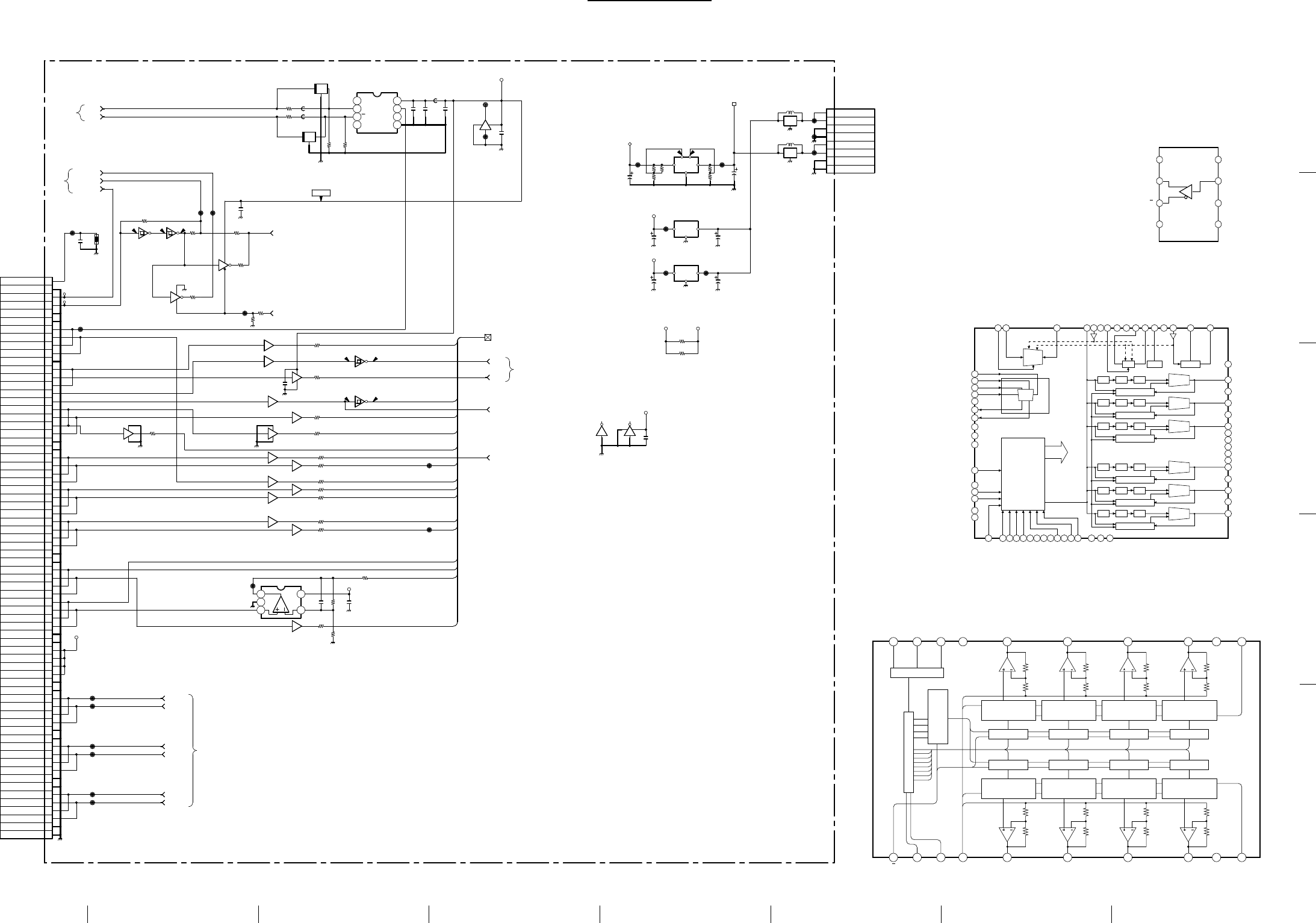
9-31 9-31
A B C D E F GH
1
2
3
4
5
VPL-PX20/PX30
4.81.2
0
D+5V
4.9 2.8 4.9
0
5.0
5.0
IO G
IO G
1
2
3
4
5
6
7
8
GI
O
ON/OFFADJ
1234
5 6 7 8
EMI
EMI
123
4 5
A1
A2
A3
A4
A5
A6
A7
A8
A9
A10
A11
A12
A13
A14
A15
A16
A17
A18
A19
A20
A21
A22
A23
A24
A25
A26
A27
A28
A29
A30
A31
A32
A33
A34
B1
B2
B3
B4
B5
B6
B7
B8
B9
B10
B11
B12
B13
B14
B15
B16
B17
B18
B19
B20
B21
B22
B23
B24
B25
B26
B27
B28
B29
B30
B31
B32
B33
B34
A35
B35
EMI
EMI
FB639
FB640
FL603
FL604
IC625
C755
FB641
R487
R488
C711
R472
R476
R483
R482
R484
C754
R651
C759
CN605
C640
CN600
R629
R1623
R1625
TP616
TP617
JL612
JL627
JL628
JL629
JL630
JL631
JL632
JL634
JL635
R1628
R1629
R1630
JL604
JL607
JL608
JL609
JL640
JL642
JL652
R708
R709
R704
R703 R705
JL618
IC608
JL644
R1624
JL611
JL603
JL610
IC618(2/2)
C728
IC618(1/2)
R1637
C757
C756
R1642
L611
L612
FL600
FL601
C653
C649
C648 C652
C654 C662
R479
R471
R477
JL672
R478
R474
R475
R480
R470
C769
TH600
IC605
IC606
IC626(4/6)
IC626(3/6)
IC626(2/6)
IC626(5/6)
IC626(6/6)
C719
JL643
JL641
IC615(8/8)
IC615(7/8)
IC615(6/8)
IC615(1/8)
IC615(2/8)
IC615(3/8)
IC615(4/8)
IC615(5/8)
IC626(1/6)
IC614(4/8)
IC614(1/8)
IC614(2/8)
IC614(3/8)
IC614(5/8)
IC614(6/8)
IC614(7/8)
IC614(8/8)
IC624
R485
R486
R1641
R1638
330
1/16W
:CHIP 330
1/16W
:CHIP
0.1
16V
B:CHIP
BLM11B750S
BLM11B750S
MC100ELT20
PECL DRV
#
#
0.1
16V
B:CHIP
47
1/16W
:CHIP
47
1/16W
:CHIP
47
1/16W
:CHIP
270
1/16W
:CHIP
470
1/16W
:CHIP
0.1
16V
B:CHIP
#
5p
:CH
0.01
25V
B:CHIP
8P
:SMD
70P
47
1/16W
:CHIP
#
#
#
#
#
10k
:CHIP
1/16W
4.7k
:CHIP
1/16W
510
:RN-CP
8.2k
:RN-CP 20k
:RN-CP
PQ20VZ5U
15V REG
#
#
#
100
1/16W
:CHIP
BKM1608TS601
#
0.1
16V
B:CHIP
#
#
#
#
#
#
#
#
#
#
#
#
#
#
#
#
#
#
#
#
#
#
#
#
#
100
16V
:AL-CP
100
16V
:AL-CP
100
16V
:AL-CP
100
16V
:AL-CP
47 1/16W :CHIP
47 1/16W :CHIP
47 1/16W :CHIP
#
47 1/16W :CHIP
47 1/16W :CHIP
47 1/16W :CHIP
47 1/16W :CHIP
47 1/16W :CHIP
100
25V
:AL-CP
100
25V
:AL-CP
0.1
16V
B:CHIP
47µH
47µH
PQ05SZ1U
A5V REG
PQ05SZ1U
D5V REG
TC74VHC14FT
INV
TC74VHC14FT
INV
TC74VHC14FT
INV
TC74VHC14FT
INV
TC74VHC14FT
INV
0.1
16V
B:CHIP
#
#
TC74VHCT541AFT
BUFF
TC74VHCT541AFT
BUFF
TC74VHCT541AFT
BUFF
TC74VHCT541AFT
BUFF
TC74VHCT541AFT
BUFF
TC74VHCT541AFT
BUFF
TC74VHCT541AFT
BUFF
TC74VHCT541AFT
BUFF
TC74VHC14FT
INV
TC74VHCT541AFT
BUFF
TC74VHCT541AFT
BUFF
TC74VHCT541AFT
BUFF
TC74VHCT541AFT
BUFF
TC74VHCT541AFT
BUFF
TC74VHCT541AFT
BUFF
TC74VHCT541AFT
BUFF
TC74VHCT541AFT
BUFF
LM7131B
SID AMP
0
SHORT
0
SHORT
0
SHORT
0
SHORT
MCLK
MCLK
EVEN R
ODD B
ODD G
ODD R
D5V-2
LCD DRIVE
CLP
DWN
BLKI
EVEN B
EVEN G
A5V
SDA100K
D5V-2
SCL1
SCL
D5V-2
A5V
15.5V
17V
A5V
A5V
SCL0
PANEL CONT
D5V-2
RB DIR
9
11
2010
812
1
19
218
317
416
515
614
713
713
812
1
19
218
317
416
515
614
911
20
10
26
8
1
53
4
7
12
34
5
6
9
8
147
11 1013 12
FRP
PRG
PCG
VST
VCK
ENB
HCK1
HST
POS-CON1
POS-CON2
INV-CNT
ENB1
HCK2
SID-OUT
RGT
PANEL TEMP
GND
GND
GND
GND
GND
A5V
GND
GND
GND
GND
ECLK
HCK1
HCK2
ENB
PCG
DWN
RGT
CLP
PRG
VCK
FRP
VST
HST
INVCNT
BLK
POSCONT1
POSCONT2
A5V
EVENB
EVENG
EVENB
EVENG
EVENR
ODDB
EVENR
ODDB
ODDG
ODDR
ODDG
ODDR
NC
NC
NC
VCC
GND
D
Q
Q
ECLK
TO BC CN501
SDA100K
SCL100K
HCK1
HCK2
ENB
PCG
GND
CLP
PRG
VST
VCK
HST
FRP
POSCONT2
INVCNT
SID
POSCONT1
SID
A5V
A5V
GND
GND
GND
GND
6V
17V
17V
6V
GND
GND
GND
GND
GND
GND
GND
GND
(LCD DRIVER)
(P1)
(P1,2)
B-SS1696<08.>-C..-P3
C(3/3)
TO GA CN2104
(P2)
(P1)
(P2)
(P1)
(P2)
(P1)
(P1)
C (3/3) C (3/3)
• Refer to page 9-28 for Printed Wiring Board
• Refer to page 9-28 for Waveforms
• Refer to page 9-31 for IC Block Diagrams
CS0
20
CS1
19
CS2
18
VDD
16
Vref U2
11
VDD
17
AO4
15
CHIP SELECT
8 BIT LATCH
R2
8 BIT PRECEDENCE
SEGMENT R-2R
ADDRESS
DECODER
R1
AO3
14
8 BIT LATCH
R2
8 BIT PRECEDENCE
SEGMENT R-2R
R1
AO2
13
8 BIT LATCH
R2
8 BIT PRECEDENCE
SEGMENT R-2R
R1
AO1
12
8 BIT LATCH
R2
8 BIT PRECEDENCE
SEGMENT R-2R
R1
R
1
SCL
2
SDA
3
GND
10
Vref U1
9
Vref L
8
AO5
4
I C BUS TRANSCIVER
2
8 BIT LATCH
R1
8 BIT PRECEDENCE
SEGMENT R-2R
R2
AO6
5
8 BIT LATCH
R1
8 BIT PRECEDENCE
SEGMENT R-2R
R2
AO7
6
8 BIT LATCH
R1
8 BIT PRECEDENCE
SEGMENT R-2R
R2
AO8
7
8 BIT LATCH
R1
8 BIT PRECEDENCE
SEGMENT R-2R
R2
M62399FP (IC602)
OFFSET CANCEL
SID
S/H S/H S/H
BIAS VCOM GND2
VCOMOUT
VCOMOFST
SIGCEN
NC
ISET
SID OUT
SID IN
D.P
D.P
SID OFST
VCC
FRP
SH IN
45
INV OUT
46
VIDEO IN
47
OFFSET
48
DLY CNT 49
MCLK 50
MCLK/ 51
INV CNT 52
VDD 53
CLK OUT 54
CLK OUT/ 55
CLK IN TIMING
GENERATOR
S/H
PULSES
OFFSET CANCEL
MODE TIMMING
59
NC 60
CLK IN/ 61
POS CNT1
1
POS CNT2
2
NEXT OUT
3
NEXT IN
4
F/R CNT
5
GND
6
NC
7
D.P
8
D.P
9
S/12 CNT
10
NC
11
ENB
12
DIR CNT
13
NC
14
NC
15
NC
16
PRG 62
NC 63
NC 64
D.P 56
D.P 57
DGND 58
44 43 42 41 40 39 38 37 36 35 34 33
32
SH OUT1
31
NC
30
SH OUT2
29
NC
28
SH OUT3
27
PVCC
26
D.P
25
D.P
24
PGND
23
NC
22
SH OUT4
SH OUT5
SH OUT6
21
D
CLOCK
DELAY
INVERT
AMP
BUFFER
OFFSET CANCEL
S/H S/H S/H
BUFFER
OFFSET CANCEL
S/H S/H S/H
BUFFER
OFFSET CANCEL
S/H S/H S/H
19
17
NC
18
NC
20
BUFFER
OFFSET CANCEL
S/H S/H S/H
BUFFER
OFFSET CANCEL
S/H S/H S/H
BUFFER
CXA2112R (IC603, 604, 609, 610, 611, 612)
8VCC
7DO
6NC
TTL
PECL
5GND
NC
Q
Q
NC
1
2
3
4
MC100ELT20 (IC625)
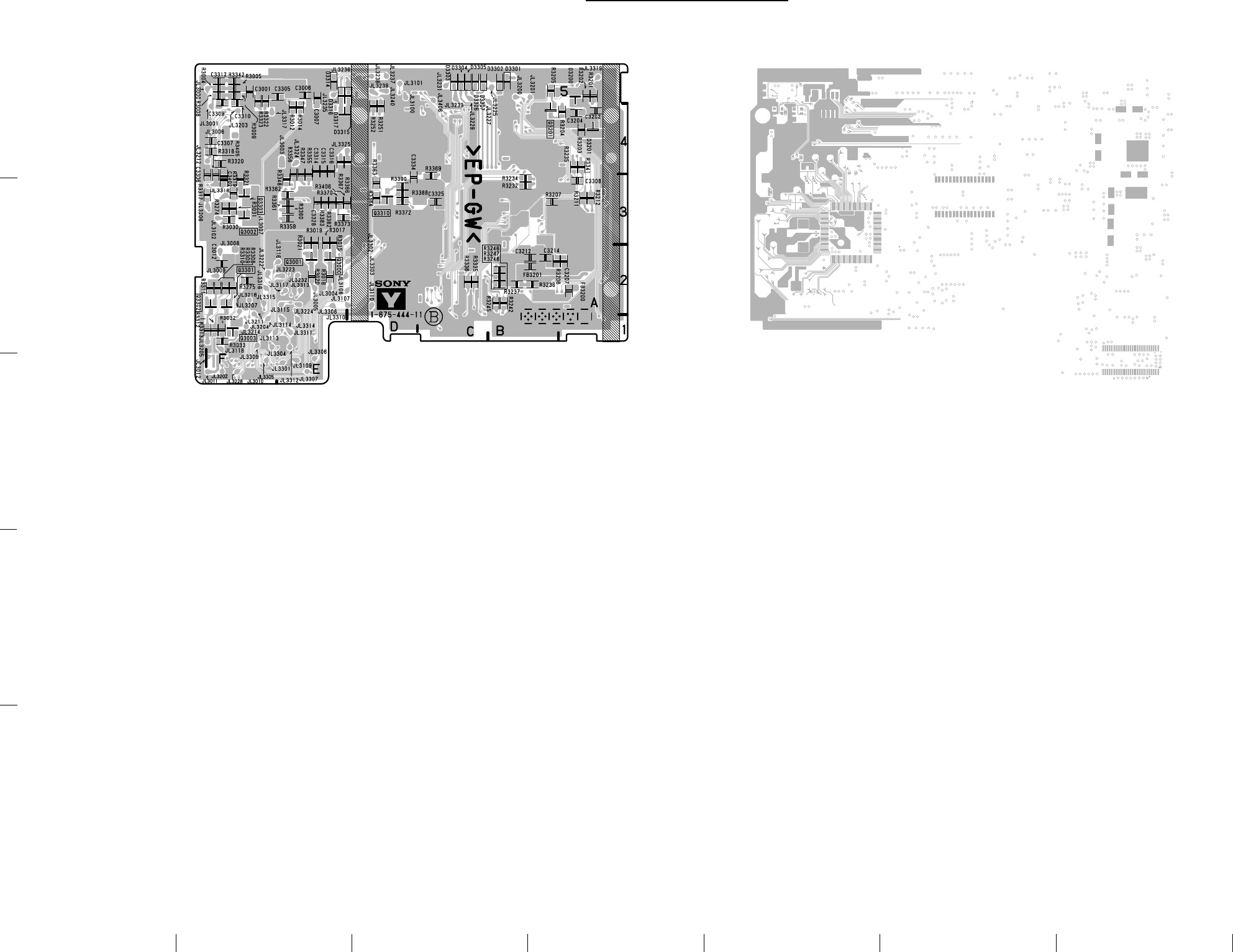
9-32 9-32
A B C D E F GH
1
2
3
4
5
VPL-PX20/PX30
Y, S, NF, NR Y, S, NF, NR
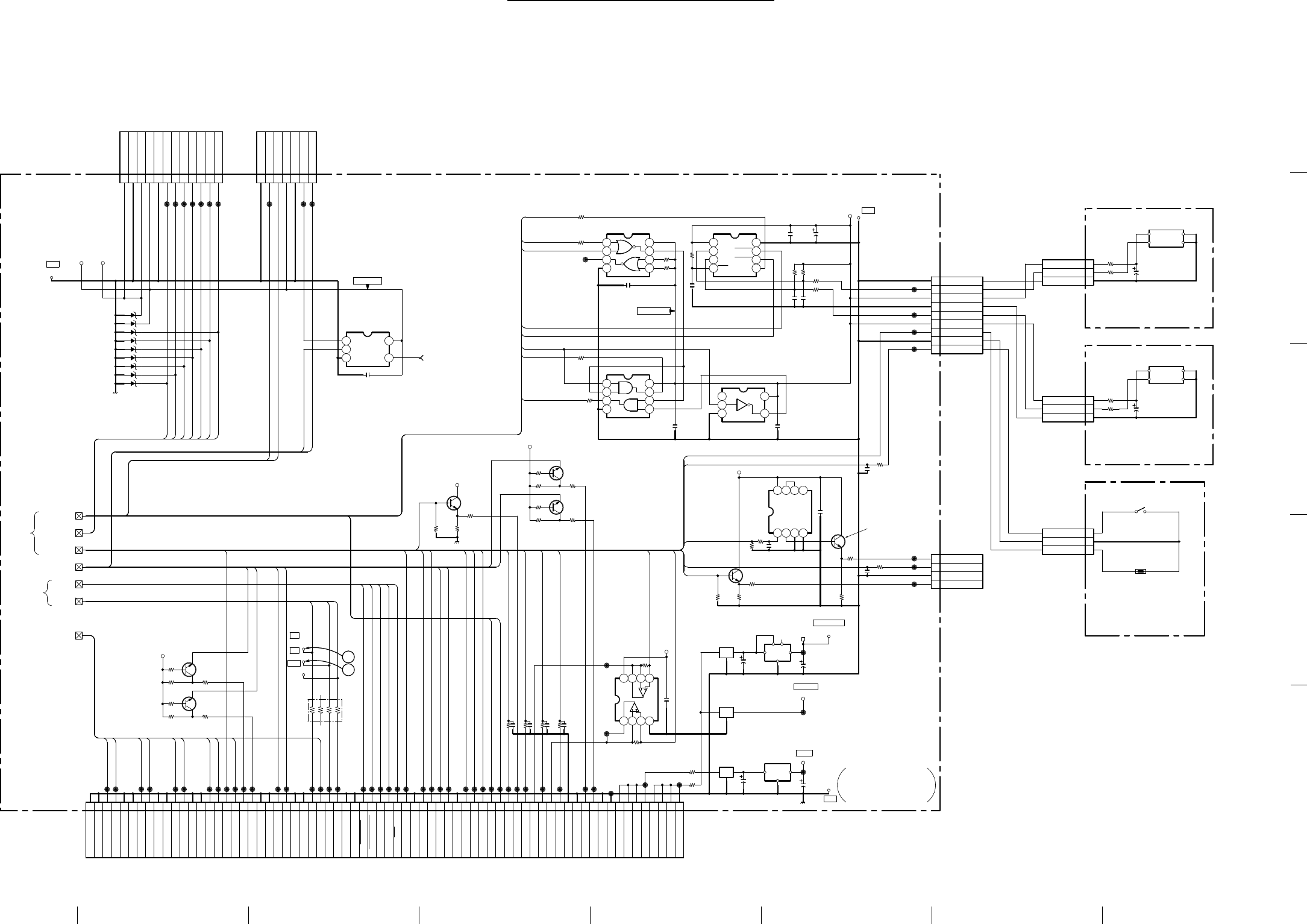
9-33 9-33
A B C D E F GH
1
2
3
4
5
VPL-PX20/PX30
SUB +5V
D+5V-1
1
2
G
IO
ON/OFF ADJ
A1
A2
A3
A4
A5
A6
A7
A8
A9
A10
A11
A12
A13
A14
A15
A16
A17
A18
A19
A20
A21
A22
A23
A24
A25
A26
A27
A28
A29
A30
A31
A32
A33
A34
B1
B2
B3
B4
B5
B6
B7
B8
B9
B10
B11
B12
B13
B14
B15
B16
B17
B18
B19
B20
B21
B22
B23
B24
B25
B26
B27
B28
B29
B30
B31
B32
B33
B34
A35
B35
1
2
3
4
5
6
7
8
9
10
11
12
1
2
3
4
5
6
7
1234
5 6 7 8
123
4 5
1234
5 6 7 8
1234
5 6 7 8
123
4 5
1 2 3 4
5678
1
2
3
VCC
OUT
GND1
GND2
1
2
3
VCC
OUT
GND1
GND2
1
2
3
EMI
EMI
EMI
IO
G
1
2
3
4
1234
5678
1
2
3
4
5
6
7
8
9
CN3000
R3002
R3004
R3005
R3007
R3008
R3009
R3012
R3014
R3015 R3016
R3017
R3019
R3020R3021
C3006 C3007
C3008 C3009
C3012
C3013 C3014
JL3003
JL3006
JL3007
JL3008
JL3009
JL3010
JL3011 JL3012
RB3003
FL3000
FL3001
FL3002
TP3000
TP3008
IC3002 IC3003
IC3004
IC3006
IC3007
Q3000
Q3001
TP3009
TP3202
TP3203
TP3206
JL3100
JL3101
JL3206
JL3102
JL3201
JL3200
JL3225
JL3227
JL3229
JL3231
JL3233
JL3107
JL3108
JL3109
JL3110
JL3113
JL3114
JL3223
JL3224
JL3222
JL3115
JL3232
JL3228
JL3116
JL3117
JL3204
JL3211
JL3118
JL3207
JL3214
JL3216
JL3205
JL3202
Q3002
Q3003
R3032
R3033
C3001
R3274
R3275
R3031
R3030
R3231
R3264
R3265
CN3003CN3001
JL3004
JL3005
D3301
D3302
D3303
D3304
D3305
D3306
D3307
D3308
D3309
JL3301
JL3302
JL3303
JL3304
JL3305
JL3306
JL3307
R3308
R3309
R3310
R3311
Q3301
Q3302
R3312
R3313
JL3308
JL3309
JL3310
JL3311
JL3312
JL3313
JL3314
JL3315
JL3316
C3301
C3302
C3303
C3304
R3314
R3315
R3316
IC3302
JL3317
C3305
TP3303
JL3318
R3317
C3306
C3307
R3318
Q3303
R3319
R3320
R3321
R3322
R3323
C3309 C3310
C3311
R3342
C3312
IC3301
IC3401
C3401
CN3005
R3405
IC3402
C3403
JL3406
C3402
CN3002
JL3000
JL3001
JL3203
JL3212
CN3600
C3600
IC3600
R3601
R3600
CN3700
C3700
IC3700
R3701
R3700
CN2020
S2020
TH2020
R3402
R3401
47
6.3V
:AL-CP
22
16V
:AL-CP
BA033FP-E2
3.3V REG
47
6.3V
:AL-CP
22
16V
:AL-CP
NFM41P11C204
NFM41P11C204
NFM41P11C204
PQ05AZ1U
5V REG
100
:CHIP
100
:CHIP
TC7W08FU
AND
100
:CHIP
100
:CHIP
100
:CHIP
100
:CHIP
100
:CHIP
4.7k
:CHIP
100
:CHIP
4.7k
:CHIP
70P
TC7S04FU
#
BUFF
2SC3326N
BUS SW
2SC3326N
BUS SW
47k
:CHIP
47k
:CHIP
2.2k
:CHIP
2.2k
:CHIP 100*4
2SC2712-YG
BUFFER
2SC2712-YG
BUFFER
10k
:CHIP
220
:CHIP
1
10V
B:CHIP
2.2k
:CHIP
47
:CHIP
100 :CHIP
100 :CHIP
100 :CHIP
7P
WHT
:SMD
12P
WHT
:SMD
RD5.6SB-T1
RD5.6SB-T1
RD5.6SB-T1
RD5.6SB-T1
RD5.6SB-T1
RD5.6SB-T1
RD5.6SB-T1
RD5.6SB-T1
RD5.6SB-T1
2.2k
:CHIP
4.7k
:CHIP
2.2k
:CHIP
4.7k
:CHIP
2SC3326N
BUS SW
2SC3326N
BUS SW
100
:CHIP
100
:CHIP
0.01 B:CHIP
100 :CHIP
0
:CHIP
0
:CHIP
TC7W02FU
NOR
100
:CHIP
100
:CHIP
2SC2712-YG
BUFFER
47
:CHIP
10k
:CHIP
2.2k
:CHIP
100
:CHIP
100
:CHIP
0.01 B:CHIP
0.01 B:CHIP
0.01 B:CHIP
0.01
B:CHIP
0.01
B:CHIP
10k
:CHIP
10k
:CHIP
100p
50V
CH:CHIP
100p
50V
CH:CHIP
47
6.3V
:AL-CP
5.6k
:CHIP
#
#
#
#
#
#
#
#
##
#
#
#
#
#
#
#
#
#
#
#
#
#
#
#
#
#
#
#
#
#
#
#
#
#
#
#
#
#
#
#
#
#
#
#
#
#
#
#
#
#
#
#
#
#
#
#
#
#
#
#
IRMF
IRDA FILTER
0.1
25V
B:CHIP
0.1
25V
B:CHIP
0.1
25V
B:CHIP
0.1 25V B:CHIP
0.1
25V
B:CHIP
0.1
25V
B:CHIP
TC7W14FU
SCMT INV
0.1
25V
B:CHIP
#
9P
WHT
:SMD
TC7S66FU
ANALOG SW
100k
:CHIP
10
6.3V
B:CHIP
4P
WHT
:SMD
#
#
#
#
3P
WHT-I
:SMD
10
20V
:TA-CP
RS-140-T
47
1/10W
:CHIP
100
1/10W
:CHIP
3P
RED
:SMD
10
20V
:TA-CP
RS-140-T
47
1/10W
:CHIP
100
1/10W
:CHIP
3P
:SMD
LAMP COVER
LAMP TEMP
0
SHORT
0
SHORT
5V-2
5V
3.3V
5V
5V-2
COMM.BUS
OSDC
CON-PANE
CTRL
SIRCS
SYNC
5V 5V-2
USB
5V-2
5V
5V-2
5V-2
CPU_RES≠≠≠≠≠≠≠≠≠≠≠≠≠
1234
5678
1234
5678
US+
US-
DS1+
DS1-
P.ENA
P.FLG
KEY0
KEY1
POWER LED
TEMP LED
LAMP LED
P.SAVE LED
LIGHT ON
SIRCS-S
SIRCS
SCL 400K
SDA 400K
TXD S/C
RXD S/C
HD
VD
VSO
OSD CS3≠≠≠≠≠≠≠≠≠≠≠≠≠
PANEL LINK
SCLK
AUDIO CE
AUDIO MUTE
PANEL TEMP
FIL. COVER
FAN PROT1
FAN PROT2
FAN CONT1
FAN CONT2
RXD RS
TXD RS
SIRCS
MOUSE ENA≠≠≠≠≠≠≠≠≠≠≠≠≠≠≠≠≠
IRDA
IRDB
MOUSE A/B≠
POWER PROT
POWER ON
OSD CS0≠≠≠≠≠≠≠≠≠≠≠≠≠
S/C RES
DS2+
DS2-
IRDA
IRDB
NF ON≠≠≠
NR ON≠≠≠
SIRCS-S
SDAT
LAMP TEMP
LAMP COVER
LAMP PROT
LAMP ON
LAMP NORM/ECO≠≠≠≠≠≠≠
SDA 100K
SCL 100K
MS P.ENA
VBUS
INTERLACE
PIC MUTE
P96
P97
P94
SUB+5V
SUB+3.3V
D+5V
-1
-1
-1
GND
GND
-1
V+
V-
GND
HD
VD
VSO
-1
VDD VSS
IRIN1
IRIN2
IROUT
RES
IREN1
IREN2
I/O
O/I
GND
VCC
COND
1A
3Y
2A
GND
VCC
1Y
3A
2Y
TO BALAST
(P2)
TO BB CN307
GND
GND
US+
US-
GND
GND
DS1+
DS1-
GND
GND
SDA400K
SCL400K
GND
GND
GND
HD
VD
VSO
GND
GND
USB P.ENA
USB P.FLG
TXD S/C
RXD S/C
GND
GND
DS2+
DS2-
GND
S/C RES
MS P.ENA
US VBUS
GND
SDAT
SCLK
GND
PANEL LINK
AUDIO CE
AUDIO MUTE
PANEL TEMP
POWER ON
FAN PROT1
FAN CONT1
FAN CONT2
FAN PROT2
FIL. COVER
PW-OSD ENA
IRDA
IRDB
INTERLACE
PIC MUTE
P96
P97
P94
OSDC CS
GND
+6V
GND
GND
SDA100K
SCL100K
GND
POWER PROT
+6V
+6V
+6V
SUB+5V
SUB+5V
SUB+5V
SUB+5V
GND
LAMP PROT
LAMP ON
LAMP MODE
SUB+5V
GND
GND
SIRCS-NF
SUB+5V
SIRCS-NR
GND
LAMP COVER
LAMP TEMP
TO H CN3500 TO QD CN1903
GND
SUB+5V
SIRCS
SIRCS-S
GND
TXD RS
RXD RS
GND
GND
KEY1
KEY0
LIGHT ON
P.SAVE LED
LAMP LED
TEMP LED
POWER LED
SUB+5V
D+5V
D+5V
(P2)
(P2,P3)
(P2)
(P3)
Y(1/3)
B-SS1696<08.>-Y..-P1
ANALOG SW
IRDA FILTER
SCMT INV
NF
B-SS1696<08.>-NF.
(FRONT RECEIVER)
TO Y CN3005
SUB+5V
GND
SIRCS-NF
SUB+5V
GND
TO Y CN3005
(REAR RECEIVER)
B-SS1696<08.>-NR.
NR
SIRCS-NR
GND
LAMP COVER
LAMP TEMP
S
(SW AND TH)
TO Y CN3005
B-SS1696<08.>-S..
Y (1/3), S, NF, NR Y (1/3), S, NF, NR
• Refer to page 9-32 for Printed Wiring Board
• Refer to page 9-35 for Waveforms
• Refer to page 9-35 for IC Block Diagrams
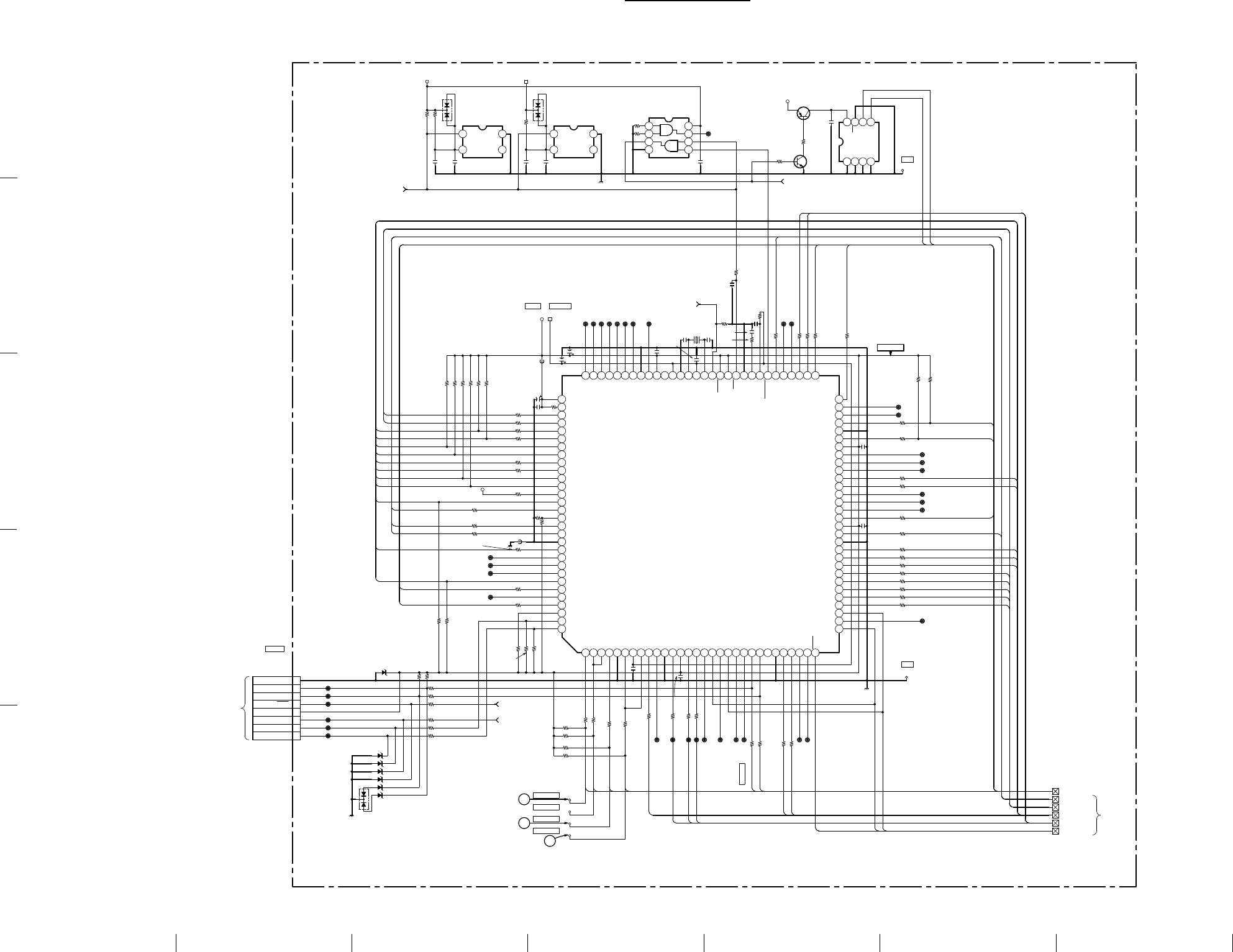
9-34 9-34
A B C D E F GH
1
2
3
4
5
VPL-PX20/PX30
D+5V-1
3
4
5
1 2 3 4 5 6 7 8 9 10 11 12 13 14 15 16 17 18 19 20 21 22 23 24 25 26 27 28 29 30
31
32
33
34
35
36
37
38
39
40
41
42
43
44
45
46
47
48
49
50
51
52
53
54
55
56
57
58
59
60
616263646566676869707172737475767778798081828384858687888990
91
92
93
94
95
96
97
98
99
100
101
102
103
104
105
106
107
108
109
110
111
112
113
114
115
116
117
118
119
120
12
3 4
12
3 4
1234
5678
1
2
3
4
5
6
7
8
1234
5678
CN3010
R3201
R3202
R3203
R3204
R3205
R3206
R3207
R3208
R3211
R3212
R3213
R3214
R3216 R3217
R3220
R3221
R3222
R3223
R3224
R3232
R3234
R3239
R3243
R3245
R3246
R3247
R3248
R3249 R3250
R3251
R3252
R3253
R3254
R3255
R3256
R3257 R3258 R3259
R3260
R3261
C3200
C3202 C3203 C3204 C3205 C3206
C3207
C3208
C3209 C3210
C3211
C3212
C3213
C3214
C3215
C3216
C3217
C3218
C3219 C3220
FB3200
JL3210
JL3213
JL3235
JL3236
JL3237
JL3238
JL3239
JL3240
JL3245
JL3246
JL3247
JL3248
JL3249
JL3250
JL3251
JL3252
JL3256
JL3257
TP3200
TP3201
IC3200
IC3201 IC3202
IC3203
Q3200
Q3201
D3200 D3201
JL3259
JL3260
JL3261
JL3262
JL3263
JL3264
JL3265
JL3266
R3267
R3268
R3215
R3276
R3277
JL3215
JL3217
R3262
R3263
JL3241
JL3242
JL3243
JL3253
R3324
R3325 JL3319
R3326
R3327
R3328
R3329
C3308
JL3322
TP3204
TP3205
TP3301
TP3302
D3310
D3311
D3312
D3313
D3314
D3315
D3316
D3317
R3330
R3331
R3332 R3333
R3334
JL3323
R3337
R3338
R3339
R3307
R3340
R3227
R3228
R3341
R3303
R3304
R3305
R3306
R3301
R3302
X3200
JL3401
JL3402
R3336
R3335
R3403
R3404
R3240
R3241
R3242
JL3403
JL3404
JL3405
IC3204
R3236
R3235
R3237
FB3201R3271
2SC2712-YG
RES SW
S-80828ANNP
RESET
22
6.3V
:AL-CP
22
6.3V
:AL-CP
22
6.3V
:AL-CP
TC7W08FU
AND
2SA1213Y
RES SW M24C64-WMN
EEPROM
BK2125HM601
1
10V
B:CHIP
1
10V
B:CHIP
10p
CH:CHIP 10p
CH:CHIP
0.01
B:CHIP
100 :CHIP
100 :CHIP
100 :CHIP
100 :CHIP
100
:CHIP
470p
CH:CHIP
10k
:CHIP
33k
:CHIP
33k
:CHIP
1k
:CHIP
47k
:CHIP
200
:RN-CP
10k
:CHIP
3k
:RN-CP
2.2k
:CHIP
2.2k
:CHIP
10k :CHIP
10k :CHIP
10k :CHIP
10k :CHIP
0
:CHIP
100 :CHIP
100 :CHIP
100 :CHIP
100 :CHIP
10k
:CHIP
10k
:CHIP
10k
:CHIP
10k
:CHIP 10k
:CHIP
100 :CHIP
100 :CHIP
100 :CHIP
100 :CHIP
100 :CHIP
100 :CHIP
100
:CHIP 100
:CHIP
100
:CHIP
100
:CHIP
100
:CHIP
10k :CHIP
10k :CHIP
100 :CHIP
1k :RN-CP
2.7k :RN-CP
2.2k
:CHIP
2.2k
:CHIP
100
:CHIP
100
:CHIP
100 :CHIP
100 :CHIP
100 :CHIP
100 :CHIP
0.01
B:CHIP
RD5.6SB-T1
RD5.6SB-T1
RD5.6SB-T1
RD5.6SB-T1
RD5.6SB-T1
RD5.6SB-T1
RD5.6SB-T1
2.2k
:CHIP
2.2k
:CHIP
100
:CHIP 100
:CHIP
100
:CHIP
100 :CHIP
100 :CHIP
100 :CHIP
100 :CHIP
100 :CHIP
100 :CHIP
100 :CHIP
10
:CHIP
330 :CHIP
330 :CHIP
330 :CHIP
330 :CHIP
1k :CHIP
1k :CHIP
8P
WHT
:SMD
S-80842ANNP
RESET
#
#
#
#
#
#
#
#
#
#
#
#
#
#
#
#
#
#
#
#
#
#
#
#
#
#
#
#
#
#
#
#
#
#
#
12.288MHz
0.1
25V
B:CHIP
0.1
25V
B:CHIP
0.1
25V
B:CHIP
0.1
25V
B:CHIP
0.1
25V
B:CHIP
0.1
25V
B:CHIP
0.1
25V
B:CHIP
0.1
25V
B:CHIP
0.1
25V
B:CHIP
0.1
25V
B:CHIP
0.1
25V
B:CHIP
DAN202K-T-146 DAN202K-T-146
DAN202K-T-146
#
#
100 :CHIP
100 :CHIP
100 :CHIP
100 :CHIP
#
#
#
#
#
#
HD64F2633TE
MAIN CPU
#
1k :CHIP
10k
:CHIP
BK2125HM601100
:CHIP
3.3V
CPU_RES
CPU_RES
FWE
3.3V
5V
5V
5V
5V-2
RESET
FWE
COMM.BUS
OSDC
CON-PANE
CTRL
SIRCS
SYNC
SIRCS
VSO
HD
VD
LIGHT ON
P.SAVE LED
LAMP LED
TEMP LED
POWER LED
LAMP ON
POWER ON
OSD CS0
PANEL LINK
AUDIO MUTE
SDA USB
SCL USB
SCL 400K
SDA 400K
RXD S/C
TXD S/C
MOUSE A/B
MOUSE ENA
OSD CS3
KEY0
KEY1
LAMP TEMP
PANEL TEMP
LAMP PROT
FAN PROT1
FAN PROT2
FAN CONT1
FAN CONT2
LAMP COVER
SCLK
FIL. COVER
SCL 400K
SDA 400K
AUDIO CE
POWER PROT
S/C RES
NF ON
NR ON
USB REQ
LAMP NORM/ECO
SCL 100K
SDA 100K
SDAT
INTERLACE
PIC MUTE
RXD RS
TXD RS
P94
P96
P97
PC0
PC1
PC2
PC3
VSS
PC4
VCC
PC5
PC6
PC7
VSS
PVCC1
PB1
PB2
PB3
PB5
PB7
PA0
PA3
VSS
P10
P11
P12
P13
IRQ0
TCLKC
P16
PE0
PE1
PE2
PE3
PE4
PE5
PE6
PE7
VSS
PD0
PVCC1
PD1
PD2
PD3
PD4
PD5
PD6
PD7
PVCC2
VSS
RXD4
TXD4
PG0
PG1
PG2
PG3
PG4
PLLVCC
PLLCAP
PLLVSS
NMI
FWE
XTAL
VCC
EXTAL
VSS
OSC1
OSC2
PVCC1
PF7/
?
VSS
PF6
PF5
PF4
PF3
PF2
PF1
PF0
AVCC
VREF
AN15/P97
AVSS
P70
P71
P72
P73
P74
MD0
MD1
MD2
TXD
RXD
VIN
GND
RES
FWR
MD1
MD2
E0
E1
E2
WC
OUT
VDD
VSS
NC
OUT
VDD
VSS
NC
GND
VCC
SCL
SDA
RES
WDTOVF
STBY
FLASH
GND
-1
-1
3.3V-15V-1
-1
-1
RXD2(/PA2)
TXD2(/PA1)
TIOCA3(/PB0)
TIOCA4(/PB4)
TIOCA5(/PB6)
(/P14)
(/P15)
TIOCB2(/P17)
TXD0(/P30)
RXD0(/P31)
SDA1(/P32)
SCL1(/P33)
SDA0(/P34)
SCL0(/P35)
(/P36)
(/P37)
AN0(/P40)
AN1(/P41)
AN2(/P42)
AN3(/P43)
DA0(/P46)
DA1(/P47)
P44
P45
P90
P91
AN10(/P92)
P93
P95
SCK3(/P75)
TXD3(/P77)
WDT P.
-1
GND
P94
AN14/P96
RXD3/P76
SDA400K
SCL400K
SCL100K
SDA100K
(P1)
(P1,P3)
(P3)
(P1,P2)
(P2)
(P1,P2)
(P2)
(MAIN CPU)
Y(2/3)
B-SS1696<08.>-Y..-P2
NC
• Refer to page 9-32 for Printed Wiring Board
• Refer to page 9-35 for Waveforms
• Refer to page 9-35 for IC Block Diagrams
Y (2/3) Y (2/3)
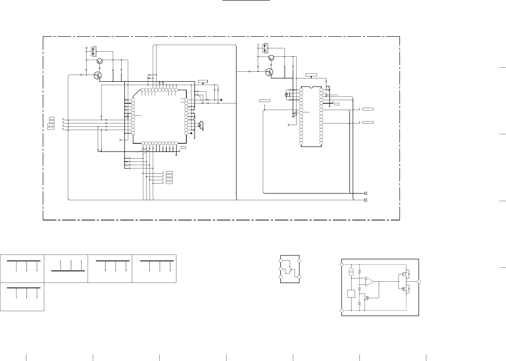
9-35 9-35
A B C D E F GH
1
2
3
4
5
VPL-PX20/PX30
D+5V-1
+3.3V
1234567891011121314151617
18 19 20 21 22 23 24 25 26 27 28 29 30 31 32 33 34
1234567891011
12
13
14
15
16
17
18
19
20
21
22
23 24 25 26 27 28 29 30 31 32 33
34
35
36
37
38
39
40
41
42
43
44
IC3304
IC3303
C3313
C3314
C3315
C3316
C3317C3318
C3319
C3320
C3321
C3322
R3343
R3344
R3346
R3345
R3349
R3350
X3301
X3302
R3357
R3358
R3364
C3323
C3324
R3366 R3367
R3368
R3365
C3325
C3327
C3326
R3371
JL3325
R3370
C3328 R3372
C3330
R3373
R3359
R3360
R3361
R3362
R3351
R3352 R3353
R3354
TP3007
TP3005
TP3006
TP3004
TP3003
TP3002
TP3001
TP3304
TP3306
TP3305
TP3307
TP3308
TP3309
R3378
R3382
R3383
Q3307
D3318
R3386
C3332
D3320
Q3310
R3389
R3390 C3334 R3391
Q3306
Q3309
R3363
R3384
R3388
R3369
R3385
R3374
JL3324
R3356
R3347R3355
R3348
10p
CH:CHIP
10p
CH:CHIP
33p
CH:CHIP
33p
CH:CHIP
1M
:CHIP
1.5k
:CHIP
15 :CHIP
15 :CHIP
15 :CHIP
15 :CHIP
24MHz
15k :CHIP
15k :CHIP
3k
:RN-CP
100k
:CHIP 100k
:CHIP
510k
:RN-CP
510k
:RN-CP
1
10V
B:CHIP 1.5k
:CHIP
10k
:CHIP
0.01
B:CHIP
10k
:CHIP
0.01
B:CHIP
#
15k :CHIP
15k :CHIP
15k :CHIP
15k :CHIP
15
:CHIP
15
:CHIP 15
:CHIP 15
:CHIP
3k
:RN-CP
0 :CHIP
0 :CHIP
#
2.2k
:CHIP
4.7
10V
F:CHIP
1k
:CHIP
1k
:CHIP 4.7
10V
F:CHIP
#
0.1
25V
B:CHIP
0.1
25V
B:CHIP
0.1
25V
B:CHIP
0.1
25V
B:CHIP
0.1
25V
B:CHIP
0.1
25V
B:CHIP
0.1
25V
B:CHIP
0.1
25V
B:CHIP
0.1
25V
B:CHIP
0.1
25V
B:CHIP
DAN202K-T-146
DAN202K-T-146
100
:CHIP
100
:CHIP
#
#
µPD72012
USB HUB CTRL
ST7263
USB MONITOR CTRL
2SA1162
DTC144EKA-T146
2SA1162
DTC144EKA-T146
0
:CHIP
4MHz
#
#
15
:CHIP
15
:CHIP
15
:CHIP
15
:CHIP
3.3V
5V
COMM.BUS
USB
RESET≠≠≠≠≠
≠≠≠≠
RESET≠≠≠≠≠
≠≠≠≠
US+
US-
DS1+
DS1-
DS2+
DS2-
DS3+
DS3-
P.FLG
P.ENA
USB REQ
DS3+
DS3-
SDA USB
SCL USB
MS P.ENA
VBUS
VBUS
VDD
OSCOUT
OSCIN
VSS
PC0
PB7
PB6
VPP
PB4
PB3
PB2
PB1
PC2
PC1
RESET
PB5
N.C.
VDDA
USBVCC
USBDM
USBDP
VSSA
PA0
PA1
N.C.
N.C.
N.C.
PA2
PA3
PA4
PA5
PA6
PA7
PB0
DVDD
DGND
PSSEL
PVSEL
DGND
UD0
UD1
D10
D11
DGND
RESET
D20
D21
D30
D31
DGND
DGND
D40
D41
D50
D51
DGND
OSL
AVDD1
CLK/X2
X1
AGND1
AGND2
AVDD2
DVDD
DGND
CS2
CS1
DVDD
DVDD
CLKSEL
PP5
PP4
PP3
PP2
PP1
CS5
CS4
CS3
-1
-1
GND
SCL USB
SDA USB
US+
DS1+
DS1-
US-
USB REQ
DS2-
DS2+
DS3+
DS3-
GND
(P1,P2)
(P1)
B-SS1696<08.>-Y..-P3
Y(3/3)
(USB HUB CTRL/USB MONITOR CTRL)
(P2)
VOO 2
VSS 4
OUT
1
VREF
S-80842ANNP-ED4-T2 (IC3201)
S-80828ANNP-ED4-T2 (IC3202)
IN/OUT
OUT/IN
1
2
GND 3
VCC
5
CONT
4
TC7S66FU (IC3401)
Y Board Waveforms
1234
5
3.2 Vp-p
TP3202 [HD]
3.2 Vp-p
TP3203 [VD]
4.5 Vp-p
TP3204 [SCL400K]
4.5 Vp-p
TP3301 [SCL100K]
4.5 Vp-p
TP3302 [SDA100K]
• Refer to page 9-32 for Printed Wiring Board
• Refer to page 9-35 for Waveforms
• Refer to page 9-35 for IC Block Diagrams
Y (3/3) Y (3/3)
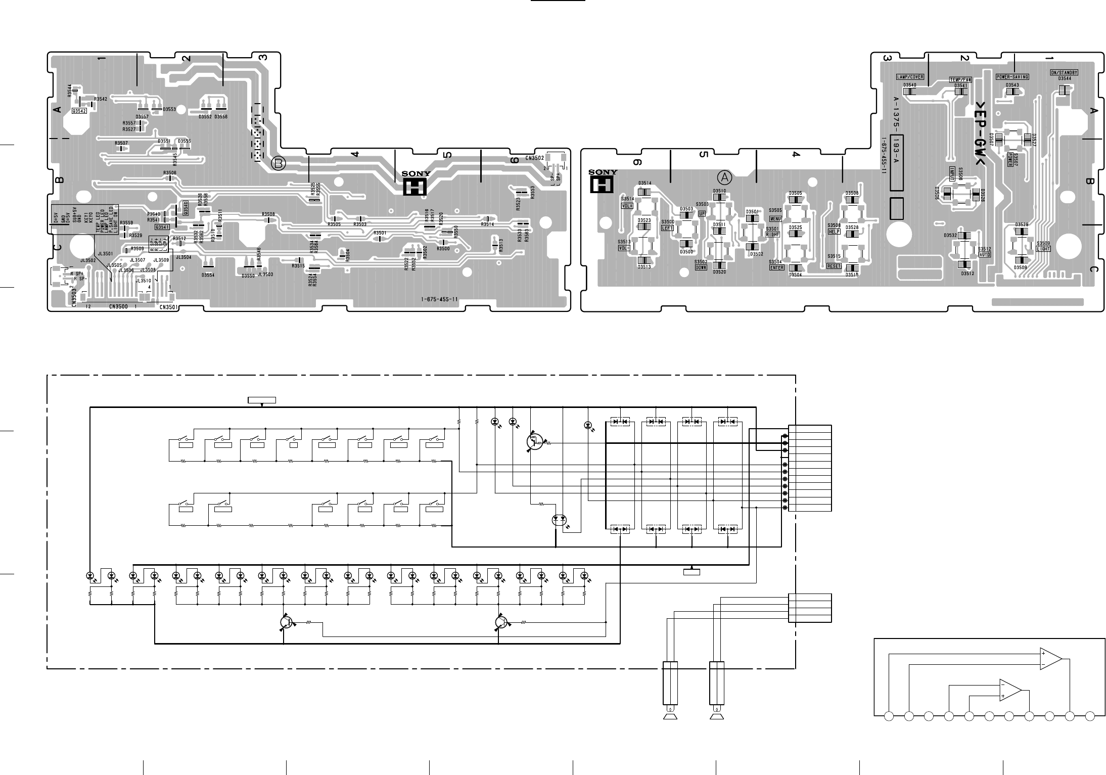
9-36 9-36
A B C D E F GH
1
2
3
4
5
VPL-PX20/PX30
0
SUB +5V
D+5V
2.6
0
0
2.6
0
5.0
5.0
-0.3
1
2
3
4
1
2
3
4
5
6
7
8
9
10
11
12
1
2
1
2
S3500 S3501 S3502 S3503 S3504 S3505 S3506 S3507
S3508 S3509 S3512 S3513 S3514 S3515
R3500 R3501 R3502 R3503 R3504 R3505 R3506 R3507
R3508 R3509 R3510 R3511 R3512 R3513 R3514 R3515
D3500 D3501 D3502 D3503 D3504 D3505 D3506 D3512 D3513D3514 D3515
D3507 D3509 D3508
D3540 D3541 D3543
R3544
Q3540
R3540
Q3541
R3541
Q3542
R3542
R3545 R3546
D3550 D3551 D3552 D3553
D3554 D3555 D3556 D3557
JL3501
JL3502
JL3503
JL3504
JL3505
JL3506
JL3507
JL3508
JL3509
JL3510
D3544
D3527 D3529 D3526 D3532 D3528D3525
R3520 R3522 R3523 R3525 R3526R3529 R3532 R3533 R3534
D3520 D3523
R3559 R3550 R3552 R3553 R3524 R3554 R3555 R3556 R3562 R3563 R3564
R3527 R3557
D3510 D3511
R3516 R3517
CN3502
CN3501
CN3500
CN3503
SEC1901C
TEMP-LED
SEC1901C
LAMP-LED
SEC1801CSEC1801C SEC1801C SEC1801C SEC1801C SEC1801C SEC1801CSEC1801C SEC1801C
SEC1801C
POWER-SAVE
DAP202K
PROTECT DAP202K
PROTECT DAP202K
PROTECT DAP202K
PROTECT
DAN202K
PROTECT
DAN202K
PROTECT
DAN202K
PROTECT
DAN202K
PROTECT
27k
:CHIP 12k
:CHIP 6.8k
:CHIP 3.9k
:CHIP 2.7k
:CHIP 2.2k
:CHIP 1.5k
:CHIP 1.8k
:CHIP
6.8k
:CHIP 3.9k
:CHIP 2.7k
:CHIP 2.2k
:CHIP 1.5k
:CHIP 1.8k
:CHIP
12k
:CHIP
27k
:CHIP
SEC1801C SEC1801C
SEC1401C SEC1801C SEC1801C
330
:CHIP
2SC2712
SW
3.3k
:CHIP
2SC2712
SW
3.3k
:CHIP
DTA144EKA
SW
1k
:CHIP
10k
:CHIP 10k
:CHIP
SEC2422C
ON/STBY
SEC1401C SEC1801C SEC1801C SEC1801C SEC1801CSEC1801CSEC1801C SEC1801C
470
:CHIP 470
:CHIP 470
:CHIP 470
:CHIP 470
:CHIP 470
:CHIP
470
:CHIP 470
:CHIP 470
:CHIP 470
:CHIP
470
:CHIP 470
:CHIP 470
:CHIP 470
:CHIP 470
:CHIP 470
:CHIP
470
:CHIP 470
:CHIP 470
:CHIP 470
:CHIP
220
:CHIP 220
:CHIP
SEC1801CSEC1801C
470
:CHIP 470
:CHIP
2P
WHT-L
:SMD
#
#
#
#
#
#
#
#
#
#
4P
WHT
:SMD
12P
WHT
:SMD
2P
WHT-I
:SMD
RESET
LEFT RIGHT DOWN UP ENTER MENU INPUT POWER
AUTO VOL- VOL+LIGHTHELP
L SP-
L SP+
R SP-
R SP+
GR
B-SS1696<08.>-H..
(CONTROL PANEL)
H
TO KS CN2952
LR
FRONT SPEAKER
GND
GND
KEY1
KEY0
LIGHT ON
P.SAVE LED
LAMP LED
TEMP LED
POWER LED
SUB+5V
D+5V
D+5V
L SP+
L SP-
R SP+
R SP-
TO Y CN3001
H – B SIDE –
SUFFIX ; -11
H – A SIDE –
SUFFIX ; -11
2 4 51 3
RIN
6 8 97
LIN NC
10 11
TDA2009A (IC2900)
H H
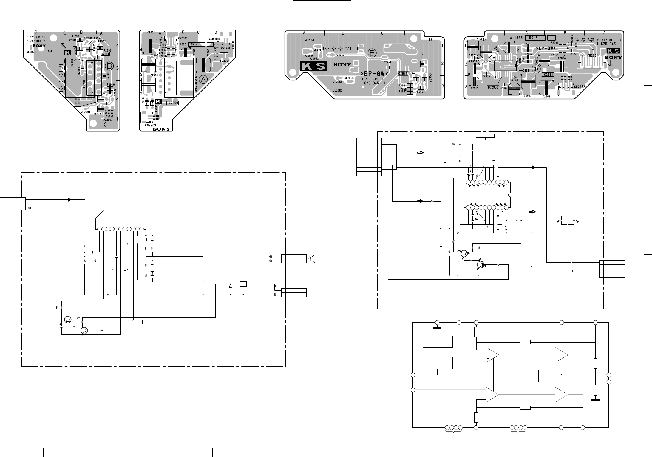
9-37 9-37
A B C D E F GH
1
2
3
4
5
VPL-PX20/PX30
AUDIO +B
L/R
1 2 3 4 5 6 7 8 9 10 11
1
2
3
EMI
1
2
1
2
IC2900
R2900 R2901
Q2900
R2902
Q2901
C2901
R2907
C2902
C2903
C2905
R2908
R2909
R2910
R2911
R2912
R2913
R2903
R2904
C2904
CN2903
C2900
CN2901
FL2001
C2908
CN2900
R2906
R2905 R2914
C2907
C2906
2SC2712
SP-MUTE
12k
:CHIP
12k
:CHIP
3.3k
:CHIP 10k
:CHIP
470
:CHIP
2SA1162
SP-MUTE
100k
:CHIP
2.2
16V
:CHIP
100
25V
:AL-CP
2.2
16V
:CHIP
100
25V
:AL-CP
100
25V
:AL-CP
TDA2009A
AUDIO AMP
68
:CHIP
2.7k
:CHIP
68
:CHIP
2.7k
:CHIP
2.2
1/4W
:FPRD
2.2
1/4W
:FPRD
2P
WHT-L
:SMD
100
25V
:AL-CP
10
35V
:AL-CP
3P
WHT-L
:SMD
2P
RED-L
:SMD
STC332B
1k
:RN-CP
470
:RN-CP 180
:RN-CP
0.1
25V
B:CHIP
0.1
25V
B:CHIP
AUD GND
GND
R IN
INV.INR
SVRR
INV.INL
L IN
N.C.
L OUT
VCC
R OUT
N.C.
SP-MUTE
L/R
AUDIO+B
MAIN+
MAIN-
GND
(AUDIO AMP)
B-SS1696<08.>-K..
K
TO QA CN809
TO GA CN2105
REAR SPEAKER
11.9 11.7
AUDIO +B
11.9 11.9
0.5
11.8
0
0.3
0
0
0
0
0
0.5
11.8
5.8
11.9
10.9
L
L
R
R
OUTVCC
GND
1
2
3
4
12345678910
11 12 13 14 15 16 17 18 19 20
1
2
3
4
5
6
7
8
9
CN2952
IC2951
IC2950
R2952
R2954
R2956
R2958
R2961
C2950 C2951
C2952
C2953 C2954
C2955 C2956
C2958
C2959
C2961
C2962
C2963
C2964
C2965
C2966
C2967
Q2950
Q2951
R2950
R2953
R2951
R2959
CN2951
R2955
C2960
C2957
R2957
R2960
2SC2712
SP-MUTE
100
16V
:AL-CP
100
16V
:AL-CP
100
16V
:AL-CP
100
16V
:AL-CP
0.22
16V
B:CHIP
0.22
16V
B:CHIP
1
16V
B:CHIP
0.015
B:CHIP
0.015
B:CHIP
1
16V
B:CHIP
2SA1162
SP-MUTE
3.3k
:CHIP
10k
:CHIP
12k
:CHIP
0.1
25V
B:CHIP
100
16V
:AL-CP
100
16V
:AL-CP 100
:CHIP
100
:CHIP
TEA2025D
AUDIO AMP
10
35V
:AL-CP
100
25V
:AL-CP
100
25V
:AL-CP
4P
WHT-L
:SMD
BA12FP-E2
9P
WHT
3.9k
:RN-CP
470
:RN-CP
3.9k
:RN-CP
470
:RN-CP
12k
:CHIP
1
16V
B:CHIP
1
16V
B:CHIP
470
:CHIP
100k
:CHIP
AUDIO +B
GND
L
GND
R
GND
SP-MUTE
NC
NC
B-SS1696<08.>-KS.
(AUDIO AMP)
KS
TO QA CN810
TO H CN3501
R SP+
R SP-
L SP+
L SP-
BRIDGE
GND
GND
F.B.
IN-R
SVRGND
IN-L
F.B.
GND
GND
BOOT
L-OUT
VS
R-OUT
BOOT-R
GND
GND
GND
GND
K – B SIDE –
SUFFIX ; -11
K – A SIDE –
SUFFIX ; -11
2
VS+
OUT 2
3
BOOT 2
8
FEED
7654
GND
20
BRIDGE
1
GND(Sub)
SVR
11
10
IN 2+ 9
IN 1+
12
FEED
13
BOOT 1
18
OUT 1
19
THERMAL
PROTECT.
START
CIRCUIT
DECOUPLING
10K
10K
5K
5K
50
50
11
22
17161514
GND
TEA2025D-013TR (IC2950)
KS – B SIDE –
SUFFIX ; -11
KS – A SIDE –
SUFFIX ; -11
K, KS K, KS

9-38 9-38
A B C D E F GH
1
2
3
4
5
VPL-PX20/PX30
F, GA F, GA
——
GA
——
1-675-445-11
IC2100 ∗A-2
IC2101 ∗D-4
IC2102 D-4
IC2102 D-2
IC2102 ∗D-2
IC2103 ∗F-2
IC2104 H-1
IC2105 ∗C-2
Q2100 B-4
Q2100 ∗B-4
Q2101 ∗B-2
Q2102 ∗B-2
Q2103 ∗E-2
Q2104 ∗A-2
Q2106 ∗C-2
Q2107 ∗G-1
Q2108 ∗H-1
Q2109 ∗A-3
Q2110 ∗A-4
Q2111 ∗B-2
∗:B Side mount
F – B SIDE –
SUFFIX ; -11
F– A SIDE –
SUFFIX ; -11
GA – B SIDE –
SUFFIX ; -11
GA– A SIDE –
SUFFIX ; -11
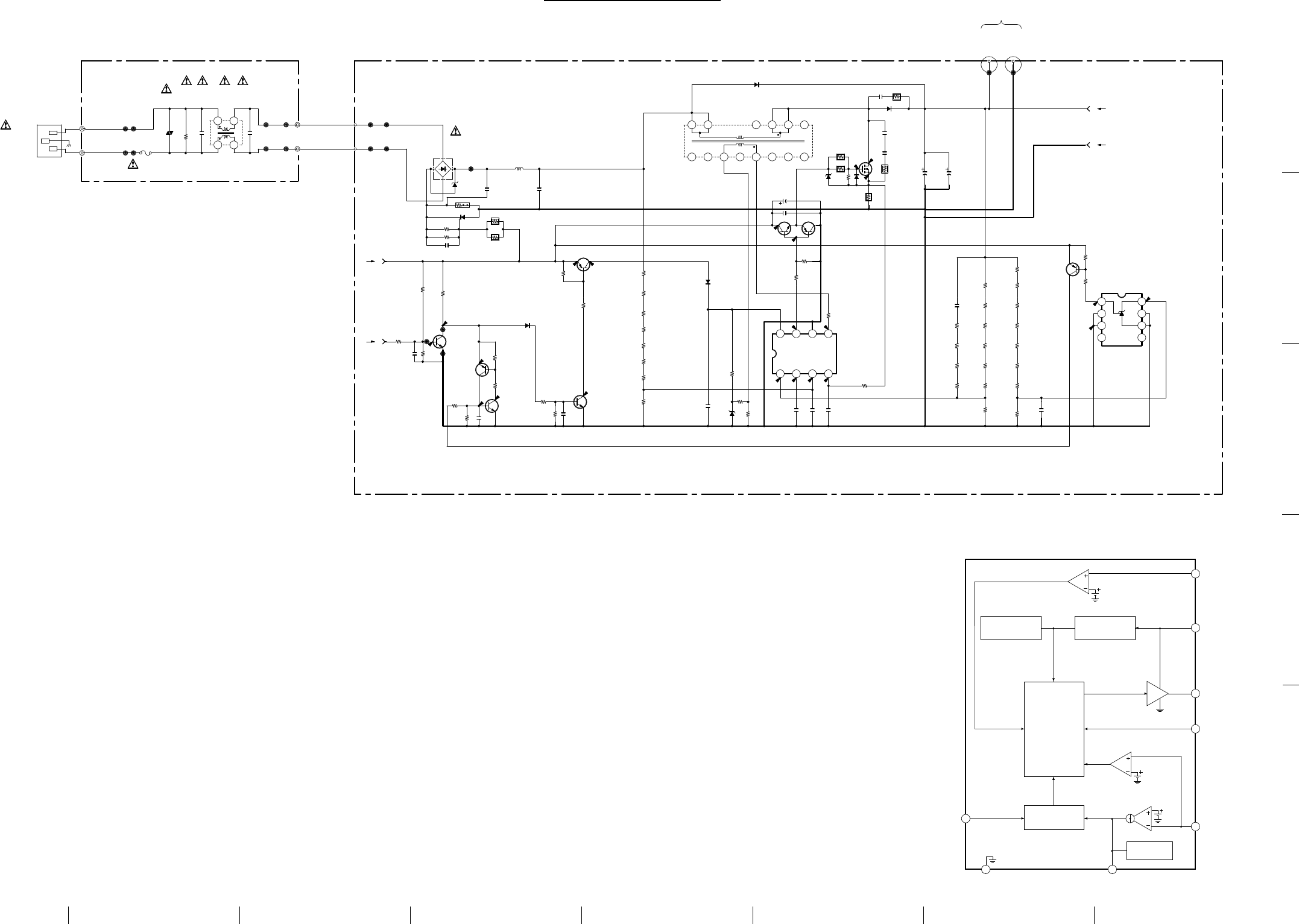
9-39 9-39
A B C D E F GH
1
2
3
4
5
VPL-PX20/PX30
*
*
*
*
*
*
*
*
*
**
***
*
*
*
**
*
*
*
1 2 3 4
5678
S
1
2
3
4
89
10
11
12
13
14
15
16
7
1234
5678
1
23
4
R2101
D2101
R2100
C2133
R2108
C2108
C2102 C2105
C2106
C2107
R2106
R2102
R2104
R2105
R2107
R2111 R2113
R2114
R2115
R2116
R2117
R2118
R2119
R2121
R2123
R2124
R2125
R2126
R2128
R2129
R2130
R2131
R2132
R2170
R2171
R2173
R2133
R2165
R2166
R2168
C2135
R2103
C2136
C2137 R2178
R2179
C2141
R2098
R2122
JL2100
JL2101
JL2102
JL2103
JL2104
JL2105 JL2106
IC2100
R2092
R2091
R2109
C2173
C2174
R2110
C2103
R2177
IC2105
R2089
R2090
R2127
R2088
R2164
R2095
R2094
R2093
C2112 C2113
R2112
R2172
R2174
R2175
R2176
C2172
C2100
R2120
R2079
JL2130
JL2131
JL2132
Q2100
Q2104
Q2105
D2108
Q2111
CN2110
CN2111
R2097
D2100
D2102
D2105
D2141
D2106
D2103
D2107
D2110
Q2110
Q2109
R2000
CN2002
CN2000
L2000
F2000
VD2000
Q2102
Q2101
Q2106
L2100
L2110
C2101
C2104
CQ003
C2002
5.6
5W
:RF
#
470
:CHIP
#
470
:CHIP
#
0.01
B:CHIP 0.01
B:CHIP
0.001
B:CHIP
2200p
500V
E
0.08
5W
:RB
47k
:CHIP
10k
:CHIP
10k
:CHIP
10k
:CHIP
10k
:CHIP 150k
:RN-CP
150k
:RN-CP
150k
:RN-CP
200k
:RN-CP
200k
:RN-CP
220k
:RN-CP
220k
:RN-CP
18k
:RN-CP
#
0
:CHIP
22k
:CHIP
100
:CHIP
220k
:RN-CP
220k
:RN-CP
220k
:RN-CP
220k
:RN-CP
220k
:RN-CP
150k
:RN-CP
150k
:RN-CP
220k
:RN-CP
10k
:RN-CP
100
:CHIP
47k
:CHIP
#
0.01
B:CHIP
#
#
##
100k
:CHIP
0
:CHIP
0.001
:CHIP
10k
:CHIP
100
:CHIP
10k
:CHIP
10k
:CHIP
0.001
B:CHIP
100
:HT
10
:FPRD
0.1
B:CHIP 8.2k
:RN-CP
TL431BCDR2
PFC OVP
10k
:CHIP
1k
:CHIP
330k
:RN-CP
10
:FPRD
120k
:CHIP
120k
:CHIP
120k
:CHIP
120k
:CHIP
220k
:RN-CP
220k
:RN-CP
220k
:RN-CP
220k
:RN-CP
220
450V
:AL
220
450V
:AL
2.2
450V
:MPS
MC33262DR2
PFC CONTROL
10k
:CHIP
0.47
400V
2.2k
1/2W
:CHIP
2.2k
1/2W
:CHIP
2SK2198
SWITCHING
2SC2712
POWER CONT
2SA1213-Y
POWER CONT
FSF10A60
RECTIFIER
2SA1162
PFC OVP
#
#
#
#
#
##
#
#
#
82k
:CHIP
D6SB80
800V,6A
MAIN RECT
TF861S
SWITCH (SCR)
UDZ27B
CLAMPER
D2FS6
CLAMP
RM11A
PROTECT
D1FS4A
CLAMP
UDZ27B
CLAMP
MA111
CLAMP
2SA1213-Y
PRI DRIVE
2SC2873-Y
PRI DRIVE
560k
1/2W
:RC
5m
5A
6.3A
ERZV14DD471
2SC2712
PFC OVP
2SA1162
PFC OVP
2SC2712
POWER CONT
250µH
690µH
1
16V
:CHIP
0.22
25V
B:CHIP
0.22
275V
:MPS
1µ
275V
:MPS
A
B
C
D
+V(W)
-V(B)
TO LAMP POWER SUPLY
ZERODET
GND
DRIVE
VCC
ISENSE
INDET
RESPONSE
VDET
VCC
POWER ON
TO STANDBY/MAIN CONVERTER
REF
K
A
A
A
A
(ACTIVE FILTER)
GA(1/2)
B-SS1696<08.>-GA.-P1
(P2)
(P2)
TO GA MOUNT
AC(N)WHT
AC(L)BLK
(P2)
(P2)
AC(N)WHT
AC(L)BLK
GREEN V<=15V
BLUE 15V<V<=50V
LIGHT BLUE 50V<V<=150V
RED 150V<V<=300V
BLACK 600V<V
YELLOW 300V<V<=600V
AC INLET
100-120V/220-240V
50/60HZ
(EMI FILTER)
F
250V
MC33262DR2 (IC2100)
Zero Current
Detect input
5
Multiplier 3
GND
6
Compensation
2
VCC
8
Drive Output
7
Current Sense
Input
4
Voltage
Feadback
Input
1
Undervoltage
Lockout
Multiplier
Quickstart
Error A mp
Overvoltage
Comparator
Vref
1.08 Vref
Zero Current Delector
2.5V
Reference
Multiplier,
Latch
PWM,
Timer,
&
Logic
• Refer to page 9-38 for Printed Wiring Board
• Refer to page 9-39 for IC Block Diagrams
F, GA (1/2) F, GA (1/2)
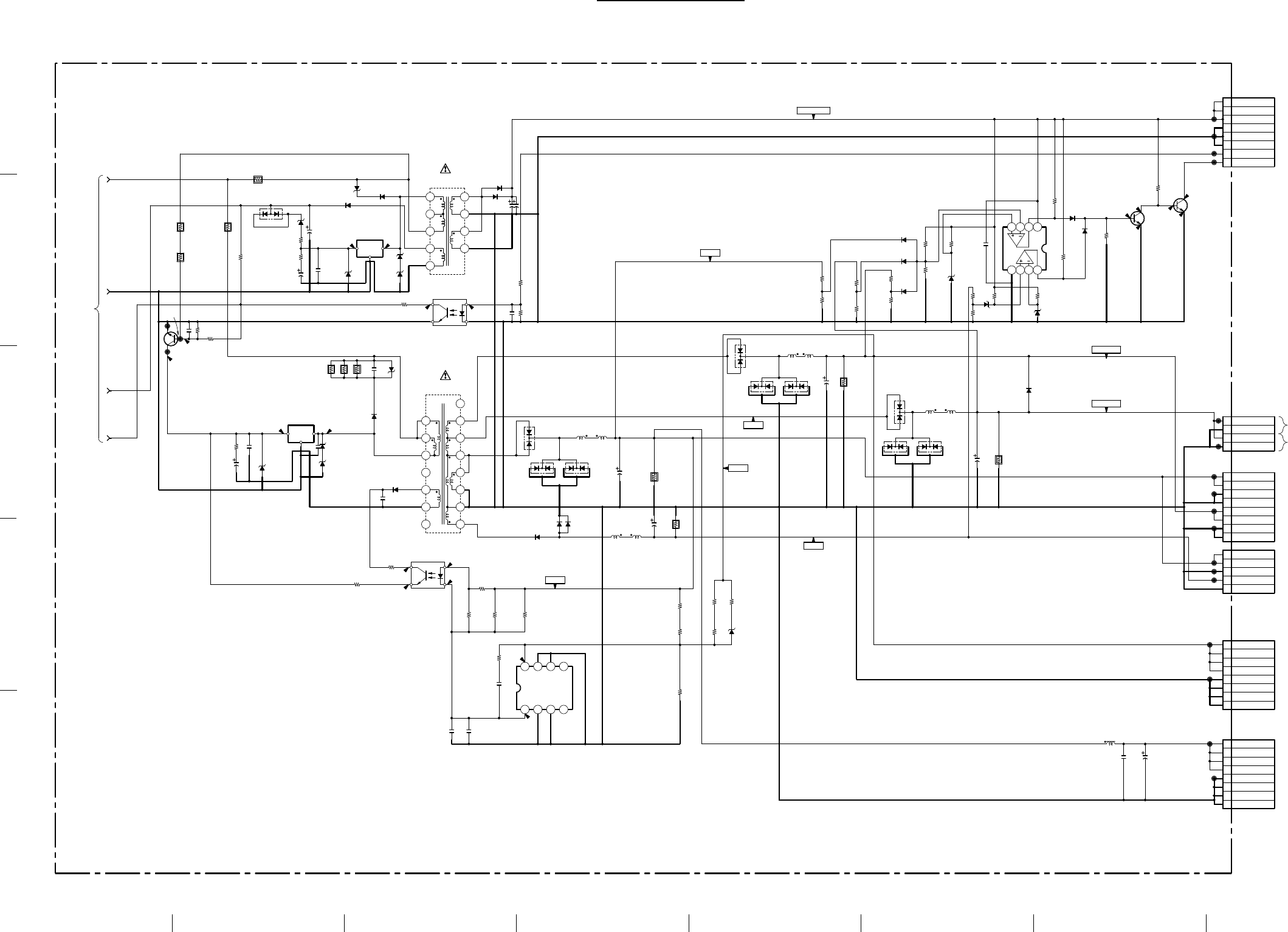
9-40 9-40
A B C D E F GH
1
2
3
4
5
VPL-PX20/PX30
0
0.6
0
0
0
0.6
SUB +5V
A+6V
+17.5V
+11.7V
A+6V
+18V
A-7V
A+6V
0 1.1
-175
5.8
5.8 480
5.8
0.3
4.8
4.0
4.5
3.4
3.4
2.4
1
2
4
3
1
2
4
3
1234
5678
1
2
3
4
5
6
7
8
9
1
2
3
4
5
6
7
8
1
2
3
4
5
6
7
8
1
2
3
4
5
6
7
8
1
2
3
4
5
6
7
8
2
3
4
5
6
7
8 9
10
11
12
13
14
15
16
1234
5 6 7 8
1
2
3
4
D
S
C
1
2
3
4
5
D
S
C
R2134
R2135
R2138
R2140
R2141
C2115
R2142
C2116
R2143
R2144
C2117
C2118
C2119
R2145
R2146 R2147 C2121
C2122
IC2102
D2124
T2100
R2148
T2101
C2125
R2151
C2126 R2152
R2153
IC2103
R2156
R2161
CN2101
CN2102
CN2104
CN2106
R2160
R2158
R2157
C2128
C2129
R2139
R2162
R2155
R2154
R2163
R2159
R2137
R2136
C2165
R2180
R2181
Q2107
Q2108
R2182
R2183
R2184
R2185
R2191
R2192
D2144
D2145
D2146
D2143
D2142
R2193
R2194
R2196
R2195
R2198
R2197
R2186
R2190 C2110
IC2101
JL2107
JL2108
JL2109
JL2110
JL2111
JL2112
JL2113
JL2114
JL2115
JL2116
JL2117
JL2118
JL2119
JL2120
JL2121
JL2122
JL2123
R2188
R2189
R2187
C2131
C2132
L2120
C2171
CN2105
CN2103
R2149
R2085
C2124 C2175
R2150
C2114
C2127
C2170
L2101 L2109
L2105 L2106
L2108
L2107
L2103
L2102
C2176
JL2133
JL2135
D2111
D2120
D2117
D2126
D2125
D2129 D2132
D2128
D2130
D2131
D2134
D2135 D2136
D2137
D2138 D2139
D2140
D2113
D2116
D2121
D2118
D2123
D2122
PH2101
PH2100
D2115
D2114
D2112
D2119
Q2103
D2127
D2133
IC2104
D2149
D2148
D2147
JL2134
0.1
B:CHIP
0.022
400V
220
25V
100
:CHIP
6.8
:CHIP
0.1
B:CHIP
6.8
:CHIP
1k
:CHIP
0.1
B:CHIP
220
:CHIP
#
TL431BCDR2
SHUNT REGULATOR
TOP223Y-BB
PWM CONTROL
22
:CHIP
4.7
:FPRD
0.1
B:CHIP
D1FL20U
4.7k
:RN-CP
0.01
B:CHIP
47
25V 100
:CHIP
1k
:CHIP
2.2
:FPRD
2.2k
1W
:RS
2.2k
1W
:RS
2.2k
1W
:RS
3900
25V
:AL
470
25V
:AL
8P
:B-TO-B
8P
:B-TO-B
8P
WHT
:S-MICRO
8P
:B-TO-B
270k
1/2W
:CHIP
270k
1/2W
:CHIP
82k
3W
:RS
82k
3W
:RS
82k
3W
:RS
47k
:CHIP
150
:CHIP
4.7k
:RN-CP
22k
:RN-CP
4.7k
:RN-CP
33k
:RN-CP
2.2k
1W
:RS
#
47k
:CHIP
0.01
B:CHIP
100
:CHIP
100
:CHIP
2SC2712
POWER PROT
2SC2712
POWER PROT
47k
:CHIP
10k
:CHIP
10k
:CHIP
10k
:CHIP
100k
:CHIP
100k
:CHIP
10k
:CHIP
10k
:CHIP
22k
:CHIP
5.6k
:CHIP
10k
:CHIP
1k
:CHIP
2.2k
:CHIP
2.2k
:CHIP
0.1
B:CHIP
TOP224Y-BB
PWM CONTROL
MA111
OR
MA111
OR
MA111
OR
MA111
OR
MA111
OR
470
:CHIP
15k
:CHIP
4.7k
:CHIP
0.1
B:CHIP
4P
RED
:S-MICRO
5P
BLK
:S-MICRO
390
:CHIP
1800
35V
:AL
1800
35V
:AL
22µH
390
:CHIP
SRT
SRT
4.7
16V
:CHIP
4.7
16V
:CHIP
390
:CHIP
47
25V
180
35V
180
10V
:AL
10µH
:LAGE 10µH
:LAGE
47µH
:LAGE 47µH
:LAGE
47µH
:MID
47µH
:MID
100µH
:MID
100µH
:MID
390
35V
1S2836
P6KE300A
CLAMPER
D2FL20U
RECTIFIER
D2FL20U
RECTIFIER
D2FL20U
RECTIFIER
D10SC9M
RECTIFIER
D10SC9M
RECTIFIER
D2FS6
RECTIFIER
D2FL20U
RECTIFIER
D2FL20U
RECTIFIER
D5LC20U
RECTIFIER
D5LC20U
RECTIFIER D5LC20U
RECTIFIER
D5LC20U
RECTIFIER
D5LC20U
RECTIFIER
D5LC20U
RECTIFIER
D2FS6
CLAMPER
#
#
#
#
#
#
#
#
#
#
#
#
#
#
#
#
#
#
#
RD12M
CLAMP
UDZ8.2B
CLAMP
FMG-G2CS
NOISE FILTER
P6KE200A
NOISE FILTER
P6KE300A
CLAMP
P6KE350A
CLAMP
PC123FY2
ISOLATER
PC123FY2
ISOLATER
P6KE300A
CLAMP
P6KE350A
CLAMP
UDZ8.2B
CLAMP
FMG-G2CS
1000V,3A
NOISE FILTER
2SC2712
POWER ON
FCQ20A06
RECTIFIER
UDZ27B
OVP
µPC393G2-E2
POWER PROT
UDZ2.2B
CLAMP
UDZ3.3B
CLAMP
UDZ2.2B
CLAMP
#
A
B
C
D
AUDIO+B
AUDIO+B
REF
K
AA
AA
A6V
A6V
17.5V
17.5V
GND 2
GND 2
6V
6V
6V
6V
GND 2
18V
18V
18V
18V
A-7V
A6V
A6V
SUB
SUB
SUB
POWER ON
GND
GND
GND
GND
GND
GND
GND
GND
GND
GND
GND
GND
GND
GND
GND
GND
GND
VCC
POWER PROT
B-SS1696<08.>-GA.-P2
(CONVERTER)
GA(2/2)
TO GB CN2300
TO GD CN2700
TO BB CN308
TO C CN600
TO K CN600
TO K CN2901
TO QA CN808
TO GC CN2500
(P1)
• Refer to page 9-38 for Printed Wiring Board
• Refer to page 9-39 for IC Block Diagrams
GA (2/2) GA (2/2)
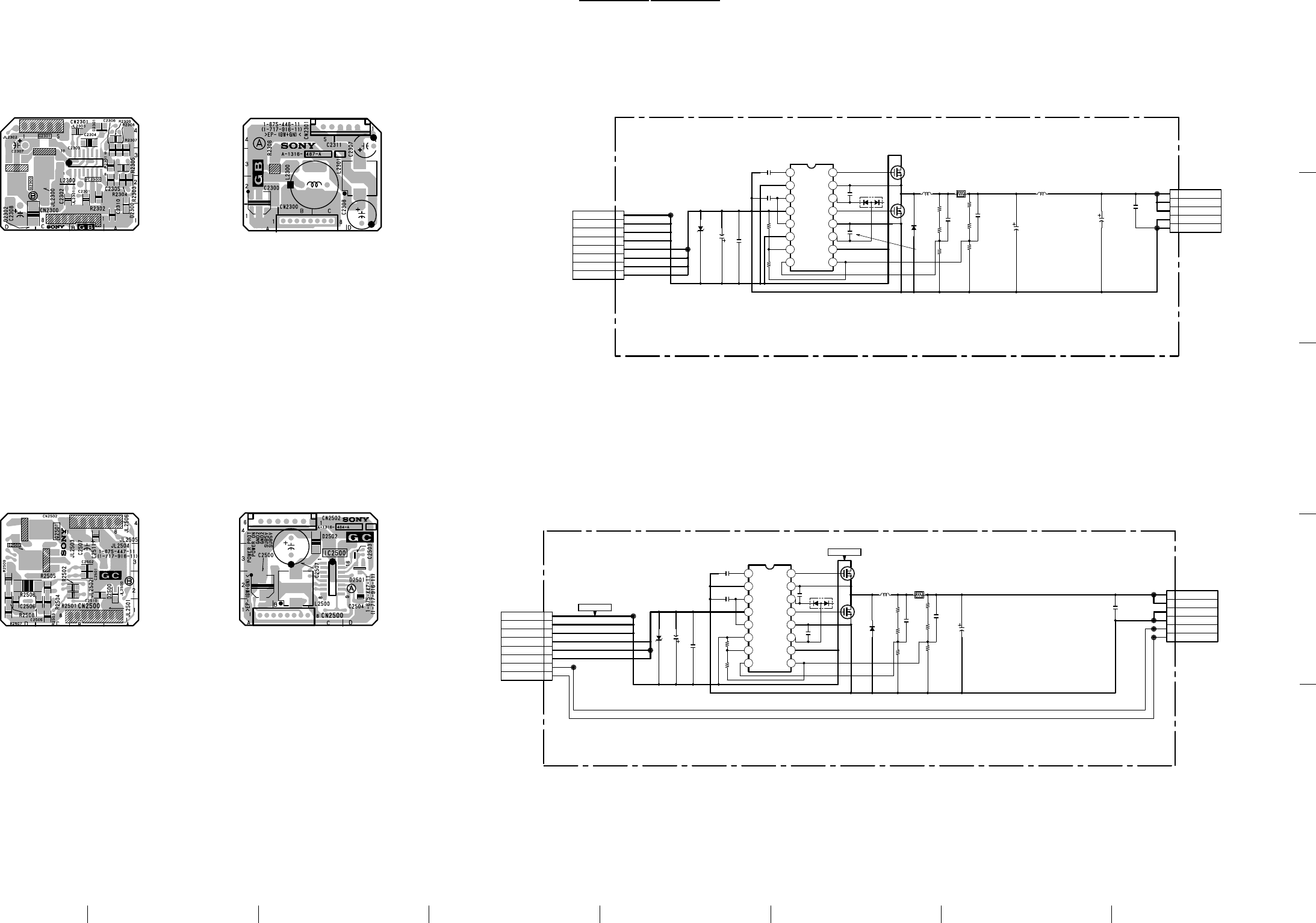
9-41 9-41
A B C D E F GH
1
2
3
4
5
VPL-PX20/PX30
1
2
3
4
5
6
7
8
12345678
9 10 11 12 13 14 15 16
S
S
1
2
3
4
5
CN2300
R2301
IC2300
C2304
R2303
R2304
R2305 C2305
R2307
R2308
R2309
C2306
C2300
CN2301
R2302
JL2300
JL2301
JL2302
JL2303
C2302
C2310
C2311
L2301
C2308
C2307
L2300
D2300
D2301
D2302
Q2301
Q2300
R2306
C2303
C2301
0.1
B:CHIP
1.5k
:RN-CP
330
:RN-CP
330
:RN-CP
4.7k
:RN-CP
0.01 0.01
0
:CHIP
4.7k
:RN-CP
1.5k
:RN-CP
33
25V
:AL-CP
8P
:B-TO-B 5P
WHT
:S-MICRO
#
0.01
B:CHIP
0.1
B:CHIP
0.1
B:CHIP
MAX797ESE
D3.3V DC-DC CONV
15µH
:SMD
680
10V
220
10V
33
:LAGE
#
#
#
#
UDZ27B
CLAMP
1S2836
RECTIFIER
D1FS4A
RECTIFIER
2SK2281
SWITCHING
2SK2281
SWITCHING
0
1W
:CHIP
4.7
16V
F:CHIP
0.33
16V
B:CHIP
6V
6V
6V
6V
SS
REF
GND
FB
CSH
DH
LX
BST
DL
VL
V+
CSL
PGSYN
SHD
SKI
D3.3V
D3.3V
D3.3V
GND
GND
GND
GND
GND
GND
(D3.3V REG)
GB
TO GA CN2101
TO BB CN308
B-SS1696<08.>-GB.
SUB +5V
SUB +5V
1
2
3
4
5
6
7
8
12345678
9 10 11 12 13 14 15 16
S
S
1
2
3
4
5
6
CN2500 C2500
R2501
R2502
C2503
R2503
R2504
R2505
C2505
R2507
R2508
R2509
C2506
C2507
L2500
JL2500
JL2501
JL2502
JL2503
JL2504
JL2505
JL2506
C2510
C2502
C2511 CN2502
IC2500
D2500
D2501
D2502
Q2501
Q2500
R2506
C2504
C2501
0.1
B:CHIP
#
#
#
#
0
:CHIP
#
0
:CHIP
0
:CHIP
0
:CHIP
0
:CHIP
22
35V
:AL-CP
1000
10V
8P
:B-TO-B
47
:SMD
0.1
B:CHIP
0.01
B:CHIP
0.1
B:CHIP 6P
WHT
:S-MICRO
MAX797ESE
SUB5V DC-DC CONV
#
#
#
#
#
#
#
UDZ27B
CLAMP
1S2836
RECTFIER
D1FS4A
RECTIFIER
2SK2281
SWITCHING
2SK2281
SWITCHING
0
1W
:CHIP
4.7
16V
F:CHIP
0.33
16V
B:CHIP
GND 2
GND 2
SUB5V
SUB5V
SS
REF
GND
FB
CSH
DH
LX
BST
DL
VL
V+
CSL
PGSYN
SHD
SKI
SUB
SUB
SUB POWER ON
POWER ON
GND
GND
GND
POWER PROT
POWER PROT
B-SS1696<08.>-GC.
(SUB5V REG)
GC
TO BB CN310
TO GA CN2106
GB – B SIDE –
SUFFIX ; -11
GB– A SIDE –
SUFFIX ; -11
GC – B SIDE –
SUFFIX ; -11
GC– A SIDE –
SUFFIX ; -11
GB, GC GB, GC
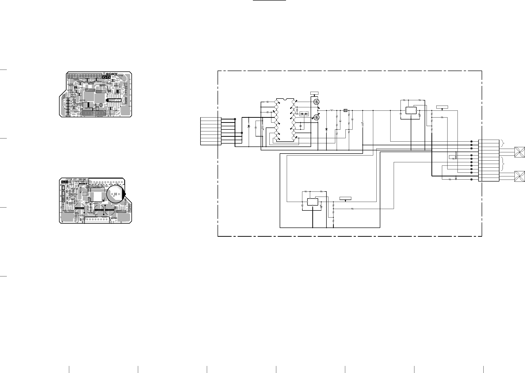
9-42 9-42
A B C D E F GH
1
2
3
4
5
VPL-PX20/PX30
+18V
+10.7V
+10.7V
3.0
12.1
12.1
1.7
2.5
2.5
2.4
2.4
2.4
4.9
1.7
16.5
12.1
15.4
12345678
9 10 11 12 13 14 15 16
S
S
1
2
3
4
5
6
7
8
G
IO
ADJ
ON/OFF
G
IO
ADJ
ON/OFF
1
2
3
4
5
6
7
8
9
10
11
12
CN2700
C2700
C2705
R2701 R2702
R2706
C2707
R2710
C2708
C2710
R2713 R2714
R2718
R2720
C2709
C2706
C2711
R2708
R2712
JL2700
JL2701 C2713
C2702
IC2702
IC2701
R2707
R2711
R2717
R2705
R2716
R2704
R2715
R2703
R2719
R2722
C2726
L2700
CN2701
D2700
D2701
JL2702
JL2703
JL2704
JL2705
JL2706
JL2707
JL2708
JL2709
JL2710
JL2711
C2725
Q2701
Q2700
D2702
C2703
IC2700
R2709
C2704
C2701
2.2k
:RN-CP 2.2k
:RN-CP
0.01
B:CHIP
0.01
B:CHIP
0.1
B:CHIP
0.1
B:CHIP
100
:CHIP
100
:CHIP
22
35V
:AL-CP
33
25V
:AL-CP
820
25V
33
25V
:AL-CP
8P
:B-TO-B
33k
:CHIP 33k
:CHIP
33k
:CHIP 33k
:CHIP
6.8k
:RN-CP
6.8k
:RN-CP
0.1
B:CHIP
0.1
B:CHIP
PQ20VZ1U
FAN+B(2) REG
PQ20VZ1U
FAN+B(1) REG
430
:RN-CP 430
:RN-CP
33k
:RN-CP
33k
:RN-CP
470
:RN-CP
470
:RN-CP
4.7k
:RN-CP
4.7k
:RN-CP
39k
:RN-CP
30k
:RN-CP
2.2
16V
F:CHIP
47
:SMD
12P
WHT
#
#
UDZ27B
CLAMP
1S2836
RECTIFIER
#
#
#
#
#
#
#
#
#
#
#
2SK2281
SWITCHING
2SK2281
SWITCHING
D1FS4A
RECTIFIER
0.1 B:CHIP
MAX797ESE
10.7V DC-DC CON
0
1W
:CHIP
4.7
16V
F:CHIP
0.33
16V
B:CHIP
GND
GND
FAN+B(2)
FAN PRO(2)
FAN+B(1)
FAN PRO(1)
FAN PRO(1)
FAN CON(1)
FAN PRO(2)
FAN CON(2)
10.7V
GND
B-SS1696<08.>-GD.
(FAN+B AND 10.7V REG)
GD
TO GA CN2102
18V
18V
18V
18V
GND
GND
GND
GND
SS
REF
GND
FB
CSH
DH
LX
BST
DL
VL
V+
CSL
PGSYN
SHD
SKI
TO BB CN310
TO BB CN308
FAN1
FAN2
GD GD
GD – B SIDE –
SUFFIX ; -11
GD– A SIDE –
SUFFIX ; -11
The material contained in this manual consists of
information that is the property of Sony Corporation.
Sony Corporation expressly prohibits the duplication of
any portion of this manual or the use thereof for any
purpose other than the operation or maintenance of the
equipment described in this manual without the express
written permission of Sony Corporation.
Le matériel contenu dans ce manuel consiste en
informations qui sont la propriété de Sony Corporation.
Sony Corporation interdit formellement la copie de
quelque partie que ce soit de ce manuel ou son emploi
pour tout autre but que des opérations ou entretiens de
l’équipement à moins d’une permission écrite de Sony
Corporation.
Das in dieser Anleitung enthaltene Material besteht aus
Informationen, die Eigentum der Sony Corporation sind.
Die Sony Corporation untersagt ausdrücklich die
Vervielfältigung jeglicher Teile dieser Anleitung oder den
Gebrauch derselben für irgendeinen anderen Zweck als
die Bedienung oder Wartung der in dieser Anleitung
beschriebenen Ausrüstung ohne ausdrückliche
schriftliche Erlaubnis der Sony Corporation.
Sony Corporation
B & P Company
English
99KZ08111-1
Printed in Japan
©1999.119-929-667-01
