VPR_User_Manual VPR User Manual 6.0
VPR_User_Manual_6.0
VPR_User_Manual_6.0
VPR_User_Manual_6.0
User Manual:
Open the PDF directly: View PDF ![]() .
.
Page Count: 38
* Current active as of 2012
VPR User’s Manual
VPR 6.0 Full Release, January 19, 2012
VPR Contributers:
*Luu, Jason (jluu@eecg.toronto.edu)
Betz, Vaughn (vaughn@eecg.toronto.edu)
Campbell, Ted (campbell@eecg.toronto.edu)
Fang, Wei Mark (fang@eecg.toronto.edu)
Jamieson, Peter (jamieson@eecg.toronto.edu)
Kuon, Ian (ikuon@eecg.toronto.edu)
Marquardt, Alexander
Ye, Andy
*Rose, Jonathon (jayar@eecg.toronto.edu)
1. Overview
VPR (Versatile Place and Route) is an FPGA CAD tool that maps a technology mapped
netlist (eg. a circuit expressed in look-up tables, flip-flops, memories, etc) to a hypothetical
FPGA specified by the user.
VPR has two required and many optional parameters; it is invoked by entering:
> vpr architecture.xml circuit_name [-options]
Architecture.xml describes the architecture of the FPGA in which the circuit is to be
realized. Circuit_name is the name of the circuit the user wants to map onto the FPGA. By
default, VPR will perform packing, placement, and routing on the circuit to the architecture. If
filenames are not explicitly specified, VPR reads in circuit_name.blif, and output three
files: 1. The packed netlist to circuit_name.net, 2. The placement to
circuit_name.place, and 3. The routing to circuit_name.route. VPR has options to
select which parts of the flow to run, what parameters those algorithms should use, as well as
file naming options.
VPR can be run in one of two basic modes. In its default mode, VPR places a circuit on an
FPGA and then repeatedly attempts to route it in order to find the minimum number of tracks
required by the specified FPGA architecture to route this circuit. If a routing is unsuccessful,
VPR increases the number of tracks in each routing channel and tries again; if a routing is
successful, VPR decreases the number of tracks before trying to route it again. Once the
minimum number of tracks required to route the circuit is found, VPR exits. The other mode of
VPR is invoked when a user specifies a specific channel width for routing. In this case, VPR
places a circuit and attempts to route it only once, with the specified channel width. If the circuit
will not route at the specified channel width, VPR simply reports that it is unroutable.
Typing VPR with no parameters will print out a list of all the available command line
parameters.
Compiling and Running VPR
1.1 Compiling VPR
If your compiler of choice is gcc and you are running a Linux or Solaris-based system, you
can compile VPR simply by typing make in the directory containing VPR’s source code and
makefile. If you prefer to use a Windows environment, project files are included for Microsoft
Visual C++ 2005. If you prefer to use a linux-based environment for development in Windows,
then we recommend using the Cygwin package to compile VPR. Graphics are not supported
when compiling with Visual C++, but should be supported when compiling with Cygwin.
If your compiler and/or architecture are different, however, you will have to make some
small modifications to the makefile. First, change the CC = gcc line in the makefile so that CC is
set to the name of your desired compiler. Second, you may want to change the line
OPT_FLAGS = -O3 to set OPT_FLAGS to the value that gives the highest level of optimization
with your compiler, and it may be necessary to give the linker different options so it finds all the
relevant libraries on your machine. If, during compilation, you get an error that type XPointer is
not defined, uncomment the “typedef char *XPointer” line in graphics.c (many X Windows
implementations do not define the XPointer type). Finally, if you are compiling VPR on a system
without X Windows (e.g. Windows NT), you should add a “#define NO_GRAPHICS” line to the
top of vpr_types.h. VPR’s built-in graphics will all be removed by this define, allowing
compilation on non-X11 machines.
1.2 Typical CAD Flow using VPR
Figure 1 illustrates the CAD flow we typically use. First, Odin II [16] converts a Verilog
Hardware Destription Language (HDL) design into a flattened netlist consisting of logic gates
and blackboxes that represent heterogeneous blocks. Next, the ABC [1] synthesis package is
used to perform technology-independent logic optimization of each circuit, and then each circuit
is technology-mapped into LUTs and flip flops [2]. The output of ABC is a .blif format netlist of
LUTs, flip flops, and blackboxes. VPR [3, 4, 7, 8, 9, 10, 11] then packs this netlist into more
coarse-grained logic blocks, places the circuit, and routes it. The output of VPR consists of
several files. One file to describe the circuit packing, another file describing the circuit’s
placement, another file describing the circuit’s routing, and various files describing statistics
concerning the minimum number of tracks per channel required to successfully route, the total
wirelength, etc. In order to find the minimum number of tracks required for successful routing,
VPR actually attempts to route the circuit several times with different numbers of tracks allowed
per channel in each attempted routing.
Of course, many variations on this CAD flow are possible. It is possible to use other high-
level synthesis tools to generate the blif files that are passed into ABC. Also, one can use
different logic optimizers and technology mappers than ABC; just put the output netlist from your
technology-mapper into .blif format and feed it into VPR. Alternatively, if the logic block you are
interested in is not supported by AAPack in VPR, your CAD flow can bypass AAPack altogether
by outputting a netlist of logic blocks in .net format. VPR can place and route netlists of any
type of logic block -- you simply have to create the netlist and describe the logic block in the
FPGA architecture description file. Finally, if you want only to route a placement produced by
another CAD tool you can create a placement file in VPR format, and have VPR route this pre-
existing placement.
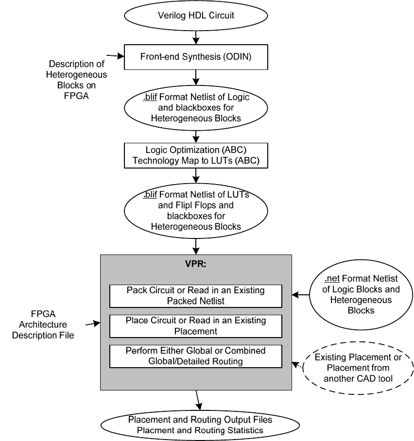
Figure 1
2. Operation of VPR
This section outlines how VPR’s placement and routing options/graphics work; Section 3
describes the format of each of the four VPR specific files.
2.1 Graphics
The graphics included in VPR are very easy to use. First, compile VPR with graphics option
on (see Makefile), then a window will pop up when you run VPR. Click any mouse button on
the arrow keys to pan the view, or click on the Zoom-In, Zoom-Out and Zoom-Fit keys to
zoom the view. Click on the Window button, then on the diagonally opposite corners of a box,
to zoom in on a particular area. Selecting PostScript creates a PostScript file (in pic1.ps,
pic2.ps, etc.) of the image on screen. Proceed tells VPR to continue with the next step in
placing and routing the circuit, while Exit aborts the program. The menu buttons will be greyed
out to show they are not selectable when VPR is working, rather than interactively displaying
graphics.
The Toggle Nets button toggles the nets in the circuit visible/invisible. When a placement is
being displayed, routing information is not yet known so nets are simply drawn as a “star;” that
is, a straight line is drawn from the net source to each of its sinks. Click on any clb in the
display, and it will be highlighted in green, while its fanin and fanout are highlighted in blue and
red, respectively. Once a circuit has been routed the true path of each net will be shown.
Again, you can click on Toggle Nets to make net routings visible or invisible, and clicking on a
clb or pad will highlight their fanins and fanouts.
When a routing is on-screen, clicking on Toggle RR will switch between various views of
the routing resources available in the FPGA. Wiring segments and clb pins are drawn in black,
connections from wiring segments to input pins are shown in blue, connections from output pins
to wiring segments are shown in red, and connections between wiring segments are shown in
green. The points at which wiring segments connect to clb pins (connection box switches) are
marked with an “X”. Switch box connections will have buffers (triangles) or pass transistors
(circles) drawn on top of them, depending on the type of switch each connection uses. Clicking
on a clb or pad will overlay the routing of all nets connected to that block on top of the drawing
of the FPGA routing resources, and will label each of the pins on that block with its pin number.
The routing resource view can be very useful in ensuring that you have correctly described your
FPGA in the architecture description file -- if you see switches where they shouldn’t be or pins
on the wrong side of a clb, your architecture description needs to be revised.
When a routing is shown on-screen, clicking on the Congestion button will show any
overused routing resources (wires or pins) in red, if any overused resources exist. Finally, when
a routing is on screen you can click on the Crit. Path button to see each of the nets on the
critical path in turn. The current net on the critical path is highlighted in cyan; its source block is
shown in yellow and the critical sink is shown in green.
NOTE: For this release, a few of the less common options are not fully tested and so are
not necessarily working properly. As well, the –nx –ny and –aspect_ratio options are now part of
the architecture file. Anything related to timing is not working. The options not debugged are:
• num_regions
• base_cost_type
• place_cost_type
2.2 Command-Line Options
VPR has a lot of options. The options most people will be interested in are -inner_num, -
route_chan_width, and -route_type. In general for the other options the defaults are fine, and
only people looking at how different CAD algorithms perform will try many of them. To
understand what the more esoteric placer and router options actually do, buy [3] or download [7,
8, 9, 10] from the author’s web page (http://www.eecg.toronto.edu/~vaughn).
In the following text, values in angle brackets, e.g. <int>, should be replaced by the
appropriate filename or number. Values in curly braces separated by vertical bars, e.g. {on |
off}, indicate all the permissible choices for an option.
2.2.1 Filename Options
VPR by default appends .blif, .net, .place, and .route to the circuit name provided by the
user. Use the options below to override this default naming behaviour.
-blif_file <string>
Path to technology mapped user circuit in blif format
-net_file <string>
Path to packed user circuit in net format
-place_file <string>
Path to final placement file
-route_file <string>
Path to final routing file
-outfile_prefix <string>
Prefix output files with specified string (unless specifically specifed as above.
2.2.2 General Options
VPR runs all three stages of pack, place, and route if none of –pack, –place, or –route are
specified.
-nodisp
Disables all graphics. Useful if you're not running X Windows.
Default: graphics enabled.
-auto <int>
Can be 0, 1, or 2. This sets how often you must click Proceed to continue execution after
viewing the graphics. The higher the number, the more infrequently the program will pause.
Default: 1.
-pack
Run packing stage
Default: Off
-place
Run placement stage
Default: Off
-route
Run routing stage

Default: Off
-timing_analysis { on | off }
Turn timing analysis of the routing on or off. If it is off, you don’t have to specify the various
timing analysis parameters in the architecture file.
Default: on, unless architecture file does not have timing information
-timing_analyze_only_with_net_delay <float> Deprecated
Perform timing analysis on netlist assuming all edges have the same specified delay
Default: off
-full_stats
Print out some extra statistics about the circuit and its routing useful for wireability analysis.
Default: off
2.2.3 Packer Options
AAPack is the packing tool built into VPR. AAPack takes as input a technology-mapped blif
netlist consisting of LUTs, flip-flops, memories, mulitpliers, etc and outputs a .net formatted
netlist composed of more complex logic blocks. The logic blocks available on the FPGA are
specified through the FPGA architecture file. For people not working on CAD, you can probably
leave defaults for all options
-connection_driven_clustering {on | off}
Controls whether or not AAPack prioritizes the absorption of nets with fewer connections into a
complex logic block over nets with more connections.
Default: on
-allow_unrelated_clustering {on | off}
Controls whether or not primitives with no attraction to the current cluster can be packed into
it.
Default: on.
-alpha_clustering <float>
.A tradeoff parameter that controls the optimization of timing vs area. A value of 0 focuses
solely on area, a value of 1 focuses entirely on timing.
Default: 0.75
-beta_clustering <float>
A tradeoff parameter that controls the optimization of smaller net absorption vs. the
optimization of signal sharing. A value of 0 focuses solely on signal sharing, while a value of 1
focuses solely on absorbing smaller nets into a cluster. This option is meaningful only when
connection_driven_clustering is on.
Default: 0.9.
-cluster_only
When specified, VPR will exit after packing and will not do placement or routing.
Default: off.
-timing_driven_clustering {on|off}
Controls whether or not to do timing driven clustering
Default: on
-cluster_seed_type {timing|max_inputs}
Controls whether to seed a new complex logic block based on timing or based on the block

with the most inputs.
Default: timing
2.2.4 Placer Options
By default, the automatic annealing schedule [3, 9] is used. This schedule gathers statistics
as the placement progresses, and uses them to determine how to update the temperature,
when to exit, etc. This schedule is generally superior to any user-specified schedule. If any of
init_t, exit_t or alpha_t is specified, the user schedule, with a fixed initial temperature, final
temperature and temperature update factor is used.
-seed <int>
Sets the initial random seed used by the placer.
Default: 1.
-num_regions <int> Deprecated
Used only with the nonlinear cost function. VPR will compute congestion on an array of
num_regions X num_regions subareas. Large values of num_regions greatly slow the placer.
Default: 4.
Note: This is not supported and may not be working this release
-enable_timing_computations {on | off}
Controls whether or not the placement algorithm prints estimates of the circuit speed of the
placement it generates. This setting affects statistics output only, not optimization behaviour.
Default: on if timing-driven placement is specified, off otherwise.
-block_dist <int> Deprecated
Specifies that the placement algorithm should print out an estimate of the circuit critical path,
assuming that each inter-block connection is between blocks a (horizontal) distance of block_dist
logic blocks apart. This setting affects statistics output only, not optimization behaviour.
Default: 1. (Currently the code that prints out this lower bound is #ifdef ’ed out in place.c -- define
PRINT_LOWER_BOUND in place.c to reactivate it.)
-inner_num <float>
The number of moves attempted at each temperature is inner_num * num_blocks^(4/3) in the
circuit. The number of blocks in a circuit is the number of pads plus the number of clbs.
Changing inner_num is the best way to change the speed/quality tradeoff of the placer, as it
leaves the highly-efficient automatic annealing schedule on and simply changes the number of
moves per temperature.
Note: Specifying -inner_num 1 will speed up the placer by a factor of 10 while typically
reducing placement quality only by 10% or less (depends on the architecture). Hence users
more concerned with CPU time than quality may find this a more appropriate value of
inner_num.
Default: 10.
-init_t <float>
The starting temperature of the anneal for the manual annealing schedule.
Default: 100.
-exit_t <float>
The (manual) anneal will terminate when the temperature drops below the exit temperature.
Default: 0.01.
-alpha_t <float>

The temperature is updated by multiplying the old temperature by alpha_t when the manual
annealing schedule is enabled.
Default: 0.8.
-fix_pins {random | <file.pads>}
Do not allow the placer to move the I/O locations about during the anneal. Instead, lock each
I/O pad to some location at the start of the anneal.
If -fix_pins random is specified, each I/O block is locked to a random pad location to model
the effect of poor board-level I/O constraints. If any word other than random is specified after -
fix_pins, that string is taken to be the name of a file listing the desired location of each I/O
block in the netlist (i.e. -fix_pins <file.pads>).
This pad location file is in the same format as a normal placement file, but only specifies the
locations of I/O pads, rather than the locations of all blocks.
Default: off (i.e. placer chooses pad locations).
-place_algorithm {bounding_box | net_timing_driven | path_timing_driven}
Controls the algorithm used by the placer.
Bounding_box focuses purely on minimizing the bounding box wirelength of the circuit.
Path_timing_driven focuses on minimizing both wirelength and the critical path delay.
Net_timing_driven is similar to path_timing_driven, but assumes that all nets have the same
delay when estimating the critical path during placement, rather than using the current
placement to obtain delay estimates.
Default: path_timing_driven.
-place_cost_type {linear | nonlinear}
Select the (wirelength portion of the) placement cost function. For FPGAs in which all
channels have the same width the linear cost function reduces to a bounding box wirelength
cost function. The nonlinear cost function, on the other hand, considers both wirelength and
congestion during placement.
Default: linear.
Note: Nonlinear is not supported this release and may give unusual results
-place_chan_width <int>
Can be used with the nonlinear cost function to tell VPR how many tracks a channel of relative
width 1 is expected to need to complete routing of this circuit. VPR will then place the circuit
only once, and repeatedly try routing the circuit as usual. If place_chan_width is not specified
and the nonlinear cost is used, VPR will replace and reroute the circuit for each channel width
at which it attempts to map the circuit.
2.2.5 Placement Options Valid Only With Timing-Driven Placement
Timing Driven placement is used by default, unless the architecture file is missing timing
information.
-timing_tradeoff <float>
Controls the trade-off between bounding box minimization and delay minimization in the
placer. A value of 0 makes the placer focus completely on bounding box (wirelength)
minimization, while a value of 1 makes the placer focus completely on timing optimization.
Default: 0.5.
-recompute_crit_iter <int>
Controls how many temperature updates occur before the placer performs a timing analysis to
update its estimate of the criticality of each connection.
Default: 1.
-inner_loop_recompute_divider <int>
Controls how many times the placer performs a timing analysis to update its criticality estimates
while at a single temperature.
Default: 0.
-td_place_exp_first <float>
Controls how critical a connection is considered as a function of its slack, at the start of the anneal.
If this value is 0, all connections are considered equally critical. If this value is large, connections
with small slacks are considered much more critical than connections with small slacks. As the
anneal progresses, the exponent used in the criticality computation gradually changes from its
starting value of td_place_exp_first to its final value of td_place_exp_last.
Default: 1.
-td_place_exp_last <float>
Controls how critical a connection is considered as a function of its slack, at the end of the anneal.
See discussion for -td_place_exp_first, above.
Default: 8.
2.2.6 Router Options
-max_router_iterations <int>
The number of iterations of a Pathfinder-based router that will be executed before a circuit is
declared unrouteable (if it hasn’t routed successfully yet) at a given channel width.
Default: 50.
Speed-quality trade-off: reduce this number to speed up the router, at the cost of some increase in
final track count. This is most effective if -initial_pres_fac is simultaneously increased.
-initial_pres_fac <float>
Sets the starting value of the present overuse penalty factor.
Default: 0.5.
Speed-quality trade-off: increase this number to speed up the router, at the cost of some increase in
final track count. Values of 1000 or so are perfectly reasonable.
-first_iter_pres_fac <float>
Similar to -initial_pres_fac. This sets the present overuse penalty factor for the very first routing
iteration. -initial_pres_fac sets it for the second iteration.
Default: 0.5.
-pres_fac_mult <float>
Sets the growth factor by which the present overuse penalty factor is multiplied after each router
iteration.
Default: 1.3.
-acc_fac <float>
Specifies the accumulated overuse factor (historical congestion cost factor).
Default: 1.
-bb_factor <int>
Sets the distance (in channels) outside of the bounding box of its pins a route can go. Larger
numbers slow the router somewhat, but allow for a more exhaustive search of possible routes.
Default: 3.
-base_cost_type {demand_only | delay_normalized | intrinsic_delay}
Sets the basic cost of using a routing node (resource). Demand_only sets the basic cost of a
node according to how much demand is expected for that type of node. Delay_normalized is
similar, but normalizes all these basic costs to be of the same magnitude as the typical delay
through a routing resource. Intrinsic_delay sets the basic cost of a node to its intrinsic delay.
Default: delay_normalized for the timing-driven router and demand_only for the breadth-first
router.
Note: intrinsic_delay is not supported this release and may give unusual results
-bend_cost <float>
The cost of a bend. Larger numbers will lead to routes with fewer bends, at the cost of some
increase in track count. If only global routing is being performed, routes with fewer bends will
be easier for a detailed router to subsequently route onto a segmented routing architecture.
Default: 1 if global routing is being performed, 0 if combined global/detailed routing is being
performed.
-route_type {global | detailed}
Specifies whether global routing or combined global and detailed routing should be performed.
Default: detailed (i.e. combined global and detailed routing).
-route_chan_width <int>
Tells VPR to route the circuit with a certain channel width. No binary search on channel
capacity will be performed to find the minimum number of tracks required for routing -- VPR
simply reports whether or not the circuit will route at this channel width.
-router_algorithm {breadth_first | timing_driven | directed_search}
Selects which router algorithm to use. The breadth-first router focuses solely on routing a
design successfully, while the timing-driven router focuses both on achieving a successful
route and achieving good circuit speed. The breadth-first router is capable of routing a design
using slightly fewer tracks than the timing-driving router (typically 5% if the timing- driven
router uses its default parameters; this can be reduced to about 2% if the router parameters
are set so the timing-driven router pays more attention to routability and less to area). The
designs produced by the timing-driven router are much faster, however, (2x - 10x) and it uses
less CPU time to route. The directed_search router is routability-driven and uses an A*
heuristic to improve runtime over breadth_first.
Default: timing_driven.
2.2.7 Timing-Driven Router Options
-astar_fac <float>
Sets how aggressive the directed search used by the timing-driven router is. Values between
1 and 2 are reasonable, with higher values trading some quality for reduced CPU time.
Default: 1.2.
-max_criticality <float>
Sets the maximum fraction of routing cost that can come from delay (vs. coming from
routability) for any net. A value of 0 means no attention is paid to delay; a value of 1 means
nets on the critical path pay no attention to congestion.
Default: 0.99.
-criticality_exp <float>
Controls the delay - routability tradeoff for nets as a function of their slack. If this value is 0, all
nets are treated the same, regardless of their slack. If it is very large, only nets on the critical path
will be routed with attention paid to delay. Other values produce more moderate tradeoffs.
Default: 1.
3. File Formats
In all the file format that follow, a sharp (#) character anywhere in a line indicates that the
rest of the line is a comment, while a backslash (\) at the end of a line (and not in a comment)
means that this line is continued on the line below.
3.1 FPGA Architecture File (.xml) Format
The architecture file is specified in xml format. It is composed of a hierarchy of start and
end tags with optional attributes and content inside each tag giving additional information. As a
convention, curly brackets {…} represents an option with each option separated by |. For
example, a={1 | 2 | open} means field “a” can take a value of 1, 2, or open.
The first tag in all architecture files is the <architecture> tag. This tag contains all other
tags in the architecture file. The architecture tag contains six other tags. They are <models>,
<layout>, <device>, <switchlist>, <segmentlist>, and < complexblocklist>.
3.1.1 Description of Recognized Blif Models
The <models> tag contains <model name=”model_name”> tags. Each <model> tag
describes the .subckt model_name blif instances that are accepted by the FPGA
architecture. The name of the model must match the corresponding name of the blif model.
Standard blif structures (.names, .latch, .input, .output) are accepted by VPR by default so
these models should not described in the <models> tag.
Each model tag must contain 2 tags: <input_ports> and <output_ports>. Each of
these contains <port> tags explained below.
<port name=”string” { is_clock=”0|1”}/>
This tag defines the port for a model. The name attribute specifies the name of the port and
the is_clock attribute specifies whether a port is a clock (1) or not (0). The is_clock attribute
applies only to input ports.
3.1.2 Description of Global FPGA Information
<layout {auto=”float” | width=”int” height=” int”}/>
This tag specifies the size and shape of the FPGA in grid units. The keyword auto indicates
that the size should be chosen to be the minimal dimensions that fits the given circuit. The size
is determined from the number grid tiles used by the circuit as well as the number of IO pins
that it uses. The aspect ratio of the FPGA is given after the auto keyword and is the ratio
width/height.
Alternately, the size can be explicitly given as the size in the x direction (width) followed by the
size in the y direction (height).
<device>content</device>
Content inside this tag specifies device information. It contains the tags <sizing>, <timing>,
<area>, <chan_width_distr>, and <switch_block>.
<switchlist>content</switchlist>
Content inside this tag contains a group of <switch> tags that specify the types of switches
and their properties.
<segmentlist>content</segmentlist>
Content inside this tag contains a group of <segment> tags that specify the types of wire
segments and their properties.
<complexblocklist>content</complexblocklist>
Content inside this tag contains a group of <pb_type> tags that specify the types of functional
blocks and their properties.
3.1.3 Description of Device Information in the FPGA
The tags within the device tag are described in the following table.
<sizing R_minW_nmos="float" R_minW_pmos="float" ipin_mux_trans_size="int"/>
Specifies parameters used by the area model built into VPR
R_minW_nmos attribute:
The resistance of minimum-width nmos transistor. This data is used only by the area model
built into VPR.
R_minW_pmos attribute:
The resistance of minimum-width pmos transistor. This data is used only by the area model
built into VPR.
ipin_mux_trans_size attribute:
This specifies the size of each transistor in the ipin muxes. Given in minimum transistor units.
The mux is implemented as a two-level mux.).
<timing C_ipin_cblock="float" T_ipin_cblock="float"/>
Optional. Attributes specify timing information general to the device and must be specified for
timing analysis.
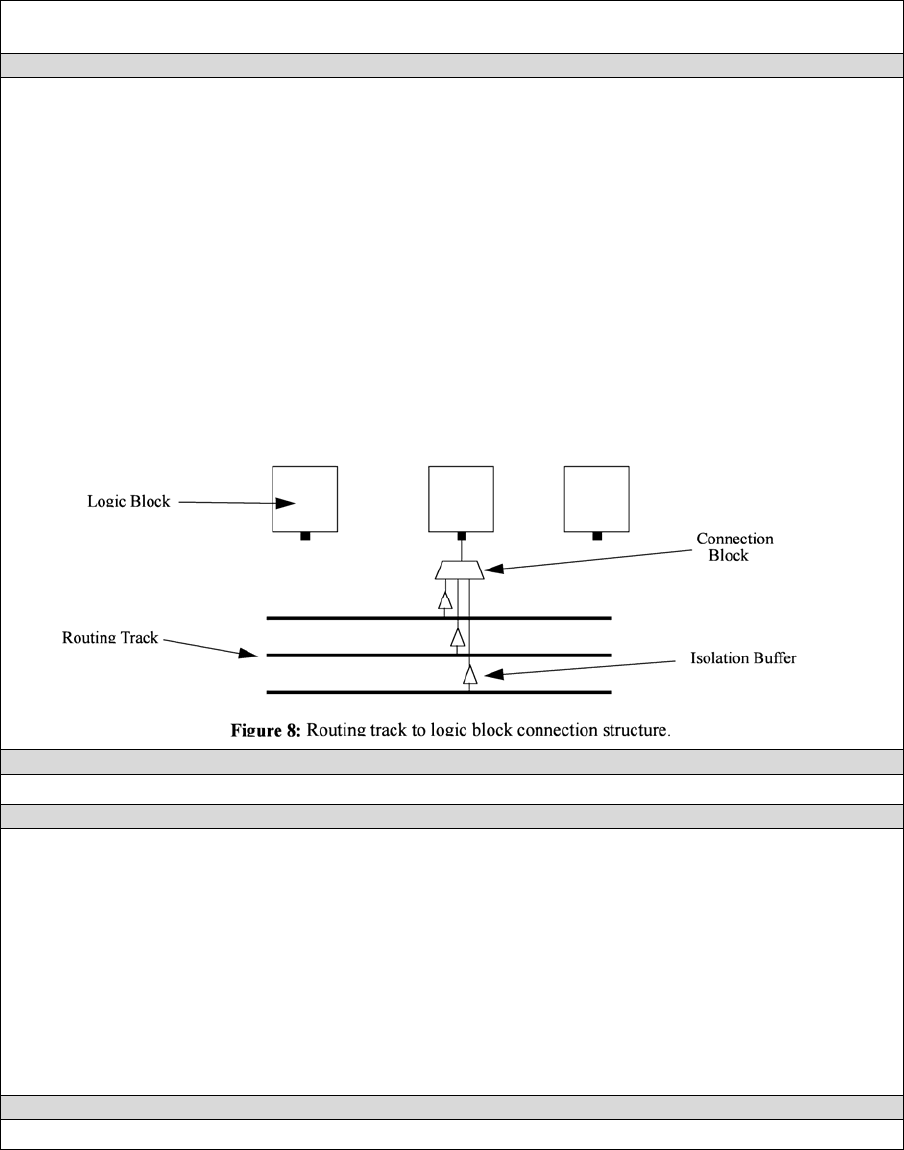
C_ipin_cblock attribute:
Input capacitance of the buffer isolating a routing track from the connection boxes
(multiplexers) that select the signal to be connected to an logic block input pin. One of these
buffers is inserted in the FPGA for each track at each location at which it connects to a
connection box. For example, a routing segment that spans three logic blocks, and connects
to logic blocks at two of these three possible locations would have two isolation buffers
attached to it. If a routing track connects to the logic blocks both above and below it at some
point, only one isolation buffer is inserted at that point. If your connection from routing track to
connection block does not include a buffer, set this parameter to the capacitive loading a track
would see at each point where it connects to a logic block or blocks.
T_ipin_cblock attribute:
Delay to go from a routing track, through the isolation buffer (if your architecture contains
these) and a connection block (typically a multiplexer) to a logic block input pin.
<area grid_logic_tile_area="float"/>
Used for an area estimate of the amount of area taken by all the functional blocks.
<switch_block type="{wilton|subset|universal}" fs="int"/>
C When using bidirectional segments, all the switch blocks [12] have Fs = 3. That is,
whenever horizontal and vertical channels intersect, each wire segment can connect to three
other wire segments. The exact topology of which wire segment connects to which can be
one of three choices. The subset switch box is the planar or domain-based switch box used in
the Xilinx 4000 FPGAs -- a wire segment in track 0 can only connect to other wire segments in
track 0 and so on. The wilton switch box is described in [13], while the universal switch box is
described in [14]. To see the topology of a switch box, simply hit the “Toggle RR” button when
a completed routing is on screen in VPR. In general the wilton switch box is the best of these
three topologies and leads to the most routable FPGAs.
When using unidirectional segments, a modified wilton switch block pattern is used regardless
of the specified switch_block_type.
<chan_width_distr>content</chan_width_distr>
Content inside this tag is described in the next table
If global routing is to be performed, channels in different directions and in different parts of
the FPGA can be set to different relative widths. This is specified in the content within the
<chan_width_distr> tag. If detailed routing is to be performed, however, all the channels in the
FPGA must have the same width.
<io width= “float”/>
Width of the channels between the pads and core relative to the widest core channel.
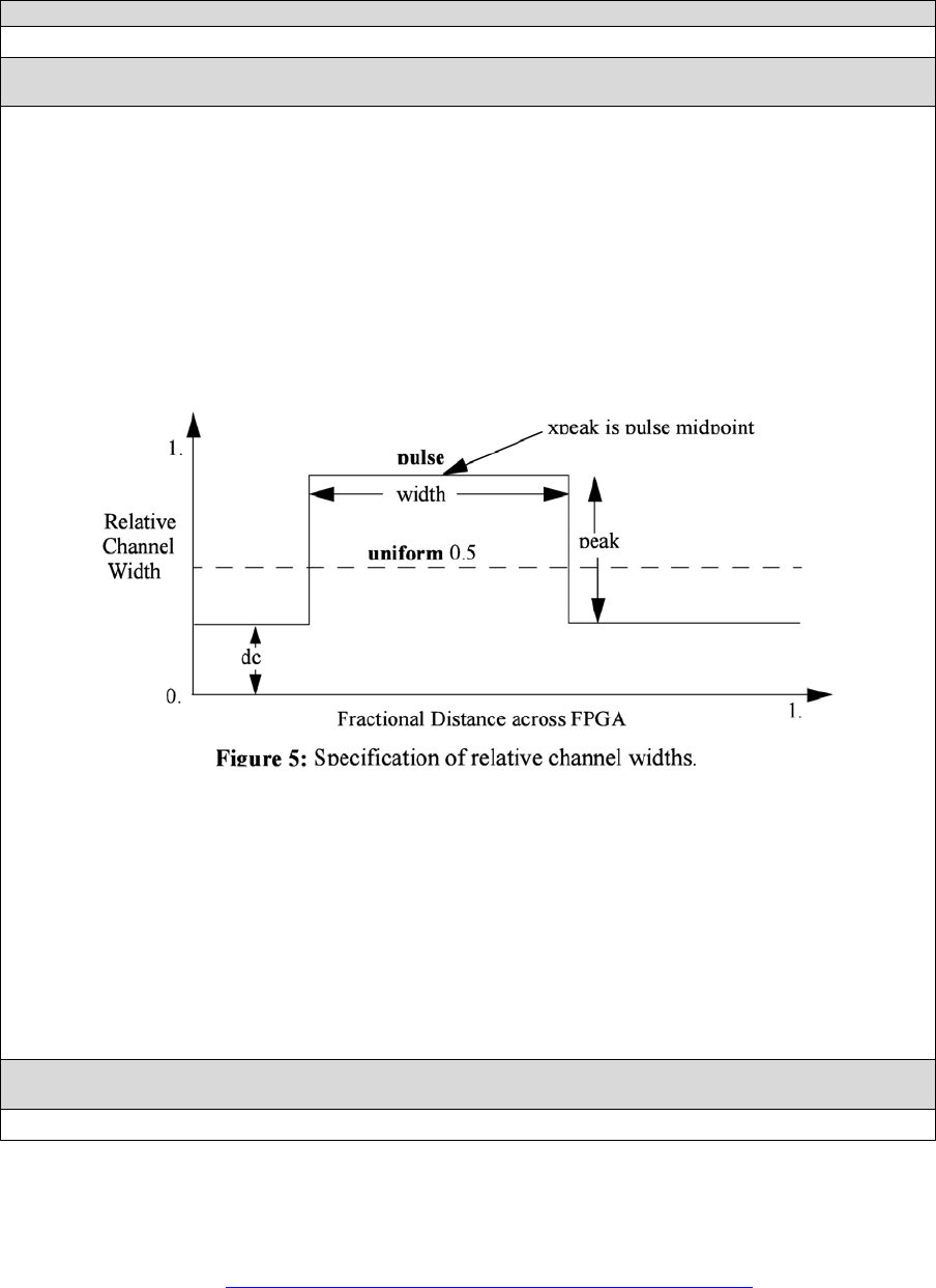
<x distr=”{gaussian|uniform|pulse|delta}” peak=”float” width=” float” xpeak=” float” dc=”
float”/>
(Unknown if works properly)
The italicized quantities are needed only for pulse, gaussian, and delta (which doesn’t need
width). Most values are from 0 to 1. Sets the distribution of tracks for the x-directed channels --
the channels that run horizontally.
If uniform is specified, you simply specify one argument, peak. This value (by convention
between 0 and 1) sets the width of the x-directed core channels relative to the y-directed
channels and the channels between the pads and core. Figure should make the specification
of uniform (dashed line) and pulse (solid line) channel widths more clear. The gaussian
keyword takes the same four parameters as the pulse keyword, and they are all interpreted in
exactly the same manner except that in the gaussian case width is the standard deviation of
the function.
The delta function is used to specify a channel width distribution in which all the channels have
the same width except one. The syntax is chan_width_x delta peak xpeak dc. Peak is the
extra width of the single wide channel. Xpeak is between 0 and 1 and specifies the location
within the FPGA of the extra-wide channel -- it is the fractional distance across the FPGA at
which this extra-wide channel lies. Finally, dc specifies the width of all the other channels. For
example, the statement chan_width_x delta 3 0.5 1 specifies that the horizontal channel in the
middle of the FPGA is four times as wide as the other channels.
Examples:
<x distr=”uniform” peak=”1”/>
<x distr=”gaussian” width=”0.5” peak=”0.8” xpeak=”0.6” dc=”0.2”/>
<y distr=”{gaussian|uniform|pulse|delta}” peak=” float” width=” float” xpeak=” float” dc=”
float”/>
Sets the distribution of tracks for the y-directed channels.
3.1.4 Description of Complex Logic Blocks
For step-by-step walkthrough examples on how to build a complex block using this
language, please refer to http://www.eecg.utoronto.ca/vpr/arch_language.html.
The content within the <complexblocklist> tag describes the complex logic blocks
found within the FPGA. It contains <pb_type> tags. Each complex logic block is specified by
a <pb_type name=”string” height=”int”> tag. The name attribute is the name for the
complex block. The height attribute specifies how many grid tiles the block takes up.
The internals of a complex block is described using a hierarchy of <pb_type> tags. The
top-level <pb_type> tag specifies the complex block. Children <pb_type> tags are either
clusters (which contain other <pb_type> tags) or leaves (do not contain other <pb_type>
tags). Clusters can contain other clusters and leaves so there is no restriction on the hierarchy
that can be specified using this language. All children <pb_type> tags contain the attribute
num_pb=”int” which describes the number of instances of that particular type of cluster or
leaf block in that section of the hierarchy. All children <pb_type> tags must have a name
=”string” attribute where the name must be unique with respect to any parent, sibling, or
child <pb_type> tag. Leaf <pb_type> tags may optionally have a blif_model=”string”
attribute. This attribute describes the type of block in the blif file that this particular leaf can
implement. For example, a leaf that implements a LUT should have blif_model=”.names”.
Similarly, a leaf that implements “.subckt user_block_A” should have attribute
blif_model=”.subckt user_block_A”. The input, output, and/or clock, ports for these
leaves must match the ports specified in the <models> section of the architecture file. There is
a special attribute for leaf nodes called class that will be described in more detail later.
The following tags are common to all <pb_type> tags.
<input name=”string” num_pins=”int” equivalent=”true|false”/>
Describes an input port. Multple input ports are described using multiple <input> tags.
name attribute:
Name of the input port.
num_pins attribute:
Number of pins that this input port has
equivalent attribute (applies only to top-level pb_type):
Describes if the pins of the port are logically equivalent. Input logical equivalence means that
the pin order can be swapped without changing functionality. For example, an AND gate has
logically equivalent inputs because you can swap the order of the inputs and it’s still correct;
an adder, on the otherhand, is not logically equivalent because if you swap the MSB with the
LSB, the results are completely wrong.
<output name=”string” num_pins=”int” equivalent=”true|false”/>
Describes an output port. Multple output ports are described using multiple <output> tags.
name attribute:
Name of the output port.
num_pins attribute:
Number of pins that this output port has
equivalent attribute (applies only to top-level pb_type):
Describes if the pins of the port are logically equivalent. (See above case on inputs),
<clock name=”string” num_pins=”int” equivalent=”true|false”/>

Describes a clock port. Multple clock ports are described using multiple <clock> tags.
name attribute:
Name of the clock port.
num_pins attribute:
Number of pins that this clock port has
equivalent attribute (applies only to top-level pb_type):
Describes if the pins of the port are logically equivalent. (See above case on inputs).
<mode name=”string”>
Specifies a mode of operation for the <pb_type>. Each child mode tag denotes a different
mode of operation for that <pb_type>. A mode tag contains <pb_type> tags and
<interconnect> tags. If a <pb_type> has only one mode of operation, then this mode tag can
be omitted. More on interconnect later.
name attribute:
Name for this mode. Must be unique compared to other modes.
The following tags are unique to the top level <pb_type> of a complex logic block. They
describe how this complex block interface with the extra block world.
<fc_in type="{frac|abs|full}">{int | float}</fc_in>
Content:
Sets the number of tracks to which each logic block input pin connects in each channel
bordering the pin. The Fc value used is always the minimum of the specified Fc and the
channel width, W. It is best to set the type attribute to full if you want Fc to always be W.
type attribute:
The type attribute indicates whether the Fc [12] value should be interpreted as the number of
tracks to which each pin connects (absolute), or the fraction of tracks in a channel to which
each pin connects (fractional). Note: type absolute or fractional for Fc_in and Fc_out must be
the same. Full disregards whether it is fractional or absolute and can be used in either case.
<fc_out type="{frac|abs|full}">{int | float}</fc_out>
Content:
Sets the number of tracks to which each logic block output pin connects in each channel
bordering the pin.
Type attribute is the same as described above in Fc_in
<pinlocations pattern=”spread|custom”>
Describes the locations where the input, output, and clock pins are distributed in a complex
logic block.
The pattern “spread” denotes that the pins are to be spread evenly on all sides of the complex
block.
The pattern “custom” allows the architect to specify specifically where the pins are to be
placed using <loc> tags. A <loc> tag is defined as:

<loc side="{left|right|bottom|top}"
offset=”int”>name_of_complex_logic_block.port_name[int:int] … </loc>
Where … represents repeat as needed (Do not put … in the architecture file). The side
attribute specifies which of the four directions the pins in the contents are located on and offset
attribute specifies the grid distance from the bottom grid tile that the pin is specified for. Pins
on the bottom grid tile have an offset value of 0 (offset defaults to 0 if not specified). The offset
value must be less than the height of the functional block. Pin groupings are specified by the
complex block name, the port those pins belong to, and the range of pins being referenced. A
functional block may not contain pins inside of itself (ie. Not on the periphery of the block).
Physical equivalence for a pin is specified by listing a pin more than once for different
locations. For example, a LUT whose output can exit from the top and bottom of a block will
have its output pin specified twice: once for the top and once for the bottom.
<gridlocations>
Specifies the columns on the FPGA that will consist of this functional block. The columns are
specified by a group of <loc> tags and there are three ways to use this tag:
<loc type="col" start="<int>" repeat="<int>" priority="<int>"/>
This specifies an absolute column assignment. The first column to contain this functional
block is specified in start. Every column that satisfies x = start_x + k*repeat, where k is any
integer, will be composed of this functional block.
<loc type="rel" pos="0.5" priority="<int>"/>
This specifies a single column to be composed of this functional block where the column is
specified as a fraction of the width.
<loc type="fill" priority="1"/>
This is a special specification such that all unspecified columns get assigned this functional
block.
For all three <loc> tags, the priority attribute is used to resolve collisions when two different
functional block is supposed to use the same column. The larger integer specified for priority
gets the location.
As stated earlier, the mode tag contains <pb_type> tags and a <interconnect> tag.
The following describes the tags that are accepted in the <interconnect> tag.
<complete name=”string” input=”string” output=”string”/>
Describes a fully connected crossbar. Any pin in the inputs can connect to any pin at the
output.
name attribute:
Identifier for the interconnect.
input attribute:
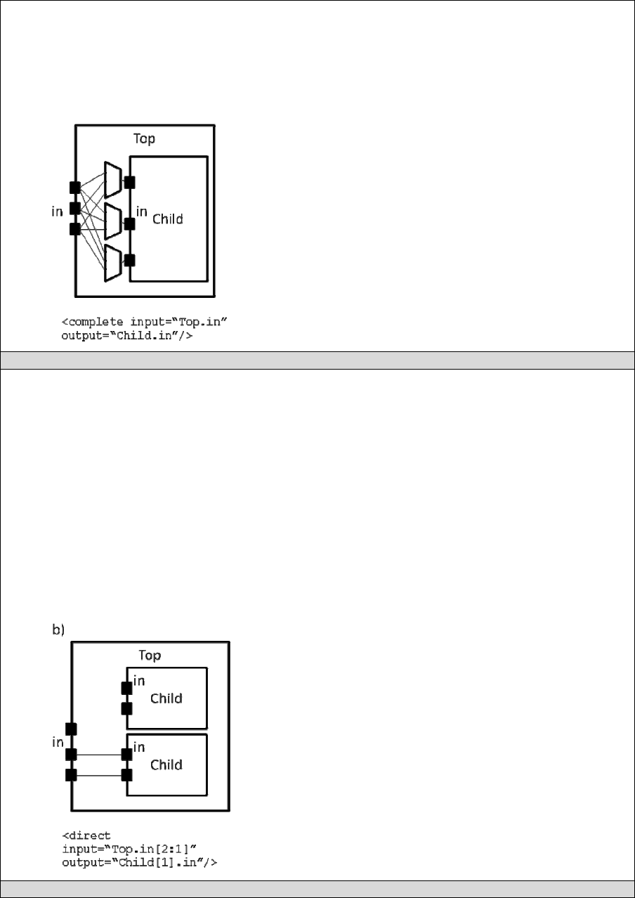
Pins that are inputs to this interconnect
output attribute:
Pins that are outputs of this interconnect.
Example:
<direct name=”string” input=”string” output=”string”/>
Describes a 1-to-1 mapping between input pins and output pins.
name attribute:
Identifier for the interconnect.
input attribute:
Pins that are inputs to this interconnect
output attribute:
Pins that are outputs of this interconnect.
Example:
<mux name=”string” input=”string” output=”string”/>
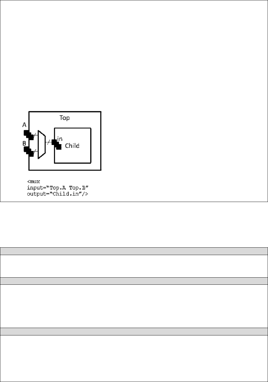
Describes a bus-based multiplexer. Note: Buses are not yet supported so all muxes must use
one bit wide data only!
name attribute:
Identifier for the interconnect.
input attribute:
Pins that are inputs to this interconnect. Different data lines are separated by a space.
output attribute:
Pins that are outputs of this interconnect.
Example:
Using these structures, we believe that one can describe any digital complex logic block.
However, we believe that certain kinds of logic structuers are common enough in FPGAs that
special shortcuts should be available to make their specification easier. These logic structures
are: flip-flops, LUTs, and memories. These structures are described using a “class=string”
attribute in the <pb_type> leaf that it pertains to. The classes we offer are:
lut Describes a K-input lookup table. The unique characteristic of a lookup table is that all inputs
to the lookup table are logically equivalent. When this class is used, the input port must have
a port_class=”lut_in” attribute and the output port must have a port_class=”lut_out” attribute
flipflop
Describes a flipflop.
Input port must have a port_class=”D” attribute added.
Output port must have a port_class=”Q” attribute added.
Clock port must have a port_class=”clock” attribute added.
Memory
Describes a memory. Memories are unique in that a single memory physical primitive can
hold multiple, smaller, logical memories as long as: 1) The address, clock, and control inputs
are identical and 2) There exists sufficient physical data pins to satisfy the netlist memories
when the different netlist memories are merged together into one physical memory.
For single ported memories, there should be:
An input port with port_class=”address” attribute
An input port with port_class=”data_in” attribute
An input port with port_class=”write_en” attribute
An output port with port_class=”data_out” attribute
A clock port with port_class=”clock” attribute
An input port with port_class=”address1” attribute
An input port with port_class=”data_in1” attribute
An input port with port_class=”write_en1” attribute
An input port with port_class=”address2” attribute
An input port with port_class=”data_in2” attribute
An input port with port_class=”write_en2” attribute
An output port with port_class=”data_out1” attribute
An output port with port_class=”data_out2” attribute
A clock port with port_class=”clock” attribute
Timing is specified through children tags for pb_type tags or complete, direct, or mux tags
as follows:
<delay_constant max=”float” in_port=”string” out_port=”string”/>
Delay equal to max for connections involving input to output ports
<delay_matrix type=”max” in_port=”string” out_port=”string”> matrix </delay>
Describe a timing matrix for all edges going from in_port to out_port. Number of rows of matrix
should equal the number of inputs, number of columns should equal the number of outputs.
For example a 4 input pin 3 output pin timing matrix would look like:
1.2e-10 1.4e-10 3.2e-10
4.6e-10 1.9e-10 2.2e-10
4.5e-10 6.7e-10 3.5e-10
7.1e-10 2.9e-10 8.7e-10
<T_setup value=”float” port=”string” clock=”string”/>
Specify setup time (value) for pins of port. The clock attribute describes which clock this setup
time is with respect to.
Note: Applies to sequential pb_type only
<T_clock_to_Q max=”float” port=”string” clock=”string”/>
Specify the clock-to-Q delay of output port of sequential pb_type. Delay is specified by the
max attribute, pins by the port attribute, and the clock this refers to by the clock attribute.
3.1.5 Description of the Wire Segments
The content within the <segmentlist> tag consists of a group of <segment> tags. The
<segment> tag and its contents are described in the table below.
<segment length=”int” type=”{bidir|unidir}” freq=”float” Rmetal=”float”
Cmetal=”float”>content</segment>
Describes the properties of a segment
length: Either the number of logic blocks spanned by each segment, or the keyword longline.
Longline means segments of this type span the entire FPGA array.
freq: The supply of routing tracks composed of this type of segment. VPR automatically
determines the percentage of tracks for each segment type by taking the frequency for the type
specified and dividing with the sum of all frequencies. It is recommended that the sum of all
segment frequencies be in the range 1 to 100.
Rmetal: Resistance per unit length (in terms of logic blocks) of this wiring track, in Ohms. For
example, a segment of length 5 with Rmetal = 10 Ohms / logic block would have an end-to-end
resistance of 50 Ohms.
Cmetal: Capacitance per unit length (in terms of logic blocks) of this wiring track, in Farads. For
example, a segment of length 5 with Cmetal = 2e-14 F / logic block would have a total metal
capacitance of 10e-13F.
directionality: This is either uni_directional or bi_directional and indicates whether a segment
has multiple drive points (bi_directional), or a single driver at one end of the wire segment
(uni_directional). All segments must have the same directionality value. See [15] for a
description of uni-directional single-driver wire segments.
Content contains the switch names and the depopulation pattern as described below.
<sb type=”pattern”>int list</sb>
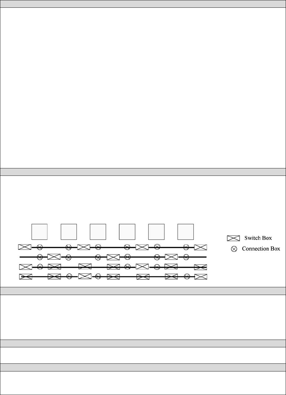
This tag describes the switch block depopulation (as illustrated in the figure below) for this
particular wire segment. For example, the firsth length 6 wire in the figure below has an sb
pattern of “1 0 1 0 1 0 1”. The second wire has a pattern of “0 1 0 1 0 1 0”. A “1” indicates the
existance of a switch block and a “0” indicates that there is no switch box at that point. Note that
there a 7 entries in the integer list for a length 6 wire. For a length L wire there must be L+1
entries seperated by spaces.
<cb type=”pattern”>int list</cb>
This tag describes the connection block depopulation (as illustrated by the circles in the figure
above) for this particular wire segment. For example, the firsth length 6 wire in the figure below
has an sb pattern of “1 1 1 1 1 1”. The third wire has a pattern of “1 0 0 1 1 0”. A “1” indicates
the existance of a connection block and a “0” indicates that there is no connection box at that
point. Note that there a 6 entries in the integer list for a length 6 wire. For a length L wire there
must be L entries seperated by spaces.
<mux name=”match name”/>
Option for UNIDIRECTIONAL only. Tag must be included and the “match name” must be the
same as the name you give in <switch type=”mux” name=”…
<wire switch name=”match name”/>
Option for BIDIRECTIONAL only. Tag must be included and the “match name” must be the
same as the name you give in <switch type=”buffer” name=”… for the switch which represents
the wire switch in your architecture.

wire_switch: The index of the switch type used by other wiring segments to drive this type of
segment. That is, switches going to this segment from other pieces of wiring will use this type of
switch.
<wire switch name=”match name”/>
Option for BIDIRECTIONAL only. Tag must be included and the “match name” must be the
same as the name you give in <switch type=”buffer” name=”… for the switch which represents
the output pin switch in your architecture.
opin_switch: The index of the switch type used by clb and pad output pins to drive this type of
segment.
NOTE: In unidirectional segment mode, there is only a single buffer on the segment. Its type is
specified by assigning the same switch index to both wire_switch and opin_switch. VPR will
error out if these two are not the same.
NOTE: The switch used in unidirectional segment mode must be buffered.
3.1.6 Description of the Switch list
The content within the <switchlist> tag consists of a group of <switch> tags. The
<switch> tag and its contents are described in the table below.
<switch type=”{buffered|mux}” name=”unique name” R=”float” Cin=” float” Cout=” float”
Tdel=” float” buf_size=”float” mux_trans_size=”float”/>
Describes a a type of switch. This statement defines what a certain type of switch is -- segment
statements refer to a switch types by their number (the number right after the switch keyword).
The various values are:
name: is a unique alphanumeric string which needs to match the segment definition (see above)
buffered: if this switch is a tri-state buffer
mux: if this is a multiplexer
R: resistance of the switch.
Cin: Input capacitance of the switch.
Cout: Output capacitance of the switch.
Tdel: Intrinsic delay through the switch. If this switch was driven by a zero resistance source,
and drove a zero capacitance load, its delay would be Tdel + R * Cout. The ‘switch’ includes
both the mux and buffer when in unidirectional mode.
buf_size: [Only for unidirectional and optional] May only be used in unidirectional mode. This is
an optional parameter that specifies area of the buffer in minimum-width transistor area units. If
not given will be determined from R value. This allows you to use timing models without R’s and
C’s and still be able to measure area.
mux_trans_size: [Only for unidirectional and optional] This parameter must be used if and only
if unidirectional segments are used since bidirectional mode switches don’t have muxes. The
value controls the size of each transistor in the mux, measured in minimum width transistors.
The mux is a two-level mux.
3.1.7 An Example Architecture Specification
The listing below is for an FPGA with I/O pads, soft logic blocks (called CLB), configurable
memory hard logic blocks, and fracturable multipliers. This architecture is based off a
<!-- VPR Architecture Specification File -->
<!--
Quick XML Primer:
-> Data is hierarchical and composed of tags (similar to HTML)
-> All tags must be of the form <foo>content</foo> OR <foo /> with the
latter form indicating no content. Don't forget the slash at the end.
-> Inside a start tag you may specify attributes in the form key="value".
Refer to manual for the valid attributes for each element.
-> Comments may be included anywhere in the document except inside a tag
where it's attribute list is defined.
-> Comments may contain any characters except two dashes.
-->
<!--
Architecture based off Stratix IV
Use closest ifar architecture: K06 N10 45nm fc 0.15 area-delay optimized, scale to 40 nm using
linear scaling
n10k06l04.fc15.area1delay1.cmos45nm.bptm.cmos45nm.xml
- because documentation sparser for soft logic (delays not in QUIP), harder to track down,
not worth our time considering the level of accuracy is approximate
- delays multiplied by 40/45 to normalize for process difference between stratix 4 and 45
nm technology (called full scaling)
Use delay numbers off Altera device handbook:
http://www.altera.com/literature/hb/stratix-iv/stx4_5v1.pdf
http://www.altera.com/literature/hb/stratix-iv/stx4_siv51004.pdf
http://www.altera.com/literature/hb/stratix-iv/stx4_siv51003.pdf
multipliers at 600 MHz, no detail on 9x9 vs 36x36
- datasheets unclear
- claims 4 18x18 independant multipliers, following test indicates that this is not the
case:
created 4 18x18 mulitpliers, logiclocked them to a single DSP block, compile
result - 2 18x18 multipliers got packed together, the other 2 got ejected out of the
logiclock region without error
conclusion - just take the 600 MHz as is, and Quartus II logiclock hasn't fixed the
bug that I've seen it do to registers when I worked at Altera (ie. eject without warning)
-->
<architecture>
<!-- ODIN II specific config -->
<models>
<model name="multiply">
<input_ports>
<port name="a"/>
<port name="b"/>
</input_ports>
<output_ports>
<port name="out"/>
</output_ports>
</model>
<model name="single_port_ram">
<input_ports>
<port name="we"/> <!-- control -->
<port name="addr"/> <!-- address lines -->
<port name="data"/> <!-- data lines can be broken down into smaller bit widths minimum
size 1 -->
<port name="clk" is_clock="1"/> <!-- memories are often clocked -->
</input_ports>
<output_ports>
<port name="out"/> <!-- output can be broken down into smaller bit widths minimum size 1
-->
</output_ports>
</model>
<model name="dual_port_ram">
<input_ports>
<port name="we1"/> <!-- write enable -->
<port name="we2"/> <!-- write enable -->
<port name="addr1"/> <!-- address lines -->
<port name="addr2"/> <!-- address lines -->
<port name="data1"/> <!-- data lines can be broken down into smaller bit widths minimum
size 1 -->
<port name="data2"/> <!-- data lines can be broken down into smaller bit widths minimum
size 1 -->
<port name="clk" is_clock="1"/> <!-- memories are often clocked -->
</input_ports>
<output_ports>
<port name="out1"/> <!-- output can be broken down into smaller bit widths minimum size 1
-->
<port name="out2"/> <!-- output can be broken down into smaller bit widths minimum size 1
-->
</output_ports>
</model>
</models>
<!-- ODIN II specific config ends -->
<!-- Physical descriptions begin (area optimized for N8-K6-L4 -->
<layout auto="1.0"/>
<device>
<sizing R_minW_nmos="6065.520020" R_minW_pmos="18138.500000"
ipin_mux_trans_size="1.222260"/>
<timing C_ipin_cblock="0.000000e+00" T_ipin_cblock="7.247000e-11"/>
<area grid_logic_tile_area="14813.392"/> <!--area is for soft logic only-->
<chan_width_distr>
<io width="1.000000"/>
<x distr="uniform" peak="1.000000"/>
<y distr="uniform" peak="1.000000"/>
</chan_width_distr>
<switch_block type="wilton" fs="3"/>
</device>
<switchlist>
<switch type="mux" name="0" R="0.000000" Cin="0.000000e+00"
Cout="0.000000e+00" Tdel="6.837e-11" mux_trans_size="2.630740" buf_size="27.645901"/>
</switchlist>
<segmentlist>
<segment freq="1.000000" length="4" type="unidir" Rmetal="0.000000"
Cmetal="0.000000e+00">
<mux name="0"/>
<sb type="pattern">1 1 1 1 1</sb>
<cb type="pattern">1 1 1 1</cb>
</segment>
</segmentlist>
<complexblocklist>
<!-- Capacity is a unique property of I/Os, it is the maximum number of I/Os that can be
placed at the same (X,Y) location on the FPGA -->
<pb_type name="io" capacity="8">
<input name="outpad" num_pins="1"/>
<output name="inpad" num_pins="1"/>
<clock name="clock" num_pins="1"/>
<!-- IOs can operate as either inputs or outputs -->
<mode name="inpad">
<pb_type name="inpad" blif_model=".input" num_pb="1">
<output name="inpad" num_pins="1"/>
</pb_type>
<interconnect>
<direct name="inpad" input="inpad.inpad" output="io.inpad">
<delay_constant max="4.243e-11" in_port="inpad.inpad" out_port="io.inpad"/>
</direct>
</interconnect>
</mode>
<mode name="outpad">
<pb_type name="outpad" blif_model=".output" num_pb="1">
<input name="outpad" num_pins="1"/>
</pb_type>
<interconnect>
<direct name="outpad" input="io.outpad" output="outpad.outpad">
<delay_constant max="1.394e-11" in_port="io.outpad" out_port="outpad.outpad"/>
</direct>
</interconnect>
</mode>
<fc_in type="frac">0.15</fc_in>
<fc_out type="frac">0.10</fc_out>
<!-- IOs go on the periphery of the FPGA, for consistency,
make it physically equivalent on all sides so that only one definition of I/Os is
needed.
If I do not make a physically equivalent definition, then I need to define 4 different
I/Os, one for each side of the FPGA
-->
<pinlocations pattern="custom">
<loc side="left">io.outpad io.inpad io.clock</loc>
<loc side="top">io.outpad io.inpad io.clock</loc>
<loc side="right">io.outpad io.inpad io.clock</loc>
<loc side="bottom">io.outpad io.inpad io.clock</loc>
</pinlocations>
<gridlocations>
<loc type="perimeter" priority="10"/>
</gridlocations>
</pb_type>
<pb_type name="clb">
<input name="I" num_pins="33" equivalent="true"/>
<output name="O" num_pins="10" equivalent="false"/>
<clock name="clk" num_pins="1"/>
<!-- Describe basic logic element -->
<pb_type name="ble" num_pb="10">
<input name="in" num_pins="6"/>
<output name="out" num_pins="1"/>
<clock name="clk" num_pins="1"/>
<pb_type name="soft_logic" num_pb="1">
<input name="in" num_pins="6"/>
<output name="out" num_pins="1"/>
<mode name="n1_lut6">
<pb_type name="lut6" blif_model=".names" num_pb="1" class="lut">
<input name="in" num_pins="6" port_class="lut_in"/>
<output name="out" num_pins="1" port_class="lut_out"/>
<!-- LUT timing using delay matrix -->
<delay_matrix type="max" in_port="lut6.in" out_port="lut6.out">
2.690e-10
2.690e-10
2.690e-10
2.690e-10
2.690e-10
2.690e-10
</delay_matrix>
</pb_type>
<interconnect>
<direct name="direct1" input="soft_logic.in[5:0]"
output="lut6[0:0].in[5:0]"/>
<direct name="direct2" input="lut6[0:0].out" output="soft_logic.out[0:0]"/>
</interconnect>
</mode>
</pb_type>
<pb_type name="ff" blif_model=".latch" num_pb="1" class="flipflop">
<input name="D" num_pins="1" port_class="D"/>
<output name="Q" num_pins="1" port_class="Q"/>
<clock name="clk" num_pins="1" port_class="clock"/>
<T_setup value="2.448e-10" port="ff.D" clock="clk"/>
<T_clock_to_Q max="7.732e-11" port="ff.Q" clock="clk"/>
</pb_type>
<interconnect>
<!-- Two ff, make ff available to only corresponding luts -->
<direct name="direct1" input="ble.in" output="soft_logic.in"/>
<direct name="direct2" input="soft_logic.out" output="ff.D"/>
<direct name="direct4" input="ble.clk" output="ff.clk"/>
<mux name="mux1" input="ff.Q soft_logic.out" output="ble.out"/>
</interconnect>
</pb_type>
<interconnect>
<complete name="crossbar" input="clb.I ble[9:0].out" output="ble[9:0].in">
<delay_constant max="8.044000e-11" in_port="clb.I" out_port="ble[9:0].in" />
<delay_constant max="7.354000e-11" in_port="ble[9:0].out" out_port="ble[9:0].in" />
</complete>
<complete name="clks" input="clb.clk" output="ble[9:0].clk">
</complete>
<direct name="clbouts" input="ble[9:0].out" output="clb.O">
</direct>
</interconnect>
<fc_in type="frac">0.15</fc_in>
<fc_out type="frac">0.1</fc_out>
<pinlocations pattern="spread"/>
<gridlocations>
<loc type="fill" priority="1"/>
</gridlocations>
</pb_type>
<!-- This is the 36*36 uniform mult -->
<pb_type name="mult_36" height="4">
<input name="a" num_pins="36"/>
<input name="b" num_pins="36"/>
<output name="out" num_pins="72"/>
<mode name="two_divisible_mult_18x18">
<pb_type name="divisible_mult_18x18" num_pb="2">
<input name="a" num_pins="18"/>
<input name="b" num_pins="18"/>
<output name="out" num_pins="36"/>
<mode name="two_mult_9x9">
<pb_type name="mult_9x9_slice" num_pb="2">
<input name="A_cfg" num_pins="9"/>
<input name="B_cfg" num_pins="9"/>
<output name="OUT_cfg" num_pins="18"/>
<pb_type name="mult_9x9" blif_model=".subckt multiply" num_pb="1">
<input name="a" num_pins="9"/>
<input name="b" num_pins="9"/>
<output name="out" num_pins="18"/>
<delay_constant max="1.667e-9" in_port="mult_9x9.a" out_port="mult_9x9.out"/>
<delay_constant max="1.667e-9" in_port="mult_9x9.b" out_port="mult_9x9.out"/>
</pb_type>
<interconnect>
<direct name="a2a" input="mult_9x9_slice.A_cfg" output="mult_9x9.a">
</direct>
<direct name="b2b" input="mult_9x9_slice.B_cfg" output="mult_9x9.b">
</direct>
<direct name="out2out" input="mult_9x9.out" output="mult_9x9_slice.OUT_cfg">
</direct>
</interconnect>
</pb_type>
<interconnect>
<direct name="a2a" input="divisible_mult_18x18.a"
output="mult_9x9_slice[1:0].A_cfg">
</direct>
<direct name="b2b" input="divisible_mult_18x18.b"
output="mult_9x9_slice[1:0].B_cfg">
</direct>
<direct name="out2out" input="mult_9x9_slice[1:0].OUT_cfg"
output="divisible_mult_18x18.out">
</direct>
</interconnect>
</mode>
<mode name="mult_18x18">
<pb_type name="mult_18x18_slice" num_pb="1">
<input name="A_cfg" num_pins="18"/>
<input name="B_cfg" num_pins="18"/>
<output name="OUT_cfg" num_pins="36"/>
<pb_type name="mult_18x18" blif_model=".subckt multiply" num_pb="1" >
<input name="a" num_pins="18"/>
<input name="b" num_pins="18"/>
<output name="out" num_pins="36"/>
<delay_constant max="1.667e-9" in_port="mult_18x18.a"
out_port="mult_18x18.out"/>
<delay_constant max="1.667e-9" in_port="mult_18x18.b"
out_port="mult_18x18.out"/>
</pb_type>
<interconnect>
<direct name="a2a" input="mult_18x18_slice.A_cfg" output="mult_18x18.a">
</direct>
<direct name="b2b" input="mult_18x18_slice.B_cfg" output="mult_18x18.b">
</direct>
<direct name="out2out" input="mult_18x18.out"
output="mult_18x18_slice.OUT_cfg">
</direct>
</interconnect>
</pb_type>
<interconnect>
<direct name="a2a" input="divisible_mult_18x18.a"
output="mult_18x18_slice.A_cfg">
</direct>
<direct name="b2b" input="divisible_mult_18x18.b"
output="mult_18x18_slice.B_cfg">
</direct>
<direct name="out2out" input="mult_18x18_slice.OUT_cfg"
output="divisible_mult_18x18.out">
</direct>
</interconnect>
</mode>
</pb_type>
<interconnect>
<direct name="a2a" input="mult_36.a" output="divisible_mult_18x18[1:0].a">
</direct>
<direct name="b2b" input="mult_36.b" output="divisible_mult_18x18[1:0].b">
</direct>
<direct name="out2out" input="divisible_mult_18x18[1:0].out" output="mult_36.out">
</direct>
</interconnect>
</mode>
<mode name="mult_36x36">
<pb_type name="mult_36x36_slice" num_pb="1">
<input name="A_cfg" num_pins="36"/>
<input name="B_cfg" num_pins="36"/>
<output name="OUT_cfg" num_pins="72"/>
<pb_type name="mult_36x36" blif_model=".subckt multiply" num_pb="1">
<input name="a" num_pins="36"/>
<input name="b" num_pins="36"/>
<output name="out" num_pins="72"/>
<delay_constant max="1.667e-9" in_port="mult_36x36.a" out_port="mult_36x36.out"/>
<delay_constant max="1.667e-9" in_port="mult_36x36.b" out_port="mult_36x36.out"/>
</pb_type>
<interconnect>
<direct name="a2a" input="mult_36x36_slice.A_cfg" output="mult_36x36.a">
</direct>
<direct name="b2b" input="mult_36x36_slice.B_cfg" output="mult_36x36.b">
</direct>
<direct name="out2out" input="mult_36x36.out" output="mult_36x36_slice.OUT_cfg">
</direct>
</interconnect>
</pb_type>
<interconnect>
<direct name="a2a" input="mult_36.a" output="mult_36x36_slice.A_cfg">
</direct>
<direct name="b2b" input="mult_36.b" output="mult_36x36_slice.B_cfg">
</direct>
<direct name="out2out" input="mult_36x36_slice.OUT_cfg" output="mult_36.out">
</direct>
</interconnect>
</mode>
<fc_in type="frac">0.15</fc_in>
<fc_out type="frac">0.10</fc_out>
<pinlocations pattern="spread"/>
<gridlocations>
<loc type="col" start="4" repeat="8" priority="2"/>
</gridlocations>
</pb_type>
<!-- Memory based off Stratix IV 144K memory. Setup time set to match flip-flop setup time at 45
nm. Clock to q based off 144K max MHz -->
<pb_type name="memory" height="6">
<input name="addr1" num_pins="17"/>
<input name="addr2" num_pins="17"/>
<input name="data" num_pins="72"/>
<input name="we1" num_pins="1"/>
<input name="we2" num_pins="1"/>
<output name="out" num_pins="72"/>
<clock name="clk" num_pins="1"/>
<mode name="mem_2048x72_sp">
<pb_type name="mem_2048x72_sp" blif_model=".subckt single_port_ram" class="memory"
num_pb="1">
<input name="addr" num_pins="11" port_class="address"/>
<input name="data" num_pins="72" port_class="data_in"/>
<input name="we" num_pins="1" port_class="write_en"/>
<output name="out" num_pins="72" port_class="data_out"/>
<clock name="clk" num_pins="1" port_class="clock"/>
<T_setup value="2.448e-10" port="mem_2048x72_sp.addr" clock="clk"/>
<T_setup value="2.448e-10" port="mem_2048x72_sp.data" clock="clk"/>
<T_setup value="2.448e-10" port="mem_2048x72_sp.we" clock="clk"/>
<T_clock_to_Q max="1.852e-9" port="mem_2048x72_sp.out" clock="clk"/>
</pb_type>
<interconnect>
<direct name="address1" input="memory.addr1[10:0]" output="mem_2048x72_sp.addr">
</direct>
<direct name="data1" input="memory.data[71:0]" output="mem_2048x72_sp.data">
</direct>
<direct name="writeen1" input="memory.we1" output="mem_2048x72_sp.we">
</direct>
<direct name="dataout1" input="mem_2048x72_sp.out" output="memory.out[71:0]">
</direct>
<direct name="clk" input="memory.clk" output="mem_2048x72_sp.clk">
</direct>
</interconnect>
</mode>
<mode name="mem_4096x36_dp">
<pb_type name="mem_4096x36_dp" blif_model=".subckt dual_port_ram" class="memory"
num_pb="1">
<input name="addr1" num_pins="12" port_class="address1"/>
<input name="addr2" num_pins="12" port_class="address2"/>
<input name="data1" num_pins="36" port_class="data_in1"/>
<input name="data2" num_pins="36" port_class="data_in2"/>
<input name="we1" num_pins="1" port_class="write_en1"/>
<input name="we2" num_pins="1" port_class="write_en2"/>
<output name="out1" num_pins="36" port_class="data_out1"/>
<output name="out2" num_pins="36" port_class="data_out2"/>
<clock name="clk" num_pins="1" port_class="clock"/>
<T_setup value="2.448e-10" port="mem_4096x36_dp.addr1" clock="clk"/>
<T_setup value="2.448e-10" port="mem_4096x36_dp.data1" clock="clk"/>
<T_setup value="2.448e-10" port="mem_4096x36_dp.we1" clock="clk"/>
<T_setup value="2.448e-10" port="mem_4096x36_dp.addr2" clock="clk"/>
<T_setup value="2.448e-10" port="mem_4096x36_dp.data2" clock="clk"/>
<T_setup value="2.448e-10" port="mem_4096x36_dp.we2" clock="clk"/>
<T_clock_to_Q max="1.852e-9" port="mem_4096x36_dp.out1" clock="clk"/>
<T_clock_to_Q max="1.852e-9" port="mem_4096x36_dp.out2" clock="clk"/>
</pb_type>
<interconnect>
<direct name="address1" input="memory.addr1[11:0]" output="mem_4096x36_dp.addr1">
</direct>
<direct name="address2" input="memory.addr2[11:0]" output="mem_4096x36_dp.addr2">
</direct>
<direct name="data1" input="memory.data[35:0]" output="mem_4096x36_dp.data1">
</direct>
<direct name="data2" input="memory.data[71:36]" output="mem_4096x36_dp.data2">
</direct>
<direct name="writeen1" input="memory.we1" output="mem_4096x36_dp.we1">
</direct>
<direct name="writeen2" input="memory.we2" output="mem_4096x36_dp.we2">
</direct>
<direct name="dataout1" input="mem_4096x36_dp.out1" output="memory.out[35:0]">
</direct>
<direct name="dataout2" input="mem_4096x36_dp.out2" output="memory.out[71:36]">
</direct>
<direct name="clk" input="memory.clk" output="mem_4096x36_dp.clk">
</direct>
</interconnect>
</mode>
<mode name="mem_4096x36_sp">
<pb_type name="mem_4096x36_sp" blif_model=".subckt single_port_ram" class="memory"
num_pb="1">
<input name="addr" num_pins="12" port_class="address"/>
<input name="data" num_pins="36" port_class="data_in"/>
<input name="we" num_pins="1" port_class="write_en"/>
<output name="out" num_pins="36" port_class="data_out"/>
<clock name="clk" num_pins="1" port_class="clock"/>
<T_setup value="2.448e-10" port="mem_4096x36_sp.addr" clock="clk"/>
<T_setup value="2.448e-10" port="mem_4096x36_sp.data" clock="clk"/>
<T_setup value="2.448e-10" port="mem_4096x36_sp.we" clock="clk"/>
<T_clock_to_Q max="1.852e-9" port="mem_4096x36_sp.out" clock="clk"/>
</pb_type>
<interconnect>
<direct name="address1" input="memory.addr1[11:0]" output="mem_4096x36_sp.addr">
</direct>
<direct name="data1" input="memory.data[35:0]" output="mem_4096x36_sp.data">
</direct>
<direct name="writeen1" input="memory.we1" output="mem_4096x36_sp.we">
</direct>
<direct name="dataout1" input="mem_4096x36_sp.out" output="memory.out[35:0]">
</direct>
<direct name="clk" input="memory.clk" output="mem_4096x36_sp.clk">
</direct>
</interconnect>
</mode>
<mode name="mem_9182x18_dp">
<pb_type name="mem_9182x18_dp" blif_model=".subckt dual_port_ram" class="memory"
num_pb="1">
<input name="addr1" num_pins="13" port_class="address1"/>
<input name="addr2" num_pins="13" port_class="address2"/>
<input name="data1" num_pins="18" port_class="data_in1"/>
<input name="data2" num_pins="18" port_class="data_in2"/>
<input name="we1" num_pins="1" port_class="write_en1"/>
<input name="we2" num_pins="1" port_class="write_en2"/>
<output name="out1" num_pins="18" port_class="data_out1"/>
<output name="out2" num_pins="18" port_class="data_out2"/>
<clock name="clk" num_pins="1" port_class="clock"/>
<T_setup value="2.448e-10" port="mem_9182x18_dp.addr1" clock="clk"/>
<T_setup value="2.448e-10" port="mem_9182x18_dp.data1" clock="clk"/>
<T_setup value="2.448e-10" port="mem_9182x18_dp.we1" clock="clk"/>
<T_setup value="2.448e-10" port="mem_9182x18_dp.addr2" clock="clk"/>
<T_setup value="2.448e-10" port="mem_9182x18_dp.data2" clock="clk"/>
<T_setup value="2.448e-10" port="mem_9182x18_dp.we2" clock="clk"/>
<T_clock_to_Q max="1.852e-9" port="mem_9182x18_dp.out1" clock="clk"/>
<T_clock_to_Q max="1.852e-9" port="mem_9182x18_dp.out2" clock="clk"/>
</pb_type>
<interconnect>
<direct name="address1" input="memory.addr1[12:0]" output="mem_9182x18_dp.addr1">
</direct>
<direct name="address2" input="memory.addr2[12:0]" output="mem_9182x18_dp.addr2">
</direct>
<direct name="data1" input="memory.data[17:0]" output="mem_9182x18_dp.data1">
</direct>
<direct name="data2" input="memory.data[35:18]" output="mem_9182x18_dp.data2">
</direct>
<direct name="writeen1" input="memory.we1" output="mem_9182x18_dp.we1">
</direct>
<direct name="writeen2" input="memory.we2" output="mem_9182x18_dp.we2">
</direct>
<direct name="dataout1" input="mem_9182x18_dp.out1" output="memory.out[17:0]">
</direct>
<direct name="dataout2" input="mem_9182x18_dp.out2" output="memory.out[35:18]">
</direct>
<direct name="clk" input="memory.clk" output="mem_9182x18_dp.clk">
</direct>
</interconnect>
</mode>
<mode name="mem_9182x18_sp">
<pb_type name="mem_9182x18_sp" blif_model=".subckt single_port_ram" class="memory"
num_pb="1">
<input name="addr" num_pins="13" port_class="address"/>
<input name="data" num_pins="18" port_class="data_in"/>
<input name="we" num_pins="1" port_class="write_en"/>
<output name="out" num_pins="18" port_class="data_out"/>
<clock name="clk" num_pins="1" port_class="clock"/>
<T_setup value="2.448e-10" port="mem_9182x18_sp.addr" clock="clk"/>
<T_setup value="2.448e-10" port="mem_9182x18_sp.data" clock="clk"/>
<T_setup value="2.448e-10" port="mem_9182x18_sp.we" clock="clk"/>
<T_clock_to_Q max="1.852e-9" port="mem_9182x18_sp.out" clock="clk"/>
</pb_type>
<interconnect>
<direct name="address1" input="memory.addr1[12:0]" output="mem_9182x18_sp.addr">
</direct>
<direct name="data1" input="memory.data[17:0]" output="mem_9182x18_sp.data">
</direct>
<direct name="writeen1" input="memory.we1" output="mem_9182x18_sp.we">
</direct>
<direct name="dataout1" input="mem_9182x18_sp.out" output="memory.out[17:0]">
</direct>
<direct name="clk" input="memory.clk" output="mem_9182x18_sp.clk">
</direct>
</interconnect>
</mode>
<mode name="mem_18194x9_dp">
<pb_type name="mem_18194x9_dp" blif_model=".subckt dual_port_ram" class="memory"
num_pb="1">
<input name="addr1" num_pins="14" port_class="address1"/>
<input name="addr2" num_pins="14" port_class="address2"/>
<input name="data1" num_pins="9" port_class="data_in1"/>
<input name="data2" num_pins="9" port_class="data_in2"/>
<input name="we1" num_pins="1" port_class="write_en1"/>
<input name="we2" num_pins="1" port_class="write_en2"/>
<output name="out1" num_pins="9" port_class="data_out1"/>
<output name="out2" num_pins="9" port_class="data_out2"/>
<clock name="clk" num_pins="1" port_class="clock"/>
<T_setup value="2.448e-10" port="mem_18194x9_dp.addr1" clock="clk"/>
<T_setup value="2.448e-10" port="mem_18194x9_dp.data1" clock="clk"/>
<T_setup value="2.448e-10" port="mem_18194x9_dp.we1" clock="clk"/>
<T_setup value="2.448e-10" port="mem_18194x9_dp.addr2" clock="clk"/>
<T_setup value="2.448e-10" port="mem_18194x9_dp.data2" clock="clk"/>
<T_setup value="2.448e-10" port="mem_18194x9_dp.we2" clock="clk"/>
<T_clock_to_Q max="1.852e-9" port="mem_18194x9_dp.out1" clock="clk"/>
<T_clock_to_Q max="1.852e-9" port="mem_18194x9_dp.out2" clock="clk"/>
</pb_type>
<interconnect>
<direct name="address1" input="memory.addr1[13:0]" output="mem_18194x9_dp.addr1">
</direct>
<direct name="address2" input="memory.addr2[13:0]" output="mem_18194x9_dp.addr2">
</direct>
<direct name="data1" input="memory.data[8:0]" output="mem_18194x9_dp.data1">
</direct>
<direct name="data2" input="memory.data[17:9]" output="mem_18194x9_dp.data2">
</direct>
<direct name="writeen1" input="memory.we1" output="mem_18194x9_dp.we1">
</direct>
<direct name="writeen2" input="memory.we2" output="mem_18194x9_dp.we2">
</direct>
<direct name="dataout1" input="mem_18194x9_dp.out1" output="memory.out[8:0]">
</direct>
<direct name="dataout2" input="mem_18194x9_dp.out2" output="memory.out[17:9]">
</direct>
<direct name="clk" input="memory.clk" output="mem_18194x9_dp.clk">
</direct>
</interconnect>
</mode>
<mode name="mem_18194x9_sp">
<pb_type name="mem_18194x9_sp" blif_model=".subckt single_port_ram" class="memory"
num_pb="1">
<input name="addr" num_pins="14" port_class="address"/>
<input name="data" num_pins="9" port_class="data_in"/>
<input name="we" num_pins="1" port_class="write_en"/>
<output name="out" num_pins="9" port_class="data_out"/>
<clock name="clk" num_pins="1" port_class="clock"/>
<T_setup value="2.448e-10" port="mem_18194x9_sp.addr" clock="clk"/>
<T_setup value="2.448e-10" port="mem_18194x9_sp.data" clock="clk"/>
<T_setup value="2.448e-10" port="mem_18194x9_sp.we" clock="clk"/>
<T_clock_to_Q max="1.852e-9" port="mem_18194x9_sp.out" clock="clk"/>
</pb_type>
<interconnect>
<direct name="address1" input="memory.addr1[13:0]" output="mem_18194x9_sp.addr">
</direct>
<direct name="data1" input="memory.data[8:0]" output="mem_18194x9_sp.data">
</direct>
<direct name="writeen1" input="memory.we1" output="mem_18194x9_sp.we">
</direct>
<direct name="dataout1" input="mem_18194x9_sp.out" output="memory.out[8:0]">
</direct>
<direct name="clk" input="memory.clk" output="mem_18194x9_sp.clk">
</direct>
</interconnect>
</mode>
<fc_in type="frac">0.15</fc_in>
<fc_out type="frac">0.10</fc_out>
<pinlocations pattern="spread"/>
<gridlocations>
<loc type="col" start="2" repeat="8" priority="2"/>
</gridlocations>
</pb_type>
</complexblocklist>
</architecture>
Notice that for the CLB, all the inputs are of the same class, indicating they are all logically
equivalent, and all the outputs are of the same class, indicating they are also logically
equivalent. This is usually true for cluster-based logic blocks, as the local routing within the
block usually provides full (or near full) connectivity. However, for other logic blocks, the inputs
and all the outputs are not logically equivalent. For example, consider the memory block.
Swapping inputs going into the data input port changes the logic of the block because the data
output order no longer matches the data input.
3.2 Circuit Netlist (.net) Format
The circuit .net format is an xml language that describes how the user circuit is packed into
the complex blocks of a target architecture. The basic building block of the .net language is the
block tag. This tag corresponds to a physical block in the FPGA architcture.
A block tag has the following attributes:
Name
A name to identify this component of the FPGA. For leaf nodes, the name of the block should
match the name of the unpacked primitive. If this block does not have children or does not
implement a particular leaf node, it should be named with the keyword “open”.
Instance
The phyiscal block in the FPGA architecture that the current block represents. Should be of
format: architecture_instance_name[instance #]
A block tag contains the children tags: inputs, outputs, globals. Each of these tags in turn
contain port tags. Each port tag has an attribute name that matches with the name of the port in
the FPGA architecture that it corresponds to. Within each port tag, is a space delimited list of
connections connected to each pin of the port. Using the following format:
When the pin in question is an input pin to the complex block or an output of a primitive,
then the net name is used. Unused pins are identified with the keyword open. For all other
connections, the naming convention uses block_instance.port[pin#]->interconnect_name.
The top level block tag is a special tag that represents the FPGA itself. It follows the format
<block name=”file_name.net” instance=”FPGA_packed_netlist[0]”>
<inputs> list of input nets </inputs>
<outputs> list of output nets </outputs>
<globals> list of global nets </globals>
… block tags each representing a used complex block…
</block>
The following is an example of what a .net file would look like. In this example, the circuit
has 3 inputs (pa, pb, pc) and 4 outputs (out:pd, out:pe, out:pf, out:pg). The io pad is set to
inpad mode and is driven by the inpad:
<block name="b1.net" instance="FPGA_packed_netlist[0]">
<inputs>
pa pb pc
</inputs>
<outputs>
out:pd out:pe out:pf out:pg
</outputs>
<globals>
</globals>
<block name="pa" instance="io[0]" mode="inpad">
<inputs>
<port name="outpad">open </port>
</inputs>
<outputs>
<port name="inpad">inpad[0].inpad[0]->inpad </port>
</outputs>
<globals>
<port name="clock">open </port>
</globals>
<block name="pa" instance="inpad[0]">
<inputs>
</inputs>
<outputs>
<port name="inpad">pa </port>
</outputs>
<globals>
</globals>
</block>
</block>
…
3.3 Placement File Format:
The first line of the placement file lists the netlist (.net) and architecture (.arch) files used to
create this placement. This information is used to ensure you are warned if you accidentally
route this placement with a different architecture or netlist file later. The second line of the file
gives the size of the logic block array used by this placement.
All the following lines have the format:
block_name x y subblock_number
The block name is the name of this block, as given in the input netlist. X and y are the row
and column in which the block is placed, respectively. The subblock number is meaningful only
for pads. Since we can have more than one pad in a row or column when io_rat is set to be
greater than 1 in the architecture file, the subblock number specifies which of the several
possible pad locations in row x and column y contains this pad. Note that the first pads occupied
at some (x, y) location are always those with the lowest subblock numbers -- i.e. if only one pad
at (x, y) is used, the subblock number of the I/O placed there will be zero. For clbs, the
subblock number is always zero.
The placement files output by VPR also include (as a comment) a fifth field: the block
number. This is the internal index used by VPR to identify a block -- it may be useful to know
this index if you are modifying VPR and trying to debug something.
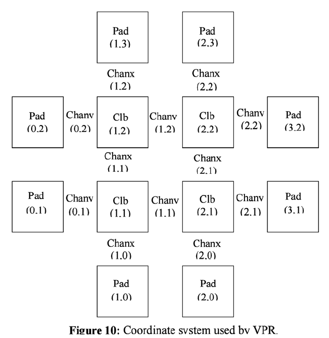
Figure shows the coordinate system used by VPR via a small 2 x 2 clb FPGA. The
number of clbs in the x and y directions are denoted by nx and ny, respectively. Clbs all go in
the area with x between 1 and nx and y between 1 and ny, inclusive. All pads either have x
equal to 0 or nx + 1 or y equal to 0 or ny + 1.
An example placement file is given below.
Netlist file: xor5.net Architecture file: sample.arch
Array size: 2 x 2 logic blocks
#block name x y subblk block number
#---------- -- -- ------ ------------
a 0 1 0 #0 -- NB: block number is a comment.
b 1 0 0 #1
c 0 2 1 #2
d 1 3 0 #3
e 1 3 1 #4
out:xor5 0 2 0 #5
xor5 1 2 0 #6
[1] 1 1 0 #7
The blocks in a placement file can be listed in any order.
3.4 Routing File Format
The first line of the routing file gives the array size, nx x ny. The remainder of the routing
file lists the global or the detailed routing for each net, one by one. Each routing begins with the
word net, followed by the net index used internally by VPR to identify the net and, in brackets,
the name of the net given in the netlist file. The following lines define the routing of the net.
Each begins with a keyword that identifies a type of routing segment. The possible keywords
are SOURCE (the source of a certain output pin class), SINK (the sink of a certain input pin
class), OPIN (output pin), IPIN (input pin), CHANX (horizontal channel), and CHANY (vertical
channel). Each routing begins on a SOURCE and ends on a SINK. In brackets after the
keyword is the (x, y) location of this routing resource. Finally, the pad number (if the SOURCE,
SINK, IPIN or OPIN was on an I/O pad), pin number (if the IPIN or OPIN was on a clb), class
number (if the SOURCE or SINK was on a clb) or track number (for CHANX or CHANY) is listed
-- whichever one is appropriate. The meaning of these numbers should be fairly obvious in
each case. If we are attaching to a pad, the pad number given for a resource is the subblock
number defining to which pad at location (x, y) we are attached. See Figure for a diagram of
the coordinate system used by VPR. In a horizontal channel (CHANX) track 0 is the
bottommost track, while in a vertical channel (CHANY) track 0 is the leftmost track. Note that if
only global routing was performed the track number for each of the CHANX and CHANY
resources listed in the routing will be 0, as global routing does not assign tracks to the various
nets.
For an N-pin net, we need N-1 distinct wiring “paths” to connect all the pins. The first wiring
path will always go from a SOURCE to a SINK. The routing segment listed immediately after the
SINK is the part of the existing routing to which the new path attaches. It is important to realize
that the first pin after a SINK is the connection into the already specified routing tree; when
computing routing statistics be sure that you do not count the same segment several times by
ignoring this fact. An example routing for one net is listed below.
Net 5 (xor5)
SOURCE (1,2) Class: 1 # Source for pins of class 1.
OPIN (1,2) Pin: 4
CHANX (1,1) Track: 1
CHANX (2,1) Track: 1
IPIN (2,2) Pin: 0
SINK (2,2) Class: 0 # Sink for pins of class 0 on a clb.
CHANX (1,1) Track: 1 # Note: Connection to existing routing!
CHANY (1,2) Track: 1
CHANX (2,2) Track: 1
CHANX (1,2) Track: 1
IPIN (1,3) Pad: 1
SINK (1,3) Pad: 1 # This sink is an output pad at (1,3), subblock 1.
Nets which are specified to be global in the netlist file (generally clocks) are not routed.
Instead, a list of the blocks (name and internal index) which this net must connect is printed out.
The location of each block and the class of the pin to which the net must connect at each block
is also printed. For clbs, the class is simply whatever class was specified for that pin in the
architecture input file. For pads the pinclass is always -1; since pads do not have logically-
equivalent pins, pin classes are not needed. An example listing for a global net is given below.
Net 146 (pclk): global net connecting:
Block pclk (#146) at (1, 0), pinclass -1.
Block pksi_17_ (#431) at (3, 26), pinclass 2.
Block pksi_185_ (#432) at (5, 48), pinclass 2.
Block n_n2879 (#433) at (49, 23), pinclass 2.
4. Debugging Aids
After parsing the netlist and architecture files, VPR dumps out an image of its internal data
structures into net.echo and arch.echo. These files can be examined to be sure that VPR is
parsing the input files as you expect. The critical_path.echo file lists details about the critical
path of a circuit, and is very useful for determining why your circuit is so fast or so slow. Various
other data structures can be output if you uncomment the calls to the output routines; search
the code for echo to see the various data that can be dumped.
If the preprocessor flag DEBUG is defined in vpr_types.h, some additional sanity checks
are performed during a run. I normally leave DEBUG on all the time, as it only slows execution
by 1 to 2%. The major sanity checks are always enabled, regardless of the state of DEBUG.
Finally, if VERBOSE is set in vpr_types.h, a great deal of intermediate data will be printed to the
screen as VPR runs. If you set verbose, you may want to redirect screen output to a file.
The initial and final placement costs provide useful numbers for regression testing the
netlist parsers and the placer, respectively. I generate and print out a routing serial number to
allow easy regression testing of the router.
Finally, if you need to route an FPGA whose routing architecture cannot be described in
VPR’s architecture description file, don’t despair! The router, graphics, sanity checker, and
statistics routines all work only with a graph that defines all the available routing resources in
the FPGA and the permissible connections between them. If you change the routines that build
this graph (in rr_graph*.c) so that they create a graph describing your FPGA, you should be able
to route your FPGA. If you want to read a text file describing the entire routing resource graph,
call the dump_rr_graph subroutine.
5. References
[1] J. Pistorius, M. Hutton, A. Mishchenko, and R. Brayton. "Benchmarking method and designs
targeting logic synthesis for FPGAs", Proc. IWLS '07, pp. 230-237.
[2] S. Cho, S. Chatterjee, A. Mishchenko, and R. Brayton, "Efficient FPGA mapping using
priority cuts". (Poster.) Proc. FPGA '07.
[3] V. Betz, J. Rose and A. Marquardt, Architecture and CAD for Deep-Submicron FPGAs,
Kluwer Academic Publishers, 1999.
[4] V. Betz, “Architecture and CAD for the Speed and Area Optimization of FPGAs,” Ph.D.
Dissertation, University of Toronto, 1998.
[5] V. Betz and J. Rose, “Cluster-Based Logic Blocks for FPGAs: Area-Efficiency vs. Input
Sharing and Size,” CICC, 1997, pp. 551 - 554.
[6] A. Marquardt, V. Betz and J. Rose, “Using Cluster-Based Logic Blocks and Timing-Driven
Packing to Improve FPGA Speed and Density,” ACM/SIGDA Int. Symp. on FPGAs, 1999,
pp. 37 - 46.
[7] V. Betz and J. Rose, “Directional Bias and Non-Uniformity in FPGA Global Routing
Architectures,” ICCAD, 1996, pp. 652 - 659.
[8] V. Betz and J. Rose, “On Biased and Non-Uniform Global Routing Architectures and CAD
Tools for FPGAs,” CSRI Technical Report #358, Department of Electrical and Computer
Engineering, University of Toronto, 1996. (Available for download from
http://www.eecg.toronto.edu/~vaughn/ papers/techrep.ps.Z).
[9] V. Betz and J. Rose, “VPR: A New Packing, Placement and Routing Tool for FPGA
Research,” Seventh International Workshop on Field-Programmable Logic and
Applications, 1997, pp. 213 - 222.
[10] A. Marquardt, V. Betz and J. Rose, “Timing-Driven Placement for FPGAs,” ACM/SIGDA Int.
Symp. on FPGAs, 2000, pp. 203 - 213.
[11] V. Betz and J. Rose, “Automatic Generation of FPGA Routing Architectures from High-
Level Descriptions,” ACM/SIGDA Int. Symp. on FPGAs, 2000, pp. 175 - 184.
[12] S. Brown, R. Francis, J. Rose, and Z. Vranesic, Field-Programmable Gate Arrays, Kluwer
Academic Publishers, 1992.
[13] S. Wilton, “Architectures and Algorithms for Field-Programmable Gate Arrays with
Embedded Memories,” Ph.D. Dissertation, University of Toronto, 1997. (Available for
download from http://www.ece.ubc.ca/~stevew/publications.html).
[14] Y. W. Chang, D. F. Wong, and C. K. Wong, “Universal Switch Modules for FPGA Design,”
ACM Trans. on Design Automation of Electronic Systems, Jan. 1996, pp. 80 - 101.
[15] G. Lemieux, E. Lee, M. Tom, and A. Yu, “Direction and Single-Driver Wires in FPGA
Interconnect,” International Conference on Field-Programmable Technology, 2004, pp.
41-48
[16] P. Jamieson, K. Kent, F. Gharibian, and L. Shannon. Odin II-An Open-Source Verilog HDL
Synthesis Tool for CAD Research. In IEEE Annual Int’l Symp. on Field-Programmable
Custom Computing Machines, pages 149–156. IEEE, 2010.
