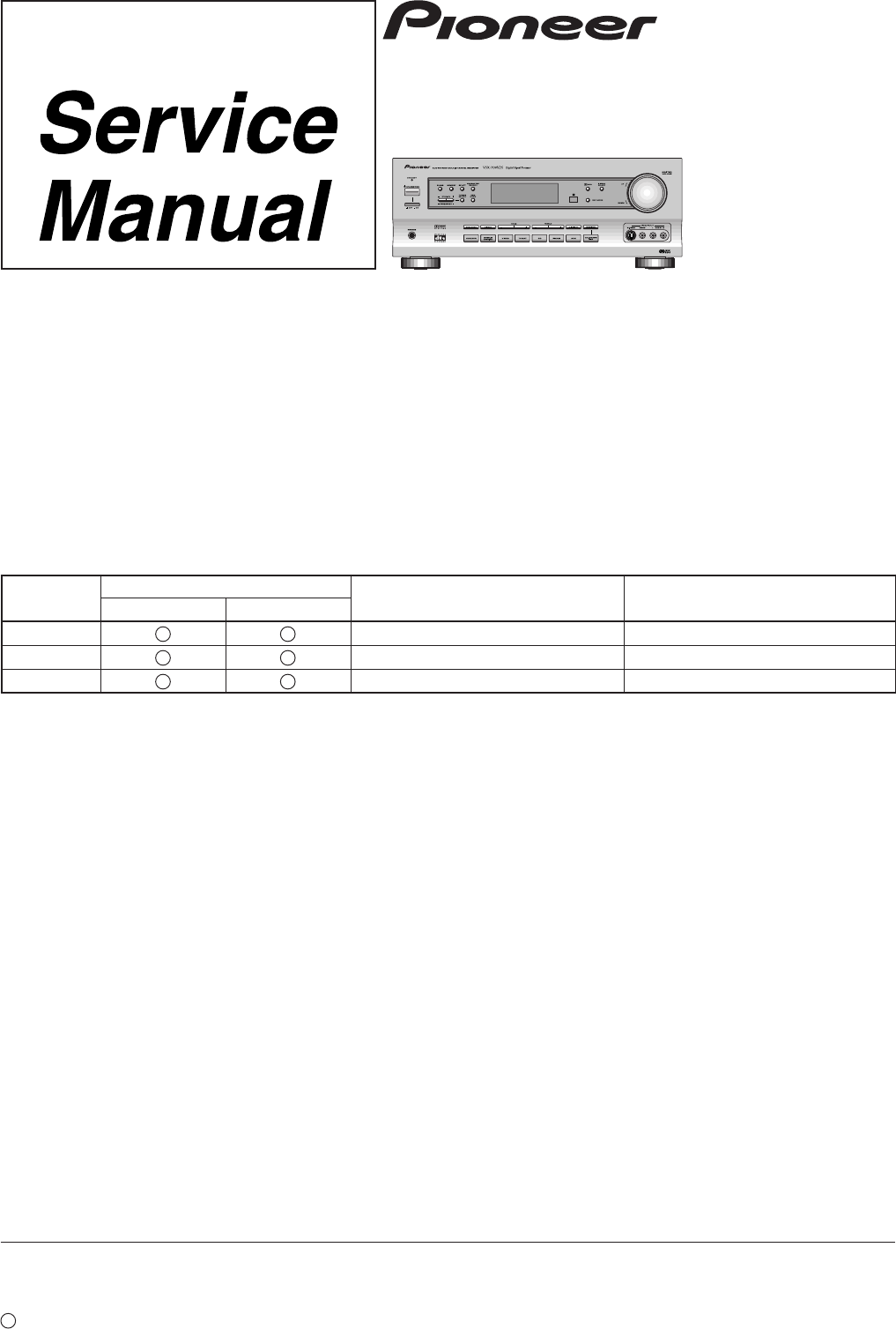
RRV2274 VSX 609RDS 609 709
User Manual: VSX-609RDS
Open the PDF directly: View PDF ![]() .
.
Page Count: 64
ORDER NO.
PIONEER CORPORATION 4-1, Meguro 1-chome, Meguro-ku, Tokyo 153-8654, Japan
PIONEER ELECTRONICS SERVICE, INC. P.O. Box 1760, Long Beach, CA 90801-1760, U.S.A.
PIONEER EUROPE N.V. Haven 1087, Keetberglaan 1, 9120 Melsele, Belgium
PIONEER ELECTRONICS ASIACENTRE PTE. LTD. 253 Alexandra Road, #04-01, Singapore 159936
PIONEER CORPORATION 2000
c
RRV2274
1. SAFETY INFORMATION...................................... 2
2. EXPLODED VIEWS AND PARTS LIST ............... 3
3. BLOCK DIAGRAM AND SCHEMATIC DIAGRAM..... 8
4. PCB CONNECTION DIAGRAM ......................... 28
5. PCB PARTS LIST ............................................... 43
6. ADJUSTMENT .................................................... 48
CONTENTS
7. GENERAL INFORMATION ................................ 49
7.1 DISASSEMBLY ............................................ 49
7.2 PARTS .......................................................... 50
7.2.1 IC ............................................................ 50
7.2.2 DISPLAY................................................. 55
8. PANEL FACILITIES AND SPECIFICATIONS....... 57
T – ZZK MAR. 2000 Printed in Japan
THIS MANUAL IS APPLICABLE TO THE FOLLOWING MODEL(S) AND TYPE(S).
AUDIO/VIDEO MULTI-CHANNEL RECEIVER
VSX-709RDS
VSX-609RDS
Type Model Power Requirement Remarks
VSX-709RDS VSX-609RDS
MYXJIEW AC220-230V
MYXJIGR AC220-230V
MVXJI AC230V
2
VSX-709RDS, VSX-609RDS
1. SAFETY INFORMATION
This service manual is intended for qualified service technicians ; it is not meant for the casual do-it-
yourselfer. Qualified technicians have the necessary test equipment and tools, and have been trained
to properly and safely repair complex products such as those covered by this manual.
Improperly performed repairs can adversely affect the safety and reliability of the product and may
void the warranty. If you are not qualified to perform the repair of this product properly and safely, you
should not risk trying to do so and refer the repair to a qualified service technician.
WARNING
This product contains lead in solder and certain electrical parts contain chemicals which are known to the state of California to cause
cancer, birth defects or other reproductive harm. Health & Safety Code Section 25249.6 – Proposition 65
NOTICE
(FOR CANADIAN MODEL ONLY)
Fuse symbols (fast operating fuse) and/or (slow operating fuse) on PCB indicate that replacement parts must
be of identical designation.
REMARQUE
(POUR MODÈLE CANADIEN SEULEMENT)
Les symboles de fusible (fusible de type rapide) et/ou (fusible de type lent) sur CCI indiquent que les pièces
de remplacement doivent avoir la même désignation.
ANY MEASUREMENTS NOT WITHIN THE LIMITS
OUTLINED ABOVE ARE INDICATIVE OF A POTENTIAL
SHOCK HAZARD AND MUST BE CORRECTED BEFORE
RETURNING THE APPLIANCE TO THE CUSTOMER.
2. PRODUCT SAFETY NOTICE
Many electrical and mechanical parts in the appliance
have special safety related characteristics. These are
often not evident from visual inspection nor the protection
afforded by them necessarily can be obtained by using
replacement components rated for voltage, wattage, etc.
Replacement parts which have these special safety
characteristics are identified in this Service Manual.
Electrical components having such features are identified
by marking with a on the schematics and on the parts list
in this Service Manual.
The use of a substitute replacement component which does
not have the same safety characteristics as the PIONEER
recommended replacement one, shown in the parts list in
this Service Manual, may create shock, fire, or other hazards.
Product Safety is continuously under review and new
instructions are issued from time to time. For the latest
information, always consult the current PIONEER Service
Manual. A subscription to, or additional copies of, PIONEER
Service Manual may be obtained at a nominal charge from
PIONEER.
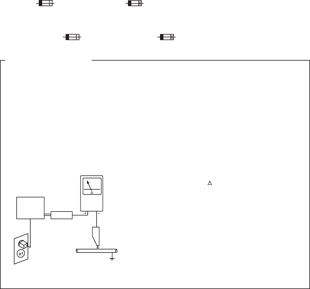
1. SAFETY PRECAUTIONS
The following check should be performed for the
continued protection of the customer and service
technician.
LEAKAGE CURRENT CHECK
Measure leakage current to a known earth ground (water
pipe, conduit, etc.) by connecting a leakage current tester
such as Simpson Model 229-2 or equivalent between the
earth ground and all exposed metal parts of the appliance
(input/output terminals, screwheads, metal overlays, control
shaft, etc.). Plug the AC line cord of the appliance directly
into a 120V AC 60Hz outlet and turn the AC power switch
on. Any current measured must not exceed 0.5mA.
(FOR USA MODEL ONLY)
Leakage
current
tester
Reading should
not be above
0.5mA
Device
under
test
Test all
exposed metal
surfaces
Also test with
plug reversed
(Using AC adapter
plug as required)
Earth
ground
AC Leakage Test
3
VSX-709RDS, VSX-609RDS
1
2
4
73
8
9
5
17
10
11
6
5
6
12
MYXJIEW and
MVXJI Types Only
VSX-709RDS Only
VSX-609RDS
13
MYXJIEW and
MYXJIGR Types Only
MYXJIEW Type Only
15
16
14
2.1 PACKING
1 FM Wire Antenna ADH7005
2 AM Loop Antenna ATB7009
3 Polyethylene Bag Z21-038
(0.03 × 230 × 340)
NSP 4 Warranty Card ARY7022
5 Remote Control Unit See Contrast table (2)
6 Battery Cover See Contrast table (2)
NSP 7 Dry Cell Battery See Contrast table (2)
8 Left Pad AHA7263
9 Right Pad AHA7264
10 Packing Sheet AHG7069
11 Packing Case See Contrast table (2)
12 Operating Instructions See Contrast table (2)
(English)
13 Operating Instructions See Contrast table (2)
(German)
14 Operating Instructions See Contrast table (2)
(Spanish/Portuguese)
15 Operating Instructions See Contrast table (2)
(Italian/French)
16 Operating Instructions See Contrast table (2)
(Dutch/Swedish)
17 RC Holder See Contrast table (2)
(1) PACKING PARTS LIST
Mark No. Description Part No.
2. EXPLODED VIEWS AND PARTS LIST
NOTES: • Parts marked by "NSP" are generally unavailable because they are not in our Master Spare Parts List.
• The mark found on some component parts indicates the importance of the safety factor of the part.
Therefore, when replacing, be sure to use parts of identical designation.
• Screws adjacent to mark on the product are used for disassembly.
(2) CONTRAST TABLE
VSX-709RDS/MYXJIEW, MYXJIGR, MVXJI, VSX-609RDS/MYXJIEW, MYXJIGR and MVXJI are constructed the
same except for the following :
Part No.
Mark No. Symbol and Description VSX-709RDS VSX-609RDS Remarks
/MYXJIEW /MYXJIGR /MVXJI /MYXJIEW /MYXJIGR /MVXJI
5 Remote Control Unit AXD7249 AXD7249 AXD7249 AXD7247 AXD7247 AXD7247
6 Battery Cover AZN7826 AZN7826 AZN7826 AZA7378 AZA7378 AZA7378
NSP 7 Dry Cell Battery (LR6, AA) VEM1021 VEM1021 VEM1021 Not used Not used Not used
NSP 7 Dry Cell Battery (R6P, AA) Not used Not used Not used VEM-013 VEM-013 VEM-013
11 Packing Case AHD7832 AHD7832 AHD7832 AHD7831 AHD7831 AHD7831
12 Operating Instructions (English) ARB7215 Not used ARB7215 ARB7215 Not used ARB7215
13 Operating Instructions (German) ARC7273 ARC7273 Not used ARC7273 ARC7273 Not used
14 Operating Instructions ARC7274 Not used Not used ARC7274 Not used Not used
(Spanish/Portuguese)
15 Operating Instructions ARC7275 Not used Not used ARC7275 Not used Not used
(Italian/French)
16 Operating Instructions ARC7276 Not used Not used ARC7276 Not used Not used
(Dutch/Swedish)
17 RC Holder AHB7035 AHB7035 AHB7035 Not used Not used Not used
4
VSX-709RDS, VSX-609RDS
G
D
L
K
H
M
J
I
CI
J
M
L
K
H
E
E
B
A
C
D
F
N
N
F
A
B
35
45
46
G
36
31
18
24
19
36
36
36
36
36
36
36
36
36
36
36
36
36
36
26
15
7
1
2
5
27
12
13
14
16
36
43
44
36
17
4
3
98
6
36
11
36
36
37
37 38
38 36
36
36
10
Accessory of
Front Panel
36
34
36
36
47
36
Refer to
"2.3 FRONT PANEL SECTION".
39
39
29
28
30
41
42
47
36
31
23
36
For MVXJI Type
20
21
19
36
39
36
36
25
39
39
33
33
22
VSX-709RDS
Only
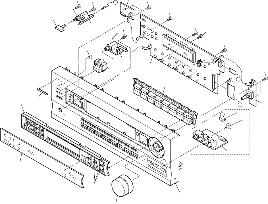
2.2 EXTERIOR SECTION
5
VSX-709RDS, VSX-609RDS
1 D.D & INPUT Assy See Contrast table (2)
2 VIDEO&6CH IN Assy See Contrast table (2)
NSP 3 AMP INPUT Assy AWX7382
4 AMP&PRIMARY Assy See Contrast table (2)
5 REGULATOR Assy AWX7467
6 TRANS 2 Assy AWX7468
7 FM/AM TUNER Unit AXX7048
NSP 8 TRANS 1 Assy AWX7390
NSP 9 TRANS 3 Assy AWX7392
10 Power Transformer (AC230V) ATS7259
11 Fuse (FU1 : T2.5A) REK1026
12 FFC (J31 : 32P/180 BD 60V) ADD7222
(D.D & INPUT CN102 ↔ FRONT CN402)
13 FFC (J32 : 19P/200 BD 60V) ADD7221
(D.D & INPUT CN103 ↔ FRONT CN401)
14 FFC (J33 : 13P/200 BD 60V) ADD7220
(D.D & INPUT CN104 ↔ VIDEO&6CH IN CN303)
15 FFC (J34 : 13P/80 BD 60V) ADD7189
(D.D & INPUT CN105 ↔ FM/AM TUNER CN1)
16 FFC (J35 : 17P/90 BD 60V) ADD7219
(D.D & INPUT CN106 ↔ AMP INPUT CN290)
17 FFC (J36 : 22P/80 BD 60V) ADD7224
(REGULATOR CN801 ↔ AMP&PRIMARY CN53)
18 Strain Relief CM-22B
19 AC Power Cord See Contrast table (2)
20 Fuse (T5A) See Contrast table (2)
(1) EXTERIOR SECTION PARTS LIST
Mark No. Description Part No. Mark No. Description Part No.
21 Fuse Holder See Contrast table (2)
22 Top Cover 808 AME7375
NSP 23 Under Base 409 ANA7094
24 Rear Panel See Contrast table (2)
25 Bonnet Case AZN7779
26 PCB Angle ANG7253
27 Shield R3 ANG7277
28 Heat Sink Angle F ANG7251
29 Heat Sink Angle R ANG7252
NSP 30 Heat Sink 0.8 ANH7110
31 Insulator PNW2766
32 • • • • • •
33 Push Rivet AEC7025
34 PCB Mold AMR2533
NSP 35 Fuse Card AAX7277
36 Screw BBZ30P080FMC
37 Screw BBZ30P200FMC
38 Screw ABA7043
39 Screw FBT40P080FZK
40 • • • • • •
41 DIGITAL IN Assy See Contrast table (2)
42 FFC (J37 : 6P/150 BD 60V) ADD7223
(D.D & INPUT CN1501 ↔ DIGITAL IN CN1901)
43 S. VIDEO Assy See Contrast table (2)
44 BOARD TO BOARD Assy See Contrast table (2)
45 LARGE SP Assy See Contrast table (2)
46 LARGE SP CONNECTION Assy See Contrast table (2)
47 Screw IBZ30P080FMC
(2) CONTRAST TABLE
VSX-709RDS/MYXJIEW, MYXJIGR, MVXJI, VSX-609RDS/MYXJIEW, MYXJIGR and MVXJI are constructed the
same except for the following : Part No.
Mark No. Symbol and Description VSX-709RDS VSX-609RDS Remarks
/MYXJIEW /MYXJIGR /MVXJI /MYXJIEW /MYXJIGR /MVXJI
1 D.D & INPUT Assy AWX7464 AWX7464 AWX7464 AWX7497 AWX7497 AWX7497
2 VIDEO&6CH IN Assy AWX7458 AWX7458 AWX7458 AWX7474 AWX7474 AWX7474
4 AMP&PRIMARY Assy AWX7484 AWX7484 AWX7484 AWX7478 AWX7478 AWX7478
19 AC Power Cord VDG1061 VDG1061 VDG1063 VDG1061 VDG1061 VDG1063
20 Fuse (T5A) Not used Not used PEK1003 Not used Not used PEK1003
21 Fuse Holder Not used Not used VKR1003 Not used Not used VKR1003
24 Rear Panel ANC7897 ANC7897 ANC7897 ANC7896 ANC7896 ANC7896
41 DIGITAL IN Assy AWX7461 AWX7461 AWX7461 AWX7505 AWX7505 AWX7505
43 S. VIDEO Assy AWX7462 AWX7462 AWX7462 Not used Not used Not used
44 BOARD TO BOARD Assy AWX7463 AWX7463 AWX7463 Not used Not used Not used
45 LARGE SP Assy AWX7510 AWX7510 AWX7510 Not used Not used Not used
46 LARGE SP CONNECTION Assy AWX7504 AWX7504 AWX7504 Not used Not used Not used
6
VSX-709RDS, VSX-609RDS
2.3 FRONT PANEL SECTION
G
B
A
11 13
10
14
17
7
4
2
6
Cut
9
12
18
17
1
3
16
16
16 16
16
16
16
19
16
8
5
16
VSX-709RDS Only
7
VSX-709RDS, VSX-609RDS
(1) FRONT PANEL SECTION PARTS LIST
Mark No. Description Part No.
1 FRONT Assy See Contrast table (2)
2 POWER SW Assy AWX7385
NSP 3 R. ENCODER Assy AWX7386
NSP 4 H.P. Assy AWX7556
5 MECHA SW Assy AWX7443
6 Volume Knob AAB7179
7 Power Button AAD7440
8 Power Button M AAD7442
9 Window AAK7721
10 F Button See Contrast table (2)
Mark No. Description Part No.
11 Sub Panel AAD7552
12 F Panel See Contrast table (2)
13 Name Plate PAM1776
14 LED Lens PNW2019
15 • • • • • •
16 Screw PPZ30P080FMC
17 Screw ABA7009
18 FRONT VIDEO Assy See Contrast table (2)
19 8P Shield Cable See Contrast table (2)
(2) CONTRAST TABLE
VSX-709RDS/MYXJIEW, MYXJIGR, MVXJI, VSX-609RDS/MYXJIEW, MYXJIGR and MVXJI are constructed the
same except for the following :
Part No.
Mark No. Symbol and Description VSX-709RDS VSX-609RDS Remarks
/MYXJIEW /MYXJIGR /MVXJI /MYXJIEW /MYXJIGR /MVXJI
1 FRONT Assy AWX7459 AWX7459 AWX7459 AWX7477 AWX7477 AWX7477
10 F Button AAD7564 AAD7564 AAD7564 AAD7562 AAD7562 AAD7562
12 F Panel AMB7677 AMB7677 AMB7677 AMB7675 AMB7675 AMB7675
18 FRONT VIDEO Assy AWX7460 AWX7460 AWX7460 Not used Not used Not used
19 8P Shield Cable ADX7306 ADX7306 ADX7306 Not used Not used Not used
VSX-709RDS, VSX-609RDS
8
A
B
C
D
1234
1234
N
P
7
5
9
3
1
11
CN901
3
CN354
IC351, IC352
3
P
3
CN901
4
CN301
8
8
P
CN901
6
CN107
3
5
FRONT VIDEO ASSY
S. VIDEO ASSY
FRONT VIDEO ASSY
FRONT VIDEO ASSY
AXX7048 UNIT
CN105
6
CN305
IC101
IC303
IC1901
IC302
IC302
IC301
IC104
IC102
IC1701
IC1101
IC1201
B
H
J
7
7
7
19
11
CN104
7
9
11
CN1901
2
CN1501
2
5
3
7
5
9
1
11
5
5
3
25
1
3
4
6
123
38
38
21
26
23
25
67
IC1703
67
IC1705
DTS DECODER
67
IC1705
12
4
6
3
8
7
19
18
17
12
11
10
9
5
1
7
2
11
910
D.D & INPUT ASSY
DIGITAL
IN ASSY
VIDEO & 6CH IN ASSY
VSX-709RDS ONLY
VSX-709RDS ONLY
VSX-709RDS ONLY VSX-709RDS ONLY
VSX-709RDS ONLY
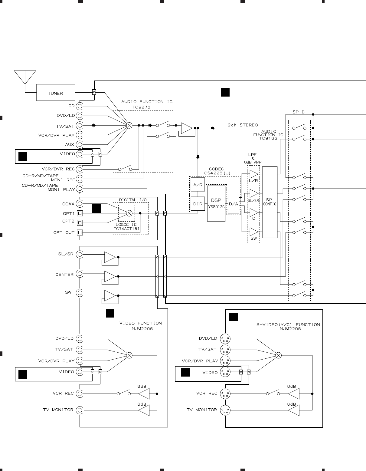
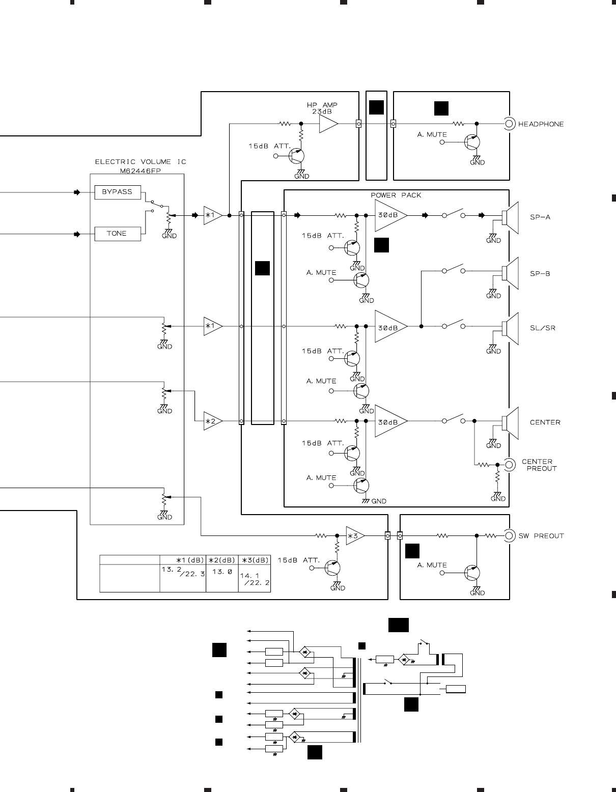
3. BLOCK DIAGRAM AND SCHEMATIC DIAGRAM
3.1 BLOCK DIAGRAM
VSX-709RDS, VSX-609RDS
9
A
B
C
D
5678
5678
IC103
IC105
IC106
IC107
IC108
IC107
Q112 Q303
Q603
Q601
Q653
Q651
Q632
Q631
H
CN104
1CN305
1
11
15
17
31
34
33
36
6
9
57
57
57
57
31
IC602
18
14
IC602
24 26
IC601 RY751
RY753
RY754
RY752
22 15
Q551
Q105
I
K
C
A
CN102
3551
J43
4
CN106
4601
1
10 5
69
+12V
-12V
T1
POWER
TRANSFORMER
T51
AC IN
D801–D804
U+5V
D51-D54
RY51
IC51
IC801
CN101 IC802
NECK+B
POWER AMP
IC601, IC602
NECK-B
D702
D701
+BVL
+BVH
-BVH
-BVL
FL AC
FL AC
Q701
Q702
S591
C
C
B
D+5V D805–D808
IC803
A+5V IC804
CN101
F
B
CN101
B
CN402
K
AMP & PRIMARY ASSY
GB
MECHA SW ASSY
AMP & PRIMARY ASSY
REGULATOR ASSY
AMP & PRIMARY ASSY
VIDEO &
6CH IN ASSY
H.P. ASSY
FRONT ASSY
AMP INPUT ASSY
VSX-709RDS
VSX-609RDS
VSX-709RDS, VSX-609RDS
10
A
B
C
D
1234
1234
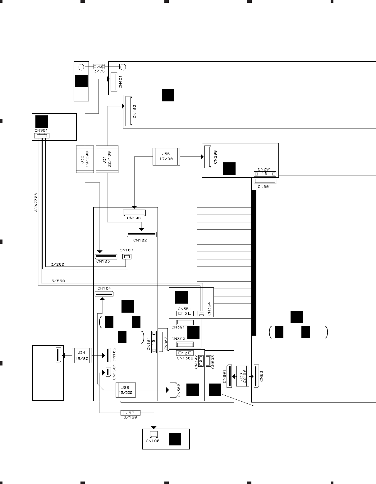
3.2 OVERALL WIRING CONNECTION DIAGRAM and AMP INPUT ASSY
BOARD TO
BOARD ASSY
(VSX-709RDS
: AWX7463)
S. VIDEO
ASSY
(VSX-709RDS
: AWX7462)
FRONT
VIDEO ASSY
(VSX-709RDS
: AWX7460)
N
P
O
FRONT ASSY
(VSX-709RDS : AWX7579)
(VSX-609RDS : AWX7477)
K
R.ENCODER
ASSY
(AWX7386)
L
D.D & INPUT ASSY
(VSX-709RDS
: AWX7464)
(VSX-609RDS
: AWX7497)
B
REGULATOR ASSY
(AWX7467)
F
DIGITAL IN ASSY
(VSX-709RDS : AWX7461)
(VSX-609RDS : AWX7505)
J
VIDEO&6CH IN ASSY
(VSX-709RDS : AWX7458)
(VSX-609RDS : AWX7474)
H
AMP&PRIMARY
ASSY
(VSX-709RDS
: AWX7484)
(VSX-609RDS
: AWX7478)
C
AMP INPUT ASSY
(AWX7382)
A
FM/AM
TUNER
UNIT
(AXX7048)
491
511
C1/2, C2/2
B1/3, B2/3,
B3/3
VSX-709RDS, VSX-609RDS
11
A
B
C
D
5678
5678
Note : When ordering service parts, be sure to refer to "EXPLODED VIEWS and PARTS LIST" or "PCB PARTS LIST".
A
LARGE SP ASSY
(VSX-709RDS : AWX7510)
R
LARGE SP
CONNECTION
ASSY
(VSX-709RDS : AWX7504)
Q
AMP INPUT ASSY
(AWX7382)
A
CN106
CN601
B1/3
C1/2
POWER SW ASSY
(AWX7385)
M
H.P.
ASSY
(AWX7556)
I
TRANS3
ASSY
(AWX7392)
E
TRANS1 ASSY
(AWX7390)
GA
MECHA SW ASSY
(AWX7443)
GB
TRANS2
ASSY
(AWX7468)
D
471
J3
J7J6
501
403
551
701
851
J1J2
J4J5


VSX-709RDS, VSX-609RDS
19
A
B
C
D
5678
5678
VSX-709RDS
VSX-609RDS
VSX
-709RDS
VSX
-609RDS
VSX-609RDS
ONLY
VSX-709RDS
ONLY
VSX
-709RDS
ONLY
TRANS3 ASSY
(AWX7392)
E
TRANS2
ASSY
(AWX7468)
D
POWER TRANSFORMER
CN785
Q
CAUTION : FOR CONTINUED PROTECTION
AGAINST RISK OF FIRE.
REPLACE ONLY WITH SAME TYPE
NO. 49101.6 FOR IC851, IC852 AND
IC853 MFD, BY LITTELFUSE INC.
CAUTION : FOR CONTINUED PROTECTION
AGAINST RISK OF FIRE.
REPLACE ONLY WITH SAME TYPE
NO. 491001 FOR IC603 MFD, BY
LITTELFUSE INC.
C2/2
C2/2
1/2
C
E
D

VSX-709RDS, VSX-609RDS
21
A
B
C
D
5678
5678
2/2
C
AMP&PRIMARY ASSY
(VSX-709RDS : AWX7484)
(VSX-609RDS : AWX7478)
C2/2
C1/2
C1/2
TRANS1 ASSY
(AWX7390)
GB
GA
MECHA SW ASSY
(AWX7443)
POWER TRANSFORMER
LIVE
NEUTRAL
REK1026 (T2.5A)
ATT7037
AC POWER CORD
MYXJIEW : VDG1061
MYXJIGR : VDG1061
MVXJI : VDG1063
• NOTE FOR FUSE REPLACEMENT
FOR CONTINUED PROTECTION AGAINST RISK OF FIRE.
REPLACE WITH SAME TYPE AND RATINGS ONLY.
CAUTION -
CAUTION : FOR CONTINUED PROTECTION
AGAINST RISK OF FIRE.
REPLACE ONLY WITH SAME TYPE
NO. 491.315 FOR IC52 MFD, BY
LITTELFUSE INC.
GBGA
VSX-709RDS, VSX-609RDS
22
A
B
C
D
1234
1234
VSX-609RDS
VSX-709RDS
VSX-709RDS ONLY
CN390
O
VIDEO&6CH IN ASSY
(VSX-709RDS : AWX7458)
(VSX-609RDS : AWX7474)
H
CN104 CN803
F
B1/3
VIDEO SW IC
3.8 VIDEO&6CH IN, H. P. and DIGITAL IN ASSYS
H
VSX-709RDS, VSX-609RDS
23
A
B
C
D
1234
1234
VSX-709RDS
ONLY
H.P. ASSY
(AWX7556)
I
DIGITAL IN ASSY
(VSX-709RDS : AWX7461)
(VSX-609RDS : AWX7505)
J
CN1501
B2/3
403
K
JI

VSX-709RDS, VSX-609RDS
25
A
B
C
D
5678
5678
POWER
SW ASSY
(AWX7385)
M
551
I
FRONT ASSY
S451 : DOLBY PRO LOGIC
S452 : DSP MODE
S453 : SIGNAL SELECT
S454 : MONITOR
S455 : TREBLE (+)
S456 : FM/AM
S457 : LOUDNESS
S458 : TREBLE (–)
S459 : BASS (+)
S460 : VIDEO
S461 : TV/SAT
S462 : CD
S463 : DIRECT
S464 : BASS (–)
S465 : DVD/LD
S466 : VCR/DVR
S467 : SPEAKERS
S469 : MPX MODE
S470 : MEMORY
S471 : CLASS
S472 : TUNING SELECT
S473 : STATION (+)
S474 : STATION (–)
S475 : CD-R
S476 : AUX
SYSTEM CONTROL MCU
MK


VSX-709RDS, VSX-609RDS
28
A
B
C
D
1234
1234
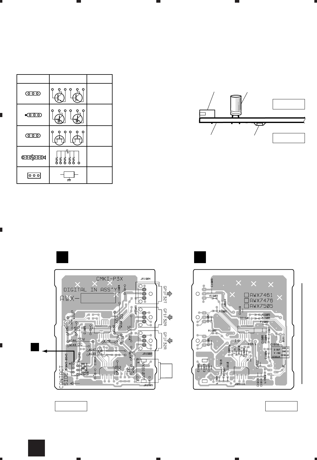
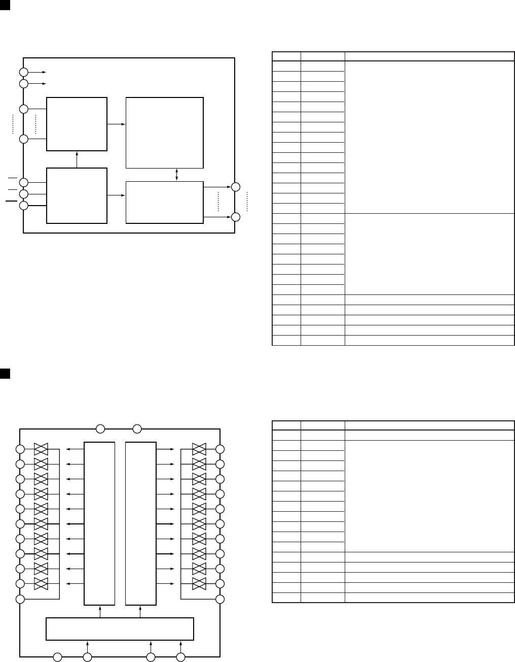
NOTE FOR PCB DIAGRAMS :
1. Part numbers in PCB diagrams match those in the schematic
diagrams.
2. A comparison between the main parts of PCB and schematic
diagrams is shown below.
3. The parts mounted on this PCB include all necessary parts for
several destinations.
For further information for respective destinations, be sure to
check with the schematic diagram.
4. View point of PCB diagrams.
Symbol In PCB
Diagrams Symbol In Schematic
Diagrams Part Name
BCE
D
D
G
G
S
S
BCE
BCE
DGS
BCEBCE
BCE
Transistor
Transistor
with resistor
Field effect
transistor
Resistor array
3-terminal
regulator
Capacitor
Connector
P.C.Board Chip Part
SIDE A
SIDE B
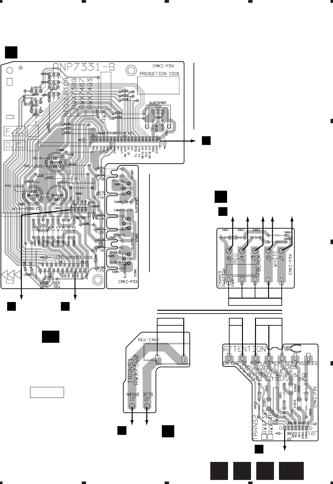
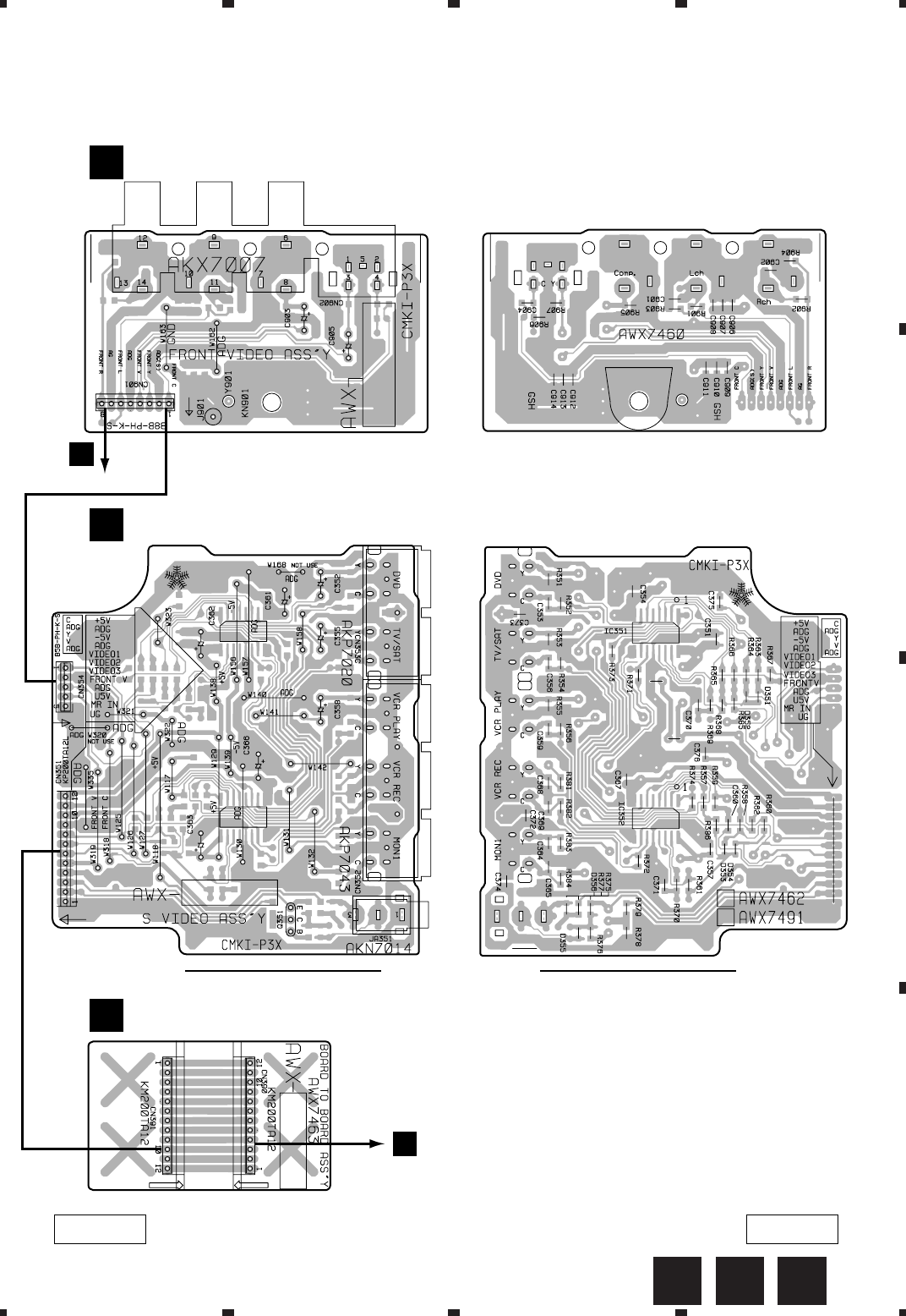
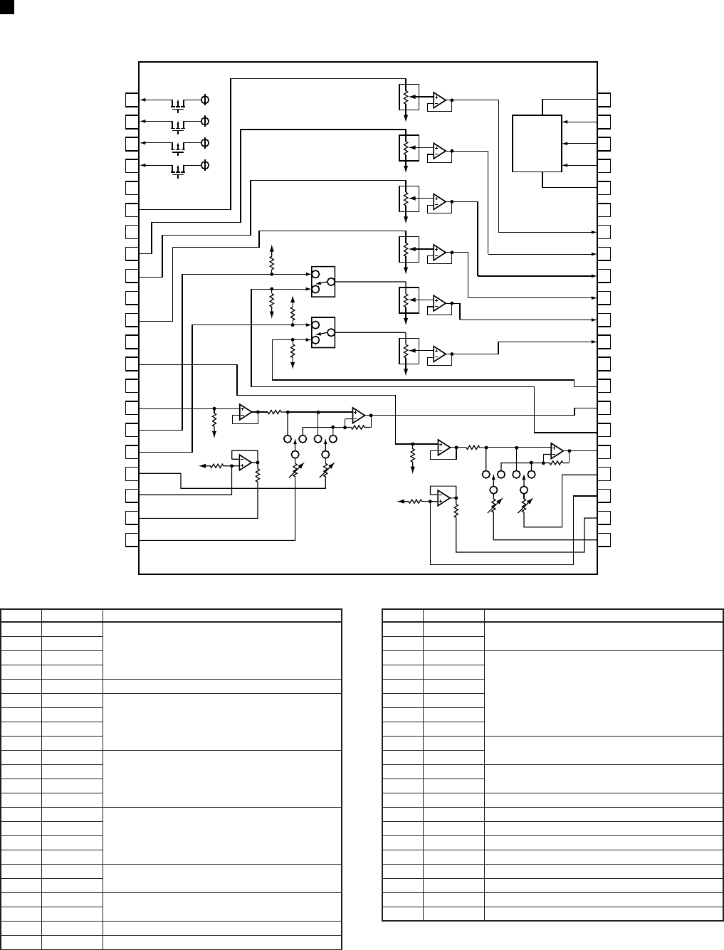
4. PCB CONNECTION DIAGRAM
4.1 DIGITAL IN ASSY
J
(ANP7341-A)
CN1501
B
SIDE A
DIGITAL IN ASSY
J
(ANP7341-A)
DIGITAL IN ASSY
J
SIDE B
IC1901
IC1902
VSX-709RDS, VSX-609RDS
29
A
B
C
D
1234
1234
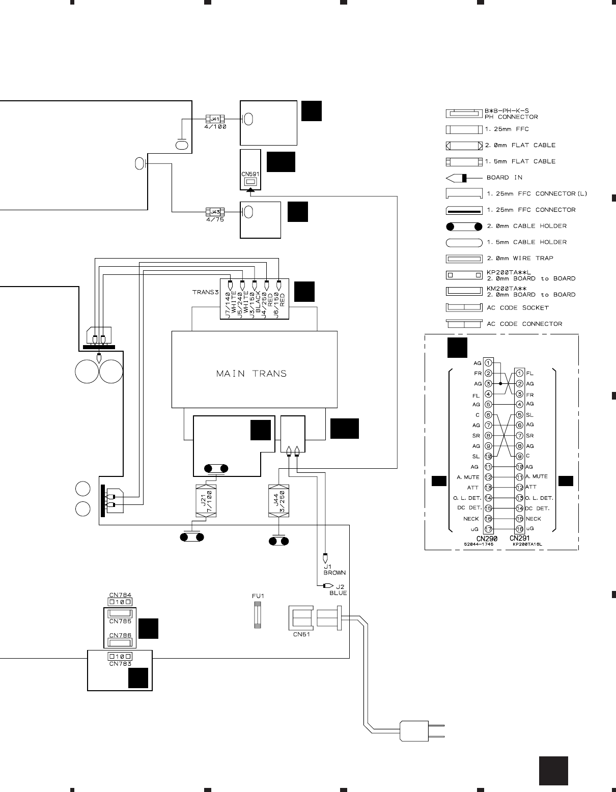
4.2 TRANS2, TRANS3, REGULATOR and TRANS1 ASSYS
FE
(ANP7331-B)
Q805
Q803
Q806
Q801
Q804
Q802
IC804
REGULATOR ASSY
F
TRANS3 ASSY
E
TRANS2 ASSY
D
CN53
C
CN306
H
CN101
B
701
C
J1 J2
C
J6 J4 J3 J5 J7
C
SIDE A
IC802
IC803
IC801
POWER TRANSFORMER
TRANS1 ASSY
GA
D
GA
VSX-709RDS, VSX-609RDS
30
A
B
C
D
1234
1234
AMP INPUT ASSY
A
AMP&PRIMARY ASSY
C
CN106
B
Q604
Q606
Q605
Q602
Q603
IC601
IC603
Q632
Q704
Q702
Q703
Q701
Q631
Q656
IC602
Q633
Q655
Q691
Q692
Q652
Q654
Q651
Q653
J7
E
J6
E
J3
E
(ANP7331-B)
SIDE A
(ANP7331-B)
SIDE A
GB
MECHA SW ASSY
(ANP7341-A)
SIDE B
(ANP7341-A)
SIDE A
A C
4.3 AMP INPUT and AMP&PRIMARY ASSYS
GB


VSX-709RDS, VSX-609RDS
40
A
B
C
D
1234
1234
H
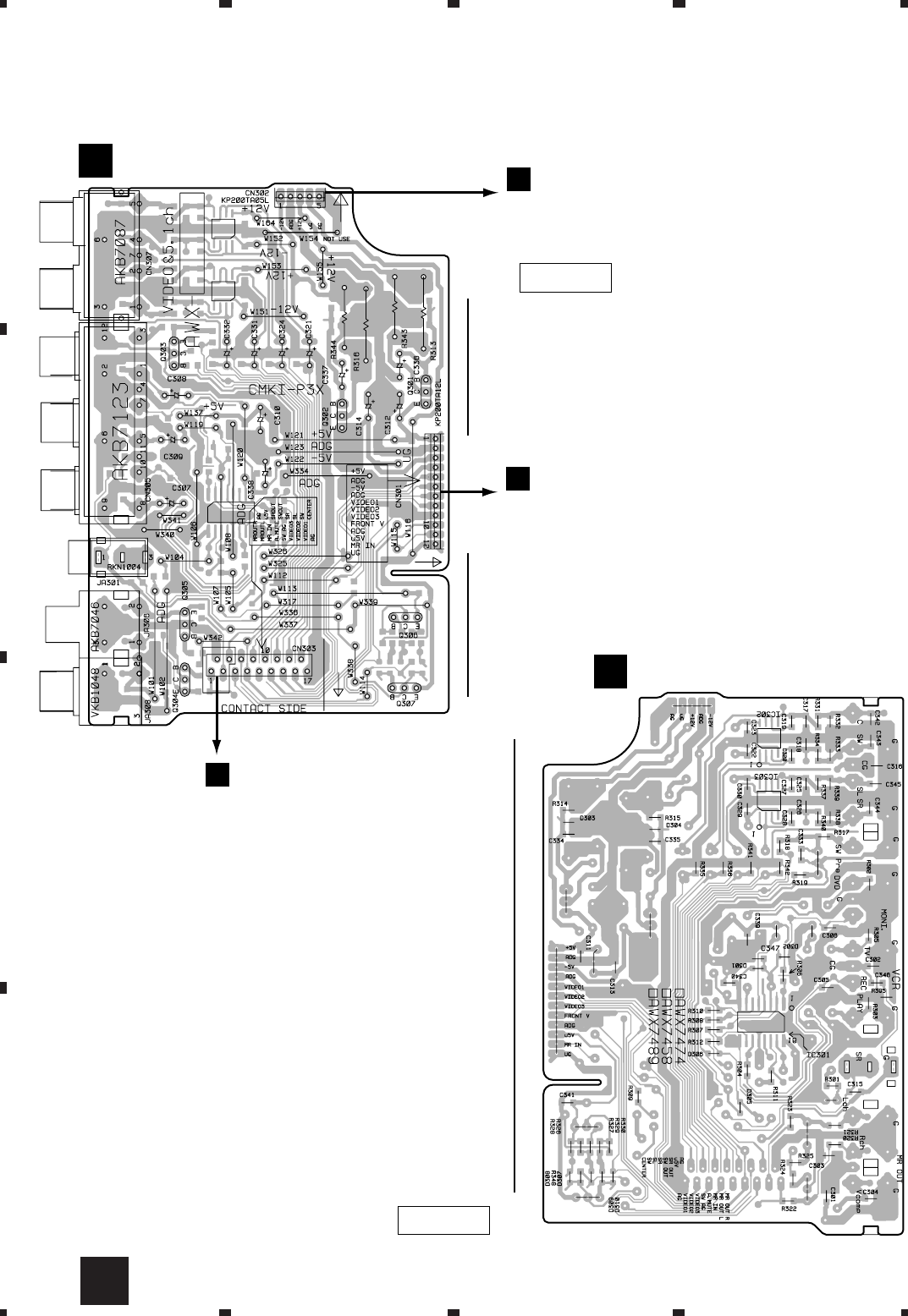
4.6 VIDEO&6CH IN ASSY
(ANP7341-A)
VIDEO&6CH IN ASSY
H
CN104
B
CN803
F
SIDE A
Q301
Q303
Q306
Q305
Q307
Q304
Q302
(ANP7341-A)
SIDE B
VIDEO&6CH IN ASSY
H
IC302
IC303
IC301
CN390
O
(VSX-709RDS)
VSX-709RDS, VSX-609RDS
41
A
B
C
D
1234
1234
4.7 S.VIDEO, BOARD TO BOARD and FRONT VIDEO ASSYS
(ANP7341-A)
FRONT VIDEO ASSY
P
CN107
B
CN301
H
SIDE A
(ANP7341-A)
SIDE B
BOARD TO BOARD ASSY
O
S. VIDEO ASSY
N
IC351 IC352Q351
P
O
N
VSX-709RDS, VSX-609RDS
42
A
B
C
D
1234
1234
4.8 LARGE SP CONNECTION and LARGE SP ASSYS
Q R
(ANP7331-B)
LARGE SP ASSY
R
LARGE SP CONNECTION ASSY
Q
CN784
C
SIDE A
43
VSX-709RDS, VSX-609RDS
Mark No. Description Part No. Mark No. Description Part No.
5. PCB PARTS LIST
NOTES: •The mark found on some component parts indicates the importance of the safety factor of the part.
Therefore, when replacing, be sure to use parts of identical designation.
•When ordering resistors, first convert resistance values into code form as shown in the following examples.
Ex.1 When there are 2 effective digits (any digit apart from 0), such as 560 ohm and 47k ohm (tolerance is shown by J=5%,
and K=10%).
560 Ω→56 × 101→561 ........................................................ RD1/4PU 5 6 1 J
47k Ω→47 × 103→473 ........................................................ RD1/4PU 4 7 3 J
0.5 Ω→R50 ..................................................................................... RN2H R 5 0 K
1 Ω→1R0 ..................................................................................... RS1P 1 R
0
K
Ex.2 When there are 3 effective digits (such as in high precision metal film resistors).
5.62k Ω→ 562 × 101→5621 ...................................................... RN1/4PC
5
6
2 1 F
Part No.
Mark Symbol and Description VSX-709RDS VSX-609RDS Remarks
/MYXJIEW, /MYXJIEW,
MYXJIGR, MVXJI MYXJIGR, MVXJI
NSP COMPLEX ASSY AWK7573 AWK7567
POWER SW ASSY AWX7385 AWX7385
NSP R.ENCODER ASSY AWX7386 AWX7386
MECHA SW ASSY AWX7443 AWX7443
VIDEO&6CH IN ASSY AWX7458 AWX7474
FRONT ASSY AWX7459 AWX7477
FRONT VIDEO ASSY AWX7460 Not used
DIGITAL IN ASSY AWX7461 AWX7505
S. VIDEO ASSY AWX7462 Not used
BOARD TO BOARD ASSY AWX7463 Not used
NSP H.P. ASSY AWX7556 AWX7556
NSP AMP&PS ASSY AWK7574 AWK7568
NSP AMP INPUT ASSY AWX7382 AWX7382
REGULATOR ASSY AWX7467 AWX7467
TRANS2 ASSY AWX7468 AWX7468
NSP TRANS1 ASSY AWX7390 AWX7390
NSP TRANS3 ASSY AWX7392 AWX7392
AMP&PRIMARY ASSY AWX7484 AWX7478
LARGE SP CONNECTION ASSY AWX7504 Not used
LARGE SP ASSY AWX7510 Not used
D.D & INPUT ASSY AWX7464 AWX7497
CONTRAST OF PCB ASSEMBLIES
D.D & INPUT ASSY
B
AWX7497 and AWX7464 are constructed the same except for the following :
Mark Symbol and Description Part No. Remarks
AWX7464 AWX7497
CN107 3P CONNECTOR POST B3B-PH-K-S Not used
101, 102 PCB BINDER VEF1040 Not used
VIDEO&6CH IN ASSY
H
AWX7474 and AWX7458 are constructed the same except for the following :
Mark Symbol and Description Part No. Remarks
AWX7458 AWX7474
R309 RS1/10S101J Not used
R313, R316 RS2LMF560J Not used
R343, R344 Not used RS1LMF820J
CN301 12P SOCKET KP200TA12L Not used
44
VSX-709RDS, VSX-609RDS
Mark No. Description Part No. Mark No. Description Part No.
Mark No. Description Part No. Mark No. Description Part No.
AMP INPUT ASSY
OTHERS
CN290 17P CONNECTOR 52044-1745
CN291 16P SOCKET KP200TA16L
D.D & INPUT ASSY
SEMICONDUCTORS
IC1101 CS4226-KQ(J)
IC1301 KM68257EJ-15
IC108 M5216FP
IC103 M62446FP
IC1001 NJM2100M
IC1602–IC1604,IC1701–IC1705 NJM4558MD
IC1401 PQ20WZ51
IC102 TC9163AF
IC1601 TC9164AF
IC101 TC9273F-007
IC104–IC107 UPC4570G2
IC1201 YSS912C
Q101, Q102 2SC2412K
Q1001, Q1002, Q105–Q112 2SC3326
Q1601–Q1606 2SC3326
Q1003, Q1101, Q1607, Q1608, Q1610 DTA124EK
Q1004, Q1102, Q1609 DTC124EK
D1601, D1602 1SS181
D103, D105, D106 1SS355
D104 UDZS5.1B
D101, D102 UDZS6.8B
COILS AND FILTERS
L1401 CHIP SOLID INDUCTOR ATL7002
F1101, F1123, F1124, F1203, F1204 DTF1064
F1302, F1601, F1602 CHIP BEAD DTF1064
F101, F111, F112 CHIP BEAD DTF1067
L1101–L1104 QTL1013
CHIP SOLID INDUCTOR
CAPACITORS
C101–C114, C1207, C1209, C1213 CCSQCH101J50
C1217, C1218, C1221, C1303 CCSQCH101J50
C1640, C1641, C197, C198 CCSQCH101J50
C207, C208 CCSQCH101J50
C211, C212 CCSQCH220J50
C1119 CCSQCH271J50
C1123, C1124 CCSQCH331J50
C1118, C1130, C1639 CCSQCH471J50
C1001, C1002, C121, C1212, C122 CCSRCH101J50
C1223, C123, C126–C128 CCSRCH101J50
PCB PARTS LIST FOR VSX-709RDS UNLESS OTHERWISE NOTED
FRONT ASSY
K
AWX7477 and AWX7459 are constructed the same except for the following :
Mark Symbol and Description Part No. Remarks
AWX7459 AWX7477
R428 Not used RS1/10S472J
R429 RS1/10S0R0J RS1/10S751J
AMP&PRIMARY ASSY
C
AWX7478 and AWX7484 are constructed the same except for the following :
Mark Symbol and Description Part No. Remarks
AWX7484 AWX7478
C757–C759 Not used CQMBA472J50
C769 CKCYB102K50 Not used
R757 Not used RD1/4PU223J
R758 Not used RD1/4PU222J
CN751 SPEAKER TERMINAL 6-P Not used AKE7020
CN753 PIN JACK 1-P Not used AKB7042
CN784 10P SOCKET KP250NA10 Not used
DIGITAL IN ASSY
J
AWX7505 and AWX7461 are constructed the same except for the following :
Mark Symbol and Description Part No. Remarks
AWX7461 AWX7505
C1903 CKSQYB104K25 Not used
R1903 RS1/10S101J Not used
JA1904 OPTICAL LINK OUT GP1F32T Not used
B
A
45
VSX-709RDS, VSX-609RDS
Mark No. Description Part No. Mark No. Description Part No.
C152–C154, C159, C160 CCSRCH101J50
C163, C164 CCSRCH101J50
C1102, C1736 CCSRCH102J50
C1707, C1708, C1721, C1722, C173 CCSRCH151J50
C1735, C174 CCSRCH151J50
C1113, C1114 CCSRCH180J50
C1203, C1204 CCSRCH200J50
C1601, C1602, C1609, C1610, C167 CCSRCH221J50
C1623 CCSRCH271J50
C1103, C1104 CCSRCH390J50
C1101, C1106, C1110, C1210 CCSRCH471J50
C1603, C1604, C1611, C1612 CCSRCH471J50
C130–C137, C146 CEAT100M50
C1116, C1121, C1122, C1201, C1404 CEAT101M10
C157, C175, C176 CEAT101M16
C1112 CEAT1R0M50
C1713, C1714, C1727, C1728 CEAT220M25
C1739, C1740 CEAT220M25
C1005, C1202 CEAT221M6R3
C144, C145, C147–C151, C205 CEAT3R3M50
C117, C118, C161, C162 CEAT470M25
C165, C166, C169 CEAT470M25
C155, C156 CEAT471M10
C1003, C1004, C115, C116, C1401 CEAT4R7M50
C1605, C1606, C1613, C1614 CEAT4R7M50
C1625, C1626, C170, C194, C195 CEAT4R7M50
C201 CEAT4R7M50
C1115 CEATR47M50
C1301 CEJA101M10
C1007, C1008 CEJANP100M10
C1129, C1132, C1206, C1208 CKSQYB103K50
C1215, C1216, C1220, C1302 CKSQYB103K50
C1607, C1608, C1619, C1620 CKSQYB103K50
C1629, C1630, C177–C180, C183 CKSQYB103K50
C186–C193, C199 CKSQYB103K50
C1108 CKSQYB224K16
C140, C143 CKSQYB334K16
C1009, C1111, C1117, C1133, C1219 CKSQYF104Z25
C1224, C1225, C1228, C1229, C1231 CKSQYF104Z25
C1304, C1631, C1632, C209 CKSQYF104Z25
C184, C185 CKSQYF473Z50
C1006, C1128, C1134, C119, C120 CKSRYB103K50
C1205, C1211, C1214, C1222 CKSRYB103K50
C124, C125, C158, C1636, C1637 CKSRYB103K50
C1642, C1709, C171, C1710–C1712 CKSRYB103K50
C172, C1723–C1726, C1737, C1738 CKSRYB103K50
C1705, C1706, C1719, C1720 CKSRYB104K16
C1733, C1734 CKSRYB104K16
C1621 CKSRYB122K50
C168 CKSRYB152K50
C139, C142 CKSRYB153K50
C1615–C1618, C1627, C1703, C1704 CKSRYB222K50
C1717, C1718, C1731 CKSRYB222K50
C1107 CKSRYB223K50
C1701, C1702, C1715, C1716, C1729 CKSRYB682K50
C1732 CKSRYB682K50
C138, C141 CKSRYB822K50
C1105, C1109, C1226, C1227, C1230 CKSRYF104Z16
C1232, C202 CKSRYF104Z16
C1628 CKSRYF104Z50
RESISTORS
R1302, R1689 RS1/10S0R0J
R211, R212 RS1/10S100J
R1206–R1208, R1638–R1640 RS1/10S102J
R115–R118, R121, R122 RS1/10S104J
R132–R135, R139–R143 RS1/10S104J
R157, R158, R163, R164 RS1/10S104J
R185, R186, R192, R193 RS1/10S104J
R183 RS1/10S122J
R144 RS1/10S204J
R103, R104, R111, R112 RS1/10S222J
R101, R102, R105–R110 RS1/10S331J
R113, R114, R129, R130 RS1/10S331J
R1211–R1213 RS1/10S472J
R138, R1641, R1713, R1714 RS1/10S473J
R1727, R1728, R1741, R1742, R182 RS1/10S473J
R174, R175 RS1LMF101J
Other Resistors RS1/16S&&&J
OTHERS
CN1501 CONNECTOR 6P 52045-0645
CN104, CN105 13P CONNECTOR 52045-1345
CN106 17P CONNECTOR 52045-1745
CN103 19P CONNECTOR 52045-1945
CN102 32P CONNECTOR 52045-3245
JA101–JA104 PIN JACK(4P) AKB7048
CN107 3P CONNECTOR POST B3B-PH-K-S
CN101 19P SOCKET KP200TA19L
101, 102 PCB BINDER VEF1040
X1101 CRYSTAL RESONATOR RSS1052
(18.432MHz)
X1201 CRYSTAL RESONATOR VSS1140
(12.288MHz)
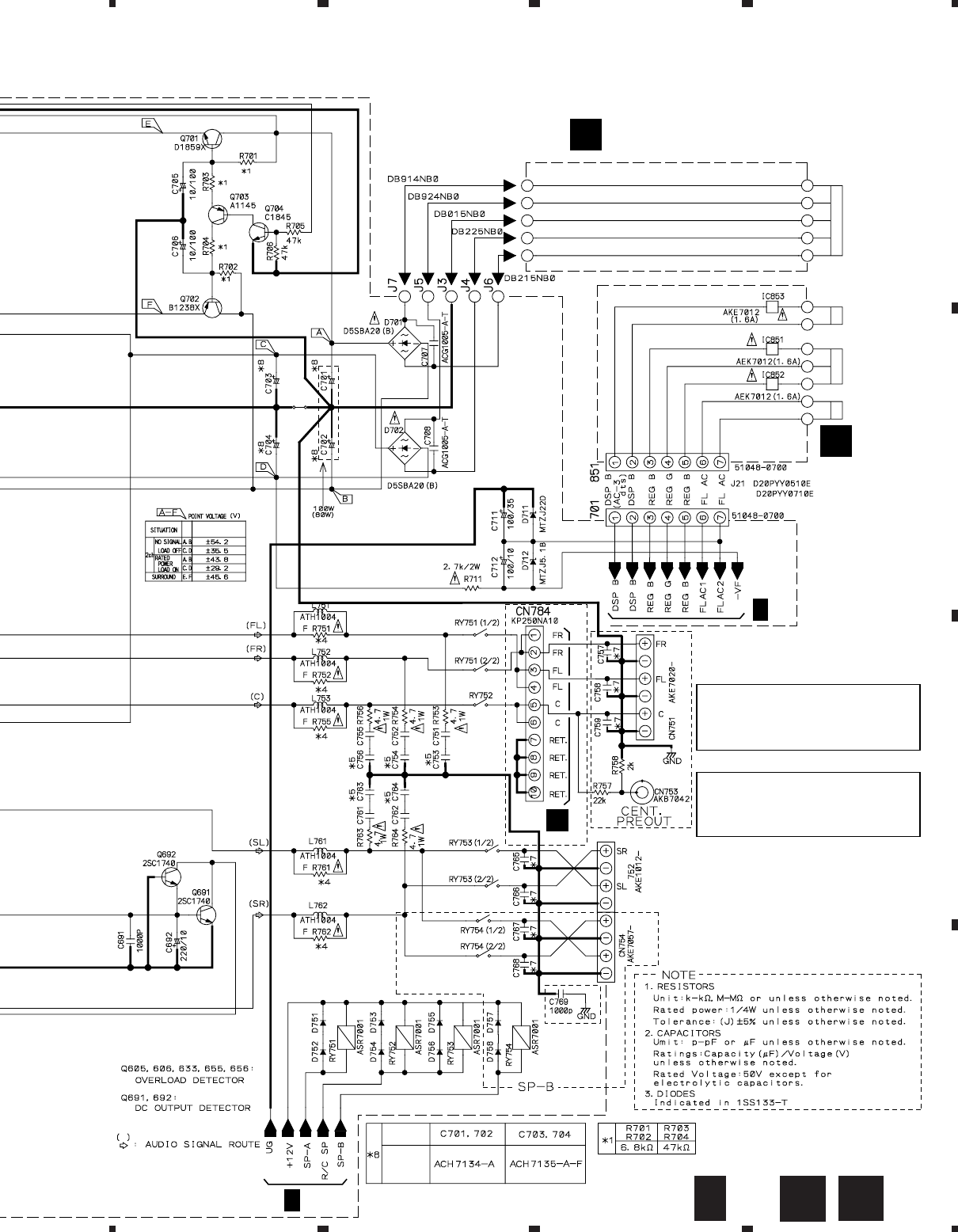
AMP&PRIMARY ASSY
SEMICONDUCTORS
IC52 PROTECTOR (315mA) AEK7003
IC603 PROTECTOR (1A) AEK7009
IC51 NJM78M56FA
IC601 PAC010A
IC602 PAC011A
Q703 2SA1145
Q702 2SB1238X
Q691, Q692 2SC1740S
Q704 2SC1845
Q605, Q606, Q633, Q655, Q656 2SC2240
Q601–Q604, Q631, Q632 2SC2878
Q651–Q654 2SC2878
Q701 2SD1859X
Q51 KRC101M
D56, D57, D601–D604 1SS133
D631, D632, D651–D654 1SS133
D751–D758 1SS133
D701, D702 D5SBA20(B)
D711 MTZJ22D
D58 MTZJ5.1A
D712 MTZJ5.1B
D605, D606, D633, D634 MTZJ8.2A
D51–D55 S5688G
C
46
VSX-709RDS, VSX-609RDS
Mark No. Description Part No. Mark No. Description Part No.
COILS AND FILTERS
L751–L753, L761, L762 ATH1004
L52 XTF3001
SWITCHES AND RELAYS
RY751–RY754 ASR7001
RY51 JOE LOWPOWER RELAY ASR7013
CAPACITORS
C707, C708 (0.01µF/AC250V) ACG1005
C51, C52 (10000pF/AC250V) ACG7020
C701, C702 (4700µF/63V) ACH7134
C703, C704 (3300µF/42V) ACH7135
C607–C610, C634, C635 CCCSL120J50
C657–C660 CCCSL120J50
C613, C614, C637, C663, C664 CCCSL221J50
C615, C616, C638, C665, C666 CEANP2R2M50
C705, C706 CEAT100M2A
C712 CEAT101M10
C611, C612, C636, C661, C662 CEAT101M16
C711 CEAT101M35
C53 CEAT102M16
C692 CEAT221M10
C54 CEAT470M25
C605, C606, C633, C655, C656 CEAT4R7M50
C751–C756, C761–C764 CFTYA224J50
C55–C57 CGCYX103M25
C601, C602, C631, C651, C652 CKCYB102K50
C691, C769 CKCYB102K50
C603, C604, C632, C653, C654 CKCYB331K50
C765–C768 CQMBA472J50
RESISTORS
R615, R616, R638, R665, R666 ACN7094
(0.22Ω/5W)
R52 RD1/2PM270J
R751, R752, R755, R761, R762 RD1/4PMF101J
R753, R754, R756, R763, R764 RS1LMF4R7J
R711 RS2LMF272J
Other Resistors RD1/4PU&&&J
OTHERS
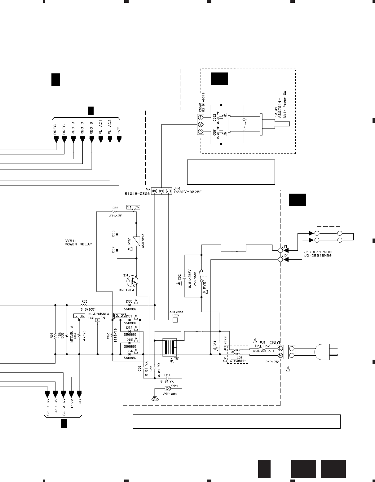
53 3P CABLE HOLDER 51048-0300
701 7P CABLE HOLDER 51048-0700
CN53 22P CONNECTOR 52045-2245
CN754 SPEAKER TERMINAL 8-P AKE7057
H51, H52 FUSE CLIP AKR7001
T51 STANDBY TRANSFORMER ATT7037
J44 3P JUMPER WIRE D20PYY0325E
CN601 16P PLUG KM200TA16
CN784 10P SOCKET KP250NA10
CN51 AC CODE SOCKET RKP1751
KN51, KN601 VNF1084
EARTH METAL FITTING
TRANS2 ASSY
SEMICONDUCTORS
IC851–IC853 PROTECTOR (1.6A) AEK7012
OTHERS
851 7P CABLE HOLDER 51048-0700
TRANS3 ASSY
TRANS3 ASSY has no service part.
REGULATOR ASSY
SEMICONDUCTORS
IC803, IC804 NJM78M05FA
IC801 NJM78M12FA
IC802 NJM79M12FA
Q801, Q803, Q805 KRA103M
Q802, Q804, Q806 KRC101M
D801–D808 S5688G
CAPACITORS
C808, C811 CEAT101M10
C805, C806 CEAT101M16
C809 CEAT222M16
C801, C802 CEAT222M25
C803, C804, C807, C810 CGCYX103M25
OTHERS
CN801 22P CONNECTOR 52045-2245
CN802 19P PLUG KM200TA19
CN803 5P PLUG KM200TA5
TRANS1 ASSY
TRANS1 ASSY has no service part.
MECHA SW ASSY
SWITCHES AND RELAYS
S591 ASG7014
CAPACITORS
C591, C592 CKSQYF103Z50
OTHERS
CN591 52151-0310
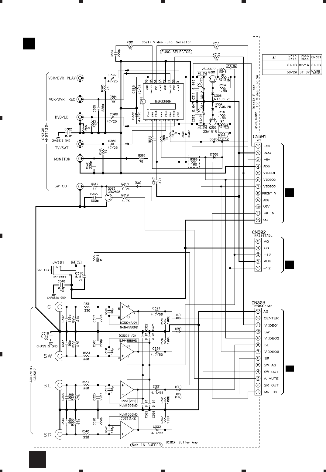
VIDEO&6CH IN ASSY
SEMICONDUCTORS
IC301 NJM2296M
IC302, IC303 NJM4558MD
Q302 2SA1515
Q303 2SC2878
Q301 2SC3377
D301, D302, D305, D306 1SS355
D303, D304 UDZS6.2B
CAPACITORS
C319, C320, C327, C328 CCSQCH101J50
C342–C345 CCSQCH101J50
C347 CCSQCH470J50
C307–C310, C312, C314, C338 CEAT470M25
C321, C324, C331, C332 CEAT4R7M50
D
E
F
H
GA
GB

47
VSX-709RDS, VSX-609RDS
Mark No. Description Part No. Mark No. Description Part No.
C302, C315, C316, C322, C323 CKSQYB103K50
C329, C330 CKSQYB103K50
C346 CKSQYB104K16
C304–C306, C317, C318 CKSQYB221K50
C325, C326 CKSQYB221K50
C333 CKSQYB331K50
C311, C313 CKSQYB473K50
RESISTORS
R313, R316 RS2LMF560J
Other Resistors RS1/10S&&&J
OTHERS
CN303 13P CONNECTOR 52044-1345
CN307 PIN JACK(4P) AKB7087
CN305 6P PIN JACK AKB7123
CN301 12P SOCKET KP200TA12L
CN302 5P SOCKET KP200TA5L
JA301 JACK RKN1004
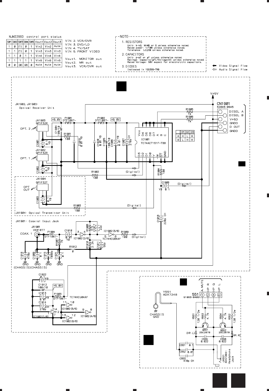
H.P. ASSY
SEMICONDUCTORS
Q551, Q552 2SC2878
CAPACITORS
C553 CCSQCH471J50
C552 CKSQYB103K50
C551 CKSQYB104K16
C555, C556 CKSQYB223K50
RESISTORS
R551, R552 RS1/2LMF121J
Other Resistors RS1/10S&&&J
OTHERS
551 CABLE HOLDER(4P) 51063-0405
JA551 JACK RKN1002
DIGITAL IN ASSY
SEMICONDUCTORS
IC1901 TC74ACT151F
IC1902 TC74HCU04AF
COILS AND FILTERS
F1901–F1904 CHIP BEAD DTF1067
CAPACITORS
C1917 CCSQCH220J50
C1918 CCSQCH221J50
C1907, C1914 CCSQCH271J50
C1916 CCSQCH471J50
C1911 CCSQCH560J50
C1904, C1905, C1912 CEAT101M10
C1915 CKSQYB102K50
C1906, C1910, C1913, C1919, C1920 CKSQYB103K50
C1922 CKSQYB103K50
C1901–C1903, C1908, C1909, C1921 CKSQYB104K25
RESISTORS
All Resistors RS1/10S&&&J
OTHERS
CN1901 CONNECTOR 6P 52045-0645
JA1902,JA1903 GP1F32R
OPTICAL RECEIV MOD.
JA1904 OPTICAL LINK OUT GP1F32T
JA1901 JACK VKB1077
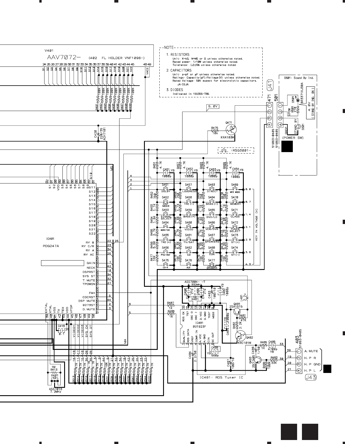
FRONT ASSY
SEMICONDUCTORS
IC481 BU1923F
IC401 PDG247B
Q481 2SA1515
Q405 2SA933S
Q483 2SC1740S
Q401, Q402, Q442, Q471 KRA103M
Q403, Q441, Q482 KRC101M
D407, D408, D442 1SS355
D403, D405 DAN217
D401, D404 DAP202K
COILS AND FILTERS
L401, L481 LFEA2R2J
SWITCHES AND RELAYS
S451–S477 XSG3001
CAPACITORS
C404 (0.047F/5.5V) ACH7017
C420 (220µF/35V) ACH7101
C489, C490 CCSQCH270J50
C483, C487 CEAT101M10
C486 CEAT1R0M50
C402, C405 CEAT221M6R3
C409, C410, C484 CEAT2R2M50
C412 CEAT470M50
C442 CEJA470M10
C451–C454, C481, C482, C495 CKSQYB102K50
C401, C403, C411, C441, C531 CKSQYB103K50
C408, C416, C418, C491–C494 CKSQYB104K16
C532 CKSQYB223K25
C485 CKSQYB472K50
C406, C407 CKSQYB473K16
C488 CKSQYB561K50
RESISTORS
All Resistors RS1/10S&&&J
OTHERS
491 CABLE HOLDER(3P) 51063-0305
403, 471 CABLE HOLDER(4P) 51063-0405
CN401 19P CONNECTOR 52044-1945
CN402 32P CONNECTOR 52044-3245
V401 FL TUBE AAV7072
X481 CRYSTAL RESONATOR ASS7004
(4.332MHz)
X401 CERAMIC RESONATOR ASS7018
(7.2MHz)
401 REMOTE RECEIVER UNIT GP1U27X
I
J
K

48
VSX-709RDS, VSX-609RDS
Mark No. Description Part No. Mark No. Description Part No.
6. ADJUSTMENT
There is no information to be shown in this chapter.
R.ENCODER ASSY
SWITCHES AND RELAYS
S511 ASX7004
OTHERS
511 CABLE HOLDER(3P) 51063-0305
POWER SW ASSY
SEMICONDUCTORS
D501 BR3371XJ30A
SWITCHES AND RELAYS
S501 XSG3001
RESISTORS
All Resistors RS1/10S&&&J
OTHERS
501 CABLE HOLDER(4P) 51063-0405
S. VIDEO ASSY
SEMICONDUCTORS
IC351, IC352 NJM2296M
D351–D354 1SS355
CAPACITORS
C375, C376 CCSQCH470J50
C352, C355, C358, C361–C363 CEAT470M25
C366 CEAT470M25
C372, C373 CKSQYB103K50
C353, C356, C359, C360 CKSQYB104K25
C364, C365, C368–C371 CKSQYB221K50
RESISTORS
All Resistors RS1/10S&&&J
OTHERS
CN353 MINI DIN SOCKET 2P AKP7020
CN352 MINI DIN SOCKET 3P AKP7043
CN354 CONNECTOR POST B5B-PH-K-S
CN351 12P SOCKET KP200TA12L
BOARD TO BOARD ASSY
OTHERS
CN390, CN391 12P PLUG KM200TA12
FRONT VIDEO ASSY
CAPACITORS
C903, C905 CEAT470M25
C908, C911, C914 CKSQYB103K50
C904, C906, C909, C912 CKSQYB104K25
C901, C902 CKSQYB221K50
C907, C910, C913 CKSQYB471K50
M
L
N
O
P
RESISTORS
All Resistors RS1/10S&&&J
OTHERS
CN902 PIN JACK(4P) AKX7007
KN901 EARTH METAL FITTING VNF1084
LARGE SP CONNECTION ASSY
OTHERS
CN785, CN786 10P PLUG KM250NA10L
LARGE SP ASSY
CAPACITORS
C781–C783 CQMBA472J50
RESISTORS
All Resistors RD1/4PU&&&J
OTHERS
CN782 PIN JACK 1P AKB7042
CN781 SPEAKER TERMINAL 6P AKE7056
CN783 10P SOCKET KP250NA10
Q
R
49
VSX-709RDS, VSX-609RDS
2
×2
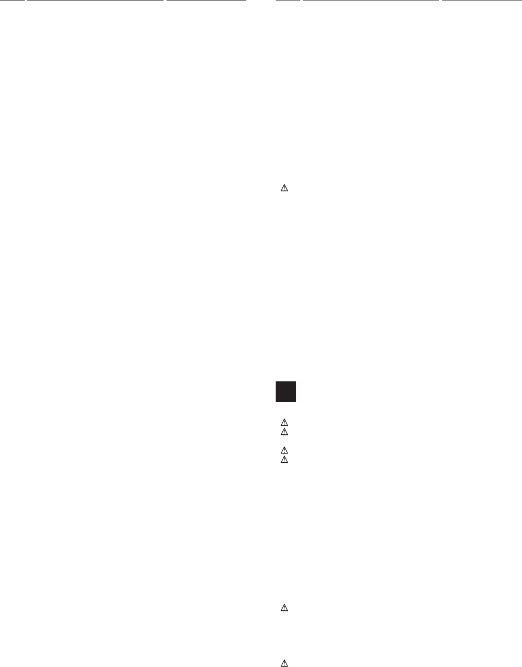
Remove the Bonnet (seven screws).
1
Rear Panel
Pull up
2
2
4
Diagnosis
AMP&PRIMARY Assy
REGULATOR Assy
Heat Sink
5
×2
2
×3
2
×5
3
×3
×2
2
×3
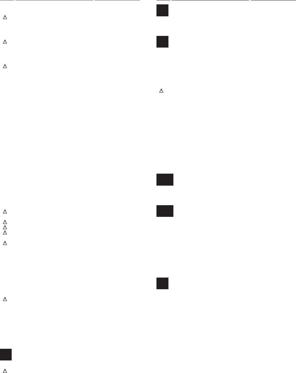
7.1 DISASSEMBLY
7. GENERAL INFORMATION
Diagnosis
PCB Location
AMP&PRIMARY Assy
FRONT Assy
FRONT VIDEO Assy
AMP INPUT Assy
D.D & INPUT Assy
VIDEO&6CH IN Assy
FM/AM TUNER Unit
REGULATOR Assy
DIGITAL IN Assy
H.P. Assy
TRANS 3 Assy
TRANS 2 Assy
TRANS 1 Assy
P
R. ENCODER Assy
L
A
B
H
LARGE SP Assy
R
S.VIDEO Assy
N
F
K
J
I
E
GA
D
C
POWER SW Assy
M
MECHA SW Assy
GB
Note : This photograph shows other models.
However, the work method is the same.
50
VSX-709RDS, VSX-609RDS
PDG247A (FRONT ASSY : IC401)
• System Control MCU
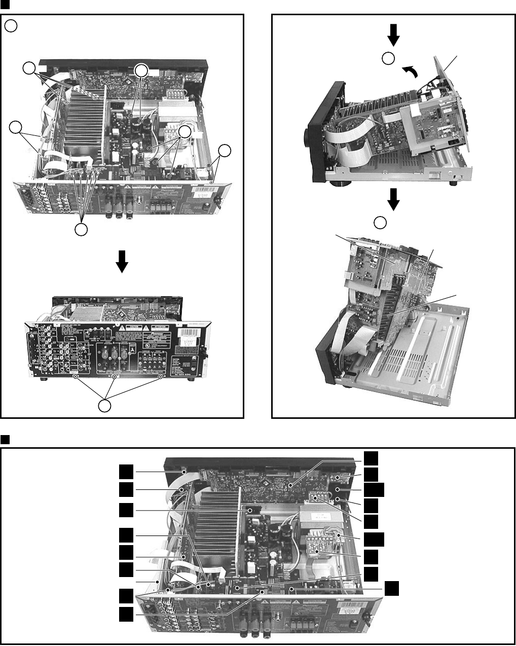
• Pin Arrangement (Top View)
• The information shown in the list is basic information and may not correspond exactly to that shown in the schematic diagrams.
7.2 PARTS
7.2.1 IC
1G2
G1
NC
ACIN
RDS_DT
RDS_CK
OVFB
RMC
MRIN
PLL_CE
CDC_CS
CDC_CK
CDC_DO
CDC_DI
STEREO
TUNED
ENC_A
ENC_B
A.MUTE
CSB
DSP_CS
DSP_CK
DSP_SI
DSP_SO
VER_2
ST_EVR
PLL_DO
KEYIN1
KEYIN2
G1/A1
G0/A0
NC
PE0/EC0/INT0
PE1/EC1/INT1
PE2/INT2
PE3/INT3/NMI
PE4/RMC
PE5
PE6/PWM
PE7/TO/ADJ
PC0/KR0
PC1/KR1
PC2/KR2
PC3/KR3
PC4/KR4
PC5/KR5
PC6/KR6
PC7/KR7
PB0/CINT
PB1/CS0
PB2/SCK0
PB3/SI0
PB4/SO0
PB5/SCK1
PB6/SI1
PB7/SO1
AVREF
PA1/AN0
PA1/AN1
KEYIN3
KEYIN4
VERSION
AMP_DC
AMP_OL
MVRATT
VIDEO1
VIDEO2
VIDEO3
SYS_CK
SYS_DT
PA2/AN2
PA3/AN3
PA4/AN4
PA5/AN5
PA6/AN6
PA7/AN7
AVSS
RST
EXTAL
XTAL
VSS
TX
TEX
VDD
VFIP
PD0/A55
PD1/A54
PD2/A53
PD3/A52
PD4/A51
A21
A22
A23
PH7/A24
PH6/A25
PH5/A26
PH4/A27
PH3/A28
PH2/A29
PH1/A30
PH0/A31
PG7/A32
PG6/A33
PG5/A34
PG4/A35
PG3/A36
PG2/A37
PG1/A38
PG0/A39
PF7/A40
PF6/A41
PF5/A42
PF4/A43
PF3/A44
PF2/A45
PF1/A46
PF0/A47
PD7/A48
PD6/A49
PD5/A50
S11
S12
S13
S14
S15
S16
S17
S18
S19
S20
S21
S22
RY_B
RY_C/R
RY_A
RY_AC
GAIN
NECK
DSP_RST
9164_CS
T_MUTE
T_POWON
FM+(RDS)
CDC_RST
DSP_MT
9273_CS
D_MUTE
G2/A2
G3/A3
G4/A4
G5/A5
G6/A6
G7/A7
G8/A8
G9/A9
G10/A10
G11/A11
G12/A12
VDD
G13/A13
G14/A14
G15/A15
A16
A17
A18
A19
A20
G3
G4
G5
G6
G7
G8
G9
G10
S1
S2
S3
S4
S5
S6
S7
S8
S9
S10
2
3
4
5
6
7
8
9
10
11
12
13
14
15
16
17
18
19
20
100
99
98
97
96
95
94
93
92
91
90
89
88
87
86
85
84
83
82
81
31
32
33
34
35
36
37
38
39
40
41
42
43
44
45
46
47
48
49
50
21
22
23
24
25
26
27
28
29
30
80
79
78
77
76
75
74
73
72
71
70
69
68
67
66
65
64
63
62
61
60
59
58
57
56
55
54
53
52
51

51
VSX-709RDS, VSX-609RDS
No. Pin Name I/O Pin Function Active
1 G2 O Grid output 2 H
2 G1 O Grid output 1 H
3NC −Connect to VDD
4 ACIN I AC pulse input
5 RDS_DT I Serial control DATA signal of RDS communication
6 RDS_CK I Serial control CLOCK signal of RDS communication
7 DIRLOCK I ERR/OVER input from CODEC
8 RMC I Remote control signal input (no-carrier signal)
9 MRIN I MULTI-ROOM input
10 PLL_CE O Chip select signal for communication with LC72131 (tuner) H
11 CDC_CS O CODEC chip serect
12 CDC_CK O CODEC, TC9164 control clock
13 CDC_DO O CODEC, TC9164 control data output
14 CDC_DI I Data input from CODEC
15 STEREO I Stereo/Monoral signal judgment signal
16 TUNED I TUNED information
17 ENC_A I Rotary encoder signal input A
18 ENC_B I Rotary encoder signal input B
19 AMUTE O Audio mute L
20 CSB O Chip select for control of YSS912 sub DSP L
21 DSP_CS O Chip select for control of YSS912 main DSP L
22 DSP_CK O Clock signal for communication with YSS912 H
23 DSP_SI I DATA input for communication with YSS912
24 DSP_SO O DATA output signal for communication with YSS912 H
25 VER_2 I Destination switch 2
26 ST_EVR O Strobe signal for communication with electric volume IC H
27 PLL_DO I Data input signal for communication with LC72131 (tuner)
28 AVref −Connect to VDD
29 KEYIN1 I Key input A/D conversion port 1
30 KEYIN2 I Key input A/D conversion port 2
31 KEYIN3 I Key input A/D conversion port 3
32 KEYIN4 I Key input A/D conversion port 4
33 VER 1 I Destination switch (A/D input)
34 AMP_DC I DC abnormality detection of protection circuit (L : Abnormality detection) L
35 AMP_OL I Over-load detection of protection circuit (L : Abnormality detection) L
36 MVRATT O ATT control of master volume (L : Less than -15dB) H
37 AVSS −Connect to VSS
38 RST −Reset
39 EXTAL −Connect to the oscillator (7.2MHz)
40 XTAL −
41 VSS −Connect to VSS
42 TX −Open
43 TEX −Connect to VSS
44 VDD −+5V
45 VFDP −-30V
46 VIDEO1
O NJM2296D control H47 VIDEO2
48 VIDEO3
49 SYS_DT O Data signal for communication with M62446, TC9163, TC9164 and PLL H
O Clock signal for communication with M62446, TC9163, TC9164 and PLL H
50 SYS_CK
• Pin Function

52
VSX-709RDS, VSX-609RDS
No. Pin Name I/O Pin Function Active
51 D_MUTE
O TC9273 Chip select
O Digital mute (Not used)
O DSP mute (ASSY mute)
H
H
H
52 9273_CS
53 DSP_MT
54 CDC_RST O CODEC reset H
55 FM+(RDS) O Tr switch ON/OFF for power supply of RDS decoder (L : AM, power OFF , H : Other) H
56 O Not used
57 T_POWON O Tuner module ON/OFF (North America model only) H
58 T_MUTE O Tuner mute H
59 9164 CS O TC9163, TC9164 Chip select H
60 DSP_RST O YSS912 reset
61 NECK_SEL O 5.1ch, surround mode and A+B Stereo : H / Stereo : L H/L
62 GAIN_SEL O Gain select (5.1ch and Stereo of analog input : H ) H
63 O Not used H
64 RY_AC O AC relay ON/OFF H
65 RY_A O Speaker A relay ON/OFF H
66 RY_C/R O Rear/Center Speaker relay ON/OFF H
67 O Not used H
68 O Not used H
69 S22
O
Segment output 22
H
70 S21 Segment output 21
71 S20 Segment output 20
72 S19 Segment output 19
73 S18 Segment output 18
74 S17 Segment output 17
75 S16 Segment output 16
76 S15 Segment output 15
77 S14 Segment output 14
78 S13 Segment output 13
79 S12 Segment output 12
80 S11 Segment output 11
81 S10 Segment output 10
82 S9 Segment output 9
H
83 S8 Segment output 8
84 S7 Segment output 7
85 S6 Segment output 6
86 S5 Segment output 5
87 S4 Segment output 4
88 S3 Segment output 3
89 VDD −5V
90 S2
O
OSegment output 2
H
91 S1 Segment output 1
92 Not used (Fixed Vfdp)
93 G10 Grid output 10
94 G9 Grid output 9
95 G8 Grid output 8
96 G7 Grid output 7
97 G6 Grid output 6
98 G5 Grid output 5
99 G4 Grid output 4
100 G3 Grid output 3
53
VSX-709RDS, VSX-609RDS
OUT4
OUT3
OUT2
OUT1
AVDD
SWin
GNDS
SRin
1
2
3
4
5
6
7
8
SLin
GNDC
Cin
GNDR
Rin
GNDL
Lin
BYPASSR
9
10
11
12
13
14
15
16
BYPASSR
LTRE
LBASS3
LBASS2
LBASS1
17
18
19
20
21
MCU
I/F
DVDD
CLK
DATA
LATCH
DGND
AGND
SWout
<SW>
Volume
17-24kΩ
SRout
42
41
40
39
38
37
36
35
SLout
Cout
Rout
Lout
AVSS
CL1
CL2
CR1
34
33
32
31
30
29
28
27
CR2
RTRE
RBASS3
RBASS2
RBASS1
26
25
24
23
22
<SR>
Volume
17-24kΩ
<SL>
Volume
17-24kΩ
<C>
Volume
17-24kΩ
<R>
<R>
Volume
17-24kΩ
70kΩ70kΩ
<L>
Volume
17-24kΩ
S
T
70kΩ70kΩ
70kΩ
12kΩ
12kΩ
300kΩ
1.5kΩ
S
T
<L>
70kΩ
12kΩ
12kΩ
300kΩ
1.5kΩ
M62446FP (D.D & INPUT ASSY : IC103)
• Sound Controller IC (Volume and Tone Control)
• Pin Function
• Block Diagram
No. Pin Name Function
1 OUT4
2 OUT3 Output port (open drain of PchTr)
3 OUT2
4 OUT1
5 AVDD Analog positive power supply port
7 GNDS
10 GNDC GND (connect to analog ground)
12 GNDR
14 GNDL
6 SWin
8 SRin Volume input
9 SLin
11 Cin
36 SWout
35 SRout Volume output
34 SLout
33 Cout
13 Rin TONE input
15 Lin
16 BYPASSR L and R Volume input at bypass
17 BYPASSL
31 Lout L output
32 Rout R output
No. Pin Name Function
18 LTRE TONE TREBLE frequency control port
25 RTRE
19 LBASS3
24 RBASS3
20 LBASS2 TONE BASS frequency control port
23 RBASS2
21 LBASS1
22 RBASS1
26 CR2 TONE output port
28 CL2
27 CR1 L and R volume input
29 CL1
31 Lout L output
32 Rout R output
30 AVSS Analog negative power supply port
37 AGND Analog ground port
38 DGND Digital ground port
39 LATCH Latch input port
40 DATA Data input port
41 CLK Clock input port for data transmission
42 DVDD Digital power supply port
54
VSX-709RDS, VSX-609RDS
W24257AJ-12 (D.D & INPUT ASSY : IC1301)
• 32K × 8 High-Speed CMOS Static RAM
• Block Diagram • Pin Function
VDD
DSS
A0
A14
28
14
10
1
20
22
27
I/O8
19
I/O1
11
CS
OE
WE
DECORER
DATA I/O
CORE
ARRAY
CONTROL
No. Pin Name Function
1 A14
2 A12
3A7
4A6
5A5
6A4
7A3
8 A2 Addres Inputs
9A1
10 A0
21 A10
23 A11
24 A9
25 A8
26 A13
11 I/O1
12 I/O2
13 I/O3
15 I/O4 Data Inputs/Outputs
16 I/O5
17 I/O6
18 I/O7
19 I/O8
14 Vss Ground
20 CS Chip Select Input
22 OE Output Enable Input
27 WE Write Enable Input
28 Vdd Power Supply
TC9273F-007 (D.D & INPUT ASSY : IC101)
• Analog Switch Array
• Block Diagram • Pin Function
VDDDSS
S1
281
CKGND
1413
STBDATA
1615
2
S2
3
S3
4
S4
5
S5
6
S6
7
S7
8
S8
9
S9
10
Level Shift + Shift Register Circuit
(L-ch)
10 bit
Latch
Circuit
(R-ch)
10 bit
Latch
Circuit
S10
11
S11
S1
S2
S3
S4
S5
S6
S7
S8
S9
S10
S11
12
27
26
25
24
23
22
21
20
19
18
17
No. Pin Name Function
1 VSS Minus Power Supply
2, 27 S1
3, 26 S2
4, 25 S3
5, 24 S4
6, 23 S5
7, 22 S6 Input and Output
8, 21 S7
9, 20 S8
10, 19 S9
21, 18 S10
26, 17 S11
13 GND Digital Ground
14 CK Clock Input
15 DATA Data Input
16 STB Strobe Input
28 VDD Plus Power Supply
55
VSX-709RDS, VSX-609RDS
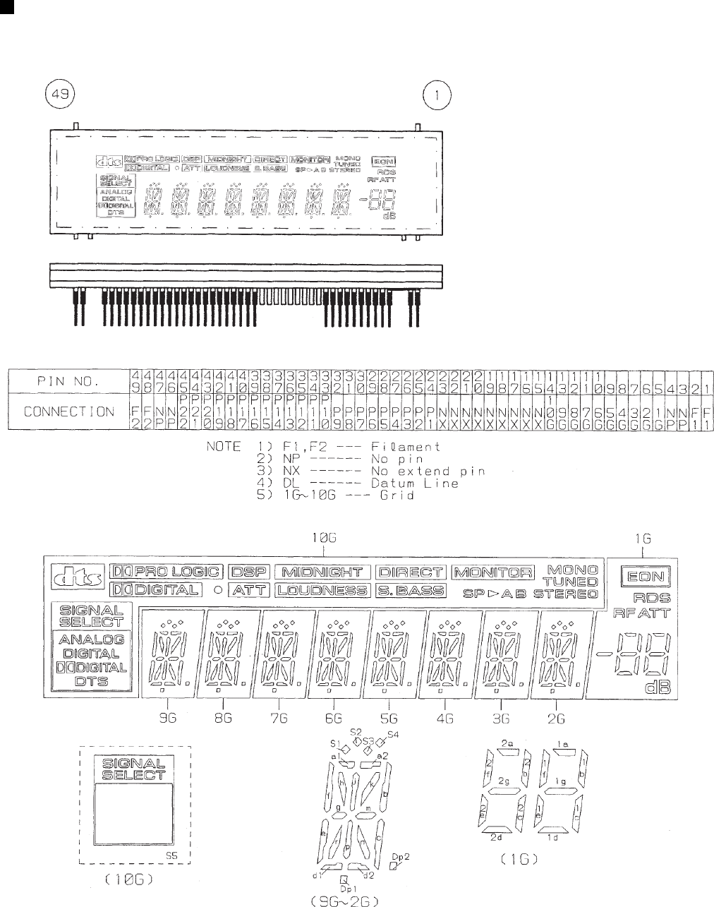
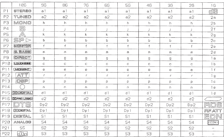
AAV7072 (FRONT ASSY : V401)
• FL DISPLAY
7.2.2 DISPLAY
• Pin Assignment
• Pin Connection
• Grid Assignment
56
VSX-709RDS, VSX-609RDS
• Anode Connection
57
VSX-709RDS, VSX-609RDS
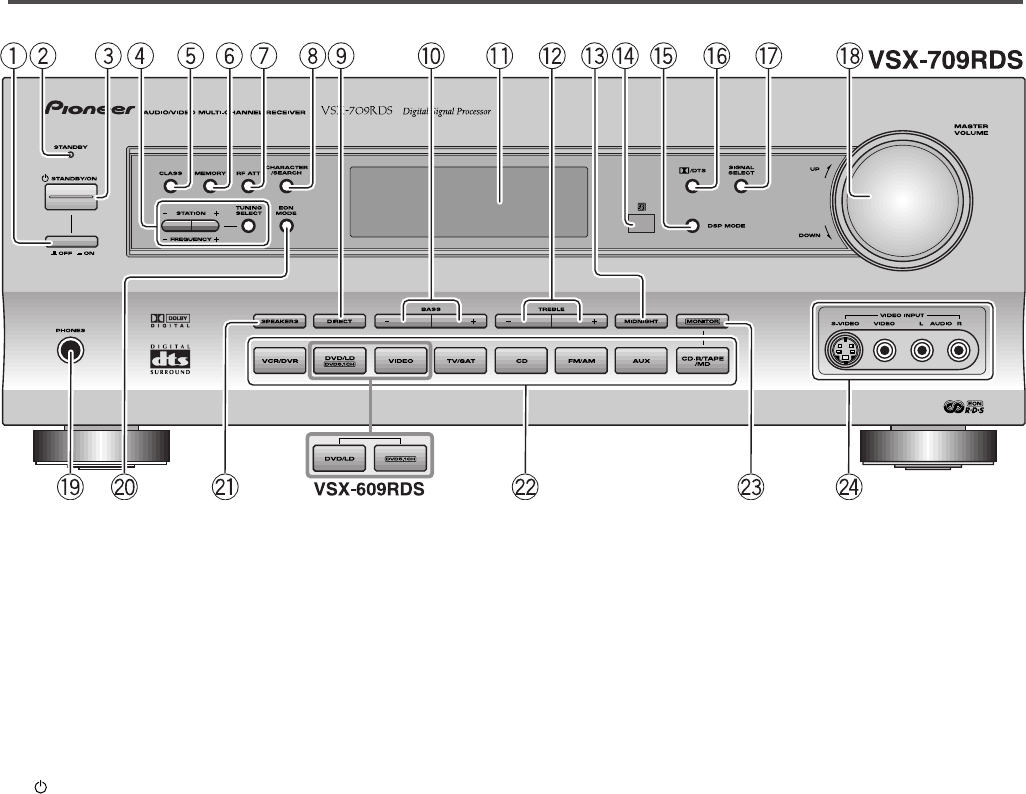
8.1 PANEL FACILITIES
8. PANEL FACILITIES AND SPECIFICATIONS
Front Panel
This illustration shows the VSX-709RDS model.
1— OFF/ _ ON (Main power) button
If the button is OFF (—), the power of the receiver is shut off
and the STANDBY/ON button (3) on the receiver or the
remote control do not function. Pressing the button again
will turn the receiver ON (_) and the receiver enters the
standby mode. In the standby mode, you can turn on the
receiver using the STANDBY/ON button (3) on the receiver
or the remote control.
2STANDBY indicator
Lights when the receiver is in standby mode (note that the
receiver consumes a small amount of power (1 W) in
standby mode).
3 STANDBY/ON button
Switches the receiver between on and standby (note that
the receiver consumes a small amount of power (1 W) in
standby mode).
4TUNING SELECT button
Switches between station memory and frequency select
modes.
STATION (+/–) buttons
Selects station memories when using the tuner.
FREQUENCY (+/–) buttons
Selects the frequency when using the tuner.
5CLASS button
Switches between the three banks (classes) of station
memories.
6MEMORY button
Press to memorize a station for recall using the STATION
(+/–) buttons.
7RF ATT button
Use to lower the input level of a radio signal that is too
powerful or contain interference thus causing the receiver to
distort
8CHARACTER/SEARCH button
Use to search for different program types in RDS mode. It is
also used to input station names.
9 DIRECT button
Use to switch Direct playback on or off. This mode
bypasses the tone controls and channel levels for the most
accurate reproduction of a program source.
0BASS (+/–) buttons
Use to increase/decrease bass (within a range of – 6 dB to
6 dB in 2 dB steps).
-Display
=TREBLE (+/–) buttons
Use to increase/decrease treble (within a range of – 6 dB to
6 dB in 2 dB steps).
~MIDNIGHT button
Use when listening to movie soundtracks at low volume.
This feature will enable you to hear quiet sounds and not
get jolted by loud or sudden sound effects.
! Remote sensor (Î)
Receives the signals from the remote control.
@DSP MODE button
Use to switch between the various DSP modes available
(HALL1, HALL 2, JAZZ, DANCE, THEATER1, THEATER
2) and DSP off. Use to create different surround sound
effects from any stereo source.
#2 /DTS button
Use to switch between the various Dolby/DTS surround
modes.
$SIGNAL SELECT button
Use to select between an analog or digital signal.
%MASTER VOLUME
Use to set the overall listening volume.
58
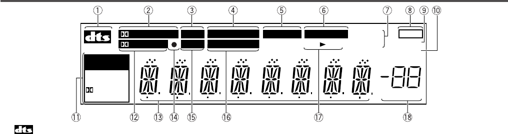
VSX-709RDS, VSX-609RDS
dB
PRO LOGIC
DIGITAL
DSP
ATT
SIGNAL
SELECT
MIDNIGHT
LOUDNESS
DIRECT
S.BASS
MONITOR EON
RDS
RF ATT
TUNED
MONO
ANALOG
DIGITAL
DIGITAL
DTS
SP AB STEREO
Display
^PHONES jack
Use to connect headphones but this does not switch the
speakers off.
&EON MODE button
Use to search for different programs that are transmitting
traffic or news information (this search method is called
EON).
* SPEAKERS button
Use to switch the speaker system A = B = A+B = off.
( Function buttons
Use to select a source for playback or recording.
)MONITOR button
Press to switch tape monitoring on/off.
_VIDEO INPUT jacks (VSX-709RDS only)
Connect a video camera, video game system, etc. to the
VIDEO INPUT jacks.
1 indicator
Lights when DTS mode is being used.
22 PRO LOGIC indicator
When the 2(Dolby)/DTS mode of the receiver is on, this
lights to indicate playback of a two channel source.
3DSP indicator
Lights when any Advanced Theater or DSP mode is
selected.
4MIDNIGHT indicator
Lights when Midnight listening mode is in use.
5DIRECT indicator
Lights when Direct playback is ON. This function bypasses
all tone, balance, DSP and Dolby Surround effects.
6 MONITOR indicator
Lights when MONITOR is selected to hear a recording as
it’s being made.
7Tuner indicators
MONO:
Lights when the mono mode is set using the
MPX button.
TUNED:
Lights when a broadcast is being received.
STEREO:
Lights when a stereo FM broadcast is being received in
Auto stereo mode.
8EON indicator
The box around EON indicator lights to inform you that the
currently tuned station carries the EON data service.
When the EON mode is set, the EON indicator ligh†s, but
during actual reception of an EON broadcast the EON
indicator will flash. An empty box in the EON indicator spot
means it is possible to pick up an EON broadcast but the
receiver has not been set to do so (this will only appear
when RDS is switched on).
9RDS indicator
Lights when an RDS broadcast is received.
0RF ATT indicator
Lights when the RF ATT is on.
- SIGNAL SELECT indicators
Light to indicate the type of input signal assigned for the
current component (see “Front Panel“, $, SIGNAL
SELECT).
ANALOG : Lights when an analog signal is selected.
DIGITAL : Lights when a digital audio signal is selected.
2 DIGITAL : Lights when a Dolby Digital signal is played.
DTS: Lights when a source with DTS audio signals is
played.
=2 DIGITAL indicator
When the 2(Dolby)/DTS mode of the receiver is on, this
lights to indicate playback of a Dolby Digital signal. However
2 PRO LOGIC lights during 2 channel playback of Dolby
Digital.
~Character display
Shows the radio frequency or function (DVD/LD, CD, etc.)
receiver is using .
!÷ (Overload) indicator
This lights when an analog signal is too strong (the SIGNAL
SELECT needs to be on ANALOG). It indicates the sound is
distorting and the signal should be reduced.
@ATT indicator
Lights when ATT is used to attenuate (reduce) the level of
the input signal (can only be used in ANALOG mode).
#LOUDNESS indicator
Lights when the LOUDNESS, used to boost the bass and
treble in quiet listening, is on.
$SP 3 AB (Speakers) indicator
Shows if the speaker system is on or not. SP 3A and/or B
means speakers are switched on. SP 3 means speakers
are switched off.
% Master volume level display
Shows the overall volume level. Volume level is maintained
even when the power is off. – – – dB indicates the minimum
level, and 0 dB indicates the maximum level.
• Depending on the level settings you make for
individual channels, the MAX level can range between
–10 dB and 0 dB.
59
VSX-709RDS, VSX-609RDS
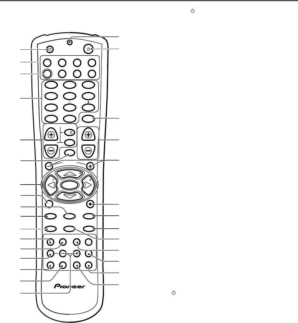
Remote Control (VSX-709RDS)
1SOURCE button
Use to turn on/off other components connected to the
receiver.
2MULTI CONTROL buttons
Use to put the receiver/remote control in the stated mode.
For other equipment controls, see Controlling the Rest of
Your System.
3RCV button
Use this button when setting up the surround sound for the
receiver.
4Number/Mode buttons
Use the number buttons to select the radio frequency in tuner
Direct access mode or the tracks in CD, DVD mode etc.
Also, buttons marked with the following names have special
functions. If you try to use one of these functions but the
display flashes it means that function cannot be used in the
current mode (for example DSP modes cannot be used when
5.1 CH setting is on).
MIDNIGHT
Use to put receiver in Midnight mode. To use first press the
RCV button then operate this button.
5.1 CH
When the DVD/LD or DVD 5.1 CH function is selected each
press switches the DVD/LD input between DVD/LD and DVD
5.1 CH. To use first press the RCV button then operate this
button.
ATT
Use to attenunate (lower) the level of an analog input signal
and prevent distortion. To use first press the RCV button
then operate this button.
SIGNAL SELECT
Use to select the proper signal (analog, digital) for the source
you are inputting. To use first press the RCV button then
operate this button.
EFFECT +/– buttons
Use to adjust the amount of effect in different DSP sound
modes or advanced listening modes. To use, first press the
RCV button then operate this button.
5TV CONTROL buttons
The following five sets of buttons are dedicated TV controls.
TV VOL +/– buttons
Use to adjust the volume on your TV.
TV button
Use to turn on the power of the TV.
TV FUNC button
Use select the TV function.
6 2 3 5∞ ( FQ +/–, ST +/–) & ENTER buttons
Use these arrow buttons when setting up your surround
sound system (see pages 15 – 20). These buttons are also
used to control DVD menus/options. The FQ +/– buttons can
be used to find radio frequencies. The ST +/– buttons can
be used to select the stations of memorized radio
frequencies.
78 button
Use to pause other components.
Î
SOURCE
DISC
MIDNIGHT
SIGNAL SELECT
TV CONTROL
TV VOL
TVFUNC
TV
MENU
ENTER
D.ACCESS BAND CLASS
CH SELECT CH LEVEL
AV PRE-PROGRAMMED AND LEARNING
REMOTE CONTROL UNIT
DSP TEST TONE
FL DIMMER
LOUDNESS FUNCTION SETUPMUTING
MPX DISPLAY RF ATT
FQ
FQ
ST ST
CHANNEL
EFFECT
MASTER VOLUME
+10
5.1CH
MULTI CONTROL
ATT
DVD TV VCR CD-R
RCV CD TUN TVC
RECEIVER
123
456
789
7
4
¢
3
1
¡
0
8
2
1
=
~
!
@
8
9
0
4
6
2
3
-
7
_
¡
$
™
£
%
*
(
)
^
&
∞
+
#
5
¢

60
VSX-709RDS, VSX-609RDS
_ 4 button (DISPLAY)
Use to skip backward tracks on CD players etc. Also use to
display the RDS information.
+ TEST TONE
Use to sound the TEST TONE when setting up the surround
sound of the receiver. To use, first press the RCV button,
then operate this button.
¡FL DIMMER button
Use to make the fluorescent display (FL) dimmer or brighter.
There are three brightness settings as well as an off setting.
™ SETUP button
Use this button when setting up the remote control to control
other components.
£MUTING button
Use to mute the sound or restore the sound if it has been
muted.
¢MENU button
Use to access different menus associated with your DVD
player.
∞CHANNEL +/– buttons
Use to change channels on your TV.
81 button (BAND)
Use to fast reverse search on CD etc.
Also use to switch between the AM and FM band when in
TUNER mode.
9 3 button (D. ACCESS)
Use to play other components. Also use to directly access a
radio station by pressing the number of the station you
want.
0 7 button (MPX)
Use to stop other components. Also use to switch between
auto stereo and mono reception of FM broadcasts. If the
signal is weak then switching to MONO will improve the
sound quality.
- 2 button
Use to put receiver in Dolby Digital, Dolby Surround and DTS
modes. To use first press the RCV button then operate this
button.
= DSP button
Use to put receiver in one of the DSP modes. To use first
press the RCV button then operate this button.
~ CH SELECT
Use to select a speaker when setting up the surround sound
of the receiver. To use, first press the RCV button, then
operate this button.
! LOUDNESS button
Use to switch on the loudness. This feature is useful for
getting good bass and treble sounds listening at low
volumes.
@ FUNCTION button
Use to select the playback or recording source. This button
lets you cycle through the different functions of the receiver
in the following order: CD, tuner (FM/AM), AUX, CD-R/
TAPE/MD, VCR/DVR, DVD/LD, VIDEO and TV/SAT.
# CH LEVEL +/– buttons
Use to adjust the output level of the selected channel(s).
$LED display
This display flashes when a command is sent from the
remote control to the receiver. It also flashes at other times,
for example, when teaching the receiver preset codes.
%RECEIVER button
This switches the receiver between STANDBY mode and
power ON.
^DISC button
Only used when controlling other components.
& MASTER VOLUME +/– buttons
Use to set the overall listening volume.
*¶ button
Use to record with other components.
(¡ button (CLASS)
Use to fast forward search on CDs etc. Also use the CLASS
feature to switch between the three banks (classes) of
station memories.
)¢ button (RF ATT)
Use to skip forward tracks on CD players etc. Also use to
lower the input level of a radio signal.
61
VSX-709RDS, VSX-609RDS
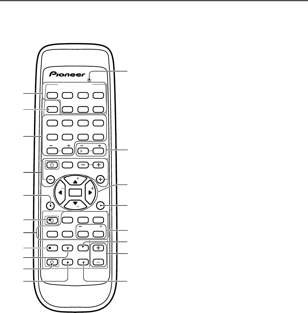
Remote Control (VSX-609RDS)
1MULTI CONTROL buttons
Use to put the receiver/remote control in the stated mode.
For other equipment controls, see Controlling the Rest of
Your System.
2RECEIVER button
Use this button when setting up the surround sound for the
receiver.
3Number/Mode buttons
Use the number buttons to select the radio frequency in tuner
Direct access mode or the tracks in CD, DVD mode etc.
Also, buttons marked with the following names have special
functions. If you try to use one of these functions but the
display flashes it means that function cannot be used in the
current mode (for example DSP modes cannot be used when
5.1 CH setting is on).
2
Use to put receiver in Dolby Digital, Dolby Surround and DTS
modes. To use first press the RECEIVER button then operate
this button.
DSP MODE
Use to put receiver in one of the DSP modes. To use first
press the RECEIVER button then operate this button.
MIDNIGHT
Use to put receiver in Midnight mode. To use, first press the
RECEIVER button, then operate this button.
5.1 CH
When the DVD/LD or DVD 5.1 CH function is selected each
press switches the DVD/LD input between DVD/LD and DVD
5.1 CH. To use, first press the RECEIVER button, then
operate this button.
CHANNEL SELECT
Use to select a speaker when setting up the surround sound
of the receiver. To use, first press the RECEIVER button,
then operate this button.
TEST TONE
Use to sound the TEST TONE when setting up the surround
sound of the receiver. To use, first press the RECEIVER
button, then operate this button.
ATT
Use to attenunate (lower) the level of an analog input signal
and prevent distortion. To use, first press the RECEIVER
button, then operate this button.
CHANNEL LEVEL +/–
Use to set up the levels of the surround sound of the receiver.
To use, first press the RECEIVER button, then operate this
button.
SIGNAL SELECT
Use to select the proper signal (analog, digital) for the source
your are inputting. To use, first press the RECEIVER button,
then operate this button.
MULTI CONTROL
DVD/LD TV/SAT VCR/DVR CD
SOURCE CLASS MPX BAND
LOUDNESS FUNCTION MUTING
RECEIVER
D.ACCESS
ATT
VOL
MENU TOP
MENU
VOL
CH
2
DSP MODE
MIDNIGHT
5.1CH
CD-R/
TAPE/MD
CHANNEL
SELECT
CHANNEL
LEVEL EFFECT
ENTER
FQ
FQ
ST ST
FL
DIMMER REMOTE
SETUP
MASTER
VOLUME
AUDIO/VIDEO PRE-PROGRAMMED
REMOTE CONTROL UNIT
TV CONTROL
FUNC
10 DISC
SIGNAL
SELECT
TEST
TONE
RECEIVER
TUNER
TV CONT
Î
12 3 4
1 ¡ 4 ¢
7 8 3
56 7 8
90
CHANNEL
DISPLAY RF ATT
2
6
8
5
1
3
0
9
-
=
!
@
~
#
%
$
^
7
4

62
VSX-709RDS, VSX-609RDS
=LED display
This display flashes when a command is sent from the
remote control to the receiver. It also flashes at other times,
for example when teaching the receiver preset codes.
~EFFECT +/– buttons
Use to adjust the amount of effect in different DSP sound
modes or advanced listening modes.
! 2 3 5∞ ( FQ +/–, ST +/–) & ENTER buttons
Use these arrow buttons when setting up your surround
sound system (see pages 15 – 20). These buttons are also
used to control DVD menus/options and for deck 1 of a
double cassette deck player. The FQ +/– buttons can be
used to find radio frequencies. The ST +/– buttons can be
used to select the stations of memorized radio frequencies.
@ TOP MENU button
In DVD mode this button brings you to the top or most
fundamental menu.
# CHANNEL +/– buttons (4/DISPLAY, ¢/RF
ATT)
Use to select the stations of memorized radio frequencies.
Also use to skip tracks backward or forward on CDs, DVDs,
etc. Also use to display the RDS information (DISPLAY) and
use to lower the input level of a radio signal (RF ATT).
$MUTING button
Use to mute the sound or restore the sound if it has been
muted.
%MASTER VOLUME +/– buttons
Use to set the overall listening volume.
^ REMOTE SETUP button
Use this button when setting up the remote control to control
other components.
4TV CONTROL buttons
The following four sets of buttons are dedicated TV controls.
FUNC button
Use to select the TV function.
button
Use to turn on the power of the TV.
CH +/– buttons
Use to change channels on your TV.
VOL +/– buttons
Use to adjust the volume on your TV.
5MENU button
Use to access different menus associated with your DVD
player.
6 SOURCE button
Use to turn on/off other components connected to the
receiver.
7The following buttons are both controls for
other components (like a DVD player) and
dedicated tuner controls. The tuner controls are
explained here. You can use them after you
have pushed the TUNER MULTI CONTROL
button.
CLASS button
Use to switch between the three banks (classes) of station
memories.
MPX button
Use to switch between auto stereo and mono reception of
FM broadcasts. If the signal is weak then switching to
MONO will improve the sound quality. Also, this is the
pause button for CDs, tapes, DVDs, etc.
BAND button
Use to switch between the AM and FM band when in
TUNER mode.
D. ACCESS button
Use to directly access a radio station by pressing the
number of the station you want.
8LOUDNESS button
Use to switch on the loudness. This feature is useful for
getting good bass and treble sounds listening at low
volumes.
9 FUNCTION button
Use to select the playback or recording source. This button
lets you cycle through the different functions of the receiver
in the following order: CD, tuner (FM/AM), AUX, CDR/
TAPE/MD, VCR/DVR, DVD/LD, DVD 5.1 CH., and TV/SAT.
0RECEIVER button
This switches the receiver between STANDBY mode and
power ON.
-FL DIMMER button
Use this button to make the fluorescent display (FL) dimmer
or brighter. There are three brightness settings as well as an
off setting.
63
VSX-709RDS, VSX-609RDS
7 Audio cords
Use audio cords (not supplied) to connect the audio components.
Cassette deck placement
Cassette deck placement
Depending on where the cassette deck is placed, noise may occur during playback of your cassette deck which is caused by leakage
flux from the transformer in the receiver. If you experience noise, move the cassette deck farther away from the receiver.
Connect red plugs to R (right) and white plugs to L (left).
Be sure to insert completely.
L
R
Audio Components
To begin set up connect your audio components to the jacks as shown below. These are all analog connections and your analog audio
components (cassette deck etc.) use these jacks. Remember that for components you want to record with you need to hook up four
plugs (a set of stereo ins and a set of stereo outs), but for components that only play you only need to hook up one set of stereo plugs
(two plugs). To use Digital sources features you must hook up your digital components to the digital inputs, but it is also a good idea to
hook up your digital components to analog audio jacks. If you want to record to/from digital components (like an MD) to/from analog
components you must hook up your digital equipment with these analog connections.
• Only the VSX-709RDS has S-video jacks and optical digital out jack.
• The arrows indicate the direction of the audio signal.
REC PLAY
L
R
L
R
OUTPUT
CD player CD-R
or Cassette deck
or MD recorder
VSX-709RDS
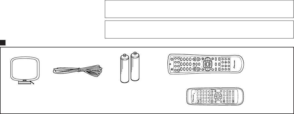
64
VSX-709RDS, VSX-609RDS
8.2 SPECIFICATIONS
Sensitivity (DIN) ...................................... Mono: 1.1 µV (S/N 26 dB)
Stereo: 50 µV (S/N 46 dB)
Signal-to-Noise Ratio ................................. Mono: 76 dB (at 85 dBf)
Stereo: 72 dB (at 85 dBf)
Signal-to-Noise Ratio (DIN) ......................................... Mono: 62 dB
Stereo: 58 dB
Distortion........................................................ Stereo: 0.6 % (1 kHz)
Alternate Channel Selectivity ................................. 70 dB (400 kHz)
Stereo Separation ...................................................... 40 dB (1 kHz)
Frequency Response ................................. 30 Hz to 15 kHz (± 1dB)
Antenna Input ........................................................ 75 Ω unbalanced
AM Tuner Section
Frequency Range........................................... 531 kHz to 1,602 kHz
Sensitivity (IHF, Loop antenna) ......................................... 350 µV/m
Selectivity ................................................................................ 30 dB
Signal-to-Noise Ratio .............................................................. 50 dB
Antenna ...................................................................... Loop antenna
Miscellaneous
Power Requirements
UK model ...................................................... AC 230 V, 50/60 Hz
European model .................................. AC 220 – 230 V, 50/60 Hz
Power Consumption ............................................................... 220 W
Power Consumption in Standby mode .................................... 1.0 W
Dimensions
VSX-709RDS ........................... 420 (W) × 158 (H) × 401 (D) mm
VSX-609RDS ........................... 420 (W) × 158 (H) × 391 (D) mm
Weight (without package)
VSX-709RDS ..................................................................... 8.4 kg
VSX-609RDS ..................................................................... 8.4 kg
Furnished Parts
FM Antenna ................................................................................... 1
AM Loop Antenna .......................................................................... 1
Dry Cell Batteries
VSX-709RDS (SIZE “AA” (IEC LR6)) ......................................... 2
VSX-609RDS (SIZE “AA” (IEC R6P)) ........................................ 2
Remote Control Unit ...................................................................... 1
Operating Instructions .................................................................... 1
NOTE:
Specifications and the design are subject to possible
modifications without notice, due to improvements.
AM loop antenna
(ATB7009) FM wire antenna
(ADH7005)
VSX-609RDS:
AA size IEC R6P batteries (x2)
VSX-709RDS:
AA size IEC LR6 batteries (x2)
VSX-609RDS
VSX-709RDS
SOURCE
MIDNIGHT
SIGNAL SELECT
TV CONTROL
TV VOL
TVFUNC
TV
MENU
ENTER
D.ACCESS BAND CLASS
CH SELECT CH LEVEL
AV PRE-PROGRAMMED AND LEARNING
REMOTE CONTROL UNIT
DSP TEST TONE
FL DIMMER
LOUDNESS FUNCTION SETUPMUTING
MPX DISPLAY RF ATT
FQ
FQ
ST ST
CHANNEL
EFFECT
MASTER VOLUME
DISC
+10
5.1CH
MULTI CONTROL
ATT
DVD TV VCR CD-R
RCV CD TUN TVC
RECEIVER
123
456
789
7
4
¢
3
1
¡
0
8
2
Î
MULTI CONTROL
DVD/LD TV/SAT VCR/DVR CD
SOUCE CLASS MPX BAND
LOUDNESS FUNCTION MUTING
RECEIVER
D.ACCESS
ATT
VOL
MENU TOP
MENU
VOL
CH
2
DSP MODE
MIDNIGHT
5.1CH
CD-R/
TAPE/MD
CHANNEL
SELECT
CHANNEL
LEVEL EFFECT
ENTER
ENTER
FQ
FQ
ST ST
FL
DIMMER REMOTE
SETUP
MASTER
VOLUME
AUDIO/VIDEO PRE-PROGRAMMED
REMOTE CONTROL UNIT
TV CONTROL
FUNC
10 DISC
SIGNAL
SELECT
TEST
TONE
RECEIVER
TUNER
TV CONT
Î
12 3 4
1 ¡ 4 ¢
7 8 3
56 7 8
90
‡
CHANNEL
DISPLAY RF ATT
Accessories
Manufactured under license from Digital Theater Systems, Inc. US Pat. No. 5,451,942 and other
worldwide patents issues and pending. “DTS” and “DTS Digital Surround” are trademarks of Digital
Theater Systems, Inc. © 1996 Digital Theater Systems, Inc. All right reserved.
Manufactured under license from Dolby Laboratories. “Dolby”, “Pro Logic” and the double-D symbol
are trademarks of Dolby Laboratories. Confidential unpublished works. © 1992 - 1997 Dolby
Laboratories. All rights reserved.
Remote control unit
(AXD7247)
Remote control unit
(AXD7249)
Amplifier Section
Continuous Power Output (STEREO MODE)
FRONT .......................80 W + 80 W (DIN 1 kHz, THD 0.9 %, 8Ω)
Continuous Power Output (SURROUND MODE)
FRONT ..................................... 80 W/ch (1 kHz, THD 0.9 %, 8Ω)
CENTER ....................................... 80 W (1 kHz, THD 0.9 %, 8Ω)
SURROUND............................. 80 W/ch (1 kHz, THD 0.9 %, 8Ω)
• Above specifications are applicable when the power supply is
230V.
Input (Sensitivity/Impedance)
VCR/DVR, DVD/LD, TV/SAT, CD, AUX,
CD-R/TAPE/MD (, VIDEO) .................................... 200 mV/47 kΩ
Frequency Response
VCR/DVR, DVD/LD, TV/SAT, CD, AUX,
CD-R/TAPE/MD (, VIDEO) ................... 5 Hz to 100,000 Hz dB
Output (Level/Impedance)
VCR/DVR, CD-R/TAPE/MD .................................. 200 mV/2.2 kΩ
Tone Control
BASS ................................................................... ± 6 dB (100 Hz)
TREBLE .............................................................. ± 6 dB (10 kHz)
LOUDNESS .................................. +9 dB/+9 dB (100 Hz/10 kHz)
Signal-to-Noise Ratio
[DIN (Continuous rated power output/50 mW)]
VCR/DVR, DVD/LD, TV/SAT, CD, AUX,
CD-R/TAPE/MD (, VIDEO) ....................................... 88 dB/64 dB
VIDEO Section
Input (Sensitivity/Impedance)
VCR/DVR, TV/SAT, DVD/LD (, VIDEO) ..................... 1 Vp-p/75 Ω
Output (Level/Impedance)
VCR/DVR, TO MONITOR TV .................................... 1 Vp-p/75 Ω
Frequency Response
VCR/DVR, TV/SAT, DVD/LD (, VIDEO)
= TO MONITOR TV...................................... 5 Hz to 7 MHz dB
Signal-to-Noise Ratio .............................................................. 55 dB
FM Tuner Section
Frequency Range .......................................... 87.5 MHz to 108 MHz
Usable Sensitivity ....................... Mono: 15.2 dBf, IHF (1.6 µV/75 Ω)
50 dB Quieting Sensitivity ........................................ Mono: 20.2 dBf
Stereo: 41.2 dBf
+0
–3
+0
–3
