MOTOTRBO XPR 2500 Mobile Radio Basic Service Manual Series/XPR2500 68009620001 A XPR2500
User Manual: -XPR Series/XPR2500 Basic service manual 68009620001-A
Open the PDF directly: View PDF ![]() .
.
Page Count: 100
- Foreword
- Document History
- Table of Contents
- Foreword i
- Commercial Warranty xi
- Chapter 1 Introduction 1-1
- Chapter 2 Test Equipment and Service Aids 2-1
- Chapter 3 Transceiver Performance Testing 3-1
- Chapter 4 Radio Programming and Tuning 4-1
- Chapter 5 Disassembly/Reassembly Procedures 5-1
- Chapter 6 Basic Troubleshooting 6-1
- Chapter 7 Accessories 7-1
- Appendix A Replacement Parts Ordering A-1
- Appendix B Motorola Service Centers B-1
- Appendix C Limited Level 3 Servicing C-1
- Glossary Glossary-1
- List of Figures
- List of Tables
- Commercial Warranty
- Chapter 1 Introduction
- 1.1 Notations Used in This Manual
- 1.2 Radio Description
- 1.3 Control Head Description
- 1.4 MOTOTRBO Mobile Radio Model Numbering Scheme
- 1.5 VHF High Power (136–174 MHz) Model Chart
- 1.6 VHF Low Power (136–174 MHz) Model Chart
- 1.7 UHF1 High Power (403–470 MHz) Model Chart
- 1.8 UHF1 Low Power (403–470 MHz) Model Chart
- 1.9 Specifications
- Chapter 2 Test Equipment and Service Aids
- Chapter 3 Transceiver Performance Testing
- Chapter 4 Radio Programming and Tuning
- Chapter 5 Disassembly/Reassembly Procedures
- 5.1 Introduction
- 5.2 Preventive Maintenance
- 5.3 Safe Handling of CMOS and LDMOS Devices
- 5.4 Repair Procedures and Techniques – General
- 5.5 Disassembling and Reassembling the Radio – General
- 5.6 Radio Disassembly – Detailed
- 5.7 Radio Reassembly – Detailed
- 5.8 Exploded Mechanical Views and Parts Lists
- 5.9 Torque Chart
- Chapter 6 Basic Troubleshooting
- Chapter 7 Accessories
- Appendix A Replacement Parts Ordering
- Appendix B Motorola Service Centers
- Appendix C Limited Level 3 Servicing
- Glossary
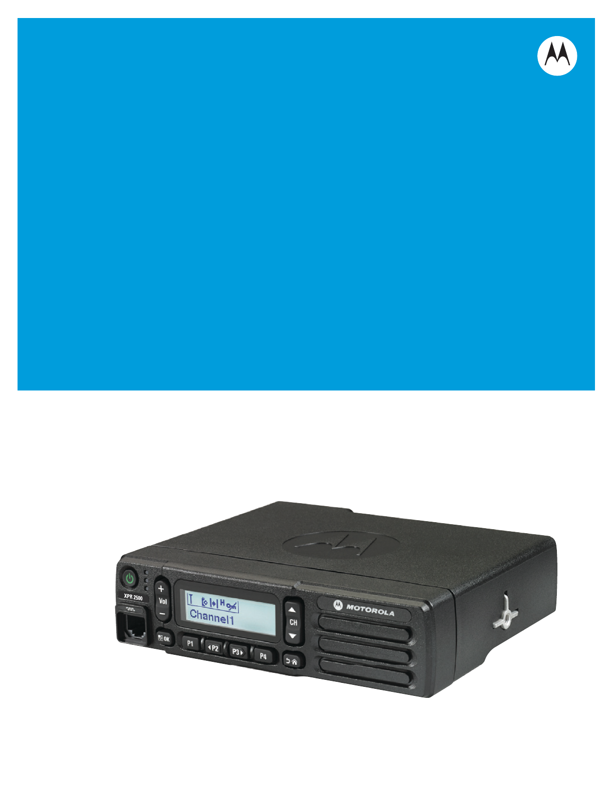
PROFESSIONAL DIGITAL TWO-WAY RADIOS
MOTOTRBOTM
XPRTM 2500
ALPHANUMERIC
DISPLAY MOBILE
BASIC SERVICE
MANUAL

i
Foreword
This manual covers all XPR™ 2500 Mobiles, unless otherwise specified. It includes all the information necessary to
maintain peak product performance and maximum working time, using levels 1 and 2 maintenance procedures. This level
of service goes down to the board replacement level and is typical of some local service centers, Motorola Authorized
Dealers, self-maintained customers, and distributors.
Product Safety and RF Exposure Compliance
ATTENTION!
Before using the mobile two-way product, XPR™ 2500, read the RF Energy Exposure and Safety guide
that ships with the radio which contains important operating instructions for safe usage and RF
energy awareness and control for Compliance with applicable Standards and Regulations.
Computer Software Copyrights
The Motorola products described in this manual may include copyrighted Motorola computer programs stored in
semiconductor memories or other media. Laws in the United States and other countries preserve for Motorola certain
exclusive rights for copyrighted computer programs, including, but not limited to, the exclusive right to copy or reproduce
in any form the copyrighted computer program. Accordingly, any copyrighted Motorola computer programs contained in
the Motorola products described in this manual may not be copied, reproduced, modified, reverse-engineered, or
distributed in any manner without the express written permission of Motorola. Furthermore, the purchase of Motorola
products shall not be deemed to grant either directly or by implication, estoppel, or otherwise, any license under the
copyrights, patents or patent applications of Motorola, except for the normal non-exclusive license to use that arises by
operation of law in the sale of a product.
Document Copyrights
No duplication or distribution of this document or any portion thereof shall take place without the express written
permission of Motorola. No part of this manual may be reproduced, distributed, or transmitted in any form or by any
means, electronic or mechanical, for any purpose without the express written permission of Motorola.
Disclaimer
The information in this document is carefully examined, and is believed to be entirely reliable. However, no responsibility is
assumed for inaccuracies. Furthermore, Motorola reserves the right to make changes to any products herein to improve
readability, function, or design. Motorola does not assume any liability arising out of the applications or use of any product
or circuit described herein; nor does it cover any license under its patent rights nor the rights of others.
Trademarks
MOTOROLA, MOTO, MOTOROLA SOLUTIONS and the Stylized M logo are trademarks or registered trademarks of
Motorola Trademark Holdings, LLC and are used under license. All other trademarks are the property of their respective
owners.
© 2013 Motorola Solutions, Inc. All rights reserved.
These servicing instructions are for use by qualified personnel only. To
reduce the risk of electric shock, do not perform any servicing other than
that contained in the Operating Instructions unless you are qualified to do
so. Refer all servicing to qualified service personnel.
!
C a u t i o n

ii
Notes

iii
Document History
The following major changes have been implemented in this manual since the previous edition.
Edition Description Date
68009620001-A Initial Release. June 2013

iv
Notes

Table of Contents v
Table of Contents
Foreword..........................................................................................................i
Product Safety and RF Exposure Compliance .............................................................................................i
Computer Software Copyrights ....................................................................................................................i
Document Copyrights ...................................................................................................................................i
Disclaimer.....................................................................................................................................................i
Trademarks ..................................................................................................................................................i
Document History ........................................................................................ iii
Commercial Warranty ...................................................................................xi
Limited Warranty ........................................................................................................................................xi
MOTOROLA COMMUNICATION PRODUCTS ..............................................................................xi
I. What This Warranty Covers And For How Long .....................................................................xi
II. General Provisions ................................................................................................................ xii
III. State Law Rights .................................................................................................................. xii
IV. How To Get Warranty Service ............................................................................................. xii
V. What This Warranty Does Not Cover.................................................................................... xii
VI. Patent And Software Provisions ......................................................................................... xiii
VII. Governing Law................................................................................................................... xiii
Chapter 1 Introduction ......................................................................... 1-1
1.1 Notations Used in This Manual .................................................................................................... 1-1
1.2 Radio Description ........................................................................................................................ 1-1
1.3 Control Head Description............................................................................................................. 1-2
1.3.1 Control Head Controls ..................................................................................................... 1-2
1.4 MOTOTRBO Mobile Radio Model Numbering Scheme............................................................... 1-3
1.5 VHF High Power (136–174 MHz) Model Chart ........................................................................... 1-4
1.6 VHF Low Power (136–174 MHz) Model Chart ........................................................................... 1-4
1.7 UHF1 High Power (403–470 MHz) Model Chart ........................................................................ 1-5
1.8 UHF1 Low Power (403–470 MHz) Model Chart ......................................................................... 1-5
1.9 Specifications............................................................................................................................... 1-6
Chapter 2 Test Equipment and Service Aids ..................................... 2-1
2.1 Recommended Test Equipment .................................................................................................. 2-1
2.2 Service Aids................................................................................................................................. 2-2
2.3 Programming Cables ................................................................................................................... 2-3
2.4 Programming and Test Cable ...................................................................................................... 2-3
2.5 Test Cable ................................................................................................................................... 2-4
2.6 Accessory Cable .......................................................................................................................... 2-5

vi Table of Contents
Chapter 3 Transceiver Performance Testing ..................................... 3-1
3.1 General ........................................................................................................................................ 3-1
3.2 Setup............................................................................................................................................ 3-1
3.3 Alphanumeric Display Model Test Mode ..................................................................................... 3-2
3.3.1 Entering Display Radio Test Mode .................................................................................. 3-2
3.3.2 RF Test Mode .................................................................................................................. 3-2
3.3.3 Alphanumeric Display Test Mode .................................................................................... 3-3
3.3.4 LED Test Mode................................................................................................................ 3-3
3.3.5 Backlight Test Mode ........................................................................................................3-3
3.3.6 Speaker Tone Test Mode ................................................................................................ 3-3
3.3.7 Earpiece Tone Test Mode ............................................................................................... 3-3
3.3.8 Audio Loopback Test Mode ............................................................................................. 3-3
3.3.9 Audio Loopback Earpiece Test Mode.............................................................................. 3-4
3.3.10 Button Test Mode ............................................................................................................ 3-4
Chapter 4 Radio Programming and Tuning ....................................... 4-1
4.1 Introduction .................................................................................................................................. 4-1
4.2 Customer Programming Software Setup ..................................................................................... 4-1
4.3 AirTracer Application Tool............................................................................................................ 4-2
4.4 Radio Tuning Setup ..................................................................................................................... 4-3
Chapter 5 Disassembly/Reassembly Procedures ............................. 5-1
5.1 Introduction .................................................................................................................................. 5-1
5.2 Preventive Maintenance .............................................................................................................. 5-1
5.2.1 Inspection ........................................................................................................................ 5-1
5.2.2 Cleaning Procedures ....................................................................................................... 5-1
5.3 Safe Handling of CMOS and LDMOS Devices ............................................................................ 5-2
5.4 Repair Procedures and Techniques – General............................................................................ 5-4
5.5 Disassembling and Reassembling the Radio – General.............................................................. 5-5
5.6 Radio Disassembly – Detailed ..................................................................................................... 5-5
5.6.1 Control Head Removal .................................................................................................... 5-5
5.6.2 Top Cover Removal......................................................................................................... 5-6
5.6.3 Transceiver Board Removal ............................................................................................ 5-7
5.6.4 Disassembly of Alphanumeric Display Control Head .................................................... 5-12
5.7 Radio Reassembly – Detailed.................................................................................................... 5-16
5.7.1 Reassembly of Alphanumeric Display Control Head ..................................................... 5-16
5.7.2 Radio Assembly.............................................................................................................5-20
5.7.3 Thermal Pad Replacement Procedure .......................................................................... 5-21
5.7.4 Transceiver Board Reassembly..................................................................................... 5-25
5.7.5 Option Board Installation ............................................................................................... 5-33
5.7.6 Assemble Control Head to Radio Assembly.................................................................. 5-35
5.8 Exploded Mechanical Views and Parts Lists ............................................................................. 5-36
5.8.1 Radio Assembly Exploded View and Parts List ............................................................ 5-36
5.8.2 Alphanumeric Display Control Head Exploded View and Parts List .............................. 5-38
5.9 Torque Chart.............................................................................................................................. 5-39

Table of Contents vii
Chapter 6 Basic Troubleshooting ....................................................... 6-1
6.1 Introduction .................................................................................................................................. 6-1
6.1.1 High Power RF Precaution .............................................................................................. 6-1
6.2 Replacement Service Kit Procedures .......................................................................................... 6-1
6.3 Power-Up Error Codes ................................................................................................................ 6-2
Chapter 7 Accessories ......................................................................... 7-1
7.1 Introduction .................................................................................................................................. 7-1
7.1.1 Antennas ......................................................................................................................... 7-1
7.1.2 Audio ............................................................................................................................... 7-2
7.1.3 Cables ............................................................................................................................. 7-2
7.1.4 Mounting Kits................................................................................................................... 7-2
7.1.5 Miscellaneous Accessories ............................................................................................. 7-3
7.1.6 Service Tools................................................................................................................... 7-3
Appendix A Replacement Parts Ordering..............................................A-1
A.1 Basic Ordering Information ..........................................................................................................A-1
A.2 Motorola Online ...........................................................................................................................A-1
A.3 Mail Orders ..................................................................................................................................A-1
A.4 Telephone Orders........................................................................................................................A-1
A.5 Fax Orders ...................................................................................................................................A-1
A.6 Parts Identification .......................................................................................................................A-2
A.7 Product Customer Service...........................................................................................................A-2
Appendix B Motorola Service Centers...................................................B-1
B.1 Servicing Information ...................................................................................................................B-1
B.2 Motorola Service Center ..............................................................................................................B-1
B.3 Motorola Federal Technical Center .............................................................................................B-1
B.4 Canadian Technical Logistics Center ..........................................................................................B-1
Appendix C Limited Level 3 Servicing ...................................................C-1
C.1 Maintenance ................................................................................................................................C-1
C.2 Component Location and Parts List.............................................................................................C-1
Glossary......................................................................................... Glossary-1

viii List of Figures
List of Figures
Figure 1-1 Radio Control Head.............................................................................................................. 1-2
Figure 1-2 Mobile Radio Model Numbering Scheme............................................................................. 1-3
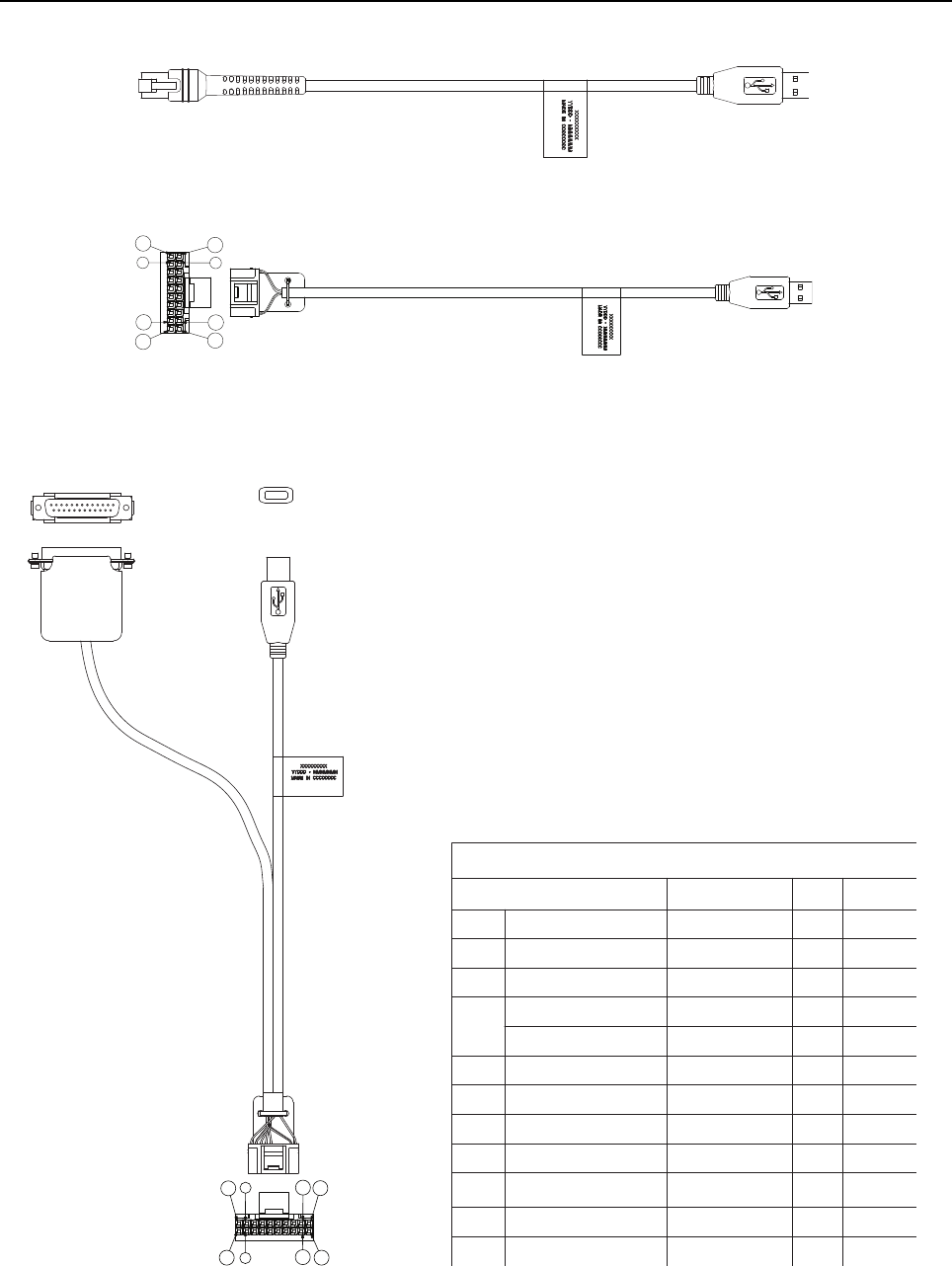
Figure 2-1 Front Telco MMP USB Programming Cable PMKN4147_ ................................................... 2-3
Figure 2-2 Back 20 Pin MAP USB Programming Cable PMKN4148_................................................... 2-3
Figure 2-3 Back 20 Pin MAP Test and USB Programming Cable PMKN4149_ .................................... 2-3
Figure 2-4 Back 20 Pin MAP Test Cable PMKN4150_ .......................................................................... 2-4
Figure 2-5 Back 16 Pin MAP Universal Cable PMKN4151_ ................................................................. 2-5
Figure 4-1 Customer Programming Software Setup from Front Connector .......................................... 4-1
Figure 4-2 Customer Programming Software Setup from Rear Accessory Connector ......................... 4-2
Figure 4-3 Customer Programming Software Setup with Test Box Connection .................................... 4-2
Figure 4-4 Radio Tuning Equipment Setup ........................................................................................... 4-3
Figure 4-5 Radio Tuning Equipment Setup (Alternative Method) .......................................................... 4-3
Figure 5-1 Typical Control Head Removal............................................................................................. 5-5
Figure 5-2 Flexible Connection Removal .............................................................................................. 5-6
Figure 5-3 Top Cover Removal (Image May Not Match Exact Product)................................................ 5-6
Figure 5-4 Option Board Removal (Image May Not Match Exact Product) ........................................... 5-7
Figure 5-5 Die Cast Main Shield Removal ............................................................................................ 5-8
Figure 5-6 PA Screw Removal............................................................................................................... 5-9
Figure 5-7 Accessory Connector Removal ............................................................................................ 5-9
Figure 5-8 DC Cable Removal ............................................................................................................ 5-10
Figure 5-9 RF Connector Nut Removal ............................................................................................... 5-10
Figure 5-10 Transceiver Board Removal............................................................................................... 5-11
Figure 5-11 Control Head Flex Removal ............................................................................................... 5-12
Figure 5-12 Speaker Tape Removal ...................................................................................................... 5-12
Figure 5-13 Keypad Assembly Removal ............................................................................................... 5-13
Figure 5-14 Speaker Removal............................................................................................................... 5-13
Figure 5-15 PCB Removal..................................................................................................................... 5-14
Figure 5-16 Indicator Barrier Removal .................................................................................................. 5-14
Figure 5-17 LCD and LCD Flex Removal .............................................................................................. 5-15
Figure 5-18 LCD Display Assembly....................................................................................................... 5-16
Figure 5-19 Indicator Barrier Assembly ................................................................................................. 5-16
Figure 5-20 Speaker Assembly ............................................................................................................. 5-17
Figure 5-21 Assembling PCB to Keypad ............................................................................................... 5-17
Figure 5-22 Speaker Connection........................................................................................................... 5-18
Figure 5-23 Assembling Keypad to Control Head Housing ................................................................... 5-18
Figure 5-24 Assembling Speaker Tape to PCB ..................................................................................... 5-19
Figure 5-25 Assembling Control Head Flex to Control Head Board ...................................................... 5-19
Figure 5-26 Thermal Pads and Shield Gasketing on Chassis and Die Cast Main Shield ..................... 5-20
Figure 5-27 Chassis with Thermal Pads................................................................................................ 5-20
Figure 5-28 Replacing Regulator Thermal Pads ................................................................................... 5-21
Figure 5-29 Replacing Audio PA Thermal Pad ...................................................................................... 5-22
Figure 5-30 Replacing Final Driver Thermal Pad .................................................................................. 5-23
Figure 5-31 Replacing PCB Thermal Pad ............................................................................................. 5-24
Figure 5-32 Applying Thermal Grease .................................................................................................. 5-25
Figure 5-33 Placing the Transceiver Board in the Chassis.................................................................... 5-25
Figure 5-34 Inserting RF Lock Washer and Nut .................................................................................... 5-26
Figure 5-35 Screw Sequence to Compress PCB .................................................................................. 5-26
Figure 5-36 Installing PA Screws........................................................................................................... 5-27
Figure 5-37 Screw Removal .................................................................................................................. 5-27
Figure 5-38 Inserting Accessory Connector .......................................................................................... 5-28

List of Figures ix
Figure 5-39 Assembling Die Cast Main Shield onto Chassis ................................................................ 5-28
Figure 5-40 Screw Sequence to Tighten Die Cast Main Shield ............................................................ 5-29
Figure 5-41 RF Connector Nut Final Torque ......................................................................................... 5-29
Figure 5-42 Installing DC Cable Assembly............................................................................................ 5-30
Figure 5-43 Inspection of Cover Assembly with Seal............................................................................ 5-31
Figure 5-44 Assembling Cover onto Chassis ........................................................................................5-31
Figure 5-45 Rear Latch in Secure Position ........................................................................................... 5-32
Figure 5-46 MAP Connector Cover Installation.....................................................................................5-32
Figure 5-47 Orientation of Option Board Flex to Option Board ............................................................. 5-33
Figure 5-48 Assemble Option Board to Radio Chassis (Image May Not Match Exact Product) ........... 5-33
Figure 5-49 Align Option Board to Mounting Holes............................................................................... 5-34
Figure 5-50 Assemble Control Head to Chassis ................................................................................... 5-35
Figure 5-51 Flex Connection Connectors.............................................................................................. 5-35
Figure 5-52 Radio Assembly Exploded View ........................................................................................ 5-36
Figure 5-53 Alphanumeric Display Control Head Exploded View ......................................................... 5-38
Figure C-1 PCB Top Side View ..............................................................................................................C-1

xList of Tables
List of Tables
Table 1-1 Radio Frequency Ranges and Power Levels....................................................................... 1-1
Table 2-1 Recommended Test Equipment ........................................................................................... 2-1
Table 2-2 Service Aids ......................................................................................................................... 2-2
Table 2-3 Wire Diagram for PMKN4150_.............................................................................................2-4
Table 2-4 Wire Diagram for PMKN4151_ ............................................................................................2-5
Table 3-1 Initial Equipment Control Settings ........................................................................................ 3-1
Table 3-2 Front Panel Access Test Mode Displays.............................................................................. 3-2
Table 3-3 Test Environments................................................................................................................ 3-5
Table 3-4 Test Channel Spacing .......................................................................................................... 3-5
Table 3-5 Test Frequencies ................................................................................................................. 3-5
Table 3-6 Transmitter Performance Checks.........................................................................................3-6
Table 3-7 Receiver Performance Checks ............................................................................................3-7
Table 4-1 Radio Software Program Kit................................................................................................. 4-1
Table 5-1 Lead Free Solder Wire Part Number List ............................................................................. 5-4
Table 5-2 Lead Free Solder Paste Part Number List ........................................................................... 5-4
Table 5-3 Radio Exploded View Parts List .........................................................................................5-37
Table 5-4 Alphanumeric Display Control Head (PMLN6441_) Exploded View Parts List .................. 5-38
Table 5-5 Torque Specifications for Nuts and Screws........................................................................ 5-39
Table 6-1 Power-Up Error Codes ......................................................................................................... 6-2
Table C-1. Component Parts List.......................................................................................................... C-1

Commercial Warranty xi
Commercial Warranty
Limited Warranty
MOTOROLA COMMUNICATION PRODUCTS
I. What This Warranty Covers And For How Long
MOTOROLA SOLUTIONS, INC. (“MOTOROLA”) warrants the MOTOROLA manufactured
Communication Products listed below (“Product”) against defects in material and workmanship
under normal use and service for a period of time from the date of purchase as scheduled below:
The mobiles additionally ship with a standard 1-year Repair Service Advantage (RSA)(for U.S.
customers) or Extended Warranty (for Canada customers) options can be selected for an additional
fee. At the time of order you must choose the warranty option.
For more RSA or Extended Warranty information, please refer to the price pages or Motorola Online
(https://businessonline.motorolasolutions.com) > Resource Center > Services > Service Product
Offerings > Repair Service Advantage or Extended Warranty.
Motorola, at its option, will at no charge either repair the Product (with new or reconditioned parts),
replace it (with a new or reconditioned Product), or refund the purchase price of the Product during
the warranty period provided it is returned in accordance with the terms of this warranty. Replaced
parts or boards are warranted for the balance of the original applicable warranty period. All replaced
parts of Product shall become the property of MOTOROLA.
This express limited warranty is extended by MOTOROLA to the original end user purchaser only
and is not assignable or transferable to any other party. This is the complete warranty for the Product
manufactured by MOTOROLA. MOTOROLA assumes no obligations or liability for additions or
modifications to this warranty unless made in writing and signed by an officer of MOTOROLA.
Unless made in a separate agreement between MOTOROLA and the original end user purchaser,
MOTOROLA does not warrant the installation, maintenance or service of the Product.
MOTOROLA cannot be responsible in any way for any ancillary equipment not furnished by
MOTOROLA which is attached to or used in connection with the Product, or for operation of the
Product with any ancillary equipment, and all such equipment is expressly excluded from this
warranty. Because each system which may use the Product is unique, MOTOROLA disclaims
liability for range, coverage, or operation of the system as a whole under this warranty.
XPR 2500 Digital Mobile Radios Two (2) Years
Product Accessories One (1) Year

xii Commercial Warranty
II. General Provisions
This warranty sets forth the full extent of MOTOROLA's responsibilities regarding the Product.
Repair, replacement or refund of the purchase price, at MOTOROLA's option, is the exclusive
remedy. THIS WARRANTY IS GIVEN IN LIEU OF ALL OTHER EXPRESS WARRANTIES. IMPLIED
WARRANTIES, INCLUDING WITHOUT LIMITATION, IMPLIED WARRANTIES OF
MERCHANTABILITY AND FITNESS FOR A PARTICULAR PURPOSE, ARE LIMITED TO THE
DURATION OF THIS LIMITED WARRANTY. IN NO EVENT SHALL MOTOROLA BE LIABLE FOR
DAMAGES IN EXCESS OF THE PURCHASE PRICE OF THE PRODUCT, FOR ANY LOSS OF
USE, LOSS OF TIME, INCONVENIENCE, COMMERCIAL LOSS, LOST PROFITS OR SAVINGS
OR OTHER INCIDENTAL, SPECIAL OR CONSEQUENTIAL DAMAGES ARISING OUT OF THE
USE OR INABILITY TO USE SUCH PRODUCT, TO THE FULL EXTENT SUCH MAY BE
DISCLAIMED BY LAW.
III. State Law Rights
SOME STATES DO NOT ALLOW THE EXCLUSION OR LIMITATION OF INCIDENTAL OR
CONSEQUENTIAL DAMAGES OR LIMITATION ON HOW LONG AN IMPLIED WARRANTY
LASTS, SO THE ABOVE LIMITATION OR EXCLUSIONS MAY NOT APPLY.
This warranty gives specific legal rights, and there may be other rights which may vary from state to
state.
IV. How To Get Warranty Service
You must provide proof of purchase (bearing the date of purchase and Product item serial number)
in order to receive warranty service and, also, deliver or send the Product item, transportation and
insurance prepaid, to an authorized warranty service location. Warranty service will be provided by
Motorola through one of its authorized warranty service locations. If you first contact the company
which sold you the Product, it can facilitate your obtaining warranty service. You can also call
Motorola at 1-888-567-7347 US/Canada.
V. What This Warranty Does Not Cover
A. Defects or damage resulting from use of the Product in other than its normal and customary
manner.
B. Defects or damage from misuse, accident, water, or neglect.
C. Defects or damage from improper testing, operation, maintenance, installation, alteration,
modification, or adjustment.
D. Breakage or damage to antennas unless caused directly by defects in material workmanship.
E. A Product subjected to unauthorized Product modifications, disassemblies or repairs
(including, without limitation, the addition to the Product of non-Motorola supplied equipment)
which adversely affect performance of the Product or interfere with Motorola's normal
warranty inspection and testing of the Product to verify any warranty claim.
F. Product which has had the serial number removed or made illegible.
G. Freight costs to the repair depot.
H. A Product which, due to illegal or unauthorized alteration of the software/firmware in the
Product, does not function in accordance with MOTOROLA’s published specifications or the
FCC type acceptance labeling in effect for the Product at the time the Product was initially
distributed from MOTOROLA.
I. Scratches or other cosmetic damage to Product surfaces that does not affect the operation of
the Product.
J. Normal and customary wear and tear.

Commercial Warranty xiii
VI. Patent And Software Provisions
MOTOROLA will defend, at its own expense, any suit brought against the end user purchaser to the
extent that it is based on a claim that the Product or parts infringe a United States patent, and
MOTOROLA will pay those costs and damages finally awarded against the end user purchaser in
any such suit which are attributable to any such claim, but such defense and payments are
conditioned on the following:
A. that MOTOROLA will be notified promptly in writing by such purchaser of any notice of such
claim;
B. that MOTOROLA will have sole control of the defense of such suit and all negotiations for its
settlement or compromise; and
C. should the Product or parts become, or in MOTOROLA's opinion be likely to become, the
subject of a claim of infringement of a United States patent, that such purchaser will permit
MOTOROLA, at its option and expense, either to procure for such purchaser the right to
continue using the Product or parts or to replace or modify the same so that it becomes
noninfringing or to grant such purchaser a credit for the Product or parts as depreciated and
accept its return. The depreciation will be an equal amount per year over the lifetime of the
Product or parts as established by MOTOROLA.
MOTOROLA will have no liability with respect to any claim of patent infringement which is based
upon the combination of the Product or parts furnished hereunder with software, apparatus or
devices not furnished by MOTOROLA, nor will MOTOROLA have any liability for the use of ancillary
equipment or software not furnished by MOTOROLA which is attached to or used in connection with
the Product. The foregoing states the entire liability of MOTOROLA with respect to infringement of
patents by the Product or any parts thereof.
Laws in the United States and other countries preserve for MOTOROLA certain exclusive rights for
copyrighted MOTOROLA software such as the exclusive rights to reproduce in copies and distribute
copies of such Motorola software. MOTOROLA software may be used in only the Product in which
the software was originally embodied and such software in such Product may not be replaced,
copied, distributed, modified in any way, or used to produce any derivative thereof. No other use
including, without limitation, alteration, modification, reproduction, distribution, or reverse
engineering of such MOTOROLA software or exercise of rights in such MOTOROLA software is
permitted. No license is granted by implication, estoppel or otherwise under MOTOROLA patent
rights or copyrights.
VII. Governing Law
This Warranty is governed by the laws of the State of Illinois, USA.

xiv Commercial Warranty
Notes
Chapter 1 Introduction
1.1 Notations Used in This Manual
Throughout the text in this publication, you will notice the use of note and caution notations. These
notations are used to emphasize that safety hazards exist, and due care must be taken and
observed.
NOTE: An operational procedure, practice, or condition that is essential to emphasize.
1.2 Radio Description
The XPR 2500 mobile radios are available in the following frequency ranges and power levels.
These radios are among the most sophisticated two-way radios available. They have a
robust design for radio users who need high performance, quality, and reliability in their daily
communications. This architecture provides the capability of supporting a multitude of legacy and
advanced features resulting in a more cost-effective two-way radio communications solution.
CAUTION indicates a potentially hazardous situation which, if
not avoided, might result in equipment damage.
Table 1-1 Radio Frequency Ranges and Power Levels
Freq. Band Bandwidth Power Level
VHF 136–174 MHz 1–25 Watts
25–45 Watts
UHF B1 403–470 MHz 1–25 Watts
25–40 Watts
!
C a u t i o n
1-2 Introduction: Control Head Description
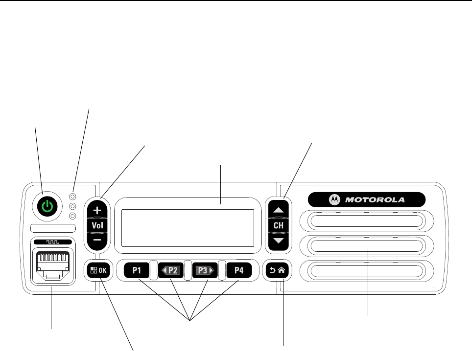
1.3 Control Head Description
The control head used with the radio has logic circuitry that operates the standard and optional
features built into the system.
The following illustration shows the typical radio control head.
Figure 1-1 Radio Control Head
1.3.1 Control Head Controls
• POWER BUTTON – Turns the radio on and off.
• VOLUME CHANGING ROCKER – Press top side to increment or bottom side to decrement the
volume.
• CHANNEL CHANGING ROCKER – Press top side to increment or bottom side to decrement
the channel.
• LED INDICATORS – Red, yellow and green light-emitting diodes indicate operating status.
• LCD (Liquid Crystal Display) – 132x36 display provides visual information about many radio
features.
• OK/MENU BUTTON – One button to provide menu navigation and selection interface.
• PROGRAMMABLE BUTTONS – Four buttons are field programmable using the CPS.
• RETURN/HOME BUTTON – One button which quickly brings you to the home page.
LCD Screen
Volume Changing
Power Button
Speaker
Return/Home Button
Programmable Buttons
Accessory Connector
LED
Indicators
OK/Menu Button
Rocker
Channel Changing
Rocker

Introduction: MOTOTRBO Mobile Radio Model Numbering Scheme 1-3
1.4 MOTOTRBO Mobile Radio Model Numbering Scheme
Figure 1-2 Mobile Radio Model Numbering Scheme
Model No.Example : AA M 0 2 Q P H 9 J A 1 A N
Position : 1 2 3 4 5 6 7 8 9 10 11 12
Unique Variations
N: Standard Package
Version Letter
Feature Level
1: Mini-U (Mobile)
2: BNC (Mobile)
Primary System Type
A: Conventional
B: Trunking
C: Analog Only
Primary Operation
J: Basic (No GPS, No Bluetooth)
K: GPS and Bluetooth
L: GPS Only
M: Bluetooth Only
Channel Information
9: Variable/Programmable
Channel Spacing
Power Level
N: 1–25W
P: 25–40W
Q: 25–45W
R: 1–40W
M: 10–35W
MOTOTRBO Mobile
XPR 2500 : 02
Band
J
M
P
Q
T
X
U
VPhysical Packages
H: Mid Tier (Alphanumeric Display)
Mobile
AZ: Asia
LA: Latin America
AA: North America (except Mexico)
MD: Europe/Middle East/
Africa/Australia
: 136–174 MHz
: 217–222 MHz
: 300–400 MHz
: 403–470 MHz
: 450–512 MHz
: 450–520 MHz
: 806–941 MHz
: 806–870 MHz
1-4 Introduction: VHF High Power (136–174 MHz) Model Chart
1.5 VHF High Power (136–174 MHz) Model Chart
1.6 VHF Low Power (136–174 MHz) Model Chart
VHF 136–174 MHz 25–45W, Mini-U
Model Description
AAM02JQH9JA1_N 136–174 MHz, 25–45W, MOTOTRBO XPR 2500 Alphanumeric
Display Mobile
Item Description
X PMUD3240_S *Service Kit, VHF, 25–45W
XPMLN6441_ Alphanumeric Display Model Control Head
X 68009614001 Mobile Quick Reference Guide and Safety Booklet
X = Item Included
* = Service Kit is the main board only
_ = the latest version kit. When ordering a kit, refer to your specific kit for the suffix number.
VHF 136–174 MHz 1–25W, Mini-U
Model Description
AAM02JNH9JA1_N 136–174 MHz, 1–25W, MOTOTRBO XPR 2500 Alphanumeric
Display Mobile
Item Description
X PMUD3241_S *Service Kit , VHF, 1–25W
XPMLN6441_ Alphanumeric Display Model Control Head
X 68009614001 Mobile Quick Reference Guide and Safety Booklet
X = Item Included
* = Service Kit is the main board only
_ = the latest version kit. When ordering a kit, refer to your specific kit for the suffix number.
Introduction: UHF1 High Power (403–470 MHz) Model Chart 1-5
1.7 UHF1 High Power (403–470 MHz) Model Chart
1.8 UHF1 Low Power (403–470 MHz) Model Chart
UHF1 403–470 MHz 25–40W, Mini-U
Model Description
AAM02QPH9JA1_N 403–470 MHz, 25–40W, MOTOTRBO XPR 2500 Alphanumeric
Display Mobile
Item Description
X PMUE4164_S *Service Kit, UHF1, 25–40W
XPMLN6441_ Alphanumeric Display Model Control Head
X 68009614001 Mobile Quick Reference Guide and Safety Booklet
X = Item Included
* = Service Kit is the main board only
_ = the latest version kit. When ordering a kit, refer to your specific kit for the suffix number.
UHF1 403–470 MHz 1–25W, Mini-U
Model Description
AAM02QNH9JA1_N 403–470 MHz, 1–25W, MOTOTRBO XPR 2500 Alphanumeric
Display Mobile
Item Description
X PMUE4168_S *Service Kit, UHF1, 1–25W
XPMLN6441_ Alphanumeric Display Model Control Head
X 68009614001 Mobile Quick Reference Guide and Safety Booklet
X = Item Included
* = Service Kit is the main board only
_ = the latest version kit. When ordering a kit, refer to your specific kit for the suffix number.
1-6 Introduction: Specifications
1.9 Specifications
General
Specification VHF UHF1
Model: Alphanumeric Display
Channel Capacity: 128
Typical RF Output:
Low Power
High Power
1–25 W
25–45 W
1–25 W
25–40 W
Frequency Range: 136–174 MHz 403–470 MHz
Dimensions: (HxWxL) 1.7 x 6.7 x 5.3 in
(44 x 169 x 134 mm)
Weight: 2.9 lbs. (1.3 kg)
Current Drain:
Standby
Rx @ rated audio
Transmit
0.81 A max
2 A max
1–25 W: 11.0 A max
25–40 W: 14.5 A max
25–45 W: 14.5 A max
FCC Description: 1–25 W:
ABZ99FT3090
25–45 W:
ABZ99FT3091
1–25 W:
ABZ99FT4092
25–40 W:
ABZ99FT4093
IC Description: 1–25 W:
109AB-99FT3090
25–45 W:
109AB-99FT3091
1–25 W:
109AB-99FT4092
25–40 W:
109AB-99FT4093
Introduction: Specifications 1-7
*25 kHz may not be available in the U.S. for Part 90 operation due to the FCC’s Narrowbanding
requirements.
Receiver
Specification VHF UHF1
Model: Alphanumeric Display
Frequency: 136–174 MHz 403–470 MHz
Channel Spacing: 12.5 kHz/25 kHz*
Frequency
Stability:
(-30°C to +60°C, +25°C
Ref)
±0.5 ppm
Analog Sensitivity
(12 dB SINAD):
0.3 µV
0.22 µV (typical)
Digital Sensitivity:
(5% BER)
0.25 µV
0.19 µV (typical)
Intermodulation
TIA603D: 75 dB 70 dB
Adjacent Channel
Selectivity
TIA603D: 50 dB @ 12.5 kHz,
75 dB @ 25 kHz
50 dB @ 12.5 kHz,
70 dB @ 25 kHz
Spurious
Rejection
TIA603D: 75 dB 70 dB
Rated Audio: 4 W (Internal)
7.5 W (External – 8 ohms)
13 W (External – 4 ohms)
Audio Distortion @
Rated Audio:
3% (Typical)
Hum and Noise: -40 dB @ 12.5 kHz
-45 dB @ 25 kHz
Audio Response: TIA603D
Conducted
Spurious Emission
(TIA603D):
-57 dBm
1-8 Introduction: Specifications
*25 kHz may not be available in the U.S. for Part 90 operation due to the FCC’s Narrowbanding
requirements.
Transmitter
Specification VHF UHF1
Model: Alphanumeric Display
Frequency: 136–174 MHz 403–470 MHz
Channel Spacing: 12.5 kHz/25 kHz*
Frequency
Stability:
(-30°C to +60°C, +25°C
Ref)
±0.5 ppm
Power Output:
Low Power
High Power
1–25 W
25–45 W
1–25 W
25–40 W
Modulation
Limiting:
±2.5 kHz @ 12.5 kHz
±5.0 kHz @ 25 kHz
FM Hum and Noise: -40 dB @ 12.5 kHz
-45 dB @ 25 kHz
Conducted/
Radiated
Emission:
-36 dBm <1 GHz
-30 dBm >1 GHz
Adjacent
Channel Power
(TIA603D):
60 dB @ 12.5 kHz
70 dB @ 25 kHz
Audio Response: TIA603D
Audio Distortion: 3%
FM Modulation:12.5 kHz: 11K0F3E
25 kHz: 16K0F3E
4FSK Digital
Modulation:
12.5 kHz Data: 7K60F1D & 7K60FXD
12.5 kHz Voice: 7K60F1E & 7K60FXE
Combination of 12.5 kHz Voice & Data: 7K60F1W
Digital Vocoder Type: AMBE+2™
Digital Protocol: ETSI TS 102 361-1
ETSI TS 102 361-2
ETSI TS 102 361-3

Introduction: Specifications 1-9
Self-Quieter
VHF UHF1
153.6 MHz +/- 10 kHz 422.4 MHz
172.8 MHz +/- 10 kHz –
Military Standards 810C, D, E, F & G
MIL-STD 810C MIL-STD 810D MIL-STD 810E MIL-STD 810F MIL-STD 810G
Method Proc./Cat Method Proc./Cat Method Proc./Cat Method Proc./Cat Method Proc./Cat
Low
Pressure
500.1 I500.2 II 500.3 II 500.4 II 500.5 II
High
Temperature
501.1 I, II 501.2 I/A1,
II/A1
501.3 I/A,
II/AI
501.4 I/HOT,
II/HOT
501.5 I/AI, II
Low
Temperature
502.1 I502.2 I/C3,
II/C1
502.3 I/C3,
II/C1
502.4 I/C3,
II/C1
502.5 I/C3, II
Temperature
Shock
503.1 – 503.2 I/A1/C3 503.3 I/AI/C3 503.4 I 503.5 I/C
Solar
Radiation
505.1 II 505.2 I505.3 I505.4 I505.5 I/A1
Rain 506.1 I, II 506.2 I, II 506.3 I, II 506.4 I, III 506.5 I, III
Humidity 507.1 II 507.2 II 507.3 II 507.4 –507.5 II - Aggra-
vated
Salt Fog 509.1 – 509.2 – 509.3 – 509.4 – 509.5 –
Dust 510.1 I510.2 I510.3 I510.4 I510.5 I
Vibration 514.2 VIII/F,
Curve-W
514.3 I/10,
II/3
514.4 I/10,
II/3
514.5 I/24 514.6 I/24
Shock 516.2 I, II 516.3 I, IV 516.4 I, IV 516.5 I, IV 516.6 I, IV,
V, VI

1-10 Introduction: Specifications
**Radio meets IP54 and MIL-STD rating with microphone sealing boot and rear accessory connector cover
properly installed.
Specifications subject to change without notice. All specifications shown are typical.
Radio meets applicable regulatory requirements. Version 1 05/13
Environmental Specifications
Operating Temperature -30°C / +60°C
Storage Temperature -40°C / +85°C
Thermal Shock Per MIL-STD
Humidity Per MIL-STD
ESD IEC 61000-4-2 Level 3
Dust and Water Intrusion IP54, MIL-STD**
Packaging Test Per MIL-STD

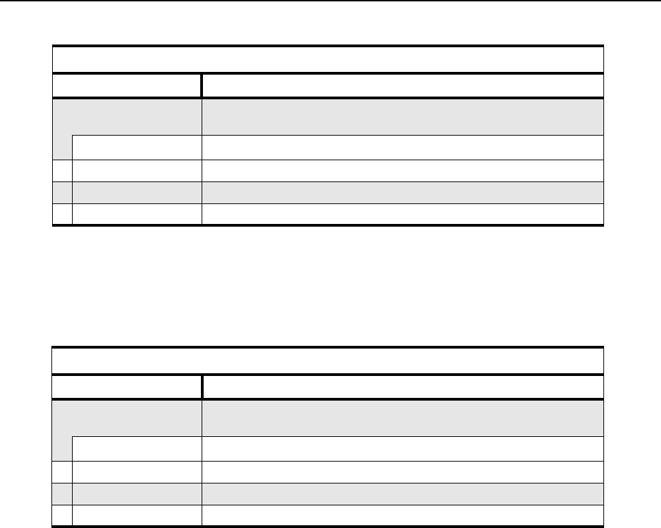
Chapter 2 Test Equipment and Service Aids
2.1 Recommended Test Equipment
The list of equipment contained in Table 2-1 includes most of the standard test equipment required
for servicing Motorola mobile radios.
Table 2-1 Recommended Test Equipment
Equipment Characteristic Example Application
Service Monitor Can be used as a
substitute for items
marked with an asterisk
(*)
Aeroflex 3920 or equivalent Frequency/deviation meter and
signal generator for wide-range
troubleshooting and alignment
Digital RMS
Multimeter*
100 µV to 300 V
5 Hz to 1 MHz
10 Mega Ohm Impedance
Fluke 179 or equivalent
(www.fluke.com)
AC/DC voltage and current
measurements. Audio voltage
measurements.
RF Signal
Generator*
100 MHz to 1 GHz
-130 dBM to +10 dBM
FM Modulation 0 kHz to
10 kHz
Agilent N5181
(www.agilent.com) or equivalent
Receiver measurements
Oscilloscope* 2 Channels
50 MHz Bandwidth
5 mV/div to 20 V/div
Tektronix TDS1001b
(www.tektronix.com) or
equivalent
Waveform measurements
Power Meter and
Sensor*
5% Accuracy
100 MHz to 500 MHz
50 Watts
Bird 43 Thruline Watt Meter
(www.bird-electronic.com) or
equivalent
Transmitter power output
measurements
RF Millivolt Meter 100 mV to 3 V RF
10 kHz to 1 GHz
Boonton 92EA
(www.boonton.com) or
equivalent
RF level measurements
Power Supply 0 V to 32 V
0 A to 20 A
B&K Precision 1790
(www.bkprecision.com) or
equivalent
Voltage supply

2-2 Test Equipment and Service Aids: Service Aids
2.2 Service Aids
Table 2-2 lists the service aids recommended for working on the radio. While all of these items are
available from Motorola, most are standard workshop equipment items, and any equivalent item
capable of the same performance may be substituted for the item listed.
Table 2-2 Service Aids
Motorola
Part Number Description Application
RLN4460_ Test Box Enables connection to audio/accessory jack. Allows
switching for radio testing.
RVN5115_ Customer Programming
Software on CD-ROM
Allows servicer to program radio parameters, tune and
troubleshoot radios.
PMKN4147_ Front Telco MMP USB
Programming Cable
Connects the radio’s front connector to a USB port for
radio programming and data applications.
PMKN4148_ Back 20 Pin MAP USB
Programming Cable
Connects the radio’s rear connector to a USB port for
radio programming and data applications.
PMKN4149_ Back 20 Pin MAP Test and USB
Programming Cable
Connects the radio’s rear connector to a USB port for
radio programming, data applications, testing and
alignment.
PMKN4150_ Back 20 Pin MAP Test Cable Connects the radio’s rear connector for testing. Must
use in conjunction with PMKN4147_ (Front Telco MMP
USB Programming Cable) for radio programming and
alignment.
PMKN4151_ Back 16 Pin MAP Universal
Cable
Connects the radio’s rear connector to the center 16
pins with unterminted connectors at the user end.
HPN4007_ Power Supply Provides the radio with power when bench testing.
PMEN4041_ Chassis Eliminator Kit Test Fixture used to bench test the radio PCB.
6686119B01 Control Head Dismantling Tool Assists in the removal of radio control head.
Test Equipment and Service Aids: Programming Cables 2-3
2.3 Programming Cables
Figure 2-1 Front Telco MMP USB Programming Cable PMKN4147_
Figure 2-2 Back 20 Pin MAP USB Programming Cable PMKN4148_
2.4 Programming and Test Cable
Figure 2-3 Back 20 Pin MAP Test and USB Programming Cable PMKN4149_
20
2
19
1
15
17
16
18
14
915±15
CABLE
1455±24
CABLE
TO MOBILE RADIO
ACCESSORY
CONNECTOR
VIEWED FROM
FRONT (PIN END)
OF CONNECTOR
USB CONNECTORDB 25 CONNECTOR
20 2
19 115
17
16 18
1
14 25
13
1
14 25
13
WIRE DIAGRAM
20 PIN
ACCESSORY PORT CONNECTOR
USB DB25P
PIN 19 VCC (5v) (USB VBUS) PIN 1
PIN 18 DATA - PIN 2
PIN 17 DATA + PIN 3
PIN 20
GROUND (USB) PIN 4
DRAIN WIRE AND BRAID SHELL
PIN 1 SPEAKER - PIN 2 & 7
PIN 2 EXT MIC AUDIO PIN 10 & 15
PIN 3 PROGM INPUT (EXT. PTT) PIN 20
PIN 7 GROUND (DB25) PIN 16
WIRE COLOR
RED
WHITE
GREEN
BLACK
DRAIN WIRE/BRAID
ORANGE
GREY
PINK
PIN 5 FLAT TX AUDIO YELLOW PIN 18
BLACK
PIN 15 RSSI BROWN PIN 19
PIN 16 SPEAKER + PURPLE PIN 1 & 5
2-4 Test Equipment and Service Aids: Test Cable
2.5 Test Cable
Figure 2-4 Back 20 Pin MAP Test Cable PMKN4150_
Table 2-3 Wire Diagram for PMKN4150_
20
2
19
1
15
17
16
18
1
14 25
13
1
14 25
13
WIRE DIAGRAM
20 PIN
ACCESSORY PORT CONNECTOR WIRE COLOR DB25P
PIN
No. DESCRIPTION
1 SPEAKER - 2 & 7
2 EXT MIC 10 & 15
3GPI_1
(EXT PTT) 20
5 FLAT TX 18
16 SPEAKER + 1 & 5
-- --
ORANGE
GREY
PINK
YELLOW
7 GROUND BLACK 16
15 RSSI BROWN 19
PURPLE
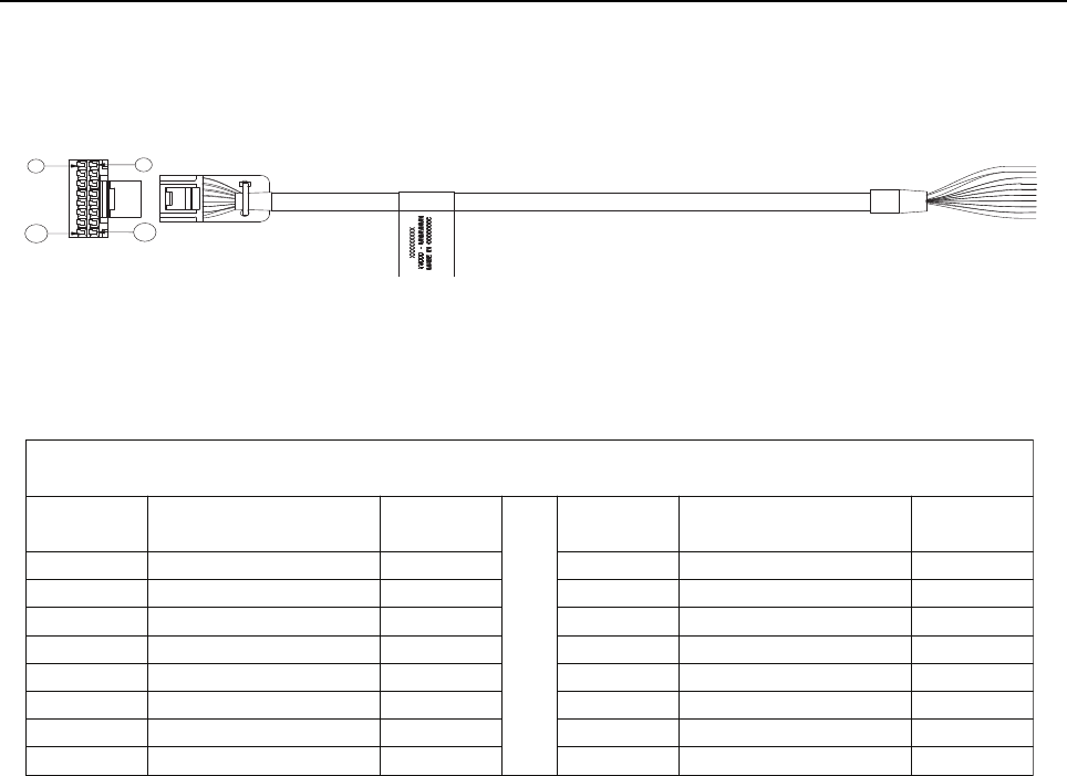
Test Equipment and Service Aids: Accessory Cable 2-5
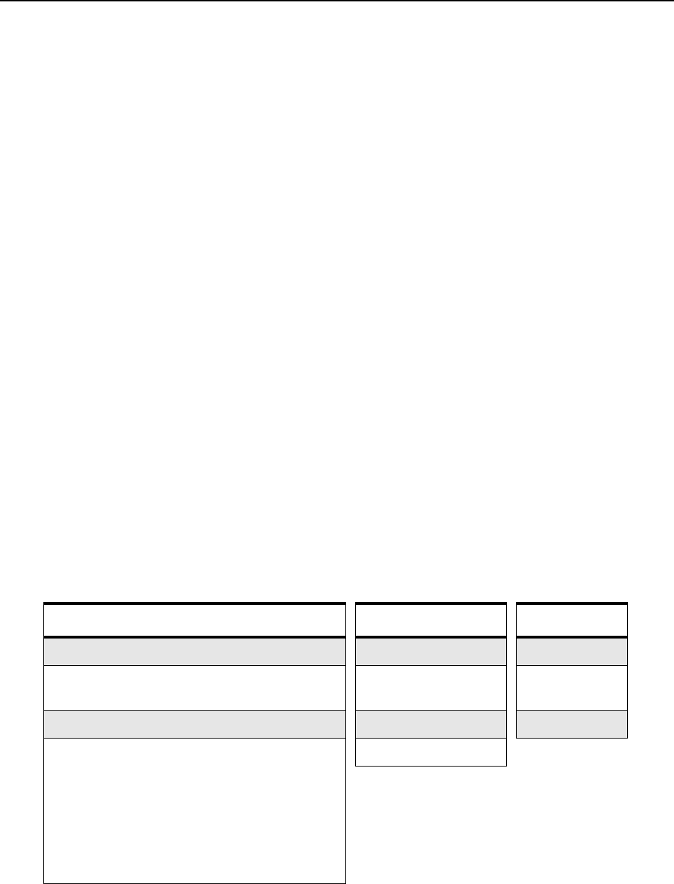
2.6 Accessory Cable
Figure 2-5 Back 16 Pin MAP Universal Cable PMKN4151_
Table 2-4 Wire Diagram for PMKN4151_
(*) NOTE: CRIMP YELLOW WIRE AND DRAIN WIRE TO TERMINAL ON 26 PIN CONNECTOR.
TIN YELLOW WIRE AND DRAIN WIRE TOGETHER ON WIRE LEAD SIDE
PIN POSITION
1
15
16
2
WIRE DIAGRAM
16 PIN
CONNECTOR WIRE COLOR WIRE LEAD
SIDE
16 PIN
CONNECTOR WIRE COLOR WIRE LEAD
SIDE
1 BLACK NC 9 PURPLE NC
2 WHITE NC 10 GREY NC
3 GREEN NC 11 PINK NC
4 * YELLOW / DRAIN WIRE NC * 12 WHT / BLK NC
5 ORANGE NC 13 WHT / BRN NC
6 BLUE NC 14 WHT / RED NC
7 BROWN NC 15 WHT / ORG NC
8 RED NC 16 WHT / GRN NC

2-6 Test Equipment and Service Aids: Accessory Cable
Notes
Chapter 3 Transceiver Performance Testing
3.1 General
These radios meet published specifications through their manufacturing process by utilizing
high-accuracy laboratory-quality test equipment. The recommended field service equipment
approaches the accuracy of the manufacturing equipment with few exceptions. This accuracy must
be maintained in compliance with the manufacturer’s recommended calibration schedule.
3.2 Setup
Supply voltage is provided using a 13.8 VDC power supply. (Note: applying 13.8 VDC at the DC
power cable will ensure a minimum of 13.2 VDC at the DC connector of the radio). The equipment
required for alignment procedures is shown in the Radio Tuning Equipment Setup Diagram,
Figure 4-4.
Initial equipment control settings should be as indicated in Table 3-1. The remaining tables in this
chapter contain the following related technical data:
Table Number Title
3-2 Front Panel Access Test Mode Displays
3-3 Test E nvi ronm ents
3-4 Test Channel Spacing
3-5 Test Frequencies
3-6 Transmitter Performance Checks
3-7 Receiver Performance Checks
Table 3-1 Initial Equipment Control Settings
Service Monitor Power Supply Test Set
Monitor Mode: Power Monitor Voltage: 13.8 VDC Speaker set: A
RF Attenuation: -70 DC On/Standby:
Standby
Speaker/load:
Speaker
AM, CW, FM: FM Volt Range: 20 V PTT: OFF
Oscilloscope Source: Mod
Oscilloscope Horizontal: 10 mSec/Div
Oscilloscope Vertical: 2.5 kHz/Div
Oscilloscope Trigger: Auto
Monitor Image: Hi
Monitor Bandwidth: Narrow
Monitor Squelch: middle setting
Monitor Vol: 1/4 setting
Current: 20 A
3-2 Transceiver Performance Testing: Alphanumeric Display Model Test Mode
3.3 Alphanumeric Display Model Test Mode
3.3.1 Entering Display Radio Test Mode
1. Turn the radio on.
2. Within ten seconds after self test is complete, press button P2, five times in succession.
3. The radio beeps and will show a series of displays that will give information regarding various
version numbers and subscriber specific information. The displays are described in
Table 3-2.
NOTE: The radio stops at each display for 2 seconds before moving to the next information display.
If the information cannot fit into 1 line, the radio display scrolls automatically character by
character after 1 second to view the whole information. If the Top Navigation Button () is
pressed before the last information display, the radio shall suspend the information display
until the user presses Bottom Navigation Button ( ) to resume the information display. The
radio beeps for each button press. After the last display, RF Test Mode will be displayed.
3.3.2 RF Test Mode
When the radio is operating in its normal environment, the radio's microcontroller controls the RF
channel selection, transmitter key-up, and receiver muting, according to the customer codeplug
configuration. However, when the unit is on the bench for testing, alignment, or repair, it must be
removed from its normal environment via a special routine, called TEST MODE or air test.
In RF Test Mode, the display upon the first line is “RF Test”, together with the power level icon at the
right end of the first line. The display upon the second line is the test environment, the channel
number and channel spacing (“CSQ CHXX SP25”). The default test environment is CSQ.
1. Each short press of button P2 changes the test environment
(CSQ->TPL->DIG->USQ->CSQ). The radio beeps once when radio toggles to CSQ, beeps
twice for TPL, beeps three times for DIG and beeps four times for USQ.
NOTE: DIG is digital mode and other test environments are analog mode as described in
Table 3-3.
2. Each short press of button P1 toggles the channel spacing between 20 kHz, 25 kHz and
12.5 kHz. The radio beeps once when radio toggles to 20 kHz, beeps twice for 25 kHz and
beeps three times for 12.5 kHz.
Table 3-2 Front Panel Access Test Mode Displays
Name of Display Description Appears
Service Mode The literal string indicates the radio has entered test mode. Always
Host Version The version of host firmware. Always
DSP Version The version of DSP firmware. Always
Model Number The radio’s model number as programmed in the codeplug. Always
MSN The radio’s serial number as programmed in the codeplug. Always
FLASHCODE The FLASH codes as programmed in the codeplug. Always
RF Band The radio’s band. Always

Transceiver Performance Testing: Alphanumeric Display Model Test Mode 3-3
3. Pressing of the Channel Changing Rocker changes the test channel from 1 to 14. Press the
top side to increase or bottom side to decrease the channel number. The radio beeps in each
position. The channel test frequencies are described in Table 3-5.
3.3.3 Alphanumeric Display Test Mode
1. Press and hold button P1 in RF Test Mode. The radio beeps once and momentarily displays
‘Display Test Mode’.
2. Upon entering Display Test Mode, the radio displays a horizontal line on row 8 (center row).
3. With each button press, the radio fills up the screen with 2 horizontal lines from the center row
(1 line each above and below the center row) until the top and bottom of the screen (row 7–0
and 9–16) is completely filled.
4. When the screen is filled up with the horizontal lines, any button press clears the screen and
displays vertical lines at column 0, 6, 12, 18, 24, 30, 36, 42, 48, 54, 60. Any button press fills
the screen with vertical lines, (1 line to the right of all existing lines) until the display is filled.
3.3.4 LED Test Mode
1. Press and hold button P1 after Display Test Mode. The radio beeps once and displays
“LED Test Mode”.
2. Upon any button press, the radio lights on the red LED and displays “Red LED On”.
3. Consequently, upon any button press, the red LED is turned off and the radio lights on the
green LED and displays “Green LED On”.
4. Consequently, upon any button press, the green LED is turned off and the radio shall light on
the yellow LED and displays “Yellow LED On”.
3.3.5 Backlight Test Mode
1. Press and hold button P1 after LED Test Mode. The radio beeps once and displays
“Backlight Test Mode”.
2. The radio lights on both LCD and keypad backlight together.
3.3.6 Speaker Tone Test Mode
1. Press and hold button P1 after Backlight Test Mode. The radio beeps once and displays
“Speaker Tone Test Mode”.
2. The radio generates a 1 kHz tone with the internal speaker.
3.3.7 Earpiece Tone Test Mode
1. Press and hold button P1 after Speaker Tone Test Mode. The radio beeps once and displays
“Earpiece Tone Test Mode”.
2. The radio generates a 1 kHz tone with the earpiece.
3.3.8 Audio Loopback Test Mode
1. Press and hold button P1 after Earpiece Tone Test Mode. The radio beeps once and
displays “Audio Loopback Test Mode”.
2. The radio shall route any audio on the mic to the internal speaker.

3-4 Transceiver Performance Testing: Alphanumeric Display Model Test Mode
3.3.9 Audio Loopback Earpiece Test Mode
1. Press and hold button P1 after Audio Loopback Test Mode. The radio beeps once and
displays “Audio Loopback Earpiece Test”.
2. The radio shall route any audio on the mic to the accessory earpiece.
3.3.10 Button Test Mode
1. Press and hold button P1 after Audio Loopback Earpiece Test Mode. The radio beeps once
and displays “Button Test”.
2. The radio also displays the Button Command Opcode (BCO) and state (BCO/state) on the
screen upon any button state changes.
3. The radio must be powered off to end Test Mode.
Transceiver Performance Testing: Alphanumeric Display Model Test Mode 3-5
Table 3-5 Test Frequencies
Table 3-3 Test Environments
No. of
Beeps Description Function
1Carrier Squelch
(CSQ)
RX: unsquelch if carrier detected
TX: mic audio
2 Tone Private-Line
(TPL)
RX: unsquelch if carrier and tone (192.8 Hz) detected
TX: mic audio + tone (192.8 Hz)
3Digital
(DIG)
RX: unsquelch if carrier and digital code detected
TX: mic audio
4 Unsquelch
(USQ)
RX: constant unsquelch
TX: mic audio
Table 3-4 Test Channel Spacing
Number of Beeps Channel Spacing
120 kHz
2 25 kHz
312.5 kHz
Test Mode Test Channel
Low Power
Test Channel
High Power
VHF
(MHz)
UHF1
(MHz)
TX 1 8 136.075 403.000
RX 1 8 136.075 403.000
TX 2 9 142.575 414.150
RX 2 9 142.575 414.150
TX 310 146.575 425.350
RX 3 10 146.575 425.350
TX 411 155.575 436.500
RX 4 11 155.575 436.500
TX 512 161.575 447.675
RX 5 12 161.575 447.675
TX 613 167.575 458.850
RX 6 13 167.575 458.850
TX 714 174.975 470.000
RX 7 14 174.975 470.000

3-6 Transceiver Performance Testing: Alphanumeric Display Model Test Mode
Table 3-6 Transmitter Performance Checks
Test Name Communications
Analyzer Radio Test Set Comment
Reference
Frequency
(see Note
below
Table 3-6)
Mode: PWR MON
4th channel test frequency*
Monitor: Frequency error
Input at RF In/Out
TEST MODE,
Test Channel 4,
carrier squelch
PTT to
continuously
transmit (during
the performance
check)
Frequency error:
±90 Hz (VHF)
±150 Hz (UHF)
Power RF As above TEST MODE
Test Channel 4,
carrier squelch
TEST MODE
Test Channel 11,
carrier squelch
As above Low Power Set:
1.0–1.3 W: (VHF 1–25 W,
UHF1 1–25 W)
25–29 W: (VHF 25–45 W,
UHF1 25–40 W)
High Power Set:
25–29 W: (VHF 1–25 W,
UHF1 1–25 W)
40–47 W: (UHF1 25–40 W)
45–53 W: (VHF 25–45 W)
Voice
Modulation
Mode: PWR MON
4th channel test frequency*
atten to -70, input to RF In/
Out
Monitor: DVM, AC Volts
Set 1 kHz Mod Out level for
800mVrms at test set,
800mVrms at AC/DC test
set jack
TEST MODE
Test Channel 4,
carrier squelch
As above, meter
selector to mic
Deviation:
2.5 kHz Max.
(12.5 kHz Ch. Sp.)
4 kHz Max.
(20 kHz Ch. Sp.)
5 kHz Max.
(25 kHz Ch. Sp.)
Voice
Modulation
(internal)
Mode: PWR MON
4th channel test frequency*
atten to -70, input to RF In/
Out
TEST MODE,
Test Channel 4
carrier squelch
output at
antenna
Remove
modulation input
Deviation:
2.5 kHz Max.
(12.5 kHz Ch. Sp.)
4 kHz Max.
(20 kHz Ch. Sp.)
5 kHz Max.
(25 kHz Ch. Sp.)
TPL
Modulation
As above
4th channel test frequency*
BW to narrow
TEST MODE,
Test Channel 4
TPL
As above Deviation:
0.25–0.5 kHz
(12.5 kHz Ch. Sp.)
0.4–0.8 kHz
(20 kHz Ch. Sp.)
0.5–1.0 kHz
(25 kHz Ch. Sp.)

Transceiver Performance Testing: Alphanumeric Display Model Test Mode 3-7
* See Table 3-5
NOTE: It is recommended that the reference oscillator be recalibrated after two years to maintain
optimized Dual Capacity Direct Mode performance.
*See Table 3-5
FSK Error DMR mode. FSK error TEST MODE,
Digital mode,
transmit with
O.153 test
pattern
Key up radio
with O.153 test
pattern
modulation
using Tuner
Not Exceed 5%
Magnitude
Error
DMR mode. Magnitude error As above As above Not Exceed 1%
Symbol
Deviation
DMR mode. Symbol
deviation
As above As above Symbol Deviation should
be within 648 +/-10% and
1944 +/-10%
Transmitter
BER
DMR mode As above As above Transmitter BER should be
0%
Table 3-7 Receiver Performance Checks
Test Name Communications
Analyzer Radio Test Set Comment
Rated Audio Mode: GEN
Output level: 1.0 mV RF
4th channel test frequency*
Mod: 1 kHz tone at
3 kHz deviation
Monitor: DVM: AC Volts
TEST MODE
Test Channel 4,
25 kHz channel
spacing,
carrier squelch
PTT to OFF
(center), meter
selector to
Audio PA
Set volume control to
7.5 Vrms
Distortion As above, except to
distortion
As above As above Distortion <5.0%
Sensitivity
(SINAD)
As above, except SINAD,
lower the RF level for 12 dB
SINAD.
As above PTT to OFF
(center)
RF input to be <0.3 µV
Noise Squelch
Threshold
(only radios
with
conventional
system need
to be tested)
RF level set to 1 mV RF As above PTT to OFF
(center), meter
selection to
Audio PA, spkr/
load to speaker
Set volume control to
7.5 Vrms
As above, except change
frequency to a conventional
system. Raise RF level from
zero until radio unsquelches.
out of TEST
MODE; select a
conventional
system
As above Unsquelch to occur at
<0.25 µV.
Preferred SINAD =
9–10 dB
Receiver BER IFR DMR mode. Signal
generator with O.153 test
pattern
Test mode,
Digital mode,
receive O.153
test pattern
Read BER using
Tuner. Adjust
RF level to get
5% BER
RF level to be
<0.3 µV for 5% BER
Table 3-6 Transmitter Performance Checks (Continued)
Test Name Communications
Analyzer Radio Test Set Comment

3-8 Transceiver Performance Testing: Alphanumeric Display Model Test Mode
Notes
Chapter 4 Radio Programming and Tuning
4.1 Introduction
This chapter provides an overview of the MOTOTRBO Customer Programming Software (CPS), as
well as the Tuner and AirTracer applications, which are all designed for use on a Windows 8/7/Vista/
XP operating system. These programs are available in one kit as listed in Table 4-1. An Installation
Guide is also included with the kit.
NOTE: Refer to the appropriate program on-line help files for the programming procedures.
Table 4-1 Radio Software Program Kit
4.2 Customer Programming Software Setup
The Customer Programming Software setups, shown in Figure 4-1 and Figure 4-2, are used to
program the radio.
NOTE: Refer to the appropriate program on-line help files for the programming procedures.
CAUTION: Computer USB ports can be sensitive to Electronic Discharge.
Do not touch exposed contacts on cable when connected to a computer.
Description Kit Number
MOTOTRBO CPS, Tuner and AirTracer Applications CD RVN5115_
Figure 4-1 Customer Programming Software Setup from Front Connector
Power
Supply
13.8VDC
Front Telco MMP USB
Programming Cable PMKN4147_
Front Connector
o i d a R
DC
RF
ACC
USB
4-2 Radio Programming and Tuning: AirTracer Application Tool
Figure 4-2 Customer Programming Software Setup from Rear Accessory Connector
Figure 4-3 Customer Programming Software Setup with Test Box Connection
4.3 AirTracer Application Tool
The MOTOTRBO AirTracer application tool has the ability to capture over-the-air digital radio traffic
and save the captured data into a file. The AirTracer application tool can also retrieve and save
internal error logs from MOTOTRBO radios. The saved files can be analyzed by trained Motorola
personnel to suggest improvements in system configurations or to help isolate problems.
DC
RF
ACC
Power
Supply
13.8 VDC
Rear Accessory
Connector
USB
Back 20 Pin MAP USB
Programming Cable PMKN4148_
Radio
DC
RF
ACC
Power
Supply
13.8 VDC
Rear Accessory
Connector
USB
No
Connection
Test Box RLN4460_
Radio
Back 20 Pin MAP Test and USB
Programming Cable PMKN4149_
Radio Programming and Tuning: Radio Tuning Setup 4-3
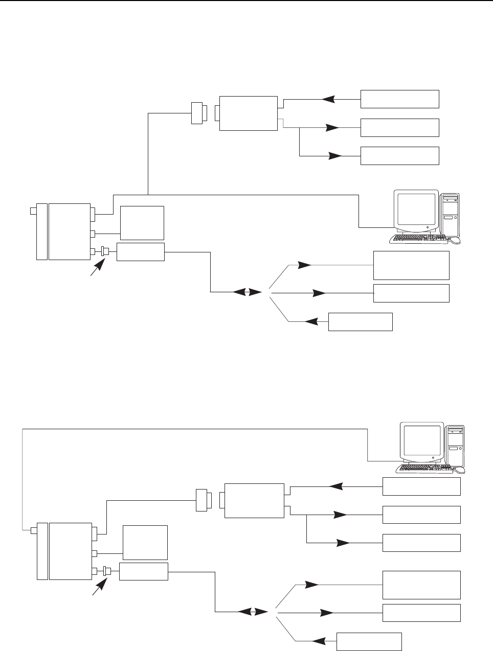
4.4 Radio Tuning Setup
A personal computer (PC), Windows 8/7/Vista/XP and a tuner program (which is available as part of
the MOTOTRBO CPS kit) are required to tune the radio. To perform the tuning procedures, the radio
must be connected to the PC and test equipment setup as shown in Figure 4-4 or Figure 4-5.
Figure 4-4 Radio Tuning Equipment Setup
Figure 4-5 Radio Tuning Equipment Setup (Alternative Method)
WATT meter
Audio Generator
SINAD Meter
AC Voltmeter
30 dB Pad
Audio I n Tx
Rx
RF Generator
RLN4460_
Tes t Box
Service Monit o r
P o w e r
Supp l y
13. 8 V D C
o i d a R
DC
RF
A C C
Back 20 Pin MAP Test and USB
Programming Cable PMKN4149_
USB
Tx
Tx
(if needed)
Mini UHF
to BNC Adaptor
WATT meter
Audio Generator
SINAD Meter
AC Voltmeter
30 dB Pad
Audio In Tx
Rx
RF Generator
RLN4460_
Tes t Box
Service Monitor
P o w e r
Supp l y
13. 8 V D C
o i d a R
DC
RF
A C C
Front Telco MMP USB
Programming Cable PMKN4147_
USB
Tx
Tx
(if needed)
Mini UHF
to BNC Adaptor
Back 20 Pin MAP Test
Cable PMKN4150_

4-4 Radio Programming and Tuning: Radio Tuning Setup
Notes

Chapter 5 Disassembly/Reassembly Procedures
5.1 Introduction
This chapter provides details about the following:
• Preventive maintenance (inspection and cleaning).
• Safe handling of CMOS and LDMOS devices.
• Repair procedures and techniques.
• Disassembly and reassembly of the radio.
5.2 Preventive Maintenance
Periodic visual inspection and cleaning is recommended.
5.2.1 Inspection
Check that the external surfaces of the radio are clean, and that all external controls and switches
are functional. It is not recommended to inspect the interior electronic circuitry.
5.2.2 Cleaning Procedures
The following procedures describe the recommended cleaning agents and the methods to be used
when cleaning the external and internal surfaces of the radio. External surfaces include the control
head and housing assembly. These surfaces should be cleaned whenever a periodic visual
inspection reveals the presence of smudges, grease, and/or grime.
NOTE: Internal surfaces should be cleaned only when the radio is disassembled for service or repair.
The only recommended agent for cleaning the external radio surfaces is a 0.5% solution of a mild
dishwashing detergent in water. The only factory recommended liquid for cleaning the printed circuit
boards and their components is isopropyl alcohol (100% by volume).
Use all chemicals as prescribed by the manufacturer. Be sure to follow all
safety precautions as defined on the label or material safety data sheet.
The effects of certain chemicals and their vapors can have harmful results on
certain plastics. Avoid using aerosol sprays, tuner cleaners and other
chemicals.
!
C a u t i o n

5-2 Disassembly/Reassembly Procedures: Safe Handling of CMOS and LDMOS Devices
Cleaning External Plastic Surfaces
Apply the 0.5% detergent-water solution sparingly with a stiff, non-metallic, short-bristled brush to
work all loose dirt away from the radio. Use a soft, absorbent, lintless cloth or tissue to remove the
solution and dry the radio. Make sure that no water remains entrapped near the connectors, cracks,
or crevices.
Cleaning Internal Circuit Boards and Components
Isopropyl alcohol (100%) may be applied with a stiff, non-metallic, short-bristled brush to dislodge
embedded or caked materials located in hard-to-reach areas. The brush stroke should direct the
dislodged material out and away from the inside of the radio. Make sure that controls or tunable
components are not soaked with alcohol. Do not use high-pressure air to hasten the drying process
since this could cause the liquid to collect in unwanted places. Once the cleaning process is
complete, use a soft, absorbent, lintless cloth to dry the area. Do not brush or apply any isopropyl
alcohol to the frame, control head and housing assembly.
NOTE: Always use a fresh supply of alcohol and a clean container to prevent contamination by
dissolved material (from previous usage).
5.3 Safe Handling of CMOS and LDMOS Devices
Complementary Metal Oxide Semiconductor (CMOS) and Laterally Diffused Metal Oxide
Semiconductor (LDMOS) devices are used in this family of radios, and are susceptible to damage by
electrostatic or high voltage charges. Damage can be latent, resulting in failures occurring weeks or
months later. Therefore, special precautions must be taken to prevent device damage during
disassembly, troubleshooting, and repair.
Handling precautions are mandatory for CMOS/LDMOS circuits and are especially important in low
humidity conditions.

Disassembly/Reassembly Procedures: Safe Handling of CMOS and LDMOS Devices 5-3
DO NOT attempt to disassemble the radio without first referring to the following CAUTION
statement.
This radio contains static-sensitive devices. Do not open the radio unless you are
properly grounded. Take the following precautions when working on this unit:
• Store and transport all CMOS/LDMOS devices in conductive
material so that all exposed leads are shorted together. Do not insert
CMOS/LDMOS devices into conventional plastic “snow” trays used
for storage and transportation of other semiconductor devices.
• Ground the working surface of the service bench to protect the
CMOS/LDMOS device. We recommend using a wrist strap, two
ground cords, a table mat, a floor mat, ESD shoes, and an ESD
chair.
• Wear a conductive wrist strap in series with a 100k resistor to
ground. (Replacement wrist straps that connect to the bench top
covering are Motorola part number 4280385A59).
• Do not wear nylon clothing while handling CMOS/LDMOS devices.
• Do not insert or remove CMOS/LDMOS devices with power applied.
Check all power supplies used for testing CMOS/LDMOS devices to
be certain that there are no voltage transients present.
• When straightening CMOS/LDMOS pins, provide ground straps for
the apparatus used.
• When soldering, use a grounded soldering iron.
• If at all possible, handle CMOS/LDMOS devices by the package and
not by the leads. Prior to touching the unit, touch an electrical
ground to remove any static charge that you may have
accumulated. The package and substrate may be electrically
common. If so, the reaction of a discharge to the case would cause
the same damage as touching the leads.
!
C a u t i o n
5-4 Disassembly/Reassembly Procedures: Repair Procedures and Techniques – General
5.4 Repair Procedures and Techniques – General
Any rework or repair on Environmentally Preferred Products must be done using the appropriate
lead-free solder wire and lead-free solder paste as stated in the following table:
Parts Replacement and Substitution
Check the parts list for the proper Motorola part number and order the part from the nearest Motorola
Radio Products and Solutions Organization listed in Appendix A of this manual.
Rigid Circuit Boards
This family of radios uses bonded, multi-layer, printed circuit boards. Since the inner layers are not
accessible, some special considerations are required when soldering and unsoldering components.
The printed-through holes may interconnect multiple layers of the printed circuit. Therefore, exercise
care to avoid pulling the plated circuit out of the hole.
When soldering near a connector:
• Avoid accidentally getting solder in the connector.
• Be careful not to form solder bridges between the connector pins.
• Examine your work closely for shorts due to solder bridges.
NOTE Environmentally Preferred Products (EPP) (refer to the marking on the printed circuit
boards – examples shown below) were developed and assembled using environmentally
preferred components and solder assembly techniques to comply with the European
Union’s Restriction of Hazardous Substances (ROHS 2) Directive 2011/65/EU and
Waste Electrical and Electronic Equipment (WEEE) Directive 2012/19/EU. To
maintain product compliance and reliability, use only the Motorola specified parts in this
manual.
Table 5-1 Lead Free Solder Wire Part Number List
Motorola
Part Number Alloy Flux Type Flux Content
by Weight
Melting
Point
Supplier Part
number Diameter Weight
1088929Y01 95.5Sn/3.8Ag/0.7Cu RMA Version 2.7–3.2% 217°C 52171 0.015” 1lb spool
Table 5-2 Lead Free Solder Paste Part Number List
Motorola Part
Number
Manufacturer Part
Number Viscosity Type Composition & Percent Metal Liquid
Temperature
1085674C03 NC-SMQ230 900–1000KCPs
Brookfield (5rpm)
Type 3
(-325/+500)
(95.5%Sn-3.8%Ag-0.7%Cu)
89.3%
217°C
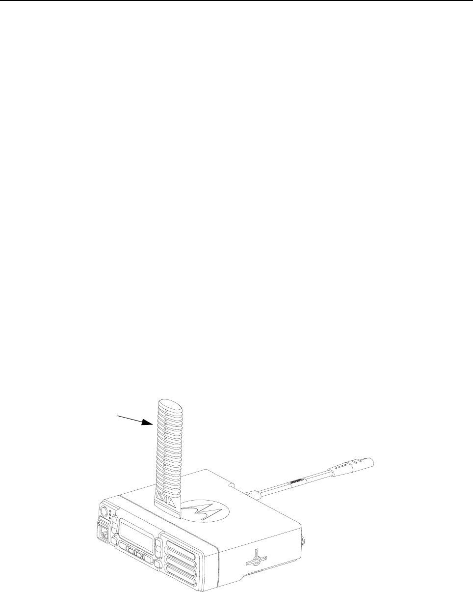
Disassembly/Reassembly Procedures: Disassembling and Reassembling the Radio – General 5-5
5.5 Disassembling and Reassembling the Radio – General
Since these radios may be disassembled and reassembled with the use of only eleven screws
(board to casting), it is important to pay particular attention to the snaps and tabs, and how parts
align with each other.
The following tools are required for disassembling and assembling the radio:
• Small Flat Blade Screwdriver
• Control Head Dismantling Tool (Motorola Part No. 6686119B01)
•Torque Driver (2–36 lbs-in or 0.2–4.0 N-m), (Motorola Part No. RSX4043A)
• TORX™ T10 Driver Bit (Motorola Part No. 6680387A74)
• TORX™ T8 Driver Bit (Motorola Part No. 6680387A72)
• TORX™ T6 Driver Bit (Motorola Part No. 6680387A70 - for use with Option Board only)
• 9/16” Deep Socket Driver (RF Connector Nut)
If a unit requires more complete testing or service than is customarily performed at the basic level,
please send radio to a Motorola Service Center listed in Appendix B.
The following disassembly procedures should be performed only if necessary.
5.6 Radio Disassembly – Detailed
The procedure to remove and replace the control head, top cover or transceiver board is similar for
all models. A typical procedure is therefore provided in this section followed by detailed disassembly
procedures for each specific control head model.
5.6.1 Control Head Removal
1. Insert the dismantling tool in the groove between the control head and the radio assembly as
shown in Figure 5-1.
2. Press the dismantling tool under the control head to release the snap features.
Figure 5-1 Typical Control Head Removal
Dismantling
Tool
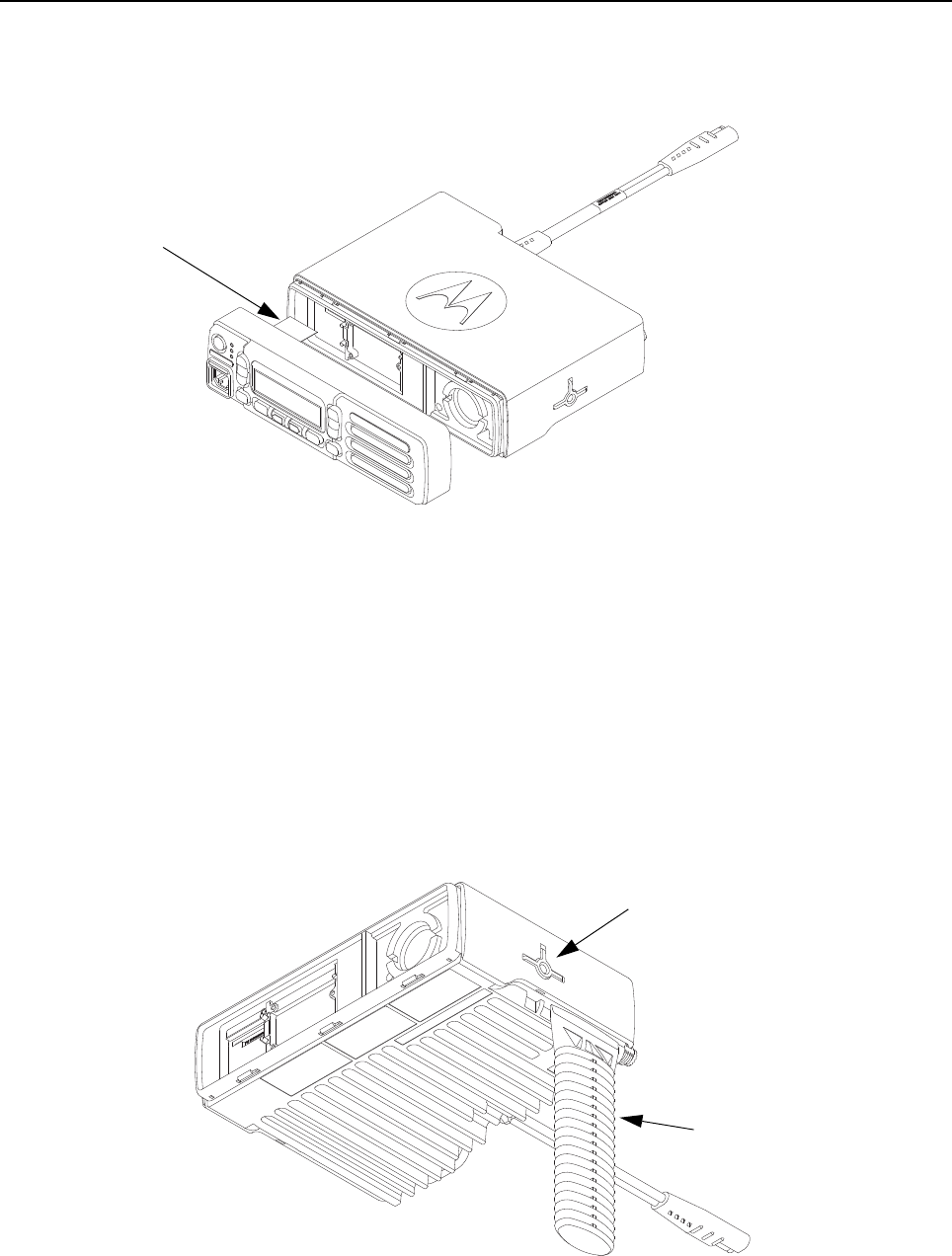
5-6 Disassembly/Reassembly Procedures: Radio Disassembly – Detailed
3. Pull the control head away from the radio assembly as shown in Figure 5-2.
NOTE: During the control head disassembly, the control head PCB may snap out of position. The
control head PCB will need to be snapped back in place prior to reassembly.
Figure 5-2 Flexible Connection Removal
4. Remove the flex cable from the socket on the radio assembly as shown in Figure 5-2.
5.6.2 Top Cover Removal
1. Insert the dismantling tool between the top cover and the chassis as shown in
Figure 5-3.
2. Press on the dismantling tool until one side wall of the top cover starts to clear the chassis
trunnion mounting features.
3. Repeat step 2 for the other side of the top cover.
4. A small flat screwdriver may be required to release the rear catch.
5. Lift the top cover from the chassis.
Figure 5-3 Top Cover Removal (Image May Not Match Exact Product)
Flex Cable
Dismantling
Tool
Trunnion Mounting
Feature
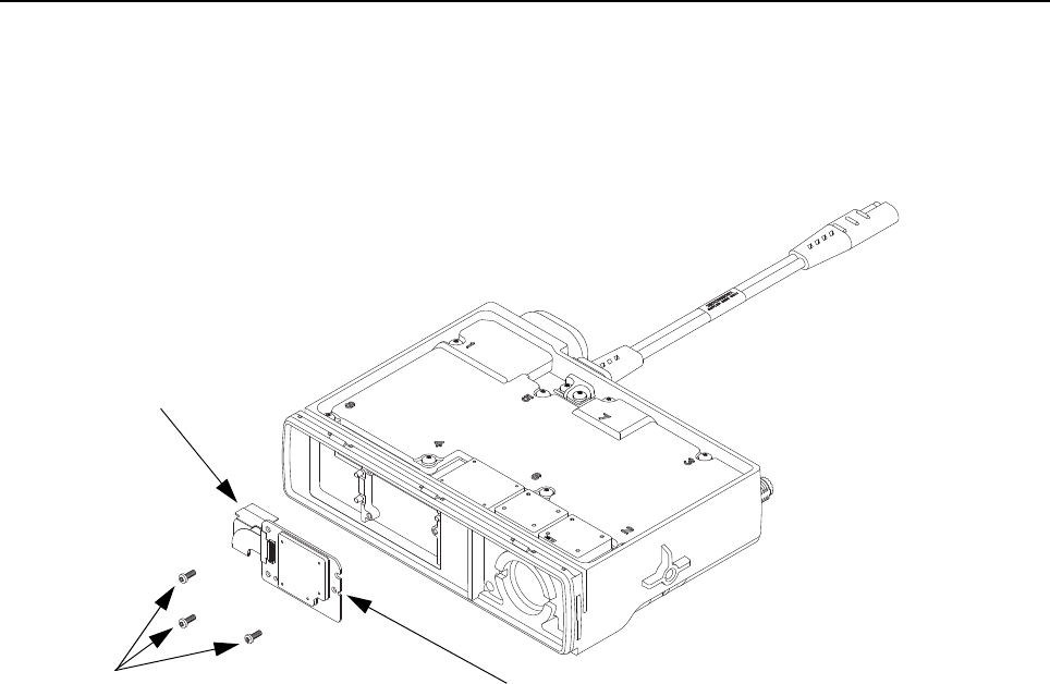
Disassembly/Reassembly Procedures: Radio Disassembly – Detailed 5-7
5.6.3 Transceiver Board Removal
1. Using a T6 TORX™ driver, remove the screws securing the option board to the chassis
(Option Board Only).
2. Unplug the flex from the transceiver board (Option Board Only).
Figure 5-4 Option Board Removal (Image May Not Match Exact Product)
Option Board
Option Board Flex
Screws
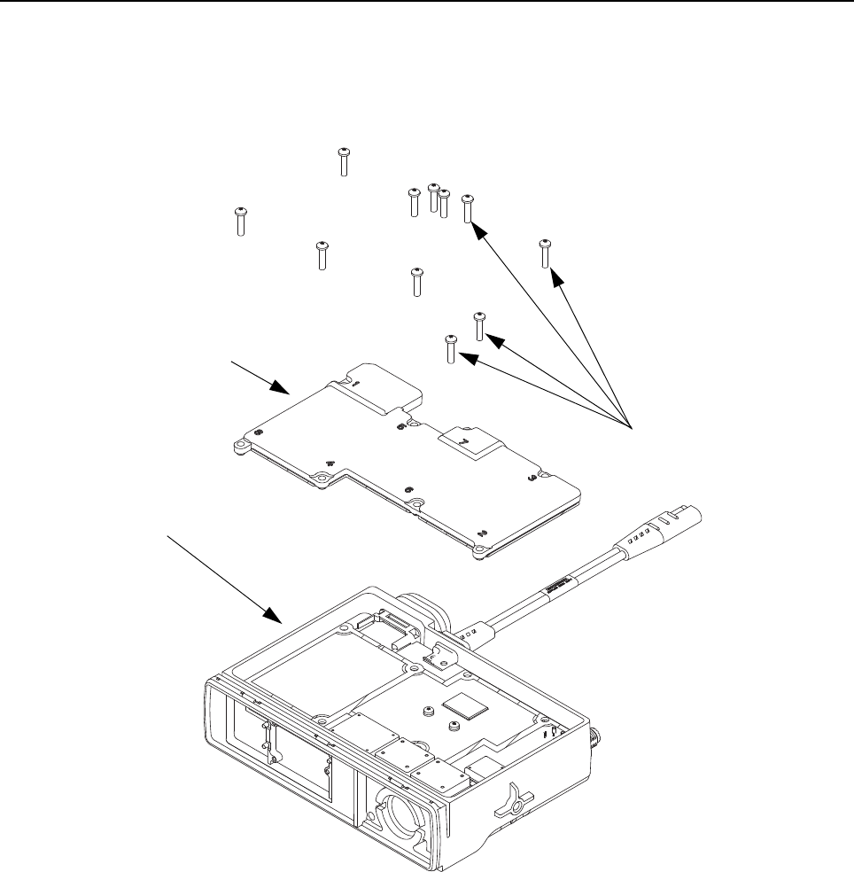
5-8 Disassembly/Reassembly Procedures: Radio Disassembly – Detailed
3. Remove the eight screws from the die cast main shield, the one screw directly on the PCB
and the two screws from the DC Cable using the T10 TORX™ driver as shown in Figure 5-5.
4. Lift the die cast main shield from the chassis.
Figure 5-5 Die Cast Main Shield Removal
Radio
Chassis
Die Cast
Main Shield
Screws (11)
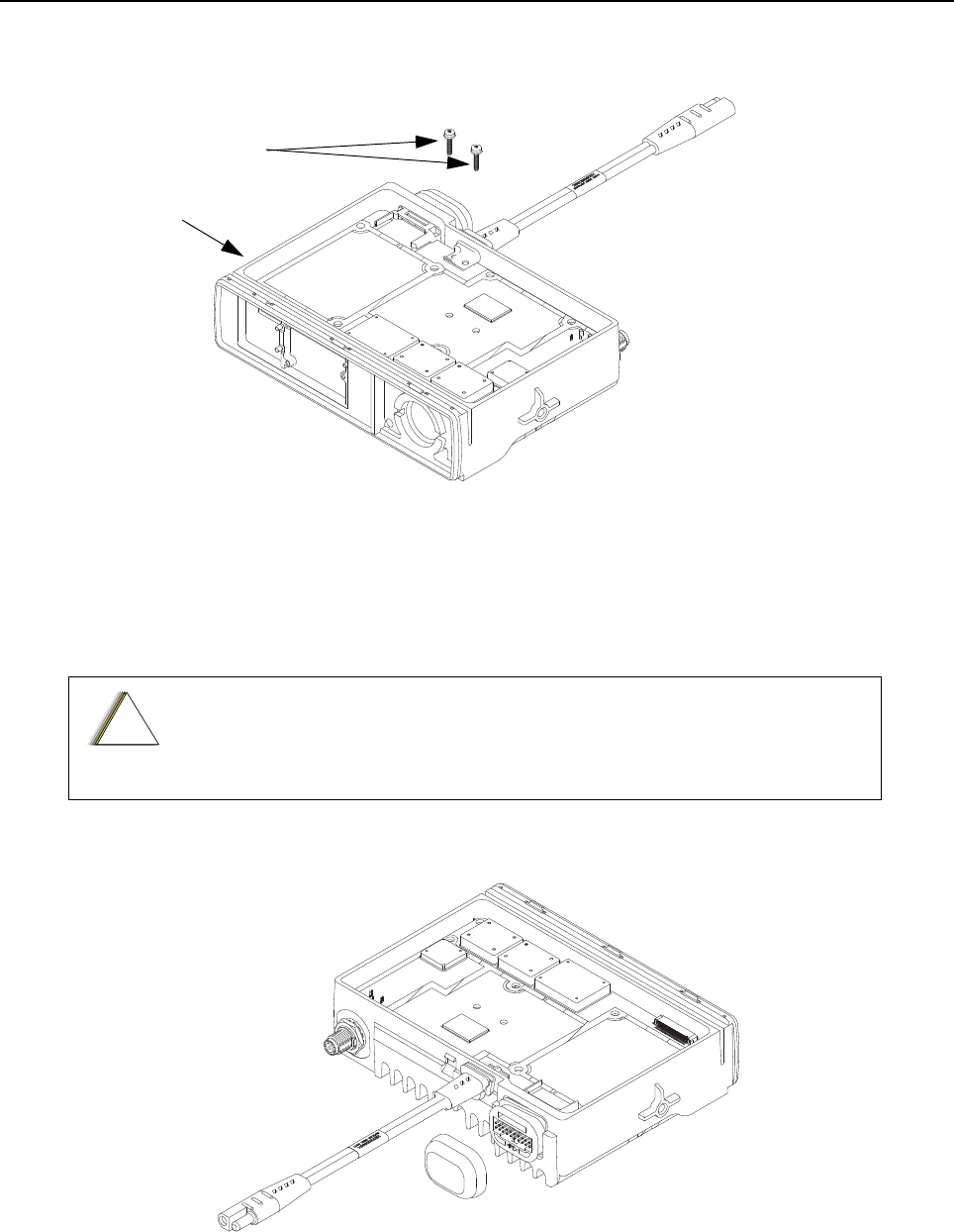
Disassembly/Reassembly Procedures: Radio Disassembly – Detailed 5-9
5. Remove the two screws from the PCB using the T8 TORX™ driver as shown in Figure 5-6.
NOTE: Do not remove the washers from the screws.
Figure 5-6 PA Screw Removal
6. Remove the accessory connector cap.
7. Remove the accessory connector from the radio assembly by pulling the connector straight
out of the radio chassis as shown in Figure 5-7.
Figure 5-7 Accessory Connector Removal
The accessory connector should never be removed when the die cast main
shield is still assembled to the radio.
Radio
Chassis
Screws (2)
!
C a u t i o n
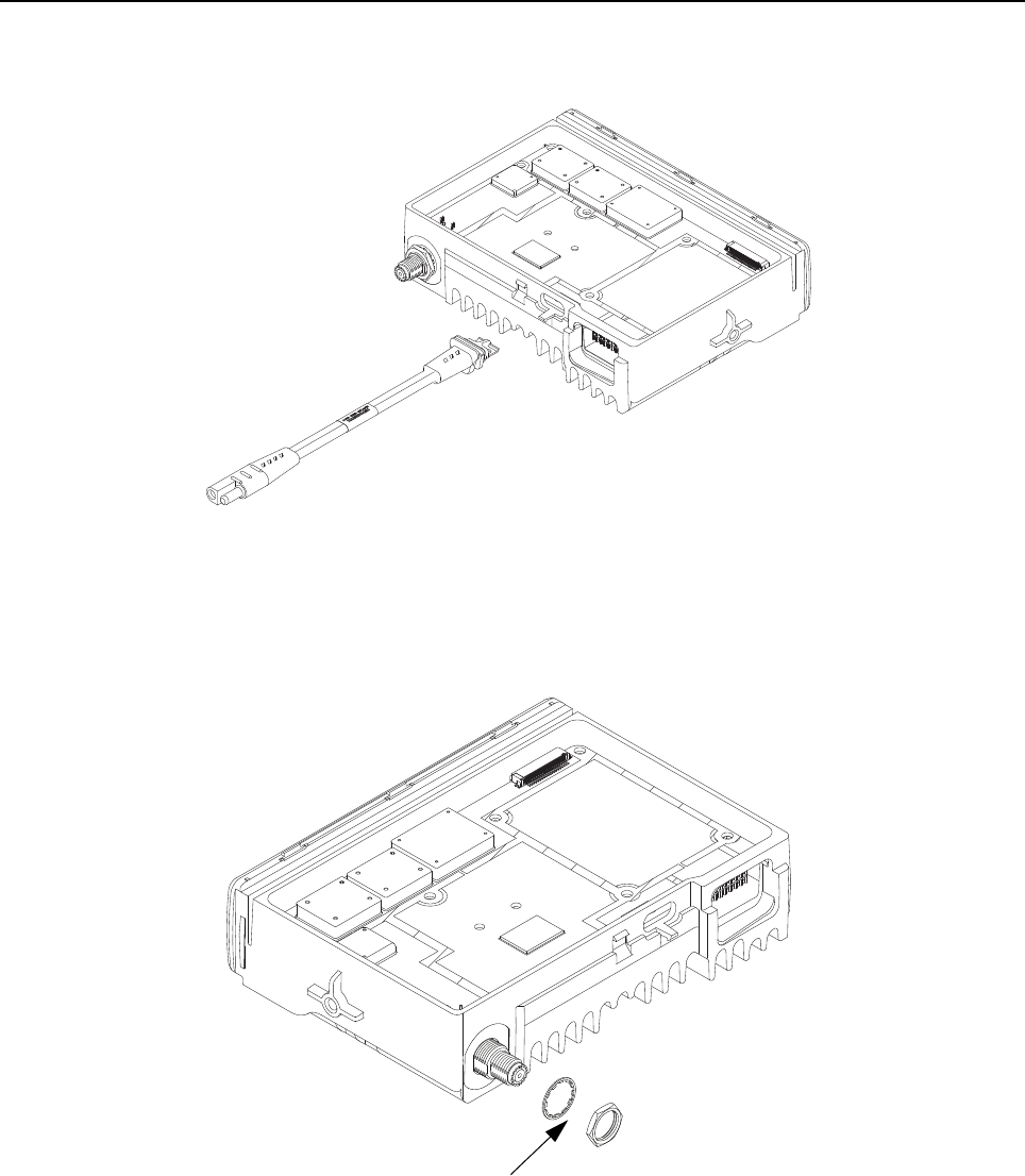
5-10 Disassembly/Reassembly Procedures: Radio Disassembly – Detailed
8. Remove the DC Cable by gently pulling it away from the radio chassis as shown in
Figure 5-8.
Figure 5-8 DC Cable Removal
9. Remove the RF connector nut and lock washer using a 9/16” deep socket driver
(Figure 5-9).
Figure 5-9 RF Connector Nut Removal
RF Lock Washer and Nut
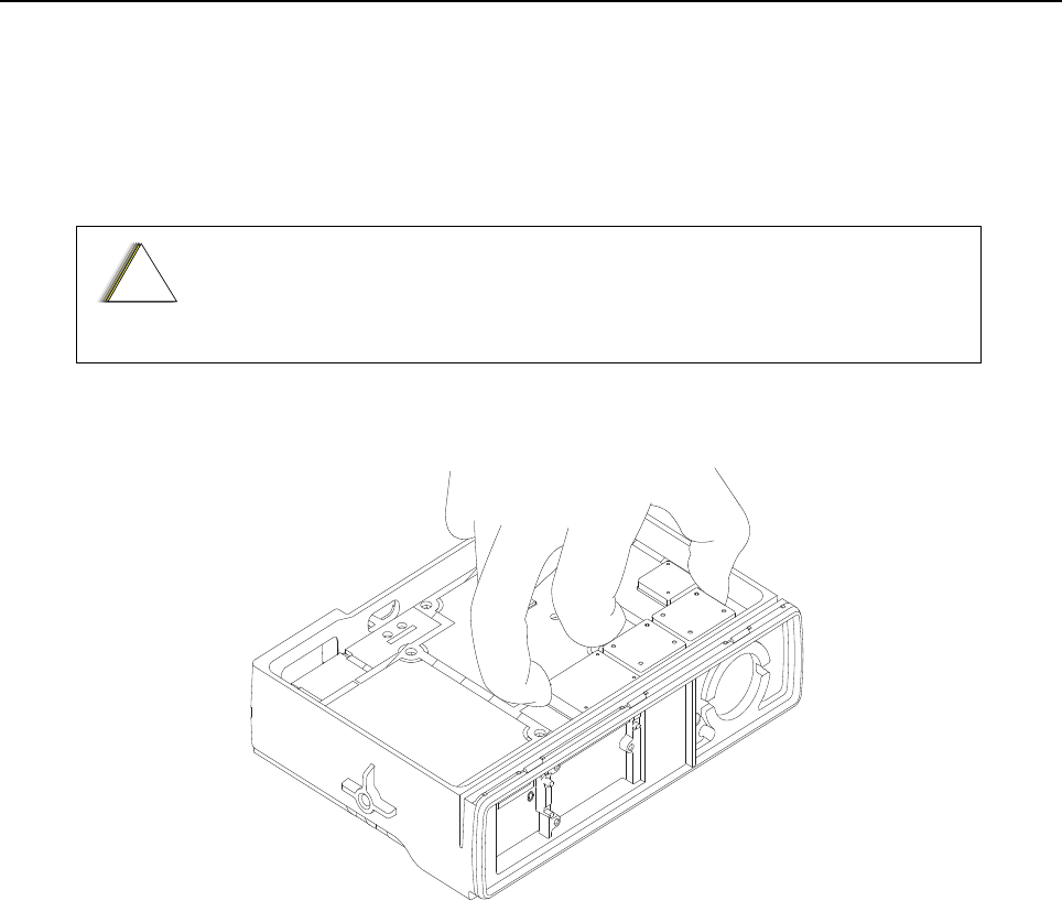
Disassembly/Reassembly Procedures: Radio Disassembly – Detailed 5-11
10. Remove the transceiver board by grabbing and lifting the SMT shields and lift the transceiver
board, as shown in Figure 5-10. Then, slide the transceiver board towards the front of the
radio to allow the RF connector to clear the chassis. Handle the transceiver board by the
edges only and store it in an antistatic bag.
NOTE: If the RF connector gasket remain in the chassis, remove it and place it back on the connector.
Every time the Transceiver Board is removed, the Final Driver Thermal Pad must be replaced.
Figure 5-10 Transceiver Board Removal
The thermal pads can act as an adhesive and cause stress to critical
components on the transceiver board if the transceiver board is lifted too
quickly.
!
C a u t i o n
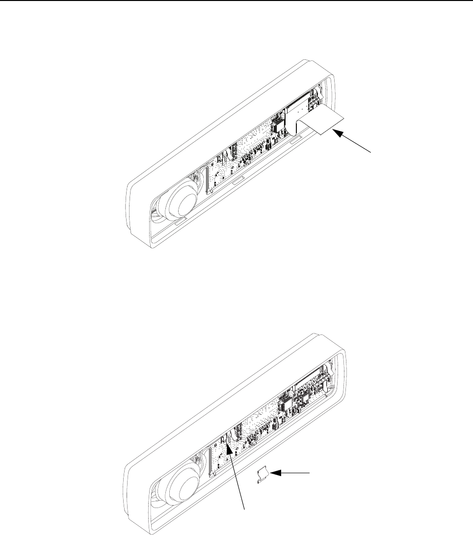
5-12 Disassembly/Reassembly Procedures: Radio Disassembly – Detailed
5.6.4 Disassembly of Alphanumeric Display Control Head
1. Unplug the control head flex from the control head board by gently pulling the flex out of the
connector as shown in Figure 5-11.
Figure 5-11 Control Head Flex Removal
2. Remove the speaker tape from the PCB by using a tweezer as shown in Figure 5-12.
3. Disconnect the speaker connector from the control head board.
Figure 5-12 Speaker Tape Removal
Control Head Flex
Speaker Tape
Speaker Connector
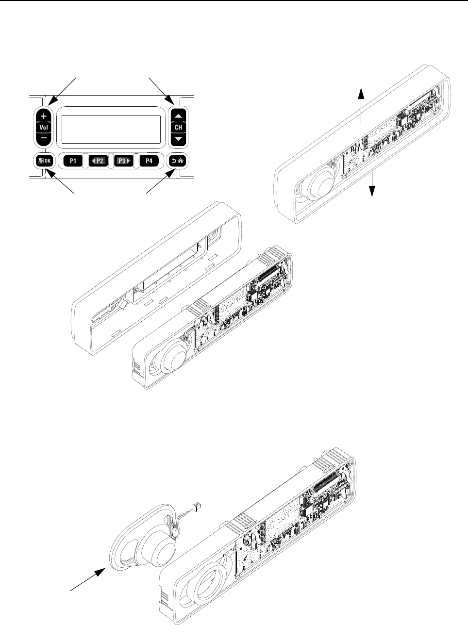
Disassembly/Reassembly Procedures: Radio Disassembly – Detailed 5-13
4. Remove the keypad assembly from the control head housing by pushing on the keypad
buttons while disengaging the control head PCB by deflecting the control head housing side
walls. Once the keypad begins to separate from the control head housing, pull both
components apart. Refer to Figure 5-13.
Figure 5-13 Keypad Assembly Removal
5. Remove the speaker from the keypad assembly as shown in Figure 5-14.
Figure 5-14 Speaker Removal
Keypad Buttons
to Push
Keypad Buttons
to Push
Deflecting Direction
Deflecting Direction
Speaker
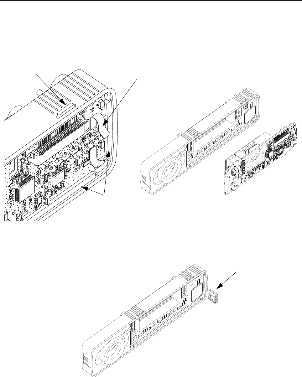
5-14 Disassembly/Reassembly Procedures: Radio Disassembly – Detailed
6. Gently lift the keypad upwards to disengage the PCB tabs from the keypad openings.
Simultaneously, remove the keypad flaps around the PCB. Then remove the PCB from the
keypad. Refer to Figure 5-15.
NOTE: Do not touch or contaminate the conductive contacts (especially the grounding contacts) on
the PCB.
Figure 5-15 PCB Removal
7. Gently remove the indicator barrier from the keypad as shown in Figure 5-16.
Figure 5-16 Indicator Barrier Removal
PCB Tab Protruding
Through Keypad
Opening
Keypad Flaps
Constraining The
PCB On All 4 Sides
Grounding
Contact
Indicator Barrier
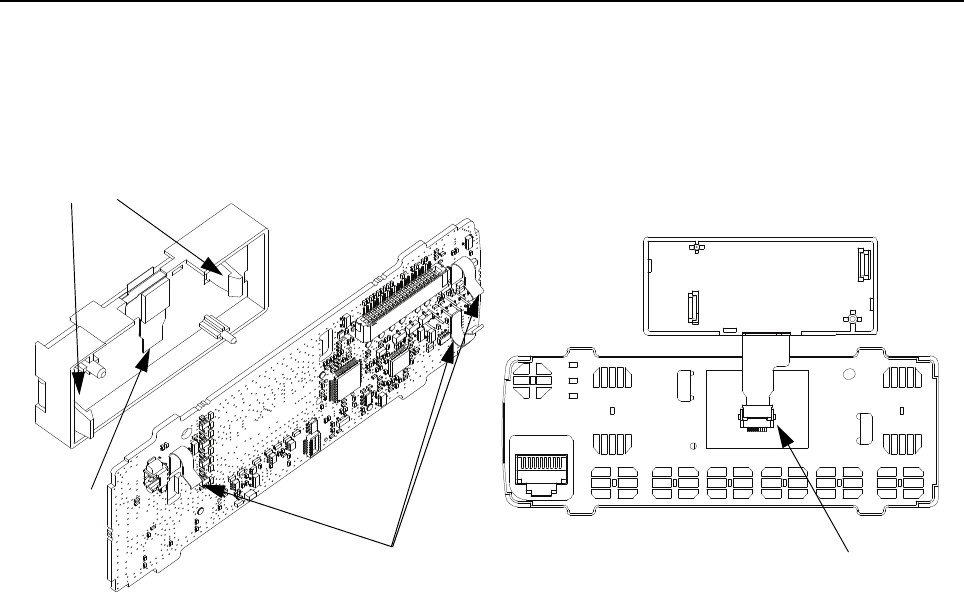
Disassembly/Reassembly Procedures: Radio Disassembly – Detailed 5-15
8. Gently push the LCD display latch and remove the LCD from the PCB. Refer to Figure 5-17.
9. Remove the LCD flex from the connector.
NOTE: Do not touch or contaminate the conductive contacts (especially the grounding contacts) on
the PCB.
Figure 5-17 LCD and LCD Flex Removal
LCD Latch
LCD Flex
Connector
Grounding
Contacts
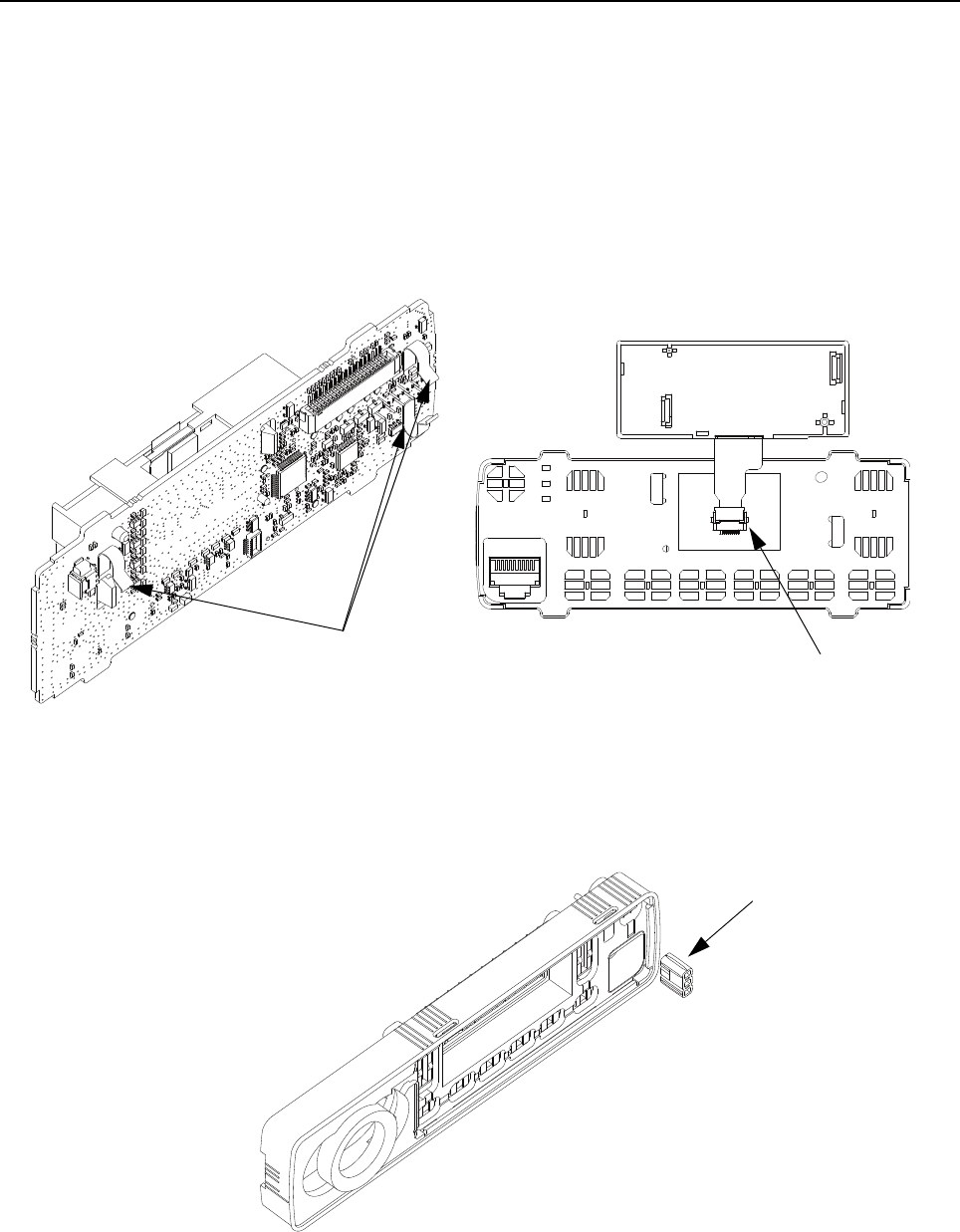
5-16 Disassembly/Reassembly Procedures: Radio Reassembly – Detailed
5.7 Radio Reassembly – Detailed
5.7.1 Reassembly of Alphanumeric Display Control Head
1. Connect the display flex to the connector on the PCB.
2. Align the LCD alignment pins to the PCB holes.
3. Firmly press along the outer perimeter of the display until the LCD display latch is attached to
the PCB. Refer to Figure 5-18.
NOTE: Do not touch or contaminate the conductive contacts (especially the grounding contacts) on
the PCB.
Figure 5-18 LCD Display Assembly
4. Gently assemble the indicator barrier to the keypad as shown in Figure 5-19.
Figure 5-19 Indicator Barrier Assembly
Connector
Grounding
Contacts
Indicator Barrier
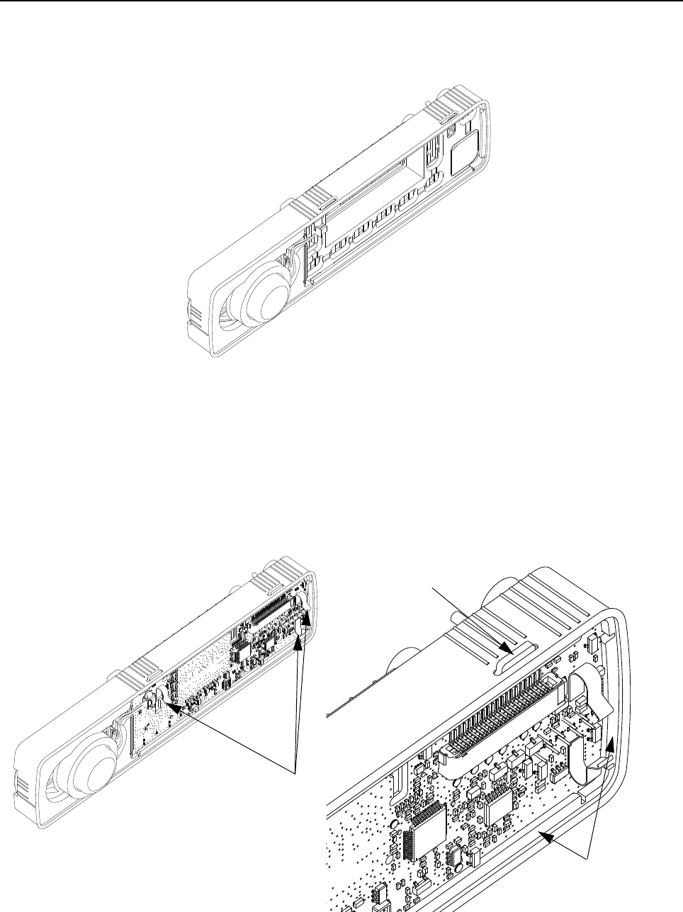
Disassembly/Reassembly Procedures: Radio Reassembly – Detailed 5-17
5. Assemble the speaker to the keypad. Refer to Figure 5-20.
NOTE: Be sure to orient the speaker in the direction of the wire and connector towards the middle of
the control head.
Figure 5-20 Speaker Assembly
6. Assemble PCB assembly to the keypad as shown in Figure 5-21.
NOTE: Verify that the PCB is properly positioned to the keypad:
1) The four PCB tabs should protrude through the keypad openings.
2) The PCB should be seated to the keypad so the keypad flaps constrain the PCB.
NOTE: Do not touch or contaminate the conductive contacts (especially the grounding contacts) on
the PCB.
Figure 5-21 Assembling PCB to Keypad
Keypad Flaps
Constraining The
PCB On All 4 Sides
PCB Tab Protruding
Through Keypad
Opening
Grounding
Contacts
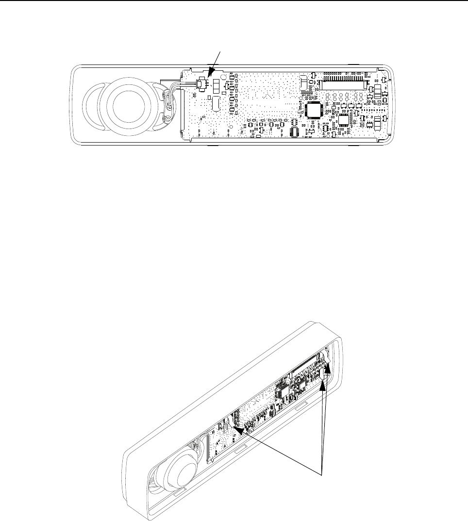
5-18 Disassembly/Reassembly Procedures: Radio Reassembly – Detailed
7. Connect the speaker plug to its mating connector on the control head board as shown in
Figure 5-22.
Figure 5-22 Speaker Connection
8. Assemble the keypad with the PCB and speaker assembled to the control head housing.
Refer to Figure 5-23.
NOTE: PCB needs to be snapped into the control head housing. Ensure entire keypad is fully seated
to the control head housing.
Do not touch or contaminate the conductive contacts (especially the grounding contacts) on
the PCB.
Figure 5-23 Assembling Keypad to Control Head Housing
Speaker Connector
Grounding
Contacts
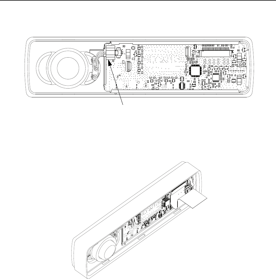
Disassembly/Reassembly Procedures: Radio Reassembly – Detailed 5-19
9. Assemble the speaker tape on the speaker wire and PCB. Press the speaker tape and make
sure it sticks firmly on the PCB. Refer to Figure 5-24.
Figure 5-24 Assembling Speaker Tape to PCB
10. Gently plug the control head flex to the control head board as shown in Figure 5-25.
Figure 5-25 Assembling Control Head Flex to Control Head Board
Speaker Tape
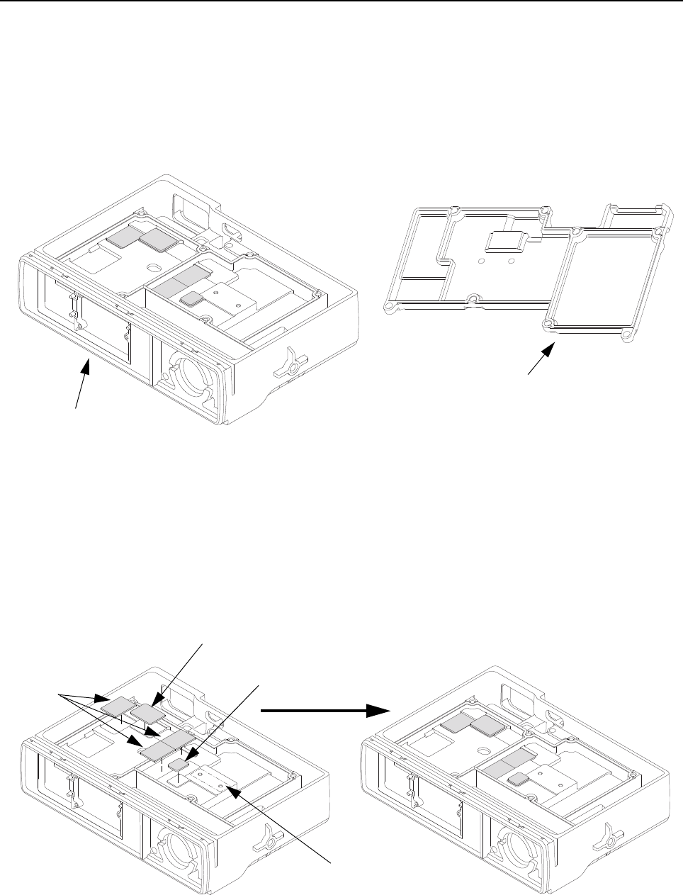
5-20 Disassembly/Reassembly Procedures: Radio Reassembly – Detailed
5.7.2 Radio Assembly
1. Prior to reassembling the radio, inspect all seals and sealing surfaces for damage (nicks,
cuts, etc.) or debris. Refer to the exploded view and bill of materials for the correct part
numbers and replace parts, as necessary. Replace all new seals on their respective parts.
For both the die cast main shield and the chassis, thoroughly inspect the shield gasketing for
damage and verify all thermal pads are in place and free from damage and debris. See
Section 5.7.3: Thermal Pad Replacement Procedure on page 5-21 to replace damaged pads.
Figure 5-26 Thermal Pads and Shield Gasketing on Chassis and Die Cast Main Shield
2. Thoroughly inspect the chassis and verify all thermal pads are in place and free from
damage. See Section 5.7.3: Thermal Pad Replacement Procedure on page 5-21 to replace
damaged pads.
NOTE: Every time the Transceiver Board is removed, the Final Driver Thermal Pad must be
replaced.
Figure 5-27 Chassis with Thermal Pads
Chassis with Thermal Pads
Die Cast Main Shield
and Shield Gasketing
and Shield Gasketing
Audio PA Thermal Pad
Final Driver Thermal Pad
(75012058002)
(75012059001)
Thermal
(75012018001)
Regulator
Pad
Thermal Grease (1110022A55)
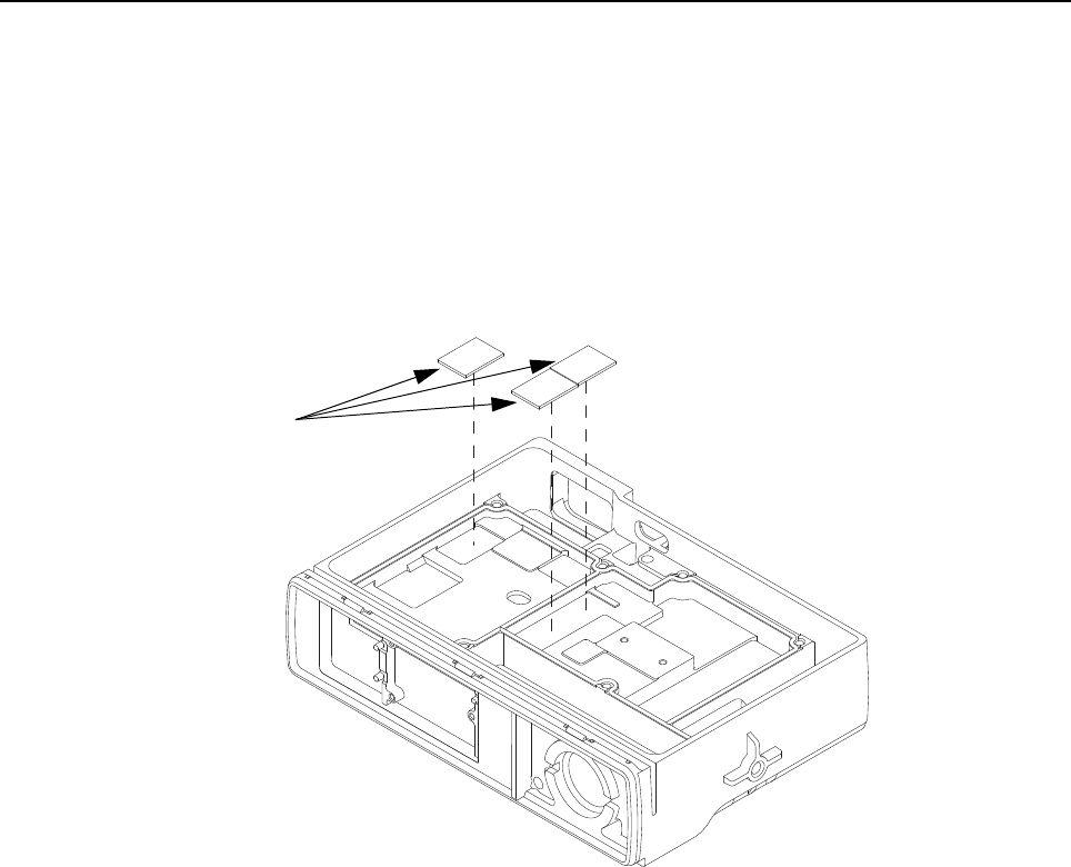
Disassembly/Reassembly Procedures: Radio Reassembly – Detailed 5-21
5.7.3 Thermal Pad Replacement Procedure
Regulator Thermal Pad Replacement
1. Use a plastic flat-edge tool to lift the pad from the chassis surface. Discard the old pad.
2. Use a soft cloth to remove any remaining residue. Alcohol can also be used, if necessary.
Care should be taken to minimize any cleaning-agent contact with the surrounding shield
gasket.
3. Once the surface is clean and dry, remove the new pad from the shipping liner, and place it
on the chassis as shown in Figure 5-28.
Figure 5-28 Replacing Regulator Thermal Pads
Regulator Thermal
Pad (75012018001)
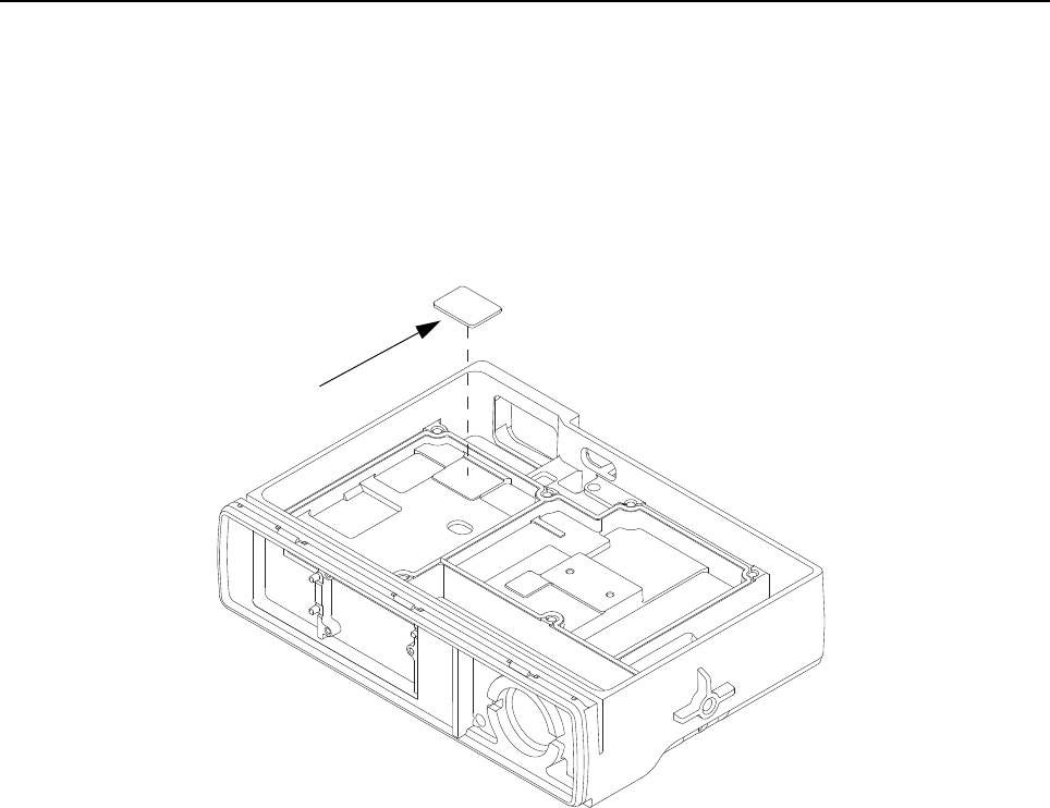
5-22 Disassembly/Reassembly Procedures: Radio Reassembly – Detailed
Audio PA Thermal Pad Replacement
1. Use a plastic flat-edge tool to lift the pad from the chassis surface. Discard the old pad.
2. Use a soft cloth to remove any remaining residue. Alcohol can also be used, if necessary.
Care should be taken to minimize any cleaning-agent contact with the surrounding shield
gasket.
3. Once the surface is clean and dry, remove the new pad from the shipping liner, and place the
pad on to the chassis as shown in Figure 5-29.
Figure 5-29 Replacing Audio PA Thermal Pad
Audio PA Thermal Pad
(75012059001)
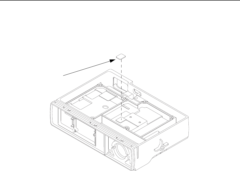
Disassembly/Reassembly Procedures: Radio Reassembly – Detailed 5-23
Final Driver Thermal Pad Replacement
1. Use a plastic flat-edge tool to lift each pad from the transceiver board. Discard the old pad.
2. Use a soft cloth to remove any remaining residue. Alcohol can also be used, if necessary.
3. Once the surface is clean and dry, remove the new pad from the shipping liner, and place the
pad on to the chassis as shown in Figure 5-30.
Figure 5-30 Replacing Final Driver Thermal Pad
Final Driver Thermal Pad
(75012058002)
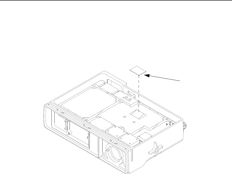
5-24 Disassembly/Reassembly Procedures: Radio Reassembly – Detailed
PCB Thermal Pad Replacement
1. Use a plastic flat-edge tool to lift the pad from the transceiver board. Discard the old pad.
2. Use a soft cloth to remove any remaining residue. Alcohol can also be used, if necessary.
3. Once the surface is clean and dry, remove the new pad from the shipping liner, and place the
pad on to the transceiver board as shown in Figure 5-31.
NOTE: The PCB Thermal Pad is NOT placed for the UHF1 1–25W models. Placing the pad on a
UHF1 1–25W model may degrade radio performance.
Figure 5-31 Replacing PCB Thermal Pad
Thermal Pad
(75012018001)
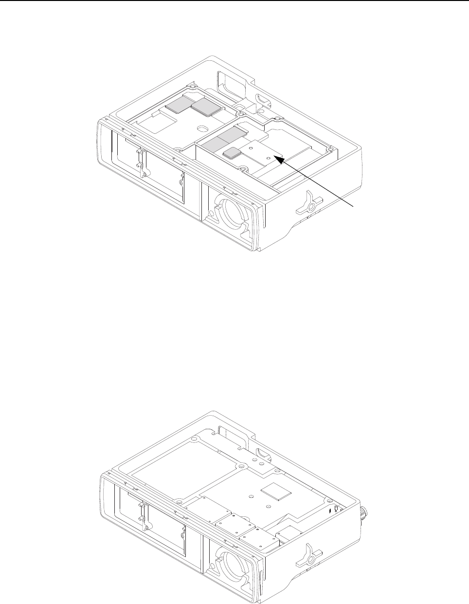
Disassembly/Reassembly Procedures: Radio Reassembly – Detailed 5-25
5.7.4 Transceiver Board Reassembly
1. Apply thermal grease to the PA area. Refer to Figure 5-32.
Figure 5-32 Applying Thermal Grease
2. Insert the transceiver board into the chassis by tilting the transceiver board (approximately 45
degrees) and sliding it into place, taking care to line up the RF connector with the opening in
the back of the chassis.
NOTE: Prior to board installation verify thal all thermal pads are present. Verify that a thermal pad is
present on the PCB.
Push the board down to fully seat it to the radio chassis.
Figure 5-33 Placing the Transceiver Board in the Chassis
Thermal Grease
(1110022A55)
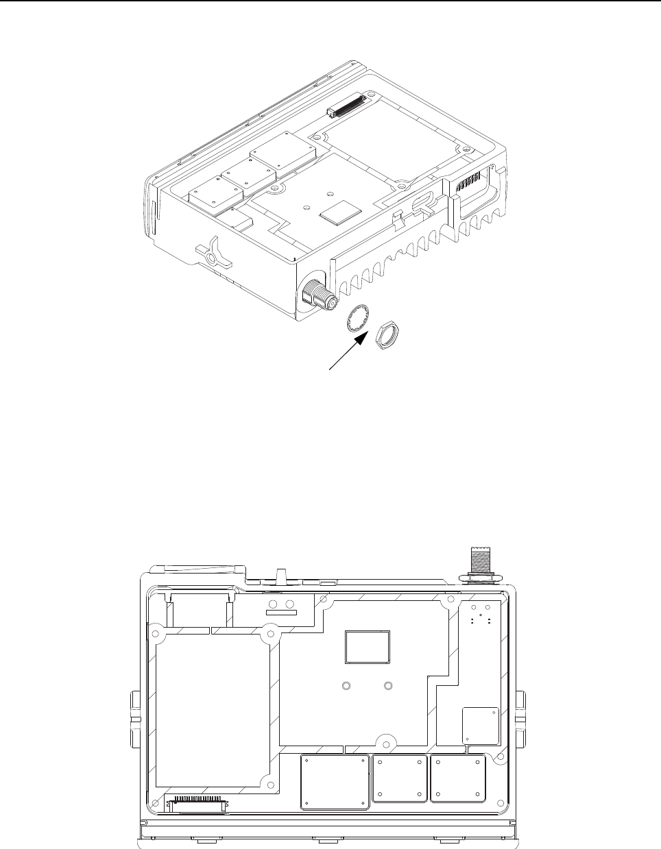
5-26 Disassembly/Reassembly Procedures: Radio Reassembly – Detailed
3. Using a 9/16” deep socket driver install the lock washer and nut to an initial torque of 0.9 N-m
(8 lbs-in). Refer to Figure 5-34.
Figure 5-34 Inserting RF Lock Washer and Nut
4. Using a T10 TORX™ driver insert three main shield thread forming screws (M3) at locations
3, 5 and 6 to compress the PCB. Tighten the screws to 1.0 N-m (9 lbs-in).
NOTE: This step is required; otherwise, damage could result to the final transmitter PA device.
Figure 5-35 Screw Sequence to Compress PCB
RF Lock Washer and Nut
5
6
3
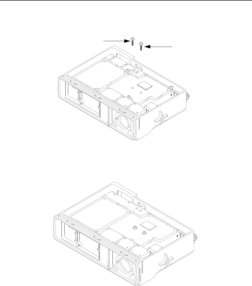
Disassembly/Reassembly Procedures: Radio Reassembly – Detailed 5-27
5. While the board is pressed down, align the PA holes on PCB to mounting holes on chassis
and insert two (M2.5) machine screws with washers (see Figure 5-36 for PA Screw
sequence). Using a T8 TORX™ tighten the screws to 0.45 N-m (4 lbs-in).
Figure 5-36 Installing PA Screws
6. Using a T10 TORX™ driver remove the screws from locations 3, 5 and 6.
Figure 5-37 Screw Removal
Install This Screw First
Install This Screw Second
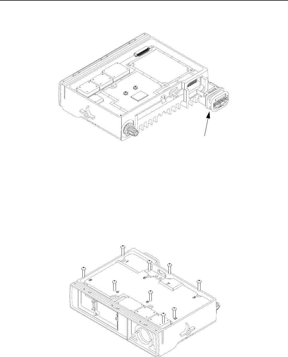
5-28 Disassembly/Reassembly Procedures: Radio Reassembly – Detailed
7. Insert the accessory connector into the radio assembly and press into place until the
connector is flush with the chassis. Refer to Figure 5-38.
Figure 5-38 Inserting Accessory Connector
8. Place the main shield on the transceiver board and lock in place the accessory connector by
aligning the main shield locking tabs to the pockets of the accessory connector.
9. Insert eight main shield thread forming screws (M3) through the shield and one thread
forming screw (M3) through the board.
10. Using a T10 TORX™ driver follow the sequence marked on the main shield and tighten all
nine screws to 1.47 N-m (13 lbs-in). Refer to Figure 5-39.
11. Retighten the eight screws on the main shield a second time.
Figure 5-39 Assembling Die Cast Main Shield onto Chassis
Accessory
Connector
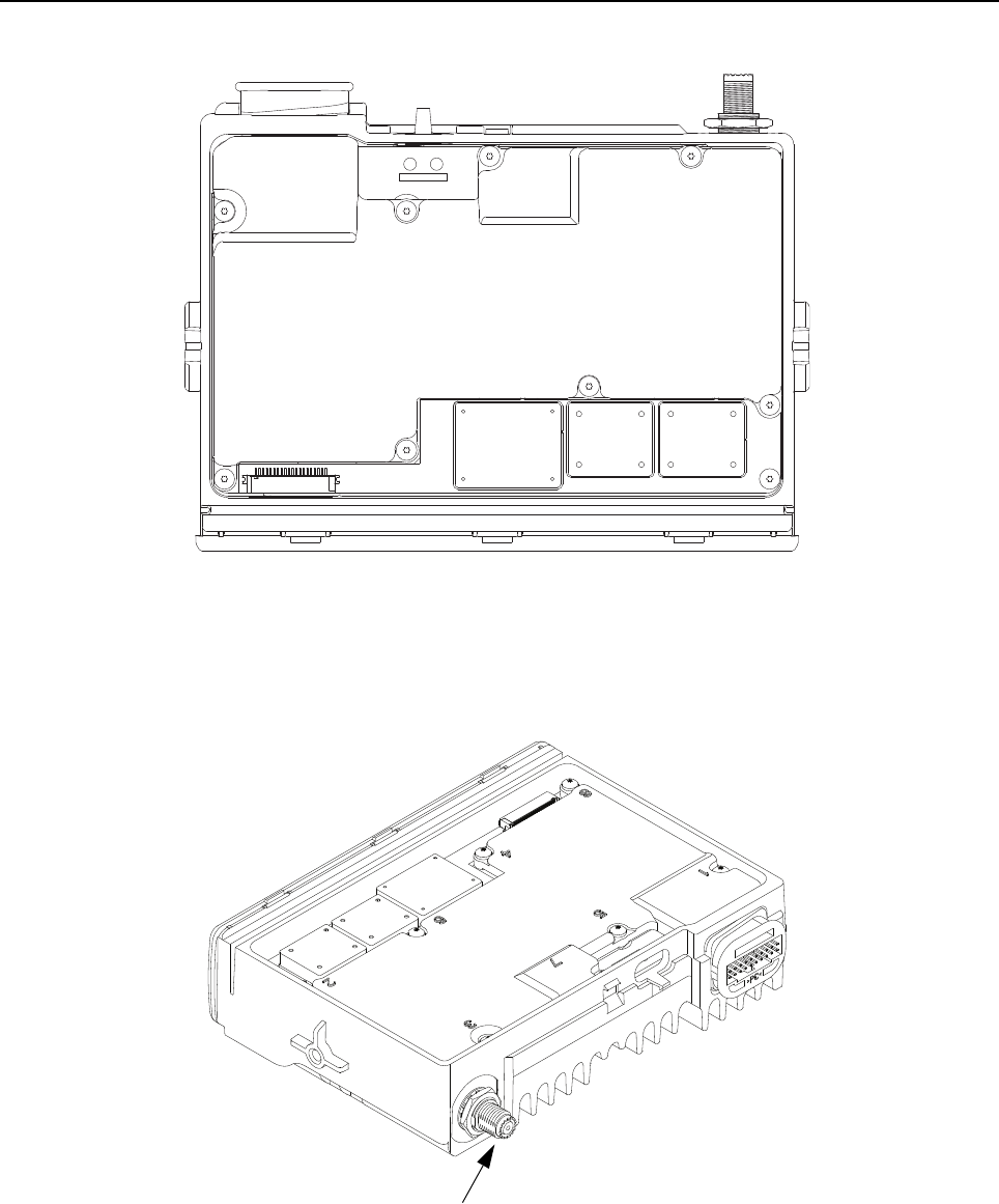
Disassembly/Reassembly Procedures: Radio Reassembly – Detailed 5-29
Figure 5-40 Screw Sequence to Tighten Die Cast Main Shield
12. Use a 9/16” deep socket driver to further tighten the nut to a final torque of 2.15 N-m
(19 lbs-in).
Figure 5-41 RF Connector Nut Final Torque
1
84
5
7
62
3
RF Connector Lock Washer and Nut
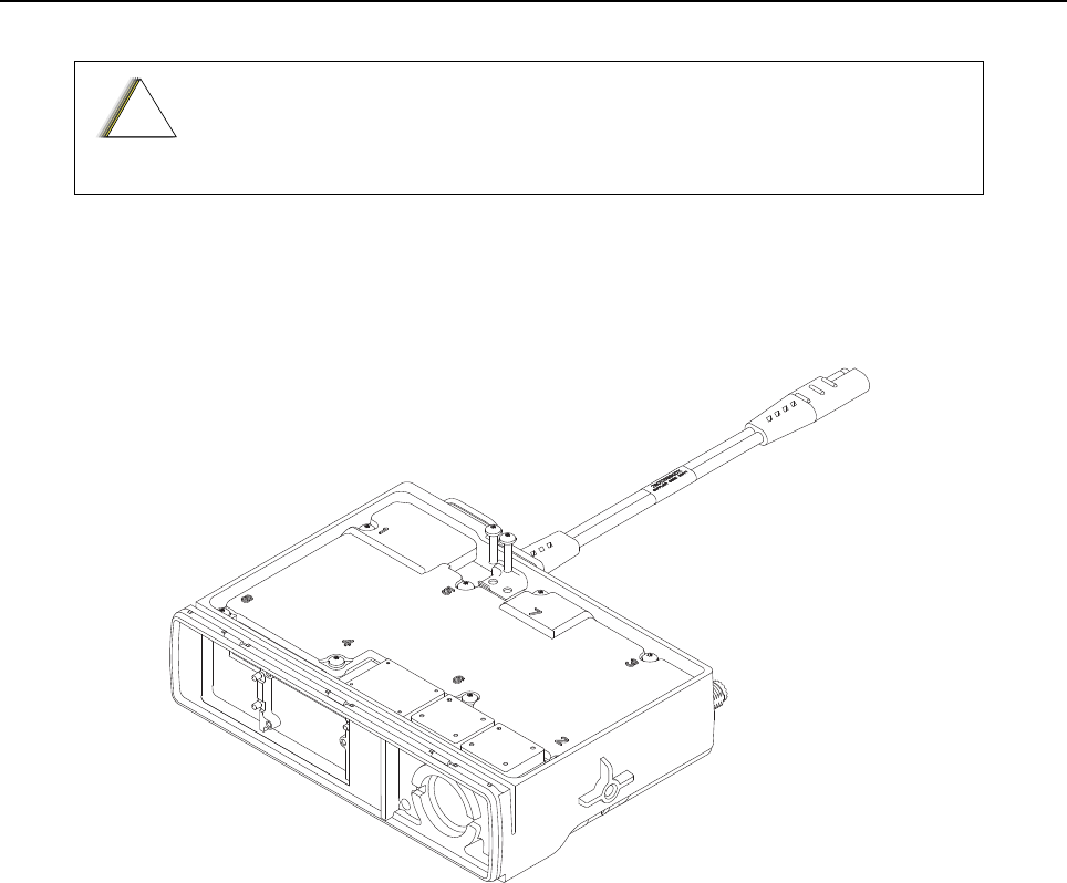
5-30 Disassembly/Reassembly Procedures: Radio Reassembly – Detailed
13. Install the DC Cable Assembly to the radio chassis slot. Ensure that it is seated correctly on
the chassis hook located below the DC Cable.
14. Insert two thread forming screws (M3).
15. Using a T10 TORX™ driver, tighten the screws to 1.47 N-m (13 lbs-in). Refer to Figure 5-42.
Figure 5-42 Installing DC Cable Assembly
Do not leave the transceiver board in the chassis for extended periods of time
without the RF lock washer and nut assembled, or damage to the board
connectors may occur.
!
C a u t i o n
Disassembly/Reassembly Procedures: Radio Reassembly – Detailed 5-31
16. Thoroughly inspect the cover assembly with seal attached. Ensure the seal is fully seated on
the cover and the locking tabs engaged at all six locations.
Figure 5-43 Inspection of Cover Assembly with Seal
17. Gently spread both sides of the cover.
18. Align the top cover to the chassis and snap the cover in place uniformly. Ensure the alignment
posts on the cover slide into the alignment slots on the chassis and that the rear latch is
secure.
Figure 5-44 Assembling Cover onto Chassis
Locking Tab
(6 Places)
Radio Chassis
Main Cover
5-32 Disassembly/Reassembly Procedures: Radio Reassembly – Detailed
NOTE: Ensure the DC Cable locking tabs fit in the designated slots on the connector overmold. Avoid
biting of locking tabs on the overmold.
Figure 5-45 Rear Latch in Secure Position
19. Install the MAP Connector cover.
Figure 5-46 MAP Connector Cover Installation
DC Cable Locking Tabs
MAP Connector Cover
Disassembly/Reassembly Procedures: Radio Reassembly – Detailed 5-33
5.7.5 Option Board Installation
1. Orient the option board flex so that contacts face option board. Secure connector latch to
option board as referenced in Figure 5-47. Note white line on flex should be aligned with
connector latch.
Figure 5-47 Orientation of Option Board Flex to Option Board
2. Maintaining the bend orientation, connect the flex cable from the option board to the main
board connector.
Figure 5-48 Assemble Option Board to Radio Chassis (Image May Not Match Exact Product)
Latch
Option Board Flex
Option Board
Option Board Flex
Screws
5-34 Disassembly/Reassembly Procedures: Radio Reassembly – Detailed
3. Align option board to mounting holes ensuring that the flex tabs are against the chassis
alignment posts.
Figure 5-49 Align Option Board to Mounting Holes
4. Using a T6 TORX™ driver, tighten the three screws to 0.28 N-m (2.5 lbs-in) to secure the
option board to the chassis.
NOTE: Regulatory Requirements
All MOTOTRBO radios are designed and engineered to meet all regulatory requirements for the
country or region of sale. Any option board designed for the MOTOTRBO Option Board ADK must
not compromise the regulatory compliance of the MOTOTRBO radio.
The 3rd party developer is responsible for providing all information, upon request by a regulatory
authority, in regards to any materials or substances used in the manufacture of an option board as it
pertains to its end-of-life.
Please review the terms of the MOTOTRBO License Agreement for more information on the
Licensed Developer or Application Partner responsibilities for regulatory compliance.
Flex Tab
Chassis
Alignment Posts
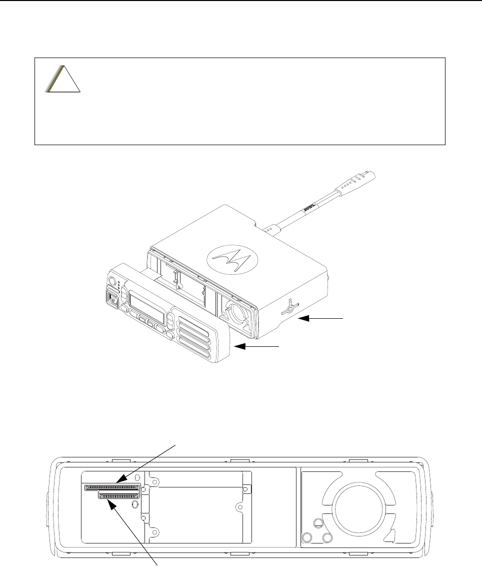
Disassembly/Reassembly Procedures: Radio Reassembly – Detailed 5-35
5.7.6 Assemble Control Head to Radio Assembly
1. Verify that the flex cable is fully seated in the connector on the control head assembly.
Figure 5-50 Assemble Control Head to Chassis
2. Assemble flex cable to the flex connector in the radio assembly, making sure it is fully seated.
Figure 5-51 Flex Connection Connectors
3. Assemble the control head to the radio chassis by aligning one side of the control head
assembly tabs to one side of the radio chassis tabs and then rotate the control head
assembly until the other side engages.
Make sure the main cover is assembled onto the radio chassis before
assembling the control head onto the radio chassis.
During the control head disassembly, the control head PCB may snap out of
position. The control head PCB will need to be snapped back in place prior to
reassembly.
!
C a u t i o n
Radio Chassis
Control Head
Option Board Connector
Control Head Connector
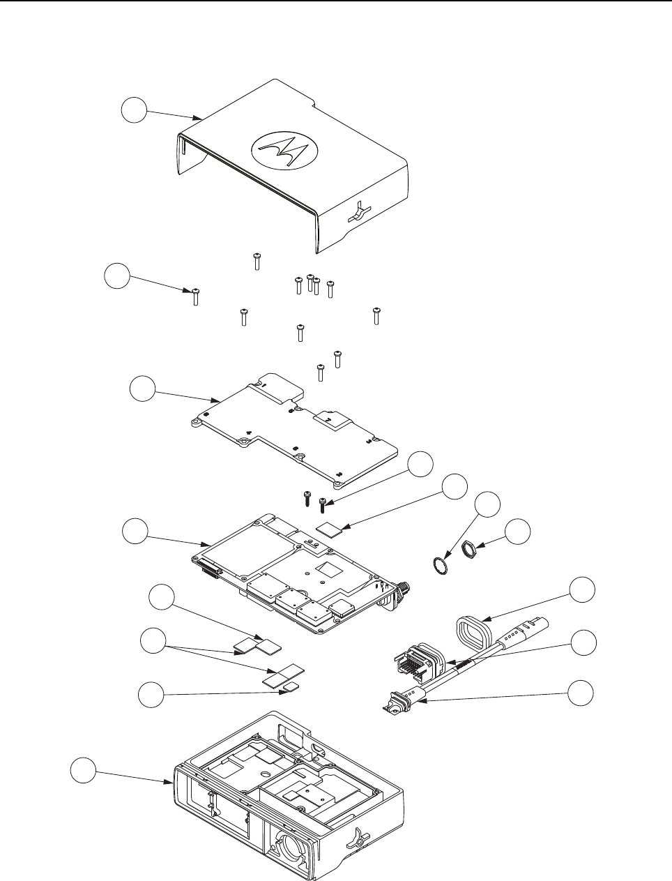
5-36 Disassembly/Reassembly Procedures: Exploded Mechanical Views and Parts Lists
5.8 Exploded Mechanical Views and Parts Lists
5.8.1 Radio Assembly Exploded View and Parts List
Figure 5-52 Radio Assembly Exploded View
1
5
4
2
6
7
8
13
10
3
9
14
15
12
11
Disassembly/Reassembly Procedures: Exploded Mechanical Views and Parts Lists 5-37
Table 5-3 Radio Exploded View Parts List
Item No. Description Part Number
1 Chassis, Die Cast 0104056J09
2 Thermal Pad, Final Driver 75012058002
3 Thermal Pad, Regulator 75012018001
4 Thermal Pad, Audio PA 75012059001
5 PCB, Transceiver
See Section 1.5 to
1.8 to identify proper
board.
6 Main Shield, Die Cast 26012273001
7 Screw - M3x0.5x13mm 0310943J12
8 Main Cover and Gasket Assembly 15012229001
9 Screw - M2.5x0.45x12mm with Washer 03012037002
10
Thermal Pad, PA Output Match
VHF 25–45W, VHF 1–25W, UHF1 25–40W 75012018001
UHF1 1–25W NOT PLACED
11 Lock Washer, RF Connector 04012004001
12 Nut, RF Connector 02012015001
13 Accessory Connector Cover 3202607Y01
14 Accessory Connector 28012058001
15 DC Cable Assembly 28012059001
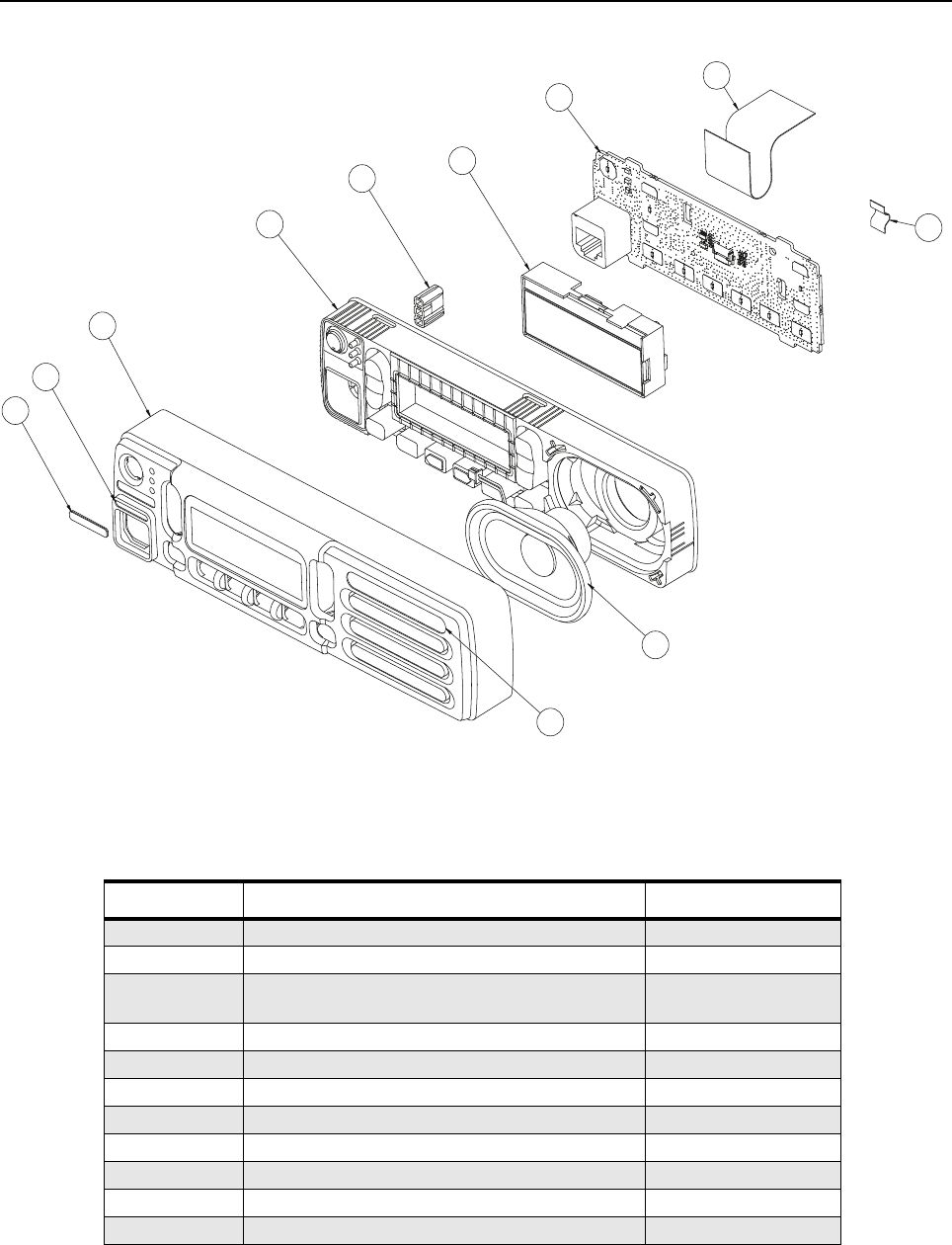
5-38 Disassembly/Reassembly Procedures: Exploded Mechanical Views and Parts Lists
5.8.2 Alphanumeric Display Control Head Exploded View and Parts List
Figure 5-53 Alphanumeric Display Control Head Exploded View
*Note: The PCB Assembly is not available for servicing. Must order PMLN6441_ (Alphanumeric
Display Control Head Kit)
Table 5-4 Alphanumeric Display Control Head (PMLN6441_) Exploded View Parts List
Item no Description Part No
1Nameplate, XPR 2500 33012051010
2 Label, Accessory Indicator 54012312001
3Housing Front Assembly, Alphanumeric Control
Head Plus
0104057J46
4 Nameplate, Motorola Logo 33012052001
5Speaker 5015935H02
6 Keypad, Alphanumeric Control Head Plus 75012212001
7Light Guide Holder 07012052001
8 2 Line Monochrome Display Module 72012024001
9PCB Assembly 0104057J47*
10 Cable Flex, Control Head 30012065001
11 Speaker Tape 11012133001
1
3
2
6
7
8
9
5
11
4
10
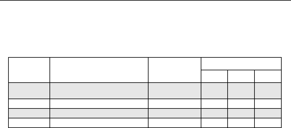
Disassembly/Reassembly Procedures: Torque Chart 5-39
5.9 Torque Chart
Table 5-5 lists the various nuts and screws by part number and description, followed by the torque
values in different units of measure. Torque all screws to the recommended value when assembling
the radio.
Table 5-5 Torque Specifications for Nuts and Screws
Part
Number Description Driver/Socket
Torque
N-m lbs-in kg-cm
02012015001 Nut, RF Connector 9/16” deep socket
driver
2.15 19 21.9
0310909E03 Screw, M2x0.4x6mm, Pan Head T6 Torx™0.28 2.5 2.9
03012037002 Screw, M2.5x0.45x12mm, Pan Head T8 Torx™0.45 44.6
0310943J12 Screw, M3x0.5x13mm, Pan Head T10 Torx™1.5 13 15

5-40 Disassembly/Reassembly Procedures: Torque Chart
Notes
Chapter 6 Basic Troubleshooting
6.1 Introduction
This chapter contains error codes and board replacement procedures. This section can help you
isolate a problem to the board level. If the radio does not pass all the performance checks in
Chapter 3 or exhibits an error code listed below, then the circuit board should be replaced. Please
send the radio to a Motorola Service Center listed in Appendix B.
NOTE: To access the various connector pins, use the housing eliminator/test fixture along with the
diagrams found in this section of the manual. (See Section, "Service Aids" on page 2-2, for
the appropriate Motorola service aids and tools part numbers.)
6.1.1 High Power RF Precaution
6.2 Replacement Service Kit Procedures
Once a problem has been isolated to a specific board, install the appropriate service kit (see Model
Charts in section 1.5 on page 1-4 through section 1.8 on page 1-5), which is orderable from Motorola
Radio Products and Solutions Organization at 1-800-422-4210.
Refer to https://businessonline.motorolasolutions.com for further information.
If a board is replaced, it does not necessarily need to be retuned if it has been factory tuned. It
should however be checked for performance before being placed into service. Of particular concern
is the Bias DAC, which will need to be set for the appropriate final device bias current prior to keying
up the radio. If the bias is not properly set it may be possible to cause damage to the transmitter.
The radio might transmit while the technician believes the radio is in receive
mode under the following conditions: radio failure, digital affiliation, a
defective PTT button, or other unintentional activations.
To avoid possible equipment damage, when performing both transmit and
receive tests, a suitable attenuator rated at 100 W or more should always
be used with test equipment connected to the RF connector. The only
exception to this is when the equipment’s input power rating is higher than
the maximum output power of the radio.
The Tuner Tool only allows the serial number of a blank board to be entered
once. Be very attentive during this procedure.
!
C a u t i o n
!
C a u t i o n
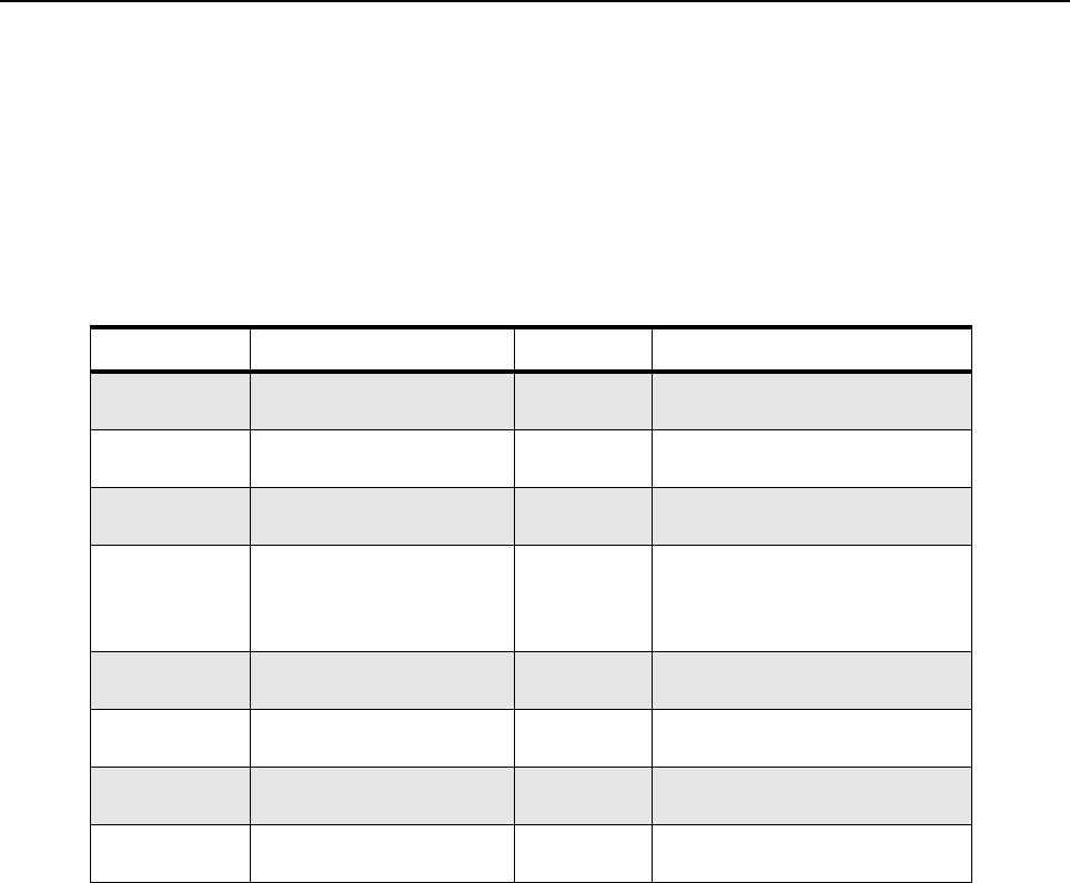
6-2 Basic Troubleshooting: Power-Up Error Codes
6.3 Power-Up Error Codes
When the radio is turned on (powered-up), the radio performs cursory tests to determine if its basic
electronics and software are in working order. Problems detected during these tests are presented
as error codes on the radio’s display. The presence of an error should prompt the user that a
problem exists and that a service technician should be contacted.
Self-test errors are classified as either fatal or non-fatal. Fatal errors inhibit user operation; non-fatal
errors do not. Use the following tables to aid in understanding particular power-up error code
displays.
Table 6-1 Power-Up Error Codes
Error Code Description Error Type Corrective Action
ERROR 01/02 FLASH ROM Codeplug
Checksum
NON-FATAL Reprogram the codeplug.
ERROR 01/22 Tuning Codeplug
Checksum
NON-FATAL Reprogram the tuning partition.
FAIL 01/82 FLASH ROM Codeplug
Checksum
FATAL Reprogram the codeplug.
FAIL 01/90 General Hardware Error FATAL Turn the radio off, then on. If
problem persists, send radio to
the nearest Motorola Solutions
Depot.
FAIL 01/92 Security Partition
Checksum
FATAL Reprogram the security partition.
FAIL 01/93 FlashPORT AUTHENT
CODE Failure
FATAL Contact the depot.
FAIL 01/A2 Tuning Codeplug
Checksum
FATAL Reprogram the tuning partition.
FAIL 02/90 RF Hardware Error FATAL Send radio to the nearest
Motorola Solutions Depot.
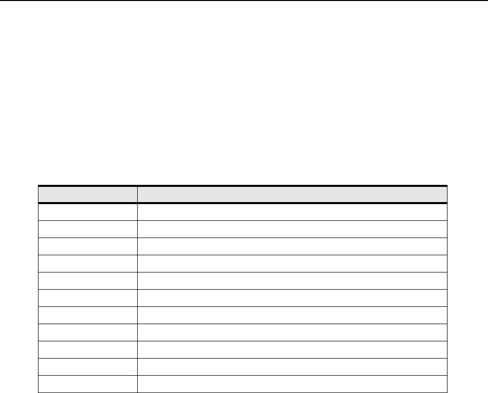
Chapter 7 Accessories
7.1 Introduction
Motorola provides the following approved accessories to improve the productivity of your digital
mobile two-way radio.
For a list of Motorola-approved antennas, and other accessories, visit the following web site:
http://www.motorolasolutions.com
7.1.1 Antennas
Part No. Description
HAD4006_ VHF, 136–144 MHz, 1/4 Wave Roof Mount, Mini-U
HAD4007_ VHF, 144–150.8 MHz, 1/4 Wave Roof Mount, Mini-U
HAD4008_ VHF, 150.8–162 MHz, 1/4 Wave Roof Mount, Mini-U
HAD4009_ VHF, 162–174 MHz, 1/4 Wave Roof Mount, Mini-U
HAD4022_ VHF, 132–174 MHz, 3.0 dB Gain, Through-hole Mount, Mini-U
HAE4002_ UHF, 403–430 MHz, 1/4 Wave Roof Mount, Mini-U
HAE4003_ UHF, 450–470 MHz, 1/4 Wave Roof Mount, Mini-U
HAE4010_ UHF, 406–420 MHz, 3.5 dB Gain Roof Mount, Mini-U
HAE4011_ UHF, 450–470 MHz, 3.5 dB Gain Roof Mount, Mini-U
HAE6022_ UHF, 403–527 MHz, 2.0 dB Gain, Through-hole Mount, Mini-U
RAE4004_RB UHF, 445–470 MHz, 5.0 dB Gain Roof Mount, Mini-U
7-2 Accessories: Introduction
7.1.2 Audio
7.1.3 Cables
7.1.4 Mounting Kits
Part No. Description
GMMN4065_ Visor Microphone (Omni-Direction)
HLN9073_ Microphone Hang-up Clip (requires install)
HLN9414_ Microphone Hang-up Clip (Universal – no install required)
HSN8145_ External Speaker 7.5 W
PMLN6481_ Telephone Style Handset Kit (Includes Hang Up Cup)
PMMN4089_ Enhanced Keypad Microphone
PMMN4090_ Compact Microphone with Clip
PMMN4091_ Heavy Duty Microphone
RSN4001_ External Speaker 13 W
PMLN6520_ Telephone Style Handset
Part No. Description
HKN4137_ Mobile Power Cable 10 FT., 14 AWG, 15 A
HKN4191_ Mobile Power Cable 10 FT., 12 AWG, 20 A
HKN4192_ Mobile Power Cable 20 FT., 10 AWG, 20 A
PMKN4147_ Front Telco MMP USB Programming Cable
PMKN4148_ Back 20 Pin MAP USB Programming Cable
HKN9327_R Ignition Switch Cable
PMKN4151_ Back 16 Pin MAP Universal Cable
GMKN4084_ Speaker Extension Cable
Part No. Description
FTN6083_ DIN Mount
RLN6466_ Low Profile Trunnion Kit
RLN6467_ High Profile Trunnion KIt
RLN6468_ Key Lock Trunnion Kit
03012045001 Trunnion Wing Screw M5x0.8x9.9 mm
Accessories: Introduction 7-3
7.1.5 Miscellaneous Accessories
7.1.6 Service Tools
Part No. Description
RLN4836_R External PTT with Emergency Footswitch
RLN4856_ Footswitch with Remote PTT
RLN4857_ Pushbutton with Remote PTT
HLN9457_ 16 Pin MAP Connector Kit
GMBN1021_ Rear Accessory Connector Seal with Connector and Pins
PMLN6544_ Generic Option Board
PMLN5620_ Connector Extender (20 pcs)
Part No. Description
GPN6145_ Mobile Radio Power Supply Unit
HPN4007_ Desktop Power Supply 1–60W
6686119B01 Control Head Removal Tool
66012020001 RFIC Repair Kit
PMEN4041_ Chassis Eliminator Kit
PMKN4149_ Back 20 Pin MAP Test and USB Programming Cable
PMKN4150_ Back 20 Pin MAP Test Cable
RLN4460_ Radio Test Box
6680388A26 Mobile Crimping Tool
GKN6266_ Power Supply Cable (for GPN6145)(PWR CBL DC BASE RENA)
3060665A04 Power Cable (US Plug) (110V CHGR LINE CORD)
RSX4043_ Torque Driver
6680387A74 TORX™ T10 Driver Bit
6680387A72 TORX™ T8 Driver Bit
6680387A70 TORX™ T6 Driver Bit

7-4 Accessories: Introduction
Notes

Appendix A Replacement Parts Ordering
A.1 Basic Ordering Information
Some replacement parts, spare parts, and/or product information can be ordered directly. While
parts may be assigned with a Motorola part number, this does not guarantee that they are available
from Motorola Radio Products and Solutions Organization (RPSO). Some parts may have become
obsolete and no longer available in the market due to cancelations by the supplier. If no Motorola
part number is assigned, the part is normally not available from Motorola, or is not a user-serviceable
part. Part numbers appended with an asterisk are serviceable by Motorola Depot only.
A.2 Motorola Online
Motorola Online users can access our online catalog at
https://businessonline.motorolasolutions.com
To register for online access, please call 1-800-422-4210 (for U.S. and Canada Service Centers
only). International customers can obtain assistance at https://businessonline.motorolasolutions.com
A.3 Mail Orders
Mail orders are only accepted by the US Federal Government Markets Division (USFGMD).
Motorola
7031 Columbia Gateway Drive
3rd Floor - Order Processing
Columbia, MD 21046
U.S.A.
A.4 Telephone Orders
Radio Products and Solutions Organization*
(United States and Canada)
7:00 AM to 7:00 PM (Central Standard Time)
Monday through Friday (Chicago, U.S.A.)
1-800-422-4210
1-847-538-8023 (United States and Canada)
U.S. Federal Government Markets Division (USFGMD)
1-877-873-4668
8:30 AM to 5:00 PM (Eastern Standard Time)
A.5 Fax Orders
Radio Products and Solutions Organization*
(United States and Canada)
1-800-622-6210
1-847-576-3023 (United States and Canada)
USFGMD
(Federal Government Orders)
1-800-526-8641 (For Parts and Equipment Purchase Orders)

A-2 Replacement Parts Ordering: Parts Identification
A.6 Parts Identification
Radio Products and Solutions Organization*
(United States and Canada)
1-800-422-4210
A.7 Product Customer Service
Radio Products and Solutions Organization (United States and Canada)
1-800-927-2744
* The Radio Products and Solutions Organization (RPSO) was formerly known as the Radio
Products Services Division (RPSD) and/or the Accessories and Aftermarket Division (AAD).

Appendix B Motorola Service Centers
B.1 Servicing Information
If a unit requires further complete testing, knowledge and/or details of component level
troubleshooting or service than is customarily performed at the basic level, please send the radio to
a Motorola Service Center as listed below or your nearest Authorized Service Center.
B.2 Motorola Service Center
1220 Don Haskins Drive
Suite A
El Paso, TX 79936
Tel: 915-872-8200
B.3 Motorola Federal Technical Center
10105 Senate Drive
Lanham, MD 20706
Tel: 1-800-969-6680
Fax: 1-800-784-4133
B.4 Canadian Technical Logistics Center
181 Whitehall Drive
Markham, Ontario
L3R 9T1
Toll Free: 800-543-3222

B-2 Motorola Service Centers Canadian Technical Logistics Center
Notes
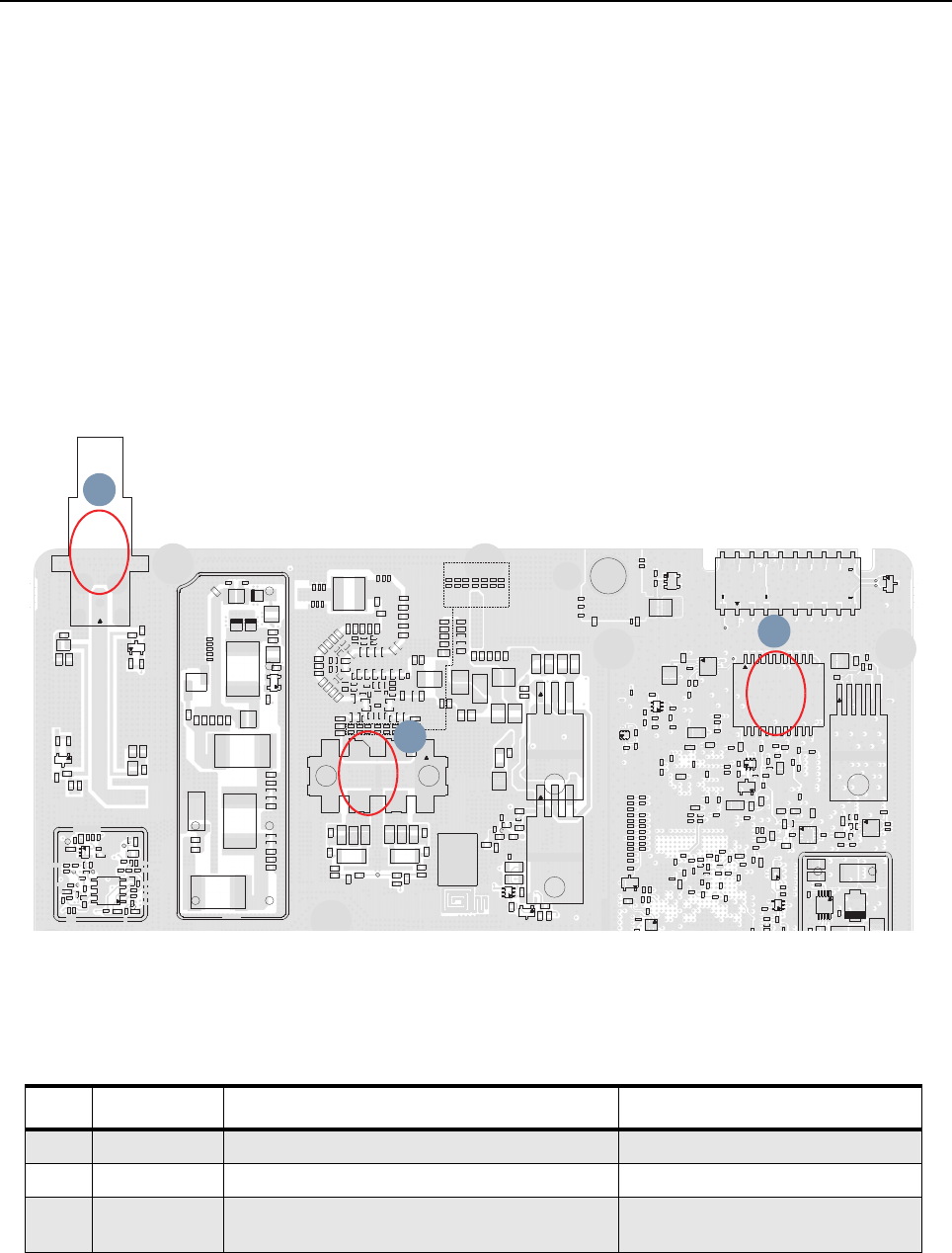
Appendix C Limited Level 3 Servicing
C.1 Maintenance
For details on the following, please refer to Chapter 5 Disassembly/Reassembly Procedures –
Section 5.2 on page 5-1 to Section 5.4 on page 5-4.
• Preventive maintenance (inspection and cleaning).
• Safe handling of CMOS and LDMOS devices.
• Repair procedures and techniques.
C.2 Component Location and Parts List
Figure C-1 PCB Top Side View
Table C-1. Component Parts List
No. Circuit Ref. Motorola Part Number Description
1J0700 09009348001 Mini-UHF Female RF Connector
2 U3204 51012450001 IC Audio Amplifier 1 Per Package
3Q0702 48012067002 (UHF1 1–25W/VHF 1–25W)
48012022001 (UHF1 25–40W/VHF 25–45W) RF MOSFET Power Transistor
G2
G1
2
3
J0700
2
3
R0950
C0950
R0957
R0958
C0951
C0952
D0950
L0952
R0956
2
3
R0955
R0954
C0955
D0951
C0954 R0953
C0953
R0951
L0950
R0952
L0951
1
4
58
2
5
4
3
R0913
R0962
C0957
R0961
C0902
R0959
C0901
R0922
C0900
R0921
R0965
C0925
C0917
R0920
R0916
C0916
R0917
U0902
TP0902
R0933
R0929
TP0904
R0928
R0924
TP0903
C0926
R0923
R0919
R0745
R0749
C0911
R0939
TP0900
RT0900
R0940
R0914
R0904
R0915
SH0900
C0772
C0776
C0918
R0932
R0931
U0904
R0960
C0956
R0930
C0919 R0744
2
3
4
C0929
L0852
L0727
C0855
C0788
C0822
C0718
C0928
SH0700
C0853
L0711
C0815
C0819
C0807
C0851
C0820
L0876
L0712
C0852
C0876
D0876
L0875
C0816
L0857
C0880
C0875
L0885
D0875
C0787
C0785
C0786
C0850
D0700
L0877
D0877
C0777
C0766 C0722
L0708
L0854
C0750
C0823
C0789
C0854
C0825
C0846
C0809
C0824
23
18
2
20
17
19
E4102
TP4103
E4100
E4101
VR4110
E4103
TP4102
J4100
5
C3112
C3129
R3107
R3175
C3111
R3106
10
11
20
U3204
5
10
6
3120
D3104
C3119
R3116
U3102
76
C3116
C3175
R3111
R3141
C3154
106
5
C3144
C3118
R3108
C3150
C3173
R3146
C3153
C3151
U3108
C3122
E3113
E3111
R3147
C3171
63
5
610
6
4
3
C2004
C2016
C2010
C2011
C2009
C3214
R3138
R3176
C2005
R3264
R3265
R3208
R3262
C3230
Q3201
R3256
R3230
R3231
R3142
R3263
R3132
C3209
R3261
Q3205
C3225
TP3109
U3109
C3152
C3106
R3102
R3101
C3102
C2008
6
4
3
3
2
R3200
E3202
Q3209
C3204
R3204
C2015
C2013
R3280
C3228
R3254
C3222
C3221
C3224
C3218
C3231
C3219
R3203
C3227
U3202
C3226
R3285
R1060
C3229
C2014
R3290
R3287
C3257
C2012
8
5
4
C3223
E3104
C1029
R3119
C3123
U3103
C3124
C1032
E1002
6U3100
3
45
TP4101
C3021
E3100
C3046
C3042
C3044
C3047
C3020
C3050
U3112
R3110
R3150
M3000
C3051
5
6
7
8
2
9
3
4
C0812
R0725
R0735
R0727
Q0702
M0700
R0738
R0732
R0734
C0814
C0753
R0737
R0741
R0739
TP0708
R0746
C0761
R0740
C0754
R0709
R0743
R0710
R0742
C0764
3
2G1
C3012
Q3000
C3013
R3015
R3006
C3014
C0745
R3005
E0701
3
2
R3004
R3003
R3002
R3001
C0857
C0848
R0736
C0828
C0752
C0818
C0714
C0934
C0858
E0703
L0710
3
6
G1
32
C0710
R0700
R0704
R0723
C0701
TP0710
C0731
R0720
R0935
0934
U0903
0921
R0883
R0712
C0775
Q0701
Q3001
R0711
R0718
C0727
C0732
C0706
5
4
6
9
43
5
037
038
U1010
R1042
C1021
R1045
R1001
R3173
U1004
C1010
C1009
R1023
C1008
E1003
C1002
C1005
C1047
E1004
E1001
C1060
C2020
C2007
C1025
R1026
C1006
C1007
C1015
C2006
C1041
C3248
R1049
R1051
R1050
C1013
C1014
R1036
R1052
R1035
R1044
R1033
C1001
R1046
C1019
C1020
C1044
R1012
C1042
C1026
C1018
C1022
C1017
C1028
C1036
C1023
C1003
R1019
C1035
C1045
R1027
R1021
R1028
R1014
R1016
R1018
R1062
R1064
R1011
R1024
R1030
R1010
R1040
R1031
R1069
R1025
R1022
3
2
6
43
10
C3140
C3139
U3106
R1077
R3180
C3180
R3181
Q1002
E3109
C0932
C0867
C3003
C0707
C0712
C0716
C0721
C0740
C0742
C0733
C3002
C0755
C0730
C0748
C0723
C0800
C0751
C0737
C0941
C0942
C0940
C0726
R0775
R0784
R0786
R0785
R0774
R0776
R0779
R0778
R0782
R0781
R0783
R0777
R0758
R0780
C0763
C0806
C0811
C0758
C0736
C0759
C0810
C0770
L0706
C0791
C0859
C0790
C0803
C0780
C0781
C0860
C0861
R0771
C0843
C0782
C0821
C0774
C0801
C0769
C0792
C0804
C0795
C0779
C0768
C0930
C0939
C0842
C0841
C0840
C0808
C0746
C0773
C0802
C0938
C0872
C0767
C0844
R0789
R0788
C0873
C0933
R0787
R0770
R0772
R0773
R0769
R0766
R0767
R0768
R0795
R0794
C0868
C0847
C0864
C0862
R0790
C0869
C0874
C0870
R0797
R0792
R0793
R0799
C0728
C0845
C0756
C0757
R0810R0804
R0811
R0803
R0802
R0801
R0796
R0800
C0771
C0805
C0863
C0865
R0798 R0760
R0763
R0807
R0808
R0812
R0809
R0805
R0806
R0791
2
1
3

C-2 Limited Level 3 Servicing: Component Location and Parts List
Notes

Glossary Glossary
This glossary contains an alphabetical listing of terms and their definitions that are applicable to
portable and mobile subscriber radio products. All terms do not necessarily apply to all radios, and
some terms are merely generic in nature.
Term Definition
Analog Refers to a continuously variable signal or a circuit or device designed to
handle such signals.
Band Frequencies allowed for a specific purpose.
CMOS Complementary Metal Oxide Semiconductor.
CPS Customer Programming Software: Software with a graphical user interface
containing the feature set of a radio.
Default A pre-defined set of parameters.
Digital Refers to data that is stored or transmitted as a sequence of discrete symbols
from a finite set; most commonly this means binary data represented using
electronic or electromagnetic signals.
DPL Digital Private-Line: A type of digital communications that utilizes privacy call,
as well as memory channel and busy channel lock out to enhance
communication efficiency.
FCC Federal Communications Commission.
Frequency Number of times a complete electromagnetic-wave cycle occurs in a fixed unit
of time (usually one second).
GPIO General-Purpose Input/Output.
GPS Global Positioning System.
IC Integrated Circuit: An assembly of interconnected components on a small
semiconductor chip, usually made of silicon. One chip can contain millions of
microscopic components and perform many functions.
IF Intermediate Frequency.
kHz kilohertz: One thousand cycles per second. Used especially as a radio
frequency unit.
LCD Liquid-Crystal Display: An LCD uses two sheets of polarizing material with a
liquid-crystal solution between them. An electric current passed through the
liquid causes the crystals to align so that light cannot pass through them.
LDMOS Laterally Diffused Metal Oxide Semiconductor.
LED Light Emitting Diode: An electronic device that lights up when electricity is
passed through it.
MDC Motorola Digital Communications.

Glossary-2
MHz Megahertz: One million cycles per second. Used especially as a radio
frequency unit.
Paging One-way communication that alerts the receiver to retrieve a message.
PC Board Printed Circuit Board. Also referred to as a PCB.
PL Private-Line Tone Squelch: A continuous sub-audible tone that is transmitted
along with the carrier.
Programming Cable A cable that allows the CPS to communicate directly with the radio using USB.
Receiver Electronic device that amplifies RF signals. A receiver separates the audio
signal from the RF carrier, amplifies it, and converts it back to the original
sound waves.
Repeater Remote transmit/receive facility that re-transmits received signals in order to
improve communications range and coverage (conventional operation).
RF Radio Frequency: The portion of the electromagnetic spectrum between audio
sound and infrared light (approximately 10 kHz to 10 GHz).
RX Receive.
Signal An electrically transmitted electromagnetic wave.
Spectrum Frequency range within which radiation has specific characteristics.
Squelch Muting of audio circuits when received signal levels fall below a pre-determined
value. With carrier squelch, all channel activity that exceeds the radio’s preset
squelch level can be heard.
TOT Time-out Timer: A timer that limits the length of a transmission.
TPL Tone Private Line.
Transceiver Transmitter-receiver. A device that both transmits and receives analog or digital
signals. Also abbreviated as XCVR.
Transmitter Electronic equipment that generates and amplifies an RF carrier signal,
modulates the signal, and then radiates it into space.
TX Transmit.
UHF Ultra-High Frequency.
USB Universal Serial Bus: An external bus standard that supports data transfer rates
of 12 Mbps.
VHF Very High Frequency.
VIP Vehicle Interface Port.
XPR Refers to Digital Professional Radio model names in the MOTOTRBO
Professional Digital Two-Way Radio System.
Term Definition

Motorola Solutions, Inc.
1303 East Algonquin Road
Schaumburg, Illinois 60196 U.S.A.
MOTOROLA, MOTO, MOTOROLA SOLUTIONS and
the Stylized M logo are trademarks or registered trademarks
of Motorola Trademark Holdings, LLC and are used under license.
All other trademarks are the property of their respective owners.
© 2013 Motorola Solutions, Inc. All rights reserved.
June 2013.
www.motorolasolutions.com/mototrbo
*68009620001*
68009620001-A
