Motorola XPR 8300/XPR 8400 MOTOTRBO Repeater Detailed Service Manual Series/XPR8300 XPR8400 6816811H01 G XPR8300
User Manual: -XPR Series/XPR8300 XPR8400 Detailed Service Manual 6816811H01-G
Open the PDF directly: View PDF ![]() .
.
Page Count: 532 [warning: Documents this large are best viewed by clicking the View PDF Link!]
- Front Cover
- Foreword
- Document History
- Commercial Warranty
- Table of Contents
- Summary of Printed Circuit Boards and Bands available
- Chapt1_Service Maintainability
- Chapt2_Repeater Indicator Board
- Section 1 Theory of Operation
- Section 2 Repeater Indicator Boards/Schematics/Parts Lists
- Theory of Operation
- Repeater Indicator Boards/Schematics/Parts Lists
- Chapt3_Connector Board
- Section 1 Theory of Operation
- Section 2 Connector Boards/Schematics/Parts Lists
- Theory of Operation
- Connector Boards/Schematics/Parts Lists
- Chapt4_Controller
- Section 1 Theory of Operation
- Section 2 Troubleshooting Charts
- Section 3 Controller Schematics/Parts Lists
- Theory of Operation
- Troubleshooting Charts
- Controller Schematics/Parts Lists
- Chapt5_VHF_LP
- Chapt6_VHF_HP
- Chapt7_UHF1_LP
- Chapt8_UHF1_HP
- Chapt9_UHF2_HP
- Appendix A
- Appendix B
- Glossary
- Back Cover
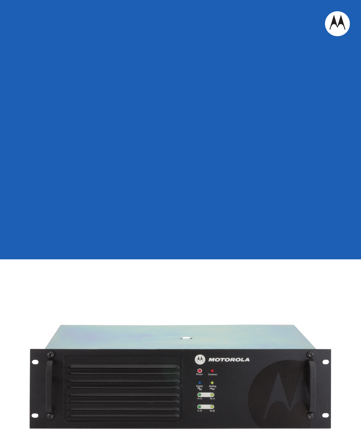
PROFESSIONAL DIGITAL TWO-WAY RADIO SYSTEM
MOTOTRBO™
REPEATER
DETAILED SERVICE
MANUAL
XPR™ 8300 REPEATER
XPR™ 8400 REPEATER

i
Foreword
This manual covers all models of the XPR™ 8300/XPR™8400 Repeater, unless otherwise specified. This manual
provides sufficient information to enable qualified service technicians to troubleshoot and repair the XPR™8300/
XPR™ 8400 Repeater to the component level.
For details on radio operation or basic troubleshooting, refer to the applicable manuals available separately.
Product Safety and RF Exposure Compliance
ATTENTION!
Before using this product, XPR™ 8300/XPR™ 8400 Repeater, read the RF Exposure and Safety guide
that ships with the repeater which contains important operating instructions for safe usage and RF
energy awareness and control for Compliance with applicable Standards and Regulations.
Computer Software Copyrights
The Motorola products described in this manual may include copyrighted Motorola computer programs stored in
semiconductor memories or other media. Laws in the United States and other countries preserve for Motorola certain
exclusive rights for copyrighted computer programs, including, but not limited to, the exclusive right to copy or reproduce
in any form the copyrighted computer program. Accordingly, any copyrighted Motorola computer programs contained in
the Motorola products described in this manual may not be copied, reproduced, modified, reverse-engineered, or
distributed in any manner without the express written permission of Motorola. Furthermore, the purchase of Motorola
products shall not be deemed to grant either directly or by implication, estoppel, or otherwise, any license under the
copyrights, patents or patent applications of Motorola, except for the normal non-exclusive license to use that arises by
operation of law in the sale of a product.
Document Copyrights
No duplication or distribution of this document or any portion thereof shall take place without the express written
permission of Motorola. No part of this manual may be reproduced, distributed, or transmitted in any form or by any
means, electronic or mechanical, for any purpose without the express written permission of Motorola.
Disclaimer
The information in this document is carefully examined, and is believed to be entirely reliable. However, no responsibility is
assumed for inaccuracies. Furthermore, Motorola reserves the right to make changes to any products herein to improve
readability, function, or design. Motorola does not assume any liability arising out of the applications or use of any product
or circuit described herein; nor does it cover any license under its patent rights nor the rights of others.
Trademarks
MOTOROLA, MOTO, MOTOROLA SOLUTIONS and the Stylized M logo are trademarks or registered trademarks of
Motorola Trademark Holdings, LLC and are used under license. All other trademarks are the property of their respective
owners.
© 2006–2010, 2014 Motorola Solutions, Inc. All rights reserved.
These servicing instructions are for use by qualified personnel only. To
reduce the risk of electric shock, do not perform any servicing other than
that contained in the Operating Instructions unless you are qualified to do
so. Refer all servicing to qualified service personnel.
!
C a u t i o n

ii
Notes

iii
Document History
The following major changes have been implemented in this manual since the previous edition:
Edition Description Date
6816811H01-A Initial edition. May 2007
6816811H01-B Added VHF High Power Band Information June 2007
6816811H01-C Added UHF Low Power and VHF Low Power Band
Information. Added issue C boards to all bands.
Nov. 2007
6816811H01-D Added UHF2 Band Information. June 2008
6816811H01-E For UHF2 Band: changed four capacitors namely
C0811, C0812, C0719 and C0746 in Power Amp
schematic and parts list .
Added section: Summary of Printed Circuit Boards and
Bands available in manual.
June 2009
6816811H01-F Added R6 Controller.
Added Repeater Indicator Board PMLN5643_.
Added Connector Board PMLN5644_.
Added a new set of Printed Circuit Boards, Schematics
and Parts Lists to: VHF (High & Low Power), UHF1
(High & Low Power), UHF2 (High Power) bands.
Sept. 2010
6816811H01-G Replaced Parts List of UHF1 HP PCB 8486777Z15.
Added 8486777Z15 Printed Circuit Board, Schematics
and Parts List to UHF2 band.
Feb. 2014

iv
Notes

Commercial Warranty v
Commercial Warranty
Limited Warranty
MOTOROLA COMMUNICATION PRODUCTS
I. What This Warranty Covers And For How Long
MOTOROLA INC. (“MOTOROLA”) warrants the MOTOROLA manufactured Communication
Products listed below (“Product”) against defects in material and workmanship under normal use and
service for a period of time from the date of purchase as scheduled below:
Motorola, at its option, will at no charge either repair the Product (with new or reconditioned parts),
replace it (with a new or reconditioned Product), or refund the purchase price of the Product during
the warranty period provided it is returned in accordance with the terms of this warranty. Replaced
parts or boards are warranted for the balance of the original applicable warranty period. All replaced
parts of Product shall become the property of MOTOROLA.
This express limited warranty is extended by MOTOROLA to the original end user purchaser only
and is not assignable or transferable to any other party. This is the complete warranty for the Product
manufactured by MOTOROLA. MOTOROLA assumes no obligations or liability for additions or
modifications to this warranty unless made in writing and signed by an officer of MOTOROLA.
Unless made in a separate agreement between MOTOROLA and the original end user purchaser,
MOTOROLA does not warrant the installation, maintenance or service of the Product.
MOTOROLA cannot be responsible in any way for any ancillary equipment not furnished by
MOTOROLA which is attached to or used in connection with the Product, or for operation of the
Product with any ancillary equipment, and all such equipment is expressly excluded from this
warranty. Because each system which may use the Product is unique, MOTOROLA disclaims
liability for range, coverage, or operation of the system as a whole under this warranty.
II. General Provisions
This warranty sets forth the full extent of MOTOROLA'S responsibilities regarding the Product.
Repair, replacement or refund of the purchase price, at MOTOROLA's option, is the exclusive
remedy. THIS WARRANTY IS GIVEN IN LIEU OF ALL OTHER EXPRESS WARRANTIES.
IMPLIED WARRANTIES, INCLUDING WITHOUT LIMITATION, IMPLIED WARRANTIES OF
MERCHANTABILITY AND FITNESS FOR A PARTICULAR PURPOSE, ARE LIMITED TO THE
DURATION OF THIS LIMITED WARRANTY. IN NO EVENT SHALL MOTOROLA BE LIABLE FOR
DAMAGES IN EXCESS OF THE PURCHASE PRICE OF THE PRODUCT, FOR ANY LOSS OF
USE, LOSS OF TIME, INCONVENIENCE, COMMERCIAL LOSS, LOST PROFITS OR SAVINGS
OR OTHER INCIDENTAL, SPECIAL OR CONSEQUENTIAL DAMAGES ARISING OUT OF THE
USE OR INABILITY TO USE SUCH PRODUCT, TO THE FULL EXTENT SUCH MAY BE
DISCLAIMED BY LAW.
Repeater Two (2) Years
Product Accessories One (1) Year

vi Commercial Warranty
III. State Law Rights
SOME STATES DO NOT ALLOW THE EXCLUSION OR LIMITATION OF INCIDENTAL OR
CONSEQUENTIAL DAMAGES OR LIMITATION ON HOW LONG AN IMPLIED WARRANTY
LASTS, SO THE ABOVE LIMITATION OR EXCLUSION MAY NOT APPLY.
This warranty gives specific legal rights, and there may be other rights which may vary from state to
state.
IV. How To Get Warranty Service
You must provide proof of purchase (bearing the date of purchase and Product item serial number)
in order to receive warranty service and, also, deliver or send the Product item, transportation and
insurance prepaid, to an authorized warranty service location. Warranty service will be provided by
Motorola through one of its authorized warranty service locations. If you first contact the company
which sold you the Product, it can facilitate your obtaining warranty service. You can also call
Motorola at 1-888-567-7347 US/Canada.
V. What This Warranty Does Not Cover
A. Defects or damage resulting from use of the Product in other than its normal and customary
manner.
B. Defects or damage from misuse, accident, water, or neglect.
C. Defects or damage from improper testing, operation, maintenance, installation, alteration,
modification, or adjustment.
D. Breakage or damage to antennas unless caused directly by defects in material workmanship.
E. A Product subjected to unauthorized Product modifications, disassemblies or repairs
(including, without limitation, the addition to the Product of non-Motorola supplied equipment)
which adversely affect performance of the Product or interfere with Motorola's normal
warranty inspection and testing of the Product to verify any warranty claim.
F. Product which has had the serial number removed or made illegible.
G. Freight costs to the repair depot.
H. A Product which, due to illegal or unauthorized alteration of the software/firmware in the
Product, does not function in accordance with MOTOROLA’s published specifications or the
FCC type acceptance labeling in effect for the Product at the time the Product was initially
distributed from MOTOROLA.
I. Scratches or other cosmetic damage to Product surfaces that does not affect the operation of
the Product.
J. Normal and customary wear and tear.

Commercial Warranty vii
VI. Patent And Software Provisions
MOTOROLA will defend, at its own expense, any suit brought against the end user purchaser to the
extent that it is based on a claim that the Product or parts infringe a United States patent, and
MOTOROLA will pay those costs and damages finally awarded against the end user purchaser in
any such suit which are attributable to any such claim, but such defense and payments are
conditioned on the following:
A. that MOTOROLA will be notified promptly in writing by such purchaser of any notice of such
claim;
B. that MOTOROLA will have sole control of the defense of such suit and all negotiations for its
settlement or compromise; and
C. should the Product or parts become, or in MOTOROLA's opinion be likely to become, the
subject of a claim of infringement of a United States patent, that such purchaser will permit
MOTOROLA, at its option and expense, either to procure for such purchaser the right to
continue using the Product or parts or to replace or modify the same so that it becomes
noninfringing or to grant such purchaser a credit for the Product or parts as depreciated and
accept its return. The depreciation will be an equal amount per year over the lifetime of the
Product or parts as established by MOTOROLA.
MOTOROLA will have no liability with respect to any claim of patent infringement which is based
upon the combination of the Product or parts furnished hereunder with software, apparatus or
devices not furnished by MOTOROLA, nor will MOTOROLA have any liability for the use of ancillary
equipment or software not furnished by MOTOROLA which is attached to or used in connection with
the Product. The foregoing states the entire liability of MOTOROLA with respect to infringement of
patents by the Product or any parts thereof.
Laws in the United States and other countries preserve for MOTOROLA certain exclusive rights for
copyrighted MOTOROLA software such as the exclusive rights to reproduce in copies and distribute
copies of such Motorola software. MOTOROLA software may be used in only the Product in which
the software was originally embodied and such software in such Product may not be replaced,
copied, distributed, modified in any way, or used to produce any derivative thereof. No other use
including, without limitation, alteration, modification, reproduction, distribution, or reverse
engineering of such MOTOROLA software or exercise of rights in such MOTOROLA software is
permitted. No license is granted by implication, estoppel or otherwise under MOTOROLA patent
rights or copyrights.
VII. Governing Law
This Warranty is governed by the laws of the State of Illinois, USA.

Notes
viii Commercial Warranty

February, 2014
XPR 8300/XPR 8400
MOTOTRBO Repeater
Detailed Service Manual
Contents
Chapter 1 Service Maintainability
Chapter 2 Repeater Indicator Board Service Information
Chapter 3 Connector Board Service Information
Chapter 4 Controller Service Information
Chapter 5 VHF Low Power Service Information
Chapter 6 VHF High Power Service Information
Chapter 7 UHF1 Low Power Service Information
Chapter 8 UHF1 High Power Service Information
Chapter 9 UHF2 High Power Service Information
Appendix A Replacement Parts Ordering
Appendix B Motorola Service Centers
Glossary

x
Notes

xi
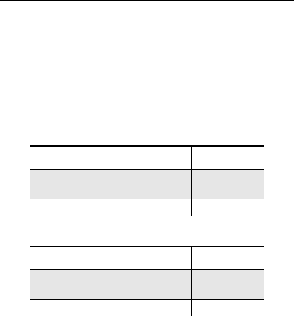
Summary of Printed Circuit Boards and Bands available:
Table below lists all the bands available in this manual and the revision of the Printed Circuit Boards used. For
details, please refer to the respective chapters.
Chapter Description PC Board Part Number Board Revision
2Repeater Indicator Board (PMLN4814_) 8415470H02 B
2 Repeater Indicator Board (PMLN5269_) 8415470H04 D
2Repeater Indicator Board (PMLN5643_) 84012135001 A
3 Connector Board (PMLN4815_) 8415472H01 A
3Connector Board (PMLN5270_) 8415472H05 E
3 Connector Board (PMLN5644_) 8402133002 B
5VHF Low Power 136–174 MHz, 1–25 W 8471495L01
8471495L03
8471495L04
A
C
D
6 VHF High Power 136–174 MHz, 25–45 W 8478023A12
8478023A16
8478023A17
P8
C
D
7UHF1 Low Power 403–470 MHz, 1–25 W 8471165L03
8471165L05
8471165L06
A
C
D
8 UHF1 High Power 403–470 MHz, 25–40 W 8486777Z12
8486777Z14
8486777Z15
A
C
D
9UHF2 High Power 450–512 MHz, 1–40 W 8471696M01
8471696M02
8486777Z15
A
D
D

xii
Notes

XPR 8300/XPR8400
MOTOTRBO Repeater
Chapter 1
Service Maintainability
M
Issue: February, 2014

Computer Software Copyrights
The Motorola products described in this manual may include copyrighted Motorola computer programs stored
in semiconductor memories or other media. Laws in the United States and other countries preserve for
Motorola certain exclusive rights for copyrighted computer programs, including, but not limited to, the
exclusive right to copy or reproduce in any form the copyrighted computer program. Accordingly, any
copyrighted Motorola computer programs contained in the Motorola products described in this manual may
not be copied, reproduced, modified, reverse-engineered, or distributed in any manner without the express
written permission of Motorola. Furthermore, the purchase of Motorola products shall not be deemed to grant
either directly or by implication, estoppel, or otherwise, any license under the copyrights, patents or patent
applications of Motorola, except for the normal non-exclusive license to use that arises by operation of law in
the sale of a product.

i
Chapter 1 – Service Maintainability
Table of Contents
Section 1 Introduction
1.0 Notations Used in This Manual ............................................................................1-1
2.0 Repeater Description ...........................................................................................1-1
Section 2 Maintenance
1.0 Introduction ..........................................................................................................2-1
2.0 Preventive Maintenance ......................................................................................2-1
2.1 Inspection .......................................................................................................2-1
2.2 Cleaning Procedures ......................................................................................2-1
3.0 Safe Handling of CMOS and LDMOS Devices ....................................................2-2
4.0 Repair Procedures and Techniques – General....................................................2-3
Section 3 Test Equipment and Service Aids
1.0 Recommended Test Equipment ..........................................................................3-1
2.0 Service Aids .........................................................................................................3-2
3.0 Programming Cables ...........................................................................................3-3

ii
Notes
1-1
Section 1
INTRODUCTION
1.0 Notations Used in This Manual
Throughout the text in this publication, you will notice the use of note and caution notations. These
notations are used to emphasize that safety hazards exist, and due care must be taken and
observed.
NOTE: An operational procedure, practice, or condition that is essential to emphasize.
2.0 Repeater Description
The XPR 8300/XPR 8400 repeater is available in the following frequency ranges and power levels.
This repeater is among the most sophisticated two-way repeaters available. It has a robust design
for users who need high performance, quality, and reliability in their daily communications. This
architecture provides the capability of supporting a multitude of legacy and advanced features
resulting in a more cost-effective two-way repeater communications solution.
CAUTION indicates a potentially hazardous situation which, if
not avoided, might result in equipment damage.
Table 1-1 Frequency Ranges and Power Levels
Freq. Band Bandwidth Power Level
VHF 136–174 MHz 1–25 Watts
25–45 Watts
350 350–400 MHz 25–40 Watts
UHF B1 403–470 MHz 1–25 Watts
25–40 Watts
UHF B2 450–512 MHz 1–40 Watts
!
C a u t i o n

1-2 Repeater Description
Notes

2-1
Section 2
MAINTENANCE
1.0 Introduction
This chapter provides details about the following:
•Preventive maintenance (inspection and cleaning).
•Safe handling of CMOS and LDMOS devices.
•Repair procedures and techniques.
2.0 Preventive Maintenance
Periodic visual inspection and cleaning is recommended.
2.1 Inspection
Check that the external surfaces of the repeater are clean, and that all external controls and
switches are functional. It is not recommended to inspect the interior electronic circuitry.
2.2 Cleaning Procedures
The following procedures describe the recommended cleaning agents and the methods to be used
when cleaning the external and internal surfaces of the repeater. External surfaces include the top
cover and repeater enclosure.
Periodically clean smudges and grime from exterior enclosure. Use a soft, non-abrasive cloth
moistened in a mild soap and water solution Rinse the surface using a second cloth moistened in
clean water, and clean any dirt or debris from the fan grill and louvers on the front side.
NOTE: Internal surfaces should be cleaned only when the repeater is disassembled for service or
repair.
The only recommended agent for cleaning the external repeater surfaces is a 0.5% solution of a mild
dishwashing detergent in water. The only factory recommended liquid for cleaning the printed circuit
boards and their components is isopropyl alcohol (100% by volume).
Cleaning Internal Circuit Boards and Components
Isopropyl alcohol (100%) may be applied with a stiff, non-metallic, short-bristled brush to dislodge
embedded or caked materials located in hard-to-reach areas. The brush stroke should direct the
dislodged material out and away from the inside of the repeater. Make sure that controls or tunable
components are not soaked with alcohol. Do not use high-pressure air to hasten the drying process
since this could cause the liquid to collect in unwanted places. Once the cleaning process is
complete, use a soft, absorbent, lintless cloth to dry the area. Do not brush or apply any isopropyl
alcohol to the top cover and repeater enclosure.
NOTE: Always use a fresh supply of alcohol and a clean container to prevent contamination by
dissolved material (from previous usage).

2-2 Safe Handling of CMOS and LDMOS Devices
3.0 Safe Handling of CMOS and LDMOS Devices
Complementary Metal Oxide Semiconductor (CMOS) and Laterally Diffused Metal Oxide
Semiconductor (LDMOS) devices are used in this family of repeaters, and are susceptible to
damage by electrostatic or high voltage charges. Damage can be latent, resulting in failures
occurring weeks or months later. Therefore, special precautions must be taken to prevent device
damage during disassembly, troubleshooting, and repair.
Handling precautions are mandatory for CMOS/LDMOS circuits and are especially important in low
humidity conditions.
DO NOT attempt to disassemble the repeater without first referring to the following CAUTION
statement.
This repeater contains static-sensitive devices. Do not open the repeater unless you
are properly grounded. Take the following precautions when working on this unit:
• Store and transport all CMOS/LDMOS devices in conductive
material so that all exposed leads are shorted together. Do not insert
CMOS/LDMOS devices into conventional plastic “snow” trays used
for storage and transportation of other semiconductor devices.
• Ground the working surface of the service bench to protect the
CMOS/LDMOS device. We recommend using a wrist strap, two
ground cords, a table mat, a floor mat, ESD shoes, and an ESD
chair.
• Wear a conductive wrist strap in series with a 100k resistor to
ground. (Replacement wrist straps that connect to the bench top
covering are Motorola part number 4280385A59).
• Do not wear nylon clothing while handling CMOS/LDMOS devices.
• Do not insert or remove CMOS/LDMOS devices with power applied.
Check all power supplies used for testing CMOS/LDMOS devices to
be certain that there are no voltage transients present.
• When straightening CMOS/LDMOS pins, provide ground straps for
the apparatus used.
• When soldering, use a grounded soldering iron.
• If at all possible, handle CMOS/LDMOS devices by the package and
not by the leads. Prior to touching the unit, touch an electrical
ground to remove any static charge that you may have
accumulated. The package and substrate may be electrically
common. If so, the reaction of a discharge to the case would cause
the same damage as touching the leads.
!
C a u t i o n
Repair Procedures and Techniques – General 2-3
4.0 Repair Procedures and Techniques – General
Any rework or repair on Environmentally Preferred Products must be done using the appropriate
lead-free solder wire and lead-free solder paste as stated in the following table:
Parts Replacement and Substitution
When damaged parts are replaced, identical parts should be used. If the identical replacement part
is not locally available, check the parts list for the proper Motorola part number and order the part.
Refer to Appendix A of this manual.
Rigid Circuit Boards
The repeater uses bonded, multi-layer, printed circuit boards. Since the inner layers are not
accessible, some special considerations are required when soldering and unsoldering components.
The printed through holes may interconnect multiple layers of the printed circuit. Therefore, exercise
care to avoid pulling the plated circuit out of the hole.
When soldering near a connector:
•Avoid accidentally getting solder in the connector.
•Be careful not to form solder bridges between the connector pins.
•Examine your work closely for shorts due to solder bridges.
For soldering components with Hot-Air or infra red solder systems, please check your user guide of
the solder system to get information on solder temperature and time for the different housings of the
integrated circuits and other components.
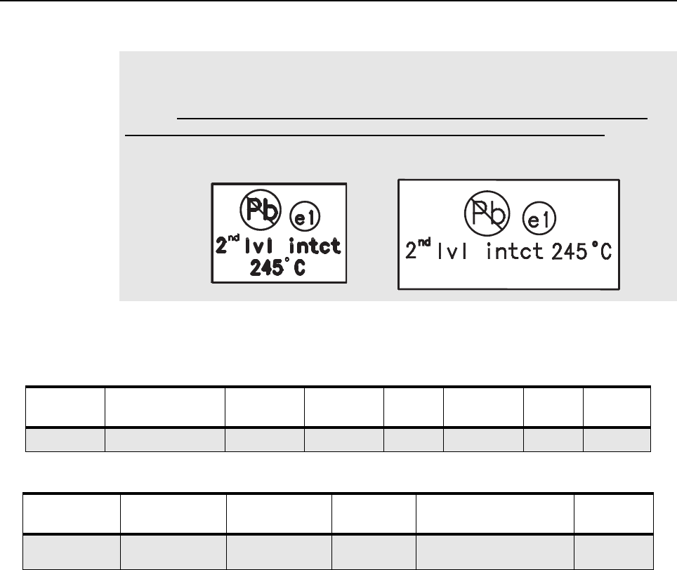
NOTE Environmentally Preferred Products (EPP) (refer to the marking on the printed circuit
boards – examples shown below) were developed and assembled using environmentally
preferred components and solder assembly techniques to comply with the European
Union’s Restriction of Hazardous Substances (ROHS 2) Directive 2011/65/EU and
Waste Electrical and Electronic Equipment (WEEE) Directive 2012/19/EU. To
maintain product compliance and reliability, use only the Motorola specified parts in this
manual.
Table 2-1 Lead Free Solder Wire Part Number List
Motorola
Part Number Alloy Flux Type Flux Content
by Weight
Melting
Point
Supplier Part
number Diameter Weight
1088929Y01 95.5Sn/3.8Ag/0.7Cu RMA Version 2.7–3.2% 217°C 52171 0.015” 1lb spool
Table 2-2 Lead Free Solder Paste Part Number List
Motorola Part
Number
Manufacturer Part
Number Viscosity Type Composition & Percent Metal Liquid
Temperature
1085674C03 NC-SMQ230 900–1000KCPs
Brookfield (5rpm)
Type 3
(-325/+500)
(95.5%Sn–3.8%Ag–0.7%Cu)
89.3%
217°C

2-4 Repair Procedures and Techniques – General
Notes

3-1
Section 3
TEST EQUIPMENT AND SERVICE AIDS
1.0 Recommended Test Equipment
The list of equipment contained in Table 3-1 includes most of the standard test equipment required
for servicing Motorola repeaters.
Table 3-1 Recommended Test Equipment
Equipment Characteristic Example Application
Service Monitor Can be used as a
substitute for items
marked with an asterisk
(*)
Aeroflex 3920, or equivalent Frequency/deviation meter and
signal generator for wide-range
troubleshooting and alignment
Digital RMS
Multimeter*
100 µV to 300 V
5 Hz to 1 MHz
10 Mega Ohm
Impedance
Fluke 179 or equivalent
(www.fluke.com)
AC/DC voltage and current
measurements. Audio voltage
measurements.
RF Signal
Generator*
100 MHz to 1 GHz
-130 dBM to +10 dBM
FM Modulation 0 kHz to
10 kHz
Agilent N5181
(www.agilent.com) or equivalent
Receiver measurements
Oscilloscope* 2 Channels
50 MHz Bandwidth
5 mV/div to 20 V/div
Tektronix TDS1001b
(www.tektronix.com) or
equivalent
Waveform measurements
Power Meter and
Sensor*
5% Accuracy
100 MHz to 500 MHz
50 Watts
Bird 43 Thruline Watt Meter
(www.bird-electronic.com) or
equivalent
Transmitter power output
measurements
RF Millivolt Meter 100 mV to 3 V RF
10 kHz to 1 GHz
Boonton 92EA
(www.boonton.com) or
equivalent
RF level measurements

3-2 Service Aids
2.0 Service Aids
Table 3-2 lists the service aids recommended for working on the repeater. While all of these items
are available from Motorola, most are standard workshop equipment items, and any equivalent item
capable of the same performance may be substituted for the item listed.
Table 3-2 Service Aids
Motorola
Part Number Description Application
RLN4460_ Test Box Enables connection to audio/accessory jack. Allows
switching for radio testing.
RVN5115_ Customer Programming Soft-
ware on CD-ROM
Allows servicer to program repeater parameters, tune
and troubleshoot repeaters.
PMKN4010_ Mobile & Repeater Rear
Programming Cable
Connects the radio’s rear connector to a USB port for
radio programming and data applications.
PMKN4016_ Mobile & Repeater Rear
Accessory Programming and
Test Cable
Connects the radio’s rear connector to a USB port for
radio programming, data applications, testing and
alignment.
PMKN4018_ Mobile & Repeater Rear
Accessory Connector Universal
Cable
Connects the radio’s rear connector to accessory
devices such as desk sets. Cable contains all 26 wires
and is unterminated at the user end.
Programming Cables 3-3
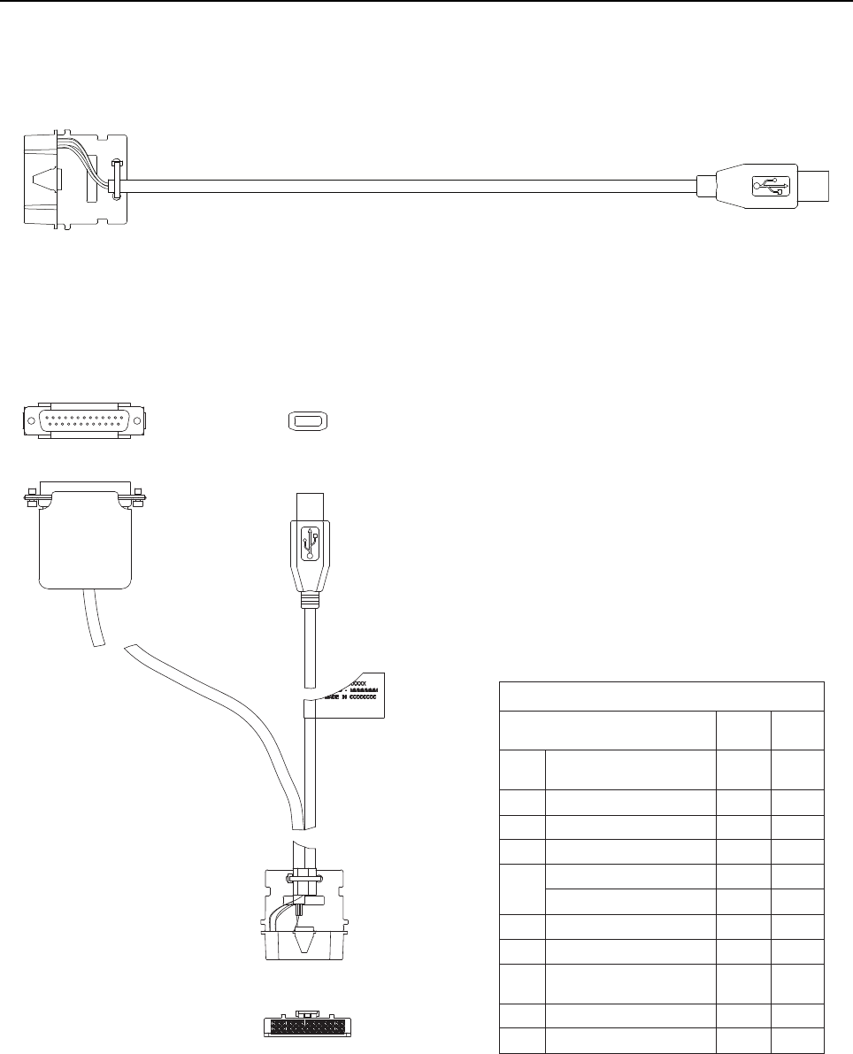
3.0 Programming Cables
Figure 3-1 Mobile & Repeater Rear Programming Cable PMKN4010_
Figure 3-2 Mobile & Repeater Rear Accessory Programming and Test Cable PMKN4016_
TABLE 2-3: WIRE DIAGRAM
26 PIN
ACCESSORY PORT CONNECTOR USB DB25P
PIN
NO. DESCRIPTION
3 VCC (5v) 1
2DATA - 2
1DATA + 3
4
GND 4
DRAIN WIRE AND BRAID SHELL
7SPEAKER -9
71EXT MIC11
17 DIGI IN I
(EXT PTT) 20
61GND61
1SPEAKER +01
DB 25 CONNECTOR
1
1
14 25
13 14
915±15
CABLE 1455±24
CABLE
TO MOBILE RADIO
ACCESSORY
CONNECTOR
VIEWED FROM
FRONT (PIN END)
OF CONNECTOR
1
226
25
13
14 25
USB CONNECTOR

3-4 Programming Cables
Notes

XPR 8300/XPR 8400
MOTOTRBO Repeater
Chapter 2
Repeater Indicator Board
Service Information
M
Issue: February, 2014

Computer Software Copyrights
The Motorola products described in this manual may include copyrighted Motorola computer programs stored
in semiconductor memories or other media. Laws in the United States and other countries preserve for
Motorola certain exclusive rights for copyrighted computer programs, but not limited to, the exclusive right to
copy or reproduce in any form, the copyrighted computer program. Accordingly, any copyrighted Motorola
computer programs contained in the Motorola products described in this manual may not be copied,
reproduced, modified, reverse-engineered, or distributed in any manner without the express written
permission of Motorola. Furthermore, the purchase of Motorola products shall not be deemed to grant either
directly or by implication, estoppel or otherwise, any license under the copyrights, patents or patent
applications of Motorola, except for the normal non-exclusive license to use that arises by operation of law in
the sale of a product.

i
Chapter 2 – Repeater Indicator Board Service
Information
Table of Contents
Section 1 Theory of Operation
1.0 Overview ..............................................................................................................1-1
2.0 Repeater Indicator Board.....................................................................................1-1
3.0 Ethernet Interface ................................................................................................1-2
Section 2 Repeater Indicator Boards/Schematics/Parts Lists
1.0 Allocation of Printed Circuit Boards, Schematics and Parts Lists ........................2-1
1.1 Repeater Indicator Board Circuits ..................................................................2-1
2.0 Repeater Indicator Board (PMLN4814_) PCB/Schematics/Parts List .................2-3
Repeater Indicator Board PCB 8415470H02 (Top Side)........................................2-3
Repeater Indicator Board PCB 8415470H02 (Bottom Side) ..................................2-4
Repeater Indicator Board Schematic Diagram (Sheet 1 of 2) ................................2-5
Repeater Indicator Board Schematic Diagram (Sheet 2 of 2) ................................2-6
2.1 Repeater Indicator Board Parts List PMLN4814_ ..........................................2-7
3.0 Repeater Indicator Board (PMLN5269_) PCB/Schematics/Parts List .................2-9
Repeater Indicator Board PCB 8415470H04 (Top Side)........................................2-9
Repeater Indicator Board PCB 8415470H04 (Bottom Side) ................................2-10
Repeater Indicator Board Schematic Diagram (Sheet 1 of 2) ..............................2-11
Repeater Indicator Board Schematic Diagram (Sheet 2 of 2) ..............................2-12
3.1 Repeater Indicator Board Parts List PMLN5269_ ........................................2-13
4.0 Repeater Indicator Board (PMLN5643_) PCB/Schematics/Parts List ...............2-15
Repeater Indicator Board PCB 84012135001 (Top Side) ....................................2-15
Repeater Indicator Board PCB 84012135001 (Bottom Side) ...............................2-16
Repeater Indicator Board Schematic Diagram (Sheet 1 of 2) ..............................2-17
Repeater Indicator Board Schematic Diagram (Sheet 2 of 2) ..............................2-18
4.1 Repeater Indicator Board Parts List PMLN5643_ ........................................2-19

ii
Notes
1-1
Section 1
THEORY OF OPERATION
1.0 Overview
This section provides a detailed theory of operation for the Repeater Indicator Board and its
components.
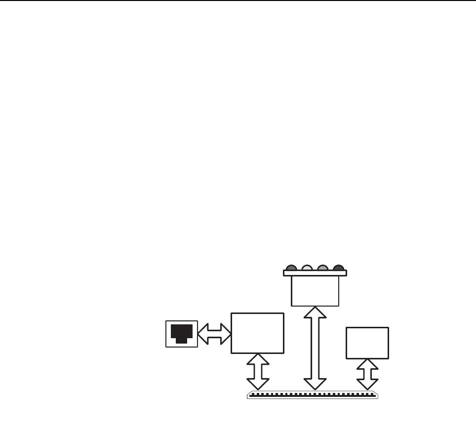
2.0 Repeater Indicator Board
The Repeater Indicator board contains circuitry to drive the front panel indicator LEDs, an RTC
battery for the RTC in the transmit radio, as well as an Ethernet controller.
Figure 1-1 Repeater Indicator Board Block Diagram
All of the indicator LEDs that are on the front of the Repeater chassis reside on the Repeater
Indicator board. Each is controlled by a shift register (U6) data out signal and a digital transistor. The
shift register accepts serial data in from the transmit radio's OMAP processor via a SPI bus. A
74LVC07 buffer (U9) level shifts these signals from 3.3 V to 1.8 V.
The Repeater Disable LED is a dual-purpose LED that is hardware controlled initially at power-up.
As soon as VBUS power is available on the Repeater Indicator board, the hardware circuitry for the
Repeater Disable LED will cause it to blink periodically. When the software initialization is completed
by the firmware, the blink circuitry will be disabled by the firmware. At that point, the Repeater
Disable LED can be used for its intended purpose of displaying when the Repeater Disable function
is turned on.
USB to
Ethernet
Interface
Display
Driver
RTC
Backup
Ethernet to
Rear Panel
Flex to Transmit Radi o
Front Panel Indicators

1-2 Ethernet Interface
The power LED is the only LED that is not controlled by the software. This bi-color LED gets turned
on green when the 13.8 V output from the power supply is valid. It turns on red when A/C power is
lost, and the repeater's backup battery is used.
The Real Time Clock (RTC) battery (M1) is connected to the transmit radio through the Control
Head Connector (J1, pin 30).
3.0 Ethernet Interface
The Repeater board uses an SMSC LAN9500 USB to 10/100 Ethernet controller (U8) to convert
data from USB to Ethernet and vice-versa. An external 128 x 8 EEPROM (U2) is used to store the
Ethernet MAC address and various USB configuration parameters. The transformer (T1) provides
isolation between the Ethernet port and the Ethernet controller.
The LAN9500 controller integrates a 10/100 Ethernet MAC, 10/100 Ethernet PHY, USB 2.0 device
controller, TAP controller, EEPROM controller, and a FIFO controller with 30 KB of internal packet
buffering. The Ethernet controller supports auto-negotiation, auto-polarity correction, HP Auto-
MDIX, and is compliant with the IEEE 802.3 and IEEE 802.3u standards. The internal EEPROM
controller is used to load various USB configuration parameters and the device MAC address upon
power-up. The USB portion of the LAN9500 integrates a High-speed USB 2.0 device controller and
USB PHY. The USB device controller configures to Full-speed when communicating with the USB
host controller on the TX transceiver board.
The LAN9500 integrates a 10/100 Ethernet MAC and an IEEE 802.3 PHY for twisted pair Ethernet
applications. The PHY can be configured for 10Base-T (10 Mbps) or 100Base-TX (100 Mbps) and
supports auto-negotiation, and full or half-duplex configurations. The controller also provides LED
control signals for indicating Ethernet speed, link, and duplex configuration status. The Ethernet
speed and Link LEDs reside on the Connector board's external Ethernet connector. The Link LED is
the yellow LED and is lit solid when an Ethernet link is valid or blinking when there is transmit or
receive activity. The speed LED is the green LED and indicates 100 Mbit operation when lit.
All of the Ethernet signals are transported to the Connector board through an Ethernet cable that
connects the Repeater board to the Connector board. The LED signals are transported to the
Connector board through an 8-pin cable that is also connected between the Repeater board and
Connector board. (Applicable for VHF/UHF 32 MB repeaters).
2-1
Section 2
REPEATER INDICATOR BOARDS/SCHEMATICS/PARTS
LISTS
1.0 Allocation of Printed Circuit Boards, Schematics and Parts Lists
1.1 Repeater Indicator Board Circuits
This Chapter shows the Printed Circuit Boards (PCB), Schematics and Parts Lists for the Repeater
Indicator Board circuits.
Table 2-1 Repeater Indicator Board Schematic Diagrams and Parts List
PCB :
8415470H02 Repeater Indicator Board Top Side
8415470H02 Repeater Indicator Board Bottom Side
Page 2-3
Page 2-4
SCHEMATICS
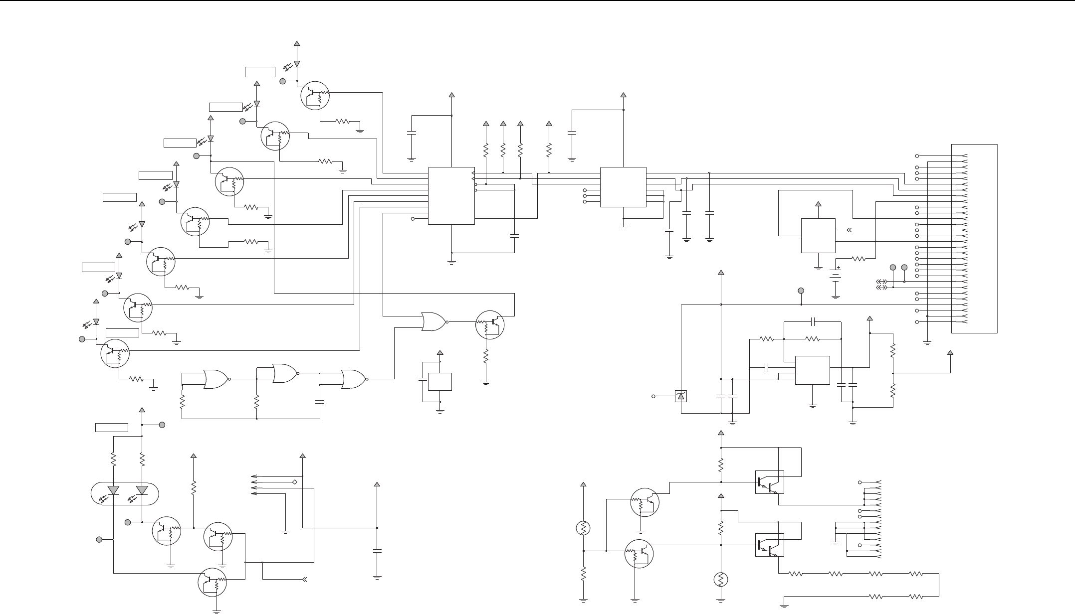
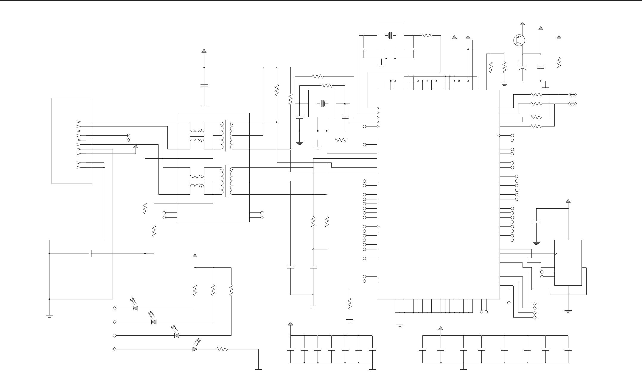
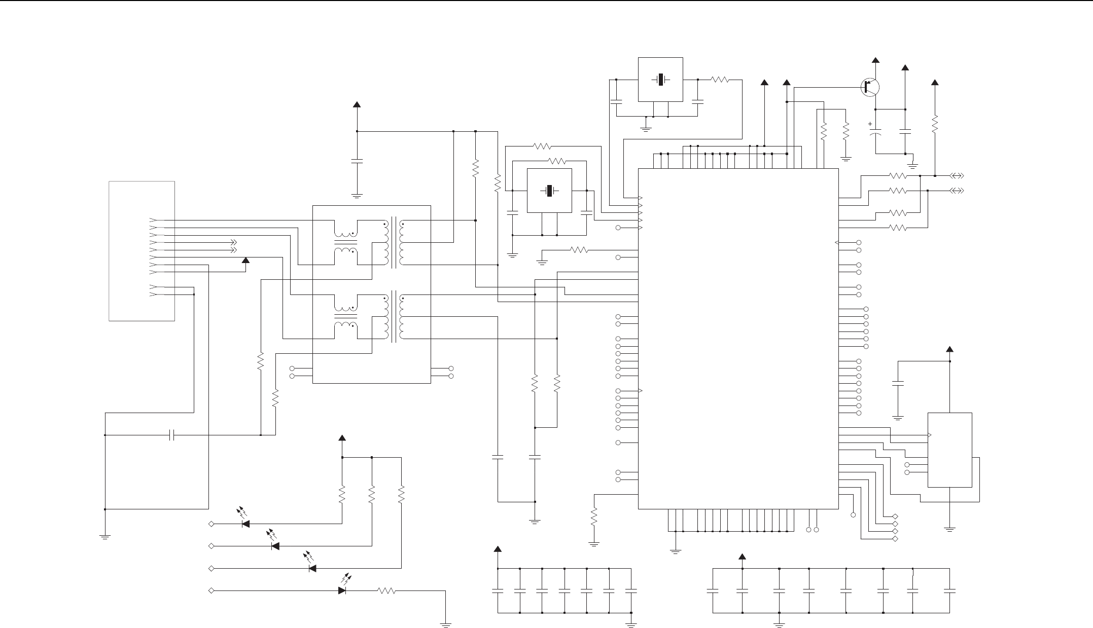
Repeater Indicator Board Schematic Diagram (Sheet 1 of 2)
Repeater Indicator Board Schematic Diagram (Sheet 2 of 2)
Page 2-5
Page 2-6
Parts List
Repeater Indicator Board, PMLN4814_ Page 2-7
Table 2-2 Repeater Indicator Board Schematic Diagrams and Parts List
PCB :
8415470H04 Repeater Indicator Board Top Side
8415470H04 Repeater Indicator Board Bottom Side
Page 2-9
Page 2-10
SCHEMATICS
Repeater Indicator Board Schematic Diagram (Sheet 1 of 2)
Repeater Indicator Board Schematic Diagram (Sheet 2 of 2)
Page 2-11
Page 2-12
Parts List
Repeater Indicator Board, PMLN5269_ Page 2-13

2-2 Allocation of Printed Circuit Boards, Schematics and Parts
Table 2-3: Repeater Indicator Board Schematic Diagrams and Parts List
PCB :
84012135001 Repeater Indicator Board Top Side
84012135001 Repeater Indicator Board Bottom Side
Page 2-15
Page 2-16
SCHEMATICS
Repeater Indicator Board Schematic Diagram (Sheet 1 of 2)
Repeater Indicator Board Schematic Diagram (Sheet 2 of 2)
Page 2-17
Page 2-18
Parts List
Repeater Indicator Board, PMLN5643_ Page 2-19
Repeater Indicator Board (PMLN4814_) PCB/Schematics/Parts List 2-3
2.0 Repeater Indicator Board (PMLN4814_) PCB/Schematics/Parts List
C7
C8
C26
C27
C28
C29
C30
C37
C38
C39
C40
C49
C50
C52
C54
C55
C56
1
D7
1
D8
1
D9
1D25
10
6
4
3
2
5
7
9
8
J2
3
42
J4
G2 G1
12
J5
12
M1
2
3
Q7
2
3
Q9
2
3
Q10
2
3
Q11
2
3
Q12
2
3
Q18
2
3
Q19
2
3
Q20
2
3
Q21
2
3
Q22
2
3
Q23
2
3
Q24
R22
R23
R24
R38
R39
R40
R41
R42
R43
R45 R46
R47
R48
R49
R50
R51
R53
R55
R56
R57
R58
R59
R60
R61
R62
R63
R64
R65
R66
R67
R68
R69
R70
R71
R73
R74
R75
R76
R77
R79
R80
R81
16 9
8
1
T1
TP1TP2
TP3
TP4
TP5
TP6
TP7
TP8
TP9 TP10
TP11
TP12
TP13
1
4
58
U2
U5
16
1
8
9
U6
76
51
26 1
U8
14
7
8
U9
14
7
8
U12
U14
VR1
43
2
Y1
2
34
Y2
(For reference only – board is not field-repairable)
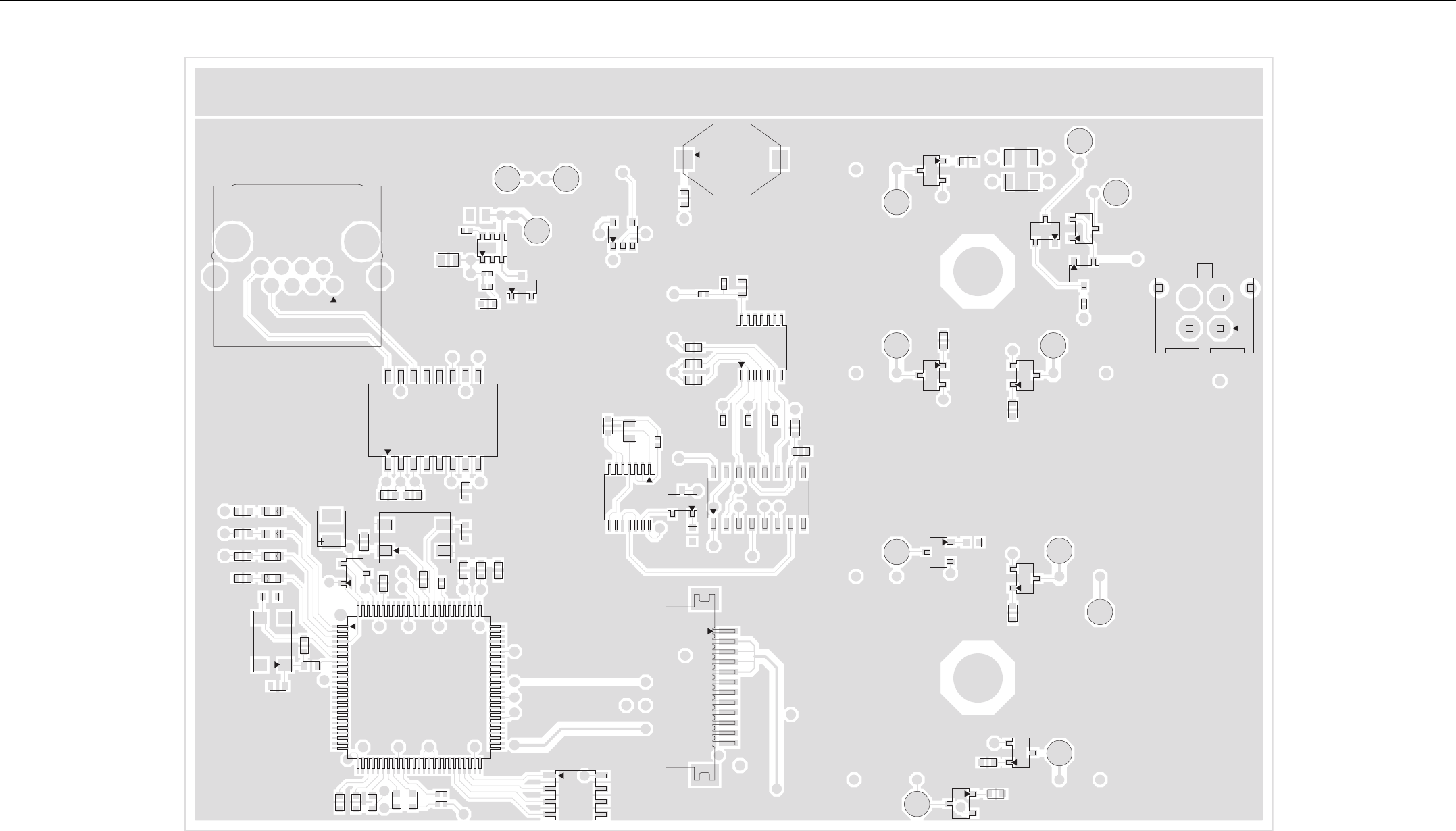
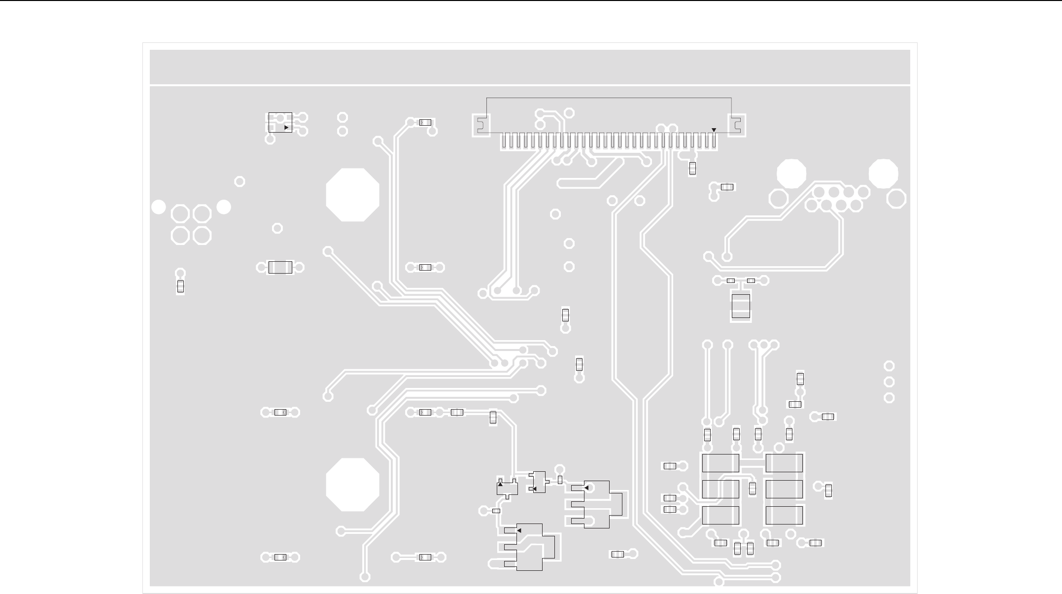
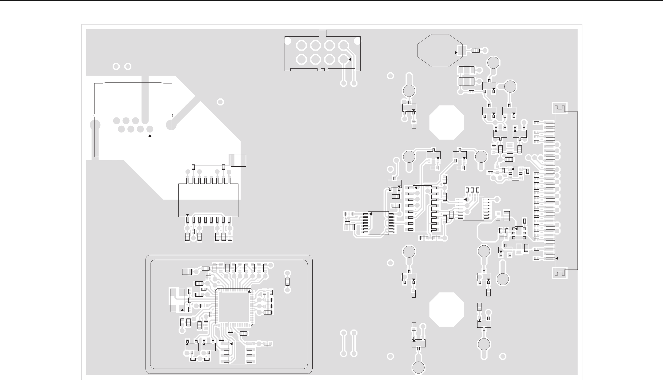
Repeater Indicator Board PCB 8415470H02 (Top Side)
2-4 Repeater Indicator Board (PMLN4814_) PCB/Schematics/Parts List
C9
C10
C11
C12
C13
C15
C16
C17
C18
C19
C22
C34
C35
C36
C41
C42
C43
C44
C45
C46
C47
C48
C51
C53
D10
1
D18
1
D19
1D20
1D21
1D22
1D23
D24
30
J1
4
32
1
Q17
R1
R2 R3
R4
R5 R6
R7
R8
R31R32
R78
RT1
RT2
2
3
U10
4
32
1
U11
2
3
U13
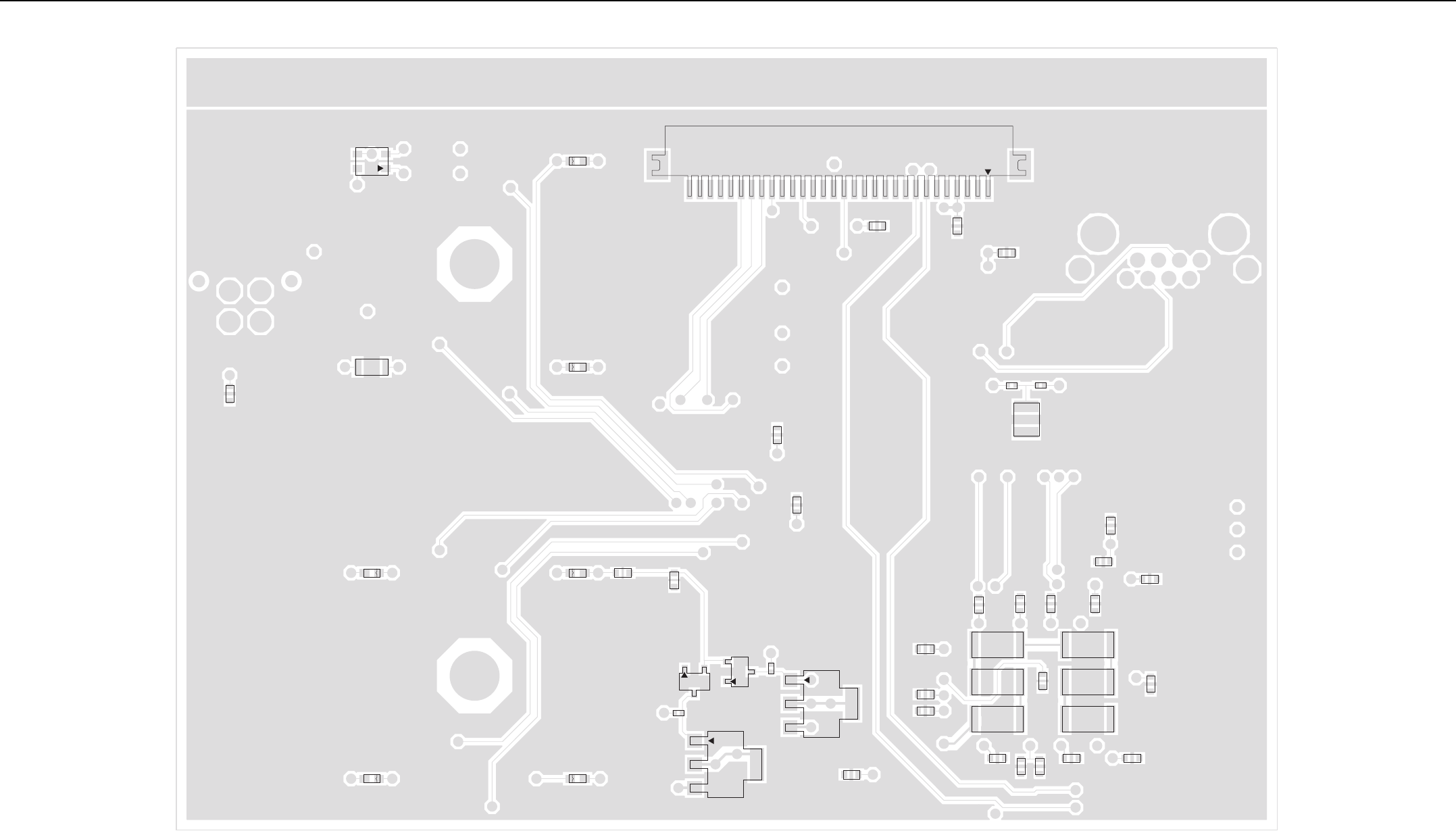
Repeater Indicator Board PCB 8415470H02 (Bottom Side)
(For reference only – board is not field-repairable)
Repeater Indicator Board (PMLN4814_) PCB/Schematics/Parts List 2-5
CONTROL HEAD
CONNECTOR
J1-18
J1-3
J1-9
J1-10
J1-23
J1-14
J1-11
J1-13
J1-1
J1-5
J1-20
J1-19
J1-17
J1-29
J1-6
J1-21
J1-24
J1-8
J1-16
J1-4
J1-25
J1-2
J1-30
J1-22
J1-12
J1-26
J1-27
J1-28
J1-15
J1-7
18
3
9
10
11
23
14
13
5
1
19
20
29
17
6
21
24
8
16
4
25
2
30
22
12
26
27
28
15
7
NC
NC
NC
NC
NC
NC
NC
NC
NC
NC
NC
NC
NC
NC
NC
NC
NC
NC
NC
ROW_2
COL_2
LED_CS
SERIAL_CLK
SERIAL_DATA
BAT_RTC
TP2
1
TP1
1
M1
SOCKET
2.2K
R58
USB_DP
USB_DM
FAN_FAIL
COM
GND
IN
NO
V_POS
1
3
4
2
5
MAX4645
U14
3V3
TP3
1
VBUS
C28
100pF 100pF
C27
C26
100pF
1
3
5
9
11
13
147
2
4
6
8
10
12
NC
NC
NC
Y_1
Y_2
Y_3
Y_4
Y_5
Y_6
A_1
A_2
A_3
A_4
A_5
A_6
GND VCC
U9
0.1uF
C52
1V8
R64
2K2K
R66
2K
R65
2K
R63
3V33V33V3 3V3
0.1uF
C56
DIG_LED
ANG_LED
TXA_LED
TXB_LED
RXA_LED
RXB_LED
BLINK_DIS
RPT_DIS
NC
16
5
6
7
9
8
15
1
2
3
4
10
12
13
14
11
SRCLR
VCC
QF
QG
QH1
QH2
RCLK
RCLR
SER
SRCLK
GND
QA
QB
QC
QD
QE
U6
C22
0.1uF
3V3
R38
510
10K
47K
13V6
1
TP4
Q7
D18
TxA
D19
13V6
10K
47K
TxB
Q9
1
TP5
13V6
2
10K
47K
510
R39
RPT DIS
D20
13V6
1
TP6
Y
Q11
RxA
R40
510
D21
10K
47K
510
R41
10K
47K
RxB 13V6
TP7
1
Q10
Y
D22
Q12
Y
TP8 1
13V6
10K
47K
R42
510
ANALOG
D23
2
13V6
1
TP9 1
DIGITAL
1
Q19
3
R55
510
Q20
2
3
D24
LED
1
TP10
10K
47K
MC74LCX02
U12-1
2
3
1
270
R56
R59
2MEG
13V6
TP11
1
POWER
R43
1.2K
D10
LED
13
R51
1.2K
13V6
R81
8.2K
RED
GRN
Q24
24
TP13
1
TP12
1
10K
47K
Q23
Q18
10K
47K
10K
47K
4
NU
J4-4
J4-33
J4-11
J4-22
CONNECTOR
POWER
FAN_FAIL
BAT_MODE
BAT_MODE
C51
0.1uF
13V6
13V6
U12-5
PWR_GND
7
GND
14
VCC
3V3
0.1uF
C53
R57
510
Q21
10K
47K
12
13
U12-4
11
MC74LCX02
U12-3
8
9
10
C39
1.0uF
R60
1MEG
4
MC74LCX02
U12-2
5
6
1
NC6.2V
VR1
13V6
C29
1.0uF
0.1uF
C34
C30
1.0uF
C35
0.1uF 2
1
R79
10K
2FB
GND
5
6NP
VCONT
4
VIN
3
VOUT 1
U5
C55
1000pF
R80
6.2K
C54
100pF
10K
R62
3V3
R69
7.5K
1V8
13V6
10K
RT1
R1
1.8K
U10
47K
47K
U13
47K
47K
13V6
8.2K
R2
Q17
4
2
3
10K
RT2
NU
R78
8.2K
R3
8.2
U11
4
2
3
HEATER CIRCUITS
NC
NC
NC
NC
R6
R8
R5
10
J5-1111
6
J5-10
J5-55
J5-6
J5-22
g2
12
J5-13g1
J5-14
J5-12
J5-11
8
J5-99
J5-77
J5-8
4
J5-33
J5-4
R7
8.2
8.2
8.2
8.28.2
R4
1
1
Repeater Indicator Board Schematic Diagram (Sheet 1 of 2)
(For reference only – board is not field-repairable)
2-6 Repeater Indicator Board (PMLN4814_) PCB/Schematics/Parts List
CONTROLLER
USB TO ETHERNET
RJ45 ETHERNET
CONNECTOR
NC
2V5
R71
510
R73
0
NC
D7
2
GND1
4
OUT
3IN1
NC
NC
Y1
XTAL_25MHZ
25MHz
GND
NC
0.1uF
C44
C49
18pF
C45
0.1uF
R68
D9
1.5K
NC
NC
NC
510
R24
NC
C12
0.1uF
R2 2
3V3
NC
C19
1000pF
510
R76
NC
R45
0
NEG3
9NEG4
1
POS1
POS2
16
6
POS3
POS4
11
51
10 CT_4
NC1 4
5
NC2
12 NC3
NC4
13
3
NEG1
14 NEG2
8
T1
XFMR
2
CT_1
15 CT_2
CT_37
R48
51
VSSIO5
93
74 XLNKSTS
0.1uF
C7
97
VSENSE
13 VSS25 A
VSS25 B
40
VSS25 C
56
22 VSSIO1
VSSIO2
44
51 VSSIO3
VSSIO4
66 61
VDDIO470
VDDIO596
31
VMF
30
VMH
VPF 33
VPH32
98 VSA
90
VAA T
VCTRL99
12
VDD25A41
VDD25B 57
VDD25C
100
VDDAH
VDDIO14
49
VDDIO2
VDDIO3
58 TXD1
TXD2
55
54 TXD3
TXEN
60
89 TXON
TXOP
88
VAAR76
84
VAAREF
11
TEST2C
TEST2D 14
15
TEST2E
TEST2F 16
TEST2G17
18
TEST2H
62 TXCLK
TXD0
59
65 RXDV
RXER
63
RXIN
77
RXIP
78
TEST1A
91
TEST1B
92
TEST2A9
10
TEST2B
35
RPU
RREF 28
RST
95
RXCLK
64
67 RXD0
RXD1
68
69 RXD2
RXD3
71
72
MDC
MDIO73
NC1
50
75 NC2
7OCLK12
OCLK25
85
94 POREN
83 RIBB
ICLK25
86
LED0 1
2
LED1
LED2 3
5
LED3
LED4 6
LINE0 42
43
LINE1
GNDT
GPIO025
24
GPIO123
GPIO2
GPIO321
GPIO420
19
GPIO5
8ICLK12
26
DVDD1
DVDD2 39
48
EECS
46
EEDI
EEDO45
47
EESK
GNDR
79
82 GNDREF
87
ANTESTA80
81
ANTESTB
27
AVDD1
AVDD2 34
COL
53
52 CRS
36 DGND1
DGND2
38
ADM8515
U8
29 AGND1
AGND2
37
NC
R31
75
NU
1.5K
R67
NC
NC
D8
10K
NC
NC
8
J2-77
R53
6
J2-55
J2-8
R23
J2-6
0.1uF
510
C18
0.1uF
C17
2GND
4GND1
3
OUT
1IN
3V3
NC
NC
NC
NC
12MHz
CX-91F Y2
C40
10uF
0.1uF
C41
J2-11
J2-33
3V3
18pF
C37
R75
33
R74
33
C38
NC
NC
C16
18pF
NC
NCNC
0.1uF
CLK_SD
2
CS
1
DC
7
GND
5
NC
6SDI
3SDO4
VC C 8
0.1uF
NC
AT93C46A
U2
C42
R61 1MEG
18pF
C50
NC
C46
0.1uF
NC
NC
NC
C47
0.1uF
C48
NC
NC
13V6
0.1uF
51
R47
Q22
2V5
NC
0.1uF
NC
NC
NC
NC
NC
C10
NC
R46
51
C9
0.1uF
NC
0.1uF
C11
0
R77
C36
0.1uF
C8
0.1uF
9
NC
3V3
R50
0
J2-10
J2-9
3V3
NC
NC
NC
NC
510
R70
NC
0.1uF
C43
3V3
R490
R3 2
75
2V5
J2-22
J2-44
D25
NC
0.1uF
C13
3V3
NC
FULL_SPD
EEDO
EEDI
EECS
EECK
BAT_MODE
RJ_RXP
RJ_TXP
RJ_TXM
FAN_FAIL
RJ_RXM
USB_DP
USB_DM
C15
0.1uF
LINK_ACT
FDUP_COL
SPEED
TXP
TXN
RXP
RXN
FULL_SPD
FDUP_COL
LINK_ACT
SPEED
CLK25M_I
RIBB
10
Repeater Indicator Board Schematic Diagram (Sheet 2 of 2)
(For reference only – board is not field-repairable)

Repeater Indicator Board (PMLN4814_) PCB/Schematics/Parts List 2-7
2.1 Repeater Indicator Board Parts List
PMLN4814_
Circuit
Ref
Motorola Part
No Description
C07 2113945C31 CAP, 0.1uF
C08 2113945C31 CAP, 0.1uF
C09 2113945C31 CAP, 0.1uF
C10 2113945C31 CAP, 0.1uF
C11 2113945C31 CAP, 0.1uF
C12 2113945C31 CAP, 0.1uF
C13 2113945C31 CAP, 0.1uF
C15 2113945C31 CAP, 0.1uF
C16 2113945C31 CAP, 0.1uF
C17 2113945C31 CAP, 0.1uF
C18 2113945C31 CAP, 0.1uF
C19 2186154V01 CAP, 1000pF
C22 2113945C31 CAP, 0.1uF
C26 2113944A40 CAP, 100pF
C27 2113944A40 CAP, 100pF
C28 2113944A40 CAP, 100pF
C29 2113946E02 CAP, 1.0uF
C30 2113946E02 CAP, 1.0uF
C34 2113945C31 CAP, 0.1uF
C35 2113945C31 CAP, 0.1uF
C36 2113945C31 CAP, 0.1uF
C37 2113944C33 CAP, 18pF
C38 2113944C33 CAP, 18pF
C39 2113946E02 CAP, 1.0uF
C40 2313960D07 CAPP, 10uF
C41 2113945C31 CAP, 0.1uF
C42 2113945C31 CAP, 0.1uF
C43 2113945C31 CAP, 0.1uF
C44 2113945C31 CAP, 0.1uF
C45 2113945C31 CAP, 0.1uF
C46 2113945C31 CAP, 0.1uF
C47 2113945C31 CAP, 0.1uF
C48 2113945C31 CAP, 0.1uF
C49 2113944C33 CAP, 18pF
C50 2113944C33 CAP, 18pF
C51 2113945C31 CAP, 0.1uF
C52 2113945C31 CAP, 0.1uF
C53 2113945C31 CAP, 0.1uF
C54 2113944A40 CAP, 100pF
C55 2113945A09 CAP, 1000pF
C56 2113945C31 CAP, 0.1uF
D07 4815809H03 HT-S91UY
D08 4815809H01 HT-S91UYG
D09 4815809H02 HT-S91URO
D10 4887557T01 HSMF-C155
D18 4815809H01 HT-S91UYG
D19 4815809H01 HT-S91UYG
D20 4815809H02 HT-S91URO
D21 4815809H03 HT-S91UY
D22 4815809H03 HT-S91UY
D23 4815809H03 HT-S91UY
D24 4883288Y04 HSMB-C150
D25 4815809H03 HT-S91UY
J1 0915555H01 30 pin
J2 0915930H01 RJ45
J5 0971174L01 12 pin
M1 0985888K02 SOCKET
Q07 4815261H01 DTC114YKAF
Circuit
Ref
Motorola Part
No Description
Q09 4815261H01 DTC114YKAF
Q10 4815261H01 DTC114YKAF
Q11 4815261H01 DTC114YKAF
Q12 4815261H01 DTC114YKAF
Q17 4815867H01 PZTA14
Q18 4815261H01 DTC114YKAF
Q19 4815261H01 DTC114YKAF
Q20 4815261H01 DTC114YKAF
Q21 4815261H01 DTC114YKAF
Q22 4815700H01 2SB1197K
Q23 4815261H01 DTC114YKAF
Q24 4815261H01 DTC114YKAF
R01 0613952H79 RES, 1.8K
R02 0613952Q95 RES, 8.2K
R03 0613959Q23 RES, 8
R04 0613959Q23 RES, 8
R05 0613959Q23 RES, 8
R06 0613959Q23 RES, 8
R07 0613959Q23 RES, 8
R08 0613959Q23 RES, 8
R22 0613952H66 RES, 510
R23 0613952H66 RES, 510
R24 0613952H66 RES, 510
R31 0613952Q46 RES, 75
R32 0613952Q46 RES, 75
R38 0613952H66 RES, 510
R39 0613952H66 RES, 510
R40 0613952H66 RES, 510
R41 0613952H66 RES, 510
R42 0613952H66 RES, 510
Circuit
Ref
Motorola Part
No Description
R43 0613958S75 RES, 1.2K
R45 0613952H42 RES, 51
R46 0613952H42 RES, 51
R47 0613952H42 RES, 51
R48 0613952H42 RES, 51
R49 0613952H13 RES, 3.3
R50 0613952H13 RES, 3.3
R51 0613958S75 RES, 1.2K
R53 0613952N01 RES, 10K
R55 0613952H66 RES, 510
R56 0613952H59 RES, 270
R57 0613952H66 RES, 510
R58 0613952H81 RES, 2.2K
R59 0613952R56 RES, 2MEG
R60 0613952J49 RES, 1MEG
R61 0613952J49 RES, 1MEG
R62 0613952N01 RES, 10K
R63 0613952H80 RES, 2K
R64 0613952H80 RES, 2K
R65 0613952H80 RES, 2K
R66 0613952H80 RES, 2K
R68 0613952Q77 RES, 1.5K
R69 0613952Q94 RES, 7.5K
R70 0613952H66 RES, 510
R71 0613952H66 RES, 510
R73 0613952G67 RES, 0
R74 0613952H37 RES, 33
R75 0613952H37 RES, 33
R76 0613952G67 RES, 0
R77 0613952G67 RES, 0
Circuit
Ref
Motorola Part
No Description

2-8 Repeater Indicator Board (PMLN4814_) PCB/Schematics/Parts List
R78 0613952Q95 RES, 8.2K
R79 0613952N01 RES, 10K
R80 0613952H92 RES, 6.2K
R81 0613952Q95 RES, 2K
RT1 0615471H01 THERM, 10K
T1 2515640H01 XFMR_H1260
U02 5171839H01 IC, AT93C46EN
U05 5115391H01 TK11100CSC
U06 5115476H01 SN74AHC594DR
U08 5171161L01 ADM8515
U09 5115502H01 SN74LVC07ADR
U10 4815263H01 DTC144EKAF
U11 4815867H01 PZTA14
U12 5114007A02 MC74LCX02
U13 4815263H01 DTC144EKAF
U14 5185229Y01 MAX4645EUK+T
VR1 4813977M13 6.2V Zener
Y1 4802582S71 XTAL_25MHz
Y2 4809612J45 CX-91F
PCB 8415470H02
Circuit
Ref
Motorola Part
No Description

Repeater Indicator Board (PMLN5269_) PCB/Schematics/Parts List 2-9
3.0 Repeater Indicator Board (PMLN5269_) PCB/Schematics/Parts List
(For reference only – board is not field-repairable)
10
6
4
3
2
5
7
9
8
J2
16 9
8
1
T1
R45 R46
C8
C7
R47
R48
C49
43
2
Y1
C40
C50
2
3
Q22
R53
R73
R77
C38
1
D7
1
D8
1
D9
1
D25
R22
R23
R24
R71
2
34
Y2
C37
R61
R76
76
51
26 1
U8
R50
R70
R75
R49
R67
R68
R74
1
4
58
U2
G2 G1
12
J5
2
3
Q21
R57
14
7
8
U12
C39
R59
R60
C26
C27
C28
C56
R63
16
1
8
9
U6
14
7
8
U9
R64
R65
R66
C16
C52
C59
U14
C57
R82
R85
C58 C60
R83
R84
1M1
FT6
2
2
3
Q11
R40
FT12
FT13
R43
R51
2
3
Q18
2
3
Q23
FT9
2
3
Q19
R55
2
3
Q20
R56
FT10
2
3
Q24
R81
3
42
J4
VR3
VR2
FT7
2
3
Q10
R41
FT4
2
3
Q7
FT11
R38
FT5
2
3
Q9
2
3
Q12
R39
R42
FT8
C29
C30
C55
U5
FT1FT2
FT3
C54
R79
R80
VR1
2
3
Q27
2
3
Q26
R86
R87
2
3
Q25
2
3
Q28
R58
Repeater Indicator Board PCB 8415470H04 (Top Side)
2-10 Repeater Indicator Board (PMLN5269_) PCB/Schematics/Parts List
C51
D24
D10
1
D20
1
D23
30
J1
C34
C35
C19
R31
R32
C41
C44
C45
C46
C53
C12
C13
C18
R6
R7
R8
C11
C17
C42
C43
C47
RT2
R3
R4
R5
C10
C15
C48
4
3
2
1
U11
C9
4
3
2
1
Q17
1
D21
R1
RT1
2
3
U13
2
3
U10
R78
1
D22
R2
1
D19
1
D18
C22
C36
Repeater Indicator Board PCB 8415470H04 (Bottom Side)
(For reference only – board is not field-repairable)

Repeater Indicator Board (PMLN5269_) PCB/Schematics/Parts List 2-11
HT-S91UYG
D19
TxA
1
FT4
13V6
HT-S91UYG
D18
Q7
10K
47K
TxB
1
FT5
13V6
RPT DIS
13V6
Q9
1
FT6
HT-S91URO
D20
10K
47K
RxA
RxB
FT7 1
Q11
13V6
HT-S91UY
D21
10K
47K
13V6
ANALOG
13V6
FT8 1
HT-S91UY
D22 Q10
FT9 1
13V6
Q12
1
2
D23
HT-S91UY
10K
47K
Q23
R81
8.2K
Q18
10K
47K
10K
47K
GRNRED
POWER
Q24
13V6
D10
LED
1
13V6
1.2K
R51
FT11
1
FT12 1
FT13 1
R43
1.2K
10K
47K
3
24
R42
510
2
3
Q19
FT10
1
270
R56
D24
LED
2
3
Q20
10K
47K
10K
47K
10K
47K
DIGITAL
1510
R55
R59
2MEG
1
R60
1MEG
1
MC74LCX02
U12-1
2
3
MC74LCX02
U12-3
8
9
10
MC74LCX02
U12-2
5
6
4
1.0uF
C39
J4-22
J4-11
J4-33
J4-44
NU
CONNECTOR
POWER
13V6
BAT_MODE
BAT_MODE
NU
BAT_MODE_N
6.2V
VR3
13V6
0.1uF
C51
2K
R83
Q25
10K
47K
NU
NU
NU
GPIO_1
GPIO_2
NU
NU
R57
510
GND
14
VCC
U12-5
PWR_GND
7
NC
R86
2K
1V8
Q26
C53
0.1uF
1V8
NC2K
R87
3V3
6.2V
10K
47K
10K
47K
10K
47K
VR2
1V8
Q27
U12-4
MC74LCX02
11
12
13
Q21
DIG_LED
ANG_LED
TXA_LED
TXB_LED
RXA_LED
RXB_LED
BLINK_DIS
RPT_DIS
NC
2
3
4
5
6
7
9
15
1
510
R41
R38
510
510
R39
R40
510
3V3
SN74AHC594
U6
C22
0.1uF
14
SER
SRCLK
SRCLR
VCC
QD
QE
QF
QG
QH1
QH2
RCLK
RCLR
GND
QA
QB
QC
2K
R66
3V3
0.1uF
C56
3V33V3 3V3
2K
R63
2K
R64
13
11
10
16
12
8
R65
2K
C52
0.1uF
GND VCC
Y_1
Y_2
Y_3
Y_4
Y_5
Y_6
A_1
A_2
A_3
A_4
A_5
A_6
NC
714
2
4
6
8
10
12
1
3
5
9
11
13
U9
SN74LVC07A
1V8
NC
NC
C28
100pF
C26
100pF
100pF
C27
FAN_FAIL
VBUS
Q28
10K
47K
2K
R84
1V8
FT3
1
R58
2.2K
M1
SOCKET
USB_DP
USB_DM
FT1
1
FT2
1
BAT_MODE_N
GPIO_2
FAN_FAIL_N
NC
NC
NC
NC
NC
NC
NC
NC
NC
GPIO_1
NC
NC
NC
NC
3V3
R79
10K
C54
100pF
VCONT
VIN
VOUT
U5
TK11100CSC
FB
GND
NP
1
6.2K
R80
4
3
1
2
6
C55
1000pF
C35
0.1uF
2
5
1.0uF
C30
1.0uF
C29
0.1uF
C34
6.2V
VR1
NC
13V6
4
2
3
Q17
1
8.2K
R2
13V6
R78
8.2K
U10
13V6
R1
1.8K
10K
RT1
U13
47K
47K
47K
47K
NU
10K
RT2
2
3
U11
1
4
J5-33
R7
R3
8.28.28.28.2
8.28.2
J5-22
NC
NC
R4 R5
J5-99
J5-77
J5-88
J5-1111
J5-1010
J5-66
J5-55
J5-13g1
J5-11
R8
J5-14g2
NC
R6
J5-1212
J5-44
NC
HEATER CIRCUITS
0.1uF
2
1
C58
FB
2
GND
NP
6
VCONT
4
VIN
3
VOUT 1
R82
2K
C57
5
100pF
U14
TK11100CSC
R85
4.7K
C59
1000pF
1V8
J1-2121
29
J1-1717
J1-29
18 J1-18
5
J1-11
J1-5
25
J1-2727
J1-25
J1-2828
6
J1-77
J1-6
J1-1313
J1-2424
8J1-8
2
J1-3030
J1-2
J1-1212
J1-2222
J1-1616
J1-44
J1-1515
J1-1010
J1-2323
J1-1919
J1-2020
9
J1-33
J1-9
J1-2626
J1-1111
J1-1414
LED_CS
SERIAL_CLK
SERIAL_DATA
BAT_RTC
NC
NC
NC
NC
CONTROL HEAD
CONNECTOR
1.0uF
C60
Repeater Indicator Board Schematic Diagram (Sheet 1 of 2)
(For reference only – board is not field-repairable)
2-12 Repeater Indicator Board (PMLN5269_) PCB/Schematics/Parts List
RJ45 ETHERNET
CONNECTOR
J2-99
J2-10 10
J2-44
J2-22
J2-11
J2-33
8
J2-77
6
J2-55
J2-8
J2-6
BAT_MODE
RJ_RXP
RJ_TXP
RJ_TXM
FAN_FAIL
RJ_RXM13V6
75
R32
NC
NC
C19
1000pF
75
R31
9
16
11
10
12
13
14
15
NEG4
POS2
POS4
CT_4
NC3
NC4
NEG2
XFMR
T1
CT_2
POS1
POS3
CT_3
NC1
NC2
NEG1
NEG3
CT_1
NC
NC
1
6
4
5
3
8
2
7
C9
0.1uF
3V3
51
R46 12MHz
GND
2
GND1
4
OUT 3
IN
1
Y2
CX-91F
C37
18pF 18pF
C38
1MEG
R61
0
51
R76
R45
74
58
55
54
60
89
88
62
59
65
63
77
78
91
92
95
64
67
68
69
71
7
85
94
83
86
8
53
52
R77
0
R47
51
NC
51
R48
NC
TXP
TXN
RXP
RXN
NC
NC
NC
NC
NC
NC
NC
NC
NC
NC
NC
NC
NC
NC
NC
NC
NC
0.1uF
C8 C7
0.1uF
RIBB
R53
10K
R23
510
R24
510
3V3
R22
510
HT-S91UY
D25
HT-S91UYG
D8
D7
HT-S91UY
D9
HT-S91URO
FULL_SPD
LINK_ACT
FDUP_COL
SPEED
510
R71
0.1uF
C43C46
0.1uF 0.1uF 0.1uF
C48 C47
2V5
0.1uF
C42 C44
0.1uF 0.1uF
C45
93
13
40
56
22
44
51
66
98
50
75
87
79
82
36
38
29
37
VSENSE
VDDIO3
VDDIO4
VDDIO5
VAAT
VCTRL
VDD25A
VDD25B
VDD25C
VDDAH
VDDIO1
VDDIO2
VAAR
VAAREF
RPU
RREF
DVDD1
DVDD2
AVDD1
AVDD2
CONTROLLER
USB TO ETHERNET
VMF
VMH
VPF
VPH
TEST2C
TEST2D
TEST2E
TEST2F
TEST2G
TEST2H
TEST2A
TEST2B
MDC
MDIO
LED0
LED1
LED2
LED3
LED4
LINE0
LINE1
GPIO0
GPIO1
GPIO2
GPIO3
GPIO4
GPIO5
EECS
EEDI
EEDO
EESK
ANTESTA
ANTESTB
U8
ADM8515
VSSIO5
XLNKSTS
VSS25A
VSS25B
VSS25C
VSSIO1
VSSIO2
VSSIO3
VSSIO4
VSA
TXD1
TXD2
TXD3
TXEN
TXON
TXOP
TXCLK
TXD0
RXDV
RXER
TEST1A
TEST1B
RXD0
RXD1
RXD2
RXD3
NC1
NC2
RIBB
GNDR
GNDREF
GNDT
COL
CRS
DGND1
DGND2
AGND1
AGND2
RXIN
RXIP
RST
RXCLK
OCLK12
OCLK25
POREN
ICLK25
ICLK12
97
61
70
96
90
99
12
41
57
100
4
49
76
84
35
28
26
39
27
34
CLK25M_I
31
30
33
32
11
14
15
16
17
18
9
10
72
73
1
2
3
5
6
42
43
25
24
23
21
20
19
48
46
45
47
80
81
C50
18pF
0
R73
XTAL_25MHZ
Y1
2GND
4GND1
3OUT 1
IN
25MHz
C49
18pF
CLK25M_O 3V32V5
R70
510
2V5
Q22
10uF
C40 C41
0.1uF
3V3
3V3
R67
1.5K
NU
R68
1.5K
R50 3.3
3.3
R49
33
R75
33
R74
USB_DP
USB_DM
NC
NC
NC
NC
NC
NC
NC
NC
NC
NC
NC
NC
NC
NC
NC
NC
NC
NC
NC
NC
3V3
0.1uF
C10
8
U2
AT93C46A
CLK_SD
CS
DC
GND
NC
SDISDO
VCC
EEDO
EEDI
EECS
EECK
NC
NC
2
1
7
6
3
NC
NC
NC
FULL_SPD
FDUP_COL
LINK_ACT
SPEED
5
4
0.1uF
C36
3V3
C13
0.1uF 0.1uF
C15C11
0.1uF
C16
0.1uF0.1uF
C17 C18
0.1uF0.1uF
C12
Repeater Indicator Board Schematic Diagram (Sheet 2 of 2)
(For reference only – board is not field-repairable)
Repeater Indicator Board (PMLN5269_) PCB/Schematics/Parts List 2-13
3.1 Repeater Indicator Board Parts List
PMLN5269_
Circuit
Ref
Motorola Part
No Description
C07 2113945C31 CAP, 0.1uF
C08 2113945C31 CAP, 0.1uF
C09 2113945C31 CAP, 0.1uF
C10 2113945C31 CAP, 0.1uF
C11 2113945C31 CAP, 0.1uF
C12 2113945C31 CAP, 0.1uF
C13 2113945C31 CAP, 0.1uF
C15 2113945C31 CAP, 0.1uF
C16 2113945C31 CAP, 0.1uF
C17 2113945C31 CAP, 0.1uF
C18 2113945C31 CAP, 0.1uF
C19 2186154V01 CAP, 1000pF
C22 2113945C31 CAP, 0.1uF
C26 2113944A40 CAP, 100pF
C27 2113944A40 CAP, 100pF
C28 2113944A40 CAP, 100pF
C29 2113946E02 CAP, 1.0uF
C30 2113946E02 CAP, 1.0uF
C34 2113945C31 CAP, 0.1uF
C35 2113945C31 CAP, 0.1uF
C36 2113945C31 CAP, 0.1uF
C37 2113944C33 CAP, 18pF
C38 2113944C33 CAP, 18pF
C39 2113946E02 CAP, 1.0uF
C40 2313960D07 CAPP, 10uF
C41 2113945C31 CAP, 0.1uF
C42 2113945C31 CAP, 0.1uF
C43 2113945C31 CAP, 0.1uF
C44 2113945C31 CAP, 0.1uF
C45 2113945C31 CAP, 0.1uF
C46 2113945C31 CAP, 0.1uF
C47 2113945C31 CAP, 0.1uF
C48 2113945C31 CAP, 0.1uF
C49 2113944C33 CAP, 18pF
C50 2113944C33 CAP, 18pF
C51 2113945C31 CAP, 0.1uF
C52 2113945C31 CAP, 0.1uF
C53 2113945C31 CAP, 0.1uF
C54 2113944A40 CAP, 100pF
C55 2113945A09 CAP, 1000pF
C56 2113945C31 CAP, 0.1uF
C57 2113944A40 CAP, 100pF
C58 2113945C31 CAP, 0.1uF
C59 2113945A09 CAP, 10000pF
C60 2113946E02 CAP, 1.0 uF
D07 4815809H03 HT-S91UY
D08 4815809H01 HT-S91UYG
D09 4815809H02 HT-S91URO
D10 4887557T01 HSMF-C155
D18 4815809H01 HT-S91UYG
D19 4815809H01 HT-S91UYG
D20 4815809H02 HT-S91URO
D21 4815809H03 HT-S91UY
D22 4815809H03 HT-S91UY
D23 4815809H03 HT-S91UY
D24 4883288Y04 HSMB-C150
D25 4815809H03 HT-S91UY
J1 0915555H01 30 pin
Circuit
Ref
Motorola Part
No Description
J2 0915930H01 RJ45
J5 0971174L01 12 pin
M1 0985888K02 SOCKET
Q07 4815261H01 DTC114YKAF
Q09 4815261H01 DTC114YKAF
Q10 4815261H01 DTC114YKAF
Q11 4815261H01 DTC114YKAF
Q12 4815261H01 DTC114YKAF
Q17 4815867H01 PZTA14
Q18 4815261H01 DTC114YKAF
Q19 4815261H01 DTC114YKAF
Q20 4815261H01 DTC114YKAF
Q21 4815261H01 DTC114YKAF
Q22 4815700H01 2SB1197K
Q23 4815261H01 DTC114YKAF
Q24 4815261H01 DTC114YKAF
Q25 4815261H01 DTC114YKAF
Q28 4815261H01 DTC114YKAF
R01 0613952H79 RES, 1.8K
R02 0613952Q95 RES, 8.2K
R03 0613959Q23 RES, 8
R04 0613959Q23 RES, 8
R05 0613959Q23 RES, 8
R06 0613959Q23 RES, 8
R07 0613959Q23 RES, 8
R08 0613959Q23 RES, 8
R22 0613952H66 RES, 510
R23 0613952H66 RES, 510
R24 0613952H66 RES, 510
R31 0613952Q46 RES, 75
Circuit
Ref
Motorola Part
No Description
R32 0613952Q46 RES, 75
R38 0613952H66 RES, 510
R39 0613952H66 RES, 510
R40 0613952H66 RES, 510
R41 0613952H66 RES, 510
R42 0613952H66 RES, 510
R43 0613958S75 RES, 1.2K
R45 0613952H42 RES, 51
R46 0613952H42 RES, 51
R47 0613952H42 RES, 51
R48 0613952H42 RES, 51
R49 0613952H13 RES, 3.3
R50 0613952H13 RES, 3.3
R51 0613958S75 RES, 1.2K
R53 0613952N01 RES, 10K
R55 0613952H66 RES, 510
R56 0613952H59 RES, 270
R57 0613952H66 RES, 510
R58 0613952H81 RES, 2.2K
R59 0613952R56 RES, 2MEG
R60 0613952J49 RES, 1MEG
R61 0613952J49 RES, 1MEG
R63 0613952H80 RES, 2K
R64 0613952H80 RES, 2K
R65 0613952H80 RES, 2K
R66 0613952H80 RES, 2K
R68 0613952Q77 RES, 1.5K
R70 0613952H66 RES, 510
R71 0613952H66 RES, 510
R73 0613952G67 RES, 0
Circuit
Ref
Motorola Part
No Description

2-14 Repeater Indicator Board (PMLN5269_) PCB/Schematics/Parts List
R74 0613952H37 RES, 33
R75 0613952H37 RES, 33
R76 0613952G67 RES, 0
R77 0613952G67 RES, 0
R78 0613952Q95 RES, 8.2K
R79 0613952N01 RES, 10K
R80 0613952H92 RES, 6.2K
R81 0613952Q95 RES, 8.2K
R82 0613952H80 RES, 2K
R83 0613952H80 RES, 2K
R84 0613952H80 RES, 2K
R85 0613952Q89 RES, 4.7K
RT1 0615471H01 THERM, 10K
T1 2515640H01 XFMR_H1260
U02 5171839H01 AT93C46A
U05 5115391H01 TK11100CSC
U06 5115476H01 SN74AHC594DR
U08 5171161L01 ADM8515
U09 5115502H01 SN74LVC07ADR
U10 4815263H01 DTC144EKAF
U11 4815867H01 PZTA14
U12 5114007A02 MC74LCX02
U13 4815263H01 DTC144EKAF
U14 5115391H01 TK11100CSC
VR1 4813977M13 6.2V Zener
Y1 4802582S71 XTAL_25MHZ
Y2 4809612J45 CX-91F
PCB 8415470H04
Circuit
Ref
Motorola Part
No Description
Repeater Indicator Board (PMLN5643_) PCB/Schematics/Parts List 2-15
4.0 Repeater Indicator Board (PMLN5643_) PCB/Schematics/Parts List
10
6
4
3
2
5
7
9
8
J2
C19
R31
R32
16 9
8
T1
C7
C8
C9
C82
C83
R88
C46
2
3
Q29
2
3
Q32
R68
R100 R101
R102
1
4
58
U2
C84
SH1
43
U8
C36
C42
C48
E3
R91
R92
C11
C12
C17
C44
R45
R46
R47
R48
R97
C10
C43
C45
C47
C49 C50
C70
C71
C85
E1
E2
R53
R73
R98
R99
29
15
2
3
4
Y1
C41
FT8
2
3
Q12
R42
FT5
2
3
Q9
2
3
Q7
R38
R39
FT11
2
3
Q10
R41
C56
FT7
R63
14
7
8
U12
C39
R59
R60
C53
2
3
Q21
R57
16
1
8
9
U6
C22
R64
R65
R66
14
7
8
U9 C26
C27
C28
C29
C30
C34
C35
C54
C55
FT4
R79
R80
U5
VR1
C61
C62
C63
C68
C69
C72
C73
C74
C75
C76
C77
C78
C79
C80
C81
R95
R96
C52
C57
C58
C59
C60
FT10
R82
R83
R84
R85
U14
C64
C65
C66
C67
30
J1
2
3
Q25
2
3
Q28
2
3
Q18
2
3
Q23
2
3
Q19
2
3
Q20
R55 R56
FT9
2
3
Q11
FT6
R40
8
5
4
J3 1
2M1 R58
FT12
FT13
2
3
Q24
R43
R51
R81
Repeater Indicator Board PCB 84012135001 (Top Side)
(For reference only - board is not field-repairable)
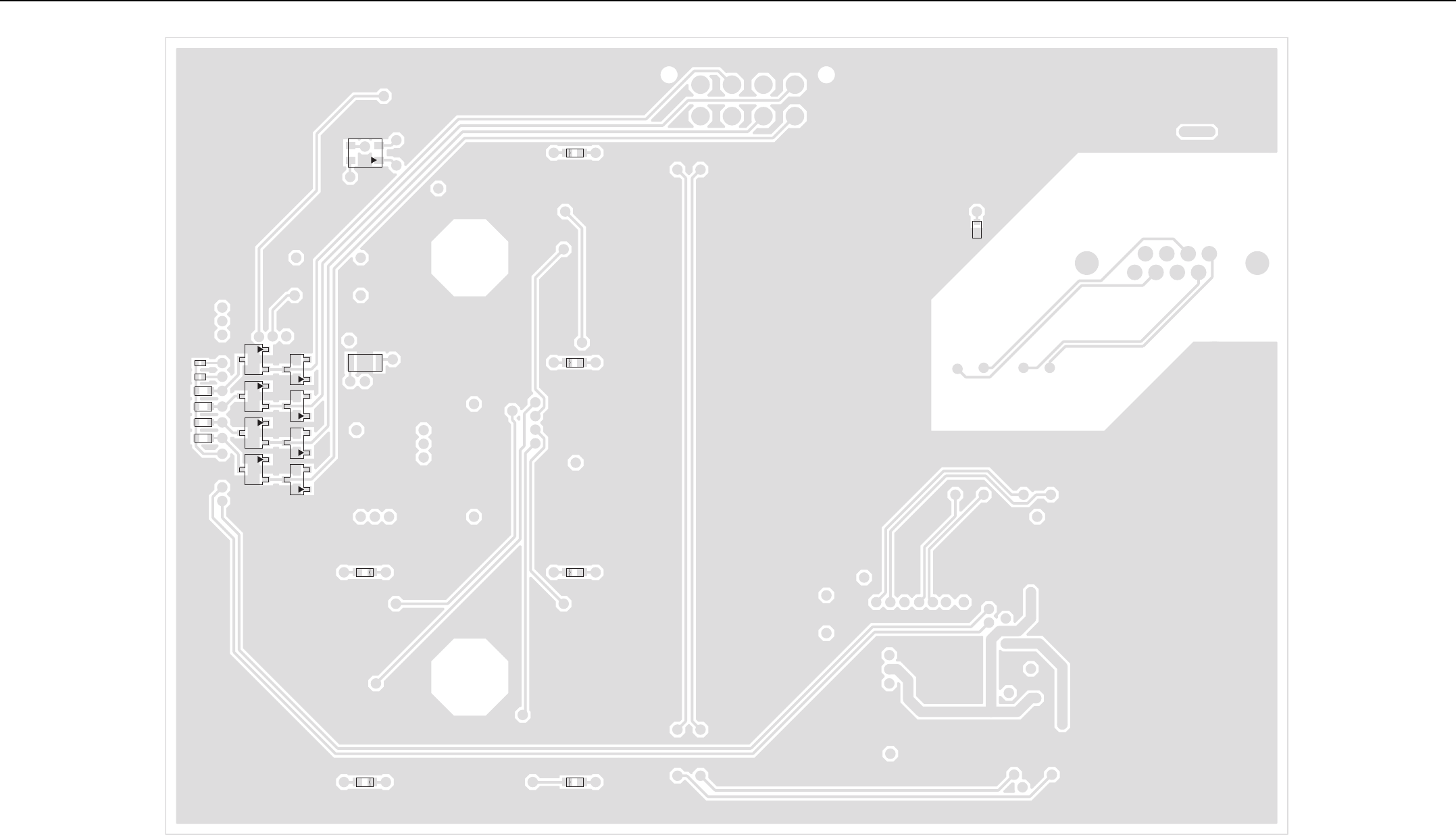
2-16 Repeater Indicator Board (PMLN5643_) PCB/Schematics/Parts List
C13
D10
1
D18
1
D19
1
D20
1
D21
1
D22
1
D23
D24
2
3
Q26
2
3
Q27
2
3
Q30
2
3
Q31
R86
R87
R89
R90
R93
R94
U15 VR2 VR3 VR4
Repeater Indicator Board PCB 84012135001 (Bottom Side)
(For reference only – board is not field-repairable)
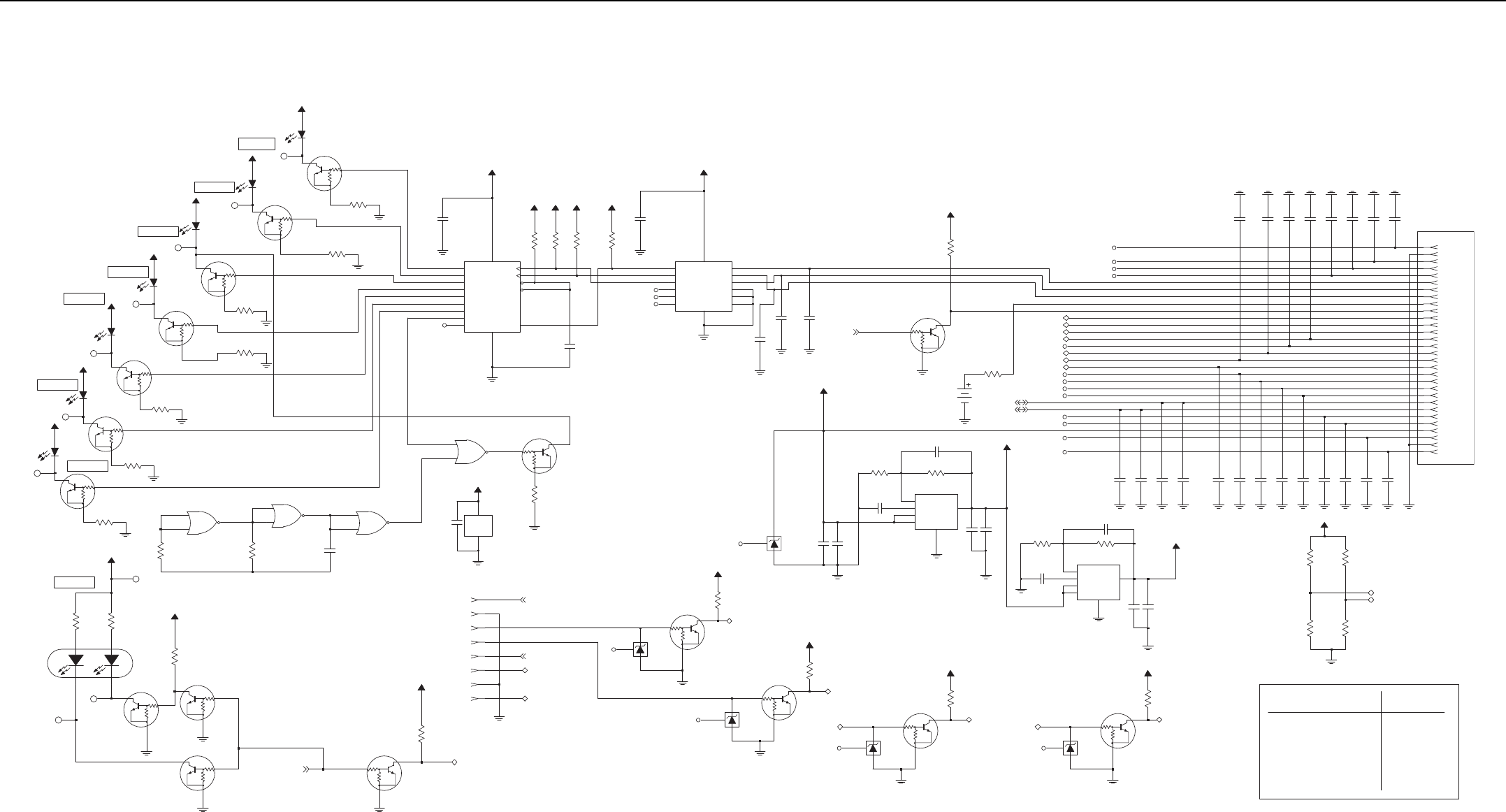
Repeater Indicator Board (PMLN5643_) PCB/Schematics/Parts List 2-17
R57
510
1.0uF
C39
MC74LCX02
U12-1
2
3
1
R60
1MEG
C53
0.1uF
R59
2MEG
Q21
10K
47K
12
13
U12-4
MC74LCX02
11
MC74LCX02
U12-2
5
6
4
3V3
MC74LCX02
U12-3
8
9
10
U12-5
PWR_GND
7
GND
14
VCC
Q23
Q18
R81
8.2K
13V6
10K
47K
10K
47K
BAT_MODE
BAT_MODE
GRN
POWER
RED
13V6
D10
LED
2
1
1.2K
R43
Q24
FT12
1
1
FT11
R51
FT13
1
1.2K
10K
47K
3
4
DIGITAL
Q20
2
3
11.5K
R56
10K
47K
10K
47K
Q19
2
3
1
D24
HSMR-C150 R55
510
FT10
1
R38
510
510
R39
10K
47K
TxA
FT4 1
HT-S91UYG
D18
13V6
13V6
TxB
RPT DIS
RxA
RxB
ANALOG
HT-S91URO
D20
D19
HT-S91UYG
13V6
Q12
13V6
FT8 1
FT6
1
FT5 1
Q9
D23
HT-S91UY
1
2
Q10
HT-S91UY
D22
13V6
10K
47K
10K
47K
10K
47K
10K
47K
1
FT9
HT-S91UY
D21
Q7
R40
510
510
R41
13V6
Q11
1
R42
510
FT7
13V6
R83
2K
Q25
10K
47K
BAT_MODE_N
1V8
J3-1
J3-2
J3-7
J3-6
J3-4
J3-5
J3-3
J3-8
FAN_HW_ID1_INV
CONN_HW_ID0_INV
CONN_HW_ID1_INV
YELLOW_LED
GREEN_LED
FAN_HW_ID0_INV
R86
2K
VR2
Q26
10K
47K
1V8
VR1
NC
FAN_HW_ID0
1V8
NC
Q31
U15
R87
2K
Q27
10K
47K
10K
47K
2K
R90
NC
1V8
NCVR4
2K
R89
Q30
VR3
1V8
CONN_HW_ID0_INV
CONN_HW_ID1_INV
FAN_HW_ID1
CONN_HW_ID1 CONN_HW_ID0
10K
47K
13
SER
11
SRCLK
10
SRCLR
16
VCC
2
3QD
4QE
5QF
6QG
7QH1
9QH2
12
RCLK
RCLR
SN74AHC594
U6
8GND
15 QA
1QB
QC
NC
ANG_LED
TXA_LED
TXB_LED
RXA_LED
RXB_LED
BLINK_DIS
RPT_DIS
DIG_LED
3V3
C22
0.1uF
2K
R65
2K
R66 R64
2K2K
R63
3V3 3V33V3 3V3
0.1uF
C52
NC
GND
7
VCC 14
Y_1
2
4Y_2
Y_3
6
Y_4
8
Y_5
10
Y_6
12
A_11
3
A_2
A_35
A_49
A_511
A_613
U9
SN74LVC07A
NC
NC
C28
100pF
100pF
C27
C26
100pF
FAN_FAIL
VBUS
Q28
10K
47K
2K
R84
1V8
C30
1.0uF
C54
100pF
2
1
C35
0.1uF
R79
10K
C55
1000pF
0.1uF
C34
R80
6.2K
C29
1.0uF
TK11100CSC
2FB
GND
5
6NP
VCONT
4
VIN
3
VOUT 1
U5
3V3
M1
SOCKET
R58
2.2K
USB_DM
USB_DP
R82 2K
2
1
C58
0.1uF
1000pF
C59
1V8
1.0uF
C60
4
VIN
3
VOUT 1
U14
K11100CSCT
FB
2
GND
5
NP
6
VCONT
R85
4.7K
100pF
C57
NC
NC
NC
NC
NC
NC
NC
NC
NC
NC
NC
NC
CONN_HW_ID0
CONN_HW_ID1
FAN_HW_ID0
FAN_HW_ID1
SERIAL_DATA
SERIAL_CLK
LED_CS
BAT_RTC
FAN_FAIL_N
BAT_MODE_N
REP_HW_ID0
REP_HW_ID1
CONTROL HEAD
CONNECTOR
NU
C67
220pF
C66
220pF
NU
220pF
C64
NU
220pF
C62
NU
220pF
NU
C68
NU
C61
220pF
NU
C63
220pF 220pF
C65
NU
24
J1-2222
J1-24
J1-1616
J1-3030
20
18
J1-2121
J1-20
J1-18
J1-22
23
J1-11
J1-23
25
J1-2626
J1-25
J1-1515
J1-1717
J1-1212
28
J1-1010
27
J1-2929
J1-28
J1-27
14 J1-14
J1-44
J1-77
J1-66
J1-55
13
J1-1111
J1-13
J1-1919
J1-33
J1-88
J1-99
REPEATER HW ID(01) = 01
NU
10K
R96
4.7K
R95
REP_HW_ID0
REP_HW_ID1
R94
4.7K
1V8
10K
R93
NUNU
C75
NU
220pF
C80
NUNU
220pF220pF
C79C78
NU
220pF220pF
C76
NU
33pF
NU
C71 C72
220pF
NU
C74
NU
220pF
NU
220pF
C81
220pF
C69
NU
C70
33pF
NU
220pF
NU
C77
NU
C73
220pF
01
11
0
TBD
0
AM8515
LAN9500
REPEATER VERSION VALUE
TBD
ID0
0
1
ID1
NC
0.1uF
C56
14
1V8
NC
Repeater Indicator Board Schematic Diagram (Sheet 1 of 2)
(For reference only – board is not field-repairable)
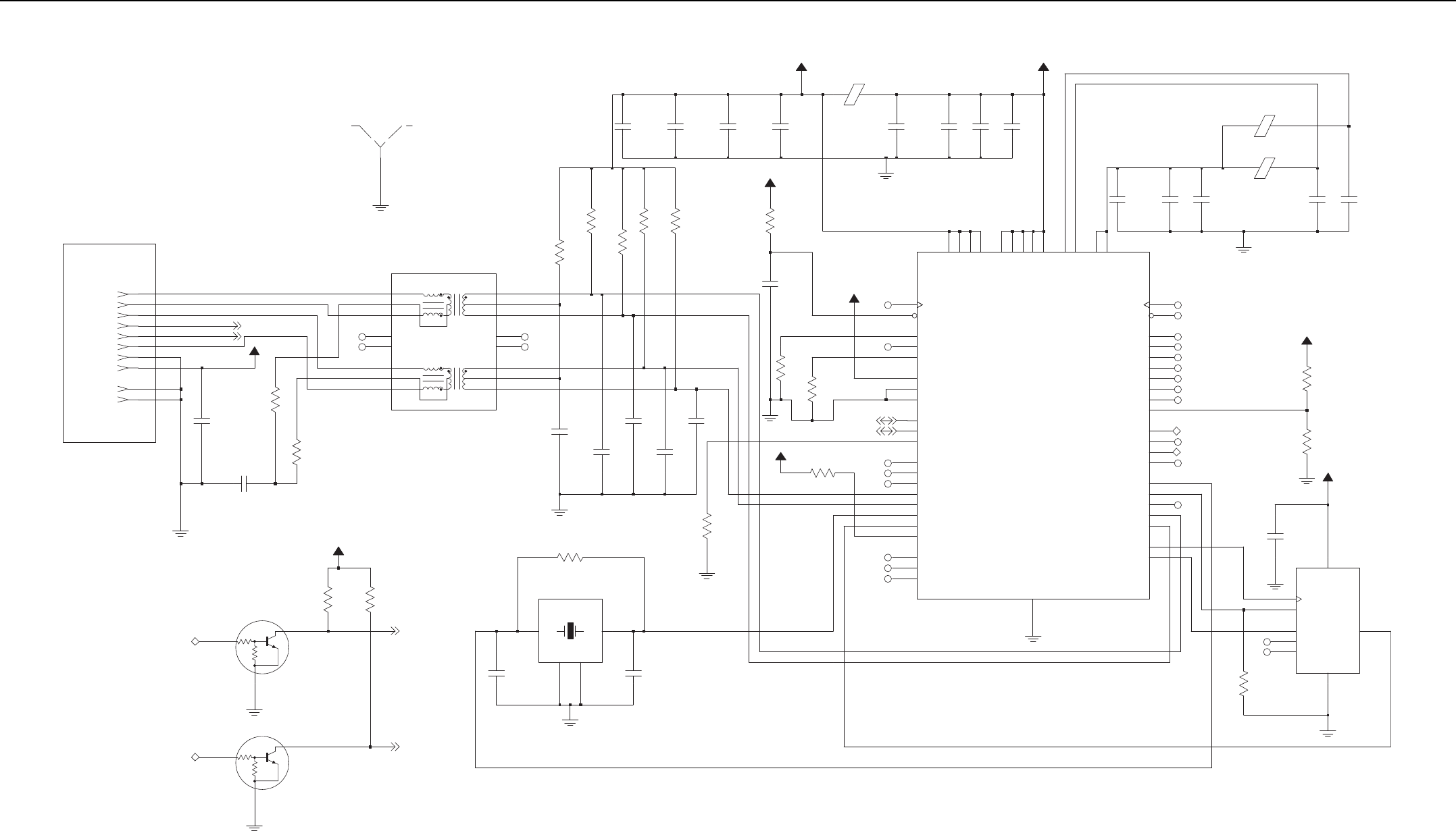
2-18 Repeater Indicator Board (PMLN5643_) PCB/Schematics/Parts List
*NON-STANDARD RJ45 PINOUT
NU
1
SH1
SHIELD
RJ45 ETHERNET
CONNECTOR
J2-10 10
J2-99
J2-11
J2-88
J2-22
7
J2-33
J2-66
J2-44
J2-55
J2-713V6
BAT_MODE
RJ_TXP
FAN_FAIL
RJ_TXM
RJ_RXP
RJ_RXM
75
R32
75
R31
0.1uF
C13
1000pF
C19
TX_POS
NC
T1
NC
NC4
RD_NEG
RD_POS
TD_NEG
TD_POS
TX_NEG
XFMR
CT1
CT2
GND1
NC3
16
NC
NC13
8
6
RX_NEG
9
RX_POS
11
3
1
14
2
7
15
10 GND2
4NC1
NC2
512
R48
51
51
R47
10
R88
51
R45
R46
51
3V3
R53
10K
0.1uF
C10
INT_PHY_SEL
NC
3V3
NC
R97
12.4K
10K
R102
USB_DM
USB_DP
R73
0
3V3
C7
R98
12K
15pF
15pF
C9
C8
.022uF
15pF
15pF
C83
C82
IN
1
Y1
XTAL
25MHz
GND
2
GND1
4
OUT 3
C49
30pF
C50
30pF
GREEN_LED
YELLOW_LED
301
R101 R100
301
3V3
Q29
10K
47K
Q32
NSPD_LED
NLNKA_LED
10K
47K
R99
1MEG
TXN
TXP
3V3
128 x 8 bits
10K
R92
R91
10K
NU
C84
R68
10K
0.1uF
2CLK_SD
1
7DC
5GND
6NC
3SDI 4
SDO
8
VCC
U2
AT93C46A
3V3
NC
NC
NC
128_EEPROM_SEL
NC
NC
NC
NC
NC
NC
NC
NC
NC
NC
NC
NLNKA_LED
NSPD_LED
U8
LAN9500I
XI
USBDM
USBDP
USBRBIAS
VBUS_DET
TMS_RXD2
TXCLK
TXEN
RXN
RXP
TCK_RXD1
TDI_RXD3
TEST1
TEST2
TEST3
NTRST_RXD0
PHY_SEL
RESET
RXDV
RXER
EEDI
EXRES
XO
TXP
TXD0_GPIO4_EEP_DISABLE
TXD1_GPIO5_RMT_WKP
TXD2_GPIO6_PORT_SWAP
TXD3_GPIO7_EEP_SIZE
TXN
TDO_NPHY_RST
NSPD_LED_GPIO10
PHY_INT
RXCLK
EEDO_AUTOMDIX_EN
MDC_GPIO2
MDIO_GPIO1
NC
NFDX_LED_GPIO8
NLNKA_LED_GPIO9
COL_GPIO0
CRS_GPIO3
EECLK_PWR_SEL
EECS
USB TO ETHERNET
CONTROLLER
VSS VDD33IO_4
VDD33IO_5
VDD18USBPLL
VDD33A_1
VDD33A_2
VDD33A_3
VDD33A_4
VDD33IO_1
VDD33IO_2
VDD33IO_3
VDD18CORE_1
VDD18CORE_2
VDD18PLL
NC
NC
NC
NC
NC
NC
18
11
12
16
20
39
47
43
5
6
38
40
49
13
33
36
34
24
42
44
32
8
51
52
17
4
7
9
15
25
35
48
21
50
10
57
19
3
56
55
54
53
2
37
28
1
41
31
22
23
14
26
27
46
45
29
30
BLM18PG121SN1
E1
E2
BLM18PG121SN1
0.1uF
0.1uF
C42 C45
C43
0.1uF
1.0uF
C41 C44
0.1uF
3V3
C48
0.1uF
0.1uF
C17
0.1uF
C11 C47
0.1uF
C46
0.1uF
C85
0.1uF
C36
C12
0.1uF
0.1uF
BLM18PG121SN1
E3
3V3A
CS
Repeater Indicator Board Schematic Diagram (Sheet 2 of 2)
(For reference only – board is not field-repairable)
Repeater Indicator Board (PMLN5643_) PCB/Schematics/Parts List 2-19
4.1 Repeater Indicator Board Parts List
PMLN5643_
Circuit
Ref
Motorola
Part No. Description
C10 2113945C31 0.1 UF
C11 2113945C31 0.1 UF
C12 2113945C31 0.1 UF
C13 2113945C31 0.1 UF
C17 2113945C31 0.1 UF
C19 2186154V01 1 NF
C22 2113945C31 0.1 UF
C26 2113944A40 100 PF
C27 2113944A40 100 PF
C28 2113944A40 100 PF
C29 2113946E02 1.0 UF
C30 2113946E02 1.0 UF
C34 2113945C31 0.1 UF
C35 2113945C31 0.1 UF
C36 2113945C31 0.1 UF
C39 2113946E02 1.0 UF
C41 2113946E02 1.0 UF
C42 2113945C31 0.1 UF
C43 2113945C31 0.1 UF
C44 2113945C31 0.1 UF
C45 2113945C31 0.1 UF
C46 2113945C31 0.1 UF
C47 2113945C31 0.1 UF
C48 2113945C31 0.1 UF
C49 2115153H44 CAP, CERAMIC
C50 2115153H44 CAP, CERAMIC
C52 2113945C31 0.1 UF
C53 2113945C31 0.1 UF
C54 2113944A40 100 PF
C55 2113945A09 1000 PF
C56 2113945C31 0.1 UF
C57 2113944A40 100 PF
C58 2113945C31 0.1 UF
C59 2113945A09 1000 PF
C60 2113946E02 1.0 UF
C61 NOT PLACED –
C62 NOT PLACED –
C63 NOT PLACED –
C64 NOT PLACED –
C65 NOT PLACED –
C66 NOT PLACED –
C67 NOT PLACED –
C68 NOT PLACED –
C69 NOT PLACED –
C7 2113944M22 15 PF
C70 NOT PLACED –
C71 NOT PLACED –
C72 NOT PLACED –
C73 NOT PLACED –
C74 NOT PLACED –
C75 NOT PLACED –
C76 NOT PLACED –
C77 NOT PLACED –
C78 NOT PLACED –
C79 NOT PLACED –
C8 2113944M22 15 PF
C80 NOT PLACED –
C81 NOT PLACED –
Circuit
Ref
Motorola
Part No. Description
C82 2113944M22 15 PF
C83 2113944M22 15 PF
C84 2113945C31 0.1 UF
C85 2113945C31 0.1 UF
C9 2113945C04 22000 PF
D10 4887557T01 LED BI COLOR RED
GREEN
D18 4815809H01 GREEN LED
D19 4815809H01 GREEN LED
D20 4815809H02 RED LED
D21 4815809H03 YELLOW LED
D22 4815809H03 YELLOW LED
D23 4815809H03 YELLOW LED
D24 48010088001 BLUE LED
E1 7686949J15 FLTR,FERR
E2 7686949J15 FLTR,FERR
E3 7686949J15 FLTR,FERR
J1 0915555H01 CONNECTOR,
30 POSITION
J2 0915930H01 RJ-45, CAT5
SHIELDED, ONE PORT
J3 9012030001 8 PIN CONNECTOR
M1 0985888K02 SKT RTC BTTY LEAP
PASTE 1085674C03 PASTE/NC-SMQ230
Q10 4815261H01 TRANSISTOR, NPN
Q11 4815261H01 TRANSISTOR, NPN
Q12 4815261H01 TRANSISTOR, NPN
Q18 4815261H01 TRANSISTOR, NPN
Q19 4815261H01 TRANSISTOR, NPN
Q20 4815261H01 TRANSISTOR, NPN
Q21 4815261H01 TRANSISTOR, NPN
Circuit
Ref
Motorola
Part No. Description
Q23 4815261H01 TRANSISTOR, NPN
Q24 4815261H01 TRANSISTOR, NPN
Q25 4815261H01 TRANSISTOR, NPN
Q26 4815261H01 TRANSISTOR, NPN
Q27 4815261H01 TRANSISTOR, NPN
Q28 4815261H01 TRANSISTOR, NPN
Q29 4815261H01 TRANSISTOR, NPN
Q30 4815261H01 TRANSISTOR, NPN
Q31 4815261H01 TRANSISTOR, NPN
Q32 4815261H01 TRANSISTOR, NPN
Q7 4815261H01 TRANSISTOR, NPN
Q9 4815261H01 TRANSISTOR, NPN
R100 0613952L47 301
R101 0613952L47 301
R102 0613952N01 10.0K
R31 0613952Q46 75
R32 0613952Q46 75
R38 0613952H66 510
R39 0613952H66 510
R40 0613952H66 510
R41 0613952H66 510
R42 0613952H66 510
R43 0613958S75 1200
R45 0613952H42 51
R46 0613952H42 51
R47 0613952H42 51
R48 0613952H42 51
R51 0613958S75 1200
R53 0613952N01 10.0K
R55 0613952H66 510
Circuit
Ref
Motorola
Part No. Description
2-20 Repeater Indicator Board (PMLN5643_) PCB/Schematics/Parts List
R56 0613952H77 1500
R57 0613952H66 510
R58 0613952H81 2200
R59 0613952R56 2.0M
R60 0613952J49 1.0M
R63 0613952H80 2000
R64 0613952H80 2000
R65 0613952H80 2000
R66 0613952H80 2000
R68 0613952N01 10.0K
R73 0613952G67 0
R79 0613952N01 10.0K
R80 0613952H92 6200
R81 0613952Q95 8200
R82 0613952H80 2000
R83 0613952H80 2000
R84 0613952H80 2000
R85 0613952Q89 4700
R86 0613952H80 2000
R87 0613952H80 2000
R88 0613952Q25 10
R89 0613952H80 2000
R90 0613952H80 2000
R91 NOT PLACED –
R92 0613952N01 10.0K
R93 NOT PLACED –
R94 0613952Q89 4700
R95 0613952Q89 4700
R96 NOT PLACED –
R97 0613952E10 12.4K
Circuit
Ref
Motorola
Part No. Description
R98 0613952Z55 12K
R99 0613952R49 1.0M
T1 2489647C01 TRANSFORMER
U12 5114007A02 NOR GATE
U14 5115391H01 LINEAR REGULATOR
IC
U15 4813977M13 DIODE
U2 51012124001 IC,SERIAL EEPROM
U5 5115391H01 LINEAR REGULATOR
IC
U6 5115476H01 8-BIT SHIFT REGISTER
U8 51009265001 LAN9500
U9 5115502H01 SN74LVC07APWR
VR1 4813977M13 DIODE
VR2 4813977M13 DIODE
VR3 4813977M13 DIODE
VR4 4813977M13 DIODE
Y1 4884121Y01 XTAL, SMT 25MHZ,
50PPM
PCB 84012135001
Circuit
Ref
Motorola
Part No. Description

XPR 8300/XPR 8400
MOTOTRBO Repeater
Chapter 3
Connector Board
Service Information
M
Issue: February, 2014

Computer Software Copyrights
The Motorola products described in this manual may include copyrighted Motorola computer programs stored
in semiconductor memories or other media. Laws in the United States and other countries preserve for
Motorola certain exclusive rights for copyrighted computer programs, but not limited to, the exclusive right to
copy or reproduce in any form, the copyrighted computer program. Accordingly, any copyrighted Motorola
computer programs contained in the Motorola products described in this manual may not be copied,
reproduced, modified, reverse-engineered, or distributed in any manner without the express written
permission of Motorola. Furthermore, the purchase of Motorola products shall not be deemed to grant either
directly or by implication, estoppel or otherwise, any license under the copyrights, patents or patent
applications of Motorola, except for the normal non-exclusive license to use that arises by operation of law in
the sale of a product.

i
Chapter 3 – Connector Board Service Information
Table of Contents
Section 1 Theory of Operation
1.0 Overview ..............................................................................................................1-1
2.0 Connector Board..................................................................................................1-1
2.1 Fan .................................................................................................................1-1
2.2 AC/DC Power Supply .....................................................................................1-2
2.3 Battery Backup Operation (Applicable for 32 MB MHz repeaters only)..........1-2
Section 2 Connector Boards/Schematics/Parts Lists
1.0 Allocation of Printed Circuit Boards, Schematics and Parts Lists ........................2-1
1.1 Connector Board Circuits ...............................................................................2-1
2.0 Connector Board (PMLN4815_) PCB/Schematics/Parts List ..............................2-3
Connector Board PCB 8415472H01 ......................................................................2-3
Connector Board Schematic Diagram (Sheet 1 of 2) .............................................2-4
Connector Board Schematic Diagram (Sheet 2 of 2) .............................................2-5
2.1 Connector Board Parts List PMLN4815_ ......................................................2-6
3.0 Connector Board (PMLN5270_) PCB/Schematics/Parts List ..............................2-7
Connector Board PCB 8415472H05 ......................................................................2-7
Connector Board Schematic Diagram (Sheet 1 of 2) .............................................2-8
Connector Board Schematic Diagram (Sheet 2 of 2) .............................................2-9
3.1 Connector Board Parts List PMLN5270_ .....................................................2-10
4.0 Connector Board (PMLN5644_) PCB/Schematics/Parts List ............................2-11
Connector Board PCB 84012133002 ...................................................................2-11
Connector Board Schematic Diagram (Sheet 1 of 2) ...........................................2-12
Connector Board Schematic Diagram (Sheet 2 of 2) ...........................................2-13
4.1 Connector Board Parts List PMLN5644_ .....................................................2-14

ii
Notes
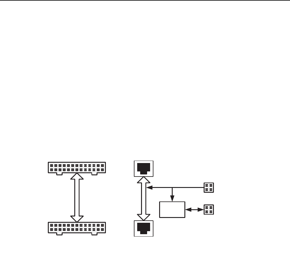
1-1
Section 1
THEORY OF OPERATION
1.0 Overview
This section provides a detailed theory of operation for the Connector Board and its components.
2.0 Connector Board
The Connector board has two purposes: provide a place for the Repeater’s MAP and Ethernet
connectors to be mounted and a location for the Repeater’s fan control circuitry.
Figure 1-1 Connector Board Block Diagram
2.1 Fan
The fan control logic is provided by the fan controller IC (U51). This is a device from Cypress
Semiconductor. There are basically two functions provided by the fan controller. First, it provides a
PWM output based on a temperature input, and secondly, it provides detection of fan failure based
on the fan tachometer reading.
The Repeater’s internal chassis temperature is measured with an LM50 precision temperature
sensor IC (U52). This IC outputs a voltage that is linearly proportional to temperature at 10 mV/°C,
and with an offset of +500 mV. The output voltage of the LM50 ranges from +200 mV at -30°C to
1.1 V at +60°C.
Fan
Control
To MAP Connector On
Transmit Radio
To MAP Connector On
Rear Panel
To Ethernet
Conne ctor On
Rear Panel
To Power
Supply
To Fan

1-2 Connector Board
The fan controller ID (U51) controls the speed of the fan by adjusting the PWM output (pin 1) from
0% to 100%. As long as the fan continues to work, pulses are output from the fan and input to the
fan controller (pin 2).
Starting with the PMLN5644B Connector Board, a slide switch (S1) has been added to the board
that allows the fan to be configured to a fixed full speed or variable speed operation. The factory
default setting is full speed. For applications where full fan speed is not appropriate, the slide switch
position can be moved from the default left (F) full speed, to the optional right (N) temperature
regulated position. After the adjustment, the variable speed behavior will be as follows: the fan will
idle low and be held constant from 10°C to 30°. Between 30°C and 45°C, the fan will increase in
speed and reach full speed at 46°C.
2.2 AC/DC Power Supply
The Repeater uses the PMPN4001A switch-mode, Power Supply Unit (PSU). It is capable of 200 W
and designed for a 50 W UHF or VHF repeater system. This supply has UL, CE, and TUV regulatory
approvals and is usable in all regions by using the correct line cord. The AC input is auto-ranging
with no manual switch being specified to operate from 90 V-270 V and 47 Hz-63 Hz. It outputs a
nominal voltage of 13.8 V with a voltage tolerance of +/- 5%.
It has Power Factor Correction circuitry and is rated at 15 A across the whole operating temperature
range of -30°C to +60°C. It also has a built-in battery revert circuit with a float output available for
maintaining the charge on a battery and has UL, CE, & TUV approvals. The battery revert connector
is accessible in the back of the power supply.
The supply has over-load, over-voltage, and over-temperature protection. In an overload condition,
the PSU goes into a hiccup mode where it recovers automatically after the fault condition is
removed. During an over-voltage condition, the PSU shuts down and will have to be re-powered on
to recover. In an over-temperature condition, the PSU also shuts down, but will recover after the
temperature goes down.
The PSU is not designed to be field serviceable. If it is determined that the PSU is not functioning,
the whole unit needs to be replaced.
2.3 Battery Backup Operation (Applicable for 32 MB MHz repeaters only)
If AC power is removed or interrupted, the repeater will switch to its battery backup until AC is
restored. The battery backup operation is controlled by a voltage sensing circuit on the connector
board. During DC operation, the circuit monitors the DC voltage of the battery connected to the
backup terminal on the PSU and enables or disables the unit accordingly to maintain reliable
repeater operation.
When the battery voltage dips below approximately 7.5 V, the repeater will disable itself until either
AC is restored or the battery voltage recovers to above 10.5 V. When heavy loading is present, the
battery voltage may swing from 7.5 V to 10.5 V as soon as the unit disables and the loading is
removed. Intermittent functionality may occur during this mode of operation, but it is normal and
expected during low battery backup operation.

2-1
Section 2
CONNECTOR BOARDS/SCHEMATICS/PARTS LISTS
1.0 Allocation of Printed Circuit Boards, Schematics and Parts Lists
1.1 Connector Board Circuits
This Chapter shows the Printed Circuit Boards (PCB), Schematics and Parts Lists for the Connector
Board circuits.
.
Table 2-1 Connector Board Schematic Diagrams and Parts List
PCB :
8415472H01 Connector Board Page 2-3
SCHEMATICS
Connector Board Schematic Diagram (Sheet 1 of 2)
Connector Board Schematic Diagram (Sheet 2 of 2)
Page 2-4
Page 2-5
Parts List
Connector Board, PMLN4815_ Page 2-6
Table 2-2 Connector Board Schematic Diagrams and Parts List
PCB :
8415472H05 Connector Board Page 2-7
SCHEMATICS
Connector Board Schematic Diagram (Sheet 1 of 2)
Connector Board Schematic Diagram (Sheet 2 of 2)
Page 2-8
Page 2-9
Parts List
Connector Board, PMLN5270_ Page 2-10

2-2 Allocation of Printed Circuit Boards, Schematics and Parts
Table 2-3: Connector Board Schematic Diagrams and Parts List
PCB :
84012133002 Connector Board Page 2-11
SCHEMATICS
Connector Board Schematic Diagram (Sheet 1 of 2)
Connector Board Schematic Diagram (Sheet 2 of 2)
Page 2-12
Page 2-13
Parts List
Connector Board, PMLN5644_ Page 2-14

Connector Board (PMLN4815_) PCB/Schematics/Parts List 2-3
2.0 Connector Board (PMLN4815_) PCB/Schematics/Parts List
C80
C81
C82
C83
C84
C85 C86
C87
C88
C89
C90
C91
C92
D50
D51
D52
J6
3
42
J7
10
6
4
3
2
5
7
9
8
J8
10
6
4
3
2
5
7
9
8
J9
26
27
2
J10
25
26
2
J11
3
42
J12
6
4
3
J13
P1
R90
R91
R92
R93
R94
R95
R96
U50
20
10
11
U51
U52
Connector Board PCB 8415472H01
(For reference only – board is not field-repairable)
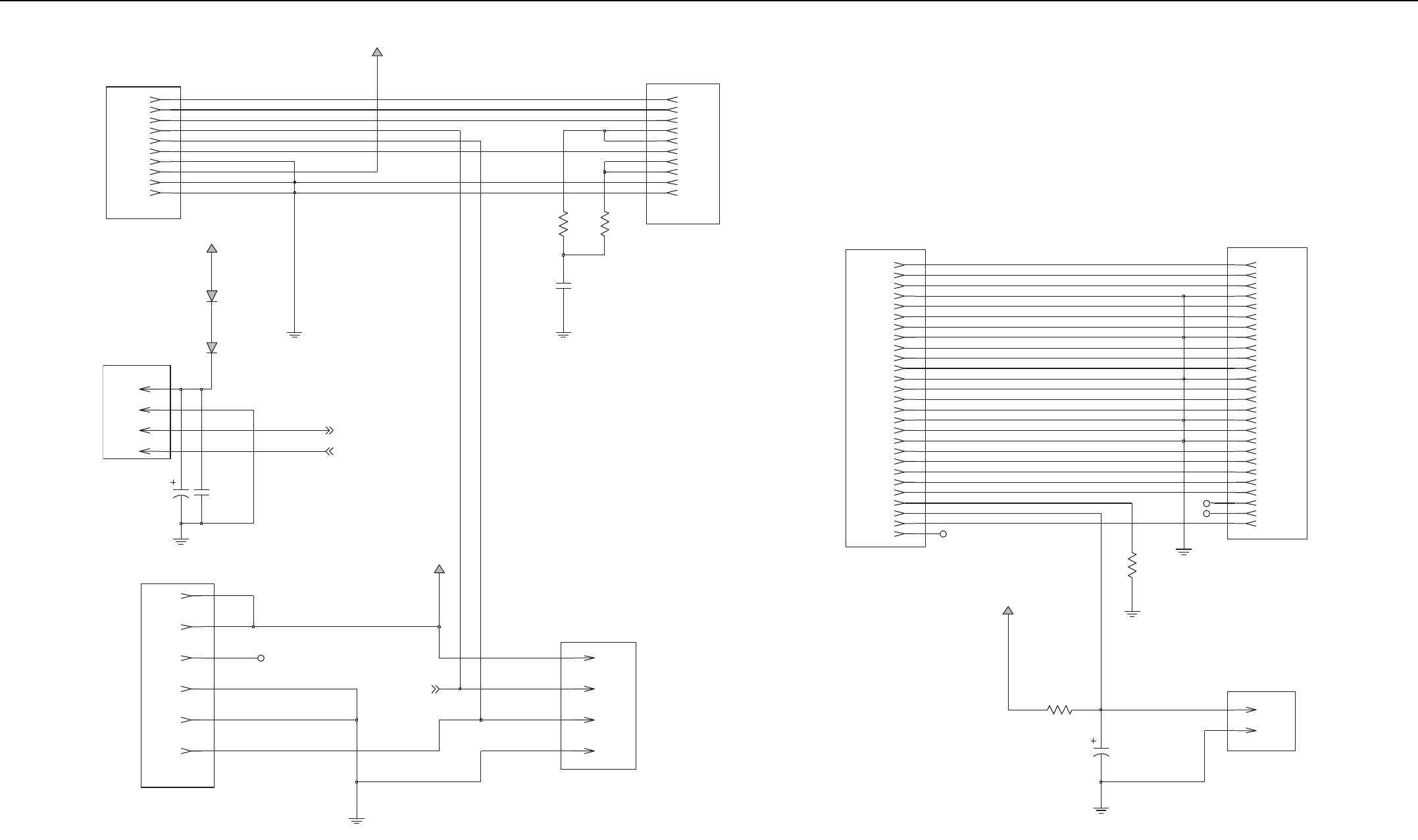
2-4 Connector Board (PMLN4815_) PCB/Schematics/Parts List
RECEIVER ACC CONN
RJ45 EXTERNAL
EXTERNAL ACC CONN
REPEATER BRD CONN
TRANSMIT ACC CONN
J11-22
RJ45 INTERNAL
POWER SUPPLY CONN
FAN CONN
J10-16 16
J9-1010
1
J6-22
1
J13-3 3
J6-1
6
J13-5 5
J7-1
2
J8-7 7
J13-6
J11-33
J9-2
C82
0.1uF
13V8
2.2K
J9-33
J13-2 2
R93
J10-2 2
$V
4
D50
$V
J10-15 15
J10-14 14
J7-4
11
J10-13 13
4
J8-3 3
J10-11
R90
J8-4
8
J10-18 18
75
2
J10-24 24
J9-8
J11-1111
J7-2
4
NC
J11-1414
26
13V8
J10-25 25
J12-4
NC
J10-26
4
13V8
C80
1000pF
2
J11-11
J13-4
4
J12-11
J12-2
J11-55
J11-4
J8-5 5
J11-99
4
J10-4 4
J9-11
J10-3 3
J9-4
7
J9-99
0
J10-7
J10-22 22
$V
R92
23
J11-66
D51
$V
J10-23
19
J11-2121
6
J11-1717
J11-19
10
J9-77
J9-6
NC
J8-9 9
J8-10
5
J8-2 2
21
J11-88
J10-5
7
J8-6 6
J10-21
24
J11-2323
J11-7
J11-2222
J11-24
J9-55
J11-2020
J11-1212
J10-8 8
10uF
12
13V8
J8-1 1
C83
75
J10-12
J10-19 19
J10-20 20
R91
J11-1010
25
10uF
C81
18
J11-2626
J11-25
J11-1616
J11-18
J11-1515
J11-1313
3
J12-33
J10-27 27 NC
J7-3
J10-1 1
J10-17 17
$V
J10-9 9
J10-10 10
6
J13-1 1
USB_DP_MAP
APM_2_1-WIRE
GP5_3
GP5_7
FAN_FAIL
FAN_FAIL
FAN_FAI L
J8-8 8
J10-6
SRC_IND
IGN_SENSE
RJ45_TXP
RJ45_TXN
RJ45_RXP
RJ45_RXN
USB_DM_MAP
VBUS_MAP
APM_1_1-WIRE
VIP_1
EXT_SWB+
EXT_SPKR-
TX_AUDIO
EXT_SPKR+
RX_AUDIO
AUX_AUDIO_OUT_2_TXD
GP5_1
GP5_2
EMERG_SW
FAN_TACH
PWM_OUT
GP5_8
AUX_AUDIO_OUT_1_RXD
GP5_6
(For reference only – board is not field-repairable)
Connector Board Schematic Diagram (Sheet 1 of 2)

Connector Board (PMLN4815_) PCB/Schematics/Parts List 2-5
PROGRAMMING HEADER
100pF
5V
13V8
P1-22
5 P1-5
P1-44
5V
0.1uF
1
P1-33
P1-1
5V
5V
C89
0.1uF
3
LM50
U52
GND
C88
U51
R95
C91
C85 C87
1.0uF
POS 1
VOUT
2
TK11100CSC
U50
2FB
0.1uF
0.1uF
NC
5V
R96
2.2K
R94
39.2K
5
GND
6NP
4VCONT
3VIN
1
VOUT
13K
NC
NC
NC
NC
NC
NC
D52
NC
0.1uF
NC
NC
P1_6
P1_7 6
VDD 20
VSS1
5
VSS2
10
XRES
15
C92
P0_6
P0_7
1
P1_0 11
P1_1 9
P1_2 12
P1_3 8
P1_4 13
P1_5 7
14
P0_0
16
P0_1
4
P0_2
17
P0_3
3
P0_4
18
P0_5
2
19
C84 1.0uF
C86
1000pF
PWM_OUT
FAN_FAIL
FAN_TACH
ISSP_CLK
ISSP_DATA
XRES
TEMPERATURE
C90
(For reference only – board is not field-repairable)
Connector Board Schematic Diagram (Sheet 2 of 2)

2-6 Connector Board (PMLN4815_) PCB/Schematics/Parts List
2.1 Connector Board Parts List
PMLN4815_
Circuit
Ref
Motorola Part
No Description
C80 2186154V01 CAP, 1000pF
C81 2313960D07 CAPP, 10uF
C82 2113945C31 CAP, 0.1uF
C84 2113945C31 CAP, 0.1uF
C85 2113945C31 CAP, 0.1uF
C86 2113946E02 CAP, 1.0uF
C87 2113946E02 CAP, 1.0uF
C88 2113945C31 CAP, 0.1uF
C89 2113945C31 CAP, 0.1uF
C90 2113945A09 CAP, 1000pF
C91 2113944A40 CAP, 100pF
C92 2113945C31 CAP, 0.1uF
D50 4813978B01 Diode SMB 1A 40V
D51 4813978B01 Diode SMB 1A 40V
D52 4813978B01 Diode SMB 1A 40V
J7 2815631H01 Connector, 4 Pin
J8 0915930H01 Connector, 10 Pin
J9 0915930H01 Connector, 10 Pin
J10 2816476H01 Connector, 28 Pin
J11 0971878L01 Connector, 26 Pin
J13 2815632H01 Connector, 6 Pin
R90 0613952Q46 RES, 75
R91 0613952Q46 RES, 75
R92 0613952G67 RES, 0
R94 0613952N12 RES, 13
R95 0613952N58 RES, 39.2K
R96 0613952H81 RES, 2.2K
U50 5115391H01 TK11100CSC
U51 0104030J35 IC, Fan Controller
U52 5115022H01 IC Temperature Sensor
PCB 8415472H01
Circuit
Ref
Motorola Part
No Description
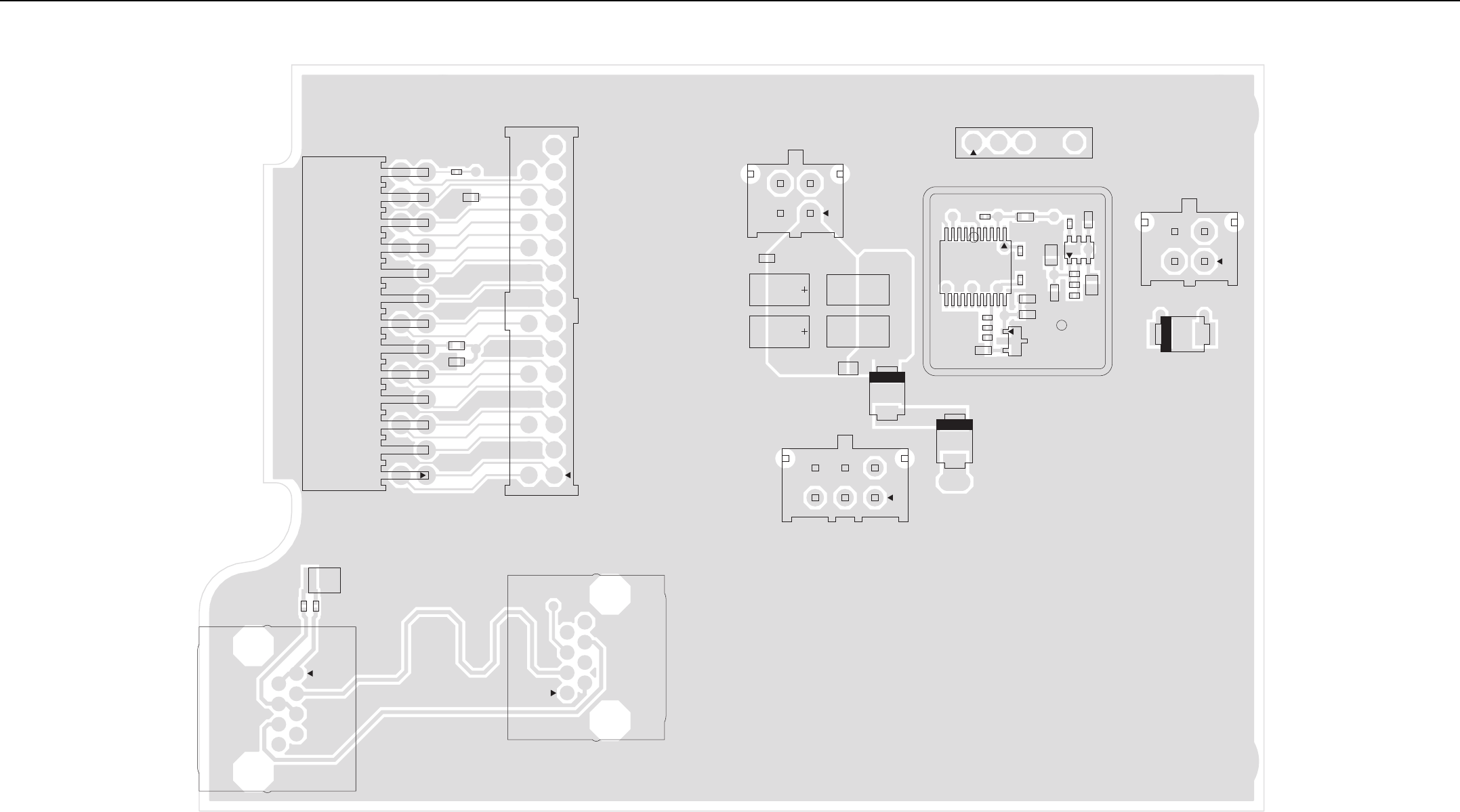
Connector Board (PMLN5270_) PCB/Schematics/Parts List 2-7
3.0 Connector Board (PMLN5270_) PCB/Schematics/Parts List
2
J10
2
J11
26
27
25
26
R92
R97
R98
R99
C80
9
R90
R91
10
6
4
3
2
5
7
8
J9
10
6
4
3
2
5
7
9
8
J8
6
4
3
J13
D50
D51
R101
C99
C100
R100
R102
C82
3
42
J7
P1
C84
C85
C86
C87
C88
C89
C90
C91
C92
C93 C94
C95
C96
C97
C98
R94
R95
R96
U50
20
10
11
U51
U52
SH50
3
42
J12
D52
Connector Board PCB 8415472H05
(For reference only – board is not field-repairable)
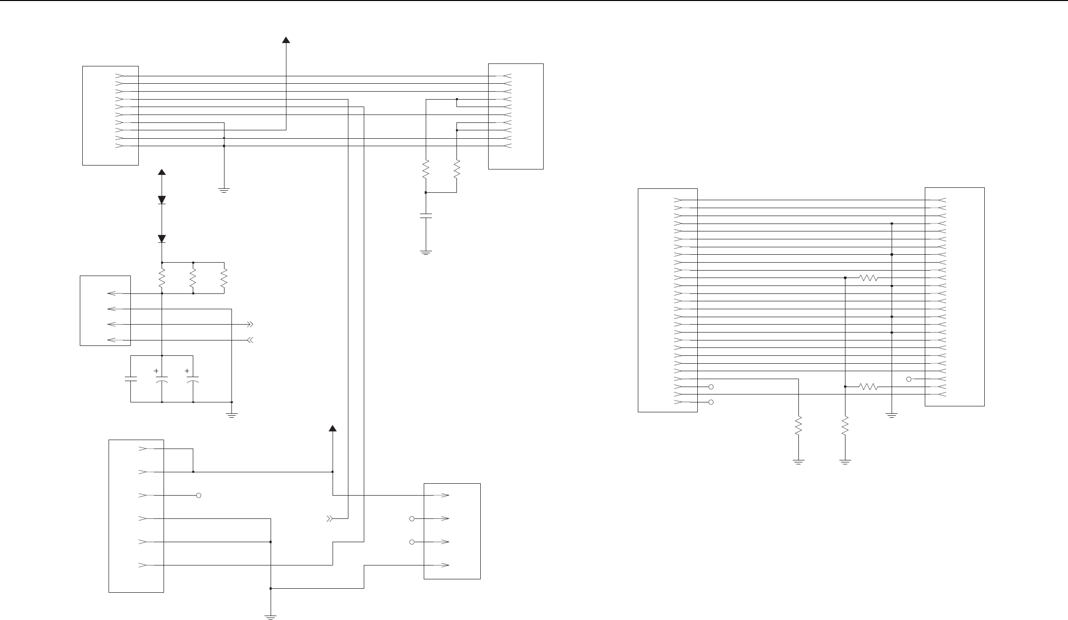
2-8 Connector Board (PMLN5270_) PCB/Schematics/Parts List
(For reference only – board is not field-repairable)
RJ45 INTERNAL
4
J8-3 3
J8-4
7
J8-8 8
J8-7
J8-5 5
J8-2 2
6J8-6
J8-10 10
J8-9 9
J8-1 1
D50
13V8
D51
R101
NU
0
R100
2.22.2
R102
FAN CONN
J7-2 2
J7-1 1
J7-4 4
J7-3 3
0.1uF
C82
33uF
C100
C99
33uF
FAN_TACH
PWM_OUT
POWER SUPPLY CONN
J13-4
J13-3
J13-5
J13-6
J13-1
2
3
4
5
6
1
J13-2
NC
SRC_IND
FAN_FAIL
REPEATER BRD CONN
J12-22
J12-11
J12-4
NU
4
NC
NC
J12-33
13V8
75
R90
75
R91
1000pF
C80
RJ45 EXTERNAL
8 J9-8
4
1
J9-4
J9-99
J9-1
7 J9-7
J9-22
3 J9-3
10 J9-10
J9-66
5 J9-5
13V8
RJ45_TXP
RJ45_TXN
RJ45_RXP
RJ45_RXN
FAN_FAIL
TRANSMIT ACC CONN
J10-11
J10-12
J10-20
J10-18
J10-3
J10-4
J10-7
J10-16
J10-9
J10-26
J10-25
J10-22
J10-2
J10-14
J10-15
J10-13
J10-8
J10-5
J10-21
J10-27
J10-17
J10-10
J10-1
J10-24
J10-6
J10-23
J10-19
11
12
20
18
16
25
26
22
14
13
15
21
27
17
10
9
8
7
6
5
4
3
2
1
24
23
19
NC
NC
TX_AUDIO
USB_DP_MAP
USB_DM_MAP
VBUS_MAP
APM_1_1-WIRE
VIP_1
EXT_SWB+
EXT_SPKR-
EXT_SPKR+
RX_AUDIO
AUX_AUDIO_OUT_2_TXD
GP5_1
GP5_2
EMERG_SW
AUX_AUDIO_OUT_1_RXD
GP5_6
APM_2_1-WIRE
GP5_3
GP5_7
GP5_8 NC
4.7K
R98
NU
0
R92 0
R99
NU
0
R97
EXTERNAL ACC CONN
J11-4
J11-2
J11-9
J11-1
J11-11
J11-14
J11-22
J11-5
J11-10
J11-26
J11-25
J11-18
J11-16
J11-8
J11-7
J11-13
J11-3
J11-15
J11-6
J11-19
J11-21
J11-17
J11-12
J11-20
J11-24
J11-23
4
2
9
1
11
14
22
5
25
10
26
18
16
8
7
13
3
15
6
21
17
19
12
20
24
23
Connector Board Schematic Diagram (Sheet 1 of 2)
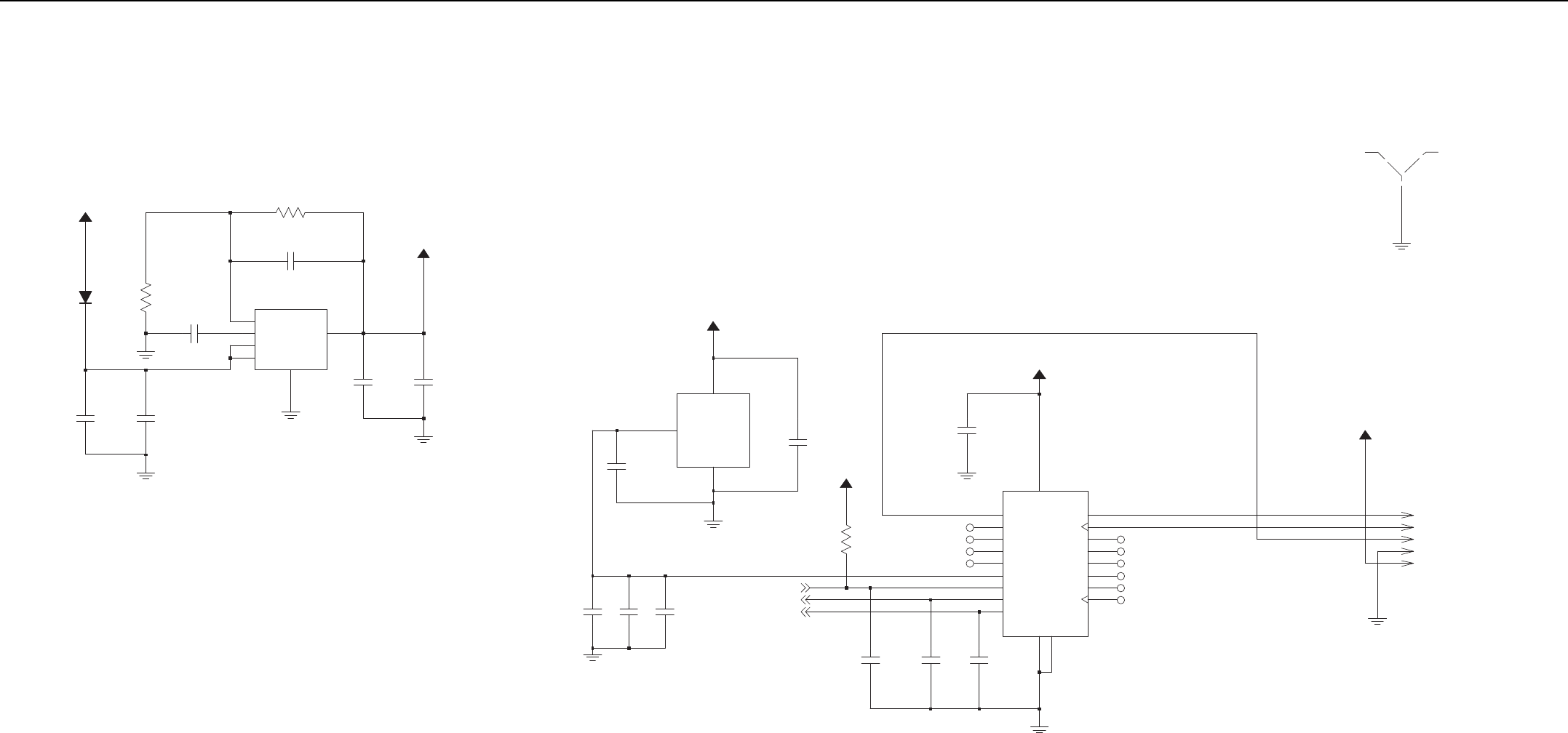
Connector Board (PMLN5270_) PCB/Schematics/Parts List 2-9
(For reference only – board is not field-repairable)
100pF
C91
2FB
5GND
6NP
4VCONT
3VIN
1
VOUT
TK11100CSC
U50
D52
1000pF
13V8
C90
39.2K
R95
13K
R94
C86
0.1uF
C84
1.0uF
C85
0.1uF
C87
1.0uF
5V
0.1uF
C92
5V
GND
3POS 1
VOUT
2
LM50
U52
5V
R96
2.2K
0.1uF
C88
1500pF
C96
120pF
C98
220pF
C97
PWM_OUT
FAN_FAIL
FAN_TACH
NC
NC
NC
NC
TEMPERATURE
C95
NU
C94
NU
100pF
C93
NU
100pF100pF
NC
NC
NC
NC
NC
NC
7
14
P1_6
P1_7 6
VDD 20
VSS1
VSS2
XRES
15
2
19 P0_6
P0_7
1
P1_0 11
P1_1 9
P1_2 12
P1_3 8
P1_4 13
P1_5
P0_0
16
P0_1
4
P0_2
17
P0_3
3
P0_4
18
P0_5
CY8C21334
U51
0.1uF
C89
5
10
5V
5V
ISSP_CLK
ISSP_DATA
XRES
PROGRAMMING HEADER
NU
5
P1-44
P1-22
P1-5
1
P1-33
P1-1
SHIELD
SH50
1
Connector Board Schematic Diagram (Sheet 2 of 2)
2-10 Connector Board (PMLN5270_) PCB/Schematics/Parts List
3.1 Connector Board Parts List
PMLN5270_
Circuit
Ref
Motorola Part
No Description
C80 2186154V01 CAP, 1000pF
C82 2113945C31 CAP, 0.1uF
C84 2113945C31 CAP, 0.1uF
C85 2113945C31 CAP, 0.1uF
C86 2113946E02 CAP, 1.0uF
C87 2113946E02 CAP, 1.0uF
C88 2113945C31 CAP, 0.1uF
C89 2113945C31 CAP, 0.1uF
C90 2113945A09 CAP, 1000pF
C91 2113944A40 CAP, 100pF
C92 2113945C31 CAP, 0.1uF
C96 2113944A41 CAP, 120 pF
C97 2113944A44 CAP, 220 pF
C98 2113945A10 CAP, 1500 pF
C99 2314030E85 CAP, 33 uF
C100 2314030E85 CAP, 33 uF
D50 4813978B01 78B01
D51 4813978B01 78B01
D52 4813978B01 78B01
J7 2815631H01 CONN_P
J8 0915930H01 CONN_J
J9 0915930H01 CONN_J
J10 2816476H01 CONN_J
J11 0971878L01 CONN_P
J13 2815632H01 CONN_J
R90 0613952Q46 RES, 75
R91 0613952Q46 RES, 75
R92 0613952G67 RES, 0
R94 0613952N12 RES, 13K
R95 0613952N58 RES, 39.2K
R96 0613952H81 RES, 2.2K
R97 0613952G67 RES, 0
R100 0613959Y09 RES, 2.2
R102 0613959Y09 RES, 2.2
SH50 2686423Z02 SHIELD
U50 5115391H01 TK11100CSC
U51 0104030J35 CY8C21334
U52 5115022H01 LM50
PCB 8415472H05
Circuit
Ref
Motorola Part
No Description
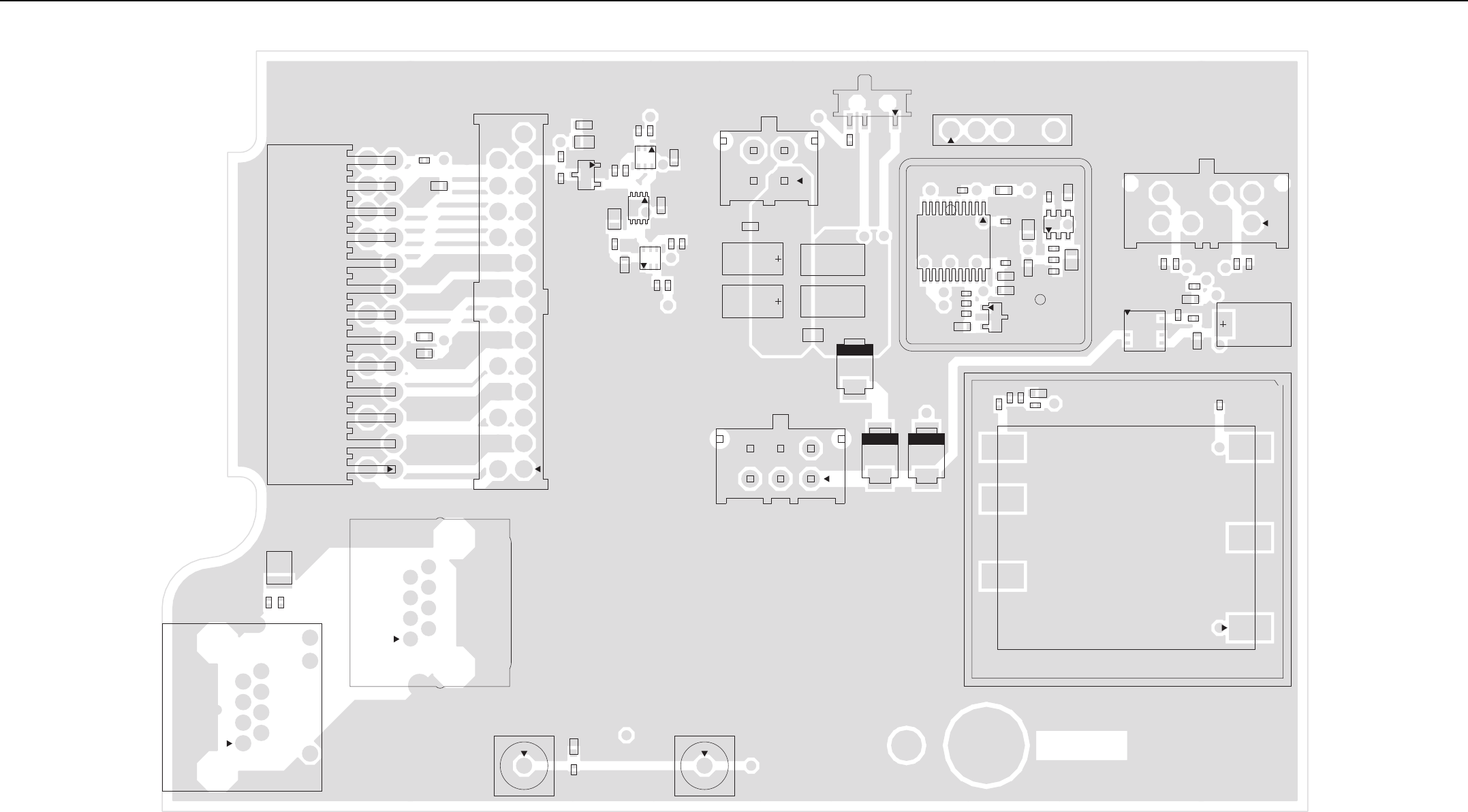
Connector Board (PMLN5644_) PCB/Schematics/Parts List 2-11
4.0 Connector Board (PMLN5644_) PCB/Schematics/Parts List
2004
C
C111
J15
L1
10
6
4
3
2
5
7
9
8
J8
C80
R90
R91
8
6
4
2
J9
J14
R97
R99
2
J11
25
26
R92
R98 26
27
J10
2
C106
C110
2
3
Q1
R112
R113
C104
R106
R107
R108
R109
3
46
U55
C101
C102
C103
R103
R104
R105
R110
R111
U53
3
4
6
U54
3
42
J7
R134
2
3
G2
G1
G4 G3
S1
P1
C95
20
10
11
U51
C92
C96
C97
C98
SH50
U52
C85 C87
C88
C89
C93
C94
C84
C86
C90
C91
R94
R95
R96
U50
C82
C99
C100
R100
R101
R102
D51
6
4
3
J13
D50
D52
2
1
SH51
74
Y1
3
C113
C115
C116
L2
R125
R132
C105
C109
C114
R114
R115
R116
R117
R123
R124
R133
U56
8
5
4
J12
Connector Board PCB 84012133002
(For reference only – board is not field-repairable)
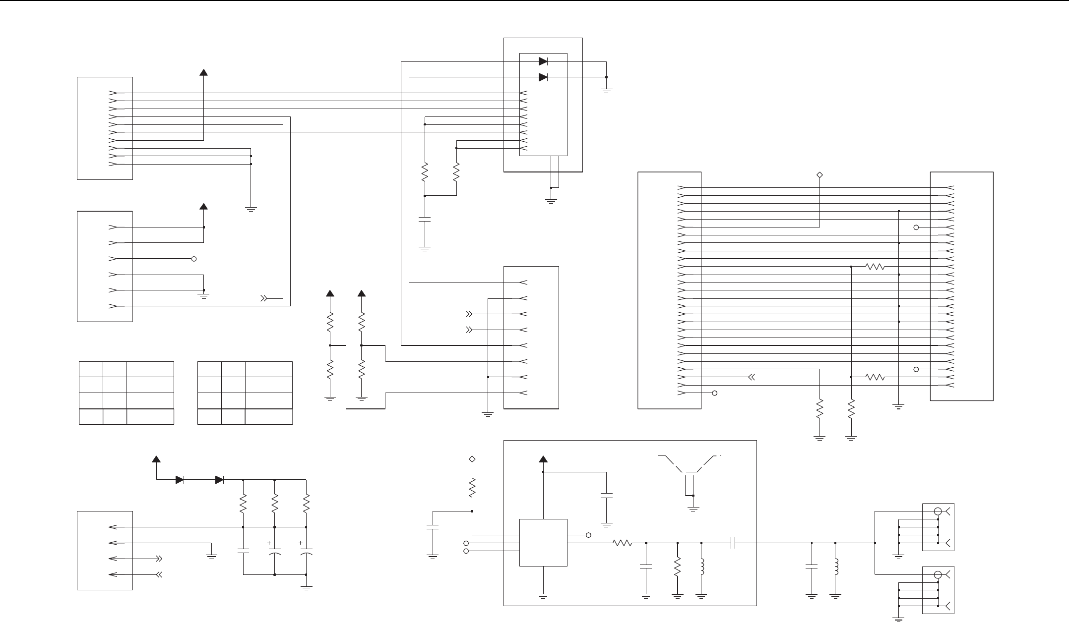
2-12 Connector Board (PMLN5644_) PCB/Schematics/Parts List
(For reference only - board is not field-repairable)
1 RESERVED
0
RJ45 EXTERNAL
0
BIT_0
0
1
DESCRIPTION
1
RESERVED
0 1 RESERVED
BIT_0 DESCRIPTION
EXTERNAL ACC CONN
RJ45 INTERNAL
REPEATER BRD CONN
0 BAT, OCXO1
BIT_1
FAN_CTRL_ID TABLE
RESERVED
OCXO SHIELD
FAN CONN
POWER SUPPLY CONN
11
HW_ID TABLE
BIT_1
TRANSMIT ACC CONN
0
0 RESERVED
0
RESERVED
1 BAT ONLY
3
J10-11 11
J10-16 16
J8-3
33uF
J8-7 7
C99 C100
390nH
33uF
R117
L2
NU
10K
0
R116
10K
1
12V
NU
R101
47pF
J8-1
J13-3
C116
12
NC
J7-3 3
R99
0
J10-12
21
J10-17 17
NU
J10-21
2
J10-10 10
C82
0.1uF
J11-2626
J7-2
J10- 9 9
J11- 77
4
J13-1
22
J11-1717
J10- 4
J12-8
J10-22
J10- 1
J11- 66
8
C113
.01uF
J10-23 23
NU
75
R90
13V8
390nH
L1
J10- 7 7
J11- 44
J8-2 2
J11- 55
NU
390pF
C111
27
J8-10 10
5V
J10-27
0
0.1uF
C114
J11-1818
R133
J11-1616
3
1J12-1
4J12-4
15
J11-2121
J11- 3
J8-8 8
J11-15
NC
J10-14 14
2
1
NC
R102
2.2
J10- 2
13V8
6J12-6
J10-15 15
R115
10K
9
J10-13 13
3
J11-1010
J8-9
19
J11-1111
J10- 3
J11-19
J10- 5 5
C80
1000pF
8
J10- 6 6
J8-5 5
J10- 8 8
R97
0
J12-7
7
J8-4 4
J11- 8
12
J7-4 4
4.7K
J11-12
NC
13V8
NU
R98
NU
10K
R114
4
3
2
1
NC
J10-19 19
5V
J11-2525
J13-4
GND
7
NC1
5
NC2
6OUTPUT 4
VCC 3
VCONT
1VREF 2
1K
Y1
OCXO-220
16.8MHz
R132
2J12-2
3J12-3
G3
G4
2.2
R100
G4
J15
C
G1
G2
24
J14
C
G1
G2
G3
J13-2
J11-24
SH51
SHIELD
1
2
5J12-5
470pF
0
C115
14
J10-18 18
R92
5
J7-1 1
J11-14J13-5
J10-20 20
R91
75
J10-25 25
J11- 22
NC
NC
J11-2020
D51
J11-2222
J8-6 6
J13-6 6
1
470
R125
J8
NEG1
NEG2
POS1
POS2
J11- 1
GND2
J1
J2
J3
J4
J5
J6
J7
13
J9
GND1
26
J11-2323
J11-13
D50
J10-26
J11- 99
J10-24 24
EMERG_SW
GP5_7
GP5_3
GP5_6
GP5_2
GP5_1
AUX_AUDIO_OUT_2_TXD
RX_AUDIO
AUX_AUDIO_OUT_1_RXD
TX_AUDIO
EXT_SPKR+
EXT_SPKR-
EXT_SWB+
VBUS_MAP
USB_DM_MAP
USB_DP_MAP
HW_ID_0
HW_ID_1
EXT_WARP
EXT_WARP
LED_GREEN
EXT_WARP
LED_YELLOW
RJ45_TXP
RJ45_RXN
FAN_TACH
PWM_OUT
FAN_CTRL_ID_1
RJ45_TXN
FAN_FAIL
FAN_FAIL
RJ45_RXP
SRC_IND
FAN_CTRL_ID_0
IGN_SENSE
APM_2_1-WIRE
VIP_1
GP5_8
Connector Board Schematic Diagram (Sheet 1 of 2)
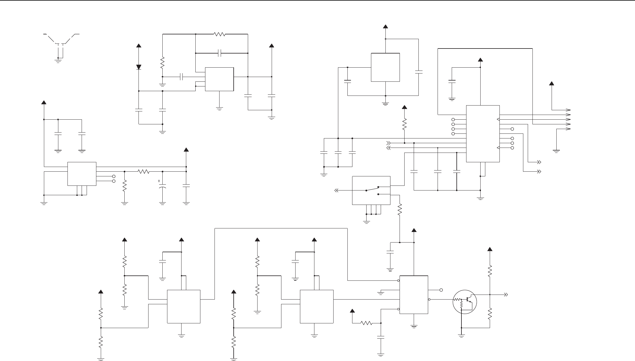
Connector Board (PMLN5644_) PCB/Schematics/Parts List 2-13
(For reference only - board is not field-repairable)
NU
NC
PROGRAMMING HEADER
Q1
C109
22uF
C88
VCC1 2
5
VCC2
VEE
1
VOUT 6
0.1uF
U54
NCS2200
INNEG
3INPOS
4
0.1uF
5V
0.1uF
C104
332
C103
2.8K
R109
R123
13V8
OUT 5
R106
4.75K
ADJ 8
GND1
2
GND2
7
GND3
9
IN
3
NC1 4
NC2 6
ON_OFF
1
U56
LM2941
R94
13K
100pF
C91
NC
NC
1000pF
C90
3INNEG
4INPOS
2
VCC1
VCC2 5
1VEE
6
VOUT
C86
1.0uF
NCS2200
U55
R113
R112
24K
120pF
C96
5.1K
GND4
G4
NC
13V8
5V
SWITCH
1
A1
2A2
3
A3
G1 GND1
G2 GND2
GND3
G3
NU
C95
S1
4.75K
R103
100pF
P1-22
5V
1.47K
R110
0.1uF
C106
C97
220pF
NC
NC
10K
47K
C93
C102
0.1uF
NC
100pF
NU
C105
0.1uF
P1-55
13V8
5V
U52
LM50
3GND 1
POS
2VOUT
R95
39.2K
P1-11
R96
2.2K
C89
0.1uF0.1uF
C92
R134
10K
1500pF
C98
P1-33
R107
4.75K
5V
P1-44
NC
NC
1.0uF
C110
D52
5V
10K
R111
3
Q*
VCC 8
5V
4.75K
R104
U53
NL17SZ74
CLR
6
1CP
D
2
GND
4
PR
7
Q5
C101
4.42K
R105
NC
1.0uF
C87
13V8
C85
1.0uF
6
VCONT
4
VIN
3
VOUT 1
5V
0.1uF
U50
TK11100CSC
FB
2
GND
5
NP
C84
0.1uF
5V
1
2
13V8
NC
14
6
P1_7
20
VDD
5VSS1
VSS2
10
15 XRES
SHIELD
SH50
19
1P0_7
11
P1_0 9
P1_1
P1_2 12
8
P1_3 13
P1_4 7
P1_5
P1_6
CY8C21334
16 P0_0
4P0_1
P0_2
17
3P0_3
18 P0_4
2P0_5
P0_6
C94
5V
U51
R124 100pF
NU
12V
2.8K
4.87K
R108
5V
XRES
ISSP_CLK
ISSP_DATA
FAN_CTRL_ID_0
FAN_CTRL_ID_1
PWM_OUT
FAN_FAIL
FAN_TACH
TEMPERATURE
IGN_SENSE
Connector Board Schematic Diagram (Sheet 2 of 2)
2-14 Connector Board (PMLN5644_) PCB/Schematics/Parts List
4.1 Connector Board Parts List
PMLN5644_
Circuit
Ref
Motorola Part
No Description
C80 2186154V01 1 NF
C82 2113945C31 0.1UF
C84 2113945C31 0.1UF
C85 2113945C31 0.1UF
C86 2113946E02 1.0 UF
C87 2113946E02 1.0 UF
C88 2113945C31 0.1UF
C89 2113945C31 0.1UF
C90 2113945A09 1000 PF
C91 2113944A40 100 PF
C92 2113945C31 0.1UF
C93 NOT PLACED –
C94 NOT PLACED –
C95 NOT PLACED –
C96 2113944A41 120 PF
C97 2113944A44 220 PF
C98 2113945A10 1500 PF
C99 2314030E85 33 UF
C100 2314030E85 33 UF
C101 2113946E02 1.0 UF
C102 2113945C31 0.1UF
C103 2113945C31 0.1UF
C104 2113945C31 0.1UF
C105 NOT PLACED –
C106 NOT PLACED –
C109 NOT PLACED –
C110 NOT PLACED –
C111 NOT PLACED –
C113 NOT PLACED –
C114 NOT PLACED –
C115 NOT PLACED –
C116 NOT PLACED –
D50 4813978B01 DIODE
D51 4813978B01 DIODE
D52 4813978B01 DIODE
J7 2815631H01 CONNECTOR,
4 POSITION, PCB
J8 0915930H01 RJ-45, CAT5 SHIELDED
J9 0985459Y01 JACK, RJ45, GRN &
YELLOW LEDS
J10 2816476H01 CONNECTOR,
28 POSITION
J11 0971878L01 CONNECTOR, 26
POSITION
J12 9012030001 8 PIN CONNECTOR
J13 2815632H01 CONNECTOR,
6 POSITION
J14 NOT PLACED –
J15 NOT PLACED –
L1 NOT PLACED –
L2 NOT PLACED –
P1 NOT PLACED –
Q1 4815261H01 TRANSISTOR
R90 0613952Q46 75
R91 0613952Q46 75
R92 0613952G67 0
R94 0613952N12 13.0K
R95 0613952N58 39.2K
R96 0613952H81 2200
R97 0613952G67 0
Circuit
Ref
Motorola Part
No Description
R98 NOT PLACED –
R99 NOT PLACED –
R100 0613959Y09 2.2
R101 NOT PLACED –
R102 0613959Y09 2.2
R103 0613952M66 4750
R104 0613952M66 4750
R105 0613952M63 4420
R106 0613952M66 4750
R107 0613952M66 4750
R108 0613952M67 4870
R109 0613952M44 2800
R110 0613952M17 1470
R111 0613952R01 10K
R112 0613952Q90 5100
R113 0613952R10 24K
R114 0613952R01 10K
R115 NOT PLACED –
R116 0613952R01 10K
R117 NOT PLACED –
R123 NOT PLACED –
R124 NOT PLACED –
R125 NOT PLACED –
R132 NOT PLACED –
R133 NOT PLACED –
R134 0613952R01 10K
S1 40012028001 SWITCH
SH50 2686423Z02 SHIELD, 19 X 19 X 3.03
MM
SH51 NOT PLACED –
Circuit
Ref
Motorola Part
No Description
U50 5115391H01 LINEAR REGULATOR
IC
U51 0104036J82 CY8C21334-24PVXIT
U52 5115022H01 IC TEMPERATURE
SENSOR
U53 5114007M28 17SZ74 IC
U54 5109817F82 LOW VOLTAGE
COMPARATOR
U55 5109817F82 LOW VOLTAGE
COMPARATOR
U56 NOT PLACED –
Y1 NOT PLACED –
PASTE 1085674C03 PASTE/NC-SMQ230
PCB 84012133002
Circuit
Ref
Motorola Part
No Description

XPR 8300/XPR 8400
MOTOTRBO Repeater
Chapter 4
Controller
Service Information
M
Issue: February, 2014

Computer Software Copyrights
The Motorola products described in this manual may include copyrighted Motorola computer programs stored
in semiconductor memories or other media. Laws in the United States and other countries preserve for
Motorola certain exclusive rights for copyrighted computer programs, but not limited to, the exclusive right to
copy or reproduce in any form, the copyrighted computer program. Accordingly, any copyrighted Motorola
computer programs contained in the Motorola products described in this manual may not be copied,
reproduced, modified, reverse-engineered, or distributed in any manner without the express written
permission of Motorola. Furthermore, the purchase of Motorola products shall not be deemed to grant either
directly or by implication, estoppel or otherwise, any license under the copyrights, patents or patent
applications of Motorola, except for the normal non-exclusive license to use that arises by operation of law in
the sale of a product.

i
Chapter 4 – Controller Service Information
Table of Contents
Section 1 Theory of Operation
1.0 Controller .............................................................................................................1-1
1.1 Radio Power Distribution ................................................................................1-2
1.2 Power On/Off..................................................................................................1-4
1.3 Clocks.............................................................................................................1-6
1.4 Serial Peripheral Interface (SPI).....................................................................1-7
1.5 Serial Synchronous Interface (SSI) ................................................................1-8
1.6 ACC_ID Interface ...........................................................................................1-9
1.7 USB Interface ...............................................................................................1-10
1.8 Mobile Accessory Port (MAP).......................................................................1-11
1.9 Repeater Interconnections Interface ............................................................1-14
Section 2 Troubleshooting Charts
1.0 Controller Troubleshooting Chart.........................................................................2-1
2.0 Power-Up Troubleshooting Chart ........................................................................2-2
3.0 Audio Troubleshooting Chart ...............................................................................2-3
Section 3 Controller Schematics/Parts Lists
1.0 Allocation of Schematics and Parts List...............................................................3-1
1.1 Controller Circuits ...........................................................................................3-1
2.0 Controller R1 Schematic Diagrams......................................................................3-5
Controller – GPS Schematic Diagram ....................................................................3-5
Controller DC Supply Schematic Diagram .............................................................3-6
Controller DC Distribution Schematic Diagram ......................................................3-7
Controller Peripheral Schematic Diagram (sheet 1 of 2) ........................................3-8
Controller Peripheral Schematic Diagram (sheet 2 of 2) ........................................3-9
Controller Microprocessor Schematic Diagram ....................................................3-10
Controller Memories Schematic Diagram.............................................................3-11
Controller Audio and USB Schematic Diagram ....................................................3-12
2.1 Controller R1 Parts List ................................................................................3-13

ii
3.0 Controller R2 Schematic Diagrams ...................................................................3-19
Controller – GPS Schematic Diagram .................................................................. 3-19
Controller DC Supply Schematic Diagram ........................................................... 3-20
Controller DC Distribution Schematic Diagram .................................................... 3-21
Controller Peripheral Schematic Diagram (sheet 1 of 2) ...................................... 3-22
Controller Peripheral Schematic Diagram (sheet 2 of 2) ...................................... 3-23
Controller Microprocessor Schematic Diagram .................................................... 3-24
Controller Memories Schematic Diagram............................................................. 3-25
Controller Audio and USB Schematic Diagram .................................................... 3-26
3.1 Controller R2 Parts List ................................................................................ 3-27
4.0 Controller R4 Schematic Diagrams ...................................................................3-33
Controller – GPS Schematic Diagram .................................................................. 3-33
Controller DC Supply Schematic Diagram ........................................................... 3-34
Controller DC Distribution Schematic Diagram .................................................... 3-35
Controller Peripheral Schematic Diagram (sheet 1 of 2) ...................................... 3-36
Controller Peripheral Schematic Diagram (sheet 2 of 2) ...................................... 3-37
Controller Microprocessor Schematic Diagram .................................................... 3-38
Controller Memories Schematic Diagram............................................................. 3-39
Controller Audio and USB Schematic Diagram .................................................... 3-40
4.1 Controller R4 Parts List ................................................................................ 3-41
5.0 Controller R5 Schematic Diagrams ...................................................................3-47
Controller – GPS Schematic Diagram .................................................................. 3-47
Controller DC Supply Schematic Diagram ........................................................... 3-48
Controller DC Distribution Schematic Diagram .................................................... 3-49
Controller Peripheral Schematic Diagram (sheet 1 of 2) ...................................... 3-50
Controller Peripheral Schematic Diagram (sheet 2 of 2) ...................................... 3-51
Controller Microprocessor Schematic Diagram .................................................... 3-52
Controller Memories Schematic Diagram............................................................. 3-53
Controller Audio and USB Schematic Diagram .................................................... 3-54
5.1 Controller R5 Parts List ............................................................................... 3-55
6.0 Controller R6 Schematic Diagrams ...................................................................3-61
Controller – GPS Schematic Diagram .................................................................. 3-61
Controller DC Supply Schematic Diagram ........................................................... 3-62
Controller DC Distribution Schematic Diagram .................................................... 3-63
Controller Peripheral Schematic Diagram (sheet 1 of 2) ...................................... 3-64
Controller Peripheral Schematic Diagram (sheet 2 of 2) ...................................... 3-65
Controller Microprocessor Schematic Diagram .................................................... 3-66
Controller Memories Schematic Diagram............................................................. 3-67
Controller Audio and USB Schematic Diagram .................................................... 3-68
6.1 Controller R6 Parts List ................................................................................ 3-69
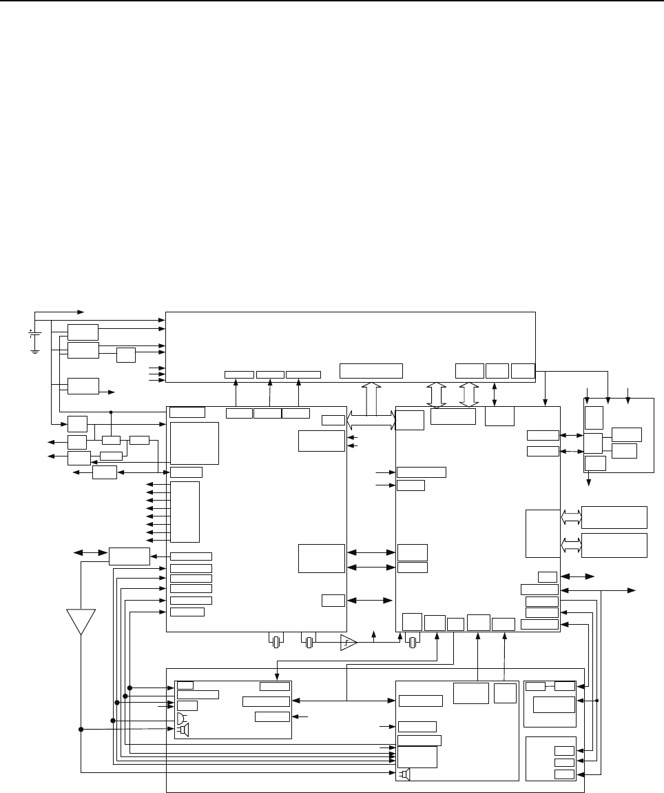
1-1
Section 1
THEORY OF OPERATION
1.0 Controller
The Controller section consists of 4 main ICs. These are the Texas Instrument OMAP 1710 Host/
DSP Processor (U1000), Flash memory (U2000), SDRAM memory (U2001) and the MAKO Audio/
Power Management (U3200) chip.
Figure 1-1 shows how the Controller interfaces with the RF section, and peripherals in an
XPR 8300/XPR 8400 repeater. The Controller, RF section, and Accessory interface are placed on a
single Transceiver board.
Figure 1-1 Controller Block Diagram
Power
Management
MEM I/F
FLASH
RAM
Audio Atten.
SiRF
IC
SPI
SSI
USB1,2 TXCR
Voice Codec
11 Channels
ADC
DAC1 DAC2 DAC3
ON_OFF_CTRL
12 MHz
24.576 MHz 32.768 KHz
LDOs
4-Wire SPI
I S S X T
SPI_1
USB0
USB1
UART1
UART3
Audio Preamp
9.3V
Reg.
RF Interface
Battery
9.3V
Reg.
9.3V
Reg.
Curr.
Limit
SW2
V4_2.775V
V2_1.875V
V3_1.35V
Core
Reg.
1.4V
V6_2.9V
V7_2.775V
V8_5V
V9_3V
V10_3.3V
CLK
PLL
Peripherals
I S S X R
5V_GPS 5V
Reg. FET SW1
5V
Reg
9.3V_RF
PA_SUPPLY
PA_Driver_Supply
5V_RF
SW5
VBUS
Reg.
VBUS1,2
GPIOs
V2_1.875V Peripheral_IO
Core
1.4V
Control Head
TDA1519C
ON/OFF Switch
ON/OFF Logic
LCD Driver/LED
Keypad
&Navigation
buttons
Audio
PA
GCAI MMP
OPT_SELA
USB_RS232
Interfaces
VBUS2
Audio PA
Rear Accessory (MAP)
Emerg/Ignition
Serial_Parallel IC
USB2
V2_1.875V
V4_2.775V
V7_2.775V
Option Board
Repeater
Vdd
Supply
SPI_2 KEYPAD
I/F
MAKO
(LDOs,Codec,USB,1-Wire,ADC,DAC)
OMAP1710
(MPU & DSP)
Volume
Encoder
DATA
GPIOs MPUIOs
EXT_SWB+
EXT_SWB+
VBUS1
McBSP3
McBSP2
McBSP1
GPS
GPIOs Logic
CTRL
SSI
SYNC
SSI
Dir. CTRL /
SYNC
GPIOs
GPIOs
GPIO
4-Wire SSI
I2C
I2C
DC Supply
4-Wire SSI
32.768KHz
32.768KHz
Level
Shift
5V_GPS
1.5V
2.8V
Reg.
9.3V 2.9V Reg.
Buffer
ADS
1-Wire
Curr.
Sense
Curr. Sense
Curr. Sense
Batt. Sense
I2C
TOMAHAWK_ABACUS
SPI
ABACUS
SSI
RF
CNTRL 16.8MHz
FET_ENX
FE_TUNE PA_BIAS RAMP_DAC
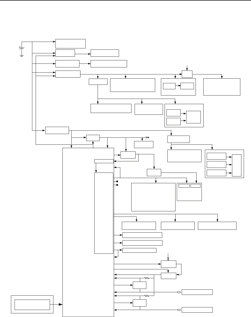
1-2 Controller
1.1 Radio Power Distribution
Figure 1-2 illustrates the controller DC power distribution throughout the transceiver board.
Figure 1-2 Radio DC Distribution
Battery
(J3000)
SW_9.3V_PA_Reg
U3005 & U3006
SW_9.3V_RF_Reg.
U3001
U0100 GPO_4
Switcher1
(Q3200)
5V_Reg.
U0941
*TX pwr cntrl attenuator ckt
MAKO
(U3200)
TX_Pwr_Cntrl
V4_2.775V
V2_1.875V
V3_1.35V
V7_2.775V
V8_5V
V9_3V
V10_3.3V
*TX_PA_Final (Q0702)
*Antenna Switch ckt.
*Audio_PA (U3500)
Ext_SWB+
U3003
Log Amp
U0940
SW_5V_Reg.
U3002
Accessory Connectory
(J4000-7)
*TX_PA_Pre-Driver (U0700)
*TX_PA_Driver (U0703)
*Volume Atten.(U3501)
*1-Wire LevelTranslator (U3508)
*Synthesizer (U0100)
*IF Amp (Q0500)
*GPS Antenna Sense
RXBE
3V_Reg
U0601
3.6V_Reg
Q0601
ABACUS3
*Shift Register (U4000)
*Peripheral Inverter ckts
*USB1 D+/D- ESD (D4001)
*USB2 D+/D- ESD (D4000)
*Audio OpAmp (U3502 &U3505)
*Control Head (E4001, J4001-1)
*TX PA Pressure Pad Switch (S0700)
*TX VCO Buffer (Q0302)
P_FET
Q0107
*RX VCO Buffer (Q0202)
*RX FE Amp (Q0402)
*RX FE AGC
*RX FE DAC Doubler (Q0403)
*RX 1
st
LO Amp (Q0405)
UNSW_9.3V_Reg
U3040
9.1V
9.3V
12.6V
9.3V
UNSW_5V_Reg.
U3004
GPS
2.8V_RF_Reg
U6402
2.8V_Dig_Reg
U6406 SiRF
1.5V_RTC_Reg
U6407
P_FET
(Q3201)
9.3V
Switcher5
(Q3202)
9.1V
Switcher2
FET_ENX
BPLUS &
BAT_7V5
PA_BPLUS
1.4V_Reg.
U3201
1.4V (0.87mA/MHz)
LOGIC_VDD
OMAP1710
(U1000)
CDVVDVDD
*SDRAM (U2001)
*FLASH (U2000)
*32.678KHz Square (U3203)
*16.8MHz Square (U1006)
* SSI Buffer (U4005:U4008)
*GPS Logics Translator (U1005)
*Logic Translator (U4001)
*Tomahawk Digital IO (U0100)
*Abacus3 Digital IO (U0600)
Not Used
Not Used
*16.8MHz Buffer (Q0100)
*Tomahawk Digital (U0100)
*Tomahawk TCXO (Y0100)
*Tomahawk Analog (U0100)
*GPS Logics Translator (U1005)
*I
2
C Bus Translator (U3503)
*USB /GPIO1&2 Switch (U3504)
V6_2.9V *1-WireTranslator (U3508)
*GCAI GPIO_1& GPIO_2 Pull-Up
ATOD0
FET
(Q3207)
FET
(Q3203)
9.1V
SW1_SUMCOMP
SW5_SUMCOMP
5.25VUSB_CONNECT
FET
(Q3204)
VBUS1_CMD
VBUS2_CMD
USB_Supply
0.2
0.2
VBUS1_SEN
VBUS2_SEN
VBUS1
VBUS2
3.6V
ON_OFF_CNTRL
Ignition (J4000-25)
(ON: >7V)
(OFF: 0V)
IGN_X
VBUS1_MMP (J4001-27)
VBUS2_MAP (J4000-3)
LDOs
5V, 500mA (max)
5V, 500mA (max)
5V
5V
*Option Board
(J4003-1)

Controller 1-3
Voltage regulation is provided to the controller, GPS and RF sections by the following devices:
•+9.3V_PA: U3005, U3006, and U3030
•+9.3V_CNTRL: U3040 and U3030
•+9.3V_SW: U3001
•+12.6V_Ext SWB+: U3003
•+1.5V GPS RTC: U6407
•+1.4V OMAP Core: U3201
•Supplies for the Controller section: U3200 (MAKO)
•Supplies for the RF and GPS sections: U0601, U0941,U3002,U3004,U6402, and U6406
The 9V3_PA regulator uses Op Amp U3030-1 as a controlling element. The regulated output
voltage is divided by R3039 and R3040 and compared with an accurate reference voltage (5.1V DC)
determined by VR3040. The Op Amp's output voltage at pin 1 varies the amount of conduction in
transistors Q3032, U3005 and U3006 as necessary to keep voltages equal on pins 2 and 3 of the
Op Amp. A characteristic of the Op Amp which allows the regulator to start up is the fact the output
is high when both inputs are low, which occurs momentarily at turn-on. Dual diode D3030 serves two
purposes. Diode D3030 is used to protect transistors U3005 and U3006 if the 9.3V_PA line is
grounded. When this happens Q3032's base can only be 0.7V DC and transistors U3005 and
U3006 will be turned off. Diode D3030 also provides temperature compensation of the regulated
output voltage. The 9V3_PA supply powers the low level and driver stages of the RF power
amplifier.
The MAKO and GPS regulators are powered by the 9V3_CNTRL supply. Op amp U3030-2
functions as a controlling element for the 9V3_CNTRL regulator. The regulated output voltage is
divided by R3045 and R3046 and compared with the reference voltage determined by VR3040. The
Op Amp's output voltage at pin 7 varies the amount of conduction in transistors Q3040 and U3040
as necessary to keep equal voltages on pins 5 and 6 of the Op Amp. As is the case with the 9V3_PA
regulator, the Op Amp characteristic allows the regulator to start up when both Op Amp inputs are
momentarily low at turn-on. Dual diode D3040 serves two purposes. Diode D3040 is used to protect
transistor U3040 if the 9.3V_CNTRL line is grounded. When this happens Q3040's base can only be
0.7V DC and transistor U3040 will be turned off. Diode D3030 also provides temperature
compensation of the regulated output voltage.
Regulator U3001 generates the 9.3 V required by most RF, power control, and audio circuits. Input
and output capacitors C3005, and C3006/C3007/C3046 are used to reduce high frequency noise.
R3003 and R3004 resistor divider set the output voltage to 9.3 V. This regulator output is
electronically enabled by 0 V signal at pin 2. MAKO (U3200) FET_ENX, Q3206, and Q3041 are
used to control the on-off at U3001 pin 2.
Regulator U3003 generates the 12.6 V required by external accessory device at connector J4000-7.
Input and output capacitors C3012, and C3012 / C3013 are used to reduce high frequency noise.
R3003 and R3004 resistor divider set the output voltage to 12.6 V. This regulator output is
electronically enabled by 0 V signal at pin 2. MAKO (U3200) FET_ENX, Q3206, and Q3041 are
used to control the on-off at U3003 pin 2.
There are a total of eight other LDO regulators used to regulate the 9.3 V supply down to specific
application voltages. U0941, U3002, and U3004 are set to supply 5 V output. U0601 is set to supply
3 V for the Abacus III IC. U6402 and U6406 generate 2.8 V for GPS Digital IO and RF circuitry while
U6407 regulator provides 1.5 V for the GPS RTC module. U3201 regulator, which is capable of
handling up to 1 Amp, is set to 1.4 V for the OMAP core.

1-4 Controller
Switcher1 (Q3200) in conjunction with the MAKO power management IC (U3200) is a highly
efficient dc-dc converter. In this application, it is configured as a synchronous buck dc-dc regulator. It
generates an accurate 3.6 V output, which supplies directly to the MAKO internal Switcher2 circuit
as well as the 1.4 V regulator for the OMAP Core (U3201). A pulse width modulated (PWM) signal is
output from U3200 pin G14 to Q3200 pin 4 and controls the output voltage level. External
components L3200 and C3203 are needed to filter out the dc-dc converter output. R3200 (0.1 ohm)
is used for current sense and over-current circuit protection with 2 A threshold. MAKO Switcher2
output 2.3 V and supplies to the rest of MAKO internal LDOs.
Switcher5 (Q3202) circuitry is similar to Switcher1. It is also configured as a synchronous buck
dc-dc regulator. It generates an accurate 5.2 V output, which supplies directly to both VBUS1 and
VBUS2 supplies. External components L3202 and C3212 are needed to filter out the output. Q3208
and Q3207 prevent internal voltage leakage onto VBUS_SUPPLY (U3200 pin B13). When the radio
is operated in the HOST mode, USB_CONNECT (U3200 pin L6) is toggled HIGH (3.3 V) turning on
PMOS FET (Q3207) through Q3208 inverter, and thus provides 5.2 V to both Q3203 and Q3204
drains. Software will enable VBUS1_CMD and VBUS2_CMD either VBUS1 or VBUS2 port base on
the detection mechanism. Note, only one of two VBUS ports can supply up to 500 mA (max) at one
time. R3207 and R3208 (0.2 ohm) are used for current sense and over-current circuit protection with
800 mA threshold. In device mode, USB_CONNECT is toggled LOW to disable VBUS supply.
The MAKO power management IC (U3200) provides eight more LDOs. Some LDOs are
programmable to meet the requirement for various ASIC devices. V2, V3, and V9 are programmable
via SPI while V4, V5, V6, V8, and V10 are fixed. See Figure 1-2 for details.
1.2 Power On/Off
The repeater is switched on by asserting the ignition sense input high. On 8 MB repeaters, this
signal is internally wired high, in both transmit and receive radios. On 32 MB repeaters, this signal is
controlled by circuitry on the Connector board. It is driven high when the repeater’s power supply is
switched on, or when the battery voltage is above 8.6 V in battery backup mode.
When the repeater’s power supply is switched on, Q4006 is driven into saturation which pulls its
collector to ground and presents an active low to MAKO IGN_X input (U3200 pin B4). When there is
no voltage at J4000 pin 25, Q4006 is turned off and its collector is internally pulled high by the
MAKO Vsave supply. Because of the noisy nature of ignition signal, a long debounce period of
250ms is used before it will be recognized as a valid input.
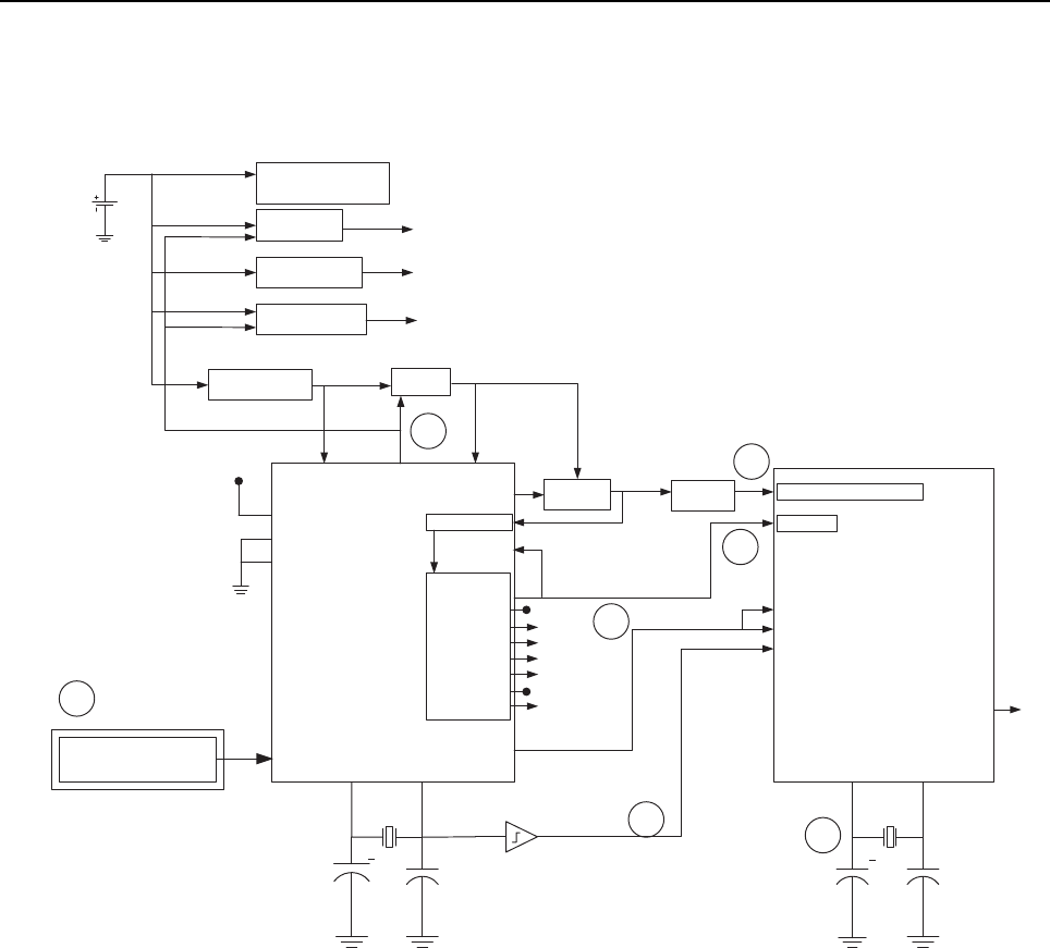
Controller 1-5
1.2.1 Power-Up Sequence
Figure 1-3 details the typical power-up sequence on the mobile radio and the following events that
occur sequentially.
Figure 1-3 Power-Up Sequence
1. User switches on the power supply unit which initiates an ignition sense power on state.
2. The MAKO (U3200) generates an output low at FET_ENX (pin E2) once it detects a valid
input at either Mech_SW (pin E4), Emerg_PB (pin F4), or IGN_X (pin B4). Q3206 dual
PNP/NPN transistor acts as a double inverter between the MAKO and Q3201 power
MOSFET switch as well as over voltage protection. This logic low at the gate of Q3201 results
in switching 9.3 V to both Q3200 Switcher circuitry and 1.4 V regulator (U3201).
3. Next the MAKO (U3200) asserts the RESETX (pin C5) low to the OMAP for an additional
32mS after all the DC regulators are stable. It is then de-asserted, allowing the OMAP
processor to start.
Battery
(J3000)
SW_9.3V_PA_Reg
U3005 & U3006
SW_9.3V_RF_Reg.
U3001
Switcher1
(Q3200)
MAKO
(U3200) V4_2.775V
V2_1.875V
V3_1.35V
V7_2.775V
V8_5V
V9_3V
V10_3.3V
*TX_PA_Final (Q0702)
*Antenna Switch ckt.
*Audio_PA (U3500)
Ext_SWB+
U3003
UNSW_9.3V_Reg
U3040
9.3V
12.6V
9.3V
P_FET
(Q3201)
9.3V 9.1V
Switcher2
FET_ENX
BPLUS &
BAT_7V5
PA_BPLUS
1.4V_Reg.
U3201
LOGIC_VDD
OMAP1710
(U1000)
1.4V Core (0.87mA/MHz)
Not Used
Not Used
V6_2.9V
SW1_SUMCOMP 3.6V
LDOs
OSC_IN (Y2) OSC_OUT (W3)
12MHZ
+20 ppm
Y1000
32.768KHZ
XTAL32_OUTXTAL32_IN
+20 ppm
Y3201
U3202
U3203
RST_OUT (AA20)
PWRON_RST (R12)
MPU_RST (U20)
1.8V IO
POWER ON RESET
PGLDO2
PGLDO3
Default
Voltage
Selection
For V2
and V3
ON_OFF_CNTRL
Ignition (J4000-25)
(ON: >7V)
(OFF: 0V)
IGN_X RESETX
1
2
3
4
5
6
7
SW_TYPE
2.5V

1-6 Controller
1.3 Clocks
Figure 1-4 illustrates the controller clocks used throughout the radio.
Figure 1-4 Clock Connections
The OMAP processor (U1000), which consists of an ARM and DSP core, needs three clocks for
operation: a 32.768 kHz square-wave, a 12 MHz sine-wave, and a 16.8 MHz square-wave clock.
The 16.8 MHz clock source is provided from the Tomahawk TCXO with its supporting circuitry
Q0100 buffer amplifier, routes to squarer-circuit U1006, and feed to EXT_CLK (U1000 pin N18). The
32.768 kHz clock is generated by the MAKO crystal Y3201 oscillator; converted to a gated clock by
U3202 and U3303 circuitry; then directly feed to OMAP CLK32_IN (U1000 pin P13) as well as GPS
IC (U6400). The OMAP needs the 32.786 kHz to determine the input reference clock (12, 13, or
19.2 MHz) applied to OSC_IN (U1000 pin Y2). Without this 32 kHz clock, the OMAP will potentially
program all the wrong dividers for USB and UART booting. The 12 MHz sine-wave is the main
system reference clock for the OMAP which all the internal clocks are derived from. External pull-up
on OSC32K_IN (U1000 pin V13) and grounding both OSC32K_OUT (pin AA1 and VSS_11 (pin
Y13) indicating that an external 32 kHz clock is used. The 24.576 MHz crystal (Y3200) oscillator is
the reference clock for MAKO CODEC and SSI clock.
MPU CLK
EXT_CLK (N18)
CLK32K_IN (P13)
OSC_IN (Y2)
OSC_OUT (W3)
OSC32K_IN (V13)
OSC32K_OUT (AA13)
SYS_CLK_IN (Y4)
DPLL1
General Pupose
TIMER
ARX DAC
XOSC BASE
CLK2 OUT
16.8 MHZ
TCXO
+0.5 ppm (GPS & Repeater)
+1.5 ppm (NONGPS)
FREF
24.576MHZ 32.768KHZ
XOUT XIN XTAL32_OUTXTAL32_IN
+20 ppm+30 ppm
TOMAHAWK P2
U0100
ABACUS III
U0600
MAKO P2
U3200
xN
DSP CLKxN
TC CLKxN
12MHZ
+20 ppm
1.4V
10K
OMAP1710
U1000
U1006
U3202
U3203
Q0100
32.768 KHz
16.8MHz
Y3201Y3200 Y1000
VSS_11 (Y13)
OMAP 3.3 Core
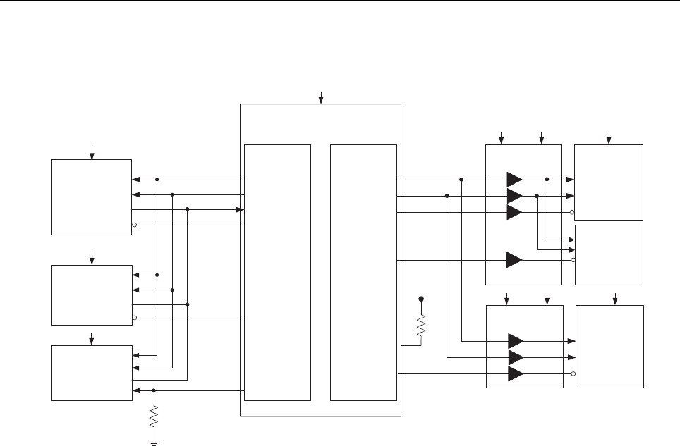
Controller 1-7
1.4 Serial Peripheral Interface (SPI)
Figure 1-5 illustrates the controller SPI used throughout the radio.
Figure 1-5 SPI Connections
The OMAP processor (U1000) has two SPI busses that it uses to communicate with the various
peripheral IC's. The first is the High Performance Data (HPD) SPI bus and the second is the
multi-media card (MMC) SPI.
The HPD SPI is a synchronous serial bus made up of four lines, SPI_CLK, SPI_MOSI, SPI_MISO,
and chip select. The SPI_CLK line is used to control the speed of the data to/from the peripheral IC's
and the OMAP processor. This clock can be adjusted to different speed based on the IC's
specification.
HPD SPI module is used to interface to Tomahawk (U0100), Abacus III (U0600), and the MAKO
(U3200). This interface operates at 1.8 V logic levels. SPI_MOSI, or commonly known as
TRANSMIT Data, is a data string from the OMAP while SPI_MISO or RECEIVE Data is data string
to the OMAP.
The MMC SPI is a 3-wire bus; consisting of SERIAL_CLK, SERIAL_DATA, and chip select. This SPI
bus is used to interface to accessory Serial-Parallel IC (U4000), the repeater board LED's and LCD
driver. For accessory Serial-Parallel IC, the logic level out of the processor is level shifted from 1.8 V
to 5 V through U4001 and pull-up resistors R4100, R4101, and R4103.
HPD SPI
1.8V
10K
Level Translator
U6003
SN74LVC07A
1.8V
LED’s Register
U6002
SN74AHC594
LED_CS
DISPLAY_CS
LCD
Interface
DATA
DATA
CLOCK
TOMAHAW K P2
U0100
1.8V
CEX
SPI_DW
SPI_DR
SPI_CLK
ABACUS III
U0600
PE
PD
DOUTB
PC
MAKO P2
U3200
SPI_CS
SPI_CLK
SPI_DO
GPIO_44 (P15)
SPIF.DOUT (W21)
SPIF.DIN (U18)
SPIF.SCK (U19)
GPIO_9 (Y8)
GPIO_58 (R11)
SPI_DI
OMAP1710
U1000
MMC1 SPI
SPI.CS1 (P19)
SPI.CLK (M14)
MMC.CMD (P11)
SPI.RDY (R18)
SPI.CS2 (P20)
SPI.CS3 (P18)
CLOCK
Level Translator
U4001
SN74LVC 07A
Accy’s t Register
U4000
SN74AHC594
LED_CS
DATA
CLOCK
1.8V
1.8V
2.9V 2.9V
1.8V 5V 5V
47K
1.8V
SPI_CLK
SPI_MOSI
SPI_MISO
THK_CE
MAKO_CE
ABACUS3_CE
SERIAL_DATA
SERIAL_CLK
LED_CS
DISPLAY_CS
PROGM_IO_CS
1-8 Controller
1.5 Serial Synchronous Interface (SSI)
Figure 1-6 illustrates the controller SSI used on XPR series radios controller design.
Figure 1-6 SSI Connections
The OMAP processor (U1000) has a total of three SSI or multi-channel buffer serial ports (McBSP)
modules that are used to directly interface to the CODECs in the Tomahawk, Abacus, and MAKO
and between Tx and Rx radios within a Repeater.
As shown in Figure 1-6, McBSP1 is a 4-wire bus and interface to the MAKO CODEC. McBSP2 is
6-wire bus; 3-wire dedicated to the Tomahawk Tx audio and the other 3-wire to Abacus Rx audio.
McBSP3 is a 4-wire bus, and used primarily to interface between Tx and Rx radios within a
Repeater.
McBSP2
Buffers
SN74AVC1T45
1.8V
Cypher I/F
J4002
DATA_OUT
FSYNC
CLOCK
TOMAHAWK P2
U0100
1.8V
DMCS
SDTX
SFTX
TXCLK
ABACUS III
U0600
DOUTA
FS
CLKOUT
MAKO P2
U3200
VC_TX
VC_DCLK
VC_FSYNC
GPIO_2 (D15)
McBSP2.DX (AA5)
McBSP2.FSX (W7)
McBSP2.CLKX (Y6)
VC_RX
OMAP1710
U1000
McBSP3.DR (T19)
McBSP3.CLKX (N14)
McBSP3.DX (P14)
McBSP3.FSX (AA17)
1.8V
1.8V
1.8V
McBSP2.DR (P10)
McBSP2.FSR (W6)
McBSP2.CLKR (V7)
McBSP1
McBSP1.DX (H18)
McBSP1.CLKX (G21)
McBSP1.DR (H20)
McBSP1.FSX (H15)
McBSP3
DATA_IN
ARMIO_11 (W10)
GPIO_26 (AA9) SYSTEN_SYNC
1.8V
10K
B
B
B
A
A
A
BA
A-->BHIGH
B-->ALOW
OperationDIR
AB
SYNCB GPIO_40 (W15)
U4005
U4004
U4006
U4007
DIR U4008
10K
R4106

Controller 1-9
1.6 ACC_ID Interface
Smart accessories use the Accessory ID (ACC_ID) Interface to help the repeater determine which
smart accessory, if any, are attached to the repeater. Figure 1-7 illustrates the ACC_ID connections
used within the radio.
Figure 1-7 ACC_ID Interface Connections
The MAKO (U3200) serves as a driver between the OMAP ACC_ID bus and the device. Level
translator (U3508) is required to level shift between 2.9 V to 5 V.
ACC_ID_MAP (M8)
MAKO
U3200
2-BitTranslator
U3508
2.9V
R3514
Vref1 Vref2
2.9V 5V
SDA1 SDA2
5V
OMAP1710
U1000
HDQ (N20) ACC_ID_UP (L7)
R3592
R3588
1.875V
MAP
1-10 Controller
1.7 USB Interface
The OMAP processor (U1000) supports two USB ports. The radio makes use of these USB ports to
communicate with smart accessories, and connection to a host computer for radio programming via
CPS and tuning via the Tuner Tool. Only one of these ports is available (via the MAP connector), the
other is dedicated to the Ethernet controller.
Note: The USB ports are designed to support Motorola accessories and approved applications only
and will not support third party "Plug-n-Play" USB devices.
Figure 1-8 shows the details of the HSSI connections within the radio.
Figure 1-8 USB Interface Connections
The OMAP processor USB host controller communicates with accessories at either 1.5 Mbps or
12 Mbps data rates depending on the accessory. Either port can be used as a host or a device, the
only limitation is that both ports cannot be used as a device at the same time.
The MAKO (U3200) incorporates two USB transceivers that provide the physical layer signaling for
the two ports. Each transceiver generates and receives the DP and DM differential signals of the
USB port. The transceiver interfaces to the OMAP processor through a three-wire interface
consisting of two bi-directional signals (SE0 and DAT), and one uni-directional signal (TXEN). The
MAKO also includes two bus monitors that sense the connection or removal of a device and
determine whether or not to supply current to that device via Q3203 or Q3204 up to a maximum of
500 mA per port.
1subV
r
otinoM
1BSU
reviecsnar
T
eri
W
6/3
dn
a
FI
IP
S
srets
igeR
)6N(
P
D
)7P( MD
)6L( tcennoC_BS
U
2s
ubV
rotin
o
M
2BSU
reviecs
narT
eriW 3
dna
FI
IPS
sre
ts
ige
R
)
11F
(
sn
eS
_
2s
u
BV
)
8
0
B(
E
O
_
1
B
S
U
)
80D( 0ES_1B
SU
)80C( DX
T
_TA
D
_1
B
SU
)
90
A
(
S
T
R_
VCR_
EO_
2
B
SU
)
90C
(
DXR
_
M
V
_
0
ES
_
2
BS
U
)90B
(
PV_TAD_2
B
SU
okaM
0171 PAMO
1 puor
G niP
0 puo
rG niP )
2
1D
(
2s
u
BV
)
3
1
C
( dm
C
_2
suB
V
)21E(
sne
S_
1suBV
)01H( 1s
u
BV
)4
1
C
(
d
m
C
_
1
suBV
5WS_V
elbanE suBV 1
elbas
iD suB
V
0
)7N( PD
)8P
( MD
+D
-
D
suBV
s
u
B
V
PAM
8023R
7023R
04
23R
)61W( NEXT_1BS
U
)41W( TA
D
_1BSU
)
3
1
R(
0
ES_1BSU
)
4
W(
N
E
X
T 0BSU
)9
P(
TA
D
_
0
B
SU
)
5
1L( TNI_BSU
)8R(
0
E
S_0BSU
)0
1
C
(
XT
N
I_
B
S
U
+D
-D
3
0
23Q
4
023
Q
7023Q
8023Q
tenrehtE
o
T
rellortnoC
Controller 1-11
1.8 Mobile Accessory Port (MAP)
The Mobile Accessory Port (MAP) is a newly defined Motorola accessory port that contains audio,
programmable digital I/O, serial interfaces, and accessory supply lines; and is similar in function to
Motorola's legacy products accessory connectors.
Table 1-1 Mobile Accessory Port Functions
MAP Pin
Number MAP Pin Name MAKO Pin
1USB_D+
USB for programming or Smart Accessory
2 USB_D-
3V_Bus
4 USB_Ground
5ACC_MAP_ID_2 Accessory Identifier
6 ACC_MAP_ID_1
7Ext_SWB+ Switched Battery Voltage
8 Power Ground Ground
9Ext_Spkr- External Speaker
10 Ext_Spkr+
11 Tx_Audio Tx Audio Input
12 Audio Ground Ground
13 Aux_Audio_Out_1 Auxiliary Audio Output (not supported in the
repeater)
14 Rx_Audio Rx Audio Output (not supported in the
repeater)
15 Aux_Audio_Out_2 Auxiliary Audio Output (not supported in the
repeater)
16 Ground Ground
17 Prgm_In_1_(PTT) Programmable Input with prescribed function
of PTT
18 Ground Ground
19 Prgm_IO_2 (Monitor) Programmable Input/Output with prescribed
function Monitor
20 Prgm_IO_6 Programmable Input/Output
21 Prgm_IO_3 (Chan_Act) Programmable Input/Output with prescribed
function Channel Activity
22 Prgm_IO_7 Programmable Input/Output

1-12 Controller
1.8.1 MAP Programmable I/Os
The MAP contains 7 general purpose I/Os. One is specifically an output, 1 is specifically an input,
and the remaining 5 can be either input or output. The MAP also contains 2 dedicated inputs. All
input signals map directly to OMAP (U1000) GPIOs, while all outputs are controlled from the OMAP
through a SPI connected shift register (U4000) referred here as the Acc_Shift_Reg. While 7 of the 9
I/Os are general purpose and designed to be programmable through the CPS, several have
recommended functions that will be detailed below.
All of the programmable I/Os, except the dedicated inputs, use inverted logic, IE: a 1 on the
connector as an input will be seen by the OMAP as a 0 and visa versa. Also, a 1 output by the
OMAP through the Acc_Shift_Reg will be seen as a 0 output on the connector.
•Prgm_In_1 (PTT): Programmable input that has the recommended function of Push-To-Talk
(PTT). This signal connects to the OMAP GPIO_7 (U1000 pin M15) as an input.
•Prgm_IO_2 (Monitor): Programmable input/output that has the recommended function of
Monitor. This signal connects to the OMAP GPIO_32 (U1000 pin B17) as an input. The output
for this signal is driven from Acc_Shift_Reg bit 0 (U4000 pin 15).
•Prgm_IO_3 (Chan_Act): Programmable input/output that has the recommended function of
Channel Activity (Chan_Act). This signal connects to the OMAP GPIO_33 (U1000 pin J14) as
an input. The output for this signal is driven from Acc_Shift_Reg bit 1(U4000 pin 1).
•Prgm_I_4 (Emergency): Dedicated input that is having the function of Emergency
(Emerg_Sw). This signal connects to the MAKO EMERG_PB (U3200 pin F4) as an input.
•Prgm_IO_6: Programmable input/output. This signal connects to the OMAP ARMIO_15
(U1000 pin E19) as an input. The output for this signal is driven from Acc_Shift_Reg bit 2
(U4000 pin 2).
•Prgm_IO_7: Programmable input/output. This signal connects to the OMAP ARMIO_3
(U1000 pin V8) as an input. The output for this signal is driven from Acc_Shift_Reg bit 3
(U4000 pin 3).
•Prgm_IO_8: Programmable input/output. This signal connects to the OMAP GPIO_24 (U1000
pin V5) as an input. The output for this signal is driven from Acc_Shift_Reg bit 4 (U4000 pin
4). This IO is not supported in the repeater.
•Prgm_Out_9 (Ext_Alarm): Programmable output that has the recommended function of
External Alarm (Ext_Alarm). The output for this signal is driven from Acc_Shift_Reg bit 5
(U4000 pin 5).
23 Prgm_In_4 (Emergency) Programmable Input with dedicated function
for Emergency Switch
24 Prgm_IO_8 Programmable Input/Output (not supported in
the repeater)
25 Prgm_1_5 (Ign_Sense) Not Used
26 Prgm_Out_9 (Ext_Alarm) Programmable Output with prescribed
function of External Alarm
Table 1-1 Mobile Accessory Port Functions
MAP Pin
Number MAP Pin Name MAKO Pin

Controller 1-13
1.8.2 MAP Serial Interfaces
The MAP includes 2 serial interfaces: an USB port and an ACC_ID interface. The USB port can be
used as either a device (radio is device) or as a host (radio is host). When configured as a device,
the radio can be programmed or tuned using MOTOTRBO CPS or Tuner software. When
configured as a host, various smart accessories can be used with the radio. See section 1.7 on page
1-10 for more information on the USB interface.
The ACC_ID interface is used by accessories to provide the radio with information needed to
configure the interface for that accessory. See section 1.6 on page 1-9 for more information on the
ACC_ID interface.
Note: The USB ports are designed to support Motorola accessories and appoved applications only
and will not support third party "Plug-n-Play" USB devices.
1.8.3 MAP Audio Signals
The MAP has Speaker and Tx audio input. Speaker audio is a differential output from the radio's
audio PA (U3500). The speaker output available for monitor functions only. Tx audio is a mic/line
level input audio for transmit, it is available in test mode only.
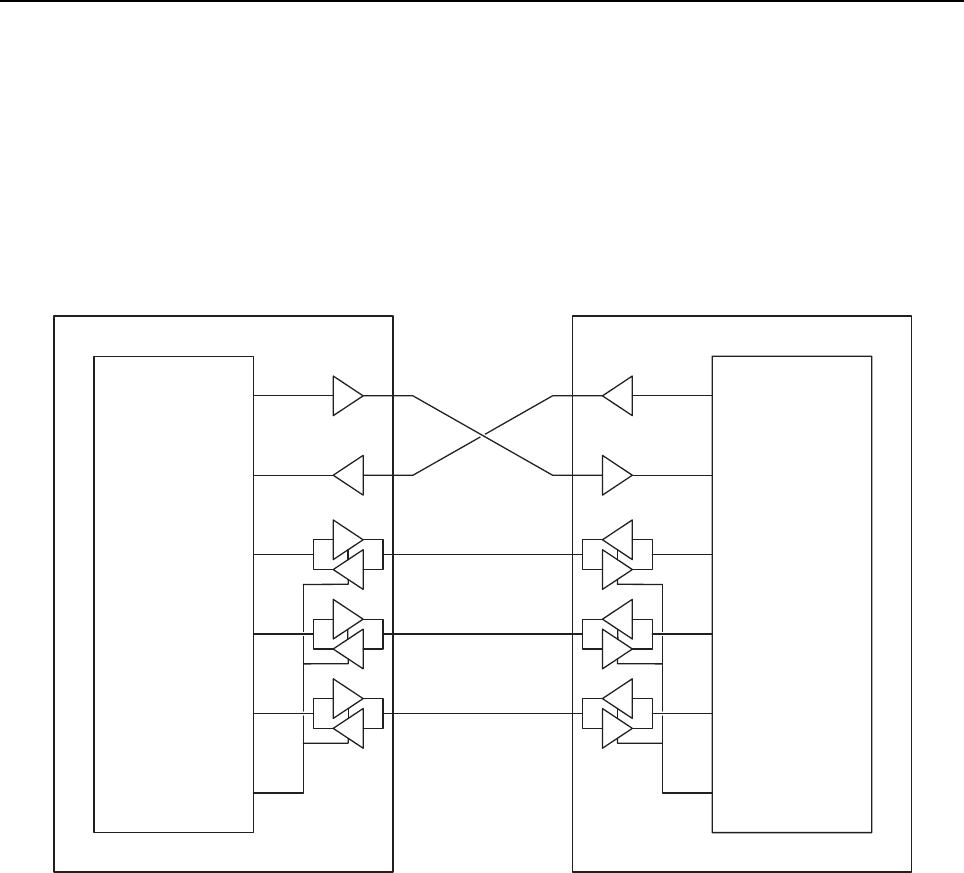
1-14 Controller
1.9 Repeater Interconnections Interface
The Repeater’s architecture uses two mobiles, one for transmit, one for receive to form a repeater.
The Repeater Interconnection Interface is used to communicate between the Tx and Rx radios
within the Repeater. This is accomplished by using one of the SSI ports from the OMAP (U1000)
and level shifters/drivers (U4004, U4005, U4006, and U4007). Both data and commands/responses
can be passed via this interface. The interface consists of two separate serial paths, one from the
Rx radio to the Tx radio; and one from the Tx radio to the Rx radio. The Tx radio is considered the
master while the Rx radio is the slave, meaning that the Tx radio generates the sync and clock for
both communication paths. Figure 1-9 shows the basic block diagram of this interconnection.
Figure 1-9 Repeater Interconnection Interface
McBSP3_Dx
McBSP3_Rx
McBSP3_Fsync
McBSP3_Clk
System Sync
Dir
OMAP
McBSP3_Dx
McBSP3_Rx
McBSP3_Fsync
McBSP3_Clk
System Sync
Dir
OMAP
GPIO_26
ARMIO_11 = 0
GPIO_26
ARMIO_11 = 1
Tx Radio Rx Radio

2-1
Section 2
TROUBLESHOOTING CHARTS
1.0 Controller Troubleshooting Chart
Problem has been
diagnosed to either the Tx
or Rx Radio. Remove
faulty radio and proceed
from here.
9.3V_RF @
pin 5 of U3001?
5V_SW @
pin 1 of U3002?
Controller
OK
Check 9R1
9.1V@ E0401
Q0108 pin 2
=2.8V
Check gate Q0107 for 0V.
Check these three conditions @
U3001 (pin 4=13.2V; pin 2=0V;
pin 1=1.26V) before replacing
U3001.
Yes
No
Check these conditions @
U3002 (pin 4=9.3V; pin 2=1.26V;
before replacing U3002.
No
Yes
Yes
No
No
Yes
Check SPI programming
to Tomahawk IC.
Check
Lock_Detect
1.875V @
R2518
No
Check Tomahawk GPO Register
settings to see GPIO_4 is set to
output HIGH.
Yes
The individual
radio.
Will Tuner
connect to the
Radio?
No
Yes
Controller
OK
2-2 Power-Up Troubleshooting Chart
2.0 Power-Up Troubleshooting Chart
Repeater does not
fully initialize
(Disabled LED
stays blinking)
Does Repeater
initialize properly
now?
Re-insert or replace SSI
cable
Replace Connector
Board and/or
Accessory Cable
Does Repeater
initialize properly
now?
Can it repeat?
Re-insert or Replace
30 pin Front Panel
cable
Do all LEDs flash
on power-up?
Replace Front Panel
Board
Troubleshoot Rx
Radio
Yes Yes
No
No
No
Done
Done
Yes
No
Done
Yes
Does Repeater
initialize properly
now?
Done
Troubleshoot Tx
Radio
No
Yes

Audio Troubleshooting Chart 2-3
3.0 Audio Troubleshooting Chart
Yes
Yes
Yes
Yes
U3501: AUDIO ATTENUATOR
pin 9: +5V
pin 8: +5V
pin 7: GND
pin 2: +2.5V
pin 6: PROBE I2C CLK
pin 5: PROBE I2C DATA
pin 1: PROBE AUDIO IN (+2.5V BIAS)
pin10: PROBE AUDIO OUT (+2.5V BIAS)
U3505: OP-AMP
pin 4: +9.3V
pin 11: GND
pin 5: +4.5V BIAS
pin 6: PROBE AUDIO IN (+4.5V BIAS)
pin 7: PROBE AUDIO OUT (+4.5V BIAS)
U3200: MAKO
TP_MAKO_DCLK: PROBE CLK
TP_MAKO_FSYNC: PROBE FSYNC
TP_MAKO_RX: PROBE DIGITAL AUDIO IN
xU1000: OMAP
No
No
No
No
Audio
self-
check
This test should be
performed with the
individual RX or TX
radio removed
from the repeater.
Using the tuner
tool, set the radio
into RX audio test
and connect an
external speaker
to the radio’s map.
This test assumes
standard RF input
60% full deviation
1kHz audio tone.
Is audio present
at speaker
outputs?
Can
the volume be
adjusted using
tuner?
Self-check
completed
Is audio present
at pin 7 of U3505
Verify U3501
connections
before replacing
Verify U3505
connections
before replacing
Is audio present
at
pin
6 of U3505
Verify SSI input
into U3200 before
replacing
If SSI input is not
present then
replace U1000

2-4 Audio Troubleshooting Chart
Notes

3-1
Section 3
CONTROLLER SCHEMATICS/PARTS LISTS
1.0 Allocation of Schematics and Parts List
1.1 Controller Circuits
This Chapter shows the Schematics and the Parts Lists for the Controller circuits.
Table 3-1 Controller GPS R1 Schematic Diagrams and Parts List
Controller R1 used on PCB:
8471165L03_A UHF (403–470 MHz), 1–25 W
8486777Z12_A UHF (403–470 MHz), 25–40 W
SCHEMATICS
Controller GPS
DC Supply
DC Distribution
Peripheral (sheet 1 of 2)
Peripheral (sheet 2 of 2)
Microprocessor
Memories
Audio and USB
Page 3-5
Page 3-6
Page 3-7
Page 3-8
Page 3-9
Page 3-10
Page 3-11
Page 3-12
Parts List
Controller Page 3-13
Table 3-2 Controller GPS R2 Schematic Diagrams and Parts List
Controller R2 used on PCB:
8471495L01_A VHF (136–174 MHz), 1–25 W
8478023A12_A VHF (136–174 MHz), 25–45 W
SCHEMATICS
Controller GPS
DC Supply
DC Distribution
Peripheral (sheet 1 of 2)
Peripheral (sheet 2 of 2)
Microprocessor
Memories
Audio and USB
Page 3-19
Page 3-20
Page 3-21
Page 3-22
Page 3-23
Page 3-24
Page 3-25
Page 3-26
Parts List
Controller Page 3-27

3-2 Allocation of Schematics and Parts List
Table 3-3 Controller GPS R4 Schematic Diagrams and Parts List
Controller R4 used on PCB:
8471495L03_C VHF (136–174 MHz), 1–25 W
8478023A16_C VHF (136–174 MHz), 25–45 W
8471165L05_C UHF (403–470 MHz), 1–25 W
8486777Z14_C UHF (403–470 MHz), 25–40 W
SCHEMATICS
Controller GPS
DC Supply
DC Distribution
Peripheral (sheet 1 of 2)
Peripheral (sheet 2 of 2)
Microprocessor
Memories
Audio and USB
Page 3-33
Page 3-34
Page 3-35
Page 3-36
Page 3-37
Page 3-38
Page 3-39
Page 3-40
Parts List
Controller Page 3-41
Table 3-4 Controller GPS R5 Schematic Diagrams and Parts List
Controller R5 used on PCB:
8471696M01_A UHF2 (450–512 MHz), 1–40 W
SCHEMATICS
Controller GPS
DC Supply
DC Distribution
Peripheral (sheet 1 of 2)
Peripheral (sheet 2 of 2)
Microprocessor
Memories
Audio and USB
Page 3-47
Page 3-48
Page 3-49
Page 3-50
Page 3-51
Page 3-52
Page 3-53
Page 3-54
Parts List
Controller Page 3-55
Allocation of Schematics and Parts List 3-3
Table 3-5 Controller GPS R6 Schematic Diagrams and Parts List
Controller R6 used on PCB:
8471495L04_D VHF (136–174 MHz), 1–25 W
8478023A17_D VHF (136–174 MHz), 25–45 W
8471165L06_D UHF (403–470 MHz), 1–25 W
8486777Z15_D UHF (403–470 MHz), 25–40 W
8471696M02_D UHF (450–512 MHz), 25–45 W
SCHEMATICS
Controller GPS
DC Supply
DC Distribution
Peripheral (sheet 1 of 2)
Peripheral (sheet 2 of 2)
Microprocessor
Memories
Audio and USB
Page 3-61
Page 3-62
Page 3-63
Page 3-64
Page 3-65
Page 3-66
Page 3-67
Page 3-68
Parts List
Controller Page 3-69
Table 3-6 Hardware ID Table R6 Controller
Circuit
Ref
VHF UHF B1 UHF B2
Motorola
Part No. Desc.
Motorola
Part No. Desc.
Motorola
Part No. Desc.
R3503 0613952R07 18K 0613952R07 18K 0613952R07 18K
R3504 0613952N15 14K 1% 0613952N15 14K 1% 0613952N15 14K 1%
R3505 0613952N01 10K 0613952Z52 6.8K 1% 0613952Z48 4.7K
R3507 0613952R11 27K 0613952R11 27K 0613952R11 27K
R3508 0613952M01 1K 1% 0613952M01 1K 1% 0613952M01 1K 1%
R3509 0613952M30 2K 0613952Z48 4.7K 0613952Z48 4.7K

3-4 Allocation of Schematics and Parts List
Notes
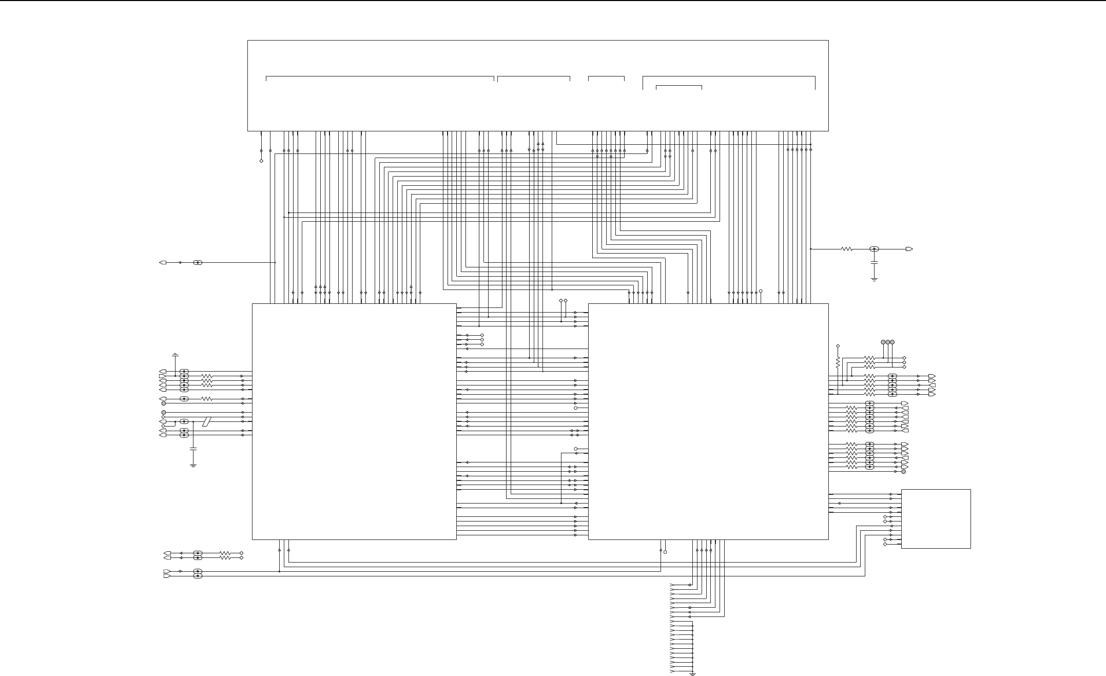
Controller R1 Schematic Diagrams 3-5
2.0 Controller R1 Schematic Diagrams
GPS
( SHEET 1 )
MICROCONTROLLER
(OMAP 1710: SHEET 1)
(MEMORY: SHEET 2)
( MAKO AUDIO_DIGITAL_USB/RS232 : SHEET 3)
MAKO_AUDIO_DC
( DC SUPPLY: SHEET 1)
( MAKO POWER MANAGEMENT : SHEET 2)
MMP
CONTROL HEAD REAR ACCESSORY REPEATER INTERFACE
PERIPHERALS
OPTION BOARD INTERFACE
( 1 SHEET )
USB1_DAT
USB1_SE0
USB1_TXEN
USB_INT
RS232_TX
RX_CLK
RX_DATA
RX_FSYNC
SERIAL_CLK
SERIAL_DATA
SPI_CLK
SPI_MISO
SPI_MOSI
THK_CE
TX_CLK
TX_DATA
TX_FSYNC
USB0_DAT
USB0_SE0
USB0_TXEN
MAKO_OPT_GPIO3
MAKO_OPT_INT
MAKO_RX
MAKO_TX
MOBILE_DISPLAY_CMD
McBSP3_CLK
McBSP3_DR
McBSP3_DX
McBSP3_FSX
OMAP_CORE_LDO
ONE_WIRE_UP
OPT_GPIO_1
OPT_GPIO_2
POR
PTT
RESET_OUT
RS232_RX
KEYPAD_COL2
KEYPAD_COL3
KEYPAD_ROW0
KEYPAD_ROW1
KEYPAD_ROW2
KEYPAD_ROW3
LED_CS
LOCK_DETECT
MAKO_AD_TRIGGER
MAKO_CE
MAKO_DCLK
MAKO_FSYNC
MAKO_GPIO_RX
MAKO_INT
MAKO_OPT_GPIO0
MAKO_OPT_GPIO2
GPS_RESET_LS
GPS_RX_L
S
GPS_TX_LS
I2C_CLK
I2C_DATA
JTAG_NEMU0
JTAG_NEMU1
JTAG_NTRST
JTAG_RTCK
JTAG_TCK
JTAG_TDI
JTAG_TDO
JTAG_TMS
KEYPAD_COL0
KEYPAD_COL1
GPIO_15
GPIO_18
GPIO_25
GPIO_26
GPIO_27
GPIO_3
(SW1 / VOL_A )GPIO_30
(SW2 / VOL_B) GPIO_31
(SW4 / MONITOR) GPIO_32
(SW8 / CHANNEL_ACT) GPIO_33
GPIO_40
GPIO_5
GPIO_60
GPS_BOOT_SELECT
GPS_ON_OFF_LS
1.875V_DIG_V2
16.8_MHZ_BUFF
2.775V_DIG_V4
3.3V_DIG_V10
32KHZ_CLK
ABACUS3_CE
ADAPT_SW
ANT_EN
ARMIO_12
J2500-3
(KEYPAD_ROW4 / GP5_6)ARMIO_15
ARMIO_2
(6.0 MHz)
(1.20 MHz)
(20.0 KHz)
(4.20 MHz)
(84.0 KHz)
(Active LOW)
(Active LOW)
(Active HIGH)
(BL_EN / GP5_7) ARMIO_3
ARMIO_6
AUDIO_PA_ENA
DEEP_SLEEP
DIR_CTRL
DISPLAY_CS
DMCS
EXT_MIC_ENA
GATED_32KHZ_OMAP
GP5_8
(RED_LED / RX_ATTN_1)
J2500-14
0
R2504
J2500-6
10K
J2500-1
R252
9
R2513 0
R25280
BLM21PG300SN1
E2500
0
R2526
0
R2502
0
R2514
R2512 0
0
R2508
0
0
R2524
J2500-20
R2523
J2500-18
J2500-12
1
J2500-7
SPI_MOSI_1
NC
J2500-13
J2500-5
J2500-2
J2500-19
R25210
R2501 0
NC
RF_ATTN_ 2
J2500-15
SPI_MISO_1
1
J2500-9
J2500-17
0
R2511
R25250
2.9V_MAKO_V6 1
R2510 0
0
R2519
0
0
R2518
NC
R2507
R2515 0
J2500-11
R2520 0
0
R2506
VCONT
0
R2500
1.875V
16.8MHz
32KHZ_GPS
5V_ACTIVE_ANT
ANT_CURRENT
GPS_5V
GPS_BOOT_SEL
GPS_ON_OFF_LS
GPS_RESET_LS
GPS_RX_L S
GPS_TX_LS
R2517 0
RTC_BATTERY
RX_AUDIO
SERIAL_CLK
SERIAL_DATA
SSI_CLK
SSI_DATA_IN
SSI_DATA_OUT
SSI_FSYNC
SW_9V3
SYSTEM_SYNC
USB2_DM
USB2_DP
VBUS1
VBUS2
VOLUME_1
VOLUME_2
McBSP3_DR
McBSP3_DX
McBSP3_FSX
ONE_WIRE_1
ONE_WIRE_2
ON_OFF_SW
OPT_BRD_PTT
OPT_GPIO_1
OPT_GPIO_2
PROGM_IO_CS
PUB_ADDRESS_1
PUB_ADDRESS_1_EN
PUB_ADDRESS_2
PUB_ADDRESS_2_EN
RESET
RESET_OUT
GPIO_3_PTT
GPIO_4_HOOK
HANDSET_AUDIO
INT_MIC+
INT_SPKR+
INT_SPKR-
KEYPAD_COL_0
KEYPAD_COL_1
KEYPAD_COL_2
KEYPAD_ROW_0
KEYPAD_ROW_1
KEYPAD_ROW_2
KEYPAD_ROW_3
LED_CS
MIC_GROUND
McBSP3_CLKX
DISPLAY_CS
EXT_MIC+
EXT_SPKR+
EXT_SPKR-
EXT_SWB+
GP5_1_PTT
GP5_2_MONITOR
GP5_3_CHAN_ACTIVITY
GP5_4_EMERGENCY
GP5_5_IGNITION_SENSE
GP5_6_TxDc_BUS+
GP5_7_RxDc_BUS-
GP5_8_CTSs_RESET
GPIO_0_PWR_ON
GPIO_1_USB1_DP
GPIO_2_USB1_DM
1
J2500-16
1V8
3.3V
5V
9V3
ARMIO_6
DIR_CTRL
DISPLAY_CMD
USB_INT
VBUS1
VBUS2
NC
SPI_CLK_1
SPI_MISO
SPI_MOSI
SPKR+
SPKR-
SW_9V3
TX_DAC
USB0_DAT
USB0_SE0
USB0_TXEN
USB1_DAT
USB1_DM
USB1_DP
USB1_SE0
USB1_TXEN
USB2_DM
USB2_DP
ON_OFF_MECH
PA_BIAS
PA_TEMP
POR
PUB_ADDRESS_1
PUB_ADDRESS_1_EN
PUB_ADDRESS_2
PUB_ADDRESS_2_EN
PUB_ADDRESS_MIC_EN
RAW_B+
RS232_RX
RS232_TX
RTC_BATTERY
RX_AUDIO
RX_FLTR_VCTRL
SPI_CLK
MAKO_DCLK
MAKO_FSYNC
MAKO_INT
MAKO_OPT_GPIO0
MAKO_OPT_GPIO2
MAKO_OPT_GPIO3
MAKO_OPT_INT
MAKO_RX
MAKO_TX
MIC_GROUND
MMP_GPIO1_INPUT
MMP_GPIO2_INPUT
OMAP_CORE_LDO
ONE_WIRE_1
ONE_WIRE_2
ONE_WIRE_UP
EXT_MIC_ENA
EXT_SWB+
GATED_32KHZ_OMAP
GP5_4_EMERGENCY
GP5_5_IGNITION_SENSE
GPIO_0_PWR_ON
GPIO_3_PTT
GPIO_4_HOOK
HANDSET_AUDI O
I2C_CLK
I2C_DATA
INT_MIC+
LOW_LEVEL_MUTE
LO_BATTERY_DET
MAKO_AD_TRIGGER
MAKO_CE
1.875V_DIG_V2
16.8_MHZ_BUFF
2.775V_ANA_V7
2.775V_DIG_V4
2.9V_DIG_V6
3.3V_DIG_V10
3.6V_DIG_VSW1
32KHZ_GPS
5V
5V_SW
9V3
9V3_PA
ANT_CURRENT_DET
AUDIO_PA_ENA
EXT_MIC+
C2500
220pF
0
R2516
3.6V_MAKO_SW1 1
J2500-8
0
R2527
220p
F
C2501
R2522
J2500-4
0
J2500-10
R2509 0
2.775V_V4
16.8_MHZ_BUFF
1.875V_V2
RX_SSI_SYNCB
LO_BATTERY_DET
9V3_PA
9V3
5V
1.875V_V2
RESET_OUT
2.775V_V 4
1.875V_V 2
5V_SW
5V_SW
SPI_MOSI_MAKO
SPI_CLK_MAKO
THK_CS
SPI_MOSI
SPI_MISO
SPI_CLK
ABACUS3_CSTX_DAC
SPI_MOSI_MAKO
SPI_MISO_MAKO
SPI_CLK_MAKO
RAW_B+
PA_BIAS
LOCK_DETEC T
PC_ATTEN_ENA
DMCS
ADAPT_SW
2.775V_ANA_V7
RX_FLTR_VCTRL
TX_SSI_FSYNC
TX_SSI_DATA
TX_SSI_CLK
RX_SSI_FSYNC
RX_SSI_DATA
RX_SSI_CLK
1.875V_V2
5V
ANT_ENABLE
PREDRIVE_SW
1.875V_DIG_V2 2.775V_V4
2.775V_DIG_V4
5V
5V_SW
16.8_GPS
PA_TEMP
SPI_MISO_MAKO
Controller – GPS Schematic Diagram
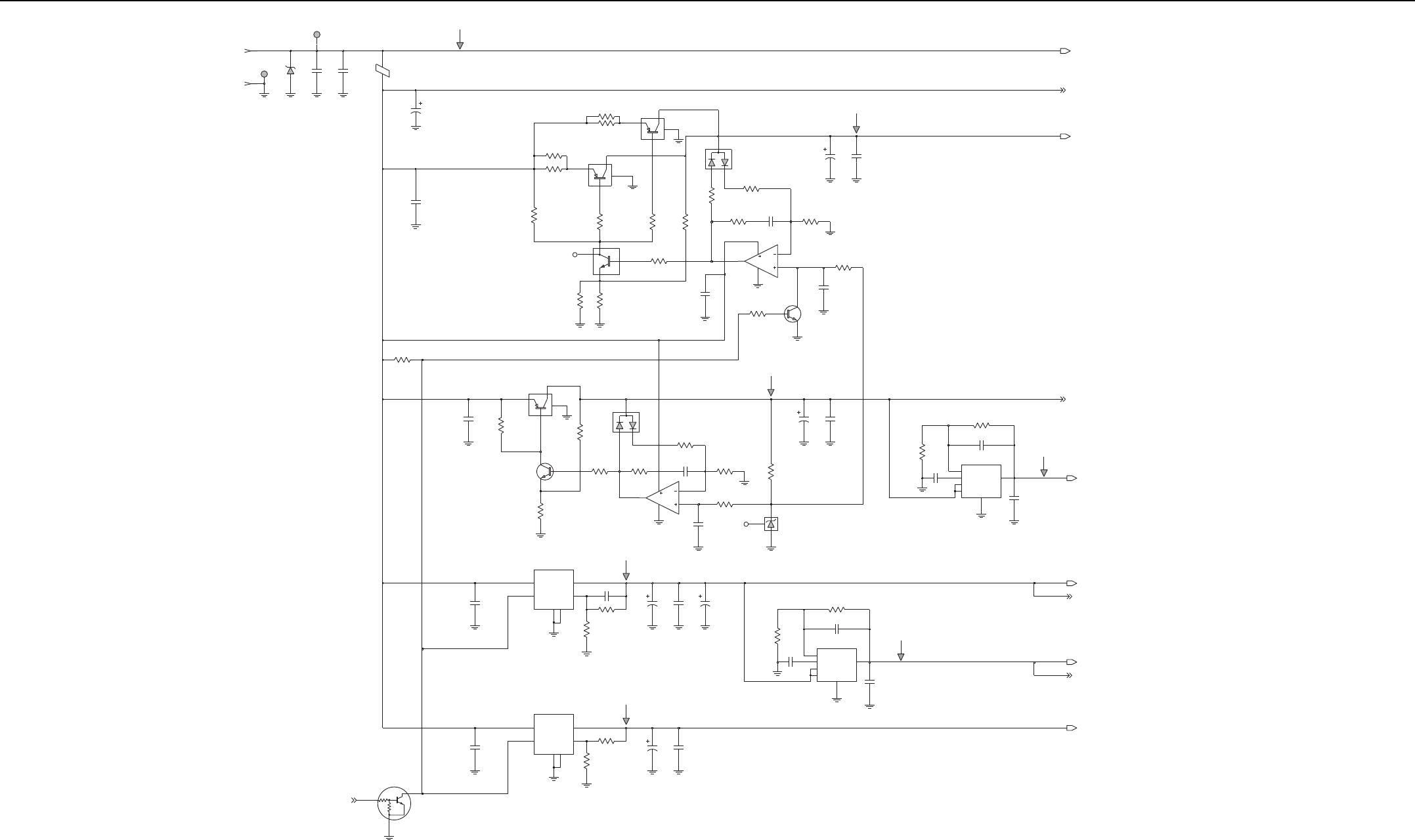
3-6 Controller R1 Schematic Diagrams
MAKO_ON_OFF_CONTROL
EXT_SWB+
UNSWB+
9V3
9V3
9V3_PA
9V3_CNTRL
C3015
33uF
NP
U3002
FB
2
GND
5
OFF: 4.8V
ON: 0 V
U3040,U3005,U3006 change to 4813971D34
13.6V
9.3V
9.3V
9.3V
(TO PA DRIVER ONLY )
(TO GPS & PERIPHERAL BLOCKS )
13.6V (NOMINAL)
5V
(TO TX PA)
(TO AUDIO PA)
(TO MAKO )
( TO REAR ACCESSORY)
(TO RX BACKEND, SYNTH,GPS ANTENNA)
(TO SYNTH, VCO, RX FE, PWR CNTRL,CONTROLHEAD)
5V
10uF
C3002
VIN
3
VOUT 1
0.1uF
C3044
U3004
FB
2
GND
5
NP
6
VCONT
4
4
E3000
U3030-1
2
3
1
8
R3055 0.1
2.74K 1%
R3040
5%
220
R3006
C3016
100pF
VBAT_GROUND
1
D3040
ON_OFF
VIN
4VOUT 5
470pF
C3000
U3003
1
ADJ
3GND1
6GND2
2
0.10uF
VR3040
C3046
R3009
1%39.2K
C3032
.01uF
C3007
0.1uF
.01uF
U3005
1
2
3
G1
C3041
1
2
3
G1
C3045
NU
0105959T72
U3040
33uF
470pF
C3012
0
Q3040
R3057
Q3041
R3056 0.1
R3051
R3002
0
10K
33uF
330
R3037
C3006
R3046
1%2.74K
2K 1%
R3039
10
R3035
D3030
C3013
NC
NC
22uF
R3048
R3044
330
680
1K
R3033
R3042
Q3030
0.1
0.1uF
C3014
C3031
R3003
0.1uF
R3005
3.57K
1%
R3004
562
1%
5%
2.2K
680
C3043
R3043
1
2
3
G1
33uF
U3006
C3008
1000pF
R3054
0
0
R3053
470pF
C3019
R3045
1%2K
R3052
0
R3050
150
Q3032
C3042
.01uF
VR3000
6
VCONT
4
VIN
3
VOUT 1
R3010
1%
13K
VOUT 5
100pF
C3009
U3001
ADJ 1
3GND1
6GND2
2ON_OFF
VIN
4
10
R3036
5164015H94
LM2941
VBAT
1
C3030
.01uF
C3020
C3017
47pF
J3000- 2 2
1000pF
100K
R3041
150
R3038
NU
1.0uF
C3010
C3021
0.1uF
7
8
4
470pF
C3040
U3030-2
6
5
C3005
470pF
0613952N58
13K
1%
R3008
39.2K 1%
R3007
330
R3034
1
0.1
R3032
J3000- 1
10K
R3030
R3047
100K
1.0uF
C3011
RAW_B+
5V_SW
5V_SW
5V
47K
47K
Controller DC Supply Schematic Diagram
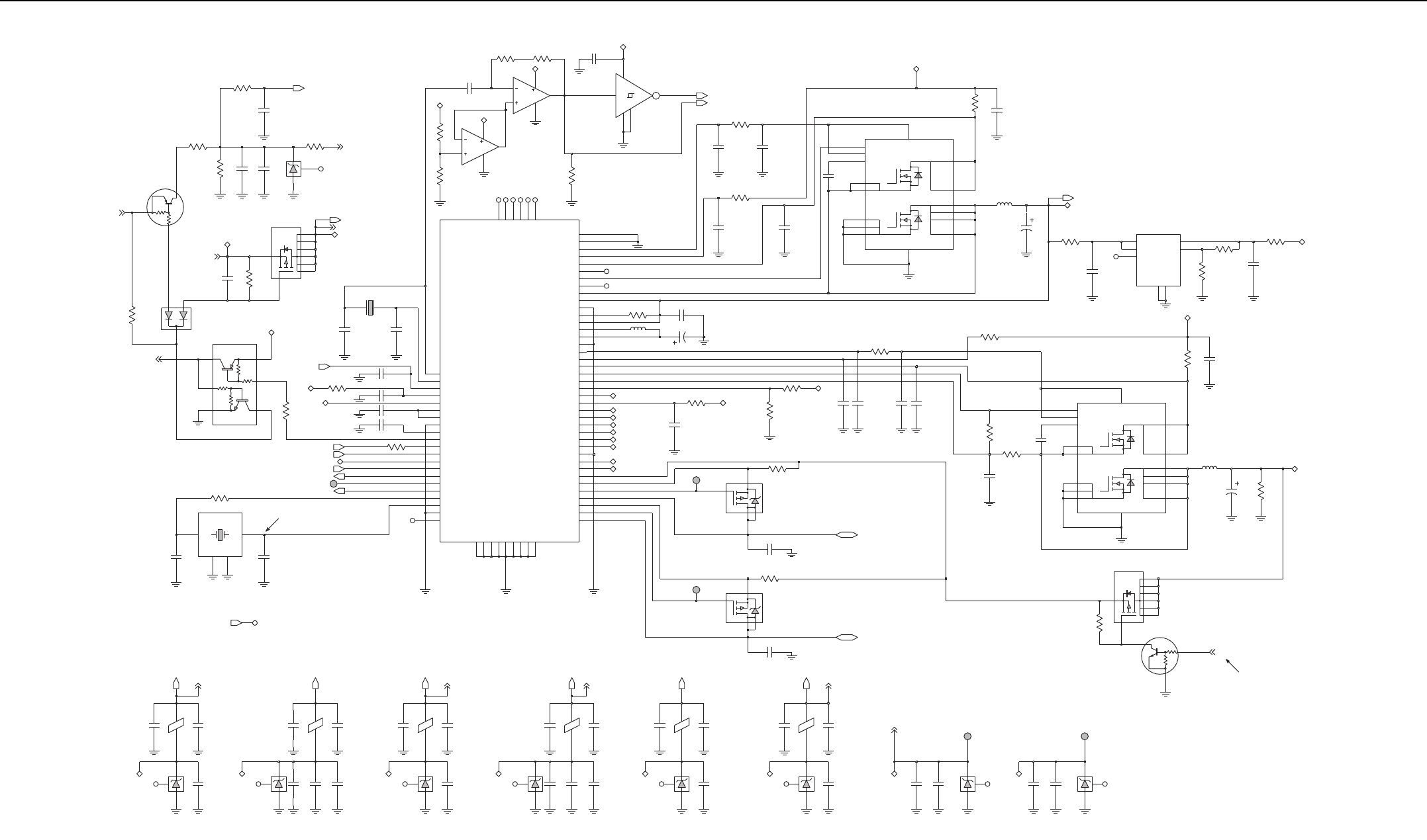
Controller R1 Schematic Diagrams 3-7
OFF: 0.0V
( ON= 0V; OFF=9.3V )
ON: 3.6V
24.576MHz
OFF: 0V (DEFAULT)
Change R3246 to 0613952N12 (13K) for OMAP1610
ON: 3.3V (MAKO V10)
FROM MAKO USB_CONNECT (L6 )
Vpk-pk: 2.2V - 2.4V
Sine Wave
ON: 4.75V to 5.25V (5.0V typical)
OFF: 0.0V
ON: 4.75V to 5.25V (5.0V typical)
OFF: 0.0V
( TO MMP
)
( TO MAP )
ON: 5.2V - 5.3V
OFF: 0.0V
OFF: 0.0Vpk
ON: 5Vpk; 230 KHZ PWM
OFF: 0.0Vpk
ON: 5Vpk; 230 KHZ PWM
VR3204VR3203
C3240
100pF 220pF
E3202
C3229
VR3206
Q3201
16
S2A
6
S2B
7
S2C
8
SYNC_EN
5
VDD 13
2
D2A9
D2B10
D2C11
D2D12
GND
3
4IN
S1A
15
S1B
Q3200
14 CBOOT D1A1
D1B
MAKO_GATED_32KHz 1
NC
R3207 0.2
C3207
NC
0.1uF
NC
E3205
NC
C3269
1.0uF
1
C3262
2.2uF
0
VBUS2_CMD
0.10uF
NC
R3245
NC
NC
C3202
NC
C3274
220pF
100pF
C3249
D3200
220pF
C3221
SI8401DB
Q3203
2
3
1
4
C3275
NC
10.0uF
GND
3
IN
2
NC
1
OUT 4
VCC 5
33pF
C3214
U3203
2.2uF
C3234
R3240
47K
R3210
C3233
220pF
14.3K
1%
4GND2
1
HOT1
3HOT2
0.10uF
C3222
CX-101F
Y3200
2GND1
C3261
220pF
5.1 R3241
C3260
1.0uF1.0uF
C3248
0 R3201
C3219
220pF
Q3205
E3201 C3226
0.10uF
4IN
S1A
15
S1B
16
S2A
6
S2B
7
S2C
8
SYNC_EN
5
13
VDD
14 CBOOT D1A1
D1B2
D2A9
D2B10
D2C11
D2D12
3GND
SI4724CY
Q3202
6
3
1
4
R3236
1K
Q3206
2
5
NC
NU
C3272
10pF
R3227
10K
1.0uF
C3243
4.7K
0
R3206
R3224
R3215
0
C3257
1.0uF
22uFC3206
0
R3218
NU
R3217
0
C3237
2.2uF
Q3204
2
3
1
4
R3226
33K
NTHS5441T1
R3238
10
Q3207
VR3202VR3201
C3232
0.10uF
R3233
0
C3225
220pF
4.7uF
C3282
C3215
NC
2.2uF
33pF
NC NC
C3239
DTC114YKAF
2
3
1
10uF
C3238
Q3208
C3218
0.10uF C3228
R3228
0.10uF
0
R3216
0
R323 7
10K
L3201
68uF
C3203
22uH
C3220
0.10uF
10pF
C3273
NU
1.0uF
C3276
0.1uF
0.1uF
C3280
C3278
6.81K
1%
R3246
C3204
5.6pF
C3227
NC
Y3201
21
220pF
220K
R3223
32.768KHz
XTAL
A13 XOUT
A12
XTAL32_IN
C1 XTAL32_OUT
B1
22uH
L3202
VBUS1
C14
VBUS1_CMD
E12
VBUS1_SENS
D12
VBUS2
C13
VBUS2_CMD
F11
VBUS2_SENS
B13
VBUS_SUPPLY
VSAVE
C2
XIN
V06_O P6
V07_O
K3
V08_I K4
V08_O
L1
V09_O
L9
V10_GND
J10
V10_I M6
V10_O
H10
SW5_VOUT
E14
SW5_VSENSE
SW_TYPE
B3
M1 TCXO_IN
TCXO_SEL_16_24
D4
N4
V02_O P4
V03_O N5
V04_O P3
SW2_LX
J12
SW2_VCC K14
SW2_VCCS
J13
SW2_VOUT
G11
SW5_PHASE
E13
SW5_SUMCOM P
D13
SW5_VDD F13
SW5_VDDHV
F12
SW1_PHASE
G14
SW1_SUMCOMP_DL
G13
SW1_VDD G12
SW1_VDDHV
H12
SW1_VOUT
J11
SW1_VSEN_BST
H11
SW1_VSEN_BUK
L14
SW2_GND
J14
M5
B14
NC6
C3
PGLDO2 A2
PGLDO3
REG_3V6
D3
RESETX
C5
H13
SW1_DH
H14
SW1_GND
F14
G4
IGN_X
B4
INT_X
D5
MECH_SW
E4
A1
NC1 A14
NC2 P1
NC3 P14
NC4
NC5
GND2
J4 GND3
G5 GND4
K9 GND5
L4 GND6
D14 GND7
H5 GND8
D9 GND9
HV_BG
D2 BAT_7V5
D1
BAT_RTC
F3
BAT_TYPE
B2
EMERG_PB
F4 FET_ENX
E2
GATED_32K_CLK
F5
P5 GND1
M7
5185143E77
PWR_MNGR_BLOCK
U3200-1
BAT_3V6
R3220
2MEG
C3201
2.2uF
C3247
10uF
NC
C3210 2.2uF
1VIN1
6VIN2
5
VOUT
R3209
43.2K
U3201
LP8340
ADJ 4
GND1
2
GND2
7
NC
3
C3208 2.2uF
U3202-1
C2
C3
C1
B1
B3
1.0uF
C3270
10K
R3248
220pF
R3219
C3231
C3216
2MEG
R3247
4.7uF
VR3207
51.1K
1%
1
MAKO_V8_5V
0.10uF
C3283
100K
R3239
10
1
R3205
MAKO_V9_3V
C3217
220pF
NC
2.2uF
C3254
1
0.2
R3208
0.1uF
VBUS1_CMD
C3281
220K
R3222
E3208
NC
E3206
NC
1.0uF
C3277
C321 2
NC
0.1
68uF
R3203
22uF
C3265
C3200
1.0uF
C3252
22uF
0
NU
22uH
R3225
C3279
0.1uF
L3200
0.10uF
VR3200
C3209
4.7uF
VR3208
C3213
A1
B1
B3 U3202-2
A2
A3
NC
R3204
0.1
5.6pF
C3205
E3203
C3211 1000pF
R3243
5.1
VR3205
0.1
C3266
2.2uF
R3200
3V_V9_MAKO
1.875V_DIG_V2
1.875V_DIG_V2 OMAP_CORE_LDO 2.775V_DIG_V4
2.775V_DIG_V4 2.9V_DIG_V6
2.9V_DIG_V6 2.775V_ANA_V7
3.3V_DIG_V10
3.3V_DIG_V10
SW_9V3
SW_9V3
UNSWB+
1.875V_V2_MAKO
3.6V_DIG_VSW1
3.6V_DIG_VSW1
VSAVE
VSAVE
OMAP_CORE_LDO_1
VSW5
1.875V_V2_MAKO
2.775V_V4_MAKO
2.775V_V7_MAKO
3.3V_V10_MAKO
5V_V8_MAKO
5V_V8_MAKO
ON_OFF_MECH
MAKO_INT
GP5_4_EMERGENCYGP5_4_EMERGENCY
GP5_5_IGNITION_SENSE
VSAVE
OMAP_CORE_LDO_1
USB_CONNECT
VSW5
LO_BATTERY_DET
BATTERY_SENSE
VBUS1
VBUS2
VSAVE
32KHZ_GPS
VSAVE
GATED_32KHZ_OMAP
9V3_CNTRL
RTC_BATTERY
MAKO_ON_OFF_CONTROL
9V3_CNTRL
SW_9V3
SW_9V3
SW_9V3
9V3_CNTRL
9V3_CNTRL
3.3V_V10_MAKO
3.6V_DIG_VSW1
3V_V9_MAKO
5V_V8_MAKO
SW_9V3
2.775V_V7_MAKO
2.9V_V6_MAKO
2.775V_V4_MAKO
1.875V_V2_MAKO
16.8_MHZ_BUFF
POR
OMAP_CORE_LDO_1
2.9V_V6_MAKO
47K
47K
47K
10K
Controller DC Distribution Schematic Diagram
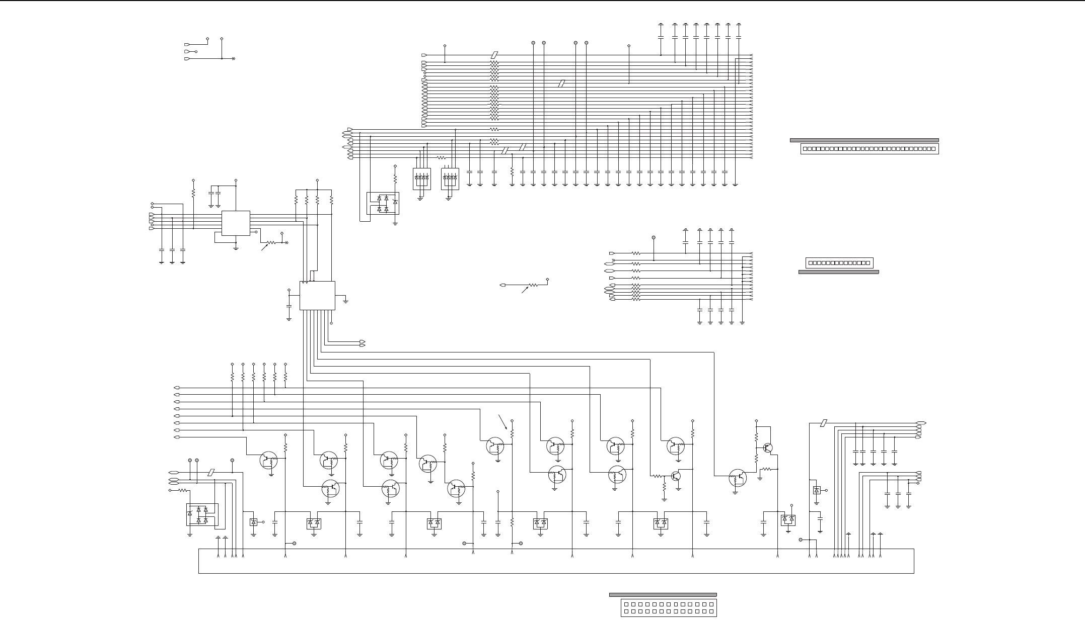
3-8 Controller R1 Schematic Diagrams
VBUS_MAP
GROUND
CONTROL HEAD INTERFACE
11
2
USB / MAP_ID_GROUND
9
13
18
MOBILE REPEATER: 0 OHM
MOBILE SUSCRIBER: NOT_USED
MOBILE REPEATER: 0 OHM
1
PCB
EXT_SWB+
14 16
EMERG SW
13
POWER GROUND
GROUND
711 3
EXT_SPKR+
MOBILE SUSCRIBER: NOT_USED
24
25
GP5_7
J4001 FRONT VIEW
10
AUX_AUDIO_OUT_2
GP5_2_(MONITOR)
1012
J4003 FRONT VIEW
3
20
1357 25
30
REPEATER: 0 OHM
MOBILE SUBSCRIBER: NOT_USED
USB_DP_MAP
13
1
27
10
23
22
AUDIO GROUND
21
6
9
17 19
J4000 REAR VIEW
24 16 14 4
26
PCB
GP5_6
5
22
GP5_3_(CHAN_ACT)
4
29
PCB
23
2
VIP_1_(EXT ALARM )
GP5_1_(EXT PTT)
OPTION BOARD INTERFACE
8
1412
15
EXT_SPKR-
68
11
12
9
MAP_ID_2
ACCESSORY INTERFACE (26-PIN)
5
26
246
USB_DM_MAP
TX_AUDIO
IGN_SENSE
MAP_ID_1
28
8
RX_AUDIO
15 21
7
18
GP5_8
17
AUX_AUDIO_OUT_1
20 19
3
1
C4062
NU
220pF
8
Y_5 10
Y_6 12
Q4004 F
2
9
A_5
11
A_6
13
GND
7VCC 14
Y_1 2
Y_2 4
Y_3 6
Y_4
U4001
A_1
1
A_2
3
A_3
5
A_4
R4050
10K
USB2_D M
1
J4000-2424
C4035
330pF
6
K4
330pF
C4034
VR4008
5.6V
2A1
5
A2
1
K1 3
K2 4
K3
Q4014
1
3
2
NU
10K
R4035
NU
C4072
220pF
R4098
4.7K
D4000
1
23
4
K3 4
K4 6
J4003- 77
A1
2
A2
5
K1 1
K2 3
220pF
NU
5.6V
VR4007
1.2K
C4044
J4000-2323
R4101
10K
R4055
4.7K
220pF
R4040
R4071
NU
C4071
10K
R4054
0
R4045
C4022
4.7K
220pF
220pF
C4085
C4061
NU
J4001-2020
220pF
19
J4001-1919
10K
J4000-19
J4001-2828
R4031
NC
C4043
220pF
J4001-1313
J4001-1616
C4026
220pF
220pF
33
R4070
C4065
R4049
2.7K
R4069 33
J4003-11
11
R4086
0
NU
10K
2
3
1
R4079
F
Q4010
220pF
C4024
0
R4083
220pF
J4001-1111
C4048
R4067 33
1
NC
NU
R4090
0
J4000-2
J4003- 1
J4003-14
14
J4001-1010
R4078 0
220pF
IGNITION_SENSE
1
NU
C4074
EMERGENCY 1
C4006
220pF
VR4006
8
J4003-1010
Q4007
J4000-1
J4000-8
J4001-1717
J4003- 22
220pF
C4068
J4001-1515
Q4000 F
0.10uF
C4073
220pF
C4067
220pF
C4031
NC
C4014
220pF 220pF
C4028
C4000
220pF
NU
VCC
16
33
R4065
QG
6
QH1
7
QH2
9
RCLK 12
RCLR 13
SER 14
SRCLK 11
SRCLR 10
GND 8
QA
15
QB
1
QC
2
QD
3
QE
4
QF
5
10K
U4000
R4034
MMBZ20V
VR4004
1.2K
R4103
J4001- 11
Q4012
2
3
1
220pF
NU
C4019
R4080 0
J4001- 66
33
R4001
J4000-1414
J4001-1414
Q4006
J4000-1313
MMBZ20V
VR4000
MMBZ20V
VR4002
NU
C4005
220pF
USB1_D P
1
BLM21PG221SN1
E4001
J4001- 44
MMBZ20V
VR4001
51
R4010
R4041
C4046
220pF
NC
4.7K
220pF
C4027
J4000-2020
J4000-16 16
220pF
C4042
J4003- 66
R4012 0
VR4003
MMBZ20V
1
23
4
C4051
NU
D4001
C4063
220pF
C4047
220pF
NU
C4059
220pF
2
220pF
220pF
J4001- 2
J4000-1717
C4066
4.7K
R4046
NC
R4043
4.7K
220pF
C4016
33
R4005
J4001- 55
220pF
NU
C4002
220pF
3
NU
C4060
Q4013
J4003- 3
R4061
4.7K
33
J4001-2222
R4042
VBUS1
1
E4003
VBUS2
1
R4023
1.2K
Q4008
2
3
1
J4003- 88
Q4003 F
Q4005
C4023
220pF
4.7K
R4047
F
4.7K
C4004
NU R4044
NU
220pF220pF
NU
C4003
R4002 33
C4049
220pF
NU
R4000 33
220pF
C4053
9
NU
R4048
J4003- 9
15
1.5K
R4085 0
J4000-15
J4001-1212
J4001-2929
0
C4030
R4076
220pF
NC
C4069
220pF
R4082 0
R4004 33
C4084
0.10uF
1
VR4005
Q4011
OPT_SSI_SYNC
J4001-2121
220pF
C4017
27
220pF
C4064
E4000
J4001-27
12
J4003-13
13
J4003-12
J4001-2323
0
R4081
220pF
E4005
NU
C4075
J4000-6
J4000-7
1
E4002
J4001-2424
Q4002
2
3
1
33
R4003
NU
F
J4001- 99
220pF
C4020
1.2K
1
R4100
J4001- 88
USB1_D M
0
R4084
Q4015 F
F
Q4001
J4003- 44
220pF
C4033
0
R4011
NU
220pF
C4076
NU
BK1005HM471
E4004
J4000-4 4
2
1
3
R4030
MMP_1_WIRE
1
J4000-5
APM_1_WIRE1
EXT_PTT
1
C4045
220pF
33
R4064
R4032
10K
J4001- 33
J4001- 77
220pF
C4013
J4001-3030
R4006 470
5
220pF
C4015
R4066 33
J4003- 5
C4018
26
J4000-2525
220pF
12
J4000-26
J4000-1111
J4000-12
NU
220pF
C4055
J4000-9
R4063 33
J4000-3
220pF
C4001
NU
J4000-2222
47K
R4089
0
R4074
J4001-2626
C4025
220pF
220pF
C4070
J4001-2525
J4001-1818
220pF
C4029
220pF
C4032
10K
R4088
390K
R4009 51
18
R4051
J4000-2121
J4000-10 10
9
5
6
7
J4000-18
USB2_D P
1
C4058
NU
Q4009
220pF
R4068
C4021
220pF
220pF
33
220pF
C4040
C4041
1V8
ARMIO_6
WD_RESET
WD_RESET
WD_RESET
ONE_WIRE_2
ONE_WIRE_1
MIC_GROUND
NU
R4033
EXT_SWB+
EXT_SWB+
GP5_1_PTT
GP5_4_EMERGENCY
3.3V
J4001_9
ON_OFF_SW
USB2_DM
USB2_DP
5V
GPIO_4_HOOK
VBUS1
INT_MIC +
GPIO_0_PWR_ON
GPIO_3_PTT
GPIO_2_USB1_DM
GPIO_1_USB1_DP
SSI_CLK
SSI_DATA_OUT
SSI_DATA_IN
RESET
9V3
RESET
RESET
DISPLAY_CS
SERIAL_DATA
SERIAL_CLK
LED_CS
DISPLAY_CMD
HANDSET_AUDIO
SHARED_SYSTEM_SYNC
VBUS2
5V
PUB_ADDRESS_2
RX_AUDIO
PUB_ADDRESS_1
EXT_MIC+
EXT_SPKR+
EXT_SPKR-
INT_SPKR-
5V
5V
5V
PROGM_IO_CS
SERIAL_DATA
SERIAL_DATA
SERIAL_CLK
SERIAL_CLK
1V8 5V
1V8
1V8 1V8
5V
PUB_ADDRESS_1_EN
PUB_ADDRESS_2_EN
SSI_FSYNC
1V81V81V81V81V81V8
SW_9V3
OPT_GPIO_1
OPT_BRD_PTT
OPT_GPIO_2
J4001_9
RTC_BATTERY
EXT_SWB+
GP5_7_RxDc_BUS-
5V
GP5_8_CTSs_Reset
5V5V
5V
GP5_5_IGNITION_SENSE
GP5_3_CHAN_ACTIVITY
5V 5V
GP5_6_TxDc_BUS+
5V
5V
GP5_2_MONITOR
RESET_OUT
KEYPAD_ROW_1
KEYPAD_ROW_3
KEYPAD_COL_1
VOLUME_1
KEYPAD_ROW_0
KEYPAD_ROW_2
KEYPAD_COL_0
KEYPAD_COL_2
VOLUME_2
INT_SPKR+
10K
47K
10K
47K
10K
47K
10K
47K
10K
47K
47K
47K
47K
47K
47K
47K
47K
47K
47K
47K
47K
47K
47K
47K
47K
47K
47K
47K
Controller Peripheral Schematic Diagram (sheet 1 of 2)
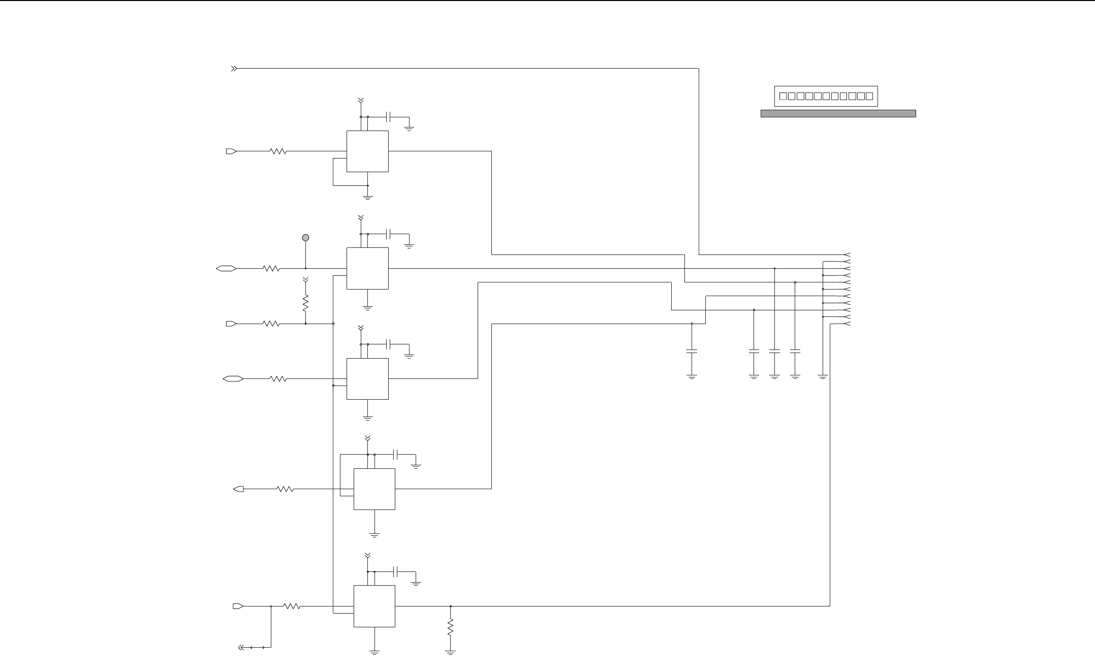
Controller R1 Schematic Diagrams 3-9
REPEATER CONNECTOR
J4002 FRONT VIEW
24
PCB
119753 10
8
1
R4106
10K
J4002- 33
TP4000
J4002- 88
J4002- 22
6
J4002- 77
4
J4002- 55
J4002- 6
J4002-1010
J4002- 4
J4002- 99
NU
220pF
C4010
NU
220pF
C4011
NU
220pF
220pF
C4007 C4012
11
J4002- 11
NU
J4002-11
0
R4096
0
0
R4093
0
R4095
R4097
VCCA A1
VCCB A2
0.10uF
C4088
U4006
AC1
B
C2
DIR
B2
GND
B1
C1
A
C2 B
B2 DIR
B1 GND
A1
VCCA A2
VCCB
0.10uF
U4005
C4087
VCCA A2
VCCB
C4089
0.10uF
U4007
C1
A
C2 B
B2 DIR
B1 GND
A1
0.10uF
C4086
0
C4090
R4094
B1 VCCA A1
VCCB A2
0.10uF
U4008
AC1
B
C2
DIR
B2
GND
10K
R4105
AC1
B
C2
DIR
B2
GND
B1 VCCA A1
VCCB A2
U4004
R4099 0
SHARED_SYSTEM_SYNC
WD_RESET
McBSP3_DR
McBSP3_CLKX
1V8
1V8
1V8
DIR_CTRL
1V8
1V8
McBSP3_DX
McBSP3_FSX
1V8
SYSTEM_SYNC
16
Controller Peripheral Schematic Diagram (sheet 2 of 2)

3-10 Controller R1 Schematic Diagrams
(Used as SW2 for PORTABLE, Volume B for MOBILE)
(GPIO_3 for PORTABLE-Green LED)
MCBSP3
DNP
DELETED REF
(Used as SW1 for PORTABLE, Volume A for MOBILE)
U1008
Date rate: 20 of 8 bits packet per chip select
CLK rate: 1 MHz
LARGEST REF
GP DEVICE CONFIG
Place for
C1039
RF CONTROLS
R1050 Y1001
FREQ SWITCH
GPS
(Used as SW8 for PORTABLE, Channel Activity for MOBILE)
(Used as GREEN_LED for PORTABLE, PA_ENABLE for MOBILE)
(MOBILE ONLY)
PLACED FOR
(1.4V for OMAP1710 & 1.55V for OMAP1610)
PLACE FOR GP
DEVICE FAST BOOT
(SPI.CS3 for MOBILE Shift Register Chip Select)
MOBILE ONY
(Used as BL_EN for PORTABLE, GP5_7 for MOBILE
LED & Display CS: Active Low
OMAP1710
(Used as SW4 for PORTABLE, Monitor for MOBILE)
JTAG
(Used as RED_LED for PORTABLE, RX_ATTN_1 for MOBILE)
OMAP1710
(0.87mA/MHz for OMAP1710 & 1.06mA/MHz for OMAP1610)
(MOBILE ONLY)
SERIAL FLASH SPI
6
15
6
1
14
8
6
47K
8
R1071
5
4
NU
R1066
10K
R1025
10K
3
0
9
15
0
14
0
12
13
11
4
3
12
R1067
4.7K
NU
18pF
C1030
11
13
1
10
5
8
3
4.7K
R1054
2
7
5
3
7K20
8R21
9W20
Z_STATE_1
W16
P15
N14
2
K2
G1
B1
2
B7
3
A13
4B16
5A21
6F20
1
B5
AA21
Y13
AA7
Y3
AA1
U2
N1
UART1_RX
UART2_CTS
UART2_RX
L14
USB0_DAT
P9
R8 USB0_SE0
U18
W21
D10
H7
TCK
TDI
AA19
TMS
TRST
UART1_CTS
C4
D8
C10
D14
SDDQS_H
SDDQS_L
B4
C8
C11
D13
D12
C12
C5
D7
D5
C7
G9
B12
B3
C3
D6
C6
D11
C13
H9
H11
B6
A1
G10
B9
G12
G11
RST_OUT
AA20
RTCK
Y17
RTC_ON_NOFF
Y12
RTC_WAKE_INT
W13
A2
B2
B8
H10
NC
OSC1_I N
OSC1_OUT
OSC32K_IN
OSC32K_OUT
PWRON_RESET
E5 RESERVED
P12 RESET_MODE
W11
U19
N15
V8
T19
T20
MPU_BOOT
MPU_RST
AA17
MCSI2_DIN
W9 MCSI2_DOUT
MCSI2_SYNC
MMC_CMD
P11
R11
V10
W10
H18
MCBSP1_FSX
MCBSP2_DR
MCBSP2_DX
MCBSP2_FSR
MCBSP2_FSX
MCSI1_DIN
MCSI1_DOUT
D16
B18
LOW_STATE_1
LOW_STATE_2
LOW_STATE_3
V6
LOW_STATE_4
W5
M18
MCBSP1_DR
D15
C19
G14
H13
A20
B19
C18
D17
C20
D18
B21
C17
B17
G13
A17
C16
C21
G19
KBR_0
KBR_1
KBR_2
KBR_3
KBR_4
B15
Y8
W8
T18
I2C_SDA
V20
F18
D20
D1 9
E1 8
N21
M20
M14
P18
P20
P19
GPIO_62
M7
M15
F_CS3
N8
F_RP
W1
F_WP
V4
R18
R19
N20
N18
N19
FDATA_7
FDATA_8
FDATA_9
FRDY
F_CS1
M3
F_CS1U
F_CS2
M4
F_CS2U
FDATA_13
FDATA_14
FDATA_15
FDATA_2
FDATA_3
FDATA_4
FDATA_5
FDATA_6
FADD_ 8
J7
FADD_ 9
F3
FADV
L4
FDATA_0
FDATA_1
FDATA_10
FDATA_11
FDATA_12
FADD_23
K3
FADD_24
L7
E1 FADD_25
FADD_ 3
C1
E4 FADD_ 4
FADD_ 5
D2
FADD_ 6
F4
FADD_ 7
E3
FADD_16
K7
FADD_17
J2
J4 FADD_18
FADD_19
J3
FADD_ 2
D3
FADD_20
F2
FADD_21
L8
K4 FADD_22
H8
FADD_ 1
J8
FADD_10
G4
FADD_11
G3
G2 FADD_12
FADD_13
K8
H4 FADD_14
FADD_15
H3
V16
W17
EN_F_BE_0
L3
EN_F_BE_1
M8
EN_F_OE
U4
EN_F_WE
W2
EN_SDCKE
EN_USB_PUEN
W4
DVDD4_1
DVDD4_2
DVDD4_3
DVDD4_4
DVDD5_1
DVDD5_2
DVDD5_3
V12 DVDDRTC
DVDD1_1
DVDD1_2
DVDD1_3
DVDD1_4
DVDD1_5
DVDD2_1
DVDD2_2
DVDD2_3
J1
Y21
1A15
2Y20
3Y9
4M2
A11
W12
AA3
A9
A3
E2
B13
B20
J21
R20
CLK_MCSI2
V11 CLK_MMC
CLK_M_REQ
C15
CLK_S D
C9
V19
CONF
CS_SDRAM
CLK_B
CLK_B_REQ
CLK_B_UART2
Y4
H19
CLK_F N3
CLK_L_CAM
J15
CLK_M
CLK_MCSI1
L1 8
CLK32K_IN
R13
CLKR_MCBSP2
CLKS_MCBSP1
CLKX_MCBSP1
CLKX_MCBSP2
CLKX_SD
K15
K19
K18
J14
J19
J18
L1 5
M19
U1000
BFAIL
L1 9
K14
OMAP1710
1
0
R1047
1
10
7
5
11
NU
0
R1035
4
9
10
0
R1020
10K
R1017
0
R1021
10K
R1034
2
12
1
9
7
2
6
0
4
SERIAL_DATA
ARMIO_6
SERIAL_CLK
MCBSP3_FSX
GPS_BOOT_SELECT
1.875V
JTAG_NTRST
MCBSP3_DR
LED_CS
DISPLAY_CS
OMAP_CORE
CVDDA
ARMIO_2
1.875V
DVDD2
1.875V
GPIO_3
OMAP_CORE
JTAG_NEMU0
JTAG_NEMU1
JTAG_RTCK
JTAG_TCK
JTAG_TDI
JTAG_TDO
JTAG_TMS
ONE_WIRE_UP
DMCS
DEEP_SLEEP
ADAPT_SW
LOCK_DETECT
ANT_E N
DIR_CTRL
2.775V_DIG_V4 2.775V_DIG_V4
1.875V
1.875V_DIG_V2
1.875V_DIG_V2
OMAP_CORE_LDO
3.3V_DIG_V10
DVDD2
LDO_FILTER
1.875V
1.875V
VDD_DL
L
MCBSP3_CLK
MCBSP3_DX
GPIO_60
RESET_OUT
GPS_ON_OFF_LS
GPIO_15
PTT
ARMIO_3
AUDIO_PA_ENA
ARMIO_12
GPIO_30
GPIO_31
GPS_RX_LS
GPIO_32
GPS_TX_LS
GPIO_33
GPS_RESET_LS
16.8MHz Squarer
(FROM MAKO
)
OPTION SELECT
( RESET CIRCUIT PROVIDED BY MAKO
)
1.0Vpkpk
RS232
KEYPAD ROW
( BUFFERRED 16.8 FROM TOMAHAWK )
FLASH
MAKO SSI
BOOT FROM CS3
TOMAHAWK SSI
(FROM MAKO )
(MOBILE ONLY)
DNP
(FROM MAKO
)
ABACUS3 SSI
(Used as KEYPAD_ROW4 for PORTABLE, GP5_6 for MOBILE)
BOOT FROM CS0
(MOBILE ONLY)
GND
2
GND1
4
OUT
3IN 1
Y1000
CX-91F
12MHz
18pF
C101
8
R1028
0
1
TP_MAKO_RX
1
TP_MAKO_FSYNC
0
R1048
1
TP_POR
R1070
0
TP_MAKO_TX
1
18pF
C1019
TP_MAKO_DCLK
1
R1027
10K
NU
1
A2
3
GND 2
VCC
5
Y1 6
Y2 4
U100 6
A1
10K
R1006
10MEG
R1002
.01uF
C1032
47K
R1026
R1044
0
C1033
0.10uF
10K
R1045
0
NU
R1046
NU
0
R1072
R1001
10K
16.8_MHZ_BUFF
1K
R1041
GPIO_40
RS232_TX
1.875V
MAKO_OPT_GPIO2
1.875V
FLASH_WAI T
GATED_32KHZ_OMAP
1.875V
RS232_RX
MAKO_AD_TRIGGER
FLASH_CTL(5:0 )
1.875V
EMIFS_ADD(23:1)
EMIFS_DATA(15:0)
OMAP_CORE
MAKO_FSYNC
RX_CLK
TX_CLK
RX_DATA
TX_DATA
RX_FSYNC
TX_FSYNC
OPT_GPIO_1
POR
MAKO_GPIO_RX
GPIO_ 5
MAKO_OPT_INT
KEYPAD_ROW0
KEYPAD_ROW1
KEYPAD_ROW2
KEYPAD_ROW3
ARMIO_15
MAKO_DCLK
MAKO_INT
MAKO_TX
MAKO_RX
FLASH_CLK
MAKO_OPT_GPIO0
MAKO_OPT_GPIO3
OPT_GPIO_2
EXT_MIC_ENA
32KHZ_CLK
GP5_8
USB#0 RESERVED FOR MOBILE
OMAP1610
I2C
Place for
USB#1
Place for
OMAP1710
USB#2
USB#0
( INTERFACE WITH MAKO )
OPTION BOARD
4
20
7
13
2
0
23
19
4
4.7K
R1005
22
2
3
9
5
6
16
21
11
TP100
0
3
1
8
18
17
12
5
14
10
1
0
R1014
15
USB1_SE0
USB2_SE0
GPIO_18
I2C_CLK
I2C_DATA
USB2_DAT
USB0_SE0
USB0_DAT
USB0_TXEN
USB1_TXEN
USB1_DAT
USB2_SUSPEN D
GPIO_26
GPIO_25
USB_INT
USB2_RCV
(MOBILE ONLY)
PORTABLE DISPLAY
(Used as KEYPAD_COL4 for PORTABLE and Public Add Mic for MOBILE)
SDRAM
KEYPAD COLUMN
SPI
R1036
10K
1
TX_RAMP
MAKO_CE
ABACUS3_CE
THK_CE
1.875V
SPI_CL K
SPI_MISO
SPI_MOSI
SDRAM_CTL(6:0 )
SDRAM_DATA(15:0)
SDRAM_CLK
SDRAM_CLK_EN
SDRAM_CS
SDRAM_ADD(12:0)
MOBILE_DISPLAY_CMD
KEYPAD_COL 0
KEYPAD_COL 1
KEYPAD_COL 2
KEYPAD_COL 3
GPIO_27
DISPLAY_CMD
DISPLAY_CE
DISPLAY_DATA0
DISPLAY_DATA1
DISPLAY_DATA2
DISPLAY_DATA3
DISPLAY_DATA4
DISPLAY_DATA5
DISPLAY_DATA6
DISPLAY_DATA7
Place for
OMAP1710
DECOUPLING CAPACITORS
OMAP1610
Place for
C1008
100pF100pF
C1004
1.0uF
C1034
C1036
1.0uF
R1000
10
R1019
5.1
C1000
100pF
C1012
0.10uF
0.10uF
C1001 C1002
0.10uF
0.10uF
C1016
C1014
0.10uF
C1007
100pF
C1006
0.10uF
0.10uF
C1013C1003
100pF
C1009
0.10uF
C1011
100pF
0.10uF
C1005
10
R1060
C104 4
0.10uF
1.0uF
C101 7
0.10uF
C1015 C1031
0.10uF
C1037
2.2uF
2.2u F
C1035
0.10uF
C1010
LDO_FILTER
OMAP_CORE
1.875V
CVDD A
OMAP_CORE
DVDD2
OMAP_CORE
VDD_DLL
OMAP_CORE
CVDD4
CVDDA
CVDD_
CVDD_
CVDD_
CVDD_
CVDD_DL
CVDD_RTC
CVDD1
CVDD2
CVDD2_1
CVDD2_2
CVDD3_1
CVDD3_2
CVDD3_3
CVDD3_4
VSS_
VSS_
VSS_
VSS_17
VSS_18
VSS_19
VSS_
VSS_
VSS_
VSS_
VSS_
VSS_
VSS_10
VSS_11
VSS_12
VSS_13
VSS_14
VSS_15
VSS_16
L1
A5
A7
B10
B14
R1
H2
C2
A19
E21
U21
Y16
L21
AA2
Y7
AA11
Z_STATE_2
Z_STATE_3
UART3_RX
UWIRE_SDI
UWIRE_SDO
SDRAM_DQMU
SDRAM_RAS
TDO
SDRAM_CAS
SDRAM_DQML
SADD_8
SADD_9
SBANK_0
SBANK_1
SADD_12
SADD_13
SADD_2
SADD_3
SADD_4
SADD_5
SADD_6
SADD_7
SADD_0
SADD_1
SADD_10
SADD_11
MCBSP1_DX
LCD_PIXEL_9
LCD_VSYN C
LOW_STATE_5
LCD_PIXEL_1 5
LCD_PIXEL_2
LCD_PIXEL_3
LCD_PIXEL_4
LCD_PIXEL_5
LCD_PIXEL_6
LCD_PIXEL_7
LCD_PIXEL_8
LCD_HSYNC
LCD_PIXEL_0
LCD_PIXEL_1
LCD_PIXEL_1 0
LCD_PIXEL_1 1
LCD_PIXEL_1 2
LCD_PIXEL_1 3
LCD_PIXEL_1 4
KBC_4
KBC_5
LCD_AC
I2C_SCL
KBC_0
KBC_1
KBC_2
KBC_3
EN_WE_SDRAM
CLK_P_LCD
CLK_S_UWIRE
CLK_EX_CAM
V14
Y5
R9
W18
Y19
V17
Y18
R14
C14
D4
Y2
W3
V13
AA13
R12
J20
U20
AA9
V9
H15
P10
AA5
W6
W7
V15
W14
AA15
Y14
H20
G18
F1 9
H14
E20
E19
R3
R4
T2
V2
Y1
P3
U3
T4
V3
N7
P2
P4
P7
R2
N4
N2
T3
P8
U1
H12
Y10
R10
V18
G8
Y15
W15
V5
P14
P13
V7
G20
G21
Y6
D9
W19
SDATA_6
SDATA_7
SDATA_8
SDATA_9
SDATA_12
SDATA_13
SDATA_14
SDATA_15
SDATA_2
SDATA_3
SDATA_4
SDATA_5
SDATA_0
SDATA_1
SDATA_10
SDATA_11
MMC_DAT3
MPUIO_
MPUIO_
MPUIO_
MPUIO_
MPUIO_
MCSI1_SYN
MMC_DAT0
MMC_DAT1
MMC_DAT2
GPIO_8
GPIO_9
GPIO_14
GPIO_15
GPIO_2
GPIO_3
GPIO_4
GPIO_6
GPIO_7
GPIO_0
GPIO_1
GPIO_11
GPIO_12
GPIO_13
EMU0
EMU1
CAM_VS
CLK32K_OUT
CAM_D_2
CAM_D_3
CAM_D_4
CAM_D_5
CAM_D_6
CAM_D_7
CAM_H
CAM_RSTZ
CAM_D_0
CAM_D_1
1
2
3
4
5
C
S
Controller Microprocessor Schematic Diagram
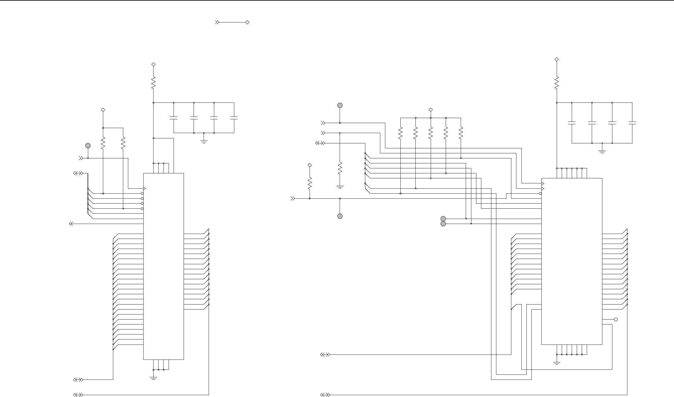
Controller R1 Schematic Diagrams 3-11
Bootstrap Mode = 48 MH z
Normal Mode = 72 MH z
FLASH
ST 4Mx16
SDRAM
MICRON 8Mx16
8MByte 16MByte
0104024J27 (Pre-Flashed Part)
NC
0
1
2
0
1
13
3
15
5
9
10
11
4
5
C2006
0.10uF
10K
3
F1 VSS2
VSSQ1
G2
VSSQ2
G8
WAIT
D3
WP
D6
4
R2000
D7 NC
B5 RP
A4
VDD1 G4
VDD2 E1
VDDQ1 G6
VDDQ2
VPP A5
VSS1
A3
D6 E3
D7 G1
D8 G7
D9 F6
EN_E
E7
F8 EN_G
C4 EN_L
C5 EN_W
D12 D5
D13 F3
D14 F2
D15 E2
D2 E5
D3 G5
E4
D4
D5 G3
A7
C7
A8
A2
A9
B2
B4 CLK_K
D0 F7
D1 E6
F5
D10
D11 F4
C6 A19
A2
C8
A20
B3
A21
C3
A3
B8
A4
A8
A5
B7
A7 A6
A1 A11
A12
B1
A13
C1
A14
D2
A15
D1
A16
D4
A17
B6
A18
A6
M58WR064FB
U2000
A0
E8
A1
D8
A10
C2
8
23
0
1
12
13
14
16
17
18
19
6
7
4
1
6
12
0
14
9
10
11
6
7
8
3
4
5
15
1
2
5
13
14
15
9
10
11
6
7
8
9
3
44
TP_FLASH_CLK
TP_SDRAM_CS
2
TP_SDRAM_BA1
TP_SDRAM_CLK
C2004
100pF
.01uF
C2005
0.10uF
C2007
100pF
C2000
R2005
3
5
2
10K 10K
R2006
20
21
22
R2009
10K
0.10uF
C2003
R2010
R2007
10K
R2012
10K
10K
5
10K
TP_SDRAM_BA0
R2013
D7 VSSQ4
F9 WE
12
3
2
C7
VDDQ3 D3
VDDQ4
A1 VSS1
E3 VSS2
J1 VSS3
A3 VSSQ1
B7 VSSQ2
C3 VSSQ3
NC2 G1
F8 RAS
F1 UDQM
A9
VDD1 E7
VDD2 J9
VDD3 A7
VDDQ1 B3
VDDQ2
C8
DQ4 D9
DQ5 D8
DQ6 E9
DQ7 E1
DQ8 D2
DQ9
E8 LDQM
E2
NC1
D1
DQ10 C2
DQ11 C1
DQ12 B2
DQ13 B1
DQ14 A2
DQ15
B8
DQ2 C9
DQ3
G7 BA0
G8 BA1
F7 CAS
F3 CKE
F2 CLK
G9 CS
A8
DQ0 B9
DQ1
J8 A2
J7 A3
J3 A4
J2 A5
H3 A6
H2 A7
H1 A8
G3 A9
U2001
H7 A0
H8 A1
H9 A10
G2 A11
6
7
8
0
1
2
0
R2011
11
12
R2004
0
R2008
10
.01uF
10K
0.10uF
C2002C2001
EMIFS_DATA(15:0)
EMIFS_ADD(23:1)
FLASH_CTL(5:0)
FLASH_CLK
FLASH_WAI T
1.875V_DIG_V2
1.875V_DIG_V21.875V_DIG_V2
1.875V_DIG_V2
SDRAM_DATA(15:0)
SDRAM_ADD(12:0)
SDRAM_CTL(6:0)
SDRAM_CLK_EN
1.875V_DIG_V2
1.875V_DIG_V2
SDRAM_CLK
SDRAM_CS
1.875V_DIG_V2
Controller Memories Schematic Diagram

3-12 Controller R1 Schematic Diagrams
600mV RMS
330mV RMS
70mV RMS (RX AUDIO)
MAKO USB
MAKO SSI
MAKO UART 7.8V RMS
5.3VDC muted
(SOURCE)
(7.5 W @ 8 ohms)
9.3VDC unmuted
52mV RMS for rated audio
HW_I D
7.8V RMS
MAKO SPI
3.91V (27.5W)
4.12V (44W)
MOBILE SUSCRIBER: 0 OHM
MOBILE REPEATER: NOT_USED
80mV RMS (TX AUDIO)
MOBILE SUBSCRIBER: NOT_USED
MOBILE REPEATER: 33K
(7.5 W @ 8 ohms)
V15
10KR3580
100
R3545
10
R3530
220K
NU
3
B
2
CLK_SCL
6
DI S
8
GND
7
SDI_SDA
5SDO_NC 4
9
VDD
W
AD5161
U3501
A
1
AD0_CS*
NU
100pFC3511
33K
R3505
R3536
100K
10uF
C3517
2
5
6
3
1
4
SCL2 6
SDA1
4SDA2 5
VREF1 2
VREF2 7
Q3502
U3508
PCA9306
EN 8
GND
1
SCL1
3
R3500 27
220pF
C3514
Q3505
2
5
6
3
1
4
R3513
0
E3501
R3508
0
C3530
220pF
VC_DCLK
E7
VC_FSYNC
D7
VC_RX
A7
VC_TX
B7
VC_TX3V
M4
NC
USB1_SE0
D8
USB2_DAT_VP
B9
P8
USB2_DM
USB2_DP N7
USB2_OE_RCV_RTS
A9
USB2_SE0_VM_RXD
C9
L6
USB_CONNECT
USB_INTX
C10
TXDO_BDI_UP_3V
J5
UART2_RXD_OD
A10 UART2_TXD
E9
UCM_SS
N3
USB1_DAT_TXD
C8
P7
USB1_DM
N6
USB1_DP
USB1_OE
B8
N9
SB96_BDO_KF_5V
N13
SB96_BUS_BUSY
SPI_CLK
E6
SPI_CS
D6
SPI_DI
B6
SPI_DO
C6
M10
TXDO_BDI_5V
TXDO_BDI_ENC_3V
K6
OPT_GPIO3
D11
RS232_USB_X
A8
RTS_FILLSEN_3V
M3 M11
RTS_FILLSEN_5V
RXDIN_3V
P2
N12
RXDIN_5V
RXDIN_ENC_3V
N2
SB96D_BDO_KF_3V
N8
OPTB_SEL0 P11
OPTB_SEL1 K8
OPTB_SEL2 P12
OPTB_SEL3 N11
B12 OPTION_INTX
OPT_GPIO0
F10
OPT_GPIO1
C11
OPT_GPIO2
G10
P9
ONE_WIRE_1 M8
ONE_WIRE_2 L8
ONE_WIRE_BATT
ONE_WIRE_UP
L7
OPTA_SEL0 P10
OPTA_SEL1 K7
OPTA_SEL2 M9
OPTA_SEL3 N10
BBP_SYNC
B5
BOOT_NORM_X
C7
BUSY_IN
C12
BUSY_OUT
E11
CABLE_DET_3V
D10
P13
CTS_CABLE_DET_5V
CTS_X
B10
LOGIC_VDD
A6
DIGITAL_BLOCK
U3200-2
APCO
L5
BBP_CLK
A5
R3593
200K
10uF
C3536
10K
R3573
220pF
NC
13
12
14
4
11
C3515
2
5
6
3
1
4
U3505- 4
C3542
Q3504
0.10uF
R3562 0
NC
R3524
560
10K
NC
R3534
VR3504
5.1K
R3587
R3533
24K
NU
I2C_CLK
1
5
SDA2
2VREF1
7VREF2
PCA9306
U3503
8
EN
1
GND
3SCL1 6
SCL2
4SDA1
1000pF
C3505
100
R3576
NC
R3575
C3504
1000pF
1K
R3569
1K
NC
R3526
0
10K
NC
R3514
C3534
10uF
2K
R3571
10K
(VALUE)
R3511
1
R3539
24K
6
3
1
4
NC
Q3501
2
5
U3502-2
6
5
7
4
11
C3501
NC
NC
0.1uF
10K
10.0uF
C3500
R3579
220pF
C3531
0
R3507
R3584
22K 22K
R3585
C3540
0.10uF
100
NC
NC
1
R3540
USB1_SEO
C3538
.01uF
0.1uF
C3535
1.0uF
C3502
10K
R3595
NC
150
R3596
10K
RT3500
9
10
8
4
11
NC
3
U3502-3
NC
R3502
10K
1
EXT_MIC
1
USB1_DAT
R3538
39K
R3537
MAKO_CE
1
0
GND2
IN V
9
M_SS
8
NINV
1OUT1 4
OUT2 6
3RR
VCC
7
1
TDA1519C
U3500
GND1
2
5
1
2
NC
NC
I2C_DATA
VR3503
MMBZ20V
3
0.10uF C3528
3.3K
R3594
R3548
100K
24K
24K
R3542 R3541
R3506
10K
51.1K
R3588
0
R3563
10K
R3559
R3574
10K
4
11
R3582
16.2K
1
U3505-3
MC3403
9
10
8
NC
USB1_TXEN
R3577
26.7K
220pF
C3525
24K
1.0uF
C3526
R3523
0.10uF
C3539
24K
R3520
C3527
0.1uF
NC
C3524
10uF
NC
NC
R3510
27
R3547
560
22K
R3528
0.1uF
C3512 10uF
C3509
0.10uF
C3541
VR3502
3
1
2
U3505- 2
6
5
7
4
11
E3500
R3581 10K
10uF
C3533
R3529
NU
51
R3504
33K
R3532
100
TX_RAMP_DAC
1
1.0uF
C3520
NC
15K
R3521
100pFC3513
1.0uF
NC
330pF
C3518
H3 VC_OUT_P
VFUSE E8
L10
VMES
VREF
A4
C3510
PA_IN_P
G2
PWR_CTRL N1
SCAN_EN C4
TEST A3
A11 TX_RX
J3 VCM 1
VCM 2
H4
H2 VC_OUT_M
FE_TUNE2 M2
K1 INT_MIC_M
K2 INT_MIC_P
INT_SPKR_M
F2 INT_SPKR_P
F1
L2 MIC_BIAS
PA_BPLUS
E1
PA_IN_M
G3
K12
ATOD_7 K13
ATOD_8
E3 BPLUS
J1 EXT_MIC_M
J2 EXT_MIC_P
EXT_SPKR_M
G1 EXT_SPKR_P
H1
FE_TUNE1 L3
B11 AD_TRI G
N14
ATOD_0 M13
ATOD_1 L11
ATOD_2 M14
ATOD_3 L12
ATOD_4 L13
ATOD_5 K11
ATOD_6
NC
U3200-3
PA_CODEC_A2D_BLOCK
M12
ADC_VREF
U3502-4
13
12
14
4
11
200K
R3578
C3516 1.0uF
NC
560
R3535
E3502
C35290.10uF
16.2K
R3583
47uF
C351 9
33K
R3503
2.2K
R3592
100K
R3525
R3546
15K
U3502-1
2
3
1
4
11
1.0uF
C3532
R3509
C3507 2200pF
0
R3549
30K
R3560
47K
10K
R3572
COM 1
B1
COM 2
C2
D1
GND
IN 1 B2
IN 2 C1
NO1
A1
NO2
D2
A2
V_POS
INT_MIC
1
TS5A23166
U3504
NC
NC
47uF
C3506
1.0uF
C3544
1.0uF
C3543
0.10uF
C3523
0
R3586
Q3500
2
3
1
R3544
24K
E3503
NC
NC
R3550 C3545
220pF
82K
1.0uF
C3508
0.1uF
27
C3521
R3512
R3515
R3591
2.2K 1000pF
10K
C3503
2113945A09
(VALUE )
470pF
R3516
24K
C3522
R3561 0
R3558
10K
U3505-1
2
3
1
4
11
NC
5
6
3
1
4
NC
Q3503
2
R3501 27
ONE_WIRE_UP
1.875V_V2_MAKO
1.875V_DIG_V2
I2C_CLK
I2C_DATA
2.775V_DIG_V4
USB0_DAT
USB0_SE0
USB2_DM
USB_INT
USB2_DP
5V_SW
2.9V_DIG_V6
ANT_CURRENT_DET
5V_V8_MAKO
ONE_WIRE_1
ONE_WIRE_2
USB1_DM
MAKO_OPT_GPIO3
MAKO_TX
1.875V_DIG_V2
TX_DAC
USB1_DAT
USB1_TXEN
USB1_SE0
2.775V_DIG_V4
LOW_LEVEL_MUTE
5V_SW
MMP_GPIO1_INPUT
MMP_GPIO2_INPUT
1.875V_DIG_V2
1.875V_DIG_V2
5V_SW
5V_SW
5V_V8_MAKO
5V_V8_MAKO
3.3V_DIG_V10
MAKO_CE
MIC_GROUND
PUB_ADDRESS_MIC_EN
PUB_ADDRESS_1_EN
INT_MIC +
EXT_MIC_ENA
HW_ID2
HW_ID1
HW_ID0
2.9V_DIG_V6
2.9V_DIG_V6
UNSWB+
UNSWB+
9V3
9V3
3.3V_DIG_V10
3.3V_DIG_V10
SW_9V3
USB0_TXEN
GPIO_0_PWR_ON
GPIO_4_HOOK
GPIO_3_PTT
BATTERY_SENSE
USB1_DP
VAG
9V3
9V3
9V3 VAG
VAG
VAG
RX_AUDIO
9V3
PA_TEM P
2.9V_DIG_V6
EXT_MIC+
HW_ID1
HW_ID0
HW_ID2
PUB_ADDRESS_2_EN
RS232_RX
RS232_TX
9V3_CNTRL
RX_FLTR_VCTRL
9V3
9V3
9V3
9V3
PUB_ADDRESS_1
PUB_ADDRESS_2
VAG
VAG
VAG
9V3
AUDIO_PA_ENA
9V3
UNSWB+
SPKR+
SPKR-
9V3
VAG HANDSET_AUDIO
USB_CONNECT
MAKO_AD_TRIGGER
PA_BIAS
SPI_CLK
SPI_MOSI
SPI_MISO
MAKO_DCLK
MAKO_FSYNC
MAKO_RX
1.875V_V2_MAKO
MAKO_OPT_INT
MAKO_OPT_GPIO0
MAKO_OPT_GPIO2
10K
47K
Controller Audio and USB Schematic Diagram

Controller R1 Schematic Diagrams 3-13
2.1 Controller R1 Parts List
Circuit
Ref
Motorola Part
No Description
C1000 2113944A40 100pF
C1001 2113945Y02 0.10uF
C1002 2113945Y02 0.10uF
C1003 2113944A40 100pF
C1004 2113944A40 100pF
C1005 2113945Y02 0.10uF
C1006 2113945Y02 0.10uF
C1007 2113944A40 100pF
C1008 2113944A40 100pF
C1009 2113945Y02 0.10uF
C1010 2113945Y02 0.10uF
C1011 2113944A40 100pF
C1012 2113945Y02 0.10uF
C1013 2113945Y02 0.10uF
C1014 2113945Y02 0.10uF
C1015 2113945Y02 0.10uF
C1016 2113945Y02 0.10uF
C1017 2113946E02 1.0uF
C1018 2113944A28 18pF
C1019 2113944A28 18pF
C1030 2113944A28 18pF
C1031 2113945Y02 0.10uF
C1032 2113945B02 .01uF
C1033 2113945Y02 0.10uF
C1034 2113946S35 1.0uF
C1035 2113946D05 2.2uF
C1036 2113946S35 1.0uF
C1037 2113946D05 2.2uF
C1044 2113945Y02 0.10uF
C2000 2113944A40 100pF
C2001 2113945B02 .01uF
C2002 2113945Y02 0.10uF
C2003 2113945Y02 0.10uF
C2004 2113944A40 100pF
C2005 2113945B02 .01uF
C2006 2113945Y02 0.10uF
C2007 2113945Y02 0.10uF
C2500 2113944A44 220pF
C2501 2113944A44 220pF
C3000 2113944C06 470pF
C3002 2371403L02 10uF
C3005 2113944C06 470pF
C3006 2314030E85 33uF
C3007 2113945C31 0.1uF
C3008 2113945A09 1000pF
C3009 2113944A40 100pF
C3010 2113946S35 1.0uF
C3011 2113946S35 1.0uF
C3012 2113944C06 470pF
C3013 2314030J28 22uF
C3014 2113945C31 0.1uF
C3015 2113944C38 47pF
C3016 2113944A40 100pF
C3017 2113945A09 1000pF
C3018 2389289U01 10uF
C3019 2113944C06 470pF
C3020 2314030E85 33uF
C3021 2113945C31 0.1uF
C3030 2113945C02 .01uF
Circuit
Ref
Motorola Part
No Description
C3031 2113945C31 0.1uF
C3032 2113945B02 .01uF
C3040 2113944C06 470pF
C3041 2113945C02 .01uF
C3042 2113945B02 .01uF
C3043 2314030E85 33uF
C3044 2113945C31 0.1uF
C3045 NOT PLACED –
C3046 2113945Y02 0.10uF
C3200 2113946J04 22uF
C3201 2113946D05 2.2uF
C3202 2113945Y02 0.10uF
C3203 2316410H02 68uF
C3204 2115153H21 5.6pF
C3205 2115153H21 5.6pF
C3206 2316410H01 22uF
C3207 2113945C31 0.1uF
C3208 2113946D05 2.2uF
C3209 2113945Y02 0.10uF
C3210 2113946D05 2.2uF
C3211 2113945A09 1000pF
C3212 2316410H02 68uF
C3213 2113946F03 4.7uF
C3214 2115153H45 33pF
C3215 2115153H45 33pF
C3216 2113946F03 4.7uF
C3217 2113944A44 220pF
C3218 2113945Y02 0.10uF
C3219 2113944A44 220pF
C3220 2113945Y02 0.10uF
Circuit
Ref
Motorola Part
No Description
C3221 2113944A44 220pF
C3222 2113945Y02 0.10uF
C3225 2113944A44 220pF
C3226 2113945Y02 0.10uF
C3227 2113944A44 220pF
C3228 2113945Y02 0.10uF
C3229 2113944A44 220pF
C3231 2113944A44 220pF
C3232 2113945Y02 0.10uF
C3233 2113944A44 220pF
C3234 2113946D05 2.2uF
C3237 2113946D05 2.2uF
C3238 2113946H02 10uF
C3239 2113946D05 2.2uF
C3240 2113944C45 100pF
C3243 2113946S35 1.0uF
C3247 2113946H02 10uF
C3248 2113946S35 1.0uF
C3249 2113944C45 100pF
C3252 2113946S35 1.0uF
C3254 2113946D05 2.2uF
C3257 2113946S35 1.0uF
C3260 2113946S35 1.0uF
C3261 2113944A44 220pF
C3262 2113946N03 2.2uF
C3265 2113946J04 22uF
C3266 2113946D05 2.2uF
C3269 2113946S35 1.0uF
C3270 2113946S35 1.0uF
C3272 2115153H27 10pF
Circuit
Ref
Motorola Part
No Description

3-14 Controller R1 Schematic Diagrams
C3273 NOT PLACED –
C3274 2113944A44 220pF
C3275 2113946J03 10.0uF
C3276 2113946S35 1.0uF
C3277 2113946S35 1.0uF
C3278 2113945C31 0.1uF
C3279 2113945C31 0.1uF
C3280 2113945C31 0.1uF
C3281 2113945C31 0.1uF
C3282 2113946F03 4.7uF
C3283 2113945Y02 0.10uF
C3500 2113946J03 10.0uF
C3501 2113945G91 0.1uF
C3502 2113945C31 0.1uF
C3503 2113945A09 1000pF
C3504 2113945A09 1000pF
C3505 2113945A09 1000pF
C3506 2314030F30 47uF
C3507 2113945A11 2200pF
C3508 2113945C31 0.1uF
C3509 2313960D07 10uF
C3510 2113945A03 330pF
C3511 2113944A40 100pF
C3512 2113945C31 0.1uF
C3513 2113944A40 100pF
C3514 2113944A44 220pF
C3515 2113944A44 220pF
C3516 2113946S35 1.0uF
C3517 2314030M51 10uF
C3518 2113946S35 1.0uF
Circuit
Ref
Motorola Part
No Description
C3519 2314030F30 47uF
C3520 2113946S35 1.0uF
C3521 2113946S35 1.0uF
C3522 2113945A05 470pF
C3523 2113945Y02 0.10uF
C3524 2313960D07 10uF
C3525 2113944A44 220pF
C3526 2113946S35 1.0uF
C3527 2113945C31 0.1uF
C3528 2113945Y02 0.10uF
C3529 2113945Y02 0.10uF
C3530 2113944A44 220pF
C3531 2113944A44 220pF
C3532 2113946S35 1.0uF
C3533 2313960D07 10uF
C3534 2313960D07 10uF
C3535 2113946S35 1.0uF
C3536 2314030M51 10uF
C3538 2113945B02 .01uF
C3539 2113945Y02 0.10uF
C3540 2113945Y02 0.10uF
C3541 2113945Y02 0.10uF
C3542 2113945Y02 0.10uF
C3543 2113946S35 1.0uF
C3544 2113946S35 1.0uF
C3545 2113944A44 220pF
C4000 NOT PLACED –
C4001 NOT PLACED –
C4002 NOT PLACED –
C4003 NOT PLACED –
Circuit
Ref
Motorola Part
No Description
C4004 NOT PLACED –
C4005 NOT PLACED –
C4006 2113944A44 220pF
C4007 NOT PLACED –
C4010 NOT PLACED –
C4011 NOT PLACED –
C4012 NOT PLACED –
C4013 2113944A44 220pF
C4014 2113944A44 220pF
C4015 2113944A44 220pF
C4016 2113944A44 220pF
C4017 2113944A44 220pF
C4018 2113944A44 220pF
C4019 NOT PLACED –
C4020 NOT PLACED –
C4021 2113944A44 220pF
C4022 2113944A44 220pF
C4023 2113944A44 220pF
C4024 2113944A44 220pF
C4025 2113944A44 220pF
C4026 2113944A44 220pF
C4027 2113944A44 220pF
C4028 2113944A44 220pF
C4029 2113944A44 220pF
C4030 2113944A44 220pF
C4031 2113944A44 220pF
C4032 2113944A44 220pF
C4033 2113944A44 220pF
C4034 2113945A03 330pF
C4035 2113945A03 330pF
Circuit
Ref
Motorola Part
No Description
C4040 2113944A44 220pF
C4041 2113944A44 220pF
C4042 2113944A44 220pF
C4043 2113944A44 220pF
C4044 2113944A44 220pF
C4045 2113944A44 220pF
C4046 2113944A44 220pF
C4047 2113944A44 220pF
C4048 2113944A44 220pF
C4049 NOT PLACED –
C4051 NOT PLACED –
C4053 NOT PLACED –
C4055 NOT PLACED –
C4058 NOT PLACED –
C4059 NOT PLACED –
C4060 NOT PLACED –
C4061 NOT PLACED –
C4062 NOT PLACED –
C4063 2113944A44 220pF
C4064 2113944A44 220pF
C4065 2113944A44 220pF
C4066 2113944A44 220pF
C4067 2113944A44 220pF
C4068 2113944A44 220pF
C4069 2113944A44 220pF
C4070 2113944A44 220pF
C4071 NOT PLACED –
C4072 NOT PLACED –
C4073 2113945Y02 0.10uF
C4074 NOT PLACED –
Circuit
Ref
Motorola Part
No Description
Controller R1 Schematic Diagrams 3-15
C4075 NOT PLACED –
C4076 NOT PLACED –
C4084 2113945Y02 0.10uF
C4085 2113944A44 220pF
C4086 2113945Y02 0.10uF
C4087 2113945Y02 0.10uF
C4088 2113945Y02 0.10uF
C4089 2113945Y02 0.10uF
C4090 2113945Y02 0.10uF
D3030 4813978P07 DIODE, SWITCHING
D3040 4813978P07 DIODE, SWITCHING
D3200 4813978C02 DIODE, SWITCHING
D4000 4866544A01 DIODE, DUAL
D4001 4866544A01 DIODE, DUAL
E2500 2480675U01 FERRITE BEAD
E3000 2485011Y01 FERRITE BEAD
E3201 2480675U01 FERRITE BEAD
E3202 2480675U01 FERRITE BEAD
E3203 2480675U01 FERRITE BEAD
E3205 2480675U01 FERRITE BEAD
E3206 2480675U01 FERRITE BEAD
E3208 2480675U01 FERRITE BEAD
E3500 2485011Y01 FERRITE BEAD
E3501 2485011Y01 FERRITE BEAD
E3502 2485011Y01 FERRITE BEAD
E3503 2485011Y01 FERRITE BEAD
E4000 2485011Y01 FERRITE BEAD
E4001 7686949J14 FERRITE BEAD
E4002 7686949J14 FERRITE BEAD
E4003 NOT PLACED –
Circuit
Ref
Motorola Part
No Description
E4004 2409134J25 FERRITE BEAD
E4005 2409134J25 FERRITE BEAD
J2500 0905505Y02 22-PIN JTAG
CONNECTOR
J3000 0905902V09 DC POWER CONNEC-
TOR
J4000 0916017H01 26-PIN ACCESSORY
CONNECTOR
J4001 0915555H01 30-PIN CONTROL
HEAD CONNECTOR
J4002 0915558H01 11-PIN REPEATER
CONNECTOR
J4003 0915556H01 14-PIN OPT BRD
CONNECTOR
L3200 2415005H02 22uH
L3201 2415005H02 22uH
L3202 2415005H02 22uH
Q3030 4813973M07 NPN
Q3032 4813973B01 NPN
Q3040 4813973M07 NPN
Q3041 4815263H01 ANALOG SWITCH
Q3200 5185956E76 N-CHANNEL SYN-
CHRONOUS MOSFET
Q3201 4813970A62 P-CHANNEL MOSFET
Q3202 5185956E76 N-CHANNEL SYN-
CHRONOUS MOSFET
Q3203 4805585Q23 PMOS FET
Q3204 4805585Q23 PMOS FET
Q3205 4815262H01 ANALOG SWITCH
Q3206 4815272H01 ANALOG SWITCH
Q3207 4813970A62 P-CHANNEL MOSFET
Q3208 4815261H01 ANALOG SWITCH
Q3500 4815261H01 ANALOG SWITCH
Circuit
Ref
Motorola Part
No Description
Q3501 4815272H01 ANALOG SWITCH
Q3502 4815272H01 ANALOG SWITCH
Q3503 4815272H01 ANALOG SWITCH
Q3504 4815272H01 ANALOG SWITCH
Q3505 4815272H01 ANALOG SWITCH
Q4000 4815263H01 ANALOG SWITCH
Q4001 4815263H01 ANALOG SWITCH
Q4002 4815261H01 ANALOG SWITCH
Q4003 4815263H01 ANALOG SWITCH
Q4004 4815261H01 ANALOG SWITCH
Q4005 4815263H01 ANALOG SWITCH
Q4006 4815263H01 ANALOG SWITCH
Q4007 4815263H01 ANALOG SWITCH
Q4008 4815261H01 ANALOG SWITCH
Q4009 4815263H01 ANALOG SWITCH
Q4010 4815261H01 ANALOG SWITCH
Q4011 4815263H01 ANALOG SWITCH
Q4012 4815261H01 ANALOG SWITCH
Q4013 4816023H01 PNP
Q4014 4813973A06 NPN
Q4015 4815263H01 ANALOG SWITCH
R1000 0613952Q25 10
R1001 0613952R01 10K
R1002 0613952J73 10MEG
R1005 0613952Q89 4.7K
R1006 0613952R01 10K
R1014 0613952R66 0
R1017 0613952R01 10K
R1019 0613952Q18 5.1
R1020 0613952R66 0
Circuit
Ref
Motorola Part
No Description
R1021 0613952R66 0
R1025 0613952R01 10K
R1026 0613952R17 47K
R1027 NOT PLACED –
R1028 0613952R66 0
R1034 0613952R01 10K
R1035 NOT PLACED –
R1036 0613952R01 10K
R1041 0613952Q73 1K
R1044 0613952R66 0
R1045 0613952R01 10K
R1046 NOT PLACED –
R1047 0613952R66 0
R1048 0613952R66 0
R1054 0613952Q89 4.7K
R1060 0613952Q25 10
R1066 NOT PLACED –
R1067 NOT PLACED –
R1070 0613952R66 0
R1071 0613952R17 47K
R1072 NOT PLACED –
R2000 0613952R01 10K
R2004 0613952R66 0
R2005 0613952R01 10K
R2006 0613952R01 10K
R2007 0613952R01 10K
R2008 0613952R01 10K
R2009 0613952R01 10K
R2010 0613952R01 10K
R2011 0613952R66 0
Circuit
Ref
Motorola Part
No Description

3-16 Controller R1 Schematic Diagrams
R2012 0613952R01 10K
R2013 0613952R01 10K
R2500 0613952R66 0
R2501 0613952R66 0
R2502 0613952R66 0
R2504 0613952R66 0
R2506 0613952R66 0
R2507 0613952R66 0
R2508 0613952R66 0
R2509 0613952R66 0
R2510 0613952R66 0
R2511 0613952R66 0
R2512 0613952R66 0
R2513 0613952R66 0
R2514 0613952R66 0
R2515 0613952R66 0
R2516 0613952R66 0
R2517 0613952R66 0
R2518 0613952R66 0
R2519 0613952R66 0
R2520 0613952R66 0
R2521 0613952R66 0
R2522 0613952R66 0
R2523 0613952R66 0
R2524 0613952R66 0
R2525 0613952R66 0
R2526 0613952R66 0
R2527 0613952R66 0
R2528 0613952R66 0
R2529 0613952R01 10K
Circuit
Ref
Motorola Part
No Description
R3002 0613952R01 10K
R3003 0613952M54 3.57K
R3004 0613952L73 562
R3005 0613952Q81 2.2K
R3006 0613952Q57 220
R3007 0613952N58 39.2K
R3008 0613952N12 13K
R3009 0613952N58 39.2K
R3010 0613952N12 13K
R3030 0613952R01 10K
R3032 0615871H01 0.1
R3033 0615871H01 0.1
R3034 0613952H61 330
R3035 0613952H25 10
R3036 0613952H25 10
R3037 0613959G61 330
R3038 NOT PLACED –
R3039 0613952M30 2K
R3040 0613952M43 2.74K
R3041 0613952R25 100K
R3042 0613952H69 680
R3043 0613952H69 680
R3044 0613958S61 330
R3045 0613952M30 2K
R3046 0613952M43 2.74K
R3047 0613952R25 100K
R3048 0613952Q73 1K
R3050 0613959Q53 150
R3051 0613952G67 0
R3052 0613952G67 0
Circuit
Ref
Motorola Part
No Description
R3053 0613952R66 0
R3054 0613952R66 0
R3055 0615871H01 0.1
R3056 0615871H01 0.1
R3057 0613952R66 0
R3200 0615871H01 0.1
R3201 0613952R66 0
R3203 0615871H01 0.1
R3204 0615871H01 0.1
R3205 0613952R25 100K
R3206 0613952R66 0
R3207 0686135Z02 0.2
R3208 0686135Z02 0.2
R3209 0613952N62 43.2K
R3210 0613952N16 14.3K
R3215 0613952G67 0
R3216 0613952G67 0
R3217 NOT PLACED –
R3218 0613952R66 0
R3219 0613952R56 2MEG
R3220 0613952R56 2MEG
R3222 0613952R33 220K
R3223 0613952R33 220K
R3224 0613952Q89 4.7K
R3225 NOT PLACED –
R3226 0613952R13 33K
R3227 NOT PLACED –
R3228 0613952G67 0
R3233 0613952R66 0
R3236 0613952Q73 1K
Circuit
Ref
Motorola Part
No Description
R3237 0613952R01 10K
R3238 0613952H25 10
R3239 0613952H25 10
R3240 0613952R17 47K
R3241 0613952Q18 5.1
R3243 0613952Q18 5.1
R3245 0613952G67 0
R3246 0613952M81 6.81K
R3247 0613952N69 51.1K
R3248 0613952R01 10K
R3500 0613952Q35 27
R3501 0613952Q35 27
R3502 0613952R01 10K
R3503 0613952R13 33K
R3504 NOT PLACED –
R3505 NOT PLACED –
R3506 0613952R01 10K
R3507 NOTPLACED –
R3508 0613952R66 0
R3509 0613952R66 0
R3510 0613952Q35 27
R3511 0613952R01 10K
R3512 0613952Q35 27
R3513 0613952R66 0
R3514 0613952R01 10K
R3515 0613952R01 10K
R3516 0613952R10 24K
R3520 0613952R10 24K
R3521 0613952R05 15K
R3523 0613952R10 24K
Circuit
Ref
Motorola Part
No Description
Controller R1 Schematic Diagrams 3-17
R3524 0613952Q67 560
R3525 0613952R25 100K
R3526 0613952R66 0
R3528 0613952R09 22K
R3529 0613952Q42 51
R3530 NOT PLACED –
R3532 0613952Q49 100
R3533 0613952R10 24K
R3534 0613952R01 10K
R3535 0613952Q67 560
R3536 0613952R25 100K
R3537 0613952R66 0
R3538 0613952R15 39K
R3539 0613952R10 24K
R3540 0613952Q49 100
R3541 0613952R10 24K
R3542 0613952R10 24K
R3544 0613952R10 24K
R3545 0613952Q49 100
R3546 0613952R05 15K
R3547 0613952Q67 560
R3548 0613952J25 100K
R3549 0613952R12 30K
R3550 0613952R23 82K
R3558 0613952R01 10K
R3559 0613952R01 10K
R3560 0613952R17 47K
R3561 0613952R66 0
R3562 0613952R66 0
R3563 0613952R66 0
Circuit
Ref
Motorola Part
No Description
R3569 0613952Q73 1K
R3571 0613952Q80 2K
R3572 0613952R01 10K
R3573 0613952R01 10K
R3574 0613952R01 10K
R3575 0613952Q73 1K
R3576 0613952Q49 100
R3577 0613952N42 26.7K
R3578 0613952R32 200K
R3579 0613952R01 10K
R3580 0613952R01 10K
R3581 0613952R01 10K
R3582 0613952N21 16.2K
R3583 0613952N21 16.2K
R3584 0613952R09 22K
R3585 0613952R09 22K
R3586 0613952R66 0
R3587 NOT PLACED –
R3588 0613952N69 51.1K
R3591 0613952Q81 2.2K
R3592 0613952Q81 2.2K
R3593 0613952R32 200K
R3594 0613952Q85 3.3K
R3595 0613952R01 10K
R3596 0613952H53 150
R4000 0613952Q37 33
R4001 0613952Q37 33
R4002 0613952Q37 33
R4003 0613952Q37 33
R4004 0613952Q37 33
Circuit
Ref
Motorola Part
No Description
R4005 0613952Q37 33
R4006 0613952Q65 470
R4009 0613952Q42 51
R4010 0613952Q42 51
R4011 0613952R66 0
R4012 0613952R66 0
R4023 0613952Q75 1.2K
R4030 NOT PLACED –
R4031 0613952R01 10K
R4032 0613952R01 10K
R4033 NOT PLACED –
R4034 0613952R01 10K
R4035 0613952R01 10K
R4040 0613952Q89 4.7K
R4041 0613952Q89 4.7K
R4042 0613952Q89 4.7K
R4043 0613952Q89 4.7K
R4044 0613952Q89 4.7K
R4045 0613952Q89 4.7K
R4046 0613952Q89 4.7K
R4047 0613952Q89 4.7K
R4048 0613952Q77 1.5K
R4049 0613958H83 2.7K
R4050 0613952R01 10K
R4051 0613952Q89 4.7K
R4054 0613952R01 10K
R4055 0613952R01 10K
R4061 0613952Q37 33
R4063 0613952Q37 33
R4064 0613952Q37 33
Circuit
Ref
Motorola Part
No Description
R4065 0613952Q37 33
R4066 0613952Q37 33
R4067 0613952Q37 33
R4068 0613952Q37 33
R4069 0613952Q37 33
R4070 0613952Q37 33
R4071 0613952R66 0
R4074 0613952R66 0
R4076 0613952R66 0
R4078 0613952R66 0
R4079 0613952R01 10K
R4080 0613952R66 0
R4081 0613952R66 0
R4082 0613952R66 0
R4083 0613952R66 0
R4084 0613952R66 0
R4085 0613952R66 0
R4086 0613952R66 0
R4088 0613952R01 10K
R4089 0613952R17 47K
R4090 0613952R66 0
R4093 0613952R66 0
R4094 0613952R66 0
R4095 0613952R66 0
R4096 0613952R66 0
R4097 0613952R66 0
R4098 0613952Q89 4.7K
R4099 0613952R66 0
R4100 0613952Q75 1.2K
R4101 0613952Q75 1.2K
Circuit
Ref
Motorola Part
No Description
3-18 Controller R1 Schematic Diagrams
R4103 0613952Q75 1.2K
R4105 0613952R01 10K
R4106 0613952R01 10K
RT3500 0615471H01 THERMISTOR, 10K
U1000 5102495J13 MICROPROCESSOR
U1006 5115001H02 IC, DUAL UNBUF-
FERED INVERTER
U2000 0104024J27 IC, 8MB FLASH
U2001 5171614M01 IC, 16MB SDRAM
U3001 5164015H94 VOLTAGE REGULATOR
U3002 5115391H01 VOLTAGE REGULATOR
U3003 5164015H94 VOLTAGE REGULATOR
U3004 5115391H01 VOLTAGE REGULATOR
U3005 0105959T72 PNP
U3006 0105959T72 PNP
U3030 5116525H01 DUAL OPAMP
U3040 0105959T72 PNP
U3200 5185143E77 IC, POWER
MANAGEMENT
U3201 5115616H01 VOLTAGE REGULATOR
U3202 5115453H01 DUAL OPAMP
U3203 5114007A43 IC, SCHMITT TRIGGER
U3500 5102463J95 AUDIO PA
U3501 5115368H01 DIGITAL ATTENUATOR
U3502 5114016A18 QUAD OPAMP
U3503 5164852H47 IC, LEVEL
TRANSLATOR
U3504 5171395L01 IC, CMOS SWITCH
U3505 5114016A18 QUAD OPAMP
U3508 5164852H47 IC, LEVEL
TRANSLATOR
Circuit
Ref
Motorola Part
No Description
U4000 5115476H01 IC, SERIAL-TO-PARAL-
LEL CONVERTER
U4001 5115502H01 LOGIC TRANSLATOR
U4004 5115865H01 IC, BUFFER
U4005 5115865H01 IC, BUFFER
U4006 5115865H01 IC, BUFFER
U4007 5115865H01 IC, BUFFER
U4008 5115865H01 IC, BUFFER
VR3000 4813979C17 TRANSIENT
SUPPRESSOR
VR3040 4813977M10 DIODE, 5.1V ZENER
VR3200 4813977M10 DIODE, 5.1V ZENER
VR3201 4813977M05 DIODE, 3.3V ZENER
VR3202 4813977M05 DIODE, 3.3V ZENER
VR3203 4813977M05 DIODE, 3.3V ZENER
VR3204 4813977M13 DIODE, 6.2V ZENER
VR3205 4813977M05 DIODE, 3.3V ZENER
VR3206 4813977M13 DIODE, 6.2V ZENER
VR3207 4813977M13 DIODE, 6.2V ZENER
VR3208 4813977M13 DIODE, 6.2V ZENER
VR3502 4813977A48 DIODE, 20V ZENER
VR3503 4813977A48 DIODE, 20V ZENER
VR3504 4813977A48 DIODE, 20V ZENER
VR4000 4813977A48 DIODE, 20V ZENER
VR4001 4813977A48 DIODE, 20V ZENER
VR4002 4813977A48 DIODE, 20V ZENER
VR4003 4813977A48 DIODE, 20V ZENER
VR4004 4813977A48 DIODE, 20V ZENER
VR4005 4813977M13 DIODE, 6.2V ZENER
VR4006 4813977M13 DIODE, 6.2V ZENER
VR4007 NOT PLACED –
Circuit
Ref
Motorola Part
No Description
VR4008 NOT PLACED –
Y1000 4809612J45 12 MHZ CRYSTAL
Y3200 4815028H01 24.576 MHZ CRYSTAL
Y3201 4802582S80 32 KHZ CRYSTAL
Circuit
Ref
Motorola Part
No Description
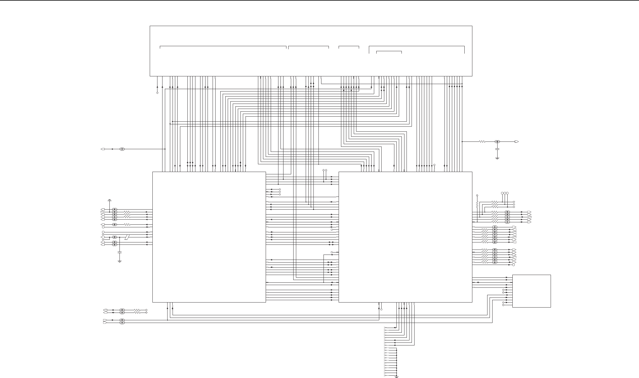
Controller R2 Schematic Diagrams 3-19
3.0 Controller R2 Schematic Diagrams
( MAKO AUDIO_DIGITAL_USB/RS232 : SHEET 3)
MAKO_AUDIO_DC
( DC SUPPLY: SHEET 1)
( MAKO POWER MANAGEMENT : SHEET 2)
RAW_B+
RX_FLTR_VCTRL
TX_DAC
PA_BIAS
PA_TEMP
LO_BATTERY_DET
5V
5V_SW
9V3_PA
2.775V_ANA_V7
2.9V_DIG_V6
3.6V_DIG_VSW1
32KHZ_GPS
ANT_CURRENT_DET
16.8_MHZ_BUFF
USB1_DM
USB1_DP
USB2_DM
USB2_DP
VBUS1
VBUS2
RTC_BATTERY
RX_AUDIO
SPKR+
SPKR-
MIC_GROUND
ONE_WIRE_1
ONE_WIRE_2
ON_OFF_MECH
PUB_ADDRESS_1
PUB_ADDRESS_1_EN
PUB_ADDRESS_2
PUB_ADDRESS_2_EN
HANDSET_AUDIO
INT_MIC+
9V3
EXT_MIC+
EXT_SWB+
GP5_4_EMERGENCY
GP5_5_IGNITION_SENSE
GPIO_0_PWR_ON
GPIO_3_PTT
GPIO_4_HOOK
PUB_ADDRESS_MIC_EN
SPI_CLK
SPI_MISO
SPI_MOSI
SW_9V3
MAKO_TX
OMAP_CORE_LDO
I2C_CLK
I2C_DATA
LOW_LEVEL_MUTE
MAKO_AD_TRIGGER
MAKO_CE
MAKO_DCLK
MAKO_FSYNC
MAKO_INT
MAKO_OPT_GPIO0
MAKO_OPT_GPIO2
MAKO_OPT_GPIO3
MAKO_OPT_INT
MAKO_RX
AUDIO_PA_ENA
EXT_MIC_ENA
1.875V_DIG_V2
2.775V_DIG_V4
3.3V_DIG_V10
USB0_TXEN
USB1_DAT
USB1_SE0
USB1_TXEN
USB_INT
RS232_RX
RS232_TX
USB0_DAT
USB0_SE0
MMP_GPIO1_INPUT
MMP_GPIO2_INPUT
ONE_WIRE_UP
POR
GATED_32KHZ_OMAP
2.9V_MAKO_V6
3.6V_MAKO_SW1
LO_BATTERY_DET
9V3_PA
5V
5V_SW
5V_SW
TX_DAC
RAW_B+
PA_BIAS
2.775V_ANA_V7
RX_FLTR_VCTRL
PA_TEMP R2500 0
R2502 0
0
R2501
0
R2504
1
E2500
BLM21PG300SN1
1
1500pF
C2501
9V3
MICROCONTROLLER
(OMAP 1710: SHEET 1)
(MEMORY: SHEET 2)
GPS
( SHEET 1)
(SW4 / MONITOR)
(SW8 / CHANNEL_ACT)
(KEYPAD_ROW4 / GP5_6)
(BL_EN / GP5_7)
SERIAL_CLK
SERIAL_DATA
MOBILE_DISPLAY_CMD
McBSP3_CLK
McBSP3_DR
McBSP3_DX
McBSP3_FSX
PTT
RESET_OUT
KEYPAD_COL3
KEYPAD_ROW0
KEYPAD_ROW1
KEYPAD_ROW2
KEYPAD_ROW3
LED_CS
KEYPAD_COL0
KEYPAD_COL1
KEYPAD_COL2
GPIO_26
GPIO_3
GPIO_30
(SW1 / VOL_A)
GPIO_31
(SW2 / VOL_B)
GPIO_32
GPIO_33
ARMIO_15
ARMIO_3
ARMIO_6
DIR_CTRL
DISPLAY_CS
GP5_8
USB0_TXEN
USB1_DAT
USB1_SE0
USB1_TXEN
USB_INT
RS232_RX
RS232_TX
USB0_DAT
USB0_SE0
MAKO_OPT_INT
MAKO_RX
MAKO_TX
OMAP_CORE_LDO
ONE_WIRE_UP
OPT_GPIO_1
OPT_GPIO_2
POR
MAKO_AD_TRIGGER
MAKO_CE
MAKO_DCLK
MAKO_FSYNC
MAKO_GPIO_RX
MAKO_INT
MAKO_OPT_GPIO0
MAKO_OPT_GPIO2
MAKO_OPT_GPIO3
I2C_CLK
I2C_DATA
GPIO_18
GPIO_25
GPIO_27
GPIO_5
ARMIO_12
ARMIO_2
AUDIO_PA_ENA
EXT_MIC_ENA
GATED_32KHZ_OMAP
1.875V_DIG_V2
2.775V_DIG_V4
3.3V_DIG_V10
JTAG_NEMU0
JTAG_NEMU1
JTAG_NTRST
JTAG_RTCK
JTAG_TCK
JTAG_TDI
JTAG_TDO
JTAG_TMS
16.8_MHZ_BUFF
32KHZ_CLK
RX_CLK
RX_DATA
RX_FSYNC
SPI_CLK
SPI_MISO
SPI_MOSI
THK_CE
TX_CLK
TX_DATA
TX_FSYNC
LOCK_DETECT
GPS_ON_OFF_LS
GPS_RESET_LS
GPS_RX_LS
GPS_TX_LS
(RED_LED / RX_ATTN_1)
GPIO_40
GPIO_60
GPS_BOOT_SELECT
ANT_EN
DEEP_SLEEP
DMCS
GPIO_15
ABACUS3_CE
ADAPT_SW
0
R2506
16.8_MHZ_BUFF
0
R2507 1.875V_V21.875V_DIG_V2
2.775V_V42.775V_DIG_V4
16.8_GPS
NC
J2500-13
J2500-4
J2500-10
J2500-15
J2500-17
J2500-9
J2500-16
J2500-1
J2500-8
J2500-20
J2500-2
J2500-19
J2500-5
J2500-6
J2500-11
J2500-3
J2500-7
J2500-18
J2500-12
J2500-14
2.775V_V4
1.875V_V2
5V
5V_SW
1.875V
16.8MHz
32KHZ_GPS
5V_ACTIVE_ANT
ANT_CURRENT
GPS_5V
GPS_BOOT_SEL
GPS_ON_OFF_LS
GPS_RESET_LS
GPS_RX_LS
GPS_TX_LS
VCONT
RF_ATTN_2
LOCK_DETECT
PC_ATTEN_ENA
DMCS
ADAPT_SW
ANT_ENABLE
PREDRIVE_SW
R2516
R2517
R2515
R2520
R2519
R2518
0
0
0
0
0
0
RX_SSI_SYNCB
TX_SSI_FSYNC (84.0 KHz)
TX_SSI_DATA
TX_SSI_CLK (4.20 MHz)
RX_SSI_FSYNC (20.0 KHz)
RX_SSI_DATA
RX_SSI_CLK (1.20 MHz)
R2510
R2511
R2514
R2512
R2509
R2513
0
0
0
0
0
0
(Active LOW)
THK_CS
SPI_MOSI
SPI_MISO
SPI_CLK (6.0 MHz)
ABACUS3_CS (Active LOW)
0
0
0
0
0
0
0
0
R2572
R2525
R2526
R2524
R2528
SPI_MOSI_MAKO
SPI_CLK_MAKO
SPI_MISO_MAKO
SPI_MISO_1
1
SPI_CLK_1
1SPI_MOSI_1
1
R2522
10K
R2529
R2523
R2521
1.875V_V2
220pF
C2500
R2508 0RESET_OUT
VOLUME_1
VOLUME_2
RESET
SERIAL_CLK
SERIAL_DATA
LED_CS
DISPLAY_CMD
DISPLAY_CS
INT_SPKR-
KEYPAD_COL_0
KEYPAD_COL_1
KEYPAD_COL_2
KEYPAD_ROW_0
KEYPAD_ROW_1
KEYPAD_ROW_2
KEYPAD_ROW_3
MIC_GROUND
INT_SPKR+
VBUS1
ONE_WIRE_1
GPIO_0_PWR_ON
GPIO_1_USB1_DP
GPIO_2_USB1_DM
GPIO_3_PTT
GPIO_4_HOOK
HANDSET_AUDIO
INT_MIC+
SYSTEM_SYNC
ON_OFF_SW
RTC_BATTERY
McBSP3_CLKX
McBSP3_DR
McBSP3_DX
McBSP3_FSX
9V3
ARMIO_6
DIR_CTRL
SSI_CLK
SSI_DATA_IN
SSI_DATA_OUT
SSI_FSYNC
SW_9V3
OPT_BRD_PTT
OPT_GPIO_1
OPT_GPIO_2
PROGM_IO_CS
RESET_OUT
1V8
3.3V
GP5_1_PTT
GP5_2_MONITOR
GP5_3_CHAN_ACTIVITY
GP5_6_TxDc_BUS+
GP5_7_RxDc_BUS-
GP5_8_CTSs_RESET
USB2_DM
USB2_DP
VBUS2
PUB_ADDRESS_1
PUB_ADDRESS_1_EN
PUB_ADDRESS_2
PUB_ADDRESS_2_EN
ONE_WIRE_2
GP5_4_EMERGENCY
GP5_5_IGNITION_SENSE
RX_AUDIO
EXT_SWB+
5V
EXT_MIC+
EXT_SPKR+
EXT_SPKR-
5V
MMP
CONTROL HEAD REAR ACCESSORY REPEATER INTERFACE
PERIPHERALS
OPTION BOARD INTERFACE
( 1 SHEET)
(Active HIGH)
2.775V_V4
1.875V_V2
SPI_MOSI_MAKO
SPI_MISO_MAKO
SPI_CLK_MAKO
NC
NC
NC
Controller – GPS Schematic Diagram

3-20 Controller R2 Schematic Diagrams
13.6V (NOMINAL)
U3040,U3005,U3006 change to 4813971D34
9.3V
9.3V
13.6V
5V
5V
9.3V
J3000-1
VBAT_GROUND
1
J3000-2 2
VBAT
1
1
VR3000 470pF
C3000
C3015
47pF
C3002
10uF
E3000
0.1
0.1
0.1
0.1
R3056
U3005
1
2
3
G1
R3033
R3032
U3006
1
2
3
G1
R3055
R3036
10
R3034
330
10
R3035
0
R3051
NC
R3050
Q3032
150
R3038
150
NU
0.1uF
C3031
Q3030
10K
R3030
.01uF
C3032
2
3
1
8
4
U3030-1
R3040
1%
2.74K
R3041
100K
R3048
1K
33uF
C3043 C3044
0.1uF
1.0uF
C3011
FB
5GND
NP
VCONT
1
VOUT
U3004
TK11100CSC
5V
5V
2
6
4
3VIN
C3016
100pF
R3008
1%
13K
R3007
1%
39.2K
1000pF
C3017
100K
R3047
VR3040
NC
2.74K
1%
R3046
C3042
.01uF
U3030-2
6
5
7
8
4
0
R3054
R3045
0
R3052
2K
1%
.01uF
C3041
680
R3043
D3040
Q3040
U3040
1
2
3
G1
680
R3042
330
R3044
C3040
470pF
R3002
10K
ON_OFF
2
45
U3001
LM2941
1
ADJ
GND1
3
GND2
6
470pF
C3005
VIN VOUT
0.10uF
C3046
R3003
1%
3.57K
R3004
1%
562
C3045
33uF
NU
C3007
0.1uF
33uF
C3006
13K
1%
R3010
FB
5GND
6NP
4VCONT
3VIN
VOUT
2
1000pF
C3008
1
TK11100CSC
U3002
0.10uF
C3009
C3010
1.0uF
39.2K
1%
R3009 9V3
5V_SW
5V_SW
(TO RX BACKEND, SYNTH,GPS ANTENNA)
ON: 0V
OFF: 4.8V
Q3041
47K
47K
C3012
470pF
MAKO_ON_OFF_CONTROL
1
GND1
3
GND2
6
ON_OFF
2
4VIN 5
VOUT
LM2941
U3003
ADJ
R3006
220
5%
R3005
2.2K
5%
22uF
C3013 C3014
0.1uF
EXT_SWB+ ( TO REAR ACCESSORY)
9V3 (TO SYNTH, VCO, RX FE, PWR CNTRL,CONTROLHEAD)
(TO GPS & PERIPHERAL BLOCKS)
9V3_CNTRL (TO MAKO)
UNSWB+ (TO AUDIO PA)
9V3_PA (TO PA DRIVER ONLY)
RAW_B+ (TO TX PA)
C3021
0.1uF
33uF
C3020
R3053
0
.01uF
C3030
D3030
R3039
1%
2K
0
R3057
R3037
330
This cap only use to support
DC connector during reflow.
NC
C3019
470pF
10uF
C3018
NC
Controller DC Supply Schematic Diagram
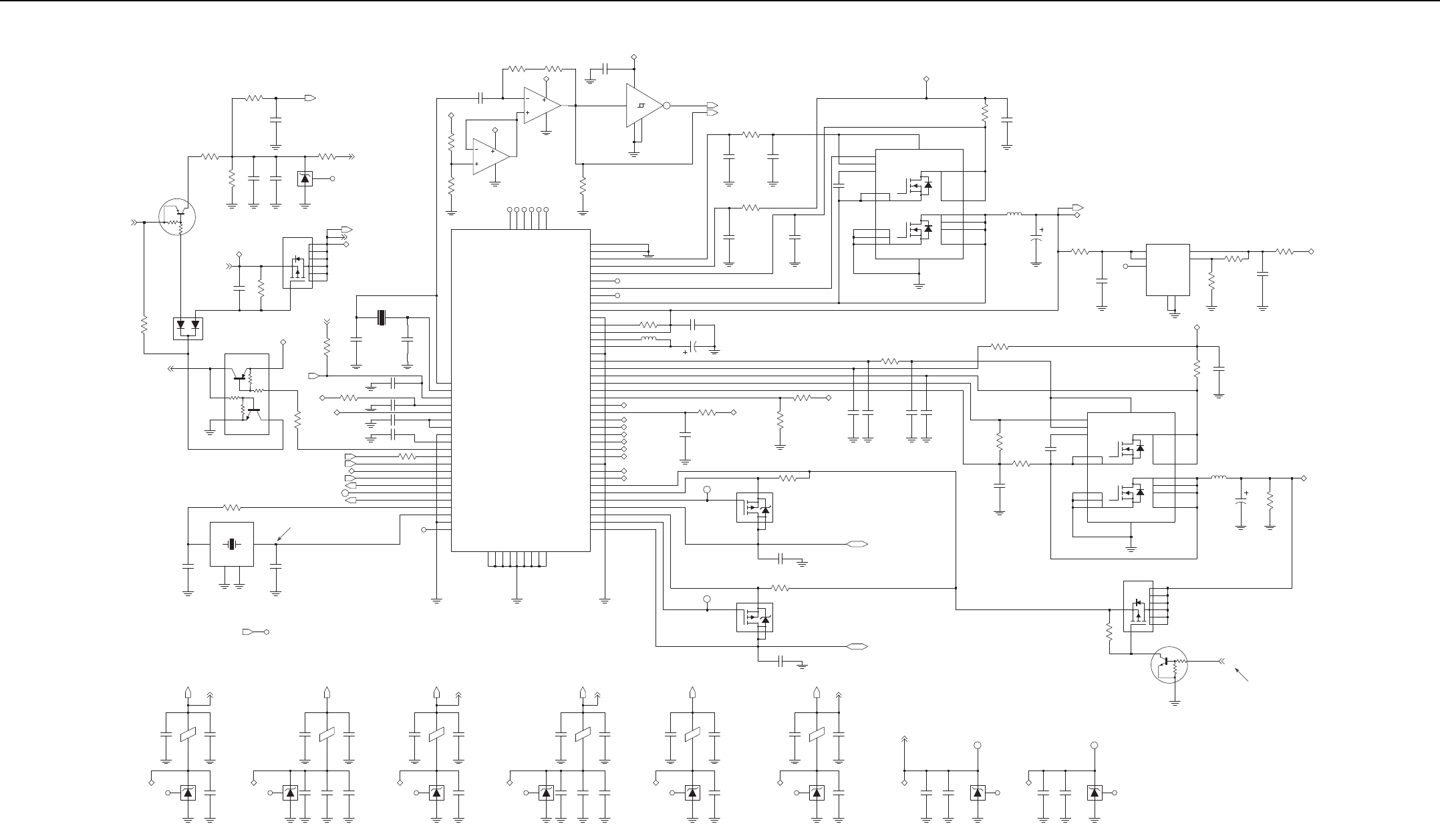
Controller R2 Schematic Diagrams 3-21
5185143E77
C3261
220pF
C3274
220pF
10.0uF
C3275
R3210
14.3K
1%
Q3205
DTA144EKAF
0
R3228
R3209
43.2K
VR3200
NC
UNSWB+
47K
47K
LO_BATTERY_DET
BATTERY_SENSE
R3233
0
C3262
2.2uF
NTHS5441T1
Q3201
R3205
100K
SW_9V3
SW_9V3
SW_9V3
9V3_CNTRL
9V3_CNTRL
5.6pF
C3204
Y3201
21
32.768KHz
XTAL
C3205
5.6pF
D3200
10K
R3249
6
3
1
4
EMD9FT2R
Q3206
2
5
R3248
10K
RTC_BATTERY
5V
9V3_CNTRL
MAKO_ON_OFF_CONTROL
C3207 0.1uF
R3206
0
R3226
33K
C3210 2.2uF
2.2uFC3208
1000pFC3211
VSAVE
9V3_CNTRL
MAKO_GATED_32KHz 1
0
R3218
VSAVE
MAKO_INT
GP5_4_EMERGENCY
GP5_5_IGNITION_SENSE
POR
ON_OFF_MECH
24.576MHz
Vpk-pk: 2.2V - 2.4V
Sine Wave
C3214
33pF
2GND1
4GND2
1
HOT1
3
CX-101F
Y3200
0
R3201
33pF
C3215
HOT2
NC
H5
D9
P5
M7
J4
G5
K9
L4
D14
C2
A13
A12
C1
B1
B3
M1
D4
D3
C5
G4
B4
D5
E4
F5
D2
D1
F3
B2
F4
E2
VSAVE
XIN
XOUT
XTAL32_IN
XTAL32_OUT
SW_TYPE
TCXO_IN
TCXO_SEL_16_24
REG_3V6
RESETX
HV_BG
IGN_X
INT_X
MECH_SW
GATED_32K_CLK
BAT_3V6
BAT_7V5
BAT_RTC
BAT_TYPE
EMERG_PB
FET_ENX
GND8
GND9
GND1
GND2
GND3
GND4
GND5
GND6
GND7
NC3
NC4
NC5
NC6
NC1
NC2
VBUS_SUPPLY
V10_I
V10_O
VBUS1
VBUS1_CMD
VBUS1_SENS
VBUS2
VBUS2_CMD
VBUS2_SENS
V03_O
V04_O
V06_O
V07_O
V08_I
V08_O
V09_O
V10_GND
SW5_VDD
SW5_VDDHV
SW5_VOUT
SW5_VSENSE
V02_O
SW1_VSEN_BUK
SW2_GND
SW2_LX
SW2_VCC
SW2_VCCS
SW2_VOUT
SW5_PHASE
SW5_SUMCOMP
SW1_DH
SW1_GND
SW1_PHASE
SW1_SUMCOMP_DL
SW1_VDD
SW1_VDDHV
SW1_VOUT
SW1_VSEN_BST
PGLDO2
PGLDO3
PWR_MNGR_BLOCK
U3200-1
B13
J10
M6
H10
C14
E12
D12
C13
F11
P4
N5
P3
P6
K3
K4
L1
L9
D13
F13
F12
E14
N4
H11
L14
J14
J12
K14
J13
G11
E13
H13
H14
F14
G14
G13
G12
H12
J11
C3
A2
NC
NC
NC
NC
P1
P14
M5
B14
A1
A14 NC
NC
NC
NC
0613952Q73
R3236
1K
C3272
10pF
R3223
220K
220K
A1
B1
B3 U3202-2
LMC6035ITLX
A2
A3
VSAVE
VSAVE
R3222
2
1
4
5
5114007A43
NL17SZ14
U3203
3
2MEG
R3220 4.7uF
C3282
U3202-1
LMC6035ITLX
C2
C3
C1
B1
B3
R3219
2MEG
1.875V_V2_MAKO
VSAVE
IN
NC
OUT
VCCGND
R3238
10
C3201
2.2uF
1.0uF
C3276
32KHZ_GPS
GATED_32KHZ_OMAP
OFF: 0.0Vpk
ON: 5Vpk; 230 KHZ PWM
5.1
R3241
C3278
0.1uF
C3279
0.1uF
C3200
22uF
R3200
0.1
SW_9V3
SYNC_EN
5
VDD 13
4IN
S1A
15
S1B
16
Q3200
14 CBOOT D1A 1
D1B 2
0.10uF
C3202
ON: 3.6V
OFF: 0.0V
C3203
68uF
22uH
L3200
3.6V_DIG_VSW1
3.6V_DIG_VSW1
C3269
1.0uF
0
R3245
6VIN2 ADJ
GND1
2
GND2
7
NC
3
1VIN1
NC
Change R3246 to 0613952N12 (13K) for OMAP1610
5
VOUT
U3201
LP8340
4
R3246
6.81K
1%
C3270
1.0uF
51.1K
1%
R3247
R3215
0
OMAP_CORE_LDO_1
22uF
C3265R3204
0.1
SW_9V3
ON: 5.2V - 5.3V
OFF: 0.0V
R3237
10K
22uH
L3202
68uF
C3212
VSW5
OFF: 0V (DEFAULT)
ON: 3.3V (MAKO V10)
FROM MAKO USB_CONNECT (L6)
USB_CONNECT
R3240
47K
NTHS5441T1
Q3207
2
10K
47K
3
1
Q3208
DTC114YKAF
D1A
D1B
D2A
D2B
D2C
D2D
1
2
9
10
11
12
IN
SYNC_EN
13
VDD
CBOOT
SI4724CY
Q3202
S1A
S1B
S2A
S2B
S2C
3GND
4
15
16
6
7
8
5
14
0.10uF
C3209
ON: 5Vpk; 230 KHZ PWM
OFF: 0.0Vpk
4.7K
R3224
NU
10pF
C3273
0
NU
R3225
R3239
10
0.1uF
C3280 C3281
0.1uF
C3266
2.2uF
1.0uF
C3277
VSW5
NU
R3227
10K
0
R3216
C3234
2.2uF
NU
R3217
0
OMAP_CORE_LDO_1
3V_V9_MAKO
2.775V_V7_MAKO
2.9V_V6_MAKO
2.775V_V4_MAKO
1.875V_V2_MAKO
3.3V_V10_MAKO
3.6V_DIG_VSW1
5V_V8_MAKO
SW_9V3
0.2
R3207
SI8401DB
Q3203
2
3
1
4
VBUS1_CMD
1
VBUS2_CMD
1
2
3
1
4
SI8401DB
Q3204
4.7uF
C3216
4.7uF
C3213
0.2
R3208
ON: 4.75V to 5.25V (5.0V typical)
OFF: 0.0V
VBUS2
( TO MAP )
3.3V_DIG_V10
3.3V_DIG_V10
5V_V8_MAKO
NC C3257
1.0uF
C3232
0.10uF
C3231
220pF
VR3207
E3208
3.3V_V10_MAKO
220pF VR3206
C3229
NC
MAKO_V8_5V
2.2uF
C3254
1
5V_V8_MAKO
C3233
220pF
C3260
1.0uF
NC
MAKO_V9_3V
1
VR3208
3V_V9_MAKO
0.10uF
C3228
220pF
C3227
E3206
NC 1.0uF
C3252
VR3205
2.775V_ANA_V7
2.775V_V7_MAKO
E3205
NC 100pF
C3249
VR3204
1.0uF
C3248
C3226
0.10uF
220pF
C3225
C3247
10uF
2.9V_DIG_V6
2.9V_DIG_V6
2.9V_V6_MAKO
220pF
C3221
VR3203
0.10uF
C3222
NC 1.0uF
C3243
E3203
2.775V_DIG_V4
2.775V_DIG_V4
2.775V_V4_MAKO
C3240
100pF
E3202
C3219
220pF
VR3202 C3239
2.2uF
NC
10uF
C3238
C3220
0.10uF
OMAP_CORE_LDO_1
OMAP_CORE_LDO
NC
E3201
VR3201 C3237
2.2uF
C3218
0.10uF
C3217
220pF
1.875V_DIG_V2
1.875V_DIG_V2
1.875V_V2_MAKO
NC
16.8_MHZ_BUFF
22uHL3201
R3203 0.1
22uFC3206
C3283 0.10uF
R3243
5.1
ON: 4.75V to 5.25V (5.0V typical)
OFF: 0.0V
VBUS1
( TO MMP)
S2C
8
D2C 11
D2D 12
GND
3
S2A
6
S2B
7
D2A 9
D2B 10
Controller DC Distribution Schematic Diagram

3-22 Controller R2 Schematic Diagrams
ACCESSORY INTERFACE (26-PIN)
CONTROL HEAD INTERFACE
OPTION BOARD INTERFACE
PCB
J4001 FRONT VIEW
I/O History
PCB
J4003 FRONT VIEW
P1 0102726B32
PCB
J4000 REAR VIEW
ARMIO_6
RESET
PROGM_IO_CS
SERIAL_DATA
SERIAL_DATA
SERIAL_CLK
SERIAL_CLK
220pF
C4074
NU
C4071
NU
220pF 220pF
C4072
NU
10K
R4079
1V8
0.10uF
C4084C4085
220pF
1V8
SN74LVC07A
U4001
11
13
1
3
5
9
Y_5
Y_6
A_5
A_6
GND VCC
Y_1
Y_2
Y_3
Y_4
A_1
A_2
A_3
A_4 10
12
14
2
4
6
8
NC
7
MOBILE SUBSCRIBER: NOT_USED
MOBILE REPEATER: 0 OHM
0
R4086
NU
WD_RESET
WD_RESET
R4100
1.2K 1.2K
R4023 1.2K
R4103
1.2K
R4101
5V
NC
C4073
0.10uF
16 VCC
6QG
7QH1
9QH2
12
RCLK
13
RCLR
14
SER
11
SRCLK
10
SRCLR
8
GND
15 QA
1QB
2QC
3QD
4QE
5QF
SN74AHC594
U4000
5V
PUB_ADDRESS_1_EN
PUB_ADDRESS_2_EN
1V81V81V81V81V81V8
NU
R4033
R4030
NU
10K
R4032
R4055
10K
R4054
10K
10K
R4031
GP5_1_PTT
GP5_4_EMERGENCY
GP5_7_RxDc_BUS-
GP5_8_CTSs_Reset
GP5_5_IGNITION_SENSE
GP5_3_CHAN_ACTIVITY
GP5_6_TxDc_BUS+
GP5_2_MONITOR
USB2_DP
1
E4002
BLM21PG221SN1
1
VBUS2USB2_DM
1
R4035
10K
USB2_DM
USB2_DP
VBUS2
5V
1
2
4
3
D4000
4866544A01
EMERG SW
POWER GROUND
GROUND
EXT_SPKR+
GP5_7
USB_DP_MAP
USB_DM_MAP
TX_AUDIO
IGN_SENSE
MAP_ID_1
RX_AUDIO
GP5_8
AUX_AUDIO_OUT_1
VBUS_MAP
GROUND
USB / MAP_ID_GROUND
EXT_SWB+
GP5_6
GP5_3_(CHAN_ACT)
VIP_1_(EXT ALARM)
GP5_1_(EXT PTT)
EXT_SPKR-
MAP_ID_2
AUX_AUDIO_OUT_2
GP5_2_(MONITOR)
AUDIO GROUND
J4000-18
J4000-10
J4000-21
J4000-26
J4000-25
J4000-12
J4000-11
J4000-9
J4000-22
J4000-3
J4000-4
J4000-5
J4000-7
J4000-6
J4000-15
J4000-17
J4000-20
J4000-16
J4000-13
J4000-14
J4000-2
J4000-8
J4000-1
J4000-23
J4000-19
J4000-24
18
4
2
1
3
21
10
25
26
5
6
9
7
8
11
12
22
15
17
16
20
14
13
23
19
24
16 24
15 21
11
97531
1814 26
228
642 1210 20
25
13 23
17 19
ONE_WIRE_2
EXT_SPKR-
EXT_SWB+
EXT_SWB+
PUB_ADDRESS_2
RX_AUDIO
PUB_ADDRESS_1
EXT_MIC+
EXT_SPKR+
220pF
C4069C4067
220pF 220pF
C4068
220pF
C4075
NU
220pF
C4064 220pF
C4066
220pF
C4063 220pF
C4065
220pF
C4070
BK1005HM471
E4005
NC
VR4006
APM_1_WIRE
1
NC
VR4004
MMBZ20V
4813977A48
220pF
C4048
R4048
1.5K
BCW68GLT1G
4816023H01
Q4013
DTC114YKAF
4815261H01
Q4012
210K
47K
3
1
R4049
2.7K
R4050
10K
EXT_SWB+
10K
R4088
R4089
47K
Q4011
DTC144EKAF
4815263H01
R4047
4.7K
47K
47K
MMBZ20V
4813977A48
VR4003 C4047
220pF
BCW65A
1
3
2
Q4014
5V
4815263H01
Q4009
DTC144EKAF
R4046
4.7K
1
Q4010
DTC114YKAF
4815261H01
2
3
10K
47K
47K
47K
5V
C4045
220pF C4046
220pF
MOBILE REPEATER: 0 OHM
MOBILE SUBSCRIBER: NOT_USED
390K
R4051
C4040
C4041
220pF
220pF
EXT_PTT
1
DTC114YKAF
4815261H01
2
3
1
Q4002
DTC144EKAF
DTC144EKAF
Q4015
4815263H01
4815263H01
Q4001
NC
VR4005
Q4003
DTC144EKAF
4815263H01
4815263H01
Q4005
DTC144EKAF
4.7K
R4044
NU
4.7K
R4043
R4042
4.7K
4815261H01
2
3
10K
47K
47K47K
47K
47K
47K
47K
47K
47K
47K
47K
47K 47K
47K
10K
10K
47K
47K 47K
1
Q4008
DTC114YKAF
R4041
4.7K
C4042
220pF
DTC144EKAF
4815263H01
Q4006
4813977A48
VR4000
MMBZ20V VR4002
MMBZ20V
4813977A48
4813977A48
VR4001
MMBZ20V
DTC144EKAF
4815263H01
Q4000
11 IGNITION_SENSE
EMERGENCY
DTC144EKAF
4815263H01
Q4007
R4040
4.7K
R4045
4.7K
C4043
220pF
R4098
4.7K
C4044
220pF
2
3
1
WD_RESET
DTC114YKAF
4815261H01
Q4004
5V
5V
5V
5V 5V
5V
5V
0
R4074
R4084 0
0
R4085
0
R4076
R4082 0
R4081 0
R4080 0
0
R4078
R4083 0
SSI_DATA_OUT
SSI_DATA_IN
SHARED_SYSTEM_SYNC
SSI_FSYNC
SSI_CLK
SW_9V3
OPT_GPIO_1
OPT_BRD_PTT
OPT_GPIO_2
RESET_OUT
MOBILE REPEATER: 0 OHM
MOBILE SUBSCRIBER: NOT_USED
0
R4090 NU
J4001_9
RTC_BATTERY
C4055
220pF
NU
OPT_SSI_SYNC
1
220pF
C4049
NU NU
C4053
220pF
220pF
NU
C4051
NU
220pF
C4059
J4003-44
J4003-55
J4003-13
13
J4003-12
12
J4003-99
3 J4003-3
J4003-88
6 J4003-6
J4003-11
J4003-14
14
J4003-1010
J4003-22
J4003-11
11
J4003-77
NU
C4058
220pF 220pF
C4060
NU
220pF
NU
C4061
NU
C4062
220pF
8713421412119531106
13 711 325 128 18 1720 19 24529 23 15 6826 101230 27 22 21 924 16 14
25 J4001-25
J4001-2626
J4001-1818
J4001-33
J4001-77
J4001-3030
J4001-2323
J4001-2424
J4001-99
8 J4001-8
J4001-2929
J4001-1212
J4001-2121
J4001-2727
J4001-2
2
J4001-55
J4001-2222
4 J4001-4
1 J4001-1
6 J4001-6
J4001-1414
J4001-1010
17 J4001-17
15 J4001-15
J4001-1111
20
J4001-1919
J4001-20
28 J4001-28
J4001-1616
J4001-1313
220pF C4032
220pF
C4029
220pF
C4021
220pF
C4018 C4025
220pF 220pF
C4033C4015
220pF C4020
220pF C4030
220pF220pF
C4017 220pF
C4023C4016
220pF 220pF
C4027
220pF
C4019 C4031
220pF
C4014
220pF C4028
220pF
C4026
220pF
C4024
220pF
C4022
220pF
NU
NU
0
NU
R4011
C4076
220pF330pF
C4035
C4034
330pF
C4013
220pF 220pF
NUNU
220pF
C4004C4003
NU
220pF
C4002
220pF
C4005
NUNU
220pF
C4000
220pF
C4006
J4001_9 C4001
220pF
NU
MOBILE REPEATER: NOT_USED
MOBILE SUBSCRIBER: 33 OHM
1
MMP_1_WIRE
1
USB1_DM
1
E4003
VBUS1 USB1_DP
1
RESET
ON_OFF_SW
9V3
RESET
DISPLAY_CS
SERIAL_DATA
SERIAL_CLK
LED_CS
DISPLAY_CMD
HANDSET_AUDIO
INT_SPKR-
KEYPAD_ROW_1
KEYPAD_ROW_3
KEYPAD_COL_1
VOLUME_1
KEYPAD_ROW_0
KEYPAD_ROW_2
KEYPAD_COL_0
KEYPAD_COL_2
VOLUME_2
INT_SPKR+
R4068
R4063
R4064
R4066
R4003
R4004
R4002
R4000
R4005
R4061
R4001
R4065
R4070
R4069
R4067
R4071
33
33
33
33
33
33
33
33
33
33
33
33
33
33
33
0
51
R4009
470
R4006
51
R4010
E4004
BK1005HM471
E4001 BLM21PG221SN1
GPIO_1_USB1_DP
ONE_WIRE_1
MIC_GROUND
GPIO_4_HOOK
VBUS1
INT_MIC+
GPIO_0_PWR_ON
GPIO_3_PTT
GPIO_2_USB1_DM
D4001
14
23
4866544A01
R4034
10K
5V
0
R4012
6
NU
A1
2
A2
5
K1 1
K2 3
K3 4
K4
5.6V
VR4008
6
K4
VR4007
5.6V
NU
2A1
5
A2
1
K1 3
K2 4
K3
E4000
NC
3.3V
5V
5V 1V8
1V8 1V8
Controller Peripheral Schematic Diagram (sheet 1 of 2)
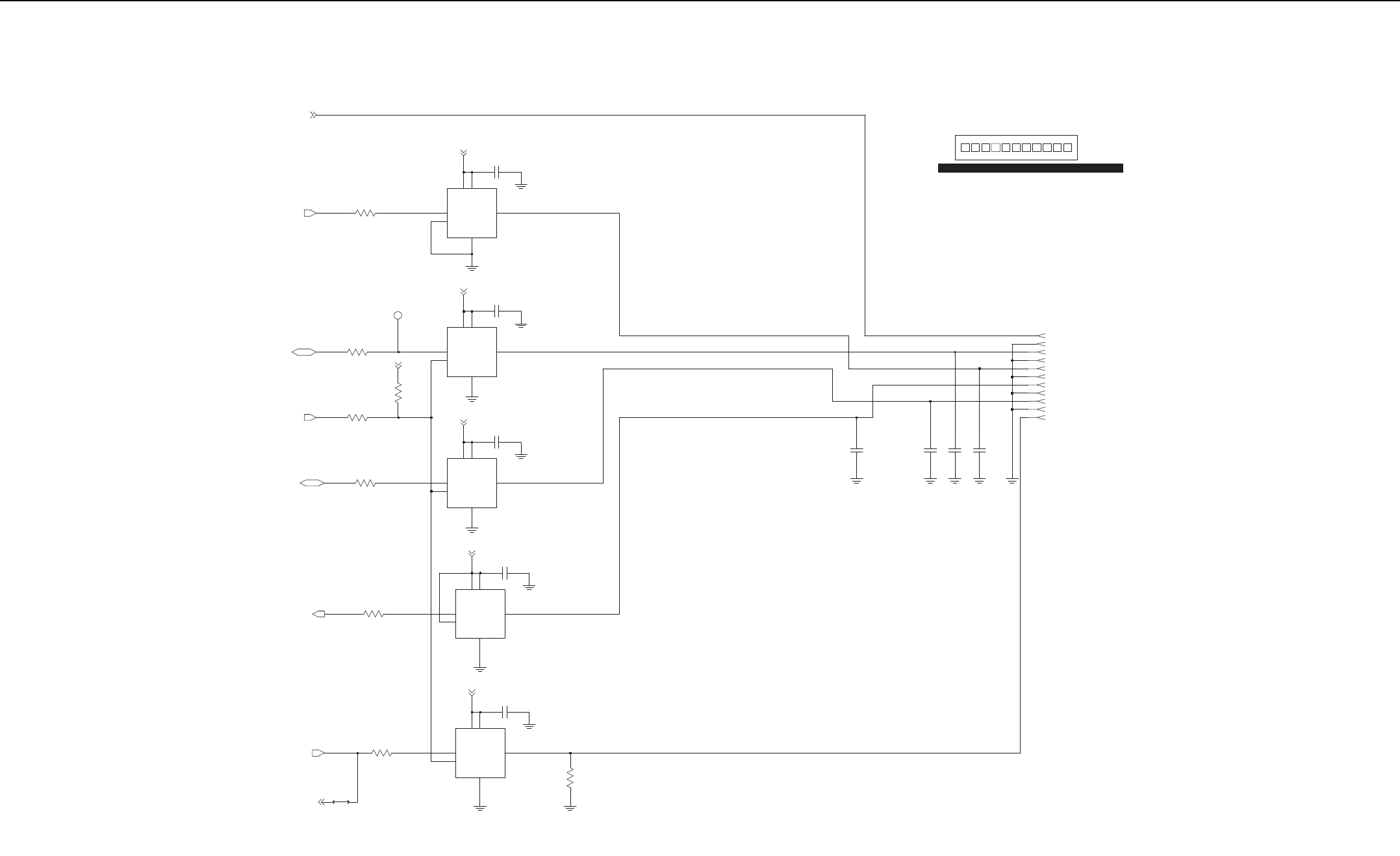
Controller R2 Schematic Diagrams 3-23
B
REPEATER CONNECTOR
PCB
10
J4002 FRONT VIEW
21345678911
J4002-3
J4002-2
J4002-7
J4002-8
J4002-5
J4002-6
J4002-4
J4002-9
J4002-10
J4002-1
J4002-11
3
8
2
7
5
6
10
4
9
1
11
C4010
220pF
NU
220pF
NU
220pF
NU
C4012C4011
220pF
NU
C4007
C4086
0.10uF
B1 GND
A1
VCCA A2
VCCB
SN74AVC1T45
C1
A
C2 B
B2 DIR
1V8
0R4097
McBSP3_DX
0.10uF
C4087
U4004
C1
B
C2
DIR
B2
GND
B1 VCCA A1
VCCB A2
U4005
SN74AVC1T45
A
1V8
10K
R4105
0R4099
TP4000
1
0R4095
DIR_CTRL
1V8
McBSP3_FSX
0.10uF
C4089
AC1
B
C2
DIR
B2
GND
B1 VCCA A1
VCCB A2
U4007
SN74AVC1T45
0
R4094
C4090
0.10uF
C1
A
C2 B
B2 DIR
B1 GND
A1
VCCA A2
VCCB
SN74AVC1T45
U4008 10K
R4106
R4096 0
0
R4093
C4088
0.10uF
C1
A
C2
B2 DIR
B1 GND
A1
VCCA A2
VCCB
SN74AVC1T45
U4006
SYSTEM_SYNC
SHARED_SYSTEM_SYNC
McBSP3_DR
McBSP3_CLKX
1V8
1V8
1V8
WD_RESET
Controller Peripheral Schematic Diagram (sheet 2 of 2)
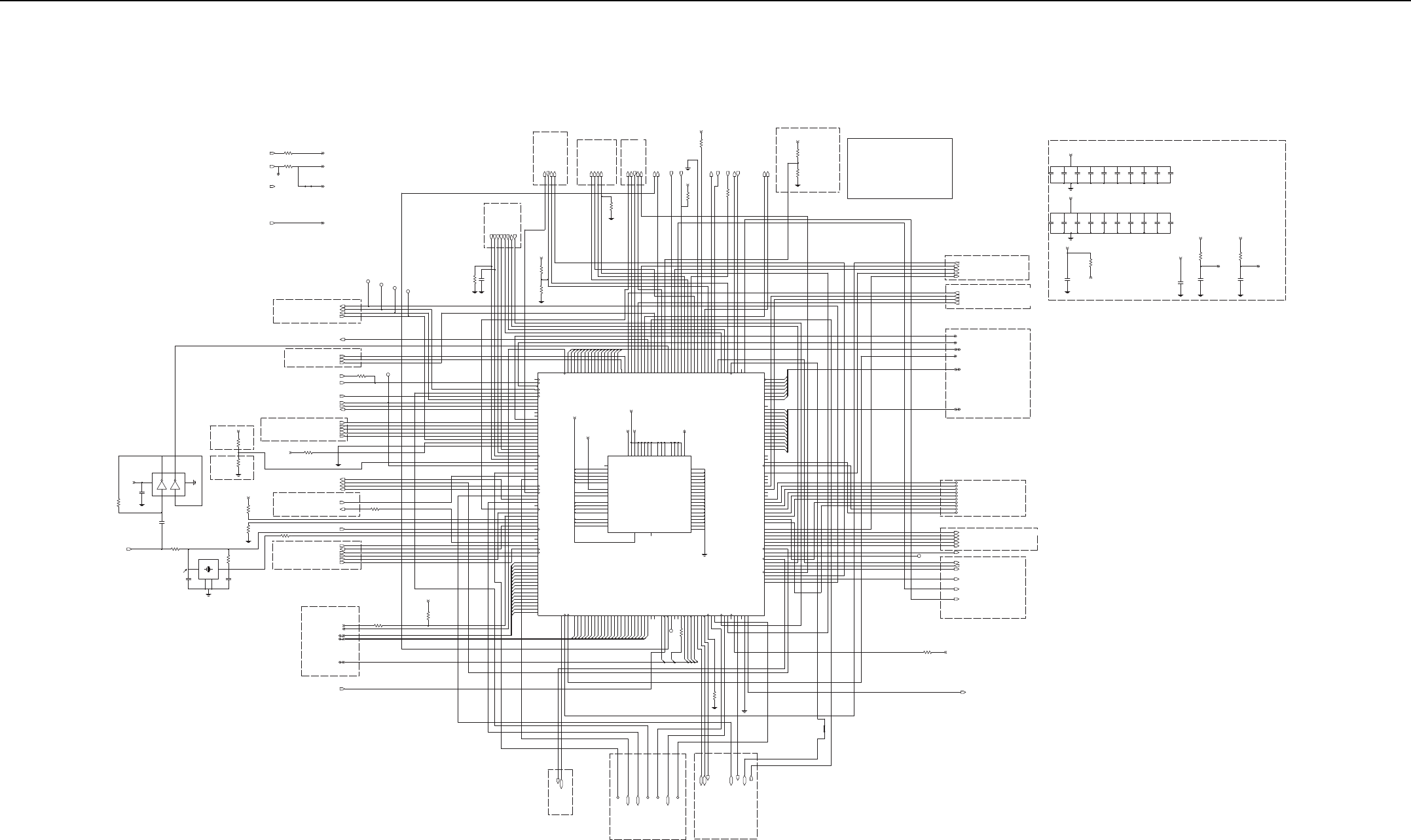
3-24 Controller R2 Schematic Diagrams
0
OMAP1610 / 1710
DECOUPLING CAPACITORS
Place for
(1.4V for OMAP1710 & 1.55V for OMAP1610)
(0.87mA/MHz for OMAP1710 & 1.06mA/MHz for OMAP1610)
OMAP1710
0
R1020
0
R1021
1.875V
DVDD2
OMAP_CORE
2.775V_DIG_V4 2.775V_DIG_V4
1.875V_DIG_V2
1.875V_DIG_V2
OMAP_CORE_LDO
3.3V_DIG_V10
MAKO SSI MAKO_FSYNC
MAKO_DCLK
MAKO_TX
MAKO_RX
1
TP_MAKO_RX
1
TP_MAKO_FSYNC
TP_MAKO_TX
1
TP_MAKO_DCLK
1
18pF
C1030
4.7K
R1054 NU
R1066
10K
R1067
4.7K
NU
1.875V
JTAG
JTAG_NTRST
JTAG_NEMU0
JTAG_NEMU1
JTAG_RTCK
JTAG_TCK
JTAG_TDI
JTAG_TDO
JTAG_TMS
MCBSP3
MCBSP3_FSX
MCBSP3_DR
MCBSP3_CLK
MCBSP3_DX
SERIAL FLASH SPI
SERIAL_DATA
SERIAL_CLK
LED_CS
DISPLAY_CS
LED & Display CS: Active Low
Date rate: 20 of 8 bits packet per chip select
CLK rate: 1 MHz
GPS
GPS_BOOT_SELECT
GPS_ON_OFF_LS
GPS_RX_LS
GPS_TX_LS
GPS_RESET_LS
ONE_WIRE_UP
GPIO_60 (Used as GREEN_LED for PORTABLE, PA_ENABLE for MOBILE)
GPIO_15 (Used as RED_LED for PORTABLE, RX_ATTN_1 for MOBILE)
PTT
R1025 10K
1.875V
0
R1047
PLACED FOR
MOBILE ONY
10K
R1017 1.875V
(GPIO_3 for PORTABLE-Green LED)
(SPI.CS3 for MOBILE Shift Register Chip Select)
ARMIO_6
ARMIO_2
GPIO_3
DIR_CTRL
ARMIO_3 (Used as BL_EN for PORTABLE, GP5_7 for MOBILE
AUDIO_PA_ENA (MOBILE ONLY)
ARMIO_12 (MOBILE ONLY)
GP DEVICE CONFIG
10K
R1034
1.875V
DNP
PLACE FOR
GP DEVICE
FAST BOOT
NU
0
R1035
DELETED REF
U1008
LARGEST REF
R1050 Y1001 C1039
47K
R1071
OPTION SELECT (FROM MAKO)
1
TP_POR
MAKO_OPT_GPIO2
MAKO_OPT_GPIO0
MAKO_OPT_GPIO3
(MOBILE ONLY) EXT_MIC_ENA
(FROM MAKO) GATED_32KHZ_OMAP
( RESET CIRCUIT PROVIDED BY MAKO) POR
MAKO_GPIO_RX
GPIO_5
MAKO_INT
(FROM MAKO) 32KHZ_CLK
0
R1048
DNP
BOOT FROM CS3
BOOT FROM CS0
R1028
0
R1027
10K
NU
1.875V
10K
R1045
1.875V
(Used as KEYPAD_ROW4 for PORTABLE, GP5_6 for MOBILE)
KEYPAD ROW
KEYPAD_ROW0
KEYPAD_ROW1
KEYPAD_ROW2
KEYPAD_ROW3
ARMIO_15
GPIO_40
MAKO_AD_TRIGGER
OPT_GPIO_1
OPT_GPIO_2
RS232
R1001
10K RS232_TX
RS232_RX
OMAP_CORE
R1070
0
1K
R1041
R1044
0 (MOBILE ONLY) GP5_8
ABACUS3 SSI
TOMAHAWK SSI
RX_CLK
TX_CLK
RX_DATA
TX_DATA
RX_FSYNC
TX_FSYNC
( BUFFERRED 16.8
FROM TOMAHAWK)
1.0Vpkpk
GND
2
GND1
4
OUT
3 IN 1
Y1000 CX-91F
12MHz
18pF
C1018 18pF
C1019
10MEG
R1002
C1032
NU
0
R1072
16.8_MHZ_BUFF
.01uF
1
A2
3
GND
2
VCC
5
Y1 6
Y2 4
U1006
NL27WZU04
A1
47K
R1026
C1033
0.10uF
1.875V
16.8MHz Squarer
FLASH
0
NU
R1046
FLASH_WAIT
FLASH_CTL(5:0)
EMIFS_ADD(23:1)
EMIFS_DATA(15:0)
FLASH_CLK
10K
R1006
1.875V
15
1
14
8
0
13
4
3
12
11
5
9
10
7
2
6
Place for
OMAP1710
Place for
OMAP1610
1.0uF
C1034
R1000
10
R1019
C1000
100pF
C1012
0.10uF
0.10uF
C1001 C1002
0.10uF
0.10uF
C1016
0.10uF
C1013 C1003
100pF
C1011
100pF
10
R1060
C1044
0.10uF
1.0uF
C1017
0.10uF
C1015 C1031
0.10uF
C1037
2.2uF
2.2uF
C1035
LDO_FILTER
OMAP_CORE
1.875V
CVDDA
OMAP_CORE
DVDD2
OMAP_CORE
VDD_DLL
OMAP_CORE
C1008
100pF 100pF
C1004 C1036
1.0uF
C1014
0.10uF
C1007
100pF
C1006
0.10uF
C1009
0.10uF 0.10uF
C1005
0.10uF
C1010
5.1
SDRAM
SDRAM_CTL(6:0)
SDRAM_DATA(15:0)
SDRAM_CLK
SDRAM_CLK_EN
SDRAM_CS
SDRAM_ADD(12:0)
FREQ SWITCH
(Used as SW8 for PORTABLE, Channel Activity for MOBILE)
(Used as SW4 for PORTABLE, Monitor for MOBILE)
(Used as SW2 for PORTABLE, Volume B for MOBILE)
(Used as SW1 for PORTABLE, Volume A for MOBILE)
DMCS
DEEP_SLEEP
ADAPT_SW
LOCK_DETECT
ANT_EN
GPIO_30
GPIO_31
GPIO_32
GPIO_33
RF CONTROLS
(Used as KEYPAD_COL4 for NEO and Public Add Mic for MORPHEUS)
KEYPAD COLUMN
SPI
R1036
10K
1 TX_RAMP
MAKO_CE
ABACUS3_CE
THK_CE
1.875V
SPI_CLK
SPI_MISO
SPI_MOSI
MOBILE_DISPLAY_CMD (MOBILE ONLY)
KEYPAD_COL0
KEYPAD_COL1
KEYPAD_COL2
KEYPAD_COL3
GPIO_27
PORTABLE
DISPLAY
DISPLAY_CMD
DISPLAY_CE
DISPLAY_DATA0
DISPLAY_DATA1
DISPLAY_DATA2
DISPLAY_DATA3
DISPLAY_DATA4
DISPLAY_DATA5
DISPLAY_DATA6
DISPLAY_DATA7
4
20
7
13
23
19
22
2
9
6
16
21
11
3
1
8
18
17
12
5
14
10
15
4.7K
R1005
2
0
4
3
5
1
TP1000
1
0
R1014
USB#0
( INTERFACE WITH MAKO)
USB#0 RESERVED FOR MOBILE
USB#1
USB1_SE0
USB0_SE0
USB0_DAT
USB0_TXEN
USB1_TXEN
USB1_DAT
USB_INT
USB#2
I2C
OPTION BOARD
USB2_SE0
GPIO_18
I2C_CLK
I2C_DATA
USB2_DAT
USB2_SUSPEND
GPIO_26
GPIO_25
USB2_RCV
OMAP1610
Place for
OMAP1710
Place for
MAKO_OPT_INT RESET_OUT
6
5
4
3
15
14
13
8
2
1
10
7
11
12
9
0
D9
P13
H12
G21
Y10
G20
H15
R12
Y1
P3
C14
D4
G8
E19
E20
H14
F19
G18
H20
W19
V18
Y19
V17
W18
Y18
J20
U20
R14
Y5
V14
R9
W15
Y15
P14
W14
V15
AA9
V9
R10
P10
V2
V13
AA13
AA5
V5
Y2
W3
AA15
Y14
W7
V7
Y6
W6
V3
T4
U3
U1
P8
T3
T2
R4
R3
R2
P7
P4
P2
N7
N2
N4
CLKX_SD
CLK32K_IN
EN_SDCKE
CLKX_MCBSP1
CLK_MCSI2
CLKS_MCBSP1
MCBSP1_FSX
PWRON_RESET
F_CS1U
F_CS2U
SDDQS_H
SDDQS_L
CS_SDRAM
KBR_4
KBR_3
KBR_2
KBR_1
KBR_0
MCBSP1_DR
BFAIL
CONF
TDI
TMS
TCK
TRST
MPU_BOOT
MPU_RST
UART1_CTS
UART2_CTS
UART1_RX
UART2_RX
CLK_B_REQ
CLK_B
CLK_MCSI1
MCSI1_DOUT
MCSI1_DIN
MCSI2_DIN
MCSI2_SYNC
CLK_M_REQ
MCBSP2_DR
FRDY
OSC32K_IN
OSC32K_OUT
MCBSP2_DX
CLK_M
OSC1_IN
OSC1_OUT
LOW_STATE_1
LOW_STATE_2
MCBSP2_FSX
CLKR_MCBSP2
CLKX_MCBSP2
MCBSP2_FSR
FDATA_15
FDATA_14
FDATA_13
FDATA_12
FDATA_11
FDATA_10
FDATA_9
FDATA_8
FDATA_7
FDATA_6
FDATA_5
FDATA_4
FDATA_3
FDATA_2
FDATA_1
FDATA_0
EN_WE_SDRAM
SDRAM_RAS
SDRAM_DQMU
SDRAM_DQML
SDRAM_CAS
SBANK_1
SBANK_0
SADD_13
SADD_12
SADD_11
SADD_10
SADD_9
SADD_8
SADD_7
SADD_6
SADD_5
SADD_4
SADD_3
SADD_2
SADD_1
SADD_0
LCD_VSYNC
LCD_HSYNC
LCD_AC
CLK_P_LCD
LCD_PIXEL_15
LCD_PIXEL_14
LCD_PIXEL_13
LCD_PIXEL_12
LCD_PIXEL_11
LCD_PIXEL_10
LCD_PIXEL_9
LCD_PIXEL_8
LCD_PIXEL_7
LCD_PIXEL_6
LCD_PIXEL_5
LCD_PIXEL_4
LCD_PIXEL_3
LCD_PIXEL_2
LCD_PIXEL_1
LCD_PIXEL_0
KBS_5
KBS_4
KBS_3
KBS_2
KBS_1
KBS_0
CLK_EX_CAM
LOW_STATE_5
UART3_RX
12C_SCL
TDO
UWIRE_SDI
UWIRE_SDO
CLK_S_UWIRE
Z_STATE_3
Z_STATE_2
MCBSP1_DX
H8
H7
D10
C8
B4
C3
B3
H11
H9
H10
B8
B12
G9
G11
G12
B9
G10
A1
B6
B2
A2
B18
C20
B15
C15
D15
C16
A17
G13
B17
C17
D16
D17
C18
B19
A20
H13
G14
C19
B21
D18
G19
C21
E18
D19
D20
F18
H19
M18
L14
T18
AA19
U18
W21
V19
N14
P15
H18
CLK_F
SDATA_15
SDATA_14
SDATA_13
SDATA_12
SDATA_11
SDATA_10
SDATA_9
SDATA_8
SDATA_7
SDATA_6
SDATA_5
SDATA_4
SDATA_3
SDATA_2
SDATA_1
SDATA_0
CAM_D_7
CAM_D_6
CAM_D_5
CAM_D_4
CAM_D_3
CAM_D_2
CAM_D_1
CAM_D_0
CAM_VS
CAM_HS
CAM_RSTZ
GPIO_15
GPIO_14
GPIO_13
GPIO_12
GPIO_11
GPIO_9
GPIO_8
GPIO_7
GPIO_6
GPIO_4
GPIO_3
GPIO_2
GPIO_1
GPIO_0
MPUIO_5
MPUIO_4
MPUIO_3
MPUIO_2
MPUIO_1
EMU0
EMU1
MSCI1_SYNC
CLK32K_OUT
MMC_DAT3
MMC_DAT2
MMC_DAT1
MMC_DAT0
N3
C12
D12
D13
C11
C13
D11
D14
C10
D8
C4
C7
D5
D7
C5
C6
D6
J18
J19
J14
K18
K19
K15
K14
L19
L18
L15
M19
M20
N21
N19
N18
N20
W8
Y8
M15
P19
P20
P18
M14
R19
R18
T20
T19
V8
N15
U19
V16
W17
AA17
R13
W11
W10
V10
R11
12C_SDA
CLK_L_CAM
CLK_SD
FADD_1
FADD_2
FADD_3
FADD_4
FADD_5
FADD_6
FADD_7
FADD_8
FADD_9
FADD_10
FADD_11
FADD_12
FADD_13
FADD_14
FADD_15
FADD_16
FADD_17
FADD_18
FADD_19
FADD_20
FADD_21
FADD_22
FADD_23
FADD_24
FADD_25
FADV
EN_F_BE_0
EN_F_BE_1
GPIO_62
F_CS1
F_CS2
F_CS3
EN_F_OE
F_RP
EN_F_WE
F_WP
USB0_SE0
USB0_DAT
EN_USB_PUEN
CLK_B_QUART2
LOW_STATE_3
LOW_STATE_4
RTCK
MCS12_DOUT
MMC_CMD
CLK_MMC
RTC_ON_NOFF
Z_STATE_1
RTC_WAKE_INT
RESET_MODE
RST_OUT
V20
J15
C9
J8
D3
C1
E4
D2
F4
E3
J7
F3
G4
G3
G2
K8
H4
H3
K7
J2
J4
J3
F2
L8
K4
K3
L7
E1
L4
L3
M8
M7
M3
M4
N8
U4
W1
W2
V4
R8
P9
W4
Y4
V6
W5
Y17
W9
P11
V11
Y12
W16
W13
P12
AA20
E5 RESERVED
V12 DVDDRTC
U1000
OMAP1710
OMAP_CORE
CVDDA
DVDD2
LDO_FILTER
1.875V
VDD_DLL
6
0
1
3
5
2
4
6
8
9
0
12
11
10
5
7
3
2
1
4
VSS_7
VSS_8
VSS_9
VSS_17
VSS_18
VSS_19
VSS_2
VSS_3
VSS_4
VSS_5
VSS_6
VSS_1
VSS_10
VSS_11
VSS_12
VSS_13
VSS_14
VSS_15
VSS_16
NC
DVDD4_1
DVDD4_2
DVDD4_3
DVDD4_4
DVDD5_1
DVDD5_2
DVDD5_3
DVDD1_1
DVDD1_2
DVDD1_3
DVDD1_4
DVDD1_5
DVDD2_1
DVDD2_2
DVDD2_3
CVDDA
CVDD_RTC
CVDD_DLL
CVDD_1
CVDD_2
CVDD_3
CVDD_4
CVDD1
CVDD2
CVDD2_1
CVDD2_2
CVDD3_1
CVDD3_2
CVDD3_3
CVDD3_4
CVDD4
B5
B7
A13
B16
A21
F20
K20
R21
W20
AA21
Y13
AA7
Y3
AA1
U2
N1
K2
G1
B1
Y21
W12
A11
A15
Y20
Y9
M2
AA3
A9
A3
E2
B13
B20
J21
R20
J1
L1
A19
E21
U21
Y16
L21
AA2
Y7
AA11
A5
A7
B10
B14
R1
H2
C2
Controller Microprocessor Schematic Diagram
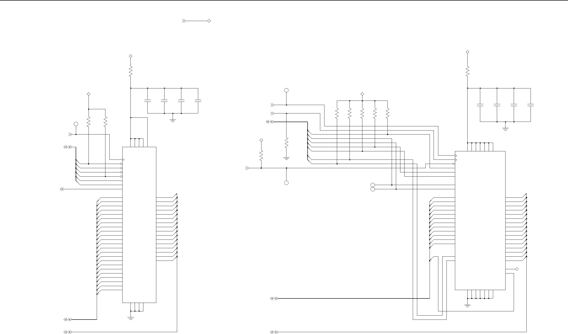
Controller R2 Schematic Diagrams 3-25
FLASH SDRAM
1.875V_DIG_V21.875V_DIG_V2
10K
R2000
TP_FLASH_CLK R2012
10K
FLASH_CTL(5:0)
FLASH_CLK
1.875V_DIG_V2
4
0
1
3
5
2
D3
D6
B5
E7
F8
C4
C5
B4
FLASH_WAIT
13
15
9
10
11
4
5
3
23
16
17
18
19
12
14
6
7
8
1
2
20
21
22 D7
C7
A2
B2
C6
C8
B3
C3
B8
A8
B7
A7
A1
B1
C1
D2
D1
D4
B6
A6
E8
D8
C2
VSS2
VSSQ1
VSSQ2
VSS1
F1
G2
G8
A3
EMIFS_DATA(15:0)
EMIFS_ADD(23:1)
NC
A7
A8
A9
A19
A20
A21
A5
A6
A11
A12
A13
A14
A15
A16
A17
A18
A10
ST 4Mx16
WAIT
D6
D7
D8
D9
D12
D13
D14
D15
D2
D3
D4
D5
D0
D1
D10
D11
A2
A3
A4
A0
A1
0
1
2
8
12
13
14
6
7
15
5
9
10
11
3
4
E3
G1
G7
F6
D5
F3
F2
E2
E5
G5
E4
G3
F7
E6
F5
F4
8MByte
WP
RP
EN_E
EN_G
EN_L
EN_W
CLK_K M58WR064FB
U2000
0104024J27 (Pre-Flashed Part)
A4
VDD1 G4
VDD2 E1
VDDQ1 G6
VDDQ2
VPP A5
100pF
C2000
0.10uF
C2003
R2004
0
.01uF 0.10uF
C2002
C2001
1.875V_DIG_V2
Bootstrap Mode = 48 MHz
Normal Mode = 72 MHz
TP_SDRAM_CLK
SDRAM_CTL(6:0)
SDRAM_CLK_EN
SDRAM_CLK
R2010
10K
10K
R2013
1.875V_DIG_V2
TP_SDRAM_CS
SDRAM_CS
4
1
6
0
5
3
2
TP_SDRAM_BA1
TP_SDRAM_BA0
9
10
11
3
4
5
6
7
8
0
1
2
F9
F8
G7
G8
F7
F3
F2
G9
J8
J7
J3
J2
H3
H2
H1
G3
H7
H8
H9
G2
WE
RAS
BA0
BA1
CAS
CKE
CLK
CS
A2
A3
A4
A5
A6
A7
A8
A9
A0
A1
A10
A11
VDDQ3
VDDQ4
VDD1
VDD2
VDD3
VDDQ1
VDDQ2
16MByte
C7
D3
A9
E7
J9
A7
B3
U2001
DQ4
DQ5
DQ6
DQ7
DQ8
DQ9
DQ10
DQ11
DQ12
DQ13
DQ14
DQ15
DQ2
DQ3
DQ0
DQ1
0
1
3
5
13
14
15
6
7
8
9
4
2
11
12
10
MICRON 8Mx16
C8
D9
D8
E9
E1
D2
D1
C2
C1
B2
B1
A2
B8
C9
A8
B9
NC
D7
12
A1
E3
J1
A3
B7
C3
G1
F1 UDQM
E8 LDQM
E2
NC2
NC1
VSSQ4
VSS1
VSS2
VSS3
VSSQ1
VSSQ2
VSSQ3
C2006
0.10uF
C2004
100pF
.01uF
C2005
0.10uF
C2007
0
R2011
1.875V_DIG_V2
R2005
10K 10K
R2006 R2009
10K
R2007
10K
R2008
10K
1.875V_DIG_V2
SDRAM_DATA(15:0)
SDRAM_ADD(12:0)
Controller Memories Schematic Diagram
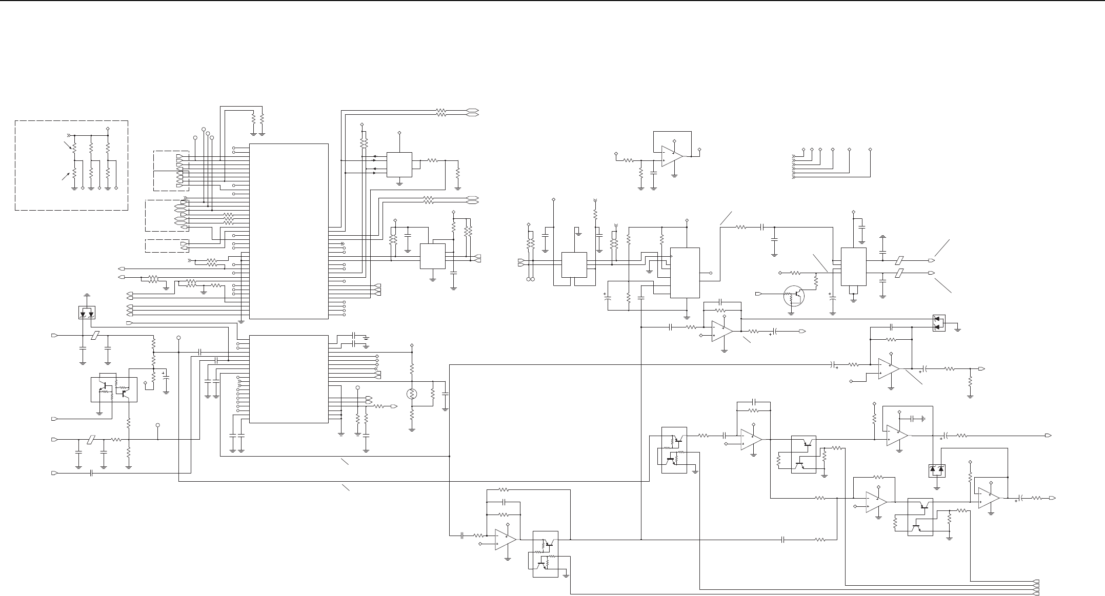
3-26 Controller R2 Schematic Diagrams
HW_ID
MOBILE REPEATER: 33K
MOBILE SUBSCRIBER: NOT_USED
MOBILE REPEATER: NOT_USED
MOBILE SUSCRIBER: 0 OHM
NU
R3504
33K
R3507 0
33K
R3505
NU
R3508 0
0
R3509
33K
R3503
HW_ID1
HW_ID0
2.9V_DIG_V6
2.9V_DIG_V6
HW_ID2
MAKO SPI
MAKO SSI
MAKO_CE
MAKO_TX
SPI_CLK
SPI_MOSI
SPI_MISO
MAKO_DCLK
MAKO_FSYNC
MAKO_RX
1USB1_DAT
MAKO_CE
1
USB1_SEO
1
USB1_TXEN
1
MAKO USB
USB0_SE0
USB_INT
USB1_SE0
USB0_DAT
USB0_TXEN
USB1_DAT
USB1_TXEN
1.875V_V2_MAKO
MAKO UART
RS232_RX
RS232_TX
R3562 0
R3579 10K
R3561 0
R3588 51.1K
0
R3563
1.875V_V2_MAKO
NC
NC
NC
NC
NC
NC
NC
NC
3
1
2
VR3503
MMBZ20V
MMP_GPIO1_INPUT
MMP_GPIO2_INPUT
ONE_WIRE_UP
MAKO_OPT_GPIO3
MAKO_AD_TRIGGER
MAKO_OPT_INT
MAKO_OPT_GPIO0
MAKO_OPT_GPIO2
2
5
6
3
1
4
Q3501
EMD9FT2R
220pF
C3515
220pF
C3514
E3502
INT_MIC+
EXT_MIC_ENA
100
R3532
1.0uF
C3520
0
R3526
R3547
560
EXT_MIC
1
C3521 1.0uF
10uF
C3524
INT_MIC
1
C3516
1.0uF
560
R3535
0.10uF
C3523
9V3
C3518
1.0uF
E3503
220pF
C3531 R3538
39K
R3537
0
C3530
220pF
MIC_GROUND
EXT_MIC+
C3528 0.10uF
C3529 0.10uF
NC
NC
NC
NC
NC
NC
NC
SW_9V3
9V3_CNTRL
NC
NC
A4
A11
J3
H4
H2
H3
F2
F1
L2
E1
G3
G2
J1
J2
G1
H1
K1
K2
E3
B11
VREF
TEST
TX_RX
VCM1
VCM2
VC_OUT_M
VC_OUT_P
VFUSE
VMES
INT_SPKR_M
INT_SPKR_P
MIC_BIAS
PA_BPLUS
PA_IN_M
PA_IN_P
PWR_CTRL
SCAN_EN
EXT_MIC_M
EXT_MIC_P
EXT_SPKR_M
EXT_SPKR_P
FE_TUNE1
FE_TUNE2
INT_MIC_M
INT_MIC_P
ATOD_2
ATOD_3
ATOD_4
ATOD_5
ATOD_6
ATOD_7
ATOD_8
BPLUS
U3200-3
PA_CODEC_A2D_BLOCK
ADC_VREF
AD_TRIG
ATOD_0
ATOD_1
L10
L11
M14
L12
L13
K11
K12
K13
M12
N14
M13
A3
E8
N1
C4
L3
M2
100pF
C3513
100pF
C3511
10K
R3595
ANT_CURRENT_DET
BATTERY_SENSE
PA_TEMP
2.9V_DIG_V6
HW_ID1
HW_ID0
HW_ID2
4.12V (44W)
3.91V (27.5W)
1
TX_RAMP_DAC
100
R3576
C3538
.01uF
2K
R3571
C3545
220pF
82K
R3550
10K
RT3500
26.7K
R3577 TX_DAC
RX_FLTR_VCTRL
PA_BIAS
70mV RMS (RX AUDIO)
80mV RMS (TX AUDIO)
MC3403
6
5
7
4
11
U3505-2
C3522 470pF
R3530
220K
NU
10K
R3534
R3549 30K
3
1
4
EMD9FT2R
Q3502
2
5
6
1.0uF
C3526
VAG
9V3
150
R3596
V15
R3539
24K
220pF
C3525
R3536 100K
1.0uF
C3532 MC3403
U3502-2
6
5
7
4
2
5
6
3
1
4
Q3503
EMD9FT2R
VAG
9V3
11
5
Q3504
UMZ2NTR
24
3
1
6
24K
R3544
10K
R3551
10K
R3553
R3554
47K
R3546
15K
1.0uF
C3535
R3542
24K
MC3403
U3502-1
2
3
1
4
11
VAG
9V3
10uF
C3534
R3541
24K
100
R3545
5
UMZ2NTR
Q3505
21
6
4
3
MMBZ20V
VR3504
11
MC3403
U3502-4
13
12
14
4
10K
R3555
47K
R3556
10K
R3552
PUB_ADDRESS_1_EN
PUB_ADDRESS_2_EN
LOW_LEVEL_MUTE
PUB_ADDRESS_MIC_EN
9V3
PUB_ADDRESS_1
PUB_ADDRESS_2
VAG
R3540
100
10uF
C3533
0.1uF
C3527
24K
R3533
9
10
8
4
11 MC3403
U3502-3
VAG
9V3
330mV RMS
51
R3529
100K
R3548
47uF
C3519
RX_AUDIO
MC3403
U3505-1
1
4
11
2
3
9V3
C3510 330pF
100K
R3525
22K
R3528
10uF
C3517
VAG
10KR3580
10K
R3581
R3583 16.2K
16.2K
R3582 5.1K
R3587
NU
B9
A9
C9
C10
A10
E9
C8
B8
D8
K6
J5
A8
M3
P2
N2
N8
B12
F10
C11
G10
D11
L7
C7
C12
E11
D10
B10
A6
L5
D7
A7
B7
M4
E7
N3
E6
D6
B6
C6
A5
B5
NC
NC
NC
NC
DIGITAL_BLOCK
U3200-2
R3560
47K
10K
R3572
VC_FSYNC
VC_RX
VC_TX
VC_TX3V
USB2_DAT_VP
USB2_OE_RCV_RTS
USB2_SE0_VM_RXD
USB_INTX
VC_DCLK
UART2_RXD_OD
UART2_TXD
UCM_SS
USB1_DAT_TXD
USB1_OE
USB1_SE0
SPI_CLK
SPI_CS
SPI_DI
SPI_DO
TXDO_BDI_ENC_3V
TXDO_BDI_UP_3V
RS232_USB_X
RTS_FILLSEN_3V
RXDIN_3V
RXDIN_ENC_3V
SB96D_BDO_KF_3V
OPTION_INTX
OPT_GPIO0
OPT_GPIO1
OPT_GPIO2
OPT_GPIO3
ONE_WIRE_UP
BOOT_NORM_X
BUSY_IN
BUSY_OUT
CABLE_DET_3V
CTS_X
LOGIC_VDD
APCO
BBP_CLK
BBP_SYNC
USB2_DM
USB2_DP
USB_CONNECT
USB1_DM
USB1_DP
SB96_BUS_BUSY
TXDO_BDI_5V
RTS_FILLSEN_5V
RXDIN_5V
SB96_BDO_KF_5V
OPTB_SEL1
OPTB_SEL2
OPTB_SEL3
ONE_WIRE_2
ONE_WIRE_BATT
OPTA_SEL0
OPTA_SEL1
OPTA_SEL2
OPTA_SEL3
OPTB_SEL0
CTS_CABLE_DET_5V
ONE_WIRE_1
P8
N7
L6
P7
N6
N13
M10
M11
N12
N9
K8
P12
N11
M8
L8
P10
K7
M9
N10
P11
P13
P9
NC
NC
NC
NC
NC
NC
NC
NC
NC
GPIO_0_PWR_ON
GPIO_4_HOOK
GPIO_3_PTT
USB_
CONNECT
SCL1
3SCL2
SDA1
4SDA2
VREF1
VREF2
EN
GND
6
5
2
7
8
C3542
0.10uF
U3508
PCA9306
1
R3514
10K
C3541
0.10uF
10K
R3515
2.9V_DIG_V6
2.2K
R3592
ONE_WIRE_1
ONE_WIRE_2
I2C_CLK
I2C_DATA
R3593
200K
R3591
2.2K
5V_SW
R3500 27
27
R3501 USB2_DM
USB2_DP
R3594
3.3K
10K
R3573
1
I2C_DATA
C3539
0.10uF
I2C_CLK 1
R3574
10K
1.875V_DIG_V2
6
SCL2
4SDA1 5
SDA2
2VREF1
7VREF2
PCA9306
U3503
8
EN
1
GND
3SCL1
600mV RMS
15K
R3521
10uF
C3536
13
12
14
4
11
U3505-4
MC3403 R3524
560
R3575
1K
C3512
10uF
C3509
0.1uF
C3508
0.1uF C3507 2200pF
24K
R3523
9V3
VAG
5.3VDC muted
9.3VDC unmuted
210K
47K
3
1
Q3500
DTC114YKAF
GND2
INV
9
M_SS
8
NINV
1
3RR
VCC 7
TDA1519
U3500
GND1
2
5
2113945A09
1000pF
1000pF
24K
C3503
R3516
R3520
24K
47uF
C3506
AUDIO_PA_ENA
9V3
1000pF
C3505
C3504
1000pF
OUT1 4
OUT2 6
C
E3500
E3501
VR3502
3
1
2
7.8V RMS
(7.5 W @ 8 ohms)
7.8V RMS
(7.5 W @ 8 ohms)
C3501
0.1uF
UNSWB+
SPKR+
SPKR-
52mV RMS for rated audio
C3502
0.1uF
10K
10K
R3511
0613952R01
1.875V_DIG_V2
1.875V_DIG_V2
5V_SW
5V_SW
5V_V8_MAKO
5V_V8_MAKO
UNSWB+
UNSWB+
9V3
9V3
3.3V_DIG_V10
3.3V_DIG_V10
R3586
0
R3584
22K R3585
22K
R3512
27
A1
NO2
D2
V_POS
U3504
COM1
B1
COM2
C2
D1 GND
IN1 B2
IN2 C1
NO1
TS5A23166
27 R3510
5V_V8_MAKO
3.3V_DIG_V10
A2
USB1_DP
USB1_DM
1.875V_DIG_V2 2.775V_DIG_V4
200K
R3578
C3540
0.10uF
R3569
1K
R3559 10K
10K
R3558
R3513
0
2.775V_DIG_V4
5V_SW
CLK_SCL
DIS
GND
SDI_SDA
SDO_NC
9
VDD
W
AD5161
U3501
A
AD0_CS*
B
4
10
NC
6
8
7
5
1
3
2
(SOURCE)
10.0uF
C3500
10K
R3506
R3502
10K 10
8
4
11
U3505-3
MC3403
9
9V3
VAG
9V3
HANDSET_AUDIO
Controller Audio and USB Schematic Diagram

Controller R2 Schematic Diagrams 3-27
3.1 Controller R2 Parts List
Circuit
Ref
Motorola Part
No Description
C1000 2113944A40 100pF
C1001 2113945Y02 0.10uF
C1002 2113945Y02 0.10uF
C1003 2113944A40 100pF
C1004 2113944A40 100pF
C1005 2113945Y02 0.10uF
C1006 2113945Y02 0.10uF
C1007 2113944A40 100pF
C1008 2113944A40 100pF
C1009 2113945Y02 0.10uF
C1010 2113945Y02 0.10uF
C1011 2113944A40 100pF
C1012 2113945Y02 0.10uF
C1013 2113945Y02 0.10uF
C1014 2113945Y02 0.10uF
C1015 2113945Y02 0.10uF
C1016 2113945Y02 0.10uF
C1017 2113946E02 1.0uF
C1018 2113944A28 18pF
C1019 2113944A28 18pF
C1030 2113944A28 18pF
C1031 2113945Y02 0.10uF
C1032 2113945B02 .01uF
C1033 2113945Y02 0.10uF
C1034 2113946S35 1.0uF
C1035 2113946D05 2.2uF
C1036 2113946S35 1.0uF
C1037 2113946D05 2.2uF
C1044 2113945Y02 0.10uF
C2000 2113944A40 100pF
C2001 2113945B02 .01uF
C2002 2113945Y02 0.10uF
C2003 2113945Y02 0.10uF
C2004 2113944A40 100pF
C2005 2113945B02 .01uF
C2006 2113945Y02 0.10uF
C2007 2113945Y02 0.10uF
C2500 2113944A44 220pF
C2501 2113945A10 1500pF
C3000 2113944C06 470pF
C3002 2371403L02 10uF
C3005 2113944C06 470pF
C3006 2314030E85 33uF
C3007 2113945C31 0.1uF
C3008 2113945A09 1000pF
C3009 2113945Y02 0.10uF
C3010 2113946S35 1.0uF
C3011 2113946S35 1.0uF
C3012 2113944C06 470pF
C3013 2314030J28 22uF
C3014 2113945C31 0.1uF
C3015 2113944C38 47pF
C3016 2113944A40 100pF
C3017 2113945A09 1000pF
C3018 2389289U01 10uF
C3019 2113944C06 470pF
C3020 2314030E85 33uF
C3021 2113945C31 0.1uF
C3030 2113945C02 .01uF
Circuit
Ref
Motorola Part
No Description
C3031 2113945C31 0.1uF
C3032 2113945B02 .01uF
C3040 2113944C06 470pF
C3041 2113945C02 .01uF
C3042 2113945B02 .01uF
C3043 2314030E85 33uF
C3044 2113945C31 0.1uF
C3045 NOT PLACED –
C3046 2113945Y02 0.10uF
C3200 2113946J04 22uF
C3201 2113946D05 2.2uF
C3202 2113945Y02 0.10uF
C3203 2316410H02 68uF
C3204 2115153H21 5.6pF
C3205 2115153H21 5.6pF
C3206 2316410H01 22uF
C3207 2113945C31 0.1uF
C3208 2113946D05 2.2uF
C3209 2113945Y02 0.10uF
C3210 2113946D05 2.2uF
C3211 2113945A09 1000pF
C3212 2316410H02 68uF
C3213 2113946F03 4.7uF
C3214 2115153H45 33pF
C3215 2115153H45 33pF
C3216 2113946F03 4.7uF
C3217 2113944A44 220pF
C3218 2113945Y02 0.10uF
C3219 2113944A44 220pF
C3220 2113945Y02 0.10uF
Circuit
Ref
Motorola Part
No Description
C3221 2113944A44 220pF
C3222 2113945Y02 0.10uF
C3225 2113944A44 220pF
C3226 2113945Y02 0.10uF
C3227 2113944A44 220pF
C3228 2113945Y02 0.10uF
C3229 2113944A44 220pF
C3231 2113944A44 220pF
C3232 2113945Y02 0.10uF
C3233 2113944A44 220pF
C3234 2113946D05 2.2uF
C3237 2113946D05 2.2uF
C3238 2113946H02 10uF
C3239 2113946D05 2.2uF
C3240 2113944C45 100pF
C3243 2113946S35 1.0uF
C3247 2113946H02 10uF
C3248 2113946S35 1.0uF
C3249 2113944C45 100pF
C3252 2113946S35 1.0uF
C3254 2113946D05 2.2uF
C3257 2113946S35 1.0uF
C3260 2113946S35 1.0uF
C3261 2113944A44 220pF
C3262 2113946N03 2.2uF
C3265 2113946J04 22uF
C3266 2113946D05 2.2uF
C3269 2113946S35 1.0uF
C3270 2113946S35 1.0uF
C3272 2115153H27 10pF
Circuit
Ref
Motorola Part
No Description

3-28 Controller R2 Schematic Diagrams
C3273 NOT PLACED –
C3274 2113944A44 220pF
C3275 2113946J03 10.0uF
C3276 2113946S35 1.0uF
C3277 2113946S35 1.0uF
C3278 2113945C31 0.1uF
C3279 2113945C31 0.1uF
C3280 2113945C31 0.1uF
C3281 2113945C31 0.1uF
C3282 2113946F03 4.7uF
C3283 2113945Y02 0.10uF
C3500 2113946J03 10.0uF
C3501 2113945G91 0.1uF
C3502 2113945C31 0.1uF
C3503 2113945A09 1000pF
C3504 2113945A09 1000pF
C3505 2113945A09 1000pF
C3506 2314030F30 47uF
C3507 2113945A11 2200pF
C3508 2113945C31 0.1uF
C3509 2313960D07 10uF
C3510 2113945A03 330pF
C3511 2113944A40 100pF
C3512 2113945C31 0.1uF
C3513 2113944A40 100pF
C3514 2113944A44 220pF
C3515 2113944A44 220pF
C3516 2113946S35 1.0uF
C3517 2314030M51 10uF
C3518 2113946S35 1.0uF
Circuit
Ref
Motorola Part
No Description
C3519 2314030F30 47uF
C3520 2113946S35 1.0uF
C3521 2113946S35 1.0uF
C3522 2113945A05 470pF
C3523 2113945Y02 0.10uF
C3524 2313960D07 10uF
C3525 2113944A44 220pF
C3526 2113946S35 1.0uF
C3527 2113945C31 0.1uF
C3528 2113945Y02 0.10uF
C3529 2113945Y02 0.10uF
C3530 2113944A44 220pF
C3531 2113944A44 220pF
C3532 2113946S35 1.0uF
C3533 2313960D07 10uF
C3534 2313960D07 10uF
C3535 2113946S35 1.0uF
C3536 2314030M51 10uF
C3538 2113945B02 .01uF
C3539 2113945Y02 0.10uF
C3540 2113945Y02 0.10uF
C3541 2113945Y02 0.10uF
C3542 2113945Y02 0.10uF
C3545 2113944A44 220pF
C4000 NOT PLACED –
C4001 NOT PLACED –
C4002 NOT PLACED –
C4003 NOT PLACED –
C4004 NOT PLACED –
C4005 NOT PLACED –
Circuit
Ref
Motorola Part
No Description
C4006 2113944A44 220pF
C4007 NOT PLACED –
C4010 NOT PLACED –
C4011 NOT PLACED –
C4012 NOT PLACED –
C4013 2113944A44 220pF
C4014 2113944A44 220pF
C4015 2113944A44 220pF
C4016 2113944A44 220pF
C4017 2113944A44 220pF
C4018 2113944A44 220pF
C4019 NOT PLACED –
C4020 NOT PLACED –
C4021 2113944A44 220pF
C4022 2113944A44 220pF
C4023 2113944A44 220pF
C4024 2113944A44 220pF
C4025 2113944A44 220pF
C4026 2113944A44 220pF
C4027 2113944A44 220pF
C4028 2113944A44 220pF
C4029 2113944A44 220pF
C4030 2113944A44 220pF
C4031 2113944A44 220pF
C4032 2113944A44 220pF
C4033 2113944A44 220pF
C4034 2113945A03 330pF
C4035 2113945A03 330pF
C4040 2113944A44 220pF
C4041 2113944A44 220pF
Circuit
Ref
Motorola Part
No Description
C4042 2113944A44 220pF
C4043 2113944A44 220pF
C4044 2113944A44 220pF
C4045 2113944A44 220pF
C4046 2113944A44 220pF
C4047 2113944A44 220pF
C4048 2113944A44 220pF
C4049 NOT PLACED –
C4051 NOT PLACED –
C4053 NOT PLACED –
C4055 NOT PLACED –
C4058 NOT PLACED –
C4059 NOT PLACED –
C4060 NOT PLACED –
C4061 NOT PLACED –
C4062 NOT PLACED –
C4063 2113944A44 220pF
C4064 2113944A44 220pF
C4065 2113944A44 220pF
C4066 2113944A44 220pF
C4067 2113944A44 220pF
C4068 2113944A44 220pF
C4069 2113944A44 220pF
C4070 2113944A44 220pF
C4071 NOT PLACED –
C4072 NOT PLACED –
C4073 2113945Y02 0.10uF
C4074 NOT PLACED –
C4075 NOT PLACED –
C4076 NOT PLACED –
Circuit
Ref
Motorola Part
No Description

Controller R2 Schematic Diagrams 3-29
C4084 2113945Y02 0.10uF
C4085 2113944A44 220pF
C4086 2113945Y02 0.10uF
C4087 2113945Y02 0.10uF
C4088 2113945Y02 0.10uF
C4089 2113945Y02 0.10uF
C4090 2113945Y02 0.10uF
D3030 4813978P07 DIODE, SWITCHING
D3040 4813978P07 DIODE, SWITCHING
D3200 4813978C02 DIODE, SWITCHING
D4000 4866544A01 DIODE, DUAL
D4001 4866544A01 DIODE, DUAL
E2500 2480675U01 FERRITE BEAD
E3000 2485011Y01 FERRITE BEAD
E3201 2480675U01 FERRITE BEAD
E3202 2480675U01 FERRITE BEAD
E3203 2480675U01 FERRITE BEAD
E3205 2480675U01 FERRITE BEAD
E3206 2480675U01 FERRITE BEAD
E3208 2480675U01 FERRITE BEAD
E3500 2485011Y01 FERRITE BEAD
E3501 2485011Y01 FERRITE BEAD
E3502 2485011Y01 FERRITE BEAD
E3503 2485011Y01 FERRITE BEAD
E4000 2485011Y01 FERRITE BEAD
E4001 7686949J14 FERRITE BEAD
E4002 7686949J14 FERRITE BEAD
E4003 NOTPLACED
E4004 2409134J25 FERRITE BEAD
E4005 2409134J25 FERRITE BEAD
Circuit
Ref
Motorola Part
No Description
J2500 0905505Y02 22-PIN JTAG
CONNECTOR
J3000 0905902V09 DC POWER
CONNECTOR
J4000 0916017H01 26-PIN ACCESSORY
CONNECTOR
J4001 0915555H01 30-PIN CONTROL
HEAD CONNECTOR
J4002 0915558H01 11-PIN REPEATER
CONNECTOR
J4003 0915556H01 14-PIN OPT BRD
CONNECTOR
L3200 2415005H02 22uH
L3201 2415005H02 22uH
L3202 2415005H02 22uH
Q3030 4813973M07 NPN
Q3032 4813973B01 NPN
Q3040 4813973M07 NPN
Q3041 4815263H01 ANALOG SWITCH
Q3200 5185956E76 N-CHANNEL SYN-
CHRONOUS MOSFET
Q3201 4813970A62 P-CHANNEL MOSFET
Q3202 5185956E76 N-CHANNEL SYN-
CHRONOUS MOSFET
Q3203 4805585Q23 PMOS FET
Q3204 4805585Q23 PMOS FET
Q3205 4815262H01 ANALOG SWITCH
Q3206 4815272H01 ANALOG SWITCH
Q3207 4813970A62 P-CHANNEL MOSFET
Q3208 4815261H01 ANALOG SWITCH
Q3500 4815261H01 ANALOG SWITCH
Q3501 4815272H01 ANALOG SWITCH
Q3502 4815272H01 ANALOG SWITCH
Circuit
Ref
Motorola Part
No Description
Q3503 4815272H01 ANALOG SWITCH
Q3504 4815270H01 ANALOG SWITCH
Q3505 4815270H01 ANALOG SWITCH
Q4000 4815263H01 ANALOG SWITCH
Q4001 4815263H01 ANALOG SWITCH
Q4002 4815261H01 ANALOG SWITCH
Q4003 4815263H01 ANALOG SWITCH
Q4004 4815261H01 ANALOG SWITCH
Q4005 4815263H01 ANALOG SWITCH
Q4006 4815263H01 ANALOG SWITCH
Q4007 4815263H01 ANALOG SWITCH
Q4008 4815261H01 ANALOG SWITCH
Q4009 4815263H01 ANALOG SWITCH
Q4010 4815261H01 ANALOG SWITCH
Q4011 4815263H01 ANALOG SWITCH
Q4012 4815261H01 ANALOG SWITCH
Q4013 4816023H01 PNP
Q4014 4813973A06 NPN
Q4015 4815263H01 ANALOG SWITCH
R1000 0613952Q25 10
R1001 0613952R01 10K
R1002 0613952J73 10MEG
R1005 0613952Q89 4.7K
R1006 0613952R01 10K
R1014 0613952R66 0
R1017 0613952R01 10K
R1019 0613952Q18 5.1
R1020 0613952R66 0
R1021 0613952R66 0
R1025 0613952R01 10K
Circuit
Ref
Motorola Part
No Description
R1026 0613952R17 47K
R1027 NOT PLACED –
R1028 0613952R66 0
R1034 0613952R01 10K
R1035 NOT PLACED –
R1036 0613952R01 10K
R1041 0613952Q73 1K
R1044 0613952R66 0
R1045 0613952R01 10K
R1046 NOT PLACED –
R1047 0613952R66 0
R1048 0613952R66 0
R1054 0613952Q89 4.7K
R1060 0613952Q25 10
R1066 NOT PLACED –
R1067 NOT PLACED –
R1070 0613952R66 0
R1071 0613952R17 47K
R1072 NOT PLACED –
R2000 0613952R01 10K
R2004 0613952R66 0
R2005 0613952R01 10K
R2006 0613952R01 10K
R2007 0613952R01 10K
R2008 0613952R01 10K
R2009 0613952R01 10K
R2010 0613952R01 10K
R2011 0613952R66 0
R2012 0613952R01 10K
R2013 0613952R01 10K
Circuit
Ref
Motorola Part
No Description

3-30 Controller R2 Schematic Diagrams
R2500 0613952R66 0
R2501 0613952R66 0
R2502 0613952R66 0
R2504 0613952R66 0
R2506 0613952R66 0
R2507 0613952R66 0
R2508 0613952R66 0
R2509 0613952R66 0
R2510 0613952R66 0
R2511 0613952R66 0
R2512 0613952R66 0
R2513 0613952R66 0
R2514 0613952R66 0
R2515 0613952R66 0
R2516 0613952R66 0
R2517 0613952R66 0
R2518 0613952R66 0
R2519 0613952R66 0
R2520 0613952R66 0
R2521 0613952R66 0
R2522 0613952R66 0
R2523 0613952R66 0
R2524 0613952R66 0
R2525 0613952R66 0
R2526 0613952R66 0
R2527 0613952R66 0
R2528 0613952R66 0
R2529 0613952R01 10K
R3002 0613952R01 10K
R3003 0613952M54 3.57K
Circuit
Ref
Motorola Part
No Description
R3004 0613952L73 562
R3005 0613952Q81 2.2K
R3006 0613952Q57 220
R3007 0613952N58 39.2K
R3008 0613952N12 13K
R3009 0613952N58 39.2K
R3010 0613952N12 13K
R3030 0613952R01 10K
R3032 0615871H01 0.1
R3033 0615871H01 0.1
R3034 0613952H61 330
R3035 0613952H25 10
R3036 0613952H25 10
R3037 0613959G61 330
R3038 NOT PLACED –
R3039 0613952M30 2K
R3040 0613952M43 2.74K
R3041 0613952R25 100K
R3042 0613952H69 680
R3043 0613952H69 680
R3044 0613958S61 330
R3045 0613952M30 2K
R3046 0613952M43 2.74K
R3047 0613952R25 100K
R3048 0613952Q73 1K
R3050 0613959Q53 150
R3051 0613952G67 0
R3052 0613952G67 0
R3053 0613952R66 0
R3054 0613952R66 0
Circuit
Ref
Motorola Part
No Description
R3055 0615871H01 0.1
R3056 0615871H01 0.1
R3057 0613952R66 0
R3200 0615871H01 0.1
R3201 0613952R66 0
R3203 0615871H01 0.1
R3204 0615871H01 0.1
R3205 0613952R25 100K
R3206 0613952R66 0
R3207 0686135Z02 0.2
R3208 0686135Z02 0.2
R3209 0613952N62 43.2K
R3210 0613952N16 14.3K
R3215 0613952G67 0
R3216 0613952G67 0
R3217 NOT PLACED –
R3218 0613952R66 0
R3219 0613952R56 2MEG
R3220 0613952R56 2MEG
R3222 0613952R33 220K
R3223 0613952R33 220K
R3224 0613952Q89 4.7K
R3225 NOT PLACED –
R3226 0613952R13 33K
R3227 NOT PLACED –
R3228 0613952G67 0
R3233 0613952R66 0
R3236 0613952Q73 1K
R3237 0613952R01 10K
R3238 0613952H25 10
Circuit
Ref
Motorola Part
No Description
R3239 0613952H25 10
R3240 0613952R17 47K
R3241 0613952Q18 5.1
R3243 0613952Q18 5.1
R3245 0613952G67 0
R3246 0613952M81 6.81K
R3247 0613952N69 51.1K
R3248 0613952R01 10K
R3249 NOTPLACED
R3500 0613952Q35 27
R3501 0613952Q35 27
R3502 0613952R01 10K
R3503 0613952R13 33K
R3504 NOT PLACED –
R3505 NOT PLACED –
R3506 0613952R01 10K
R3507 NOTPLACED
R3508 0613952R66 0
R3509 0613952R66 0
R3510 0613952Q35 27
R3511 0613952R01 10K
R3512 0613952Q35 27
R3513 0613952R66 0
R3514 0613952R01 10K
R3515 0613952R01 10K
R3516 0613952R10 24K
R3520 0613952R10 24K
R3521 0613952R05 15K
R3523 0613952R10 24K
R3524 0613952Q67 560
Circuit
Ref
Motorola Part
No Description

Controller R2 Schematic Diagrams 3-31
R3525 0613952R25 100K
R3526 0613952R66 0
R3528 0613952R09 22K
R3529 0613952Q42 51
R3530 NOT PLACED –
R3532 0613952Q49 100
R3533 0613952R10 24K
R3534 0613952R01 10K
R3535 0613952Q67 560
R3536 0613952R25 100K
R3537 0613952R66 0
R3538 0613952R15 39K
R3539 0613952R10 24K
R3540 0613952Q49 100
R3541 0613952R10 24K
R3542 0613952R10 24K
R3544 0613952R10 24K
R3545 0613952Q49 100
R3546 0613952R05 15K
R3547 0613952Q67 560
R3548 0613952J25 100K
R3549 0613952R12 30K
R3550 0613952R23 82K
R3551 0613952R01 RES, 10K
R3552 0613952R01 RES, 10K
R3553 0613952R01 RES, 10K
R3554 0613952R17 RES, 47K
R3555 0613952R01 RES, 10K
R3556 0613952R17 RES, 47K
R3558 0613952R01 10K
Circuit
Ref
Motorola Part
No Description
R3559 0613952R01 10K
R3560 0613952R17 47K
R3561 0613952R66 0
R3562 0613952R66 0
R3563 0613952R66 0
R3569 0613952Q73 1K
R3571 0613952Q80 2K
R3572 0613952R01 10K
R3573 0613952R01 10K
R3574 0613952R01 10K
R3575 0613952Q73 1K
R3576 0613952Q49 100
R3577 0613952N42 26.7K
R3578 0613952R32 200K
R3579 0613952R01 10K
R3580 0613952R01 10K
R3581 0613952R01 10K
R3582 0613952N21 16.2K
R3583 0613952N21 16.2K
R3584 0613952R09 22K
R3585 0613952R09 22K
R3586 0613952R66 0
R3587 NOT PLACED –
R3588 0613952N69 51.1K
R3591 0613952Q81 2.2K
R3592 0613952Q81 2.2K
R3593 0613952R32 200K
R3594 0613952Q85 3.3K
R3595 0613952R01 10K
R3596 0613952H53 150
Circuit
Ref
Motorola Part
No Description
R4000 NOTPLACED
R4001 0613952Q37 33
R4002 0613952Q37 33
R4003 0613952Q37 33
R4004 0613952Q37 33
R4005 0613952Q37 33
R4006 0613952Q65 470
R4009 0613952Q42 51
R4010 0613952Q42 51
R4011 0613952R66 0
R4012 0613952R66 0
R4023 0613952Q75 1.2K
R4030 NOT PLACED –
R4031 0613952R01 10K
R4032 0613952R01 10K
R4033 NOT PLACED –
R4034 0613952R01 10K
R4035 0613952R01 10K
R4040 0613952Q89 4.7K
R4041 0613952Q89 4.7K
R4042 0613952Q89 4.7K
R4043 0613952Q89 4.7K
R4044 0613952Q89 4.7K
R4045 0613952Q89 4.7K
R4046 0613952Q89 4.7K
R4047 0613952Q89 4.7K
R4048 0613952Q77 1.5K
R4049 0613958H83 2.7K
R4050 0613952R01 10K
R4051 0613952Q89 4.7K
Circuit
Ref
Motorola Part
No Description
R4054 0613952R01 10K
R4055 0613952R01 10K
R4061 0613952Q37 33
R4063 0613952Q37 33
R4064 0613952Q37 33
R4065 0613952Q37 33
R4066 0613952Q37 33
R4067 0613952Q37 33
R4068 0613952Q37 33
R4069 0613952Q37 33
R4070 0613952Q37 33
R4071 0613952R66 0
R4074 0613952R66 0
R4076 0613952R66 0
R4078 0613952R66 0
R4079 0613952R01 10K
R4080 0613952R66 0
R4081 0613952R66 0
R4082 0613952R66 0
R4083 0613952R66 0
R4084 0613952R66 0
R4085 0613952R66 0
R4086 0613952R66 0
R4088 0613952R01 10K
R4089 0613952R17 47K
R4090 0613952R66 0
R4093 0613952R66 0
R4094 0613952R66 0
R4095 0613952R66 0
R4096 0613952R66 0
Circuit
Ref
Motorola Part
No Description
3-32 Controller R2 Schematic Diagrams
R4097 0613952R66 0
R4098 0613952Q89 4.7K
R4099 0613952R66 0
R4100 0613952Q75 1.2K
R4101 0613952Q75 1.2K
R4103 0613952Q75 1.2K
R4105 0613952R01 10K
R4106 0613952R01 10K
RT3500 0615471H01 THERMISTOR, 10K
U1000 5102495J13 MICROPROCESSOR
U1006 5115001H02 IC, DUAL UNBUF-
FERED INVERTER
U2000 0104024J27 IC, 8MB FLASH
U2001 5171614M01 IC, 16MB SDRAM
U3001 5164015H94 VOLTAGE REGULATOR
U3002 5115391H01 VOLTAGE REGULATOR
U3003 5164015H94 VOLTAGE REGULATOR
U3004 5115391H01 VOLTAGE REGULATOR
U3005 0105959T72 PNP
U3006 0105959T72 PNP
U3030 5116525H01 DUAL OPAMP
U3040 0105959T72 PNP
U3200 5185143E77 IC, POWER
MANAGEMENT
U3201 5115616H01 VOLTAGE REGULATOR
U3202 5115453H01 DUAL OPAMP
U3203 5114007A43 IC, SCHMITT TRIGGER
U3500 5102463J95 AUDIO PA
U3501 5115368H01 DIGITAL ATTENUATOR
U3502 5114016A18 QUAD OPAMP
Circuit
Ref
Motorola Part
No Description
U3503 5164852H47 IC, LEVEL
TRANSLATOR
U3504 5171395L01 IC, CMOS SWITCH
U3505 5114016A18 QUAD OPAMP
U3508 5164852H47 IC, LEVEL
TRANSLATOR
U4000 5115476H01 IC, SERIAL-TO-PARAL-
LEL CONVERTER
U4001 5115502H01 LOGIC TRANSLATOR
U4004 5115865H01 IC, BUFFER
U4005 5115865H01 IC, BUFFER
U4006 5115865H01 IC, BUFFER
U4007 5115865H01 IC, BUFFER
U4008 5115865H01 IC, BUFFER
VR3000 4813979C17 TRANSIENT
SUPPRESSOR
VR3040 4813977M10 DIODE, 5.1V ZENER
VR3200 4813977M10 DIODE, 5.1V ZENER
VR3201 4813977M05 DIODE, 3.3V ZENER
VR3202 4813977M05 DIODE, 3.3V ZENER
VR3203 4813977M05 DIODE, 3.3V ZENER
VR3204 4813977M13 DIODE, 6.2V ZENER
VR3205 4813977M05 DIODE, 3.3V ZENER
VR3206 4813977M13 DIODE, 6.2V ZENER
VR3207 4813977M13 DIODE, 6.2V ZENER
VR3208 4813977M13 DIODE, 6.2V ZENER
VR3502 4813977A48 DIODE, 20V ZENER
VR3503 4813977A48 DIODE, 20V ZENER
VR3504 4813977A48 DIODE, 20V ZENER
VR4000 4813977A48 DIODE, 20V ZENER
VR4001 4813977A48 DIODE, 20V ZENER
VR4002 4813977A48 DIODE, 20V ZENER
Circuit
Ref
Motorola Part
No Description
VR4003 4813977A48 DIODE, 20V ZENER
VR4004 4813977A48 DIODE, 20V ZENER
VR4005 4813977M13 DIODE, 6.2V ZENER
VR4006 4813977M13 DIODE, 6.2V ZENER
VR4007 NOT PLACED –
VR4008 NOT PLACED –
Y1000 4809612J45 12 MHZ CRYSTAL
Y3200 4815028H01 24.576 MHZ CRYSTAL
Y3201 4802582S80 32 KHZ CRYSTAL
Circuit
Ref
Motorola Part
No Description
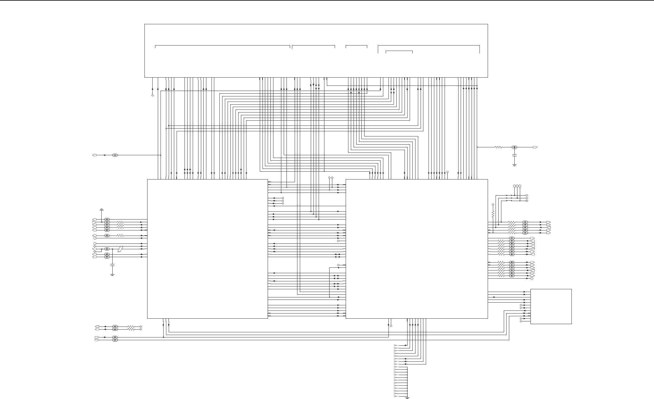
Controller R4 Schematic Diagrams 3-33
4.0 Controller R4 Schematic Diagrams
E2500
BLM21PG300SN1
0
R2504
0
R2500
R2501 0
0
R2502
3.6V_MAKO_SW1 1
1
2.9V_MAKO_V6
LO_BATTERY_DET
9V3_PA
5V
5V_SW
5V_SW
TX_DAC
RAW_B+
PA_BIAS
2.775V_ANA_V7
RX_FLTR_VCTRL
PA_TEMP
C2501
1500pF
TX_DAC
PA_TEMP
RAW_B+
RX_FLTR_VCTRL
PA_BIAS
LO_BATTERY_DET
2.775V_ANA_V7
2.9V_DIG_V6
3.6V_DIG_VSW1
5V
5V_SW
9V3_PA
( MAKO AUDIO_DIGITAL_USB/RS232 : SHEET 3)
MAKO_AUDIO_DC
( DC SUPPLY: SHEET 1)
( MAKO POWER MANAGEMENT : SHEET 2)
VBUS2
SPKR-
USB1_DM
USB1_DP
USB2_DM
USB2_DP
VBUS1
PUB_ADDRESS_1
PUB_ADDRESS_1_EN
PUB_ADDRESS_2
PUB_ADDRESS_2_EN
RTC_BATTERY
RX_AUDIO
SPKR+
MIC_GROUND
ONE_WIRE_1
ONE_WIRE_2
ON_OFF_MECH
GP5_4_EMERGENCY
GP5_5_IGNITION_SENSE
GPIO_0_PWR_ON
GPIO_3_PTT
GPIO_4_HOOK
HANDSET_AUDIO
INT_MIC+
9V3
EXT_MIC+
EXT_SWB+
SW_9V3
USB0_DAT
USB0_SE0
USB0_TXEN
USB1_DAT
USB1_SE0
USB1_TXEN
USB_INT
POR
PUB_ADDRESS_MIC_EN
RS232_RX
RS232_TX
SPI_CLK
SPI_MISO
SPI_MOSI
MAKO_INT
MAKO_OPT_GPIO0
MAKO_OPT_GPIO2
MAKO_OPT_GPIO3
MAKO_OPT_INT
MAKO_RX
MAKO_TX
MMP_GPIO1_INPUT
MMP_GPIO2_INPUT
OMAP_CORE_LDO
ONE_WIRE_UP
GATED_32KHZ_OMAP
I2C_CLK
I2C_DATA
LOW_LEVEL_MUTE
MAKO_AD_TRIGGER
MAKO_CE
MAKO_DCLK
MAKO_FSYNC
2.775V_DIG_V4
3.3V_DIG_V10
AUDIO_PA_ENA
EXT_MIC_ENA
1.875V_DIG_V2
SPI_MOSI_MAKO
SPI_MISO_MAKO
SPI_CLK_MAKO
2.775V_V4 1.875V_V2
(Active HIGH)
NC
NC
USB0_DAT
USB0_SE0
USB0_TXEN
USB1_DAT
USB1_SE0
USB1_TXEN
USB_INT
OPT_GPIO_2
POR
RS232_RX
RS232_TX
MAKO_GPIO_RX
MAKO_INT
MAKO_OPT_GPIO0
MAKO_OPT_GPIO2
MAKO_OPT_GPIO3
MAKO_OPT_INT
MAKO_RX
MAKO_TX
OMAP_CORE_LDO
ONE_WIRE_UP
OPT_GPIO_1
MAKO_AD_TRIGGER
MAKO_CE
MAKO_DCLK
MAKO_FSYNC
GPIO_5
I2C_CLK
I2C_DATA
EXT_MIC_ENA
GATED_32KHZ_OMAP
GPIO_18
GPIO_25
GPIO_27
3.3V_DIG_V10
ARMIO_12
ARMIO_2
AUDIO_PA_ENA
1.875V_DIG_V2
2.775V_DIG_V4
J2500-14
J2500-11
J2500-3
J2500-1
J2500-6
J2500-19
J2500-5
J2500-2
J2500-18
J2500-12
J2500-20
J2500-7
J2500-4
J2500-8
J2500-10
J2500-15
J2500-9
J2500-17
J2500-13
J2500-16
NC
JTAG_TDO
JTAG_TMS
JTAG_NEMU0
JTAG_NEMU1
JTAG_NTRST
JTAG_RTCK
JTAG_TCK
JTAG_TDI
32KHZ_CLK
16.8_MHZ_BUFF
PTT
RESET_OUT
SERIAL_CLK
SERIAL_DATA
MOBILE_DISPLAY_CMD
McBSP3_CLK
McBSP3_DR
McBSP3_DX
McBSP3_FSX
KEYPAD_COL0
KEYPAD_COL1
KEYPAD_COL2
KEYPAD_COL3
KEYPAD_ROW0
KEYPAD_ROW1
KEYPAD_ROW2
KEYPAD_ROW3
LED_CS
GP5_8
GPIO_26
GPIO_3
(SW1 / VOL_A)
GPIO_30
(SW2 / VOL_B)
GPIO_31
(SW4 / MONITOR)
GPIO_32
(SW8 / CHANNEL_ACT)
GPIO_33
(KEYPAD_ROW4 / GP5_6)
ARMIO_15
(BL_EN / GP5_7)
ARMIO_3
ARMIO_6
DIR_CTRL
DISPLAY_CS
NC
MICROCONTROLLER
(OMAP 1710: SHEET 1)
(MEMORY: SHEET 2)
PERIPHERALS
( 1 SHEET )
9V3
5V
REAR ACCESSORY
SSI_CLK
SSI_DATA_IN
SSI_DATA_OUT
SSI_FSYNC
SW_9V3
SYSTEM_SYNC
USB2_DM
USB2_DP
VBUS1
VBUS2
VOLUME_1
VOLUME_2
ON_OFF_SW
OPT_BRD_PTT
OPT_GPIO_1
OPT_GPIO_2
PROGM_IO_CS
PUB_ADDRESS_1
PUB_ADDRESS_1_EN
PUB_ADDRESS_2
PUB_ADDRESS_2_EN
RESET
RESET_OUT
RTC_BATTERY
RX_AUDIO
SERIAL_CLK
SERIAL_DATA
INT_SPKR-
KEYPAD_COL_0
KEYPAD_COL_1
KEYPAD_COL_2
KEYPAD_ROW_0
KEYPAD_ROW_1
KEYPAD_ROW_2
KEYPAD_ROW_3
LED_CS
MIC_GROUND
McBSP3_CLKX
McBSP3_DR
McBSP3_DX
McBSP3_FSX
ONE_WIRE_1
ONE_WIRE_2
EXT_SWB+
GP5_1_PTT
GP5_2_MONITOR
GP5_3_CHAN_ACTIVITY
GP5_4_EMERGENCY
GP5_5_IGNITION_SENSE
GP5_6_TxDc_BUS+
GP5_7_RxDc_BUS-
GP5_8_CTSs_RESET
GPIO_0_PWR_ON
GPIO_1_USB1_DP
GPIO_2_USB1_DM
GPIO_3_PTT
GPIO_4_HOOK
HANDSET_AUDIO
INT_MIC+
INT_SPKR+
1V8
3.3V
5V
9V3
ARMIO_6
DIR_CTRL
DISPLAY_CMD
DISPLAY_CS
EXT_MIC+
EXT_SPKR+
EXT_SPKR-
MMP
CONTROL HEAD
REPEATER INTERFACEOPTION BOARD INTERFACE
C2500
220pF
RESET_OUT
R2508
0
1SPI_MOSI_1
SPI_MISO_1
1
SPI_CLK_1
1
TX_DATA
TX_FSYNC
RX_CLK
RX_DATA
RX_FSYNC
SPI_CLK
SPI_MISO
SPI_MOSI
THK_CE
TX_CLK
LOCK_DETECT
GPIO_40
GPIO_60
GPS_BOOT_SELECT
GPS_ON_OFF_LS
GPS_RESET_LS
GPS_RX_LS
GPS_TX_LS
(RED_LED / RX_ATTN_1)
GPIO_15
ABACUS3_CE
ADAPT_SW
ANT_EN
DEEP_SLEEP
DMCS
R2529 10K
SPI_CLK_MAKO
SPI_MOSI_MAKO
SPI_MISO_MAKO
1.875V_V2
(Active LOW)
(Active LOW)
(6.0 MHz)
SPI_CLK
ABACUS3_CS
THK_CS
SPI_MOSI
SPI_MISO
(1.20 MHz)
(20.0 KHz)
(4.20 MHz)
(84.0 KHz)
RX_SSI_SYNCB
TX_SSI_FSYNC
TX_SSI_DATA
TX_SSI_CLK
RX_SSI_FSYNC
RX_SSI_DATA
RX_SSI_CLK
RF_ATTN_2
LOCK_DETECT
PC_ATTEN_ENA
DMCS
ADAPT_SW
ANT_ENABLE
PREDRIVE_SW
R2526 0
R2528 0
R2527 0
0
R2524
R2525 0
R2513 0
0
R2518
R2515 0
0
R2520
0
R2516
0
R2511
0
R2514
R2512 0
0
R2509
R2517 0
0
R2519
R2510 0
2.775V_V4
1.875V_V2
5V
5V_SW
GPS
( SHEET 1 )
GPS_TX_LS
VCONT
1.875V
16.8MHz
32KHZ_GPS
5V_ACTIVE_ANT
ANT_CURRENT
GPS_5V
GPS_BOOT_SEL
GPS_ON_OFF_LS
GPS_RESET_LS
GPS_RX_LS
16.8_MHZ_BUFF
32KHZ_GPS
ANT_CURRENT_DET
R2507 0
0
R2506
16.8_MHZ_BUFF
1.875V_V21.875V_DIG_V2
2.775V_V42.775V_DIG_V4
16.8_GPS
Controller – GPS Schematic Diagram
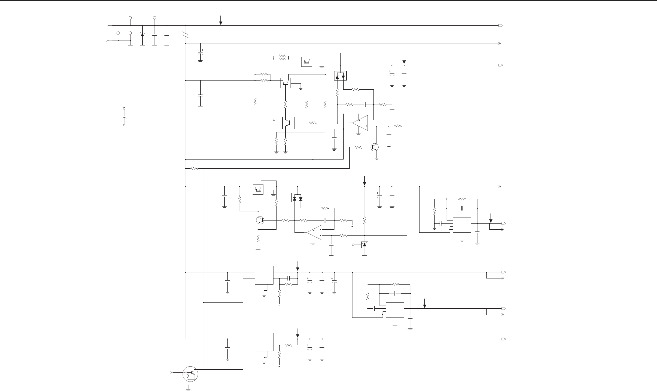
3-34 Controller R4 Schematic Diagrams
VR3000
1
J3000-1
VBAT
1
C3015
47pF
2
J3000-2
SP3000
1
VBAT_GROUND
1
SP3001
C3000
470pF
1
13.6V (NOMINAL)
E3000
C3002
10uF
C3019
470pF
DC connector during reflow.
This cap only use to support
10uF
C3018
NC
NC
10K
R3002
C3040
470pF
680
R3042
U3040
1
2
3
G1
0
R3052
330
R3044
Q3040
680
R3043
2K 1%
R3045
0
R3054 .01uF
C3041
2.74K 1%
R3046
D3040
.01uF
C3042
6
5
7
8
4
U3030-2
NC
100K
R3047
R3048
1K
VR3040
C3044
0.1uF33uF
C3043
9.3V
Q3030
R3030
10K
.01uF
C3032
100K
R3041
R3051
0
2
3
1
8
4
U3030-1
R3040
1%
2.74K
0.1uF
C3031
9.3V
C3021
0.1uF
33uF
C3020
2K
R3039
1%
D3030
R3053
0.01uF
C3030
0
R3057
R3037
330
R3035
10 R3036
10
150
R3050
Q3032
NU
R3038
150
NC
R3034
330
R3033
0.1
R3032
0.1
1
3
G1
U3005
0.1
R3055
2
3
G1
U3006
1
2
0.1
R3056
5V
C3011
1.0uF
9V3_CNTRL (TO MAKO)
5V
5V (TO GPS & PERIPHERAL BLOCKS)
R3007
1%
39.2K
2FB
5GND
6NP
4VCONT
3VIN
1
VOUT
U3004
TK11100CSC
100pFC3016
1%
13K
R3008
C3017
1000pF
9V3 (TO SYNTH, VCO, RX FE, PWR CNTRL,CONTROLHEAD)
9V3
EXT_SWB+ ( TO REAR ACCESSORY)
5V_SW (TO RX BACKEND, SYNTH,GPS ANTENNA)
5V_SW
5V
C3010
1.0uF
3VIN
1
VOUT
13K
1%
R3010
TK11100CSC
U3002
2FB
5
GND
6NP
4VCONT
C3009 0.1uF
39.2K
1%
R3009
C3008
1000pF
9.3V
C3007
0.1uF
33uF
NU
C3045
C3006
33uF
0.10uFC3046
R3003
1%
3.57K
1%
562
R3004
1
ADJ
GND1
3
GND2
6
ON_OFF
2
4VIN5
VOUT
U3001
LM2941
470pF
C3005
13.6V
C3013
22uF
R3006
220
5%
0.1uF
C3014
R3005
2.2K
5%
4VIN5
VOUT
ADJ 1
GND1
3
GND2
6
ON_OFF
2
OFF: 4.8V
ON: 0 V
C3012
470pF
LM2941
U3003
Q3041
47K
47K
MAKO_ON_OFF_CONTROL
UNSWB+ (TO AUDIO PA)
9V3_PA (TO PA DRIVER ONLY )
RAW_B+ (TO TX PA)
Controller DC Supply Schematic Diagram
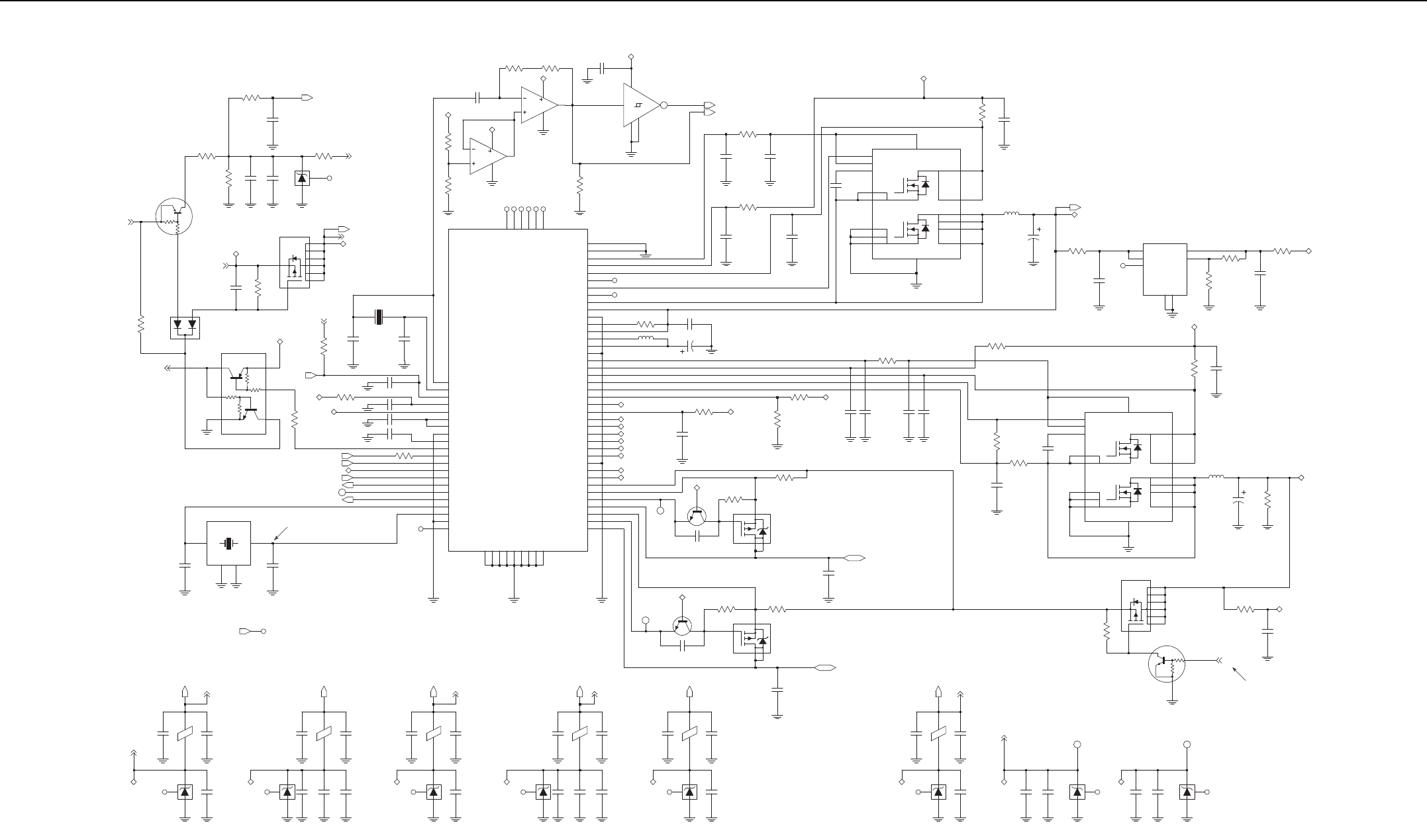
Controller R4 Schematic Diagrams 3-35
1
2
0
R3228
C3274
220pF
LO_BATTERY_DET
R3233
0
BATTERY_SENSE
D3200
47K
47K
R3248
10K
UNSWB+
MAKO_ON_OFF_CONTROL
100K
R3205
DTA144EKAF
Q3205
2.2uF
C3262
9V3_CNTRL
9V3_CNTRL
NC
VR3200
C3275
10.0uF
R3210
1%
14.3K C3261
220pF
43.2K
R3209
Q3201
NTHS5441T1
SW_9V3
SW_9V3
SW_9V3
5.6pF
C3204 C3205
5.6pF
32.768KHz
21
Y3201
XTAL
NU
10K
R3249
Q3206
EMD9FT2R
5V
9V3_CNTRL
2
5
6
3
1
4
RTC_BATTERY
( ON= 0V; OFF=9.3V)
33K
R3226
C3211 1000pF
0
R3206
C3210 2.2uF
2.2uFC3208
C3207 0.1uF
VSAVE
9V3_CNTRL
1
MAKO_GATED_32KHz
VSAVE
MAKO_INT
GP5_4_EMERGENCYGP5_4_EMERGENCY
GP5_5_IGNITION_SENSE
POR
ON_OFF_MECH
0
R3218
24.576MHz
Vpk-pk: 2.2V - 2.4V
Sine Wave
C3215
33pF
33pF
C3214
3
Y3200
CX-101F
GND1
2
GND2
4
HOT1 1
HOT2
NC
1.875V_DIG_V2
1.875V_DIG_V2
16.8_MHZ_BUFF
220pF
C3217
2.2uF
C3237
VR3201
0.10uF
C3218
E3201
NC
1.875V_V2_MAKO
1.875V_V2_MAKO
VR3202 C3239
NC
2.2uF
C3238
10uF 100pF
C3240
OMAP_CORE_LDO_1
0.10uF
C3220
E3202
C3219
220pF
OMAP_CORE_LDO
C3243
1.0uF
C3221
220pF
E3203
NC
VR3203
C3222
0.10uF
2.775V_DIG_V4
2.775V_DIG_V4
2.775V_V4_MAKO
NC
10uF
C3247 C3249
100pF
VR3204
E3205
220pF
C3225
C3248
1.0uF
C3226
0.10uF
2.9V_DIG_V6
2.9V_DIG_V6
2.9V_V6_MAKO
0.10uF
C3228
NC
VR3205
E3206
C3252
1.0uF
C3227
220pF
2.775V_ANA_V7
2.775V_V7_MAKO
OFF: 0.0V
ON: 4.75V to 5.25V (5.0V typical)
4.7uF
C3216
VBUS2 (TO MAP)
R3208
0.2
Q3204
2
3
1
4
SI8401DB
C3291
0.10uF
Q3210
VBUS2_CMD
1
100K
R3252
VSW5_CNTRL
ON: 4.75V to 5.25V (5.0V typical)
OFF: 0.0V
C3213
4.7uF
VBUS1 ( TO MMP )
Q3209
1
4
0.2
R3207
SI8401DB
Q3203
2
3
C3289
0.10uF
R3250
100K
1
VSW5_CNTRL
VBUS1_CMD
NC
C2
A13
A12
C1
B1
B3
M1
D4
D3
C5
G4
B4
D5
E4
D2
D1
F3
B2
F4
E2
F5
VSAVE
XIN
XOUT
XTAL32_IN
XTAL32_OUT
SW_TYPE
TCXO_IN
TCXO_SEL_16_24
REG_3V6
RESETX
HV_BG
IGN_X
INT_X
MECH_SW
BAT_3V6
BAT_7V5
BAT_RTC
BAT_TYPE
EMERG_PB
FET_ENX
GATED_32K_CLK
GND9
D9
GND1
P5
GND2
M7
GND3
J4
GND4
G5
GND5
K9
GND6
L4
GND7
D14
GND8
H5
V10_O
VBUS1
VBUS1_CMD
VBUS1_SENS
VBUS2
VBUS2_CMD
VBUS2_SENS
VBUS_SUPPLY
V04_O
V06_O
V07_O
V08_I
V08_O
V09_O
V10_GND
V10_I
SW5_VDDHV
SW5_VOUT
SW5_VSENSE
V02_O
V03_O
SW2_GND
SW2_LX
SW2_VCC
SW2_VCCS
SW2_VOUT
SW5_PHASE
SW5_SUMCOMP
SW5_VDD
SW1_GND
SW1_PHASE
SW1_SUMCOMP_DL
SW1_VDD
SW1_VDDHV
SW1_VOUT
SW1_VSEN_BST
SW1_VSEN_BUK
PGLDO2
PGLDO3
SW1_DH
U3200-1
PWR_MNGR_BLOCK
M6
H10
C14
E12
D12
C13
F11
B13
N5
P3
P6
K3
K4
L1
L9
J10
F13
F12
E14
N4
P4
L14
J14
J12
K14
J13
G11
E13
D13
H14
F14
G14
G13
G12
H12
J11
H11
C3
A2
H13
NC
NC
3.3V_V10_MAKO
3.6V_DIG_VSW1
3V_V9_MAKO
5V_V8_MAKO
SW_9V3
2.775V_V7_MAKO
2.9V_V6_MAKO
2.775V_V4_MAKO
1.875V_V2_MAKO
C3280
0.1uF
0
R3217
NU
R3216 0
10K
R3227
NU
2.2uF
C3234
OMAP_CORE_LDO_1
VSW5
10
R3239
C3277
1.0uF 2.2uF
C3266
0.1uF
C3281 OFF: 0.0Vpk
ON: 5Vpk; 230 KHZ PWM
C3273
10pF
NU
R3224
4.7K
5.1
R3243
0
R3225
NU
Q3207
NTHS5441T1
R3240
47K
DTC114YKAF
Q3208
2
10K
47K
3
1
OFF: 0V (DEFAULT)
ON: 3.3V (MAKO V10)
FROM MAKO USB_CONNECT (L6)
0.10uF
C3290
47K
R3253
VSW5_CNTRL
USB_CONNECT
MAKO_V9_3V
1
MAKO_V8_5V
1
C3254
2.2uF
NC NC
220pF
C3229
VR3206 VR3208
220pF
C3233 C3260
1.0uF
3V_V9_MAKO
5V_V8_MAKO
5V_V8_MAKO
0.10uF
C3232
NC
VR3207
E3208
1.0uF
C3257
220pF
C3231
3.3V_DIG_V10
3.3V_DIG_V10
3.3V_V10_MAKO
NC
NC
NC4 P14
M5
NC5
NC6 B14
NC1 A1
NC2 A14
NC3 P1
NC
NC
NC
NC
R3223
220K
LMC6035ITLX
U3202-2
1K
R3236
10pF
C3272
A2
A3
A1
B3
220K
R3222
VSAVE
VSAVE
B1
R3220
2MEG
R3219
2MEG
B1
B3 LMC6035ITLX
U3202-1
C2
C3
C1
VSAVE
NL17SZ14
3GND
2IN
1NC
4
OUT
5
VCC
C3282
4.7uF
1.875V_V2_MAKO
U3203
32KHZ_GPS
GATED_32KHZ_OMAP
1.0uF
R3238
10
C3201
2.2uF
C3276
0.1uF
C3278
R3241
5.1
C3283 0.10uF
C3206 22uF
L3201 22uH
0.1R3203
OFF: 0.0Vpk
ON: 5Vpk; 230 KHZ PWM
0.1uF
C3279
C3202
0.10uF
5SYNC_EN
IN
4
15 S1A
16 S1B
CBOOT
1
13
VDD
Q3200
4
0.1
R3200
C3200
22uF
7S2B
8S2C
10
D2B
11
D2C
12
D2D
3GND
6S2A
D1A
D1B
9
D2A
OFF: 0.0V
ON: 3.6V
C3203
68uF 0
R3245
22uH
L3200
3.6V_DIG_VSW1
3.6V_DIG_VSW1
C3269
1.0uF
Change R3246 to 0613952N12 (13K) for OMAP1610
LP8340
U3201
R3246
1%
6.81K
1%
51.1K
R3247
0
R3215
C3270
1.0uF
OMAP_CORE_LDO_1
NC
GND1
7GND2
3NC
VIN1
1
VIN2
6VOUT 5
4
ADJ
2
0.1
R3204
Q3202
SI4724CY
22uF
C3265
SW_9V3
OFF: 0.0V
ON: 5.2V - 5.3V
VSW5
L3202
22uH
10K
R3237
C3212
68uF
0.10uF
C3209
16 S1B
6S2A
7S2B
8S2C
5SYNC_EN
VDD 13
2
D1B
9
D2A
10
D2B
11
D2C
12
D2D
GND
3
IN
4
15 S1A
CBOOT 1
14 D1A
SW_9V3
Controller DC Distribution Schematic Diagram
3-36 Controller R4 Schematic Diagrams
NC
3.3V
1V8
1V8 1V8
5V
5V
GPIO_0_PWR_ON
GPIO_3_PTT
GPIO_2_USB1_DM
GPIO_1_USB1_DP
ONE_WIRE_1
MIC_GROUND
GPIO_4_HOOK
VBUS1
INT_MIC+
ON_OFF_SW
9V3
RESET
DISPLAY_CS
SERIAL_DATA
SERIAL_CLK
LED_CS
DISPLAY_CMD
HANDSET_AUDIO
INT_SPKR-
KEYPAD_ROW_1
KEYPAD_ROW_3
KEYPAD_COL_1
VOLUME_1
KEYPAD_ROW_0
KEYPAD_ROW_2
KEYPAD_COL_0
KEYPAD_COL_2
VOLUME_2
INT_SPKR+
MOBILE REPEATER: NOT_USED
MOBILE SUBSCRIBER: 33 OHM
E4000
RESET
R4005
R4061
R4071
R4001
R4065
R4068
R4070
R4003
R4063
R4002
R4000
R4069
R4067
R4064
R4006
R4066
R4004
33
33
0
33
33
33
33
33
33
33
33
33
33
33
33
33
51
51
470
R4010
R4009
BLM21PG221SN1E4001
BK1005HM471
E4004
ARMIO_6
RESET
PROGM_IO_CS
SERIAL_DATA
SERIAL_DATA
SERIAL_CLK
SERIAL_CLK
NU
C4071
220pF
NU
C4074
220pF
220pF
NU
C4072
5
9
11
13
1
3
NC
6
Y_4 8
Y_5 10
Y_6 12
A_4
A_5
A_6
GND
7VCC 14
Y_1 2
Y_2 4
Y_3
U4001
SN74LVC07A
A_1
A_2
A_3
220pF
C4085
10K
R4079 C4084
0.10uF
1V8 1V8
MOBILE REPEATER: 0 OHM
MOBILE SUBSCRIBER: NOT_USED
R4086
0NU
WD_RESET
WD_RESET
5V
1.2K
R4103
1.2K
R4023R4100
1.2K
R4101
1.2K
3
4
5
6
7
9
15
1
2
NC
SER
SRCLK
SRCLR
VCC
16
QD
QE
QF
QG
QH1
QH2
RCLK
RCLR
GND
QA
QB
QC
0.10uF
C4073
5V
14
11
10
12
13
U4000
SN74AHC594
8
PUB_ADDRESS_1_EN
PUB_ADDRESS_2_EN
1V81V81V81V81V8 1V8
10KR4054
10KR4055
R4031 10K
R4033 NU
R4032 10K
R4030 NU
R4040
4.7K
47K
47K
Q4000
DTC144EKAF
5V
VBUS2
1
USB2_DP
1
BLM21PG221SN1
E4002
USB2_DM
1
10K
R4035
USB2_DM
USB2_DP
VBUS2
5V
4
D4000
1
32
TX_AUDIO
GP5_6
GP5_3_(CHAN_ACT)
VIP_1_(EXT ALARM)
GP5_1_(EXT PTT)
MAP_ID_2
EXT_SPKR-
AUX_AUDIO_OUT_2
GP5_2_(MONITOR)
USB_DM_MAP
IGN_SENSE
MAP_ID_1
AUDIO GROUND
EMERG SW
POWER GROUND
GROUND
EXT_SPKR+
GP5_7
USB_DP_MAP
RX_AUDIO
EXT_SWB+
GP5_8
AUX_AUDIO_OUT_1
VBUS_MAP
GROUND
USB / MAP_ID_GROUND
9
18 22
PCB
21210 14
2513
J4000 REAR VIEW
2317
16 24
7
264
13 19
20
5
86
15 2111
ACCESSORY INTERFACE (26-PIN)
VR4000
MMBZ20V
220pF
C4040
EXT_PTT
1
NC
VR4005
220pF
C4041
47K
47K
47K
10K
DTC144EKAF
Q4001
DTC114YKAF
Q4002
2
3
1
R4041
4.7K
5V
4.7K
47K
47K
47K
10K
R4042
Q4004
DTC114YKAF
2
3
1
DTC144EKAF
Q4003
5V
220pF
C4042
Q4015
DTC144EKAF
4.7K
47K
47K
47K
47K
47K
47K
R4098
DTC144EKAF
Q4005
5V
R4043
4.7K
5V
MOBILE REPEATER: 0 OHM
MOBILE SUBSCRIBER: NOT_USED
Q4006
DTC144EKAF
NU
R4044
4.7K
5V
WD_RESET
MMBZ20V
VR4001
EMERGENCY 1
C4043
220pF
R4051
390K
C4044
220pF
MMBZ20V
VR4002
1IGNITION_SENSE
220pF
C4045
4.7K
47K
47K
10K
47K
R4045
DTC114YKAF
Q4008
2
3
1
Q4007
DTC144EKAF
5V
C4046
220pF
R4046
4.7K
47K
47K
47K
10K
Q4009
DTC144EKAF
Q4010
2
3
1
DTC114YKAF
5V
10K
R4088
Q4014
1
3
2
BCW65A
R4089
47K
4.7K
47K
47K
R4047
DTC144EKAF
Q4011
5V
VR4003
MMBZ20V 220pF
C4047
BCW68GLT1G
Q4013
R4050
10K
Q4012
DTC114YKAF
2
3
1
R4049
2.7K
10K
47K
1.5K
R4048
EXT_SWB+
E4005
BK1005HM471
NC
NC
MMBZ20V
VR4004
220pF
C4070
VR4006
C4048
220pF
1
APM_1_WIRE
220pF
C4067
220pF
C4068 C4069
220pF
EXT_SPKR+
EXT_SPKR-
EXT_SWB+
EXT_SWB+
ONE_WIRE_2
RX_AUDIO
PUB_ADDRESS_1
EXT_MIC+
PUB_ADDRESS_2
220pF
C4063
NU
C4075
220pF
C4065
220pF220pF
C4064 C4066
220pF
GP5_1_PTT
GP5_4_EMERGENCY
GP5_7_RxDc_BUS-
GP5_8_CTSs_Reset
GP5_5_IGNITION_SENSE
GP5_3_CHAN_ACTIVITY
GP5_6_TxDc_BUS+
GP5_2_MONITOR
MOBILE REPEATER: 0 OHM
MOBILE SUBSCRIBER: NOT_USED
0NU
R4090 J4001_9
RTC_BATTERY
4
D4001
1
32
R4034
10K
5V
VR4008
2
5
NUNU
VR4007
2
5
A1
A2
K1
K2
K3
K4
K1
K2
K3
K4
A1
A2
NC NC
R4012 0
1
3
4
6
1
3
4
6
C4014
220pF
C4035
330pF330pF
C4034 0
R4011
NU
220pF
C4076
220pF
C4016 C4029 C4032
220pF 220pF
C4027
220pF220pF
C4022
220pF
C4028
220pF
NU
C4019
220pF
C4021
220pF
C4031
220pF
C4026
220pF
C4018 C4020
NU
220pF 220pF
C4033C4025
220pF
C4024
220pF
C4017
220pF
C4023
220pF220pF
C4015
220pF
C4030
PCB
J4001 FRONT VIEW
2629 232830 27 24 22 2125 20 15 10121416 13 1118 1719 56897 3412
5
25
19
20
6
14
22
4
28
13
16
1
8
29
12
17
15
10
24
9
18
26
11
3
7
30
27
2
23
21
J4001-5
J4001-25
J4001-19
J4001-20
J4001-6
J4001-14
J4001-22
J4001-4
J4001-28
J4001-16
J4001-13
J4001-1
J4001-8
J4001-12
J4001-29
J4001-17
J4001-15
J4001-10
J4001-24
J4001-9
J4001-18
J4001-26
J4001-11
J4001-7
J4001-3
J4001-30
J4001-27
J4001-2
J4001-23
J4001-21
CONTROL HEAD INTERFACE
E4003
1
VBUS1 USB1_DP
1
1
USB1_DMMMP_1_WIRE
1
J4001_9
NU
C4002
220pF 220pF
NU
C4005
NU
C4000
220pF 220pF
C4006C4001
NU
220pF 220pF
C4004
NU
C4003
NU
220pF
C4013
220pF
J4000-17 17
4
2
1
3
J4000-16 16
J4000-20 20
J4000-19 19
13
J4000-14 14
J4000-13
J4000-2
J4000-10 10
J4000-18 18
J4000-1
J4000-21 21
12J4000-12
J4000-25 25
6
5
9
J4000-26 26
J4000-6
J4000-7
8
7
J4000-23 23
J4000-8
J4000-24 24
J4000-9
J4000-3
J4000-11 11
J4000-22 22
J4000-5
J4000-15 15
J4000-4
Controller Peripheral Schematic Diagram (sheet 1 of 2)

Controller R4 Schematic Diagrams 3-37
1V8
1V8
WD_RESET
R4093
R4095
0
0
R4097
0
R4099
0
McBSP3_CLKX
DIR_CTRL
McBSP3_DX
McBSP3_FSX
B
C2
DIR
B2
GND
VCCA A1
VCCB A2
A
0.10uF
C4086
1V8
C1
U4004
SN74AVC1T45
B1
10K
R4105
1
TP4000
1V8
VCCA
VCCB
C1
A
C2 B
B2 DIR
GND
A1
A2
C4087
0.10uF
1V8
SN74AVC1T45
U4005
B1
0.10uF
C4088
B
DIR
GND
VCCA A1
VCCB A2
A
1V8
C2
B2
B1
U4006
SN74AVC1T45
C1
VCCB
C4089
0.10uF
C1
A
C2 B
B2 DIR
B1 GND
VCCA
SN74AVC1T45
U4007
1V8
A2
A1
VCCA
VCCB
0.10uF
C4090
U4008
SN74AVC1T45
AC1
B
C2
DIR
B2
GND
B1
1V8
A1
A2
0
R4094
SYSTEM_SYNC
SYSTEM_SYNC
R4096
0
McBSP3_DR
R4106
10K
REPEATER CONNECTOR
J4002-99
J4002-11
2
J4002-33
7
J4002-88
J4002-2
J4002-66
J4002-7
J4002-44
J4002-55
J4002-1010
J4002-1111
NU
220pF
C4010
NU
220pF
C4011
NU
220pF220pF
C4007 C4012
NU
J4002 FRONT VIEW
PCB
112134 10567 8 9
SSI_DATA_OUT
SSI_FSYNC
SSI_CLK
SSI_DATA_IN
B1 GND
A1
VCCA A2
VCCB
SN74AVC1T45
U4009
C1
A
C2 B
B2 DIR
C4091
0.10uF
1V8
0
R4074
AB
C2
DIR
B2
GND
VCCA
VCCB
U4010
SN74AVC1T45
C1
B1
0.10uF
C4092
A1
A2
1V8
0
R4076
0
R4078
R4085 0
0
R4083
R4082 0
0
R4081
OPT_BRD_PTT
OPT_GPIO_1
OPT_GPIO_2
RESET_OUT
E4006
OPT_SSI_SYNC
1
SW_9V3
SYSTEM_SYNC
220pF
NU
C4059
NU
220pF
C4055
NU
220pF
C4053
220pF
C4051
NU
C4049
220pF
NU
51pF
C4093
NU
C4094
NU
33pF
14
12
J4003-13
13
J4003-14
J4003-11
11
J4003-12
10
J4003-9
J4003-10
J4003-7
J4003-8
J4003-5
J4003-6
J4003-4
J4003-2
J4003-3
J4003-1
9
7
8
5
6
3
4
1
2
220pF
C4058
NU
C4061
NU
220pF
NU
C4060
220pF
C4062
NU
220pF
OPTION BOARD INTERFACE
131012345678 9 12 1411
PCB
J4003 FRONT VIEW
OPERATION
HIGH
LOW B ---->A
DIR
B <----A
0
R4080
Controller Peripheral Schematic Diagram (sheet 2 of 2)
3-38 Controller R4 Schematic Diagrams
Place for
(1.4V for OMAP1710 & 1.55V for OMAP1610)
OMAP1710
(0.87mA/MHz for OMAP1710 & 1.06mA/MHz for OMAP1610)
R1020
0
R1021
01.875V
DVDD2
OMAP_CORE
2.775V_DIG_V4 2.775V_DIG_V4
1.875V_DIG_V2
1.875V_DIG_V2
OMAP_CORE_LDO
3.3V_DIG_V10
MAKO SSI
TP_MAKO_DCLK
1
TP_MAKO_TX
1
TP_MAKO_RX
1
TP_MAKO_FSYNC
1
MAKO_FSYNC
MAKO_DCLK
MAKO_TX
MAKO_RX
(FROM MAKO)
OPTION SELECT
(MOBILE ONLY)
MAKO_OPT_GPIO2
MAKO_OPT_GPIO0
MAKO_OPT_GPIO3
EXT_MIC_ENA
(FROM MAKO)
(RESET CIRCUIT PROVIDED BY MAKO)
(FROM MAKO)
TP_POR
1
R1048
0
GATED_32KHZ_OMAP
POR
MAKO_GPIO_RX
GPIO_5
MAKO_INT
32KHZ_CLK
16.8MHz Squarer
C1033
0.10uF
47K
R1026
4
Y2
U1006
1A1
3A2
2
GND
5VCC
6
Y1
NL27WZU04
1.875V
( BUFFERRED 16.8 FROM TOMAHAWK)
C1032
.01uF
16.8_MHZ_BUFF
1.0Vpkpk
10MEG
R1002
18pF
C1019
2GND
4
GND1
3
OUT
1
12MHz
CX-91F
Y1000
C101 8
18pF
10K
R1001
0
R1044
OMAP_CORE
ABACUS3 SSI
RS232
TOMAHAWK SSI
R1041 1K
0
R1070
GPIO_40
RS232_TX
RS232_RX
MAKO_AD_TRIGGER
RX_CLK
TX_CLK
RX_DATA
TX_DATA
RX_FSYNC
TX_FSYNC
OPT_GPIO_1
OPT_GPIO_2
GP5_8
(MOBILE ONLY)
DNP
BOOT
FROM
CS
3
BOOT
FROM
CS
0
10K
R1027
NU
0
R1028
1.875V
(Used as KEYPAD_
ROW4 for PORTABLE,
GP5_6 for MOBILE)
KEYPAD ROW
R1045 10K
1.875V
KEYPAD_ROW0
KEYPAD_ROW1
KEYPAD_ROW2
KEYPAD_ROW3
ARMIO_15
R1054
4.7K C1030
18pF
NU
4.7K
R1067
NU
10K
R1066
1.875V
JTAG
JTAG_NTRST
JTAG_NEMU0
JTAG_NEMU1
JTAG_RTCK
JTAG_TCK
JTAG_TDI
JTAG_TDO
JTAG_TMS
47K
R1071
OMAP1710
LED & Display CS: Active Low
MCBSP3
CLK rate: 1 MHz
Date rate: 20 of 8 bits packet per chip select
GPS
SERIAL FLASH SPI
SERIAL_DATA
SERIAL_CLK
MCBSP3_FSX
GPS_BOOT_SELECT
MCBSP3_DR
LED_CS
DISPLAY_CS
MCBSP3_CLK
MCBSP3_DX
GPS_ON_OFF_LS
GPS_RX_LS
GPS_TX_LS
GPS_RESET_LS
MOBILE ONY
(Used as BL_EN for PORTABLE, GP5_7 for MOBILE)
(GPIO_3 for PORTABLE-Green LED)
(Used as GREEN_LED for PORTABLE, PA_ENABLE for MOBILE)
PLACED FOR
(SPI.CS3 for MOBILE Shift Register Chip Select)
(Used as RED_LED for PORTABLE, RX_ATTN_1 for MOBILE)
R1047
0
10KR1025
R1017 10K
ARMIO_6
ARMIO_2
GPIO_3
ONE_WIRE_UP
DIR_CTRL
1.875V
1.875V
GPIO_60
GPIO_15
PTT
ARMIO_3
(MOBILE ONLY)
(MOBILE ONLY)
AUDIO_PA_ENA
ARMIO_12
DNP
U1008
DELETED REF
LARGEST REF
GP DEVICE CONFIG
Y1001R1050C1039
PLACE FOR GP
DEVICE FAST BOOT
NU
R1035
0
10K
R1034
1.875V
DECOUPLING CAPACITORS
0.10uF
C1031
2.2uF
C1037
C1035
2.2uF
C1010
0.10uF
100pF
C1011
C1005
0.10uF 0.10uF
C1006
0.10uF
C1013
100pF
C1003
0.10uF
C1009
C1001
0.10uF 0.10uF
C1002
0.10uF
C1014C1007
100pF
100pF
C1000
C1004
100pF
C1034
1.0uF
1.0uF
C1036
100pF
C1008
C1015
0.10uF
OMAP_CORE
1.875V
(Used as SW4 for PORTABLE, Monitor for MOBILE)
(Used as SW2 for PORTABLE, Volume B for MOBILE)
(Used as SW1 for PORTABLE, Volume A for MOBILE)
FREQ SWITCH
(Used as SW8 for PORTABLE, Channel Activity for MOBILE)
DMCS
DEEP_SLEEP
ADAPT_SRF CONTROLS
LOCK_DETECT
ANT_EN
GPIO_30
GPIO_31
GPIO_32
GPIO_33
Place for
OMAP1710
Place for
OMAP1610
C1017
1.0uF
R1019
5.1
LDO_FILTER
OMAP_CORE
SDRAM
SDRAM_CTL(6:0)
SDRAM_DATA(15:0)
SDRAM_CLK
SDRAM_CLK_EN
SDRAM_CS
SDRAM_ADD(12:0)
KEYPAD COLUMN
SPI
(Used as KEYPAD_COL4 for NEO and Public Add Mic for MORPHEUS)
PORTABLE DISPLAY
1TX_RAMP
MAKO_CE
ABACUS3_CE
THK_CE
SPI_CLK
SPI_MISO
SPI_MOSI
MOBILE_DISPLAY_CMD
KEYPAD_COL0
KEYPAD_COL1
KEYPAD_COL2
KEYPAD_COL3
GPIO_27
DISPLAY_CMD
DISPLAY_CE
DISPLAY_DATA0
DISPLAY_DATA1
DISPLAY_DATA2
DISPLAY_DATA3
DISPLAY_DATA4
DISPLAY_DATA5
DISPLAY_DATA6
DISPLAY_DATA7
(MOBILE ONLY)
10K
R1036
1.875V
RESET_OUT
R1060
10
0.10uF
C1044C1016
0.10uF
0.10uF
C1012
R1000
10
CVDDA
OMAP_CORE
DVDD2
VDD_DLL
OMAP_CORE
IN
FLASH
NU
0
R1046
FLASH_WAIT
FLASH_CTL(5:0)
EMIFS_ADD(23:1)
EMIFS_DATA(15:0)
MAKO_OPT_INT
FLASH_CLK
R1006
10K
1.875V
7
2
6
5
9
10
11
13
12
4
3
0
8
1
14
15
0
11
1
10
7
2
8
13
14
15
4
5
3
6
12
9
2
4
4
5
7
3
2
10
5
3
1
11
0
9
0
12
6
8
6
1
I2C
I2C_CLK
I2C_DATA
USB#2
OPTION BOARD
USB2_SE0
GPIO_18
USB2_DAT
USB2_SUSPEND
GPIO_26
GPIO_25
USB2_RCV
( INTERFACE WITH MAKO)
USB#0
USB#0 RESERVED FOR MOBILE
USB#1
USB1_SE0
USB0_SE0
USB0_DAT
USB0_TXEN
USB1_TXEN
USB1_DAT
USB_INT
OMAP1610
Place for
OMAP1710
Place for
R1005 4.7K
5
3
0
4
2
1
V17
Y18
R14
V14
Y5
R9
D4
W18
Y19
C14
R12
J20
U20
Y2
W3
V13
AA13
W6
W7
V15
W14
AA9
V9
H20
H15
P10
AA5
AA15
Y14
H14
E20
E19
G18
F19
Y1
P3
P4
P7
R2
R3
R4
T2
V2
N2
T3
P8
U1
U3
T4
V3
N7
P2
N4
H12
V18
G8
V5
P14
Y10
R10
G20
G21
Y6
D9
Y15
W15
P13
V7
W19
FDATA_4
FDATA_5
FDATA_6
FDATA_7
FDATA_8
FDATA_9
FDATA_10
FDATA_11
FDATA_12
FDATA_13
FDATA_14
FDATA_15
FDATA_2
FDATA_3
FDATA_0
FDATA_1
OSC32K_OUT
OSC1_IN
OSC1_OUT
OSC32K_IN
MCBSP2_FSX
MCSI1_DIN
MCSI1_DOUT
MCSI2_DIN
MCSI2_SYNC
MCBSP2_DR
MCBSP2_DX
MCBSP2_FSR
LOW_STATE_1
LOW_STATE_2
FRDY
CLK_M
CLK_MCSI1
CLK_M_REQ
CLKX_MCBSP2
CLK_B
CLK_B_REQ
CLKR_MCBSP2
TMS
TRST
UART1_CTS
UART1_RX
UART2_CTS
UART2_RX
SDDQS_H
SDDQS_L
TCK
TDI
PWRON_RESET
MPU_BOOT
MPU_RST
MCBSP1_DR
MCBSP1_FSX
KBR_3
KBR_4
KBR_0
KBR_1
KBR_2
F_CS1U
F_CS2U
EN_SDCKE
CONF
CS_SDRAM
CLK_MCSI2
CLKX_MCBSP1
CLKX_SD
CLK32K_IN
CLKS_MCBSP1
BFAIL
D7
D5
C7
C4
D8
C10
D14
C6
D11
C13
C11
D13
D12
C12
C5
D6
Y8
W8
N20
N18
N19
N21
M20
N3
J18
L15
M19
L18
L19
K14
K15
K19
K18
J14
J19
T20
R11
V10
W10
W11
U19
N15
V8
T19
AA17
P19
M15
M14
P18
P20
R18
R19
V16
W17
R13
SDATA_2
SDATA_3
SDATA_4
SDATA_5
SDATA_6
SDATA_7
SDATA_8
SDATA_9
SDATA_0
SDATA_1
SDATA_10
SDATA_11
SDATA_12
SDATA_13
SDATA_14
SDATA_15
GPIO_11
GPIO_12
GPIO_13
GPIO_14
GPIO_15
CLK_F
CAM_D_6
CAM_D_7
CAM_HS
CAM_RSTZ
CAM_VS
CAM_D_0
CAM_D_1
CAM_D_2
CAM_D_3
CAM_D_4
CAM_D_5
MPUIO_4
MPUIO_5
MPUIO_1
MPUIO_2
MPUIO_3
MCSI1_SYNC
GPIO_4
GPIO_6
GPIO_7
GPIO_8
GPIO_9
GPIO_1
GPIO_2
GPIO_3
GPIO_0
EMU0
EMU1
CLK32K_OUT
B4
C8
D10
H7
G10
B9
G12
G11
G9
B12
B3
C3
A2
B2
B8
H10
H9
H11
B6
A1
B19
C18
D17
D16
B18
B17
G13
A17
C16
D15
C19
G14
H13
A20
B15
C20
D18
B21
C17
H8
C15
N14
P15
U18
W21
AA19
L14
M18
H18
D20
D19
E18
C21
G19
T18
F18
V19
H19
Z_STATE_2
Z_STATE_3
UWIRE_SDI
UWIRE_SDO
TDO
UART3_RX
SDRAM_CAS
SDRAM_DQML
SDRAM_DQMU
SDRAM_RAS
SADD_5
SADD_6
SADD_7
SADD_8
SADD_9
SBANK_0
SBANK_1
SADD_1
SADD_10
SADD_11
SADD_12
SADD_13
SADD_2
SADD_3
SADD_4
SADD_0
MMC_DAT0
MMC_DAT1
MMC_DAT2
MMC_DAT3
LOW_STATE_5
MCBSP1_DX
LCD_PIXEL_5
LCD_PIXEL_6
LCD_PIXEL_7
LCD_PIXEL_8
LCD_PIXEL_9
LCD_VSYNC
LCD_PIXEL_11
LCD_PIXEL_12
LCD_PIXEL_13
LCD_PIXEL_14
LCD_PIXEL_15
LCD_PIXEL_2
LCD_PIXEL_3
LCD_PIXEL_4
LCD_AC
LCD_HSYNC
LCD_PIXEL_0
LCD_PIXEL_1
LCD_PIXEL_10
KBC_0
KBC_1
KBC_2
KBC_3
KBC_4
KBC_5
I2C_SCL
EN_WE_SDRAM
CLK_S_UWIRE
CLK_P_LCD
CLK_EX_CAM
U1000
OMAP1710
OMAP_CORE
CVDDA
DVDD2
LDO_FILTER
1.875V
VDD_DLL
Z_STATE_1
USB0_DAT
USB0_SE0
RESET_MODE
RST_OUT
RTCK
RTC_ON_NOFF
RTC_WAKE_INT
MMC_CMD
MCSI2_DOUT
LOW_STATE_4
LOW_STATE_3
GPIO_62
I2C_SDA
F_CS1
F_CS2
F_CS3
F_RP
F_WP
FADD_5
FADD_6
FADD_7
FADD_8
FADD_9
FADV
FADD_2
FADD_20
FADD_21
FADD_22
FADD_23
FADD_24
FADD_25
FADD_3
FADD_4
FADD_13
FADD_14
FADD_15
FADD_16
FADD_17
FADD_18
FADD_19
EN_F_OE
EN_F_WE
EN_USB_PUEN
FADD_1
FADD_10
FADD_11
FADD_12
EN_F_BE_0
EN_F_BE_1
CLK_SD
CLK_L_CAM
CLK_MMC
CLK_B_UART2
0
R1014
1
TP1000
W16
R8
P9
P12
AA20
Y17
Y12
W13
W9
P11
W5
V6
M7
M4
N8
W1
V4
M3
L4
U4
W2
W4
L3
M8
V11
Y4
V20
E4
D2
F4
E3
J7
F3
F2
L8
K4
K3
L7
E1
C1
G2
K8
H4
H3
K7
J2
J4
J3
D3
J8
G4
G3
C9
J15
15
12
5
14
10
11
3
1
8
18
17
6
16
21
22
2
9
23
19
7
13
20
4
VSS_3
VSS_4
VSS_5
VSS_6
VSS_7
VSS_8
VSS_9
VSS_13
VSS_14
VSS_15
VSS_16
VSS_17
VSS_18
VSS_19
VSS_2
VSS_1
VSS_10
VSS_11
VSS_12
RESERVED
DVDD5_1
DVDD5_2
DVDD5_3
DVDDRTC
DVDD2_1
DVDD2_2
DVDD2_3
DVDD4_1
DVDD4_2
DVDD4_3
DVDD4_4
DVDD1_1
DVDD1_2
DVDD1_3
DVDD1_4
DVDD1_5
CVDD_3
CVDD_4
CVDD_DLL
CVDD_RTC
CVDD3_1
CVDD3_2
CVDD3_3
CVDD3_4
CVDD4
CVDDA
CVDD_1
CVDD_2
CVDD1
CVDD2
CVDD2_1
CVDD2_2
A13
B16
A21
F20
K20
R21
W20
Y3
AA1
U2
N1
K2
G1
B1
B7
B5
AA21
Y13
AA7
E5
L1 NC
H2
C2
V12
L21
AA2
Y7
AA11
A5
A7
B10
B14
R1
M2
A11
W12
A19
E21
U21
Y16
B20
J21
R20
J1
Y21
A15
Y20
Y9
AA3
A9
A3
E2
B13
Controller Microprocessor Schematic Diagram

Controller R4 Schematic Diagrams 3-39
FLASH SDRAM
1.875V_DIG_V21.875V_DIG_V2
10K
4
R2000
0
1
TP_FLASH_CLK
3
5
2
R2012
10K
FLASH_CTL(5:0)
FLASH_CLK
FLASH_WAIT
1.875V_DIG_V2
VDD1
VDD2
VDDQ1
VDDQ2
VPP
A4
G4
E1
G6
A5
8MByte
0104024J27 (Pre-Flashed Part)
M58WR064FB
U2000
D3
D6
D7
B5
E7
F8
C4
C5
C7
A2
B2
B4
C6
C8
B3
C3
B8
A8
B7
A7
A1
B1
C1
D2
D1
D4
B6
A6
E8
D8
C2
13
15
9
10
11
4
5
3
23
16
17
18
19
12
14
6
7
8
1
2
20
21
22
F1
VSS2
VSSQ1
G2
VSSQ2
G8
VSS1
A3
ST 4Mx16
WAIT
WP
NC
RP
D6
D7
D8
D9
EN_E
EN_G
EN_L
EN_W
D12
D13
D14
D15
D2
D3
D4
D5
A7
A8
A9
CLK_K
D0
D1
D10
D11
A19
A2
A20
A21
A3
A4
A5
A6
A11
A12
A13
A14
A15
A16
A17
A18
A0
A1
A10
0
1
2
8
12
13
14
6
7
15
5
9
10
11
3
4
E3
G1
G7
F6
D5
F3
F2
E2
E5
G5
E4
G3
F7
E6
F5
F4
SDRAM_DATA(15:0)
SDRAM_ADD(12:0)
D7 VSSQ4
A1
VSS1
E3
VSS2
J1
VSS3
A3
VSSQ1
B7 VSSQ2
C3 VSSQ3
9
10
11
3
4
5
12
6
7
8
0
1
2
F9
F8
F1
E8
G7
G8
F7
F3
F2
G9
J8
J7
J3
J2
H3
H2
H1
G3
H7
H8
H9
G2
MICRON 8Mx16
WE
VDDQ3
VDDQ4
RAS
UDQM
VDD1
VDD2
VDD3
VDDQ1
VDDQ2
LDQM
BA0
BA1
CAS
CKE
CLK
CS
A2
A3
A4
A5
A6
A7
A8
A9
A0
A1
A10
A11
16MByte
C7
D3
A9
E7
J9
A7
B3
U2001
NC2
DQ4
DQ5
DQ6
DQ7
DQ8
DQ9
NC1
DQ10
DQ11
DQ12
DQ13
DQ14
DQ15
DQ2
DQ3
DQ0
DQ1
NC
G1
C8
D9
D8
E9
E1
D2
E2
D1
C2
C1
B2
B1
A2
B8
C9
A8
B9
0
1
3
5
13
14
15
6
7
8
9
4
2
11
12
10
C2006
0.10uF
C2004
100pF.01uF
C2005
0.10uF
C2007
0
R2011
1.875V_DIG_V2
TP_SDRAM_BA1
R2005 R2006 R2009
10K
R2007
10K10K10K
TP_SDRAM_BA0
R2008
10K
1.875V_DIG_V2
Bootstrap Mode = 48 MHz
Normal Mode = 72 MHz
TP_SDRAM_CS
TP_SDRAM_CLK
R2010
10K
10K
R2013
SDRAM_CTL(6:0)
SDRAM_CLK_EN
SDRAM_CLK
SDRAM_CS
4
1
6
0
5
3
2
1.875V_DIG_V2
100pF
C2000
0.10uF
C2003
.01uF 0.10uF
C2002C2001
R2004
0
1.875V_DIG_V2
EMIFS_DATA(15:0)
EMIFS_ADD(23:1)
Controller Memories Schematic Diagram
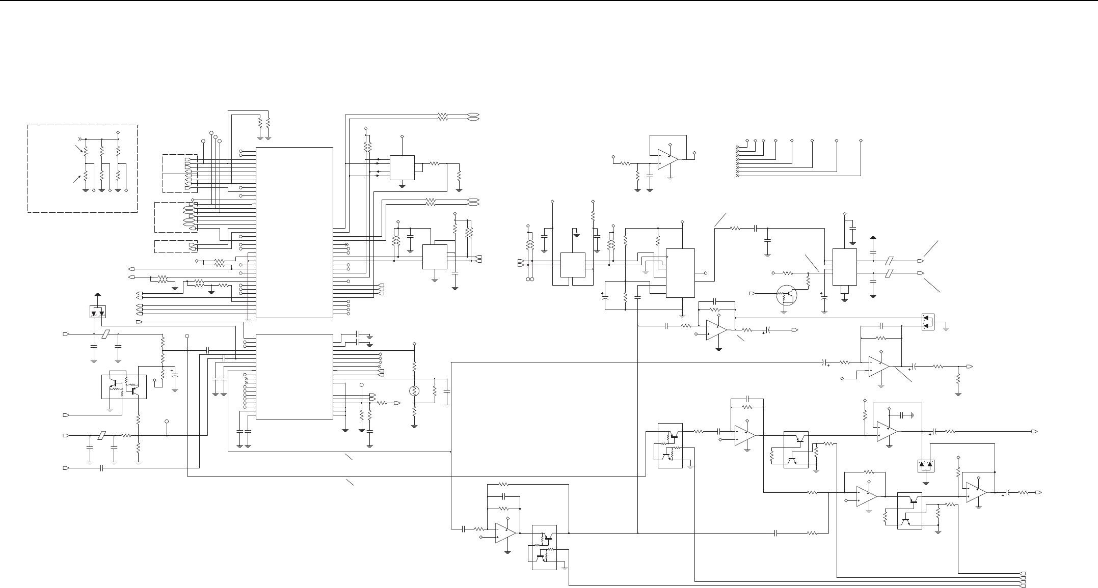
3-40 Controller R4 Schematic Diagrams
1
MOBILE REPEATER: NOT_USED
MOBILE REPEATER: 33K
MOBILE SUBSCRIBER: NOT_USED
MOBILE SUSCRIBER: 0 OHM
HW_ID
NU
33K
R3504
0
R3509
NU
R3505
33K
R3507
0
33K
R3503
0
R3508
HW_ID0
2.9V_DIG_V6
2.9V_DIG_V6
HW_ID2
HW_ID1
MAKO SSI
MAKO UART
MAKO SPI
MAKO USB
USB0_DAT
USB0_SE0
USB0_TXEN
1.875V_V2_MAKO
MAKO_CE
USB_INT
MAKO_TX
USB1_DAT
USB1_TXEN
USB1_SE0
RS232_TX
SPI_CLK
SPI_MOSI
SPI_MISO
MAKO_DCLK
MAKO_FSYNC
MAKO_RX
RS232_RX
USB1_SEO
1
USB1_DAT
1
1
MAKO_CE
1
USB1_TXEN
R3560
10K 47K
R3572
NC
NC
NC
NC
NC
NC
NC
NC
NC
NC
NC
NC
E7
D7
A7
B7
M4
D8
B9
A9
C9
C10
J5
A10
E9
N3
C8
B8
E6
D6
B6
C6
K6
D11
A8
M3
P2
N2
N8
B12
F10
C11
G10
L7
B5
C7
C12
E11
D10
B10
A6
L5
A5
VC_DCLK
VC_FSYNC
VC_RX
VC_TX
VC_TX3V
USB1_SE0
USB2_DAT_VP
USB2_OE_RCV_RTS
USB2_SE0_VM_RXD
USB_INTX
TXDO_BDI_UP_3V
UART2_RXD_OD
UART2_TXD
UCM_SS
USB1_DAT_TXD
USB1_OE
SPI_CLK
SPI_CS
SPI_DI
SPI_DO
TXDO_BDI_ENC_3V
OPT_GPIO3
RS232_USB_X
RTS_FILLSEN_3V
RXDIN_3V
RXDIN_ENC_3V
SB96D_BDO_KF_3V
OPTION_INTX
OPT_GPIO0
OPT_GPIO1
OPT_GPIO2
ONE_WIRE_UP
BBP_SYNC
BOOT_NORM_X
BUSY_IN
BUSY_OUT
CABLE_DET_3V
CTS_X
LOGIC_VDD
APCO
BBP_CLK
U3200-2
DIGITAL_BLOCK
USB2_DM
USB2_DP
USB_CONNECT
USB1_DM
USB1_DP
SB96_BDO_KF_5V
SB96_BUS_BUSY
TXDO_BDI_5V
RTS_FILLSEN_5V
RXDIN_5V
OPTB_SEL0
OPTB_SEL1
OPTB_SEL2
OPTB_SEL3
ONE_WIRE_1
ONE_WIRE_2
ONE_WIRE_BATT
OPTA_SEL0
OPTA_SEL1
OPTA_SEL2
OPTA_SEL3
CTS_CABLE_DET_5V
NC
NC
NC
NC
NC
NC
NC
NC
NC
P8
N7
L6
P7
N6
N9
N13
M10
M11
N12
P11
K8
P12
N11
P9
M8
L8
P10
K7
M9
N10
P13
USB_CONNECT
GPIO_0_PWR_ON
GPIO_4_HOOK
GPIO_3_PTT
0.10uF
C3542
PCA9306
U3508
1
6
SCL2
SDA1 5
SDA2
VREF1
VREF2
8
EN
GND
SCL1
4
2
7
3
R3591
2.2K
200K
R3593
R3592
2.2K
USB2_DM
USB2_DP
5V_SW
R3515
10K
C3541
0.10uF
10K
R3514
27R3500
27R3501
2.9V_DIG_V6
R3573
10K
1
I2C_CLK
I2C_DATA 1
10K
R3574
C3539
0.10uF
ONE_WIRE_1
ONE_WIRE_2
1.875V_DIG_V2
I2C_CLK
I2C_DATA
1.875V_DIG_V2
SCL1
3SCL2 6
SDA1
4SDA2 5
VREF1
2
VREF2
7
U3503
PCA9306
EN 8
GND 1
0.1uF
C3508
C3536
10uF
0.1uF
C3512
1K
R3575
R3559
10K
R3578
200K
10K
R3558
0.10uF
C3540
1K
R3569
2.775V_DIG_V4
2.775V_DIG_V4
9
AD0_CS*
B
CLK_SCL
DIS
GND
SDI_SDA
SDO_NC
VDD
U3501
AD5161
A
R3513
0
5V_SW
NC
10
W
4
3
2
6
8
5
1
7
R3523
24K
VAG
R3521 15K
MC3403
U3505-4
13
12
14
4
11
2200pF
C3507
9V3
600mV RMS
560
R3524 C3509
10uF
5.3VDC muted
9.3VDC unmuted
52mV RMS for rated audio
C3503
1000pF
10K
R3511 C3502
0.1uF
R3516
24K
9V3
DTC114YKAF
Q3500
2
3
10K
47K
R3520
24K
AUDIO_PA_ENA C3506
47uF
HANDSET_AUDIO
RR
3
7
VCC
2GND1
GND2
5
9INV
8M_SS
1NINV
4
OUT1
6
OUT2
0.1uF
C3501
U3500
TDA1519C
E3500
C3505
1000pF
1000pF
C3504
E3501
UNSWB+
(7.5 W @ 8 ohms)
7.8V RMS
(7.5 W @ 8 ohms)
7.8V RMS
SPKR+
SPKR-
VR3502
3
1
2
330mV RMS 100K
R3548
51
R3529
RX_AUDIO
330pF
C3510
C3519
47uF
R3525 100K
1
4
U3505-1
MC3403
9V3
R3528
22K
C3517
10uF 2
3
VAG
11
VAG
PUB_ADDRESS_1
PUB_ADDRESS_2
24K
R3541
VR3504
MMBZ20V
VAG
100
R3540
10uF
C3533
C3534
10uF R3545
100
U3502-4
MC3403
13
12
14
4
11
9V3
R3555 10K
R3556
47K
R3552
10K
214
536
Q3505
UMZ2NTR
R3542
24K
2
3
1
4
11
U3502-1
MC3403
VAG
9V3
24K
R3533
11U3502-3
MC3403
9
10
8
4
0.1uF
C3527
9V3
UMZ2NTR
Q3504
21
4
536
10K
47K
R3554
R3553
R3551
10K
24K
R3544
C3535
1.0uF R3546
15K
V15
EMD9FT2R
Q3503
2
5
6
3
1
4
R3539
24K
C3525
220pF
100K
R3536
11
C3532
1.0uF U3502-2
MC3403
6
5
7
4
VAG
9V3
PUB_ADDRESS_1_EN
PUB_ADDRESS_2_EN
LOW_LEVEL_MUTE
PUB_ADDRESS_MIC_EN
10K
R3506 C3500
10.0uF
10K
R3502
9V3
(SOURCE)
4
11
MC3403
U3505-3
9
10
8
9V3 VAG
1.875V_V2_MAKO
1.875V_V2_MAKO
2.775V_DIG_V4
2.775V_DIG_V4
1.875V_DIG_V2
1.875V_DIG_V2
5V_SW
5V_SW
5V_V8_MAKO
UNSWB+
UNSWB+
9V3
3.3V_DIG_V10
3.3V_DIG_V10
9V3
5V_V8_MAKO
USB1_DP
USB1_DM
R3512 27
R3510 27
3.3K
R3594
R3586
0
GND
D1
B2
IN1
C1
IN2
A1 NO1
D2 NO2
V_POS
A2
U3504
TS5A23166
B1 COM1
C2 COM2
22K
R3584 22K
5V_V8_MAKO
3.3V_DIG_V10
R3585
R3588 51.1K
10K
R3579
1.875V_V2_MAKO
3
1
2
MMBZ20V
VR3503
220pF
C3515
E3502
C3514
220pF
MMP_GPIO1_INPUT
MMP_GPIO2_INPUT
ONE_WIRE_UP
MAKO_OPT_GPIO3
INT_MIC+
MAKO_AD_TRIGGER
MAKO_OPT_INT
MAKO_OPT_GPIO0
MAKO_OPT_GPIO2
R3583
NU
R3587
5.1K
R3580
16.2K
R3582
R3581 10K
16.2K
10K
100
R3532
EXT_MIC
1
R3535
560
INT_MIC
1
560
R3547
0
R3526
10uF
C3524
9V3
2
5
6
3
1
4
EMD9FT2R
Q3501
C3518
1.0uF
E3503
C3531
220pF 39K
R3538
R3537
0
220pF
C3530
MIC_GROUND
EXT_MIC+
EXT_MIC_ENA
C3520 1.0uF
C3521 1.0uF
C3516 1.0uF
0.10uF
C3523
A4
A11
J3
H4
H2
H3
F2
F1
L2
E1
G3
G2
J1
J2
G1
H1
K1
K2
E3
B11
NC
NC
NC
NC
NC
NC
NC
NC
NC
SW_9V3
9V3_CNTRL
C3528 0.10uF
0.10uFC3529
VREF
TEST
TX_RX
VCM1
VCM2
VC_OUT_M
VC_OUT_P
VFUSE
VMES
INT_SPKR_M
INT_SPKR_P
MIC_BIAS
PA_BPLUS
PA_IN_M
PA_IN_P
PWR_CTRL
SCAN_EN
EXT_MIC_M
EXT_MIC_P
EXT_SPKR_M
EXT_SPKR_P
FE_TUNE1
FE_TUNE2
INT_MIC_M
INT_MIC_P
ATOD_2
ATOD_3
ATOD_4
ATOD_5
ATOD_6
ATOD_7
ATOD_8
BPLUS
PA_CODEC_A2D_BLOCK
U3200-3
ADC_VREF
AD_TRIG
ATOD_0
ATOD_1
A3
E8
L10
N1
C4
L3
M2
L11
M14
L12
L13
K11
K12
K13
M12
N14
M13
C3513 100pF
C3511 100pF
R3595
10K
ANT_CURRENT_DET
BATTERY_SENSE
PA_TEMP
2.9V_DIG_V6
HW_ID1
HW_ID0
HW_ID2
80mV RMS (TX AUDIO)
70mV RMS (RX AUDIO)
4.12V (44W)
3.91V (27.5W)
1
TX_RAMP_DAC
R3550
82K
2K
R3571
.01uF
C3538
26.7K
R3577 R3596
150
RT3500
10K
R3576
100
TX_DAC
RX_FLTR_VCTRL
PA_BIAS
220pF
C3545
7
11
Q3502
EMD9FT2R
2
5
6
3
1
4
470pF
C3522
1.0uF
C3526
R3534
10K
30K
R3549
NU 220K
R3530
MC3403
U3505-2
6
5
4
9V3
VAG
Controller Audio and USB Schematic Diagram
Controller R4 Schematic Diagrams 3-41
4.1 Controller R4 Parts List
Circuit
Ref
Motorola Part
No Description
C1000 2113944A40 100pF
C1001 2113945Y02 0.10uF
C1002 2113945Y02 0.10uF
C1003 2113944A40 100pF
C1004 2113944A40 100pF
C1005 2113945Y02 0.10uF
C1006 2113945Y02 0.10uF
C1007 2113944A40 100pF
C1008 2113944A40 100pF
C1009 2113945Y02 0.10uF
C1010 2113945Y02 0.10uF
C1011 2113944A40 100pF
C1012 2113945Y02 0.10uF
C1013 2113945Y02 0.10uF
C1014 2113945Y02 0.10uF
C1015 2113945Y02 0.10uF
C1016 2113945Y02 0.10uF
C1017 2113946E02 1.0uF
C1018 2113944A28 18pF
C1019 2113944A28 18pF
C1030 2113944A28 18pF
C1031 2113945Y02 0.10uF
C1032 2113945B02 0.01uF
C1033 2113945Y02 0.10uF
C1034 2113946S35 1.0uF
C1035 2113946D05 2.2uF
C1036 2113946S35 1.0uF
C1037 2113946D05 2.2uF
C1044 2113945Y02 0.10uF
C2000 2113944A40 100pF
C2001 2113945B02 0.01uF
C2002 2113945Y02 0.10uF
C2003 2113945Y02 0.10uF
C2004 2113944A40 100pF
C2005 2113945B02 0.01uF
C2006 2113945Y02 0.10uF
C2007 2113945Y02 0.10uF
C2500 2113944A44 220pF
C2501 2113945A10 1500pF
C3000 2113944C06 470pF
C3002 2371403L02 10uF
C3005 2113944C06 470pF
C3006 2314030E85 33uF
C3007 2113945C31 0.1uF
C3008 2113945A09 1000pF
C3009 2113945Y02 0.1uF
C3010 2113946S35 1.0uF
C3011 2113946S35 1.0uF
C3012 2113944C06 470pF
C3013 2314030J28 22uF
C3014 2113945C31 0.1uF
C3015 2113944C38 47pF
C3016 2113944A40 100pF
C3017 2113945A09 1000pF
C3018 2389289U01 10uF
C3019 2113944C06 470pF
C3020 2314030E85 33uF
C3021 2113945C31 0.1uF
C3030 2113945C02 0.01uF
Circuit
Ref
Motorola Part
No Description
C3031 2113945C31 0.1uF
C3032 2113945B02 0.01uF
C3040 2113944C06 470pF
C3041 2113945C02 0.01uF
C3042 2113945B02 0.01uF
C3043 2314030E85 33uF
C3044 2113945C31 0.1uF
C3045 NOT PLACED –
C3046 2113945Y02 0.10uF
C3200 2113946J04 22uF
C3201 2113946D05 2.2uF
C3202 2113945Y02 0.10uF
C3203 2316410H02 68uF
C3204 2115153H21 5.6pF
C3205 2115153H21 5.6pF
C3206 2316410H01 22uF
C3207 2113945C31 0.1uF
C3208 2113946D05 2.2uF
C3209 2113945Y02 0.10uF
C3210 2113946D05 2.2uF
C3211 2113945A09 1000pF
C3212 2316410H02 68uF
C3213 2113946F03 4.7uF
C3214 2115153H45 33pF
C3215 2115153H45 33pF
C3216 2113946F03 4.7uF
C3217 2113944A44 220pF
C3218 2113945Y02 0.10uF
C3219 2113944A44 220pF
C3220 2113945Y02 0.10uF
Circuit
Ref
Motorola Part
No Description
C3221 2113944A44 220pF
C3222 2113945Y02 0.10uF
C3225 2113944A44 220pF
C3226 2113945Y02 0.10uF
C3227 2113944A44 220pF
C3228 2113945Y02 0.10uF
C3229 2113944A44 220pF
C3231 2113944A44 220pF
C3232 2113945Y02 0.10uF
C3233 2113944A44 220pF
C3234 2113946D05 2.2uF
C3237 2113946D05 2.2uF
C3238 2113946H02 10uF
C3239 2113946D05 2.2uF
C3240 2113944C45 100pF
C3243 2113946S35 1.0uF
C3247 2113946H02 10uF
C3248 2113946S35 1.0uF
C3249 2113944C45 100pF
C3252 2113946S35 1.0uF
C3254 2113946D05 2.2uF
C3257 2113946S35 1.0uF
C3260 2113946S35 1.0uF
C3261 2113944A44 220pF
C3262 2113946N03 2.2uF
C3265 2113946J04 22uF
C3266 2113946D05 2.2uF
C3269 2113946S35 1.0uF
C3270 2113946S35 1.0uF
C3272 2115153H27 10pF
Circuit
Ref
Motorola Part
No Description

3-42 Controller R4 Schematic Diagrams
C3273 NOT PLACED –
C3274 2113944A44 220pF
C3275 2113946J03 10.0uF
C3276 2113946S35 1.0uF
C3277 2113946S35 1.0uF
C3278 2113945C31 0.1uF
C3279 2113945C31 0.1uF
C3280 2113945C31 0.1uF
C3281 2113945C31 0.1uF
C3282 2113946F03 4.7uF
C3283 2113945Y02 0.10uF
C3289 2113945Y02 0.10uF
C3290 2113945Y02 0.10uF
C3291 2113945Y02 0.10uF
C3500 2113946J03 10.0uF
C3501 2113945G91 0.1uF
C3502 2113945C31 0.1uF
C3503 2113945A09 1000pF
C3504 2113945A09 1000pF
C3505 2113945A09 1000pF
C3506 2314030F30 47uF
C3507 2113945A11 2200pF
C3508 2113945C31 0.1uF
C3509 2313960D07 10uF
C3510 2113945A03 330pF
C3511 2113944A40 100pF
C3512 2113945C31 0.1uF
C3513 2113944A40 100pF
C3514 2113944A44 220pF
C3515 2113944A44 220pF
Circuit
Ref
Motorola Part
No Description
C3516 2113946S35 1.0uF
C3517 2314030M51 10uF
C3518 2113946S35 1.0uF
C3519 2314030F30 47uF
C3520 2113946S35 1.0uF
C3521 2113946S35 1.0uF
C3522 2113945A05 470pF
C3523 2113945Y02 0.10uF
C3524 2313960D07 10uF
C3525 2113944A44 220pF
C3526 2113946S35 1.0uF
C3527 2113945C31 0.1uF
C3528 2113945Y02 0.10uF
C3529 2113945Y02 0.10uF
C3530 2113944A44 220pF
C3531 2113944A44 220pF
C3532 2113946S35 1.0uF
C3533 2313960D07 10uF
C3534 2313960D07 10uF
C3535 2113946S35 1.0uF
C3536 2314030M51 10uF
C3538 2113945B02 0.01uF
C3539 2113945Y02 0.10uF
C3540 2113945Y02 0.10uF
C3541 2113945Y02 0.10uF
C3542 2113945Y02 0.10uF
C3545 2113944A44 220pF
C4000 NOT PLACED –
C4001 NOT PLACED –
C4002 NOT PLACED –
Circuit
Ref
Motorola Part
No Description
C4003 NOT PLACED –
C4004 NOT PLACED –
C4005 NOT PLACED –
C4006 2113944A44 220pF
C4007 NOT PLACED –
C4010 NOT PLACED –
C4011 NOT PLACED –
C4012 NOT PLACED –
C4013 2113944A44 220pF
C4014 2113944A44 220pF
C4015 2113944A44 220pF
C4016 2113944A44 220pF
C4017 2113944A44 220pF
C4018 2113944A44 220pF
C4019 NOT PLACED –
C4020 NOT PLACED –
C4021 2113944A44 220pF
C4022 2113944A44 220pF
C4023 2113944A44 220pF
C4024 2113944A44 220pF
C4025 2113944A44 220pF
C4026 2113944A44 220pF
C4027 2113944A44 220pF
C4028 2113944A44 220pF
C4029 2113944A44 220pF
C4030 2113944A44 220pF
C4031 2113944A44 220pF
C4032 2113944A44 220pF
C4033 2113944A44 220pF
C4034 2113945A03 330pF
Circuit
Ref
Motorola Part
No Description
C4035 2113945A03 330pF
C4040 2113944A44 220pF
C4041 2113944A44 220pF
C4042 2113944A44 220pF
C4043 2113944A44 220pF
C4044 2113944A44 220pF
C4045 2113944A44 220pF
C4046 2113944A44 220pF
C4047 2113944A44 220pF
C4048 2113944A44 220pF
C4049 NOT PLACED –
C4051 NOT PLACED –
C4053 NOT PLACED –
C4055 NOT PLACED –
C4058 NOT PLACED –
C4059 NOT PLACED –
C4060 NOT PLACED –
C4061 NOT PLACED –
C4062 NOT PLACED –
C4063 2113944A44 220pF
C4064 2113944A44 220pF
C4065 2113944A44 220pF
C4066 2113944A44 220pF
C4067 2113944A44 220pF
C4068 2113944A44 220pF
C4069 2113944A44 220pF
C4070 2113944A44 220pF
C4071 NOT PLACED –
C4072 NOT PLACED –
C4073 2113945Y02 0.10uF
Circuit
Ref
Motorola Part
No Description
Controller R4 Schematic Diagrams 3-43
C4074 NOT PLACED –
C4075 NOT PLACED –
C4076 NOT PLACED –
C4084 2113945Y02 0.10uF
C4085 2113944A44 220pF
C4086 2113945Y02 0.10uF
C4087 2113945Y02 0.10uF
C4088 2113945Y02 0.10uF
C4089 2113945Y02 0.10uF
C4090 2113945Y02 0.10uF
C4091 2113945Y02 0.10uF
C4092 2113945Y02 0.10uF
C4093 NOT PLACED –
C4094 NOT PLACED –
D3030 4813978P07 DIODE, SWITCHING
D3040 4813978P07 DIODE, SWITCHING
D3200 4813978C02 DIODE, SWITCHING
D4000 4866544A01 DIODE, DUAL
D4001 4866544A01 DIODE, DUAL
E2500 2480675U01 FERRITE BEAD
E3000 2485011Y01 FERRITE BEAD
E3201 2480675U01 FERRITE BEAD
E3202 2480675U01 FERRITE BEAD
E3203 2480675U01 FERRITE BEAD
E3205 2480675U01 FERRITE BEAD
E3206 2480675U01 FERRITE BEAD
E3208 2480675U01 FERRITE BEAD
E3500 2485011Y01 FERRITE BEAD
E3501 2485011Y01 FERRITE BEAD
E3502 2485011Y01 FERRITE BEAD
Circuit
Ref
Motorola Part
No Description
E3503 2485011Y01 FERRITE BEAD
E4000 2485011Y01 FERRITE BEAD
E4001 7686949J14 FERRITE BEAD
E4002 7686949J14 FERRITE BEAD
E4003 NOT PLACED –
E4004 2409134J25 FERRITE BEAD
E4005 2409134J25 FERRITE BEAD
E4006 2409134J25 FERRITE BEAD
J2500 0905505Y02 22-PIN JTAG
CONNECTOR
J3000 0905902V09 DC POWER
CONNECTOR
J4000 0916017H01 26-PIN ACCESSORY
CONNECTOR
J4001 0915555H01 30-PIN CONTROL
HEAD CONNECTOR
J4002 0915558H01 CONN_J
J4003 0915556H01 14-PIN OPT BRD
CONNECTOR
L3200 2415005H02 22uH
L3201 2415005H02 22uH
L3202 2415005H02 22uH
Q3030 4813973M07 NPN
Q3032 4813973B01 NPN
Q3040 4813973M07 NPN
Q3041 4815263H01 ANALOG SWITCH
Q3200 5185956E76 N-CHANNEL
SYNCHRONOUS
MOSFET
Q3201 4813970A62 P-CHANNEL MOSFET
Q3202 5185956E76 N-CHANNEL
SYNCHRONOUS
MOSFET
Q3203 4805585Q23 PMOS FET
Circuit
Ref
Motorola Part
No Description
Q3204 4805585Q23 PMOS FET
Q3205 4815262H01 ANALOG SWITCH
Q3206 4815272H01 ANALOG SWITCH
Q3207 4813970A62 P-CHANNEL MOSFET
Q3208 4815261H01 ANALOG SWITCH
Q3209 4813973M07 ANALOG SWITCH
Q3210 4813973M07 ANALOG SWITCH
Q3500 4815261H01 ANALOG SWITCH
Q3501 4815272H01 ANALOG SWITCH
Q3502 4815272H01 ANALOG SWITCH
Q3503 4815272H01 ANALOG SWITCH
Q3504 4815270H01 ANALOG SWITCH
Q3505 4815270H01 ANALOG SWITCH
Q4000 4815263H01 ANALOG SWITCH
Q4001 4815263H01 ANALOG SWITCH
Q4002 4815261H01 ANALOG SWITCH
Q4003 4815263H01 ANALOG SWITCH
Q4004 4815261H01 ANALOG SWITCH
Q4005 4815263H01 ANALOG SWITCH
Q4006 4815263H01 ANALOG SWITCH
Q4007 4815263H01 ANALOG SWITCH
Q4008 4815261H01 ANALOG SWITCH
Q4009 4815263H01 ANALOG SWITCH
Q4010 4815261H01 ANALOG SWITCH
Q4011 4815263H01 ANALOG SWITCH
Q4012 4815261H01 ANALOG SWITCH
Q4013 4816023H01 PNP
Q4014 4813973A06 NPN
Q4015 4815263H01 ANALOG SWITCH
R1000 0613952Q25 10
Circuit
Ref
Motorola Part
No Description
R1001 0613952R01 10K
R1002 0613952J73 10MEG
R1005 0613952Q89 4.7K
R1006 0613952R01 10K
R1014 0613952R66 0
R1017 0613952R01 10K
R1019 0613952Q18 5.1
R1020 0613952R66 0
R1021 0613952R66 0
R1025 0613952R01 10K
R1026 0613952R17 47K
R1027 NOT PLACED –
R1028 0613952R66 0
R1034 0613952R01 10K
R1035 NOT PLACED –
R1036 0613952R01 10K
R1041 0613952Q73 1K
R1044 0613952R66 0
R1045 0613952R01 10K
R1046 NOT PLACED –
R1047 0613952R66 0
R1048 0613952R66 0
R1054 0613952Q89 4.7K
R1060 0613952Q25 10
R1066 NOT PLACED –
R1067 NOT PLACED –
R1070 0613952R66 0
R1071 0613952R17 47K
R2000 0613952R01 10K
R2004 0613952R66 0
Circuit
Ref
Motorola Part
No Description

3-44 Controller R4 Schematic Diagrams
R2005 0613952R01 10K
R2006 0613952R01 10K
R2007 0613952R01 10K
R2008 0613952R01 10K
R2009 0613952R01 10K
R2010 0613952R01 10K
R2011 0613952R66 0
R2012 0613952R01 10K
R2013 0613952R01 10K
R2500 0613952R66 0
R2501 0613952R66 0
R2502 0613952R66 0
R2504 0613952R66 0
R2506 0613952R66 0
R2507 0613952R66 0
R2508 0613952R66 0
R2509 0613952R66 0
R2510 0613952R66 0
R2511 0613952R66 0
R2512 0613952R66 0
R2513 0613952R66 0
R2514 0613952R66 0
R2515 0613952R66 0
R2516 0613952R66 0
R2517 0613952R66 0
R2518 0613952R66 0
R2519 0613952R66 0
R2520 0613952R66 0
R2524 0613952R66 0
R2525 0613952R66 0
Circuit
Ref
Motorola Part
No Description
R2526 0613952R66 0
R2527 0613952R66 0
R2528 0613952R66 0
R2529 0613952R01 10K
R3002 0613952R01 10K
R3003 0613952M54 3.57K
R3004 0613952L73 562
R3005 0613952Q81 2.2K
R3006 0613952Q57 220
R3007 0613952N58 39.2K
R3008 0613952N12 13K
R3009 0613952N58 39.2K
R3010 0613952N12 13K
R3030 0613952R01 10K
R3032 0615871H01 0.1
R3033 0615871H01 0.1
R3034 0613952H61 330
R3035 0613952H25 10
R3036 0613952H25 10
R3037 0613959G61 330
R3038 NOT PLACED –
R3039 0613952M30 2K
R3040 0613952M43 2.74K
R3041 0613952R25 100K
R3042 0613952H69 680
R3043 0613952H69 680
R3044 0613958S61 330
R3045 0613952M30 2K
R3046 0613952M43 2.74K
R3047 0613952R25 100K
Circuit
Ref
Motorola Part
No Description
R3048 0613952Q73 1K
R3050 0613959Q53 150
R3051 0613952G67 0
R3052 0613952G67 0
R3053 0613952R66 0
R3054 0613952R66 0
R3055 0615871H01 0.1
R3056 0615871H01 0.1
R3057 0613952R66 0
R3200 0615871H01 0.1
R3203 0615871H01 0.1
R3204 0615871H01 0.1
R3205 0613952R25 100K
R3206 0613952R66 0
R3207 0686135Z02 0.2
R3208 0686135Z02 0.2
R3209 0613952N62 43.2K
R3210 0613952N16 14.3K
R3215 0613952G67 0
R3216 0613952G67 0
R3217 NOT PLACED –
R3218 0613952R66 0
R3219 0613952R56 2MEG
R3220 0613952R56 2MEG
R3222 0613952R33 220K
R3223 0613952R33 220K
R3224 0613952Q89 4.7K
R3225 NOT PLACED –
R3226 0613952R13 33K
R3227 NOT PLACED –
Circuit
Ref
Motorola Part
No Description
R3228 0613952G67 0
R3233 0613952R66 0
R3236 0613952Q73 1K
R3237 0613952R01 10K
R3238 0613952H25 10
R3239 0613952H25 10
R3240 0613952R17 47K
R3241 0613952Q18 5.1
R3243 0613952Q18 5.1
R3245 0613952G67 0
R3246 0613952M81 6.81K
R3247 0613952N69 51.1K
R3248 0613952R01 10K
R3249 NOT PLACED –
R3250 0613952R25 100K
R3252 0613952R25 100K
R3253 0613952R17 47K
R3500 0613952Q35 27
R3501 0613952Q35 27
R3502 0613952R01 10K
R3503 0613952R13 33K
R3504 NOT PLACED –
R3505 NOT PLACED –
R3506 0613952R01 10K
R3507 NOT PLACED –
R3508 0613952R66 0
R3509 0613952R66 0
R3510 0613952Q35 27
R3511 0613952R01 10K
R3512 0613952Q35 27
Circuit
Ref
Motorola Part
No Description

Controller R4 Schematic Diagrams 3-45
R3513 0613952R66 0
R3514 0613952R01 10K
R3515 0613952R01 10K
R3516 0613952R10 24K
R3520 0613952R10 24K
R3521 0613952R05 15K
R3523 0613952R10 24K
R3524 0613952Q67 560
R3525 0613952R25 100K
R3526 0613952R66 0
R3528 0613952R09 22K
R3529 0613952Q42 51
R3530 NOT PLACED –
R3532 0613952Q49 100
R3533 0613952R10 24K
R3534 0613952R01 10K
R3535 0613952Q67 560
R3536 0613952R25 100K
R3537 0613952R66 0
R3538 0613952R15 39K
R3539 0613952R10 24K
R3540 0613952Q49 100
R3541 0613952R10 24K
R3542 0613952R10 24K
R3544 0613952R10 24K
R3545 0613952Q49 100
R3546 0613952R05 15K
R3547 0613952Q67 560
R3548 0613952J25 100K
R3549 0613952R12 30K
Circuit
Ref
Motorola Part
No Description
R3550 0613952R23 82K
R3551 0613952R01 10K
R3552 0613952R01 10K
R3553 0613952R01 10K
R3554 0613952R17 47K
R3555 0613952R01 10K
R3556 0613952R17 47K
R3558 0613952R01 10K
R3559 0613952R01 10K
R3560 0613952R17 47K
R3569 0613952Q73 1K
R3571 0613952Q80 2K
R3572 0613952R01 10K
R3573 0613952R01 10K
R3574 0613952R01 10K
R3575 0613952Q73 1K
R3576 0613952Q49 100
R3577 0613952N42 26.7K
R3578 0613952R32 200K
R3579 0613952R01 10K
R3580 0613952R01 10K
R3581 0613952R01 10K
R3582 0613952N21 16.2K
R3583 0613952N21 16.2K
R3584 0613952R09 22K
R3585 0613952R09 22K
R3586 0613952R66 0
R3587 NOT PLACED –
R3588 0613952N69 51.1K
R3591 0613952Q81 2.2K
Circuit
Ref
Motorola Part
No Description
R3592 0613952Q81 2.2K
R3593 0613952R32 200K
R3594 0613952Q85 3.3K
R3595 0613952R01 10K
R3596 0613952H53 150
R4000 NOT PLACED –
R4001 0613952Q37 33
R4002 0613952Q37 33
R4003 0613952Q37 33
R4004 0613952Q37 33
R4005 0613952Q37 33
R4006 0613952Q65 470
R4009 0613952Q42 51
R4010 0613952Q42 51
R4011 0613952R66 0
R4012 0613952R66 0
R4023 0613952Q75 1.2K
R4030 NOT PLACED –
R4031 0613952R01 10K
R4032 0613952R01 10K
R4033 NOT PLACED –
R4034 0613952R01 10K
R4035 0613952R01 10K
R4040 0613952Q89 4.7K
R4041 0613952Q89 4.7K
R4042 0613952Q89 4.7K
R4043 0613952Q89 4.7K
R4044 0613952Q89 4.7K
R4045 0613952Q89 4.7K
R4046 0613952Q89 4.7K
Circuit
Ref
Motorola Part
No Description
R4047 0613952Q89 4.7K
R4048 0613952Q77 1.5K
R4049 0613958H83 2.7K
R4050 0613952R01 10K
R4051 0613952R39 390K
R4054 0613952R01 10K
R4055 0613952R01 10K
R4061 0613952Q37 33
R4063 0613952Q37 33
R4064 0613952Q37 33
R4065 0613952Q37 33
R4066 0613952Q37 33
R4067 0613952Q37 33
R4068 0613952Q37 33
R4069 0613952Q37 33
R4070 0613952Q37 33
R4071 0613952R66 0
R4074 0613952R66 0
R4076 0613952R66 0
R4078 0613952R66 0
R4079 0613952R01 10K
R4080 0613952R66 0
R4081 0613952R66 0
R4082 0613952R66 0
R4083 0613952R66 0
R4085 0613952R66 0
R4086 0613952R66 0
R4088 0613952R01 10K
R4089 0613952R17 47K
R4090 0613952R66 0
Circuit
Ref
Motorola Part
No Description
3-46 Controller R4 Schematic Diagrams
R4093 0613952R66 0
R4094 0613952R66 0
R4095 0613952R66 0
R4096 0613952R66 0
R4097 0613952R66 0
R4098 0613952Q89 4.7K
R4099 0613952R66 0
R4100 0613952Q75 1.2K
R4101 0613952Q75 1.2K
R4103 0613952Q75 1.2K
R4105 0613952R01 10K
R4106 0613952R01 10K
RT3500 0615471H01 THERMISTOR, 10K
SP3000 1015349H03 SOLDER_PREFORM
SP3001 1015349H03 SOLDER_PREFORM
U1000 5102495J13 MICROPROCESSOR
U1006 5115001H02 IC, DUAL
UNBUFFERED
INVERTER
U2000 0104024J27 IC, 8MB FLASH
U2001 5171614M01 IC, 16MB SDRAM
U3001 5164015H94 VOLTAGE REGULATOR
U3002 5115391H01 VOLTAGE REGULATOR
U3003 5164015H94 VOLTAGE REGULATOR
U3004 5115391H01 VOLTAGE REGULATOR
U3005 0105959T72 PNP
U3006 0105959T72 PNP
U3030 5116525H01 DUAL OPAMP
U3040 0105959T72 PNP
U3200 5185143E77 IC, POWER
MANAGEMENT
Circuit
Ref
Motorola Part
No Description
U3201 5115616H01 VOLTAGE REGULATOR
U3202 5115453H01 DUAL OPAMP
U3203 5114007A43 IC, SCHMITT TRIGGER
U3500 5102463J95 AUDIO PA
U3501 5115368H01 DIGITAL ATTENUATOR
U3502 5114016A18 QUAD OPAMP
U3503 5164852H47 IC, LEVEL
TRANSLATOR
U3504 5171395L01 IC, CMOS SWITCH
U3505 5114016A18 QUAD OPAMP
U3508 5164852H47 IC, LEVEL
TRANSLATOR
U4000 5115476H01 IC, SERIAL-TO-
PARALLEL
CONVERTER
U4001 5115502H01 LOGIC TRANSLATOR
U4004 5115865H01 IC, BUFFER
U4005 5115865H01 IC, BUFFER
U4006 5115865H01 IC, BUFFER
U4007 5115865H01 IC, BUFFER
U4008 5115865H01 IC, BUFFER
U4009 5115865H01 IC, BUFFER
U4010 5115865H01 IC, BUFFER
VR3000 4813979C17 TRANSIENT
SUPPRESSOR
VR3040 4813977M10 DIODE, 5.1V ZENER
VR3200 4813977M10 DIODE, 5.1V ZENER
VR3201 4813977M05 DIODE, 3.3V ZENER
VR3202 4813977M05 DIODE, 3.3V ZENER
VR3203 4813977M05 DIODE, 3.3V ZENER
VR3204 4813977M13 DIODE, 6.2V ZENER
VR3205 4813977M05 DIODE, 3.3V ZENER
Circuit
Ref
Motorola Part
No Description
VR3206 4813977M13 DIODE, 6.2V ZENER
VR3207 4813977M13 DIODE, 6.2V ZENER
VR3208 4813977M13 DIODE, 6.2V ZENER
VR3502 4813977A48 DIODE, 20V ZENER
VR3503 4813977A48 DIODE, 20V ZENER
VR3504 4813977A48 DIODE, 20V ZENER
VR4000 4813977A48 DIODE, 20V ZENER
VR4001 4813977A48 DIODE, 20V ZENER
VR4002 4813977A48 DIODE, 20V ZENER
VR4003 4813977A48 DIODE, 20V ZENER
VR4004 4813977A48 DIODE, 20V ZENER
VR4005 4813977M13 DIODE, 6.2V ZENER
VR4006 4813977M13 DIODE, 6.2V ZENER
VR4007 NOT PLACED –
VR4008 NOT PLACED –
Y1000 4809612J45 12 MHZ CRYSTAL
Y3200 4815028H01 24.576 MHZ CRYSTAL
Y3201 4802582S80 32 KHZ CRYSTAL
Circuit
Ref
Motorola Part
No Description
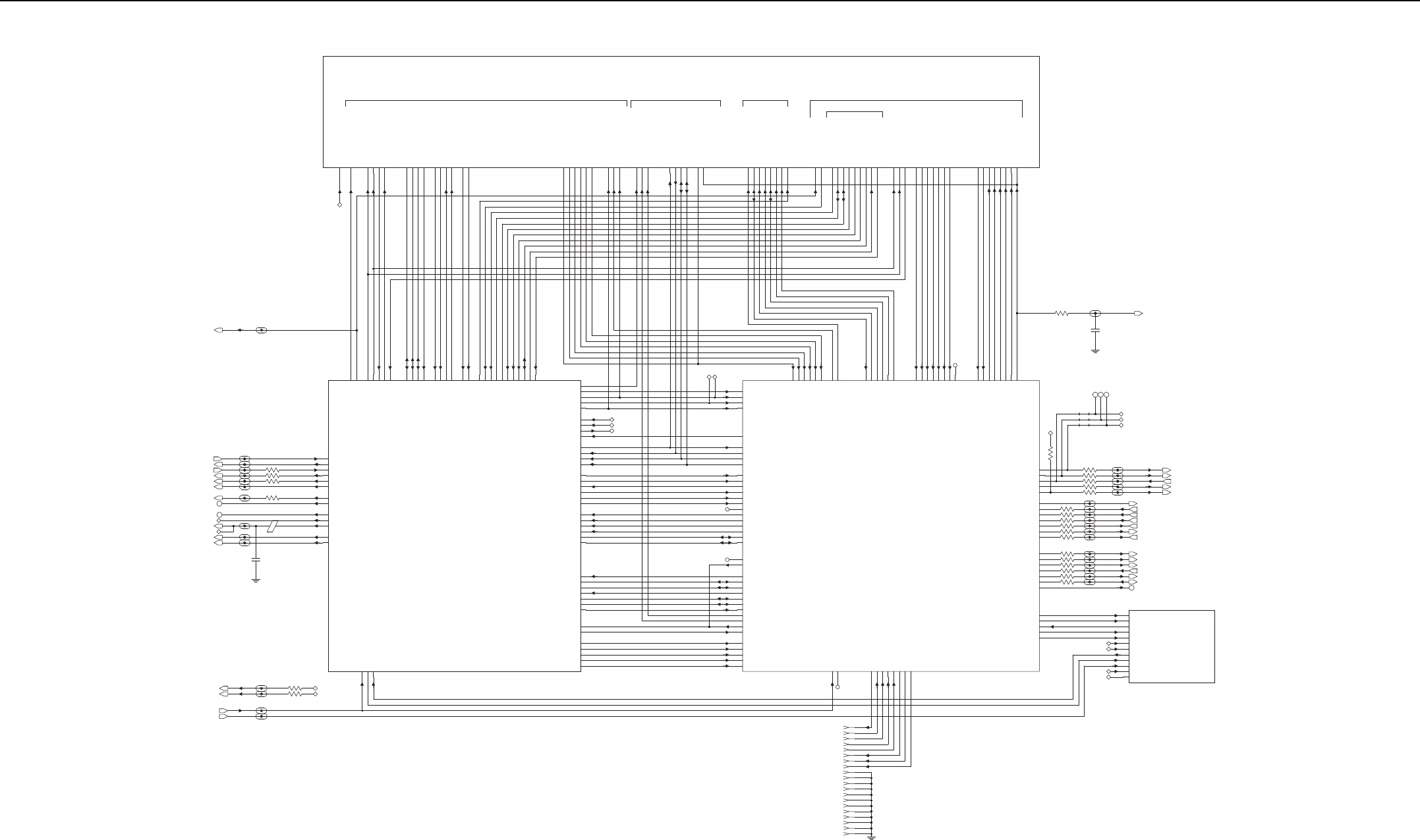
Controller R5 Schematic Diagrams 3-47
5.0 Controller R5 Schematic Diagrams
NC
VBUS2
VOLUME_1
VOLUME_2
PUB_ADDRESS_2
PUB_ADDRESS_2_EN
RESET
RESET_OUT
RTC_BATTERY
RX_AUDIO
SERIAL_CLK
SERIAL_DATA
SSI_CLK
SSI_DATA_IN
SSI_DATA_OUT
SSI_FSYNC
SW_9V3
SYSTEM_SYNC
USB2_DM
USB2_DP
VBUS1
KEYPAD_ROW_3
LED_CS
MIC_GROUND
McBSP3_CLKX
McBSP3_DR
McBSP3_DX
McBSP3_FSX
ONE_WIRE_1
ONE_WIRE_2
ON_OFF_SW
OPT_BRD_PTT
OPT_GPIO_1
OPT_GPIO_2
PROGM_IO_CS
PUB_ADDRESS_1
PUB_ADDRESS_1_EN
GP5_8_CTSs_RESET
GPIO_0_PWR_ON
GPIO_1_USB1_DP
GPIO_2_USB1_DM
GPIO_3_PTT
GPIO_4_HOOK
HANDSET_AUDIO
INT_MIC+
INT_SPKR+
INT_SPKR-
KEYPAD_COL_0
KEYPAD_COL_1
KEYPAD_COL_2
KEYPAD_ROW_0
KEYPAD_ROW_1
KEYPAD_ROW_2
ARMIO_6
DIR_CTRL
DISPLAY_CMD
DISPLAY_CS
EXT_MIC+
EXT_SPKR+
EXT_SPKR-
EXT_SWB+
GP5_1_PTT
GP5_2_MONITOR
GP5_3_CHAN_ACTIVITY
GP5_4_EMERGENCY
GP5_5_IGNITION_SENSE
GP5_6_TxDc_BUS+
GP5_7_RxDc_BUS-
1V8
3.3V
5V
9V3
5V
MMP
CONTROL HEADREAR ACCESSORY REPEATER INTERFACE
PERIPHERALS
OPTION BOARD INTERFACE
( 1 SHEET )
9V3
2.9V_MAKO_V6
LO_PWR_DET
VSWR_DET
3.6V_MAKO_SW1
9V3_PA
5V
5V_SW
5V_SW
TX_DAC
RAW_B+
LO_BATTERY_DET
PA_BIAS
2.775V_ANA_V7
RX_FLTR_VCTRL
1
1
R2500 0
R2502 0
0
R2501
R2504 0
C2501
1500pF
BLM21PG300SN1
E2500
VSWR_DET
TX_DAC
PA_BIAS
RAW_B+
RX_FLTR_VCTRL
LO_BATTERY_DET
LO_PWR_DET
2.775V_ANA_V7
2.9V_DIG_V6
3.6V_DIG_VSW1
5V
5V_SW
9V3_PA
( MAKO AUDIO_DIGITAL_USB/RS232 : SHEET 3)
MAKO_AUDIO_DC
( DC SUPPLY: SHEET 1)
( MAKO POWER MANAGEMENT : SHEET 2)
VBUS1
VBUS2
SPI_MOSI
SPKR+
SPKR-
SW_9V3
USB0_DAT
USB0_SE0
USB0_TXEN
USB1_DAT
USB1_DM
USB1_DP
USB1_SE0
USB1_TXEN
USB2_DM
USB2_DP
USB_INT
ON_OFF_MECH
POR
PUB_ADDRESS_1
PUB_ADDRESS_1_EN
PUB_ADDRESS_2
PUB_ADDRESS_2_EN
PUB_ADDRESS_MIC_EN
RS232_RX
RS232_TX
RTC_BATTERY
RX_AUDIO
SPI_CLK
SPI_MISO
MAKO_DCLK
MAKO_FSYNC
MAKO_INT
MAKO_OPT_GPIO0
MAKO_OPT_GPIO2
MAKO_OPT_GPIO3
MAKO_OPT_INT
MAKO_RX
MAKO_TX
MIC_GROUND
MMP_GPIO1_INPUT
MMP_GPIO2_INPUT
OMAP_CORE_LDO
ONE_WIRE_1
ONE_WIRE_2
ONE_WIRE_UP
EXT_MIC_ENA
EXT_SWB+
GATED_32KHZ_OMAP
GP5_4_EMERGENCY
GP5_5_IGNITION_SENSE
GPIO_0_PWR_ON
GPIO_3_PTT
GPIO_4_HOOK
HANDSET_AUDIO
I2C_CLK
I2C_DATA
INT_MIC+
LOW_LEVEL_MUTE
MAKO_AD_TRIGGER
MAKO_CE
1.875V_DIG_V2
16.8_MHZ_BUFF
2.775V_DIG_V4
3.3V_DIG_V10
32KHZ_GPS
9V3
ANT_CURRENT_DET
AUDIO_PA_ENA
EXT_MIC+
0
R2506
0
R2507
16.8_MHZ_BUFF
1.875V_V21.875V_DIG_V2
2.775V_V42.775V_DIG_V4
16.8_GPS
SPI_MOSI_MAKO
SPI_MISO_MAKO
SPI_CLK_MAKO
(Active HIGH: ~ 27us)
2.775V_V4
1.875V_V2
NC
NC
NC
MICROCONTROLLER
(OMAP 1710: SHEET 1)
(MEMORY: SHEET 2)
USB_INT
RX_FSYNC
SERIAL_CLK
SERIAL_DATA
SPI_CLK
SPI_MISO
SPI_MOSI
THK_CE
TX_CLK
TX_DATA
TX_FSYNC
USB0_DAT
USB0_SE0
USB0_TXEN
USB1_DAT
USB1_SE0
USB1_TXEN
McBSP3_CLK
McBSP3_DR
McBSP3_DX
McBSP3_FSX
ONE_WIRE_UP
OPT_GPIO_1
OPT_GPIO_2
POR
PTT
RESET_OUT
RS232_RX
RS232_TX
RX_CLK
RX_DATA
KEYPAD_ROW2
KEYPAD_ROW3
LED_CS
LOCK_DETECT
MAKO_AD_TRIGGER
MAKO_CE
MAKO_DCLK
MAKO_FSYNC
MAKO_GPIO_RX
MAKO_INT
MAKO_OPT_GPIO0
MAKO_OPT_GPIO2
MAKO_OPT_GPIO3
MAKO_OPT_INT
MAKO_RX
MAKO_TX
MOBILE_DISPLAY_CMD
I2C_CLK
I2C_DATA
JTAG_NEMU0
JTAG_NEMU1
JTAG_NTRST
JTAG_RTCK
JTAG_TCK
JTAG_TDI
JTAG_TDO
JTAG_TMS
KEYPAD_COL0
KEYPAD_COL1
KEYPAD_COL2
KEYPAD_COL3
KEYPAD_ROW0
KEYPAD_ROW1
GPIO_27
GPIO_3
GPIO_30
GPIO_31
GPIO_32
GPIO_33
GPIO_40
GPIO_5
GPIO_60
GPS_BOOT_SELECT
GPS_ON_OFF_LS
GPS_RESET_LS
GPS_RX_LS
GPS_TX_LS
ARMIO_3
ARMIO_6
AUDIO_PA_ENA
DEEP_SLEEP
DIR_CTRL
DISPLAY_CS
DMCS
EXT_MIC_ENA
GATED_32KHZ_OMAP
GP5_8
GPIO_15
GPIO_18
GPIO_25
GPIO_26
1.875V_DIG_V2
16.8_MHZ_BUFF
2.775V_DIG_V4
3.3V_DIG_V10
32KHZ_CLK
ABACUS3_CE
ADAPT_SW
ANT_EN
ARMIO_12
ARMIO_15
ARMIO_2
OMAP_CORE_LDO
(SW1 / VOL_A)
(SW2 / VOL_B)
(SW4 / MONITOR)
(SW8 / CHANNEL_ACT)
(BL_EN / GP5_7)
(RED_LED / RX_ATTN_1)
(KEYPAD_ROW4 / GP5_6)
J2500-15
J2500-13
J2500-9
J2500-7
J2500-18
J2500-2
J2500-19
J2500-4
J2500-8
J2500-10
J2500-3
J2500-16
J2500-14
J2500-17
J2500-20
J2500-12
J2500-11
J2500-6
J2500-1
J2500-5
SPI_MISO_1
1
SPI_CLK_1
1SPI_MOSI_1
1
220pF
C2500
R2508
0
RESET_OUT
SPI_CLK_MAKO
SPI_MOSI_MAKO
SPI_MISO_MAKO
R2529 10K 1.875V_V2
0
R2525
0
R2527
R2524 0
R2528 0
R2526 0
(6.0 MHz)
(Active LOW: ~27us)
(Active LOW: 20-86us)
THK_CS
SPI_MOSI
SPI_MISO
SPI_CLK
ABACUS3_CS
(84.0 KHz)
(1.20 MHz)
(20.0 KHz)
(4.20 MHz)
RX_SSI_SYNCB
TX_SSI_FSYNC
TX_SSI_DATA
TX_SSI_CLK
RX_SSI_FSYNC
RX_SSI_DATA
RX_SSI_CLK
RF_ATTN_2
LOCK_DETECT
PC_ATTEN_ENA
DMCS
ADAPT_SW
ANT_ENABLE
PREDRIVE_SW
R2509
R2516
R2520
R2514
R2510
R2519
R2517
R2515
R2512
R2513
R2518
R2511
0
0
0
0
0
0
0
0
0
0
0
0
2.775V_V4
1.875V_V2
5V
5V_SW
32KHZ_GPS
5V_ACTIVE_ANT
ANT_CURRENT
GPS_5V
GPS_BOOT_SEL
GPS_ON_OFF_LS
GPS_RESET_LS
GPS_RX_LS
GPS_TX_LS
VCONT
1.875V
16.8MHz
GPS
( SHEET 1 )
Controller – GPS Schematic Diagram
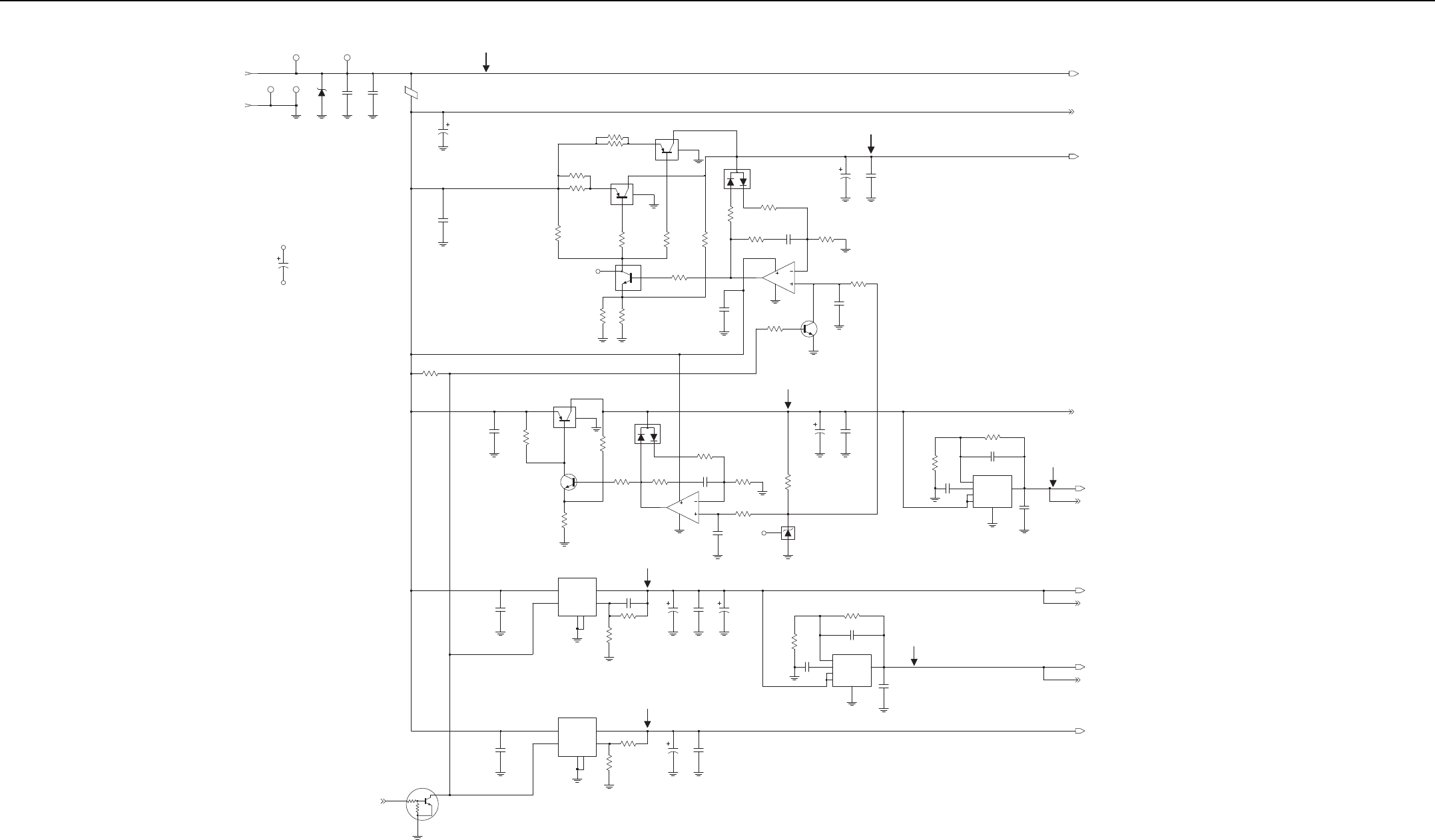
3-48 Controller R5 Schematic Diagrams
J3000-1 1
C3015
47pF
2
J3000-2
VR3000
1
1
SP3000
FT_VBAT_GROUND
FT_VBAT
1
C3000
470pF
1
SP3001
E3000
C3002
10uF
C3019
470pF
This cap only use to support
DC connector during reflow.
NC
10uF
C3018
NC
13.6V (NOMINAL)
2
3
U3005
R3033
0.1
R3032
0.1
R3055
0.1
0.1
R3056
1
G1
R3035
10
330
R3034
NU
R3038
150
NC
150
R3050
Q3032
R3051
0
10
R3036
R3039
1%
2K
.01uF
C3030
D3030
R3053
0
0
R3057
R3037
330
U3006
1
2
3
G1
U3040,U3005,U3006 change to 4813971D34
9.3V
C3021
0.1uF
33uF
C3020
1%
2.74K
R3040
R3041
100K
Q3030
R3030
10K
.01uF
C3032
2
3
1
8
4
U3030-1
0.1uF
C3031
U3040
1
2
3
G1
680
R3043
C3040
470pF
680
R3042
10K
R3002
330
R3044
Q3040
1
ADJ
GND1
GND2
ON_OFF
2
4VIN5
VOUT
3
6
U3001
LM2941
470pF
C3005
OFF: 4.8V
ON: 0V
C3012
470pF
Q3041
47K
47K
MAKO_ON_OFF_CONTROL
5
VOUT
ADJ 1
GND1
3
GND2
6
ON_OFF
2
4VIN
LM2941
U3003
13.6V
C3013
22uF 0.1uF
C3014
2.2K
5%
R3005
R3006
220
5%
9.3V
0.10uF
C3046
1%
3.57K
R3003
R3004
1%
562
C3006
33uF
33uF
NU
C3045
C3007
0.1uF
.01uF
C3042
8
4
U3030-2
6
5
7
NC
R3047
100K
2K
1%
R3045
0
R3052 R3054
0
2.74K
1%
R3046
D3040
.01uF
C3041
VR3040
R3048
1K
9.3V
0.1uF
C3044
33uF
C3043
6
4
3
2
39.2K
R3007
1%
5GND
NP
VCONT
VIN
1
VOUT
U3004
TK11100CSC
FB
100pF
C3016
R3008
1%
13K
C3017
1000pF
5V
C3011
1.0uF
5V
5V (TO GPS & PERIPHERAL BLOCKS)
(TO MAKO)
9V3_CNTRL
(TO PA DRIVER ONLY)
(TO TX PA)
(TO AUDIO PA)
UNSWB+
9V3_PA
RAW_B+
(TO SYNTH, VCO, RX FE, PWR CNTRL,CONTROLHEAD)
9V3
9V3
( TO REAR ACCESSORY)
EXT_SWB+
5V_SW
5V_SW
(TO RX BACKEND, SYNTH,GPS ANTENNA)
5V
VIN
1
VOUT
U3002
2FB
5GND
6NP
4VCONT
3
TK11100CSC
C3009
0.10uF
39.2K
1%
R3009
13K
1%
R3010
C3008
1000pF
1.0uF
C3010
Controller DC Supply Schematic Diagram
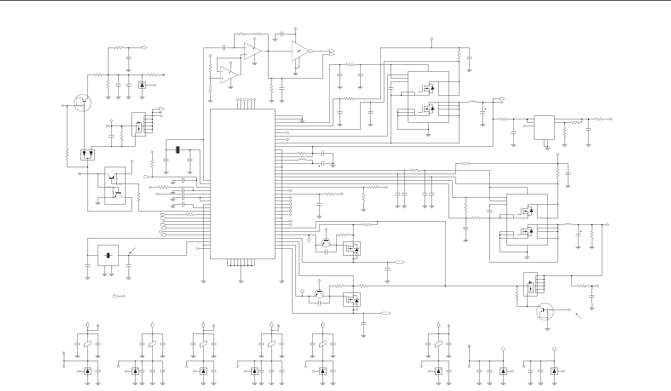
Controller R5 Schematic Diagrams 3-49
C3274
220pF
0
R3228
LO_BATTERY_DET
0
R3233
BATTERY_SENSE
NC
VR3200
C3261
220pF
14.3K
1%
R3210
R3209
43.2K
10.0uF
C3275
Q3205
47K
47K
DTA144EKAF
UNSWB+
C3262
2.2uF 100K
R3205
9V3_CNTRL
9V3_CNTRL
R3248
10K
EMD9FT2R
Q3206
D3200
MAKO_ON_OFF_CONTROL
10K
NU
R3249
5V
9V3_CNTRL
( ON= 0V; OFF=9.3V)
2
5
6
3
1
4
33K
R3226
VSAVE
RTC_BATTERY
9V3_CNTRL C3210 2.2uF
0.1uF
C3207
2.2uF
C3208
0
R3206
1000pF
C3211
32.768KHz
XTAL
Y3201
21
C3205
5.6pF
C3204
5.6pF
NTHS5441T1
Q3201
SW_9V3
SW_9V3
SW_9V3
C1
B1
C2
A13
A12
B3
M1
D4
D3
C5
D5
E4
G4
B4
F3
B2
F4
E2
F5
D2
D1
NC
R3218 0
MAKO_GATED_32KHz 1
VSAVE
MAKO_INT
GP5_4_EMERGENCY
GP5_5_IGNITION_SENSE
POR
ON_OFF_MECH
Vpk-pk: 2.2V - 2.4V
Sine Wave
24.576MHz
33pF
C3214
3HOT2
CX-101F
Y3200
2GND1
4GND2
1
HOT1
C3215
33pF
NC
16.8_MHZ_BUFF
1.875V_DIG_V2
1.875V_DIG_V2
E3201
C3217
220pF
NC
C3218
0.10uF
VR3201
C3237
2.2uF
1.875V_V2_MAKO
1.875V_V2_MAKO
OMAP_CORE_LDO_1
NC
VR3202
C3219
220pF
E3202
0.10uF
C3220
OMAP_CORE_LDO
C3240
100pF
C3239
2.2uF10uF
C3238
0.10uF
C3222
E3203
NC
VR3203
1.0uF
C3243
220pF
C3221
2.775V_DIG_V4
2.775V_V4_MAKO
2.775V_DIG_V4
C3248
1.0uF 100pF
C3249
VR3204
C3247
10uF
NC
2.9V_V6_MAKO
220pF
C3225 C3226
0.10uF
E3205
2.9V_DIG_V6
2.9V_DIG_V6
1.0uF
C3252
220pF
C3227 E3206
VR3205
NC
C3228
0.10uF
2.775V_V7_MAKO
ON: 4.75V to 5.25V (5.0V typical)
OFF: 0.0V
( TO MAP) VBUS2
3.3V_DIG_V10
3.3V_DIG_V10
SI8401DB
2
3
1
4
0.2
Q3204
R3208
4.7uF
C3216
2.775V_ANA_V7
R3252
100K
1
VBUS2_CMD
0.10uF
C3291
Q3210
VSW5_CNTRL
SI8401DB
2
3
1
4
Q3203
Q3209
0.10uF
C3289
VBUS1_CMD 1
VSW5_CNTRL
100K
R3250 R3207
0.2
OFF: 0.0V
( TO MMP)
C3213
4.7uF
VBUS1
ON: 4.75V to 5.25V (5.0V typical)
C3281
0.1uF
C3266
2.2uF
C3277
1.0uF
0.1uF
C3280
VSW5
10
R3239
R3216
0
NU
R3227
10K
OMAP_CORE_LDO_1
C3234
2.2uF
0NU
R3217
3.3V_V10_MAKO
3.6V_DIG_VSW1
3V_V9_MAKO
5V_V8_MAKO
SW_9V3
2.775V_V7_MAKO
2.9V_V6_MAKO
2.775V_V4_MAKO
1.875V_V2_MAKO
R3203 0.1
22uFC3206
22uHL3201
C3283 0.10uF
NC
NC
R3241
5.1
C3278
0.1uF
ON: 5Vpk; 230 KHZ PWM
OFF: 0.0Vpk
C3279
0.1uF
7
S2C
8
SYNC_EN
5
4IN
S1A
15
S1B
16
S2A
6
S2B
14 CBOOT
C3202
0.10uF
VDD 13
Q3200
10
D2C 11
D2D 12
D1A 1
D1B 2
D2A 9
D2B
GND
3
OFF: 0.0V
ON: 3.6V
C3269
1.0uF
22uH
L3200
NC
0
R3245
68uF
C3203
3.6V_DIG_VSW1
3.6V_DIG_VSW1
VIN2
VOUT
ADJ
GND1
GND2
NC
VIN1 5
U3201
LP8340
4
2
7
3
1
6
C3270
1.0uF
51.1K
1%
R3247 6.81K
1%
R3246
Change R3246 to 0613952N12 (13K) for OMAP1610
SW_9V3
R3215
0
OMAP_CORE_LDO_1
22uF
C3265
R3204
0.1
13
VDD
SI4724CY
Q3202
D1B
D2A
D2B
D2C
D2D
D1A
2
9
10
11
12
3GND
1
S1B
S2A
S2B
S2C
SYNC_EN
IN
S1A
CBOOT
16
6
7
8
5
4
15
14
ON: 5Vpk; 230 KHZ PWM
OFF: 0.0Vpk
NU
R3225
0
R3224
4.7K
10pF
C3273
NU
C3209
0.10uF
XTAL32_IN
XTAL32_OUT
VSAVE
XIN
XOUT
SW_TYPE
TCXO_IN
TCXO_SEL_16_24
REG_3V6
RESETX
INT_X
MECH_SW
GND4
GND5
GND6
GND7
GND8
GND9
HV_BG
IGN_X
BAT_RTC
BAT_TYPE
EMERG_PB
FET_ENX
GATED_32K_CLK
GND1
GND2
GND3
BAT_3V6
BAT_7V5
G5
K9
L4
D14
H5
D9
P5
M7
J4
A1
NC1 A14
NC2 P1
NC3 P14
NC4
NC5 M5
B14
NC6
NC
NC
NC
NC
NC
NC
VBUS1_SENS
VBUS2
VBUS2_CMD
VBUS2_SENS
VBUS_SUPPLY
V08_I
V08_O
V09_O
V10_GND
V10_I
V10_O
VBUS1
VBUS1_CMD
V02_O
V03_O
V04_O
V06_O
V07_O
SW2_VCCS
SW2_VOUT
SW5_PHASE
SW5_SUMCOMP
SW5_VDD
SW5_VDDHV
SW5_VOUT
SW5_VSENSE
SW1_VDD
SW1_VDDHV
SW1_VOUT
SW1_VSEN_BST
SW1_VSEN_BUK
SW2_GND
SW2_LX
SW2_VCC
PGLDO2
PGLDO3
SW1_DH
SW1_GND
SW1_PHASE
SW1_SUMCOMP_DL
PWR_MNGR_BLOCK
U3200-1
E12
D12
C13
F11
B13
K3
K4
L1
L9
J10
M6
H10
C14
N4
P4
N5
P3
P6
K14
J13
G11
E13
D13
F13
F12
E14
G13
G12
H12
J11
H11
L14
J14
J12
C3
A2
H13
H14
F14
G14
R3236
1K
C3292
1000pF
220K
R3223
220K
R3222
B3 U3202-2
LMC6035ITLX
A2
A3
A1
B1
VSAVE
VSAVE
GND
3
IN
2
NC
1
OUT 4
VCC 5
C1
NL17SZ14
U3203
4.7uF
C3282 1.875V_V2_MAKO
C2
C3
B1
B3 U3202-1
LMC6035ITLX
2MEG
R3219
R3220
2MEG
C3272
10pF
VSAVE
32KHZ_GPS
GATED_32KHZ_OMAP
C3276
1.0uF
10
R3238
2.2uF
C3201
C3200
22uF
R3200
0.1
SW_9V3
R3243
5.1
ON: 5.2V - 5.3V
OFF: 0.0V
68uF
C3212
22uH
L3202
R3237
10K
VSW5
C3290
0.10uF
R3253
47K
VSW5_CNTRL
OFF: 0V (DEFAULT)
ON: 3.3V (MAKO V10)
FROM MAKO USB_CONNECT (L6)
USB_CONNECT
Q3208
DTC114YKAF
2
10K
47K
3
1
MAKO_V9_3V
1
VR3208
NC
C3260
1.0uF
C3233
220pF
MAKO_V8_5V
NC
VR3206
3V_V9_MAKO
220pF
C3229
1
C3254
2.2uF
5V_V8_MAKO
5V_V8_MAKO
E3208
C3231
220pF
C3232
0.10uF
VR3207 C3257
1.0uF
NC
3.3V_V10_MAKO
47K
R3240
Q3207
NTHS5441T1
Controller DC Distribution Schematic Diagram
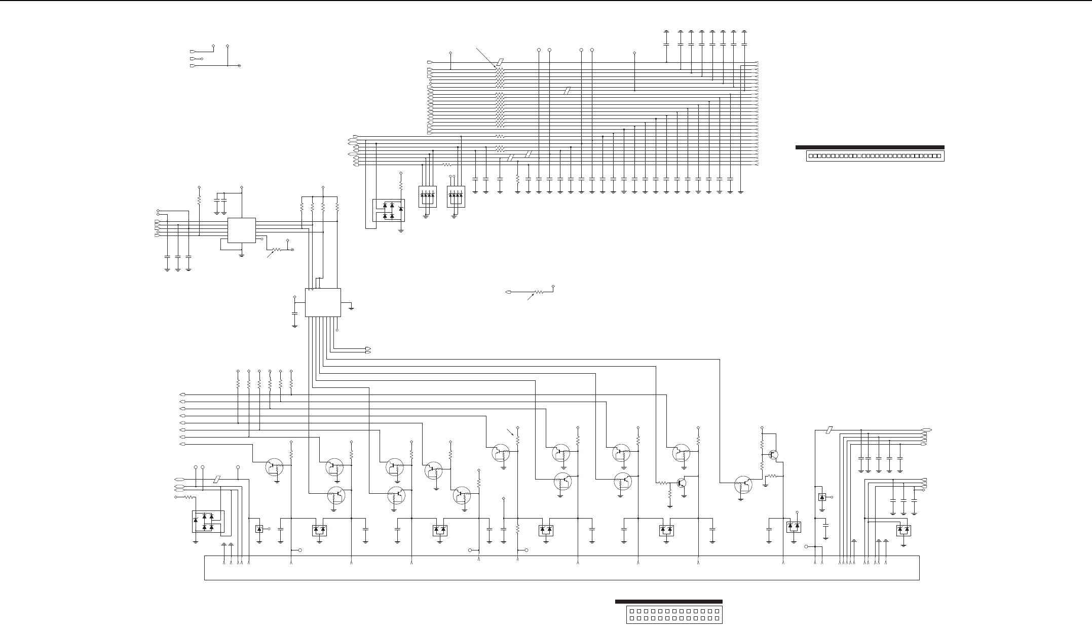
3-50 Controller R5 Schematic Diagrams
1
1
NC
3.3V
1V8
1V8 1V8
5V
5V
9
11
13
1
3
5
Y_4
Y_5
Y_6
A_4
A_5
A_6
GND
7VCC
Y_1
Y_2
Y_3
A_1
A_2
A_3
NC
8
10
12
14
2
4
6
U4001
SN74LVC07A
220pF
C4085
1V8
C4084
0.10uF
R4079
10K
1V8
NU
C4071
220pF
NU
C4074
220pF
NU
C4072
220pF
ARMIO_6
RESET
PROGM_IO_CS
SERIAL_DATA
SERIAL_DATA
SERIAL_CLK
SERIAL_CLK
MOBILE REPEATER: 0 OHM
MOBILE SUBSCRIBER: NOT_USED
NU
R4086
0WD_RESET
WD_RESET
9
15
1
2
3
4
5
6
7
NC
QH2
RCLK
RCLR
SER
SRCLK
SRCLR
VCC
16
QA
QB
QC
QD
QE
QF
QG
QH1
GND 8
0.10uF
C4073
5V
14
U4000
SN74AHC594
12
13
11
10
PUB_ADDRESS_1_EN
PUB_ADDRESS_2_EN
R4055
10K
NU R4033
R4031
10K
10K R4054
R4030
NU
R4032
10K
1V81V81V81V81V8 1V8
GP5_1_PTT
GP5_4_EMERGENCY
GP5_7_RxDc_BUS-
GP5_8_CTSs_Reset
GP5_5_IGNITION_SENSE
GP5_3_CHAN_ACTIVITY
GP5_6_TxDc_BUS+
GP5_2_MONITOR
10K
R4035
1
23
4
D4000
USB2_DM
USB2_DP
VBUS2
5V
FT_VBUS2
1
BLM21PG221SN1
E4002
FT_USB2_DP
1
FT_USB2_DM
1
DTC144EKAF
2
47K
47K 47K
47K
10K
47K
10K
47K
47K
47K
47K
47K
47K
47K
47K
47K
47K
47K
47K
47K
47K
47K
3
1
Q4000
R4040
4.7K
5V
Q4001
2
3
1
DTC144EKAF
1
DTC114YKAF
Q4002
2
3
4.7K
R4041
5V
VR4000
3
1
2
MMBZ20V
EXT_PTT
C4040
220pF
1
VR4005
2
3
1
NC
47K
10K
47K
10K
47K
10K
220pF
C4042
C4041
220pF
Q4004
DTC114YKAF
2
3
1
Q4003
2
3
1
DTC144EKAF
4.7K
R4042
5V
DTC144EKAF
2
3
1
Q4015
4.7K
R4098
5V
4.7K
R4043
5V
Q4006
DTC144EKAF
2
3
1
1
DTC144EKAF
Q4005
2
3
MMBZ20V
VR4001
3
1
2
FT_EMERGENCY 1
220pF
C4043 390K
R4051
1FT_IGNITION_SENSE
C4044
220pF
VR4002
3
1
2
MMBZ20V
WD_RESET
220pF
C4045
Q4008
2
3
1
DTC114YKAF
DTC144EKAF
2
3
1
Q4007
R4045
4.7K
5V
MOBILE SUBSCRIBER: NOT_USED
MOBILE REPEATER: 0 OHM
NU
R4044
4.7K
5V
R4046
4.7K
3
1
Q4009
DTC144EKAF
2
3
1
DTC114YKAF
Q4010
2
5V
10K
R4088
BCW65A
Q4014
1
3
2
R4089
47K
DTC144EKAF
Q4011
2
3
1
4.7K
R4047
VR4003
MMBZ20V
3
1
2
C4046
220pF
C4047
220pF
3
1
Q4012
DTC114YKAF
2
BCW68GLT1G
1
3
2Q4013
R4050
10K
R4049
2.7K
1.5K
R4048
EXT_SWB+
5V
NC
2
MMBZ20V
VR4004
3
1
1
FT_APM_1_WIRE
220pF
C4048
NC
2
3
1
VR4006
220pF
C4070
E4005
BK1005HM471
220pF
C4067
220pF
C4068 C4069
220pF
EXT_SPKR+
EXT_SPKR-
EXT_SWB+
EXT_SWB+
C4063
220pF
C4065
220pF220pF
NU
C4075 C4064
220pF 220pF
C4066
ONE_WIRE_2
RX_AUDIO
PUB_ADDRESS_1
EXT_MIC+
PUB_ADDRESS_2
1
2
VR4009
MMBZ20V
3
GPIO_2_USB1_DM
GPIO_1_USB1_DP
ONE_WIRE_1
MIC_GROUND
GPIO_4_HOOK
VBUS1
INT_MIC+
GPIO_0_PWR_ON
GPIO_3_PTT
R4023
1.2K
R4103
1.2K
R4100
1.2K
R4101
1.2K
5V
23
4
D4001
10K
R4034
5V
VR4008
2A1
5
A2
NU
A1
2
A2
5
NU
VR4007
K3
K4
K1
K2
K1
K2
K3
K4
NCNC
4
6
1
3
1
3
4
6
R4012 0
ON_OFF_SW
9V3
RESET
DISPLAY_CS
SERIAL_DATA
SERIAL_CLK
LED_CS
DISPLAY_CMD
HANDSET_AUDIO
INT_SPKR-
KEYPAD_ROW_1
KEYPAD_ROW_3
KEYPAD_COL_1
VOLUME_1
KEYPAD_ROW_0
KEYPAD_ROW_2
KEYPAD_COL_0
KEYPAD_COL_2
VOLUME_2
INT_SPKR+
MOBILE REPEATER: NOT_USED
MOBILE SUBSCRIBER: 33 OHM
RESET
R4061
R4071
R4005
R4001
R4068
R4065
R4070
R4003
R4063
R4000
R4069
R4002
R4066
R4064
R4004
R4067
33
0
33
33
33
33
33
33
33
33
33
33
33
33
33
E4000
33
CONTROL HEAD INTERFACE
1
FT_USB1_DPFT_VBUS1
1
FT_USB1_DM
1
1
FT_MMP_1_WIRE
J4001_9
E4003
51
R4010
51
R4009
R4006 470
220pF
C4027
220pF
C4029
220pF
C4032
220pF
C4022C4016
220pF 220pF
C4018
220pF
C4031
220pF
C4028C4019
220pF
C4021
220pF220pF
C4020C4014
220pF 220pF
C4026 C4033
220pF220pF
C4024
220pF
C4017 C4025
220pF
C4023
220pF
C4015
220pF 220pF
C4030
NU NU
330pF
C4034 C4035
330pF
0
R4011
220pF
C4076
NU
BLM21PG221SN
E4001
BK1005HM471
E4004
NU
C4002
220pF
NU
C4005
220pF
C4000
220pF
NU
220pF
C4001
NU
220pF
C4006
220pF
C4013
NU
220pF
C4004
220pF
NU
C4003
PCB
J4001 FRONT VIEW
91687 3425
16 15 1227 24 22 2128 13 1120 1926
29 2325 101418 1730
J4001-2020
J4001-1919
J4001-2828
J4001-55
J4001-2222
J4001-2525
J4001-44
16
J4001-1212
J4001-1313
J4001-16
J4001-1414
J4001-2929
J4001-11
J4001-66
J4001-2424
8J4001-8
J4001-1717
10
J4001-1515
J4001-10
J4001-3030
J4001-99
J4001-1818
7
J4001-33
J4001-7
J4001-2121
J4001-2626
J4001-2323
J4001-2727
2J4001-2
J4001-1111
MOBILE REPEATER: 0 OHM
MOBILE SUBSCRIBER: NOT_USED
NU
R4090
0
J4001_9
RTC_BATTERY
17919
J4000 REAR VIEW
23111357 15 21 2513
2618 24
20814 22
PCB
2641210 16
AUX_AUDIO_OUT_1
GP5_6
EXT_SPKR-
MAP_ID_2
AUDIO GROUND
EMERG SW
POWER GROUND
GROUND
EXT_SPKR+
VIP_1_(EXT ALARM)
GP5_7
AUX_AUDIO_OUT_2
IGN_SENSE
MAP_ID_1
TX_AUDIO
RX_AUDIO
EXT_SWB+
GP5_8
USB / MAP_ID_GROUND
USB_DP_MAP
GROUND
VBUS_MAP
USB_DM_MAP
GP5_3_(CHAN_ACT)
GP5_1_(EXT PTT)
GP5_2_(MONITOR)
ACCESSORY INTERFACE (26-PIN)
J4000-16
J4000-19
J4000-17
J4000-20
J4000-2
J4000-14
J4000-13
J4000-12
J4000-9
J4000-26
J4000-25
J4000-6
J4000-7
J4000-21
J4000-10
J4000-18
J4000-1
J4000-3
J4000-11
J4000-22
J4000-23
J4000-8
J4000-24
J4000-4
J4000-15
J4000-5
16
19
17
20
13
14
12
9
26
5
6
25
7
18
4
2
1
3
21
10
11
22
8
23
24
15
Controller Peripheral Schematic Diagram (sheet 1 of 2)
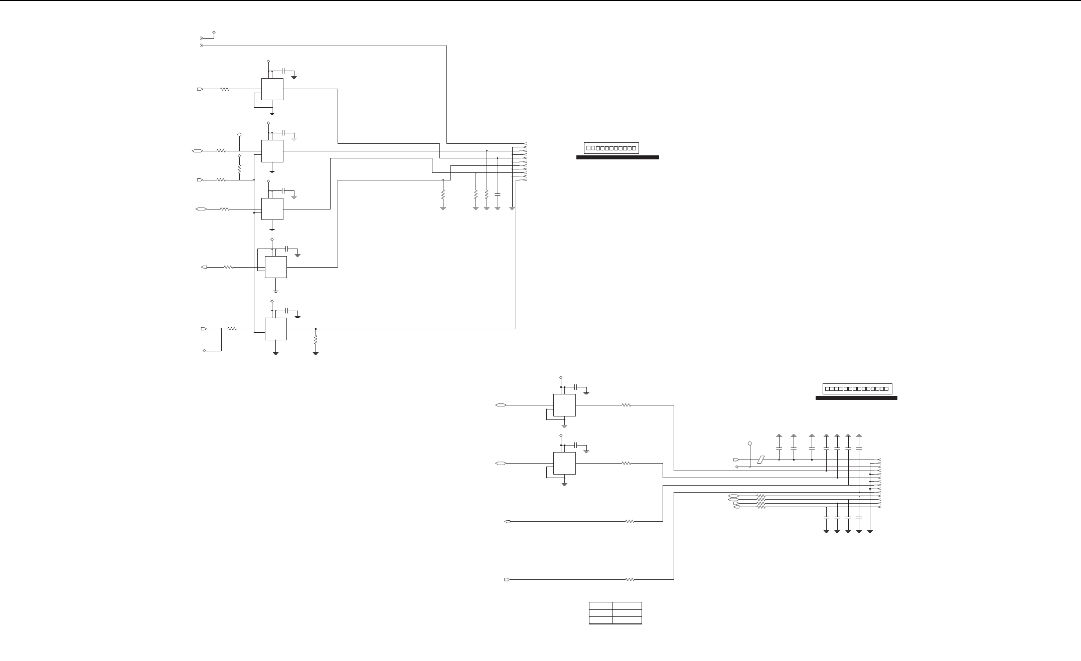
Controller R5 Schematic Diagrams 3-51
B1
C1
McBSP3_DR
McBSP3_CLKX
DIR_CTRL
McBSP3_DX
McBSP3_FSX
SYSTEM_SYNC
SYSTEM_SYNC
A
C2 B
B2 DIR
GND
A1
VCCA A2
VCCB
SN74AVC1T45
U4005
C1
R4099
0
R4105
10K
R4096
R4093
0
R4095
0
0
C4088
DIR
B2
GND
B1 VCCA A1
VCCB A2
0.10uF
U4006
SN74AVC1T45
AC1
B
C2
0.10uF
C4089
C4087
0.10uF
R4094
0AC1
B
C2
DIR
B2
GND
B1 VCCA
VCCB
U4008
SN74AVC1T45
1
TP4000
1V8
1V8
1V8
1V8
R4106
10K
C1
A
C2 B
B2 DIR
B1 GND
A1
VCCA A2
VCCB
SN74AVC1T45
U4007
0.10uF
C4090
A1
A2
1V8
0.10uF
C4086
GND
B1 VCCA A1
VCCB A2
U4004
SN74AVC1T45
AC1
B
C2
DIR
B2
R4097
0
1V8
1V8
1V8
WD_RESET
220pF
NU
NU
NU
100K
R4072
100K
R4075 C4012
NU
100K
R4073
PCB
J4002 FRONT VIEW
REPEATER CONNECTOR
10
4321 5678 9 11
1
J4002-88
J4002-22
6
J4002-77
J4002-55
J4002-6
9 J4002-9
J4002-33
J4002-1
11
J4002-44
J4002-10
10
J4002-11
0
R4080
0
R4078
SSI_DATA_OUT
SSI_CLK
SSI_DATA_IN
A1
VCCB A2
0.10uF
C4092
U4010
SN74AVC1T45
AB
C2
DIR
B2
GND
B1 VCCA
0
R4074
0
R4076
B1 GND
A1
VCCA A2
VCCB
SN74AVC1T45
U4009
C1
A
C2 B
B2 DIR
C4091
0.10uF
SSI_FSYNC
1V8
1V8
R4085 0
0
R4083
R4082 0
0
R4081
OPT_SSI_SYNC
1
OPT_BRD_PTT
OPT_GPIO_1
OPT_GPIO_2
RESET_OUT
SW_9V3
SYSTEM_SYNC
9
7
J4003-88
J4003-9
5
J4003-66
J4003-7
J4003-5
J4003-14
14
12 J4003-13
13
J4003-11
11 J4003-12
J4003-1010
J4003-33
J4003-44
1
J4003-22
J4003-1
NU
C4059
220pF
E4006
220pF
C4055
220pF
C4053
NU
220pF
C4051
NU NU
220pF
NU
C4049C4094
51pF
C4093
NU NU
33pF
PCB
J4003 FRONT VIEW
OPTION BOARD INTERFACE
21 34567891011121314
C4058
NU
220pF
NU
220pF
C4060
220pF
C4061
220pF
NU
C4062
NU
LOW
HIGH
OPERATIONDIR
B ---->A
B <----A
Controller Peripheral Schematic Diagram (sheet 2 of 2)
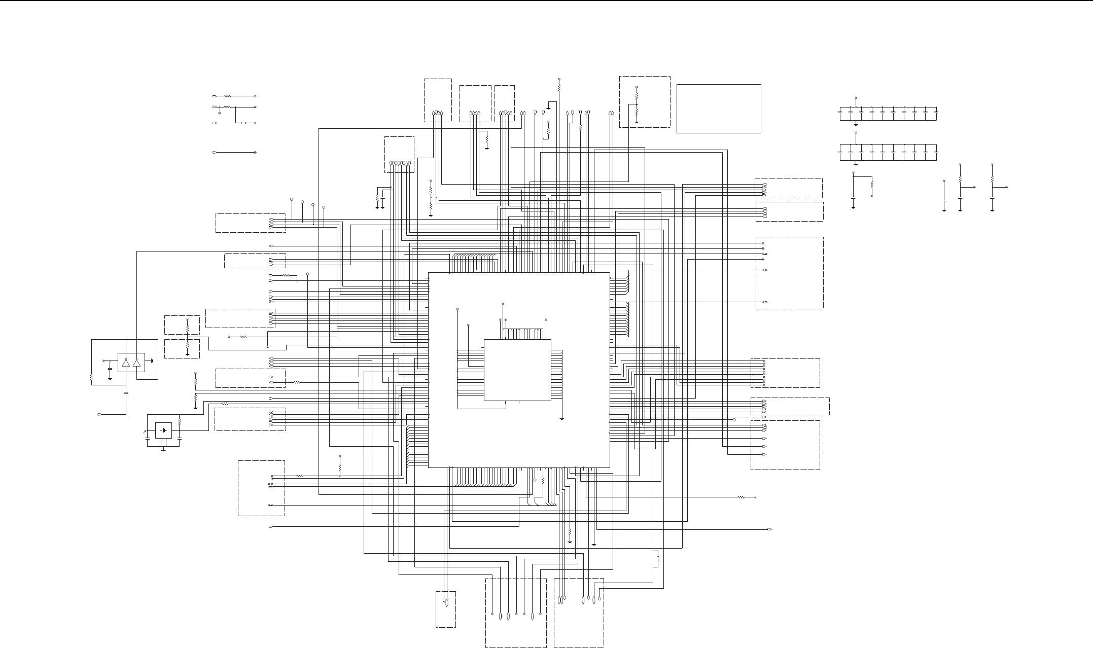
3-52 Controller R5 Schematic Diagrams
2.775V_DIG_V4
1.875V_DIG_V2
OMAP_CORE_LDO
3.3V_DIG_V10
(0.87mA/MHz for OMAP1710 & 1.06mA/MHz for OMAP1610)
Place for
OMAP1710
(1.4V for OMAP1710 & 1.55V for OMAP1610)
R1021
0
0
R1020
1.875V
DVDD2
OMAP_CORE
2.775V_DIG_V4
1.875V_DIG_V2
1
1
TP_MAKO_RX
TP_MAKO_FSYNC
TP_MAKO_TX
1
TP_MAKO_DCLK
1
(FROM MAKO)
KEYPAD ROW
MAKO SSI
(Used as KEYPAD_ROW4 for PORTABLE, GP5_6 for MOBILE)
(MOBILE ONLY)
(FROM MAKO)
OPTION SELECT
( RESET CIRCUIT PROVIDED BY MAKO)
0
R1048
10K
R1045
MAKO_OPT_GPIO2
1.875V
GATED_32KHZ_OMAP
MAKO_FSYNC
POR
MAKO_GPIO_RX
GPIO_5
KEYPAD_ROW0
KEYPAD_ROW1
KEYPAD_ROW2
KEYPAD_ROW3
ARMIO_15
MAKO_DCLK
MAKO_INT
MAKO_TX
MAKO_RX
MAKO_OPT_GPIO0
MAKO_OPT_GPIO3
EXT_MIC_ENA
32KHZ_CLK
(FROM MAKO)
1.0Vpkpk
18pF
C1018
IN1
Y1000
CX-91F
12MHz
GND
2
GND1
4
OUT
3
18pF
C1019
10MEG
R1002
R1044
0
R1001
10K
OMAP_CORE
( BUFFERRED 16.8 FROM TOMAHAWK)
16.8MHz Squarer
NL27WZU04
A1
1
A2
3
GND 2
VCC
5
Y1 6
Y2 4
U1006
.01uF
C1032
R1026
47K
C1033
0.10uF
16.8_MHZ_BUFF
1.875V
BOOT FROM CS3
BOOT FROM CS0
DNP
R1028
0
R1027
10K
NU
1.875V
RS232
GPIO_40
RS232_TX
RS232_RX
MAKO_AD_TRIGGER
OPT_GPIO_1
OPT_GPIO_2
R1070
0
1K
R1041
(MOBILE ONLY) GP5_8
TOMAHAWK SSI
ABACUS3 SSIRX_CLK
TX_CLK
RX_DATA
TX_DATA
RX_FSYNC
TX_FSYNC
FLASH
FLASH_WAIT
FLASH_CTL(5:0)
EMIFS_ADD(23:1)
EMIFS_DATA(15:0)
FLASH_CLK
MAKO_OPT_INT
0NU
R1046 10K
R1006
1.875V
JTAG
JTAG_NTRST
JTAG_NEMU0
JTAG_NEMU1
JTAG_RTCK
JTAG_TCK
JTAG_TDI
JTAG_TDO
JTAG_TMS
10K
NU
R1066
R1067
4.7K
NU
18pFC1030
4.7K
R1054
1.875V
R1071
47K
MCBSP3
MCBSP3_FSX
MCBSP3_DR
MCBSP3_CLK
MCBSP3_DX
PLACE FOR GP
DEVICE FAST BOOT
Y1001C1039 R1050
LARGEST REF
GP DEVICE CONFIG
DNP
DELETED REF
U1008
R1034
10K
NU
0
R1035
1.875V
(MOBILE ONLY)
(MOBILE ONLY)AUDIO_PA_ENA
ARMIO_12
OMAP1710
SERIAL FLASH SPI
(Used as RED_LED for PORTABLE, RX_ATTN_1 for MOBILE)
CLK rate: 1 MHz
Date rate: 20 of 8 bits packet
per chip select
(Used as GREEN_LED for PORTABLE, PA_ENABLE for MOBILE)
GPS
LED & Display CS: Active Low
SERIAL_DATA
SERIAL_CLK
GPS_BOOT_SELECT
LED_CS
DISPLAY_CS
GPS_ON_OFF_LS
GPS_RX_LS
GPS_TX_LS
GPS_RESET_LS
PLACED FOR
(Used as BL_EN for PORTABLE, GP5_7 for MOBILE
MOBILE ONY
(GPIO_3 for PORTABLE-Green LED)
(SPI.CS3 for MOBILE Shift Register Chip Select)
10KR1017
R1025
10K
0
R1047
ARMIO_6
ARMIO_2
GPIO_3
ONE_WIRE_UP
DIR_CTRL
1.875V
1.875V
GPIO_60
GPIO_15
PTT
ARMIO_3
TP_POR
1
I2C
I2C_CLK
I2C_DATA
OPTION BOARD
USB#2
USB2_SE0
GPIO_18
USB2_DAT
USB2_SUSPEND
GPIO_26
GPIO_25
USB2_RCV
USB#1USB#0
( INTERFACE WITH MAKO)
USB#0 RESERVED FOR MOBILE
USB1_SE0
USB0_SE0
USB0_DAT
USB0_TXEN
USB1_TXEN
USB1_DAT
USB_INT
OMAP1610
Place for
4.7K
R1005
OMAP1710
Place for
1.875V
RESET_OUT
R1036
10K
1TX_RAMP
SPI
MAKO_CE
ABACUS3_CE
THK_CE
SPI_CLK
SPI_MISO
SPI_MOSI
(MOBILE ONLY)MOBILE_DISPLAY_CMD
(Used as KEYPAD_COL4 for NEO and Public Add Mic for MORPHEUS)
KEYPAD COLUMN
KEYPAD_COL0
KEYPAD_COL1
KEYPAD_COL2
KEYPAD_COL3
GPIO_27
PORTABLE DISPLAY
DISPLAY_CMD
DISPLAY_CE
DISPLAY_DATA0
DISPLAY_DATA1
DISPLAY_DATA2
DISPLAY_DATA3
DISPLAY_DATA4
DISPLAY_DATA5
DISPLAY_DATA6
DISPLAY_DATA7
SDRAM_CTL(6:0)
SDRAM_DATA(15:0)
SDRAM_CLK
SDRAM_CLK_EN
SDRAM_CS
SDRAM_ADD(12:0)
SDRAM
(Used as SW1 for PORTABLE, Volume A for MOBILE)
(Used as SW8 for PORTABLE, Channel Activity for MOBILE)
(Used as SW2 for PORTABLE, Volume B for MOBILE)
(Used as SW4 for PORTABLE, Monitor for MOBILE)
FREQ SWITCH
GPIO_30
GPIO_31
GPIO_32
GPIO_33
RF CONTROLS
DMCS
DEEP_SLEEP
ADAPT_SW
LOCK_DETECT
ANT_EN Place for
Place for
OMAP1610 OMAP1710
R1019
5.1
1.0uF
C1017
LDO_FILTER
OMAP_CORE
R1000
10
C1012
0.10uF 0.10uF
C1016
R1060
10
C1044
0.10uF
CVDDA
OMAP_CORE
DVDD2
VDD_DLL
OMAP_CORE
C1008
100pF100pF
C1004 C1036
1.0uF
C1014
0.10uF
100pF
C1007
C1006
0.10uF
C1009
0.10uF
C1005
0.10uF 0.10uF
C1010 C1037
2.2uF
1.875V
C1015
0.10uF 1.0uF
C1034
C1000
100pF 0.10uF
C1001 C1002
0.10uF
C1013
0.10uF
C1003
100pF
C1011
100pF 2.2uF
C1035C1031
0.10uF
DECOUPLING CAPACITORS
OMAP_CORE
15
14
8
12
1
0
13
4
3
11
5
9
6
2
7
10
R2
R3
R4
T2
U1
U3
T4
V3
N7
P2
P4
P7
N4
N2
T3
P8
C14
D4
R12
H15
F19
H14
E20
E19
P3
Y1
H12
G8
Y10
D9
P13
G20
G21
R14
V14
Y5
R9
W18
Y19
V17
Y18
U20
AA13
J20
W14
AA9
V9
H20
P10
AA5
V15
G18
V2
P14
R10
V18
Y15
W15
V5
W19
Y2
W3
V13
W6
W7
AA15
Y14
V7
Y6
6
9
12
4
5
3
15
14
13
8
2
1
10
7
11
0
C7
C4
D8
C10
D14
C13
C11
D13
D12
C12
C5
D7
D5
D6
C6
D11
W10
W11
U19
N15
V8
T19
T20
AA17
R11
V10
M15
Y8
W8
N19
N21
M20
M14
P18
P20
P19
R18
R19
N20
N18
V16
W17
N3
M19
L18
R13
K14
K15
K19
K18
J14
J19
J18
L15
L19
6
0
1
3
5
2
4
6
1
8
9
0
12
11
10
5
7
3
2
4
P15
N14
W21
L14
U18
AA19
H18
M18
E18
C21
G19
T18
F18
D20
D19
V19
H19
D17
D16
C16
D15
C19
G14
H13
A20
B19
C18
D18
B21
C17
B17
G13
A17
B18
B15
C20
C15
G11
G9
B12
H10
H9
H11
B6
A1
G10
B9
G12
A2
B2
B8
C8
D10
H7
B4
B3
C3
H8
1
2
0
4
3
5
V20
E3
J7
F3
K4
K3
L7
E1
C1
E4
D2
F4
H3
K7
J2
J4
J3
D3
F2
L8
J8
G4
G3
G2
K8
H4
C9
J15
P9
R8
W5
M7
N8
W1
V4
M3
M4
L4
W4
L3
M8
U4
W2
W16
P12
AA20
Y17
Y12
W13
W9
P11
V6
V11
Y4
TP1000 1
R1014 0
4
20
7
13
23
19
22
9
2
6
16
21
11
3
1
18
17
12
5
14
10
15
8
Z_STATE_1
USB0_DAT
USB0_SE0
RESET_MODE
RST_OUT
RTCK
RTC_ON_NOFF
RTC_WAKE_INT
MCSI2_DOUT
MMC_CMD
LOW_STATE_3
LOW_STATE_4
I2C_SDA
GPIO_62
F_CS3
F_RP
F_WP
F_CS1
F_CS2
FADD_7
FADD_8
FADD_9
FADV
FADD_22
FADD_23
FADD_24
FADD_25
FADD_3
FADD_4
FADD_5
FADD_6
FADD_15
FADD_16
FADD_17
FADD_18
FADD_19
FADD_2
FADD_20
FADD_21
EN_USB_PUEN
FADD_1
FADD_10
FADD_11
FADD_12
FADD_13
FADD_14
EN_F_BE_0
EN_F_BE_1
EN_F_OE
EN_F_WE
CLK_MMC
CLK_SD
CLK_B_UART2
CLK_L_CAM
UART1_CTS
UART1_RX
UART2_CTS
UART2_RX
TCK
TD
TMS
TRST
SDDQS_H
SDDQS_L
MPU_RST
OSC1_IN
OSC1_OUT
OSC32K_IN
OSC32K_OUT
PWRON_RESET
MPU_BOOT
MCSI1_DOUT
MCSI2_DIN
MCSI2_SYNC
MCBSP1_DR
MCBSP1_FSX
MCBSP2_DR
MCBSP2_DX
MCBSP2_FSR
MCBSP2_FSX
MCSI1_DIN
LOW_STATE_1
LOW_STATE_2
KBR_0
KBR_1
KBR_2
KBR_3
KBR_4
F_CS2U
FDATA_6
FDATA_7
FDATA_8
FDATA_9
FRDY
F_CS1U
FDATA_12
FDATA_13
FDATA_14
FDATA_15
FDATA_2
FDATA_3
FDATA_4
FDATA_5
FDATA_0
FDATA_1
FDATA_10
FDATA_11
EN_SDCKE
CS_SDRAM
CLK_MCSI1
CLK_MCSI2
CLK_M_REQ
CONF
CLKX_SD
CLK_B
CLK_B_REQ
CLK_M
CLK32K_IN
CLKR_MCBSP2
CLKS_MCBSP1
CLKX_MCBSP1
CLKX_MCBSP2
BFAIL
SDATA_5
SDATA_6
SDATA_7
SDATA_8
SDATA_9
SDATA_11
SDATA_12
SDATA_13
SDATA_14
SDATA_15
SDATA_2
SDATA_3
SDATA_4
SDATA_0
SDATA_1
SDATA_10
MPUIO_1
MPUIO_2
MPUIO_3
MPUIO_4
MPUIO_5
MCSI1_SYNC
GPIO_7
GPIO_8
GPIO_9
GPIO_13
GPIO_14
GPIO_15
GPIO_2
GPIO_3
GPIO_4
GPIO_6
GPIO_0
GPIO_1
GPIO_11
GPIO_12
EMU0
EMU1
CLK_F
CAM_RSTZ
CAM_VS
CLK32K_OUT
CAM_D_1
CAM_D_2
CAM_D_3
CAM_D_4
CAM_D_5
CAM_D_6
CAM_D_7
CAM_HS
CAM_D_0
Z_STATE_2
Z_STATE_3
UWIRE_SDO
UART3_RX
UWIRE_SDI
SDRAM_DQML
SDRAM_DQMU
SDRAM_RAS
TDO
SDRAM_CAS
SADD_7
SADD_8
SADD_9
SBANK_0
SBANK_1
SADD_11
SADD_12
SADD_13
SADD_2
SADD_3
SADD_4
SADD_5
SADD_6
SADD_0
SADD_1
SADD_10
MMC_DAT2
MMC_DAT0
MMC_DAT1
MCBSP1_DX
LCD_PIXEL_8
LCD_PIXEL_9
LCD_VSYNC
LOW_STATE_5
LCD_PIXEL_14
LCD_PIXEL_15
LCD_PIXEL_2
LCD_PIXEL_3
LCD_PIXEL_4
LCD_PIXEL_5
LCD_PIXEL_6
LCD_PIXEL_7
LCD_AC
LCD_HSYNC
LCD_PIXEL_0
LCD_PIXEL_1
LCD_PIXEL_10
LCD_PIXEL_11
LCD_PIXEL_12
LCD_PIXEL_13
KBC_3
KBC_4
KBC_5
I2C_SCL
KBC_0
KBC_1
KBC_2
EN_WE_SDRAM
CLK_P_LCD
CLK_S_UWIRE
CLK_EX_CAM
MMC_DAT3
OMAP1710
U1000
OMAP_CORE
CVDDA
DVDD2
LDO_FILTER
1.875V
VDD_DLL
F20
K20
R21
W20
N1
K2
G1
B1
B7
A13
B16
A21
B5
AA21
Y13
AA7
Y3
AA1
U2
VSS_6
VSS_7
VSS_8
VSS_9
VSS_16
VSS_17
VSS_18
VSS_19
VSS_2
VSS_3
VSS_4
VSS_5
VSS_1
VSS_10
VSS_11
VSS_12
VSS_13
VSS_14
VSS_15
NC
RESERVED
DVDDRTC
DVDD2_3
DVDD4_1
DVDD4_2
DVDD4_3
DVDD4_4
DVDD5_1
DVDD5_2
DVDD5_3
CVDD_RTC
DVDD1_1
DVDD1_2
DVDD1_3
DVDD1_4
DVDD1_5
DVDD2_1
DVDD2_2
CVDD3_4
CVDD4
CVDDA
CVDD_1
CVDD_2
CVDD_3
CVDD_4
CVDD_DLL
CVDD1
CVDD2
CVDD2_1
CVDD2_2
CVDD3_1
CVDD3_2
CVDD3_3
L1
E5
V12
AA11
A5
A7
B10
B14
R1
H2
C2
A19
E21
U21
Y16
L21
AA2
Y7
W12
R20
J1
Y21
A15
Y20
Y9
M2
A11
AA3
A9
A3
E2
B13
B20
J21
Controller Microprocessor Schematic Diagram
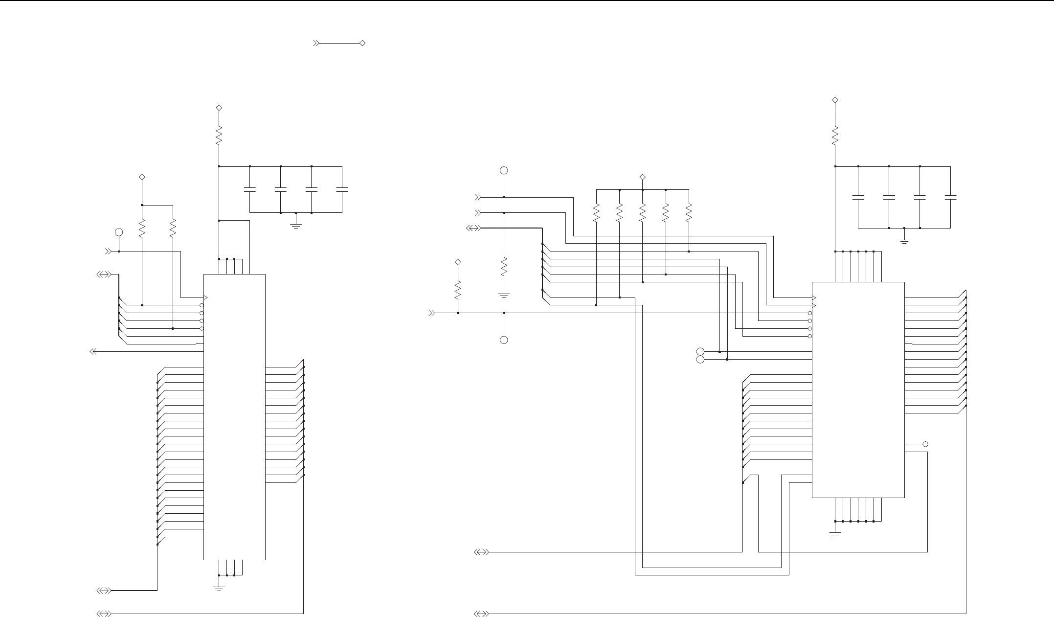
Controller R5 Schematic Diagrams 3-53
1.875V_DIG_V2 1.875V_DIG_V2
FLASH
R2004
0
1.875V_DIG_V2
10K
R2000
TP_FLASH_CLK 10K
R2012
FLASH_CTL(5:0)
FLASH_CLK
1.875V_DIG_V2
4
0
1
3
5
2
FLASH_WAITD3
D6
E7
F8
C4
C5
B5
B4
2
3
4
5
1
9
10
11
17
18
19
20
21
22
23
12
13
14
15
16
6
7
8
D7
A2
B2
C8
B3
C3
B8
A8
B7
A7
C7
B1
C1
D2
D1
D4
B6
A6
C6
E8
D8
C2
A1
G2
G8
A3
F1
VSSQ2
VSS1
VSS2
VSSQ1
NC
A9
A20
A21
A3
A4
A5
A6
A7
A8
A13
A14
A15
A16
A17
A18
A19
A2
A0
A1
A10
A11
A12
ST 4Mx16
D8
D9
D14
D15
D2
D3
D4
D5
D6
D7
D0
D1
D10
D11
D12
D13
WAIT
WP
RP
VDD1
VDD2
VDDQ1
VDDQ2
VPP
EN_E
EN_G
EN_L
EN_W
CLK_K
0104024J27 (Pre-Flashed Part)
8MByte
M58WR064FB
U2000
A4
G4
E1
G6
A5
C2001
.01uF
C2003
0.10uF0.10uF
C2002C2000
100pF
TP_SDRAM_CLK
R2010
10K
10K
R2013
TP_SDRAM_CS
SDRAM_CTL(6:0)
SDRAM_CLK_EN
SDRAM_CLK
SDRAM_CS
1.875V_DIG_V2 6
4
1
5
0
3
2
Normal Mode = 72 MHz (Morpheus); 90 MHz (Cypher)
Bootstrap Mode = 48 MHz
10K
R2005 R2006
10K10K
R2008 R2009
10K 10K
R2007
1.875V_DIG_V2
11
4
5
6
7
8
9
10
0
1
2
3
TP_SDRAM_BA1
12
TP_SDRAM_BA0
VSSQ1
B7 VSSQ2
C3 VSSQ3
D7 VSSQ4
A1 VSS1
E3 VSS2
J1 VSS3
A3
WE
RAS
CS
A7
A8
A9
BA0
BA1
CAS
CKE
CLK
A1
A2
A3
A4
A5
A6
A0
DQMH
DQML
A10
A11
F9
F1
E8
F8
H1
G3
G7
G8
F7
F3
F2
G9
H9
G2
J8
J7
J3
J2
H3
H2
H7
H8
MICRON 8Mx16
VDD3
VDDQ1
VDDQ2
VDDQ3
VDDQ4
DQ9
NC1
NC2
VDD1
VDD2
DQ15
DQ2
DQ3
DQ4
DQ5
DQ6
DQ7
DQ8
DQ0
DQ1
DQ10
DQ11
DQ12
DQ13
DQ14
A7
B3
C7
D3
A9
E7
J9
U2001
MT48H8M16LFB4 -8IT:J
E2
G1
B8
C9
C8
D9
D8
E9
E1
D2
A8
B9
D1
C2
C1
B2
B1
A2
NC
16MByte
0
1
14
15
7
8
9
10
11
12
13
2
3
4
5
6
C2006
0.10uF
C2004
100pF
C2007
.01uF
C2005
0.10uF
0
R2011
1.875V_DIG_V2
SDRAM
SDRAM_DATA(15:0)
SDRAM_ADD(12:0)
G1
G7
F6
F3
F2
E2
E5
G5
E4
G3
E3
F7
E6
F5
F4
D5
10
11
12
13
14
15
4
5
6
7
8
9
0
1
2
3
EMIFS_DATA(15:0)
EMIFS_ADD(23:1)
Controller Memories Schematic Diagram
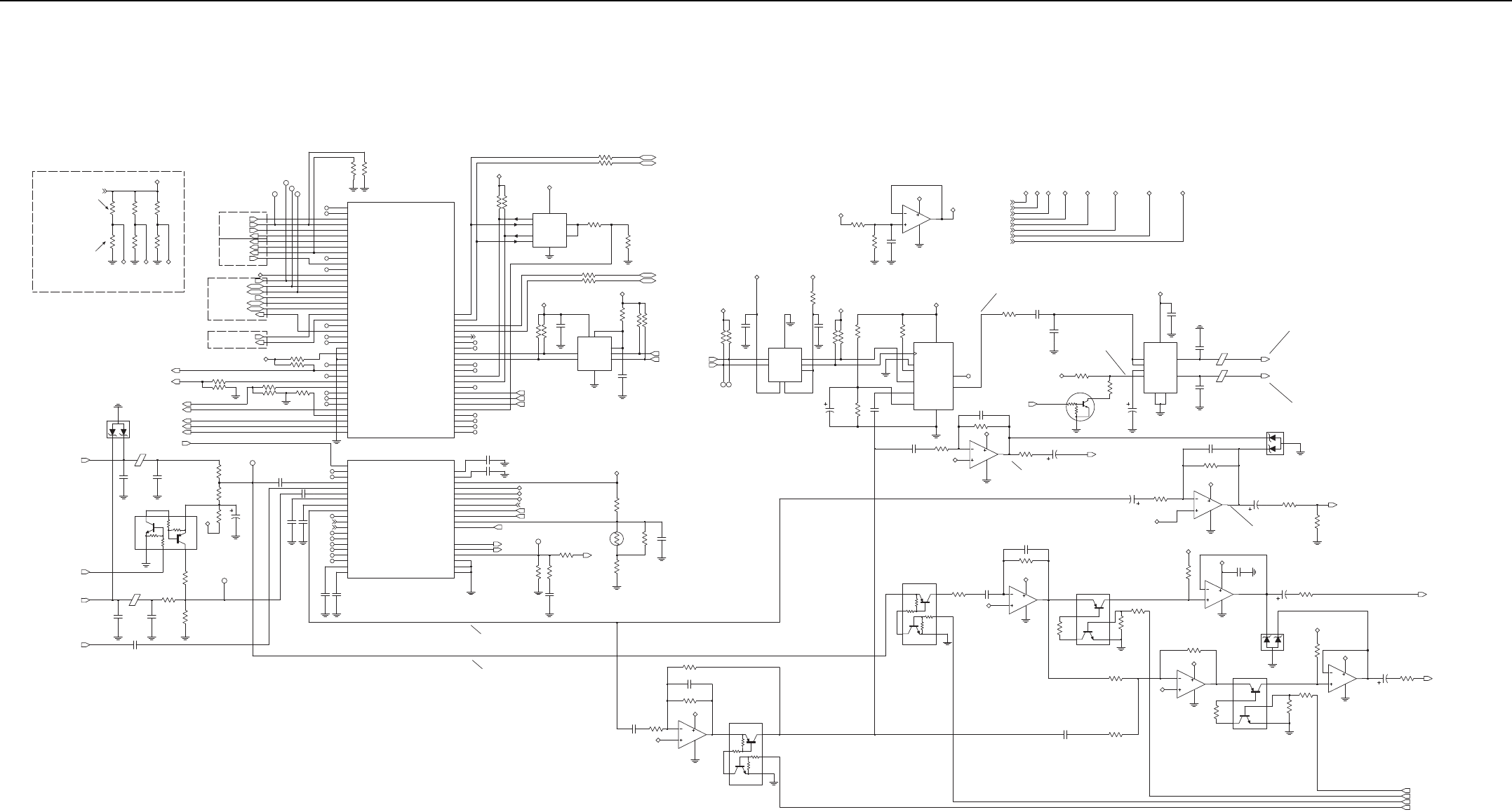
3-54 Controller R5 Schematic Diagrams
MOBILE SUSCRIBER: 0 OHM
MOBILE REPEATER: NOT_USED
MOBILE SUBSCRIBER: NOT_USED
HW_ID
MOBILE REPEATER: 33K
R3507 0
R3509 0
0
R3508
HW_ID0
2.9V_DIG_V6
HW_ID2
HW_ID1
R3504
NU
33K NU
R3505
33K
R3503
33K
2.9V_DIG_V6
NC
1USB1_SEO
NC
NC
USB1_TXEN
1
NC
MAKO_CE
1
USB1_DAT
1
MAKO UART
MAKO USB
USB0_DAT
USB0_SE0
USB0_TXEN
USB_INT
USB1_DAT
USB1_TXEN
USB1_SE0
RS232_TX
RS232_RX
MAKO SSI
MAKO SPI
1.875V_V2_MAKO
MAKO_CE
MAKO_TX
SPI_CLK
SPI_MOSI
SPI_MISO
MAKO_DCLK
MAKO_FSYNC
MAKO_RX
NC
NC
NC
NC
NC
NC
NC
NC
R3588 51.1K
10K
R3579
1.875V_V2_MAKO
3
1
2
MMBZ20V
VR3503
E3502
MMP_GPIO1_INPUT
MMP_GPIO2_INPUT
ONE_WIRE_UP
MAKO_OPT_GPIO3
INT_MIC+
MAKO_AD_TRIGGER
MAKO_OPT_INT
MAKO_OPT_GPIO0
MAKO_OPT_GPIO2
NU
R3587
5.1K
R3583
16.2K R3582
16.2K
10K
R3581
R3580 10K
C3520 1.0uF
C3521 1.0uF
NC
C3516
1.0uF NC
C3523 0.10uF
INT_MIC
1
0
R3526
560
R3547
C3515
220pF
C3514
220pF
R3532
100
10uF
C3524
R3535
560
EXT_MIC
1
9V3
EMD9FT2R
Q3501
2
5
6
3
1
4
1.0uF
C3518
220pF
C3530
MIC_GROUND
EXT_MIC+
EXT_MIC_ENA
E3503
C3531
220pF 39K
R3538
R3537
0
NC
NC
NC
NC
NC
NC
NC
SW_9V3
9V3_CNTRL
H3
A4
G2
A11
J3
H4
H2
K1
K2
F2
F1
L2
E1
G3
E3
J1
J2
G1
H1
B11
0.10uF
C3528
0.10uF
C3529
VC_OUT_P
VFUSE
VMES
VREF
PA_IN_P
PWR_CTRL
SCAN_EN
TEST
TX_RX
VCM1
VCM2
VC_OUT_M
FE_TUNE2
INT_MIC_M
INT_MIC_P
INT_SPKR_M
INT_SPKR_P
MIC_BIAS
PA_BPLUS
PA_IN_M
ATOD_7
ATOD_8
BPLUS
EXT_MIC_M
EXT_MIC_P
EXT_SPKR_M
EXT_SPKR_P
FE_TUNE1
AD_TRIG
ATOD_0
ATOD_1
ATOD_2
ATOD_3
ATOD_4
ATOD_5
ATOD_6
PA_CODEC_A2D_BLOCK
U3200-3
ADC_VREF
L10
K12
K13
N14
M13
L11
M14
L12
L13
K11
M12
E8
N1
C4
A3
M2
L3 4.12V (44W)
3.91V (27.5W)
R3571
2K
.01uF
C3538
R3550
82K
TX_RAMP_DAC
1
RT3500
10K 220pF
C3545
R3576
100
R3595
10K
R3596
150
26.7K
R3577
VSWR_DET
ANT_CURRENT_DET
BATTERY_SENSE
TX_DAC
LO_PWR_DET
2.9V_DIG_V6
HW_ID1
HW_ID0
HW_ID2
RX_FLTR_VCTRL
PA_BIAS
C3513 100pF
C3511 100pF
EN
1GND
3SCL1 SCL2
4SDA1 SDA2
VREF1
VREF2
PCA9306
U3508
GPIO_0_PWR_ON
GPIO_4_HOOK
GPIO_3_PTT
R3515 10K
R3514 10K
8
6
5
2
7
C3541
0.10uF
2.9V_DIG_V6
C3542
0.10uF
I2C_CLK 1
R3573
10K
0.10uF
C3539
1
I2C_DATA 10K
R3574
ONE_WIRE_1
ONE_WIRE_2
1.875V_DIG_V2
I2C_CLK
I2C_DATA
1.875V_DIG_V2
A1
D2
B1
C2
R3586
0
22K
R3584 R3585
22K
C1
IN2
NO1
NO2
V_POS
A2
U3504
TS5A23166
COM1
COM2
D1
B2
IN1
5V_V8_MAKO
3.3V_DIG_V10
3.3K
R3594
27R3501
200K
R3593
2.2K
R3591
R3500 27
R3592 2.2K
USB2_DM
USB2_DP
5V_SW
GND
27
R3512
R3510 27 USB1_DP
USB1_DM
1
SCL1
3SCL2 6
SDA1
4SDA2 5
VREF1
VREF2
U3503
PCA9306
EN 8
GND
10K
R3558
R3559 10K
200K
R3578
0.10uF
C3540
2.775V_DIG_V4
2.775V_DIG_V4
0
R3513
1K
R3569
W
AD0_CS*
B
CLK_SCL
DIS
GND
SDI_SDA
SDO_NC
A
4
VDD
9
U3501
AD5161
NC
2
6
8
5
10
1
3
7
0.1uF
C3508
C3536
10uF 1K
R3575
2
7
125mV RMS
15K
R3521
560
R3524
24K
R3523
2200pF
C3507
U3505-4
13
12
14
4
11
MC3403
22K
0.1uF
R3528
C3512
C3509
10uF
C3517
10uF
9V3
VAG
VAG
HANDSET_AUDIO
210K
47K
1
AUDIO_PA_ENA
5.3VDC muted
9.3VDC unmuted
52mV RMS for rated audio
R3511
10K 0.1uF
C3502
C3503
1000pF
5V_SW
DTC114YKAF
Q3500
3
R3516
24K
24K
R3520
9V3
C3506
47uF
7
VCC
2GND1
GND2
5
9INV
8M_SS
1NINV
4
OUT1
6
OUT2
RR
3
1000pF
C3504
C3505
1000pF
E3501
U3500
TDA1519C
E3500
0.1uF
C3501
UNSWB+
7.8V RMS
(7.5 W @ 8 ohms)
7.8V RMS
(7.5 W @ 8 ohms)
SPKR+
SPKR-
1
2
VR3502
3
330mV RMS 100K
R3548
C3519
47uF
330pF
C3510
R3529
51
U3505-1
MC3403
2
3
1
4
11
100K
R3525
RX_AUDIO
9V3
R3533
24K
U3502-3
MC3403
9
10
8
4
11
0.1uF
C3527
VAG
9V3
R3553 10K
R3554
47K
24K
R3544
Q3504
21
36
4
5
UMZ2NTR
R3551
10K
10uF
C3534
VR3504
MMBZ20V
10K
R3555
R3541
24K
R3542
24K
R3556
47K
41
5
Q3505
UMZ2NTR
2
36
13
12
14
4
11
4
11 U3502-4
MC3403
U3502-1
MC3403
2
3
1
10K
R3552
R3545
100
9V3
PUB_ADDRESS_2
VAG
VAG
9V3
C3535
1.0uF 15K
R3546
24K
R3539
3
1
2
C3525
220pF
100K
R3536
1.0uF
U3502-2
MC3403
6
5
7
4
11
C3532
VAG
9V3
V15
5
6
4
EMD9FT2R
Q3503
PUB_ADDRESS_1
100
R3540
C3533
10uF
PUB_ADDRESS_1_EN
PUB_ADDRESS_2_EN
LOW_LEVEL_MUTE
PUB_ADDRESS_MIC_EN
5
6
3
1
4
2
C3526
1.0uF R3534
10K
470pF
C3522
30K
R3549
Q3502
EMD9FT2R
NU 220K
R3530
4
11
MC3403
U3505-2
6
5
7
9V3
VAG
70mV RMS (RX AUDIO)
80mV RMS (TX AUDIO)
47K
R3560
R3572
10K
D7
A7
B7
M4
B9
A9
C9
C10
E7
A10
E9
N3
C8
B8
D8
E6
D6
B6
C6
K6
J5
A8
M3
P2
N2
N8
B12
F10
C11
G10
D11
L7
C7
C12
E11
D10
B10
A6
L5
A5
B5
P8
N7
L6
P7
N6
N9
N13
M10
M11
N12
K8
P12
N11
P9
M8
L8
P10
K7
M9
N10
P11
P13
VC_DCLK
VC_FSYNC
VC_RX
VC_TX
VC_TX3V
USB1_SE0
USB2_DAT_VP
USB2_DM
USB2_DP
USB2_OE_RCV_RTS
USB2_SE0_VM_RXD
USB_CONNECT
USB_INTX
TXDO_BDI_UP_3V
UART2_RXD_OD
UART2_TXD
UCM_SS
USB1_DAT_TXD
USB1_DM
USB1_DP
USB1_OE
SB96_BUS_BUSY
SPI_CLK
SPI_CS
SPI_DI
SPI_DO
TXDO_BDI_5V
TXDO_BDI_ENC_3V
OPT_GPIO3
RS232_USB_X
RTS_FILLSEN_3V
RTS_FILLSEN_5V
RXDIN_3V
RXDIN_5V
RXDIN_ENC_3V
SB96D_BDO_KF_3V
SB96_BDO_KF_5V
OPTB_SEL0
OPTB_SEL1
OPTB_SEL2
OPTB_SEL3OPTION_INTX
OPT_GPIO0
OPT_GPIO1
OPT_GPIO2
ONE_WIRE_2
ONE_WIRE_BATT
ONE_WIRE_UP
OPTA_SEL0
OPTA_SEL1
OPTA_SEL2
OPTA_SEL3
BBP_SYNC
BOOT_NORM_X
BUSY_IN
BUSY_OUT
CABLE_DET_3V
CTS_CABLE_DET_5V
CTS_X
LOGIC_VDD
ONE_WIRE_1
U3200-2
DIGITAL_BLOCK
APCO
BBP_CLK
NC
NC
NC
NC
NC
NC
NC
NC
NC
USB_CONNECT
1.875V_V2_MAKO
2.775V_DIG_V4
1.875V_DIG_V2
5V_SW
5V_V8_MAKO
UNSWB+
9V3
3.3V_DIG_V10
(SOURCE)
1.875V_V2_MAKO
2.775V_DIG_V4
1.875V_DIG_V2
5V_SW
5V_V8_MAKO
UNSWB+
9V3
3.3V_DIG_V10
VAG
C3500
10.0uF
10K
R3502
R3506
10K
MC3403
U3505-3
9
10
8
4
11
9V3
9V3
Controller Audio and USB Schematic Diagram

Controller R5 Schematic Diagrams 3-55
5.1 Controller R5 Parts List
Circuit
Ref
Motorola Part
No Description
C1000 2113944A40 100pF
C1001 2113945Y02 0.10uF
C1002 2113945Y02 0.10uF
C1003 2113944A40 100pF
C1004 2113944A40 100pF
C1005 2113945Y02 0.10uF
C1006 2113945Y02 0.10uF
C1007 2113944A40 100pF
C1008 2113944A40 100pF
C1009 2113945Y02 0.10uF
C1010 2113945Y02 0.10uF
C1011 2113944A40 100pF
C1012 2113945Y02 0.10uF
C1013 2113945Y02 0.10uF
C1014 2113945Y02 0.10uF
C1015 2113945Y02 0.10uF
C1016 2113945Y02 0.10uF
C1017 2113946E02 1.0uF
C1018 2113944A28 18pF
C1019 2113944A28 18pF
C1030 2113944A28 18pF
C1031 2113945Y02 0.10uF
C1032 2113945B02 .01uF
C1033 2113945Y02 0.10uF
C1034 2113946S35 1.0uF
C1035 2113946D05 2.2uF
C1036 2113946S35 1.0uF
C1037 2113946D05 2.2uF
C1044 2113945Y02 0.10uF
C2000 2113944A40 100pF
C2001 2113945B02 .01uF
C2002 2113945Y02 0.10uF
C2003 2113945Y02 0.10uF
C2004 2113944A40 100pF
C2005 2113945B02 .01uF
C2006 2113945Y02 0.10uF
C2007 2113945Y02 0.10uF
C2500 2113944A44 220pF
C2501 2113945A10 1500pF
C3000 2113944C06 470pF
C3002 2371403L02 10uF
C3005 2113944C06 470pF
C3006 2314030E85 33uF
C3007 2113945C31 0.1uF
C3008 2113945A09 1000pF
C3009 2113945Y02 0.10uF
C3010 2113946S35 1.0uF
C3011 2113946S35 1.0uF
C3012 2113944C06 470pF
C3013 2314030J28 22uF
C3014 2113945C31 0.1uF
C3015 2113944C38 47pF
C3016 2113944A40 100pF
C3017 2113945A09 1000pF
C3018 2389289U01 10uF
C3019 2113944C06 470pF
C3020 2314030E85 33uF
C3021 2113945C31 0.1uF
C3030 2113945C02 .01uF
Circuit
Ref
Motorola Part
No Description
C3031 2113945C31 0.1uF
C3032 2113945B02 .01uF
C3040 2113944C06 470pF
C3041 2113945C02 .01uF
C3042 2113945B02 .01uF
C3043 2314030E85 33uF
C3044 2113945C31 0.1uF
C3045 NOT PLACED –
C3046 2113945Y02 0.10uF
C3200 2113946J04 22uF
C3201 2113946D05 2.2uF
C3202 2113945Y02 0.10uF
C3203 2316410H02 68uF
C3204 2115153H21 5.6pF
C3205 2115153H21 5.6pF
C3206 2316410H01 22uF
C3207 2113945C31 0.1uF
C3208 2113946D05 2.2uF
C3209 2113945Y02 0.10uF
C3210 2113946D05 2.2uF
C3211 2113945A09 1000pF
C3212 2316410H02 68uF
C3213 2113946F03 4.7uF
C3214 2115153H45 33pF
C3215 2115153H45 33pF
C3216 2113946F03 4.7uF
C3217 2113944A44 220pF
C3218 2113945Y02 0.10uF
C3219 2113944A44 220pF
C3220 2113945Y02 0.10uF
Circuit
Ref
Motorola Part
No Description
C3221 2113944A44 220pF
C3222 2113945Y02 0.10uF
C3225 2113944A44 220pF
C3226 2113945Y02 0.10uF
C3227 2113944A44 220pF
C3228 2113945Y02 0.10uF
C3229 2113944A44 220pF
C3231 2113944A44 220pF
C3232 2113945Y02 0.10uF
C3233 2113944A44 220pF
C3234 2113946D05 2.2uF
C3237 2113946D05 2.2uF
C3238 2113946H02 10uF
C3239 2113946D05 2.2uF
C3240 2113944C45 100pF
C3243 2113946S35 1.0uF
C3247 2113946H02 10uF
C3248 2113946S35 1.0uF
C3249 2113944C45 100pF
C3252 2113946S35 1.0uF
C3254 2113946D05 2.2uF
C3257 2113946S35 1.0uF
C3260 2113946S35 1.0uF
C3261 2113944A44 220pF
C3262 2113946N03 2.2uF
C3265 2113946J04 22uF
C3266 2113946D05 2.2uF
C3269 2113946S35 1.0uF
C3270 2113946S35 1.0uF
C3272 2115153H27 10pF
Circuit
Ref
Motorola Part
No Description

3-56 Controller R5 Schematic Diagrams
C3273 NOT PLACED –
C3274 2113944A44 220pF
C3275 2113946J03 10.0uF
C3276 2113946S35 1.0uF
C3277 2113946S35 1.0uF
C3278 2113945C31 0.1uF
C3279 2113945C31 0.1uF
C3280 2113945C31 0.1uF
C3281 2113945C31 0.1uF
C3282 2113946F03 4.7uF
C3283 2113945Y02 0.10uF
C3289 2113945Y02 0.10uF
C3290 2113945Y02 0.10uF
C3291 2113945Y02 0.10uF
C3292 2113945A09 1000pF
C3500 2113946J03 10.0uF
C3501 2113945G91 0.1uF
C3502 2113945C31 0.1uF
C3503 2113945A09 1000pF
C3504 2113945A09 1000pF
C3505 2113945A09 1000pF
C3506 2314030F30 47uF
C3507 2113945A11 2200pF
C3508 2113945C31 0.1uF
C3509 2313960D07 10uF
C3510 2113945A03 330pF
C3511 2113944A40 100pF
C3512 2113945C31 0.1uF
C3513 2113944A40 100pF
C3514 2113944A44 220pF
Circuit
Ref
Motorola Part
No Description
C3515 2113944A44 220pF
C3516 2113946S35 1.0uF
C3517 2314030M51 10uF
C3518 2113946S35 1.0uF
C3519 2314030F30 47uF
C3520 2113946S35 1.0uF
C3521 2113946S35 1.0uF
C3522 2113945A05 470pF
C3523 2113945Y02 0.10uF
C3524 2313960D07 10uF
C3525 2113944A44 220pF
C3526 2113946S35 1.0uF
C3527 2113945C31 0.1uF
C3528 2113945Y02 0.10uF
C3529 2113945Y02 0.10uF
C3530 2113944A44 220pF
C3531 2113944A44 220pF
C3532 2113946S35 1.0uF
C3533 2313960D07 10uF
C3534 2313960D07 10uF
C3535 2113946S35 1.0uF
C3536 2314030M51 10uF
C3538 2113945B02 .01uF
C3539 2113945Y02 0.10uF
C3540 2113945Y02 0.10uF
C3541 2113945Y02 0.10uF
C3542 2113945Y02 0.10uF
C3545 2113944A44 220pF
C4000 NOT PLACED –
C4001 NOT PLACED –
Circuit
Ref
Motorola Part
No Description
C4002 NOT PLACED –
C4003 NOT PLACED –
C4004 NOT PLACED –
C4005 NOT PLACED –
C4006 2113944A44 220pF
C4012 NOT PLACED –
C4013 2113944A44 220pF
C4014 2113944A44 220pF
C4015 2113944A44 220pF
C4016 2113944A44 220pF
C4017 2113944A44 220pF
C4018 2113944A44 220pF
C4019 NOT PLACED –
C4020 NOT PLACED –
C4021 2113944A44 220pF
C4022 2113944A44 220pF
C4023 2113944A44 220pF
C4024 2113944A44 220pF
C4025 2113944A44 220pF
C4026 2113944A44 220pF
C4027 2113944A44 220pF
C4028 2113944A44 220pF
C4029 2113944A44 220pF
C4030 2113944A44 220pF
C4031 2113944A44 220pF
C4032 2113944A44 220pF
C4033 2113944A44 220pF
C4034 2113945A03 330pF
C4035 2113945A03 330pF
C4040 2113944A44 220pF
Circuit
Ref
Motorola Part
No Description
C4041 2113944A44 220pF
C4042 2113944A44 220pF
C4043 2113944A44 220pF
C4044 2113944A44 220pF
C4045 2113944A44 220pF
C4046 2113944A44 220pF
C4047 2113944A44 220pF
C4048 2113944A44 220pF
C4049 NOT PLACED –
C4051 NOT PLACED –
C4053 NOT PLACED –
C4055 NOT PLACED –
C4058 NOT PLACED –
C4059 NOT PLACED –
C4060 NOT PLACED –
C4061 NOT PLACED –
C4062 NOT PLACED –
C4063 2113944A44 220pF
C4064 2113944A44 220pF
C4065 2113944A44 220pF
C4066 2113944A44 220pF
C4067 2113944A44 220pF
C4068 2113944A44 220pF
C4069 2113944A44 220pF
C4070 2113944A44 220pF
C4071 NOT PLACED –
C4072 NOT PLACED –
C4073 2113945Y02 0.10uF
C4074 NOT PLACED –
C4075 NOT PLACED –
Circuit
Ref
Motorola Part
No Description
Controller R5 Schematic Diagrams 3-57
C4076 NOT PLACED –
C4084 2113945Y02 0.10uF
C4085 2113944A44 220pF
C4086 2113945Y02 0.10uF
C4087 2113945Y02 0.10uF
C4088 2113945Y02 0.10uF
C4089 2113945Y02 0.10uF
C4090 2113945Y02 0.10uF
C4091 2113945Y02 0.10uF
C4092 2113945Y02 0.10uF
C4093 NOT PLACED –
C4094 NOT PLACED –
D3030 4813978P07 DIODE, SWITCHING
D3040 4813978P07 DIODE, SWITCHING
D3200 4813978C02 DIODE, SWITCHING
D4000 4866544A01 DIODE, DUAL
D4001 4866544A01 DIODE, DUAL
E2500 2480675U01 FERRITE BEAD
E3000 2485011Y01 FERRITE BEAD
E3201 2480675U01 FERRITE BEAD
E3202 2480675U01 FERRITE BEAD
E3203 2480675U01 FERRITE BEAD
E3205 2480675U01 FERRITE BEAD
E3206 2480675U01 FERRITE BEAD
E3208 2480675U01 FERRITE BEAD
E3500 2485011Y01 FERRITE BEAD
E3501 2485011Y01 FERRITE BEAD
E3502 2485011Y01 FERRITE BEAD
E3503 2485011Y01 FERRITE BEAD
E4000 2485011Y01 FERRITE BEAD
Circuit
Ref
Motorola Part
No Description
E4001 7686949J14 FERRITE BEAD
E4002 7686949J14 FERRITE BEAD
E4003 NOT PLACED –
E4004 2409134J25 FERRITE BEAD
E4005 2409134J25 FERRITE BEAD
E4006 2409134J25 FERRITE BEAD
J2500 NOT PLACED –
J3000 0905902V09 DC POWER
CONNECTOR
J4000 0916017H01 26-PIN ACCESSORY
CONNECTOR
J4001 0915555H01 30-PIN CONTROL
HEAD CONNECTOR
J4002 0915558H01 11-PIN REPEATER
CONNECTOR
J4003 0915556H01 14-PIN OPT BRD
CONNECTOR
L3200 2415005H02 22uH
L3201 2415005H02 22uH
L3202 2415005H02 22uH
Q3030 4813973M07 NPN
Q3032 4813973B01 NPN
Q3040 4813973M07 NPN
Q3041 4815263H01 ANALOG SWITCH
Q3200 5185956E76 N-CHANNEL SYN-
CHRONOUS MOSFET
Q3201 4813970A62 P-CHANNEL MOSFET
Q3202 5185956E76 N-CHANNEL SYN-
CHRONOUS MOSFET
Q3203 4805585Q23 PMOS FET
Q3204 4805585Q23 PMOS FET
Q3205 4815262H01 ANALOG SWITCH
Q3206 4815272H01 ANALOG SWITCH
Circuit
Ref
Motorola Part
No Description
Q3207 4813970A62 P-CHANNEL MOSFET
Q3208 4815261H01 ANALOG SWITCH
Q3209 4813973M07 NPN
Q3210 4813973M07 NPN
Q3500 4815261H01 ANALOG SWITCH
Q3501 4815272H01 ANALOG SWITCH
Q3502 4815272H01 ANALOG SWITCH
Q3503 4815272H01 ANALOG SWITCH
Q3504 4815270H01 ANALOG SWITCH
Q3505 4815270H01 ANALOG SWITCH
Q4000 4815263H01 ANALOG SWITCH
Q4001 4815263H01 ANALOG SWITCH
Q4002 4815261H01 ANALOG SWITCH
Q4003 4815263H01 ANALOG SWITCH
Q4004 4815261H01 ANALOG SWITCH
Q4005 4815263H01 ANALOG SWITCH
Q4006 4815263H01 ANALOG SWITCH
Q4007 4815263H01 ANALOG SWITCH
Q4008 4815261H01 ANALOG SWITCH
Q4009 4815263H01 ANALOG SWITCH
Q4010 4815261H01 ANALOG SWITCH
Q4011 4815263H01 ANALOG SWITCH
Q4012 4815261H01 ANALOG SWITCH
Q4013 4816023H01 PNP
Q4014 4813973A06 NPN
Q4015 4815263H01 ANALOG SWITCH
R1000 0613952Q25 10
R1001 0613952R01 10K
R1002 0613952J73 10MEG
R1005 0613952Q89 4.7K
Circuit
Ref
Motorola Part
No Description
R1006 0613952R01 10K
R1014 0613952R66 0
R1017 0613952R01 10K
R1019 0613952Q18 5.1
R1020 0613952R66 0
R1021 0613952R66 0
R1025 0613952R01 10K
R1026 0613952R17 47K
R1027 NOT PLACED –
R1028 0613952R66 0
R1034 0613952R01 10K
R1035 NOT PLACED –
R1036 0613952R01 10K
R1041 0613952Q73 1K
R1044 0613952R66 0
R1045 0613952R01 10K
R1046 NOT PLACED
R1047 0613952R66 0
R1048 0613952R66 0
R1054 0613952Q89 4.7K
R1060 0613952Q25 10
R1066 NOT PLACED –
R1067 NOT PLACED –
R1070 0613952R66 0
R1071 0613952R17 47K
R2000 0613952R01 10K
R2004 0613952R66 0
R2005 0613952R01 10K
R2006 0613952R01 10K
R2007 0613952R01 10K
Circuit
Ref
Motorola Part
No Description

3-58 Controller R5 Schematic Diagrams
R2008 0613952R01 10K
R2009 0613952R01 10K
R2010 0613952R01 10K
R2011 0613952R66 0
R2012 0613952R01 10K
R2013 0613952R01 10K
R2500 0613952R66 0
R2501 0613952R66 0
R2502 0613952R66 0
R2504 0613952R66 0
R2506 0613952R66 0
R2507 0613952R66 0
R2508 0613952R66 0
R2509 0613952R66 0
R2510 0613952R66 0
R2511 0613952R66 0
R2512 0613952R66 0
R2513 0613952R66 0
R2514 0613952R66 0
R2515 0613952R66 0
R2516 0613952R66 0
R2517 0613952R66 0
R2518 0613952R66 0
R2519 0613952R66 0
R2520 0613952R66 0
R2524 0613952R66 0
R2525 0613952R66 0
R2526 0613952R66 0
R2527 0613952R66 0
R2528 0613952R66 0
Circuit
Ref
Motorola Part
No Description
R2529 0613952R01 10K
R3002 0613952R01 10K
R3003 0613952M54 3.57K
R3004 0613952L73 562
R3005 0613952Q81 2.2K
R3006 0613952Q57 220
R3007 0613952N58 39.2K
R3008 0613952N12 13K
R3009 0613952N58 39.2K
R3010 0613952N12 13K
R3030 0613952R01 10K
R3032 0615871H01 0.1
R3033 0615871H01 0.1
R3034 0613952H61 330
R3035 0613952H25 10
R3036 0613952H25 10
R3037 0613959G61 330
R3038 NOT PLACED –
R3039 0613952M30 2K
R3040 0613952M43 2.74K
R3041 0613952R25 100K
R3042 0613952H69 680
R3043 0613952H69 680
R3044 0613958S61 330
R3045 0613952M30 2K
R3046 0613952M43 2.74K
R3047 0613952R25 100K
R3048 0613952Q73 1K
R3050 0613959Q53 150
R3051 0613952G67 0
Circuit
Ref
Motorola Part
No Description
R3052 0613952G67 0
R3053 0613952R66 0
R3054 0613952R66 0
R3055 0615871H01 0.1
R3056 0615871H01 0.1
R3057 0613952R66 0
R3200 0615871H01 0.1
R3203 0615871H01 0.1
R3204 0615871H01 0.1
R3205 0613952R25 100K
R3206 0613952R66 0
R3207 0686135Z02 0.2
R3208 0686135Z02 0.2
R3209 0613952N62 43.2K
R3210 0613952N16 14.3K
R3215 0613952G67 0
R3216 0613952G67 0
R3217 NOT PLACED –
R3218 0613952R66 0
R3219 0613952R56 2MEG
R3220 0613952R56 2MEG
R3222 0613952R33 220K
R3223 0613952R33 220K
R3224 0613952Q89 4.7K
R3225 NOT PLACED –
R3226 0613952R13 33K
R3227 NOT PLACED –
R3228 0613952G67 0
R3233 0613952R66 0
R3236 0613952Q73 1K
Circuit
Ref
Motorola Part
No Description
R3237 0613952R01 10K
R3238 0613952H25 10
R3239 0613952H25 10
R3240 0613952R17 47K
R3241 0613952Q18 5.1
R3243 0613952Q18 5.1
R3245 0613952G67 0
R3246 0613952M81 6.81K
R3247 0613952N69 51.1K
R3248 0613952R01 10K
R3249 NOT PLACED –
R3250 0613952R25 100K
R3252 0613952R25 100K
R3253 0613952R17 47K
R3500 0613952Q35 27
R3501 0613952Q35 27
R3502 0613952R01 10K
R3503 0613952R13 33K
R3504 NOT PLACED –
R3505 NOT PLACED –
R3506 0613952R01 10K
R3507 NOT PLACED –
R3508 0613952R66 0
R3509 0613952R66 0
R3510 0613952Q35 27
R3511 0613952R01 10K
R3512 0613952Q35 27
R3513 0613952R66 0
R3514 0613952R01 10K
R3515 0613952R01 10K
Circuit
Ref
Motorola Part
No Description

Controller R5 Schematic Diagrams 3-59
R3516 0613952R10 24K
R3520 0613952R10 24K
R3521 0613952R05 15K
R3523 0613952R10 24K
R3524 0613952Q67 560
R3525 0613952R25 100K
R3526 0613952R66 0
R3528 0613952R09 22K
R3529 0613952Q42 51
R3530 NOT PLACED –
R3532 0613952Q49 100
R3533 0613952R10 24K
R3534 0613952R01 10K
R3535 0613952Q67 560
R3536 0613952R25 100K
R3537 0613952R66 0
R3538 0613952R15 39K
R3539 0613952R10 24K
R3540 0613952Q49 100
R3541 0613952R10 24K
R3542 0613952R10 24K
R3544 0613952R10 24K
R3545 0613952Q49 100
R3546 0613952R05 15K
R3547 0613952Q67 560
R3548 0613952J25 100K
R3549 0613952R12 30K
R3550 0613952R23 82K
R3551 0613952R01 10K
R3552 0613952R01 10K
Circuit
Ref
Motorola Part
No Description
R3553 0613952R01 10K
R3554 0613952R17 47K
R3555 0613952R01 10K
R3556 0613952R17 47K
R3558 0613952R01 10K
R3559 0613952R01 10K
R3560 0613952R17 47K
R3569 0613952Q73 1K
R3571 0613952Q80 2K
R3572 0613952R01 10K
R3573 0613952R01 10K
R3574 0613952R01 10K
R3575 0613952Q73 1K
R3576 0613952Q49 100
R3577 0613952N42 26.7K
R3578 0613952R32 200K
R3579 0613952R01 10K
R3580 0613952R01 10K
R3581 0613952R01 10K
R3582 0613952N21 16.2K
R3583 0613952N21 16.2K
R3584 0613952R09 22K
R3585 0613952R09 22K
R3586 0613952R66 0
R3587 NOT PLACED –
R3588 0613952N69 51.1K
R3591 0613952Q81 2.2K
R3592 0613952Q81 2.2K
R3593 0613952R32 200K
R3594 0613952Q85 3.3K
Circuit
Ref
Motorola Part
No Description
R3595 0613952R01 10K
R3596 0613952H53 150
R4000 NOT PLACED –
R4001 0613952Q37 33
R4002 0613952Q37 33
R4003 0613952Q37 33
R4004 0613952Q37 33
R4005 0613952Q37 33
R4006 0613952Q65 470
R4009 0613952Q42 51
R4010 0613952Q42 51
R4011 0613952R66 0
R4012 0613952R66 0
R4023 0613952Q75 1.2K
R4030 NOT PLACED –
R4031 0613952R01 10K
R4032 0613952R01 10K
R4033 NOT PLACED –
R4034 0613952R01 10K
R4035 0613952R01 10K
R4040 0613952Q89 4.7K
R4041 0613952Q89 4.7K
R4042 0613952Q89 4.7K
R4043 0613952Q89 4.7K
R4044 0613952Q89 4.7K
R4045 0613952Q89 4.7K
R4046 0613952Q89 4.7K
R4047 0613952Q89 4.7K
R4048 0613952Q77 1.5K
R4049 0613958H83 2.7K
Circuit
Ref
Motorola Part
No Description
R4050 0613952R01 10K
R4051 0613952R39 390K
R4054 0613952R01 10K
R4055 0613952R01 10K
R4061 0613952Q37 33
R4063 0613952Q37 33
R4064 0613952Q37 33
R4065 0613952Q37 33
R4066 0613952Q37 33
R4067 0613952Q37 33
R4068 0613952Q37 33
R4069 0613952Q37 33
R4070 0613952Q37 33
R4071 0613952R66 0
R4072 NOT PLACED –
R4073 NOT PLACED –
R4074 0613952R66 0
R4075 NOT PLACED –
R4076 0613952R66 0
R4078 0613952R66 0
R4079 0613952R01 10K
R4080 0613952R66 0
R4081 0613952R66 0
R4082 0613952R66 0
R4083 0613952R66 0
R4085 0613952R66 0
R4086 0613952R66 0
R4088 0613952R01 10K
R4089 0613952R17 47K
R4090 0613952R66 0
Circuit
Ref
Motorola Part
No Description
3-60 Controller R5 Schematic Diagrams
R4093 0613952R66 0
R4094 0613952R66 0
R4095 0613952R66 0
R4096 0613952R66 0
R4097 0613952R66 0
R4098 0613952Q89 4.7K
R4099 0613952R66 0
R4100 0613952Q75 1.2K
R4101 0613952Q75 1.2K
R4103 0613952Q75 1.2K
R4105 0613952R01 10K
R4106 0613952R01 10K
RT3500 0615471H01 THERMISTOR, 10K
SP3000 1015349H03 SOLDER PREFORM
SP3001 1015349H03 SOLDER PREFORM
U1000 5102495J13 MICROPROCESSOR
U1006 5115001H02 IC, DUAL UNBUF-
FERED INVERTER
U2000 0104024J27 IC, 8MB FLASH
U2001 5171614M01 IC, 16MB SDRAM
U3001 5164015H94 VOLTAGE
REGULATOR
U3002 5115391H01 VOLTAGE
REGULATOR
U3003 5164015H94 VOLTAGE
REGULATOR
U3004 5115391H01 VOLTAGE
REGULATOR
U3005 0105959T72 PNP
U3006 0105959T72 PNP
U3030 5116525H01 DUAL OPAMP
U3040 0105959T72 PNP
Circuit
Ref
Motorola Part
No Description
U3200 5185143E77 IC, POWER
MANAGEMENT
U3201 5115616H01 VOLTAGE
REGULATOR
U3202 5115453H01 DUAL OPAMP
U3203 5114007A43 IC, SCHMITT TRIGGER
U3500 5102463J95 AUDIO PA
U3501 5115368H01 DIGITAL ATTENUATOR
U3502 5114016A18 QUAD OPAMP
U3503 5164852H47 IC, LEVEL
TRANSLATOR
U3504 5171395L01 IC, CMOS SWITCH
U3505 5114016A18 QUAD OPAMP
U3508 5164852H47 IC, LEVEL
TRANSLATOR
U4000 5115476H01 IC, SERIAL-TO-PARAL-
LEL CONVERTER
U4001 5115502H01 LOGIC TRANSLATOR
U4004 5115865H01 IC, BUFFER
U4005 5115865H01 IC, BUFFER
U4006 5115865H01 IC, BUFFER
U4007 5115865H01 IC, BUFFER
U4008 5115865H01 IC, BUFFER
U4009 5115865H01 IC, BUFFER
U4010 5115865H01 IC, BUFFER
VR3000 4813979C17 TRANSIENT
SUPPRESSOR
VR3040 4813977M10 DIODE, 5.1V ZENER
VR3200 4813977M10 DIODE, 5.1V ZENER
VR3201 4813977M05 DIODE, 3.3V ZENER
VR3202 4813977M05 DIODE, 3.3V ZENER
VR3203 4813977M05 DIODE, 3.3V ZENER
VR3204 4813977M13 DIODE, 6.2V ZENER
Circuit
Ref
Motorola Part
No Description
VR3205 4813977M05 DIODE, 3.3V ZENER
VR3206 4813977M13 DIODE, 6.2V ZENER
VR3207 4813977M13 DIODE, 6.2V ZENER
VR3208 4813977M13 DIODE, 6.2V ZENER
VR3502 4813977A48 DIODE, 20V ZENER
VR3503 4813977A48 DIODE, 20V ZENER
VR3504 4813977A48 DIODE, 20V ZENER
VR4000 4813977A48 DIODE, 20V ZENER
VR4001 4813977A48 DIODE, 20V ZENER
VR4002 4813977A48 DIODE, 20V ZENER
VR4003 4813977A48 DIODE, 20V ZENER
VR4004 4813977A48 DIODE, 20V ZENER
VR4005 4813977M13 DIODE, 6.2V ZENER
VR4006 4813977M13 DIODE, 6.2V ZENER
VR4007 NOT PLACED –
VR4008 NOT PLACED –
VR4009 4813977A48 DIODE, 20V ZENER
Y1000 4809612J45 12 MHZ CRYSTAL
Y3200 4815028H01 24.576 MHZ CRYSTAL
Y3201 4802582S80 32 KHZ CRYSTAL
Circuit
Ref
Motorola Part
No Description
Controller R6 Schematic Diagrams 3-61
6.0 Controller R6 Schematic Diagrams
MMP
CONTROL HEAD REAR ACCESSORY REPEATER INTERFACEOPTION BOARD INTERFACE
( 1 SHEET )
GPS
( SHEET 1 )
( MAKO AUDIO_DIGITAL_USB/RS232 : SHEET 3)
( DC SUPPLY: SHEET 1)
( MAKO POWER MANAGEMENT : SHEET 2)
(OMAP 1710: SHEET 1)
(MEMORY: SHEET 2)
(Active HIGH: ~ 27us)
Controller Module Version Changes
AUDIO_DC
P3
P2
CNTLR
PERIPHERALS
REF. DESIGNATOR RANGE ON THIS SHEET:
NEO P1 CNTRL
X
X
GPS X
NEO P7
(6.0 MHz)
(1.20 MHz)
(20.0 KHz)
(4.20 MHz)
(84.0 KHz)
(Active LOW: ~27us)
(Active LOW: 20-86us)
J2500-10
J2500-4
J2500-13
RF_ATTN_2
J2500-15
1
J2500-9
R2509
SPI_MISO_1
1
R2525
2.9V_MAKO_V6
NC
R2527
R2519
C2501
NC
1.875V
16.8MHz
32KHZ_GPS
5V_ACTIVE_ANT
ANT_CURRENT
GPS_5V
GPS_BOOT_SEL
GPS_ON_OFF_LS
GPS_RESET_LS
GPS_RX_LS
GPS_TX_LS
VCONT
SW_9V3
SYSTEM_SYNC
USB2_DM
USB2_DP
VBUS1
VBUS2
VOLUME_1
VOLUME_2
J2500-17
PROGM_IO_CS
PUB_ADDRESS_1
PUB_ADDRESS_1_EN
PUB_ADDRESS_2
PUB_ADDRESS_2_EN
RESET
RESET_OUT
RTC_BATTERY
RX_AUDIO
SERIAL_CLK
SERIAL_DATA
SSI_CLK
SSI_DATA_IN
SSI_DATA_OUT
SSI_FSYNC
KEYPAD_ROW_0
KEYPAD_ROW_1
KEYPAD_ROW_2
KEYPAD_ROW_3
LED_CS
MIC_GROUND
McBSP3_CLKX
McBSP3_DR
McBSP3_DX
McBSP3_FSX
ONE_WIRE_1
ONE_WIRE_2
ON_OFF_SW
OPT_BRD_PTT
OPT_GPIO_1
OPT_GPIO_2
GP5_4_EMERGENCY
GP5_5_IGNITION_SENSE
GP5_6_TxDc_BUS+
GP5_7_RxDc_BUS-
GP5_8_CTSs_RESET
GPIO_0_PWR_ON
GPIO_1_USB1_DP
GPIO_2_USB1_DM
GPIO_3_PTT
GPIO_4_HOOK
HANDSET_AUDIO
INT_MIC+
INT_SPKR+
INT_SPKR-
KEYPAD_COL_0
KEYPAD_COL_1
KEYPAD_COL_2
1V8
3.3V
5V
9V3
ARMIO_6
DIR_CTRL
DISPLAY_CMD
DISPLAY_CS
EXT_MIC+
EXT_SPKR+
EXT_SPKR-
EXT_SWB+
GP5_1_PTT
GP5_2_MONITOR
GP5_3_CHAN_ACTIVITY
C2500
R2516
R2500
VBUS1
VBUS2
J2500-7
J2500-18
SPI_MISO
SPI_MOSI
SPKR+
SPKR-
SW_9V3
USB0_DAT
USB0_SE0
USB0_TXEN
USB1_DAT
USB1_DM
USB1_DP
USB1_SE0
USB1_TXEN
USB2_DM
USB2_DP
USB_INT
ONE_WIRE_1
ONE_WIRE_2
ONE_WIRE_UP
ON_OFF_MECH
POR
PUB_ADDRESS_1
PUB_ADDRESS_1_EN
PUB_ADDRESS_2
PUB_ADDRESS_2_EN
PUB_ADDRESS_MIC_EN
RAW_B+
RS232_RX
RS232_TX
RTC_BATTERY
RX_AUDIO
SPI_CLK
MAKO_DAC1
MAKO_DAC2
MAKO_DCLK
MAKO_FSYNC
MAKO_INT
MAKO_OPT_GPIO0
MAKO_OPT_GPIO2
MAKO_OPT_GPIO3
MAKO_OPT_INT
MAKO_RAMP_DAC3
MAKO_RX
MAKO_TX
MIC_GROUND
MMP_GPIO1_INPUT
MMP_GPIO2_INPUT
OMAP_CORE_LDO
GATED_32KHZ_OMAP
GP5_4_EMERGENCY
GP5_5_IGNITION_SENSE
GPIO_0_PWR_ON
GPIO_3_PTT
GPIO_4_HOOK
HANDSET_AUDIO
I2C_CLK
I2C_DATA
INT_MIC+
LOW_LEVEL_MUTE
LO_BATTERY_DET
MAKO_ADC5
MAKO_ADC8
MAKO_AD_TRIGGER
MAKO_CE
16.8_MHZ_BUFF
2.775V_ANA_V7
2.775V_DIG_V4
2.9V_DIG_V6
3.3V_DIG_V10
3.6V_DIG_VSW1
32KHZ_GPS
5V
5V_SW
9V3
9V3_PA
ANT_CURRENT_DET
AUDIO_PA_ENA
EXT_MIC+
EXT_MIC_ENA
EXT_SWB+
NC
1.875V_DIG_V2
R2517
J2500-11
R2515
J2500-6
R2520
J2500-2
J2500-19
J2500-8
R2501
R2506
J2500-3
R2514
R2510
J2500-14
1
J2500-16
R2507
SPI_CLK_1
R2511
NC
R2502
3.6V_MAKO_SW1 1
R2524
J2500-20
R2528
J2500-12
J2500-1
R2529
E2500
J2500-5
R2526
R2512
R2508
R2504
SPI_MOSI_1
1
R2513
USB1_DAT
USB1_SE0
USB1_TXEN
USB_INT
RS232_TX
RX_CLK
RX_DATA
RX_FSYNC
SERIAL_CLK
SERIAL_DATA
SPI_CLK
SPI_MISO
SPI_MOSI
THK_CE
TX_CLK
TX_DATA
TX_FSYNC
USB0_DAT
USB0_SE0
USB0_TXEN
MAKO_OPT_INT
MAKO_RX
MAKO_TX
MOBILE_DISPLAY_CMD
McBSP3_CLK
McBSP3_DR
McBSP3_DX
McBSP3_FSX
OMAP_CORE_LDO
ONE_WIRE_UP
OPT_GPIO_1
OPT_GPIO_2
POR
PTT
RESET_OUT
RS232_RX
KEYPAD_ROW0
KEYPAD_ROW1
KEYPAD_ROW2
KEYPAD_ROW3
LED_CS
LOCK_DETECT
MAKO_AD_TRIGGER
MAKO_CE
MAKO_DCLK
MAKO_FSYNC
MAKO_GPIO_RX
MAKO_INT
MAKO_OPT_GPIO0
MAKO_OPT_GPIO2
MAKO_OPT_GPIO3
GPS_RESET_LS
GPS_RX_LS
GPS_TX_LS
I2C_CLK
I2C_DATA
JTAG_NEMU0
JTAG_NEMU1
JTAG_NTRST
JTAG_RTCK
JTAG_TCK
JTAG_TDI
JTAG_TDO
JTAG_TMS
KEYPAD_COL0
KEYPAD_COL1
KEYPAD_COL2
KEYPAD_COL3
GPIO_25
GPIO_26
GPIO_27
GPIO_28
GPIO_3
GPIO_30
(SW1 / VOL_A)
GPIO_31
(SW2 / VOL_B)
GPIO_32
(SW4 / MONITOR) GPIO_33
(SW8 / CHANNEL_ACT)
GPIO_40
GPIO_5
GPIO_60
GPS_BOOT_SELECT
GPS_ON_OFF_LS
ARMIO_12
ARMIO_15
(KEYPAD_ROW4 / GP5_6)
ARMIO_2
ARMIO_3
(BL_EN / GP5_7)
ARMIO_6
AUDIO_PA_ENA
DIR_CTRL
DISPLAY_CS
DMCS
EXT_MIC_ENA
GATED_32KHZ_OMAP
GP5_8
GPIO_15
(RED_LED / RX_ATTN_1)
GPIO_18
1.875V_DIG_V2
16.8_MHZ_BUFF
2.775V_DIG_V4
3.3V_DIG_V10
32KHZ_CLK
ABACUS3_CE
ADAPT_SW
ANT_EN
2.775V_V4
16.8_MHZ_BUFF
1.875V_V2
SPI_CLK_MAKO
SPI_MOSI_MAKO
SPI_MISO_MAKO
MAKO_ADC8
MAKO_ADC5
R2518
RX_SSI_SYNCB
9V3_PA
9V3
5V
1.875V_V2
RESET_OUT
2.775V_V4
1.875V_V2
5V_SW
5V_SW
MAKO_RAMP_DAC3
SPI_MOSI_MAKO
SPI_MISO_MAKO
SPI_CLK_MAKO
RAW_B+
LO_BATTERY_DET
MAKO_DAC2
LOCK_DETECT
PC_ATTEN_ENA
DMCS
ADAPT_SW
2.775V_ANA_V7
MAKO_DAC1
TX_SSI_FSYNC
TX_SSI_DATA
TX_SSI_CLK
RX_SSI_FSYNC
RX_SSI_DATA
RX_SSI_CLK
1.875V_V2
5V
ANT_ENABLE
PRESSURE_PAD_DET
1.875V_DIG_V2 2.775V_V4
2.775V_DIG_V4
5V
5V_SW
16.8_GPS
THK_CS
SPI_MOSI
SPI_MISO
SPI_CLK
ABACUS3_CS
PERIPHERALS
MAKO_AUDIO_DC
MICROCONTROLLER
2500- 2599
Controller – GPS Schematic Diagram
3-62 Controller R6 Schematic Diagrams
47K
47K
DC connector during reflow.
13.6V (NOMINAL)
5V
(TO TX PA)
(TO AUDIO PA)
(TO MAKO )
( TO REAR ACCESSORY)
(TO RX BACKEND, SYNTH,GPS ANTENNA)
(TO SYNTH, VCO, RX FE, PWR CNTRL,CONTROLHEAD)
5V
(TO GPS & PERIPHERAL BLOCKS )
This cap only use to support
ON: 0 V
OFF: 4.8V
U3040,U3005,U3006 change to 4813971D34
13.6V
9.3V
9.3V
9.3V
(TO PA DRIVER ONLY )
VOUT 1
C3044
U3004
FB
2
GND
5
NP
6
VCONT
4
VIN
3
E3000
U3030-1
2
3
1
8
4
U3030-2
6
5
7
8
4
C3005
R3008
C3013
R3044
R3048
R3042
C3031
C3032
C3007
C3041
R3004
R3043
C3043
NC
NP
6
VCONT
4
VIN
3
VOUT 1
R3010
U3002
FB
2
GND
5
C3018
C3009
R3054
R3053
U3006
1
2
3
G1
C3008
R3046
C3006
3
GND1
6
GND2
2
ON_OFF
VIN
4
VOUT
5
U3001
ADJ
1
R3038
NU
C3030
C3021
C3040
C3020
NC
C3015
Q3040
R3057
SP3001
1
R3056
R3045
R3052
R3050
R3055
R3040
D3030
NC
NC
R3033
Q3041
Q3030
R3032
J3000-1 1
R3002
R3037
R3006
C3016
C3002
R3047
C3011
C3014
R3003
R3005
U3005
1
2
3
G1
1
2
3
G1
C3017
U3040
J3000-2 2
R3041
R3007
R3034
FT_VBAT_GROUND
1
SP3000
1
C3012
C3045
NU
R3036
1
D3040
FT_VBAT
C3000
1
ADJ
3
GND1
6
GND2
2
ON_OFF
VIN
4
VOUT
5
U3003
R3039
R3035
C3019
R3051
Q3032
C3042
VR3000
R3030
C3046
VR3040
R3009
C3010
MAKO_ON_OFF_CONTROL
EXT_SWB+
UNSWB+
9V3
9V3
9V3_PA
9V3_CNTRL
RAW_B+
5V_SW
5V_SW
5V
5V
Controller DC Supply Schematic Diagram
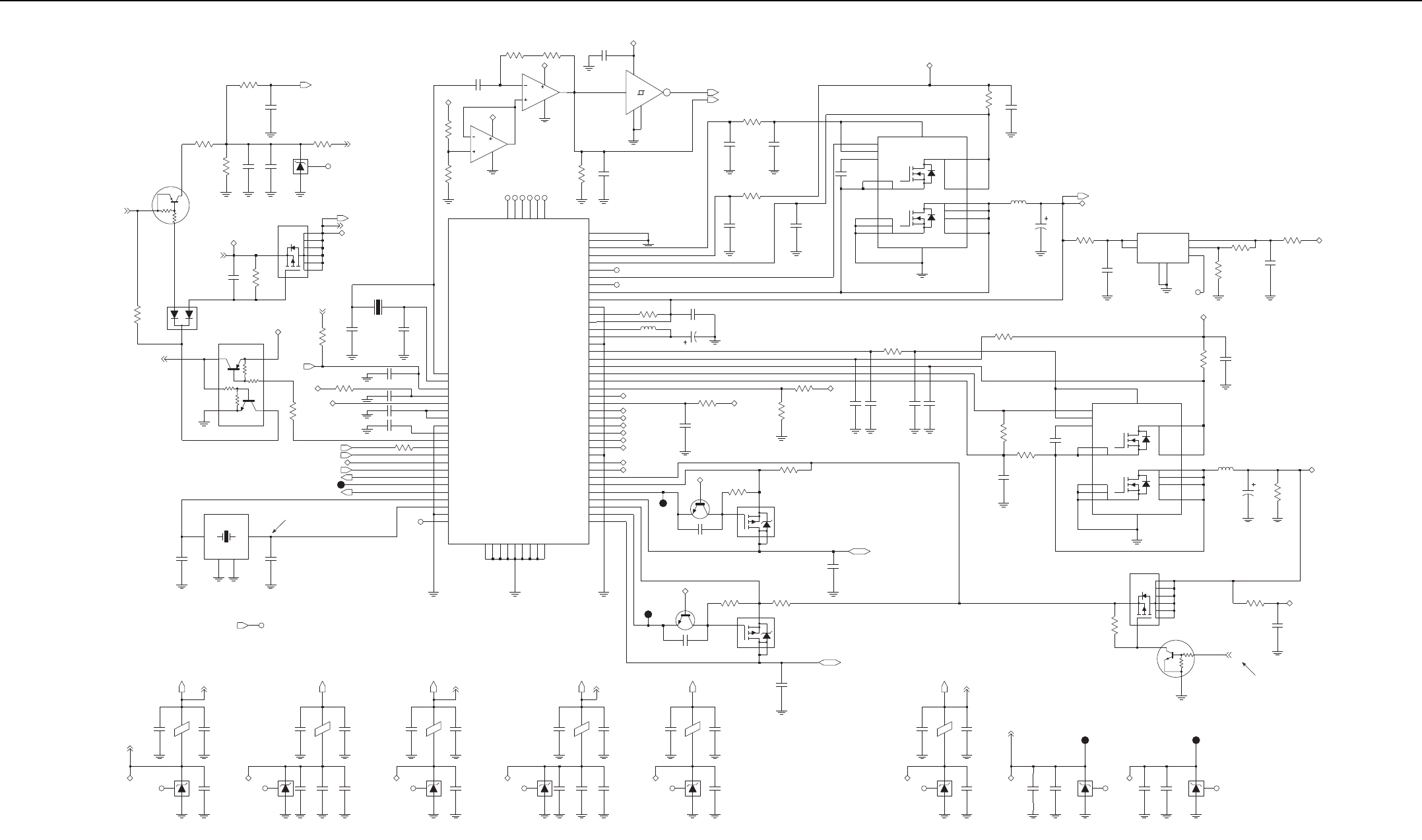
Controller R6 Schematic Diagrams 3-63
47K
47K
10K
47K
OFF: 0.0V
ON: 5Vpk; 230 KHZ PWM
OFF: 0.0Vpk
ON: 5Vpk; 230 KHZ PWM
OFF: 0.0Vpk
24.576MHz
OFF: 0V (DEFAULT)
Change R3246 to 0613952N12 (13K) for OMAP1610
ON: 3.3V (MAKO V10)
FROM MAKO USB_CONNECT (L6)
Vpk-pk: 2.2V - 2.4V
Sine Wave
ON: 4.75V to 5.25V (5.0V typical)
OFF: 0.0V
ON: 4.75V to 5.25V (5.0V typical)
OFF: 0.0V
( TO MMP )
( TO MAP )
ON: 5.2V - 5.3V
OFF: 0.0V
( ON= 0V; OFF=9.3V)
ON: 3.6V
R3210
C3222
R3209
C3260
C3208
C3225
3
NC
1VIN1
6VIN2
5
VOUT
U3201
ADJ 4
G1 CTGND
2GND
C3290
C3207
R3215
C3257
C3262
NC
C3269
Q3201
R3240
L3200
C3210
C3213
Q3209
B1
B3
R3207
U3202-1
C2
C3
C1
C3270
R3248
C3248
C3219
4
NC
Q3206
2
5
6
3
1
C3281
C3265
NC
R3225
NU
15
S1B
16
S2A
6
S2B
7
S2C
8
SYNC_EN
5
VDD 13
1
D1B 2
D2A 9
D2B 10
D2C 11
D2D 12
GND
3
4IN
S1A
Q3200
14 CBOOT D1A
Q3203
2
3
1
4
C3289
R3252
C3261
R3241
R3253
R3250
NC
VBUS1_CMD
1
NC
C3266
R3219
Q3205
R3222
C3200
C3252
R3247
6.2V
VR3207
MAKO_GATED_32KHz 1
NC
3.3V
VR3205
R3243
C3231
VR3208
C3218
NC
6.2V
1
C3227
32.768KHz
Y3201
2
E3201 C3226
1
R3245
E3208
VBUS2_CMD
HOT2
NC
NC
C3202
Y3200
2GND1
4GND2
1
HOT1
3
R3206 $V
C3282
D3200
R3200
S2A
6
S2B
7
S2C
8
SYNC_EN
5
13
VDD
D2A 9
D2B 10
D2C 11
D2D 12
3GND
4IN
S1A
15
S1B
16
Q3202
14 CBOOT D1A 1
D1B 2
R3236
3.3V
VR3203
IN
2
NC
1
OUT 4
VCC 5
NC
C3240
U3203
GND
3
E3206
C3214
NC
NC
R3208
MAKO_V8_5V
1
R3203
C3279
C3277
C1 XTAL32_OUT
B1
R3233
VBUS1_SENS
D12
VBUS2
C13
VBUS2_CMD
F11
VBUS2_SENS
B13
VBUS_SUPPLY
VSAVE
C2
XIN
A13 XOUT
A12
XTAL32_IN
V08_I K4
V08_O
L1
V09_O
L9
V10_GND
J10
V10_I M6
V10_O
H10
VBUS1
C14
VBUS1_CMD
E12
B3
M1 TCXO_IN
TCXO_SEL_16_24
D4
N4
V02_O P4
V03_O N5
V04_O P3
V06_O P6
V07_O
K3
SW2_VCCS
J13
SW2_VOUT
G11
SW5_PHASE
E13
SW5_SUMCOMP
D13
SW5_VDD F13
SW5_VDDHV
F12
SW5_VOUT
E14
SW5_VSENSE
SW_TYPE
SW1_VDD G12
SW1_VDDHV
H12
SW1_VOUT
J11
SW1_VSEN_BST
H11
SW1_VSEN_BUK
L14
SW2_GND
J14
SW2_LX
J12
SW2_VCC K14
PGLDO2 A2
PGLDO3
REG_3V6
D3
RESETX
C5
H13
SW1_DH
H14
SW1_GND
F14
SW1_PHASE
G14
SW1_SUMCOMP_DL
G13
D5
MECH_SW
E4
A1
NC1 A14
NC2 P1
NC3 P14
NC4
NC5 M5
B14
NC6
C3
GND4
K9 GND5
L4 GND6
D14 GND7
H5 GND8
D9 GND9
HV_BG
G4
IGN_X
B4
INT_X
F3
BAT_TYPE
B2
EMERG_PB
F4 FET_ENX
E2
GATED_32K_CLK
F5
P5 GND1
M7 GND2
J4 GND3
G5
U3200-1
BAT_3V6
D2 BAT_7V5
D1
BAT_RTC
U3202-2
A2
A3
A1
B1
B3
NC
E3205
C3205
E3203
NC
NC
NC
C3233
C3291
C3216
Q3210
R3224
C3249
C3274
C3243
C3221
C3275
R3249
VR3204
6.2V
E3202
C3229
3
1
4
C3234
Q3204
2
C3206
C3212
R3226
Q3207
C3209
VR3200
3.3V
VR3201
C3232
R3216
R3220
R3204
C3247
NC
NC
NC
C3211
C3280
2
3
1
C3237
Q3208
C3238
C3204
NU
NC
R3227
L3202
L3201
C3220
C3283
R3239
C3273 NU
VR3206
C3292
6.2V
C3276
R3218
C3278
NU
R3217
R3246
VR3202
R3238
C3228
3.3V
R3228 C3272
R3223
C3201
R3205
C3203
R3237
C3254
C3215
1
C3239
MAKO_V9_3V
32KHZ_GPS
C3217
2.775V_DIG_V4 2.9V_DIG_V6
2.9V_DIG_V6 2.775V_ANA_V7
3.3V_DIG_V10
3.3V_DIG_V10
SW_9V3
SW_9V3
UNSWB+
1.875V_V2_MAKO
3.6V_DIG_VSW1
3.6V_DIG_VSW1
VSAVE
VSAVE
RTC_BATTERY
5V
VSW5_CNTRL
VBUS1
VSW5_CNTRL
VBUS2
VSW5_CNTRL
VSW5
1.875V_V2_MAKO
1.875V_V2_MAKO
2.775V_V4_MAKO
2.775V_V7_MAKO
3.3V_V10_MAKO
5V_V8_MAKO
5V_V8_MAKO
3V_V9_MAKO
1.875V_DIG_V2
1.875V_DIG_V2 OMAP_CORE_LDO 2.775V_DIG_V4
MAKO_INT
GP5_4_EMERGENCYGP5_4_EMERGENCY
GP5_5_IGNITION_SENSE
VSAVE
OMAP_CORE_LDO_1
USB_CONNECT
VSW5
LO_BATTERY_DET
BATTERY_SENSE
VSAVE
VSAVE
GATED_32KHZ_OMAP
OMAP_CORE_LDO_1
9V3_CNTRL
MAKO_ON_OFF_CONTROL
9V3_CNTRL
SW_9V3
SW_9V3
SW_9V3
9V3_CNTRL
9V3_CNTRL
3.3V_V10_MAKO
3.6V_DIG_VSW1
3V_V9_MAKO
5V_V8_MAKO
SW_9V3
2.775V_V7_MAKO
2.9V_V6_MAKO
2.775V_V4_MAKO
1.875V_V2_MAKO
16.8_MHZ_BUFF
POR
ON_OFF_MECH
OMAP_CORE_LDO_1
2.9V_V6_MAKO
Controller DC Distribution Schematic Diagram
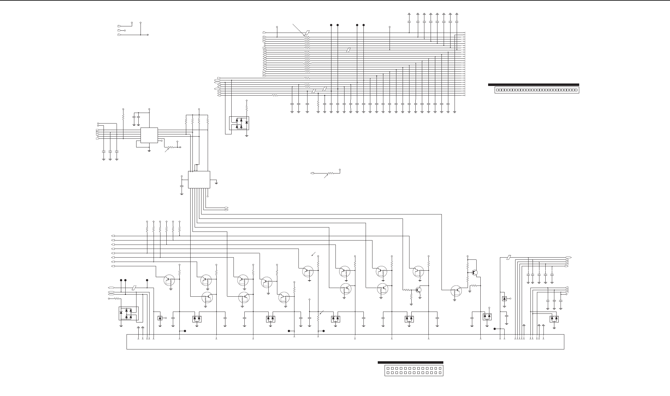
3-64 Controller R6 Schematic Diagrams
47K
47K
10K
47K
47K
47K
10K
47K
47K
47K
10K
47K
47K
47K
47K
47K
47K
47K 10K
47K
47K
47K
47K
47K
10K
47K
47K
47K
25
22
GP5_3_(CHAN_ACT)
USB / MAP_ID_GROUND
MOBILE SUBSCRIBER: NOT_USED
24
MOBILE SUBSCRIBER: NOT_USED
USB_DM_MAP
TX_AUDIO
23
22
AUDIO GROUND
EXT_SWB+
18
GP5_8
17
GP5_7
1210
AUX_AUDIO_OUT_2
GP5_2_(MONITOR)
10
1
IGN_SENSE
13
POWER GROUND
GROUND
711 3
EXT_SPKR+
MAP_ID_1
12
RX_AUDIO
11
AUX_AUDIO_OUT_1
15 21
9
17
2629
PCB
23
2
VIP_1_(EXT ALARM)
GP5_1_(EXT PTT)
MOBILE REPEATER: 0 OHM
9
18
MOBILE REPEATER: 0 OHM
GP5_6
264
25
MOBILE SUBSCRIBER: 33 OHM
19
20
68
8
J4000 REAR VIEW
357
MAP_ID_2
(1.0 MHz)
14
6
J4001 FRONT VIEW
PCB
1
EXT_SPKR-
15
USB_DP_MAP
MOBILE REPEATER: NOT_USED
25
30
13
28
14 16
EMERG SW
REPEATER: 15 kohm
SUBSCRIBER: 390 kohm
REPEATER: DTC114YKAF
SUBSCRIBER: DTC144EKAF
4
GROUND
27 24 21 20 19
VBUS_MAP
16
2
3
1
R4001
J4001-1414
Q4006
23
4
J4000-14
D4001
1
C4046
C4063
J4000-16
C4047
19
J4001-20
20
J4001-19
3
1
2
J4000-19
J4000-20
NC
VR4004
C4042
C4016
R4005
R4046
Q4008
2
3
1
J4001-4
4
C4031
R4010
R4040
C4071
NC
NU
J4001-2222
R4042 1
3
2
J4001-2525
Q4013
R4043
R4061
R4031
13
J4001-1616
NC
FT_VBUS2
1
J4001-13
R4023
NC
R4041
C4027
R4003
Q4002
2
3
1
C4020
NU
C4067
1
C4014
Q4009
2
3
1
FT_USB1_DM
J4000-13
R4068
C4040
C4041
R4071
C4018
VR4001
3
1
2
J4000-6
J4000-26
E4002
3
1
Q4012
2
3
1
Q4000
2
R4011
J4001-2323
R4066
1
23
4
R4098
FT_USB2_DM
1
D4000
J4001-17
17
C4029 C4032
R4045
C4022
R4055
J4001-1212
1
NU
R4033
E4001
FT_USB1_DP
1
E4003
FT_VBUS1
R4063
C4001
NU
5
J4001-2424
J4000-7
J4001-5
NU
C4002
VR4000
3
1
2
J4000-17
3
1
2
VR4002
C4064
NU
C4005
J4001-66
C4065
C4021
R4070
R4049
J4000-9
R4035
J4000-25
R4067
NU
R4090
J4000-5
R4101
FT_MMP_1_WIRE
1
2
3
1
C4015
Q4001
2
3
1
Q4015
E4005
2
3
1
J4001-2929
Q4005
NC
NU
C4074
C4073
C4068
J4000-2
15
J4001-10
10
J4001-15
C4085
C4026
J4001-3030
J4001-2828
C4043
R4012
VR4003
3
1
2
NU
R4086
R4079
1FT_IGNITION_SENSE
1
J4001-2727
FT_EMERGENCY
E4000
J4000-12
C4069
J4001-2
2
C4066
J4001-1111
C4048
C4028
C4000
NU
R4065
QH1
7
QH2
9
RCLK 12
RCLR 13
SER 14
SRCLK 11
SRCLR 10
VCC
16 GND 8
QA
15
QB
1
QC
2
QD
3
QE
4
QF
5
QG
6
U4000
R4034
R4000
E4004
NU R4044
1
R4069
Q4010
2
3
12
C4024
13
GND
7VCC 14
Y_1 2
Y_2 4
Y_3 6
Y_4 8
Y_5 10
Y_6
A_1
1
A_2
3
A_3
5
A_4
9
A_5
11
A_6
U4001
Q4014
1
3
2
R4050
R4103
8 J4001-8
NU
C4075
J4001-33
J4001-77
C4013
Q4011
2
3
1
C4044
J4001-2121
NU
C4072
R4088
R4009
R4051
J4001-11
J4000-15
FT_USB2_DP
1
R4054
J4001-1818
C4033
Q4003
2
3
1
NU
C4023
J4000-4
R4030
R4006
1
C4006
VR4006
2
3
J4000-10
J4000-18
J4000-1
J4000-21
J4000-23
J4000-24
C4034 C4035
26
C4025
C4004
J4001-26
C4070
NU
2
3
1
C4017
Q4004
J4000-3
J4000-11
J4000-22
R4089
NU
C4019
J4001-99
R4100
C4076 C4030
NU
R4004
VR4005
2
3
1
C4084
2
3
1
NC
Q4007
FT_APM_1_WIRE
1
J4000-8
EXT_PTT
1
C4045
R4064
R4032
C4003
NU
R4047
R4002
2
VR4009
3
1
R4048
EXT_SPKR+
EXT_SPKR-
GPIO_4_HOOK
VBUS1
ONE_WIRE_1
INT_MIC+
GPIO_0_PWR_ON
GPIO_3_PTT
GPIO_1_USB1_DP
GPIO_2_USB1_DM
RX_AUDIO
PUB_ADDRESS_1
EXT_MIC+
EXT_SWB+
EXT_SWB+
GP5_1_PTT
GP5_4_EMERGENCY
3.3V
J4001_9
ON_OFF_SW
USB2_DM
USB2_DP
5V
1V8
ARMIO_6
WD_RESET
WD_RESET
WD_RESET
ONE_WIRE_2
MIC_GROUND
1V8 5V
1V8
1V8 1V8
5V
PUB_ADDRESS_1_EN
PUB_ADDRESS_2_EN
RESET
9V3
RESET
RESET
DISPLAY_CS
SERIAL_DATA
SERIAL_CLK
LED_CS
DISPLAY_CMD
HANDSET_AUDIO
VBUS2
5V
PUB_ADDRESS_2
1V81V81V81V81V8
J4001_9
RTC_BATTERY
INT_SPKR-
5V
5V
5V
PROGM_IO_CS
SERIAL_DATA
SERIAL_DATA
SERIAL_CLK
SERIAL_CLK
EXT_SWB+
GP5_7_RxDc_BUS-
5V
GP5_8_CTSs_Reset
5V
5V
5V
GP5_5_IGNITION_SENSE
GP5_3_CHAN_ACTIVITY
5V 5V
GP5_6_TxDc_BUS+
5V
5V
GP5_2_MONITOR
1V8
KEYPAD_ROW_1
KEYPAD_ROW_3
KEYPAD_COL_1
VOLUME_1
KEYPAD_ROW_0
KEYPAD_ROW_2
KEYPAD_COL_0
KEYPAD_COL_2
VOLUME_2
INT_SPKR+
CONTROL HEAD INTERFACE
ACCESSORY INTERFACE (26-PIN)
Controller Peripheral Schematic Diagram (sheet 1 of 2)
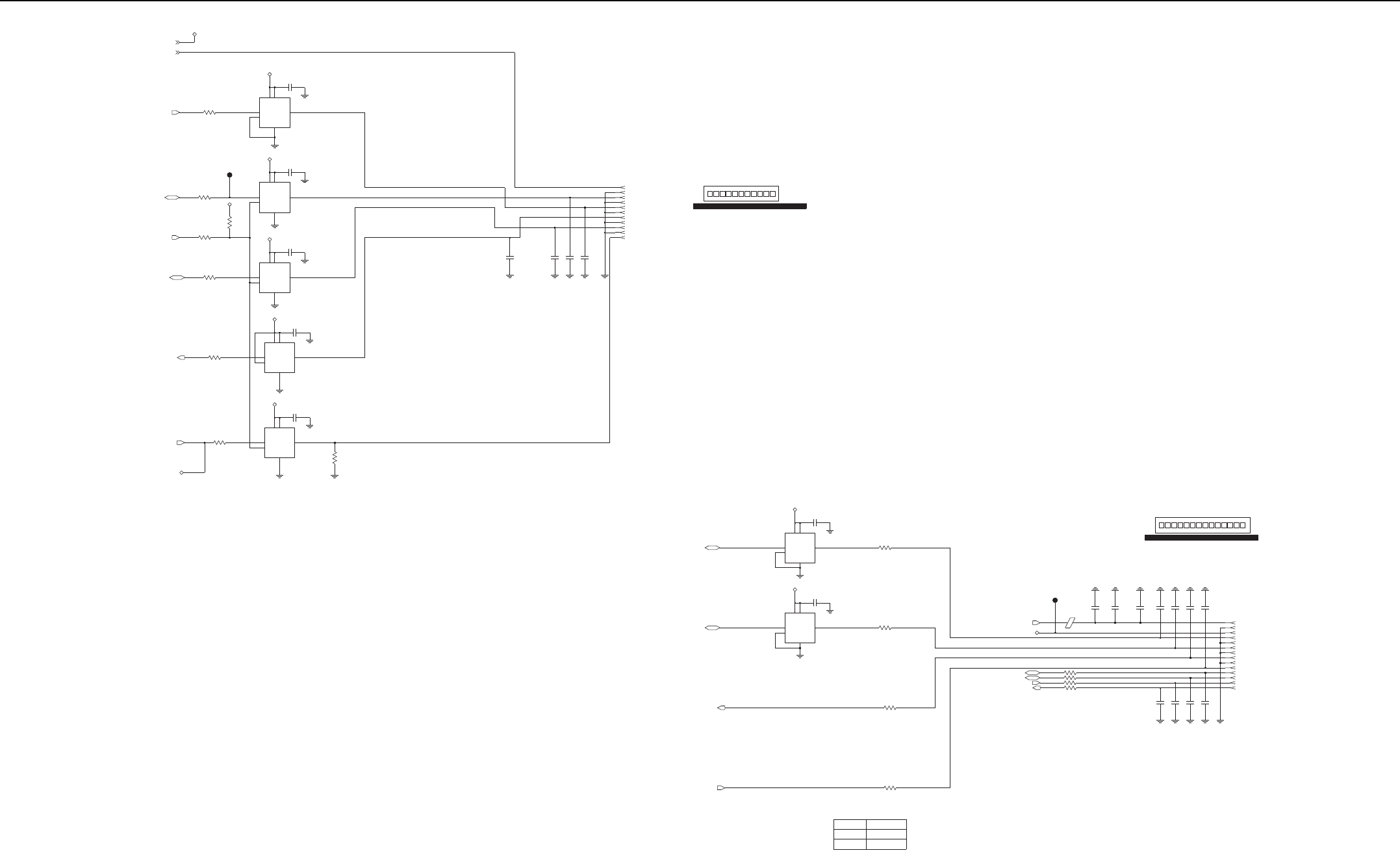
Controller R6 Schematic Diagrams 3-65
2
PCB
J4003 FRONT VIEW
246 8 10 12 141357911 13
LOW
(1.20 MHz)
HIGH
OPERATION
B ---->A
DIR
B <----A
46810135
PCB
J4002 FRONT VIEW
7911
R4093
R4095
E4006
C4055
C4053
NU
C4051
NU NU
C1
A
C2 B
B2 DIR
B1 GND
A1
VCCA A2
VCCB
U4005
R4099
R4078
NU
C4011
C4092
C2
DIR
B2
GND
B1
VCCA A1
VCCB A2
U4010
AC1
B
R4082
9
R4081
7J4003-88J4003-9
NU
C4060
J4003-7
NU
R4105
C4062
GND
B1 VCCA A1
VCCB A2
U4006
AC1
B
C2
DIR
B2
C4089
C4087
J4002-88
J4002-2
2
J4002-7
7
C4058
NU
NU
C4059
C4061
NU
AC1
B
C2
DIR
B2
GND
B1 VCCA A1
VCCB A2
DIR
B1 GND
A1
VCCA A2
VCCB
U4008
U4009
C1
A
C2 B
B2
U4004
AC1
B
C2
DIR
B2
GND
B1 VCCA A1
VCCB A2
J4003-11
11
R4096
NU
C4094
C4049
NU
R4074
R4076
9
R4080
C4010
J4002-9
C4086
NU
C4012
NU
R4085
10
R4083
11
J4002-4
4
J4003-10
J4002-10
10 J4002-11
5J4003-6
6
R4097
J4003-5
C4088
J4003-11
C1
A
C2 B
B2 DIR
B1 GND
A1
VCCA A2
VCCB
R4106
U4007
C4093
J4002-6
6
NU
J4002-55
R4094
1
C4090
J4002-3
3
TP4000
NU
C4007
1
J4002-1
1
OPT_SSI_SYNC
J4003-13
13 J4003-14
14
C4091
J4003-12
12
J4003-3
3J4003-44
1V8
1V8
1V8
1V8
1V8
1V8
1V8
1V8
SSI_DATA_OUT
J4003-2
2
OPT_BRD_PTT
SSI_FSYNC
SSI_CLK
SSI_DATA_IN
OPT_GPIO_1
OPT_GPIO_2
RESET_OUT
SW_9V3
1V8
1V8
SYSTEM_SYNC
McBSP3_DR
McBSP3_CLKX
DIR_CTRL
McBSP3_DX
McBSP3_FSX
SYSTEM_SYNC
SYSTEM_SYNC
WD_RESET
REPEATER CONNECTOR
OPTION BOARD INTERFACE
Controller Peripheral Schematic Diagram (sheet 2 of 2)
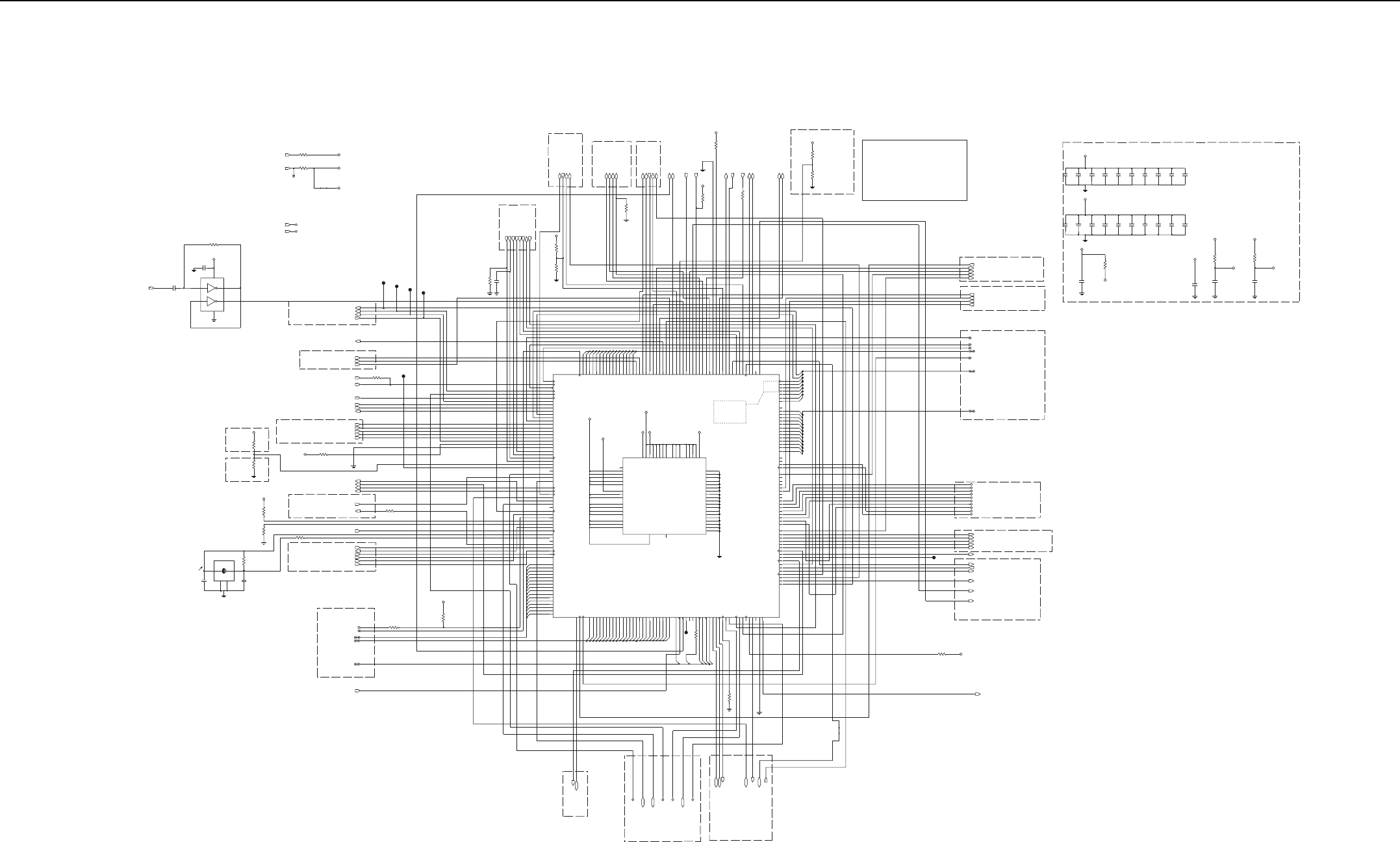
3-66 Controller R6 Schematic Diagrams
FLASH
MAKO SSI
16.8MHz Squarer
( BUFFERRED 16.8 FROM TOMAHAWK )
GPS
OMAP1710
DECOUPLING CAPACITORS
PLACED FOR
(MOBILE ONLY)
(Used as KEYPAD_COL4 for NEO and Public Add Mic for MORPHEUS)
SDRAM
DNP
USB#2
SPI
USB#0
ABACUS3 SSI
(FROM MAKO )
Place for
FREQ SWITCH
LARGEST REF
LED & Display CS: Active Low
(Used as BL_EN for PORTABLE, GP5_7 for MOBILE
MOBILE ONY
(Used as SW2 for PORTABLE, Volume B for MOBILE)
PORTABLE DISPLAY
R1050
MCBSP3
(FROM MAKO )
(GPIO_3 for PORTABLE-Green LED)
DNP
(Used as SW8 for PORTABLE, Channel Activity for MOBILE)
(Used as GREEN_LED for PORTABLE, PA_ENABLE for MOBILE)
C1039
OMAP1610
DELETED REF
U1008
OMAP1710
(SPI.CS3 for MOBILE Shift Register Chip Select)
(MOBILE ONLY)
GP DEVICE CONFIG
KEYPAD COLUMN
(Used as KEYPAD_ROW4 for PORTABLE, GP5_6 for MOBILE)
Place for
( INTERFACE WITH MAKO )
(Used as SW4 for PORTABLE, Monitor for MOBILE)
Place for
TOMAHAWK SSI
CLK rate: 1 MHz
(Used as SW1 for PORTABLE, Volume A for MOBILE)
KEYPAD ROW
(0.87mA/MHz for OMAP1710 & 1.06mA/MHz for OMAP1610)
OPTION SELECT
( RESET CIRCUIT PROVIDED BY MAKO )
USB#0 RESERVED FOR MOBILE
Place for
I2C
OMAP1610
(MOBILE ONLY)
1.0Vpkpk
BOOT FROM CS3
OMAP1710
Date rate: 20 of 8 bits packet per chip select
RS232
PLACE FOR GP DEVICE FAST BOOT
BOOT FROM CS0
RF CONTROLS
SERIAL FLASH SPI
(MOBILE ONLY)
JTAG
(Used as RED_LED for PORTABLE, RX_ATTN_1 for MOBILE)
(MOBILE ONLY)
Y1001
C1032
13
OPTION BOARD
OMAP1710
Place for
(1.4V for OMAP1710 & 1.55V for OMAP1610)
(FROM MAKO )
USB#1
TP_POR
1
R1066
NU
NC
NC
5
C1017
5
R1035
NU
R1045
Z_STATE_1
W16
Z_STATE_2 P15
Z_STATE_3 N14
2
4
VSS_2 B7
VSS_3 A13
VSS_4 B16
VSS_5 A21
VSS_6 F20
VSS_7 K20
VSS_8 R21
VSS_9 W20
VSS_12 AA7
VSS_13 Y3
VSS_14 AA1
VSS_15 U2
VSS_16 N1
VSS_17 K2
VSS_18 G1
VSS_19 B1
UART3_RX L14
USB0_DAT
P9
R8 USB0_SE0
UWIRE_SDI U18
W21
UWIRE_SDO
VSS_1 B5
VSS_10 AA21
VSS_11 Y13
TDI
Y19
AA19
TDO
V17 TMS
TRST
Y18
UART1_CTS
R14
V14 UART1_RX
UART2_CTS
Y5
UART2_RX
R9
SDATA_9 D14
SDDQS_H
C14
D4 SDDQS_L SDRAM_CAS
B4
C8
SDRAM_DQML
SDRAM_DQMU
D10
SDRAM_RAS
H7
TCK
W18
SDATA_15 C12
SDATA_2 C5
SDATA_3 D7
SDATA_4 D5
SDATA_5 C7
SDATA_6 C4
SDATA_7 D8
SDATA_8 C10
SBANK_1 C3
SDATA_0 D6
SDATA_1 C6
SDATA_10 D11
SDATA_11 C13
SDATA_12 C11
SDATA_13 D13
SDATA_14 D12
SADD_3 A1
G10
SADD_4
SADD_5 B9
SADD_6 G12
SADD_7 G11
SADD_8 G9
SADD_9 B12
SBANK_0 B3
RTC_WAKE_INT
W13
A2
SADD_0
SADD_1 B2
SADD_10 B8
SADD_11 H10
H9
SADD_12
SADD_13 H11
SADD_2 B6
OSC32K_IN
V13 OSC32K_OUT
AA13
R12 PWRON_RESET
E5 RESERVED
P12 RESET_MODE
RST_OUT
AA20
RTCK
Y17
RTC_ON_NOFF
Y12
MPUIO_3 V8
MPUIO_4 T19
MPUIO_5 T20
J20 MPU_BOOT
MPU_RST
U20 NC
L1
OSC1_IN
Y2 OSC1_OUT
W3
MCSI2_SYNC
V9
MMC_CMD
P11
MMC_DAT0 R11
MMC_DAT1 V10
MMC_DAT2 W10
MMC_DAT3 W11
MPUIO_1 U19
MPUIO_2 N15
AA5 MCBSP2_DX
W6 MCBSP2_FSR
W7 MCBSP2_FSX
MCSI1_DIN
V15
W14 MCSI1_DOUT
MCSI1_SYNC AA17
AA9 MCSI2_DIN
W9 MCSI2_DOUT
Y14 LOW_STATE_2
LOW_STATE_3
V6
LOW_STATE_4
W5
LOW_STATE_5 M18
MCBSP1_DR
H20
H18
MCBSP1_DX
MCBSP1_FSX
H15
MCBSP2_DR
P10 H13
LCD_PIXEL_4
LCD_PIXEL_5 A20
LCD_PIXEL_6 B19
LCD_PIXEL_7 C18
D17
LCD_PIXEL_8
LCD_PIXEL_9 D16
LCD_VSYNC B18
LOW_STATE_1
AA15
LCD_PIXEL_10 C17
LCD_PIXEL_11 B17
LCD_PIXEL_12 G13
LCD_PIXEL_13 A17
LCD_PIXEL_14 C16
LCD_PIXEL_15 D15
LCD_PIXEL_2 C19
LCD_PIXEL_3 G14
KBR_1
F19
H14 KBR_2
KBR_3
E20
E19 KBR_4
LCD_AC B15
LCD_HSYNC C20
D18
LCD_PIXEL_0
LCD_PIXEL_1 B21
I2C_SDA
V20
KBC_0 F18
KBC_1 D20
KBC_2 D19
KBC_3 E18
KBC_4 C21
KBC_5 G19
KBR_0
G18
GPIO_3 P18
GPIO_4 P20
GPIO_6 P19
GPIO_62
M7
GPIO_7 M15
GPIO_8 Y8
GPIO_9 W8
T18
I2C_SCL
GPIO_0 R18
GPIO_1 R19
GPIO_11 N20
GPIO_12 N18
GPIO_13 N19
GPIO_14 N21
GPIO_15 M20
GPIO_2 M14
V2 FRDY
F_CS1
M3
F_CS1U
Y1
F_CS2
M4
F_CS2U
P3
F_CS3
N8
F_RP
W1
F_WP
V4
FDATA_2
N7 FDATA_3
P2 FDATA_4
P4 FDATA_5
P7 FDATA_6
R2 FDATA_7
R3
R4 FDATA_8
FDATA_9
T2
FDATA_0
N4
N2 FDATA_1
FDATA_10
T3 FDATA_11
P8
U1 FDATA_12
FDATA_13
U3 FDATA_14
T4 FDATA_15
V3
FADD_3
C1
E4 FADD_4
FADD_5
D2
FADD_6
F4
FADD_7
E3
FADD_8
J7
FADD_9
F3
FADV
L4
FADD_19
J3
FADD_2
D3
FADD_20
F2
FADD_21
L8
K4 FADD_22
FADD_23
K3
FADD_24
L7
E1 FADD_25
FADD_11
G3
G2 FADD_12
FADD_13
K8
H4 FADD_14
FADD_15
H3
FADD_16
K7
FADD_17
J2
J4 FADD_18
EN_F_BE_1
M8
EN_F_OE
U4
EN_F_WE
W2
EN_SDCKE
H12
EN_USB_PUEN
W4
EN_WE_SDRAM
SDRAM_CAS
SDRAM_DQML
SDRAM_DQMU
SDRAM_RAS
EN_WE_SDRAM
H8
FADD_1
J8
FADD_10
G4
DVDD4_4
B14
DVDD5_1
R1
DVDD5_2
H2
DVDD5_3
C2
V12 DVDDRTC
EMU0 V16
EMU1 W17
EN_F_BE_0
L3
DVDD1_4
Y16
L21 DVDD1_5
DVDD2_1
AA2
DVDD2_2
Y7
DVDD2_3
AA11
A5 DVDD4_1
DVDD4_2
A7
DVDD4_3
B10
CVDD_2 Y20
CVDD_3 Y9
CVDD_4 M2
CVDD_DLL A11
W12
CVDD_RTC
DVDD1_1
A19
DVDD1_2
E21
U21 DVDD1_3
CVDD2_2 E2
CVDD3_1 B13
CVDD3_2 B20
CVDD3_3 J21
CVDD3_4 R20
J1
CVDD4
CVDDA Y21
CVDD_1 A15
C15
CLK_P_LCD
CLK_SD
C9
V19
CLK_S_UWIRE
CONF
V18
CS_SDRAM
G8
CVDD1 AA3
A9
CVDD2
CVDD2_1 A3
H19
CLK_EX_CAM
CLK_F N3
CLK_L_CAM
J15
V5 CLK_M
CLK_MCSI1
P14
Y10 CLK_MCSI2
V11 CLK_MMC
CLK_M_REQ
R10
V7 CLKR_MCBSP2
G20 CLKS_MCBSP1
G21 CLKX_MCBSP1
Y6 CLKX_MCBSP2
CLKX_SD
D9
Y15 CLK_B
CLK_B_REQ
W15
CLK_B_UART2
Y4
CAM_D_5 J14
CAM_D_6 J19
CAM_D_7 J18
CAM_HS L15
CAM_RSTZ M19
CAM_VS L18
P13 CLK32K_IN
R13
CLK32K_OUT
BFAIL
W19
CAM_D_0 L19
CAM_D_1 K14
CAM_D_2 K15
CAM_D_3 K19
CAM_D_4 K18
2
21
U1000
A1
1
A2
3
GND
2
VCC
5
Y1 6
Y2 4
U1006
5
10
C1006
C1013
R1036
3
C1005
C1044
10
NC
NC
18
R1054
C1003
C1009
12
R1014
0
C1010
15
R1001
R1041
4
7
1
R1060
6
5
2
7
R1044
2
5
11
C1011
NC
11
NC
3
R1047
NC
NC
C1035
NC
TP1000 1
C1004
R1071
7
8
3
12
NC
8
6
3
R1025
R1000
1
2
0
4
9
TP_MAKO_RX
12
C1007
C1001
C1002
R1005
C1012
R1006
C1034
3
5
C1036
NC
TP_MAKO_DCLK
1
8
R1027
R1067
NU
NU
19
R1070
R1020
3
13
22
8
0
12
C1033
R1048
1
8
NC
7
17
C1030
R1021
C1031
4
7
R1028
9
2
16
C1014
1
11
6
NC
20
C1016
15
14
15
4
0
NC
14
R1019
25
R1026
R1034
24
C1015
1
4
1
9
TP_MAKO_TX
1
NU
14
9
10
1
R1046
4
GND2
1
HOT1
3
HOT2
10
TX_RAMP
Y1000
12MHz
GND1
2
R1002
C1018 C1019
1
6
NC
R1017
C1008
TP_MAKO_FSYNC
1
6
13
11
0
NC
23
C1000
EMIFS_ADD(25:1)
1.875V
16.8_MHZ_BUFF
SDRAM_CTL(8:0)
C1037
1.875V
JTAG_NTRST
MCBSP3_DR
MAKO_CE
LED_CS
DISPLAY_CS
ABACUS3_CE
CVDDA
OMAP_CORE
OMAP_CORE
CVDDA
ARMIO_2
THK_CE
RS232_TX
1.875V
DVDD2
USB1_SE0
LDO_FILTER
SERIAL_DATA
ARMIO_6
USB2_RCV
GPIO_18
FLASH_WAIT
GATED_32KHZ_OMAP
OMAP_CORE
JTAG_NEMU0
JTAG_NEMU1
JTAG_RTCK
JTAG_TCK
JTAG_TDI
JTAG_TDO
JTAG_TMS
ONE_WIRE_UP
SPI_CLK
SPI_MISO
SPI_MOSI
DMCS
GPIO_28
ADAPT_SW
LOCK_DETECT
ANT_EN
DIR_CTRL
SERIAL_CLK
MCBSP3_FSX
GPS_BOOT_SELECT
GPIO_40
OMAP_CORE
1.875V
SDRAM_DATA(15:0)
SDRAM_CLK
SDRAM_CLK_EN
SDRAM_CS
1.875V
2.775V_DIG_V4
1.875V
MAKO_OPT_GPIO2
1.875V
GPIO_3
1.875V
1.875V
DVDD2
DVDD2
LDO_FILTER
1.875V
OMAP_CORE
SDRAM_ADD(12:0)
USB2_SE0
RS232_RX
I2C_CLK
I2C_DATA
SDRAM_CLKX
USB2_DAT
MOBILE_DISPLAY_CMD
MAKO_AD_TRIGGER
USB0_SE0
USB0_DAT
USB0_TXEN
1.875V
VDD_DLL
MCBSP3_CLK
FLASH_CTL(5:0)
1.875V
EMIFS_DATA(15:0)
OMAP_CORE
VDD_DLL
OMAP_CORE
1.875V_DIG_V2
1.875V_DIG_V2
OMAP_CORE_LDO
3.3V_DIG_V10
TX_CLK
RX_DATA
TX_DATA
RX_FSYNC
TX_FSYNC
USB1_TXEN
MCBSP3_DX
OPT_GPIO_1
USB1_DAT
USB2_SUSPEND
GPIO_26
GPIO_25
POR
GPIO_60
MAKO_GPIO_RX
GPIO_5
RESET_OUT
MAKO_OPT_INT
GPS_ON_OFF_LS
GPIO_15
PTT
KEYPAD_COL0
KEYPAD_COL1
KEYPAD_COL2
KEYPAD_COL3
GPIO_27
KEYPAD_ROW0
KEYPAD_ROW1
KEYPAD_ROW2
KEYPAD_ROW3
ARMIO_15
DISPLAY_CMD
DISPLAY_CE
DISPLAY_DATA0
DISPLAY_DATA1
DISPLAY_DATA2
DISPLAY_DATA3
DISPLAY_DATA4
DISPLAY_DATA5
DISPLAY_DATA6
DISPLAY_DATA7
MAKO_DCLK
MAKO_INT
MAKO_TX
MAKO_RX
MAKO_FSYNC
RX_CLK
FLASH_CLK
ARMIO_3
AUDIO_PA_ENA
ARMIO_12
GPIO_30
GPIO_31
GPS_RX_LS
GPIO_32
GPS_TX_LS
GPIO_33
MAKO_OPT_GPIO0
MAKO_OPT_GPIO3
OPT_GPIO_2
USB_INT
EXT_MIC_ENA
32KHZ_CLK
GP5_8
GPS_RESET_LS
Controller Microprocessor Schematic Diagram
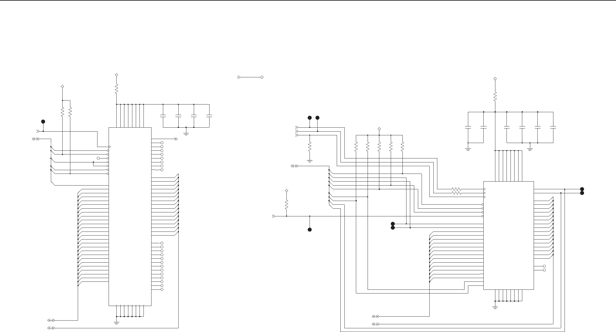
Controller R6 Schematic Diagrams 3-67
7
8
FLASH DDR SDRAM
Bootstrap Mode = 48 MHz
Normal Mode = 72 MHz
32 MBYTES
32MB (65nm Die Shrink)
5
6
C2000
23
R2000
6
7
8
9
10
11
12
12
13
14
15
NU
R2013
R2012
TP_FLASH_CLK
C2001 C2003
12
3
C2002
13
14
15
1
11
R2004
R2005 R2006
NU
2
3
4
5
NU
2
4
1
6
0
1
8
9
10
5
2
4
1
2
3
9
10
11
7
NC
NC
NC
NC
NC
0
18
19
20
21
22
NC
NC
L8 VSS8
G7
WAIT
24
25
16
17
D4
VPP
B4 VSS1
C4 VSS2
L1 VSS3
L2 VSS4
L5 VSS5
L6 VSS6
L7 VSS7
K2
RFU9
B5
VCC1 B6
VCC2 K6
VCC3 L4
VCC4
J8
VCCQ1 K7
VCCQ2 L3
VCCQ3
K8
RFU13
C5
RFU2 D5
RFU3 D6
RFU4 E3
RFU5 F3
RFU6 H1
RFU7 J1
RFU8
H8 EN_F2_OE
F4 EN_RST
F5 EN_WE
E4 EN_WP
C2
RFU1
K3
RFU10 K4
RFU11 K5
RFU12
A8
DU4 M1
DU5 M2
DU6 M7
DU7 M8
DU8
K1 EN_F1_CE
J2 EN_F1_OE
G8 EN_F2_CE
G5
DQ5 J6
DQ6 H7
DQ7 G2
DQ8 J3
DQ9
A1
DU1 A2
DU2 A7
DU3
J4
DQ11 H5
DQ12 G6
DQ13 H6
DQ14 J7
DQ15
G3
DQ2 H4
DQ3 J5
DQ4
E2 A7
F6 A8
D7 A9
E5 ADV
C6 CLK
H2
DQ0 H3
DQ1
G4
DQ10
B7 A21
C7 A22
C3 A23
D3 A24
D1 A3
B1 A4
C1 A5
F2 A6
F7 A14
E8 A15
F8 A16
D2 A17
B2 A18
B3 A19
E1 A2
E6 A20
G1 A0
F1 A1
E7 A10
B8 A11
C8 A12
D8 A13
TP_SDRAM_CLKX
8
U2000
TP_SDRAM_BA1
TP_SDRAM_BA0
TP_SDRAM_CLK
TP_SDRAM_CS
2
3
4
10
11
12
13
14
15
9
R2008
NU
R2009
NU
NU
R2007
0
1
5
0
R2010
F1 VSS2
K1 VSS3
A3 VSSQ1
B9 VSSQ2
C1 VSSQ3
D9 VSSQ4
E1 VSSQ5
G7 WE
F9
VDD2 K9
VDD3 A7
VDDQ1 B1
VDDQ2 C9
VDDQ3 D1
VDDQ4 E9
VDDQ5
A1 VSS1
F8 LDM
E8
LDQS
NC1 F3
F7
NC2
G9 RAS
F2 UDM
E2
UDQS
A9
VDD1
C7
DQ3 C8
DQ4 D7
DQ5
DQ6 D8
E7
DQ7 E3
DQ8 D2
DQ9
G1 EN_CKE
B7
DQ1
D3
DQ10 C2
DQ11 C3
DQ12 B2
DQ13 B3
DQ14 A2
DQ15
B8
DQ2
H1 A9
H8 BA0
H9 BA1
G8 CAS
G2 CK
G3 CK*
H7 CS
A8
DQ0
H3 A12
K7 A2
K8 A3
K2 A4
K3 A5
J1 A6
J2 A7
J3 A8
U2001
J8 A0
J9 A1
J7 A10_AP
H2 A11
TP_DDR_LDQS
1
0
3
NC
TP_DDR_UDQS
NC
4
5
6
NC
C2004
NC
NC
NC
C2005
C2006
C2007
NC
NC NC
7
8
NC
NC
NC
NC
NC
2
3
4
5
6
R2015
R2014
R2011
C2009 C2008
NC
NC
NC
7
EMIFS_DATA(15:0)
EMIFS_ADD(25:1)
FLASH_CTL(5:0)
CHIP_ENABLE
FLASH_CLK
WRITE_PROTECT
1.875V_DIG_V2
1.875V_DIG_V2 1.875V_DIG_V2
1.875V_DIG_V2
SDRAM_DATA(15:0)
SDRAM_ADD(12:0)
SDRAM_CTL(8:0)
SDRAM_CLK_EN
1.875V_DIG_V2
SDRAM_CLK
SDRAM_CS
1.875V_DIG_V2
SDRAM_CLKX
LATCH_ENABLE
OUTPUT_ENABLE
RESET
WRITE_ENABLE
FLASH_WAIT
1.875V_DIG_V2
Controller Memories Schematic Diagram
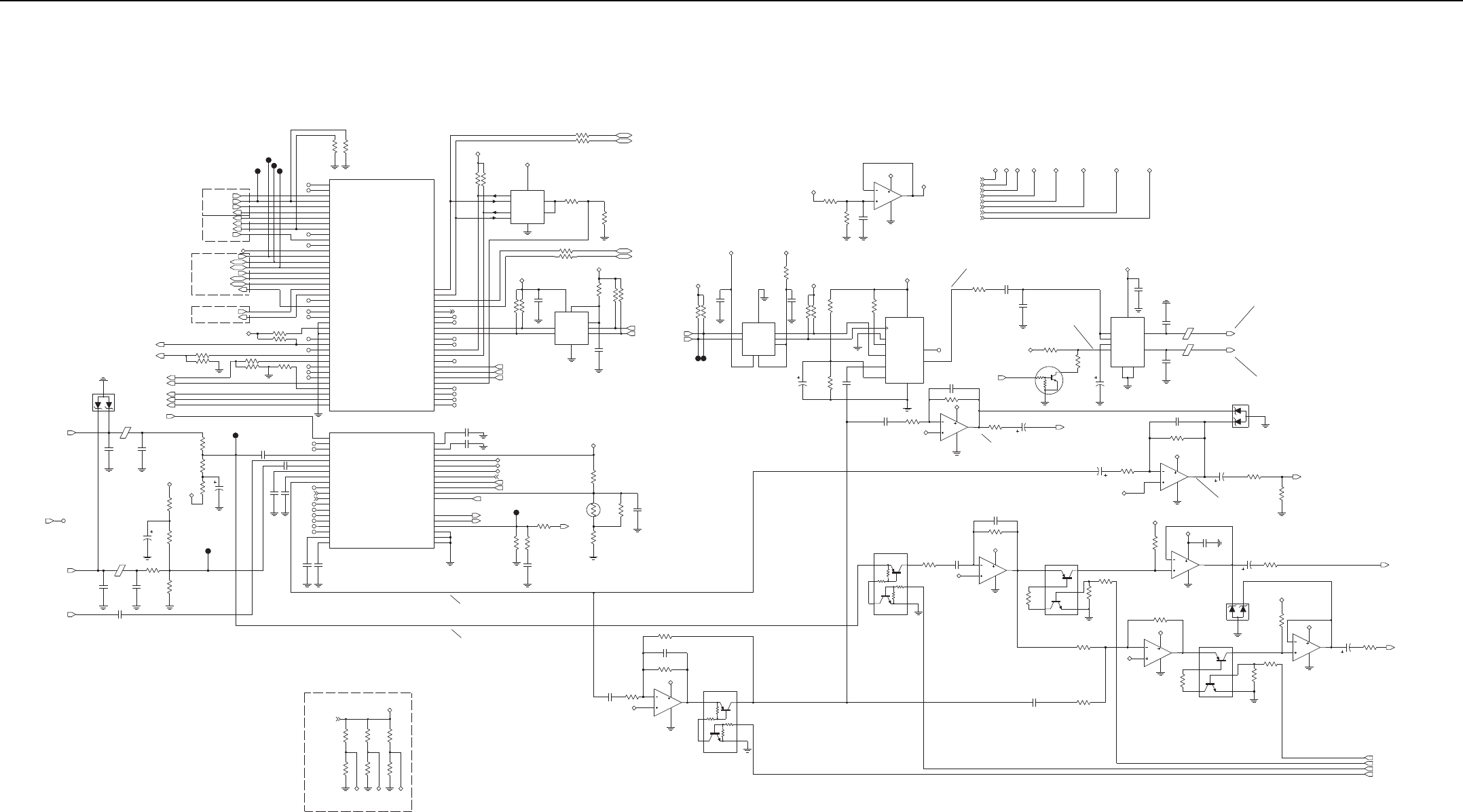
3-68 Controller R6 Schematic Diagrams
HW_ID
R3507
R3508
R3509 R3505
R3504
R3503
2.9V_DIG_V6
HW_ID2
HW_ID1
HW_ID0
2.9V_DIG_V6
10K
47K
V15
(7.5 W @ 8 ohms)
MAKO UART
80mV RMS (TX AUDIO)
MAKO SSI
4.12V (44W)
3.91V (27.5W)
MAKO SPI
125mV RMS
330mV RMS
70mV RMS (RX AUDIO)
7.8V RMS
5.3VDC muted
(SOURCE)
(7.5 W @ 8 ohms)
9.3VDC unmuted
52mV RMS for rated audio
7.8V RMS
MAKO USB
NC
R3554
R3553
C3503
R3516
C3522
C3545
R3594
R3541
R3548
NC
R3542
NC
C3526
C3518
C3538
NC
NC
E3503
VR3503
3
1
2
Q3500
23
1
R3544
NC
USB1_SEO
1
R3540
R3539
R3511
NC
R3550
C3508
C3521
R3549
R3560
R3572
C3535
NC
NC
C3528
R3559
41
5
TX_RAMP_DAC
1
Q3504
2
36
C3500
C3531
R3558
NC
R3584
C3501
R3547 R3528
C3512
C3509
R3512
R3591
E3500
R3515
R3523
SCL1
3
SCL2
6
SDA1
4
SDA2
5
VREF1
2
VREF2
7
U3503
EN
8
GND
1
C3505
R3586
C3504
R3575
C3513
USB1_DAT
1
C3510
TX_RX
A11
VCM1
J3
H4 VCM2
VC_OUT_M
H2 VC_OUT_P
H3
E8
VFUSE
VMES L10
A4 VREF
F1 INT_SPKR_P
MIC_BIAS
L2
E1 PA_BPLUS
G3 PA_IN_M
G2 PA_IN_P
N1
PWR_CTRL C4
SCAN_EN A3
TEST
EXT_MIC_P
J2
G1 EXT_SPKR_M
H1 EXT_SPKR_P
L3
FE_TUNE1 M2
FE_TUNE2
INT_MIC_M
K1 INT_MIC_P
K2
F2 INT_SPKR_M
ATOD_3 M14
ATOD_4 L12
ATOD_5 L13
ATOD_6 K11
ATOD_7 K12
ATOD_8 K13
BPLUS
E3
EXT_MIC_M
J1
U3200-3
ADC_VREF M12
AD_TRIG
B11
ATOD_0 N14
ATOD_1 M13
ATOD_2 L11
NC
1
R3537
VREF2
MAKO_CE
8
EN
1
GND
3
SCL1
6
SCL2
4
SDA1
5
SDA2
2
VREF1
7
R3500
U3508
C3514
C3534
R3571
NC
C3530
R3506
C3516
EXT_MIC
1
R3588
NINV
4
OUT1
6
OUT2
RR
3
7
VCC
R3580
U3500
2
GND1 GND2
5
9
INV
8
M_SS
1
R3574
NC
R3529
R3595
R3596
RT3500
U3502-4
13
12 14
4
11
2
31
4
11
R3546
U3502-1
C3507
R3536
6
57
4
11
C3532 U3502-2
IN1
C1
IN2
A1
NO1
D2
NO2
V_POS
A2
R3545
U3504
B1
COM1
C2
COM2
GND
D1
B2
NC
INT_MIC
1
NC
R3514
R3526
2
5
6
3
1
4
1
4
11
NC
Q3502
U3505-1
2
3
C3540
R3585
R3532
R3578
3
1
2
C3541
57
4
11
VR3502
U3505-2
6
R3510
R3581
2
5
6
3
1
4
NC
C3533
Q3503
R3576
NC
C3502
R3551
R3569
USB_CONNECT L6
C10 USB_INTX
E7 VC_DCLK
D7 VC_FSYNC
A7 VC_RX
B7 VC_TX
M4 VC_TX3V
USB1_DP N6
B8 USB1_OE
D8 USB1_SE0
B9 USB2_DAT_VP
USB2_DM P8
N7
USB2_DP
A9 USB2_OE_RCV_RTS
C9 USB2_SE0_VM_RXD
TXDO_BDI_5V M10
K6 TXDO_BDI_ENC_3V
J5 TXDO_BDI_UP_3V
A10 UART2_RXD_OD
E9 UART2_TXD
N3 UCM_SS
C8 USB1_DAT_TXD
USB1_DM P7
N2 RXDIN_ENC_3V
N8 SB96D_BDO_KF_3V
SB96_BDO_KF_5V N9
SB96_BUS_BUSY N13
E6 SPI_CLK
D6 SPI_CS
B6 SPI_DI
C6 SPI_DO
C11 OPT_GPIO1
G10 OPT_GPIO2
D11 OPT_GPIO3
A8 RS232_USB_X
M3 RTS_FILLSEN_3V
RTS_FILLSEN_5V M11
P2 RXDIN_3V
RXDIN_5V N12
M9
OPTA_SEL2 N10
OPTA_SEL3 P11
OPTB_SEL0 K8
OPTB_SEL1 P12
OPTB_SEL2 N11
OPTB_SEL3OPTION_INTX
B12
F10 OPT_GPIO0
B10 CTS_X
A6 LOGIC_VDD
ONE_WIRE_1 P9
ONE_WIRE_2 M8
ONE_WIRE_BATT L8
L7 ONE_WIRE_UP
P10
OPTA_SEL0 K7
OPTA_SEL1
L5 APCO
A5 BBP_CLK
B5 BBP_SYNC
C7 BOOT_NORM_X
C12 BUSY_IN
E11 BUSY_OUT
D10 CABLE_DET_3V
CTS_CABLE_DET_5V P13
U3200-2
C3506
R3538
NU
I2C_DATA 1
NC
R3583
C3523
R3592
R3525
2
36
41
5
Q3505
R3513
NC
E3501
R3593
R3555
NC
R3530
C3543
5SDI_SDA
4
SDO_NC
VDD
9
10
W
NU
1A
3AD0_CS*
2B
6CLK_SCL
8DIS
7GND
U3501
C3511
U3505-4
13
12
14
4
11
NC
R3556
C3519
NC
R3524
9
10
8
4
11
NC
NC
U3502-3
U3505-3
9
10 8
4
11
R3582
1
C3536
NC
USB1_TXEN
R3502
NC
R3573
R3579
C3542
R3534
NC
R3535
R3590
R3552
R3587
NU
R3533
I2C_CLK 1
C3539
R3520
C3527
C3524
VR3504
C3520
NC
R3521
R3577
NC
R3501
E3502
C3529
NC
NC
C3517
C3515
C3525
9V3
EXT_MIC_ENA
ONE_WIRE_1
ONE_WIRE_2
VAG
9V3
PUB_ADDRESS_1_EN
PUB_ADDRESS_2_EN
USB0_DAT
USB0_SE0
USB0_TXEN
1.875V_V2_MAKO
1.875V_V2_MAKO
1.875V_V2_MAKO
1.875V_V2_MAKO
2.775V_DIG_V4
2.775V_DIG_V4
2.775V_DIG_V4
2.775V_DIG_V4
MAKO_ADC8
MMP_GPIO1_INPUT
MMP_GPIO2_INPUT
1.875V_DIG_V2
1.875V_DIG_V2
5V_SW
5V_SW
5V_V8_MAKO
5V_V8_MAKO
3.3V_DIG_V10
MAKO_CE
MIC_GROUND
ONE_WIRE_UP
1.875V_DIG_V2
I2C_CLK
I2C_DATA
USB2_DM
USB_INT
USB2_DP
5V_SW
2.9V_DIG_V6
ANT_CURRENT_DET
5V_V8_MAKO
UNSWB+
UNSWB+
9V3
9V3
3.3V_DIG_V10
3.3V_DIG_V10
SW_9V3
GPIO_0_PWR_ON
GPIO_4_HOOK
GPIO_3_PTT
BATTERY_SENSE
USB1_DP
USB1_DM
MAKO_OPT_GPIO3
MAKO_TX
1.875V_DIG_V2
MAKO_RAMP_DAC3
USB1_DAT
USB1_TXEN
USB1_SE0
LOW_LEVEL_MUTE
5V_SW
9V3
9V3
9V3 VAG
VAG
VAG
RX_AUDIO
9V3
MAKO_ADC5
2.9V_DIG_V6
HW_ID1
HW_ID0
HW_ID2
PUB_ADDRESS_MIC_EN
INT_MIC+
EXT_MIC+
RS232_TX
9V3_
CNTRL
MAKO_DAC1
9V3
9V3
9V3
PUB_ADDRESS_1
PUB_ADDRESS_2
VAG
VAG
9V3
VAG
AUDIO_PA_ENA
9V3
UNSWB+
SPKR+
SPKR-
9V3
VAG HANDSET_AUDIO
USB_CONNECT
MAKO_AD_TRIGGER
MAKO_DAC2
SPI_CLK
SPI_MOSI
SPI_MISO
MAKO_DCLK
MAKO_FSYNC
MAKO_RX
MAKO_OPT_INT
MAKO_OPT_GPIO0
MAKO_OPT_GPIO2
RS232_RX
Controller Audio and USB Schematic Diagram

Controller R6 Schematic Diagrams 3-69
6.1 Controller R6 Parts List
Circuit
Ref
Motorola Part
No Description
C1000 2113944A40 CAP, 100pF
C1001 2113945Y02 CAP, 0.10uF
C1002 2113945Y02 CAP, 0.10uF
C1003 2113944A40 CAP, 100pF
C1004 2113944A40 CAP, 100pF
C1005 2113945Y02 CAP, 0.10uF
C1006 2113945Y02 CAP, 0.10uF
C1007 2113944A40 CAP, 100pF
C1008 2113944A40 CAP, 100pF
C1009 2113945Y02 CAP, 0.10uF
C1010 2113945Y02 CAP, 0.10uF
C1011 2113944A40 CAP, 100pF
C1012 2113945Y02 CAP, 0.10uF
C1013 2113945Y02 CAP, 0.10uF
C1014 2113945Y02 CAP, 0.10uF
C1015 2113945Y02 CAP, 0.10uF
C1016 2113945Y02 CAP, 0.10uF
C1017 2113946E02 CAP, 1.0uF
C1018 2113944A28 CAP, 18pF
C1019 2113944A28 CAP, 18pF
C1030 2113944A28 CAP, 18pF
C1031 2113945Y02 CAP, 0.10uF
C1032 2113945B02 CAP, .01uF
C1033 2113945Y02 CAP, 0.10uF
C1034 2113946S35 CAP, 1.0uF
C1035 2113946D05 CAP, 2.2uF
C1036 2113946S35 CAP, 1.0uF
C1037 2113946D05 CAP, 2.2uF
C1044 2113945Y02 CAP, 0.10uF
C2000 2113944A40 CAP, 100pF
C2001 2113945B02 CAP, .01uF
C2002 2113945Y02 CAP, 0.10uF
C2003 2113945Y02 CAP, 0.10uF
C2004 2113944A40 CAP, 100pF
C2005 2113945B02 CAP, .01uF
C2006 2113945Y02 CAP, 0.10uF
C2007 2113945Y02 CAP, 0.10uF
C2008 2113946D05 CAP, 2.2uF
C2009 2113946D05 CAP, 2.2uF
C2500 2113944A44 CAP, 220pF
C2501 2113945A10 CAP, 1500pF
C3000 2113944C06 CAP, 470pF
C3002 2371403L02 CAPP, 10uF
C3005 2113944C06 CAP, 470pF
C3006 2314030E85 CAPP, 33uF
C3007 2113945C31 CAP, 0.1uF
C3008 2113945A09 CAP, 1000pF
C3009 2113945Y02 CAP, 0.10uF
C3010 2113946S35 CAP, 1.0uF
C3011 2113946S35 CAP, 1.0uF
C3012 2113944C06 CAP, 470pF
C3013 2314030J28 CAPP, 22uF
C3014 2113945C31 CAP, 0.1uF
C3015 2113944C38 CAP, 47pF
C3016 2113944A40 CAP, 100pF
C3017 2113945A09 CAP, 1000pF
C3018 2389289U01 CAPP, 10uF
C3019 2113944C06 CAP, 470pF
C3020 2314030E85 CAPP, 33uF
Circuit
Ref
Motorola Part
No Description
C3021 2113945C31 CAP, 0.1uF
C3030 2113945C02 CAP, .01uF
C3031 2113945C31 CAP, 0.1uF
C3032 2113945B02 CAP, .01uF
C3040 2113944C06 CAP, 470pF
C3041 2113945C02 CAP, .01uF
C3042 2113945B02 CAP, .01uF
C3043 2314030E85 CAPP, 33uF
C3044 2113945C31 CAP, 0.1uF
C3045 NOT PLACED –
C3046 2113945Y02 CAP, 0.10uF
C3200 2113946J04 CAP, 22uF
C3201 2113946D05 CAP, 2.2uF
C3202 2113945Y02 CAP, 0.10uF
C3203 2316410H02 CAPP, 68uF
C3204 2115153H21 CAP, 5.6pF
C3205 2115153H21 CAP, 5.6pF
C3206 2316410H01 CAPP, 22uF
C3207 2113945C31 CAP, 0.1uF
C3208 2113946D05 CAP, 2.2uF
C3209 2113945Y02 CAP, 0.10uF
C3210 2113946D05 CAP, 2.2uF
C3211 2113945A09 CAP, 1000pF
C3212 2316410H02 CAPP, 68uF
C3213 2113946F03 CAP, 4.7uF
C3214 2115153H45 CAP, 33pF
C3215 2115153H45 CAP, 33pF
C3216 2113946F03 CAP, 4.7uF
C3217 2113944A44 CAP, 220pF
C3218 2113945Y02 CAP, 0.10uF
Circuit
Ref
Motorola Part
No Description
C3219 2113944A44 CAP, 220pF
C3220 2113945Y02 CAP, 0.10uF
C3221 2113944A44 CAP, 220pF
C3222 2113945Y02 CAP, 0.10uF
C3225 2113944A44 CAP, 220pF
C3226 2113945Y02 CAP, 0.10uF
C3227 2113944A44 CAP, 220pF
C3228 2113945Y02 CAP, 0.10uF
C3229 2113944A44 CAP, 220pF
C3231 2113944A44 CAP, 220pF
C3232 2113945Y02 CAP, 0.10uF
C3233 2113944A44 CAP, 220pF
C3234 2113946D05 CAP, 2.2uF
C3237 2113946D05 CAP, 2.2uF
C3238 2113946H02 CAP, 10uF
C3239 2113946D05 CAP, 2.2uF
C3240 2113944C45 CAP, 100pF
C3243 2113946S35 CAP, 1.0uF
C3247 2113946H02 CAP, 10uF
C3248 2113946S35 CAP, 1.0uF
C3249 2113944C45 CAP, 100pF
C3252 2113946S35 CAP, 1.0uF
C3254 2113946D05 CAP, 2.2uF
C3257 2113946S35 CAP, 1.0uF
C3260 2113946S35 CAP, 1.0uF
C3261 2113944A44 CAP, 220pF
C3262 2113946N03 CAP, 2.2uF
C3265 2113946J04 CAP, 22uF
C3266 2113946D05 CAP, 2.2uF
C3269 2113946S35 CAP, 1.0uF
Circuit
Ref
Motorola Part
No Description

3-70 Controller R6 Schematic Diagrams
C3270 2113946S35 CAP, 1.0uF
C3272 2115153H27 CAP, 10pF
C3273 NOT PLACED –
C3274 2113944A44 CAP, 220pF
C3275 2113946J03 CAP, 10.0uF
C3276 2113946S35 CAP, 1.0uF
C3277 2113946S35 CAP, 1.0uF
C3278 2113945C31 CAP, 0.1uF
C3279 2113945C31 CAP, 0.1uF
C3280 2113945C31 CAP, 0.1uF
C3281 2113945C31 CAP, 0.1uF
C3282 2113946F03 CAP, 4.7uF
C3283 2113945Y02 CAP, 0.10uF
C3289 2113945Y02 CAP, 0.10uF
C3290 2113945Y02 CAP, 0.10uF
C3291 2113945Y02 CAP, 0.10uF
C3292 2113945A09 CAP, 1000pF
C3500 2113946J03 CAP, 10.0uF
C3501 2113945G91 CAP, 0.1uF
C3502 2113945C31 CAP, 0.1uF
C3503 2113945A09 CAP, 1000pF
C3504 2113945A09 CAP, 1000pF
C3505 2113945A09 CAP, 1000pF
C3506 2314030F30 CAPP, 47uF
C3507 2113945A11 CAP, 2200pF
C3508 2113945C31 CAP, 0.1uF
C3509 2313960D07 CAPP, 10uF
C3510 2113945A03 CAP, 330pF
C3511 2113944A40 CAP, 100pF
C3512 2113945C31 CAP, 0.1uF
Circuit
Ref
Motorola Part
No Description
C3513 2113944A40 CAP, 100pF
C3514 2113944A44 CAP, 220pF
C3515 2113944A44 CAP, 220pF
C3516 2113946S35 CAP, 1.0uF
C3517 2314030M51 CAPP, 10uF
C3518 2113946S35 CAP, 1.0uF
C3519 2314030F30 CAPP, 47uF
C3520 2113946S35 CAP, 1.0uF
C3521 2113946S35 CAP, 1.0uF
C3522 2113945A05 CAP, 470pF
C3523 2113945Y02 CAP, 0.10uF
C3524 2313960D07 CAPP, 10uF
C3525 2113944A44 CAP, 220pF
C3526 2113946S35 CAP, 1.0uF
C3527 2113945C31 CAP, 0.1uF
C3528 2113945Y02 CAP, 0.10uF
C3529 2113945Y02 CAP, 0.10uF
C3530 2113944A44 CAP, 220pF
C3531 2113944A44 CAP, 220pF
C3532 2113946S35 CAP, 1.0uF
C3533 2313960D07 CAPP, 10uF
C3534 2313960D07 CAPP, 10uF
C3535 2113946S35 CAP, 1.0uF
C3536 2314030M51 CAPP, 10uF
C3538 2113945B02 CAP, .01uF
C3539 2113945Y02 CAP, 0.10uF
C3540 2113945Y02 CAP, 0.10uF
C3541 2113945Y02 CAP, 0.10uF
C3542 2113945Y02 CAP, 0.10uF
C3543 2313960D07 CAPP, 10uF
Circuit
Ref
Motorola Part
No Description
C3545 2113944A44 CAP, 220pF
C4000 NOT PLACED –
C4001 NOT PLACED –
C4002 NOT PLACED –
C4003 NOT PLACED –
C4004 NOT PLACED –
C4005 NOT PLACED –
C4006 2113944A44 CAP, 220pF
C4007 NOT PLACED –
C4010 NOT PLACED –
C4011 NOT PLACED –
C4012 NOT PLACED –
C4013 2113944A44 CAP, 220pF
C4014 2113944A44 CAP, 220pF
C4015 2113944A44 CAP, 220pF
C4016 2113944A44 CAP, 220pF
C4017 2113944A44 CAP, 220pF
C4018 2113944A44 CAP, 220pF
C4019 NOT PLACED –
C4020 NOT PLACED –
C4021 2113944A44 CAP, 220pF
C4022 2113944A44 CAP, 220pF
C4023 2113944A44 CAP, 220pF
C4024 2113944A44 CAP, 220pF
C4025 2113944A44 CAP, 220pF
C4026 2113944A44 CAP, 220pF
C4027 2113944A44 CAP, 220pF
C4028 2113944A44 CAP, 220pF
C4029 2113944A44 CAP, 220pF
C4030 2113944A44 CAP, 220pF
Circuit
Ref
Motorola Part
No Description
C4031 2113944A44 CAP, 220pF
C4032 2113944A44 CAP, 220pF
C4033 2113944A44 CAP, 220pF
C4034 2113945A03 CAP, 330pF
C4035 2113945A03 CAP, 330pF
C4040 2113944A44 CAP, 220pF
C4041 2113944A44 CAP, 220pF
C4042 2113944A44 CAP, 220pF
C4043 2113944A44 CAP, 220pF
C4044 2113944A44 CAP, 220pF
C4045 2113944A44 CAP, 220pF
C4046 2113944A44 CAP, 220pF
C4047 2113944A44 CAP, 220pF
C4048 2113944A44 CAP, 220pF
C4049 NOT PLACED –
C4051 NOT PLACED –
C4053 NOT PLACED –
C4055 NOT PLACED –
C4058 NOT PLACED –
C4059 NOT PLACED –
C4060 NOT PLACED –
C4061 NOT PLACED –
C4062 NOT PLACED –
C4063 2113944A44 CAP, 220pF
C4064 2113944A44 CAP, 220pF
C4065 2113944A44 CAP, 220pF
C4066 2113944A44 CAP, 220pF
C4067 2113944A44 CAP, 220pF
C4068 2113944A44 CAP, 220pF
C4069 2113944A44 CAP, 220pF
Circuit
Ref
Motorola Part
No Description
Controller R6 Schematic Diagrams 3-71
C4070 2113944A44 CAP, 220pF
C4071 NOT PLACED –
C4072 NOT PLACED –
C4073 2113945Y02 CAP, 0.10uF
C4074 NOT PLACED –
C4075 NOT PLACED –
C4076 NOT PLACED –
C4084 2113945Y02 CAP, 0.10uF
C4085 2113944A44 CAP, 220pF
C4086 2113945Y02 CAP, 0.10uF
C4087 2113945Y02 CAP, 0.10uF
C4088 2113945Y02 CAP, 0.10uF
C4089 2113945Y02 CAP, 0.10uF
C4090 2113945Y02 CAP, 0.10uF
C4091 2113945Y02 CAP, 0.10uF
C4092 2113945Y02 CAP, 0.10uF
C4093 NOT PLACED –
C4094 NOT PLACED –
D3030 4813978P07 DIODE, SWITCHING
D3040 4813978P07 DIODE, SWITCHING
D3200 4813978C02 DIODE, SWITCHING
D4000 4866544A01 DIODE, DUAL
D4001 4866544A01 DIODE, DUAL
E2500 2480675U01 FERRITE BEAD
E3000 2485011Y01 FERRITE BEAD
E3201 2480675U01 FERRITE BEAD
E3202 2480675U01 FERRITE BEAD
E3203 2480675U01 FERRITE BEAD
E3205 2480675U01 FERRITE BEAD
E3206 2480675U01 FERRITE BEAD
Circuit
Ref
Motorola Part
No Description
E3208 2480675U01 FERRITE BEAD
E3500 2485011Y01 FERRITE BEAD
E3501 2485011Y01 FERRITE BEAD
E3502 2485011Y01 FERRITE BEAD
E3503 2485011Y01 FERRITE BEAD
E4000 2485011Y01 FERRITE BEAD
E4001 7686949J14 FERRITE BEAD
E4002 7686949J14 FERRITE BEAD
E4003 NOT PLACED –
E4004 2409134J25 FERRITE BEAD
E4005 2409134J25 FERRITE BEAD
E4006 2409134J25 FERRITE BEAD
J2500 0915064H02 CONN_J
J3000 0905902V09 DC POWER
CONNECTOR
J4000 0916017H01 26-PIN ACCESSORY
CONNECTOR
J4001 0915555H01 30-PIN CONTROL
HEAD CONNECTOR
J4002 0915558H01 CONN_J
J4003 0915556H01 14-PIN OPT BOARD
CONNECTOR
L3200 2415005H02 IDCTR, 22uH
L3201 2415005H02 IDCTR, 22uH
L3202 2415005H02 IDCTR, 22uH
Q3030 4813973M07 NPN
Q3032 4813973B01 NPN
Q3040 4813973M07 NPN
Q3041 4815263H01 ANALOG SWITCH
Q3200 5185956E76 N-CHANNEL SYN-
CHRONOUS MOSFET
Q3201 4813970A62 P-CHANNEL MOSFET
Circuit
Ref
Motorola Part
No Description
Q3202 5185956E76 N-CHANNEL SYN-
CHRONOUS MOSFET
Q3203 4805585Q23 PMOSFET
Q3204 4805585Q23 PMOSFET
Q3205 4815262H01 ANALOG SWITCH
Q3206 4815272H01 ANALOG SWITCH
Q3207 4813970A62 P-CHANNEL MOSFET
Q3208 4815261H01 ANALOG SWITCH
Q3209 4813973M07 NPN
Q3210 4813973M07 NPN
Q3500 4815261H01 ANALOG SWITCH
Q3502 4815272H01 ANALOG SWITCH
Q3503 4815272H01 ANALOG SWITCH
Q3504 4815270H01 ANALOG SWITCH
Q3505 4815270H01 ANALOG SWITCH
Q4000 4815263H01 ANALOG SWITCH
Q4001 4815263H01 ANALOG SWITCH
Q4002 4815261H01 ANALOG SWITCH
Q4003 4815263H01 ANALOG SWITCH
Q4004 4815261H01 ANALOG SWITCH
Q4005 4815263H01 ANALOG SWITCH
Q4006 4815261H01 ANALOG SWITCH
Q4007 4815263H01 ANALOG SWITCH
Q4008 4815261H01 ANALOG SWITCH
Q4009 4815263H01 ANALOG SWITCH
Q4010 4815261H01 ANALOG SWITCH
Q4011 4815263H01 ANALOG SWITCH
Q4012 4815261H01 ANALOG SWITCH
Q4013 4816023H01 PNP
Q4014 4813973A06 NPN
Q4015 4815263H01 ANALOG SWITCH
Circuit
Ref
Motorola Part
No Description
R1000 0613952Q25 RES, 10
R1001 0613952R01 RES, 10K
R1002 0613952J73 RES, 10MEG
R1005 0613952Q89 RES, 4.7K
R1006 0613952R01 RES, 10K
R1014 0613952R66 RES, 0
R1017 0613952R01 RES, 10K
R1019 0613952Q18 RES, 5.1
R1020 0613952R66 RES, 0
R1021 0613952R66 RES, 0
R1025 0613952R01 RES, 10K
R1026 0613952R17 RES, 47K
R1027 NOT PLACED –
R1028 0613952R66 RES, 0
R1034 0613952R01 RES, 10K
R1035 NOT PLACED –
R1036 0613952R01 RES, 10K
R1041 0613952Q73 RES, 1K
R1044 0613952R66 RES, 0
R1045 0613952R01 RES, 10K
R1046 NOT PLACED –
R1047 0613952R66 RES, 0
R1048 0613952R66 RES, 0
R1054 0613952Q89 RES, 4.7K
R1060 0613952Q25 RES, 10
R1066 NOT PLACED –
R1067 NOT PLACED –
R1070 0613952R66 RES, 0
R1071 0613952R17 RES, 47K
R2000 0613952R01 RES, 10K
Circuit
Ref
Motorola Part
No Description

3-72 Controller R6 Schematic Diagrams
R2004 0613952R66 RES, 0
R2005 NOT PLACED –
R2006 NOT PLACED –
R2007 NOT PLACED –
R2008 NOT PLACED –
R2009 NOT PLACED –
R2010 0613952R01 RES, 10K
R2011 0613952R66 RES, 0
R2012 0613952R01 RES, 10K
R2013 NOT PLACED –
R2014 0613952Q37 RES, 33
R2015 0613952Q37 RES, 33
R2500 0613952R66 RES, 0
R2501 0613952R66 RES, 0
R2502 0613952R66 RES, 0
R2504 0613952R66 RES, 0
R2506 0613952R66 RES, 0
R2507 0613952R66 RES, 0
R2508 0613952R66 RES, 0
R2509 0613952R66 RES, 0
R2510 0613952R66 RES, 0
R2511 0613952R66 RES, 0
R2512 0613952R66 RES, 0
R2513 0613952R66 RES, 0
R2514 0613952R66 RES, 0
R2515 0613952R66 RES, 0
R2516 0613952R66 RES, 0
R2517 0613952R66 RES, 0
R2518 0613952R66 RES, 0
R2519 0613952R66 RES, 0
Circuit
Ref
Motorola Part
No Description
R2520 0613952R66 RES, 0
R2524 0613952R66 RES, 0
R2525 0613952R66 RES, 0
R2526 0613952R66 RES, 0
R2527 0613952R66 RES, 0
R2528 0613952R66 RES, 0
R2529 0613952R01 RES, 10K
R3002 0613952R01 RES, 10K
R3003 0613952M54 RES, 3.57K
R3004 0613952L73 RES, 562
R3005 0613952Q81 RES, 2.2K
R3006 0613952Q57 RES, 220
R3007 0613952N58 RES, 39.2K
R3008 0613952N12 RES, 13K
R3009 0613952N58 RES, 39.2K
R3010 0613952N12 RES, 13K
R3030 0613952R01 RES, 10K
R3032 0615871H01 RES, 0.1
R3033 0615871H01 RES, 0.1
R3034 0613952H61 RES, 330
R3035 0613952H25 RES, 10
R3036 0613952H25 RES, 10
R3037 0613959G61 RES, 330
R3038 NOT PLACED –
R3039 0613952M30 RES, 2K
R3040 0613952M43 RES, 2.74K
R3041 0613952R25 RES, 100K
R3042 0613952H69 RES, 680
R3043 0613952H69 RES, 680
R3044 0613958S61 RES, 330
Circuit
Ref
Motorola Part
No Description
R3045 0613952M30 RES, 2K
R3046 0613952M43 RES, 2.74K
R3047 0613952R25 RES, 100K
R3048 0613952Q73 RES, 1K
R3050 0613959Q53 RES, 150
R3051 0613952G67 RES, 0
R3052 0613952G67 RES, 0
R3053 0613952R66 RES, 0
R3054 0613952R66 RES, 0
R3055 0615871H01 RES, 0.1
R3056 0615871H01 RES, 0.1
R3057 0613952R66 RES, 0
R3200 0615871H01 RES, 0.1
R3203 0615871H01 RES, 0.1
R3204 0615871H01 RES, 0.1
R3205 0613952R25 RES, 100K
R3206 0613952R66 RES, 0
R3207 0686135Z02 RES, 0.2
R3208 0686135Z02 RES, 0.2
R3209 0613952N62 RES, 43.2K
R3210 0613952N16 RES, 14.3K
R3215 0613952G67 RES, 0
R3216 0613952G67 RES, 0
R3217 NOT PLACED –
R3218 0613952R66 RES, 0
R3219 0613952R56 RES, 2MEG
R3220 0613952R56 RES, 2MEG
R3222 0613952R33 RES, 220K
R3223 0613952R33 RES, 220K
R3224 0613952Q89 RES, 4.7K
Circuit
Ref
Motorola Part
No Description
R3225 NOT PLACED –
R3226 0613952R13 RES, 33K
R3227 NOT PLACED –
R3228 0613952G67 RES, 0
R3233 0613952R66 RES, 0
R3236 0613952Q73 RES, 1K
R3237 0613952R01 RES, 10K
R3238 0613952H25 RES, 10
R3239 0613952H25 RES, 10
R3240 0613952R17 RES, 47K
R3241 0613952Q18 RES, 5.1
R3243 0613952Q18 RES, 5.1
R3245 0613952G67 RES, 0
R3246 0613952M81 RES, 6.81K
R3247 0613952N69 RES, 51.1K
R3248 0613952R01 RES, 10K
R3249 NOT PLACED –
R3250 0613952R25 RES, 100K
R3252 0613952R25 RES, 100K
R3253 0613952R17 RES, 47K
R3500 0613952Q35 RES, 27
R3501 0613952Q35 RES, 27
R3502 0613952R01 RES, 10K
R3503 Refer to Table 3-6 on page 3-3
R3504 Refer to Table 3-6 on page 3-3
R3505 Refer to Table 3-6 on page 3-3
R3506 0613952R01 10K
R3507 Refer to Table 3-6 on page 3-3
R3508 Refer to Table 3-6 on page 3-3
R3509 Refer to Table 3-6 on page 3-3
Circuit
Ref
Motorola Part
No Description

Controller R6 Schematic Diagrams 3-73
R3510 0613952Q35 RES, 27
R3511 0613952R01 RES, 10K
R3512 0613952Q35 RES, 27
R3513 0613952R66 RES, 0
R3514 0613952R01 RES, 10K
R3515 0613952R01 RES, 10K
R3516 0613952R10 RES, 24K
R3520 0613952R10 RES, 24K
R3521 0613952R05 RES, 15K
R3523 0613952R10 RES, 24K
R3524 0613952Q67 RES, 560
R3525 0613952R25 RES, 100K
R3526 0613952R66 RES, 0
R3528 0613952R09 RES, 22K
R3529 0613952Q42 RES, 51
R3530 NOT PLACED –
R3532 0613952Q49 RES, 100
R3533 0613952R10 RES, 24K
R3534 0613952R01 RES, 10K
R3535 0613952Q67 RES, 560
R3536 0613952R25 RES, 100K
R3537 0613952R66 RES, 0
R3538 NOT PLACED –
R3539 0613952R10 RES, 24K
R3540 0613952Q49 RES, 100
R3541 0613952R10 RES, 24K
R3542 0613952R10 RES, 24K
R3544 0613952R10 RES, 24K
R3545 0613952Q49 RES, 100
R3546 0613952R05 RES, 15K
Circuit
Ref
Motorola Part
No Description
R3547 0613952Q67 RES, 560
R3548 0613952J25 RES, 100K
R3549 0613952R12 RES, 30K
R3550 0613952R23 RES, 82K
R3551 0613952R01 RES, 10K
R3552 0613952R01 RES, 10K
R3553 0613952R01 RES, 10K
R3554 0613952R17 RES, 47K
R3555 0613952R01 RES, 10K
R3556 0613952R17 RES, 47K
R3558 0613952R01 RES, 10K
R3559 0613952R01 RES, 10K
R3560 0613952R17 RES, 47K
R3569 0613952Q73 RES, 1K
R3571 0613952Q80 RES, 2K
R3572 0613952R01 RES, 10K
R3573 0613952R01 RES, 10K
R3574 0613952R01 RES, 10K
R3575 0613952Q73 RES, 1K
R3576 0613952Q49 RES, 100
R3577 0613952N42 RES, 26.7K
R3578 0613952R32 RES, 200K
R3579 0613952R01 RES, 10K
R3580 0613952R01 RES, 10K
R3581 0613952R01 RES, 10K
R3582 0613952N21 RES, 16.2K
R3583 0613952N21 RES, 16.2K
R3584 0613952R09 RES, 22K
R3585 0613952R09 RES, 22K
R3586 0613952R66 RES, 0
Circuit
Ref
Motorola Part
No Description
R3587 NOT PLACED –
R3588 0613952N69 RES, 51.1K
R3590 0613952Q49 RES, 100
R3591 0613952Q81 RES, 2.2K
R3592 0613952Q81 RES, 2.2K
R3593 0613952R32 RES, 200K
R3594 0613952Q85 RES, 3.3K
R3595 0613952R01 RES, 10K
R3596 0613952H53 RES, 150
R4000 NOT PLACED –
R4001 0613952Q37 RES, 33
R4002 0613952Q37 RES, 33
R4003 0613952Q37 RES, 33
R4004 0613952Q37 RES, 33
R4005 0613952Q37 RES, 33
R4006 0613952Q65 RES, 470
R4009 0613952Q42 RES, 51
R4010 0613952Q42 RES, 51
R4011 0613952R66 RES, 0
R4012 0613952R66 RES, 0
R4023 0613952Q75 RES, 1.2K
R4030 NOT PLACED –
R4031 0613952R01 RES, 10K
R4032 0613952R01 RES, 10K
R4033 NOT PLACED –
R4034 0613952R01 RES, 10K
R4035 0613952R01 RES, 10K
R4040 0613952Q89 RES, 4.7K
R4041 0613952Q89 RES, 4.7K
R4042 0613952Q89 RES, 4.7K
Circuit
Ref
Motorola Part
No Description
R4043 0613952Q89 RES, 4.7K
R4044 NOT PLACED –
R4045 0613952Q89 RES, 4.7K
R4046 0613952Q89 RES, 4.7K
R4047 0613952Q89 RES, 4.7K
R4048 0613952Q77 RES, 1.5K
R4049 0613958H83 RES, 2.7K
R4050 0613952R01 RES, 10K
R4051 0613952R05 RES, 15K
R4054 0613952R01 RES, 10K
R4055 0613952R01 RES, 10K
R4061 0613952Q37 RES, 33
R4063 0613952Q37 RES, 33
R4064 0613952Q37 RES, 33
R4065 0613952Q37 RES, 33
R4066 0613952Q37 RES, 33
R4067 0613952Q37 RES, 33
R4068 0613952Q37 RES, 33
R4069 0613952Q37 RES, 33
R4070 0613952Q37 RES, 33
R4071 0613952R66 RES, 0
R4074 0613952R66 RES, 0
R4076 0613952R66 RES, 0
R4078 0613952R66 RES, 0
R4079 0613952R01 RES, 10K
R4080 0613952R66 RES, 0
R4081 0613952R66 RES, 0
R4082 0613952R66 RES, 0
R4083 0613952R66 RES, 0
R4085 0613952R66 RES, 0
Circuit
Ref
Motorola Part
No Description
3-74 Controller R6 Schematic Diagrams
R4086 0613952R66 RES, 0
R4088 0613952R01 RES, 10K
R4089 0613952R17 RES, 47K
R4090 0613952R66 RES, 0
R4093 0613952R66 RES, 0
R4094 0613952R66 RES, 0
R4095 0613952R66 RES, 0
R4096 0613952R66 RES, 0
R4097 0613952R66 RES, 0
R4098 0613952Q89 RES, 4.7K
R4099 0613952R66 RES, 0
R4100 0613952Q75 RES, 1.2K
R4101 0613952Q75 RES, 1.2K
R4103 0613952Q75 RES, 1.2K
R4105 0613952R01 RES, 10K
R4106 0613952R01 RES, 10K
RT3500 0615471H01 THERM, 10K
SP3000 1015349H03 SOLDER_PREFORM
SP3001 1015349H03 SOLDER_PREFORM
U1000 5102495J13 MICROPROCESSOR
U1006 5115001H02 IC, DUAL UNBUF-
FERED INVERTER
U2000 0104034J63 IC, 32MB FLASH
U2001 51012031001 IC, 32MB SDRAM
U3001 5164015H94 VOLTAGE
REGULATOR
U3002 5115391H01 VOLTAGE
REGULATOR
U3003 5164015H94 VOLTAGE
REGULATOR
U3004 5115391H01 VOLTAGE
REGULATOR
Circuit
Ref
Motorola Part
No Description
U3005 0105959T72 PNP
U3006 0105959T72 PNP
U3030 5116525H01 DUAL OPAMP
U3040 0105959T72 PNP
U3200 5185143E77 PWR_MNGR_BLOCK
U3201 5189680C06 VOLTAGE
REGULATOR
U3202 5115453H01 DUAL OPAMP
U3203 5114007A43 IC SCHMITTTRIGGER
U3500 5102463J95 AUDIO PA
U3501 5115368H01 DIGITAL ATTENUATOR
U3502 5114016A18 QUAD OPAMP
U3503 5164852H47 IC, LEVEL
TRANSLATOR
U3504 5171395L01 IC, CMOS SWITCH
U3505 5114016A18 QUAD OPAMP
U3508 5164852H47 IC, LEVEL
TRANSLATOR
U4000 5115476H01 IC, SERIAL-TO-PARAL-
LEL CONVERTER
U4001 5115502H01 LOGIC TRANSLATOR
U4004 5178395A01 IC, BUFFER
U4005 5178395A01 IC, BUFFER
U4006 5178395A01 IC, BUFFER
U4007 5178395A01 IC, BUFFER
U4008 5178395A01 IC, BUFFER
U4009 5178395A01 IC, BUFFER
U4010 5178395A01 IC, BUFFER
VR3000 48012043001 TRANSORB DC 28V
VR3040 4813977M10 DIODE, 5.1V ZENER
VR3200 4813977M10 DIODE, 5.1V ZENER
VR3201 4813977M05 DIODE, 3.3V ZENER
Circuit
Ref
Motorola Part
No Description
VR3202 4813977M05 DIODE, 3.3V ZENER
VR3203 4813977M05 DIODE, 3.3V ZENER
VR3204 4813977M13 DIODE, 6.2V ZENER
VR3205 4813977M05 DIODE, 3.3V ZENER
VR3206 4813977M13 DIODE, 6.2V ZENER
VR3207 4813977M13 DIODE, 6.2V ZENER
VR3208 4813977M13 DIODE, 6.2V ZENER
VR3502 4813977A48 DIODE, 20V ZENER
VR3503 4813977A48 DIODE, 20V ZENER
VR3504 4813977A48 DIODE, 20V ZENER
VR4000 4813977A48 DIODE, 20V ZENER
VR4001 4813977A48 DIODE, 20V ZENER
VR4002 4813977A48 DIODE, 20V ZENER
VR4003 4813977A48 DIODE, 20V ZENER
VR4004 4813977A48 DIODE, 20V ZENER
VR4005 4813977M13 DIODE, 6.2V ZENER
VR4006 4813977M13 DIODE, 6.2V ZENER
VR4009 4813977A48 DIODE, 20V ZENER
Y1000 93012000001 12 MHZ CRYSTAL
Y3200 4815028H01 24.576 MHZ CRYSTAL
Y3201 4802582S80 32 KHZ CRYSTAL
Circuit
Ref
Motorola Part
No Description

XPR 8300/XPR 8400
MOTOTRBO Repeater
Chapter 5
VHF (136–174 MHz)
1–25W
Service Information
M
Issue: February, 2014

Computer Software Copyrights
The Motorola products described in this manual may include copyrighted Motorola computer programs stored
in semiconductor memories or other media. Laws in the United States and other countries preserve for
Motorola certain exclusive rights for copyrighted computer programs, including, but not limited to, the
exclusive right to copy or reproduce in any form the copyrighted computer program. Accordingly, any
copyrighted Motorola computer programs contained in the Motorola products described in this manual may
not be copied, reproduced, modified, reverse-engineered, or distributed in any manner without the express
written permission of Motorola. Furthermore, the purchase of Motorola products shall not be deemed to grant
either directly or by implication, estoppel, or otherwise, any license under the copyrights, patents or patent
applications of Motorola, except for the normal non-exclusive license to use that arises by operation of law in
the sale of a product.

i
Chapter 5 – VHF Low Power Service Information
Table of Contents
Section 1 Theory of Operation
1.0 Introduction ..........................................................................................................1-1
1.1 Receiver .........................................................................................................1-2
1.2 Transmitter .....................................................................................................1-2
1.3 Repeater Indicator Board ...............................................................................1-2
1.4 Connector Board ............................................................................................1-3
1.5 Fan .................................................................................................................1-4
1.6 AC/DC Power Supply .....................................................................................1-4
2.0 Repeater Interconnections and Cables................................................................1-5
3.0 Mobile Radio’s Theory of Operation ....................................................................1-6
3.1 VHF (136–174 MHz) Receiver Circuitry .........................................................1-6
3.2 VHF (136–174 MHz) Transmitter Circuitry – 25 Watt.....................................1-9
3.3 Frequency Generation Circuitry....................................................................1-13
Section 2 Troubleshooting Charts
1.0 Troubleshooting Flow Chart for Receiver ............................................................2-1
2.0 Troubleshooting Flow Chart for 25W Transmitter ................................................2-4
3.0 Troubleshooting Flow Chart for Synthesizer........................................................2-5
4.0 Troubleshooting Flow Chart for Tx VCO (Sheet 1 of 2) .......................................2-6
5.0 Troubleshooting Flow Chart for Rx VCO (Sheet 1 of 2).......................................2-8

ii
Section 3 VHF PCB/Schematics/Parts List
1.0 Allocation of Schematics and Circuit Boards .......................................................3-1
1.1 Controller Circuits........................................................................................... 3-1
2.0 VHF (136–174 MHz) 1–25W PCB/Schematics/Parts List ................................... 3-3
VHF (136–174 MHz) 1–25W 8471495L04 Top Side.............................................. 3-3
VHF (136–174 MHz) 1–25W 8471495L04 Bottom Side......................................... 3-4
VHF (136–174 MHz) 1–25W Overall Schematic Diagram ..................................... 3-5
VHF (136–174 MHz) 1–25W Receiver Front-End Schematic Diagram.................. 3-6
VHF (136–174 MHz) 1–25W Receiver IF Amp Schematic Diagram ...................... 3-7
VHF (136–174 MHz) 1–25W Receiver Back-End Schematic Diagram .................. 3-8
VHF (136–174 MHz) 1–25W Power Amplifier Schematic Diagram........................ 3-9
VHF (136–174 MHz) 1–25W Power Control Schematic Diagram ........................ 3-10
VHF (136–174 MHz) 1–25W Synthesizer Schematic Diagram ............................ 3-11
VHF (136–174 MHz) 1–25W Receiver VCO Schematic Diagram........................ 3-12
VHF (136–174 MHz) 1–25W Transmit VCO Schematic Diagram ........................ 3-13
VHF PCB 8471495L04 Parts List 1–25W............................................................ 3-14
3.0 VHF (136–174 MHz) 1–25W PCB/Schematics/Parts List ................................. 3-19
VHF (136–174 MHz) 1–25W 8471495L01 Top Side............................................ 3-19
VHF (136–174 MHz) 1–25W 8471495L01 Bottom Side....................................... 3-20
VHF (136–174 MHz) 1–25W 8471495L03 Top Side............................................ 3-21
VHF (136–174 MHz) 1–25W 8471495L03 Bottom side .......................................3-22
VHF (136–174 MHz) 1–25W Overall Schematic Diagram ................................... 3-23
VHF (136–174 MHz) 1–25W Receiver Front-End Schematic Diagram................ 3-24
VHF (136–174 MHz) 1–25W Receiver IF Amp Schematic Diagram .................... 3-25
VHF (136–174 MHz) 1–25W Receiver Back-End Schematic Diagram ................3-26
VHF (136–174 MHz) 1–25W Power Amplifier Schematic Diagram...................... 3-27
VHF (136–174 MHz) 1–25W Power Control Schematic Diagram ........................ 3-28
VHF (136–174 MHz) 1–25W Synthesizer Schematic Diagram ............................ 3-29
VHF (136–174 MHz) 1–25W Receiver VCO Schematic Diagram........................ 3-30
VHF (136–174 MHz) 1–25W Transmit VCO Schematic Diagram ........................ 3-31
VHF PCB 8471495L01 and 8471495L03 Parts List 1–25W................................. 3-32
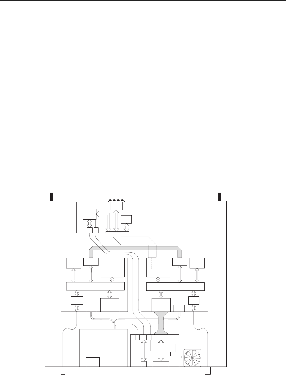
1-1
Section 1
THEORY OF OPERATION
1.0 Introduction
The MOTOTRBO repeater consists of two MOTOTRBO mobile radios; one to act as a receiver, and
one to act as a transmitter and controller. Both of these radios contain specialized software that
allows them to function together as a repeater. The Repeater also contains a Repeater Indicator
board and a Connector board. A block diagram of the repeater is shown in Figure 1-1. The Repeater
Indicator board contains the Front-Panel LED circuitry as well as an Ethernet interface. The
Connector board is a multifunctional board that is primarily used to pass signals to and from
modules inside the chassis to the outside of the chassis.
The Repeater contains the following assemblies and sections:
•Receiver
•Transmitter
•Repeater Indicator Board
•Connector Board
•Fan
•AC/DC PSU
Figure 1-1 Repeater Block Diagram
Power Supply
RF
Rx In
Tx Control Radio
Fan
USB to
Ethernet
Interface
Display
Driver
RTC
Backup
Repeater Board
Repeater
Interface
Mobile
Accessory
Port (MAP)
Rear Connector
Rx Radio
Rx RF
Option
Board
Interface
Controller
Control Head
Interface
Control Head
Interface
Mobile Mic
Port (MMP)
Front Connector
Mobile Mic
Port (MMP)
Front Connector
DC
Power
Repeater
Interface
Mobile
Accessory
Port (MAP)
Rear Connector
Tx RF
Option
Board
Interface
Controller
DC
Power
RF
Tx Out
AC
Power
Connector Board
Fan
Control
Ethernet
Connector
MAP
Connector

1-2 Introduction
1.1 Receiver
The receiver uses a transceiver board which is based on the mobile radio's transceiver board. The
board uses the same PCB as the mobile radio board, but is populated differently to work in the
Repeater application. Only the receiver related functions of the board are utilized in this application,
even though the circuitry for transmit also exists on the board.
The Repeater receiver is identical in functionality to the mobile radio's receiver differing only in the
audio path. On the mobile radio, the decoded audio is sent to a DAC, and then to the speaker. In the
Repeater, this audio information is sent out through the SSI link to the transmit radio to be
processed. Details of the receiver theory of operation can be found in Section 3.1.
1.2 Transmitter
The transmitter consists of a transceiver board which is based on the mobile radio's transceiver
board housed in a transmit chassis. The transmit radio is identical to the receive board from a
hardware standpoint. The difference between the two is the software that is running on them, how
they are connected within the Repeater, and an additional heat sink that is mounted to the chassis.
The added heatsink and the Repeater fan allow the transmitter to be cooled sufficiently when
operating in a 60°C, full-duty cycle environment.
The transmit radio acts as the master controller for the Repeater. It handles all controller related
tasks for the Repeater, including management of the receive radio. The transmit radio is responsible
for processing the audio sent from the receive radio and repeating it out at the Tx frequency. Details
of the transmitter theory of operation can be found in Section 3.2.
1.3 Repeater Indicator Board
The Repeater Indicator board contains circuitry to drive the front panel indicator LEDs, an RTC
battery for the RTC in the transmit radio, as well as an Ethernet controller.
Figure 1-2 Repeater Indicator Board Block Diagram
All of the indicator LEDs that are on the front of the Repeater chassis reside on the Repeater
Indicator board. Each is controlled by a shift register (U6) data out signal and a digital transistor. The
shift register accepts serial data in from the transmit radio's OMAP processor via a SPI bus. A
74LVC07 buffer (U9) level shifts these signals from 3.3 V to 1.8 V.
USB to
Ethernet
Interface
Display
Driver
RTC
Backup
Ethernet to
Rear Panel
Flex to Transmit Radio
Front Panel Indicators

Introduction 1-3
The Repeater Disable LED is a dual-purpose LED that is hardware controlled initially at power-up.
As soon as VBUS power is available on the Repeater Indicator board, the hardware circuitry for the
Repeater Disable LED will cause it to blink periodically. When the software initialization is completed
by the firmware, the blink circuitry will get disabled by the firmware. At that point, the Repeater
Disable LED can be used for its intended purpose of displaying when the Repeater Disable function
is turned on.
The power LED is the only LED that is not controlled by the software. This bi-color LED gets turned
on green when the 13.8 V output from the power supply is valid. It turns on red when A/C power is
lost, and the repeater's backup battery is used.
The Real Time Clock (RTC) battery (M1) is connected to the transmit radio through the Control
Head (J1, pin 30).
Details of the Ethernet Controller can be found in Chapter 2.
1.4 Connector Board
The Connector board has two purposes: provide a place for the Repeater's MAP and Ethernet
connectors to be mounted and a location for the Repeater’s fan control circuitry.
Figure 1-3 Connector Board Block Diagram
Fan
Control
To MAP Conne ctor On
Transmit Radio
To MAP Conne ctor On
Rear Panel
To Ethernet
Conne ctor On
Rear Panel
To Power
Supply
To Fan

1-4 Introduction
1.5 Fan
The fan control logic is provided by the fan controller IC (U51). This is a device from Cypress
Semiconductor. There are basically two functions provided by the fan controller. First, it provides a
PWM output based on a temperature input, and secondly, it provides detection of fan failure based
on the fan tachometer reading.
The Repeater’s internal chassis temperature is measured with an LM50 precision temperature
sensor IC (U52). This IC outputs a voltage that is linearly proportional to temperature at 10 mV/°C,
and with an offset of +500 mV. The output voltage of the LM50 ranges from +200 mV at -30°C to
1.1 V at +60°C.
The fan controller IC (U51) controls the speed of the fan by adjusting the PWM output (pin 1) from
0% to 100%. As long as the fan continues to work, pulses are output from the fan and input to the
fan controller (pin 2).
1.6 AC/DC Power Supply
The Repeater uses the PMPN4001A switch-mode, Power Supply Unit (PSU). It is capable of 200 W
and designed for a 50 W UHF or VHF repeater system. This supply has UL, CE, and TUV regulatory
approvals and is usable in all regions by using the correct line cord. The AC input is auto-ranging
with no manual switch being specified to operate from 90 V-270 V and 47 Hz-63 Hz. It outputs a
nominal voltage of 13.8 V with a voltage tolerance of +/- 5%.
It has Power Factor Correction circuitry and is rated at 15 A across the whole operating temperature
range of -30°C to +60°C. It also has a built-in battery revert circuit with a float output available for
maintaining the charge on a battery and has UL, CE, & TUV approvals. The battery revert connector
is accessible in the back of the power supply.
The supply has over-load, over-voltage, and over-temperature protection. In an overload condition,
the PSU goes into a hiccup mode where it recovers automatically after the fault condition is
removed. During an over-voltage condition, the PSU shuts down and will have to be re-powered on
to recover. In an over-temperature condition, the PSU also shuts down, but will recover after the
temperature goes down.
The PSU is not designed to be field serviceable. If it is determined that the PSU is not functioning,
the whole unit needs to be replaced.

Repeater Interconnections and Cables 1-5
2.0 Repeater Interconnections and Cables
Figure 1-4 shows the Cable interconnections inside the Repeater.
Figure 1-4 Repeater Cabling Diagram
The details of each of these cables/interconnections are as follows:
1. Two conductor DC power cables to the transmit and receive radios.
2. Six conductor DC power cable to the connector Board. Supplies power for the fan and
Repeater Indicator board via cable 6.
3. RF Coax to connect the receive radio to the back of the Repeater. This cable has a BNC
connector on the Repeater’s rear panel.
4. RF Coax to connect the transmit radio to the back of the Repeater. This cable has an N type
connector on the Repeater’s rear panel.
5. CAT5 cable with RJ45 style connectors on both ends. This cable connects the Ethernet
controller on the Repeater Indicator board to the Repeater's back panel and provides power
from the Connector Board to the Repeater Indicator board for the LED indicators.
Power Supply
RF
Rx In
Tx Control Radio
Fan
USB to
Ethernet
Interface
Display
Driver
RTC
Backup
Repeater Board
Repeater
Interface
Mobile
Accessory
Port (MAP)
Rear Connector
Rx Radio
Rx RF
Option
Board
Interface
Controller
Control Head
Interface
Control Head
Interface
Mobile Mic
Port (MMP)
Front Connector
Mobile Mic
Port (MMP)
Front Connector
DC
Power
Repeater
Interface
Mobile
Accessory
Port (MAP)
Rear Connector
Tx RF
Option
Board
Interface
Controller
DC
Power
RF
Tx Out
AC
Power
Connector Board
Fan
Control
Ethernet
Connector
MAP
Connector
1
28
43
6
7
5
9

1-6 Mobile Radio’s Theory of Operation
6. Eleven conductor flex cable. Provides the SSI connection between the transmit and receive
radios. Refer to Section 1.5 for more details on this interface.
7. Thirty conductor flex cable. Provides the connection from the transmit radio to the Repeater
Indicator board and includes SPI signals to drive the LED indicators, RTC backup supply, and
the interface to the Ethernet controller.
8. Twenty six conductor cable. Provides the connection from the transmit radio's MAP to the
MAP located on the Repeater's rear panel.
9. Eight pin conductor cable. Provides Ethernet LED signals from Repeater Board and HWID
signals from Connector Board (Applicable for 32 MB repeaters only).
3.0 Mobile Radio’s Theory of Operation
The sections that follow provide a detailed theory of operation for the VHF circuits in the two
MOTOTRBO mobile radios. For details of the theory of operation and troubleshooting for the
associated Controller circuits, refer to the Controller Section of this manual.
3.1 VHF (136–174 MHz) Receiver Circuitry
The receiver is configured as a dual-conversion superheterodyne receiver, capable of both FM and
4-level FSK demodulation. The major blocks are the front-end, the mixer, Xtal filter, and the Abacus
III back-end IC. The overall block diagram is shown in Figure 1-5.
Figure 1-5 Receiver Block Diagram
3.1.1 Receiver Front-End
The front-end consists of a 2-pole varactor-tuned pre-selector filter, an LNA, a 2-pole varactor-tuned
post-selector filter, and a passive double-balanced mixer. The received signal applied to the antenna
is routed through the harmonic filter and PIN diode controlled antenna switch (D0702). A logic high
level on ANT_ENABLE configures the antenna switch for Tx operation while a logic low places the
switch in Rx mode. The insertion loss of the harmonic filter and antenna switch combined is
approximately 0.8 dB max in Rx mode with slightly more loss at the upper end of the band. From this
point, the Rx signal is routed to the Local Distance Switch (D0400/R0407), which biases on a diode
in normal operation to minimize any insertion loss. Under strong signal conditions and for improved
intermodulation protection from interfering signals, the switch can be turned on by the signal
RF_ATTEN_1, which introduces approximately 10 dB of additional path loss. Activation of the switch
can be accomplished manually by the user or left in the default setting.
T/R ANT
Switch
Hi-Speed
A/D
VCO
X
AD9864
4-Pole LIMITER/IF
AMP
STAGE
DSP
Processor
SPI
&
SSI
BU
S
Sw. 10 dB
Attenuator
10 bit
DAC
LNA
2-Pole
Varactor
Tuned
2-Pole
Varactor
Tuned
D/A
10 bit
DAC
44.85 Mhz
1
st
L.O. High
Side Injection
Fo + 44.85
MHz
SPEAKER
2
nd
L.O.
42.6 or 47.1
MHz
2nd
L.O.

Mobile Radio’s Theory of Operation 1-7
The signal next reaches the pre-selector filter, which is a 2-pole varactor-tuned filter with 5 zeros
that are optimized to provide image frequency rejection. This filter, and the similarly designed post-
selector filter, provide over 75 dB of image response rejection. The 3 dB bandwidth for both filters
varies across the band with a minimum of 32 MHz at 136 MHz and a maximum of 38 MHz around
174 MHz. Half-IF rejection from the filters is also frequency dependent with a minimum of
approximately 7.5 dB achieved at the worst-case frequency of 174 MHz. Both filters have variable
center frequencies that are adjusted by the FE_TUNE signal, which is derived from the output of a
10-bit DAC internal to the MAKO IC (U3200). The voltage is scaled up by a voltage doubler (Q0403)
in order to provide the required linearity for the filters. Both filters are matched to the LNA (Q0402) to
optimize the amplifier’s noise figure (2.0 dB) and to provide an LNA gain of 16 dB to the signal. The
combined gain of the filters and LNA is about 14 dB. Active bias transistor Q0401 maintains the
collector current of Q0402 constant at 25 mA. The LNA, active bias circuit, Local Distance Switch,
and voltage doubler are all supplied by 9R1_FILT, which is derived from 9R1 after filtering.
Following the post-selector filter is the Class 2, double-balanced mixer. It is comprised of baluns
T0400 and T0401 and diode ring mixer D0405. Injection amplifier Q0405 provides 15 dB of gain to
the Rx VCO injection signal. Another amplifier, Q0202, located in the VCO block, also provides gain
for the LO signal and isolation from high RF signals entering the mixer. The signal applied to the LO
port of the mixer is +16 dBm minimum after passing through the 3-pole/1-zero, low-pass injection
filter. The LO injection is high-side and mixes the signal down to an IF frequency of 44.85 MHz. The
output of the mixer is connected to a diplexer network, which terminates out-of-band frequencies
into 51 ohms (R0427) while appearing as high impedance to the 44.85 MHz IF signal.
3.1.2 Receiver Back-End
The signal entering the back-end is matched to 4-pole crystal filter, FL0500, by C0507 and L0503.
The filter is centered at 44.85 MHz with a 3 dB bandwidth of 13.4 kHz. IF amplifiers Q0500 and
Q0501 follow the crystal filter and provide both amplification and limiting to the signal. An overall
gain of 24 dB is available from the composite IF amplifier to lower-level IF signals. As the signal level
increases, Q0501 begins to limit and eventually saturates out at approximately –16 dBm. The
purpose of the limiting is to provide protection to the AD9864 Abacus III back-end IC (U0600). An
internal 16 dB attenuator is also engaged to provide attenuation to the Abacus’s input signal,
working with the external amplifier to limit the signal below the ADC clip point. The block diagram for
the AD9864 is shown in Figure 1-6 below. At IF levels exceeding –26 dBm into U0600, the 2nd LO
synthesizer internal to U0600 can be pulled, causing corruption of the I/Q data being delivered to the
DSP.
Figure 1-6 AD9864 Block Diagram
MXOP
-16dB
IFIN
FREF
IOUTL CLKP CLKN VREFP VCM VREFN PE
DOUTA
DOUTB
PC PDLOP LON IOUTC
MXON IF2P IF2N GCP GCN
FS
CLKOUT
AD9864
LNA
LO
SYN
LO VCO AND
LOOP FILTER LOOP FILTER
CLK SYN VOLTAGE
REFERENCE SPI
CONTROL LOGIC
FORMATTING/SSI
DECIMATION
FILTER
Σ-Δ ADC
AGC

1-8 Mobile Radio’s Theory of Operation
The Abacus III accepts the 44.85 MHz signal, processes it, and sends out baseband I/Q data in
16-bit format to the DSP at a 20 kHz rate. Internal to the Abacus III is an LNA and 16 dB FE
attenuator, an internal integer-N synthesizer used to control the external 2nd LO VCO, a
Sigma-Delta ADC and decimation filter, and control and formatting logic for outputting the baseband
I/Q data. External to U0600 is the 2nd LO VCO with active device Q0600 and its associated circuitry
including the loop filter consisting of C0613, C0618, and R0603. The 2nd LO mixes the 44.85 MHz
IF signal down to 2.25 MHz before being input to the ADC where it is sampled. The tank circuit
(L0608, C0605, C0642, R0617) and varactor (D0601) for the internal clock synthesizer, work with
the loop filter (R0618, C0643, C0646) to provide the 18 MHz clocking signal to the internal ADC,
decimation filter, and SSI formatting circuitry. A 3 Volt regulator (U0601) provides a clean 3 Volt
supply to U0600. Transistor Q0601 is configured as a super filter to provide the 2nd LO transistor
with a low noise supply. The reference clock for U0600 is 16.8_REF, which is a buffered (Q0100)
16.8 MHz clock from the synthesizer block.
Shown below in Figure 1-7, is the block diagram of the signal flow through the receiver back-end. All
the blocks within the dotted box represent the DSP software algorithms internal to U1000.
Figure 1-7 Signal Flow through Receiver Back-End
The DSP takes the incoming 20 kHz data-stream and passes the information through an FIR (Finite
Impulse Response) filter, which provides rejection from any in-band adjacent channel interference.
The remaining filter data is then sent through a decimation process further reducing its frequency to
8 kHz.
Depending on whether the repeater is in Analog or Digital mode determines the kind of signal
processing used. If the radio is in Analog mode, the remaining 8 kHz data is sent through the FM
Discriminator and De-emphasis subroutines in the DSP code. If the repeater is in Digital mode, the
remaining 8 kHz data is still sent through the FM Discriminator but an additional "Symbol Recovery"
routine is applied along with a standard AMBE+2™ Vocoder process. The resultant audio (still
represented by high-speed data) is sent to a DAC (U3200), which drives several gain stages. These
gain stages consist of an I2C audio attenuator (U3501) and a high-power audio PA (U3500)
providing the user with at least 3 Watts of power through the internal speaker.
44.85
MHz
IF
44.85
MHz
IF
AD9864 Hi
SPEED
ADC
AD9864 Hi
SPEED
ADC
FIR
DSP ANALOG FM MODE
DSP DIGITAL 4FSK MODE
FIR
FM
DISCRIMINATOR
FM
DISCRIMINATOR
DEEMPHASIS
DAC
DAC
AMBE+2
VOCODER
4-FSK
SYMBOL
RECOVERY ANALOG AUDIO
GAIN STAGES
ANALOG AUDIO
GAIN STAGES
SPEAKER
SPEAKER
TM
ΣΔ
ΣΔ
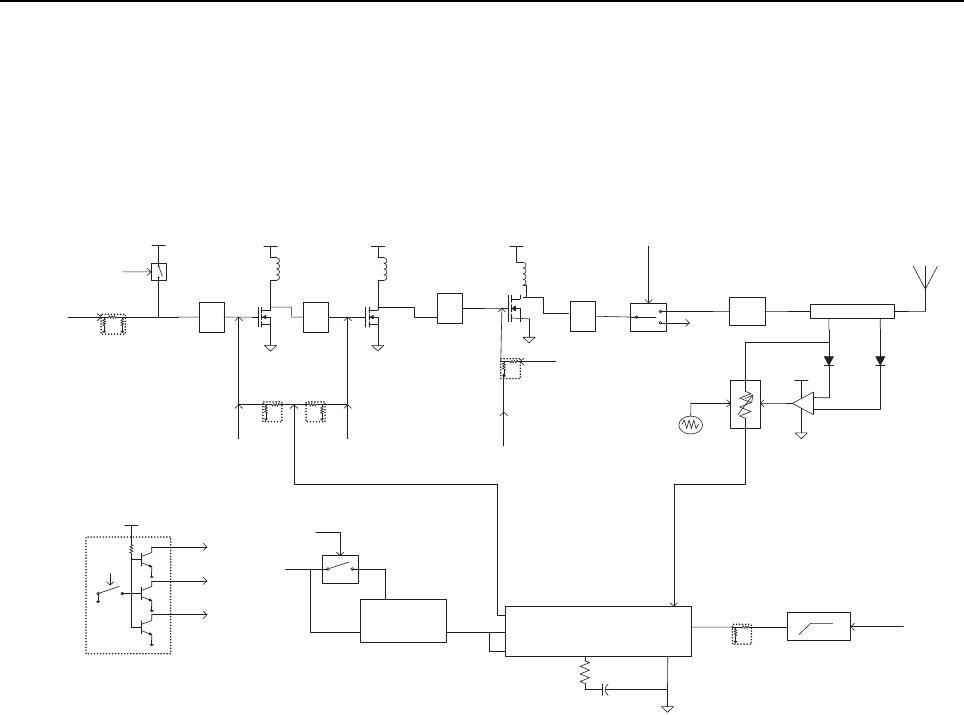
Mobile Radio’s Theory of Operation 1-9
3.2 VHF (136–174 MHz) Transmitter Circuitry – 25 Watt
The Transmitter consists of the power amplifier circuitry and the power control circuitry. The power
amplifier is responsible for delivering a faithful replica of the VCO output amplified up to the desired
output power level, free from distortion. The power control circuitry is responsible for ensuring that
the desired output power level is maintained in both analog and digital modes, as well as protecting
the power amplifier from damage due to heat, antenna mismatch, out-of-range battery voltage, or
mis-assembly.
Figure 1-8 VHF 25 Watt Low-Power Transmitter Detailed Block Diagram
3.2.1 Power Amplifier
The radio’s 25 Watt power amplifier (PA) is a 3-stage amplifier, which amplifies the output of the
VCO to the required transmit power level. The first stage is an adjustable gain LDMOS pre-driver
(RD01MUS1, Q0705), followed by an adjustable gain LDMOS driver (RD07MVS1, Q0703), and the
fixed-gain LDMOS final device (MRF1535, Q0702). A transmit/receive (T/R) switch and a harmonic
filter complete the transmit lineup.
3.2.2 Pre-Driver Stage
Pre-driver is a low power LDMOS device (RD01MUS1, Q0705), which delivers up to +27 dBm
power to the driver stage. Its gain is controlled by varying the gate bias voltage and varies from low
gain up to approximately 14 dB power gain. The gate bias voltage is controlled with the V_cont
signal and is controlled in parallel with the driver stage gain.
The input match to this stage is a high-pass topology comprised of L0716, L0718, and C0795.
(High-pass matches are used where appropriate to minimize the chances of low frequency
regeneration within the amplifier.) The inter-stage match between the pre-driver and driver stages is
comprised of C0790, C0786, C0791, C0792, L0717, and L0719 arranged in a high-pass topology.
T/ R
Switch
Harmonic
Filter
TX _ DAC
Active
Reconstruction
Filter
Log Amp Controller
V _ CONTROL
SW _ 9 V 1
9 V 3
+ 5 V Regulator
PA_ENABLE
-5 dBm
(nominal)
TX _ INJ
INPUT
FROM
VCO
ANT_ENABLE
9V3_TX9V3_TX
SW_9V1
Reflected
Port
Microstrip
Dual
Directional
Coupler
Forward
Port
+
TX Port
RX Port
To FE
A+
Voltage
Controlled
Variable
Attenuator
Thermal
Cutback
AD8315VAPC RF IN
VPOS
ENBL COMM
FLTR
VSET
VCONT
VIN+ 5 VOUT
Pad
To Pressure
Pad Switch
To Pressure
Pad Switch To Pressure
Pad Switch
9 V 3
Pressure
Pad Clos es
Switch
To Predriver
To Driver
To Final
9V3_TX
LDMOS
Predriver
RD01MUS1
LDMOS
Driver
RD07MVS1
ANT _ ENABLE
Pressure
Pad
Switch
Match
Match
Match
Match
FINAL_BIAS
CW/4 FSK
+7dBm

1-10 Mobile Radio’s Theory of Operation
Additional footprints are provided on the printed circuit board to allow for possible engineering
optimizations to this match. These are non-populated parts C0793, C0794, C0817, C0820, and
C0821.
3.2.3 Driver Stage
The next stage is a medium-power LDMOS device (RD07MVS1, Q0703), which delivers up to +38
dBm to the final device. Its gain is controlled by varying the gate bias voltage and varies from low
gain up to approximately 10 dB power gain. The gate bias voltage is controlled with the V_cont
signal and is controlled in parallel with the pre-driver stage gain.
R0718, R0720, R0754, and R0755 are required to improve the bandwidth of the driver stage. The
inter-stage match between the driver and final device is comprised of C0819, C0746, C0754,
C0745, and associated micro-strips on the PCB. Additional footprints are provided on the printed
circuit board to allow for possible engineering optimizations to this match. These are non-populated
parts C0753, C0755 and C0752.
3.2.4 Final Stage
The final stage is a high-power LDMOS device (MRF1535, Q0702). The package is mounted to a
copper carrier to improve thermal conductivity to the chassis and also to more tightly control the RF
load, allowing higher and more consistent maximum output power. This stage is biased at a
quiescent current of 100 mA and operates with a fixed-gain of approximately 14 dB, allowing the
radio to be set to a maximum output power of 35 Watts. The quiescent current is set by adjusting the
Final_Bias signal.
The output match consists of C0719, C0720, C0721, C0726, C0727, C0741, C0724, C0725 and
L0714 and the associated microstrip line on the PCB. The output matching circuitry of this stage has
extremely critical part location requirements. Any repairs must be done with care to ensure the
replaced components are placed accurately and properly soldered. Of particular concern are the
output matching capacitors, C0719, C0720, C0721, C0726, and C0727. The resistor networks at the
input of each of the final elements are required to improve the bandwidth of the circuit. These
resistors are R0712, R0716, R0717, R0719, R0721, R0726, R0732, R0733, R0734, R0736, R0737,
and R0739.
Additional footprints are provided on the printed circuit board to allow for possible engineering
optimizations to this match. These are non-populated parts C0722, C0729, and C0730. If the final
device is replaced, the bias voltage must be re-tuned using the Customer Programming Software
(CPS). Care must be taken not to damage the device by exceeding the maximum allowed quiescent
current. The maximum allowable current is 500 mA, but the design is optimized for 100 mA as noted
earlier. The device can tolerate up to 5 Amps for brief periods of time without damage.
3.2.5 Antenna Switch
The Antenna Switch (T/R switch) has two modes of operation, transmit and receive.
Transmit mode:
The antenna switch utilizes the existing dc feed (A+) to the final stage device (Q0702). Both PIN
diodes, D0700 and D0702, are turned on during key-up by forward biasing them. Forward biasing is
achieved by pulling down the voltage at the cathode end of D0702 to around 12.2 Volts (0.7 Volt
drop across each diode). Q0704 is configured as a current sink that maintains the current through
the antenna switch diodes at 100 mA, as set by VR0700 and R0738.

Mobile Radio’s Theory of Operation 1-11
The current sink is enabled during transmit mode by ANT_ENABLE asserting thru Q0706 and
associated circuitry. When the PIN diodes are conducting, an RF ground is formed at the anode of
the lower PIN diode D0702, which places the series L0710 and L0724 in parallel with C0803. The
values of L0710, L0724, and C0803 are chosen so that they are in parallel resonance at the center
of the transmit band, making them appear as an open-circuit so that a 50 ohm power path is
maintained thru the top PIN diode to the harmonic filter. To further attenuate the Tx signal from
getting to the Rx front-end, a PIN diode pair (D0703) is placed in the Rx path separated from the
D0702 short by a quarter wave inductor (L0730 & L0731). This diode pair shorts to ground in
transmit mode so that the receiver sees as little transmitter power as possible.
Receive mode:
The DC current thru the PIN diodes is interrupted by turning off the current sink. The RF path now
flows from the Harmonic Filter thru the matching circuit formed by C0803, L0710, and L0724, then to
pi network C0766, L0730, L0731, and C0772. The additional shunt diodes (D0703) will be high
impedance since no bias current is flowing from the switched Tx power line.
3.2.6 Harmonic Filter
Inductors L0720, L0721, L0706, L0707, L0708, L0709, L0722, and L0723, and capacitors C0742,
C0739, C0740, C0735, and C0750, form a harmonic filter which is a 7th order low-pass filter with
two notches; this is used to attenuate harmonic energy from the transmitter before it reaches the
antenna. The harmonic filter also prevents high-level RF signals above the receiver passband from
reaching the receiver circuits, improving spurious response rejection. R0713 and L0728 are used to
drain any electrostatic charges that might otherwise build up on the antenna.
3.2.7 Directional Coupler
The dual directional microstrip coupler is implemented at the harmonic filter output to sample both
forward and reverse directed transmitter power. RF power from the transmitter PA passes through
the microstrip coupler before reaching the antenna. Forward RF power is coupled to the U0940 log
detector / controller via the voltage controlled attenuator (VCA) stage consisting of pin diodes
D0901, D0902, and D0903. The log detector/controller regulates the gain of PA stages Q0703 and
Q0705 (via V_cont) as necessary, thus ensuring that the forward power out of the radio is held to a
constant value.
The directional coupler functions not only as part of the transmitter power regulation circuit but also
as part of the VSWR load detection circuitry. Its physical location close to the antenna connector
allows accurate VSWR sense at the transmitter output. Forward and reverse coupled signals are
rectified by D0904 and D0905, respectively. Resulting DC voltage FWD_DETECTED is proportional
to RF power while REV_DETECTED is proportional to reflected RF power. The detected voltages
are fed to the respective inputs of difference amplifier U0901. The difference amplifier output is
applied to variable attenuator control stage U0900-1.
An abnormally high reflected power level, such as may be caused by a damaged antenna, also
causes an increase in the difference amplifier output voltage. An increased difference amplifier
output causes a reduction in attenuation by the VCA. As a result, the increased RF signal applied to
the log detector/controller causes the controller to reduce the gain of PA stages Q0703 and Q0705.
Transmitter power is thus reduced to prevent damage to the final device due to an improper load.

1-12 Mobile Radio’s Theory of Operation
3.2.8 Power Control
The transmitter uses PA controller IC, U0940, to control the power output of the radio. A portion of
the forward RF power from the transmitter is sampled by the directional coupler and delivered via
the VCA to the RFIN port of the PA controller IC (pin 1). The PA controller, a log detector type,
provides temperature-stable, high accuracy control over a typical 50 dB dynamic range.
The MAKO IC contains a digital-to-analog converter (DAC), which provides a reference voltage
(TX_DAC) at the input of reconstruction filter stage U0900-2. The filtered reference voltage at the
output of U0900-2 is divided by the combination of R0942 and R0946 before reaching the VSET
input of the PA controller IC (pin 3). Thermistor RT0953 is used in combination with R0954 to
compensate reference voltage drift at operating temperature extremes. Reference voltage level is
programmable through the SPI lines of the MAKO. This reference voltage is proportional to the
desired power setting of the transmitter, and is factory programmed at several points across the
frequency range of the transmitter to offset frequency response variations of the transmitter's
coupled power circuits.
The PA controller IC provides a DC output voltage at pin 7 (VAPC), which is divided to provide gate
bias for PA pre-driver and driver stages. The 0 to 5 VDC range at U0940 pin 7, is applied as
V_CONTROL to power-adjust the transmitter by controlling the gate bias of stages Q0703 and
Q0705. Voltage divider combination R0727 and R0728 provide gate bias to Q0703 while divider
combination R0750 and R0751 provide gate bias to Q0705. This adjusts the transmitter power
output to the intended value. The ratios of each of these resistor dividers are chosen to ensure that
Q0703 and Q0705 are both running at their nominal design condition at rated output power.
Variations in sampled forward transmitter power cause the PA controller IC to adjust the control
voltage above or below its nominal value to raise or lower output power in order to maintain
transmitter output power relative to the reference voltage applied to VSET.
A power control attenuator circuit was added to the 25 Watt transmitter circuitry in order to extend
the range of the RF detection in the RF detector at low-power levels. This enables the power control
loop to close at lower relative power levels and is needed because of the greater relative power-set
range (1-25 Watt, 14 dB). The PC_ATTEN_ENA activation threshold is set in software for operation
at lower power levels, typically 1-5 Watt. When the PC_ATTEN_ENA is activated, the VCA is driven
to its minimum attenuation level, which increases the RF level at the AD8315 (U0940) for a given
transmitter power level. The radio software adjusts the K&M tuning accordingly such that proper
power-set is maintained at operating powers both above and below the activation threshold point.
3.2.9 Power Ramp Profile Control
In order to limit transient adjacent channel power at the transmitter's output, the ramped power
should follow a raised-cosine profile. The PA controller IC has a linear slope function when scaled in
dB/V. To achieve the desired raised-cosine profile of the output power, the ramped reference voltage
provided by the MAKO DAC follows a raised-cosine approximation. The MAKO DAC reference
output is low-pass filtered by the DAC reconstruction filter before it is applied to the VSET input of
the PA controller IC. Reconstruction filtering reduces spurious emissions in the RF spectrum as a
result of the finite steps of the DAC. Loop filter capacitor C0926, in conjunction with resistor R0950
and the integrator within the PA controller IC, control the loop dynamics. Loop dynamics have been
optimized to achieve sufficient speed to follow the required ramping profiles while meeting switching
transient requirements over varied power levels. Accurate control of the power-rise (ramp-up) and
power-decay (ramp-down) characteristics minimizes splatter into adjacent channels.

Mobile Radio’s Theory of Operation 1-13
3.2.10 Load Dump Protection
In order to protect the transmitter line-up in the case where extremely high voltage spike occurs, a
simple load dump protection circuit is implemented. This circuit is placed at the gate of PA stage
Q0703 and consists of resistors R0980, R0981, R0982 and transistor Q0710. When high voltage
spike (>29.9 V_) is sensed at power supply (A+), the base-to-emitter voltage VBE of this transistor
will be above threshold voltage and this will cause the transistor to turn on. The VBE is controlled by
a combination of R0980 and R0981 which form a voltage divider circuit. When Q0710 is turned on, it
will drain the current from PA stage Q0703 via R0982 and thus preventing the transmission of power
and keep the transmitter line-up from any damage.
3.2.11 Thermal Protection
Thermistor RT0908 and R0902 form a voltage divider with the output proportional to the sensed
circuit board temperature in the vicinity of the transmitter driver and final devices. The voltage
divider output is routed to operational amplifier U0901-2, which provides a dc voltage via diode
junction D0900 to control the attenuation level of the VCA stage. For the condition that the
temperature threshold set by resistive divider combination R0901 and R0909 is reached, the VCA is
driven to increase the RFIN signal at the PA controller IC (pin 1). This increase will cause the PA
controller IC to adjust the PA control voltage below its nominal value to decrease transmitter output
power. The temperature will be reduced by lowering transmitter output power relative to the
reference voltage applied to VSET.
3.2.12 Out-of-Range Battery Protection
Transmitter power cutback, under extended battery supply voltage operation, is provided for by
monitoring the battery supply in the controller circuit of the radio in order to change the VSET input
of the PA controller IC (pin 3) for reduced transmitter output. This cutback starts when the battery
voltage at the connector is 15.3 Volts or greater and has a 2 dB/V slope. In addition, a second low
battery detect circuit is implemented in hardware. This hardware cutback forces a 1.2 dB drop in RF
power level when the battery voltage drops below 12 Volts.
3.2.13 Pressure Pad Switch
The power control circuitry includes a safety switch (S0700) that consists of a conductive portion of
the rubber pad which pushes the RF final transistor Q0702 against the chassis. When the chassis
cover and rubber pad are properly assembled, the conductive portion of the pad contacts a pattern
on the circuit board, electrically closing switch S0700. If the cover and pad are not in place, switch
S0700 is open-circuited and the power control circuit is disabled, turning off the gate bias to Q0702,
Q0703, and Q0705. This prevents thermal damage of the RF transistors which might occur if the
transmitter is operated without adequate heat sinking.
3.3 Frequency Generation Circuitry
The synthesizer subsystem consists of the reference oscillator (Y0100), the fractional-N Synthesizer
IC (Tomahawk II, U0100), and the Voltage Controlled Oscillator VCO.
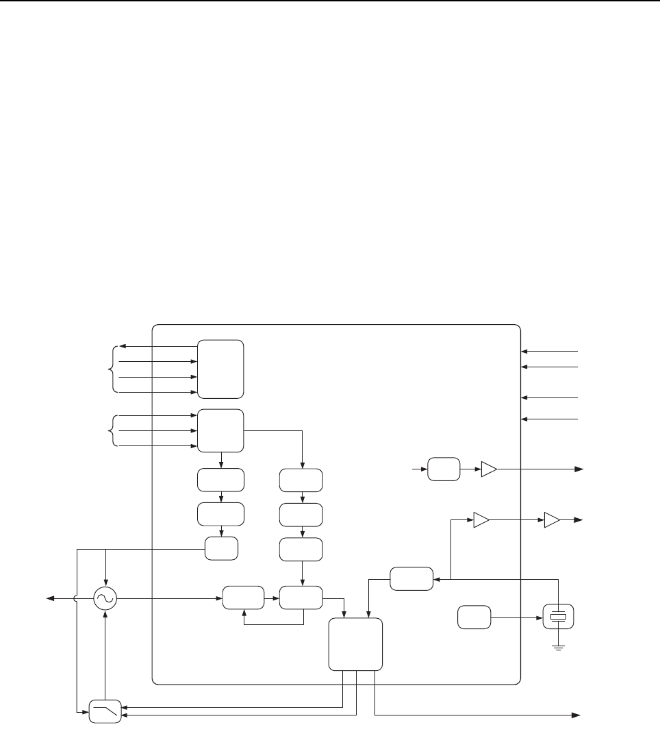
1-14 Mobile Radio’s Theory of Operation
3.3.1 Reference Oscillator
The reference oscillator (Y0100) contains a temperature compensated crystal oscillator with a
frequency of 16.8 MHz. A digital-to-analog (DAC) converter internal to U0100 (Tomahawk) and
controlled by the microprocessor via serial interface (SPI), sets the voltage at the AUX_DAC output
of U0100 (pin H6) to set the frequency of the oscillator. The output of the oscillator (pin 3 of Y0100)
is applied to pin K5 (XOSC_BASE) of U0100.
3.3.2 Fractional-N Synthesizer
The Tomahawk II Synthesizer IC (U0100) consists of a pre-scaler, a programmable divider and
divider control logic, phase detector, charge pump, a D/A converter in the high frequency analog
modulation path, an attenuator to balance the high and low frequency modulation paths, a serial
interface for control (SPI), a serial interface for modulation (SSI), and a super filter for the regulated
2.45 Volts.
Figure 1-9 VHF Synthesizer Block Diagram
A voltage of 2.775 Volts applied to the super filter input (U0100 pin J4) supplies an output voltage of
2.45 VDC (SF_OUT) at pin K4. This supplies the VCO and the VCO modulation bias circuit (via
R0321). The super filter supply voltage is provided by the 2.775 Volt regulator within U3200. The
synthesizer is also supplied by the 5 Volt regulator, U3002, another 2.775 Volt regulator within
U3200, and a 1.875 Volt regulator within U3200.
SPI
Interface
Data Write
Clock
CEX
Data
Fsync
Clock
SPI
SSI
(Modulation )
Prescaler Main Di vider
VCO
Fracti onal
Unit
DS
18 - bit
Modulation
Unit
Main
Phase/ Freq.
Detector
And
Charge Pumps
Reference
Divider
TCXO
(16 .8 M H z)
AUX
D/ A
Main _CP LOCK DETECT
Buffer Buffer
16 .8M H z REF
Loop Filter
5V
2.775V Dig
2.775 V A na
1.875V Dig
TOMAHAWK II
Fractional -N
Synthesizer
(U0100)
D9
Data ReadD10
C11
D8
F11
F10
F9
J2
G3
Adapt _CP
H1 D7
SF _OUT
Super
Filter
2 .775 V Ana K4
H6
J11
K5
H2,J3
A7
A5,A10,B2,B9,
G2,J4,J6, J10,
K2,L6
B7 ,E 11, G10 ,J1
Digital
Attenuator
SSI
Interface
D/A
Waveform
Gener ator
K8 HP MOD
PRSC
TX / LO
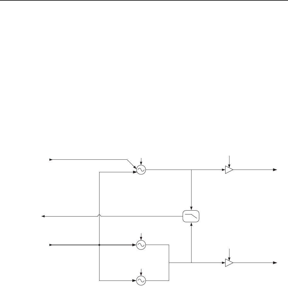
Mobile Radio’s Theory of Operation 1-15
The output signal LOCK (U0100-D7) provides information about the lock status of the synthesizer
loop. A high level at this output indicates a stable loop. A discrete buffer amplifier (Q0100) provides
a buffered 16.8 MHz reference frequency to other parts of the radio.
The serial programming interface (SPI) is connected to the microprocessor via the data lines
SPI_DW (U0100-D9) and SPI_DR (U0100-D10), clock line SPI_CLK (U0100-C11), and chip enable
line CEX (U0100-D8). The serial modulation interface (SSI) is connected to the DSP via the data
line SDTX (U0100-F11), clock line TXCLK (U0100-F10), and frame sync line SFTX (U0100-F9).
3.3.3 Voltage Controlled Oscillator (VCO)
The Voltage Controlled Oscillator (VCO) subsystem consists of three Colpitts oscillators (two Rx and
one Tx), a single-stage Tx buffer amplifier, a single-stage Rx buffer amplifier, oscillator bias control
switches, and the modulation circuitry.
Figure 1-10 VHF VCO Block Diagram
The VHF Rx VCO design incorporates two varactor-tunable Colpitts oscillators. Each Rx oscillator
has a tuning range of 19 MHz, sufficient to cover the Rx frequency range of 180.85 MHz to 218.85
MHz. A single Tx oscillator covers the frequency range of 136 MHz to 174 MHz. The oscillators
resonate at fundamental operating frequencies. Three (active-low logic) general purpose output
lines (GPO1, GPO3, and GPO6) from the Tomahawk IC (U0100-B4, E5, and H8) provide the control
for independent bias selection to each oscillator (VCO_SEL) via the PNP transistor switches U0304
and U0201. The 2.45 Volt super filtered output, SF_OUT, of the Tomahawk IC (U0100-K4) supplies
the bias to the oscillators. A portion of the VCO output signal is lightly coupled through coupling
capacitors C0331 and C0231, routed through a low-pass filter (formed by L0221, C0235, L0230,
C0265, and C0233), and fed back to the M_PRSC input of the Tomahawk IC (U0100-J2).
TX VCO 1
RX VCO 1
RX VCO 2
TX Buffer Amp
RX Buffer Amp
Low Pass
Filter
TX INJ
RX INJ
To U0700
To Q0405
Steering Line Voltage
(VCTRL)
9V3 _VCO
( U3001 -5 )
9R1
(Q0107 )
RX_VCO _SEL 2
(U0100 - H8 )
RX_VCO _SEL 1
(U0100 -B4)
TX_VCO_SEL 1
(U0100 -E 5)
High Port Modulation
(HP_MOD_OUT)
(U0100 -K8)
Prescaler
(U0100 -J2)
VHF VCO
Subsystem

1-16 Mobile Radio’s Theory of Operation
High-port modulation is scaled through a voltage divider (comprised of R0319, R0320, and R0321)
and applied to the Tx modulation varactor diode CR0300. The Tx VCO frequency is modulated via
coupling capacitor C0310.
A discrete single-stage Tx buffer amplifier (comprised of the NPN transistor Q0302 and surrounding
components) amplifies the signal from the Tx oscillator to the level required by the first stage of the
Transmitter Power Amplifier (U0700). The Tx buffer amplifier also provides sufficient isolation from
any undesired load-pulling from the Transmitter Power Amplifier. The bias for Q0302 is provided by
the 9.3 Volt regulator U3001.
A discrete single-stage Rx buffer amplifier (comprised of the NPN transistor Q0202 and surrounding
components) amplifies the signal from the Rx oscillator to the level required by the LO injection
amplifier (Q0405). The Rx buffer amplifier also provides sufficient isolation from any undesired
load-pulling from high input levels in the receiver front-end. GPO4 from the Tomahawk IC
(U0100-D4) controls the transistor switch (comprised of Q0108 and Q0107), that enables the 9.1
Volt bias to Q0202 (via the 9.3 Volt regulator U3001).
3.3.4 Synthesizer Operation
The complete synthesizer subsystem is comprised mainly of the Tomahawk Synthesizer IC,
Reference Oscillator (crystal oscillator with temperature compensation), loop filter circuitry, VCO,
and DC supplies. The VCO feedback signal, PRSC, is fed to pin J2 of U0100 (M_PRSC) via a
low-pass filter (L0221, C0235, L0230, C0265 and C0233) which attenuates harmonics and provides
the correct level to close the phase-locked loop.
The prescaler in the Synthesizer IC (U0100) is a four-level prescaler capable of dividing by 4, 5, 6,
and 7. The main loop N divider is configured to be an 8-bit divider. The divide-by-N portion of the
main loop is set via the SPI. The fractional portion of the divider is realized using a 3-accumulator,
24-bit fractional divider. The SPI is used to set the desired divide ratio.
The output of the prescaler is applied to the main loop divider. The output of the main divider is sent
to the phase/frequency detector, which compares the main divider’s output signal with the reference
signal. The reference signal is generated by dividing down the signal of the reference oscillator
(Y0100). The output signal of the phase/frequency detector is a pulsed signal which is routed to the
charge pumps. The main charge pump current is programmable through the SPI with its output at
pin G3 of U0100 (MN_CP). The loop filter transforms this current into a steering voltage that is
applied to the VCO.
To reduce lock time when new frequency data has been loaded into the synthesizer, an adapt
charge pump, providing much greater current than the main charge pump, is turned on for a finite
amount of time to quickly charge or discharge the loop filter capacitors to steer the VCO to the
desired frequency. The output of the adapt charge pump passes to the loop filter via pin H1 of
U0100 (MN_ADAPT_CP). When the synthesizer is within the lock range and the adapt timer runs
out, the adapt charge pump is powered down and the main charge pump takes over. A settled
synthesizer loop is indicated by a high level at signal LOCK (U0100-D7), which is routed to the
microprocessor. Q0102 is configured as a current source to provide a steady 1.5 mA during the
adapt period. U0101 is an analog switch that opens the adapt path slightly before the end of the
adapt period to prevent the current from the current source from pushing the VCO off frequency.

Mobile Radio’s Theory of Operation 1-17
Modulation is performed by applying a digital data stream via the SSI bus from the DSP (U1000) to
the synthesizer (U0100). In order to meet spurious and phase noise requirements, the PLL
bandwidth was designed to be narrower than the full modulation bandwidth, therefore requiring the
use of dual-port modulation. Internal to the synthesizer (U0100), low-port modulation is added to the
fractional-N division numerator to trace out the modulation versus time while the high-port data
stream passes through an interpolating waveform generator, a digital attenuator (for modulation
balancing), and then is converted to an analog signal through a 10-bit DAC before modulating the
VCO. This high-port analog modulation output (HP_MOD_OUT, U0100-K8) is connected to the
VCO modulation varactor diode (CR0300) via C0360 and R0319.

1-18 Mobile Radio’s Theory of Operation
Notes
2-1
Section 2
TROUBLESHOOTING CHARTS
1.0 Troubleshooting Flow Chart for Receiver (Sheet 1 of 3)
Set up radio in Analog
Receive mode on
desired channel
with Squelch open
1st LO
> +2 dBm
at R0422?
No
Audio Tone
present
at Speaker?
Yes
Volume
level
adjusted
properly?
Check U3501
bias and
replace part if
necessary
Audio at pin 1
of U3501?
Verify audio path to
U3501
B
Audio at pin 10
of U3501?
Check connections to
external speaker and
replace speaker if
necessary
Verify audio path
between U3500 and
pin 1 of U3501
Audio at pin 4
of U3500?
Audio at pin 1
of U3500?
Check biasing
before replacing
U3500
1st LO
(180.925 MHz)
> +16 dBm
at TP0401?
Check biasing on
Q0405 before replacing
9 VDC
present
at R0417?
Check
9R1 path back to
Synthesizer
Check VCO
Troubleshooting
Flow Chart
RF level
of on-channel
signal > -45 dBm
on pin 4
of T0401?
A
Check T0400 and D0405
and replace if necessary
Yes
Yes
Yes Yes
No
No
No
Yes
Yes
No
No
No
Yes
Yes
No
No
No
Yes
Yes
NO RX AUDIO
No
Spray or inject 44.85 MHz
RF carrier modulated with
1 kHz Audio Tone into XTAL
Filter FL0500
Setup repeater to receive at
136.075 MHz with the RX brick
open and connected to the
system.
Apply an on-channel
RF carrier at -47 dBm modulated
with 1 kHz tone
at the RX antenna port.
Audio at pin 6
of U3505?
All Troubleshooting within
the dotted line is done on
the TX Brick

2-2 Troubleshooting Flow Chart for Receiver
1.1 Troubleshooting Flow Chart for Receiver (Sheet 2 of 3)
A
Voltage level
> 2.7 VDC
on D0401?
+9.0 VDC
on pin 4
of Q0403?
Check circuitry around
D0401 and D0403 for shorts
and opens
Check biasing on
Q0403 before replacing
Check biasing circuitry of
Q0401 and Q0402 before
replacing
RF level
of on-channel
Signal > -45 dBm
at C0420?
Is voltage
at R0409
= 0.7 VDC?
Voltage
< 0.5 VDC
at pin 2
of Q0400?
Check biasing
circuitry of
Q0400 before
replacing
Check biasing circuitry of
Q0402 before replacing
No
Yes
No
No No
No No
Yes
Yes
Yes
Yes
Yes
Check Synthesizer
Troubleshooting
Flow Chart
~ 6.8 VDC at
L0400/D0400?
Check D0403 and associated
capacitors for opens and shorts
and replace if necessary

Troubleshooting Flow Chart for Receiver 2-3
1.2 Troubleshooting Flow Chart for Receiver (Sheet 3 of 3)
B
16.8 MHz
present
at C0622?
Check Synthesizer
Troubleshooting
Flow Chart
2nd LO
> 0 dBm and
at 42.6 MHz
at TP0600?
Yes
No
No
Yes
44.85 MHz
present
at TP0602?
2.25 MHz
present
at C0625?
No
Yes
No
Yes
18 MHz
present
at L0608?
Check diode
continuity before
replacing D0601
Replace components
as needed
No No
Yes Yes No
Yes
Check for visible
solder shorts near
pins before replacing
U0600
~ 1.65 VDC
on R0617?
Clock
VCO and LF
components
OK?
DC continuity
through
biasing components
E0600 - E0610?
Replace
defective biasing
component
Yes
No
3.0 VDC
on pin 1
of U0601?
Check Controller
Troubleshooting
Flow Chart
5.0 VDC
at E0610?
Check biasing on
U0601 before
replacing
Yes Yes
3.5 VDC
at E0609?
No
No No
Yes
Check biasing on
Q0601 before
replacing
Remove Shield
SH0500.
Check biasing on
Q0600 and
check continuity
on D0600.
Replace parts if
necessary.
Check 5 VDC supply and
biasing components
before replacing
Q0500 or Q0501
Biasing
correct on
Q0500 and
Q0501?
~ 3.0 VDC
on L0604
and L0605?
Check biasing
components and 3 VDC
supply. Replace
any parts if necessary.
No
Yes
No
Yes
Check FL0500 matching
components before
replacing
44.85 MHz
present
at pin 6 of
FL0500?
Check signal gain
and biasing
before replacing
Q0500 or Q0501
No
Yes
All Troubleshooting on this
page is done on the RX Brick
2-4 Troubleshooting Flow Chart for 25W Transmitter
2.0 Troubleshooting Flow Chart for 25W Transmitter
Place Switch or R0775
Check 9V3_PA Regulator in
Controller Troubleshooting
Flow Chart
Is Voltage at
TP0910 >
1 VDC?
Check Bias Set Circuit;
bias tune
Replace U0700
Check VCO Troubleshooting
Flow Chart
Is TP0909
>1 VDC?
NO TRANSMITTER
POWER
Check Q0705 and
associated circuitry
Check 9.3 V Regulator
circuit Check T/R bias circuit
Check 5 V Regulator
circuit
Replace Q0702
Check MAKO
Troubleshooting Flow Chart
Check U0900-2 and
associated circuitry
Replace U0940
Does
TP0702 =
9.3 VDC?
Is TP0913
= 9.1 VDC?
Is U0941
Pin1 =
5 VDC?
Is voltage at TP
TX_RAMP_DAC
in controller > 3
VDC?
Is D0702
~12.4 VDC?
is TP0707
~2.2 VDC?
Is Pressure
Pad Switch
in place?
Is Power at
TP0704 ~ +4
dBm?
Is TP0703
-11 dBm?
Is resistance to
ground at Q0702
TP0707 > 10
kohms?
Is Power at
TP0709 ~14
dB > TP0710?
Is Power at
TP0702 ~10
dB > TP0709 ?
Check Q0703 and
associated circuitry
Is Power at
D0700 ~10
dB > TP0702?
Check Q0702 and
associated circuitry
Measure relative power through the remainder of TR switch and LPF to find open circuit.
Perform visual inspection of circuit.
No
No
No
No
No
No
No
No
No
No
No
No
No
No
Yes
Yes
Yes
Yes
Yes Yes
Yes Yes
Yes Yes
Yes
Yes
Yes
Yes
Yes
No

Troubleshooting Flow Chart for Synthesizer 2-5
3.0 Troubleshooting Flow Chart for Synthesizer
Start
Visual check of
the Board OK?
Correct
Problem
NO
YES
+5 V at R0100? NO
YES
Check 5 V
Regulator
U3002
+2.775 V at
R0101 and
R0103?
Check U3200
+1.875 V at
R0102? Check U3200
NO
YES
NO
YES
Is 16.8 MHz
Signal at C0145?
NO
YES
Check Y0100
Is 16.8 MHz
Signal at R0155?
NO Is 16.8 MHz
Signal at R0109?
NO Replace
U0100
YES
Check Q0100
and surrounding
components
YES
Is Radio in Tx or
Rx mode?
Tx
Is
GPO3 low
(<0.5 V), and
GPO1 and GPO6 are
high (>1.4 V)?
NO
YES
Rx
NO
YES
+2.45 V at
C0137
(SF_OUT)?
NO Are C0136,
C0137 OK?
Replace or
resolder
components
NO
Replace U0100
YES
YES
1.5 ms pulse at
TP_ADAPT_SW
when channel
changed?
NO 1.5 ms (inverted)
pulse at R2517 when
channel changed?
Check P U1000
Troubleshooting
Chart
NO
YES
Check Q0106,
R0159
Is
either GPO1 or
GPO6 low (<0.5 V),
but not both, and
GPO3 high
(>1.4 V)?
YES
Is RF Prescaler level
(at C0265) between 100
mVpk and 300 mVpk
(harmonics <-15 dBc)?
NO Check VCO
Troubleshooting
Chart
Is SPI
Programming
OK?
Check P U1000
Troubleshooting
Chart
Replace
U0100
Is SPI
Programming
OK?
Check P U1000
Troubleshooting
Chart
Replace
U0100
YES
NO
NO
YES
Replace
U0100
YES
Is Modulation
Present at
C0360?
Is Tx SSI activity
present on CLK,
FSYNC, and DATA
lines (R2512, R2514,
R2513)
Check P U1000
Troubleshooting
Chart
YES
NO
NO
YES

2-6 Troubleshooting Flow Chart for Tx VCO (Sheet 1 of 2)
4.0 Troubleshooting Flow Chart for Tx VCO (Sheet 1 of 2)
2.556 V at C0362 &
C0363
~ 0 VDC at
C0348?
2.556 VDC at
C0300?
V
be
= 0.7 V
for Q0300?
Yes
Yes
Check biasing
components then
replace Q0302 if
needed
Check biasing
components then
replace Q0302 if
needed
V
be
= 0.7 VDC
for Q0302?
No
No
No
No TX VCO signal at C0318
Visual check
of board
OK? Correct problem
Correct problem
Radio did not boot up
properly or check
9V3 Regulator
Radio did not boot up
properly or check
9V3 Regulator
9 VDC at L0300?
Check biasing
components then
replace Q0302 if
needed
Check biasing
components then
replace Q0302 if
needed
V
be
= 0.7 VDC
for Q0302?
Yes
Yes
No TX VCO signal at C0318
Visual check
of board
OK? Correct problem
Correct problem
Radio did not boot up
properly or check
9V3 Regulator
Radio did not boot up
properly or check
9V3 Regulator
9 VDC at L0300?
No
No
No
Check Synthesizer
Troubleshooting
Chart
Check Synthesizer
Troubleshooting
Chart
Radio is not
programmed for
VCO1 Transmit Mode
or U0100 not
functional
Check biasing
components then
replace Q0300 if
needed
Check biasing
components then
replace Q0300 if
needed
Yes
No
Yes
RF signal
present at
R0332?
Check components
between R0332 and
L0305 for shorts or
opens
Check CR301 - CR304
and L0310, L0307,
C0308, C0313, C0320,
and C0314 for short
Yes
Check CR0301 - CR0304,
L0310, L0307, C0308, C0313,
C0320, and C0314
for shorts or opens
Radio is not programmed for
VCO 1 Transmit Mode
or U0100 not functional
Troubleshooting Flow Chart for Tx VCO (Sheet 1 of 2) 2-7
4.1 Troubleshooting Flow Chart for Tx VCO (Sheet 2 of 2)
DC Voltage
at R0311
between 0.6
and 4.5 VDC?
Check Synthesizer
Troubleshooting
Flow Chart
Check Synthesizer
Troubleshooting
Flow Chart
Yes
No
-
Tx VCO locked but no
high-port modulation
~2.1 VDC at
VCO side of
C0360?
Check R0321, R0320,
R0319, and CR0300
for open or short
Modulation at
CR0300?
No
Yes
Replace C0310
Yes
Modulation at
C0361?
No
Replace C0360
Yes
Check C0361 and
C0334 for short and
then check
Synthesizer
Troubleshooting
Flow Chart
Check C0361 and
C0334 for a short and
then check
Synthesizer
Troubleshooting
Flow Chart
No
Tx VCO not locked
at correct frequency
Check C0323, C0325,
and C0329 and all
components between
C0326 and C0314 for
shorts or opens
Check R0321, R0320, R0319,
and CR0300 for
shorts or opens
2-8 Troubleshooting Flow Chart for Rx VCO (Sheet 1 of 2)
5.0 Troubleshooting Flow Chart for Rx VCO (Sheet 1 of 2)
2.556 V at C0362 &
C0363
Check Synthesizer
Troubleshooting
Flow Chart
Check Synthesizer
Troubleshooting
Flow Chart
Radio is not
programmed for
Receive Mode or
U0100 not functional
~0 VDC at
C0258?
2.556 VDC at
C0236?
Vbe
= 0.7 VDC
for Q0201?
Yes
Yes
No
No
No
VCO 2
Check biasing
components and
then replace Q0202 if
needed
Check biasing
components and
then replace Q0202 if
needed
Vbe
= 0.7 V
for Q0202?
Yes
Yes
No
No
No
No Rx VCO signal at C0218
Visual check
of board
OK? Correct problem
Correct problem
Radio did not boot up
properly or check
9V3 Regulator
Radio did not boot up
properly or check
9V3 Regulator
9 VDC at E0201?
Check biasing
components and
then replace Q0200 if
needed
Check biasing
components and
then replace Q0200 if
needed
2.556 V at C0362 &
C0363
~0 VDC at
C0248?
2.556 VDC at
C0200?
Vbe= 0.7 VDC
for Q0200?
No
Yes
Yes
No
No
No
VCO 1
Check Synthesizer
Troubleshooting
Flowchart
Check Synthesizer
Troubleshooting
Flowchart
Radio is not
programmed for
Receive Mode or
U0100 not functional
Radio is not
programmed for VCO 1
Receive Mode or
U0100 not functional
Yes RF signal
present at
R0219?
Check CR205 - CR208
and L0218, L0215,
C0243, C0245, C0250,
and C0246 for short or
open
Yes
Yes
Check components between
R0219 and L0205
for shorts or opens
Check biasing components
and then replace Q0201
if needed
Yes
Radio programmed for
Rx VCO 1 or 2?
Check CR0201 - CR0204 and
L0210, L0207, C0220,
C0213, C0208, and C0214
for shorts or opens
Radio is not programmed
for VCO 2 Receive Mode
or U0100 not functional
Check CR0205 – CR0208 and
L0218, L0215, C0243,
C0245, C0250, and C0246
for shorts or opens
Troubleshooting Flow Chart for Rx VCO (Sheet 1 of 2) 2-9
5.1 Troubleshooting Flow Chart for Rx VCO (Sheet 2 of 2)
Rx VCO not locked
Rx VCO not locked
at correct frequency
DC Voltage
at R0211
between 0.6
and 4.5 VDC?
Check Synthesizer
Troubleshooting
Check Synthesizer
Troubleshooting
Flow Chart
No
Yes
Rx VCO 1 or
VCO 2
selected?
Check components
between C0253 and
C0246 for open or
short
VCO 1 VCO 2
Check C0223, C0225, and C0229
and all components between
C0226 and C0214 for
shorts or opens
Check C0251, C0252, and C0259
and all components between
C0253 and C0246 for
shorts or opens

2-10 Troubleshooting Flow Chart for Rx VCO (Sheet 1 of 2)
Notes

3-1
Section 3
VHF PCB/SCHEMATICS/PARTS LIST
1.0 Allocation of Schematics and Circuit Boards
1.1 Controller Circuits
The VHF circuits are contained on the Printed Circuit Board (PCB) which also contains the
Controller circuits. This Chapter shows the schematics for the VHF circuits only, refer to the
Controller section for details of the related Controller circuits. The PCB component layouts in this
Chapter show both the Controller and VHF circuit components. The VHF schematics and the related
PCB and parts list are shown in the table below.
NOTE: The VHF Schematics and parts lists are the same for 8471495L01 and 8471495L03. Only
the Controller circuits are different between the two PCBs.
Table 3-1 VHF 1–25W Diagrams and Parts List
PCB:
8471495L01 Main Board Top Side
8471495L01 Main Board Bottom Side
8471495L03 Main Board Top Side
8471495L03 Main Board Bottom Side
Page 3-19
Page 3-20
Page 3-21
Page 3-22
SCHEMATICS
Overall
Receiver Front-End
Receiver IF Amp
Receiver Back-End
Power Amplifier
Power Control
Synthesizer
Receiver VCO
Transmit VCO
Page 3-23
Page 3-24
Page 3-25
Page 3-26
Page 3-27
Page 3-28
Page 3-29
Page 3-30
Page 3-31
Parts List
8471495L01 and 8471495L03 Page 3-32

3-2 Allocation of Schematics and Circuit Boards
Table 3-2: VHF 1–25W Diagrams and Parts List
PCB:
8471495L04 Main Board Top Side
8471495L04 Main Board Bottom Side
Page 3-3
Page 3-4
SCHEMATICS
Overall
Receiver Front-End
Receiver IF Amp
Receiver Back-End
Power Amplifier
Power Control
Synthesizer
Receiver VCO
Transmit VCO
Page 3-5
Page 3-6
Page 3-7
Page 3-8
Page 3-9
Page 3-10
Page 3-11
Page 3-12
Page 3-13
Parts List
8471495L04 Page 3-14
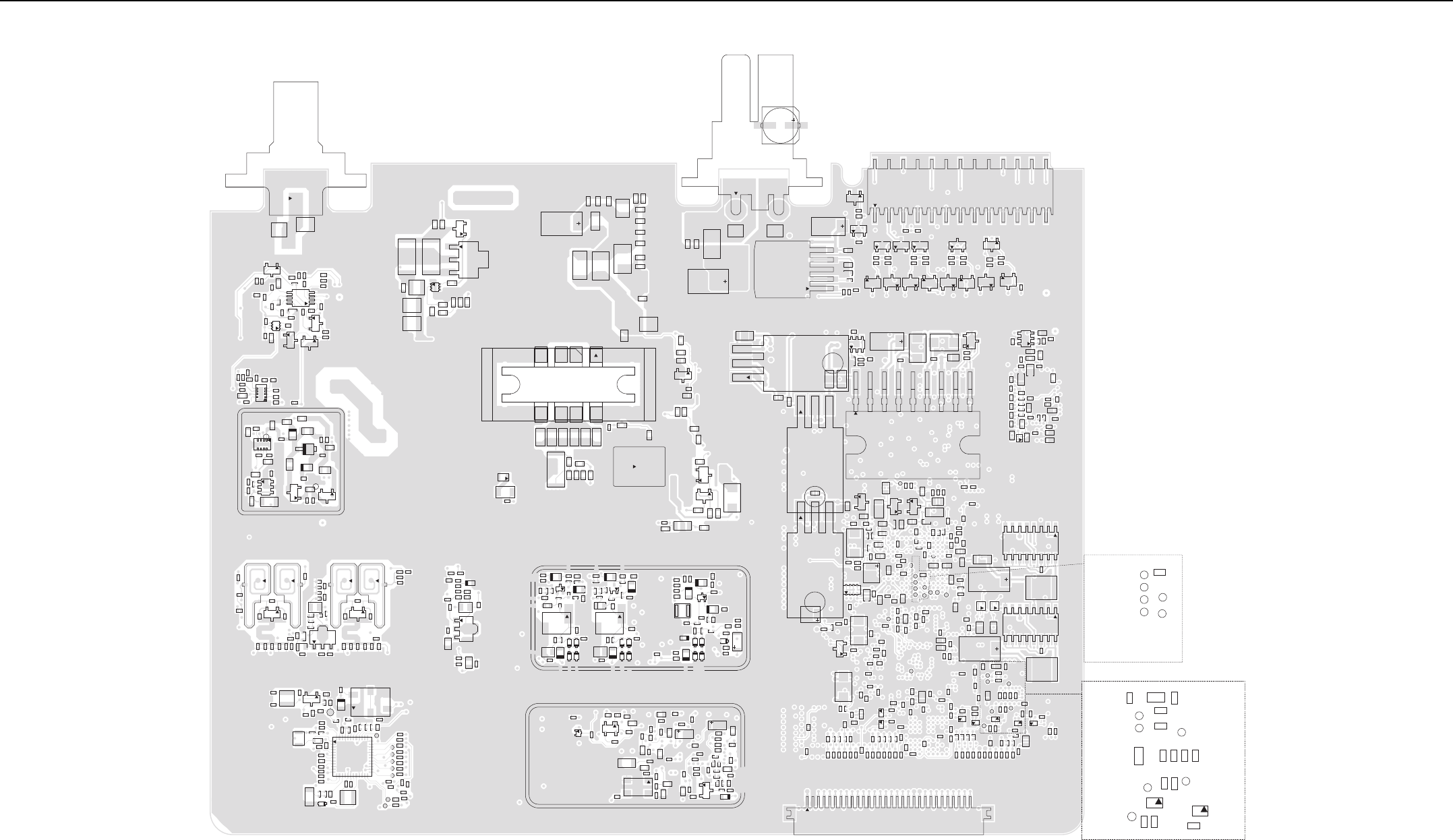
VHF (136–174 MHz) 1–25W PCB/Schematics/Parts List 3-3
2.0 VHF (136–174 MHz) 1–25W PCB/Schematics/Parts List
R3587
TP_MAKO_DCLK
TP_MAKO_FSYNC
TP_MAKO_RX
TP_MAKO_TX
USB1_SEO
USB1_TXEN
C2006
C2007
C2008
C2009
R2005
R2007
R2008
R2009
R2013
R2014
R2015
R4095
R4097
R4099
TP4000
TP_SDRAM_BA0
TP_SDRAM_BA1
TP_SDRAM_CLK
TP_SDRAM_CLKX
TP_SDRAM_CS
U4004
U4005
2.9V_MAKO_V6
3.6V_MAKO_SW1
C0100
C0102
C0103
C0104
C0105
C0109
C0110
C0111
C0113
C0117
C0118
C0120
C0121
C0122
C0124
C0125
C0126
C0127
C0128
C0129
C0130
C0132
C0133
C0140
C0141
C0142
C0143
C0144
C0145
C0146
C0171
C0175
C0177
C0178
C0180
C0195
C0196
C0200
C0201
C0204
C0205
C0206
C0208
C0213
C0214
C0215
C0220
C0223
C0225
C0226
C0229
C0236
C0237 C0240
C0241
C0242
C0243
C0245
C0246
C0247
C0250
C0251
C0252
C0253
C0259
C0300
C0301
C0304
C0305
C0306
C0308
C0310
C0313
C0314
C0315
C0320
C0323
C0325
C0326
C0329
C0332
C0334
C0360
C0361
C0405
C0406
C0408
C0409
C0410
C0411
C0413
C0414
C0415
C0416
C0417
C0418
C0419
C0420
C0423
C0424
C0425
C0426
C0427
C0428
C0429
C0430
C0431
C0432
C0433
C0434
C0435
C0437
C0438
C0439
C0440
C0442
C0450
C0451
C0455
C0457
C0502
C0504
C0509
C0510
C0515
C0516
C0605
C0611
C0615
C0617
C0619
C0620
C0621
C0622
C0623
C0625
C0626
C0627
C0629
C0630
C0631
C0633
C0638
C0642
C0643
C0644
C0645
C0646
C0650
C0700
C0701
C0702
C0703
C0704
C0705
C0706
C0707
C0708
C0709
C0710
C0711
C0712
C0713 C0714
C0731
C0738
C0771
C0776
C0777
C0778
C0779
C0796
C0797
C0798
C0799
C0802
C0804
C0805
C0823 C0824
C0900
C0901
C0904
C0906
C0907
C0908
C0909
C0910
C0914
C0915
C0918
C0921
C0922
C0926
C0929
C0931
C0934
C0935
C0936
C0937
C0939
C0947
C0948
C0949
C0950
C0951
C0960
C0961
C0962
C0963
C0964
C0965
C0967
C0968
C1000
C1001
C1002
C1003
C1004
C1005
C1006
C1008
C1007
C1009
C1010
C1011
C1012
C1013
C1014
C1015
C1016
C1017
C1018
C1019
C1030
C1031
C1034
C1036
C1037
C2000
C2001 C2002
C2003
C2004
C2005
C2500
C3000
C3002
C3005
C3006
C3007
C3008
C3009
C3010
C3015
C3018
C3019
C3040 C3046
C3202
C3203
C3207
C3208
C3209
C3210
C3211
C3212
C3213
C3216
C3219
C3220
C3225
C3226
C3229
C3234
C3238
C3239
C3240
C3247
C3248
C3249
C3254
C3262
C3273
C3276
C3277
C3278
C3280
C3283
C3292
C3501
C3504 C3505
C3506
C3511
C3513
C3514
C3515
C3516
C3518
C3520 C3523
C3524
C3528
C3529
C3530
C3531
C3538
C3543
C3545
C4000
C4001
C4002
C4003
C4004
C4005
C4006
C4013
C4016
C4017
C4018
C4019
C4020
C4021
C4022
C4023
C4024
C4025
C4026
C4027
C4028
C4029
C4030
C4031
C4032
C4033
C4034
C4035
C4040 C4041 C4042 C4043 C4044
C4045
C4046 C4047
C4048
C4075
C4089
C4090
C4091
C4092
C6406
C6407
C6408
C6416
C6417
C6418
C6419
C6420
C6421
C6422 C6423
C6426
C6427
C6428
C6429
C6430
C6431
C6433
C6439
C6440
C6445
C6450
C6451
CLKOUT
CR0201
CR0202
CR0203
CR0204
CR0205
CR0206
CR0207
CR0208
CR0300
CR0301
CR0302
CR0303
CR0304
D0401 D0403
D0601
D0900
D0901
D0902
D0903
D0906
D0907
DOUTA
DOUTB
E0600
E0601
E0602
E0604
E0605
E0606
E0607
E0608
E0700
E0701
E0703
E3000
E3202
E3205
E3500
E3501
E3502 E3503
E4000
E4001
E4005
E6401
E6402
E6407
23
4
5
6
FL0500
FS
3
2
J0700
J3000
25
26
2
J4000
30
J4001
L0100
L0202
L0203
L0207
L0209
L0210
L0212
L0213
L0214
L0215
L0217
L0218
L0219
L0302
L0303
L0307
L0309
L0310
L0312
L0401
L0402
L0403
L0404
L0405
L0407
L0411
L0414
L0504
L0506
L0604
L0608
L0725
L0728
L0900
L0901
L0902
L3200
L3202
1
M0700
MAKO_GATED_32KHz
PCPD
PE
Q0100
Q0102
Q0106
Q0200
Q0201
Q0300
Q0402
Q0405
Q0501
Q0700
23
Q0701
D
G
S
SS
S
87
32
45
6
Q0702
4
3
2
1
Q0704
6
3
4
Q0706
Q0710
63
4
Q0900
Q0901
16
1
8
9
Q3200
4
5
8
Q3201
16
1
8
9
Q3202
23
4
Q3203
23
4
Q3204
23
Q3500
2
3
Q4000
23
Q4002
23
Q4004
2
3
Q4005
2
3
Q4006
23
Q4008
23
Q4010
2
3
Q4011
Q4013
R0100
R0101
R0102
R0105
R0106
R0107
R0108
R0109
R0110
R0111
R0114
R0116
R0117
R0118
R0119
R0123
R0144
R0146
R0147
R0148
R0155
R0156
R0157
R0158
R0159
R0161
R0201
R0204
R0205
R0211
R0216
R0224
R0225
R0226
R0229
R0240 R0241
R0301
R0304
R0305
R0311
R0316
R0319
R0320
R0321
R0404
R0406
R0407
R0409
R0410
R0411
R0412
R0417
R0418 R0419
R0420
R0421
R0422 R0423
R0424
R0425
R0432
R0436
R0437
R0439
R0440
R0441
R0442
R0443
R0444
R0445
R0503
R0510
R0606
R0607
R0608
R0609
R0610 R0611
R0612
R0613
R0614
R0615
R0617
R0618
R0619
R0621
R0622
R0623
R0627
R0712
R0713
R0716
R0721
R0722
R0727
R0729
R0730
R0731 R0734
R0735
R0737
R0738
R0739
R0742
R0745
R0746
R0748
R0749
R0750
R0751
R0752
R0753
R0756
R0757
R0761
R0775
R0777
R0779
R0780
R0781
R0900
R0901
R0902
R0903
R0906
R0907
R0909
R0911
R0912
R0914
R0915
R0916
R0917
R0920
R0923
R0924
R0925
R0926
R0927
R0928
R0929
R0930
R0936
R0937
R0940
R0950
R0980
R0981
R0982
R0983
R0984
R0985
R0986
R0987
R0988
R0989
R0990
R0991
R0993
R0994
R0995
R1000
R1001
R1002
R1005
R1006
R1014
R1017
R1019
R1020
R1021
R1025
R1027
R1028
R1034
R1035
R1036
R1041
R1045
R1066
R1067
R1071
R2000
R2004
R2006
R2010
R2011
R2012
R2529
R3002
R3003
R3004
R3009
R3010
R3032
R3033
R3035
R3036
R3042
R3056
R3203
R3205
R3206
R3217
R3218
R3224
R3225
R3233
R3500
R3501
R3503
R3504
R3505
R3507
R3508
R3509
R3514
R3515
R3516
R3520
R3526
R3532
R3535
R3537
R3538
R3547
R3550
R3560
R3571
R3576
R3580
R3583
R3588
R3590
R3594
R3595
R3596
R4000
R4001
R4002
R4003
R4004
R4005
R4006
R4009
R4010
R4011
R4012
R4040 R4041 R4042 R4043 R4044
R4045
R4046 R4047
R4048
R4050
R4051
R4061
R4063
R4064
R4065
R4066
R4067
R4068
R4069
R4070
R4071
R4093
R4094
R4096
R4105
R6402
R6403
R6443
R6444
R6445
R6446
R6449
R6450
R6454
R6455
R6456
R6458
R6459
R6460
R6461
R6465
R6466
R6467
1
RT0908
RT3500
1
2
SH0100
1
2
SH0200
SH0900
SP0701
SP0702
SP0703 SP0704
SP0705SP0706
SP0707SP0708
SP3000
SP3001
TP0601
TP1000
TP_POR
U602
1
37
25
13
U0600
U0901
4
58
U0940
U0941
4
5
8
U0943
1
6
5
U3001
U3002
3
2
1
U3005
3
2
1
U3006
3
2
1
U3040
9
U3500
U4006
U4007 U4008
U4009 U4010
U6402
U6407
USB1_DAT
VBUS1_CMD
VBUS2_CMD
VR0700
VR3202
VR3204
VR3206
VR3503
VR4000 VR4001 VR4002
VR4003
VR4004
VR4005
43
2
Y0100
VHF (136–174 MHz) 1–25W 8471495L04 Top Side
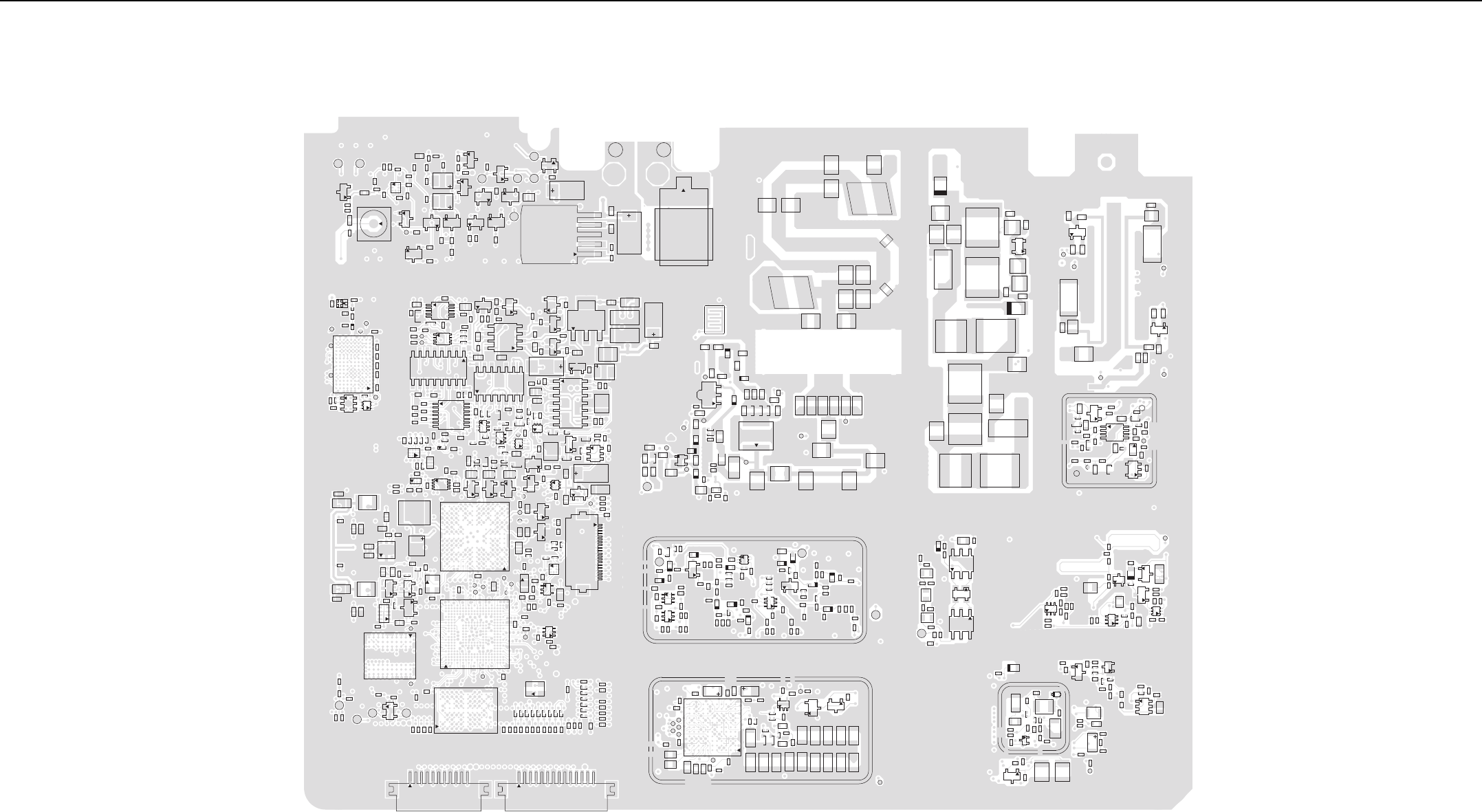
3-4 VHF (136–174 MHz) 1–25W PCB/Schematics/Parts List
C0729
C0741
C0723
C0902
C0903
C0911
C0912
C0913
C0916 C0917
C0919
C0920
C0923
C0925
C0927
C0928
C0940
C0941 C0942
C0943
C0944
C0945
C0953
D0904
D0905
L0903
L0904
Q0902
R0910
R0913
R0918
R0919
R0921
R0922
R0938
R0941
R0942
R0943
R0944
R0946
R0947
R0951
R0954
R0955
R0960
R0970
R0972
R0973
R0975
R0976
R0977
R0978
R0979
1
RT0953
12
SH0901
TP0903
TP0904
TP0907
TP0909
TP0910
TP0911
TP0913
U0900
U0942
C0400
C0401
C0402 C0403
C0404
C0407
C0412
C0421
C0422
C0436
C0452
C0453
C0454
C0456
CR0400
D0400
D0402
E0400
E0401
E0403
E0404
L0400
L0406
63
4
Q0400
Q0401
Q0403
R0400
R0401
R0402
R0403
R0408
R0413
R0414
R0415
R0416
R0428
R0429
R0430
R0431
R0435
TP0400
C0503
C0506
C0512
C0513
C0514
C0628
C0632
C0634
C0635
C0636
C0637
C0640
C0641
C0651
D0500
E0500
E0603
E0610
L0605
Q0500
R0502
R0508
R0509
R0511
R0512
R0616
R0625
R0626
U0601
C0601
R0500
R0501
TP0600
C0602
C0603
C0604
C0607
C0610
C0612
C0613
C0614
C0616
C0618
C0647
C0648
C0649 D0600
E0609
L0602
L0603
Q0600
Q0601
R0601
R0602
R0603
R0604
R0605
R0620 R0624
2
1
SH0500
C0441
C0443
C0444
C0445 C0446
C0447
C0448
C0449
C0458
C0459
C0460
D0405
L0408
L0409
L0410
L0412
R0426
R0427
R0446
6
4
3
T0400
64
3
T0401
TP0401
C0507
L0503
C0735
C0739
C0740
C0742
C0750
C0766
C0767
C0772
C0803
C0822
D0700
D0702
D0703
L0706
L0707
L0708 L0709
L0710
L0720 L0721
L0722
L0723
L0724
L0729
L0730
L0731
C0716
C0717
C0718
C0719 C0720
C0721
C0722
C0724 C0725
C0726
C0727
C0730
C0733
C0734
C0745
C0746
C0752
C0753
C0754
C0755
C0770
C0775
C0780
C0783
C0786
C0790
C0791
C0792
C0793
C0794
C0795
C0801
C0817
C0818
C0819
C0820
C0821
E0702
L0700
L0702
L0705
L0714
L0715
L0716
L0717
L0718
L0719
1
3
Q0703
Q0705
R0702
R0710
R0717
R0718
R0719
R0720
R0723
R0726
R0728
R0732
R0733
R0736
R0740
R0747
R0754
R0755
R0759
S0700
TP0702
TP0704
TP0707
TP0709
TP0710
TP0711
TP0713
U0700 VR3000
C0728
C0732
C0806
E0704
R0706
R0711
R0714
R0715
R0760
TP0703
TP0705
C0101
C0106
C0107
C0108
C0112
C0114
C0115
C0119
C0123
C0131
C0134
C0135
C0136
C0137
C0138
C0147
C0148
C0149
C0150
C0151
C0156
C0157
C0158
C0159
C0160
C0161
C0162
C0163
C0164
C0165
C0166
C0179
C0191
C0192 C0193
C0194
Q0107
23
Q0108
R0103
R0104
R0113 R0115
R0120
R0122 R0125
R0126
R0127
R0128
R0131
R0134
R0139
R0140
R0160
1
2
SH0101
TP501
TP502 TP503
TP504
TP_ADAPT_SW
TP_TEST1
TP_TEST2
L11
A11
L1
U0100
4
3
5
U0101
TP_VCTRL
ANT_C
C3012
C3013
C3014
C3045
C3533
C3534
C4063
C4064
C4065
C4066
C4067 C4068
C4069
C4070
C6412
C6413
C6435
C6436
C6437
C6438
D4000
E6400
EXT_PTT
FT_APM_1_WIRE
FT_EMERGENC
Y
FT_IGNITION_SENSE
FT_USB2_DM
FT_USB2_DP
FT_VBAT
FT_VBAT_GROUND
FT_VBUS2
J6400
L6402
2
3
Q4001
2
3
Q4003
23
Q4007
23
Q4009
2
3
Q4012
Q4014
2
3
Q4015
Q6401
R3005 R3006
R3529
R3540
R3545
R3548
R4030
R4031
R4032
R4033
R4035
R4049
R4054
R4055
R4088
R4089
R4098
R6407
R6430
R6432
R6433
R6434
R6435
R6436
R6437
1
6
5
U3003
C1
C3
A3
U6405
VR3504
VR4006
VR4009
VR6400
C3020
C3021
C3030
C3032
C3519
D3030 Q3030
4
3
2
1
Q3032
2
3
Q3041
R3030
R3034
R3037
R3038
R3039
R3040 R3041
R3050
R3051
R3053
R3055
R3057
R3524
VR3502
C3011
C3016
C3017
C3274
C3500
C3507
C3509
R2500
R3007
R3008
R3228
R3502
R3506
R3521
R3523
U3004
7
814
U3505
VR3200
C3043
C3044
C3221
C3222
C3227
C3228
C3231
C3232
C3243
C3252
C3257
C3261
C3275
C3510
C3512
1C3517
C3522
C3525
C3526
C3527
C3532
C3535
C3541
C3542
C4071
C4072
C4073
C4074
C4084
C4085
C6434
C6449
C6452
E3203E3206E3208
E4002
INT_MIC
2
3
Q3205
63
4
Q3502
63
4
Q3503
Q3504
Q3505
R1047
R3209
R3210
R3248
R3525
R3528
R3530
R3533
R3534
R3536
R3539
R3541
R3542
R3544
R3546
R3549
R3551
R3552
R3553
R3554
R3555
R3556
R3586 R3593
R4023
R4079
R4086
R4100
R4101
R4103
R6401
R6416
R6417
R6418
R6419
R6464
R6468
R6469
R6470
7
U3502
U3508
14
7
8
U4001
U6404
U6408
C1032
C1033
C1035
C1044
C3200
C3201
C3204
C3205
C3206
C3214
C3215
C3217
C3218
C3233
C3237 C3260
C3265
C3266
C3269
C3270
C3272
C3279
C3281
C3282
C3289
C3290
C3291
C3521
C4007
C4010
C4011
C4012
C4014
C4015
C4049
C4051
C4053
C4055
C4058
C4059
C4060
C4061
C4062
C4076
C4086
C4087
C4088
C4093
C4094
D3200
D4001
E3201
E4003
E4004
E4006
EXT_MIC
FT_MMP_1_WIRE
FT_USB1_DM
FT_USB1_DP
FT_VBUS1
G2
20
G1
J2500
11
J4002
14
J4003
L3201
MAKO_CE
MAKO_V8_5V
MAKO_V9_3V
OPT_SSI_SYNC
Q3040
6
3
4
Q3206
4
5
8
Q3207
2
3
Q3208
Q3209
Q3210
R1026
R1044
R1046
R1048
R1054
R1060
R1070
R2501
R2502
R2504
R2506 R2507
R2508
R2509
R2510
R2511
R2512
R2513 R2514
R2515
R2516
R2517
R2518
R2519
R2520
R2524
R2525 R2526
R2527
R2528
R3043
R3044
R3200
R3204
R3207
R3208 R3215
R3216
R3219
R3220
R3222
R3223
R3226
R3227
R3236
R3237
R3238
R3239
R3240
R3241
R3243
R3245
R3246 R3247
R3249
R3250
R3252
R3253
R3510
R3512
R3572
R3577
R3579
R3581
R3582
R3584 R3585
R3591
R3592
R4034
R4074
R4076
R4078
R4080
R4081
R4082
R4083
R4085
R4090
R4106
RF_ATTN_2
SPI_CLK_1
SPI_MISO_1
SPI_MOSI_1
TP_DDR_LDQS
TP_DDR_UDQS
TP_FLASH_CLK
TX_RAMP
TX_RAMP_DAC
A21 AA21
AA1
U1000 43
6
U1006
A1 M1
M8
A8
U2000
K1
A9
K9
U2001
P1
A1
A14 P14
U3200
64
3
U3201
C1
C3
A3
U3202
4
3
5
U3203
U3504
8
5
4
VR3201
VR3203
VR3205
VR3207
VR3208
43
2
Y1000
4
3
2
Y3200
Y3201
1.2V_RTC_TEST 2.8V_RF_TEST
C2501
C3031
C3041
C3042
C3502
C3503
C3508
1
C3536
C3539
C3540
C6401
C6414
C6432
C6443
C6444
C6446
CLK_ACQ_TEST
D3040
E2500
3
4
2
5
FL6401
I2C_CLK
I2C_DATA
IF_TEST
L6403
63
4
Q6402
R3045
R3046
R3047 R3048
R3052
R3054
R3511
R3513
R3558
R3559
R3569
R3573
R3574
R3575
R3578
R6404
R6405
R6409
R6410
R6411
R6420
R6438
R6439
R6440
R6457
ROUT_TEST
SPI_CLK_TEST
14
58
U3030
10
6
5
U3501
8
14
85
4
U3503
16
1
8
9
U4000
P10
A10
P1
A1
U6401
U6406
VR3040
C0202
C0203
C0207
C0209
C0211
C0217
C0218
C0219
C0221
C0222
C0224
C0231
C0233
C0235
C0238
C0239
C0248
C0249
C0257
C0258
C0260
C0261
C0262
C0264
C0265 C0302
C0303
C0307
C0309
C0311
C0312
C0317
C0318
C0319
C0321
C0322
C0324
C0327
C0328
C0331
C0338
C0339
C0348
C0349
C0364
E0201
E0301
L0200
L0204
L0205
L0206
L0211
L0221
L0230
L0300
L0304
L0305
L0306
L0311
Q0202
Q0302
R0202
R0203
R0206
R0207
R0208
R0210
R0212
R0213
R0218
R0219
R0220
R0221
R0230
R0302
R0303
R0306
R0307
R0308
R0310 R0312
R0327
R0328
R0332
R0333
R0334
R0336
R0337
R0338
R0339
R0340
R0343
R0345
R0347
1
2SH0300
TP0200
TP0300
TP0301
U0201
6
3
4
U0303
U0304 U0305
VHF (136–174 MHz) 1–25W 8471495L04 Bottom Side

VHF (136–174 MHz) 1–25W PCB/Schematics/Parts List 3-5
VCO_VHF
( TX: SHEET 1 )
( RX: SHEET 2 )
RXBE_44.85MHZ
(IF AMP: SHEET 1)
(ABACUS3: SHEET 2)
CONTROLLER_&_GPS_R6
( TOP LEVEL: SHEET 1)
TX_LP_VHF
( PC: SHEET 2 )
( PA: SHEET 1 )
RXFE_VHF
( 1 SHEET )
SYNTH
1
3
0
1V8
5V
5V_FE
IF
REF_CLK
SPI_ABACUS_CEX
SPI_ABACUS_CLK
SPI_ABACUS_DATA
SSI_ABACUS_CLKOUT
SSI_ABACUS_DOUTA
SSI_ABACUS_DOUTB
SSI_ABACUS_FSYNC
SSI_ABACUS_SYNCB
3
PRSC
RXINJ
RX_VCO_SEL1
RX_VCO_SEL2
SF_TH
TXINJ
TX_VCO_SEL1
VCTRL
2
0
0
4
NC
2
0
9R1
9V3_SYNTH_IN
9V3_SYNTH_OUT
9V3_VCO
HP_MOD_OUT
PREDRIVE_SWSFTX
SF_OUT
SPI_CLK_IN
SPI_CLK_OUT
SPI_MISO_IN
SPI_MISO_OUT
SPI_MOSI_IN
SPI_MOSI_OUT
TH_CEX
TX_CLK
TX_VCO_SEL1_
TX_VCO_SEL2_
VCTRL
1
ADAPT_SW
DMCS
HP_MOD_OUT
LOCK
PRSC
RF_ATTN_1
RSTB RX_SSI_CLK_PASS_IN
RX_SSI_CLK_PASS_OUT
RX_SSI_DATA_PASS_IN
RX_SSI_DATA_PASS_OUT
RX_SSI_FSYNC_PASS_IN
RX_SSI_FSYNC_PASS_OUT
RX_VCO_SEL1_
RX_VCO_SEL2_
SDTX
2
1.8V_TH_DIG
16.8_GPS
16.8_REF
1V8_BE
2.8V_TH_ANA
2.8V_TH_DIG
5V
5V_BE
9R1
9V3
ABACUS3_CEX_IN
ABACUS3_CEX_OUT
ABACUS3_SYNCB_IN
ABACUS3_SYNCB_OUT
1
1
9R1
9V3_TX_SW
FE_TUNE IF
RF_ATTEN_1
RX_IN
RX_INJ
2
0
1
2
2
0
NC
3
9V3_TX_SW
9V3_VCO
ANT_ENABLE
FINAL_BIAS_1
LO_BATTERY_DET
LO_PWR_DET
PA_SUPPLY
PC_ATTEN_ENA
PREDRIVE_SW
PRESSURE_PAD
RX_IN
TX_DAC
TX_INJ
VSWR_DET
NC
0
3
0
1
NC
9V3
9V3_PA
9V3_SYNTH
RX_SSI_CLK
RX_SSI_DATA
RX_SSI_FSYNC
RX_SSI_SYNCB
SPI_CLK
SPI_MISO
SPI_MOSI
THK_CS
TX_SSI_CLK
TX_SSI_DATA
TX_SSI_FSYNC
1
2
9V3_PA
ABACUS3_CS
ADAPT_SW
ANT_ENABLE
DMCS
LOCK_DETECT
LO_BATTERY_DET
MAKO_ADC5
MAKO_ADC8
MAKO_DAC1
MAKO_DAC2
MAKO_RAMP_DAC3
PC_ATTEN_ENA
PRESSURE_PAD_DET
RAW_B+
RESET_OUT
0
1
4
2
1.875V_DIG_V2
16.8_GPS
16.8_MHZ_BUFF
2.775V_ANA_V7
2.775V_DIG_V4
5V_SW
9V3
TX_SSI_BUS(0:2)
ABACUS_SPI_BUS(0:3)
SPI_BUS(0:4)
RX_SSI_BUS(0:2)
ABACUS_SSI_BUS(0:2)
0
2
2
1
1
VHF (136–174 MHz) 1–25W Overall Schematic Diagram
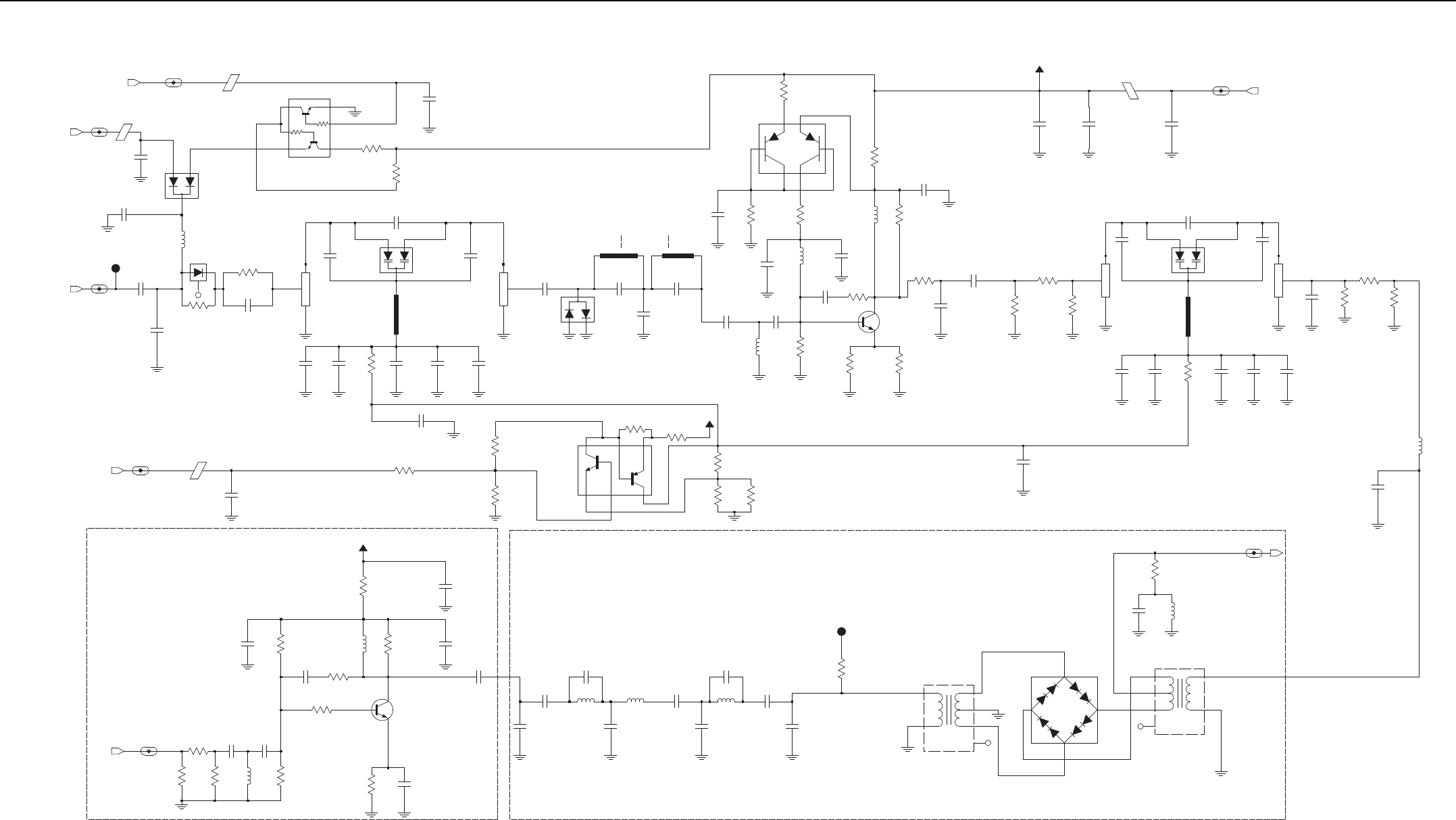
3-6 VHF (136–174 MHz) 1–25W PCB/Schematics/Parts List
(In-Band Tuning range 2.70 ~ 7.80 VDC)
10 dB Attenuator
10 dB Attenuator ON @ High for RF_ATTEN_1
MAKO ( 0 ~ 4.6 VDC)
(Micro-strip 40 mm Aggregate)
Hi-Side Zeros for Preselector
8:1 Balun
4:1 Balun
7.5 dB Attenuator
R0445
R0444
L0413
C0459
C0451
NU
R0443
NU
R0442
R0441
C0432
C0409
R0413
C0418
NU
C0460
9V3_TX_SW_8
C0415
C0428
C0437
C0404
R0411
R0431
D0402
R0402
1IO1 2
IO2
3
IO3
4IO4
C0414
D0405
C0458
C0405
R0414
R0404
9R1_FILT
C0436
C0417
C0440
C0445
Q0402
(VALUE)
L0406
9R1_FE_7
C0447
C0454
D0401
R0407
R0437
R0408
R0403
C0434
R0424
C0416
TP0400
1
C0443
C0419
C0429
R0420
RXIN_FE_6
C0423
C0450
C0455
C0426
RF_ATTEN_1_8
D0403
R0416
C0435
R0409
R0421
C0410
(VALUE)
C0427
C0457
R0400
C0401
L0401
(VALUE)
T0400
NC 5
4
6
3
2
15
NC
4
6
3
2
1
L0400
C0424
T0401
R0422
C0442
R0430
L0410
E0404
C0407
C0402
C0408
3
2
C0421
L0404
1
C0431
R0426
E0401
CR0400
1
3
2
C0441
1
RX_INJ_FE_5
R0417
TP0401
9R1_FILT
FE_TUNE_FE_3
C0403
R0406
NC
R0429
R0412
13
2
NC
L0403
R0401
C0444
C0438
C0433
C0425
R0428
R0410
R0436
C0400
C0449
13
2
NC
Q0401
C0422
L0405
(VALUE)
R0435
R0419
C0411
(VALUE)
C0456
C0439
3
2
L0412
L0402
1
C0420
NU
C0412
C0406
L0411
Q0405
E0400
9R1_FILT
R0415
L0407
R0432
R0423
D0400
C0453
IF_FE_3
R0425
3
1
4
C0430
Q0400
2
5
6
C0448
R0427
Q0403
2
3
6
4
1
5
L0409
C0413
(VALUE)
L0414
C0446
E0403
R0439
R0440
(VALUE)
C0452
L0408
R0418
9V3_TX_SW
FE_TUNE
RX_IN
RX_INJ
9R1
RF_ATTEN_1
IF
VHF (136–174 MHz) 1–25W Receiver Front-End Schematic Diagram
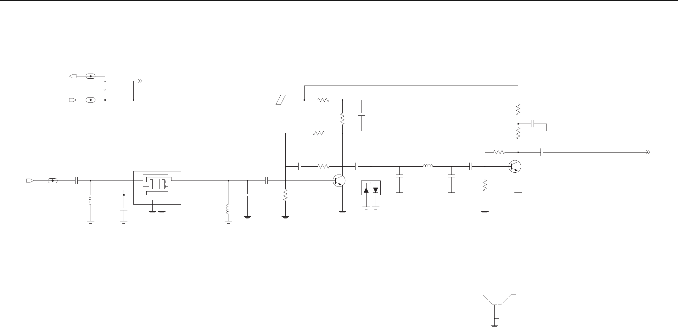
VHF (136–174 MHz) 1–25W PCB/Schematics/Parts List 3-7
4-POLE
0.72V
1.43V
0.76V
1.6V
VHF -- 44.85MHz
IF_TO_ABACUS
R0501
IFIN_BE_8
R0511
C0514
R0512
R0509
R0508
C0510
L0504
NU
IN
3OUT 6
FL0500
44.85MHz
CC1
2
CC2
5
GND1
1
GND2
4
C0516
NU
L0506
5V_BE_5
NU
C0515
C0502
C0503
C0513
1
2
C0512
R0503
SH0500
Q0501
L0503
E0500
RX_FE_3
C0509
NU
R0510
C0506
C0507
Q0500
1
3
2
C0504
R0500
R0502
D0500
IF
IF_OUT
5V
5V
5V_FE
VHF (136–174 MHz) 1–25W Receiver IF Amp Schematic Diagram
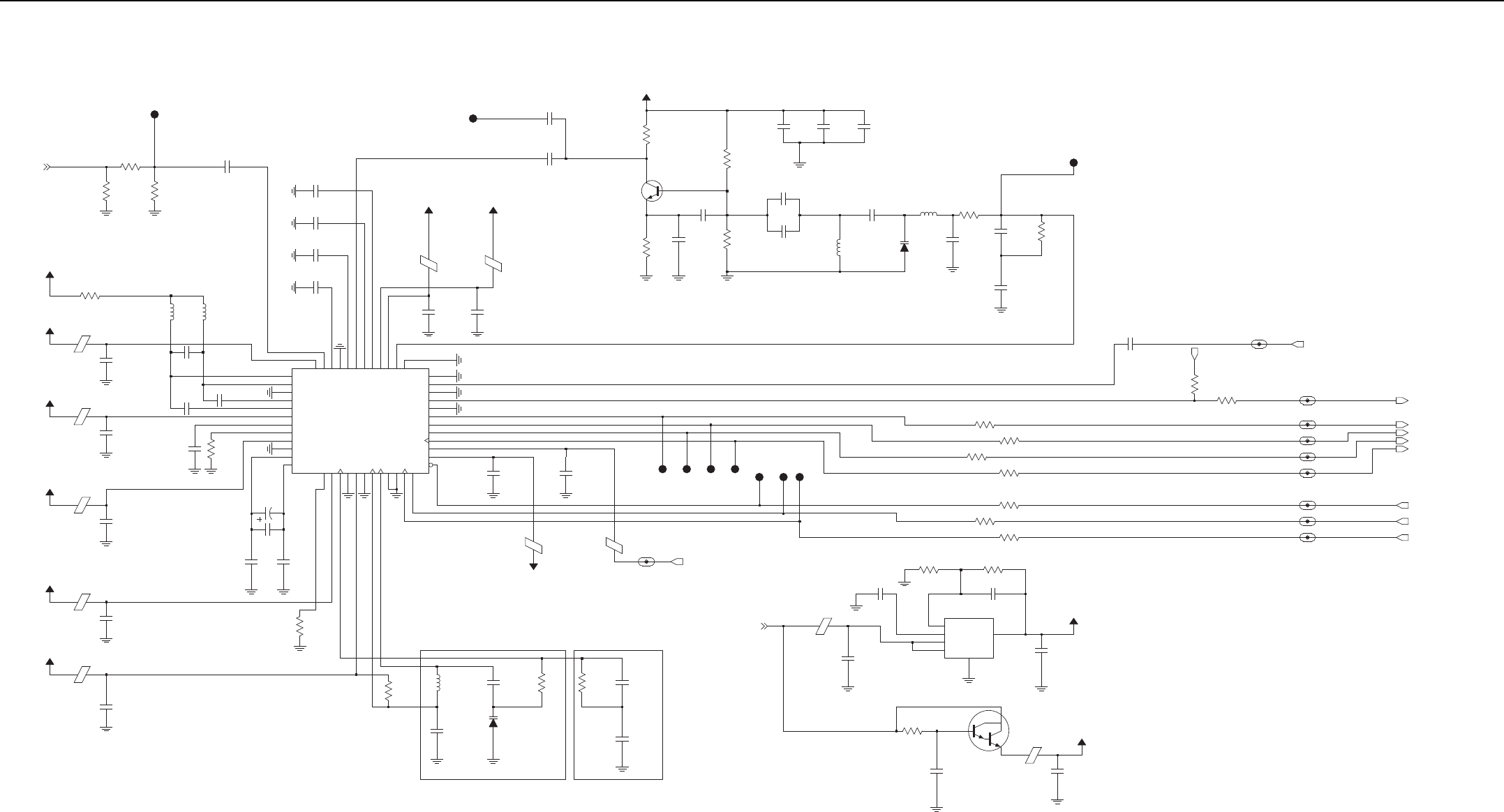
3-8 VHF (136–174 MHz) 1–25W PCB/Schematics/Parts List
2nd LO VCO VHF (42.6MHz/47.1 MHz)
SPF_3.5V
CLOCK LF
2nd LO LF
#
#
#
CLOCK VCO
#
*
NU
R0622
R0626
E0603
R0608
C0622
DOUTB
C0645
TP0600
3VA
R0620
E0604
3VA
R0604
2FB
5
GND
6NP
4VCONT
3VIN
1
VOUT
3VA
U0601
C0615
3VA
R0612
C0619
C0641
DOUTA_1_BE_5
R0624
E0610
C0617
E0606
R0619
NU
E0601
C0647
R0623
L0603
D0601
C0643
DOUTB_1_BE_5
C0614
PD
C0628
14
VREFN
12 VREFP
11
C0625
9
VDDC
17
VDDD 26
VDDF
6
VDDH 27
VDDI 48
VDDL 40
VDDP 39
VDDQ
43
MXON
2MXOP
1
PC
23
PD
24
PE 25
13 RREF
SYNCB 33
VDDA
21
GNDS2 34
IF2N
4
IF2P
5
IFIN 47
IOUTC
15
IOUTL 38
LON 42
LOP
18
GNDD
22
GNDF
3
GNDH 32
GNDI 45
GNDL 36
GNDP 37
GNDQ
16
GNDS1
41
DOUTA 29
DOUTB 30
FREF 35
FS 31
GCN
8GCP
7
GNDA
10
GNDC
CLKN
20
CLKOUT 28
19 CLKP
CXIF 46
CXVL 44
CXVM
FS_1_BE_5
U0600
C0637
Q0600
1V8_3
C0612
E0608
C0650
R0609
R0617
R0601
R0610
C0603
R0614
C0633
C0631
C0629
CLKOUT
FS
5V
3VA
C0623
C0616
3VA
FREF_IF
NU
C0610
R0618
C0630
C0613
PE
C0646
E0600
L0602
C0636
C0635
3VA
C0651
R0613
C0618
C0648
L0604
C0626
CLKOUT_1_BE_5
C0601
R0602
R0616
VVCO
R0627
R0621
R0603
FC_1_BE_5
C0640
D0600
E0607
VVCO
E0609
C0627
C0604
C0621
C0634
R0625
C0649
R0615
E0605
FE_1_BE_5
E0602
Q0601
3VA
C0611
L0605
C0644
NU
C0605
R0607
PC
SB_1_BE_5
TP0601
C0632
U602
1
C0607
L0608
3VA
DOUTA
R0606
C0642
R0611
FD_1_BE_5
R0605
C0602
C0638
C0620
IF_OUT
5V
SSI_ABACUS_FSYNC
SPI_ABACUS_CEX
REF_CLK
SPI_ABACUS_CLK
SSI_ABACUS_DOUTA
SSI_ABACUS_CLKOUT
SSI_ABACUS_DOUTB
SPI_ABACUS_DATA
SSI_ABACUS_SYNCB
1V8
1V8
VHF (136–174 MHz) 1–25W Receiver Back-End Schematic Diagram
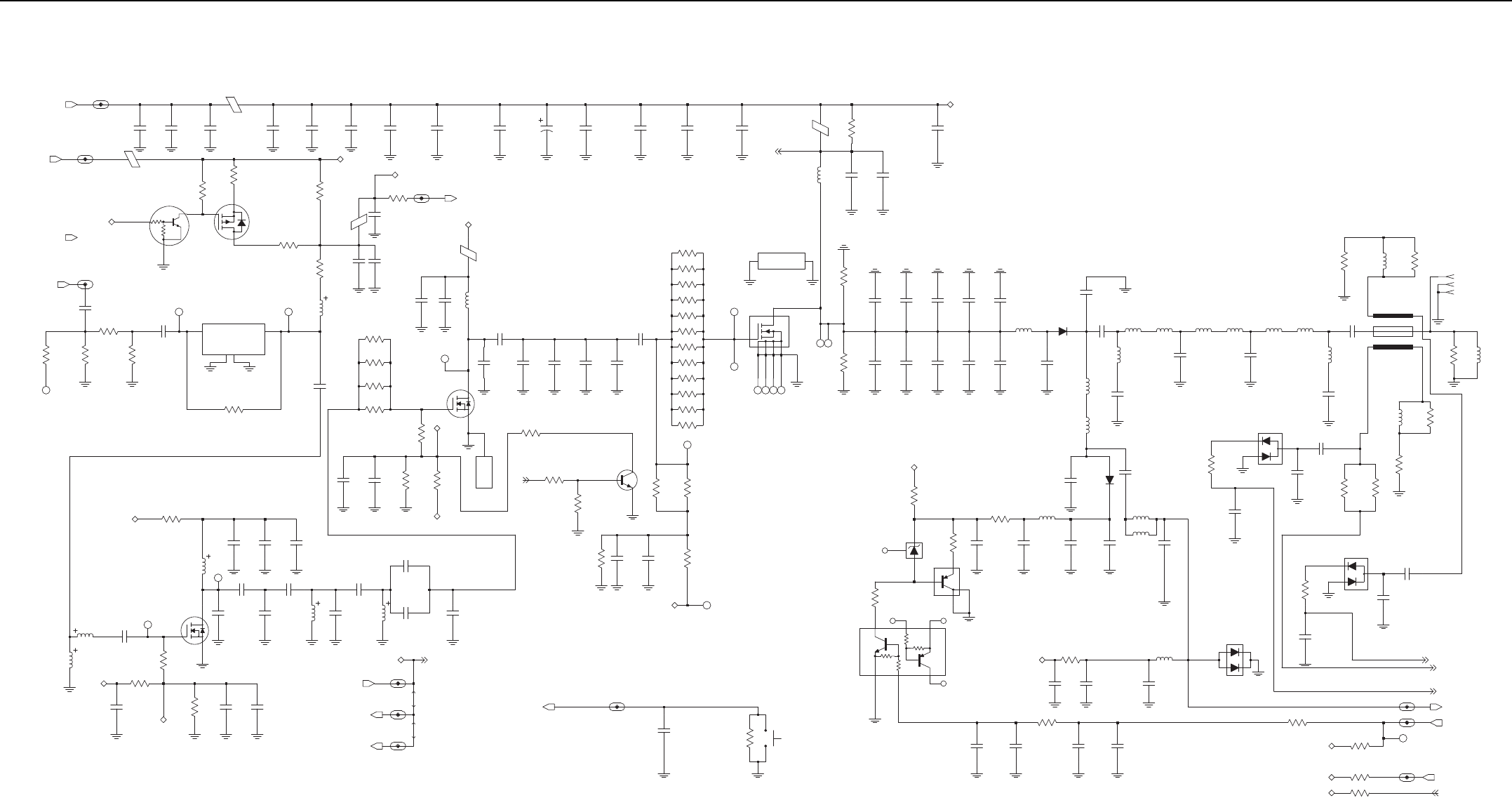
VHF (136–174 MHz) 1–25W PCB/Schematics/Parts List 3-9
C0702
C0701C0700
PA_SUPPLY_TX_PA
PA_SUPPLY
9V3_PA
10K
47K
Q0701
R0777
-11 dBm +4 dBm
3.3V @ Id=27mA
4
RF_IN
1VD_RF_OUT 3
U0700
NU
GND1
2
GND2
TP0704
Q0700
TP0703
R0706
L0705
R0779
R0759
C0733
R0780
Test Point to check Ref Osc warping
+8 dBm
R0760
TX_INJ_TX_PA
R0711
R0715
C0728
R0714
TP0705
TX_INJ
Antenna_En
PREDRIVE_SW
E0700
E0703
NU
R0702
E0704
C0806
9V3_TX
To Rx PIN diode for 12mA bias
To Tx/Rx Switch bias - 10mA
R0746
9V3_TX_SW
9V3_TX_SW
9V3_TX_SW_Main
9V3_TX
L0700
C0738
C0710 C0711
C0712 C0708 C0709
Load
C0705
C0704
C0703
NU
C0707
C0706
NU
C0718
NU
C0732
C0745
C0819
L0702
C0753 C0755
NU
C0752 C0754
C0746
R0982
R0981
R0980
Load
C0804 C0805
NU
R0756 R0757
TP0711
Final_Bias
R0730 R0731
NU
Q0710
R0739
R0712
R0721
R0732
R0719
R0717
R0716
R0733
R0736
R0726
R0734
R0737
MRF1535 Flat Lead
SP0701 1
SP0703 1
SP0704 1
SP0702 1
1
SP0705
1
SP0707
SP0708 1
SP0706
1
Q0702
PIN1
1PIN2 2
HS0700
C0720 C0730
NU
R0710
C0724C0726
L0714
C0722
C0719 C0721 C0729
NU
C0727 C0725
R0723
R0729
A+
L0731
C0779C0777C0776 C0778
D0702
C0767
D0700
L0730
C0742
C0766
R0735
L0722
L0710
L0724
L0725
C0741
L0721 L0708 L0709L0720 L0707L0706
L0723
C0740
C0750
C0940
D0904
R0973
L0904
NU
R0978
C0942
C0941
R0976R0977
R0975
C0739
C0735
C0803
NU
L0903 R0972
R0970
W = 22.6 mil
W = 22.6 mil
L = 1030 mil
S = 35.4 mil
W = 90.2 mil
S = 35.4 mil
C0723
J0700-33
1J0700-1
J0700-22
R0713 L0728
C0944
C0943
D0905
R0979
C0945
FWD_POWER
REV_DETECTED
RX_IN
ANT_ENABLE
FINAL_BIAS_1
FWD_DETECTED
V_CONTROL
TP0713
ANT_ENABLE_TX_PA
IF5
RX_IN_TX_PA
R0753
R0761
R0752
R0749
Final_Bias
Antenna_En
V_cont
D0703
Long Trace around PA
Bypass both sides
C0824
NU
C0823
R0781 L0729
C0822
9V3_TX_SW_Main
C0797
C0796
R0748
C0798 C0799
NC
Q0706
NCNC
VR0700
R0745
NC
Q0704
R0738
PRESSURE_PDA_TX_PA
PRESSURE_PAD
NU
R0775 S0700
C0968
NU
C0713 C0731
C0714
R0742
E0701
A+
E0702
R0720
R0754
C0734
R0718
TP0702
R0755
C0717 C0716
NU
Q0703
D
3
S
21
G
V_G2
1
POS
M0700
2.46V @ Vcont=4.5V (Ids=700mA)
R0722
R0728
C0818
NU
R0727
C0770
V_cont
NU
C0793
NU
C0817 NU
C0794
L0719
C0792
C0791
9V3
9V3
9V3
9V3_VCO
9V3_SYNTH
TP0709
C0783C0775
NU
R0740
C0780
NU
L0715
9V3_TX
NU
C0821
C0786
L0717
C0790
C0820
NU
Q0705
D
G
S
L0718
TP0710
L0716 C0795
2.70V @ Vcont=4.5V (Ids=100mA)
C0801
R0751
NU
C0802
R0747
C0771
NU
R0750
V_G1
V_cont
TP0707
C0772
VHF (136–174 MHz) 1–25W Power Amplifier Schematic Diagram
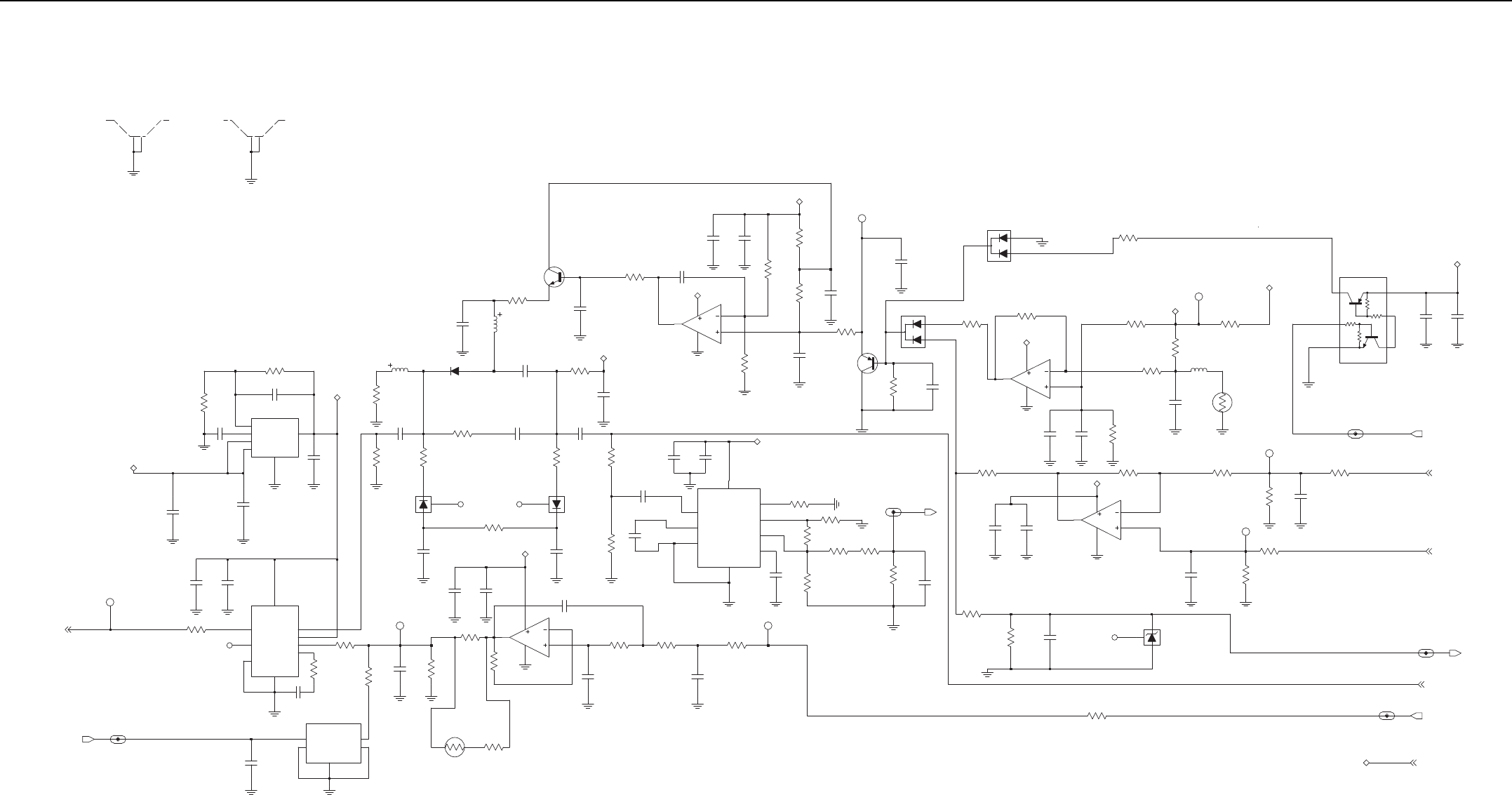
3-10 VHF (136–174 MHz) 1–25W PCB/Schematics/Parts List
2.85V (44W)
2.10V (27.5W)
TP0909
LO_BATTERY_DET
V_CONTROL
LO_BATTERY_DET
NC1 NC2
RESET_OUT
GND
INPUT
C0953
45
U0942
21
3
1.35V (44W)
1.28V (27.5W)
R0942
U0900-2
6
5
7
8
4
R0947
C0925
R0946
C0903C0902
TP0910
R0955
R0954
RT0953
R0941
R0950
C0926
3
VSET
COMM
ENBL 2
FLTR 4
GND
9
NC
RFIN 1
VAPC
VPOS 8
U0940
NC
C0922
R0940
5
6
7
C0921
0.1uF
C0951
C0949
9V3
NP
VCONT
VIN
FB
GND
6
4
3
1
VOUT
2
5
C0950
R0937
R0936
U0941
C0947
C0948
R0928
C0931
R0924
L0902
R0927
R0926
D0901
R0925
D0902
NC
NC
9V3_PC
C0936
L0901
Q0902
C0918
R0913
C0914
C0934 C0935
R0929
C0962
C0960
D0903
VPOS
U0943
C0961
C0916
R0917
R0989
9V3_PC
C0923
C0937
R0988
C0963
7
VSET
CLPF
COMM
GND
INHI
INLO
TADJ
VOUT 5
4
3
2
1
8
6
R0995
R0984 R0994
R0991
R0993
LO_PWR_DET
LO_PWR_DET
R0985
NU
C0965
R0983
NU
C0964
TP0911
C0928
R0951 R0944
C0927
R0943
SH0901
1
2
SH0900
1
2
C0917
R0919
C0913
C0911
R0960
R0910
C0919
R0918
C0920
1
8
Q0901
R0922
R0921
9V3_PC
9V3_PC
U0900-1
2
3
4
C0912
9
5V
R0930
C0915
D0900 R0906
R0900
9V3_PC
5
7
8
4
U0901-2
6
R0909
C0906
C0907
R0923
2
3
1
8
4
U0901-1
C0909C0908
R0914
9V3_PC
0.38V (44W)
0.21V (27.5W)R0911
TP0903
R0912
2.67V (44W)
2.01V (27.5W)
C0939
TP0904
R0916
R0920
C0910
R0915
RT0908
R0902
L0900
C0904
R0901
R0903
9V3_PC
TP0913
R0907
9V3
R0990
Q0900
C0901
C0900
9V3
PC_ATTEN_ENA_TX_PA
FWD_DETECTED
PC_ATTEN_ENA
REV_DETECTED
TX_DAC
FWD_POWER
VSWR_DET
9V3 9V3
TX_DAC
VSWR_DET
C0967 5.1V
D0907
R0987
R0986
R0938
NC
1.0V or less, typical
1
2
3
D0906
C0929
TP0907
5V
VHF (136–174 MHz) 1–25W Power Control Schematic Diagram

VHF (136–174 MHz) 1–25W PCB/Schematics/Parts List 3-11
R1
R2
10K
47K
0.5 ppm
VHF=1500pF
---
Note: High Port modulation injection through loop filter for U1 and U2 only
HI: 2.8V
U1=220pF
U2=120pF
C0191,C0192,C0193,C0194: NU (UHF B1)
VHF=1500pF
SF_OUT VOLTAGE: 2.45V
Unlocked: 0V
U1=220pF
Buffer to Abacus/Controller
9R1 SWITCH FOR FRONT-END
C0157, C0159, C0160,C0162,C0163,C0191,C0192,C0193,C0194: NU (UHF B2)
GPO LINES
U2=120pF
U1=220pF
U1=220pF
VCO STEERING LINE VOLTAGE: 0.6V TO 4.4V
U2=120pF
VCO STEERING LINE VOLTAGE: 0.6V TO 4.4V
VHF=1500pF
VHF=1500pF
U2=120pF
U2=120pF
Adapt OFF: 0V
U1=220pF
VHF=1500pF
4875188M01
LOW: 0V
1.5 ppm
VCO SEL: ACTIVE LOW
Adapt ON: 5V
Locked: 1.8V
GPO_4
TCXO (Y0100)
Switch for Adapt Transient
NC
NC
NC
R0170
C0166
C0100
C0105
L0100
C0137
RX_SSI_DATA_IN
NC
R0114
R0147
SPI_MOSI_IN
NU
ABACUS3_SYNCB_OUT
R0100
NC
5V_BE_SYNTH
TP504
1
RX_SSI_CLK_OUT
C0107
NC
NC
C0136
C0133
NC
C0140
1
C0106
NC
TP_TEST1
SPI_MISO_IN
R0160
NC4
3
OUTPUT
4
VCC
1VCONT
NC
NC
NC
Y0100
16.8MHz
GND
2
5
NC1
NC2 6
NC3 7
8
R0113
9R1_SYNTH
C0148
C0102
C0138
3GND
1INOUT
4ONOFF_CONTROL
2OUTIN
5
VCC
R0125
NC
U0101
NC
GPO_3_SYNTH
NC
NC
C0179
ABACUS3_SYNCB_IN
RX_SSI_DATA_OUT
C0147
C0135
C0171
C0132
C0157
C0127
NC
LOCK_SYNTH
R0140
C0120
Q0100
C0194 C0159
C0191
NC
VCTRL_SYNTH
C0126
C0112
NC
NC
NC
NC
1V8_BE_SYNTH
SF_OUT_SYNTH
R0158
NU
HP_MOD_OUT_SYNTH
16.8_REF_CONTROLLER_SYNTH
NU
C0119
NC
NU
C0113
NC
1
R0148
1
2
TP_VCTRL
SH0100
1
2
SH0101
R0159
C0144
NC
C0160
ABACUS3_CEX_IN
R0118
C0141
NC
RX_SSI_CLK_IN
C0162
C0103
R0103
R0107
C0124
Q0108
R0122
NC
RX_SSI_FSYNC_IN
NC
NC
NU
C0161
C0122
NU
GPO_6_SYNTH
9V3_SYNTH
R0157
Q0106
GND
IN
OUT
C0117
C0134
R0115
TX_DAC_VCC
G7
TX_GND1
F6 TX_GND2
J6
TX_VCC
F1
VCO_DAC
K5 XOSC_BASE
XOSC_EMIT
L5
G6
XOSC_GND
TCLK
D7
TEST1 C7
TEST2
B3
TM
F10
TXCLK
K7 TXI
L7 TXQ
H7
TX_DAC_GND L6
SPI_CLK
D10
SPI_DR
D9
SPI_DW
SSI_GND E8
E11
SSI_VCC
SUB1
K10
F5 SUB2
F3 SUB3
G8
SDM_VAG
A9
SDM_VREFM B8
SDM_VREFP
D11
SDR
F11
SDTX
F9
SFTX
K4 SF_OUT
C9 SMD_CLK_GEN_GND
C11
A5
RX_AVCC2
RX_EN_OUT
B1
D3
SCAN_EN
F2 SCAN_IN
E9
SCLK_OUT
SDM_CLK_GEN_VCC A10
SDM_REF_GND A8
SDM_REF_VCC B9
B10 RXFS
C2 RXI
C1 RXIX
D1 RXQ
D2 RXQX
RX_AGND1 C3
D5
RX_AGND2
B2
RX_AVCC1
OSCREG_GND
OSCREG_OUT
H5
J4OSCREG_SPLY
K11 PABIAS_DAC
L9 PHCLK
RFSTEPA
A3
E6 RSTB
E7
RXACQ
E10
M_PRSCX
A1 NC1
A11 NC2
NC3
L1
L11 NC4
NTXI
L8
NTXQ
K6
L4 OSCREG_BYP
J5
MAIN_GND
MAIN_PDET_VCC G2
J1
MAIN_VCC
H1
MN_ADAPT_CP
G3
MN_CP
G5
MN_CP_GND
MN_CP_VCC H2
J2
M_PRSC
H3
GPO5
H8 GPO6
K8
HP_MOD_OUT
J9INCR_DECR
F8
LGND1 C8
LGND2
G10
LVCC1
B7
LVCC2
G4
ESC_TEST
K2
ESC_VCC
C6 FBI
B6 FBQ
B4 GPO1_TEST1
A4 GPO2_TEST2
GPO3_TEST3
E5
GPO4_TEST4
D4
K9
EF_OUTM
J8
J7EF_OUTP
ESC_CP L3
ESC_CPBIAS L2
K3
ESC_CP_GND J3
ESC_CP_VCC
H4
ESC_GND
K1
ESC_IN
E1
G9 CLK_CP
H11 CLK_EMIT
H10
CLK_GND
J10
CLK_VCC
G1
DAC_ADAPT
A2 DC_CAL
L10 DEEPSLEEP
F7
DMCS
BP_I
F4 BP_IX
E2 BP_Q
BP_QX
E3
D8
CEX
H9 CLK1_OUT
J11 CLK2_OUT
G11 CLK_BASE
D6 ACE2
AGC_DAC
B5
AGC_FLAG
C4 AGC_REF
C5
H6 ARX_DAC
C10 ASPI_CLK
B11 ASPI_DATA
A7
ASPI_VCC
E4
U0100
A6 ACE1
DMCS_SYNTH
C0131
C0130
R0131
C0128
SPI_CLK_IN
NU
C0121
1
NC
TP_TEST2
C0129
C0165
R0146
ADAPT_SW_SYNTH
C0143
C0125
2.8V_TH_ANA_SYNTH
RX_SSI_FSYNC_OUT
C0178
C0177
C0175
NC
SFTX_SYNTH
NC
C0156
R0105
R0110
R0144
NC
R0161
C0110
PRSC_SYNTH
R0116
C0101
NC
C0164
C0104
NC
R0134
C0123
C0158
TX_CLK_SYNTH
C0109
NC
NU
R0126
Q0107
R0120
R0155
C0146
ABACUS3_CEX_OUT
NC
1
NC
C0115
TH_CEX_SYNTH
TP_ADAPT_SW
SPI_MOSI_OUT
GPO_2_SYNTH
R0102
TP503
1
NC
C0142
C0108
NC
NC
NC
SDTX_SYNTH
NC
R0104
R0111
RSTB_SYNTH
1.8V_TH_DIG_SYNTH
C0180
TP501
1
R0119
R0128
R0123
C0145
R0108
C0114
C0149
C0196
C0195
SPI_CLK_OUT
16.8_GPS_SYNTH
SPI_MISO_OUT
C0111
NU
C0151
R0156
2.8V_TH_DIG_SYNTH
C0150
R0127
R0106
NC
4
NC
Q0102 2
1
3
NC
NC
R0101
R0117
R0109
5V_SYNTH
TP502
1
GPO_1_SYNTH
C0163
GPO_5_SYNTH
16.8_REF_BE_SYNTH
C0118
C0193
NC
NC
C0192
ABACUS3_SYNCB_IN ABACUS3_SYNCB_OUT
VCTRL
9V3
R0139
SPI_MOSI_IN
SPI_MOSI_IN
SPI_CLK_IN
SPI_CLK_IN
SPI_MISO_IN
SPI_MISO_IN
5V
2.8V_DIG
RX_VCO_SEL1_
5V_BE
9R1
16.8_REF
1V8_BE
1.8V_TH_DIG
1.8V_DIG
RSTB
16.8_GPS
ADAPT_SW
5V_TH
TX_VCO_SEL1_
HP_MOD_OUT
TH_CEX
SPI_MOSI_IN
SPI_CLK_IN
2.8V_TH_DIG
2.8V_DIG
2.8V_TH_ANA
2.8V_ANA
1.8V_DIG
1.8V_DIG
5V_TH
RX_SSI_DATA_PASS_OUT
RX_SSI_CLK_PASS_OUT
RX_SSI_FSYNC_PASS_OUT
RX_SSI_CLK_PASS_IN
ABACUS3_CEX_OUT
SPI_MISO_OUT
SPI_MOSI_OUT
SPI_CLK_OUT
ABACUS3_CEX_IN
RX_SSI_DATA_PASS_IN
RX_SSI_FSYNC_PASS_IN
TX_VCO_SEL2_
RF_ATTN_1
RX_VCO_SEL2_
PRSC
2.8V_ANA
DMCS
5V_TH
2.8V_ANA
1.8V_DIG
2.8V_ANA
2.8V_ANA
SDTX
SFTX
SF_OUT
LOCK
TX_CLK
SPI_MISO_IN
2.8V_ANA
5V_TH
VHF (136–174 MHz) 1–25W Synthesizer Schematic Diagram
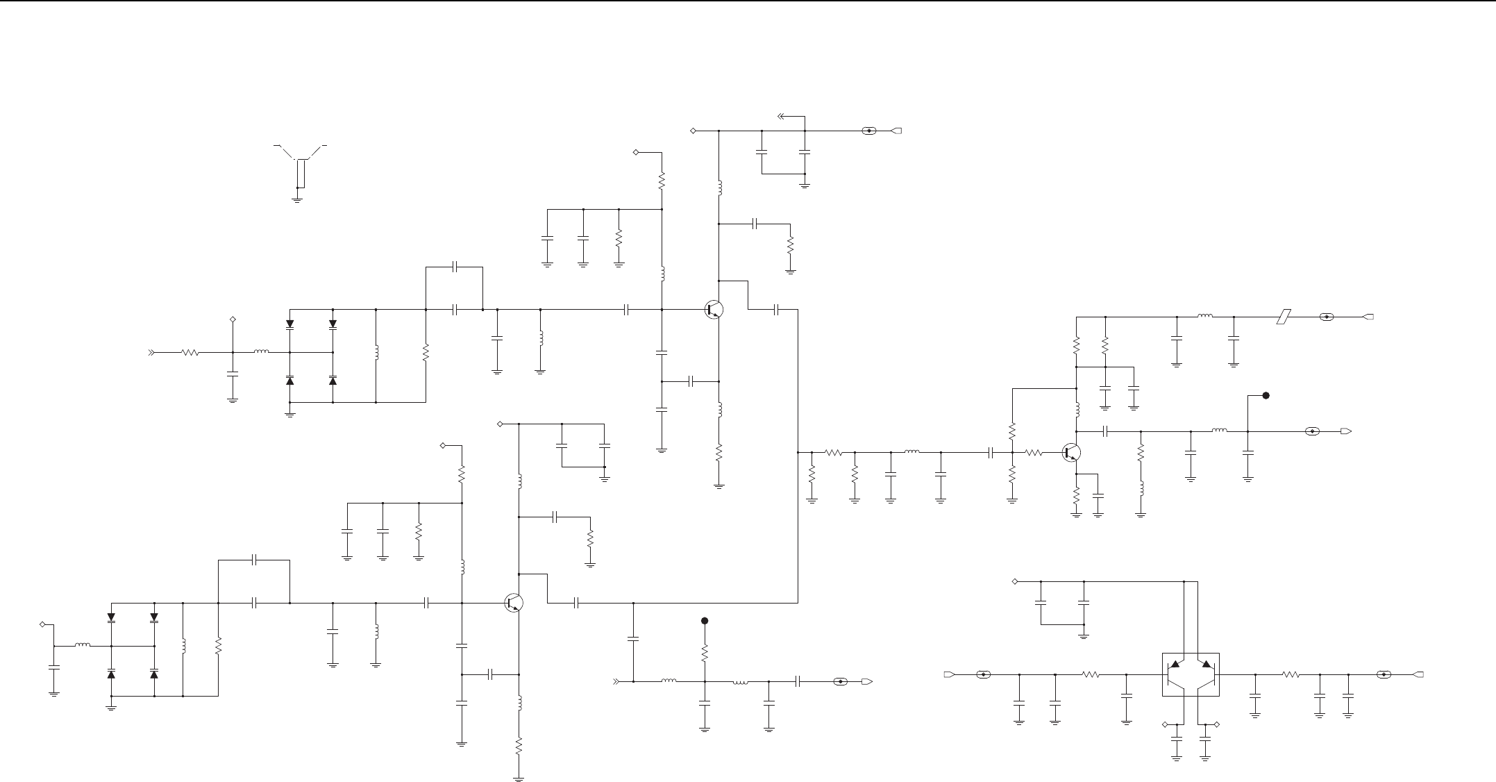
3-12 VHF (136–174 MHz) 1–25W PCB/Schematics/Parts List
RX1_SEL: 2.7 V (High)
Super Filter Voltage (SF_TH)
VCTRL: 0.6-4.5 V
RX VCO 1
SF_TH: 2.5 V
Steering Line Voltage (VCTRL_TH)
RX Buffer Amplifier
RX Prescaler
0.1 V (Low)
RX2_SEL: 2.7 V (High)
RX VCO 2
PRSC (RX): 180-220 MHz
RXINJ: 180-220 MHz
0.1 V (Low)
-5 to -15 dBm
+10 dBm
TP0301
1
C0231
PRSC_VCO_UHF1_5
L0211
C0211
L0206
R0202
CR0208
L0204
CR0202
C0215C0214
R0207
9R1_VCO_UHF1_7
CR0205
U0201
RX2_SEL_VCO_UHF1_5
R0201
R0230
R0208
C0209
Q0201
C0248
R0204
C0221
C0250
C0259
R0221
L0202
C0237
L0221
R0203
L0210
L0213
L0218
L0217
R0220
R0206
C0246
C0242C0241
C0262 C0264
L0207
R0205
CR0201
CR0204
C0223
C0225
L0219
C0206
C0203
C0201
C0233
NU
E0201
TP0200
1
C0252
C0229
C0224
NU
C0204
C0238
L0212
C0219
C0200
C0235
L0209
R0224
C0208
R0212
R0226
C0265
CR0206
L0214
C0251
R0240
NU
Q0200
RXINJ_VCO_UHF1_5
C0226
C0253 R0213
NU
C0220
C0218
C0207
L0200
C0258
C0213
R0225
C0222
NU
C0205
R0210
NU
R0241
C0239
C0243
C0245
L0230 RX1_SEL_VCO_UHF1_5
C0240
L0203
SF_TH_VCO_UHF1_6
R0218
C0249 C0257
SH0200
1
2
R0219
CR0207
R0211
Q0202
C0217
L0205
C0236
CR0203
C0261 C0260
R0216
C0202
L0215
C0247
R0229
PRESC_TX
RX1
RX2
RX_VCO_SEL1 RX_VCO_SEL2
VCTRL
SF_TH
RXSL
SF_TH
RX1 RX2
PRSC
RXSL
9R1
SF_TH
SF_TH
SF_TH
RXINJ
VHF (136–174 MHz) 1–25W Receiver VCO Schematic Diagram

VHF (136–174 MHz) 1–25W PCB/Schematics/Parts List 3-13
Steering Line Voltage (VCTRL_TH)
Super Filter Voltage (SF_TH)
SF_TH: 2.5 V
0.1 V (Low)
TX VCO
PRSC (TX): 136-174MHz
TX Buffer Amplifier
TX Prescaler
VCTRL: 0.6-4.5 V
-5 to -15 dBm
TX1_SEL: 2.7 V (High)
6 dBm
TXINJ: 136-174MHz
L0302
C0326
CR0301
9V3_VCO_UHF1_7
C0339
R0307
C0361
R0334
TP0300
1
C0318
NU
L0311
C0303
TXINJ_VCO_UHF1_5
C0332
R0311 R0312
R0319
R0345
NC
U0304
CR0303
U0305
R0302
NC
C0334
L0307
C0320
C0308
C0327
C0322
NU
R0305
C0311
R0343
C0321
R0347
TX1_SEL_VCO_UHF1_5
NU
C0305
CR0302
R0340
C0328
U0303
C0324
NU
C0329
L0300
C0314
R0332
C0319
R0308
R0320
R0333
C0304
C0301
Q0300
C0364
L0305
C0309
VCTRL_VCO_UHF1_7
L0306
L0312
C0331
Q0302
C0317
R0304
E0301
C0302
C0349
CR0304
R0336
NU
C0310
NU
R0338
R0316
C0323
R0303
L0303
C0306
C0360
CR0300
C0307
R0339
R0327
C0300
C0325
C0338
R0306
C0312
L0310
C0313
C0348
XMIT_SEL_VCO_UHF1_6
R0328
NU
R0321
R0301
NC
HP_MOD_OUT_VCO_UHF1_7
L0304
R0310
R0337
C0315
SH0300
1
2
L0309
SF_TH
TX_VCO_SEL1
PRESC_TX
AMP_SEL
AMP_SEL
9V3_SYNTH_OUT 9V3_SYNTH_IN
PREDRIVE_SW
TX1
VSF
TX1 SF_TH
VSF
TXINJ
SF_TH
TX1
9V3_VCO
HP_MOD_OUT
VCTRL
VCTRL
VHF (136–174 MHz) 1–25W Transmit VCO Schematic Diagram

3-14 VHF (136–174 MHz) 1–25W PCB/Schematics/Parts List
VHF PCB 8471495L04 Parts List 1–25W
Circuit
Ref
Motorola
Part No. Description
C0100 2113944A44 220pF
C0101 2113944A44 220pF
C0102 2113944A44 220pF
C0103 2113945C31 0.1uF
C0104 2113944A44 220pF
C0105 2113945C31 0.1uF
C0106 2113945C31 0.1uF
C0107 2113945C31 0.1uF
C0108 2113944A44 220pF
C0109 2113945C31 0.1uF
C0110 2113945C31 0.1uF
C0111 2113945C31 0.1uF
C0112 2113944A44 220pF
C0113 NOT PLACED –
C0114 2113946E02 1.0uF
C0115 2113946E02 1.0uF
C0117 2113944A44 220pF
C0118 2113945C31 0.1uF
C0119 NOT PLACED –
C0120 2113945B02 .01uF
C0121 NOT PLACED –
C0122 2113945B02 .01uF
C0123 2113946E02 1.0uF
C0124 2113945C31 0.1uF
C0125 2113944A44 220pF
C0126 2113944A44 220pF
C0127 2113944A44 220pF
C0128 2113944A44 220pF
C0129 2113945C31 0.1uF
C0130 2113944A44 220pF
C0131 2113944A44 220pF
C0132 2113944A44 220pF
C0133 2313960B30 4.7uF
C0134 2113944A44 220pF
C0135 2313960B32 10uF
C0136 2113945C31 0.1uF
C0137 2313960B32 10uF
C0138 2113944A44 220pF
C0140 2313960B30 4.7uF
C0141 2113945C31 0.1uF
C0142 2113944A44 220pF
C0143 2113944A44 220pF
C0144 2113945C31 0.1uF
C0145 2113945B02 .01uF
C0146 2113944A44 220pF
C0147 2113944A44 220pF
C0148 2113945D01 .033uF
C0149 2113945C04 .022uF
C0150 2113945C31 0.1uF
C0151 2113945C31 0.1uF
C0156 2185419D06 0.1uF
C0157 2185419D06 0.1uF
C0158 2185419D06 0.1uF
C0159 2185419D06 0.1uF
C0160 2185419D06 0.1uF
C0161 2185419D06 0.1uF
C0162 2185419D06 0.1uF
C0163 2185419D06 0.1uF
C0164 2185419D06 0.1uF
C0165 2185419D06 0.1uF
C0166 2185419D06 0.1uF
C0171 2113945B02 .01uF
C0175 2113944A44 220pF
C0177 2113944A44 220pF
C0178 2113944A44 220pF
C0179 2113944A44 220pF
C0180 2113945C31 0.1uF
C0191 NOT PLACED –
C0192 NOT PLACED –
C0193 NOT PLACED –
C0194 NOT PLACED –
C0195 2113945A05 470pF
C0196 2113946H02 10uF
C0200 2113944A44 220pF
C0201 2113945Y02 0.10uF
C0202 2113945C02 .01uF
C0203 2113944A44 220pF
C0204 2113944A44 220pF
C0205 2113945Y02 0.10uF
C0206 2113944A44 220pF
C0207 2113945C04 .022uF
C0208 2115153H18 4.3pF
C0209 2113944A44 220pF
C0211 2113944A44 220pF
C0213 2115153H17 3.9pF
C0214 2115153H34 11pF
C0215 2115153H20 5.1pF
C0217 2113944A44 220pF
C0218 NOT PLACED –
C0219 NOT PLACED –
C0220 2115153H17 3.9pF
C0221 2115153H14 3.0pF
C0222 NOT PLACED –
C0223 2115153H46 36pF
C0224 NOT PLACED –
C0225 2115153H51 56pF
C0226 2113944A44 220pF
C0229 2115153H42 24pF
C0230 2113944C47 150pF
C0231 2115153H14 3.0pF
C0233 NOT PLACED –
Circuit
Ref
Motorola
Part No. Description
C0235 2115153H22 6.2pF
C0236 2113944A44 220pF
C0237 2113945Y02 0.10uF
C0238 2113944A44 220pF
C0239 2113945Y02 0.10uF
C0240 2113944A44 220pF
C0241 2113945Y02 0.10uF
C0242 2113944A44 220pF
C0243 2115153H13 2.7pF
C0245 2115153H14 3.0pF
C0246 2115153H27 10pF
C0247 2115153H20 5.1pF
C0248 2113944A44 220pF
C0249 2113945Y02 0.10uF
C0250 2115153H16 3.6pF
C0251 2115153H40 20pF
C0252 2115153H48 43pF
C0253 2113944A44 220pF
C0257 2113944A44 220pF
C0258 2113945Y02 0.10uF
C0259 2115153H35 12pF
C0300 2113944A44 220pF
C0301 2113945Y02 0.10uF
C0302 2113945C02 .01uF
C0303 2113944A44 220pF
C0304 2113944A44 220pF
C0305 2113945Y02 0.10uF
C0306 2113944A44 220pF
C0307 2113945C04 .022uF
C0308 2115153H15 3.3pF
C0309 2113944A44 220pF
C0310 2115153H01 0.5pF
C0311 2113944A44 220pF
C0313 2115153H15 3.3pF
C0314 2115153H35 12pF
C0315 2115153H20 5.1pF
C0316 2313960B32 10uF
C0317 2113944A44 220pF
C0318 2115153H15 3.3pF
C0319 NOT PLACED –
C0320 2115153H20 5.1pF
C0321 2115153H24 7.5pF
C0322 NOT PLACED –
C0323 2115153H43 27pF
C0324 NOT PLACED –
C0325 2115153H51 56pF
C0326 2113944A44 220pF
C0327 NOT PLACED –
C0328 NOT PLACED –
C0329 2115153H38 16pF
C0331 2115153H14 3.0pF
Circuit
Ref
Motorola
Part No. Description
C0334 2113944A44 220pF
C0336 2113944A44 220pF
C0337 2113945Y02 0.10uF
C0340 2113944A44 220pF
C0341 2113945Y02 0.10uF
C0342 2113944A44 220pF
C0343 2115153H15 3.3pF
C0344 2115153H01 0.5pF
C0345 2115153H15 3.3pF
C0346 2115153H24 7.5pF
C0347 2115153H20 5.1pF
C0348 2113944A44 220pF
C0349 2113945Y02 0.10uF
C0350 2115153H18 4.3pF
C0351 2115153H42 24pF
C0352 2115153H50 51pF
C0353 2113944A44 220pF
C0357 2113944A44 220pF
C0358 2113945Y02 0.10uF
C0359 2115153H38 16pF
C0360 2313960B30 4.7uF
C0361 2113944C51 1000pF
C0362 2113944A44 220pF
C0363 2113945Y02 0.10uF
C0400 NOT PLACED –
C0401 2113945C31 0.1uF
C0402 2113944A44 220pF
C0403 2115153H49 47pF
C0404 NOT PLACED –
C0405 2113944A44 220pF
C0406 2115153H27 10pF
C0407 2115153H13 2.7pF
C0408 2115153H27 10pF
C0409 2115153H13 2.7pF
C0410 2115153H22 6.2pF
C0411 2115153H22 6.2pF
C0412 2115153H14 3.0pF
C0413 2115153H57 100pF
C0414 2113944A44 220pF
C0415 2115153H21 5.6pF
C0416 2115153H22 6.2pF
C0417 2115153H22 6.2pF
C0419 2113945Y02 0.10uF
C0420 2115153H03 1.0pF
C0421 2115153H13 2.7pF
C0422 2115153H26 9.1pF
C0423 2113944A44 220pF
C0424 2113944A44 220pF
C0425 2113944A44 220pF
C0426 2113944A44 220pF
C0427 2113944A44 220pF
Circuit
Ref
Motorola
Part No. Description

VHF (136–174 MHz) 1–25W PCB/Schematics/Parts List 3-15
C0428 2113944A44 220pF
C0429 2113944A44 220pF
C0430 2113944A44 220pF
C0431 2113944A44 220pF
C0432 2113944A44 220pF
C0433 NOT PLACED –
C0434 2113944A44 220pF
C0435 NOT PLACED –
C0436 2113944A44 220pF
C0437 2113944A44 220pF
C0438 2113944A44 220pF
C0439 NOT PLACED –
C0440 2113944A44 220pF
C0441 2115153H11 2.2pF
C0442 2115153H25 8.2pF
C0443 2115153H41 22pF
C0444 2115153H41 22pF
C0445 2115153H37 15pF
C0446 2115153H20 5.1pF
C0447 2115153H27 10pF
C0448 2115153H26 9.1pF
C0449 2115153H20 5.1pF
C0451 2115153H41 22pF
C0452 2115153H26 9.1pF
C0453 2115153H20 5.1pF
C0454 2115153H26 9.1pF
C0455 2113945C31 0.1uF
C0456 2113944A40 100pF
C0457 2113945C31 0.1uF
C0458 2115153H40 20pF
C0459 2115153H40 20pF
C0460 2113946F05 10uF
C0461 2115153H40 20pF
C0462 2115153H40 20pF
C0463 2115153H06 1.3pF
C0464 2115153H06 1.3pF
C0502 2113945Y02 0.10uF
C0503 2113945Y02 0.10uF
C0504 2113945Y02 0.10uF
C0506 2113945Y02 0.10uF
C0507 2115153H39 18pF
C0509 NOT PLACED –
C0510 2115153H22 6.2pF
C0512 2113945Y02 0.10uF
C0513 2113945Y02 0.10uF
C0514 2113945Y02 0.10uF
C0515 NOT PLACED –
C0516 NOT PLACED –
C0601 2115153H48 43pF
C0602 2113945B02 .01uF
C0603 2113944A44 220pF
Circuit
Ref
Motorola
Part No. Description
C0604 2113945Y02 0.10uF
C0605 2115153H48 43pF
C0607 2115153H39 18pF
C0610 2115153H53 68pF
C0611 2113945A09 1000pF
C0612 2115153H34 11pF
C0613 2185419D03 0.01uF
C0614 2115153H48 43pF
C0615 2113945B02 .01uF
C0616 NOT PLACED –
C0617 2113945Y02 0.10uF
C0618 2185419D06 0.1uF
C0619 2113945Y02 0.10uF
C0620 2113945Y02 0.10uF
C0621 2113945Y02 0.10uF
C0622 2113945A09 1000pF
C0623 2113945Y02 0.10uF
C0625 2113944C89 200pF
C0626 2113944A40 100pF
C0627 2113944A40 100pF
C0628 2113945Y02 0.10uF
C0629 2113945A11 2200pF
C0630 2113945Y02 0.10uF
C0631 2113945Y02 0.10uF
C0632 2313960B30 4.7uF
C0633 2113945Y02 0.10uF
C0634 2113945B02 .01uF
C0635 2113944A40 100pF
C0636 2113944A40 100pF
C0637 2113946S35 1.0uF
C0638 2113945Y02 0.10uF
C0640 2113946N03 2.2uF
C0641 2113945B02 .01uF
C0642 2115153H53 68pF
C0643 2113945Y02 0.10uF
C0644 2113945Y02 0.10uF
C0645 2113945B02 .01uF
C0646 2113946G04 0.68uF
C0647 2113946J03 10.0uF
C0648 2113946J03 10.0uF
C0649 2113945A12 3300pF
C0650 2115153H44 30pF
C0651 2115153H57 100pF
C0700 2113944C82 30pF
C0701 2113945C04 .022uF
C0702 2113944C55 2200pF
C0703 2113944C82 30pF
C0704 2113945C04 .022uF
C0705 2113944C51 1000pF
C0706 NOT PLACED –
C0707 NOT PLACED –
Circuit
Ref
Motorola
Part No. Description
C0708 2113944C51 1000pF
C0709 2113945C31 0.1uF
C0710 2371403L02 10uF
C0711 NOT PLACED –
C0712 2113944C51 1000pF
C0713 2111078B42 100pF
C0714 2111078B42 100pF
C0715 NOT PLACED –
C0716 2113944A41 120pF
C0717 2113945A09 1000pF
C0718 2113945A09 1000pF
C0719 2111078B25 27pF
C0720 NOT PLACED –
C0721 NOT PLACED –
C0722 NOT PLACED –
C0723 2111078B39 75pF
C0724 2113944A41 120pF
C0725 2113944A41 120pF
C0726 2111078B20 18pF
C0727 NOT PLACED –
C0728 2113944C42 75pF
C0729 NOT PLACED –
C0730 NOT PLACED –
C0731 NOT PLACED –
C0732 2113951B41 24pF
C0733 2113944C42 75pF
C0734 2113944C84 43pF
C0735 2111078B39 75pF
C0736 2113944A41 120pF
C0737 NOT PLACED –
C0738 2111078B07 5.6pF
C0739 2185400Y36 12pF
C0740 2185400Y36 12pF
C0741 NOT PLACED –
C0742 2111078B07 5.6pF
C0743 2113944C37 39pF
C0744 2113944C38 47pF
C0745 2113944F44 12pF
C0746 2111078B25 27pF
C0747 NOT PLACED –
C0748 2111078B11 8.2pF
C0749 NOT PLACED –
C0751 NOT PLACED –
C0752 2113944A41 120pF
C0753 2111078B39 75pF
C0754 NOT PLACED –
C0755 NOT PLACED –
C0756 2113944F44 12pF
C0757 2113944C42 75pF
C0758 NOT PLACED –
C0759 2113944C42 75pF
Circuit
Ref
Motorola
Part No. Description
C0760 NOT PLACED –
C0761 2113951B41 24pF
C0763 2113944A41 120pF
C0764 NOT PLACED –
C0765 NOT PLACED –
C0766 NOT PLACED –
C0767 2113944C42 75pF
C0768 2113944A41 120pF
C0769 2113944F51 24pF
C0770 2113944A41 120pF
C0771 NOT PLACED –
C0772 2113944C16 2.7pF
C0774 2113944F51 24pF
C0775 2113945C04 .022uF
C0776 2113944C42 75pF
C0777 2113944C47 150pF
C0778 2111078B30 34pF
C0779 2111078B29 33pF
C0780 2113944A41 120pF
C0781 2113944C42 75pF
C0782 2113944C51 1000pF
C0783 2113944A41 120pF
C0785 2113944C42 75pF
C0786 2113944C84 43pF
C0787 2113944C84 43pF
C0788 NOT PLACED –
C0789 NOT PLACED –
C0790 NOT PLACED –
C0791 2113944A80 20pF
C0792 2113944A28 18pF
C0793 2113944A25 10pF
C0794 NOT PLACED –
C0795 2113944C75 8.2pF
C0796 2113944C42 75pF
C0797 2113944C51 1000pF
C0798 2113944C51 1000pF
C0799 2113944C42 75pF
C0800 NOT PLACED –
C0801 2113944A41 120pF
C0802 2113944A41 120pF
C0803 2111078B01 3.3pF
C0804 2113944C42 75pF
C0805 2113944C51 1000pF
C0806 NOT PLACED –
C0807 NOT PLACED –
C0808 NOT PLACED –
C0809 2113944C30 10pF
C0810 2113944C42 75pF
C0811 NOT PLACED –
C0812 NOT PLACED –
C0813 NOT PLACED –
Circuit
Ref
Motorola
Part No. Description

3-16 VHF (136–174 MHz) 1–25W PCB/Schematics/Parts List
C0814 2113944C46 120pF
C0815 2113944C41 68pF
C0817 2113951A31 7.50pF
C0818 2113944F54 33pF
C0819 2113944F54 33pF
C0828 2113944F54 33pF
C0829 2113944F54 33pF
C0832 2113951B41 24pF
C0845 2113944F44 12pF
C0856 2113944F44 12pF
C0861 2113951B41 24pF
C0869 2113944F51 24pF
C0874 2113944F51 24pF
C0900 2113944A41 120pF
C0901 2113945C31 0.1uF
C0902 2113945C31 0.1uF
C0903 2113944A41 120pF
C0904 2113944A41 120pF
C0906 2113944A41 120pF
C0907 2113945C02 .01uF
C0908 2113945C31 0.1uF
C0909 2113944A41 120pF
C0910 2113944A41 120pF
C0911 2113944A41 120pF
C0912 2113944A41 120pF
C0913 2113944A41 120pF
C0914 2113944A41 120pF
C0915 2113944A41 120pF
C0916 2113944A41 120pF
C0917 2113945A09 1000pF
C0918 2113944A41 120pF
C0919 2113945C31 0.1uF
C0920 2113944A41 120pF
C0921 2113945C31 0.1uF
C0922 2113944A41 120pF
C0923 2113944C55 2200pF
C0925 2113944A41 120pF
C0926 2113945L41 4700pF
C0927 2113944C02 220pF
C0928 2113944C53 1500pF
C0929 2113944A41 120pF
C0931 2113944A41 120pF
C0934 2113944A41 120pF
C0935 2113944A41 120pF
C0936 2113944A41 120pF
C0937 2113944A41 120pF
C0939 2113944A41 120pF
C0940 2113944C46 120pF
C0941 2113944M17 9.1pF
C0942 2113944C42 75pF
C0943 2113944C42 75pF
Circuit
Ref
Motorola
Part No. Description
C0944 2113944M06 3.3pF
C0945 2113944C42 75pF
C0947 2113944A40 100pF
C0948 2113946S35 1.0uF
C0949 2113946G01 2.2uF
C0950 2113945A09 1000pF
C0951 2113945C31 0.1uF
C0953 2113944A41 120pF
C0960 2113944A52 1000pF
C0961 2113945C31 0.1uF
C0962 2113944A40 100pF
C0963 2113944A52 1000pF
C0964 2113944A23 8.2pF
C0965 2113944A40 100pF
C0966 2113944A41 120pF
C0967 2113944A41 120pF
CR0201 4815096H01 DIODE VARACTOR 1SV305
CR0202 4815096H01 DIODE VARACTOR 1SV305
CR0203 4815096H01 DIODE VARACTOR 1SV305
CR0204 4815096H01 DIODE VARACTOR 1SV305
CR0205 4815096H01 DIODE VARACTOR 1SV305
CR0206 4815096H01 DIODE VARACTOR 1SV305
CR0207 4815096H01 DIODE VARACTOR 1SV305
CR0208 4815096H01 DIODE VARACTOR 1SV305
CR0300 4815096H01 DIODE VARACTOR 1SV305
CR0301 4815096H01 DIODE VARACTOR 1SV305
CR0302 4815096H01 DIODE VARACTOR 1SV305
CR0303 4815096H01 DIODE VARACTOR 1SV305
CR0304 4815096H01 DIODE VARACTOR 1SV305
CR0305 4815096H01 DIODE VARACTOR 1SV305
CR0306 4815096H01 DIODE VARACTOR 1SV305
CR0307 4815096H01 DIODE VARACTOR 1SV305
CR0308 4815096H01 DIODE VARACTOR 1SV305
CR0400 4813974A19 DIODE, SCHOTTKY
D0400 NOT PLACED –
D0401 4885055Y01 DIODE VARACTOR 1SV229
D0402 4885055Y01 DIODE VARACTOR 1SV229
D0403 4885055Y01 DIODE VARACTOR 1SV229
D0404 4885055Y01 DIODE VARACTOR 1SV229
D0405 4815090H01 DIODE, MIXER
D0406 4885055Y01 DIODE VARACTOR 1SV229
D0407 4885055Y01 DIODE VARACTOR 1SV229
D0408 4885055Y01 DIODE VARACTOR 1SV229
D0409 4885055Y01 DIODE VARACTOR 1SV229
D0500 4813974A19 DIODE, SCHOTTKY
D0600 4815096H01 DIODE VARACTOR 1SV305
D0601 4815096H01 DIODE VARACTOR 1SV305
D0700 4802482J02 DIODE, PIN
D0702 4802482J02 DIODE, PIN
D0703 4875430M01 DIODE, PIN
D0704 4813974A06 DIODE, PIN
Circuit
Ref
Motorola
Part No. Description
D0900 4813978C02 DIODE, SWITCHING
D0901 4815023H01 DIODE, PIN
D0902 4815024H01 DIODE, PIN
D0903 4815024H01 DIODE, PIN
D0904 4813974A21 DIODE, SCHOTTKY
D0905 4813974A21 DIODE, SCHOTTKY
D0906 4813978C02 DIODE, SWITCHING
D0907 4813977M10 DIODE, 5.1V ZENER
E0201 2409134J25 FERRITE BEAD
E0301 2409134J25 FERRITE BEAD
E0302 NOT PLACED –
E0400 NOT PLACED –
E0401 2409134J25 FERRITE BEAD
E0403 2409134J25 FERRITE BEAD
E0500 2409134J25 FERRITE BEAD
E0600 2409134J25 FERRITE BEAD
E0601 2409134J25 FERRITE BEAD
E0602 2409134J25 FERRITE BEAD
E0603 2409134J25 FERRITE BEAD
E0604 2409134J25 FERRITE BEAD
E0605 2409134J25 FERRITE BEAD
E0606 2409134J25 FERRITE BEAD
E0607 2409134J25 FERRITE BEAD
E0608 2409134J25 FERRITE BEAD
E0609 2409134J25 FERRITE BEAD
E0610 2480640Z01 FERRITE BEAD
E0700 2485011Y01 FERRITE BEAD
E0701 2485011Y01 FERRITE BEAD
E0702 7671656M01 FERRITE BEAD
E0703 2485011Y01 FERRITE BEAD
E0704 2409134J25 FERRITE BEAD
FL0500 9116854H02 73.35 MHZ CRYSTAL FILTER
HS0700 0104038J81 HEATSINK
J0700 0905901V11 MINI-U RF CONNECTOR
L0100 2414017N29 270nH
L0200 2414017N28 220nH
L0202 2414032F42 470nH
L0203 2414032F42 470nH
L0204 2414017N28 220nH
L0205 2414017N20 47nH
L0206 2414017N14 15nH
L0207 2415385H02 12.5nH
L0209 2414032F42 470nH
L0210 2414015A21 27nH
L0211 2414017N28 220nH
L0212 2414032F42 470nH
L0213 2414032F42 470nH
L0214 2414032F42 470nH
L0215 2415385H02 12.5nH
L0217 2414032F42 470nH
L0218 2414015A20 22nH
Circuit
Ref
Motorola
Part No. Description
L0219 2414032F42 470nH
L0221 2414017N19 39nH
L0300 2414017N28 220nH
L0302 2414032F42 470nH
L0303 2414032F42 470nH
L0304 2414017N28 220nH
L0305 2414017N19 39nH
L0306 2414017N12 10nH
L0307 2415385H01 8nH
L0309 2414032F42 470nH
L0310 2414015A32 18nH
L0311 2414017N28 220nH
L0312 2414032F42 470nH
L0313 2414032F42 470nH
L0314 2414032F42 470nH
L0315 2415385H01 8nH
L0317 2414032F42 470nH
L0318 2414015A32 18nH
L0319 2414032F42 470nH
L0401 2414015B24 15nH
L0402 NOT PLACED –
L0403 NOT PLACED –
L0404 NOT PLACED –
L0405 NOT PLACED –
L0406 2414015B29 10nH
L0407 2414015B16 27nH
L0408 2414015B15 22nH
L0409 2414015B15 22nH
L0410 2414015B15 22nH
L0411 2414015B15 22nH
L0412 2414017N20 47nH
L0413 2414017N28 220nH
L0414 2414015B23 12nH
L0503 2414015B27 390nH
L0504 NOT PLACED –
L0506 2414032B66 820nH
L0602 2414032K23 2.7uH
L0603 2414032D20 270nH
L0604 2466505A01 10uH
L0605 2466505A01 10uH
L0608 2414032B76 4.7uH
L0700 2460592A01 17nH
L0702 2479990G01 33.47nH
L0705 2414017N26 150nH
L0706 2460592A01 17nH
L0707 2460592A01 17nH
L0708 2460592A01 17nH
L0709 2414017N26 150nH
L0710 2460592A02 12.5nH
L0711 2414017N26 150nH
L0712 NOT PLACED –
Circuit
Ref
Motorola
Part No. Description

VHF (136–174 MHz) 1–25W PCB/Schematics/Parts List 3-17
L0714 2479990N01 43.67nH
L0715 2414017N26 150nH
L0716 2414017N27 180nH
L0717 2414017N06 3.3nH
L0718 NOT PLACED –
L0719 2414017N22 68nH
L0720 2414017N06 3.3nH
L0721 2414017N11 8.2nH
L0722 2414032B60 390nH
L0723 NOT PLACED –
L0900 2414032D30 1uH
L0901 2414032F42 470nH
L0902 2414032F42 470nH
L0903 2414032F23 12nH
L0904 2414032F22 8.2nH
L0905 2414017N24 100nH
M0700 2686201B02 HEATSINK
Q0100 4802197J95 NPN RF TRANSISTOR
Q0102 4815359H01 DUAL PNP
Q0106 4816134H01 ANALOG SWITCH
Q0107 4813970A59 P-CHANNEL MOSFET
Q0108 4815261H01 ANALOG SWITCH
Q0200 4885061Y01 NPN RF TRANSISTOR
Q0201 4885061Y01 NPN RF TRANSISTOR
Q0202 4802197J95 NPN RF TRANSISTOR
Q0300 4885061Y01 NPN RF TRANSISTOR
Q0301 4885061Y01 NPN RF TRANSISTOR
Q0302 4802197J95 NPN RF TRANSISTOR
Q0400 NOT PLACED –
Q0401 4815267H01 DUAL PNP
Q0402 4885593U03 NPN RF TRANSISTOR
Q0403 4815270H01 ANALOG SWITCH
Q0405 4885593U03 NPN RF TRANSISTOR
Q0500 4802197J95 NPN RF TRANSISTOR
Q0501 4802197J95 NPN RF TRANSISTOR
Q0600 4805793Y10 NPN RF TRANSISTOR
Q0601 4813973A04 NPN DARLINGTON
Q0701 4816013H01 DUAL NPN/PNP
Q0702 48012048002 RF POWER AMPLIFIER,
LDMOS
Q0703 4816548H01 N_CHANNEL LDMOS DRIVER
Q0704 4813973B02 PNP
Q0705 4816547H01 N-CHANNEL LDMOS PRE-
DRIVER
Q0706 4815272H01 ANALOG SWITCH
Q0711 4815271H01 ANALOG SWITCH
Q0900 4815272H01 ANALOG SWITCH
Q0901 4813973A13 PNP
Q0902 4813973M07 NPN
R0100 0613952R66 0
R0101 0613952R66 0
Circuit
Ref
Motorola
Part No. Description
R0102 0613952R66 0
R0103 0613952R66 0
R0104 0613952R17 47K
R0105 0613952Q58 240
R0106 0613952Q83 2.7K
R0107 0613952Q57 220
R0108 0613952Q80 2K
R0109 0613952R66 0
R0110 0613952Q42 51
R0111 0613952R66 0
R0113 0613952R01 10K
R0114 0613952Q80 2K
R0115 0613952R66 0
R0116 0613952R66 0
R0117 0613952R12 30K
R0118 0613952R66 0
R0119 0613952Q35 27
R0120 0613952R01 10K
R0122 NOT PLACED –
R0123 0613952R19 56K
R0125 0613952R66 0
R0126 NOT PLACED –
R0127 0613952Q49 100
R0128 0613952R66 0
R0131 0613952Q58 240
R0134 0613952Q35 27
R0139 0613952Q78 1.6K
R0140 0613952Q31 18
R0144 0613952R01 10K
R0146 0613952R66 0
R0147 NOT PLACED –
R0148 0613952Q60 300
R0155 0613952R66 0
R0156 NOT PLACED –
R0157 NOT PLACED –
R0158 NOT PLACED –
R0159 0613952R01 10K
R0160 0613952R25 100K
R0161 0613952R25 100K
R0170 0613952R66 0
R0201 0613952Q85 3.3K
R0202 0613952Q75 1.2K
R0203 0613952Q75 1.2K
R0204 0613952Q95 8.2K
R0205 0613952Q49 100
R0206 0613952R05 15K
R0207 0613952Q25 10
R0208 0613952Q42 51
R0210 0613952Q89 4.7K
R0211 0613952R66 0
R0212 0613952R66 0
Circuit
Ref
Motorola
Part No. Description
R0213 0613952R01 10K
R0216 0613952Q51 120
R0218 0613952R01 10K
R0219 0613952Q66 510
R0220 0613952Q25 10
R0221 0613952Q66 510
R0224 0613952Q92 6.2K
R0225 0613952Q94 7.5K
R0226 0613952Q49 100
R0229 0613952Q54 160
R0230 0613952Q89 4.7K
R0301 0613952Q85 3.3K
R0302 0613952Q66 510
R0303 0613952Q66 510
R0304 0613952Q95 8.2K
R0305 0613952Q49 100
R0306 0613952R05 15K
R0307 0613952Q25 10
R0308 0613952Q42 51
R0310 0613952Q89 4.7K
R0311 0613952R66 0
R0312 0613952R66 0
R0316 0613952Q46 75
R0319 0613952R32 200K
R0320 0613952R05 15K
R0321 0613952Q83 2.7K
R0324 0613952Q80 2K
R0325 0613952Q95 8.2K
R0326 0613952Q49 100
R0327 0613952R01 10K
R0329 0613952Q50 110
R0331 0613952R01 10K
R0332 0613952Q56 200
R0333 0613952Q35 27
R0334 0613952Q56 200
R0337 0613952R66 0
R0400 0613952R05 15K
R0401 0613952Q91 5.6K
R0402 0613958H55 180
R0403 NOT PLACED –
R0404 0613952Q57 220
R0405 0613952Q91 5.6K
R0406 0613952Q83 2.7K
R0407 0613952G67 0
R0409 0613952Q75 1.2K
R0410 0613952R25 100K
R0411 0613958H55 180
R0412 0613952R25 100K
R0413 0613952Q69 680
R0414 0613952Q69 680
R0415 0613952Q69 680
Circuit
Ref
Motorola
Part No. Description
R0416 0613952Q69 680
R0417 0613958H25 10
R0418 0613952Q77 1.5K
R0419 0613952Q83 2.7K
R0420 0613952Q83 2.7K
R0421 0613958H25 10
R0422 0613952K25 17.8
R0423 0613952L46 294
R0424 0613952L46 294
R0425 0613952Q75 1.2K
R0426 0613952Q83 2.7K
R0427 0613952Q25 10
R0428 0613952R01 10K
R0429 0613952Q69 680
R0430 0613952R01 10K
R0431 NOT PLACED –
R0432 NOT PLACED –
R0433 0613952R66 0
R0434 0613958H49 100
R0435 0613952R66 0
R0436 0613952Q67 560
R0437 0613952R66 0
R0438 0613952Q67 560
R0440 0613952R25 100K
R0441 0613952R25 100K
R0443 0613952R25 100K
R0444 0613952R25 100K
R0500 0613952Q90 5.1K
R0501 0613952Q61 330
R0502 0613952R08 20K
R0503 0613952R12 30K
R0508 0613952R19 56K
R0509 0613952Q89 4.7K
R0510 0613952R12 30K
R0511 0613952Q75 1.2K
R0512 0613952Q42 51
R0601 0613952Q45 68
R0602 0613952R01 10K
R0603 0613952Q80 2K
R0604 0613952R10 24K
R0605 0613952Q61 330
R0606 0613952Q42 51
R0607 NOT PLACED –
R0608 0613952R66 0
R0609 0613952R66 0
R0610 0613952R66 0
R0611 0613952R66 0
R0612 0613952R66 0
R0613 0613952R66 0
R0614 0613952R66 0
R0615 0613952R66 0
Circuit
Ref
Motorola
Part No. Description

3-18 VHF (136–174 MHz) 1–25W PCB/Schematics/Parts List
R0616 0613952R25 100K
R0617 0613952R01 10K
R0618 0613952Q63 390
R0619 0613952R01 10K
R0620 0613952Q96 9.1K
R0621 0613952R66 0
R0622 NOT PLACED –
R0623 NOT PLACED –
R0624 0613952Q90 5.1K
R0625 0613952N69 51.1K
R0626 0613952N81 68.1K
R0627 0613952R66 0
R0700 0613958H44 62
R0701 0613958J74 0
R0702 NOT PLACED –
R0706 0613958S51 120
R0709 0613959Q60 300
R0711 0613952H57 220
R0712 0613952H48 91
R0713 0613959H12 30K
R0714 0613952H46 75
R0715 0613952H46 75
R0718 0613952H25 10
R0719 0613959Q25 10
R0720 0613952H25 10
R0722 0613952H89 4.7K
R0724 0613952H79 1.8K
R0725 0613952Q59 270
R0726 0613952N01 10K
R0727 0613952H95 8.2K
R0728 0613952J01 10K
R0729 0613952J01 10K
R0730 0613952H73 1K
R0732 0613952H73 1K
R0734 0613952G67 0
R0735 0613959Y49 100
R0738 0613959Y42 51
R0739 NOT PLACED –
R0740 0613952J25 100K
R0741 0613952J17 47K
R0742 0613959Q25 10
R0743 0613958S73 1K
R0744 NOT PLACED –
R0745 0613952H65 470
R0747 0613952H89 4.7K
R0748 0613952J19 56K
R0749 0613952G67 0
R0750 0613952J07 18K
R0751 0613952J08 20K
R0752 0613952G67 0
R0753 0613952H73 1K
Circuit
Ref
Motorola
Part No. Description
R0754 0613952H25 10
R0755 0613952H25 10
R0756 0613952J25 100K
R0757 0613952J17 47K
R0759 0613952H25 10
R0760 0613952Q83 2.7K
R0761 0613952G67 0
R0762 0613958S29 15
R0763 0613958S29 15
R0764 0613958S29 15
R0765 0613958S29 15
R0766 0613958S29 15
R0768 0613958S29 15
R0769 0613958S29 15
R0770 0613958S29 15
R0771 0613958S29 15
R0773 0613958S29 15
R0775 0613952G67 0
R0777 0613952H25 10
R0900 0613952N73 56.2K
R0901 0613952N62 43.2K
R0902 0613952M50 3.24K
R0903 0613952N34 22.1K
R0906 0613952R66 0
R0907 0613952R66 0
R0909 0613952N62 43.2K
R0910 0613952H73 1K
R0911 0613952N01 10K
R0912 0613952N30 20K
R0913 0613952R66 0
R0914 0613952P26 182K
R0915 0613952N81 68.1K
R0916 0613952M59 4.02K
R0917 0613952H91 5.6K
R0918 0613952H63 390
R0919 0613952R15 39K
R0920 0613952N42 26.7K
R0921 0613952H81 2.2K
R0922 0613952R14 36K
R0923 0613952R66 0
R0924 0613952H91 5.6K
R0925 0613952H91 5.6K
R0926 0613958H53 150
R0927 0613952H42 51
R0928 0613958H39 39
R0929 0613958H39 39
R0930 0613952R07 18K
R0931 0613952R66 0
R0936 0613952N66 47.5K
R0937 0613952N21 16.2K
R0938 0613952R66 0
Circuit
Ref
Motorola
Part No. Description
R0940 0613952R66 0
R0941 0613952R66 0
R0942 0613952M81 6.81K
R0943 0613952N58 39.2K
R0944 0613952R66 0
R0946 0613952M51 3.32K
R0947 0613952R66 0
R0950 0613952N01 10K
R0951 0613952N62 43.2K
R0954 0613952R40 430K
R0955 0613952P01 100K
R0960 0613952H82 2.4K
R0970 0613958H56 200
R0971 0613958H55 180
R0973 NOT PLACED –
R0974 0613958H55 180
R0975 0613958H56 200
R0976 0613952H53 150
R0977 0613952H53 150
R0978 0613952G67 0
R0979 0613952G67 0
R0981 0613952R07 18K
R0982 0613952R01 10K
R0983 0613952R01 10K
R0984 NOT PLACED –
R0985 0613952N81 68.1K
R0986 0613952N81 68.1K
R0987 0613952N81 68.1K
R0988 0613952Q42 51
R0989 NOT PLACED –
R0994 NOT PLACED –
R0995 NOT PLACED –
RT0908 0615585H01 47K
RT0953 0615585H01 47K
SH0100 2615362H01 SHIELD
SH0101 2615362H01 SHIELD
SH0300 2615362H01 SHIELD
SH0301 2615362H01 SHIELD
SH0500 2615576H01 SHIELD
SH0900 2686423Z02 SHIELD
SH0901 2686425Z02 SHIELD
T0400 2515121H01 BALUN XFMR
T0401 2515121H01 BALUN XFMR
U0100 5104932K08 IC, FRACN SYNTHESIZER
U0101 5114000B59 ANALOG SWITCH
U0201 4815267H01 DUAL PNP
U0303 NOT PLACED –
U0304 4815267H01 DUAL PNP
U0600 5102495J14 IC, RF ASIC
U0601 5115391H01 VOLTAGE REGULATOR
U0700 4802246J29 PA PRE-DRIVER
Circuit
Ref
Motorola
Part No. Description
U0900 5115147H01 DUAL OPAMP
U0901 5115147H01 DUAL OPAMP
U0940 5180390L83 IC, PA CONTROLLER
U0941 5115391H01 VOLTAGE REGULATOR
U0942 5114004A35 VOLTAGE DETECTOR
U0943 5178286A01 IC, VOLTAGE DETECTOR
VR0700 4813977M11 DIODE, 5.6V ZENER
Y0100 5116032H01 0.5 PPM 16.8 MHZ TCXO
(GPS Models Only)
Circuit
Ref
Motorola
Part No. Description
VHF (136–174 MHz) 1–25W PCB/Schematics/Parts List 3-19
3.0 VHF (136–174 MHz) 1–25W PCB/Schematics/Parts List
3
2
J0700
L0728
R0713
C0906
C0907
C0910
C0939
R0901
R0911
R0912
R0916
R0920
C0900
C0901
C0908
C0909
C0915
D0900
D0906
63
4
Q0900
Q0901
R0900
R0902
R0903
R0906
R0907
R0909
R0914
R0915
R0923
R0930
R0931
U0901
SH0900
C0929
C0914
C0921
C0922
C0926
C0931
C0934
C0935
C0947
C0948
C0949
C0950
C0951
D0901
L0901
L0902
R0917
R0924
R0926
R0927
R0928
R0929
R0936
R0937
R0940
R0950
4
58
U0940
U0941
C0918
C0936
C0937
D0902
D0903
R0925
C0405
C0406
C0409
C0410
C0411
C0413
C0414
C0418
C0419
C0420
C0423
C0424
C0425
C0426
C0427
C0433
C0435 C0455
D0401
L0401
L0402
L0405
L0414
Q0402
R0404
R0406
R0407
R0409
R0410
R0435
R0439
R0440
L0403
L0404
C0408
C0416
C0417
C0428
C0429
C0430
C0431
C0432
C0434
D0403
R0412
R0411
R0436
R0437
C0504
C0515
C0516
L0506
C0509
C0605
23
4
5
6
FL0500
L0504
Q0501
R0503 R0510
R0621
R0622
R0623
TP0602
C0776
C0777
C0778
C0779
C0796
C0797
C0798
C0799
L0725
4
32
Q0704
6
3
4
Q0706
R0729
R0735
R0738
R0745
R0748
R0749 VR0700
1
D
SS
32
SP0703
SP0704
SP0707
SP0708
Q0702
8
G
SS
4
5
6
SP0701
SP0702
SP0705
SP0706
7
C0802
R0712
R0716
R0721
R0734
R0737
R0739
6
3
4
Q0708
63
4
Q0709
R0722
R0727
C0804
C0805 R0730
R0731
R0753
R0756
R0757
1
M0700
C0904
L0900
1
RT0908
C0437
C0438
C0439
C0440
C0442
C0450
C0451
C0457
L0407
L0411
Q0405
R0417
R0418 R0419
R0420
R0421
R0422 R0423
R0424
R0425
R0432
C0200
C0201
C0204
C0205
C0206
C0214
C0215
C0223
C0225
C0229
C0247
L0202
L0203
L0212
Q0200
R0201
R0204
R0205
R0216
C0208
C0213
C0220
C0226
CR0201
CR0202
CR0203
CR0204
L0209
L0210
C0243
C0245
C0250
C0253
CR0205
CR0206
CR0207
CR0208
L0217
L0218
R0240 R0241
SH0200
L0207 L0215
C0236
C0237 C0240
C0241
C0242
C0246
C0251
C0252
C0259
L0213
L0214
L0219
Q0201
R0224
R0225
R0226 R0229
C0304
C0308
C0310
C0313
C0314
C0315
C0320
C0323
C0325
C0326
C0329
C0332
C0334
C0360
C0361
CR0300
CR0301
CR0302
CR0303
CR0304
L0302
L0307
L0309
L0310
L0312
Q0300
R0211
R0305
R0311
R0316
R0319
R0320
R0321
C0300
C0301
C0305
C0306
L0303
R0301
R0304
U3040
C3524
C3514
VR3503
C3515
E3502
63
4
Q3501
R3526
R3532
R3547
C2500
C4000
C4001
C4002
C4003
C4004
C4005
C4006
C4013
C4028
C4029
C4030
C4031
C4032
C4033
E4000
R1005
R1071
R2529
R3580R3583
R4000
R4001
R4002
R4003R4004
R4005
C1003
C1006
R1014
R1019
C1001
C1004
C1005
C1010
C1012
C1015
C1018
C1019
R1001
R1002
R1006
R1036
R1041
R1072
R2012
R4061
R4063
R4064
R4065
R4066
R4067
C1000
R1017
R1025
R1034
R1035
R1045
TP1000
TP_SDRAM_CLK
C1030
C1002
C1032
C1034
R1026
TP_POR
43
6
U1006
C2004
C4014
C4015
C4034
C4035
C4076
E4001
E4004
R2008
R2009
R2013
R4009
R4010
R4011
R4012
R4095
R4106
TP4000
TP_SDRAM_BA1
VR4007
C1008
C1011
C1013
C1014
C1016
C1017
C2000
C2001
C2002
C2003
C2005
C4016
C4017
C4018
C4019
C4020
C4021
C4022
C4023
C4024
C4025
C4026
C4027
D4001
R1000
R1066
R1067
R2000
R2004
R4006
R4034
R4068
R4069
R4070
R4071
C1007
C1036
C2006
C2007
R2005
R2006
R2007 R2010
R2011
TP_SDRAM_BA0
TP_SDRAM_CS
C3209
L3202
C3212
16
1
8
9
Q3202
L3200
C3202
16
1
8
9
Q3200
C3203
R3203
C1031
C1033
C1009
C1037
C3213
C3216
C3280
23
4
Q3203
23
4
Q3204
R1021
U3005
R3042
3
2
1
2.9V_MAKO_V6
C3219
C3220
C3225
C3226
C3239
R1020
U3500
C3240
R3217
C3234
C3247
C3248
C3249
C3516
E3205
R3571
R3576
VR3202
VR3204
C3040
C3229
C3254
C3530
C3538
VR3206
C6451
R3594
R6467
C3545
R3500
R3501
R3503
R3550
R3595
RT3500
C3238
E3202
C3276
C3283
R3505
R3509
R3596
C3513
R3233
R3507
C3273
C3277
R1027
R1028
R3224
R3225
VBUS1_CMD
VBUS2_CMD
3.6V_
MAKO_
SW1
C3278
C3511
R3504
R3508 R3514
R3515
R3587
C3518
C3521 C3523
R3588
C3207
C3208
C3262
C3520
C3531
4
5
8
Q3201
R3205
R3206
R3535
R3537
R3538
E3503
C3210
C3211
C3528
C3529
MAKO_GATED_
32KHz
R3218
R3560
TP_MAKO_DCLK
TP_MAKO_FSYNC
TP_
MAKO_
RX
TP_MAKO_TX
USB1_DAT
USB1_SEO
USB1_
TXEN
C6406
C6407
C6408
C6419
C6420
C6421
C6422 C6423
C6430
C6431
C6433
C6439
C6440
C6445
C6450
E6401
R6443
R6444
R6445
R6446
R6449
R6450
R6454
R6455
R6456
R6458
R6459
R6460
R6461
R6465
R6466
U6407
C6416
C6417
C6418
C6426
C6427
C6428
C6429
E6402
E6407
R6402
R6403
U6402
C3501
C3504 C3505
C3506
E3500
E3501
Q3500
R3516
R3520
2
3
C3008
C3009
C3010
R3009
R3010
U3002
C3046
R3003
R3033
R3056
3
2
1
R3032
R3035
R3036
3
2
1
U3006
C0823
C0824
E0703
Q0700
2
3
Q0701
R0746
R0761
R0777
R0779
R0780
R0781
C0771
6
3
4
Q0707
R0751
R0750
R0752
C0702
Q0710
R0980
R0981
R0773
R0982
C0713
C0731
C0700
C0701
C0703
C0704
C0705
C0706
C0707
C0708
C0709
C0710
C0711
C0712
C0714
C0738
E0700
E0701
R0742
C3000
C3002
C3015
E3000
1
6
5
U3001
C3005
C3006
C3007
C3019
C4048
Q4013
R3002
R3004
R4048
R4050
C4040 C4041 C4042 C4043 C4045
C4046 C4047
C4075E4005
R4040 R4041 R4042 R4043 R4045
R4046 R4047
VR4000 VR4001 VR4002
VR4003VR4005
J4000
VR4004
C4044
2
3
Q4000
2
3
Q4002
2
3
Q4004
2
3
Q4005
2
3
Q4006
2
3
Q4008
2
3
Q4010
2
3
Q4011
R4044
R4051
25
26
2
C3018
J3000
C0510
C0620
C0622
C0630
C0631
C0644
C0645
CLKOUT
DOUTA
DOUTB
E0600
E0605
E0606
E0608
FS
L0608
PC PD
PE
R0607
R0608
R0609
R0611
R0612
R0613
R0614
R0615
R0619
R0627
TP0601
C0502
C0623
C0625
C0626
C0627
C0629
C0633
C0638
C0642
C0643
C0646
D0601
E0602
E0604
E0607
L0604
R0606
R0610
R0617
R0618 1
37
25
13
U0600
C0611
C0615
C0617
C0619
C0621
C0650
E0601
C0110
C0126
Q0102
Q0106
R0100
R0114
R0117
R0118
R0148
R0159
C0104
C0111
C0125
C0129 C0143
C0144
C0145
C0146
C0177
C0180
C0196
R0111
R0116
R0161
SH0100
4
3
2
Y0100
C0124
C0100
C0103
C0113
C0127
C0128
C0130
C0132
C0133
C0178
R0123
R0158
C0109
C0140
R0102
R0109
R0147
R0155
R0156
R0157
C0105
C0141
C0142 R0119
C0102
C0117
C0118
C0120
C0121
C0122
C0171
C0175
C0195
L0100
Q0100
R0101
R0105
R0106
R0107
R0108
R0110
R0144
R0146
J4001
30
9
VHF (136–174 MHz) 1–25W 8471495L01 Top Side

3-20 VHF (136–174 MHz) 1–25W PCB/Schematics/Parts List
USB2_DMUSB2_DP
VBUS2
C4069
C4070
Q4012
32
Q4009
3
2
R4054
R4049
VR4006
APM_1_WIRE
C4064
C4065
C4066
C4067 C4068
C3533
C3534
R3529
R3540
R3545
R3548
VR3504
C4063
C6436
C6438
R6435
R6436
EMERGENCY
IGNITION_SENSE
C6435
C6437
C6413
C6412
E6400
L6402
Q6401
R6407
R6433
R6434
R6430
R6432
U6405
VR6400
ANT_C
Q4007
3
2
Q4015
3
2
R4030
R4032
R4033
R4055
R4098
R6437
EXT_PTT
Q4001
3
2
Q4014
R4089
R4031
R4088
D4000
R4035
C3045
U3003
5
6
1
C3013
VBAT
VBAT_GROUND
C3014
C3012R3006R3005
VR3000
C0724 C0725
C0721C0726
C0722
C0727
C0719 C0720
L0700
R0710
R0723
C0729C0730
C0741
L0714
C0822
C0767
C0766
C0772
D0702
D0703
L0710
L0724
L0729
L0730
L0731
C0735
C0742
C0803
D0700
L0722
L0721
L0720
C0739
L0706
C0740
C0750
L0707
L0723
L0709
L0708
R0717
R0719
R0726
R0732
R0733
R0736
TP0702
TP0707
TP0711
C0746
C0753
C0755
C0754
C0745
C0752
C0819
L0702
R0718
R0720
R0754
R0755
R0728
C0818
C0770
C0793
C0792
C0794
L0719
C3021
C3020
C3509
1Q3032
23
4
R3055
R3037
R3038
R3050
Q4003
3
2
1.5V_RTC_TEST 2.8V_RF_TEST
CLK_ACQ_TEST
IF_TEST
ROUT_TEST
SPI_CLK_TEST
C6446
R6411
R6420
C6443
C6401
C6414
C6432
C6444
5
FL6401
2
3
L6403
Q6402 4
3
6
R6438
R6440
R6457
R6409
R6410
R6439
R6405
R6404
U6406
A1 P1
A10 P10
4
U6401
L3201
C3279
C3200
R3200
R2500
C3206
C3215
Y3200
2
34
TX_RAMP
C3281
C3269
C3270
C3201
C3266
C3265
C3214
Q3208
3
2
Q3207
85
4R3240
R3227
R3237
R3247
R3215
R3216
R3245
R3246
R3241
R3243
R3204
R3238
R3239
R3207
R3208
3
4
6
U3201
1
A1
J1
A9
J9
U2001
USB1_DP
C4007
C4010
C4011
C4012
MMP_1_WIRE
USB1_DM
VBUS1
C4086
C4087
C4088
C4089
C4090
R4093
R4094
R4096
R4097 R4099
U4004
U4005 U4006
U4007
U4008
VR4008
R4105
G8A8
A1 G1
U2000
AA21
A21
AA1
U1000
TP_FLASH_CLK
R1046
43
2
Y1000
C4049
C4051
C4053
C4055
C4058
C4059
C4060
C4061
C4062
R2509
R2510
R2511
R2504
R2506
R2508
R2513
R2516
R2517
R2518
R2524
R2525
R4074
R4076
R4078
R4080
R4081
R4082
R4083
R4084
R4085
R2501
R2507
R2512
R2514
R2526
R2527
R2528
P14
P1
U3200
A1
A14
R2521
R2522
R2523
C1035
RF_ATTN_2
MAKO_CE
SPI_CLK_1
SPI_MISO_1
SPI_MOSI_1
R3201
R3561
R3562
R3563
R3572
R3579
R1048
R2515
C3282
R3220
U3203
5
34
C1044
C3272C3204
R1060
R1054
OPT_SSI_SYNC
R1044
R1070
I2C_CLK
I2C_DATA
C3502
C3508
C2501
C3539 C3540
R3054
R3513
C3503
C3041
C3536
1
D3040
E2500
R3511
R3558
R3559
R3573
R3574
R3569
R3575
R3045
R3046
R3578
U3501
56
10
U3503
45
8
U4000
9
81
16
C4071
C4085
C4073
C4084
R4086R4023
C4072
C4074
C6434
R1047
R6401
R6468
C3257
C6449
R4100
R4101
R4103
R6464
U4001
8
7
14
U6404
C6452
R3586
R6416
R6417
R6418
R6419
R6469
R6470
U6408
C3541
R3510
R3512
R3584 R3585 U3508
U3504
E4002
C3542
R3591
R3592
R3593
45
8
VR3207
VR3203
VR3205
MAKO_V8_5V
D3200
EXT_MIC
MAKO_V9_3V
C3217
C3233
C3218
R4090
C3205
E4003
R3249
R3236
R3582
R3219
R3222 R3223
U3202
A3
C3
C1
VR3201 VR3208
Y3201
C3260
C3237
E3201
Q3040
R3226
R3043
TX_RAMP_DAC
21
1
J2500
20
22
R3581
C3261
C3043
Q3206
4
36
R3248
R3228
R3044
R3210
R2502
R2519
R2520
R3577
C3031
C3032
R3053
R3057
C3030
D3030 Q3030
Q3041
3
2R3030
R3041
R3051
R3034
R3039
R3040
8
54
1
U3030
VR3040
C3042
R3047 R3048
R3052 C3519
R3524
VR3502
C3507
C3500
R3502
R3506
R3521
14
8
7
U3505
C3274
C3044
C3011
C3526
C3017
C3016
C3510
C3517
1
R3525
R3523
R3528
R3007
R3008
U3004
VR3200
C3512
C3522
C3275
Q3502
4
3
6
R3549
R3209
Q3205
3
2
C3221
C3227
C3231
C3222
C3228
C3232
C3243
C3535
E3203
E3206
E3208
R3556
R3555
R3546
R3544
C3252
R3534
R3530
C3525
C3527
C3532
Q3504
Q3505
Q3503
43
6
R3554
R3551
R3552
R3553
R4079
R3536
R3533
R3539
R3541
R3542
INT_
MIC
14 8
7
U3502
TP0703
TP0704
TP0710
TP0713
TP0705
C0783
C0801
C0775
C0717
C0718
C0728
C0733
C0734 C0795
C0716
C0780
E0702 R0740
L0718
L0705
L0716
R0702
R0706
R0711
R0747
R0714
R0715
R0760
U0700
R0759
C0806
C0732
E0704
3
1
Q0703
TP0709
C0786
C0790
C0791
C0817
C0820
C0821
L0717
Q0705
R0775
S0700
L0715
D0405
T0400
3
46
T0401
3
4
6
TP0301
TP0401
C0446
C0449
C0441
C0448
C0458
R0433
C0445
C0443
C0444
C0447
L0408
L0409
L0410
L0412
R0427
R0426 R0434
TP0300
C0311
C0312
C0327
C0338
C0348
C0328
C0339
C0349
C0318
R0340
R0345
R0347
C0319
C0364
L0304
L0311
L0305
Q0302
U0304 U0305
R0327
R0328
R0308
R0339
R0338 R0343
C0302
C0303
C0309
C0324
R0312
R0337
C0307
E0301
L0300
U0303
4
3
6
R0302
R0310
R0307
R0336
SH0300
C0260
C0317
C0235
C0233
C0321
C0265
C0331
C0322
L0230
L0221
L0306
R0333
R0303
R0230
R0306
R0332
R0334
C0238
C0257
C0264
C0239
C0258
C0219
U0201
R0218
TP0200
C0202
C0203
C0207
C0211
C0248
C0261
C0262
C0209
C0249
C0218
C0221
C0222
C0224
C0231
R0212
E0201
L0200
L0204
L0211
L0205
L0206
Q0202
R0220
R0213
R0219
R0221
R0202
R0203
R0206
R0207
R0208
R0210
C0217
C0101
C0150
C0151
C0137
C0149
C0156
C0158
C0161 C0166
R0115
R0122 R0125
R0128
R0104
R0127
R0139
R0140
SH0101
U0101
TP501
TP502 TP503
TP504
TP_TEST1
C0112
C0119
C0131
C0134
C0136
C0115
C0123
C0135
R0103
R0113
U0100
L1
A11
L11
TP_TEST2 C0108
C0147
C0106
C0107
C0114
R0126
TP_ADAPT_SW
C0179
C0148
C0157
C0159
C0160
C0162
C0163
C0164
C0165
C0191
C0192 C0193
C0194
Q0107
Q0108
3
2
R0120
R0160
C0138
R0131
R0134
5
34
TP_VCTRL
C0603
C0602
C0614
C0610
C0612
C0613
C0616
C0649 D0600
L0603
Q0600
R0602
R0601
R0603 R0624
R0605 R0604
SH0500
L0602
C0607
C0618
C0604
C0647
C0648
E0609
Q0601
R0620
C0507
L0503
TP0600
C0634
C0632
C0628
C0601
C0637
C0635
C0636
E0603
R0616
C0513
E0610
L0605
C0641
C0651
C0503
C0512
C0514
C0506
C0640
D0500
E0500
Q0500
R0512
R0508
R0509
R0502
R0511
R0500
R0501
R0625
R0626
U0601
C0436
C0456
R0428
E0403
Q0403
R0408
R0430
R0400
R0413
R0414
R0415
R0416
R0429
C0401
C0402
E0401
Q0401
R0401 R0402
E0400
L0406
C0454
C0452
C0453
C0403
C0412
C0422
CR0400
TP0400
C0400
C0404
C0407
R0403
C0421
D0400
D0402
E0404
L0400
Q0400
43
6
R0431
TP0913
L0904
R0973
R0975
TP0903
TP0904
C0943
C0945
C0944
D0905
R0979
R0970
C0723
L0903
R0972
TP0907 TP0909
C0940
C0942
C0941
D0904
R0978
R0976
R0977
TP0910
C0925
R0941
R0946
R0955
R0913
SH0901
C0902
C0903
C0912
R0947
R0921 R0942
C0919
C0911
C0916
C0920
R0938
Q0902
R0910
R0918
R0919
R0922
TP0911
C0913
C0953
R0944
C0917
C0928
C0927
C0923
R0943
R0951
R0954
R0960
1
RT0953
U0900
U0942
J4003 14
J4002 11
A3C3
C1
J6400
VHF (136–174 MHz) 1–25W 8471495L01 Bottom Side
VHF (136–174 MHz) 1–25W PCB/Schematics/Parts List 3-21
3
2
J0700
C0900
C0901 C0906
C0907
C0908
C0909
C0910
C0915
C0939
D0900
D0906
L0728
63
4
Q0900
Q0901
R0713
R0900
R0901
R0902
R0903
R0906
R0907
R0909
R0911
R0912
R0914
R0915
R0916
R0920
R0923
R0930
R0931
U0901
C0776
C0777
C0778
C0779
C0796
C0797
C0798
C0799
L0725
4
321
Q0704
6
3
4
Q0706 R0729
R0735
R0738
R0745
R0748
R0749 VR0700
C0700
C0701
C0703
C0704
C0705
C0706
C0707
C0708
C0709
C0710
C0711
C0712
C0714
C0738
E0700
E0701
R0742
C0771
C0823
C0824
E0703
Q0700
23
Q0701
6
3
4
Q0707
R0746
R0751
R0761
R0777
R0779
R0780
R0781
1
M0700
7
Q0710
R0750
R0752
R0773
R0980
R0981
R0982
C0702
C0713
C0731
D
SS
32
Q0702
SP0703
SP0704
SP0707
SP0708
8
C0802
C0804
C0805
C0904
L0900
R0712
R0716
R0721
R0730
R0731 R0734
R0737
R0739
R0753
R0756
R0757
1
RT0908
G
SS
4
5
6SP0701
SP0702
SP0705SP0706
6
3
4
Q0708
63
4
Q0709
R0722
R0727
C0914
C0918
C0921
C0922
C0926
C0929
C0931
C0934
C0935
C0936
C0937
C0947
C0948
C0949
C0950
C0951
D0901
D0902
D0903
L0901
L0902
R0917
R0924
R0925
R0926
R0927
R0928
R0929
R0936
R0937
R0940
R0950
SH0900
4
58
U0940
U0941
C0409
C0413
C0418
C0420
C0455
L0402
L0405
R0407
R0435
R0440
C0405
C0406 C0408
C0410
C0411
C0414
C0416
C0417
C0419
C0423
C0424
C0425
C0426
C0427
C0428
C0429
C0430
C0431
C0432
C0433
C0434
C0435
D0401 D0403
L0401
L0403
L0404
L0414
Q0402
R0404
R0406
R0409
R0410
R0411
R0412
R0436
R0437
R0439
C0502
C0504
C0509
C0510
C0515
C0516
C0605
C0611
C0615
C0617
C0619
C0620
C0621
C0622
C0623
C0625
C0626
C0627
C0629
C0630
C0631
C0633
C0638 C0644
C0650
CLKOUT
DOUTA
DOUTB
E0600
E0601
E0602
E0604
E0605
E0606
E0607
E0608
23
4
5
6
FL0500
FS
L0504
L0506
L0604
PC
PD
PE
Q0501
R0503
R0510
R0606
R0607
R0608
R0609
R0610 R0611
R0612
R0613
R0614
R0615
R0621
R0622
R0623
R0627
TP0601
TP0602
C0642
C0643
C0645
C0646
D0601
L0608
R0617
R0618
R0619
1
37
25
13
U0600
C0440
C0442
C0451
L0407
L0411
R0418
R0419
R0420
R0421
R0422
R0424
R0425
C0450
R0423
C0437
C0438
C0439
C0457
Q0405
R0417
R0432
C3018
J3000
C3000
C3002
C3015
E3000
SP3000
SP3001
1
6
5
U3001
C3006
C3007
C4048
C4075
E4005
25
26
2
J4000
Q4013
R4048
R4050
VR4000 VR4001 VR4002
VR4003
VR4004
VR4005
C3005
C3019
C3046
C4040 C4041 C4042 C4043
C4046
C4047
2
3
Q4000
23
Q4002
Q4004
Q4005
Q4006
Q4008
Q4010
Q4011
R3002
R3003
R3004
R4040 R4041 R4042 R4043
R4046 R4047
C4044
C4045
23
2
3
2
3
23
23
2
3
R4044
R4045
R4051
R3032
3
2
1
R3035
R3036
R3056
U3006
R3033
3
2
1
U3005
C3008
C3009
C3010
C3501
C3504
C3505
C3506
E3500
E3501
23
Q3500
R3009
R3010
R3516
R3520
U3002
9
U3500
C6416
C6417
C6418
C6419
C6426
C6427
C6428
C6429
C6445
C6450
E6402
E6407
R6402
R6403
R6445
R6449
R6450
R6465
R6466
U6402
C6406
C6407
C6408
C6420
C6421
C6422
C6423
C6430
C6431
C6433
C6439
C6440
E6401
R6443
R6444
R6446
R6454 R6455
R6456
R6458
R6459
R6460
R6461
U6407
16
1
8
9
Q3200
C3202
L3200
16
1
8
9
Q3202
C3209
L3202
2.9V_MAKO_V6
3.6V_
MAKO_
SW1
C1032 C3040
C3203
C3207
C3208
C3210
C3211
C3219
C3220
C3225
C3226
C3229
C3234
C3238
C3239
C3240
C3247
C3248
C3249
C3254
C3262
C3273
C3276
C3277
C3278
C3283
C3511
C3513
C3516
C3518
C3520
C3521 C3523
C3528
C3529
C3530
C3531
C3538 C3545
C6451
E3202
E3205
E3503
4
5
8
Q3201
R1020
R1026
R3042
R3203
R3205
R3206
R3217
R3218
R3224
R3233
R3500
R3501
R3504
R3505
R3507
R3508
R3509
R3514
R3515
R3535 R3537
R3538
R3550
R3571
R3576
R3587
R3588
R3594
R3595
R3596
R6467
RT3500
TP_POR
4
3
6
VBUS1_CMD
VBUS2_CMD
VR3202
VR3204
VR3206
C1000
C1001
C1003
C1004
C1005
C1006
C1010
C1012
C1015
C1017
C1018
C1019
C1030
C2001
C2002
C2003
C2500
C3514 C3515
C3524
C4000
C4001
C4002
C4003
C4004
C4005
C4006
C4013
C4028
C4029
C4030
C4031
C4032
C4033
E4000
63
4
Q3501
R1001
R1002
R1005
R1006
R1014
R1019
R1036
R1041
R1045
R1071
R2000
R2012
R2529
R3526
R3532
R3547
R3580
R3583
R4000
R4001
R4002
R4003
R4004
R4005
R4061
R4063
R4064
R4065
R4066
R4067
TP1000
TP_SDRAM_CLK
U1006
VR3503
C1008
C1011
C1013
C1014
C2000
C2004
C2005
C2006
C2007
C4014
C4015
C4016
C4017
C4018
C4019
C4020
C4021
C4022
C4023
C4024
C4025
C4026
C4027
C4034
C4035
C4076
D4001
E4001
E4004
R1066
R1067
R2004
R2005
R2006
R2007
R2008
R2009
R2010
R2011
R2013
R4006
R4009
R4010
R4011
R4012
R4034
R4068
R4069
R4070
R4071
R4095
R4106
TP4000
TP_SDRAM_BA0
TP_SDRAM_BA1
TP_SDRAM_CS
VR4007
C1002
C1007
C1009
C1016
C1031
C1033
C1034
C1036
C1037
C3212
C3213
C3216
C3280
E3502
23
4
Q3203
23
4
Q3204
R1000
R1017
R1021
R1025
R1027
R1028
R1034
R1035
R3225
R3560
U3040
R3503
MAKO_GATED_32KHz
TP_MAKO_DCLK
TP_MAKO_FSYNC
TP_MAKO_RX
TP_MAKO_TX
3
2
1
USB1_DAT
USB1_SEO
USB1_TXEN
30
J4001
C0304
C0308
C0310
C0314
C0315
C0323
C0325
C0329
C0332
C0334
C0360
C0361
CR0300
CR0302
L0312
Q0300
R0305
R0316
R0319
R0320
R0321
C0243
C0250
C0300
C0301
C0305
C0306
C0313
C0320
C0326
CR0202
CR0205
CR0206 CR0301
CR0303
CR0304
L0302
L0303
L0307
L0309
L0310
R0211
R0241
R0301
R0304
R0311
SH0200
C0245
C0200
C0201
C0204
C0205
C0206
C0208
C0213
C0214
C0215
C0220
C0223
C0225
C0226
C0229
C0236
C0237 C0240
C0241
C0242
C0246
C0247
C0251
C0252
C0253
C0259
CR0201
CR0203
CR0204
CR0207
CR0208
L0202
L0203
L0209
L0210
L0212
L0213
L0214
L0215
L0217
L0218
L0219
Q0200
Q0201
R0201
R0204
R0205
R0216
R0224
R0225
R0226
R0229
R0240
L0207
C0104
C0109
C0111
C0113
C0117
C0118
C0121
C0122
C0127
C0128
C0132
C0133
C0140
C0143
C0144
C0171
C0177
C0178
C0195
L0100
Q0100
R0101
R0102
R0105
R0106
R0107 R0108
R0109
R0144
R0147
R0155
R0156
R0157
R0158
C0100
C0102
C0103
C0105
C0110
C0120
C0124
C0125
C0126
C0129
C0130
C0141
C0142
C0145
C0146
C0175
C0180
C0196
Q0102
Q0106
R0100
R0110
R0111
R0114 R0116
R0117R0118
R0119
R0123
R0146
R0148
R0159
R0161
SH0100
43
2
Y0100
VHF (136–174 MHz) 1–25W 8471495L03 Top Side
3-22 VHF (136–174 MHz) 1–25W PCB/Schematics/Parts List
ANT_C
APM_1_WIRE
C3045
C3533
C3534
C4063
C4064
C4065
C4066
C4067 C4068
C4069
C4070
C6412
C6413
C6435
C6436
C6437
C6438
D4000
E6400
EMERGENCY
EXT_PTT
IGNITION_SENSE
J6400
L6402
2
3
Q4001
2
3
Q4003
23
Q4007
23
Q4009
2
3
Q4012
Q4014
2
3
Q4015
Q6401
R3529
R3540
R3545 R3548
R4030
R4031
R4032
R4033
R4035
R4054
R4055
R4088
R4089
R4098
R6407
R6430
R6432
R6433
R6434
R6435
R6436
R6437
1
6
5
U3003
C1
C3
A3
U6405
USB2_DM
USB2_DP
VBUS2
VR3504
VR4006
VR6400
R4049
C3012
C3013
C3014
R3005
R3006
VBAT
VBAT_GROUND
VR3000
2.8V_RF_TEST
C6401
C6414
C6432
C6443
C6444
CLK_ACQ_TEST
3
4
2
5
FL6401
IF_TEST
L6403
R6404
R6405
R6409
R6410
R6411
R6420
R6438
R6439
R6440
R6457
ROUT_TEST
SPI_CLK_TEST
P10
A10
P1
A1
U6401
1.5V_RTC_TEST
C3200
C3201
C3231
C3257
C3270
C3279
C3541
C3542
C4071
C4072
C4074
C4084
C4085
C6434
C6446
C6449
C6452
E3206
E3208
E4002
L3201
63
4
Q6402
R1047
R3200
R3215
R3238
R3241
R3246 R3247
R3510
R3512
R3556
R3584 R3585
R3586
R3591
R3592
R3593
R4023 R4086
R4100
R4101
R4103
R6401
R6416
R6417
R6418
R6419
R6464
R6468
R6469
R6470
U3504
85
4
U3508
U6404
U6406
U6408
VR3205
VR3207
C3206
C3214
C3215
C3265
C3266
C3269
C3281
C3289
C3290
C3291
4
5
8
Q3207
2
3
Q3208
Q3209
Q3210
R2500
R3204
R3207
R3208
R3216 R3227
R3237
R3239
R3240
R3243
R3245
R3250
R3252
R3253
TX_RAMP
J1A1
U2001
A14
1
64
3
U3201
4
3
2
Y3200
C3031
C3221
C3222
C3227
C3228
C3232
C3243
C3252
C3261 C3275
C3503
C3512
C3517
C3522
C3525
C3526
C3527
C3532
C3535
C4073
E3203
I2C_DATA
INT_
MIC
6
3
4
Q3206
63
4
Q3502
6
Q3503
Q3504
Q3505
R3052
R3210
R3226
R3228
R3248
R3530
R3533
R3534
R3536
R3539
R3541
R3542
R3544
R3546
R3549
R3551
R3552
R3553
R3555
R3573
R3574
R4079
P1
A1
P14
U3200
7
8
14
U3502
16
1
8
9
U4000
14
7
8
U4001
3
4
R3554
C1035
C1044
C3204
C3205
C3217
C3218
C3272
C3282
E3201
E4003
MAKO_CE
R1044
R1048
R1054
R1060
R1070
R2515
R3219
R3220
R3222
R3223
R3236
R3572
R3579
R4090
RF_ATTN_2
SPI_CLK_1
SPI_MISO_1
SPI_MOSI_1
AA21
C1
C3
A3
U3202
4
3
5
U3203
Y3201
22
20
1
21
J2500
OPT_SSI_SYNC
A21
AA1
U1000
C3011
C3016
C3017
C3043
C3044
C3233
C3237 C3260
C3274
C3507
D3200
EXT_MIC
MAKO_V8_5V
MAKO_V9_3V
Q3040
23
Q3205
R2502
R2519
R2520
R3007
R3008
R3043
R3044
R3209
R3249
R3502
R3506
R3523
R3577
R3581
R3582
TX_RAMP_DAC
U3004
7
814
U3505
VR3200
VR3201
VR3203
VR3208
C3500
C3509
4
3
2
1Q3032
R3037
R3051
R3057
R3521
R3524
C3020
C3021
R3038
R3050
R3055
C3510
C3519
R3525
R3528
VR3502
C3030
C3032
D3030 Q3030
23
Q3041
R3030
R3034
R3039
R3040
R3041
R3053
14VR3040
C2501
C3041
C3042
C3502
C3508
1
C3536
C3539 C3540
D3040
E2500
I2C_
CLK
R3045
R3046
R3047 R3048
R3054
R3511
R3513
R3558
R3559
R3569
R3575
R3578
58
U3030
10
6
5
U3501
8
5
4
U3503
1
C4007
C4010
C4011
C4012
C4086
C4087
C4088
C4089
C4090
MMP_1_WIRE
R4093
R4094
R4096
R4097 R4099
R4105
J9A9
U4004
U4005
U4006
U4007
U4008
USB1_DM
USB1_DP
VBUS1
VR4008
C4049
C4051
C4053
C4055
C4058
C4059
C4060
C4061
C4062
C4093
C4094
R2501
R2504
R2506 R2507
R2508
R2509
R2510
R2511
R2512
R2513 R2514
R2516
R2517
R2518
R2524
R2525 R2526
R2527
R2528
R4074
R4076
R4078
R4080
R4081
R4082
R4083
R4085
U4009
U4010
C4091 C4092
E4006
2
34
Y1000
R1046
TP_FLASH_CLK
G1A1
A8 G8
U2000
11
J4002 14
J4003
TP_VCTRL
C0156
C0157
C0158
C0159
C0160
C0161
C0162
C0163
C0164
C0165
C0191
C0192 C0193
C0194
C0101
C0137
C0138
C0148
C0149
C0150
C0151
C0166
C0179
Q0107
23
Q0108
R0104
R0115
R0120
R0122 R0125
R0127
R0128 R0131
R0134
R0139
R0140
R0160
TP_ADAPT_SW
4
3
5
U0101
C0106
C0107
C0108
C0112
C0114
C0115
C0119
C0123
C0131
C0134
C0135
C0136
C0147
R0103
R0113
R0126
SH0101
TP501
TP502 TP503
TP504
TP_TEST1
TP_TEST2
L11
A11
U0100
L1
C0503
C0506
C0507
C0512
C0513
C0514
C0601
C0602
C0603
C0604
C0607
C0610
C0612
C0613
C0614
C0616
C0618
C0628
C0632
C0634
C0635
C0636
C0637
C0640
C0641
C0647
C0648
C0649
C0651
D0500
D0600
E0500
E0603
E0609
E0610
L0602
L0603
L0605
Q0500
Q0600
Q0601
R0500
R0501
R0502
R0508
R0509
R0511
R0512
R0601
R0602R0603
R0604
R0605
R0616
R0620 R0624
R0625
R0626
SH0500
TP0600
U0601
L0503
C0400
C0401
C0402 C0403
C0404 C0407
C0412
C0421
C0422
C0436
C0452
C0453
C0454
C0456
CR0400
D0400
D0402
E0400
E0401
E0403
E0404
L0400
L0406
Q0400
Q0401
Q0403
R0400
R0401
R0402
R0403
R0408
R0413
R0414
R0415
R0416
R0428
R0429
R0430
R0431
63
4
TP0400
C0723
C0902
C0903
C0911
C0912
C0913
C0916
C0917
C0919
C0920
C0923
C0925
C0927
C0928
C0953
Q0902
R0910
R0913
R0918
R0919
R0921
R0922
R0938
R0941
R0942
R0943
R0944
R0946
R0947
R0951
R0954
R0955
R0960
1
RT0953
SH0901
TP0907
TP0909
TP0910
TP0911
U0900
U0942
C0739
C0740
C0750
L0706
L0707
L0708 L0709
L0723
C0940
C0941 C0942
C0943
C0944
C0945
D0904
D0905
L0710
L0720 L0721
L0722
L0724
L0903
L0904
R0970
R0972
R0973
R0975
R0976
R0977
R0978
R0979
TP0903
TP0904
TP0913
C0766
C0767
C0772
C0822
D0702
D0703
L0729
L0730
L0731
C0735
C0742
C0803
D0700
C0729
C0730
C0741
L0714
C0721
C0722
C0726
C0727
R0710
R0723
C0719 C0720
L0700
C0724 C0725
R0717
R0719
R0726
R0732
R0733
R0736
TP0707
C0746
C0753
C0754
C0755
TP0711
C0745
C0752
C0819
TP0702
1
3
Q0703
C0770
C0786
C0790
C0791
C0792
C0793
C0794
C0817
C0818
C0820
C0821
L0715
L0717
L0719
R0718
R0720
R0728
R0754
R0755
R0775
S0700
TP0709
C0716
C0717
C0718
C0728
C0732
C0733
C0734
C0775
C0780
C0783
C0795
C0801
C0806 E0702
E0704
L0702
L0705
L0716
L0718
Q0705
R0702
R0706
R0711
R0714
R0715
R0740
R0747
R0759
R0760
TP0703
TP0704
TP0705
TP0710
TP0713
U0700
C0441
C0443
C0444
C0445
C0446
C0447
C0448
C0449
C0458
D0405
L0408
L0409
L0410
L0412
R0426
R0427
R0433
R0434
6
4
3
T0400
64
3
T0401
TP0401
C0202
C0203
C0207
C0209
C0211
C0217
C0218
C0219
C0221
C0222
C0231
E0201
L0200
L0204
L0205
L0206
L0211
R0203
R0206
R0208
R0219
R0220
R0221
SH0300
TP0200
TP0301
C0224
C0233
C0235
C0238
C0239
C0248
C0249
C0257
C0258
C0260
C0261
C0262
C0264
C0265
C0302
C0303
C0307
C0309
C0311
C0312
C0317
C0318
C0319
C0321
C0322
C0324
C0327
C0328
C0331
C0338
C0339
C0348
C0349
C0364
E0301
L0221
L0230
L0300
L0304
L0305
L0306
L0311 Q0202
Q0302
R0202
R0207
R0210
R0212
R0213
R0218
R0230
R0302
R0303
R0306
R0307
R0308
R0310 R0312
R0327
R0328
R0332
R0333
R0334
R0336
R0337
R0338
R0339
R0340
R0343
R0345
R0347
TP0300
U0201
6
3
4
U0303
U0304
U0305
VHF (136–174 MHz) 1–25W 8471495L03 Bottom side
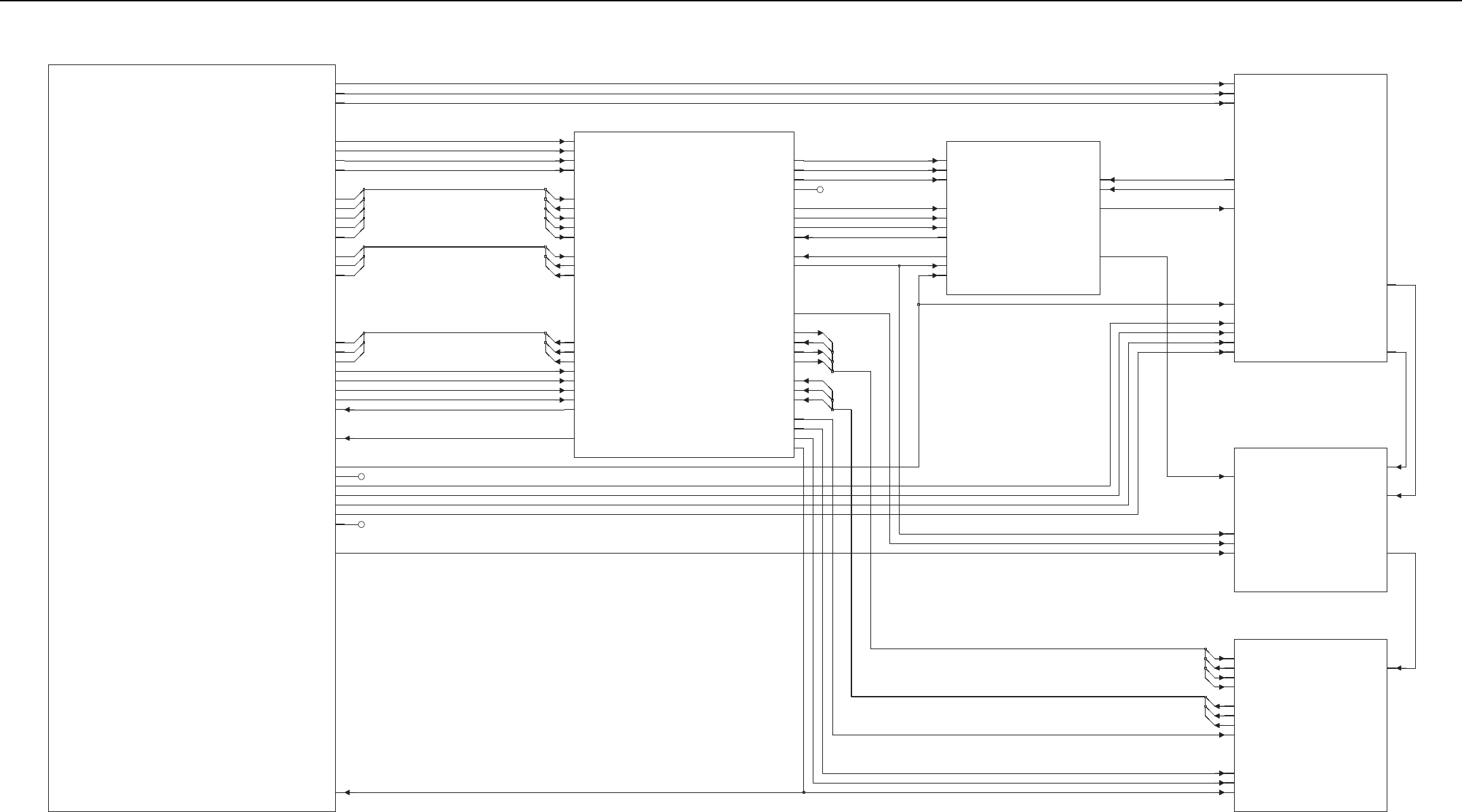
VHF (136–174 MHz) 1–25W PCB/Schematics/Parts List 3-23
CONTROLLER_&_GPS_R2
( TOP LEVEL: SHEET 1)
PC_ATTEN_ENA
PREDRIVE_SW
RAW_B+
RESET_OUT
RX_FLTR_VCTRL
RX_SSI_CLK
RX_SSI_DATA
RX_SSI_FSYNC
RX_SSI_SYNCB
SPI_CLK
SPI_MISO
SPI_MOSI
THK_CS
TX_DAC
TX_SSI_CLK
TX_SSI_DATA
TX_SSI_FSYNC
16.8_GPS
16.8_MHZ_BUFF
2.775V_ANA_V7
2.775V_DIG_V4
5V_SW
9V3
9V3_PA
ABACUS3_CS
ADAPT_SW
ANT_ENABLE
DMCS
LOCK_DETECT
LO_BATTERY_DET
PA_BIAS
PA_TEMP
1.875V_DIG_V2
1
0
1
3
0
2
1
2
0
2
4
TX_SSI_BUS(0:2)
SPI_BUS(0:4)
RX_SSI_BUS(0:2)
NC
NC
2
3
1
1
1
2
0
2
0
4
0
TX_VCO_SEL2_
VCTRL
RX_VCO_SEL1_
RX_VCO_SEL2_
SF_OUT
SPI_CLK_OUT
SPI_MISO_OUT
SPI_MOSI_OUT
TX_VCO_SEL1_
ABACUS3_CEX_OUT
ABACUS3_SYNCB_OUT
HP_MOD_OUT
PRSC
RF_ATTN_1
RX_SSI_CLK_PASS_IN
RX_SSI_DATA_PASS_IN
RX_SSI_FSYNC_PASS_IN
16.8_REF
1V8_BE
5V_BE
9R1
9V3
RX_SSI_FSYNC_PASS_OUT
SDTX
SFTX
SPI_CLK_IN
SPI_MISO_IN
SPI_MOSI_IN
TH_CEX
TX_CLK
ABACUS3_CEX_IN
ABACUS3_SYNCB_IN
ADAPT_SW
DMCS
LOCK
RSTB
RX_SSI_CLK_PASS_OUT
RX_SSI_DATA_PASS_OUT
1.8V_TH_DIG
16.8_GPS
2.8V_TH_ANA
2.8V_TH_DIG
5V
SYNTH
NC
2
0
3
1
0
1
2
9V3_SYNTH_IN
9V3_VCO
RXINJ
TXINJ
VCO_VHF
( TX: SHEET 1)
( RX: SHEET 2)
9R1
9V3_SYNTH_OUT
HP_MOD_OUT
PREDRIVE_SW
PRSC
RX_VCO_SEL1
RX_VCO_SEL2
SF_TH
TX_VCO_SEL1
VCTRL
9V3_SYNTH
9V3_VCO
TX_INJ
( PA: SHEET 1)
( PC: SHEET 2)
TX_HP_VHF
9V3_TX_SW
ANT_ENABLE
FINAL_BIAS_1
LO_BATTERY_DET
PREDRIVE_SW
RX_IN
TX_DAC
RXFE_VHF
( 1 SHEET)
9R1
9V3_TX_SW
FE_TUNE IF
RF_ATTEN_1
RX_IN
RX_INJ
(ABACUS3: SHEET 2)
RXBE_73.35MHZ
(IF AMP: SHEET 1)
SPI_ABACUS_CLK
SPI_ABACUS_DATA
SSI_ABACUS_CLKOUT
SSI_ABACUS_DOUTA
SSI_ABACUS_DOUTB
SSI_ABACUS_FSYNC
SSI_ABACUS_SYNCB
16.8_REF
1V8
5V
IF
SPI_ABACUS_CEX
2
2
3
1
0
0
1
ABACUS_SPI_BUS(0:3)
ABACUS_SSI_BUS(0:2)
9V3
9V3_PA
PA_SUPPLY
VHF (136–174 MHz) 1–25W Overall Schematic Diagram
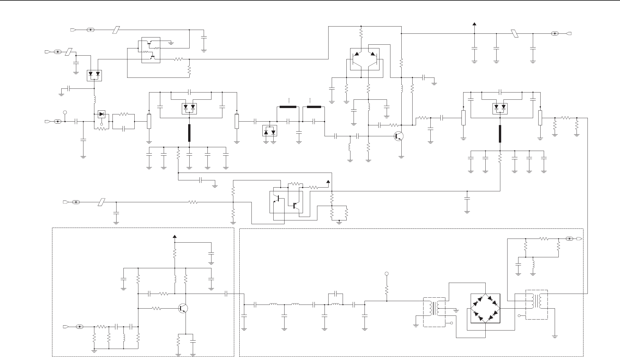
3-24 VHF (136–174 MHz) 1–25W PCB/Schematics/Parts List
(VALUE)
(VALUE)
(VALUE)
(VALUE)
(VALUE)
(VALUE)
(VALUE)
10 dB Attenuator ON @ High for RF_ATTEN_1
E0400
BK1005HM471
RF_ATTEN_1_8
RF_ATTEN_1
9V3_TX_SW_8
E0404
BK1005HM471
9V3_TX_SW
MMBD6100
D0402
1500pF
C0407
TP0400
TEST_POINT
C0404
1500pF
1
RXIN_FE_6
C0413
RX_IN
4.7pF
C0421
1500pF
10 dB Attenuator
NC
220
R0407
470
R0435
470pF
C0418
560nH
L0400
D0400
2
13
13
L0405
10nH
D0401
1SV228
20pF
C0411
C0406
6.8pF
C0410
20pF
10nH 2
L0402
C0455
1500pF
1
3
2
CR0400
MMBD352
C0453
39pF
C0412
47pF
15pF
C0452
Hi-Side Zeros for Preselector
(Micro-strip 40 mm Aggregate)
C0427
51pF
C0426
43pF
C0423
56pF
C0424
43pF C0425
51pF
100K
R0410
C0433
1500pF
MAKO ( 0 ~ 4.6 VDC)
680
R0429
FE_TUNE_FE_3
E0403
BK1005HM471
C0436
1500pF
FE_TUNE
9R1_FILT
56
R0417
2.7K
R0419
L0407
560nH
1500pF
C0437
Q0405
NE85634
1500pF
C0438
C0442
1500pF
2.67K
R0418
C0439
1500pF
C0440
0.10uF
R0420
2.7K
0
R0421
7.5 dB Attenuator
C0451
68pF
R0424
150
R0425
1K
47nH
L0411
RX_INJ_FE_5
C0450
9.1pF
150
R0423
R0422
51
RX_INJ
62
R0432 1500pF
C0457
L0409
68nH
2%
L0408
2%
68nH
24pF
C0443
C0447
24pF
C0446
10pF
C0441
3.9pF
22pF
C0448
30pF
C0445 47nH
2%
L0410
24pF
C0444
C0449
10pF
1
TEST_POINT
TP0401
R0426
10K
NC
XFMR
T0400
5
NC
4
6
3
2
1
IO2 2
IO3 3
IO4
4
IO1
1
D0405
NC
T0401
NC
5
4
6
3
2
1
XFMR
150nH
L0412
R0427
51
82pF
C0458
0
R0433 IF_FE_3
R0434
270
NU
IF
51pF
C0432
51pF
C0429
C0428
43pF 43pF
C0430 C0431
56pF
100K
R0412
1500pF
C0434
39
R0411
R0437
150
R0436
150
10nH
2
13
13
L0404
15pF
C0417
C0408
6.2pF
10nH
L0403
2
D0403
1SV228
15pF
C0416
C0409
12pF
3.9pF
NU
C0420
R0440
20
NE85634
Q0402
C0405
1500pF
R0404
2.7K
22
R0402
R0406
C0435
1.0uF
L0401
56nH
620
0.10uF
C0419
560nH
L0414
3.6K
R0439
1500pF
C0456
15K
R0400
R0409
3K
1500pF
C0414
C0422
43pF
C0454
1500pF
39nH
5%
L0406
9R1_FILT
(In-Band Tuning range 2.70 ~ 7.80 VDC)
R0416
680
R0415
680
680
R0414
0
R0428
680
R0413
2
3
6
4
1
5
Q0403
UMZ2NTR
R0408
10K
10K
R0430
10K
R0431
1500pF
C0400
6
3
1
4
Q0400
2
5
R0403
0
9R1_FILT
51pF
C0403
BK1005HM471
E0401
C0402
1500pF
C0401
0.1uF
9R1_FE_7
9R1
Q0401
UMT1NFTN
1K
R0401
VHF (136–174 MHz) 1–25W Receiver Front-End Schematic Diagram

VHF (136–174 MHz) 1–25W PCB/Schematics/Parts List 3-25
UHF -- 73.35MHz
4-POLE
VHF -- 44.85MHz
5V_BE_5
5V
5V
BK1005HM471
E0500
1.2K
R0511
20K
R0502
R0501
330
0.10uF
C0514
1.43V
C0512
0.10uF
0.76V
1
3
2
PBR941
Q0500
4.7K
R0509
0.10uF
C0503
C0509
NU
C0506
0.10uF
R0508
L0504
NU
56K
L0503
330nH
6.2pF
C0510
18pF
C0507
IFIN_BE_83OUT 6
FL0500
MXF45
44.85MHz
CC1
2
CC2
5
GND1
1
GND2
4
IN
IF
NU
C0515
D0500
MMBD352
IF_TO_ABACUS
0.72V
1.6V
C0516
NU
0.10uF
C0502
0.10uF
C0513
R0503
Q0501
30K
PBR941
R0510
30K
C0504
0.10uF
R0500
5.1K
51
R0512
820nH
IF_OUT
L0506
1
SHIELD
SH0500
VHF (136–174 MHz) 1–25W Receiver IF Amp Schematic Diagram

3-26 VHF (136–174 MHz) 1–25W PCB/Schematics/Parts List
0
R0621
R0623
NU
NU
R0622
IF_OUT
TP0602
TEST_POINT
1
C0650
30pF
1000pF
C0611
.01uF
C0615
C0619
0.10uF
0.10uF
C0617
L0605
10uH
L0604
10uH
3VA
51
R0606
E0602
BK1005HM471
3VA
C0623
0.10uF
C0628
0.10uF
E0603
BK1005HM471
3VA
0.10uF
C0633
3VA
E0604
BK1005HM471
C0638
0.10uF
E0607
BK1005HM471
3VA
0.10uF
C0644
E0608
BK1005HM471
3VA
R0616
100K
100pF
C0636
100pF
C0635
.01uF
C0634
4.7uF
C0632
R0610
0
C0629
2200pF
C0627
100pF
100pF
C0626
C0625
200pF
12
11
9
6
2
1
4
5
10
3
8
7
VREFN
VREFP
VDDA
VDDF
MXON
MXOP
IF2N
IF2P
GNDA
GNDF
GCN
GCP
14
17
23
24
13
16
21
15
18
22
20
19
VDDQ
VDDC
PC
PD
RREF
GNDQ
GNDS1
IOUTC
GNDC
GNDD
CLKN
CLKP
VDDP
SYNCB
VDDD
VDDH
VDDI
VDDL
LON
LOP
PE
GNDS2
IFIN
IOUTL
GNDH
GNDI
GNDL
GNDP
CXVL
CXVM
DOUTA
DOUTB
FREF
FS
AD9864
U0600
CLKOUT
CXIF
39
48
40
42
43
47
38
45
37
44
41
46
33
26
27
25
34
32
36
29
30
35
31
28
BK1005HM471
E0600
BK1005HM471
E0601
C0620
0.10uF
C0621
0.10uF
0.10uF
C0631
0.10uF
C0630
E0605
BK1005HM471 BK1005HM471
E0606
1V8_3
3VA
1V8
DOUTA
PCPE PD
DOUTBFS CLKOUT
0
R0611
0
R0613
0
R0614
0
R0615
R0609
0
R0608
0
0
R0612
TK11100CSC
FB
2
GND
5
NP
6
VCONT
4
VIN
3
VOUT 1
U0601
R0625
51.1K
1500pF
C0651
68.1K
R0626
C0641
.01uF
C0640
2.2uF
E0610
BK1005HM471
5V
BK1005HM471
E0609
Q0601
73A04
C0647
10.0uF
R0620
9.1K
C0648
10.0uF
VVCO
3VA
C0637
1.0uF
SSI_ABACUS_FSYNC
SPI_ABACUS_CEX
SPI_ABACUS_CLK
SSI_ABACUS_DOUTA
SSI_ABACUS_CLKOUT
SSI_ABACUS_DOUTB
SPI_ABACUS_DATA
SSI_ABACUS_SYNCB
FD_1_BE_5
FE_1_BE_5
SB_1_BE_5
CLKOUT_1_BE_5
FS_1_BE_5
DOUTA_1_BE_5
DOUTB_1_BE_5
FC_1_BE_5
NU
R0607
0
R0627
FREF_IF
1000pF
C0622
16.8_REF
1V8
Abacus SSI FS = 20 kHz
Abacus SPI CE = Active Low (2.8 Vp-p)
Abacus SSI CLK_OUT = 1.2 MHz
SPF_3.5V
2nd LO VCO VHF (42.6MHz/47.1 MHz)
2nd LO VCO UHF (71.1MHz/75.6 MHz)
R0605
330
18pF
C0607
10K
R0602
VVCO
NU
C0616
68pF
C0610
43pF
C0614
Q0600
NE68519
68
R0601
24K
R0604
L0603
270nH
2nd LO LF
.01uF
C0602
0.10uF
C0604
1uF
C0618
TEST_POINT
TP0601
510
R0603
D0600
1SV305
C0649
3300pF
0.1uF
C0613
L0602
2.7uH
C0612
13pF
C0603
220pF
5.1K
R0624
C0605
43pF
C0601
43pF
TEST_POINT
TP0600
5V 3VA
CLOCK VCO
L0608
4.7uH 68pF
C0642
D0601
1SV305
.01uF
C0645
R0619
10K
CLOCK LF
R0618
390
C0646
0.68uF
10K
R0617
0.10uF
C0643
VHF (136–174 MHz) 1–25W Receiver Back-End Schematic Diagram
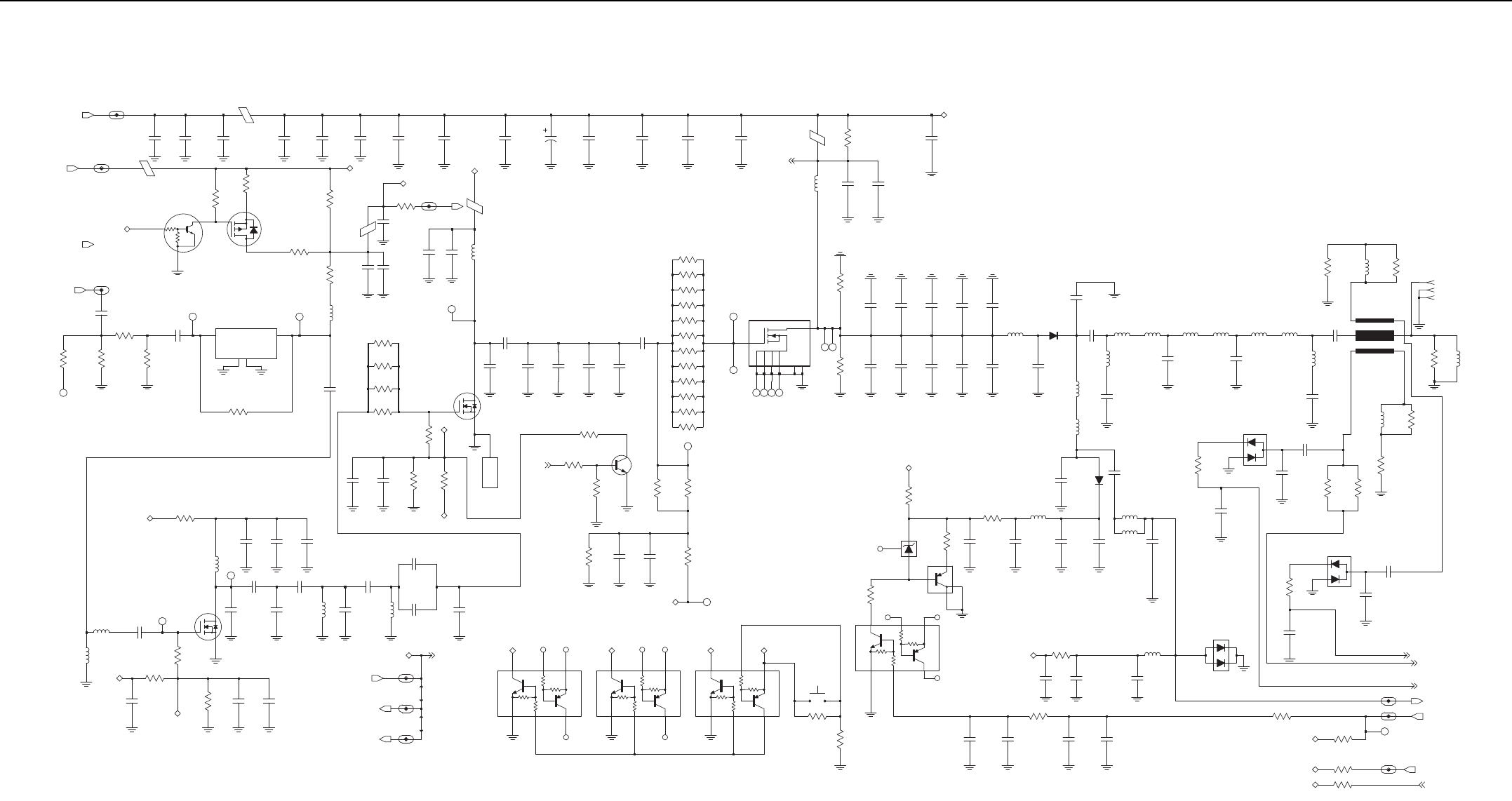
VHF (136–174 MHz) 1–25W PCB/Schematics/Parts List 3-27
C0731
470pF
470pF
C0714
C0713
NU
470pF
A+
17nH
L0700
E0701
10
R0742
C0709
0.1uF
Load
2.2uF
C0738 C0708
1000pF
C0710
10uF
470pF
C0712 C0711
.01uF
PA_SUPPLY
9V3_PA
30K
R0713
1.5uH
L0728
R0973
0
NU
47nH
L0904
R0975
82
R0976
39
39
R0977
C0941
24pF
1000pF
C0940
25nH
L0706
180pF
C0735
13pF
C0750
18nH
L0708
28nH
L0723
18nH
L0720
25nH
L0721
18nH
L0707
43pF
C0739
20pF
C0803
470pF
C0723
25nH
L0709
C0740
47pF
22pF
C0741
D0700
25nH
L0710
L0724
25nH
L0722
17.5nH
8.2pF
C0742
NU
11pF
C0722
51pF
C0719
36pF
C0724
28pF
NU
C0729
C0726
82pF
36pF
C0725
27pF
C0730
NU
C0727
11pF
82pF
C0721
51pF
C0720
17nH
L0714
R0723
1MEG
R0710
1MEG
1
SP0708
SP0707 1
GND2
D
GND1
S1
S2
S3
S4
G
Q0702
MRF1535 Flat Lead
SP0701 1
SP0703 1
SP0702 1
1
SP0704
SP0706
1
R0719
15
1
SP0705
TP0707
TPSM0_762
R0733
15
R0726
15
15
R0736
15
R0712
R0734
15
15
R0739
R0737
15
R0732
15
15
R0717
15
R0721
15
R0716
36pF
C0819
470pF
C0745
180pF
C0754C0753
82pF
C0746
470pF
43pF
NUNUNU
C0755C0752
75pF
0
R0982
2.4K
R0981
100K
R0980
Q0710
Load
1K
R0730 R0731
51
NU
C0805
100pF
NU
100K
R0756
TPSM0_762
TP0711
1000pF
C0804 47K
R0757
Final_Bias
Q0709
68K
R0773
SWITCH
S0700
NU
0
R0775
9V3
Final_Bias
NC
NC
Q0706
NC
R0745
470
C0943
1000pF
D0905
R0979
0C0944
10pF
1000pF
C0945
IF|if_sig5
ANT_ENABLE_TX_PA
IF|if_sig4
IF5
TP0713
TPSM0_762
0
R0752
1K
R0753
IF|if_sig6
RX_IN_TX_PA
R0761
0
FWD_POWER
RX_IN
ANT_ENABLE
FINAL_BIAS_1
Final_Bias
Antenna_En
FWD_DETECTED
REV_DETECTED
V_CONTROL
V_cont
R0749
0
D0703
Long Trace around PA
Bypass both sides
1.2uH
L0729
1000pF
C0823 C0824
1000pF
NU
C0822
1000pF
9V3_TX_SW_Main
1K
R0781
150pF
C0796
56K
R0748
1000pF
C0797
C0798
1000pF 150pF
C0799
Q0704
1000pF
C0776
39pF
C0779
L0731
100nH
100nH
L0730
R0735
100
L0725
1.2uH
C0777
1000pF 10pF
C0772
C0778
150pF
27pF
C0766
D0702 C0767
470pF
VR0700
51
R0738
10K
R0729
NC
A+
NC NC
NC
NC
NC
Q0707 Q0708
NCV_G2V_G1
150nH
L0715
.022uF
C0775
TPSM0_762
TP0709
1500pF
C0783
C0780
NU
270pF
R0740
0
9V3_TX
R0755
27
150nH
L0705
27
R0754
R0718
27
27
R0720
470pF
C0734
22K
R0722
R0728
4.7K
C0770
1500pF470pF
NU
C0818 22K
R0727
V_G2
V_cont
HEATSINK
M0700
POS 1
3
21
D
G
S
Q0703
C0700
33pF 33pF
C0703 C0706
NU
3000pF
IF|if_sig3
3000pF
C0707
NU
E0700
C0705
1000pF
1000pF
C0702
C0701
.033uF
C0704
.033uF
E0703
PA_SUPPLY_TX_PA
IF|if_sig3
9V3_TX
R0777
100K
Q0701
47K
10K
R0779
0
Q0700
PREDRIVE_SW
Antenna_En
+7.5 dBm
-5 dBm
Test Point to check Ref Osc warping
3.8V @ Id=55mA
-5 dBm
120
R0711
R0714
75
C0733
470pF
75
R0715
R0780
0
3
1VD_RF_OUT
U0700
NU
2GND1
4GND2
RF_IN
R0706
220
C0728
470pF
0
R0759
TP0705
TPSM1_50
R0760
10K
IF|if_sig5
TX_INJ_TX_PA
TPSM0_762
TP0704
TP0703
TPSM0_762
TX_INJ
NU
C0716
270pF
33.47nH
L0702
270pF
C0732
NU
1000pF
C0717
C0718
1000pF
TP0702
TPSM0_762
To Rx PIN diode for 12mA bias
To Tx/Rx Switch bias - 10mA
E0702
IF|if_sig8
1500pF
C0806
R0746
0
NU
R0702
0
BK1005HM471
E0704
9V3_TX_SW
9V3_TX
9V3_TX_SW_Main
18K
R0750
D
G
S
68nH
L0718
270pF
NU
C0802
470pF
C0795
L0716
8.2nH
TP0710
TPSM0_762
V_G1
V_cont
C0801
1500pF
R0751
27K
NU
470pF
C0771
Q0705
56pF
C0791
12nH
L0717
150pF
C0817
NU
150pF
NU
C0820
220pF
C0790
100
R0747
C0821
NU
150pF
470pF
C0786
C0794
NU
47pF
C0792
470pF
C0793
NU
1000pF
L0719
6.8nH
9V3 9V3
IF|if_sig3
IF|if_sig7
IF|if_sig7
9V3_VCO
9V3_SYNTH
9V3
1000pF
C0942
D0904
0
R0978
J0700-11
J0700-33
J0700-22
W = 90.2 milS = 35.4 mil
W = 22.6 mil
W = 22.6 mil
L = 1030 mil
S = 35.4 mil
R0970
100 NU
47nH
L0903 R0972
0
VHF (136–174 MHz) 1–25W Power Amplifier Schematic Diagram
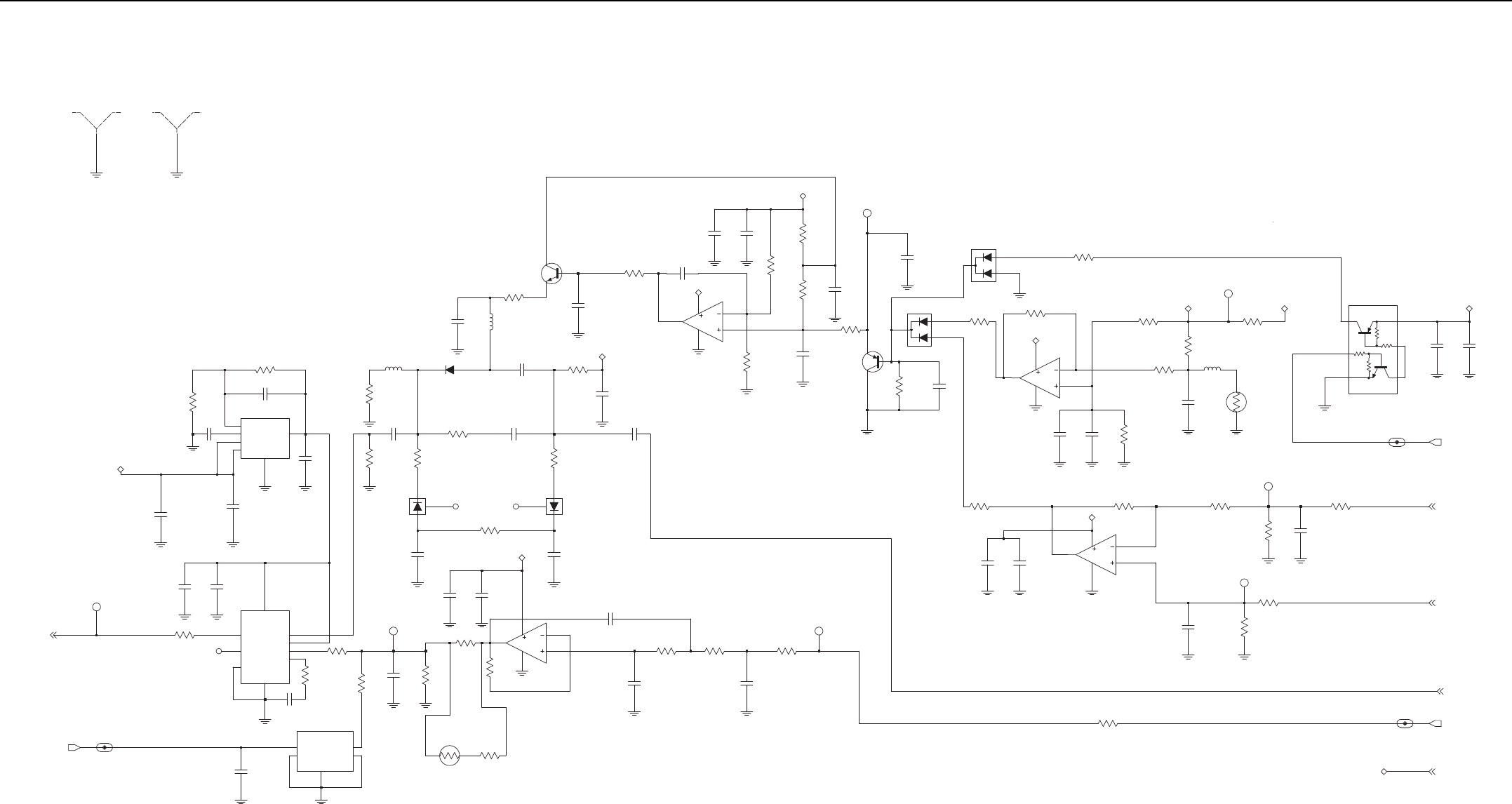
3-28 VHF (136–174 MHz) 1–25W PCB/Schematics/Parts List
1
SHIELD
SH0901
1
SHIELD
SH0900
C0947
100pF
0.1uF
(VALUE)
C0951
C0949
1000pF
C0950
2.2uF
2FB
5GND
6NP
4VCONT
3VIN
1
VOUT
TK11100CSC
U0941
16.2K
1%
R0937
47.5K
R0936
1.0uF
C0948
1%
7
VPOS 8
3
U0940
5
2
4
6
1
AD8315ACPZ-REEL
0.1uF
C0921 C0922
1500pF
VAPC
VSET
COMM
ENBL
FLTR
GND
NC
RFIN
R0940
0NC
1.35V (44W)
1.28V (27.5W)
R0941
0
3.32K
R0946
C0925
1500pF
R0950
10K
TP0910
100K
R0955
9
C0953
1500pF
2
4NC1 NC2
RESET_OUT
U0942
NCP301
GND
3
INPUT
4700pF
C0926
5
1
LO_BATTERY_DET
LO_BATTERY_DET
2.85V (44W)
2.10V (27.5W)
TP0909
V_CONTROL
9V3
RT0953
47K
R0954
430K
AD8566
U0900-2
6
5
7
8
4
R0947
0
6.81K
R0942
R0925
R0943
5.6K
220pF
C0927
39.2K
C0936
1500pF
C0903
1500pF C0923
2200pF
2113945C31
C0902
0.1uF
9V3_PC
NCNC
D0902 D0903
C0937
1500pF
R0928
47
R0926
75
R0927
51
1500pF
C0931
C0934
1500pF
R0924
5.6K
C0918
1500pF
1500pF
C0935
R0929
47
R0917
5.6K
1500pF
C0916
R0913
0
2414017K32
L0901
560nH
C0914
1500pF
Q0902
D0901
C0912
1500pF
9V3_PC
1K
R0910
2
3
1
8
4
U0900-1
AD8566
39K
R0919
C0917
1000pF
9V3_PC
R0921
2.2K
Q0901
C0919
0.1uF
2.4K
R0960
1500pF
C0913
R0922
36K
1500pF
C0911
C0920
1500pF
390
R0918
9V3_PC
AD8566
U0901-2
6
5
7
8
4
9V3_PC
R0930
18K
D0900
0
R0906
R0900
56K
C0915
1500pF
NOTE: VOLTAGES SHOWN FOR ANALOG TX MODE
1.0V or less, typical
TP0907
C0929
1500pF
D0906
TP0913
R0901
43K
R0931
0
0
R0907
9V3_PC 9V3
C0904
1500pF
RT0908
47K
22K
R0903
C0906
1500pF
C0907
.01uF R0909
43K
3.3K
R0902
1uH
L0900
PC_ATTEN_ENA_TX_PA
PC_ATTEN_ENA
0.1uF
C0901
1500pF
C0900
Q0900 9V3
FWD_DETECTED
REV_DETECTED
43.2K
R0951 R0944
1000pF
2113944C51
C0928
0
TP0911
0.1uF
C0908
1500pF
C0909 3
1
8
4
U0901-1
AD8566
2
0
R0923 R0914
390K
9V3_PC
TX_DAC
FWD_POWER
TX_DAC
9V39V3
0.38V (44W)
0.21V (27.5W)
C0910
1500pF
0613952R66
R0938
0
0613952Q89
R0911
4.7K
TP0903
27K
0613952R11
R0912
2.67V (44W)
2.01V (27.5W)
0613952R19
56K
R0915
100
R0916
1500pF
C0939
R0920
33K
TP0904
560nH
L0902
2414017K32
VHF (136–174 MHz) 1–25W Power Control Schematic Diagram

VHF (136–174 MHz) 1–25W PCB/Schematics/Parts List 3-29
SPI_MOSI_IN
SPI_CLK_IN
SPI_MISO_IN
ABACUS3_SYNCB_IN
SPI_MOSI_IN
SPI_CLK_IN
SPI_MISO_IN
RX_SSI_DATA_PASS_OUT
RX_SSI_CLK_PASS_OUT
RX_SSI_FSYNC_PASS_OUT
ABACUS3_CEX_IN
SPI_CLK_IN
RX_SSI_FSYNC_IN
SPI_MOSI_IN
SPI_MISO_IN
RX_SSI_CLK_IN
ABACUS3_SYNCB_IN
ABACUS3_CEX_IN
RX_SSI_DATA_IN
RX_SSI_CLK_OUT
RX_SSI_FSYNC_OUT
ABACUS3_CEX_OUT
SPI_MOSI_OUT
ABACUS3_SYNCB_OUT
SPI_CLK_OUT
SPI_MISO_OUT
RX_SSI_DATA_OUT
ABACUS3_SYNCB_OUT
RX_SSI_FSYNC_PASS_IN
RX_SSI_CLK_PASS_IN
ABACUS3_CEX_OUT
SPI_MISO_OUT
SPI_MOSI_OUT
SPI_CLK_OUT
RX_SSI_DATA_PASS_IN
Buffer to Abacus/Controller
R0105
240
.01uF
C0120
51
R0110
PBR941
Q0100
C0195
470pF
L0100
270nH R0108
2K
220
R0107
10K
R0144
.01uF
C0171
2.8V_DIG
.01uF
C0122
R0106
2.7K
(VHF=1500pF)
C0118
0.1uF220pF
C0117
(VHF=1500pF)
C0104
220pF C0105
0.1uF
1.0uF
C0115
1.0uF
C0114
1.8V_DIG
2.8V_ANA
1.8V_DIG
2.8V_ANA
0.1uF
C0106
(VHF=1500pF)
220pF
C0108
(VHF=1500pF)
220pF
C0178
47K
R0104
0.1uF
C0111
C0103
0.1uF
C0110
0.1uF
(VHF=1500pF)
220pF
C0102
(VHF=1500pF)
C0101
220pF
(VHF=1500pF)
220pF
C0177
1.8V_DIG
0.1uF C0107
0.1uF
C0109
TP_TEST2
TP_TEST1
11
(VHF=1500pF)
C0100
220pF
(VHF=1500pF)
220pF
C0175
2.8V_ANA
1.8V_DIG
R0103
0
0
R0102
Unlocked: 0V
Locked: 1.8V
(VHF=1500pF)
220pF
C0112
NU
220pF
C0121C0119
NU
220pF
NU
220pF
C0113
TP502
1TP504
1
TP503
1
1
TP501
R0111
0
2.8V_ANA
(VHF=1500pF)
220pF
C0125C0124
0.1uF
0.1uF
C0129 5V_TH
R0148
1202K
R0114
21
34
R0117
30K
BCV62
Q0102
R0118
0
Adapt OFF: 0V
Adapt ON: 5V
0
R0115
TP_ADAPT_SW
1
R0159
10K
5V_TH
(VHF=1500pF)
220pF
C0179
(VHF=1500pF)
C0138
220pF
5V_TH
Switch for Adapt Transient
VCC 5
U0101
MC74VHC1GT66
GND
3
INOUT
1
ONOFF_CONTROL
4
OUTIN
2
NU
R0122 0
R0125
0
Q0106
DTC114YM
GND
R1
R2
OUT
IN
ADAPT_SW_SYNTH
ADAPT_SW
R0120
10K
VCO STEERING LINE VOLTAGE: 0.6V TO 4.4V
VCTRL_SYNTH
VCTRL
Note: High Port modulation injection through loop filter for UHF only
(VHF=NU)
(VHF=NU)
R0140
18
R0139
1.6K
(VHF=0.1uF)
0.1uF
C0166
.022uF
C0149
(VHF=51)
(VHF=NU)
(VHF=10)
(VHF=51)
0
R0128
C0151
0.1uF
R0134
27
.033uF
C0148
R0127
100
C0150
0.1uF
(VHF=150)
R0131
240
VCO STEERING LINE VOLTAGE: 0.6V TO 4.4V
1
TP_VCTRL
C0163
0.1uF0.1uF
C0162C0194
0.1uF
C0157
0.1uF0.1uF 0.1uF
C0192C0193 C0161
0.1uF
C0160
0.1uF
C0191
0.1uF
C0159
0.1uF
C0164
0.1uF
C0165
0.1uF0.1uF
C0156
0.1uF
C0158
C0191,C0192,C0193,C0194: NU (UHF)
5116032H01
1.5 ppm 0.5 ppm
5102495J07TCXO (Y0100)
(VHF=1500pF)
.01uF
C0145
C0142
220pF
2GND
OUTPUT 3
VC
1
VCC 4
16.8MHz
TCO5826
Y0100
(VHF=1500pF)
0.1uF
C0180 C0146
220pF100K
R0161
10uF
C0196
R0123
56K
C0141
0.1uF
27
R0119
4.7uF
C0140
2.8V_ANA
10K
NU
R0126
(VHF=1500pF)
C0147
220pF
RX_VCO_SEL1_
TX_VCO_SEL1_
TX_VCO_SEL2_
RF_ATTN_1
RX_VCO_SEL2_
GPO_4
GPO_6_SYNTH
GPO_1_SYNTH
GPO_2_SYNTH
GPO_3_SYNTH
GPO_5_SYNTH
(VHF=1500pF) (VHF=1500pF)
(VHF=1500pF)
220pF
C0128
220pF
C0127
220pF
C0126
R0155
0
NU
R0157
0
R0147
0
NU
VCO SEL: ACTIVE LOW
GPO LINES
LOW: 0V
HI: 2.8V
16.8_REF_BE_SYNTH
16.8_GPS_SYNTH
16.8_REF_CONTROLLER_SYNTH
16.8_REF
16.8_GPS
R0146
0
9R1_SYNTH
100K
R0160
9V3_SYNTH
NTR1P02T1
Q0107
9V3
9R1
9R1 SWITCH FOR FRONT-END
Q0108
DTC114YKAF
RSTB_SYNTH
RSTB
47K
10K
1
SHIELD
SH0101
1
SH0100
SHIELD
PRSC_SYNTH
HP_MOD_OUT_SYNTH
SF_OUT_SYNTH
SF_OUT VOLTAGE: 2.45V
HP_MOD_OUT
PRSC
SF_OUT
TH_CEX
SPI_MOSI_IN
SPI_CLK_IN
DMCS
SDTX
SFTX
LOCK
TX_CLK
SPI_MISO_IN
DMCS_SYNTH
SFTX_SYNTH
SDTX_SYNTH
TX_CLK_SYNTH
LOCK_SYNTH
TH_CEX_SYNTH
5V
5V_BE
1V8_BE
1.8V_TH_DIG
2.8V_TH_DIG
2.8V_TH_ANA
5V_SYNTH
1V8_BE_SYNTH
1.8V_TH_DIG_SYNTH
5V_BE_SYNTH
2.8V_TH_DIG_SYNTH
2.8V_TH_ANA_SYNTH
R0100
0
R0101
0
2.8V_DIG
5V_TH
0
R0109
0
NU
R0158
C0123
1.0uF
0
NU
R0156
C0132
220pF220pF
C0131
220pF
C0130
(VHF=1500pF) (VHF=1500pF)(VHF=1500pF)
10K
R0113
NC
NC
NC
NC
NC
NC
NC
NC
NC
NC
C0135
10uF 0.1uF
C0136
C0133
4.7uF
(VHF=1500pF)
C0143
220pF
R0116
0
0.1uF
C0144
10uF
C0137
(VHF=1500pF)
220pF
C0134
2.8V_ANA
NC
NC
NC
NC
NC
NC
NC
NC
SC51650VF
U0100
NC
NC
NC
NC
NC
NC
NC
NC
NC
NC
NC
NC
NC
NC
NC
NC
NC
NC
NC
NC
NC
NC
NC
NC
NC
NC
TXI
TXQ
TCLK
SCAN_IN
SDM_VAG
RXIX
RXQ
RXQX
RX_EN_OUT
PABIAS_DAC
PHCLK
RFSTEPA
RXI
NTXI
NTXQ
INCR_DECR
FBI
FBQ
DC_CAL
BP_Q
BP_QX
CLK1_OUT
CLK2_OUT
AGC_FLAG
AGC_REF
ARX_DAC
BP_I
BP_IX
AGC_DAC
K7
L7
G8
F2
B10
C1
D1
D2
B1
K11
L9
A3
C2
L8
K6
J9
C6
B6
A2
E2
E3
H9
J11
C4
C5
H6
E4
F4
B5
TX_GND2
XOSC_BASE
XOSC_EMIT
SUB1
SUB2
SUB3
SF_OUT
SMD_CLK_GEN_GND
OSCREG_SPLY
RSTB
OSCREG_BYP
OSCREG_OUT
GPO1_TEST1
GPO2_TEST2
GPO3_TEST3
GPO4_TEST4
GPO5
GPO6
DEEPSLEEP
EF_OUTM
EF_OUTP
CLK_BASE
CLK_CP
CLK_EMIT
ASPI_CLK
ASPI_DATA
ACE1
ACE2
NC2
NC3
NC4
NC1
F6
K5
L5
K10
F5
F3
K4
C9
J4
E6
A11
L1
L11
L4
H5
A1
B4
A4
E5
D4
K9
H8
L10
J8
J7
G11
G9
H11
C10
B11
A6
D6
VCO_DAC
TXCLK
SPI_DW
SDR
SDTX
SFTX
SPI_CLK
SPI_DR
SCLK_OUT
RXACQ
RXFS
MN_ADAPT_CP
MN_CP
M_PRSC
M_PRSCX
HP_MOD_OUT
MAIN_PDET_VCC
ESC_CP
ESC_IN
DAC_ADAPT
DMCS
CEX
F1
F10
D9
D11
F11
F9
C11
D10
E9
E7
E10
H1
G3
J2
H3
K8
G2
L3
K1
G1
F7
D8
TX_VCC
XOSC_GND
TEST2
TM
TX_DAC_GND
TX_DAC_VCC
TX_GND1
SSI_GND
SSI_VCC
TEST1
SDM_VREFP
SCAN_EN
SDM_CLK_GEN_VCC
SDM_REF_GND
SDM_REF_VCC
SDM_VREFM
RX_AGND1
RX_AGND2
RX_AVCC1
RX_AVCC2
OSCREG_GND
MAIN_VCC
MN_CP_GND
MN_CP_VCC
LGND1
LGND2
LVCC1
LVCC2
MAIN_GND
ESC_CPBIAS
ESC_CP_GND
ESC_CP_VCC
ESC_GND
ESC_TEST
ESC_VCC
CLK_GND
CLK_VCC
ASPI_VCC
J6
G6
C7
B3
H7
L6
G7
E8
E11
D7
B8
D3
A10
A8
B9
A9
C3
D5
B2
A5
J5
J1
G5
H2
F8
C8
G10
B7
G4
L2
K3
J3
H4
E1
K2
H10
J10
A7
NC
VHF (136–174 MHz) 1–25W Synthesizer Schematic Diagram

3-30 VHF (136–174 MHz) 1–25W PCB/Schematics/Parts List
1
SHIELD
SH0200
RX VCO 1
RXSL
Steering Line Voltage (VCTRL_TH)
VCTRL: 0.6-4.5V
L0209
680nH
C0226
1500pF
R0211
0
VCTRL
CR0203
CR0202
CR0201
CR0204
150nH
L0210
NU
R0240
R0224
6.2K
R0225
8.2K
1500pF
C0242
0.10uF
C0241
RX2
C0250
11pF
L0214
680nH
22nH
L0215
C0246
10pF
20pF
C0259
22pF
C0251
680nH
L0219
82pF
C0252
10pF
C0247
Q0201
3.9pF
C0231
PRESC_TX
180nH
L0221
R0229
150
C0235
15pF NU
C0233
L0230
180nH 20pF
C0265
R0230
4.3K
TP0301
1
PRSC_VCO_UHF1_5
PRSC
PRSC (RX): 180-220 MHz
-5 to -15 dBm
RX Prescaler
RX1_SEL_VCO_UHF1_5
RX_VCO_SEL1
0.1 V (Low)
RX1_SEL: 2.7 V (High)
1500pF
C0248 C0249
0.10uF
R0213
10K
1500pF
C0261
1500pF
C0262
1500pF
C0264
RX1
U0201
RX2
1500pF
C0260
R0218
10K
C0257
1500pF C0258
0.10uF 0.1 V (Low)
RX2_SEL: 2.7 V (High)
RX2_SEL_VCO_UHF1_5
RX_VCO_SEL2
C0239
0.10uF
1500pF
C0238
SF_TH
R0220
51
R0219
120
C0221
12pF
120
R0221 C0222
NU
L0206
27nH
C0217
1500pF 10
R0207
R0210
4.7K
15K
R0206
NU
C0224
0
R0212
L0211
220nH
R0208
47PBR941
Q0202
C0211
1500pF
8.2pF
C0219
L0205
68nH
NU
C0218
RXINJ_VCO_UHF1_5
TP0200
1
+5 dBm
RXINJ: 180-220 MHz
RXINJ
C0202
.01uF
L0200
220nH
C0209
0.10uF
1500pF
C0203
C0207
1500pF
220nH
L0204
510
R0203
R0202
510
RX Buffer Amplifier
9R1_VCO_UHF1_7
E0201
9R1
Super Filter Voltage (SF_TH)
SF_TH: 2.5V
SF_TH_VCO_UHF1_6
SF_TH
0.10uF
C0201C0200
1500pF
SF_TH
SF_TH
L0202
680nH
2.4K
R0201
6.2pF
C0215
C0204
1500pF
100
R0205
RX1
Q0200
680nH
L0203
R0204
4.3K
C0205
0.10uF 1500pF
C0206
11pF
C0214
C0223
C0225
39pF
120pF
36pF
C0229 680nH
L0212
150
R0216
L0213
680nH
1500pF
C0236
R0226
100
C0240
1500pF
0.10uF
C0237
SF_TH
C0220
10pF
L0207
27nH
15pF
C0208
C0213
15pF
RX VCO 2
12pF
C0245
C0243
12pF
R0241
NU
220nH
L0218
CR0205
CR0208
CR0206
CR0207
1500pF
C0253
L0217
680nH
RXSL
VHF (136–174 MHz) 1–25W Receiver VCO Schematic Diagram
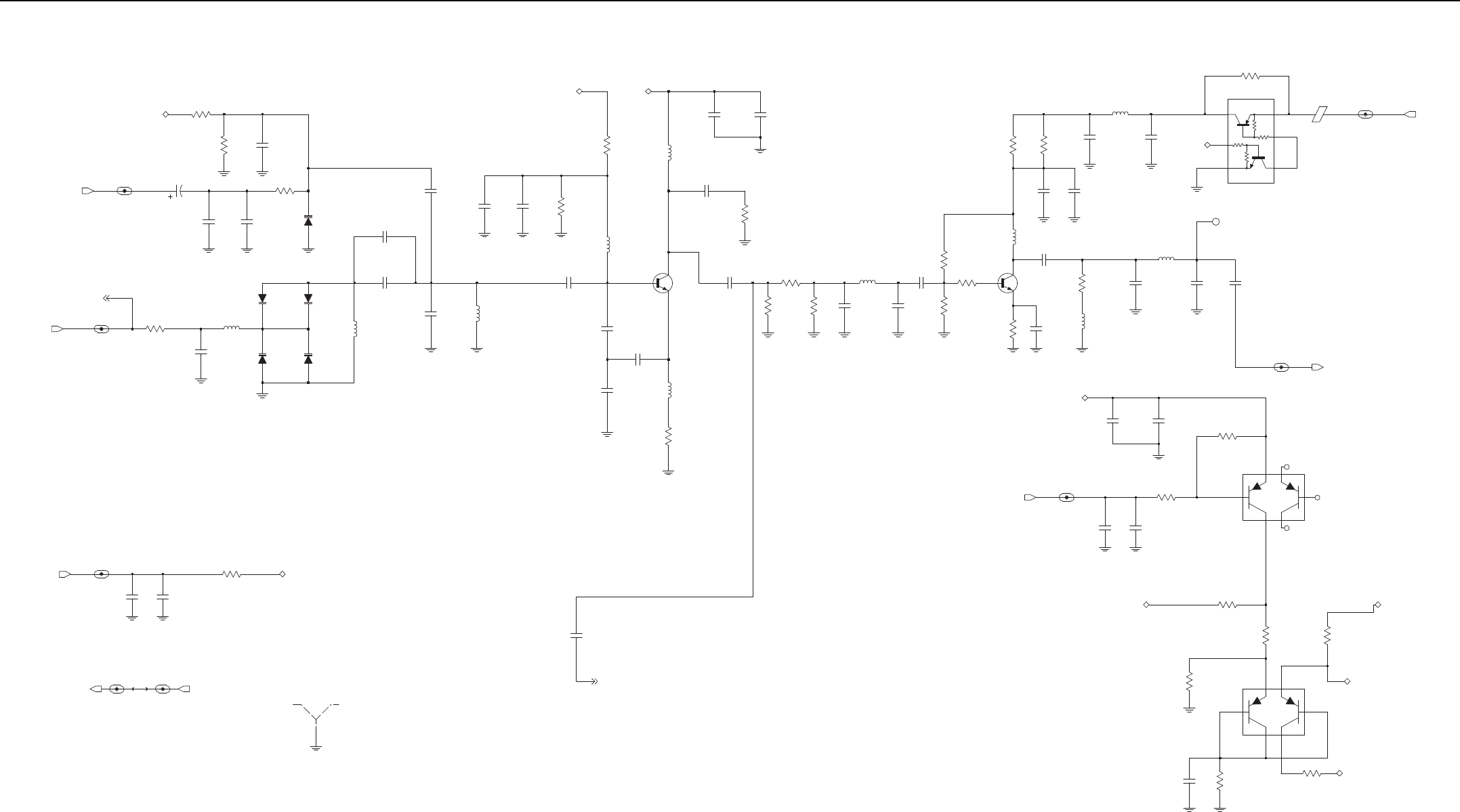
VHF (136–174 MHz) 1–25W PCB/Schematics/Parts List 3-31
TX Prescaler
PRSC (TX): 136-174MHz
-5 to -15 dBm
TX VCO1
TX Buffer Amplifier
6 dBm
TXINJ: 136-174MHz
0.1 V (Low)
TX1_SEL: 2.7 V (High)
SF_TH: 2.5V
Super Filter Voltage (SF_TH)
VCTRL: 0.6-4.5V
Steering Line Voltage (VCTRL_TH)
R0320
100K 2.4pF
C0332
R0321
10K
HP_MOD_OUT_VCO_UHF1_7
C0360
4.7uF
SF_TH
HP_MOD_OUT
C0334
220pF
R0319
20K
1500pF
C0361 CR0300
CR0302
1SV325
CR0304
1SV3051SV325
CR0303
1SV305
CR0301
C0326
1500pF
680nH
VCTRL_VCO_UHF1_70
R0311 L0309
VCTRL
VCTRL
15pF
C0313
15pF
C0308
56nH
C0320
5.1pF L0307
82nH
L0310
1.0pF
C0310
4.7K
R0304
1500pF
C0306
0.10uF
C0305
R0301
3.9K
15pF
C0314
680nH
L0303
30pF
R0316
110
27pF
C0323
C0329
680nH
L0312
C0325
150pF
18
R0333
Q0300
R0332
300
100
R0305
C0315
2.0pF
680nH
L0302
C0304
1500pF
C0301
0.10uF1500pF
C0300
R0334
300 NU
C0322 C0321
(VALUE)
6.2pF
180nH
L0306
4.7K
R0310
1500pF
C0317
R0307
82
NU
C0324
R0312
0
R0308
47
270nH
L0311
Q0302
PBR941
C0311
1500pF
L0304
270nH
1500pF
C0309
.022uF
C0307
510
R0302
L0300
220nH
C0303
1500pF
R0303
510
.01uF
C0302
AMP_SEL
U0303
1TP0300
68nH
L0305
13pF
C0319 C0318
NU 1500pF
C0312
TXINJ_VCO_UHF1_5
TXINJ
NC
U0304
NC
NC
10K
R0328
NU
0.10uF
C0339
C0338
1500pF
SF_TH
R0327
10K
TX1_SEL_VCO_UHF1_5
TX_VCO_SEL1
0.10uF
C0349
C0348
1500pF
TX1
R0345
0
1.2K
R0338
NU
8.2K
R0339
C0364
0.1uF R0343
43K R0347
NU
0
TX1
U0305
R0340
0
VSF
SF_TH
0
R0337
E0301
9V3_VCO_UHF1_7
9V3_VCO
VSFTX1
SHIELD
SH0300
1
0.10uF
C0328
XMIT_SEL_VCO_UHF1_6
1500pF
C0327
9V3_SYNTH_OUT 9V3_SYNTH_IN
PREDRIVE_SW
10K
R0336
NU
AMP_SEL
C0331
1.0pF
PRESC_TX
R0306
15K
VHF (136–174 MHz) 1–25W Transmit VCO Schematic Diagram

3-32 VHF (136–174 MHz) 1–25W PCB/Schematics/Parts List
VHF PCB 8471495L01 and 8471495L03 Parts
List 1–25W
Circuit
Ref
Motorola
Part No. Description
C0100 2113945A10 1500pF
C0101 2113945A10 1500pF
C0102 2113945A10 1500pF
C0103 2113945C31 0.1uF
C0104 2113945A10 1500pF
C0105 2113945C31 0.1uF
C0106 2113945C31 0.1uF
C0107 2113945C31 0.1uF
C0108 2113945A10 1500pF
C0109 2113945C31 0.1uF
C0110 2113945C31 0.1uF
C0111 2113945C31 0.1uF
C0112 2113945A10 1500pF
C0113 NOT PLACED –
C0114 2113946E02 1.0uF
C0115 2113946E02 1.0uF
C0117 2113945A10 1500pF
C0118 2113945C31 0.1uF
C0119 NOT PLACED –
C0120 2113945B02 .01uF
C0121 NOT PLACED –
C0122 2113945B02 .01uF
C0123 2113946E02 1.0uF
C0124 2113945C31 0.1uF
C0125 2113945A10 1500pF
C0126 2113945A10 1500pF
C0127 2113945A10 1500pF
C0128 2113945A10 1500pF
C0129 2113945C31 0.1uF
C0130 2113945A10 1500pF
C0131 2113945A10 1500pF
C0132 2113945A10 1500pF
C0133 2313960B30 4.7uF
C0134 2113945A10 1500pF
C0135 2313960B32 10uF
C0136 2113945C31 0.1uF
C0137 2313960B32 10uF
C0138 2113945A10 1500pF
C0140 2313960B30 4.7uF
C0141 2113945C31 0.1uF
C0142 2113945A10 1500pF
C0143 2113945A10 1500pF
C0144 2113945C31 0.1uF
C0145 2113945B02 .01uF
C0146 2113945A10 1500pF
C0147 2113945A10 1500pF
C0148 NOT PLACED –
C0149 2113945C31 0.1uF
C0150 2113945C31 0.1uF
C0151 2113945C31 0.1uF
C0156 2185419D06 0.1uF
C0157 2185419D06 0.1uF
C0158 2185419D06 0.1uF
C0159 2185419D06 0.1uF
C0160 2185419D06 0.1uF
C0161 2185419D06 0.1uF
C0162 2185419D06 0.1uF
C0163 2185419D06 0.1uF
C0164 2185419D06 0.1uF
C0165 2185419D06 0.1uF
C0166 2185419D06 0.1uF
C0171 2113945B02 .01uF
C0175 2113945A10 1500pF
C0177 2113945A10 1500pF
C0178 2113945A10 1500pF
C0179 2113945A10 1500pF
C0180 2113945C31 0.1uF
C0191 2185419D06 0.1uF
C0192 2185419D06 0.1uF
C0193 2185419D06 0.1uF
C0194 2185419D06 0.1uF
C0195 2113945A05 470pF
C0196 2113946H02 10uF
C0200 2113945A10 1500pF
C0201 2113945Y02 0.10uF
C0202 2113945B02 .01uF
C0203 2113945A10 1500pF
C0204 2113945A10 1500pF
C0205 2113945Y02 0.10uF
C0206 2113945A10 1500pF
C0207 2113945A10 1500pF
C0208 2115153H37 15pF
C0209 2113945Y02 0.10uF
C0211 2113945A10 1500pF
C0213 2115153H37 15pF
C0214 2115153H34 11pF
C0215 2115153H22 6.2pF
C0217 2113945A10 1500pF
C0218 NOT PLACED –
C0219 2115153H25 8.2pF
C0220 2115153H27 10pF
C0221 2115153H35 12pF
C0222 NOT PLACED –
C0223 2115153H47 39pF
C0224 NOT PLACED –
C0225 2115153H59 120pF
C0226 2113945A10 1500pF
C0229 2115153H46 36pF
C0231 2115153H17 3.9pF
C0233 NOT PLACED –
Circuit
Ref
Motorola
Part No. Description
C0235 2115153H37 15pF
C0236 2113945A10 1500pF
C0237 2113945Y02 0.10uF
C0238 2113945A10 1500pF
C0239 2113945Y02 0.10uF
C0240 2113945A10 1500pF
C0241 2113945Y02 0.10uF
C0242 2113945A10 1500pF
C0243 2115153H35 12pF
C0245 2115153H35 12pF
C0246 2115153H27 10pF
C0247 2115153H27 10pF
C0248 2113945A10 1500pF
C0249 2113945Y02 0.10uF
C0250 2115153H34 11pF
C0251 2115153H41 22pF
C0252 2115153H55 82pF
C0253 2113945A10 1500pF
C0257 2113945A10 1500pF
C0258 2113945Y02 0.10uF
C0259 2115153H40 20pF
C0260 2113945A10 1500pF
C0261 2113945A10 1500pF
C0262 2113945A10 1500pF
C0264 2113945A10 1500pF
C0265 2115153H40 20pF
C0300 2113945A10 1500pF
C0301 2113945Y02 0.10uF
C0302 2113945B02 .01uF
C0303 2113945A10 1500pF
C0304 2113945A10 1500pF
C0305 2113945Y02 0.10uF
C0306 2113945A10 1500pF
C0307 2113945B04 .022uF
C0308 2115153H37 15pF
C0309 2113945A10 1500pF
C0310 2115153H03 1.0pF
C0311 2113945A10 1500pF
C0312 2113945A10 1500pF
C0313 2115153H37 15pF
C0314 2115153H37 15pF
C0315 2115153H10 2.0pF
C0317 2113945A10 1500pF
C0318 NOT PLACED –
C0319 2115153H36 13pF
C0320 2115153H20 5.1pF
C0321 2115153H22 6.2pF
C0322 NOT PLACED –
C0323 2115153H44 30pF
C0324 NOT PLACED –
C0325 2113944A42 150pF
Circuit
Ref
Motorola
Part No. Description
C0326 2113945A10 1500pF
C0327 2113945A10 1500pF
C0328 2113945Y02 0.10uF
C0329 2115153H43 27pF
C0331 2115153H03 1.0pF
C0332 2115153H12 2.4pF
C0334 2113944A44 220pF
C0338 2113945A10 1500pF
C0339 2113945Y02 0.10uF
C0348 2113945A10 1500pF
C0349 2113945Y02 0.10uF
C0360 2313960B30 4.7uF
C0361 2113945A10 1500pF
C0364 2113946B04 0.1uF
C0400 2113945A10 1500pF
C0401 2113945C31 0.1uF
C0402 2113945A10 1500pF
C0403 2115153H50 51pF
C0404 2113945A10 1500pF
C0405 2113945A10 1500pF
C0406 2115153H23 6.8pF
C0407 2113945A10 1500pF
C0408 2115153H22 6.2pF
C0409 2115153H35 12pF
C0410 2115153H40 20pF
C0411 2115153H40 20pF
C0412 2115153H49 47pF
C0413 2113945A10 1500pF
C0414 2113945A10 1500pF
C0416 2115153H37 15pF
C0417 2115153H37 15pF
C0418 2113945A05 470pF
C0419 2113945Y02 0.10uF
C0420 NOT PLACED –
C0421 2115153H19 4.7pF
C0422 2115153H48 43pF
C0423 2115153H51 56pF
C0424 2115153H48 43pF
C0425 2115153H50 51pF
C0426 2115153H48 43pF
C0427 2115153H50 51pF
C0428 2115153H48 43pF
C0429 2115153H50 51pF
C0430 2115153H48 43pF
C0431 2115153H51 56pF
C0432 2115153H50 51pF
C0433 2113945A10 1500pF
C0434 2113945A10 1500pF
C0435 2113946S35 1.0uF
C0436 2113945A10 1500pF
C0437 2113945A10 1500pF
Circuit
Ref
Motorola
Part No. Description

VHF (136–174 MHz) 1–25W PCB/Schematics/Parts List 3-33
C0438 2113945A10 1500pF
C0439 2113945A10 1500pF
C0440 2113945Y02 0.10uF
C0441 2115153H17 3.9pF
C0442 2113945A10 1500pF
C0443 2115153H42 24pF
C0444 2115153H42 24pF
C0445 2115153H44 30pF
C0446 2115153H27 10pF
C0447 2115153H42 24pF
C0448 2115153H41 22pF
C0449 2115153H27 10pF
C0450 2115153H26 9.1pF
C0451 2115153H53 68pF
C0452 2115153H37 15pF
C0453 2115153H47 39pF
C0454 2113945A10 1500pF
C0455 2113945A10 1500pF
C0456 2113945A10 1500pF
C0457 2113945A10 1500pF
C0458 2115153H55 82pF
C0502 2113945Y02 0.10uF
C0503 2113945Y02 0.10uF
C0504 2113945Y02 0.10uF
C0506 2115153H35 12pF
C0507 2115153H38 18pF
C0509 NOT PLACED –
C0510 2115153H24 7.5pF
C0512 2113945Y02 0.10uF
C0513 2113945Y02 0.10uF
C0514 2113945Y02 0.10uF
C0515 NOT PLACED –
C0516 NOT PLACED –
C0601 2115153H48 43pF
C0602 2113945B02 .01uF
C0603 2113944A44 220pF
C0604 2113945Y02 0.10uF
C0605 2115153H48 43pF
C0607 2115153H37 15pF
C0610 2115153H51 56pF
C0611 2113945A09 1000pF
C0612 2115153H39 18pF
C0613 2113945G91 0.1uF
C0614 2115153H41 22pF
C0615 2113945B02 .01uF
C0616 NOT PLACED –
C0617 2113945Y02 0.10uF
C0618 2115358H25 1uF
C0619 2113945Y02 0.10uF
C0620 2113945Y02 0.10uF
C0621 2113945Y02 0.10uF
Circuit
Ref
Motorola
Part No. Description
C0622 2113945A09 1000pF
C0623 2113945Y02 0.10uF
C0625 2113944C89 200pF
C0626 2113944A40 100pF
C0627 2113944A40 100pF
C0628 2113945Y02 0.10uF
C0629 2113945A11 2200pF
C0630 2113945Y02 0.10uF
C0631 2113945Y02 0.10uF
C0632 2313960B30 4.7uF
C0633 2113945Y02 0.10uF
C0634 2113945B02 .01uF
C0635 2113944A40 100pF
C0636 2113944A40 100pF
C0637 2113946S35 1.0uF
C0638 2113945Y02 0.10uF
C0640 2113946N03 2.2uF
C0641 2113945B02 .01uF
C0642 2115153H53 68pF
C0643 2113945Y02 0.10uF
C0644 2113945Y02 0.10uF
C0645 2113945B02 .01uF
C0646 2113946G04 0.68uF
C0647 2113946J03 10.0uF
C0648 2113946J03 10.0uF
C0649 2113945A12 3300pF
C0650 2115153H44 30pF
C0651 2113945A10 1500pF
C0700 2113944C36 33pF
C0701 2113945C25 .033uF
C0702 2113944C51 1000pF
C0703 2113944C36 33pF
C0704 2113945C25 .033uF
C0705 2113944C51 1000pF
C0706 NOT PLACED –
C0707 NOT PLACED –
C0708 2113944C51 1000pF
C0709 2113945C31 0.1uF
C0710 2371403L02 10uF
C0711 2113945L49 .01uF
C0712 2113944C06 470pF
C0713 NOT PLACED –
C0714 2111078B59 470pF
C0716 NOT PLACED –
C0717 2113945A09 1000pF
C0718 2113945A09 1000pF
C0719 2111078B35 51pF
C0720 2111078B35 51pF
C0721 2111078B40 82pF
C0722 NOT PLACED –
C0723 2111078B59 470pF
Circuit
Ref
Motorola
Part No. Description
C0724 2111078B31 36pF
C0725 2111078B31 36pF
C0726 2111078B40 82pF
C0727 2111078B14 11pF
C0728 2113944C06 470pF
C0729 NOT PLACED –
C0730 NOT PLACED –
C0731 2111078B59 470pF
C0732 NOT PLACED –
C0733 2113944C06 470pF
C0734 2113944C06 470pF
C0735 2111078B49 180pF
C0738 2113955D13 2.2uF
C0739 2111078B33 43pF
C0740 2111078B34 47pF
C0741 2111078B22 22pF
C0742 2111078B11 8.2pF
C0745 2111078B59 470pF
C0746 2111078B59 470pF
C0750 2111078B16 13pF
C0752 NOT PLACED –
C0753 NOT PLACED –
C0754 2111078B47 180pF
C0755 NOT PLACED –
C0766 2113944C35 27pF
C0767 2113944C06 470pF
C0770 2113945A10 1500pF
C0771 NOT PLACED –
C0772 2113944C30 10pF
C0775 NOT PLACED –
C0776 2113944C51 1000pF
C0777 2113944C51 1000pF
C0778 2111078B47 150pF
C0779 2111078B32 39pF
C0780 NOT PLACED –
C0783 2113945A10 1500pF
C0786 2113944C06 470pF
C0790 2113944C02 220pF
C0791 2113944C39 56pF
C0792 2113944C06 470pF
C0793 NOT PLACED –
C0794 NOT PLACED –
C0795 2113944C06 470pF
C0796 2113944C47 150pF
C0797 2113944C51 1000pF
C0798 2113944C51 1000pF
C0799 2113944C47 150pF
C0801 2113945A10 1500pF
C0802 NOT PLACED –
C0803 2111078B21 20pF
C0804 2113944C51 1000pF
Circuit
Ref
Motorola
Part No. Description
C0805 NOT PLACED –
C0806 2113945A10 1500pF
C0817 NOT PLACED –
C0818 NOT PLACED
C0819 2111078B31 36pF
C0820 NOT PLACED –
C0821 NOT PLACED –
C0822 2113944C51 1000pF
C0823 2113944C51 1000pF
C0824 NOT PLACED –
C0900 2113945A10 1500pF
C0901 2113945C31 0.1uF
C0902 2113945C31 0.1uF
C0903 2113945A10 1500pF
C0904 2113945A10 1500pF
C0906 2113945A10 1500pF
C0907 2113945C02 .01uF
C0908 2113945C31 0.1uF
C0909 2113945A10 1500pF
C0910 2113945A10 1500pF
C0911 2113945A10 1500pF
C0912 2113945A10 1500pF
C0913 2113945A10 1500pF
C0914 2113945A10 1500pF
C0915 2113945A10 1500pF
C0916 2113945A10 1500pF
C0917 2113945A09 1000pF
C0918 2113945A10 1500pF
C0919 2113945C31 0.1uF
C0920 2113945A10 1500pF
C0921 2113945C31 0.1uF
C0922 2113945A10 1500pF
C0923 2113944C55 2200pF
C0925 2113945A10 1500pF
C0926 2113945L41 4700pF
C0927 2113944C02 220pF
C0928 2113944C51 1000pF
C0929 2113945A10 1500pF
C0931 2113945A10 1500pF
C0934 2113945A10 1500pF
C0935 2113945A10 1500pF
C0936 2113945A10 1500pF
C0937 2113945A10 1500pF
C0939 2113945A10 1500pF
C0940 2113944C51 1000pF
C0941 2113944M27 24pF
C0942 2113944C51 1000pF
C0943 2113944C51 1000pF
C0944 2113944M18 10pF
C0945 2113944C51 1000pF
C0947 2113944A40 100pF
Circuit
Ref
Motorola
Part No. Description

3-34 VHF (136–174 MHz) 1–25W PCB/Schematics/Parts List
C0948 2113946S35 1.0uF
C0949 2113946G01 2.2uF
C0950 2113945A09 1000pF
C0951 2113945C31 0.1uF
C0953 2113945A10 1500pF
R0980 0613952J25 100K
R0981 0613952H82 2.4K
R0982 0613952G67 0
CR0201 4815096H01 DIODE VARACTOR 1SV305
CR0202 4815096H01 DIODE VARACTOR 1SV305
CR0203 4815096H01 DIODE VARACTOR 1SV305
CR0204 4815096H01 DIODE VARACTOR 1SV305
CR0205 4815096H01 DIODE VARACTOR 1SV305
CR0206 4815096H01 DIODE VARACTOR 1SV305
CR0207 4815096H01 DIODE VARACTOR 1SV305
CR0208 4815096H01 DIODE VARACTOR 1SV305
CR0300 4815096H01 DIODE VARACTOR 1SV305
CR0301 4815096H01 DIODE VARACTOR 1SV305
CR0302 4815059H01 DIODE VARACTOR 1SV325
CR0303 4815059H01 DIODE VARACTOR 1SV325
CR0304 4815096H01 DIODE VARACTOR 1SV305
CR0400 4813974A19 DIODE, SCHOTTKY
D0400 4813974A06 DIODE, PIN
D0401 4885094Y01 DIODE VARACTOR 1SV228
D0402 4813978C02 DIODE, PIN
D0403 4885094Y01 DIODE VARACTOR 1SV228
D0405 4815090H01 DIODE, MIXER
D0500 4813974A19 DIODE, SCHOTTKY
D0600 4815096H01 DIODE VARACTOR 1SV305
D0601 4815096H01 DIODE VARACTOR 1SV305
D0700 4802482J02 DIODE, PIN
D0702 4802482J02 DIODE, PIN
D0703 4886622Y06 DIODE, PIN
D0900 4813978C02 DIODE, SWITCHING
D0901 4815897H01 DIODE, PIN
D0902 4815024H01 DIODE, PIN
D0903 4815024H01 DIODE, PIN
D0904 4813974A21 DIODE, SCHOTTKY
D0905 4813974A21 DIODE, SCHOTTKY
E0201 2480640Z01 FERRITE BEAD
E0301 2480640Z01 FERRITE BEAD
E0400 2409134J25 FERRITE BEAD
E0401 2409134J25 FERRITE BEAD
E0403 2409134J25 FERRITE BEAD
E0404 2409134J25 FERRITE BEAD
E0500 2409134J25 FERRITE BEAD
E0600 2409134J25 FERRITE BEAD
E0601 2409134J25 FERRITE BEAD
E0602 2409134J25 FERRITE BEAD
E0603 2409134J25 FERRITE BEAD
E0604 2409134J25 FERRITE BEAD
Circuit
Ref
Motorola
Part No. Description
E0605 2409134J25 FERRITE BEAD
E0606 2409134J25 FERRITE BEAD
E0607 2409134J25 FERRITE BEAD
E0608 2409134J25 FERRITE BEAD
E0609 2409134J25 FERRITE BEAD
E0610 2480640Z01 FERRITE BEAD
E0700 2485011Y01 FERRITE BEAD
E0701 2485011Y01 FERRITE BEAD
E0702 7671656M01 FERRITE BEAD
E0703 2485011Y01 FERRITE BEAD
E0704 2409134J25 FERRITE BEAD
FL0500 9180022M11 73.35MHZ CRYSTAL FILTER
J0700 0905901V11 MINI-U RF CONNECTOR
L0100 2414017N29 270nH
L0200 2414017N28 220nH
L0202 2414017K33 680nH
L0203 2414017K33 680nH
L0204 2414017N28 220nH
L0205 2414017N22 68nH
L0206 2414017N17 27nH
L0207 2416077H12 27nH
L0209 2414017K33 680nH
L0210 2414015B06 150nH
L0211 2414017N28 220nH
L0212 2414017K33 680nH
L0213 2414017K33 680nH
L0214 2414017K33 680nH
L0215 2416077H11 22nH
L0217 2414017K33 680nH
L0218 2414015B08 220nH
L0219 2414017K33 680nH
L0221 2414017N27 180nH
L0230 2414017N27 180nH
L0300 2414017N28 220nH
L0302 2414017K33 680nH
L0303 2414017K33 680nH
L0304 2414017N29 270nH
L0305 2414017N22 68nH
L0306 2414017N27 180nH
L0307 2414015C08 56nH
L0309 2414017K33 680nH
L0310 2414017N23 82nH
L0311 2414017N29 270nH
L0312 2414017K33 680nH
L0400 2414017K32 560nH
L0401 2414032F31 56nH
L0402 NOT PLACED –
L0403 NOT PLACED –
L0404 NOT PLACED –
L0405 NOT PLACED –
L0406 2414032F29 39nH
Circuit
Ref
Motorola
Part No. Description
L0407 2414032F74 560nH
L0408 2414015B02 68nH
L0409 2414015B02 68nH
L0410 2414015B12 47nH
L0411 2414017N20 47nH
L0412 2414017N26 150nH
L0414 2414017K32 560nH
L0503 2414015B32 330nH
L0504 NOT PLACED –
L0506 2414032B70 1.5uH
L0602 2414032K29 8.2uH
L0603 2414032D28 820nH
L0604 2466505A01 10uH
L0605 2466505A01 10uH
L0608 2414032B76 4.7uH
L0700 2460592A01 17nH
L0702 2479990G01 33.47nH
L0705 2414017N26 150nH
L0706 2485873L02 25nH
L0707 2485873L01 18nH
L0708 2485873L01 18nH
L0709 2485873L02 25nH
L0710 2485873L02 25nH
L0714 2460592A01 17nH
L0715 2414017N26 150nH
L0716 2414017N11 8.2nH
L0717 2414017N13 12nH
L0718 2414017N22 68nH
L0719 2414017N10 6.8nH
L0720 2485873L01 18nH
L0721 2485873L02 25nH
L0722 2415385H04 17.5nH
L0723 2415385H06 28nH
L0724 2485873L02 25nH
L0725 2414032B69 1.2uH
L0728 2414032B70 1.5uH
L0729 2414032B69 1.2uH
L0730 2414032B53 100nH
L0731 2414032B53 100nH
L0745 2460591A01 4.22nH
L0900 2414032D30 1uH
L0901 2414017K32 560nH
L0902 2414017K32 560nH
L0903 NOT PLACED –
L0904 NOT PLACED –
M0700 2686201B02 HEATSINK
Q0100 4802197J95 NPN RF TRANSISTOR
Q0102 4815359H01 DUAL PNP
Q0106 4816134H01 ANALOG SWITCH
Q0107 4813970A59 P-CHANNEL MOSFET
Q0108 4815261H01 ANALOG SWITCH
Circuit
Ref
Motorola
Part No. Description
Q0200 4805793Y10 NPN RF TRANSISTOR
Q0201 4805793Y10 NPN RF TRANSISTOR
Q0202 4802197J95 NPN RF TRANSISTOR
Q0300 4805793Y10 NPN RF TRANSISTOR
Q0302 4802197J95 NPN RF TRANSISTOR
Q0400 4815271H01 ANALOG SWITCH
Q0401 4815267H01 DUAL PNP
Q0402 4871127H01 NPN RF TRANSISTOR
Q0403 4815270H01 DUAL NPN/PNP
Q0405 4871127H01 NPN RF TRANSISTOR
Q0500 4802197J95 NPN RF TRANSISTOR
Q0501 4802197J95 NPN RF TRANSISTOR
Q0600 4805793Y10 NPN RF TRANSISTOR
Q0601 4813973A04 NPN DARLINGTON
Q0700 4813970A59 P-CHANNEL MOSFET
Q0701 4815261H01 ANALOG SWITCH
Q0702 0104025J50 MRF1535PA ASSEMBLY
Q0703 4816548H01 N-CHANNEL LDMOS DRIVER
Q0704 4813973B02 PNP
Q0705 4816547H01 N-CHANNEL LDMOS PRE-
DRIVER
Q0706 4815272H01 ANALOG SWITCH
Q0707 4815272H01 ANALOG SWITCH
Q0708 4815272H01 ANALOG SWITCH
Q0709 4815272H01 ANALOG SWITCH
Q0710 4813973M01 ANALOG SWITCH
Q0900 4815272H01 ANALOG SWITCH
Q0901 4813973A13 PNP
Q0902 4813973M07 NPN
R0100 0613952R66 0
R0101 0613952R66 0
R0102 0613952R66 0
R0103 0613952R66 0
R0104 0613952R17 47K
R0105 0613952Q58 240
R0106 0613952Q83 2.7K
R0107 0613952Q57 220
R0108 0613952Q80 2K
R0109 0613952R66 0
R0110 0613952Q42 51
R0111 0613952R66 0
R0113 0613952R01 10K
R0114 0613952Q80 2K
R0115 0613952R66 0
R0116 0613952R66 0
R0117 0613952R12 30K
R0118 0613952R66 0
R0119 0613952Q35 27
R0120 0613952R01 10K
R0122 NOT PLACED –
R0123 0613952R19 56K
Circuit
Ref
Motorola
Part No. Description

VHF (136–174 MHz) 1–25W PCB/Schematics/Parts List 3-35
R0125 0613952R66 0
R0126 NOT PLACED –
R0127 0613952Q42 51
R0128 0613952Q25 10
R0131 0613952Q53 150
R0134 0613952Q42 51
R0139 NOT PLACED –
R0140 NOT PLACED –
R0144 0613952R01 10K
R0146 0613952R66 0
R0147 NOT PLACED –
R0148 0613952Q51 120
R0155 0613952R66 0
R0156 NOT PLACED –
R0157 NOT PLACED –
R0158 NOT PLACED –
R0159 0613952R01 10K
R0160 0613952R25 100K
R0161 0613952R25 100K
R0201 0613952Q82 2.4K
R0202 0613952Q66 510
R0203 0613952Q66 510
R0204 0613952Q88 4.3K
R0205 0613952Q49 100
R0206 0613952R05 15K
R0207 0613952Q25 10
R0208 0613952Q41 47
R0210 0613952Q89 4.7K
R0211 0613952R66 0
R0212 0613952R66 0
R0213 0613952R01 10K
R0216 0613952Q53 150
R0218 0613952R01 10K
R0219 0613952Q51 120
R0220 0613952Q42 51
R0221 0613952Q51 120
R0224 0613952Q92 6.2K
R0225 0613952Q95 8.2K
R0226 0613952Q49 100
R0229 0613952Q53 150
R0230 0613952Q88 4.3K
R0240 NOT PLACED –
R0241 NOT PLACED –
R0301 0613952Q87 3.9K
R0302 0613952Q66 510
R0303 0613952Q66 510
R0304 0613952Q89 4.7K
R0305 0613952Q49 100
R0306 0613952R05 15K
R0307 0613952Q47 82
R0308 0613952Q41 47
Circuit
Ref
Motorola
Part No. Description
R0310 0613952Q89 4.7K
R0311 0613952R66 0
R0312 0613952R66 0
R0316 0613952Q50 110
R0319 0613952R08 20K
R0320 0613952R25 100K
R0321 0613952R01 10K
R0327 0613952R01 10K
R0328 NOT PLACED –
R0332 0613952Q60 300
R0333 0613952Q31 18
R0334 0613952Q60 300
R0336 NOT PLACED –
R0337 0613952R66 0
R0338 NOT PLACED –
R0339 0613952Q95 8.2K
R0340 0613952R66 0
R0343 0613952R16 43K
R0345 0613952R66 0
R0347 NOT PLACED –
R0400 0613952R05 15K
R0401 0613952Q73 1K
R0402 0613958H33 22
R0403 0613952R66 0
R0404 0613952Q83 2.7K
R0406 0613952Q68 620
R0407 0613952Q57 220
R0408 0613952R01 10K
R0409 0613952Z43 3K
R0410 0613952R25 100K
R0411 0613952Q39 39
R0412 0613952R25 100K
R0413 0613952Q69 680
R0414 0613952Q69 680
R0415 0613952Q69 680
R0416 0613952Q69 680
R0417 0613958H43 56
R0418 0613952M42 2.67K
R0419 0613952Q83 2.7K
R0420 0613952Q83 2.7K
R0421 0613952R66 0
R0422 0613952Q42 51
R0423 0613952Q53 150
R0424 0613952Q53 150
R0425 0613952M01 1K
R0426 0613952R01 10K
R0427 0613952Q42 51
R0428 0613952R66 0
R0429 0613952Q69 680
R0430 0613952R01 10K
R0431 0613952R01 10K
Circuit
Ref
Motorola
Part No. Description
R0432 0613958H44 62
R0433 0613952R66 0
R0434 NOT PLACED –
R0435 0613952Q65 470
R0436 0613952Q53 150
R0437 0613952Q53 150
R0439 0613952Z45 3.6K
R0440 0613952Q32 20
R0500 0613952Q90 5.1K
R0501 0613952Q61 330
R0502 0613952R08 20K
R0503 0613952R12 30K
R0508 0613952R19 56K
R0509 0613952Q89 4.7K
R0510 0613952R12 30K
R0511 0613952Q75 1.2K
R0512 0613952Q42 51
R0601 0613952Q51 120
R0602 0613952R01 10K
R0603 0613952Q66 510
R0604 0613952R10 24K
R0605 0613952Q61 330
R0606 0613952Q42 51
R0607 NOT PLACED –
R0608 0613952R66 0
R0609 0613952R66 0
R0610 0613952R66 0
R0611 0613952R66 0
R0612 0613952R66 0
R0613 0613952R66 0
R0614 0613952R66 0
R0615 0613952R66 0
R0616 0613952R25 100K
R0617 0613952R01 10K
R0618 0613952Q63 390
R0619 0613952R01 10K
R0620 0613952Q96 9.1K
R0621 0613952R66 0
R0622 NOT PLACED –
R0623 NOT PLACED –
R0624 0613952Q90 5.1K
R0625 0613952N69 51.1K
R0626 0613952N81 68.1K
R0627 0613952R66 0
R0702 NOT PLACED –
R0706 0613958H57 220
R0710 0613958J49 1MEG
R0711 0613952H51 120
R0712 0613958S29 15
R0713 0613959H12 30K
R0714 0613952H46 75
Circuit
Ref
Motorola
Part No. Description
R0715 0613952H46 75
R0716 0613958S29 15
R0717 0613958S29 15
R0718 0613952H35 27
R0719 0613958S29 15
R0720 0613952H35 27
R0721 0613958S29 15
R0722 0613952J07 18K
R0723 0613958J49 1MEG
R0726 0613958S29 15
R0727 0613952J05 15K
R0728 0613952H89 4.7K
R0729 0613952J01 10K
R0730 0613952H73 1K
R0731 NOT PLACED –
R0732 0613958S29 15
R0733 0613958S29 15
R0734 0613958S29 15
R0735 0613959Y49 100
R0736 0613958S29 15
R0737 0613958S29 15
R0738 0613959Y42 51
R0739 0613958S29 15
R0740 0613958J74 0
R0742 0613959Q25 10
R0745 0613952H65 470
R0746 0613952R66 0
R0747 0613952H49 100
R0748 0613952J19 56K
R0749 0613952G67 0
R0750 0613952J07 18K
R0751 0613952J11 27K
R0752 0613952G67 0
R0753 0613952H73 1K
R0754 0613952H35 27
R0755 0613952H35 27
R0756 0613952J25 100K
R0757 0613952J17 47K
R0759 0613958J74 0
R0760 0613952J01 10K
R0761 0613952G67 0
R0773 0613952J21 68K
R0775 NOT PLACED –
R0777 0613952J25 100K
R0779 0613952G67 0
R0780 0613952G67 0
R0781 0613958S73 1K
R0900 0613952R19 56K
R0901 0613952R16 43K
R0902 0613952Q88 4.3K
R0903 0613952R09 22K
Circuit
Ref
Motorola
Part No. Description

3-36 VHF (136–174 MHz) 1–25W PCB/Schematics/Parts List
R0906 0613952R66 0
R0907 0613952R66 0
R0909 0613952R16 43K
R0910 0613952H73 1K
R0911 0613952Q89 4.7K
R0912 0613952R11 27K
R0913 0613952R66 0
R0914 0613952R39 390K
R0915 0613952R19 56K
R0916 0613952Q49 100
R0917 0613952H91 5.6K
R0918 0613952H63 390
R0919 0613952R15 39K
R0920 0613952R13 33K
R0921 0613952H81 2.2K
R0922 0613952R14 36K
R0923 0613952R66 0
R0924 0613952H91 5.6K
R0925 0613952H91 5.6K
R0926 0613958H46 75
R0927 0613952H42 51
R0928 0613958H41 47
R0929 0613958H41 47
R0930 0613952R07 18K
R0931 0613952R66 0
R0936 0613952N66 47.5K
R0937 0613952N21 16.2K
R0938 0613952R66 0
R0940 0613952R66 0
R0941 0613952R66 0
R0942 0613952M81 6.81K
R0943 0613952N58 39.2K
R0944 0613952R66 0
R0946 0613952M51 3.32K
R0947 0613952R66 0
R0950 0613952N01 10K
R0951 0613952N62 43.2K
R0954 0613952R40 430K
R0955 0613952P01 100K
R0960 0613952H82 2.4K
R0970 0613959Y49 100
R0972 0613952G67 0
R0973 0613952G67 0
R0975 0613959Y47 82
R0976 0613952H39 39
R0977 0613952H39 39
R0978 0613952G67 0
R0979 0613952G67 0
RT0908 0615585H01 THERMISTOR, 47K
RT0953 0615585H01 THERMISTOR, 47K
SH0100 2615362H01 SHIELD
Circuit
Ref
Motorola
Part No. Description
SH0101 2615362H01 SHIELD
SH0200 2615362H01 SHIELD
SH0300 2615362H01 SHIELD
SH0500 2615576H01 SHIELD
SH0900 2686423Z02 SHIELD
SH0901 2686425Z02 SHIELD
SP0701 1015349H01 SOLDER_PREFORM
SP0702 1015349H01 SOLDER_PREFORM
SP0703 1015349H01 SOLDER_PREFORM
SP0704 1015349H01 SOLDER_PREFORM
SP0705 1015349H01 SOLDER_PREFORM
SP0706 1015349H01 SOLDER_PREFORM
SP0707 1015349H01 SOLDER_PREFORM
SP0708 1015349H01 SOLDER_PREFORM
T0400 2515121H01 BALUN XFMR
T0401 2515121H01 BALUN XFMR
U0100 5104932K08 IC, FRACN SYNTHESIZER
U0101 5114000B59 ANALOG SWITCH
U0201 4815267H01 DUAL PNP
U0303 4815272H01 ANALOG SWITCH
U0304 4815267H01 DUAL PNP
U0305 4815267H01 DUAL PNP
U0600 5102495J14 IC, RF ASIC
U0601 5115391H01 VOLTAGE REGULATOR
U0700 NOT PLACED –
U0900 5115147H01 DUAL OPAMP
U0901 5115147H01 DUAL OPAMP
U0940 5180390L83 IC, PA CONTROLLER
U0941 5115391H01 VOLTAGE REGULATOR
U0942 5114004A35 VOLTAGE DETECTOR
VR0700 4813977M11 DIODE, 5.6V ZENER
Y0100 5116032H01 0.5 PPM 16.8 MHZ TCXO
(GPS Models only)
Circuit
Ref
Motorola
Part No. Description

XPR 8300/XPR 8400
MOTOTRBO Repeater
Chapter 6
VHF (136–174 MHz)
25–45W
Service Information
M
Issue: February, 2014

Computer Software Copyrights
The Motorola products described in this manual may include copyrighted Motorola computer programs stored
in semiconductor memories or other media. Laws in the United States and other countries preserve for
Motorola certain exclusive rights for copyrighted computer programs, including, but not limited to, the
exclusive right to copy or reproduce in any form the copyrighted computer program. Accordingly, any
copyrighted Motorola computer programs contained in the Motorola products described in this manual may
not be copied, reproduced, modified, reverse-engineered, or distributed in any manner without the express
written permission of Motorola. Furthermore, the purchase of Motorola products shall not be deemed to grant
either directly or by implication, estoppel, or otherwise, any license under the copyrights, patents or patent
applications of Motorola, except for the normal non-exclusive license to use that arises by operation of law in
the sale of a product.

i
Chapter 6 – VHF High Power Service Information
Table of Contents
Section 1 Theory of Operation
1.0 Introduction ..........................................................................................................1-1
1.1 Receiver .........................................................................................................1-2
1.2 Transmitter .....................................................................................................1-2
1.3 Repeater Indicator Board ...............................................................................1-2
1.4 Connector Board ............................................................................................1-3
1.5 Fan .................................................................................................................1-4
1.6 AC/DC Power Supply .....................................................................................1-4
2.0 Repeater Interconnections and Cables................................................................1-5
3.0 Mobile Radio’s Theory of Operation ....................................................................1-6
3.1 VHF (136–174 MHz) Receiver Circuitry .........................................................1-6
3.2 VHF (136–174 MHz) Transmitter Circuitry – 45 Watt.....................................1-9
3.3 Frequency Generation Circuitry....................................................................1-13
Section 2 Troubleshooting Charts
1.0 Troubleshooting Flow Chart for Receiver ............................................................2-1
2.0 Troubleshooting Flow Chart for 45W Transmitter ................................................2-4
3.0 Troubleshooting Flow Chart for Synthesizer........................................................2-5
4.0 Troubleshooting Flow Chart for Tx VCO (Sheet 1 of 2) .......................................2-6
5.0 Troubleshooting Flow Chart for Rx VCO (Sheet 1 of 2).......................................2-8

ii
Section 3 VHF PCB/Schematics/Parts List
1.0 Allocation of Schematics and Circuit Boards .......................................................3-1
1.1 Controller Circuits........................................................................................... 3-1
2.0 VHF (136–174 MHz) 25–45W PCB/Schematics/Parts List ................................. 3-3
VHF (136–174 MHz) 25–45W 8478023A12 Top Side ........................................... 3-3
VHF (136–174 MHz) 25–45W 8478023A12 Bottom Side ...................................... 3-4
VHF (136–174 MHz) 25–45W 8478023A16 Top Side ........................................... 3-5
VHF (136–174 MHz) 25–45W 8478023A16 Bottom side....................................... 3-6
VHF (136–174 MHz) 25–45W Overall Schematic Diagram ................................... 3-7
VHF (136–174 MHz) 25–45W Receiver Front-End Schematic Diagram................ 3-8
VHF (136–174 MHz) 25–45W Receiver IF Amp Schematic Diagram .................... 3-9
VHF (136–174 MHz) 25–45W Receiver Back-End Schematic Diagram .............. 3-10
VHF (136–174 MHz) 25–45W Power Amplifier Schematic Diagram.................... 3-11
VHF (136–174 MHz) 25–45W Power Control Schematic Diagram ...................... 3-12
VHF (136–174 MHz) 25–45W Synthesizer Schematic Diagram .......................... 3-13
VHF (136–174 MHz) 25–45W Receiver VCO Schematic Diagram...................... 3-14
VHF (136–174 MHz) 25–45W Transmit VCO Schematic Diagram ...................... 3-15
VHF PCB 8478023A12 and 8478023A16 Parts List 25–45W.............................. 3-16
3.0 VHF (136–174 MHz) 25–45W PCB/Schematics/Parts List ............................... 3-21
VHF (136–174 MHz) 25–45W 8478023A17 Top Side ......................................... 3-21
VHF (136–174 MHz) 25–45W 8478023A17 Bottom Side .................................... 3-22
VHF (136–174 MHz) 25–45W Overall Schematic Diagram ................................. 3-23
VHF (136–174 MHz) 25–45W Receiver Front-End Schematic Diagram.............. 3-24
VHF (136–174 MHz) 25–45W Receiver IF Amp Schematic Diagram .................. 3-25
VHF (136–174 MHz) 25–45W Receiver Back-End Schematic Diagram .............. 3-26
VHF (136–174 MHz) 25–45W Power Amplifier Schematic Diagram.................... 3-27
VHF (136–174 MHz) 25–45W Power Control Schematic Diagram ...................... 3-28
VHF (136–174 MHz) 25–45W Synthesizer Schematic Diagram .......................... 3-29
VHF (136–174 MHz) 25–45W Receiver VCO Schematic Diagram...................... 3-30
VHF (136–174 MHz) 25–45W Transmit VCO Schematic Diagram ...................... 3-31
VHF PCB 8478023A17 Parts List 25–45W .......................................................... 3-32
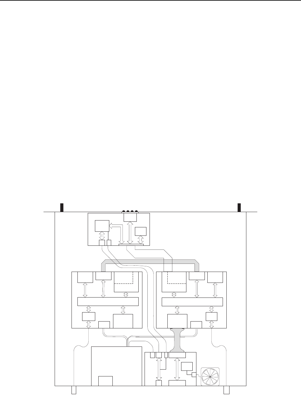
Introduction 1-1
Section 1
THEORY OF OPERATION
1.0 Introduction
The MOTOTRBO repeater consists of two MOTOTRBO mobile radios; one to act as a receiver, and
one to act as a transmitter and controller. Both of these radios contain specialized software that
allows them to function together as a repeater. The Repeater also contains a Repeater Indicator
board and a Connector board. A block diagram of the repeater is shown in Figure 1-1. The Repeater
Indicator board contains the Front-Panel LED circuitry as well as an Ethernet interface. The
Connector board is a multifunctional board that is primarily used to pass signals to and from
modules inside the chassis to the outside of the chassis.
The Repeater contains the following assemblies and sections:
•Receiver
•Transmitter
•Repeater Indicator Board
•Connector Board
•Fan
•AC/DC PSU
Figure 1-1 Repeater Block Diagram
Power Supply
RF
Rx In
Tx Control Radio
Fan
USB to
Ethernet
Interface
Display
Driver
RTC
Backup
Repeater Board
Repeater
Interface
Mobile
Accessory
Port (MAP)
Rear Connector
Rx Radio
Rx RF
Option
Board
Interface
Controller
Control Head
Interface
Control Head
Interface
Mobile Mic
Port (MMP)
Front Connector
Mobile Mic
Port (MMP)
Front Connector
DC
Power
Repeater
Interface
Mobile
Accessory
Port (MAP)
Rear Connector
Tx RF
Option
Board
Interface
Controller
DC
Power
RF
Tx Out
AC
Power
Connector Board
Fan
Control
Ethernet
Connector
MAP
Connector

1-2 Introduction
1.1 Receiver
The receiver uses a transceiver board which is based on the mobile radio's transceiver board. The
board uses the same PCB as the mobile radio board, but is populated differently to work in the
Repeater application. Only the receiver related functions of the board are utilized in this application,
even though the circuitry for transmit also exists on the board.
The Repeater receiver is identical in functionality to the mobile radio's receiver differing only in the
audio path. On the mobile radio, the decoded audio is sent to a DAC, and then to the speaker. In the
Repeater, this audio information is sent out through the SSI link to the transmit radio to be
processed. Details of the receiver theory of operation can be found in Section 3.1.
1.2 Transmitter
The transmitter consists of a transceiver board which is based on the mobile radio's transceiver
board housed in a transmit chassis. The transmit radio is identical to the receive board from a
hardware standpoint. The difference between the two is the software that is running on them, how
they are connected within the Repeater, and an additional heat sink that is mounted to the chassis.
The added heatsink and the Repeater fan allow the transmitter to be cooled sufficiently when
operating in a 60°C, full-duty cycle environment.
The transmit radio acts as the master controller for the Repeater. It handles all controller related
tasks for the Repeater, including management of the receive radio. The transmit radio is responsible
for processing the audio sent from the receive radio and repeating it out at the Tx frequency. Details
of the transmitter theory of operation can be found in Section 3.2.
1.3 Repeater Indicator Board
The Repeater Indicator board contains circuitry to drive the front panel indicator LEDs, an RTC
battery for the RTC in the transmit radio, as well as an Ethernet controller.
Figure 1-2 Repeater Indicator Board Block Diagram
All of the indicator LEDs that are on the front of the Repeater chassis reside on the Repeater
Indicator board. Each is controlled by a shift register (U6) data out signal and a digital transistor. The
shift register accepts serial data in from the transmit radio's OMAP processor via a SPI bus. A
74LVC07 buffer (U9) level shifts these signals from 3.3 V to 1.8 V.
USB to
Ethernet
Interface
Display
Driver
RTC
Backup
Ethernet to
Rear Panel
Flex to Transmit Radio
Front Panel Indicators

Introduction 1-3
The Repeater Disable LED is a dual-purpose LED that is hardware controlled initially at power-up.
As soon as VBUS power is available on the Repeater Indicator board, the hardware circuitry for the
Repeater Disable LED will cause it to blink periodically. When the software initialization is completed
by the firmware, the blink circuitry will get disabled by the firmware. At that point, the Repeater
Disable LED can be used for its intended purpose of displaying when the Repeater Disable function
is turned on.
The power LED is the only LED that is not controlled by the software. This bi-color LED gets turned
on green when the 13.8 V output from the power supply is valid. It turns on red when A/C power is
lost, and the repeater's backup battery is used.
The Real Time Clock (RTC) battery (M1) is connected to the transmit radio through the Control
Head (J1, pin 30).
Details of the Ethernet Controller can be found in Chapter 2.
1.4 Connector Board
The Connector board has two purposes: provide a place for the Repeater's MAP and Ethernet
connectors to be mounted and a location for the Repeater’s fan control circuitry.
Figure 1-3 Connector Board Block Diagram
Fan
Control
To MAP Conne ctor On
Transmit Radio
To MAP Conne ctor On
Rear Panel
To Ethernet
Conne ctor On
Rear Panel
To Power
Supply
To Fan

1-4 Introduction
1.5 Fan
The fan control logic is provided by the fan controller IC (U51). This is a device from Cypress
Semiconductor. There are basically two functions provided by the fan controller. First, it provides a
PWM output based on a temperature input, and secondly, it provides detection of fan failure based
on the fan tachometer reading.
The Repeater’s internal chassis temperature is measured with an LM50 precision temperature
sensor IC (U52). This IC outputs a voltage that is linearly proportional to temperature at 10 mV/°C,
and with an offset of +500 mV. The output voltage of the LM50 ranges from +200 mV at -30°C to
1.1 V at +60°C.
The fan controller IC (U51) controls the speed of the fan by adjusting the PWM output (pin 1) from
0% to 100%. As long as the fan continues to work, pulses are output from the fan and input to the
fan controller (pin 2).
1.6 AC/DC Power Supply
The Repeater uses the PMPN4001A switch-mode, Power Supply Unit (PSU). It is capable of 200 W
and designed for a 50 W UHF or VHF repeater system. This supply has UL, CE, and TUV regulatory
approvals and is usable in all regions by using the correct line cord. The AC input is auto-ranging
with no manual switch being specified to operate from 90 V-270 V and 47 Hz-63 Hz. It outputs a
nominal voltage of 13.8 V with a voltage tolerance of +/- 5%.
It has Power Factor Correction circuitry and is rated at 15 A across the whole operating temperature
range of -30°C to +60°C. It also has a built-in battery revert circuit with a float output available for
maintaining the charge on a battery and has UL, CE, & TUV approvals. The battery revert connector
is accessible in the back of the power supply.
The supply has over-load, over-voltage, and over-temperature protection. In an overload condition,
the PSU goes into a hiccup mode where it recovers automatically after the fault condition is
removed. During an over-voltage condition, the PSU shuts down, and will have to be re-powered on
to recover. In an over-temperature condition, the PSU also shuts down but will recover after the
temperature goes down.
The PSU is not designed to be field serviceable. If it is determined that the PSU is not functioning,
the whole unit needs to be replaced.

Repeater Interconnections and Cables 1-5
2.0 Repeater Interconnections and Cables
Figure 1-4 shows the Cable interconnections inside the Repeater.
Figure 1-4 Repeater Cabling Diagram
The details of each of these cables/interconnections are as follows:
1. Two conductor DC power cables to the transmit and receive radios.
2. Six conductor DC power cable to the connector Board. Supplies power for the fan and
Repeater Indicator board via cable 6.
3. RF Coax to connect the receive radio to the back of the Repeater. This cable has a BNC
connector on the Repeater’s rear panel.
4. RF Coax to connect the transmit radio to the back of the Repeater. This cable has an N type
connector on the Repeater’s rear panel.
5. CAT5 cable with RJ45 style connectors on both ends. This cable connects the Ethernet
controller on the Repeater Indicator board to the Repeater's back panel and provides power
from the Connector Board to the Repeater Indicator board for the LED indicators.
Power Supply
RF
Rx In
Tx Control Radio
Fan
USB to
Ethernet
Interface
Display
Driver
RTC
Backup
Repeater Board
Repeater
Interface
Mobile
Accessory
Port (MAP)
Rear Connector
Rx Radio
Rx RF
Option
Board
Interface
Controller
Control Head
Interface
Control Head
Interface
Mobile Mic
Port (MMP)
Front Connector
Mobile Mic
Port (MMP)
Front Connector
DC
Power
Repeater
Interface
Mobile
Accessory
Port (MAP)
Rear Connector
Tx RF
Option
Board
Interface
Controller
DC
Power
RF
Tx Out
AC
Power
Connector Board
Fan
Control
Ethernet
Connector
MAP
Connector
1
28
43
6
7
5
9
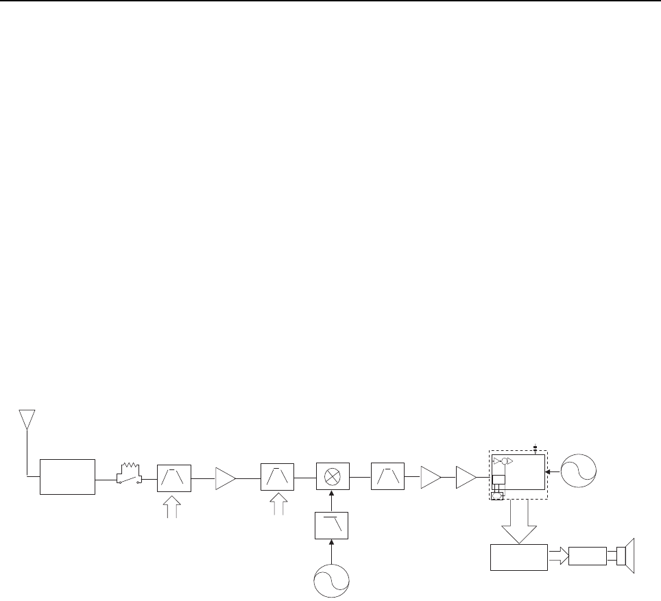
1-6 Mobile Radio’s Theory of Operation
6. Eleven conductor flex cable. Provides the SSI connection between the transmit and receive
radios. Refer to Section 1.5 for more details on this interface.
7. Thirty conductor flex cable. Provides the connection from the transmit radio to the Repeater
Indicator board and includes SPI signals to drive the LED indicators, RTC backup supply, and
the interface to the Ethernet controller.
8. Twenty six conductor cable. Provides the connection from the transmit radio's MAP to the
MAP located on the Repeater's rear panel.
9. Eight pin conductor cable. Provides Ethernet LED signals from Repeater Board and HWID
signals from Connector Board (Applicable for 32 MB repeaters only).
3.0 Mobile Radio’s Theory of Operation
The sections that follow provide a detailed theory of operation for the VHF circuits in the two
MOTOTRBO mobile radios. For details of the theory of operation and troubleshooting for the
associated Controller circuits, refer to the Controller Section of this manual.
3.1 VHF (136–174 MHz) Receiver Circuitry
The receiver is configured as a dual-conversion superheterodyne receiver, capable of both FM and
4-level FSK demodulation. The major blocks are the front-end, the mixer, Xtal filter, and the Abacus
III back-end IC. The overall block diagram is shown in Figure 1-5.
Figure 1-5 Receiver Block Diagram
3.1.1 Receiver Front-End
The front-end consists of a 2-pole varactor-tuned pre-selector filter, an LNA, a 2-pole varactor-tuned
post-selector filter, and a passive double-balanced mixer. The received signal applied to the antenna
is routed through the harmonic filter and PIN diode controlled antenna switch (D0702). A logic high
level on ANT_ENABLE configures the antenna switch for Tx operation while a logic low places the
switch in Rx mode. The insertion loss of the harmonic filter and antenna switch combined is
approximately 0.8 dB max in Rx mode with slightly more loss at the upper end of the band. From this
point, the Rx signal is routed to the Local Distance Switch (D0400/R0407), which biases on a diode
in normal operation to minimize any insertion loss. Under strong signal conditions and for improved
intermodulation protection from interfering signals, the switch can be turned on by the signal
RF_ATTEN_1, which introduces approximately 10 dB of additional path loss. Activation of the switch
can be accomplished manually by the user or left in the default setting.
T/R ANT
Switch
Hi-Speed
A/D
VCO
X
AD9864
4-Pole LIMITER/IF
AMP
STAGE
DSP
Processor
SPI
&
SSI
BU
S
Sw. 10 dB
Attenuator
10 bit
DAC
LNA
2-Pole
Varactor
Tuned
2-Pole
Varactor
Tuned
D/A
10 bit
DAC
44.85 Mhz
1
st
L.O. High
Side Injection
Fo + 44.85
MHz
SPEAKER
2
nd
L.O.
42.6 or 47.1
MHz
2nd
L.O.
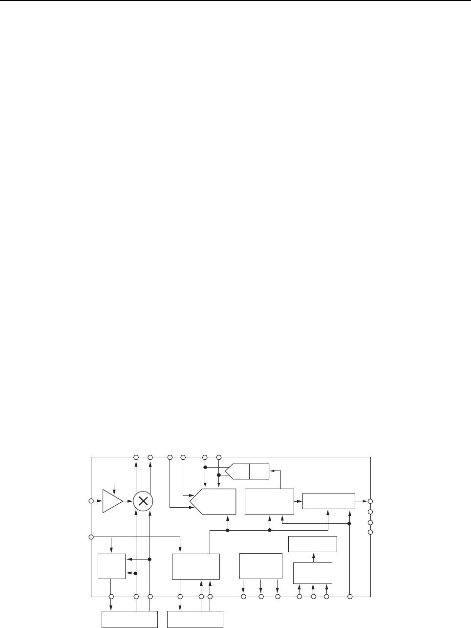
Mobile Radio’s Theory of Operation 1-7
The signal next reaches the pre-selector filter, which is a 2-pole varactor-tuned filter with 5 zeros
that are optimized to provide image frequency rejection. This filter, and the similarly designed
post-selector filter, provide over 75 dB of image response rejection. The 3 dB bandwidth for both
filters varies across the band with a minimum of 32 MHz at 136 MHz and a maximum of 38 MHz
around 174 MHz. Half-IF rejection from the filters is also frequency dependent with a minimum of
approximately 7.5 dB achieved at the worst-case frequency of 174 MHz. Both filters have variable
center frequencies that are adjusted by the FE_TUNE signal, which is derived from the output of a
10-bit DAC internal to the MAKO IC (U3200). The voltage is scaled up by a voltage doubler (Q0403)
in order to provide the required linearity for the filters. Both filters are matched to the LNA (Q0402) to
optimize the amplifier’s noise figure (2.0 dB) and to provide an LNA gain of 16 dB to the signal. The
combined gain of the filters and LNA is about 14 dB. Active bias transistor Q0401 maintains the
collector current of Q0402 constant at 25 mA. The LNA, active bias circuit, Local Distance Switch,
and voltage doubler are all supplied by 9R1_FILT, which is derived from 9R1 after filtering.
Following the post-selector filter is the Class 2, double-balanced mixer. It is comprised of baluns
T0400 and T0401 and diode ring mixer D0405. Injection amplifier Q0405 provides 15 dB of gain to
the Rx VCO injection signal. Another amplifier, Q0202, located in the VCO block, also provides gain
for the LO signal and isolation from high RF signals entering the mixer. The signal applied to the LO
port of the mixer is +16 dBm minimum after passing through the 3-pole/1-zero, low-pass injection
filter. The LO injection is high-side and mixes the signal down to an IF frequency of 44.85 MHz. The
output of the mixer is connected to a diplexer network, which terminates out-of-band frequencies
into 51 ohms (R0427) while appearing as high impedance to the 44.85 MHz IF signal.
3.1.2 Receiver Back-End
The signal entering the back-end is matched to 4-pole crystal filter, FL0500, by C0507 and L0503.
The filter is centered at 44.85 MHz with a 3 dB bandwidth of 13.4 kHz. IF amplifiers Q0500 and
Q0501 follow the crystal filter and provide both amplification and limiting to the signal. An overall
gain of 24 dB is available from the composite IF amplifier to lower-level IF signals. As the signal level
increases, Q0501 begins to limit and eventually saturates out at approximately –16 dBm. The
purpose of the limiting is to provide protection to the AD9864 Abacus III back-end IC (U0600). An
internal 16 dB attenuator is also engaged to provide attenuation to the Abacus’s input signal,
working with the external amplifier to limit the signal below the ADC clip point. The block diagram for
the AD9864 is shown in Figure 1-6 below. At IF levels exceeding –26 dBm into U0600, the 2nd LO
synthesizer internal to U0600 can be pulled, causing corruption of the I/Q data being delivered to the
DSP.
Figure 1-6 AD9864 Block Diagram
MXOP
-16dB
IFIN
FREF
IOUTL CLKP CLKN VREFP VCM VREFN PE
DOUTA
DOUTB
PC PDLOP LON IOUTC
MXON IF2P IF2N GCP GCN
FS
CLKOUT
AD9864
LNA
LO
SYN
LO VCO AND
LOOP FILTER LOOP FILTER
CLK SYN VOLTAGE
REFERENCE SPI
CONTROL LOGIC
FORMATTING/SSI
DECIMATION
FILTER
Σ-Δ ADC
AGC
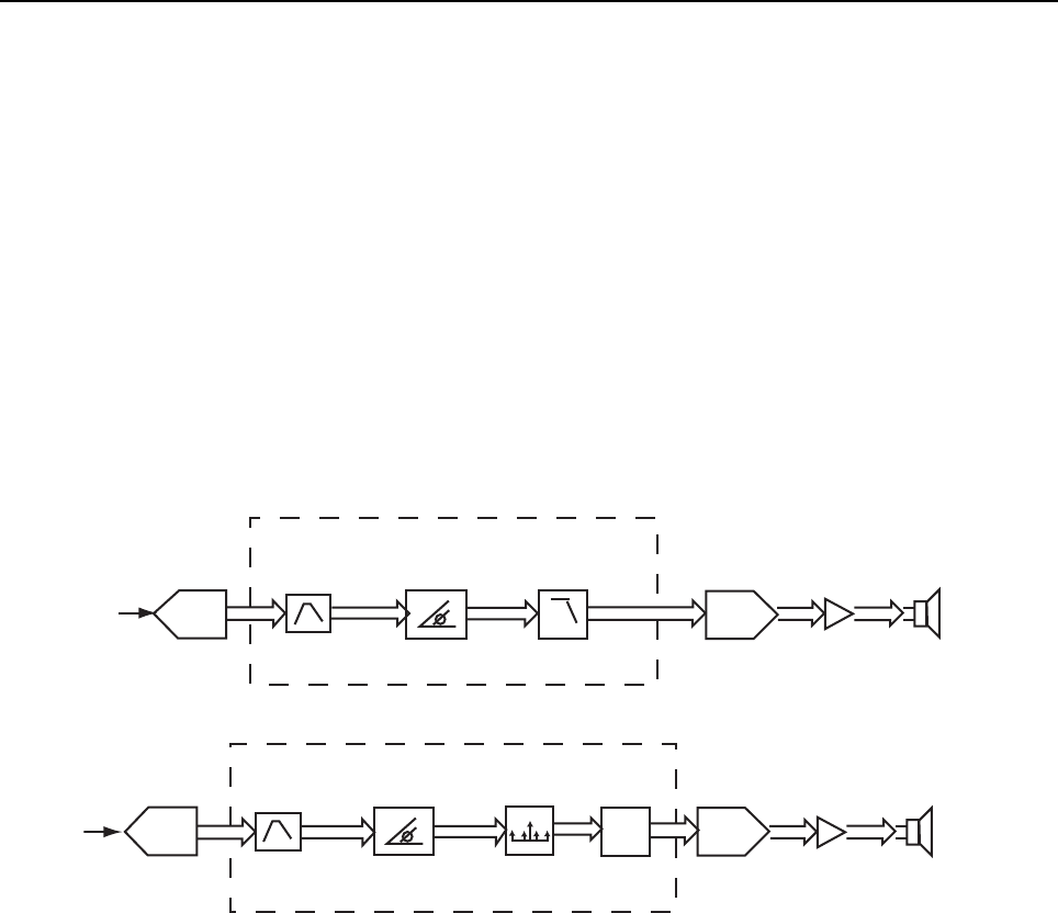
1-8 Mobile Radio’s Theory of Operation
The Abacus III accepts the 44.85 MHz signal, processes it, and sends out baseband I/Q data in 16-
bit format to the DSP at a 20 kHz rate. Internal to the Abacus III is an LNA and 16 dB FE attenuator,
an internal integer-N synthesizer used to control the external 2nd LO VCO, a Sigma-Delta ADC and
decimation filter, and control and formatting logic for outputting the baseband I/Q data. External to
U0600 is the 2nd LO VCO with active device Q0600 and its associated circuitry including the loop
filter consisting of C0613, C0618, and R0603. The 2nd LO mixes the 44.85 MHz IF signal down to
2.25 MHz before being input to the ADC where it is sampled. The tank circuit (L0608, C0605,
C0642, R0617) and varactor (D0601) for the internal clock synthesizer, work with the loop filter
(R0618, C0643, C0646) to provide the 18 MHz clocking signal to the internal ADC, decimation filter,
and SSI formatting circuitry. A 3 Volt regulator (U0601) provides a clean 3 Volt supply to U0600.
Transistor Q0601 is configured as a super filter to provide the 2nd LO transistor with a low noise
supply. The reference clock for U0600 is 16.8_REF, which is a buffered (Q0100) 16.8 MHz clock
from the synthesizer block.
Shown below in Figure 1-7, is the block diagram of the signal flow through the receiver back-end. All
the blocks within the dotted box represent the DSP software algorithms internal to U1000.
Figure 1-7 Signal Flow through Receiver Back-End
The DSP takes the incoming 20 kHz data-stream and passes the information through an FIR (Finite
Impulse Response) filter, which provides rejection from any in-band adjacent channel interference.
The remaining filter data is then sent through a decimation process further reducing its frequency to
8 kHz.
Depending on whether the repeater is in Analog or Digital mode determines the kind of signal
processing used. If the radio is in Analog mode, the remaining 8 kHz data is sent through the FM
Discriminator and De-emphasis subroutines in the DSP code. If the repeater is in Digital mode, the
remaining 8 kHz data is still sent through the FM Discriminator but an additional "Symbol Recovery"
routine is applied along with a standard AMBE+2™ Vocoder process. The resultant audio (still
represented by high-speed data) is sent to a DAC (U3200), which drives several gain stages. These
gain stages consist of an I2C audio attenuator (U3501) and a high-power audio PA (U3500)
providing the user with at least 3 Watts of power through the internal speaker.
44.85
MHz
IF
44.85
MHz
IF
AD9864 Hi
SPEED
ADC
AD9864 Hi
SPEED
ADC
FIR
DSP ANALOG FM MODE
DSP DIGITAL 4FSK MODE
FIR
FM
DISCRIMINATOR
FM
DISCRIMINATOR
DEEMPHASIS
DAC
DAC
AMBE+2
VOCODER
4-FSK
SYMBOL
RECOVERY ANALOG AUDIO
GAIN STAGES
ANALOG AUDIO
GAIN STAGES
SPEAKER
SPEAKER
TM
ΣΔ
ΣΔ

Mobile Radio’s Theory of Operation 1-9
3.2 VHF (136–174 MHz) Transmitter Circuitry – 45 Watt
The Transmitter consists of the power amplifier circuitry and the power control circuitry. The power
amplifier is responsible for delivering a faithful replica of the VCO output amplified up to the desired
output power level, free from distortion. The power control circuitry is responsible for ensuring that
the desired output power level is maintained in both analog and digital modes, as well as protecting
the power amplifier from damage due to heat, antenna mismatch, out-of-range battery voltage, or
mis-assembly.
Figure 1-8 VHF 45 Watt High-Power Transmitter Detailed Block Diagram
3.2.1 Power Amplifier
The radio’s 45 Watt power amplifier (PA) is a 4-stage amplifier, which amplifies the output of the
VCO to the required transmit power level. The first stage is an LDMOS (Lateral Diffuse MOS)
50 ohm fixed-gain block (ADA-4743, U0700), followed by the adjustable gain LDMOS pre-driver
(RD01MUS1, Q0705), an adjustable gain LDMOS driver (RD07MVS1, Q0703), and the fixed-gain
LDMOS final device (MRF1550, Q0702). A transmit/receive (T/R) switch and a harmonic filter
complete the transmit lineup.
3.2.2 Input Stage (50 Ohm Fixed-Gain Block)
The first stage (ADA-4743, U0700) is an integrated circuit with internally matched 50 ohm input and
output stages providing approximately 16.5 dB power gain. Its purpose is to provide reverse
isolation between the PA and the VCO to lessen the risk of VCO load pull and to provide appropriate
power to the pre-driver stage. The ADA-4743 is biased at 27 mA during transmit by R0706, which is
switched to 9V3 during Tx by Q0701 (controlled by Antenna_En). The ADA-4743 is preceded by a
19 dB resistive pad to further improve reverse isolation.
T/ R
Switch
Harmonic
Filter
Agil ent
ADA4743
TX_DAC
Active
Reconstruction
Filter
Log Amp Controller
V_CONTROL
SW_9V1
9V3
+5V Regulator
PA_ ENABLE
-
5 dBm
(nominal)
TX_INJ
INPUT
FROM
VCO
ANT_ENABLE
9V3_TX 9V3_TX
SW_9V1
Reflected
Port
Microstrip
Dual
Directional
Coupler
Forward
Port
+
TX Port
RX Port
To FE
Matc
h
Matc
h
A+
Voltage
Controlled
Variable
Attenuator
Thermal
Cutback
AD
I831
5
VAPC RF
IN
VPOS
ENB
L
COM
M
FLTR
VSET
VCONT
VI
N+5 VOUT
Pad
To Pressure
Pad Switch
To Pressure
Pad Switch To Pressure
Pad Switch
9V3
Pressure
Pad C loses
Switch
To Predr iver
To Driver
To Final
9V3_TX
LDMOS
Predriver
RD01MUS1
LDMOS
Driver
RD07MVS1
ANT_ENABLE
Pressure
Pad
Switch
Match
Match
FINAL_BIAS
CW/4 FSK
+7dBm

1-10 Mobile Radio’s Theory of Operation
3.2.3 Pre-Driver Stage
The next stage is a low power LDMOS device (RD01MUS1, Q0705), which delivers up to +27 dBm
power to the driver stage. Its gain is controlled by varying the gate bias voltage and varies from low
gain up to approximately 14 dB power gain. The gate bias voltage is controlled with the V_cont
signal and is controlled in parallel with the driver stage gain.
The input match to this stage is a high-pass topology comprised of L0716, L0718, and C0795.
(High-pass matches are used where appropriate to minimize the chances of low frequency
regeneration within the amplifier.) The inter-stage match between the pre-driver and driver stages is
comprised of C0790, C0786, C0791, C0792, L0717, and L0719 arranged in a high-pass topology.
Additional footprints are provided on the printed circuit board to allow for possible engineering
optimizations to this match. These are non-populated parts C0793, C0794, C0817, C0820, and
C0821.
3.2.4 Driver Stage
The next stage is a medium-power LDMOS device (RD07MVS1, Q0703), which delivers up to +38
dBm to the final device. Its gain is controlled by varying the gate bias voltage and varies from low
gain up to approximately 10 dB power gain. The gate bias voltage is controlled with the V_cont
signal and is controlled in parallel with the pre-driver stage gain.
R0718, R0720, R0754, and R0755 are required to improve the bandwidth of the driver stage. The
inter-stage match between the driver and final device is comprised of C0819, C0746, C0752,
C0754, L0745, and associated micro-strips on the PCB. Additional footprints are provided on the
printed circuit board to allow for possible engineering optimizations to this match. These are
non-populated parts C0753 and C0755.
3.2.5 Final Stage
The final stage is a high-power LDMOS device (MRF1550, Q0702). The package is mounted to a
copper carrier to improve thermal conductivity to the chassis and also to more tightly control the RF
load, allowing higher and more consistent maximum output power. This stage is biased at a
quiescent current of 500 mA and operates with a fixed gain of approximately 14 dB, allowing the
radio to be set to a maximum output power of 54 Watts. The quiescent current is set by adjusting the
Final_Bias signal.
The output match consists of C0719, C0720, C0721,C0722, C0726, C0727, C0729, C0741, and
L0714 and the associated microstrip line on the PCB. The output matching circuitry of this stage has
extremely critical part location requirements. Any repairs must be done with care to ensure the
replaced components are placed accurately and properly soldered. Of particular concern are the
output matching capacitors, C0719, C0720, C0721, C0722, C0726, C0727, and C0729. The
resistor networks at the input of each of the final elements are required to improve the bandwidth of
the circuit. These resistors are R0712, R0716, R0717, R0719, R0721, R0726, R0732, R0733,
R0734, R0736, R0737, and R0739.
Additional footprints are provided on the printed circuit board to allow for possible engineering
optimizations to this match. These are non-populated parts C0724, C0725, and C0730. If the final
device is replaced, the bias voltage must be re-tuned using the Customer Programming Software
(CPS). Care must be taken not to damage the device by exceeding the maximum allowed quiescent
current. The maximum allowable current is 750 mA, but the design is optimized for 500 mA as noted
earlier. The device can tolerate up to 5 Amps for brief periods of time without damage.

Mobile Radio’s Theory of Operation 1-11
3.2.6 Antenna Switch
The Antenna Switch (T/R switch) has two modes of operation, transmit and receive.
Transmit mode:
The antenna switch utilizes the existing dc feed (A+) to the final stage device (Q0702). Both PIN
diodes, D0700 and D0702, are turned on during key-up by forward biasing them. Forward biasing is
achieved by pulling down the voltage at the cathode end of D0702 to around 12.2 Volts (0.7 Volt
drop across each diode). Q0704 is configured as a current sink that maintains the current through
the antenna switch diodes at 100 mA, as set by VR0700 and R0738. The current sink is enabled
during transmit mode by ANT_ENABLE asserting thru Q0706 and associated circuitry. When the
PIN diodes are conducting, an RF ground is formed at the anode of the lower PIN diode D0702,
which places the series L0710 and L0724 in parallel with C0803. The values of L0710, L0724, and
C0803 are chosen so that they are in parallel resonance at the center of the transmit band, making
them appear as an open-circuit so that a 50 ohm power path is maintained thru the top PIN diode to
the harmonic filter. To further attenuate the Tx signal from getting to the Rx front-end, a PIN diode
pair (D0703) is placed in the Rx path separated from the D0702 short by a quarter wave inductor
(L0730 & L0731). This diode pair shorts to ground in transmit mode so that the receiver sees as
little transmitter power as possible.
Receive mode:
The DC current thru the PIN diodes is interrupted by turning off the current sink. The RF path now
flows from the Harmonic Filter thru the matching circuit formed by C0803, L0710, and L0724, then to
pi network C0766, L0730, L0731, and C0772. The additional shunt diodes (D0703) will be high
impedance since no bias current is flowing from the switched Tx power line.
3.2.7 Harmonic Filter
Inductors L0720, L0721, L0706, L0707, L0708, L0709, L0722, and L0723, and capacitors C0742,
C0739, C0740, C0735, and C0750, form a harmonic filter which is a 7th order low-pass filter with
two notches; this is used to attenuate harmonic energy from the transmitter before it reaches the
antenna. The harmonic filter also prevents high-level RF signals above the receiver passband from
reaching the receiver circuits, improving spurious response rejection. R0713 and L0728 are used to
drain any electrostatic charges that might otherwise build up on the antenna.
3.2.8 Directional Coupler
The dual directional microstrip coupler is implemented at the harmonic filter output to sample both
forward and reverse directed transmitter power. RF power from the transmitter PA passes through
the microstrip coupler before reaching the antenna. Forward RF power is coupled to the U0940 log
detector / controller via the voltage controlled attenuator (VCA) stage consisting of pin diodes
D0901, D0902, and D0903. The log detector/controller regulates the gain of PA stages Q0703 and
Q0705 (via V_cont) as necessary, thus ensuring that the forward power out of the radio is held to a
constant value.
The directional coupler functions not only as part of the transmitter power regulation circuit but also
as part of the VSWR load detection circuitry. Its physical location close to the antenna connector
allows accurate VSWR sense at the transmitter output. Forward and reverse coupled signals are
rectified by D0904 and D0905, respectively. Resulting DC voltage FWD_DETECTED is proportional
to RF power while REV_DETECTED is proportional to reflected RF power. The detected voltages
are fed to the respective inputs of difference amplifier U0901. The difference amplifier output is
applied to variable attenuator control stage U0900-1.

1-12 Mobile Radio’s Theory of Operation
An abnormally high reflected power level, such as may be caused by a damaged antenna, also
causes an increase in the difference amplifier output voltage. An increased difference amplifier
output causes a reduction in attenuation by the VCA. As a result, the increased RF signal applied to
the log detector/controller causes the controller to reduce the gain of PA stages Q0703 and Q0705.
Transmitter power is thus reduced to prevent damage to the final device due to an improper load.
3.2.9 Power Control
The transmitter uses PA controller IC, U0940, to control the power output of the radio. A portion of
the forward RF power from the transmitter is sampled by the directional coupler and delivered via
the VCA to the RFIN port of the PA controller IC (pin 1). The PA controller, a log detector type,
provides temperature-stable, high accuracy control over a typical 50 dB dynamic range.
The MAKO IC contains a digital-to-analog converter (DAC), which provides a reference voltage
(TX_DAC) at the input of reconstruction filter stage U0900-2. The filtered reference voltage at the
output of U0900-2 is divided by the combination of R0942 and R0946 before reaching the VSET
input of the PA controller IC (pin 3). Thermistor RT0953 is used in combination with R0954 to
compensate reference voltage drift at operating temperature extremes. Reference voltage level is
programmable through the SPI lines of the MAKO. This reference voltage is proportional to the
desired power setting of the transmitter, and is factory programmed at several points across the
frequency range of the transmitter to offset frequency response variations of the transmitter's
coupled power circuits.
The PA controller IC provides a DC output voltage at pin 7 (VAPC), which is divided to provide gate
bias for PA pre-driver and driver stages. The 0 to 5 VDC range at U0940 pin 7, is applied as
V_CONTROL to power-adjust the transmitter by controlling the gate bias of stages Q0703 and
Q0705. Voltage divider combination R0727 and R0728 provide gate bias to Q0703 while divider
combination R0750 and R0751 provide gate bias to Q0705. This adjusts the transmitter power
output to the intended value. The ratios of each of these resistor dividers are chosen to ensure that
Q0703 and Q0705 are both running at their nominal design condition at rated output power.
Variations in sampled forward transmitter power cause the PA controller IC to adjust the control
voltage above or below its nominal value to raise or lower output power in order to maintain
transmitter output power relative to the reference voltage applied to VSET.
3.2.10 Power Ramp Profile Control
In order to limit transient adjacent channel power at the transmitter's output, the ramped power
should follow a raised-cosine profile. The PA controller IC has a linear slope function when scaled in
dB/V. To achieve the desired raised-cosine profile of the output power, the ramped reference voltage
provided by the MAKO DAC follows a raised-cosine approximation. The MAKO DAC reference
output is low-pass filtered by the DAC reconstruction filter before it is applied to the VSET input of
the PA controller IC. Reconstruction filtering reduces spurious emissions in the RF spectrum as a
result of the finite steps of the DAC. Loop filter capacitor C0926, in conjunction with resistor R0950
and the integrator within the PA controller IC, control the loop dynamics. Loop dynamics have been
optimized to achieve sufficient speed to follow the required ramping profiles while meeting switching
transient requirements over varied power levels. Accurate control of the power-rise (ramp-up) and
power-decay (ramp-down) characteristics minimizes splatter into adjacent channels.

Mobile Radio’s Theory of Operation 1-13
3.2.11 Thermal Protection
Thermistor RT0908 and R0902 form a voltage divider with the output proportional to the sensed
circuit board temperature in the vicinity of the transmitter driver and final devices. The voltage
divider output is routed to operational amplifier U0901-2, which provides a dc voltage via diode
junction D0900 to control the attenuation level of the VCA stage. For the condition that the
temperature threshold set by resistive divider combination R0901 and R0909 is reached, the VCA is
driven to increase the RFIN signal at the PA controller IC (pin 1). This increase will cause the PA
controller IC to adjust the PA control voltage below its nominal value to decrease transmitter output
power. The temperature will be reduced by lowering transmitter output power relative to the
reference voltage applied to VSET.
3.2.12 Out-of-Range Battery Protection
Transmitter power cutback, under extended battery supply voltage operation, is provided for by
monitoring the battery supply in the controller circuit of the radio in order to change the VSET input
of the PA controller IC (pin 3) for reduced transmitter output. This cutback starts when the battery
voltage at the connector is 15.3 Volts or greater and has a 2 dB/V slope. In addition, a second low
battery detect circuit is implemented in hardware. This hardware cutback forces a 1.2 dB drop in RF
power level when the battery voltage drops below 11.6 Volts and exhibits about 0.6 Volts of
hysteresis before returning to normal power.
3.2.13 Pressure Pad Switch
The power control circuitry includes a safety switch (S0700) that consists of a conductive portion of
the rubber pad which pushes the RF final transistor Q0702 against the chassis. When the chassis
cover and rubber pad are properly assembled, the conductive portion of the pad contacts a pattern
on the circuit board, electrically closing switch S0700. If the cover and pad are not in place, switch
S0700 is open-circuited and the power control circuit is disabled, turning off the gate bias to Q0702,
Q0703, and Q0705. This prevents thermal damage of the RF transistors which might occur if the
transmitter is operated without adequate heat sinking.
3.3 Frequency Generation Circuitry
The synthesizer subsystem consists of the reference oscillator (Y0100), the fractional-N Synthesizer
IC (Tomahawk II, U0100), and the Voltage Controlled Oscillator VCO.
3.3.1 Reference Oscillator
The reference oscillator (Y0100) contains a temperature compensated crystal oscillator with a
frequency of 16.8 MHz. A digital-to-analog (DAC) converter internal to U0100 (Tomahawk) and
controlled by the microprocessor via serial interface (SPI), sets the voltage at the AUX_DAC output
of U0100 (pin H6) to set the frequency of the oscillator. The output of the oscillator (pin 3 of Y0100)
is applied to pin K5 (XOSC_BASE) of U0100.
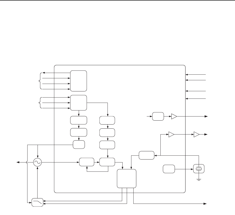
1-14 Mobile Radio’s Theory of Operation
3.3.2 Fractional-N Synthesizer
The Tomahawk II Synthesizer IC (U0100) consists of a pre-scaler, a programmable divider and
divider control logic, phase detector, charge pump, a D/A converter in the high frequency analog
modulation path, an attenuator to balance the high and low frequency modulation paths, a serial
interface for control (SPI), a serial interface for modulation (SSI), and a super filter for the regulated
2.45 Volts.
Figure 1-9 VHF Synthesizer Block Diagram
A voltage of 2.775 Volts applied to the super filter input (U0100 pin J4) supplies an output voltage of
2.45 VDC (SF_OUT) at pin K4. This supplies the VCO and the VCO modulation bias circuit (via
R0321). The super filter supply voltage is provided by the 2.775 Volt regulator within U3200. The
synthesizer is also supplied by the 5 Volt regulator, U3002, another 2.775 Volt regulator within
U3200, and a 1.875 Volt regulator within U3200.
The output signal LOCK (U0100-D7) provides information about the lock status of the synthesizer
loop. A high level at this output indicates a stable loop. A discrete buffer amplifier (Q0100) provides
a buffered 16.8 MHz reference frequency to other parts of the radio.
The serial programming interface (SPI) is connected to the microprocessor via the data lines
SPI_DW (U0100-D9) and SPI_DR (U0100-D10), clock line SPI_CLK (U0100-C11), and chip enable
line CEX (U0100-D8). The serial modulation interface (SSI) is connected to the DSP via the data
line SDTX (U0100-F11), clock line TXCLK (U0100-F10), and frame sync line SFTX (U0100-F9).
SPI
Interface
Data Write
Clock
CEX
Data
Fsync
Clock
SPI
SSI
(Modulation )
Prescaler Main Di vider
VCO
Fracti onal
Unit
DS
18 - bit
Modulation
Unit
Main
Phase/ Freq.
Detector
And
Charge Pumps
Reference
Divider
TCXO
(16 .8 M H z)
AUX
D/ A
Main _CP LOCK DETECT
Buffer Buffer
16 .8M H z REF
Loop Filter
5V
2.775V Dig
2.775 V A na
1.875V Dig
TOMAHAWK II
Fractional -N
Synthesizer
(U0100)
D9
Data ReadD10
C11
D8
F11
F10
F9
J2
G3
Adapt _CP
H1 D7
SF _OUT
Super
Filter
2 .775 V Ana K4
H6
J11
K5
H2,J3
A7
A5,A10,B2,B9,
G2 ,J4 ,J6, J10,
K2,L6
B7 ,E11, G10 ,J1
Digital
Attenuator
SSI
Interface
D/A
Waveform
Gener ator
K8 HP MOD
PRSC
TX / LO
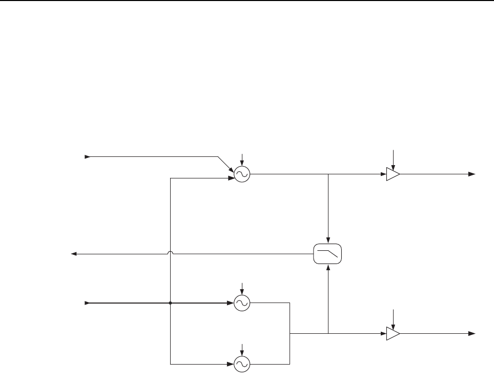
Mobile Radio’s Theory of Operation 1-15
3.3.3 Voltage Controlled Oscillator (VCO)
The Voltage Controlled Oscillator (VCO) subsystem consists of three Colpitts oscillators (two Rx and
one Tx), a single-stage Tx buffer amplifier, a single-stage Rx buffer amplifier, oscillator bias control
switches, and the modulation circuitry.
Figure 1-10 VHF VCO Block Diagram
The VHF Rx VCO design incorporates two varactor-tunable Colpitts oscillators. Each Rx oscillator
has a tuning range of 19 MHz, sufficient to cover the Rx frequency range of 180.85 MHz to 218.85
MHz. A single Tx oscillator covers the frequency range of 136 MHz to 174 MHz. The oscillators
resonate at fundamental operating frequencies. Three (active-low logic) general purpose output
lines (GPO1, GPO3, and GPO6) from the Tomahawk IC (U0100-B4, E5, and H8) provide the control
for independent bias selection to each oscillator (VCO_SEL) via the PNP transistor switches U0304
and U0201. The 2.45 Volt super filtered output, SF_OUT of the Tomahawk IC (U0100-K4), supplies
the bias to the oscillators. A portion of the VCO output signal is lightly coupled through coupling
capacitors C0331 and C0231, routed through a low-pass filter (formed by L0221, C0235, L0230,
C0265, and C0233), and fed back to the M_PRSC input of the Tomahawk IC (U0100-J2).
High-port modulation is scaled through a voltage divider (comprised of R0319, R0320, and R0321)
and applied to the Tx modulation varactor diode CR0300. The Tx VCO frequency is modulated via
coupling capacitor C0310.
TX VCO 1
RX VCO 1
RX VCO 2
TX Buffer Amp
RX Buffer Amp
Low Pass
Filter
TX INJ
RX INJ
To U0700
To Q0405
Steering Line Voltage
(VCTRL)
9V3 _VC O
( U3001 -5 )
9R1
(Q0107 )
RX_VCO_SEL 2
(U0100 - H8 )
RX_VCO_SEL 1
(U0100 -B4)
TX_VCO_SEL 1
(U0100 -E 5)
High Port Modulation
(HP_MOD_OUT)
(U0100 -K8)
Prescaler
( U0100 -J2 )
VHF VCO
Subsystem

1-16 Mobile Radio’s Theory of Operation
A discrete single-stage Tx buffer amplifier (comprised of the NPN transistor Q0302 and surrounding
components) amplifies the signal from the Tx oscillator to the level required by the first stage of the
Transmitter Power Amplifier (U0700). The Tx buffer amplifier also provides sufficient isolation from
any undesired load-pulling from the Transmitter Power Amplifier. The bias for Q0302 is provided by
the 9.3 Volt regulator U3001.
A discrete single-stage Rx buffer amplifier (comprised of the NPN transistor Q0202 and surrounding
components) amplifies the signal from the Rx oscillator to the level required by the LO injection
amplifier (Q0405). The Rx buffer amplifier also provides sufficient isolation from any undesired
load-pulling from high input levels in the receiver front-end. GPO4 from the Tomahawk IC
(U0100-D4) controls the transistor switch (comprised of Q0108 and Q0107), that enables the 9.1
Volt bias to Q0202 (via the 9.3 Volt regulator U3001).
3.3.4 Synthesizer Operation
The complete synthesizer subsystem is comprised mainly of the Tomahawk Synthesizer IC,
Reference Oscillator (crystal oscillator with temperature compensation), loop filter circuitry, VCO,
and DC supplies. The VCO feedback signal, PRSC, is fed to pin J2 of U0100 (M_PRSC) via a
low-pass filter (L0221, C0235, L0230, C0265 and C0233) which attenuates harmonics and provides
the correct level to close the phase-locked loop.
The prescaler in the Synthesizer IC (U0100) is a four-level prescaler capable of dividing by 4, 5, 6,
and 7. The main loop N divider is configured to be an 8-bit divider. The divide-by-N portion of the
main loop is set via the SPI. The fractional portion of the divider is realized using a 3-accumulator,
24-bit fractional divider. The SPI is used to set the desired divide ratio.
The output of the prescaler is applied to the main loop divider. The output of the main divider is sent
to the phase/frequency detector, which compares the main divider’s output signal with the reference
signal. The reference signal is generated by dividing down the signal of the reference oscillator
(Y0100). The output signal of the phase/frequency detector is a pulsed signal which is routed to the
charge pumps. The main charge pump current is programmable through the SPI with its output at
pin G3 of U0100 (MN_CP). The loop filter transforms this current into a steering voltage that is
applied to the VCO.
To reduce lock time when new frequency data has been loaded into the synthesizer, an adapt
charge pump, providing much greater current than the main charge pump, is turned on for a finite
amount of time to quickly charge or discharge the loop filter capacitors to steer the VCO to the
desired frequency. The output of the adapt charge pump passes to the loop filter via pin H1 of
U0100 (MN_ADAPT_CP). When the synthesizer is within the lock range and the adapt timer runs
out, the adapt charge pump is powered down and the main charge pump takes over. A settled
synthesizer loop is indicated by a high level at signal LOCK (U0100-D7), which is routed to the
microprocessor. Q0102 is configured as a current source to provide a steady 1.5 mA during the
adapt period. U0101 is an analog switch that opens the adapt path slightly before the end of the
adapt period to prevent the current from the current source from pushing the VCO off frequency.

Mobile Radio’s Theory of Operation 1-17
Modulation is performed by applying a digital data stream via the SSI bus from the DSP (U1000) to
the synthesizer (U0100). In order to meet spurious and phase noise requirements, the PLL
bandwidth was designed to be narrower than the full modulation bandwidth, therefore requiring the
use of dual-port modulation. Internal to the synthesizer (U0100), low-port modulation is added to the
fractional-N division numerator to trace out the modulation versus time while the high-port data
stream passes through an interpolating waveform generator, a digital attenuator (for modulation
balancing), and then is converted to an analog signal through a 10-bit DAC before modulating the
VCO. This high-port analog modulation output (HP_MOD_OUT, U0100-K8) is connected to the
VCO modulation varactor diode (CR0300) via C0360 and R0319.

1-18 Mobile Radio’s Theory of Operation
Notes

2-1
Section 2
TROUBLESHOOTING CHARTS
1.0 Troubleshooting Flow Chart for Receiver (Sheet 1 of 3)
Set up radio in Analog
Receive mode on
desired channel
with Squelch open
1st LO
> +2 dBm
at R0422?
No
Audio Tone
present
at Speaker?
Yes
Volume
level
adjusted
properly?
Check U3501
bias and
replace part if
necessary
Audio at pin 1
of U3501?
Verify audio path to
U3501
B
Audio at pin 10
of U3501?
Check connections to
external speaker and
replace speaker if
necessary
Verify audio path
between U3500 and
pin 1 of U3501
Audio at pin 4
of U3500?
Audio at pin 1
of U3500?
Check biasing
before replacing
U3500
1st LO
(180.925 MHz)
> +16 dBm
at TP0401?
Check biasing on
Q0405 before replacing
9 VDC
present
at R0417?
Check
9R1 path back to
Synthesizer
Check VCO
Troubleshooting
Flow Chart
RF level
of on-channel
signal > -45 dBm
on pin 4
of T0401?
A
Check T0400 and D0405
and replace if necessary
Yes
Yes
Yes Yes
No
No
No
Yes
Yes
No
No
No
Yes
Yes
No
No
No
Yes
Yes
NO RX AUDIO
No
Spray or inject 44.85 MHz
RF carrier modulated with
1 kHz Audio Tone into XTAL
Filter FL0500
Setup repeater to receive at
136.075 MHz with the RX brick
open and connected to the
system.
Apply an on-channel
RF carrier at -47 dBm modulated
with 1 kHz tone
at the RX antenna port.
Audio at pin 6
of U3505?
All Troubleshooting within
the dotted line is done on
the TX Brick
2-2 Troubleshooting Flow Chart for Receiver
1.1 Troubleshooting Flow Chart for Receiver (Sheet 2 of 3)
A
Voltage level
> 2.7 VDC
on D0401?
+9.0 VDC
on pin 4
of Q0403?
Check circuitry around
D0401 and D0403 for shorts
and opens
Check biasing on
Q0403 before replacing
Check biasing circuitry of
Q0401 and Q0402 before
replacing
RF level
of on-channel
Signal > -45 dBm
at C0420?
Is voltage
at R0409
= 0.7 VDC?
Voltage
< 0.5 VDC
at pin 2
of Q0400?
Check biasing
circuitry of
Q0400 before
replacing
Check biasing circuitry of
Q0402 before replacing
No
Yes
No
No No
No No
Yes
Yes
Yes
Yes
Yes
Check Synthesizer
Troubleshooting
Flow Chart
~ 6.8 VDC at
L0400/D0400?
Check D0403 and associated
capacitors for opens and shorts
and replace if necessary
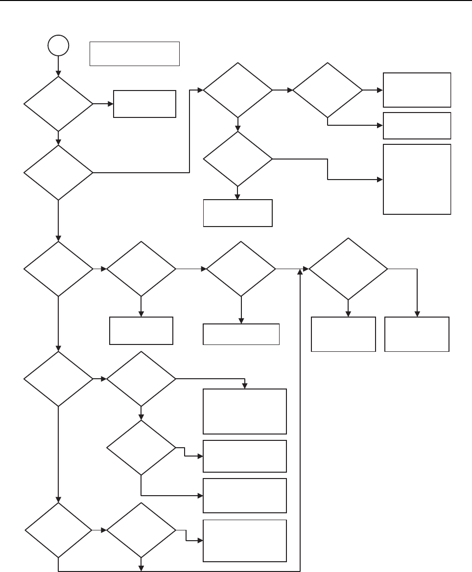
Troubleshooting Flow Chart for Receiver 2-3
1.2 Troubleshooting Flow Chart for Receiver (Sheet 3 of 3)
B
16.8 MHz
present
at C0622?
Check Synthesizer
Troubleshooting
Flow Chart
2nd LO
> 0 dBm and
at 42.6 MHz
at TP0600?
Yes
No
No
Yes
44.85 MHz
present
at TP0602?
2.25 MHz
present
at C0625?
No
Yes
No
Yes
18 MHz
present
at L0608?
Check diode
continuity before
replacing D0601
Replace components
as needed
No No
Yes Yes No
Yes
Check for visible
solder shorts near
pins before replacing
U0600
~ 1.65 VDC
on R0617?
Clock
VCO and LF
components
OK?
DC continuity
through
biasing components
E0600 - E0610?
Replace
defective biasing
component
Yes
No
3.0 VDC
on pin 1
of U0601?
Check Controller
Troubleshooting
Flow Chart
5.0 VDC
at E0610?
Check biasing on
U0601 before
replacing
Yes Yes
3.5 VDC
at E0609?
No
No No
Yes
Check biasing on
Q0601 before
replacing
Remove Shield
SH0500.
Check biasing on
Q0600 and
check continuity
on D0600.
Replace parts if
necessary.
Check 5 VDC supply and
biasing components
before replacing
Q0500 or Q0501
Biasing
correct on
Q0500 and
Q0501?
~ 3.0 VDC
on L0604
and L0605?
Check biasing
components and 3 VDC
supply. Replace
any parts if necessary.
No
Yes
No
Yes
Check FL0500 matching
components before
replacing
44.85 MHz
present
at pin 6 of
FL0500?
Check signal gain
and biasing
before replacing
Q0500 or Q0501
No
Yes
All Troubleshooting on this
page is done on the RX Brick

2-4 Troubleshooting Flow Chart for 45W Transmitter
2.0 Troubleshooting Flow Chart for 45W Transmitter
Place Switch or R0775
Check 9V3_PA Regulator in
Controller Troubleshooting
Flow Chart
Is Voltage at
TP0910 >
1 VDC?
Check Bias Set Circuit;
bias tune
Replace U0700
Check VCO Troubleshooting
Flow Chart
Is TP0909
>1 VDC?
NO TRANSMITTER
POWER
Check Q0705 and
associated circuitry
Check 9.3 V Regulator
circuit Check T/R bias circuit
Check 5 V Regulator
circuit
Replace Q0702
Check MAKO
Troubleshooting Flow Chart
Check U0900-2 and
associated circuitry
Replace U0940
Does
TP0702 =
9.3 VDC?
Is TP0913
= 9.1 VDC?
Is U0941
Pin1 =
5 VDC?
Is voltage at TP
TX_RAMP_DAC
in controller > 3
VDC?
Is D0702
~12.4 VDC?
is TP0707
~2.2 VDC?
Is Pressure
Pad Switch
in place?
Is Power at
TP0704 ~ +4
dBm?
Is TP0703
-11 dBm?
Is resistance to
ground at Q0702
TP0707 > 10
kohms?
Is Power at
TP0709 ~14
dB > TP0710?
Is Power at
TP0702 ~10
dB > TP0709 ?
Check Q0703 and
associated circuitry
Is Power at
D0700 ~10
dB > TP0702?
Check Q0702 and
associated circuitry
Measure relative power through the remainder of TR switch and LPF to find open circuit.
Perform visual inspection of circuit.
No
No
No
No
No
No
No
No
No
No
No
No
No
No
Yes
Yes
Yes
Yes
Yes Yes
Yes Yes
Yes Yes
Yes
Yes
Yes
Yes
Yes
No
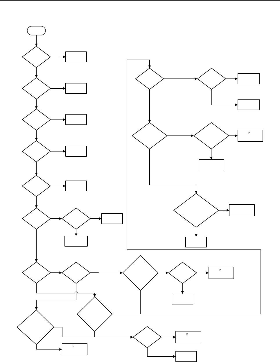
Troubleshooting Flow Chart for Synthesizer 2-5
3.0 Troubleshooting Flow Chart for Synthesizer
Start
Visual check of
the Board OK?
Correct
Problem
NO
YES
+5 V at R0100? NO
YES
Check 5 V
Regulator
U3002
+2.775 V at
R0101 and
R0103?
Check U3200
+1.875 V at
R0102? Check U3200
NO
YES
NO
YES
Is 16.8 MHz
Signal at C0145?
NO
YES
Check Y0100
Is 16.8 MHz
Signal at R0155?
NO Is 16.8 MHz
Signal at R0109?
NO Replace
U0100
YES
Check Q0100
and surrounding
components
YES
Is Radio in Tx or
Rx mode?
Tx
Is
GPO3 low
(<0.5 V), and
GPO1 and GPO6 are
high (>1.4 V)?
NO
YES
Rx
NO
YES
+2.45 V at
C0137
(SF_OUT)?
NO Are C0136,
C0137 OK?
Replace or
resolder
components
NO
Replace U0100
YES
YES
1.5 ms pulse at
TP_ADAPT_SW
when channel
changed?
NO 1.5 ms (inverted)
pulse at R2517 when
channel changed?
Check P U1000
Troubleshooting
Chart
NO
YES
Check Q0106,
R0159
Is
either GPO1 or
GPO6 low (<0.5 V),
but not both, and
GPO3 high
(>1.4 V)?
YES
Is RF Prescaler level
(at C0265) between 100
mVpk and 300 mVpk
(harmonics <-15 dBc)?
NO Check VCO
Troubleshooting
Chart
Is SPI
Programming
OK?
Check P U1000
Troubleshooting
Chart
Replace
U0100
Is SPI
Programming
OK?
Check P U1000
Troubleshooting
Chart
Replace
U0100
YES
NO
NO
YES
Replace
U0100
YES
Is Modulation
Present at
C0360?
Is Tx SSI activity
present on CLK,
FSYNC, and DATA
lines (R2512, R2514,
R2513)
Check P U1000
Troubleshooting
Chart
YES
NO
NO
YES
2-6 Troubleshooting Flow Chart for Tx VCO (Sheet 1 of 2)
4.0 Troubleshooting Flow Chart for Tx VCO (Sheet 1 of 2)
2.556 V at C0362 &
C0363
~ 0 VDC at
C0348?
2.556 VDC at
C0300?
V
be
= 0.7 V
for Q0300?
Yes
Yes
Check biasing
components then
replace Q0302 if
needed
Check biasing
components then
replace Q0302 if
needed
V
be
= 0.7 VDC
for Q0302?
No
No
No
No TX VCO signal at C0318
Visual check
of board
OK? Correct problem
Correct problem
Radio did not boot up
properly or check
9V3 Regulator
Radio did not boot up
properly or check
9V3 Regulator
9 VDC at L0300?
Check biasing
components then
replace Q0302 if
needed
Check biasing
components then
replace Q0302 if
needed
V
be
= 0.7 VDC
for Q0302?
Yes
Yes
No TX VCO signal at C0318
Visual check
of board
OK? Correct problem
Correct problem
Radio did not boot up
properly or check
9V3 Regulator
Radio did not boot up
properly or check
9V3 Regulator
9 VDC at L0300?
No
No
No
Check Synthesizer
Troubleshooting
Chart
Check Synthesizer
Troubleshooting
Chart
Radio is not
programmed for
VCO1 Transmit Mode
or U0100 not
functional
Check biasing
components then
replace Q0300 if
needed
Check biasing
components then
replace Q0300 if
needed
Yes
No
Yes
RF signal
present at
R0332?
Check components
between R0332 and
L0305 for shorts or
opens
Check CR301 - CR304
and L0310, L0307,
C0308, C0313, C0320,
and C0314 for short
Yes
Check CR0301 - CR0304,
L0310, L0307, C0308, C0313,
C0320, and C0314
for shorts or opens
Radio is not programmed for
VCO 1 Transmit Mode
or U0100 not functional

Troubleshooting Flow Chart for Tx VCO (Sheet 1 of 2) 2-7
4.1 Troubleshooting Flow Chart for Tx VCO (Sheet 2 of 2)
DC Voltage
at R0311
between 0.6
and 4.5 VDC?
Check Synthesizer
Troubleshooting
Flow Chart
Check Synthesizer
Troubleshooting
Flow Chart
Yes
No
-
Tx VCO locked but no
high-port modulation
~2.1 VDC at
VCO side of
C0360?
Check R0321, R0320,
R0319, and CR0300
for open or short
Modulation at
CR0300?
No
Yes
Replace C0310
Yes
Modulation at
C0361?
No
Replace C0360
Yes
Check C0361 and
C0334 for short and
then check
Synthesizer
Troubleshooting
Flow Chart
Check C0361 and
C0334 for a short and
then check
Synthesizer
Troubleshooting
Flow Chart
No
Tx VCO not locked
at correct frequency
Check C0323, C0325,
and C0329 and all
components between
C0326 and C0314 for
shorts or opens
Check R0321, R0320, R0319,
and CR0300 for
shorts or opens

2-8 Troubleshooting Flow Chart for Rx VCO (Sheet 1 of 2)
5.0 Troubleshooting Flow Chart for Rx VCO (Sheet 1 of 2)
2.556 V at C0362 &
C0363
Check Synthesizer
Troubleshooting
Flow Chart
Check Synthesizer
Troubleshooting
Flow Chart
Radio is not
programmed for
Receive Mode or
U0100 not functional
~0 VDC at
C0258?
2.556 VDC at
C0236?
Vbe
= 0.7 VDC
for Q0201?
Yes
Yes
No
No
No
VCO 2
Check biasing
components and
then replace Q0202 if
needed
Check biasing
components and
then replace Q0202 if
needed
Vbe
= 0.7 V
for Q0202?
Yes
Yes
No
No
No
No Rx VCO signal at C0218
Visual check
of board
OK? Correct problem
Correct problem
Radio did not boot up
properly or check
9V3 Regulator
Radio did not boot up
properly or check
9V3 Regulator
9 VDC at E0201?
Check biasing
components and
then replace Q0200 if
needed
Check biasing
components and
then replace Q0200 if
needed
2.556 V at C0362 &
C0363
~0 VDC at
C0248?
2.556 VDC at
C0200?
Vbe= 0.7 VDC
for Q0200?
No
Yes
Yes
No
No
No
VCO 1
Check Synthesizer
Troubleshooting
Flowchart
Check Synthesizer
Troubleshooting
Flowchart
Radio is not
programmed for
Receive Mode or
U0100 not functional
Radio is not
programmed for VCO 1
Receive Mode or
U0100 not functional
Yes RF signal
present at
R0219?
Check CR205 - CR208
and L0218, L0215,
C0243, C0245, C0250,
and C0246 for short or
open
Yes
Yes
Check components between
R0219 and L0205
for shorts or opens
Check biasing components
and then replace Q0201
if needed
Yes
Radio programmed for
Rx VCO 1 or 2?
Check CR0201 - CR0204 and
L0210, L0207, C0220,
C0213, C0208, and C0214
for shorts or opens
Radio is not programmed
for VCO 2 Receive Mode
or U0100 not functional
Check CR0205 – CR0208 and
L0218, L0215, C0243,
C0245, C0250, and C0246
for shorts or opens

Troubleshooting Flow Chart for Rx VCO (Sheet 1 of 2) 2-9
5.1 Troubleshooting Flow Chart for Rx VCO (Sheet 2 of 2)
Rx VCO not locked
Rx VCO not locked
at correct frequency
DC Voltage
at R0211
between 0.6
and 4.5 VDC?
Check Synthesizer
Troubleshooting
Check Synthesizer
Troubleshooting
Flow Chart
No
Yes
Rx VCO 1 or
VCO 2
selected?
Check components
between C0253 and
C0246 for open or
short
VCO 1 VCO 2
Check C0223, C0225, and C0229
and all components between
C0226 and C0214 for
shorts or opens
Check C0251, C0252, and C0259
and all components between
C0253 and C0246 for
shorts or opens

2-10 Troubleshooting Flow Chart for Rx VCO (Sheet 1 of 2)
Notes

3-1
Section 3
VHF PCB/SCHEMATICS/PARTS LIST
1.0 Allocation of Schematics and Circuit Boards
1.1 Controller Circuits
The VHF circuits are contained on the Printed Circuit Board (PCB) which also contains the
Controller circuits. This Chapter shows the schematics for the VHF circuits only, refer to the
Controller section for details of the related Controller circuits. The PCB component layouts in this
Chapter show both the Controller and VHF circuit components. The VHF schematics and the related
PCB and parts list are shown in the table below.
NOTE: The VHF Schematics and parts lists are the same for 8478023A12 and 8478023A16. Only
the Controller circuits are different between the two PCBs.
Table 3-1 VHF 25–45W Diagrams and Parts List
PCB:
8478023A12 Main Board Top Side
8478023A12 Main Board Bottom Side
8478023A16 Main Board Top Side
8478023A16 Main Board Bottom Side
Page 3-3
Page 3-4
Page 3-5
Page 3-6
SCHEMATICS
Overall
Receiver Front-End
Receiver IF Amp
Receiver Back-End
Power Amplifier
Power Control
Synthesizer
Receiver VCO
Transmit VCO
Page 3-7
Page 3-8
Page 3-9
Page 3-10
Page 3-11
Page 3-12
Page 3-13
Page 3-14
Page 3-15
Parts List
8478023A12 and 8478023A16 Page 3-16

3-2 Allocation of Schematics and Circuit Boards
Table 3-2: VHF 25–45W Diagrams and Parts List
PCB:
8478023A17 Main Board Top Side
8478023A17 Main Board Bottom Side
Page 3-21
Page 3-22
SCHEMATICS
Overall
Receiver Front-End
Receiver IF Amp
Receiver Back-End
Power Amplifier
Power Control
Synthesizer
Receiver VCO
Transmit VCO
Page 3-23
Page 3-24
Page 3-25
Page 3-26
Page 3-27
Page 3-28
Page 3-29
Page 3-30
Page 3-31
Parts List
8478023A17 Page 3-32
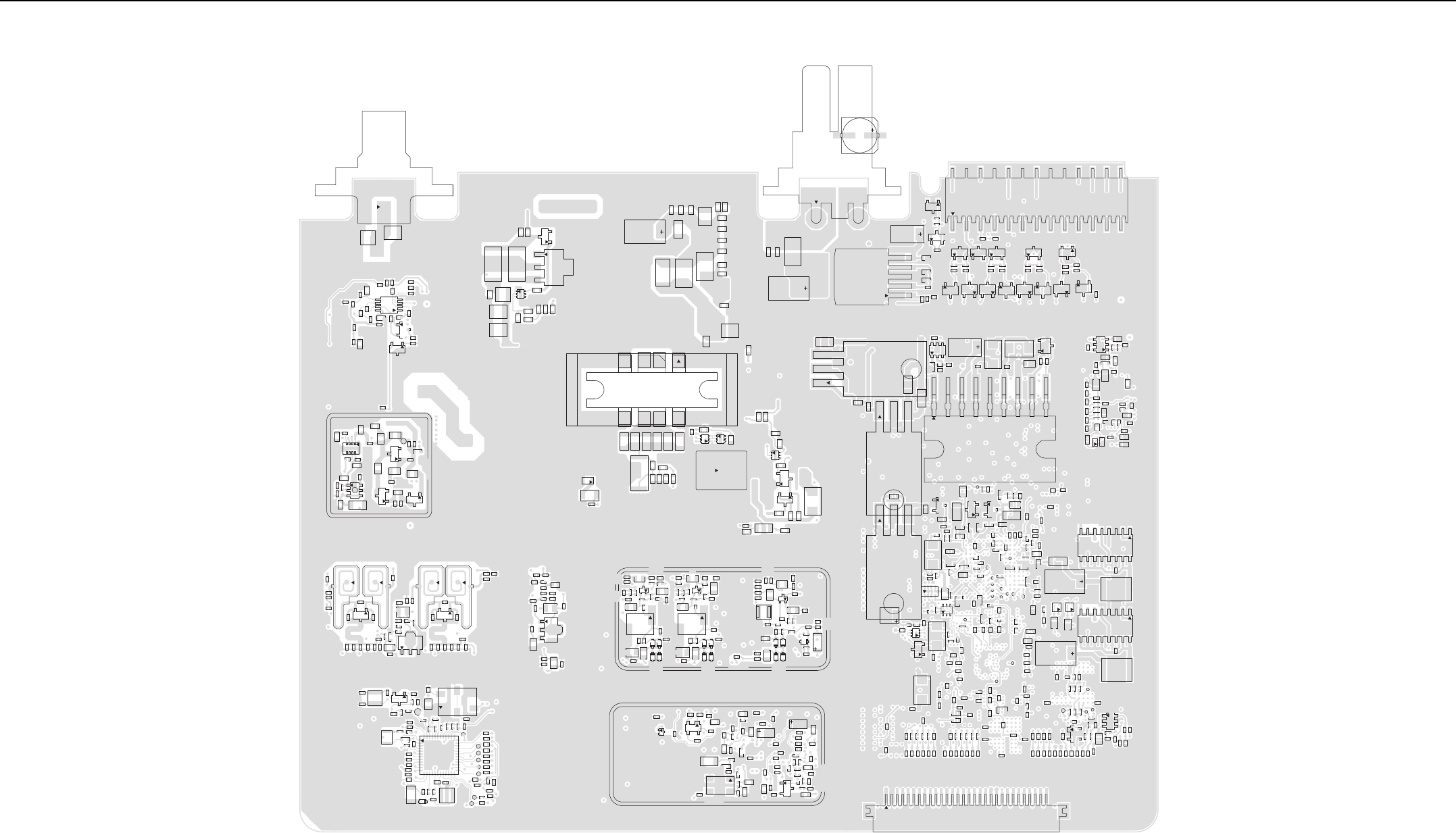
VHF (136–174 MHz) 25–45W PCB/Schematics/Parts List 3-3
2.0 VHF (136–174 MHz) 25–45W PCB/Schematics/Parts List
3
2
J0700
L0728
R0713
C0900
C0901 C0906
C0907
C0908
C0909
C0910
C0915
C0939
D0900
Q0901
R0900
R0901
R0902
R0903
R0906
R0907
R0909
R0911
R0912
R0914
R0915
R0916
R0920
R0923
R0930
U0901
C0776
C0777
C0778
C0779
C0796
C0797
C0798
C0799
L0725
4
3 2 1
Q0704
6
3 4
Q0706
R0729
R0735
R0738
R0745
R0748
R0749 VR0700
C0700
C0701
C0702
C0703
C0704
C0705
C0706
C0707
C0708
C0709
C0710
C0711
C0712
C0713
C0714
C0731
C0738
E0700
E0701
R0742
R0773
C0802
C0804
C0805
C0904
L0900
1
M0700
D
G
S
S S
S
8 7
3 2
4
5
6
Q0702
6
3 4
Q0708
6
3
4
Q0709
R0712
R0716
R0721
R0722
R0727
R0730
R0731 R0734
R0737
R0739
R0753
R0756
R0757
1 RT0908
SP0701
SP0702
SP0703
SP0704
SP0705
SP0706
SP0707
SP0708
C0771
C0823 C0824
E0703
Q0700
2
3
Q0701
6
3
4
Q0707
R0746
R0750
R0751
R0752
R0761
R0777
R0779
R0780
R0781
C0914
C0918
C0921
C0922
C0926
C0929
C0931
C0934
C0935
C0936
C0937
C0947
C0948
C0949
C0950
C0951
D0901
D0902
D0903
L0901
L0902
R0917
R0924
R0925
R0926
R0927
R0928
R0929
R0936
R0937
R0940
R0950
SH0900
4
5 8 U0940
U0941
C0502
C0504
C0509
C0510
C0515
C0516
C0605
C0611
C0615
C0617
C0619
C0620
C0621
C0622
C0623
C0625
C0626
C0627
C0629
C0630
C0631
C0633
C0638
C0642
C0643
C0644
C0645
C0646
C0650
CLKOUT
D0601
DOUTA
DOUTB
E0600
E0601
E0602
E0604
E0605
E0606
E0607 E0608
2 3
4
5
6
FL0500
FS
L0504
L0506
L0604
L0608
PC PD
PE
Q0501
R0503
R0510
R0606
R0607
R0608
R0609
R0610 R0611
R0612
R0613
R0614
R0615
R0617
R0618
R0619
R0621
R0622
R0623
R0627
TP0601
TP0602
1
37
25
13
U0600
C0405
C0406 C0408
C0409
C0410
C0411
C0413
C0414
C0416
C0417
C0418
C0419
C0420
C0423
C0424
C0425
C0426
C0427
C0428
C0429
C0430
C0431
C0432
C0433
C0434
C0435
C0455
D0401 D0403
L0401
L0402
L0403
L0404
L0405
L0414 Q0402
R0404
R0406
R0407
R0409
R0410
R0411
R0412
R0435
R0436
R0437
R0439
R0440
C0437
C0438
C0439
C0440
C0442
C0450
C0451
C0457
L0407
L0411
Q0405
R0417
R0418 R0419
R0420
R0421
R0422 R0423
R0424
R0425
R0432
C0100
C0102
C0103
C0104
C0105
C0109
C0110
C0111
C0113
C0117
C0118
C0120
C0121
C0122
C0124
C0125
C0126
C0127
C0128
C0129
C0130
C0132
C0133
C0140
C0141
C0142
C0143
C0144
C0145
C0146
C0171
C0175
C0177
C0178
C0180
C0195
C0196
L0100
Q0100
Q0102
Q0106
R0100
R0101
R0102
R0105
R0106
R0107
R0108
R0109
R0110
R0111
R0114
R0116
R0117
R0118
R0119 R0123
R0144
R0146
R0147
R0148
R0155
R0156
R0157
R0158
R0159
R0161
SH0100
4 3
2
Y0100
C3000
C3002
C3006
C3015
C3018
E3000
J3000
25
26
2
J4000
1
6
5
U3001
2.9V_MAKO_V6
C3008
C3009
C3010
C3501
C3504 C3505
C3506
E3500
E3501
2
3
Q3500
R3009
R3010
R3032
R3033
R3035
R3036
R3042
R3056
R3516
R3520
U3002
3
2
1
U3005
3
2
1
U3006
3
2
1
9
U3500
C1000
C1001
C1002
C1003
C1004
C1005
C1006
C1007
C1008
C1009
C1010
C1011
C1012
C1013
C1014
C1015 C1016
C1017
C1018
C1019
C1030
C1031
C1032
C1033
C1034
C1036
C1037
C2000
C2001
C2002
C2003
C2004
C2005
C2006
C2007
C2500
C3040
C3202
C3203
C3207
C3208
C3209
C3210
C3211
C3212
C3213
C3216
C3219
C3220
C3225
C3226
C3229
C3234
C3238
C3239
C3240
C3247
C3248
C3249
C3254
C3262
C3273
C3276
C3277
C3278
C3280
C3283
C3511
C3513
C3514
C3515
C3516
C3518
C3520
C3521
C3523
C3524
C3528
C3529
C3530
C3531
C3538 C3545
C4000
C4001
C4002
C4003
C4004
C4005
C4006
C4013
C4014
C4015
C4016
C4017
C4018
C4019
C4020
C4021
C4022
C4023
C4024
C4025
C4026
C4027
C4028
C4029
C4030
C4031
C4032
C4033
C4034
C4035
C4076
C6451
D4001
E3202
E3205
E3502 E3503
E4000
E4001
E4004
30
J4001
L3200
L3202
16
1
8
9
Q3200
4 5
8
Q3201
16
1
8
9
Q3202
2 3
4
Q3203
2 3
4
Q3204
6
3
4
Q3501
R1000
R1001
R1002
R1005
R1006
R1014
R1017
R1019
R1020
R1021
R1025
R1026
R1027
R1028
R1034
R1035
R1036
R1041
R1045
R1066
R1067
R1071
R1072
R2000
R2004
R2005
R2006
R2007
R2008
R2009 R2010
R2011
R2012
R2013
R2529
R3203
R3205
R3206
R3217
R3218
R3224
R3225
R3233
R3500
R3501
R3503
R3504
R3505
R3507
R3508
R3509
R3514
R3515
R3526
R3532
R3535
R3537
R3538
R3547
R3550
R3560
R3571
R3576
R3580
R3583
R3587
R3588
R3594
R3595
R3596
R4000
R4001
R4002
R4003
R4004
R4005
R4006
R4009
R4010
R4011
R4012
R4034
R4061
R4063
R4064
R4065
R4066
R4067
R4068
R4069
R4070
R4071
R4095
R4106
R6467
RT3500
TP1000
TP4000
TP_POR
TP_SDRAM_BA0
TP_SDRAM_BA1
TP_SDRAM_CLK
TP_SDRAM_CS
4 3
6
U1006
U3040
VBUS1_CMD
VBUS2_CMD
VR3202
VR3204
VR3206
VR3503
VR4007
MAKO_GATED_32KHz
TP_MAKO_DCLK
TP_MAKO_FSYNC
TP_MAKO_RX
TP_MAKO_TX
USB1_DAT
USB1_SEO
USB1_TXEN
C6406
C6407
C6408
C6416
C6417
C6418
C6419
C6420
C6421
C6422 C6423
C6426
C6427
C6428
C6429
C6430
C6431
C6433
C6439
C6440
C6445
C6450
E6401
E6402
E6407
R6402
R6403
R6443
R6444
R6445
R6446
R6449
R6450
R6454
R6455
R6456
R6458
R6459
R6460
R6461
R6465
R6466
U6402
U6407
C3005
C3007
C3019
C3046
C4040 C4041 C4042 C4043 C4044
C4045
C4046 C4047
C4048
C4075
E4005
2
3
Q4000
2
3
Q4002
2
3
Q4004
2
3
Q4005
2
3
Q4006
2
3
Q4008
2
3
Q4010
2
3
Q4011
Q4013
R3002
R3003
R3004
R4040 R4041 R4042 R4043 R4044
R4045
R4046 R4047
R4048
R4050
R4051
VR4000 VR4001 VR4002
VR4003
VR4004
VR4005
C0200
C0201
C0204
C0205
C0206
C0208
C0213
C0214
C0215
C0220
C0223
C0225
C0226
C0229
C0236
C0237 C0240
C0241
C0242
C0243
C0245
C0246
C0247
C0250
C0251
C0252
C0253
C0259
C0300
C0301
C0304
C0305
C0306
C0308
C0310
C0313
C0314
C0315
C0320
C0323
C0325
C0326
C0329
C0332
C0334
C0360
C0361
CR0201
CR0202
CR0203
CR0204
CR0205
CR0206
CR0207
CR0208
CR0300
CR0301
CR0302
CR0303
CR0304
L0202
L0203
L0207
L0209
L0210
L0212
L0213
L0214
L0215
L0217
L0218
L0219
L0302
L0303
L0307
L0309
L0310
L0312
Q0200 Q0201
Q0300
R0201
R0204
R0205
R0211
R0216
R0224
R0225
R0226 R0229
R0240 R0241
R0301
R0304
R0305
R0311
R0316
R0319
R0320
R0321
SH0200
VHF (136–174 MHz) 25–45W 8478023A12 Top Side
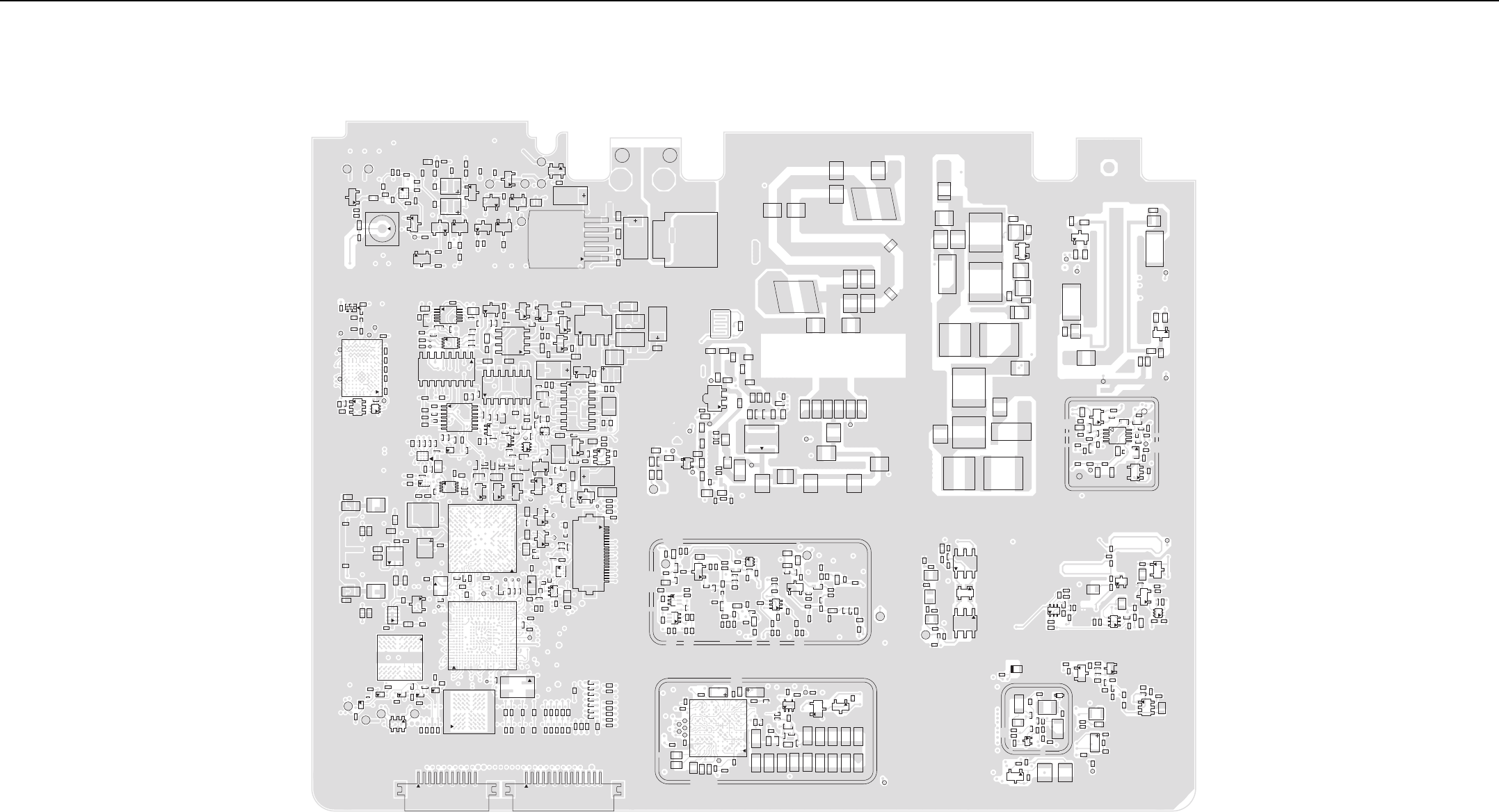
3-4 VHF (136–174 MHz) 25–45W PCB/Schematics/Parts List
1.5V_RTC_TEST
2.8V_RF_TEST
ANT_C
APM_1_WIRE
C0101
C0106
C0107
C0108
C0112
C0114
C0115
C0119
C0123
C0131
C0134
C0135
C0136
C0137
C0138
C0147
C0148
C0149
C0150
C0151
C0156
C0157
C0158
C0159
C0160
C0161
C0162
C0163
C0164
C0165
C0166
C0179
C0191
C0192 C0193
C0194
C0202
C0203
C0207
C0209
C0211
C0217
C0218
C0219
C0221
C0222
C0224
L0230
C0231
C0233
C0235
C0238
C0239
C0248
C0249
C0257
C0258
C0260
C0261
C0262
C0264
C0302
C0303
C0307
C0309
C0311
C0312
C0317
C0318
C0319
C0321
C0322
C0324
C0327
C0328
C0331
C0338
C0339
C0348
C0349
C0364
C0400
C0401
C0402 C0403
C0404
C0407
C0412
C0421
C0422
C0436
C0441
C0443
C0444
C0445 C0446
C0447
C0448
C0449
C0452
C0453
C0454
C0456
C0458
C0503
C0506
C0507
C0512
C0513
C0514
C0601
C0602
C0603
C0604
C0607
C0610
C0612
C0613
C0614
C0616
C0618
C0628
C0632
C0634
C0635
C0636
C0637
C0640
C0641
C0647
C0648
C0649
C0651
C0716
C0717
C0718
C0719 C0720
C0721
C0722
C0723
C0724 C0725
C0726
C0727
C0728
C0729C0730
C0732
C0733
C0734
C0735
C0739
C0740
C0741
C0742
C0746
C0750
C0752
C0753
C0754
C0755
C0766
C0767
C0770
C0772
C0775
C0780
C0783
C0786
C0790
C0791
C0792
C0793
C0794
C0795
C0801
C0803
C0806
C0817
C0818
C0819
C0820
C0821
C0822
C0902
C0903
C0911
C0912
C0913
C0916
C0917
C0919
C0920
C0923
C0925
C0927
C0928
C0940
C0941 C0942
C0943
C0944
C0945
C0953
C1035
C1044
C2501
C3011
C3012
C3013
C3014
C3016
C3017
C3020
C3021
C3030
C3031
C3032
C3041
C3042
C3043
C3044
C3045
C3200
C3201
C3204
C3205
C3206
C3214
C3215
C3217
C3218
C3221
C3222
C3227
C3228
C3231
C3232
C3233
C3237
C3243
C3252
C3257
C3260
C3261
C3265
C3266
C3269
C3270
C3272
C3274
C3275
C3279
C3281
C3282
C3500
C3502
C3503
C3507
C3508
C3509
C3510
C3512
1C3517
C3519
C3522
C3525
C3526
C3527
C3532
C3533
C3534
C3535
1
C3536
C3539 C3540
C3541
C3542
C4007
C4010
C4011
C4012
C4049
C4051
C4053
C4055
C4058
C4059
C4060
C4061
C4062
C4063
C4064
C4065
C4066
C4067 C4068
C4069
C4070
C4071
C4072
C4073
C4074
C4084
C4085
C4086
C4087
C4088
C4089
C4090
C6401
C6412
C6413
C6414
C6432
C6434
C6435
C6436
C6437
C6438
C6443
C6444
C6446
C6449
C6452
CLK_ACQ_TEST
CR0400
D0400
D0402
D0405
D0500
D0600
D0700
D0702
D0703
D0904
D0905
D3030
D3040
D3200
D4000
E0201
E0301
E0400
E0401
E0403
E0404
E0500
E0603
E0609
E0610
E0704
E2500
E3201
E3203
E3206
E3208
E4002
E4003
E6400
EMERGENCY
EXT_MIC
EXT_PTT
3
4
2
5
FL6401
I2C_CLK
I2C_DATA
IF_TEST
IGNITION_SENSE
INT_MIC
22
20
1
21
J2500
11
J4002
14
J4003
J6400
L0200
L0204
L0205
L0206
L0211
L0221
L0300
L0304
L0305
L0306
L0311
L0400
L0406
L0408
L0409
L0410
L0412
L0503
L0602
L0603
L0605
L0700
L0702
L0705
L0706
L0707
L0708 L0709
L0710
L0714
L0715
L0716
L0717
L0718
L0719
L0720 L0721
L0722
L0723
L0724
L0729
L0730
L0731
L0745
L0903
L0904
L3201
L6402
L6403
MAKO_CE
MAKO_V8_5V
MAKO_V9_3V
MMP_1_WIRE
OPT_SSI_SYNC
Q0107
2
3
Q0108
Q0202
Q0302
63
4
Q0400
Q0401
Q0403
Q0500
Q0600
Q0601
1
3
Q0703
Q0705
Q0902
Q3030
4
3
2
1Q3032
Q3040
2
3
Q3041
2
3
Q3205
6
3
4
Q3206
4
5
8
Q3207
2
3
Q3208
63
4
Q3502
63
4
Q3503
Q3504
Q3505
2
3
Q4001
2
3
Q4003
2
3
Q4007
2
3
Q4009
2
3
Q4012
Q4014
2
3
Q4015
Q6401
63
4
Q6402
R0103
R0104
R0113 R0115
R0120
R0122 R0125
R0126
R0127
R0128 R0131
R0134
R0139
R0140
R0160
R0202
R0203
R0206
R0207
R0208
R0210
R0212
R0213
R0218
R0219
R0220
R0221
R0230
C0265
R0302
R0303
R0306
R0307
R0308
R0310 R0312
R0327
R0328
R0332
R0333
R0334
R0336
R0337
R0338
R0339
R0340
R0343
R0345
R0347
R0400
R0401
R0402
R0403
R0408
R0413
R0414
R0415
R0416
R0426
R0427
R0428
R0429 R0430
R0431
R0433
R0434
R0500
R0501
R0502
R0508
R0509
R0511
R0512
R0601
R0602 R0603
R0604
R0605
R0616
R0620 R0624
R0625
R0626
R0702
E0702
R0706
R0710
R0711
R0714
R0715
R0717
R0718
R0719
R0720
R0723
R0726
R0728
R0732
R0733
R0736
R0740
R0747
R0754
R0755
R0760
R0775
R0910
R0913
R0918
R0919
R0921
R0922
R0938
R0941
R0942
R0943
R0944
R0946
R0947
R0951
R0954
R0955
R0960
R0970
R0972
R0973
R0975
R0976
R0977 R0978
R0979
R1044
R1046
R1047
R1048
R1054
R1060
R1070
R2500
R2501
R2502
R2504
R2506 R2507
R2508
R2509
R2510
R2511
R2512
R2513 R2514
R2515
R2516
R2517
R2518
R2519
R2520
R2521
R2522
R2523
R2524
R2525 R2526
R2527
R2528
R3005
R3006
R3007
R3008
R3030
R3034
R3037
R3038
R3039
R3040
R3041
R3043
R3044
R3045
R3046
R3047 R3048
R3050
R3051
R3052
R3053
R3054
R3055
R3057
R3200
R3201
R3204
R3207
R3208
R3209
R3210
R3215
R3216
R3219
R3220
R3222
R3223
R3226
R3227
R3228
R3236
R3237
R3238
R3239
R3240
R3241
R3243
R3245
R3246 R3247
R3248
R3249
R3502
R3506
R3510
R3511
R3512
R3513
R3521
R3523
R3524
R3525
R3528
R3529
R3530
R3533
R3534
R3536
R3539
R3540
R3541
R3542
R3544
R3545
R3546
R3548
R3549
R3551
R3552
R3553
R3554
R3555
R3556
R3558
R3559
R3561
R3562
R3563
R3569
R3572
R3573
R3574
R3575
R3577
R3578
R3579
R3581
R3582
R3584 R3585
R3586
R3591
R3592
R3593
R4023
R4030
R4031
R4032
R4033
R4035
R4049
R4054
R4055
R4074
R4076
R4078
R4079
R4080
R4081
R4082
R4083
R4084
R4085
R4086
R4088
R4089
R4090
R4093
R4094
R4096
R4097
R4098
R4099
R4100
R4101
R4103
R4105
R6401
R6404
R6405
R6407
R6409
R6410
R6411
R6416
R6417
R6418
R6419
R6420
R6430
R6432
R6433
R6434
R6435
R6436
R6437
R6438
R6439
R6440
R6457
R6464
R6468
R6469
R6470
RF_ATTN_2
ROUT_TEST
1
RT0953
S0700
SH0101
SH0300
SH0500
SH0901
SPI_CLK_1
SPI_CLK_TEST
SPI_MISO_1
SPI_MOSI_1
6
4
3
T0400
64
3
T0401
TP501
TP502 TP503
TP504
TP0200
TP0300
TP0301
TP0400
TP0401
TP0600
TP0702
TP0703
TP0704
TP0705
TP0707
TP0709
TP0710
TP0711
TP0713
TP0903
TP0904
TP0907
TP0909
TP0910
TP0911
TP0913
TP_ADAPT_SW
TP_FLASH_CLK
TP_TEST1
TP_TEST2
TP_VCTRL
TX_RAMP
TX_RAMP_DAC
L11A11
L1
U0100
4
3
5
U0101 U0201
6
3
4
U0303
U0304
U0305
U0601
U0700
U0900
U0942
A21 AA21
AA1
U1000
G1A1
A8 G8
U2000
J9 A9
J1 A1
U2001
1
6
5
U3003
U3004
14
58
U3030
P1
A1
A14 P14
U3200
1
64
3
U3201
C1
C3A3
U3202
4
3
5
U3203
10
6
5
U3501
7
8
14
U3502
85
4
U3503
U3504
7
814
U3505
85
4
U3508
16
1
8
9
U4000
14
7
8
U4001
U4004
U4005 U4006 U4007
U4008
P10
A10
P1
A1
U6401
U6404
C1
C3 A3
U6405
U6406
U6408
USB1_DM
USB1_DP
USB2_DM
USB2_DP
VBAT
VBAT_GROUND
VBUS1
VBUS2
VR3000
VR3040
VR3200
VR3201
VR3203
VR3205
VR3207
VR3208
VR3502
VR3504
VR4006
VR4008
VR6400
2
34
Y1000
4
3
2
Y3200
Y3201
VHF (136–174 MHz) 25–45W 8478023A12 Bottom Side
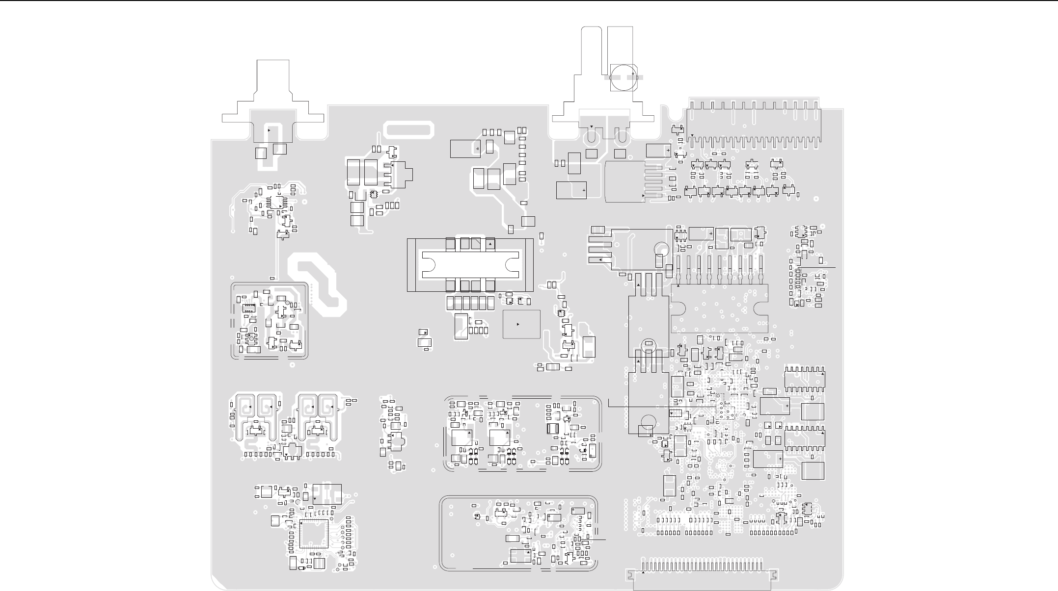
VHF (136–174 MHz) 25–45W PCB/Schematics/Parts List 3-5
3
2
J0700
L0728
R0713
C0900
C0901 C0906
C0907
C0908
C0909
C0910
C0915
C0939
D0900
Q0901
R0900
R0901
R0902
R0903
R0906
R0907
R0909
R0911
R0912
R0914
R0915
R0916
R0920
R0923
R0930
U0901
C0914
C0918
C0929
C0931
C0934
C0935
C0936
C0937
D0903
L0901
L0902
R0917
R0924
R0925
R0926
R0927
R0929
SH0900
C0921
C0922
C0926
C0947
C0948
C0949
C0950
C0951
D0901
D0902 R0928
R0936
R0937
R0940
R0950
4
58
U0940
U0941
6
3
4
C0776
C0777
C0778
C0779
C0796
C0797
C0798
C0799
L0725
4
321
Q0704
Q0706 R0729
R0735
R0738
R0745
R0748
R0749 VR0700
C0700
C0701
C0702
C0703
C0704
C0705
C0706
C0707
C0708
C0709
C0710
C0711
C0712
C0713 C0714
C0731
C0738
C3002
E0700
E0701
E3000
R0742
R0773
C3000
C3015
SP3000
SP3001
1
6
5
U3001
R3032
3
2
1
U3006
25
26
2
J4000
C3018
J3000
2
3
23
23
2
3
2
3
23
23
2
3
C0904
L0900
1
RT0908
C0804
C0805
R0712
R0716
R0721
R0730
R0731 R0734
R0737
R0739
R0753
R0756
R0757
D
SS
32
SP0703
SP0704
SP0707
SP0708
GSS
8
456
Q0702
SP0701SP0702 SP0705
SP0706
1
M0700
6
3
4
63
4
C0802
Q0708
Q0709
R0722
R0727
7
R0750
R0752
C0771
Q0700
23
Q0701
6
3
4
Q0707
R0751
R0761
R0780
C0823
C0824
R0746
R0777
R0779
R0781
E0703
R3033
R3035
R3036
R3056
3
2
1
U3005
R3042
3
2
1
C0406
C0410
C0411
C0413
C0414
C0418
C0419
C0423
C0424
C0425
C0426
C0427
C0433
C0435 C0455
D0401
L0402
L0405
L0414
Q0402
R0404
R0406
R0407
R0409
R0410
R0435
R0439
C0405
C0408
C0409
C0416
C0417
C0420
C0428
C0429
C0430
C0431
C0432
C0434
D0403
L0401
L0403
L0404
R0412
R0440
R0411
R0436
R0437
C0502
C0504
C0509
C0510
C0611
C0615
C0617
C0619
C0620
C0621
C0622
C0623
C0625
C0626
C0627
C0629
C0630
C0631
C0633
C0638
C0642
C0643
C0644
C0645
C0646
C0650
CLKOUT
D0601
DOUTA
DOUTB
E0600
E0601
E0602
E0604
E0605 E0606
E0607
E0608
FS
L0504
L0604
L0608 PC
PD
PE
Q0501R0510
R0606
R0607
R0608
R0609
R0610 R0611
R0612
R0613
R0614
R0615
R0617
R0618
R0619
R0621
R0622
R0623
R0627
TP0601
TP0602
1
37
25
13
U0600
C0515
C0516
C0605
23
4
5
6
FL0500
L0506
R0503
C0437
C0438
C0439
C0440
C0442
C0451
C0457
L0411
Q0405
R0417
R0419
R0420
R0421
R0422 R0423
R0424
R0425
R0432
C0450
L0407
R0418
C6406
C6407
C6408
C6416
C6417
C6418
C6419
C6420
C6421
C6422
C6426
C6427
C6428
C6429
C6430
C6431
C6433
C6439
C6440
C6445
C6450
E6401
E6402
E6407
R6402
R6403
R6443
R6444
R6445
R6446
R6449
R6450
R6454
R6455
R6456
R6458
R6459
R6460
R6461
R6465
R6466
U6402
U6407
C6423
C3501
C3505
C3506
E3500
E3501
23
Q3500
R3516
R3520
C3005
C3006
C3007
C3019
C3046
C4040 C4041 C4042 C4043 C4044
C4045
C4046 C4047
C4048
C4075E4005
Q4000
Q4002
Q4004
Q4005
Q4006
Q4008
Q4010
Q4011
Q4013
R3002
R3003
R3004
R4040 R4041 R4042 R4043 R4044
R4045
R4046 R4047
R4048
R4050
R4051
VR4000
VR4001 VR4002
VR4003
VR4004
VR4005
C3008
C3009
C3010
C3504
R3009
R3010
U3002
9
U3500
C0200
C0201
C0204
C0205
C0206
C0208
C0214
C0215
C0220
C0223
C0225
C0229
C0236
C0237 C0240
C0241
C0242
C0246
C0247
C0251
C0252
C0259
L0202
L0203
L0212
L0213
L0214
L0215
L0219
Q0200
Q0201
R0201
R0204
R0205
R0216
R0224
R0225
R0226
R0229
R0240
C0213
C0226
C0243
C0245
C0250
C0253
CR0201
CR0202
CR0203
CR0204
CR0205
CR0206
CR0207
CR0208
L0209
L0210
L0217
L0218 R0211
R0241
SH0200
L0207
C0300
C0301
C0304
C0305
C0306
C0313
C0315
C0320
C0326
CR0301
CR0303
CR0304
L0302
L0303
L0307
L0309
L0310
L0312
Q0300
R0301
R0304
R0305
R0311
R0316
C0308
C0310
C0314
C0323
C0325
C0329
C0332
C0334
C0360
C0361
CR0300
CR0302
R0319
R0320
R0321
30
J4001
C0100
C0102
C0103
C0104
C0105
C0109
C0110
C0111
C0113
C0117
C0118
C0120
C0121
C0122
C0124
C0125
C0126
C0127
C0128
C0129
C0130
C0132
C0133
C0140
C0141
C0142 C0143
C0144
C0145
C0146
C0171
C0175
C0177
C0178
C0180
C0195
C0196
L0100
Q0100
Q0102
Q0106
R0100
R0101
R0102
R0105 R0106
R0107 R0108
R0109
R0110
R0111
R0114
R0116
R0117R0118
R0119
R0123
R0144
R0146
R0147
R0148
R0155
R0156
R0157
R0158
R0159
R0161
SH0100
43
2
Y0100
C3209
L3202
C3203
L3200
16
1
8
9
Q3202
C3202
16
1
8
9
Q3200
C2500
C4000
C4001
C4002
C4003
C4004
C4005
C4006
C4013
C4028
C4029
C4030
C4031
C4032
C4033
R1071
R2529
R4000
C2002
C4014
C4015
C4016
C4017
C4018
C4019
C4020
C4021
C4022
C4023
C4024
C4025
C4026
C4027
E4001
E4004
C4076
R1014 R1019
R2000
C2000
C2001
C2003
E4000
R2004
R2012
R3580R3583
C1003
C1005
C1006
C1008
C1011
C1013
C1017
C1018
C1019
C2005
R1002
R1005
R1006
R1041
R1066
R1067
R4001
R4002
R4003
R4004
R4005
R4006
R4061
R4063
R4064
R4065
R4066
R4067
R4068
R4069
R4070
R4071
TP1000
TP_SDRAM_CLK
C1007
C1009
C1014
C1016
C1036
C1037
C2004
C2006
C2007
C3212
C3213
C3216
C4034
C4035
D4001
23
4
Q3203
23
4
Q3204
R1000
R1021
R2005
R2006
R2007
R2008
R2009
R2010
R2011
R2013
R4009
R4010
R4011
R4012
R4034
R4095
R4106
TP4000
TP_SDRAM_BA0
TP_SDRAM_BA1
TP_SDRAM_CS
VR4007
C1000
C1001
C1004
C1010
C1012
C1015
C1030
C1031
C1033
C3280
C3514
E3502
R1001
R1017
R1025
R1034
R1035
R1036
R1045
C3515
C3524
63
4
Q3501
R3526
R3532
R3547
VR3503
C1002
C1032
C1034
C3208
C3210
C3529
4
5
8
Q3201
R1026
R1027
R1028
R3205
R3206
R3560
TP_POR
4
3
6
U1006
2.9V_MAKO_V6
C3040
C3247 E3205
VR3206
3.6V_
MAKO_
SW1
C3207
C3211
C3219
C3220
C3225
C3226
C3229
C3234
C3238
C3239
C3240
C3248
C3249
C3254
C3262
C3273
C3276
C3277
C3278
C3283
C3511
C3513
C3516
C3518
C3520
C3521 C3523 C3528
C3530
C3531
C3538 C3545
C6451
E3202
E3503
R1020
R3203
R3217
R3218
R3224
R3225
R3233
R3500
R3501
R3503
R3504
R3505
R3507
R3508
R3514
R3515
R3535
R3537
R3538
R3550
R3571
R3576
R3587
R3588
R3594
R3595
R3596
R6467
RT3500
U3040
VR3202
VR3204
R3509
VBUS1_CMD
VBUS2_CMD
MAKO_GATED_32KHz
TP_MAKO_DCLK
TP_MAKO_FSYNC
TP_MAKO_RX
TP_MAKO_TX
USB1_DAT
USB1_SEO
USB1_TXEN
VHF (136–174 MHz) 25–45W 8478023A16 Top Side
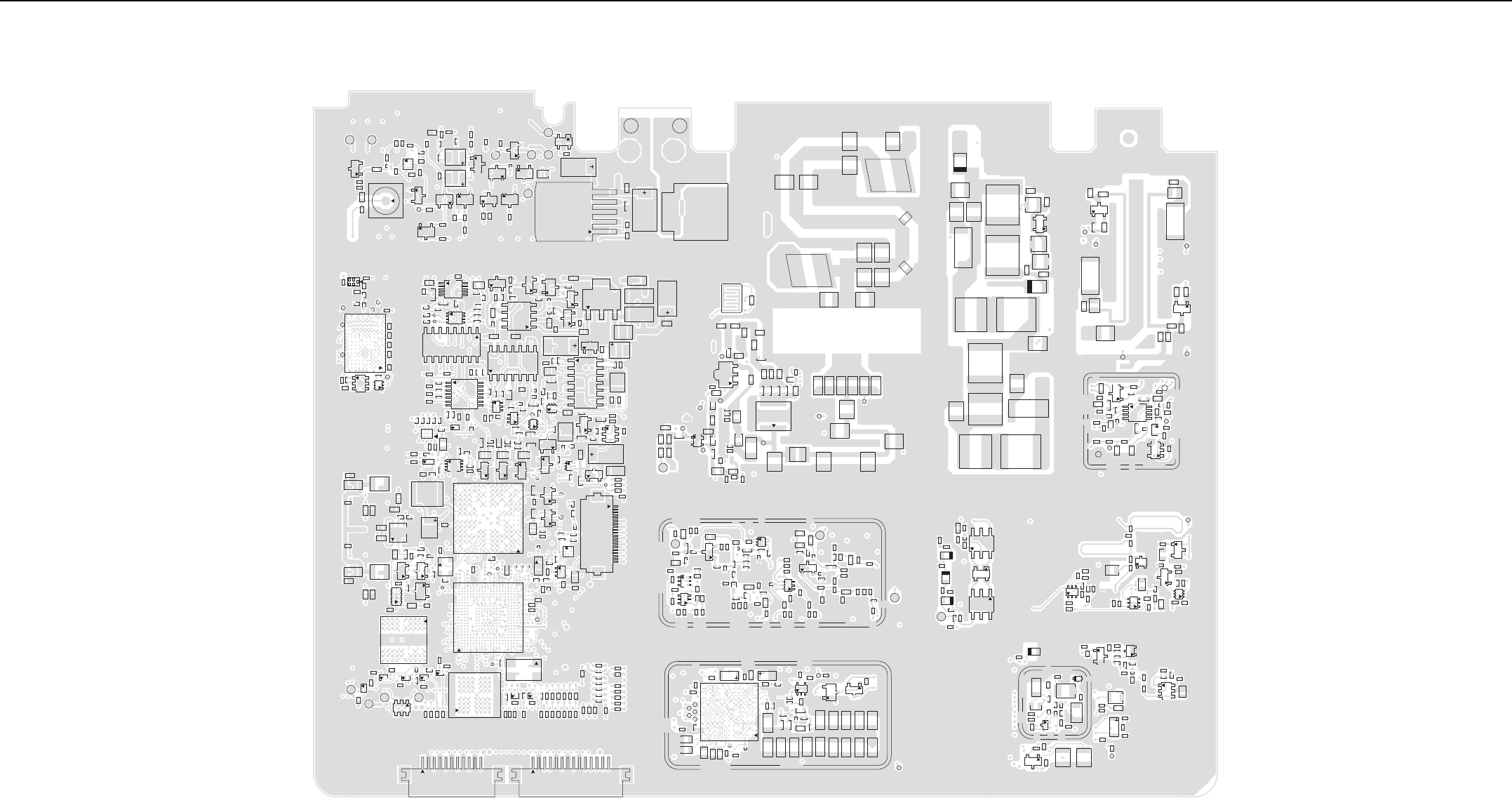
3-6 VHF (136–174 MHz) 25–45W PCB/Schematics/Parts List
ANT_C
C4063
C4064
C4065
C4066
C6412
C6413
C6435
C6436
C6437
C6438
EMERGENCY
IGNITION_SENSE
J6400
L6402
2
3
Q4003
23
Q4007
2
3
Q4015
Q6401
R3529
R3540
R3548
R4030
R4032
R4033
R4055
R4098
R6407
R6430
R6432
R6433
R6434
R6435
R6436
R6437
C1
C3
A3
U6405
VR6400
APM_1_WIRE
C3045
C3533
C3534
C4067 C4068
C4069
C4070
D4000
EXT_PTT
2
3
Q4001
23
Q4009
2
3
Q4012
Q4014
R3545
R4031
R4035
R4049
R4054
R4088
R4089
1
6
5
U3003
USB2_DM
USB2_DP
VBUS2
VR3504
VR4006
C3012
C3013
C3014
R3005 R3006
VBAT
VBAT_GROUND
VR3000
C0719 C0720
C0721
C0722
C0724 C0725
C0726
C0727
C0729
C0730
C0741
L0700
L0714
R0710
R0723
C0735
C0739
C0740 C0742
C0750
C0766
C0767
C0772
C0803 C0822
D0702
D0703
L0706
L0707
L0708 L0709
L0720 L0721
L0722
L0723
L0730
L0731
D0700
L0710L0724
L0729
C0723
C0940
C0941 C0942
C0943
C0944
C0945
D0904
D0905
L0903
L0904
R0970
R0972
R0973
R0975
R0976
R0977
R0978
R0979
TP0903
TP0904
TP0907
TP0909 TP0913
C0602
C0603
C0604
C0607
C0610
C0612
C0613
C0614
C0616
C0618
C0647
C0648
C0649
D0600
E0609
L0602
L0603
Q0600
Q0601
R0601
R0602
R0603
R0604
R0605
R0616
R0620 R0624
SH0500
C0601
C0628
C0632
C0634
C0635
C0636
E0603
TP0600
C0401
C0402 C0403
C0456
C0503
C0506
C0507 C0512
C0513
C0514
C0637
C0640
C0641
C0651
D0500
E0400
E0401
E0500
E0610
L0503
L0605
Q0401
Q0500
R0400
R0401
R0500
R0501
R0502
R0508
R0509
R0511
R0512
R0625
R0626
U0601
C0400
C0404
C0407
C0412
C0421
C0422
C0436
C0452
C0453
C0454
CR0400
D0400
D0402
E0403
E0404
L0400
L0406
63
4
Q0400
Q0403
R0402
R0403
R0408
R0413
R0414
R0415
R0416
R0428
R0429
R0430
R0431
TP0400
C0441
C0443
C0444
C0445
C0446
C0447
C0448
C0449
C0458
D0405
L0408
L0409
L0410
L0412
R0426
R0427
R0433
R0434
6
4
3T0400
64
3
T0401
TP0401
C0202
C0203
C0207
C0209
C0217
C0222
C0224
C0231
E0201
L0200
L0204
L0206
R0202
R0203
R0206
R0207
R0212
R0219
R0220
R0221
SH0300
TP0200
TP0301
C0211
C0218
C0219
C0221
C0233
C0248
C0249
C0257
C0258
C0261
C0262
C0265
C0303
C0307
C0309
C0317
C0322
C0331
E0301
L0205
L0211
L0221
L0230
L0300
L0306
Q0202
R0208
R0210
R0213
R0218
R0230
R0332
R0333
R0334
R0337
C0235
C0238
C0239
C0260
C0264
C0302
U0201
C0311
C0312
C0318
C0319
C0321
C0324
C0327
C0328
C0338
C0339
C0348
C0349
C0364
L0304
L0305
L0311
Q0302
R0302
R0303
R0306
R0307
R0308
R0310
R0312
R0328
R0336
R0338
R0339
R0340
R0343
R0345
R0347
TP0300
6
3
4U0303
U0304 U0305
R0327
TP_VCTRL
C0156
C0157
C0158
C0161
C0163
C0164
C0165
C0192
C0194
C0159
C0160
C0162
C0191
C0193
C3020
C3021
R3038
R3050
R3055
C6414
3
4
2
5
FL6401
R6409
C6443
C6444
CLK_ACQ_TEST
IF_TEST
L6403
R6410 R6411
ROUT_TEST
SPI_CLK_TEST
P10
A10
P1
A1
U6401
1.5V_RTC_TEST
C6401
C6432
C6446
63
4
Q6402
R6404
R6405
R6420
R6438
R6439
R6440
R6457
U6406
2.8V_RF_TEST C2501
C3030
C3031
C3032
C3041
C3042
C3502
C3503
C3508
C3509
1
C3536
C3539
C3540
D3030
D3040
E2500
I2C_
CLK
I2C_DATA
Q3030
4
3
2
1Q3032
23
Q3041
R3030
R3034
R3037
R3039
R3040
R3041
R3045
R3046
R3047R3048
R3051
R3052
R3053
R3054 R3057
R3511
R3513
R3524
R3558
R3559
R3569
R3573
R3574
R3575
R3578
14
58
U3030
10
6
5
U3501
8
5
4
U3503
VR3040
VR3502
C3011 C3016
C3017
C3274
C3500
C3507
R3007
R3008
R3228
R3502
R3506
R3521
R3523
U3004
C3510
C3519
R3525
R3528
1C3517
C3526
7
814
U3505
C4073
C4084
C4085
C3257
C4071
C4072
C4074
C6434
C6449
C6452
R1047
R3510
R3512
R4023 R4086
R4100
R4101
R4103
R6401
R6416
R6417
R6418
R6419
R6464
R6468
R6469
R6470
U3504
14
7
8
U4001
U6404
U6408
C3200
C3201
C3206
C3265
C3266
C3269
C3270
C3279
C3281
C3289
C3290
C3291
C3541
C3542
E4002
L3201
4
5
8
Q3207
2
3
Q3208 Q3209
Q3210
R2500
R3200
R3204
R3207
R3208
R3215
R3216
R3237
R3238
R3239
R3240
R3241
R3243
R3245
R3246 R3247
R3250
R3252
R3253
R3584 R3585
R3586
R3591
R3592
R3593
J9 A9
J1 A1
U2001
1
64
3
U3201
8
5
4
U3508
C1035
C3214
R3227
SPI_CLK_1
SPI_MISO_1
SPI_MOSI_1
TX_RAMP
A21 AA21
C3215
MAKO_CE
R3572
R3579
RF_ATTN_2
A1
A14
U3200
4
3
2
Y3200
P1
P14
VR3203
VR3205
VR3207
C1044
C3204 C3272
C3282
OPT_SSI_SYNC
R1044
R1048
R1054
R1060
R1070
R2515
R3220
4
3
5
U3203
22
20
1
21
J2500
C3043
C3205
C3217
C3218
C3233
C3237 C3260
C3261
E3201
E4003
EXT_MIC
MAKO_V8_5V
MAKO_V9_3V
Q3040
6
3
4
Q3206
R2502
R2519
R2520
R3043
R3044
R3210
R3219
R3222
R3223
R3226
R3236 R3248
R3249
R3577
R3581
R3582
R4090
TX_RAMP_DAC
C1
C3
A3
U3202
VR3201 VR3208
Y3201
AA1
U1000
C3221
C3222
C3227
C3228
C3231
C3232
C3243
C3252
C3275
C3512
C3522
C3525
C3527
C3532
C3535
D3200
E3203
E3206
E3208
INT_
MIC
23
Q3205
64
Q3502
63
4
Q3503
Q3504
Q3505
R3209
R3530
R3533
R3534
R3536
R3539
R3541
R3542
R3544
R3546
R3549
R3551
R3552
R3553
R3554
R3555
R3556 R4079
C3044
3
VR3200
7
8
14
U3502
16
1
8
9
U4000
11
J4002
14
J4003
C4007
C4010
C4011
C4012
C4086
C4087
C4088
C4089
C4090
MMP_1_WIRE
R4093
R4094
R4096
R4097 R4099
R4105
U4004
U4005
U4006
U4007
U4008
USB1_DM
USB1_DP
VBUS1
VR4008
G1A1
A8 G8
U2000
C4049
C4051
C4053
C4055
C4058
C4059
C4060
C4061
C4062
C4091
C4092
C4093
C4094 E4006 R1046
R2501
R2504
R2506 R2507
R2508
R2509
R2510
R2511
R2512
R2513 R2514
R2516
R2517
R2518
R2524
R2525 R2526
R2527
R2528
R4074
R4076
R4078
R4080
R4081
R4082
R4083
R4085
TP_FLASH_CLK
U4009
U4010
2
34
Y1000
C0911 C0913
C0916
C0919
C0920
C0927
C0928
R0918
R0919
R0922
R0938
R0944 R0951
R0960
SH0901
TP0911
C0902
C0903
C0912
C0917
C0923
C0925
C0953
Q0902
R0910
R0913
R0921
R0941
R0942
R0943
R0946
R0947
R0954
R0955
1
RT0953
TP0910
U0900
U0942
C0770
C0786
C0790 C0791
C0792
C0793
C0794
C0817
C0818
C0820
C0821
L0715 L0717
L0719
Q0705
R0718
R0720
R0728
R0754
R0755
R0775
S0700
TP0709
C0746
C0755
R0717
R0719
R0726
R0732
R0733
R0736
TP0707
TP0711
C0752
C0753
C0754
C0819
L0745
1
3
Q0703
TP0702
C0716
C0717
C0718
C0728
C0732
C0733 C0734
C0775
C0780
C0783
C0795
C0801
C0806 E0702
E0704
L0702
L0705 L0716
L0718
R0702
R0706
R0711
R0714
R0715
R0747
R0760
TP0703
TP0704
TP0705
TP0710
TP0713
U0700
R0740
E6400
Q0107
23
Q0108
R0160
C0101
C0106
C0107
C0108
C0112
C0114
C0115
C0119
C0123
C0131
C0134
C0135
C0136
C0137
C0138
C0147
C0148
C0149
C0150
C0151
C0166
C0179
R0103
R0104
R0113 R0115
R0120
R0122 R0125
R0126
R0127
R0128
R0131
R0134
R0139
R0140
SH0101
TP501
TP502 TP503
TP504
TP_ADAPT_SW
TP_TEST1
TP_TEST2
A11
U0100
4
3
5
U0101
L11
L1
VHF (136–174 MHz) 25–45W 8478023A16 Bottom side

VHF (136–174 MHz) 25–45W PCB/Schematics/Parts List 3-7
CONTROLLER_&_GPS_R2
( TOP LEVEL: SHEET 1)
PC_ATTEN_ENA
PREDRIVE_SW
RAW_B+
RESET_OUT
RX_FLTR_VCTRL
RX_SSI_CLK
RX_SSI_DATA
RX_SSI_FSYNC
RX_SSI_SYNCB
SPI_CLK
SPI_MISO
SPI_MOSI
THK_CS
TX_DAC
TX_SSI_CLK
TX_SSI_DATA
TX_SSI_FSYNC
16.8_GPS
16.8_MHZ_BUFF
2.775V_ANA_V7
2.775V_DIG_V4
5V_SW
9V3
9V3_PA
ABACUS3_CS
ADAPT_SW
ANT_ENABLE
DMCS
LOCK_DETECT
LO_BATTERY_DET
PA_BIAS
PA_TEMP
1.875V_DIG_V2
1
0
1
3
0
2
1
2
0
2
4
TX_SSI_BUS(0:2)
SPI_BUS(0:4)
RX_SSI_BUS(0:2)
NC
NC
2
3
1
1
1
2
0
2
0
4
0
TX_VCO_SEL2_
VCTRL
RX_VCO_SEL1_
RX_VCO_SEL2_
SF_OUT
SPI_CLK_OUT
SPI_MISO_OUT
SPI_MOSI_OUT
TX_VCO_SEL1_
ABACUS3_CEX_OUT
ABACUS3_SYNCB_OUT
HP_MOD_OUT
PRSC
RF_ATTN_1
RX_SSI_CLK_PASS_IN
RX_SSI_DATA_PASS_IN
RX_SSI_FSYNC_PASS_IN
16.8_REF
1V8_BE
5V_BE
9R1
9V3
RX_SSI_FSYNC_PASS_OUT
SDTX
SFTX
SPI_CLK_IN
SPI_MISO_IN
SPI_MOSI_IN
TH_CEX
TX_CLK
ABACUS3_CEX_IN
ABACUS3_SYNCB_IN
ADAPT_SW
DMCS
LOCK
RSTB
RX_SSI_CLK_PASS_OUT
RX_SSI_DATA_PASS_OUT
1.8V_TH_DIG
16.8_GPS
2.8V_TH_ANA
2.8V_TH_DIG
5V
SYNTH
NC
2
0
3
1
0
1
2
9V3_SYNTH_IN
9V3_VCO
RXINJ
TXINJ
VCO_VHF
( TX: SHEET 1)
( RX: SHEET 2)
9R1
9V3_SYNTH_OUT
HP_MOD_OUT
PREDRIVE_SW
PRSC
RX_VCO_SEL1
RX_VCO_SEL2
SF_TH
TX_VCO_SEL1
VCTRL
9V3_SYNTH
9V3_VCO
TX_INJ
( PA: SHEET 1)
( PC: SHEET 2)
TX_HP_VHF
9V3_TX_SW
ANT_ENABLE
FINAL_BIAS_1
LO_BATTERY_DET
PREDRIVE_SW
RX_IN
TX_DAC
RXFE_VHF
( 1 SHEET)
9R1
9V3_TX_SW
FE_TUNE IF
RF_ATTEN_1
RX_IN
RX_INJ
(ABACUS3: SHEET 2)
RXBE_73.35MHZ
(IF AMP: SHEET 1)
SPI_ABACUS_CLK
SPI_ABACUS_DATA
SSI_ABACUS_CLKOUT
SSI_ABACUS_DOUTA
SSI_ABACUS_DOUTB
SSI_ABACUS_FSYNC
SSI_ABACUS_SYNCB
16.8_REF
1V8
5V
IF
SPI_ABACUS_CEX
2
2
3
1
0
0
1
ABACUS_SPI_BUS(0:3)
ABACUS_SSI_BUS(0:2)
9V3
9V3_PA
PA_SUPPLY
VHF (136–174 MHz) 25–45W Overall Schematic Diagram

3-8 VHF (136–174 MHz) 25–45W PCB/Schematics/Parts List
(VALUE)
(VALUE)
(VALUE)
(VALUE)
(VALUE)
(VALUE)
(VALUE)
10 dB Attenuator ON @ High for RF_ATTEN_1
E0400
BK1005HM471
RF_ATTEN_1_8
RF_ATTEN_1
9V3_TX_SW_8
E0404
BK1005HM471
9V3_TX_SW
MMBD6100
D0402
1500pF
C0407
TP0400
TEST_POINT
C0404
1500pF
1
RXIN_FE_6
C0413
RX_IN
4.7pF
C0421
1500pF
10 dB Attenuator
NC
220
R0407
470
R0435
470pF
C0418
560nH
L0400
D0400
2
13
13
L0405
10nH
D0401
1SV228
20pF
C0411
C0406
6.8pF
C0410
20pF
10nH 2
L0402
C0455
1500pF
1
3
2
CR0400
MMBD352
C0453
39pF
C0412
47pF
15pF
C0452
Hi-Side Zeros for Preselector
(Micro-strip 40 mm Aggregate)
C0427
51pF
C0426
43pF
C0423
56pF
C0424
43pF C0425
51pF
100K
R0410
C0433
1500pF
MAKO ( 0 ~ 4.6 VDC)
680
R0429
FE_TUNE_FE_3
E0403
BK1005HM471
C0436
1500pF
FE_TUNE
9R1_FILT
56
R0417
2.7K
R0419
L0407
560nH
1500pF
C0437
Q0405
NE85634
1500pF
C0438
C0442
1500pF
2.67K
R0418
C0439
1500pF
C0440
0.10uF
R0420
2.7K
0
R0421
7.5 dB Attenuator
C0451
68pF
R0424
150
R0425
1K
47nH
L0411
RX_INJ_FE_5
C0450
9.1pF
150
R0423
R0422
51
RX_INJ
62
R0432 1500pF
C0457
L0409
68nH
2%
L0408
2%
68nH
24pF
C0443
C0447
24pF
C0446
10pF
C0441
3.9pF
22pF
C0448
30pF
C0445 47nH
2%
L0410
24pF
C0444
C0449
10pF
1
TEST_POINT
TP0401
R0426
10K
NC
XFMR
T0400
5
NC
4
6
3
2
1
IO2 2
IO3 3
IO4
4
IO1
1
D0405
NC
T0401
NC
5
4
6
3
2
1
XFMR
150nH
L0412
R0427
51
82pF
C0458
0
R0433 IF_FE_3
R0434
270
NU
IF
51pF
C0432
51pF
C0429
C0428
43pF 43pF
C0430 C0431
56pF
100K
R0412
1500pF
C0434
39
R0411
R0437
150
R0436
150
10nH
2
13
13
L0404
15pF
C0417
C0408
6.2pF
10nH
L0403
2
D0403
1SV228
15pF
C0416
C0409
12pF
3.9pF
NU
C0420
R0440
20
NE85634
Q0402
C0405
1500pF
R0404
2.7K
22
R0402
R0406
C0435
1.0uF
L0401
56nH
620
0.10uF
C0419
560nH
L0414
3.6K
R0439
1500pF
C0456
15K
R0400
R0409
3K
1500pF
C0414
C0422
43pF
C0454
1500pF
39nH
5%
L0406
9R1_FILT
(In-Band Tuning range 2.70 ~ 7.80 VDC)
R0416
680
R0415
680
680
R0414
0
R0428
680
R0413
2
3
6
4
1
5
Q0403
UMZ2NTR
R0408
10K
10K
R0430
10K
R0431
1500pF
C0400
6
3
1
4
Q0400
2
5
R0403
0
9R1_FILT
51pF
C0403
BK1005HM471
E0401
C0402
1500pF
C0401
0.1uF
9R1_FE_7
9R1
Q0401
UMT1NFTN
1K
R0401
VHF (136–174 MHz) 25–45W Receiver Front-End Schematic Diagram
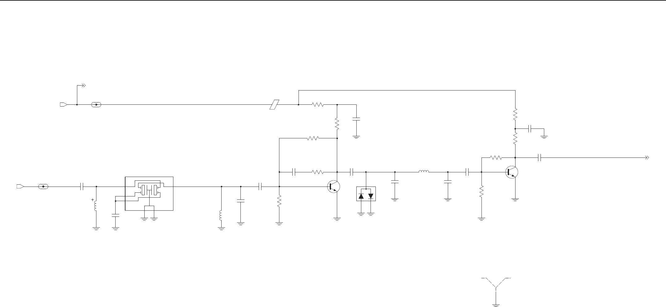
VHF (136–174 MHz) 25–45W PCB/Schematics/Parts List 3-9
UHF -- 73.35MHz
4-POLE
VHF -- 44.85MHz
5V_BE_5
5V
5V
BK1005HM471
E0500
1.2K
R0511
20K
R0502
R0501
330
0.10uF
C0514
1.43V
C0512
0.10uF
0.76V
1
3
2
PBR941
Q0500
4.7K
R0509
0.10uF
C0503
C0509
NU
C0506
0.10uF
R0508
L0504
NU
56K
L0503
330nH
6.2pF
C0510
18pF
C0507
IFIN_BE_8 3OUT 6
FL0500
MXF45
44.85MHz
CC1
2
CC2
5
GND1
1
GND2
4
IN
IF
NU
C0515
D0500
MMBD352
IF_TO_ABACUS
0.72V
1.6V
C0516
NU
0.10uF
C0502
0.10uF
C0513
R0503
Q0501
30K
PBR941
R0510
30K
C0504
0.10uF
R0500
5.1K
51
R0512
820nH
IF_OUT
L0506
1
SHIELD
SH0500
VHF (136–174 MHz) 25–45W Receiver IF Amp Schematic Diagram
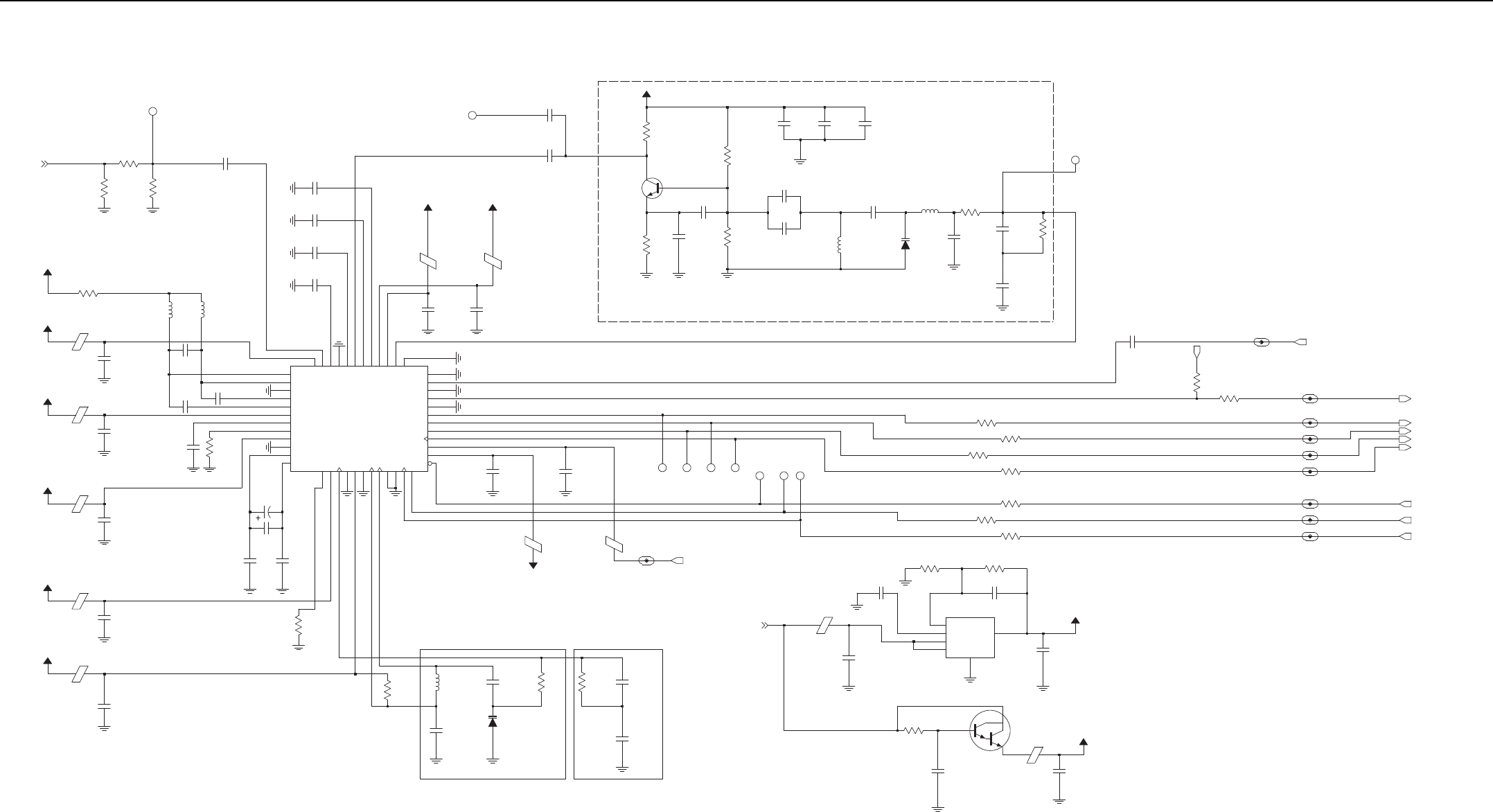
3-10 VHF (136–174 MHz) 25–45W PCB/Schematics/Parts List
0
R0621
R0623
NU
NU
R0622
IF_OUT
TP0602
TEST_POINT
1
C0650
30pF
1000pF
C0611
.01uF
C0615
C0619
0.10uF
0.10uF
C0617
L0605
10uH
L0604
10uH
3VA
51
R0606
E0602
BK1005HM471
3VA
C0623
0.10uF
C0628
0.10uF
E0603
BK1005HM471
3VA
0.10uF
C0633
3VA
E0604
BK1005HM471
C0638
0.10uF
E0607
BK1005HM471
3VA
0.10uF
C0644
E0608
BK1005HM471
3VA
R0616
100K
100pF
C0636
100pF
C0635
.01uF
C0634
4.7uF
C0632
R0610
0
C0629
2200pF
C0627
100pF
100pF
C0626
C0625
200pF
12
11
9
6
2
1
4
5
10
3
8
7
VREFN
VREFP
VDDA
VDDF
MXON
MXOP
IF2N
IF2P
GNDA
GNDF
GCN
GCP
14
17
23
24
13
16
21
15
18
22
20
19
VDDQ
VDDC
PC
PD
RREF
GNDQ
GNDS1
IOUTC
GNDC
GNDD
CLKN
CLKP
VDDP
SYNCB
VDDD
VDDH
VDDI
VDDL
LON
LOP
PE
GNDS2
IFIN
IOUTL
GNDH
GNDI
GNDL
GNDP
CXVL
CXVM
DOUTA
DOUTB
FREF
FS
AD9864
U0600
CLKOUT
CXIF
39
48
40
42
43
47
38
45
37
44
41
46
33
26
27
25
34
32
36
29
30
35
31
28
BK1005HM471
E0600
BK1005HM471
E0601
C0620
0.10uF
C0621
0.10uF
0.10uF
C0631
0.10uF
C0630
E0605
BK1005HM471 BK1005HM471
E0606
1V8_3
3VA
1V8
DOUTA
PCPE PD
DOUTBFS CLKOUT
0
R0611
0
R0613
0
R0614
0
R0615
R0609
0
R0608
0
0
R0612
TK11100CSC
FB
2
GND
5
NP
6
VCONT
4
VIN
3
VOUT 1
U0601
R0625
51.1K
1500pF
C0651
68.1K
R0626
C0641
.01uF
C0640
2.2uF
E0610
BK1005HM471
5V
BK1005HM471
E0609
Q0601
73A04
C0647
10.0uF
R0620
9.1K
C0648
10.0uF
VVCO
3VA
C0637
1.0uF
SSI_ABACUS_FSYNC
SPI_ABACUS_CEX
SPI_ABACUS_CLK
SSI_ABACUS_DOUTA
SSI_ABACUS_CLKOUT
SSI_ABACUS_DOUTB
SPI_ABACUS_DATA
SSI_ABACUS_SYNCB
FD_1_BE_5
FE_1_BE_5
SB_1_BE_5
CLKOUT_1_BE_5
FS_1_BE_5
DOUTA_1_BE_5
DOUTB_1_BE_5
FC_1_BE_5
NU
R0607
0
R0627
FREF_IF
1000pF
C0622
16.8_REF
1V8
Abacus SSI FS = 20 kHz
Abacus SPI CE = Active Low (2.8 Vp-p)
Abacus SSI CLK_OUT = 1.2 MHz
SPF_3.5V
2nd LO VCO VHF (42.6MHz/47.1 MHz)
2nd LO VCO UHF (71.1MHz/75.6 MHz)
R0605
330
18pF
C0607
10K
R0602
VVCO
NU
C0616
68pF
C0610
43pF
C0614
Q0600
NE68519
68
R0601
24K
R0604
L0603
270nH
2nd LO LF
.01uF
C0602
0.10uF
C0604
1uF
C0618
TEST_POINT
TP0601
510
R0603
D0600
1SV305
C0649
3300pF
0.1uF
C0613
L0602
2.7uH
C0612
13pF
C0603
220pF
5.1K
R0624
C0605
43pF
C0601
43pF
TEST_POINT
TP0600
5V 3VA
CLOCK VCO
L0608
4.7uH 68pF
C0642
D0601
1SV305
.01uF
C0645
R0619
10K
CLOCK LF
R0618
390
C0646
0.68uF
10K
R0617
0.10uF
C0643
VHF (136–174 MHz) 25–45W Receiver Back-End Schematic Diagram
VHF (136–174 MHz) 25–45W PCB/Schematics/Parts List 3-11
PA_SUPPLY_TX_PA
E0703
C0700
33pF C0702
1000pF
.033uF
C0701
2743019447
E0700
PA_SUPPLY
9V3_PA
C0706
NU
3000pF
33pF
C0703 1000pF
C0705C0704
.033uF
+8 dBm
Q0701
DTC114YKAF
10K
47K
220
R0711
TX_INJ_TX_PA
100K
R0777
R0779
0
Q0700
C0728
470pF
PREDRIVE_SW
Antenna_En
TX_INJ
-11 dBm
TP0703
1
C0733
470pF
+4 dBm
TP0704
R0706
220
R0780
0
3
U0700
ADA4743
GND2
RF_IN VD_RF_OUT
GND1
3.3V @ Id=27mA
2
4
Test Point to check Ref Osc warping
62
R0715
10K
R0760
TP0705
62
R0714
470pF
C0734
C0718
1000pF
R0718
C0732
NU
270pF
150nH
L0705
NU
C0716
270pF
1000pF
C0717
9V3_TX
E0702
2508053007Y3
4.22nH
L0745
33.47nH
L0702
180pF
C0819
NU
C0753
130pF
470pF
C0746
C0752
330pF
NU
56pF
C0755
390pF
C0754
TP0702
1
3
2
Q0703
D
G
S
4.7K
R0728
R0727
15K
1500pF
C0770
C0818
470pF
NU
R0722
18K
HEATSINK
M0700
V_cont
2.46V @ Vcont=4.5V (Ids=700mA)
POS 1
V_G2
27
R0720
27
R0754
27
27
R0755
270pF
C0780
NU
.022uF
C0775
NU
TP0709
C0783
1500pF
150nH
L0715
0
R0740
9V3_TX
D
G
S
Q0705
TP0710
68nH
L0718
L0716
8.2nH
100
R0747
470pF
C0795
2.70V @ Vcont=4.5V (Ids=100mA)
18K
R0750
C0802
270pF
NU
V_cont
C0771
NU
470pF
27K
R0751
1500pF
C0801
V_G1
C0786
470pF
56pF
C0791
L0717
12nH
220pF
C0790
150pF
NU
C0820 NU
150pF
C0817
150pF
C0821
NU
9V3_VCO
9V3
6.8nH
L0719
1000pF
C0793
NU
C0792
470pF
9V3 9V3
47pF
C0794
NU
NC
Q0707
V_G1
9V3_SYNTH
NC
Q0708
NC NCNC
NC
V_G2
Q0709
TP0711
9V3
Final_Bias
S0700
SWITCH
Final_Bias
C0798
1000pF
NU
0
R0775
68K
R0773
NC
C0799
150pF
56K
R0748
1000pF
C0797
150pF
C0796
1.2uH
L0729
D0703
C0822
1000pF
NU
C0824
1000pF
1000pF
C0823
Bypass both sides
Long Trace around PA
R0781
1K
9V3_TX_SW_Main
R0761
0
IF5
TP0713
1K
R0753
0
R0752
R0749
0
FINAL_BIAS_1Final_Bias
Antenna_En
V_CONTROLV_cont
RX_IN_TX_PA
ANT_ENABLE_TX_PA
RX_IN
ANT_ENABLE
FWD_DETECTED
FWD_POWER
REV_DETECTED
C0945
1000pF
C0943
1000pF
D0905
C0944
10pF
R0979
0
C0941
24pF
R0975
82
39
R0977
1000pF
C0940
39
R0976
NU
47nH
L0904
30K
R0713 L0728
1.5uH
0
R0973
C0723
470pF
25nH
L0709
18nH
L0708
W = 22.6 mil
W = 22.6 mil
L = 1030 mil
W = 90.2 mil
S = 35.4 mil
51pF
C0740
0
R0978
D0904
14pF
C0750
28nH
L0723
C0772
10pF
1000pF
C0942
L0731
100nH
C0777
1000pF
C0778
150pF
C0776
1000pF 39pF
C0779
100nH
L0730
C0767
470pF
51
R0738
10K
R0729
L0725
1.2uH
NC
NC
VR0700
Q0706
100
R0735
Q0704
A+
D0702
27pF
C0766
8.2pF
C0742
25nH
L0710
C0739
47pF
25nH
L0724
L0722
17.5nH
82pF
C0727
22pF
C0741
100pF
C0721
R0723
1MEG
D0700
56pF
C0729
43pF
C0719
NU
30pF
C0725
43pF
C0720
NU
33pF
C0724
82pF
C0722
C0726
100pF 27pF
C0730
NU
1MEG
R0710
17nH
L0714
18nH
L0720
180pF
C0735
20pF
C0803
18nH
L0707
25nH
L0706
25nH
L0721
S = 35.4 mil
47nH
L0903
NU
R0972
0
R0970
100
2J0700-2
J0700-1
1
J0700-3
3
NC
R0745
470
C0804
1000pF
R0757
47K
NU
C0805
100pF
R0756
100K
R0731
51
NU
R0730
1K
MRF1550 Flat Lead
1
SP0703
SP0702 1
SP0701 1
SP0704 1
1
SP0707
SP0708 1
S1
S2
S3
S4
D
G
GND1
GND2
Q0702
1
SP0705 SP0706
15
R0732
R0726
15
R0721
15
15
R0719
15
R0716
15
R0717
15
R0739
R0737
15
R0733
15
15
R0736
R0734
15
15
R0712
1
TP0707
C0710
10uF
470pF
C0712
2.2uF
C0738
3000pF
C0707
NU
0
NU
R0702
9V3_TX
1500pF
C0806
R0746
0
E0704
To Rx PIN diode for 12mA bias
9V3_TX_SW 9V3_TX_SW
To Tx/Rx Switch bias - 10mA
9V3_TX_SW_Main
C0708
1000pF
.01uF
C0711
17nH
L0700
C0709
0.1uF
NU
470pF
C0713 C0731
470pF
C0714
A+
470pF
10
R0742
E0701
VHF (136–174 MHz) 25–45W Power Amplifier Schematic Diagram
3-12 VHF (136–174 MHz) 25–45W PCB/Schematics/Parts List
3
SHIELD
SH0900
1
SHIELD
SH0901
1
47.5K
1%
R0936
C0947
100pF
VIN
VOUT
FB
GND
NP
VCONT
3
1
TK11100CSC
U0941
2
6
4
1000pF
C0950
16.2K
1%
R0937
9V
5
(VALUE)
C0951
0.1uF
C0949
2.2uF
C0948
1.0uF
560nH
L0902
NC
C0931
1500pF
D0901
5.6K
R0924
D0902
39
NC
R0927
51
R0926
150
R0928
C0934
1500pF
D0903
R0929
39
5.6K
R0925
NC
C0937
1500pF
9V3_PC
0.1uF
C0902
1500pF
C0903
1500pF
C0936
1.28V (27.5W)
1.35V (44W)
TP0910
R0942
6.81K
3.32K
R0946
100K
R0955
1500pF
C0925 0 AD8566
U0900-2
R0947
8
4
6
5
7
2200pF
C0923
R0943
39.2K
220pF
C0927
TP0911
C0928
1000pF
0
R0944
43.2K
R0951
R0954
430K
RT0953
47K
4700pF
C0926
3
INPUT
2
4 NC1 5
NC2
1
RESET_OUT
U0942
NCP301
GND
C0953
1500pF
R0950
10K
9
0
R0941
LO_BATTERY_DET
LO_BATTERY_DET
V_CONTROL
2.85V (44W)
2.10V (27.5W)
TP0909
0
R0940 6
7
5
NC
1500pF
C0922
0.1uF
C0921
AD8315ACPZ-REEL
U0940
NC
RFIN 1
VAPC
VPOS 8
3
VSET
COMM
ENBL 2
FLTR 4
GND
5.6K
R0917
1500pF
C0916
C0914
1500pF
1500pF
C0935
9V3_PC
0
560nH
R0913
L0901
Q0902
1500pF
C0918
C0912
1500pF
R0910
1K
2
3
1
8
4
1000pF
C0917
9V3_PC
U0900-1
AD8566
39K
R0919 1500pF
C0913
Q0901
36K
R0922
2.4K
R0960 1500pF
C0911
1.0V or less, typical
C0929
1500pF
TP0907
1500pF
C0915
D0900
18K
R0930
8
4
6
5
7
R0900
56K
9V3_PC
AD8566
U0901-2
0
R0906
.01uF
C0907
43K
R0909
C0906
1500pF
22K
R0903
R0901
43K
TP0913
9V3_PC
L0900
1uH
47K
1500pF
C0904
RT0908
3.3K
R0902
0
R0907
1500pF
C0900 C0901
0.1uF
9V3
R0916
100
R0920
33K 1500pF
C0939
R0915
75K
2.01V (27.5W)
2.67V (44W)
TP0904
REV_DETECTED
FWD_POWER
FWD_DETECTED
TX_DAC
9V3 9V3
TX_DAC
0.21V (27.5W)
0.38V (44W)
1500pF
C0910 R0912
27K
R0911
4.7K
TP0903
.0476
R0938
0
U0901-1
AD8566
2
3
1
8
4
330K
9V3_PC
R0923
0
R0914
1500pF
C0909 C0908
0.1uF
390
R0918
2.2K
R0921
C0920
1500pF
C0919
0.1uF
9V3_PC
VHF (136–174 MHz) 25–45W Power Control Schematic Diagram

VHF (136–174 MHz) 25–45W PCB/Schematics/Parts List 3-13
SPI_MOSI_IN
SPI_CLK_IN
SPI_MISO_IN
ABACUS3_SYNCB_IN
SPI_MOSI_IN
SPI_CLK_IN
SPI_MISO_IN
RX_SSI_DATA_PASS_OUT
RX_SSI_CLK_PASS_OUT
RX_SSI_FSYNC_PASS_OUT
ABACUS3_CEX_IN
SPI_CLK_IN
RX_SSI_FSYNC_IN
SPI_MOSI_IN
SPI_MISO_IN
RX_SSI_CLK_IN
ABACUS3_SYNCB_IN
ABACUS3_CEX_IN
RX_SSI_DATA_IN
RX_SSI_CLK_OUT
RX_SSI_FSYNC_OUT
ABACUS3_CEX_OUT
SPI_MOSI_OUT
ABACUS3_SYNCB_OUT
SPI_CLK_OUT
SPI_MISO_OUT
RX_SSI_DATA_OUT
ABACUS3_SYNCB_OUT
RX_SSI_FSYNC_PASS_IN
RX_SSI_CLK_PASS_IN
ABACUS3_CEX_OUT
SPI_MISO_OUT
SPI_MOSI_OUT
SPI_CLK_OUT
RX_SSI_DATA_PASS_IN
Buffer to Abacus/Controller
R0105
240
.01uF
C0120
51
R0110
PBR941
Q0100
C0195
470pF
L0100
270nH R0108
2K
220
R0107
10K
R0144
.01uF
C0171
2.8V_DIG
.01uF
C0122
R0106
2.7K
(VHF=1500pF)
C0118
0.1uF220pF
C0117
(VHF=1500pF)
C0104
220pF C0105
0.1uF
1.0uF
C0115
1.0uF
C0114
1.8V_DIG
2.8V_ANA
1.8V_DIG
2.8V_ANA
0.1uF
C0106
(VHF=1500pF)
220pF
C0108
(VHF=1500pF)
220pF
C0178
47K
R0104
0.1uF
C0111
C0103
0.1uF
C0110
0.1uF
(VHF=1500pF)
220pF
C0102
(VHF=1500pF)
C0101
220pF
(VHF=1500pF)
220pF
C0177
1.8V_DIG
0.1uF C0107
0.1uF
C0109
TP_TEST2
TP_TEST1
11
(VHF=1500pF)
C0100
220pF
(VHF=1500pF)
220pF
C0175
2.8V_ANA
1.8V_DIG
R0103
0
0
R0102
Unlocked: 0V
Locked: 1.8V
(VHF=1500pF)
220pF
C0112
NU
220pF
C0121C0119
NU
220pF
NU
220pF
C0113
TP502
1TP504
1
TP503
1
1
TP501
R0111
0
2.8V_ANA
(VHF=1500pF)
220pF
C0125C0124
0.1uF
0.1uF
C0129 5V_TH
R0148
1202K
R0114
21
34
R0117
30K
BCV62
Q0102
R0118
0
Adapt OFF: 0V
Adapt ON: 5V
0
R0115
TP_ADAPT_SW
1
R0159
10K
5V_TH
(VHF=1500pF)
220pF
C0179
(VHF=1500pF)
C0138
220pF
5V_TH
Switch for Adapt Transient
VCC 5
U0101
MC74VHC1GT66
GND
3
INOUT
1
ONOFF_CONTROL
4
OUTIN
2
NU
R0122 0
R0125
0
Q0106
DTC114YM
GND
R1
R2
OUT
IN
ADAPT_SW_SYNTH
ADAPT_SW
R0120
10K
VCO STEERING LINE VOLTAGE: 0.6V TO 4.4V
VCTRL_SYNTH
VCTRL
Note: High Port modulation injection through loop filter for UHF only
(VHF=NU)
(VHF=NU)
R0140
18
R0139
1.6K
(VHF=0.1uF)
0.1uF
C0166
.022uF
C0149
(VHF=51)
(VHF=NU)
(VHF=10)
(VHF=51)
0
R0128
C0151
0.1uF
R0134
27
.033uF
C0148
R0127
100
C0150
0.1uF
(VHF=150)
R0131
240
VCO STEERING LINE VOLTAGE: 0.6V TO 4.4V
1
TP_VCTRL
C0163
0.1uF0.1uF
C0162C0194
0.1uF
C0157
0.1uF0.1uF 0.1uF
C0192C0193 C0161
0.1uF
C0160
0.1uF
C0191
0.1uF
C0159
0.1uF
C0164
0.1uF
C0165
0.1uF0.1uF
C0156
0.1uF
C0158
C0191,C0192,C0193,C0194: NU (UHF)
5116032H01
1.5 ppm 0.5 ppm
5102495J07TCXO (Y0100)
(VHF=1500pF)
.01uF
C0145
C0142
220pF
2GND
OUTPUT 3
VC
1
VCC 4
16.8MHz
TCO5826
Y0100
(VHF=1500pF)
0.1uF
C0180 C0146
220pF100K
R0161
10uF
C0196
R0123
56K
C0141
0.1uF
27
R0119
4.7uF
C0140
2.8V_ANA
10K
NU
R0126
(VHF=1500pF)
C0147
220pF
RX_VCO_SEL1_
TX_VCO_SEL1_
TX_VCO_SEL2_
RF_ATTN_1
RX_VCO_SEL2_
GPO_4
GPO_6_SYNTH
GPO_1_SYNTH
GPO_2_SYNTH
GPO_3_SYNTH
GPO_5_SYNTH
(VHF=1500pF) (VHF=1500pF)
(VHF=1500pF)
220pF
C0128
220pF
C0127
220pF
C0126
R0155
0
NU
R0157
0
R0147
0
NU
VCO SEL: ACTIVE LOW
GPO LINES
LOW: 0V
HI: 2.8V
16.8_REF_BE_SYNTH
16.8_GPS_SYNTH
16.8_REF_CONTROLLER_SYNTH
16.8_REF
16.8_GPS
R0146
0
9R1_SYNTH
100K
R0160
9V3_SYNTH
NTR1P02T1
Q0107
9V3
9R1
9R1 SWITCH FOR FRONT-END
Q0108
DTC114YKAF
RSTB_SYNTH
RSTB
47K
10K
1
SHIELD
SH0101
1
SH0100
SHIELD
PRSC_SYNTH
HP_MOD_OUT_SYNTH
SF_OUT_SYNTH
SF_OUT VOLTAGE: 2.45V
HP_MOD_OUT
PRSC
SF_OUT
TH_CEX
SPI_MOSI_IN
SPI_CLK_IN
DMCS
SDTX
SFTX
LOCK
TX_CLK
SPI_MISO_IN
DMCS_SYNTH
SFTX_SYNTH
SDTX_SYNTH
TX_CLK_SYNTH
LOCK_SYNTH
TH_CEX_SYNTH
5V
5V_BE
1V8_BE
1.8V_TH_DIG
2.8V_TH_DIG
2.8V_TH_ANA
5V_SYNTH
1V8_BE_SYNTH
1.8V_TH_DIG_SYNTH
5V_BE_SYNTH
2.8V_TH_DIG_SYNTH
2.8V_TH_ANA_SYNTH
R0100
0
R0101
0
2.8V_DIG
5V_TH
0
R0109
0
NU
R0158
C0123
1.0uF
0
NU
R0156
C0132
220pF220pF
C0131
220pF
C0130
(VHF=1500pF) (VHF=1500pF)(VHF=1500pF)
10K
R0113
NC
NC
NC
NC
NC
NC
NC
NC
NC
NC
C0135
10uF 0.1uF
C0136
C0133
4.7uF
(VHF=1500pF)
C0143
220pF
R0116
0
0.1uF
C0144
10uF
C0137
(VHF=1500pF)
220pF
C0134
2.8V_ANA
NC
NC
NC
NC
NC
NC
NC
NC
SC51650VF
U0100
NC
NC
NC
NC
NC
NC
NC
NC
NC
NC
NC
NC
NC
NC
NC
NC
NC
NC
NC
NC
NC
NC
NC
NC
NC
NC
TXI
TXQ
TCLK
SCAN_IN
SDM_VAG
RXIX
RXQ
RXQX
RX_EN_OUT
PABIAS_DAC
PHCLK
RFSTEPA
RXI
NTXI
NTXQ
INCR_DECR
FBI
FBQ
DC_CAL
BP_Q
BP_QX
CLK1_OUT
CLK2_OUT
AGC_FLAG
AGC_REF
ARX_DAC
BP_I
BP_IX
AGC_DAC
K7
L7
G8
F2
B10
C1
D1
D2
B1
K11
L9
A3
C2
L8
K6
J9
C6
B6
A2
E2
E3
H9
J11
C4
C5
H6
E4
F4
B5
TX_GND2
XOSC_BASE
XOSC_EMIT
SUB1
SUB2
SUB3
SF_OUT
SMD_CLK_GEN_GND
OSCREG_SPLY
RSTB
OSCREG_BYP
OSCREG_OUT
GPO1_TEST1
GPO2_TEST2
GPO3_TEST3
GPO4_TEST4
GPO5
GPO6
DEEPSLEEP
EF_OUTM
EF_OUTP
CLK_BASE
CLK_CP
CLK_EMIT
ASPI_CLK
ASPI_DATA
ACE1
ACE2
NC2
NC3
NC4
NC1
F6
K5
L5
K10
F5
F3
K4
C9
J4
E6
A11
L1
L11
L4
H5
A1
B4
A4
E5
D4
K9
H8
L10
J8
J7
G11
G9
H11
C10
B11
A6
D6
VCO_DAC
TXCLK
SPI_DW
SDR
SDTX
SFTX
SPI_CLK
SPI_DR
SCLK_OUT
RXACQ
RXFS
MN_ADAPT_CP
MN_CP
M_PRSC
M_PRSCX
HP_MOD_OUT
MAIN_PDET_VCC
ESC_CP
ESC_IN
DAC_ADAPT
DMCS
CEX
F1
F10
D9
D11
F11
F9
C11
D10
E9
E7
E10
H1
G3
J2
H3
K8
G2
L3
K1
G1
F7
D8
TX_VCC
XOSC_GND
TEST2
TM
TX_DAC_GND
TX_DAC_VCC
TX_GND1
SSI_GND
SSI_VCC
TEST1
SDM_VREFP
SCAN_EN
SDM_CLK_GEN_VCC
SDM_REF_GND
SDM_REF_VCC
SDM_VREFM
RX_AGND1
RX_AGND2
RX_AVCC1
RX_AVCC2
OSCREG_GND
MAIN_VCC
MN_CP_GND
MN_CP_VCC
LGND1
LGND2
LVCC1
LVCC2
MAIN_GND
ESC_CPBIAS
ESC_CP_GND
ESC_CP_VCC
ESC_GND
ESC_TEST
ESC_VCC
CLK_GND
CLK_VCC
ASPI_VCC
J6
G6
C7
B3
H7
L6
G7
E8
E11
D7
B8
D3
A10
A8
B9
A9
C3
D5
B2
A5
J5
J1
G5
H2
F8
C8
G10
B7
G4
L2
K3
J3
H4
E1
K2
H10
J10
A7
NC
VHF (136–174 MHz) 25–45W Synthesizer Schematic Diagram
3-14 VHF (136–174 MHz) 25–45W PCB/Schematics/Parts List
1
SHIELD
SH0200
RX VCO 1
RXSL
Steering Line Voltage (VCTRL_TH)
VCTRL: 0.6-4.5V
L0209
680nH
C0226
1500pF
R0211
0
VCTRL
CR0203
CR0202
CR0201
CR0204
150nH
L0210
NU
R0240
R0224
6.2K
R0225
8.2K
1500pF
C0242
0.10uF
C0241
RX2
C0250
11pF
L0214
680nH
22nH
L0215
C0246
10pF
20pF
C0259
22pF
C0251
680nH
L0219
82pF
C0252
10pF
C0247
Q0201
3.9pF
C0231
PRESC_TX
180nH
L0221
R0229
150
C0235
15pF NU
C0233
L0230
180nH 20pF
C0265
R0230
4.3K
TP0301
1
PRSC_VCO_UHF1_5
PRSC
PRSC (RX): 180-220 MHz
-5 to -15 dBm
RX Prescaler
RX1_SEL_VCO_UHF1_5
RX_VCO_SEL1
0.1 V (Low)
RX1_SEL: 2.7 V (High)
1500pF
C0248 C0249
0.10uF
R0213
10K
1500pF
C0261
1500pF
C0262
1500pF
C0264
RX1
U0201
RX2
1500pF
C0260
R0218
10K
C0257
1500pF C0258
0.10uF 0.1 V (Low)
RX2_SEL: 2.7 V (High)
RX2_SEL_VCO_UHF1_5
RX_VCO_SEL2
C0239
0.10uF
1500pF
C0238
SF_TH
R0220
51
R0219
120
C0221
12pF
120
R0221 C0222
NU
L0206
27nH
C0217
1500pF 10
R0207
R0210
4.7K
15K
R0206
NU
C0224
0
R0212
L0211
220nH
R0208
47PBR941
Q0202
C0211
1500pF
8.2pF
C0219
L0205
68nH
NU
C0218
RXINJ_VCO_UHF1_5
TP0200
1
+5 dBm
RXINJ: 180-220 MHz
RXINJ
C0202
.01uF
L0200
220nH
C0209
0.10uF
1500pF
C0203
C0207
1500pF
220nH
L0204
510
R0203
R0202
510
RX Buffer Amplifier
9R1_VCO_UHF1_7
E0201
9R1
Super Filter Voltage (SF_TH)
SF_TH: 2.5V
SF_TH_VCO_UHF1_6
SF_TH
0.10uF
C0201C0200
1500pF
SF_TH
SF_TH
L0202
680nH
2.4K
R0201
6.2pF
C0215
C0204
1500pF
100
R0205
RX1
Q0200
680nH
L0203
R0204
4.3K
C0205
0.10uF 1500pF
C0206
11pF
C0214
C0223
C0225
39pF
120pF
36pF
C0229 680nH
L0212
150
R0216
L0213
680nH
1500pF
C0236
R0226
100
C0240
1500pF
0.10uF
C0237
SF_TH
C0220
10pF
L0207
27nH
15pF
C0208
C0213
15pF
RX VCO 2
12pF
C0245
C0243
12pF
R0241
NU
220nH
L0218
CR0205
CR0208
CR0206
CR0207
1500pF
C0253
L0217
680nH
RXSL
VHF (136–174 MHz) 25–45W Receiver VCO Schematic Diagram

VHF (136–174 MHz) 25–45W PCB/Schematics/Parts List 3-15
TX Prescaler
PRSC (TX): 136-174MHz
-5 to -15 dBm
TX VCO1
TX Buffer Amplifier
6 dBm
TXINJ: 136-174MHz
0.1 V (Low)
TX1_SEL: 2.7 V (High)
SF_TH: 2.5V
Super Filter Voltage (SF_TH)
VCTRL: 0.6-4.5V
Steering Line Voltage (VCTRL_TH)
R0320
100K 2.4pF
C0332
R0321
10K
HP_MOD_OUT_VCO_UHF1_7
C0360
4.7uF
SF_TH
HP_MOD_OUT
C0334
220pF
R0319
20K
1500pF
C0361 CR0300
CR0302
1SV325
CR0304
1SV3051SV325
CR0303
1SV305
CR0301
C0326
1500pF
680nH
VCTRL_VCO_UHF1_7 0
R0311 L0309
VCTRL
VCTRL
15pF
C0313
15pF
C0308
56nH
C0320
5.1pF L0307
82nH
L0310
1.0pF
C0310
4.7K
R0304
1500pF
C0306
0.10uF
C0305
R0301
3.9K
15pF
C0314
680nH
L0303
30pF
R0316
110
27pF
C0323
C0329
680nH
L0312
C0325
150pF
18
R0333
Q0300
R0332
300
100
R0305
C0315
2.0pF
680nH
L0302
C0304
1500pF
C0301
0.10uF1500pF
C0300
R0334
300 NU
C0322 C0321
(VALUE)
6.2pF
180nH
L0306
4.7K
R0310
1500pF
C0317
R0307
82
NU
C0324
R0312
0
R0308
47
270nH
L0311
Q0302
PBR941
C0311
1500pF
L0304
270nH
1500pF
C0309
.022uF
C0307
510
R0302
L0300
220nH
C0303
1500pF
R0303
510
.01uF
C0302
AMP_SEL
U0303
1TP0300
68nH
L0305
13pF
C0319 C0318
NU 1500pF
C0312
TXINJ_VCO_UHF1_5
TXINJ
NC
U0304
NC
NC
10K
R0328
NU
0.10uF
C0339
C0338
1500pF
SF_TH
R0327
10K
TX1_SEL_VCO_UHF1_5
TX_VCO_SEL1
0.10uF
C0349
C0348
1500pF
TX1
R0345
0
1.2K
R0338
NU
8.2K
R0339
C0364
0.1uF R0343
43K R0347
NU
0
TX1
U0305
R0340
0
VSF
SF_TH
0
R0337
E0301
9V3_VCO_UHF1_7
9V3_VCO
VSFTX1
SHIELD
SH0300
1
0.10uF
C0328
XMIT_SEL_VCO_UHF1_6
1500pF
C0327
9V3_SYNTH_OUT 9V3_SYNTH_IN
PREDRIVE_SW
10K
R0336
NU
AMP_SEL
C0331
1.0pF
PRESC_TX
R0306
15K
VHF (136–174 MHz) 25–45W Transmit VCO Schematic Diagram
3-16 VHF (136–174 MHz) 25–45W PCB/Schematics/Parts List
VHF PCB 8478023A12 and 8478023A16 Parts
List 25–45W
Circuit
Ref
Motorola
Part No. Description
C0100 2113945A10 1500pF
C0101 2113945A10 1500pF
C0102 2113945A10 1500pF
C0103 2113945C31 0.1uF
C0104 2113945A10 1500pF
C0105 2113945C31 0.1uF
C0106 2113945C31 0.1uF
C0107 2113945C31 0.1uF
C0108 2113945A10 1500pF
C0109 2113945C31 0.1uF
C0110 2113945C31 0.1uF
C0111 2113945C31 0.1uF
C0112 2113945A10 1500pF
C0113 NOT PLACED –
C0114 2113946E02 1.0uF
C0115 2113946E02 1.0uF
C0117 2113945A10 1500pF
C0118 2113945C31 0.1uF
C0119 NOT PLACED –
C0120 2113945B02 .01uF
C0121 NOT PLACED –
C0122 2113945B02 .01uF
C0123 2113946E02 1.0uF
C0124 2113945C31 0.1uF
C0125 2113945A10 1500pF
C0126 2113945A10 1500pF
C0127 2113945A10 1500pF
C0128 2113945A10 1500pF
C0129 2113945C31 0.1uF
C0130 2113945A10 1500pF
C0131 2113945A10 1500pF
C0132 2113945A10 1500pF
C0133 2313960B30 4.7uF
C0134 2113945A10 1500pF
C0135 2313960B32 10uF
C0136 2113945C31 0.1uF
C0137 2313960B32 10uF
C0138 2113945A10 1500pF
C0140 2313960B30 4.7uF
C0141 2113945C31 0.1uF
C0142 2113945A10 1500pF
C0143 2113945A10 1500pF
C0144 2113945C31 0.1uF
C0145 2113945B02 .01uF
C0146 2113945A10 1500pF
C0147 2113945A10 1500pF
C0148 NOT PLACED –
C0149 2113945C31 0.1uF
C0150 2113945C31 0.1uF
C0151 2113945C31 0.1uF
C0156 2185419D06 0.1uF
C0157 2185419D06 0.1uF
C0158 2185419D06 0.1uF
C0159 2185419D06 0.1uF
C0160 2185419D06 0.1uF
C0161 2185419D06 0.1uF
C0162 2185419D06 0.1uF
C0163 2185419D06 0.1uF
C0164 2185419D06 0.1uF
C0165 2185419D06 0.1uF
C0166 2185419D06 0.1uF
C0171 2113945B02 .01uF
C0175 2113945A10 1500pF
C0177 2113945A10 1500pF
C0178 2113945A10 1500pF
C0179 2113945A10 1500pF
C0180 2113945C31 0.1uF
C0191 2185419D06 0.1uF
C0192 2185419D06 0.1uF
C0193 2185419D06 0.1uF
C0194 2185419D06 0.1uF
C0195 2113945A05 470pF
C0196 2113946H02 10uF
C0200 2113945A10 1500pF
C0201 2113945Y02 0.10uF
C0202 2113945B02 .01uF
C0203 2113945A10 1500pF
C0204 2113945A10 1500pF
C0205 2113945Y02 0.10uF
C0206 2113945A10 1500pF
C0207 2113945A10 1500pF
C0208 2115153H37 15pF
C0209 2113945Y02 0.10uF
C0211 2113945A10 1500pF
C0213 2115153H37 15pF
C0214 2115153H34 11pF
C0215 2115153H22 6.2pF
C0217 2113945A10 1500pF
C0218 NOT PLACED –
C0219 2115153H25 8.2pF
C0220 2115153H27 10pF
C0221 2115153H35 12pF
C0222 NOT PLACED –
C0223 2115153H47 39pF
C0224 NOT PLACED –
C0225 2115153H59 120pF
C0226 2113945A10 1500pF
C0229 2115153H46 36pF
C0231 2115153H17 3.9pF
C0233 NOT PLACED –
Circuit
Ref
Motorola
Part No. Description
C0235 2115153H37 15pF
C0236 2113945A10 1500pF
C0237 2113945Y02 0.10uF
C0238 2113945A10 1500pF
C0239 2113945Y02 0.10uF
C0240 2113945A10 1500pF
C0241 2113945Y02 0.10uF
C0242 2113945A10 1500pF
C0243 2115153H35 12pF
C0245 2115153H35 12pF
C0246 2115153H27 10pF
C0247 2115153H27 10pF
C0248 2113945A10 1500pF
C0249 2113945Y02 0.10uF
C0250 2115153H34 11pF
C0251 2115153H41 22pF
C0252 2115153H55 82pF
C0253 2113945A10 1500pF
C0257 2113945A10 1500pF
C0258 2113945Y02 0.10uF
C0259 2115153H40 20pF
C0260 2113945A10 1500pF
C0261 2113945A10 1500pF
C0262 2113945A10 1500pF
C0264 2113945A10 1500pF
C0265 2115153H40 20pF
C0300 2113945A10 1500pF
C0301 2113945Y02 0.10uF
C0302 2113945B02 .01uF
C0303 2113945A10 1500pF
C0304 2113945A10 1500pF
C0305 2113945Y02 0.10uF
C0306 2113945A10 1500pF
C0307 2113945B04 .022uF
C0308 2115153H37 15pF
C0309 2113945A10 1500pF
C0310 2115153H03 1.0pF
C0311 2113945A10 1500pF
C0312 2113945A10 1500pF
C0313 2115153H37 15pF
C0314 2115153H37 15pF
C0315 2115153H10 2.0pF
C0317 2113945A10 1500pF
C0318 NOT PLACED –
C0319 2115153H36 13pF
C0320 2115153H20 5.1pF
C0321 2115153H22 6.2pF
C0322 NOT PLACED –
C0323 2115153H44 30pF
C0324 NOT PLACED –
C0325 2113944A42 150pF
Circuit
Ref
Motorola
Part No. Description
C0326 2113945A10 1500pF
C0327 2113945A10 1500pF
C0328 2113945Y02 0.10uF
C0329 2115153H43 27pF
C0331 2115153H03 1.0pF
C0332 2115153H12 2.4pF
C0334 2113944A44 220pF
C0338 2113945A10 1500pF
C0339 2113945Y02 0.10uF
C0348 2113945A10 1500pF
C0349 2113945Y02 0.10uF
C0360 2313960B30 4.7uF
C0361 2113945A10 1500pF
C0364 2113946B04 0.1uF
C0400 2113945A10 1500pF
C0401 2113945C31 0.1uF
C0402 2113945A10 1500pF
C0403 2115153H50 51pF
C0404 2113945A10 1500pF
C0405 2113945A10 1500pF
C0406 2115153H23 6.8pF
C0407 2113945A10 1500pF
C0408 2115153H22 6.2pF
C0409 2115153H35 12pF
C0410 2115153H40 20pF
C0411 2115153H40 20pF
C0412 2115153H49 47pF
C0413 2113945A10 1500pF
C0414 2113945A10 1500pF
C0416 2115153H37 15pF
C0417 2115153H37 15pF
C0418 2113945A05 470pF
C0419 2113945Y02 0.10uF
C0420 NOT PLACED –
C0421 2115153H19 4.7pF
C0422 2115153H48 43pF
C0423 2115153H51 56pF
C0424 2115153H48 43pF
C0425 2115153H50 51pF
C0426 2115153H48 43pF
C0427 2115153H50 51pF
C0428 2115153H48 43pF
C0429 2115153H50 51pF
C0430 2115153H48 43pF
C0431 2115153H51 56pF
C0432 2115153H50 51pF
C0433 2113945A10 1500pF
C0434 2113945A10 1500pF
C0435 2113946S35 1.0uF
C0436 2113945A10 1500pF
C0437 2113945A10 1500pF
Circuit
Ref
Motorola
Part No. Description

VHF (136–174 MHz) 25–45W PCB/Schematics/Parts List 3-17
C0438 2113945A10 1500pF
C0439 2113945A10 1500pF
C0440 2113945Y02 0.10uF
C0441 2115153H17 3.9pF
C0442 2113945A10 1500pF
C0443 2115153H42 24pF
C0444 2115153H42 24pF
C0445 2115153H44 30pF
C0446 2115153H27 10pF
C0447 2115153H42 24pF
C0448 2115153H41 22pF
C0449 2115153H27 10pF
C0450 2115153H26 9.1pF
C0451 2115153H53 68pF
C0452 2115153H37 15pF
C0453 2115153H47 39pF
C0454 2113945A10 1500pF
C0455 2113945A10 1500pF
C0456 2113945A10 1500pF
C0457 2113945A10 1500pF
C0458 2115153H55 82pF
C0502 2113945Y02 0.10uF
C0503 2113945Y02 0.10uF
C0504 2113945Y02 0.10uF
C0506 2115153H35 12pF
C0507 2115153H38 18pF
C0509 NOT PLACED –
C0510 2115153H24 7.5pF
C0512 2113945Y02 0.10uF
C0513 2113945Y02 0.10uF
C0514 2113945Y02 0.10uF
C0515 NOT PLACED –
C0516 NOT PLACED –
C0601 2115153H48 43pF
C0602 2113945B02 .01uF
C0603 2113944A44 220pF
C0604 2113945Y02 0.10uF
C0605 2115153H48 43pF
C0607 2115153H37 15pF
C0610 2115153H51 56pF
C0611 2113945A09 1000pF
C0612 2115153H39 18pF
C0613 2113945G91 0.1uF
C0614 2115153H41 22pF
C0615 2113945B02 .01uF
C0616 NOT PLACED –
C0617 2113945Y02 0.10uF
C0618 2115358H25 1uF
C0619 2113945Y02 0.10uF
C0620 2113945Y02 0.10uF
C0621 2113945Y02 0.10uF
Circuit
Ref
Motorola
Part No. Description
C0622 2113945A09 1000pF
C0623 2113945Y02 0.10uF
C0625 2113944C89 200pF
C0626 2113944A40 100pF
C0627 2113944A40 100pF
C0628 2113945Y02 0.10uF
C0629 2113945A11 2200pF
C0630 2113945Y02 0.10uF
C0631 2113945Y02 0.10uF
C0632 2313960B30 4.7uF
C0633 2113945Y02 0.10uF
C0634 2113945B02 .01uF
C0635 2113944A40 100pF
C0636 2113944A40 100pF
C0637 2113946S35 1.0uF
C0638 2113945Y02 0.10uF
C0640 2113946N03 2.2uF
C0641 2113945B02 .01uF
C0642 2115153H53 68pF
C0643 2113945Y02 0.10uF
C0644 2113945Y02 0.10uF
C0645 2113945B02 .01uF
C0646 2113946G04 0.68uF
C0647 2113946J03 10.0uF
C0648 2113946J03 10.0uF
C0649 2113945A12 3300pF
C0650 2115153H44 30pF
C0651 2113945A10 1500pF
C0700 2113944C36 33pF
C0701 2113945C25 .033uF
C0702 2113944C51 1000pF
C0703 2113944C36 33pF
C0704 2113945C25 .033uF
C0705 2113944C51 1000pF
C0706 NOT PLACED –
C0707 NOT PLACED –
C0708 2113944C51 1000pF
C0709 2113945C31 0.1uF
C0710 2371403L02 10uF
C0711 2113945L49 .01uF
C0712 2113944C06 470pF
C0713 NOT PLACED –
C0714 2111078B59 470pF
C0716 NOT PLACED –
C0717 2113945A09 1000pF
C0718 2113945A09 1000pF
C0719 2111078B33 43pF
C0720 2111078B33 43pF
C0721 2111078B42 100pF
C0722 2111078B40 82pF
C0723 2111078B59 470pF
Circuit
Ref
Motorola
Part No. Description
C0724 NOT PLACED –
C0725 NOT PLACED –
C0726 2111078B42 100pF
C0727 2111078B40 82pF
C0728 2113944C06 470pF
C0729 2111078B36 56pF
C0730 NOT PLACED –
C0731 2111078B59 470pF
C0732 NOT PLACED –
C0733 2113944C06 470pF
C0734 2113944C06 470pF
C0735 2111078B49 180pF
C0738 2113955D13 2.2uF
C0739 2111078B34 47pF
C0740 2111078B35 51pF
C0741 2111078B22 22pF
C0742 2111078B11 8.2pF
C0746 2111078B59 470pF
C0750 2111078B17 14pF
C0752 2111078B55 330pF
C0753 NOT PLACED –
C0754 2111078B57 390pF
C0755 NOT PLACED –
C0766 2113944C35 27pF
C0767 2113944C06 470pF
C0770 2113945A10 1500pF
C0771 NOT PLACED –
C0772 2113944C30 10pF
C0775 NOT PLACED –
C0776 2113944C51 1000pF
C0777 2113944C51 1000pF
C0778 2111078B47 150pF
C0779 2111078B32 39pF
C0780 NOT PLACED –
C0783 2113945A10 1500pF
C0786 2113944C06 470pF
C0790 2113944C02 220pF
C0791 2113944C39 56pF
C0792 2113944C06 470pF
C0793 NOT PLACED –
C0794 NOT PLACED –
C0795 2113944C06 470pF
C0796 2113944C47 150pF
C0797 2113944C51 1000pF
C0798 2113944C51 1000pF
C0799 2113944C47 150pF
C0801 2113945A10 1500pF
C0802 NOT PLACED –
C0803 2111078B21 20pF
C0804 2113944C51 1000pF
C0805 NOT PLACED –
Circuit
Ref
Motorola
Part No. Description
C0806 2113945A10 1500pF
C0817 NOT PLACED –
C0818 NOT PLACED –
C0819 2111078B49 180pF
C0820 NOT PLACED –
C0821 NOT PLACED –
C0822 2113944C51 1000pF
C0823 2113944C51 1000pF
C0824 NOT PLACED –
C0900 2113945A10 1500pF
C0901 2113945C31 0.1uF
C0902 2113945C31 0.1uF
C0903 2113945A10 1500pF
C0904 2113945A10 1500pF
C0906 2113945A10 1500pF
C0907 2113945C02 .01uF
C0908 2113945C31 0.1uF
C0909 2113945A10 1500pF
C0910 2113945A10 1500pF
C0911 2113945A10 1500pF
C0912 2113945A10 1500pF
C0913 2113945A10 1500pF
C0914 2113945A10 1500pF
C0915 2113945A10 1500pF
C0916 2113945A10 1500pF
C0917 2113945A09 1000pF
C0918 2113945A10 1500pF
C0919 2113945C31 0.1uF
C0920 2113945A10 1500pF
C0921 2113945C31 0.1uF
C0922 2113945A10 1500pF
C0923 2113944C55 2200pF
C0925 2113945A10 1500pF
C0926 2113945L41 4700pF
C0927 2113944C02 220pF
C0928 2113944C51 1000pF
C0929 2113945A10 1500pF
C0931 2113945A10 1500pF
C0934 2113945A10 1500pF
C0935 2113945A10 1500pF
C0936 2113945A10 1500pF
C0937 2113945A10 1500pF
C0939 2113945A10 1500pF
C0940 2113944C51 1000pF
C0941 2113944M27 24pF
C0942 2113944C51 1000pF
C0943 2113944C51 1000pF
C0944 2113944M18 10pF
C0945 2113944C51 1000pF
C0947 2113944A40 100pF
C0948 2113946S35 1.0uF
Circuit
Ref
Motorola
Part No. Description

3-18 VHF (136–174 MHz) 25–45W PCB/Schematics/Parts List
C0949 2113946G01 2.2uF
C0950 2113945A09 1000pF
C0951 2113945C31 0.1uF
C0953 2113945A10 1500pF
CR0201 4815096H01 DIODE VARACTOR 1SV305
CR0202 4815096H01 DIODE VARACTOR 1SV305
CR0203 4815096H01 DIODE VARACTOR 1SV305
CR0204 4815096H01 DIODE VARACTOR 1SV305
CR0205 4815096H01 DIODE VARACTOR 1SV305
CR0206 4815096H01 DIODE VARACTOR 1SV305
CR0207 4815096H01 DIODE VARACTOR 1SV305
CR0208 4815096H01 DIODE VARACTOR 1SV305
CR0300 4815096H01 DIODE VARACTOR 1SV305
CR0301 4815096H01 DIODE VARACTOR 1SV305
CR0302 4815059H01 DIODE VARACTOR 1SV325
CR0303 4815059H01 DIODE VARACTOR 1SV325
CR0304 4815096H01 DIODE VARACTOR 1SV305
CR0400 4813974A19 DIODE, SCHOTTKY
D0400 4813974A06 DIODE, PIN
D0401 4885094Y01 DIODE VARACTOR 1SV228
D0402 4813978C02 DIODE, PIN
D0403 4885094Y01 DIODE VARACTOR 1SV228
D0405 4815090H01 DIODE, MIXER
D0500 4813974A19 DIODE, SCHOTTKY
D0600 4815096H01 DIODE VARACTOR 1SV305
D0601 4815096H01 DIODE VARACTOR 1SV305
D0700 4802482J02 DIODE, PIN
D0702 4802482J02 DIODE, PIN
D0703 4886622Y06 DIODE, PIN
D0900 4813978C02 DIODE, SWITCHING
D0901 4815023H01 DIODE, PIN
D0902 4815024H01 DIODE, PIN
D0903 4815024H01 DIODE, PIN
D0904 4813974A21 DIODE, SCHOTTKY
D0905 4813974A21 DIODE, SCHOTTKY
E0201 2480640Z01 FERRITE BEAD
E0301 2480640Z01 FERRITE BEAD
E0400 2409134J25 FERRITE BEAD
E0401 2409134J25 FERRITE BEAD
E0403 2409134J25 FERRITE BEAD
E0404 2409134J25 FERRITE BEAD
E0500 2409134J25 FERRITE BEAD
E0600 2409134J25 FERRITE BEAD
E0601 2409134J25 FERRITE BEAD
E0602 2409134J25 FERRITE BEAD
E0603 2409134J25 FERRITE BEAD
E0604 2409134J25 FERRITE BEAD
E0605 2409134J25 FERRITE BEAD
E0606 2409134J25 FERRITE BEAD
E0607 2409134J25 FERRITE BEAD
E0608 2409134J25 FERRITE BEAD
Circuit
Ref
Motorola
Part No. Description
E0609 2409134J25 FERRITE BEAD
E0610 2480640Z01 FERRITE BEAD
E0700 2485011Y01 FERRITE BEAD
E0701 2485011Y01 FERRITE BEAD
E0702 7671656M01 FERRITE BEAD
E0703 2485011Y01 FERRITE BEAD
E0704 2409134J25 FERRITE BEAD
FL0500 9180022M11 73.35MHZ CRYSTAL FILTER
J0700 0905901V11 MINI-U RF CONNECTOR
L0100 2414017N29 270nH
L0200 2414017N28 220nH
L0202 2414017K33 680nH
L0203 2414017K33 680nH
L0204 2414017N28 220nH
L0205 2414017N22 68nH
L0206 2414017N17 27nH
L0207 2416077H12 27nH
L0209 2414017K33 680nH
L0210 2414015B06 150nH
L0211 2414017N28 220nH
L0212 2414017K33 680nH
L0213 2414017K33 680nH
L0214 2414017K33 680nH
L0215 2416077H11 22nH
L0217 2414017K33 680nH
L0218 2414015B08 220nH
L0219 2414017K33 680nH
L0221 2414017N27 180nH
L0230 2414017N27 180nH
L0300 2414017N28 220nH
L0302 2414017K33 680nH
L0303 2414017K33 680nH
L0304 2414017N29 270nH
L0305 2414017N22 68nH
L0306 2414017N27 180nH
L0307 2414015C08 56nH
L0309 2414017K33 680nH
L0310 2414017N23 82nH
L0311 2414017N29 270nH
L0312 2414017K33 680nH
L0400 2414017K32 560nH
L0401 2414032F31 56nH
L0402 NOT PLACED –
L0403 NOT PLACED –
L0404 NOT PLACED –
L0405 NOT PLACED –
L0406 2414032F29 39nH
L0407 2414032F74 560nH
L0408 2414015B02 68nH
L0409 2414015B02 68nH
L0410 2414015B12 47nH
Circuit
Ref
Motorola
Part No. Description
L0411 2414017N20 47nH
L0412 2414017N26 150nH
L0414 2414017K32 560nH
L0503 2414015B32 330nH
L0504 NOT PLACED –
L0506 2414032B70 1.5uH
L0602 2414032K29 8.2uH
L0603 2414032D28 820nH
L0604 2466505A01 10uH
L0605 2466505A01 10uH
L0608 2414032B76 4.7uH
L0700 2460592A01 17nH
L0702 2479990G01 33.47nH
L0705 2414017N26 150nH
L0706 2485873L02 25nH
L0707 2485873L01 18nH
L0708 2485873L01 18nH
L0709 2485873L02 25nH
L0710 2485873L02 25nH
L0714 2460592A01 17nH
L0715 2414017N26 150nH
L0716 2414017N11 8.2nH
L0717 2414017N13 12nH
L0718 2414017N22 68nH
L0719 2414017N10 6.8nH
L0720 2485873L01 18nH
L0721 2485873L02 25nH
L0722 2415385H04 17.5nH
L0723 2415385H06 28nH
L0724 2485873L02 25nH
L0725 2414032B69 1.2uH
L0728 2414032B70 1.5uH
L0729 2414032B69 1.2uH
L0730 2414032B53 100nH
L0731 2414032B53 100nH
L0745 2460591A01 4.22nH
L0900 2414032D30 1uH
L0901 2414017K32 560nH
L0902 2414017K32 560nH
L0903 NOT PLACED –
L0904 NOT PLACED –
M0700 2686201B02 HEATSINK
Q0100 4802197J95 NPN RF TRANSISTOR
Q0102 4815359H01 DUAL PNP
Q0106 4816134H01 ANALOG SWITCH
Q0107 4813970A59 P-CHANNEL MOSFET
Q0108 4815261H01 ANALOG SWITCH
Q0200 4805793Y10 NPN RF TRANSISTOR
Q0201 4805793Y10 NPN RF TRANSISTOR
Q0202 4802197J95 NPN RF TRANSISTOR
Q0300 4805793Y10 NPN RF TRANSISTOR
Circuit
Ref
Motorola
Part No. Description
Q0302 4802197J95 NPN RF TRANSISTOR
Q0400 4815271H01 ANALOG SWITCH
Q0401 4815267H01 DUAL PNP
Q0402 4871127H01 NPN RF TRANSISTOR
Q0403 4815270H01 DUAL NPN/PNP
Q0405 4871127H01 NPN RF TRANSISTOR
Q0500 4802197J95 NPN RF TRANSISTOR
Q0501 4802197J95 NPN RF TRANSISTOR
Q0600 4805793Y10 NPN RF TRANSISTOR
Q0601 4813973A04 NPN DARLINGTON
Q0700 4813970A59 P-CHANNEL MOSFET
Q0701 4815261H01 ANALOG SWITCH
Q0702 0105958T74 MRF1550PA ASSEMBLY
Q0703 4816548H01 N-CHANNEL LDMOS DRIVER
Q0704 4813973B02 PNP
Q0705 4816547H01 N-CHANNEL LDMOS PRE-
DRIVER
Q0706 4815272H01 ANALOG SWITCH
Q0707 4815272H01 ANALOG SWITCH
Q0708 4815272H01 ANALOG SWITCH
Q0709 4815272H01 ANALOG SWITCH
Q0901 4813973A13 PNP
Q0902 4813973M07 NPN
R0100 0613952R66 0
R0101 0613952R66 0
R0102 0613952R66 0
R0103 0613952R66 0
R0104 0613952R17 47K
R0105 0613952Q58 240
R0106 0613952Q83 2.7K
R0107 0613952Q57 220
R0108 0613952Q80 2K
R0109 0613952R66 0
R0110 0613952Q42 51
R0111 0613952R66 0
R0113 0613952R01 10K
R0114 0613952Q80 2K
R0115 0613952R66 0
R0116 0613952R66 0
R0117 0613952R12 30K
R0118 0613952R66 0
R0119 0613952Q35 27
R0120 0613952R01 10K
R0122 NOT PLACED –
R0123 0613952R19 56K
R0125 0613952R66 0
R0126 NOT PLACED –
R0127 0613952Q42 51
R0128 0613952Q25 10
R0131 0613952Q53 150
R0134 0613952Q42 51
Circuit
Ref
Motorola
Part No. Description

VHF (136–174 MHz) 25–45W PCB/Schematics/Parts List 3-19
R0139 NOT PLACED –
R0140 NOT PLACED –
R0144 0613952R01 10K
R0146 0613952R66 0
R0147 NOT PLACED –
R0148 0613952Q51 120
R0155 0613952R66 0
R0156 NOT PLACED –
R0157 NOT PLACED –
R0158 NOT PLACED –
R0159 0613952R01 10K
R0160 0613952R25 100K
R0161 0613952R25 100K
R0201 0613952Q82 2.4K
R0202 0613952Q66 510
R0203 0613952Q66 510
R0204 0613952Q88 4.3K
R0205 0613952Q49 100
R0206 0613952R05 15K
R0207 0613952Q25 10
R0208 0613952Q41 47
R0210 0613952Q89 4.7K
R0211 0613952R66 0
R0212 0613952R66 0
R0213 0613952R01 10K
R0216 0613952Q53 150
R0218 0613952R01 10K
R0219 0613952Q51 120
R0220 0613952Q42 51
R0221 0613952Q51 120
R0224 0613952Q92 6.2K
R0225 0613952Q95 8.2K
R0226 0613952Q49 100
R0229 0613952Q53 150
R0230 0613952Q88 4.3K
R0240 NOT PLACED –
R0241 NOT PLACED –
R0301 0613952Q87 3.9K
R0302 0613952Q66 510
R0303 0613952Q66 510
R0304 0613952Q89 4.7K
R0305 0613952Q49 100
R0306 0613952R05 15K
R0307 0613952Q47 82
R0308 0613952Q41 47
R0310 0613952Q89 4.7K
R0311 0613952R66 0
R0312 0613952R66 0
R0316 0613952Q50 110
R0319 0613952R08 20K
R0320 0613952R25 100K
Circuit
Ref
Motorola
Part No. Description
R0321 0613952R01 10K
R0327 0613952R01 10K
R0328 NOT PLACED –
R0332 0613952Q60 300
R0333 0613952Q31 18
R0334 0613952Q60 300
R0336 NOT PLACED –
R0337 0613952R66 0
R0338 NOT PLACED –
R0339 0613952Q95 8.2K
R0340 0613952R66 0
R0343 0613952R16 43K
R0345 0613952R66 0
R0347 NOT PLACED –
R0400 0613952R05 15K
R0401 0613952Q73 1K
R0402 0613958H33 22
R0403 0613952R66 0
R0404 0613952Q83 2.7K
R0406 0613952Q68 620
R0407 0613952Q57 220
R0408 0613952R01 10K
R0409 0613952Z43 3K
R0410 0613952R25 100K
R0411 0613952Q39 39
R0412 0613952R25 100K
R0413 0613952Q69 680
R0414 0613952Q69 680
R0415 0613952Q69 680
R0416 0613952Q69 680
R0417 0613958H43 56
R0418 0613952M42 2.67K
R0419 0613952Q83 2.7K
R0420 0613952Q83 2.7K
R0421 0613952R66 0
R0422 0613952Q42 51
R0423 0613952Q53 150
R0424 0613952Q53 150
R0425 0613952M01 1K
R0426 0613952R01 10K
R0427 0613952Q42 51
R0428 0613952R66 0
R0429 0613952Q69 680
R0430 0613952R01 10K
R0431 0613952R01 10K
R0432 0613958H44 62
R0433 0613952R66 0
R0434 NOT PLACED –
R0435 0613952Q65 470
R0436 0613952Q53 150
R0437 0613952Q53 150
Circuit
Ref
Motorola
Part No. Description
R0439 0613952Z45 3.6K
R0440 0613952Q32 20
R0500 0613952Q90 5.1K
R0501 0613952Q61 330
R0502 0613952R08 20K
R0503 0613952R12 30K
R0508 0613952R19 56K
R0509 0613952Q89 4.7K
R0510 0613952R12 30K
R0511 0613952Q75 1.2K
R0512 0613952Q42 51
R0601 0613952Q51 120
R0602 0613952R01 10K
R0603 0613952Q66 510
R0604 0613952R10 24K
R0605 0613952Q61 330
R0606 0613952Q42 51
R0607 NOT PLACED –
R0608 0613952R66 0
R0609 0613952R66 0
R0610 0613952R66 0
R0611 0613952R66 0
R0612 0613952R66 0
R0613 0613952R66 0
R0614 0613952R66 0
R0615 0613952R66 0
R0616 0613952R25 100K
R0617 0613952R01 10K
R0618 0613952Q63 390
R0619 0613952R01 10K
R0620 0613952Q96 9.1K
R0621 0613952R66 0
R0622 NOT PLACED –
R0623 NOT PLACED –
R0624 0613952Q90 5.1K
R0625 0613952N69 51.1K
R0626 0613952N81 68.1K
R0627 0613952R66 0
R0702 NOT PLACED –
R0706 0613958H57 220
R0710 0613958J49 1MEG
R0711 0613952H57 220
R0712 0613958S29 15
R0713 0613959H12 30K
R0714 0613952H44 62
R0715 0613952H44 62
R0716 0613958S29 15
R0717 0613958S29 15
R0718 0613952H35 27
R0719 0613958S29 15
R0720 0613952H35 27
Circuit
Ref
Motorola
Part No. Description
R0721 0613958S29 15
R0722 0613952J07 18K
R0723 0613958J49 1MEG
R0726 0613958S29 15
R0727 0613952J05 15K
R0728 0613952H89 4.7K
R0729 0613952J01 10K
R0730 0613952H73 1K
R0731 NOT PLACED –
R0732 0613958S29 15
R0733 0613958S29 15
R0734 0613958S29 15
R0735 0613959Y49 100
R0736 0613958S29 15
R0737 0613958S29 15
R0738 0613959Y42 51
R0739 0613958S29 15
R0740 0613958J74 0
R0742 0613959Q25 10
R0745 0613952H65 470
R0746 0613952R66 0
R0747 0613952H49 100
R0748 0613952J19 56K
R0749 0613952G67 0
R0750 0613952J07 18K
R0751 0613952J11 27K
R0752 0613952G67 0
R0753 0613952H73 1K
R0754 0613952H35 27
R0755 0613952H35 27
R0756 0613952J25 100K
R0757 0613952J17 47K
R0760 0613952J01 10K
R0761 0613952G67 0
R0773 0613952J21 68K
R0775 NOT PLACED –
R0777 0613952J25 100K
R0779 0613952G67 0
R0780 0613952G67 0
R0781 0613958S73 1K
R0900 0613952R19 56K
R0901 0613952R16 43K
R0902 0613952Q88 4.3K
R0903 0613952R09 22K
R0906 0613952R66 0
R0907 0613952R66 0
R0909 0613952R16 43K
R0910 0613952H73 1K
R0911 0613952Q89 4.7K
R0912 0613952R11 27K
R0913 0613952R66 0
Circuit
Ref
Motorola
Part No. Description
3-20 VHF (136–174 MHz) 25–45W PCB/Schematics/Parts List
R0914 0613952R37 330K
R0915 0613952R22 75K
R0916 0613952Q49 100
R0917 0613952H91 5.6K
R0918 0613952H63 390
R0919 0613952R15 39K
R0920 0613952R13 33K
R0921 0613952H81 2.2K
R0922 0613952R14 36K
R0923 0613952R66 0
R0924 0613952H91 5.6K
R0925 0613952H91 5.6K
R0926 0613958H53 150
R0927 0613952H42 51
R0928 0613958H39 39
R0929 0613958H39 39
R0930 0613952R07 18K
R0936 0613952N66 47.5K
R0937 0613952N21 16.2K
R0938 0613952R66 0
R0940 0613952R66 0
R0941 0613952R66 0
R0942 0613952M81 6.81K
R0943 0613952N58 39.2K
R0944 0613952R66 0
R0946 0613952M51 3.32K
R0947 0613952R66 0
R0950 0613952N01 10K
R0951 0613952N62 43.2K
R0954 0613952R40 430K
R0955 0613952P01 100K
R0960 0613952H82 2.4K
R0970 0613959Y49 100
R0972 0613952G67 0
R0973 0613952G67 0
R0975 0613959Y47 82
R0976 0613952H39 39
R0977 0613952H39 39
R0978 0613952G67 0
R0979 0613952G67 0
RT0908 0615585H01 THERMISTOR, 47K
RT0953 0615585H01 THERMISTOR, 47K
SH0100 2615362H01 SHIELD
SH0101 2615362H01 SHIELD
SH0200 2615362H01 SHIELD
SH0300 2615362H01 SHIELD
SH0500 2615576H01 SHIELD
SH0900 2686423Z02 SHIELD
SH0901 2686425Z02 SHIELD
SP0701 1015349H01 SOLDER_PREFORM
SP0702 1015349H01 SOLDER_PREFORM
Circuit
Ref
Motorola
Part No. Description
SP0703 1015349H01 SOLDER_PREFORM
SP0704 1015349H01 SOLDER_PREFORM
SP0705 1015349H01 SOLDER_PREFORM
SP0706 1015349H01 SOLDER_PREFORM
SP0707 1015349H01 SOLDER_PREFORM
SP0708 1015349H01 SOLDER_PREFORM
T0400 2515121H01 BALUN XFMR
T0401 2515121H01 BALUN XFMR
U0100 5104932K08 IC, FRACN SYNTHESIZER
U0101 5114000B59 ANALOG SWITCH
U0201 4815267H01 DUAL PNP
U0303 4815272H01 ANALOG SWITCH
U0304 4815267H01 DUAL PNP
U0305 4815267H01 DUAL PNP
U0600 5102495J14 IC, RF ASIC
U0601 5115391H01 VOLTAGE REGULATOR
U0700 4802246J29 PA PRE-DRIVER
U0900 5115147H01 DUAL OPAMP
U0901 5115147H01 DUAL OPAMP
U0940 5180390L83 IC, PA CONTROLLER
U0941 5115391H01 VOLTAGE REGULATOR
U0942 5114004A35 VOLTAGE DETECTOR
VR0700 4813977M11 DIODE, 5.6V ZENER
Y0100 5116032H01 0.5 PPM 16.8 MHZ TCXO
(GPS Models only)
Circuit
Ref
Motorola
Part No. Description
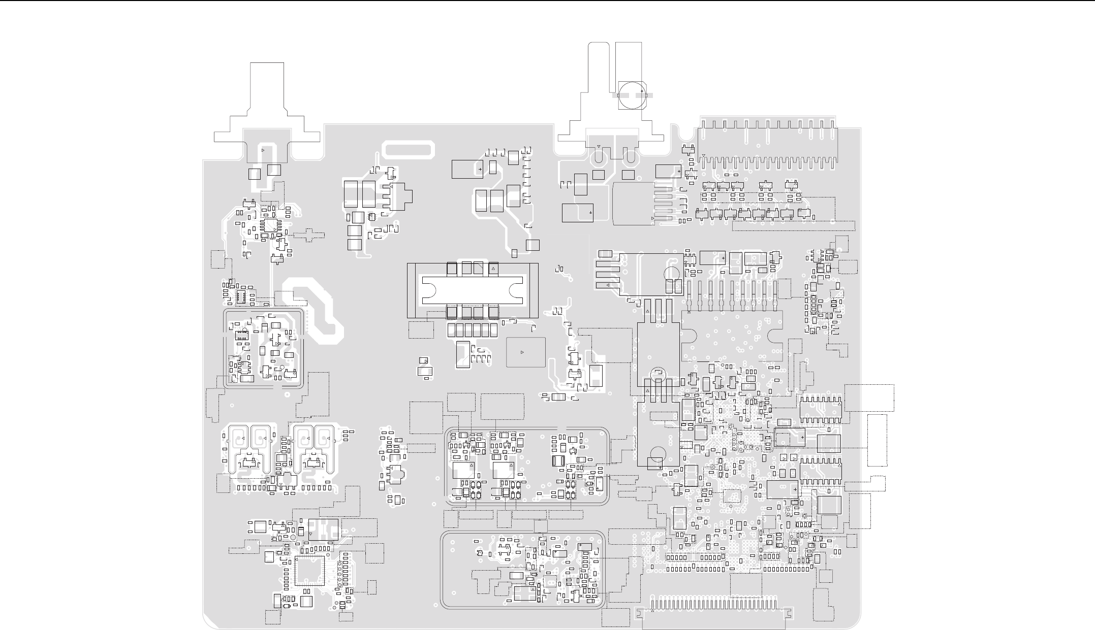
VHF (136–174 MHz) 25–45W PCB/Schematics/Parts List 3-21
3.0 VHF (136–174 MHz) 25–45W PCB/Schematics/Parts List
2.9V_MAKO_V6
3.6V_MAKO_SW1
C0100
C0102
C0103
C0104
C0105
C0109
C0110
C0111
C0113
C0117
C0118
C0120
C0121
C0122
C0124
C0125
C0126
C0127
C0128
C0129
C0130
C0132
C0133
C0140
C0141
C0142
C0143
C0144
C0145
C0146
C0171
C0175
C0177
C0178
C0180
C0195
C0196
C0200
C0201
C0204
C0205
C0206
C0208
C0213
C0214
C0215
C0220
C0223
C0225
C0226
C0229
C0236
C0237 C0240
C0241
C0242
C0243
C0245
C0246
C0247
C0250
C0251
C0252
C0253
C0259
C0300
C0301
C0304
C0305
C0306
C0308
C0310
C0313
C0314
C0315
C0320
C0323
C0325
C0326
C0329
C0332
C0334
C0360
C0361
C0405
C0406 C0408
C0409
C0410
C0411
C0413
C0414
C0415
C0416
C0417
C0418
C0419
C0420
C0423
C0424
C0425
C0426
C0427
C0428
C0429
C0430
C0431
C0432
C0433
C0434
C0435
C0437
C0438
C0439
C0440
C0442
C0450
C0451
C0455
C0457
C0502
C0504
C0509
C0510
C0515
C0516 C0605
C0611
C0615
C0617
C0619
C0620
C0621
C0622
C0623
C0625
C0626
C0627
C0629
C0630
C0631
C0633
C0638
C0642
C0643
C0644
C0645
C0646
C0650
C0700
C0701
C0702
C0703
C0704
C0705
C0706
C0707
C0708
C0709
C0710
C0711
C0712
C0713
C0714
C0731
C0738
C0771
C0776
C0777
C0778
C0779
C0796
C0797
C0798
C0799
C0802
C0804
C0805
C0823 C0824
C0900
C0901
C0904
C0906
C0907
C0908
C0909
C0910
C0914
C0915
C0918
C0921
C0922
C0926
C0929
C0931
C0934
C0935
C0936
C0937 C0939
C0947
C0948
C0949
C0950
C0951
C0960
C0961
C0962
C0963
C0964
C0965
C0966
C0967
C1000
C1001
C1002
C1003
C1004
C1005
C1006
C1007
C1008
C1009
C1010
C1011
C1012
C1013
C1014
C1015
C1016
C1017
C1018
C1019
C1030
C1031
C1034
C1036
C1037
C2000
C2001
C2002
C2003
C2004
C2005
C2006
C2007
C2008
C2009
C2500
C3000
C3002
C3005
C3006
C3007
C3008
C3009
C3010
C3015
C3018
C3019
C3040 C3046
C3202
C3203
C3207
C3208
C3209
C3210
C3211
C3212
C3213
C3216
C3219
C3220
C3225
C3226
C3229
C3234
C3238
C3239
C3240
C3247
C3248
C3249
C3254
C3262
C3273
C3276
C3277
C3278
C3280
C3283
C3292
C3501
C3504 C3505
C3506
C3511
C3513
C3514
C3515
C3516
C3518
C3520
C3523
C3524
C3528
C3529
C3530
C3531
C3538
C3543
C3545
C4000
C4001
C4002
C4003
C4004
C4005
C4006
C4013
C4016
C4017
C4018
C4019
C4020
C4021
C4022
C4023
C4024
C4025
C4026
C4027
C4028
C4029
C4030
C4031
C4032
C4033
C4034
C4035
C4040 C4041 C4042 C4043 C4045
C4046 C4047
C4048
C4075
C4089
C4090
C4091
C4092
C6406
C6407
C6408
C6416
C6417
C6418
C6419
C6420
C6421
C6422
C6423
C6426
C6427
C6428
C6429
C6430
C6431
C6433
C6439
C6440
C6445
C6450
C6451
CLKOUT
CR0201 CR0202
CR0203CR0204 CR0205 CR0206
CR0207 CR0208
CR0300
CR0301
CR0302CR0303
CR0304
D0401 D0403
D0601
D0900
D0901
D0902
D0903
D0907
DOUTA
DOUTB
E0600
E0601
E0602
E0604
E0605
E0606
E0607
E0608
E0700
E0701
E0703
E3000
E3202
E3205
E3500
E3501
E3502 E3503
E4000
E4001
E4005
E6401
E6402
E6407
23
4
5
6
FL0500
FS
3
2
J0700
J3000
25
26
2
J4000
30
J4001
L0100
L0202
L0203
L0207
L0209
L0210
L0212
L0213
L0214
L0215
L0217
L0218
L0219
L0302
L0303
L0307
L0309
L0310
L0312
L0401
L0402
L0403
L0404
L0405
L0407
L0411
L0414
L0504
L0506
L0604
L0608
L0725
L0728
L0900
L0901
L0902
L3200
L3202
1
M0700
MAKO_GATED_32KHz
PC
PD
PE
Q0100
Q0102
Q0106
Q0200
Q0201
Q0300
Q0402
Q0405
Q0501
Q0700
2
3
Q0701
D
G
S
SS
S
87
32
4
56
Q0702
4
3
2
1
Q0704
6
3
4
Q0706
Q0901
16
1
8
9
Q3200
4
58
Q3201
16
1
8
9
Q3202
23
4
Q3203
23
4
Q3204
2
3
Q3500
2
3
Q4000
2
3
Q4002
2
3
Q4004
2
3
Q4005
2
3
Q4006
2
3
Q4008
2
3
Q4010
2
3
Q4011
Q4013
R0100
R0101
R0102
R0105
R0106
R0107
R0108
R0109
R0110
R0111
R0114
R0116
R0117
R0118
R0119
R0123
R0144
R0146
R0147
R0148 R0155
R0156
R0157
R0158
R0159
R0161
R0201
R0204
R0205
R0211
R0216
R0224
R0225
R0226
R0229
R0240 R0241
R0301
R0304
R0305
R0311
R0316
R0319
R0320
R0321
R0404
R0406
R0407
R0409
R0410
R0411
R0412
R0417
R0418 R0419
R0420
R0421
R0422 R0423
R0424
R0425
R0432
R0436
R0437
R0439
R0440
R0441
R0442
R0443
R0444
R0445
R0503
R0510
R0606
R0607
R0608
R0609
R0610 R0611
R0612
R0613
R0614
R0615
R0617
R0618
R0619
R0621
R0622
R0623
R0627
R0712
R0713
R0716
R0721
R0722
R0727
R0729
R0730
R0731 R0734
R0735
R0737
R0738
R0739
R0742
R0745
R0746
R0748
R0749
R0750
R0751
R0752
R0753
R0756
R0757 R0761
R0775
R0777
R0779
R0780
R0781
R0900
R0901
R0902
R0903
R0906
R0907
R0909
R0911
R0912
R0914
R0915
R0916
R0917
R0920
R0923
R0924
R0925
R0926
R0927
R0928
R0929
R0930
R0936R0937
R0940
R0950
R0981
R0982
R0983
R0984
R0985
R0986
R0987
R0988
R0989
R0994
R0995
R1000
R1001
R1002
R1005
R1006
R1014
R1017
R1019
R1020
R1021
R1025
R1027
R1028
R1034
R1035
R1036
R1041
R1045
R1066
R1067
R1071
R2000
R2004
R2005
R2006
R2007
R2008
R2009
R2010
R2011
R2012
R2013
R2014
R2015
R2529
R3002
R3003
R3004
R3009
R3010
R3032
R3033
R3035
R3036
R3042
R3056
R3203
R3205
R3206
R3217
R3218
R3224
R3225
R3233
R3500
R3501
R3503
R3504
R3505
R3507
R3508
R3509
R3514
R3515
R3516
R3520
R3526
R3532
R3535
R3537
R3538
R3547
R3550
R3560
R3571
R3576
R3580
R3583
R3587
R3588
R3590
R3594
R3595
R3596
R4000
R4001
R4002
R4003
R4004
R4005
R4006
R4009
R4010
R4011
R4012
R4040 R4041 R4042 R4043
C4044
R4044
R4045R4046 R4047
R4048
R4050
R4051
R4061
R4063
R4064
R4065
R4066
R4067
R4068
R4069
R4070
R4071
R4093
R4094
R4095
R4096 R4097
R4099
R4105
R6402
R6403
R6443
R6444
R6445
R6446
R6449
R6450 R6454 R6455
R6456
R6458
R6459
R6460
R6461
R6465
R6466
R6467
1
RT0908
RT3500
1
2
SH0100
1
2
SH0200
SH0900
SP0701
SP0702
SP0703
SP0704
SP0705
SP0706
SP0707
SP0708
SP3000
SP3001
TP0601
TP1000
TP4000
TP_MAKO_DCLK
TP_MAKO_FSYNC
TP_MAKO_RX
TP_MAKO_TX
TP_POR
TP_SDRAM_BA0
TP_SDRAM_BA1
TP_SDRAM_CLK
TP_SDRAM_CLKX
TP_SDRAM_CS
U602
1
37
25
13
U0600
U0901
4
58
U0940
U0941
4
5
8
U0943
1
6
5
U3001
U3002
3
2
1
U3005
3
2
1
U3006
3
2
1
U3040
9
U3500
U4004
U4005
U4006
U4007
U4008
U4009
U4010
U6402
U6407
USB1_DAT
USB1_SEO
USB1_TXEN
VBUS1_CMD
VBUS2_CMD
VR0700
VR3202
VR3204
VR3206
VR3503
VR4000 VR4001 VR4002
VR4003
VR4004
VR4005
43
2
Y0100
VHF (136–174 MHz) 25–45W 8478023A17 Top Side
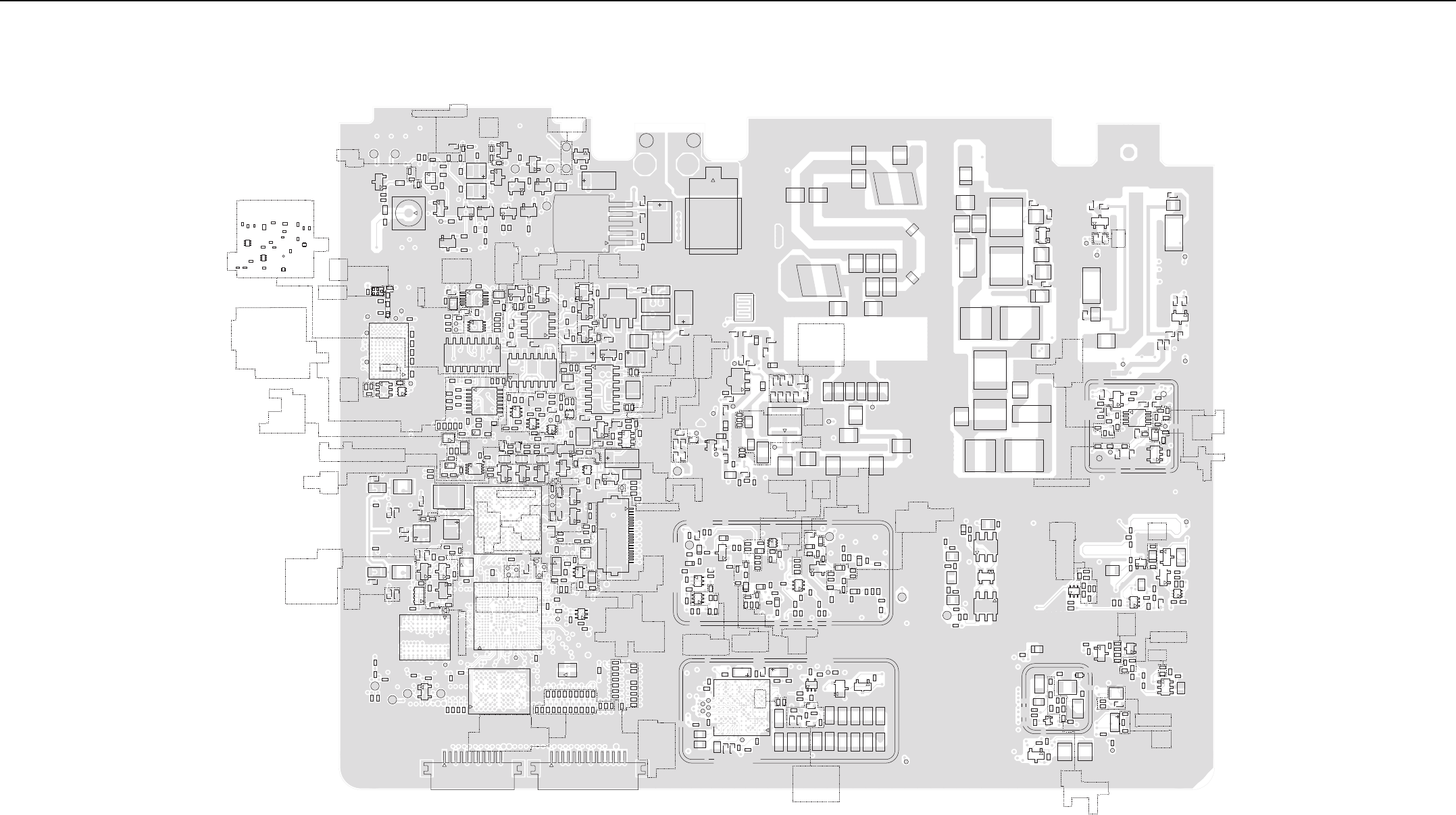
3-22 VHF (136–174 MHz) 25–45W PCB/Schematics/Parts List
1.2V_RTC_TEST
2.8V_RF_TEST
ANT_C
C0101
C0106
C0107
C0108
C0112
C0114
C0115
C0119
C0123
C0131
C0134
C0135
C0136
C0137
C0138
C0147
C0148
C0149
C0150
C0151
C0156
C0157
C0158
C0159
C0160
C0161
C0162
C0163
C0164
C0165
C0166
C0179
C0191
C0192 C0193
C0194
C0202
C0203
C0207
C0209
C0211
C0217
C0218
C0219
C0221
C0222
C0224
C0231
C0233 C0235
C0238
C0239
C0248
C0249
C0257
C0258
C0260
C0261
C0262
C0264
C0265
C0302
C0303
C0307
C0309
C0311
C0312
C0317
C0318
C0319
C0321
C0322
C0324
C0327
C0328
C0331
C0338
C0339
C0348
C0349
C0364
C0400
C0401
C0402 C0403
C0404
C0407
C0412
C0421
C0422
C0436
C0441
C0443
C0444
C0445
C0446
C0447
C0448
C0449
C0452
C0453
C0454
C0456
C0458
C0459
C0460
C0503
C0506
C0507
C0512
C0513
C0514
C0601
C0602
C0603
C0604
C0607
C0610
C0612
C0613
C0614
C0616
C0618
C0628
C0632
C0634
C0635
C0636
C0637
C0640
C0641
C0647
C0648
C0649
C0651
C0716
C0717
C0718
C0719 C0720
C0721
C0722
C0723
C0724 C0725
C0726
C0727
C0728
C0729 C0730
C0732
C0733
C0734
C0735
C0739
C0740
C0741
C0742
C0746 C0747
C0750
C0752
C0753
C0754
C0755
C0766
C0767
C0770
C0772
C0775
C0780
C0783
C0786
C0790
C0791
C0792
C0793
C0794
C0795
C0801
C0803
C0806
C0817
C0818
C0819
C0820
C0821
C0822
C0902
C0903
C0911
C0912
C0913
C0916
C0917
C0919
C0920
C0923
C0925
C0927
C0928
C0940
C0941 C0942
C0943
C0944
C0945
C0953
C1032
C1033
C1035
C1044
C2501
C3011
C3012
C3013
C3014
C3016
C3017
C3020
C3021
C3030
C3031
C3032
C3041
C3042
C3043
C3044
C3045
C3200
C3201
C3204
C3205
C3206
C3214
C3215
C3217
C3218
C3233
C3237
C3260 C3261
C3265
C3266
C3269
C3270
C3272
C3274
C3275
C3279
C3281
C3282
C3289
C3290
C3291
C3500
C3502
C3503
C3507
C3508
C3509
C3510
C3512
1C3517
C3519
C3521
C3526
C3533
C3534
C3535
1
C3536
C3539 C3540
C3541
C3542
C4007
C4010
C4011
C4012
C4014
C4015
C4049
C4051
C4053
C4055
C4058
C4059
C4060
C4061
C4062
C4063 C4064
C4065
C4066
C4067
C4068
C4069
C4070
C4071
C4072
C4073
C4074
C4076
C4084
C4085
C4086
C4087
C4088
C4093
C4094
C6401
C6412
C6413
C6414
C6432
C6434
C6435
C6436
C6437
C6438
C6443
C6444
C6446
C6449
C6452
CLK_ACQ_TEST
CR0400
D0400
D0402
D0405
D0500
D0600
D0700
D0702
D0703
D0904
D0905
D3030
D3040
D3200
D4000
D4001
E0201
E0301
E0400
E0401
E0403
E0404
E0500
E0603
E0609
E0610
E0702
E0704
E2500
E3201
E3203E3206E3208
E4002
E4003
E4004
E4006
E6400
EXT_MIC
EXT_PTT
3
4
2
5FL6401
FT_APM_1_WIRE
FT_EMERGENCY
FT_IGNITION_SENSE
FT_MMP_1_WIRE
FT_USB1_DM
FT_USB1_DP
FT_USB2_DM
FT_USB2_DP FT_VBAT
FT_VBAT_GROUND
FT_VBUS1
FT_VBUS2
I2C_CLK
I2C_DATA
IF_TEST
G2
20
G1
J2500
11
J4002
14
J4003
J6400
L0200
L0204
L0205
L0206
L0211
L0221
L0230
L0300
L0304
L0305
L0306
L0311
L0400
L0406
L0408
L0409
L0410
L0412
L0413
L0503
L0602
L0603
L0605
L0700
L0702
L0705
L0706
L0707
L0708 L0709
L0710
L0714
L0715
L0716
L0717
L0718
L0719
L0720 L0721
L0722
L0723
L0724
L0729
L0730
L0731
L0745
L0903
L0904
L3201
L6402
L6403
MAKO_CE
MAKO_V8_5V
MAKO_V9_3V
OPT_SSI_SYNC
Q0107
2
3
Q0108
Q0202
Q0302
63
4
Q0400
Q0401
Q0403
Q0500
Q0600
Q0601
1
3
Q0703
Q0705
Q0902
Q3030
4
3
2
1
Q3032
Q3040
23
Q3041
2
3
Q3205
6
3
4
Q3206
4
5
8
Q3207
2
3
Q3208
Q3209
Q3210
63
4
63
4
2
3
Q4001
2
3
Q4003
2
3
Q4007
23
Q4009
2
3
Q4012
Q4014
2
3
Q4015
Q6401
63
4
Q6402
R0103
R0104
R0113 R0115
R0120
R0122 R0125
R0126
R0127
R0128 R0131
R0134
R0139
R0140
R0160
R0202
R0203
R0206
R0207
R0208
R0210
R0212
R0213
R0218
R0219
R0220
R0221
R0230
R0302
R0303
R0306
R0307
R0308
R0310
R0312
R0327
R0328
R0332
R0333
R0334
R0336
R0337
R0338
R0339
R0340
R0343
R0345
R0347
R0400
R0401
R0402
R0403
R0408
R0413
R0414
R0415
R0416
R0426
R0427
R0428
R0429
R0430
R0431
R0435
R0500
R0501
R0502
R0508
R0509
R0511
R0512
R0601
R0602
R0603
R0604
R0605
R0616
R0620
R0624
R0625
R0626
R0702
R0706
R0710
R0711
R0714
R0715
R0717
R0718
R0719
R0720
R0723
R0726 R0728
R0732
R0733
R0736
R0740
R0747
R0754
R0755
R0760
R0910
R0913
R0918
R0919
R0921
R0922
R0938
R0941
R0942
R0943
R0944
R0946
R0947
R0951
R0954
R0955
R0960
R0970
R0972
R0973
R0975
R0976
R0977 R0978
R0979
R1026
R1044
R1046
R1047
R1048
R1054
R1060
R1070
R2500
R2501
R2502
R2504
R2506 R2507
R2508
R2509
R2510
R2511
R2512
R2513 R2514
R2515
R2516
R2517
R2518
R2519
R2520
R2524
R2525 R2526
R2527
R2528
R3005 R3006
R3007
R3008
R3030
R3034
R3037
R3038
R3039
R3040 R3041
R3043
R3044
R3045
R3046
R3047
R3048
R3050
R3051
R3052
R3053
R3054
R3055
R3057
R3200
R3204
R3207
R3208
R3209
R3210
R3215
R3216
R3219
R3220
R3222 R3223
R3226
R3227
R3228
R3236
R3237
R3238
R3239
R3240
R3241
R3243
R3245
R3246 R3247
R3248
R3249
R3250
R3252
R3253
R3502
R3506
R3510
R3511
R3512
R3513
R3521
R3523
R3524
R3525
R3528
R3529
R3540
R3545
R3546
R3548
R3556
R3558
R3559
R3569
R3572
R3573
R3574
R3575
R3577
R3578
R3579 R3581
R3582
R3584 R3585
R3586
R3591
R3592
R3593
R4023
R4030
R4031
R4032
R4033
R4034
R4035
R4049
R4054
R4055
R4074
R4076
R4078
R4080
R4081
R4082
R4083
R4085
R4086
R4088
R4089
R4090
R4098
R4100
R4101
R4103
R4106
R6401
R6404
R6405
R6407
R6409
R6410
R6411
R6416
R6417
R6418
R6419
R6420
R6430
R6432
R6433
R6434
R6435
R6436
R6437
R6438
R6439
R6440
R6457
R6464
R6468
R6469
R6470
RF_ATTN_2
ROUT_TEST
1
RT0953
S0700
1
2
SH0101
1
2
SH0300
2
1
SH0500
12
SH0901
SPI_CLK_1
SPI_CLK_TEST
SPI_MISO_1
SPI_MOSI_1
6
4
3
T0400
64
3
T0401
TP501
TP502 TP503
TP504
TP0200
TP0300
TP0301
TP0400
TP0401
TP0600
TP0702
TP0703
TP0704
TP0705
TP0707
TP0709
TP0710
TP0711
TP0713
TP0903
TP0904
TP0907 TP0909
TP0910
TP0911
TP0913
TP_ADAPT_SW
TP_DDR_LDQS
TP_DDR_UDQS
TP_FLASH_CLK
TP_TEST1
TP_TEST2
TP_VCTRL
TX_RAMP
TX_RAMP_DAC
L11A11
L1
U0100
4
3
5
U0101
U0201
6
3
4
U0303
U0304 U0305
U0601
U0700
U0900
U0942
A21 AA21
AA1
U1000
43
6
U1006
A1 M1
M8
A8
U2000
K1
A9
K9
U2001
1
6
5
U3003
U3004
14
58
U3030
P1
A1
A14 P14
U3200
64
3
U3201
C1
C3A3
U3202
4
3
5
U3203
10
6
5
U3501
7
8
14
U3502
85
4
U3503
U3504
7
814
U3505
85
4
U3508
16
1
8
9
U4000
14
7
8
U4001
P10
A10
P1
A1
U6401
U6404
C1
C3
A3
U6405
U6406
U6408
VR3000
VR3040
VR3200
VR3201
VR3203
VR3205
VR3207
VR3208
VR3502
VR3504
VR4006
VR4009
VR6400
43
2
Y1000
4
3
2
Y3200
Y3201
R3544
R3552
R3555
C3522
C3525
Q3505
R3533
R3534
R3536
R3549
C3527
R3541
R3542
R4079
Q3504
R3551
R3553
R3554
R3530
C3532
INT_MIC
Q3503
Q3502
C3221
C3222
C3227
C3228
C3231
C3232 C3243
C3252
C3257
VHF (136–174 MHz) 25–45W 8478023A17 Bottom Side
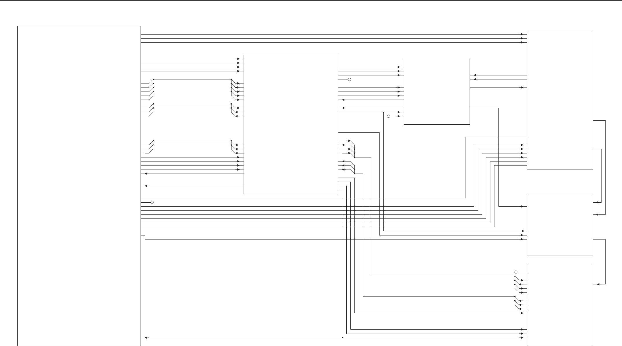
VHF (136–174 MHz) 25–45W PCB/Schematics/Parts List 3-23
CONTROLLER_&_GPS_R6
( TOP LEVEL: SHEET 1)
RXFE_VHF
( 1 SHEET )
( PA: SHEET 1 )
( PC: SHEET 2 )
TX_HP_VHF
VCO_VHF
( TX: SHEET 1 )
( RX: SHEET 2 )
RXBE_44.85MHZ
(IF AMP: SHEET 1)
(ABACUS3: SHEET 2)
SYNTH
2
1
3
1
1
1V8
5V
5V_FE
IF
NC
2
0
REF_CLK
SPI_ABACUS_CEX
SPI_ABACUS_CLK
SPI_ABACUS_DATA
SSI_ABACUS_CLKOUT
SSI_ABACUS_DOUTA
SSI_ABACUS_DOUTB
SSI_ABACUS_FSYNC
SSI_ABACUS_SYNCB
2
0
SPI_CLK_IN
SPI_CLK_OUT
SPI_MISO_IN
SPI_MISO_OUT
SPI_MOSI_IN
SPI_MOSI_OUT
TH_CEX
TX_CLK
TX_VCO_SEL1_
TX_VCO_SEL2_
VCTRL
1
4
LOCK
PRSC
RF_ATTN_1
RSTB RX_SSI_CLK_PASS_IN
RX_SSI_CLK_PASS_OUT
RX_SSI_DATA_PASS_IN
RX_SSI_DATA_PASS_OUT
RX_SSI_FSYNC_PASS_IN
RX_SSI_FSYNC_PASS_OUT
RX_VCO_SEL1_
RX_VCO_SEL2_
SDTX
SFTX
SF_OUT
1.8V_TH_DIG
16.8_GPS
16.8_REF
1V8_BE
2.8V_TH_ANA
2.8V_TH_DIG
5V
5V_BE
9R1
9V3
ABACUS3_CEX_IN
ABACUS3_CEX_OUT
ABACUS3_SYNCB_IN
ABACUS3_SYNCB_OUT
ADAPT_SW
DMCS
HP_MOD_OUT
3
0
0
2
2
1
1
2
0
0
2
3
1
0
9R1
9V3_SYNTH_IN
9V3_SYNTH_OUT
9V3_VCO
HP_MOD_OUT
PREDRIVE_SW
PRSC
RXINJ
RX_VCO_SEL1
RX_VCO_SEL2
SF_TH
TXINJ
TX_VCO_SEL1
VCTRL
PRESSURE_PAD
RX_IN
TX_DAC
TX_INJ
VSWR_DET
1
4
NC
2
0
2
9V3
9V3_PA
9V3_SYNTH
9V3_TX_SW
9V3_VCO
ANT_ENABLE
FINAL_BIAS_1
LO_BATTERY_DET
LO_PWR_DET
PA_SUPPLY
SPI_MISO
SPI_MOSI
THK_CS
TX_SSI_CLK
TX_SSI_DATA
TX_SSI_FSYNC
NC
9R1
9V3_TX_SW
FE_TUNE IF
RF_ATTEN_1
RX_IN
RX_INJ
LOCK_DETECT
LO_BATTERY_DET
MAKO_ADC5
MAKO_ADC8
MAKO_DAC1
MAKO_DAC2
MAKO_RAMP_DAC3
PC_ATTEN_ENA
PRESSURE_PAD_DET
RAW_B+
RESET_OUT
RX_SSI_CLK
RX_SSI_DATA
RX_SSI_FSYNC
RX_SSI_SYNCB
SPI_CLK
1
NC
1.875V_DIG_V2
16.8_GPS
16.8_MHZ_BUFF
2.775V_ANA_V7
2.775V_DIG_V4
5V_SW
9V3
9V3_PA
ABACUS3_CS
ADAPT_SW
ANT_ENABLE
DMCS
TX_SSI_BUS(0:2)
ABACUS_SPI_BUS(0:3)
SPI_BUS(0:4)
RX_SSI_BUS(0:2)
ABACUS_SSI_BUS(0:2)
1
2
0
3
0
VHF (136–174 MHz) 25–45W Overall Schematic Diagram
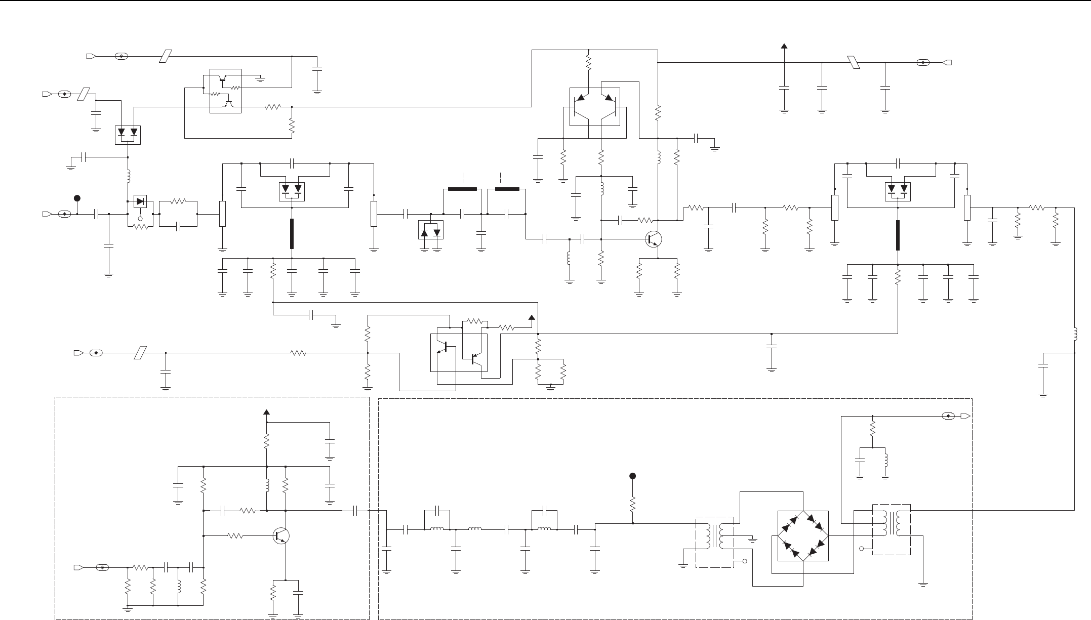
3-24 VHF (136–174 MHz) 25–45W PCB/Schematics/Parts List
(In-Band Tuning range 2.70 ~ 7.80 VDC)
10 dB Attenuator
10 dB Attenuator ON @ High for RF_ATTEN_1
MAKO ( 0 ~ 4.6 VDC)
(Micro-strip 40 mm Aggregate)
Hi-Side Zeros for Preselector
8:1 Balun
4:1 Balun
7.5 dB Attenuator
R0445
R0444
L0413
C0459
C0451
NU
R0443
NU
R0442
R0441
C0432
C0409
R0413
C0418
NU
C0460
9V3_TX_SW_8
C0415
C0428
C0437
C0404
R0411
R0431
D0402
R0402
1IO1 2
IO2
3
IO3
4IO4
C0414
D0405
C0458
C0405
R0414
R0404
9R1_FILT
C0436
C0417
C0440
C0445
Q0402
(VALUE)
L0406
9R1_FE_7
C0447
C0454
D0401
R0407
R0437
R0408
R0403
C0434
R0424
C0416
TP0400
1
C0443
C0419
C0429
R0420
RXIN_FE_6
C0423
C0450
C0455
C0426
RF_ATTEN_1_8
D0403
R0416
C0435
R0409
R0421
C0410
(VALUE)
C0427
C0457
R0400
C0401
L0401
(VALUE)
T0400
NC 5
4
6
3
2
15NC
4
6
3
2
1
L0400
C0424
T0401
R0422
C0442
R0430
L0410
E0404
C0407
C0402
C0408
3
2
C0421
L0404
1
C0431
R0426
E0401
CR0400
1
3
2
C0441
1
RX_INJ_FE_5
R0417
TP0401
9R1_FILT
FE_TUNE_FE_3
C0403
R0406
NC
R0429
R0412
13
2
NC
L0403
R0401
C0444
C0438
C0433
C0425
R0428
R0410
R0436
C0400
C0449
13
2
NC
Q0401
C0422
L0405
(VALUE)
R0435
R0419
C0411
(VALUE)
C0456
C0439
3
2
L0412
L0402
1
C0420
NU
C0412
C0406
L0411
Q0405
E0400
9R1_FILT
R0415
L0407
R0432
R0423
D0400
C0453
IF_FE_3
R0425
3
1
4
C0430
Q0400
2
5
6
C0448
R0427
Q0403
2
3
6
4
1
5
L0409
C0413
(VALUE)
L0414
C0446
E0403
R0439
R0440
(VALUE)
C0452
L0408
R0418
9V3_TX_SW
FE_TUNE
RX_IN
RX_INJ
9R1
RF_ATTEN_1
IF
VHF (136–174 MHz) 25–45W Receiver Front-End Schematic Diagram
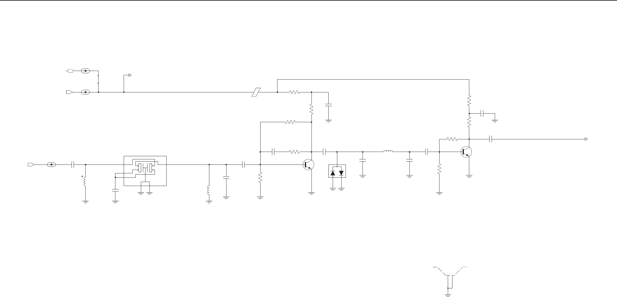
VHF (136–174 MHz) 25–45W PCB/Schematics/Parts List 3-25
4-POLE
0.72V
1.43V
0.76V
1.6V
VHF -- 44.85MHz
IF_TO_ABACUS
R0501
IFIN_BE_8
R0511
C0514
R0512
R0509
R0508
C0510
L0504
NU
IN
3OUT 6
FL0500
44.85MHz
CC1
2
CC2
5
GND1
1
GND2
4
C0516
NU
L0506
5V_BE_5
NU
C0515
C0502
C0503
C0513
1
2
C0512
R0503
SH0500
Q0501
L0503
E0500
RX_FE_3
C0509
NU
R0510
C0506
C0507
Q0500
1
3
2
C0504
R0500
R0502
D0500
IF
IF_OUT
5V
5V
5V_FE
VHF (136–174 MHz) 25–45W Receiver IF Amp Schematic Diagram

3-26 VHF (136–174 MHz) 25–45W PCB/Schematics/Parts List
2nd LO VCO VHF (42.6MHz/47.1 MHz)
SPF_3.5V
CLOCK LF
2nd LO LF
#
#
#
CLOCK VCO
#
*
NU
R0622
R0626
E0603
R0608
C0622
DOUTB
C0645
TP0600
3VA
R0620
E0604
3VA
R0604
2FB
5
GND
6NP
4VCONT
3VIN
1
VOUT
3VA
U0601
C0615
3VA
R0612
C0619
C0641
DOUTA_1_BE_5
R0624
E0610
C0617
E0606
R0619
NU
E0601
C0647
R0623
L0603
D0601
C0643
DOUTB_1_BE_5
C0614
PD
C0628
14
VREFN
12 VREFP
11
C0625
9
VDDC
17
VDDD 26
VDDF
6
VDDH 27
VDDI 48
VDDL 40
VDDP 39
VDDQ
43
MXON
2MXOP
1
PC
23
PD
24
PE 25
13 RREF
SYNCB 33
VDDA
21
GNDS2 34
IF2N
4
IF2P
5
IFIN 47
IOUTC
15
IOUTL 38
LON 42
LOP
18
GNDD
22
GNDF
3
GNDH 32
GNDI 45
GNDL 36
GNDP 37
GNDQ
16
GNDS1
41
DOUTA 29
DOUTB 30
FREF 35
FS 31
GCN
8GCP
7
GNDA
10
GNDC
CLKN
20
CLKOUT 28
19 CLKP
CXIF 46
CXVL 44
CXVM
FS_1_BE_5
U0600
C0637
Q0600
1V8_3
C0612
E0608
C0650
R0609
R0617
R0601
R0610
C0603
R0614
C0633
C0631
C0629
CLKOUT
FS
5V
3VA
C0623
C0616
3VA
FREF_IF
NU
C0610
R0618
C0630
C0613
PE
C0646
E0600
L0602
C0636
C0635
3VA
C0651
R0613
C0618
C0648
L0604
C0626
CLKOUT_1_BE_5
C0601
R0602
R0616
VVCO
R0627
R0621
R0603
FC_1_BE_5
C0640
D0600
E0607
VVCO
E0609
C0627
C0604
C0621
C0634
R0625
C0649
R0615
E0605
FE_1_BE_5
E0602
Q0601
3VA
C0611
L0605
C0644
NU
C0605
R0607
PC
SB_1_BE_5
TP0601
C0632
U602
1
C0607
L0608
3VA
DOUTA
R0606
C0642
R0611
FD_1_BE_5
R0605
C0602
C0638
C0620
IF_OUT
5V
SSI_ABACUS_FSYNC
SPI_ABACUS_CEX
REF_CLK
SPI_ABACUS_CLK
SSI_ABACUS_DOUTA
SSI_ABACUS_CLKOUT
SSI_ABACUS_DOUTB
SPI_ABACUS_DATA
SSI_ABACUS_SYNCB
1V8
1V8
VHF (136–174 MHz) 25–45W Receiver Back-End Schematic Diagram
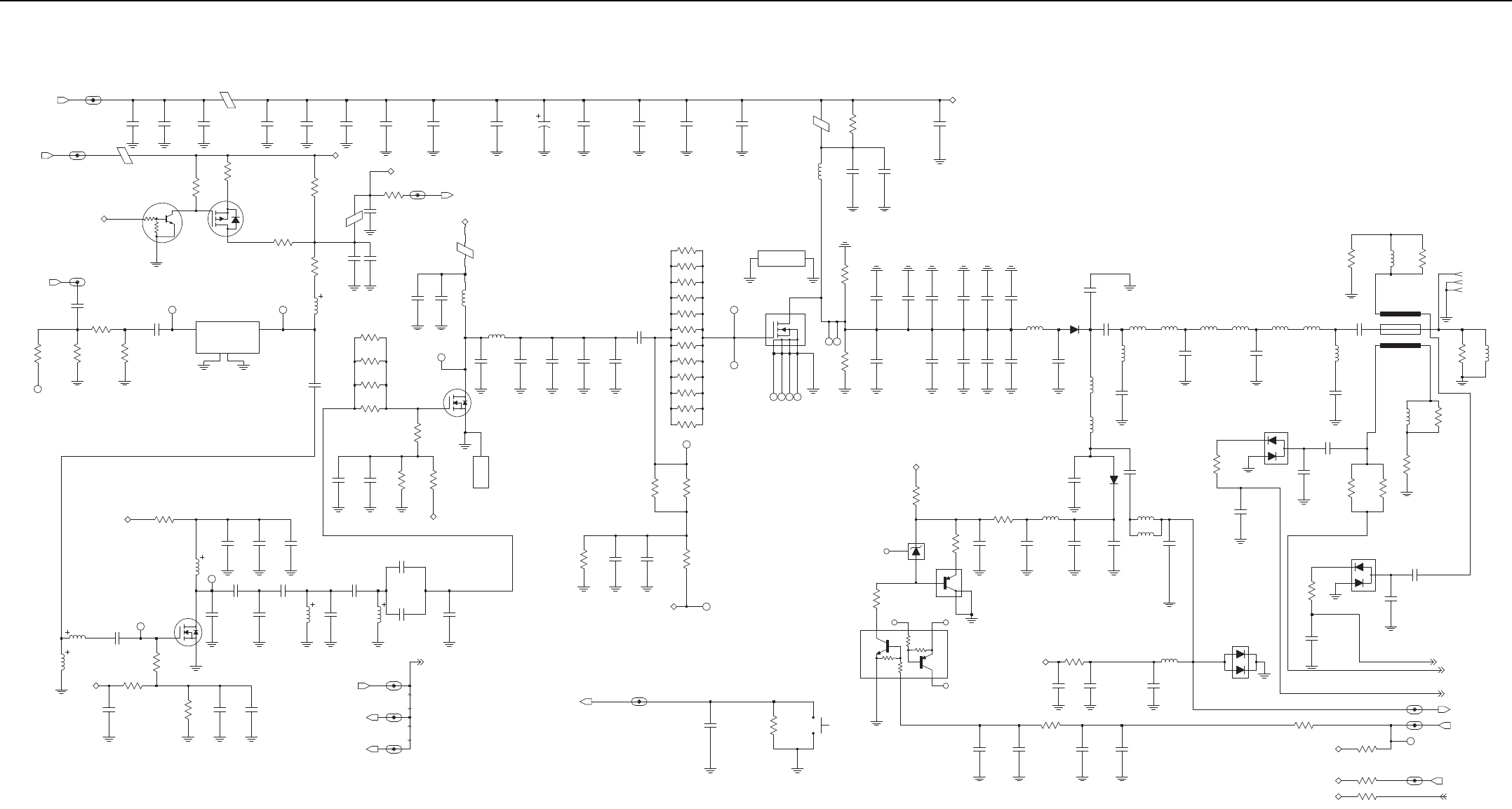
VHF (136–174 MHz) 25–45W PCB/Schematics/Parts List 3-27
PA_SUPPLY_TX_PA
PA_SUPPLY
9V3_PA
C0710
E0700
C0700 C0712 C0708 C0709C0738C0703C0701 C0702
NU
C0707C0705
NU
C0706C0704 C0711
10K
47K
Q0701
R0780
R0777
Q0700
E0703 R0779
Antenna_En
C0718
NU
C0732
E0704
C0806
R0702
NU
GND1
GND2
RF_IN VD_RF_OUT
3.3V @ Id=27mA
+4 dBm
-11 dBm
U0700
2
4
13
TP0703
R0706
TP0704 L0705
+8 dBm
Test Point to check Ref Osc warping
R0711
TX_INJ_TX_PA
C0728
R0714
TP0705
R0715
R0760
TX_INJ
C0733
9V3
9V3
9V3_VCO
9V3_SYNTH
NU
C0794
2.70V @ Vcont=4.5V (Ids=100mA)
NU
C0821
R0750
NU
C0771
L0716
TP0710
C0786
R0751
C0791
C0801
L0715
NU
C0817
C0793
NU
L0719
NU
C0780 C0783
C0820
NU
R0747
C0775
NU
Q0705
D
G
S
L0717
C0795
C0802
NU
L0718
C0790
R0740
C0792
TP0709
V_cont
9V3_TX
2.46V @ Vcont=4.5V (Ids=700mA)
R0727
R0722
M0700
1
POS
C0770
R0728
NU
C0818
V_cont
D
G
3
S
2
Q0703
1
TP0702
R0754
R0720
R0755
R0718
C0734
C0819
L0745
C0755
NU
C0754
NU
C0753
C0752
C0746
NU
C0716
C0717
E0702
L0702
9V3_TX
To Rx PIN diode for 12mA bias
To Tx/Rx Switch bias - 10mA
R0746
9V3_TX_SW
9V3_TX_SW
9V3_TX
9V3_TX_SW_Main
R0736
R0716
R0717
R0739
R0721
R0734
R0737
R0726
R0712
R0732
R0733
R0719
1
1
1
1
SP0704
SP0703
SP0702
SP0701
C0805
NU
C0804
R0756 R0757
TP0711
R0730 R0731
NU
Final_Bias
C0966
PRESSURE_PAD_TX_PA
PRESSURE_PAD
S0700
NU
R0775
C0798
R0748
C0796 C0797
C0799
Long Trace around PA
Bypass both sides
C0823
R0781
C0824
NU
C0822
L0729
9V3_TX_SW_Main
R0745
NC
NC
Q0704
Q0706
NC
R0738
R0729
NC
VR0700
A+
C0772
L0731
C0778C0777 C0779
D0702
L0730
C0766
C0767
L0725
R0735
C0776
C0714
E0701
L0700
R0742
C0731
NU
C0713
A+
HS0700
1PIN1 2
PIN2
SP0705 1SP0706
1
1
SP0707
SP0708 1
Q0702
R0723
NU
C0725 C0741C0727C0721
NU
C0729C0719
L0714
NU
C0724
R0710
C0720 C0730C0747 C0722C0726
NU
L0710
D0700
L0724
L0721 L0706 L0709L0708
L0707L0720
C0803
L0722
C0735
C0740
C0739
C0742
L0723
C0750
R0977
C0941
R0976
C0940
R0973
L0904
NU
R0975
D0904
R0978
C0942
C0943
C0944
R0979
C0945
D0905
D0703
RX_IN_TX_PA
ANT_ENABLE_TX_PA
RX_IN
ANT_ENABLE
FINAL_BIAS_1
FWD_DETECTED
FWD_POWER
REV_DETECTED
V_CONTROL
IF5
TP0713
R0749
R0761
R0753
R0752
Final_Bias
Antenna_En
V_cont
W = 22.6 mil
L = 1030 mil
S = 35.4 mil
W = 90.2 mil
S = 35.4 mil
W = 22.6 mil R0713
L0903
NU
R0972
R0970
J0700-1
1
2J0700-2
L0728
C0723
J0700-33
TP0707
VHF (136–174 MHz) 25–45W Power Amplifier Schematic Diagram
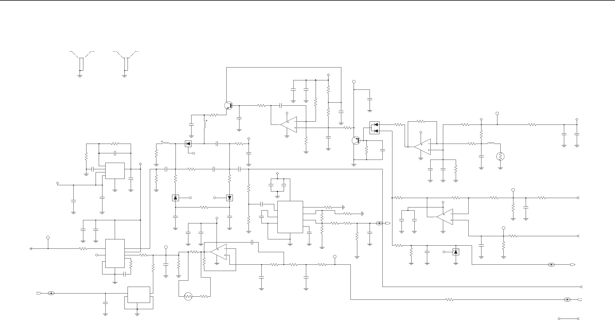
3-28 VHF (136–174 MHz) 25–45W PCB/Schematics/Parts List
12
SH0901
12
SH0900
GND
6NP
4VCONT
3VIN
VOUT
U0941
2FB
5
C0949
C0948
C0951
R0937
9V3
1
R0936
C0950
C0947
5V
2.85V (44W)
2.10V (27.5W)
R0940
TP0909
LO_BATTERY_DET
V_CONTROL
LO_BATTERY_DET
C0922
8
U0940
C0921
VAPC
VPOS
VSET
COMM
ENBL
FLTR
GND
NC
RFIN
R0950
C0926
7
3
5
2
4
9
6
1
R0941
NC
NC1 NC2
RESET_OUT
U0942
GND
INPUT
C0953
45
1
3
2
RT0953
R0946
R0954
R0955
C0925
1.35V (44W)
1.28V (27.5W)
TP0910 R0942
C0902 C0903
L0902
R0928
D0902
R0924
D0901
C0936
NC
NC
NC
C0931
R0925
R0927
9V3_PC
D0903
C0937
R0929
C0935
R0926 C0934
C0914 R0917
9V3_PC
C0918
R0913
L0901
Q0902
C0912
4
U0900-1
2
3
1
8
C0916
9V3_PC
R0910 C0917
R0960
R0921
C0913
R0918
R0919
R0922
C0920
Q0901
C0919
C0911
9V3_PC
1.0V or less, typical
C0915
R0930
D0900
TP0907
C0929
R0906
6
5
7
8
4
U0901-2
R0900
9V3_PC
C0906
R0909
C0907
R0902
L0900
R0903
R0901
TP0913
C0904 RT0908
9V3_PC
2.67V (44W)
2.01V (27.5W)
0.38V (44W)
0.21V (27.5W)
R0916
TP0904
C0939
C0910
R0920
R0912
R0911
TP0903
R0915
VSWR_DET
TX_DAC
9V3
VSWR_DET
FWD_POWER
9V3
FWD_DETECTED
REV_DETECTED
TX_DAC
C0900 C0901
9V3
R0907
R0923 R0914
9V3_PC
2
3
U0901-1
1
8
4
NC D0907
5.1V
C0967
R0938
R0987
R0986
C0909C0908
LO_PWR_DET
LO_PWR_DET
C0965
NU
R0985
R0944
NU
R0983
C0964
R0984
TP0911
R0982
R0981
R0994
R0995
VOUT
VPOS
VSET
CLPF
COMM
GND
INHI
INLO
TADJ
5
7
4
3
2
9
1
8
6
U0943
C0962C0961
C0960
R0989
5V
C0923
C0963
R0988
R0951
R0943
C0927 C0928
R0947
6
5
7
8
4
U0900-2
VHF (136–174 MHz) 25–45W Power Control Schematic Diagram
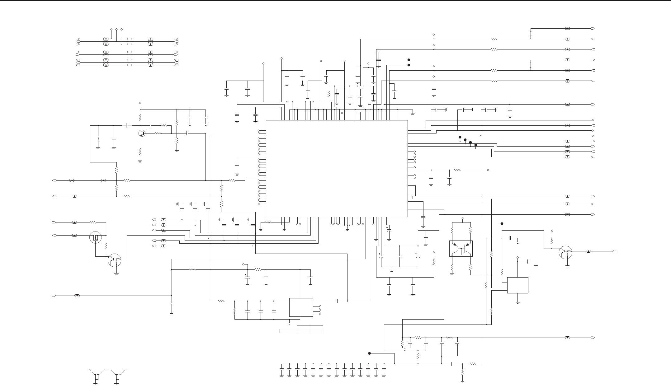
VHF (136–174 MHz) 25–45W PCB/Schematics/Parts List 3-29
R1
R2
10K
47K
0.5 ppm
VHF=1500pF
---
Note: High Port modulation injection through loop filter for U1 and U2 only
HI: 2.8V
U1=220pF
U2=120pF
C0191,C0192,C0193,C0194: NU (UHF B1)
VHF=1500pF
SF_OUT VOLTAGE: 2.45V
Unlocked: 0V
U1=220pF
Buffer to Abacus/Controller
9R1 SWITCH FOR FRONT-END
C0157, C0159, C0160,C0162,C0163,C0191,C0192,C0193,C0194: NU (UHF B2)
GPO LINES
U2=120pF
U1=220pF
U1=220pF
VCO STEERING LINE VOLTAGE: 0.6V TO 4.4V
U2=120pF
VCO STEERING LINE VOLTAGE: 0.6V TO 4.4V
VHF=1500pF
VHF=1500pF
U2=120pF
U2=120pF
Adapt OFF: 0V
U1=220pF
VHF=1500pF
4875188M01
LOW: 0V
1.5 ppm
VCO SEL: ACTIVE LOW
Adapt ON: 5V
Locked: 1.8V
GPO_4
TCXO (Y0100)
Switch for Adapt Transient
NC
NC
NC
R0170
C0166
C0100
C0105
L0100
C0137
RX_SSI_DATA_IN
NC
R0114
R0147
SPI_MOSI_IN
NU
ABACUS3_SYNCB_OUT
R0100
NC
5V_BE_SYNTH
TP504
1
RX_SSI_CLK_OUT
C0107
NC
NC
C0136
C0133
NC
C0140
1
C0106
NC
TP_TEST1
SPI_MISO_IN
R0160
NC4
3
OUTPUT
4
VCC
1VCONT
NC
NC
NC
Y0100
16.8MHz
GND
2
5
NC1
NC2 6
NC3 7
8
R0113
9R1_SYNTH
C0148
C0102
C0138
3GND
1INOUT
4ONOFF_CONTROL
2OUTIN
5
VCC
R0125
NC
U0101
NC
GPO_3_SYNTH
NC
NC
C0179
ABACUS3_SYNCB_IN
RX_SSI_DATA_OUT
C0147
C0135
C0171
C0132
C0157
C0127
NC
LOCK_SYNTH
R0140
C0120
Q0100
C0194 C0159
C0191
NC
VCTRL_SYNTH
C0126
C0112
NC
NC
NC
NC
1V8_BE_SYNTH
SF_OUT_SYNTH
R0158
NU
HP_MOD_OUT_SYNTH
16.8_REF_CONTROLLER_SYNTH
NU
C0119
NC
NU
C0113
NC
1
R0148
1
2
TP_VCTRL
SH0100
1
2
SH0101
R0159
C0144
NC
C0160
ABACUS3_CEX_IN
R0118
C0141
NC
RX_SSI_CLK_IN
C0162
C0103
R0103
R0107
C0124
Q0108
R0122
NC
RX_SSI_FSYNC_IN
NC
NC
NU
C0161
C0122
NU
GPO_6_SYNTH
9V3_SYNTH
R0157
Q0106
GND
IN
OUT
C0117
C0134
R0115
TX_DAC_VCC
G7
TX_GND1
F6 TX_GND2
J6
TX_VCC
F1
VCO_DAC
K5 XOSC_BASE
XOSC_EMIT
L5
G6
XOSC_GND
TCLK
D7
TEST1 C7
TEST2
B3
TM
F10
TXCLK
K7 TXI
L7 TXQ
H7
TX_DAC_GND L6
SPI_CLK
D10
SPI_DR
D9
SPI_DW
SSI_GND E8
E11
SSI_VCC
SUB1
K10
F5 SUB2
F3 SUB3
G8
SDM_VAG
A9
SDM_VREFM B8
SDM_VREFP
D11
SDR
F11
SDTX
F9
SFTX
K4 SF_OUT
C9 SMD_CLK_GEN_GND
C11
A5
RX_AVCC2
RX_EN_OUT
B1
D3
SCAN_EN
F2 SCAN_IN
E9
SCLK_OUT
SDM_CLK_GEN_VCC A10
SDM_REF_GND A8
SDM_REF_VCC B9
B10 RXFS
C2 RXI
C1 RXIX
D1 RXQ
D2 RXQX
RX_AGND1 C3
D5
RX_AGND2
B2
RX_AVCC1
OSCREG_GND
OSCREG_OUT
H5
J4 OSCREG_SPLY
K11 PABIAS_DAC
L9 PHCLK
RFSTEPA
A3
E6 RSTB
E7
RXACQ
E10
M_PRSCX
A1 NC1
A11 NC2
NC3
L1
L11 NC4
NTXI
L8
NTXQ
K6
L4 OSCREG_BYP
J5
MAIN_GND
MAIN_PDET_VCC G2
J1
MAIN_VCC
H1
MN_ADAPT_CP
G3
MN_CP
G5
MN_CP_GND
MN_CP_VCC H2
J2
M_PRSC
H3
GPO5
H8 GPO6
K8
HP_MOD_OUT
J9 INCR_DECR
F8
LGND1 C8
LGND2
G10
LVCC1
B7
LVCC2
G4
ESC_TEST
K2
ESC_VCC
C6 FBI
B6 FBQ
B4 GPO1_TEST1
A4 GPO2_TEST2
GPO3_TEST3
E5
GPO4_TEST4
D4
K9
EF_OUTM
J8
J7 EF_OUTP
ESC_CP L3
ESC_CPBIAS L2
K3
ESC_CP_GND J3
ESC_CP_VCC
H4
ESC_GND
K1
ESC_IN
E1
G9 CLK_CP
H11 CLK_EMIT
H10
CLK_GND
J10
CLK_VCC
G1
DAC_ADAPT
A2 DC_CAL
L10 DEEPSLEEP
F7
DMCS
BP_I
F4 BP_IX
E2 BP_Q
BP_QX
E3
D8
CEX
H9 CLK1_OUT
J11 CLK2_OUT
G11 CLK_BASE
D6 ACE2
AGC_DAC
B5
AGC_FLAG
C4 AGC_REF
C5
H6 ARX_DAC
C10 ASPI_CLK
B11 ASPI_DATA
A7
ASPI_VCC
E4
U0100
A6 ACE1
DMCS_SYNTH
C0131
C0130
R0131
C0128
SPI_CLK_IN
NU
C0121
1
NC
TP_TEST2
C0129
C0165
R0146
ADAPT_SW_SYNTH
C0143
C0125
2.8V_TH_ANA_SYNTH
RX_SSI_FSYNC_OUT
C0178
C0177
C0175
NC
SFTX_SYNTH
NC
C0156
R0105
R0110
R0144
NC
R0161
C0110
PRSC_SYNTH
R0116
C0101
NC
C0164
C0104
NC
R0134
C0123
C0158
TX_CLK_SYNTH
C0109
NC
NU
R0126
Q0107
R0120
R0155
C0146
ABACUS3_CEX_OUT
NC
1
NC
C0115
TH_CEX_SYNTH
TP_ADAPT_SW
SPI_MOSI_OUT
GPO_2_SYNTH
R0102
TP503
1
NC
C0142
C0108
NC
NC
NC
SDTX_SYNTH
NC
R0104
R0111
RSTB_SYNTH
1.8V_TH_DIG_SYNTH
C0180
TP501
1
R0119
R0128
R0123
C0145
R0108
C0114
C0149
C0196
C0195
SPI_CLK_OUT
16.8_GPS_SYNTH
SPI_MISO_OUT
C0111
NU
C0151
R0156
2.8V_TH_DIG_SYNTH
C0150
R0127
R0106
NC
4
NC
Q0102 2
1
3
NC
NC
R0101
R0117
R0109
5V_SYNTH
TP502
1
GPO_1_SYNTH
C0163
GPO_5_SYNTH
16.8_REF_BE_SYNTH
C0118
C0193
NC
NC
C0192
ABACUS3_SYNCB_IN ABACUS3_SYNCB_OUT
VCTRL
9V3
R0139
SPI_MOSI_IN
SPI_MOSI_IN
SPI_CLK_IN
SPI_CLK_IN
SPI_MISO_IN
SPI_MISO_IN
5V
2.8V_DIG
RX_VCO_SEL1_
5V_BE
9R1
16.8_REF
1V8_BE
1.8V_TH_DIG
1.8V_DIG
RSTB
16.8_GPS
ADAPT_SW
5V_TH
TX_VCO_SEL1_
HP_MOD_OUT
TH_CEX
SPI_MOSI_IN
SPI_CLK_IN
2.8V_TH_DIG
2.8V_DIG
2.8V_TH_ANA
2.8V_ANA
1.8V_DIG
1.8V_DIG
5V_TH
RX_SSI_DATA_PASS_OUT
RX_SSI_CLK_PASS_OUT
RX_SSI_FSYNC_PASS_OUT
RX_SSI_CLK_PASS_IN
ABACUS3_CEX_OUT
SPI_MISO_OUT
SPI_MOSI_OUT
SPI_CLK_OUT
ABACUS3_CEX_IN
RX_SSI_DATA_PASS_IN
RX_SSI_FSYNC_PASS_IN
TX_VCO_SEL2_
RF_ATTN_1
RX_VCO_SEL2_
PRSC
2.8V_ANA
DMCS
5V_TH
2.8V_ANA
1.8V_DIG
2.8V_ANA
2.8V_ANA
SDTX
SFTX
SF_OUT
LOCK
TX_CLK
SPI_MISO_IN
2.8V_ANA
5V_TH
VHF (136–174 MHz) 25–45W Synthesizer Schematic Diagram
3-30 VHF (136–174 MHz) 25–45W PCB/Schematics/Parts List
RX1_SEL: 2.7 V (High)
Super Filter Voltage (SF_TH)
VCTRL: 0.6-4.5 V
RX VCO 1
SF_TH: 2.5 V
Steering Line Voltage (VCTRL_TH)
RX Buffer Amplifier
RX Prescaler
0.1 V (Low)
RX2_SEL: 2.7 V (High)
RX VCO 2
PRSC (RX): 180-220 MHz
RXINJ: 180-220 MHz
0.1 V (Low)
-5 to -15 dBm
+10 dBm
TP0301
1
C0231
PRSC_VCO_UHF1_5
L0211
C0211
L0206
R0202
CR0208
L0204
CR0202
C0215C0214
R0207
9R1_VCO_UHF1_7
CR0205
U0201
RX2_SEL_VCO_UHF1_5
R0201
R0230
R0208
C0209
Q0201
C0248
R0204
C0221
C0250
C0259
R0221
L0202
C0237
L0221
R0203
L0210
L0213
L0218
L0217
R0220
R0206
C0246
C0242C0241
C0262 C0264
L0207
R0205
CR0201
CR0204
C0223
C0225
L0219
C0206
C0203
C0201
C0233
NU
E0201
TP0200
1
C0252
C0229
C0224
NU
C0204
C0238
L0212
C0219
C0200
C0235
L0209
R0224
C0208
R0212
R0226
C0265
CR0206
L0214
C0251
R0240
NU
Q0200
RXINJ_VCO_UHF1_5
C0226
C0253 R0213
NU
C0220
C0218
C0207
L0200
C0258
C0213
R0225
C0222
NU
C0205
R0210
NU
R0241
C0239
C0243
C0245
L0230 RX1_SEL_VCO_UHF1_5
C0240
L0203
SF_TH_VCO_UHF1_6
R0218
C0249
C0257
SH0200
1
2
R0219
CR0207
R0211
Q0202
C0217
L0205
C0236
CR0203
C0261
C0260
R0216
C0202
L0215
C0247
R0229
PRESC_TX
RX1
RX2
RX_VCO_SEL1
RX_VCO_SEL2
VCTRL
SF_TH
RXSL
SF_TH
RX1 RX2
PRSC
RXSL
9R1
SF_TH
SF_TH
SF_TH
RXINJ
VHF (136–174 MHz) 25–45W Receiver VCO Schematic Diagram
VHF (136–174 MHz) 25–45W PCB/Schematics/Parts List 3-31
Steering Line Voltage (VCTRL_TH)
Super Filter Voltage (SF_TH)
SF_TH: 2.5 V
0.1 V (Low)
TX VCO
PRSC (TX): 136-174MHz
TX Buffer Amplifier
TX Prescaler
VCTRL: 0.6-4.5 V
-5 to -15 dBm
TX1_SEL: 2.7 V (High)
6 dBm
TXINJ: 136-174MHz
L0302
C0326
CR0301
9V3_VCO_UHF1_7
C0339
R0307
C0361
R0334
TP0300
1
C0318
NU
L0311
C0303
TXINJ_VCO_UHF1_5
C0332
R0311 R0312
R0319
R0345
NC
U0304
CR0303
U0305
R0302
NC
C0334
L0307
C0320
C0308
C0327
C0322
NU
R0305
C0311
R0343
C0321
R0347
TX1_SEL_VCO_UHF1_5
NU
C0305
CR0302
R0340
C0328
U0303
C0324
NU
C0329
L0300
C0314
R0332
C0319
R0308
R0320
R0333
C0304
C0301
Q0300
C0364
L0305
C0309
VCTRL_VCO_UHF1_7
L0306
L0312
C0331
Q0302
C0317
R0304
E0301
C0302
C0349
CR0304
R0336
NU
C0310
NU
R0338
R0316
C0323
R0303
L0303
C0306
C0360
CR0300
C0307
R0339
R0327
C0300
C0325
C0338
R0306
C0312
L0310
C0313
C0348
XMIT_SEL_VCO_UHF1_6
R0328
NU
R0321
R0301
NC
HP_MOD_OUT_VCO_UHF1_7
L0304
R0310
R0337
C0315
SH0300
1
2
L0309
SF_TH
TX_VCO_SEL1
PRESC_TX
AMP_SEL
AMP_SEL
9V3_SYNTH_OUT 9V3_SYNTH_IN
PREDRIVE_SW
TX1
VSF
TX1 SF_TH
VSF
TXINJ
SF_TH
TX1
9V3_VCO
HP_MOD_OUT
VCTRL
VCTRL
VHF (136–174 MHz) 25–45W Transmit VCO Schematic Diagram

3-32 VHF (136–174 MHz) 25–45W PCB/Schematics/Parts List
VHF PCB 8478023A17 Parts List 25–45W
Circuit
Ref
Motorola
Part No. Description
C0100 2113945A10 1500pF
C0101 2113945A10 1500pF
C0102 2113945A10 1500pF
C0103 2113945C31 0.1uF
C0104 2113945A10 1500pF
C0105 2113945C31 0.1uF
C0106 2113945C31 0.1uF
C0107 2113945C31 0.1uF
C0108 2113945A10 1500pF
C0109 2113945C31 0.1uF
C0110 2113945C31 0.1uF
C0111 2113945C31 0.1uF
C0112 2113945A10 1500pF
C0113 NOT PLACED –
C0114 2113946E02 1.0uF
C0115 2113946E02 1.0uF
C0117 2113945A10 1500pF
C0118 2113945C31 0.1uF
C0119 NOT PLACED –
C0120 2113945B02 .01uF
C0121 NOT PLACED –
C0122 2113945B02 .01uF
C0123 2113946E02 1.0uF
C0124 2113945C31 0.1uF
C0125 2113945A10 1500pF
C0126 2113945A10 1500pF
C0127 2113945A10 1500pF
C0128 2113945A10 1500pF
C0129 2113945C31 0.1uF
C0130 2113945A10 1500pF
C0131 2113945A10 1500pF
C0132 2113945A10 1500pF
C0133 2313960B30 4.7uF
C0134 2113945A10 1500pF
C0135 2313960B32 10uF
C0136 2113945C31 0.1uF
C0137 2313960B32 10uF
C0138 2113945A10 1500pF
C0140 2313960B30 4.7uF
C0141 2113945C31 0.1uF
C0142 2113945A10 1500pF
C0143 2113945A10 1500pF
C0144 2113945C31 0.1uF
C0145 2113945B02 .01uF
C0146 2113945A10 1500pF
C0147 2113945A10 1500pF
C0148 NOT PLACED –
C0149 2113945C31 0.1uF
C0150 2113945C31 0.1uF
C0151 2113945C31 0.1uF
C0156 2185419D06 0.1uF
C0157 2185419D06 0.1uF
C0158 2185419D06 0.1uF
C0159 2185419D06 0.1uF
C0160 2185419D06 0.1uF
C0161 2185419D06 0.1uF
C0162 2185419D06 0.1uF
C0163 2185419D06 0.1uF
C0164 2185419D06 0.1uF
C0165 2185419D06 0.1uF
C0166 2185419D06 0.1uF
C0171 2113945B02 .01uF
C0175 2113945A10 1500pF
C0177 2113945A10 1500pF
C0178 2113945A10 1500pF
C0179 2113945A10 1500pF
C0180 2113945C31 0.1uF
C0191 2185419D06 0.1uF
C0192 2185419D06 0.1uF
C0193 2185419D06 0.1uF
C0194 2185419D06 0.1uF
C0195 2113945A05 470pF
C0196 2113946H02 10uF
C0200 2113945A10 1500pF
C0201 2113945Y02 0.10uF
C0202 2113945B02 .01uF
C0203 2113945A10 1500pF
C0204 2113945A10 1500pF
C0205 2113945Y02 0.10uF
C0206 2113945A10 1500pF
C0207 2113945A10 1500pF
C0208 2115153H37 15pF
C0209 2113945Y02 0.10uF
C0211 2113945A10 1500pF
C0213 2115153H37 15pF
C0214 2115153H34 11pF
C0215 2115153H22 6.2pF
C0217 2113945A10 1500pF
C0218 NOT PLACED –
C0219 2115153H25 8.2pF
C0220 2115153H27 10pF
C0221 2115153H35 12pF
C0222 NOT PLACED –
C0223 2115153H47 39pF
C0224 NOT PLACED –
C0225 2115153H59 120pF
C0226 2113945A10 1500pF
C0229 2115153H46 36pF
C0231 2115153H17 3.9pF
C0233 NOT PLACED –
C0235 2115153H37 15pF
Circuit
Ref
Motorola
Part No. Description
C0236 2113945A10 1500pF
C0237 2113945Y02 0.10uF
C0238 2113945A10 1500pF
C0239 2113945Y02 0.10uF
C0240 2113945A10 1500pF
C0241 2113945Y02 0.10uF
C0242 2113945A10 1500pF
C0243 2115153H35 12pF
C0245 2115153H35 12pF
C0246 2115153H27 10pF
C0247 2115153H27 10pF
C0248 2113945A10 1500pF
C0249 2113945Y02 0.10uF
C0250 2115153H34 11pF
C0251 2115153H41 22pF
C0252 2115153H55 82pF
C0253 2113945A10 1500pF
C0257 2113945A10 1500pF
C0258 2113945Y02 0.10uF
C0259 2115153H40 20pF
C0260 2113945A10 1500pF
C0261 2113945A10 1500pF
C0262 2113945A10 1500pF
C0264 2113945A10 1500pF
C0265 2115153H40 20pF
C0300 2113945A10 1500pF
C0301 2113945Y02 0.10uF
C0302 2113945B02 .01uF
C0303 2113945A10 1500pF
C0304 2113945A10 1500pF
C0305 2113945Y02 0.10uF
C0306 2113945A10 1500pF
C0307 2113945B04 .022uF
C0308 2115153H37 15pF
C0309 2113945A10 1500pF
C0310 2115153H03 1.0pF
C0311 2113945A10 1500pF
C0312 2113945A10 1500pF
C0313 2115153H37 15pF
C0314 2115153H37 15pF
C0315 2115153H10 2.0pF
C0317 2113945A10 1500pF
C0318 NOT PLACED –
C0319 2115153H36 4.3pF
C0320 2115153H20 5.1pF
C0321 2115153H22 6.2pF
C0322 NOT PLACED –
C0323 2115153H44 30pF
C0324 NOT PLACED –
C0325 2113944A42 150pF
C0326 2113945A10 1500pF
Circuit
Ref
Motorola
Part No. Description
C0327 2113945A10 1500pF
C0328 2113945Y02 0.10uF
C0329 2115153H43 27pF
C0331 2115153H03 1.0pF
C0332 2115153H12 2.4pF
C0334 2113944A44 220pF
C0338 2113945A10 1500pF
C0339 2113945Y02 0.10uF
C0348 2113945A10 1500pF
C0349 2113945Y02 0.10uF
C0360 2313960B30 4.7uF
C0361 2113945A10 1500pF
C0364 2113946B04 0.1uF
C0400 NOT PLACED –
C0401 2113945C31 0.1uF
C0402 2113945A10 1500pF
C0403 2115153H50 51pF
C0404 NOT PLACED –
C0405 2113945A10 1500pF
C0406 2115153H23 6.8pF
C0407 NOT PLACED –
C0408 2115153H22 6.2pF
C0409 2115153H35 12pF
C0410 2115153H40 20pF
C0411 2115153H40 20pF
C0412 2115153H49 47pF
C0413 2113944A44 220pF
C0414 2113945A10 1500pF
C0415 NOT PLACED –
C0416 2115153H37 15pF
C0417 2115153H37 15pF
C0418 NOT PLACED –
C0419 2113945Y02 0.10uF
C0420 NOT PLACED –
C0421 NOT PLACED –
C0422 2115153H48 43pF
C0423 2115153H51 56pF
C0424 2115153H48 43pF
C0425 2115153H50 51pF
C0426 2115153H48 43pF
C0427 2115153H50 51pF
C0428 2115153H48 43pF
C0429 2115153H50 51pF
C0430 2115153H48 43pF
C0431 2115153H51 56pF
C0432 2115153H50 51pF
C0433 2113945A10 1500pF
C0434 2113945A10 1500pF
C0435 2113946S35 1.0uF
C0436 2113945A10 1500pF
C0437 2113945A10 1500pF
Circuit
Ref
Motorola
Part No. Description

VHF (136–174 MHz) 25–45W PCB/Schematics/Parts List 3-33
C0438 2113945A10 1500pF
C0439 2113945A10 1500pF
C0440 2113945Y02 0.10uF
C0441 2115153H17 3.9pF
C0442 2115153H39 18pF
C0443 2115153H42 24pF
C0444 2115153H42 24pF
C0445 2115153H44 30pF
C0446 2115153H27 10pF
C0447 2115153H42 24pF
C0448 2115153H41 22pF
C0449 2115153H27 10pF
C0450 2115153H42 24pF
C0451 2115153H50 51pF
C0452 2115153H37 15pF
C0453 2115153H47 39pF
C0454 2113944A84 43pF
C0455 2113944A36 68pF
C0456 2113945A10 1500pF
C0457 2113945A10 1500pF
C0458 2115153H55 82pF
C0459 NOT PLACED –
C0460 NOT PLACED –
C0502 2113945Y02 0.10uF
C0503 2113945Y02 0.10uF
C0504 2113945Y02 0.10uF
C0506 2115153H35 12pF
C0507 2115153H40 20pF
C0509 NOT PLACED –
C0510 2115153H24 7.5pF
C0512 2113945Y02 0.10uF
C0513 2113945Y02 0.10uF
C0514 2113945Y02 0.10uF
C0515 NOT PLACED –
C0516 NOT PLACED –
C0601 2115153H48 43pF
C0602 2113945B02 .01uF
C0603 2113944A44 220pF
C0604 2113945Y02 0.10uF
C0605 2115153H48 43pF
C0607 2115153H37 15pF
C0610 2115153H51 56pF
C0611 2113945A09 1000pF
C0612 2115153H39 18pF
C0613 2185419D03 0.01uF
C0614 2115153H41 22pF
C0615 2113945B02 .01uF
C0616 NOT PLACED –
C0617 2113945Y02 0.10uF
C0618 2115358H25 0.1uF
C0619 2113945Y02 0.10uF
Circuit
Ref
Motorola
Part No. Description
C0620 2113945Y02 0.10uF
C0621 2113945Y02 0.10uF
C0622 2113945A09 1000pF
C0623 2113945Y02 0.10uF
C0625 2113944C89 200pF
C0626 2113944A40 100pF
C0627 2113944A40 100pF
C0628 2113945Y02 0.10uF
C0629 2113945A11 2200pF
C0630 2113945Y02 0.10uF
C0631 2113945Y02 0.10uF
C0632 2313960B30 4.7uF
C0633 2113945Y02 0.10uF
C0634 2113945B02 .01uF
C0635 2113944A40 100pF
C0636 2113944A40 100pF
C0637 2113946S35 1.0uF
C0638 2113945Y02 0.10uF
C0640 2113946N03 2.2uF
C0641 2113945B02 .01uF
C0642 2115153H53 68pF
C0643 2113945Y02 0.10uF
C0644 2113945Y02 0.10uF
C0645 2113945B02 .01uF
C0646 2113946G04 0.68uF
C0647 2113946J03 10.0uF
C0648 2113946J03 10.0uF
C0649 2113945A12 3300pF
C0650 2115153H44 30pF
C0651 2115153H57 100pF
C0700 2113944C36 33pF
C0701 2113945C25 .033uF
C0702 2113944C51 1000pF
C0703 2113944C36 33pF
C0704 2113945C25 .033uF
C0705 2113944C51 1000pF
C0706 NOT PLACED –
C0707 NOT PLACED –
C0708 2113944C51 1000pF
C0709 2113945C31 0.1uF
C0710 2371403L02 10uF
C0711 2113945L49 .01uF
C0712 2113944C06 470pF
C0713 NOT PLACED –
C0714 2111078B59 470pF
C0716 NOT PLACED –
C0717 2113945A09 1000pF
C0718 2113945A09 1000pF
C0719 2111078B32 39pF
C0720 2111078B32 39pF
C0721 2111078B40 82pF
Circuit
Ref
Motorola
Part No. Description
C0722 2111078B41 91pF
C0723 2111078B59 470pF
C0724 NOT PLACED –
C0725 NOT PLACED –
C0726 NOT PLACED –
C0727 2111078B40 82pF
C0728 2113944C06 470pF
C0729 NOT PLACED –
C0730 2111078B35 51pF
C0731 2111078B59 470pF
C0732 NOT PLACED –
C0733 2113944C06 470pF
C0734 2113944C06 470pF
C0735 2111078B46 140pF
C0738 2113955D13 2.2uF
C0739 2111078B34 47pF
C0740 2111078B34 47pF
C0741 2111078B22 22pF
C0742 2185400Y36 12pF
C0746 2111078B59 470pF
C0747 2111078B41 91pF
C0750 2185400Y32 8.2pF
C0752 2111078B55 330pF
C0753 NOT PLACED –
C0754 2111078B57 390pF
C0755 NOT PLACED –
C0766 2113944C35 27pF
C0767 2113944C06 470pF
C0770 2113945A10 1500pF
C0771 NOT PLACED –
C0772 2113944C30 10pF
C0775 NOT PLACED –
C0776 2113944C51 1000pF
C0777 2113944C51 1000pF
C0778 2111078B47 150pF
C0779 2111078B27 30pF
C0780 NOT PLACED –
C0783 2113945A10 1500pF
C0786 2113944C06 470pF
C0790 2113944C02 220pF
C0791 2113944C39 56pF
C0792 2113944C06 470pF
C0793 NOT PLACED –
C0794 NOT PLACED –
C0795 2113944C06 470pF
C0796 2113944C47 150pF
C0797 2113944C51 1000pF
C0798 2113944C51 1000pF
C0799 2113944C47 150pF
C0801 2113945A10 1500pF
C0802 NOT PLACED –
Circuit
Ref
Motorola
Part No. Description
C0803 2111078B19 16pF
C0804 2113944C51 1000pF
C0805 NOT PLACED –
C0806 2113945A10 1500pF
C0817 NOT PLACED –
C0818 NOT PLACED –
C0819 2111078B49 180pF
C0820 NOT PLACED –
C0821 NOT PLACED –
C0822 2113944C51 1000pF
C0823 2113944C51 1000pF
C0824 NOT PLACED –
C0900 2113945A10 1500pF
C0901 2113945C31 0.1uF
C0902 2113945C31 0.1uF
C0903 2113945A10 1500pF
C0904 2113945A10 1500pF
C0906 2113945A10 1500pF
C0907 2113945C02 .01uF
C0908 2113945C31 0.1uF
C0909 2113945A10 1500pF
C0910 2113945A10 1500pF
C0911 2113945A10 1500pF
C0912 2113945A10 1500pF
C0913 2113945A10 1500pF
C0914 2113945A10 1500pF
C0915 2113945A10 1500pF
C0916 2113945A10 1500pF
C0917 2113945A09 1000pF
C0918 2113945A10 1500pF
C0919 2113945C31 0.1uF
C0920 2113945A10 1500pF
C0921 2113945C31 0.1uF
C0922 2113945A10 1500pF
C0923 2113944C55 2200pF
C0925 2113945A10 1500pF
C0926 2113945L41 4700pF
C0927 2113944C02 220pF
C0928 2113944C51 1000pF
C0929 2113945A10 1500pF
C0931 2113945A10 1500pF
C0934 2113945A10 1500pF
C0935 2113945A10 1500pF
C0936 2113945A10 1500pF
C0937 2113945A10 1500pF
C0939 2113945A10 1500pF
C0940 2113944C51 1000pF
C0941 2113944M27 24pF
C0942 2113944C51 1000pF
C0943 2113944C51 1000pF
C0944 2113944M19 11pF
Circuit
Ref
Motorola
Part No. Description

3-34 VHF (136–174 MHz) 25–45W PCB/Schematics/Parts List
C0945 2113944C51 1000pF
C0947 2113944A40 100pF
C0948 2113946S35 1.0uF
C0949 2113946G01 2.2uF
C0950 2113945A09 1000pF
C0951 2113945C31 0.1uF
C0953 2113945A10 1500pF
C0960 2113945A14 4700pF
C0961 2113945C31 0.1uF
C0962 2113945A10 1500pF
C0963 2113945A14 4700pF
C0964 2113945A14 4700pF
C0965 2113945A10 1500pF
C0966 2113945A10 1500pF
C0967 2113945A10 1500pF
CR0201 4815096H01 DIODE VARACTOR 1SV305
CR0202 4815096H01 DIODE VARACTOR 1SV305
CR0203 4815096H01 DIODE VARACTOR 1SV305
CR0204 4815096H01 DIODE VARACTOR 1SV305
CR0205 4815096H01 DIODE VARACTOR 1SV305
CR0206 4815096H01 DIODE VARACTOR 1SV305
CR0207 4815096H01 DIODE VARACTOR 1SV305
CR0208 4815096H01 DIODE VARACTOR 1SV305
CR0300 4815096H01 DIODE VARACTOR 1SV305
CR0301 4815096H01 DIODE VARACTOR 1SV305
CR0302 4815059H01 DIODE VARACTOR 1SV325
CR0303 4815059H01 DIODE VARACTOR 1SV325
CR0304 4815096H01 DIODE VARACTOR 1SV305
CR0400 4813974A19 DIODE, SCHOTTKY
D0400 NOT PLACED –
D0401 4885094Y01 DIODE VARACTOR 1SV228
D0402 NOT PLACED –
D0403 4885094Y01 DIODE VARACTOR 1SV228
D0405 4815090H01 DIODE, MIXER
D0500 4813974A19 DIODE, SCHOTTKY
D0600 4815096H01 DIODE VARACTOR 1SV305
D0601 4815096H01 DIODE VARACTOR 1SV305
D0700 4802482J02 DIODE, PIN
D0702 4802482J02 DIODE, PIN
D0703 4886622Y06 DIODE, PIN
D0900 4813978C02 DIODE, SWITCHING
D0901 4815023H01 DIODE, PIN
D0902 4815024H01 DIODE, PIN
D0903 4815024H01 DIODE, PIN
D0904 4813974A21 DIODE, SCHOTTKY
D0905 4813974A21 DIODE, SCHOTTKY
D0907 4813977M10 DIODE, 5.1V ZENER
E0201 2480640Z01 FERRITE BEAD
E0301 2480640Z01 FERRITE BEAD
E0400 NOT PLACED –
E0401 2409134J25 FERRITE BEAD
Circuit
Ref
Motorola
Part No. Description
E0403 2409134J25 FERRITE BEAD
E0404 NOT PLACED –
E0500 2409134J25 FERRITE BEAD
E0600 2409134J25 FERRITE BEAD
E0601 2409134J25 FERRITE BEAD
E0602 2409134J25 FERRITE BEAD
E0603 2409134J25 FERRITE BEAD
E0604 2409134J25 FERRITE BEAD
E0605 2409134J25 FERRITE BEAD
E0606 2409134J25 FERRITE BEAD
E0607 2409134J25 FERRITE BEAD
E0608 2409134J25 FERRITE BEAD
E0609 2409134J25 FERRITE BEAD
E0610 2480640Z01 FERRITE BEAD
E0700 2485011Y01 FERRITE BEAD
E0701 2485011Y01 FERRITE BEAD
E0702 7671656M01 FERRITE BEAD
E0703 2485011Y01 FERRITE BEAD
E0704 2409134J25 FERRITE BEAD
FL0500 9180022M11 44.85 MHZ CRYSTAL FILTER
HS0700 0104038J81 HEATSINK
J0700 0905901V11 MINI-U RF CONNECTOR
L0100 2414017N29 270nH
L0200 2414017N28 220nH
L0202 2414017K33 680nH
L0203 2415347H01 1000nH
L0204 2414017N28 220nH
L0205 2414017N22 68nH
L0206 2414017N17 27nH
L0207 2416077H12 27nH
L0209 2414017K33 680nH
L0210 2414015B06 150nH
L0211 2414017N28 220nH
L0212 2414017K33 680nH
L0213 2414017K33 680nH
L0214 2414017K33 680nH
L0215 2416077H11 22nH
L0217 2414017K33 680nH
L0218 2414015B08 220nH
L0219 2414017K33 680nH
L0221 2414017N27 180nH
L0230 2414017N27 180nH
L0300 2414017N28 220nH
L0302 2414017K33 680nH
L0303 2414017K33 680nH
L0304 2414017N29 270nH
L0305 2414017N22 68nH
L0306 2414017N27 180nH
L0307 2414015C08 56nH
L0309 2414017K33 680nH
L0310 2414017N23 82nH
Circuit
Ref
Motorola
Part No. Description
L0311 2414017N29 270nH
L0312 2414017K33 680nH
L0400 NOT PLACED –
L0401 2414032F31 56nH
L0402 NOT PLACED –
L0403 NOT PLACED –
L0404 NOT PLACED –
L0405 NOT PLACED –
L0406 2414032F29 39nH
L0407 2414032F30 47nH
L0408 2414015B02 68nH
L0409 2414015B02 68nH
L0410 2414015B12 47nH
L0411 2414017N20 47nH
L0412 2414017N26 150nH
L0413 0613958J74 0
L0414 2414017K32 560nH
L0503 2414017K33 680nH
L0504 NOT PLACED –
L0506 2414032B70 1.5uH
L0602 2414032K29 2.7uH
L0603 2414032D28 270nH
L0604 2466505A01 10uH
L0605 2466505A01 10uH
L0608 2414032B76 4.7uH
L0700 2460592A01 17nH
L0702 2479990G01 33.47nH
L0705 2414017N26 150nH
L0706 2485873L02 25nH
L0707 2485873L01 18nH
L0708 2485873L01 18nH
L0709 2485873L02 25nH
L0710 2485873L02 25nH
L0714 2460592A01 17nH
L0715 2414017N26 150nH
L0716 2414017N11 8.2nH
L0717 2414017N13 12nH
L0718 2414017N22 68nH
L0719 2414017N10 6.8nH
L0720 2485873L01 18nH
L0721 2485873L02 25nH
L0722 2415385H04 17.5nH
L0723 2415385H08 43nH
L0724 2485873L02 25nH
L0725 2414032B69 1.2uH
L0728 2414032B70 1.5uH
L0729 2414032B69 1.2uH
L0730 2414032B53 100nH
L0731 2414032B53 100nH
L0745 2460591A01 4.22nH
L0900 2414032D30 1uH
Circuit
Ref
Motorola
Part No. Description
L0901 2414017K32 560nH
L0902 2414017K32 560nH
L0903 NOT PLACED –
L0904 NOT PLACED –
M0700 2686201B02 HEATSINK
Q0100 4802197J95 NPN RF TRANSISTOR
Q0102 4815359H01 DUAL PNP
Q0106 4816134H01 ANALOG SWITCH
Q0107 4813970A59 P-CHANNEL MOSFET
Q0108 4815261H01 ANALOG SWITCH
Q0200 4885061Y01 NPN RF TRANSISTOR
Q0201 4885061Y01 NPN RF TRANSISTOR
Q0202 4802197J95 NPN RF TRANSISTOR
Q0300 4885061Y01 NPN RF TRANSISTOR
Q0302 4802197J95 NPN RF TRANSISTOR
Q0400 NOT PLACED –
Q0401 4815267H01 DUAL PNP
Q0402 4871127H01 NPN RF TRANSISTOR
Q0403 4815270H01 ANALOG SWITCH
Q0405 4871127H01 NPN RF TRANSISTOR
Q0500 4802197J95 NPN RF TRANSISTOR
Q0501 4802197J95 NPN RF TRANSISTOR
Q0600 4805793Y10 NPN RF TRANSISTOR
Q0601 4813973A04 NPN DARLINGTON
Q0700 4813970A59 P-CHANNEL MOSFET
Q0701 4815261H01 ANALOG SWITCH
Q0702 48012048003 RF POWER AMPLIFIER,
LDMOS
Q0703 4816548H01 N_CHANNEL LDMOS DRIVER
Q0704 4813973B02 PNP
Q0705 4816547H01 N-CHANNEL LDMOS PRE-
DRIVER
Q0706 4815272H01 ANALOG SWITCH
Q0901 4813973A13 PNP
Q0902 4813973M07 NPN
R0100 0613952R66 0
R0101 0613952R66 0
R0102 0613952R66 0
R0103 0613952R66 0
R0104 0613952R17 47K
R0105 0613952Q58 240
R0106 0613952Q83 2.7K
R0107 0613952Q57 220
R0108 0613952Q80 2K
R0109 0613952R66 0
R0110 0613952Q42 51
R0111 0613952R66 0
R0113 0613952R01 10K
R0114 0613952Q80 2K
R0115 0613952R66 0
R0116 0613952R66 0
Circuit
Ref
Motorola
Part No. Description

VHF (136–174 MHz) 25–45W PCB/Schematics/Parts List 3-35
R0117 0613952R12 30K
R0118 0613952R66 0
R0119 0613952Q35 27
R0120 0613952R01 10K
R0122 NOT PLACED –
R0123 0613952R19 56K
R0125 0613952R66 0
R0126 NOT PLACED –
R0127 0613952Q42 51
R0128 0613952Q25 10
R0131 0613952Q53 150
R0134 0613952Q42 51
R0139 NOT PLACED –
R0140 NOT PLACED –
R0144 0613952R01 10K
R0146 0613952R66 0
R0147 NOT PLACED –
R0148 0613952Q60 300
R0155 0613952R66 0
R0156 NOT PLACED –
R0157 NOT PLACED –
R0158 NOT PLACED –
R0159 0613952R01 10K
R0160 0613952R25 100K
R0161 0613952R25 100K
R0170 0613952R66 0
R0201 0613952Q82 2.4K
R0202 0613952Q66 510
R0203 0613952Q66 510
R0204 0613952Q88 4.3K
R0205 0613952Q49 100
R0206 0613952R05 15K
R0207 0613952Q25 10
R0208 0613952Q41 47
R0210 0613952Q89 4.7K
R0211 0613952R66 0
R0212 0613952R66 0
R0213 0613952R01 10K
R0216 0613952Q53 150
R0218 0613952R01 10K
R0219 0613952Q51 120
R0220 0613952Q42 51
R0221 0613952Q51 120
R0224 0613952Q92 6.2K
R0225 0613952Q95 8.2K
R0226 0613952Q49 100
R0229 0613952Q53 150
R0230 0613952Q88 4.3K
R0240 NOT PLACED –
R0241 NOT PLACED –
R0301 0613952Q87 3.9K
Circuit
Ref
Motorola
Part No. Description
R0302 0613952Q66 510
R0303 0613952Q66 510
R0304 0613952Q89 4.7K
R0305 0613952Q49 100
R0306 0613952R05 15K
R0307 0613952Q47 82
R0308 0613952Q41 47
R0310 0613952Q89 4.7K
R0311 0613952R66 0
R0312 0613952R66 0
R0316 0613952Q50 110
R0319 0613952R08 20K
R0320 0613952R25 100K
R0321 0613952R01 10K
R0327 0613952R01 10K
R0328 NOT PLACED –
R0332 0613952Q60 300
R0333 0613952Q31 18
R0334 0613952Q60 300
R0336 NOT PLACED –
R0337 0613952R66 0
R0338 NOT PLACED –
R0339 0613952Q95 8.2K
R0340 0613952R66 0
R0343 0613952R16 43K
R0345 0613952R66 0
R0347 NOT PLACED –
R0400 0613952R05 15K
R0401 0613952Q73 1K
R0402 0613958H33 22
R0403 NOT PLACED –
R0404 0613952Q83 2.7K
R0406 0613952Q68 620
R0407 0613952R66 0
R0408 0613952R01 10K
R0409 0613952Z43 3K
R0410 0613952R25 100K
R0411 0613952Q28 13
R0412 0613952R25 100K
R0413 0613952Q69 680
R0414 0613952Q69 680
R0415 0613952Q69 680
R0416 0613952Q69 680
R0417 0613958H25 10
R0418 0613952Q80 2K
R0419 0613952Q83 2.7K
R0420 0613952Q83 2.7K
R0421 0613952R66 0
R0422 0613952Q31 18
R0423 0613952Q60 300
R0424 0613952Q60 300
Circuit
Ref
Motorola
Part No. Description
R0425 0613952Q75 1.2K
R0426 0613952R01 10K
R0427 0613952Q42 51
R0428 0613952R66 0
R0429 0613952Q69 680
R0430 0613952R01 10K
R0431 NOT PLACED –
R0432 0613958H49 100
R0435 0613958T74 0
R0436 0613952Q53 150
R0437 0613952Q53 150
R0439 0613952Z45 3.6K
R0440 0613952Q32 20
R0441 0613952R66 0
R0442 NOT PLACED –
R0443 NOT PLACED –
R0444 0613952Q20 6.2
R0445 0613952Q20 6.2
R0500 0613952Q90 5.1K
R0501 0613952Q61 330
R0502 0613952R08 20K
R0503 0613952R12 30K
R0508 0613952R19 56K
R0509 0613952Q89 4.7K
R0510 0613952R12 30K
R0511 0613952Q75 1.2K
R0512 0613952Q42 51
R0601 0613952Q51 120
R0602 0613952R01 10K
R0603 0613952Q80 2K
R0604 0613952R10 24K
R0605 0613952Q61 330
R0606 0613952Q42 51
R0607 NOT PLACED –
R0608 0613952R66 0
R0609 0613952R66 0
R0610 0613952R66 0
R0611 0613952R66 0
R0612 0613952R66 0
R0613 0613952R66 0
R0614 0613952R66 0
R0615 0613952R66 0
R0616 0613952R25 100K
R0617 0613952R01 10K
R0618 0613952Q63 390
R0619 0613952R01 10K
R0620 0613952Q96 9.1K
R0621 0613952R66 0
R0622 NOT PLACED –
R0623 NOT PLACED –
R0624 0613952Q90 5.1K
Circuit
Ref
Motorola
Part No. Description
R0625 0613952N69 51.1K
R0626 0613952N81 68.1K
R0627 0613952R66 0
R0702 NOT PLACED –
R0706 0613958H53 150
R0710 0613958J49 1MEG
R0711 0613952H57 220
R0712 0613958S29 15
R0713 0613959H12 30K
R0714 0613952H44 62
R0715 0613952H44 62
R0716 0613958S29 15
R0717 0613958S29 15
R0718 0613952H35 27
R0719 0613958S29 15
R0720 0613952H35 27
R0721 0613958S29 15
R0722 0613952J07 18K
R0723 0613958J49 1MEG
R0726 0613958S29 15
R0727 0613952J05 15K
R0728 0613952H89 4.7K
R0729 0613952J01 10K
R0730 0613952H73 1K
R0731 NOT PLACED –
R0732 0613958S29 15
R0733 0613958S29 15
R0734 0613958S29 15
R0735 0613959Y49 100
R0736 0613958S29 15
R0737 0613958S29 15
R0738 0613959Y42 51
R0739 0613958S29 15
R0740 0613958J74 0
R0742 0613959Q25 10
R0745 0613952H65 470
R0746 0613952R66 0
R0747 0613952H49 100
R0748 0613952J19 56K
R0749 0613952G67 0
R0750 0613952J07 18K
R0751 0613952J11 27K
R0752 0613952G67 0
R0753 0613952H73 1K
R0754 0613952H35 27
R0755 0613952H35 27
R0756 0613952J25 100K
R0757 0613952J17 47K
R0760 0613952J01 10K
R0761 0613952G67 0
R0775 0613952G67 0
Circuit
Ref
Motorola
Part No. Description

3-36 VHF (136–174 MHz) 25–45W PCB/Schematics/Parts List
R0777 0613952J25 100K
R0779 0613952H37 33
R0780 0613952H37 33
R0781 0613958S73 1K
R0900 0613952R19 56K
R0901 0613952R16 43K
R0902 0613952Q87 3.9K
R0903 0613952R09 22K
R0906 0613952R66 0
R0907 0613952R66 0
R0909 0613952R16 43K
R0910 0613952H73 1K
R0911 0613952Q87 3.9K
R0912 0613952R11 27K
R0913 0613952R66 0
R0914 0613952R37 330K
R0915 0613952R22 75K
R0916 0613952Q49 100
R0917 0613952H91 5.6K
R0918 0613952H63 390
R0919 0613952R15 39K
R0920 0613952R13 33K
R0921 0613952H81 2.2K
R0922 0613952R14 36K
R0923 0613952R66 0
R0924 0613952H91 5.6K
R0925 0613952H91 5.6K
R0926 0613958H53 150
R0927 0613952H42 51
R0928 0613958H39 39
R0929 0613958H39 39
R0930 0613952R07 18K
R0936 0613952N66 47.5K
R0937 0613952N21 16.2K
R0938 0613952R66 0
R0940 0613952R66 0
R0941 0613952R66 0
R0942 0613952M81 6.81K
R0943 0613952N58 39.2K
R0944 0613952R66 0
R0946 0613952M51 3.32K
R0947 0613952R66 0
R0950 0613952N01 10K
R0951 0613952N62 43.2K
R0954 0613952R40 430K
R0955 0613952P01 100K
R0960 0613952H82 2.4K
R0970 0613959Y47 82
R0972 0613952H25 10
R0973 0613952G67 0
R0975 0613959Y47 82
Circuit
Ref
Motorola
Part No. Description
R0976 0613952H39 39
R0977 0613952H39 39
R0978 0613952G67 0
R0979 0613952G67 0
R0981 0613952R07 18K
R0982 0613952N24 17.4K
R0983 NOT PLACED –
R0984 0613952M01 1K 1%
R0985 NOT PLACED –
R0986 0613952N93 90.9K
R0987 0613952N64 45.3K
R0988 0613952K68 49.9
R0989 0613952H60 300
R0994 0613952R66 0
R0995 0613952N02 10.2K
RT0908 0615585H01 47K
RT0953 0615585H01 47K
SH0100 2615362H01 SHIELD
SH0101 2615362H01 SHIELD
SH0200 2615362H01 SHIELD
SH0300 2615362H01 SHIELD
SH0500 2615576H01 SHIELD
SH0900 2686423Z02 SHIELD
SH0901 2686425Z02 SHIELD
SP0701 1015349H01 SOLDER_PREFORM
SP0702 1015349H01 SOLDER_PREFORM
SP0703 1015349H01 SOLDER_PREFORM
SP0704 1015349H01 SOLDER_PREFORM
SP0705 1015349H01 SOLDER_PREFORM
SP0706 1015349H01 SOLDER_PREFORM
SP0707 1015349H01 SOLDER_PREFORM
SP0708 1015349H01 SOLDER_PREFORM
T0400 2515121H01 BALUN XFMR
T0401 2515121H01 BALUN XFMR
U0100 5104932K08 IC, FRACN SYNTHESIZER
U0101 5114000B59 ANALOG SWITCH
U0201 4815267H01 DUAL PNP
U0303 4815272H01 ANALOG SWITCH
U0304 4815267H01 DUAL PNP
U0305 4815267H01 DUAL PNP
U0600 5102495J14 IC, RF ASIC
U0601 5115391H01 VOLTAGE REGULATOR
U0700 4802246J29 PA PRE-DRIVER
U0900 5115147H01 DUAL OPAMP
U0901 5115147H01 DUAL OPAMP
U0940 5180390L83 IC, PA CONTROLLER
U0941 5115391H01 VOLTAGE REGULATOR
U0942 5114004A35 VOLTAGE DETECTOR
U0943 5178286A01 IC, VOLTAGE DETECTOR
Circuit
Ref
Motorola
Part No. Description
VR0700 4813977M11 DIODE, 5.6V ZENER
Y0100 5116032H01 0.5 PPM 16.8 MHZ TCXO
(GPS Models Only)
Circuit
Ref
Motorola
Part No. Description

XPR 8300/XPR 8400
MOTOTRBO Repeater
Chapter 7
UHF1 (403–470 MHz)
1–25W
Service Information
M
Issue: February, 2014

Computer Software Copyrights
The Motorola products described in this manual may include copyrighted Motorola computer programs stored
in semiconductor memories or other media. Laws in the United States and other countries preserve for
Motorola certain exclusive rights for copyrighted computer programs, including, but not limited to, the
exclusive right to copy or reproduce in any form the copyrighted computer program. Accordingly, any
copyrighted Motorola computer programs contained in the Motorola products described in this manual may
not be copied, reproduced, modified, reverse-engineered, or distributed in any manner without the express
written permission of Motorola. Furthermore, the purchase of Motorola products shall not be deemed to grant
either directly or by implication, estoppel, or otherwise, any license under the copyrights, patents or patent
applications of Motorola, except for the normal non-exclusive license to use that arises by operation of law in
the sale of a product.

i
Chapter 7 – UHF1 Low Power Service Information
Table of Contents
Section 1 Theory of Operation
1.0 Introduction ..........................................................................................................1-1
1.1 Receiver .........................................................................................................1-2
1.2 Transmitter .....................................................................................................1-2
1.3 Repeater Indicator Board ...............................................................................1-2
1.4 Connector Board ............................................................................................1-3
1.5 Fan .................................................................................................................1-4
1.6 AC/DC Power Supply .....................................................................................1-4
2.0 Repeater Interconnections and Cables................................................................1-5
3.0 Mobile Radio’s Theory of Operation ....................................................................1-6
3.1 UHF1 (403–470 MHz) Receiver Circuitry .......................................................1-6
3.2 UHF1 (403–470 MHz) Transmitter Circuitry – 25 Watt...................................1-9
3.3 Frequency Generation Circuitry....................................................................1-13
Section 2 Troubleshooting Charts
1.0 Troubleshooting Flow Chart for Receiver ............................................................2-1
2.0 Troubleshooting Flow Chart for 25W Transmitter ................................................2-4
3.0 Troubleshooting Flow Chart for Synthesizer........................................................2-5
4.0 Troubleshooting Flow Chart for Tx VCO (Sheet 1 of 2) .......................................2-6
5.0 Troubleshooting Flow Chart for Rx VCO (Sheet 1 of 2).......................................2-8
6.0 Troubleshooting Flow Chart for Repeater..........................................................2-10

ii
Section 3 UHF1 PCB/Schematics/Parts List
1.0 Allocation of Schematics and Circuit Boards .......................................................3-1
1.1 Controller Circuits........................................................................................... 3-1
2.0 UHF1 (403–470 MHz) 1–25W PCB/Schematics/Parts List ................................. 3-3
UHF1 (403–470 MHz) 1–25W 8471165L03 Top Side............................................ 3-3
UHF1 (403–470 MHz) 1–25W 8471165L03 Bottom Side ...................................... 3-4
UHF1 (403–470 MHz) 1–25W 8471165L05 Top Side............................................ 3-5
UHF1 (403–470 MHz) 1–25W 8471165L05 Bottom side ....................................... 3-6
UHF1 (403–470 MHz) 1–25W Overall Schematic Diagram ................................... 3-7
UHF1 (403–470 MHz) 1–25W Receiver Front-End Schematic Diagram ...............3-8
UHF1 (403–470 MHz) 1–25W Receiver IF Amp Schematic Diagram.................... 3-9
UHF1 (403–470 MHz) 1–25W Receiver Back-End Schematic Diagram..............3-10
UHF1 (403–470 MHz) 1–25W Power Amplifier Schematic Diagram ................... 3-11
UHF1 (403–470 MHz) 1–25W Power Control Schematic Diagram...................... 3-12
UHF1 (403–470 MHz) 1–25W Synthesizer Schematic Diagram.......................... 3-13
UHF1 (403–470 MHz) 1–25W Receiver VCO Schematic Diagram...................... 3-14
UHF1 (403–470 MHz) 1–25W Transmit VCO Schematic Diagram...................... 3-15
UHF1 PCB 8471165L03 and 8471165L05 Parts List 1–25W .............................. 3-16
3.0 UHF1 (403–470 MHz) 1–25W PCB/Schematics/Parts List ............................... 3-21
UHF1 (403–470 MHz) 1–25W 8471165L06 Top Side.......................................... 3-21
UHF1 (403–470 MHz) 1–25W 8471165L06 Bottom Side .................................... 3-22
UHF1 (403–470 MHz) 1–25W Overall Schematic Diagram ................................. 3-23
UHF1 (403–470 MHz) 1–25W Receiver Front-End Schematic Diagram .............3-24
UHF1 (403–470 MHz) 1–25W Receiver IF Amp Schematic Diagram.................. 3-25
UHF1 (403–470 MHz) 1–25W Receiver Back-End Schematic Diagram..............3-26
UHF1 (403–470 MHz) 1–25W Power Amplifier Schematic Diagram ................... 3-27
UHF1 (403–470 MHz) 1–25W Power Control Schematic Diagram...................... 3-28
UHF1 (403–470 MHz) 1–25W Synthesizer Schematic Diagram.......................... 3-29
UHF1 (403–470 MHz) 1–25W Receiver VCO Schematic Diagram...................... 3-30
UHF1 (403–470 MHz) 1–25W Transmit VCO Schematic Diagram...................... 3-31
UHF1 PCB 8471165L06 Parts List 1–25W .......................................................... 3-32

1-1
Section 1
THEORY OF OPERATION
1.0 Introduction
The MOTOTRBO repeater consists of two MOTOTRBO mobile radios; one to act as a receiver, and
one to act as a transmitter and controller. Both of these radios contain specialized software that
allows them to function together as a repeater. The Repeater also contains a Repeater Indicator
board and a Connector board. A block diagram of the repeater is shown in Figure 1-1. The Repeater
Indicator board contains the Front-Panel LED circuitry as well as an Ethernet interface. The
Connector board is a multifunctional board that is primarily used to pass signals to and from
modules inside the chassis to the outside of the chassis.
The Repeater contains the following assemblies and sections:
•Receiver
•Transmitter
•Repeater Indicator Board
•Connector Board
•Fan
•AC/DC PSU
Figure 1-1 Repeater Block Diagram
Power Supply
RF
Rx In
Tx Control Radio
Fan
USB to
Ethernet
Interface
Display
Driver
RTC
Backup
Repeater Board
Repeater
Interface
Mobile
Accessory
Port (MAP)
Rear Connector
Rx Radio
Rx RF
Option
Board
Interface
Controller
Control Head
Interface
Control Head
Interface
Mobile Mic
Port (MMP)
Front Connector
Mobile Mic
Port (MMP)
Front Connector
DC
Power
Repeater
Interface
Mobile
Accessory
Port (MAP)
Rear Connector
Tx RF
Option
Board
Interface
Controller
DC
Power
RF
Tx Out
AC
Power
Connector Board
Fan
Control
Ethernet
Connector
MAP
Connector
1-2 Introduction
1.1 Receiver
The receiver uses a transceiver board which is based on the mobile radio's transceiver board. The
board uses the same PCB as the mobile radio board, but is populated differently to work in the
Repeater application. Only the receiver related functions of the board are utilized in this application,
even though the circuitry for transmit also exists on the board.
The Repeater receiver is identical in functionality to the mobile radio's receiver differing only in the
audio path. On the mobile radio, the decoded audio is sent to a DAC, and then to the speaker. In the
Repeater, this audio information is sent out through the SSI link to the transmit radio to be
processed. Details of the receiver theory of operation can be found in Section 3.1.
1.2 Transmitter
The transmitter consists of a transceiver board which is based on the mobile radio's transceiver
board housed in a transmit chassis. The transmit radio is identical to the receive board from a
hardware standpoint. The difference between the two is the software that is running on them, how
they are connected within the Repeater, and an additional heat sink that is mounted to the chassis.
The added heatsink and the Repeater fan allow the transmitter to be cooled sufficiently when
operating in a 60°C, full-duty cycle environment.
The transmit radio acts as the master controller for the Repeater. It handles all controller related
tasks for the Repeater, including management of the receive radio. The transmit radio is responsible
for processing the audio sent from the receive radio and repeating it out at the Tx frequency. Details
of the transmitter theory of operation can be found in Section 3.2.
1.3 Repeater Indicator Board
The Repeater Indicator board contains circuitry to drive the front panel indicator LEDs, an RTC
battery for the RTC in the transmit radio, as well as an Ethernet controller.
Figure 1-2 Repeater Indicator Board Block Diagram
All of the indicator LEDs that are on the front of the Repeater chassis reside on the Repeater
Indicator board. Each is controlled by a shift register (U6) data out signal and a digital transistor. The
shift register accepts serial data in from the transmit radio's OMAP processor via a SPI bus. A
74LVC07 buffer (U9) level shifts these signals from 3.3 V to 1.8 V.
USB to
Ethernet
Interface
Display
Driver
RTC
Backup
Ethernet to
Rear Panel
Flex to Transmit Radio
Front Panel Indicators
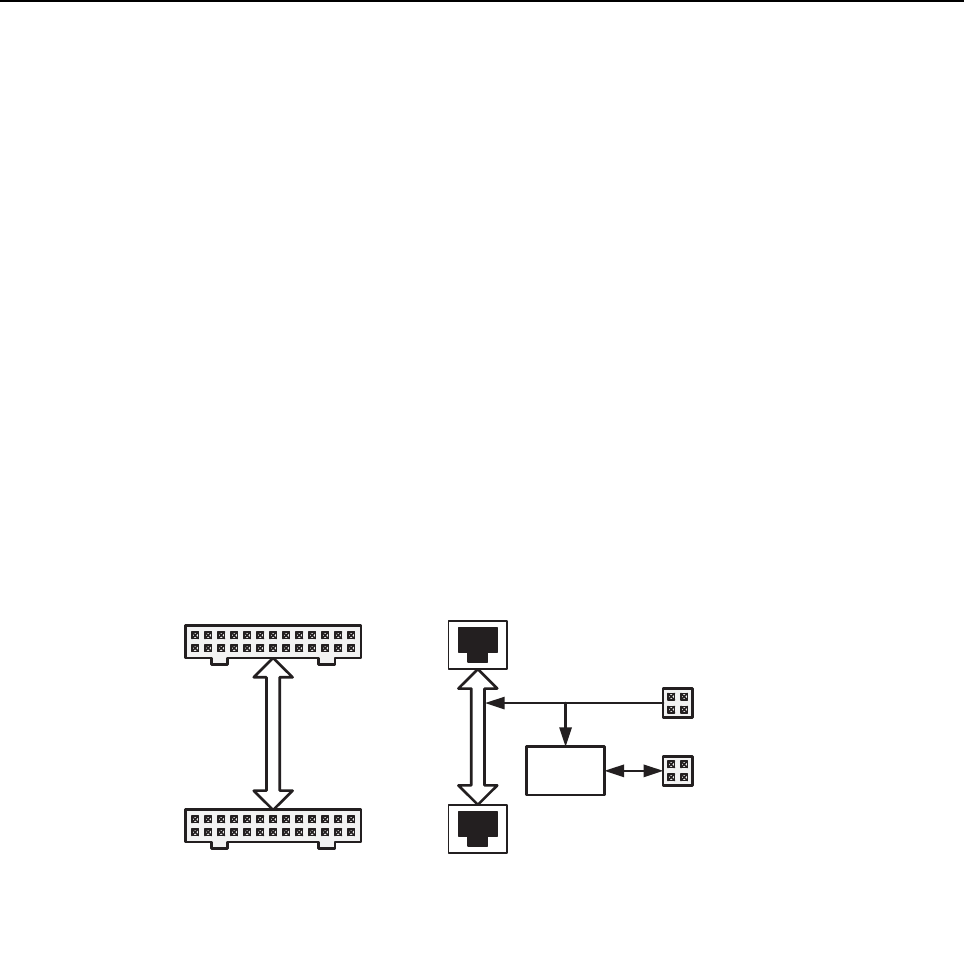
Introduction 1-3
The Repeater Disable LED is a dual-purpose LED that is hardware controlled initially at power-up.
As soon as VBUS power is available on the Repeater Indicator board, the hardware circuitry for the
Repeater Disable LED will cause it to blink periodically. When the software initialization is completed
by the firmware, the blink circuitry will get disabled by the firmware. At that point, the Repeater
Disable LED can be used for its intended purpose of displaying when the Repeater Disable function
is turned on.
The power LED is the only LED that is not controlled by the software. This bi-color LED gets turned
on green when the 13.8 V output from the power supply is valid. It turns on red when A/C power is
lost, and the repeater's backup battery is used.
The Real Time Clock (RTC) battery (M1) is connected to the transmit radio through the Control
Head (J1, pin 30).
Details of the Ethernet Controller can be found in Chapter 2.
1.4 Connector Board
The Connector board has two purposes: provide a place for the Repeater's MAP and Ethernet
connectors to be mounted and a location for the Repeater’s fan control circuitry.
Figure 1-3 Connector Board Block Diagram
Fan
Control
To MAP Conne ctor On
Transmit Radio
To MAP Conne ctor On
Rear Panel
To Ethernet
Conne ctor On
Rear Panel
To Power
Supply
To Fan

1-4 Introduction
1.5 Fan
The fan control logic is provided by the fan controller IC (U51). This is a device from Cypress
Semiconductor. There are basically two functions provided by the fan controller. First, it provides a
PWM output based on a temperature input, and secondly, it provides detection of fan failure based
on the fan tachometer reading.
The Repeater’s internal chassis temperature is measured with an LM50 precision temperature
sensor IC (U52). This IC outputs a voltage that is linearly proportional to temperature at 10 mV/°C,
and with an offset of +500 mV. The output voltage of the LM50 ranges from +200 mV at -30°C to
1.1 V at +60°C.
The fan controller IC (U51) controls the speed of the fan by adjusting the PWM output (pin 1) from
0% to 100%. As long as the fan continues to work, pulses are output from the fan and input to the
fan controller (pin 2).
1.6 AC/DC Power Supply
The Repeater uses the PMPN4001A switch-mode, Power Supply Unit (PSU). It is capable of 200 W
and designed for a 50 W UHF or VHF repeater system. This supply has UL, CE, and TUV regulatory
approvals and is usable in all regions by using the correct line cord. The AC input is auto-ranging
with no manual switch being specified to operate from 90 V-270 V and 47 Hz-63 Hz. It outputs a
nominal voltage of 13.8 V with a voltage tolerance of +/- 5%.
It has Power Factor Correction circuitry and is rated at 15 A across the whole operating temperature
range of -30°C to +60°C. It also has a built-in battery revert circuit with a float output available for
maintaining the charge on a battery and has UL, CE, & TUV approvals. The battery revert connector
is accessible in the back of the power supply.
The supply has over-load, over-voltage, and over-temperature protection. In an overload condition,
the PSU goes into a hiccup mode where it recovers automatically after the fault condition is
removed. During an over-voltage condition, the PSU shuts down, and will have to be re-powered on
to recover. In an over-temperature condition, the PSU also shuts down but will recover after the
temperature goes down.
The PSU is not designed to be field serviceable. If it is determined that the PSU is not functioning,
the whole unit needs to be replaced.
Repeater Interconnections and Cables 1-5
2.0 Repeater Interconnections and Cables
Figure 1-4 shows the Cable interconnections inside the Repeater.
Figure 1-4 Repeater Cabling Diagram
The details of each of these cables/interconnections are as follows:
1. Two conductor DC power cables to the transmit and receive radios.
2. Six conductor DC power cable to the connector Board. Supplies power for the fan and
Repeater Indicator board via cable 6.
3. RF Coax to connect the receive radio to the back of the Repeater. This cable has a BNC
connector on the Repeater’s rear panel.
4. RF Coax to connect the transmit radio to the back of the Repeater. This cable has an N type
connector on the Repeater’s rear panel.
5. CAT5 cable with RJ45 style connectors on both ends. This cable connects the Ethernet
controller on the Repeater Indicator board to the Repeater's back panel and provides power
from the Connector Board to the Repeater Indicator board for the LED indicators.
Power Supply
RF
Rx In
Tx Control Radio
Fan
USB to
Ethernet
Interface
Display
Driver
RTC
Backup
Repeater Board
Repeater
Interface
Mobile
Accessory
Port (MAP)
Rear Connector
Rx Radio
Rx RF
Option
Board
Interface
Controller
Control Head
Interface
Control Head
Interface
Mobile Mic
Port (MMP)
Front Connector
Mobile Mic
Port (MMP)
Front Connector
DC
Power
Repeater
Interface
Mobile
Accessory
Port (MAP)
Rear Connector
Tx RF
Option
Board
Interface
Controller
DC
Power
RF
Tx Out
AC
Power
Connector Board
Fan
Control
Ethernet
Connector
MAP
Connector
1
28
43
6
7
5
9

1-6 Mobile Radio’s Theory of Operation
6. Eleven conductor flex cable. Provides the SSI connection between the transmit and receive
radios. Refer to Section 1.5 for more details on this interface.
7. Thirty conductor flex cable. Provides the connection from the transmit radio to the Repeater
Indicator board and includes SPI signals to drive the LED indicators, RTC backup supply, and
the interface to the Ethernet controller.
8. Twenty six conductor cable. Provides the connection from the transmit radio's MAP to the
MAP located on the Repeater's rear panel.
9. Eight pin conductor cable. Provides Ethernet LED signals from Repeater Board and HWID
signals from Connector Board (Applicable for 32 MB repeaters only).
3.0 Mobile Radio’s Theory of Operation
The sections that follow provide a detailed theory of operation for the UHF circuits in the two
MOTOTRBO mobile radios. For details of the theory of operation and troubleshooting for the
associated Controller circuits, refer to the Controller Section of this manual.
3.1 UHF1 (403–470 MHz) Receiver Circuitry
The receiver is configured as a dual-conversion superheterodyne receiver, capable of both FM and
4-level FSK demodulation. The major blocks are the front-end, the mixer, Xtal filter, and the Abacus
III back-end IC. The overall block diagram is shown in Figure 1-5.
Figure 1-5 Receiver Block Diagram
3.1.1 Receiver Front-End
The front-end consists of a 2-pole varactor-tuned pre-selector filter, an LNA, a 2-pole varactor-tuned
post-selector filter, and a passive double-balanced mixer. The received signal applied to the antenna
is routed through the harmonic filter and PIN diode controlled antenna switch (D0702). A logic high
level on ANT_ENABLE configures the antenna switch for Tx operation while a logic low places the
switch in Rx mode. The insertion loss of the harmonic filter and antenna switch combined is
approximately 0.5 dB max in Rx mode. From this point, the Rx signal is routed to the Local Distance
switch (D0400/R0407), which biases on a diode in normal operation to minimize any insertion loss.
Under strong signal conditions and for improved intermodulation protection from interfering signals,
the switch can be turned on by the signal RF_ATTEN_1 which introduces approximately 10 dB of
additional path loss. Activation of the switch can be accomplished manually by the user or left in the
default setting.
T/R ANT
Switch Hi-Speed
A/D
2nd
L.O.
VCO
X
AD9864
4-Pole
73.35 MHz
LIMITER/
IF AMP
STAGE
DSP
Processor
SPI
&
SSI
BUS
Sw. 10 dB
Attenuator
10 bit
DAC
LNA
2-Pole
Varactor
Tuned
2-Pole
Varactor
Tuned
2nd L.O.
71.1 or 75.6
MHz
1st L.O.
Low Side
Injection
F0 - 73.35
MHz
D/A
SPEAKER
10 bit
DAC

Mobile Radio’s Theory of Operation 1-7
The signal next reaches the pre-selector filter, which is a 2-pole, varactor-tuned filter with 5 zeros
that are optimized to provide image frequency rejection. This filter, along with the similarly designed
post-selector filter, provides over 75 dB of image response rejection. The 3 dB bandwidth for both
filters varies across the band with a minimum of 19 MHz at 403 MHz and a maximum of 40 MHz
around 436 MHz. Half-IF rejection from the filters is also frequency dependent with a minimum of
approximately 10 dB achieved at the worst-case frequency of 436 MHz. Both filters have variable
center frequencies that are adjusted by the FE_TUNE signal, which is derived from the output of a
10-bit DAC internal to the MAKO IC (U3200). The voltage is scaled up by a voltage doubler (Q0403)
in order to provide the required linearity for the filters. Both filters are matched to the LNA (Q0402) to
optimize the amplifier’s noise figure (2.0 dB) and to provide an LNA gain of 15 dB to the signal. The
combined gain of the filters and LNA is about 13 dB. Current source Q0401 maintains the collector
current of Q0402 constant at 20 mA. The LNA, current source, Local Distance switch, and voltage
doubler are all supplied by 9R1_FILT, which is derived from 9R1 after filtering.
Following the post-selector filter is the Class 2, double-balanced mixer. It is comprised of baluns
T0400 and T0401 and diode ring mixer D0405. Injection amplifier Q0405 provides 10 dB of gain to
the Rx VCO injection signal. Another amplifier, Q0202, located in the VCO block, also provides gain
for the LO signal and isolation from high RF signals entering the mixer. The signal applied to the LO
port of the mixer is +16 dBm minimum after passing through the 3-pole/1-zero, low-pass injection
filter. The LO injection is low-side and mixes the signal down to an IF frequency of 73.35 MHz. The
output of the mixer is connected to a diplexer network, which terminates out-of-band frequencies in
51 ohms (R0427) while appearing as high impedance to the 73.35 MHz IF signal.
3.1.2 Receiver Back-End
The signal entering the back-end is matched to 4-pole crystal filter, FL0500, by C0507 and L0503.
The filter is centered at 73.35 MHz with a 3 dB bandwidth of 12 kHz. IF amplifiers Q0500 and Q0501
follow the crystal filter and provide both amplification and limiting to the signal. An overall gain of 25
dB is available from the composite IF amplifier to lower-level IF signals. As the signal level
increases, Q0501 begins to limit and eventually saturates out at approximately –16 dBm. The
purpose of the limiting is to provide protection to the AD9864 Abacus III back-end IC (U0600). At IF
levels exceeding –32 dBm into U0600, the 2nd LO synthesizer internal to U0600 can be pulled,
causing corruption of the I/Q data being delivered to the DSP. The block diagram for the AD9864 is
shown in Figure 1-6 below.
Figure 1-6 AD9864 Block Diagram
1-8 Mobile Radio’s Theory of Operation
The Abacus III accepts the 73.35 MHz signal, processes it, and sends out I/Q data in 16-bit format to
the DSP at a 20 kHz rate. Internal to the Abacus III is an LNA and 16 dB FE attenuator, an internal
integer-N synthesizer used to control the external 2nd LO VCO, a Sigma-Delta ADC and decimation
filter, and control and formatting logic for outputting the baseband I/Q data. External to U0600 is the
2nd LO VCO with active device Q0600 and its associated circuitry including the loop filter consisting
of C0613, C0618, and R0603. The 2nd LO mixes the 73.35 MHz IF signal down to 2.25 MHz before
being input to the ADC where it is sampled. The tank circuit (L0608, C0605, C0642, R0617) and
varactor (D0601) for the internal clock synthesizer, work with the loop filter (R0618, C0643, C0646)
to provide the 18 MHz clocking signal to the internal ADC, decimation filter, and SSI formatting
circuitry. A 3 Volt regulator (U0601) provides a clean supply to U0600. Transistor Q0601 is
configured as a super filter to provide the 2nd LO transistor with a low-noise supply. The reference
clock for U0600 is 16.8_REF, which is a buffered (Q0100) 16.8 MHz clock from the synthesizer
block.
Shown below in Figure 1-7 is a simplified block diagram of the signal flow through the receiver
back-end and the DSP processor portion of the OMAP (U1000). All of the blocks within the dotted
box represent the DSP software algorithms internal to the DSP.
Figure 1-7 Signal Flow through Receiver Back-End
The DSP takes the incoming 20 kHz data stream and passes the information through an FIR (Finite
Impulse Response) filter, which provides rejection from any in-band adjacent channel interference.
The remaining filter data is then sent through a decimation process further reducing its frequency to
8 kHz.
Depending on whether the repeater is in Analog or Digital mode determines the type of signal
processing used. If in Analog mode, the remaining 8 kHz data is sent through the FM Discriminator
and De-emphasis subroutines in the DSP code. If the repeater is in Digital mode, the 8 kHz data is
again passed through the FM Discriminator but an additional Symbol Recovery routine is applied
along with a standard AMBE+2™ Vocoder process. The data is sent to the MAKO (U3200), which
provides digital to analog conversion and drives the audio gain stages. Detailed information
regarding this can be found in the Audio Section of the Controller Theory of Operation.
FIR
4-FSK
SYMBOL
RECOVERY
AMBE+2
TM
VOCODER
DSP DIGITAL 4FSK MODE
Σ ∆
AD9864 Hi
SPEED
ADC
SPEAKER
ANALOG AUDIO
GAIN STAGES
DAC
FIR
FM
DISCRIMINATOR DEEMPHASIS
DSP ANALOG FM MODE
Σ ∆
AD9864 Hi
SPEED
ADC
SPEAKER
ANALOG AUDIO
GAIN STAGES
DAC
73.35
MHz
IF
73.35
MHz
IF
FM
DISCRIMINATOR

Mobile Radio’s Theory of Operation 1-9
3.2 UHF1 (403–470 MHz) Transmitter Circuitry – 25 Watt
The Transmitter consists of the power amplifier (PA) circuitry and the power control circuitry. The
power amplifier provides amplification of the signal from the VCO up to the desired output power.
The power control block is responsible for ensuring the desired output power level is maintained in
both analog and digital modes, as well as protecting the power amplifier from damage due to heat,
antenna mismatch, out-of-range battery voltage, and poor assembly.
Figure 1-8 UHF 25 Watt Low-Power Transmitter Detailed Block Diagram
3.2.1 Power Amplifier
The radio’s 25 Watt power amplifier (PA) is a 4-stage amplifier which amplifies the output of the VCO
to the required transmit power level. The first stage is an LDMOS (Lateral Double Diffuse MOS)
50 ohm fixed-gain block (ADA-4743, U0700) followed by the adjustable gain LDMOS pre-driver
(RD01MUS1, Q0705), an adjustable gain LDMOS driver (RD07MVS1, Q0703), and the fixed-gain
LDMOS final device (MRF1570, Q0702). A transmit/receive (T/R) switch and a harmonic filter
complete the transmit lineup.
3.2.2 Input Stage (50 Ohm Fixed-Gain Block)
The first stage (ADA-4743, U0700) is an integrated circuit with internally matched 50 ohm input and
output stages providing approximately 16.5 dB power gain. It provides reverse isolation between the
PA and the VCO to lessen the risk of VCO load-pull and it also supplies appropriate power to the
pre-driver stage. The ADA-4743 is biased at 60 mA during transmit by R0706, which is switched to
9V3_TX during TX operation by Q0701 (controlled by Antenna_En). The ADA-4743 is preceded by
an 16 dB resistive pad to further improve reverse isolation.
T/ R
Switch
Harmonic
Filter
Agilent
AD A 4743
TX_DAC
Active
Reconstruction
Filter
Log Amp Controller
V_ CONTROL
9V3
+5 V Regulator
-5 dBm
(nominal)
TX_INJ
CW / 4 FSK
+13 dBm
INPUT
FROM
VCO
ANT_ ENABLE
9V3_TX 9V3_TX
BATTERY_DET
SW_9V1
Reflected
Port
Microstrip
Dual
Directional
Coupler
Forw ard
Port
+
TX Port
RX Port
To FE
Match
Match
Match/
Splitter
Match/
Combiner
A+
A+
Voltage
Controlled
Variable
Attenuator
Thermal
Cutback
AD8315
VAPC RF IN
VPOS
ENBL COMMFLTR
VSET
VCONT
VIN +5 VOUT
Pad
To Pressure
Pad Switch
To Pressure
Pad Switch
FINAL_BIAS
To Pressure
Pad Switch
9V3
Pressure
Pad C loses
Switch
To Predriver
To Driver
To Final
9V3_TX
LDMOS
Predriver
RD01MUS1
LDMOS
Driver
RD 07MVS1
LDMOS
Final
MRF1570
ANT_ ENABLE
Pressure
Pad
Switch
PC_ ATTEN_ENA
9V3

1-10 Mobile Radio’s Theory of Operation
3.2.3 Pre-Driver Stage
The next stage is a low-power, LDMOS device (RD01MUS1, Q0705), which delivers up to +27 dBm
to the driver stage. Its gain is controlled by varying the gate bias voltage and varies from low gain up
to approximately 14 dB power gain. The gate bias voltage is controlled in parallel with the driver
stage by the V_cont signal.
The input match to this stage is a high-pass topology comprising of L0718, C0817, and L0721.
High-pass matches are used where appropriate to minimize the chances of low frequency
regeneration within the amplifier. R0759 and R0777 are required to improve the bandwidth of this
circuit. The inter-stage match between the pre-driver and driver stages is comprised of L0720,
C0786, and C0791 arranged in a high-pass topology. Additional pads are provided on the
transceiver board to allow for possible engineering optimizations to this match. These are non-
populated parts C0789, C0792, C0793, and C0794.
3.2.4 Driver Stage
The third stage is a medium-power, LDMOS device (RD07MVS1, Q0703), which delivers up to +38
dBm to the final device. Its gain is controlled by varying the gate bias voltage and varies from low
gain up to approximately 11 dB of power gain. The gate bias voltage is controlled with the V_cont
signal and is controlled in parallel with the pre-driver stage gain.
R0718, R0720, R0754, and R0755 are required to improve the bandwidth of the driver stage. The
inter-stage match (as well as the power splitter) between the driver and final device is comprised of
C0753, C0813, C0818, C0819, C0732, C0743, C0744, and C0761, and associated micro-strips on
the PCB. Additional pads are provided on the printed circuit board to allow for possible engineering
optimizations to this match. These are non-populated parts C0754, C0755, C0729, C0730, C0731,
C0808, C0764, C0760, and C0765.
3.2.5 Final Stage
The final stage is a high-power, LDMOS device (MRF1570, Q0702) consisting of two parallel,
high-power devices within 1 plastic package. The package is mounted to a copper carrier to improve
thermal conductivity to the chassis and also to more tightly control the RF load, allowing higher and
more consistent maximum output power. This stage is biased at a quiescent current of 750 mA and
operates with a fixed-gain of approximately 10 dB, allowing the radio to be set to a maximum output
power of 30 Watts. The quiescent current is set by adjusting the Final_Bias signal. Both elements of
this transistor are fabricated on the same semiconductor die and are well matched, allowing control
via a single voltage.
Both the input and output matching circuits of this stage have extremely critical part location
requirements. Any repairs must be done with care to ensure the replaced components are placed
accurately and properly soldered. Of particular concern are input matching capacitors C0732 and
C0761 and output matching capacitors C0811 and C0812. The resistor networks at the input of each
of the final elements are required to improve the bandwidth of the circuit. These resistors are R0762
through R0773.
The output matching circuit and power combiner is comprised of C0811, C0719, C0812, C0746,
C0726, and C0737 and associated microstrips fabricated on the printed circuit board. Additional
pads are provided on the pc board to allow for possible engineering optimizations to this match.
These are non-populated parts C0720, C0721, C0747, C0748, C0727, and C0741. R0719 is added
as a preventative measure against half-carrier regeneration.

Mobile Radio’s Theory of Operation 1-11
If the final device fails and has to be replaced, R0719 should be carefully inspected to ensure
against any damage caused by the final device. Replacement of the final device requires that the
bias voltage be re-tuned using the Customer Programming Software (CPS). Care must be taken not
to damage the device by exceeding the maximum allowed quiescent current which is 1 Amp. The
device can tolerate up to 5 Amps for brief periods of time without damage.
3.2.6 Antenna Switch
The antenna switch (T/R switch) routes the signal between either the transmitter or receiver and the
antenna. In transmit mode, it utilizes the existing dc feed (A+) to the final stage device (Q0702). Both
PIN diodes D0700 and D0702 are turned on during key-up through forward biasing. This is achieved
by pulling down the voltage at the cathode end of D0702 to approximately 12.2 Volts (0.7 Volt drop
across each diode). Q0704 is configured as a current sink that maintains the current through the
antenna switch diodes at 100 mA, as set by VR0700 and R0738. The current sink is enabled during
transmit mode by ANT_ENABLE, which is asserted through Q0706 and associated circuitry. When
the PIN diodes are conducting, an RF ground is formed at the anode of the lower PIN diode, D0702,
which places L0710 and C0803 in parallel. The values of L0710 and C0803 are chosen so as to be
parallel resonant at the center of the transmit band, making them appear as an open-circuit so that a
50 ohm power path is maintained through the top PIN diode to the harmonic filter.
In receive mode, DC current through the PIN diodes is interrupted by turning off the current sink.
The RF path now flows from the harmonic filter, through the matching circuit formed by L0710,
C0803, and the capacitive divider formed by C0767 and C0772. C0766, currently unplaced, is
provided for possible future engineering optimizations to this match. The purpose of L0719 is to form
a parallel resonant tank with the reverse capacitance of D0700, improving the receive path return
loss at the receive input of the T/R switch.
3.2.7 Harmonic Filter
Inductors L0706, L0707, L0708, and capacitors C0742, C0739, C0740, and C0738 form a
7-element low-pass filter to attenuate harmonic energy from the transmitter. R0713 is used to drain
any electrostatic charges that might otherwise build up on the antenna. The harmonic filter also
prevents high-level RF signals above the receiver pass-band from reaching the receiver circuits,
improving spurious response rejection.
3.2.8 Directional Coupler
The dual-directional microstrip coupler is implemented at the harmonic filter output to sample both
forward and reverse directed transmitter power. RF power from the transmitter PA passes through
the microstrip coupler before reaching the antenna. Forward RF power is coupled to the U0940 log
detector/controller via the voltage-controlled attenuator (VCA) stage consisting of pin diodes D0901,
D0902, and D0903. The log detector/controller regulates the gain of PA stages Q0703 and Q0705
(via V_cont), thus ensuring that the forward power out of the radio is held to a constant value.
The directional coupler functions not only as part of the transmitter power regulation circuit but also
as part of the VSWR load-detection circuitry. Its physical location close to the antenna connector
allows accurate VSWR sense at the transmitter output. Forward and reverse coupled signals are
rectified by D0904 and D0905, respectively. DC voltage FWD_DETECTED is proportional to RF
power while REV_DETECTED is proportional to reflected RF power. The detected voltages are fed
to the respective inputs of difference amplifier U0901. The difference amplifier output is applied to
the variable attenuator control stage, U0900-1. An abnormally high reflected power level, i.e., a
damaged antenna, also causes an increase in the difference amplifier output voltage.

1-12 Mobile Radio’s Theory of Operation
This causes a reduction in attenuation by the VCA. As a result, the greater RF signal applied to the
log detector/controller causes the controller to reduce the gain of PA stages Q0703 and Q0705.
Transmitter power is thus reduced to prevent damage to the final device due to an improper load.
3.2.9 Power Control
The transmitter uses PA controller IC, U0940 to control the power output of the radio. A portion of
the forward RF power from the transmitter is sampled by the directional coupler and delivered via
the VCA to the RFIN port of the PA controller IC (pin 1). The PA controller, a log detector type,
provides temperature-stable, high-accuracy control over a typical 50 dB dynamic range.
The MAKO IC contains a digital-to-analog converter (DAC), which provides a reference voltage
(TX_DAC) at the input of reconstruction filter stage U0900-2. The filtered reference voltage at the
output of U0900-2 is divided by the combination of R0942 and R0946 before reaching the VSET
input of the PA controller IC (pin 3). Thermistor RT0953 is used in combination with R0954 to
compensate reference voltage drift at operating temperature extremes. Reference voltage level is
programmable through the SPI lines of the MAKO. This reference voltage is proportional to the
desired power setting of the transmitter and is factory programmed at several points across the
frequency range of the transmitter to offset frequency response variations of the transmitter’s
coupled power circuits.
The PA controller IC provides a dc output voltage at pin 7 (VAPC), which is divided to provide gate
bias for PA pre-driver and driver stages. The 0 Volts to 5 Volts range at U0940, pin 7, is applied as
V_CONTROL to power-adjust the transmitter by controlling the gate bias of stages Q0703 and
Q0705. Voltage divider combination R0727 and R0728 provides gate bias to Q0703 while divider
combination R0750 and R0751 provides gate bias to Q0705. This adjusts the transmitter power
output to the intended value. The ratio of each of these resistive dividers is chosen to ensure that
Q0703 and Q0705 are both running at their nominal design condition at rated output power.
Variations in sampled forward transmitter power cause the PA controller IC to adjust the control
voltage above or below its nominal value to raise or lower output power in order to maintain
transmitter output power relative to the reference voltage applied to VSET.
A power control attenuator circuit was added to the 25 Watt transmitter circuitry in order to extend
the range of the RF detection in the RF detector at low-power levels. This enables the power control
loop to close at lower relative power levels and is needed because of the greater relative power-set
range (1-25 Watt, 14 dB). The PC_ATTEN_ENA activation threshold is set in software for operation
at lower power levels, typically 1-5 Watt. When the PC_ATTEN_ENA is activated, the VCA is driven
to its minimum attenuation level, which increases the RF level at the AD8315 (U0940) for a given
transmitter power level. The radio software adjusts the K&M tuning accordingly such that proper
power-set is maintained at operating powers both above and below the activation threshold point.
3.2.10 Power Ramp Profile Control
In order to minimize the transient adjacent channel power at the transmitter’s output, the ramped
power follows a raised-cosine profile. The PA controller IC has a linear slope function when scaled in
dB/V. To achieve the desired raised-cosine profile of the output power, the ramped reference voltage
provided by the MAKO DAC follows a raised-cosine approximation. The MAKO DAC reference
output is low-pass filtered by the DAC reconstruction filter before it is applied to the VSET input of
the PA controller IC.

Mobile Radio’s Theory of Operation 1-13
Reconstruction filtering reduces spurious emissions in the RF spectrum as a result of the finite steps
of the DAC. Loop filter capacitor C0926 in conjunction with resistor R0950 and the integrator within
the PA controller IC, set the loop dynamics. The loop response has been optimized to achieve
sufficient speed to follow the required ramping profiles while meeting switching transient
requirements over varied power levels. Accurate control of the power-rise (ramp-up) and
power-decay (ramp-down) characteristics minimizes splatter into adjacent channels.
3.2.11 Thermal Protection
Thermistor RT0908 in combination with R0902, form a voltage divider with the output proportional to
the sensed transceiver board temperature in the vicinity of the transmitter driver and final devices.
The voltage divider output is routed to an operational amplifier U0901-2, which provides a dc voltage
via diode junction D0900 to control the attenuation level of the VCA stage. For the condition that the
temperature threshold set by resistive divider combination R0901 and R0909 is reached, the VCA is
driven to increase the RFIN signal at the PA controller IC (pin 1). This increase will cause the
controller IC to adjust the PA control voltage below its nominal value to decrease transmitter output
power. Temperature will be reduced by lowering transmitter output power relative to the reference
voltage applied to VSET.
3.2.12 Out-of-Range Battery Protection
Transmitter power cutback under extended battery supply voltage operation is provided for by
monitoring the battery supply in the controller circuit of the radio in order to change the VSET input
of the PA controller IC (pin 3) for reduced transmitter output. This feature allows transmitter PA
dissipation to be limited at high-line battery supply operating conditions while limiting transmitter PA
overdrive conditions at low-line battery supply operating conditions.
3.2.13 Pressure Pad Switch
The power control circuitry includes a safety switch (S0700) that consists of a conductive portion of
the rubber pad which pushes the RF final transistor Q0702 against the chassis. When the chassis
cover and rubber pad are properly assembled, the conductive portion of the pad contacts a pattern
on the transceiver board, electrically closing switch S0700. If the cover and pad are not in place,
switch S0700 is open-circuited and the power control circuit is disabled, turning off the gate bias to
Q0702, Q0703, and Q0705. This prevents thermal damage of the RF transistors which could occur
if the transmitter is operated without adequate heat sinking.
3.3 Frequency Generation Circuitry
The synthesizer subsystem consists of the reference oscillator (Y0100), the fractional-N synthesizer
IC (Tomahawk II, U0100), and the Voltage Controlled Oscillator VCO.
3.3.1 Reference Oscillator
The reference oscillator (Y0100) contains a temperature compensated crystal oscillator with a
frequency of 16.8 MHz. A digital-to-analog (DAC) converter internal to U0100 (Tomahawk) and
controlled by the microprocessor via serial interface (SPI), sets the voltage at the AUX_DAC output
of U0100 (pin H6) to set the frequency of the oscillator. The output of the oscillator (pin 3 of Y0100)
is applied to pin K5 (XOSC_BASE) of U0100.
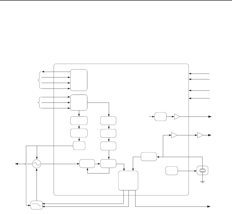
1-14 Mobile Radio’s Theory of Operation
3.3.2 Fractional-N Synthesizer
The Tomahawk II synthesizer IC (U0100) consists of a pre-scaler, a programmable divider and
divider control logic, phase detector, charge pump, a D/A converter in the high frequency analog
modulation path, an attenuator to balance the high and low frequency modulation paths, a serial
interface for control (SPI), a serial interface for modulation (SSI), and a super filter for the regulated
2.45 Volts.
Figure 1-9 UHF Synthesizer Block Diagram
A voltage of 2.775 Volts applied to the super filter input (U0100 pin J4) supplies an output voltage of
2.45 Vdc (SF_OUT) at pin K4. This supplies the VCO and the VCO modulation bias circuit (via
R0321). The super filter supply voltage is provided by the 2.775 Volt regulator within U3200. The
synthesizer is also supplied by the 5 Volt regulator, U3002, another 2.775 Volt regulator within
U3200, and a 1.875 Volt regulator within U3200.
The output signal LOCK (U0100-D7) provides information about the lock status of the synthesizer
loop. A high level at this output indicates a stable loop. A discrete buffer amplifier (Q0100) provides
a buffered 16.8 MHz reference frequency to other parts of the radio.
The serial programming interface (SPI) is connected to the microprocessor via the data lines
SPI_DW (U0100-D9) and SPI_DR (U0100-D10), clock line SPI_CLK (U0100-C11), and chip enable
line CEX (U0100-D8). The serial modulation interface (SSI) is connected to the DSP via the data
line SDTX (U0100-F11), clock line TXCLK (U0100-F10), and frame sync line SFTX (U0100-F9).
SPI
Interface
Data Write
Clock
CEX
Data
Fsync
Clock
SPI
SSI
(Modulation )
Prescaler Main Divider
VCO
Fractional
Unit
DS
18 - bit
Modulation
Unit
Main
Phase / Fr eq.
Detector
And
Charge Pumps
Reference
Divider
TCXO
(16 .8 M H z)
AUX
D/ A
Main_CP LOCK DETECT
Buffer Buffer
16.8MHz REF
Loop Filter
5V
2 .775V Dig
2.775 V A na
1 .875V Dig
TOMAHAWK II
Fractional -N
Synthesizer
(U0100)
D9
Data ReadD10
C11
D8
F11
F10
F9
J2
Adapt _CP
H1 D7
SF _OUT
Super
Filter
2 .775V Ana K4
H6
J11
K5
H2,J3
A7
A5,A10,B2,B9,
G2 ,J4 ,J6, J10,
K2,L6
B7 ,E 11, G10 ,J1
Digital
Attenuator
SSI
Interface
D/A
Waveform
Generator
K8 HP MOD
PRSC
TX / LO
G3
Mobile Radio’s Theory of Operation 1-15
3.3.3 Voltage Controlled Oscillator (VCO)
The Voltage Controlled Oscillator (VCO) subsystem consists of four Colpitts oscillators (two each for
Tx and Rx), a single-stage Tx buffer amplifier, a single-stage Rx buffer amplifier, oscillator bias
control switches, and the modulation circuitry.
Figure 1-10 UHF VCO Block Diagram
The UHF VCO design incorporates a total of four oscillators; two varactor-tunable Colpitts oscillators
each for Tx and Rx. Each oscillator has a tuning range of 33.5 MHz, sufficient to cover the Rx and
Tx frequency ranges of 326.65 MHz to 396.65 MHz and 403 MHz to 470 MHz, respectively. The
oscillators resonate at fundamental operating frequencies. Four (active-low logic) general purpose
output lines (GPO1, GPO2, GPO3, and GPO6) from the Tomahawk IC (U0100-B4, A4, E5, and H8)
provide the control for independent bias selection to each oscillator (VCO_SEL) via the PNP
transistor switches U0304 and U0201. The 2.45 Volt super filtered output, SF_OUT, of the
Tomahawk IC (U0100-K4) supplies the bias to the oscillators. A portion of the VCO output signal is
lightly coupled through coupling capacitors C0331 and C0231, routed through a low-pass filter
(formed by L0221, C0235, C0230, and C0233), and fed back to the M_PRSC input of the
Tomahawk IC (U0100-J2).
High-port modulation is scaled through a voltage divider (comprised of R0319, R0320, and R0321)
and applied to the Tx modulation varactor diode CR0300. The TX VCO frequency is modulated via
coupling capacitors C0310 and C0344. High-port modulation is also applied to the VCO steering line
(through R0139, R0140 and C0166) which modulates the main VCO tuning varactors.
TX VCO 1
TX VCO 2
RX VCO 1
RX VCO 2
TX Buffer Amp
RX Buffer Amp
Low Pass
Filter
TX INJ
RX INJ
To U0700
To Q 0405
Steering Line Voltage
(VCTRL)
9V3 _VC O
( U3001 -5 )
9R1
(Q0107 )
RX_VCO_SEL2
(U0100 - H8 )
RX_VCO_SEL1
(U0100 -B4)
TX_VCO_SEL 2
(U0100 -A 4)
TX_VCO_SEL 1
(U0100 -E 5)
High Port Modulation
(HP_MOD_OUT)
(U0100 -K8)
Prescaler
( U0100 -J2 )
UHF VCO
Subsystem

1-16 Mobile Radio’s Theory of Operation
A discrete single-stage Tx buffer amplifier (comprised of the NPN transistor Q0302 and surrounding
components) amplifies the signal from the Tx oscillator to the level required by the first stage of the
Transmitter Power Amplifier (U0700). The TX buffer amplifier also provides sufficient isolation from
any undesired load-pulling from the Transmitter Power Amplifier. The bias for Q0302 is provided by
the 9.3 Volt regulator U3001.
A discrete single-stage Rx buffer amplifier (comprised of the NPN transistor Q0202 and surrounding
components) amplifies the signal from the Rx oscillator to the level required by the LO injection
amplifier (Q0405). The Rx buffer amplifier also provides sufficient isolation from any undesired
load-pulling from high input levels in the receiver front-end. GPO4 from the Tomahawk IC (U0100-
D4) controls the transistor switch (comprised of Q0108 and Q0107), that enables the 9.1 Volt bias to
Q0202 (via the 9.3 Volt regulator U3001).
3.3.4 Synthesizer Operation
The complete synthesizer subsystem is comprised mainly of the Tomahawk synthesizer IC,
Reference Oscillator (crystal oscillator with temperature compensation), loop filter circuitry, VCO,
and DC supplies. The VCO feedback signal, PRSC, is fed to pin J2 of U0100 (M_PRSC) via a
low-pass filter (L0221, C0235, C0230, and C0233) which attenuates harmonics and provides the
correct level to close the phase-locked loop.
The prescaler in the synthesizer IC (U0100) is a four-level prescaler capable of dividing by 4, 5, 6,
and 7. The main loop N divider is configured to be an 8-bit divider. The divide-by-N portion of the
main loop is set via the SPI. The fractional portion of the divider is realized using a 3-accumulator,
24-bit fractional divider. The SPI is used to set the desired divide ratio.
The output of the prescaler is applied to the main loop divider. The output of the main divider is sent
to the phase/frequency detector, which compares the main divider’s output signal with the reference
signal. The reference signal is generated by dividing down the signal of the reference oscillator
(Y0100). The output signal of the phase/frequency detector is a pulsed signal which is routed to the
charge pumps. The main charge pump current is programmable through the SPI with its output at
pin G3 of U0100 (MN_CP). The loop filter transforms this current into a steering voltage that is
applied to the VCO.
To reduce lock time when new frequency data has been loaded into the synthesizer, an adapt
charge pump providing much greater current than the main charge pump is turned on for a finite
amount of time to quickly charge or discharge the loop filter capacitors to steer the VCO to the
desired frequency. The output of the adapt charge pump passes to the loop filter via pin H1 of
U0100 (MN_ADAPT_CP). When the synthesizer is within the lock range and the adapt timer runs
out, the adapt charge pump is powered down and the main charge pump takes over. A settled
synthesizer loop is indicated by a high level at signal LOCK (U0100-D7), which is routed to the
microprocessor. Q0102 is configured as a current source to provide a steady 1.5 mA during the
adapt period. U0101 is an analog switch that opens the adapt path slightly before the end of the
adapt period to prevent the current from the current source from pushing the VCO off frequency.

Mobile Radio’s Theory of Operation 1-17
Modulation is performed by applying a digital data stream via the SSI bus from the DSP (U1000) to
the synthesizer (U0100). In order to meet spurious and phase noise requirements, the PLL
bandwidth was designed to be narrower than the full modulation bandwidth, therefore requiring the
use of dual-port modulation. Internal to the synthesizer (U0100), low-port modulation is added to the
fractional-N division numerator to trace out the modulation versus time while the high-port data
stream passes through an interpolating waveform generator, a digital attenuator (for modulation
balancing), and then gets converted to an analog signal through a 10-bit DAC before modulating the
VCO. This high-port analog modulation output (HP_MOD_OUT, U0100-K8) is connected to the
VCO modulation varactor diode (CR0300) via C0360 and R0319, and to the loop filter via R0139,
R0140, and C0166.

1-18 Mobile Radio’s Theory of Operation
Notes

2-1
Section 2
TROUBLESHOOTING CHARTS
1.0 Troubleshooting Flow Chart for Receiver (Sheet 1 of 3)
Set up radio in Analog
Receive mode on
desired channel
with Squelch open
1st LO
> +5 dBm
at R0422?
Spray or inject 73.35 MHz
RF carrier modulated with
1 kHz Audio Tone into XTAL
Filter FL0500
No
Audio Tone
present
at Speaker?
Yes
Volume
level
adjusted
properly?
Check U3501
bias and
replace part if
necessary
Audio at pin 1
of U3501?
Verify audio path to
U3501
Setup repeater unit to
receive at frequency
403.025 MHz
with the RX Brick open &
connected to the system.
Apply an on-channel
RF carrier at -47 dBm modulated
with 1 kHz tone
at the RX antenna port
B
Audio at pin 6
of U3505?
Audio at pin 10
of U3501?
Check connections to
external speaker and replace
speaker if necessary
Verify audio path
between U3500 and
pin 1 of U3501
Audio at pin 4
of U3500?
Audio at pin 1
of U3500?
Check Biasing
before replacing
U3500
1st LO
(329.675 MHz)
> +16 dBm
at TP0401?
Check biasing on
Q0405 before replacing
9 VDC
present
at R0417?
Check
9R1 path back to
Synthesizer
Check VCO
Troubleshooting
Flow Chart
RF level
of on-channel
signal > -45 dBm
on pin 4
of T0401?
A
Check T0400 and D0405
and replace if necessary
Yes
Yes
Yes
No
No
Yes
YesNo
No
No
Yes
Yes
No
No
No
Yes
Yes
NO RX AUDIO
No
ALL Troubleshooting within the
dotted line is done on the TX BRICK
No
Yes
2-2 Troubleshooting Flow Chart for Receiver
1.1 Troubleshooting Flow Chart for Receiver (Sheet 2 of 3)
A
Voltage level
>2.7 VDC
on D0401?
+9.0 VDC
on pin 4
at Q0403?
Check circuitry around
D0401, D0402, D0403, and
D0404 for shorts and opens
~ 0.8 VDC at
R0432/D0400?
Check biasing on
Q0403 before replacing
Check biasing circuitry of
Q0401 and Q0402 before
replacing
RF level
of on-channel
Signal > -45 dBm
at C0420?
Is voltage
at R0409
~ 0.7 VDC?
Voltage
< 0.5 VDC
at pin 2
of Q0400?
Check biasing
circuitry of
Q0400 before
replacing
Check D0403, D0404, and
associated capcacitors
for opens and shorts.
Replace if necessary
Check biasing circuitry of
Q0402 before replacing
No
Yes
No
No
No
Yes
Yes
Yes
Yes
Yes
Check Synthesizer
Troubleshooting
Flow Chart
ALL Troubleshooting on this page is
done on the RX BRICK
No
No

Troubleshooting Flow Chart for Receiver 2-3
1.2 Troubleshooting Flow Chart for Receiver (Sheet 3 of 3)
B
16.8 MHz
present
at C0622?
Check Synthesizer
Troubleshooting
Flow Chart
2nd LO
> 0 dBm and
at 71.1 MHz
at TP0600?
Yes
No
No
Yes
73.35 MHz
present
at TP0602?
2.25 MHz
present
at C0625?
No
Yes
No
Yes
18 MHz
present
at L0608?
Check diode
continuity before
replacing D0601 Replace components
as needed
No No
Yes No
Yes
Check for visible
solder shorts near
pins before replacing
U0600
~ 1.65 VDC
on R0617?
Clock
VCO and LF
components
OK?
DC continuity
through
biasing components
E0600 - E0610?
Replace
defective biasing
component
Yes
No
3.0 VDC
on pin 1
of U0601?
Check Controller
Troubleshooting
Flow Chart
5.0 VDC
at E0610?
Check biasing on
U0601 before
replacing
No
Yes Yes
3.5 VDC
at E0609?
No
Yes
Check biasing on
Q0601 before
replacing
Remove Shield
SH0500
Check biasing on
Q0600 and
check continuity
on D0600.
Replace if necessary
Check 5 VDC
supply and biasing
components
before replacing
Q0500 or Q0501
Biasing
correct on
Q0500 and
Q0501?
~ 3.0 VDC
on L0604
and L0605?
Check biasing
components and 3 VDC supply.
Replace parts if necessary
No
Yes
No
Yes
73.35 MHz
present
at pin 6 of
FL0500?
Check signal gain
and biasing
before replacing
Q0500 or Q0501
No
Yes
ALL Troubleshooting on this page
is done on the RX BRICK
No
Check FL0500 matching
components before replacing
Yes

2-4 Troubleshooting Flow Chart for 25W Transmitter
2.0 Troubleshooting Flow Chart for 25W Transmitter
Is TP0909
> 1 VDC?
No Transmitter
Power
Is TP0913
= 9.1 VDC?
Check 9.3V Regulator
circuit (U3001)
Is U0941 Pin 1
= 5 VDC?
Check 5V Regulator
circuit (U0941)
Is voltage at
TP(TX_RAMP_DA
C) in controller
> 3 VDC?
Check MAKO
Troubleshooting Flow Chart
Is voltage at
TP0910
> 1 VDC?
Check U0900-2 and
associated circuitry
Replace U0940
Is TP0702
= 9.3 VDC?
Check 9V3_PA Regulator in
Controller Troubleshooting
Flow Chart
Are TP0707
and TP0708
~ 2.2 VDC?
Is power
at TP0704
~ 16.5 dBm?
Is Pressure Pad
Switch in place?
Place Switch or
R0775
Is resistance
to ground at Q0702
G1 and G2
~ 66 kohm?
Replace Q0702 *
* Note: If Q0702 is replaced radio must be bias set and power set.
1) Levels are during Transmit Mode (analog), 13.6V at battery connector, 50 ohm termination on transmitter.
2) Make sure PCB is screwed into chassis during these tests to avoid final device damage.
Check Bias Set
Circuit; bias tune
Is TP0703
0 dBm?
Check VCO
Troubleshooting
Flow Chart
Replace U0700
Is power at
TP0709 ~ 15 dB
> TP0710?
Is power at
TP0702 ~ 10 dB
> TP0709?
Check Q0705 and
associated circuitry
Check Q0703 and
associated circuitry
Is power at
D0700-A ~ 10 dB
> TP0702?
Check Q0702 and
associated circuitry
Measure relative power thru remainder of TR switch and LPF to find
open circuit. Perform visual inspection of circuit.
Is D0702-K
~ 12.4 VDC?
Check T/R bias
circuit
Yes
Yes
Yes
Yes
Yes
No
Yes
Yes
Yes
Yes
No
No
Yes
No
No
Yes
No
Yes
No
Yes
No
Yes
No
No
No
Yes
No
No
No
No
3) When making measurements within the transmitter using an RF power probe, be careful that the rating
of the probe is not exceeded. The “relative” measurements listed in the flow chart should be made with a
scope probe connected to a spectrum analyzer or similar instrument to avoid damaging sensitive power
probes.
Troubleshooting Flow Chart for Synthesizer 2-5
3.0 Troubleshooting Flow Chart for Synthesizer
Start
Visual check of
the Board OK?
Correct
Problem
+5V at R0100?
Check 5V
Regulator
U3002
+2.775V at
R0101 and
R0103?
Check U3200
+1.875V at
R0102? Check U3200
Is 16.8MHz
Signal at C0145? Check Y0100
Is 16.8MHz
Signal at R0155? Is 16.8MHz
Signal at R0109?
Replace
U0100
Check Q0100
and surrounding
components
Is Radio in TX or
RX mode?
TX
RX
+2.45V at C0137
(SF_OUT)?
Are C0136,
C0137 OK?
Replace or
resolder
components
Replace U0100
1.5ms pulse at
TP_ADAPT_SW
when channel
changed?
1.5ms (inverted)
pulse at R2517 when
channel changed?
Check P U1000
Troubleshooting
Chart
Check Q0106,
R0159
Is either GPO1 or
GPO6 low (<0.5V),
but not both, and
GPO2 and GPO3 are
high (>1.4V)?
Is RF Prescaler level
(at C0233) between
100mVpk and 300mVpk
(harmonics <-15dBc)?
Check VCO
Troubleshooting
Chart
Is SPI
Programming
OK?
Check P U1000
Troubleshooting
Chart
Replace
U0100
Is SPI
Programming
OK?
Check P U1000
Troubleshooting
Chart
Replace
U0100
Replace
U0100
Is Modulation
Present at
R0139?
Is Tx SSI activity
present on CLK,
FSYNC, and DATA
lines (R2512, R2514,
R2513)?
Check P U1000
Troubleshooting
Chart
Is either GPO2 or
GPO3 low (<0.5V),
but not both, and
GPO1 and GPO6 are
high (>1.4V)?
No
No
No
No
No
No No
No
No
No No
No No
No
NoNo
No
No
Yes
Yes
Yes
Yes
Yes
Yes
Yes
Yes
Yes
Yes
Yes
Yes
Yes
Yes
Yes Yes
Yes
Yes

2-6 Troubleshooting Flow Chart for Tx VCO (Sheet 1 of 2)
4.0 Troubleshooting Flow Chart for Tx VCO (Sheet 1 of 2)
2.556 V at C0362 &
C0363
Check Synthesizer
Troubleshooting
Chart
Check Synthesizer
Troubleshooting
Chart
Radio is not
programmed for
Transmit Mode or
U0100 not functional
~ 0 VDC at
C0358?
2.556 VDC at
C0336?
Replace Q0301
Check biasing components
and then replace Q0301
if needed
Vbe
= 0.7 V
for Q0301?
Yes
Yes
VCO 2
Check biasing
components then
replace Q0302 if
needed
Check biasing
components then
replace Q0302 if
needed
Vbe
= 0.7 VDC
for Q0302?
No
No
No
No
No
No
No TX VCO signal at C0318
Visual check
of board
OK? Correct problem
Correct problem
Radio did not boot up
properly or check
9V3 Regulator
Radio did not boot up
properly or check
9V3 Regulator
9 VDC at L0300?
Check biasing
components then
replace Q0302 if
needed
Check biasing
components then
replace Q0302 if
needed
Vbe
= 0.7 VDC
for Q0302?
Yes
Yes
No TX VCO signal at C0318
Visual check
of board
OK? Correct problem
Correct problem
Radio did not boot up
properly or check
9V3 Regulator
Radio did not boot up
properly or check
9V3 Regulator
9 VDC at L0300?
Radio programmed for
Tx VCO 1 or 2?
2.556 V at C0362 &
C0363
~ 0 VDC at
C0348?
2.556 VDC at
C0300?
Vbe
= 0.7 VDC
for Q0300?
Yes
Yes
No
No
No
VCO 1
Check Synthesizer
Troubleshooting
Chart
Check Synthesizer
Troubleshooting
Chart
Radio is not
programmed for
VCO1 Transmit Mode
or U0100 not
functional
Check biasing
components then
replace Q0300 if
needed
Check biasing
components then
replace Q0300 if
needed
Yes
No
Yes RF signal
present at
R0332?
Check components
between R0332 and
L0305 for shorts or
opens
Check CR301 - CR304
and L0310, L0307,
C0308, C0313, C0320,
and C0314 for short
Check CR305 - CR308
and L0315, L0318,
C0343, C0345, C0350,
and C0346 for short
Yes
Yes
Radio is not programmed for
VCO 2 Transmit Mode or
U0100 not functional
Check CR0305 - CR0308,
L0315, L0318, C0343, C0345,
C0350, and C0346
for shorts or opens
Check CR0301 - CR0304,
L0310, L0307, C0308, C0313,
C0320, and C0314
for shorts or opens
Radio is not programmed for
VCO 1 Transmit Mode
or U0100 not functional

Troubleshooting Flow Chart for Tx VCO (Sheet 1 of 2) 2-7
4.1 Troubleshooting Flow Chart for Tx VCO (Sheet 2 of 2)
DC Voltage
at R0311
between 0.6
and 4.5 VDC?
Check Synthesizer
Troubleshooting
Flow Chart
Check Synthesizer
Troubleshooting
Flow Chart
Yes
No
Tx VCO 1 or
VCO 2
selected?
Check components
between C0353 and
C0346 for open or
short
VCO 1 VCO 2
-
Tx VCO locked but no
high-port modulation
~2.1 VDC at
VCO side of
C0360?
Check R0321, R0320,
R0319, and CR0300
for open or short
Modulation at
CR0300?
No
Yes
Replace C0310
Yes
Modulation at
C0361?
No
Replace C0360
Yes
Check C0361 and
C0334 for short and
then check
Synthesizer
Troubleshooting
Flow Chart
Check C0361 and
C0334 for a short and
then check
Synthesizer
Troubleshooting
Flow Chart
No
Tx VCO not locked
at correct frequency
Check C0323, C0325,
and C0329 and all
components between
C0326 and C0314 for
shorts or opens
Check C0351, C0352, and C0359
and all components between
C0353 and C0346 for
shorts or opens
Check R0321, R0320, R0319,
and CR0300 for
shorts or opens
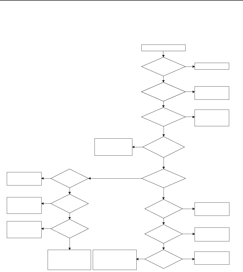
2-8 Troubleshooting Flow Chart for Rx VCO (Sheet 1 of 2)
5.0 Troubleshooting Flow Chart for Rx VCO (Sheet 1 of 2)
2.556 V at C0362 &
C0363
Check Synthesizer
Troubleshooting
Flow Chart
Check Synthesizer
Troubleshooting
Flow Chart
Radio is not
programmed for
Receive Mode or
U0100 not functional
~0 VDC at
C0258?
2.556 VDC at
C0236?
Vbe
= 0.7 VDC
for Q0201?
Yes
Yes
No
No
No
VCO 2
Check biasing
components and
then replace Q0202 if
needed
Check biasing
components and
then replace Q0202 if
needed
Vbe
= 0.7 V
for Q0202?
Yes
Yes
No
No
No
No Rx VCO signal at C0218
Visual check
of board
OK? Correct problem
Correct problem
Radio did not boot up
properly or check
9V3 Regulator
Radio did not boot up
properly or check
9V3 Regulator
9 VDC at E0201?
Check biasing
components and
then replace Q0200 if
needed
Check biasing
components and
then replace Q0200 if
needed
2.556 V at C0362 &
C0363
~0 VDC at
C0248?
2.556 VDC at
C0200?
Vbe= 0.7 VDC
for Q0200?
No
Yes
Yes
No
No
No
VCO 1
Check Synthesizer
Troubleshooting
Flowchart
Check Synthesizer
Troubleshooting
Flowchart
Radio is not
programmed for
Receive Mode or
U0100 not functional
Radio is not
programmed for VCO 1
Receive Mode or
U0100 not functional
Yes RF signal
present at
R0219?
Check CR205 - CR208
and L0218, L0215,
C0243, C0245, C0250,
and C0246 for short or
open
Yes
Yes
Check components between
R0219 and L0205
for shorts or opens
Check biasing components
and then replace Q0201
if needed
Yes
Radio programmed for
Rx VCO 1 or 2?
Check CR0201 - CR0204 and
L0210, L0207, C0220,
C0213, C0208, and C0214
for shorts or opens
Radio is not programmed
for VCO 2 Receive Mode
or U0100 not functional
Check CR0205 – CR0208 and
L0218, L0215, C0243,
C0245, C0250, and C0246
for shorts or opens
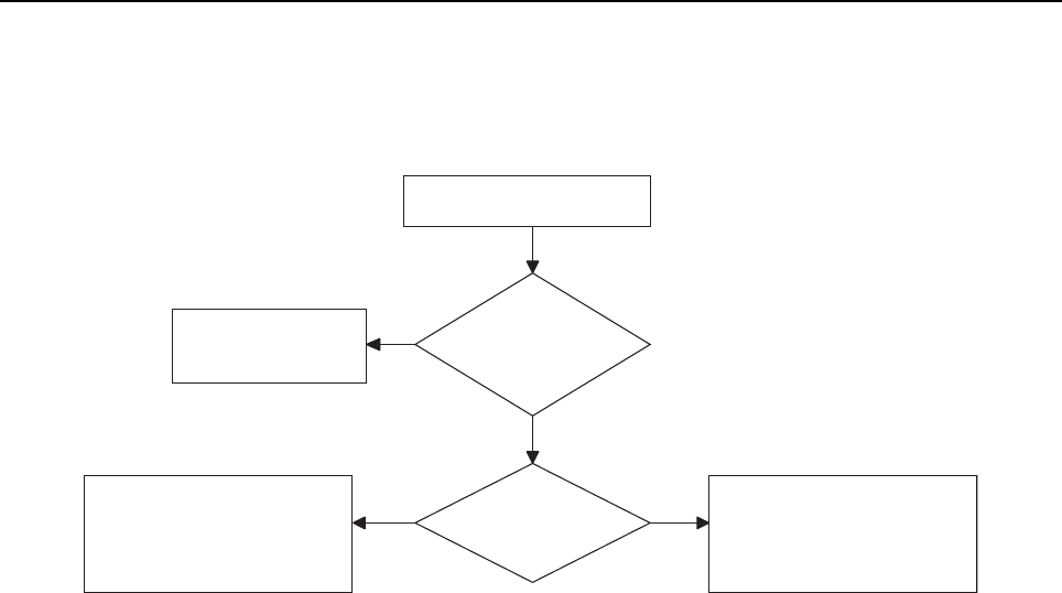
Troubleshooting Flow Chart for Rx VCO (Sheet 1 of 2) 2-9
5.1 Troubleshooting Flow Chart for Rx VCO (Sheet 2 of 2)
Rx VCO not locked
Rx VCO not locked
at correct frequency
DC Voltage
at R0211
between 0.6
and 4.5 VDC?
Check Synthesizer
Troubleshooting
Check Synthesizer
Troubleshooting
Flow Chart
No
Yes
Rx VCO 1 or
VCO 2
selected?
Check components
between C0253 and
C0246 for open or
short
VCO 1 VCO 2
Check C0223, C0225, and C0229
and all components between
C0226 and C0214 for
shorts or opens
Check C0251, C0252, and C0259
and all components between
C0253 and C0246 for
shorts or opens

2-10 Troubleshooting Flow Chart for Repeater
6.0 Troubleshooting Flow Chart for Repeater
Repeater does not
fully initialize
(Disabled LED
stays blinking)
Does Repeater
initialize properly
now?
Re-insert or replace SSI
cable
Replace Connector
Board and/or
Accessory Cable
Does Repeater
initialize properly
now?
Can it repeat?
Re-insert or Replace
30 pin Front Panel
cable
Do all LEDs flash
on power-up?
Replace Front Panel
Board
Troubleshoot Rx
Radio
Yes Yes
No
No
No
Done
Done
Yes
No
Done
Yes
Does Repeater
initialize properly
now?
Done
Troubleshoot Tx
Radio
No
Yes

3-1
Section 3
UHF1 PCB/SCHEMATICS/PARTS LIST
1.0 Allocation of Schematics and Circuit Boards
1.1 Controller Circuits
The UHF circuits are contained on the Printed Circuit Board (PCB) which also contains the
Controller circuits. This Chapter shows the schematics for the UHF circuits only, refer to the
Controller section for details of the related Controller circuits. The PCB component layouts and the
Parts Lists in this Chapter show both the Controller and UHF circuit components. The UHF
schematics and the related PCB and parts list are shown in the table below.
NOTE: The UHF Schematics and parts lists are the same for 8471165L03 and 8471165L05. Only
the Controller circuits are different between the two PCBs.
Table 3-1 UHF1 1–25W Diagrams and Parts List
PCB :
8471165L03 Main Board Top Side
8471165L03 Main Board Bottom Side
8471165L05 Main Board Top Side
8471165L05 Main Board Bottom Side
Page 3-3
Page 3-4
Page 3-5
Page 3-6
SCHEMATICS
Overall
Receiver Front- End
Receiver IF Amp
Receiver Back-End
Power Amplifier
Power Control
Synthesizer
Receiver VCO
Transmit VCO
Page 3-7
Page 3-8
Page 3-9
Page 3-10
Page 3-11
Page 3-12
Page 3-13
Page 3-14
Page 3-15
Parts List
8471165L03 and 8471165L05 Page 3-16

3-2 Allocation of Schematics and Circuit Boards
Table 3-2: UHF1 1–25W Diagrams and Parts List
PCB :
8471165L06 Main Board Top Side
8471165L06 Main Board Bottom Side
Page 3-21
Page 3-22
SCHEMATICS
Overall
Receiver Front- End
Receiver IF Amp
Receiver Back-End
Power Amplifier
Power Control
Synthesizer
Receiver VCO
Transmit VCO
Page 3-23
Page 3-24
Page 3-25
Page 3-26
Page 3-27
Page 3-28
Page 3-29
Page 3-30
Page 3-31
Parts List
8471165L06 Page 3-32
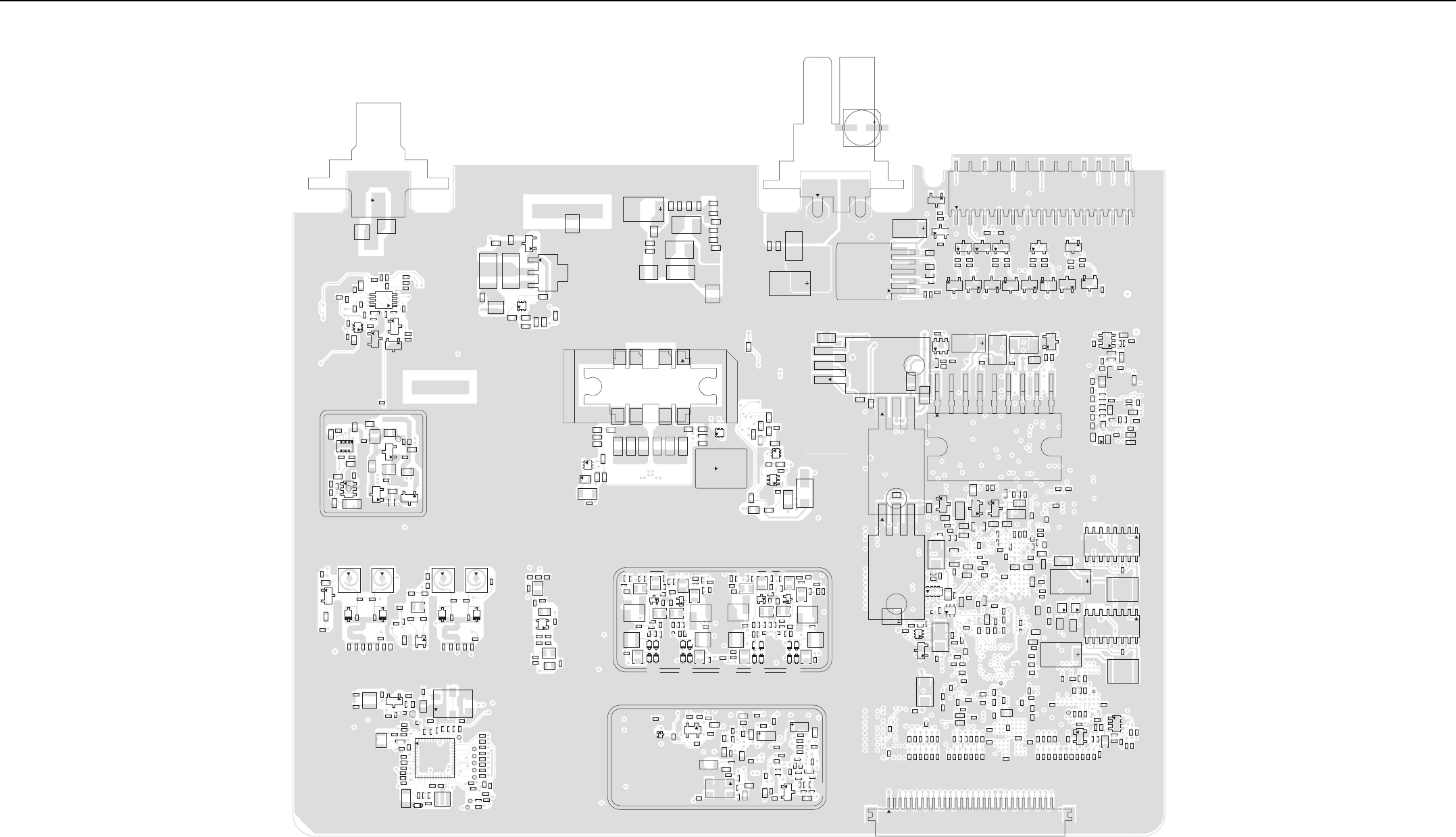
UHF1 (403–470 MHz) 1–25W PCB/Schematics/Parts List 3-3
2.0 UHF1 (403–470 MHz) 1–25W PCB/Schematics/Parts List
3
2
J0700
C0900
C0901 C0906
C0907
C0908
C0909
C0910
C0915
C0939
D0900
D0906
Q0900
Q0901
R0900
R0901
R0902
R0903
R0906
R0907
R0909
R0911
R0912
R0914
R0915
R0916
R0920
R0923
R0930
R0931
U0901
C0929
C0914
C0918
C0921
C0922
C0926
C0931
C0934
C0935
C0936
C0937
C0947
C0948
C0949
C0950
C0951
D0901
D0902
D0903
L0901
L0902
R0917
R0924
R0925
R0926
R0927
R0928
R0929
R0936
R0937
R0940
R0950
SH0900
4
58
U0940
U0941
L0722
R0713
C0748
C0776
C0777
C0796
C0797
C0798
C0799
L0714
4
321
Q0704
Q0706
R0729
R0735
R0738
R0745
R0748
R0749
VR0700
C0700
C0701
C0702
C0703
C0704
C0705
C0706
C0707
C0708
C0709
C0710
C0711
C0712
C0713
E0700
E0701
R0742
R0776
C0714
SP0702SP0703SP0705 SP0707
234
7
865
Q0702
SP0700SP0701SP0704 SP0706
C0804
C0805
1
M0700
Q0708
R0730
R0732
R0756
R0762
R0763
R0764
R0768
R0771
R0773
C0781
C0782
C0904
L0900
Q0709
R0740
R0741
R0753
R0757
1
RT0908
10 9
C0718
C0788
C0802
E0703
L0723
Q0701
Q0707
R0700
R0702
R0703
R0706
R0734
R0744
R0750
R0751
R0752
R0761
R0778
C0253
CR0205
CR0206
CR0207
CR0208
L0218
C0208
C0213
C0214
C0220
C0223
C0225
C0226
C0229
C0243
C0245
C0246
C0251
C0252
C0259
CR0201
CR0202
CR0203
CR0204
L0207
L0209
L0210
L0212
L0217
L0219
C0250
C0200
C0201
C0205
C0206
C0215
L0203
Q0200
R0201
R0204
C0204
C0236
C0237
C0240
C0241
C0242
C0247
C0306
C0308
C0310
C0313
C0326
C0343
C0344
C0345
C0346
C0351
CR0301
CR0302
CR0303
CR0304
CR0305
CR0306
CR0307
CR0308
L0202
L0213
L0214
L0215
L0309
L0310
Q0201
R0205
R0211
R0216
R0224
R0225
R0226
R0229
R0304
R0311
SH0301
C0350
C0353
L0315
L0317
L0318
C0300
C0301
C0304
C0305
C0314
C0315
C0320
C0323
C0325
C0329
C0352
C0359
L0302
L0303
L0307 L0312 L0319
Q0300
R0301
R0305
R0316
R0329
C0336
C0337
C0340 C0341
C0342
C0347
L0313
L0314
Q0301
R0324
R0325
R0326
C0437
C0438
C0439
C0440
C0442
C0451
L0407
L0411
4
32
Q0405
R0417
R0418 R0419
R0420
R0421
R0422
R0423
R0424
R0425
R0433
C0404
C0405
C0406 C0407 C0408 C0409
C0410
C0411
C0414
C0415
C0416
C0417
C0418
C0419
C0420
C0421
C0423
C0424
C0425
C0426
C0427
C0428
C0429
C0430
C0431
C0432
C0433
C0434
D0400
D0401
D0402
D0403
D0404
L0401
L0402 L0403 L0404
L0405
L0413
4
32
Q0402
R0404
R0405
R0406
R0407
R0409
R0412
R0432
C0502
C0504
C0509
C0510
C0515
C0516
C0605
C0611
C0615
C0617
C0619
C0620
C0621
C0622
C0623
C0625
C0626
C0627
C0629
C0630
C0631
C0633
C0638
C0642
C0643
C0644
C0645
C0646
C0650
CLKOUT
D0601
DOUTA
DOUTB
E0600
E0601
E0602
E0604
E0605
E0606
E0607
E0608
23
4
5
6
FL0500
FS
L0504
L0506
L0604
L0608
PC
PD
PE
Q0501
R0503 R0510
R0606
R0607
R0608
R0609
R0610 R0611
R0612
R0613
R0614
R0615
R0617
R0618
R0619
R0621
R0622
R0623
R0627
TP0601
TP0602
1
37
25
13
U0600
R0410
C3018
J3000
C3000
C3002
C3015
E3000
1
6
5
U3001
C3005
C3006
C3007
C3008
C3019
C3046
C4040
C4041
C4042 C4043 C4044
C4045
C4046 C4047
C4048
C4075
E4005
2
3
Q4000
2
3
Q4002
2
3
Q4004
2
3
Q4005
2
3
Q4006
2
3
Q4008
2
3
Q4010
2
3
Q4011
Q4013
R3002
R3003
R3004
R4040 R4041 R4042 R4043 R4044
R4045
R4046 R4047
R4048
R4050
R4051
VR4000 VR4001 VR4002
VR4003
VR4004
VR4005
25
26
2
J4000
R0774
R3032
R3033
R3035
R3036
R3056
3
2
1
3
2
1
U3006
C3009
C3010
C3501
C3504 C3505
C3506
E3500
E3501
2
3
Q3500
R3009
R3010
R3516
R3520
U3002
9
U3500
C6406
C6407
C6408
C6416
C6417
C6418
C6419
C6420
C6421
C6422 C6423
C6426
C6427
C6428
C6429
C6430
C6431
C6433
C6439
C6440
C6445
C6450
E6401
E6402
E6407
R6402
R6403
R6443
R6444
R6445
R6446
R6449
R6450
R6454
R6455
R6456
R6458
R6459
R6460
R6461
R6465
R6466
U6402
U6407
R3042
U3005
3
2
1
C3524
U3040
C3207
C3211
C3262
C3276
C3278
C3283
C3511
C3516
C3518
C3520
C3521
C3523
C3528
C3531
C3545
C6451
E3202
E3503
4
5
8
Q3201
R3203
R3218
R3500
R3501
R3505
R3508
R3514
R3535
R3537
R3538
R3550
R3587
R3588
R3594
R3595
R3596
R6467
RT3500
C3040
C3219
C3220
C3225
C3226
C3229
C3234
C3238
C3239
C3240
C3247
C3248
C3249
C3254
C3513
C3530
C3538
E3205
R1020
R3217
R3233
R3503
R3504
R3507
R3509
R3515
R3571
R3576
VR3202
VR3204
VR3206
C3202
16
1
8
9
Q3200
C2500
C4000
C4001
C4002
C4003
C4004
C4005
C4006
C4013
C4028
C4029
C4030
C4031
C4032
C4033
E4000
R1071
R2529
R4000
R4001
R4002
R4003
R4004
R4005
C4014
C4015
C4016
C4017
C4018
C4019
C4020
C4021
C4022
C4023
C4024
C4025
C4026
C4027
C4034
C4035
C4076
E4001
E4004
R4009
R4010
R4011
R4012
R4106
VR4007
C2004
C2005
C2006
D4001
L3202
R2006
R2007
R2008
R2009 R2010
R2013
R4006
R4034
R4095
TP4000
C1008
C1011
C1013
C1017
C2000
C2001
C2002
C2003
C2007
R1014
R1066
R1067
R2000
R2004
R2005
R2011
R4061
R4063
R4064
R4065
R4066
R4067
R4068
R4069
R4070
R4071
C1001
C1003
C1004
C1005
C1006
C1012
C1015
C1018
C1019
C3514
R1002
R1005 R1006
R1019
R1041
R1072
R2012
R3580
R3583
TP1000
C1007
C1009
C1014
C1016
C1031
C1033
C1036
C1037
C3273
C3277
C3280
R1000
R1021
R3224
R3225
C3203
C3209
C3212
C3213
C3216
L3200
16
1
8
9
Q3202
23
4
Q3203
23
4
Q3204
C1000
C1002
C1010
C1030
C1032
C1034
C3208
C3210
C3515
C3529
E3502
Q3501
R1001
R1017
R1025
R1026
R1027 R1028
R1034
R1035
R1036
R1045
R3205
R3206
R3526
R3532
R3547
R3560
43
6
U1006
VR3503
30
J4001
C0104
C0110
C0111
C0113
C0124
C0125
C0126 C0128
C0132
C0133
C0143
C0145
C0146
C0177
C0178
C0196
Q0102
Q0106
R0100
R0111
R0114
R0116
R0117
R0118
R0148
R0158
R0159
SH0100
4
3
2
Y0100
C0102
C0103
C0105
C0120
C0121
C0129
C0130
C0141
C0142
C0144
C0171
C0175
C0180
Q0100
R0107
R0110
R0119
R0123
R0146
R0161
C0100
C0109
C0117
C0118
C0122
C0127
C0140
C0195
L0100
R0101
R0102
R0105
R0106
R0108
R0109
R0144
R0147
R0155
R0156
R0157
UHF1 (403–470 MHz) 1–25W 8471165L03 Top Side

3-4 UHF1 (403–470 MHz) 1–25W PCB/Schematics/Parts List
APM_1_WIRE
C3045
C4067
C4069
C4070
D4000
EXT_PTT
2
3
Q4001
2
3
Q4009
2
3
Q4012
R4031
R4035
R4049
R4054
USB2_DM
USB2_DP
VBUS2
VR3504
VR4006
ANT_C
C4063
C4064
C4065
C4066
C4068
C6412
C6413
C6435
C6436
C6437
C6438
E6400
EMERGENCY
IGNITION_SENSE
J6400
L6402
2
3
Q4003
2
3
Q4007 Q4014
2
3
Q4015
Q6401
R3529
R3540
R3545 R3548
R4030
R4032
R4033
R4055
R4088
R4089
R4098
R6407
R6430
R6432
R6433
R6434
R6435
R6436
R6437
C1
C3A3
U6405
VR6400
C3533
C3534
1
6
5
U3003
C3012
C3013
C3014
R3005 R3006
VBAT_GROUND
VBAT
VR3000
C2501
C3502
C3503
1
C3536
C3539 C3540
C6401
C6414
C6432
C6443
C6444
C6446
3
4
2
5
FL6401
L6403
Q6402
R3511
R3513
R3558
R3559
R3573
R3574
R3575
R3578
R6404
R6405
R6409
R6410
R6411
R6420
R6438
R6439
R6440
R6457
8
5
4
U3503
16
1
8
9
U4000
P10
A10
P1
A1
U6401
U6406
C3020
C3021
C3030
C3031
C3032
C3041
C3042
C3500
C3507
C3508
C3509
D3030
D3040
E2500
Q3030
4
3
2
1
Q3032
2
3
Q3041
R3030
R3034
R3037
R3038
R3039
R3040
R3041
R3045
R3046
R3047 R3048
R3050
R3051
R3052
R3053
R3054
R3055
R3057
R3502
R3506
R3521
R3524
R3569
14
58
U3030
10
6
5
U3501
VR3040
VR3502
C3510
C3519
R3525
7
814
U3505
1
C3517
C3526
C4071
C4072
C4073
C4074
C4084
C4085
C6434
C6449
C6452
R3528
R4023
R4086
R4100
R4101
R4103
R6416
R6417
R6418
R6419
R6464
7
8
14
U3502
C3200
C3201
C3206
C3269
C3270
C3279
C3541
C3542
E4002
L3201
R1047
R2500
R3200
R3207
R3208 R3215
R3238
R3241
R3243
R3245
R3246 R3247
R3510
R3512
R3584 R3585
R3586
R3593
R6401
R6468
R6469
R6470
1
64
3
U3201
U3504
14
7
8
U4001
U6404
U6408
C3214
C3215
C3265
C3266
C3281
4
5
8
Q3207
2
3
Q3208
R3204
R3216
R3227
R3237
R3239
R3240
4
3
2
Y3200
C3221
C3227
C3231
C3252
E3208
R3591
R3592
P1
A1
A14 P14
U3200
8
5
4
U3508
C3232
C3257
C3525
C3527
C3535
C3544
Q3504
Q3505
R3533
R3534
R3541
R3542
R3546
R4079
C3011
C3016
C3017
C3044
C3222
C3228
C3243
C3261
C3274
C3275
C3512
C3522
C3532
C3543
E3203
E3206
2
3
Q3205
Q3502
Q3503
R3007
R3008
R3209
R3210
R3228
R3248
R3523
R3530
R3536
R3539
R3544
R3549
U3004
VR3200
VR3203
VR3205
VR3207
C1044
C3204
C3205
C3217
C3218
C3233
C3237
C3260
C3272
C3282
D3200
E3201
E4003
Q3206
R1044
R1048
R1054
R1060
R1070
R2515
R2521
R2522
R2523
R3043
R3219
R3220
R3222
R3223
R3226
R3236
R3581
R3582
R4090
C1
C3A3
U3202
4
3
5
U3203
VR3201 VR3208
Y3201
C3043
22
20
1
21
J2500
Q3040
R2502
R2519
R2520
R3044
R3577
C1035
R3201
R3561
R3562
R3563
R3572
R3579
TX_RAMP
A21 AA21
AA1
U1000
C4055
C4058
C4060
C4061
C4062
R2501
R2504
R2506 R2507
R2508
R2509
R2510
R2511
R2512
R2513 R2514
R2516
R2517
R2518
R2524
R2525 R2526
R2527
R2528
R4080
R4081
R4082
R4083
R4085
14
J4003
11
J4002
J9 A9
J1 A1
U2001
C4007
C4010
C4011
C4012
C4086
C4087
C4088
C4089
C4090
MMP_1_WIRE
R4093
R4094
R4096
R4097
R4099
R4105
U4004 U4005
U4006
U4007
USB1_DM
USB1_DP
VBUS1
VR4008
U4008
G1
A1
A8 G8
U2000
C4049
C4051
C4053
C4059
R1046
R4074
R4076
R4078
R4084
2
34
Y1000
C0719
C0720
C0721
C0726
C0727
C0737
C0741
C0746
C0747
C0811 C0812
L0700
R0719
C0810
D0700
L0719
C0735
C0742
C0766
C0767
C0772
C0778
C0779
C0803
D0702
L0710
TP0713
C0738
C0739
C0740
L0706
L0707
L0708
C0943
C0944
C0945
D0905
L0903
R0970
R0971
R0972
R0979
TP0903
TP0904
C0723
C0940
C0941 C0942
D0904
L0904
R0973
R0974
R0975
R0976
R0977
R0978
TP0907
TP0913
C0902
C0903
C0911
C0912
C0913
C0916
C0917
C0919
C0920
Q0902
R0910
R0913
R0918
R0919
R0921
R0922
R0938
R0941
R0944
R0960
C0923
C0925
C0927
C0928
C0953
R0942
R0946
R0947
R0951
R0954
R0955
1
RT0953
SH0901
U0942
R0943
U0900
C0412
C0413
C0422
C0452
C0453
C0454
C0455
CR0400
L0406
Q0401
R0400
R0401
TP0400
C0401
C0402
C0403
C0436
E0401
E0403
Q0403
R0402
R0413
R0414 R0415
R0416
R0428
R0429 R0430
C0400
C0441
C0443
C0444
C0445
C0446
C0447
C0448
C0449
C0456
C0507
D0405
E0400
L0408
L0409
L0410
L0412
L0503
Q0400
R0403
R0426
R0427
R0431
6
4
3
T0400
64
3
T0401
TP0401
C0503
C0506
C0512
C0513
C0514
C0601
C0628
C0632
C0634
C0635
C0636
C0637
C0640
C0641
C0647
C0648
C0651
D0500
E0500
E0603
E0610
L0605
Q0500
R0501
R0502
R0508
R0509
R0511
R0616
R0625
R0626
U0601
TP0600
R0500
R0512
C0612
C0649 D0600
R0603
R0624
C0602
C0603
C0607
C0610
C0613
C0614
C0616
C0618
L0602
L0603
Q0600
R0601
R0602
R0604
R0605
SH0500
C0604
E0609
Q0601
R0620
C0728R0711
R0714
R0715
R0760
TP0703
TP0705
C0716
C0717
C0733 C0734
C0775
C0780
C0786
C0787
C0789
C0791
C0795
C0800
C0801
C0814
C0815
C0817
L0702
L0705
L0715
L0718
L0720
L0721
Q0705
R0739
R0747
R0759
R0775
R0777
S0700
U0700
TP0909
TP0709
TP0704
C0729 C0730
C0731
C0732
C0743
C0744
C0745
C0753
C0754
C0755
C0756
C0760
C0761
C0764
C0765
C0770
C0771
C0792
C0793
C0794
C0808
C0809
C0813
C0818 C0819
1
3
Q0703
R0718
R0720
R0722
R0727 R0728
R0754
R0755
R0765
R0766
R0767
R0769
R0770
R0772
TP0708
TP0711
TP0702
TP0707
TP0301
C0156
C0157
C0158
C0161
C0163
C0164
C0165
C0192
C0194
C0159
C0160
C0162
C0191
C0193
C0101
C0131
C0137
C0138
C0148
C0149
C0150
C0151
C0166
C0179
Q0107
2
3
Q0108
R0104 R0115
R0120
R0122
R0125
R0127
R0128 R0131
R0134
R0139
R0140
R0160
SH0101
L11
L1
4
3
5
U0101
C0106
C0107
C0108
C0112
C0114
C0115
C0119
C0123
C0134
C0135
C0136
C0147
R0103
R0113
R0126
A11
U0100
C0221
C0222
C0231
L0206
R0219
R0221
C0202
C0207
C0209
E0201
L0200
L0204
R0206
R0220
C0203
C0211
C0217
C0218
C0219
C0224
C0230
C0233
C0235
C0238
C0239
C0248
C0249
C0257
C0258
C0302
C0303
C0307
C0309
C0331
E0301
L0205
L0211
L0221
L0300
R0202
R0203
R0207
R0208
R0210
R0212
R0213
R0218
R0230
R0302
R0303 R0337
SH0300
U0201
U0303
Q0202
C0311
C0316
C0317
C0318
C0319
C0321
C0322
C0324
C0327
C0328
C0334
C0348
C0349
C0357
C0358
C0360
C0361
C0362
C0363
CR0300
E0302
L0304
L0305
L0306
L0311
Q0302
R0306
R0307
R0308
R0310
R0312
R0319
R0320
R0321
R0327
R0331
R0332
R0333
R0334
U0304
UHF1 (403–470 MHz) 1–25W 8471165L03 Bottom Side
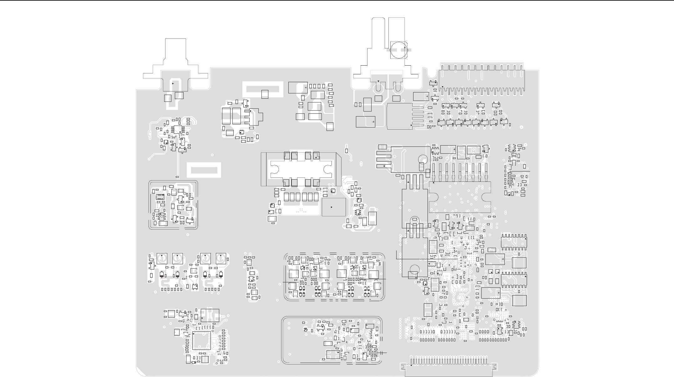
UHF1 (403–470 MHz) 1–25W PCB/Schematics/Parts List 3-5
3
2
J0700
L0722
R0713
C0900
C0901 C0906
C0907
C0908
C0909
C0910
C0915
C0939
D0900
D0906
Q0900
Q0901
R0900
R0901
R0902
R0903
R0906
R0907
R0909
R0911
R0912
R0914
R0915
R0916
R0920
R0923
R0930
R0931
U0901
C0929
C0914
C0918
C0921
C0922
C0926
C0931
C0934
C0935
C0936
C0937
C0947
C0948
C0949
C0950
C0951
D0901
D0902
D0903
L0901
L0902
R0917
R0924
R0925
R0926
R0927
R0928
R0929
R0936
R0937
R0940
R0950
SH0900
4
58
U0940
U0941
C0404
C0405
C0406 C0407 C0408 C0409
C0410
C0411
C0414
C0415
C0416
C0417
C0418
C0419
C0420
C0421
C0423
C0424
C0425
C0426
C0427
C0428
C0429
C0430
C0431
C0432
C0433
C0434
D0400
D0401
D0402
D0403
D0404
L0401
L0402 L0403 L0404
L0405
L0413
4
32
Q0402
R0404
R0405
R0406
R0407
R0409
R0410 R0412
R0432
C0622
C0630
C0631
C0644
CLKOUT
DOUTA
DOUTB
E0605 E0606
E0608
FS
PC
PD
PE
R0607
R0608
R0609
R0611
R0612
R0613
R0614
R0615
R0627
TP0601
C0510
C0605
C0611
C0615
C0617
C0619
C0620
C0621
C0627
C0629
C0633
C0638
C0642
C0643
C0645
C0646
D0601
E0600
E0604
E0607
23
4
5
6
FL0500
L0608
R0610
R0617
R0618
R0619
1
37
25
13
U0600
C0502
C0504
C0509
C0515
C0516
C0623
C0625
C0626
C0650
E0601
E0602
L0504
L0506
L0604
Q0501
R0503
R0510
R0606
R0621
R0622
R0623
TP0602
C0437
C0438
C0439
C0440
C0442
C0451
L0407
L0411
4
32
Q0405
R0417
R0418 R0419
R0420
R0421
R0422
R0423
R0424
R0425
R0433
C0748
C0776
C0777
C0796
C0797
C0798
C0799
L0714
4
321
Q0704
Q0706
R0729
R0735
R0738
R0745
R0748
R0749
VR0700
C0700
C0701
C0702
C0703
C0704
C0705
C0706
C0707
C0708
C0709
C0710
C0711
C0712
C0714
E0700
E0701
R0742
R0776
C0713
C0718
C0781
C0782
C0788
C0802
C0804
C0805
C0904
E0703
L0723
L0900
1
M0700
Q0701
10
2
3
4
786
9
5
Q0702
Q0707
Q0708
Q0709
R0700
R0702
R0703
R0706
R0730
R0732
R0734
R0740
R0741
R0744
R0750
R0751
R0752
R0753
R0756
R0757
R0761
R0762
R0763
R0764
R0768
R0771
R0773
R0774
R0778
1
RT0908
SP0700SP0701
SP0702
SP0703
SP0704
SP0705
SP0706
SP0707
30
J4001
C1003
C1006
C1008
C1011
C1013
C1017
C2000
C2001
C2002
C2003
C2004
C2005
C2006
C2500
C4000
C4001
C4002
C4003
C4004
C4005
C4006
C4014
C4015
C4016
C4017
C4018
C4019
C4020
C4021
C4022
C4023
C4024
C4025
C4026
C4027
C4028
C4029
C4030
C4031
C4032
C4033
C4034
C4035
C4076
D4001
E4001
E4004
R1014
R1019
R1066
R1067
R2000
R2004
R2007
R2008
R2009
R2013
R2529
R4000
R4001
R4002
R4003
R4004
R4005
R4006
R4009
R4010
R4011
R4012
R4034
R4061
R4063
R4064
R4065
R4066
R4067
R4068
R4069
R4070
R4071
R4095
R4106
TP1000
TP_SDRAM_BA0
TP_SDRAM_BA1
TP_SDRAM_CLK
TP_SDRAM_CS
VR4007
C1001
C1005
C1012 C1014
C1016
C1018
C1019
C2007
C3209
C3212
C4013
E4000
L3202
R1000
R1002
R1005
R1006
R1041
R1071
R2005
R2006
R2010
R2011
R2012
R3580R3583
TP4000
C3202
C3203
L3200
16
1
8
9
Q3200
16
1
8
9
Q3202
C6406
C6407
C6408
C6416
C6417
C6418
C6419
C6420
C6421
C6422
C6423
C6426
C6427
C6428
C6429
C6430
C6431
C6433
C6439
C6440
C6445
C6450
E6401
E6402
E6407
R6402
R6403
R6443
R6444
R6445
R6446
R6449
R6450
R6454
R6455
R6456
R6458
R6459
R6460
R6461
R6465
R6466
U6402
U6407
C3501
C3505
E3501
23
Q3500
R3516
R3520
C3009
C3504
C3506
E3500
R3010
C3008
C3010
R3009
U3002
9
U3500
C3018
J3000
C3000
C3002
C3015
E3000
SP3000
SP3001
1
6
5
U3001
25
26
2
J4000
C3005
C3006
C3007
C3019
C3046
C4040 C4041 C4042 C4043 C4044
C4045
C4046 C4047
C4048
C4075
E4005
2
3
Q4000
23
Q4002
23
Q4004
2
3
Q4005
2
3
Q4006
23
Q4008
23
Q4010
2
3
Q4011
Q4013
R3002
R3003
R3004
R4040 R4041 R4042 R4043 R4044
R4045
R4046 R4047
R4048
R4050
R4051
VR4000 VR4001 VR4002
VR4003
VR4004
VR4005
R3032
3
2
1
U3006
R3033
R3056
R3035
R3036
3
2
1
U3005
C0109
C0117
C0118
C0171
C0195
L0100
R0101
R0102
R0105
R0106
R0107
R0108
R0144
R0147
C0100
C0102
C0103
C0104
C0105
C0110
C0111
C0113
C0120
C0121
C0122
C0124
C0125
C0126
C0127
C0128
C0129
C0130
C0132
C0133
C0140
C0141
C0142
C0143
C0144
C0145
C0146 C0175
C0177
C0178
C0180
C0196
Q0100
Q0106
R0100
R0109
R0110
R0111
R0114
R0116
R0117
R0118
R0119
R0123
R0146
R0148
R0155
R0156
R0157
R0158
R0159
R0161
43
2
Y0100
Q0102
SH0100
MAKO_GATED_32KHz
TP_MAKO_DCLK
TP_MAKO_FSYNC
TP_MAKO_RX
TP_MAKO_TX
USB1_DAT
USB1_SEO
USB1_TXEN
C3514
C3524
Q3501
R3042
R3526
R3532
R3547 3
2
1
U3040
VR3503
C1004
C3515
E3502
C1000
C1002
C1010
C1015
C1030
C1032
C1034
C3207
C3208
C3210
C3211
C3262
C3520
C3521
C3523
C3529
C3531
E3503
4
5
8
Q3201
R1001
R1017
R1025
R1026
R1027 R1028
R1034
R1035
R1036
R1045
R3205
R3206
R3218
R3535
R3537
R3538
R3560
TP_POR
43
6
U1006
C1007
C1009
C1031
C1033
C1036
C1037
C3213
C3216
C3280
23
4
Q3203
23
4
Q3204
R1021
R3225
VBUS1_CMD
VBUS2_CMD
2.9V_MAKO_V6
C3040
C3219
C3220
C3225
C3226
C3229
C3234
C3238
C3239
C3240
C3247
C3248
C3249
C3254
C3273
C3276
C3277
C3278
C3283
C3511
C3513
C3516
C3518
C3528
C3530
C3538
C3545
E3202
E3205
R1020
R3203
R3217
R3224
R3233
R3500
R3501
R3503
R3504
R3505
R3507
R3508
R3509
R3514
R3515
R3550
R3571
R3576
R3587
R3588
R3594
R3595
R3596
RT3500
VR3202
VR3204
VR3206
3.6V_MAKO_
SW1
C6451
R6467
C0308
C0310
C0313 C0314
C0323
C0325
C0329
C0343
C0344
C0345
C0346
C0350
C0351
C0353
C0359
CR0302
CR0303
CR0304
CR0305
CR0306
CR0307
CR0308
L0317
L0318
SH0301
C0336
C0340 C0341
C0342
C0352
L0314
L0315
L0319
R0324
R0325
R0326
C0208
C0213
C0220
C0225
C0226
C0229
C0243
C0245 C0246
C0251
C0252C0259
L0207
C0200
C0201
C0205
C0206
C0236
C0237
C0241
C0300
C0301
C0305
R0201
R0204
R0205
R0224
R0226
R0304
C0214
C0223
C0250
C0253
C0320
CR0205
CR0206
CR0207
CR0208
CR0301
L0212
L0217
L0218
L0219 L0307
L0310
R0211
R0311
CR0201
CR0202
CR0203
CR0204
L0209
L0210
C0215
C0247
R0216
R0229
C0204
C0240
C0242
C0306
C0326
L0202
L0203
L0214
L0215
L0309
Q0200
Q0201
R0225
R0301
C0304
C0315
C0337
C0347
L0302
L0303
L0313
Q0300
Q0301
R0305
R0329
L0312
R0316
L0213
UHF1 (403–470 MHz) 1–25W 8471165L05 Top Side

3-6 UHF1 (403–470 MHz) 1–25W PCB/Schematics/Parts List
2.8V_RF_TEST
C6401
C6414
C6443
C6444
3
4
2
5
FL6401
IF_TEST R6409
R6410
R6411
L6403
R6420
R6438
R6439
R6440
R6457
P10
A10
P1
A1
U6401
C6432
CLK_ACQ_TEST
R6405
ROUT_TEST
SPI_CLK_TEST
1.5V_RTC_TEST
C6446
Q6402
R6404
U6406
C3200
C3201
C3279
R3200
R3215
R3238
R3241
C3206
C3270
R2500
R3246 R3247
C3214
C3215
C3265
C3266
C3269
C3281
C3289
C3290
C3291
4
5
8
Q3207
2
3
Q3208
Q3209
Q3210
R3204
R3207
R3208
R3216 R3227
R3237
R3239
R3240
R3243 R3245
R3250
R3252
R3253
R3572
TX_RAMP
1
64
3
U3201
4
3
2
Y3200
L3201
A21 AA21
U1000
C3257
C3541
C3542
C4071
C4072
C4073
C4074
C4084
C4085
C6434
C6449
C6452
E3208
E4002
R1047
R3510
R3512
R3556
R3584 R3585
R3586
R3591
R3592
R3593
R4023 R4086
R4100
R4101
R4103
R6401
R6416
R6417
R6418
R6419
R6464
R6468
R6469
R6470
U3504
8
5
4
U3508
14
7
8
U4001
U6404
U6408
ANT_C
APM_1_WIRE
C3533
C3534
C4063
C4064
C4065
C4066
C4067
C4068
C4069
C4070
C6412
C6413
C6435
C6436
C6437
C6438
E6400
EMERGENCY
IGNITION_SENSE
L6402 Q4007
2
3
Q4015
Q6401
R3529
R3540
R3545
R3548
R4030
R4033
R4098
R6407
R6430
R6432
R6433
R6434
R6435
R6436
R6437
C1
C3
A3
U6405
VR3504
VR6400
EXT_PTT
J6400
2
3
Q4001
2
3
Q4003
23
23
Q4009
2
3
Q4012
Q4014
R4031
R4032
R4049
R4054
R4055
R4088
R4089
USB2_DP
VBUS2
VR4006
C3045
D4000
R4035
1
6
5
U3003
USB2_DM
C3012
C3013
C3014
R3005 R3006
VR3000
VBAT
VBAT_GROUND
C3502
C3503
C3508
1
C3536
R3573
R3574
R3575
C2501
C3041
C3042
C3539
C3540
D3040
E2500
I2C_
CLK
I2C_DATA
R3041
R3045
R3046
R3047
R3048
R3054
R3511
R3513
R3558
R3559
R3569
R3578
14
58
U3030
10
6
5
U3501
8
5
4
U3503
VR3040
C3020
C3021
C3030
C3032
C3509
D3030 Q3030
4
3
2
1Q3032
23
Q3041
R3030
R3034
R3037
R3038
R3039
R3040 R3050
R3051
R3053
R3055
R3057
R3524
VR3502
C3011
C3016
C3017
C3500
C3507
R3007
R3502
R3506
R3521
U3004
7
814
U3505
C3274
R3008
R3228
C3031
C3510
C3512
C3517
C3519
C3522
C3525
C3526
C3532
Q3502
R3052
R3523
R3525
R3528
R3530
R3533
R3534
R3536
R3542
R3549
R3553
R4079
7
8
14
U3502
VR3200
C3221
C3222
C3227
C3228
C3231
C3232
C3243
C3252
C3275
C3527
C3535
D3200
E3203
E3206
INT_MIC
MAKO_V8_5V
Q3205
Q3503
Q3504
Q3505
R3209
R3539
R3541
R3544
R3546
R3551
R3552
R3554
R3555
16
1
8
9
U4000
VR3203
VR3205
VR3207
C3043
C3044
C3261
MAKO_V9_3V
Q3040
Q3206
R2502
R2519
R2520
R3043
R3044
R3210
R3226
R3248
R3577
R3581
TX_RAMP_DAC
23
C3218
C3233
C3237
C3260
E3201
E4003
R3582
VR3201 VR3208
EXT_MIC
22
20
1
21
J2500
R3223
R3249
R4090
C1044
C3204
C3205
C3217
C3272
C3282
OPT_SSI_SYNC
R1044
R1048
R1054
R1060
R1070
R2515
R3219
R3220
R3222
R3236
SPI_CLK_1
SPI_MISO_1
SPI_MOSI_1
C1
C3
A3
U3202
4
3
5
U3203
Y3201
C1035
MAKO_CE
R3579
RF_ATTN_2
P1
A1
A14 P14
U3200
11
J4002 14
J4003
C4007
C4010
C4011
C4012
C4086
C4088
C4089
MMP_1_WIRE
R1046
R4093
R4094
R4096
TP_FLASH_CLK
AA1
G1A1
A8 G8
U2000
J9 A9
J1 A1
U2001
U4006
U4007
U4008
USB1_DM
USB1_DP
VBUS1
VR4008
C4087
C4090
R4097 R4099
R4105
U4004
U4005
2
34
Y1000
C4049
C4051
C4053
C4055
C4058
C4059
C4060
C4061
C4062
C4091
C4092
C4093
C4094
E4006
R2501
R2504
R2506 R2507
R2508
R2509
R2510
R2511
R2512
R2513 R2514
R2516
R2517
R2518
R2524
R2525 R2526
R2527
R2528
R4074
R4076
R4078
R4080
R4081
R4082
R4083
R4085
U4009
U4010
C0719
C0720
C0721
C0726
C0727
C0737
C0741
C0746
C0747
C0811 C0812
L0700
R0719
C0735
C0742
C0766
C0767
C0772
C0778
C0779
C0803
C0810
D0700
D0702
L0706
L0710
L0719
TP0713
C0943
C0944
C0945
D0905
L0903
R0970
R0971
R0972
R0979
TP0903
TP0904
L0904
R0973
R0974
R0975
C0940
C0941 C0942
D0904
R0976
R0977 R0978
TP0913
C0723
TP0907
C0400
C0401
C0402
C0403
C0412
C0413
C0422
C0436
C0452
C0453
C0454
C0455
CR0400
E0400
E0401
E0403
L0406
Q0400
Q0401
Q0403
R0400
R0401
R0402
R0403
R0413
R0414
R0415
R0416
R0428
R0429 R0430
R0431
TP0400
C0503
C0506
C0512
C0513
C0514
C0601
C0602
C0603
C0604
C0607
C0610
C0612
C0613
C0614
C0618
C0628
C0632
C0634
C0635
C0636
C0637
C0640
C0641
C0647
C0648
C0649 C0651
D0500
D0600 E0500
E0603
E0609
E0610
L0503
L0602
L0603
L0605
Q0500
Q0600
Q0601
R0500
R0501
R0502
R0508
R0509
R0511
R0512
R0601
R0602 R0603
R0604
R0605
R0616
R0620 R0624
R0625
R0626
SH0500
TP0600
U0601
C0507
C0616
TP_VCTRL
C0441
C0443
C0444
C0445
C0446
C0447
C0448
C0449
C0456
D0405
L0409
L0410
L0412
R0426
R0427
6
4
3T0400
64
3
T0401
TP0401
L0408
C0902
C0903
C0911
C0912
C0913
C0916
C0917
C0919
C0920
C0925
C0953
Q0902
R0910
R0913
R0918
R0919
R0921
R0922
R0938
R0941
R0944
R0946
R0955
R0960
TP0910
C0923
C0927
C0928
R0942
R0943
R0947
R0951
R0954
1
RT0953
SH0901
TP0911
U0942
U0900
C0738
C0739
C0740
L0707
L0708
R0775
S0700
C0716
C0717
C0728
C0729
C0730
C0731
C0732
C0733 C0734
C0743
C0744
C0745
C0753
C0754
C0755
C0756
C0760
C0761
C0764
C0770
C0771
C0775
C0780
C0786
C0787
C0789
C0791
C0792
C0793
C0794
C0795
C0800
C0801
C0808
C0809
C0813
C0814
C0815
C0817
C0818 C0819
L0702
L0705
L0715
L0718
L0720
L0721 1
3
Q0703
Q0705
R0711
R0714
R0715
R0718
R0720
R0722
R0727
R0728
R0739
R0747
R0754
R0755
R0759
R0760
R0765
R0766
R0767
R0769
R0770
R0772
R0777
TP0702
TP0703
TP0704
TP0705
TP0707
TP0708
TP0709
TP0710
TP0711
TP0909
U0700
C0765
1
C0156
C0157
C0158
C0161
C0163
C0164
C0165
C0192
C0194
C0159
C0160
C0162
C0191
C0193
C0101
C0106
C0107
C0108
C0112
C0114
C0115
C0119
C0123
C0131
C0134
C0135
C0136
C0137
C0138
C0147
C0148
C0149
C0150
C0151
C0166
C0179
Q0107
23
Q0108
R0103
R0104
R0113 R0115
R0120
R0122 R0125
R0126
R0127
R0128 R0131
R0134
R0139
R0140
R0160
SH0101
TP501
TP502 TP503
TP504
TP_ADAPT_SW
TP_TEST1
TP_TEST2
L11
A11
L1
U0100
4
3
5
U0101
TP0301
C0230
C0235
C0248
C0249
C0257
C0258
C0302
C0303
C0307
C0309
C0311
C0316
C0317
C0318
C0319
C0321
C0322
C0324
C0327
C0328
C0331
C0334
C0348
C0349
C0357
C0358
C0360
C0361
C0362
C0363
CR0300
E0301
E0302
L0221
L0300
L0304
L0305
L0306
L0311
Q0302
R0230
R0302
R0303
R0306
R0307
R0308
R0310
R0312
R0319
R0320
R0321
R0327
R0331
R0332
R0333
R0334
R0337
SH0300
U0201
U0303
U0304
C0202
C0203
C0207
C0209
C0211
C0217
C0218
C0219
C0221
C0222
C0224
C0231
C0233
C0238
C0239
E0201
L0200
L0204
L0205
L0206
L0211
Q0202
R0202
R0203
R0206
R0207
R0208
R0210
R0212
R0213
R0218
R0219
R0220
R0221
UHF1 (403–470 MHz) 1–25W 8471165L05 Bottom side
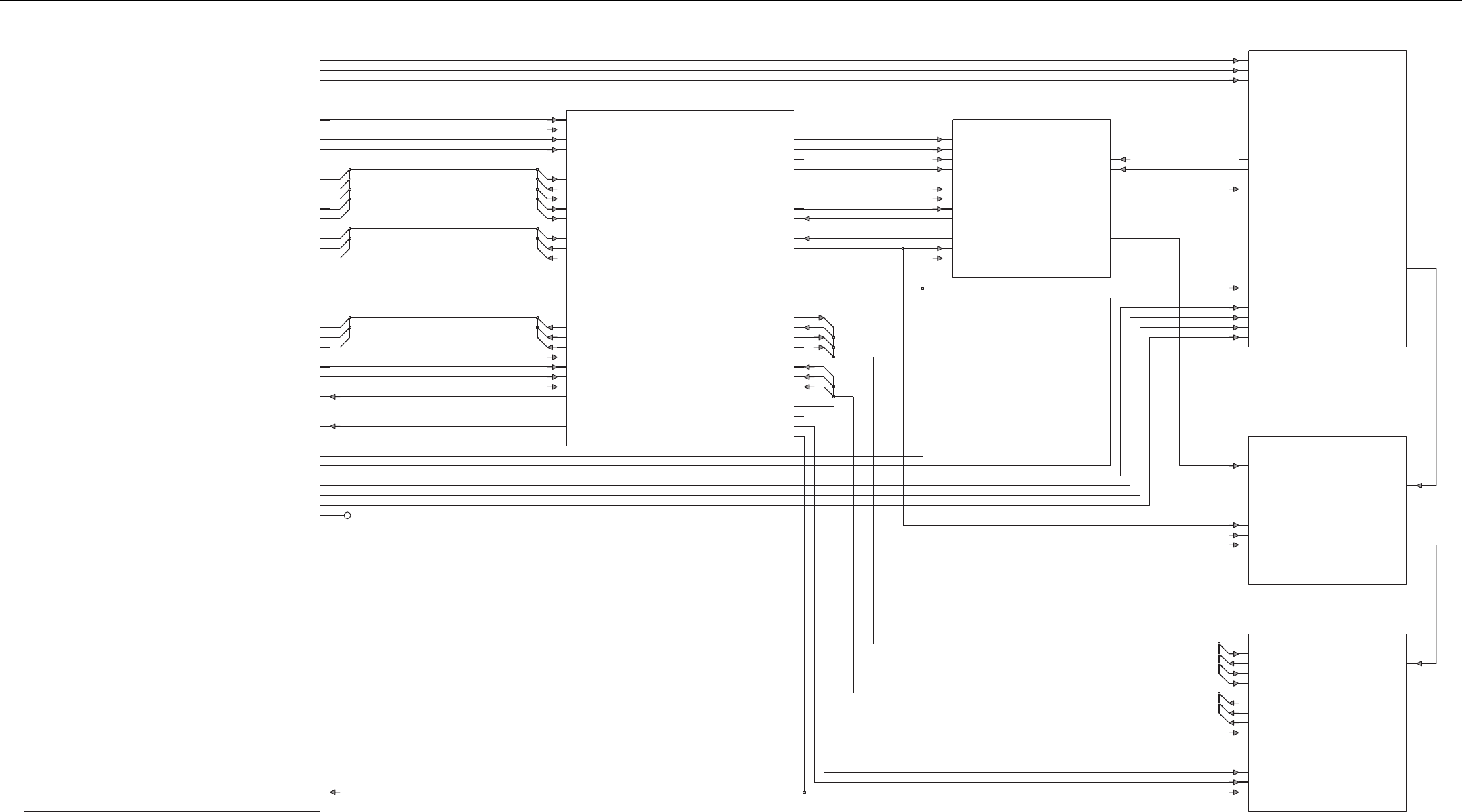
UHF1 (403–470 MHz) 1–25W PCB/Schematics/Parts List 3-7
( RX: SHEET 2 )
VCO_UHF1
( TX: SHEET 1 )
( PC: SHEET 2 )
TX_LP_UHF1
( PA: SHEET 1 )
(ABACUS3: SHEET 2)
RXBE_73.35MHZ
(IF AMP: SHEET 1)
SYNTH
CONTROLLER_&_GPS
( TOP LEVEL: SHEET 1)
RXFE_UHF1
( 1 SHEET )
1
1
3
0
RXINJ
RX_VCO_SEL1
RX_VCO_SEL2
SF_TH
TXINJ
TX_VCO_SEL1
TX_VCO_SEL2
VCTRL
2
0
3
NC
0
4
3
9R1
9V3_SYNTH_IN
9V3_SYNTH_OUT
9V3_VCO
HP_MOD_OUT
PREDRIVE_SW
PRSC
1
3
4
0
2
1
2
0
1
2
0
1
2
1
2
0
2
9R1
FE_TUNE IF
RF_ATTEN_1
RX_IN
RX_INJ
RESET_OUT
RX_FLTR_VCTRL
RX_SSI_CLK
RX_SSI_DATA
RX_SSI_FSYNC
RX_SSI_SYNCB
SPI_CLK
SPI_MISO
SPI_MOSI
THK_CS
TX_DAC
TX_SSI_CLK
TX_SSI_DATA
TX_SSI_FSYNC
2.775V_ANA_V7
2.775V_DIG_V4
5V_SW
9V3
9V3_PA
ABACUS3_CS
ADAPT_SW
ANT_ENABLE
DMCS
LOCK_DETECT
LO_BATTERY_DET
PA_BIAS
PA_TEMP
PC_ATTEN_ENA
PREDRIVE_SW
RAW_B+
TX_VCO_SEL1_
TX_VCO_SEL2_
VCTRL
2
0
1
1
1.875V_DIG_V2
16.8_GPS
16.8_MHZ_BUFF
RX_SSI_DATA_PASS_OUT
RX_SSI_FSYNC_PASS_IN
RX_SSI_FSYNC_PASS_OUT
RX_VCO_SEL1_
RX_VCO_SEL2_
SDTX
SFTX
SF_OUTSPI_CLK_IN
SPI_CLK_OUT
SPI_MISO_IN
SPI_MISO_OUT
SPI_MOSI_IN
SPI_MOSI_OUT
TH_CEX
TX_CLK 9R1
9V3
ABACUS3_CEX_IN
ABACUS3_CEX_OUT
ABACUS3_SYNCB_IN
ABACUS3_SYNCB_OUT
ADAPT_SW
DMCS
HP_MOD_OUT
LOCK
PRSC
RF_ATTN_1
RSTB RX_SSI_CLK_PASS_IN
RX_SSI_CLK_PASS_OUT
RX_SSI_DATA_PASS_IN
SPI_ABACUS_DATA
SSI_ABACUS_CLKOUT
SSI_ABACUS_DOUTA
SSI_ABACUS_DOUTB
SSI_ABACUS_FSYNC
SSI_ABACUS_SYNCB
2
1.8V_TH_DIG
16.8_GPS
16.8_REF
1V8_BE
2.8V_TH_ANA
2.8V_TH_DIG
5V
5V_BE
PC_ATTEN_ENA
PREDRIVE_SW
RX_IN
TX_DAC
TX_INJ
0
2
16.8_REF
1V8
5V
IF
SPI_ABACUS_CEX
SPI_ABACUS_CLK
TX_SSI_BUS(0:2)
ABACUS_SPI_BUS(0:3)
SPI_BUS(0:4)
RX_SSI_BUS(0:2)
ABACUS_SSI_BUS(0:2)
1
0
9V3
9V3_PA
9V3_SYNTH
9V3_VCO
ANT_ENABLE
FINAL_BIAS_1
LO_BATTERY_DET
PA_SUPPLY
UHF1 (403–470 MHz) 1–25W Overall Schematic Diagram
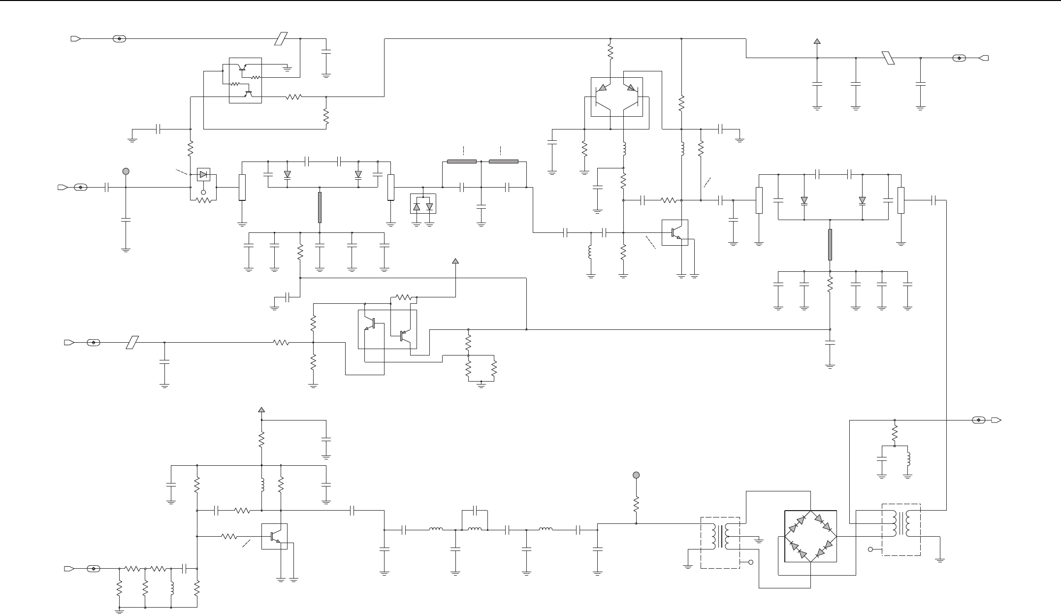
3-8 UHF1 (403–470 MHz) 1–25W PCB/Schematics/Parts List
0.6 VDC
8.6 VDC
0.7 VDC
Hi-Side Zeros for Preselector
0.8 VDC Typical
MAKO ( 0 ~ 4.6 VDC)
10 dB Attenuator
(3.00 ~ 8.00 VDC)
+16.0 dBm Min. (250 mV P-P)
8.4 VDC
(Micro-strip 20 mm Each)
L0403
12
3
10nH
D0404
10nH
L0404
12
3
C0434
220pF
1
TEST_POINT
TP0401
C0443
4.7pF
C0420
R0419
1.2K
100pF
220pF
680
C0405
C0426
56pF
R0429
5NC
4
6
3
2
1
680
XFMR
T0401
C0442
8.2pF
R0414
L0406
680
NC
15nH
2%
R0416
RF_ATTEN_1_3
220pF
C0437
NC
Q0405
Q0402
R0412
100K
C0404
220pF
(VALUE)
6.8pF
D0401
C0422
D0402
C0438
220pF
R0425
332
1%
56pF
C0430
9R1_FILT
C0428
47pF
L0413
R0403
0
C0423
220nH
4.7pF
47pF
C0452
R0413
680
9R1_FE_6
R0424
1%
121
IF_FE_8
5.6K
R0405
R0410 100K
RX_INJ_FE_5
4.7pF
C0417
56pF
C0429
2
3
6
4
1
5
12pF
Q0403
220pF
C0409
10nH
12
3
C0402
9.1pF
C0448
L0402
NU
C0424
C0439
100pF
C0413
56pF
C0447
10pF
R0432
R0431
10K
100pF
680
C0441
C0456
2.2pF
(VALUE)
C0440
220pF
(VALUE)
6.2pF
C0411
C0425
56pF
D0405
IO1
1IO2 2
IO3 3
IO4
4
220pF
C0418
L0407
2%
27nH
680
D0400
R0415
R0401
680
2%
(VALUE)
L0401
15nH
C0446
R0402
10
8.2pF
C0421
NU
T0400
XFMR
NC 5
4
6
3
2
1
10nH
12
3
E0400
L0405
TP0400
TEST_POINT
1
C0408
1.5pF
27K
R0400
L0408
2%
22nH
C0410
6.2pF
(VALUE)
22nH
2%
L0410
C0451
22pF
5.6pF
C0412
R0418
0.1uF
C0455
1%
3.65K
220pF
C0400
1.2K
R0409
C0431
56pF
R0430
10K
220pFC0436
NC
1
3
2
C0433
CR0400
MMBD352
53.6
1%
NU
L0411
R0422
9R1_FILT
22nH
2%
47pF
C0403
FE_TUNE_FE_4
L0412
47nH
C0415
RXIN_FE_6
4.3pF
(VALUE)
R0404
2.7K
C0453
3.9pF
C0401
C0454
6.8pF
25
6
3
1
4
0.1uF
5
6
3
1
4
Q0401
Q0400
2
C0406
5.6pF
D0403
100pF
C0444
51
R0407
390
R0427
R0406
2.7K
22nH
2%
L0409
C0427
47pF
E0403
220pF
C0414
39
R0417
10K
R0428
0.10uF
R0420
1.2K
C0419
R0433
R0421
10
0
R0426
2.7K
C0445
9R1_FILT
C0432
47pF
10pF
C0449
4.7pF
C0416
13pF
E0401
C0407
2.7pF
RX_IN
RF_ATTEN_1
R0423
121
1%
FE_TUNE
RX_INJ
9R1
IF
UHF1 (403–470 MHz) 1–25W Receiver Front-End Schematic Diagram
UHF1 (403–470 MHz) 1–25W PCB/Schematics/Parts List 3-9
1.43V
0.76V
1.6V
VHF -- 44.85MHz
UHF -- 73.35MHz
4-POLE
0.72V
IF_TO_ABACUS
NU
C0515
0.10uF
C0502
0.10uF
C0503
0.10uF
C0513
1
R0503
SHIELD
SH0500
Q0501
30K
L0503 330nH
E0500
6.2pF
C0510
C0509
NU
C0506
0.10uF R0510
30K
18pF
C0507
1
3
2
C0504
0.10uF
Q0500
20K
R0500
R0502
CC2
5
GND1
1
GND2
4
IN
3OUT 6
5.1K
FL0500
TS75
73.35MHz
CC1
2D0500
R0501
330
C0512
0.10uF
R0511
IFIN_BE_8
R0512
1.2K
C0514
51
0.10uF
R0509
4.7K
NU
56K
R0508
5V_BE_5
L0504
820nH
NU
L0506
5V
5V
IF
IF_OUT
C0516
UHF1 (403–470 MHz) 1–25W Receiver IF Amp Schematic Diagram

3-10 UHF1 (403–470 MHz) 1–25W PCB/Schematics/Parts List
#
*
#
#
#
#
CLOCK VCO
#
CLOCK LF
2nd LO VCO UHF (71.1MHz/75.6 MHz)
2nd LO VCO VHF (42.6MHz/47.1 MHz)
#
#
#
C0641
DOUTA_1_BE_5
2nd LO LF
SPF_3.5V
.01uF
R0624
5.1K
E0606
BK1005HM471
E0610
0.10uF
C0617
R0619
10K
270nH
L0603
0.10uF
C0643
DOUTB_1_BE_5
1.0uF
C0637
FS_1_BE_5
1V8_3
Q0600
13pF
C0612
C0603
E0608
NU
220pF
68.1K
R0622
E0603
R0626
R0608
0
0.10uF
C0623
C0622
1000pF
3VA
C0645
.01uF
TP0600
TEST_POINT
3VA
68pF
C0610
R0618
390
C0630
0.1uF
C0613
0.10uF
R0620
PE
3VA
9.1K
24K
E0604
100pF
R0604
3VA
C0651
NU
E0601
VOUT
3VA
R0623
2FB
5
GND
6
NP
4VCONT
3
VIN
1
.01uF
U0601
0
C0615
0.10uF
3VA
R0612
43pF
C0619
C0601
PD
C0614
43pF
0.10uF
C0628
200pF
C0625
VDDH
27
VDDI 48
VDDL 40
VDDP
39
VDDQ
14
VREFN
12 VREFP
11
PD
24
PE 25
13 RREF
SYNCB
33
VDDA
9
VDDC
17
VDDD 26
VDDF
6
IFIN 47
IOUTC
15
IOUTL 38
LON
42
LOP 43
MXON
2MXOP
1
PC
23
GNDI 45
GNDL
36
GNDP
37
GNDQ
16
GNDS1
21
GNDS2
34
IF2N
4
IF2P
5
FS
31
GCN
8GCP
7
GNDA
10
GNDC
18
GNDD
22
GNDF
3
GNDH 32
CLKOUT
28
19 CLKP
CXIF
46
CXVL
44
CXVM 41
DOUTA
29
DOUTB 30
FREF
35
U0600
AD9864
CLKN
20
R0627
0
R0621
0
R0603
510
C0640
2.2uF
30pF
C0650
0
R0609
R0617
10K
68
R0601
R0610
0
R0614
VVCO
C0633
0.10uF
0
0.10uF
DOUTB
C0631
CLKOUTFS
C0649 3300pF
5V
R0615
0
NU
C0616
Q0601
3VA
FREF_IF
C0611
73A04
10uH
L0605
1000pF
0.10uF
C0605
C0644
43pF
0.68uF
C0646
E0600
2.7uH
L0602
C0636
100pF
C0635
100pF
R0613
0
C0618
1uF
C0648
10.0uF10.0uF
C0647
D0601
10uH
L0604
C0626
100pF
C0607
TEST_POINT
TP0602
1
18pF
10K
CLKOUT_1_BE_5
100K
R0616
R0602
L0608
VVCO
DOUTA
4.7uH
FC_1_BE_5
3VA
1SV305
D0600
R0606
51
68pF
C0642
R0611
0
2200pF
C0629
C0634
.01uF
R0625
51.1K
R0605
330
.01uF
FD_1_BE_5
C0638
C0602
C0620
0.10uF
0.10uF
E0607
E0609
C0627
100pF
0.10uF
C0604
C0621
0.10uF
FE_1_BE_5
E0605
R0607
NU
3VA
E0602
SB_1_BE_5
PC
TP0601
TEST_POINT
4.7uF
C0632
IF_OUT
5V
SSI_ABACUS_FSYNC
SPI_ABACUS_CEX
16.8_REF
SPI_ABACUS_CLK
SSI_ABACUS_DOUTA
SSI_ABACUS_CLKOUT
SSI_ABACUS_DOUTB
SPI_ABACUS_DATA
SSI_ABACUS_SYNCB
1V8
1V8
UHF1 (403–470 MHz) 1–25W Receiver Back-End Schematic Diagram
UHF1 (403–470 MHz) 1–25W PCB/Schematics/Parts List 3-11
2.2VDC (TX Only)
16dB Pad
-5 dBm
Test Point to check Ref Osc warping
S = 0.93 mm
W = 0.625 mm
MRF1570, Flat Lead
2.2VDC (TX Only)
S = 0.54 mm
2.10V (27.5W)
16.5 dBm
3.2VDC
L = 19 mm
W = 2.5 mm
9.1VDC
W = 0.625 mm
9.3V DC (use scope with bandwidth limit to measure)
2.85V (44W)
C0747
1000pF
C0708
100K
NU
R0756
NC
150pF
C0804
NU
R0739
1000pF
C0805
C0745
100pF
R0745
470
150pF
C0940
R0775
NU
C0716
220pF
C0797
1000pF
D0702
0
PA_SUPPLY_TX_PA
TP0709
NC
NU
R0972
NU
C0748
NU
100pF
C0731
.022uF
L0710
C0701
S0700
17nH
SWITCH
C0742
5.6pF
C0782
1000pF
20K
R0774
L0903
.022uF
C0775
10nH
0
R0752
5.6pF
C0941
R0975
220
TP0713
NU
C0800
150pF
R0738
C0799
J0700-1
1
51
C0734
20pF
Q0704
NU
C0765
10pF
C0791
Q0706
0
R0749
SP0702
16pF
C0819
R0730
15
R0771
1K
C0721
NU
10
R0719
ANT_ENABLE_TX_PA
R0762 15
15nH
NU
L0904
220
R0974
NC
GND1
2
GND2
4
RF_IN
13
VD_RF_OUT
D
G
S
ADA4743
U0700
Q0705
NC
C0813
30pF
15
TP0707
C0738
R0767
5.6pF
30pF
L0706
17nH
R0751
20K
C0703
33pF
C0778
R0766
NU
82nH
L0723
PREDRIVE_SW
Q0707
R0978
0
47pF
C0728
C0764
NU
150pF
C0796
Q0703
D1
G
3
S
2
R0753
C0795
1K
R0747
47pF
0
4.7K
C0798
R0776
NC
1000pF
C0781
150pF
D0905
150nH
NU
L0715
C0815
R0765
10K
R0729
150pF
C0801
220pF
C0777
RX_IN_TX_PA
150pF
R0740
100K
R0728
NC
150pF
C0942
10K
NC
R0754
10
3.3pF
C0772
R0763
68
R0715
15
6.2K
10
R0755
R0727
R0773 15
R0761
R0722
4.7K
NC
0
C0704
.022uF
NU
R0778
C0789
20pF
C0786
NU
R0744
100
200
R0970
R0703
Q0709
0
L0708
Q0701
FINAL_BIAS_1_TX_PA
17nH
100pF
C0723
TP0708
NC
10
R0742
120
R0977
TP0710
R0706
150
L0707
17nH
R0741
C0788
0.1uF
TP0703
47K
C0737
3.9pF
100pF
C0713
16pF
Q0708
2.7K
C0818
C0767
R0760
GND1
GND2
S1
S2
S3
S4
12pF
D1
D2
G1
G2
SP0700
Q0702
R0772 15
0
R0973
R0770
NU
C0808
15pF
NU
C0717
1000pF
R0711
TP0704
150
22pF
C0726
L0720
3.3nH
C0766
NU
TP0702
C0802
SP0701
220pF
NC
C0770
220pF
C0945
150pF
C0817
NC
R0720
10
R0718
10pF
10
NU
C0771
L0718
12nH
SP0704
C0812
33pF
TP0705
150pF
C0943
47K
R0757
R0971
180
100pF
C0714
NU
C0729
220pF
C0780
12pF
C0740
NU
C0794
C0733
20pF
NU
R0700
2743019447
E0701
R0976
150
33pF
C0811
NU
NU
C0792
47p
F
C0760
J0700-3
3
C0814
SP0703
R0764 15
150pF
C0776
SP0707
L0705
150nH
C0803
4.3pF
NC
E0700
2743019447
R0714
68
1000pF
C0705
91pF
C0753
TX_INJ_TX_PA
15
R0768
D0700
10K
NU
R0750
NC
C0809
C0755
NU
C0735
C0706
100pF
C0739
12pF
NU
56K
R0748
C0702
2200pF
C0730
NU
C0720
NU
L0721
3.3nH
10
C0746
27pF
R0777
SP0705
10
R0759
D0904
56pF
C0743
43pF
C0744
C0719
27pF
1K
R0732
C0761
E0703
56pF
NU
C0727
R0979
0
SP0706
C0756
100pF
0.1uF
C0709
J0700-2
2
C0754
NU
82nH
L0719
L0702
33.47nH
C0732
1.5uH
L0722
56pF
L0714
43.67nH
C0779
33pF
VR0700
1000pF
C0718
30K
R0713
C0710
L0700
17nH
10uF
100
R0735
30pF
C0700
NU
R0769
NU
R0702
4.7pF
C0944
150pF
C0810
TP0711
NU
C0711
M0700
1
POS
NU
C0707
C0787
HEATSINK
47pF
NU
C0793
NU
C0741
1000pF
C0712
A+
TX_INJ
9V3_TX
9V39V3
9V3
Gate_1
Gate_2
R0734
0
PREDRIVE_SW
9V3_PA
9V3_VCO
9V3_SYNTH
Final_Bias
V_G2
V_G2V_G1
V_G1
9V3
Antenna_En
Antenna_En
Gate_1 Gate_2
Final_Bias
Final_Bias
V_cont
V_cont
V_cont
FINAL_BIAS_1
9V3_TX
9V3_TX
ANT_ENABLE
V_CONTROL
REV_DETECTED
FWD_POWER
FWD_DETECTED
A+
PA_SUPPLY
RX_IN
2.2K 47K
47K
47K
UHF1 (403–470 MHz) 1–25W Power Amplifier Schematic Diagram

3-12 UHF1 (403–470 MHz) 1–25W PCB/Schematics/Parts List
2.67V (44W)
0.21V (27.5W)
1.28V (27.5W)
5V DC
1.0V or less, typical
1.35V (44W)
2.10V (27.5W)
2.85V (44W )
0.38V (44W)
2.01V (27.5W)
NOTE: VOLTAGES SHOWN FOR ANALOG TX MODE
R0915
220pF
68K
R0930
C0912
C0906
18
K
22 K
220p F
1K
R092 0
U0901-2
6
5
7
8
4
R0910
C0931
220pF
C0937
220pF
NC
D0901
C0927
220pF
C0919
0.1uF
R0912
33K
C0948
1.0uF
220pF
C0922
C0926
4700pF
1
RESET_OUT
R0928
39
U0942
GND
3
INPUT
2
4NC1 5
NC
2
220p F
C093
9
D090
2
TP0913
22 K
R0903
2.2K
R0921
NC
R0950
10K
C0913
NC
220pF Q0901
R0929
39
R0914
180 K
C0911
220pF
1
2
3
R0931
D0906
PC_ATTEN_ENA_TX_PA
0
2
5
6
3
1
4
R0900
56 K
Q0900
220pF
C0935
TP0910
R0911
330
RT0908
47K
C0902
0.1uF
0.1uF
C092 1
100K
1%
R0955
0
NC
C0908
R0944
2
3
1
8
4
0.1uF
R091
9
U0901-1
1
R0922
39K
R0924
36K
5.6K
5.6K
C0947
100pF
R0917
5%
430K
RT0953
R0954
C090 4
47K
220p F
220pF
TP090 4
C0900
SH
0900
SHIELD
1
TP0907
5.6K
R092 5
C0928
1500pF
C091
7
1000pF
L0900
1uH
0.1uF
C0951
43.2K
R0951
C0923
2200pF
C0925
220pF
0
R0906
L0901
470nH
SHIELD
SH
0901
1
220pF
C0910
1000pF
C0950
16.2K
1%
R0937
R0901
43K
R0942
6.81K
2FB
5GND
6NP
4VCONT
3VIN
1
VOUT
1
U0941
C0934
220pF
220pF
C0929
220p F
C0909
8
4
R0913
0
U0900-2
6
5
7
Q0902
C0936
TP0909
LO_BATTERY_DET
220pF
0
R0941
R0927
51
43 K
220p F
C0903
R0909
C0914
220pF
R0943
39.2K
R091 6
0
R0907
6.8K
TP0903
D0903
220pF
C0918
R0936
47.5K 1%
220pF
3.32K
R0946
C0915
C0907
.01uF
VAPC
7
VPO S 8
3
VSET
R0923
0
U0940
COMM
5
ENBL 2
FLTR 4
GND
9
NC
6
RFIN 1
C0949
D0900
1
2
3
2.2uF
R0940
0
220pF
220pF
C0920
390
R0918
C0953
R0926
150
470nH
L0902
2.4K
R0960
R0902
3.3K
220p F
U0900-1
2
3
1
8
4
C0916
TP0911
R0947
0
TX_DAC
R093 8
0
9V3_PC
FWD_DETECTED
9V3
PC_ATTEN_ENA
C0901
0.1uF
9V3_PC
TX_DAC
9V39V
3
9V3
LO_BATTERY_DET
V_CONTRO L
9V3_PC 9V
3
REV_DETECTED
9V3_PC
9V3_PC
9V3_PC
9V3_PC
FWD_POWER
UHF1 (403–470 MHz) 1–25W Power Control Schematic Diagram

UHF1 (403–470 MHz) 1–25W PCB/Schematics/Parts List 3-13
1.5 ppm
TCXO (Y0100)
Locked: 1.8V
LOW: 0V
5116032H01
VCO SEL: ACTIVE LOW
Adapt OFF: 0V
Unlocked: 0V
0.5 ppm
VCO STEERING LINE VOLTAGE: 0.6V TO 4.4V
Buffer to Abacus/Controller
GPO_4
Adapt ON: 5V
9R1 SWITCH FOR FRONT-END
5102495J07
GPO_5_SYNTH
Switch for Adapt Transient
GPO LINES
HI: 2.8V
ABACUS3_SYNCB_OUT
SF_OUT_SYNTH
NC
100
220pF
C0138
R0127
ADAPT_SW_SYNTH
21
34
Q0107
Q0102
10K
R0120
NC
2.8V_TH_ANA_SYNTH
NC
10uF
C0196
ABACUS3_CEX_OUT
C0133
4.7uF
NC
4.7uF
C0140
NC
RX_SSI_DATA_IN
0
R0122
C0148
NC
NC
NU
RX_SSI_FSYNC_OUT
.033uF
ABACUS3_CEX_IN
5V_BE_SYNTH
GPO_3_SYNTH
TP501
1
220pF
C0147
1.0uF
NC
C0149
.022uF
C0114
C0158
0.1uF
R0111
0
220
NC
NC
0.1uF
R0107
2.8V_TH_DIG_SYNTH
C0150
240
R0131
1
NC
RX_SSI_DATA_OUT
TP_VCTRL
R0161
100K
NC
1V8_BE_SYNTH
SPI_MOSI_OUT
TH_CEX_SYNTH
R0102
C0156
0.1uF
0
0
R0147
NC
R0139
NU
0
1.6K
C0123
R0101
220pF
1.0uF
1
C0177
1.8V_TH_DIG_SYNTH
NC
TP504
1
RSTB_SYNTH
R0106
TP_TEST1
NU
2.7K
SPI_CLK_OUT
0
R0156
C0111
0.1uF
NC
NC
SPI_MISO_OUT
10K
R0159
R0118
0
NC
C0125
220pF
220pF
16.8_GPS_SYNTH
C0131
TP503
1
C0130
220pF
NC
R0155
C0142
0
16.8_REF_CONTROLLER_SYNTH
220pF
C0113
220pF
NU
TP_ADAPT_SW
1
C0126
220pF
NC
LOCK_SYNTH
NC
0
R0146
0.1uF
C0159
C0146
220pF
0.1uF
C0124
Q0108
SPI_MISO_IN
NC
Q0100
R0103
R0140
18
0
NC
NC
220pF
C0101
220pF
TX_CLK_SYNTH
C0179
NU
HP_MOD_OUT_SYNTH
5V_SYNTH
1VC
4
VCC
0
R0158
Y0100
TCO5826
16.8MHz
GND
2
3
OUTPUT
3
GND
1INOUT
4ONOFF_CONTROL
2OUTIN
5
VCC
TP_TEST2
1
NC
U0101
0.1uF
1
C0129
SHIELD
SH0100
1
SH0101
SHIELD
C0127
220pF
1.0uF
ABACUS3_SYNCB_IN
C0115
220pF
NU
NC
NC
GPO_2_SYNTH
C0119
0.1uF
C0166
9V3_SYNTH
2185419D06
Q0106
NC
0.1uF
C0165
C0136
0.1uF
0.1uF
C0164
R0134
27
C0120
.01uF
0.1uF
NU
C0100
C0194
C0117
220pF
220pF
SDTX_SYNTH
0.1uF
C0191
NU
VCTRL_SYNTH
RX_SSI_CLK_IN
C0141
0.1uF
220pF
NC
0
R0125
C0178
0
NC
NC
NC
R0100
0.1uF
C0180
NC
NC
C0195
220pF
470pF
10K
R0126
C0175
NC
NU
120
R0148
C0112
220pF
R0109
0
220pF
C0104
NC
NC
PRSC_SYNTH
R0123
NC
.01uF
56K
C0145
C0128
220pF
L0100
270nH
10uF
C0137
C0143
C0134
220pF
R0108
220pF
C0103
2K
SPI_MOSI_IN
0.1uF
SFTX_SYNTH
XOSC_BASE
XOSC_EMIT
L5
G6
XOSC_GN D
0
R0115
TXI
L7 TXQ
H7
TX_DAC_GN D L6
TX_DAC_VCC
G7
TX_GND1
F6
TX_GND2
J6
TX_VCC
F1
VCO_DAC
K5
K10
F5
SUB2
F3
SUB3
G8 TCLK
D7
TEST1 C7
TEST2
B3
TM
F10
TXCLK
K7
SFTX
K4 SF_OUT
C9 SMD_CLK_GEN_GN D
C11
SPI_CLK
D10
SPI_DR
D9
SPI_DW
SSI_GN D E8
E11
SSI_VCC
SUB1
A10
SDM_REF_GN D A8
SDM_REF_VCC
B9
B10 SDM_VAG
A9
SDM_VREFM B8
SDM_VREFP
D11
SDR
F11
SDTX
F9
C3
D5
RX_AGND2
B2
RX_AVCC1
A5
RX_AVCC2
RX_EN_OUT
B1
D3
SCAN_EN
F2 SCAN_I N
E9
SCLK_OUT
SDM_CLK_GEN_VCC
A3
E6 RSTB
E7
RXACQ
E10
RXFS
C2 RXI
C1 RXI X
D1 RXQ
D2 RXQ X
RX_AGND1
L8
NTXQ
K6
L4 OSCREG_BYP
J5
OSCREG_GND
OSCREG_OUT
H5
J4 OSCREG_SPLY
K11 PABIAS_DAC
L9
PHCLK
RFSTEPA
G5
MN_CP_GN D
MN_CP_VCC H2
J2
M_PRSC
H3
M_PRSCX
A1
NC1
A11
NC2
NC3
L1
L11 NC4
NTXI
C8
LGND2
G10
LVCC1
B7
LVCC2
G4
MAIN_GN D
MAIN_PDET_VCC G2
J1
MAIN_VCC
H1
MN_ADAPT_CP
G3
MN_CP
GPO2_TEST2
GPO3_TEST3
E5
GPO4_TEST4
D4
K9 GPO 5
H8 GPO 6
K8
HP_MOD_OU T
J9
INCR_DECR
F8
LGND1
ESC_CP_VCC
H4
ESC_GN D
K1
ESC_I N
E1
ESC_TEST
K2
ESC_VCC
C6
FBI
B6
FBQ
B4 GPO1_TEST1
A4
DC_CAL
L10
DEEPSLEEP
F7
DMCS
EF_OUTM
J8
J7 EF_OUTP
ESC_CP L3
ESC_CPBIAS L2
K3
ESC_CP_GN D J3
CLK1_OUT
J11 CLK2_OUT
G11 CLK_BASE
G9 CLK_CP
H11 CLK_EMIT
H10
CLK_GN D
J10
CLK_VCC
G1
DAC_ADAPT
A2
ASPI_CLK
B11 ASPI_DATA
A7
ASPI_VCC
E4 BP_I
F4 BP_I X
E2 BP_Q
BP_Q X
E3
D8
CEX
H9
A6 ACE1
D6
ACE2
AGC_DAC
B5
AGC_FLAG
C4 AGC_REF
C5
H6
ARX_DAC
C10
0
5104932K08
U0100
SC51650VF
NC
R0128
C0108
220pF
C0107
0.1uF
NC
C0151
0.1uF
0
R0157
NU
0.1uF
27
C0110
220pF
C0102
R0119
0.1uF
2K
C0162
R0114
NC
C0132
220pF
SPI_CLK_I N
C0109
0.1uF
RX_SSI_FSYNC_IN
0.1uF
C0157
R0160
100K
NC
R0105
0.1uF
240
NC
C0160C0193
NU
0
R0116
NU
0.1uF
30K
C0192
0.1uF
RX_SSI_CLK_OUT
R0117
C0105
0.1uF
R0110
NC
10K
51
R0144
R0104
47K
0.1uF
C0161
C0122
.01uF
0.1uF
C0106
GPO_6_SYNTH
0.1uF
C0163
16.8_REF_BE_SYNTH
NC
C0118
0.1uF
C0171
.01uF
10uF
C0135
1
GPO_1_SYNTH
DMCS_SYNTH
TP502
9R1_SYNTH
10K
R0113
220pF
NU
NC
C0121
HP_MOD_OUT
ABACUS3_SYNCB_IN ABACUS3_SYNCB_OUT
C0144
0.1uF
RX_SSI_FSYNC_PASS_IN
SPI_MOSI_IN
SPI_MOSI_IN
SPI_CLK_IN
SPI_CLK_IN
SPI_MISO_IN
SPI_MISO_IN
5V
2.8V_DI G
RX_VCO_SEL1_
5V_BE
9V3
9R1
16.8_REF
1V8_BE
1.8V_TH_DIG
1.8V_DI G
RSTB
16.8_GPS
ADAPT_SW
5V_TH
TX_VCO_SEL1_
TH_CEX
SPI_MOSI_IN
SPI_CLK_IN
2.8V_TH_DIG
2.8V_DI G
2.8V_TH_ANA
2.8V_ANA
1.8V_DI G
1.8V_DI G
5V_TH
RX_SSI_DATA_PASS_OUT
RX_SSI_CLK_PASS_OUT
RX_SSI_FSYNC_PASS_OUT
RX_SSI_CLK_PASS_IN
ABACUS3_CEX_OUT
SPI_MISO_OU T
SPI_MOSI_OU T
SPI_CLK_OUT
ABACUS3_CEX_IN
RX_SSI_DATA_PASS_IN
5V_TH
TX_VCO_SEL2_
RF_ATTN_1
RX_VCO_SEL2_
VCTRL
PRSC
2.8V_ANA
DMCS
5V_TH
2.8V_ANA
1.8V_DI G
2.8V_ANA
2.8V_ANA
SDTX
SFTX
SF_OUT
LOCK
TX_CLK
SPI_MISO_I N
2.8V_AN
A
47K
10K
R1
R2
OUT
GND
IN
UHF1 (403–470 MHz) 1–25W Synthesizer Schematic Diagram
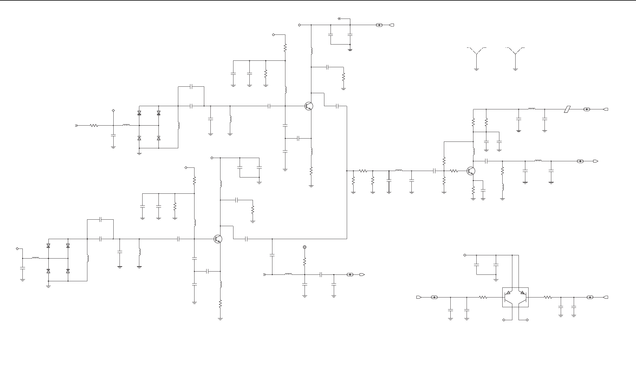
3-14 UHF1 (403–470 MHz) 1–25W PCB/Schematics/Parts List
RXINJ: 329.65 - 396.65 MHz
+6 dBm
RX VCO 2
Steering Line Voltage (VCTRL_TH)
PRSC (RX): 329.65 - 396.65 MHz
RX Prescaler
RX1_SEL: 2.7 V (High)
-5 to -15 dBm
RX Buffer Amplifier
Super Filter Voltage (SF_TH)
0.1 V (Low)
SF_TH: 2.5 V
R0204
8.2K
0.1 V (Low)
RX VCO 1
RX2_SEL: 2.7 V (High)
VCTRL: 0.6-4.5 V
1.2K
C0238
220pF
R0202
L0213
470nH
1.2K
R0203
C0257
220pF
C0235
6.2pF
39nH
L0221
220pF
C0236
RX2_SEL_VCO_UHF1_5
220nH
L0219
470nH
L0200
3.6pF
C0250
L0207
12.5nH
C0209
220pF
C0207
.022uF
C0218
NU
4.3pF
C0208
1.0pF
12.5nH
L0215
0.10uF
C0239
U0201
RX1_SEL_VCO_UHF1_5
CR0206
TP0301
1
L0214
470nH
R0206
15K
470nH
L0203
10pF
C0246
R0229
160
CR0205
CR0204
10K
Q0201
L0211
R0213
C0211
220pF
220nH
3.0pF
C0247
C0221
R0205
5.1pF
C0213
3.9pF
100
3.3K
R0201
470nH
C0243
2.7pF
L0202
C0200
220pF
C0206
0.10uF
C0241
220pF
C0229
10
R0207
24pF
0.10uF
PRSC_VCO_UHF1_5
C0201
NU
C0233
SF_TH_VCO_UHF1_6
36pF
C0223
CR0201
51
C0226
220pF
R0208
C0220
3.0pF
C0245
3.9pF
10K
C0240
220pF
0.10uF
R0218
C0249
CR0208
E020 1
CR0203
R0211
0
27nH
L0210
Q0200
56pF
C0225
220pF
C0259
12pF
9R1_VCO_UHF1_7
C0242
C0230
150pF
R0230
4.7K
100
R0226
L0218
22nH
220pF
C0248
220pF
C0253
47nH
L0205
R0210
L0209
470nH
C0237
4.7K
0.10uF
R0212
0
43pF
Q0202
220nH
C0252
C0217
L0204
470nH
L0217
220pF
C0202
.01uF
NU
C0224
R0216
120
0.10uF
CR0207
C0205
1.0pF
NU
220pF
C0203
C0219
R0225
R0220
10 15nH
7.5K
C0251
20pF
L0206
R0221
510
R0219
510
L0212
470nH
3.0pF
C0231
C0204
220pF
11pF
C0214
CR0202
5.1pF
C0215
SH0300
SHIELD
SH0301
SHIELD
C0222
3.0pF
NU
6.2K
0.10uF
C0258
SF_TH
RXINJ_VCO_UHF1_5
R0224
RXINJ
RXSL
PRESC_TX
RX1
RX2
RX_VCO_SEL1
RX1 RX2
RX_VCO_SEL2
VCTRL
PRSC
SF_TH
RXSL
9R1
SF_TH
SF_THSF_TH
UHF1 (403–470 MHz) 1–25W Receiver VCO Schematic Diagram

UHF1 (403–470 MHz) 1–25W PCB/Schematics/Parts List 3-15
+11 dBm
TX Prescaler
Super Filter Voltage (SF_TH)
-5 to -15 dBm
SF_TH: 2.5 V
0.1 V (Low)
0.1 V (Low)
Steering Line Voltage (VCTRL_TH)
TX Buffer Amplifier
TX2_SEL: 2.7 V (High)
TXINJ: 403-470 MHz
TX1_SEL: 2.7 V (High)
PRSC (TX): 403-470 MHz
TX_BUFFER_SEL: 1.8 V (ON)
0.1 V (OFF)
TX VCO 2
TX VCO 1
VCTRL: 0.6-4.5 V
R0320
15K
C0341
0.10uF
R030 8
R0325
8.2K
51
R0324
2K
TXINJ_VCO_UHF1_5
L0313
15K
R030 6
470nH
R0326
100
3.3pF
C0313
L0318
18nH
R0331
10K
75
R0316
L0310
18nH
220pF
C0303
0.5pF
C0344
1000pF
C0361
510
R0303
220pF
C0300
TX2_SEL_VCO_UHF1_5
R033 4
200
27
R0333
R0329
110
R0327
C0360
4.7uF
10K
470nH
L0312
R031 0
4.7K
0.10uF
C0305
C0362
220pF
C0340
220pF
220pF
C0311
8nH
CR0302
L0307
0.10uF
C0301
220pF
C0342
CR0300
C0337
0.10uF
0
U0304
PBR941
R0337
220n H
Q0302
L0311
470nH
L0314
39nH
L0305
Q0300
0.5pF
C0310
C0351
24pF
10
C0331
3.0p F
R030 7
0.10uF
E0302
NU
C034 9
220pF
470nH
L0319
CR0308
C0353
NU
1.0pF
C0345
3.3pF
C0319
TX1_SEL_VCO_UHF1_5
0.10uF
C0328
NU
L0304
8.2K
R0304
220nH
51pF
220pF
C0309
5.1pF
C0352
C0320
R0301
3.3K
470nH
.01u F
C030 2
10nH
L0303
R0321
2.7K
L0306
C0334
0613952Q83
L030 0
220pF
16pF
C0359
220nH
470nH
L0302
C0357
220pF
C0317
L0309
220pF
CR0304
470nH
C0314
12pF
L0315
8nH
0
R0311
7.5pF
C0346 C0347
5.1pF
R0305
CR0305
510
R0302
100
C0326
C0324
NU
220pF
200
R0332
220pF
PREDRIVE_SW_VCO_UHF1_6
C0306
0.10uF
C0363
C0348
220pF
5.1p F
CR0307
C0315
Q0301
C0336
220pF
C0329
16pF
VCTRL_VCO_UHF1_7
CR0303
R031 2
0
220pF
C030 4
NU
.022u F
C030 7
9V3_VCO_UHF1_7
C0327
220pF
E0301
NU
200K
U0303
56pF
0613952R32
R0319
7.5pF
C032 5
3.0pF
NU
C0322
C0321
C0343
C0358
0.10uF
3.3pF
3.3pF
CR0306
C0316
10uF
C0308
CR0301
C0323
27pF
(VALUE)
C0350
4.3pF
HP_MOD_OUT_VCO_UHF1_ 7
C0318
470nH
L0317
SF_TH
HP_MOD_OUT
TX2TX1
SF_TH
SF_TH
TX_VCO_SEL 1 TX_VCO_SEL2
3.3pF
SF_TH
TX2
TX1
SF_TH
VMOD
VS L
9V3_VCO
VCTRL
VCTRL
VSL
VMOD
PRESC_TX
9T1
9T1
9V3_SYNTH_OUT 9V3_SYNTH_I N
TXINJ
PREDRIVE_SW
UHF1 (403–470 MHz) 1–25W Transmit VCO Schematic Diagram

3-16 UHF1 (403–470 MHz) 1–25W PCB/Schematics/Parts List
UHF1 PCB 8471165L03 and 8471165L05 Parts
List 1–25W
Circuit
Ref
Motorola
Part No. Description
C0100 2113944A44 220pF
C0101 2113944A44 220pF
C0102 2113944A44 220pF
C0103 2113945C31 0.1uF
C0104 2113944A44 220pF
C0105 2113945C31 0.1uF
C0106 2113945C31 0.1uF
C0107 2113945C31 0.1uF
C0108 2113944A44 220pF
C0109 2113945C31 0.1uF
C0110 2113945C31 0.1uF
C0111 2113945C31 0.1uF
C0112 2113944A44 220pF
C0113 NOT PLACED –
C0114 2113946E02 1.0uF
C0115 2113946E02 1.0uF
C0117 2113944A44 220pF
C0118 2113945C31 0.1uF
C0119 NOT PLACED –
C0120 2113945B02 .01uF
C0121 NOT PLACED –
C0122 2113945B02 .01uF
C0123 2113946E02 1.0uF
C0124 2113945C31 0.1uF
C0125 2113944A44 220pF
C0126 2113944A44 220pF
C0127 2113944A44 220pF
C0128 2113944A44 220pF
C0129 2113945C31 0.1uF
C0130 2113944A44 220pF
C0131 2113944A44 220pF
C0132 2113944A44 220pF
C0133 2313960B30 4.7uF
C0134 2113944A44 220pF
C0135 2313960B32 10uF
C0136 2113945C31 0.1uF
C0137 2313960B32 10uF
C0138 2113944A44 220pF
C0140 2313960B30 4.7uF
C0141 2113945C31 0.1uF
C0142 2113944A44 220pF
C0143 2113944A44 220pF
C0144 2113945C31 0.1uF
C0145 2113945B02 .01uF
C0146 2113944A44 220pF
C0147 2113944A44 220pF
C0148 2113945D01 .033uF
C0149 2113945C04 .022uF
C0150 2113945C31 0.1uF
C0151 2113945C31 0.1uF
C0156 2185419D06 0.1uF
C0157 2185419D06 0.1uF
C0158 2185419D06 0.1uF
C0159 2185419D06 0.1uF
C0160 2185419D06 0.1uF
C0161 2185419D06 0.1uF
C0162 2185419D06 0.1uF
C0163 2185419D06 0.1uF
C0164 2185419D06 0.1uF
C0165 2185419D06 0.1uF
C0166 2185419D06 0.1uF
C0171 2113945B02 .01uF
C0175 2113944A44 220pF
C0177 2113944A44 220pF
C0178 2113944A44 220pF
C0179 2113944A44 220pF
C0180 2113945C31 0.1uF
C0191 NOT PLACED –
C0192 NOT PLACED –
C0193 NOT PLACED –
C0194 NOT PLACED –
C0195 2113945A05 470pF
C0196 2113946H02 10uF
C0200 2113944A44 220pF
C0201 2113945Y02 0.10uF
C0202 2113945C02 .01uF
C0203 2113944A44 220pF
C0204 2113944A44 220pF
C0205 2113945Y02 0.10uF
C0206 2113944A44 220pF
C0207 2113945C04 .022uF
C0208 2115153H18 4.3pF
C0209 2113944A44 220pF
C0211 2113944A44 220pF
C0213 2115153H17 3.9pF
C0214 2115153H34 11pF
C0215 2115153H20 5.1pF
C0217 2113944A44 220pF
C0218 NOT PLACED –
C0219 NOT PLACED –
C0220 2115153H17 3.9pF
C0221 2115153H14 3.0pF
C0222 NOT PLACED –
C0223 2115153H46 36pF
C0224 NOT PLACED –
C0225 2115153H51 56pF
C0226 2113944A44 220pF
C0229 2115153H42 24pF
C0230 2113944C47 150pF
C0231 2115153H14 3.0pF
Circuit
Ref
Motorola
Part No. Description
C0233 NOT PLACED –
C0235 2115153H22 6.2pF
C0236 2113944A44 220pF
C0237 2113945Y02 0.10uF
C0238 2113944A44 220pF
C0239 2113945Y02 0.10uF
C0240 2113944A44 220pF
C0241 2113945Y02 0.10uF
C0242 2113944A44 220pF
C0243 2115153H13 2.7pF
C0245 2115153H14 3.0pF
C0246 2115153H27 10pF
C0247 2115153H20 5.1pF
C0248 2113944A44 220pF
C0249 2113945Y02 0.10uF
C0250 2115153H16 3.6pF
C0251 2115153H40 20pF
C0252 2115153H48 43pF
C0253 2113944A44 220pF
C0257 2113944A44 220pF
C0258 2113945Y02 0.10uF
C0259 2115153H35 12pF
C0300 2113944A44 220pF
C0301 2113945Y02 0.10uF
C0302 2113945C02 .01uF
C0303 2113944A44 220pF
C0304 2113944A44 220pF
C0305 2113945Y02 0.10uF
C0306 2113944A44 220pF
C0307 2113945C04 .022uF
C0308 2115153H15 3.3pF
C0309 2113944A44 220pF
C0310 2115153H01 0.5pF
C0311 2113944A44 220pF
C0313 2115153H15 3.3pF
C0314 2115153H35 12pF
C0315 2115153H20 5.1pF
C0316 2313960B32 10uF
C0317 2113944A44 220pF
C0318 2115153H15 3.3pF
C0319 NOT PLACED –
C0320 2115153H20 5.1pF
C0321 2115153H24 7.5pF
C0322 NOT PLACED –
C0323 2115153H43 27pF
C0324 NOT PLACED –
C0325 2115153H51 56pF
C0326 2113944A44 220pF
C0327 NOT PLACED –
C0328 NOT PLACED –
C0329 2115153H38 16pF
Circuit
Ref
Motorola
Part No. Description
C0331 2115153H14 3.0pF
C0334 2113944A44 220pF
C0336 2113944A44 220pF
C0337 2113945Y02 0.10uF
C0340 2113944A44 220pF
C0341 2113945Y02 0.10uF
C0342 2113944A44 220pF
C0343 2115153H15 3.3pF
C0344 2115153H01 0.5pF
C0345 2115153H15 3.3pF
C0346 2115153H24 7.5pF
C0347 2115153H20 5.1pF
C0348 2113944A44 220pF
C0349 2113945Y02 0.10uF
C0350 2115153H18 4.3pF
C0351 2115153H42 24pF
C0352 2115153H50 51pF
C0353 2113944A44 220pF
C0357 2113944A44 220pF
C0358 2113945Y02 0.10uF
C0359 2115153H38 16pF
C0360 2313960B30 4.7uF
C0361 2113944C51 1000pF
C0362 2113944A44 220pF
C0363 2113945Y02 0.10uF
C0400 2113944A44 220pF
C0401 2113945C31 0.1uF
C0402 2113944A44 220pF
C0403 2115153H49 47pF
C0404 2113944A44 220pF
C0405 2113944A44 220pF
C0406 2115153H21 5.6pF
C0407 2115153H13 2.7pF
C0408 2115153H08 1.5pF
C0409 2115153H35 12pF
C0410 2115153H22 6.2pF
C0411 2115153H22 6.2pF
C0412 2115153H21 5.6pF
C0413 2113944C45 100pF
C0414 2113944A44 220pF
C0415 2115153H18 4.3pF
C0416 2115153H19 4.7pF
C0417 2115153H19 4.7pF
C0418 2113944A44 220pF
C0419 2113945Y02 0.10uF
C0420 2115153H19 4.7pF
C0421 NOT PLACED –
C0422 2115153H23 6.8pF
C0423 2115153H49 47pF
C0424 2115153H51 56pF
C0425 2115153H51 56pF
Circuit
Ref
Motorola
Part No. Description

UHF1 (403–470 MHz) 1–25W PCB/Schematics/Parts List 3-17
C0426 2115153H51 56pF
C0427 2115153H49 47pF
C0428 2115153H49 47pF
C0429 2115153H51 56pF
C0430 2115153H51 56pF
C0431 2115153H51 56pF
C0432 2115153H49 47pF
C0433 NOT PLACED –
C0434 2113944A44 220pF
C0436 2113944A44 220pF
C0437 2113944A44 220pF
C0438 2113944A44 220pF
C0439 NOT PLACED –
C0440 2113944A44 220pF
C0441 2115153H11 2.2pF
C0442 2115153H25 8.2pF
C0443 2115153H57 100pF
C0444 2115153H57 100pF
C0445 2115153H27 10pF
C0446 2115153H25 8.2pF
C0447 2115153H27 10pF
C0448 2115153H26 9.1pF
C0449 2115153H36 13pF
C0451 2115153H41 22pF
C0452 2115153H19 4.7pF
C0453 2115153H17 3.9pF
C0454 2115153H23 6.8pF
C0455 2113945C31 0.1uF
C0456 2113944A40 100pF
C0502 2113945Y02 0.10uF
C0503 2113945Y02 0.10uF
C0504 2113945Y02 0.10uF
C0506 2113945Y02 0.10uF
C0507 2115153H39 18pF
C0509 NOT PLACED –
C0510 2115153H22 6.2pF
C0512 2113945Y02 0.10uF
C0513 2113945Y02 0.10uF
C0514 2113945Y02 0.10uF
C0515 NOT PLACED –
C0516 NOT PLACED –
C0601 2115153H48 43pF
C0602 2113945B02 .01uF
C0603 2113944A44 220pF
C0604 2113945Y02 0.10uF
C0605 2115153H48 43pF
C0607 2115153H39 18pF
C0610 2115153H53 68pF
C0611 2113945A09 1000pF
C0612 2115153H36 13pF
C0613 2113945G91 0.1uF
Circuit
Ref
Motorola
Part No. Description
C0614 2115153H48 43pF
C0615 2113945B02 .01uF
C0616 NOT PLACED –
C0617 2113945Y02 0.10uF
C0618 2115358H25 1uF
C0619 2113945Y02 0.10uF
C0620 2113945Y02 0.10uF
C0621 2113945Y02 0.10uF
C0622 2113945A09 1000pF
C0623 2113945Y02 0.10uF
C0625 2113944C89 200pF
C0626 2113944A40 100pF
C0627 2113944A40 100pF
C0628 2113945Y02 0.10uF
C0629 2113945A11 2200pF
C0630 2113945Y02 0.10uF
C0631 2113945Y02 0.10uF
C0632 2313960B30 4.7uF
C0633 2113945Y02 0.10uF
C0634 2113945B02 .01uF
C0635 2113944A40 100pF
C0636 2113944A40 100pF
C0637 2113946S35 1.0uF
C0638 2113945Y02 0.10uF
C0640 2113946N03 2.2uF
C0641 2113945B02 .01uF
C0642 2115153H53 68pF
C0643 2113945Y02 0.10uF
C0644 2113945Y02 0.10uF
C0645 2113945B02 .01uF
C0646 2113946G04 0.68uF
C0647 2113946J03 10.0uF
C0648 2113946J03 10.0uF
C0649 2113945A12 3300pF
C0650 2115153H44 30pF
C0651 2115153H57 100pF
C0700 2113944C82 30pF
C0701 2113945C04 .022uF
C0702 2113944C55 2200pF
C0703 2113944C82 30pF
C0704 2113945C04 .022uF
C0705 2113944C51 1000pF
C0706 NOT PLACED –
C0707 NOT PLACED –
C0708 2113944C51 1000pF
C0709 2113945C31 0.1uF
C0710 2371403L02 10uF
C0711 NOT PLACED –
C0712 2113944C51 1000pF
C0713 2111078B42 100pF
C0714 2111078B42 100pF
Circuit
Ref
Motorola
Part No. Description
C0716 2113944A44 220pF
C0717 2113945A09 1000pF
C0718 2113945A09 1000pF
C0719 2111078B25 27pF
C0720 NOT PLACED –
C0721 NOT PLACED –
C0723 2111078B42 100pF
C0726 2111078B22 22pF
C0727 NOT PLACED –
C0728 2113944C38 47pF
C0729 NOT PLACED –
C0730 NOT PLACED –
C0731 NOT PLACED –
C0732 2111078B36 56pF
C0733 2113944C80 20pF
C0734 2113944C80 20pF
C0735 2111078B42 100pF
C0737 2111078B03 3.9pF
C0738 2111078B07 5.6pF
C0739 2171388L01 12pF
C0740 2171388L01 12pF
C0741 NOT PLACED –
C0742 2111078B07 5.6pF
C0743 2113944C39 56pF
C0744 2113944C84 43pF
C0745 2111078B42 100pF
C0746 2111078B25 27pF
C0747 NOT PLACED –
C0748 NOT PLACED –
C0753 2111078B41 91pF
C0754 NOT PLACED –
C0755 NOT PLACED –
C0756 2111078B42 100pF
C0760 NOT PLACED –
C0761 2111078B36 56pF
C0764 NOT PLACED –
C0765 NOT PLACED –
C0766 NOT PLACED –
C0767 2113944C31 12pF
C0770 2113944A44 220pF
C0771 NOT PLACED –
C0772 2113944C18 3.3pF
C0775 2113945C04 .022uF
C0776 2113944C47 150pF
C0777 2113944C47 150pF
C0778 2111078B29 33pF
C0779 2111078B29 33pF
C0780 2113944A44 220pF
C0781 2113944C47 150pF
C0782 2113944C51 1000pF
C0786 2113944C80 20pF
Circuit
Ref
Motorola
Part No. Description
C0787 2113944C38 47pF
C0788 NOT PLACED –
C0789 NOT PLACED –
C0791 2113944A25 10pF
C0792 NOT PLACED –
C0793 NOT PLACED –
C0794 NOT PLACED –
C0795 2113944C38 47pF
C0796 2113944C47 150pF
C0797 2113944C51 1000pF
C0798 2113944C51 1000pF
C0799 2113944C47 150pF
C0800 NOT PLACED –
C0801 2113944A44 220pF
C0802 2113944A44 220pF
C0803 2111078B04 4.3pF
C0804 2113944C47 150pF
C0805 2113944C51 1000pF
C0808 NOT PLACED –
C0809 NOT PLACED –
C0810 2113944C47 150pF
C0811 2111078B29 33pF
C0812 2111078B29 33pF
C0813 2111078B27 30pF
C0814 2113944C38 47pF
C0815 2113944C47 150pF
C0817 2113944C30 10pF
C0818 2111078B19 16pF
C0819 2111078B19 16pF
C0900 2113944A44 220pF
C0901 2113945C31 0.1uF
C0902 2113945C31 0.1uF
C0903 2113944A44 220pF
C0904 2113944A44 220pF
C0906 2113944A44 220pF
C0907 2113945C02 .01uF
C0908 2113945C31 0.1uF
C0909 2113944A44 220pF
C0910 2113944A44 220pF
C0911 2113944A44 220pF
C0912 2113944A44 220pF
C0913 2113944A44 220pF
C0914 2113944A44 220pF
C0915 2113944A44 220pF
C0916 2113944A44 220pF
C0917 2113945A09 1000pF
C0918 2113944A44 220pF
C0919 2113945C31 0.1uF
C0920 2113944A44 220pF
C0921 2113945C31 0.1uF
C0922 2113944A44 220pF
Circuit
Ref
Motorola
Part No. Description

3-18 UHF1 (403–470 MHz) 1–25W PCB/Schematics/Parts List
C0923 2113944C55 2200pF
C0925 2113944A44 220pF
C0926 2113945L41 4700pF
C0927 2113944C02 220pF
C0928 2113944C53 1500pF
C0929 2113944A44 220pF
C0931 2113944A44 220pF
C0934 2113944A44 220pF
C0935 2113944A44 220pF
C0936 2113944A44 220pF
C0937 2113944A44 220pF
C0939 2113944A44 220pF
C0940 2113944C47 150pF
C0941 2113944M12 5.6pF
C0942 2113944C47 150pF
C0943 2113944C47 150pF
C0944 2113944M10 4.7pF
C0945 2113944C47 150pF
C0947 2113944A40 100pF
C0948 2113946S35 1.0uF
C0949 2113946G01 2.2uF
C0950 2113945A09 1000pF
C0951 2113945C31 0.1uF
C0953 2113944A44 220pF
CR0201 4815096H01 DIODE VARACTOR 1SV305
CR0202 4815096H01 DIODE VARACTOR 1SV305
CR0203 4815096H01 DIODE VARACTOR 1SV305
CR0204 4815096H01 DIODE VARACTOR 1SV305
CR0205 4815096H01 DIODE VARACTOR 1SV305
CR0206 4815096H01 DIODE VARACTOR 1SV305
CR0207 4815096H01 DIODE VARACTOR 1SV305
CR0208 4815096H01 DIODE VARACTOR 1SV305
CR0300 4815096H01 DIODE VARACTOR 1SV305
CR0301 4815096H01 DIODE VARACTOR 1SV305
CR0302 4815096H01 DIODE VARACTOR 1SV305
CR0303 4815096H01 DIODE VARACTOR 1SV305
CR0304 4815096H01 DIODE VARACTOR 1SV305
CR0305 4815096H01 DIODE VARACTOR 1SV305
CR0306 4815096H01 DIODE VARACTOR 1SV305
CR0307 4815096H01 DIODE VARACTOR 1SV305
CR0308 4815096H01 DIODE VARACTOR 1SV305
CR0400 4813974A19 DIODE, SCHOTTKY
D0400 4813974A06 DIODE, PIN
D0401 4885055Y01 DIODE VARACTOR 1SV229
D0402 4885055Y01 DIODE VARACTOR 1SV229
D0403 4885055Y01 DIODE VARACTOR 1SV229
D0404 4885055Y01 DIODE VARACTOR 1SV229
D0405 4815090H01 DIODE, MIXER
D0500 4813974A19 DIODE, SCHOTTKY
D0600 4815096H01 DIODE VARACTOR 1SV305
D0601 4815096H01 DIODE VARACTOR 1SV305
Circuit
Ref
Motorola
Part No. Description
D0700 4802482J02 DIODE, PIN
D0702 4802482J02 DIODE, PIN
D0900 4813978C02 DIODE, SWITCHING
D0901 4815023H01 DIODE, PIN
D0902 4815024H01 DIODE, PIN
D0903 4815024H01 DIODE, PIN
D0904 4813974A21 DIODE, SCHOTTKY
D0905 4813974A21 DIODE, SCHOTTKY
D0906 4813978C02 DIODE, SWITCHING
E0201 2409134J25 FERRITE BEAD
E0301 2409134J25 FERRITE BEAD
E0302 NOT PLACED –
E0400 2409134J25 FERRITE BEAD
E0401 2409134J25 FERRITE BEAD
E0403 2409134J25 FERRITE BEAD
E0500 2409134J25 FERRITE BEAD
E0600 2409134J25 FERRITE BEAD
E0601 2409134J25 FERRITE BEAD
E0602 2409134J25 FERRITE BEAD
E0603 2409134J25 FERRITE BEAD
E0604 2409134J25 FERRITE BEAD
E0605 2409134J25 FERRITE BEAD
E0606 2409134J25 FERRITE BEAD
E0607 2409134J25 FERRITE BEAD
E0608 2409134J25 FERRITE BEAD
E0609 2409134J25 FERRITE BEAD
E0610 2480640Z01 FERRITE BEAD
E0700 2485011Y01 FERRITE BEAD
E0701 2485011Y01 FERRITE BEAD
E0703 2485011Y01 FERRITE BEAD
FL0500 9116854H01 73.35MHZ CRYSTAL FILTER
J0700 0905901V11 MINI-U RF CONNECTOR
L0100 2414017N29 270nH
L0200 2414017N28 220nH
L0202 2414032F42 470nH
L0203 2414032F42 470nH
L0204 2414017N28 220nH
L0205 2414017N20 47nH
L0206 2414017N14 15nH
L0207 2415385H02 12.5nH
L0209 2414032F42 470nH
L0210 2414015A21 27nH
L0211 2414017N28 220nH
L0212 2414032F42 470nH
L0213 2414032F42 470nH
L0214 2414032F42 470nH
L0215 2415385H02 12.5nH
L0217 2414032F42 470nH
L0218 2414015A20 22nH
L0219 2414032F42 470nH
L0221 2414017N19 39nH
Circuit
Ref
Motorola
Part No. Description
L0300 2414017N28 220nH
L0302 2414032F42 470nH
L0303 2414032F42 470nH
L0304 2414017N28 220nH
L0305 2414017N19 39nH
L0306 2414017N12 10nH
L0307 2415385H01 8nH
L0309 2414032F42 470nH
L0310 2414015A32 18nH
L0311 2414017N28 220nH
L0312 2414032F42 470nH
L0313 2414032F42 470nH
L0314 2414032F42 470nH
L0315 2415385H01 8nH
L0317 2414032F42 470nH
L0318 2414015A32 18nH
L0319 2414032F42 470nH
L0401 2414015B24 15nH
L0402 NOT PLACED –
L0403 NOT PLACED –
L0404 NOT PLACED –
L0405 NOT PLACED –
L0406 2414015B24 15nH
L0407 2414015B16 27nH
L0408 2414015B15 22nH
L0409 2414015B15 22nH
L0410 2414015B15 22nH
L0411 2414015B15 22nH
L0412 2414017N20 47nH
L0413 2414017N28 220nH
L0503 2414017K29 330nH
L0504 NOT PLACED –
L0506 2414032B66 820nH
L0602 2414032K23 2.7uH
L0603 2414032D20 270nH
L0604 2466505A01 10uH
L0605 2466505A01 10uH
L0608 2414032B76 4.7uH
L0700 2460592A01 17nH
L0702 2479990G01 33.47nH
L0705 2414017N26 150nH
L0706 2460592A01 17nH
L0707 2460592A01 17nH
L0708 2460592A01 17nH
L0710 2460592A01 17nH
L0714 2479990N01 43.67nH
L0715 2414017N26 150nH
L0718 2414017N13 12nH
L0719 2414017N23 82nH
L0720 2414017N06 3.3nH
L0721 2414017N06 3.3nH
Circuit
Ref
Motorola
Part No. Description
L0722 2414032B70 1.5uH
L0723 NOT PLACED –
L0900 2414032D30 1uH
L0901 2414032F42 470nH
L0902 2414032F42 470nH
L0903 2414032F66 10nH
L0904 NOT PLACED –
M0700 2686201B02 HEATSINK
Q0100 4802197J95 NPN RF TRANSISTOR
Q0102 4815359H01 DUAL PNP
Q0106 4816134H01 ANALOG SWITCH
Q0107 4813970A59 P-CHANNEL MOSFET
Q0108 4815261H01 ANALOG SWITCH
Q0200 4805793Y10 NPN RF TRANSISTOR
Q0201 4805793Y10 NPN RF TRANSISTOR
Q0202 4802197J95 NPN RF TRANSISTOR
Q0300 4805793Y10 NPN RF TRANSISTOR
Q0301 4805793Y10 NPN RF TRANSISTOR
Q0302 4802197J95 NPN RF TRANSISTOR
Q0400 4815271H01 ANALOG SWITCH
Q0401 4815267H01 DUAL PNP
Q0402 4885593U03 NPN RF TRANSISTOR
Q0403 4815270H01 DUAL NPN/PNP
Q0405 4885593U03 NPN RF TRANSISTOR
Q0500 4802197J95 NPN RF TRANSISTOR
Q0501 4802197J95 NPN RF TRANSISTOR
Q0600 4805793Y10 NPN RF TRANSISTOR
Q0601 4813973A04 NPN DARLINGTON
Q0701 4816013H01 DUAL NPN/PNP
Q0702 0105958T75 MRF1570 PA ASSEMBLY
Q0703 4816548H01 N-CHANNEL LDMOS DRIVER
Q0704 4813973B02 PNP
Q0705 4816547H01 N-CHANNEL LDMOS PRE-
DRIVER
Q0706 4815272H01 ANALOG SWITCH
Q0707 4815272H01 ANALOG SWITCH
Q0708 4815272H01 ANALOG SWITCH
Q0709 4815272H01 ANALOG SWITCH
Q0900 4815272H01 ANALOG SWITCH
Q0901 4813973A13 PNP
Q0902 4813973M07 NPN
R0100 0613952R66 0
R0101 0613952R66 0
R0102 0613952R66 0
R0103 0613952R66 0
R0104 0613952R17 47K
R0105 0613952Q58 240
R0106 0613952Q83 2.7K
R0107 0613952Q57 220
R0108 0613952Q80 2K
R0109 0613952R66 0
Circuit
Ref
Motorola
Part No. Description

UHF1 (403–470 MHz) 1–25W PCB/Schematics/Parts List 3-19
R0110 0613952Q42 51
R0111 0613952R66 0
R0113 0613952R01 10K
R0114 0613952Q80 2K
R0115 0613952R66 0
R0116 0613952R66 0
R0117 0613952R12 30K
R0118 0613952R66 0
R0119 0613952Q35 27
R0120 0613952R01 10K
R0122 NOT PLACED –
R0123 0613952R19 56K
R0125 0613952R66 0
R0126 NOT PLACED –
R0127 0613952Q49 100
R0128 0613952R66 0
R0131 0613952Q58 240
R0134 0613952Q35 27
R0139 0613952Q78 1.6K
R0140 0613952Q31 18
R0144 0613952R01 10K
R0146 0613952R66 0
R0147 NOT PLACED –
R0148 0613952Q51 120
R0155 0613952R66 0
R0156 NOT PLACED –
R0157 NOT PLACED –
R0158 NOT PLACED –
R0159 0613952R01 10K
R0160 0613952R25 100K
R0161 0613952R25 100K
R0201 0613952Q85 3.3K
R0202 0613952Q75 1.2K
R0203 0613952Q75 1.2K
R0204 0613952Q95 8.2K
R0205 0613952Q49 100
R0206 0613952R05 15K
R0207 0613952Q25 10
R0208 0613952Q42 51
R0210 0613952Q89 4.7K
R0211 0613952R66 0
R0212 0613952R66 0
R0213 0613952R01 10K
R0216 0613952Q51 120
R0218 0613952R01 10K
R0219 0613952Q66 510
R0220 0613952Q25 10
R0221 0613952Q66 510
R0224 0613952Q92 6.2K
R0225 0613952Q94 7.5K
R0226 0613952Q49 100
Circuit
Ref
Motorola
Part No. Description
R0229 0613952Q54 160
R0230 0613952Q89 4.7K
R0301 0613952Q85 3.3K
R0302 0613952Q66 510
R0303 0613952Q66 510
R0304 0613952Q95 8.2K
R0305 0613952Q49 100
R0306 0613952R05 15K
R0307 0613952Q25 10
R0308 0613952Q42 51
R0310 0613952Q89 4.7K
R0311 0613952R66 0
R0312 0613952R66 0
R0316 0613952Q46 75
R0319 0613952R32 200K
R0320 0613952R05 15K
R0321 0613952Q83 2.7K
R0324 0613952Q80 2K
R0325 0613952Q95 8.2K
R0326 0613952Q49 100
R0327 0613952R01 10K
R0329 0613952Q50 110
R0331 0613952R01 10K
R0332 0613952Q56 200
R0333 0613952Q35 27
R0334 0613952Q56 200
R0337 0613952R66 0
R0400 0613952R11 27K
R0401 0613952Q69 680
R0402 0613958H25 10
R0403 0613952R66 0
R0404 0613952Q83 2.7K
R0405 0613952Q91 5.6K
R0406 0613952Q83 2.7K
R0407 0613952H63 390
R0409 0613952Q75 1.2K
R0410 0613952R25 100K
R0412 0613952R25 100K
R0413 0613952Q69 680
R0414 0613952Q69 680
R0415 0613952Q69 680
R0416 0613952Q69 680
R0417 0613958H39 39
R0418 0613952M55 3.65K
R0419 0613952Q75 1.2K
R0420 0613952Q75 1.2K
R0421 0613958H25 10
R0422 0613952K71 53.6
R0423 0613952L09 121
R0424 0613952L09 121
R0425 0613952L51 332
Circuit
Ref
Motorola
Part No. Description
R0426 0613952Q83 2.7K
R0427 0613952Q42 51
R0428 0613952R01 10K
R0429 0613952Q69 680
R0430 0613952R01 10K
R0431 0613952R01 10K
R0432 0613952H69 680
R0433 0613952R66 0
R0500 0613952Q90 5.1K
R0501 0613952Q61 330
R0502 0613952R08 20K
R0503 0613952R12 30K
R0508 0613952R19 56K
R0509 0613952Q89 4.7K
R0510 0613952R12 30K
R0511 0613952Q75 1.2K
R0512 0613952Q42 51
R0601 0613952Q45 68
R0602 0613952R01 10K
R0603 0613952Q66 510
R0604 0613952R10 24K
R0605 0613952Q61 330
R0606 0613952Q42 51
R0607 NOT PLACED –
R0608 0613952R66 0
R0609 0613952R66 0
R0610 0613952R66 0
R0611 0613952R66 0
R0612 0613952R66 0
R0613 0613952R66 0
R0614 0613952R66 0
R0615 0613952R66 0
R0616 0613952R25 100K
R0617 0613952R01 10K
R0618 0613952Q63 390
R0619 0613952R01 10K
R0620 0613952Q96 9.1K
R0621 0613952R66 0
R0622 NOT PLACED –
R0623 NOT PLACED –
R0624 0613952Q90 5.1K
R0625 0613952N69 51.1K
R0626 0613952N81 68.1K
R0627 0613952R66 0
R0700 NOT PLACED –
R0702 NOT PLACED –
R0703 0613958J74 0
R0706 0613958S53 150
R0711 0613952H53 150
R0713 0613959H12 30K
R0714 0613952H45 68
Circuit
Ref
Motorola
Part No. Description
R0715 0613952H45 68
R0718 0613952H25 10
R0719 0613959Q25 10
R0720 0613952H25 10
R0722 0613952H89 4.7K
R0727 0613952H92 6.2K
R0728 0613952J01 10K
R0729 0613952J01 10K
R0730 0613952H73 1K
R0732 0613952H73 1K
R0734 0613952G67 0
R0735 0613959Y49 100
R0738 0613959Y42 51
R0739 NOT PLACED –
R0740 0613952J25 100K
R0741 0613952J17 47K
R0742 0613959Q25 10
R0744 NOT PLACED –
R0745 0613952H65 470
R0747 0613952H89 4.7K
R0748 0613952J19 56K
R0749 0613952G67 0
R0750 0613952J01 10K
R0751 0613952J08 20K
R0752 0613952G67 0
R0753 0613952H73 1K
R0754 0613952H25 10
R0755 0613952H25 10
R0756 0613952J25 100K
R0757 0613952J17 47K
R0759 0613952H25 10
R0760 0613952Q83 2.7K
R0761 0613952G67 0
R0762 0613958S29 15
R0763 0613958S29 15
R0764 0613958S29 15
R0765 NOT PLACED –
R0766 NOT PLACED –
R0767 0613958S29 15
R0768 0613958S29 15
R0769 NOT PLACED –
R0770 NOT PLACED –
R0771 0613958S29 15
R0772 0613958S29 15
R0773 0613958S29 15
R0774 0613952J08 20K
R0775 NOT PLACED –
R0776 0613958J74 0
R0777 0613952H25 10
R0778 NOT PLACED –
R0900 0613952R19 56K
Circuit
Ref
Motorola
Part No. Description
3-20 UHF1 (403–470 MHz) 1–25W PCB/Schematics/Parts List
R0901 0613952R16 43K
R0902 0613952Q88 4.3K
R0903 0613952R09 22K
R0906 0613952R66 0
R0907 0613952R66 0
R0909 0613952R16 43K
R0910 0613952H73 1K
R0911 0613952Q61 330
R0912 0613952R13 33K
R0913 0613952R66 0
R0914 0613952R31 180K
R0915 0613952R21 68K
R0916 0613952Q93 6.8K
R0917 0613952H91 5.6K
R0918 0613952H63 390
R0919 0613952R15 39K
R0920 0613952R09 22K
R0921 0613952H81 2.2K
R0922 0613952R14 36K
R0923 0613952R66 0
R0924 0613952H91 5.6K
R0925 0613952H91 5.6K
R0926 0613958H53 150
R0927 0613952H42 51
R0928 0613958H39 39
R0929 0613958H39 39
R0930 0613952R07 18K
R0931 0613952R66 0
R0936 0613952N66 47.5K
R0937 0613952N21 16.2K
R0938 0613952R66 0
R0940 0613952R66 0
R0941 0613952R66 0
R0942 0613952M81 6.81K
R0943 0613952N58 39.2K
R0944 0613952R66 0
R0946 0613952M51 3.32K
R0947 0613952R66 0
R0950 0613952N01 10K
R0951 0613952N62 43.2K
R0954 0613952R40 430K
R0955 0613952P01 100K
R0960 0613952H82 2.4K
R0970 0613958H56 200
R0971 0613958H55 180
R0972 NOT PLACED –
R0973 0613952G67 0
R0974 0613958H57 220
R0975 0613958H57 220
R0976 0613952H53 150
R0977 0613952H51 120
Circuit
Ref
Motorola
Part No. Description
R0978 0613952G67 0
R0979 0613952G67 0
RT0908 0615585H01 THERMISTOR, 47K
RT0953 0615585H01 THERMISTOR, 47K
SH0100 2615362H01 SHIELD
SH0101 2615362H01 SHIELD
SH0300 2615362H01 SHIELD
SH0301 2615362H01 SHIELD
SH0500 2615576H01 SHIELD
SH0900 2686423Z02 SHIELD
SH0901 2686425Z02 SHIELD
SP0700 1015349H01 SOLDER PREFORM
SP0701 1015349H01 SOLDER PREFORM
SP0702 1015349H01 SOLDER PREFORM
SP0703 1015349H01 SOLDER PREFORM
SP0704 1015349H01 SOLDER PREFORM
SP0705 1015349H01 SOLDER PREFORM
SP0706 1015349H01 SOLDER PREFORM
SP0707 1015349H01 SOLDER PREFORM
T0400 2515121H01 BALUN XFMR
T0401 2515121H01 BALUN XFMR
U0100 5104932K08 IC, FRACN SYNTHESIZER
U0101 5114000B59 ANALOG SWITCH
U0201 4815267H01 DUAL PNP
U0303 NOT PLACED –
U0304 4815267H01 DUAL PNP
U0600 5102495J14 IC, RF ASIC
U0601 5115391H01 VOLTAGE REGULATOR
U0700 4802246J29 PA PRE-DRIVER
U0900 5115147H01 DUAL OPAMP
U0901 5115147H01 DUAL OPAMP
U0940 5180390L83 IC, PA CONTROLLER
U0941 5115391H01 VOLTAGE REGULATOR
U0942 5114004A35 VOLTAGE DETECTOR
VR0700 4813977M11 DIODE, 5.6V ZENER
Y0100 5116032H01 0.5 PPM 16.8 MHZ TCXO
(GPS Models only)
Circuit
Ref
Motorola
Part No. Description
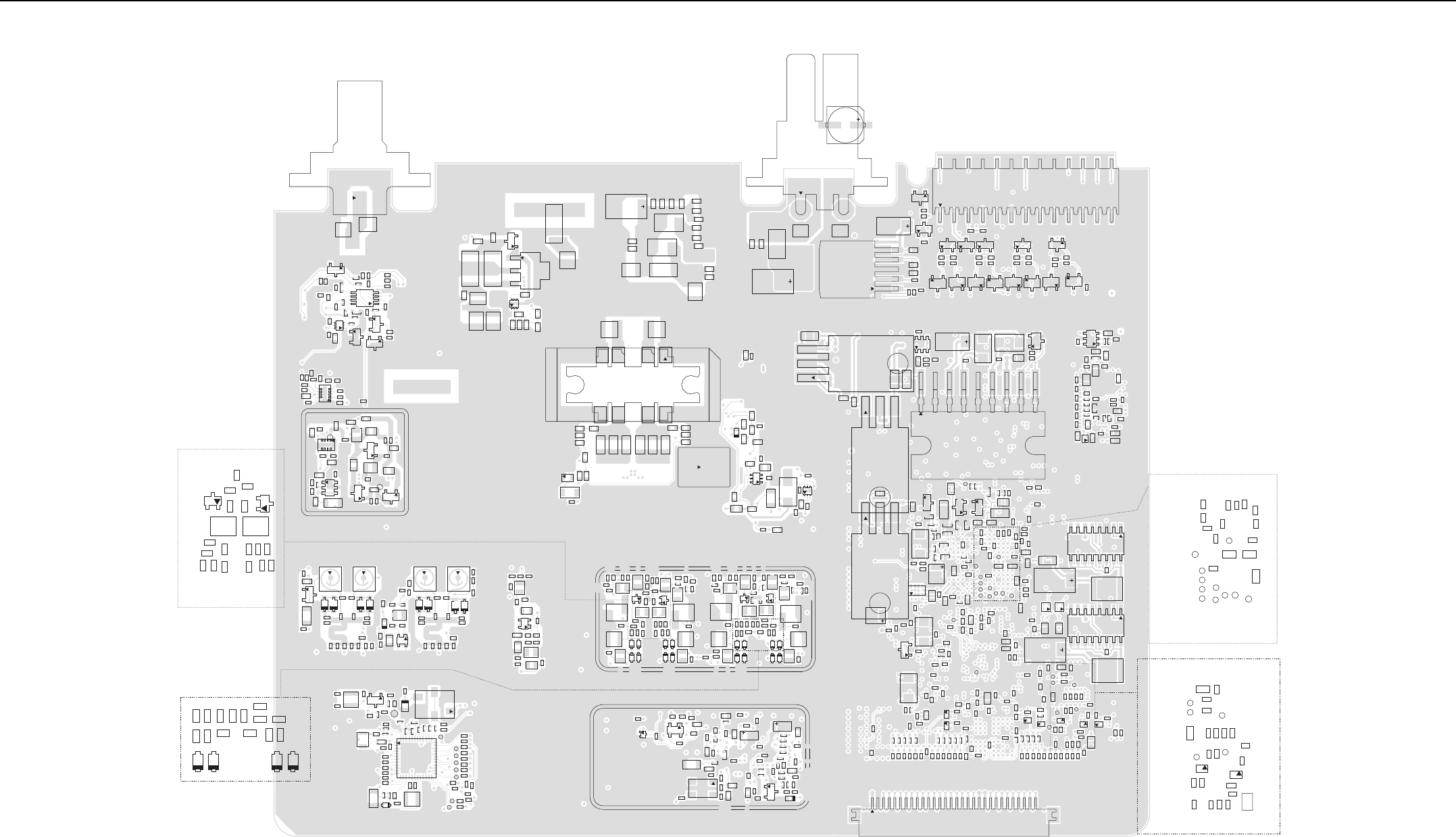
UHF1 (403–470 MHz) 1–25W PCB/Schematics/Parts List 3-21
3.0 UHF1 (403–470 MHz) 1–25W PCB/Schematics/Parts List
2.9V_MAKO_V6
C0100
C0102
C0103
C0104
C0105
C0109
C0110
C0111
C0113
C0117
C0118
C0120
C0121
C0122
C0124
C0125
C0126
C0127
C0128
C0129
C0130
C0132
C0133
C0140
C0141
C0142
C0143
C0144
C0145
C0146
C0171
C0175
C0177
C0178
C0180
C0195
C0196
C0200
C0201
C0205
C0206
C0220
C0226
C0236
C0237
C0240 C0241
C0242
C0250
C0253
C0300
C0301
C0304
C0305
C0306
C0315
C0320
C0326
C0336
C0337
C0340 C0341
C0342
C0347
C0350
C0353
C1000
C1001
C1002
C1003
C1004
C1005
C1006
C1007
C1008
C1009
C1010
C1011
C1012
C1013
C1014
C1015
C1016
C1017
C1018
C1019
C1030
C1031
C1034
C1036
C1037
C2000
C2001
C2002
C2003
C2005 C2007
C2500
C3040
C3202
C3203
C3207
C3208
C3209
C3210
C3211
C3212
C3213
C3216
C3219
C3220
C3225
C3226
C3229
C3234
C3238
C3239
C3240
C3247
C3248
C3249
C3254
C3262
C3273
C3280
C3292
C3514
C3515
C3516
C3518
C3520
C3523
C3524
C3528
C3529
C3530
C3531
C3538
C3543
C3545
C4000
C4001
C4002
C4003
C4004
C4005
C4006
C4013
C4016
C4017
C4018
C4019
C4020
C4021
C4022
C4023
C4024
C4025
C4026
C4027
C4028
C4029
C4030
C4031
C4032
C4033
C4090
C4091
C4092
C6451
CR0201
CR0202
CR0203
CR0204
CR0205
CR0206
CR0207
CR0208
CR0303
CR0304
CR0307
CR0308
E3202
E3205
E3502 E3503
E4000
E4001
3
2
J0700
30
J4001
L0100
L0202
L0203
L0207
L0209
L0210
L0213
L0214
L0215
L0217
L0218
L0302
L0303
L0307
L0309
L0310
L0312
L0313
L0314
L0315
L0317
L0318
L0319
L3200
L3202
Q0100
Q0102
Q0106
Q0300
Q0301
16
1
8
9
Q3200
4
5
8
Q3201
16
1
8
9
Q3202
23
4
Q3203
23
4
Q3204
R0100
R0101
R0102
R0105
R0106
R0107
R0108
R0109
R0110
R0111
R0114
R0116
R0117
R0118
R0119R0123
R0144
R0146
R0147
R0148
R0155
R0156
R0157
R0158
R0159
R0161
R0201
R0204
R0205
R0211
R0224
R0225
R0226
R0301
R0304
R0305
R0311
R0316
R0324
R0325
R0326
R0329
R1000
R1001
R1002
R1005
R1006
R1014
R1017
R1019
R1020
R1021
R1025
R1027
R1028
R1034
R1035
R1036
R1041
R1045
R1066
R1067
R1071
R2000
R2004
R2006
R2011
R2012
R2529
R3203
R3205
R3206
R3217
R3218
R3224
R3225
R3500
R3501
R3505
R3526
R3532
R3535
R3537
R3538
R3547
R3550
R3560
R3571
R3576
R3580
R3583
R3588
R3590
R3594
R3595
R3596
R4000
R4001
R4002
R4003
R4004
R4005
R4011
R4012
R4061
R4063
R4064
R4065
R4066
R4067
R4068
R4069
R4070
R4071
R4093
R4094
R4096
R4105
R6467
RT3500
1
2
SH0100
1
2
SH0301
TP1000
TP4000
TP_POR
U3040
9
U3500
U4006
U4007 U4008
U4009 U4010
VR3202
VR3204
VR3206
VR3503
43
2
Y0100
3.6V_MAKO_SW1
C3276
C3278
C3283
C3511
C3513
R3233
R3503
R3504
R3507
R3508
R3509
R3514 R3515
R3587
TP_MAKO_DCLK
TP_MAKO_FSYNC
TP_MAKO_RX
TP_MAKO_TX
USB1_DAT
USB1_SEO
USB1_TXEN
VBUS1_CMD
VBUS2_CMD
MAKO_GATED_32KHz
C2004
C2006
C2008
C2009
C4034
C4035
C4089
R2005
R2007
R2008
R2009
R2010
R2013
R2014
R2015
R4006
R4009
R4010
R4095
R4097
R4099
TP_SDRAM_BA0
TP_SDRAM_BA1
TP_SDRAM_CLK
TP_SDRAM_CLKX
TP_SDRAM_CS
U4004
U4005
C0308
C0310
C0313 C0314
C0323
C0325
C0329
C0343
C0344
C0345
C0346
C0351
C0352
C0359
CR0301
CR0302
CR0305
CR0306
C0204
C0208
C0213
C0214
C0215
C0223
C0225
C0229
C0243
C0245 C0246
C0247
C0251
C0252
C0259
L0212 L0219
Q0200
Q0201
R0216
R0229
C0900
C0901 C0906
C0907
C0908
C0909
C0910
C0915
C0939
C0967
D0900
D0906
D0907
L0722
63
4
Q0900
Q0901
R0713
R0900
R0901
R0902
R0903
R0906
R0907
R0909
R0911
R0912
R0914
R0915
R0916
R0920
R0923
R0930
R0931
R0986
R0987
U0901
C0751
C0776
C0777
C0778
C0779
C0796
C0797
C0798
C0799
L0712
L0714
4
3
2
1
Q0704
63
4
Q0706
R0729
R0735
R0738
R0745
R0748
R0749
VR0700
C0700
C0701
C0702
C0703
C0704
C0705
C0706
C0707
C0708
C0709
C0710
C0711
C0712
C0713
C0714
C0715
C0722
C3000
C3002
C3015
E0700
E0701
E3000
R0742
SP3000
SP3001
C3005
C3006
C3007
C3018
C3019
C3046
C4040 C4041 C4042 C4043 C4044
C4045
C4046 C4047
C4048
C4075E4005
J3000
25
26
2
J4000
2
3
Q4000
2
3
Q4002
2
3
Q4004
2
3
Q4005
2
3
Q4006
2
3
Q4008
2
3
Q4010
2
3
Q4011
Q4013
R3002
R3003
R3004
R4040 R4041 R4042 R4043 R4044
R4045
R4046 R4047
R4048
R4050
R4051
1
6
5
U3001
VR4000 VR4001 VR4002
VR4003
VR4004
VR4005
C0929
C0960
C0961
C0962
C0963
C0964
C0965
R0981
R0982
R0983
R0984 R0985
R0988
R0994
R0995
4
5
8
U0943
C0914
C0918
C0921
C0922
C0926
C0931
C0934
C0935
C0936
C0937
C0947
C0948
C0949
C0950
C0951
D0901
D0902
D0903
L0901
L0902
R0917
R0924
R0925
R0926
R0927
R0928
R0929
R0936R0937
R0940
R0950
R0989
SH0900
4
58U0940
U0941
C6406
C6407
C6408
C6416
C6417
C6418
C6419
C6420
C6421
C6422
C6423
C6426
C6427
C6428
C6429
C6430
C6431
C6433
C6439
C6440
C6445
C6450
E6401
E6402
E6407
R6402
R6403
R6443
R6444
R6445
R6446
R6449
R6450
R6454
R6455
R6456
R6458
R6459
R6460
R6461
R6465
R6466
U6402
U6407
C3008
C3009
C3010 C3501
C3504 C3505
C3506
E3500
E3501
2
3
Q3500
R3009
R3010
R3516
R3520
U3002
C0966
R0775
R3032
R3033
R3036
R3056
3
2
1
U3006
R3035
3
2
1
U3005
R3042
3
2
1
C0437
C0438
C0439
C0440
C0442
C0451
C0457
L0407
L0411
4
32
Q0405
R0417
R0418 R0419
R0420
R0421
R0422
R0423
R0424
R0425
R0433
R0434
C0404
C0405
C0406
C0407
C0408
C0409
C0410
C0411
C0414
C0415
C0416
C0417
C0419
C0420
C0421
C0423
C0424
C0425
C0426
C0427
C0428
C0429
C0430
C0431
C0432
C0433
C0434
C0458 C0459
C0460
C0461
C0462
D0400
D0401
D0402
D0403
D0404
D0406
D0407
D0408
D0409
L0401
L0402 L0403 L0404
L0405
L0413
4
32
Q0402
R0404
R0405
R0406
R0407
R0409
R0410 R0412
R0432
R0435
R0436
R0437
R0438
R0440 R0441
R0443
R0444
C0502
C0504
C0509
C0510
C0515
C0516
C0605
C0611
C0615
C0617
C0619
C0620
C0621
C0622
C0623
C0625
C0626
C0627
C0629
C0630
C0631
C0633
C0638
C0642
C0643
C0644
C0645
C0646
C0650
CLKOUT
D0601
DOUTA
DOUTB
E0600
E0601
E0602
E0604
E0605
E0606
E0607
E0608
5
6
4
3
2
1
FL0500
FS
L0504
L0506
L0604
L0608
PC
PD
PE
Q0501
R0503
R0510
R0606
R0607
R0608
R0609
R0610 R0611
R0612
R0613
R0614
R0615
R0617
R0618
R0619
R0621
R0622
R0623
R0627
TP0601
U602
1
37
25
13
U0600
C0718
C0724
C0759
C0768
C0781
C0782
C0783
C0788
C0802
C0804
C0805
C0806C0807
C0904
E0702
E0703
E0704
L0723
L0900
1
M0700
Q0701
5
9
6
87
432
10 Q0702
63
4Q0711
R0700
R0702
R0706
R0724
R0725
R0726
R0730
R0732
R0734
R0740
R0741
R0744
R0750
R0751
R0752
R0753
R0756
R0757
R0761
R0762
R0763
R0764
R0768
R0771
R0773
1
RT0908
SP0700SP0701
SP0702SP0703
SP0704
SP0705
SP0706
SP0707
UHF1 (403–470 MHz) 1–25W 8471165L06 Top Side
3-22 UHF1 (403–470 MHz) 1–25W PCB/Schematics/Parts List
1.2V_RTC_TEST
2.8V_RF_TEST
ANT_C
C0101
C0106
C0107
C0108
C0112
C0114
C0115
C0119
C0123
C0131
C0134
C0135
C0136
C0137
C0138
C0147
C0148
C0149
C0150
C0151
C0156
C0157
C0158
C0159
C0160
C0161
C0162
C0163
C0164
C0165
C0166
C0179
C0191
C0192 C0193
C0194
C0202
C0203
C0207
C0209
C0211
C0217
C0218
C0219
C0221
C0222
C0224
C0230
C0231
C0233
C0235
C0238
C0239
C0248
C0249
C0257
C0258
C0302
C0303
C0307
C0309
C0311
C0316
C0317
C0318
C0319
C0321
C0322
C0324
C0327
C0328
C0331
C0334
C0348
C0349
C0357
C0358
C0360
C0361
C0362
C0363
C0400
C0401
C0402
C0403
C0412
C0413
C0422
C0435
C0436
C0441
C0443
C0444
C0445
C0446
C0447
C0448
C0449
C0452
C0453
C0454
C0455
C0456
C0463
C0464
C0503
C0506
C0507
C0512
C0513
C0514
C0601
C0602
C0603
C0604
C0607
C0610
C0612
C0613
C0614
C0616
C0618
C0628
C0632
C0634
C0635
C0636
C0637
C0640
C0641
C0647
C0648
C0649
C0651
C0716
C0717
C0719
C0720
C0721
C0723
C0725
C0726
C0727
C0728
C0729 C0730
C0731
C0732
C0733
C0734
C0735
C0736
C0737
C0738
C0739
C0740
C0741
C0742
C0743
C0744
C0745
C0746
C0747
C0748
C0749
C0752
C0753
C0754
C0755
C0756
C0757
C0758
C0760
C0761
C0763
C0764
C0765
C0766
C0767
C0769
C0770
C0771
C0772
C0774
C0775
C0780
C0785
C0786
C0787
C0789
C0790
C0791
C0792
C0793
C0794
C0795
C0800
C0801
C0803
C0808
C0809
C0810
C0811 C0812
C0813
C0814
C0815
C0817
C0818 C0819
C0828 C0829
C0832
C0845
C0856
C0861
C0869
C0874
C0902
C0903
C0911
C0912
C0913
C0916
C0917
C0919
C0920
C0923 C0925
C0927
C0928
C0940
C0941 C0942
C0943
C0944
C0945
C0953
C1032
C1033
C1035
C1044
C2501
C3011
C3012
C3013
C3014
C3016
C3017
C3020
C3021
C3030
C3031
C3032
C3041
C3042
C3043
C3044
C3045
C3200
C3201
C3204
C3205
C3206
C3214
C3215
C3217
C3218
C3221
C3222
C3227
C3228
C3231
C3232
C3233
C3237
C3243
C3252
C3257
C3260
C3261
C3265
C3266
C3269
C3270
C3272
C3274
C3275
C3279
C3281
C3282
C3289
C3290
C3291
C3500
C3502
C3503
C3507
C3508
C3509
C3510
C3512
1C3517
C3519
C3521
C3522
C3525
C3526
C3527
C3532
C3533
C3534
C3535
1
C3536
C3539 C3540
C3541
C3542
C4007
C4010
C4011
C4012
C4014
C4015
C4049
C4051
C4053
C4055
C4058
C4059
C4060
C4061
C4062
C4063
C4064
C4065
C4066
C4067 C4068
C4069
C4070
C4071
C4072
C4073
C4074
C4076
C4084
C4085
C4086
C4087 C4088
C4093
C4094
C6401
C6412
C6413
C6414
C6432
C6434
C6435
C6436
C6437
C6438
C6443
C6444
C6446
C6449
C6452
CLK_ACQ_TEST
CR0300
CR0400
D0405
D0500
D0600
D0700
D0702
8
4
5
D0703
D0704
D0904
D0905
D3030
D3040
D3200
D4000
D4001
E0201
E0301
E0302
E0400
E0401
E0403
E0500
E0603
E0609
E0610
E2500
E3201
E3203
E3206
E3208
E4002
E4003
E4004
E4006
E6400
EXT_MIC
EXT_PTT
3
4
2
5
FL6401
FT0400
FT0401
FT_APM_1_WIRE
FT_EMERGENCY
FT_IGNITION_SENSE
FT_MMP_1_WIRE
FT_USB1_DM
FT_USB1_DP
FT_USB2_DM
FT_USB2_DP
FT_VBAT
FT_VBAT_GROUND
FT_VBUS1
FT_VBUS2
I2C_CLK
I2C_DATA
IF_TEST
INT_MIC
G2
20
G1
J2500
11
J4002
14
J4003
J6400
L0200
L0204
L0205
L0206
L0211
L0221
L0300
L0304
L0305
L0306
L0311
L0406
L0408
L0409
L0410
L0412
L0414
L0503
L0602
L0603
L0605
L0700
L0702
L0705
L0706
L0707
L0708
L0709
L0710
L0711
L0715
L0716
L0717
L0718
L0719
L0720
L0721
L0903
L0904
L0905
L3201
L6402
L6403
MAKO_CE
MAKO_V8_5V
MAKO_V9_3V
OPT_SSI_SYNC
Q0107
2
3
Q0108
Q0202
Q0302
63
4Q0400
Q0401
Q0403
Q0500
Q0600
Q0601
1
3
Q0703
Q0705
Q0902
Q3030
4
3
2
1
Q3032
Q3040
2
3
Q3041
2
3
Q3205
6
3
4
Q3206
4
58
Q3207
2
3
Q3208
Q3209
Q3210
63
4
Q3502
63
4
Q3503
Q3504
Q3505
2
3
Q4001
2
3
Q4003
2
3
Q4007
2
3
Q4009
2
3
Q4012
Q4014
2
3
Q4015
Q6401
63
4
Q6402
R0103
R0104
R0113 R0115
R0120
R0122 R0125
R0126
R0127
R0128 R0131
R0134
R0139
R0140
R0160
R0202
R0203
R0206
R0207
R0208
R0210
R0212
R0213
R0218
R0219
R0220
R0221
R0230
R0302
R0303
R0306
R0307
R0308
R0310
R0312
R0319
R0320
R0321
R0327
R0331
R0332
R0333
R0334
R0337
R0400
R0401
R0402
R0403
R0411
R0413
R0414
R0415
R0416
R0426
R0427
R0428
R0429 R0430
R0431
R0500
R0501
R0502
R0508
R0509
R0511
R0512
R0601
R0602
R0603
R0604
R0605
R0616
R0620
R0624
R0625
R0626
R0701
R0709
R0711
R0712
R0714 R0715
R0718
R0719
R0720
R0722
R0727 R0728
R0739
R0743
R0747
R0754
R0755
R0759
R0760
R0765
R0766
R0769
R0770
R0777
R0910
R0913
R0918
R0919
R0921
R0922
R0938
R0941
R0942
R0943
R0944
R0946
R0947
R0951
R0954
R0955
R0960
R0970
R0971
R0973
R0974
R0975
R0976
R0977 R0978
R0979
R1026
R1044
R1046
R1047
R1048
R1054
R1060
R1070
R2500
R2501
R2502
R2504
R2506 R2507
R2508
R2509
R2510
R2511
R2512
R2513 R2514
R2515
R2516
R2517
R2518
R2519
R2520
R2524
R2525 R2526
R2527
R2528
R3005
R3006
R3007
R3008
R3030
R3034
R3037
R3038
R3039
R3040 R3041
R3043
R3044
R3045
R3046
R3047 R3048
R3050
R3051
R3052
R3053
R3054
R3055
R3057
R3200
R3204
R3207
R3208
R3209
R3210
R3215
R3216
R3219
R3220
R3222
R3223
R3226
R3227
R3228
R3236
R3237
R3238
R3239
R3240
R3241
R3243
R3245
R3246
R3247
R3248
R3249
R3250
R3252
R3253
R3502
R3506
R3510
R3511
R3512
R3513
R3521
R3523
R3524
R3525
R3528
R3529
R3530
R3533
R3534
R3536
R3539
R3540
R3541
R3542
R3544
R3545
R3546
R3548
R3549
R3551
R3552
R3553
R3554
R3555
R3556
R3558
R3559
R3569
R3572
R3573
R3574
R3575
R3577
R3578
R3579
R3581
R3582
R3584R3585
R3586
R3591
R3592
R3593
R4023
R4030
R4031
R4032
R4033
R4034
R4035
R4049
R4054
R4055
R4074
R4076
R4078
R4079
R4080
R4081
R4082
R4083
R4085
R4086
R4088
R4089
R4090
R4098
R4100
R4101
R4103
R4106
R6401
R6404
R6405
R6407
R6409
R6410
R6411
R6416
R6417
R6418
R6419
R6420
R6430
R6432
R6433
R6434
R6435
R6436
R6437
R6438
R6439
R6440
R6457
R6464
R6468
R6469
R6470
RF_ATTN_2
ROUT_TEST
1
RT0953
S0700
1
2SH0101
1
2
SH0300
2
1
SH0500
12
SH0901
SPI_CLK_1
SPI_CLK_TEST
SPI_MISO_1
SPI_MOSI_1
6
4
3
T0400
64
3
T0401
TP501
TP502 TP503
TP504
TP0301
TP0600
TP0702
TP0703
TP0704
TP0705
TP0707
TP0708
TP0709
TP0710
TP0711
TP0713
TP0903
TP0904
TP0907
TP0909
TP0910
TP0911
TP0913
TP_ADAPT_SW
TP_DDR_LDQS
TP_DDR_UDQS
TP_FLASH_CLK
TP_TEST1
TP_TEST2
TP_VCTRL
TX_RAMP
TX_RAMP_DAC
L11A11
L1
U0100
4
3
5
U0101
U0201
6
3
4
U0303
U0304
U0601
U0700
U0900
U0942
A21 AA21
AA1
U1000
43
6
U1006
A1 M1
M8
A8
U2000
K1
A9
K9
U2001
1
6
5
U3003
U3004
14
58
U3030
P1
A1
A14 P14
U3200
64
3
U3201
C1
C3A3
U3202
4
3
5
U3203
10
6
5
U3501
7
8
14
U3502
85
4
U3503
U3504
7
814
U3505
85
4
U3508
16
1
8
9
U4000
14
7
8
U4001
P10
A10
P1
A1
U6401
U6404
C1
C3
A3
U6405
U6406
U6408
VR3000
VR3040
VR3200
VR3201
VR3203
VR3205
VR3207
VR3208
VR3502
VR3504
VR4006
VR4009
VR6400
43
2
Y1000
4
3
2
Y3200
Y3201
UHF1 (403–470 MHz) 1–25W 8471165L06 Bottom Side
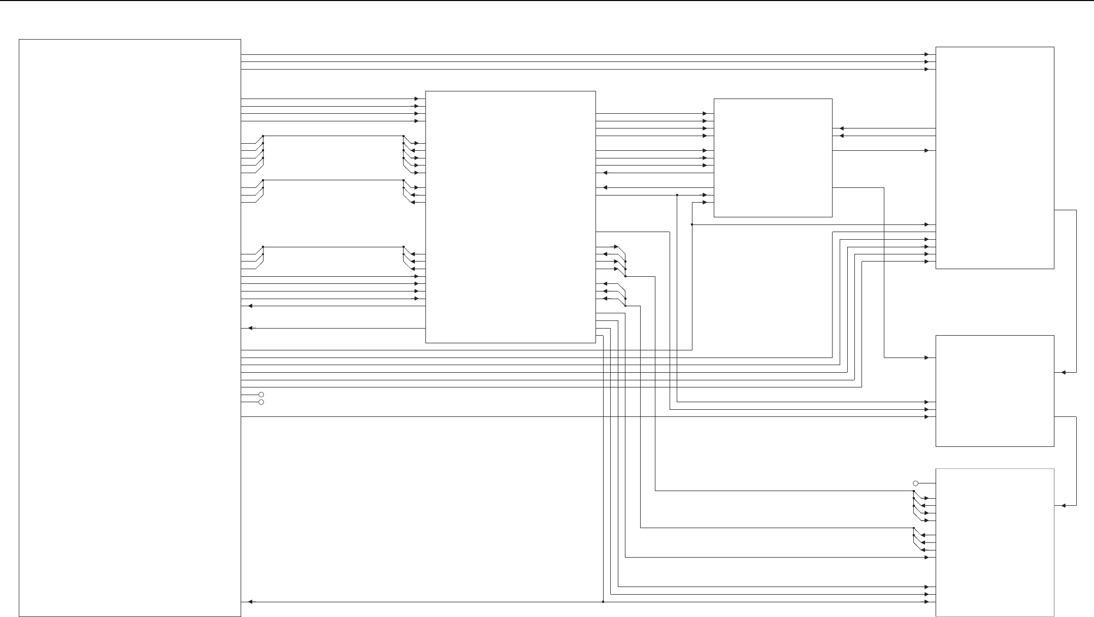
UHF1 (403–470 MHz) 1–25W PCB/Schematics/Parts List 3-23
SYNTH
( RX: SHEET 2 )
VCO_UHF1
( TX: SHEET 1 )
RXFE_UHF1
( 1 SHEET )
CONTROLLER_&_GPS_R5
( TOP LEVEL: SHEET 1)
( PC: SHEET 2 )
TX_LP_UHF1
( PA: SHEET 1 )
RXBE_73.35MHZ
(IF AMP: SHEET 1)
(ABACUS3: SHEET 2)
4
0
2
1
0
NC
NC
2
0
1
2
1
3
0
1V8
5V
5V_FE
IF
REF_CLK
SPI_ABACUS_CEX
SPI_ABACUS_CLK
SPI_ABACUS_DATA
SSI_ABACUS_CLKOUT
SSI_ABACUS_DOUTA
SSI_ABACUS_DOUTB
SSI_ABACUS_FSYNC
SSI_ABACUS_SYNCB
9V3
9V3_PA
9V3_SYNTH
9V3_VCO
ANT_ENABLE
FINAL_BIAS_1
LO_BATTERY_DET
PA_SUPPLY
PC_ATTEN_ENA
PREDRIVE_SW
RX_IN
TX_DAC
TX_INJ
2
1
1
NC
1
2
0
2
RX_SSI_SYNCB
SPI_CLK
SPI_MISO
SPI_MOSI
THK_CS
TX_DAC
TX_SSI_CLK
TX_SSI_DATA
TX_SSI_FSYNC
VSWR_DET
2
0
ABACUS3_CS
ADAPT_SW
ANT_ENABLE
DMCS
LOCK_DETECT
LO_BATTERY_DET
LO_PWR_DET
PA_BIAS
PC_ATTEN_ENA
PREDRIVE_SW
RAW_B+
RESET_OUT
RX_FLTR_VCTRL
RX_SSI_CLK
RX_SSI_DATA
RX_SSI_FSYNC
9R1
FE_TUNE IF
RF_ATTEN_1
RX_IN
RX_INJ
2
1.875V_DIG_V2
16.8_GPS
16.8_MHZ_BUFF
2.775V_ANA_V7
2.775V_DIG_V4
5V_SW
9V3
9V3_PA
HP_MOD_OUT
PREDRIVE_SW
PRSC
RXINJ
RX_VCO_SEL1
RX_VCO_SEL2
SF_TH
TXINJ
TX_VCO_SEL1
TX_VCO_SEL2
VCTRL
0
2
1
3
0
1
0
9R1
9V3_SYNTH_IN
9V3_SYNTH_OUT
9V3_VCO
TH_CEX
TX_CLK
TX_VCO_SEL1_
TX_VCO_SEL2_
VCTRL
2
0
3
1
RX_SSI_CLK_PASS_OUT
RX_SSI_DATA_PASS_IN
RX_SSI_DATA_PASS_OUT
RX_SSI_FSYNC_PASS_IN
RX_SSI_FSYNC_PASS_OUT
RX_VCO_SEL1_
RX_VCO_SEL2_
SDTX
SFTX
SF_OUTSPI_CLK_IN
SPI_CLK_OUT
SPI_MISO_IN
SPI_MISO_OUT
SPI_MOSI_IN
SPI_MOSI_OUT
5V
5V_BE
9R1
9V3
ABACUS3_CEX_IN
ABACUS3_CEX_OUT
ABACUS3_SYNCB_IN
ABACUS3_SYNCB_OUT
ADAPT_SW
DMCS
HP_MOD_OUT
LOCK
PRSC
RF_ATTN_1
RSTB RX_SSI_CLK_PASS_IN
TX_SSI_BUS(0:2)
ABACUS_SPI_BUS(0:3)
SPI_BUS(0:4)
RX_SSI_BUS(0:2)
ABACUS_SSI_BUS(0:2)
1
4
3
1.8V_TH_DIG
16.8_GPS
16.8_REF
1V8_BE
2.8V_TH_ANA
2.8V_TH_DIG
UHF1 (403–470 MHz) 1–25W Overall Schematic Diagram
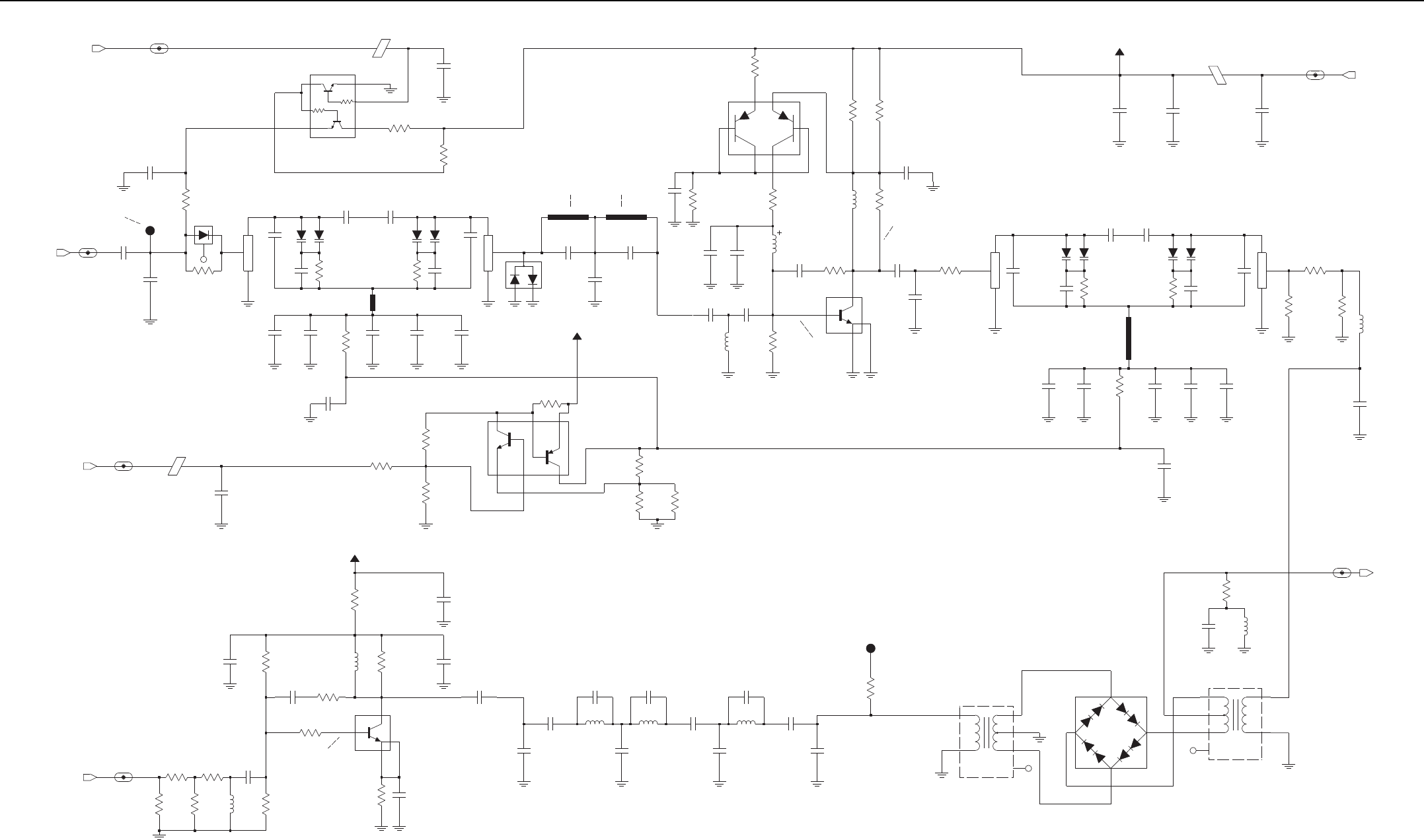
3-24 UHF1 (403–470 MHz) 1–25W PCB/Schematics/Parts List
(Not Placed)
7.0 VDC
Hi-Side Zeros for Preselector
Zo/Zin=4:1
10 dB Attenuator
0.7 VDC
Zo/Zin=4:1
(3.00 ~ 8.00 VDC)
+16.0 dBm Min. (250 mV P-P)
MAKO ( 0 ~ 4.6 VDC)
3.7 VDC Typical
8.9 VDC Typical
0.8 VDC Typical
3.0 VDC Typical
(Micro-strip 20 mm Each)
C0464
C0444
R0404
C0453
FT0401
1
C0459
C0423
C0409
RX_INJ_FE_5
C0454
C0449
D0403
R0436
NU
D0407
C0416
Q0403
2
3
6
4
1
5
R0437
R0405
C0414 D0404
R0414
E0401
C0452
C0460
D0402
L0408
D0401
C0422
C0402
(VALUE)
NU
R0431
NU
L0414
C0433
C0434
R0430
C0406 R0400
RXIN_FE_6
FE_TUNE_FE_4
D0405
1IO1 2
IO2
3
IO3
4IO4
L0407
R0440
C0420
CR0400
1
3
2
D0409
NC
R0402
L0402
12
3
NU
R0422
D0400
C0440
IF_FE_8
R0425
D0408
C0463
NU
NU
C0439
C0410
E0400
4
6
3
2
1
(VALUE)
T0400
5
NC
1
C0428
FT0400
C0419
L0409
R0403
NU
(VALUE)
C0411
C0405
C0447
RF_ATTEN_1_3
C0427
R0407 R0441
L0401
(VALUE)
NC
C0457
C0441
(VALUE)
R0415 R0416
R0417
R0426
C0445
C0417
R0424
C0412
C0413
C0403
R0435
C0429 C0432
NU
C0431
C0400
R0444
C0451
L0413
NC
5
4
6
3
2
1
R0428
T0401
C0421
R0409
C0437
L0410
12
3
R0427
L0403
C0456
C0438
C0442
NC
C0408
3
1
4
C0430
Q0400
NU
2
5
6
R0421
C0407
C0446
C0435
NU
C0461
C0401
R0418
E0403
R0410
R0434
R0420
C0436
C0462 R0443
R0412
C0415
L0405
12
3
(VALUE)
R0423
L0411
C0426C0425
.0476
C0448
R0433
R0406
Q0402
Q0405
R0413
R0429
R0419
9R1_FE_6
C0424
25
6
3
1
4
C0443
Q0401
C0458
L0412
L0406
D0406
R0438
NU
R0411
R0432
NU C0455
12
3
NU
L0404
C0404
RX_INJ
R0401
RF_ATTEN_1
IF
RX_IN
FE_TUNE
9R1
9R1_FILT
9R1_FILT
9R1_FILT
UHF1 (403–470 MHz) 1–25W Receiver Front-End Schematic Diagram

UHF1 (403–470 MHz) 1–25W PCB/Schematics/Parts List 3-25
1.43V
0.76V
1.6V
0.72V
4-POLE
IF_TO_ABACUS
73.35MHz
R0511
IFIN_BE_8
R0512
C0514
R0508
R0509
NU
C0510
L0504
GND1
2
GND2
5
IN
1OUT 4
FL0500
CC1
3
CC2
6
L0506
C0516
NU
5V_BE_5
C0502
NU
C0515
C0503
C0513
SH0500
1
2
R0503
Q0501
E0500
L0503
C0509
NU
RX_FE_3
R0510
C0506
1
3
2
C0507
Q0500
C0504
R0502
R0500
D0500
R0501
C0512
IF
IF_OUT
5V
5V
5V_FE
UHF1 (403–470 MHz) 1–25W Receiver IF Amp Schematic Diagram
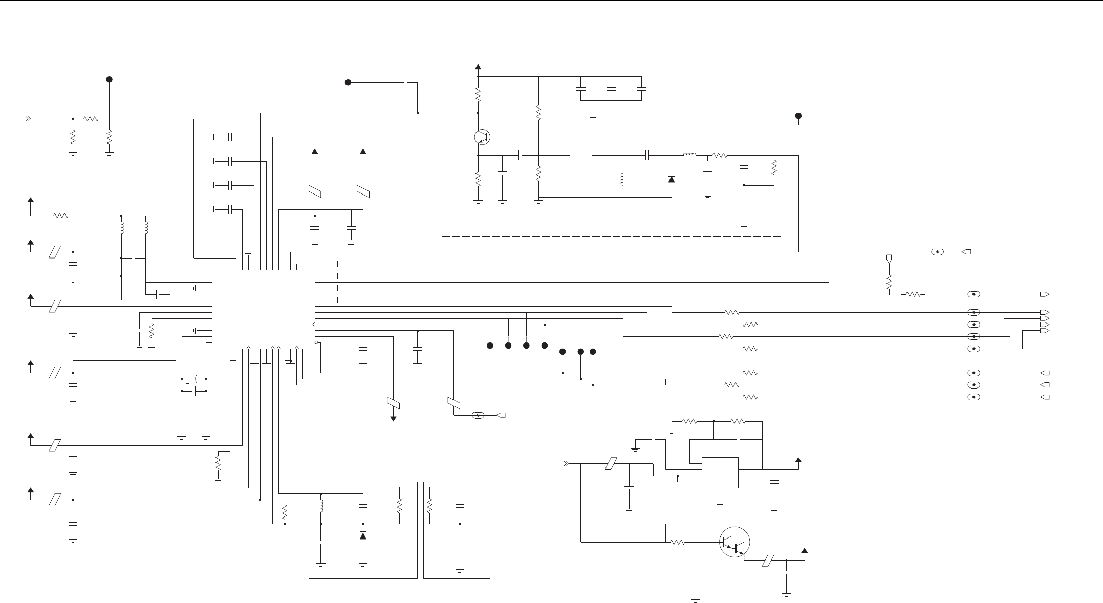
3-26 UHF1 (403–470 MHz) 1–25W PCB/Schematics/Parts List
2nd LO VCO UHF (71.1MHz/75.6 MHz)
SPF_3.5V
CLOCK LF
2nd LO LF
CLOCK VCO
#
*
R0611
R0605
FD_1_BE_5
R0602
R0616
C0620
D0600
E0609
C0604
C0621
C0634
E0602
E0605
3VA
C0611
Q0601
SB_1_BE_5
PC
TP0601
R0615
C0649
FE_1_BE_5
NU
C0616
U602
1
C0632
L0608
C0607
C0605
NU
R0607
C0646
3VA
DOUTA
L0602
R0606
C0648
L0604
C0642
C0601
CLKOUT_1_BE_5
VVCO
C0628
C0602
C0638
R0603
C0640
FC_1_BE_5
R0617
R0601
E0607
VVCO
C0627
C0631
C0629
FS
R0625
5V
3VA
C0623
C0615
R0612
3VA
FREF_IF
C0610
R0618
C0644
L0605
PE
C0613
E0600
R0624
C0636
E0610
C0635
R0613
3VA
C0651
C0618
C0647
D0601
C0626
R0608
E0603
DOUTB
C0622
C0645
48
VDDI
40
VDDL 39
VDDP
14 VDDQ
12 VREFN
11 VREFP
C0625
25
PE
RREF
13
33
SYNCB
9VDDA
17 VDDC
26
VDDD
6VDDF
27
VDDH
15 IOUTC
38
IOUTL
42
LON
43
LOP
2MXON
1MXOP
23 PC
24 PD
36
GNDL
37
GNDP
16 GNDQ
21 GNDS1
34
GNDS2
4IF2N
5IF2P
47
IFIN
8GCN
7GCP
10 GNDA
18 GNDC
22 GNDD
3GNDF
32
GNDH
45
GNDI
CLKP
19
46
CXIF
44
CXVL
41
CXVM
29
DOUTA
30
DOUTB
35
FREF
31
FS
U0600
20 CLKN
28
CLKOUT
FS_1_BE_5
R0627
C0637
R0621
3VA
TP0600
R0610
R0620
C0603
C0633
R0614
3VA
E0604
VCONT
4
VIN
3
VOUT 1
3VA
R0604
U0601
FB
2
GND
5
NP
6
3VA
CLKOUT
DOUTA_1_BE_5
C0619
C0641
E0606
C0630
C0617
R0619
E0601
NU
R0623
L0603
C0643
C0614
DOUTB_1_BE_5
PD
1V8_3
Q0600
E0608
C0612
C0650
R0609
R0622
R0626
NU
IF_OUT
5V
SSI_ABACUS_FSYNC
SPI_ABACUS_CEX
REF_CLK
SPI_ABACUS_CLK
SSI_ABACUS_DOUTA
SSI_ABACUS_CLKOUT
SSI_ABACUS_DOUTB
SPI_ABACUS_DATA
SSI_ABACUS_SYNCB
1V8
1V8
UHF1 (403–470 MHz) 1–25W Receiver Back-End Schematic Diagram

UHF1 (403–470 MHz) 1–25W PCB/Schematics/Parts List 3-27
PA_SUPPLY_TX_PA
E0703
Antenna_En
9V3_PA
PA_SUPPLY
C0701
E0700
C0702C0700
9V3_TX
2.2K
47K
47K
47K
Q0701
R0706
C0724
C0718
C0725
E0704
R0700
R0702
NU 9V3_Tx_Sw
13 dBm
3.2VDC
TP0704
L0705
13
VD_RF_OUT
U0700
GND1
GND2
RF_IN
2
4
-3 dBm
C0733
TP0703
C0752
L0709
C0768
C0763
R0712
D0704
L0711
LO_PWR_PAD
HI_PWR_PAD
Test Point to check 11dB/17dB Pad
18dB RL
+8 dBm
Ref Osc Warping
R0715
R0711
C0736
TP0705
TX_INJ_TX_PA
NC
R0760
R0714
C0728
TX_INJ
C0785 C0795 C0817
L0717
C0734
L0718
NU
L0721
2.10V (27.5W)
2.85V (44W)
9.1VDC
NU
C0788
TP0710 TP0709
NU
R0744
NU
L0723
R0734
9V3_TX
C0775
L0715
C0780
C0789
C0814
NU L0720
Q0705
R0747
D
G
S
R0759
R0777
V_cont
C0801
R0751 NU
C0800
R0750
C0802
9V3
9V3_VCO
9V3_SYNTH
NU
C0790
C0786
C0787
C0791
R0739
NU
C0792
NU
C0794
C0793
C0815
M0700
1
POS
NU
C0771 R0727R0728
C0770
V_cont
DS
21
G
3
Q0703
R0722
R0754
R0755
R0718
R0720
C0818
C0829
C0828
C0753
C0809
NU
C0755
NU
C0813
C0744C0743
NU
C0754
NU
C0819
NU
C0749
C0808
SP0707
SP0705
SP0704
SP0706
SP0703
SP0702
R0719
ATC
MRF1570, Flat Lead
Q0702
NU
C0720
C0807
NU
C0811
1PIN1 2
PIN2
HS0700
C0719
R0762
R0763
C0832
C0732
SP0700
R0765
R0764
R0709
Gate_1
R0773
C0869
R0771
C0774
R0768
C0769
C0874
R0770
R0769
R0766
C0761 C0861
SP0701
Gate_2
C0856
C0760
NU
NU
C0764
C0756
C0765
NU
2.2VDC (TX Only) 2.2VDC (TX Only)
TP0707 TP0708
R0732
R0730
Gate_2
Gate_1
R0756
C0805
R0740
C0782
R0741
R0757
C0781
C0804
TP0711
PRESSURE_PAD
Final_Bias
R0738
NC
NC
Q0706
R0745
Q0704
NC
C0776
C0778
VR0700
R0729
R0735
C0777 C0779
L0714
A+
NC
R0761
TP0713
R0749 ANT_ENABLE_TX_PA
ANT_ENABLE
C0797
C0796
C0798 C0799
R0748
Antenna_En
R0753
RX_IN_TX_PA
Final_Bias
R0752
FINAL_BIAS_1_TX_PA
9V3_TX
LO_PWR_PAD
HI_PWR_PAD
V_cont
9V3_TX
LO_PWR_PAD
HI_PWR_PAD
FINAL_BIAS_1
FWD_DETECTED
FWD_POWER
V_CONTROL
RX_IN
D0905
R0979
C0944
C0943
REV_DETECTED
C0945
R0976R0977
R0975
L0904 R0973
NU
R0974
W = 0.625 mm
W = 0.625 mm
W = 2.5 mm
S = 0.93 mm
L = 19 mm
S = 0.54 mm
L0722
R0713
2
J0700-33
J0700-1
1
J0700-2
C0738C0739 C0740C0803 C0742
L0710
D0700
L0708
C0735 C0723
L0706 L0707
R0971
R0970
L0903
L0905
R0978
C0940
D0904
C0941
C0767
C0772
C0942
NU
C0766
R0701
ATC
ATC
NU
C0806
C0748
C0812 C0751
NU
L0712
NU
NU
C0721
C0747
NU
NU
C0741
C0746
NU
C0727
C0810 L0719
NU
C0737
C0726
C0758
NU
C0757
C0759
L0716
R0743
9V3_Tx_Sw
A3
A4
A5
K1
K2
K3
K4
D0703
A1
A2
D0702
C0714
E0701
C0713
R0742
C0722
NU
C0715
NU
L0700
A+
C0710 C0712
C0711
NU
C0704C0703
NU
C0706 C0707
NU
C0708C0705 C0709
C0845
NU
C0729
C0731
NU
C0745
C0730
NU
L0702
E0702
C0716
C0717
TP0702
9V3_TX
PRESSURE_PAD_TX_PA
PRESSURE_PAD
S0700
R0775
C0966
UHF1 (403–470 MHz) 1–25W Power Amplifier Schematic Diagram
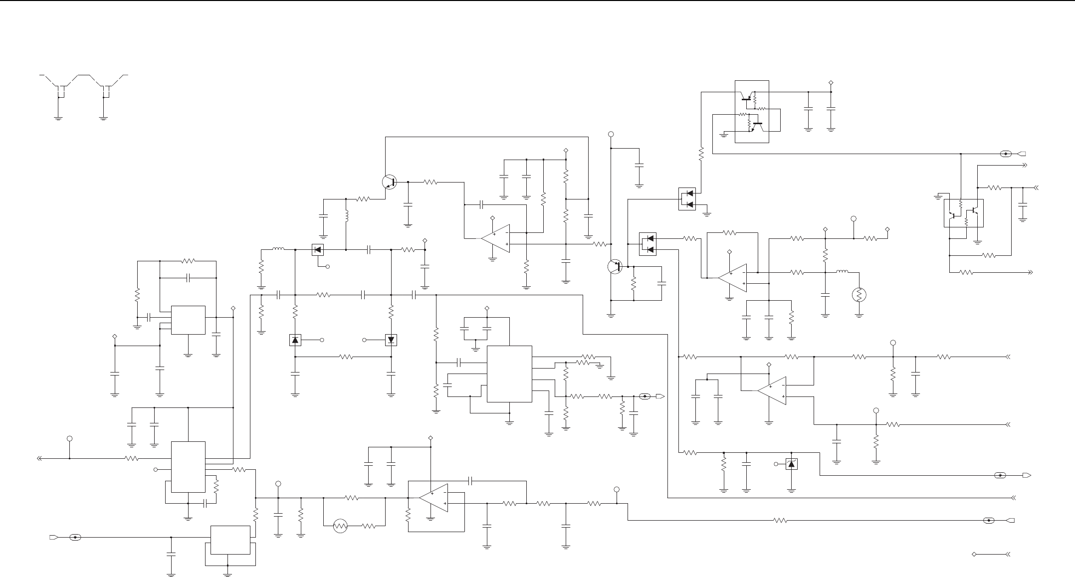
3-28 UHF1 (403–470 MHz) 1–25W PCB/Schematics/Parts List
SH0901
1
2
SH0900
1
2
R0940
C0921
NC
C0922
6
7
5
5V DC
8
U0940
NC
RFINVAPC
VPOS
VSET
COMM
ENBL
FLTR
GND
1
3
2
4
1.35V (44W)
1.28V (27.5W)
C0926
R0950
R0941
TP0910
9
NC2
RESET_OUT
U0942
GND
INPUT
NC1 5
3
2
4
C0953
C0925
R0946
R0955
1
RT0953
R0954
C0902
R0942
C0903
6
5
7
8
4
U0900-2
R0947
C0923
9V3_PC
R0937
C0950
C0949
C0951
0.1uF
C0947
R0936
2FB
5GND
6NP
4VCONT
3VIN
1
VOUT
U0941
C0948
5V
2.10V (27.5W)
2.85V (44W)
TP0909
V_CONTROL
9V3
R0927 R0928
L0902
R0924 NC
NC
D0901
D0902
R0926
C0931
L0901
R0913
Q0902
C0918
R0910
C0914 R0917
C0912
9V3_PC
C0934
C0916
C0935
D0903
NC
R0929
C0936 C0937
R0925
R0989
NU
R0988
C0960
7U0943
C0961 C0962
5V
TADJ
VOUT
VPOS
VSET
CLPF
COMM
GND
INHI
INLO
6
5
4
3
2
9
1
8
C0963 R0994
NU
R0995
NU
LO_PWR_DET
C0965
R0984
NU
R0981
R0982
R0983 R0985
LO_PWR_DET
R0930
R0906
C0915
D0900
1
2
3
1
2
3
D0906
C0929
R0931
0.6V typical
NOTE: VOLTAGES SHOWN FOR ANALOG TX MODE
Cutback starts about 2.2V
TP0907
C0920
R0918
R0921
C0919
9V3_PC
C0911
R0960
C0913
R0922
R0919 Q0901
3
1
8
4
U0900-1
2
C0917
9V3_PC
LO_BATTERY_DET
LO_BATTERY_DET
C0900 C0901
Q0900 9V3
2
5
6
3
1
4
R0907
TP0913
R0901
9V3_PC 9V3
Cypher: 2.4Kohm 5%
R0902
L0900
R0903
C0904 RT0908
C0907 C0906
R0909
R0900
4
U0901-2
6
5
7
8
9V3_PC
R0923 R0914
9V3_PC
U0901-1
2
3
1
8
4
C0908 C0909
R0986
R0987
C0967
D0907
5.1V
NC
0.38V (44W)
0.21V (27.5W)
C0910
TP0903
R0912
R0911
R0938
R0951 R0944
C0927
R0943
TP0911
C0928
C0964
4.0V (44W)
3.2V (27.5W)
TP0904
R0916R0915
C0939
R0920
9V3 to FW bias PIN in HP mode
TX_DAC
VSWR_DET
HI_PWR_PAD
VSWR_DET
FWD_POWER
TX_DAC
9V3
9V3
FWD_DETECTED
REV_DETECTED
R0724
R0725
9V3 to REV bias PIN in LP mode
PC_ATTEN_ENA_TX_PA
C0783
PC_ATTEN_ENA
9V3_TX
LO_PWR_PAD
5
6
3
1
4
Q0711
2
R0726
UHF1 (403–470 MHz) 1–25W Power Control Schematic Diagram

UHF1 (403–470 MHz) 1–25W PCB/Schematics/Parts List 3-29
R1
R2
10K
47K
0.5 ppm
VHF=1500pF
---
Note: High Port modulation injection through loop filter for U1 and U2 only
HI: 2.8V
U1=220pF
U2=120pF
C0191,C0192,C0193,C0194: NU (UHF B1)
VHF=1500pF
SF_OUT VOLTAGE: 2.45V
Unlocked: 0V
U1=220pF
Buffer to Abacus/Controller
9R1 SWITCH FOR FRONT-END
C0157, C0159, C0160,C0162,C0163,C0191,C0192,C0193,C0194: NU (UHF B2)
GPO LINES
U2=120pF
U1=220pF
U1=220pF
VCO STEERING LINE VOLTAGE: 0.6V TO 4.4V
U2=120pF
VCO STEERING LINE VOLTAGE: 0.6V TO 4.4V
VHF=1500pF
VHF=1500pF
U2=120pF
U2=120pF
Adapt OFF: 0V
U1=220pF
VHF=1500pF
4875188M01
LOW: 0V
1.5 ppm
VCO SEL: ACTIVE LOW
Adapt ON: 5V
Locked: 1.8V
GPO_4
TCXO (Y0100)
Switch for Adapt Transient
NC
NC
NC
R0170
C0166
C0100
C0105
L0100
C0137
RX_SSI_DATA_IN
NC
R0114
R0147
SPI_MOSI_IN
NU
ABACUS3_SYNCB_OUT
R0100
NC
5V_BE_SYNTH
TP504
1
RX_SSI_CLK_OUT
C0107
NC
NC
C0136
C0133
NC
C0140
1
C0106
NC
TP_TEST1
SPI_MISO_IN
R0160
NC4
3
OUTPUT
4
VCC
1VCONT
NC
NC
NC
Y0100
16.8MHz
GND
2
5
NC1
NC2 6
NC3 7
8
R0113
9R1_SYNTH
C0148
C0102
C0138
3GND
1INOUT
4ONOFF_CONTROL
2OUTIN
5
VCC
R0125
NC
U0101
NC
GPO_3_SYNTH
NC
NC
C0179
ABACUS3_SYNCB_IN
RX_SSI_DATA_OUT
C0147
C0135
C0171
C0132
C0157
C0127
NC
LOCK_SYNTH
R0140
C0120
Q0100
C0194 C0159
C0191
NC
VCTRL_SYNTH
C0126
C0112
NC
NC
NC
NC
1V8_BE_SYNTH
SF_OUT_SYNTH
R0158
NU
HP_MOD_OUT_SYNTH
16.8_REF_CONTROLLER_SYNTH
NU
C0119
NC
NU
C0113
NC
1
R0148
1
2
TP_VCTRL
SH0100
1
2
SH0101
R0159
C0144
NC
C0160
ABACUS3_CEX_IN
R0118
C0141
NC
RX_SSI_CLK_IN
C0162
C0103
R0103
R0107
C0124
Q0108
R0122
NC
RX_SSI_FSYNC_IN
NC
NC
NU
C0161
C0122
NU
GPO_6_SYNTH
9V3_SYNTH
R0157
Q0106
GND
IN
OUT
C0117
C0134
R0115
TX_DAC_VCC
G7
TX_GND1
F6 TX_GND2
J6
TX_VCC
F1
VCO_DAC
K5 XOSC_BASE
XOSC_EMIT
L5
G6
XOSC_GND
TCLK
D7
TEST1 C7
TEST2
B3
TM
F10
TXCLK
K7 TXI
L7 TXQ
H7
TX_DAC_GND L6
SPI_CLK
D10
SPI_DR
D9
SPI_DW
SSI_GND E8
E11
SSI_VCC
SUB1
K10
F5 SUB2
F3 SUB3
G8
SDM_VAG
A9
SDM_VREFM B8
SDM_VREFP
D11
SDR
F11
SDTX
F9
SFTX
K4 SF_OUT
C9 SMD_CLK_GEN_GND
C11
A5
RX_AVCC2
RX_EN_OUT
B1
D3
SCAN_EN
F2 SCAN_IN
E9
SCLK_OUT
SDM_CLK_GEN_VCC A10
SDM_REF_GND A8
SDM_REF_VCC B9
B10 RXFS
C2 RXI
C1 RXIX
D1 RXQ
D2 RXQX
RX_AGND1 C3
D5
RX_AGND2
B2
RX_AVCC1
OSCREG_GND
OSCREG_OUT
H5
J4 OSCREG_SPLY
K11 PABIAS_DAC
L9 PHCLK
RFSTEPA
A3
E6 RSTB
E7
RXACQ
E10
M_PRSCX
A1 NC1
A11 NC2
NC3
L1
L11 NC4
NTXI
L8
NTXQ
K6
L4 OSCREG_BYP
J5
MAIN_GND
MAIN_PDET_VCC G2
J1
MAIN_VCC
H1
MN_ADAPT_CP
G3
MN_CP
G5
MN_CP_GND
MN_CP_VCC H2
J2
M_PRSC
H3
GPO5
H8 GPO6
K8
HP_MOD_OUT
J9 INCR_DECR
F8
LGND1 C8
LGND2
G10
LVCC1
B7
LVCC2
G4
ESC_TEST
K2
ESC_VCC
C6 FBI
B6 FBQ
B4 GPO1_TEST1
A4 GPO2_TEST2
GPO3_TEST3
E5
GPO4_TEST4
D4
K9
EF_OUTM
J8
J7 EF_OUTP
ESC_CP L3
ESC_CPBIAS L2
K3
ESC_CP_GND J3
ESC_CP_VCC
H4
ESC_GND
K1
ESC_IN
E1
G9 CLK_CP
H11 CLK_EMIT
H10
CLK_GND
J10
CLK_VCC
G1
DAC_ADAPT
A2 DC_CAL
L10 DEEPSLEEP
F7
DMCS
BP_I
F4 BP_IX
E2 BP_Q
BP_QX
E3
D8
CEX
H9 CLK1_OUT
J11 CLK2_OUT
G11 CLK_BASE
D6 ACE2
AGC_DAC
B5
AGC_FLAG
C4 AGC_REF
C5
H6 ARX_DAC
C10 ASPI_CLK
B11 ASPI_DATA
A7
ASPI_VCC
E4
U0100
A6 ACE1
DMCS_SYNTH
C0131
C0130
R0131
C0128
SPI_CLK_IN
NU
C0121
1
NC
TP_TEST2
C0129
C0165
R0146
ADAPT_SW_SYNTH
C0143
C0125
2.8V_TH_ANA_SYNTH
RX_SSI_FSYNC_OUT
C0178
C0177
C0175
NC
SFTX_SYNTH
NC
C0156
R0105
R0110
R0144
NC
R0161
C0110
PRSC_SYNTH
R0116
C0101
NC
C0164
C0104
NC
R0134
C0123
C0158
TX_CLK_SYNTH
C0109
NC
NU
R0126
Q0107
R0120
R0155
C0146
ABACUS3_CEX_OUT
NC
1
NC
C0115
TH_CEX_SYNTH
TP_ADAPT_SW
SPI_MOSI_OUT
GPO_2_SYNTH
R0102
TP503
1
NC
C0142
C0108
NC
NC
NC
SDTX_SYNTH
NC
R0104
R0111
RSTB_SYNTH
1.8V_TH_DIG_SYNTH
C0180
TP501
1
R0119
R0128
R0123
C0145
R0108
C0114
C0149
C0196
C0195
SPI_CLK_OUT
16.8_GPS_SYNTH
SPI_MISO_OUT
C0111
NU
C0151
R0156
2.8V_TH_DIG_SYNTH
C0150
R0127
R0106
NC
4
NC
Q0102 2
1
3
NC
NC
R0101
R0117
R0109
5V_SYNTH
TP502
1
GPO_1_SYNTH
C0163
GPO_5_SYNTH
16.8_REF_BE_SYNTH
C0118
C0193
NC
NC
C0192
ABACUS3_SYNCB_IN ABACUS3_SYNCB_OUT
VCTRL
9V3
R0139
SPI_MOSI_IN
SPI_MOSI_IN
SPI_CLK_IN
SPI_CLK_IN
SPI_MISO_IN
SPI_MISO_IN
5V
2.8V_DIG
RX_VCO_SEL1_
5V_BE
9R1
16.8_REF
1V8_BE
1.8V_TH_DIG
1.8V_DIG
RSTB
16.8_GPS
ADAPT_SW
5V_TH
TX_VCO_SEL1_
HP_MOD_OUT
TH_CEX
SPI_MOSI_IN
SPI_CLK_IN
2.8V_TH_DIG
2.8V_DIG
2.8V_TH_ANA
2.8V_ANA
1.8V_DIG
1.8V_DIG
5V_TH
RX_SSI_DATA_PASS_OUT
RX_SSI_CLK_PASS_OUT
RX_SSI_FSYNC_PASS_OUT
RX_SSI_CLK_PASS_IN
ABACUS3_CEX_OUT
SPI_MISO_OUT
SPI_MOSI_OUT
SPI_CLK_OUT
ABACUS3_CEX_IN
RX_SSI_DATA_PASS_IN
RX_SSI_FSYNC_PASS_IN
TX_VCO_SEL2_
RF_ATTN_1
RX_VCO_SEL2_
PRSC
2.8V_ANA
DMCS
5V_TH
2.8V_ANA
1.8V_DIG
2.8V_ANA
2.8V_ANA
SDTX
SFTX
SF_OUT
LOCK
TX_CLK
SPI_MISO_IN
2.8V_ANA
5V_TH
UHF1 (403–470 MHz) 1–25W Synthesizer Schematic Diagram

3-30 UHF1 (403–470 MHz) 1–25W PCB/Schematics/Parts List
0.1 V (Low)
VCTRL: 0.6-4.5 V
RX2_SEL: 2.7 V (High)
RX VCO 1
RX Buffer Amplifier
RX1_SEL: 2.7 V (High)
0.1 V (Low)
Steering Line Voltage (VCTRL_TH)
RXINJ: 329.65 - 396.65 MHz
RX VCO 2
RX Prescaler
-5 to -15 dBm
Super Filter Voltage (SF_TH)
SF_TH: 2.5 V
PRSC (RX): 329.65 - 396.65 MHz
NU
C0222
+6 dBm
C0258
R0224
RXINJ_VCO_UHF1_5
E0201
C0249
CR0208
CR0203
R0211 L0210
Q0200
C0225
C0259
9R1_VCO_UHF1_7
C0242
C0230
R0230
R0216
C0205
CR0207
C0203
C0219
R0220
NU
L0206
R0225
C0251
R0221
C0217
L0217
C0224
NU
C0202
L0202
C0243
C0200
C0206
C0229
C0241
R0219
R0207
L0212
C0231
C0204
C0214
CR0202
C0215
SH0300
1
2
SH0301
1
2
C0240
R0218RX1_SEL_VCO_UHF1_5
TP0301
1
CR0206
R0206
L0214
L0203
C0246
R0229
CR0204
L0218
R0226
C0248
C0253
L0205
L0209
R0210
R0212
C0237
Q0202
L0204
C0252
RX2_SEL_VCO_UHF1_5
C0236
L0200
L0219
C0250
C0201
PRSC_VCO_UHF1_5
SF_TH_VCO_UHF1_6
C0233
NU
C0223
C0226
CR0201
R0208
C0245
C0220
R0204
R0202
C0238
R0203
L0213
C0235
C0257
L0221
CR0205
Q0201
R0213
L0211
C0221
C0211
C0247
R0205
C0213
R0201
L0207
C0209
C0207
C0208
NU
C0218
L0215
C0239
U0201
RXINJ
RXSL
PRESC_TX
RX1
RX2
RX_VCO_SEL1
RX1 RX2
RX_VCO_SEL2
VCTRL
PRSC
SF_TH
SF_TH
RXSL
9R1
SF_TH
SF_TH
SF_TH
UHF1 (403–470 MHz) 1–25W Receiver VCO Schematic Diagram
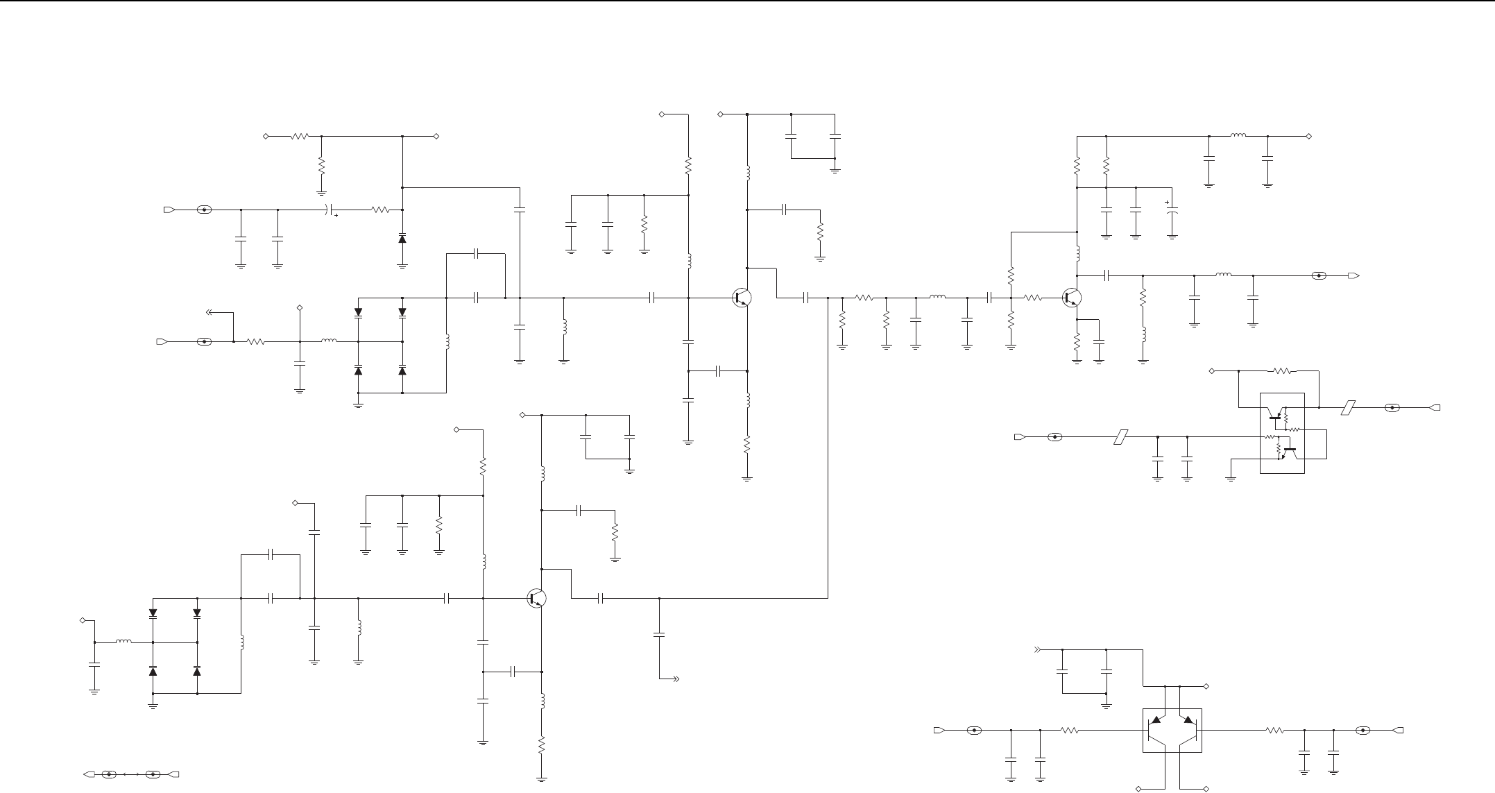
UHF1 (403–470 MHz) 1–25W PCB/Schematics/Parts List 3-31
VCTRL: 0.6-4.5 V
TX VCO 1
0.1 V (OFF)
TX VCO 2
TX Prescaler
TX2_SEL: 2.7 V (High)
-5 to -15 dBm
Steering Line Voltage (VCTRL_TH)
SF_TH: 2.5 V
0.1 V (Low)
TX Buffer Amplifier
0.1 V (Low)
+11 dBm
Super Filter Voltage (SF_TH)
TX_BUFFER_SEL: 1.8 V (ON)
PRSC (TX): 403-470 MHz
TX1_SEL: 2.7 V (High)
TXINJ: 403-470 MHz
R0326
C0313
L0318
R0316
R0331
C0303
L0310
C0344
R0303
C0361
C0300
TX2_SEL_VCO_UHF1_5
R0320
C0341
R0308
R0327
C0360
L0312
C0305
R0310
C0362
C0311
C0340
L0307
C0301
CR0302
C0342
CR0300
R0325
R0324
R0306 TXINJ_VCO_UHF1_5
L0313
Q0302
L0311
L0314
L0305
C0310
Q0300
C0351
R0307
C0331
E0302
NU
L0319
C0349
C0353
CR0308
C0319
NU
TX1_SEL_VCO_UHF1_5
C0345
C0328
NU
R0304
L0304
R0333
R0334
R0329
C0302
L0303
R0321
L0306
C0334
L0300
C0359
L0302
C0317
C0357
L0309
CR0304
C0314
C0337
U0304
C0346
R0337
CR0305
C0347
R0305
R0302
C0326
C0324
NU
R0332
C0306
PREDRIVE_SW_VCO_UHF1_6
C0363
C0348
C0315
CR0307
Q0301
C0336
C0329
C0309
C0352
C0320
R0301
C0327
NU
E0301
9V3_VCO_UHF1_7
U0303
NU
R0319
C0325
C0321
NU
C0322
C0343
C0358
CR0306
C0308
C0316
(VALUE)
CR0301
C0323
HP_MOD_OUT_VCO_UHF1_7
C0350
L0317
C0318
L0315
VCTRL_VCO_UHF1_7 R0311
CR0303
R0312
C0304
PREDRIVE_SW
SF_TH
HP_MOD_OUT
TX2TX1
SF_TH
SF_TH
TX_VCO_SEL1 TX_VCO_SEL2
C0307
SF_TH
TX2
TX1
SF_TH
VMOD
VSL
9V3_VCO
VCTRL
VCTRL
VSL
VMOD
PRESC_TX
9T1
9T1
9V3_SYNTH_OUT 9V3_SYNTH_IN
TXINJ
UHF1 (403–470 MHz) 1–25W Transmit VCO Schematic Diagram

3-32 UHF1 (403–470 MHz) 1–25W PCB/Schematics/Parts List
UHF1 PCB 8471165L06 Parts List 1–25W
Circuit
Ref
Motorola
Part No. Description
C0100 2113944A44 220pF
C0101 2113944A44 220pF
C0102 2113944A44 220pF
C0103 2113945C31 0.1uF
C0104 2113944A44 220pF
C0105 2113945C31 0.1uF
C0106 2113945C31 0.1uF
C0107 2113945C31 0.1uF
C0108 2113944A44 220pF
C0109 2113945C31 0.1uF
C0110 2113945C31 0.1uF
C0111 2113945C31 0.1uF
C0112 2113944A44 220pF
C0113 NOT PLACED –
C0114 2113946E02 1.0uF
C0115 2113946E02 1.0uF
C0117 2113944A44 220pF
C0118 2113945C31 0.1uF
C0119 NOT PLACED –
C0120 2113945B02 .01uF
C0121 NOT PLACED –
C0122 2113945B02 .01uF
C0123 2113946E02 1.0uF
C0124 2113945C31 0.1uF
C0125 2113944A44 220pF
C0126 2113944A44 220pF
C0127 2113944A44 220pF
C0128 2113944A44 220pF
C0129 2113945C31 0.1uF
C0130 2113944A44 220pF
C0131 2113944A44 220pF
C0132 2113944A44 220pF
C0133 2313960B30 4.7uF
C0134 2113944A44 220pF
C0135 2313960B32 10uF
C0136 2113945C31 0.1uF
C0137 2313960B32 10uF
C0138 2113944A44 220pF
C0140 2313960B30 4.7uF
C0141 2113945C31 0.1uF
C0142 2113944A44 220pF
C0143 2113944A44 220pF
C0144 2113945C31 0.1uF
C0145 2113945B02 .01uF
C0146 2113944A44 220pF
C0147 2113944A44 220pF
C0148 2113945D01 .033uF
C0149 2113945C04 .022uF
C0150 2113945C31 0.1uF
C0151 2113945C31 0.1uF
C0156 2185419D06 0.1uF
C0157 2185419D06 0.1uF
C0158 2185419D06 0.1uF
C0159 2185419D06 0.1uF
C0160 2185419D06 0.1uF
C0161 2185419D06 0.1uF
C0162 2185419D06 0.1uF
C0163 2185419D06 0.1uF
C0164 2185419D06 0.1uF
C0165 2185419D06 0.1uF
C0166 2185419D06 0.1uF
C0171 2113945B02 .01uF
C0175 2113944A44 220pF
C0177 2113944A44 220pF
C0178 2113944A44 220pF
C0179 2113944A44 220pF
C0180 2113945C31 0.1uF
C0191 NOT PLACED –
C0192 NOT PLACED –
C0193 NOT PLACED –
C0194 NOT PLACED –
C0195 2113945A05 470pF
C0196 2113946H02 10uF
C0200 2113944A44 220pF
C0201 2113945Y02 0.10uF
C0202 2113945C02 .01uF
C0203 2113944A44 220pF
C0204 2113944A44 220pF
C0205 2113945Y02 0.10uF
C0206 2113944A44 220pF
C0207 2113945C04 .022uF
C0208 2115153H18 4.3pF
C0209 2113944A44 220pF
C0211 2113944A44 220pF
C0213 2115153H17 3.9pF
C0214 2115153H34 11pF
C0215 2115153H20 5.1pF
C0217 2113944A44 220pF
C0218 NOT PLACED –
C0219 NOT PLACED –
C0220 2115153H17 3.9pF
C0221 2115153H14 3.0pF
C0222 NOT PLACED –
C0223 2115153H46 36pF
C0224 NOT PLACED –
C0225 2115153H51 56pF
C0226 2113944A44 220pF
C0229 2115153H42 24pF
C0230 2113944C47 150pF
C0231 2115153H14 3.0pF
C0233 NOT PLACED –
Circuit
Ref
Motorola
Part No. Description
C0235 2115153H22 6.2pF
C0236 2113944A44 220pF
C0237 2113945Y02 0.10uF
C0238 2113944A44 220pF
C0239 2113945Y02 0.10uF
C0240 2113944A44 220pF
C0241 2113945Y02 0.10uF
C0242 2113944A44 220pF
C0243 2115153H13 2.7pF
C0245 2115153H14 3.0pF
C0246 2115153H27 10pF
C0247 2115153H20 5.1pF
C0248 2113944A44 220pF
C0249 2113945Y02 0.10uF
C0250 2115153H16 3.6pF
C0251 2115153H40 20pF
C0252 2115153H48 43pF
C0253 2113944A44 220pF
C0257 2113944A44 220pF
C0258 2113945Y02 0.10uF
C0259 2115153H35 12pF
C0300 2113944A44 220pF
C0301 2113945Y02 0.10uF
C0302 2113945C02 .01uF
C0303 2113944A44 220pF
C0304 2113944A44 220pF
C0305 2113945Y02 0.10uF
C0306 2113944A44 220pF
C0307 2113945C04 .022uF
C0308 2115153H15 3.3pF
C0309 2113944A44 220pF
C0310 2115153H01 0.5pF
C0311 2113944A44 220pF
C0313 2115153H15 3.3pF
C0314 2115153H35 12pF
C0315 2115153H20 5.1pF
C0316 2313960B32 10uF
C0317 2113944A44 220pF
C0318 2115153H15 3.3pF
C0319 NOT PLACED –
C0320 2115153H20 5.1pF
C0321 2115153H24 7.5pF
C0322 NOT PLACED –
C0323 2115153H43 27pF
C0324 NOT PLACED –
C0325 2115153H51 56pF
C0326 2113944A44 220pF
C0327 NOT PLACED –
C0328 NOT PLACED –
C0329 2115153H38 16pF
C0331 2115153H14 3.0pF
Circuit
Ref
Motorola
Part No. Description
C0334 2113944A44 220pF
C0336 2113944A44 220pF
C0337 2113945Y02 0.10uF
C0340 2113944A44 220pF
C0341 2113945Y02 0.10uF
C0342 2113944A44 220pF
C0343 2115153H15 3.3pF
C0344 2115153H01 0.5pF
C0345 2115153H15 3.3pF
C0346 2115153H24 7.5pF
C0347 2115153H20 5.1pF
C0348 2113944A44 220pF
C0349 2113945Y02 0.10uF
C0350 2115153H18 4.3pF
C0351 2115153H42 24pF
C0352 2115153H50 51pF
C0353 2113944A44 220pF
C0357 2113944A44 220pF
C0358 2113945Y02 0.10uF
C0359 2115153H38 16pF
C0360 2313960B30 4.7uF
C0361 2113944C51 1000pF
C0362 2113944A44 220pF
C0363 2113945Y02 0.10uF
C0400 NOT PLACED –
C0401 2113945C31 0.1uF
C0402 2113944A44 220pF
C0403 2115153H49 47pF
C0404 NOT PLACED –
C0405 2113944A44 220pF
C0406 2115153H27 10pF
C0407 2115153H13 2.7pF
C0408 2115153H27 10pF
C0409 2115153H13 2.7pF
C0410 2115153H22 6.2pF
C0411 2115153H22 6.2pF
C0412 2115153H20 5.1pF
C0413 2115153H57 100pF
C0414 2113944A44 220pF
C0415 2115153H21 5.6pF
C0416 2115153H22 6.2pF
C0417 2115153H22 6.2pF
C0419 2113945Y02 0.10uF
C0420 2115153H03 1.0pF
C0421 2115153H13 2.7pF
C0422 2115153H26 9.1pF
C0423 2113944A44 220pF
C0424 2113944A44 220pF
C0425 2113944A44 220pF
C0426 2113944A44 220pF
C0427 2113944A44 220pF
Circuit
Ref
Motorola
Part No. Description

UHF1 (403–470 MHz) 1–25W PCB/Schematics/Parts List 3-33
C0428 2113944A44 220pF
C0429 2113944A44 220pF
C0430 2113944A44 220pF
C0431 2113944A44 220pF
C0432 2113944A44 220pF
C0433 NOT PLACED –
C0434 2113944A44 220pF
C0435 2115153H17 3.9pF
C0436 2113944A44 220pF
C0437 2113944A44 220pF
C0438 2113944A44 220pF
C0439 NOT PLACED –
C0440 2113944A44 220pF
C0441 2115153H11 2.2pF
C0442 2115153H25 8.2pF
C0443 2115153H41 22pF
C0444 2115153H41 22pF
C0445 2115153H37 15pF
C0446 2115153H20 5.1pF
C0447 2115153H27 10pF
C0448 2115153H26 9.1pF
C0449 2115153H20 5.1pF
C0451 2115153H41 22pF
C0452 2115153H26 9.1pF
C0453 2115153H20 5.1pF
C0454 2115153H26 9.1pF
C0455 2113945C31 0.1uF
C0456 2113944A40 100pF
C0457 2113945C31 0.1uF
C0458 2115153H40 20pF
C0459 2115153H40 20pF
C0460 2113946F05 10uF
C0461 2115153H40 20pF
C0462 2115153H40 20pF
C0463 2115153H06 1.3pF
C0464 2115153H06 1.3pF
C0502 2113945Y02 0.10uF
C0503 2113945Y02 0.10uF
C0504 2113945Y02 0.10uF
C0506 2113945Y02 0.10uF
C0507 2115153H39 18pF
C0509 NOT PLACED –
C0510 2115153H22 6.2pF
C0512 2113945Y02 0.10uF
C0513 2113945Y02 0.10uF
C0514 2113945Y02 0.10uF
C0515 NOT PLACED –
C0516 NOT PLACED –
C0601 2115153H48 43pF
C0602 2113945B02 .01uF
C0603 2113944A44 220pF
Circuit
Ref
Motorola
Part No. Description
C0604 2113945Y02 0.10uF
C0605 2115153H48 43pF
C0607 2115153H39 18pF
C0610 2115153H53 68pF
C0611 2113945A09 1000pF
C0612 2115153H34 11pF
C0613 2185419D03 0.01uF
C0614 2115153H48 43pF
C0615 2113945B02 .01uF
C0616 NOT PLACED –
C0617 2113945Y02 0.10uF
C0618 2185419D06 0.1uF
C0619 2113945Y02 0.10uF
C0620 2113945Y02 0.10uF
C0621 2113945Y02 0.10uF
C0622 2113945A09 1000pF
C0623 2113945Y02 0.10uF
C0625 2113944C89 200pF
C0626 2113944A40 100pF
C0627 2113944A40 100pF
C0628 2113945Y02 0.10uF
C0629 2113945A11 2200pF
C0630 2113945Y02 0.10uF
C0631 2113945Y02 0.10uF
C0632 2313960B30 4.7uF
C0633 2113945Y02 0.10uF
C0634 2113945B02 .01uF
C0635 2113944A40 100pF
C0636 2113944A40 100pF
C0637 2113946S35 1.0uF
C0638 2113945Y02 0.10uF
C0640 2113946N03 2.2uF
C0641 2113945B02 .01uF
C0642 2115153H53 68pF
C0643 2113945Y02 0.10uF
C0644 2113945Y02 0.10uF
C0645 2113945B02 .01uF
C0646 2113946G04 0.68uF
C0647 2113946J03 10.0uF
C0648 2113946J03 10.0uF
C0649 2113945A12 3300pF
C0650 2115153H44 30pF
C0651 2115153H57 100pF
C0700 2113944C82 30pF
C0701 2113945C04 .022uF
C0702 2113944C55 2200pF
C0703 2113944C82 30pF
C0704 2113945C04 .022uF
C0705 2113944C51 1000pF
C0706 NOT PLACED –
C0707 NOT PLACED –
Circuit
Ref
Motorola
Part No. Description
C0708 2113944C51 1000pF
C0709 2113945C31 0.1uF
C0710 2371403L02 10uF
C0711 NOT PLACED –
C0712 2113944C51 1000pF
C0713 2111078B42 100pF
C0714 2111078B42 100pF
C0715 NOT PLACED –
C0716 2113944A41 120pF
C0717 2113945A09 1000pF
C0718 2113945A09 1000pF
C0719 2111078B25 27pF
C0720 NOT PLACED –
C0721 NOT PLACED –
C0722 NOT PLACED –
C0723 2111078B39 75pF
C0724 2113944A41 120pF
C0725 2113944A41 120pF
C0726 2111078B20 18pF
C0727 NOT PLACED –
C0728 2113944C42 75pF
C0729 NOT PLACED –
C0730 NOT PLACED –
C0731 NOT PLACED –
C0732 2113951B41 24pF
C0733 2113944C42 75pF
C0734 2113944C84 43pF
C0735 2111078B39 75pF
C0736 2113944A41 120pF
C0737 NOT PLACED –
C0738 2111078B07 5.6pF
C0739 2185400Y36 12pF
C0740 2185400Y36 12pF
C0741 NOT PLACED –
C0742 2111078B07 5.6pF
C0743 2113944C37 39pF
C0744 2113944C38 47pF
C0745 2113944F44 12pF
C0746 2111078B25 27pF
C0747 NOT PLACED –
C0748 2111078B11 8.2pF
C0749 NOT PLACED –
C0751 NOT PLACED –
C0752 2113944A41 120pF
C0753 2111078B39 75pF
C0754 NOT PLACED –
C0755 NOT PLACED –
C0756 2113944F44 12pF
C0757 2113944C42 75pF
C0758 NOT PLACED –
C0759 2113944C42 75pF
Circuit
Ref
Motorola
Part No. Description
C0760 NOT PLACED –
C0761 2113951B41 24pF
C0763 2113944A41 120pF
C0764 NOT PLACED –
C0765 NOT PLACED –
C0766 NOT PLACED –
C0767 2113944C42 75pF
C0768 2113944A41 120pF
C0769 2113944F51 24pF
C0770 2113944A41 120pF
C0771 NOT PLACED –
C0772 2113944C16 2.7pF
C0774 2113944F51 24pF
C0775 2113945C04 .022uF
C0776 2113944C42 75pF
C0777 2113944C47 150pF
C0778 2111078B30 34pF
C0779 2111078B29 33pF
C0780 2113944A41 120pF
C0781 2113944C42 75pF
C0782 2113944C51 1000pF
C0783 2113944A41 120pF
C0785 2113944C42 75pF
C0786 2113944C84 43pF
C0787 2113944C84 43pF
C0788 NOT PLACED –
C0789 NOT PLACED –
C0790 NOT PLACED –
C0791 2113944A80 20pF
C0792 2113944A28 18pF
C0793 2113944A25 10pF
C0794 NOT PLACED –
C0795 2113944C75 8.2pF
C0796 2113944C42 75pF
C0797 2113944C51 1000pF
C0798 2113944C51 1000pF
C0799 2113944C42 75pF
C0800 NOT PLACED –
C0801 2113944A41 120pF
C0802 2113944A41 120pF
C0803 2111078B01 3.3pF
C0804 2113944C42 75pF
C0805 2113944C51 1000pF
C0806 NOT PLACED –
C0807 NOT PLACED –
C0808 NOT PLACED –
C0809 2113944C30 10pF
C0810 2113944C42 75pF
C0811 NOT PLACED –
C0812 NOT PLACED –
C0813 NOT PLACED –
Circuit
Ref
Motorola
Part No. Description

3-34 UHF1 (403–470 MHz) 1–25W PCB/Schematics/Parts List
C0814 2113944C46 120pF
C0815 2113944C41 68pF
C0817 2113951A31 7.50pF
C0818 2113944F54 33pF
C0819 2113944F54 33pF
C0828 2113944F54 33pF
C0829 2113944F54 33pF
C0832 2113951B41 24pF
C0845 2113944F44 12pF
C0856 2113944F44 12pF
C0861 2113951B41 24pF
C0869 2113944F51 24pF
C0874 2113944F51 24pF
C0900 2113944A41 120pF
C0901 2113945C31 0.1uF
C0902 2113945C31 0.1uF
C0903 2113944A41 120pF
C0904 2113944A41 120pF
C0906 2113944A41 120pF
C0907 2113945C02 .01uF
C0908 2113945C31 0.1uF
C0909 2113944A41 120pF
C0910 2113944A41 120pF
C0911 2113944A41 120pF
C0912 2113944A41 120pF
C0913 2113944A41 120pF
C0914 2113944A41 120pF
C0915 2113944A41 120pF
C0916 2113944A41 120pF
C0917 2113945A09 1000pF
C0918 2113944A41 120pF
C0919 2113945C31 0.1uF
C0920 2113944A41 120pF
C0921 2113945C31 0.1uF
C0922 2113944A41 120pF
C0923 2113944C55 2200pF
C0925 2113944A41 120pF
C0926 2113945L41 4700pF
C0927 2113944C02 220pF
C0928 2113944C53 1500pF
C0929 2113944A41 120pF
C0931 2113944A41 120pF
C0934 2113944A41 120pF
C0935 2113944A41 120pF
C0936 2113944A41 120pF
C0937 2113944A41 120pF
C0939 2113944A41 120pF
C0940 2113944C46 120pF
C0941 2113944M17 9.1pF
C0942 2113944C42 75pF
C0943 2113944C42 75pF
Circuit
Ref
Motorola
Part No. Description
C0944 2113944M06 3.3pF
C0945 2113944C42 75pF
C0947 2113944A40 100pF
C0948 2113946S35 1.0uF
C0949 2113946G01 2.2uF
C0950 2113945A09 1000pF
C0951 2113945C31 0.1uF
C0953 2113944A41 120pF
C0960 2113944A52 1000pF
C0961 2113945C31 0.1uF
C0962 2113944A40 100pF
C0963 2113944A52 1000pF
C0964 2113944A23 8.2pF
C0965 2113944A40 100pF
C0966 2113944A41 120pF
C0967 2113944A41 120pF
CR0201 4815096H01 DIODE VARACTOR 1SV305
CR0202 4815096H01 DIODE VARACTOR 1SV305
CR0203 4815096H01 DIODE VARACTOR 1SV305
CR0204 4815096H01 DIODE VARACTOR 1SV305
CR0205 4815096H01 DIODE VARACTOR 1SV305
CR0206 4815096H01 DIODE VARACTOR 1SV305
CR0207 4815096H01 DIODE VARACTOR 1SV305
CR0208 4815096H01 DIODE VARACTOR 1SV305
CR0300 4815096H01 DIODE VARACTOR 1SV305
CR0301 4815096H01 DIODE VARACTOR 1SV305
CR0302 4815096H01 DIODE VARACTOR 1SV305
CR0303 4815096H01 DIODE VARACTOR 1SV305
CR0304 4815096H01 DIODE VARACTOR 1SV305
CR0305 4815096H01 DIODE VARACTOR 1SV305
CR0306 4815096H01 DIODE VARACTOR 1SV305
CR0307 4815096H01 DIODE VARACTOR 1SV305
CR0308 4815096H01 DIODE VARACTOR 1SV305
CR0400 4813974A19 DIODE, SCHOTTKY
D0400 NOT PLACED –
D0401 4885055Y01 DIODE VARACTOR 1SV229
D0402 4885055Y01 DIODE VARACTOR 1SV229
D0403 4885055Y01 DIODE VARACTOR 1SV229
D0404 4885055Y01 DIODE VARACTOR 1SV229
D0405 4815090H01 DIODE, MIXER
D0406 4885055Y01 DIODE VARACTOR 1SV229
D0407 4885055Y01 DIODE VARACTOR 1SV229
D0408 4885055Y01 DIODE VARACTOR 1SV229
D0409 4885055Y01 DIODE VARACTOR 1SV229
D0500 4813974A19 DIODE, SCHOTTKY
D0600 4815096H01 DIODE VARACTOR 1SV305
D0601 4815096H01 DIODE VARACTOR 1SV305
D0700 4802482J02 DIODE, PIN
D0702 4802482J02 DIODE, PIN
D0703 4875430M01 DIODE, PIN
D0704 4813974A06 DIODE, PIN
Circuit
Ref
Motorola
Part No. Description
D0900 4813978C02 DIODE, SWITCHING
D0901 4815023H01 DIODE, PIN
D0902 4815024H01 DIODE, PIN
D0903 4815024H01 DIODE, PIN
D0904 4813974A21 DIODE, SCHOTTKY
D0905 4813974A21 DIODE, SCHOTTKY
D0906 4813978C02 DIODE, SWITCHING
D0907 4813977M10 DIODE, 5.1V ZENER
E0201 2409134J25 FERRITE BEAD
E0301 2409134J25 FERRITE BEAD
E0302 NOT PLACED –
E0400 NOT PLACED –
E0401 2409134J25 FERRITE BEAD
E0403 2409134J25 FERRITE BEAD
E0500 2409134J25 FERRITE BEAD
E0600 2409134J25 FERRITE BEAD
E0601 2409134J25 FERRITE BEAD
E0602 2409134J25 FERRITE BEAD
E0603 2409134J25 FERRITE BEAD
E0604 2409134J25 FERRITE BEAD
E0605 2409134J25 FERRITE BEAD
E0606 2409134J25 FERRITE BEAD
E0607 2409134J25 FERRITE BEAD
E0608 2409134J25 FERRITE BEAD
E0609 2409134J25 FERRITE BEAD
E0610 2480640Z01 FERRITE BEAD
E0700 2485011Y01 FERRITE BEAD
E0701 2485011Y01 FERRITE BEAD
E0702 7671656M01 FERRITE BEAD
E0703 2485011Y01 FERRITE BEAD
E0704 2409134J25 FERRITE BEAD
FL0500 9116854H02 73.35 MHZ CRYSTAL FILTER
HS0700 0104038J81 HEATSINK
J0700 0905901V11 MINI-U RF CONNECTOR
L0100 2414017N29 270nH
L0200 2414017N28 220nH
L0202 2414032F42 470nH
L0203 2414032F42 470nH
L0204 2414017N28 220nH
L0205 2414017N20 47nH
L0206 2414017N14 15nH
L0207 2415385H02 12.5nH
L0209 2414032F42 470nH
L0210 2414015A21 27nH
L0211 2414017N28 220nH
L0212 2414032F42 470nH
L0213 2414032F42 470nH
L0214 2414032F42 470nH
L0215 2415385H02 12.5nH
L0217 2414032F42 470nH
L0218 2414015A20 22nH
Circuit
Ref
Motorola
Part No. Description
L0219 2414032F42 470nH
L0221 2414017N19 39nH
L0300 2414017N28 220nH
L0302 2414032F42 470nH
L0303 2414032F42 470nH
L0304 2414017N28 220nH
L0305 2414017N19 39nH
L0306 2414017N12 10nH
L0307 2415385H01 8nH
L0309 2414032F42 470nH
L0310 2414015A32 18nH
L0311 2414017N28 220nH
L0312 2414032F42 470nH
L0313 2414032F42 470nH
L0314 2414032F42 470nH
L0315 2415385H01 8nH
L0317 2414032F42 470nH
L0318 2414015A32 18nH
L0319 2414032F42 470nH
L0401 2414015B24 15nH
L0402 NOT PLACED –
L0403 NOT PLACED –
L0404 NOT PLACED –
L0405 NOT PLACED –
L0406 2414015B29 10nH
L0407 2414015B16 27nH
L0408 2414015B15 22nH
L0409 2414015B15 22nH
L0410 2414015B15 22nH
L0411 2414015B15 22nH
L0412 2414017N20 47nH
L0413 2414017N28 220nH
L0414 2414015B17 18nH
L0503 2414015B27 390nH
L0504 NOT PLACED –
L0506 2414032B66 820nH
L0602 2414032K23 2.7uH
L0603 2414032D20 270nH
L0604 2466505A01 10uH
L0605 2466505A01 10uH
L0608 2414032B76 4.7uH
L0700 2460592A01 17nH
L0702 2479990G01 33.47nH
L0705 2414017N26 150nH
L0706 2460592A01 17nH
L0707 2460592A01 17nH
L0708 2460592A01 17nH
L0709 2414017N26 150nH
L0710 2460592A02 12.5nH
L0711 2414017N26 150nH
L0712 NOT PLACED –
Circuit
Ref
Motorola
Part No. Description

UHF1 (403–470 MHz) 1–25W PCB/Schematics/Parts List 3-35
L0714 2479990N01 43.67nH
L0715 2414017N26 150nH
L0716 2414017N27 180nH
L0717 2414017N06 3.3nH
L0718 NOT PLACED –
L0719 2414017N22 68nH
L0720 2414017N06 3.3nH
L0721 2414017N11 8.2nH
L0722 2414032B60 390nH
L0723 NOT PLACED –
L0900 2414032D30 1uH
L0901 2414032F42 470nH
L0902 2414032F42 470nH
L0903 2414032F23 12nH
L0904 2414032F22 8.2nH
L0905 2414017N24 100nH
M0700 2686201B02 HEATSINK
Q0100 4802197J95 NPN RF TRANSISTOR
Q0102 4815359H01 DUAL PNP
Q0106 4816134H01 ANALOG SWITCH
Q0107 4813970A59 P-CHANNEL MOSFET
Q0108 4815261H01 ANALOG SWITCH
Q0200 4885061Y01 NPN RF TRANSISTOR
Q0201 4885061Y01 NPN RF TRANSISTOR
Q0202 4802197J95 NPN RF TRANSISTOR
Q0300 4885061Y01 NPN RF TRANSISTOR
Q0301 4885061Y01 NPN RF TRANSISTOR
Q0302 4802197J95 NPN RF TRANSISTOR
Q0400 NOT PLACED –
Q0401 4815267H01 DUAL PNP
Q0402 4885593U03 NPN RF TRANSISTOR
Q0403 4815270H01 ANALOG SWITCH
Q0405 4885593U03 NPN RF TRANSISTOR
Q0500 4802197J95 NPN RF TRANSISTOR
Q0501 4802197J95 NPN RF TRANSISTOR
Q0600 4805793Y10 NPN RF TRANSISTOR
Q0601 4813973A04 NPN DARLINGTON
Q0701 4816013H01 DUAL NPN/PNP
Q0702 48012048002 RF POWER AMPLIFIER,
LDMOS
Q0703 4816548H01 N_CHANNEL LDMOS DRIVER
Q0704 4813973B02 PNP
Q0705 4816547H01 N-CHANNEL LDMOS PRE-
DRIVER
Q0706 4815272H01 ANALOG SWITCH
Q0711 4815271H01 ANALOG SWITCH
Q0900 4815272H01 ANALOG SWITCH
Q0901 4813973A13 PNP
Q0902 4813973M07 NPN
R0100 0613952R66 0
R0101 0613952R66 0
Circuit
Ref
Motorola
Part No. Description
R0102 0613952R66 0
R0103 0613952R66 0
R0104 0613952R17 47K
R0105 0613952Q58 240
R0106 0613952Q83 2.7K
R0107 0613952Q57 220
R0108 0613952Q80 2K
R0109 0613952R66 0
R0110 0613952Q42 51
R0111 0613952R66 0
R0113 0613952R01 10K
R0114 0613952Q80 2K
R0115 0613952R66 0
R0116 0613952R66 0
R0117 0613952R12 30K
R0118 0613952R66 0
R0119 0613952Q35 27
R0120 0613952R01 10K
R0122 NOT PLACED –
R0123 0613952R19 56K
R0125 0613952R66 0
R0126 NOT PLACED –
R0127 0613952Q49 100
R0128 0613952R66 0
R0131 0613952Q58 240
R0134 0613952Q35 27
R0139 0613952Q78 1.6K
R0140 0613952Q31 18
R0144 0613952R01 10K
R0146 0613952R66 0
R0147 NOT PLACED –
R0148 0613952Q60 300
R0155 0613952R66 0
R0156 NOT PLACED –
R0157 NOT PLACED –
R0158 NOT PLACED –
R0159 0613952R01 10K
R0160 0613952R25 100K
R0161 0613952R25 100K
R0170 0613952R66 0
R0201 0613952Q85 3.3K
R0202 0613952Q75 1.2K
R0203 0613952Q75 1.2K
R0204 0613952Q95 8.2K
R0205 0613952Q49 100
R0206 0613952R05 15K
R0207 0613952Q25 10
R0208 0613952Q42 51
R0210 0613952Q89 4.7K
R0211 0613952R66 0
R0212 0613952R66 0
Circuit
Ref
Motorola
Part No. Description
R0213 0613952R01 10K
R0216 0613952Q51 120
R0218 0613952R01 10K
R0219 0613952Q66 510
R0220 0613952Q25 10
R0221 0613952Q66 510
R0224 0613952Q92 6.2K
R0225 0613952Q94 7.5K
R0226 0613952Q49 100
R0229 0613952Q54 160
R0230 0613952Q89 4.7K
R0301 0613952Q85 3.3K
R0302 0613952Q66 510
R0303 0613952Q66 510
R0304 0613952Q95 8.2K
R0305 0613952Q49 100
R0306 0613952R05 15K
R0307 0613952Q33 22
R0308 0613952Q42 51
R0310 0613952Q89 4.7K
R0311 0613952R66 0
R0312 0613952R66 0
R0316 0613952Q46 75
R0319 0613952R32 200K
R0320 0613952R05 15K
R0321 0613952Q83 2.7K
R0324 0613952Q80 2K
R0325 0613952Q95 8.2K
R0326 0613952Q49 100
R0327 0613952R01 10K
R0329 0613952Q50 110
R0331 0613952R01 10K
R0332 0613952Q56 200
R0333 0613952Q35 27
R0334 0613952Q56 200
R0337 0613952R66 0
R0400 0613952R05 15K
R0401 0613952Q91 5.6K
R0402 0613958H55 180
R0403 NOT PLACED –
R0404 0613952Q57 220
R0405 0613952Q91 5.6K
R0406 0613952Q83 2.7K
R0407 0613952G67 0
R0409 0613952Q75 1.2K
R0410 0613952R25 100K
R0411 0613958H55 180
R0412 0613952R25 100K
R0413 0613952Q69 680
R0414 0613952Q69 680
R0415 0613952Q69 680
Circuit
Ref
Motorola
Part No. Description
R0416 0613952Q69 680
R0417 0613958H25 10
R0418 0613952Q77 1.5K
R0419 0613952Q83 2.7K
R0420 0613952Q83 2.7K
R0421 0613958H25 10
R0422 0613952K25 17.8
R0423 0613952L46 294
R0424 0613952L46 294
R0425 0613952Q75 1.2K
R0426 0613952Q83 2.7K
R0427 0613952Q25 10
R0428 0613952R01 10K
R0429 0613952Q69 680
R0430 0613952R01 10K
R0431 NOT PLACED –
R0432 NOT PLACED –
R0433 0613952R66 0
R0434 0613958H49 100
R0435 0613952R66 0
R0436 0613952Q67 560
R0437 0613952R66 0
R0438 0613952Q67 560
R0440 0613952R25 100K
R0441 0613952R25 100K
R0443 0613952R25 100K
R0444 0613952R25 100K
R0500 0613952Q90 5.1K
R0501 0613952Q61 330
R0502 0613952R08 20K
R0503 0613952R12 30K
R0508 0613952R19 56K
R0509 0613952Q89 4.7K
R0510 0613952R12 30K
R0511 0613952Q75 1.2K
R0512 0613952Q42 51
R0601 0613952Q45 68
R0602 0613952R01 10K
R0603 0613952Q80 2K
R0604 0613952R10 24K
R0605 0613952Q61 330
R0606 0613952Q42 51
R0607 NOT PLACED –
R0608 0613952R66 0
R0609 0613952R66 0
R0610 0613952R66 0
R0611 0613952R66 0
R0612 0613952R66 0
R0613 0613952R66 0
R0614 0613952R66 0
R0615 0613952R66 0
Circuit
Ref
Motorola
Part No. Description

3-36 UHF1 (403–470 MHz) 1–25W PCB/Schematics/Parts List
R0616 0613952R25 100K
R0617 0613952R01 10K
R0618 0613952Q63 390
R0619 0613952R01 10K
R0620 0613952Q96 9.1K
R0621 0613952R66 0
R0622 NOT PLACED –
R0623 NOT PLACED –
R0624 0613952Q90 5.1K
R0625 0613952N69 51.1K
R0626 0613952N81 68.1K
R0627 0613952R66 0
R0700 0613958H44 62
R0701 0613958J74 0
R0702 NOT PLACED –
R0706 0613958S51 120
R0709 0613959Q60 300
R0711 0613952H57 220
R0712 0613952H48 91
R0713 0613959H12 30K
R0714 0613952H46 75
R0715 0613952H46 75
R0718 0613952H25 10
R0719 0613959Q25 10
R0720 0613952H25 10
R0722 0613952H89 4.7K
R0724 0613952H79 1.8K
R0725 0613952Q59 270
R0726 0613952N01 10K
R0727 0613952H95 8.2K
R0728 0613952J01 10K
R0729 0613952J01 10K
R0730 0613952H73 1K
R0732 0613952H73 1K
R0734 0613952G67 0
R0735 0613959Y49 100
R0738 0613959Y42 51
R0739 NOT PLACED –
R0740 0613952J25 100K
R0741 0613952J17 47K
R0742 0613959Q25 10
R0743 0613958S73 1K
R0744 NOT PLACED –
R0745 0613952H65 470
R0747 0613952H89 4.7K
R0748 0613952J19 56K
R0749 0613952G67 0
R0750 0613952J07 18K
R0751 0613952J08 20K
R0752 0613952G67 0
R0753 0613952H73 1K
Circuit
Ref
Motorola
Part No. Description
R0754 0613952H25 10
R0755 0613952H25 10
R0756 0613952J25 100K
R0757 0613952J17 47K
R0759 0613952H25 10
R0760 0613952Q83 2.7K
R0761 0613952G67 0
R0762 0613958S29 15
R0763 0613958S29 15
R0764 0613958S29 15
R0765 0613958S29 15
R0766 0613958S29 15
R0768 0613958S29 15
R0769 0613958S29 15
R0770 0613958S29 15
R0771 0613958S29 15
R0773 0613958S29 15
R0775 0613952G67 0
R0777 0613952H25 10
R0900 0613952N73 56.2K
R0901 0613952N62 43.2K
R0902 0613952M50 3.24K
R0903 0613952N34 22.1K
R0906 0613952R66 0
R0907 0613952R66 0
R0909 0613952N62 43.2K
R0910 0613952H73 1K
R0911 0613952N01 10K
R0912 0613952N30 20K
R0913 0613952R66 0
R0914 0613952P26 182K
R0915 0613952N81 68.1K
R0916 0613952M59 4.02K
R0917 0613952H91 5.6K
R0918 0613952H63 390
R0919 0613952R15 39K
R0920 0613952N42 26.7K
R0921 0613952H81 2.2K
R0922 0613952R14 36K
R0923 0613952R66 0
R0924 0613952H91 5.6K
R0925 0613952H91 5.6K
R0926 0613958H53 150
R0927 0613952H42 51
R0928 0613958H39 39
R0929 0613958H39 39
R0930 0613952R07 18K
R0931 0613952R66 0
R0936 0613952N66 47.5K
R0937 0613952N21 16.2K
R0938 0613952R66 0
Circuit
Ref
Motorola
Part No. Description
R0940 0613952R66 0
R0941 0613952R66 0
R0942 0613952M81 6.81K
R0943 0613952N58 39.2K
R0944 0613952R66 0
R0946 0613952M51 3.32K
R0947 0613952R66 0
R0950 0613952N01 10K
R0951 0613952N62 43.2K
R0954 0613952R40 430K
R0955 0613952P01 100K
R0960 0613952H82 2.4K
R0970 0613958H56 200
R0971 0613958H55 180
R0973 NOT PLACED –
R0974 0613958H55 180
R0975 0613958H56 200
R0976 0613952H53 150
R0977 0613952H53 150
R0978 0613952G67 0
R0979 0613952G67 0
R0981 0613952R07 18K
R0982 0613952R01 10K
R0983 0613952R01 10K
R0984 NOT PLACED –
R0985 0613952N81 68.1K
R0986 0613952N81 68.1K
R0987 0613952N81 68.1K
R0988 0613952Q42 51
R0989 NOT PLACED –
R0994 NOT PLACED –
R0995 NOT PLACED –
RT0908 0615585H01 47K
RT0953 0615585H01 47K
SH0100 2615362H01 SHIELD
SH0101 2615362H01 SHIELD
SH0300 2615362H01 SHIELD
SH0301 2615362H01 SHIELD
SH0500 2615576H01 SHIELD
SH0900 2686423Z02 SHIELD
SH0901 2686425Z02 SHIELD
T0400 2515121H01 BALUN XFMR
T0401 2515121H01 BALUN XFMR
U0100 5104932K08 IC, FRACN SYNTHESIZER
U0101 5114000B59 ANALOG SWITCH
U0201 4815267H01 DUAL PNP
U0303 NOT PLACED –
U0304 4815267H01 DUAL PNP
U0600 5102495J14 IC, RF ASIC
U0601 5115391H01 VOLTAGE REGULATOR
U0700 4802246J29 PA PRE-DRIVER
Circuit
Ref
Motorola
Part No. Description
U0900 5115147H01 DUAL OPAMP
U0901 5115147H01 DUAL OPAMP
U0940 5180390L83 IC, PA CONTROLLER
U0941 5115391H01 VOLTAGE REGULATOR
U0942 5114004A35 VOLTAGE DETECTOR
U0943 5178286A01 IC, VOLTAGE DETECTOR
VR0700 4813977M11 DIODE, 5.6V ZENER
Y0100 5116032H01 0.5 PPM 16.8 MHZ TCXO
(GPS Models Only)
Circuit
Ref
Motorola
Part No. Description

XPR 8300/XPR 8400
MOTOTRBO Repeater
Chapter 8
UHF1 (403–470 MHz)
25–40W
Service Information
M
Issue: February, 2014

Computer Software Copyrights
The Motorola products described in this manual may include copyrighted Motorola computer programs stored
in semiconductor memories or other media. Laws in the United States and other countries preserve for
Motorola certain exclusive rights for copyrighted computer programs, including, but not limited to, the
exclusive right to copy or reproduce in any form the copyrighted computer program. Accordingly, any
copyrighted Motorola computer programs contained in the Motorola products described in this manual may
not be copied, reproduced, modified, reverse-engineered, or distributed in any manner without the express
written permission of Motorola. Furthermore, the purchase of Motorola products shall not be deemed to grant
either directly or by implication, estoppel, or otherwise, any license under the copyrights, patents or patent
applications of Motorola, except for the normal non-exclusive license to use that arises by operation of law in
the sale of a product.

i
Chapter 8 – UHF1 High Power Service Information
Table of Contents
Section 1 Theory of Operation
1.0 Introduction ..........................................................................................................1-1
1.1 Receiver .........................................................................................................1-2
1.2 Transmitter .....................................................................................................1-2
1.3 Repeater Indicator Board ...............................................................................1-2
1.4 Connector Board ............................................................................................1-3
1.5 Fan .................................................................................................................1-4
1.6 AC/DC Power Supply .....................................................................................1-4
2.0 Repeater Interconnections and Cables................................................................1-5
3.0 Mobile Radio’s Theory of Operation ....................................................................1-6
3.1 UHF (403–470 MHz) Receiver Circuitry .........................................................1-6
3.2 UHF (403–470 MHz) Transmitter Circuitry – 40 Watt.....................................1-9
3.3 Frequency Generation Circuitry....................................................................1-14
Section 2 Troubleshooting Charts
1.0 Troubleshooting Flow Chart for Receiver ............................................................2-1
2.0 Troubleshooting Flow Chart for 40W Transmitter ................................................2-4
3.0 Troubleshooting Flow Chart for Synthesizer........................................................2-5
4.0 Troubleshooting Flow Chart for Tx VCO (Sheet 1 of 2) .......................................2-6
5.0 Troubleshooting Flow Chart for Rx VCO (Sheet 1 of 2).......................................2-8
6.0 Troubleshooting Flow Chart for Repeater..........................................................2-10

ii
Section 3 UHF1 PCB/Schematics/Parts Lists
1.0 Allocation of Schematics and Circuit Boards .......................................................3-1
1.1 Controller Circuits........................................................................................... 3-1
2.0 UHF1 (403–470 MHz) 25–40W PCB/Schematics/Parts List ............................... 3-3
UHF1 (403–470 MHz) 25–40W 8486777Z12 Top Side .........................................3-3
UHF1 (403–470 MHz) 25–40W 8486777Z12 Bottom Side .................................... 3-4
UHF1 (403–470 MHz) 25–40W 8486777Z14 Top Side .........................................3-5
UHF1 (403–470 MHz) 25–40W 8486777Z14 Bottom side..................................... 3-6
UHF1 (403–470 MHz) 25–40W Overall Schematic Diagram ................................. 3-7
UHF1 (403–470 MHz) 25–40W Receiver Front-End Schematic Diagram .............3-8
UHF1 (403–470 MHz) 25–40W Receiver IF Amp Schematic Diagram.................. 3-9
UHF1 (403–470 MHz) 25–40W Receiver Back-End Schematic Diagram............3-10
UHF1 (403–470 MHz) 25–40W Power Amplifier Schematic Diagram ................. 3-11
UHF1 (403–470 MHz) 25–40W Power Control Schematic Diagram.................... 3-12
UHF1 (403–470 MHz) 25–40W Synthesizer Schematic Diagram........................ 3-13
UHF1 (403–470 MHz) 25–40W Receiver VCO Schematic Diagram.................... 3-14
UHF1 (403–470 MHz) 25–40W Transmit VCO Schematic Diagram.................... 3-15
UHF1 PCB 8486777Z12 and 8486777Z14 Parts List 25–40W ............................ 3-16
3.0 UHF1 (403–470 MHz) 25–40W PCB/Schematics/Parts List ............................. 3-21
UHF1 (403–470 MHz) 25–40W 8486777Z15 Top Side .......................................3-21
UHF1 (403–470 MHz) 25–40W 8486777Z15 Bottom Side .................................. 3-22
UHF1 (403–470 MHz) 25–40W Overall Schematic Diagram ............................... 3-23
UHF1 (403–470 MHz) 25–40W Receiver Front-End Schematic Diagram ...........3-24
UHF1 (403–470 MHz) 25–40W Receiver IF Amp Schematic Diagram................ 3-25
UHF1 (403–470 MHz) 25–40W Receiver Back-End Schematic Diagram............3-26
UHF1 (403–470 MHz) 25–40W Power Amplifier Schematic Diagram ................. 3-27
UHF1 (403–470 MHz) 25–40W Power Control Schematic Diagram.................... 3-28
UHF1 (403–470 MHz) 25–40W Synthesizer Schematic Diagram........................ 3-29
UHF1 (403–470 MHz) 25–40W Receiver VCO Schematic Diagram.................... 3-30
UHF1 (403–470 MHz) 25–40W Transmit VCO Schematic Diagram.................... 3-31
UHF1 PCB 8486777Z15 Parts List 25–40W ........................................................ 3-32

1-1
Section 1
THEORY OF OPERATION
1.0 Introduction
The MOTOTRBO repeater consists of two MOTOTRBO mobile radios; one to act as a receiver, and
one to act as a transmitter and controller. Both of these radios contain specialized software that
allows them to function together as a repeater. The Repeater also contains a Repeater Indicator
board and a Connector board. A block diagram of the repeater is shown in Figure 1-1. The Repeater
Indicator board contains the Front-Panel LED circuitry as well as an Ethernet interface. The
Connector board is a multifunctional board that is primarily used to pass signals to and from
modules inside the chassis to the outside of the chassis.
The Repeater contains the following assemblies and sections:
•Receiver
•Transmitter
•Repeater Indicator Board
•Connector Board
•Fan
•AC/DC PSU
Figure 1-1 Repeater Block Diagram
Power Supply
RF
Rx In
Tx Control Radio
Fan
USB to
Ethernet
Interface
Display
Driver
RTC
Backup
Repeater Board
Repeater
Interface
Mobile
Accessory
Port (MAP)
Rear Connector
Rx Radio
Rx RF
Option
Board
Interface
Controller
Control Head
Interface
Control Head
Interface
Mobile Mic
Port (MMP)
Front Connector
Mobile Mic
Port (MMP)
Front Connector
DC
Power
Repeater
Interface
Mobile
Accessory
Port (MAP)
Rear Connector
Tx RF
Option
Board
Interface
Controller
DC
Power
RF
Tx Out
AC
Power
Connector Board
Fan
Control
Ethernet
Connector
MAP
Connector

1-2 Introduction
1.1 Receiver
The receiver uses a transceiver board which is based on the mobile radio's transceiver board. The
board uses the same PCB as the mobile radio board, but is populated differently to work in the
Repeater application. Only the receiver related functions of the board are utilized in this application,
even though the circuitry for transmit also exists on the board.
The Repeater receiver is identical in functionality to the mobile radio's receiver differing only in the
audio path. On the mobile radio, the decoded audio is sent to a DAC, and then to the speaker. In the
Repeater, this audio information is sent out through the SSI link to the transmit radio to be
processed. Details of the receiver theory of operation can be found in Section 3.1.
1.2 Transmitter
The transmitter consists of a transceiver board which is based on the mobile radio's transceiver
board housed in a transmit chassis. The transmit radio is identical to the receive board from a
hardware standpoint. The difference between the two is the software that is running on them, how
they are connected within the Repeater, and an additional heat sink that is mounted to the chassis.
The added heatsink and the Repeater fan allow the transmitter to be cooled sufficiently when
operating in a 60°C, full-duty cycle environment.
The transmit radio acts as the master controller for the Repeater. It handles all controller related
tasks for the Repeater, including management of the receive radio. The transmit radio is responsible
for processing the audio sent from the receive radio and repeating it out at the Tx frequency. Details
of the transmitter theory of operation can be found in Section 3.2.
1.3 Repeater Indicator Board
The Repeater Indicator board contains circuitry to drive the front panel indicator LEDs, an RTC
battery for the RTC in the transmit radio, as well as an Ethernet controller.
Figure 1-2 Repeater Indicator Board Block Diagram
All of the indicator LEDs that are on the front of the Repeater chassis reside on the Repeater
Indicator board. Each is controlled by a shift register (U6) data out signal and a digital transistor. The
shift register accepts serial data in from the transmit radio's OMAP processor via a SPI bus. A
74LVC07 buffer (U9) level shifts these signals from 3.3 V to 1.8 V.
USB to
Ethernet
Interface
Display
Driver
RTC
Backup
Ethernet to
Rear Panel
Flex to Transmit Radio
Front Panel Indicators

Introduction 1-3
The Repeater Disable LED is a dual-purpose LED that is hardware controlled initially at power-up.
As soon as VBUS power is available on the Repeater Indicator board, the hardware circuitry for the
Repeater Disable LED will cause it to blink periodically. When the software initialization is completed
by the firmware, the blink circuitry will get disabled by the firmware. At that point, the Repeater
Disable LED can be used for its intended purpose of displaying when the Repeater Disable function
is turned on.
The power LED is the only LED that is not controlled by the software. This bi-color LED gets turned
on green when the 13.8 V output from the power supply is valid. It turns on red when A/C power is
lost, and the repeater's backup battery is used.
The Real Time Clock (RTC) battery (M1) is connected to the transmit radio through the Control
Head (J1, pin 30).
Details of the Ethernet Controller can be found in Chapter 2.
1.4 Connector Board
The Connector board has two purposes: provide a place for the Repeater's MAP and Ethernet
connectors to be mounted and a location for the Repeater’s fan control circuitry.
Figure 1-3 Connector Board Block Diagram
Fan
Control
To MAP Conne ctor On
Transmit Radio
To MAP Conne ctor On
Rear Panel
To Ethernet
Conne ctor On
Rear Panel
To Power
Supply
To Fan

1-4 Introduction
1.5 Fan
The fan control logic is provided by the fan controller IC (U51). This is a device from Cypress
Semiconductor. There are basically two functions provided by the fan controller. First, it provides a
PWM output based on a temperature input, and secondly, it provides detection of fan failure based
on the fan tachometer reading.
The Repeater’s internal chassis temperature is measured with an LM50 precision temperature
sensor IC (U52). This IC outputs a voltage that is linearly proportional to temperature at 10 mV/°C,
and with an offset of +500 mV. The output voltage of the LM50 ranges from +200 mV at -30°C to
1.1 V at +60°C.
The fan controller IC (U51) controls the speed of the fan by adjusting the PWM output (pin 1) from
0% to 100%. As long as the fan continues to work, pulses are output from the fan and input to the
fan controller (pin 2).
1.6 AC/DC Power Supply
The Repeater uses the PMPN4001A switch-mode, Power Supply Unit (PSU). It is capable of 200 W
and designed for a 50 W UHF or VHF repeater system. This supply has UL, CE, and TUV regulatory
approvals and is usable in all regions by using the correct line cord. The AC input is auto-ranging
with no manual switch being specified to operate from 90 V-270 V and 47 Hz-63 Hz. It outputs a
nominal voltage of 13.8 V with a voltage tolerance of +/- 5%.
It has Power Factor Correction circuitry and is rated at 15 A across the whole operating temperature
range of -30°C to +60°C. It also has a built-in battery revert circuit with a float output available for
maintaining the charge on a battery and has UL, CE, & TUV approvals. The battery revert connector
is accessible in the back of the power supply.
The supply has over-load, over-voltage, and over-temperature protection. In an overload condition,
the PSU goes into a hiccup mode where it recovers automatically after the fault condition is
removed. During an over-voltage condition, the PSU shuts down, and will have to be re-powered on
to recover. In an over-temperature condition, the PSU also shuts down but will recover after the
temperature goes down.
The PSU is not designed to be field serviceable. If it is determined that the PSU is not functioning,
the whole unit needs to be replaced.

Repeater Interconnections and Cables 1-5
2.0 Repeater Interconnections and Cables
Figure 1-4 shows the Cable interconnections inside the Repeater.
Figure 1-4 Repeater Cabling Diagram
The details of each of these cables/interconnections are as follows:
1. Two conductor DC power cables to the transmit and receive radios.
2. Six conductor DC power cable to the connector Board. Supplies power for the fan and
Repeater Indicator board via cable 6.
3. RF Coax to connect the receive radio to the back of the Repeater. This cable has a BNC
connector on the Repeater’s rear panel.
4. RF Coax to connect the transmit radio to the back of the Repeater. This cable has an N type
connector on the Repeater’s rear panel.
5. CAT5 cable with RJ45 style connectors on both ends. This cable connects the Ethernet
controller on the Repeater Indicator board to the Repeater's back panel and provides power
from the Connector Board to the Repeater Indicator board for the LED indicators.
Power Supply
RF
Rx In
Tx Control Radio
Fan
USB to
Ethernet
Interface
Display
Driver
RTC
Backup
Repeater Board
Repeater
Interface
Mobile
Accessory
Port (MAP)
Rear Connector
Rx Radio
Rx RF
Option
Board
Interface
Controller
Control Head
Interface
Control Head
Interface
Mobile Mic
Port (MMP)
Front Connector
Mobile Mic
Port (MMP)
Front Connector
DC
Power
Repeater
Interface
Mobile
Accessory
Port (MAP)
Rear Connector
Tx RF
Option
Board
Interface
Controller
DC
Power
RF
Tx Out
AC
Power
Connector Board
Fan
Control
Ethernet
Connector
MAP
Connector
1
28
43
6
7
5
9
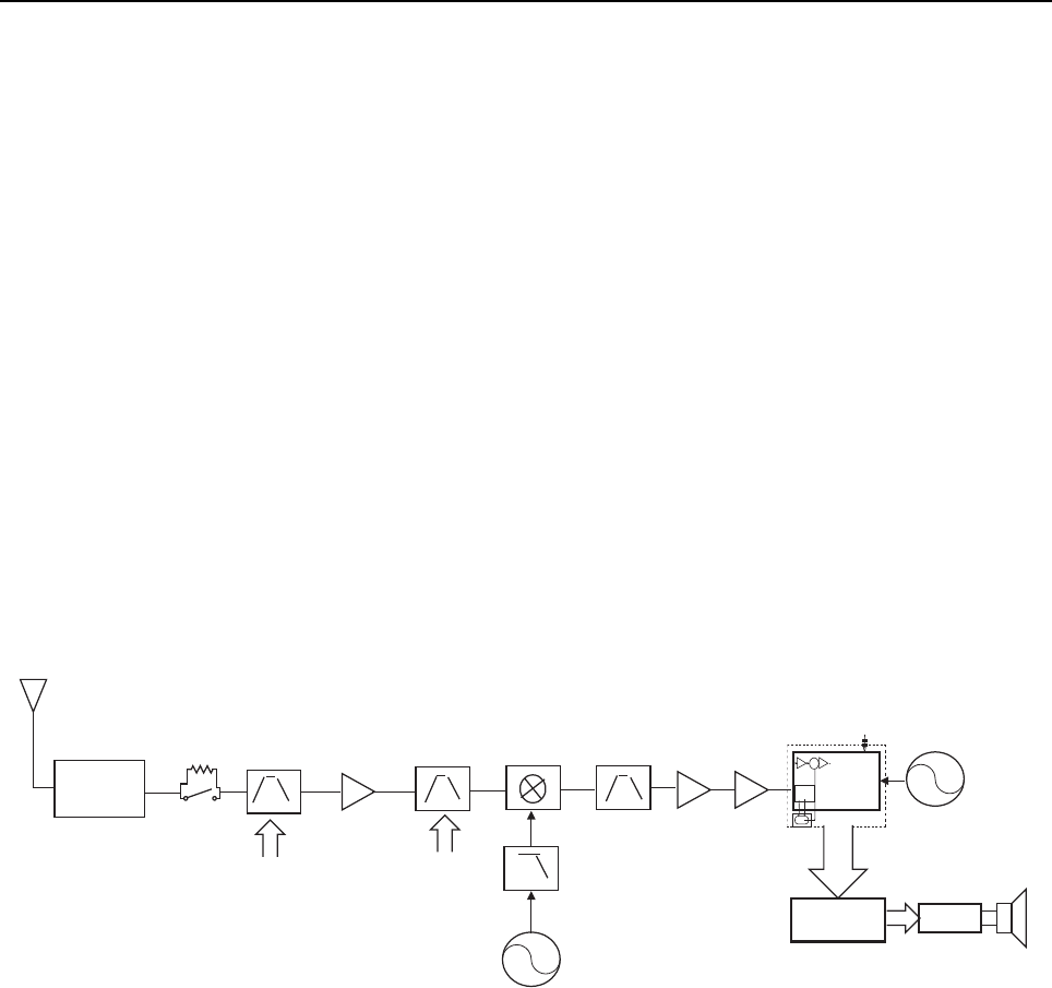
1-6 Mobile Radio’s Theory of Operation
6. Eleven conductor flex cable. Provides the SSI connection between the transmit and receive
radios. Refer to Section 1.5 for more details on this interface.
7. Thirty conductor flex cable. Provides the connection from the transmit radio to the Repeater
Indicator board and includes SPI signals to drive the LED indicators, RTC backup supply, and
the interface to the Ethernet controller.
8. Twenty six conductor cable. Provides the connection from the transmit radio's MAP to the
MAP located on the Repeater's rear panel.
9. Eight pin conductor cable. Provides Ethernet LED signals from Repeater Board and HWID
signals from Connector Board (Applicable for 32 MB repeaters only).
3.0 Mobile Radio’s Theory of Operation
The sections that follow provide a detailed theory of operation for the UHF circuits in the two
MOTOTRBO mobile radios. For details of the theory of operation and troubleshooting for the
associated Controller circuits, refer to the Controller Section of this manual.
3.1 UHF (403–470 MHz) Receiver Circuitry
The receiver is configured as a dual-conversion superheterodyne receiver, capable of both FM and
4-level FSK demodulation. The major blocks are the front-end, the mixer, Xtal filter, and the Abacus
III back-end IC. The overall block diagram is shown in Figure 1-5.
Figure 1-5 Receiver Block Diagram
3.1.1 Receiver Front-End
The front-end consists of a 2-pole varactor-tuned pre-selector filter, an LNA, a 2-pole varactor-tuned
post-selector filter, and a passive double-balanced mixer. The received signal applied to the antenna
is routed through the harmonic filter and PIN diode controlled antenna switch (D0702). A logic high
level on ANT_ENABLE configures the antenna switch for Tx operation while a logic low places the
switch in Rx mode. The insertion loss of the harmonic filter and antenna switch combined is
approximately 0.5 dB max in Rx mode. From this point, the Rx signal is routed to the Local Distance
switch (D0400/R0407), which biases on a diode in normal operation to minimize any insertion loss.
In the repeater, the diode is always biased on with the potential intermodulation improvement
through use of the resistive attenuation not accessible.
T/R ANT
Switch Hi-Speed
A/D
2nd
L.O.
VCO
X
AD9864
4-Pole
73.35 MHz
LIMITER/
IF AMP
STAGE
DSP
Processor
SPI
&
SSI
BUS
Sw. 10 dB
Attenuator
10 bit
DAC
LNA
2-Pole
Varactor
Tuned
2-Pole
Varactor
Tuned
2nd L.O.
71.1 or 75.6
MHz
1st L.O.
Low Side
Injection
F0 - 73.35
MHz
D/A
SPEAKER
10 bit
DAC
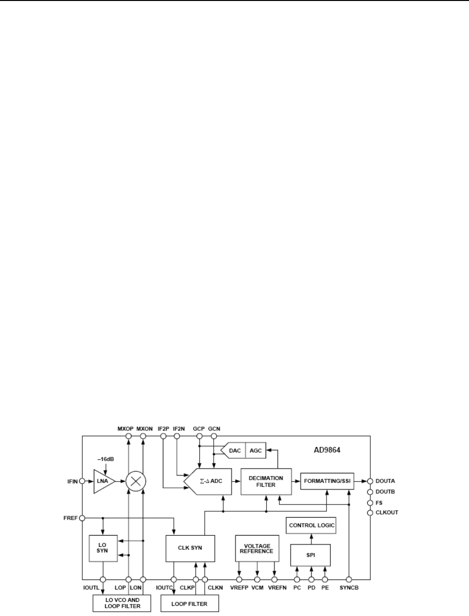
Mobile Radio’s Theory of Operation 1-7
The signal next reaches the pre-selector filter, which is a 2-pole varactor-tuned filter with 5 zeros
that are optimized to provide image frequency rejection. This filter, along with the similarly designed
post-selector filter, provides over 75 dB of image response rejection. The 3 dB bandwidth for both
filters varies across the band with a minimum of 19 MHz at 403 MHz and a maximum of 40 MHz
around 436 MHz. Half-IF rejection from the filters is also frequency dependent with a minimum of
approximately 10 dB achieved at the worst-case frequency of 436 MHz. Both filters have variable
center frequencies that are adjusted by the FE_TUNE signal, which is derived from the output of a
10-bit DAC internal to the MAKO IC (U3200). The voltage is scaled up by a voltage doubler (Q0403)
in order to provide the required linearity for the filters. Both filters are matched to the LNA (Q0402) to
optimize the amplifier’s noise figure (2.0 dB) and to provide an LNA gain of 15 dB to the signal. The
combined gain of the filters and LNA is about 13 dB. Current source Q0401 maintains the collector
current of Q0402 constant at 20 mA. The LNA, current source, Local Distance switch, and voltage
doubler are all supplied by 9R1_FILT, which is derived from 9R1 after filtering.
Following the post-selector filter is the Class 2, double-balanced mixer. It is comprised of baluns
T0400 and T0401 and diode ring mixer D0405. Injection amplifier Q0405 provides 10 dB of gain to
the Rx VCO injection signal. Another amplifier, Q0202, located in the VCO block, also provides gain
for the LO signal and isolation from high RF signals entering the mixer. The signal applied to the LO
port of the mixer is +16 dBm minimum after passing through the 3-pole/1-zero, low-pass injection
filter. The LO injection is low-side and mixes the signal down to an IF frequency of 73.35 MHz. The
output of the mixer is connected to a diplexer network, which terminates out-of-band frequencies in
51 ohms (R0427) while appearing as high impedance to the 73.35 MHz IF signal.
3.1.2 Receiver Back-End
The signal entering the back-end is matched to 4-pole crystal filter, FL0500, by C0507 and L0503.
The filter is centered at 73.35 MHz with a 3 dB bandwidth of 12 kHz. IF amplifiers Q0500 and Q0501
follow the crystal filter and provide both amplification and limiting to the signal. An overall gain of
25 dB is available from the composite IF amplifier to lower-level IF signals. As the signal level
increases, Q0501 begins to limit and eventually saturates out at approximately –16 dBm. The
purpose of the limiting is to provide protection to the AD9864 Abacus III back-end IC (U0600). At IF
levels exceeding –32 dBm into U0600, the 2nd LO synthesizer internal to U0600 can be pulled,
causing corruption of the I/Q data being delivered to the DSP. The block diagram for the AD9864 is
shown in Figure 1-6 below.
Figure 1-6 AD9864 Block Diagram

1-8 Mobile Radio’s Theory of Operation
The Abacus III accepts the 73.35 MHz signal, processes it, and sends out I/Q data in 16-bit format to
the DSP at a 20 kHz rate. Internal to the Abacus III is an LNA and 16 dB FE attenuator, an internal
integer-N synthesizer used to control the external 2nd LO VCO, a Sigma-Delta ADC and decimation
filter, and control and formatting logic for outputting the baseband I/Q data. External to U0600 is the
2nd LO VCO with active device Q0600 and its associated circuitry including the loop filter consisting
of C0613, C0618, and R0603. The 2nd LO mixes the 73.35 MHz IF signal down to 2.25 MHz before
being input to the ADC where it is sampled. The tank circuit (L0608, C0605, C0642, R0617) and
varactor (D0601) for the internal clock synthesizer, work with the loop filter (R0618, C0643, C0646)
to provide the 18 MHz clocking signal to the internal ADC, decimation filter, and SSI formatting
circuitry. A 3 Volt regulator (U0601) provides a clean supply to U0600. Transistor Q0601 is
configured as a super filter to provide the 2nd LO transistor with a low-noise supply. The reference
clock for U0600 is 16.8_REF, which is a buffered (Q0100) 16.8 MHz clock from the synthesizer
block.
Shown below in Figure 1-7, is a simplified block diagram of the signal flow through the receiver
back-end and the DSP processor portion of the OMAP (U1000). All of the blocks within the dotted
box represent the DSP software algorithms internal to the DSP.
Figure 1-7 Signal Flow through Receiver Back-End
The DSP takes the incoming 20 kHz data stream and passes the information through an FIR (Finite
Impulse Response) filter, which provides rejection from any in-band adjacent channel interference.
The remaining filter data is then sent through a decimation process further reducing its frequency to
8 kHz.
Depending on whether the repeater is in Analog or Digital mode determines the type of signal
processing used. If in Analog mode, the remaining 8 kHz data is sent through the FM Discriminator
and De-emphasis subroutines in the DSP code. If the repeater is in Digital mode, the 8 kHz data is
again passed through the FM Discriminator but an additional Symbol Recovery routine is applied
along with a standard AMBE+2™ Vocoder process. The data is sent to the MAKO (U3200), which
provides digital to analog conversion and drives the audio gain stages. Detailed information
regarding this can be found in the Audio Section of the Controller Theory of Operation.
FIR
4-FSK
SYMBOL
RECOVERY
AMBE+2
TM
VOCODER
DSP DIGITAL 4FSK MODE
Σ ∆
AD9864 Hi
SPEED
ADC
SPEAKER
ANALOG AUDIO
GAIN STAGES
DAC
FIR
FM
DISCRIMINATOR DEEMPHASIS
DSP ANALOG FM MODE
Σ ∆
AD9864 Hi
SPEED
ADC
SPEAKER
ANALOG AUDIO
GAIN STAGES
DAC
73.35
MHz
IF
73.35
MHz
IF
FM
DISCRIMINATOR
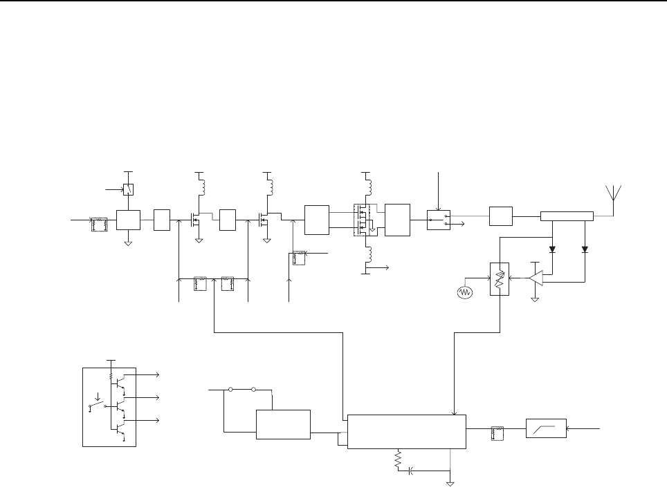
Mobile Radio’s Theory of Operation 1-9
3.2 UHF (403–470 MHz) Transmitter Circuitry – 40 Watt
The Transmitter consists of the power amplifier (PA) circuitry and the power control circuitry. The
power amplifier provides amplification of the signal from the VCO up to the desired output power.
The power control block is responsible for ensuring the desired output power level is maintained in
both analog and digital modes, as well as protecting the power amplifier from damage due to heat,
antenna mismatch, out-of-range battery voltage, and poor assembly.
Figure 1-8 UHF 40 Watt High-Power Transmitter Detailed Block Diagram
3.2.1 Power Amplifier
The radio’s 40 Watt power amplifier (PA) is a 4-stage amplifier which amplifies the output of the VCO
to the required transmit power level. The first stage is an LDMOS (Lateral Double Diffuse MOS)
50 ohm fixed-gain block (ADA-4743, U0700) followed by the adjustable gain LDMOS pre-driver
(RD01MUS1, Q0705), an adjustable gain LDMOS driver (RD07MVS1, Q0703), and the fixed-gain
LDMOS final device (MRF1570, Q0702). A transmit/receive (T/R) switch and a harmonic filter
complete the transmit lineup.
3.2.2 Input Stage (50 Ohm Fixed-Gain Block)
The first stage (ADA-4743, U0700) is an integrated circuit with internally matched 50 ohm input and
output stages providing approximately 16.5 dB power gain. It provides reverse isolation between the
PA and the VCO to lessen the risk of VCO load-pull and it also supplies appropriate power to the
pre-driver stage. The ADA-4743 is biased at 60 mA during transmit by R0706, which is switched to
9V3_TX during TX by Q0701 (controlled by Antenna_En). The ADA-4743 is preceded by an 11 dB
resistive pad to further improve reverse isolation.
T/ R
Switch
Harmonic
Filter
Agil ent
AD A 4743
TX_DAC
Active
Reconstruction
Filter
Log Amp Controller
V_ CONTROL
SW_9V1
9V3
+5 V Regulator
-5 dBm
(nominal)
TX_INJ
CW / 4 FSK
+13 dBm
INPUT
FROM
VCO
ANT_ ENABLE
9V3_TX 9V3_TX
BATTERY_DET
SW_9V1
Reflec ted
Port
Microstrip
Dual
Directional
Coupler
Forward
Port
+
TX Port
RX Port
To FE
Match
Match
Match/
Splitter
Match/
Combiner
A+
A+
Voltage
Controlled
Variable
Attenuator
Thermal
Cutback
AD 8315VAPC RF IN
VPOS
ENBL COMM
FLTR
VSET
VCONT
VIN +5 VOUT
Pad
To Pressure
Pad Switch
To Pressure
Pad Switch
FINAL_BIAS
To Pressure
Pad Switch
9V3
Pressure
Pad C loses
Switch
To Predriver
To Driver
To Final
9V3_TX
LDMOS
Predriver
RD 01MUS1
LDMOS
Driver
RD 07 MVS1
LDMOS
Final
MRF1570
ANT_ ENABLE
Pressure
Pad
Switch

1-10 Mobile Radio’s Theory of Operation
3.2.3 Pre-Driver Stage
The next stage is a low-power, LDMOS device (RD01MUS1, Q0705), which delivers up to +27 dBm
to the driver stage. Its gain is controlled by varying the gate bias voltage and varies from low gain up
to approximately 14 dB power gain. The gate bias voltage is controlled in parallel with the driver
stage by the V_cont signal.
The input match to this stage is a high-pass topology comprised of L0718, C0817, and L0721.
High-pass matches are used where appropriate to minimize the chances of low frequency
regeneration within the amplifier. R0759 and R0777 are required to improve the bandwidth of this
circuit. The inter-stage match between the pre-driver and driver stages is comprised of L0720,
C0786, and C0791 arranged in a high-pass topology. Additional pads are provided on the
transceiver board to allow for possible engineering optimizations to this match. These are
non-populated parts C0789, C0792, C0793, and C0794.
3.2.4 Driver Stage
The third stage is a medium-power, LDMOS device (RD07MVS1, Q0703), which delivers up to
+38 dBm to the final device. Its gain is controlled by varying the gate bias voltage and varies from
low gain up to approximately 11 dB of power gain. The gate bias voltage is controlled with the
V_cont signal and is controlled in parallel with the pre-driver stage gain.
R0718, R0720, R0754, and R0755 are required to improve the bandwidth of the driver stage. The
inter-stage match (as well as the power splitter) between the driver and final device is comprised of
C0753, C0813, C0818, C0819, C0732, C0743, C0744 and C0761, and associated micro-strips on
the PCB. Additional pads are provided on the printed circuit board to allow for possible engineering
optimizations to this match. These are non-populated parts C0754, C0755, C0729, C0730, C0731,
C0808, C0764, C0760, and C0765.
3.2.5 Final Stage
The final stage is a high-power, LDMOS device (MRF1570, Q0702) consisting of two parallel,
high-power devices within 1 plastic package. The package is mounted to a copper carrier to improve
thermal conductivity to the chassis and also to more tightly control the RF load, allowing higher and
more consistent maximum output power. This stage is biased at a quiescent current of 750 mA and
operates with a fixed-gain of approximately 10 dB, allowing the radio to be set to a maximum output
power of 48 Watts. The quiescent current is set by adjusting the Final_Bias signal. Both elements of
this transistor are fabricated on the same semiconductor die and are well matched, allowing control
via a single voltage.
Both the input and output matching circuits of this stage have extremely critical part location
requirements. Any repair must be done with care to ensure the replaced components are placed
accurately and properly soldered. Of particular concern are input matching capacitors C0732 and
C0761 and output matching capacitors C0811 and C0812. The resistor networks at the input of each
of the final elements are required to improve the bandwidth of the circuit. These resistors are R0762
through R0773.

Mobile Radio’s Theory of Operation 1-11
The output matching circuit and power combiner is comprised of C0811, C0719, C0812, C0746,
C0726, and C0737 and associated microstrips fabricated on the printed circuit board. Additional
pads are provided on the PC board to allow for possible engineering optimizations to this match.
These are non-populated parts C0720, C0721, C0747, C0748, C0727, and C0741. R0719 is added
as a preventative measure against half-carrier regeneration. If the final device fails and has to be
replaced, R0719 should be carefully inspected to ensure against any damage caused by the final
device. Replacement of the final device requires that the bias voltage be re-tuned using the
Customer Programming Software (CPS). Care must be taken not to damage the device by
exceeding the maximum allowed quiescent current which is 1 Amp. The device can tolerate up to
5 Amps for brief periods of time without damage.
3.2.6 Antenna Switch
The antenna switch (T/R switch) routes the signal between either the transmitter or receiver and the
antenna. In transmit mode, it utilizes the existing dc feed (A+) to the final stage device (Q0702). Both
PIN diodes D0700 and D0702 are turned on during key-up through forward biasing. This is achieved
by pulling down the voltage at the cathode end of D0702 to approximately 12.2 Volts (0.7 Volt drop
across each diode). Q0704 is configured as a current sink that maintains the current through the
antenna switch diodes at 100 mA, as set by VR0700 and R0738. The current sink is enabled during
transmit mode by ANT_ENABLE, which is asserted through Q0706 and associated circuitry. When
the PIN diodes are conducting, an RF ground is formed at the anode of the lower PIN diode, D0702,
which places L0710 and C0803 in parallel. The values of L0710 and C0803 are chosen so as to be
parallel resonant at the center of the transmit band, making them appear as an open-circuit so that a
50 ohm power path is maintained through the top PIN diode to the harmonic filter.
In receive mode, DC current through the PIN diodes is interrupted by turning off the current sink.
The RF path now flows from the harmonic filter, through the matching circuit formed by L0710,
C0803, and the capacitive divider formed by C0767 and C0772. C0766, currently unplaced, is
provided for possible future engineering optimizations to this match. The purpose of L0719 is to form
a parallel resonant tank with the reverse capacitance of D0700, improving the receive path return
loss at the receive input of the T/R switch.
3.2.7 Harmonic Filter
Inductors L0706, L0707, L0708, and capacitors C0742, C0739, C0740, and C0738 form a
7-element low-pass filter to attenuate harmonic energy from the transmitter. R0713 is used to drain
any electrostatic charges that might otherwise build up on the antenna. The harmonic filter also
prevents high-level RF signals above the receiver pass-band from reaching the receiver circuits,
improving spurious response rejection.
3.2.8 Directional Coupler
The dual-directional microstrip coupler is implemented at the harmonic filter output to sample both
forward and reverse directed transmitter power. RF power from the transmitter PA passes through
the microstrip coupler before reaching the antenna. Forward RF power is coupled to the U0940 log
detector/controller via the voltage-controlled attenuator (VCA) stage consisting of pin diodes D0901,
D0902, and D0903. The log detector/controller regulates the gain of PA stages Q0703 and Q0705
(via V_cont), thus ensuring that the forward power out of the radio is held to a constant value.

1-12 Mobile Radio’s Theory of Operation
The directional coupler functions not only as part of the transmitter power regulation circuit but also
as part of the VSWR load-detection circuitry. Its physical location close to the antenna connector
allows accurate VSWR sense at the transmitter output. Forward and reverse coupled signals are
rectified by D0904 and D0905, respectively. DC voltage FWD_DETECTED is proportional to RF
power while REV_DETECTED is proportional to reflected RF power. The detected voltages are fed
to the respective inputs of difference amplifier U0901. The difference amplifier output is applied to
the variable attenuator control stage, U0900-1. An abnormally high reflected power level, i.e., a
damaged antenna, also causes an increase in the difference amplifier output voltage. This causes a
reduction in attenuation by the VCA. As a result, the greater RF signal applied to the log detector/
controller causes the controller to reduce the gain of PA stages Q0703 and Q0705. Transmitter
power is thus reduced to prevent damage to the final device due to an improper load.
3.2.9 Power Control
The transmitter uses PA controller IC, U0940 to control the power output of the radio. A portion of
the forward RF power from the transmitter is sampled by the directional coupler and delivered via
the VCA to the RFIN port of the PA controller IC (pin 1). The PA controller, a log detector type,
provides temperature-stable, high-accuracy control over a typical 50 dB dynamic range.
The MAKO IC contains a digital-to-analog converter (DAC), which provides a reference voltage
(TX_DAC) at the input of reconstruction filter stage U0900-2. The filtered reference voltage at the
output of U0900-2 is divided by the combination of R0942 and R0946 before reaching the VSET
input of the PA controller IC (pin 3). Thermistor RT0953 is used in combination with R0954 to
compensate reference voltage drift at operating temperature extremes. Reference voltage level is
programmable through the SPI lines of the MAKO. This reference voltage is proportional to the
desired power setting of the transmitter and is factory programmed at several points across the
frequency range of the transmitter to offset frequency response variations of the transmitter’s
coupled power circuits.
The PA controller IC provides a dc output voltage at pin 7 (VAPC), which is divided to provide gate
bias for PA pre-driver and driver stages. The 0 Volts to 5 Volts range at U0940, pin 7, is applied as
V_CONTROL to power-adjust the transmitter by controlling the gate bias of stages Q0703 and
Q0705. Voltage divider combination R0727 and R0728 provides gate bias to Q0703 while divider
combination R0750 and R0751 provides gate bias to Q0705. This adjusts the transmitter power
output to the intended value. The ratio of each of these resistive dividers is chosen to ensure that
Q0703 and Q0705 are both running at their nominal design condition at rated output power.
Variations in sampled forward transmitter power cause the PA controller IC to adjust the control
voltage above or below its nominal value to raise or lower output power in order to maintain
transmitter output power relative to the reference voltage applied to VSET.

Mobile Radio’s Theory of Operation 1-13
3.2.10 Power Ramp Profile Control
In order to minimize the transient adjacent channel power at the transmitter’s output, the ramped
power follows a raised-cosine profile. The PA controller IC has a linear slope function when scaled in
dB/V. To achieve the desired raised-cosine profile of the output power, the ramped reference voltage
provided by the MAKO DAC follows a raised-cosine approximation. The MAKO DAC reference
output is low-pass filtered by the DAC reconstruction filter before it is applied to the VSET input of
the PA controller IC.
Reconstruction filtering reduces spurious emissions in the RF spectrum as a result of the finite steps
of the DAC. Loop filter capacitor C0926 in conjunction with resistor R0950 and the integrator within
the PA controller IC, set the loop dynamics. The loop response has been optimized to achieve
sufficient speed to follow the required ramping profiles while meeting switching transient
requirements over varied power levels. Accurate control of the power-rise (ramp-up) and power-
decay (ramp-down) characteristics minimizes splatter into adjacent channels.
3.2.11 Thermal Protection
Thermistor RT0908 in combination with R0902, form a voltage divider with the output proportional to
the sensed transceiver board temperature in the vicinity of the transmitter driver and final devices.
The voltage divider output is routed to an operational amplifier U0901-2, which provides a dc voltage
via diode junction D0900 to control the attenuation level of the VCA stage. For the condition that the
temperature threshold set by resistive divider combination R0901 and R0909 is reached, the VCA is
driven to increase the RFIN signal at the PA controller IC (pin 1). This increase will cause the
controller IC to adjust the PA control voltage below its nominal value to decrease transmitter output
power. Temperature will be reduced by lowering transmitter output power relative to the reference
voltage applied to VSET.
The extruded heat sink on the transmitter chassis helps to get the heat away from the transmit
circuitry more efficiently. Because the heat transfer is better than the mobile chassis due to the fan
and heat sink, there are some component values in this area that are different from those in the
MOTOTRBO mobile chassis.
3.2.12 Out-of-Range Battery Protection
Transmitter power cutback under extended battery supply voltage operation is provided for by
monitoring the battery supply in the controller circuit of the radio in order to change the VSET input
of the PA controller IC (pin 3) for reduced transmitter output. This feature allows transmitter PA
dissipation to be limited at high-line battery supply operating conditions while limiting transmitter PA
overdrive conditions at low-line battery supply operating conditions.
3.2.13 Pressure Pad Switch
The power control circuitry includes a safety switch (S0700) that consists of a conductive portion of
the rubber pad which pushes the RF final transistor Q0702 against the chassis. When the chassis
cover and rubber pad are properly assembled, the conductive portion of the pad contacts a pattern
on the transceiver board, electrically closing switch S0700. If the cover and pad are not in place,
switch S0700 is open-circuited and the power control circuit is disabled, turning off the gate bias to
Q0702, Q0703, and Q0705. This prevents thermal damage of the RF transistors which could occur
if the transmitter is operated without adequate heat sinking.
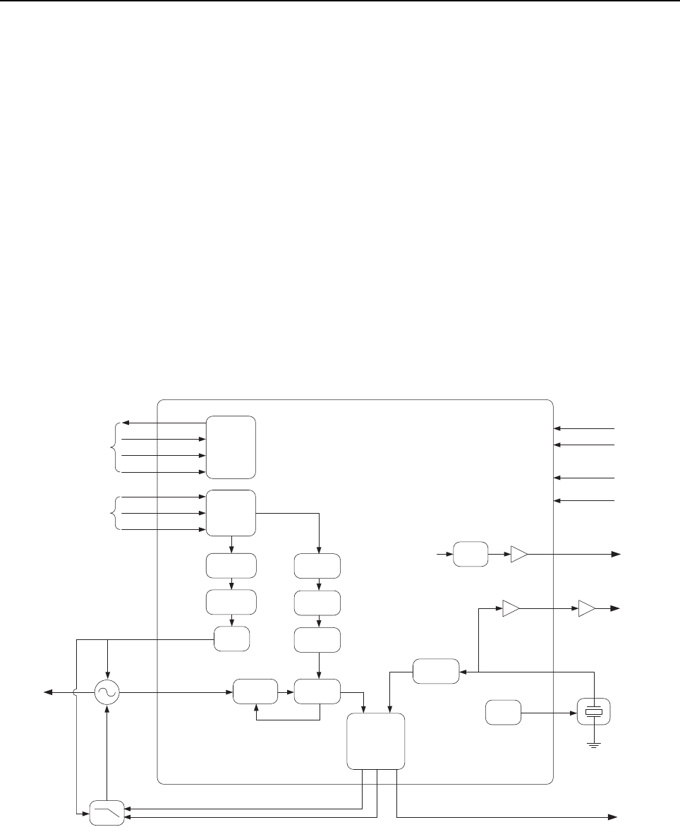
1-14 Mobile Radio’s Theory of Operation
3.3 Frequency Generation Circuitry
The synthesizer subsystem consists of the reference oscillator (Y0100), the fractional-N synthesizer
IC (Tomahawk II, U0100), and the Voltage Controlled Oscillator VCO.
3.3.1 Reference Oscillator
The reference oscillator (Y0100) contains a temperature compensated crystal oscillator with a
frequency of 16.8 MHz. A digital-to-analog (DAC) converter internal to U0100 (Tomahawk) and
controlled by the mP via serial interface (SPI), sets the voltage at the AUX_DAC output of U0100
(pin H6) to set the frequency of the oscillator. The output of the oscillator (pin 3 of Y0100) is applied
to pin K5 (XOSC_BASE) of U0100.
3.3.2 Fractional-N Synthesizer
The Tomahawk II synthesizer IC (U0100) consists of a pre-scaler, a programmable divider and
divider control logic, phase detector, charge pump, a D/A converter in the high frequency analog
modulation path, an attenuator to balance the high and low frequency modulation paths, a serial
interface for control (SPI), a serial interface for modulation (SSI), and a super filter for the regulated
2.45 Volts.
Figure 1-9 UHF Synthesizer Block Diagram
SPI
Interface
Data Write
Clock
CEX
Data
Fsync
Clock
SPI
SSI
(Modulation )
Prescaler Main Divider
VCO
Fractional
Unit
DS
18 - bit
Modulation
Unit
Main
Phase / Fr eq.
Detector
And
Charge Pumps
Reference
Divider
TCXO
(16 .8 M H z)
AUX
D/ A
Main_CP LOCK DETECT
Buffer Buffer
16.8MHz REF
Loop Filter
5V
2 .775V Dig
2.775 V A na
1 .875V Dig
TOMAHAWK II
Fractional -N
Synthesizer
(U0100)
D9
Data ReadD10
C11
D8
F11
F10
F9
J2
Adapt _CP
H1 D7
SF _OUT
Super
Filter
2 .775V Ana K4
H6
J11
K5
H2,J3
A7
A5,A10,B2,B9,
G2 ,J4 ,J6, J10,
K2,L6
B7 ,E 11, G10 ,J1
Digital
Attenuator
SSI
Interface
D/A
Waveform
Generator
K8 HP MOD
PRSC
TX / LO
G3
Mobile Radio’s Theory of Operation 1-15
A voltage of 2.775 Volts applied to the super filter input (U0100 pin J4) supplies an output voltage of
2.45 Vdc (SF_OUT) at pin K4. This supplies the VCO and the VCO modulation bias circuit (via
R0321). The super filter supply voltage is provided by the 2.775 Volt regulator within U3200. The
synthesizer is also supplied by the 5 Volt regulator, U3002, another 2.775 Volt regulator within
U3200, and a 1.875 Volt regulator within U3200.
The output signal LOCK (U0100-D7) provides information about the lock status of the synthesizer
loop. A high level at this output indicates a stable loop. A discrete buffer amplifier (Q0100) provides
a buffered 16.8 MHz reference frequency to other parts of the radio.
The serial programming interface (SPI) is connected to the microprocessor via the data lines
SPI_DW (U0100-D9) and SPI_DR (U0100-D10), clock line SPI_CLK (U0100-C11), and chip enable
line CEX (U0100-D8). The serial modulation interface (SSI) is connected to the DSP via the data
line SDTX (U0100-F11), clock line TXCLK (U0100-F10), and frame sync line SFTX (U0100-F9).
3.3.3 Voltage Controlled Oscillator (VCO)
The Voltage Controlled Oscillator (VCO) subsystem consists of four Colpitts oscillators (two each for
Tx and Rx), a single-stage Tx buffer amplifier, a single-stage Rx buffer amplifier, oscillator bias
control switches, and the modulation circuitry.
Figure 1-10 UHF VCO Block Diagram
The UHF VCO design incorporates a total of four oscillators; two varactor-tunable Colpitts oscillators
each for Tx and Rx. Each oscillator has a tuning range of 33.5 MHz, sufficient to cover the Rx and
Tx frequency ranges of 326.65 MHz to 396.65 MHz and 403 MHz to 470 MHz, respectively. The
oscillators resonate at fundamental operating frequencies. Four (active-low logic) general purpose
output lines (GPO1, GPO2, GPO3, and GPO6) from the Tomahawk IC (U0100-B4, A4, E5, and H8)
provide the control for independent bias selection to each oscillator (VCO_SEL) via the PNP
transistor switches U0304 and U0201.
TX VCO 1
TX VCO 2
RX VCO 1
RX VCO 2
TX Buffer Amp
RX Buffer Am p
Low Pass
Filter
TX INJ
RX INJ
To U0700
To Q 0405
Steering Line Voltage
(VCTRL)
9V3 _VC O
( U3001 -5 )
9R1
(Q0107 )
RX_VCO_SEL2
(U0100 - H8 )
RX_VCO_SEL1
(U0100 -B4)
TX_VCO_SEL 2
(U0100 -A 4)
TX_VCO_SEL 1
(U0100 -E 5)
High Port Modulation
(HP_MOD_OUT)
(U0100 -K8)
Prescaler
( U0100 -J2 )
UHF VCO
Subsystem

1-16 Mobile Radio’s Theory of Operation
The 2.45 Volt super filtered output, SF_OUT, of the Tomahawk IC (U0100-K4) supplies the bias to
the oscillators. A portion of the VCO output signal is lightly coupled through coupling capacitors
C0331 and C0231, routed through a low-pass filter (formed by L0221, C0235, C0230, and C0233),
and fed back to the M_PRSC input of the Tomahawk IC (U0100-J2).
High-port modulation is scaled through a voltage divider (comprised of R0319, R0320, and R0321)
and applied to the Tx modulation varactor diode CR0300. The TX VCO frequency is modulated via
coupling capacitors C0310 and C0344. High-port modulation is also applied to the VCO steering line
(through R0139, R0140 and C0166) which modulates the main VCO tuning varactors.
A discrete single-stage Tx buffer amplifier (comprised of the NPN transistor Q0302 and surrounding
components) amplifies the signal from the Tx oscillator to the level required by the first stage of the
Transmitter Power Amplifier (U0700). The TX buffer amplifier also provides sufficient isolation from
any undesired load-pulling from the Transmitter Power Amplifier. The bias for Q0302 is provided by
the 9.3 Volt regulator U3001.
A discrete single-stage Rx buffer amplifier (comprised of the NPN transistor Q0202 and surrounding
components) amplifies the signal from the Rx oscillator to the level required by the LO injection
amplifier (Q0405). The Rx buffer amplifier also provides sufficient isolation from any undesired
load-pulling from high input levels in the receiver front-end. GPO4 from the Tomahawk IC
(U0100-D4) controls the transistor switch (comprised of Q0108 and Q0107), that enables the 9.1
Volt bias to Q0202 (via the 9.3 Volt regulator U3001).
3.3.4 Synthesizer Operation
The complete synthesizer subsystem is comprised mainly of the Tomahawk synthesizer IC,
Reference Oscillator (crystal oscillator with temperature compensation), loop filter circuitry, VCO,
and DC supplies. The VCO feedback signal, PRSC, is fed to pin J2 of U0100 (M_PRSC) via a
low-pass filter (L0221, C0235, C0230, and C0233) which attenuates harmonics and provides the
correct level to close the phase-locked loop.
The prescaler in the synthesizer IC (U0100) is a four-level prescaler capable of dividing by 4, 5, 6,
and 7. The main loop N divider is configured to be an 8-bit divider. The divide-by-N portion of the
main loop is set via the SPI. The fractional portion of the divider is realized using a 3-accumulator,
24-bit fractional divider. The SPI is used to set the desired divide ratio.
The output of the prescaler is applied to the main loop divider. The output of the main divider is sent
to the phase/frequency detector, which compares the main divider’s output signal with the reference
signal. The reference signal is generated by dividing down the signal of the reference oscillator
(Y0100). The output signal of the phase/frequency detector is a pulsed signal which is routed to the
charge pumps. The main charge pump current is programmable through the SPI with its output at
pin G3 of U0100 (MN_CP). The loop filter transforms this current into a steering voltage that is
applied to the VCO.

Mobile Radio’s Theory of Operation 1-17
To reduce lock time when new frequency data has been loaded into the synthesizer, an adapt
charge pump providing much greater current than the main charge pump is turned on for a finite
amount of time to quickly charge or discharge the loop filter capacitors to steer the VCO to the
desired frequency. The output of the adapt charge pump passes to the loop filter via pin H1 of
U0100 (MN_ADAPT_CP). When the synthesizer is within the lock range and the adapt timer runs
out, the adapt charge pump is powered down and the main charge pump takes over. A settled
synthesizer loop is indicated by a high level at signal LOCK (U0100-D7), which is routed to the
microprocessor. Q0102 is configured as a current source to provide a steady 1.5 mA during the
adapt period. U0101 is an analog switch that opens the adapt path slightly before the end of the
adapt period to prevent the current from the current source from pushing the VCO off frequency.
Modulation is performed by applying a digital data stream via the SSI bus from the DSP (U1000) to
the synthesizer (U0100). In order to meet spurious and phase noise requirements, the PLL
bandwidth was designed to be narrower than the full modulation bandwidth, therefore requiring the
use of dual-port modulation. Internal to the synthesizer (U0100), low-port modulation is added to the
fractional-N division numerator to trace out the modulation versus time while the high-port data
stream passes through an interpolating waveform generator, a digital attenuator (for modulation
balancing), and then gets converted to an analog signal through a 10-bit DAC before modulating the
VCO. This high-port analog modulation output (HP_MOD_OUT, U0100-K8) is connected to the
VCO modulation varactor diode (CR0300) via C0360 and R0319, and to the loop filter via R0139,
R0140, and C0166.

1-18 Mobile Radio’s Theory of Operation
Notes
2-1
Section 2
TROUBLESHOOTING CHARTS
1.0 Troubleshooting Flow Chart for Receiver (Sheet 1 of 3)
Set up radio in Analog
Receive mode on
desired channel
with Squelch open
1st LO
> +5 dBm
at R0422?
Spray or inject 73.35 MHz
RF carrier modulated with
1 kHz Audio Tone into XTAL
Filter FL0500
No
Audio Tone
present
at Speaker?
Yes
Volume
level
adjusted
properly?
Check U3501
bias and
replace part if
necessary
Audio at pin 1
of U3501?
Verify audio path to
U3501
Setup repeater unit to
receive at frequency
403.025 MHz
with the RX Brick open &
connected to the system.
Apply an on-channel
RF carrier at -47 dBm modulated
with 1 kHz tone
at the RX antenna port
B
Audio at pin 6
of U3505?
Audio at pin 10
of U3501?
Check connections to
external speaker and replace
speaker if necessary
Verify audio path
between U3500 and
pin 1 of U3501
Audio at pin 4
of U3500?
Audio at pin 1
of U3500?
Check Biasing
before replacing
U3500
1st LO
(329.675 MHz)
> +16 dBm
at TP0401?
Check biasing on
Q0405 before replacing
9 VDC
present
at R0417?
Check
9R1 path back to
Synthesizer
Check VCO
Troubleshooting
Flow Chart
RF level
of on-channel
signal > -45 dBm
on pin 4
of T0401?
A
Check T0400 and D0405
and replace if necessary
Yes
Yes
Yes
No
No
Yes
YesNo
No
No
Yes
Yes
No
No
No
Yes
Yes
NO RX AUDIO
No
ALL Troubleshooting within the
dotted line is done on the TX BRICK
No
Yes

2-2 Troubleshooting Flow Chart for Receiver
1.1 Troubleshooting Flow Chart for Receiver (Sheet 2 of 3)
A
Voltage level
>2.7 VDC
on D0401?
+9.0 VDC
on pin 4
at Q0403?
Check circuitry around
D0401, D0402, D0403, and
D0404 for shorts and opens
~ 0.8 VDC at
R0432/D0400?
Check biasing on
Q0403 before replacing
Check biasing circuitry of
Q0401 and Q0402 before
replacing
RF level
of on-channel
Signal > -45 dBm
at C0420?
Is voltage
at R0409
~ 0.7 VDC?
Voltage
< 0.5 VDC
at pin 2
of Q0400?
Check biasing
circuitry of
Q0400 before
replacing
Check D0403, D0404, and
associated capcacitors
for opens and shorts.
Replace if necessary
Check biasing circuitry of
Q0402 before replacing
No
Yes
No
No
No
Yes
Yes
Yes
Yes
Yes
Check Synthesizer
Troubleshooting
Flow Chart
ALL Troubleshooting on this page is
done on the RX BRICK
No
No
Troubleshooting Flow Chart for Receiver 2-3
1.2 Troubleshooting Flow Chart for Receiver (Sheet 3 of 3)
B
16.8 MHz
present
at C0622?
Check Synthesizer
Troubleshooting
Flow Chart
2nd LO
> 0 dBm and
at 71.1 MHz
at TP0600?
Yes
No
No
Yes
73.35 MHz
present
at TP0602?
2.25 MHz
present
at C0625?
No
Yes
No
Yes
18 MHz
present
at L0608?
Check diode
continuity before
replacing D0601 Replace components
as needed
No No
Yes No
Yes
Check for visible
solder shorts near
pins before replacing
U0600
~ 1.65 VDC
on R0617?
Clock
VCO and LF
components
OK?
DC continuity
through
biasing components
E0600 - E0610?
Replace
defective biasing
component
Yes
No
3.0 VDC
on pin 1
of U0601?
Check Controller
Troubleshooting
Flow Chart
5.0 VDC
at E0610?
Check biasing on
U0601 before
replacing
No
Yes Yes
3.5 VDC
at E0609?
No
Yes
Check biasing on
Q0601 before
replacing
Remove Shield
SH0500
Check biasing on
Q0600 and
check continuity
on D0600.
Replace if necessary
Check 5 VDC
supply and biasing
components
before replacing
Q0500 or Q0501
Biasing
correct on
Q0500 and
Q0501?
~ 3.0 VDC
on L0604
and L0605?
Check biasing
components and 3 VDC supply.
Replace parts if necessary
No
Yes
No
Yes
73.35 MHz
present
at pin 6 of
FL0500?
Check signal gain
and biasing
before replacing
Q0500 or Q0501
No
Yes
ALL Troubleshooting on this page
is done on the RX BRICK
No
Check FL0500 matching
components before replacing
Yes
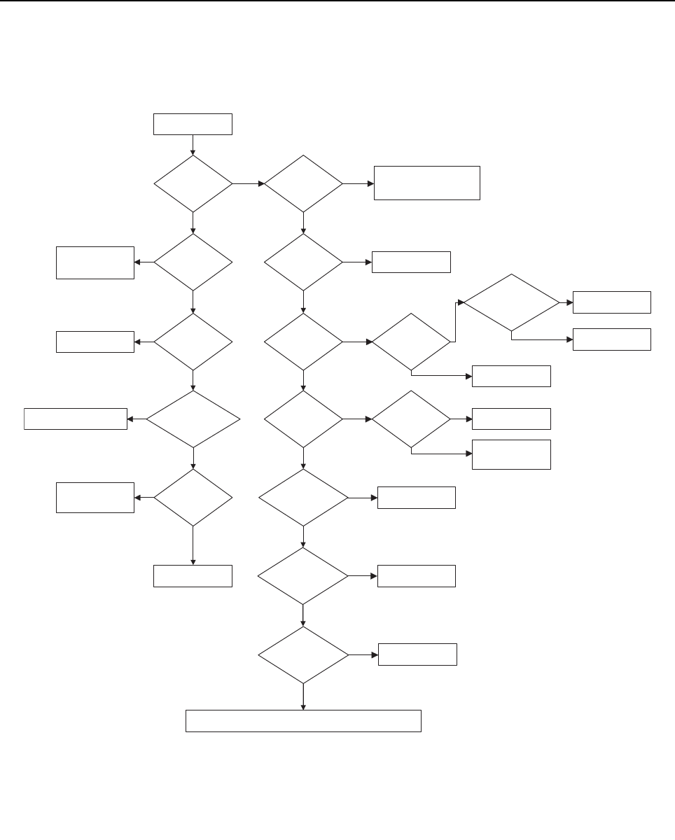
2-4 Troubleshooting Flow Chart for 40W Transmitter
2.0 Troubleshooting Flow Chart for 40W Transmitter
Is TP0909
> 1 VDC?
No Transmitter
Power
Is TP0913
= 9.1 VDC?
Check 9.3V Regulator
circuit (U3001)
Is U0941 Pin 1
= 5 VDC?
Check 5V Regulator
circuit (U0941)
Is voltage at
TP(TX_RAMP_DA
C) in controller
> 3 VDC?
Check MAKO
Troubleshooting Flow Chart
Is voltage at
TP0910
> 1 VDC?
Check U0900-2 and
associated circuitry
Replace U0940
Is TP0702
= 9.3 VDC?
Check 9V3_PA Regulator in
Controller Troubleshooting
Flow Chart
Are TP0707
and TP0708
~ 2.2 VDC?
Is power
at TP0704
~ 16.5 dBm?
Is Pressure Pad
Switch in place?
Place Switch or
R0775
Is resistance
to ground at Q0702
G1 and G2
~ 66 kohm?
Replace Q0702 *
* Note: If Q0702 is replaced radio must be bias set and power set.
1) Levels are during Transmit Mode (analog), 13.6V at battery connector, 50 ohm termination on transmitter.
2) Make sure PCB is screwed into chassis during these tests to avoid final device damage.
Check Bias Set
Circuit; bias tune
Is TP0703
0 dBm?
Check VCO
Troubleshooting
Flow Chart
Replace U0700
Is power at
TP0709 ~ 15 dB
> TP0710?
Is power at
TP0702 ~ 10 dB
> TP0709?
Check Q0705 and
associated circuitry
Check Q0703 and
associated circuitry
Is power at
D0700-A ~ 10 dB
> TP0702?
Check Q0702 and
associated circuitry
Measure relative power thru remainder of TR switch and LPF to find
open circuit. Perform visual inspection of circuit.
Is D0702-K
~ 12.4 VDC?
Check T/R bias
circuit
Yes
Yes
Yes
Yes
Yes
No
Yes
Yes
Yes
Yes
No
No
Yes
No
No
Yes
No
Yes
No
Yes
No
Yes
No
No
No
Yes
No
No
No
No
3) When making measurements within the transmitter using an RF power probe, be careful that the rating
of the probe is not exceeded. The “relative” measurements listed in the flow chart should be made with a
scope probe connected to a spectrum analyzer or similar instrument to avoid damaging sensitive power
probes.

Troubleshooting Flow Chart for Synthesizer 2-5
3.0 Troubleshooting Flow Chart for Synthesizer
Start
Visual check of
the Board OK?
Correct
Problem
+5V at R0100?
Check 5V
Regulator
U3002
+2.775V at
R0101 and
R0103?
Check U3200
+1.875V at
R0102? Check U3200
Is 16.8MHz
Signal at C0145? Check Y0100
Is 16.8MHz
Signal at R0155? Is 16.8MHz
Signal at R0109?
Replace
U0100
Check Q0100
and surrounding
components
Is Radio in TX or
RX mode?
TX
RX
+2.45V at C0137
(SF_OUT)?
Are C0136,
C0137 OK?
Replace or
resolder
components
Replace U0100
1.5ms pulse at
TP_ADAPT_SW
when channel
changed?
1.5ms (inverted)
pulse at R2517 when
channel changed?
Check P U1000
Troubleshooting
Chart
Check Q0106,
R0159
Is either GPO1 or
GPO6 low (<0.5V),
but not both, and
GPO2 and GPO3 are
high (>1.4V)?
Is RF Prescaler level
(at C0233) between
100mVpk and 300mVpk
(harmonics <-15dBc)?
Check VCO
Troubleshooting
Chart
Is SPI
Programming
OK?
Check P U1000
Troubleshooting
Chart
Replace
U0100
Is SPI
Programming
OK?
Check P U1000
Troubleshooting
Chart
Replace
U0100
Replace
U0100
Is Modulation
Present at
R0139?
Is Tx SSI activity
present on CLK,
FSYNC, and DATA
lines (R2512, R2514,
R2513)?
Check P U1000
Troubleshooting
Chart
Is either GPO2 or
GPO3 low (<0.5V),
but not both, and
GPO1 and GPO6 are
high (>1.4V)?
No
No
No
No
No
No No
No
No
No No
No No
No
NoNo
No
No
Yes
Yes
Yes
Yes
Yes
Yes
Yes
Yes
Yes
Yes
Yes
Yes
Yes
Yes
Yes Yes
Yes
Yes

2-6 Troubleshooting Flow Chart for Tx VCO (Sheet 1 of 2)
4.0 Troubleshooting Flow Chart for Tx VCO (Sheet 1 of 2)
2.556 V at C0362 &
C0363
Check Synthesizer
Troubleshooting
Chart
Check Synthesizer
Troubleshooting
Chart
Radio is not
programmed for
Transmit Mode or
U0100 not functional
~ 0 VDC at
C0358?
2.556 VDC at
C0336?
Replace Q0301
Check biasing components
and then replace Q0301
if needed
Vbe
= 0.7 V
for Q0301?
Yes
Yes
VCO 2
Check biasing
components then
replace Q0302 if
needed
Check biasing
components then
replace Q0302 if
needed
Vbe
= 0.7 VDC
for Q0302?
No
No
No
No
No
No
No TX VCO signal at C0318
Visual check
of board
OK? Correct problem
Correct problem
Radio did not boot up
properly or check
9V3 Regulator
Radio did not boot up
properly or check
9V3 Regulator
9 VDC at L0300?
Check biasing
components then
replace Q0302 if
needed
Check biasing
components then
replace Q0302 if
needed
Vbe
= 0.7 VDC
for Q0302?
Yes
Yes
No TX VCO signal at C0318
Visual check
of board
OK? Correct problem
Correct problem
Radio did not boot up
properly or check
9V3 Regulator
Radio did not boot up
properly or check
9V3 Regulator
9 VDC at L0300?
Radio programmed for
Tx VCO 1 or 2?
2.556 V at C0362 &
C0363
~ 0 VDC at
C0348?
2.556 VDC at
C0300?
Vbe
= 0.7 VDC
for Q0300?
Yes
Yes
No
No
No
VCO 1
Check Synthesizer
Troubleshooting
Chart
Check Synthesizer
Troubleshooting
Chart
Radio is not
programmed for
VCO1 Transmit Mode
or U0100 not
functional
Check biasing
components then
replace Q0300 if
needed
Check biasing
components then
replace Q0300 if
needed
Yes
No
Yes RF signal
present at
R0332?
Check components
between R0332 and
L0305 for shorts or
opens
Check CR301 - CR304
and L0310, L0307,
C0308, C0313, C0320,
and C0314 for short
Check CR305 - CR308
and L0315, L0318,
C0343, C0345, C0350,
and C0346 for short
Yes
Yes
Radio is not programmed for
VCO 2 Transmit Mode or
U0100 not functional
Check CR0305 - CR0308,
L0315, L0318, C0343, C0345,
C0350, and C0346
for shorts or opens
Check CR0301 - CR0304,
L0310, L0307, C0308, C0313,
C0320, and C0314
for shorts or opens
Radio is not programmed for
VCO 1 Transmit Mode
or U0100 not functional
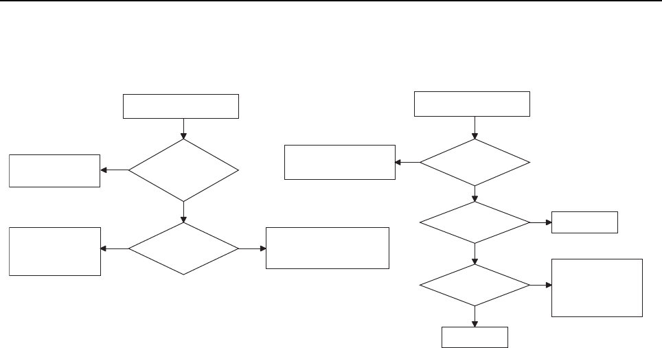
Troubleshooting Flow Chart for Tx VCO (Sheet 1 of 2) 2-7
4.1 Troubleshooting Flow Chart for Tx VCO (Sheet 2 of 2)
DC Voltage
at R0311
between 0.6
and 4.5 VDC?
Check Synthesizer
Troubleshooting
Flow Chart
Check Synthesizer
Troubleshooting
Flow Chart
Yes
No
Tx VCO 1 or
VCO 2
selected?
Check components
between C0353 and
C0346 for open or
short
VCO 1 VCO 2
-
Tx VCO locked but no
high-port modulation
~2.1 VDC at
VCO side of
C0360?
Check R0321, R0320,
R0319, and CR0300
for open or short
Modulation at
CR0300?
No
Yes
Replace C0310
Yes
Modulation at
C0361?
No
Replace C0360
Yes
Check C0361 and
C0334 for short and
then check
Synthesizer
Troubleshooting
Flow Chart
Check C0361 and
C0334 for a short and
then check
Synthesizer
Troubleshooting
Flow Chart
No
Tx VCO not locked
at correct frequency
Check C0323, C0325,
and C0329 and all
components between
C0326 and C0314 for
shorts or opens
Check C0351, C0352, and C0359
and all components between
C0353 and C0346 for
shorts or opens
Check R0321, R0320, R0319,
and CR0300 for
shorts or opens

2-8 Troubleshooting Flow Chart for Rx VCO (Sheet 1 of 2)
5.0 Troubleshooting Flow Chart for Rx VCO (Sheet 1 of 2)
2.556 V at C0362 &
C0363
Check Synthesizer
Troubleshooting
Flow Chart
Check Synthesizer
Troubleshooting
Flow Chart
Radio is not
programmed for
Receive Mode or
U0100 not functional
~0 VDC at
C0258?
2.556 VDC at
C0236?
Vbe
= 0.7 VDC
for Q0201?
Yes
Yes
No
No
No
VCO 2
Check biasing
components and
then replace Q0202 if
needed
Check biasing
components and
then replace Q0202 if
needed
Vbe
= 0.7 V
for Q0202?
Yes
Yes
No
No
No
No Rx VCO signal at C0218
Visual check
of board
OK? Correct problem
Correct problem
Radio did not boot up
properly or check
9V3 Regulator
Radio did not boot up
properly or check
9V3 Regulator
9 VDC at E0201?
Check biasing
components and
then replace Q0200 if
needed
Check biasing
components and
then replace Q0200 if
needed
2.556 V at C0362 &
C0363
~0 VDC at
C0248?
2.556 VDC at
C0200?
Vbe= 0.7 VDC
for Q0200?
No
Yes
Yes
No
No
No
VCO 1
Check Synthesizer
Troubleshooting
Flowchart
Check Synthesizer
Troubleshooting
Flowchart
Radio is not
programmed for
Receive Mode or
U0100 not functional
Radio is not
programmed for VCO 1
Receive Mode or
U0100 not functional
Yes RF signal
present at
R0219?
Check CR205 - CR208
and L0218, L0215,
C0243, C0245, C0250,
and C0246 for short or
open
Yes
Yes
Check components between
R0219 and L0205
for shorts or opens
Check biasing components
and then replace Q0201
if needed
Yes
Radio programmed for
Rx VCO 1 or 2?
Check CR0201 - CR0204 and
L0210, L0207, C0220,
C0213, C0208, and C0214
for shorts or opens
Radio is not programmed
for VCO 2 Receive Mode
or U0100 not functional
Check CR0205 – CR0208 and
L0218, L0215, C0243,
C0245, C0250, and C0246
for shorts or opens

Troubleshooting Flow Chart for Rx VCO (Sheet 1 of 2) 2-9
5.1 Troubleshooting Flow Chart for Rx VCO (Sheet 2 of 2)
Rx VCO not locked
Rx VCO not locked
at correct frequency
DC Voltage
at R0211
between 0.6
and 4.5 VDC?
Check Synthesizer
Troubleshooting
Check Synthesizer
Troubleshooting
Flow Chart
No
Yes
Rx VCO 1 or
VCO 2
selected?
Check components
between C0253 and
C0246 for open or
short
VCO 1 VCO 2
Check C0223, C0225, and C0229
and all components between
C0226 and C0214 for
shorts or opens
Check C0251, C0252, and C0259
and all components between
C0253 and C0246 for
shorts or opens

2-10 Troubleshooting Flow Chart for Repeater
6.0 Troubleshooting Flow Chart for Repeater
Repeater does not
fully initialize
(Disabled LED
stays blinking)
Does Repeater
initialize properly
now?
Re-insert or replace SSI
cable
Replace Connector
Board and/or
Accessory Cable
Does Repeater
initialize properly
now?
Can it repeat?
Re-insert or Replace
30 pin Front Panel
cable
Do all LEDs flash
on power-up?
Replace Front Panel
Board
Troubleshoot Rx
Radio
Yes Yes
No
No
No
Done
Done
Yes
No
Done
Yes
Does Repeater
initialize properly
now?
Done
Troubleshoot Tx
Radio
No
Yes

3-1
Section 3
UHF1 PCB/SCHEMATICS/PARTS LISTS
1.0 Allocation of Schematics and Circuit Boards
1.1 Controller Circuits
The UHF1 circuits are contained on the Printed Circuit Board (PCB) which also contains the
Controller circuits. This Chapter shows the schematics for the UHF1 circuits only, refer to the
Controller section for details of the related Controller circuits. The PCB component layouts in this
Chapter show both the Controller and UHF1 circuit components. The UHF1 schematics and the
related PCB and parts list are shown in the tables below.
NOTE: The UHF Schematics and parts lists are the same for 8486777Z12 and 8486777Z14. Only
the Controller circuits are different between the two PCBs.
Table 3-1 UHF1 25–40W Diagrams and Parts List
PCB :
8486777Z12 Main Board Top Side
8486777Z12 Main Board Bottom Side
8486777Z14 Main Board Top Side
8486777Z14 Main Board Bottom Side
Page 3-3
Page 3-4
Page 3-5
Page 3-6
SCHEMATICS
Overall
Receiver Front-End
Receiver IF Amp
Receiver Back-End
Power Amplifier
Power Control
Synthesizer
Receiver VCO
Transmit VCO
Page 3-7
Page 3-8
Page 3-9
Page 3-10
Page 3-11
Page 3-12
Page 3-13
Page 3-14
Page 3-15
Parts List
8486777Z12 and 8486777Z14 Page 3-16

3-2 Allocation of Schematics and Circuit Boards
Table 3-2: UHF1 25-40W Diagrams and Parts List
PCB:
8486777Z15 Main Board Top Side
8486777Z15 Main Board Bottom Side
Page 3-21
Page 3-22
SCHEMATICS
Overall
Receiver Front-End
Receiver IF Amp
Receiver Back-End
Power Amplifier
Power Control
Synthesizer
Receiver VCO
Transmit VCO
Page 3-23
Page 3-24
Page 3-25
Page 3-26
Page 3-27
Page 3-28
Page 3-29
Page 3-30
Page 3-31
Parts List
8486777Z15 Page 3-32
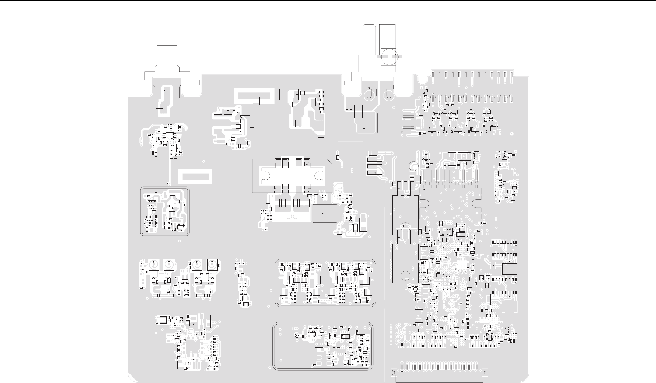
UHF1 (403–470 MHz) 25–40W PCB/Schematics/Parts List 3-3
2.0 UHF1 (403–470 MHz) 25–40W PCB/Schematics/Parts List
2.9V_MAKO_V6
3.6V_MAKO_
SW1
C0100
C0102
C0103
C0104
C0105
C0109
C0110
C0111
C0113
C0117
C0118
C0120
C0121
C0122
C0124
C0125
C0126
C0127
C0128
C0129
C0130
C0132
C0133
C0140
C0141
C0142
C0143
C0144
C0145
C0146
C0171
C0175
C0177
C0178
C0180
C0195
C0196
C0200
C0201
C0204
C0205
C0206
C0208
C0213
C0214
C0215
C0220
C0223
C0225
C0226
C0229
C0236
C0237
C0240
C0241
C0242
C0243
C0245
C0246
C0247
C0250
C0251
C0252
C0253
C0259
C0300
C0301
C0304
C0305
C0306
C0308
C0310
C0313 C0314
C0315
C0320
C0323
C0325
C0326
C0329
C0336
C0337
C0340 C0341
C0342
C0343
C0344
C0345
C0346
C0347
C0350
C0351
C0352
C0353
C0359
C0404
C0405
C0406 C0407 C0408 C0409
C0410
C0411
C0414
C0415
C0416
C0417
C0418
C0419
C0420
C0421
C0423
C0424
C0425
C0426
C0427
C0428
C0429
C0430
C0431
C0432
C0433
C0434
C0437
C0438
C0439
C0440
C0442
C0450
C0451
C0502
C0504
C0509
C0510
C0515
C0516
C0605
C0611
C0615
C0617
C0619
C0620
C0621
C0622
C0623
C0625
C0626
C0627
C0629
C0630
C0631
C0633
C0638
C0642
C0643
C0644
C0645
C0646
C0650
C0700
C0701
C0702
C0703
C0704
C0705
C0706
C0707
C0708
C0709
C0710
C0711
C0712
C0713
C0714
C0718
C0748
C0776
C0777
C0781
C0782
C0788
C0796
C0797
C0798
C0799
C0802
C0804
C0805
C0900
C0901
C0904
C0906
C0907
C0908
C0909
C0910
C0914
C0915
C0918
C0921
C0922
C0926
C0929
C0931
C0934
C0935
C0936
C0937
C0939
C0947
C0948
C0949
C0950
C0951
C1000
C1001
C1002
C1003
C1004
C1005
C1006
C1007
C1008
C1009
C1010
C1011
C1012
C1013
C1014
C1015 C1016
C1017
C1018
C1019
C1030
C1031
C1032
C1033
C1034
C1036
C1037
C2000
C2001
C2002
C2003
C2004
C2005
C2006
C2007
C2500
C3000
C3002
C3005
C3006
C3007
C3008
C3009
C3010
C3015
C3018
C3019
C3040 C3046
C3202
C3203
C3207
C3208
C3209
C3210
C3211
C3212
C3213
C3216
C3219
C3220
C3225
C3226
C3229
C3234
C3238
C3239
C3240
C3247
C3248
C3249
C3254
C3262
C3273
C3276
C3277
C3278
C3280
C3283
C3501
C3504 C3505
C3506
C3511
C3513
C3514
C3515
C3516
C3518
C3520
C3521
C3523
C3524
C3528
C3529
C3530
C3531
C3538 C3545
C4000
C4001
C4002
C4003
C4004
C4005
C4006
C4013
C4014
C4015
C4016
C4017
C4018
C4019
C4020
C4021
C4022
C4023
C4024
C4025
C4026
C4027
C4028
C4029
C4030
C4031
C4032
C4033
C4034
C4035
C4040 C4041 C4042 C4043 C4044
C4045
C4046C4047
C4048
C4075
C4076
C6406
C6407
C6408
C6416
C6417
C6418
C6419
C6420
C6421
C6422
C6423
C6426
C6427
C6428
C6429
C6430
C6431
C6433
C6439
C6440
C6445
C6450
C6451
CLKOUT
CR0201
CR0202
CR0203
CR0204
CR0205
CR0206
CR0207
CR0208
CR0301
CR0302
CR0303
CR0304
CR0305
CR0306
CR0307
CR0308
D0400
D0401
D0402
D0403
D0404
D0601
D0900
D0901
D0902
D0903
D4001
DOUTA
DOUTB
E0600
E0601
E0602
E0604
E0605
E0606
E0607
E0608
E0700
E0701
E0703
E3000
E3202
E3205
E3500
E3501
E3502 E3503
E4000
E4001
E4004
E4005
E6401
E6402
E6407
23
4
5
6
FL0500
FS
3
2
J0700
J3000
25
26
2
J4000
30
J4001
L0100
L0202
L0203
L0207
L0209
L0210
L0212
L0213
L0214
L0215
L0217
L0218
L0219
L0302
L0303
L0307
L0309
L0310
L0312
L0313
L0314
L0315
L0317
L0318
L0319
L0401
L0402 L0403 L0404L0405
L0407
L0411
L0413
L0504
L0506
L0604
L0608
L0714
L0722
L0900
L0901
L0902
L3200
L3202
1
M0700
MAKO_GATED_32KHz
PCPD PE
Q0100
Q0102
Q0106
Q0200
Q0201
Q0300
Q0301
4
32
Q0402
4
32
Q0405
Q0501
Q0701
10
2
3
4
7
86
9
5
Q0702
4
321
Q0704
Q0706
Q0707
Q0708
Q0709
Q0901
16
1
8
9
Q3200
4
5
8
Q3201
16
1
8
9
Q3202
23
4
Q3203
23
4
Q3204
2
3
Q3500
Q3501
2
3
Q4000
2
3
Q4002
2
3
Q4004
2
3
Q4005
2
3
Q4006
2
3
Q4008
2
3
Q4010
2
3
Q4011
Q4013
R0100
R0101
R0102
R0105
R0106
R0107
R0108
R0109
R0110
R0111
R0114
R0116
R0117
R0118
R0119 R0123
R0144
R0146
R0147
R0148 R0155
R0156
R0157
R0158
R0159
R0161
R0201
R0204
R0205
R0211
R0216
R0224
R0225
R0226
R0229
R0301
R0304
R0305
R0311
R0316
R0324
R0325
R0326
R0329
R0404
R0405
R0406
R0407
R0409
R0410 R0412
R0417
R0418 R0419
R0420
R0421
R0422 R0423
R0424
R0425
R0432
R0503
R0510
R0606
R0607
R0608
R0609
R0610 R0611
R0612
R0613
R0614
R0615
R0617
R0618
R0619
R0621
R0622
R0623
R0627
R0700
R0702
R0703
R0706
R0713
R0729
R0730
R0732
R0734
R0735
R0738
R0740
R0741
R0742
R0744
R0745
R0748
R0749
R0750
R0751
R0752
R0753
R0756
R0757
R0761
R0762
R0763
R0764
R0768
R0771
R0773
R0774
R0776
R0778
R0900
R0901
R0902
R0903
R0906
R0907
R0909
R0911
R0912
R0914
R0915
R0916
R0917
R0920
R0923
R0924
R0925
R0926
R0927
R0928
R0929
R0930
R0936R0937
R0940
R0950
R1000
R1001
R1002
R1005
R1006
R1014
R1017
R1019
R1020
R1021
R1025
R1026
R1027 R1028
R1034
R1035
R1036
R1041
R1045
R1066
R1067
R1071
R1072
R2000
R2004
R2005
R2006
R2007
R2008
R2009 R2010
R2011
R2012
R2013
R2529
R3002
R3003
R3004
R3009
R3010
R3032
R3033
R3035
R3036
R3042
R3056
R3203
R3205
R3206
R3217
R3218
R3224
R3225
R3233
R3500
R3501
R3503
R3504
R3505
R3507
R3508
R3509
R3514
R3515
R3516
R3520
R3526
R3532
R3535
R3537
R3538
R3547
R3550
R3560
R3571
R3576
R3580
R3583
R3587
R3588
R3594
R3595
R3596
R4000
R4001
R4002
R4003
R4004
R4005
R4006
R4009
R4010
R4011
R4012
R4034
R4040 R4041 R4042 R4043 R4044
R4045
R4046 R4047
R4048
R4050
R4051
R4061
R4063
R4064
R4065
R4066
R4067
R4068
R4069
R4070
R4071
R4095
R4106
R6402
R6403
R6443
R6444
R6445
R6446
R6449
R6450
R6454
R6455
R6456
R6458
R6459
R6460
R6461
R6465
R6466
R6467
1
RT0908
RT3500
SH0100
SH0301
SH0900
SP0700
SP0701
SP0702
SP0703
SP0704
SP0705
SP0706
SP0707
TP0601
TP1000
TP4000
TP_MAKO_DCLK
TP_MAKO_FSYNC
TP_
MAKO_
RX
TP_MAKO_TX
TP_POR
TP_SDRAM_BA0
TP_SDRAM_BA1
TP_SDRAM_CLK
TP_SDRAM_CS
TP0602
1
37
25
13
U0600
U0901
4
58
U0940
U0941
43
6
U1006
1
6
5
U3001
U3002
3
2
1
U3005
3
2
1
U3006
3
2
1
U3040
9
U3500
U6402
U6407
USB1_DAT
USB1_SEO
USB1_TXEN
VBUS1_CMD
VBUS2_CMD
VR0700
VR3202
VR3204
VR3206
VR3503
VR4000 VR4001 VR4002
VR4003
VR4004
VR4005
VR4007
43
2
Y0100
UHF1 (403–470 MHz) 25–40W 8486777Z12 Top Side
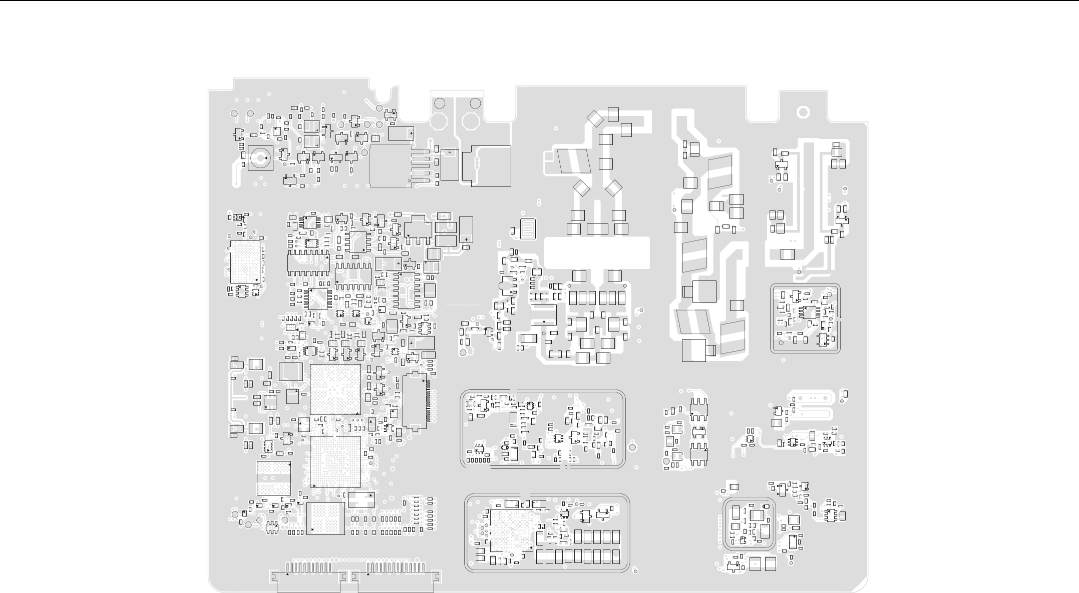
3-4 UHF1 (403–470 MHz) 25–40W PCB/Schematics/Parts List
1.5V_RTC_TEST
2.8V_RF_TEST
ANT_C
APM_1_WIRE
C0101
C0106
C0107
C0108
C0112
C0114
C0115
C0119
C0123
C0131
C0134
C0135
C0136
C0137
C0138
C0147
C0148
C0149
C0150
C0151
C0156
C0157
C0158
C0159
C0160
C0161
C0162
C0163
C0164
C0165
C0166
C0179
C0191
C0192 C0193
C0194
C0202
C0203
C0207
C0209
C0211
C0217
C0218
C0219
C0221
C0222
C0224
C0230
C0231
C0233
C0235
C0238
C0239
C0248
C0249
C0257
C0258
C0302
C0303
C0307
C0309
C0311
C0316
C0317
C0318
C0319
C0321
C0322
C0324
C0327
C0328
C0331
C0334
C0348
C0349
C0357
C0358
C0360
C0361
C0362
C0363
C0400
C0401
C0402
C0403
C0412
C0413
C0422
C0436
C0441
C0443
C0444
C0445
C0446
C0447
C0448
C0449
C0452
C0453
C0454
C0455
C0456
C0503
C0506
C0507
C0512
C0513
C0514
C0601
C0602
C0603
C0604
C0607
C0610
C0612
C0613
C0614
C0616
C0618
C0628
C0632
C0634
C0635
C0636
C0637
C0640
C0641
C0647
C0648
C0649
C0651
C0716
C0717
C0719
C0720
C0721
C0723
C0726
C0727
C0728
C0729 C0730
C0731
C0732
C0733
C0734
C0735
C0737
C0738
C0739
C0740
C0741
C0742
C0743
C0744
C0745
C0746
C0747
C0753
C0754
C0755
C0756
C0760
C0761
C0764
C0765
C0766
C0767
C0770
C0771
C0772
C0775
C0778
C0779
C0780
C0786
C0787
C0789
C0791
C0792
C0793
C0794
C0795
C0800
C0801
C0803
C0808
C0809
C0810
C0811 C0812
C0813
C0814
C0815
C0817
C0818 C0819
C0902
C0903
C0911
C0912
C0913
C0916
C0917
C0919
C0920
C0923
C0925
C0927
C0928
C0940
C0941 C0942
C0943
C0944
C0945
C0953
C1035
C1044
C2501
C3011
C3012
C3013
C3014
C3016
C3017
C3020
C3021
C3030
C3031
C3032
C3041
C3042
C3043
C3044
C3045
C3200
C3201
C3204
C3205
C3206
C3214
C3215
C3217
C3218
C3221
C3222
C3227
C3228
C3231
C3232
C3233
C3237
C3243
C3252
C3257
C3260
C3261
C3265
C3266
C3269
C3270
C3272
C3274
C3275
C3279
C3281
C3282
C3500
C3502
C3503
C3507
C3508
C3509
C3510
C3512
1C3517
C3519
C3522
C3525
C3526
C3527
C3532
C3533
C3534
C3535
1
C3536
C3539 C3540
C3541
C3542
C3543
C3544
C4007
C4010
C4011
C4012
C4049
C4051
C4053
C4055
C4058
C4059
C4060
C4061
C4062
C4063
C4064
C4065
C4066
C4067 C4068
C4069
C4070
C4071
C4072
C4073
C4074
C4084
C4085
C4086
C4087
C4088
C4089
C4090
C6412
C6413
C6414
C6432
C6434
C6435
C6436
C6437
C6438
C6443
C6444
C6446
C6449
C6452
CLK_ACQ_TEST
CR0300
CR0400
D0405
D0500
D0600
D0700
D0702
D0904
D0905
D3030
D3040
D3200
D4000
E0201
E0301
E0302
E0400
E0401
E0403
E0500
E0603
E0609
E0610
E2500
E3201
E3203
E3206
E3208
E4002
E4003
E6400
EMERGENCY
EXT_MIC
EXT_PTT
3
4
2
5
FL6401
I2C_CLK
I2C_DATA
IF_TEST
IGNITION_SENSE
INT_MIC
22
20
1
21
J2500
11
J4002
14
J4003
J6400
L0200
L0204
L0205
L0206
L0211
L0221
L0300
L0304
L0305
L0306
L0311
L0406
L0408
L0409
L0410
L0412
L0503
L0602
L0603
L0605
L0700
L0702
L0705
L0706
L0707
L0708
L0710
L0715
L0718
L0719
L0720
L0721
L0903
L0904
L3201
L6402
L6403
MAKO_CE
MAKO_V8_5V
MAKO_V9_3V
MMP_1_WIRE
OPT_SSI_SYNC
Q0107
2
3
Q0108
Q0202
Q0302
Q0400
Q0401
Q0403
Q0500
Q0600
Q0601
1
3
Q0703
Q0705
Q0902
Q3030
4
3
2
1Q3032
Q3040
2
3
Q3041
2
3
Q3205
Q3206
4
5
8
Q3207
2
3
Q3208
Q3502
Q3503
Q3504
Q3505
2
3
Q4001
2
3
Q4003
2
3
Q4007
2
3
Q4009
2
3
Q4012
Q4014
2
3
Q4015
Q6401
Q6402
R0103
R0104
R0113
R0115
R0120
R0122
R0125
R0126
R0127
R0128 R0131
R0134
R0139
R0140
R0160
R0202
R0203
R0206
R0207
R0208
R0210
R0212
R0213
R0218
R0219
R0220
R0221
R0230
R0302
R0303
R0306
R0307
R0308
R0310
R0312
R0319
R0320
R0321
R0327
R0331
R0332
R0333
R0334
R0337
R0400
R0401
R0402
R0403
R0413
R0414
R0415
R0416
R0426
R0427
R0428
R0429
R0430
R0431
R0500
R0501
R0502
R0508
R0509
R0511
R0512
R0601
R0602 R0603
R0604
R0605
R0616
R0620
R0624
R0625
R0626
R0711
R0714
R0715
R0718
R0719
R0720
R0722
R0727 R0728
R0739
R0747
R0754
R0755
R0759
R0760
R0765
R0766
R0767
R0769
R0770
R0772
R0775
R0777
R0910
R0913
R0918
R0919
R0921
R0922
R0938
R0941
R0942
R0943
R0944
R0946
R0947
R0951
R0954
R0955
R0960
R0970
R0971
R0972
R0973
R0974
R0975
R0976
R0977 R0978
R0979
R1044
R1046
R1047
R1048
R1054
R1060
R1070
R2500
R2501
R2502
R2504
R2506 R2507
R2508
R2509
R2510
R2511
R2512
R2513 R2514
R2515
R2516
R2517
R2518
R2519
R2520
R2521
R2522
R2523
R2524
R2525 R2526
R2527
R2528
R3005 R3006
R3007
R3008
R3030
R3034
R3037
R3038
R3039
R3040
R3041
R3043
R3044
R3045
R3046
R3047
R3048
R3050
R3051
R3052
R3053
R3054
R3055
R3057
R3200
R3201
R3204
R3207
R3208
R3209
R3210
R3215
R3216
R3219
R3220
R3222 R3223
R3226
R3227
R3228
R3236
R3237
R3238
R3239
R3240
R3241
R3243
R3245
R3246 R3247
R3248
R3502
R3506
R3510
R3511
R3512
R3513
R3521
R3523
R3524
R3525
R3528
R3529
R3530
R3533
R3534
R3536
R3539
R3540
R3541
R3542
R3544
R3545
R3546
R3548
R3549
R3558
R3559
R3561
R3562
R3563
R3569
R3572
R3573
R3574
R3575
R3577
R3578
R3579
R3581
R3582
R3584 R3585
R3586
R3591
R3592
R3593
R4023
R4030
R4031
R4032
R4033
R4035
R4049
R4054
R4055
R4074
R4076
R4078
R4079
R4080
R4081
R4082
R4083
R4084
R4085
R4086
R4088
R4089
R4090
R4093
R4094
R4096
R4097
R4098
R4099
R4100
R4101
R4103
R4105
R6401
R6404
R6405
R6407
R6408
R6409
R6410
R6411
R6416
R6417
R6418
R6419
R6420
R6430
R6432
R6433
R6434
R6435
R6436
R6437
R6438
R6439 R6440 R6457
R6464
R6468
R6469
R6470
RF_ATTN_2
ROUT_TEST
1
RT0953
S0700
SH0101
SH0300
SH0500
SH0901
SPI_CLK_1
SPI_CLK_TEST
SPI_MISO_1
SPI_MOSI_1
6
4
3
T0400
64
3
T0401
TP501
TP502
TP503
TP504
TP0301
TP0400
TP0401
TP0600
TP0702
TP0703
TP0704
TP0705
TP0707
TP0708
TP0709
TP0710
TP0711
TP0713
TP0903
TP0904
TP0907
TP0909
TP0910
TP0911
TP0913
TP_ADAPT_SW
TP_FLASH_CLK
TP_TEST1
TP_TEST2
TP_VCTRL
TX_RAMP
TX_RAMP_DAC
L11A11
L1
U0100
4
3
5
U0101
U0201
U0303
U0304
U0601
U0700
U0900
U0942
A21 AA21
AA1
U1000
G1A1
A8 G8
U2000
J9 A9
J1 A1
U2001
1
6
5
U3003
U3004
14
58
U3030
P1
A1
A14 P14
U3200
1
64
3
U3201
C1
C3A3
U3202
4
3
5
U3203
10
6
5
U3501
7
8
14
U3502
85
4
U3503
U3504
7
814
U3505
85
4
U3508
16
1
8
9
U4000
14
7
8
U4001
U4004
U4005
U4006
U4007
U4008
P10
A10
P1
A1
U6401
U6404
C1
C3A3
U6405
U6406
U6408
USB1_DM
USB1_DP
USB2_DM
USB2_DP
VBAT
VBAT_GROUND
VBUS1
VBUS2
VR3000
VR3040
VR3200
VR3201
VR3203
VR3205
VR3207
VR3208
VR3502
VR3504
VR4006
VR4008
VR6400
2
34
Y1000
4
3
2
Y3200
Y3201
UHF1 (403–470 MHz) 25–40W 8486777Z12 Bottom Side
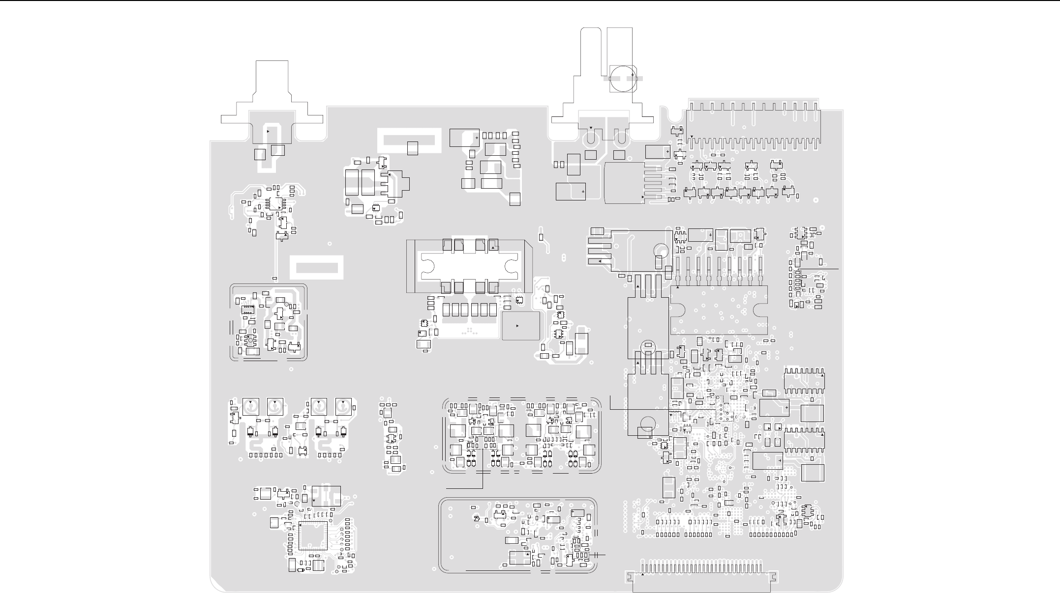
UHF1 (403–470 MHz) 25–40W PCB/Schematics/Parts List 3-5
3
2
J0700
L0722
R0713
C0900
C0901 C0906
C0907
C0908
C0909
C0910
C0915
C0939
D0900
Q0901
R0900
R0901
R0902
R0903
R0906
R0907
R0909
R0911
R0912
R0914
R0915
R0916
R0920
R0923
R0930
U0901
C0929
C0914
C0918
C0921
C0922
C0926
C0931
C0934
C0935
C0936
C0937
C0947
C0948
C0949
C0950
C0951
D0901
D0902
D0903
L0901
L0902
R0917
R0924
R0925
R0926
R0927
R0928
R0929
R0936
R0937
R0940
R0950
SH0900
4
58
U0940
U0941
C0404
C0406
C0410
C0411
C0421
D0400
D0401
D0402
L0402
L0405
R0407
R0410
R0432
C0423
C0424
C0425
C0426
C0427
C0433
C0434
L0413
Q0402
C0405
C0407 C0408 C0409
C0414
C0415
C0416
C0417
C0418
C0419
C0420
C0428
C0429
C0430
C0431
C0432
D0403
D0404
L0403 L0404
R0404
R0405
R0406
R0409
R0412
L0401
4
32
C0509
C0510
C0605
C0611
C0615
C0617
C0619
C0620
C0621
C0622
C0623
C0625
C0626
C0627
C0629
C0630
C0631
C0633
C0638
C0642
C0643
C0644
C0645
C0646
C0650
CLKOUT
D0601
DOUTA
DOUTB
E0600
E0601
E0602
E0604
E0605 E0606
E0607 E0608
23
4
5
6
FL0500
FS
L0504
L0604
L0608
PC
PD
PE
R0503
R0510
R0606
R0607
R0608
R0609
R0610 R0611
R0612
R0613
R0614
R0615
R0617
R0618
R0619
R0621
R0623
R0627
TP0601
TP0602
1
37
25
13
U0600
C0502
C0504
C0515
C0516
L0506
Q0501
R0622
C0117
C0118
C0122
C0171
C0195
R0101
R0102
R0105
R0106
R0107 R0108
R0144
C0100
C0102
C0109
C0113
C0120
C0121
C0130
C0132
C0140
C0175
C0178
L0100
Q0100
R0109
R0110
R0146
R0147
R0155
R0156
R0157
C0103
C0104
C0105
C0110
C0111
C0124
C0125
C0126
C0127
C0128
C0129
C0133
C0141
C0142 C0143
C0144
C0145
C0146
C0177
C0180
C0196
Q0102
Q0106
R0100
R0111
R0114
R0116
R0117
R0118
R0119
R0123
R0148
R0158
R0159
R0161
SH0100
43
2
Y0100
30
J4001
R3042
3
2
1
9
U3500
U3005
C1019
C2000
C2001
C2002
C2003
C2500
C4000
C4001
C4002
C4003
C4004
C4005
C4006
C4013
C4016
C4017
C4018
C4019
C4020
C4021
C4022
C4023
C4024
C4025
C4026
C4027
C4028
C4029
C4030
C4031
C4032
C4033
E4000
R1002
R1005
R1014
R1041
R1071
R2000
R2004
R2012
R2529
R3580
R3583
R4000
R4001
R4002
R4003
R4004
R4005
R4006
R4034
R4061
R4063
R4064
R4065
R4066
R4067
R4068
R4069
R4070
R4071
C2004
C2006
C2007
C3209
C3212
C4014
C4015
C4034
C4035
C4076
D4001
E4001
E4004
L3202
R2005
R2006
R2007
R2008
R2009 R2010
R2011
R2013
R4009
R4010
R4011
R4012
R4095
R4106
TP4000
TP_SDRAM_BA0
TP_SDRAM_BA1
TP_SDRAM_CS
VR4007
C1003
C1005
C1006
C1007
C1008
C1011
C1013
C1014
C1016
C1017
C1018
C1036
C1037
C2005
R1000
R1006
R1019
R1066
R1067
TP1000
TP_SDRAM_CLK
C1000
C1001
C1004
C1010
C1012
C1015
C1030
C3514
R1001
R1025
R1034
R1035
R1036
R1045
TP_POR
C3515
C3524
E3502
Q3501
R3526
R3532
R3547
VR3503
C3040
C3207
C3210
C3211
C3229
C3234
C3247
C3248
C3249
C3254
C3262
C3516
C3518
C3520
C3521
C3530
C3538
E3205
E3503
R3205
R3206
R3217
R3218
R3514
R3515
R3535R3537
R3538 R3571
R3576
R3588
U3040
VR3204
VR3206
C1002
C1031
C1032
C1033
C1034
C3208
C3216
C3273
C3276
C3277
C3280
C3283
C3529
C3531
L3200
4
5
8
Q3201
16
1
8
9
Q3202
23
4
Q3203
23
4
Q3204
R1017
R1026
R1027
R1028
R3203
R3224
R3225
R3560
R3596
RT3500
43
6
U1006
VBUS1_CMD
VBUS2_CMD
C1009
C3213
R1021
C3202
C3203
16
1
8
9
Q3200
2.9V_MAKO_V6
3.6V_
MAKO_
SW1
C3219
C3220
C3225
C3226
C3238
C3239
C3240
C3278
C3511
C3513
C3523
C3528
C3545
C6451
E3202
R1020
R3233
R3500
R3501
R3503
R3504
R3505
R3507
R3508
R3509
R3550
R3587
R3594
R3595
R6467
VR3202
MAKO_GATED_32KHz
TP_MAKO_DCLK
TP_MAKO_FSYNC
TP_MAKO_RX
TP_MAKO_TX
USB1_DAT
USB1_SEO
USB1_TXEN
C0437
C0438
C0439
C0440
C0442
C0451
L0407
L0411
4
32
Q0405
R0417
R0418 R0419
R0420
R0421
R0422
R0423
R0424
R0425
R0433
C0748
C0776
C0777
C0796
C0797
C0798
C0799
L0714
10
4
321
Q0704
Q0706
R0729
R0735
R0738
R0745
R0748
R0749
VR0700
2
3
4
Q0702
SP0702
SP0703
SP0705
SP0707
R0762
R0763
R0764
R0768
R0771
R0773
1
M0700
C0718
C0788
C0802
E0703
Q0701
Q0707
R0700
R0702
R0703
R0706
R0734 R0744
R0750
R0751
R0752
R0761
R0778
C0781
C0782
C0804
C0805
C0904
L0900
Q0708
Q0709
R0730
R0732
R0740
R0741
R0753
R0756
R0757
1
RT0908
SP0700SP0701
7
865
SP0704
SP0706
C0714
9
R0774
C0700
C0701
C0702
C0703
C0704
C0705
C0706
C0707
C0708
C0709
C0710
C0711
C0712
C0713
E0700
E0701
R0742
R0776
C3000
C3002
C3015
E3000
SP3000
SP3001
1
6
5
U3001
C3006
R3032
3
2
1
R3033
R3056
3
2
1
U3006
R3035
R3036
C3005
C3007
C3019
C3046
C4040 C4041 C4042 C4043 C4044
C4045
C4046 C4047
C4048
C4075
E4005
25
26
2
J4000
2
3
Q4000
23
Q4002
23
Q4004
2
3
Q4005
2
3
Q4006
23
Q4008
23
Q4010
2
3
Q4011
Q4013
R3002
R3003
R3004
R4040 R4041 R4042 R4043 R4044
R4045
R4046 R4047
R4048
R4050
R4051
VR4000
VR4001 VR4002
VR4003
VR4004
VR4005
C6406
C6407
C6408
C6416
C6417
C6418
C6419
C6420
C6421
C6422
C6423
C6426
C6427
C6428
C6429
C6430
C6431
C6433
C6439
C6440
C6445
C6450
E6401
E6402
E6407
R6402
R6403
R6443
R6444 R6445
R6446
R6449
R6450
R6454
R6455
R6456
R6458
R6459
R6460
R6461 R6465
R6466
U6402
U6407
C3008
C3009
C3010
C3501
C3504 C3505
C3506
E3500
E3501
23
Q3500
R3009
R3010
R3516
R3520
U3002
C3018
J3000
C0200
C0201
C0204
C0205
C0206
C0215
C0223
C0236
C0237
C0247
L0202
L0203
L0212
L0213
L0219
Q0201
R0201
R0204
R0205
R0216
R0229
C0208
C0213
C0214
C0220
C0225
C0226
C0229
C0243
C0245 C0246
C0251
C0252C0259
CR0201
CR0202
CR0203
L0207
L0209
Q0200
CR0204
L0210
CR0205
CR0206
CR0207
CR0208
C0250
C0253
C0313
C0320
C0326
CR0301
CR0303
CR0304
CR0307
CR0308
L0215
L0217
L0218
L0309
L0310
R0211
R0311
SH0301
C0308
C0310
C0314
C0323
C0325
C0329
C0343
C0344
C0345
C0346
C0350
C0351
C0352
C0353
C0359
CR0302 CR0305
CR0306
L0315
L0317
L0318
L0319
C0240
C0241
C0242
C0300
C0301
C0304
C0305
C0306
C0315
C0336
C0337
C0340 C0341
C0342
C0347
L0214
L0302
L0303
L0307 L0312
L0313
L0314
Q0300
Q0301
R0224
R0225
R0226
R0301
R0304
R0305
R0316
R0324
R0325 R0326
R0329
UHF1 (403–470 MHz) 25–40W 8486777Z14 Top Side
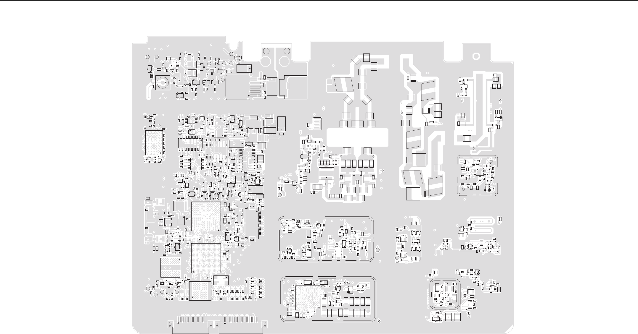
3-6 UHF1 (403–470 MHz) 25–40W PCB/Schematics/Parts List
C3012
C3013
C3014
R3005 R3006
VR3000
ANT_C
APM_1_WIRE
C3045
C3533
C3534
C4063
C4064
C4065
C4066
C4067 C4068
C4069
C4070
C6412
C6413
C6435
C6436
C6437
C6438
D4000
E6400
EMERGENCY
EXT_PTT
IGNITION_SENSE
J6400
L6402
2
3
Q4001
2
3
Q4003
23
Q4007
23
Q4009
2
3
Q4012
Q4014
2
3
Q4015
Q6401
R3529
R3540
R3545 R3548
R4030
R4031
R4032
R4033
R4035
R4049
R4054
R4055
R4088
R4089
R4098
R6407
R6430
R6432
R6433
R6434
R6435
R6436
R6437
1
6
5
U3003
C1
C3A3
U6405
USB2_DM
USB2_DP
VBAT
VBAT_GROUND
VBUS2
VR3504
VR4006
VR6400
C0719
C0720
C0721
C0726
C0727
C0737
C0741
C0746
C0747
C0811 C0812
L0700
R0719
S0700
R0775
C3020
C3021
R3038
R3050
R3055
C3509
4
3
2
1Q3032
R3037
C6414
3
4
2
5
FL6401
R6409
1.5V_RTC_TEST
2.8V_RF_TEST
C6401
C6432
C6443
C6444
C6446
CLK_ACQ_TEST
IF_TEST
L6403
Q6402
R3573
R3574
R4023
R4100
R4101
R4103
R6404
R6405
R6410
R6420
R6438
R6439
R6440
R6457
ROUT_TEST
SPI_CLK_TEST
P10
A10
P1
A1
U6401
U6406
R6411
C3508
1
C3536
R3569
R3575
C2501
C3016
C3017
C3030
C3032
C3041
C3042
C3500
C3502
C3503
C3507
C3539 C3540
D3030
D3040
E2500
I2C_
CLK
I2C_DATA
Q3030
23
Q3041
R3007
R3030
R3034
R3039
R3040
R3041
R3045
R3046
R3047
R3048
R3051
R3053
R3054 R3057
R3502
R3506
R3511
R3513
R3521
R3524
R3558
R3559
R3578
14
58
U3030
10
6
5
U3501
8
5
4
U3503
7
814
U3505
VR3040
VR3502
C3031 C3519
C4071
C4072
C4073
C4074
C4084
C4085
R3052
R4086 7
8
14
U3502
16
1
8
9
U4000
14
8
U4001
C3257
C3541
C3542
C6434
C6449
C6452
E4002
R1047
R3510
R3512
R3584 R3585
R3586
R3591
R3592
R3593
R6401
R6416
R6417
R6418
R6419
R6464
R6468
U3504
8
5
4
U3508
7
U6404
U6408
R6469
R6470
C3200
C3279
L3201
R3200
R3215
R3241
C3221
C3222
C3227
C3228
C3231
C3232
C3243
C3252
C3525
C3527
C3532
C3535
INT_
MIC
Q3503
Q3504
Q3505
R3530
R3533
R3534
R3536
R3539
R3541
R3542
R3544
R3546
R3551
R3552
R3553
R3554
R3555
R3556 R4079
C3011
C3043
C3274
C3275
C3510
C3512
C3517
C3522
C3526
Q3502
R3008
R3228
R3523
R3525
R3528
R3549
U3004
VR3200
C3201
C3206
C3214
C3215
C3265
C3266
C3269
C3270
C3281
C3289
C3290
C3291
4
5
8
Q3207
2
3
Q3208
Q3209
Q3210
R2500
R3204
R3207
R3208
R3216 R3227
R3237
R3238
R3239
R3240
R3243
R3245
R3246
R3247
R3250
R3252
R3253
TX_RAMP
J1 A1
U2001
P1
A1
A14 P14
U3200
1
64
3
U3201
4
3
2Y3200
C1035
C1044
C3204
C3205
C3217
C3218
C3272 C3282
E4003
22
20
21
J2500
MAKO_CE
OPT_SSI_SYNC
R1044
R1048
R1054
R1060
R1070
R2502
R2515
R2519
R2520
R3219
R3220
R3222 R3223
R3236
R3249
R3572
R3577
R3579
R3581
R3582
R4090
RF_ATTN_2
SPI_CLK_1
SPI_MISO_1
SPI_MOSI_1
A21 AA21
AA1
U1000
C1
C3
A3
U3202
4
3
5
U3203
Y3201
C3044
C3233
C3237
C3260
C3261
D3200
E3201
E3203
E3206E3208
EXT_MIC
MAKO_V8_5V
MAKO_V9_3V
Q3040
23
Q3205
Q3206
R3043
R3044
R3209
R3210
R3226
R3248
TX_RAMP_DAC
VR3201
VR3203
VR3205
VR3207
VR3208
11
J4002 14
J4003
G1A1
A8 G8
U2000
C4007
C4010
C4011
C4012
C4086
C4087
C4088
C4089
C4090
MMP_1_WIRE
R4093
R4094
R4099
R4105
J9 A9
U4004
U4005
U4006
U4007
U4008
USB1_DM
USB1_DP
VBUS1
VR4008
R4097 R4096
R1046
TP_FLASH_CLK 2
34
Y1000
C4049
C4051
C4053
C4055
C4058
C4059
C4060
C4061
C4062
C4091
C4092
C4093
C4094
E4006
R2501
R2504
R2506 R2507
R2508
R2509
R2510
R2511
R2512
R2513 R2514
R2516
R2517
R2518
R2524
R2525 R2526
R2527
R2528
R4074
R4076
R4078
R4080
R4081
R4082
R4083
R4085
U4009
U4010
TP_VCTRL
C0503
C0506
C0507 C0512
C0513
C0514
C0640
C0641
C0651
D0500
E0500E0610
L0503
Q0500
R0500
R0501
R0502
R0508 R0509
R0511
R0512
R0625
R0626
U0601
C0601
C0604
C0628
C0632
C0634
C0635
C0636
C0637
C0647
C0648
E0603
E0609
L0605
Q0601
R0616
R0620
TP0600
C0602
C0603
C0607
C0610
C0612
C0613
C0614
C0616
C0618
C0649 D0600
L0602
L0603
Q0600
R0601
R0602
R0603
R0604
R0605
R0624
SH0500
C0400
C0441
C0443
C0444
C0445
C0446
C0447
C0448
C0449
C0456
D0405
E0400
L0408
L0409
L0410
L0412
Q0400
R0403
R0426
R0427
R0431
6
4
T0400
64
3
T0401
TP0301
TP0401
C0401
C0402
C0403
C0412
C0413
C0422
C0436
C0452
C0453
C0454
C0455
CR0400
E0401
E0403
L0406
Q0401
Q0403
R0400
R0401
R0402
R0413
R0414 R0415
R0416
R0428
R0429 R0430 TP0400
C0738
C0740
L0707
L0708
C0739
C0766
C0767
C0772
L0706
C0735
C0742
C0778
C0779
C0803
C0810
D0700
D0702
L0710
L0719
TP0713
C0943
C0944
C0945
D0905
R0979
TP0903
TP0904
C0723
L0903
R0970
R0971
R0972
TP0907
C0940
C0941
C0942
D0904
L0904
R0973
R0974
R0975
R0976
R0977 R0978
TP0913
C0902
C0903
C0912
C0925
C0953
R0913
R0921 R0941
R0946
R0955
TP0910
C0911
C0913
C0916
C0917
C0919
C0920
C0923
C0927
C0928 Q0902
R0910
R0918
R0919
R0922
R0938
R0942
R0943
R0944
R0947
R0951
R0954
R0960
1
RT0953
SH0901
TP0911
U0900
U0942
C0732 C0761
TP0708
TP0711
R0765
R0766
R0767
R0769
R0770
R0772
C0716
C0717
C0728
C0733
C0734
C0743
C0770
C0771
C0775
C0780
C0786
C0787
C0789
C0791
C0792
C0793
C0794
C0795
C0800
C0801
C0809
C0814
C0815
C0817
L0702
L0705
L0715
L0718
L0720
L0721 1
3
Q0703
Q0705
R0711
R0714
R0715
R0718
R0720
R0722
R0727 R0728
R0739
R0747
R0754
R0755
R0759
R0760
R0777
TP0702
TP0703
TP0704
TP0705
TP0707
TP0709
TP0710
TP0909
U0700
C0729
C0730
C0731
C0744
C0745
C0753
C0754
C0755
C0756
C0760
C0764
C0765
C0808
C0813
C0818 C0819
1
1
3
C0311
C0319
L0305
L0311
R0308
C0302
C0303
C0309
C0316
C0317
C0318
C0321
C0322
C0324
C0327
C0328
C0331
C0334
C0348
C0349
C0357
C0358
C0360
C0361
C0362
C0363
CR0300
E0301
E0302
L0221
L0300
L0304
L0306
Q0302
R0302
R0303
R0306
R0307 R0310
R0312
R0319
R0320
R0321
R0327
R0331
R0332
R0333
R0334
R0337
SH0300
U0303
U0304
C0202
C0203
C0207
C0209
C0217
C0218
C0219
C0221
C0222
C0224
C0230
C0231
C0233
C0235
C0238
C0239
C0248
C0249
C0257
C0258
C0307
E0201
L0200
L0204
L0205
L0206
L0211
Q0202
R0202
R0203
R0206
R0207
R0208
R0210
R0212
R0213
R0218
R0219
R0220
R0221
R0230
U0201
C0211
C0156
C0157
C0158
C0161
C0163
C0164
C0165
C0192
C0194
C0159
C0160
C0162
C0191
C0193
C0101
C0131
C0134
C0135
C0136
C0137
C0138
C0148
C0149
C0150
C0151
C0166
C0179
Q0107
23
Q0108
R0103
R0104
R0113
R0115
R0120
R0122 R0125
R0127
R0128
R0131
R0134
R0139
R0140
R0160
TP501
TP502 TP503
TP504
TP_ADAPT_SW
TP_TEST1
L11
U0100
4
3
5
U0101
C0106
C0107
C0108
C0112
C0114
C0115
C0119
C0123
C0147
R0126
TP_TEST2
A11
L1
SH0101
UHF1 (403–470 MHz) 25–40W 8486777Z14 Bottom side
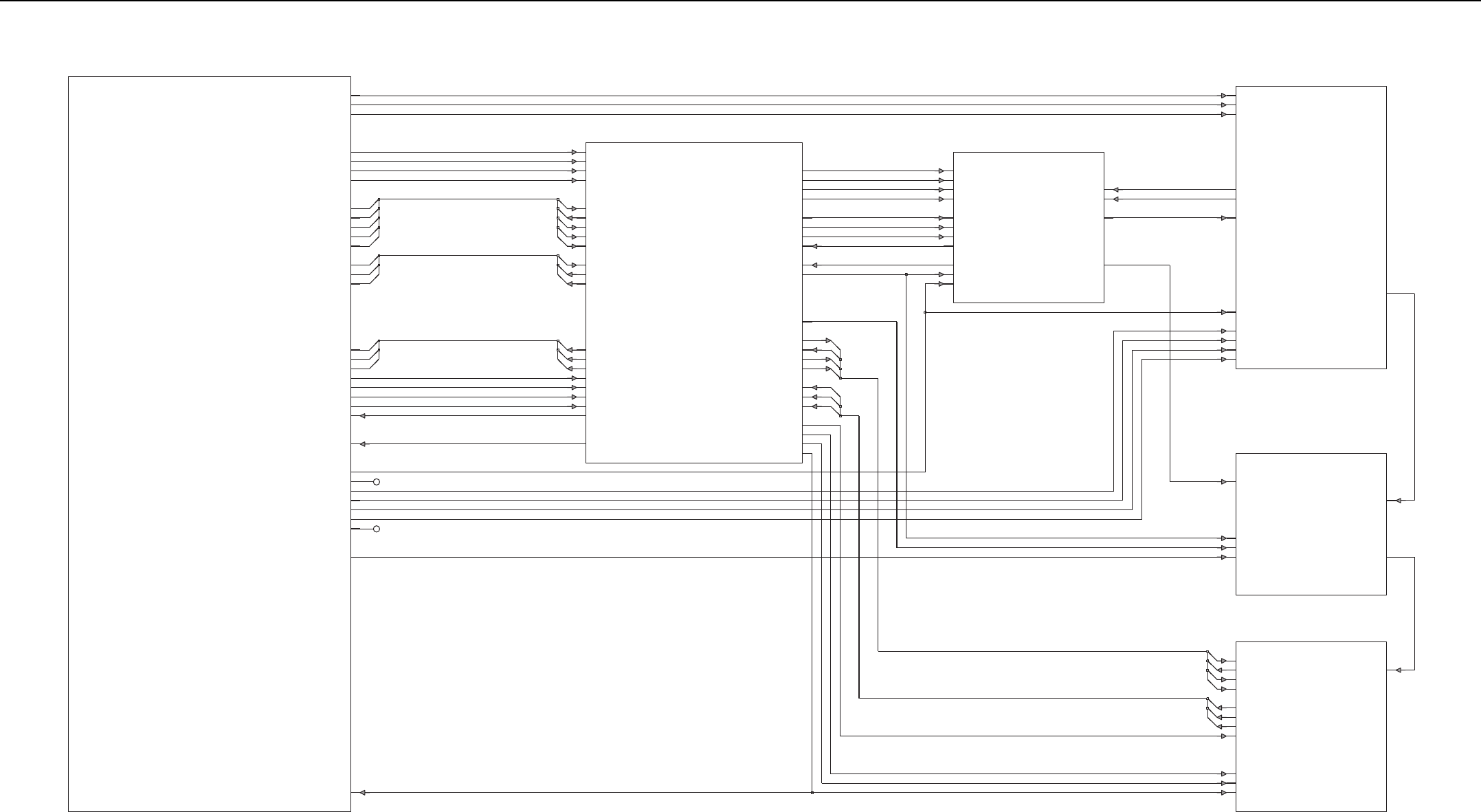
UHF1 (403–470 MHz) 25–40W PCB/Schematics/Parts List 3-7
( PC: SHEET 2 )
TX_HP_UHF1
( PA: SHEET 1 )
RXFE_UHF1
( 1 SHEET )
SYNTH
(ABACUS3: SHEET 2)
RXBE_73.35MHZ
(IF AMP: SHEET 1)
CONTROLLER_&_GPS
( TOP LEVEL: SHEET 1)
( RX: SHEET 2 )
VCO_UHF1
( TX: SHEET 1 )
9R1
FE_TUNE IF
RF_ATTEN_1
RX_IN
RX_INJ
2
0
2
9V3
9V3_PA
9V3_SYNTH
9V3_VCO
ANT_ENABLE
FINAL_BIAS_1
LO_BATTERY_DET
PA_SUPPLY
PREDRIVE_SW
RX_IN
TX_DAC
TX_INJ
2
1
3
0
1
0
0
9V3_SYNTH_OUT
9V3_VCO
HP_MOD_OUT
PREDRIVE_SW
PRSC
RXINJ
RX_VCO_SEL1
RX_VCO_SEL2
SF_TH
TXINJ
TX_VCO_SEL1
TX_VCO_SEL2
VCTRL
1
RX_SSI_SYNCB
SPI_CLK
SPI_MISO
SPI_MOSI
THK_CS
TX_DAC
TX_SSI_CLK
TX_SSI_DATA
TX_SSI_FSYNC
2
0
9R1
9V3_SYNTH_IN
ABACUS3_CS
ADAPT_SW
ANT_ENABLE
DMCS
LOCK_DETECT
LO_BATTERY_DET
PA_BIAS
PA_TEMP
PC_ATTEN_ENA
PREDRIVE_SW
RAW_B+
RESET_OUT
RX_FLTR_VCTRL
RX_SSI_CLK
RX_SSI_DATA
RX_SSI_FSYNC
0
1
4
3
1.875V_DIG_V2
16.8_GPS
16.8_MHZ_BUFF
2.775V_ANA_V7
2.775V_DIG_V4
5V_SW
9V3
9V3_PA
1V8
5V
IF
SPI_ABACUS_CEX
SPI_ABACUS_CLK
SPI_ABACUS_DATA
SSI_ABACUS_CLKOUT
SSI_ABACUS_DOUTA
SSI_ABACUS_DOUTB
SSI_ABACUS_FSYNC
SSI_ABACUS_SYNCB
NC
TX_VCO_SEL1_
TX_VCO_SEL2_
VCTRL
1
3
4
NC
2
16.8_REF
RX_SSI_DATA_PASS_OUT
RX_SSI_FSYNC_PASS_IN
RX_SSI_FSYNC_PASS_OUT
RX_VCO_SEL1_
RX_VCO_SEL2_
SDTX
SFTX
SF_OUT
SPI_CLK_IN
SPI_CLK_OUT
SPI_MISO_IN
SPI_MISO_OUT
SPI_MOSI_IN
SPI_MOSI_OUT
TH_CEX
TX_CLK 9R1
9V3
ABACUS3_CEX_IN
ABACUS3_CEX_OUT
ABACUS3_SYNCB_IN
ABACUS3_SYNCB_OUT
ADAPT_SW
DMCS
HP_MOD_OUT
LOCK
PRSC
RF_ATTN_1
RSTB RX_SSI_CLK_PASS_IN
RX_SSI_CLK_PASS_OUT
RX_SSI_DATA_PASS_IN
2
0
1
2
1.8V_TH_DIG
16.8_GPS
16.8_REF
1V8_BE
2.8V_TH_ANA
2.8V_TH_DIG
5V
5V_BE
0
2
3
2
0
1
TX_SSI_BUS(0:2)
ABACUS_SPI_BUS(0:3)
SPI_BUS(0:4)
RX_SSI_BUS(0:2)
ABACUS_SSI_BUS(0:2)
0
1
1
1
2
UHF1 (403–470 MHz) 25–40W Overall Schematic Diagram

3-8 UHF1 (403–470 MHz) 25–40W PCB/Schematics/Parts List
0.6 VDC
8.6 VD
C
0.7 VDC
Hi-Side Zeros for Preselector
0.8 VDC Typical
MAKO ( 0 ~ 4.6 VDC)
10 dB Attenuator
(3.00 ~ 8.00 VDC)
+16.0 dBm Min. (250 mV P-P)
8.4 VDC
(Micro-strip 20 mm Each)
L0403
12
3
10nH
D0404
10nH
L0404
12
3
C0434
220pF
1
TEST_POINT
TP0401
C0443
4.7pF
C0420
R0419
1.2K
100pF
220pF
680
C0405
C0426
56pF
R0429
5NC
4
6
3
2
1
680
XFMR
T0401
C0442
8.2pF
R0414
L0406
680
NC
15nH
2%
R0416
RF_ATTEN_1_3
220pF
C0437
NC
Q0405
BFG540W
Q0402
R0412
100K
C0404
220pF
(VALUE)
6.8pF
D0401
C0422
D0402
C0438
220pF
R0425
332
1%
56pF
C0430
9R1_FILT
C0428
47pF
L0413
R0403
0
C0423
220n H
4.7pF
47pF
C0452
R0413
680
9R1_FE_6
R0424
1%
121
IF_FE_8
5.6K
R0405
R0410 100K
RX_INJ_FE_5
4.7pF
C0417
56pF
C0429
2
3
6
4
1
5
12pF
Q0403
UMZ2NTR
220pF
C0409
10nH
12
3
C0402
9.1pF
C0448
L0402
NU
C0424
C0439
100pF
C0413
56pF
C0447
10pF
R0432
R0431
10K
100pF
680
C0441
C0456
2.2pF
(VALUE)
C0440
220pF
(VALUE)
6.2pF
C0411
C0425
56pF
D0405
IO1
1IO2 2
IO3 3
IO4
4
220pF
C0418
L0407
2%
27nH
680
D0400
R0415
R0401
680
2%
(VALUE)
L0401
15nH
C0446
R0402
10
8.2pF
C0421
NU
T0400
XFMR
NC 5
4
6
3
2
1
10nH
12
3
E0400
L0405
TP0400
TEST_POINT
1
C0408
1.5pF
27K
R0400
L0408
2%
22nH
C0410
6.2pF
(VALUE)
22nH
2%
L0410
C0451
22pF
5.6pF
C0412
R0418
0.1uF
C0455
1%
3.65K
220pF
C0400
1.2K
R0409
C0431
56pF
R0430
10K
220pFC0436
NC
1
3
2
C0433
CR0400
53.6
1%
NU
L0411
R0422
9R1_FILT
22nH
2%
47pF
C0403
FE_TUNE_FE_4
L0412
47nH
C0415
RXIN_FE_6
4.3pF
(VALUE)
R0404
2.7K
C0453
3.9pF
C0401
C0454
6.8pF
25
6
3
1
4
0.1uF
5
6
3
1
4
Q0401
Q0400
2
C0406
5.6pF
D0403
100pF
C0444
51
R0407
390
R0427
R0406
2.7K
22nH
2%
L0409
C0427
47pF
E0403
220pF
C0414
39
R0417
10K
R0428
0.10uF
R0420
1.2K
C0419
R0433
R0421
10
0
R0426
2.7K
C0445
9R1_FILT
C0432
47pF
10pF
C0449
4.7pF
C0416
13pF
E0401
C0407
2.7pF
RX_IN
RF_ATTEN_1
R0423
121
1%
FE_TUNE
RX_IN
J
9R1
IF
UHF1 (403–470 MHz) 25–40W Receiver Front-End Schematic Diagram

UHF1 (403–470 MHz) 25–40W PCB/Schematics/Parts List 3-9
1.43V
0.76V
1.6V
VHF -- 44.85MHz
UHF -- 73.35MHz
4-POLE
0.72V
IF_TO_ABACUS
NU
C0515
0.10uF
C0502
0.10uF
C0503
0.10uF
C0513
1
R0503
SHIELD
SH0500
Q0501
30K
L0503 330nH
E0500
6.2pF
C0510
C0509
NU
C0506
0.10uF R0510
30K
18pF
C0507
1
3
2
C0504
0.10uF
Q0500
20K
R0500
R0502
CC2
5
GND1
1
GND2
4
IN
3OUT 6
5.1K
FL0500
TS75
73.35MHz
CC1
2D0500
R0501
330
C0512
0.10uF
R0511
IFIN_BE_8
R0512
1.2K
C0514
51
0.10uF
R0509
4.7K
NU
56K
R0508
5V_BE_5
L0504
820nH
NU
L0506
5V
5V
IF
IF_OUT
C0516
UHF1 (403–470 MHz) 25–40W Receiver IF Amp Schematic Diagram
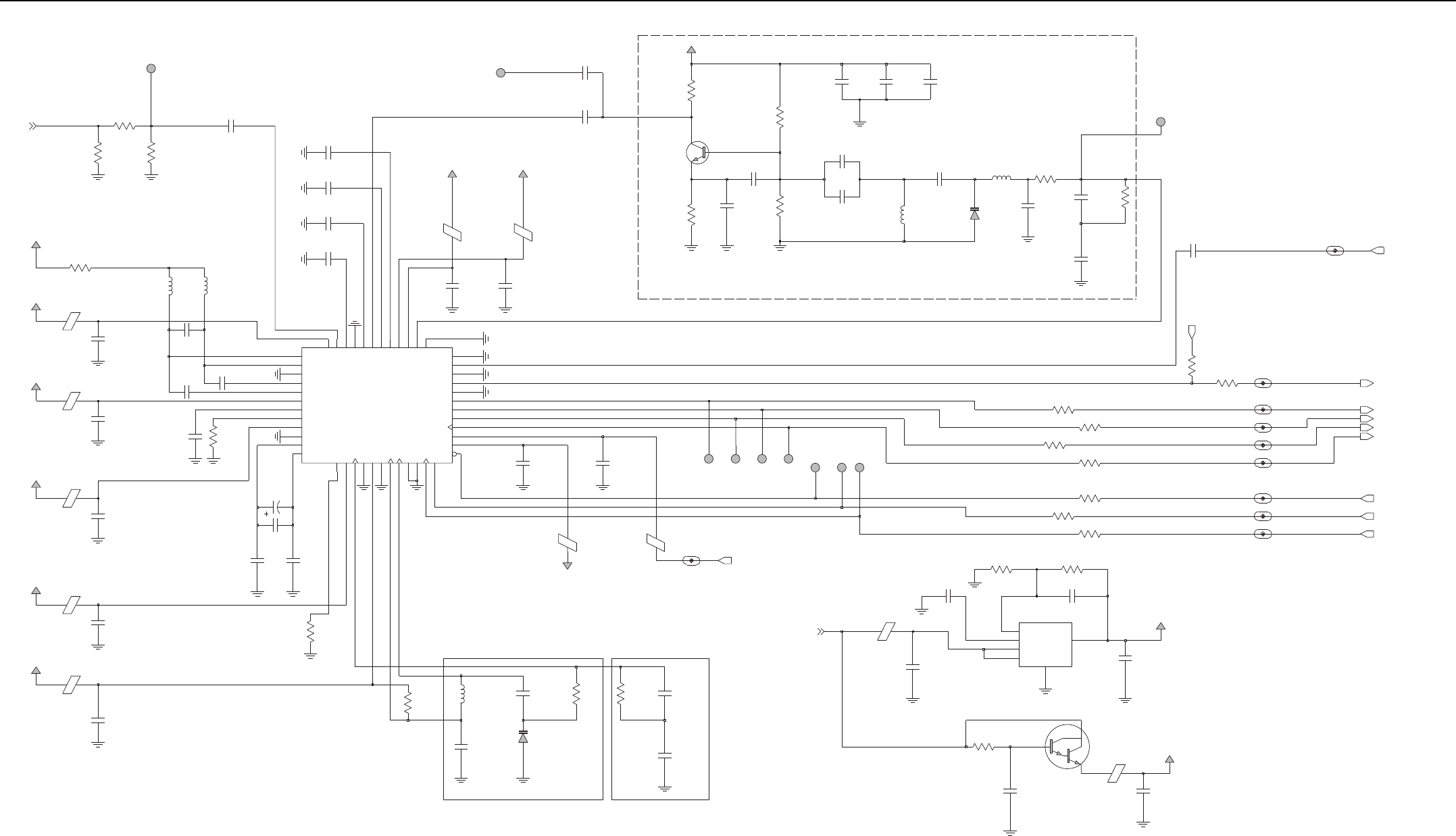
3-10 UHF1 (403–470 MHz) 25–40W PCB/Schematics/Parts List
#
*
#
#
#
#
CLOCK VCO
#
CLOCK LF
2nd LO VCO UHF (71.1MHz/75.6 MHz)
2nd LO VCO VHF (42.6MHz/47.1 MHz)
#
#
#
C0641
DOUTA_1_BE_5
2nd LO LF
SPF_3.5V
.01uF
R0624
5.1K
E0606
BK1005HM471
E0610
0.10uF
C0617
R0619
10K
270nH
L0603
0.10uF
C0643
DOUTB_1_BE_5
1.0uF
C0637
FS_1_BE_5
1V8_3
Q0600
13pF
C0612
C0603
E0608
NU
220pF
68.1K
R0622
E0603
R0626
R0608
0
0.10uF
C0623
C0622
1000pF
3VA
C0645
.01uF
TP0600
TEST_POINT
3VA
68pF
C0610
R0618
390
C0630
0.1uF
C0613
0.10uF
R0620
PE
3VA
9.1K
24K
E0604
100pF
R0604
3VA
C0651
NU
E0601
VOUT
3VA
R0623
2FB
5
GND
6
NP
4VCONT
3
VIN
1
.01uF
U0601
0
C0615
0.10uF
3VA
R0612
43pF
C0619
C0601
PD
C0614
43pF
0.10uF
C0628
200pF
C0625
VDDH
27
VDDI 48
VDDL 40
VDDP
39
VDDQ
14
VREFN
12 VREFP
11
PD
24
PE 25
13 RREF
SYNCB
33
VDDA
9
VDDC
17
VDDD 26
VDDF
6
IFIN 47
IOUTC
15
IOUTL 38
LON
42
LOP 43
MXON
2MXOP
1
PC
23
GNDI 45
GNDL
36
GNDP
37
GNDQ
16
GNDS1
21
GNDS2
34
IF2N
4
IF2P
5
FS
31
GCN
8GCP
7
GNDA
10
GNDC
18
GNDD
22
GNDF
3
GNDH 32
CLKOUT
28
19 CLKP
CXIF
46
CXVL
44
CXVM 41
DOUTA
29
DOUTB 30
FREF
35
U0600
AD9864
CLKN
20
R0627
0
R0621
0
R0603
510
C0640
2.2uF
30pF
C0650
0
R0609
R0617
10K
68
R0601
R0610
0
R0614
VVCO
C0633
0.10uF
0
0.10uF
DOUTB
C0631
CLKOUTFS
C0649 3300pF
5V
R0615
0
NU
C0616
Q0601
3VA
FREF_IF
C0611
73A04
10uH
L0605
1000pF
0.10uF
C0605
C0644
43pF
0.68uF
C0646
E0600
2.7uH
L0602
C0636
100pF
C0635
100pF
R0613
0
C0618
1uF
C0648
10.0uF10.0uF
C0647
D0601
10uH
L0604
C0626
100pF
C0607
TEST_POINT
TP0602
1
18pF
10K
CLKOUT_1_BE_5
100K
R0616
R0602
L0608
VVCO
DOUTA
4.7uH
FC_1_BE_5
3VA
1SV305
D0600
R0606
51
68pF
C0642
R0611
0
2200pF
C0629
C0634
.01uF
R0625
51.1K
R0605
330
.01uF
FD_1_BE_5
C0638
C0602
C0620
0.10uF
0.10uF
E0607
E0609
C0627
100pF
0.10uF
C0604
C0621
0.10uF
FE_1_BE_5
E0605
R0607
NU
3VA
E0602
SB_1_BE_5
PC
TP0601
TEST_POINT
4.7uF
C0632
IF_OUT
5V
SSI_ABACUS_FSYNC
SPI_ABACUS_CEX
16.8_REF
SPI_ABACUS_CLK
SSI_ABACUS_DOUTA
SSI_ABACUS_CLKOUT
SSI_ABACUS_DOUTB
SPI_ABACUS_DATA
SSI_ABACUS_SYNCB
1V8
1V8
UHF1 (403–470 MHz) 25–40W Receiver Back-End Schematic Diagram
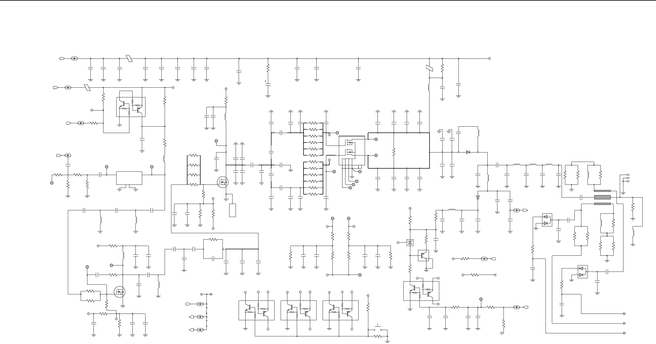
UHF1 (403–470 MHz) 25–40W PCB/Schematics/Parts List 3-11
2.85V (44W)
MRF1570, Flat Lead
2.10V (27.5W)
16.5 dBm
2.2VDC (TX Only)
0 dBm
3.2VDC
9.3V DC (use scope with bandwidth limit to measure)
L = 585 mi l
W = 90.2 mi l
S = 35.4 mil
S = 35.4 mil
2.2VDC (TX Only)
11dB Pad
9.1VDC
W = 22.6 mi l
Test Point to check Ref Osc warping
W = 22.6 mi l
27pF
C0719
56pF
R0732
1K
E0703
C0761
C0727
NU
R0979
TP0711
0
C0711
NU
C0707
NU
M070 0
HEATSINK
POS 1
C0730
NU NU
C0720
30pF
C0700
NU
R0702
L0714
33pF
C0779
43.67n H
VR0700
30K
C0718
1000p F
10uF
R0713
C071 0
17nH
L0700
R0735
100
43pF
C0744
C0705
1000p F
C0787
47pF
C079 3
NU
C0741
NU
C0712
1000p F
J0700-1
1
20pF
C0734
1000pF
Q0704
C0708
C0747
NU
100 K
R0756 C080 4
150pF
C0703
17nH
L0706
30pF
20K
R0751
C0778
33pF
R0744
NU
.022uF
C0701
L0710
17nH
S070 0
SWITC H
D0702
0
R0734
L0702
L0719
82nH
33.47nH
L0722
1.5uH
100pF
C0732
56pF
C0735
C0706
NU
12pF
C0739
2200pF
C0702
R0748
56K
C0729
NU
220pF
C0740
12pF
C0780
C0794
NU
20pF
C0733
L0721
3.3nH
27pF
C0746
NU
R0769
C0944
4.7p F
C0800
NU
0
R0972
NU
TP0709
NC
NU
C0731
100pF
TP0713
NU
C0748
C0799
R0738
51
150pF
10K
220pF
C0801
R0729 C0777
150pF
RX_IN_TX_PA
100K
R0740
C0765
NU
Q0706
10pF
NU
NC
C0791
C0805
1000p F
R073 9
100pF
C0745
470
R0745
R0759
10
C0810
150pF
C0743
56pF
C080 3
D0904
4.3pF
NC
2743019447
E0700
91
R0714
TP0702
NU
C0766
C0802
220pF
NC
SP0701
C0753
91pF
TX_INJ_TX_PA
C0709
0.1u F
SP0706
J0700-2
2
100pF
C0756
NU
C0754
C0809
NU
C0755
NC
NU
C0943
150pF
R0757
47K
100pF
180
R0971
C0714
120
R0977
150
R0706
TP0710
17nH
L0707
R0700
NU
E0701
2743019447
150
R0976
R0777
SP0705
10
15R0764
SP0707
C0776
150pF
L0705
150nH
82
R0711
TP0704
3.3n H
L0720
C0726
22pF
R0715
91
R0763 15
10
R075 5
220pF
C0770
R072 0
150pF
C0945
NC
10
R0768 15
D0700
10K
R0750
C0812
33pF
TP0705
NC
C0723
100pF
TP070 8
R0742
10
C0795
47pF
R0747
4.7K
0
R0776
NC
C0798
1000pF
D090 5
NU
0.1u F
C0788
R0741
47K
TP0703
100pF
3.9pF
C0737
C0713
C0811
33pF
NU
C0792
NU
C0760
3
47pF
C0814
SP0703
J0700-3
15
R0772
R0973
0
NU
R0770
NU
15pF
C0808
1000pF
C0717
10
R075 4
3.3p F
C0772
R0719
10
15R0762
NU
15nH
ANT_ENABLE_TX_PA
NC
L0904
ADA4743
2GND1
4GND2
1RF_IN VD_RF_OUT 3
R0974
220
R0727
U0700
15
R0773
6.2K
4.7K
R072 2
0
R0761
10
C0817
10pF
12nH
L0718
R0718
C0771
NU
200
SP0704
Q0709
R0970
0
Q0701
R0703
17nH
RN49A2
L0708
47pF
FINAL_BIAS_1_TX_PA
150pF
C0728
Q0703
1
D
3G
2S
C0796
R0753 1K
0
L0903
10nH
C0941
5.6p F
R075 2
220
R0975
150nH
L0715
150pF
C0781
NU
R0765
C0815
150pF
Q0708
R0760
16pF
C0818
2.7K
S3
S4
C0767
12pF
D1
D2
G1
G2
GND1
GND2
S1
S2
Q0702
10K
NC
SP0700
R072 8
NC
C0942
150pF
R0749
0
16pF
SP0702
15
C0819
R0771
C0721
R073 0
1K
NU
C0940
150pF
NU
R0775
220p F
C0716
1000pF
C0797
Q0705
D
G
S
30pF
C0813
TP0707
NC
15R0767
NC
C0738
5.6pF
.022u F
C0704
C0789
NU
NU
20pF
R0778
C0786
Q0707
NU
R0766
0
R0978
PREDRIVE_SW
NU
C0764
5.6pF
C0742
R0774
20K
1000pF
C0782
C0775
.022uF
A+
TX_INJ
9V3_T X
9V 39V 3
9V 3
Gate_1
Gate_2
PA_SUPPLY_TX_PA
PREDRIVE_SW
9V3_PA
9V3_VCO
9V3_SYNTH
Final_Bias
V_G2
V_G2V_G1
V_G1
9V3
Antenna_En
Antenna_E n
Gate_1 Gate_2
Final_Bias
Final_Bias
V_cont
V_cont
V_cont
FINAL_BIAS_1
9V3_TX
9V3_TX
ANT_ENABLE
V_CONTROL
REV_DETECTED
FWD_POWER
FWD_DETECTED
A+
PA_SUPPLY
RX_IN
2.2K
47K
47K
47K
UHF1 (403–470 MHz) 25–40W Power Amplifier Schematic Diagram
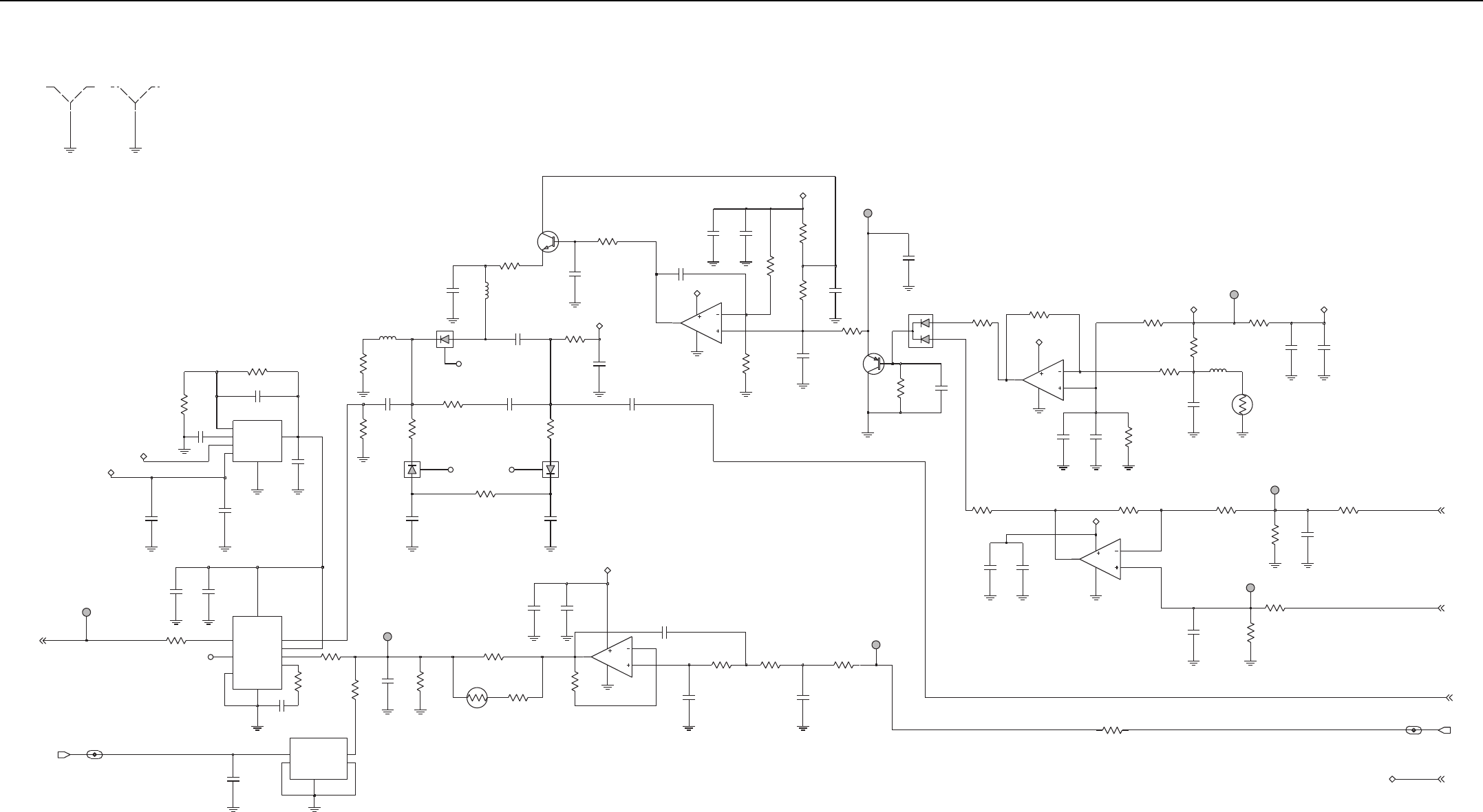
3-12 UHF1 (403–470 MHz) 25–40W PCB/Schematics/Parts List
2.10V (27.5W)
1.35V (44W )
2.85V (44W)
1.28V (27.5W)
5V DC
NOTE: VOLTAGES SHOWN FOR ANALOG TX MODE
2.67V (44W)
2.01V (27.5W)
0.38V (44W)
0.21V (27.5W)
1.0V or less, typical
2
3
1
8
4
AD856 6
U0900-1
0
R0947
TP0911
0
R0940
220pF
C0920
43K
R0901
220pF
C0927
U0900-2
6
5
7
8
4
TP0909
4700pF
C0926
39
R0928
NCP301
U0942
3GND
2INPUT
NC1
4NC2 5
RESET_OUT 1
C0939
220p F
6.8K
R0916
TP0903
R0907
0
D0903
C0918
220pF
1500pF
C0928
.01uF
C0907
0
R0923
1000pF
C0917
R0941
0
C0903
220pF
220pF
C0914
180 K
R0914
R0942
L0900
6.81K
9GND
6NC
1
RFIN
7VAPC
8
VPOS
VSET 3
1uH
U0940
AD8315ACPZ-REEL
5COMM
2
ENBL
4
FLTR
2200pF
C0923
220pF
C0953
R0918
390
150
R0926
TP0907
0.1uF
C0902
LO_BATTERY_DET
R0955
1%
100K
L0902
470nH
R0960
2.4K
3.3K
R0902
220pF
C0916
C0949
2.2uF
D0900
SHIELD
1
C0910
220pF
R0917
SH
0901
5.6K
100pF
C0947
220pF
C0937
D0901
0
R0938 TX_DAC
0.1uF
C0901
C0948
1.0uF
NC
C0922
220pF
D090 2
NC
TP0913
C0936
220pF
39
R092 9
Q0901
47K
RT0908
R0930
18 K
C0921
0.1uF
2
GND
5
NP
6
VCONT
4
VIN
3
VOUT 1
U0941
FB
220pF
C0934
R0936
1%47.5K
R0946
3.32K
220pF
C0915
Q0902
TP0910
R0910
6
5
7
8
4
1K
0.1uF
U0901-2
AD8566
C0908
51
R0927
43 K
R0909
220pF
C0925
R0903
22K
R0921
2.2K
R092 5
5.6K
R0906
0
470nH
L0901
220pF
C0911
430K
5%
R0954
RT0953
47K
C0919
NC
33K
R0912
0.1uF
1000pF
1%
16.2K
C0950
R0937
56K
R0900
C0935
220pF
C0912
R0915
68K
330
R0911
220pF
220pF
(VALUE)
0.1uF
C0913
43.2K
C0951
R0951
220p F
10K
R0950
22K
R0920
C0906
NC
C0929
220pF
R0913
C0909
220pF
0
R0922
36K
R0924
5.6K
C0931
220pF
R0943
0
R0944
U0901-1
2
3
1
8
4
39.2K
AD8566
220pF
R091 9
39K
C0900
C0904
220pF
SW_9V1
FWD_DETECTED
SHIELD
SH
0900
1
TP090 4
SW_9V1
TX_DAC
9V39V3
SW_9V1
9V3
LO_BATTERY_DET
V_CONTRO L
SW_9V1 9V3
REV_DETECTED
SW_9V1
SW_9V1
SW_9V1
SW_9V1
FWD_POWER
UHF1 (403–470 MHz) 25–40W Power Control Schematic Diagram
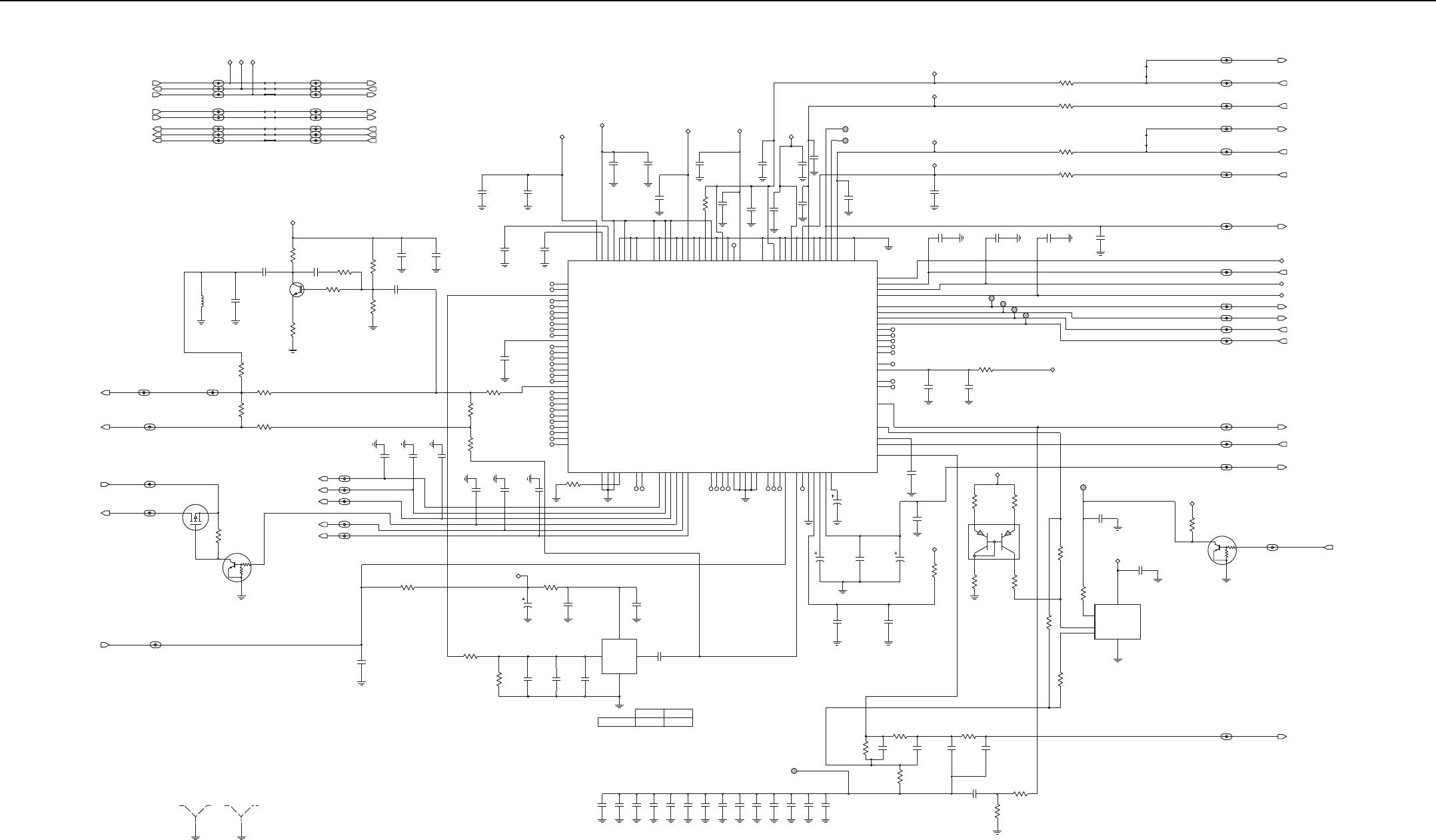
UHF1 (403–470 MHz) 25–40W PCB/Schematics/Parts List 3-13
1.5 ppm
TCXO (Y0100)
Locked: 1.8 V
LOW: 0V
5116032H01
VCO SEL: ACTIVE LO W
Adapt OFF: 0V
Unlocked: 0V
0.5 ppm
VCO STEERING LINE VOLTAGE: 0.6V TO 4.4V
Buffer to Abacus/Controller
GPO_4
Adapt ON: 5V
9R1 SWITCH FOR FRONT-EN D
5102495J07
GPO_5_SYNTH
Switch for Adapt Transient
GPO LINES
HI: 2.8V
ABACUS3_SYNCB_OUT
SF_OUT_SYNTH
NC
100
220pF
C0138
R0127
ADAPT_SW_SYNTH
21
34
Q0107
Q0102
10K
R0120
NC
2.8V_TH_ANA_SYNTH
NC
10uF
C0196
ABACUS3_CEX_OUT
C0133
4.7uF
NC
4.7uF
C0140
NC
RX_SSI_DATA_IN
0
R0122
C0148
NC
NC
NU
RX_SSI_FSYNC_OUT
.033uF
ABACUS3_CEX_IN
5V_BE_SYNTH
GPO_3_SYNTH
TP501
1
220pF
C0147
1.0uF
NC
C0149
.022uF
C0114
C0158
0.1uF
R0111
0
220
NC
NC
0.1uF
R0107
2.8V_TH_DIG_SYNTH
C0150
240
R0131
1
NC
RX_SSI_DATA_OUT
TP_VCTRL
R0161
100K
NC
1V8_BE_SYNTH
SPI_MOSI_OUT
TH_CEX_SYNTH
R0102
C0156
0.1uF
0
0
R0147
NC
R0139
NU
0
1.6K
C0123
R0101
220pF
1.0uF
1
C0177
1.8V_TH_DIG_SYNTH
NC
TP504
1
RSTB_SYNTH
R0106
TP_TEST1
NU
2.7K
SPI_CLK_OUT
0
R0156
C0111
0.1uF
NC
NC
SPI_MISO_OUT
10K
R0159
R0118
0
NC
C0125
220pF
220pF
16.8_GPS_SYNTH
C0131
TP503
1
C0130
220pF
NC
R0155
C0142
0
16.8_REF_CONTROLLER_SYNTH
220pF
C0113
220pF
NU
TP_ADAPT_SW
1
C0126
220pF
NC
LOCK_SYNTH
NC
0
R0146
0.1uF
C0159
C0146
220pF
0.1uF
C0124
Q0108
SPI_MISO_IN
NC
Q0100
R0103
R0140
18
0
NC
NC
220pF
C0101
220pF
TX_CLK_SYNTH
C0179
NU
HP_MOD_OUT_SYNTH
5V_SYNTH
1VC
4
VCC
0
R0158
Y0100
16.8MHz
GND
2
3
OUTPUT
3GND
1INOUT
4ONOFF_CONTROL
2OUTIN
5
VCC
TP_TEST2
1
NC
MC74VHC1GT66
U0101
0.1uF
1
C0129
SHIELD
SH0100
1
SH0101
SHIELD
C0127
220pF
1.0uF
ABACUS3_SYNCB_I N
C0115
220pF
NU
NC
NC
GPO_2_SYNTH
C0119
0.1uF
C0166
9V3_SYNTH
DTC114YM
Q0106
NC
0.1uF
C0165
C0136
0.1uF
0.1uF
C0164
R0134
27
C0120
.01uF
0.1uF
NU
C0100
C0194
C0117
220pF
220pF
SDTX_SYNTH
0.1uF
C0191
NU
VCTRL_SYNTH
RX_SSI_CLK_I N
C0141
0.1uF
220pF
NC
0
R0125
C0178
0
NC
NC
NC
R0100
0.1uF
C0180
NC
NC
C0195
220pF
470pF
10K
R0126
C0175
NC
NU
120
R0148
C0112
220pF
R0109
0
220pF
C0104
NC
NC
PRSC_SYNTH
R0123
NC
.01uF
56K
C0145
C0128
220pF
L0100
270nH
10uF
C0137
C0143
C0134
220pF
R0108
220pF
C0103
2K
SPI_MOSI_IN
0.1uF
SFTX_SYNTH
XOSC_BASE
XOSC_EMIT
L5
G6
D
0
R0115
TXI
L7 TXQ
H7
DL6
G7
F6 TX_GND2
J6
F1
VCO_DAC
K5
K10
F5 SUB2
F3 SUB3
G8 TCLK
D7
C7
B3
F10
TXCLK
K7
SFTX
K4 SF_OUT
C9 SMD_CLK_GEN_GN D
C11
SPI_CLK
D10
SPI_DR
D9
SPI_DW
DE8
E11
SUB1
A10
DA8
B9
B10 SDM_VAG
A9
B8
D11
SDR
F11
SDTX
F9
C3
D5
B2
A5
RX_EN_OUT
B1
D3
F2 SCAN_I N
E9
SCLK_OUT
A3
E6 RSTB
E7
RXACQ
E10
RXFS
C2 RXI
C1 RXI X
D1 RXQ
D2 RXQ X
L8
NTXQ
K6
L4 OSCREG_BYP
J5
D
OSCREG_OUT
H5
J4 OSCREG_SPLY
K11 PABIAS_DAC
L9 PHCLK
RFSTEPA
G5
D
H2
J2
M_PRSC
H3
M_PRSCX
A1 NC1
A11 NC2
NC3
L1
L11 NC4
NTXI
C8
G10
B7
G4
D
MAIN_PDET_VCC G2
J1
H1
MN_ADAPT_CP
G3
MN_CP
GPO2_TEST2
GPO3_TEST3
E5
GPO4_TEST4
D4
K9 GPO 5
H8 GPO 6
K8
HP_MOD_OUT
J9 INCR_DECR
F8
H4
D
K1
ESC_IN
E1
K2
C6 FBI
B6 FBQ
B4 GPO1_TEST1
A4
DC_CAL
L10 DEEPSLEEP
F7
DMCS
EF_OUTM
J8
J7 EF_OUTP
ESC_CP L3
L2
K3
DJ3
CLK1_OUT
J11 CLK2_OUT
G11 CLK_BASE
G9 CLK_CP
H11 CLK_EMIT
H10
D
J10
G1
DAC_ADAPT
A2
ASPI_CLK
B11 ASPI_DATA
A7
E4 BP_I
F4 BP_I X
E2 BP_Q
BP_Q X
E3
D8
CEX
H9
A6 ACE1
D6 ACE2
AGC_DAC
B5
AGC_FLAG
C4 AGC_REF
C5
H6 ARX_DAC
C10
0
5104932K08
U0100
SC51650VF
NC
R0128
C0108
220pF
C0107
0.1uF
NC
C0151
0.1uF
0
R0157
NU
0.1uF
27
C0110
220pF
C0102
R0119
0.1uF
2K
C0162
R0114
NC
C0132
220pF
SPI_CLK_IN
C0109
0.1uF
RX_SSI_FSYNC_IN
0.1uF
C0157
R0160
100K
NC
R0105
0.1uF
240
NC
C0160C0193
NU
0
R0116
NU
0.1uF
30K
C0192
0.1uF
RX_SSI_CLK_OUT
R0117
C0105
0.1uF
R0110
NC
10K
51
R0144
R0104
47K
0.1uF
C0161
C0122
.01uF
0.1uF
C0106
GPO_6_SYNTH
0.1uF
C0163
16.8_REF_BE_SYNTH
NC
C0118
0.1uF
C0171
.01uF
10uF
C0135
1
GPO_1_SYNTH
DMCS_SYNTH
TP502
9R1_SYNTH
10K
R0113
220pF
NU
NC
C0121
HP_MOD_OUT
ABACUS3_SYNCB_I N ABACUS3_SYNCB_OUT
C0144
0.1uF
RX_SSI_FSYNC_PASS_IN
SPI_MOSI_IN
SPI_MOSI_IN
SPI_CLK_I N
SPI_CLK_I N
SPI_MISO_IN
SPI_MISO_IN
5V
2.8V_DI G
RX_VCO_SEL1_
5V_BE
9V3
9R1
16.8_REF
1V8_BE
1.8V_TH_DIG
1.8V_DI G
RSTB
16.8_GPS
ADAPT_SW
5V_TH
TX_VCO_SEL1_
TH_CEX
SPI_MOSI_IN
SPI_CLK_I N
2.8V_TH_DIG
2.8V_DIG
2.8V_TH_ANA
2.8V_ANA
1.8V_DI G
1.8V_DIG
5V_TH
RX_SSI_DATA_PASS_OUT
RX_SSI_CLK_PASS_OUT
RX_SSI_FSYNC_PASS_OUT
RX_SSI_CLK_PASS_I N
ABACUS3_CEX_OUT
SPI_MISO_OUT
SPI_MOSI_OUT
SPI_CLK_OUT
ABACUS3_CEX_I N
RX_SSI_DATA_PASS_I N
5V_TH
TX_VCO_SEL2_
RF_ATTN_1
RX_VCO_SEL2_
VCTRL
PRSC
2.8V_ANA
DMCS
5V_TH
2.8V_ANA
1.8V_DI G
2.8V_ANA
2.8V_ANA
SDTX
SFTX
SF_OUT
LOCK
TX_CLK
SPI_MISO_IN
2.8V_AN
A
10K
47K
R1
R2
IN
GND
OUT
XOSC_GN
TX_DAC_GN
TX_DAC_VCC
TX_GND1
TX_VCC
TEST1
TEST2
TM
SSI_GN
SSI_VCC
SDM_REF_GN
SDM_REF_VCC
SDM_VREFM
SDM_VREFP
RX_AGND2
RX_AVCC1
RX_AVCC2
SCAN_EN
SDM_CLK_GEN_VCC
RX_AGND1
OSCREG_GN
MN_CP_GN
MN_CP_VCC
LGND2
LVCC1
LVCC2
MAIN_GN
MAIN_VCC
LGND1
ESC_CP_VCC
ESC_GN
ESC_TEST
ESC_VCC
ESC_CPBIAS
ESC_CP_GN
CLK_GN
CLK_VCC
ASPI_VCC
UHF1 (403–470 MHz) 25–40W Synthesizer Schematic Diagram
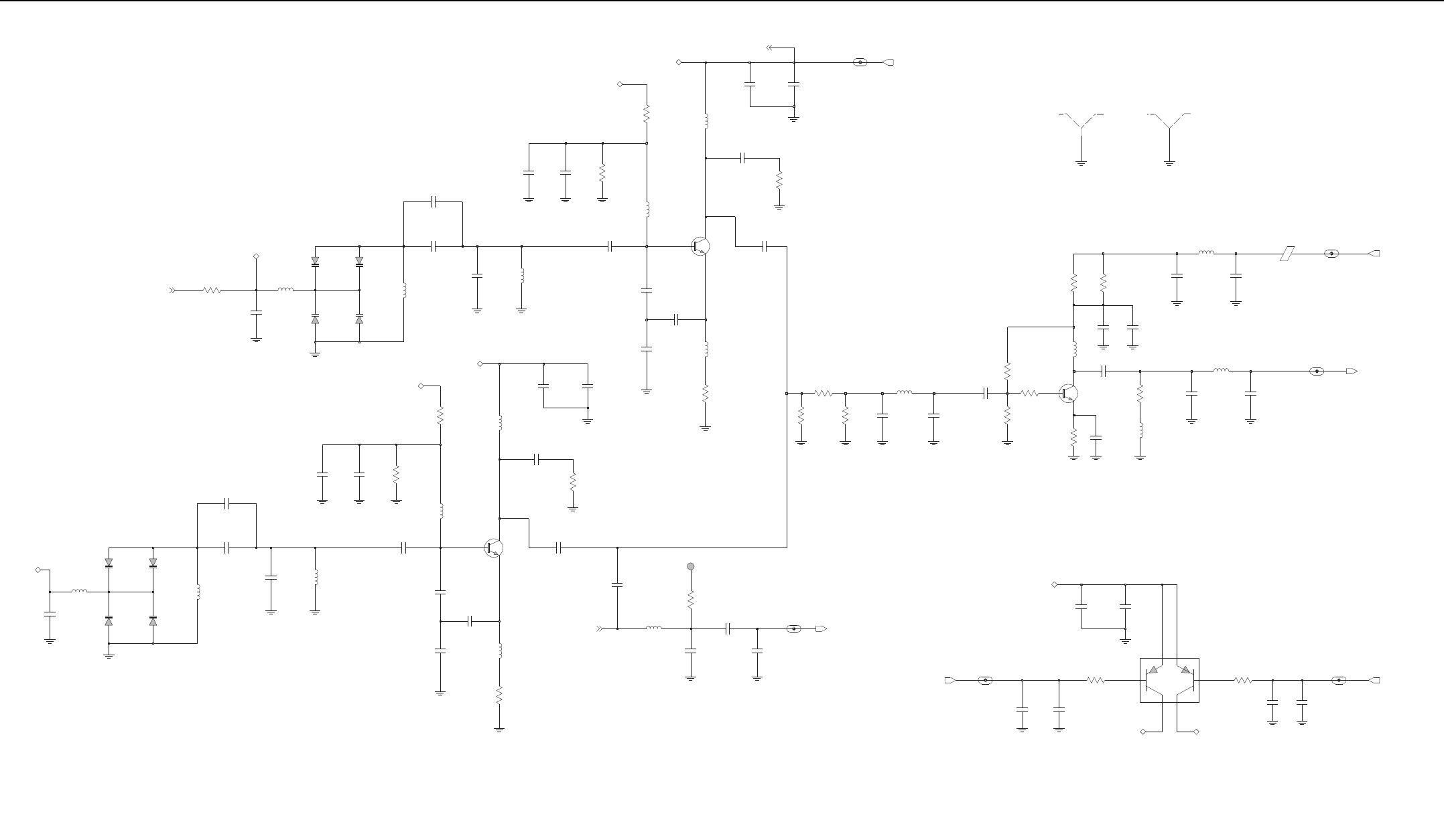
3-14 UHF1 (403–470 MHz) 25–40W PCB/Schematics/Parts List
RXINJ: 329.65 - 396.65 MHz
+6 dBm
RX VCO 2
Steering Line Voltage (VCTRL_TH)
PRSC (RX): 329.65 - 396.65 MHz
RX Prescaler
RX1_SEL: 2.7 V (High)
-5 to -15 dBm
RX Buffer Amplifier
Super Filter Voltage (SF_TH)
0.1 V (Low)
SF_TH: 2.5 V
R0204
8.2K
0.1 V (Low)
RX VCO 1
RX2_SEL: 2.7 V (High)
VCTRL: 0.6-4.5 V
1.2K
C0238
220pF
R0202
L0213
470nH
1.2K
R0203
C0257
220pF
C0235
6.2pF
39nH
L0221
220pF
C0236
RX2_SEL_VCO_UHF1_5
220nH
L0219
470nH
L0200
3.6pF
C0250
L0207
12.5nH
C0209
220pF
C0207
.022uF
C0218
NU
4.3pF
C0208
1.0pF
12.5nH
L0215
0.10uF
C0239
U0201
RX1_SEL_VCO_UHF1_5
CR0206
TP0301
1
L0214
470nH
R0206
15K
470nH
L0203
10pF
C0246
R0229
160
CR0205
CR0204
10K
Q0201
L0211
R0213
C0211
220pF
220nH
3.0pF
C0247
C0221
R0205
5.1pF
C0213
3.9pF
100
3.3K
R0201
470nH
C0243
2.7pF
L0202
C0200
220pF
C0206
0.10uF
C0241
220pF
C0229
10
R0207
24pF
0.10uF
PRSC_VCO_UHF1_5
C0201
NU
C0233
SF_TH_VCO_UHF1_6
36pF
C0223
CR0201
51
C0226
220pF
R0208
C0220
3.0pF
C0245
3.9pF
10K
C0240
220pF
0.10uF
R0218
C0249
CR0208
E0201
CR0203
R0211
0
27nH
L0210
Q0200
56pF
C0225
220pF
C0259
12pF
9R1_VCO_UHF1_7
C0242
C0230
150pF
R0230
4.7K
100
R0226
L0218
22nH
220pF
C0248
220pF
C0253
47nH
L0205
R0210
L0209
470nH
C0237
4.7K
0.10uF
R0212
0
43pF
Q0202
220nH
C0252
C0217
L0204
470nH
L0217
220pF
C0202
.01uF
NU
C0224
R0216
120
0.10uF
CR0207
C0205
1.0pF
NU
220pF
C0203
C0219
R0225
R0220
10 15nH
7.5K
C0251
20pF
L0206
R0221
510
R0219
510
L0212
470nH
3.0pF
C0231
C0204
220pF
11pF
C0214
CR0202
5.1pF
C0215
SH0300
SHIELD SH0301
SHIELD
C0222
3.0pF
NU
6.2K
0.10uF
C0258
SF_TH
RXINJ_VCO_UHF1_5
R0224
RXINJ
RXSL
PRESC_TX
RX1
RX2
RX_VCO_SEL1
RX1 RX 2
RX_VCO_SEL2
VCTRL
PRSC
SF_TH
RXSL
9R1
SF_TH
SF_TH
SF_TH
UHF1 (403–470 MHz) 25–40W Receiver VCO Schematic Diagram
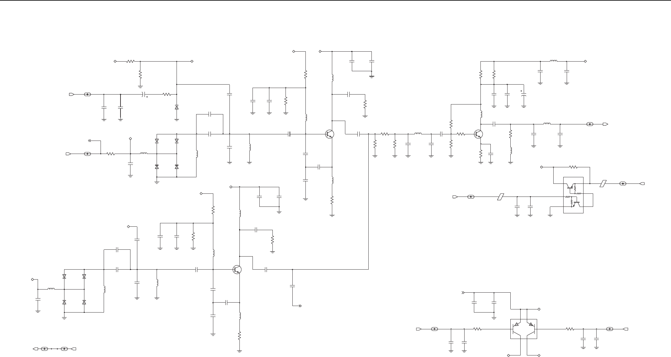
UHF1 (403–470 MHz) 25–40W PCB/Schematics/Parts List 3-15
+11 dBm
TX Prescaler
Super Filter Voltage (SF_TH)
-5 to -15 dBm
SF_TH: 2.5 V
0.1 V (Low )
0.1 V (Low)
Steering Line Voltage (VCTRL_TH)
TX Buffer Amplifier
TX2_SEL: 2.7 V (High)
TXINJ: 403-470 MHz
TX1_SEL: 2.7 V (High)
PRSC (TX): 403-470 MHz
TX_BUFFER_SEL: 1.8 V (ON)
0.1 V (OFF)
TX VCO 2
TX VCO 1
VCTRL: 0.6-4.5 V
R0320
15K
C0341
0.10uF
R0308
R0325
8.2K
51
R0324
2K
TXINJ_VCO_UHF1_5
L0313
15K
R0306
470nH
R0326
100
3.3pF
C0313
L0318
18nH
R0331
10K
75
R0316
L0310
18nH
220pF
C0303
0.5pF
C0344
1000pF
C036 1
51 0
R0303
220pF
C0300
TX2_SEL_VCO_UHF1_5
R0334
200
27
R0333
R0329
110
R0327
C0360
4.7uF
10 K
470nH
L0312
R0310
4.7K
0.10uF
C0305
C0362
220pF
C0340
220pF
220pF
C0311
8nH
CR0302
L0307
0.10uF
C0301
220pF
C0342
CR0300
C0337
0.10uF
0
U0304
PBR941
R0337
220n H
Q0302
L0311
470nH
L0314
39nH
L0305
Q0300
0.5pF
C0310
C0351
24pF
10
C0331
3.0p F
R0307
0.10uF
E0302
NU
C0349
220pF
470nH
L0319
CR0308
C0353
NU
1.0p F
C0345
3.3pF
C0319
TX1_SEL_VCO_UHF1_5
0.10uF
C0328
NU
L0304
8.2K
R0304
220nH
51pF
220pF
C0309
5.1pF
C0352
C0320
R0301
3.3K
470nH
.01u F
C030 2
10nH
L0303
R0321
2.7K
L0306
C0334
L030 0
220pF
16pF
C0359
220nH
470nH
L0302
C0357
220pF
C0317
L0309
220pF
CR0304
470nH
C0314
12pF
L0315
8nH
0
R0311
7.5pF
C0346 C0347
5.1pF
R0305
CR0305
510
R0302
100
C0326
C0324
NU
220pF
20 0
R0332
220pF
PREDRIVE_SW_VCO_UHF1_6
C0306
0.10uF
C0363
C0348
220pF
5.1p F
CR0307
C0315
Q0301
C0336
220pF
C0329
16pF
VCTRL_VCO_UHF1_7
CR0303
R0312
0
220pF
C0304
NU
.022uF
C0307
9V3_VCO_UHF1_ 7
C0327
220pF
E0301
NU
200K
U0303
56pF
0613952R32
R0319
7.5pF
C032 5
3.0pF
NU
C0322
C0321
C0343
C0358
0.10uF
3.3pF
3.3pF
CR0306
C0316
10uF
C0308
CR0301
C0323
27pF
(VALUE)
C0350
4.3pF
HP_MOD_OUT_VCO_UHF1_7
C0318
470nH
L0317
SF_TH
HP_MOD_OUT
TX2TX1
SF_T H
SF_TH
TX_VCO_SEL1 TX_VCO_SEL2
3.3pF
SF_TH
TX2
TX1
SF_TH
VMOD
VS L
9V3_VCO
VCTRL
VCTRL
VSL
VMOD
PRESC_TX
9T1
9T1
9V3_SYNTH_OUT 9V3_SYNTH_I N
TXINJ
PREDRIVE_S W
UHF1 (403–470 MHz) 25–40W Transmit VCO Schematic Diagram

3-16 UHF1 (403–470 MHz) 25–40W PCB/Schematics/Parts List
UHF1 PCB 8486777Z12 and 8486777Z14 Parts
List 25–40W
Circuit
Ref
Motorola
Part No. Description
C0100 2113944A44 220pF
C0101 2113944A44 220pF
C0102 2113944A44 220pF
C0103 2113945C31 0.1uF
C0104 2113944A44 220pF
C0105 2113945C31 0.1uF
C0106 2113945C31 0.1uF
C0107 2113945C31 0.1uF
C0108 2113944A44 220pF
C0109 2113945C31 0.1uF
C0110 2113945C31 0.1uF
C0111 2113945C31 0.1uF
C0112 2113944A44 220pF
C0113 NOT PLACED –
C0114 2113946E02 1.0uF
C0115 2113946E02 1.0uF
C0117 2113944A44 220pF
C0118 2113945C31 0.1uF
C0119 NOT PLACED –
C0120 2113945B02 .01uF
C0121 NOT PLACED –
C0122 2113945B02 .01uF
C0123 2113946E02 1.0uF
C0124 2113945C31 0.1uF
C0125 2113944A44 220pF
C0126 2113944A44 220pF
C0127 2113944A44 220pF
C0128 2113944A44 220pF
C0129 2113945C31 0.1uF
C0130 2113944A44 220pF
C0131 2113944A44 220pF
C0132 2113944A44 220pF
C0133 2313960B30 4.7uF
C0134 2113944A44 220pF
C0135 2313960B32 10uF
C0136 2113945C31 0.1uF
C0137 2313960B32 10uF
C0138 2113944A44 220pF
C0140 2313960B30 4.7uF
C0141 2113945C31 0.1uF
C0142 2113944A44 220pF
C0143 2113944A44 220pF
C0144 2113945C31 0.1uF
C0145 2113945B02 .01uF
C0146 2113944A44 220pF
C0147 2113944A44 220pF
C0148 2113945D01 .033uF
C0149 2113945C04 .022uF
C0150 2113945C31 0.1uF
C0151 2113945C31 0.1uF
C0156 2185419D06 0.1uF
C0157 2185419D06 0.1uF
C0158 2185419D06 0.1uF
C0159 2185419D06 0.1uF
C0160 2185419D06 0.1uF
C0161 2185419D06 0.1uF
C0162 2185419D06 0.1uF
C0163 2185419D06 0.1uF
C0164 2185419D06 0.1uF
C0165 2185419D06 0.1uF
C0166 2185419D06 0.1uF
C0171 2113945B02 .01uF
C0175 2113944A44 220pF
C0177 2113944A44 220pF
C0178 2113944A44 220pF
C0179 2113944A44 220pF
C0180 2113945C31 0.1uF
C0191 NOT PLACED –
C0192 NOT PLACED –
C0193 NOT PLACED –
C0194 NOT PLACED –
C0195 2113945A05 470pF
C0196 2113946H02 10uF
C0200 2113944A44 220pF
C0201 2113945Y02 0.10uF
C0202 2113945C02 .01uF
C0203 2113944A44 220pF
C0204 2113944A44 220pF
C0205 2113945Y02 0.10uF
C0206 2113944A44 220pF
C0207 2113945C04 .022uF
C0208 2115153H18 4.3pF
C0209 2113944A44 220pF
C0211 2113944A44 220pF
C0213 2115153H17 3.9pF
C0214 2115153H34 11pF
C0215 2115153H20 5.1pF
C0217 2113944A44 220pF
C0218 NOT PLACED –
C0219 NOT PLACED –
C0220 2115153H17 3.9pF
C0221 2115153H14 3.0pF
C0222 NOT PLACED –
C0223 2115153H46 36pF
C0224 NOT PLACED –
C0225 2115153H51 56pF
C0226 2113944A44 220pF
C0229 2115153H42 24pF
C0230 2113944C47 150pF
C0231 2115153H14 3.0pF
Circuit
Ref
Motorola
Part No. Description
C0233 NOT PLACED –
C0235 2115153H22 6.2pF
C0236 2113944A44 220pF
C0237 2113945Y02 0.10uF
C0238 2113944A44 220pF
C0239 2113945Y02 0.10uF
C0240 2113944A44 220pF
C0241 2113945Y02 0.10uF
C0242 2113944A44 220pF
C0243 2115153H13 2.7pF
C0245 2115153H14 3.0pF
C0246 2115153H27 10pF
C0247 2115153H20 5.1pF
C0248 2113944A44 220pF
C0249 2113945Y02 0.10uF
C0250 2115153H16 3.6pF
C0251 2115153H40 20pF
C0252 2115153H48 43pF
C0253 2113944A44 220pF
C0257 2113944A44 220pF
C0258 2113945Y02 0.10uF
C0259 2115153H35 12pF
C0300 2113944A44 220pF
C0301 2113945Y02 0.10uF
C0302 2113945C02 .01uF
C0303 2113944A44 220pF
C0304 2113944A44 220pF
C0305 2113945Y02 0.10uF
C0306 2113944A44 220pF
C0307 2113945C04 .022uF
C0308 2115153H15 3.3pF
C0309 2113944A44 220pF
C0310 2115153H01 0.5pF
C0311 2113944A44 220pF
C0313 2115153H15 3.3pF
C0314 2115153H35 12pF
C0315 2115153H20 5.1pF
C0316 2313960B32 10uF
C0317 2113944A44 220pF
C0318 2115153H15 3.3pF
C0319 NOT PLACED –
C0320 2115153H20 5.1pF
C0321 2115153H24 7.5pF
C0322 NOT PLACED –
C0323 2115153H43 27pF
C0324 NOT PLACED –
C0325 2115153H51 56pF
C0326 2113944A44 220pF
C0327 NOT PLACED –
C0328 NOT PLACED –
C0329 2115153H38 16pF
Circuit
Ref
Motorola
Part No. Description
C0331 2115153H14 3.0pF
C0334 2113944A44 220pF
C0336 2113944A44 220pF
C0337 2113945Y02 0.10uF
C0340 2113944A44 220pF
C0341 2113945Y02 0.10uF
C0342 2113944A44 220pF
C0343 2115153H15 3.3pF
C0344 2115153H01 0.5pF
C0345 2115153H15 3.3pF
C0346 2115153H24 7.5pF
C0347 2115153H20 5.1pF
C0348 2113944A44 220pF
C0349 2113945Y02 0.10uF
C0350 2115153H18 4.3pF
C0351 2115153H42 24pF
C0352 2115153H50 51pF
C0353 2113944A44 220pF
C0357 2113944A44 220pF
C0358 2113945Y02 0.10uF
C0359 2115153H38 16pF
C0360 2313960B30 4.7uF
C0361 2113944C51 1000pF
C0362 2113944A44 220pF
C0363 2113945Y02 0.10uF
C0400 2113944A44 220pF
C0401 2113945C31 0.1uF
C0402 2113944A44 220pF
C0403 2115153H49 47pF
C0404 2113944A44 220pF
C0405 2113944A44 220pF
C0406 2115153H21 5.6pF
C0407 2115153H13 2.7pF
C0408 2115153H08 1.5pF
C0409 2115153H35 12pF
C0410 2115153H22 6.2pF
C0411 2115153H22 6.2pF
C0412 2115153H21 5.6pF
C0413 2113944C45 100pF
C0414 2113944A44 220pF
C0415 2115153H18 4.3pF
C0416 2115153H19 4.7pF
C0417 2115153H19 4.7pF
C0418 2113944A44 220pF
C0419 2113945Y02 0.10uF
C0420 2115153H19 4.7pF
C0421 NOT PLACED –
C0422 2115153H23 6.8pF
C0423 2115153H49 47pF
C0424 2115153H51 56pF
C0425 2115153H51 56pF
Circuit
Ref
Motorola
Part No. Description

UHF1 (403–470 MHz) 25–40W PCB/Schematics/Parts List 3-17
C0426 2115153H51 56pF
C0427 2115153H49 47pF
C0428 2115153H49 47pF
C0429 2115153H51 56pF
C0430 2115153H51 56pF
C0431 2115153H51 56pF
C0432 2115153H49 47pF
C0433 NOT PLACED –
C0434 2113944A44 220pF
C0436 2113944A44 220pF
C0437 2113944A44 220pF
C0438 2113944A44 220pF
C0439 NOT PLACED –
C0440 2113944A44 220pF
C0441 2115153H11 2.2pF
C0442 2115153H25 8.2pF
C0443 2115153H57 100pF
C0444 2115153H57 100pF
C0445 2115153H27 10pF
C0446 2115153H25 8.2pF
C0447 2115153H27 10pF
C0448 2115153H26 9.1pF
C0449 2115153H36 13pF
C0451 2115153H41 22pF
C0452 2115153H19 4.7pF
C0453 2115153H17 3.9pF
C0454 2115153H23 6.8pF
C0455 2113945C31 0.1uF
C0456 2113944A40 100pF
C0502 2113945Y02 0.10uF
C0503 2113945Y02 0.10uF
C0504 2113945Y02 0.10uF
C0506 2113945Y02 0.10uF
C0507 2115153H39 18pF
C0509 NOT PLACED –
C0510 2115153H22 6.2pF
C0512 2113945Y02 0.10uF
C0513 2113945Y02 0.10uF
C0514 2113945Y02 0.10uF
C0515 NOT PLACED –
C0516 NOT PLACED –
C0601 2115153H48 43pF
C0602 2113945B02 .01uF
C0603 2113944A44 220pF
C0604 2113945Y02 0.10uF
C0605 2115153H48 43pF
C0607 2115153H39 18pF
C0610 2115153H53 68pF
C0611 2113945A09 1000pF
C0612 2115153H36 13pF
C0613 2113945G91 0.1uF
Circuit
Ref
Motorola
Part No. Description
C0614 2115153H48 43pF
C0615 2113945B02 .01uF
C0616 NOT PLACED –
C0617 2113945Y02 0.10uF
C0618 2115358H25 1uF
C0619 2113945Y02 0.10uF
C0620 2113945Y02 0.10uF
C0621 2113945Y02 0.10uF
C0622 2113945A09 1000pF
C0623 2113945Y02 0.10uF
C0625 2113944C89 200pF
C0626 2113944A40 100pF
C0627 2113944A40 100pF
C0628 2113945Y02 0.10uF
C0629 2113945A11 2200pF
C0630 2113945Y02 0.10uF
C0631 2113945Y02 0.10uF
C0632 2313960B30 4.7uF
C0633 2113945Y02 0.10uF
C0634 2113945B02 .01uF
C0635 2113944A40 100pF
C0636 2113944A40 100pF
C0637 2113946S35 1.0uF
C0638 2113945Y02 0.10uF
C0640 2113946N03 2.2uF
C0641 2113945B02 .01uF
C0642 2115153H53 68pF
C0643 2113945Y02 0.10uF
C0644 2113945Y02 0.10uF
C0645 2113945B02 .01uF
C0646 2113946G04 0.68uF
C0647 2113946J03 10.0uF
C0648 2113946J03 10.0uF
C0649 2113945A12 3300pF
C0650 2115153H44 30pF
C0651 2115153H57 100pF
C0700 2113944C82 30pF
C0701 2113945C04 .022uF
C0702 2113944C55 2200pF
C0703 2113944C82 30pF
C0704 2113945C04 .022uF
C0705 2113944C51 1000pF
C0706 NOT PLACED –
C0707 NOT PLACED –
C0708 2113944C51 1000pF
C0709 2113945C31 0.1uF
C0710 2371403L02 10uF
C0711 NOT PLACED –
C0712 2113944C51 1000pF
C0713 2111078B42 100pF
C0714 2111078B42 100pF
Circuit
Ref
Motorola
Part No. Description
C0716 2113944A44 220pF
C0717 2113945A09 1000pF
C0718 2113945A09 1000pF
C0719 2111078B25 27pF
C0720 NOT PLACED –
C0721 NOT PLACED –
C0723 2111078B42 100pF
C0726 2111078B22 22pF
C0727 NOT PLACED –
C0728 2113944C38 47pF
C0729 NOT PLACED –
C0730 NOT PLACED –
C0731 NOT PLACED –
C0732 2111078B36 56pF
C0733 2113944C80 20pF
C0734 2113944C80 20pF
C0735 2111078B42 100pF
C0737 2111078B03 3.9pF
C0738 2111078B07 5.6pF
C0739 2171388L01 12pF
C0740 2171388L01 12pF
C0741 NOT PLACED –
C0742 2111078B07 5.6pF
C0743 2113944C39 56pF
C0744 2113944C84 43pF
C0745 2111078B42 100pF
C0746 2111078B25 27pF
C0747 NOT PLACED –
C0748 NOT PLACED –
C0753 2111078B41 91pF
C0754 NOT PLACED –
C0755 NOT PLACED –
C0756 2111078B42 100pF
C0760 NOT PLACED –
C0761 2111078B36 56pF
C0764 NOT PLACED –
C0765 NOT PLACED –
C0766 NOT PLACED –
C0767 2113944C31 12pF
C0770 2113944A44 220pF
C0771 NOT PLACED –
C0772 2113944C18 3.3pF
C0775 2113945C04 .022uF
C0776 2113944C47 150pF
C0777 2113944C47 150pF
C0778 2111078B29 33pF
C0779 2111078B29 33pF
C0780 2113944A44 220pF
C0781 2113944C47 150pF
C0782 2113944C51 1000pF
C0786 2113944C80 20pF
Circuit
Ref
Motorola
Part No. Description
C0787 2113944C38 47pF
C0788 NOT PLACED –
C0789 NOT PLACED –
C0791 2113944A25 10pF
C0792 NOT PLACED –
C0793 NOT PLACED –
C0794 NOT PLACED –
C0795 2113944C38 47pF
C0796 2113944C47 150pF
C0797 2113944C51 1000pF
C0798 2113944C51 1000pF
C0799 2113944C47 150pF
C0800 NOT PLACED –
C0801 2113944A44 220pF
C0802 2113944A44 220pF
C0803 2111078B04 4.3pF
C0804 2113944C47 150pF
C0805 2113944C51 1000pF
C0808 NOT PLACED –
C0809 NOT PLACED –
C0810 2113944C47 150pF
C0811 2111078B29 33pF
C0812 2111078B29 33pF
C0813 2111078B27 30pF
C0814 2113944C38 47pF
C0815 2113944C47 150pF
C0817 2113944C30 10pF
C0818 2111078B19 16pF
C0819 2111078B19 16pF
C0900 2113944A44 220pF
C0901 2113945C31 0.1uF
C0902 2113945C31 0.1uF
C0903 2113944A44 220pF
C0904 2113944A44 220pF
C0906 2113944A44 220pF
C0907 2113945C02 .01uF
C0908 2113945C31 0.1uF
C0909 2113944A44 220pF
C0910 2113944A44 220pF
C0911 2113944A44 220pF
C0912 2113944A44 220pF
C0913 2113944A44 220pF
C0914 2113944A44 220pF
C0915 2113944A44 220pF
C0916 2113944A44 220pF
C0917 2113945A09 1000pF
C0918 2113944A44 220pF
C0919 2113945C31 0.1uF
C0920 2113944A44 220pF
C0921 2113945C31 0.1uF
C0922 2113944A44 220pF
Circuit
Ref
Motorola
Part No. Description

3-18 UHF1 (403–470 MHz) 25–40W PCB/Schematics/Parts List
C0923 2113944C55 2200pF
C0925 2113944A44 220pF
C0926 2113945L41 4700pF
C0927 2113944C02 220pF
C0928 2113944C53 1500pF
C0929 2113944A44 220pF
C0931 2113944A44 220pF
C0934 2113944A44 220pF
C0935 2113944A44 220pF
C0936 2113944A44 220pF
C0937 2113944A44 220pF
C0939 2113944A44 220pF
C0940 2113944C47 150pF
C0941 2113944M12 5.6pF
C0942 2113944C47 150pF
C0943 2113944C47 150pF
C0944 2113944M10 4.7pF
C0945 2113944C47 150pF
C0947 2113944A40 100pF
C0948 2113946S35 1.0uF
C0949 2113946G01 2.2uF
C0950 2113945A09 1000pF
C0951 2113945C31 0.1uF
C0953 2113944A44 220pF
CR0201 4815096H01 DIODE VARACTOR 1SV305
CR0202 4815096H01 DIODE VARACTOR 1SV305
CR0203 4815096H01 DIODE VARACTOR 1SV305
CR0204 4815096H01 DIODE VARACTOR 1SV305
CR0205 4815096H01 DIODE VARACTOR 1SV305
CR0206 4815096H01 DIODE VARACTOR 1SV305
CR0207 4815096H01 DIODE VARACTOR 1SV305
CR0208 4815096H01 DIODE VARACTOR 1SV305
CR0300 4815096H01 DIODE VARACTOR 1SV305
CR0301 4815096H01 DIODE VARACTOR 1SV305
CR0302 4815096H01 DIODE VARACTOR 1SV305
CR0303 4815096H01 DIODE VARACTOR 1SV305
CR0304 4815096H01 DIODE VARACTOR 1SV305
CR0305 4815096H01 DIODE VARACTOR 1SV305
CR0306 4815096H01 DIODE VARACTOR 1SV305
CR0307 4815096H01 DIODE VARACTOR 1SV305
CR0308 4815096H01 DIODE VARACTOR 1SV305
CR0400 4813974A19 DIODE, SCHOTTKY
D0400 4813974A06 DIODE, PIN
D0401 4885055Y01 DIODE VARACTOR 1SV229
D0402 4885055Y01 DIODE VARACTOR 1SV229
D0403 4885055Y01 DIODE VARACTOR 1SV229
D0404 4885055Y01 DIODE VARACTOR 1SV229
D0405 4815090H01 DIODE, MIXER
D0500 4813974A19 DIODE, SCHOTTKY
D0600 4815096H01 DIODE VARACTOR 1SV305
D0601 4815096H01 DIODE VARACTOR 1SV305
Circuit
Ref
Motorola
Part No. Description
D0700 4802482J02 DIODE, PIN
D0702 4802482J02 DIODE, PIN
D0900 4813978C02 DIODE, SWITCHING
D0901 4815023H01 DIODE, PIN
D0902 4815024H01 DIODE, PIN
D0903 4815024H01 DIODE, PIN
D0904 4813974A21 DIODE, SCHOTTKY
D0905 4813974A21 DIODE, SCHOTTKY
E0201 2409134J25 FERRITE BEAD
E0301 2409134J25 FERRITE BEAD
E0302 NOT PLACED –
E0400 2409134J25 FERRITE BEAD
E0401 2409134J25 FERRITE BEAD
E0403 2409134J25 FERRITE BEAD
E0500 2409134J25 FERRITE BEAD
E0600 2409134J25 FERRITE BEAD
E0601 2409134J25 FERRITE BEAD
E0602 2409134J25 FERRITE BEAD
E0603 2409134J25 FERRITE BEAD
E0604 2409134J25 FERRITE BEAD
E0605 2409134J25 FERRITE BEAD
E0606 2409134J25 FERRITE BEAD
E0607 2409134J25 FERRITE BEAD
E0608 2409134J25 FERRITE BEAD
E0609 2409134J25 FERRITE BEAD
E0610 2480640Z01 FERRITE BEAD
E0700 2485011Y01 FERRITE BEAD
E0701 2485011Y01 FERRITE BEAD
E0703 2485011Y01 FERRITE BEAD
FL0500 9116854H01 73.35 MHz CRYSTAL FILTER
J0700 0905901V11 MINI-U RF CONNECTOR
L0100 2414017N29 270nH
L0200 2414017N28 220nH
L0202 2414032F42 470nH
L0203 2414032F42 470nH
L0204 2414017N28 220nH
L0205 2414017N20 47nH
L0206 2414017N14 15nH
L0207 2415385H02 12.5nH
L0209 2414032F42 470nH
L0210 2414015A21 27nH
L0211 2414017N28 220nH
L0212 2414032F42 470nH
L0213 2414032F42 470nH
L0214 2414032F42 470nH
L0215 2415385H02 12.5nH
L0217 2414032F42 470nH
L0218 2414015A20 22nH
L0219 2414032F42 470nH
L0221 2414017N19 39nH
L0300 2414017N28 220nH
Circuit
Ref
Motorola
Part No. Description
L0302 2414032F42 470nH
L0303 2414032F42 470nH
L0304 2414017N28 220nH
L0305 2414017N19 39nH
L0306 2414017N12 10nH
L0307 2415385H01 8nH
L0309 2414032F42 470nH
L0310 2414015A32 18nH
L0311 2414017N28 220nH
L0312 2414032F42 470nH
L0313 2414032F42 470nH
L0314 2414032F42 470nH
L0315 2415385H01 8nH
L0317 2414032F42 470nH
L0318 2414015A32 18nH
L0319 2414032F42 470nH
L0401 2414015B24 15nH
L0402 NOT PLACED –
L0403 NOT PLACED –
L0404 NOT PLACED –
L0405 NOT PLACED –
L0406 2414015B24 15nH
L0407 2414015B16 27nH
L0408 2414015B15 22nH
L0409 2414015B15 22nH
L0410 2414015B15 22nH
L0411 2414015B15 22nH
L0412 2414017N20 47nH
L0413 2414017N28 220nH
L0503 2414017K29 330nH
L0504 NOT PLACED –
L0506 2414032B66 820nH
L0602 2414032K23 2.7uH
L0603 2414032D20 270nH
L0604 2466505A01 10uH
L0605 2466505A01 10uH
L0608 2414032B76 4.7uH
L0700 2460592A01 17nH
L0702 2479990G01 33.47nH
L0705 2414017N26 150nH
L0706 2460592A01 17nH
L0707 2460592A01 17nH
L0708 2460592A01 17nH
L0710 2460592A01 17nH
L0714 2479990N01 43.67nH
L0715 2414017N26 150nH
L0718 2414017N13 12nH
L0719 2414017N23 82nH
L0720 2414017N06 3.3nH
L0721 2414017N06 3.3nH
L0722 2414032B70 1.5uH
Circuit
Ref
Motorola
Part No. Description
L0900 2414032D30 1uH
L0901 2414032F42 470nH
L0902 2414032F42 470nH
L0903 2414032F66 10nH
L0904 NOT PLACED –
M0700 2686201B02 HEATSINK
Q0100 4802197J95 NPN RF TRANSISTOR
Q0102 4815359H01 DUAL PNP
Q0106 4816134H01 ANALOG SWITCH
Q0107 4813970A59 P-CHANNEL MOSFET
Q0108 4815261H01 ANALOG SWITCH
Q0200 4805793Y10 NPN RF TRANSISTOR
Q0201 4805793Y10 NPN RF TRANSISTOR
Q0202 4802197J95 NPN RF TRANSISTOR
Q0300 4805793Y10 NPN RF TRANSISTOR
Q0301 4805793Y10 NPN RF TRANSISTOR
Q0302 4802197J95 NPN RF TRANSISTOR
Q0400 4815271H01 ANALOG SWITCH
Q0401 4815267H01 DUAL PNP
Q0402 4885593U03 NPN RF TRANSISTOR
Q0403 4815270H01 DUAL NPN/PNP
Q0405 4885593U03 NPN RF TRANSISTOR
Q0500 4802197J95 NPN RF TRANSISTOR
Q0501 4802197J95 NPN RF TRANSISTOR
Q0600 4805793Y10 NPN RF TRANSISTOR
Q0601 4813973A04 NPN DARLINGTON
Q0701 4816013H01 DUAL NPN/PNP
Q0702 0105958T75 MRF1570 PA ASSEMBLY
Q0703 4816548H01 N-CHANNEL LDMOS DRIVER
Q0704 4813973B02 PNP
Q0705 4816547H01 N-CHANNEL LDMOS PRE-
DRIVER
Q0706 4815272H01 ANALOG SWITCH
Q0707 4815272H01 ANALOG SWITCH
Q0708 4815272H01 ANALOG SWITCH
Q0709 4815272H01 ANALOG SWITCH
Q0901 4813973A13 PNP
Q0902 4813973M07 NPN
R0100 0613952R66 0
R0101 0613952R66 0
R0102 0613952R66 0
R0103 0613952R66 0
R0104 0613952R17 47K
R0105 0613952Q58 240
R0106 0613952Q83 2.7K
R0107 0613952Q57 220
R0108 0613952Q80 2K
R0109 0613952R66 0
R0110 0613952Q42 51
R0111 0613952R66 0
R0113 0613952R01 10K
Circuit
Ref
Motorola
Part No. Description

UHF1 (403–470 MHz) 25–40W PCB/Schematics/Parts List 3-19
R0114 0613952Q80 2K
R0115 0613952R66 0
R0116 0613952R66 0
R0117 0613952R12 30K
R0118 0613952R66 0
R0119 0613952Q35 27
R0120 0613952R01 10K
R0122 NOT PLACED –
R0123 0613952R19 56K
R0125 0613952R66 0
R0126 NOT PLACED –
R0127 0613952Q49 100
R0128 0613952R66 0
R0131 0613952Q58 240
R0134 0613952Q35 27
R0139 0613952Q78 1.6K
R0140 0613952Q31 18
R0144 0613952R01 10K
R0146 0613952R66 0
R0147 NOT PLACED –
R0148 0613952Q51 120
R0155 0613952R66 0
R0156 NOT PLACED –
R0157 NOT PLACED –
R0158 NOT PLACED –
R0159 0613952R01 10K
R0160 0613952R25 100K
R0161 0613952R25 100K
R0201 0613952Q85 3.3K
R0202 0613952Q75 1.2K
R0203 0613952Q75 1.2K
R0204 0613952Q95 8.2K
R0205 0613952Q49 100
R0206 0613952R05 15K
R0207 0613952Q25 10
R0208 0613952Q42 51
R0210 0613952Q89 4.7K
R0211 0613952R66 0
R0212 0613952R66 0
R0213 0613952R01 10K
R0216 0613952Q51 120
R0218 0613952R01 10K
R0219 0613952Q66 510
R0220 0613952Q25 10
R0221 0613952Q66 510
R0224 0613952Q92 6.2K
R0225 0613952Q94 7.5K
R0226 0613952Q49 100
R0229 0613952Q54 160
R0230 0613952Q89 4.7K
R0301 0613952Q85 3.3K
Circuit
Ref
Motorola
Part No. Description
R0302 0613952Q66 510
R0303 0613952Q66 510
R0304 0613952Q95 8.2K
R0305 0613952Q49 100
R0306 0613952R05 15K
R0307 0613952Q25 10
R0308 0613952Q42 51
R0310 0613952Q89 4.7K
R0311 0613952R66 0
R0312 0613952R66 0
R0316 0613952Q46 75
R0319 0613952R32 200K
R0320 0613952R05 15K
R0321 0613952Q83 2.7K
R0324 0613952Q80 2K
R0325 0613952Q95 8.2K
R0326 0613952Q49 100
R0327 0613952R01 10K
R0329 0613952Q50 110
R0331 0613952R01 10K
R0332 0613952Q56 200
R0333 0613952Q35 27
R0334 0613952Q56 200
R0337 0613952R66 0
R0400 0613952R11 27K
R0401 0613952Q69 680
R0402 0613958H25 10
R0403 0613952R66 0
R0404 0613952Q83 2.7K
R0405 0613952Q91 5.6K
R0406 0613952Q83 2.7K
R0407 0613952H63 390
R0409 0613952Q75 1.2K
R0410 0613952R25 100K
R0412 0613952R25 100K
R0413 0613952Q69 680
R0414 0613952Q69 680
R0415 0613952Q69 680
R0416 0613952Q69 680
R0417 0613958H39 39
R0418 0613952M55 3.65K
R0419 0613952Q75 1.2K
R0420 0613952Q75 1.2K
R0421 0613958H25 10
R0422 0613952K71 53.6
R0423 0613952L09 121
R0424 0613952L09 121
R0425 0613952L51 332
R0426 0613952Q83 2.7K
R0427 0613952Q42 51
R0428 0613952R01 10K
Circuit
Ref
Motorola
Part No. Description
R0429 0613952Q69 680
R0430 0613952R01 10K
R0431 0613952R01 10K
R0432 0613952H69 680
R0433 0613952R66 0
R0500 0613952Q90 5.1K
R0501 0613952Q61 330
R0502 0613952R08 20K
R0503 0613952R12 30K
R0508 0613952R19 56K
R0509 0613952Q89 4.7K
R0510 0613952R12 30K
R0511 0613952Q75 1.2K
R0512 0613952Q42 51
R0601 0613952Q45 68
R0602 0613952R01 10K
R0603 0613952Q66 510
R0604 0613952R10 24K
R0605 0613952Q61 330
R0606 0613952Q42 51
R0607 NOT PLACED –
R0608 0613952R66 0
R0609 0613952R66 0
R0610 0613952R66 0
R0611 0613952R66 0
R0612 0613952R66 0
R0613 0613952R66 0
R0614 0613952R66 0
R0615 0613952R66 0
R0616 0613952R25 100K
R0617 0613952R01 10K
R0618 0613952Q63 390
R0619 0613952R01 10K
R0620 0613952Q96 9.1K
R0621 0613952R66 0
R0622 NOT PLACED –
R0623 NOT PLACED –
R0624 0613952Q90 5.1K
R0625 0613952N69 51.1K
R0626 0613952N81 68.1K
R0627 0613952R66 0
R0700 NOT PLACED –
R0702 NOT PLACED –
R0703 0613958J74 0
R0706 0613958S53 150
R0711 0613952H47 82
R0713 0613959H12 30K
R0714 0613952H48 91
R0715 0613952H48 91
R0718 0613952H25 10
R0719 0613959Q25 10
Circuit
Ref
Motorola
Part No. Description
R0720 0613952H25 10
R0722 0613952H89 4.7K
R0727 0613952H92 6.2K
R0728 0613952J01 10K
R0729 0613952J01 10K
R0730 0613952H73 1K
R0732 0613952H73 1K
R0734 0613952G67 0
R0735 0613959Y49 100
R0738 0613959Y42 51
R0739 NOT PLACED –
R0740 0613952J25 100K
R0741 0613952J17 47K
R0742 0613959Q25 10
R0744 NOT PLACED –
R0745 0613952H65 470
R0747 0613952H89 4.7K
R0748 0613952J19 56K
R0749 0613952G67 0
R0750 0613952J01 10K
R0751 0613952J08 20K
R0752 0613952G67 0
R0753 0613952H73 1K
R0754 0613952H25 10
R0755 0613952H25 10
R0756 0613952J25 100K
R0757 0613952J17 47K
R0759 0613952H25 10
R0760 0613952Q83 2.7K
R0761 0613952G67 0
R0762 0613958S29 15
R0763 0613958S29 15
R0764 0613958S29 15
R0765 NOT PLACED –
R0766 NOT PLACED –
R0767 0613958S29 15
R0768 0613958S29 15
R0769 NOT PLACED –
R0770 NOT PLACED
R0771 0613958S29 15
R0772 0613958S29 15
R0773 0613958S29 15
R0774 0613952J08 20K
R0775 NOT PLACED –
R0776 0613958J74 0
R0777 0613952H25 10
R0778 NOT PLACED –
R0900 0613952R19 56K
R0901 0613952R16 43K
R0902 0613952Q85 3.3K
R0903 0613952R09 22K
Circuit
Ref
Motorola
Part No. Description
3-20 UHF1 (403–470 MHz) 25–40W PCB/Schematics/Parts List
R0906 0613952R66 0
R0907 0613952R66 0
R0909 0613952R16 43K
R0910 0613952H73 1K
R0911 0613952Q61 330
R0912 0613952R13 33K
R0913 0613952R66 0
R0914 0613952R31 180K
R0915 0613952R21 68K
R0916 0613952Q93 6.8K
R0917 0613952H91 5.6K
R0918 0613952H63 390
R0919 0613952R15 39K
R0920 0613952R09 22K
R0921 0613952H81 2.2K
R0922 0613952R14 36K
R0923 0613952R66 0
R0924 0613952H91 5.6K
R0925 0613952H91 5.6K
R0926 0613958H53 150
R0927 0613952H42 51
R0928 0613958H39 39
R0929 0613958H39 39
R0930 0613952R07 18K
R0936 0613952N66 47.5K
R0937 0613952N21 16.2K
R0938 0613952R66 0
R0940 0613952R66 0
R0941 0613952R66 0
R0942 0613952M81 6.81K
R0943 0613952N58 39.2K
R0944 0613952R66 0
R0946 0613952M51 3.32K
R0947 0613952R66 0
R0950 0613952N01 10K
R0951 0613952N62 43.2K
R0954 0613952R40 430K
R0955 0613952P01 100K
R0960 0613952H82 2.4K
R0970 0613958H56 200
R0971 0613958H55 180
R0972 NOT PLACED –
R0973 0613952G67 0
R0974 0613958H57 220
R0975 0613958H57 220
R0976 0613952H53 150
R0977 0613952H51 120
R0978 0613952G67 0
R0979 0613952G67 0
RT0908 0615585H01 THERMISTOR, 47K
RT0953 0615585H01 THERMISTOR, 47K
Circuit
Ref
Motorola
Part No. Description
SH0100 2615362H01 SHIELD
SH0101 2615362H01 SHIELD
SH0300 2615362H01 SHIELD
SH0301 2615362H01 SHIELD
SH0500 2615576H01 SHIELD
SH0900 2686423Z02 SHIELD
SH0901 2686425Z02 SHIELD
SP0700 1015349H01 SOLDER PREFORM
SP0701 1015349H01 SOLDER PREFORM
SP0702 1015349H01 SOLDER PREFORM
SP0703 1015349H01 SOLDER PREFORM
SP0704 1015349H01 SOLDER PREFORM
SP0705 1015349H01 SOLDER PREFORM
SP0706 1015349H01 SOLDER PREFORM
SP0707 1015349H01 SOLDER PREFORM
T0400 2515121H01 BALUN XFMR
T0401 2515121H01 BALUN XFMR
U0100 5104932K08 IC, FRACN SYNTHESIZER
U0101 5114000B59 ANALOG SWITCH
U0201 4815267H01 DUAL PNP
U0303 NOT PLACED –
U0304 4815267H01 DUAL PNP
U0600 5102495J14 IC, RF ASIC
U0601 5115391H01 VOLTAGE REGULATOR
U0700 4802246J29 PA PRE-DRIVER
U0900 5115147H01 DUAL OPAMP
U0901 5115147H01 DUAL OPAMP
U0940 5180390L83 IC, PA CONTROLLER
U0941 5115391H01 VOLTAGE REGULATOR
U0942 5114004A35 VOLTAGE DETECTOR
VR0700 4813977M11 DIODE, 5.6V ZENER
Y0100 5116032H01 0.5PPM 16.8 MHz TCXO (GPS
Models only)
Circuit
Ref
Motorola
Part No. Description
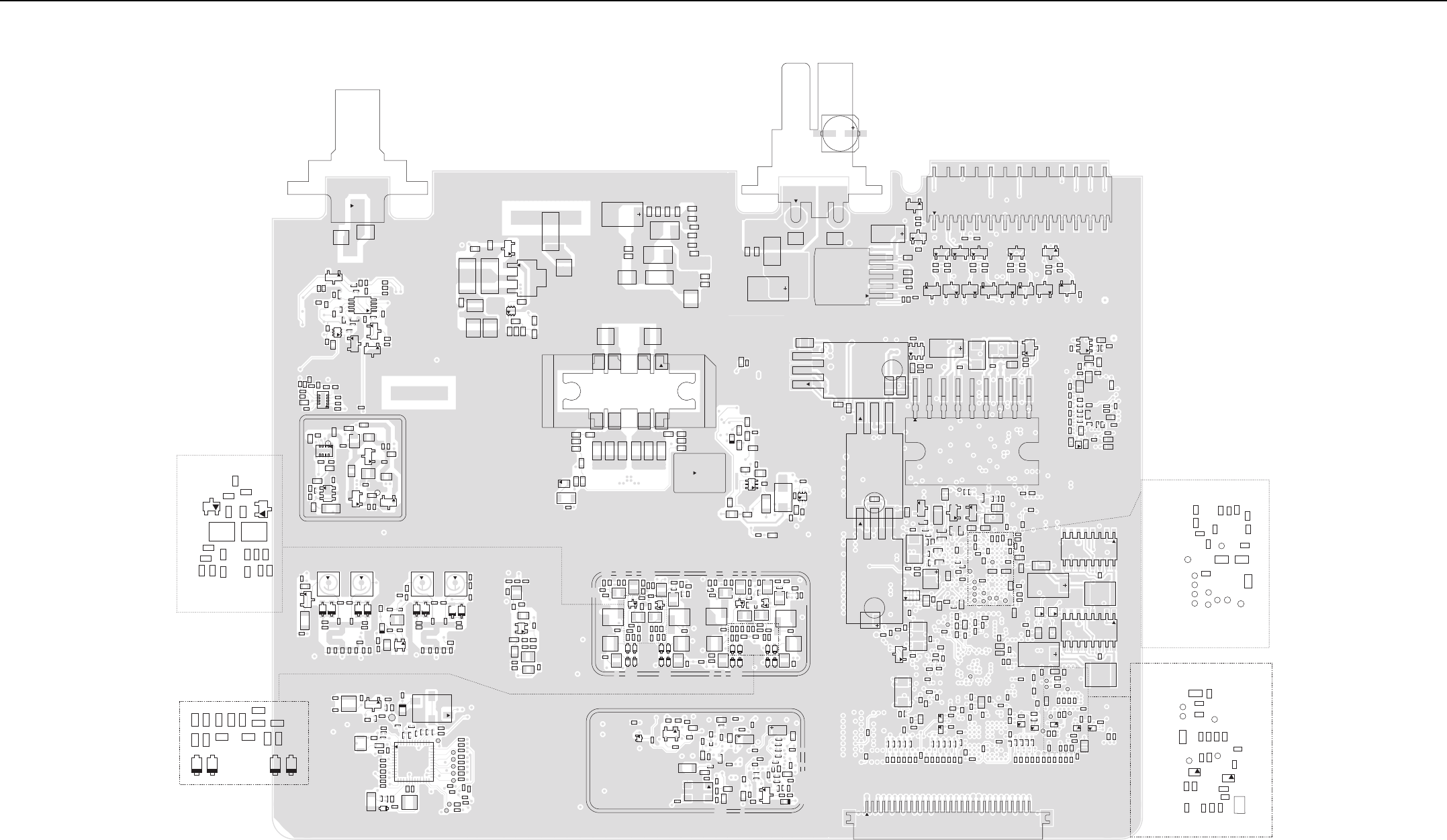
UHF1 (403–470 MHz) 25–40W PCB/Schematics/Parts List 3-21
3.0 UHF1 (403–470 MHz) 25–40W PCB/Schematics/Parts List
2.9V_MAKO_V6
C0100
C0102
C0103
C0104
C0105
C0109
C0110
C0111
C0113
C0117
C0118
C0120
C0121
C0122
C0124
C0125
C0126
C0127
C0128
C0129
C0130
C0132
C0133
C0140
C0141
C0142
C0143
C0144
C0145
C0146
C0171
C0175
C0177
C0178
C0180
C0195
C0196
C0200
C0201
C0205
C0206
C0220
C0226
C0236
C0237
C0240 C0241
C0242
C0250
C0253
C0300
C0301
C0304
C0305
C0306
C0315
C0320
C0326
C0336
C0337
C0340 C0341
C0342
C0347
C0350
C0353
C1000
C1001
C1002
C1003
C1004
C1005
C1006
C1007
C1008
C1009
C1010
C1011
C1012
C1013
C1014
C1015
C1016
C1017
C1018
C1019
C1030
C1031
C1034
C1036
C1037
C2000
C2001
C2002
C2003
C2005 C2007
C2500
C3040
C3202
C3203
C3207
C3208
C3209
C3210
C3211
C3212
C3213
C3216
C3219
C3220
C3225
C3226
C3229
C3234
C3238
C3239
C3240
C3247
C3248
C3249
C3254
C3262
C3273
C3280
C3292
C3514
C3515
C3516
C3518
C3520
C3523
C3524
C3528
C3529
C3530
C3531
C3538
C3543
C3545
C4000
C4001
C4002
C4003
C4004
C4005
C4006
C4013
C4016
C4017
C4018
C4019
C4020
C4021
C4022
C4023
C4024
C4025
C4026
C4027
C4028
C4029
C4030
C4031
C4032
C4033
C4090
C4091
C4092
C6451
CR0201
CR0202
CR0203
CR0204
CR0205
CR0206
CR0207
CR0208
CR0303
CR0304
CR0307
CR0308
E3202
E3205
E3502 E3503
E4000
E4001
3
2
J0700
30
J4001
L0100
L0202
L0203
L0207
L0209
L0210
L0213
L0214
L0215
L0217
L0218
L0302
L0303
L0307
L0309
L0310
L0312
L0313
L0314
L0315
L0317
L0318
L0319
L3200
L3202
Q0100
Q0102
Q0106
Q0300
Q0301
16
1
8
9
Q3200
4
5
8
Q3201
16
1
8
9
Q3202
23
4
Q3203
23
4
Q3204
R0100
R0101
R0102
R0105
R0106
R0107
R0108
R0109
R0110
R0111
R0114
R0116
R0117
R0118
R0119R0123
R0144
R0146
R0147
R0148
R0155
R0156
R0157
R0158
R0159
R0161
R0201
R0204
R0205
R0211
R0224
R0225
R0226
R0301
R0304
R0305
R0311
R0316
R0324
R0325
R0326
R0329
R1000
R1001
R1002
R1005
R1006
R1014
R1017
R1019
R1020
R1021
R1025
R1027
R1028
R1034
R1035
R1036
R1041
R1045
R1066
R1067
R1071
R2000
R2004
R2006
R2011
R2012
R2529
R3203
R3205
R3206
R3217
R3218
R3224
R3225
R3500
R3501
R3505
R3526
R3532
R3535
R3537
R3538
R3547
R3550
R3560
R3571
R3576
R3580
R3583
R3588
R3590
R3594
R3595
R3596
R4000
R4001
R4002
R4003
R4004
R4005
R4011
R4012
R4061
R4063
R4064
R4065
R4066
R4067
R4068
R4069
R4070
R4071
R4093
R4094
R4096
R4105
R6467
RT3500
1
2
SH0100
1
2
SH0301
TP1000
TP4000
TP_POR
U3040
9
U3500
U4006
U4007 U4008
U4009 U4010
VR3202
VR3204
VR3206
VR3503
43
2
Y0100
3.6V_MAKO_SW1
C3276
C3278
C3283
C3511
C3513
R3233
R3503
R3504
R3507
R3508
R3509
R3514 R3515
R3587
TP_MAKO_DCLK
TP_MAKO_FSYNC
TP_MAKO_RX
TP_MAKO_TX
USB1_DAT
USB1_SEO
USB1_TXEN
VBUS1_CMD
VBUS2_CMD
MAKO_GATED_32KHz
C2004
C2006
C2008
C2009
C4034
C4035
C4089
R2005
R2007
R2008
R2009
R2010
R2013
R2014
R2015
R4006
R4009
R4010
R4095
R4097
R4099
TP_SDRAM_BA0
TP_SDRAM_BA1
TP_SDRAM_CLK
TP_SDRAM_CLKX
TP_SDRAM_CS
U4004
U4005
C0308
C0310
C0313 C0314
C0323
C0325
C0329
C0343
C0344
C0345
C0346
C0351
C0352
C0359
CR0301
CR0302
CR0305
CR0306
C0204
C0208
C0213
C0214
C0215
C0223
C0225
C0229
C0243
C0245 C0246
C0247
C0251
C0252
C0259
L0212 L0219
Q0200
Q0201
R0216
R0229
C0900
C0901 C0906
C0907
C0908
C0909
C0910
C0915
C0939
C0967
D0900
D0906
D0907
L0722
63
4
Q0900
Q0901
R0713
R0900
R0901
R0902
R0903
R0906
R0907
R0909
R0911
R0912
R0914
R0915
R0916
R0920
R0923
R0930
R0931
R0986
R0987
U0901
C0751
C0776
C0777
C0778
C0779
C0796
C0797
C0798
C0799
L0712
L0714
4
3
2
1
Q0704
63
4
Q0706
R0729
R0735
R0738
R0745
R0748
R0749
VR0700
C0700
C0701
C0702
C0703
C0704
C0705
C0706
C0707
C0708
C0709
C0710
C0711
C0712
C0713
C0714
C0715
C0722
C3000
C3002
C3015
E0700
E0701
E3000
R0742
SP3000
SP3001
C3005
C3006
C3007
C3018
C3019
C3046
C4040 C4041 C4042 C4043 C4044
C4045
C4046 C4047
C4048
C4075E4005
J3000
25
26
2
J4000
2
3
Q4000
2
3
Q4002
2
3
Q4004
2
3
Q4005
2
3
Q4006
2
3
Q4008
2
3
Q4010
2
3
Q4011
Q4013
R3002
R3003
R3004
R4040 R4041 R4042 R4043 R4044
R4045
R4046 R4047
R4048
R4050
R4051
1
6
5
U3001
VR4000 VR4001 VR4002
VR4003
VR4004
VR4005
C0929
C0960
C0961
C0962
C0963
C0964
C0965
R0981
R0982
R0983
R0984 R0985
R0988
R0994
R0995
4
5
8
U0943
C0914
C0918
C0921
C0922
C0926
C0931
C0934
C0935
C0936
C0937
C0947
C0948
C0949
C0950
C0951
D0901
D0902
D0903
L0901
L0902
R0917
R0924
R0925
R0926
R0927
R0928
R0929
R0936R0937
R0940
R0950
R0989
SH0900
4
58U0940
U0941
C6406
C6407
C6408
C6416
C6417
C6418
C6419
C6420
C6421
C6422
C6423
C6426
C6427
C6428
C6429
C6430
C6431
C6433
C6439
C6440
C6445
C6450
E6401
E6402
E6407
R6402
R6403
R6443
R6444
R6445
R6446
R6449
R6450
R6454
R6455
R6456
R6458
R6459
R6460
R6461
R6465
R6466
U6402
U6407
C3008
C3009
C3010 C3501
C3504 C3505
C3506
E3500
E3501
2
3
Q3500
R3009
R3010
R3516
R3520
U3002
C0966
R0775
R3032
R3033
R3036
R3056
3
2
1
U3006
R3035
3
2
1
U3005
R3042
3
2
1
C0437
C0438
C0439
C0440
C0442
C0451
C0457
L0407
L0411
4
32
Q0405
R0417
R0418 R0419
R0420
R0421
R0422
R0423
R0424
R0425
R0433
R0434
C0404
C0405
C0406
C0407
C0408
C0409
C0410
C0411
C0414
C0415
C0416
C0417
C0419
C0420
C0421
C0423
C0424
C0425
C0426
C0427
C0428
C0429
C0430
C0431
C0432
C0433
C0434
C0458 C0459
C0460
C0461
C0462
D0400
D0401
D0402
D0403
D0404
D0406
D0407
D0408
D0409
L0401
L0402 L0403 L0404
L0405
L0413
4
32
Q0402
R0404
R0405
R0406
R0407
R0409
R0410 R0412
R0432
R0435
R0436
R0437
R0438
R0440 R0441
R0443
R0444
C0502
C0504
C0509
C0510
C0515
C0516
C0605
C0611
C0615
C0617
C0619
C0620
C0621
C0622
C0623
C0625
C0626
C0627
C0629
C0630
C0631
C0633
C0638
C0642
C0643
C0644
C0645
C0646
C0650
CLKOUT
D0601
DOUTA
DOUTB
E0600
E0601
E0602
E0604
E0605
E0606
E0607
E0608
5
6
4
3
2
1
FL0500
FS
L0504
L0506
L0604
L0608
PC
PD
PE
Q0501
R0503
R0510
R0606
R0607
R0608
R0609
R0610 R0611
R0612
R0613
R0614
R0615
R0617
R0618
R0619
R0621
R0622
R0623
R0627
TP0601
U602
1
37
25
13
U0600
C0718
C0724
C0759
C0768
C0781
C0782
C0783
C0788
C0802
C0804
C0805
C0806C0807
C0904
E0702
E0703
E0704
L0723
L0900
1
M0700
Q0701
5
9
6
87
432
10 Q0702
63
4Q0711
R0700
R0702
R0706
R0724
R0725
R0726
R0730
R0732
R0734
R0740
R0741
R0744
R0750
R0751
R0752
R0753
R0756
R0757
R0761
R0762
R0763
R0764
R0768
R0771
R0773
1
RT0908
SP0700SP0701
SP0702SP0703
SP0704
SP0705
SP0706
SP0707
UHF1 (403–470 MHz) 25–40W 8486777Z15 Top Side

3-22 UHF1 (403–470 MHz) 25–40W PCB/Schematics/Parts List
1.2V_RTC_TEST
2.8V_RF_TEST
ANT_C
C0101
C0106
C0107
C0108
C0112
C0114
C0115
C0119
C0123
C0131
C0134
C0135
C0136
C0137
C0138
C0147
C0148
C0149
C0150
C0151
C0156
C0157
C0158
C0159
C0160
C0161
C0162
C0163
C0164
C0165
C0166
C0179
C0191
C0192 C0193
C0194
C0202
C0203
C0207
C0209
C0211
C0217
C0218
C0219
C0221
C0222
C0224
C0230
C0231
C0233
C0235
C0238
C0239
C0248
C0249
C0257
C0258
C0302
C0303
C0307
C0309
C0311
C0316
C0317
C0318
C0319
C0321
C0322
C0324
C0327
C0328
C0331
C0334
C0348
C0349
C0357
C0358
C0360
C0361
C0362
C0363
C0400
C0401
C0402
C0403
C0412
C0413
C0422
C0435
C0436
C0441
C0443
C0444
C0445
C0446
C0447
C0448
C0449
C0452
C0453
C0454
C0455
C0456
C0463
C0464
C0503
C0506
C0507
C0512
C0513
C0514
C0601
C0602
C0603
C0604
C0607
C0610
C0612
C0613
C0614
C0616
C0618
C0628
C0632
C0634
C0635
C0636
C0637
C0640
C0641
C0647
C0648
C0649
C0651
C0716
C0717
C0719
C0720
C0721
C0723
C0725
C0726
C0727
C0728
C0729 C0730
C0731
C0732
C0733
C0734
C0735
C0736
C0737
C0738
C0739
C0740
C0741
C0742
C0743
C0744
C0745
C0746
C0747
C0748
C0749
C0752
C0753
C0754
C0755
C0756
C0757
C0758
C0760
C0761
C0763
C0764
C0765
C0766
C0767
C0769
C0770
C0771
C0772
C0774
C0775
C0780
C0785
C0786
C0787
C0789
C0790
C0791
C0792
C0793
C0794
C0795
C0800
C0801
C0803
C0808
C0809
C0810
C0811 C0812
C0813
C0814
C0815
C0817
C0818 C0819
C0828 C0829
C0832
C0845
C0856
C0861
C0869
C0874
C0902
C0903
C0911
C0912
C0913
C0916
C0917
C0919
C0920
C0923 C0925
C0927
C0928
C0940
C0941 C0942
C0943
C0944
C0945
C0953
C1032
C1033
C1035
C1044
C2501
C3011
C3012
C3013
C3014
C3016
C3017
C3020
C3021
C3030
C3031
C3032
C3041
C3042
C3043
C3044
C3045
C3200
C3201
C3204
C3205
C3206
C3214
C3215
C3217
C3218
C3221
C3222
C3227
C3228
C3231
C3232
C3233
C3237
C3243
C3252
C3257
C3260
C3261
C3265
C3266
C3269
C3270
C3272
C3274
C3275
C3279
C3281
C3282
C3289
C3290
C3291
C3500
C3502
C3503
C3507
C3508
C3509
C3510
C3512
1C3517
C3519
C3521
C3522
C3525
C3526
C3527
C3532
C3533
C3534
C3535
1
C3536
C3539 C3540
C3541
C3542
C4007
C4010
C4011
C4012
C4014
C4015
C4049
C4051
C4053
C4055
C4058
C4059
C4060
C4061
C4062
C4063
C4064
C4065
C4066
C4067 C4068
C4069
C4070
C4071
C4072
C4073
C4074
C4076
C4084
C4085
C4086
C4087 C4088
C4093
C4094
C6401
C6412
C6413
C6414
C6432
C6434
C6435
C6436
C6437
C6438
C6443
C6444
C6446
C6449
C6452
CLK_ACQ_TEST
CR0300
CR0400
D0405
D0500
D0600
D0700
D0702
8
4
5
D0703
D0704
D0904
D0905
D3030
D3040
D3200
D4000
D4001
E0201
E0301
E0302
E0400
E0401
E0403
E0500
E0603
E0609
E0610
E2500
E3201
E3203
E3206
E3208
E4002
E4003
E4004
E4006
E6400
EXT_MIC
EXT_PTT
3
4
2
5
FL6401
FT0400
FT0401
FT_APM_1_WIRE
FT_EMERGENCY
FT_IGNITION_SENSE
FT_MMP_1_WIRE
FT_USB1_DM
FT_USB1_DP
FT_USB2_DM
FT_USB2_DP
FT_VBAT
FT_VBAT_GROUND
FT_VBUS1
FT_VBUS2
I2C_CLK
I2C_DATA
IF_TEST
INT_MIC
G2
20
G1
J2500
11
J4002
14
J4003
J6400
L0200
L0204
L0205
L0206
L0211
L0221
L0300
L0304
L0305
L0306
L0311
L0406
L0408
L0409
L0410
L0412
L0414
L0503
L0602
L0603
L0605
L0700
L0702
L0705
L0706
L0707
L0708
L0709
L0710
L0711
L0715
L0716
L0717
L0718
L0719
L0720
L0721
L0903
L0904
L0905
L3201
L6402
L6403
MAKO_CE
MAKO_V8_5V
MAKO_V9_3V
OPT_SSI_SYNC
Q0107
2
3
Q0108
Q0202
Q0302
63
4Q0400
Q0401
Q0403
Q0500
Q0600
Q0601
1
3
Q0703
Q0705
Q0902
Q3030
4
3
2
1
Q3032
Q3040
2
3
Q3041
2
3
Q3205
6
3
4
Q3206
4
58
Q3207
2
3
Q3208
Q3209
Q3210
63
4
Q3502
63
4
Q3503
Q3504
Q3505
2
3
Q4001
2
3
Q4003
2
3
Q4007
2
3
Q4009
2
3
Q4012
Q4014
2
3
Q4015
Q6401
63
4
Q6402
R0103
R0104
R0113 R0115
R0120
R0122 R0125
R0126
R0127
R0128 R0131
R0134
R0139
R0140
R0160
R0202
R0203
R0206
R0207
R0208
R0210
R0212
R0213
R0218
R0219
R0220
R0221
R0230
R0302
R0303
R0306
R0307
R0308
R0310
R0312
R0319
R0320
R0321
R0327
R0331
R0332
R0333
R0334
R0337
R0400
R0401
R0402
R0403
R0411
R0413
R0414
R0415
R0416
R0426
R0427
R0428
R0429 R0430
R0431
R0500
R0501
R0502
R0508
R0509
R0511
R0512
R0601
R0602
R0603
R0604
R0605
R0616
R0620
R0624
R0625
R0626
R0701
R0709
R0711
R0712
R0714 R0715
R0718
R0719
R0720
R0722
R0727 R0728
R0739
R0743
R0747
R0754
R0755
R0759
R0760
R0765
R0766
R0769
R0770
R0777
R0910
R0913
R0918
R0919
R0921
R0922
R0938
R0941
R0942
R0943
R0944
R0946
R0947
R0951
R0954
R0955
R0960
R0970
R0971
R0973
R0974
R0975
R0976
R0977 R0978
R0979
R1026
R1044
R1046
R1047
R1048
R1054
R1060
R1070
R2500
R2501
R2502
R2504
R2506 R2507
R2508
R2509
R2510
R2511
R2512
R2513 R2514
R2515
R2516
R2517
R2518
R2519
R2520
R2524
R2525 R2526
R2527
R2528
R3005
R3006
R3007
R3008
R3030
R3034
R3037
R3038
R3039
R3040 R3041
R3043
R3044
R3045
R3046
R3047 R3048
R3050
R3051
R3052
R3053
R3054
R3055
R3057
R3200
R3204
R3207
R3208
R3209
R3210
R3215
R3216
R3219
R3220
R3222
R3223
R3226
R3227
R3228
R3236
R3237
R3238
R3239
R3240
R3241
R3243
R3245
R3246
R3247
R3248
R3249
R3250
R3252
R3253
R3502
R3506
R3510
R3511
R3512
R3513
R3521
R3523
R3524
R3525
R3528
R3529
R3530
R3533
R3534
R3536
R3539
R3540
R3541
R3542
R3544
R3545
R3546
R3548
R3549
R3551
R3552
R3553
R3554
R3555
R3556
R3558
R3559
R3569
R3572
R3573
R3574
R3575
R3577
R3578
R3579
R3581
R3582
R3584R3585
R3586
R3591
R3592
R3593
R4023
R4030
R4031
R4032
R4033
R4034
R4035
R4049
R4054
R4055
R4074
R4076
R4078
R4079
R4080
R4081
R4082
R4083
R4085
R4086
R4088
R4089
R4090
R4098
R4100
R4101
R4103
R4106
R6401
R6404
R6405
R6407
R6409
R6410
R6411
R6416
R6417
R6418
R6419
R6420
R6430
R6432
R6433
R6434
R6435
R6436
R6437
R6438
R6439
R6440
R6457
R6464
R6468
R6469
R6470
RF_ATTN_2
ROUT_TEST
1
RT0953
S0700
1
2SH0101
1
2
SH0300
2
1
SH0500
12
SH0901
SPI_CLK_1
SPI_CLK_TEST
SPI_MISO_1
SPI_MOSI_1
6
4
3
T0400
64
3
T0401
TP501
TP502 TP503
TP504
TP0301
TP0600
TP0702
TP0703
TP0704
TP0705
TP0707
TP0708
TP0709
TP0710
TP0711
TP0713
TP0903
TP0904
TP0907
TP0909
TP0910
TP0911
TP0913
TP_ADAPT_SW
TP_DDR_LDQS
TP_DDR_UDQS
TP_FLASH_CLK
TP_TEST1
TP_TEST2
TP_VCTRL
TX_RAMP
TX_RAMP_DAC
L11A11
L1
U0100
4
3
5
U0101
U0201
6
3
4
U0303
U0304
U0601
U0700
U0900
U0942
A21 AA21
AA1
U1000
43
6
U1006
A1 M1
M8
A8
U2000
K1
A9
K9
U2001
1
6
5
U3003
U3004
14
58
U3030
P1
A1
A14 P14
U3200
64
3
U3201
C1
C3A3
U3202
4
3
5
U3203
10
6
5
U3501
7
8
14
U3502
85
4
U3503
U3504
7
814
U3505
85
4
U3508
16
1
8
9
U4000
14
7
8
U4001
P10
A10
P1
A1
U6401
U6404
C1
C3
A3
U6405
U6406
U6408
VR3000
VR3040
VR3200
VR3201
VR3203
VR3205
VR3207
VR3208
VR3502
VR3504
VR4006
VR4009
VR6400
43
2
Y1000
4
3
2
Y3200
Y3201
UHF1 (403–470 MHz) 25–40W 8486777Z15 Bottom Side
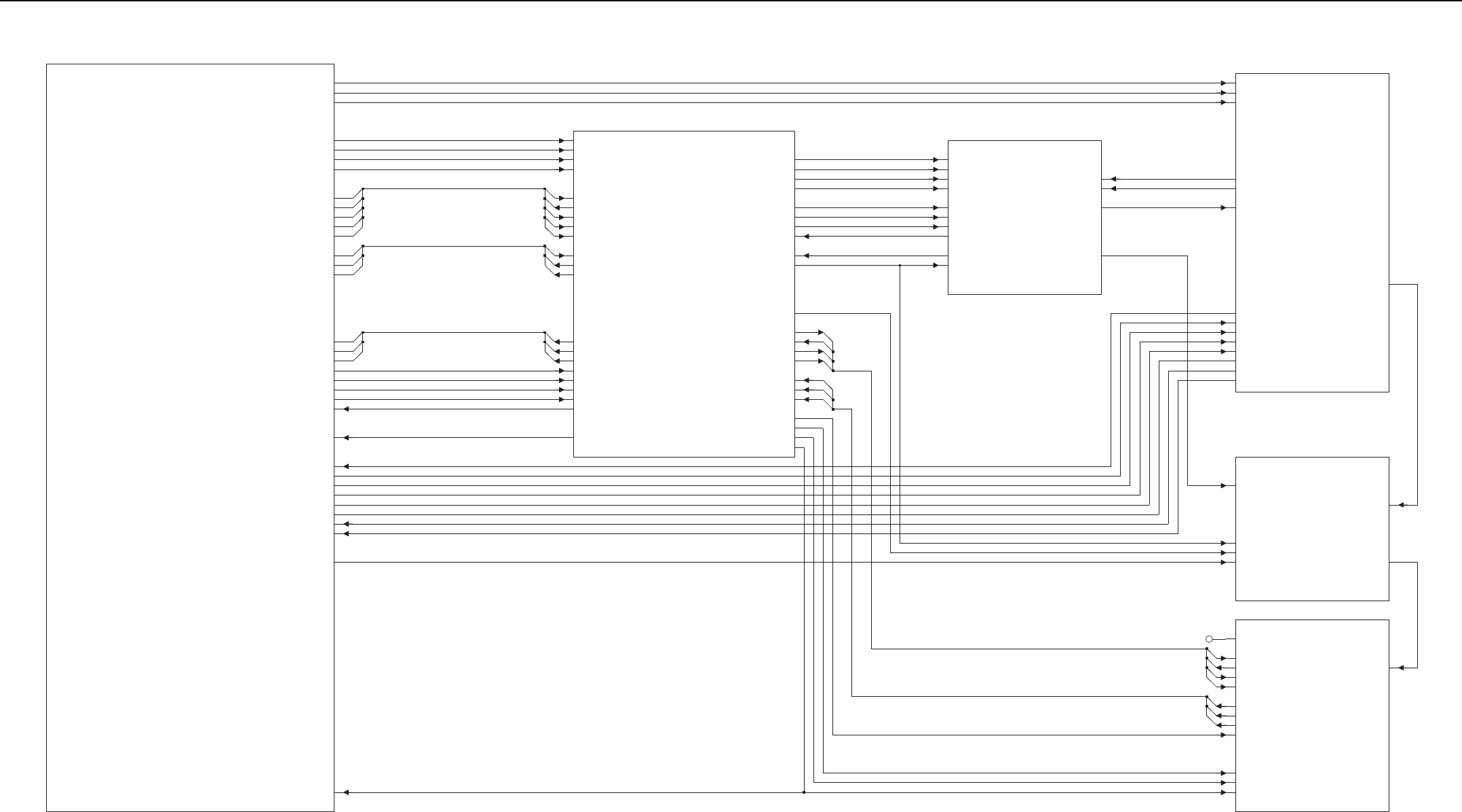
UHF1 (403–470 MHz) 25–40W PCB/Schematics/Parts List 3-23
( RX: SHEET 2 )
VCO_UHF1
( TX: SHEET 1 )
CONTROLLER_&_GPS_R6
( TOP LEVEL: SHEET 1)
( PA: SHEET 1 )
( PC: SHEET 2 )
TX_HP_UHF1
SYNTH
RXFE_UHF1
( 1 SHEET )
RXBE_73.35MHZ
(IF AMP: SHEET 1)
(ABACUS3: SHEET 2)
2
NC
1
3
4
SF_TH
TXINJ
TX_VCO_SEL1
TX_VCO_SEL2
VCTRL
1
0
2
1
0
2
3
9R1
9V3_SYNTH_IN
9V3_SYNTH_OUT
9V3_VCO
HP_MOD_OUT
PRSC
RXINJ
RX_VCO_SEL1
RX_VCO_SEL2
2
0
0
1
1
22
2
1V8
5V
5V_FE
IF
REF_CLK
SPI_ABACUS_CEX
SPI_ABACUS_CLK
SPI_ABACUS_DATA
SSI_ABACUS_CLKOUT
SSI_ABACUS_DOUTA
SSI_ABACUS_DOUTB
SSI_ABACUS_FSYNC
SSI_ABACUS_SYNCB
1
0
0
2
9R1
FE_TUNE IF
RF_ATTEN_1
RX_IN
RX_INJ
0
1
1
1
3
0
VCTRL
0
1
4
3
2
2
RX_SSI_FSYNC_PASS_OUT
RX_VCO_SEL1_
RX_VCO_SEL2_
SDTX
SFTX
SF_OUTSPI_CLK_IN
SPI_CLK_OUT
SPI_MISO_IN
SPI_MISO_OUT
SPI_MOSI_IN
SPI_MOSI_OUT
TH_CEX
TX_CLK
TX_VCO_SEL1_
TX_VCO_SEL2_
ABACUS3_CEX_IN
ABACUS3_CEX_OUT
ABACUS3_SYNCB_IN
ABACUS3_SYNCB_OUT
ADAPT_SW
DMCS
HP_MOD_OUT
LOCK
PRSC
RF_ATTN_1
RSTB RX_SSI_CLK_PASS_IN
RX_SSI_CLK_PASS_OUT
RX_SSI_DATA_PASS_IN
RX_SSI_DATA_PASS_OUT
RX_SSI_FSYNC_PASS_IN
RX_IN
TX_DAC
TX_INJ
VSWR_DET
0
1.8V_TH_DIG
16.8_GPS
16.8_REF
1V8_BE
2.8V_TH_ANA
2.8V_TH_DIG
5V
5V_BE
9R1
9V3
SPI_MOSI
THK_CS
TX_SSI_CLK
TX_SSI_DATA
TX_SSI_FSYNC
9V3
9V3_PA
9V3_SYNTH
9V3_VCO
ANT_ENABLE
FINAL_BIAS_1
LO_BATTERY_DET
LO_PWR_DET
PA_SUPPLY
PC_ATTEN_ENA
PRESSURE_PAD
MAKO_ADC5
MAKO_ADC8
MAKO_DAC1
MAKO_DAC2
MAKO_RAMP_DAC3
PC_ATTEN_ENA
PRESSURE_PAD_DET
RAW_B+
RESET_OUT
RX_SSI_CLK
RX_SSI_DATA
RX_SSI_FSYNC
RX_SSI_SYNCB
SPI_CLK
SPI_MISO
TX_SSI_BUS(0:2)
ABACUS_SPI_BUS(0:3)
SPI_BUS(0:4)
RX_SSI_BUS(0:2)
ABACUS_SSI_BUS(0:2)
1.875V_DIG_V2
16.8_GPS
16.8_MHZ_BUFF
2.775V_ANA_V7
2.775V_DIG_V4
5V_SW
9V3
9V3_PA
ABACUS3_CS
ADAPT_SW
ANT_ENABLE
DMCS
LOCK_DETECT
LO_BATTERY_DET
UHF1 (403–470 MHz) 25–40W Overall Schematic Diagram

3-24 UHF1 (403–470 MHz) 25–40W PCB/Schematics/Parts List
(Not Placed)
7.0 VDC
Hi-Side Zeros for Preselector
Zo/Zin=4:1
10 dB Attenuator
0.7 VDC
Zo/Zin=4:1
(3.00 ~ 8.00 VDC)
+16.0 dBm Min. (250 mV P-P)
MAKO ( 0 ~ 4.6 VDC)
3.7 VDC Typical
8.9 VDC Typical
0.8 VDC Typical
3.0 VDC Typical
(Micro-strip 20 mm Each)
C0464
C0444
R0404
C0453
FT0401
1
C0459
C0423
C0409
RX_INJ_FE_5
C0454
C0449
D0403
R0436
NU
D0407
C0416
Q0403
2
3
6
4
1
5
R0437
R0405
C0414 D0404
R0414
9R1_FILT
E0401
C0452
C0460
D0402
L0408
D0401
C0422
C0402
(VALUE)
NU
R0431
NU
L0414
C0433
C0434
R0430
C0406 R0400
RXIN_FE_6
FE_TUNE_FE_4
D0405
1IO1 2
IO2
3
IO3
4IO4
L0407
R0440
C0420
CR0400
1
3
2
D0409
NC
R0402
L0402
12
3
NU
R0422
D0400
C0440
IF_FE_8
R0425
D0408
C0463
NU
NU
C0439
C0410
E0400
4
6
3
2
1
(VALUE)
T0400
5
NC
1
C0428
FT0400
C0419
L0409
R0403
NU
(VALUE)
C0411
C0405
C0447
RF_ATTEN_1_3
C0427
R0407 R0441
L0401
(VALUE)
NC
C0457
C0441
(VALUE)
R0415 R0416
R0417
R0426
C0445
C0417
9R1_FILT
R0424
C0412
C0413
C0403
R0435
C0429 C0432
NU
C0431
C0400
R0444
C0451
L0413
NC
5
4
6
3
2
1
R0428
T0401
C0421
R0409
C0437
L0410
12
3
R0427
L0403
C0456
C0438
C0442
NC
C0408
3
1
4
C0430
Q0400
NU
2
5
6
R0421
C0407
C0446
C0435
NU
C0461
C0401
R0418
E0403
R0410
R0434
R0420
C0436
C0462 R0443
R0412
C0415
L0405
12
3
(VALUE)
R0423
L0411
C0426
C0425
.0476
C0448
R0433
R0406
Q0402
Q0405
R0413
R0429
R0419
9R1_FE_6
C0424
25
6
3
1
4
C0443
Q0401
C0458
9R1_FILT
L0412
L0406
D0406
R0438
NU
R0411
R0432
NU
C0455
12
3
NU
L0404
C0404
RX_INJ
R0401
RF_ATTEN_1
IF
RX_IN
FE_TUNE
9R1
UHF1 (403–470 MHz) 25–40W Receiver Front-End Schematic Diagram
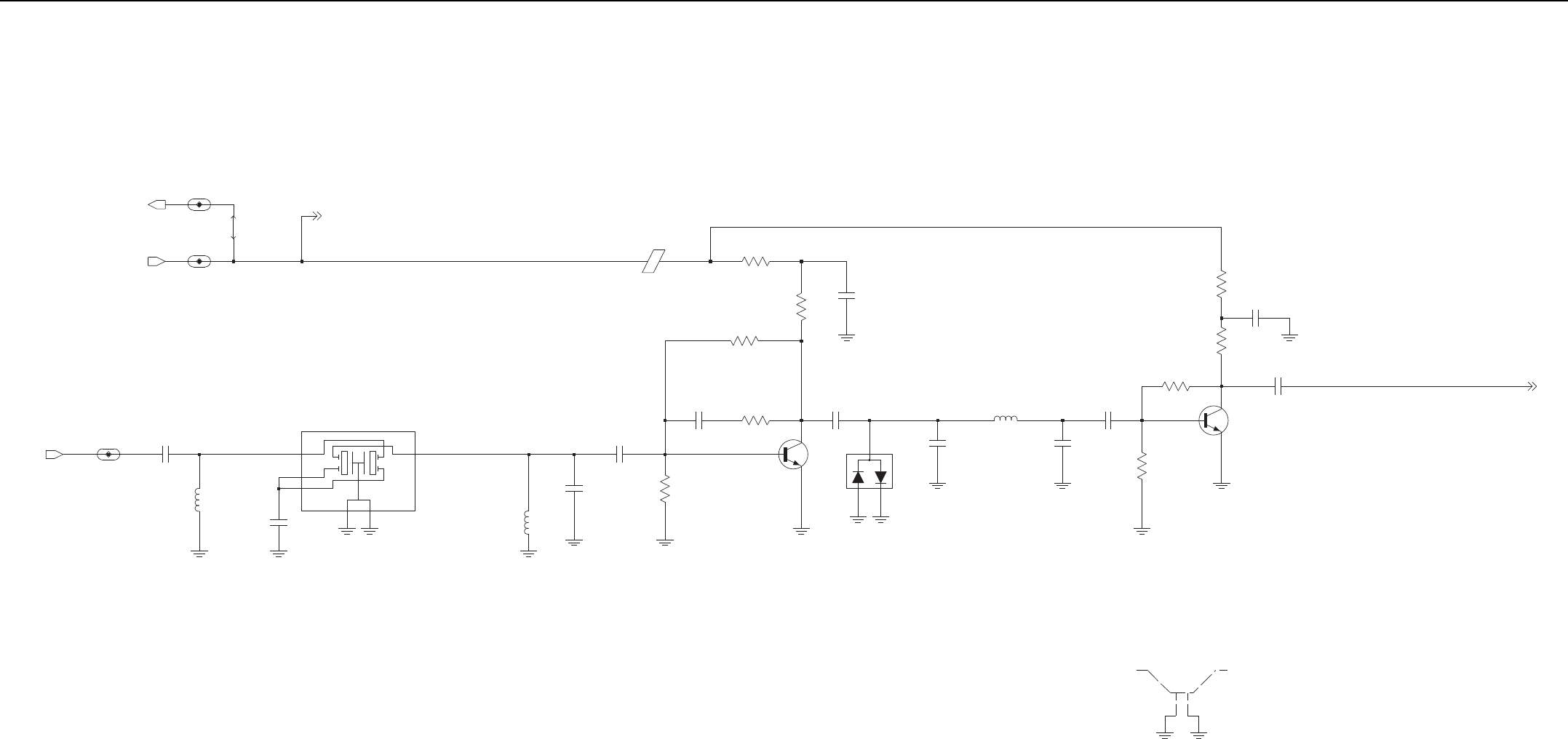
UHF1 (403–470 MHz) 25–40W PCB/Schematics/Parts List 3-25
1.43V
0.76V
1.6V
0.72V
4-POLE
IF_TO_ABACUS
73.35MHz
R0511
IFIN_BE_8
R0512
C0514
R0508
R0509
NU
C0510
L0504
GND1
2
GND2
5
IN
1OUT 4
FL0500
CC1
3
CC2
6
L0506
C0516
NU
5V_BE_5
C0502
NU
C0515
C0503
C0513
SH0500
1
2
R0503
Q0501
E0500
L0503
C0509
NU
RX_FE_3
R0510
C0506
1
3
2
C0507
Q0500
C0504
R0502
R0500
D0500
R0501
C0512
IF
IF_OUT
5V
5V
5V_FE
UHF1 (403–470 MHz) 25–40W Receiver IF Amp Schematic Diagram
3-26 UHF1 (403–470 MHz) 25–40W PCB/Schematics/Parts List
2nd LO VCO UHF (71.1MHz/75.6 MHz)
SPF_3.5V
CLOCK LF
2nd LO LF
CLOCK VCO
#
*
R0611
R0605
FD_1_BE_5
R0602
R0616
C0620
D0600
E0609
C0604
C0621
C0634
E0602
E0605
3VA
C0611
Q0601
SB_1_BE_5
PC
TP0601
R0615
C0649
FE_1_BE_5
NU
C0616
U602
1
C0632
L0608
C0607
C0605
NU
R0607
C0646
3VA
DOUTA
L0602
R0606
C0648
L0604
C0642
C0601
CLKOUT_1_BE_5
VVCO
C0628
C0602
C0638
R0603
C0640
FC_1_BE_5
R0617
R0601
E0607
VVCO
C0627
C0631
C0629
FS
R0625
5V
3VA
C0623
C0615
R0612
3VA
FREF_IF
C0610
R0618
C0644
L0605
PE
C0613
E0600
R0624
C0636
E0610
C0635
R0613
3VA
C0651
C0618
C0647
D0601
C0626
R0608
E0603
DOUTB
C0622
C0645
48
VDDI
40
VDDL
39
VDDP
14
VDDQ
12
VREFN
11
VREFP
C0625
25
PE
RREF
13
33
SYNCB
9
VDDA
17
VDDC
26
VDDD
6
VDDF
27
VDDH
15
IOUTC
38
IOUTL
42
LON
43
LOP
2
MXON
1
MXOP
23
PC
24
PD
36
GNDL
37
GNDP
16
GNDQ
21
GNDS1
34
GNDS2
4
IF2N
5
IF2P
47
IFIN
8
GCN
7
GCP
10
GNDA
18
GNDC
22
GNDD
3
GNDF
32
GNDH
45
GNDI
CLKP
19
46
CXIF
44
CXVL
41
CXVM
29
DOUTA
30
DOUTB
35
FREF
31
FS
U0600
20
CLKN
28
CLKOUT
FS_1_BE_5
R0627
C0637
R0621
3VA
TP0600
R0610
R0620
C0603
C0633 R0614
3VA
E0604
VCONT
4
VIN
3
VOUT 1
3VA
R0604
U0601
FB
2
GND
5
NP
6
3VA
CLKOUT
DOUTA_1_BE_5
C0619
C0641
E0606
C0630
C0617
R0619
E0601
NU
R0623
L0603
C0643
C0614
DOUTB_1_BE_5
PD
1V8_3
Q0600
E0608
C0612
C0650
R0609
R0622
R0626
NU
IF_OUT
5V
SSI_ABACUS_FSYNC
SPI_ABACUS_CEX
REF_CLK
SPI_ABACUS_CLK
SSI_ABACUS_DOUTA
SSI_ABACUS_CLKOUT
SSI_ABACUS_DOUTB
SPI_ABACUS_DATA
SSI_ABACUS_SYNCB
1V8
1V8
UHF1 (403–470 MHz) 25–40W Receiver Back-End Schematic Diagram
UHF1 (403–470 MHz) 25–40W PCB/Schematics/Parts List 3-27
PA_SUPPLY_TX_PA
PA_SUPPLY
E0703
9V3_PA
Antenna_En
Test Point to check 11dB/17dB Pad
18dB RL
+8 dBm
Ref Osc Warping
R0715
R0711
L0709 C0768
C0763
C0736
TP0705
TX_INJ_TX_PA
NC
R0760
R0714
R0712
D0704
C0728
L0711
LO_PWR_PAD
TX_INJ
HI_PWR_PAD
-3 dBm
C0733
TP0703
1
C0752 13 dBm
3.2VDC
TP0704
L0705
R0706
3
VD_RF_OUT
U0700
GND1
2
GND2
4
RF_IN
C0724
C0718
C0725
E0704
R0700
R0702
NU
9V3_TX
9V3_Tx_Sw
2.2K
47K
47K
47K
Q0701
C0701
E0700
C0702C0700
E0702
9V3_TX
L0702
C0716
C0717
TP0702
R0754
R0755
R0718
R0720
D1
G
3
S
2
Q0703
NU
C0771
R0722
R0727
R0728
C0770 M0700
1
POS
NU
C0790
C0786
C0787
C0791
R0739
NU
C0815
V_cont
C0792
NU
C0794
C0793
9V3
9V3_VCO
9V3_SYNTH
C0801
R0751
NU
C0800
R0750
C0802
V_cont
R0747
C0789
C0814
NU
L0720
D
G
S
Q0705
R0759
R0777
2.10V (27.5W)
2.85V (44W)
9.1VDC
NU
C0788
TP0710 TP0709
NU
R0744
NU
L0723
R0734
9V3_TX
C0775
L0715
C0780
L0717
C0785 C0734
L0718
NU
C0795
L0721
C0817
C0818
C0829
C0856
C0828
C0760
NU
C0753
C0809
NU
C0755
NU
C0813
C0744C0743
NU
C0764
C0756
NU
C0754
C0765
NU
NU
C0819
C0808
NU
C0749
R0773
R0771
C0774
R0768
C0874
R0770
R0769
R0766
C0761 C0861
SP0701
Gate_2
1PIN1 2
PIN2
HS0700
L0708
C0738
C0735
C0739 C0740
C0803 C0742
L0706 L0707 C0723
R0971
R0970
L0903
L0905
W = 0.625 mm
W = 0.625 mm
W = 2.5 mm
S = 0.93 mm
L = 19 mm
S = 0.54 mm
L0722R0713
C0767
C0772
NU
C0766
D0702
R0701
R0978
C0940
D0904
C0942
C0941
R0976R0977
R0975
L0904 R0973
NU
R0974
2
J0700-33
J0700-1
1
J0700-2
D0905
C0945
R0979
C0944
C0943
REV_DETECTED
9V3_TX
LO_PWR_PAD
HI_PWR_PAD
FINAL_BIAS_1
FWD_DETECTED
FWD_POWER
V_CONTROL
RX_IN
R0752
R0753
RX_IN_TX_PA
FINAL_BIAS_1_TX_PA
9V3_TX
LO_PWR_PAD
HI_PWR_PAD
V_cont
Final_Bias
C0797
C0796
R0761
TP0713
R0749 ANT_ENABLE_TX_PA
R0748
Antenna_En
ANT_ENABLE
C0798
NC
C0799
S0700
R0775
C0966
PRESSURE_PAD_TX_PA
PRESSURE_PAD
TP0711
Final_Bias
C0758
NU
C0757
C0759
L0716
R0743
9V3_Tx_Sw
A3
A4
A5
K1
K2
K3
K4
D0703
A1
A2
NC
Q0706
R0745
NC
R0738
Q0704
C0776
2.2VDC (TX Only) 2.2VDC (TX Only)
TP0707
NC
TP0708
R0740
C0782
R0741
R0757
C0781
R0732
VR0700
PRESSURE_PAD
Gate_2
R0730
Gate_1
R0756
C0805
C0804
C0778
R0729
R0735
C0777 C0779
L0714
A+
ATC
L0710
C0748
C0751
NU
L0712
NU
NU
C0741
NU
C0727
ATC
NU
C0806
C0812
NU
C0721
C0747
NU
C0746
SP0707
SP0705
SP0704
SP0706
SP0703
SP0702
R0719
ATC
NU
C0720
C0807
NU
C0811
C0719
NU
C0737
C0726
C0810 L0719
D0700
C0704C0703
NU
C0706 C0707
NU
C0708C0705 C0709
C0714
E0701
C0713
R0742
C0722
NU
C0715
NU
L0700
A+
C0710 C0712
C0711
NU
R0762
R0763
R0765
R0764
C0869
C0845
C0769
NU
C0729
C0731
NU
C0745
C0730
NU
MRF1570, Flat Lead
Q0702
C0832
C0732
SP0700
R0709
Gate_1
UHF1 (403–470 MHz) 25–40W Power Amplifier Schematic Diagram

3-28 UHF1 (403–470 MHz) 25–40W PCB/Schematics/Parts List
SH0901
1
2
SH0900
1
2
R0937
C0950 2FB
5GND
6NP
4VCONT
3VIN
1
VOUT
U0941
C0948
5V
5V DC
C0949
C0951
0.1uF
9V3
R0940
NC NC
6
RFIN 1
VAPC
7
VPOS 8
3
VSET
U0940
COMM
5
ENBL 2
FLTR 4
GND
C0921 C0922
C0926
R0950
R0941
9
5
NC2
1
RESET_OUT
U0942
GND
3
INPUT
2
4NC1
C0953
LO_BATTERY_DET
LO_BATTERY_DET
2.10V (27.5W)
2.85V (44W)
TP0909
V_CONTROL
1.35V (44W)
1.28V (27.5W)
C0925 RT0953
R0954
C0902
R0946
R0955
R0942
TP0910
C0903
6
5
7
8
4
U0900-2
R0947
C0923
C0927
R0943 R0951 R0944
TP0911
C0928
R0987 C0967 D0907
5.1V
NC
R0938
R0986
C0908
R0923 R0914
C0909
9V3_PC
U0901-1
2
3
1
8
4
R0994
NU
R0995
NU
LO_PWR_DET
C0965
R0984
NU
R0981
R0982
R0983 R0985
LO_PWR_DET
TADJ
VOUT
VPOS
VSET
CLPF
COMM
GND
INHI
INLO
C0964
R0989
NU
6
5
7
4
U0943
3
2
9
1
8
C0961 C0962
R0988
C0960
C0963
5V
D0903
C0937
9V3_PC
C0934
C0916
C0935
C0914 R0917
R0929
9V3_PC
NC
R0926
R0928
NCNC
D0902
R0925
C0936
R0927
L0902
R0924
D0901
C0931
L0901
R0913
Q0902
C0918
3
1
8
4
U0900-1
2
9V3_PC
C0913
C0920
R0918
C0911
R0922
R0919
R0921
R0960
C0919
C0917
Q0901
9V3_PC
R0930
C0915
D0900
1
2
3
R0900
1
2
3
D0906
R0906
4
U0901-2
6
5
7
8
9V3_PC
0.6V typical
Cutback starts about 2.2V
TP0907
C0929
R0931
NOTE: VOLTAGES SHOWN FOR ANALOG TX MODE
2
5
6
3
1
4
C0900 C0901
Q0900 9V3
Cypher: 2.4Kohm 5%
R0907
C0904
R0902
TP0913
R0901
L0900
RT0908
R0903
9V3_PC 9V3
C0907 C0906
R0909
4.0V (44W)
3.2V (27.5W)
0.38V (44W)
0.21V (27.5W)
C0910
TP0904
R0916R0915
TP0903
R0912
C0939
R0911
R0920
9V3 to FW bias PIN in HP mode
R0724
R0725
HI_PWR_PAD
9V3 to REV bias PIN in LP mode
5
6
3
1
4
Q0711
2
PC_ATTEN_ENA_TX_PA
C0783
R0726
PC_ATTEN_ENA
9V3_TX
LO_PWR_PAD
FWD_DETECTED
REV_DETECTED
VSWR_DET
FWD_POWER
TX_DAC
9V3
TX_DAC
VSWR_DET
9V3
R0910
C0912
C0947
R0936
UHF1 (403–470 MHz) 25–40W Power Control Schematic Diagram

UHF1 (403–470 MHz) 25–40W PCB/Schematics/Parts List 3-29
R1
R2
10K
47K
0.5 ppm
VHF=1500pF
---
Note: High Port modulation injection through loop filter for U1 and U2 only
HI: 2.8V
U1=220pF
U2=120pF
C0191,C0192,C0193,C0194: NU (UHF B1)
VHF=1500pF
SF_OUT VOLTAGE: 2.45V
Unlocked: 0V
U1=220pF
Buffer to Abacus/Controller
9R1 SWITCH FOR FRONT-END
C0157, C0159, C0160,C0162,C0163,C0191,C0192,C0193,C0194: NU (UHF B2)
GPO LINES
U2=120pF
U1=220pF
U1=220pF
VCO STEERING LINE VOLTAGE: 0.6V TO 4.4V
U2=120pF
VCO STEERING LINE VOLTAGE: 0.6V TO 4.4V
VHF=1500pF
VHF=1500pF
U2=120pF
U2=120pF
Adapt OFF: 0V
U1=220pF
VHF=1500pF
4875188M01
LOW: 0V
1.5 ppm
VCO SEL: ACTIVE LOW
Adapt ON: 5V
Locked: 1.8V
GPO_4
TCXO (Y0100)
Switch for Adapt Transient
NC
NC
NC
R0170
C0166
C0100
C0105
L0100
C0137
RX_SSI_DATA_IN
NC
R0114
R0147
SPI_MOSI_IN
NU
ABACUS3_SYNCB_OUT
R0100
NC
5V_BE_SYNTH
TP504
1
RX_SSI_CLK_OUT
C0107
NC
NC
C0136
C0133
NC
C0140
1
C0106
NC
TP_TEST1
SPI_MISO_IN
R0160
NC4
3
OUTPUT
4
VCC
1VCONT
NC
NC
NC
Y0100
16.8MHz
GND
2
5
NC1
NC2 6
NC3 7
8
R0113
9R1_SYNTH
C0148
C0102
C0138
3GND
1INOUT
4ONOFF_CONTROL
2OUTIN
5
VCC
R0125
NC
U0101
NC
GPO_3_SYNTH
NC
NC
C0179
ABACUS3_SYNCB_IN
RX_SSI_DATA_OUT
C0147
C0135
C0171
C0132
C0157
C0127
NC
LOCK_SYNTH
R0140
C0120
Q0100
C0194 C0159
C0191
NC
VCTRL_SYNTH
C0126
C0112
NC
NC
NC
NC
1V8_BE_SYNTH
SF_OUT_SYNTH
R0158
NU
HP_MOD_OUT_SYNTH
16.8_REF_CONTROLLER_SYNTH
NU
C0119
NC
NU
C0113
NC
1
R0148
1
2
TP_VCTRL
SH0100
1
2
SH0101
R0159
C0144
NC
C0160
ABACUS3_CEX_IN
R0118
C0141
NC
RX_SSI_CLK_IN
C0162
C0103
R0103
R0107
C0124
Q0108
R0122
NC
RX_SSI_FSYNC_IN
NC
NC
NU
C0161
C0122
NU
GPO_6_SYNTH
9V3_SYNTH
R0157
Q0106
GND
IN
OUT
C0117
C0134
R0115
TX_DAC_VCC
G7
TX_GND1
F6 TX_GND2
J6
TX_VCC
F1
VCO_DAC
K5 XOSC_BASE
XOSC_EMIT
L5
G6
XOSC_GND
TCLK
D7
TEST1 C7
TEST2
B3
TM
F10
TXCLK
K7 TXI
L7 TXQ
H7
TX_DAC_GND L6
SPI_CLK
D10
SPI_DR
D9
SPI_DW
SSI_GND E8
E11
SSI_VCC
SUB1
K10
F5 SUB2
F3 SUB3
G8
SDM_VAG
A9
SDM_VREFM B8
SDM_VREFP
D11
SDR
F11
SDTX
F9
SFTX
K4 SF_OUT
C9 SMD_CLK_GEN_GND
C11
A5
RX_AVCC2
RX_EN_OUT
B1
D3
SCAN_EN
F2 SCAN_IN
E9
SCLK_OUT
SDM_CLK_GEN_VCC A10
SDM_REF_GND A8
SDM_REF_VCC B9
B10 RXFS
C2 RXI
C1 RXIX
D1 RXQ
D2 RXQX
RX_AGND1 C3
D5
RX_AGND2
B2
RX_AVCC1
OSCREG_GND
OSCREG_OUT
H5
J4 OSCREG_SPLY
K11 PABIAS_DAC
L9 PHCLK
RFSTEPA
A3
E6 RSTB
E7
RXACQ
E10
M_PRSCX
A1 NC1
A11 NC2
NC3
L1
L11 NC4
NTXI
L8
NTXQ
K6
L4 OSCREG_BYP
J5
MAIN_GND
MAIN_PDET_VCC G2
J1
MAIN_VCC
H1
MN_ADAPT_CP
G3
MN_CP
G5
MN_CP_GND
MN_CP_VCC H2
J2
M_PRSC
H3
GPO5
H8 GPO6
K8
HP_MOD_OUT
J9 INCR_DECR
F8
LGND1 C8
LGND2
G10
LVCC1
B7
LVCC2
G4
ESC_TEST
K2
ESC_VCC
C6 FBI
B6 FBQ
B4 GPO1_TEST1
A4 GPO2_TEST2
GPO3_TEST3
E5
GPO4_TEST4
D4
K9
EF_OUTM
J8
J7 EF_OUTP
ESC_CP L3
ESC_CPBIAS L2
K3
ESC_CP_GND J3
ESC_CP_VCC
H4
ESC_GND
K1
ESC_IN
E1
G9 CLK_CP
H11 CLK_EMIT
H10
CLK_GND
J10
CLK_VCC
G1
DAC_ADAPT
A2 DC_CAL
L10 DEEPSLEEP
F7
DMCS
BP_I
F4 BP_IX
E2 BP_Q
BP_QX
E3
D8
CEX
H9 CLK1_OUT
J11 CLK2_OUT
G11 CLK_BASE
D6 ACE2
AGC_DAC
B5
AGC_FLAG
C4 AGC_REF
C5
H6 ARX_DAC
C10 ASPI_CLK
B11 ASPI_DATA
A7
ASPI_VCC
E4
U0100
A6 ACE1
DMCS_SYNTH
C0131
C0130
R0131
C0128
SPI_CLK_IN
NU
C0121
1
NC
TP_TEST2
C0129
C0165
R0146
ADAPT_SW_SYNTH
C0143
C0125
2.8V_TH_ANA_SYNTH
RX_SSI_FSYNC_OUT
C0178
C0177
C0175
NC
SFTX_SYNTH
NC
C0156
R0105
R0110
R0144
NC
R0161
C0110
PRSC_SYNTH
R0116
C0101
NC
C0164
C0104
NC
R0134
C0123
C0158
TX_CLK_SYNTH
C0109
NC
NU
R0126
Q0107
R0120
R0155
C0146
ABACUS3_CEX_OUT
NC
1
NC
C0115
TH_CEX_SYNTH
TP_ADAPT_SW
SPI_MOSI_OUT
GPO_2_SYNTH
R0102
TP503
1
NC
C0142
C0108
NC
NC
NC
SDTX_SYNTH
NC
R0104
R0111
RSTB_SYNTH
1.8V_TH_DIG_SYNTH
C0180
TP501
1
R0119
R0128
R0123
C0145
R0108
C0114
C0149
C0196
C0195
SPI_CLK_OUT
16.8_GPS_SYNTH
SPI_MISO_OUT
C0111
NU
C0151
R0156
2.8V_TH_DIG_SYNTH
C0150
R0127
R0106
NC
4
NC
Q0102 2
1
3
NC
NC
R0101
R0117
R0109
5V_SYNTH
TP502
1
GPO_1_SYNTH
C0163
GPO_5_SYNTH
16.8_REF_BE_SYNTH
C0118
C0193
NC
NC
C0192
ABACUS3_SYNCB_IN ABACUS3_SYNCB_OUT
VCTRL
9V3
R0139
SPI_MOSI_IN
SPI_MOSI_IN
SPI_CLK_IN
SPI_CLK_IN
SPI_MISO_IN
SPI_MISO_IN
5V
2.8V_DIG
RX_VCO_SEL1_
5V_BE
9R1
16.8_REF
1V8_BE
1.8V_TH_DIG
1.8V_DIG
RSTB
16.8_GPS
ADAPT_SW
5V_TH
TX_VCO_SEL1_
HP_MOD_OUT
TH_CEX
SPI_MOSI_IN
SPI_CLK_IN
2.8V_TH_DIG
2.8V_DIG
2.8V_TH_ANA
2.8V_ANA
1.8V_DIG
1.8V_DIG
5V_TH
RX_SSI_DATA_PASS_OUT
RX_SSI_CLK_PASS_OUT
RX_SSI_FSYNC_PASS_OUT
RX_SSI_CLK_PASS_IN
ABACUS3_CEX_OUT
SPI_MISO_OUT
SPI_MOSI_OUT
SPI_CLK_OUT
ABACUS3_CEX_IN
RX_SSI_DATA_PASS_IN
RX_SSI_FSYNC_PASS_IN
TX_VCO_SEL2_
RF_ATTN_1
RX_VCO_SEL2_
PRSC
2.8V_ANA
DMCS
5V_TH
2.8V_ANA
1.8V_DIG
2.8V_ANA
2.8V_ANA
SDTX
SFTX
SF_OUT
LOCK
TX_CLK
SPI_MISO_IN
2.8V_ANA
5V_TH
UHF1 (403–470 MHz) 25–40W Synthesizer Schematic Diagram

3-30 UHF1 (403–470 MHz) 25–40W PCB/Schematics/Parts List
0.1 V (Low)
VCTRL: 0.6-4.5 V
RX2_SEL: 2.7 V (High)
RX VCO 1
RX Buffer Amplifier
RX1_SEL: 2.7 V (High)
0.1 V (Low)
Steering Line Voltage (VCTRL_TH)
RXINJ: 329.65 - 396.65 MHz
RX VCO 2
RX Prescaler
-5 to -15 dBm
Super Filter Voltage (SF_TH)
SF_TH: 2.5 V
PRSC (RX): 329.65 - 396.65 MHz
NU
C0222
+6 dBm
C0258
R0224
RXINJ_VCO_UHF1_5
E0201
C0249
CR0208
CR0203
R0211 L0210
Q0200
C0225
C0259
9R1_VCO_UHF1_7
C0242
C0230
R0230
R0216
C0205
CR0207
C0203
C0219
R0220
NU
L0206
R0225
C0251
R0221
C0217
L0217
C0224
NU
C0202
L0202
C0243
C0200
C0206
C0229
C0241
R0219
R0207
L0212
C0231
C0204
C0214
CR0202
C0215
SH0300
1
2
SH0301
1
2
C0240
R0218RX1_SEL_VCO_UHF1_5
TP0301
1
CR0206
R0206
L0214
L0203
C0246
R0229
CR0204
L0218
R0226
C0248
C0253
L0205
L0209
R0210
R0212
C0237
Q0202
L0204
C0252
RX2_SEL_VCO_UHF1_5
C0236
L0200
L0219
C0250
C0201
PRSC_VCO_UHF1_5
SF_TH_VCO_UHF1_6
C0233
NU
C0223
C0226
CR0201
R0208
C0245
C0220
R0204
R0202
C0238
R0203
L0213
C0235
C0257
L0221
CR0205
Q0201
R0213
L0211
C0221
C0211
C0247
R0205
C0213
R0201
L0207
C0209
C0207
C0208
NU
C0218
L0215
C0239
U0201
RXINJ
RXSL
PRESC_TX
RX1
RX2
RX_VCO_SEL1
RX1 RX2
RX_VCO_SEL2
VCTRL
PRSC
SF_TH
SF_TH
RXSL
9R1
SF_TH
SF_TH
SF_TH
UHF1 (403–470 MHz) 25–40W Receiver VCO Schematic Diagram

UHF1 (403–470 MHz) 25–40W PCB/Schematics/Parts List 3-31
VCTRL: 0.6-4.5 V
TX VCO 1
0.1 V (OFF)
TX VCO 2
TX Prescaler
TX2_SEL: 2.7 V (High)
-5 to -15 dBm
Steering Line Voltage (VCTRL_TH)
SF_TH: 2.5 V
0.1 V (Low)
TX Buffer Amplifier
0.1 V (Low)
+11 dBm
Super Filter Voltage (SF_TH)
TX_BUFFER_SEL: 1.8 V (ON)
PRSC (TX): 403-470 MHz
TX1_SEL: 2.7 V (High)
TXINJ: 403-470 MHz
R0326
C0313
L0318
R0316
R0331
C0303
L0310
C0344
R0303
C0361
C0300
TX2_SEL_VCO_UHF1_5
R0320
C0341
R0308
R0327
C0360
L0312
C0305
R0310
C0362
C0311
C0340
L0307
C0301
CR0302
C0342
CR0300
R0325
R0324
R0306
TXINJ_VCO_UHF1_5
L0313
Q0302
L0311
L0314
L0305
C0310
Q0300
C0351
R0307
C0331
E0302
NU
L0319
C0349
C0353
CR0308
C0319
NU
TX1_SEL_VCO_UHF1_5
C0345
C0328
NU
R0304
L0304
R0333
R0334
R0329
C0302
L0303
R0321
L0306
C0334
L0300
C0359
L0302
C0317
C0357
L0309
CR0304
C0314
C0337
U0304
C0346
R0337
CR0305
C0347
R0305
R0302
C0326
C0324
NU
R0332
C0306
PREDRIVE_SW_VCO_UHF1_6
C0363
C0348
C0315
CR0307
Q0301
C0336
C0329
C0309
C0352
C0320
R0301
C0327
NU
E0301
9V3_VCO_UHF1_7
U0303
NU
R0319
C0325
C0321
NU
C0322
C0343
C0358
CR0306
C0308
C0316
(VALUE)
CR0301
C0323
HP_MOD_OUT_VCO_UHF1_7
C0350
L0317
C0318
L0315
VCTRL_VCO_UHF1_7 R0311
CR0303
R0312
C0304
PREDRIVE_SW
SF_TH
HP_MOD_OUT
TX2
TX1
SF_TH
SF_TH
TX_VCO_SEL1 TX_VCO_SEL2
C0307
SF_TH
TX2
TX1
SF_TH
VMOD
VSL
9V3_VCO
VCTRL
VCTRL
VSL
VMOD
PRESC_TX
9T1
9T1
9V3_SYNTH_OUT 9V3_SYNTH_IN
TXINJ
UHF1 (403–470 MHz) 25–40W Transmit VCO Schematic Diagram

3-32 UHF1 (403–470 MHz) 25–40W PCB/Schematics/Parts List
UHF1 PCB 8486777Z15 Parts List 25–40W
Circuit
Ref
Motorola
Part No. Description
C0100 2113944A44 220pF
C0101 2113944A44 220pF
C0102 2113944A44 220pF
C0103 2113945C31 0.1uF
C0104 2113944A44 220pF
C0105 2113945C31 0.1uF
C0106 2113945C31 0.1uF
C0107 2113945C31 0.1uF
C0108 2113944A44 220pF
C0109 2113945C31 0.1uF
C0110 2113945C31 0.1uF
C0111 2113945C31 0.1uF
C0112 2113944A44 220pF
C0113 NOT PLACED –
C0114 211394600 1.0uF
C0115 211394600 1.0uF
C0117 2113944A44 220pF
C0118 2113945C31 0.1uF
C0119 NOT PLACED –
C0120 2113945B02 .01uF
C0121 NOT PLACED –
C0122 2113945B02 .01uF
C0123 211394600 1.0uF
C0124 2113945C31 0.1uF
C0125 2113944A44 220pF
C0126 2113944A44 220pF
C0127 2113944A44 220pF
C0128 2113944A44 220pF
C0129 2113945C31 0.1uF
C0130 2113944A44 220pF
C0131 2113944A44 220pF
C0132 2113944A44 220pF
C0133 2313960B30 4.7uF
C0134 2113944A44 220pF
C0135 2313960B32 10uF
C0136 2113945C31 0.1uF
C0137 2313960B32 10uF
C0138 2113944A44 220pF
C0140 2313960B30 4.7uF
C0141 2113945C31 0.1uF
C0142 2113944A44 220pF
C0143 2113944A44 220pF
C0144 2113945C31 0.1uF
C0145 2113945B02 .01uF
C0146 2113944A44 220pF
C0147 2113944A44 220pF
C0148 2113945D01 .033uF
C0149 2113945C04 .022uF
C0150 2113945C31 0.1uF
C0151 2113945C31 0.1uF
C0156 2185419D06 0.1uF
C0157 2185419D06 0.1uF
C0158 2185419D06 0.1uF
C0159 2185419D06 0.1uF
C0160 2185419D06 0.1uF
C0161 2185419D06 0.1uF
C0162 2185419D06 0.1uF
C0163 2185419D06 0.1uF
C0164 2185419D06 0.1uF
C0165 2185419D06 0.1uF
C0166 2185419D06 0.1uF
C0171 2113945B02 .01uF
C0175 2113944A44 220pF
C0177 2113944A44 220pF
C0178 2113944A44 220pF
C0179 2113944A44 220pF
C0180 2113945C31 0.1uF
C0191 NOT PLACED –
C0192 NOT PLACED –
C0193 NOT PLACED –
C0194 NOT PLACED –
C0195 2113945A05 470pF
C0196 2113946H02 10uF
C0200 2113944A44 220pF
C0201 2113945Y02 0.10uF
C0202 2113945C02 .01uF
C0203 2113944A44 220pF
C0204 2113944A44 220pF
C0205 2113945Y02 0.10uF
C0206 2113944A44 220pF
C0207 2113945C04 .022uF
C0208 2115153H18 4.3pF
C0209 2113944A44 220pF
C0211 2113944A44 220pF
C0213 2115153H17 3.9pF
C0214 2115153H34 11pF
C0215 2115153H20 5.1pF
C0217 2113944A44 220pF
C0218 NOT PLACED –
C0219 NOT PLACED –
C0220 2115153H17 3.9pF
C0221 2115153H14 3.0pF
C0222 NOT PLACED –
C0223 2115153H46 36pF
C0224 NOT PLACED –
C0225 2115153H51 56pF
C0226 2113944A44 220pF
C0229 2115153H42 24pF
C0230 2113944C47 150pF
C0231 2115153H14 3.0pF
C0233 NOT PLACED –
Circuit
Ref
Motorola
Part No. Description
C0235 2115153H22 6.2pF
C0236 2113944A44 220pF
C0237 2113945Y02 0.10uF
C0238 2113944A44 220pF
C0239 2113945Y02 0.10uF
C0240 2113944A44 220pF
C0241 2113945Y02 0.10uF
C0242 2113944A44 220pF
C0243 2115153H13 2.7pF
C0245 2115153H14 3.0pF
C0246 2115153H27 10pF
C0247 2115153H20 5.1pF
C0248 2113944A44 220pF
C0249 2113945Y02 0.10uF
C0250 2115153H16 3.6pF
C0251 2115153H40 20pF
C0252 2115153H48 43pF
C0253 2113944A44 220pF
C0257 2113944A44 220pF
C0258 2113945Y02 0.10uF
C0259 2115153H35 12pF
C0300 2113944A44 220pF
C0301 2113945Y02 0.10uF
C0302 2113945C02 .01uF
C0303 2113944A44 220pF
C0304 2113944A44 220pF
C0305 2113945Y02 0.10uF
C0306 2113944A44 220pF
C0307 2113945C04 .022uF
C0308 2115153H15 3.3pF
C0309 2113944A44 220pF
C0310 2115153H01 0.5pF
C0311 2113944A44 220pF
C0313 2115153H15 3.3pF
C0314 2115153H35 12pF
C0315 2115153H20 5.1pF
C0316 2313960B32 10uF
C0317 2113944A44 220pF
C0318 2115153H15 3.3pF
C0319 NOT PLACED –
C0320 2115153H20 5.1pF
C0321 2115153H24 7.5pF
C0322 NOT PLACED –
C0323 2115153H43 27pF
C0324 NOT PLACED –
C0325 2115153H51 56pF
C0326 2113944A44 220pF
C0327 NOT PLACED –
C0328 NOT PLACED –
C0329 2115153H38 16pF
C0331 2115153H14 3.0pF
Circuit
Ref
Motorola
Part No. Description
C0334 2113944A44 220pF
C0336 2113944A44 220pF
C0337 2113945Y02 0.10uF
C0340 2113944A44 220pF
C0341 2113945Y02 0.10uF
C0342 2113944A44 220pF
C0343 2115153H15 3.3pF
C0344 2115153H01 0.5pF
C0345 2115153H15 3.3pF
C0346 2115153H24 7.5pF
C0347 2115153H20 5.1pF
C0348 2113944A44 220pF
C0349 2113945Y02 0.10uF
C0350 2115153H18 4.3pF
C0351 2115153H42 24pF
C0352 2115153H50 51pF
C0353 2113944A44 220pF
C0357 2113944A44 220pF
C0358 2113945Y02 0.10uF
C0359 2115153H38 16pF
C0360 2313960B30 4.7uF
C0361 2113944C51 1000pF
C0362 2113944A44 220pF
C0363 2113945Y02 0.10uF
C0400 NOT PLACED –
C0401 2113945C31 0.1uF
C0402 2113944A44 220pF
C0403 2115153H49 47pF
C0404 NOT PLACED –
C0405 2113944A44 220pF
C0406 2115153H27 10pF
C0407 2115153H13 2.7pF
C0408 2115153H27 10pF
C0409 2115153H13 2.7pF
C0410 2115153H22 6.2pF
C0411 2115153H22 6.2pF
C0412 2115153H20 5.1pF
C0413 2115153H57 100pF
C0414 2113944A44 220pF
C0415 2115153H21 5.6pF
C0416 2115153H22 6.2pF
C0417 2115153H22 6.2pF
C0419 2113945Y02 0.10uF
C0420 2115153H03 1.0pF
C0421 2115153H13 2.7pF
C0422 2115153H26 9.1pF
C0423 2113944A44 220pF
C0424 2113944A44 220pF
C0425 2113944A44 220pF
C0426 2113944A44 220pF
C0427 2113944A44 220pF
Circuit
Ref
Motorola
Part No. Description

UHF1 (403–470 MHz) 25–40W PCB/Schematics/Parts List 3-33
C0428 2113944A44 220pF
C0429 2113944A44 220pF
C0430 2113944A44 220pF
C0431 2113944A44 220pF
C0432 2113944A44 220pF
C0433 NOT PLACED –
C0434 2113944A44 220pF
C0435 2115153H17 3.9pF
C0436 2113944A44 220pF
C0437 2113944A44 220pF
C0438 2113944A44 220pF
C0439 NOT PLACED –
C0440 2113944A44 220pF
C0441 2115153H11 2.2pF
C0442 2115153H25 8.2pF
C0443 2115153H41 22pF
C0444 2115153H41 22pF
C0445 2115153H37 15pF
C0446 2115153H20 5.1pF
C0447 2115153H27 10pF
C0448 2115153H26 9.1pF
C0449 2115153H20 5.1pF
C0451 2115153H41 22pF
C0452 2115153H26 9.1pF
C0453 2115153H20 5.1pF
C0454 2115153H26 9.1pF
C0455 2113945C31 0.1uF
C0456 2113944A40 100pF
C0457 2113945C31 0.1uF
C0458 2115153H40 20pF
C0459 2115153H40 20pF
C0460 2113946F05 10uF
C0461 2115153H40 20pF
C0462 2115153H40 20pF
C0463 2115153H06 1.3pF
C0464 2115153H06 1.3pF
C0502 2113945Y02 0.10uF
C0503 2113945Y02 0.10uF
C0504 2113945Y02 0.10uF
C0506 2113945Y02 0.10uF
C0507 2115153H39 18pF
C0509 NOT PLACED –
C0510 2115153H22 6.2pF
C0512 2113945Y02 0.10uF
C0513 2113945Y02 0.10uF
C0514 2113945Y02 0.10uF
C0515 NOT PLACED –
C0516 NOT PLACED –
C0601 2115153H48 43pF
C0602 2113945B02 .01uF
C0603 2113944A44 220pF
Circuit
Ref
Motorola
Part No. Description
C0604 2113945Y02 0.10uF
C0605 2115153H48 43pF
C0607 2115153H39 18pF
C0610 2115153H53 68pF
C0611 2113945A09 1000pF
C0612 2115153H34 11pF
C0613 2185419D03 0.01uF
C0614 2115153H48 43pF
C0615 2113945B02 .01uF
C0616 NOT PLACED –
C0617 2113945Y02 0.10uF
C0618 2185419D06 0.1uF
C0619 2113945Y02 0.10uF
C0620 2113945Y02 0.10uF
C0621 2113945Y02 0.10uF
C0622 2113945A09 1000pF
C0623 2113945Y02 0.10uF
C0625 2113944C89 200pF
C0626 2113944A40 100pF
C0627 2113944A40 100pF
C0628 2113945Y02 0.10uF
C0629 2113945A11 2200pF
C0630 2113945Y02 0.10uF
C0631 2113945Y02 0.10uF
C0632 2313960B30 4.7uF
C0633 2113945Y02 0.10uF
C0634 2113945B02 .01uF
C0635 2113944A40 100pF
C0636 2113944A40 100pF
C0637 2113946S35 1.0uF
C0638 2113945Y02 0.10uF
C0640 2113946N03 2.2uF
C0641 2113945B02 .01uF
C0642 2115153H53 68pF
C0643 2113945Y02 0.10uF
C0644 2113945Y02 0.10uF
C0645 2113945B02 .01uF
C0646 2113946G04 0.68uF
C0647 2113946J03 10.0uF
C0648 2113946J03 10.0uF
C0649 2113945A12 3300pF
C0650 2115153H44 30pF
C0651 2115153H57 100pF
C0700 2113944C82 30pF
C0701 2113945C04 .022uF
C0702 2113944C55 2200pF
C0703 2113944C82 30pF
C0704 2113945C04 .022uF
C0705 2113944C51 1000pF
C0706 NOT PLACED –
C0707 NOT PLACED –
Circuit
Ref
Motorola
Part No. Description
C0708 2113944C51 1000pF
C0709 2113945C31 0.1uF
C0710 2371403L02 10uF
C0711 NOT PLACED –
C0712 2113944C51 1000pF
C0713 2111078B42 100pF
C0714 2111078B42 100pF
C0715 NOT PLACED –
C0716 2113944A41 120pF
C0717 2113945A09 1000pF
C0718 2113945A09 1000pF
C0719 2111078B25 27pF
C0720 NOT PLACED –
C0721 NOT PLACED –
C0722 NOT PLACED –
C0723 2111078B39 75pF
C0724 2113944A41 120pF
C0725 2113944A41 120pF
C0726 2111078B20 18pF
C0727 NOT PLACED –
C0728 2113944C42 75pF
C0729 NOT PLACED –
C0730 NOT PLACED –
C0731 NOT PLACED –
C0732 2113951B41 24pF
C0733 2113944C42 75pF
C0734 2113944C84 43pF
C0735 2111078B39 75pF
C0736 2113944A41 120pF
C0737 NOT PLACED –
C0738 2111078B07 5.6pF
C0739 2171388L01 12pF
C0740 2171388L01 12pF
C0741 NOT PLACED –
C0742 2111078B07 5.6pF
C0743 2113944C37 39pF
C0744 2113944C38 47pF
C0745 2113944F44 12pF
C0746 2111078B25 27pF
C0747 NOT PLACED –
C0748 2111078B11 8.2pF
C0749 NOT PLACED –
C0751 NOT PLACED –
C0752 2113944A41 120pF
C0753 2111078B39 75pF
C0754 NOT PLACED –
C0755 NOT PLACED –
C0756 2113944F44 12pF
C0757 2113944C42 75pF
C0758 NOT PLACED –
C0759 2113944C42 75pF
Circuit
Ref
Motorola
Part No. Description
C0760 NOT PLACED –
C0761 2113951B41 24pF
C0763 2113944A41 120pF
C0764 NOT PLACED –
C0765 NOT PLACED –
C0766 NOT PLACED –
C0767 2113944C42 75pF
C0768 2113944A41 120pF
C0769 2113944F51 24pF
C0770 2113944A41 120pF
C0771 NOT PLACED –
C0772 2113944C16 2.7pF
C0774 2113944F51 24pF
C0775 2113945C04 .022uF
C0776 2113944C42 75pF
C0777 2113944C47 150pF
C0778 2111078B34
2111078B29
47pF (TX only)
33pF (RX only)
C0779 2111078B33
2111078B29
43pF (TX only)
33pF (RX only)
C0780 2113944A41 120pF
C0781 2113944C42 75pF
C0782 2113944C51 1000pF
C0783 2113944A41 120pF
C0785 2113944C42 75pF
C0786 2113944C84 43pF
C0787 2113944C84 43pF
C0788 NOT PLACED –
C0789 NOT PLACED –
C0790 NOT PLACED –
C0791 2113944A80 20pF
C0792 2113944A28 18pF
C0793 2113944A25 10pF
C0794 NOT PLACED –
C0795 2113944C75 8.2pF
C0796 2113944C42 75pF
C0797 2113944C51 1000pF
C0798 2113944C51 1000pF
C0799 2113944C42 75pF
C0800 NOT PLACED –
C0801 2113944A41 120pF
C0802 2113944A41 120pF
C0803 2111078B01 3.3pF
C0804 2113944C42 75pF
C0805 2113944C51 1000pF
C0806 NOT PLACED –
C0807 NOT PLACED –
C0808 NOT PLACED –
C0809 2113944C30 10pF
C0810 2113944C42 75pF
C0811 2185400Y46 33pF
Circuit
Ref
Motorola
Part No. Description

3-34 UHF1 (403–470 MHz) 25–40W PCB/Schematics/Parts List
C0812 2185400Y46 33pF
C0813 NOT PLACED –
C0814 2113944C46 120pF
C0815 2113944C41 68pF
C0817 2113951A31 7.50pF
C0818 2113944F54 33pF
C0819 2113944F54 33pF
C0828 2113944F54 33pF
C0829 2113944F54 33pF
C0832 2113951B41 24pF
C0845 2113944F44 12pF
C0856 2113944F44 12pF
C0861 2113951B41 24pF
C0869 2113944F51 24pF
C0874 2113944F51 24pF
C0900 2113944A41 120pF
C0901 2113945C31 0.1uF
C0902 2113945C31 0.1uF
C0903 2113944A41 120pF
C0904 2113944A41 120pF
C0906 2113944A41 120pF
C0907 2113945C02 .01uF
C0908 2113945C31 0.1uF
C0909 2113944A41 120pF
C0910 2113944A41 120pF
C0911 2113944A41 120pF
C0912 2113944A41 120pF
C0913 2113944A41 120pF
C0914 2113944A41 120pF
C0915 2113944A41 120pF
C0916 2113944A41 120pF
C0917 2113945A09 1000pF
C0918 2113944A41 120pF
C0919 2113945C31 0.1uF
C0920 2113944A41 120pF
C0921 2113945C31 0.1uF
C0922 2113944A41 120pF
C0923 2113944C55 2200pF
C0925 2113944A41 120pF
C0926 2113945L41 4700pF
C0927 2113944C02 220pF
C0928 2113944C53 1500pF
C0929 2113944A41 120pF
C0931 2113944A41 120pF
C0934 2113944A41 120pF
C0935 2113944A41 120pF
C0936 2113944A41 120pF
C0937 2113944A41 120pF
C0939 2113944A41 120pF
C0940 2113944C46 120pF
C0941 2113944M17 9.1pF
Circuit
Ref
Motorola
Part No. Description
C0942 2113944C42 75pF
C0943 2113944C42 75pF
C0944 2113944M06 3.3pF
C0945 2113944C42 75pF
C0947 2113944A40 100pF
C0948 2113946S35 1.0uF
C0949 2113946G01 2.2uF
C0950 2113945A09 1000pF
C0951 2113945C31 0.1uF
C0953 2113944A41 120pF
C0960 2113945A14 4700pF
C0961 2113945C31 0.1uF
C0962 2113944A40 100pF
C0963 2113945A14 4700pF
C0964 2113944A23 8.2pF
C0965 2113944A40 100pF
C0966 2113944A41 120pF
C0967 2113944A41 120pF
CR02011 4815096H01 DIODE VARACTOR 1SV305
CR02022 4815096H01 DIODE VARACTOR 1SV305
CR02033 4815096H01 DIODE VARACTOR 1SV305
CR02044 4815096H01 DIODE VARACTOR 1SV305
CR0205 4815096H01 DIODE VARACTOR 1SV305
CR0206 4815096H01 DIODE VARACTOR 1SV305
CR0207 4815096H01 DIODE VARACTOR 1SV305
CR0208 4815096H01 DIODE VARACTOR 1SV305
CR0300 4815096H01 DIODE VARACTOR 1SV305
CR0301 4815096H01 DIODE VARACTOR 1SV305
CR0302 4815096H01 DIODE VARACTOR 1SV305
CR0303 4815096H01 DIODE VARACTOR 1SV305
CR0304 4815096H01 DIODE VARACTOR 1SV305
CR0305 4815096H01 DIODE VARACTOR 1SV305
CR0306 4815096H01 DIODE VARACTOR 1SV305
CR0307 4815096H01 DIODE VARACTOR 1SV305
CR0308 4815096H01 DIODE VARACTOR 1SV305
CR0400 4813974A19 DIODE, SCHOTTKY
D0400 NOT PLACED –
D0401 4885055Y01 DIODE VARACTOR 1SV229
D0402 4885055Y01 DIODE VARACTOR 1SV229
D0403 4885055Y01 DIODE VARACTOR 1SV229
D0404 4885055Y01 DIODE VARACTOR 1SV229
D0405 4815090H01 DIODE, MIXER
D0406 4885055Y01 DIODE VARACTOR 1SV229
D0407 4885055Y01 DIODE VARACTOR 1SV229
D0408 4885055Y01 DIODE VARACTOR 1SV229
D0409 4885055Y01 DIODE VARACTOR 1SV229
D0500 4813974A19 DIODE, SCHOTTKY
D0600 4815096H01 DIODE VARACTOR 1SV305
D0601 4815096H01 DIODE VARACTOR 1SV305
D0700 2111078B59
4802482J02
470 PF (TX only)
DIODE, PIN (RX only)
Circuit
Ref
Motorola
Part No. Description
D0702 2111078B59
4802482J02
470 PF (TX only)
DIODE, PIN (RX only)
D0703 4875430M01 DIODE, PIN
D0704 4813974A06 DIODE, PIN
D0900 4813978C02 DIODE, SWITCHING
D0901 4815023H01 DIODE, PIN
D0902 4815024H01 DIODE, PIN
D0903 4815024H01 DIODE, PIN
D0904 4813974A21 DIODE, SCHOTTKY
D0905 4813974A21 DIODE, SCHOTTKY
D0906 4813978C02 DIODE, SWITCHING
D0907 4813977M10 DIODE, 5.1V ZENER
E0201 2409134J25 FERRITE BEAD
E0301 2409134J25 FERRITE BEAD
E0302 NOT PLACED –
E0400 NOT PLACED –
E0401 2409134J25 FERRITE BEAD
E0403 2409134J25 FERRITE BEAD
E0500 2409134J25 FERRITE BEAD
E0600 2409134J25 FERRITE BEAD
E0601 2409134J25 FERRITE BEAD
E0602 2409134J25 FERRITE BEAD
E0603 2409134J25 FERRITE BEAD
E0604 2409134J25 FERRITE BEAD
E0605 2409134J25 FERRITE BEAD
E0606 2409134J25 FERRITE BEAD
E0607 2409134J25 FERRITE BEAD
E0608 2409134J25 FERRITE BEAD
E0609 2409134J25 FERRITE BEAD
E0610 2480640Z01 FERRITE BEAD
E0700 2485011Y01 FERRITE BEAD
E0701 2485011Y01 FERRITE BEAD
E0702 7671656M01 FERRITE BEAD
E0703 2485011Y01 FERRITE BEAD
E0704 2409134J25 FERRITE BEAD
FL050 0 9116854H0 2 73.35 MHZ CRYSTAL
FILTER
HS070 0 0104038J8 1 HEATSINK
J0700 0905901V11 MINI-U RF CONNECTOR
L0100 2414017N29 270nH
L0200 2414017N28 220nH
L0202 2414032F42 470nH
L0203 2414032F42 470nH
L0204 2414017N28 220nH
L0205 2414017N20 47nH
L0206 2414017N14 15nH
L0207 2415385H02 12.5nH
L0209 2414032F42 470nH
L0210 2414015A21 27nH
L0211 2414017N28 220nH
L0212 2414032F42 470nH
Circuit
Ref
Motorola
Part No. Description
L0213 2414032F42 470nH
L0214 2414032F42 470nH
L0215 2415385H02 12.5nH
L0217 2414032F42 470nH
L0218 2414015A20 22nH
L0219 2414032F42 470nH
L0221 2414017N19 39nH
L0300 2414017N28 220nH
L0302 2414032F42 470nH
L0303 2414032F42 470nH
L0304 2414017N28 220nH
L0305 2414017N19 39nH
L0306 2414017N12 10nH
L0307 2415385H01 8nH
L0309 2414032F42 470nH
L0310 2414015A32 18nH
L0311 2414017N28 220nH
L0312 2414032F42 470nH
L0313 2414032F42 470nH
L0314 2414032F42 470nH
L0315 2415385H01 8nH
L0317 2414032F42 470nH
L0318 2414015A32 18nH
L0319 2414032F42 470nH
L0401 2414015B24 15nH
L0402 NOT PLACED –
L0403 NOT PLACED –
L0404 NOT PLACED –
L0405 NOT PLACED –
L0406 2414015B29 10nH
L0407 2414015B16 27nH
L0408 2414015B15 22nH
L0409 2414015B15 22nH
L0410 2414015B15 22nH
L0411 2414015B15 22nH
L0412 2414017N20 47nH
L0413 2414017N28 220nH
L0414 2414015B17 18nH
L0503 2414015B27 390nH
L0504 NOT PLACED –
L0506 2414032B66 820nH
L0602 2414032K23 2.7uH
L0603 2414032D20 270nH
L0604 2466505A01 10uH
L0605 2466505A01 10uH
L0608 2414032B76 4.7uH
L0700 2460592A01 17nH
L0702 2479990G01 33.47nH
L0705 2414017N26 150nH
L0706 2460592A01 17nH
L0707 2460592A01 17nH
Circuit
Ref
Motorola
Part No. Description

UHF1 (403–470 MHz) 25–40W PCB/Schematics/Parts List 3-35
L0708 2460592A01 17nH
L0709 2414017N26 150nH
L0710 2460592A02 12.5nH
L0711 2414017N26 150nH
L0712 NOT PLACED –
L0714 2479990N01 43.67nH
L0715 2414017N26 150nH
L0716 2414017N27 180nH
L0717 2414017N06 3.3nH
L0718 NOT PLACED –
L0719 2414017N22 68nH
L0720 2414017N06 3.3nH
L0721 2414017N11 8.2nH
L0722 2414032B60 390nH
L0723 NOT PLACED –
L0900 2414032D30 1uH
L0901 2414032F42 470nH
L0902 2414032F42 470nH
L0903 2414032F23 12nH
L0904 2414032F22 8.2nH
L0905 2414017N24 100nH
M0700 2686201B02 HEATSINK
Q0100 4802197J95 NPN RF TRANSISTOR
Q0102 4815359H01 DUAL PNP
Q0106 4816134H01 ANALOG SWITCH
Q0107 4813970A59 P-CHANNEL MOSFET
Q0108 4815261H01 ANALOG SWITCH
Q0200 4885061Y01 NPN RF TRANSISTOR
Q0201 4885061Y01 NPN RF TRANSISTOR
Q0202 4802197J95 NPN RF TRANSISTOR
Q0300 4885061Y01 NPN RF TRANSISTOR
Q0301 4885061Y01 NPN RF TRANSISTOR
Q0302 4802197J95 NPN RF TRANSISTOR
Q0400 NOT PLACED –
Q0401 4815267H01 DUAL PNP
Q0402 4885593U03 NPN RF TRANSISTOR
Q0403 4815270H01 ANALOG SWITCH
Q0405 4885593U03 NPN RF TRANSISTOR
Q0500 4802197J95 NPN RF TRANSISTOR
Q0501 4802197J95 NPN RF TRANSISTOR
Q0600 4805793Y10 NPN RF TRANSISTOR
Q0601 4813973A04 NPN DARLINGTON
Q0701 4816013H01 DUAL NPN/PNP
Q0702 0104039J94 UHF PA ALUMINUM SLUG
ASSEMBLY
Q0703 4816548H01 N_CHANNEL LDMOS
DRIVER
Q0704 4813973B02 PNP
Q0705 4816547H01 N-CHANNEL LDMOS
PREDRIVER
Q0706 4815272H01 ANALOG SWITCH
Circuit
Ref
Motorola
Part No. Description
Q0711 4815271H01 ANALOG SWITCH
Q0900 4815272H01 ANALOG SWITCH
Q0901 4813973A13 PNP
Q0902 4813973M07 NPN
R0100 0613952R66 0
R0101 0613952R66 0
R0102 0613952R66 0
R0103 0613952R66 0
R0104 0613952R17 47K
R0105 0613952Q58 240
R0106 0613952Q83 2.7K
R0107 0613952Q57 220
R0108 0613952Q80 2K
R0109 0613952R66 0
R0110 0613952Q42 51
R0111 0613952R66 0
R0113 0613952R01 10K
R0114 0613952Q80 2K
R0115 0613952R66 0
R0116 0613952R66 0
R0117 0613952R12 30K
R0118 0613952R66 0
R0119 0613952Q35 27
R0120 0613952R01 10K
R0122 NOT PLACED –
R0123 0613952R19 56K
R0125 0613952R66 0
R0126 NOT PLACED –
R0127 0613952Q49 100
R0128 0613952R66 0
R0131 0613952Q58 240
R0134 0613952Q35 27
R0139 0613952Q78 1.6K
R0140 0613952Q31 18
R0144 0613952R01 10K
R0146 0613952R66 0
R0147 NOT PLACED –
R0148 0613952Q60 300
R0155 0613952R66 0
R0156 NOT PLACED –
R0157 NOT PLACED –
R0158 NOT PLACED –
R0159 0613952R01 10K
R0160 0613952R25 100K
R0161 0613952R25 100K
R0170 0613952R66 0
R0201 0613952Q85 3.3K
R0202 0613952Q75 1.2K
R0203 0613952Q75 1.2K
R0204 0613952Q95 8.2K
R0205 0613952Q49 100
Circuit
Ref
Motorola
Part No. Description
R0206 0613952R05 15K
R0207 0613952Q25 10
R0208 0613952Q42 51
R0210 0613952Q89 4.7K
R0211 0613952R66 0
R0212 0613952R66 0
R0213 0613952R01 10K
R0216 0613952Q51 120
R0218 0613952R01 10K
R0219 0613952Q66 510
R0220 0613952Q25 10
R0221 0613952Q66 510
R0224 0613952Q92 6.2K
R0225 0613952Q94 7.5K
R0226 0613952Q49 100
R0229 0613952Q54 160
R0230 0613952Q89 4.7K
R0301 0613952Q85 3.3K
R0302 0613952Q66 510
R0303 0613952Q66 510
R0304 0613952Q95 8.2K
R0305 0613952Q49 100
R0306 0613952R05 15K
R0307 0613952Q33 22
R0308 0613952Q42 51
R0310 0613952Q89 4.7K
R0311 0613952R66 0
R0312 0613952R66 0
R0316 0613952Q46 75
R0319 0613952R32 200K
R0320 0613952R05 15K
R0321 0613952Q83 2.7K
R0324 0613952Q80 2K
R0325 0613952Q95 8.2K
R0326 0613952Q49 100
R0327 0613952R01 10K
R0329 0613952Q50 110
R0331 0613952R01 10K
R0332 0613952Q56 200
R0333 0613952Q35 27
R0334 0613952Q56 200
R0337 0613952R66 0
R0400 0613952R05 15K
R0401 0613952Q91 5.6K
R0402 0613958H55 180
R0403 NOT PLACED –
R0404 0613952Q57 220
R0405 0613952Q91 5.6K
R0406 0613952Q83 2.7K
R0407 0613952G67 0
R0409 0613952Q75 1.2K
Circuit
Ref
Motorola
Part No. Description
R0410 0613952R25 100K
R0411 0613958H55 180
R0412 0613952R25 100K
R0413 0613952Q69 680
R0414 0613952Q69 680
R0415 0613952Q69 680
R0416 0613952Q69 680
R0417 0613958H25 10
R0418 0613952Q77 1.5K
R0419 0613952Q83 2.7K
R0420 0613952Q83 2.7K
R0421 0613958H25 10
R0422 0613952K25 17.8
R0423 0613952L46 294
R0424 0613952L46 294
R0425 0613952Q75 1.2K
R0426 0613952Q83 2.7K
R0427 0613952Q25 10
R0428 0613952R01 10K
R0429 0613952Q69 680
R0430 0613952R01 10K
R0431 NOT PLACED –
R0432 NOT PLACED –
R0433 0613952R66 0
R0434 0613958H49 100
R0435 0613952R66 0
R0436 0613952Q67 560
R0437 0613952R66 0
R0438 0613952Q67 560
R0440 0613952R25 100K
R0441 0613952R25 100K
R0443 0613952R25 100K
R0444 0613952R25 100K
R0500 0613952Q90 5.1K
R0501 0613952Q61 330
R0502 0613952R08 20K
R0503 0613952R12 30K
R0508 0613952R19 56K
R0509 0613952Q89 4.7K
R0510 0613952R12 30K
R0511 0613952Q75 1.2K
R0512 0613952Q42 51
R0601 0613952Q45 68
R0602 0613952R01 10K
R0603 0613952Q80 2K
R0604 0613952R10 24K
R0605 0613952Q61 330
R0606 0613952Q42 51
R0607 NOT PLACED –
R0608 0613952R66 0
R0609 0613952R66 0
Circuit
Ref
Motorola
Part No. Description

3-36 UHF1 (403–470 MHz) 25–40W PCB/Schematics/Parts List
R0610 0613952R66 0
R0611 0613952R66 0
R0612 0613952R66 0
R0613 0613952R66 0
R0614 0613952R66 0
R0615 0613952R66 0
R0616 0613952R25 100K
R0617 0613952R01 10K
R0618 0613952Q63 390
R0619 0613952R01 10K
R0620 0613952Q96 9.1K
R0621 0613952R66 0
R0622 NOT PLACED –
R0623 NOT PLACED –
R0624 0613952Q90 5.1K
R0625 0613952N69 51.1K
R0626 0613952N81 68.1K
R0627 0613952R66 0
R0700 0613958H44 62
R0701 0613958J74 0
R0702 NOT PLACED –
R0706 0613958S51 120
R0709 0613959Q60 300
R0711 0613952H57 220
R0712 0613952H48 91
R0713 0613959H12 30K
R0714 0613952H46 75
R0715 0613952H46 75
R0718 0613952H25 10
R0719 0613959Q25 10
R0720 0613952H25 10
R0722 0613952H89 4.7K
R0724 0613952H79 1.8K
R0725 0613952Q59 270
R0726 0613952N01 10K
R0727 0613952H95 8.2K
R0728 0613952J01 10K
R0729 0613952J01 10K
R0730 0613952H73 1K
R0732 0613952H73 1K
R0734 0613952G67 0
R0735 0613959Y49 100
R0738 0613959Y42 51
R0739 NOT PLACED –
R0740 0613952J25 100K
R0741 0613952J17 47K
R0742 0613959Q25 10
R0743 0613958S73 1K
R0744 NOT PLACED –
R0745 0613952H65 470
R0747 0613952H89 4.7K
Circuit
Ref
Motorola
Part No. Description
R0748 0613952J19 56K
R0749 0613952G67 0
R0750 0613952J07 18K
R0751 0613952J08 20K
R0752 0613952G67 0
R0753 0613952H73 1K
R0754 0613952H25 10
R0755 0613952H25 10
R0756 0613952J25 100K
R0757 0613952J17 47K
R0759 0613952H25 10
R0760 0613952Q83 2.7K
R0761 0613952G67 0
R0762 0613958S29 15
R0763 0613958S29 15
R0764 0613958S29 15
R0765 0613958S29 15
R0766 0613958S29 15
R0768 0613958S29 15
R0769 0613958S29 15
R0770 0613958S29 15
R0771 0613958S29 15
R0773 0613958S29 15
R0775 NOTPLACED –
R0777 0613952H25 10
R0900 0613952N73 56.2K
R0901 0613952N62 43.2K
R0902 0613952Q84 3K
R0903 0613952N34 22.1K
R0906 0613952R66 0
R0907 0613952R66 0
R0909 0613952N62 43.2K
R0910 0613952H73 1K
R0911 0613952N01 10K
R0912 0613952N30 20K
R0913 0613952R66 0
R0914 0613952P26 182K
R0915 0613952N81 68.1K
R0916 0613952M59 4.02K
R0917 0613952H91 5.6K
R0918 0613952H63 390
R0919 0613952R15 39K
R0920 0613952N42 26.7K
R0921 0613952H81 2.2K
R0922 0613952R14 36K
R0923 0613952R66 0
R0924 0613952H91 5.6K
R0925 0613952H91 5.6K
R0926 0613958H53 150
R0927 0613952H42 51
R0928 0613958H39 39
Circuit
Ref
Motorola
Part No. Description
R0929 0613958H39 39
R0930 0613952R07 18K
R0931 0613952R66 0
R0936 0613952N66 47.5K
R0937 0613952N21 16.2K
R0938 0613952R66 0
R0940 0613952R66 0
R0941 0613952R66 0
R0942 0613952M81 6.81K
R0943 0613952N58 39.2K
R0944 0613952R66 0
R0946 0613952M51 3.32K
R0947 0613952R66 0
R0950 0613952N01 10K
R0951 0613952N62 43.2K
R0954 0613952R40 430K
R0955 0613952P01 100K
R0960 0613952H82 2.4K
R0970 0613958H56 200
R0971 0613958H55 180
R0973 NOT PLACED –
R0974 0613958H55 180
R0975 0613958H56 200
R0976 0613952H53 150
R0977 0613952H53 150
R0978 0613952G67 0
R0979 0613952G67 0
R0981 0613952R07 18K
R0982 0613952N24 17.4K
R0983 NOTPLACED –
R0984 0613952M01 1K
R0985 NOTPLACED –
R0986 0613952N93 90.9K
R0987 0613952N64 45.3K
R0988 0613952K68 49.9K
R0989 0613952H60 300
R0994 0613952R66 0
R0995 0613952N02 10.2K
RT0908 0615585H01 47K
RT0953 0615585H01 47K
SH0100 2615362H01 SHIELD
SH0101 2615362H01 SHIELD
SH0300 2615362H01 SHIELD
SH0301 2615362H01 SHIELD
SH0500 2615362H01 SHIELD
SH0900 2686423Z02 SHIELD
SH0901 2686423Z02 SHIELD
T0400 2515121H01 BALUN XFMR
T0401 2515121H01 BALUN XFMR
U0100 5104932K08 IC, FRACN SYNTHESIZER
U0101 5114000B59 ANALOG SWITCH
Circuit
Ref
Motorola
Part No. Description
U0201 4815267H01 DUAL PNP
U0303 NOT PLACED –
U0304 4815267H01 DUAL PNP
U0600 5102495J14 IC, RF ASIC
U0601 5115391H01 VOLTAGE REGULATOR
U0700 4802246J29 PA PRE-DRIVER
U0900 5115147H01 DUAL OPAMP
U0901 5115147H01 DUAL OPAMP
U0940 5180390L83 IC, PA CONTROLLER
U0941 5115391H01 VOLTAGE REGULATOR
U0942 5114004A35 VOLTAGE DETECTOR
U0943 5178286A01 IC, VOLTAGE DETECTOR
VR0700 4813977M11 DIODE, 5.6V ZENER
Y0100 5116032H01 0.5 PPM 16.8 MHZ TCXO
(GPS Models Only)
Circuit
Ref
Motorola
Part No. Description

XPR 8300/XPR 8400
MOTOTRBO Repeater
Chapter 9
UHF2 (450–512 MHz)
1–40W
Service Information
M
Issue: February, 2014

Computer Software Copyrights
The Motorola products described in this manual may include copyrighted Motorola computer programs stored
in semiconductor memories or other media. Laws in the United States and other countries preserve for
Motorola certain exclusive rights for copyrighted computer programs, including, but not limited to, the
exclusive right to copy or reproduce in any form the copyrighted computer program. Accordingly, any
copyrighted Motorola computer programs contained in the Motorola products described in this manual may
not be copied, reproduced, modified, reverse-engineered, or distributed in any manner without the express
written permission of Motorola. Furthermore, the purchase of Motorola products shall not be deemed to grant
either directly or by implication, estoppel, or otherwise, any license under the copyrights, patents or patent
applications of Motorola, except for the normal non-exclusive license to use that arises by operation of law in
the sale of a product.

i
Chapter 9 – UHF2 High Power Service Information
Table of Contents
Section 1 Theory of Operation
1.0 Introduction ..........................................................................................................1-1
1.1 Receiver .........................................................................................................1-2
1.2 Transmitter .....................................................................................................1-2
1.3 Repeater Indicator Board ...............................................................................1-2
1.4 Connector Board ............................................................................................1-3
1.5 Fan .................................................................................................................1-4
1.6 AC/DC Power Supply .....................................................................................1-4
2.0 Repeater Interconnections and Cables................................................................1-5
3.0 Mobile Radio’s Theory of Operation ....................................................................1-6
3.1 UHF2 (450–512 MHz) Receiver Circuitry .......................................................1-6
3.2 UHF2 (450–512 MHz) Transmitter Circuitry – 40 Watt...................................1-9
3.3 Frequency Generation Circuitry....................................................................1-13
Section 2 Troubleshooting Charts
1.0 Troubleshooting Flow Chart for Receiver ............................................................2-1
2.0 Troubleshooting Flow Chart for 40 Watt Transmitter ...........................................2-4
3.0 Troubleshooting Flow Chart for Synthesizer........................................................2-5
4.0 Troubleshooting Flow Chart for Tx VCO (Sheet 1 of 2) .......................................2-6
5.0 Troubleshooting Flow Chart for Rx VCO (Sheet 1 of 2).......................................2-8
6.0 Troubleshooting Flow Chart for Repeater..........................................................2-10

ii
Section 3 UHF2 PCB/Schematics/Parts List
1.0 Allocation of Schematics and Circuit Boards .......................................................3-1
1.1 Controller Circuits........................................................................................... 3-1
2.0 UHF2 (450–512 MHz) 1–40W PCB/Schematics/Parts List ................................. 3-3
UHF2 (450–512 MHz) 1–40W 8471696M01 Top Side........................................... 3-3
UHF2 (450–512 MHz) 1–40W 8471696M01 Bottom Side ..................................... 3-4
UHF2 (450–512 MHz) 1–40W Overall Schematic Diagram ................................... 3-5
UHF2 (450–512 MHz) 1–40W Receiver Front-End Schematic Diagram ...............3-6
UHF2 (450–512 MHz) 1–40W Receiver IF Amp Schematic Diagram.................... 3-7
UHF2 (450–512 MHz) 1–40W Receiver Back-End Schematic Diagram................ 3-8
UHF2 (450–512 MHz) 1–40W Power Amplifier Schematic Diagram ..................... 3-9
UHF2 (450–512 MHz) 1–40W Power Control Schematic Diagram...................... 3-10
UHF2 (450–512 MHz) 1–40W Synthesizer Schematic Diagram.......................... 3-11
UHF2 (450–512 MHz) 1–40W Receiver VCO Schematic Diagram...................... 3-12
UHF2 (450–512 MHz) 1–40W Transmit VCO Schematic Diagram...................... 3-13
UHF2 PCB 8471696M01 Parts List 1–40W ......................................................... 3-14
3.0 UHF2 (450–512 MHz) 1– 40W PCB/Schematics/Parts List .............................. 3-19
UHF2 (450–512 MHz) 1–40W 8471696M02 Top Side......................................... 3-19
UHF2 (450–512 MHz) 1–40W 8471696M02 Bottom Side ................................... 3-20
UHF2 (450–512 MHz) 1–40W Overall Schematic Diagram ................................. 3-21
UHF2 (450–512 MHz) 1–40W Receiver Front-End Schematic Diagram .............3-22
UHF2 (450–512 MHz) 1–40W Receiver IF Amp Schematic Diagram.................. 3-23
UHF2 (450–512 MHz) 1–40W Receiver Back-End Schematic Diagram..............3-24
UHF2 (450–512 MHz) 1–40W Power Amplifier Schematic Diagram ................... 3-25
UHF2 (450–512 MHz) 1–40W Power Control Schematic Diagram...................... 3-26
UHF2 (450–512 MHz) 1–40W Synthesizer Schematic Diagram.......................... 3-27
UHF2 (450–512 MHz) 1–40W Receiver VCO Schematic Diagram...................... 3-28
UHF2 (450–512 MHz) 1–40W Transmit VCO Schematic Diagram...................... 3-29
UHF2 PCB 8471696M02 Parts List 1–40W ......................................................... 3-30
4.0 UHF2 (450–512 MHz) 1–40W PCB/Schematics/Parts List ............................... 3-35
UHF2 (450–512 MHz) 1–40W 8486777Z15 Top Side ......................................... 3-35
UHF2 (450–512 MHz) 1–40W 8486777Z15 Bottom Side .................................... 3-36
UHF2 (450–512 MHz) 1–40W Overall Schematic Diagram ................................. 3-37
UHF2 (450–512 MHz) 1–40W Receiver Front-End Schematic Diagram .............3-38
UHF2 (450–512 MHz) 1–40W Receiver IF Amp Schematic Diagram.................. 3-39
UHF2 (450–512 MHz) 1–40W Receiver Back-End Schematic Diagram..............3-40
UHF2 (450–512 MHz) 1–40W Power Amplifier Schematic Diagram ................... 3-41
UHF2 (450–512 MHz) 1–40W Power Control Schematic Diagram...................... 3-42
UHF1 (450–512 MHz) 1–40W Synthesizer Schematic Diagram.......................... 3-43
UHF2 (450–512 MHz) 1–40W Receiver VCO Schematic Diagram...................... 3-44
UHF2 (450–512 MHz) 1–40W Transmit VCO Schematic Diagram...................... 3-45
UHF2 PCB 8486777Z15 Parts List 1–40W .......................................................... 3-46

1-1
Section 1
THEORY OF OPERATION
1.0 Introduction
The MOTOTRBO repeater consists of two MOTOTRBO mobile radios; one to act as a receiver, and
one to act as a transmitter and controller. Both of these radios contain specialized software that
allows them to function together as a repeater. The Repeater also contains a Repeater Indicator
board and a Connector board. A block diagram of the repeater is shown in Figure 1-1. The Repeater
Indicator board contains the Front-Panel LED circuitry as well as an Ethernet interface. The
Connector board is a multifunctional board that is primarily used to pass signals to and from
modules inside the chassis to the outside of the chassis.
The Repeater contains the following assemblies and sections:
•Receiver
•Transmitter
•Repeater Indicator Board
•Connector Board
•Fan
•AC/DC PSU
Figure 1-1 Repeater Block Diagram
Power Supply
RF
Rx In
Tx Control Radio
Fan
USB to
Ethernet
Interface
Display
Driver
RTC
Backup
Repeater Board
Repeater
Interface
Mobile
Accessory
Port (MAP)
Rear Connector
Rx Radio
Rx RF
Option
Board
Interface
Controller
Control Head
Interface
Control Head
Interface
Mobile Mic
Port (MMP)
Front Connector
Mobile Mic
Port (MMP)
Front Connector
DC
Power
Repeater
Interface
Mobile
Accessory
Port (MAP)
Rear Connector
Tx RF
Option
Board
Interface
Controller
DC
Power
RF
Tx Out
AC
Power
Connector Board
Fan
Control
Ethernet
Connector
MAP
Connector

1-2 Introduction
1.1 Receiver
The receiver uses a transceiver board which is based on the mobile radio's transceiver board. The
board uses the same PCB as the mobile radio board, but is populated differently to work in the
Repeater application. Only the receiver related functions of the board are utilized in this application,
even though the circuitry for transmit also exists on the board.
The Repeater receiver is identical in functionality to the mobile radio's receiver differing only in the
audio path. On the mobile radio, the decoded audio is sent to a DAC, and then to the speaker. In the
Repeater, this audio information is sent out through the SSI link to the transmit radio to be
processed. Details of the receiver theory of operation can be found in Section 3.1.
1.2 Transmitter
The transmitter consists of a transceiver board which is based on the mobile radio's transceiver
board housed in a transmit chassis. The transmit radio is identical to the receive board from a
hardware standpoint. The difference between the two is the software that is running on them, how
they are connected within the Repeater, and an additional heat sink that is mounted to the chassis.
The added heatsink and the Repeater fan allow the transmitter to be cooled sufficiently when
operating in a 60°C, full-duty cycle environment.
The transmit radio acts as the master controller for the Repeater. It handles all controller related
tasks for the Repeater, including management of the receive radio. The transmit radio is responsible
for processing the audio sent from the receive radio and repeating it out at the Tx frequency. Details
of the transmitter theory of operation can be found in Section 3.2.
1.3 Repeater Indicator Board
The Repeater Indicator board contains circuitry to drive the front panel indicator LEDs, an RTC
battery for the RTC in the transmit radio, as well as an Ethernet controller.
Figure 1-2 Repeater Indicator Board Block Diagram
All of the indicator LEDs that are on the front of the Repeater chassis reside on the Repeater
Indicator board. Each is controlled by a shift register (U6) data out signal and a digital transistor. The
shift register accepts serial data in from the transmit radio's OMAP processor via a SPI bus. A
74LVC07 buffer (U9) level shifts these signals from 3.3 V to 1.8 V.
USB to
Ethernet
Interface
Display
Driver
RTC
Backup
Ethernet to
Rear Panel
Flex to Transmit Radio
Front Panel Indicators

Introduction 1-3
The Repeater Disable LED is a dual-purpose LED that is hardware controlled initially at power-up.
As soon as VBUS power is available on the Repeater Indicator board, the hardware circuitry for the
Repeater Disable LED will cause it to blink periodically. When the software initialization is completed
by the firmware, the blink circuitry will get disabled by the firmware. At that point, the Repeater
Disable LED can be used for its intended purpose of displaying when the Repeater Disable function
is turned on.
The power LED is the only LED that is not controlled by the software. This bi-color LED gets turned
on green when the 13.8 V output from the power supply is valid. It turns on red when A/C power is
lost, and the repeater's backup battery is used.
The Real Time Clock (RTC) battery (M1) is connected to the transmit radio through the Control
Head (J1, pin 30).
Details of the Ethernet Controller can be found in Chapter 2.
1.4 Connector Board
The Connector board has two purposes: provide a place for the Repeater's MAP and Ethernet
connectors to be mounted and a location for the Repeater’s fan control circuitry.
Figure 1-3 Connector Board Block Diagram
Fan
Control
To MAP Conne ctor On
Transmit Radio
To MAP Conne ctor On
Rear Panel
To Ethernet
Conne ctor On
Rear Panel
To Power
Supply
To Fan

1-4 Introduction
1.5 Fan
The fan control logic is provided by the fan controller IC (U51). This is a device from Cypress
Semiconductor. There are basically two functions provided by the fan controller. First, it provides a
PWM output based on a temperature input, and secondly, it provides detection of fan failure based
on the fan tachometer reading.
The Repeater’s internal chassis temperature is measured with an LM50 precision temperature
sensor IC (U52). This IC outputs a voltage that is linearly proportional to temperature at 10 mV/°C,
and with an offset of +500 mV. The output voltage of the LM50 ranges from +200 mV at -30°C to
1.1 V at +60°C.
The fan controller IC (U51) controls the speed of the fan by adjusting the PWM output (pin 1) from
0% to 100%. As long as the fan continues to work, pulses are output from the fan and input to the
fan controller (pin 2).
1.6 AC/DC Power Supply
The Repeater uses the PMPN4001A switch-mode, Power Supply Unit (PSU). It is capable of 200 W
and designed for a 50 W UHF or VHF repeater system. This supply has UL, CE, and TUV regulatory
approvals and is usable in all regions by using the correct line cord. The AC input is auto-ranging
with no manual switch being specified to operate from 90 V-270 V and 47 Hz-63 Hz. It outputs a
nominal voltage of 13.8 V with a voltage tolerance of +/- 5%.
It has Power Factor Correction circuitry and is rated at 15 A across the whole operating temperature
range of -30°C to +60°C. It also has a built-in battery revert circuit with a float output available for
maintaining the charge on a battery and has UL, CE, & TUV approvals. The battery revert connector
is accessible in the back of the power supply.
The supply has over-load, over-voltage, and over-temperature protection. In an overload condition,
the PSU goes into a hiccup mode where it recovers automatically after the fault condition is
removed. During an over-voltage condition, the PSU shuts down and will have to be re-powered on
to recover. In an over-temperature condition, the PSU also shuts down, but will recover after the
temperature goes down.
The PSU is not designed to be field serviceable. If it is determined that the PSU is not functioning,
the whole unit needs to be replaced.

Repeater Interconnections and Cables 1-5
2.0 Repeater Interconnections and Cables
Figure 1-4 shows the Cable interconnections inside the Repeater.
Figure 1-4 Repeater Cabling Diagram
The details of each of these cables/interconnections are as follows:
1. Two conductor DC power cables to the transmit and receive radios.
2. Six conductor DC power cable to the connector Board. Supplies power for the fan and
Repeater Indicator board via cable 6.
3. RF Coax to connect the receive radio to the back of the Repeater. This cable has a BNC
connector on the Repeater’s rear panel.
4. RF Coax to connect the transmit radio to the back of the Repeater. This cable has an N type
connector on the Repeater’s rear panel.
5. CAT5 cable with RJ45 style connectors on both ends. This cable connects the Ethernet
controller on the Repeater Indicator board to the Repeater's back panel and provides power
from the Connector Board to the Repeater Indicator board for the LED indicators.
Power Supply
RF
Rx In
Tx Control Radio
Fan
USB to
Ethernet
Interface
Display
Driver
RTC
Backup
Repeater Board
Repeater
Interface
Mobile
Accessory
Port (MAP)
Rear Connector
Rx Radio
Rx RF
Option
Board
Interface
Controller
Control Head
Interface
Control Head
Interface
Mobile Mic
Port (MMP)
Front Connector
Mobile Mic
Port (MMP)
Front Connector
DC
Power
Repeater
Interface
Mobile
Accessory
Port (MAP)
Rear Connector
Tx RF
Option
Board
Interface
Controller
DC
Power
RF
Tx Out
AC
Power
Connector Board
Fan
Control
Ethernet
Connector
MAP
Connector
1
28
43
6
7
5
9
1-6 Mobile Radio’s Theory of Operation
6. Eleven conductor flex cable. Provides the SSI connection between the transmit and receive
radios. Refer to Section 1.5 for more details on this interface.
7. Thirty conductor flex cable. Provides the connection from the transmit radio to the Repeater
Indicator board and includes SPI signals to drive the LED indicators, RTC backup supply, and
the interface to the Ethernet controller.
8. Twenty six conductor cable. Provides the connection from the transmit radio's MAP to the
MAP located on the Repeater's rear panel.
9. Eight pin conductor cable. Provides Ethernet LED signals from Repeater Board and HWID
signals from Connector Board (Applicable for 32 MB repeaters only).
3.0 Mobile Radio’s Theory of Operation
The sections that follow provide a detailed theory of operation for the UHF circuits in the two
MOTOTRBO mobile radios. For details of the theory of operation and troubleshooting for the
associated Controller circuits, refer to the Controller Section of this manual.
3.1 UHF2 (450–512 MHz) Receiver Circuitry
The UHF Band 2 receiver is configured as a dual-conversion superheterodyne receiver, capable of
both FM and 4-level FSK demodulation. Its primary features are tunable filtering in the front-end and
advanced DSP (digital signal processing) for audio recovery. The overall block diagram is shown
below in Figure 1-5. The receiver in general can be divided into three sections, front-end, back-end,
and DSP.
Figure 1-5 Receiver Block Diagram
3.1.1 Receiver Front-End
RF energy is routed from the antenna through the External Connector (J0700) to a pin diode
transmit/receive antenna switch comprised of D0700, D0702, and D0703. The antenna switch is
controlled in two different modes, either via the release of the PTT button in analog mode or by the
main processor when in digital mode. When the radio is receiving, RF energy is routed from the T/R
antenna switch to the front-end. The front-end provides rejection of any unwanted out-of-band
energy and the initial frequency conversion to the first IF (Intermediate Frequency) of 73.35 MHz.
Part of this rejection process is facilitated by two 2-pole/5-zero varactor-tuned filters, which provide
well over 75 dB of image rejection. The center frequency is adjustable over the specified receive
band and is controlled via a 10-bit DAC output that is scaled up by a voltage-doubler (Q0403) to
T/R
Antenna
Switch
Hi-Speed
A/D
2nd
L.O.
VCO
X
AD9864
4-Pole
73.35MHz
Limiter / IF
Amp Stages
DSP
Processor
SPI
&
SSI
BUS
10-bit
DAC
LNA
2-Pole
Varactor
Tuned
2-Pole
Varactor
Tuned
2nd LO
71.1 or 75.6
MHz
1st LO
F0 - 73.35
MHz
D/A
Speaker
10-bit
DAC
DBM
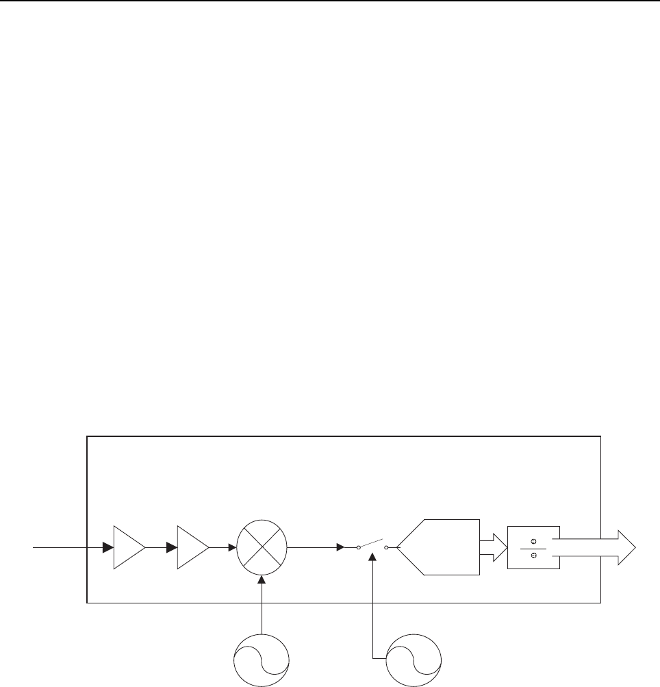
Mobile Radio’s Theory of Operation 1-7
provide the needed linearity and voltage range during operation. On UHF Band 2, the varactor
diodes are doubled-up on each side of the filter, which increases the overall IP3 of the filter, and
thus, improves intermodulation rejection. One other important role of the front-end is to amplify the
RF level coming into the receiver. The LNA (low noise amplifier), Q0402, provides the necessary
gain to help maintain the needed S/N for weak signal operation.
The first frequency conversion process is accomplished with a class 2 double-balanced octo-quad
diode ring mixer (D0405). The first local oscillator also feeds the mixer stage via an injection
amplifier and harmonic filtering. The LO is driven by a two-stage injection amp (Q0302 & Q0405),
providing a minimum of +18.5 dBm at the mixer. Between the VCO buffer (Q0302) and injection
amplifier (Q0405) stages is a 3 dB pi attenuator to increase the reverse isolation of the injection
lineup. This is needed to help mitigate any “pulling” on the main LO while in TDMA mode. The
amplified LO power then passes through a 3-pole 2-zero low-pass filter stage before reaching the
mixer. This filter reduces any unwanted products from the first LO that may cause unwanted
spurious frequencies in the mixer output. The two filter zeros are optimized to reject the LO second
harmonic, which can degrade the system IP2.
3.1.2 Receiver Back-End
After the first frequency conversion to 73.35 MHz, the IF signal passes though a crystal filter
(FL0500) with a minimum 3 dB BW of 13 kHz. The signal is then routed through a 2-stage limiter/
amplifier (Q0500 & Q0501). The limiter/amplifier stage applies the similar principle of strong and
weak signal management as in the front-end, to help achieve a dynamic range of well over 100 dB
without over-driving the DAC, internal to the AD9864 IC.
Figure 1-6 AD9864 Block Diagram
The 73.35 MHz IF signal finally reaches the AD9864 (U0600), as shown in Figure 1-6. Here another
frequency down-conversion to 2.25 MHz takes place before the resultant RF voltage gets sampled
by a Sigma-Delta converter. The Sigma-Delta converter is a high-speed DAC that outputs a 20 kHz
data stream to the main DSP.
External 2nd LO
High/Low Side
Injection
73.35 +/- 2.25 MHz
73.35
MHz
IF
LNA-16 dB
Step Atten
Σ ∆
DecimatorHi-Speed ADC
AD9864 IFIC
20 kHz DATA
18 MHz SAMPLING RATE
External 16.8 MHz
Reference
2.25 MHz IF
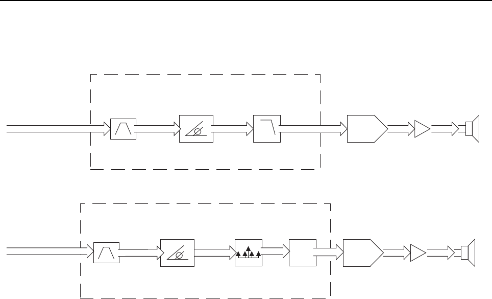
1-8 Mobile Radio’s Theory of Operation
3.1.3 Receiver DSP (Digital Signal Processing)
Shown below in Figure 1-7 is the block diagram of the signal flow through the receiver back-end. All
blocks within the dotted box represent the DSP software algorithms internal to U1000.
Figure 1-7 Signal Flow through Receiver Back-End
The DSP takes the incoming 20 kHz data-stream and passes the information through an FIR (Finite
Impulse Response) filter, which provides rejection from any in-band adjacent channel interference.
The remaining filtered data is then sent through the FM Discriminator routine. This routine is
primarily responsible for base-band information recovery. Depending on whether the radio is in
analog or digital mode determines the kind of signal processing used. If the radio is in analog mode,
the recovered base-band data is sent through FM De-emphasis and sub-audible tone (CTCSS/
CDCSS) recovery subroutines in the DSP code. If the radio is in digital mode, the recovered
base-band information is sent through a Symbol Recovery routine. The resultant data is then routed
through a standard AMBE+2™ vocoder for processing.
The output signal from either the analog or digital mode signal processing (still represented by
hi-speed data), is sent to a DAC (U3200), which converts the data stream back into usable audio.
This stage drives several additional gain stages. These gain stages consist of an I2C audio
attenuator (U3501) and a high-power audio PA (U3500) providing the user with at least 3 W of
power through an internal speaker and 13 W of audio to an external speaker.
FIR
4-FSK
SYMBOL
RECOVERY
AMBE+2
VOCODER
DSP DIGITAL 4FSK MODE
SPEAKER
ANALOG AUDIO
GAIN STAGES
DAC
FIR
FM
DISCRIMINATOR DEEMPHASIS
DSP ANALOG FM MODE
SPEAKER
ANALOG AUDIO
GAIN STAGES
DAC
FM
DISCRIMINATOR
20 kHz DATA
20 kHz DATA
TM
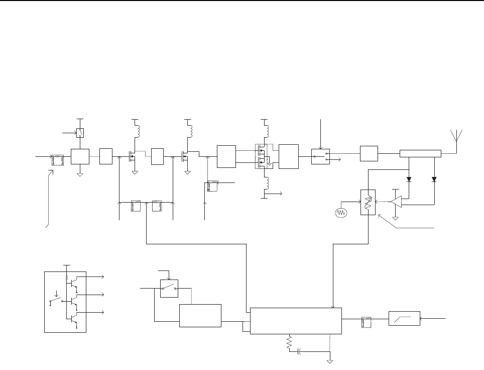
Mobile Radio’s Theory of Operation 1-9
3.2 UHF2 (450–512 MHz) Transmitter Circuitry – 40 Watt
The Transmitter consists of the power amplifier (PA) circuitry and the power control circuitry. The
power amplifier provides amplification of the signal from the VCO up to the desired output power.
The power control block is responsible for ensuring that the desired output power level is maintained
in both analog and digital modes, as well as protecting the power amplifier from damage due to heat,
antenna mismatch, out-of-range battery voltage, and poor assembly. The output power of the
transmitter can be set to operate between 1 W and 40 W.
Figure 1-8 UHF Band 2 40 Watt High-Power Transmitter Detailed Block Diagram
3.2.1 Power Amplifier
The radio’s 40 Watt power amplifier (PA) is a 4-stage amplifier which amplifies the output of the
VCO to the required transmit power level. The first stage is an LDMOS (Lateral Double Diffuse
MOS) 50 ohm fixed-gain block (ADA-4743, U0700) followed by the adjustable gain LDMOS
pre-driver (RD01MUS1, Q0705), an adjustable gain LDMOS driver (RD07MVS1, Q0703), and the
fixed-gain LDMOS final device (MRF1570, Q0702). A transmit/receive (T/R) switch and a harmonic
filter complete the transmit lineup.
3.2.2 Input Stage (50 Ohm Fixed-Gain Block)
The first stage (ADA-4743, U0700) is an integrated circuit with internally matched 50 ohm input and
output stages providing approximately 16 dB power gain. It provides reverse isolation between the
PA and the VCO to lessen the risk of VCO load-pull and it also supplies appropriate power to the
pre-driver stage. The ADA-4743 is biased at 33 mA during transmit by R0706, which is switched to
9V3_TX during Tx operation by Q0701 (controlled by Antenna_En). The ADA-4743 is preceded by a
switchable resistive pad that is 11 dB in high-power mode and 17 dB in low-power mode.
T/R
Switch
Harmonic
Filter
Agilent
ADA4743
TX_DAC
Active
Reconstruction
Filter
Log Amp Controller
V_CONTROL
9V3SW_9V1
PA_ENABLE
+5V Regulator
-5 dBm (nominal)
TX_INJ
CW / 4 FSK
+10 dBm
INPUT
FROM
VCO
ANT_ENABLE
BATTERY_DET
SW_9V1
Reflected
Port
Microstrip
Dual
Directional
Coupler
Forward
Port
+
TX Port
RX Port
To FE
Match
Match
Match/
Splitter
Match/
Combiner
A+
A+
Thermal
Cutback Voltage
Controlled
variable
Attenuator
ADI
8315
VAPC RF IN
VPOS
ENBLCOMM
FLTR
VSET
VCONT
VIN +5 VOUT
11/17dB
Switched
Attenuator
PC_Atten_En
To Pressure
Pad Switch
To Pressure
Pad Switch
FINAL_ BIAS
To Pressure
Pad Switch
9V3
Pressure
Pad Closes
Switch
To Predriver
To Driver
To Final
9V3_TX9V3_TX9V3_TX
LDMOS
Predriver
RD01MUS1
LDMOS
Driver
RD07MVS1
LDMOS
Final
MRF 1570
ANT_ENABLE
Pressure
Pad
Switch
PC_ATTEN_ENA

1-10 Mobile Radio’s Theory of Operation
3.2.3 Pre-Driver Stage
The next stage is a low-power, LDMOS device (RD01MUS1, Q0705), which delivers up to +27 dBm
to the driver stage. Its gain is controlled by varying the gate bias voltage and varies from low gain up
to approximately 14 dB power gain. The gate bias voltage is controlled in parallel with the driver
stage by the V_cont signal.
The input match to this stage is a high-pass topology consisting of C0734, L0718, C0817, L0721,
C0795, L0717, and C0785. High-pass matches are used where appropriate to minimize the
chances of low frequency regeneration within the amplifier. R0759 and R0777 are required to
improve the bandwidth of this circuit. The inter-stage match between the pre-driver and driver
stages is comprised of L0720, C0786, and C0791 arranged in a high-pass topology. Additional pads
are provided on the transceiver board to allow for possible engineering optimizations to this match.
These are non-populated parts C0789, C0792, R0739, and C0794.
3.2.4 Driver Stage
The third stage is a medium-power, LDMOS device (RD07MVS1, Q0703), which delivers up to +36
dBm to the final device. Its gain is controlled by varying the gate bias voltage and varies from low
gain up to approximately 11 dB of power gain. The gate bias voltage is controlled with the V_cont
signal and is controlled in parallel with the pre-driver stage gain.
R0718, R0720, R0754, and R0755 are required to improve the bandwidth of the driver stage. The
inter-stage match (as well as the power splitter) between the driver and final device uses a band-
pass topology.
3.2.5 Final Stage
The final stage is a high-power LDMOS device (MRF1570, Q0702) consisting of two parallel,
high-power devices within 1 plastic package. The package is mounted to a copper carrier to improve
thermal conductivity to the chassis and also to more tightly control the RF load, allowing higher and
more consistent maximum output power. This stage is biased at a quiescent current of 700 mA and
operates with a fixed gain of approximately 10 dB, allowing up to +48 dBm of output power. The
quiescent current is set by adjusting the Final_Bias signal. Both elements of this transistor are
fabricated on the same semiconductor die and are well matched, allowing control via a single
voltage.
Both the input and output matching circuits of this stage have extremely critical part location
requirements. Any repairs must be done with care to ensure the replaced components are placed
accurately and properly soldered. Of particular concern are input matching capacitors C0732,
C0832, C0861, and C0761. The resistor networks at the gates of transistor Q0702, R0762 through
R0773, improve the bandwidth of the circuit.

Mobile Radio’s Theory of Operation 1-11
The output matching circuit and power combiner is comprised of C0807, C0719, C0806, C0746,
C0726, and C0737, and associated microstrips fabricated on the printed circuit board. R0719 and
R0709 are added as a preventative measure against half-carrier regeneration. Inductor L0712 and
capacitor C0751 form a trap around 500 MHz to attenuate any ½ Fc signals.
If the final device fails and has to be replaced, R0719 should be carefully inspected to insure against
any damage caused by the final device. Replacement of the final device requires that the bias
voltage be re-tuned using the Customer Programming Software (CPS). Care must be taken not to
damage the device by exceeding the maximum allowed quiescent current which is 1 A. The device
can tolerate up to 5 A for brief periods of time without damage.
3.2.6 Antenna Switch
The Antenna Switch (T/R switch) has 2 modes, transmit mode and receive mode. An explanation of
the functionality of each follows below:
Transmit mode: The antenna switch utilizes the existing dc feed (A+) to the final stage device
(Q0702). Both PIN diodes, D0700 and D0702, are turned on during key-up by forward biasing them.
Forward biasing is achieved by pulling down the voltage at the cathode end of D0702 to around
12.2 V (0.7 V drop across each diode). Q0704 is configured as a current sink that maintains the
current through the antenna switch diodes at 50 mA, as set by VR0700 and R0738. The current sink
is enabled during transmit mode by ANT_ENABLE asserting through Q0706 and associated
circuitry. When the PIN diodes are conducting, an RF ground is formed at the anode of the lower
PIN diode D0702, which places the series L0710 in parallel with C0803. The values of L0710 and
C0803 are chosen so that they are in parallel resonance at the center of the transmit band, making
them appear as an open circuit so that a 50 ohm power path is maintained through the top PIN
diode to the harmonic filter. To further attenuate the Tx signal to prevent it from getting to the Rx
front-end, a PIN diode pair (D0703) is placed in the Rx path. This diode pair shorts to ground in
transmit mode so that the receiver sees a minimum of transmitter power.
Receive mode: The DC current through the PIN diodes is interrupted by turning off the current sink.
The RF path now flows from the harmonic filter, through the matching circuit formed by C0803 and
L0710, and then to the matching network C0766, C0767, R0701, and C0772. The additional shunt
diodes (D0703) will be high impedance since no bias current is flowing from the switched Tx power
line.
3.2.7 Harmonic Filter
Inductors L0706, L0707, L0708, and capacitors C0742, C0739, C0740, and C0738 form a
7-element low-pass filter to attenuate harmonic energy from the transmitter. R0713 is used to drain
any electrostatic charges that might otherwise build up on the antenna. The harmonic filter also
prevents high-level RF signals above the receiver pass-band from reaching the receiver circuits,
improving spurious response rejection.
3.2.8 Directional Coupler
The dual-directional microstrip coupler is implemented at the harmonic filter output to sample both
forward and reverse directed transmitter power. RF power from the transmitter PA passes through
the microstrip coupler before reaching the antenna. Forward RF power is coupled to the U0940 log
detector/controller via the voltage-controlled attenuator (VCA) stage consisting of pin diodes D0901,
D0902, and D0903. The log detector/controller regulates the gain of PA stages Q0703 and Q0705
(via V_cont), thus ensuring that the forward power out of the radio is held to a constant value.

1-12 Mobile Radio’s Theory of Operation
The directional coupler functions not only as part of the transmitter power regulation circuit but also
as part of the VSWR load-detection circuitry. Its physical location close to the antenna connector
allows accurate VSWR sense at the transmitter output. Forward and reverse coupled signals are
rectified by D0904 and D0905, respectively. DC voltage FWD_DETECTED is proportional to RF
power while REV_DETECTED is proportional to reflected RF power. The detected voltages are fed
to the respective inputs of difference amplifier U0901. The difference amplifier output is applied to
the variable attenuator control stage U0900-1. An abnormally high reflected power level, i.e., a
damaged antenna, also causes an increase in the difference amplifier output voltage. This causes a
reduction in attenuation by the VCA. As a result, the greater RF signal applied to the log detector /
controller causes the controller to reduce the gain of PA stages Q0703 and Q0705. Transmitter
power is thus reduced to prevent damage to the final device due to an improper load.
3.2.9 Power Control
The transmitter uses PA controller IC, U0940, to control the power output of the radio. A portion of
the forward RF power from the transmitter is sampled by the directional coupler and delivered via
the VCA to the RFIN port of the PA controller IC (pin 1). The PA controller, a log detector type,
provides temperature-stable, high-accuracy control over a typical 50 dB dynamic range.
The MAKO IC contains a digital-to-analog converter (DAC), which provides a reference voltage
(TX_DAC) at the input of reconstruction filter stage U0900-2. The filtered reference voltage at the
output of U0900-2 is divided by the combination of R0942 and R0946 before reaching the VSET
input of the PA controller IC (pin 3). Thermistor RT0953 is used in combination with R0954 to
compensate reference voltage drift at operating temperature extremes. Reference voltage level is
programmable through the SPI lines of the MAKO. This reference voltage is proportional to the
desired power setting of the transmitter and is factory programmed at several points across the
frequency range of the transmitter to offset frequency response variations of the transmitter’s
coupled power circuits.
The PA controller IC provides a dc output voltage at pin 7 (VAPC), which is divided to provide gate
bias for PA pre-driver and driver stages. The 0-5 V range at U0940, pin 7, is applied as
V_CONTROL to power-adjust the transmitter by controlling the gate bias of stages Q0703 and
Q0705. Voltage divider combination R0727 and R0728 provides gate bias to Q0703 while divider
combination R0750 and R0751 provides gate bias to Q0705. This adjusts the transmitter power
output to the intended value. The ratio of each of these resistive dividers is chosen to insure that
Q0703 and Q0705 are both running at their nominal design condition at rated output power.
Variations in sampled forward transmitter power cause the PA controller IC to adjust the control
voltage above or below its nominal value to raise or lower output power in order to maintain
transmitter output power relative to the reference voltage applied to VSET.
3.2.10 Power Ramp Profile Control
In order to minimize the transient adjacent channel power at the transmitter’s output, the ramped
power follows a raised cosine profile. The PA controller IC has a linear slope function when scaled in
dB/V. To achieve the desired raised cosine profile of the output power, the ramped reference
voltage provided by the MAKO DAC follows a raised cosine approximation. The MAKO DAC
reference output is low-pass filtered by the DAC reconstruction filter before it is applied to the VSET
input of the PA controller IC.

Mobile Radio’s Theory of Operation 1-13
Reconstruction filtering reduces spurious emissions in the RF spectrum as a result of the finite steps
of the DAC. Loop filter capacitor C0926, in conjunction with resistor R0950 and the integrator within
the PA controller IC, set the loop dynamics. The loop response has been optimized to achieve
sufficient speed to follow the required ramping profiles while meeting switching transient
requirements over varied power levels. Accurate control of the power-rise (ramp-up) and
power-decay (ramp-down) characteristics minimizes splatter into adjacent channels.
3.2.11 Thermal Protection
Thermistor RT0908, in combination with R0902, form a voltage divider with the output proportional
to the sensed transceiver board temperature in the vicinity of the transmitter driver and final devices.
The voltage divider output is routed to an operational amplifier U0901-2, which provides a dc voltage
via diode junction D0900 to control the attenuation level of the VCA stage. For the condition that the
temperature threshold set by resistive divider combination R0901 and R0909 is reached, the VCA is
driven to increase the RFIN signal at the PA controller IC (pin 1). This increase will cause the
controller IC to adjust the PA control voltage below its nominal value to decrease transmitter output
power. Temperature will be reduced by lowering transmitter output power relative to the reference
voltage applied to VSET.
3.2.12 Out-of-Range Battery Protection
Transmitter power cutback under extended battery supply voltage operation is provided for by
monitoring the battery supply in the controller circuit of the radio in order to change the VSET input
of the PA controller IC (pin 3) for reduced transmitter output.
3.2.13 Pressure Pad Switch
The power control circuitry includes a safety switch (S0700) that consists of a conductive portion of
the rubber pad, which pushes the RF final transistor Q0702 against the chassis. When the chassis
cover and rubber pad are properly assembled, the conductive portion of the pad contacts a pattern
on the transceiver board, electrically closing switch S0700. If the cover and pad are not in place,
switch S0700 is open-circuited and the power control circuit is disabled, turning off the gate bias to
Q0702, Q0703, and Q0705. This prevents thermal damage of the RF transistors which could occur
if the transmitter is operated without adequate heat sinking.
3.3 Frequency Generation Circuitry
The synthesizer subsystem consists of the reference oscillator (Y0100), the fractional-N synthesizer
IC (Tomahawk II, U0100), and the voltage controlled oscillator (VCO).
3.3.1 Reference Oscillator
The reference oscillator (Y0100) contains a temperature compensated crystal oscillator with a
frequency of 16.8 MHz. A digital-to-analog (DAC) converter internal to U0100 (Tomahawk) and
controlled by the microprocessor via serial interface (SPI), sets the voltage at the AUX_DAC output
of U0100 (pin H6) to set the frequency of the oscillator. The output of the oscillator (pin 3 of Y0100)
is applied to pin K5 (XOSC_BASE) of U0100.
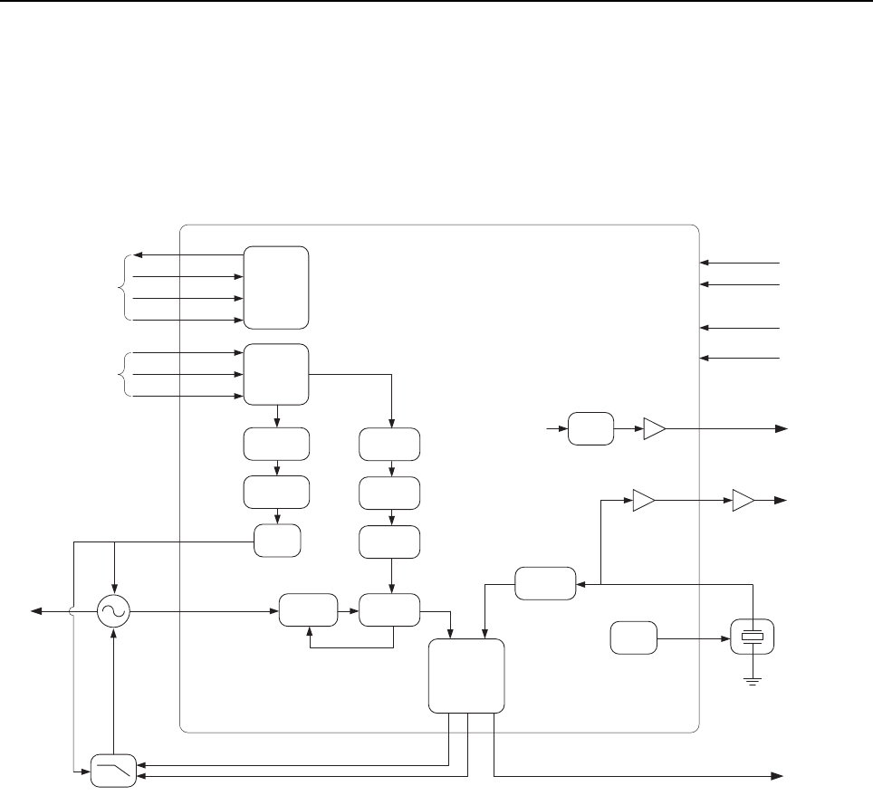
1-14 Mobile Radio’s Theory of Operation
3.3.2 Fractional-N Synthesizer
The Tomahawk II synthesizer IC (U0100) consists of a pre-scaler, a programmable divider and
divider control logic, phase detector, charge pump, a D/A converter in the high frequency analog
modulation path, an attenuator to balance the high and low frequency modulation paths, a serial
interface for control (SPI), a serial interface for modulation (SSI), and a super filter for the regulated
2.45 V.
Figure 1-9 UHF Band 2 Synthesizer Block Diagram
A voltage of 2.775 V applied to the super filter input (U0100 pin J4) supplies an output voltage of
2.45 V (SF_OUT) at pin K4. This supplies the VCO and the VCO modulation bias circuit (via
R0321). The super filter supply voltage is provided by the 2.775 V regulator within U3200. The
synthesizer is also supplied by the 5 V regulator, U3002, another 2.775 V regulator within U3200,
and a 1.875 V regulator within U3200.
The output signal LOCK (U0100-D7) provides information about the lock status of the synthesizer
loop. A high level at this output indicates a stable loop. A discrete buffer amplifier (Q0100) provides
a buffered 16.8 MHz reference frequency to other parts of the radio.
The serial programming interface (SPI) is connected to the microprocessor via the data lines
SPI_DW (U0100-D9) and SPI_DR (U0100-D10), clock line SPI_CLK (U0100-C11), and chip enable
line CEX (U0100-D8). The serial modulation interface (SSI) is connected to the DSP via the data
line SDTX (U0100-F11), clock line TXCLK (U0100-F10), and frame sync line SFTX (U0100-F9).
SPI
Interface
Data W rite
Clock
CEX
Data
Fsync
Clock
SPI
SSI
(Modulation)
Prescaler Main Divider
VCO
Fractional
Unit
DS
18-bit
Modulation
Unit
Main
Phase/Freq.
Detector
And
Charge Pumps
Reference
Divider
TCXO
(16.8MHz)
AUX
D/A
Main_CP
LOCK DETECT
Buffer Buffer
16.8MHz REF
Loop Filter
5V
2.775V Dig
2.775V Ana
1.875V Dig
TOMAHAWK II
Fractional - N
Synthesizer
(U0100)
D9
Data ReadD10
C11
D8
F11
F10
F9
J2
G3
Adapt_CP
H1 D7
SF_OUT
Super
Filter
2.775V Ana K4
H6
J11
K5
H2,J3
A7
A5,A10,B2,B9,
G2,J4,J6,J10,
K2,L6
B7,E11,G10,J1
Digital
Attenuator
SSI
Interface
D/A
Waveform
Generator
K8HP MOD
PRSC
TX / LO
Mobile Radio’s Theory of Operation 1-15
3.3.3 Voltage Controlled Oscillator (VCO)
The voltage controlled oscillator (VCO) subsystem consists of four Colpitts oscillators (two each for
Tx and Rx), a single-stage Tx buffer amplifier, a single-stage Rx buffer amplifier, oscillator bias
control switches, and the modulation circuitry.
Figure 1-10 UHF Band 2 VCO Block Diagram
Due to the limited steering line voltage provided by the Tomahawk Synthesizer IC (U0100), the UHF
Band 2 VCO design incorporates a total of four oscillators; two varactor-tunable Colpitts oscillators
each for Tx and Rx. Each oscillator has a tuning range of 38.5 MHz, sufficient to cover the Rx and
Tx frequency ranges of 376.65 MHz to 438.65 MHz and 450 MHz to 512 MHz, respectively. The
oscillators resonate at fundamental operating frequencies. Four (active-low logic) general purpose
output lines (GPO1, GPO2, GPO3, and GPO6) from the Tomahawk IC (U0100-B4, A4, E5, and H8)
provide the control for independent bias selection to each oscillator (VCO_SEL) via the PNP
transistor switches U0304 and U0201. The 2.45 V super filtered output, SF_OUT of the Tomahawk
IC (U0100-K4), supplies the bias to the oscillators. A portion of the VCO output signal is lightly
coupled through coupling capacitors C0331 and C0231, routed through a low-pass filter (formed by
L0221, C0235, C0230, and C0233), and fed back to the M_PRSC input of the Tomahawk IC
(U0100-J2).
High-port modulation is scaled through a voltage divider (comprised of R0319, R0320, and R0321)
and applied to the Tx modulation varactor diode CR0300. The Tx VCO frequency is modulated via
coupling capacitors C0310 and C0344. High-port modulation is also applied to the VCO steering line
(through R0139, R0140, and C0166) which modulates the main VCO tuning varactors.
TX VCO 1
TX VCO 2
RX VCO 1
RX VCO 2
TX Buffer Amp
RX Buffer Amp
Low Pass
Filter
TX INJ
RX INJ
To U0700
To Q0405
Steering Line Voltage
(VCTRL)
9V3_VCO
(U3001-5)
9R1
(Q0107)
RX_VCO_SEL2
(U0100-H8)
RX_VCO_SEL1
(U0100-B4)
TX_VCO_SEL2
(U0100-A4)
TX_VCO_SEL1
(U0100-E5)
High Port Modulation
(HO_MOD_OUT)
(U0100-K8)
Prescaler
(U0100-J2)
UHF Band 2
VCO
Subsystem

1-16 Mobile Radio’s Theory of Operation
A discrete single-stage Tx buffer amplifier (comprised of the NPN transistor Q0302 and surrounding
components) amplifies the signal from the Tx oscillator to the level required by the first stage of the
transmitter power amplifier (U0700). The Tx buffer amplifier also provides sufficient isolation from
any undesired load-pulling from the power amplifier. The bias for Q0302 is provided by the 9.3 V
regulator U3001.
A discrete single-stage Rx buffer amplifier (comprised of the NPN transistor Q0202 and surrounding
components) amplifies the signal from the Rx oscillator to the level required by the LO injection
amplifier (Q0405). The Rx buffer amplifier also provides sufficient isolation from any undesired load-
pulling from high input levels in the receiver front-end. GPO4 from the Tomahawk IC (U0100-D4)
controls the transistor switch (comprised of Q0108 and Q0107) that enables the 9.1 V bias to Q0202
(via the 9.3 V regulator U3001).
3.3.4 Synthesizer Operation
The complete synthesizer subsystem is comprised mainly of the Tomahawk synthesizer IC,
reference oscillator (crystal oscillator with temperature compensation), loop filter circuitry, VCO, and
DC supplies. The VCO feedback signal, PRSC, is fed to pin J2 of U0100 (M_PRSC) via a low-pass
filter (L0221, C0235, C0230, and C0233), which attenuates harmonics and provides the correct
level to close the phase-locked loop.
The prescaler in the synthesizer IC (U0100) is a four-level prescaler capable of dividing by 4, 5, 6,
and 7. The main loop N divider is configured to be an 8-bit divider. The divide-by-N portion of the
main loop is set via the SPI. The fractional portion of the divider is realized using a 3-accumulator,
24-bit fractional divider. The SPI is used to set the desired divide ratio.
The output of the prescaler is applied to the main loop divider. The output of the main divider is sent
to the phase/frequency detector, which compares the main divider’s output signal with the reference
signal. The reference signal is generated by dividing down the signal of the reference oscillator
(Y0100). The output signal of the phase/frequency detector is a pulsed signal which is routed to the
charge pumps. The main charge pump current is programmable through the SPI with its output at
pin G3 of U0100 (MN_CP). The loop filter transforms this current into a steering voltage that is
applied to the VCO.
To reduce lock time when new frequency data has been loaded into the synthesizer, an adapt
charge pump providing much greater current than the main charge pump is turned on for a finite
amount of time to quickly charge or discharge the loop filter capacitors to steer the VCO to the
desired frequency. The output of the adapt charge pump passes to the loop filter via pin H1 of
U0100 (MN_ADAPT_CP). When the synthesizer is within the lock range and the adapt timer runs
out, the adapt charge pump is powered down and the main charge pump takes over. A settled
synthesizer loop is indicated by a high level at signal LOCK (U0100-D7), which is routed to the
microprocessor. Q0102 is configured as a current source to provide a steady 0.8 mA during the
adapt period. U0101 is an analog switch that opens the adapt path slightly before the end of the
adapt period to prevent the current from the current source from pushing the VCO off frequency.

Mobile Radio’s Theory of Operation 1-17
Modulation is performed by applying a digital data stream via the SSI bus from the DSP (U1000) to
the synthesizer (U0100). In order to meet spurious and phase noise requirements, the PLL
bandwidth was designed to be narrower than the full modulation bandwidth, therefore requiring the
use of dual-port modulation. Internal to the synthesizer (U0100), low-port modulation is added to the
fractional-N division numerator to trace out the modulation versus time while the high-port data
stream passes through an interpolating waveform generator, a digital attenuator (for modulation
balancing), and then is converted to an analog signal through a 10-bit DAC before modulating the
VCO. This high-port analog modulation output (HP_MOD_OUT, U0100-K8) is connected to the
VCO modulation varactor diode (CR0300) via C0360 and R0319, and to the loop filter via R0139,
R0140, and C0166.

1-18 Mobile Radio’s Theory of Operation
Notes
2-1
Section 2
TROUBLESHOOTING CHARTS
1.0 Troubleshooting Flow Chart for Receiver (Sheet 1 of 3)
Set up radio in analog Rx mode on
desired channel with squelch open
and MAP cable and audio test box
connected to accessory port.
1st LO
> +5 dBm
at R0422?
Spray or inject 73.35 MHz
RF carrier modulated with
1 kHz audio tone into XTAL
Filter FL0500
No
Audio tone
present
at speaker?
Yes
Volume
level
adjusted
properly?
Check U3501
bias and
replace part if
necessary
Audio at pin 1
of U3501?
Verify audio path to
U3501
Set up repeater unit to
receive at frequency
462.8 MHz
with the Rx Brick open and
connected to the system.
Apply an on-channel
RF carrier at -47 dBm modulated
with 1 kHz tone
at the Rx antenna port.
B
Audio at pin
6 of U3505?
Audio at pin
10 of U3501?
Check connections to
external speaker and
replace speaker if
necessary
Verify audio path
between U3500 and
pin 1 of U3501
Audio at pin
4 of U3500?
Audio at pin
1 of U3500?
Check biasing
before replacing
U3500
1st LO
(389.45 MHz)
> +16 dBm
at FT0401?
Check biasing on
Q0405 before replacing
9 VDC
present
at R0417?
Check
9R1 path back to
synthesizer
Check VCO
Troubleshooting
Flow Chart
RF level
of on-channel
signal > -45 dBm
on pin 4
of T0401?
A
Check T0400 and D0405
and replace if necessary
Yes
Yes Yes
Yes
No
No No
Yes
YesNo
No
No
Yes
Yes
No
No
No
Yes
Yes
No Rx Audio
No
All Troubleshooting within the dotted line is done
on the Tx Brick.
2-2 Troubleshooting Flow Chart for Receiver
1.1 Troubleshooting Flow Chart for Receiver (Sheet 2 of 3)
A
Voltage level
> 2.7 VDC
on D0401?
+9.0 VDC
on pin 4
of Q0403?
Check circuitry around
D0401, D0402, D00403, and
D0404 for shorts and opens
Check biasing on
Q0403 before replacing
Check biasing circuitry of
Q0401 and Q0402 before
replacing
RF level
of on-channel
signal > -45 dBm
at C0420?
Is voltage
at R0409
~ 0.7 VDC?
Check D0403, D0404, and
associated capacitors
for opens and shorts.
Replace if necessary
Check biasing circuitry of
Q0402 before replacing
No
Yes
No
No No
Yes
Yes
Yes
All Troubleshooting on this page is
done on the Rx Brick
Troubleshooting Flow Chart for Receiver 2-3
1.2 Troubleshooting Flow Chart for Receiver (Sheet 3 of 3)
B
16.8 MHz
present
at C0622?
Check Synthesizer
Troubleshooting
Flow Chart
2nd LO
> 0 dBm and
at 71.1 MHz
at TP0600?
Yes
No
No
Yes
73.35 MHz
present
at TP0602?
2.25 MHz
present
at C0625?
No
Yes
No
Yes
18 MHz
present
at L0608?
Check diode
continuity before
replacing D0601
Replace components
as needed
No No
Yes Yes No
Yes
Check for visible
solder shorts near
pins before replacing
U0600
~ 1.65 VDC
on R0617?
Clock
VCO and LF
components
OK?
DC continuity
through
biasing components
E0600 - E0610?
Replace
defective biasing
component
Yes
No
3.0 VDC
on pin 1
of U0601?
Check Controller
Troubleshooting
Flow Chart
5.0 VDC
at E0610?
Check biasing on
U0601 before
replacing
No No
Yes Yes
3.5 VDC
at E0609?
No
Yes
Check biasing on
Q0601 before
replacing
Remove Shield
SH0500.
Check biasing on
Q0600 and
check continuity
on D0600.
Replace parts if
necessary.
Check 5 VDC supply and
biasing components
before replacing
Q0500 or Q0501
Biasing
correct on
Q0500 and
Q0501?
~ 3.0 VDC
on L0604
and L0605?
Check biasing
components and 3 VDC.
Replace parts if
necessary
No
Yes
No
Yes
Check FL0500 matching
components before
replacing
73.35 MHz
present
at pin 6 of
FL0500?
Check signal gain
and biasing
before replacing
Q0500 or Q0501
No
Yes
All Troubleshooting on this page is
done on the Rx Brick.
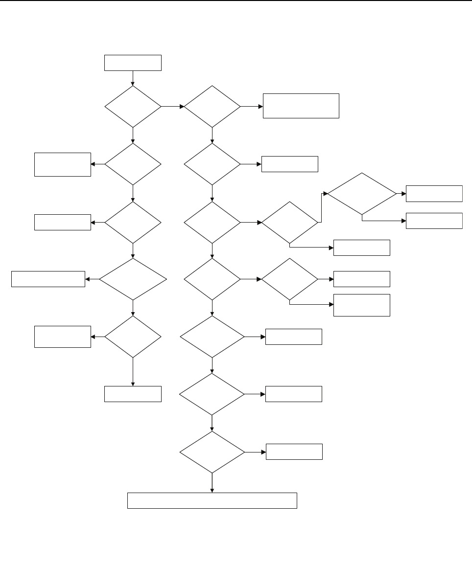
2-4 Troubleshooting Flow Chart for 40 Watt Transmitter
2.0 Troubleshooting Flow Chart for 40 Watt Transmitter
Is TP0909
> 1 VDC?
No Transmitter
Power
Is TP0913
= 9.1 VDC?
Check 9.3V Regulator
circuit (U3001)
Is U0941 Pin 1
= 5 VDC?
Check 5V Regulator
circuit (U0941)
Is voltage at
TP(TX_RAMP_DA
C) in controller
> 3 VDC?
Check MAKO
Troubleshooting Flow Chart
Is voltage at
TP0910
> 1 VDC?
Check U0900-2 and
associated circuitry
Replace U0940
Is TP0702
= 9.3 VDC?
Check 9V3_PA Regulator in
Controller Troubleshooting
Flow Chart
Are TP0707
and TP0708
~ 2.2 VDC?
Is power
at TP0704
+13 dBm?
Is Pressure Pad
Switch in place?
Place switch or
R0775
Is resistance
to ground at Q0702
G1 and G2
~ 66 kohm?
Replace Q0702 *
* Note: If Q0702 is replaced, radio must be bias set and power set.
1) Levels are during Transmit Mode (analog), 13.6V at battery connector, 50 ohm termination on transmitter.
2) Make sure PCB is screwed into chassis during these tests to avoid final device damage.
Check Bias Set
Circuit; bias tune
Is TP0703
-3 dBm?
Check VCO
Troubleshooting
Flow Chart
Replace U0700
Is power at
TP0709 ~ 15 dB
> TP0710?
Is power at
TP0702 ~ 10 dB
> TP0709?
Check Q0705 and
associated circuitry
Check Q0703 and
associated circuitry
Is power at
D0700-A ~ 10 dB
> TP0702?
Check Q0702 and
associated circuitry
Measure relative power thru remainder of T/R switch and LPF to find
open circuit. Perform vis ual inspection of circuit.
Is D0702-K
~ 12.4 VDC?
Check T/R bias
circuit
Yes
Yes
Yes
Yes
Yes
No
Yes
Yes
Yes
Yes
No
No
Yes
No
No
Yes
No
Yes
No
Yes
No
Yes
No
No
No
Yes
No
No
No
No
3) When making measurements within the transmitter using an RF power probe, be careful that the rating
of the probe is not exceeded. The “relative” measurements listed in the flow chart should be made with a
scope probe connected to a spectrum analyzer or similar instrument to avoid damaging sensitive power
probes.
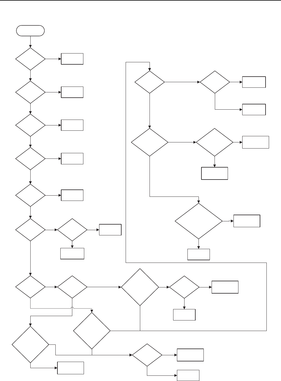
Troubleshooting Flow Chart for Synthesizer 2-5
3.0 Troubleshooting Flow Chart for Synthesizer
Start
Visual check of
the Board OK?
Correct
Problem
No
Yes
+5V at R0100? No
Yes
Check 5V
Regulator
U3002
+2.775V at
R0101 and
R0103?
Check U3200
+1.875V at
R0102?Check U3200
No
Yes
No
Yes
Is 16.8 MHz
signal at C0145?No
Yes
Check Y0100
Is 16.8 MHz Is 16.8 MHz
signal at R0155?No
signal at R0109?
NoReplace
U0100
Yes
Check Q0100
and sur r oundi ng
components
Yes
Is Radio in Tx or
Rx mode?
Tx
Is either GPO2 or
GPO3 low (<0.5V),
but not both, and
GPO1 and GPO6 are
high (>1.4V)?
No
Yes
Rx
No
Yes
+2.45V at C0137
(SF_OUT)?
NoAre C0136,
C0137 OK?
Replace or
resolder
components
No
Replace U0100
Yes
Yes
1.5 ms pulse at
TP_ADAPT_SW
when channel
changed?
No1.5 ms (inverted)
pulse at R2517 when
channel changed?
Check uP U1000
Troubleshooting
Chart
No
Yes
Check Q0106,
R0159
Is either GPO1 or
GPO6 low (<0.5V),
but not both, and
GPO2 and GPO3 ar e
high (>1.4V)?
Yes
Is RF prescaler level
(at C0233) between
100 mVpk and 300 mVpk
(harmonics <-15 dBc)?
NoCheck VCO
Troubleshooting
Chart
Is SPI
programming
OK?
Check uP U1000
Troubleshooting
Chart
Replace
U0100
Is SPI
programming
OK?
Check uP U1000
Troubleshooti ng
Chart
Replace
U0100
Yes
No
No
Yes
Replace
U0100
Yes
Is modulation
present at
R0139?
Is Tx SSI acti vity
present on CLK,
FSYNC, and DATA
lines (R2512, R2514,
R2513)?
Check uP U1000
Troubleshooti ng
Chart
Yes
No
No
Yes
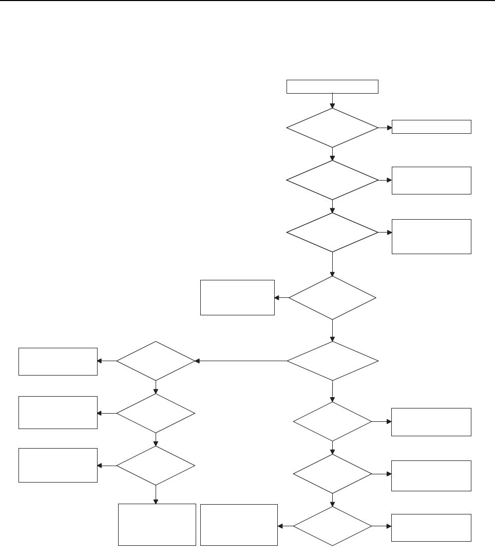
2-6 Troubleshooting Flow Chart for Tx VCO (Sheet 1 of 2)
4.0 Troubleshooting Flow Chart for Tx VCO (Sheet 1 of 2)
2.556 V at C0362 &
C0363
Check Synthesizer
Troubleshooting
Chart
Check Synthesizer
Troubleshooting
Chart
Radio is not
programmed for
Transmit Mode or
U0100 not functional
~ 0 VDC at
C0358?
2.556 VDC at
C0336?
Replace Q0301
Check biasing components
and then replace Q0301
if needed
Vbe
= 0.7 V
for Q0301?
Yes
Yes
VCO 2
Check biasing
components then
replace Q0302 if
needed
Check biasing
components then
replace Q0302 if
needed
Vbe
= 0.7 VDC
for Q0302?
No
No
No
No
No
No
No TX VCO signal at C0318
Visual check
of board
OK? Correct problem
Correct problem
Radio did not boot up
properly or check
9V3 Regulator
Radio did not boot up
properly or check
9V3 Regulator
9 VDC at L0300?
Check biasing
components then
replace Q0302 if
needed
Check biasing
components then
replace Q0302 if
needed
Vbe
= 0.7 VDC
for Q0302?
Yes
Yes
No TX VCO signal at C0318
Visual check
of board
OK? Correct problem
Correct problem
Radio did not boot up
properly or check
9V3 Regulator
Radio did not boot up
properly or check
9V3 Regulator
9 VDC at L0300?
Radio programmed for
Tx VCO 1 or 2?
2.556 V at C0362 &
C0363
~ 0 VDC at
C0348?
2.556 VDC at
C0300?
Vbe
= 0.7 VDC
for Q0300?
Yes
Yes
No
No
No
VCO 1
Check Synthesizer
Troubleshooting
Chart
Check Synthesizer
Troubleshooting
Chart
Radio is not
programmed for
VCO1 Transmit Mode
or U0100 not
functional
Check biasing
components then
replace Q0300 if
needed
Check biasing
components then
replace Q0300 if
needed
Yes
No
Yes RF signal
present at
R0332?
Check components
between R0332 and
L0305 for shorts or
opens
Check CR301-CR304
and L0310, L0307,
C0308, C0313, C0320,
and C0314 for short
Check CR305-CR308
and L0315, L0318,
C0343, C0345, C0350,
and C0346 for short
Yes
Yes
Radio is not programmed for
VCO 2 Transmit Mode or
U0100 not functional
Check CR0305 - CR0308,
L0315, L0318, C0343, C0345,
C0350, and C0346
for shorts or opens
Check CR0301 - CR0304,
L0310, L0307, C0308, C0313,
C0320, and C0314
for shorts or opens
Radio is not programmed for
VCO 1 Transmit Mode
or U0100 not functional

Troubleshooting Flow Chart for Tx VCO (Sheet 1 of 2) 2-7
4.1 Troubleshooting Flow Chart for Tx VCO (Sheet 2 of 2)
DC Voltage
at R0311
between 0.6
and 4.5 VDC?
Check Synthesizer
Troubleshooting
Flow Chart
Check Synthesizer
Troubleshooting
Flow Chart
Yes
No
Tx VCO 1 or
VCO 2
selected?
Check components
between C0353 and
C0346 for open or
short
VCO 1 VCO 2
-
Tx VCO locked but no
high-port modulation
~2.1 VDC at
VCO side of
C0360?
Check R0321, R0320,
R0319, and CR0300
for open or short
Modulation at
CR0300?
No
Yes
Replace C0310
Yes
Modulation at
C0361?
No
Replace C0360
Yes
Check C0361 and
C0334 for short and
then check
Synthesizer
Troubleshooting
Flow Chart
Check C0361 and
C0334 for a short and
then check
Synthesizer
Troubleshooting
Flow Chart
No
Tx VCO not locked
at correct frequency
Check C0323, C0325,
and C0329 and all
components between
C0326 and C0314 for
shorts or opens
Check C0351, C0352, and C0359
and all components between
C0353 and C0346 for
shorts or opens
Check R0321, R0320, R0319,
and CR0300 for
shorts or opens

2-8 Troubleshooting Flow Chart for Rx VCO (Sheet 1 of 2)
5.0 Troubleshooting Flow Chart for Rx VCO (Sheet 1 of 2)
2.556 V at C0362 &
C0363
Check Synthesizer
Troubleshooting
Flow Chart
Check Synthesizer
Troubleshooting
Flow Chart
Radio is not
programmed for
Receive Mode or
U0100 not functional
~0 VDC at
C0258?
2.556 VDC at
C0236?
Vbe
= 0.7 VDC
for Q0201?
Yes
Yes
No
No
No
VCO 2
Check biasing
components and
then replace Q0202 if
needed
Check biasing
components and
then replace Q0202 if
needed
Vbe
= 0.7 V
for Q0202?
Yes
Yes
No
No
No
No Rx VCO signal at C0218
Visual check
of board
OK? Correct problem
Correct problem
Radio did not boot up
properly or check
9V3 Regulator
Radio did not boot up
properly or check
9V3 Regulator
9 VDC at E0201?
Check biasing
components and
then replace Q0200 if
needed
Check biasing
components and
then replace Q0200 if
needed
2.556 V at C0362 &
C0363
~0 VDC at
C0248?
2.556 VDC at
C0200?
Vbe= 0.7 VDC
for Q0200?
No
Yes
Yes
No
No
No
VCO 1
Check Synthesizer
Troubleshooting
Flowchart
Check Synthesizer
Troubleshooting
Flowchart
Radio is not
programmed for
Receive Mode or
U0100 not functional
Radio is not
programmed for VCO 1
Receive Mode or
U0100 not functional
Yes RF signal
present at
R0219?
Check CR205 -CR208
and L0218, L0215,
C0243, C0245, C0250,
and C0246 for short or
open
Yes
Yes
Check components between
R0219 and L0205
for shorts or opens
Check biasing components
and then replace Q0201
if needed
Yes
Radio programmed for
Rx VCO 1 or 2?
Check CR0201 - CR0204 and
L0210, L0207, C0220,
C0213, C0208, and C0214
for shorts or opens
Radio is not programmed
for VCO 2 Receive Mode
or U0100 not functional
Check CR0205 – CR0208 and
L0218, L0215, C0243,
C0245, C0250, and C0246
for shorts or opens
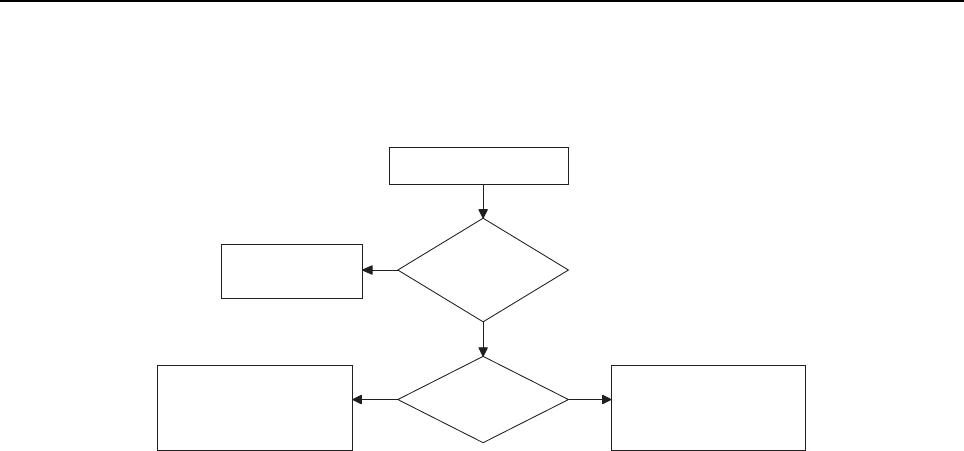
Troubleshooting Flow Chart for Rx VCO (Sheet 1 of 2) 2-9
5.1 Troubleshooting Flow Chart for Rx VCO (Sheet 2 of 2)
Rx VCO not locked
Rx VCO not locked
at correct frequency
DC Voltage
at R0211
between 0.6
and 4.5 VDC?
Check Synthesizer
Troubleshooting
Check Synthesizer
Troubleshooting
Flow Chart
No
Yes
Rx VCO 1 or
VCO 2
selected?
Check components
between C0253 and
C0246 for open or
short
VCO 1 VCO 2
Check C0223, C0225, and C0229
and all components between
C0226 and C0214 for
shorts or opens
Check C0251, C0252, and C0259
and all components between
C0253 and C0246 for
shorts or opens
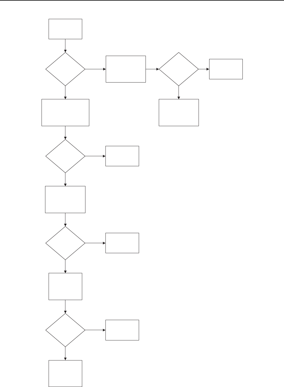
2-10 Troubleshooting Flow Chart for Repeater
6.0 Troubleshooting Flow Chart for Repeater
Repeater does not
fully initialize
(Disabled LED
stays blinking)
Does Repeater
initialize properly
now?
Re-insert or replace SSI
cable
Replace Connector
Board and/or
Accessory Cable
Does Repeater
initialize properly
now?
Can it repeat?
Re-insert or Replace
30 pin Front Panel
cable
Do all LEDs flash
on power-up?
Replace Front Panel
Board
Troubleshoot Rx
Radio
Yes Yes
No
No
No
Done
Done
Yes
No
Done
Yes
Does Repeater
initialize properly
now?
Done
Troubleshoot Tx
Radio
No
Yes

3-1
Section 3
UHF2 PCB/SCHEMATICS/PARTS LIST
1.0 Allocation of Schematics and Circuit Boards
1.1 Controller Circuits
The UHF circuits are contained on the Printed Circuit Board (PCB) which also contains the
Controller circuits. This Chapter shows the schematics for the UHF circuits only, refer to the
Controller section for details of the related Controller circuits. The PCB component layouts and the
Parts List in this Chapter show both the Controller and UHF circuit components. The UHF
schematics and the related PCB and parts list are shown in the table below.
Table 3-1 UHF2 1–40W Diagrams and Parts List
PCB :
8471696M01 Main Board Top Side
8471696M01 Main Board Bottom Side
Page 3-3
Page 3-4
SCHEMATICS
Overall
Receiver Front- End
Receiver IF Amp
Receiver Back-End
Power Amplifier
Power Control
Synthesizer
Receiver VCO
Transmit VCO
Page 3-5
Page 3-6
Page 3-7
Page 3-8
Page 3-9
Page 3-10
Page 3-11
Page 3-12
Page 3-13
Parts List
8471696M01 Page 3-14

3-2 Allocation of Schematics and Circuit Boards
Table 3-2: UHF2 1–40W Diagrams and Parts List
PCB :
8471696M02 Main Board Top Side
8471696M02 Main Board Bottom Side
Page 3-19
Page 3-20
SCHEMATICS
Overall
Receiver Front- End
Receiver IF Amp
Receiver Back-End
Power Amplifier
Power Control
Synthesizer
Receiver VCO
Transmit VCO
Page 3-21
Page 3-22
Page 3-23
Page 3-24
Page 3-25
Page 3-26
Page 3-27
Page 3-28
Page 3-29
Parts List
8471696M02 Page 3-30
Table 3-3: UHF2 1–40W Diagrams and Parts List
PCB :
8486777Z15 Main Board Top Side
8486777Z15 Main Board Bottom Side
Page 3-35
Page 3-36
SCHEMATICS
Overall
Receiver Front- End
Receiver IF Amp
Receiver Back-End
Power Amplifier
Power Control
Synthesizer
Receiver VCO
Transmit VCO
Page 3-37
Page 3-38
Page 3-39
Page 3-40
Page 3-41
Page 3-42
Page 3-43
Page 3-44
Page 3-45
Parts List
8486777Z15 Page 3-46
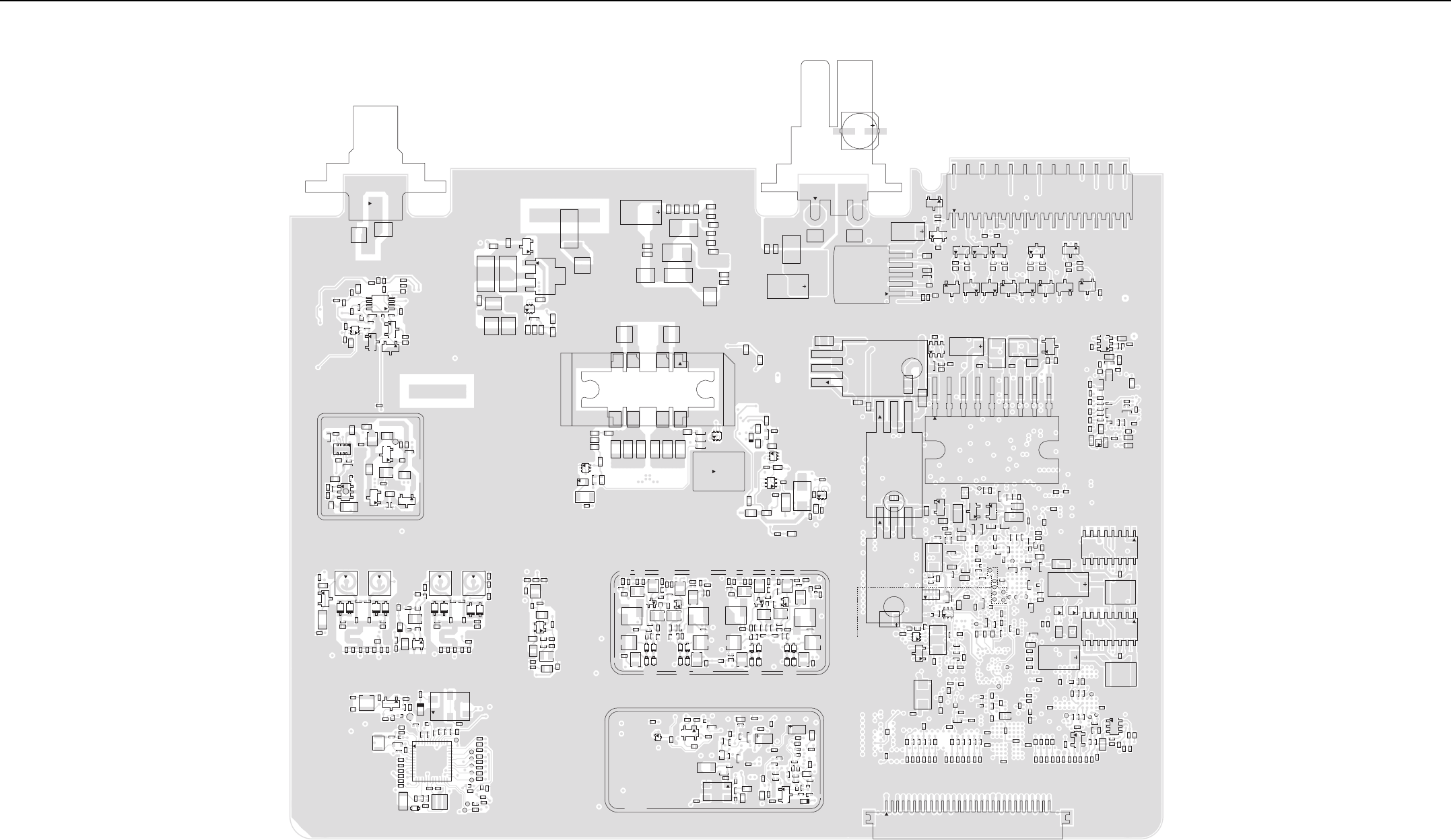
UHF2 (450–512 MHz) 1–40W PCB/Schematics/Parts List 3-3
2.0 UHF2 (450–512 MHz) 1–40W PCB/Schematics/Parts List
3
2
J0700
C0900
C0901C0906
C0907
C0908
C0909
C0910
C0915
C0939
D0900
D0906
63
4
Q0900
Q0901
R0900
R0901
R0902
R0903
R0906
R0907
R0909
R0911
R0912
R0914
R0915
R0916
R0920
R0923
R0930
R0931
U0901
L0722
R0713
3
2
1
C0751
C0776
C0777
C0778
C0779
C0796
C0797
C0798
C0799
L0712
L0714
4
Q0704
63
4
Q0706
R0729
R0735
R0738
R0745
R0748
R0749
VR0700
C0700
C0701
C0702
C0703
C0704
C0705
C0706
C0707
C0708
C0709
C0710
C0711
C0712
C0713
C0714
C0715
C0722
E0700
E0701
R0742
C3000
C3002
C3015
E3000
SP3000
C3018
J3000
SP3001
1
6
5
U3001
C3006
2
3
23
23
2
3
2
3
23
23
2
3
R4051
C3005
C3007
C3019
C3046
C4040C4041 C4042 C4043 C4044
C4045
C4046 C4047
C4048
C4075
E4005
25
26
2
J4000
Q4000 Q4002Q4004Q4005Q4006Q4008Q4010Q4011
Q4013
R3002
R3003
R3004
R4040R4041 R4042 R4043 R4044
R4045
R4046 R4047
R4048
R4050
VR4000 VR4001VR4002
VR4003
VR4004
VR4005
C6406
C6407
C6408
C6416
C6417
C6418
C6419
C6420
C6421
C6422 C6423
C6426
C6427
C6428
C6429
C6430
C6431
C6433
C6439
C6440
C6450
E6401
E6402
E6407
R6402
R6403
R6443
R6444
R6445
R6446
R6449
R6450
R6454
R6455
R6456
R6458
R6459
R6460
R6461
R6465
R6466
U6402
U6407
C6445
9
U3500
C3501
C3504C3505
C3506
E3500
E3501
23
Q3500
R3516
R3520
C3008
C3009
C3010
R3009
R3010
U3002
R3033
R3056
3
2
1
R3032
R3035
R3036
3
2
1
U3006
R0774
R0775
C0718
C0724
C0759
C0768
C0783
C0788
C0802
E0702
E0703
E0704
L0723
Q0701
6
3
4
Q0707
63
4Q0711
R0700
R0702
R0706
R0724
R0725
R0726
R0734 R0744
R0750
R0751
R0752
R0761
C0806
C0807
2
3
4
7865
Q0702
SP0700
SP0701
SP0702
SP0703
SP0704SP0705
SP0706SP0707
R0762
R0763
R0764
R0768
R0771
R0773
C0781
C0782
R0732
R0740
C0904
L0900
6
3
4
Q0709
R0741
R0753
R0757
1
RT0908
10
1
M0700
C0804
C0805
63
4Q0708
R0730R0756
C3202
L3200
16
1
8
9
Q3200
16
1
8
9
Q3202
C3209
L3202
C2000
C2002
C4014
C4015
C4016
C4017
C4018
C4019
C4020
C4021
C4022
C4023
C4024
C4025
C4026
C4027
C4076
E4001
E4004
C2004
C4034
C4035
R2013
R4009
R4010
R4011
R4012
R4106
TP_SDRAM_BA0
TP_SDRAM_BA1
VR4007
C2006
C2007
C3212
D4001
R2005
R2006
R2007
R2008
R2009R2010
R2011
R4006
R4034
R4095
TP4000
TP_SDRAM_CS
C1008
C1011
C1013
C1014
C2005
R1066
R1067
R2000
R2004
R4068
R4069
R4070
R4071
C2500
C4000
C4001
C4002
C4003
C4004
C4005
C4006
C4028
C4029
C4030
C4031
C4032
C4033
C2003
R4000
R4001
R4002
R4003
R4004
R4005
R4061
R4063
R4064
R4065
R4066
R4067
C1001
C1003
C1005
C1006
C1012
C1017
C1018
C1019
C2001
C4013
E4000
R1002
R1005
R1006
R1014
R1019
R1071
R2012
R2529
R3580
R3583
R1041
R3042
U3005
3
2
1
C0914
C0918
C0921
C0922
C0926
C0931
C0934
C0935
C0936
C0937
C0947
C0948
C0949
C0950
C0951
D0901
D0902
D0903
L0901
L0902
R0924
R0925
R0926
R0927
R0928
R0929
R0936R0937
R0940
R0950
SH0900
4
58
U0940
U0941
R0917
C0929
C0437
C0438
C0439
C0440
C0442
C0451
C0457
L0407
L0411
4
32
Q0405
R0417
R0418 R0419
R0420
R0421
R0422
R0423
R0424
R0425
R0433
R0434
C0404
C0405
C0406
C0407
C0408
C0409
C0410
C0411
C0414
C0415
C0416
C0417
C0419
C0420
C0421
C0423
C0424
C0425
C0426
C0427
C0428
C0429
C0430
C0431
C0432
C0433
C0434
C0458 C0459
C0460
C0461
C0462
D0400
D0401
D0402D0403
D0404
D0406
D0407
D0408
D0409
L0401
L0402L0403L0404
L0405
L0413
4
32
Q0402
R0404
R0405
R0406
R0407
R0409
R0410R0412
R0432
R0435
R0436
R0437
R0438
R0440R0441
R0443
R0444
C0502
C0504
C0509
C0515
C0516
C0622
C0623
C0625
C0626
C0627
C0629
C0630
C0631
C0633
C0638
C0642
C0643
C0644
C0645
C0646
C0650
CLKOUT
D0601
DOUTA
DOUTB
E0601
E0602
E0604
E0605E0606
E0607E0608
23
4
5
6
FL0500
FS
L0504
L0506
L0604
L0608
PCPD
PE
Q0501
R0503R0510
R0606
R0607
R0608
R0609
R0610R0611
R0612
R0613
R0614
R0615
R0617
R0618
R0619
R0621
R0622
R0623
R0627
TP0601
U602
1
37
25
13
U0600
C0510
C0605
C0611
C0615
C0617
C0619
C0620
C0621
E0600
C0100
C0102
C0103
C0104
C0105
C0109
C0110
C0111
C0113
C0121
C0122
C0124
C0125
C0126
C0127
C0128
C0129
C0130
C0132
C0133
C0140
C0141
C0142
C0143
C0144
C0145
C0146 C0175
C0177
C0178
C0180
C0196
Q0102
Q0106
R0100
R0101
R0102
R0108
R0109
R0110
R0111
R0114
R0116
R0117
R0118
R0119
R0123
R0147
R0148
R0155
R0156
R0157
R0158
R0159
R0161
SH0100
43
2
Y0100
C0117
C0118
C0120
C0171
C0195
L0100
Q0100
R0105
R0106
R0107
R0144
R0146
J400130
9
C6451
R3501
R3594
R6467
MAKO_GATED_32KHz
TP_MAKO_DCLK
TP_MAKO_FSYNC
TP_MAKO_RX
TP_MAKO_TX
C3515
C3524
63
4
Q3501
R3526
R3532
R3547
U3040
USB1_SEO
USB1_TXEN
VR3503
C1000
C1004
C1007
C1009
C1010
C1015
C1016
C1030
C1031
C1033
C1036
C1037
C3213
C3216
C3280
C3514
23
4
Q3203
23
4
Q3204
R1000
R1001
R1017
R1021
R1025
R1027
R1034
R1035
R1036
R1045
R3225
TP1000
TP_SDRAM_CLK
C1002
C1032
C1034
C3262
E3502
4
58
Q3201
R1026
TP_POR
4
3
6
U1006
3.6V_MAKO_SW1
C3207
C3208
C3210
C3211
C3273
C3276
C3277
C3278
C3518
C3520
C3521
C3523
C3528
C3529
C3531
E3503
R1028
R3205
R3206
R3218
R3224
R3508
R3535
R3537
R3538
R3560
R3587
R3596
USB1_DAT
VBUS1_CMD
VBUS2_CMD
C3040
C3203
C3219
C3220
C3229
C3234
C3238
C3239
C3240
C3247
C3248
C3249
C3254
C3283
C3511
C3513
C3516
C3530
C3538 C3545
E3202
E3205
R1020
R3203
R3217
R3233
R3500
R3503
R3504
R3505
R3507
R3509
R3514
R3515
R3550
R3571
R3576
R3588
R3595
RT3500
VR3202
VR3204
VR3206
2.9V_MAKO_V6
C3225
C3226
CR0203
CR0204
CR0207
CR0208
C0253
C0326
C0353
CR0303
CR0304
CR0307
CR0308
L0309
L0317
L0318
R0211
R0311
SH0301
C0308
C0313
C0314
C0320
C0323
C0325
C0329
C0343
C0345
C0346C0350
C0351
C0352
C0359
CR0301
CR0306
L0310
C0245
C0246
C0250
C0310
C0344
CR0206
CR0302CR0305
L0217
L0218
C0200
C0201
C0204
C0205
C0206
C0208
C0213
C0214
C0215
C0220
C0223
C0225
C0226
C0229
C0236
C0237
C0240
C0241
C0242
C0243
C0247
C0251
C0252
C0259
C0306
C0315
C0347
CR0201
CR0202CR0205
L0202
L0203
L0207
L0209
L0210
L0212
L0213
L0214
L0215L0219
L0303
L0307L0312 L0319
Q0200
Q0201
Q0300
Q0301
R0201
R0204
R0205
R0216
R0224
R0225
R0226
R0229 R0301
R0316
R0329
C0300
C0301
C0304
C0305
C0337
L0302
R0304
R0305
C0336
C0340C0341
C0342
L0313
L0314
R0324
R0325
R0326
L0315
UHF2 (450–512 MHz) 1–40W 8471696M01 Top Side

3-4 UHF2 (450–512 MHz) 1–40W PCB/Schematics/Parts List
C4063
C4064
C4065
C4066
C4067 C4068
C4069
C4070
C6412
C6413
C6435
C6436
C6437
C6438
E6400
FT_APM_1_WIRE
FT_EMERGENCY
FT_IGNITION_SENSE
FT_USB2_DM
FT_VBUS2
J6400
L6402
R3529
R3540
R3545 R3548
R6407
R6430
R6432
R6433
R6434
R6435
R6436
C1
C3
A3
U6405
VR4006
VR4009
VR6400
ANT_C
C3045
C3533
C3534
D4000
EXT_PTT
FT_USB2_DP
2
3
Q4001
2
3
Q4003
23
Q4007
23
Q4009
2
3
Q4012
Q4014
2
3
Q4015
Q6401
R4030
R4031
R4032
R4033
R4035
R4054
R4055
R4088
R4089
R4098
R6437
1
6
5
U3003
VR3504
R4049
C3013
VR3000
C3012 C3014
FT_VBAT
FT_VBAT_GROUND
R3005
R3006
C0719
C0720
C0721
C0726
C0727
C0737
C0741
C0746
C0747
C0811 C0812
L0700
R0719
S0700
C0725
C0735
C0742
C0748
C0757
C0758
C0766
C0767
C0772
C0803
C0810
D0700
D0702
8
4
5
D0703
R0701
L0706
L0710
L0716
L0719
R0743
TP0713
C0723
C0940
C0941 C0942
C0943
C0944
C0945
D0904
D0905
L0903
L0904
R0970
R0971
R0972
R0973
R0974
R0975
R0976
R0977 R0978
R0979
TP0903
TP0904
TP0907
TP0913
C0738
C0739
C0740
L0707
L0708
C0902
C0911
C0913
C0923
C0925
C0927
C0928
C0953
R0938
R0941
R0943
R0944
R0946
R0951
R0955
R0960
1
RT0953
SH0901
TP0910
TP0911
U0942
C0903
C0912
C0916
C0917
C0919
C0920
Q0902
R0910
R0913
R0918
R0919
R0921
R0922
R0942
R0947
R0954
U0900
C0413
FT0400
C0503
C0506
C0507C0512
C0513
C0514
C0601
C0602
C0603
C0604
C0607
C0610
C0612
C0613
C0614
C0616
C0618
C0628
C0632
C0634
C0635
C0636
C0637
C0640
C0641
C0647
C0648
C0649
C0651
D0500
D0600
E0500
E0603
E0609
E0610
L0503
L0602
L0603
L0605
Q0500
Q0600
Q0601
R0500
R0501
R0502
R0508
R0509
R0511
R0512
R0601
R0602
R0603
R0604
R0605
R0616
R0620
R0624
R0625
R0626
SH0500
TP0600
U0601
C0400
C0401
C0402
C0403
C0412
C0422
C0436
C0452
C0453
C0454
C0455
CR0400
E0400
E0401
E0403
L0406
63
4
Q0400
Q0401
Q0403
R0400
R0401
R0402
R0403
R0411
R0413
R0414
R0415
R0416
R0428
R0429
R0430
R0431
C0435
C0441
C0443
C0444
C0445
C0446
C0447
C0448
C0449
C0456
C0463
C0464
D0405
FT0301
FT0401
L0408
L0409
L0410
L0412
L0414
R0426
R0427
6
4
3
T0400
64
3
T0401
C0716
C0717
C0728
C0729
C0730
C0731
C0732
C0733
C0734
C0736
C0743
C0744
C0745
C0749
C0752
C0753
C0754
C0755
C0756
C0760
C0761
C0763
C0764
C0765
C0769
C0770
C0771
C0774
C0775
C0780
C0785
C0786
C0787
C0789
C0790
C0791
C0792
C0793
C0794
C0795
C0800
C0801
C0808
C0809
C0813
C0814
C0815
C0817
C0818 C0819
C0828 C0829
C0832
C0845
C0856
C0861
C0869
C0874
D0704
L0702
L0705
L0709
L0711
L0715
L0717
L0718
L0720
L0721 1
3
Q0703
Q0705
R0709
R0711
R0712
R0714
R0715
R0718
R0720
R0722
R0727
R0728
R0739
R0747
R0754
R0755
R0759
R0760
R0765
R0766
R0769
R0770
R0777
TP0702
TP0703
TP0704
TP0705
TP0707
TP0708
TP0709
TP0710
TP0711
TP0909
U0700
C3020
C3021
R3038
R3050
R3055
4
3
2
1
Q3032
14
J4003
11
J4002
C4049
C4051
C4053
C4055
C4058
C4059
C4060
C4061
C4062
C4093
C4094
R2501
R2504
R2506R2507
R2508
R2509
R2510
R2511
R2512
R2513 R2514
R2516
R2517
R2518
R2524
R2525 R2526
R2527
R2528
C4091 C4092
E4006
R4074
R4076
R4078
R4080
R4081
R4082
R4083
R4085
U4009
U4010
2
34
Y1000
G1A1
A8G8
U2000
R4072
R4073
R4075
C4012
C4086
C4087
C4088
C4089
C4090
FT_MMP_1_WIRE
FT_USB1_DM
FT_USB1_DP
FT_VBUS1
R1046
R4093
R4094
R4096
R4097 R4099
R4105
TP_FLASH_CLK
J9A9
J1A1
U2001
U4004
U4005
U4006
U4007
U4008
VR4008
TP_VCTRL
C0156
C0157
C0158
C0161
C0163
C0164
C0165
C0192
C0194
C0159
C0160
C0162
C0191
C0193
C0101
C0112
C0131
C0134
C0135
C0136
C0137
C0138
C0148
C0149
C0150
C0151
C0166
C0179
Q0107
23
Q0108
R0103
R0104
R0113
R0115
R0120
R0122 R0125
R0127
R0128 R0131
R0134
R0139
R0140
R0160
TP501
TP502TP503
TP504
TP_ADAPT_SW
TP_TEST1
L11
A11
L1
U0100
4
3
5
U0101
C0106
C0107
C0108
C0114
C0115
C0119
C0147
R0126
TP_TEST2
C0123
SH0101
C0302
C0318
C0321
C0322
C0324
C0327
C0328
E0301
E0302
L0300
L0306
R0302R0303
R0310
R0312
R0332
R0333
R0334
R0337
U0303
C0202
C0203
C0207
C0209
C0211
C0217
C0218
C0219
C0221
C0222
C0224
C0230
C0231
C0233
C0235
C0238
C0239
C0248
C0249
C0257
C0258
C0303
C0307
C0309
C0311
C0316
C0317
C0319
C0331
C0334
C0348
C0349
C0357
C0358
C0360
C0361
C0362
C0363
C0364
CR0300
E0201
L0200
L0204
L0205
L0206
L0211
L0221
L0304
L0305
L0311
Q0202
Q0302
R0202
R0203
R0206
R0207
R0208
R0210
R0212
R0213
R0218
R0219
R0220
R0221
R0230
R0306
R0307
R0308
R0319
R0320
R0321
R0327
R0331
SH0300
U0201
6
3
4
U0304
C1044
OPT_SSI_SYNC
R1044
R1048
R1054
R1070
R2515
C1035
C3204C3205
C3217
C3218
C3272
C3282
C3292
E3201
E4003
MAKO_CE
R1060
R3219
R3220
R3222R3223
R3236
R4090
RF_ATTN_2
SPI_CLK_1
SPI_MISO_1
SPI_MOSI_1
AA21
AA1
U1000
C1
C3A3
U3202
4
3
5
U3203
Y3201
G2
20
G1
J2500
Q3040
R2502
R2519
R2520
R3043
R3044
R3226
R3577
R3581
R3582
TX_RAMP_
DAC
C3011
C3016
C3017
C3043
C3500
R2500
R3007
R3502
R3506
U3004
R3523
7
814
U3505
VR3200
C3030
C3032
C3507
C3509
C3519
D3030Q3030
23
Q3041
R3030
R3034
R3037
R3039
R3040
R3041
R3051
R3053
R3057
R3521
R3524
VR3502
C2501
C3041
C3042
C3508
C3536
C3540
D3040
E2500
R3045
R3046
R3047
R3048
R3054
R3513
R3558
R3559
R3569
R3578
14
58
U3030
10
6
5
U3501
VR3040
C3502
C3503
1
C3539
I2C_CLK
I2C_DATA
R3511
R3573
R3574
R3575
8
5
4
U3503
1.5V_RTC_TEST
2.8V_RF_TEST
C6401
C6414
C6432
C6443
C6444
C6446
CLK_ACQ_TEST
3
4
2
5
FL6401
IF_TEST
L6403
63
4
Q6402
R4023
R6404
R6405
R6409
R6410R6411
R6420
R6438
R6439
R6440
R6457
ROUT_TEST
SPI_CLK_TEST
16
1
8
9
U4000
P10
A10
P1
A1
U6401
U6406
C3200
C3201
C3206
C3269
C3270
C3279
C3541
C3542
C4071
C4072
C4073
C4074
C4084
C4085
C6434
C6449
C6452
E4002
L3201
R1047
R3200
R3215
R3238
R3241
R3243 R3245
R3246 R3247
R3510
R3512
R3556
R3584 R3585
R3586
R4086
R4100
R4101
R4103
R6401
R6416
R6417
R6418
R6419
R6464
R6468
R6469
R6470
1
64
3
U3201
U3504
8
5
4
U3508
14
7
8
U4001
U6404
U6408
C3214
C3215
C3265
C3266
C3281
C3289
C3290
C3291
4
58
Q3207
2
3
Q3208
Q3210
R3204
R3207
R3208
R3216 R3227
R3237
R3239
R3240
R3250
R3252
R3253
R3572
R3579
TX_RAMP
A21
4
3
2
Y3200
Q3209
C3233
C3237 C3260
EXT_MIC
MAKO_V9_3V
R3249
P1
A1
A14 P14
U3200
VR3201VR3208
E3206E3208
R3591
R3592
R3593
VR3203
VR3205
VR3207
C3031
R3052
7
8
14
U3502
C3044
C3243 C3261
C3274
C3275
D3200
E3203
MAKO_V8_5V
23
Q3205
6
3
4
Q3206
R3008
R3209
R3210
R3228
R3248
C3221
C3222
C3227
C3228
C3231
C3232
C3252
C3257
C3510
C3512
1C3517
C3522
C3525
C3526
C3527
C3532
C3535
INT_
MIC
63
4
Q3502
63
4
Q3503
Q3504
Q3505
R3525
R3528
R3530
R3533
R3534
R3536
R3539
R3541
R3542
R3544
R3546
R3549
R3551
R3552
R3553
R3554
R3555
R4079
UHF2 (450–512 MHz) 1–40W 8471696M01 Bottom Side

UHF2 (450–512 MHz) 1–40W PCB/Schematics/Parts List 3-5
RX_SSI_DATA
RX_SSI_FSYNC
RX_SSI_SYNCB
SPI_CLK
SPI_MISO
SPI_MOSI
THK_CS
TX_DAC
TX_SSI_CLK
TX_SSI_DATA
TX_SSI_FSYNC
VSWR_DET
9V3
9V3_PA
ABACUS3_CS
ADAPT_SW
ANT_ENABLE
DMCS
LOCK_DETECT
LO_BATTERY_DET
LO_PWR_DET
PA_BIAS
PC_ATTEN_ENA
PREDRIVE_SW
RAW_B+
RESET_OUT
RX_FLTR_VCTRL
RX_SSI_CLK
1.875V_DIG_V2
16.8_GPS
16.8_MHZ_BUFF
2.775V_ANA_V7
2.775V_DIG_V4
5V_SW
CONTROLLER_&_GPS_R5
( TOP LEVEL: SHEET 1)
TX_SSI_BUS(0:2)
SPI_BUS(0:4)
RX_SSI_BUS(0:2)
1
0
2
4
3
2
1
2
1
0
0
NC
NC
1
2
0
4
0
2
1
2
3
0
1
SF_OUT
SPI_CLK_OUT
SPI_MISO_OUT
SPI_MOSI_OUT
TX_VCO_SEL1_
TX_VCO_SEL2_
VCTRL
HP_MOD_OUT
PRSC
RF_ATTN_1
RX_SSI_CLK_PASS_IN
RX_SSI_DATA_PASS_IN
RX_SSI_FSYNC_PASS_IN
RX_VCO_SEL1_
RX_VCO_SEL2_
16.8_REF
1V8_BE
5V_BE
9R1
9V3
ABACUS3_CEX_OUT
ABACUS3_SYNCB_OUT
SYNTH
SFTX
SPI_CLK_IN
SPI_MISO_IN
SPI_MOSI_IN
TH_CEX
TX_CLK
ADAPT_SW
DMCS
LOCK
RSTB
RX_SSI_CLK_PASS_OUT
RX_SSI_DATA_PASS_OUT
RX_SSI_FSYNC_PASS_OUT
SDTX
1.8V_TH_DIG
16.8_GPS
2.8V_TH_ANA
2.8V_TH_DIG
5V
ABACUS3_CEX_IN
ABACUS3_SYNCB_IN
2
0
3
0
2
1
1
( TX: SHEET 1 )
( RX: SHEET 2 )
VCO_UHF2_TOMAHAWK
TX_VCO_SEL2
VCTRL
9R1
9V3_SYNTH_IN
9V3_SYNTH_OUT
9V3_VCO
HP_MOD_OUT
PREDRIVE_SW
PRSC
RXINJ
RX_VCO_SEL1
RX_VCO_SEL2
SF_TH
TXINJ
TX_VCO_SEL1
( PC: SHEET 2 )
TX_HP_UHF2
( PA: SHEET 1 )
PREDRIVE_SW
RX_IN
TX_DAC
TX_INJ
9V3
9V3_PA
9V3_SYNTH
9V3_VCO
ANT_ENABLE
FINAL_BIAS_1
LO_BATTERY_DET
PA_SUPPLY
PC_ATTEN_ENA
RXFE_UHF2
( 1 SHEET )
RX_IN
RX_INJ
9R1
FE_TUNEIF
RF_ATTEN_1
(ABACUS3: SHEET 2)
RXBE_73.35MHZ
(IF AMP: SHEET 1)
IF
REF_CLK
SPI_ABACUS_CEX
SPI_ABACUS_CLK
SPI_ABACUS_DATA
SSI_ABACUS_CLKOUT
SSI_ABACUS_DOUTA
SSI_ABACUS_DOUTB
SSI_ABACUS_FSYNC
SSI_ABACUS_SYNCB
1V8
5V
1
2
1
3
0
0
2
ABACUS_SPI_BUS(0:3)
ABACUS_SSI_BUS(0:2)
UHF2 (450–512 MHz) 1–40W Overall Schematic Diagram
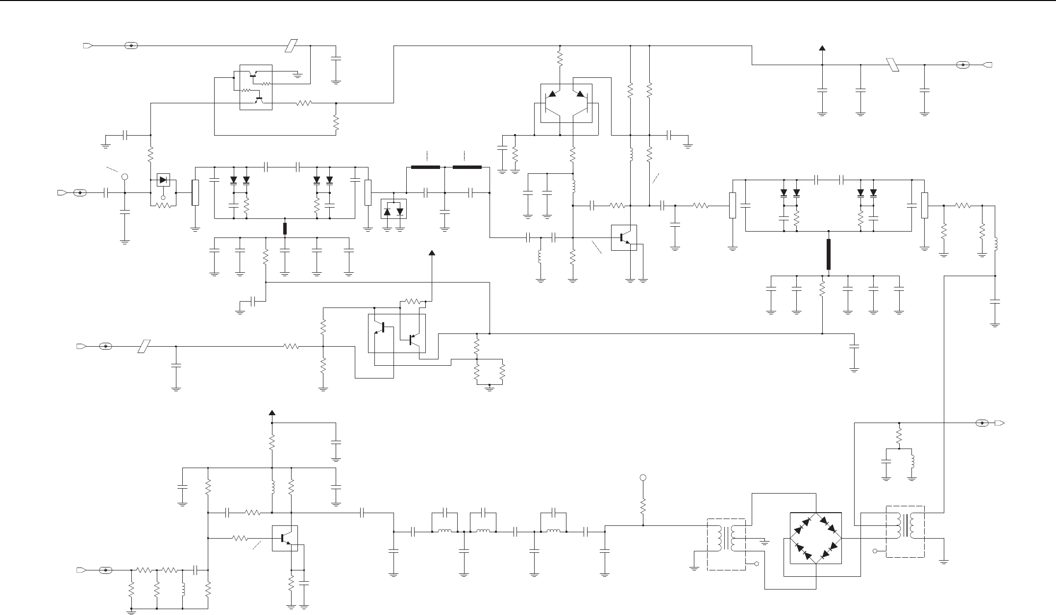
3-6 UHF2 (450–512 MHz) 1–40W PCB/Schematics/Parts List
RF_ATTEN_1_3
RF_ATTEN_1
0.8 VDC Typical
100pF
C0413
RXIN_FE_6
FT0400
TEST_POINT
1
C0421
2.7pF
RX_IN
R0432
NU
680
D0400
NU
MMBV3401LT1G
C0404
120pF
NU
10 dB Attenuator
(Not Placed)
C0462
20pF100K
R0444
D0406
1SV229
R0407
0
12
3
L0405
10nH
NC
D0401
1SV229
C0411
(VALUE)
2.0pF
2.7pF
C0407C0406
10pF
C0461
20pF
100K
R0443
D0407
1SV229
1SV229
D0402
12
3
L0402
10nH
C0410
2.0pF
(VALUE)
12
CR0400
MMBD352
C0412
3.0pF
3
NU
E0400
BK1005HM471
NU
R0403
0
10K
2
5
6
3
1
4
NU
R0431
NU
EMH4FT2R
Q0400
NU
120pF
C0400
(Micro-strip 20 mm Each)
Hi-Side Zeros for Preselector
1.5dB Pad
R0438
560
12nH
L0414
2.7pF
C0435
L0404
12
3
10nH
560
R0436
8.2
R0435
C0432
220pF
C0431
220pF
C0428
220pF220pF
C0429
100K
R0412 220pF
C0430
C0434
120pF
12
3
10nH
L0403
0
R0437
1.6pF
C0420
(VALUE)
8.6 VDC
L0413
180nH
120pF
C0415
18pF
R0405
C0405
2205.6K15nHR0404
2%
L0401
R0406
2.7K
0.10uF
C0419
(VALUE)
0.7 VDC
C0460
10uF
Q0402
BFG540W
C0454
120pF
C0414
120pF
1.2K
R0409
13pF
C0422
L0406
10nH
2%
(VALUE)
0.1uF
C0455
15K
R0400
1
4
Q0401
UMT1NFTN
25
6
3
5.6K
R0401
R0411
180
R0402
180
D0409
D0408
1SV229 1SV229 1SV229 1SV229
R0441
100K
R0440
100K
C0459
20pF
C0458
20pF
2.7pF
C0409
D0404
D0403
3.0pF
C0416
3.0pF
C0417
C0408
10pF
9R1_FE_6
C0401
0.1uF
BK1005HM471
E0401
9R1
9R1_FILT
120pF
47pF
C0403C0402
IF_FE_8
IF
L0412
47nH
R0427
10
C0456
100pF
XFMR
T0401
Zo/Zin=4:1
NC
1
5NC
4
6
3
2
IO3 3
IO4
4
D0405
IO1
1IO2 2
Zo/Zin=4:1
T0400
XFMR
NC5
4
6
3
2
1
NC
+16.0 dBm Min. (250 mV P-P)
TEST_POINT
FT0401
1
R0426
2.7K
RX_INJ_FE_5
R0425
1.2K
C0451
47pF
R0433
22nH
2%
L0411
0
R0422
17.8
1%
R0424
1%
294
R0423
294
1%
RX_INJ
3.0 VDC Typical
Q0405
BFG540W
R0434 0.1uF
C0457
100
3.7 VDC Typical
10
R0421
8.9 VDC Typical
R0420
2.7K
C0440
120pF
C0439
NU1.5K
R0418 L0407
2%
27nH
C0442
4.3pF
10
R0417 120pF
C0437
C0438
120pF
R0419
2.7K
9R1_FILT
FE_TUNE_FE_4
BK1005HM471
E0403
C0436
120pF
FE_TUNE
MAKO ( 0 ~ 4.6 VDC) 680
R0429
R0428
10K
10K
R0430
Q0403
UMZ2NTR
2
3
6
4
1
5
R0413
680
(3.00 ~ 8.00 VDC)
R0414
680
R0415
680
R0416
680
9R1_FILT
C0427
220pF
C0426
220pF
C0425
220pF220pF
C0424
220pF
C0423
100K
R0410
NU
C0433
C0453
20pF
C0452
NU
NU
C0464
1.6pF
C0463
2.2pF
(VALUE)
C0441
2.2pF
18nH
2%
L0410
9.1pF
C0448
C0445
27pF
18nH
2%
L0409
10pF
C0447
L0408
2%
18nH
5.1pF
C0446
100pF
C0443
C0449
10pF
100pF
C0444
UHF2 (450–512 MHz) 1–40W Receiver Front-End Schematic Diagram

UHF2 (450–512 MHz) 1–40W PCB/Schematics/Parts List 3-7
5V_BE_5
5V
5V
800_900/UHF1/UHF2 -- 73.35MHz
4-POLE
VHF -- 44.85MHz
IN 6
OUT
2CC1
5CC2
1GND1
4
GND2
3
VHF=820nH
800/900=18pF
U1=18pF
U2=18pF
VHF=20pF
800/900=390nH
U1=390nH
U2=390nH
L0503
390nH
18pF
C0507
IFIN_BE_8
IF
800/900=6.2pF
U1=6.2pF
U2=6.2pF
VHF=7.5pF
C0510
6.2pF
800/900=0.10uF
U1=0.10uF
U2=0.10uF
VHF=12pF
800/900=9116854H01 (D73312GQ1)
U1=9116854H01 (D73312GQ1)
U2=9116854H01 (D73312GQ1)
VHF=9180022M11 (MXF45)
L0504
NU
NU
C05090.10uF
C0506
FL0500
E0500
BK1005HM471
20K
R0502
330
R0501
R0511
1.2K
C0514
0.10uF
C0512
1.43V
56K
0.10uF
R0508
0.10uF
C0503
Q0500
PBR941
1
3
2
4.7K
R0509
0.76V
800/900=820nH
U1=820nH
U2=820nH
VHF=1.5uH
L0506
C0516
820nH
C0515
NUNU
MMBD352
D0500
1.6V
0.72V
0.10uF
C0502
R0500
5.1K
Q0501
PBR941
R0503
30K
0.10uF
C0504
R0512
51
0.10uF
C0513
30K
R0510
IF_TO_ABACUS
IF_OUT
1
SH0500
SHIELD
UHF2 (450–512 MHz) 1–40W Receiver IF Amp Schematic Diagram
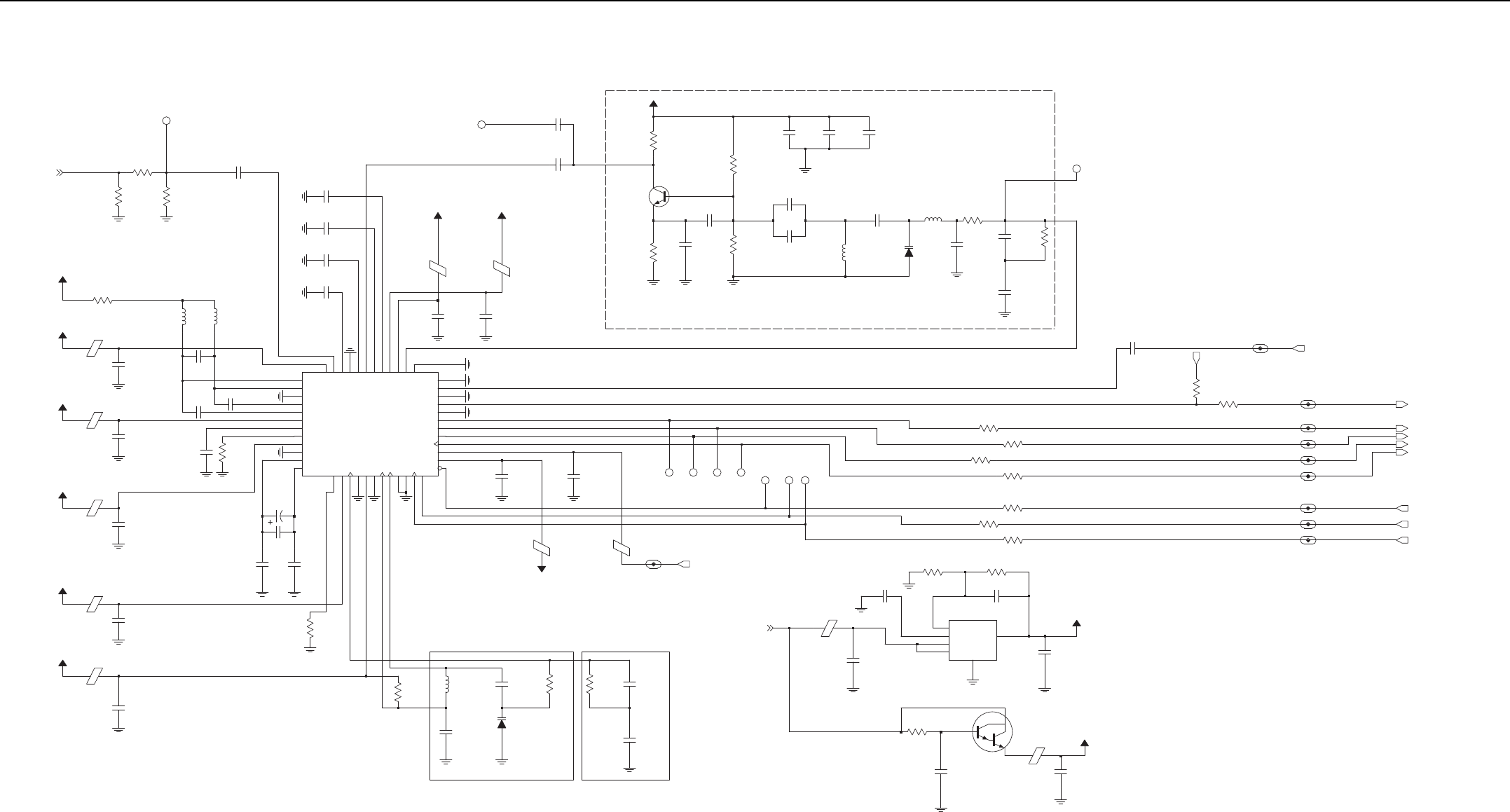
3-8 UHF2 (450–512 MHz) 1–40W PCB/Schematics/Parts List
IF_OUT
1
U602
TEST_POINT
0
R0621
NU
R0622 R0623
NU
C0650
30pF
51
R0606
3VA
L0604
10uH
L0605
10uH
C0623
0.10uF
E0602
BK1005HM471
3VA
3VAE0603
BK1005HM471
3VAE0604
BK1005HM471
0.10uF
C0633
C0625
200pF
C0628
0.10uF
0
# R0610
# C0629
2200pF
100pF
# C0627
100pF
# C0626
4.7uF
* C0632
# C0635
100pF
# R0616
100K
.01uF
# C0634
100pF
# C0636
3VAE0607
BK1005HM471
C0638
0.10uF
3VAE0608
BK1005HM471
0.10uF
C0644
14
23
24
13
17
15
16
21
18
22
20
19
11
6
12
1
9
4
5
2
3
8
7
10
48
40
39
47
38
42
43
45
37
46
44
41
VREFP VDDD
VDDF
VDDH
VDDI
VDDL
VDDP
VDDQ
VREFN
MXOP
PC
PD
PE
RREF
SYNCB
VDDA
VDDC
IF2N
IF2P
IFIN
IOUTC
IOUTL
LON
LOP
MXON
GNDF
GNDH
GNDI
GNDL
GNDP
GNDQ
GNDS1
GNDS2
DOUTB
FREF
FS
GCN
GCP
GNDA
GNDC
GNDD
CLKN
CLKOUT
CLKP
CXIF
CXVL
CXVM
DOUTA
AD9864
U0600
26
27
25
33
32
36
34
30
35
31
28
29
0.10uF
C0630
0.10uF
C0631
FSCLKOUTDOUTA
PC
DOUTB
PDPE
1V8_3
E0606
BK1005HM471
1V8
3VA
E0605
BK1005HM471
CLOCK VCO
C0645
68pF
.01uF
C0642
10K
R0617
10K
R0619
D0601
1SV305
4.7uH
L0608
CLOCK LF
C0646
0.68uF
C0643
0.10uF
390
R0618
5VFB
GND
5
NP
VCONT
VIN
VOUT 1
2
6
4
3
E0610
BK1005HM471
C0651
51.1K
R0625
100pF
68.1K
R0626
U0601
TK11100CSC
.01uF
C0641
2.2uF
C0640
0
R0608
R0609
0
0
R0615
R0614
0
0
R0613
0
R0611
0
R0612
3VA
C0637
1.0uF
10.0uF
C0648
BK1005HM471
E0609VVCO
9.1K
C0647
10.0uF
R0620
Q0601
73A04
SPI_ABACUS_CEX
SPI_ABACUS_DATA
SPI_ABACUS_CLK
SSI_ABACUS_DOUTB
SSI_ABACUS_CLKOUT
SSI_ABACUS_FSYNC
SSI_ABACUS_DOUTA
SSI_ABACUS_SYNCB
SB_1_BE_5
FD_1_BE_5
FC_1_BE_5
FE_1_BE_5
CLKOUT_1_BE_5
DOUTB_1_BE_5
DOUTA_1_BE_5
FS_1_BE_5
1000pF
C0622
R0627
0
FREF_IF
NU
R0607
1V8
REF_CLK
TEST_POINT
TP0601
0.1uF
C0618
R06032K
.01uF
C0613
800/900=11pF
U1=13pF
U2=11pF
VHF=39pF
800/900=270nH
U1=270nH
U2=270nH
VHF=820nH
800/900=2.7uH
U1=2.7uH
U2=2.7uH
VHF=8.2uH2nd LO LF
3300pF
C0649
5.1K
R0624
NU
C0616
2.7uH
L0602
24K
R0604
D0600
1SV305
L0603
270nH
C0612
13pF
C0604
0.10uF
220pF
C0603
.01uF
C0602
800/900=18pF
U1=18pF
U2=18pF
VHF=15pF
18pF
C0607
800/900=68
U1=68
U2=68
VHF=130
SPF_3.5V
VVCO
R0601
68
10K
R0602
800/900=68pF
U1=68pF
U2=68pF
VHF=56pF
800/900=43pF
U1=43pF
U2=43pF
VHF=22pF
330
R0605
Q0600
NE68519
43pF
C0614
C0610
68pF
C0605
43pF
43pF
C0601
TEST_POINT
TP0600
0.10uF
C0621
0.10uF
C0620
3VA5V
BK1005HM471
E0600
BK1005HM471
E0601
1000pF
.01uF
C0615
# C0611
C0619
0.10uF
0.10uF
C0617
2nd LO VCO VHF (42.6MHz/47.1 MHz)
2nd LO VCO UHF (71.1MHz/75.6 MHz)
UHF2 (450–512 MHz) 1–40W Receiver Back-End Schematic Diagram
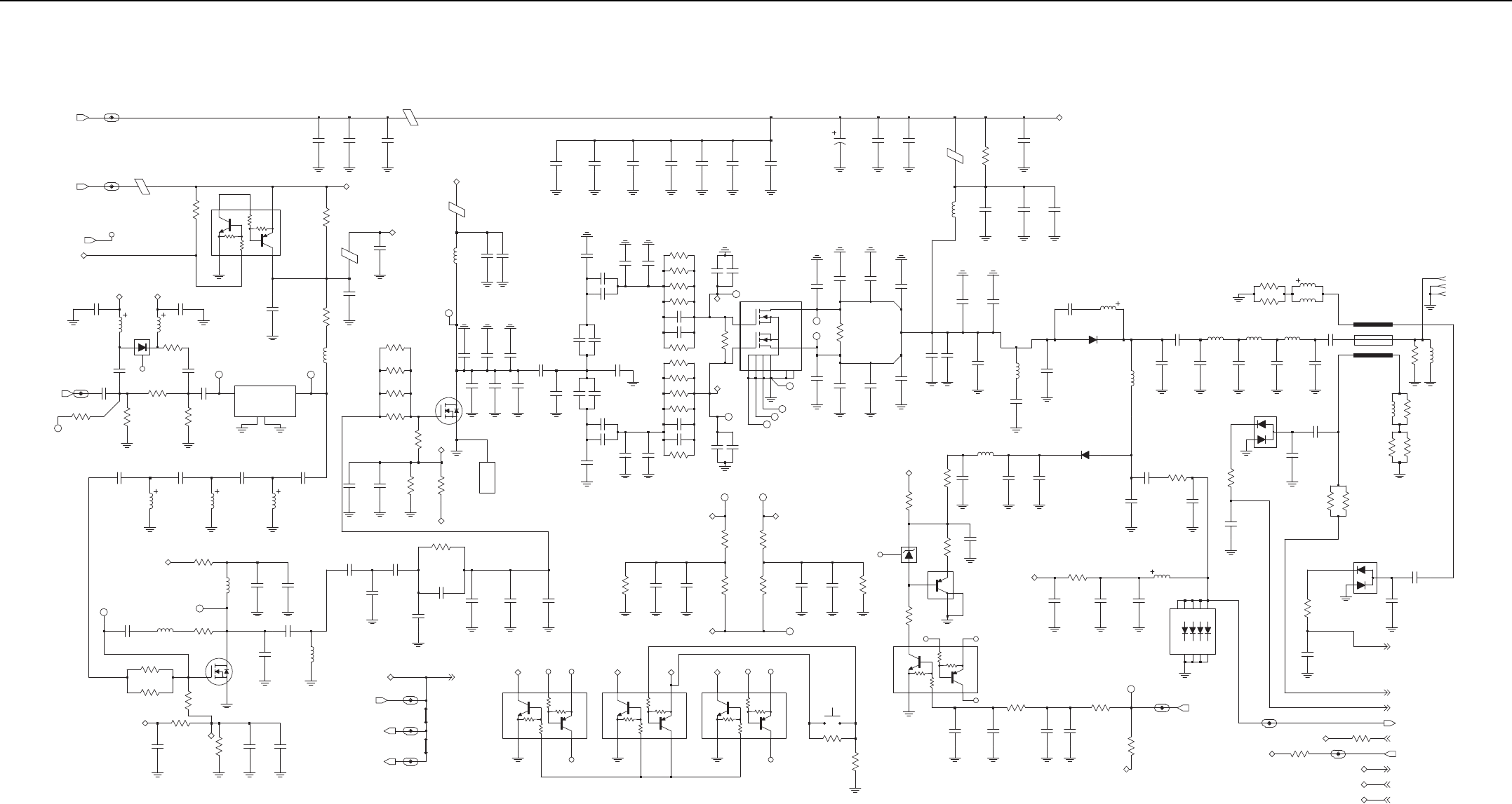
UHF2 (450–512 MHz) 1–40W PCB/Schematics/Parts List 3-9
R0700
NU
E0703
PA_SUPPLY_TX_PA
NC
PREDRIVE_SW
Antenna_En
9V3_PA
PA_SUPPLY
13 dBm
Test Point to check 11dB/17dB Pad
Ref Osc Warping
+8 dBm
3.2VDC
18dB RL
-3 dBm
C0728
75pF
TP0704
75pF
C0733
R0706
C0718
1000pF
150nH
180
VD_RF_OUT 3
L0705
U0700
ADA4743
2GND1
4GND2
1RF_IN
9.1pF 75pF
C0734
C0795
TP0703
TP0705
R0760
2.7K
TX_INJ_TX_PA
L0718
10nH
R0715
75
R0714
75
R0712
91
C0752
R0711
220
L0711
120pF
150nH
L0709
150nH
C0817
7.5pF
L0721
4.7nH3.3nH
L0717
27pF
C0785
C0763
120pF
NC
C0736
120pF
D0704
120pF
C0768
TX_INJ
HI_PWR_PAD LO_PWR_PAD
R0702
NU
RN49A2
47K
47K
47K
2.2KQ0701
9V3_TX
C0725
120pF
120pF
C0724
BK1005HM471
E0704
9V3_Tx_Sw
.022uF
C0701C0700
30pF
E0700
2743019447
2200pF
C0702
E0702
2508053007Y3
33.47nH
L0702C0716
1000pF
C0717
120pF
9V3_TX
TP0702
10
R0754
R0755
10
10
R0720
R0718
10
HEATSINK
POS 1
M0700
C0771
NU10K
R0727
6.2K
C0770R0728
R0722
120pF
4.7K
1
D
3G
2S
Q0703
V_G2
V_cont
C0815
75pF
10pF
47pF
C0791
C0787
R0739
C0792
NU
18pF
30pF
C0786
NU
C0790
9V3_VCO
9V3_SYNTH
9V3
9V3
4.7K
120pF
C0801
R0751
R0747
120pF 20K
C0802
R0750
10K C0800
NU
Q0705
D
G
S
R0759
10
10
R0777
V_G1
V_cont
2.10V (27.5W)
2.85V (44W)
9.1VDC
0
R0734
R0744
NU
C0788
NU
L0715
150nH
TP0710TP0709
C0780
120pF
C0775
.022uF
NU
L0723
9V3_TX
L0720
3.3nH
NU
C0789
C0814
120pF
Q0707
NC
NC
NC
V_G1
10pF
C0793 C0794
NU
C0804
75pF
C0805
1000pF
R0757
47K
R0756
100K 100K
R0740
75pF
C0781
47K
1000pF
C0782
R0741
TP0711
Final_Bias
2.2VDC (TX Only)
2.2VDC (TX Only)
1K
R0730
1K
R0732
TP0707TP0708
Gate_2
Gate_1
.022uF
C0704C0703
30pF
C0705
1000pF 1000pF
C0708C0709
0.1uF
C0706
NU
C0707
NU
MRF1570, Flat Lead
ATC
C0764
NU
C0753
75pF
C0730
NU
12pF
C0745
12pF
C0756
24pF
C0729
NUC0732
C0731
NU
10pF
C0755
C0744
C0743
18pF 36pF
C0754
NU
C0808
C0819
33pF
NU
33pF
C0818
Q0702
C0809
10pF
C0813
NU
SP070
0
C0807
33pF
C0828
33pF
C0829
33pF
C0845
12pF
C0856
12pF
C0832
24pF
NU
C0749
Gate_1
C0761
24pF
C0765
NU
NU
C0760
15R0764
R0763 15
R0762
15
R0773
15
C0774
R0771 15
24pF
R077015
15
R0768 15
R0769
24pF
C0769
R0766 15
R0765 15
SP070
1
C0869 24pF
C0874 24pF
C0861
24pF
Gate_2
GND2
S1
S2
S3
S4
G2
GND1
R0709
300
D1
D2
G1
ATC
7.5pF
C0746
C0747
NU
C0812
3.3pF
SP0705
SP0704
SP0706
SP0707
33pF
C0806
7.5pF
C0719
C0726
11pF
C0720
NU
R0719
10
3.3pF
C0811
SP070
2
SP070
3
C0712
1000pF
E0701
NU
C0711C0710
10uF
17nH
L0700
7.5pF
ATC
C0748
NU
C0741
NU
C0721
C0737
9.1pF
C0727
NU
C0714
100pF
75pF 68nH
C0810L0719
C0751
3.9pF
L0712
35.5nH
C0722
NU
C0715
NU
75pF
C0735
12.5nH
L0708
12.5nH
L0707
12.5nH
L0706
180
R0971
R0970
200
R0972
L0903
12nH
100nH
C0723
75pF
0
R0978
C0941
1%
9.1pF
C0940
120pF
D0904
R0976
150
150
R0977
C0738
6.8pF
12pF
C0739 C0740
12pF
4.3pF
C0742
3.3pF
C0803
D0700
12.5nH
L0710
51
VR0700 R0738
R0729
10K
C0777
75pF
R0735
100
L0714
C0778
33pF
43.67nH
470
R0745
33pF
C0779
C0776
75pF
NC
Q0706
NC
NC
NC
A+
Q0704
R0743
1K
75pF
C0759 C0758
NU75pF
C0757
L0716
180nH
9V3_Tx_Sw
D0702120pF
C0767
C0772
2.7pF
NU
C0766
0
R0701
D0905
C0942
75pF
W = 2.5 mm
S = 0.93 mm
L = 19 mm
S = 0.54 mm
W = 0.625 mm
W = 0.625 mm
30K
R0713
3
J0700-22
J0700-3
J0700-11
L0722
390nH
R0974
180
R0975
8.2nH
200
NU
L0904R0973
C0945
R0979
75pF
C0944
3.3pF
3%
0
C0943
75pF
HI_PWR_PAD
9V3_TX
LO_PWR_PAD
FINAL_BIAS_1
FWD_DETECTED
FWD_POWER
REV_DETECTED
V_CONTROL
RX_IN
R0752
0
FINAL_BIAS_1_TX_PA
R0753
1K
HI_PWR_PAD
V_cont
9V3_TX
LO_PWR_PAD
Final_Bias
RX_IN_TX_PA
ANT_ENABLE_TX_PA
ANT_ENABLE
R0748
56K
75pF
C0796
0
TP0713
R0749
C0799
75pF 1000pF
C0797
1000pF
C0798
R0761
0
S0700
SWITCH
R0774
68K
NU
R0775
Antenna_En
A1
A2
A3
A4
A5
K1
K2
K3
K4
D0703
Q0708
NCNC
Q0709
Final_Bias
9V3
V_G2
100pF
C0713
R0742
10
A+
NC
UHF2 (450–512 MHz) 1–40W Power Amplifier Schematic Diagram

3-10 UHF2 (450–512 MHz) 1–40W PCB/Schematics/Parts List
SHIELD
SH0901
11
SH0900
SHIELD
VOUT
FB
GND
NP
VCONT
VIN
1
2
5
6
4
3
TK11100CSC
U0941
47.5K
1%
R0936
C0947
100pF
C0948
1.0uF
C0950
1000pF
16.2K
1%
R0937
C0951
(VALUE)
0.1uF
2.2uF
C0949
9V3
5V DC
2.10V (27.5W)
2.85V (44W)
TP0909
V_CONTROL
LO_BATTERY_DET
LO_BATTERY_DET
C0922
120pF0.1uF
C0921
VSETNC
5
ENBL2
FLTR4
GND
9
NC
6
RFIN 1
VAPC
7
VPOS8
3
AD8315ACPZ-REEL
U0940
COMM
0
R0940
GND
INPUT
NC15
NC2
RESET_OUT
120pF
C0953
3
2
4
1
U0942
NCP301
4700pF
C0926
1.28V (27.5W)
1.35V (44W)
100K
1%
R0955 3.32K
1%
R0946
R0941
TP0910
0
R0950
10K 120pF
C0925
R0954
5%
430K
47K
RT0953
1%
6.81K
R0942
R0947
0
6
5
7
8
4
AD8566
U0900-2
120pF
C0903C0902
0.1uFC0923
2200pF
9V3_PC
NC
470nH
L0902
120pF
C0931
D0902
51
R0927
D0901
5.6K
R0924
R0928
39
NC
NC
C0912
120pF
120pF
C0935
120pF
C0918
5.6K
R0925
120pF
120pF
C0936 C0937
C0934
120pF
D0903
R0910
1K
MMBT3904
Q0902
R0917
5.6K
R0913
0
L0901
470nH
C0914
120pF
R0926
150
R0929
39
9V3_PC
39K
R0919
2
3
C0917
1000pF
C0916
120pF
U0900-1
AD8566
1
8
4
9V3_PC
C0920
120pF
C0919
0.1uF
390
R0918
2.2K
R0921
9V3_PC
MMBT3906
Q0901
2.4K
R0960
36K
R0922
120pF
C0913
C0911
120pF
0.6V typical
Cutback starts about 2.2V
NOTE: VOLTAGES SHOWN FOR ANALOG TX MODE
TP0907
120pF
C0929
1
2
3
R0931
D0906
0
0
R0906
D0900
1
2
3
R0930
18K
120pF
C0915
0
R0923
120pF
C0909
0.1uF
C0908
U0901-1
AD8566
R0914
1%
182K
3
1
8
9V3_PC
4
2
120pF
C0904RT0908
47K
R0907
0
R0902
2.4K
L0900
1uH
TP0913
43.2K
1%
R09019V3
9V3_PC
R0900
1%
56.2K
8
AD8566
U0901-2
7
9V3_PC
1%
22.1K
R0903
4
6
5
C0906
.01uF 120pF
C0907R0909
1%
43.2K
4.0V (44W)
3.2V (27.5W)
TP0904
68.1K
1%
R0915
1%
4.75K
R0916
R0920
1%
26.7K120pF
C0939
R0911
1%
10K
R0912
1%
20K
120pF
C0910
0
R0938
0.21V (27.5W)
0.38V (44W)
TP0903
FWD_POWER
REV_DETECTED
FWD_DETECTED
TX_DAC
TX_DAC
9V39V3
R0951
43.2K
1%
TP0911
0
R0944
R0943
1%
39.2K
C0928
1500pF
C0927
220pF
2
5
6
3
1
4
EMD9FT2R
Q0900
C0901
0.1uF
C0900
120pF
9V3
9V3 to REV bias PIN in LP mode
PC_ATTEN_ENA_TX_PA
PC_ATTEN_ENA
LO_PWR_PAD
9V3_TX
10K
R0726
C0783
120pF
5
6
4
2
3
1
EMH4FT2R
Q0711
9V3 to FW bias PIN in HP mode
270
R0725
R0724
1.8K
HI_PWR_PAD
UHF2 (450–512 MHz) 1–40W Power Control Schematic Diagram

UHF2 (450–512 MHz) 1–40W PCB/Schematics/Parts List 3-11
ABACUS3_SYNCB_IN
ABACUS3_CEX_IN
RX_SSI_DATA_IN
RX_SSI_FSYNC_IN
RX_SSI_CLK_IN
SPI_MOSI_IN
SPI_CLK_IN
SPI_MISO_IN
ABACUS3_SYNCB_IN
SPI_MISO_IN
SPI_MISO_IN
SPI_CLK_IN
SPI_CLK_IN
SPI_MOSI_IN
SPI_MOSI_IN
ABACUS3_CEX_IN
RX_SSI_DATA_PASS_OUT
RX_SSI_CLK_PASS_OUT
RX_SSI_FSYNC_PASS_OUT
ABACUS3_SYNCB_OUT
RX_SSI_FSYNC_OUT
RX_SSI_DATA_OUT
ABACUS3_CEX_OUT
RX_SSI_CLK_OUT
SPI_CLK_OUT
SPI_MOSI_OUT
SPI_MISO_OUT
ABACUS3_SYNCB_OUT
RX_SSI_DATA_PASS_IN
RX_SSI_CLK_PASS_IN
RX_SSI_FSYNC_PASS_IN
ABACUS3_CEX_OUT
SPI_MOSI_OUT
SPI_MISO_OUT
SPI_CLK_OUT
220
R0107
PBR941
Q0100
R0110
51
R0108
2K
C0171
10K
R0144
.01uF
Buffer to Abacus/Controller
R0105
240
.01uF
C0120
2.8V_DIG
270nH
L0100 C0195
470pF
16.8_GPS_SYNTH
16.8_REF_BE_SYNTH
16.8_REF_CONTROLLER_SYNTH
16.8_GPS
16.8_REF
R0155
0
NU
R0147
0
R0146
0
R0157
0
NU
9R1_SYNTH
9V3_SYNTH
9V3
9R1
9R1 SWITCH FOR FRONT-END
NTR1P02T1
Q0107R0160
100K
10K
47K
Q0108
DTC114YKAF
RSTB_SYNTH
RSTB
GPO_4
GPO_5_SYNTH
GPO_6_SYNTH
GPO_1_SYNTH
GPO_2_SYNTH
GPO_3_SYNTH
RX_VCO_SEL1_
TX_VCO_SEL2_
TX_VCO_SEL1_
RF_ATTN_1
RX_VCO_SEL2_
GPO LINES
HI: 2.8V
LOW: 0V
VCO SEL: ACTIVE LOW
VHF=1500pF
U2=120pF
U1=220pF
VHF=1500pF
U2=120pF
U1=220pF
VHF=1500pF
U2=120pF
U1=220pF
C0128
C0127
C0126
VHF=1500pF
U2=120pF
U1=220pF
VHF=1500pF
U2=120pF
U1=220pF
VHF=1500pF
U2=120pF
U1=220pF
C0132C0131C0130
NU
R0158
0
R0156
0
NU
R0109
0
C0123
1.0uF
VHF=1500pF
U2=120pF
U1=220pF
C0117
.01uF
C0122
0.1uF
C0118
R0106
2.7K
C0115
C0114
1.0uF
1.0uF
VHF=1500pF
U2=120pF
U1=220pF
C0104
0.1uF
C0105
2.8V_ANA
2.8V_ANA
VHF=1500pF
U2=120pF
U1=220pF
VHF=1500pF
U2=120pF
U1=220pF
C0178
C0106
0.1uF
C0108
1.8V_DIG
1.8V_DIG
VHF=1500pF
U2=120pF
U1=220pF
VHF=1500pF
U2=120pF
U1=220pF
VHF=1500pF
U2=120pF
U1=220pF
VHF=1500pF
U2=120pF
U1=220pFC0177
C0102
C0100
C0101
1.8V_DIG
C0103
0.1uF
0.1uF
C0110
0.1uF
C0111
47K
R0104
0.1uFC0107
0.1uF
C0109
TP_TEST2
1
TP_TEST1
1
2.8V_ANA
2.8V_DIG
5V_TH
1.8V_DIG
VHF=1500pF
U2=120pF
U1=220pF
C0175
C0113
NU
C0119
NU
C0121
NUVHF=1500pF
U2=120pF
U1=220pF
Locked: 1.8V
Unlocked: 0V
C0112
0
0
R0103
R0101
R0102
R0100
0
0
5V_BE
1V8_BE
1.8V_TH_DIG
2.8V_TH_ANA
5V
2.8V_TH_DIG
1V8_BE_SYNTH
5V_BE_SYNTH
5V_SYNTH
2.8V_TH_DIG_SYNTH
2.8V_TH_ANA_SYNTH
1.8V_TH_DIG_SYNTH
TX_CLK
SPI_MISO_IN
TH_CEX
SPI_MOSI_IN
SPI_CLK_IN
DMCS
SDTX
SFTX
LOCK
TX_CLK_SYNTH
SDTX_SYNTH
TH_CEX_SYNTH
SFTX_SYNTH
LOCK_SYNTH
DMCS_SYNTH
PRSC
HP_MOD_OUT
SF_OUT
SF_OUT VOLTAGE: 2.45V
SF_OUT_SYNTH
HP_MOD_OUT_SYNTH
PRSC_SYNTH
R0159
10K
5V_TH
OUT
Q0106
DTC114YM
GND
IN
R1
R2
ADAPT_SW_SYNTH
ADAPT_SW
Switch for Adapt Transient
GND
3
INOUT
ONOFF_CONTROL
OUTIN
VCC
1
4
2
5
VHF=1500pF
U2=120pF
U1=220pF
C0138
U0101
MC74VHC1GT66
R0120
10K
5V_TH
VHF=1500pF
U2=120pF
U1=220pF
C0179
Adapt ON: 5V
Adapt OFF: 0V
TP_ADAPT_SW
1
0
R0115
R0148
300
5V_TH
2K
R0114
34
21
BCV62
Q0102
30K
R0117 R0118
0
NU
R0122 0
R0125
0
U2=22
U2=0.033uFVHF=0.1uF
U2=150
VHF=10
VHF=150
VHF=51
VHF=NU
U2=0
U2=0.033uF
U1=240
U1=100 U1=0
U1=0.033uFU1=0.022uF
C0148 C0149
C0150
0.1uF0.1uF
C0151
R0127
R0131
R0128
VHF=NU
VHF=NU
U2=0.1uFU2=18
U2=10k
U1=18
U1=1.6k
VHF=0.1uF
U1=0.1uFR0140
R0139
C0166
Note: High Port modulation injection through loop filter for U1 and U2 only
VCO STEERING LINE VOLTAGE: 0.6V TO 4.4V
VCTRL_SYNTH
VCTRL
VHF=51
U2=120
U1=27
R0134
VCO STEERING LINE VOLTAGE: 0.6V TO 4.4V
TP_VCTRL1
5102495J07 5116032H01
1.5 ppm0.5 ppm
TCXO (Y0100)
VHF=1500pF
U2=120pF
U1=220pF
C0147
R0126
10K
NU
R0123
56K
VHF=1500pF
U2=120pF
U1=220pF
C0146
16.8MHz
TCO5826
Y0100
2
100K
R0161 C0196
10uF
C0180
0.1uF
3
VC
1
VCC 4
GND
OUTPUT
VHF=1500pF
U2=120pF
U1=220pF
C0142
.01uF
C0145
0.1uF
C0141
4.7uF
27
R0119
C0140
2.8V_ANA
R0113
10K
C0191,C0192,C0193,C0194: NU (UHF B1)
C0157, C0159, C0160,C0162,C0163,C0191,C0192,C0193,C0194: NU (UHF B2)
0.1uF
C0194 C0193
0.1uF0.1uF
C0192 C0191
0.1uF
C0165
0.1uF
C0164
0.1uF0.1uF
C0156 C0157
0.1uF0.1uF
C0158 C0159
0.1uF0.1uF
C0160C0161
0.1uF0.1uF
C0162 C0163
0.1uF
VHF=1500pF
U2=120pF
U1=220pF
C0143 C0144
0.1uF
10uF0.1uF
C0136C0135
U2=120pF
U1=220pF
VHF=1500pF
C0134
R0116
0
10uF
C0137
2.8V_ANA
0.1uF
C0129
C0133
4.7uF
VHF=1500pF
U2=120pF
U1=220pF
C0125
0
R0111
2.8V_ANA
C0124
0.1uF
1
1TP504
TP502
1TP503
TP501
1
NC
NC
NC
NC
NC
NC
NC
NC
NC
NC
NC
NC
NC
NC
NC
NC
NC
NC
F6
F3
K10
F5
A1
A11
L1
L11
D4
K9
H8
B4
A4
E5
L10
J8
J7
A6
D6
C10
B11
K5
L5
K4
C9
L4
H5
J4
E6
G11
G9
H11
NC
NC
NC
NC
NC
NC
NC
NC
NC
NC
NC
NC
NC
NC
NC
NC
NC
NC
NC
NC
NC
NC
NC
NC
NC
NC
G8
K7
L7
B10
B1
F2
C2
C1
D1
D2
K11
L9
A3
L8
K6
J9
C6
B6
A2
E4
F4
E2
E3
H9
J11
B5
C4
C5
H6
G6
H7
L6
G7
J6
D7
C7
B3
E8
E11
B9
A9
B8
D5
B2
A5
D3
A10
A8
C3
J5
G10
B7
G4
J1
G5
H2
F8
C8
E1
K2
L2
K3
J3
H4
A7
H10
J10
NC
XOSC_EMIT
XOSC_GND
TX_DAC_GND
TX_DAC_VCC
TX_GND1
TX_GND2
TX_VCC
VCO_DAC
XOSC_BASE
SUB3
TCLK
TEST1
TEST2
TM
TXCLK
TXI
TXQ
SMD_CLK_GEN_GND
SPI_CLK
SPI_DR
SPI_DW
SSI_GND
SSI_VCC
SUB1
SUB2
SDM_REF_GND
SDM_REF_VCC
SDM_VAG
SDM_VREFM
SDM_VREFP
SDR
SDTX
SFTX
SF_OUT
RX_AVCC1
RX_AVCC2
RX_EN_OUT
SCAN_EN
SCAN_IN
SCLK_OUT
SDM_CLK_GEN_VCC
RXACQ
RXFS
RXI
RXIX
RXQ
RXQX
RX_AGND1
RX_AGND2
NTXQ
OSCREG_BYP
OSCREG_GND
OSCREG_OUT
OSCREG_SPLY
PABIAS_DAC
PHCLK
RFSTEPA
RSTB
MN_CP_VCC
M_PRSC
M_PRSCX
NC1
NC2
NC3
NC4
NTXI
LVCC2
MAIN_GND
MAIN_PDET_VCC
MAIN_VCC
MN_ADAPT_CP
MN_CP
MN_CP_GND
GPO3_TEST3
GPO4_TEST4
GPO5
GPO6
HP_MOD_OUT
INCR_DECR
LGND1
LGND2
LVCC1
ESC_IN
ESC_TEST
ESC_VCC
FBI
FBQ
GPO1_TEST1
GPO2_TEST2
DMCS
EF_OUTM
EF_OUTP
ESC_CP
ESC_CPBIAS
ESC_CP_GND
ESC_CP_VCC
ESC_GND
CLK_BASE
CLK_CP
CLK_EMIT
CLK_GND
CLK_VCC
DAC_ADAPT
DC_CAL
DEEPSLEEP
ASPI_VCC
BP_I
BP_IX
BP_Q
BP_QX
CEX
CLK1_OUT
CLK2_OUT
ACE1
ACE2
AGC_DAC
AGC_FLAG
AGC_REF
ARX_DAC
ASPI_CLK
ASPI_DATA
SC51650VF
U0100
F1
F10
C11
D10
D9
D11
F11
F9
E9
E7
E10
J2
H3
G2
H1
G3
K8
K1
F7
L3
G1
D8
1
SHIELD
SH0101
1
SH0100
SHIELD
UHF2 (450–512 MHz) 1–40W Synthesizer Schematic Diagram
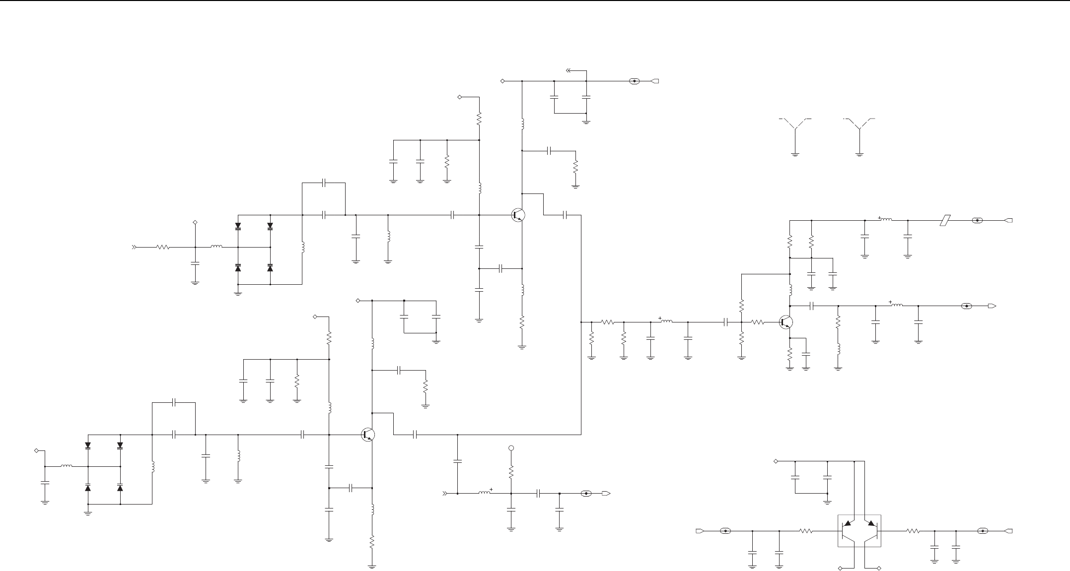
3-12 UHF2 (450–512 MHz) 1–40W PCB/Schematics/Parts List
390nH
L0217
L0218
22nH
CR0206
120pF
C0253
CR0205
CR0208
CR0207
RXSL
RX VCO2
C0250
4.3pF
4.3pF
C0245
C0243
3.9pF
L0215
8nH
0.10uF
C0241
120pF
C0242
7.5K
R0225
L0214
390nH
C0246
11pF
43pF
15pF
C0252
C0251
20pF
C0259
390nH
L0219
150
R0229
3.0pF
C0231
C0247
Q0201
7.5pF
C0240
120pFR0226
100
L0213
390nH
3.6K
R0224
SF_TH
RX2C0236
120pF
C0237
0.10uF
L0212
390nH
62
R0216
27pF
C0229
C0225
56pF
36pF
C0223
390nH
L0203
Q0200
8.2K
R0204
C0205
0.10uF
C0206
120pF
11pF
C0214
L0202
390nH
3K
R0201
RX1
SF_TH
R0205
100
C0215
3.0pF
120pF
C0204
0.10uF
C0201C0200
120pF
SF_TH
Super Filter Voltage (SF_TH)
SF_TH: 2.5V
SF_TH_VCO_UHF1_6
SF_TH
SH0300
SHIELD
SH0301
SHIELD
RX Buffer Amplifier
220nH
L0200
9R1_VCO_UHF1_7
C0202
.01uF
120pF
C0203
E0201
R0202
510
R0203
510
9R1
RXINJ: 376.65 - 453.65 MHz
+10 dBm
RXINJ_VCO_UHF1_5
RXINJ
3.0pF
C0218
C0219
0.5pF
L0205
39nH
220nH
L0211
51
R0208
L0204
220nH
510
R0220
10
R0221
R0219
510C0221
7.5pF
120pF
C0207
.022uF
C0211
C0224
120pF
R0212
10
R0210
R0206
15K
PBR941
4.7K
C0217 Q0202
120pF
C0209
120pF
5.1
R0207
L0206
12nH
C0222
3.0pF
RX VCO1
Steering Line Voltage (VCTRL_TH)
VCTRL: 0.6-4.5V
VCTRL
L0209
390nH
CR0202CR0201
CR0204CR0203
0
R0211
C0226
120pF
RXSL
8nH
L0207
6.8pF
C0220
18nH
L0210
C0213
3.9pF
4.3pF
C0208
L0221
33nH
R0230
4.7K
FT0301
1
C0235
4.3pF
C0230
150pF
NU
C0233
PRESC_TX
RX Prescaler
PRSC (RX): 329.65 - 396.65 MHz
-5 to -15 dBm
PRSC_VCO_UHF1_5
PRSC
RX1_SEL: 2.7 V (High)
0.1 V (Low)
RX1_SEL_VCO_UHF1_5
0.10uF
120pF
C0248 C0249
RX_VCO_SEL1
R0213
10K
RX1
U0201
RX2
0.10uF
C0239C0238
120pF
SF_TH
0.1 V (Low)
RX2_SEL: 2.7 V (High)
10K
R0218
RX2_SEL_VCO_UHF1_5
C0258
C0257
120pF0.10uF
RX_VCO_SEL2
UHF2 (450–512 MHz) 1–40W Receiver VCO Schematic Diagram
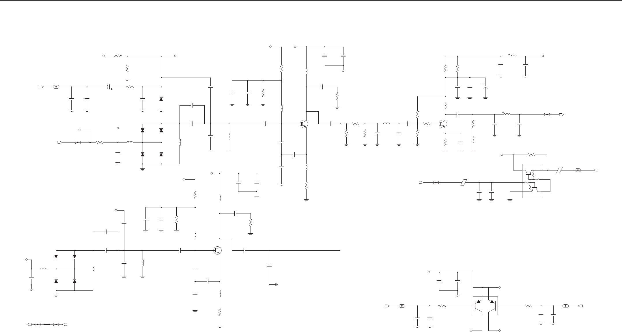
UHF2 (450–512 MHz) 1–40W PCB/Schematics/Parts List 3-13
HP_MOD_OUT_VCO_UHF1_7
C0360
C0361
1000pF
4.7uF
C0334
120pF
15K
R0320
24K
R0319
2.7K
R0321
HP_MOD_OUT
SF_TH
VCTRL: 0.6-4.5V
Steering Line Voltage (VCTRL_TH)
TX VCO1
L0309
390nH
VCTRL_VCO_UHF1_7
C0326
120pF
CR0302CR0301
CR0304CR0303
R0311
0
VCTRL
VCTRL
VSL
NU
C0364 CR0300
C0310
0.5pFC0305
0.10uF120pF
C0306
8.2K
R0304
8nH
L0307
4.3pF
C0308
18nH
L0310
5.1pF
C0314
4.3pF
3.6pF
C0320
C0313
L0314
390nH
C0344
0.5pF
0.10uF
C0341 C0342
120pF
C0346
5.1pF
8.2K
R0325
L0313
390nH
3K
R0324
SF_TH
TX2C0337
0.10uF
120pF
C0340
120pF
C0336
100
R0326
4.7pF
C0347
Q0301
L0319
390nH
C0359
16pF
51
R0329
51pF
C0352
C0351
24pF
C0350
2.2pF8nH
L0315
3.0pF
C0345
C0343
3.0pF
TX VCO2
VMOD
L0317
390nHL0318
18nH
CR0306
120pF
C0353
CR0305
CR0308CR0307
VSL
9V3_SYNTH_IN
9V3_SYNTH_OUT
PRSC (TX): 403-470 MHz
-5 to -15 dBm
TX Prescaler
6.2pF
C0331
PRESC_TX
TX1
VMOD
L0302
390nH
3.3K
R0301
100
R0305
C0301
0.10uF
C0304
120pF
C0300
120pF
SF_TH
390nH
L0303
Q0300
C0315
6.2pFR0333
27
200
R0334
R0332
200
C0321
10pF
L0306
39
R0307
C0322
10nH
15pF
R0306
15K
4.7K
R0310
C0317
120pF
L0312
390nH
68
R0316
51pF
C0325
13pF
C0329
24pF
C0323
0.1 V (OFF)
TX_BUFFER_SEL: 1.8 V (ON)
NU
U0303
PREDRIVE_SW_VCO_UHF1_6NU
E0302
NU
C0328
0.10uF
NU
220pF
C0327
PREDRIVE_SW
9V3_VCO_UHF1_7
0
R0337
E0301
9T1
9V3_VCO
TXINJ: 450-527 MHz
+10 dBm
TXINJ_VCO_UHF1_5
TXINJ
TX Buffer Amplifier
L0300
220nH
C0302
.01uF
120pF
C0303
R0302
750750
R0303
9T1
C0316
10uF
L0304
220nH
220nH
L0311
C0318
3.3pF
C0309
120pF
L0305
27nH
NU
C0319
R0308
51
C0307
.022uF
C0311
120pF
C0324
120pF
20
R0312
PBR941
Q0302
Super Filter Voltage (SF_TH)
0.1 V (Low)
TX1_SEL: 2.7 V (High)
SF_TH: 2.5V
TX1_SEL_VCO_UHF1_5
SF_TH
TX_VCO_SEL1
10K
R0327
C0349
0.10uF
120pF
C0348
C0363
0.10uF
C0362
120pF
U0304
TX1TX2
10K
R0331
0.10uF
C0358
SF_TH
C0357
120pF
TX2_SEL: 2.7 V (High)
0.1 V (Low)
TX2_SEL_VCO_UHF1_5
TX_VCO_SEL2
UHF2 (450–512 MHz) 1–40W Transmit VCO Schematic Diagram

3-14 UHF2 (450–512 MHz) 1–40W PCB/Schematics/Parts List
UHF2 PCB 8471696M01 Parts List 1–40W
Circuit
Ref
Motorola
Part No. Description
C0100 2113944A41 120pF
C0101 2113944A41 120pF
C0102 2113944A41 120pF
C0103 2113945C31 0.1uF
C0104 2113944A41 120pF
C0105 2113945C31 0.1uF
C0106 2113945C31 0.1uF
C0107 2113945C31 0.1uF
C0108 2113944A41 120pF
C0109 2113945C31 0.1uF
C0110 2113945C31 0.1uF
C0111 2113945C31 0.1uF
C0112 2113944A41 120pF
C0113 NOT PLACED –
C0114 2113946E02 1.0uF
C0115 2113946E02 1.0uF
C0117 2113944A41 120pF
C0118 2113945C31 0.1uF
C0119 NOT PLACED –
C0120 2113945B02 .01uF
C0121 NOT PLACED –
C0122 2113945B02 .01uF
C0123 2113946E02 1.0uF
C0124 2113945C31 0.1uF
C0125 2113944A41 120pF
C0126 2113944A41 120pF
C0127 2113944A41 120pF
C0128 2113944A41 120pF
C0129 2113945C31 0.1uF
C0130 2113944A41 120pF
C0131 2113944A41 120pF
C0132 2113944A41 120pF
C0133 2313960B30 4.7uF
C0134 2113944A41 120pF
C0135 2313960B32 10uF
C0136 2113945C31 0.1uF
C0137 2313960B32 10uF
C0138 2113944A41 120pF
C0140 2313960B30 4.7uF
C0141 2113945C31 0.1uF
C0142 2113944A41 120pF
C0143 2113944A41 120pF
C0144 2113945C31 0.1uF
C0145 2113945B02 .01uF
C0146 2113944A41 120pF
C0147 2113944A41 120pF
C0148 2113945D01 .033uF
C0149 2113945D01 .033uF
C0150 2113945C31 0.1uF
C0151 2113945C31 0.1uF
C0156 2185419D06 0.1uF
C0157 NOT PLACED –
C0158 2185419D06 0.1uF
C0159 NOT PLACED –
C0160 NOT PLACED –
C0161 2185419D06 0.1uF
C0162 NOT PLACED –
C0163 NOT PLACED –
C0164 2185419D06 0.1uF
C0165 2185419D06 0.1uF
C0166 2185419D06 0.1uF
C0171 2113945B02 .01uF
C0175 2113944A41 120pF
C0177 2113944A41 120pF
C0178 2113944A41 120pF
C0179 2113944A41 120pF
C0180 2113945C31 0.1uF
C0191 NOT PLACED –
C0192 NOT PLACED –
C0193 NOT PLACED –
C0194 NOT PLACED –
C0195 2113945A05 470pF
C0196 2113946H02 10uF
C0200 2113944A41 120pF
C0201 2113945Y02 0.10uF
C0202 2113945C02 .01uF
C0203 2113944A41 120pF
C0204 2113944A41 120pF
C0205 2113945Y02 0.10uF
C0206 2113944A41 120pF
C0207 2113945C04 .022uF
C0208 2115153H18 4.3pF
C0209 2113944A41 120pF
C0211 2113944A41 120pF
C0213 2115153H17 3.9pF
C0214 2115153H34 11pF
C0215 2115153H14 3.0pF
C0217 2113944A41 120pF
C0218 2115153H14 3.0pF
C0219 2115153H01 0.5pF
C0220 2115153H23 6.8pF
C0221 2115153H24 7.5pF
C0222 2115153H14 3.0pF
C0223 2115153H46 36pF
C0224 2113944A41 120pF
C0225 2115153H51 56pF
C0226 2113944A41 120pF
C0229 2115153H43 27pF
C0230 2113944C47 150pF
C0231 2115153H14 3.0pF
C0233 NOT PLACED –
Circuit
Ref
Motorola
Part No. Description
C0235 2115153H18 4.3pF
C0236 2113944A41 120pF
C0237 2113945Y02 0.10uF
C0238 2113944A41 120pF
C0239 2113945Y02 0.10uF
C0240 2113944A41 120pF
C0241 2113945Y02 0.10uF
C0242 2113944A41 120pF
C0243 2115153H17 3.9pF
C0245 2115153H18 4.3pF
C0246 2115153H34 11pF
C0247 2115153H24 7.5pF
C0248 2113944A41 120pF
C0249 2113945Y02 0.10uF
C0250 2115153H18 4.3pF
C0251 2115153H40 20pF
C0252 2115153H48 43pF
C0253 2113944A41 120pF
C0257 2113944A41 120pF
C0258 2113945Y02 0.10uF
C0259 2115153H37 15pF
C0300 2113944A41 120pF
C0301 2113945Y02 0.10uF
C0302 2113945C02 .01uF
C0303 2113944A41 120pF
C0304 2113944A41 120pF
C0305 2113945Y02 0.10uF
C0306 2113944A41 120pF
C0307 2113945C04 .022uF
C0308 2115153H18 4.3pF
C0309 2113944A41 120pF
C0310 2115153H01 0.5pF
C0311 2113944A41 120pF
C0313 2115153H18 4.3pF
C0314 2115153H20 5.1pF
C0315 2115153H22 6.2pF
C0316 2313960B32 10uF
C0317 2113944A41 120pF
C0318 2115153H15 3.3pF
C0319 NOT PLACED –
C0320 2115153H16 3.6pF
C0321 2115153H27 10pF
C0322 2115153H37 15pF
C0323 2115153H42 24pF
C0324 2113944A41 120pF
C0325 2115153H50 51pF
C0326 2113944A41 120pF
C0327 NOT PLACED –
C0328 NOT PLACED –
C0329 2115153H36 13pF
C0331 2115153H22 6.2pF
Circuit
Ref
Motorola
Part No. Description
C0334 2113944A41 120pF
C0336 2113944A41 120pF
C0337 2113945Y02 0.10uF
C0340 2113944A41 120pF
C0341 2113945Y02 0.10uF
C0342 2113944A41 120pF
C0343 2115153H14 3.0pF
C0344 2115153H01 0.5pF
C0345 2115153H14 3.0pF
C0346 2115153H20 5.1pF
C0347 2115153H19 4.7pF
C0348 2113944A41 120pF
C0349 2113945Y02 0.10uF
C0350 2115153H11 2.2pF
C0351 2115153H42 24pF
C0352 2115153H50 51pF
C0353 2113944A41 120pF
C0357 2113944A41 120pF
C0358 2113945Y02 0.10uF
C0359 2115153H38 16pF
C0360 2313960B30 4.7uF
C0361 2113944C51 1000pF
C0362 2113944A41 120pF
C0363 2113945Y02 0.10uF
C0364 NOT PLACED –
C0400 NOT PLACED –
C0401 2113945C31 0.1uF
C0402 2113944A41 120pF
C0403 2115153H49 47pF
C0404 NOT PLACED –
C0405 2113944A41 120pF
C0406 2115153H27 10pF
C0407 2115153H13 2.7pF
C0408 2115153H27 10pF
C0409 2115153H13 2.7pF
C0410 2115153H10 2.0pF
C0411 2115153H10 2.0pF
C0412 2115153H14 3.0pF
C0413 2115153H57 100pF
C0414 2113944A41 120pF
C0415 2115153H39 18pF
C0416 2115153H14 3.0pF
C0417 2115153H14 3.0pF
C0419 2113945Y02 0.10uF
C0420 2115153H08 1.5pF
C0421 2115153H13 2.7pF
C0422 2115153H36 13pF
C0423 2113944A44 220pF
C0424 2113944A44 220pF
C0425 2113944A44 220pF
C0426 2113944A44 220pF
Circuit
Ref
Motorola
Part No. Description

UHF2 (450–512 MHz) 1–40W PCB/Schematics/Parts List 3-15
C0427 2113944A44 220pF
C0428 2113944A44 220pF
C0429 2113944A44 220pF
C0430 2113944A44 220pF
C0431 2113944A44 220pF
C0432 2113944A44 220pF
C0433 NOT PLACED –
C0434 2113944A41 120pF
C0435 2115153H13 2.7pF
C0436 2113944A41 120pF
C0437 2113944A41 120pF
C0438 2113944A41 120pF
C0439 NOT PLACED –
C0440 2113944A41 120pF
C0441 2115153H11 2.2pF
C0442 2115153H18 4.3pF
C0443 2115153H57 100pF
C0444 2115153H57 100pF
C0445 2115153H43 27pF
C0446 2115153H20 5.1pF
C0447 2115153H27 10pF
C0448 2115153H26 9.1pF
C0449 2115153H27 10pF
C0451 2115153H49 47pF
C0452 NOT PLACED –
C0453 2115153H40 20pF
C0454 2113944A41 120pF
C0455 2113945C31 0.1uF
C0456 2113944A40 100pF
C0457 2113945C31 0.1uF
C0458 2115153H40 20pF
C0459 2115153H40 20pF
C0460 2113946F05 10uF
C0461 2115153H40 20pF
C0462 2115153H40 20pF
C0463 NOT PLACED –
C0464 2115153H08 1.5pF
C0502 2113945Y02 0.10uF
C0503 2113945Y02 0.10uF
C0504 2113945Y02 0.10uF
C0506 2113945Y02 0.10uF
C0507 2115153H39 18pF
C0509 NOT PLACED –
C0510 2115153H22 6.2pF
C0512 2113945Y02 0.10uF
C0513 2113945Y02 0.10uF
C0514 2113945Y02 0.10uF
C0515 NOT PLACED –
C0516 NOT PLACED –
C0601 2115153H48 43pF
C0602 2113945B02 .01uF
Circuit
Ref
Motorola
Part No. Description
C0603 2113944A44 220pF
C0604 2113945Y02 0.10uF
C0605 2115153H48 43pF
C0607 2115153H39 18pF
C0610 2115153H53 68pF
C0611 2113945A09 1000pF
C0612 2115153H34 11pF
C0613 2185419D03 0.01uF
C0614 2115153H48 43pF
C0615 2113945B02 .01uF
C0616 NOT PLACED –
C0617 2113945Y02 0.10uF
C0618 2185419D06 0.1uF
C0619 2113945Y02 0.10uF
C0620 2113945Y02 0.10uF
C0621 2113945Y02 0.10uF
C0622 2113945A09 1000pF
C0623 2113945Y02 0.10uF
C0625 2113944C89 200pF
C0626 2113944A40 100pF
C0627 2113944A40 100pF
C0628 2113945Y02 0.10uF
C0629 2113945A11 2200pF
C0630 2113945Y02 0.10uF
C0631 2113945Y02 0.10uF
C0632 2313960B30 4.7uF
C0633 2113945Y02 0.10uF
C0634 2113945B02 .01uF
C0635 2113944A40 100pF
C0636 2113944A40 100pF
C0637 2113946S35 1.0uF
C0638 2113945Y02 0.10uF
C0640 2113946N03 2.2uF
C0641 2113945B02 .01uF
C0642 2115153H53 68pF
C0643 2113945Y02 0.10uF
C0644 2113945Y02 0.10uF
C0645 2113945B02 .01uF
C0646 2113946G04 0.68uF
C0647 2113946J03 10.0uF
C0648 2113946J03 10.0uF
C0649 2113945A12 3300pF
C0650 2115153H44 30pF
C0651 2115153H57 100pF
C0700 2113944C82 30pF
C0701 2113945C04 .022uF
C0702 2113944C55 2200pF
C0703 2113944C82 30pF
C0704 2113945C04 .022uF
C0705 2113944C51 1000pF
C0706 NOT PLACED –
Circuit
Ref
Motorola
Part No. Description
C0707 NOT PLACED –
C0708 2113944C51 1000pF
C0709 2113945C31 0.1uF
C0710 2371403L02 10uF
C0711 NOT PLACED –
C0712 2113944C51 1000pF
C0713 2111078B42 100pF
C0714 2111078B42 100pF
C0715 NOT PLACED –
C0716 2113944A41 120pF
C0717 2113945A09 1000pF
C0718 2113945A09 1000pF
C0719 2111078B10 7.5pF
C0720 NOT PLACED –
C0721 NOT PLACED –
C0722 NOT PLACED –
C0723 2111078B39 75pF
C0724 2113944A41 120pF
C0725 2113944A41 120pF
C0726 2111078B14 11pF
C0727 NOT PLACED –
C0728 2113944C42 75pF
C0729 NOT PLACED –
C0730 NOT PLACED –
C0731 NOT PLACED –
C0732 2113951B41 24pF
C0733 2113944C42 75pF
C0734 2113944C42 75pF
C0735 2111078B39 75pF
C0736 2113944A41 120pF
C0737 2111078B12 9.1pF
C0738 2111078B09 6.8pF
C0739 2171388L01 12pF
C0740 2171388L01 12pF
C0741 NOT PLACED –
C0742 2111078B04 4.3pF
C0743 2113944C33 18pF
C0744 2113944C83 36pF
C0745 2113944F44 12pF
C0746 2111078B10 7.5pF
C0747 NOT PLACED –
C0748 2111078B10 7.5pF
C0749 NOT PLACED –
C0751 2185400Y24 3.9pF
C0752 2113944A41 120pF
C0753 2111078B39 75pF
C0754 NOT PLACED –
C0755 2113944C30 10pF
C0756 2113944F44 12pF
C0757 2113944C42 75pF
C0758 NOT PLACED –
Circuit
Ref
Motorola
Part No. Description
C0759 2113944C42 75pF
C0760 NOT PLACED –
C0761 2113951B41 24pF
C0763 2113944A41 120pF
C0764 NOT PLACED –
C0765 NOT PLACED –
C0766 NOT PLACED –
C0767 2113944C46 120pF
C0768 2113944A41 120pF
C0769 2113944F51 24pF
C0770 2113944A41 120pF
C0771 NOT PLACED –
C0772 2113944C16 2.7pF
C0774 2113944F51 24pF
C0775 2113945C04 .022uF
C0776 2113944C42 75pF
C0777 2113944C42 75pF
C0778 2111078B29 33pF
C0779 2111078B29 33pF
C0780 2113944A41 120pF
C0781 2113944C42 75pF
C0782 2113944C51 1000pF
C0783 2113944A41 120pF
C0785 2113944C35 27pF
C0786 2113944C82 30pF
C0787 2113944C38 47pF
C0788 NOT PLACED –
C0789 NOT PLACED –
C0790 NOT PLACED –
C0791 2113944A25 10pF
C0792 2113944A28 18pF
C0793 2113944A25 10pF
C0794 NOT PLACED –
C0795 2113944C29 9.1pF
C0796 2113944C42 75pF
C0797 2113944C51 1000pF
C0798 2113944C51 1000pF
C0799 2113944C42 75pF
C0800 NOT PLACED –
C0801 2113944A41 120pF
C0802 2113944A41 120pF
C0803 2111078B01 3.3pF
C0804 2113944C42 75pF
C0805 2113944C51 1000pF
C0806 2185400Y46 33pF
C0807 2185400Y46 33pF
C0808 NOT PLACED –
C0809 2113944C30 10pF
C0810 2113944C42 75pF
C0811 2111078B01 3.3pF
C0812 2111078B01 3.3pF
Circuit
Ref
Motorola
Part No. Description

3-16 UHF2 (450–512 MHz) 1–40W PCB/Schematics/Parts List
C0813 NOT PLACED –
C0814 2113944C46 120pF
C0815 2113944C42 75pF
C0817 2113944C27 7.5pF
C0818 2113944F54 33pF
C0819 2113944F54 33pF
C0828 2113944F54 33pF
C0829 2113944F54 33pF
C0832 2113951B41 24pF
C0845 2113944F44 12pF
C0856 2113944F44 12pF
C0861 2113951B41 24pF
C0869 2113944F51 24pF
C0874 2113944F51 24pF
C0900 2113944A41 120pF
C0901 2113945C31 0.1uF
C0902 2113945C31 0.1uF
C0903 2113944A41 120pF
C0904 2113944A41 120pF
C0906 2113944A41 120pF
C0907 2113945C02 .01uF
C0908 2113945C31 0.1uF
C0909 2113944A41 120pF
C0910 2113944A41 120pF
C0911 2113944A41 120pF
C0912 2113944A41 120pF
C0913 2113944A41 120pF
C0914 2113944A41 120pF
C0915 2113944A41 120pF
C0916 2113944A41 120pF
C0917 2113945A09 1000pF
C0918 2113944A41 120pF
C0919 2113945C31 0.1uF
C0920 2113944A41 120pF
C0921 2113945C31 0.1uF
C0922 2113944A41 120pF
C0923 2113944C55 2200pF
C0925 2113944A41 120pF
C0926 2113945L41 4700pF
C0927 2113944C02 220pF
C0928 2113944C53 1500pF
C0929 2113944A41 120pF
C0931 2113944A41 120pF
C0934 2113944A41 120pF
C0935 2113944A41 120pF
C0936 2113944A41 120pF
C0937 2113944A41 120pF
C0939 2113944A41 120pF
C0940 2113944C46 120pF
C0941 2113944M17 9.1pF
C0942 2113944C42 75pF
Circuit
Ref
Motorola
Part No. Description
C0943 2113944C42 75pF
C0944 2113944M06 3.3pF
C0945 2113944C42 75pF
C0947 2113944A40 100pF
C0948 2113946S35 1.0uF
C0949 2113946G01 2.2uF
C0950 2113945A09 1000pF
C0951 2113945C31 0.1uF
C0953 2113944A41 120pF
CR0201 4815096H01 DIODE VARACTOR 1SV305
CR0202 4815096H01 DIODE VARACTOR 1SV305
CR0203 4815096H01 DIODE VARACTOR 1SV305
CR0204 4815096H01 DIODE VARACTOR 1SV305
CR0205 4815096H01 DIODE VARACTOR 1SV305
CR0206 4815096H01 DIODE VARACTOR 1SV305
CR0207 4815096H01 DIODE VARACTOR 1SV305
CR0208 4815096H01 DIODE VARACTOR 1SV305
CR0300 4815096H01 DIODE VARACTOR 1SV305
CR0301 4815096H01 DIODE VARACTOR 1SV305
CR0302 4815096H01 DIODE VARACTOR 1SV305
CR0303 4815096H01 DIODE VARACTOR 1SV305
CR0304 4815096H01 DIODE VARACTOR 1SV305
CR0305 4815096H01 DIODE VARACTOR 1SV305
CR0306 4815096H01 DIODE VARACTOR 1SV305
CR0307 4815096H01 DIODE VARACTOR 1SV305
CR0308 4815096H01 DIODE VARACTOR 1SV305
CR0400 4813974A19 DIODE, SCHOTTKY
D0400 NOT PLACED –
D0401 4885055Y01 DIODE VARACTOR 1SV229
D0402 4885055Y01 DIODE VARACTOR 1SV229
D0403 4885055Y01 DIODE VARACTOR 1SV229
D0404 4885055Y01 DIODE VARACTOR 1SV229
D0405 4815090H01 DIODE, MIXER
D0406 4885055Y01 DIODE VARACTOR 1SV229
D0407 4885055Y01 DIODE VARACTOR 1SV229
D0408 4885055Y01 DIODE VARACTOR 1SV229
D0409 4885055Y01 DIODE VARACTOR 1SV229
D0500 4813974A19 DIODE, SCHOTTKY
D0600 4815096H01 DIODE VARACTOR 1SV305
D0601 4815096H01 DIODE VARACTOR 1SV305
D0700 4802482J02 DIODE, PIN
D0702 4802482J02 DIODE, PIN
D0703 4875430M01 DIODE, PIN
D0704 4813974A06 DIODE, PIN
D0900 4813978C02 DIODE, SWITCHING
D0901 4815023H01 DIODE, PIN
D0902 4815024H01 DIODE, PIN
D0903 4815024H01 DIODE, PIN
D0904 4813974A21 DIODE, SCHOTTKY
D0905 4813974A21 DIODE, SCHOTTKY
D0906 4813978C02 DIODE, SWITCHING
Circuit
Ref
Motorola
Part No. Description
E0201 2409134J25 FERRITE BEAD
E0301 2409134J25 FERRITE BEAD
E0302 NOT PLACED –
E0400 NOT PLACED –
E0401 2409134J25 FERRITE BEAD
E0403 2409134J25 FERRITE BEAD
E0500 2409134J25 FERRITE BEAD
E0600 2409134J25 FERRITE BEAD
E0601 2409134J25 FERRITE BEAD
E0602 2409134J25 FERRITE BEAD
E0603 2409134J25 FERRITE BEAD
E0604 2409134J25 FERRITE BEAD
E0605 2409134J25 FERRITE BEAD
E0606 2409134J25 FERRITE BEAD
E0607 2409134J25 FERRITE BEAD
E0608 2409134J25 FERRITE BEAD
E0609 2409134J25 FERRITE BEAD
E0610 2480640Z01 FERRITE BEAD
E0700 2485011Y01 FERRITE BEAD
E0701 2485011Y01 FERRITE BEAD
E0702 7671656M01 FERRITE BEAD
E0703 2485011Y01 FERRITE BEAD
E0704 2409134J25 FERRITE BEAD
FL0500 9116854H01 73.35MHZ CRYSTAL FILTER
J0700 0905901V11 MINI-U RF CONNECTOR
L0100 2414017N29 270nH
L0200 2414017N28 220nH
L0202 2414032F41 390nH
L0203 2414032F41 390nH
L0204 2414017N28 220nH
L0205 2414017N19 39nH
L0206 2414017N13 12nH
L0207 2415385H01 8nH
L0209 2414032F41 390nH
L0210 2414015A32 18nH
L0211 2414017N28 220nH
L0212 2414032F41 390nH
L0213 2414032F41 390nH
L0214 2414032F41 390nH
L0215 2415385H01 8nH
L0217 2414032F41 390nH
L0218 2414015A20 22nH
L0219 2414032F41 390nH
L0221 2414017N18 33nH
L0300 2414017N28 220nH
L0302 2414032F41 390nH
L0303 2414032F41 390nH
L0304 2414017N28 220nH
L0305 2414017N17 27nH
L0306 2414017N12 10nH
L0307 2415385H01 8nH
Circuit
Ref
Motorola
Part No. Description
L0309 2414032F41 390nH
L0310 2414015A32 18nH
L0311 2414017N28 220nH
L0312 2414032F41 390nH
L0313 2414032F41 390nH
L0314 2414032F41 390nH
L0315 2415385H01 8nH
L0317 2414032F41 390nH
L0318 2414015A32 18nH
L0319 2414032F41 390nH
L0401 2414015B24 15nH
L0402 NOT PLACED –
L0403 NOT PLACED –
L0404 NOT PLACED –
L0405 NOT PLACED –
L0406 2414015B29 10nH
L0407 2414015B16 27nH
L0408 2414015B17 18nH
L0409 2414015B17 18nH
L0410 2414015B17 18nH
L0411 2414015B15 22nH
L0412 2414017N20 47nH
L0413 2414017N27 180nH
L0414 2414015B23 12nH
L0503 2414015B27 390nH
L0504 NOT PLACED –
L0506 2414032B66 820nH
L0602 2414032K23 2.7uH
L0603 2414032D20 270nH
L0604 2466505A01 10uH
L0605 2466505A01 10uH
L0608 2414032B76 4.7uH
L0700 2460592A01 17nH
L0702 2479990G01 33.47nH
L0705 2414017N26 150nH
L0706 2460592A02 12.5nH
L0707 2460592A02 12.5nH
L0708 2460592A02 12.5nH
L0709 2414017N26 150nH
L0710 2460592A02 12.5nH
L0711 2414017N26 150nH
L0712 2415385H07 35.5nH
L0714 2479990N01 43.67nH
L0715 2414017N26 150nH
L0716 2414017N27 180nH
L0717 2414017N06 3.3nH
L0718 2414017N12 10nH
L0719 2414017N22 68nH
L0720 2414017N06 3.3nH
L0721 2414017N08 4.7nH
L0722 2414032B60 390nH
Circuit
Ref
Motorola
Part No. Description

UHF2 (450–512 MHz) 1–40W PCB/Schematics/Parts List 3-17
L0723 NOT PLACED –
L0900 2414032D30 1uH
L0901 2414032F42 470nH
L0902 2414032F42 470nH
L0903 2414032F23 12nH
L0904 2414032F22 8.2nH
M0700 2686201B02 HEATSINK
Q0100 4802197J95 NPN RF TRANSISTOR
Q0102 4815359H01 DUAL PNP
Q0106 4816134H01 ANALOG SWITCH
Q0107 4813970A59 P-CHANNEL MOSFET
Q0108 4815261H01 ANALOG SWITCH
Q0200 4885061Y01 NPN RF TRANSISTOR
Q0201 4885061Y01 NPN RF TRANSISTOR
Q0202 4802197J95 NPN RF TRANSISTOR
Q0300 4885061Y01 NPN RF TRANSISTOR
Q0301 4885061Y01 NPN RF TRANSISTOR
Q0302 4802197J95 NPN RF TRANSISTOR
Q0400 NOT PLACED –
Q0401 4815267H01 DUAL PNP
Q0402 4885593U03 NPN RF TRANSISTOR
Q0403 4815270H01 DUAL NPN/PNP
Q0405 4885593U03 NPN RF TRANSISTOR
Q0500 4802197J95 NPN RF TRANSISTOR
Q0501 4802197J95 NPN RF TRANSISTOR
Q0600 4885061Y01 NPN RF TRANSISTOR
Q0601 4813973A04 NPN DARLINGTON
Q0701 4816013H01 DUAL NPN/PNP
Q0702 0105958T75 MRF1570 PA ASSEMBLY
Q0703 4816548H01 N-CHANNEL LDMOS DRIVER
Q0704 4813973B02 PNP
Q0705 4816547H01 N-CHANNEL LDMOS PRE-
DRIVER
Q0706 4815272H01 ANALOG SWITCH
Q0707 4815272H01 ANALOG SWITCH
Q0708 4815272H01 ANALOG SWITCH
Q0709 4815272H01 ANALOG SWITCH
Q0711 4815271H01 ANALOG SWITCH
Q0900 4815272H01 ANALOG SWITCH
Q0901 4813973A13 PNP
Q0902 4813973M07 NPN
R0100 0613952R66 0
R0101 0613952R66 0
R0102 0613952R66 0
R0103 0613952R66 0
R0104 0613952R17 47K
R0105 0613952Q58 240
R0106 0613952Q83 2.7K
R0107 0613952Q57 220
R0108 0613952Q80 2K
R0109 0613952R66 0
Circuit
Ref
Motorola
Part No. Description
R0110 0613952Q42 51
R0111 0613952R66 0
R0113 0613952R01 10K
R0114 0613952Q80 2K
R0115 0613952R66 0
R0116 0613952R66 0
R0117 0613952R12 30K
R0118 0613952R66 0
R0119 0613952Q35 27
R0120 0613952R01 10K
R0122 NOT PLACED –
R0123 0613952R19 56K
R0125 0613952R66 0
R0126 NOT PLACED –
R0127 0613952Q33 22
R0128 0613952R66 0
R0131 0613952Q53 150
R0134 0613952Q51 120
R0139 0613952R01 10K
R0140 0613952Q31 18
R0144 0613952R01 10K
R0146 0613952R66 0
R0147 NOT PLACED –
R0148 0613952Q60 300
R0155 0613952R66 0
R0156 NOT PLACED –
R0157 NOT PLACED –
R0158 NOT PLACED –
R0159 0613952R01 10K
R0160 0613952R25 100K
R0161 0613952R25 100K
R0201 0613952Q84 3K
R0202 0613952Q66 510
R0203 0613952Q66 510
R0204 0613952Q95 8.2K
R0205 0613952Q49 100
R0206 0613952R05 15K
R0207 0613952Q18 5.1
R0208 0613952Q42 51
R0210 0613952Q89 4.7K
R0211 0613952R66 0
R0212 0613952Q25 10
R0213 0613952R01 10K
R0216 0613952Q44 62
R0218 0613952R01 10K
R0219 0613952Q66 510
R0220 0613952Q25 10
R0221 0613952Q66 510
R0224 0613952Q86 3.6K
R0225 0613952Q94 7.5K
R0226 0613952Q49 100
Circuit
Ref
Motorola
Part No. Description
R0229 0613952Q53 150
R0230 0613952Q89 4.7K
R0301 0613952Q85 3.3K
R0302 0613952Q70 750
R0303 0613952Q70 750
R0304 0613952Q95 8.2K
R0305 0613952Q49 100
R0306 0613952R05 15K
R0307 0613952Q39 39
R0308 0613952Q42 51
R0310 0613952Q89 4.7K
R0311 0613952R66 0
R0312 0613952Q32 20
R0316 0613952Q45 68
R0319 0613952R10 24K
R0320 0613952R05 15K
R0321 0613952Q83 2.7K
R0324 0613952Q84 3K
R0325 0613952Q95 8.2K
R0326 0613952Q49 100
R0327 0613952R01 10K
R0329 0613952Q42 51
R0331 0613952R01 10K
R0332 0613952Q56 200
R0333 0613952Q35 27
R0334 0613952Q56 200
R0337 0613952R66 0
R0400 0613952R05 15K
R0401 0613952Q91 5.6K
R0402 0613958H55 180
R0403 NOT PLACED –
R0404 0613952Q57 220
R0405 0613952Q91 5.6K
R0406 0613952Q83 2.7K
R0407 0613952G67 0
R0409 0613952Q75 1.2K
R0410 0613952R25 100K
R0411 0613958H55 180
R0412 0613952R25 100K
R0413 0613952Q69 680
R0414 0613952Q69 680
R0415 0613952Q69 680
R0416 0613952Q69 680
R0417 0613958H25 10
R0418 0613952Q77 1.5K
R0419 0613952Q83 2.7K
R0420 0613952Q83 2.7K
R0421 0613958H25 10
R0422 0613952K25 17.8
R0423 0613952L46 294
R0424 0613952L46 294
Circuit
Ref
Motorola
Part No. Description
R0425 0613952Q75 1.2K
R0426 0613952Q83 2.7K
R0427 0613952Q25 10
R0428 0613952R01 10K
R0429 0613952Q69 680
R0430 0613952R01 10K
R0431 NOT PLACED –
R0432 NOT PLACED –
R0433 0613952R66 0
R0434 0613958H49 100
R0435 0613952Q23 8.2
R0436 0613952Q67 560
R0437 0613952R66 0
R0438 0613952Q67 560
R0440 0613952R25 100K
R0441 0613952R25 100K
R0443 0613952R25 100K
R0444 0613952R25 100K
R0500 0613952Q90 5.1K
R0501 0613952Q61 330
R0502 0613952R08 20K
R0503 0613952R12 30K
R0508 0613952R19 56K
R0509 0613952Q89 4.7K
R0510 0613952R12 30K
R0511 0613952Q75 1.2K
R0512 0613952Q42 51
R0601 0613952Q45 68
R0602 0613952R01 10K
R0603 0613952Q80 2K
R0604 0613952R10 24K
R0605 0613952Q61 330
R0606 0613952Q42 51
R0607 NOT PLACED –
R0608 0613952R66 0
R0609 0613952R66 0
R0610 0613952R66 0
R0611 0613952R66 0
R0612 0613952R66 0
R0613 0613952R66 0
R0614 0613952R66 0
R0615 0613952R66 0
R0616 0613952R25 100K
R0617 0613952R01 10K
R0618 0613952Q63 390
R0619 0613952R01 10K
R0620 0613952Q96 9.1K
R0621 0613952R66 0
R0622 NOT PLACED –
R0623 NOT PLACED –
R0624 0613952Q90 5.1K
Circuit
Ref
Motorola
Part No. Description
3-18 UHF2 (450–512 MHz) 1–40W PCB/Schematics/Parts List
R0625 0613952N69 51.1K
R0626 0613952N81 68.1K
R0627 0613952R66 0
R0700 NOT PLACED –
R0701 0613958J74 0
R0702 NOT PLACED –
R0706 0613958S55 180
R0709 0613959Q60 300
R0711 0613952H57 220
R0712 0613952H48 91
R0713 0613959H12 30K
R0714 0613952H46 75
R0715 0613952H46 75
R0718 0613952H25 10
R0719 0613959Q25 10
R0720 0613952H25 10
R0722 0613952H89 4.7K
R0724 0613952H79 1.8K
R0725 0613952Q59 270
R0726 0613952N01 10K
R0727 0613952H92 6.2K
R0728 0613952J01 10K
R0729 0613952J01 10K
R0730 0613952H73 1K
R0732 0613952H73 1K
R0734 0613952G67 0
R0735 0613959Y49 100
R0738 0613959Y42 51
R0739 NOT PLACED –
R0740 0613952J25 100K
R0741 0613952J17 47K
R0742 0613959Q25 10
R0743 0613958S73 1K
R0744 NOT PLACED –
R0745 0613952H65 470
R0747 0613952H89 4.7K
R0748 0613952J19 56K
R0749 0613952G67 0
R0750 0613952J01 10K
R0751 0613952J08 20K
R0752 0613952G67 0
R0753 0613952H73 1K
R0754 0613952H25 10
R0755 0613952H25 10
R0756 0613952J25 100K
R0757 0613952J17 47K
R0759 0613952H25 10
R0760 0613952Q83 2.7K
R0761 0613952G67 0
R0762 0613958S29 15
R0763 0613958S29 15
Circuit
Ref
Motorola
Part No. Description
R0764 0613958S29 15
R0765 0613958S29 15
R0766 0613958S29 15
R0768 0613958S29 15
R0769 0613958S29 15
R0770 0613958S29 15
R0771 0613958S29 15
R0773 0613958S29 15
R0774 0613952J21 68K
R0775 NOT PLACED –
R0777 0613952H25 10
R0900 0613952N73 56.2K
R0901 0613952N62 43.2K
R0902 0613952Q82 2.4K
R0903 0613952N34 22.1K
R0906 0613952R66 0
R0907 0613952R66 0
R0909 0613952N62 43.2K
R0910 0613952H73 1K
R0911 0613952N01 10K
R0912 0613952N30 20K
R0913 0613952R66 0
R0914 0613952P26 182K
R0915 0613952N81 68.1K
R0916 0613952M66 4.75K
R0917 0613952H91 5.6K
R0918 0613952H63 390
R0919 0613952R15 39K
R0920 0613952N42 26.7K
R0921 0613952H81 2.2K
R0922 0613952R14 36K
R0923 0613952R66 0
R0924 0613952H91 5.6K
R0925 0613952H91 5.6K
R0926 0613958H53 150
R0927 0613952H42 51
R0928 0613958H39 39
R0929 0613958H39 39
R0930 0613952R07 18K
R0931 0613952R66 0
R0936 0613952N66 47.5K
R0937 0613952N21 16.2K
R0938 0613952R66 0
R0940 0613952R66 0
R0941 0613952R66 0
R0942 0613952M81 6.81K
R0943 0613952N58 39.2K
R0944 0613952R66 0
R0946 0613952M51 3.32K
R0947 0613952R66 0
R0950 0613952N01 10K
Circuit
Ref
Motorola
Part No. Description
R0951 0613952N62 43.2K
R0954 0613952R40 430K
R0955 0613952P01 100K
R0960 0613952H82 2.4K
R0970 0613958H56 200
R0971 0613958H55 180
R0972 2414017N24 100nH
R0973 NOT PLACED –
R0974 0613958H55 180
R0975 0613958H56 200
R0976 0613952H53 150
R0977 0613952H53 150
R0978 0613952G67 0
R0979 0613952G67 0
RT0908 0615585H01 THERMISTOR, 47K
RT0953 0615585H01 THERMISTOR, 47K
SH0100 2615362H01 SHIELD
SH0101 2615362H01 SHIELD
SH0300 2615362H01 SHIELD
SH0301 2615362H01 SHIELD
SH0500 2615576H01 SHIELD
SH0900 2686423Z02 SHIELD
SH0901 2686425Z02 SHIELD
SP0700 1015349H01 SOLDER PREFORM
SP0701 1015349H01 SOLDER PREFORM
SP0702 1015349H01 SOLDER PREFORM
SP0703 1015349H01 SOLDER PREFORM
SP0704 1015349H01 SOLDER PREFORM
SP0705 1015349H01 SOLDER PREFORM
SP0706 1015349H01 SOLDER PREFORM
SP0707 1015349H01 SOLDER PREFORM
T0400 2515121H01 BALUN XFMR
T0401 2515121H01 BALUN XFMR
U0100 5104932K08 IC, FRACN SYNTHESIZER
U0101 5114000B59 ANALOG SWITCH
U0201 4815267H01 DUAL PNP
U0303 NOT PLACED –
U0304 4815267H01 DUAL PNP
U0600 5102495J14 IC, RF ASIC
U0601 5115391H01 VOLTAGE REGULATOR
U0700 4802246J29 PA PRE-DRIVER
U0900 5115147H01 DUAL OPAMP
U0901 5115147H01 DUAL OPAMP
U0940 5180390L83 IC, PA CONTROLLER
U0941 5115391H01 VOLTAGE REGULATOR
U0942 5114004A35 VOLTAGE DETECTOR
VR0700 4813977M11 DIODE, 5.6V ZENER
Y0100 5116032H01 0.5 PPM 16.8 MHZ TCXO
Circuit
Ref
Motorola
Part No. Description
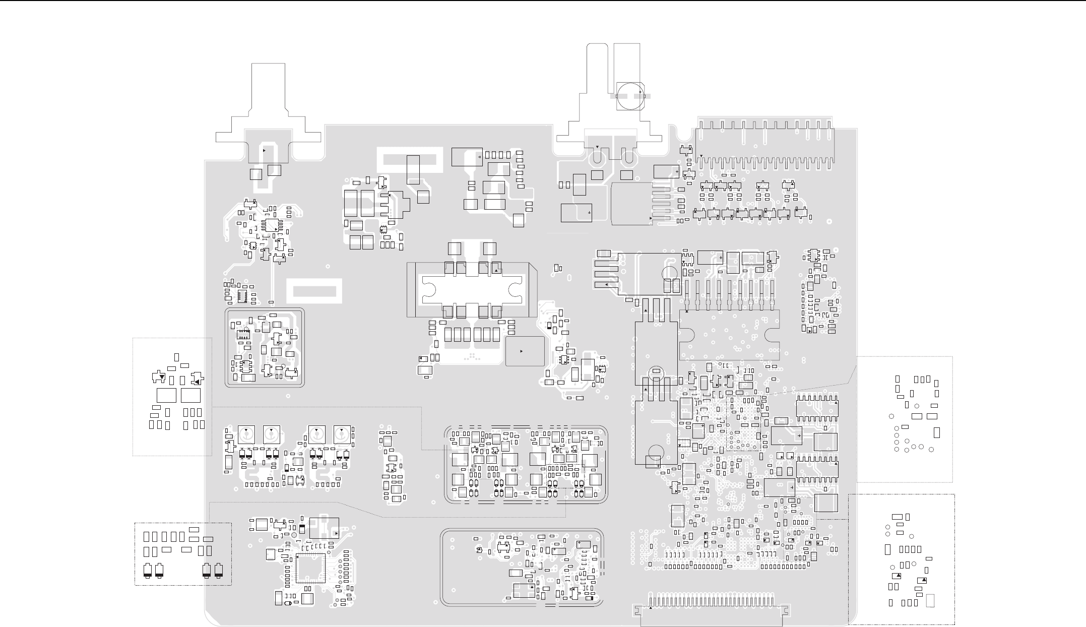
UHF2 (450–512 MHz) 1– 40W PCB/Schematics/Parts List 3-19
3.0 UHF2 (450–512 MHz) 1– 40W PCB/Schematics/Parts List
2.9V_MAKO_V6
C0100
C0102
C0103
C0104
C0105
C0109
C0110
C0111
C0113
C0117
C0118
C0120
C0121
C0122
C0124
C0125
C0126
C0127
C0128
C0129
C0130
C0132
C0133
C0140
C0141
C0142
C0143
C0144
C0145
C0146
C0171
C0175
C0177
C0178
C0180
C0195
C0196
C0200
C0201
C0205
C0206
C0220
C0226
C0236
C0237
C0240C0241
C0242
C0250
C0253
C0300
C0301
C0304
C0305
C0306
C0315
C0320
C0326
C0336
C0337
C0340C0341
C0342
C0347
C0350
C0353
C1000
C1001
C1002
C1003
C1004
C1005
C1006
C1007
C1008
C1009
C1010
C1011
C1012
C1013
C1014
C1015
C1016
C1017
C1018
C1019
C1030
C1031
C1034
C1036
C1037
C2000
C2001
C2002
C2003
C2005C2007
C2500
C3040
C3202
C3203
C3207
C3208
C3209
C3210
C3211
C3212
C3213
C3216
C3219
C3220
C3225
C3226
C3229
C3234
C3238
C3239
C3240
C3247
C3248
C3249
C3254
C3262
C3273
C3280
C3292
C3514
C3515
C3516
C3518
C3520
C3523
C3524
C3528
C3529
C3530
C3531
C3538
C3543
C3545
C4000
C4001
C4002
C4003
C4004
C4005
C4006
C4013
C4016
C4017
C4018
C4019
C4020
C4021
C4022
C4023
C4024
C4025
C4026
C4027
C4028
C4029
C4030
C4031
C4032
C4033
C4090
C4091
C4092
C6451
CR0201
CR0202
CR0203
CR0204
CR0205
CR0206
CR0207
CR0208
CR0303
CR0304
CR0307
CR0308
E3202
E3205
E3502E3503
E4000
E4001
3
2
J0700
30
J4001
L0100
L0202
L0203
L0207
L0209
L0210
L0213
L0214
L0215
L0217
L0218
L0302
L0303
L0307
L0309
L0310
L0312
L0313
L0314
L0315
L0317
L0318
L0319
L3200
L3202
Q0100
Q0102
Q0106
Q0300
Q0301
16
1
8
9
Q3200
4
5
8
Q3201
16
1
8
9
Q3202
23
4
Q3203
23
4
Q3204
R0100
R0101
R0102
R0105
R0106
R0107
R0108
R0109
R0110
R0111
R0114
R0116
R0117
R0118
R0119 R0123
R0144
R0146
R0147
R0148
R0155
R0156
R0157
R0158
R0159
R0161
R0201
R0204
R0205
R0211
R0224
R0225
R0226
R0301
R0304
R0305
R0311
R0316
R0324
R0325
R0326
R0329
R1000
R1001
R1002
R1005
R1006
R1014
R1017
R1019
R1020
R1021
R1025
R1027
R1028
R1034
R1035
R1036
R1041
R1045
R1066
R1067
R1071
R2000
R2004
R2006
R2011
R2012
R2529
R3203
R3205
R3206
R3217
R3218
R3224
R3225
R3500
R3501
R3505
R3526
R3532
R3535
R3537
R3538
R3547
R3550
R3560
R3571
R3576
R3580
R3583
R3588
R3590
R3594
R3595
R3596
R4000
R4001
R4002
R4003
R4004
R4005
R4011
R4012
R4061
R4063
R4064
R4065
R4066
R4067
R4068
R4069
R4070
R4071
R4093
R4094
R4096
R4105
R6467
RT3500
1
2
SH0100
1
2
SH0301
TP1000
TP4000
TP_POR
U3040
9
U3500
U4006
U4007U4008
U4009U4010
VR3202
VR3204
VR3206
VR3503
43
2
Y0100
3.6V_MAKO_SW1
C3276
C3278
C3283
C3511
C3513
R3233
R3503
R3504
R3507
R3508
R3509
R3514 R3515
R3587
TP_MAKO_DCLK
TP_MAKO_FSYNC
TP_MAKO_RX
TP_MAKO_TX
USB1_DAT
USB1_SEO
USB1_TXEN
VBUS1_CMD
VBUS2_CMD
MAKO_GATED_32KHz
C2004
C2006
C2008
C2009
C4034
C4035
C4089
R2005
R2007
R2008
R2009
R2010
R2013
R2014
R2015
R4006
R4009
R4010
R4095
R4097
R4099
TP_SDRAM_BA0
TP_SDRAM_BA1
TP_SDRAM_CLK
TP_SDRAM_CLKX
TP_SDRAM_CS
U4004
U4005
C0308
C0310
C0313 C0314
C0323
C0325
C0329
C0343
C0344
C0345
C0346
C0351
C0352
C0359
CR0301
CR0302
CR0305
CR0306
C0204
C0208
C0213
C0214
C0215
C0223
C0225
C0229
C0243
C0245 C0246
C0247
C0251
C0252
C0259
L0212 L0219
Q0200
Q0201
R0216
R0229
C0900
C0901C0906
C0907
C0908
C0909
C0910
C0915
C0939
C0967
D0900
D0906
D0907
L0722
63
4
Q0900
Q0901
R0713
R0900
R0901
R0902
R0903
R0906
R0907
R0909
R0911
R0912
R0914
R0915
R0916
R0920
R0923
R0930
R0931
R0986
R0987
U0901
C0751
C0776
C0777
C0778
C0779
C0796
C0797
C0798
C0799
L0712
L0714
4
3
2
1
Q0704
63
4
Q0706
R0729
R0735
R0738
R0745
R0748
R0749
VR0700
C0700
C0701
C0702
C0703
C0704
C0705
C0706
C0707
C0708
C0709
C0710
C0711
C0712
C0713
C0714
C0715
C0722
C3000
C3002
C3015
E0700
E0701
E3000
R0742
SP3000
SP3001
C3005
C3006
C3007
C3018
C3019
C3046
C4040C4041 C4042 C4043 C4044
C4045
C4046 C4047
C4048
C4075E4005
J3000
25
26
2
J4000
2
3
Q4000
2
3
Q4002
2
3
Q4004
2
3
Q4005
2
3
Q4006
2
3
Q4008
2
3
Q4010
2
3
Q4011
Q4013
R3002
R3003
R3004
R4040R4041 R4042 R4043 R4044
R4045
R4046 R4047
R4048
R4050
R4051
1
6
5
U3001
VR4000 VR4001VR4002
VR4003
VR4004
VR4005
C0929
C0960
C0961
C0962
C0963
C0964
C0965
R0981
R0982
R0983
R0984 R0985
R0988
R0994
R0995
4
5
8
U0943
C0914
C0918
C0921
C0922
C0926
C0931
C0934
C0935
C0936
C0937
C0947
C0948
C0949
C0950
C0951
D0901
D0902
D0903
L0901
L0902
R0917
R0924
R0925
R0926
R0927
R0928
R0929
R0936R0937
R0940
R0950
R0989
SH0900
4
58U0940
U0941
C6406
C6407
C6408
C6416
C6417
C6418
C6419
C6420
C6421
C6422
C6423
C6426
C6427
C6428
C6429
C6430
C6431
C6433
C6439
C6440
C6445
C6450
E6401
E6402
E6407
R6402
R6403
R6443
R6444
R6445
R6446
R6449
R6450
R6454
R6455
R6456
R6458
R6459
R6460
R6461
R6465
R6466
U6402
U6407
C3008
C3009
C3010C3501
C3504C3505
C3506
E3500
E3501
2
3
Q3500
R3009
R3010
R3516
R3520
U3002
C0966
R0775
R3032
R3033
R3036
R3056
3
2
1
U3006
R3035
3
2
1
U3005
R3042
3
2
1
C0437
C0438
C0439
C0440
C0442
C0451
C0457
L0407
L0411
4
32
Q0405
R0417
R0418 R0419
R0420
R0421
R0422
R0423
R0424
R0425
R0433
R0434
C0404
C0405
C0406
C0407
C0408
C0409
C0410
C0411
C0414
C0415
C0416
C0417
C0419
C0420
C0421
C0423
C0424
C0425
C0426
C0427
C0428
C0429
C0430
C0431
C0432
C0433
C0434
C0458 C0459
C0460
C0461
C0462
D0400
D0401
D0402
D0403
D0404
D0406
D0407
D0408
D0409
L0401
L0402L0403L0404
L0405
L0413
4
32
Q0402
R0404
R0405
R0406
R0407
R0409
R0410R0412
R0432
R0435
R0436
R0437
R0438
R0440R0441
R0443
R0444
C0502
C0504
C0509
C0510
C0515
C0516
C0605
C0611
C0615
C0617
C0619
C0620
C0621
C0622
C0623
C0625
C0626
C0627
C0629
C0630
C0631
C0633
C0638
C0642
C0643
C0644
C0645
C0646
C0650
CLKOUT
D0601
DOUTA
DOUTB
E0600
E0601
E0602
E0604
E0605
E0606
E0607
E0608
5
6
4
3
2
1
FL0500
FS
L0504
L0506
L0604
L0608
PC
PD
PE
Q0501
R0503
R0510
R0606
R0607
R0608
R0609
R0610R0611
R0612
R0613
R0614
R0615
R0617
R0618
R0619
R0621
R0622
R0623
R0627
TP0601
U602
1
37
25
13
U0600
C0718
C0724
C0759
C0768
C0781
C0782
C0783
C0788
C0802
C0804
C0805
C0806C0807
C0904
E0702
E0703
E0704
L0723
L0900
1
M0700
Q0701
5
9
6
87
432
10Q0702
63
4Q0711
R0700
R0702
R0706
R0724
R0725
R0726
R0730
R0732
R0734
R0740
R0741
R0744
R0750
R0751
R0752
R0753
R0756
R0757
R0761
R0762
R0763
R0764
R0768
R0771
R0773
1
RT0908
SP0700SP0701
SP0702SP0703
SP0704
SP0705
SP0706
SP0707
UHF2 (450–512 MHz) 1–40W 8471696M02 Top Side

3-20 UHF2 (450–512 MHz) 1– 40W PCB/Schematics/Parts List
1.2V_RTC_TEST
2.8V_RF_TEST
ANT_C
C0101
C0106
C0107
C0108
C0112
C0114
C0115
C0119
C0123
C0131
C0134
C0135
C0136
C0137
C0138
C0147
C0148
C0149
C0150
C0151
C0156
C0157
C0158
C0159
C0160
C0161
C0162
C0163
C0164
C0165
C0166
C0179
C0191
C0192 C0193
C0194
C0202
C0203
C0207
C0209
C0211
C0217
C0218
C0219
C0221
C0222
C0224
C0230
C0231
C0233
C0235
C0238
C0239
C0248
C0249
C0257
C0258
C0302
C0303
C0307
C0309
C0311
C0316
C0317
C0318
C0319
C0321
C0322
C0324
C0327
C0328
C0331
C0334
C0348
C0349
C0357
C0358
C0360
C0361
C0362
C0363
C0400
C0401
C0402
C0403
C0412
C0413
C0422
C0435
C0436
C0441
C0443
C0444
C0445
C0446
C0447
C0448
C0449
C0452
C0453
C0454
C0455
C0456
C0463
C0464
C0503
C0506
C0507
C0512
C0513
C0514
C0601
C0602
C0603
C0604
C0607
C0610
C0612
C0613
C0614
C0616
C0618
C0628
C0632
C0634
C0635
C0636
C0637
C0640
C0641
C0647
C0648
C0649
C0651
C0716
C0717
C0719
C0720
C0721
C0723
C0725
C0726
C0727
C0728
C0729 C0730
C0731
C0732
C0733
C0734
C0735
C0736
C0737
C0738
C0739
C0740
C0741
C0742
C0743
C0744
C0745
C0746
C0747
C0748
C0749
C0752
C0753
C0754
C0755
C0756
C0757
C0758
C0760
C0761
C0763
C0764
C0765
C0766
C0767
C0769
C0770
C0771
C0772
C0774
C0775
C0780
C0785
C0786
C0787
C0789
C0790
C0791
C0792
C0793
C0794
C0795
C0800
C0801
C0803
C0808
C0809
C0810
C0811 C0812
C0813
C0814
C0815
C0817
C0818 C0819
C0828 C0829
C0832
C0845
C0856
C0861
C0869
C0874
C0902
C0903
C0911
C0912
C0913
C0916
C0917
C0919
C0920
C0923 C0925
C0927
C0928
C0940
C0941 C0942
C0943
C0944
C0945
C0953
C1032
C1033
C1035
C1044
C2501
C3011
C3012
C3013
C3014
C3016
C3017
C3020
C3021
C3030
C3031
C3032
C3041
C3042
C3043
C3044
C3045
C3200
C3201
C3204
C3205
C3206
C3214
C3215
C3217
C3218
C3221
C3222
C3227
C3228
C3231
C3232
C3233
C3237
C3243
C3252
C3257
C3260
C3261
C3265
C3266
C3269
C3270
C3272
C3274
C3275
C3279
C3281
C3282
C3289
C3290
C3291
C3500
C3502
C3503
C3507
C3508
C3509
C3510
C3512
1C3517
C3519
C3521
C3522
C3525
C3526
C3527
C3532
C3533
C3534
C3535
1
C3536
C3539 C3540
C3541
C3542
C4007
C4010
C4011
C4012
C4014
C4015
C4049
C4051
C4053
C4055
C4058
C4059
C4060
C4061
C4062
C4063
C4064
C4065
C4066
C4067 C4068
C4069
C4070
C4071
C4072
C4073
C4074
C4076
C4084
C4085
C4086
C4087 C4088
C4093
C4094
C6401
C6412
C6413
C6414
C6432
C6434
C6435
C6436
C6437
C6438
C6443
C6444
C6446
C6449
C6452
CLK_ACQ_TEST
CR0300
CR0400
D0405
D0500
D0600
D0700
D0702
8
4
5
D0703
D0704
D0904
D0905
D3030
D3040
D3200
D4000
D4001
E0201
E0301
E0302
E0400
E0401
E0403
E0500
E0603
E0609
E0610
E2500
E3201
E3203
E3206
E3208
E4002
E4003
E4004
E4006
E6400
EXT_MIC
EXT_PTT
3
4
2
5
FL6401
FT0400
FT0401
FT_APM_1_WIRE
FT_EMERGENCY
FT_IGNITION_SENSE
FT_MMP_1_WIRE
FT_USB1_DM
FT_USB1_DP
FT_USB2_DM
FT_USB2_DP
FT_VBAT
FT_VBAT_GROUND
FT_VBUS1
FT_VBUS2
I2C_CLK
I2C_DATA
IF_TEST
INT_MIC
G2
20
G1
J2500
11
J4002
14
J4003
J6400
L0200
L0204
L0205
L0206
L0211
L0221
L0300
L0304
L0305
L0306
L0311
L0406
L0408
L0409
L0410
L0412
L0414
L0503
L0602
L0603
L0605
L0700
L0702
L0705
L0706
L0707
L0708
L0709
L0710
L0711
L0715
L0716
L0717
L0718
L0719
L0720
L0721
L0903
L0904
L0905
L3201
L6402
L6403
MAKO_CE
MAKO_V8_5V
MAKO_V9_3V
OPT_SSI_SYNC
Q0107
2
3
Q0108
Q0202
Q0302
63
4Q0400
Q0401
Q0403
Q0500
Q0600
Q0601
1
3
Q0703
Q0705
Q0902
Q3030
4
3
2
1
Q3032
Q3040
2
3
Q3041
2
3
Q3205
6
3
4
Q3206
4
58
Q3207
2
3
Q3208
Q3209
Q3210
63
4
Q3502
63
4
Q3503
Q3504
Q3505
2
3
Q4001
2
3
Q4003
2
3
Q4007
2
3
Q4009
2
3
Q4012
Q4014
2
3
Q4015
Q6401
63
4
Q6402
R0103
R0104
R0113 R0115
R0120
R0122 R0125
R0126
R0127
R0128 R0131
R0134
R0139
R0140
R0160
R0202
R0203
R0206
R0207
R0208
R0210
R0212
R0213
R0218
R0219
R0220
R0221
R0230
R0302
R0303
R0306
R0307
R0308
R0310
R0312
R0319
R0320
R0321
R0327
R0331
R0332
R0333
R0334
R0337
R0400
R0401
R0402
R0403
R0411
R0413
R0414
R0415
R0416
R0426
R0427
R0428
R0429 R0430
R0431
R0500
R0501
R0502
R0508
R0509
R0511
R0512
R0601
R0602
R0603
R0604
R0605
R0616
R0620
R0624
R0625
R0626
R0701
R0709
R0711
R0712
R0714 R0715
R0718
R0719
R0720
R0722
R0727 R0728
R0739
R0743
R0747
R0754
R0755
R0759
R0760
R0765
R0766
R0769
R0770
R0777
R0910
R0913
R0918
R0919
R0921
R0922
R0938
R0941
R0942
R0943
R0944
R0946
R0947
R0951
R0954
R0955
R0960
R0970
R0971
R0973
R0974
R0975
R0976
R0977 R0978
R0979
R1026
R1044
R1046
R1047
R1048
R1054
R1060
R1070
R2500
R2501
R2502
R2504
R2506R2507
R2508
R2509
R2510
R2511
R2512
R2513 R2514
R2515
R2516
R2517
R2518
R2519
R2520
R2524
R2525 R2526
R2527
R2528
R3005
R3006
R3007
R3008
R3030
R3034
R3037
R3038
R3039
R3040R3041
R3043
R3044
R3045
R3046
R3047 R3048
R3050
R3051
R3052
R3053
R3054
R3055
R3057
R3200
R3204
R3207
R3208
R3209
R3210
R3215
R3216
R3219
R3220
R3222
R3223
R3226
R3227
R3228
R3236
R3237
R3238
R3239
R3240
R3241
R3243
R3245
R3246
R3247
R3248
R3249
R3250
R3252
R3253
R3502
R3506
R3510
R3511
R3512
R3513
R3521
R3523
R3524
R3525
R3528
R3529
R3530
R3533
R3534
R3536
R3539
R3540
R3541
R3542
R3544
R3545
R3546
R3548
R3549
R3551
R3552
R3553
R3554
R3555
R3556
R3558
R3559
R3569
R3572
R3573
R3574
R3575
R3577
R3578
R3579
R3581
R3582
R3584R3585
R3586
R3591
R3592
R3593
R4023
R4030
R4031
R4032
R4033
R4034
R4035
R4049
R4054
R4055
R4074
R4076
R4078
R4079
R4080
R4081
R4082
R4083
R4085
R4086
R4088
R4089
R4090
R4098
R4100
R4101
R4103
R4106
R6401
R6404
R6405
R6407
R6409
R6410
R6411
R6416
R6417
R6418
R6419
R6420
R6430
R6432
R6433
R6434
R6435
R6436
R6437
R6438
R6439
R6440
R6457
R6464
R6468
R6469
R6470
RF_ATTN_2
ROUT_TEST
1
RT0953
S0700
1
2SH0101
1
2
SH0300
2
1
SH0500
12
SH0901
SPI_CLK_1
SPI_CLK_TEST
SPI_MISO_1
SPI_MOSI_1
6
4
3
T0400
64
3
T0401
TP501
TP502TP503
TP504
TP0301
TP0600
TP0702
TP0703
TP0704
TP0705
TP0707
TP0708
TP0709
TP0710
TP0711
TP0713
TP0903
TP0904
TP0907
TP0909
TP0910
TP0911
TP0913
TP_ADAPT_SW
TP_DDR_LDQS
TP_DDR_UDQS
TP_FLASH_CLK
TP_TEST1
TP_TEST2
TP_VCTRL
TX_RAMP
TX_RAMP_DAC
L11A11
L1
U0100
4
3
5
U0101
U0201
6
3
4
U0303
U0304
U0601
U0700
U0900
U0942
A21 AA21
AA1
U1000
43
6
U1006
A1 M1
M8
A8
U2000
K1
A9
K9
U2001
1
6
5
U3003
U3004
14
58
U3030
P1
A1
A14 P14
U3200
64
3
U3201
C1
C3A3
U3202
4
3
5
U3203
10
6
5
U3501
7
8
14
U3502
85
4
U3503
U3504
7
814
U3505
85
4
U3508
16
1
8
9
U4000
14
7
8
U4001
P10
A10
P1
A1
U6401
U6404
C1
C3
A3
U6405
U6406
U6408
VR3000
VR3040
VR3200
VR3201
VR3203
VR3205
VR3207
VR3208
VR3502
VR3504
VR4006
VR4009
VR6400
43
2
Y1000
4
3
2
Y3200
Y3201
UHF2 (450–512 MHz) 1–40W 8471696M02 Bottom Side
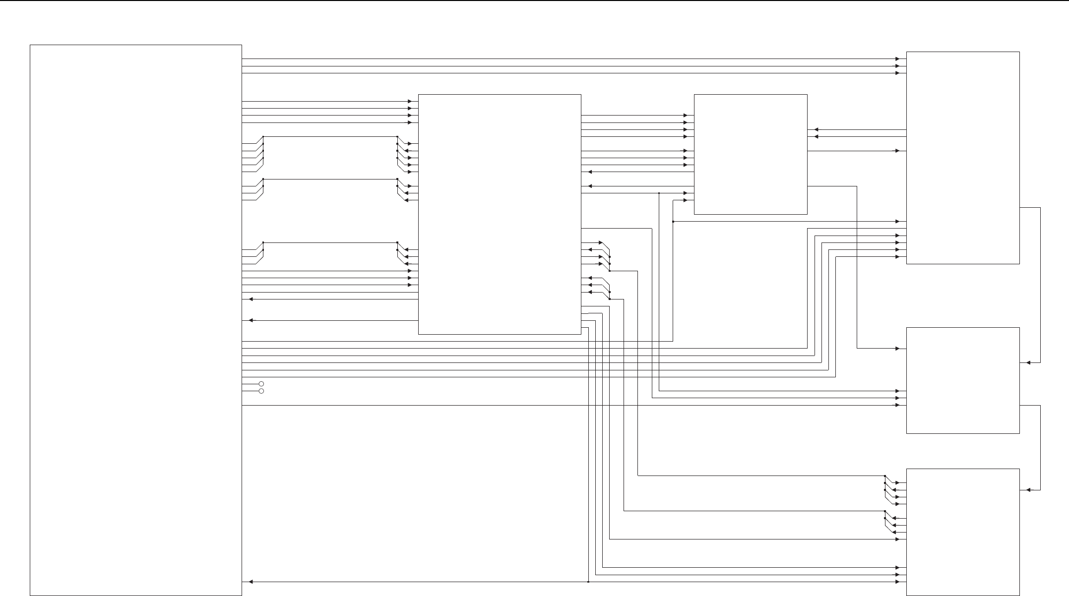
UHF2 (450–512 MHz) 1– 40W PCB/Schematics/Parts List 3-21
CONTROLLER_&_GPS_R5
( TOP LEVEL: SHEET 1)
(ABACUS3: SHEET 2)
RXBE_73.35MHZ
(IF AMP: SHEET 1)
( PC: SHEET 2 )
TX_HP_UHF2
( PA: SHEET 1 )
( TX: SHEET 1 )
( RX: SHEET 2 )
VCO_UHF2_TOMAHAWK
RXFE_UHF2
( 1 SHEET )
SYNTH
SPI_ABACUS_CEX
SPI_ABACUS_CLK
SPI_ABACUS_DATA
SSI_ABACUS_CLKOUT
SSI_ABACUS_DOUTA
SSI_ABACUS_DOUTB
SSI_ABACUS_FSYNC
SSI_ABACUS_SYNCB
3
1
SPI_CLK
SPI_MISO
SPI_MOSI
THK_CS
TX_DAC
TX_SSI_CLK
TX_SSI_DATA
TX_SSI_FSYNC
VSWR_DET
0
1V8
5V
IF
REF_CLK
ADAPT_SW
ANT_ENABLE
DMCS
LOCK_DETECT
LO_BATTERY_DET
LO_PWR_DET
PA_BIAS
PC_ATTEN_ENA
PREDRIVE_SW
RAW_B+
RESET_OUT
RX_FLTR_VCTRL
RX_SSI_CLK
RX_SSI_DATA
RX_SSI_FSYNC
RX_SSI_SYNCB
0
2
1
1.875V_DIG_V2
16.8_GPS
16.8_MHZ_BUFF
2.775V_ANA_V7
2.775V_DIG_V4
5V_SW
9V3
9V3_PA
ABACUS3_CS
0
1
2
NC
1
4
2
0
2
3
NC
1
2
0
1
1
2
4
0
RX_VCO_SEL1_
RX_VCO_SEL2_
SDTX
SFTX
SF_OUTSPI_CLK_IN
SPI_CLK_OUT
SPI_MISO_IN
SPI_MISO_OUT
SPI_MOSI_IN
SPI_MOSI_OUT
TH_CEX
TX_CLK
TX_VCO_SEL1_
TX_VCO_SEL2_
VCTRL
ABACUS3_CEX_OUT
ABACUS3_SYNCB_IN
ABACUS3_SYNCB_OUT
ADAPT_SW
DMCS
HP_MOD_OUT
LOCK
PRSC
RF_ATTN_1
RSTB RX_SSI_CLK_PASS_IN
RX_SSI_CLK_PASS_OUT
RX_SSI_DATA_PASS_IN
RX_SSI_DATA_PASS_OUT
RX_SSI_FSYNC_PASS_IN
RX_SSI_FSYNC_PASS_OUT
FE_TUNEIF
RF_ATTEN_1
RX_IN
RX_INJ
1.8V_TH_DIG
16.8_GPS
16.8_REF
1V8_BE
2.8V_TH_ANA
2.8V_TH_DIG
5V
5V_BE
9R1
9V3
ABACUS3_CEX_IN
SF_TH
TXINJ
TX_VCO_SEL1
TX_VCO_SEL2
VCTRL
3
2
1
2
9R1
0
0
2
9R1
9V3_SYNTH_IN
9V3_SYNTH_OUT
9V3_VCO
HP_MOD_OUT
PREDRIVE_SW
PRSC
RXINJ
RX_VCO_SEL1
RX_VCO_SEL2
LO_BATTERY_DET
PA_SUPPLY
PC_ATTEN_ENA
PREDRIVE_SW
RX_IN
TX_DAC
TX_INJ
1
3
0
TX_SSI_BUS(0:2)
ABACUS_SPI_BUS(0:3)
SPI_BUS(0:4)
RX_SSI_BUS(0:2)
ABACUS_SSI_BUS(0:2)
2
0
1
9V3
9V3_PA
9V3_SYNTH
9V3_VCO
ANT_ENABLE
FINAL_BIAS_1
UHF2 (450–512 MHz) 1–40W Overall Schematic Diagram
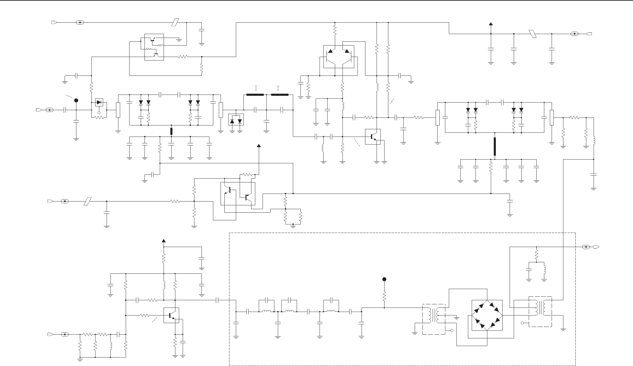
3-22 UHF2 (450–512 MHz) 1– 40W PCB/Schematics/Parts List
8.6 VDC
10 dB Attenuator
0.8 VDC Typical
Zo/Zin=4:1
MAKO ( 0 ~ 4.6 VDC)
2.3 VDC Typical
(Micro-strip 20 mm Each)
(3.00 ~ 8.00 VDC)
+16.0 dBm Min. (250 mV P-P)
8.3 VDC Typical
1.5 VDC Typical
(Not Placed)
Hi-Side Zeros for Preselector
0.7 VDC
Zo/Zin=4:1
C0411
NU
R0403
(VALUE)
R0434
C0432
C0436
R0420
(VALUE)
C0441
C0457
NU
C0444
NU
C0464
C0463
C0439
NU
R0421
C0407
R0412
R0415
NU
R0416
R0438
R0411
C0413
L0406
FE_TUNE_FE_4
R0400
RXIN_FE_6
RX_INJ_FE_5
C0409
C0455
C0443
Q0401
25
6
3
1
4
L0410
C0431
C0400
NU
R0436
R0444
D0407
NU
C0416
R0427
C0424
2
5
6
3
1
4
2
1
NUQ0400
T0401
5NC
4
6
3
D0400
R0422
NU
C0440
L0404
12
3
C0426
C0417
E0400
C0438
NU
C0442
C0408
C0458
L0412
R0429
R0419
9R1_FE_6
Q0402
R0417
Q0405
R0401
NU
R0432
D0406
C0420
R0424
9R1_FILT
C0452
R0414
RF_ATTEN_1_3
C0454
IO3 3
IO4
4
R0407
D0405
IO1
1IO2 2
L0407
R0440
C0461
C0462 R0443
D0409
1
5
NC
R0402
Q0403
2
3
6
4
R0405
L0408
C0422
(VALUE)
L0413
R0428
C0451
C0430
C0423
C0459
L0411
R0423
C0415
(VALUE)
C0425
L0401
R0413
C0449
NC
(VALUE)
D0403
D0408
IF_FE_8
R0409
R0425
NU
C0421
C0448
C0437
R0435
C0403
L0403
12
3
E0401
NC
C0456
R0437
C0414 D0404
D0402
NU
R0431
C0446
C0401
C0435
9R1_FILT
C0412
C0447
C0405
C0427
R0418
12
3
E0403
L0402
R0404
C0404
C0453
12
3
NU
L0405
L0414
R0410
NU
C0433
C0434
R0430
2
C0406
CR0400
1
3
C0460
D0401
FT0401
1
6
3
2
1
C0410
(VALUE)
T0400
NC5
4
1
C0419
L0409
FT0400
R0433
.0476
R0406
C0428
R0441
R0426
C0445
C0429
RX_INJ
9R1_FILT
C0402
RF_ATTEN_1
IF
RX_IN
FE_TUNE
9R1
UHF2 (450–512 MHz) 1–40W Receiver Front-End Schematic Diagram

UHF2 (450–512 MHz) 1– 40W PCB/Schematics/Parts List 3-23
1.43V
0.76V
1.6V
0.72V
4-POLE
IF_TO_ABACUS
73.35MHz
R0511
IFIN_BE_8
R0512
C0514
R0508
R0509
NU
C0510L0504
GND1
2
GND2
5
IN
1OUT 4
FL0500
CC1
3
CC2
6
L0506
C0516
NU
5V_BE_5
C0502
NU
C0515
C0503
C0513
SH0500
12
R0503
Q0501
E0500
L0503
C0509
NU
RX_FE_3
R0510
C0506
1
3
2
C0507
Q0500
C0504
R0502
R0500
D0500
R0501
C0512
IF
IF_OUT
5V
5V
5V_FE
UHF2 (450–512 MHz) 1–40W Receiver IF Amp Schematic Diagram

3-24 UHF2 (450–512 MHz) 1– 40W PCB/Schematics/Parts List
2nd LO VCO UHF (71.1MHz/75.6 MHz)
SPF_3.5V
CLOCK LF
2nd LO LF
CLOCK VCO
*
R0611
R0605
FD_1_BE_5
R0602
R0616
C0620
D0600
E0609
C0604
C0621
C0634
E0602
E0605
3VA
C0611
Q0601
SB_1_BE_5
PC
TP0601
R0615
C0649
FE_1_BE_5
NU
C0616
U602
1
C0632
L0608
C0607
C0605
NU
R0607
C0646
3VA
DOUTA
L0602
R0606
C0648
L0604
C0642
C0601
CLKOUT_1_BE_5
VVCO
C0628
C0602
C0638
R0603
C0640
FC_1_BE_5
R0617
R0601
E0607
VVCO
C0627
C0631
C0629
FS
R0625
5V
3VA
C0623
C0615
R0612
3VA
FREF_IF
C0610
R0618
C0644
L0605
PE
C0613
E0600
R0624
C0636
E0610
C0635
R0613
3VA
C0651
C0618
C0647
D0601
C0626
R0608
E0603
DOUTB
C0622
C0645
48
VDDI
40
VDDL39
VDDP
14 VDDQ
12 VREFN
11 VREFP
C0625
25
PE
RREF
13
33
SYNCB
9VDDA
17 VDDC
26
VDDD
6VDDF
27
VDDH
15 IOUTC
38
IOUTL
42
LON
43
LOP
2MXON
1MXOP
23 PC
24 PD
36
GNDL
37
GNDP
16 GNDQ
21 GNDS1
34
GNDS2
4IF2N
5IF2P
47
IFIN
8GCN
7GCP
10GNDA
18 GNDC
22 GNDD
3GNDF
32
GNDH
45
GNDI
CLKP
19
46
CXIF
44
CXVL
41
CXVM
29
DOUTA
30
DOUTB
35
FREF
31
FS
U0600
20CLKN
28
CLKOUT
FS_1_BE_5
R0627
C0637
R0621
3VA
TP0600
R0610
R0620
C0603
C0633
R0614
3VA
E0604
VCONT
4
VIN
3
VOUT 1
3VA
R0604
U0601
FB
2
GND
5
NP
6
3VA
CLKOUT
DOUTA_1_BE_5
C0619
C0641
E0606
C0630
C0617
R0619
E0601
NU
R0623
L0603
C0643
C0614
DOUTB_1_BE_5
PD
1V8_3
Q0600
E0608
C0612
C0650
R0609
R0622
R0626
NU
IF_OUT
5V
SSI_ABACUS_FSYNC
SPI_ABACUS_CEX
REF_CLK
SPI_ABACUS_CLK
SSI_ABACUS_DOUTA
SSI_ABACUS_CLKOUT
SSI_ABACUS_DOUTB
SPI_ABACUS_DATA
SSI_ABACUS_SYNCB
1V8
1V8
UHF2 (450–512 MHz) 1–40W Receiver Back-End Schematic Diagram

UHF2 (450–512 MHz) 1– 40W PCB/Schematics/Parts List 3-25
PA_SUPPLY_TX_PA
PA_SUPPLY
E0703
9V3_PA
Antenna_En
LO_PWR_PAD
HI_PWR_PAD
11dB/17dB Pad
18dB RL
Ref Osc Warping
-3 dBm
Test Point to check
+8 dBm
R0711
C0763
C0736
C0768
R0715
L0709
D0704
TX_INJ_TX_PA
1
TP0703
R0760
TP0705
R0712
R0714
C0728
C0733
C0752
L0711
NC
TX_INJ
3.2VDC
13 dBm
TP0704
2GND1
4GND2
RF_INVD_RF_OUT 3
U0700
L0705
R0700
C0718
R0706
C0725
C0724
E0704
9V3_Tx_Sw
R0702
NU
9V3_TX
2.2K
47K
47K
47K
Q0701
R0722
R0720
R0718
R0755
R0754
C0770R0727R0728
C0771
NU
C0817C0785 C0734C0795
L0721 L0718L0717
2.85V (44W)
2.10V (27.5W)
9.1VDC
R0751
R0747
R0777
NU
R0750
R0744
C0788
NU
L0715
NU
L0723
R0759
C0802
NU
C0780
C0789
C0814
TP0709
C0775
TP0710
L0720
R0734
C0800
NU
Q0705
D
G
S
C0801
V_cont
9V3_TX
9V3
9V3_VCO
9V3_SYNTH
C0787
C0815
C0790
NU
R0739
C0792
NU
C0794
NU
C0786
C0793
C0791
V_cont
M0700
POS 1
D
3G
2S1
Q0703
C0828
C0845
C0729
NU
C0731
NU
C0745
C0730
NU
C0818
C0754
NU
C0829
C0749
NU
C0808
C0819
NU
C0755
C0753
C0809
C0744C0743
C0813
NU
L0702
C0716C0717
TP0702
E0702
SP0701
C0861
Gate_2
C0874
R0773
R0770
R0769
R0766
C0774
R0771
R0768
C0869
R0762
R0763
R0765
R0764
C0769
MRF1570, Flat Lead
SP0700
C0732 C0832
7
6
Gate_1
R0709
L0706
C0735 L0708C0723
L0707
L0903
L0905
R0970
R0971
C0810L0719
ATC
L0710
C0748
C0727
NU
NU
C0721
D0700
C0741
NU
C0751
L0712
C0742
C0726
C0738C0739 C0740
C0803
R0977
R0974
R0976
L0904R0973
NU
R0975
D0904
C0772
R0978
C0767 R0701
C0942
NU
C0766
C0779
R0729
R0735
C0777
L0714
C0778
A+
R0738
Q0704
R0745
NC
NCNC
Q0706
C0776
9V3_Tx_Sw
VR0700
NC
C0805
R0756
C0804
TP0711
C0781
R0740
C0782
R0757 R0741
PRESSURE_PAD
Final_Bias
2.2VDC (TX Only) 2.2VDC (TX Only)
R0730R0732
TP0708TP0707
Gate_2Gate_1
C0761
C0765
NU
C0764
NU
C0760
NU
C0856
C0756
E0700
C0700 C0702C0701
9V3_TXC0704C0709C0703C
0705C0708C0706
NU
C0707
NU
C0710C0712
NU
C0711
E0701
R0742
C0713
A+
C0715
NUNU
C0722
L0700
C0714
C0737
R0719
SP0704
SP0706
SP0707
SP0702
SP0703
SP0705
1
5
8
4
Q0702
2
3
ATC
C0807
PIN1
1PIN22
C0720
C0719
C0811
HS0700
ATC
C0806
C0747
C0746C0812
PRESSURE_PAD_TX_PA
PRESSURE_PAD
C0966 R0775 S0700
C0796C0799C0798 C0797
R0748
R0761
R0749 ANT_ENABLE_TX_PA
TP0713
ANT_ENABLE
K4
A1
A2
A3
A4
A5
K1
K2
K3
D0703
NU
C0757C0758C0759
L0716
R0743
D0702
C0941
C0940
D0905
C0943
R0979
C0944
C0945
LO_PWR_PAD
HI_PWR_PAD
9V3_TX
FINAL_BIAS_1
FWD_DETECTED
FWD_POWER
REV_DETECTED
V_CONTROL
RX_IN
RX_IN_TX_PA
R0752
R0753
FINAL_BIAS_1_TX_PA
LO_PWR_PAD
HI_PWR_PAD
V_cont
9V3_TX
Final_Bias
W = 0.625 mm
W = 2.5 mm
S = 0.93 mm
L = 19 mm
S = 0.54 mm
W = 0.625 mm
R0713 L0722
2
J0700-33
J0700-11
J0700-2
Antenna_En
UHF2 (450–512 MHz) 1–40W Power Amplifier Schematic Diagram

3-26 UHF2 (450–512 MHz) 1– 40W PCB/Schematics/Parts List
SH0901SH0900
1
2
1
2
2FB
5GND
6NP
4VCONT
3VIN
1
VOUT
U0941
R0936
C0947
C0950
R0937
9V3
5V DC
C0949
C0951
0.1uF
C0948
5V
2.10V (27.5W)
2.85V (44W)
TP0909
V_CONTROL
C0922C0921
R0940
GND
NC
RFINVAPC
VSET
COMM
ENBL
FLTR 4
6
17
VPOS 8
3
U0940
5
2
NC
9
R0941
R0950
C0926
U0942
2
4NC1 5
NC2
RESET_OUT
GND
3
INPUT 1
C0953
C0925
R0955
TP0910
R0946
R0942
RT0953
R0954
6
5
7
8
4
U0900-2
R0947
C0902C0923
C0903
9V3_PC
R0943
C0927
R0951 R0944
TP0911
C0928
R0986 R0987 C0967 D0907
5.1V
NC
R0981
R0982
R0995
R0994
R0983
R0985
LO_PWR_DET
C0965
R0984
LO_PWR_DET
R0923
2
3
1
8
4
U0901-1
C0909
R0914
C0908
9V3_PC
VOUT
VPOS
VSET
CLPF
COMM
GND
INHI
INLO
TADJ
C0964
5
7
4
U0943
3
2
9
1
8
6
C0961
R0988
C0962
C0963
C0960
R0989
5V
R0925
NC
R0928
D0902
C0934
C0937
D0901
NC
NC
C0914
R0929
D0903
C0936
R0926 C0935
R0917
9V3_PC
C0916
C0912
R0910
L0901
C0918
R0913
Q0902
R0924
R0927
C0931
L0902
1.35V (44W)
1.28V (27.5W)
LO_BATTERY_DET
LO_BATTERY_DET
0.38V (44W)
0.21V (27.5W)
C0910
R0938
R0911
TP0903
R0912
4.0V (44W)
3.2V (27.5W)
R0915
R0920
TP0904
R0916
C0939
FWD_DETECTED
REV_DETECTED
9V3 to FW bias PIN in HP mode
R0724
R0725
HI_PWR_PAD
9V3 to REV bias PIN in LP mode
C0783
PC_ATTEN_ENA_TX_PA
R0726
PC_ATTEN_ENA
9V3_TX
LO_PWR_PAD
5
6
4
2
3
1
Q0711
Cypher: 2.4Kohm 5%
R0901R0907
L0900
R0902
TP0913
9V3_PC 9V3
R0903
C0904RT0908
C0907C0906R0909
7
8
4
U0901-2
6
5
R0900
9V3_PC
1
2
D0906
3
R0906
D0900
1
2
3
C0915
R0930
R0921
R0918
R0960C0911
R0922
R0919
C0913
Q0901
2
3
U0900-1
1
8
4
9V3_PC
C0917
C0919 C0920
0.6V typical
NOTE: VOLTAGES SHOWN FOR ANALOG TX MODE
Cutback starts about 2.2V
TP0907
C0929
9V3_PC
R0931
3
1
2
5
6
4
Q0900
C0901
C0900
9V3
TX_DAC
VSWR_DET
FWD_POWER
VSWR_DET
TX_DAC
9V39V3
UHF2 (450–512 MHz) 1–40W Power Control Schematic Diagram

UHF2 (450–512 MHz) 1– 40W PCB/Schematics/Parts List 3-27
R1
R2
10K
47K
0.5 ppm
VHF=1500pF
---
Note: High Port modulation injection through loop filter for U1 and U2 only
HI: 2.8V
U1=220pF
U2=120pF
C0191,C0192,C0193,C0194: NU (UHF B1)
VHF=1500pF
SF_OUT VOLTAGE: 2.45V
Unlocked: 0V
U1=220pF
Buffer to Abacus/Controller
9R1 SWITCH FOR FRONT-END
C0157, C0159, C0160,C0162,C0163,C0191,C0192,C0193,C0194: NU (UHF B2)
GPO LINES
U2=120pF
U1=220pF
U1=220pF
VCO STEERING LINE VOLTAGE: 0.6V TO 4.4V
U2=120pF
VCO STEERING LINE VOLTAGE: 0.6V TO 4.4V
VHF=1500pF
VHF=1500pF
U2=120pF
U2=120pF
Adapt OFF: 0V
U1=220pF
VHF=1500pF
4875188M01
LOW: 0V
1.5 ppm
VCO SEL: ACTIVE LOW
Adapt ON: 5V
Locked: 1.8V
GPO_4
TCXO (Y0100)
Switch for Adapt Transient
NC
NC
NC
R0170
C0166
C0100
C0105
L0100
C0137
RX_SSI_DATA_IN
NC
R0114
R0147
SPI_MOSI_IN
NU
ABACUS3_SYNCB_OUT
R0100
NC
5V_BE_SYNTH
TP504
1
RX_SSI_CLK_OUT
C0107
NC
NC
C0136
C0133
NC
C0140
1
C0106
NC
TP_TEST1
SPI_MISO_IN
R0160
NC4
3
OUTPUT
4
VCC
1VCONT
NC
NC
NC
Y0100
16.8MHz
GND
2
5
NC1
NC2 6
NC3 7
8
R0113
9R1_SYNTH
C0148
C0102
C0138
3GND
1INOUT
4ONOFF_CONTROL
2OUTIN
5
VCC
R0125
NC
U0101
NC
GPO_3_SYNTH
NC
NC
C0179
ABACUS3_SYNCB_IN
RX_SSI_DATA_OUT
C0147
C0135
C0171
C0132
C0157
C0127
NC
LOCK_SYNTH
R0140
C0120
Q0100
C0194 C0159
C0191
NC
VCTRL_SYNTH
C0126
C0112
NC
NC
NC
NC
1V8_BE_SYNTH
SF_OUT_SYNTH
R0158
NU
HP_MOD_OUT_SYNTH
16.8_REF_CONTROLLER_SYNTH
NU
C0119
NC
NU
C0113
NC
1
R0148
1
2
TP_VCTRL
SH0100
1
2
SH0101
R0159
C0144
NC
C0160
ABACUS3_CEX_IN
R0118
C0141
NC
RX_SSI_CLK_IN
C0162
C0103
R0103
R0107
C0124
Q0108
R0122
NC
RX_SSI_FSYNC_IN
NC
NC
NU
C0161
C0122
NU
GPO_6_SYNTH
9V3_SYNTH
R0157
Q0106
GND
IN
OUT
C0117
C0134
R0115
TX_DAC_VCC
G7
TX_GND1
F6 TX_GND2
J6
TX_VCC
F1
VCO_DAC
K5XOSC_BASE
XOSC_EMIT
L5
G6
XOSC_GND
TCLK
D7
TEST1 C7
TEST2
B3
TM
F10
TXCLK
K7TXI
L7TXQ
H7
TX_DAC_GNDL6
SPI_CLK
D10
SPI_DR
D9
SPI_DW
SSI_GNDE8
E11
SSI_VCC
SUB1
K10
F5 SUB2
F3 SUB3
G8
SDM_VAG
A9
SDM_VREFM B8
SDM_VREFP
D11
SDR
F11
SDTX
F9
SFTX
K4SF_OUT
C9 SMD_CLK_GEN_GND
C11
A5
RX_AVCC2
RX_EN_OUT
B1
D3
SCAN_EN
F2 SCAN_IN
E9
SCLK_OUT
SDM_CLK_GEN_VCC A10
SDM_REF_GNDA8
SDM_REF_VCC B9
B10RXFS
C2 RXI
C1 RXIX
D1 RXQ
D2 RXQX
RX_AGND1 C3
D5
RX_AGND2
B2
RX_AVCC1
OSCREG_GND
OSCREG_OUT
H5
J4OSCREG_SPLY
K11 PABIAS_DAC
L9PHCLK
RFSTEPA
A3
E6 RSTB
E7
RXACQ
E10
M_PRSCX
A1 NC1
A11 NC2
NC3
L1
L11 NC4
NTXI
L8
NTXQ
K6
L4OSCREG_BYP
J5
MAIN_GND
MAIN_PDET_VCC G2
J1
MAIN_VCC
H1
MN_ADAPT_CP
G3
MN_CP
G5
MN_CP_GND
MN_CP_VCC H2
J2
M_PRSC
H3
GPO5
H8 GPO6
K8
HP_MOD_OUT
J9INCR_DECR
F8
LGND1 C8
LGND2
G10
LVCC1
B7
LVCC2
G4
ESC_TEST
K2
ESC_VCC
C6 FBI
B6 FBQ
B4 GPO1_TEST1
A4 GPO2_TEST2
GPO3_TEST3
E5
GPO4_TEST4
D4
K9
EF_OUTM
J8
J7EF_OUTP
ESC_CP L3
ESC_CPBIAS L2
K3
ESC_CP_GNDJ3
ESC_CP_VCC
H4
ESC_GND
K1
ESC_IN
E1
G9CLK_CP
H11 CLK_EMIT
H10
CLK_GND
J10
CLK_VCC
G1
DAC_ADAPT
A2 DC_CAL
L10DEEPSLEEP
F7
DMCS
BP_I
F4 BP_IX
E2 BP_Q
BP_QX
E3
D8
CEX
H9 CLK1_OUT
J11 CLK2_OUT
G11 CLK_BASE
D6 ACE2
AGC_DAC
B5
AGC_FLAG
C4 AGC_REF
C5
H6 ARX_DAC
C10ASPI_CLK
B11 ASPI_DATA
A7
ASPI_VCC
E4
U0100
A6 ACE1
DMCS_SYNTH
C0131
C0130
R0131
C0128
SPI_CLK_IN
NU
C0121
1
NC
TP_TEST2
C0129
C0165
R0146
ADAPT_SW_SYNTH
C0143
C0125
2.8V_TH_ANA_SYNTH
RX_SSI_FSYNC_OUT
C0178
C0177
C0175
NC
SFTX_SYNTH
NC
C0156
R0105
R0110
R0144
NC
R0161
C0110
PRSC_SYNTH
R0116
C0101
NC
C0164
C0104
NC
R0134
C0123
C0158
TX_CLK_SYNTH
C0109
NC
NU
R0126
Q0107
R0120
R0155
C0146
ABACUS3_CEX_OUT
NC
1
NC
C0115
TH_CEX_SYNTH
TP_ADAPT_SW
SPI_MOSI_OUT
GPO_2_SYNTH
R0102
TP503
1
NC
C0142
C0108
NC
NC
NC
SDTX_SYNTH
NC
R0104
R0111
RSTB_SYNTH
1.8V_TH_DIG_SYNTH
C0180
TP501
1
R0119
R0128
R0123
C0145
R0108
C0114
C0149
C0196
C0195
SPI_CLK_OUT
16.8_GPS_SYNTH
SPI_MISO_OUT
C0111
NU
C0151
R0156
2.8V_TH_DIG_SYNTH
C0150
R0127
R0106
NC
4
NC
Q01022
1
3
NC
NC
R0101
R0117
R0109
5V_SYNTH
TP502
1
GPO_1_SYNTH
C0163
GPO_5_SYNTH
16.8_REF_BE_SYNTH
C0118
C0193
NC
NC
C0192
ABACUS3_SYNCB_INABACUS3_SYNCB_OUT
VCTRL
9V3
R0139
SPI_MOSI_IN
SPI_MOSI_IN
SPI_CLK_IN
SPI_CLK_IN
SPI_MISO_IN
SPI_MISO_IN
5V
2.8V_DIG
RX_VCO_SEL1_
5V_BE
9R1
16.8_REF
1V8_BE
1.8V_TH_DIG
1.8V_DIG
RSTB
16.8_GPS
ADAPT_SW
5V_TH
TX_VCO_SEL1_
HP_MOD_OUT
TH_CEX
SPI_MOSI_IN
SPI_CLK_IN
2.8V_TH_DIG
2.8V_DIG
2.8V_TH_ANA
2.8V_ANA
1.8V_DIG
1.8V_DIG
5V_TH
RX_SSI_DATA_PASS_OUT
RX_SSI_CLK_PASS_OUT
RX_SSI_FSYNC_PASS_OUT
RX_SSI_CLK_PASS_IN
ABACUS3_CEX_OUT
SPI_MISO_OUT
SPI_MOSI_OUT
SPI_CLK_OUT
ABACUS3_CEX_IN
RX_SSI_DATA_PASS_IN
RX_SSI_FSYNC_PASS_IN
TX_VCO_SEL2_
RF_ATTN_1
RX_VCO_SEL2_
PRSC
2.8V_ANA
DMCS
5V_TH
2.8V_ANA
1.8V_DIG
2.8V_ANA
2.8V_ANA
SDTX
SFTX
SF_OUT
LOCK
TX_CLK
SPI_MISO_IN
2.8V_ANA
5V_TH
UHF2 (450–512 MHz) 1–40W Synthesizer Schematic Diagram

3-28 UHF2 (450–512 MHz) 1– 40W PCB/Schematics/Parts List
+10 dBm
RXINJ: 376.65 - 453.65 MHz
RX Prescaler
RX VCO 2
RX1_SEL: 2.7 V (High)
0.1 V (Low)
Steering Line Voltage (VCTRL_TH)
SF_TH: 2.5 V
Super Filter Voltage (SF_TH)
PRSC (RX): 329.65 - 396.65 MHz
-5 to -15 dBm
RX Buffer Amplifier
CR0205
0.1 V (Low)
VCTRL: 0.6-4.5 V
RX2_SEL: 2.7 V (High)
RX VCO 1
L0211
C0238
C0211
L0213
R0205
L0221
C0235
C0223
CR0201
C0245
C0220
C0209
C0207
L0215
L0200
L0219
C0239
U0201
C0250
R0201
C0201
PRSC_VCO_UHF1_5
C0208
C0218
C0214 C0215C0213
R0218
C0240
L0207
C0257
R0203
L0214
C0246
R0229
R0226
L0218
Q0201
R0213
C0221
C0247
CR0207
R0216
SH0300
1
2
SH0301
1
2
RXINJ_VCO_UHF1_5
R0224
L0202
R0204
R0202
1
CR0206
FT0301
C0241
C0229
C0242
NU
C0233
9R1_VCO_UHF1_7
SF_TH_VCO_UHF1_6
L0206
C0248
L0209
C0253
C0219
R0220R0208
C0226
C0251
R0221
C0231
RX1_SEL_VCO_UHF1_5
C0204
CR0208
CR0203
Q0200
C0236
RX2_SEL_VCO_UHF1_5
CR0204
R0219
L0212
R0207
R0212
Q0202
CR0202
C0252
L0204
C0202
C0224
C0222
C0258
C0230
R0210
R0230
C0237
C0243
C0217
L0217
R0206
L0203
C0249
E0201
L0210R0211
C0205
C0225
C0203
C0259
R0225
L0205
C0200
C0206
RXINJ
RXSL
PRESC_TX
RX1
RX2
RX_VCO_SEL1
RX1RX2
RX_VCO_SEL2
VCTRL
PRSC
SF_TH
SF_TH
RXSL
9R1
SF_TH
SF_TH
SF_TH
UHF2 (450–512 MHz) 1–40W Receiver VCO Schematic Diagram
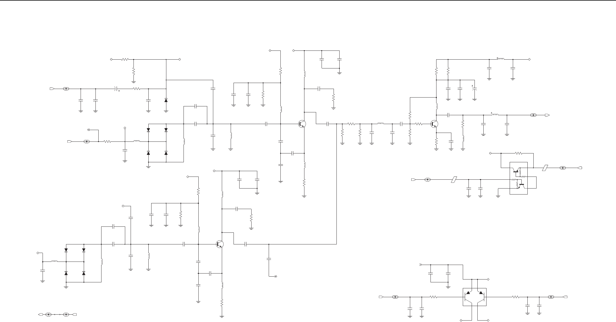
UHF2 (450–512 MHz) 1– 40W PCB/Schematics/Parts List 3-29
VCTRL: 0.6-4.5 V
TXINJ: 450-527 MHz
PRSC (TX): 403-470 MHz
TX1_SEL: 2.7 V (High)
TX VCO 1
TX Prescaler
Super Filter Voltage (SF_TH)
+10 dBm
0.1 V (Low)
TX2_SEL: 2.7 V (High)
-5 to -15 dBm
0.1 V (Low)
TX Buffer Amplifier
Steering Line Voltage (VCTRL_TH)
SF_TH: 2.5 V
TX_BUFFER_SEL: 1.8 V (ON)
0.1 V (OFF)
TX VCO 2
C0337
L0305
C0326
C0310
C0306
R0332
L0317
L0315
C0318
C0324
C0353
CR0306
C0308
CR0307
Q0301
R0304
C0358
C0357
C0316
CR0301
9V3_VCO_UHF1_7
C0336
R0310
L0312
C0359
U0303
PREDRIVE_SW_VCO_UHF1_6
NU
C0307
R0305
R0302
C0301
C0350
C0323
C0329
R0334
R0312
C0348
C0347
R0331
CR0305
Q0300
C0351 C0331
E0302
R0307
C0349
NU
L0319
C0315
C0328
TX1_SEL_VCO_UHF1_5
NU
R0320
L0304
C0341
R0301
C0327
NU
L0306
E0301
R0321
R0326
C0313
C0305
L0311
R0308
C0317
R0316
L0307
CR0302
L0318
C0362
C0340
TX2_SEL_VCO_UHF1_5
C0300
R0337
U0304
C0346
L0314
L0303
NU
C0364
C0361
R0303
C0343
C0311
L0309
CR0304
C0342
CR0300
R0333
R0329
C0302
R0325
TXINJ_VCO_UHF1_5
R0324
R0311
VCTRL_VCO_UHF1_7
CR0303
C0309
C0352
C0320
C0360
R0327
L0310
C0303
C0344
C0322
NU
L0300
L0302
C0304
C0321
C0334
NU
C0319
CR0308
C0345
R0306
Q0302
L0313
R0319
C0325
C0363
C0314
HP_MOD_OUT_VCO_UHF1_7
TX2TX1
SF_TH
SF_TH
TX_VCO_SEL1TX_VCO_SEL2
VMOD
SF_TH
TX2
TX1
SF_TH
VMOD
VSL
9V3_VCO
VCTRL
VCTRL
VSL
PRESC_TX
9T1
9T1
9V3_SYNTH_OUT 9V3_SYNTH_IN
TXINJ
PREDRIVE_SW
SF_TH
HP_MOD_OUT
UHF2 (450–512 MHz) 1–40W Transmit VCO Schematic Diagram

3-30 UHF2 (450–512 MHz) 1– 40W PCB/Schematics/Parts List
UHF2 PCB 8471696M02 Parts List 1–40W
Circuit
Ref
Motorola
Part No. Description
C0100 2113944A41 120pF
C0101 2113944A41 120pF
C0102 2113944A41 120pF
C0103 2113945C31 0.1uF
C0104 2113944A41 120pF
C0105 2113945C31 0.1uF
C0106 2113945C31 0.1uF
C0107 2113945C31 0.1uF
C0108 2113944A41 120pF
C0109 2113945C31 0.1uF
C0110 2113945C31 0.1uF
C0111 2113945C31 0.1uF
C0112 2113944A41 120pF
C0113 NOT PLACED –
C0114 2113946E02 1.0uF
C0115 2113946E02 1.0uF
C0117 2113944A41 120pF
C0118 2113945C31 0.1uF
C0119 NOT PLACED –
C0120 2113945B02 .01uF
C0121 NOT PLACED –
C0122 2113945B02 .01uF
C0123 2113946E02 1.0uF
C0124 2113945C31 0.1uF
C0125 2113944A41 120pF
C0126 2113944A41 120pF
C0127 2113944A41 120pF
C0128 2113944A41 120pF
C0129 2113945C31 0.1uF
C0130 2113944A41 120pF
C0131 2113944A41 120pF
C0132 2113944A41 120pF
C0133 2313960B30 4.7uF
C0134 2113944A41 120pF
C0135 2313960B32 10uF
C0136 2113945C31 0.1uF
C0137 2313960B32 10uF
C0138 2113944A41 120pF
C0140 2313960B30 4.7uF
C0141 2113945C31 0.1uF
C0142 2113944A41 120pF
C0143 2113944A41 120pF
C0144 2113945C31 0.1uF
C0145 2113945B02 .01uF
C0146 2113944A41 120pF
C0147 2113944A41 120pF
C0148 2113945D01 .033uF
C0149 2113945D01 .033uF
C0150 2113945C31 0.1uF
C0151 2113945C31 0.1uF
C0156 2185419D06 0.1uF
C0157 NOT PLACED –
C0158 2185419D06 0.1uF
C0159 NOT PLACED –
C0160 NOT PLACED –
C0161 2185419D06 0.1uF
C0162 NOT PLACED –
C0163 NOT PLACED –
C0164 2185419D06 0.1uF
C0165 2185419D06 0.1uF
C0166 2185419D06 0.1uF
C0171 2113945B02 .01uF
C0175 2113944A41 120pF
C0177 2113944A41 120pF
C0178 2113944A41 120pF
C0179 2113944A41 120pF
C0180 2113945C31 0.1uF
C0191 NOT PLACED –
C0192 NOT PLACED –
C0193 NOT PLACED –
C0194 NOT PLACED –
C0195 2113945A05 470pF
C0196 2113946H02 10uF
C0200 2113944A41 120pF
C0201 2113945Y02 0.10uF
C0202 2113945C02 .01uF
C0203 2113944A41 120pF
C0204 2113944A41 120pF
C0205 2113945Y02 0.10uF
C0206 2113944A41 120pF
C0207 2113945C04 .022uF
C0208 2115153H18 4.3pF
C0209 2113944A41 120pF
C0211 2113944A41 120pF
C0213 2115153H17 3.9pF
C0214 2115153H34 11pF
C0215 2115153H14 3.0pF
C0217 2113944A41 120pF
C0218 2115153H14 3.0pF
C0219 2115153H01 0.5pF
C0220 2115153H23 6.8pF
C0221 2115153H24 7.5pF
C0222 2115153H14 3.0pF
C0223 2115153H46 36pF
C0224 2113944A41 120pF
C0225 2115153H51 56pF
C0226 2113944A41 120pF
C0229 2115153H43 27pF
C0230 2113944C47 150pF
C0231 2115153H14 3.0pF
C0233 NOT PLACED –
Circuit
Ref
Motorola
Part No. Description
C0235 2115153H18 4.3pF
C0236 2113944A41 120pF
C0237 2113945Y02 0.10uF
C0238 2113944A41 120pF
C0239 2113945Y02 0.10uF
C0240 2113944A41 120pF
C0241 2113945Y02 0.10uF
C0242 2113944A41 120pF
C0243 2115153H17 3.9pF
C0245 2115153H18 4.3pF
C0246 2115153H34 11pF
C0247 2115153H24 7.5pF
C0248 2113944A41 120pF
C0249 2113945Y02 0.10uF
C0250 2115153H18 4.3pF
C0251 2115153H40 20pF
C0252 2115153H48 43pF
C0253 2113944A41 120pF
C0257 2113944A41 120pF
C0258 2113945Y02 0.10uF
C0259 2115153H37 15pF
C0300 2113944A41 120pF
C0301 2113945Y02 0.10uF
C0302 2113945C02 .01uF
C0303 2113944A41 120pF
C0304 2113944A41 120pF
C0305 2113945Y02 0.10uF
C0306 2113944A41 120pF
C0307 2113945C04 .022uF
C0308 2115153H18 4.3pF
C0309 2113944A41 120pF
C0310 2115153H01 0.5pF
C0311 2113944A41 120pF
C0313 2115153H18 4.3pF
C0314 2115153H20 5.1pF
C0315 2115153H22 6.2pF
C0316 2313960B32 10uF
C0317 2113944A41 120pF
C0318 2115153H15 3.3pF
C0319 NOT PLACED –
C0320 2115153H16 3.6pF
C0321 2115153H27 10pF
C0322 2115153H37 15pF
C0323 2115153H42 24pF
C0324 2113944A41 120pF
C0325 2115153H50 51pF
C0326 2113944A41 120pF
C0327 NOT PLACED –
C0328 NOT PLACED –
C0329 2115153H36 4.3pF
C0331 2115153H22 6.2pF
Circuit
Ref
Motorola
Part No. Description
C0334 2113944A41 120pF
C0336 2113944A41 120pF
C0337 2113945Y02 0.10uF
C0340 2113944A41 120pF
C0341 2113945Y02 0.10uF
C0342 2113944A41 120pF
C0343 2115153H14 3.0pF
C0344 2115153H01 0.5pF
C0345 2115153H14 3.0pF
C0346 2115153H20 5.1pF
C0347 2115153H19 4.7pF
C0348 2113944A41 120pF
C0349 2113945Y02 0.10uF
C0350 2115153H11 2.2pF
C0351 2115153H42 24pF
C0352 2115153H50 51pF
C0353 2113944A41 120pF
C0357 2113944A41 120pF
C0358 2113945Y02 0.10uF
C0359 2115153H38 16pF
C0360 2313960B30 4.7uF
C0361 2113944C51 1000pF
C0362 2113944A41 120pF
C0363 2113945Y02 0.10uF
C0364 NOT PLACED –
C0400 NOT PLACED –
C0401 2113945C31 0.1uF
C0402 2113944A41 120pF
C0403 2115153H49 47pF
C0404 NOT PLACED –
C0405 2113944A41 120pF
C0406 2115153H27 10pF
C0407 2115153H13 2.7pF
C0408 2115153H27 10pF
C0409 2115153H13 2.7pF
C0410 2115153H10 2.0pF
C0411 2115153H10 2.0pF
C0412 2115153H14 3.0pF
C0413 2115153H57 100pF
C0414 2113944A41 120pF
C0415 2115153H39 18pF
C0416 2115153H14 3.0pF
C0417 2115153H14 3.0pF
C0419 2113945Y02 0.10uF
C0420 2115153H08 1.6pF
C0421 2115153H13 2.7pF
C0422 2115153H36 4.3pF
C0423 2113944A44 220pF
C0424 2113944A44 220pF
C0425 2113944A44 220pF
C0426 2113944A44 220pF
Circuit
Ref
Motorola
Part No. Description

UHF2 (450–512 MHz) 1– 40W PCB/Schematics/Parts List 3-31
C0427 2113944A44 220pF
C0428 2113944A44 220pF
C0429 2113944A44 220pF
C0430 2113944A44 220pF
C0431 2113944A44 220pF
C0432 2113944A44 220pF
C0433 NOT PLACED –
C0434 2113944A41 120pF
C0435 2115153H13 2.7pF
C0436 2113944A41 120pF
C0437 2113944A41 120pF
C0438 2113944A41 120pF
C0439 NOT PLACED –
C0440 2113944A41 120pF
C0441 2115153H11 2.2pF
C0442 2115153H18 4.3pF
C0443 2115153H57 100pF
C0444 2115153H57 100pF
C0445 2115153H43 27pF
C0446 2115153H20 5.1pF
C0447 2115153H27 10pF
C0448 2115153H26 9.1pF
C0449 2115153H27 10pF
C0451 2115153H49 47pF
C0452 NOT PLACED –
C0453 2115153H40 20pF
C0454 2113944A41 120pF
C0455 2113945C31 0.1uF
C0456 2113944A40 100pF
C0457 2113945C31 0.1uF
C0458 2115153H40 20pF
C0459 2115153H40 20pF
C0460 2113946F05 10uF
C0461 2115153H40 20pF
C0462 2115153H40 20pF
C0463 NOT PLACED –
C0464 2115153H08 1.6pF
C0502 2113945Y02 0.10uF
C0503 2113945Y02 0.10uF
C0504 2113945Y02 0.10uF
C0506 2113945Y02 0.10uF
C0507 2115153H39 18pF
C0509 NOT PLACED –
C0510 2115153H22 6.2pF
C0512 2113945Y02 0.10uF
C0513 2113945Y02 0.10uF
C0514 2113945Y02 0.10uF
C0515 NOT PLACED –
C0516 NOT PLACED –
C0601 2115153H48 43pF
C0602 2113945B02 .01uF
Circuit
Ref
Motorola
Part No. Description
C0603 2113944A44 220pF
C0604 2113945Y02 0.10uF
C0605 2115153H48 43pF
C0607 2115153H39 18pF
C0610 2115153H53 68pF
C0611 2113945A09 1000pF
C0612 2115153H34 11pF
C0613 2185419D03 0.01uF
C0614 2115153H48 43pF
C0615 2113945B02 .01uF
C0616 NOT PLACED –
C0617 2113945Y02 0.10uF
C0618 2185419D06 0.1uF
C0619 2113945Y02 0.10uF
C0620 2113945Y02 0.10uF
C0621 2113945Y02 0.10uF
C0622 2113945A09 1000pF
C0623 2113945Y02 0.10uF
C0625 2113944C89 200pF
C0626 2113944A40 100pF
C0627 2113944A40 100pF
C0628 2113945Y02 0.10uF
C0629 2113945A11 2200pF
C0630 2113945Y02 0.10uF
C0631 2113945Y02 0.10uF
C0632 2313960B30 4.7uF
C0633 2113945Y02 0.10uF
C0634 2113945B02 .01uF
C0635 2113944A40 100pF
C0636 2113944A40 100pF
C0637 2113946S35 1.0uF
C0638 2113945Y02 0.10uF
C0640 2113946N03 2.2uF
C0641 2113945B02 .01uF
C0642 2115153H53 68pF
C0643 2113945Y02 0.10uF
C0644 2113945Y02 0.10uF
C0645 2113945B02 .01uF
C0646 2113946G04 0.68uF
C0647 2113946J03 10.0uF
C0648 2113946J03 10.0uF
C0649 2113945A12 3300pF
C0650 2115153H44 30pF
C0651 2115153H57 100pF
C0700 2113944C82 30pF
C0701 2113945C04 .022uF
C0702 2113944C55 2200pF
C0703 2113944C82 30pF
C0704 2113945C04 .022uF
C0705 2113944C51 1000pF
C0706 NOT PLACED –
Circuit
Ref
Motorola
Part No. Description
C0707 NOT PLACED –
C0708 2113944C51 1000pF
C0709 2113945C31 0.1uF
C0710 2371403L02 10uF
C0711 NOT PLACED –
C0712 2113944C51 1000pF
C0713 2111078B42 100pF
C0714 2111078B42 100pF
C0715 2113944F79 560pF
C0716 2113944A41 120pF
C0717 2113945A09 1000pF
C0718 2113945A09 1000pF
C0719 2111078B04 4.3pF
C0720 NOT PLACED –
C0721 2111078B04 4.3pF
C0722 NOT PLACED –
C0723 2111078B39 75pF
C0724 2113944A41 120pF
C0725 2113944A41 120pF
C0726 2111078B19 16pF
C0727 NOT PLACED –
C0728 2113944C42 75pF
C0729 NOT PLACED –
C0730 NOT PLACED –
C0731 NOT PLACED –
C0732 2113951B41 24pF
C0733 2113944C42 75pF
C0734 2113944C42 75pF
C0735 2111078B39 75pF
C0736 2113944A41 120pF
C0737 2111078B01 3.3pF
C0738 2111078B09 6.8pF
C0739 2171388L01 12pF
C0740 2171388L01 12pF
C0741 NOT PLACED –
C0742 2111078B04 4.3pF
C0743 2113944C33 18pF
C0744 2113944C83 36pF
C0745 2113944F44 12pF
C0746 2111078B04 4.3pF
C0747 NOT PLACED –
C0748 2111078B11 8.2pF
C0749 NOT PLACED –
C0751 2111078B11 8.2pF
C0752 2113944A41 120pF
C0753 2111078B39 75pF
C0754 NOT PLACED –
C0755 2113944C30 10pF
C0756 2113944F44 12pF
C0757 2113944C42 75pF
C0758 NOT PLACED –
Circuit
Ref
Motorola
Part No. Description
C0759 2113944C42 75pF
C0760 NOT PLACED –
C0761 2113951B41 24pF
C0763 2113944A41 120pF
C0764 NOT PLACED –
C0765 NOT PLACED –
C0766 NOT PLACED –
C0767 2113944C46 120pF
C0768 2113944A41 120pF
C0769 2113944F51 24pF
C0770 2113944A41 120pF
C0771 NOT PLACED –
C0772 2113944C16 2.7pF
C0774 2113944F51 24pF
C0775 2113945C04 .022uF
C0776 2113944C42 75pF
C0777 2113944C42 75pF
C0778 2111078B29 33pF
C0779 2111078B29 33pF
C0780 2113944A41 120pF
C0781 2113944C42 75pF
C0782 2113944C51 1000pF
C0783 2113944A41 120pF
C0785 2113944C35 27pF
C0786 2113944C82 30pF
C0787 2113944C38 47pF
C0788 NOT PLACED –
C0789 NOT PLACED –
C0790 NOT PLACED –
C0791 2113944A25 10pF
C0792 2113944A28 18pF
C0793 2113944A25 10pF
C0794 NOT PLACED –
C0795 2113944C29 9.1pF
C0796 2113944C42 75pF
C0797 2113944C51 1000pF
C0798 2113944C51 1000pF
C0799 2113944C42 75pF
C0800 NOT PLACED –
C0801 2113944A41 120pF
C0802 2113944A41 120pF
C0803 2111078B01 3.3pF
C0804 2113944C42 75pF
C0805 2113944C51 1000pF
C0806 2185400Y45 30pF
C0807 2185400Y45 30pF
C0808 NOT PLACED –
C0809 2113944C30 10pF
C0810 2113944C42 75pF
C0811 2111078B19 16pF
C0812 2111078B19 16pF
Circuit
Ref
Motorola
Part No. Description

3-32 UHF2 (450–512 MHz) 1– 40W PCB/Schematics/Parts List
C0813 NOT PLACED –
C0814 2113944C46 120pF
C0815 2113944C42 75pF
C0817 2113944C27 7.5pF
C0818 2113944F54 33pF
C0819 2113944F54 33pF
C0828 2113944F54 33pF
C0829 2113944F54 33pF
C0832 2113951B41 24pF
C0845 2113944F44 12pF
C0856 2113944F44 12pF
C0861 2113951B41 24pF
C0869 2113944F51 24pF
C0874 2113944F51 24pF
C0900 2113944A41 120pF
C0901 2113945C31 0.1uF
C0902 2113945C31 0.1uF
C0903 2113944A41 120pF
C0904 2113944A41 120pF
C0906 2113944A41 120pF
C0907 2113945C02 .01uF
C0908 2113945C31 0.1uF
C0909 2113944A41 120pF
C0910 2113944A41 120pF
C0911 2113944A41 120pF
C0912 2113944A41 120pF
C0913 2113944A41 120pF
C0914 2113944A41 120pF
C0915 2113944A41 120pF
C0916 2113944A41 120pF
C0917 2113945A09 1000pF
C0918 2113944A41 120pF
C0919 2113945C31 0.1uF
C0920 2113944A41 120pF
C0921 2113945C31 0.1uF
C0922 2113944A41 120pF
C0923 2113944C55 2200pF
C0925 2113944A41 120pF
C0926 2113945L41 4700pF
C0927 2113944C02 220pF
C0928 2113944C53 1500pF
C0929 2113944A41 120pF
C0931 2113944A41 120pF
C0934 2113944A41 120pF
C0935 2113944A41 120pF
C0936 2113944A41 120pF
C0937 2113944A41 120pF
C0939 2113944A41 120pF
C0940 2113944C46 120pF
C0941 2113944M17 9.1pF
C0942 2113944C42 75pF
Circuit
Ref
Motorola
Part No. Description
C0943 2113944C42 75pF
C0944 2113944M06 3.3pF
C0945 2113944C42 75pF
C0947 2113944A40 100pF
C0948 2113946S35 1.0uF
C0949 2113946G01 2.2uF
C0950 2113945A09 1000pF
C0951 2113945C31 0.1uF
C0953 2113944A41 120pF
C0960 NOT PLACED –
C0961 NOT PLACED –
C0962 NOT PLACED –
C0963 NOT PLACED –
C0964 NOT PLACED –
C0965 NOT PLACED –
C0966 2113944A41 120pF
C0967 2113944A41 120pF
CR0201 4815096H01 DIODE VARACTOR 1SV305
CR0202 4815096H01 DIODE VARACTOR 1SV305
CR0203 4815096H01 DIODE VARACTOR 1SV305
CR0204 4815096H01 DIODE VARACTOR 1SV305
CR0205 4815096H01 DIODE VARACTOR 1SV305
CR0206 4815096H01 DIODE VARACTOR 1SV305
CR0207 4815096H01 DIODE VARACTOR 1SV305
CR0208 4815096H01 DIODE VARACTOR 1SV305
CR0300 4815096H01 DIODE VARACTOR 1SV305
CR0301 4815096H01 DIODE VARACTOR 1SV305
CR0302 4815096H01 DIODE VARACTOR 1SV305
CR0303 4815096H01 DIODE VARACTOR 1SV305
CR0304 4815096H01 DIODE VARACTOR 1SV305
CR0305 4815096H01 DIODE VARACTOR 1SV305
CR0306 4815096H01 DIODE VARACTOR 1SV305
CR0307 4815096H01 DIODE VARACTOR 1SV305
CR0308 4815096H01 DIODE VARACTOR 1SV305
CR0400 4813974A19 DIODE, SCHOTTKY
D0400 NOT PLACED –
D0401 4885055Y01 DIODE VARACTOR 1SV229
D0402 4885055Y01 DIODE VARACTOR 1SV229
D0403 4885055Y01 DIODE VARACTOR 1SV229
D0404 4885055Y01 DIODE VARACTOR 1SV229
D0405 4815090H01 DIODE, MIXER
D0406 4885055Y01 DIODE VARACTOR 1SV229
D0407 4885055Y01 DIODE VARACTOR 1SV229
D0408 4885055Y01 DIODE VARACTOR 1SV229
D0409 4885055Y01 DIODE VARACTOR 1SV229
D0500 4813974A19 DIODE, SCHOTTKY
D0600 4815096H01 DIODE VARACTOR 1SV305
D0601 4815096H01 DIODE VARACTOR 1SV305
D0700 4802482J02 DIODE, PIN
D0702 4802482J02 DIODE, PIN
D0703 4875430M01 DIODE, PIN
Circuit
Ref
Motorola
Part No. Description
D0704 4813974A06 DIODE, PIN
D0900 4813978C02 DIODE, SWITCHING
D0901 4815023H01 DIODE, PIN
D0902 4815024H01 DIODE, PIN
D0903 4815024H01 DIODE, PIN
D0904 4813974A21 DIODE, SCHOTTKY
D0905 4813974A21 DIODE, SCHOTTKY
D0906 4813978C02 DIODE, SWITCHING
D0907 4813977M10 DIODE, 5.1V ZENER
E0201 2409134J25 FERRITE BEAD
E0301 2409134J25 FERRITE BEAD
E0302 NOT PLACED –
E0400 NOT PLACED –
E0401 2409134J25 FERRITE BEAD
E0403 2409134J25 FERRITE BEAD
E0500 2409134J25 FERRITE BEAD
E0600 2409134J25 FERRITE BEAD
E0601 2409134J25 FERRITE BEAD
E0602 2409134J25 FERRITE BEAD
E0603 2409134J25 FERRITE BEAD
E0604 2409134J25 FERRITE BEAD
E0605 2409134J25 FERRITE BEAD
E0606 2409134J25 FERRITE BEAD
E0607 2409134J25 FERRITE BEAD
E0608 2409134J25 FERRITE BEAD
E0609 2409134J25 FERRITE BEAD
E0610 2480640Z01 FERRITE BEAD
E0700 2485011Y01 FERRITE BEAD
E0701 2485011Y01 FERRITE BEAD
E0702 7671656M01 FERRITE BEAD
E0703 2485011Y01 FERRITE BEAD
E0704 2409134J25 FERRITE BEAD
FL0500 9116854H02 73.35 MHZ CRYSTAL FILTER
HS0700 0104038J81 HEATSINK
J0700 0905901V11 MINI-U RF CONNECTOR
L0100 2414017N29 270nH
L0200 2414017N28 220nH
L0202 2414032F41 390nH
L0203 2414032F41 390nH
L0204 2414017N28 220nH
L0205 2414017N19 39nH
L0206 2414017N13 12nH
L0207 2415385H01 8nH
L0209 2414032F41 390nH
L0210 2414015A32 18nH
L0211 2414017N28 220nH
L0212 2414032F41 390nH
L0213 2414032F41 390nH
L0214 2414032F41 390nH
L0215 2415385H01 8nH
L0217 2414032F41 390nH
Circuit
Ref
Motorola
Part No. Description
L0218 2414015A20 22nH
L0219 2414032F41 390nH
L0221 2414017N18 33nH
L0300 2414017N28 220nH
L0302 2414032F41 390nH
L0303 2414032F41 390nH
L0304 2414017N28 220nH
L0305 2414017N17 27nH
L0306 2414017N12 10nH
L0307 2415385H01 8nH
L0309 2414032F41 390nH
L0310 2414015A32 18nH
L0311 2414017N28 220nH
L0312 2414032F41 390nH
L0313 2414032F41 390nH
L0314 2414032F41 390nH
L0315 2415385H01 8nH
L0317 2414032F41 390nH
L0318 2414015A32 18nH
L0319 2414032F41 390nH
L0401 2414015B24 15nH
L0402 NOT PLACED –
L0403 NOT PLACED –
L0404 NOT PLACED –
L0405 NOT PLACED –
L0406 2414015B29 10nH
L0407 2414015B16 27nH
L0408 2414015B17 18nH
L0409 2414015B17 18nH
L0410 2414015B17 18nH
L0411 2414015B15 22nH
L0412 2414017N20 47nH
L0413 2414017N27 180nH
L0414 2414015B23 12nH
L0503 2414015B27 390nH
L0504 NOT PLACED –
L0506 2414032B66 820nH
L0602 2414032K23 2.7uH
L0603 2414032D20 270nH
L0604 2466505A01 10uH
L0605 2466505A01 10uH
L0608 2414032B76 4.7uH
L0700 2460592A01 17nH
L0702 2479990G01 33.47nH
L0705 2414017N26 150nH
L0706 2460592A02 12.5nH
L0707 2460592A02 12.5nH
L0708 2460592A02 12.5nH
L0709 2414017N26 150nH
L0710 2460592A02 12.5nH
L0711 2414017N26 150nH
Circuit
Ref
Motorola
Part No. Description

UHF2 (450–512 MHz) 1– 40W PCB/Schematics/Parts List 3-33
L0712 2415385H07 35.5nH
L0714 2479990N01 43.67nH
L0715 2414017N26 150nH
L0716 2414017N27 180nH
L0717 2414017N06 3.3nH
L0718 2414017N12 10nH
L0719 2414017N22 68nH
L0720 2414017N06 3.3nH
L0721 2414017N08 4.7nH
L0722 2414032B60 390nH
L0723 NOT PLACED –
L0900 2414032D30 1uH
L0901 2414032F42 470nH
L0902 2414032F42 470nH
L0903 2414032F23 12nH
L0904 2414032F22 8.2nH
L0905 2414017N24 100nH
M0700 2686201B02 HEATSINK
Q0100 4802197J95 NPN RF TRANSISTOR
Q0102 4815359H01 DUAL PNP
Q0106 4816134H01 ANALOG SWITCH
Q0107 4813970A59 P-CHANNEL MOSFET
Q0108 4815261H01 ANALOG SWITCH
Q0200 4885061Y01 NPN RF TRANSISTOR
Q0201 4885061Y01 NPN RF TRANSISTOR
Q0202 4802197J95 NPN RF TRANSISTOR
Q0300 4885061Y01 NPN RF TRANSISTOR
Q0301 4885061Y01 NPN RF TRANSISTOR
Q0302 4802197J95 NPN RF TRANSISTOR
Q0400 NOT PLACED –
Q0401 4815267H01 DUAL PNP
Q0402 4885593U03 NPN RF TRANSISTOR
Q0403 4815270H01 ANALOG SWITCH
Q0405 4885593U03 NPN RF TRANSISTOR
Q0500 4802197J95 NPN RF TRANSISTOR
Q0501 4802197J95 NPN RF TRANSISTOR
Q0600 4805793Y10 NPN RF TRANSISTOR
Q0601 4813973A04 NPN DARLINGTON
Q0701 4816013H01 DUAL NPN/PNP
Q0702 48012048002 RF POWER AMPLIFIER,
LDMOS
Q0703 4816548H01 N_CHANNEL LDMOS DRIVER
Q0704 4813973B02 PNP
Q0705 4816547H01 N-CHANNEL LDMOS
PRE-DRIVER
Q0706 4815272H01 ANALOG SWITCH
Q0711 4815271H01 ANALOG SWITCH
Q0900 4815272H01 ANALOG SWITCH
Q0901 4813973A13 PNP
Q0902 4813973M07 NPN
R0100 0613952R66 0
Circuit
Ref
Motorola
Part No. Description
R0101 0613952R66 0
R0102 0613952R66 0
R0103 0613952R66 0
R0104 0613952R17 47K
R0105 0613952Q58 240
R0106 0613952Q83 2.7K
R0107 0613952Q57 220
R0108 0613952Q80 2K
R0109 0613952R66 0
R0110 0613952Q42 51
R0111 0613952R66 0
R0113 0613952R01 10K
R0114 0613952Q80 2K
R0115 0613952R66 0
R0116 0613952R66 0
R0117 0613952R12 30K
R0118 0613952R66 0
R0119 0613952Q35 27
R0120 0613952R01 10K
R0122 NOT PLACED –
R0123 0613952R19 56K
R0125 0613952R66 0
R0126 NOT PLACED –
R0127 0613952Q33 100
R0128 0613952R66 0
R0131 0613952Q53 150
R0134 0613952Q51 120
R0139 0613952R01 10K
R0140 0613952Q31 18
R0144 0613952R01 10K
R0146 0613952R66 0
R0147 NOT PLACED –
R0148 0613952Q60 300
R0155 0613952R66 0
R0156 NOT PLACED –
R0157 NOT PLACED –
R0158 NOT PLACED –
R0159 0613952R01 10K
R0160 0613952R25 100K
R0161 0613952R25 100K
R0170 0613952R66 0
R0201 0613952Q84 3K
R0202 0613952Q66 510
R0203 0613952Q66 510
R0204 0613952Q95 8.2K
R0205 0613952Q49 100
R0206 0613952R05 15K
R0207 0613952Q18 5.1
R0208 0613952Q42 51
R0210 0613952Q89 4.7K
R0211 0613952R66 0
Circuit
Ref
Motorola
Part No. Description
R0212 0613952Q25 10
R0213 0613952R01 10K
R0216 0613952Q44 62
R0218 0613952R01 10K
R0219 0613952Q66 510
R0220 0613952Q25 10
R0221 0613952Q66 510
R0224 0613952Q86 3.6K
R0225 0613952Q94 7.5K
R0226 0613952Q49 100
R0229 0613952Q53 150
R0230 0613952Q89 4.7K
R0301 0613952Q85 3.3K
R0302 0613952Q70 750
R0303 0613952Q70 750
R0304 0613952Q95 8.2K
R0305 0613952Q49 100
R0306 0613952R05 15K
R0307 0613952Q39 39
R0308 0613952Q42 51
R0310 0613952Q89 4.7K
R0311 0613952R66 0
R0312 0613952Q32 20
R0316 0613952Q45 68
R0319 0613952R10 24K
R0320 0613952R05 15K
R0321 0613952Q83 2.7K
R0324 0613952Q84 3K
R0325 0613952Q95 8.2K
R0326 0613952Q49 100
R0327 0613952R01 10K
R0329 0613952Q42 51
R0331 0613952R01 10K
R0332 0613952Q56 200
R0333 0613952Q35 27
R0334 0613952Q56 200
R0337 0613952R66 0
R0400 0613952R05 15K
R0401 0613952Q91 5.6K
R0402 0613958H55 180
R0403 NOT PLACED –
R0404 0613952Q57 220
R0405 0613952Q91 5.6K
R0406 0613952Q83 2.7K
R0407 0613952G67 0
R0409 0613952Q75 1.2K
R0410 0613952R25 100K
R0411 0613958H55 180
R0412 0613952R25 100K
R0413 0613952Q69 680
R0414 0613952Q69 680
Circuit
Ref
Motorola
Part No. Description
R0415 0613952Q69 680
R0416 0613952Q69 680
R0417 0613958H25 10
R0418 0613952Q77 1.5K
R0419 0613952Q83 2.7K
R0420 0613952Q83 2.7K
R0421 0613958H25 10
R0422 0613952K25 17.8
R0423 0613952L46 294
R0424 0613952L46 294
R0425 0613952Q75 1.2K
R0426 0613952Q83 2.7K
R0427 0613952Q25 10
R0428 0613952R01 10K
R0429 0613952Q69 680
R0430 0613952R01 10K
R0431 NOT PLACED –
R0432 NOT PLACED –
R0433 0613952R66 0
R0434 0613958H49 100
R0435 0613952Q23 8.2
R0436 0613952Q67 560
R0437 0613952R66 0
R0438 0613952Q67 560
R0440 0613952R25 100K
R0441 0613952R25 100K
R0443 0613952R25 100K
R0444 0613952R25 100K
R0500 0613952Q90 5.1K
R0501 0613952Q61 330
R0502 0613952R08 20K
R0503 0613952R12 30K
R0508 0613952R19 56K
R0509 0613952Q89 4.7K
R0510 0613952R12 30K
R0511 0613952Q75 1.2K
R0512 0613952Q42 51
R0601 0613952Q45 68
R0602 0613952R01 10K
R0603 0613952Q80 2K
R0604 0613952R10 24K
R0605 0613952Q61 330
R0606 0613952Q42 51
R0607 NOT PLACED –
R0608 0613952R66 0
R0609 0613952R66 0
R0610 0613952R66 0
R0611 0613952R66 0
R0612 0613952R66 0
R0613 0613952R66 0
R0614 0613952R66 0
Circuit
Ref
Motorola
Part No. Description

3-34 UHF2 (450–512 MHz) 1– 40W PCB/Schematics/Parts List
R0615 0613952R66 0
R0616 0613952R25 100K
R0617 0613952R01 10K
R0618 0613952Q63 390
R0619 0613952R01 10K
R0620 0613952Q96 9.1K
R0621 0613952R66 0
R0622 NOT PLACED –
R0623 NOT PLACED –
R0624 0613952Q90 5.1K
R0625 0613952N69 51.1K
R0626 0613952N81 68.1K
R0627 0613952R66 0
R0700 0613958H44 62
R0701 0613958J74 0
R0702 NOT PLACED –
R0706 0613958S51 120
R0709 0613959Q60 300
R0711 0613952H57 220
R0712 0613952H48 91
R0713 0613959H12 30K
R0714 0613952H46 75
R0715 0613952H46 75
R0718 0613952H25 10
R0719 0613959Q25 10
R0720 0613952H25 10
R0722 0613952H89 4.7K
R0724 0613952H79 1.8K
R0725 0613952Q59 270
R0726 0613952N01 10K
R0727 0613952H92 6.2K
R0728 0613952J01 10K
R0729 0613952J01 10K
R0730 0613952H73 1K
R0732 0613952H73 1K
R0734 0613952G67 0
R0735 0613959Y49 100
R0738 0613959Y42 51
R0739 NOT PLACED –
R0740 0613952J25 100K
R0741 0613952J17 47K
R0742 0613959Q25 10
R0743 0613958S73 1K
R0744 NOT PLACED –
R0745 0613952H65 470
R0747 0613952H89 4.7K
R0748 0613952J19 56K
R0749 0613952G67 0
R0750 0613952J01 10K
R0751 0613952J08 20K
R0752 0613952G67 0
Circuit
Ref
Motorola
Part No. Description
R0753 0613952H73 1K
R0754 0613952H25 10
R0755 0613952H25 10
R0756 0613952J25 100K
R0757 0613952J17 47K
R0759 0613952H25 10
R0760 0613952Q83 2.7K
R0761 0613952G67 0
R0762 0613958S29 15
R0763 0613958S29 15
R0764 0613958S29 15
R0765 0613958S29 15
R0766 0613958S29 15
R0768 0613958S29 15
R0769 0613958S29 15
R0770 0613958S29 15
R0771 0613958S29 15
R0773 0613958S29 15
R0775 NOT PLACED –
R0777 0613952H25 10
R0900 0613952N73 56.2K
R0901 0613952N62 43.2K
R0902 0613952M54 3.57K
R0903 0613952N34 22.1K
R0906 0613952R66 0
R0907 0613952R66 0
R0909 0613952N62 43.2K
R0910 0613952H73 1K
R0911 0613952N01 10K
R0912 0613952N30 20K
R0913 0613952R66 0
R0914 0613952P26 182K
R0915 0613952N81 68.1K
R0916 0613952M66 4.75K
R0917 0613952H91 5.6K
R0918 0613952H63 390
R0919 0613952R15 39K
R0920 0613952N42 26.7K
R0921 0613952H81 2.2K
R0922 0613952R14 36K
R0923 0613952R66 0
R0924 0613952H91 5.6K
R0925 0613952H91 5.6K
R0926 0613958H53 150
R0927 0613952H42 51
R0928 0613958H39 39
R0929 0613958H39 39
R0930 0613952R07 18K
R0931 0613952R66 0
R0936 0613952N66 47.5K
R0937 0613952N21 16.2K
Circuit
Ref
Motorola
Part No. Description
R0938 0613952R66 0
R0940 0613952R66 0
R0941 0613952R66 0
R0942 0613952M81 6.81K
R0943 0613952N58 39.2K
R0944 0613952R66 0
R0946 0613952M51 3.32K
R0947 0613952R66 0
R0950 0613952N01 10K
R0951 0613952N62 43.2K
R0954 0613952R40 430K
R0955 0613952P01 100K
R0960 0613952H82 2.4K
R0970 0613958H56 200
R0971 0613958H55 180
R0973 NOT PLACED –
R0974 0613958H55 180
R0975 0613958H56 200
R0976 0613952H53 150
R0977 0613952H53 150
R0978 0613952G67 0
R0979 0613952G67 0
R0981 NOT PLACED –
R0982 NOT PLACED –
R0983 NOT PLACED –
R0984 NOT PLACED –
R0985 NOT PLACED –
R0986 0613952N81 68.1K
R0987 0613952N81 68.1K
R0988 NOT PLACED –
R0989 NOT PLACED –
R0994 NOT PLACED –
R0995 0613952N02 10.2K
RT0908 0615585H01 47K
RT0953 0615585H01 47K
SH0100 2615362H01 SHIELD
SH0101 2615362H01 SHIELD
SH0300 2615362H01 SHIELD
SH0301 2615362H01 SHIELD
SH0500 2615576H01 SHIELD
SH0900 2686423Z02 SHIELD
SH0901 2686425Z02 SHIELD
SP0700 1015349H01 SOLDER_PREFORM
SP0701 1015349H01 SOLDER_PREFORM
SP0702 1015349H01 SOLDER_PREFORM
SP0703 1015349H01 SOLDER_PREFORM
SP0704 1015349H01 SOLDER_PREFORM
SP0705 1015349H01 SOLDER_PREFORM
SP0706 1015349H01 SOLDER_PREFORM
SP0707 1015349H01 SOLDER_PREFORM
T0400 2515121H01 BALUN XFMR
Circuit
Ref
Motorola
Part No. Description
T0401 2515121H01 BALUN XFMR
U0100 5104932K08 IC, FRACN SYNTHESIZER
U0101 5114000B59 ANALOG SWITCH
U0201 4815267H01 DUAL PNP
U0303 NOT PLACED –
U0304 4815267H01 DUAL PNP
U0600 5102495J14 IC, RF ASIC
U0601 5115391H01 VOLTAGE REGULATOR
U0700 4802246J29 PA PRE-DRIVER
U0900 5115147H01 DUAL OPAMP
U0901 5115147H01 DUAL OPAMP
U0940 5180390L83 IC, PA CONTROLLER
U0941 5115391H01 VOLTAGE REGULATOR
U0942 5114004A35 VOLTAGE DETECTOR
U0943 5178286A01 IC, VOLTAGE DETECTOR
VR0700 4813977M11 DIODE, 5.6V ZENER
Y0100 5116032H01 0.5 PPM 16.8 MHZ TCXO
(GPS Models Only)
Circuit
Ref
Motorola
Part No. Description

UHF2 (450–512 MHz) 1–40W PCB/Schematics/Parts List 3-35
4.0 UHF2 (450–512 MHz) 1–40W PCB/Schematics/Parts List
2.9V_MAKO_V6
C0100
C0102
C0103
C0104
C0105
C0109
C0110
C0111
C0113
C0117
C0118
C0120
C0121
C0122
C0124
C0125
C0126
C0127
C0128
C0129
C0130
C0132
C0133
C0140
C0141
C0142
C0143
C0144
C0145
C0146
C0171
C0175
C0177
C0178
C0180
C0195
C0196
C0200
C0201
C0205
C0206
C0220
C0226
C0236
C0237
C0240C0241
C0242
C0250
C0253
C0300
C0301
C0304
C0305
C0306
C0315
C0320
C0326
C0336
C0337
C0340C0341
C0342
C0347
C0350
C0353
C1000
C1001
C1002
C1003
C1004
C1005
C1006
C1007
C1008
C1009
C1010
C1011
C1012
C1013
C1014
C1015
C1016
C1017
C1018
C1019
C1030
C1031
C1034
C1036
C1037
C2000
C2001
C2002
C2003
C2005C2007
C2500
C3040
C3202
C3203
C3207
C3208
C3209
C3210
C3211
C3212
C3213
C3216
C3219
C3220
C3225
C3226
C3229
C3234
C3238
C3239
C3240
C3247
C3248
C3249
C3254
C3262
C3273
C3280
C3292
C3514
C3515
C3516
C3518
C3520
C3523
C3524
C3528
C3529
C3530
C3531
C3538
C3543
C3545
C4000
C4001
C4002
C4003
C4004
C4005
C4006
C4013
C4016
C4017
C4018
C4019
C4020
C4021
C4022
C4023
C4024
C4025
C4026
C4027
C4028
C4029
C4030
C4031
C4032
C4033
C4090
C4091
C4092
C6451
CR0201
CR0202
CR0203
CR0204
CR0205
CR0206
CR0207
CR0208
CR0303
CR0304
CR0307
CR0308
E3202
E3205
E3502E3503
E4000
E4001
3
2
J0700
30
J4001
L0100
L0202
L0203
L0207
L0209
L0210
L0213
L0214
L0215
L0217
L0218
L0302
L0303
L0307
L0309
L0310
L0312
L0313
L0314
L0315
L0317
L0318
L0319
L3200
L3202
Q0100
Q0102
Q0106
Q0300
Q0301
16
1
8
9
Q3200
4
5
8
Q3201
16
1
8
9
Q3202
23
4
Q3203
23
4
Q3204
R0100
R0101
R0102
R0105
R0106
R0107
R0108
R0109
R0110
R0111
R0114
R0116
R0117
R0118
R0119 R0123
R0144
R0146
R0147
R0148
R0155
R0156
R0157
R0158
R0159
R0161
R0201
R0204
R0205
R0211
R0224
R0225
R0226
R0301
R0304
R0305
R0311
R0316
R0324
R0325
R0326
R0329
R1000
R1001
R1002
R1005
R1006
R1014
R1017
R1019
R1020
R1021
R1025
R1027
R1028
R1034
R1035
R1036
R1041
R1045
R1066
R1067
R1071
R2000
R2004
R2006
R2011
R2012
R2529
R3203
R3205
R3206
R3217
R3218
R3224
R3225
R3500
R3501
R3505
R3526
R3532
R3535
R3537
R3538
R3547
R3550
R3560
R3571
R3576
R3580
R3583
R3588
R3590
R3594
R3595
R3596
R4000
R4001
R4002
R4003
R4004
R4005
R4011
R4012
R4061
R4063
R4064
R4065
R4066
R4067
R4068
R4069
R4070
R4071
R4093
R4094
R4096
R4105
R6467
RT3500
1
2
SH0100
1
2
SH0301
TP1000
TP4000
TP_POR
U3040
9
U3500
U4006
U4007U4008
U4009U4010
VR3202
VR3204
VR3206
VR3503
43
2
Y0100
3.6V_MAKO_SW1
C3276
C3278
C3283
C3511
C3513
R3233
R3503
R3504
R3507
R3508
R3509
R3514 R3515
R3587
TP_MAKO_DCLK
TP_MAKO_FSYNC
TP_MAKO_RX
TP_MAKO_TX
USB1_DAT
USB1_SEO
USB1_TXEN
VBUS1_CMD
VBUS2_CMD
MAKO_GATED_32KHz
C2004
C2006
C2008
C2009
C4034
C4035
C4089
R2005
R2007
R2008
R2009
R2010
R2013
R2014
R2015
R4006
R4009
R4010
R4095
R4097
R4099
TP_SDRAM_BA0
TP_SDRAM_BA1
TP_SDRAM_CLK
TP_SDRAM_CLKX
TP_SDRAM_CS
U4004
U4005
C0308
C0310
C0313 C0314
C0323
C0325
C0329
C0343
C0344
C0345
C0346
C0351
C0352
C0359
CR0301
CR0302
CR0305
CR0306
C0204
C0208
C0213
C0214
C0215
C0223
C0225
C0229
C0243
C0245 C0246
C0247
C0251
C0252
C0259
L0212 L0219
Q0200
Q0201
R0216
R0229
C0900
C0901C0906
C0907
C0908
C0909
C0910
C0915
C0939
C0967
D0900
D0906
D0907
L0722
63
4
Q0900
Q0901
R0713
R0900
R0901
R0902
R0903
R0906
R0907
R0909
R0911
R0912
R0914
R0915
R0916
R0920
R0923
R0930
R0931
R0986
R0987
U0901
C0751
C0776
C0777
C0778
C0779
C0796
C0797
C0798
C0799
L0712
L0714
4
3
2
1
Q0704
63
4
Q0706
R0729
R0735
R0738
R0745
R0748
R0749
VR0700
C0700
C0701
C0702
C0703
C0704
C0705
C0706
C0707
C0708
C0709
C0710
C0711
C0712
C0713
C0714
C0715
C0722
C3000
C3002
C3015
E0700
E0701
E3000
R0742
SP3000
SP3001
C3005
C3006
C3007
C3018
C3019
C3046
C4040C4041 C4042 C4043 C4044
C4045
C4046 C4047
C4048
C4075E4005
J3000
25
26
2
J4000
2
3
Q4000
2
3
Q4002
2
3
Q4004
2
3
Q4005
2
3
Q4006
2
3
Q4008
2
3
Q4010
2
3
Q4011
Q4013
R3002
R3003
R3004
R4040R4041 R4042 R4043 R4044
R4045
R4046 R4047
R4048
R4050
R4051
1
6
5
U3001
VR4000 VR4001VR4002
VR4003
VR4004
VR4005
C0929
C0960
C0961
C0962
C0963
C0964
C0965
R0981
R0982
R0983
R0984 R0985
R0988
R0994
R0995
4
5
8
U0943
C0914
C0918
C0921
C0922
C0926
C0931
C0934
C0935
C0936
C0937
C0947
C0948
C0949
C0950
C0951
D0901
D0902
D0903
L0901
L0902
R0917
R0924
R0925
R0926
R0927
R0928
R0929
R0936R0937
R0940
R0950
R0989
SH0900
4
58U0940
U0941
C6406
C6407
C6408
C6416
C6417
C6418
C6419
C6420
C6421
C6422
C6423
C6426
C6427
C6428
C6429
C6430
C6431
C6433
C6439
C6440
C6445
C6450
E6401
E6402
E6407
R6402
R6403
R6443
R6444
R6445
R6446
R6449
R6450
R6454
R6455
R6456
R6458
R6459
R6460
R6461
R6465
R6466
U6402
U6407
C3008
C3009
C3010C3501
C3504C3505
C3506
E3500
E3501
2
3
Q3500
R3009
R3010
R3516
R3520
U3002
C0966
R0775
R3032
R3033
R3036
R3056
3
2
1
U3006
R3035
3
2
1
U3005
R3042
3
2
1
C0437
C0438
C0439
C0440
C0442
C0451
C0457
L0407
L0411
4
32
Q0405
R0417
R0418 R0419
R0420
R0421
R0422
R0423
R0424
R0425
R0433
R0434
C0404
C0405
C0406
C0407
C0408
C0409
C0410
C0411
C0414
C0415
C0416
C0417
C0419
C0420
C0421
C0423
C0424
C0425
C0426
C0427
C0428
C0429
C0430
C0431
C0432
C0433
C0434
C0458 C0459
C0460
C0461
C0462
D0400
D0401
D0402
D0403
D0404
D0406
D0407
D0408
D0409
L0401
L0402L0403L0404
L0405
L0413
4
32
Q0402
R0404
R0405
R0406
R0407
R0409
R0410R0412
R0432
R0435
R0436
R0437
R0438
R0440R0441
R0443
R0444
C0502
C0504
C0509
C0510
C0515
C0516
C0605
C0611
C0615
C0617
C0619
C0620
C0621
C0622
C0623
C0625
C0626
C0627
C0629
C0630
C0631
C0633
C0638
C0642
C0643
C0644
C0645
C0646
C0650
CLKOUT
D0601
DOUTA
DOUTB
E0600
E0601
E0602
E0604
E0605
E0606
E0607
E0608
5
6
4
3
2
1
FL0500
FS
L0504
L0506
L0604
L0608
PC
PD
PE
Q0501
R0503
R0510
R0606
R0607
R0608
R0609
R0610R0611
R0612
R0613
R0614
R0615
R0617
R0618
R0619
R0621
R0622
R0623
R0627
TP0601
U602
1
37
25
13
U0600
C0718
C0724
C0759
C0768
C0781
C0782
C0783
C0788
C0802
C0804
C0805
C0806C0807
C0904
E0702
E0703
E0704
L0723
L0900
1
M0700
Q0701
5
9
6
87
432
10Q0702
63
4Q0711
R0700
R0702
R0706
R0724
R0725
R0726
R0730
R0732
R0734
R0740
R0741
R0744
R0750
R0751
R0752
R0753
R0756
R0757
R0761
R0762
R0763
R0764
R0768
R0771
R0773
1
RT0908
SP0700SP0701
SP0702SP0703
SP0704
SP0705
SP0706
SP0707
UHF2 (450–512 MHz) 1–40W 8486777Z15 Top Side

3-36 UHF2 (450–512 MHz) 1–40W PCB/Schematics/Parts List
1.2V_RTC_TEST
2.8V_RF_TEST
ANT_C
C0101
C0106
C0107
C0108
C0112
C0114
C0115
C0119
C0123
C0131
C0134
C0135
C0136
C0137
C0138
C0147
C0148
C0149
C0150
C0151
C0156
C0157
C0158
C0159
C0160
C0161
C0162
C0163
C0164
C0165
C0166
C0179
C0191
C0192 C0193
C0194
C0202
C0203
C0207
C0209
C0211
C0217
C0218
C0219
C0221
C0222
C0224
C0230
C0231
C0233
C0235
C0238
C0239
C0248
C0249
C0257
C0258
C0302
C0303
C0307
C0309
C0311
C0316
C0317
C0318
C0319
C0321
C0322
C0324
C0327
C0328
C0331
C0334
C0348
C0349
C0357
C0358
C0360
C0361
C0362
C0363
C0400
C0401
C0402
C0403
C0412
C0413
C0422
C0435
C0436
C0441
C0443
C0444
C0445
C0446
C0447
C0448
C0449
C0452
C0453
C0454
C0455
C0456
C0463
C0464
C0503
C0506
C0507
C0512
C0513
C0514
C0601
C0602
C0603
C0604
C0607
C0610
C0612
C0613
C0614
C0616
C0618
C0628
C0632
C0634
C0635
C0636
C0637
C0640
C0641
C0647
C0648
C0649
C0651
C0716
C0717
C0719
C0720
C0721
C0723
C0725
C0726
C0727
C0728
C0729 C0730
C0731
C0732
C0733
C0734
C0735
C0736
C0737
C0738
C0739
C0740
C0741
C0742
C0743
C0744
C0745
C0746
C0747
C0748
C0749
C0752
C0753
C0754
C0755
C0756
C0757
C0758
C0760
C0761
C0763
C0764
C0765
C0766
C0767
C0769
C0770
C0771
C0772
C0774
C0775
C0780
C0785
C0786
C0787
C0789
C0790
C0791
C0792
C0793
C0794
C0795
C0800
C0801
C0803
C0808
C0809
C0810
C0811 C0812
C0813
C0814
C0815
C0817
C0818 C0819
C0828 C0829
C0832
C0845
C0856
C0861
C0869
C0874
C0902
C0903
C0911
C0912
C0913
C0916
C0917
C0919
C0920
C0923 C0925
C0927
C0928
C0940
C0941 C0942
C0943
C0944
C0945
C0953
C1032
C1033
C1035
C1044
C2501
C3011
C3012
C3013
C3014
C3016
C3017
C3020
C3021
C3030
C3031
C3032
C3041
C3042
C3043
C3044
C3045
C3200
C3201
C3204
C3205
C3206
C3214
C3215
C3217
C3218
C3221
C3222
C3227
C3228
C3231
C3232
C3233
C3237
C3243
C3252
C3257
C3260
C3261
C3265
C3266
C3269
C3270
C3272
C3274
C3275
C3279
C3281
C3282
C3289
C3290
C3291
C3500
C3502
C3503
C3507
C3508
C3509
C3510
C3512
1C3517
C3519
C3521
C3522
C3525
C3526
C3527
C3532
C3533
C3534
C3535
1
C3536
C3539 C3540
C3541
C3542
C4007
C4010
C4011
C4012
C4014
C4015
C4049
C4051
C4053
C4055
C4058
C4059
C4060
C4061
C4062
C4063
C4064
C4065
C4066
C4067 C4068
C4069
C4070
C4071
C4072
C4073
C4074
C4076
C4084
C4085
C4086
C4087 C4088
C4093
C4094
C6401
C6412
C6413
C6414
C6432
C6434
C6435
C6436
C6437
C6438
C6443
C6444
C6446
C6449
C6452
CLK_ACQ_TEST
CR0300
CR0400
D0405
D0500
D0600
D0700
D0702
8
4
5
D0703
D0704
D0904
D0905
D3030
D3040
D3200
D4000
D4001
E0201
E0301
E0302
E0400
E0401
E0403
E0500
E0603
E0609
E0610
E2500
E3201
E3203
E3206
E3208
E4002
E4003
E4004
E4006
E6400
EXT_MIC
EXT_PTT
3
4
2
5
FL6401
FT0400
FT0401
FT_APM_1_WIRE
FT_EMERGENCY
FT_IGNITION_SENSE
FT_MMP_1_WIRE
FT_USB1_DM
FT_USB1_DP
FT_USB2_DM
FT_USB2_DP
FT_VBAT
FT_VBAT_GROUND
FT_VBUS1
FT_VBUS2
I2C_CLK
I2C_DATA
IF_TEST
INT_MIC
G2
20
G1
J2500
11
J4002
14
J4003
J6400
L0200
L0204
L0205
L0206
L0211
L0221
L0300
L0304
L0305
L0306
L0311
L0406
L0408
L0409
L0410
L0412
L0414
L0503
L0602
L0603
L0605
L0700
L0702
L0705
L0706
L0707
L0708
L0709
L0710
L0711
L0715
L0716
L0717
L0718
L0719
L0720
L0721
L0903
L0904
L0905
L3201
L6402
L6403
MAKO_CE
MAKO_V8_5V
MAKO_V9_3V
OPT_SSI_SYNC
Q0107
2
3
Q0108
Q0202
Q0302
63
4Q0400
Q0401
Q0403
Q0500
Q0600
Q0601
1
3
Q0703
Q0705
Q0902
Q3030
4
3
2
1
Q3032
Q3040
2
3
Q3041
2
3
Q3205
6
3
4
Q3206
4
58
Q3207
2
3
Q3208
Q3209
Q3210
63
4
Q3502
63
4
Q3503
Q3504
Q3505
2
3
Q4001
2
3
Q4003
2
3
Q4007
2
3
Q4009
2
3
Q4012
Q4014
2
3
Q4015
Q6401
63
4
Q6402
R0103
R0104
R0113 R0115
R0120
R0122 R0125
R0126
R0127
R0128 R0131
R0134
R0139
R0140
R0160
R0202
R0203
R0206
R0207
R0208
R0210
R0212
R0213
R0218
R0219
R0220
R0221
R0230
R0302
R0303
R0306
R0307
R0308
R0310
R0312
R0319
R0320
R0321
R0327
R0331
R0332
R0333
R0334
R0337
R0400
R0401
R0402
R0403
R0411
R0413
R0414
R0415
R0416
R0426
R0427
R0428
R0429 R0430
R0431
R0500
R0501
R0502
R0508
R0509
R0511
R0512
R0601
R0602
R0603
R0604
R0605
R0616
R0620
R0624
R0625
R0626
R0701
R0709
R0711
R0712
R0714 R0715
R0718
R0719
R0720
R0722
R0727 R0728
R0739
R0743
R0747
R0754
R0755
R0759
R0760
R0765
R0766
R0769
R0770
R0777
R0910
R0913
R0918
R0919
R0921
R0922
R0938
R0941
R0942
R0943
R0944
R0946
R0947
R0951
R0954
R0955
R0960
R0970
R0971
R0973
R0974
R0975
R0976
R0977 R0978
R0979
R1026
R1044
R1046
R1047
R1048
R1054
R1060
R1070
R2500
R2501
R2502
R2504
R2506R2507
R2508
R2509
R2510
R2511
R2512
R2513 R2514
R2515
R2516
R2517
R2518
R2519
R2520
R2524
R2525 R2526
R2527
R2528
R3005
R3006
R3007
R3008
R3030
R3034
R3037
R3038
R3039
R3040R3041
R3043
R3044
R3045
R3046
R3047 R3048
R3050
R3051
R3052
R3053
R3054
R3055
R3057
R3200
R3204
R3207
R3208
R3209
R3210
R3215
R3216
R3219
R3220
R3222
R3223
R3226
R3227
R3228
R3236
R3237
R3238
R3239
R3240
R3241
R3243
R3245
R3246
R3247
R3248
R3249
R3250
R3252
R3253
R3502
R3506
R3510
R3511
R3512
R3513
R3521
R3523
R3524
R3525
R3528
R3529
R3530
R3533
R3534
R3536
R3539
R3540
R3541
R3542
R3544
R3545
R3546
R3548
R3549
R3551
R3552
R3553
R3554
R3555
R3556
R3558
R3559
R3569
R3572
R3573
R3574
R3575
R3577
R3578
R3579
R3581
R3582
R3584R3585
R3586
R3591
R3592
R3593
R4023
R4030
R4031
R4032
R4033
R4034
R4035
R4049
R4054
R4055
R4074
R4076
R4078
R4079
R4080
R4081
R4082
R4083
R4085
R4086
R4088
R4089
R4090
R4098
R4100
R4101
R4103
R4106
R6401
R6404
R6405
R6407
R6409
R6410
R6411
R6416
R6417
R6418
R6419
R6420
R6430
R6432
R6433
R6434
R6435
R6436
R6437
R6438
R6439
R6440
R6457
R6464
R6468
R6469
R6470
RF_ATTN_2
ROUT_TEST
1
RT0953
S0700
1
2SH0101
1
2
SH0300
2
1
SH0500
12
SH0901
SPI_CLK_1
SPI_CLK_TEST
SPI_MISO_1
SPI_MOSI_1
6
4
3
T0400
64
3
T0401
TP501
TP502TP503
TP504
TP0301
TP0600
TP0702
TP0703
TP0704
TP0705
TP0707
TP0708
TP0709
TP0710
TP0711
TP0713
TP0903
TP0904
TP0907
TP0909
TP0910
TP0911
TP0913
TP_ADAPT_SW
TP_DDR_LDQS
TP_DDR_UDQS
TP_FLASH_CLK
TP_TEST1
TP_TEST2
TP_VCTRL
TX_RAMP
TX_RAMP_DAC
L11A11
L1
U0100
4
3
5
U0101
U0201
6
3
4
U0303
U0304
U0601
U0700
U0900
U0942
A21 AA21
AA1
U1000
43
6
U1006
A1 M1
M8
A8
U2000
K1
A9
K9
U2001
1
6
5
U3003
U3004
14
58
U3030
P1
A1
A14 P14
U3200
64
3
U3201
C1
C3A3
U3202
4
3
5
U3203
10
6
5
U3501
7
8
14
U3502
85
4
U3503
U3504
7
814
U3505
85
4
U3508
16
1
8
9
U4000
14
7
8
U4001
P10
A10
P1
A1
U6401
U6404
C1
C3
A3
U6405
U6406
U6408
VR3000
VR3040
VR3200
VR3201
VR3203
VR3205
VR3207
VR3208
VR3502
VR3504
VR4006
VR4009
VR6400
43
2
Y1000
4
3
2
Y3200
Y3201
UHF2 (450–512 MHz) 1–40W 8486777Z15 Bottom Side

UHF2 (450–512 MHz) 1–40W PCB/Schematics/Parts List 3-37
( RX: SHEET 2 )
VCO_UHF1
( TX: SHEET 1 )
CONTROLLER_&_GPS_R6
( TOP LEVEL: SHEET 1)
( PA: SHEET 1 )
( PC: SHEET 2 )
TX_HP_UHF1
SYNTH
RXFE_UHF1
( 1 SHEET )
RXBE_73.35MHZ
(IF AMP: SHEET 1)
(ABACUS3: SHEET 2)
2
NC
1
3
4
SF_TH
TXINJ
TX_VCO_SEL1
TX_VCO_SEL2
VCTRL
1
0
2
1
0
2
3
9R1
9V3_SYNTH_IN
9V3_SYNTH_OUT
9V3_VCO
HP_MOD_OUT
PRSC
RXINJ
RX_VCO_SEL1
RX_VCO_SEL2
2
0
0
1
1
22
2
1V8
5V
5V_FE
IF
REF_CLK
SPI_ABACUS_CEX
SPI_ABACUS_CLK
SPI_ABACUS_DATA
SSI_ABACUS_CLKOUT
SSI_ABACUS_DOUTA
SSI_ABACUS_DOUTB
SSI_ABACUS_FSYNC
SSI_ABACUS_SYNCB
1
0
0
2
9R1
FE_TUNEIF
RF_ATTEN_1
RX_IN
RX_INJ
0
1
1
1
3
0
VCTRL
0
1
4
3
2
2
RX_SSI_FSYNC_PASS_OUT
RX_VCO_SEL1_
RX_VCO_SEL2_
SDTX
SFTX
SF_OUTSPI_CLK_IN
SPI_CLK_OUT
SPI_MISO_IN
SPI_MISO_OUT
SPI_MOSI_IN
SPI_MOSI_OUT
TH_CEX
TX_CLK
TX_VCO_SEL1_
TX_VCO_SEL2_
ABACUS3_CEX_IN
ABACUS3_CEX_OUT
ABACUS3_SYNCB_IN
ABACUS3_SYNCB_OUT
ADAPT_SW
DMCS
HP_MOD_OUT
LOCK
PRSC
RF_ATTN_1
RSTB RX_SSI_CLK_PASS_IN
RX_SSI_CLK_PASS_OUT
RX_SSI_DATA_PASS_IN
RX_SSI_DATA_PASS_OUT
RX_SSI_FSYNC_PASS_IN
RX_IN
TX_DAC
TX_INJ
VSWR_DET
0
1.8V_TH_DIG
16.8_GPS
16.8_REF
1V8_BE
2.8V_TH_ANA
2.8V_TH_DIG
5V
5V_BE
9R1
9V3
SPI_MOSI
THK_CS
TX_SSI_CLK
TX_SSI_DATA
TX_SSI_FSYNC
9V3
9V3_PA
9V3_SYNTH
9V3_VCO
ANT_ENABLE
FINAL_BIAS_1
LO_BATTERY_DET
LO_PWR_DET
PA_SUPPLY
PC_ATTEN_ENA
PRESSURE_PAD
MAKO_ADC5
MAKO_ADC8
MAKO_DAC1
MAKO_DAC2
MAKO_RAMP_DAC3
PC_ATTEN_ENA
PRESSURE_PAD_DET
RAW_B+
RESET_OUT
RX_SSI_CLK
RX_SSI_DATA
RX_SSI_FSYNC
RX_SSI_SYNCB
SPI_CLK
SPI_MISO
TX_SSI_BUS(0:2)
ABACUS_SPI_BUS(0:3)
SPI_BUS(0:4)
RX_SSI_BUS(0:2)
ABACUS_SSI_BUS(0:2)
1.875V_DIG_V2
16.8_GPS
16.8_MHZ_BUFF
2.775V_ANA_V7
2.775V_DIG_V4
5V_SW
9V3
9V3_PA
ABACUS3_CS
ADAPT_SW
ANT_ENABLE
DMCS
LOCK_DETECT
LO_BATTERY_DET
UHF2 (450–512 MHz) 1–40W Overall Schematic Diagram
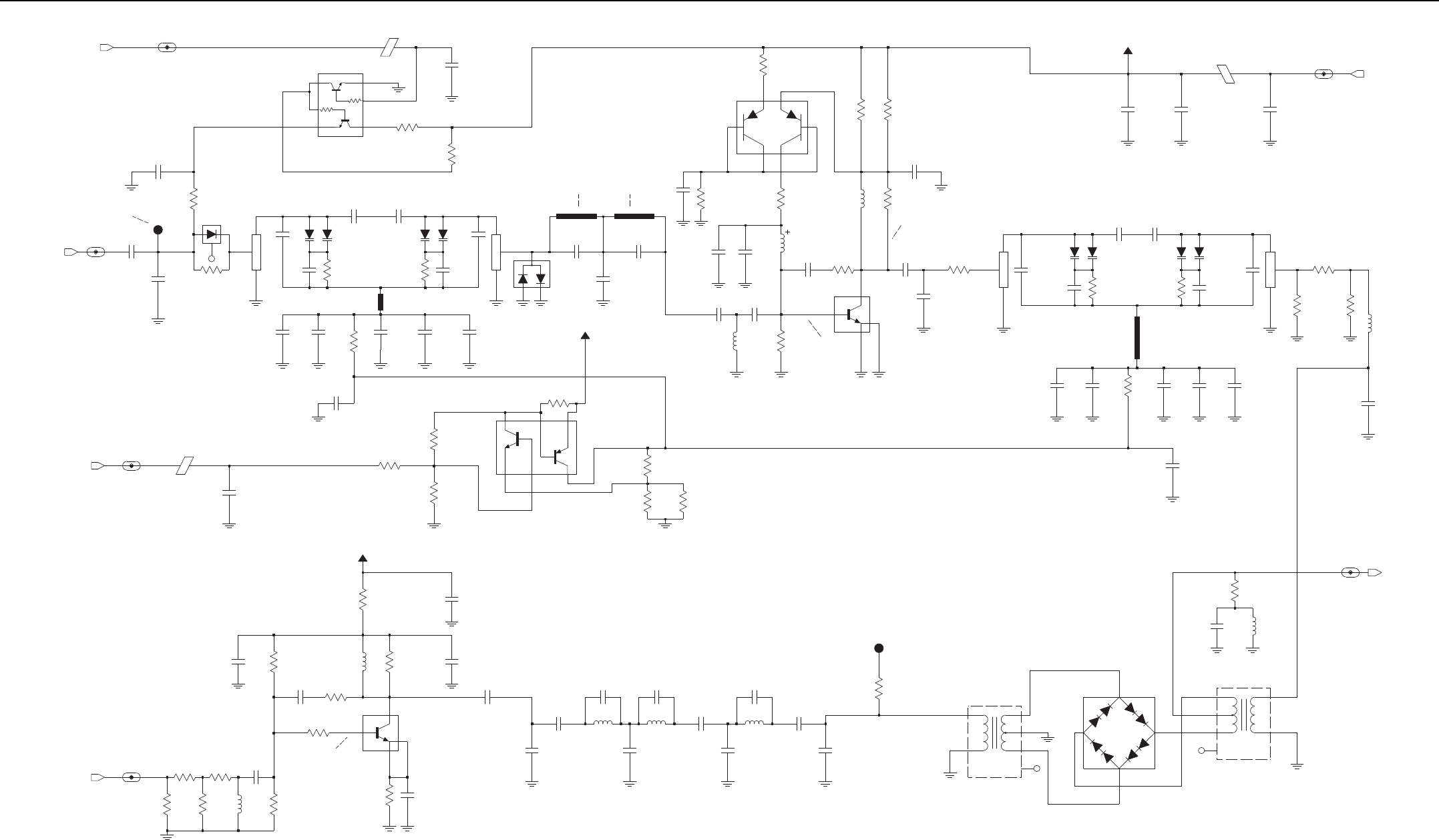
3-38 UHF2 (450–512 MHz) 1–40W PCB/Schematics/Parts List
(Not Placed)
7.0 VDC
Hi-Side Zeros for Preselector
Zo/Zin=4:1
10 dB Attenuator
0.7 VDC
Zo/Zin=4:1
(3.00 ~ 8.00 VDC)
+16.0 dBm Min. (250 mV P-P)
MAKO ( 0 ~ 4.6 VDC)
3.7 VDC Typical
8.9 VDC Typical
0.8 VDC Typical
3.0 VDC Typical
(Micro-strip 20 mm Each)
C0464
C0444
R0404
C0453
FT0401
1
C0459
C0423
C0409
RX_INJ_FE_5
C0454
C0449
D0403
R0436
NU
D0407
C0416
Q0403
2
3
6
4
1
5
R0437
R0405
C0414 D0404
R0414
9R1_FILT
E0401
C0452
C0460
D0402
L0408
D0401
C0422
C0402
(VALUE)
NU
R0431
NU
L0414
C0433
C0434
R0430
C0406R0400
RXIN_FE_6
FE_TUNE_FE_4
D0405
1IO1 2
IO2
3
IO3
4IO4
L0407
R0440
C0420
CR0400
1
3
2
D0409
NC
R0402
L0402
12
3
NU
R0422
D0400
C0440
IF_FE_8
R0425
D0408
C0463
NU
NU
C0439
C0410
E0400
4
6
3
2
1
(VALUE)
T0400
5
NC
1
C0428
FT0400
C0419
L0409
R0403
NU
(VALUE)
C0411
C0405
C0447
RF_ATTEN_1_3
C0427
R0407R0441
L0401
(VALUE)
NC
C0457
C0441
(VALUE)
R0415 R0416
R0417
R0426
C0445
C0417
9R1_FILT
R0424
C0412
C0413
C0403
R0435
C0429 C0432
NU
C0431
C0400
R0444
C0451
L0413
NC
5
4
6
3
2
1
R0428
T0401
C0421
R0409
C0437
L0410
12
3
R0427
L0403
C0456
C0438
C0442
NC
C0408
3
1
4
C0430
Q0400
NU
2
5
6
R0421
C0407
C0446
C0435
NU
C0461
C0401
R0418
E0403
R0410
R0434
R0420
C0436
C0462 R0443
R0412
C0415
L0405
12
3
(VALUE)
R0423
L0411
C0426
C0425
.0476
C0448
R0433
R0406
Q0402
Q0405
R0413
R0429
R0419
9R1_FE_6
C0424
25
6
3
1
4
C0443
Q0401
C0458
9R1_FILT
L0412
L0406
D0406
R0438
NU
R0411
R0432
NU
C0455
12
3
NU
L0404
C0404
RX_INJ
R0401
RF_ATTEN_1
IF
RX_IN
FE_TUNE
9R1
UHF2 (450–512 MHz) 1–40W Receiver Front-End Schematic Diagram

UHF2 (450–512 MHz) 1–40W PCB/Schematics/Parts List 3-39
1.43V
0.76V
1.6V
0.72V
4-POLE
IF_TO_ABACUS
73.35MHz
R0511
IFIN_BE_8
R0512
C0514
R0508
R0509
NU
C0510
L0504
GND1
2
GND2
5
IN
1OUT 4
FL0500
CC1
3
CC2
6
L0506
C0516
NU
5V_BE_5
C0502
NU
C0515
C0503
C0513
SH0500
1
2
R0503
Q0501
E0500
L0503
C0509
NU
RX_FE_3
R0510
C0506
1
3
2
C0507
Q0500
C0504
R0502
R0500
D0500
R0501
C0512
IF
IF_OUT
5V
5V
5V_FE
UHF2 (450–512 MHz) 1–40W Receiver IF Amp Schematic Diagram

3-40 UHF2 (450–512 MHz) 1–40W PCB/Schematics/Parts List
2nd LO VCO UHF (71.1MHz/75.6 MHz)
SPF_3.5V
CLOCK LF
2nd LO LF
CLOCK VCO
#
*
R0611
R0605
FD_1_BE_5
R0602
R0616
C0620
D0600
E0609
C0604
C0621
C0634
E0602
E0605
3VA
C0611
Q0601
SB_1_BE_5
PC
TP0601
R0615
C0649
FE_1_BE_5
NU
C0616
U602
1
C0632
L0608
C0607
C0605
NU
R0607
C0646
3VA
DOUTA
L0602
R0606
C0648
L0604
C0642
C0601
CLKOUT_1_BE_5
VVCO
C0628
C0602
C0638
R0603
C0640
FC_1_BE_5
R0617
R0601
E0607
VVCO
C0627
C0631
C0629
FS
R0625
5V
3VA
C0623
C0615
R0612
3VA
FREF_IF
C0610
R0618
C0644
L0605
PE
C0613
E0600
R0624
C0636
E0610
C0635
R0613
3VA
C0651
C0618
C0647
D0601
C0626
R0608
E0603
DOUTB
C0622
C0645
48
VDDI
40
VDDL
39
VDDP
14
VDDQ
12
VREFN
11
VREFP
C0625
25
PE
RREF
13
33
SYNCB
9
VDDA
17
VDDC
26
VDDD
6
VDDF
27
VDDH
15
IOUTC
38
IOUTL
42
LON
43
LOP
2
MXON
1
MXOP
23
PC
24
PD
36
GNDL
37
GNDP
16
GNDQ
21
GNDS1
34
GNDS2
4
IF2N
5
IF2P
47
IFIN
8
GCN
7
GCP
10
GNDA
18
GNDC
22
GNDD
3
GNDF
32
GNDH
45
GNDI
CLKP
19
46
CXIF
44
CXVL
41
CXVM
29
DOUTA
30
DOUTB
35
FREF
31
FS
U0600
20
CLKN
28
CLKOUT
FS_1_BE_5
R0627
C0637
R0621
3VA
TP0600
R0610
R0620
C0603
C0633 R0614
3VA
E0604
VCONT
4
VIN
3
VOUT 1
3VA
R0604
U0601
FB
2
GND
5
NP
6
3VA
CLKOUT
DOUTA_1_BE_5
C0619
C0641
E0606
C0630
C0617
R0619
E0601
NU
R0623
L0603
C0643
C0614
DOUTB_1_BE_5
PD
1V8_3
Q0600
E0608
C0612
C0650
R0609
R0622
R0626
NU
IF_OUT
5V
SSI_ABACUS_FSYNC
SPI_ABACUS_CEX
REF_CLK
SPI_ABACUS_CLK
SSI_ABACUS_DOUTA
SSI_ABACUS_CLKOUT
SSI_ABACUS_DOUTB
SPI_ABACUS_DATA
SSI_ABACUS_SYNCB
1V8
1V8
UHF2 (450–512 MHz) 1–40W Receiver Back-End Schematic Diagram

UHF2 (450–512 MHz) 1–40W PCB/Schematics/Parts List 3-41
PA_SUPPLY_TX_PA
PA_SUPPLY
E0703
9V3_PA
Antenna_En
Test Point to check 11dB/17dB Pad
18dB RL
+8 dBm
Ref Osc Warping
R0715
R0711
L0709C0768
C0763
C0736
TP0705
TX_INJ_TX_PA
NC
R0760
R0714
R0712
D0704
C0728
L0711
LO_PWR_PAD
TX_INJ
HI_PWR_PAD
-3 dBm
C0733
TP0703
1
C0752 13 dBm
3.2VDC
TP0704
L0705
R0706
3
VD_RF_OUT
U0700
GND1
2
GND2
4
RF_IN
C0724
C0718
C0725
E0704
R0700
R0702
NU
9V3_TX
9V3_Tx_Sw
2.2K
47K
47K
47K
Q0701
C0701
E0700
C0702C0700
E0702
9V3_TX
L0702
C0716
C0717
TP0702
R0754
R0755
R0718
R0720
D1
G
3
S
2
Q0703
NU
C0771
R0722
R0727
R0728
C0770M0700
1
POS
NU
C0790
C0786
C0787
C0791
R0739
NU
C0815
V_cont
C0792
NU
C0794
C0793
9V3
9V3_VCO
9V3_SYNTH
C0801
R0751
NU
C0800
R0750
C0802
V_cont
R0747
C0789
C0814
NU
L0720
D
G
S
Q0705
R0759
R0777
2.10V (27.5W)
2.85V (44W)
9.1VDC
NU
C0788
TP0710TP0709
NU
R0744
NU
L0723
R0734
9V3_TX
C0775
L0715
C0780
L0717
C0785 C0734
L0718
NU
C0795
L0721
C0817
C0818
C0829
C0856
C0828
C0760
NU
C0753
C0809
NU
C0755
NU
C0813
C0744C0743
NU
C0764
C0756
NU
C0754
C0765
NU
NU
C0819
C0808
NU
C0749
R0773
R0771
C0774
R0768
C0874
R0770
R0769
R0766
C0761 C0861
SP0701
Gate_2
1PIN12
PIN2
HS0700
L0708
C0738
C0735
C0739 C0740
C0803C0742
L0706L0707C0723
R0971
R0970
L0903
L0905
W = 0.625 mm
W = 0.625 mm
W = 2.5 mm
S = 0.93 mm
L = 19 mm
S = 0.54 mm
L0722R0713
C0767
C0772
NU
C0766
D0702
R0701
R0978
C0940
D0904
C0942
C0941
R0976R0977
R0975
L0904R0973
NU
R0974
2
J0700-33
J0700-1
1
J0700-2
D0905
C0945
R0979
C0944
C0943
REV_DETECTED
9V3_TX
LO_PWR_PAD
HI_PWR_PAD
FINAL_BIAS_1
FWD_DETECTED
FWD_POWER
V_CONTROL
RX_IN
R0752
R0753
RX_IN_TX_PA
FINAL_BIAS_1_TX_PA
9V3_TX
LO_PWR_PAD
HI_PWR_PAD
V_cont
Final_Bias
C0797
C0796
R0761
TP0713
R0749 ANT_ENABLE_TX_PA
R0748
Antenna_En
ANT_ENABLE
C0798
NC
C0799
S0700
R0775
C0966
PRESSURE_PAD_TX_PA
PRESSURE_PAD
TP0711
Final_Bias
C0758
NU
C0757
C0759
L0716
R0743
9V3_Tx_Sw
A3
A4
A5
K1
K2
K3
K4
D0703
A1
A2
NC
Q0706
R0745
NC
R0738
Q0704
C0776
2.2VDC (TX Only) 2.2VDC (TX Only)
TP0707
NC
TP0708
R0740
C0782
R0741
R0757
C0781
R0732
VR0700
PRESSURE_PAD
Gate_2
R0730
Gate_1
R0756
C0805
C0804
C0778
R0729
R0735
C0777 C0779
L0714
A+
ATC
L0710
C0748
C0751
NU
L0712
NU
NU
C0741
NU
C0727
ATC
NU
C0806
C0812
NU
C0721
C0747
NU
C0746
SP0707
SP0705
SP0704
SP0706
SP0703
SP0702
R0719
ATC
NU
C0720
C0807
NU
C0811
C0719
NU
C0737
C0726
C0810L0719
D0700
C0704C0703
NU
C0706C0707
NU
C0708C0705C0709
C0714
E0701
C0713
R0742
C0722
NU
C0715
NU
L0700
A+
C0710C0712
C0711
NU
R0762
R0763
R0765
R0764
C0869
C0845
C0769
NU
C0729
C0731
NU
C0745
C0730
NU
MRF1570, Flat Lead
Q0702
C0832
C0732
SP0700
R0709
Gate_1
UHF2 (450–512 MHz) 1–40W Power Amplifier Schematic Diagram
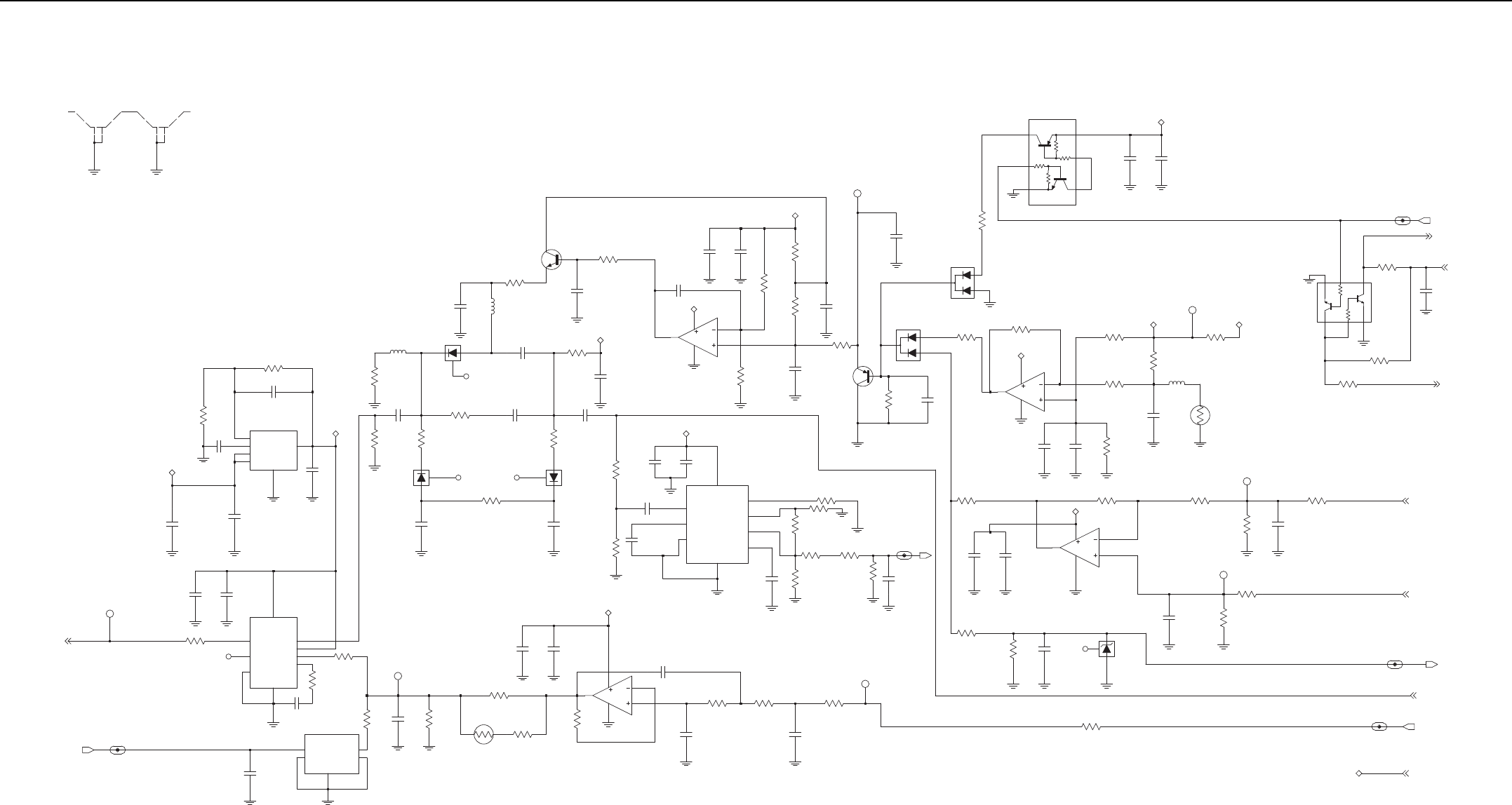
3-42 UHF2 (450–512 MHz) 1–40W PCB/Schematics/Parts List
SH0901
1
2
SH0900
1
2
R0937
C09502FB
5GND
6NP
4VCONT
3VIN
1
VOUT
U0941
C0948
5V
5V DC
C0949
C0951
0.1uF
9V3
R0940
NCNC
6
RFIN1
VAPC
7
VPOS 8
3
VSET
U0940
COMM
5
ENBL2
FLTR 4
GND
C0921 C0922
C0926
R0950
R0941
9
5
NC2
1
RESET_OUT
U0942
GND
3
INPUT
2
4NC1
C0953
LO_BATTERY_DET
LO_BATTERY_DET
2.10V (27.5W)
2.85V (44W)
TP0909
V_CONTROL
1.35V (44W)
1.28V (27.5W)
C0925 RT0953
R0954
C0902
R0946
R0955
R0942
TP0910
C0903
6
5
7
8
4
U0900-2
R0947
C0923
C0927
R0943 R0951 R0944
TP0911
C0928
R0987 C0967 D0907
5.1V
NC
R0938
R0986
C0908
R0923 R0914
C0909
9V3_PC
U0901-1
2
3
1
8
4
R0994
NU
R0995
NU
LO_PWR_DET
C0965
R0984
NU
R0981
R0982
R0983 R0985
LO_PWR_DET
TADJ
VOUT
VPOS
VSET
CLPF
COMM
GND
INHI
INLO
C0964
R0989
NU
6
5
7
4
U0943
3
2
9
1
8
C0961 C0962
R0988
C0960
C0963
5V
D0903
C0937
9V3_PC
C0934
C0916
C0935
C0914 R0917
R0929
9V3_PC
NC
R0926
R0928
NCNC
D0902
R0925
C0936
R0927
L0902
R0924
D0901
C0931
L0901
R0913
Q0902
C0918
3
1
8
4
U0900-1
2
9V3_PC
C0913
C0920
R0918
C0911
R0922
R0919
R0921
R0960
C0919
C0917
Q0901
9V3_PC
R0930
C0915
D0900
1
2
3
R0900
1
2
3
D0906
R0906
4
U0901-2
6
5
7
8
9V3_PC
0.6V typical
Cutback starts about 2.2V
TP0907
C0929
R0931
NOTE: VOLTAGES SHOWN FOR ANALOG TX MODE
2
5
6
3
1
4
C0900 C0901
Q0900 9V3
Cypher: 2.4Kohm 5%
R0907
C0904
R0902
TP0913
R0901
L0900
RT0908
R0903
9V3_PC 9V3
C0907C0906
R0909
4.0V (44W)
3.2V (27.5W)
0.38V (44W)
0.21V (27.5W)
C0910
TP0904
R0916R0915
TP0903
R0912
C0939
R0911
R0920
9V3 to FW bias PIN in HP mode
R0724
R0725
HI_PWR_PAD
9V3 to REV bias PIN in LP mode
5
6
3
1
4
Q0711
2
PC_ATTEN_ENA_TX_PA
C0783
R0726
PC_ATTEN_ENA
9V3_TX
LO_PWR_PAD
FWD_DETECTED
REV_DETECTED
VSWR_DET
FWD_POWER
TX_DAC
9V3
TX_DAC
VSWR_DET
9V3
R0910
C0912
C0947
R0936
UHF2 (450–512 MHz) 1–40W Power Control Schematic Diagram

UHF2 (450–512 MHz) 1–40W PCB/Schematics/Parts List 3-43
R1
R2
10K
47K
0.5 ppm
VHF=1500pF
---
Note: High Port modulation injection through loop filter for U1 and U2 only
HI: 2.8V
U1=220pF
U2=120pF
C0191,C0192,C0193,C0194: NU (UHF B1)
VHF=1500pF
SF_OUT VOLTAGE: 2.45V
Unlocked: 0V
U1=220pF
Buffer to Abacus/Controller
9R1 SWITCH FOR FRONT-END
C0157, C0159, C0160,C0162,C0163,C0191,C0192,C0193,C0194: NU (UHF B2)
GPO LINES
U2=120pF
U1=220pF
U1=220pF
VCO STEERING LINE VOLTAGE: 0.6V TO 4.4V
U2=120pF
VCO STEERING LINE VOLTAGE: 0.6V TO 4.4V
VHF=1500pF
VHF=1500pF
U2=120pF
U2=120pF
Adapt OFF: 0V
U1=220pF
VHF=1500pF
4875188M01
LOW: 0V
1.5 ppm
VCO SEL: ACTIVE LOW
Adapt ON: 5V
Locked: 1.8V
GPO_4
TCXO (Y0100)
Switch for Adapt Transient
NC
NC
NC
R0170
C0166
C0100
C0105
L0100
C0137
RX_SSI_DATA_IN
NC
R0114
R0147
SPI_MOSI_IN
NU
ABACUS3_SYNCB_OUT
R0100
NC
5V_BE_SYNTH
TP504
1
RX_SSI_CLK_OUT
C0107
NC
NC
C0136
C0133
NC
C0140
1
C0106
NC
TP_TEST1
SPI_MISO_IN
R0160
NC4
3
OUTPUT
4
VCC
1VCONT
NC
NC
NC
Y0100
16.8MHz
GND
2
5
NC1
NC2 6
NC3 7
8
R0113
9R1_SYNTH
C0148
C0102
C0138
3GND
1INOUT
4ONOFF_CONTROL
2OUTIN
5
VCC
R0125
NC
U0101
NC
GPO_3_SYNTH
NC
NC
C0179
ABACUS3_SYNCB_IN
RX_SSI_DATA_OUT
C0147
C0135
C0171
C0132
C0157
C0127
NC
LOCK_SYNTH
R0140
C0120
Q0100
C0194 C0159
C0191
NC
VCTRL_SYNTH
C0126
C0112
NC
NC
NC
NC
1V8_BE_SYNTH
SF_OUT_SYNTH
R0158
NU
HP_MOD_OUT_SYNTH
16.8_REF_CONTROLLER_SYNTH
NU
C0119
NC
NU
C0113
NC
1
R0148
1
2
TP_VCTRL
SH0100
1
2
SH0101
R0159
C0144
NC
C0160
ABACUS3_CEX_IN
R0118
C0141
NC
RX_SSI_CLK_IN
C0162
C0103
R0103
R0107
C0124
Q0108
R0122
NC
RX_SSI_FSYNC_IN
NC
NC
NU
C0161
C0122
NU
GPO_6_SYNTH
9V3_SYNTH
R0157
Q0106
GND
IN
OUT
C0117
C0134
R0115
TX_DAC_VCC
G7
TX_GND1
F6 TX_GND2
J6
TX_VCC
F1
VCO_DAC
K5XOSC_BASE
XOSC_EMIT
L5
G6
XOSC_GND
TCLK
D7
TEST1 C7
TEST2
B3
TM
F10
TXCLK
K7TXI
L7TXQ
H7
TX_DAC_GNDL6
SPI_CLK
D10
SPI_DR
D9
SPI_DW
SSI_GNDE8
E11
SSI_VCC
SUB1
K10
F5 SUB2
F3 SUB3
G8
SDM_VAG
A9
SDM_VREFM B8
SDM_VREFP
D11
SDR
F11
SDTX
F9
SFTX
K4SF_OUT
C9 SMD_CLK_GEN_GND
C11
A5
RX_AVCC2
RX_EN_OUT
B1
D3
SCAN_EN
F2 SCAN_IN
E9
SCLK_OUT
SDM_CLK_GEN_VCC A10
SDM_REF_GNDA8
SDM_REF_VCC B9
B10RXFS
C2 RXI
C1 RXIX
D1 RXQ
D2 RXQX
RX_AGND1 C3
D5
RX_AGND2
B2
RX_AVCC1
OSCREG_GND
OSCREG_OUT
H5
J4OSCREG_SPLY
K11 PABIAS_DAC
L9PHCLK
RFSTEPA
A3
E6 RSTB
E7
RXACQ
E10
M_PRSCX
A1 NC1
A11 NC2
NC3
L1
L11 NC4
NTXI
L8
NTXQ
K6
L4OSCREG_BYP
J5
MAIN_GND
MAIN_PDET_VCC G2
J1
MAIN_VCC
H1
MN_ADAPT_CP
G3
MN_CP
G5
MN_CP_GND
MN_CP_VCC H2
J2
M_PRSC
H3
GPO5
H8 GPO6
K8
HP_MOD_OUT
J9INCR_DECR
F8
LGND1 C8
LGND2
G10
LVCC1
B7
LVCC2
G4
ESC_TEST
K2
ESC_VCC
C6 FBI
B6 FBQ
B4 GPO1_TEST1
A4 GPO2_TEST2
GPO3_TEST3
E5
GPO4_TEST4
D4
K9
EF_OUTM
J8
J7EF_OUTP
ESC_CP L3
ESC_CPBIAS L2
K3
ESC_CP_GNDJ3
ESC_CP_VCC
H4
ESC_GND
K1
ESC_IN
E1
G9CLK_CP
H11 CLK_EMIT
H10
CLK_GND
J10
CLK_VCC
G1
DAC_ADAPT
A2 DC_CAL
L10DEEPSLEEP
F7
DMCS
BP_I
F4 BP_IX
E2 BP_Q
BP_QX
E3
D8
CEX
H9 CLK1_OUT
J11 CLK2_OUT
G11 CLK_BASE
D6 ACE2
AGC_DAC
B5
AGC_FLAG
C4 AGC_REF
C5
H6 ARX_DAC
C10ASPI_CLK
B11 ASPI_DATA
A7
ASPI_VCC
E4
U0100
A6 ACE1
DMCS_SYNTH
C0131
C0130
R0131
C0128
SPI_CLK_IN
NU
C0121
1
NC
TP_TEST2
C0129
C0165
R0146
ADAPT_SW_SYNTH
C0143
C0125
2.8V_TH_ANA_SYNTH
RX_SSI_FSYNC_OUT
C0178
C0177
C0175
NC
SFTX_SYNTH
NC
C0156
R0105
R0110
R0144
NC
R0161
C0110
PRSC_SYNTH
R0116
C0101
NC
C0164
C0104
NC
R0134
C0123
C0158
TX_CLK_SYNTH
C0109
NC
NU
R0126
Q0107
R0120
R0155
C0146
ABACUS3_CEX_OUT
NC
1
NC
C0115
TH_CEX_SYNTH
TP_ADAPT_SW
SPI_MOSI_OUT
GPO_2_SYNTH
R0102
TP503
1
NC
C0142
C0108
NC
NC
NC
SDTX_SYNTH
NC
R0104
R0111
RSTB_SYNTH
1.8V_TH_DIG_SYNTH
C0180
TP501
1
R0119
R0128
R0123
C0145
R0108
C0114
C0149
C0196
C0195
SPI_CLK_OUT
16.8_GPS_SYNTH
SPI_MISO_OUT
C0111
NU
C0151
R0156
2.8V_TH_DIG_SYNTH
C0150
R0127
R0106
NC
4
NC
Q01022
1
3
NC
NC
R0101
R0117
R0109
5V_SYNTH
TP502
1
GPO_1_SYNTH
C0163
GPO_5_SYNTH
16.8_REF_BE_SYNTH
C0118
C0193
NC
NC
C0192
ABACUS3_SYNCB_INABACUS3_SYNCB_OUT
VCTRL
9V3
R0139
SPI_MOSI_IN
SPI_MOSI_IN
SPI_CLK_IN
SPI_CLK_IN
SPI_MISO_IN
SPI_MISO_IN
5V
2.8V_DIG
RX_VCO_SEL1_
5V_BE
9R1
16.8_REF
1V8_BE
1.8V_TH_DIG
1.8V_DIG
RSTB
16.8_GPS
ADAPT_SW
5V_TH
TX_VCO_SEL1_
HP_MOD_OUT
TH_CEX
SPI_MOSI_IN
SPI_CLK_IN
2.8V_TH_DIG
2.8V_DIG
2.8V_TH_ANA
2.8V_ANA
1.8V_DIG
1.8V_DIG
5V_TH
RX_SSI_DATA_PASS_OUT
RX_SSI_CLK_PASS_OUT
RX_SSI_FSYNC_PASS_OUT
RX_SSI_CLK_PASS_IN
ABACUS3_CEX_OUT
SPI_MISO_OUT
SPI_MOSI_OUT
SPI_CLK_OUT
ABACUS3_CEX_IN
RX_SSI_DATA_PASS_IN
RX_SSI_FSYNC_PASS_IN
TX_VCO_SEL2_
RF_ATTN_1
RX_VCO_SEL2_
PRSC
2.8V_ANA
DMCS
5V_TH
2.8V_ANA
1.8V_DIG
2.8V_ANA
2.8V_ANA
SDTX
SFTX
SF_OUT
LOCK
TX_CLK
SPI_MISO_IN
2.8V_ANA
5V_TH
UHF1 (450–512 MHz) 1–40W Synthesizer Schematic Diagram

3-44 UHF2 (450–512 MHz) 1–40W PCB/Schematics/Parts List
0.1 V (Low)
VCTRL: 0.6-4.5 V
RX2_SEL: 2.7 V (High)
RX VCO 1
RX Buffer Amplifier
RX1_SEL: 2.7 V (High)
0.1 V (Low)
Steering Line Voltage (VCTRL_TH)
RXINJ: 329.65 - 396.65 MHz
RX VCO 2
RX Prescaler
-5 to -15 dBm
Super Filter Voltage (SF_TH)
SF_TH: 2.5 V
PRSC (RX): 329.65 - 396.65 MHz
NU
C0222
+6 dBm
C0258
R0224
RXINJ_VCO_UHF1_5
E0201
C0249
CR0208
CR0203
R0211 L0210
Q0200
C0225
C0259
9R1_VCO_UHF1_7
C0242
C0230
R0230
R0216
C0205
CR0207
C0203
C0219
R0220
NU
L0206
R0225
C0251
R0221
C0217
L0217
C0224
NU
C0202
L0202
C0243
C0200
C0206
C0229
C0241
R0219
R0207
L0212
C0231
C0204
C0214
CR0202
C0215
SH0300
1
2
SH0301
1
2
C0240
R0218RX1_SEL_VCO_UHF1_5
TP0301
1
CR0206
R0206
L0214
L0203
C0246
R0229
CR0204
L0218
R0226
C0248
C0253
L0205
L0209
R0210
R0212
C0237
Q0202
L0204
C0252
RX2_SEL_VCO_UHF1_5
C0236
L0200
L0219
C0250
C0201
PRSC_VCO_UHF1_5
SF_TH_VCO_UHF1_6
C0233
NU
C0223
C0226
CR0201
R0208
C0245
C0220
R0204
R0202
C0238
R0203
L0213
C0235
C0257
L0221
CR0205
Q0201
R0213
L0211
C0221
C0211
C0247
R0205
C0213
R0201
L0207
C0209
C0207
C0208
NU
C0218
L0215
C0239
U0201
RXINJ
RXSL
PRESC_TX
RX1
RX2
RX_VCO_SEL1
RX1RX2
RX_VCO_SEL2
VCTRL
PRSC
SF_TH
SF_TH
RXSL
9R1
SF_TH
SF_TH
SF_TH
UHF2 (450–512 MHz) 1–40W Receiver VCO Schematic Diagram
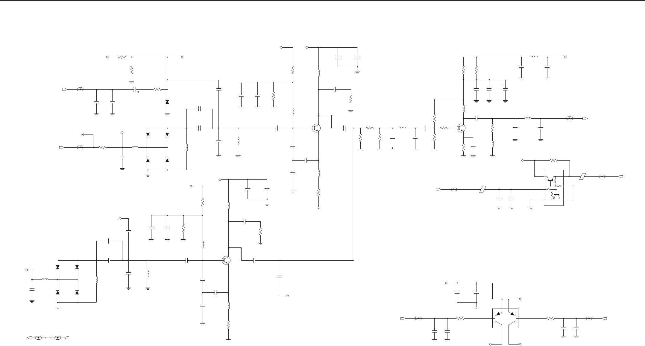
UHF2 (450–512 MHz) 1–40W PCB/Schematics/Parts List 3-45
VCTRL: 0.6-4.5 V
TX VCO 1
0.1 V (OFF)
TX VCO 2
TX Prescaler
TX2_SEL: 2.7 V (High)
-5 to -15 dBm
Steering Line Voltage (VCTRL_TH)
SF_TH: 2.5 V
0.1 V (Low)
TX Buffer Amplifier
0.1 V (Low)
+11 dBm
Super Filter Voltage (SF_TH)
TX_BUFFER_SEL: 1.8 V (ON)
PRSC (TX): 403-470 MHz
TX1_SEL: 2.7 V (High)
TXINJ: 403-470 MHz
R0326
C0313
L0318
R0316
R0331
C0303
L0310
C0344
R0303
C0361
C0300
TX2_SEL_VCO_UHF1_5
R0320
C0341
R0308
R0327
C0360
L0312
C0305
R0310
C0362
C0311
C0340
L0307
C0301
CR0302
C0342
CR0300
R0325
R0324
R0306
TXINJ_VCO_UHF1_5
L0313
Q0302
L0311
L0314
L0305
C0310
Q0300
C0351
R0307
C0331
E0302
NU
L0319
C0349
C0353
CR0308
C0319
NU
TX1_SEL_VCO_UHF1_5
C0345
C0328
NU
R0304
L0304
R0333
R0334
R0329
C0302
L0303
R0321
L0306
C0334
L0300
C0359
L0302
C0317
C0357
L0309
CR0304
C0314
C0337
U0304
C0346
R0337
CR0305
C0347
R0305
R0302
C0326
C0324
NU
R0332
C0306
PREDRIVE_SW_VCO_UHF1_6
C0363
C0348
C0315
CR0307
Q0301
C0336
C0329
C0309
C0352
C0320
R0301
C0327
NU
E0301
9V3_VCO_UHF1_7
U0303
NU
R0319
C0325
C0321
NU
C0322
C0343
C0358
CR0306
C0308
C0316
(VALUE)
CR0301
C0323
HP_MOD_OUT_VCO_UHF1_7
C0350
L0317
C0318
L0315
VCTRL_VCO_UHF1_7R0311
CR0303
R0312
C0304
PREDRIVE_SW
SF_TH
HP_MOD_OUT
TX2
TX1
SF_TH
SF_TH
TX_VCO_SEL1TX_VCO_SEL2
C0307
SF_TH
TX2
TX1
SF_TH
VMOD
VSL
9V3_VCO
VCTRL
VCTRL
VSL
VMOD
PRESC_TX
9T1
9T1
9V3_SYNTH_OUT 9V3_SYNTH_IN
TXINJ
UHF2 (450–512 MHz) 1–40W Transmit VCO Schematic Diagram

3-46 UHF2 (450–512 MHz) 1–40W PCB/Schematics/Parts List
UHF2 PCB 8486777Z15 Parts List 1–40W
Circuit
Ref
Motorola
Part No. Description
C0100 2113944A41 120pF
C0101 2113944A41 120pF
C0102 2113944A41 120pF
C0103 2113945C31 0.1uF
C0104 2113944A41 120pF
C0105 2113945C31 0.1uF
C0106 2113945C31 0.1uF
C0107 2113945C31 0.1uF
C0108 2113944A41 120pF
C0109 2113945C31 0.1uF
C0110 2113945C31 0.1uF
C0111 2113945C31 0.1uF
C0112 2113944A41 120pF
C0113 NOT PLACED –
C0114 211394600 1.0uF
C0115 211394600 1.0uF
C0117 2113944A41 120pF
C0118 2113945C31 0.1uF
C0119 NOT PLACED –
C0120 2113945B02 .01uF
C0121 NOT PLACED –
C0122 2113945B02 .01uF
C0123 211394600 1.0uF
C0124 2113945C31 0.1uF
C0125 2113944A41 120pF
C0126 2113944A41 120pF
C0127 2113944A41 120pF
C0128 2113944A41 120pF
C0129 2113945C31 0.1uF
C0130 2113944A41 120pF
C0131 2113944A41 120pF
C0132 2113944A41 120pF
C0133 2313960B30 4.7uF
C0134 2113944A41 120pF
C0135 2313960B32 10uF
C0136 2113945C31 0.1uF
C0137 2313960B32 10uF
C0138 2113944A41 120pF
C0140 2313960B30 4.7uF
C0141 2113945C31 0.1uF
C0142 2113944A41 120pF
C0143 2113944A41 120pF
C0144 2113945C31 0.1uF
C0145 2113945B02 .01uF
C0146 2113944A41 120pF
C0147 2113944A41 120pF
C0148 2113945D01 .033uF
C0149 2113945D01 .033uF
C0150 2113945C31 0.1uF
C0151 2113945C31 0.1uF
C0156 2185419D06 0.1uF
C0157 NOT PLACED –
C0158 2185419D06 0.1uF
C0159 NOT PLACED –
C0160 NOT PLACED –
C0161 2185419D06 0.1uF
C0162 NOT PLACED –
C0163 NOT PLACED –
C0164 2185419D06 0.1uF
C0165 2185419D06 0.1uF
C0166 2185419D06 0.1uF
C0171 2113945B02 .01uF
C0175 2113944A41 120pF
C0177 2113944A41 120pF
C0178 2113944A41 120pF
C0179 2113944A41 120pF
C0180 2113945C31 0.1uF
C0191 NOT PLACED –
C0192 NOT PLACED –
C0193 NOT PLACED –
C0194 NOT PLACED –
C0195 2113945A05 470pF
C0196 2113946H02 10uF
C0200 2113944A41 120pF
C0201 2113945Y02 0.10uF
C0202 2113945C02 .01uF
C0203 2113944A41 120pF
C0204 2113944A41 120pF
C0205 2113945Y02 0.10uF
C0206 2113944A41 120pF
C0207 2113945C04 .022uF
C0208 2115153H18 4.3pF
C0209 2113944A41 120pF
C0211 2113944A41 120pF
C0213 2115153H17 3.9pF
C0214 2115153H34 11pF
C0215 2115153H14 3.0pF
C0217 2113944A41 120pF
C0218 2115153H14 3.0pF
C0219 2115153H01 0.5pF
C0220 2115153H23 6.8pF
C0221 2115153H24 7.5pF
C0222 2115153H14 3.0pF
C0223 2115153H46 36pF
C0224 2113944A41 120pF
C0225 2115153H51 56pF
C0226 2113944A41 120pF
C0229 2115153H43 27pF
C0230 2113944C47 150pF
C0231 2115153H14 3.0pF
C0233 NOT PLACED –
Circuit
Ref
Motorola
Part No. Description
C0235 2115153H18 4.3pF
C0236 2113944A41 120pF
C0237 2113945Y02 0.10uF
C0238 2113944A41 120pF
C0239 2113945Y02 0.10uF
C0240 2113944A41 120pF
C0241 2113945Y02 0.10uF
C0242 2113944A41 120pF
C0243 2115153H17 3.9pF
C0245 2115153H18 4.3pF
C0246 2115153H34 11pF
C0247 2115153H24 7.5pF
C0248 2113944A41 120pF
C0249 2113945Y02 0.10uF
C0250 2115153H18 4.3pF
C0251 2115153H40 20pF
C0252 2115153H48 43pF
C0253 2113944A41 120pF
C0257 2113944A41 120pF
C0258 2113945Y02 0.10uF
C0259 2115153H37 15pF
C0300 2113944A41 120pF
C0301 2113945Y02 0.10uF
C0302 2113945C02 .01uF
C0303 2113944A41 120pF
C0304 2113944A41 120pF
C0305 2113945Y02 0.10uF
C0306 2113944A41 120pF
C0307 2113945C04 .022uF
C0308 2115153H18 4.3pF
C0309 2113944A41 120pF
C0310 2115153H01 0.5pF
C0311 2113944A41 120pF
C0313 2115153H18 4.3pF
C0314 2115153H20 5.1pF
C0315 2115153H22 6.2pF
C0316 2313960B32 10uF
C0317 2113944A41 120pF
C0318 2115153H15 3.3pF
C0319 NOT PLACED –
C0320 2115153H16 3.6pF
C0321 2115153H27 10pF
C0322 2115153H37 15pF
C0323 2115153H42 24pF
C0324 2113944A41 120pF
C0325 2115153H50 51pF
C0326 2113944A41 120pF
C0327 NOT PLACED –
C0328 NOT PLACED –
C0329 2115153H36 4.3pF
C0331 2115153H22 6.2pF
Circuit
Ref
Motorola
Part No. Description
C0334 2113944A41 120pF
C0336 2113944A41 120pF
C0337 2113945Y02 0.10uF
C0340 2113944A41 120pF
C0341 2113945Y02 0.10uF
C0342 2113944A41 120pF
C0343 2115153H14 3.0pF
C0344 2115153H01 0.5pF
C0345 2115153H14 3.0pF
C0346 2115153H20 5.1pF
C0347 2115153H19 4.7pF
C0348 2113944A41 120pF
C0349 2113945Y02 0.10uF
C0350 2115153H11 2.2pF
C0351 2115153H42 24pF
C0352 2115153H50 51pF
C0353 2113944A41 120pF
C0357 2113944A41 120pF
C0358 2113945Y02 0.10uF
C0359 2115153H38 16pF
C0360 2313960B30 4.7uF
C0361 2113944C51 1000pF
C0362 2113944A41 120pF
C0363 2113945Y02 0.10uF
C0400 NOT PLACED –
C0401 2113945C31 0.1uF
C0402 2113944A41 120pF
C0403 2115153H49 47pF
C0404 NOT PLACED –
C0405 2113944A41 120pF
C0406 2115153H27 10pF
C0407 2115153H13 2.7pF
C0408 2115153H27 10pF
C0409 2115153H13 2.7pF
C0410 2115153H10 2.0pF
C0411 2115153H10 2.0pF
C0412 2115153H14 3.0pF
C0413 2115153H57 100pF
C0414 2113944A41 120pF
C0415 2115153H39 18pF
C0416 2115153H14 3.0pF
C0417 2115153H14 3.0pF
C0419 2113945Y02 0.10uF
C0420 2115153H08 1.6pF
C0421 2115153H13 2.7pF
C0422 2115153H36 4.3pF
C0423 2113944A44 220pF
C0424 2113944A44 220pF
C0425 2113944A44 220pF
C0426 2113944A44 220pF
C0427 2113944A44 220pF
Circuit
Ref
Motorola
Part No. Description

UHF2 (450–512 MHz) 1–40W PCB/Schematics/Parts List 3-47
C0428 2113944A44 220pF
C0429 2113944A44 220pF
C0430 2113944A44 220pF
C0431 2113944A44 220pF
C0432 2113944A44 220pF
C0433 NOT PLACED –
C0434 2113944A41 120pF
C0435 2115153H13 2.7pF
C0436 2113944A41 120pF
C0437 2113944A41 120pF
C0438 2113944A41 120pF
C0439 NOT PLACED –
C0440 2113944A41 120pF
C0441 2115153H11 2.2pF
C0442 2115153H18 4.3pF
C0443 2115153H57 100pF
C0444 2115153H57 100pF
C0445 2115153H43 27pF
C0446 2115153H20 5.1pF
C0447 2115153H27 10pF
C0448 2115153H26 9.1pF
C0449 2115153H27 10pF
C0451 2115153H49 47pF
C0452 NOT PLACED –
C0453 2115153H40 20pF
C0454 2113944A41 120pF
C0455 2113945C31 0.1uF
C0456 2113944A40 100pF
C0457 2113945C31 0.1uF
C0458 2115153H40 20pF
C0459 2115153H40 20pF
C0460 2113946F05 10uF
C0461 2115153H40 20pF
C0462 2115153H40 20pF
C0463 NOT PLACED –
C0464 2115153H08 1.6pF
C0502 2113945Y02 0.10uF
C0503 2113945Y02 0.10uF
C0504 2113945Y02 0.10uF
C0506 2113945Y02 0.10uF
C0507 2115153H39 18pF
C0509 NOT PLACED –
C0510 2115153H22 6.2pF
C0512 2113945Y02 0.10uF
C0513 2113945Y02 0.10uF
C0514 2113945Y02 0.10uF
C0515 NOT PLACED –
C0516 NOT PLACED –
C0601 2115153H48 43pF
C0602 2113945B02 .01uF
C0603 2113944A44 220pF
Circuit
Ref
Motorola
Part No. Description
C0604 2113945Y02 0.10uF
C0605 2115153H48 43pF
C0607 2115153H39 18pF
C0610 2115153H53 68pF
C0611 2113945A09 1000pF
C0612 2115153H34 11pF
C0613 2185419D03 0.01uF
C0614 2115153H48 43pF
C0615 2113945B02 .01uF
C0616 NOT PLACED –
C0617 2113945Y02 0.10uF
C0618 2185419D06 0.1uF
C0619 2113945Y02 0.10uF
C0620 2113945Y02 0.10uF
C0621 2113945Y02 0.10uF
C0622 2113945A09 1000pF
C0623 2113945Y02 0.10uF
C0625 2113944C89 200pF
C0626 2113944A40 100pF
C0627 2113944A40 100pF
C0628 2113945Y02 0.10uF
C0629 2113945A11 2200pF
C0630 2113945Y02 0.10uF
C0631 2113945Y02 0.10uF
C0632 2313960B30 4.7uF
C0633 2113945Y02 0.10uF
C0634 2113945B02 .01uF
C0635 2113944A40 100pF
C0636 2113944A40 100pF
C0637 2113946S35 1.0uF
C0638 2113945Y02 0.10uF
C0640 2113946N03 2.2uF
C0641 2113945B02 .01uF
C0642 2115153H53 68pF
C0643 2113945Y02 0.10uF
C0644 2113945Y02 0.10uF
C0645 2113945B02 .01uF
C0646 2113946G04 0.68uF
C0647 2113946J03 10.0uF
C0648 2113946J03 10.0uF
C0649 2113945A12 3300pF
C0650 2115153H44 30pF
C0651 2115153H57 100pF
C0700 2113944C82 30pF
C0701 2113945C04 .022uF
C0702 2113944C55 2200pF
C0703 2113944C82 30pF
C0704 2113945C04 .022uF
C0705 2113944C51 1000pF
C0706 NOT PLACED –
C0707 NOT PLACED –
Circuit
Ref
Motorola
Part No. Description
C0708 2113944C51 1000pF
C0709 2113945C31 0.1uF
C0710 2371403L02 10uF
C0711 NOT PLACED –
C0712 2113944C51 1000pF
C0713 2111078B42 100pF
C0714 2111078B42 100pF
C0715 2113944C02 220pF
C0716 2113944A41 120pF
C0717 2113945A09 1000pF
C0718 2113945A09 1000pF
C0719 2111078B04 4.3pF
C0720 NOT PLACED –
C0721 NOT PLACED –
C0722 NOT PLACED –
C0723 2111078B39 75pF
C0724 2113944A41 120pF
C0725 2113944A41 120pF
C0726 2111078B19 16pF
C0727 NOT PLACED –
C0728 2113944C42 75pF
C0729 NOT PLACED –
C0730 NOT PLACED –
C0731 NOT PLACED –
C0732 2113951B41 24pF
C0733 2113944C42 75pF
C0734 2113944C42 75pF
C0735 2111078B39 75pF
C0736 2113944A41 120pF
C0737 NOT PLACED –
C0738 2111078B09 6.8pF
C0739 2171388L01 12pF
C0740 2171388L01 12pF
C0741 NOT PLACED –
C0742 2111078B04 4.3pF
C0743 2113944C33 18pF
C0744 2113944C83 36pF
C0745 2113944F44 12pF
C0746 2111078B04 4.3pF
C0747 NOT PLACED –
C0748 2111078B12 9.1pF
C0749 NOT PLACED –
C0751 2111078B11 8.2pF
C0752 2113944A41 120pF
C0753 2111078B39 75pF
C0754 NOT PLACED –
C0755 2113944C30 10pF
C0756 2113944F44 12pF
C0757 2113944C42 75pF
C0758 NOT PLACED –
C0759 2113944C42 75pF
Circuit
Ref
Motorola
Part No. Description
C0760 NOT PLACED –
C0761 2113951B41 24pF
C0763 2113944A41 120pF
C0764 NOT PLACED –
C0765 NOT PLACED –
C0766 NOT PLACED –
C0767 2113944C46 120pF
C0768 2113944A41 120pF
C0769 2113944F51 24pF
C0770 2113944A41 120pF
C0771 NOT PLACED –
C0772 2113944C16 2.7pF
C0774 2113944F51 24pF
C0775 2113945C04 .022uF
C0776 2113944C42 75pF
C0777 2113944C42 75pF
C0778 2111078B29 33pF
C0779 2111078B29 33pF
C0780 2113944A41 120pF
C0781 2113944C42 75pF
C0782 2113944C51 1000pF
C0783 2113944A41 120pF
C0785 2113944C35 27pF
C0786 2113944C82 30pF
C0787 2113944C38 47pF
C0788 NOT PLACED –
C0789 NOT PLACED –
C0790 NOT PLACED –
C0791 2113944A25 10pF
C0792 2113944A28 18pF
C0793 2113944A25 10pF
C0794 NOT PLACED –
C0795 2113944C29 9.1pF
C0796 2113944C42 75pF
C0797 2113944C51 1000pF
C0798 2113944C51 1000pF
C0799 2113944C42 75pF
C0800 NOT PLACED –
C0801 2113944A41 120pF
C0802 2113944A41 120pF
C0803 2111078B01 3.3pF
C0804 2113944C42 75pF
C0805 2113944C51 1000pF
C0806 2185400Y45 30pF
C0807 2185400Y45 30pF
C0808 NOT PLACED –
C0809 2113944C30 10pF
C0810 2113944C42 75pF
C0811 2111078B19 16pF
C0812 2111078B19 16pF
C0813 NOT PLACED –
Circuit
Ref
Motorola
Part No. Description

3-48 UHF2 (450–512 MHz) 1–40W PCB/Schematics/Parts List
C0814 2113944C46 120pF
C0815 2113944C42 75pF
C0817 2113944C27 7.5pF
C0818 2113944F54 33pF
C0819 2113944F54 33pF
C0828 2113944F54 33pF
C0829 2113944F54 33pF
C0832 2113951B41 24pF
C0845 2113944F44 12pF
C0856 2113944F44 12pF
C0861 2113951B41 24pF
C0869 2113944F51 24pF
C0874 2113944F51 24pF
C0900 2113944A41 120pF
C0901 2113945C31 0.1uF
C0902 2113945C31 0.1uF
C0903 2113944A41 120pF
C0904 2113944A41 120pF
C0906 2113944A41 120pF
C0907 2113945C02 .01uF
C0908 2113945C31 0.1uF
C0909 2113944A41 120pF
C0910 2113944A41 120pF
C0911 2113944A41 120pF
C0912 2113944A41 120pF
C0913 2113944A41 120pF
C0914 2113944A41 120pF
C0915 2113944A41 120pF
C0916 2113944A41 120pF
C0917 2113945A09 1000pF
C0918 2113944A41 120pF
C0919 2113945C31 0.1uF
C0920 2113944A41 120pF
C0921 2113945C31 0.1uF
C0922 2113944A41 120pF
C0923 2113944C55 2200pF
C0925 2113944A41 120pF
C0926 2113945L41 4700pF
C0927 2113944C02 220pF
C0928 2113944C53 1500pF
C0929 2113944A41 120pF
C0931 2113944A41 120pF
C0934 2113944A41 120pF
C0935 2113944A41 120pF
C0936 2113944A41 120pF
C0937 2113944A41 120pF
C0939 2113944A41 120pF
C0940 2113944C46 120pF
C0941 2113944M17 9.1pF
C0942 2113944C42 75pF
C0943 2113944C42 75pF
Circuit
Ref
Motorola
Part No. Description
C0944 2113944M06 3.3pF
C0945 2113944C42 75pF
C0947 2113944A40 100pF
C0948 2113946S35 1.0uF
C0949 2113946G01 2.2uF
C0950 2113945A09 1000pF
C0951 2113945C31 0.1uF
C0953 2113944A41 120pF
C0960 2113945A14 4700pF
C0961 2113945C31 1uF
C0962 2113944A40 100pF
C0963 2113945A14 4700pF
C0964 2113944A23 8.2pF
C0965 2113944A40 100pF
C0966 2113944A41 120pF
C0967 2113944A41 120pF
CR0201 4815096H01 DIODE VARACTOR 1SV305
CR0202 4815096H01 DIODE VARACTOR 1SV305
CR0203 4815096H01 DIODE VARACTOR 1SV305
CR0204 4815096H01 DIODE VARACTOR 1SV305
CR0205 4815096H01 DIODE VARACTOR 1SV305
CR0206 4815096H01 DIODE VARACTOR 1SV305
CR0207 4815096H01 DIODE VARACTOR 1SV305
CR0208 4815096H01 DIODE VARACTOR 1SV305
CR0300 4815096H01 DIODE VARACTOR 1SV305
CR0301 4815096H01 DIODE VARACTOR 1SV305
CR0302 4815096H01 DIODE VARACTOR 1SV305
CR0303 4815096H01 DIODE VARACTOR 1SV305
CR0304 4815096H01 DIODE VARACTOR 1SV305
CR0305 4815096H01 DIODE VARACTOR 1SV305
CR0306 4815096H01 DIODE VARACTOR 1SV305
CR0307 4815096H01 DIODE VARACTOR 1SV305
CR0308 4815096H01 DIODE VARACTOR 1SV305
CR0400 4813974A19 DIODE, SCHOTTKY
D0400 NOT PLACED –
D0401 4885055Y01 DIODE VARACTOR 1SV229
D0402 4885055Y01 DIODE VARACTOR 1SV229
D0403 4885055Y01 DIODE VARACTOR 1SV229
D0404 4885055Y01 DIODE VARACTOR 1SV229
D0405 4815090H01 DIODE, MIXER
D0406 4885055Y01 DIODE VARACTOR 1SV229
D0407 4885055Y01 DIODE VARACTOR 1SV229
D0408 4885055Y01 DIODE VARACTOR 1SV229
D0409 4885055Y01 DIODE VARACTOR 1SV229
D0500 4813974A19 DIODE, SCHOTTKY
D0600 4815096H01 DIODE VARACTOR 1SV305
D0601 4815096H01 DIODE VARACTOR 1SV305
D0700 2111078B55
4802482J02
330pF (TX only)
DIODE, PIN (RX only)
D0702 2111078B55
4802482J02
330pF (TX only)
DIODE, PIN (RX only)
Circuit
Ref
Motorola
Part No. Description
D0703 4875430M01 DIODE, PIN
D0704 4813974A06 DIODE, PIN
D0900 4813978C02 DIODE, SWITCHING
D0901 4815023H01 DIODE, PIN
D0902 4815024H01 DIODE, PIN
D0903 4815024H01 DIODE, PIN
D0904 4813974A21 DIODE, SCHOTTKY
D0905 4813974A21 DIODE, SCHOTTKY
D0906 4813978C02 DIODE, SWITCHING
D0907 4813977M10 DIODE, 5.1V ZENER
E0201 2409134J25 FERRITE BEAD
E0301 2409134J25 FERRITE BEAD
E0302 NOT PLACED –
E0400 NOT PLACED –
E0401 2409134J25 FERRITE BEAD
E0403 2409134J25 FERRITE BEAD
E0500 2409134J25 FERRITE BEAD
E0600 2409134J25 FERRITE BEAD
E0601 2409134J25 FERRITE BEAD
E0602 2409134J25 FERRITE BEAD
E0603 2409134J25 FERRITE BEAD
E0604 2409134J25 FERRITE BEAD
E0605 2409134J25 FERRITE BEAD
E0606 2409134J25 FERRITE BEAD
E0607 2409134J25 FERRITE BEAD
E0608 2409134J25 FERRITE BEAD
E0609 2409134J25 FERRITE BEAD
E0610 2480640Z01 FERRITE BEAD
E0700 2485011Y01 FERRITE BEAD
E0701 2485011Y01 FERRITE BEAD
E0702 7671656M01 FERRITE BEAD
E0703 2485011Y01 FERRITE BEAD
E0704 2409134J25 FERRITE BEAD
FL0500 9116854H02 73.35 MHZ CRYSTAL FILTER
HS0700 0104039J13 HEATSPREADER ASSEMBLY
J0700 0905901V11 MINI-U RF CONNECTOR
L0100 2414017N29 270nH
L0200 2414017N28 220nH
L0202 2414032F41 390nH
L0203 2414032F41 390nH
L0204 2414017N28 220nH
L0205 2414017H19 39nH
L0206 2414017N13 12nH
L0207 2415385H01 8nH
L0209 2414032F41 390nH
L0210 2414015A32 18nH
L0211 2414017N28 220nH
L0212 2414032F41 390nH
L0213 2414032F41 390nH
L0214 2414032F41 390nH
L0215 2415385H01 8nH
Circuit
Ref
Motorola
Part No. Description
L0217 2414032F41 390nH
L0218 2414015A20 22nH
L0219 2414032F41 390nH
L0221 2414017N18 33nH
L0300 2414017N28 220nH
L0302 2414032F41 390nH
L0303 2414032F41 390nH
L0304 2414017N28 220nH
L0305 2414017N17 27nH
L0306 2414017N12 10nH
L0307 2415385H01 8nH
L0309 2414032F41 390nH
L0310 2414015A32 18nH
L0311 2414017N28 220nH
L0312 2414032F41 390nH
L0313 2414032F41 390nH
L0314 2414032F41 390nH
L0315 2415385H01 8nH
L0317 2414032F41 390nH
L0318 2414015A32 18nH
L0319 2414032F41 390nH
L0401 2414015B24 15nH
L0402 NOT PLACED –
L0403 NOT PLACED –
L0404 NOT PLACED –
L0405 NOT PLACED –
L0406 2414015B29 10nH
L0407 2414015B16 27nH
L0408 2414015B17 18nH
L0409 2414015B17 18nH
L0410 2414015B17 18nH
L0411 2414015B15 22nH
L0412 2414017N20 47nH
L0413 2414017N27 180nH
L0414 2414015B23 12nH
L0503 2414015B27 390nH
L0504 NOT PLACED –
L0506 2414032B66 820nH
L0602 2414032K23 2.7uH
L0603 2414032D20 270nH
L0604 2466505A01 10uH
L0605 2466505A01 10uH
L0608 2414032B76 4.7uH
L0700 2460592A01 17nH
L0702 2479990G01 33.47nH
L0705 2414017N26 150nH
L0706 2460592A02 12.5nH
L0707 2460592A02 12.5nH
L0708 2460592A02 12.5nH
L0709 2414017N26 150nH
L0710 2460592A02 12.5nH
Circuit
Ref
Motorola
Part No. Description

UHF2 (450–512 MHz) 1–40W PCB/Schematics/Parts List 3-49
L0711 2414017N26 150nH
L0712 2415385H07 35.5nH
L0714 2479990N01 43.67nH
L0715 2414017N26 150nH
L0716 2414017N27 180nH
L0717 2414017N06 3.3nH
L0718 2414017N12 10nH
L0719 2414017N22 68nH
L0720 2414017N06 3.3nH
L0721 2414017N08 4.7nH
L0722 2414032B60 390nH
L0723 NOT PLACED –
L0900 2414032D30 1uH
L0901 2414032F42 470nH
L0902 2414032F42 470nH
L0903 2414032F23 12nH
L0904 2414032F22 8.2nH
L0905 2414017N24 100nH
M0700 2686201B02 HEATSINK
Q0100 4802197J95 NPN RF TRANSISTOR
Q0102 4815359H01 DUAL PNP
Q0106 4816134H01 ANALOG SWITCH
Q0107 4813970A59 P-CHANNEL MOSFET
Q0108 4815261H01 ANALOG SWITCH
Q0200 4885061Y01 NPN RF TRANSISTOR
Q0201 4885061Y01 NPN RF TRANSISTOR
Q0202 4802197J95 NPN RF TRANSISTOR
Q0300 4885061Y01 NPN RF TRANSISTOR
Q0301 4885061Y01 NPN RF TRANSISTOR
Q0302 4802197J95 NPN RF TRANSISTOR
Q0400 NOT PLACED –
Q0401 4815267H01 DUAL PNP
Q0402 4885593U03 NPN RF TRANSISTOR
Q0403 4815270H01 ANALOG SWITCH
Q0405 4885593U03 NPN RF TRANSISTOR
Q0500 4802197J95 NPN RF TRANSISTOR
Q0501 4802197J95 NPN RF TRANSISTOR
Q0600 4885061Y01 NPN RF TRANSISTOR
Q0601 4813973A04 NPN DARLINGTON
Q0701 4816013H01 DUAL NPN/PNP
Q0702 0104039J94 PA ALUMINUM SLUG ASSEM-
BLY
Q0703 4816548H01 N_CHANNEL LDMOS DRIVER
Q0704 4813973B02 PNP
Q0705 4816547H01 N-CHANNEL LDMOS PRE-D
RIVER
Q0706 4815272H01 ANALOG SWITCH
Q0711 4815271H01 ANALOG SWITCH
Q0900 4815272H01 ANALOG SWITCH
Q0901 4813973A13 PNP
Q0902 4813973M07 NPN
Circuit
Ref
Motorola
Part No. Description
R0100 0613952R66 0
R0101 0613952R66 0
R0102 0613952R66 0
R0103 0613952R66 0
R0104 0613952R17 47K
R0105 0613952Q58 240
R0106 0613952Q83 2.7K
R0107 0613952Q57 220
R0108 0613952Q80 2K
R0109 0613952R66 0
R0110 0613952Q42 51
R0111 0613952R66 0
R0113 0613952R01 10K
R0114 0613952Q80 2K
R0115 0613952R66 0
R0116 0613952R66 0
R0117 0613952R12 30K
R0118 0613952R66 0
R0119 0613952Q35 27
R0120 0613952R01 10K
R0122 NOT PLACED –
R0123 0613952R19 56K
R0125 0613952R66 0
R0126 NOT PLACED –
R0127 0613952Q33 100
R0128 0613952R66 0
R0131 0613952Q53 150
R0134 0613952Q51 120
R0139 0613952R01 10K
R0140 0613952Q31 18
R0144 0613952R01 10K
R0146 0613952R66 0
R0147 NOT PLACED –
R0148 0613952Q60 300
R0155 0613952R66 0
R0156 NOT PLACED –
R0157 NOT PLACED –
R0158 NOT PLACED –
R0159 0613952R01 10K
R0160 0613952R25 100K
R0161 0613952R25 100K
R0201 0613952Q84 3K
R0202 0613952Q66 510
R0203 0613952Q66 510
R0204 0613952Q95 8.2K
R0205 0613952Q49 100
R0206 0613952R05 15K
R0207 0613952Q18 5.1
R0208 0613952Q42 51
R0210 0613952Q89 4.7K
R0211 0613952R66 0
Circuit
Ref
Motorola
Part No. Description
R0212 0613952Q25 10
R0213 0613952R01 10K
R0216 0613952Q44 62
R0218 0613952R01 10K
R0219 0613952Q66 510
R0220 0613952Q25 10
R0221 0613952Q66 510
R0224 0613952Q86 3.6K
R0225 0613952Q94 7.5K
R0226 0613952Q49 100
R0229 0613952Q53 150
R0230 0613952Q89 4.7K
R0301 0613952Q85 3.3K
R0302 0613952Q70 750
R0303 0613952Q70 750
R0304 0613952Q95 8.2K
R0305 0613952Q49 100
R0306 0613952R05 15K
R0307 0613952Q39 39
R0308 0613952Q42 51
R0310 0613952Q89 4.7K
R0311 0613952R66 0
R0312 0613952Q32 20
R0316 0613952Q45 68
R0319 0613952R10 24K
R0320 0613952R05 15K
R0321 0613952Q83 2.7K
R0324 0613952Q84 3K
R0325 0613952Q95 8.2K
R0326 0613952Q49 100
R0327 0613952R01 10K
R0329 0613952Q42 51
R0331 0613952R01 10K
R0332 0613952Q56 200
R0333 0613952Q35 27
R0334 0613952Q56 200
R0337 0613952R66 0
R0400 0613952R05 15K
R0401 0613952Q91 5.6K
R0402 0613958H55 180
R0403 NOT PLACED –
R0404 0613952Q57 220
R0405 0613952Q91 5.6K
R0406 0613952Q83 2.7K
R0407 0613952G67 0
R0409 0613952Q75 1.2K
R0410 0613952R25 100K
R0411 0613958H55 180
R0412 0613952R25 100K
R0413 0613952Q69 680
R0414 0613952Q69 680
Circuit
Ref
Motorola
Part No. Description
R0415 0613952Q69 680
R0416 0613952Q69 680
R0417 0613958H25 10
R0418 0613952Q77 1.5K
R0419 0613952Q83 2.7K
R0420 0613952Q83 2.7K
R0421 0613958H25 10
R0422 0613952K25 17.8
R0423 0613952L46 294
R0424 0613952L46 294
R0425 0613952Q75 1.2K
R0426 0613952Q83 2.7K
R0427 0613952Q25 10
R0428 0613952R01 10K
R0429 0613952Q69 680
R0430 0613952R01 10K
R0431 NOT PLACED –
R0432 NOT PLACED –
R0433 0613952R66 0
R0434 0613958H49 100
R0435 0613952Q23 8.2
R0436 0613952Q67 560
R0437 0613952R66 0
R0438 0613952Q67 560
R0440 0613952R25 100K
R0441 0613952R25 100K
R0443 0613952R25 100K
R0444 0613952R25 100K
R0500 0613952Q90 5.1K
R0501 0613952Q61 330
R0502 0613952R08 20K
R0503 0613952R12 30K
R0508 0613952R19 56K
R0509 0613952Q89 4.7K
R0510 0613952R12 30K
R0511 0613952Q75 1.2K
R0512 0613952Q42 51
R0601 0613952Q45 68
R0602 0613952R01 10K
R0603 0613952Q80 2K
R0604 0613952R10 24K
R0605 0613952Q61 330
R0606 0613952Q42 51
R0607 NOT PLACED –
R0608 0613952R66 0
R0609 0613952R66 0
R0610 0613952R66 0
R0611 0613952R66 0
R0612 0613952R66 0
R0613 0613952R66 0
R0614 0613952R66 0
Circuit
Ref
Motorola
Part No. Description

3-50 UHF2 (450–512 MHz) 1–40W PCB/Schematics/Parts List
R0615 0613952R66 0
R0616 0613952R25 100K
R0617 0613952R01 10K
R0618 0613952Q63 390
R0619 0613952R01 10K
R0620 0613952Q96 9.1K
R0621 0613952R66 0
R0622 NOT PLACED –
R0623 NOT PLACED –
R0624 0613952Q90 5.1K
R0625 0613952N69 51.1K
R0626 0613952N81 68.1K
R0627 0613952R66 0
R0700 0613958H44 62
R0701 0613958J74 0
R0702 NOT PLACED –
R0706 0613958S51 120
R0709 0613959Q60 300
R0711 0613952H57 220
R0712 0613952H48 91
R0713 0613959H12 30K
R0714 0613952H46 75
R0715 0613952H46 75
R0718 0613952H25 10
R0719 0613959Q25 10
R0720 0613952H25 10
R0722 0613952H89 4.7K
R0724 0613952H79 1.8K
R0725 0613952Q59 270
R0726 0613952N01 10K
R0727 0613952H92 6.2K
R0728 0613952J01 10K
R0729 0613952J01 10K
R0730 0613952H73 1K
R0732 0613952H73 1K
R0734 0613952G67 0
R0735 0613959Y49 100
R0738 0613959Y42 51
R0739 NOT PLACED –
R0740 0613952J25 100K
R0741 0613952J17 47K
R0742 0613959Q25 10
R0743 0613958S73 1K
R0744 NOT PLACED –
R0745 0613952H65 470
R0747 0613952H89 4.7K
R0748 0613952J19 56K
R0749 0613952G67 0
R0750 0613952J01 10K
R0751 0613952J08 20K
R0752 0613952G67 0
Circuit
Ref
Motorola
Part No. Description
R0753 0613952H73 1K
R0754 0613952H25 10
R0755 0613952H25 10
R0756 0613952J25 100K
R0757 0613952J17 47K
R0759 0613952H25 10
R0760 0613952Q83 2.7K
R0761 0613952G67 0
R0762 0613958S29 15
R0763 0613958S29 15
R0764 0613958S29 15
R0765 0613958S29 15
R0766 0613958S29 15
R0768 0613958S29 15
R0769 0613958S29 15
R0770 0613958S29 15
R0771 0613958S29 15
R0773 0613958S29 15
R0775 NOT PLACED –
R0777 0613952H25 10
R0900 0613952N73 56.2K
R0901 0613952N62 43.2K
R0902 0613952Q84 3K
R0903 0613952N34 22.1K
R0906 0613952R66 0
R0907 0613952R66 0
R0909 0613952N62 43.2K
R0910 0613952H73 1K
R0911 0613952N01 10K
R0912 0613952N30 20K
R0913 0613952R66 0
R0914 0613952P26 182K
R0915 0613952N81 68.1K
R0916 0613952M66 4.75K
R0917 0613952H91 5.6K
R0918 0613952H63 390
R0919 0613952R15 39K
R0920 0613952N42 26.7K
R0921 0613952H81 2.2K
R0922 0613952R14 36K
R0923 0613952R66 0
R0924 0613952H91 5.6K
R0925 0613952H91 5.6K
R0926 0613958H53 150
R0927 0613952H42 51
R0928 0613958H39 39
R0929 0613958H39 39
R0930 0613952R07 18K
R0931 0613952R66 0
R0936 0613952N66 47.5K
R0937 0613952N21 16.2K
Circuit
Ref
Motorola
Part No. Description
R0938 0613952R66 0
R0940 0613952R66 0
R0941 0613952R66 0
R0942 0613952M81 6.81K
R0943 0613952N58 39.2K
R0944 0613952R66 0
R0946 0613952M51 3.32K
R0947 0613952R66 0
R0950 0613952N01 10K
R0951 0613952N62 43.2K
R0954 0613952R40 430K
R0955 0613952P01 100K
R0960 0613952H82 2.4K
R0970 0613958H56 200
R0971 0613958H55 180
R0973 NOT PLACED –
R0974 0613958H55 180
R0975 0613958H56 200
R0976 0613952H53 150
R0977 0613952H53 150
R0978 0613952G67 0
R0979 0613952G67 0
R0981 0613952R07 18K
R0982 0613952N24 17.4K
R0983 NOT PLACED –
R0984 0613952M01 1K
R0985 NOT PLACED –
R0986 0613952N93 90.9K
R0987 0613952N64 45.3K
R0988 0613952K68 49.9
R0989 0613952H60 300
R0994 0613952R66 0
R0995 0613952N02 10.2K
RT0908 0615585H01 1 47K
RT0953 0615585H01 1 47K
SH0100 2615362H01 SHIELD
SH0101 2615362H01 SHIELD
SH0300 2615362H01 SHIELD
SH0301 2615362H01 SHIELD
SH0500 2615576H01 SHIELD
SH0900 2686423Z02 SHIELD
SH0901 2686425Z02 SHIELD
SP0700 NOT PLACED -
SP0701 NOT PLACED -
SP0702 NOT PLACED -
SP0703 NOT PLACED -
SP0704 NOT PLACED -
SP0705 NOT PLACED -
SP0706 NOT PLACED -
SP0707 NOT PLACED -
T0400 2515121H01 BALUN XFMR
Circuit
Ref
Motorola
Part No. Description
T0401 2515121H01 BALUN XFMR
U0100 5104932K08 IC, FRACN SYNTHESIZER
U0101 5114000B59 ANALOG SWITCH
U0201 4815267H01 DUAL PNP
U0303 NOT PLACED –
U0304 4815267H01 DUAL PNP
U0600 5102495J14 IC, RF ASIC
U0601 5115391H01 VOLTAGE REGULATOR
U0700 4802246J29 PA PRE-DRIVER
U0900 5115147H01 DUAL OPAMP
U0901 5115147H01 DUAL OPAMP
U0940 5180390L83 IC, PA CONTROLLER
U0941 5115391H01 VOLTAGE REGULATOR
U0942 5114004A35 VOLTAGE DETECTOR
U0943 5178286A01 IC, VOLTAGE DETECTOR
VR0700 4813977M11 DIODE, 5.6V ZENER
Y0100 5116032H01 0.5 PPM 16.8 MHZ TCXO
(GPS Models Only)
Circuit
Ref
Motorola
Part No. Description

A-1
Appendix A Replacement Parts Ordering
A.1 Basic Ordering Information
When ordering replacement parts or equipment information, the complete identification number
should be included. This applies to all components, kits, and chassis. If the component part number
is not known, the order should include the number of the chassis or kit of which it is a part, and
sufficient description of the desired component to identify it.
A.2 Motorola Online
Motorola Online users can access our online catalog at
http://motorola.com/businessonline
To register for online access, please call 1-800-422-4210 (for U.S. and Canada Service Centers
only). International customers can obtain assistance at http://motorola.com/businessonline
A.3 Mail Orders
Mail orders are only accepted by the US Federal Government Markets Division (USFGMD).
Motorola
7031 Columbia Gateway Drive
3rd Floor - Order Processing
Columbia, MD 21046
U.S.A.
A.4 Telephone Orders
Radio Products and Solutions Organization*
(United States and Canada)
7:00 AM to 7:00 PM (Central Standard Time)
Monday through Friday (Chicago, U.S.A.)
1-800-422-4210
1-847-538-8023 (United States and Canada)
U.S. Federal Government Markets Division (USFGMD)
1-877-873-4668
8:30 AM to 5:00 PM (Eastern Standard Time)
A.5 Fax Orders
Radio Products and Solutions Organization*
(United States and Canada)
1-800-622-6210
1-847-576-3023 (United States and Canada)
USFGMD
(Federal Government Orders)
1-800-526-8641 (For Parts and Equipment Purchase Orders)

A-2 Replacement Parts Ordering: Parts Identification
A.6 Parts Identification
Radio Products and Solutions Organization*
(United States and Canada)
1-800-422-4210
A.7 Product Customer Service
Radio Products and Solutions Organization (United States and Canada)
1-800-927-2744
* The Radio Products and Solutions Organization (RPSO) was formerly known as the Radio
Products Services Division (RPSD) and/or the Accessories and Aftermarket Division (AAD).

B-1
Appendix B Motorola Service Centers
B.1 Servicing Information
If a unit requires further complete testing, knowledge and/or details of component level
troubleshooting or service than is customarily performed at the basic level, please send the repeater
to a Motorola Service Center as listed below or your nearest Authorized Service Center.
B.2 Motorola Service Center
1220 Don Haskins Drive
Suite A
El Paso, TX 79936
Tel: 915-872-8200
B.3 Motorola Federal Technical Center
10105 Senate Drive
Lanham, MD 20706
Tel: 1-800-969-6680
Fax: 1-800-784-4133
B.4 Motorola Canadian Technical Logistics Center
Motorola Canada Ltd.
8133 Warden Avenue
Markham, Ontario, L6G 1B3
Tel: 1-800-543-3222
Fax: 1-888-331-9872 or 1-905-948-5970

B-2 Motorola Service Centers: Motorola Canadian Technical Logistics Center
Notes

Glossary-1
Glossary Glossary
This glossary contains an alphabetical listing of terms and their definitions that are applicable to
portable and mobile subscriber radio products. All terms do not necessarily apply to all radios, and
some terms are merely generic in nature.
Term Definition
Analog Refers to a continuously variable signal or a circuit or device designed to
handle such signals.
Band Frequencies allowed for a specific purpose.
CMOS Complementary Metal Oxide Semiconductor.
CPS Customer Programming Software: Software with a graphical user interface
containing the feature set of a radio.
Default A pre-defined set of parameters.
Digital Refers to data that is stored or transmitted as a sequence of discrete symbols
from a finite set; most commonly this means binary data represented using
electronic or electromagnetic signals.
DPL Digital Private-Line: A type of digital communications that utilizes privacy call,
as well as memory channel and busy channel lock out to enhance
communication efficiency.
FCC Federal Communications Commission.
Frequency Number of times a complete electromagnetic-wave cycle occurs in a fixed unit
of time (usually one second).
GPIO General-Purpose Input/Output: Pins whose function is programmable.
IC Integrated Circuit: An assembly of interconnected components on a small
semiconductor chip, usually made of silicon. One chip can contain millions of
microscopic components and perform many functions.
IF Intermediate Frequency.
kHz kilohertz: One thousand cycles per second. Used especially as a
radio-frequency unit.
LCD Liquid-Crystal Display: An LCD uses two sheets of polarizing material with a
liquid-crystal solution between them. An electric current passed through the
liquid causes the crystals to align so that light cannot pass through them.
LDMOS Laterally Diffused Metal Oxide Semiconductor
LED Light Emitting Diode: An electronic device that lights up when electricity is
passed through it.
MDC Motorola Digital Communications.
MHz Megahertz: One million cycles per second. Used especially as a
radio-frequency unit.

Glossary-2
Paging One-way communication that alerts the receiver to retrieve a message.
PC Board Printed Circuit Board. Also referred to as a PCB.
PL Private-Line Tone Squelch: A continuous sub-audible tone that is transmitted
along with the carrier.
Programming Cable A cable that allows the CPS to communicate directly with the radio using USB.
Receiver Electronic device that amplifies RF signals. A receiver separates the audio
signal from the RF carrier, amplifies it, and converts it back to the original
sound waves.
Repeater Remote transmit/receive facility that re-transmits received signals in order to
improve communications range and coverage (conventional operation).
RF Radio Frequency: The portion of the electromagnetic spectrum between audio
sound and infrared light (approximately 10 kHz to 10 GHz).
Signal An electrically transmitted electromagnetic wave.
Spectrum Frequency range within which radiation has specific characteristics.
Squelch Muting of audio circuits when received signal levels fall below a pre-determined
value. With carrier squelch, all channel activity that exceeds the radio’s preset
squelch level can be heard.
TOT Time-out Timer: A timer that limits the length of a transmission.
TPL Tone Private Line.
Transceiver Transmitter-receiver. A device that both transmits and receives analog or digital
signals. Also abbreviated as XCVR.
Transmitter Electronic equipment that generates and amplifies an RF carrier signal,
modulates the signal, and then radiates it into space.
TX Transmit.
UHF Ultra-High Frequency.
USB Universal Serial Bus: An external bus standard that supports data transfer rates
of 12 Mbps.
USB_DM_MAP USB D- Connection at the rear accessory connector.
USB_DP_MAP USB D+ Connection at the rear accessory connector.
VHF Very High Frequency.
VIP Vehicle Interface Port.
XPR Refers to Digital Professional Repeater model names in the MOTOTRBO
Professional Digital Two-Way Radio System.
Term Definition

6816811H01-G
*6816811H01*
Motorola Solutions, Inc.
1303 East Algonquin Road
Schaumburg, Illinois 60196 U.S.A.
MOTOROLA, MOTO, MOTOROLA SOLUTIONS and
the Stylized M logo are trademarks or registered trademarks
of Motorola Trademark Holdings, LLC and are used under license.
All other trademarks are the property of their respective owners.
© 2006 – 2011, 2014 Motorola Solutions, Inc. All rights reserved.
Feb. 2014.
www.motorolasolutions.com/mototrbo
