ASTRO Digital XTL 5000 VHF/UHF Range 1/700 800 MHz Mobile Radio Detailed Service Manual XTL5000 6881096C74 B
User Manual: XTL5000 Detailed service manual 6881096C74-B
Open the PDF directly: View PDF ![]() .
.
Page Count: 528 [warning: Documents this large are best viewed by clicking the View PDF Link!]
- Title Page
- Foreword
- Document History
- Table of Contents
- Foreword ii
- Commercial Warranty xxiii
- Model Numbering, Charts, and Specifications xxvii
- Chapter 1 Introduction 1-1
- Chapter 2 Product Overview 2-1
- Chapter 3 Theory of Operation 3-1
- Chapter 4 Troubleshooting Procedures 4-1
- Chapter 5 Troubleshooting Charts 5-1
- Chapter 6 Troubleshooting Waveforms 6-1
- Chapter 7 Schematics, Component Location Diagrams, and Parts Lists 7-1
- Chapter 8 Interconnect Boards Schematics, Component Location Diagrams, and Parts Lists 8-1
- Chapter 9 Flex Cable Pin-Out Lists 9-1
- List of Figures
- List of Tables
- Related Publications
- Commercial Warranty
- Model Numbering, Charts, and Specifications
- Mobile Radio Model Numbering Scheme
- ASTRO XTL 5000 Motorcycle VHF 10-50 Watt Model Chart
- ASTRO XTL 5000 VHF 10-50 Watt Model Chart
- ASTRO XTL 5000 VHF 10-50 Watt Model Chart (cont.)
- ASTRO XTL 5000 VHF 25-110 Watt Model Chart
- ASTRO XTL 5000 VHF 25-110 Watt Model Chart (cont.)
- ASTRO XTL 5000 Motorcycle UHF Range 1 4-15 Watt Model Chart
- ASTRO XTL 5000 UHF Range 1 4-40 Watt Model Chart
- ASTRO XTL 5000 UHF Range 1 4-40 Watt Model Chart (cont.)
- ASTRO XTL 5000 UHF Range 1 25-110 Watt Model Chart
- ASTRO XTL 5000 UHF Range 1 25-110 Watt Model Chart (cont.)
- ASTRO XTL 5000 Motorcycle UHF Range 2 4-15 Watt Model Chart
- ASTRO XTL 5000 UHF Range 2 4-45 Watt Model Chart
- ASTRO XTL 5000 UHF Range 2 4-45 Watt Model Chart (cont.)
- ASTRO XTL 5000 Motorcycle 700-800 MHz 3.5-15 Watt Model Chart
- ASTRO XTL 5000 700-800 MHz 3.5-35 Watt Model Chart
- ASTRO XTL 5000 700-800 MHz 3.5-35 Watt Model Chart (cont.)
- VHF Radio Specifications
- UHF Range 1 Radio Specifications
- UHF Range 2 Radio Specifications
- 700-800 MHz Radio Specifications (Mid Power Models Only)
- Chapter 1 Introduction
- Chapter 2 Product Overview
- 2.1 Introduction
- 2.2 Functional Blocks
- 2.3 Control-Head Assembly
- 2.4 Receiver Section
- 2.5 Transmitter Section
- 2.6 Frequency Generation Unit
- 2.7 Controller Section
- Chapter 3 Theory of Operation
- 3.1 Main Board
- 3.2 Main Board Major Sections
- 3.3 Radio Power Distribution
- 3.4 Receiver Front-End
- 3.5 Receiver Back-End
- 3.6 Transmitter
- 3.7 Frequency Generation Unit (FGU)
- 3.7.1 VHF (136-174 MHz) Band
- 3.7.1.1 Reference Oscillator
- 3.7.1.2 LV Frac-N Synthesizer IC
- 3.7.1.3 Voltage Multiplier
- 3.7.1.4 Superfilter
- 3.7.1.5 Modulation
- 3.7.1.6 Charge Pump Bias
- 3.7.1.7 Loop Filter
- 3.7.1.8 Lock Detect
- 3.7.1.9 Transmitter Injection
- 3.7.1.10 Receiver Injection
- 3.7.1.11 Transmitter VCOs
- 3.7.1.12 Receiver VCOs
- 3.7.1.13 Prescaler Feedback
- 3.7.2 UHF Range 1 (380-470 MHz) Band
- 3.7.2.1 Reference Oscillator
- 3.7.2.2 LV Frac-N Synthesizer IC
- 3.7.2.3 Voltage Multiplier
- 3.7.2.4 Superfilter
- 3.7.2.5 Modulation
- 3.7.2.6 Charge Pump Bias
- 3.7.2.7 Loop Filter
- 3.7.2.8 Lock Detect
- 3.7.2.9 Transmitter Injection
- 3.7.2.10 Receiver Injection
- 3.7.2.11 Transmitter VCOs
- 3.7.2.12 Receiver VCOs
- 3.7.2.13 Prescaler Feedback
- 3.7.3 UHF Range 2 (450-520 MHz) Band
- 3.7.3.1 Reference Oscillator
- 3.7.3.2 LV Frac-N Synthesizer IC
- 3.7.3.3 Voltage Multiplier
- 3.7.3.4 Superfilter
- 3.7.3.5 Modulation
- 3.7.3.6 Charge Pump Bias
- 3.7.3.7 Loop Filter
- 3.7.3.8 Lock Detect
- 3.7.3.9 Transmitter Injection
- 3.7.3.10 Receiver Injection
- 3.7.3.11 Transmitter VCOs
- 3.7.3.12 Receiver VCOs
- 3.7.3.13 Prescaler Feedback
- 3.7.4 700-800 MHz Band
- 3.7.4.1 Reference Oscillator
- 3.7.4.2 LV Frac-N Synthesizer IC
- 3.7.4.3 Voltage Multiplier
- 3.7.4.4 Superfilter
- 3.7.4.5 Modulation
- 3.7.4.6 Charge Pump Bias
- 3.7.4.7 Loop Filter
- 3.7.4.8 Lock Detect
- 3.7.4.9 Transmitter Injection
- 3.7.4.10 Receiver Injection
- 3.7.4.11 Transmitter VCOs
- 3.7.4.12 Receiver VCOs
- 3.7.4.13 Prescaler Feedback
- 3.7.1 VHF (136-174 MHz) Band
- 3.8 Controller Section
- 3.8.1 Daughtercard Module
- 3.8.2 Controller DC Power Distribution
- 3.8.3 Encryption Voltages
- 3.8.4 Reset Circuits
- 3.8.5 Power-Up/Power-Down Sequence
- 3.8.6 MCU and DSP System Clocks
- 3.8.7 RS-232 USB Bus
- 3.8.8 Serial Communications on the External Bus (SB9600)
- 3.8.9 Serial Peripheral Interface (SPI) Bus
- 3.8.10 Receive Audio
- 3.8.11 Transmit Audio
- 3.8.12 Flash Programming
- 3.8.13 Reflashing/Upgrading Firmware
- Chapter 4 Troubleshooting Procedures
- 4.1 Introduction
- 4.2 Handling Precautions
- 4.3 Voltage Measurement and Signal Tracing
- 4.4 Power-Up Self-Check Errors
- 4.5 Operational Error Codes
- 4.6 VHF (136-174 MHz) Band Main Board Troubleshooting
- 4.7 UHF Range 1 (380-470 MHz) Band Main Board Troubleshooting
- 4.8 UHF Range 2 (450-520 MHz) Band Main Board Troubleshooting
- 4.9 700-800 MHz Main Board Troubleshooting
- 4.10 Standard Bias Tables
- 4.11 Receiver Front-End (RXFE)
- 4.12 Power Amplifier Procedures
- Chapter 5 Troubleshooting Charts
- 5.1 Introduction
- 5.2 List of Troubleshooting Charts
- 5.3 Troubleshooting Tables
- 5.4 Troubleshooting Test Points
- 5.5 Board ID Jumper Configuration
- 5.6 Flowcharts
- 5.6.1 Poor RX Sensitivity or No RX Audio (136-174 MHz)-Part 1 of 2
- 5.6.2 Poor RX Sensitivity or No RX Audio (136-174 MHz)-Part 2 of 2
- 5.6.3 RX IF-Poor SINAD or No Audio (136-174 MHz)
- 5.6.4 RX Back-End-Poor SINAD or No Audio (136-174 MHz)-Part 1 of 3
- 5.6.5 RX Back-End-Poor SINAD or No Audio (136-174 MHz)-Part 2 of 3
- 5.6.6 RX Back-End-Poor SINAD or No Audio (136-174 MHz)-Part 3 of 3
- 5.6.7 Low or No RX Injection Signal (136-174 MHz)
- 5.6.8 Low or No TX Injection Signal (136-174 MHz)
- 5.6.9 TX or RX VCO Unlock (Fail 001) (136-174 MHz)-Part 1 of 2
- 5.6.10 TX or RX VCO Unlock (Fail 001) (136-174 MHz)-Part 2 of 2
- 5.6.11 No Output Power at TX Mode (136-174 MHz)
- 5.6.12 No Output Power and IDC < 2A at TX Mode (136-174 MHz)
- 5.6.13 No 16.8 MHz Reference Oscillator Frequency (380-470 MHz and 450-520 MHz)
- 5.6.14 Poor RX Sensitivity or No RX Audio (380-470 MHz and 450-520 MHz)-Part 1 of 2
- 5.6.15 Poor RX Sensitivity or No RX Audio (380-470 MHz and 450-520 MHz)-Part 2 of 2
- 5.6.16 RX IF-Poor SINAD or No Audio (380-470 MHz and 450-520 MHz)-Part 1 of 2
- 5.6.17 RX IF-Poor SINAD or No Audio (380-470 MHz and 450-520 MHz)-Part 2 of 2
- 5.6.18 RX Back-End-Poor SINAD or No Audio (380-470 MHz and 450-520 MHz)- Part 1 of 3
- 5.6.19 RX Back-End-Poor SINAD or No Audio (380-470 MHz and 450-520 MHz)- Part 2 of 3
- 5.6.20 RX Back-End - Poor SINAD or No Audio (380-470 MHz and 450-520 MHz)- Part 3 of 3
- 5.6.21 Low or No RX Injection Signal (380-470 MHz and 450-520 MHz)
- 5.6.22 Low or No TX Injection Signal (380-470 MHz and 450-520 MHz)
- 5.6.23 No TX Audio (380-470 MHz and 450-520 MHz)
- 5.6.24 TX or RX VCO Unlock (Fail 001) (380-470 MHz and 450-520 MHz)-Part 1 of 2
- 5.6.25 TX or RX VCO Unlock (Fail 001) (380-470 MHz and 450-520 MHz)-Part 2 of 2
- 5.6.26 RF Power Amplifier (RFPA)-No or Low TX Power Output (380-470 MHz and 450-520 MHz)-Part 1 of 5
- 5.6.27 RF Power Amplifier (RFPA)-No or Low TX Power Output (380-470 MHz and 450-520 MHz)-Part 2 of 5
- 5.6.28 RF Power Amplifier (RFPA)-No or Low TX Power Output (380-470 MHz and 450-520 MHz)-Part 3 of 5
- 5.6.29 RF Power Amplifier (RFPA)-No or Low TX Power Output (380-470 MHz and 450-520 MHz)-Part 4 of 5
- 5.6.30 RF Power Amplifier (RFPA)-No or Low TX Power Output (380-470 MHz and 450-520 MHz)-Part 5 of 5
- 5.6.31 RFPA Power Control-No VGBIAS (380-470 MHz and 450-520 MHz)
- 5.6.32 No 16.8 MHz Reference Oscillator Frequency (700-800 MHz)
- 5.6.33 Poor RX Sensitivity or No RX Audio (700-800 MHz)-Part 1 of 2
- 5.6.34 Poor RX Sensitivity or No RX Audio (700-800 MHz)-Part 2 of 2
- 5.6.35 RX IF-Poor SINAD or No Audio (700-800 MHz)
- 5.6.36 RX Back-End-Poor SINAD or No Audio (700-800 MHz)-Part 1 of 3
- 5.6.37 RX Back-End-Poor SINAD or No Audio (700-800 MHz)-Part 2 of 3
- 5.6.38 RX Back-End-Poor SINAD or No Audio (700-800 MHz)-Part 3 of 3
- 5.6.39 Low or No RX Injection Signal (700-800 MHz)
- 5.6.40 Low or No TX Injection Signal (700-800 MHz)
- 5.6.41 No TX Audio (700-800 MHz)
- 5.6.42 TX or RX VCO Unlock (Fail 001) (700-800 MHz)-Part 1 of 2
- 5.6.43 TX or RX VCO Unlock (Fail 001) (700-800 MHz)-Part 2 of 2
- 5.6.44 RF Power Amplifier (RFPA)-No or Low TX Power Output (700-800 MHz)- Part 1 of 5
- 5.6.45 RF Power Amplifier (RFPA)-No or Low TX Power Output (700-800 MHz)- Part 2 of 5
- 5.6.46 RF Power Amplifier (RFPA)-No or Low TX Power Output (700-800 MHz)- Part 3 of 5
- 5.6.47 RF Power Amplifier (RFPA)-No or Low TX Power Output (700-800 MHz)- Part 4 of 5
- 5.6.48 RF Power Amplifier (RFPA)-No or Low TX Power Output (700-800 MHz)- Part 5 of 5
- 5.6.49 RFPA Power Control-No K9.1V (700-800 MHz)
- 5.6.50 RFPA Power Control-No VGBIAS (700-800 MHz)
- 5.6.51 RFPA Power Control-No or Low TX RFPA_CNTRL (700-800 MHz)-Part 1 of 2
- 5.6.52 RFPA Power Control-No or Low TX RFPA_CNTRL (700-800 MHz)-Part 2 of 2
- Chapter 6 Troubleshooting Waveforms
- 6.1 Introduction
- 6.2 XTL 5000 Waveforms
- 6.2.1 Power-On Reset Timing
- 6.2.2 Power-On to Soft Turn-On Timing
- 6.2.3 Power-Down Reset
- 6.2.4 16.8 MHz Clock Waveform
- 6.2.5 32 kHz Clock Waveform
- 6.2.6 DSP SSI Port RX Mode
- 6.2.7 DSP SSI Port TX Mode CSQ
- 6.2.8 SPI Bus Waveform
- 6.2.9 SB9600 Waveforms
- 6.2.10 SB9600 BUS+ and BUS- Waveforms
- 6.2.11 SB9600 BUS+ and RESET Waveforms
- 6.2.12 SB9600 BUSY and BUS- Waveforms
- 6.2.13 RS-232 RX Waveforms
- 6.2.14 RS-232 TX Waveforms
- 6.2.15 RS-232 RX/TX Waveforms
- 6.2.16 USB Waveforms
- 6.2.17 Serial Audio Port Waveforms
- 6.2.18 Secure Interface Waveforms
- 6.2.19 8 kHz Frame Sync Waveform
- 6.2.20 RX Audio Waveforms
- 6.2.21 TX Audio Waveforms
- 6.2.22 TX and RX 1 kHz Audio Path Sinewave and Chart
- Chapter 7 Schematics, Component Location Diagrams, and Parts Lists
- Chapter 8 Interconnect Boards Schematics, Component Location Diagrams, and Parts Lists
- Chapter 9 Flex Cable Pin-Out Lists
- Appendix A Secure Modules
- Appendix B Replacement Parts Ordering
- Glossary
- Index
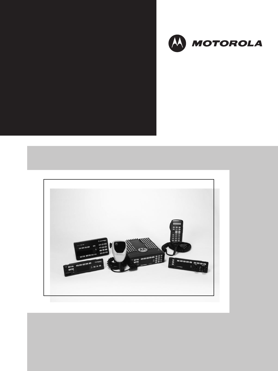
Detailed Service Manual
ASTRO® Digital XTLTM 5000
VHF
UHF Range 1 and 2
700–800 MHz
Mobile Radio

Title Page ASTRO® Digital XTL™5000
VHF/UHF Range 1/UHF Range 2/
700–800 MHz
Mobile Radio
Detailed Service Manual
Motorola, Inc.
8000 West Sunrise Boulevard
Fort Lauderdale, Florida 33322 6881096C74-B

Foreword
The information contained in this manual relates to all ASTRO® Digital XTL™ 5000 VHF/UHF Range 1/UHF Range 2/700–
800 MHz mobile radios equipped with W3, W4, W5, W7, or W9 control heads, unless otherwise specified. This manual
provides sufficient information to enable qualified service technicians to troubleshoot and repair XTL 5000 radios to the
component level.
For details on radio operation or basic troubleshooting, refer to the applicable manuals available separately. A list of related
publications is provided in the section, “Related Publications,” on page xxii.
Product Safety and RF Exposure Compliance
ATTENTION!
This radio is restricted to occupational use only to satisfy FCC RF energy exposure requirements.
Before using this product, read the RF energy awareness information and operating instructions in the
Product Safety and RF Exposure booklet enclosed with your radio (Motorola Publication part number
6881095C99) to ensure compliance with RF energy exposure limits.
For a list of Motorola-approved antennas, batteries, and other accessories, visit the following web site
which lists approved accessories: http://www.motorola.com/cgiss/index.shtml.
Manual Revisions
Changes which occur after this manual is printed are described in FMRs (Florida Manual Revisions). These FMRs provide
complete replacement pages for all added, changed, and deleted items, including pertinent parts list data, schematics, and
component layout diagrams. To obtain FMRs, contact the Radio Products and Services Division (refer to “Appendix B
Replacement Parts Ordering").
Computer Software Copyrights
The Motorola products described in this manual may include copyrighted Motorola computer programs stored in
semiconductor memories or other media. Laws in the United States and other countries preserve for Motorola certain
exclusive rights for copyrighted computer programs, including, but not limited to, the exclusive right to copy or reproduce in
any form the copyrighted computer program. Accordingly, any copyrighted Motorola computer programs contained in the
Motorola products described in this manual may not be copied, reproduced, modified, reverse-engineered, or distributed in
any manner without the express written permission of Motorola. Furthermore, the purchase of Motorola products shall not
be deemed to grant either directly or by implication, estoppel, or otherwise, any license under the copyrights, patents or
patent applications of Motorola, except for the normal non-exclusive license to use that arises by operation of law in the
sale of a product.
Document Copyrights
No duplication or distribution of this document or any portion thereof shall take place without the express written permission
of Motorola. No part of this manual may be reproduced, distributed, or transmitted in any form or by any means, electronic
or mechanical, for any purpose without the express written permission of Motorola.
Disclaimer
The information in this document is carefully examined, and is believed to be entirely reliable. However, no responsibility is
assumed for inaccuracies. Furthermore, Motorola reserves the right to make changes to any products herein to improve
readability, function, or design. Motorola does not assume any liability arising out of the applications or use of any product
or circuit described herein; nor does it cover any license under its patent rights nor the rights of others.
Trademarks
MOTOROLA, the Stylized M logo, and ASTRO are registered in the US Patent & Trademark Office. All other product or
service names are the property of their respective owners.
© Motorola, Inc. 2005.
Before using this product, read the operating instructions
for safe usage contained in the Product Safety and RF
Exposure booklet enclosed with your radio.
!
C a u t i o n

iii
Document History
The following major changes have been implemented in this manual since the previous edition:
Edition Description Date
6881096C74-B Added VHF High Power and UHF R1 High Power
models.
May, 2005

iv
This page is intentionally left blank

Table of Contents v
6881096C74-B May 25, 2005
Table of Contents
Foreword.........................................................................................................ii
Document History .........................................................................................iii
List of Figures ..............................................................................................xv
List of Tables...............................................................................................xxi
Related Publications..................................................................................xxii
Commercial Warranty...............................................................................xxiii
Limited Warranty .....................................................................................................................................xxiii
MOTOROLA COMMUNICATION PRODUCTS ............................................................................xxiii
I. What This Warranty Covers And For How Long..................................................................xxiii
II. General Provisions..............................................................................................................xxiii
III. State Law Rights................................................................................................................xxiv
IV. How To Get Warranty Service...........................................................................................xxiv
V. What This Warranty Does Not Cover .................................................................................xxiv
VI. Patent And Software Provisions ........................................................................................ xxv
VII. Governing Law ................................................................................................................. xxv
Model Numbering, Charts, and Specifications .....................................xxvii
Mobile Radio Model Numbering Scheme...............................................................................................xxvii
ASTRO XTL 5000 Motorcycle VHF 10-50 Watt Model Chart ............................................................... xxviii
ASTRO XTL 5000 VHF 10-50 Watt Model Chart....................................................................................xxix
ASTRO XTL 5000 VHF 10-50 Watt Model Chart (cont.)......................................................................... xxx
ASTRO XTL 5000 VHF 25-110 Watt Model Chart..................................................................................xxxi
ASTRO XTL 5000 VHF 25-110 Watt Model Chart (cont.)......................................................................xxxii
ASTRO XTL 5000 Motorcycle UHF Range 1 4-15 Watt Model Chart................................................... xxxiii
ASTRO XTL 5000 UHF Range 1 4-40 Watt Model Chart .....................................................................xxxiv
ASTRO XTL 5000 UHF Range 1 4-40 Watt Model Chart (cont.)...........................................................xxxv
ASTRO XTL 5000 UHF Range 1 25-110 Watt Model Chart .................................................................xxxvi
ASTRO XTL 5000 UHF Range 1 25-110 Watt Model Chart (cont.)..................................................... xxxvii
ASTRO XTL 5000 Motorcycle UHF Range 2 4-15 Watt Model Chart................................................. xxxviii
ASTRO XTL 5000 UHF Range 2 4-45 Watt Model Chart .....................................................................xxxix
ASTRO XTL 5000 UHF Range 2 4-45 Watt Model Chart (cont.)............................................................... xl
ASTRO XTL 5000 Motorcycle 700-800 MHz 3.5-15 Watt Model Chart .................................................... xli
ASTRO XTL 5000 700-800 MHz 3.5-35 Watt Model Chart ......................................................................xlii
ASTRO XTL 5000 700-800 MHz 3.5-35 Watt Model Chart (cont.) ..........................................................xliii
VHF Radio Specifications ........................................................................................................................xliv
UHF Range 1 Radio Specifications.......................................................................................................... xlv
UHF Range 2 Radio Specifications..........................................................................................................xlvi
700–800 MHz Radio Specifications (Mid Power Models Only)...............................................................xlvii

vi Table of Contents
May 25, 2005 6881096C74-B
Chapter 1 Introduction..........................................................................1-1
1.1 Notations Used in This Manual ......................................................................................................1-1
1.2 General...........................................................................................................................................1-1
Chapter 2 Product Overview ................................................................2-1
2.1 Introduction.....................................................................................................................................2-1
2.2 Functional Blocks ...........................................................................................................................2-1
2.3 Control-Head Assembly .................................................................................................................2-2
2.3.1 Display, Vacuum Fluorescent Display Driver, Vacuum Fluorescent Voltage Source,
Controls and Indicators, Status LEDs and Backlight LEDs ...............................................2-2
2.3.2 Vehicle Interface Ports ......................................................................................................2-2
2.3.2.1 Dash-Mount Control-Head Configuration (Mid Power Only) ....................................2-2
2.3.2.5 VIP Output Connections:..........................................................................................2-6
2.3.2.6 VIP Input Connections:.............................................................................................2-6
2.3.2.7 DEK Interface With Radio: Remote-Mount (W4, W5, W7, W9)................................2-7
2.3.3 Power Supplies .................................................................................................................2-7
2.3.4 Ignition Sense Circuits.......................................................................................................2-7
2.4 Receiver Section ............................................................................................................................2-8
2.4.1 VHF Band Radios..............................................................................................................2-8
2.4.1.1 Front-End Section ....................................................................................................2-8
2.4.1.2 Back-End Section.....................................................................................................2-8
2.4.2 UHF Range 1/UHF Range 2 Band Radios........................................................................2-8
2.4.2.1 Front-End Section ....................................................................................................2-8
2.4.2.2 Intermediate Frequency and Back-End....................................................................2-8
2.4.3 700–800 MHz Band Radios ..............................................................................................2-9
2.4.3.1 Front-End Section ....................................................................................................2-9
2.4.3.2 Back-End Section.....................................................................................................2-9
2.5 Transmitter Section ........................................................................................................................2-9
2.5.1 VHF Radios .......................................................................................................................2-9
2.5.2 UHF Range 1/UHF Range 2 Radios .................................................................................2-9
2.5.3 700–800 MHz Radios......................................................................................................2-10
2.5.3.1 RFPA......................................................................................................................2-10
2.5.3.2 Output Network ......................................................................................................2-10
2.5.3.3 Power Control.........................................................................................................2-10
2.5.3.4 Circuit Protection ....................................................................................................2-10
2.6 Frequency Generation Unit ..........................................................................................................2-10
2.6.1 VHF MHz Radios.............................................................................................................2-10
2.6.2 UHF Range 1/UHF Range 2 Radios ...............................................................................2-11
2.6.3 700–800 MHz Radios......................................................................................................2-11
2.7 Controller Section.........................................................................................................................2-12
2.7.1 Analog Mode of Operation ..............................................................................................2-12
2.7.2 Digital (ASTRO) Mode of Operation................................................................................2-13
2.7.3 Controller Section Circuitry..............................................................................................2-13
Chapter 3 Theory of Operation ............................................................3-1
3.1 Main Board .....................................................................................................................................3-1
3.2 Main Board Major Sections ............................................................................................................3-1
3.2.1 VHF (136–174 MHz) Band ................................................................................................3-1
3.2.2 UHF Range 1 (380-470 MHz) and UHF Range 2 (450-520 MHz) Band ...........................3-6

Table of Contents vii
6881096C74-B May 25, 2005
3.2.3 700–800 MHz Band.........................................................................................................3-10
3.3 Radio Power Distribution..............................................................................................................3-12
3.4 Receiver Front-End ......................................................................................................................3-13
3.4.1 VHF (136–174 MHz) Band ..............................................................................................3-13
3.4.1.1 15 dB Step Attenuator (U3250) ..............................................................................3-14
3.4.1.2 PIN Diode Switches................................................................................................3-14
3.4.1.3 Preselector Filters ..................................................................................................3-14
3.4.1.4 Low-Noise Amplifiers (Q3255, Q3252)...................................................................3-14
3.4.1.5 Mixer (D3258).........................................................................................................3-15
3.4.2 UHF Range 1 (380–470 MHz) Band ...............................................................................3-15
3.4.2.1 Highpass Filter and First Low-Noise Amplifier .......................................................3-16
3.4.2.2 Preselector Filter ....................................................................................................3-16
3.4.2.3 Switchable 15 dB Attenuator ..................................................................................3-16
3.4.2.4 Low-Noise Amplifier (LNA, U5302) ........................................................................3-16
3.4.2.5 Image Filter ............................................................................................................3-16
3.4.2.6 Mixer.......................................................................................................................3-16
3.4.3 UHF Range 2 (450–520 MHz) Band ...............................................................................3-17
3.4.3.1 Highpass Filter and First Low-Noise Amplifier .......................................................3-17
3.4.3.2 Preselector Filter ....................................................................................................3-18
3.4.3.3 Switchable 15 dB Attenuator ..................................................................................3-18
3.4.3.4 Low-Noise Amplifier (LNA, U5302) ........................................................................3-18
3.4.3.5 Image Filter ............................................................................................................3-18
3.4.3.6 Mixer.......................................................................................................................3-18
3.4.4 700–800 MHz Band.........................................................................................................3-19
3.4.4.1 Preselector Filters ..................................................................................................3-19
3.4.4.2 Low-Noise Amplifier (LNA, U6250) ........................................................................3-19
3.4.4.3 Mixer (U6251).........................................................................................................3-20
3.5 Receiver Back-End.......................................................................................................................3-20
3.5.1 VHF (136-174 MHz) Band...............................................................................................3-20
3.5.1.1 Intermediate Frequency (IF) Section......................................................................3-20
3.5.1.2 ABACUS III IC ........................................................................................................3-20
3.5.2 UHF Range 1 (380-470 MHz) Band ................................................................................3-21
3.5.2.1 Intermediate Frequency (IF) Filter..........................................................................3-22
3.5.2.2 ABACUS III IC (U5002) ..........................................................................................3-22
3.5.3 UHF Range 2 (450-520 MHz) Band ................................................................................3-23
3.5.3.1 Intermediate Frequency (IF) Filter..........................................................................3-23
3.5.3.2 ABACUS III IC (U5002) ..........................................................................................3-23
3.5.4 700–800 MHz Band.........................................................................................................3-24
3.5.4.1 Intermediate Frequency (IF) Filter..........................................................................3-25
3.5.4.2 ABACUS III IC (U6000) ..........................................................................................3-25
3.6 Transmitter ...................................................................................................................................3-26
3.6.1 VHF (136-174 MHz) Band...............................................................................................3-26
3.6.1.1 50-Watt Transmitter................................................................................................3-26
3.6.1.2 100-Watt Transmitter..............................................................................................3-28
3.6.1.3 Output Network (ON) - (for 50W and 100W Transmitter).......................................3-29
3.6.1.4 Power Control (for 50W and 100W Transmitter) ....................................................3-30
3.6.2 UHF Range 1 (380-470 MHz) Band ................................................................................3-31
3.6.2.1 40-Watt Transmitter................................................................................................3-31
3.6.2.2 100-Watt Transmitter..............................................................................................3-33
3.6.2.3 Output Network (ON) - (for 40W and 100W Transmitter).......................................3-34
3.6.2.4 Power Control (for 40W and 100W Transmitter) ....................................................3-35
3.6.3 UHF Range 2 (450-520 MHz) Band ................................................................................3-37
3.6.3.1 45-Watt Transmitter................................................................................................3-37
3.6.4 700–800 MHz Band.........................................................................................................3-41

viii Table of Contents
May 25, 2005 6881096C74-B
3.6.4.1 35-Watt Transmitter................................................................................................3-41
3.7 Frequency Generation Unit (FGU) ...............................................................................................3-45
3.7.1 VHF (136-174 MHz) Band...............................................................................................3-45
3.7.1.1 Reference Oscillator...............................................................................................3-46
3.7.1.2 LV Frac-N Synthesizer IC.......................................................................................3-46
3.7.1.3 Voltage Multiplier....................................................................................................3-47
3.7.1.4 Superfilter ...............................................................................................................3-47
3.7.1.5 Modulation..............................................................................................................3-47
3.7.1.6 Charge Pump Bias .................................................................................................3-48
3.7.1.7 Loop Filter ..............................................................................................................3-48
3.7.1.8 Lock Detect ............................................................................................................3-48
3.7.1.9 Transmitter Injection...............................................................................................3-48
3.7.1.10 Receiver Injection...................................................................................................3-49
3.7.1.11 Transmitter VCOs...................................................................................................3-49
3.7.1.12 Receiver VCOs.......................................................................................................3-49
3.7.1.13 Prescaler Feedback ...............................................................................................3-49
3.7.2 UHF Range 1 (380–470 MHz) Band ...............................................................................3-49
3.7.2.1 Reference Oscillator...............................................................................................3-50
3.7.2.2 LV Frac-N Synthesizer IC.......................................................................................3-50
3.7.2.3 Voltage Multiplier....................................................................................................3-51
3.7.2.4 Superfilter ...............................................................................................................3-51
3.7.2.5 Modulation..............................................................................................................3-51
3.7.2.6 Charge Pump Bias .................................................................................................3-52
3.7.2.7 Loop Filter ..............................................................................................................3-52
3.7.2.8 Lock Detect ............................................................................................................3-52
3.7.2.9 Transmitter Injection...............................................................................................3-52
3.7.2.10 Receiver Injection...................................................................................................3-52
3.7.2.11 Transmitter VCOs...................................................................................................3-53
3.7.2.12 Receiver VCOs.......................................................................................................3-53
3.7.2.13 Prescaler Feedback ...............................................................................................3-53
3.7.3 UHF Range 2 (450–520 MHz) Band ...............................................................................3-54
3.7.3.1 Reference Oscillator...............................................................................................3-55
3.7.3.2 LV Frac-N Synthesizer IC.......................................................................................3-55
3.7.3.3 Voltage Multiplier....................................................................................................3-55
3.7.3.4 Superfilter ...............................................................................................................3-56
3.7.3.5 Modulation..............................................................................................................3-56
3.7.3.6 Charge Pump Bias .................................................................................................3-56
3.7.3.7 Loop Filter ..............................................................................................................3-56
3.7.3.8 Lock Detect ............................................................................................................3-56
3.7.3.9 Transmitter Injection...............................................................................................3-57
3.7.3.10 Receiver Injection...................................................................................................3-57
3.7.3.11 Transmitter VCOs...................................................................................................3-57
3.7.3.12 Receiver VCOs.......................................................................................................3-57
3.7.3.13 Prescaler Feedback ...............................................................................................3-58
3.7.4 700–800 MHz Band.........................................................................................................3-58
3.7.4.1 Reference Oscillator...............................................................................................3-59
3.7.4.2 LV Frac-N Synthesizer IC.......................................................................................3-59
3.7.4.3 Voltage Multiplier....................................................................................................3-59
3.7.4.4 Superfilter ...............................................................................................................3-60
3.7.4.5 Modulation..............................................................................................................3-60
3.7.4.6 Charge Pump Bias .................................................................................................3-60
3.7.4.7 Loop Filter ..............................................................................................................3-60
3.7.4.8 Lock Detect ............................................................................................................3-60
3.7.4.9 Transmitter Injection...............................................................................................3-61

Table of Contents ix
6881096C74-B May 25, 2005
3.7.4.10 Receiver Injection...................................................................................................3-61
3.7.4.11 Transmitter VCOs...................................................................................................3-61
3.7.4.12 Receiver VCOs.......................................................................................................3-62
3.7.4.13 Prescaler Feedback ...............................................................................................3-62
3.8 Controller Section.........................................................................................................................3-62
3.8.1 Daughtercard Module......................................................................................................3-64
3.8.2 Controller DC Power Distribution ....................................................................................3-65
3.8.3 Encryption Voltages ........................................................................................................3-66
3.8.4 Reset Circuits ..................................................................................................................3-67
3.8.5 Power-Up/Power-Down Sequence..................................................................................3-68
3.8.5.1 Power Turn-On.......................................................................................................3-68
3.8.5.2 Power Turn-Off.......................................................................................................3-68
3.8.5.3 Emergency Power-Up/-Down Sequence................................................................3-68
3.8.6 MCU and DSP System Clocks ........................................................................................3-68
3.8.7 RS-232 USB Bus.............................................................................................................3-69
3.8.8 Serial Communications on the External Bus (SB9600)...................................................3-71
3.8.9 Serial Peripheral Interface (SPI) Bus ..............................................................................3-71
3.8.10 Receive Audio .................................................................................................................3-72
3.8.11 Transmit Audio ................................................................................................................3-74
3.8.12 Flash Programming .........................................................................................................3-75
3.8.13 Reflashing/Upgrading Firmware......................................................................................3-76
Chapter 4 Troubleshooting Procedures..............................................4-1
4.1 Introduction.....................................................................................................................................4-1
4.2 Handling Precautions .....................................................................................................................4-1
4.2.1 Parts Replacement and Substitution .................................................................................4-1
4.2.2 Rigid Circuit Boards...........................................................................................................4-2
4.2.3 Heat-Related Precautions .................................................................................................4-2
4.2.4 Daughtercard Module........................................................................................................4-2
4.2.4.1 SRAM .......................................................................................................................4-2
4.2.4.2 Testing......................................................................................................................4-2
4.3 Voltage Measurement and Signal Tracing .....................................................................................4-3
4.4 Power-Up Self-Check Errors ..........................................................................................................4-3
4.5 Operational Error Codes ................................................................................................................4-5
4.6 VHF (136–174 MHz) Band Main Board Troubleshooting...............................................................4-5
4.6.1 Display Flashes “FAIL 001” ...............................................................................................4-5
4.6.2 VCO Hybrid Assembly.......................................................................................................4-6
4.6.3 Out-of-Lock Condition .......................................................................................................4-7
4.6.4 FGU Troubleshooting Aids ................................................................................................4-7
4.6.5 No or Low Output Power (TX or RX Injection) ................................................................4-11
4.6.6 No or Low Modulation .....................................................................................................4-11
4.6.7 Troubleshooting the Back-End ........................................................................................4-11
4.7 UHF Range 1 (380–470 MHz) Band Main Board Troubleshooting ..............................................4-11
4.7.1 Display Flashes “FAIL 001” .............................................................................................4-11
4.7.2 FGU Troubleshooting Aids ..............................................................................................4-13
4.7.3 Out-of-Lock Condition .....................................................................................................4-16
4.7.4 No or Low Output Power (TX or RX Injection) ................................................................4-16
4.7.5 No or Low Modulation .....................................................................................................4-16
4.7.6 Troubleshooting the Back-End ........................................................................................4-16
4.8 UHF Range 2 (450–520 MHz) Band Main Board Troubleshooting ..............................................4-17
4.8.1 Display Flashes “FAIL 001” .............................................................................................4-17
4.8.2 FGU Troubleshooting Aids ..............................................................................................4-19

xTable of Contents
May 25, 2005 6881096C74-B
4.8.3 Out-of-Lock Condition .....................................................................................................4-22
4.8.4 No or Low Output Power (TX or RX Injection) ................................................................4-22
4.8.5 No or Low Modulation .....................................................................................................4-22
4.8.6 Troubleshooting the Back-End ........................................................................................4-22
4.9 700–800 MHz Main Board Troubleshooting.................................................................................4-22
4.9.1 Display Flashes “FAIL 001” .............................................................................................4-23
4.9.2 FGU Troubleshooting Aids ..............................................................................................4-24
4.9.3 No or Low Output Power (TX or RX Injection) ................................................................4-28
4.9.4 No or Low Modulation .....................................................................................................4-28
4.9.5 Troubleshooting the Back-End ........................................................................................4-28
4.10 Standard Bias Tables ...................................................................................................................4-28
4.11 Receiver Front-End (RXFE) .........................................................................................................4-33
4.11.1 VHF (136–174 MHz) Band ..............................................................................................4-33
4.11.2 UHF Range 1 (380–470 MHz) Band ...............................................................................4-33
4.11.3 UHF Range 2 (450–520 MHz) Band ...............................................................................4-34
4.11.4 700–800 MHz Band.........................................................................................................4-34
4.12 Power Amplifier Procedures.........................................................................................................4-34
4.12.1 VHF (136–174 MHz) Band ..............................................................................................4-34
4.12.1.1 50-Watt Power Amplifiers.......................................................................................4-34
4.12.1.2 General Troubleshooting and Repair Notes...........................................................4-34
4.12.2 UHF Range 1 (380–470 MHz) Band ...............................................................................4-35
4.12.3 UHF Range 2 (450–520 MHz) Band ...............................................................................4-35
4.12.4 700–800 MHz Band.........................................................................................................4-35
Chapter 5 Troubleshooting Charts......................................................5-1
5.1 Introduction.....................................................................................................................................5-1
5.2 List of Troubleshooting Charts .......................................................................................................5-1
5.3 Troubleshooting Tables..................................................................................................................5-3
5.3.1 For Mid Power models ......................................................................................................5-3
5.3.2 For High Power models and UHF R2 Mid Power..............................................................5-7
5.4 Troubleshooting Test Points.........................................................................................................5-12
5.5 Board ID Jumper Configuration....................................................................................................5-13
5.6 Flowcharts ....................................................................................................................................5-14
5.6.1 Poor RX Sensitivity or No RX Audio (136–174 MHz)—Part 1 of 2..................................5-15
5.6.2 Poor RX Sensitivity or No RX Audio (136–174 MHz)—Part 2 of 2..................................5-16
5.6.3 RX IF—Poor SINAD or No Audio (136–174 MHz) ..........................................................5-17
5.6.4 RX Back-End—Poor SINAD or No Audio (136–174 MHz)—Part 1 of 3..........................5-18
5.6.5 RX Back-End—Poor SINAD or No Audio (136–174 MHz)—Part 2 of 3..........................5-19
5.6.6 RX Back-End—Poor SINAD or No Audio (136–174 MHz)—Part 3 of 3..........................5-20
5.6.7 Low or No RX Injection Signal (136–174 MHz)...............................................................5-21
5.6.8 Low or No TX Injection Signal (136–174 MHz) ...............................................................5-22
5.6.9 TX or RX VCO Unlock (Fail 001) (136–174 MHz)—Part 1 of 2.......................................5-23
5.6.10 TX or RX VCO Unlock (Fail 001) (136–174 MHz)—Part 2 of 2.......................................5-24
5.6.11 No Output Power at TX Mode (136–174 MHz) ...............................................................5-25
5.6.12 No Output Power and IDC < 2A at TX Mode (136–174 MHz).........................................5-26
5.6.13 No 16.8 MHz Reference Oscillator Frequency (380–470 MHz and 450–520 MHz)........5-27
5.6.14 Poor RX Sensitivity or No RX Audio (380–470 MHz and 450–520 MHz)—Part 1 of 2 ...5-28
5.6.15 Poor RX Sensitivity or No RX Audio (380–470 MHz and 450–520 MHz)—Part 2 of 2 ...5-29
5.6.16 RX IF—Poor SINAD or No Audio (380–470 MHz and 450–520 MHz)—Part 1 of 2........5-30
5.6.17 RX IF—Poor SINAD or No Audio (380–470 MHz and 450–520 MHz)—Part 2 of 2........5-31
5.6.18 RX Back-End—Poor SINAD or No Audio (380–470 MHz and 450–520 MHz)—
Part 1 of 3........................................................................................................................5-32

Table of Contents xi
6881096C74-B May 25, 2005
5.6.19 RX Back-End—Poor SINAD or No Audio (380–470 MHz and 450–520 MHz)—
Part 2 of 3........................................................................................................................5-33
5.6.20 RX Back-End — Poor SINAD or No Audio (380–470 MHz and 450–520 MHz)—
Part 3 of 3........................................................................................................................5-34
5.6.21 Low or No RX Injection Signal (380–470 MHz and 450–520 MHz) ................................5-35
5.6.22 Low or No TX Injection Signal (380–470 MHz and 450–520 MHz).................................5-36
5.6.23 No TX Audio (380–470 MHz and 450–520 MHz)............................................................5-37
5.6.24 TX or RX VCO Unlock (Fail 001) (380–470 MHz and 450–520 MHz)—Part 1 of 2 ........5-38
5.6.25 TX or RX VCO Unlock (Fail 001) (380–470 MHz and 450–520 MHz)—Part 2 of 2 ........5-39
5.6.26 RF Power Amplifier (RFPA)—No or Low TX Power Output (380–470 MHz and 450–
520 MHz)—Part 1 of 5.....................................................................................................5-40
5.6.27 RF Power Amplifier (RFPA)—No or Low TX Power Output (380–470 MHz and 450–
520 MHz)—Part 2 of 5.....................................................................................................5-41
5.6.28 RF Power Amplifier (RFPA)—No or Low TX Power Output (380–470 MHz and 450–
520 MHz)—Part 3 of 5.....................................................................................................5-42
5.6.29 RF Power Amplifier (RFPA)—No or Low TX Power Output (380–470 MHz and 450–520
MHz)—Part 4 of 5............................................................................................................5-43
5.6.30 RF Power Amplifier (RFPA)—No or Low TX Power Output (380–470 MHz and 450–520
MHz)—Part 5 of 5............................................................................................................5-44
5.6.31 RFPA Power Control—No VGBIAS (380–470 MHz and 450–520 MHz) ........................5-45
5.6.32 No 16.8 MHz Reference Oscillator Frequency (700–800 MHz) ......................................5-46
5.6.33 Poor RX Sensitivity or No RX Audio (700–800 MHz)—Part 1 of 2..................................5-47
5.6.34 Poor RX Sensitivity or No RX Audio (700–800 MHz)—Part 2 of 2..................................5-48
5.6.35 RX IF—Poor SINAD or No Audio (700–800 MHz) ..........................................................5-49
5.6.36 RX Back-End—Poor SINAD or No Audio (700–800 MHz)—Part 1 of 3..........................5-50
5.6.37 RX Back-End—Poor SINAD or No Audio (700–800 MHz)—Part 2 of 3..........................5-51
5.6.38 RX Back-End—Poor SINAD or No Audio (700–800 MHz)—Part 3 of 3..........................5-52
5.6.39 Low or No RX Injection Signal (700–800 MHz)...............................................................5-53
5.6.40 Low or No TX Injection Signal (700–800 MHz) ...............................................................5-54
5.6.41 No TX Audio (700–800 MHz) ..........................................................................................5-55
5.6.42 TX or RX VCO Unlock (Fail 001) (700–800 MHz)—Part 1 of 2.......................................5-56
5.6.43 TX or RX VCO Unlock (Fail 001) (700–800 MHz)—Part 2 of 2.......................................5-57
5.6.44 RF Power Amplifier (RFPA)—No or Low TX Power Output (700–800 MHz)—
Part 1 of 5........................................................................................................................5-58
5.6.45 RF Power Amplifier (RFPA)—No or Low TX Power Output (700–800 MHz)—
Part 2 of 5........................................................................................................................5-59
5.6.46 RF Power Amplifier (RFPA)—No or Low TX Power Output (700–800 MHz)—
Part 3 of 5........................................................................................................................5-60
5.6.47 RF Power Amplifier (RFPA)—No or Low TX Power Output (700–800 MHz)—
Part 4 of 5........................................................................................................................5-61
5.6.48 RF Power Amplifier (RFPA)—No or Low TX Power Output (700–800 MHz)—
Part 5 of 5........................................................................................................................5-62
5.6.49 RFPA Power Control—No K9.1V (700–800 MHz) ..........................................................5-63
5.6.50 RFPA Power Control—No VGBIAS (700–800 MHz).......................................................5-64
5.6.51 RFPA Power Control—No or Low TX RFPA_CNTRL (700–800 MHz)—Part 1 of 2.......5-65
5.6.52 RFPA Power Control—No or Low TX RFPA_CNTRL (700–800 MHz)—Part 2 of 2.......5-66

xii Table of Contents
May 25, 2005 6881096C74-B
Chapter 6 Troubleshooting Waveforms ..............................................6-1
6.1 Introduction.....................................................................................................................................6-1
6.2 XTL 5000 Waveforms.....................................................................................................................6-2
6.2.1 Power-On Reset Timing ....................................................................................................6-2
6.2.2 Power-On to Soft Turn-On Timing.....................................................................................6-2
6.2.3 Power-Down Reset ...........................................................................................................6-3
6.2.4 16.8 MHz Clock Waveform................................................................................................6-3
6.2.5 32 kHz Clock Waveform ....................................................................................................6-4
6.2.6 DSP SSI Port RX Mode.....................................................................................................6-4
6.2.7 DSP SSI Port TX Mode CSQ ............................................................................................6-5
6.2.8 SPI Bus Waveform ............................................................................................................6-5
6.2.9 SB9600 Waveforms ..........................................................................................................6-6
6.2.10 SB9600 BUS+ and BUS- Waveforms ...............................................................................6-6
6.2.11 SB9600 BUS+ and RESET Waveforms ............................................................................6-7
6.2.12 SB9600 BUSY and BUS- Waveforms ...............................................................................6-7
6.2.13 RS-232 RX Waveforms .....................................................................................................6-8
6.2.14 RS-232 TX Waveforms .....................................................................................................6-8
6.2.15 RS-232 RX/TX Waveforms ...............................................................................................6-9
6.2.16 USB Waveforms................................................................................................................6-9
6.2.17 Serial Audio Port Waveforms ..........................................................................................6-10
6.2.18 Secure Interface Waveforms...........................................................................................6-10
6.2.19 8 kHz Frame Sync Waveform .........................................................................................6-11
6.2.20 RX Audio Waveforms ......................................................................................................6-11
6.2.21 TX Audio Waveforms ......................................................................................................6-12
6.2.22 TX and RX 1 kHz Audio Path Sinewave and Chart.........................................................6-12
Chapter 7 Schematics, Component Location Diagrams, and
Parts Lists ............................................................................7-1
7.1 List of Schematics, Component Location Diagrams, and Parts Lists.............................................7-1
7.2 HUD4022A/HUD4025B (VHF) Main Board ....................................................................................7-3
7.3 HUE4039A/HUE4043A (UHF Range 1) Main Board....................................................................7-72
7.4 HUE4040A (UHF Range 2) Main Board.....................................................................................7-132
7.5 HUF4017A (700-800 MHz) Main Board .....................................................................................7-174
Chapter 8 Interconnect Boards Schematics, Component Location
Diagrams, and Parts Lists...................................................8-1
8.1 List of Interconnect Board Schematics and Component Location Diagrams .................................8-1
8.2 W3 Hand-Held Control Head (HHCH) Interconnect Board ............................................................8-1
8.3 Remote Interconnect Boards (Mid Power Only).............................................................................8-2
8.4 Remote Interconnect Board (High Power Only) ...........................................................................8-13
8.5 Secure Interface Board ................................................................................................................8-20
8.6 Motorcycle Signal Routing............................................................................................................8-21

Table of Contents xiii
6881096C74-B May 25, 2005
Chapter 9 Flex Cable Pin-Out Lists .....................................................9-1
9.1 List of Flex Cables..........................................................................................................................9-1
9.2 Flex Cables ....................................................................................................................................9-1
Appendix A Secure Modules .................................................................. A-1
A.1 Universal Crypto Module Kits ........................................................................................................ A-1
A.1.1 Secure Interface Boards................................................................................................... A-1
A.2 Circuit Description ......................................................................................................................... A-2
A.3 Troubleshooting Secure Operations.............................................................................................. A-2
A.3.1 Error 09/10, Error 09/90 ...................................................................................................A-2
A.3.2 Error S03 .......................................................................................................................... A-2
A.3.3 Keyload ............................................................................................................................ A-2
Appendix B Replacement Parts Ordering ............................................. B-1
B.1 Basic Ordering Information............................................................................................................ B-1
B.2 Motorola Online ............................................................................................................................. B-1
B.3 Mail Orders.................................................................................................................................... B-1
B.4 Telephone Orders ......................................................................................................................... B-1
B.5 Fax Orders .................................................................................................................................... B-2
B.6 Parts Identification......................................................................................................................... B-2
B.7 Product Customer Service ............................................................................................................ B-2
Glossary......................................................................................... Glossary-1
Index...................................................................................................... Index-i

xiv Table of Contents
May 25, 2005 6881096C74-B
This page is intentionally left blank

List of Figures xv
6881096C74-B May 25, 2005
List of Figures
Figure 2-1. VIP Dash-Mount Configuration..............................................................................................2-2
Figure 2-2. VIP Remote-Mount Configuration..........................................................................................2-3
Figure 2-3. VIP Remote-Mount Pin-Outs (Male)......................................................................................2-3
Figure 2-4. VIP Remote-Mount W3 Control-Head Configuration.............................................................2-4
Figure 2-5. VIP Remote-Mount Plus DEK Configuration .........................................................................2-5
Figure 2-6. VIP Remote-Mount Plus DEK Pin-Outs (Male) .....................................................................2-5
Figure 3-1. XTL 5000 Main Board Sections (VHF Mid Power)—Side 1 ..................................................3-2
Figure 3-2. XTL 5000 Main Board Sections (VHF Mid Power)—Side 2 ..................................................3-3
Figure 3-3. XTL 5000 Main Board Sections (VHF High Power)—Side 1.................................................3-4
Figure 3-4. XTL 5000 Main Board Sections (VHF High Power)—Side 2.................................................3-5
Figure 3-5. XTL 5000 Main Board Sections (UHF Range 1 Mid Power and UHF Range 2)—Side 1......3-6
Figure 3-6. XTL 5000 Main Board Sections (UHF Range 1 Mid Power and UHF Range 2)—Side 2......3-7
Figure 3-7. XTL 5000 Main Board Sections (UHF Range 1 High Power)—Side 1 ..................................3-8
Figure 3-8. XTL 5000 Main Board Sections (UHF Range 1 High Power)—Side 2 ..................................3-9
Figure 3-9. XTL 5000 Main Board Sections (700–800 MHz)—Side 1 ...................................................3-10
Figure 3-10. XTL 5000 Main Board Sections (700–800 MHz)—Side 2 ...................................................3-11
Figure 3-11. DC Voltage Routing Block Diagram (UHF Range 1 and UHF Range 2) .............................3-12
Figure 3-12. DC Voltage Routing Block Diagram (VHF and 700–800 MHz)............................................3-13
Figure 3-13. Receiver Block Diagram (VHF) ...........................................................................................3-14
Figure 3-14. Receiver Front-End and Back-End (UHF Range 1) ............................................................3-15
Figure 3-15. Receiver Front-End and Back-End (UHF Range 2) ............................................................3-17
Figure 3-16. Receiver Front-End and Back-End (700–800 MHz) ............................................................3-19
Figure 3-17. ABACUS III (AD9874) IC Functional Block Diagram from Data Sheet (VHF) .....................3-21
Figure 3-18. ABACUS III (AD9874) IC Functional Block Diagram from Data Sheet (UHF Range 1) ......3-22
Figure 3-19. ABACUS III (AD9874) IC Functional Block Diagram from Data Sheet (UHF Range 2) ......3-24
Figure 3-20. ABACUS III (AD9874) IC Functional Block Diagram from Data Sheet (700–800 MHz)......3-25
Figure 3-21. 50-Watt RF Power Amplifier (RFPA) Gain Stages (VHF) ....................................................3-26
Figure 3-22. 100-Watt RF Power Amplifier (RFPA) Gain Stages (VHF) ..................................................3-28
Figure 3-23. Output Network Components (VHF)....................................................................................3-29
Figure 3-24. Power Control Components (VHF)......................................................................................3-30
Figure 3-25. 40-Watt RF Power Amplifier (RFPA) Gain Stages (UHF Range 1) .....................................3-31
Figure 3-26. 100-Watt RF Power Amplifier (RFPA) Gain Stages (UHF Range 1) ...................................3-33
Figure 3-27. Output Network Components (UHF Range 1).....................................................................3-34
Figure 3-28. Power Control Components (UHF Range 1) .......................................................................3-36
Figure 3-29. 45-Watt RF Power Amplifier (RFPA) Gain Stages (UHF Range 2) .....................................3-37
Figure 3-30. Output Network Components (UHF Range 2).....................................................................3-38
Figure 3-31. Power Control Components (UHF Range 2) .......................................................................3-40
Figure 3-32. 35-Watt RF Power Amplifier (RFPA) Gain Stages (700–800 MHz) .....................................3-41
Figure 3-33. Output Network Components (700–800 MHz) ....................................................................3-42
Figure 3-34. Power Control Components (700–800 MHz).......................................................................3-44
Figure 3-35. Frequency Generation Unit Block Diagram (VHF) ..............................................................3-46
Figure 3-36. Waveform Representation During Programming of the LV Frac-N IC (VHF) ......................3-47
Figure 3-37. Frequency Generation Unit Block Diagram (UHF Range 1)................................................3-50
Figure 3-38. Waveform Representation During Programming of the LV Frac-N IC (UHF Range 1)........3-51
Figure 3-39. Frequency Generation Unit Block Diagram (UHF Range 2)................................................3-54
Figure 3-40. Waveform Representation During Programming of the LV Frac-N IC (UHF Range 2)........3-55
Figure 3-41. Frequency Generation Unit Block Diagram (700–800 MHz) ...............................................3-58
Figure 3-42. Waveform Representation During Programming of the LV Frac-N IC .................................3-59
Figure 3-43. XTL 5000 Controller Section ...............................................................................................3-63
Figure 3-44. XTL 5000 Daughtercard Module .........................................................................................3-64

xvi List of Figures
May 25, 2005 6881096C74-B
Figure 3-45. B+ Routing for Controller Section........................................................................................3-65
Figure 3-46. Power-On Reset Circuit.......................................................................................................3-67
Figure 3-47. Patriot IC (U100) UART Configuration ................................................................................3-69
Figure 3-48. Serial Peripheral Interface (SPI) Block Diagram .................................................................3-72
Figure 3-49. XTL 5000 RX Signal Path ...................................................................................................3-73
Figure 3-50. XTL 5000 TX Signal Path....................................................................................................3-75
Figure 3-51. Boot RX and Boot TX Data Lines........................................................................................3-75
Figure 4-1. Frequency Generator Unit DC Power Supply Distribution (VHF)..........................................4-8
Figure 4-2. Frequency Generation Unit Block Diagram (VHF) ................................................................4-9
Figure 4-3. Waveform Representation During Programming of the LV Frac-N IC (U3751) ...................4-11
Figure 4-4. Frequency Generation Unit DC Power Supply Distribution (UHF Range 1)........................4-13
Figure 4-5. Frequency Generation Unit Block Diagram (UHF Range 1)................................................4-14
Figure 4-6. Waveform Representation During Programming of the LV Frac-N IC (U5752) ...................4-16
Figure 4-7. Frequency Generation Unit DC Power Supply Distribution (UHF Range 2)........................4-19
Figure 4-8. Frequency Generation Unit Block Diagram (UHF Range 2)................................................4-20
Figure 4-9. Waveform Representation During Programming of the LV Frac-N IC (U5752) ...................4-22
Figure 4-10. Frequency Generation Unit DC Power Supply Distribution (700–800 MHz) .......................4-25
Figure 4-11. Frequency Generation Unit Block Diagram (700–800 MHz) ...............................................4-26
Figure 4-12. Waveform Representation During Programming of the LV Frac-N IC (U6751) ...................4-28
Figure 5-1. Main Board Test Points—Top Side (for Mid Power) ............................................................5-12
Figure 5-2. Main Board Test Points—Bottom Side (for Mid Power).......................................................5-12
Figure 5-3. Main Board Test Points—Top Side (for High Power)...........................................................5-13
Figure 5-4. Main Board Test Points—Bottom Side (for High Power) .....................................................5-13
Figure 5-5. Poor RX Sensitivity or No RX Audio (136–174 MHz)—Part 1 of 2......................................5-15
Figure 5-6. Poor RX Sensitivity or No RX Audio (136–174 MHz)—Part 2 of 2......................................5-16
Figure 5-7. RX IF—Poor SINAD or No Audio (136–174 MHz) ..............................................................5-17
Figure 5-8. RX Back-End—Poor SINAD or No Audio (136–174 MHz)—Part 1 of 3..............................5-18
Figure 5-9. RX Back-End—Poor SINAD or No Audio (136–174 MHz)—Part 2 of 3..............................5-19
Figure 5-10. RX Back-End—Poor SINAD or No Audio (136–174 MHz)—Part 3 of 3..............................5-20
Figure 5-11. Low or No RX Injection Signal (136–174 MHz) ...................................................................5-21
Figure 5-12. Low or No TX Injection Signal (136–174 MHz) ...................................................................5-22
Figure 5-13. TX or RX VCO Unlock (Fail 001) (136–174 MHz)—Part 1 of 2...........................................5-23
Figure 5-14. TX or RX VCO Unlock (Fail 001) (136–174 MHz)—Part 2 of 2...........................................5-24
Figure 5-15. No Output Power at TX Mode (136–174 MHz) ...................................................................5-25
Figure 5-16. No Output Power and IDC < 2A at TX Mode (136–174 MHz).............................................5-26
Figure 5-17. No 16.8 MHz Reference Oscillator Frequency (380–470 MHz and 450–520 MHz)............5-27
Figure 5-18. Poor RX Sensitivity or No RX Audio (380–470 MHz and 450–520 MHz)—Part 1 of 2 .......5-28
Figure 5-19. Poor RX Sensitivity or No RX Audio (380–470 MHz and 450–520 MHz)—Part 2 of 2 .......5-29
Figure 5-20. RX IF—Poor SINAD or No Audio (380–470 MHz and 450–520 MHz)—Part 1 of 2............5-30
Figure 5-21. RX IF—Poor SINAD or No Audio (380–470 MHz and 450–520 MHz)—Part 2 of 2............5-31
Figure 5-22. RX Back-End—Poor SINAD or No Audio (380–470 MHz and 450–520 MHz)—
Part 1 of 3............................................................................................................................5-32
Figure 5-23. RX Back-End—Poor SINAD or No Audio (380–470 MHz and 450–520 MHz)—
Part 2 of 3............................................................................................................................5-33
Figure 5-24. RX Back-End—Poor SINAD or No Audio (380–470 MHz and 450–520 MHz)—
Part 3 of 3............................................................................................................................5-34
Figure 5-25. Low or No RX Injection Signal (380–470 MHz and 450–520 MHz) ....................................5-35
Figure 5-26. Low or No TX Injection Signal (380–470 MHz and 450–520 MHz).....................................5-36
Figure 5-27. No TX Audio (380–470 MHz and 450–520 MHz) ................................................................5-37
Figure 5-28. TX or RX VCO Unlock (Fail 001) (380–470 MHz and 450–520 MHz)—Part 1 of 2 ............5-38
Figure 5-29. TX or RX VCO Unlock (Fail 001) (380–470 MHz and 450–520 MHz)—Part 2 of 2 ............5-39
Figure 5-30. RF Power Amplifier (RFPA)—No or Low TX Power Output
(380–470 MHz and 450–520 MHz)—Part 1 of 5 .................................................................5-40

List of Figures xvii
6881096C74-B May 25, 2005
Figure 5-31. RF Power Amplifier (RFPA)—No or Low TX Power Output
(380–470 MHz and 450–520 MHz)—Part 2 of 5 .................................................................5-41
Figure 5-32. RF Power Amplifier (RFPA)—No or Low TX Power Output
(380–470 MHz and 450–520 MHz)—Part 3 of 5 .................................................................5-42
Figure 5-33. RFPA Power Control—No VGBIAS (380–470 MHz and 450–520 MHz).............................5-45
Figure 5-34. No 16.8 MHz Reference Oscillator Frequency (700–800 MHz) ..........................................5-46
Figure 5-35. Poor RX Sensitivity or No RX Audio (700–800 MHz)—Part 1 of 2......................................5-47
Figure 5-36. Poor RX Sensitivity or No RX Audio (700–800 MHz)—Part 2 of 2......................................5-48
Figure 5-37. RX IF—Poor SINAD or No Audio (700–800 MHz) ..............................................................5-49
Figure 5-38. RX Back-End—Poor SINAD or No Audio (700–800 MHz)—Part 1 of 3..............................5-50
Figure 5-39. RX Back-End—Poor SINAD or No Audio (700–800 MHz)—Part 2 of 3..............................5-51
Figure 5-40. RX Back-End—Poor SINAD or No Audio (700–800 MHz)—Part 3 of 3..............................5-52
Figure 5-41. Low or No RX Injection Signal (700–800 MHz) ...................................................................5-53
Figure 5-42. Low or No TX Injection Signal (700–800 MHz) ...................................................................5-54
Figure 5-43. No TX Audio (700–800 MHz) ..............................................................................................5-55
Figure 5-44. TX or RX VCO Unlock (Fail 001) (700–800 MHz)—Part 1 of 2...........................................5-56
Figure 5-45. TX or RX VCO Unlock (Fail 001) (700–800 MHz)—Part 2 of 2...........................................5-57
Figure 5-46. RF Power Amplifier (RFPA)—No or Low TX Power Output (700–800 MHz)—Part 1 of 5 ..5-58
Figure 5-47. RF Power Amplifier (RFPA)—No or Low TX Power Output (700–800 MHz)—Part 2 of 5 ..5-59
Figure 5-48. RF Power Amplifier (RFPA)—No or Low TX Power Output (700–800 MHz)—Part 3 of 5 ..5-60
Figure 5-49. RFPA Power Control—No K9.1V (700–800 MHz)...............................................................5-63
Figure 5-50. RFPA Power Control—No VGBIAS (700–800 MHz) ...........................................................5-64
Figure 5-51. RFPA Power Control—No or Low TX RFPA_CNTRL (700–800 MHz)—Part 1 of 2 ...........5-65
Figure 7-1. HUD4022A/HUD4025 Main Board Overall Block Diagram and Interconnections .................7-3
Figure 7-2. HUD4022A Controller Block Diagram and Interconnections (Sheet 1 of 2) ..........................7-4
Figure 7-3. HUD4022A Controller Block Diagram and Interconnections (Sheet 2 of 2) ..........................7-5
Figure 7-4. HUD4022A Controller Urchin IC, MUX, and AD5320 DAC Schematic .................................7-6
Figure 7-5. HUD4022A Controller Audio Schematic................................................................................7-7
Figure 7-6. HUD4022A/HUD4025B Controller Power Control (Sheet 1 of 2) ..........................................7-8
Figure 7-7. HUD4022A/HUD4025B Controller Power Control (Sheet 2 of 2) ..........................................7-9
Figure 7-8. HUD4025B/HUE4043A Controller Block Diagram ..............................................................7-10
Figure 7-9. HUD4025B/HUE4043A Controller Daughter Board Interface .............................................7-11
Figure 7-10. HUD4025B/HUE4043A Controller Urchin IC, MUX and AD5320 DAC ...............................7-12
Figure 7-11. HUD4025B/HUE4043A Controller Audio.............................................................................7-13
Figure 7-12. HUD4025B/HUE4043A Controller Interface, Secure and Power Block Diagram................7-14
Figure 7-13. HUD4025B/HUE4043A Controller Power Supply................................................................7-15
Figure 7-14. HUD4025B/HUE4043A USB/RS232 Interface ....................................................................7-16
Figure 7-15. HUD4025B/HUE4043A SB9600 .........................................................................................7-17
Figure 7-16. HUD4025B/HUE4043A Control Head Connector 1 of 2......................................................7-18
Figure 7-17. HUD4025B/HUE4043A Control Head Connector 2 of 2.....................................................7-19
Figure 7-18. HUD4025B/HUE4043A Secure Interface Connector Schematic........................................7-20
Figure 7-19. HUD4022A/HUD4025B Frequency Generation Unit Overall Schematic (Sheet 1 of 2)......7-21
Figure 7-20. HUD4022A/HUD4025B Frequency Generation Unit Overall Schematic (Sheet 2 of 2)......7-22
Figure 7-21. HUD4022A/HUD4025B VHF Transmitter VCO Schematic .................................................7-23
Figure 7-22. HUD4022A/HUD4025B Frequency Generation Unit VHF Receive Injection Schematic.....7-24
Figure 7-23. HUD4022A/HUD4025B Frequency Generation Unit VHF Transmit Injection Schematic....7-25
Figure 7-24. HUD4022A/HUD4025B Receiver Back-End Schematic......................................................7-26
Figure 7-25. HUD4022A/HUD4025B Receiver Front-End Schematic (Sheet 1 of 2) ..............................7-27
Figure 7-26. HUD4022A/HUD4025B Receiver Front-End Schematic (Sheet 2 of 2) ..............................7-28
Figure 7-27. HUD4022A/HUD4025B Receiver IF Schematic ..................................................................7-29
Figure 7-28. HUD4022A RF Power Amplifier (RF PA) Schematic (Sheet 1 of 2)....................................7-30
Figure 7-29. HUD4022A RF Power Amplifier (RF PA) Schematic (Sheet 2 of 2)....................................7-31
Figure 7-30. HUD4025B RF 100W Power Amplifier (RF PA) Schematic (Sheet 1 of 2) .........................7-32
Figure 7-31. HUD4025B RF 100W Power Amplifier (RF PA) Schematic (Sheet 2 of 2) .........................7-33

xviii List of Figures
May 25, 2005 6881096C74-B
Figure 7-32. HUD4022A Secure Block Diagram and Interconnections ..................................................7-34
Figure 7-33. HUD4022A Accessory Connector Schematic .....................................................................7-35
Figure 7-34. HUD4022A Power Supply Schematic .................................................................................7-36
Figure 7-35. HUD4022A USB/RS232/SB9600 Schematic ......................................................................7-37
Figure 7-36. HUD4022A SB9600 Schematic...........................................................................................7-38
Figure 7-37. HUD4022A USB/RS232/SB9600 VIP Input/Output Schematic...........................................7-39
Figure 7-38. HUD4022A Control-Head Connector Schematic ................................................................7-40
Figure 7-39. HUD4022A Interface Connector Schematic........................................................................7-41
Figure 7-40. HUD4022A/HUD4025B Secure Interface Board Schematic ...............................................7-42
Figure 7-41. HUD4022A Main Board Layout—Side 1 Top ......................................................................7-43
Figure 7-42. HUD4022A Main Board Layout—Side 1 Bottom .................................................................7-44
Figure 7-43. HUD4022A Main Board Layout—Side 2 Top ......................................................................7-45
Figure 7-44. HUD4022A Main Board Layout—Side 2 Bottom .................................................................7-46
Figure 7-45. HUD4025B Main Board Layout—Side 1 Top ......................................................................7-56
Figure 7-46. HUD4025B Main Board Layout—Side 1 Bottom .................................................................7-57
Figure 7-47. HUD4025B Main Board Layout—Side 2 Top ......................................................................7-58
Figure 7-48. HUD4025B Main Board Layout—Side 2 Bottom .................................................................7-59
Figure 7-49. HUE4039A/HUE4043A Main Board Overall Block Diagram and Interconnections.............7-72
Figure 7-50. HUE4039A Controller Block Diagram and Interconnections (Sheet 1 of 2) ........................7-73
Figure 7-51. HUE4039A Controller Block Diagram and Interconnections (Sheet 2 of 2) ........................7-74
Figure 7-52. HUE4039A Controller Urchin IC, MUX, and AD5320 DAC Schematic ...............................7-75
Figure 7-53. HUE4039A Controller Audio Schematic ..............................................................................7-76
Figure 7-54. HUE4039A Controller Power Control Schematic ................................................................7-77
Figure 7-55. HUE4039A/HUE4043A Frequency Generation Unit ...........................................................7-78
Figure 7-56. HUE4039A/HUE4043A Receive VCO Schematic...............................................................7-79
Figure 7-57. HUE4039A/HUE4043A Transmit VCO Schematic..............................................................7-80
Figure 7-58. HUE4039A/HUE4043A Receiver Back-End Schematic......................................................7-81
Figure 7-59. HUE4039A/HUE4043A Receiver Front-End Schematic .....................................................7-82
Figure 7-60. HUE4039A/HUE4043A Receiver Mixer Schematic.............................................................7-83
Figure 7-61. HUE4039A/HUE4043A Receiver Preselector Schematic ...................................................7-84
Figure 7-62. HUE4039A/HUE4043A Receiver IF Schematic ..................................................................7-85
Figure 7-63. HUE4039A RF Power Amplifier (RF PA) Schematic...........................................................7-86
Figure 7-64. HUE4039A/HUE4043A Output Network (ON) Schematic...................................................7-87
Figure 7-65. HUE4043A RF 100W Power Amplifier (RF PA) Schematic (Sheet 1 of 2) .........................7-88
Figure 7-66. HUE4043A RF 100W Power Amplifier (RF PA) Schematic (Sheet 2 of 2) ........................7-89
Figure 7-67. HUE4039A Secure Block Diagram and Interconnections ...................................................7-90
Figure 7-68. HUE4039A Rear Accessory Connector Schematic.............................................................7-91
Figure 7-69. HUE4039A Power Supply Schematic .................................................................................7-92
Figure 7-70. HUE4039A USB/RS232/SB9600 Schematic ......................................................................7-93
Figure 7-71. HUE4039A SB9600 Schematic ...........................................................................................7-94
Figure 7-72. HUE4039A USB/RS232/SB9600 VIP Input/Output Schematic...........................................7-95
Figure 7-73. HUE4039A Control-Head Connector Schematic.................................................................7-96
Figure 7-74. HUE4039A Secure Interface Connector Schematic............................................................7-97
Figure 7-75. HUE4039A/HUE4043A Secure Interface Board Schematic...............................................7-98
Figure 7-76. HUE4039A Main Board Layout—Side 1 Top ......................................................................7-99
Figure 7-77. HUE4039A Main Board Layout—Side 1 Middle................................................................7-100
Figure 7-78. HUE4039A Main Board Layout—Side 1 Bottom ...............................................................7-101
Figure 7-79. HUE4039A Main Board Layout—Side 2 Top ....................................................................7-102
Figure 7-80. HUE4039A Main Board Layout—Side 2 Middle................................................................7-103
Figure 7-81. HUE4039A Main Board Layout—Side 2 Bottom ...............................................................7-104
Figure 7-82. HUE4043A Main Board Layout—Side 1 Top ....................................................................7-116
Figure 7-83. HUE4043A Main Board Layout—Side 1 Bottom ...............................................................7-117
Figure 7-84. HUE4043A Main Board Layout—Side 2 Top ....................................................................7-118
Figure 7-85. HUE4043A Main Board Layout—Side 2 Bottom ...............................................................7-119

List of Figures xix
6881096C74-B May 25, 2005
Figure 7-86. HUE4040 Main Board Overall Block Diagram and Interconnections ................................7-132
Figure 7-87. HUE4040A Controller Block Diagram and Interconnections (Sheet 1 of 2) ......................7-133
Figure 7-88. HUE4040A Controller Block Diagram and Interconnections (Sheet 2 of 2) ......................7-134
Figure 7-89. HUE4040A Controller Urchin IC, MUX, and AD5320 DAC Schematic..............................7-135
Figure 7-90. HUE4040A Controller Audio Schematic ............................................................................7-136
Figure 7-91. HUE4040A Controller Power Control Schematic ..............................................................7-137
Figure 7-92. HUE4040A Frequency Generation Unit ............................................................................7-138
Figure 7-93. HUE4040A Receive VCO Schematic................................................................................7-139
Figure 7-94. HUE4040A Transmit VCO Schematic ...............................................................................7-140
Figure 7-95. HUE4040A Receiver Back-End Schematic .......................................................................7-141
Figure 7-96. HUE4040A Receiver Front-End Schematic.......................................................................7-142
Figure 7-97. HUE4040A Receiver Mixer Schematic..............................................................................7-143
Figure 7-98. HUE4040A Receiver Preselector Schematic ....................................................................7-144
Figure 7-99. HUE4040A Receiver IF Schematic ...................................................................................7-145
Figure 7-100.HUE4040A RF Power Amplifier (RF PA) Schematic........................................................7-146
Figure 7-101.HUE4040A Output Network (ON) Schematic ...................................................................7-147
Figure 7-102.HUE4040A Secure Block Diagram and Interconnections ................................................7-148
Figure 7-103.HUE4040A Rear Accessory Connector Schematic..........................................................7-149
Figure 7-104.HUE4040A Power Supply Schematic...............................................................................7-150
Figure 7-105.HUE4040A USB/RS232/SB9600 Schematic....................................................................7-151
Figure 7-106.HUE4040A Secure SB9600 Schematic............................................................................7-152
Figure 7-107.HUE4040A Secure Control-Head Connector Schematic (Sheet 1 of 2)...........................7-153
Figure 7-108.HUE4040A Secure Control-Head Connector Schematic (Sheet 2 of 2)...........................7-154
Figure 7-109.HUE4040A Secure Interface Connector Schematic.........................................................7-155
Figure 7-110.HUE4040A Secure Interface Board Schematic................................................................7-156
Figure 7-111.HUE4040A Main Board Layout—Side 1 Top ...................................................................7-157
Figure 7-112.HUE4040A Main Board Layout—Side 1 Middle ...............................................................7-158
Figure 7-113.HUE4040A Main Board Layout—Side 1 Bottom ..............................................................7-159
Figure 7-114.HUE4040A Main Board Layout—Side 2 Top ...................................................................7-160
Figure 7-115.HUE4040A Main Board Layout—Side 2 Middle ...............................................................7-161
Figure 7-116.HUE4040A Main Board Layout—Side 2 Bottom ..............................................................7-162
Figure 7-117.HUF4017A Main Board Overall Block Diagram and Interconnections .............................7-174
Figure 7-118.HUF4017A Controller Block Diagram and Interconnections (Sheet 1 of 3)......................7-175
Figure 7-119.HUF4017A Controller Block Diagram and Interconnections (Sheet 2 of 3)......................7-176
Figure 7-120.HUF4017A Controller Block Diagram and Interconnections (Sheet 3 of 3)......................7-177
Figure 7-121.HUF4017A Controller Audio Schematic ...........................................................................7-178
Figure 7-122.HUF4017A Power, Data, Secure, and Front/Rear Connector Block Diagrams................7-179
Figure 7-123.HUF4017A USB/RS232/SB9600 Schematic....................................................................7-180
Figure 7-124.Rear Accessory Connector (J0402) Schematic................................................................7-181
Figure 7-125.Control-Head Front Connector Schematic .......................................................................7-182
Figure 7-126.Controller Power Supply and Emergency Schematic.......................................................7-183
Figure 7-127.Controller RS232/SB9600 Schematic ..............................................................................7-184
Figure 7-128.Controller VIP Input/Output Schematic.............................................................................7-185
Figure 7-129.Controller Secure Interface Connector Schematic ...........................................................7-186
Figure 7-130.Secure Interface Board Schematic...................................................................................7-187
Figure 7-131.HUF4017A Controller Urchin IC, MUX, and AD5320 DAC Schematic.............................7-188
Figure 7-132.HUF4017A Controller Power Supply Schematic ..............................................................7-189
Figure 7-133.HUF4017A Receiver Back-End Schematic ......................................................................7-190
Figure 7-134.HUF4017A Receiver Front-End Schematic (Sheet 1 of 2) ...............................................7-191
Figure 7-135.HUF4017A Receiver Front-End Schematic (Sheet 2 of 2) ...............................................7-192
Figure 7-136.HUF4017A Receiver Intermediate Frequency (IF) Schematic .........................................7-193
Figure 7-137.HUF4017A RF Power Amplifier (PA) Schematic (Sheet 1 of 2) .......................................7-194
Figure 7-138.HUF4017A RF Power Amplifier (PA) Schematic (Sheet 2 of 2) .......................................7-195
Figure 7-139.HUF4017A Frequency Generation Unit Overall Schematic (Sheet 1 of 2).......................7-196

xx List of Figures
May 25, 2005 6881096C74-B
Figure 7-140.HUF4017A Frequency Generation Unit Overall Schematic (Sheet 2 of 2).......................7-197
Figure 7-141.HUF4017A Frequency Generation Unit 800 MHz Receive Injection Schematic ..............7-198
Figure 7-142.HUF4017A Frequency Generation Unit 800 MHz Transmit Injection Schematic .............7-199
Figure 7-143.HUF4017A Main Board Layout—Side 1 Top ...................................................................7-200
Figure 7-144.HUF4017A Main Board Layout—Side 1 Middle ...............................................................7-201
Figure 7-145.HUF4017A Main Board Layout—Side 1 Bottom ..............................................................7-202
Figure 7-146.HUF4017A Main Board Layout—Side 2 Top ...................................................................7-203
Figure 7-147.HUF4017A Main Board Layout—Side 2 Middle ...............................................................7-204
Figure 7-148.HUF4017A Main Board Layout—Side 2 Bottom ..............................................................7-205
Figure 7-149.HUF4017A Daughtercard Module Board Layout..............................................................7-206
Figure 8-1. HLN6883A/B, HLN6884A, HLN6885A/B Remote Interconnect Board Schematic
(for Mid Power only) ..............................................................................................................8-2
Figure 8-2. HLN6883A/B, HLN6884A, HLN6885A/B Remote Interconnect Board Component
Location Diagram (for Mid Power only) .................................................................................8-3
Figure 8-3. HLN6915B Remote Interconnect Board Schematic (for Mid Power only) .............................8-9
Figure 8-4. HLN6915B Remote Interconnect Board Component Location
Diagram (for Mid Power only)..............................................................................................8-10
Figure 8-5. HLN6901C, HLN6902C Remote Interconnect Board Schematic (for High Power only) .....8-13
Figure 8-6. HLN6901C, HLN6902C Remote Interconnect Board Component Location
Diagram (for High Power only) ............................................................................................8-14
Figure 8-7. Secure Interface Board Component Location Diagram—Side 1.........................................8-20
Figure 8-8. Secure Interface Board Component Location Diagram—Side 2.........................................8-20
Figure 8-9. Motorcycle Signal-Routing Diagram ....................................................................................8-21

List of Tables xxi
6881096C74-B May 25, 2005
List of Tables
Table 2-1. Control-Head VIP Locations ..................................................................................................2-6
Table 3-1. XTL 5000 Main Board Sections (VHF Mid Power)—Side 1 ..................................................3-2
Table 3-2. XTL 5000 Main Board Sections (VHF Mid Power)—Side 2 ..................................................3-3
Table 3-3. XTL 5000 Main Board Sections (VHF High Power)—Side 1.................................................3-4
Table 3-4. XTL 5000 Main Board Sections (VHF High Power)—Side 2.................................................3-5
Table 3-5. XTL 5000 Main Board Sections (UHF Range 1 Mid Power and UHF Range 2)—Side 1......3-6
Table 3-7. XTL 5000 Main Board Sections (UHF Range 1 High Power)—Side 1..................................3-8
Table 3-8. XTL 5000 Main Board Sections (UHF Range 1 High Power)—Side 2..................................3-9
Table 3-9. XTL 5000 Main Board Sections (700–800 MHz)—Side 1 ...................................................3-10
Table 3-10. XTL 5000 Main Board Sections (700–800 MHz)—Side 2 ...................................................3-11
Table 3-11. VCO AUX Pin Logic UHF Range 1......................................................................................3-53
Table 3-12. VCO AUX Pin Logic UHF Range 2......................................................................................3-57
Table 3-13. Integrated Circuits Voltages.................................................................................................3-66
Table 3-14. Rear Connector Naming Scheme........................................................................................3-70
Table 3-15. Remote-Mount Interconnect Board Connector Naming Scheme ........................................3-70
Table 3-16. PA Condition Voltages at U0204, Pin 8 ...............................................................................3-74
Table 3-17. Programming Cables...........................................................................................................3-77
Table 4-1. Power-Up Self-Check Error Codes........................................................................................4-3
Table 4-2. Operational Error Codes .......................................................................................................4-5
Table 4-3. Test Mode Channels..............................................................................................................4-6
Table 4-4. VCO Frequency and Switching Logic....................................................................................4-6
Table 4-5. AUX Output Frequency Requirements ..................................................................................4-7
Table 4-6. LV Frac-N U3751 Pin Descriptions (VHF) .............................................................................4-9
Table 4-7. Test Mode Channels UHF Range 1 (AUX 4 is not used for VCO selection in UHF) ...........4-12
Table 4-8. VCO Frequency Calculation and Switching Logic (UHF Range 1)......................................4-12
Table 4-9. LV Frac-N U6751 Pin Descriptions (UHF Range 1) ............................................................4-14
Table 4-10. Test Mode Channels UHF Range 2 (AUX 4 is not used for VCO selection in UHF) ...........4-17
Table 4-11. VCO Frequency Calculation and Switching Logic (UHF Range 2)......................................4-18
Table 4-12. LV Frac-N U6751 Pin Descriptions (UHF Range 2) ............................................................4-20
Table 4-13. Test Mode Channels (700–800 MHz) ..................................................................................4-23
Table 4-14. VCO Frequency Calculation and Switching Logic (700–800 MHz) .....................................4-23
Table 4-15. LV Frac-N U6751 Pin Descriptions (700–800 MHz) ............................................................4-26
Table 4-16. Standard Operating Bias: Power Lines................................................................................4-28
Table 4-17. Standard Operating Bias: Clock and Control Lines .............................................................4-29
Table 4-18. Standard Operating Bias: Audio Lines.................................................................................4-30
Table 4-19. Standard Operating Bias: VIP Lines (Dash Configuration)..................................................4-32
Table 4-20. Standard Operating Bias: VIP Lines (Standard Remote Configuration) ..............................4-32
Table 4-21. Standard Operating Bias: VIP Lines (W3 Remote Configuration) .......................................4-33
Table 5-1. List of Troubleshooting Charts...............................................................................................5-1
Table 5-2. XTL 5000 Troubleshooting Table (700–800 MHz, 380-470 MHz and 136-174 MHz)............5-3
Table 5-3. XTL 5000 Troubleshooting Table (136-174 MHz, 380-470 MHz and 450-520 MHz
Mid Power) ............................................................................................................................5-7
Table 5-4. XTL 5000 Receiver Troubleshooting Table (VHF Band) .....................................................5-11
Table 5-5. Board ID Jumper Configuration ...........................................................................................5-14
Table 5-6. RFPA DC Voltages ..............................................................................................................5-44
Table 5-7. RFPA DC Voltages ..............................................................................................................5-62
Table 6-1. List of Troubleshooting Waveforms .......................................................................................6-1
Table 6-2. TX and RX Audio Path Test Points for 1 kHz Sine Wave ....................................................6-13
Table 6-3. TX and RX Audio Path Test Points for 1 kHz Sine Wave ....................................................6-14
Table 7-1. List of Schematics, Component Location Diagrams, and Parts Lists ....................................7-1
Table 8-1. List of Interconnect Board Schematics and Component Location Diagrams ........................8-1
Table 9-1. Mid Power Dash Flex Cable J103 to P0401 Pin-Out List ......................................................9-1
Table 9-2. Mid Power Rear Accessory Flex Cable J2 to P0402 Pin-Out List .........................................9-1
Table 9-3. Mid Power Remote Flex Cable P502 to J0401 Pin-Out List..................................................9-2
Table 9-4. High Power Remote Flex Cable P0401 to J512 Pin-Out List ................................................9-3

xxii List of Tables
May 25, 2005 6881096C74-B
Table A-1. UCM Kit Listing..................................................................................................................... A-1
Table A-2. Secure Interface Board Kits.................................................................................................. A-1
Related Publications
ASTRO Digital XTL 5000 Mobile Radio with W3 Control Head User’s Guide................................ 6881096C67
ASTRO Digital XTL 5000 Mobile Radio with W4, W5, W7, and W9 Control Heads User’s Guide. 6881096C68
ASTRO Digital XTL 5000 Mobile Radio Installation Manual........................................................... 6881096C72
ASTRO Digital XTL 5000 Mobile Radios Universal Crypto Module Field Installation Instructions . 6881097C53
ASTRO Digital XTL 5000 VHF/UHF Range 1/UHF Range 2/700-800 MHz Mobile Radio
Basic Service Manual................................................................................................................ 6881096C73
ASTRO Digital Spectra and Digital Spectra Plus Mobile Radios W3/W4/W5/W7/W9
Control Head Models Service Manual ...................................................................................... 6881096C77
CPS Programming Installation Guide............................................................................................. 6881095C44
KVL 3000 User’s Manual.................................................................................................................6881131E16
System 9000 Direct Entry Keyboard Instruction Manual ......................................................... 68P80101W22-B
Commercial Warranty
Limited Warranty
MOTOROLA COMMUNICATION PRODUCTS
I. What This Warranty Covers And For How Long
MOTOROLA INC. (“MOTOROLA”) warrants the MOTOROLA manufactured Communication
Products listed below (“Product”) against defects in material and workmanship under normal use and
service for a period of time from the date of purchase as scheduled below:
Motorola, at its option, will at no charge either repair the Product (with new or reconditioned parts),
replace it (with a new or reconditioned Product), or refund the purchase price of the Product during
the warranty period provided it is returned in accordance with the terms of this warranty. Replaced
parts or boards are warranted for the balance of the original applicable warranty period. All replaced
parts of Product shall become the property of MOTOROLA.
This express limited warranty is extended by MOTOROLA to the original end user purchaser only
and is not assignable or transferable to any other party. This is the complete warranty for the Product
manufactured by MOTOROLA. MOTOROLA assumes no obligations or liability for additions or
modifications to this warranty unless made in writing and signed by an officer of MOTOROLA.
Unless made in a separate agreement between MOTOROLA and the original end user purchaser,
MOTOROLA does not warrant the installation, maintenance or service of the Product.
MOTOROLA cannot be responsible in any way for any ancillary equipment not furnished by
MOTOROLA which is attached to or used in connection with the Product, or for operation of the
Product with any ancillary equipment, and all such equipment is expressly excluded from this
warranty. Because each system which may use the Product is unique, MOTOROLA disclaims
liability for range, coverage, or operation of the system as a whole under this warranty.
II. General Provisions
This warranty sets forth the full extent of MOTOROLA's responsibilities regarding the Product.
Repair, replacement or refund of the purchase price, at MOTOROLA's option, is the exclusive
remedy. THIS WARRANTY IS GIVEN IN LIEU OF ALL OTHER EXPRESS WARRANTIES. IMPLIED
WARRANTIES, INCLUDING WITHOUT LIMITATION, IMPLIED WARRANTIES OF
MERCHANTABILITY AND FITNESS FOR A PARTICULAR PURPOSE, ARE LIMITED TO THE
DURATION OF THIS LIMITED WARRANTY. IN NO EVENT SHALL MOTOROLA BE LIABLE FOR
DAMAGES IN EXCESS OF THE PURCHASE PRICE OF THE PRODUCT, FOR ANY LOSS OF
USE, LOSS OF TIME, INCONVENIENCE, COMMERCIAL LOSS, LOST PROFITS OR SAVINGS
OR OTHER INCIDENTAL, SPECIAL OR CONSEQUENTIAL DAMAGES ARISING OUT OF THE
USE OR INABILITY TO USE SUCH PRODUCT, TO THE FULL EXTENT SUCH MAY BE
DISCLAIMED BY LAW.
ASTRO Digital XTL 5000 Mobile Radio
Units
One (1) Year
Product Accessories One (1) Year

May 25, 2005 6881096C74-B
xxiv Commercial Warranty
III. State Law Rights
SOME STATES DO NOT ALLOW THE EXCLUSION OR LIMITATION OF INCIDENTAL OR
CONSEQUENTIAL DAMAGES OR LIMITATION ON HOW LONG AN IMPLIED WARRANTY
LASTS, SO THE ABOVE LIMITATION OR EXCLUSIONS MAY NOT APPLY.
This warranty gives specific legal rights, and there may be other rights which may vary from state to
state.
IV. How To Get Warranty Service
You must provide proof of purchase (bearing the date of purchase and Product item serial number)
in order to receive warranty service and, also, deliver or send the Product item, transportation and
insurance prepaid, to an authorized warranty service location. Warranty service will be provided by
Motorola through one of its authorized warranty service locations. If you first contact the company
which sold you the Product, it can facilitate your obtaining warranty service. You can also call
Motorola at 1-888-567-7347 US/Canada.
V. What This Warranty Does Not Cover
A. Defects or damage resulting from use of the Product in other than its normal and customary
manner.
B. Defects or damage from misuse, accident, water, or neglect.
C. Defects or damage from improper testing, operation, maintenance, installation, alteration,
modification, or adjustment.
D. Breakage or damage to antennas unless caused directly by defects in material workmanship.
E. A Product subjected to unauthorized Product modifications, disassemblies or repairs
(including, without limitation, the addition to the Product of non-Motorola supplied equipment)
which adversely affect performance of the Product or interfere with Motorola's normal
warranty inspection and testing of the Product to verify any warranty claim.
F. Product which has had the serial number removed or made illegible.
G. Rechargeable batteries if:
• any of the seals on the battery enclosure of cells are broken or show evidence of
tampering.
• the damage or defect is caused by charging or using the battery in equipment or service
other than the Product for which it is specified.
H. Freight costs to the repair depot.
I. A Product which, due to illegal or unauthorized alteration of the software/firmware in the
Product, does not function in accordance with MOTOROLA's published specifications or the
FCC type acceptance labeling in effect for the Product at the time the Product was initially
distributed from MOTOROLA.
J. Scratches or other cosmetic damage to Product surfaces that does not affect the operation of
the Product.
K. Normal and customary wear and tear.

6881096C74-B May 25, 2005
Commercial Warranty xxv
VI. Patent And Software Provisions
MOTOROLA will defend, at its own expense, any suit brought against the end user purchaser to the
extent that it is based on a claim that the Product or parts infringe a United States patent, and
MOTOROLA will pay those costs and damages finally awarded against the end user purchaser in
any such suit which are attributable to any such claim, but such defense and payments are
conditioned on the following:
A. that MOTOROLA will be notified promptly in writing by such purchaser of any notice of such
claim;
B. that MOTOROLA will have sole control of the defense of such suit and all negotiations for its
settlement or compromise; and
C. should the Product or parts become, or in MOTOROLA's opinion be likely to become, the
subject of a claim of infringement of a United States patent, that such purchaser will permit
MOTOROLA, at its option and expense, either to procure for such purchaser the right to
continue using the Product or parts or to replace or modify the same so that it becomes
noninfringing or to grant such purchaser a credit for the Product or parts as depreciated and
accept its return. The depreciation will be an equal amount per year over the lifetime of the
Product or parts as established by MOTOROLA.
MOTOROLA will have no liability with respect to any claim of patent infringement which is based
upon the combination of the Product or parts furnished hereunder with software, apparatus or
devices not furnished by MOTOROLA, nor will MOTOROLA have any liability for the use of ancillary
equipment or software not furnished by MOTOROLA which is attached to or used in connection with
the Product. The foregoing states the entire liability of MOTOROLA with respect to infringement of
patents by the Product or any parts thereof.
Laws in the United States and other countries preserve for MOTOROLA certain exclusive rights for
copyrighted MOTOROLA software such as the exclusive rights to reproduce in copies and distribute
copies of such Motorola software. MOTOROLA software may be used in only the Product in which
the software was originally embodied and such software in such Product may not be replaced,
copied, distributed, modified in any way, or used to produce any derivative thereof. No other use
including, without limitation, alteration, modification, reproduction, distribution, or reverse
engineering of such MOTOROLA software or exercise of rights in such MOTOROLA software is
permitted. No license is granted by implication, estoppel or otherwise under MOTOROLA patent
rights or copyrights.
VII. Governing Law
This Warranty is governed by the laws of the State of Illinois, USA.

May 25, 2005 6881096C74-B
xxvi Commercial Warranty
Notes
6881096C74-B May 25, 2005
Model Numbering, Charts, and Specifications xxvii
Model Numbering, Charts, and Specifications
Mobile Radio Model Numbering Scheme
Figure 1. Mobile Radio Model Numbering Scheme
Position 1 - Type of Unit
M = Mobile
L = Table Top Station
Positions 2 & 3 - Model Series
Position 4 - Frequency Band
Less than 29.7MHz
29.7 to 35.99MHz
36 to 41MHz
42 to 50MHz
300 to 345MHz
66 to 80MHz
74 to 90MHz
Product Specific
VHF Range
136 to 162MHz
146 to 178MHz
174 to 210MHz
190 to 235MHz
330 to 370MHz
366 to 410MHz
403 to 437MHz
438 to 482MHz
470 to 620MHz
Product Specific
UHF Range
806 to 870MHz*
825 to 870MHz
896 to 941MHz
403-470MHz
1.0 to 1.6GHz
1.5 to 2.0GHz
Position 5 - Power Level
0 to 0.7 Watts
0.7 to 0.9 Watts
1.0 to 3.9 Watts
4.0 to 5.0 Watts
5.1 to 6.0 Watts
6.1 to 10 Watts
10.1 to 15 Watts
16 to 25 Watts
26 to 35 Watts
Position 6 - Physical Packages
RF Modem Operation
Receiver Only
Standard Control; No Display
Standard Control; With Display
Limited Keypad; No Display
Limited Keypad; With Display
Full Keypad; No Display
Full Keypad; With Display
Limited Controls; No Display
Limited Controls; Basic Display
Limited Controls; Limited Display
Rotary Controls; Standard Display
Enhanced Controls; Enhanced Display
Low Profile; No Display
Low Profile; Basic Display
Low Profile; Basic Display, Full Keypad
Tranceiver with Selectable Control Head
VDV Control Head
Control Head #2
Position 7 - Channel Spacing
0 =
1 = 5KHz
2 = 6.25KHz
3 = 10KHz
4 = 12.5KHz
5 = 15KHz
6 = 20/25KHz
7 = 30KHz
8 = 12.5/25KHz
9 = Variable/Programmable
Typical Model Number:
Position:
Position 8 - Primary Operation
Conventional/Simplex
Conventional/Duplex
Trunked Twin Type
Dual Mode Trunked
Dual Mode Trunked/Duplex
Trunked Type I
Trunked Type II
FDMA* Digital Dual Mode
TDMA** Digital Dual Mode
Single Sideband
Global Positioning Satellite Capable
Amplitude Companded Sideband (ACSB)
Digital Dispatch
Programmable
Digital Interconnect
Digital Multi-Service
9600 Capable
TDMA
* FDMA = Frequency Division Multiple Access
** TDMA = Time Division Multiple Access
Position 9 - Primary System Type
Conventional
Privacy Plus
Clear SMARTNET
Advanced Conventional Stat-Alert
Enhanced Privacy Plus
Nauganet 888 Series
Japan Specialized Mobile Radio (JSMR)
Multi-Channel Access (MCA)
CoveragePLUS
MPT1327* - Public
MPT1327* - Private
Radiocom
Tone Signalling
Binary Signalling
Phonenet
IDEN Basic
IDEN Advanced Feature
JSMR Digital
LTR Protocol
Single Sideband
Programmable
Secure Conventional
Secure SMARTNET
TETRA
SmartZone
* MPT = Ministry of Posts and Telecommunications
Position 10 - Feature Level
1 = Basic
2 = Limited Package
3 = Limited Plus
4 = Intermediate
5 = Standard Package
6 = Standard Plus
7 = Expanded Package
8 = Expanded Plus
9 = Full Feature/
Programmable
Position 11 - Version
Version Letter (Alpha) - Major Change
Position 12 -
Unique Model Variations
C = Cenelec
N = Standard Package
Positions 13 - 16
SP Model Suffix
123 4 56 7 8 91011 1213141516
M20 U R S 9 P W 1 A N S P 0 1
20 = XTL 5000
A
B
C
D
E
F
G
H
J
K
L
M
=
=
=
=
=
=
=
=
=
=
=
=
N
P
Q
R
S
T
U
V
W
X
Y
Z
=
=
=
=
=
=
=
=
=
=
=
=
A
B
C
D
E
F
G
H
J
=
=
=
=
=
=
=
=
=
36 to 60 Watts
61 to 110 Watts
Up to 125 Watts
1 to 25 Watts
25 to 40 Watts
25 to 45 Watts
10 to 35 Watts
10 to 50 Watts
25 to 110 Watts
K
L
M
N
P
Q
R
S
T
=
=
=
=
=
=
=
=
=
A
B
C
D
E
F
G
H
J
K
L
M
N
P
Q
R
S
T
U
V
W
=
=
=
=
=
=
=
=
=
=
=
=
=
=
=
=
=
=
=
=
=
A
B
C
D
E
F
G
H
J
K
L
M
N
P
Q
R
S
T
=
=
=
=
=
=
=
=
=
=
=
=
=
=
=
=
=
=
A
B
C
D
E
F
G
H
J
K
L
M
N
P
Q
R
S
T
U
V
W
X
Y
Z
2
=
=
=
=
=
=
=
=
=
=
=
=
=
=
=
=
=
=
=
=
=
=
=
=
=
MAEPF-27634-B
* For XTL 5000 "K" in Position 4 represents
136-174MHz.
* For XTL 5000 "Q" in Position 4 represents
380-470MHz.
* For XTL 5000 "S" in Position 4 represents
450-520MHz.
* For XTL 5000 "U" in Position 4 represents
764-870MHz.
Note: Values represented are not absolute,
and are given to indicate range only.
Note: Values represented are not absolute,
and are given to indicate range only.
May 25, 2005 6881096C74-B
xxviii Model Numbering, Charts, and Specifications
ASTRO XTL 5000 Motorcycle VHF 10-50 Watt Model Chart
M20KSS9PW1AN 136–174 MHz
Option Description
G67AD ADD: Remote Control Microphone W4, W5, W7
G67AF ADD: Remote Mount No Control Head Needed
G82AA ADD: Motorcycle W4 Control Head
G83AA ADD: Motorcycle W5 Control Head
G84AA ADD: Motorcycle W7 Control Head
G159AC ADD: Encryption UCM Hdw 3-Day Key Ret
G159AD ADD: Encryption UCM Hdw 30-Sec Key Ret
W22AT ADD: Hand Microphone (Motorcycle WP Mic)
W15AG ADD: Black Weather Resistant Enclosure
G151AA ADD: White Weather Resistant Enclosure
B18CM ADD: Auxiliary Speaker Spec Motorcycle
Item No. Description
XXX HLN6863_ Accessory Connector
XHUF4022_ VHF 136-174 MHz Main Board
XX HLN6861_ Hardware Standard Install
XHLN6842_ Motorcycle Hardware 800 15 w w/W90
XX HLN6884_ Motorcycle Interconnect Board
XX HKN4191_ Mobile Power Cable
XX HKN6062_ Motorcycle Control Head Cable 8’
XX HLN6865_ Remote Mount Control Head Interconnect
XHLN6125_ Hardware Housing Front Remote
XPMLN4019_ W4 Motorcycle Control Head
XX HLN6105_ Spare Button Kit
XX HLN6688_ Spare Button Kit
XHLN6876_ Secure Interface Board 3-Day Key Retention
XHLN6877_ Secure Interface Board 30-Sec Key Retention
XHMN1079_ Motorcycle Palm Microphone
X HSN6003_ Motorcycle Water Resistant Speaker
X X HKN6032_ Motorcycle Power Cable
X HLN1445_ White Motorcycle Enclosure and Hardware
X HLN1446_ Black Motorcycle Enclosure and Hardware
X = Item Included
_ = the latest version kit. When ordering a kit, refer to your specific kit for the suffix number.
6881096C74-B May 25, 2005
Model Numbering, Charts, and Specifications xxix
ASTRO XTL 5000 VHF 10-50 Watt Model Chart
(Chart continued on the next page)
M20KSS9PW1AN 136–174 MHz
Option Description
G66AA ADD: Dash Mount W4, W5, W7
G66AB ADD: Dash Mount W3
G66AC ADD: Dash Mount No Control Head Needed
G67AA ADD: Remote Mount W4, W5, W7
G67AB ADD: Remote Mount W9
G67AC ADD: Remote Mount W3
G67AE ADD: Remote Mount No Control Head
G72AA ADD: W3 Handheld Control Head
G73AA ADD: W4 Control Head
G79AA ADD: W5 Control Head
G80AA ADD: W7 Control Head
G81AA ADD: W9 Control Head
G159AC ADD: Encryption UCM Hdw 3-Day Key Ret
G159AD ADD: Encryption UCM Hdw 30-Sec Key Ret
W382AG ALT: Control Station Palm Microphone
W665BE ADD: Control Station Operation
G91AA ADD: Control Station Power Supply
Item No. Description
XHUD4022_ VHF 136-174 MHz Main Board
XXXXXXX HLN6861_ Installation Hardware
XXXXXXX HLN6863_ Accessory Connector Plug
XXXHKN4191_ Mobile Power Cable
XXHLN6885_ Handheld CH Interconnect Board
XX XHLN6883_ Remote Interconnect Board
XHLN6813_ Control Head Trunnion Kit
XHLN6432_ Back Housing Kit
XXXX HKN4192_ Mobile Power Cable 20 ft.
XXXHKN4356_ Standard 17 ft Control Head Remote Cable
XXXHKN6096_ Handheld Control Head Y Cable
XHLN4921_ Trunnion
XHMN4044_ Handheld Control Head
XXX HLN6105_ Spare Button Kit
XXX HLN6688_ Spare Button Kit
XX HLN6396_ CH DEK Compatible
XHCN1078_ W9 Control Head
X HMN1050_ Control Station Microphone
XHLN6876_ Secure Interface Board 3-Day Key Retention
XHLN6877_ Secure Interface Board 30-Sec Key Retention
X HLN6042_ Base Tray
X HLN6047_ BDW Installation Base Tray
X HPN4001_ Control Station Power Supply
X = Item Included
_ = the latest version kit. When ordering a kit, refer to your specific kit for the suffix number.
May 25, 2005 6881096C74-B
xxx Model Numbering, Charts, and Specifications
ASTRO XTL 5000 VHF 10-50 Watt Model Chart (cont.)
M20KSS9PW1AN 136–174 MHz
Option Description
W22AR ADD: W9 Palm Microphone
W22AS ADD: Hand Microphone
W109CS ALT: Microphone Handset with Hangup Cup
B18CL ADD: Auxiliary Spkr Spectra 5 Watt
W432AE ENH: 10-Watt Audio (Standard on High Power)
G296AA ADD: Antenna, 1/4 Wave Whip Roof Top VHF (136-144 MHz)
G297AA ADD: Antenna, 1/4 Wave Roof Top VHF (144-150.8 MHz)
G299AA ADD: Antenna, 1/4 Wave Roof Top VHF (150.8-162 MHz)
G300AA
ADD: Antenna, VHF (162-174 MHz, 3.4 MHz Bandwidth), 3 dB
Roof Top
G301AA
ADD: Antenna, VHF (136-174 MHz, 3.4 MHz Bandwidth) 3 dB
Roof Top
Item No. Description
XHMN1061_ W9 Palm Microphone
XHMN1080_ Standard Palm Microphone W4, W5, W7
XHLN1220_ Microphone Handset with Hangup Clip
XHSN4018_ Speaker 5 Watt
XHSN6001_ Speaker 10 Watt
XHAD4006_ Antenna,VHF (136-144 MHz) 1/4 Wave Roof Top
XHAD4007_ Antenna,VHF (144-150.8 MHz) 1/4 Wave Roof Top
XHAD4008_ Antenna,VHF (150.8-162 MHz) 1/4 Wave Roof Top
XHAD4009_ Antenna,VHF (162-174 MHz) 1/4 Wave Roof Top
X RAD4010ARB Antenna,VHF (136-174 MHz, 3.4 MHz Bandwidth) 3 dB Roof Top
X = Item Included
_ = the latest version kit. When ordering a kit, refer to your specific kit for the suffix number.

6881096C74-B May 25, 2005
Model Numbering, Charts, and Specifications xxxi
ASTRO XTL 5000 VHF 25-110 Watt Model Chart
(Chart continued on the next page)
M20KTS9PW1AN 136–174 MHz
Option Description
G67AG ADD: Screw, HP Remote Mount W4, W5, W7
G67AH ADD: Screw, HP Remote Mount W3
G67AJ ADD: Screw, HP Remote Mount W9
G67AM ADD: Screw, HP Rem Mnt No CH W4, 5, 7, 9
G655AA ADD: Quick Rel Remote Mount W3
G655AB ADD: Quick Remote Mount W4, 5, 7
G655AC ADD: Quick Rel Remote Mount W9
G655AD ADD: Quick HP Rem Mnt No CH W4, 5, 7, 9
G72AA ADD: W3 Handheld Control Head
G73AA ADD: W4 Control Head
G79AA ADD: W5 Control Head
G80AA ADD: W7 Control Head
G81AA ADD: W9 Control Head
G159AC ADD: Encryption UCM Hardware
G159AD ADD: Encryption UCM HW 30 Sec Key Ret
W22AR ADD: W9 Palm Microphone
W22AS ADD: Hand Mic
Item No. Description
XHUD4025_ VHF 136-174 MHz 110W Main Board
XXXXXXXX HKN6110_ Mobile Power Cable
XXXXXXXX HHN4048_ Remote Housing Hardware Kit, Assy
X X HLN4921_ Trunnion
XX X HLN4952_ Fuse Kit for GRN & ORG Leads
XXHLN6231_ Hardware Remote Dash for 9000 Cable
XXHLN6432_ Back Housing Kit
XXHLN6862_ HHCH Remote Accessory Cable
XXXX HLN6909_ Quick Release HP Trunnion
XXXX HLN6910_ Thumb Screw HP XTL5000 Trunnion
XHMN4044_ Handheld Control Head
XAAHN4045_ W4 Control Head
XXXHLN6105_ Spare Button Kit
XXXX HLN6688_ Spare Button Kit
XHLN6440_ W5 Control Head
X X HLN6396_ CH DEK Compatible
XHLN6441_ W7 Control Head
XHCN1078_ W9 Control Head (Black)
XHLN6876_ Secure Interface Board 3-Day Key Retention
XX NTN9738_ UCM Module
X HLN6877_ Secure Interface Board 30-Sec Key Retention
X HMN1061_ W9 Palm Microphone
X HMN1080_ Standard Palm Microphone W4, 5, 7
X = Item Included
_ = the latest version kit. When ordering a kit, refer to your specific kit for the suffix number.
May 25, 2005 6881096C74-B
xxxii Model Numbering, Charts, and Specifications
ASTRO XTL 5000 VHF 25-110 Watt Model Chart (cont.)
M20KTS9PW1AN 136–174 MHz
Option Description
W109CS ALT: Microphone Handset with Hangup Cup
G110AB INT: 17ft Control Head Cable W4, 5, 7, 9
G110AC INT: W3 Remote Y Cable
B18CL ADD: Auxiliary Speaker Spectra 5 Watt
W432AE ENH: 10 Watt Audio (Standard on high power)
G296AA ADD: Antenna 1/4 Wave Whip Roof Top 136-144 MHz
G297AA ADD: Antenna 1/4 Wave Roof Top VHF 14 -150.8 MHz
G299AA ADD: Antenna 1/4 Wave Roof Top 150.8 -162 MHz
G300AA ADD: Antenna 1/4 Wave Roof Top 162 - 175 MHz
G301AA ADD: 3 dB Antenna 136-174 MHz
W652AL ADD: VHF Ant Broadband 136-162 MHz
G629AA ADD: 1/4 Wave Broadband Ant 146-174
G792AA ADD: VHF Ant Wideband 136-174 MHz
Item No. Description
XHLN1220_ Microphone Handset with Hangup Clip
XHKN4356_ Standard 17’ CH Remote Cable
XHKN6096_ Handheld Control Head Y Cable
XHSN4031_ Speaker 5 Watt
XHSN4032_ Speaker 10 Watt
XHAD4006_ 1/4 Wave Whip Roof Top 136-144 MHz
XHAD4007_ 1/4 Wave Roof Top VHF 144-150.8 MHz
XHAD4008_ 1/4 Wave Roof Top 150.8-162 MHz
XHAD4009_ 1/4 Wave Roof Top 162-175 MHz
XRAD4010_ 3dB Antenna 136-174 MHz
XHAD4016_ Broadband 136-162 MHz
X HAD4017_ 1/4 Wave Broadband Antenna 146-174 MHz
X HAD4021_ Wideband 136-174 MHz
X = Item Included
_ = the latest version kit. When ordering a kit, refer to your specific kit for the suffix number.
6881096C74-B May 25, 2005
Model Numbering, Charts, and Specifications xxxiii
ASTRO XTL 5000 Motorcycle UHF Range 1 4-15 Watt Model Chart
M20QSS9PW1AN 380–470 MHz
Option Description
G67AD ADD: Remote Control Microphone W4, W5, W7
G67AF ADD: Remote Mount No Control Head Needed
G82AA ADD: Motorcycle W4 Control Head
G83AA ADD: Motorcycle W5 Control Head
G84AA ADD: Motorcycle W7 Control Head
G159AC ADD: Encryption UCM Hdw 3-Day Key Ret
G159AD ADD: Encryption UCM Hdw 30-Sec Key Ret
W22AT ADD: Hand Microphone (Motorcycle WP Mic)
W15AG ADD: Black Weather Resistant Enclosure
G151AA ADD: White Weather Resistant Enclosure
B18CM ADD: Auxiliary Speaker Spec Motorcycle
G210AA ADD: Motorcycle Antenna 1/4 Wave Whip 380-433 MHz
G283AA ADD: Motorcycle Antenna 1/4 WAve Whip 450-482 MHZ
Item No. Description
XXX HLN6863_ Accessory Connector
XHUE4039A UHF R1 380-470 MHz Main Board
XX HLN6861_ Hardware Standard Install
XHLN6842_ Motorcycle Hardware 800 15 w w/W90
XX HLN6884_ Motorcycle Interconnect Board
XX HKN4191_ Mobile Power Cable
XX HKN6062_ Motorcycle Control Head Cable 8’
XPMLN4019_ W4 Motorcycle Control Head
XX HLN6105_ Spare Button Kit
XX HLN6688_ Spare Button Kit
XHLN6876_ Secure Interface Board 3-Day Key Retention
XHLN6877_ Secure Interface Board 30-Sec Key Retention
XHMN1079_ Motorcycle Palm Microphone
XHSN6003_ Motorcycle Water Resistant Speaker
XX HKN6032_ Motorcycle Power Cable
XHLN1445_ White Motorcycle Enclosure and Hardware
XHLN1446_ Black Motorcycle Enclosure and Hardware
X HAE6014_ Motorcycle Antenna 1/4 Wave Whip 380-433 MHz
X RAE4024ARB Motorcycle Antenna 1/4 WAve Whip 450-482 MHZ
X = Item Included
_ = the latest version kit. When ordering a kit, refer to your specific kit for the suffix number.

May 25, 2005 6881096C74-B
xxxiv Model Numbering, Charts, and Specifications
ASTRO XTL 5000 UHF Range 1 4-40 Watt Model Chart
(Chart continued on the next page)
M20QSS9PW1AN 380–470 MHz
Option Description
G66AA ADD: Dash Mount W4, W5, W7
G66AB ADD: Dash Mount W3
G66AC ADD: Dash Mount No Control Head Needed
G67AA ADD: Remote Mount W4, W5, W7
G67AB ADD: Remote Mount W9
G67AC ADD: Remote Mount W3
G67AE ADD: Remote Mount No Control Head
G72AA ADD: W3 Handheld Control Head
G73AA ADD: W4 Control Head
G79AA ADD: W5 Control Head
G80AA ADD: W7 Control Head
G81AA ADD: W9 Control Head
G159AC ADD: Encryption UCM Hdw 3-Day Key Ret
G159AD ADD: Encryption UCM Hdw 30-Sec Key Ret
W382AG ALT: Control Station Palm Microphone
W665BE ADD: Control Station Operation
G91AA ADD: Control Station Power Supply
Item No. Description
XHUE4039_ UHF R1 380-470 MHz Main Board
XXXXXXX HLN6861_ Installation Hardware
XXXXXXX HLN6863_ Accessory Connector Plug
XXXHKN4191_ Mobile Power Cable
XXHLN6885_ Handheld CH Interconnect Board
XX XHLN6883_ Remote Interconnect Board
XHLN6813_ Control Head Trunnion Kit
XHLN6432_ Back Housing Kit
XXXX HKN4192_ Mobile Power Cable 20 ft.
XXXHKN4356_ Standard 17 ft Control Head Remote Cable
XXXHKN6096_ Handheld Control Head Y Cable
XHLN4921_ Trunnion
XHMN4044_ Handheld Control Head
XXX HLN6105_ Spare Button Kit
XXX HLN6688_ Spare Button Kit
XX HLN6396_ CH DEK Compatible
XHCN1078_ W9 Control Head
X HMN1050_ Control Station Microphone
XHLN6876_ Secure Interface Board 3-Day Key Retention
XHLN6877_ Secure Interface Board 30-Sec Key Retention
X HLN6042_ Base Tray
X HLN6047_ BDW Installation Base Tray
X HPN4001_ Control Station Power Supply
X = Item Included
_ = the latest version kit. When ordering a kit, refer to your specific kit for the suffix number.

6881096C74-B May 25, 2005
Model Numbering, Charts, and Specifications xxxv
ASTRO XTL 5000 UHF Range 1 4-40 Watt Model Chart (cont.)
M20QSS9PW1AN 380–470 MHz
Option Description
W22AR ADD: W9 Palm Microphone
W22AS ADD: Hand Microphone
W109CS ALT: Microphone Handset with Hangup Cup
B18CL ADD: Auxiliary Spkr Spectra 5 Watt
W432AE ENH: 10-Watt Audio (Standard on High Power)
G426AA ADD: Antenna 1/4 Wave Whip 450-470 MHz
G428AA ADD: Antenna 3.5 db 450-470 MHz
G430AA ADD: Antenna 5.0 dB 450-470 MHz
G425AA ADD: Antenna 1/4 Wave Whip 380-433 MHz
G427AA ADD: Antenna 3.5 dB 380-433 MHz
G429AA ADD: Antenna 5.0 dB 380-433 MHz
G431AA ADD: Antenna Wideband 380-470 MHz
Item No. Description
XHMN1061_ W9 Palm Microphone
XHMN1080_ Standard Palm Microphone W4, W5, W7
XHLN1220_ Microphone Handset with Hangup Clip
XHSN4018_ Speaker 5 Watt
XHSN6001_ Speaker 10 Watt
XHAE4003_ Antenna, 1/4 Wave Whip, 450-470 MHz
XHAE4011_ Antenna, 3.5 dB, 450-470 MHz
XRAE4014_ Antenna, 5.0 dB, 450-470 MHz
XHAE6012_ Antenna, 1/4 Wave Whip, 380-433 MHz
X HAE6010_ Antenna, 3.5 dB, 380-433 MHz
X HAE6011_ Antenna, 5.0 dB, 380-433 MHz
X HAE6013_ Antenna, 2.0 dB Wideband, 380-470 MHz
X = Item Included
_ = the latest version kit. When ordering a kit, refer to your specific kit for the suffix number.

May 25, 2005 6881096C74-B
xxxvi Model Numbering, Charts, and Specifications
ASTRO XTL 5000 UHF Range 1 25-110 Watt Model Chart
(Chart continued on the next page)
M20QTS9PW1AN 380–470 MHz
Option Description
G67AG ADD: Screw, HP Remote Mount W4, W5, W7
G67AH ADD: Screw, HP Remote Mount W3
G67AJ ADD: Screw, HP Remote Mount W9
G67AM ADD: Screw, HP Rem Mnt No CH W4, 5, 7, 9
G655AA ADD: Quick Rel Remote Mount W3
G655AB ADD: Quick Remote Mount W4, W5, W7
G655AC ADD: Quick Rel Remote Mount W9
G655AD ADD: Quick, HP Rem Mnt No CH W4, 5, 7, 9
G72AA ADD: W3 Handheld Control Head
G73AA ADD: W4 Control Head
G79AA ADD: W5 Control Head
G80AA ADD: W7 Control Head
G81AA ADD: W9 Control Head
G159AC ADD: Encryption UCM Hardware
G159AD ADD: Encryption UCM HW 30 Sec Key Ret
W22AR ADD: W9 Palm Microphone
W22AS ADD: Hand Mic
Item No. Description
XHUE2202_ UHF R1 100W 380-470 MHz
XXXXXXXX HKN6110_ Mobile Power Cable
XXXXXXXX HHN4048_ Remote Housing Hardware Kit, Assy
X X HLN4921_ Trunnion
XX X HLN4952_ Fuse Kit for GRN & ORG Leads
XXHLN6231_ HDW Remote Dash for 9000 Cable
XXHLN6432_ Back Housing Kit
XXHLN6862_ HHCH Remote Accessory Cable
XXXX HLN6909_ Quick Release HP Trunnion
XXXX HLN6910_ Thumb Screw HP XTL5000 Trunnion
XHMN4044_ Handheld Control Head
XAAHN4045_ W4 Control Head
XXXHLN6105_ Spare Button Kit
XXXX HLN6688_ Spare Button Kit
XHLN6440_ W5 Control Head
X X HLN6396_ CH DEK Compatible
XHLN6441_ W7 Control Head
XHCN1078_ W9 Control Head (Black)
XHLN6876_ Secure Interface Board 3-Day Key Retention
XX NTN9738_ UCM Module
X HLN6877_ Secure Interface Board 30-Sec Key Retention
X HMN1061_ W9 Palm Microphone
X HMN1080_ Standard Palm Microphone W4, 5, 7
X = Item Included
_ = the latest version kit. When ordering a kit, refer to your specific kit for the suffix number.
6881096C74-B May 25, 2005
Model Numbering, Charts, and Specifications xxxvii
ASTRO XTL 5000 UHF Range 1 25-110 Watt Model Chart (cont.)
M20QTS9PW1AN 380–470 MHz
Option Description
W109CS ALT: Microphone Handset with Hangup Cup
G110AB INT: 17 ft Control Head Cable W4, 5, 7, 9
G110AC INT: W3 Remote Y Cable
B18CL ADD: Auxiliary Spkr Spectra 5 Watt
W432AE ENH: 10-Watt Audio (Standard on High Power)
G425AA ADD: Antenna 1/4 Wave Whip 380-420 MHz
G426AA ADD: Antenna 1/4 Wave 450-470 MHz
G427AA ADD: Antenna 3.5 dB 380-420 MHz
G428AA ADD: Antenna 3.5 dB 450-470 MHz
G429AA ADD: Antenna 5.0 dB 380-420 MHz
G430AA ADD: Antenna 5.0 dB 450-470 MHz
G431AA ADD: Antenna Wideband 380-470 MHz
Item No. Description
XHLN1220_ Microphone Handset with Hangup Clip
XHKN4356_ Standard 17’ CH Remote Cable
XHKN6096_ Handheld Control Head Y Cable
XHSN4031_ Speaker 5 Watt
XHSN4032_ Speaker 10 Watt
XHAE6012_ 1/4 Wave Whip 380-420 MHz P 136-144 MHz
XHAE4003_ 1/4 Wave Whip 450-470 MHz
XRAE6010_ 3.5 dB, 380-420 MHz
XHAE4011_ 3.5 dB, 450-470 MHz
X HAE6011_ 5.0 dB, 380-420 MHz
X RAE4014_ 5.0 dB, 450-470 MHz
X HAE6013_ Wideband, 380-470 MHz
X = Item Included
_ = the latest version kit. When ordering a kit, refer to your specific kit for the suffix number.
May 25, 2005 6881096C74-B
xxxviii Model Numbering, Charts, and Specifications
ASTRO XTL 5000 Motorcycle UHF Range 2 4-15 Watt Model Chart
M20SSS9PW1AN 450–520 MHz
Option Description
G67AD ADD: Remote Control Microphone W4, W5, W7
G67AF ADD: Remote Mount No Control Head Needed
G82AA ADD: Motorcycle W4 Control Head
G83AA ADD: Motorcycle W5 Control Head
G84AA ADD: Motorcycle W7 Control Head
G159AC ADD: Encryption UCM Hdw 3-Day Key Ret
G159AD ADD: Encryption UCM Hdw 30-Sec Key Ret
W22AT ADD: Hand Microphone (Motorcycle WP Mic)
W15AG ADD: Black Weather Resistant Enclosure
G151AA ADD: White Weather Resistant Enclosure
B18CM ADD: Auxiliary Speaker Spec Motorcycle
G510AA ADD: Antenna LowPro Motorcycle 450-512 MHz
Item No. Description
XXX HLN6863_ Accessory Connector
XHUE4040A UHF R2 450-520 MHz Main Board
XX HLN6861_ Hardware Standard Install
XHLN6842_ Motorcycle Hardware 800 15 w w/W90
XX HLN6884_ Motorcycle Interconnect Board
XX HKN4191_ Mobile Power Cable
XX HKN6062_ Motorcycle Control Head Cable 8’
XPMLN4019_ W4 Motorcycle Control Head
XX HLN6105_ Spare Button Kit
XX HLN6688_ Spare Button Kit
XHLN6876_ Secure Interface Board 3-Day Key Retention
XHLN6877_ Secure Interface Board 30-Sec Key Retention
XHMN1079_ Motorcycle Palm Microphone
XHSN6003_ Motorcycle Water Resistant Speaker
XX HKN6032_ Motorcycle Power Cable
XHLN1445_ White Motorcycle Enclosure and Hardware
XHLN1446_ Black Motorcycle Enclosure and Hardware
X HAE6016_ Antenna, Low-Profile Motorcycle, 450-512 MHz
X = Item Included
_ = the latest version kit. When ordering a kit, refer to your specific kit for the suffix number.
6881096C74-B May 25, 2005
Model Numbering, Charts, and Specifications xxxix
ASTRO XTL 5000 UHF Range 2 4-45 Watt Model Chart
(Chart continued on the next page)
M20SSS9PW1AN 450–520 MHz
Option Description
G66AA ADD: Dash Mount W4, W5, W7
G66AB ADD: Dash Mount W3
G66AC ADD: Dash Mount No Control Head Needed
G67AA ADD: Remote Mount W4, W5, W7
G67AB ADD: Remote Mount W9
G67AC ADD: Remote Mount W3
G67AE ADD: Remote Mount No Control Head
G72AA ADD: W3 Handheld Control Head
G73AA ADD: W4 Control Head
G79AA ADD: W5 Control Head
G80AA ADD: W7 Control Head
G81AA ADD: W9 Control Head
G159AC ADD: Encryption UCM Hdw 3-Day Key Ret
G159AD ADD: Encryption UCM Hdw 30-Sec Key Ret
W382AG ALT: Control Station Palm Microphone
W665BE ADD: Control Station Operation
G91AA ADD: Control Station Power Supply
Item No. Description
XHUE4040_ UHF R2 450-520 MHz Main Board
XXXXXXX HLN6861_ Installation Hardware
XXXXXXX HLN6863_ Accessory Connector Plug
XXXHKN4191_ Mobile Power Cable
XXHLN6885_ Handheld CH Interconnect Board
XX XHLN6883_ Remote Interconnect Board
XHLN6813_ Control Head Trunnion Kit
XHLN6432_ Back Housing Kit
XXXX HKN4192_ Mobile Power Cable 20 ft.
XXXHKN4356_ Standard 17 ft Control Head Remote Cable
XXXHKN6096_ Handheld Control Head Y Cable
XHLN4921_ Trunnion
XHMN4044_ Handheld Control Head
XXX HLN6105_ Spare Button Kit
XXX HLN6688_ Spare Button Kit
XX HLN6396_ CH DEK Compatible
XHCN1078_ W9 Control Head
X HMN1050_ Control Station Microphone
XHLN6876_ Secure Interface Board 3-Day Key Retention
XHLN6877_ Secure Interface Board 30-Sec Key Retention
X HLN6042_ Base Tray
X HLN6047_ BDW Installation Base Tray
X HPN4001_ Control Station Power Supply
X = Item Included
_ = the latest version kit. When ordering a kit, refer to your specific kit for the suffix number.
May 25, 2005 6881096C74-B
xl Model Numbering, Charts, and Specifications
ASTRO XTL 5000 UHF Range 2 4-45 Watt Model Chart (cont.)
M20SSS9PW1AN 450–520 MHz
Option Description
W22AR ADD: W9 Palm Microphone
W22AS ADD: Hand Microphone
W109CS ALT: Microphone Handset with Hangup Cup
B18CL ADD: Auxiliary Spkr Spectra 5 Watt
W432AE ENH: 10-Watt Audio (Standard on High Power)
G426AA ADD: Antenna 1/4 Wave Whip 450-470 MHz
G428AA ADD: Antenna 3.5 db 450-470 MHz
G430AA ADD: Antenna 5.0 dB 450-470 MHz
G486AA ADD: Antenna 5.0 dB Gain 494-512 MHz
G490AB ADD: Antenna 1/4 Wave Whip 470-512 MHz
G493AB ADD: Antenna 3 dB Roof Top 470-495 MHz
G494AB ADD: Antenna 3 dB Roof Top 494-512 MHz
G511AA ADD: Antenna 2 dB Wide Band 450-520 MHz
W124AR ADD: Antenna 5.0 dB Gain 470-494 MHz
G510AA ADD: Antenna Low Propfile 450-512 Mhz
Item No. Description
XHMN1061_ W9 Palm Microphone
XHMN1080_ Standard Palm Microphone W4, W5, W7
XHLN1220_ Microphone Handset with Hangup Clip
XHSN4018_ Speaker 5 Watt
XHSN6001_ Speaker 10 Watt
XHAE4003_ Antenna, 1/4 Wave Whip, 450-470 MHz
XHAE4011_ Antenna, 3.5 dB, 450-470 MHz
XRAE4014_ Antenna, 5.0 dB, 450-470 MHz
X RAE4015_ Antenna, 5.0 dB, 470-494 MHz
XRAE4016_ Antenna 5.0 dB Gain 494-512 MHz
XHAE4004_ Antenna 1/4 Wave Whip 470-512 MHz
XHAE4012_ Antenna 3 dB Roof Top 470-495 MHz
XHAE4013_ Antenna 3 dB Roof Top 494-512 MHz
X HAE6015_ Antenna 2 dB Wide Band 450-520 MHz
X HAE6016_ Antenna Low Propfile 450-512 Mhz
X = Item Included
_ = the latest version kit. When ordering a kit, refer to your specific kit for the suffix number.
6881096C74-B May 25, 2005
Model Numbering, Charts, and Specifications xli
ASTRO XTL 5000 Motorcycle 700-800 MHz 3.5-15 Watt Model Chart
M20URS9PW1AN 764–870 MHz
Option Description
G67AD ADD: Remote Control Microphone W4, W5, W7
G67AF ADD: Remote Mount No Control Head Needed
G82AA ADD: Motorcycle W4 Control Head
G83AA ADD: Motorcycle W5 Control Head
G84AA ADD: Motorcycle W7 Control Head
G159AC ADD: Encryption UCM Hdw 3-Day Key Ret
G159AD ADD: Encryption UCM Hdw 30-Sec Key Ret
W22AT ADD: Hand Microphone (Motorcycle WP Mic)
W15AG ADD: Black Weather Resistant Enclosure
G151AA ADD: White Weather Resistant Enclosure
B18CM ADD: Auxiliary Speaker Spec Motorcycle
G335AU ADD: Antenna 3 dB Motorcycle 764-870 MHz
G174AB ADD: Antenna 3 dB LowPro Motorcycle 764-870 MHz
Item No. Description
XXX HLN6863_ Accessory Connector
XHUF4017_ 700-800 MHz Main Board
XX HLN6861_ Hardware Standard Install
XHLN6842_ Motorcycle Hardware 800 15 w w/W90
XX HLN6884_ Motorcycle Interconnect Board
XX HKN4191_ Mobile Power Cable
XX HKN6062_ Motorcycle Control Head Cable 8’
XPMLN4019_ W4 Motorcycle Control Head
XX HLN6105_ Spare Button Kit
XX HLN6688_ Spare Button Kit
XHLN6876_ Secure Interface Board 3-Day Key Retention
XHLN6877_ Secure Interface Board 30-Sec Key Retention
XHMN1079_ Motorcycle Palm Microphone
XHSN6003_ Motorcycle Water Resistant Speaker
XX HKN6032_ Motorcycle Power Cable
XHLN1445_ White Motorcycle Enclosure and Hardware
XHLN1446_ Black Motorcycle Enclosure and Hardware
X HAF4015_ Antenna, 3 dB Motorcycle, 764-870 MHz
X HAF4018_ Antenna, 3 dB Low-Profile Motorcycle, 764-870 MHz
X = Item Included
_ = the latest version kit. When ordering a kit, refer to your specific kit for the suffix number.

May 25, 2005 6881096C74-B
xlii Model Numbering, Charts, and Specifications
ASTRO XTL 5000 700-800 MHz 3.5-35 Watt Model Chart
(Chart continued on the next page)
M20URS9PW1AN 764–870 MHz
Option Description
G66AA ADD: Dash Mount W4, W5, W7
G66AB ADD: Dash Mount W3
G66AC ADD: Dash Mount No Control Head Needed
G67AA ADD: Remote Mount W4, W5, W7
G67AB ADD: Remote Mount W9
G67AC ADD: Remote Mount W3
G67AE ADD: Remote Mount No Control Head
G72AA ADD: W3 Handheld Control Head
G73AA ADD: W4 Control Head
G79AA ADD: W5 Control Head
G80AA ADD: W7 Control Head
G81AA ADD: W9 Control Head
G159AC ADD: Encryption UCM Hdw 3-Day Key Ret
G159AD ADD: Encryption UCM Hdw 30-Sec Key Ret
W382AG ALT: Control Station Palm Microphone
W665BE ADD: Control Station Operation
G91AA ADD: Control Station Power Supply
Item No. Description
XHUF4017_ 700-800 MHz Main Board
XXXXXXX HLN6861_ Hardware Standard Install
XXXXXXX HLN6863_ Accessory Connector
XXXHKN4191_ Mobile Power Cable
XXHLN6885_ Handheld CH Interconnect Board
XX XHLN6883_ Remote Interconnect Board
XHLN6813_ Control Head Trunnion Kit
XHLN6432_ Back Housing Kit
XXXX HKN4192_ Mobile Power Cable 20 ft.
XXXHKN4356_ Standard 17 ft Control Head Remote Cable
XHLN4921_ Trunnion
XHMN4044_ Handheld Control Head
XXX HLN6105_ Spare Button Kit
XXX HLN6688_ Spare Button Kit
XX HLN6396_ CH DEK Compatible
XHCN1078_ W9 Control Head
XHLN6876_ Secure Interface Board 3-Day Key Retention
XHLN6877_ Secure Interface Board 30-Sec Key Retention
X HMN1050_ Control Station Microphone
X HLN6042_ Mobile DeskTray
X HLN6047_ Hardware Installation Base Tray
X HPN4001_ Control Station Power Supply
X = Item Included
_ = the latest version kit. When ordering a kit, refer to your specific kit for the suffix number.
6881096C74-B May 25, 2005
Model Numbering, Charts, and Specifications xliii
ASTRO XTL 5000 700-800 MHz 3.5-35 Watt Model Chart (cont.)
M20URS9PW1AN 764–870 MHz
Option Description
W22AR ADD: W9 Palm Microphone
W22AS ADD: Hand Microphone
W109CS ALT: Microphone Handset with Hangup Cup
B18CL ADD: Auxiliary Spkr Spectra 5 Watt
W432AE ENH: 10-Watt Audio (Standard on High Power)
W484AD ADD: Antenna 3 dB Gain (764-870 MHz)
G335AT ADD: Antenna 1/4 Wave 764-870 MHz
G174AA ADD: Antenna 3 dB Low-Profile 764-870 MHz
G175AA ADD: Antenna 3 dB Elevat Feed 764-870 MHz
Item No. Description
XHMN1061_ W9 Palm Microphone
XHMN1080_ Standard Palm Microphone W4,5,7
XHLN1220_ Microphone Handset with Hangup Clip
XHSN4018_ Speaker 5 Watt
XHSN6001_ Speaker 10 Watt
XHAF4017_ Antenna, 3 dB Gain, 764-870 MHz
X HAF4016_ Antenna, 1/4 Wave, 764-870 MHz
X HAF4013_ Antenna, 3 dB Low Profile, 764-870 MHz
X HAF4014_ Antenna, 3 dB Elevated Feed, 764-870 MHz
X = Item Included
_ = the latest version kit. When ordering a kit, refer to your specific kit for the suffix number.

May 25, 2005 6881096C74-B
xliv Model Numbering, Charts, and Specifications
VHF Radio Specifications
GENERAL RECEIVER TRANSMITTER
FCC Designations: AZ492FT3806 Frequency Range: Frequency Range:
AZ492FT3808 Range 1: 136–174 MHz Range 1: 136–174 MHz
Temperature Range: Channel Spacing: 12.5 kHz/25 kHz Rated Output Power:
Operating: –30°C to +60°C Low-Power Radio: 25 Watt
Storage: –55°C to +85°C Mid-Power Radio: 50 Watt
Input Impedance: 50 Ohm High-Power Radio: 100 Watt
Power Supply: 12 Vdc Negative Ground Only
Frequency Separation: Full Bandsplit Channel Spacing: 12.5 kHz or 25 kHz
Battery Drain: (Maximum)
50 Watt: Sensitivity: (per EIA spec. RS204C) Output Impedance: 50 Ohm
Standby @ 13.8 V: 0.8 A With pre-amplifier
Receive at Rated Audio @ 13.6 V: 3.0 A 20 dB Quieting: (25 kHz Channel Spacing): Frequency Separation:
Transmit @ Rated Power: 0.25 µV Range 1: 30 MHz
10 W 8.0 A 12 dB SINAD: (25 kHz Channel Spacing):
50 W 13.0 A 0.20 µV Frequency Stability:
Without pre-amplifier (–30° to +60°C; 25°C Ref.): ±348 Hz @ 174 MHz
100 Watt: 20 dB Quieting: (25 kHz Channel Spacing):
Standby @ 13.4 V: 0.8 A 0.4 µV
Receive at Rated Audio @ 13.4 V: 3.2 A 12 dB SINAD: (25 kHz Channel Spacing): Modulation Limiting:
Transmit @ Rated Power: 0.3 µV 25 kHz Channel Spacing: ±5.0 kHz
100 W 20.0 A 12.5 kHz Channel Spacing: ±2.5 kHz
Intermodulation: (per EIA Specifications)
Mid Power Dimensions (H x W x D) With pre-amplifier Modulation Fidelity (C4FM):
W4, W5, and W7 Models: (Measured in the Analog Mode): –80 dB 12.5 kHz Digital Channel: ±2.8 kHz
Remote-Mount Control Head: 2.0" x 7.1"x 2.2" Without pre-amplifier
(50.8 mm x 180.3 mm x 55.9 mm) (Measured in the Analog Mode): –85 dB FM Hum and Noise:
Dash-Mount Radio: 2.0" x 7.1"x 9.1" 25 kHz Channel Spacing: –50 dB
(50.8 mm x 180.3 mm x 218.4 mm) Digital Sensitivity: 12.5 kHz Channel Spacing: –40 dB
With pre-amplifier
W9 Model: 1% BER (12.5 kHz channel): 0.25 µV Emission (Conduct/Radiated): –85 dBc/-20dBm
Remote-Mount Control Head: 3.4" x 6.5"x 1.7" 5% BER (12.5 kHz channel): 0.20 µV
(86.4 mm x 165.1 mm x 43.2 mm) Without pre-amplifier Audio Sensitivity:
Speaker: (excluding mounting bracket) 1% BER (12.5 kHz channel): 0.4 µV (For 60% Max. Deviation at 1 kHz): 0.08V ±3 dB
5.5" x 5.5"x 2.5" 5% BER (12.5 kHz channel): 0.3 µV
(139.7 mm x 139.7 mm x 63.5 mm)
Selectivity: (per EIA Specifications) Audio Response:
Mid Power Weight: (Measured in the Analog Mode) (Measured in the Analog Mode)
Radio: 5.1 lbs (2.3 kg) 25 kHz Channel Spacing: –90 dB (6 dB/Octave Pre-Emphasis 300 to 3000Hz):
12.5 kHz Channel Spacing: –70 dB +1, –3 dB
Speaker: 1.5 lbs (0.7 kg)
Intermodulation: (per EIA Specifications) Audio Distortion:
High Pwr Dimensions wtih Handle(H x W x D) (Measured in the Analog Mode): –80 dB (For 60% Max. Deviation at 1 kHz): 3% TIA 603
2.65” x 8.08” x 12.31”
(67.31 mm x 205.13 mm x 312.6 mm) Spurious Rejection: –90 dB Emissions Designators:
8K10F1E, 11K0F3E, 15K0F2D, 16K0F3E,
High Power Weight with Handle Frequency Stability: 20K0F1E, 15K0F1D, 11K0F1D, and 11K0F2D
8.8 lbs (4 kg) (–30° to +60°C; 25°C Reference):
±348 Hz @ 174 MHz
Audio Output: (per EIA Specifications)
(Measured in the Analog Mode):
5 Watts at Less Than 3% Distortion
10 Watts Optional with Reduced Duty Cycle
13 Watts for High-Power Radios
Specifications subject to change without notice.
All measurements are taken in the test mode at 25 kHz channel spacing except where indicated.

6881096C74-B May 25, 2005
Model Numbering, Charts, and Specifications xlv
UHF Range 1 Radio Specifications
GENERAL RECEIVER TRANSMITTER
FCC Designations: AZ492FT4862 Frequency Range: Frequency Range:
AZ492FT4870 Range 1: 380–470 MHz Range 1: 380–470 MHz
Temperature Range: Channel Spacing: 12.5 kHz/20 kHz/25 kHz Rated Output Power:
Operating: –30°C to +60°C Low-Power Radio: 25 Watt
Storage: –51°C to +85°C Input Impedance: 50 Ohm Mid-Power Radio: 50 Watt
High-Power Radio: 100 Watt
Power Supply: 12 Vdc Negative Ground Only Frequency Separation: Full Bandsplit
Channel Spacing: 12.5 kHz or 25 kHz
Battery Drain: (Maximum) Sensitivity: (per EIA spec. RS204C)
Standby @ 13.8 V: 0.85 A With pre-amplifier Output Impedance: 50 Ohm
Receive at Rated Audio @ 13.8 V: 3.2 A 20 dB Quieting: (25 kHz Channel Spacing):
Transmit @ Rated Power: 0.25 µV Frequency Separation: Full Bandsplit
10 W 8.0 A 12 dB SINAD: (25 kHz Channel Spacing):
40 W 11.0 A 0.20 µV Frequency Stability:
Without pre-amplifier (–30° to +60°C; 25°C Ref.): ±0.0002%
100 Watt: 20 dB Quieting: (25 kHz Channel Spacing):
Standby @ 13.4 V: 0.85 A 0.4 µV Modulation Limiting:
Receive at Rated Audio @ 13.4 V: 3.2 A 12 dB SINAD: (25 kHz Channel Spacing): 25 kHz Channel Spacing: ±5.0 kHz
Transmit @ Rated Power: 0.3 µV 12.5 kHz Channel Spacing: ±4.0 kHz
100 W 24.0 A 12.5 kHz Channel Spacing: ±2.5 kHz
Intermodulation: (per EIA Specifications)
Mid Power Dimensions (H x W x D) With pre-amplifier Modulation Fidelity (C4FM):
W4, W5, and W7 Models: (Measured in the Analog Mode): –80 dB 12.5 kHz Digital Channel: ±2.8 kHz
Remote-Mount Control Head: 2.0" x 7.1"x 2.2" Without pre-amplifier
(50.8 mm x 180.3 mm x 55.9 mm) (Measured in the Analog Mode): –85 dB FM Hum and Noise:
Dash-Mount Radio: 2.0" x 7.1"x 9.1" 25 kHz Channel Spacing: –45 dB
(50.8 mm x 180.3 mm x 218.4 mm) Digital Sensitivity: 12.5 kHz Channel Spacing: –40 dB
With pre-amplifier
W9 Model: 1% BER (12.5 kHz channel): 0.25 µV
Remote-Mount Control Head: 3.4" x 6.5"x 1.7" 5% BER (12.5 kHz channel): 0.20 µV Emission (Conduct/Radiated): –85 dBc/-20dBm
(86.4 mm x 165.1 mm x 43.2 mm) Without pre-amplifier
Speaker: (excluding mounting bracket) 1% BER (12.5 kHz channel): 0.4 µV Audio Sensitivity:
5.5" x 5.5"x 2.5" 5% BER (12.5 kHz channel): 0.3 µV (For 60% Max. Deviation at 1 kHz): 0.08V ±3 dB
(139.7 mm x 139.7 mm x 63.5 mm)
Selectivity: (per EIA Specifications) Audio Response:
Mid Power Weight: (Measured in the Analog Mode) (Measured in the Analog Mode)
Radio: 5.1 lbs (2.3 kg) 25 kHz Channel Spacing: –82 dB (6 dB/Octave Pre-Emphasis 300 to 3000Hz):
Speaker: 1.5 lbs (0.7 kg) 12.5 kHz Channel Spacing: –75 dB +1, –3 dB
High Pwr Dimensions with Handle (H x W x D) Spurious Rejection: –90 dB Audio Distortion:
2.65” x 8.08” x 12.31” (For 60% Max. Deviation at 1 kHz): 3% TIA 603
(67.31 mm x 205.13 mm x 312.6 mm) Frequency Stability:
(–30° to +60°C; 25°C Reference): ±0.0002% Emissions Designators:
High Power Weight with Handle 8K10F1E, 11K0F3E, 15K0F2D, 16K0F3E,
8.8 lbs (4 kg) Audio Output: (per EIA Specifications) 20K0F1E, 15K0F1D, 11K0F1D, and 11K0F2D
(Measured in the Analog Mode):
7.5 Watts at Less Than 3% Distortion
13 Watts Optional with Reduced Duty Cycle
13 Watts for High-Power Radios
Specifications subject to change without notice.
All measurements are taken in the test mode at 25 kHz channel spacing except where indicated.

May 25, 2005 6881096C74-B
xlvi Model Numbering, Charts, and Specifications
UHF Range 2 Radio Specifications
GENERAL RECEIVER TRANSMITTER
FCC Designations: AZ492FT4867 Frequency Range: Frequency Range:
Range 2: 450–520 MHz Range 2: 450–520 MHz
Temperature Range:
Operating: –30°C to +60°C Channel Spacing: 12.5 kHz/20 kHz/25 kHz Rated Output Power:
Storage: –51°C to +85°C Mid-Power Radio:
45 Watt 450–500 MHz
40 Watt 500–512 MHz
Input Impedance: 50 Ohm 25 Watt 512–520 MHz
Power Supply: 12 Vdc Negative Ground Only
Frequency Separation: Full Bandsplit Channel Spacing: 12.5 kHz or 25 kHz
Battery Drain: (Maximum)
Standby @ 13.8 V: 0.85 A Sensitivity: (per EIA spec. RS204C) Output Impedance: 50 Ohm
Receive at Rated Audio @ 13.8 V: 3.2 A With pre-amplifier
Transmit @ Rated Power: 20 dB Quieting: (25 kHz Channel Spacing): Frequency Separation: Full Bandsplit
10 W 8.0 A 0.25 µV
45 W 11.0 A 12 dB SINAD: (25 kHz Channel Spacing):
0.20 µV Frequency Stability:
Dimensions (H x W x D) Without pre-amplifier (–30° to +60°C; 25°C Ref.): ±0.0002%
W4, W5, and W7 Models: 20 dB Quieting: (25 kHz Channel Spacing):
Remote-Mount Control Head: 2.0" x 7.1"x 2.2" 0.4 µV Modulation Limiting:
(50.8 mm x 180.3 mm x 55.9 mm) 12 dB SINAD: (25 kHz Channel Spacing): 25 kHz Channel Spacing: ±5.0 kHz
Dash-Mount Radio: 2.0" x 7.1"x 9.1" 0.3 µV 12.5 kHz Channel Spacing: ±4.0 kHz
(50.8 mm x 180.3 mm x 218.4 mm) 12.5 kHz Channel Spacing: ±2.5 kHz
Intermodulation: (per EIA Specifications)
W9 Model: With pre-amplifier Modulation Fidelity (C4FM):
Remote-Mount Control Head: 3.4" x 6.5"x 1.7" (Measured in the Analog Mode): –80 dB 12.5 kHz Digital Channel: ±2.8 kHz
(86.4 mm x 165.1 mm x 43.2 mm) Without pre-amplifier
Speaker: (excluding mounting bracket) (Measured in the Analog Mode): –85 dB FM Hum and Noise:
25 kHz Channel Spacing: –45 dB
5.5" x 5.5"x 2.5" Digital Sensitivity: 12.5 kHz Channel Spacing: –40 dB
(139.7 mm x 139.7 mm x 63.5 mm) With pre-amplifier
1% BER (12.5 kHz channel): 0.25 µV
5% BER (12.5 kHz channel): 0.20 µV Emission (Conducted and Radiated): –85 dBc
Without pre-amplifier
1% BER (12.5 kHz channel): 0.4 µV Audio Sensitivity:
Weight: 5% BER (12.5 kHz channel): 0.3 µV (For 60% Max. Deviation at 1 kHz): 0.08V ±3 dB
Radio: 5.1 lbs (2.3 kg)
Speaker: 1.5 lbs (0.7 kg) Selectivity: (per EIA Specifications) Audio Response:
(Measured in the Analog Mode) (Measured in the Analog Mode)
25 kHz Channel Spacing: –82 dB (6 dB/Octave Pre-Emphasis 300 to 3000Hz):
12.5 kHz Channel Spacing: –75 dB +1, –3 dB
Spurious Rejection: –90 dB Audio Distortion:
(For 60% Max. Deviation at 1 kHz): 2% TIA 603
Frequency Stability:
(–30° to +60°C; 25°C Reference): ±0.0002% Emissions Designators:
8K10F1E, 11K0F3E, 15K0F2D, 16K0F3E,
Audio Output: (per EIA Specifications) 20K0F1E, 15K0F1D, 11K0F1D, and 11K0F2D
(Measured in the Analog Mode):
7.5 Watts at Less Than 3% Distortion
13 Watts Optional with Reduced Duty Cycle
13 Watts for High-Power Radios
Specifications subject to change without notice.
All measurements are taken in the test mode at 25 kHz channel spacing except where indicated.

6881096C74-B May 25, 2005
Model Numbering, Charts, and Specifications xlvii
700–800 MHz Radio Specifications (Mid Power Models Only)
GENERAL RECEIVER TRANSMITTER
FCC Designations: AZ492FT5823 Frequency Range: Frequency Range:
700 MHz Band: 764–776 MHz 700 MHz Band:
Temperature Range: 800 MHz Band: 851–870 MHz Repeater Mode: 794–806 MHz
Operating: –30° C to +60° C Talkaround Mode: 764–776 MHz
Storage: –40° C to +85° C Channel Spacing: 12.5 kHz/20 kHz/25 kHz 800 MHz Band:
Repeater Mode: 806–825 MHz
Power Supply: 12 Vdc Negative Ground Only Input Impedance: 50 ohm Talkaround Mode: 851–870 MHz
Battery Drain: (Maximum) Frequency Separation: Full Bandsplit Rated Output Power:
35 W: 764–806 MHz Band: 2***/30 W
Standby @ 13.8 V: 0.7 A Sensitivity: 806–870 MHz Band: 35 W
Receive at Rated Audio @ 13.8 V: 3.0 A 20 dB Quieting:
Transmit @ Rated Power: 25 kHz Channel Spacing: 0.30 µV Channel Spacing: 12.5 kHz/20 kHz/25 kHz
35 W 12.0 A 12 dB SINAD:
25 kHz Channel Spacing: 0.25 µV Output Impedance: 50 ohm
Dimensions (H x W x D)
W4, W5, and W7 Models: Digital Sensitivity**: Frequency Separation: Full Bandsplit
Remote-Mount Control Head: 2.0" x 7.1"x 2.2" 1% BER (12.5 kHz channel): 0.30 µV
(50.8 mm x 180.3 mm x 55.9 mm) 5% BER (12.5 kHz channel): 0.25 µV Frequency Stability*:
Dash-Mount Radio: 2.0" x 7.1"x 9.1" (–30° to +60°C; 25°C Ref.): ±0.00015%
(50.8 mm x 180.3 mm x 231.1 mm) Adjacent Channel Selectivity*:
W9 Model: 25 kHz Channel: 80 dB Modulation Limiting*:
Remote-Mount Control Head: 3.4" x 6.5"x 1.7" 12.5 kHz Channel: 65 dB 25 kHz Channel Spacing: ±5.0 kHz
(86.4 mm x 165.0 mm x 43.2 mm) 12.5 kHz Channel Spacing: ±2.5 kHz
Speaker: (excluding mounting bracket) Intermodulation*: 80 dB
5.5" x 5.5"x 2.5" Modulation Fidelity (C4FM)**:
(139.7 mm x 139.7 mm x 63.5 mm) Spurious Rejection*: 90 dB 12.5 kHz Digital Channel: ±2.8 kHz
Weight: Frequency Stability*: FM Hum and Noise*:
Radio: 6.1 lbs (2.8 kg) (–30° to +60° C; 25° C Ref.): ±0.00015% 20/25 kHz Channel: –40 dB
Speaker: 1.5 lbs (0.7 kg) 12.5 kHz Channel: –34 dB
Audio Output at 3% Distortion*:
7.5 Watts into 8 Ohms Emission (Conducted and Radiated):
13 Watts into 3.2 Ohms –70 dBc/–85 dBc (GNSS)
Audio Sensitivity*:
(For 60% Max. Deviation at 1 kHz):
0.08 V ±3 dB
Audio Response*:
(6 dB/Octave Pre-Emphasis 300 to 3000 Hz):
+1,–3 dB
Audio Distortion*: 2%
Emissions Designators:
8K10F1D, 8K10F1E, 11K0F3E, 16K0F3E, and
20K0F1E
Specifications subject to change without notice.
* Measured in analog mode per TIA/EIA 603 under nominal conditions.
** Measured in digital mode per TIA/EIA IS 102.CAAB.
*** 2 W. itinerant frequencies.

May 25, 2005 6881096C74-B
xlviii Model Numbering, Charts, and Specifications
Notes
Chapter 1 Introduction
1.1 Notations Used in This Manual
Throughout the text in this publication, you will notice the use of warnings, cautions, and notes.
These notations are used to emphasize that safety hazards exist, and care must be taken and
observed.
NOTE: The Note notation indicates an operational procedure, practice, or condition that is essential
to emphasize.
1.2 General
This manual includes all the information necessary to maintain peak product performance and
maximum working time. This detailed level of service (component-level) is typical of some service
centers, self-maintained customers, and distributors.
Use this manual in conjunction with the ASTRO Digital XTL 5000 VHF/UHF Range 1/UHF Range 2/
700–800 MHz Mobile Radio Basic Service Manual (Motorola part number 6881096C73), which helps
in troubleshooting a problem to a particular board.
Conduct the basic performance checks first to verify the need to analyze the radio and help pinpoint
the functional problem area. In addition, you will become familiar with the radio test mode of
operation which is a helpful tool. If any basic receiver or transmitter parameters fail to be met, the
radio should be aligned using the radio alignment procedure described in the ASTRO Digital
XTL 5000 VHF/UHF Range 1/UHF Range 2/700–800 MHz Mobile Radio Basic Service Manual.
CAUTION indicates a potentially hazardous situation which, if
not avoided, might result in equipment damage.
WARNING indicates a potentially hazardous situation
which, if not avoided, could result in death or injury.
DANGER indicates an imminently hazardous
situation which, if not avoided, will result in death or
injury.
!
C a u t i o n
D A N G E R
!

May 25, 2005 6881096C74-B
1-2 Introduction: General
Included in other areas of this manual are functional block diagrams, detailed theory of operation,
troubleshooting charts and waveforms, schematics, and parts list. You should be familiar with these
sections to aid in deducing the problem circuit. Also included are component location diagrams to aid
in locating individual circuit components, as well as IC diagrams, which identify some convenient
probe points.
The Theory of Operation section of this manual contains detailed descriptions of operations of many
circuits. Once you locate the problem area, review the Troubleshooting Chart for that circuit to fix the
problem.

Chapter 2 Product Overview
2.1 Introduction
The ASTRO Digital XTL 5000 radio is a dual-mode (trunked/conventional), microcontroller-based
transceiver incorporating a Digital Signal Processor (DSP). The microcontroller handles the general
radio control, monitors status, and processes commands input from the keypad or other user
controls. The DSP processes the typical analog signals and generates the standard signaling
digitally to provide compatibility with existing analog systems. In addition it provides for digital
modulation techniques utilizing voice encoding techniques with error correction schemes to provide
the user with enhanced range and audio quality all in a reduced bandwidth channel requirement. It
allows embedded signaling which can mix system information and data with digital voice to add the
capability of supporting a multitude of system features.
The XTL 5000 radios are wideband, synthesized, fixed-tuned radios and are available in the VHF
(136–174 MHz), UHF Range 1 (380–470 MHz), UHF Range 2 (450–520 MHz), 700 MHz, and
800 MHz bands. All XTL 5000 radios are capable of both analog operation (12.5 kHz, 20 kHz, and
25 kHz bandwidths) and ASTRO mode operation (12.5 kHz bandwidth).
NOTE: The UHF radio does not support 20 kHz bandwidth.
2.2 Functional Blocks
The XTL 5000 radios contain the following functional blocks:
• Control-Head Assembly (Dash- or Remote-Mount)—is connected directly to the front of the
transceiver or remotely by the interconnect board and control cable. This assembly contains a
vacuum fluorescent (VF) display, VF driver, microprocessor and serial bus interface.
• Radio Power Distribution—contains voltage-regulation circuitry for power distribution
throughout the radio.
• Receiver Front-End section—contains the preselector, low-noise amplifier (LNA), and mixer.
• Receiver Back-End section—contains the receiver intermediate-frequency (IF) amplifier/filter
and the digital receiver back-end integrated circuit (IC).
• Transmitter section—contains the antenna switch, directional coupler/ detector, and power
amplifier circuitry.
• Frequency Generation section—contains the synthesizer, voltage controlled oscillators (VCOs),
reference oscillator, and receive and transmit buffers.
• Controller section—combines a vocoder and a controller into a single section containing the
following elements:
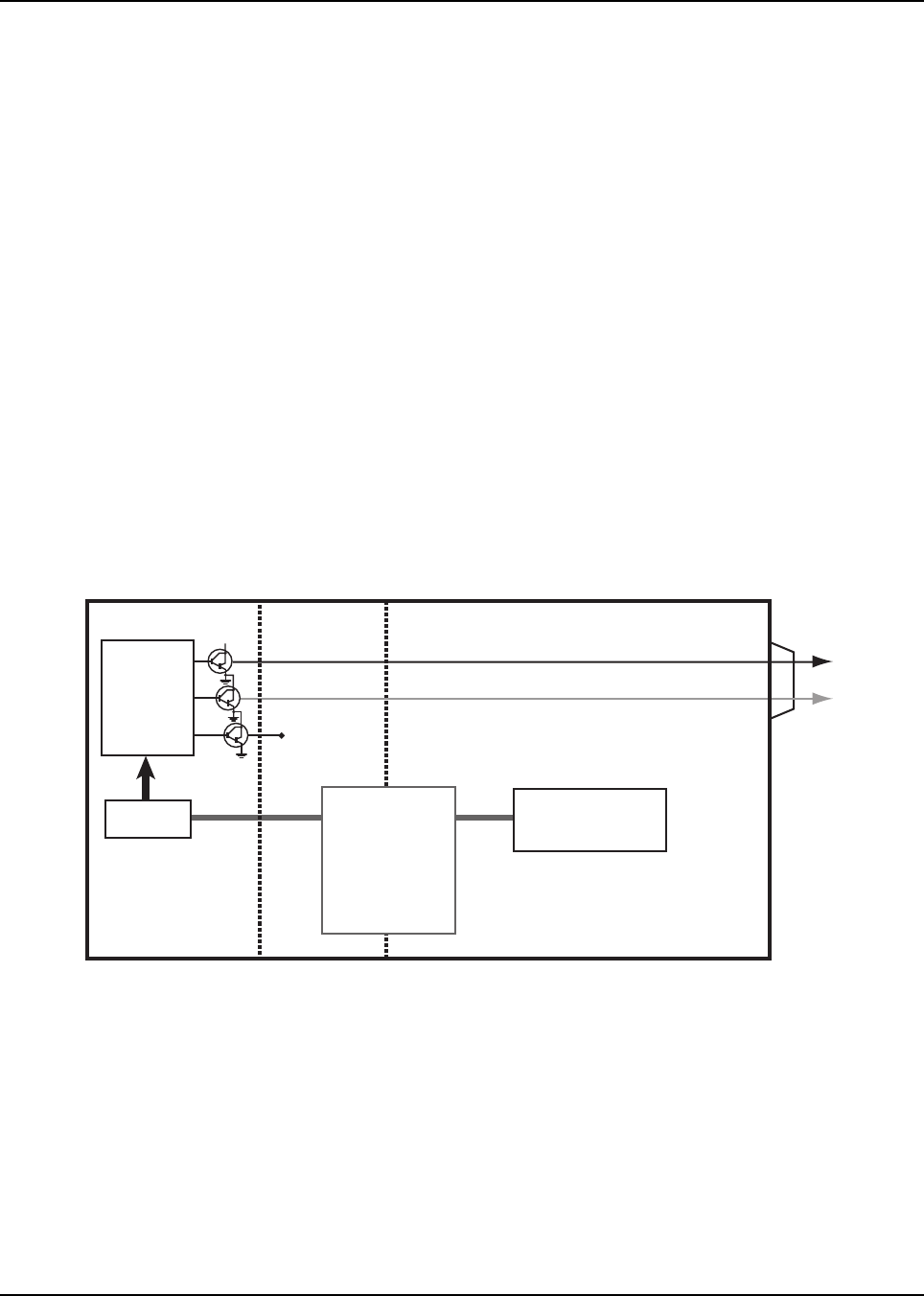
May 25, 2005 6881096C74-B
2-2 Product Overview: Control-Head Assembly
2.3 Control-Head Assembly
This section discusses the basic operation and components of each control-head assembly.
2.3.1 Display, Vacuum Fluorescent Display Driver, Vacuum Fluorescent Voltage
Source, Controls and Indicators, Status LEDs and Backlight LEDs
For information on the above, please refer to:
• W3 Control Head User’s Guide, 6881096C67 and
• W4, W5, W7 and W9 Control Heads User’s Guide, 6881096C68.
2.3.2 Vehicle Interface Ports
The Vehicle Interface Ports (VIPs) allow the control head to activate external circuits and receive
inputs from the outside world. In general, VIP outputs are used for relay control, and VIP inputs
accept inputs from external switches. The VIP IN and VIP OUT lines move as the configuration
changes from Dash, to Remote, to Remote plus DEK. See the cable kit section for typical
connections of VIP input switches and VIP output relays.
2.3.2.1 Dash-Mount Control-Head Configuration (Mid Power Only)
In the dash-mount configuration (Figure 2-1), only two VIP output pins are available, and they are
located at the 26-pin accessory connector, J2-18 and J2-19. VIP input lines are not available in this
configuration.
Figure 2-1. VIP Dash-Mount Configuration
2.3.2.2 Remote-Mount Standard Control-Head Configuration
Once the radio is put into a remote-mount configuration (Figure 2-2 on page 2-3), the two VIP output
pins located at the rear connector (J2) stop functioning, and the VIP output pins located on the back
of the control head below the area labeled "VIP" become the new VIP output pins. These
connections are used to control relays, just as in the dash-mount configuration. One end of the relay
should be connected to SWB+, while the other side is connected to VIP IN or VIP OUT pins (these
pins are software-controlled on/off switches via transistors inside the control head or on the
interconnect board).
Pin 18
Pin 19
Pin 11
Pin 12
Pin 18
Pin 19
VIP OUT 1
VIP OUT 2
Control
Head
Main Board
(Radio)
U1
MC68HC
MAEPF-27921-O
No connect
MicroprocessorSIOIC SB9600 data
lines toggle
VIP-OUT
hadware
inside the
Control Head
6881096C74-B May 25, 2005
Product Overview: Control-Head Assembly 2-3
Figure 2-2. VIP Remote-Mount Configuration
Figure 2-3. VIP Remote-Mount Pin-Outs (Male)
Control
Head
Main Board
(Radio)
U1
MC68HC
MAEPF-27922-O
MicroprocessorSIOIC SB9600 data
lines toggle
VIP-OUT
hadware
inside the
Control Head
VIP OUT 1
VIP OUT 2
1 2 3 4 5 7 8 10 11 12 13 14 15 16 17
18 19 20 21 23 24 26 27 28 29 30 31 32 33
34 35 36 37 38 40 41 43 44 45 46 47 48 49 50
SWB SWB GND GND
MICVIP RADIO
11
VIP OUT VIP IN
22
VIP OUT VIP IN
+
SWB GND
+
+
MAEPF-27918-O
May 25, 2005 6881096C74-B
2-4 Product Overview: Control-Head Assembly
2.3.2.3 Remote-Mount W3 Hand-Held Control Head Configuration
Because the W3 control head does not have an interface for VIPs on the control head itself, the radio
and the W3 interconnect board must work together to provide VIP OUT at the back of the radio
(Figure 2-4). The driving transistors (for the ON/OFF relay control) are located on the W3
interconnect board. Therefore, the microprocessor on the main board uses one set of lines to
interface with the interconnect board's transistors and a second set of return lines, which travel back
to the main board and pass through to the back of the radio. Also, by using a Y-split cable HKN6096,
VIP OUT also can be accessed at its 15-pin connector. However, the voltage levels are slightly lower
since the VIP SWB+ of the interconnect board is different from the SWB+ of the radio.
Figure 2-4. VIP Remote-Mount W3 Control-Head Configuration
2.3.2.4 Remote-Mount plus DEK Configuration
Another remote-mount configuration possibility is the addition of up to three Direct Entry Keypad
(DEK) boxes (Figure 2-5 on page 2-5). A DEK is an accessory that is used with a mobile radio to
provide extra buttons, indicators, and VIPs to the user. Just as the VIP output pins moved from the
rear of the radio to the rear of the control head, the VIP pins also move from the back of the control
head to the back of the DEK. The benefit of using a DEK box is that you gain three additional
VIP OUT and VIP IN pins for each DEK added. The first DEK box provides the original three
VIP OUT and three VIP IN pins. The next DEK provides an additional three VIP OUT and three
VIP IN pins. A final DEK box provides an additional three VIP OUT and three VIP IN pins for a total
of nine VIP OUT and nine VIP IN pins.
Pin 16
Pin 17
Pin 16
Pin 17
Pin 14
Pin 27
Pin 18
Pin 17
Pin 13
Pin 14
Pin 11
Pin 12
Pin 18
Pin 19
VIP OUT 1
Micro-
processor
VIP OUT 2
JU512
JU513
W3 Remote
Interconnect
Board
Main Board
(Radio)
MAEPF-27923-O
6881096C74-B May 25, 2005
Product Overview: Control-Head Assembly 2-5
Figure 2-5. VIP Remote-Mount Plus DEK Configuration
Figure 2-6. VIP Remote-Mount Plus DEK Pin-Outs (Male)
Kit HKN4273 contains:
- One DEK-to-DEK interface cable (A)
- One 24-pin DEK VIP connector (B)
- One 14-pin non-DEK VIP connector
- Forty cimping pins
(A) DEK interface lines:
DATA IN
DATA OUT
STROBE
CLOCK
When a DEK is added, the
radio VIPs move from J2
and from the back of the
control head to the back of
the DEK.
Main Board
(Radio)
Control Head
(W4, W5, W7, W9)
DEK A
DEK B
DEK C
SB9600 bus
messaging
interface
3 VIP - INs
3 VIP - OUTs
3 VIP - INs
3 VIP - OUTs
3 VIP - INs
3 VIP - OUTs
MAEPF-27925-O
(B)
1 2 3 4 5 7 8 10 11 12 13 14 15 16 17
18 19 20 21 23 24 26 27 28 29 30 31 32 33
34 35 36 37 38 40 41 43 44 45 46 47 48 49 50
STROBE GND CLOCK DATA VIP OUT VIP OUT SWB+
SWB+ DATA SWB+ VIP OUT SWB+ SWB+
OUT
IN
1
3
OUT STROBE 2
GND GND GND
3
2
FROM
CONTROL HEAD
OR PREVIOUS DEK BOX
TO NEXT DEK BOX DEK VIP-INs AND VIP-OUTs
IN GNDCLOCK
DATA VIP IN VIP IN
DATA VIP IN
MAEPF-27917-O
1

May 25, 2005 6881096C74-B
2-6 Product Overview: Control-Head Assembly
2.3.2.5 VIP Output Connections:
There are three VIP outputs that are used for the W9 control head and two VIP outputs for the W3,
W4, W5, and W7 control heads. The VIP outputs are normally at SWB+ levels and are driven low by
logic within the control head for both the dash- and remote-mount configurations. Field programming
of the radio can define the functions of these pins. The output transistors that drive the VIP outputs
can sink 300 mA of current and are primarily used to control external relays. These relays should be
connected between the respective VIP output pin and switched B+.
VIP outputs are controlled by SB9600 Update_Indicator messages. Therefore, multiple indicators
and their status information can be sent with a single message.
The relay can be normally ON or normally OFF depending on the configuration of the VIP outputs.
The CPS can be used to program the function of these VIP outputs in the radio.
The following are typical applications currently supported with ASTRO products:
• Horn relay
• Light relay
• Siren horn transfer
2.3.2.6 VIP Input Connections:
There are three VIP inputs that accept inputs from switches. VIP input messages are sent via the
SB9600 pins as SB9600 BUTCTL messages. One side of the switch connects to ground while the
other side connects to a buffered input to the control head. The switch can be normally closed or
normally open depending on the configuration of the VIP inputs. The CPS can be used to program
the function of these VIP inputs in the radio.
The following are typical applications currently supported in ASTRO products:
• Siren horn ring
• Auxiliary siren
For the remote configuration of W4, 5, 7 and 9 control heads, refer to sections 3.1.2 and 3.2.1 of the
Installation Manual, 6881096C72.
Table 2-1. Control-Head VIP Locations
Type Configur
-ation
Power
Level VIP Location Number of
VIP Inputs
Number of
VIP Outputs
W3 Remote Midpower J3-3 and J3-12
Remote Mount Accessory Cable
HKN6096
None 2
W3 Dash Midpower J2-18 and J2-19
Rear Accessory Connector
None 2
W4 Dash Midpower J2-18 and J2-19
Rear Accessory Connector
None 2
W5 Dash Midpower J2-18 and J2-19
Rear Accessory Connector
None 2
W7 Dash Midpower J2-18 and J2-19
Rear Accessory Connector
None 2

6881096C74-B May 25, 2005
Product Overview: Control-Head Assembly 2-7
2.3.2.7 DEK Interface With Radio: Remote-Mount (W4, W5, W7, W9)
A maximum of three DEKs can be daisy chained to a single mobile radio. DEKs are only used with
the W4, W5, W7, and W9 control heads when they are remotely mounted on the radio. DEKs are not
used with any dash-mount control heads, including W4, W5, W7, or W9. The W3 control head does
not support DEK, except in a special siren cabling configuration where the DEK 6-pin cable splits off
the SIREN cable and plugs into the back of a DEK box.
The VIP lines in the control head are used to connect a DEK. There are four lines that are needed to
communicate with the DEK: DATA IN, DATA OUT, STROBE, and CLOCK. These lines are shared
with the VIP lines in the control head (see Table 2-1 on page 2-6) and, as a result, the control head
loses its VIP lines when connected to a DEK. However, each DEK has its own VIP lines (three
VIP IN and three VIP OUT lines) that can be used.
Each DEK box is essentially a shift register consisting of eight buttons/indicators together with the
VIP lines. A raw, 48-bit stream of data from the control head is clocked into the first DEK box that is
directly connected to it. This DEK box only shifts the bits forward to DEK B, which, in turn, forwards
the bits to DEK C. Thus, bit 0 leaving the control head is actually stored as the last bit of DEK C. The
full 48 bits is always clocked in/out regardless of the number of DEKs connected. The software is
able to determine how many DEKs are actually connected by checking the "DEK present" bit for
each DEK. The VIPs provided by each DEK box can then be used for driving external circuitry.
2.3.2.7.1 DATA IN
DATA IN consists of data entering from either the control head or another DEK. DATA IN is a raw bit
stream fed into the DEK, which, in turn, essentially being a shift register, moves the data forward to
the next DEK. DATA IN is a 48-bit stream that consists of indicator data (0 = off, 1 = illuminated) and
VIP output data.
2.3.2.7.2 DATA OUT
DATA OUT consists of data leaving the DEK and either entering a control head or another DEK.
DATA OUT is a 48-bit stream that consists of button data (0 = pressed, 1 = released), VIP input data,
and DEK present.
2.3.2.7.3 STROBE
The STROBE line is used to latch the data contained in the shift registers inside the DEK box. This
line is used to inform the DEK that the data contained in its shift registers is now valid.
2.3.2.7.4 CLOCK
The CLOCK line is used to shift data in and out through the shift registers located in the DEK boxes.
2.3.3 Power Supplies
The +5-V supply is a three-terminal regulator IC to regulate the 12 V SWB+ down for the digital logic
hardware.
2.3.4 Ignition Sense Circuits
A transistor senses the vehicle ignition’s state, disabling the radio when the ignition is off. For
negative-ground systems, the orange lead is typically connected to the fuse box (+12 V).

May 25, 2005 6881096C74-B
2-8 Product Overview: Receiver Section
2.4 Receiver Section
This section discusses the receiver section components and basic operation for each band.
2.4.1 VHF Band Radios
The VHF (136–174 MHz) receiver consists of a front-end and a back-end sections.
2.4.1.1 Front-End Section
The primary function of the receiver front-end is to optimize image rejection and selectivity while
providing the first conversion. The front-end uses discreet filters and LNAs. The first filter reduces
the IF spur, image frequency response and limits some of the out-of-band interference. The second
filter following the second low-noise amplifier (LNA) provides additional image rejection and half IF
spur.
The receiver front-end signal is fed to the monolithic mixer IC where it is down converted to an IF of
109.65 MHz. The mixer is driven by the receiver injection buffer that provides 20 dBm to the mixer.
The VCO performs high side injection for the VHF band. The design maintains temperature stability,
low insertion loss, and high out-of-band rejection.
2.4.1.2 Back-End Section
The crystal filters provide IF selectivity and out-of-band signal protection to the back-end IC. Two 2-
pole crystal filters centered at 109.65 MHz that are isolated from one another by a stable, high-gain
low noise amplifier are used to meet the receiver specifications for gain, close-in intermodulation
rejection, adjacent-channel selectivity, and second-image rejection.
The output of the IF circuit is fed directly to the Abacus III digital back-end IC. The ABACUS III is an
IC with a variable-bandwidth bandpass Sigma-Delta architecture. It is capable of down-converting
analog, as well as digital, RF protocols into a baseband signal transmitted on the Synchronous Serial
Interface (SSI) bus. The ABACUS III IC converts the 109.65 MHz signal from the IF section down to
2.25 MHz using a second LO frequency of 107.4 MHz or 111.9 MHz. The second LO VCO is tuned to
107.4 MHz (low side), but can be modified to 75.6 MHz (high side injection) depends on known
spurious interference related to the programmed received frequency.
2.4.2 UHF Range 1/UHF Range 2 Band Radios
The UHF Range 1 (380–470 MHz)/UHF Range 2 (450–520 MHz) receiver consists of a front-end
section and a back-end section.
2.4.2.1 Front-End Section
The receiver front-end consists of a switchable high pass filter and LNA, a preselector, a switchable
attenuator, a second switchable low noise amplifier (always in for UHF Range 2), image filter, mixer,
and injection amplifier. The preselector filter is varactor-tuned and is aligned at the factory. The radio
tuner software can also be used to check and re-align the preselector. The switchable stage provides
AGC capability.
The signal from the preselector is amplified by the low noise amplifier, then filtered by the image filter
before it is sent to the mixer. The mixer uses the LO signal, amplified by the injection amplifier, to
convert the RF signal to IF frequency of 109.65 MHz. This signal is then sent to the IF and back-end
circuits.
2.4.2.2 Intermediate Frequency and Back-End
The Intermediate Frequency (IF) consists of a crystal filter, amplifier, a second crystal filter, and a
switchable attenuator. This provides selectivity at the IF while attenuating out-of-band signals and
protecting the back-end (BE) IC.

6881096C74-B May 25, 2005
Product Overview: Transmitter Section 2-9
The back-end is primarily the ABACUS III digital IC. The ABACUS III IC uses a variable-bandwidth
bandpass sigma-delta architecture. It is capable of down-converting analog as well as digital RF
protocols into a baseband signal, which is then transmitted over the Synchronous Serial Interface
(SSI) bus to the DSP and microprocessor.
2.4.3 700–800 MHz Band Radios
The 700–800 MHz receiver consists of a front-end section and a back-end section.
2.4.3.1 Front-End Section
The primary function of the receiver front-end is to optimize image rejection and selectivity while
providing the first conversion. The front-end uses ceramic-filter technology and includes a wideband,
monolithic amplifier. The first filter is a dual-switched filter that reduces the image frequency
response and limits some of the out-of-band interference. The second filter following the monolithic
low-noise amplifier (LNA) provides additional image rejection.
The receiver front-end signal is fed to the monolithic mixer IC where it is down converted to an IF of
73.35 MHz. The mixer is designed to provide low conversion loss and high intermodulation
performance. The mixer is driven by the receiver injection buffer, a two-stage discrete IC design used
with the receiver VCO to efficiently drive the mixer over a wide temperature range with minimum
power variation. The injection buffer provides 15 dBm to the mixer. The VCO performs low-side
injection for the 800 MHz band and high-side Injection for the 700 MHz band. The design maintains
temperature stability, low insertion loss, and high out-of-band rejection.
2.4.3.2 Back-End Section
The crystal filters provide IF selectivity and out-of-band signal protection to the back-end IC. Two
2-pole crystal filters centered at 73.35 MHz that are isolated from one another by a stable, moderate-
gain amplifier are used to meet the receiver specifications for gain, close-in intermodulation
rejection, adjacent-channel selectivity, and second-image rejection.
The output of the IF circuit is fed directly to the ABACUS III digital back-end IC. The ABACUS III is an
IC with a variable-bandwidth bandpass Sigma-Delta architecture. It is capable of down-converting
analog, as well as digital, RF protocols into a baseband signal transmitted on the Synchronous Serial
Interface (SSI) bus. The ABACUS III IC converts the 73.35 MHz signal from the IF section down to
2.25 MHz using a second LO frequency of 71.1 MHz or 75.6 MHz. The second LO VCO is tuned to
71.1 MHz (low side) or 75.6 MHz (high side injection). The choice of frequency depends on known
spurious interference related to the programmed received frequency.
2.5 Transmitter Section
This section discusses the transmitter section components and basic operation for each band.
2.5.1 VHF Radios
The VHF (136–174 MHz) transmitter consists of an RF power amplifier (RFPA), output network
(ON), and power control. See 2.5.3 700–800 MHz Radios below for an overview of the transmitter
sections.
2.5.2 UHF Range 1/UHF Range 2 Radios
The UHF Range 1 (380–470 MHz)/UHF Range 2 (450–520 MHz) transmitter consists of an RF
power amplifier (RFPA), output network (ON), and power control. See 2.5.3 700–800 MHz Radios
below for an overview of the transmitter sections.

May 25, 2005 6881096C74-B
2-10 Product Overview: Frequency Generation Unit
2.5.3 700–800 MHz Radios
The 700–800 MHz transmitter consists of an RF power amplifier (RFPA), output network (ON), and
power control.
2.5.3.1 RFPA
The RFPA is a three-stage, discrete-LDMOS transistor amplifier consisting of the following stages:
first, driver, and final.
The first stage acts as a variable-gain amplifier and feeds the driver stage, which, in turn, feeds the
final stage. All of the stages are matched using transmission lines, capacitors, and inductors. Stage
drain biases are supplied via A+ or K9.1V and DRV_9.3V (DRV_9.3V is present for UHF Range 1
and UHF Range 2 only). Stage gate biases are supplied via a digital-to-analog converter (DAC) or
the RFPA control voltage.
2.5.3.2 Output Network
The output network (ON) consists on the antenna switch, harmonic filter, and power detector. The
antenna switch operates in two modes: RX and TX.
In TX mode, the RFPA final stage is connected to the antenna through the harmonic filter and power
detector and is isolated from the RX path.
In RX mode, the antenna is connected to the RX front-end through the power detector and the
harmonic filter and is isolated from the TX path. The harmonic filter attenuates harmonics generated
by the RFPA when the antenna switch is in TX mode and provides extra selectivity in RX mode.
The power detector senses forward and reverse power and generates a detected voltage
proportional to each.
2.5.3.3 Power Control
The forward-power and reverse-power detected voltage is fed back to the power control section
where it is added to a DAC voltage determined via power tuning and compared to a reference
voltage. A control loop corrects the control voltage adjusting the first stage gain to maintain the
reference.
2.5.3.4 Circuit Protection
Final-stage current and temperature as well as radio A+ voltage and RFPA control voltage are
sensed. If a fault condition is determined, power is cut back to a level that is safe for the particular
conditions.
2.6 Frequency Generation Unit
This section discusses the frequency generation unit (FGU) components and basic operation for
each band.
2.6.1 VHF MHz Radios
The VHF (136-174 MHz) frequency generation unit consists of the following:
• Low-voltage fractional-N synthesizer IC
• 16.8 MHz reference oscillator IC
• Two receiver (RX) voltage-controlled oscillators (VCOs)
• Two transmitter (TX) voltage-controlled oscillators (VCOs)
• VCO buffer/amplifier circuits

6881096C74-B May 25, 2005
Product Overview: Frequency Generation Unit 2-11
• Associated circuitry
The reference oscillator IC provides a frequency standard to the Fractional-N synthesizer IC, the
ABACUS III digital back-end IC, and the controller section. The synthesizer turns on one of the four
VCOs (determined by mode and band of operation) and tunes it to the receiver (RX) local oscillator
(LO) or transmitter (TX) carrier frequency.
All four voltage-controlled oscillators (VCOs) employ a discrete Colpitts configuration with a N-
channel J-FET transistor. The VCOs tank consists of a varactor diode, coupling capacitor, and a
resonator. The varactor changes the oscillator frequency when the DC voltage of the steering line
changes. The output of the VCOs is coupled to the second transistor for impedance buffering, and its
output is coupled to respective TX/RX buffer amplifiers.
In TX mode, the transmitter VCO output is coupled to a three-stage buffer before being injected into
the power amplifier. In RX mode, the receiver VCO output is buffered and amplified with a two-
stages. The output of the second-stage transistor is split into two paths. One path feeds back to the
synthesizer prescaler; the other path is injected into the third-stage. The output of the third-stage
provides the proper signal level for the LO port of the RX front-end mixer.
The superfilter supplies the voltage to the first two stages of the TX buffer and to the first two stages
transistor of the RX buffer/amplifier. The voltage for the third stage of the TX buffer is supplied by a
keyed 9.1 V source to conserve current drain while the radio is receiving. The third-stage of the RX
buffer/amplifier is supplied by a 9.3 V regulator.
2.6.2 UHF Range 1/UHF Range 2 Radios
The UHF Range 1 (380–470 MHz)/UHF Range 2 (450–520 MHz) frequency generation unit consists
of the following:
• Low-voltage fractional-N synthesizer IC
• 16.8 MHz reference oscillator IC
• Three receive voltage-controlled oscillators (VCO)
• Two transmit VCOs
• VCO buffer/amplifier circuits
• Associated circuitry
See 2.6.3 700–800 MHz Radios below for an overview of the FGU sections.
2.6.3 700–800 MHz Radios
The 700–800 MHz frequency generation unit consists of the following:
• Low-voltage fractional-N synthesizer IC
• 16.8 MHz reference oscillator IC
• Two voltage-controlled oscillator (VCO) modules (receive and transmit, containing two VCOs
each)
• VCO buffer/amplifier circuits
• Associated circuitry
The reference oscillator IC provides a frequency standard to the fractional-N synthesizer IC, the
ABACUS III digital back-end IC, and the controller section. The synthesizer turns on one of the four
VCOs (determined by mode and band of operation) and tunes it to the receiver (RX) local oscillator
(LO) or transmitter (TX) carrier frequency.

May 25, 2005 6881096C74-B
2-12 Product Overview: Controller Section
The voltage-controlled oscillator (VCO) module employs a Colpitts configuration with two bipolar
stages in a common-base, common-collector configuration. The LC tank circuit's capacitive portion
consists of a varactor diode, coupling capacitor, and a laser-trimmed capacitor for frequency
adjustment. The inductive portion consists of microstrip transmission line resonators for TX VCO and
coaxial resonators for RX VCO. Tuning is performed by the module manufacturer and is not field
adjustable. The varactor changes the oscillator frequency when the DC voltage of the steering line
changes. The output of the common base is coupled to the second transistor for impedance
buffering, and its output is coupled to respective TX/RX buffer amplifiers.
In TX mode, the transmitter VCO output is coupled to a three-stage buffer before being injected into
the power amplifier. In RX mode, the receiver VCO output is buffered and amplified with a two-stage
transistor/microwave monolithic IC (MMIC) circuit. The output of the first-stage transistor is split into
two paths. One path feeds back to the synthesizer prescaler; the other path is injected into the
second-stage MMIC. The output of the MMIC provides the proper signal level for the LO port of the
RX front-end mixer.
The superfilter supplies the voltage to the first two stages of the TX buffer and to the first-stage
transistor of the RX buffer/amplifier. The voltage for the third stage of the TX buffer is supplied by a
keyed 9.1 V source to conserve current drain while the radio is receiving. The second-stage MMIC of
the RX buffer/amplifier is supplied by a 9.3 V regulator.
2.7 Controller Section
This section provides an explanation of radio operating modes and an overview of the controller
section components and circuits.
2.7.1 Analog Mode of Operation
When the radio is receiving, the signal comes from the antenna/antenna-switch to the front-end
receiver. The signal is then filtered, amplified, and mixed with the first local-oscillator signal
generated by the voltage-controlled oscillator (VCO). The resulting intermediate frequency (IF)
signal is fed to the IF circuitry, where it is again filtered and amplified. This amplified signal is passed
to the digital back-end IC, where it is mixed with the second local oscillator to create the second IF at
2.25 MHz. The analog IF is processed by an analog-to-digital (A/D) converter inside the digital back-
end IC where it is converted to a digital bit stream and divided down to a baseband signal, producing
digital samples. These samples are converted to TTL logic signals and sent to the DSP. The DSP
digitally filters and discriminates the signal, decodes the information in the signal, and identifies the
appropriate destination for it. For a voice signal, the DSP will route the digital voice data to the coder/
decoder (CODEC) for conversion to an analog signal. The CODEC will then present the signal to the
audio power amplifier, which drives the speaker. For signalling information, the DSP will decode the
message and pass it to the microcomputer.
When the radio is transmitting, microphone audio is passed to an adjustable gain circuit, then to the
CODEC where the signal is digitized. The CODEC passes digital data to the DSP where pre-
emphasis and low-pass (splatter) filtering are done. The DSP sends this signal to the modulation
digital-to-analog (D/A) converter where it is reconverted into an analog signal and scaled for
application to the voltage-controlled oscillator as a modulation signal. Transmitted signalling
information is accepted by the DSP from the microcomputer, coded appropriately, and passed to the
modulation D/A converter, which handles it the same as a voice signal. Modulation information is
passed to the synthesizer along the modulation line. A modulated carrier is provided to the power
amplifier (PA), which transmits the signal under dynamic power control.

6881096C74-B May 25, 2005
Product Overview: Controller Section 2-13
2.7.2 Digital (ASTRO) Mode of Operation
In the ASTRO mode (digital mode) of operation, the transmitted or received signal is limited to a
discrete set of deviation levels, instead of continuously varying. The receiver handles an ASTRO-
mode signal identically to an analog-mode signal up to the point where the DSP decodes the
received data. In the ASTRO receive mode, the DSP uses a specifically defined algorithm to recover
information. In the ASTRO transmit mode, microphone audio is processed identically to an analog
mode with the exception of the algorithm the DSP uses to encode the information. This algorithm will
result in deviation levels that are limited to discrete levels.
2.7.3 Controller Section Circuitry
The controller section consists of the following:
• Voltage regulators
• Data connectivity circuitry (RS-232, USB, and SB9600)
• Daughtercard module, which contains the:
- Patriot microprocessor IC
- 64-Mbit (8MB) FLASH IC
- 8-Mbit (1MB) SRAM IC
• Modulation D/A conversion circuitry
• CODEC audio circuitry
• TX power-control circuitry
• Emergency circuitry
• V.I.P input/output paths
• Secure interconnect board interface
• Front connector interface for control heads and remote-mount interconnect boards (I.B)
• Rear connector for additional accessories
• DC power-in plug
The controller section controls receive/transmit frequencies, the display, and various radio functions
using either direct logic control or serial communication to external devices. The connector J0701
provides interface between the encryption module and the controller for encrypting voice messages.
Connector J0402 provides the accessory interface to the outside rear connector while connector
J0401 provides the control-head interface.
The controller section executes a stored program located in the FLASH ROM. Data is transferred to
and from memory via an RS-232 interface on the microprocessor. The memory location from which
data is read, or to which data is written, is selected by the address lines. Besides the host and DSP
code, the customer-specific programming features (codeplug) and tuning parameters also are stored
in the FLASH ROM. The SRAM is used as scratchpad memory for the microprocessor.
The controller section is powered by SW_B+ coming from the control head, which is regulated down
to a 5 V supply. This supply powers the entire controller section and its regulators. The SW_B+
supply is removed from the board when the radio is turned off by the control-head switch.
The microprocessor is powered by a 1.55-V regulator for the microprocessor core and a 2.85-V
regulator for the I/O and control lines, while the memory is powered by a 1.85-V regulator. The 2.85-
V regulator also supplies almost all of the discrete controller circuitry. These three regulators are all
supplied by a switched 5-V regulator, which also provides power for the SB9600 data bus and for
interface to certain legacy data and control signals.

May 25, 2005 6881096C74-B
2-14 Product Overview: Controller Section
The DSP section of microprocessor performs signaling, voice encoding/decoding, audio filtering,
microphone gain and tuning, Private-Line/Digital Private Line (PL/DPL) encode, and alert-tone
generation. It processes all baseband audio signals, providing pre-emphasis and signaling/filtering of
the digital microphone audio data, as well as other transmitted signals. It also performs de-emphasis
and decoding of received digital speaker audio and other received signals. The DSP clock frequency
is derived from the 16.8 MHz reference oscillator clock input using a phase-locked loop (PLL) inside
the Patriot IC. The digital audio bus on the Patriot IC uses an 8 kHz clock, which provides the
sampling rate, and a 512 kHz clock, which provides the data rate.
The CODEC performs analog-to-digital and digital-to-analog conversions on audio signals. The DSP
controls squelch, deviation, and compensation, and it executes receiver filtering and discrimination.
The interface to the RX back-end IC (ABACUS III IC) consists of a single logic-level data line, a
1.2 MHz clock line (the discriminator data bit rate) and a 20 kHz frame-sync line (the discriminator
data sample rate). These clocks are generated by the ABACUS III IC and provided to the Patriot IC.
The interface to the TX modulation/DAC consists of a single logic-level data line, a 2.4 MHz clock
line (the modulation data bit rate), and a 48 kHz clock line (the modulation data sample rate). These
clocks are generated by the Urchin IC and provided to the Patriot IC.
Other functions provided by the controller include SB9600 communication, IC programming, and TX
power control. The SB9600 bus is used to communicate to legacy control heads and accessories. IC
programming is performed via the SPI bus for ICs including the ABACUS III, LV Frac-N, A/D, D/A,
and volume attenuator. The power-control circuitry receives power set and limit inputs from the D/A
IC and feedback from the RF power amplifier (RFPA). Based on these inputs, the circuit produces a
control voltage to maintain a fixed RF power level to the antenna.
The controller also provides detection of the On/Off and reset inputs. The reset circuits consist of the
regulator power-on reset circuit, low SW_B+ voltage-detector circuit, an ignition detection circuit, an
emergency detection circuit, and the external-bus system reset. The reset circuits allow the
microcomputer to recover from an unstable situation; for example, no battery on the radio, battery
voltage too high or too low, and remote devices on the external bus not communicating.
Communication using RS-232 protocol is provided to the rear accessory connector (J2).

Chapter 3 Theory of Operation
3.1 Main Board
This section provides a detailed circuit description of the XTL 5000 radio main board for VHF/UHF
Range 1/UHF Range 2/700–800 MHz models. The main board contains the following major
sections:
• Radio Power (page 3-12)
• Receiver Front-End (page 3-13)
• Receiver Back-End (page 3-20)
• Transmitter (page 3-26)
• Frequency Generation Unit (page 3-45)
• Controller (page 3-62)
When reading the theory of operation, refer to your appropriate schematic and component location
diagrams located in “Chapter 7. Schematics, Component Location Diagrams, and Parts Lists”. This
detailed Theory of Operation will help isolate the problem. However, first use the ASTRO Digital
XTL 5000 VHF/UHF Range 1/UHF Range 2/700–800 MHz Mobile Radio Basic Service Manual
(6881096C73) to troubleshoot the problem to a particular board.
3.2 Main Board Major Sections
This section contains the main board layouts for each radio frequency band.
3.2.1 VHF (136–174 MHz) Band
The illustrations (Figure 3-1 on page 3-2 to Figure 3-4 on page 3-5) and their accompanying tables
(Table 3-1 on page 3-2 to Table 3-4 on page 3-5) identify the location of the major sections of the
main board.
May 25, 2005 6881096C74-B
3-2 Theory of Operation: Main Board Major Sections
Figure 3-1. XTL 5000 Main Board Sections (VHF Mid Power)—Side 1
Table 3-1. XTL 5000 Main Board Sections (VHF Mid Power)—Side 1
1 Secure Connector (J0501) 8 Controller Section
2 Front Connector (J0401) 9 Audio Power Amplifier (PA)
3 RX Back-End (ABACUS III) 10 RX VCO
4 16.8 MHz Reference Oscillator 11 TX VCO
5 IF Filter 12 TX PA
6 RX Front-End 13 TX Power Control
7 Daughtercard
1
2
3
4
5
6
7
8
9
10
11
13 12
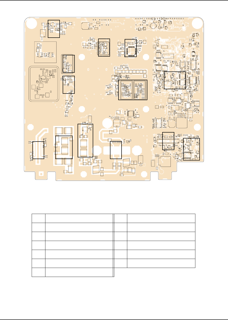
6881096C74-B May 25, 2005
Theory of Operation: Main Board Major Sections 3-3
Figure 3-2. XTL 5000 Main Board Sections (VHF Mid Power)—Side 2
Table 3-2. XTL 5000 Main Board Sections (VHF Mid Power)—Side 2
3 RX Back-End 16 Antenna Switch
5 IF Filter 17 Rear Connector (J0402)
6 Controller Section 18 RX Front-End Biasing
12 TX PA 19 RX VCO Injection Stage
13 TX Power Control 20 TX VCO Injection Stage
14 Power Detector 21 FGU (Synthesizer)
15 Harmonic Filter
5
321
19
18
20
6
14 15
16
12
17
13
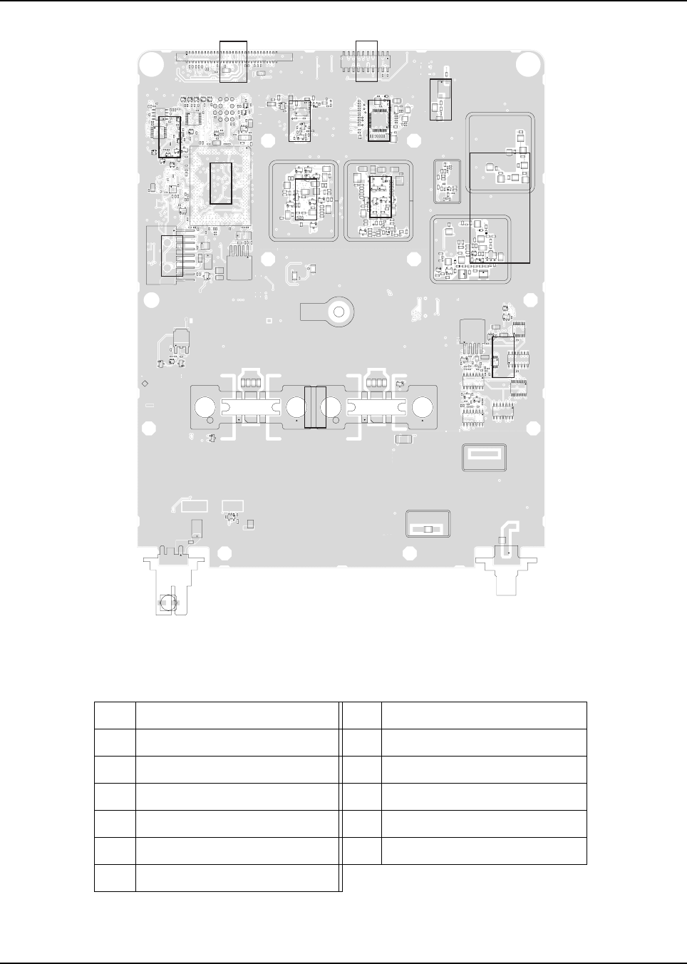
May 25, 2005 6881096C74-B
3-4 Theory of Operation: Main Board Major Sections
Figure 3-3. XTL 5000 Main Board Sections (VHF High Power)—Side 1
Table 3-3. XTL 5000 Main Board Sections (VHF High Power)—Side 1
1 Secure Connector (J0501) 8 Controller Section
2 Front Connector (J0401) 9 Audio Power Amplifier (PA)
3 RX Back-End (ABACUS III) 10 RX VCO
4 16.8 MHz Reference Oscillator 11 TX VCO
5 IF Filter 12 TX PA
6 RX Front-End 13 TX Power Control
7 Daughtercard
21
3
5
10 6
11
12
9
13
4
7
8
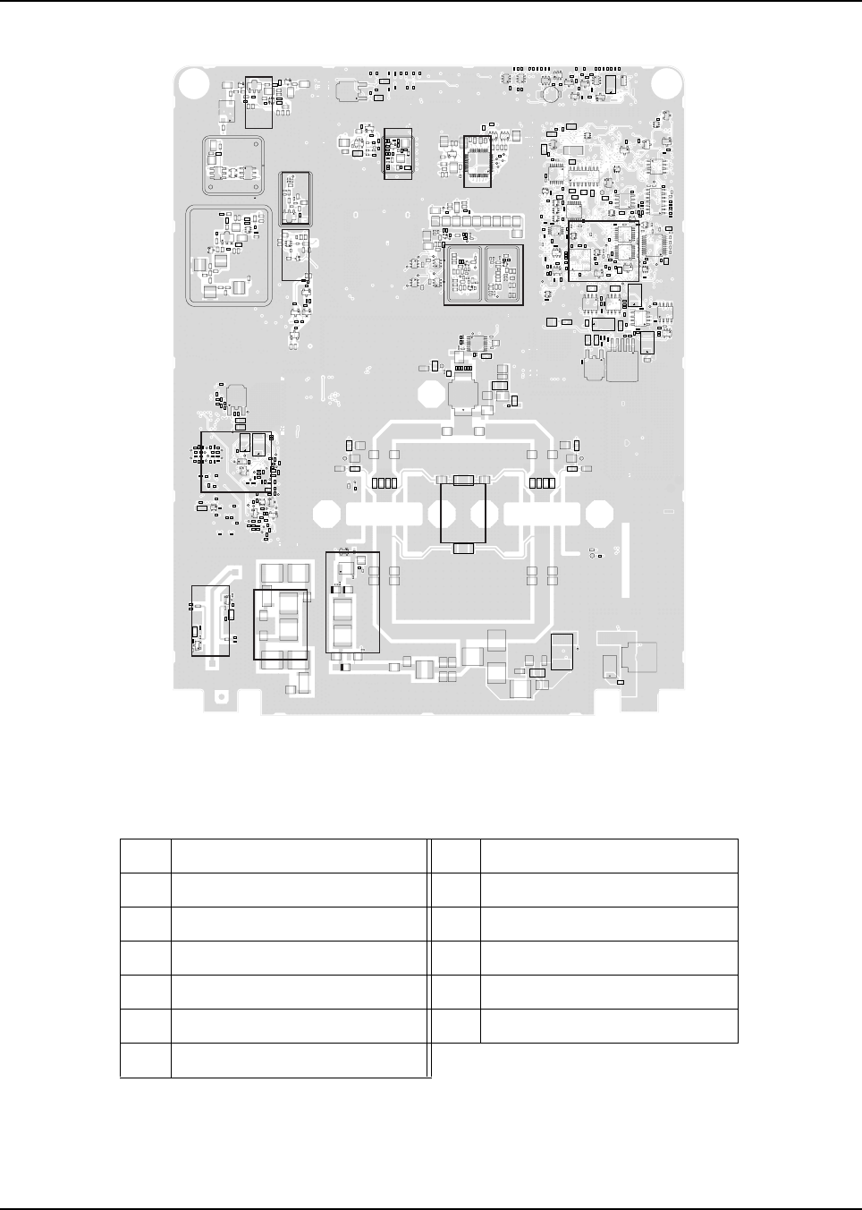
6881096C74-B May 25, 2005
Theory of Operation: Main Board Major Sections 3-5
Figure 3-4. XTL 5000 Main Board Sections (VHF High Power)—Side 2
Table 3-4. XTL 5000 Main Board Sections (VHF High Power)—Side 2
3 RX Back-End 16 Antenna Switch
5 IF Filter 17 Rear Connector (J0402)
6 Controller Section 18 RX Front-End Biasing
12 TX PA 19 RX VCO Injection Stage
13 TX Power Control 20 TX VCO Injection Stage
14 Power Detector 21 FGU (Synthesizer)
15 Harmonic Filter
5
19
321
20
6
13
12
15
14
16
18
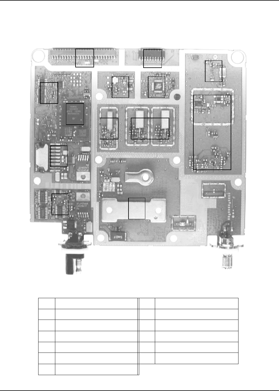
May 25, 2005 6881096C74-B
3-6 Theory of Operation: Main Board Major Sections
3.2.2 UHF Range 1 (380-470 MHz) and UHF Range 2 (450-520 MHz) Band
The illustrations (Figure 3-5 on page 3-6 to Figure 3-8 on page 3-9) and their accompanying tables
(Table 3-5 on page 3-6 and Table 3-8 on page 3-9) identify the location of the major sections of the
main board.
Figure 3-5. XTL 5000 Main Board Sections (UHF Range 1 Mid Power and UHF Range 2)—Side 1
Table 3-5. XTL 5000 Main Board Sections (UHF Range 1 Mid Power and UHF Range 2)—Side 1
1 Secure Connector (J0501) 8 Controller Section
2 Front Connector (J0401) 9 Audio Power Amplifier (PA)
3 RX Back-End (ABACUS III) 10 RX VCO
4 16.8 MHz Reference Oscillator 11 TX VCO
5 IF Filter 12 TX PA
6 RX Front-End 13 TX Power Control
7 Daughtercard
1
2
34
5
6
7
8
9
10
11
12
13
49
50
1
2
1
2
19
20
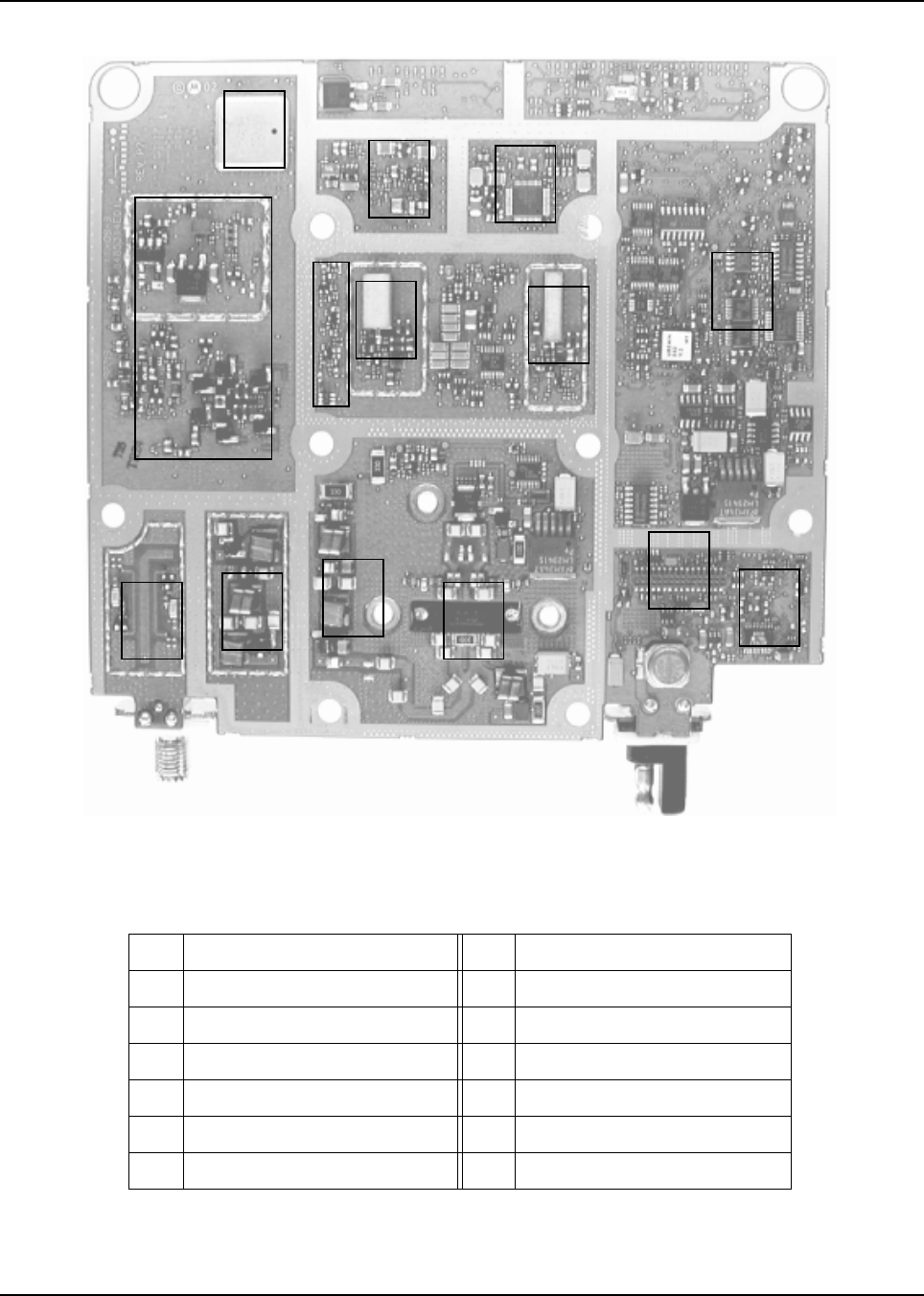
6881096C74-B May 25, 2005
Theory of Operation: Main Board Major Sections 3-7
Figure 3-6. XTL 5000 Main Board Sections (UHF Range 1 Mid Power and UHF Range 2)—Side 2
Table 3-6. XTL 5000 Main Board Sections (UHF Range 1 Mid Power and UHF Range 2)—Side 2
3 RX Back-End 13 TX Power Control
5 IF Filter 14 Power Detector
6 RX Front-End 15 Harmonic Filter
8 Controller Section 16 Antenna Switch
10 RX VCO 17 Rear Connector (J0402)
11 TX VCO 18 RX VCO Injection Stage
12 TX PA 19 FGU (Synthesizer)
5
6
15
14 16 12
17
13
8
11
10
319
18
1
2
31
32
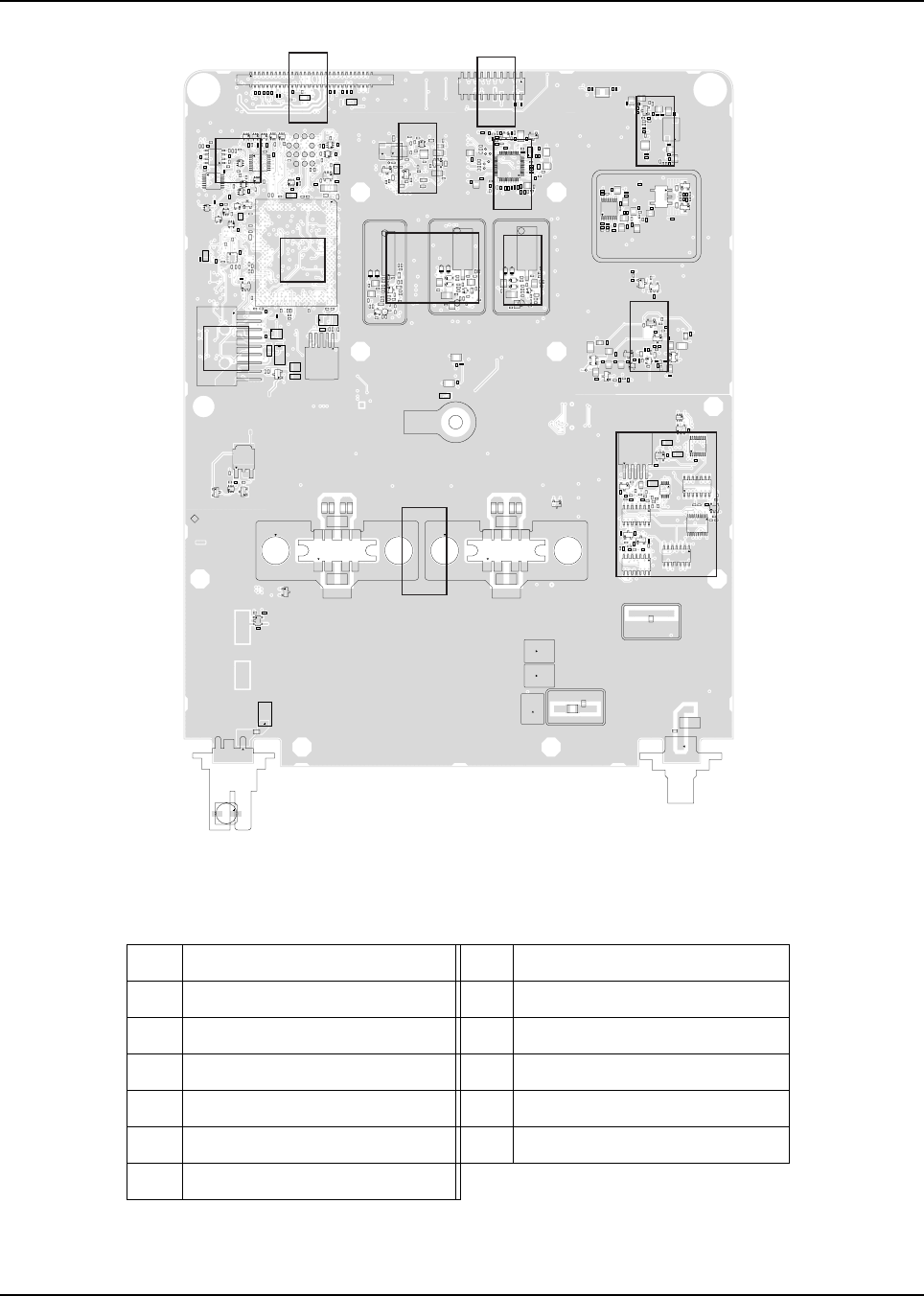
May 25, 2005 6881096C74-B
3-8 Theory of Operation: Main Board Major Sections
Figure 3-7. XTL 5000 Main Board Sections (UHF Range 1 High Power)—Side 1
Table 3-7. XTL 5000 Main Board Sections (UHF Range 1 High Power)—Side 1
1 Secure Connector (J0501) 8 Controller Section
2 Front Connector (J0401) 9 Audio Power Amplifier (PA)
3 RX Back-End (ABACUS III) 10 RX VCO
4 16.8 MHz Reference Oscillator 11 TX VCO
5 IF Filter 12 TX PA
6 RX Front-End 13 TX Power Control
7 Daughtercard
1
2
43
5
10
6
12
9
13
7
8
11
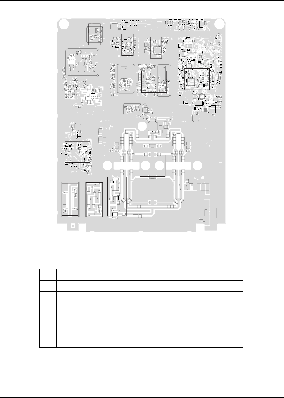
6881096C74-B May 25, 2005
Theory of Operation: Main Board Major Sections 3-9
Figure 3-8. XTL 5000 Main Board Sections (UHF Range 1 High Power)—Side 2
Table 3-8. XTL 5000 Main Board Sections (UHF Range 1 High Power)—Side 2
3 RX Back-End 13 TX Power Control
5 IF Filter 14 Power Detector
6 RX Front-End 15 Harmonic Filter
8 Controller Section 16 Antenna Switch
10 RX VCO 17 Rear Connector (J0402)
11 TX VCO 18 RX VCO Injection Stage
12 TX PA 19 FGU (Synthesizer)
5
321
6
20
13
12
16
15
14
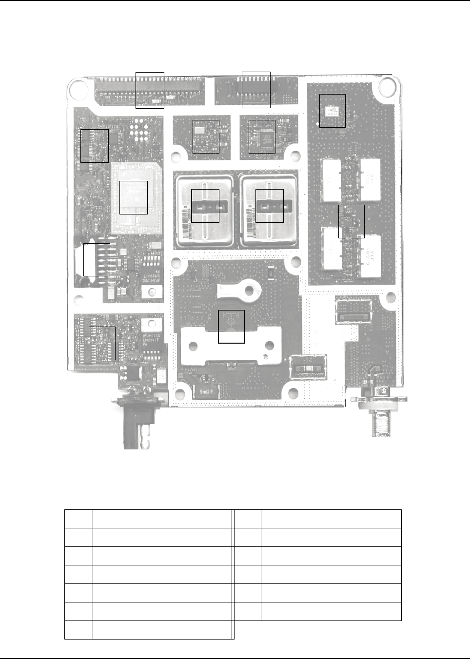
May 25, 2005 6881096C74-B
3-10 Theory of Operation: Main Board Major Sections
3.2.3 700–800 MHz Band
The illustrations (Figure 3-9 and Figure 3-10 on page 3-11) and their accompanying tables (Table 3-9
and Table 3-10 on page 3-11) identify the location of the major sections of the main board.
Figure 3-9. XTL 5000 Main Board Sections (700–800 MHz)—Side 1
Table 3-9. XTL 5000 Main Board Sections (700–800 MHz)—Side 1
1 Secure Connector (J0501) 8 Controller Section
2 Front Connector (J0401) 9 Audio Power Amplifier (PA)
3 RX Back-End (ABACUS III) 10 RX VCO
4 16.8 MHz Reference Oscillator 11 TX VCO
5 IF Filter 12 TX PA
6 RX Front-End 13 TX Power Control
7 Daughtercard
1
2
34
5
6
7
8
9
10
11
12
13
49
50
1
2
1
2
19
20
MAEPF-27876-O
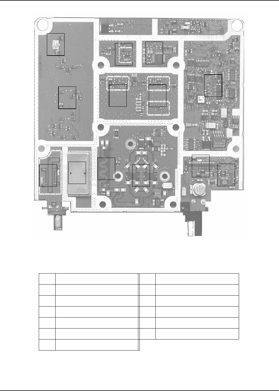
6881096C74-B May 25, 2005
Theory of Operation: Main Board Major Sections 3-11
Figure 3-10. XTL 5000 Main Board Sections (700–800 MHz)—Side 2
Table 3-10. XTL 5000 Main Board Sections (700–800 MHz)—Side 2
3 RX Back-End 16 Antenna Switch
5 IF Filter 17 Rear Connector (J0402)
6 Controller Section 18 RX Front-End Biasing
12 TX PA 19 RX VCO Injection Stage
13 TX Power Control 20 TX VCO Injection Stage
14 Power Detector 21 FGU (Synthesizer)
15 Harmonic Filter
MAEPF-27877-O
5
18
15
14 16 12
17
13
6
20
321
19
1
2
31
32
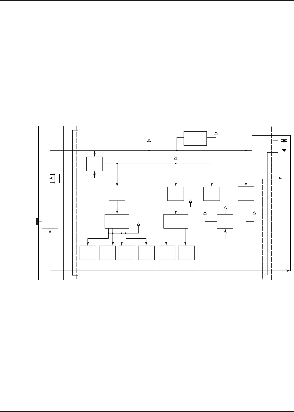
May 25, 2005 6881096C74-B
3-12 Theory of Operation: Radio Power Distribution
3.3 Radio Power Distribution
This section provides information on DC power distribution in XTL 5000 radios. In the XTL 5000
radio, power is distributed to three boards: the main board, control head, and secure interface board.
Power for the radio is supplied by the vehicle’s 12-V battery. When using a desktop adapter unit, an
external DC power supply can be connected to replace the vehicle’s battery source.
A+ (referred to as incoming unswitched battery voltage) enters the radio through the rear RF power
amplifier connector (J0950) and is the main entry for DC power. The second path, through J2, pin 25,
provides ignition sense to inhibit radio turn-on when the ignition switch is off.
When the control-head On/Off button is turned on, the three 9.3-V regulators power on the controller
section, the RX/frequency generation unit (FGU) section, and the TX section. See Figure 3-11 for the
UHF Range 1 and UHF Range 2 bands or Figure 3-12 on page 3-13 for the VHF and 700-800 MHz
bands.
Figure 3-11. DC Voltage Routing Block Diagram (UHF Range 1 and UHF Range 2)
VCC5
9.3V_FGU
9.3V_TX
GPIO
KEYED_9.1_EN
A+
SW_A+
UWW_5V
On/Off
Controller Section RX / FGU Section
Control Head
TX Section
J0401
A+ 19, 21
SWB+ 17
IGN 20 18 25
20, 22 24 SWB+
J0402 J2
J0950
9.3V
Regulator
U0500
9.33V
Regulator
U0950
9.3V
Regulator
U0951
Switch
3.0V
Regulator
U0962
2.85V
Regulator
U0501
1.85V
Regulator
U0507
1.55V
Regulator
U0502
3V
Regulator
U6002
3V
Regulator
U6750
FET
Q0503
UNSW
5V Circuit
VR0500, R0507
SIOIC
5V
Regulator
U0503
5V
Regulator
U0505
DRV_9.3V
9.3V
Regulator
U5570
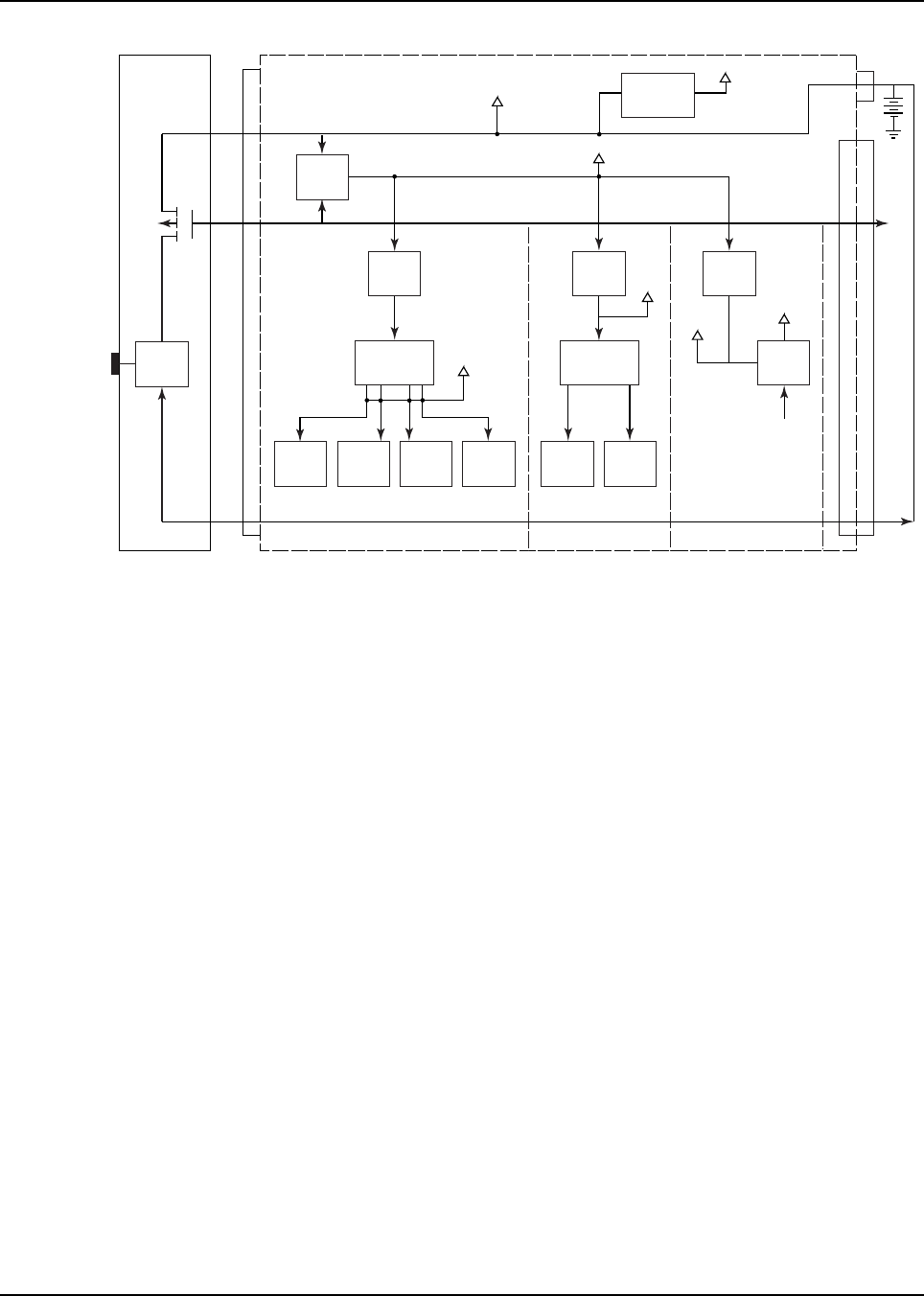
6881096C74-B May 25, 2005
Theory of Operation: Receiver Front-End 3-13
Figure 3-12. DC Voltage Routing Block Diagram (VHF and 700–800 MHz)
The 9.3 V and the A+ voltage are the main DC power for the RF section. The 9.1 V (referred to as
“keyed 9.1 V”) is controlled by the VOCON board through P501, pin 45. This DC voltage enables the
transmitter’s RF power amplifier when the VOCON board senses a lock detect from the synthesizer.
3.4 Receiver Front-End
This section provides a detailed circuit description of receiver front-end (RXFE). When reading the
Theory of Operation, refer to your appropriate schematic and component location diagrams located
in “Chapter 7. Schematics, Component Location Diagrams, and Parts Lists”. This detailed theory of
operation will help isolate the problem to a particular component.
3.4.1 VHF (136–174 MHz) Band
The receiver circuits primary duties are to detect, filter, amplify, and demodulate RF signals in the
presence of strong interfering noise and unintended signals. The receiver is broken down into the
following blocks (Figure 3-13 on page 3-14):
• Front-end, which includes:
- 15 dB step attenuator
- PIN diode switches
- Three discrete filters
- Two low-noise amplifiers
-Mixer
• Back-end, which includes:
- Two crystal filters
VCC5
9.3V_FGU
9.3V_TX
GPIO
KEYED_9.1_EN
A+
SW_A+
UWW_5V
On/Off
Controller Section RX / FGU Section
Control Head
TX Section
J0401
A+ 19, 21
SWB+ 17
IGN 20 18 25
20, 22 24 SWB+
J0402 J2
J0950
9.3V
Regulator
U0500
9.33V
Regulator
U0950
9.3V
Regulator
U0951
Switch
3.0V
Regulator
U0962
2.85V
Regulator
U0501
1.85V
Regulator
U0507
1.55V
Regulator
U0502
3V
Regulator
U6002
3V
Regulator
U6750
FET
Q0503
UNSW
5V Circuit
VR0500, R0507
SIOIC
5V
Regulator
U0503
5V
Regulator
U0505
MAEPF-27825-O
May 25, 2005 6881096C74-B
3-14 Theory of Operation: Receiver Front-End
- Low-noise IF amplifier
- ABACUS III digital back-end IC
Figure 3-13. Receiver Block Diagram (VHF)
3.4.1.1 15 dB Step Attenuator (U3250)
The 15 dB step attenuator provides protection from strong on-channel signals and interferences.
3.4.1.2 PIN Diode Switches
The VHF front end operates in two modes: Standard mode and Preamp mode. The PIN diode
switches select between the two modes. In standard mode the intermodulation performance is
improved by bypassing the first HPF and LNA. Preamp mode is characterized by higher sensitivity.
3.4.1.3 Preselector Filters
The front-end operates in the 136-174 MHz band. The front-end filters primary function is to provide
protection against out-of-band spurious responses such as image, IF, half-IF, etc. while providing flat,
low-loss response in the receive band. The front-end uses discrete LC filter technology. The first filter
is a high-pass filter that protects the first LNA from strong out-of-band signals at frequencies which
are below the receive band and is used in preamp mode only. The second and third filters are band-
pass filters that provide additional out-of-band spurious rejection.
3.4.1.4 Low-Noise Amplifiers (Q3255, Q3252)
The function of the Low-Noise Amplifiers (LNA) is to amplify the received signal with minimal noise
contribution. The first LNA (Q3255) has 10 dB of gain and is activated in Preamp mode only. A
clamping diode pair (D3256) located after the High Pass and before the first LNA protects the
receiver from strong RF signals by limiting the signal amplitude going into the amplifier. The second
LNA (Q3252) has 15 dB of gain. Both LNAs are biased with 9.3V.
Ant. SW.
Harm. FLT
RF Input
Att.
HPF LNA 1
LNA
LNA 2
Pre Mode
Std Mode
BPF 1 BPF 2
Front-end
Back-end
Mixer
LO
2 Pole
Crystal
ABACUS
Back-end
IC
2 Pole
Crystal
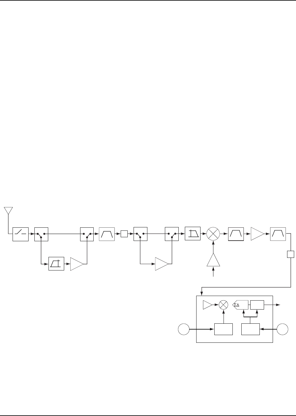
6881096C74-B May 25, 2005
Theory of Operation: Receiver Front-End 3-15
3.4.1.5 Mixer (D3258)
The received signal is down-converted by a double-balanced mixer to an Intermediate Frequency
(IF) of 109.65 MHz. The mixer is designed to provide low conversion loss and high intermodulation
performance. The injection buffer provides a 20 dBm LO signal to the mixer. High-side injection is
used.
3.4.2 UHF Range 1 (380–470 MHz) Band
The receiver circuits primary duties are to detect, filter, amplify, and demodulate RF signals in the
presence of strong interfering noise and unintended signals. The receiver (see Figure 3-14) is
broken down into the following blocks:
• Front-end, which includes:
- High pass fIlter and first low-noise amplifier (LNA)
- Preselector filter
- Switchable 15 dB attenuator
- Second LNA
- Image Filter
- First mixer
• Back-end, which includes:
- Intermediate Frequency (IF)
- ABACUS III IC
Figure 3-14. Receiver Front-End and Back-End (UHF Range 1)
Ant. SW.
Harm. FLT
Pre-Amp
Switch Pre-Amp
Switch Pre-Amp
Switch
Pre-Amp
Switch Mixer
Preselector 15 dB
Att.
Low Pass
Filter
RF Input
Crystal
24dBm
1st LO
Backend A/D Converter
SSI
Dec.
Filter
CLK
Synth.
LO
Synth.
2nd
LO
18MHz
CLK
IF Amp Crystal
109.65MHz
A
10 dB
Att.
380-470MHz
LNA
High Pass
Filter LNA
ADC
ABACUS III IC
A

May 25, 2005 6881096C74-B
3-16 Theory of Operation: Receiver Front-End
3.4.2.1 Highpass Filter and First Low-Noise Amplifier
The highpass filter and first low-noise amplifier (LNA) (11 dB gain) can be switched in and out of the
signal path by diode switches. When switched into the signal path, the sensitivity of the radio is
improved at the cost of degraded intermodulation performance. This can be necessary in fringe
areas when strong interference that can lead to intermodulation problems are not present and the
desired signal is weak.
The preamplifier version of the radio must be purchased to be able to control this option. If it has not
been purchased, the direct path created by the diode switches is the only one available, giving the
radio standard model performance with enhanced intermodulation rejection. Purchasing the
preamplifier option allows the user to select either mode with the CPS.
3.4.2.2 Preselector Filter
The front-end operates in the 380 to 470 MHz band. The front-end's primary function is to optimize
half IF rejection, image rejection, and selectivity while providing the first conversion. The front-end
uses a varactor-tuned filter that is tuned by the controller. The tuning signal is a DC control voltage
between 0 and 9V that come from the PA power control section. Low voltages are for lower
frequencies and higher voltages correspond to the higher frequencies. This filter is aligned in the
factory and can also be aligned using the Tuner software.
3.4.2.3 Switchable 15 dB Attenuator
This circuit block can provide 0 dB or 15 dB of attenuation in the signal path. Normally, it is set for
0 dB and does not affect the received signal. When strong signals are detected, the radio controller
can choose to activate this attenuator to provide protection to the back end circuits, and to enhance
high level intermodulation performance. Proprietary algorithms are used to control the switching.
3.4.2.4 Low-Noise Amplifier (LNA, U5302)
A diode (D5281) located after the varactor preselector and before the LNA protects the receiver from
strong RF signals by limiting the signal amplitude going into the amplifier. The LNA is a low-noise
monolithic IC providing ~ 15 dB of gain to the receiver. It is biased with 5 V and can be bypassed by
the radio software under very strong signal conditions.
The UHF receiver also has a second LNA based on Q5252 that can be activated or bypassed by the
radio software. This amplifier is protected by D5280 and provides 11 dB of gain. This is available
only if the preamplifier option has been purchased.
3.4.2.5 Image Filter
Following the LNA (U5302), the signal goes through a bandpass filter before it is sent to the mixer.
The passband is from 380 to 470 MHz with an insertion loss of about 2 dB, while the image rejection
is 55 dB. There is a trap on the input side of this filter to attenuate the 109.65 MHz IF.
3.4.2.6 Mixer
A passive double-balanced diode ring mixer is used to down-convert the received signal to an
Intermediate Frequency (IF) of 109.65 MHz. The mixer is designed to provide low conversion loss (<
7.0 dBm) and high intermodulation performance and requires a strong injection signal. The mixer is
driven by the receiver injection buffer, a two-stage LDMOS IC design, that amplifies the +3 dBm
high-side injection signal from the Frequency Generation Unit (FGU) to +24 dBm.
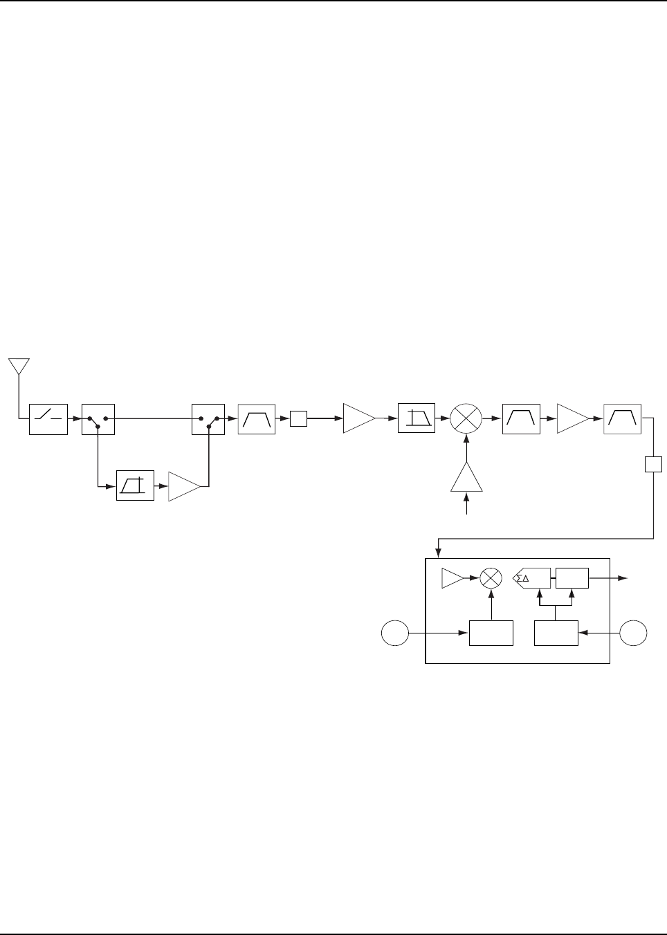
6881096C74-B May 25, 2005
Theory of Operation: Receiver Front-End 3-17
3.4.3 UHF Range 2 (450–520 MHz) Band
The receiver circuits primary duties are to detect, filter, amplify, and demodulate RF signals in the
presence of strong interfering noise and unintended signals. The receiver (see Figure 3-15) is
broken down into the following blocks:
• Front-end, which includes:
- High pass fIlter and first low-noise amplifier (LNA)
- Preselector filter
- Switchable 15 dB attenuator
- Second LNA
- Image Filter
- First mixer
• Back-end, which includes:
- Intermediate Frequency (IF)
- ABACUS III IC
Figure 3-15. Receiver Front-End and Back-End (UHF Range 2)
3.4.3.1 Highpass Filter and First Low-Noise Amplifier
The highpass filter and first low-noise amplifier (LNA) (11 dB gain) can be switched in and out of the
signal path by diode switches. When switched into the signal path, the sensitivity of the radio is
improved at the cost of degraded intermodulation performance. This can be necessary in fringe
areas when strong interference that can lead to intermodulation problems are not present and the
desired signal is weak.
The preamplifier version of the radio must be purchased to be able to control this option. If it has not
been purchased, the direct path created by the diode switches is the only one available, giving the
radio standard model performance with enhanced intermodulation rejection. Purchasing the
preamplifier option allows the user to select either mode with the CPS.
Ant. SW.
Harm. FLT
Pre-Amp
Switch Pre-Amp
Switch Mixer
Preselector 15 dB
Att.
Low Pass
Filter
RF Input
Crystal
24dBm
1st LO
Backend A/D Converter
SSI
Dec.
Filter
CLK
Synth.
LO
Synth.
2nd
LO
18MHz
CLK
IF Amp Crystal
109.65MHz
A
10 dB
Att.
450-520MHz
LNA
High Pass
Filter
LNA
ADC
ABACUS III IC
A

May 25, 2005 6881096C74-B
3-18 Theory of Operation: Receiver Front-End
3.4.3.2 Preselector Filter
The front-end operates in the 450 to 520 MHz band. The front-end's primary function is to optimize
half IF rejection, image rejection, and selectivity while providing the first conversion. The front-end
uses a varactor-tuned filter that is tuned by the controller. The tuning signal is a DC control voltage
between 0 and 9V that come from the PA power control section. Low voltages are for lower
frequencies and higher voltages correspond to the higher frequencies. This filter is aligned in the
factory and can also be aligned using the Tuner software.
3.4.3.3 Switchable 15 dB Attenuator
This circuit block can provide 0 dB or 15 dB of attenuation in the signal path. Normally, it is set for
0 dB and does not affect the received signal. When strong signals are detected, the radio controller
can choose to activate this attenuator to provide protection to the back end circuits, and to enhance
high level intermodulation performance. Proprietary algorithms are used to control the switching.
3.4.3.4 Low-Noise Amplifier (LNA, U5302)
A diode (D5281) located after the varactor preselector and before the LNA protects the receiver from
strong RF signals by limiting the signal amplitude going into the amplifier. The LNA is a low-noise
monolithic IC providing ~ 15 dB of gain to the receiver. It is biased with 5 V.
The UHF receiver also has a second LNA based on Q5252 that can be activated or bypassed by the
radio software. This amplifier is protected by D5280 and provides 11 dB of gain.
3.4.3.5 Image Filter
Following the LNA (U5302), the signal goes through a bandpass filter before it is sent to the mixer.
The passband is from 450 to 520 MHz with an insertion loss of about 2 dB, while the image rejection
is 55 dB. There is a trap on the input side of this filter to attenuate the 109.65 MHz IF.
3.4.3.6 Mixer
A passive double-balanced diode ring mixer is used to down-convert the received signal to an
Intermediate Frequency (IF) of 109.65 MHz. The mixer is designed to provide low conversion loss (<
7.0 dBm) and high intermodulation performance and requires a strong injection signal. The mixer is
driven by the receiver injection buffer, a two-stage LDMOS IC design, that amplifies the +3 dBm
high-side injection signal from the Frequency Generation Unit (FGU) to +24 dBm.
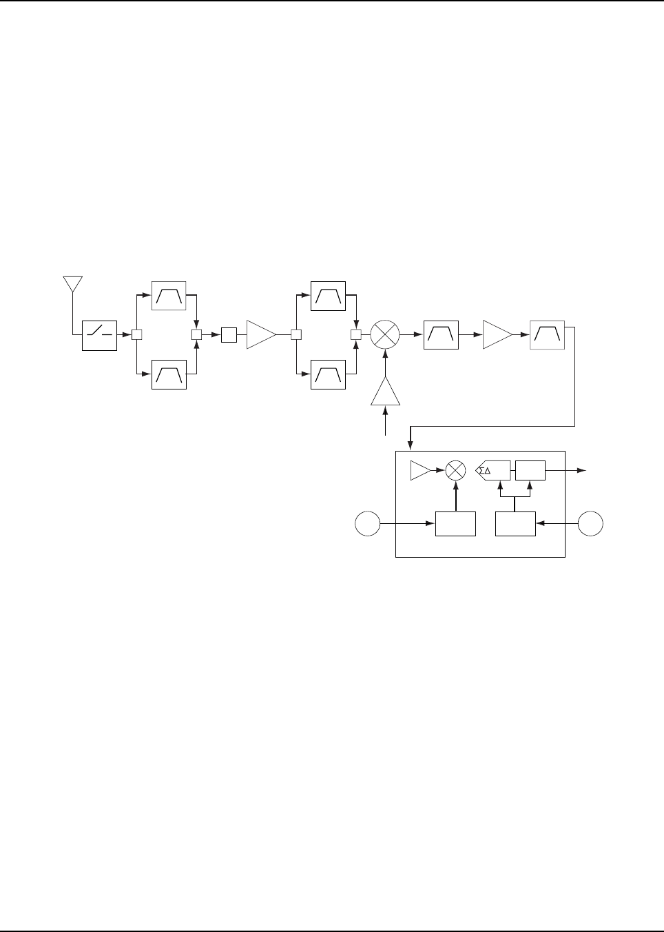
6881096C74-B May 25, 2005
Theory of Operation: Receiver Front-End 3-19
3.4.4 700–800 MHz Band
The receiver circuits primary duties are to detect, filter, amplify, and demodulate RF signals in the
presence of strong interfering noise and unintended signals. The receiver (see Figure 3-16) is
broken down into the following blocks:
• Front-end, which includes:
- Preselector filters
- Low-noise amplifier (LNA)
- First mixer
•IF
• Back-end
Figure 3-16. Receiver Front-End and Back-End (700–800 MHz)
3.4.4.1 Preselector Filters
The front-end operates in the 700 MHz and 800 MHz bands. The front-end's primary function is to
optimize image rejection and selectivity while providing the first conversion. The front- end uses fixed
ceramic-filter technology. There are two sets of filters: (B6250 and B6252) for the 800 MHz band and
(B6251 and B6253) for the 700 MHz band. These filters are switched between bands by a network of
diode switches (D6251 thru D6257) biased by RLC networks (C6254, C6260, R6254, and L6254)
that also act as RF chokes. The first filter is a dual-switched filter that reduces the image-frequency
response and limits some of the out-of-band interferers. The second filter following the monolithic
low-noise amplifier (LNA) provides additional image rejection.
3.4.4.2 Low-Noise Amplifier (LNA, U6250)
A diode (D6258) located after the first preselector and before the LNA protects the receiver from
strong RF signals by limiting the signal amplitude going into the amplifier. The LNA is a low-noise
monolithic IC providing ~ 16 dB of gain to the receiver. It is biased with 5 V at pins 1 and 6. The input
matching consists of an LC network (C6288, L6258) for optimal gain.
LNA
Ant. SW.
Harm. FLT Mixer
Preselect 2
Preselect 1
RF Input
Crystal
15dBm
1st LO
Backend A/D Converter
SSI
Dec.
Filter
CLK
Synth.
LO
Synth.
2nd
LO
18MHz
CLK
IF Amp Crystal
73.35MHz
A
700MHz
800MHz
MAEPF-27905-O
ADC
ABACUS III IC

May 25, 2005 6881096C74-B
3-20 Theory of Operation: Receiver Back-End
3.4.4.3 Mixer (U6251)
The monolithic, passive mixer IC down-converts the received signal to an Intermediate Frequency
(IF) of 73.35 MHz. The mixer is designed to provide low conversion loss (< 7.0) and high
intermodulation performance. To improve the performance of the mixer in both bands, a shunt 9.1 pF
capacitor (C6297) along with a resistive PI network (R6278, R6280, R6281) is designed at the IF
port (pin 5) of the mixer. The mixer is driven by the receiver injection buffer, a two-stage discrete/IC
design used with the VCO to efficiently drive the mixer over temperature with minimum power
variation. The injection buffer provides 15 dBm to the mixer. The VCO does high-side injection for
the 800 MHz band and low-side Injection for the 700 MHz band.
3.5 Receiver Back-End
This section discusses the receiver back-end (RXBE) components and detailed theory of operation.
The receiver back-end processes the down-converted, filtered IF signal to produce digital data for
final processing by the Patriot microcontroller IC.
3.5.1 VHF (136-174 MHz) Band
The receiver back-end contains the following major components:
• Intermediate frequency (IF) section.
• ABACUS III IC
3.5.1.1 Intermediate Frequency (IF) Section
The XTL 5000 radio uses two leadless, surface-mount, two-pole, third-overtone, quartz crystal filters
(Y3400, Y3401) separated by a 21 dB gain IF amplifier. The filters are centered at 109.65 MHz. This
narrowband bandpass filter contributes to the radio’s adjacent-channel and alternate-channel
rejection performance. Components L3401, L3403, L3404, L3405, C3421, C3414, C3409, C3416,
C3420, C3418 and C3415 are used as impedance-matching networks. Components Q3400, R3409,
R3401, R3402, R3405, R3407, and R3413 are used for biasing and stabilizing the transistor Q3400.
Components C3424, C3404 bypass the DC supply. L3400 is RF choke. Diode D3400 and Inductor
L3408 protect the Abacus and the second IF filter from strong In-band signals.
3.5.1.2 ABACUS III IC
The receiver back-end is designed around the ABACUS III (AD9874 IF digitizing subsystem) IC and
its associated circuitry. The AD9874 (Figure 3-17 on page 3-21) is a general-purpose, IF subsystem
that digitizes a low-level, 10–300 MHz IF input with a bandwidth up to 270 kHz. The signal chain of
the AD9874 consists of a variable gain, low-noise amplifier, a mixer; a bandpass, sigma-delta, A/D
converter; and a decimation filter with programmable decimation factor. An automatic gain control
(AGC) circuit provides the AD9874 with 12 dB of continuous gain adjustment. The high dynamic
range and inherent anti-aliasing provided by the bandpass, sigma-delta converter allow the AD9874
to cope with blocking signals 80 dB stronger than the desired signal. Auxiliary blocks include clock
and LO synthesizers, as well as an SPI port. Input signal RXIF is the 109.65 MHz IF from the IF
section in the receiver front-end.
Components C3000, C3038, and L3002 match the input impedance from 50 ohms (IF Filter
terminating impedance) to the ABACUS III IC input IFIN. Formatted SSI data is output to the Patriot
microcontroller IC for DSP processing on ports FS, DOUTA, and CLKOUT. Control logic is sent to
the ABACUS III IC from the Patriot microcontroller via the SPI lines (PC, PD, PE).
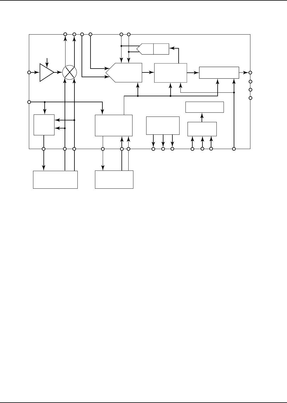
6881096C74-B May 25, 2005
Theory of Operation: Receiver Back-End 3-21
Figure 3-17. ABACUS III (AD9874) IC Functional Block Diagram from Data Sheet (VHF)
3.5.1.2.1 Second Local Oscillator
The ABACUS III IC local oscillator (LO) synthesizer controls the second LO. Signal FREF is the
16.8 MHz reference from the frequency generation unit (FGU). The second LO frequency is
107.4 MHz by default, or 111.9 MHz in special cases as necessary to avoid radio self-quieters. The
second LO signal mixes with IFIN to produce a 109.65 MHz final IF. The external VCO consists of
transistor Q3000, together with its bias and instability network and tank elements. Darlington
transistor Q3001 along with C3035 and C3017 form an active DC filter. The second-order loop filter
is comprised of C3044, C3005, and R3009.
3.5.1.2.2 Sampling Clock Oscillator
The ABACUS III IC sampling clock synthesizer, at Fclk=18 MHz (IF2=Fclk/8, where Fclk is the clock
rate), utilizes a negative-resistance core that is internal to the ABACUS III IC which, when used in
conjunction with an external LC tank (made up of L3003 and C3039) and a varactor (D3001), serves
as the VCO.
3.5.2 UHF Range 1 (380-470 MHz) Band
The receiver back-end (see Figure 3-14 on page 3-15) contains the following major components:
• Intermediate frequency (IF) filter
• ABACUS III IC
IFIN
FREF
-16dB
LNA
LO
Synth.
Sample Clock
Synthesizer
CLK VCO and
Loop Filter
LO VCOand
Loop Filter
Voltage
Reference
DAC AGC
ADC Decimation
Filter Formatting/SSI
Control Logic
fCLK = 13-26MHz
SPI
DOUTB
DOUTA
FS
CLKOUT
MXON
MXOP
IF2P
IF2N
GCP
GCN
LOP
IOUTL
LON
IOUTC
CLKP
CLKN
VREFP
VCM
VREFN
PC
PD
PE
SYNCB
MAEPF-27817-O
AD9874
May 25, 2005 6881096C74-B
3-22 Theory of Operation: Receiver Back-End
3.5.2.1 Intermediate Frequency (IF) Filter
The XTL 5000 radio uses two leadless, surface-mount, two-pole, third-overtone, quartz crystal filters
(Y5400, Y5401) separated by a 20 dB gain IF amplifier. The filter is centered at 109.65 MHz. This
narrow-bandpass filter gives the radio part of its adjacent-channel and alternate-channel rejection
performance. Impedance-matching networks are located at the input and output of each crystal. The
IF amplifier is made with Q5401. The 10 dB attenuator (U5400) located after the second crystal filter
is controlled by the software to limit the signal gain in front of the ABACUS III IC.
3.5.2.2 ABACUS III IC (U5002)
The receiver back-end is designed around the ABACUS III (AD9874 IF digitizing subsystem) IC and
its associated circuitry. The AD9874 (Figure 3-18) is a general-purpose, IF subsystem that digitizes a
low-level, 10-300 MHz IF input with a bandwidth up to 270 kHz. The signal chain of the AD9874
consists of a variable gain, low-noise amplifier, a mixer; a bandpass, sigma-delta, A/D converter; and
a decimation filter with programmable decimation factor. An automatic gain control (AGC) circuit
provides the AD9874 with 12 dB of continuous gain adjustment. The high dynamic range and
inherent anti-aliasing provided by the bandpass, sigma-delta converter allow the AD9874 to cope
with blocking signals 80 dB stronger than the desired signal. Auxiliary blocks include clock and LO
synthesizers, as well as an SPI port. Input signal RXIF is the 109.65 MHz IF from the IF filter.
Components C5002, C5007, and L5002 match the input impedance from 50 ohms (IF Filter
terminating impedance) to the ABACUS III IC input IFIN. Formatted SSI (synchronous serial
interface) data is output to the Patriot microcontroller IC for DSP processing on ports FS, DOUTA,
and CLKOUT. Control logic is sent to the ABACUS III IC from the Patriot microcontroller via the SPI
lines (PC, PD, PE).
Figure 3-18. ABACUS III (AD9874) IC Functional Block Diagram from Data Sheet (UHF Range 1)
IFIN
FREF
-16dB
LNA
LO
Synth.
Sample Clock
Synthesizer
CLK VCO and
Loop Filter
LO VCOand
Loop Filter
Voltage
Reference
DAC AGC
ADC Decimation
Filter Formatting/SSI
Control Logic
fCLK = 13-26MHz
SPI
DOUTB
DOUTA
FS
CLKOUT
MXON
MXOP
IF2P
IF2N
GCP
GCN
LOP
IOUTL
LON
IOUTC
CLKP
CLKN
VREFP
VCM
VREFN
PC
PD
PE
SYNCB
MAEPF 27817 O
AD9874

6881096C74-B May 25, 2005
Theory of Operation: Receiver Back-End 3-23
3.5.2.2.1 Second Local Oscillator (LO)
The ABACUS III IC local oscillator (LO) synthesizer controls the second LO. Signal FREF is the
16.8 MHz reference from the frequency generation unit (FGU). The second LO frequency is
107.4 MHz by default, or 111.9 MHz in special cases as necessary to avoid radio self-quieters. The
second LO signal mixes with IFIN to produce a 2.25 MHz final IF. The external VCO consists of
transistor Q5002, together with its bias and instability network and tank elements. Darlington
transistor Q5001 along with C5018 and C5050 form an active DC filter. The 2nd order loop filter is
comprised of C5044, C5045, and R5013.
3.5.2.2.2 Sampling Clock Oscillator
The ABACUS III IC sampling clock synthesizer, at Fclk=18 MHz (IF2=Fclk/8, where Fclk is the clock
rate), utilizes the clock VCO built around Q5003.
3.5.3 UHF Range 2 (450-520 MHz) Band
The receiver back-end (see Figure 3-15 on page 3-17) contains the following major components:
• Intermediate frequency (IF) filter
• ABACUS III IC
3.5.3.1 Intermediate Frequency (IF) Filter
The XTL 5000 radio uses two leadless, surface-mount, two-pole, third-overtone, quartz crystal filters
(Y5400, Y5401) separated by a 20 dB gain IF amplifier. The filter is centered at 109.65 MHz. This
narrow-bandpass filter gives the radio part of its adjacent-channel and alternate-channel rejection
performance. Impedance-matching networks are located at the input and output of each crystal. The
IF amplifier is made with Q5401. The 10 dB attenuator (U5400) located after the second crystal filter
is controlled by the software to limit the signal gain in front of the ABACUS III IC.
3.5.3.2 ABACUS III IC (U5002)
The receiver back-end is designed around the ABACUS III (AD9874 IF digitizing subsystem) IC and
its associated circuitry. The AD9874 (Figure 3-19 on page 3-24) is a general-purpose, IF subsystem
that digitizes a low-level, 10-300 MHz IF input with a bandwidth up to 270 kHz. The signal chain of
the AD9874 consists of a variable gain, low-noise amplifier, a mixer; a bandpass, sigma-delta, A/D
converter; and a decimation filter with programmable decimation factor. An automatic gain control
(AGC) circuit provides the AD9874 with 12 dB of continuous gain adjustment. The high dynamic
range and inherent anti-aliasing provided by the bandpass, sigma-delta converter allow the AD9874
to cope with blocking signals 80 dB stronger than the desired signal. Auxiliary blocks include clock
and LO synthesizers, as well as an SPI port. Input signal RXIF is the 109.65 MHz IF from the IF filter.
Components C5002, C5007, and L5002 match the input impedance from 50 ohms (IF Filter
terminating impedance) to the ABACUS III IC input IFIN. Formatted SSI (synchronous serial
interface) data is output to the Patriot microcontroller IC for DSP processing on ports FS, DOUTA,
and CLKOUT. Control logic is sent to the ABACUS III IC from the Patriot microcontroller via the SPI
lines (PC, PD, PE).
May 25, 2005 6881096C74-B
3-24 Theory of Operation: Receiver Back-End
Figure 3-19. ABACUS III (AD9874) IC Functional Block Diagram from Data Sheet (UHF Range 2)
3.5.3.2.1 Second Local Oscillator (LO)
The ABACUS III IC local oscillator (LO) synthesizer controls the second LO. Signal FREF is the
16.8 MHz reference from the frequency generation unit (FGU). The second LO frequency is
107.4 MHz by default, or 111.9 MHz in special cases as necessary to avoid radio self-quieters. The
second LO signal mixes with IFIN to produce a 2.25 MHz final IF. The external VCO consists of
transistor Q5002, together with its bias and instability network and tank elements. Darlington
transistor Q5001 along with C5018 and C5050 form an active DC filter. The 2nd order loop filter is
comprised of C5044, C5045, and R5013.
3.5.3.2.2 Sampling Clock Oscillator
The ABACUS III IC sampling clock synthesizer, at Fclk=18 MHz (IF2=Fclk/8, where Fclk is the clock
rate), utilizes the clock VCO built around Q5003.
3.5.4 700–800 MHz Band
The receiver back-end (see Figure 3-16 on page 3-19) contains the following major components:
• Intermediate frequency (IF) filter
• ABACUS III IC
IFIN
FREF
-16dB
LNA
LO
Synth.
Sample Clock
Synthesizer
CLK VCO and
Loop Filter
LO VCOand
Loop Filter
Voltage
Reference
DAC AGC
ADC Decimation
Filter Formatting/SSI
Control Logic
fCLK = 13-26MHz
SPI
DOUTB
DOUTA
FS
CLKOUT
MXON
MXOP
IF2P
IF2N
GCP
GCN
LOP
IOUTL
LON
IOUTC
CLKP
CLKN
VREFP
VCM
VREFN
PC
PD
PE
SYNCB
MAEPF 27817 O
AD9874
6881096C74-B May 25, 2005
Theory of Operation: Receiver Back-End 3-25
3.5.4.1 Intermediate Frequency (IF) Filter
The XTL 5000 radio uses two leadless, surface-mount, two-pole, third-overtone, quartz crystal filters
(B6350, B6351) separated by a 20 dB gain IF amplifier. The filter is centered at 73.35 MHz. This
narrow-bandpass filter gives the radio its adjacent-channel and alternate-channel rejection
performance. Components L6350, L6351, L6352, L6353, C6351, C6352, C6353, C6355, C6356,
and C6357 are used as impedance-matching networks. Components L6355, R6354, R6352, R6353,
C6354, and R6350 are used for biasing and stabilizing the transistor Q6350. Component C6358
bypasses the DC supply. L6355 is an RF choke.
3.5.4.2 ABACUS III IC (U6000)
The receiver back-end is designed around the ABACUS III (AD9874 IF digitizing subsystem) IC and
its associated circuitry. The AD9874 (Figure 3-20) is a general-purpose, IF subsystem that digitizes a
low-level, 10–300 MHz IF input with a bandwidth up to 270 kHz. The signal chain of the AD9874
consists of a variable gain, low-noise amplifier, a mixer; a bandpass, sigma-delta, A/D converter; and
a decimation filter with programmable decimation factor. An automatic gain control (AGC) circuit
provides the AD9874 with 12 dB of continuous gain adjustment. The high dynamic range and
inherent anti-aliasing provided by the bandpass, sigma-delta converter allow the AD9874 to cope
with blocking signals 80 dB stronger than the desired signal. Auxiliary blocks include clock and LO
synthesizers, as well as an SPI port. Input signal RXIF is the 73.35 MHz IF from the IF filter in the
receiver front-end.
Components C6000, C6001, and L6000 match the input impedance from 50 ohms (IF Filter
terminating impedance) to the ABACUS III IC input IFIN. Formatted SSI (synchronous serial
interface) data is output to the Patriot microcontroller IC for DSP processing on ports FS, DOUTA,
and CLKOUT. Control logic is sent to the ABACUS III IC from the Patriot microcontroller via the SPI
lines (PC, PD, PE).
Figure 3-20. ABACUS III (AD9874) IC Functional Block Diagram from Data Sheet (700–800 MHz)
IFIN
FREF
-16dB
LNA
LO
Synth.
Sample Clock
Synthesizer
CLK VCO and
Loop Filter
LO VCOand
Loop Filter
Voltage
Reference
DAC AGC
ADC Decimation
Filter Formatting/SSI
Control Logic
fCLK = 13-26MHz
SPI
DOUTB
DOUTA
FS
CLKOUT
MXON
MXOP
IF2P
IF2N
GCP
GCN
LOP
IOUTL
LON
IOUTC
CLKP
CLKN
VREFP
VCM
VREFN
PC
PD
PE
SYNCB
MAEPF-27817-O
AD9874
May 25, 2005 6881096C74-B
3-26 Theory of Operation: Transmitter
3.5.4.2.1 Second Local Oscillator (LO)
The ABACUS III IC local oscillator (LO) synthesizer controls the second LO. Signal FREF is the
16.8 MHz reference from the frequency generation unit (FGU). The second LO frequency is
75.6 MHz by default, or 71.1 MHz in special cases as necessary to avoid radio self-quieters. The
second LO signal mixes with IFIN to produce a 2.25 MHz final IF. The external VCO consists of
transistor Q6000, together with its bias and instability network and tank elements. Darlington
transistor Q6001 along with C6024 and C6025 form an active DC filter. The 2nd order loop filter is
comprised of C6056, C6057, and R6019.
3.5.4.2.2 Sampling Clock Oscillator
The ABACUS III IC sampling clock synthesizer, at Fclk=18 MHz (IF2=Fclk/8, where Fclk is the clock
rate), utilizes a negative-resistance core that is internal to the ABACUS III IC which, when used in
conjunction with an external LC tank (made up of L6003 and C6031) and a varactor (D6030), serves
as the VCO.
3.6 Transmitter
This section of the theory of operation provides a detailed circuit description of the transmitter, which
includes the RF power amplifier (RFPA), output network (ON), and power control.
When reading the theory of operation, refer to the appropriate schematic and component location
diagrams located in “Chapter 7. Schematics, Component Location Diagrams, and Parts Lists”. This
detailed theory of operation will help isolate the problem to a particular component. However, first
use the ASTRO Digital XTL 5000 VHF/UHF Range 1/UHF Range 2/700–800 MHz Mobile Radio
Basic Service Manual to troubleshoot the problem to a particular section.
3.6.1 VHF (136-174 MHz) Band
3.6.1.1 50-Watt Transmitter
The following text discusses the 50-W transmitter.
3.6.1.1.1 RF Power Amplifier (RFPA)
The RFPA consists of three gain stages, which are shown in Figure 3-21.
Figure 3-21. 50-Watt RF Power Amplifier (RFPA) Gain Stages (VHF)

6881096C74-B May 25, 2005
Theory of Operation: Transmitter 3-27
First Stage
The RFPA first stage provides gain that is determined by the control voltage, RFPA_CNTRL. This
control voltage is generated in the power control section and is a function of the final-stage output
power, temperature, and current, as well as the control and A+ voltage levels. See “3.6.1.4. Power
Control (for 50W and 100W Transmitter)” on page 3-30 for a detailed explanation of the power
control section.
The 2 mW TX_INJ signal is routed to the U3550 first-stage device (Pin 16, RFIN) via C3500 to an
integrated, wide-band input match. U3550 is a two-stage LDMOS device with a bandpass interstage
match consisting of C3503, L3502, C3504, R3501 and C3505 routed between VD1 (pin 14) and G2
(pin 11). L3501 and L3503 provide the K9.1V drain bias voltage for the first and second stages to
VD1 (pin 14) and RFOUT1/2 (pins 6 and 7), respectively. The RFPA_CNTRL gate bias is provided to
both stages internally via VCNTRL (pin 1). Both U3550 stages are operated Class A.
Driver Stage
C3521, L3520, C3520, and a transmission line form a low-pass, interstage match that transfers
power to the Q3530 LDMOS transistor. R3520-3 provide device stability, and R3524 and C3522
supply the VGBIAS2 gate bias. L3530-1, R3530-1, C3530, C3531, C3536 and C3537 form the A+
drain bias circuit. Q3530 is operated Class AB.
Final Stage
C3532-4, and transmission lines form a bandpass. R3532-8 provide stability for Q3550. R3540 and
C3535 supply the VGBIAS1 gate bias to Q3550. L3549-51, C3548-51, and R3551 form the A+ drain
bias circuit.
C3552-9 and transmission lines form a low-pass. Q3550 operate Class AB.
R3550, R3560, C3563, and U3561 comprise the final-stage, current-sense circuit that generates the
VCURRENT voltage proportional to the final stage current. R3560 sets the circuit gain. U3560
generates the VTEMP voltage, which is proportional to the final-stage temperature.
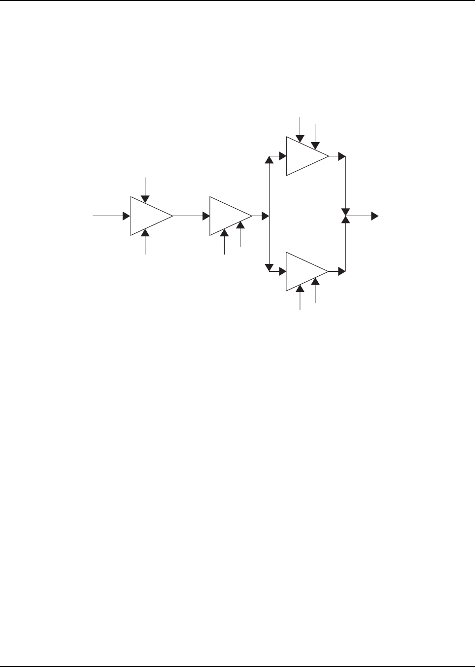
May 25, 2005 6881096C74-B
3-28 Theory of Operation: Transmitter
3.6.1.2 100-Watt Transmitter
The following text discusses the 100-W transmitter.
3.6.1.2.1 RF Power Amplifier (RFPA)
The RFPA consists of three gain stages, which are shown in Figure 3-22.
Figure 3-22. 100-Watt RF Power Amplifier (RFPA) Gain Stages (VHF)
First Stage
The RFPA first stage provides gain that is determined by the control voltage, RFPA_CNTRL. This
control voltage is generated in the power control section and is a function of the final-stage output
power, temperature, and current, as well as the control and A+ voltage levels. See “3.6.1.4. Power
Control (for 50W and 100W Transmitter)” on page 3-30 for a detailed explanation of the power
control section.
The 2 mW TX_INJ signal is routed to the U3500 first-stage device (Pin 16, RFIN) via C3500 to an
integrated, wide-band input match. U3550 is a two-stage LDMOS device with a bandpass interstage
match consisting of C3502 and L3501 routed between VD1 (pin 14) and G2 (pin 11). L3501 and
L3500 provide the K9.1V drain bias voltage for the first and second stages to VD1 (pin 14) and
RFOUT1/2 (pins 6 and 7), respectively. The RFPA_CNTRL gate bias is provided to both stages
internally via VCNTRL (pin 1). Both U3500 stages are operated Class A.
Driver Stage
C3521, L3520, C3520, and a transmission line form a low-pass, interstage match that transfers
power to the Q3520 LDMOS transistor. R3520-5 provide device stability, and R3526 and C3522
supply the VGBIAS2 gate bias. L3521, R3528, C3525, C3524, C3536, L3522 and R3527 form the
A+ drain bias circuit. Q3520 is operated Class AB.
50W
RFPA_out
100W
50W
Q3540
Q3541
Q3520
10W
5W
A+
A+
A+ Vg_bias
Vg_bias
Vg_bias
100mW
RFPA_cntrl
Tx_inj
2mW
Key9.1V
U3500
30C65
5W
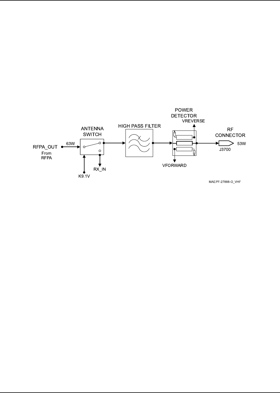
6881096C74-B May 25, 2005
Theory of Operation: Transmitter 3-29
Dual Final Stage
C3540-1, C3543-4 and transmission lines form a bandpass. R3541-8 provide stability for Q3540.
R3550-7 provide stability for Q3541. R3540 and R3568 supply the VGBIAS1 gate bias to Q3540.
R3569 and R3558 supply the VGBIAS2 gate bias to Q3541. L3540-4 and C3560-1 form the A+ drain
bias circuit. C3548-55 and transmission lines form a low-pass. Q3540-1 operate Class AB.
R3560-1, C3561, and U3561 comprise the final-stage, current-sense circuit that generates the
VCURRENT voltage proportional to the final stage current. R3564 sets the circuit gain. U3560
generates the VTEMP voltage, which is proportional to the final-stage temperature.
3.6.1.3 Output Network (ON) - (for 50W and 100W Transmitter)
The ON consists of the antenna switch, harmonic filter, and power detector (see Figure 3-23).
Figure 3-23. Output Network Components (VHF)
Antenna Switch
The antenna switch functions in two modes, which are determined by the presence of K9.1V. The
K9.1V switch bias is applied via L3700, L3731-2, and C3702. When K9.1V is present, the switch is in
TX mode. D3701-2 and D3704 are forward biased forming a low-loss path from the RFPA final stage
to the harmonic filter and a 60 dB isolation path between the RFPA final stage and the RX front-end.
Isolation is achieved via a quarter-wave transmission line between D3701 and D3702. D3701-4
serves as an ESD protection circuit against ESD discharge on the antenna connector.
When K9.1V is absent, the switch is in RX mode. D3701 and D3702 are reverse biased forming a
low-loss path from the harmonic filter to the RX front-end and a 60 dB isolation path from the
harmonic filter to the RFPA final stage. Isolation is achieved via the D3701 off resistance.
Harmonic Filter
L3720-7, C3720-3, form the twelve-element, low-pass harmonic filter. The filter attenuates
harmonics generated by the RFPA when the antenna switch is in TX mode and provides extra
selectivity when the antenna switch is in RX mode.
Power Detector
The power detector consists of two asymmetric, coupled transmission lines and detection circuitry
that detects forward and reverse power. C3730-1, D3730, L3730, R3730-3, and R3735-6 form the
forward-power detector (VFORWARD), which is used for power leveling. C3732-3, D3731, L3731,
R3737-9, and R3733-4 form the reverse-power detector (VREVERSE). L3737 provides an
electrostatic discharge path to protect the RFPA final stage device.
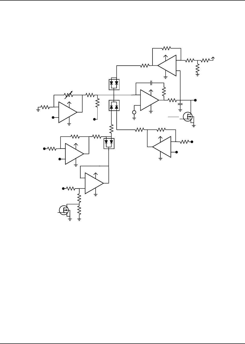
May 25, 2005 6881096C74-B
3-30 Theory of Operation: Transmitter
3.6.1.4 Power Control (for 50W and 100W Transmitter)
The power control section is comprised of a control loop to level forward power and protection
mechanisms to reduce power to a safe level for the given environmental conditions
(see Figure 3-24).
Figure 3-24. Power Control Components (VHF)
Power Control Loop
VFORWARD from the ON is buffered via the non-inverting, variable-gain stage U0956-2 whose gain
is set by EPOT U0952. The proper gain is determined during power-detection calibration tuning.
Buffered VFORWARD (U0956-2, Pin 7) is added to PWR_SET via R0971, R0972, and R0947 and
then compared to a reference determined by R0974 and R0975. PWR_SET is supplied by the
digital-to-analog converter (DAC) U0959, Pin 2. Comparator stage U0956-3 increases or decreases
RFPA_CNTRL so that the voltage at U0956-3, Pin 9 in the same at the reference voltage at U0956-
3, Pin 10. When the PWR_SET voltage is decreased, U0956-3 increases RFPA_CNTRL to increase
VFORWARD which is proportional to forward power thus increasing the power level. When the
PWR_SET voltage is increased, U0956-3 decreases RFPA_CNTRL to decrease VFORWARD, thus
decreasing the power level. The microprocessor initiates the loop through U0958-1 and Q0954.
Loop timing is set via software together with R0977, and C0973.
EEPOT
U0952
Q0954
RFPA_CNTRL
(TO RFPA)
U0957-4
U0957-4
U0956-3
Q0955
TEMP_2
(U0959, PIN 10)
VTEMP
(FROM RFPA)
PA_EN
CURR_LIM_SET
(U0959, PIN1)
VCURRENT
(FROM RFPA)
9.3V
9.3V
9.3V
9.3V
9.3V
9.3V 9.3V
VFORWARD
(FROM ON) PWR_SET
(U0959, PIN 2)
D0950
D0951
1.5V
D0952
U0957-1
U0956-2
U0957-2
TEMP_1
(U0959, PIN 9)
+
-
+
-
+
-
+
-
+
-
+
-
+
-
MAEPF-27889-O
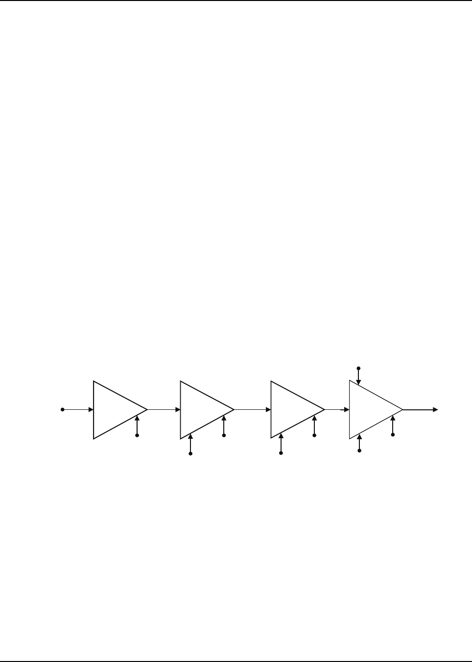
6881096C74-B May 25, 2005
Theory of Operation: Transmitter 3-31
Protection Mechanisms
Final-stage temperature is sensed in the RFPA resulting in VTEMP, which is proportional to
temperature. VTEMP is compared against a reference voltage TEMP_1 (U0959, pin 9) via U0957-1.
When VTEMP exceeds TEMP_1, the U0957-1, pin 1, voltage increases and forward biases one of
the D0951 diodes, which cuts back power. Power continues to cut back with rising temperature until
the voltage level at the junction of R0978 and R0983 is high enough to forward bias D0952, thus
clamping the cut back so that the radio meets its duty cycle specification while providing protection
against high-temperature conditions. The clamping level is set via TEMP_2 (U0959, pin 10) and
U0957-2. U0957-3 is used to sense if a high A+ battery voltage condition exists and, if it does, the
Q0955 gate is biased on, which increases the clamp voltage allowing for additional power cutback
for a high A+, high temperature condition.
Final-stage current is also monitored via VCURRENT, which is proportional to current. VCURRENT
is compared against a reference CURR_LIM_SET (U0959, pin 1) which is tuned after power
characterization. If VCURRENT exceeds CURR_LIM_SET, then U0957-4, pin 14, voltage rises and
forward biases one of the D0951 diodes, which limits power.
Finally, control voltage is limited by U0956-4 and D0950. RFPA_CNTRL can rise to the control
voltage limit set by R0942-4.
3.6.2 UHF Range 1 (380-470 MHz) Band
3.6.2.1 40-Watt Transmitter
The following text discusses the 40-W transmitter.
3.6.2.1.1 RF Power Amplifier (RFPA)
The RFPA consists of three gain stages, which are shown in Figure 3-25.
Figure 3-25. 40-Watt RF Power Amplifier (RFPA) Gain Stages (UHF Range 1)
FIRST
STAGE
0.5mW U5501
C65
250mW Q5502
1518
3.5W Q5503
1570
51W
To Antenna
Switch
RFPA_CNTRL
K9.1V
TRANSMIT
BUFFER
TX_INJ
From
FGU
2mW Q5501
C65
K9.1V
VGBIAS3
A+
DRV_9.3V
VGBIAS1
VGBIAS2 FINAL
STAGE
RFPA_OUT
DRIVER
STAGE

May 25, 2005 6881096C74-B
3-32 Theory of Operation: Transmitter
First Stage
The RFPA first stage provides gain that is determined by the control voltage, RFPA_CNTRL. This
control voltage is generated in the power control section and is a function of the final-stage output
power, temperature, and current, as well as the control and A+ voltage levels. See “3.6.2.4. Power
Control (for 40W and 100W Transmitter)” on page 3-35 for a detailed explanation of the power
control section.
The 0.5 mW TX_INJ signal is routed to the U5501 first stage device (Pin 16, RFIN) via C5508 to an
integrated, wide-band input match. U5501 is a two-stage LDMOS device with a bandpass interstage
match consisting of L5503, C5507, and C5509 routed between VD1 (pin 14) and G2 (pin 11). L5502
and L5505 provide the K9.1V drain bias voltage for the first and second stages to VD1 (pin 14) and
RFOUT1/2 (pins 6 and 7), respectively. The RFPA_CNTRL gate bias is provided to both stages
internally via VCNTRL (pin 1). Both U5501 stages are operated Class A and the second-stage output
power is approximately 250 mW.
Driver Stage
C5566, C5516, C5518 and a transmission line form a low-pass, interstage match that transfers
power to the Q5502 LDMOS transistor. R5511-R5515 provide device stability, and R5527, C5556,
C5525 and R5516 supply the VGBIAS3 gate bias. L5508, C5527, R5517, E5501 and C5526 form
the 9.3 V drain bias circuit. The 9.3 V drain voltage is supplied from regulator U5570 via R5574. The
9.3 V supply to the driver is only present during transmit and is disabled during receive via the K9.1V
signal and Q5570. Q5502 is operated Class AB and its output power is approximately 3.5 W.
Final Stage
C5559, C5560, C5535, C5538, and transmission lines form a low pass, splitter match that transfers
power to the LDMOS final-stage transistor Q5503. Q5503 contains two transistors in a single
package, each with it's own gate and drain lead. R5530, R5533, R5534 and R5536 provide stability
for Q5503. R5525, C5557, C5539 and R5520 supply the VGBIAS1 gate bias to Q5503-7. R5526,
C5558, C5540 and R5521 supply the VGBIAS2 gate bias to Q5503-6. L5510, C5549, R5523, E5502
and C5550 form the A+ drain bias circuit to Q5503-2 and Q5503-3. C5542-43, C5545-46, C5547-48,
C5551-53 and transmission lines form a low -pass combiner match that transfers approximately 51
W to the antenna switch. R5535 provides stability for Q5503. Q5503 operates Class AB.
R5522 and U5503 comprise the final-stage, current-sense circuit that generates the VCURRENT
voltage proportional to the final stage current. R5519 sets the circuit gain. U5502 generates the
VTEMP voltage, which is proportional to the final-stage temperature.
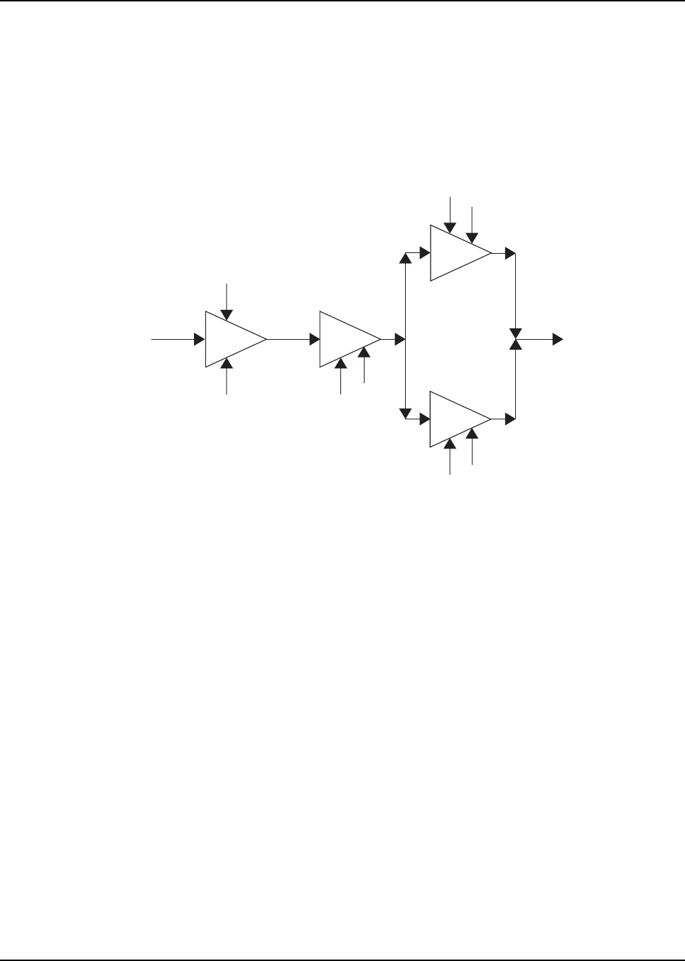
6881096C74-B May 25, 2005
Theory of Operation: Transmitter 3-33
3.6.2.2 100-Watt Transmitter
The following text discusses the 100-W transmitter.
3.6.2.2.1 RF Power Amplifier (RFPA)
The RFPA consists of three gain stages, which are shown in Figure 3-26.
Figure 3-26. 100-Watt RF Power Amplifier (RFPA) Gain Stages (UHF Range 1)
First Stage
The RFPA first stage provides gain that is determined by the control voltage, RFPA_CNTRL. This
control voltage is generated in the power control section and is a function of the final-stage output
power, temperature, and current, as well as the control and A+ voltage levels. See “3.6.2.4. Power
Control (for 40W and 100W Transmitter)” on page 3-35 for a detailed explanation of the power
control section.
The 2.5 mW TX_INJ signal is routed to the U5500 first stage device (Pin 16, RFIN) via C5524 to an
integrated, wide-band input match. U5500 is a two-stage LDMOS device with a bandpass interstage
match consisting of L5511, L5510, C5511 routed between VD1 (pin 14) and G2 (pin 11). L5510 and
R5510 provide the K9.1V drain bias voltage for the first and second stages to VD1 (pin 14) and
RFOUT1/2 (pins 6 and 7), respectively. The RFPA_CNTRL gate bias is provided to both stages
internally via VCNTRL (pin 1). Both U5501 stages are operated Class A and the second-stage output
power is approximately 300 mW.
Driver Stage
C5525, L5514, C5516, C5518, C5519, C5523 and a transmission line form a low-pass, interstage
match that transfers power to the Q5502 LDMOS transistor. R5520-R5525 provide device stability,
and R5526, C5520 and C5529 supply the VGBIAS3 gate bias. L5520, C5521, R5527, L5521, R5528
and C5522 form the A+ drain bias circuit. Q5520 is operated Class AB and its output power is
approximately 8 W.
50W
RFPA_out
100W
50W
Q5540
Q5541
Q5520
8W
4W
A+
A+
A+ Vg_bias
Vg_bias
Vg_bias
300mW
RFPA_cntrl
Tx_inj
2.5mW
Key9.1V
U5500
30C65
4W
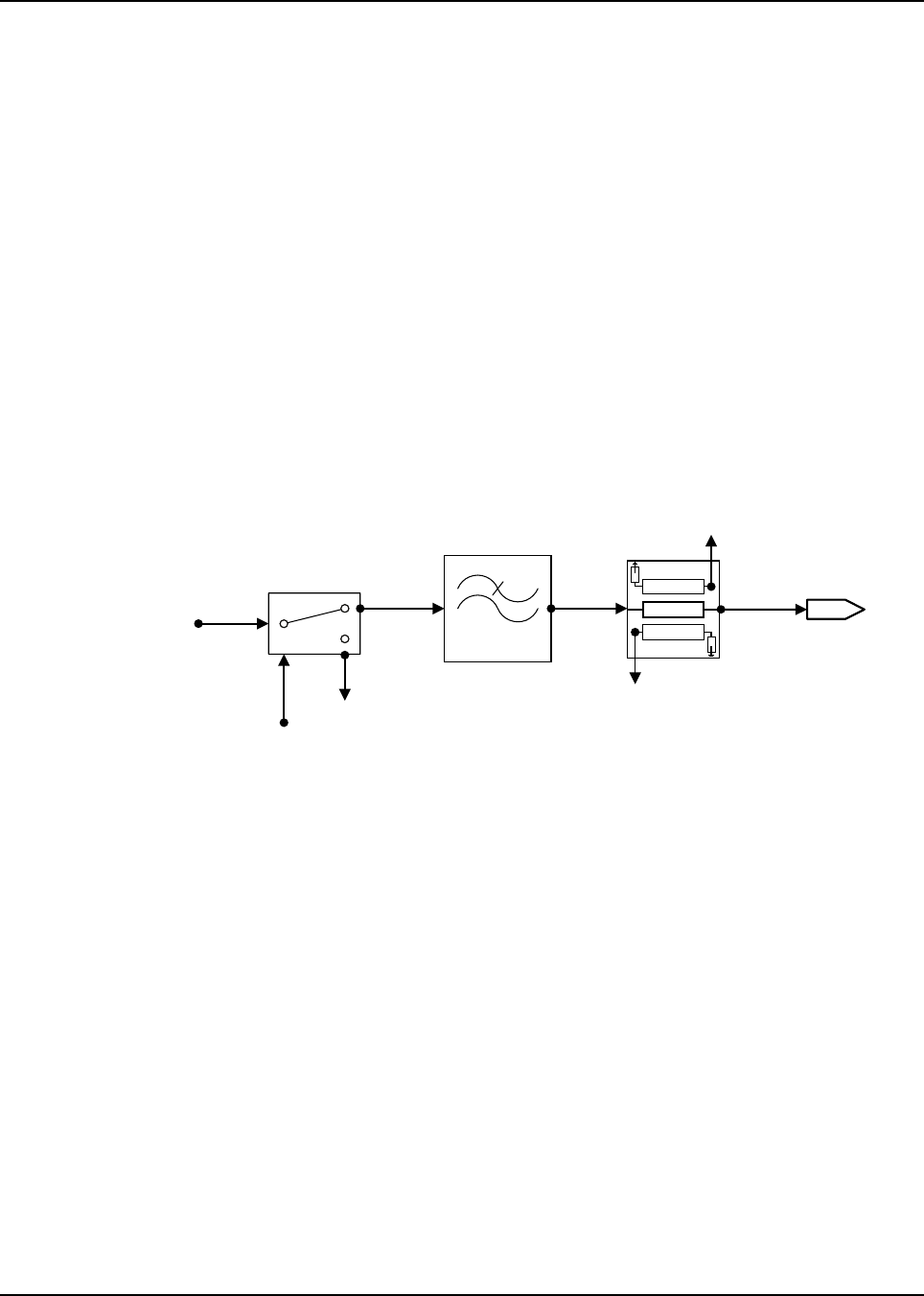
May 25, 2005 6881096C74-B
3-34 Theory of Operation: Transmitter
Dual Final Stage
C5530, C5531, C5532, C5533, C5536, C5537-41 and transmission lines form a low pass, splitter
match that transfers power to the LDMOS dual final-stage transistors Q5541 and Q5540. Q5540 and
Q5541 contain two transistors in a single package, each with it's own gate and drain lead. R5542-5,
R5548-51 provide stability for Q5540. R5552-5, R5557-60 provide stability for Q5541. R5546, C5602
and C5542 supply the VGBIAS1 gate bias to Q5540. R5581, C5550 and C5603 supply the VGBIAS2
gate bias to Q5541. L5543, L5544, R5574, C5567 and C5568 form the A+ drain bias circuit to Q5540
and Q5541. C5551-56, C5559-66, C5584, C5587, C5589 and transmission lines form a low -pass
combiner match that transfers approximately 100 W to the antenna switch. R5562 provides stability
for Q5540. R5573 provides stability for Q5541. Both Q5540 and Q5541 operate Class AB.
R5575 and U5561 comprise the final-stage, current-sense circuit that generates the VCURRENT
voltage proportional to the final stage current. R5578 sets the circuit gain. U5560 generates the
VTEMP voltage, which is proportional to the final-stage temperature.
3.6.2.3 Output Network (ON) - (for 40W and 100W Transmitter)
The ON consists of the antenna switch, harmonic filter, and power detector (see Figure 3-27).
Figure 3-27. Output Network Components (UHF Range 1)
Antenna Switch
The antenna switch functions in two modes determined by the presence of K9.1V. The K9.1V switch
bias is applied via L5701and C5702. When K9.1V is present, the switch is in TX mode. D5701,
D5702 and D5703 are forward biased forming a low-loss path from the RFPA final stage to the
harmonic filter and a 20 dB isolation path between the RFPA final stage and the RX front-end.
Isolation is achieved via a quarter-wave transmission lines between D5701 - D5702 and between
D5702 - D5703. C5709-10 resonates out the D5702-3 on inductance improving the isolation. When
K9.1V is absent, the switch is in RX mode. D5701, D5702 and D5703 are reverse biased forming a
low-loss path from the harmonic filter to the RX front-end and a 20 dB isolation path from the
harmonic filter to the RFPA final stage. Isolation is achieved via the D5701 off resistance. L5702
resonates out the D5701 off capacitance improving the isolation.
Harmonic Filter
The harmonic filter is a 7-element, equal-L Zolotarev quasi-lowpass filter consisting of C5712 and
C5713, C5719 thru C5721 and L5706 thru L5708. L5712, C5711 and L5713, C5714 form two shunt
zeros for extra attenuation at the second harmonic. C5708 acts as a DC block between the filter and
the antenna switch. The filter provides approximately 60 dB of harmonic rejection. The harmonic
filter together with the antenna switch provides approximately 0.7 dB insertion loss between the
transmitter power amplifier and the antenna.
RFPA_OUT
ANTENNA
SWITCH
H-FILTER
POWER
DETECTOR
RF
CONNECTOR
From
RFPA
51W
K9.1V
VREVERSE
VFORWARD
J5701
44W
RX_IN

6881096C74-B May 25, 2005
Theory of Operation: Transmitter 3-35
Power Detector
The power detector consists of a main microstrip transmission line that transfers power from the
harmonic filter to the antenna and two parallel lines that are used to detect the forward and reverse
power. The forward power detection line is terminated via R5707 and R5708. RF energy coupled
onto this line is rectified and filtered via D5704 and C5715 to provide a DC voltage to the power
control circuitry that is proportional to the forward transmitted power level. The detected forward
voltage is approximately 1.5 Vdc when the radio is putting out 44 watts. Thermister R5704
compensates for temperature changes in D5704 to maintain constant DC voltage versus detected
forward power over temperature.
The reverse power detection line is terminated via R5705-06. RF energy coupled onto this line is
rectified and filtered via D5705 and C5718 to provide a DC voltage to the power control circuitry that
is proportional to the reverse power level reflected back from the antenna. Thermister R5712
compensates for temperature changes in D5705 to maintain constant DC voltage versus detected
reverse power over temperature.
3.6.2.4 Power Control (for 40W and 100W Transmitter)
The power control section is comprised of a control loop to level forward power, and protection
mechanisms to reduce power to a safe level for the given environmental conditions (see Figure 3-28
on page 3-36).

May 25, 2005 6881096C74-B
3-36 Theory of Operation: Transmitter
Figure 3-28. Power Control Components (UHF Range 1)
Power Control Loop
VFORWARD from the ON is buffered via the non-inverting, variable-gain stage U0956-2 whose gain
is set by EPOT U0952. The proper gain is determined during power-detection calibration tuning.
Buffered VFORWARD (U0956-2, Pin 7) is added to PWR_SET via R0971 and R0972 and then
compared to a reference determined by R0974 and R0975. PWR_SET is supplied by the digital-to-
analog converter (DAC) U0959, Pin 2. Comparator stage U0956-3 increases or decreases
RFPA_CNTRL so that the voltage at U0956-3, Pin 9 in the same at the reference voltage at U0956-
3, Pin 10. When the PWR_SET voltage is decreased, U0956-3 increases RFPA_CNTRL to increase
VFORWARD which is proportional to forward power thus increasing the power level. When the
PWR_SET voltage is increased, U0956-3 decreases RFPA_CNTRL to decrease VFORWARD, thus
decreasing the power level. The microprocessor initiates the loop through U0958-1 and Q0954.
Loop timing is set via software together with R0977 and C0973.
EEPOT
U0952
Q0954
RFPA_CNTRL
(TO RFPA)
U0957-4
U0957-4
U0956-3
Q0955
TEMP_2
(U0959, PIN 10)
VTEMP
(FROM RFPA)
PA_EN
CURR_LIM_SET
(U0959, PIN1)
VCURRENT
(FROM RFPA)
9.3V
9.3V
9.3V
9.3V
9.3V
9.3V 9.3V
VFORWARD
(FROM ON) PWR_SET
(U0959, PIN 2)
D0950
D0951
1.5V
D0952
U0957-1
U0956-2
U0957-2
TEMP_1
(U0959, PIN 9) +
-
+
-
+
-
+
-
+
-
+
-
+
-
MAEPF-27889-O
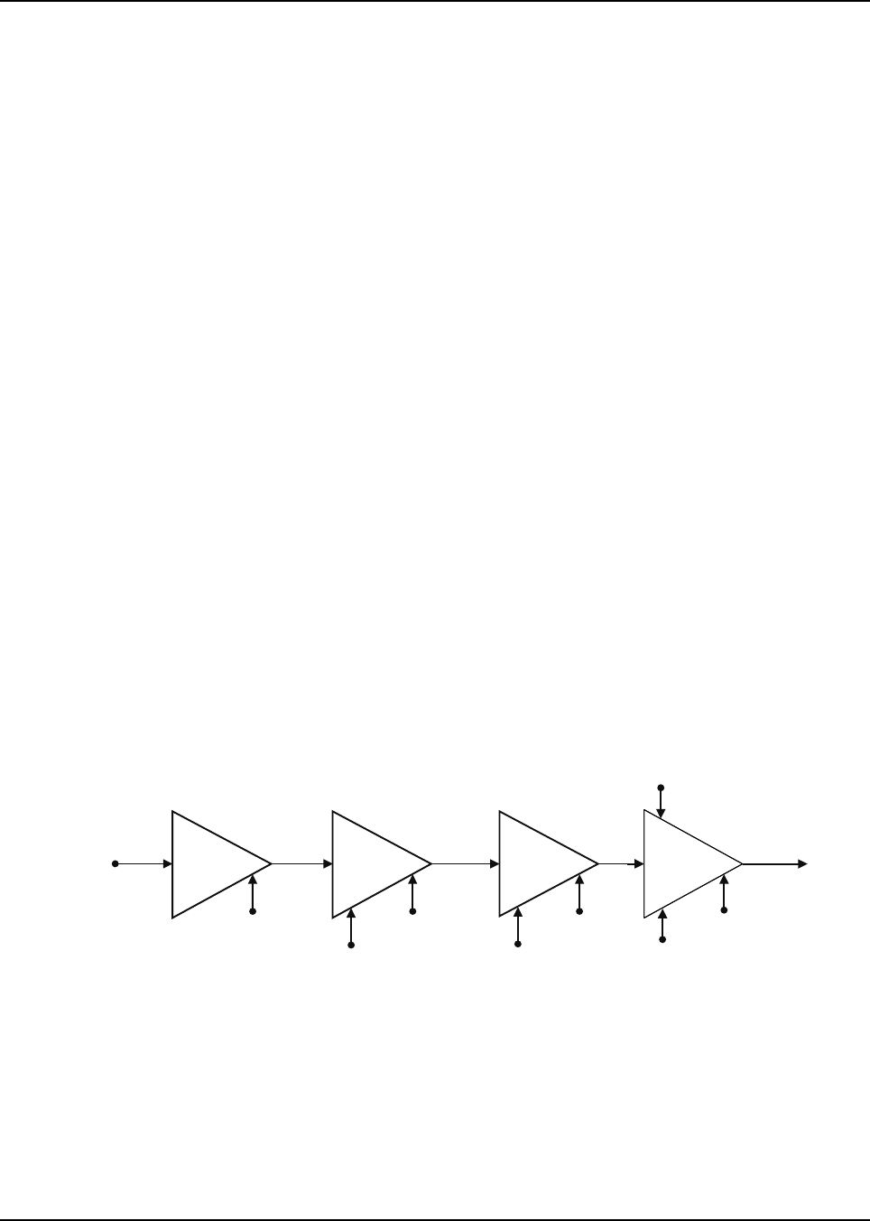
6881096C74-B May 25, 2005
Theory of Operation: Transmitter 3-37
Protection Mechanisms
Final-stage temperature is sensed in the RFPA resulting in VTEMP, which is proportional to
temperature. VTEMP is compared against a reference voltage TEMP_1 (U0959, pin 9) via U0957-1.
When VTEMP exceeds TEMP_1, the U0957-1, pin 1, voltage increases and forward biases one of
the D0951 diodes, which cuts back power. Power continues to cut back with rising temperature until
the voltage level at the junction of R0978 and R0983 is high enough to forward bias D0952, thus
clamping the cut back so that the radio meets its duty cycle specification while providing protection
against high-temperature conditions. The clamping level is set via TEMP_2 (U0959, pin 10) and
U0957-2. U0957-3 is used to sense if a high A+ battery voltage condition exists and, if it does, the
Q0955 gate is biased on, which increases the clamp voltage allowing for additional power cutback
for a high A+, high temperature condition.
Final-stage current is also monitored via VCURRENT, which is proportional to current. VCURRENT
is compared against a reference CURR_LIM_SET (U0959, pin 1) which is tuned after power
characterization. If VCURRENT exceeds CURR_LIM_SET, then U0957-4, pin 14, voltage rises and
forward biases one of the D0951 diodes, which limits power.
Finally, control voltage is limited by U0956-4 and D0950. RFPA_CNTRL can rise to the control
voltage limit set by R0942-4. U0965 provides protection against supply voltage transients. When
transients on the A+ voltage exceed 24 volts U0965 pin 1 is pulled high thus turning on Q0954 via
TX_DISABLE, R0932, U0958 disabling the control voltage to the PA first stage and momentarily
turning off the transmitter. In addition, Q0900 is turned on, forward biasing one of the D0950 diodes
and thus reducing the control voltage. When the voltage transient drops back below 20 volts, U0965
pin 1 goes low thus enabling the control loop and turning the transmitter on again.
3.6.3 UHF Range 2 (450-520 MHz) Band
3.6.3.1 45-Watt Transmitter
The following text discusses the 45-W transmitter.
3.6.3.1.1 RF Power Amplifier (RFPA)
The RFPA consists of three gain stages, which are shown in Figure 3-29.
Figure 3-29. 45-Watt RF Power Amplifier (RFPA) Gain Stages (UHF Range 2)
First Stage
The RFPA first stage provides gain that is determined by the control voltage, RFPA_CNTRL. This
control voltage is generated in the power control section and is a function of the final-stage output
power, temperature, and current, as well as the control and A+ voltage levels. See “3.6.3.1.3. Power
Control” on page 3-39 for a detailed explanation of the power control section.
FIRST
STAGE
0.5mW U5501
C65
250mW Q5502
1518
3.5W Q5503
1570
51W
To Antenna
Switch
RFPA_CNTRL
K9.1V
TRANSMIT
BUFFER
TX_INJ
From
FGU
2mW Q5501
C65
K9.1V
VGBIAS3
A+
DRV_9.3V
VGBIAS1
VGBIAS2 FINAL
STAGE
RFPA_OUT
DRIVER
STAGE
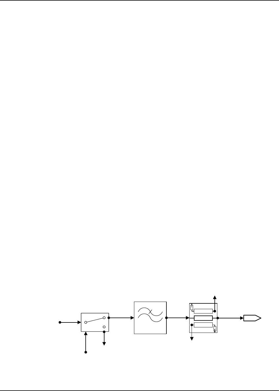
May 25, 2005 6881096C74-B
3-38 Theory of Operation: Transmitter
The 0.5 mW TX_INJ signal is routed to the U5501 first stage device (Pin 16, RFIN) via C5508 to an
integrated, wide-band input match. U5501 is a two-stage LDMOS device with a bandpass interstage
match consisting of L5503, C5507, and C5509 routed between VD1 (pin 14) and G2 (pin 11). L5502
and L5505 provide the K9.1V drain bias voltage for the first and second stages to VD1 (pin 14) and
RFOUT1/2 (pins 6 and 7), respectively. The RFPA_CNTRL gate bias is provided to both stages
internally via VCNTRL (pin 1). Both U5501 stages are operated Class A and the second-stage output
power is approximately 250 mW.
Driver Stage
C5566, C5516, C5518 and a transmission line form a low-pass, interstage match that transfers
power to the Q5502 LDMOS transistor. R5511-R5515 provide device stability, and R5527, C5556,
C5525 and R5516 supply the VGBIAS3 gate bias. L5508, C5527, R5517, E5501 and C5526 form
the 9.3 V drain bias circuit. The 9.3 V drain voltage is supplied from regulator U5570. The 9.3 V
supply to the driver is only present during transmit and is disabled during receive via the K9.1V
signal and Q5570. Q5502 is operated Class AB and its output power is approximately 3.5 W.
Final Stage
C5559, C5560, C5535, C5538, and transmission lines form a low pass, splitter match that transfers
power to the LDMOS final-stage transistor Q5503. Q5503 contains two transistors in a single
package, each with it's own gate and drain lead. R5530, R5533, R5534, R5536, R5538-R5545
provide stability for Q5503. R5525, C5557, C5539 and R5520 supply the VGBIAS1 gate bias to
Q5503-7 via U5504-2 pin7. R5526, C5558, C5540 and R5521 supply the VGBIAS2 gate bias to
Q5503-6 via U5504-1 pin 1. Gate bias voltage to the final is adjusted dependant on the temeprature
of Q5503. The output voltage from the temperature sensing IC, U5502-2, is summed via R5550 and
R5555 respectively with the gate bias voltage VGBIAS1 and VGBIAS2, via R5549 and R5554
respectively. As the temeprature of the final device decreases the bias voltage applied to the gates of
U5503 is reduced. L5510, C5549, R5523, E5502 and C5550 form the A+ drain bias circuit to Q5503-
2 and Q5503-3. C5542-43, C5545-46, C5548, C5551-53 and transmission lines form a low -pass
combiner match that transfers approximately 51 W to the antenna switch. R5535 provides stability
for Q5503. Q5503 operates Class AB.
R5522 and U5503 comprise the final-stage, current-sense circuit that generates the VCURRENT
voltage proportional to the final stage current. R5519 sets the circuit gain. U5502 generates the
VTEMP voltage, which is proportional to the final-stage temperature.
3.6.3.1.2 Output Network (ON)
The ON consists of the antenna switch, harmonic filter, and power detector (see Figure 3-30).
Figure 3-30. Output Network Components (UHF Range 2)
RFPA_OUT
ANTENNA
SWITCH
H-FILTER
POWER
DETECTOR
RF
CONNECTOR
From
RFPA
51W
K9.1V
VREVERSE
VFORWARD
J5701
44W
RX_IN

6881096C74-B May 25, 2005
Theory of Operation: Transmitter 3-39
Antenna Switch
The antenna switch functions in two modes determined by the presence of K9.1V. The K9.1V switch
bias is applied via L5701and C5702. When K9.1V is present, the switch is in TX mode. D5701,
D5702 and D5703 are forward biased forming a low-loss path from the RFPA final stage to the
harmonic filter and a 20 dB isolation path between the RFPA final stage and the RX front-end.
Isolation is achieved via a quarter-wave transmission lines between D5701 - D5702 and between
D5702 - D5703. C5709-10 resonates out the D5702-3 on inductance improving the isolation. When
K9.1V is absent, the switch is in RX mode. D5701, D5702 and D5703 are reverse biased forming a
low-loss path from the harmonic filter to the RX front-end and a 20 dB isolation path from the
harmonic filter to the RFPA final stage. Isolation is achieved via the D5701 off resistance. L5702
resonates out the D5701 off capacitance improving the isolation.
Harmonic Filter
The harmonic filter is a 7-element, equal-L Zolotarev quasi-lowpass filter consisting of C5712 and
C5713, C5719 thru C5721 and L5706 thru L5708. L5712, C5711 and L5713, C5714 form two shunt
zeros for extra attenuation at the second harmonic. C5708 acts as a DC block between the filter and
the antenna switch. The filter provides approximately 60 dB of harmonic rejection. The harmonic
filter together with the antenna switch provides approximately 0.7 dB insertion loss between the
transmitter power amplifier and the antenna.
Power Detector
The power detector consists of a main microstrip transmission line that transfers power from the
harmonic filter to the antenna and two parallel lines that are used to detect the forward and reverse
power. The forward power detection line is terminated via R5707 and R5708. RF energy coupled
onto this line is rectified and filtered via D5704 and C5715 to provide a DC voltage to the power
control circuitry that is proportional to the forward transmitted power level. The detected forward
voltage is approximately 1.5 Vdc when the radio is putting out 44 watts. Thermister R5704
compensates for temperature changes in D5704 to maintain constant DC voltage versus detected
forward power over temperature.
The reverse power detection line is terminated via R5705-06. RF energy coupled onto this line is
rectified and filtered via D5705 and C5718 to provide a DC voltage to the power control circuitry that
is proportional to the reverse power level reflected back from the antenna. Thermister R5712
compensates for temperature changes in D5705 to maintain constant DC voltage versus detected
reverse power over temperature.
3.6.3.1.3 Power Control
The power control section is comprised of a control loop to level forward power, and protection
mechanisms to reduce power to a safe level for the given environmental conditions (see Figure 3-31
on page 3-40).
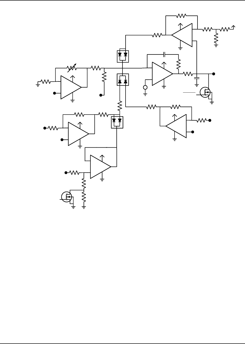
May 25, 2005 6881096C74-B
3-40 Theory of Operation: Transmitter
Figure 3-31. Power Control Components (UHF Range 2)
Power Control Loop
VFORWARD from the ON is buffered via the non-inverting, variable-gain stage U0956-2 whose gain
is set by EPOT U0952. The proper gain is determined during power-detection calibration tuning.
Buffered VFORWARD (U0956-2, Pin 7) is added to PWR_SET via R0971 and R0972 and then
compared to a reference determined by R0974 and R0975. PWR_SET is supplied by the digital-to-
analog converter (DAC) U0959, Pin 2. Comparator stage U0956-3 increases or decreases
RFPA_CNTRL so that the voltage at U0956-3, Pin 9 in the same at the reference voltage at U0956-
3, Pin 10. When the PWR_SET voltage is decreased, U0956-3 increases RFPA_CNTRL to increase
VFORWARD which is proportional to forward power thus increasing the power level. When the
PWR_SET voltage is increased, U0956-3 decreases RFPA_CNTRL to decrease VFORWARD, thus
decreasing the power level. The microprocessor initiates the loop through U0958-1 and Q0954.
Loop timing is set via software together with R0977 and C0973.
EEPOT
U0952
Q0954
RFPA_CNTRL
(TO RFPA)
U0957-4
U0957-4
U0956-3
Q0955
TEMP_2
(U0959, PIN 10)
VTEMP
(FROM RFPA)
PA_EN
CURR_LIM_SET
(U0959, PIN1)
VCURRENT
(FROM RFPA)
9.3V
9.3V
9.3V
9.3V
9.3V
9.3V 9.3V
VFORWARD
(FROM ON) PWR_SET
(U0959, PIN 2)
D0950
D0951
1.5V
D0952
U0957-1
U0956-2
U0957-2
TEMP_1
(U0959, PIN 9) +
-
+
-
+
-
+
-
+
-
+
-
+
-
MAEPF-27889-O
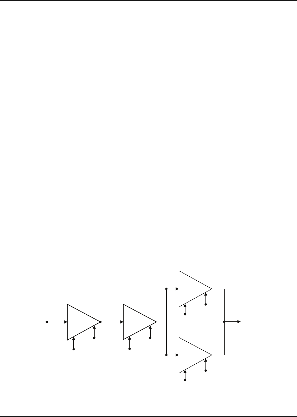
6881096C74-B May 25, 2005
Theory of Operation: Transmitter 3-41
Protection Mechanisms
Final-stage temperature is sensed in the RFPA resulting in VTEMP, which is proportional to
temperature. VTEMP is compared against a reference voltage TEMP_1 (U0959, pin 9) via U0957-1.
When VTEMP exceeds TEMP_1, the U0957-1, pin 1, voltage increases and forward biases one of
the D0951 diodes, which cuts back power. Power continues to cut back with rising temperature until
the voltage level at the junction of R0978 and R0983 is high enough to forward bias D0952, thus
clamping the cut back so that the radio meets its duty cycle specification while providing protection
against high-temperature conditions. The clamping level is set via TEMP_2 (U0959, pin 10) and
U0957-2. U0957-3 is used to sense if a high A+ battery voltage condition exists and, if it does, the
Q0955 gate is biased on, which increases the clamp voltage allowing for additional power cutback
for a high A+, high temperature condition.
Final-stage current is also monitored via VCURRENT, which is proportional to current. VCURRENT
is compared against a reference CURR_LIM_SET (U0959, pin 1) which is tuned after power
characterization. If VCURRENT exceeds CURR_LIM_SET, then U0957-4, pin 14, voltage rises and
forward biases one of the D0951 diodes, which limits power.
Finally, control voltage is limited by U0956-4 and D0950. RFPA_CNTRL can rise to the control
voltage limit set by R0942-4. U0965 provides protection against supply voltage transients. When
transients on the A+ voltage exceed 24 volts U0965 pin 1 is pulled high thus turning on Q0954 via
TX_DISABLE, R0932, U0958 disabling the control voltage to the PA first stage and momentarily
turning off the transmitter. In addition, Q0900 is turned on, forward biasing one of the D0950 diodes
and thus reducing the control voltage. When the voltage transient drops back below 20 volts, U0965
pin 1 goes low thus enabling the control loop and turning the transmitter on again.
3.6.4 700–800 MHz Band
3.6.4.1 35-Watt Transmitter
The following text discusses the 35-W transmitter.
3.6.4.1.1 RF Power Amplifier (RFPA)
The RFPA consists of three gain stages, which are shown in Figure 3-32.
Figure 3-32. 35-Watt RF Power Amplifier (RFPA) Gain Stages (700–800 MHz)
FIRST
STAGE
TX_INJ
From
FGU
2mW U6500
C65
200mW Q6520
1517
4W
Q6540
9045M
Q6541
9045M
42W
To Antenna
Switch
RFPA_CNTRL
K9.1V
VGBIAS3
A+
A+
A+
VGBIAS2
VGBIAS1
MAEPF-27887-O
FINAL
STAGE
RFPA_OUT
DRIVER
STAGE
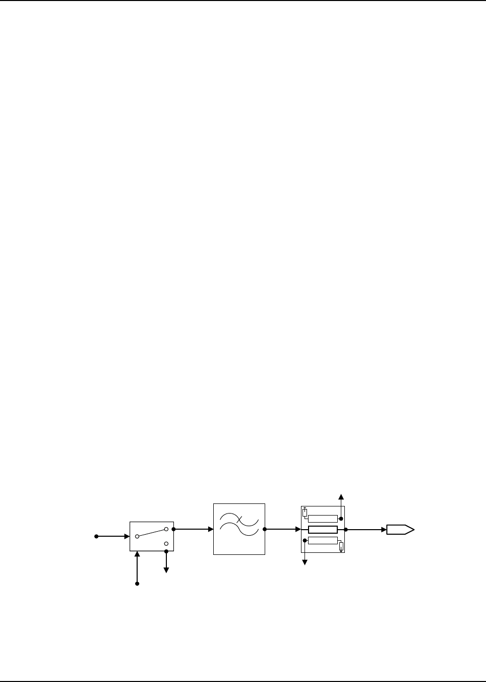
May 25, 2005 6881096C74-B
3-42 Theory of Operation: Transmitter
First Stage
The RFPA first stage provides gain that is determined by the control voltage, RFPA_CNTRL. This
control voltage is generated in the power control section and is a function of the final-stage output
power, temperature, and current, as well as the control and A+ voltage levels. See “3.6.4.1.3. Power
Control” on page 3-43 for a detailed explanation of the power control section.
The 2 mW TX_INJ signal is routed to the U6500 first-stage device (Pin 16, RFIN) via C6501 to an
integrated, wide-band input match. U6500 is a two-stage LDMOS device with a bandpass interstage
match consisting of L6502, C6506, and C6503 routed between VD1 (pin 14) and G2 (pin 11). L6501
and L6500 provide the K9.1V drain bias voltage for the first and second stages to VD1 (pin 14) and
RFOUT1/2 (pins 6 and 7), respectively. The RFPA_CNTRL gate bias is provided to both stages
internally via VCNTRL (pin 1). Both U6500 stages are operated Class A, and the second-stage
output power is approximately 200 mW.
Driver Stage
C6502, C6509, C6510, C6511, and a transmission line form a low-pass, interstage match that
transfers power to the Q6520 LDMOS transistor. R6521-5 provide device stability, and R6520 and
C6500 supply the VGBIAS1 gate bias. L6521-2, R6526-7, and C6521-5 form the A+ drain bias
circuit. Q6520 is operated Class AB, and its output power is approximately 4 W.
Final Stage
C6541-2, C6544-5, C6547-8, and transmission lines form a bandpass, splitter match that transfers
power to the LDMOS final-stage transistors Q6540 and Q6541. R6550-3, R6554-7, C6565-6, and
R6559-60 provide stability for Q6540 and Q6541, respectively. R6540 and C6540 supply the
VGBIAS1 gate bias to Q6540. R6543 and C6558 supply the VGBIAS2 gate bias to Q6541. L6542-3,
C6559-60, and R6544 form the A+ drain bias circuit.
C6549-57 and transmission lines form a low-pass, combiner match that transfers approximately
42 W to the antenna switch. Both Q6540 and Q6541 operate Class AB.
R6545-6, C6564, and U6541 comprise the final-stage, current-sense circuit that generates the
VCURRENT voltage proportional to the final stage current. R6546 sets the circuit gain. U6540
generates the VTEMP voltage, which is proportional to the final-stage temperature.
3.6.4.1.2 Output Network (ON)
The ON consists of the antenna switch, harmonic filter, and power detector (see Figure 3-33).
Figure 3-33. Output Network Components (700–800 MHz)
RFPA_OUT
ANTENNA
SWITCH
H-FILTER
POWER
DETECTOR
RF
CONNECTOR
From
RFPA
42W
K9.1V
VREVERSE
VFORWARD
J6700
38.5W
RX_IN
MAEPF-27888-O

6881096C74-B May 25, 2005
Theory of Operation: Transmitter 3-43
Antenna Switch
The antenna switch functions in two modes, which are determined by the presence of K9.1V. The
K9.1V switch bias is applied via L6700, L6702, and C6700. When K9.1V is present, the switch is in
TX mode. D6701 and D6702 are forward biased forming a low-loss path from the RFPA final stage to
the harmonic filter and a 20 dB isolation path between the RFPA final stage and the RX front-end.
Isolation is achieved via a quarter-wave transmission line between D6701 and D6702. C6703
resonates out the D6702 on inductance improving the isolation.
When K9.1V is absent, the switch is in RX mode. D6701 and D6702 are reverse biased forming a
low-loss path from the harmonic filter to the RX front-end and a 20 dB isolation path from the
harmonic filter to the RFPA final stage. Isolation is achieved via the D6701 off resistance. L6703
resonates out the D6701 off capacitance improving the isolation.
Harmonic Filter
L6720-2, C6720-1, and two open-stub transmission lines form the seven-element, low-pass
harmonic filter. The filter attenuates harmonics generated by the RFPA when the antenna switch is in
TX mode and provides extra selectivity when the antenna switch is in RX mode.
Power Detector
The power detector consists of two asymmetric, coupled transmission lines and detection circuitry
that detects forward and reverse power. C6730-1, D6730, L6730, R6730-3, and R6735-6 form the
forward-power detector (VFORWARD), which is used for power leveling. C6732-3, D6731, L6731,
R6737-9, and R6733-4 form the reverse-power detector (VREVERSE). C6734-5 provides additional
harmonic attenuation. R6740 provides an electrostatic discharge path to protect the RFPA final stage
device.
3.6.4.1.3 Power Control
The power control section is comprised of a control loop to level forward power, and protection
mechanisms to reduce power to a safe level for the given environmental conditions (see Figure 3-34
on page 3-44).
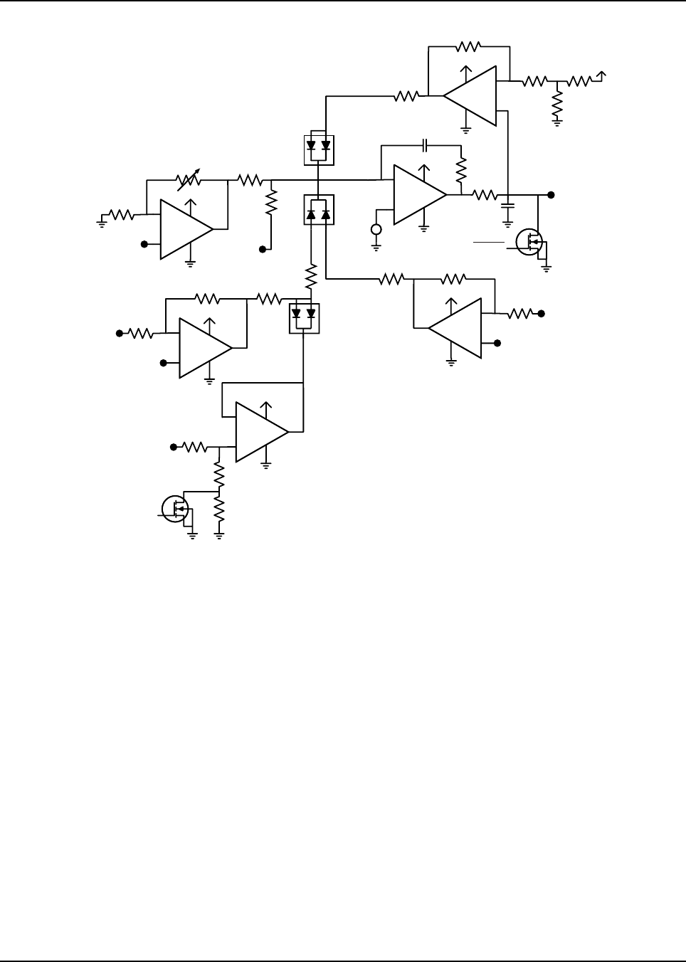
May 25, 2005 6881096C74-B
3-44 Theory of Operation: Transmitter
Figure 3-34. Power Control Components (700–800 MHz)
Power Control Loop
VFORWARD from the ON is buffered via the non-inverting, variable-gain stage U0956-2 whose gain
is set by EPOT U0952. The proper gain is determined during power-detection calibration tuning.
Buffered VFORWARD (U0956-2, Pin 7) is added to PWR_SET via R0971 and R0972 and then
compared to a reference determined by R0974 and R0975. PWR_SET is supplied by the digital-to-
analog converter (DAC) U0959, Pin 2. Comparator stage U0956-3 increases or decreases
RFPA_CNTRL so that the voltage at U0956-3, Pin 9 in the same at the reference voltage at U0956-
3, Pin 10. When the PWR_SET voltage is decreased, U0956-3 increases RFPA_CNTRL to increase
VFORWARD which is proportional to forward power thus increasing the power level. When the
PWR_SET voltage is increased, U0956-3 decreases RFPA_CNTRL to decrease VFORWARD, thus
decreasing the power level. The microprocessor initiates the loop through U0958-1 and Q0954.
Loop timing is set via software together with R0977 and C0973.
EEPOT
U0952
Q0954
RFPA_CNTRL
(TO RFPA)
U0957-4
U0957-4
U0956-3
Q0955
TEMP_2
(U0959, PIN 10)
VTEMP
(FROM RFPA)
PA_EN
CURR_LIM_SET
(U0959, PIN1)
VCURRENT
(FROM RFPA)
9.3V
9.3V
9.3V
9.3V
9.3V
9.3V 9.3V
VFORWARD
(FROM ON) PWR_SET
(U0959, PIN 2)
D0950
D0951
1.5V
D0952
U0957-1
U0956-2
U0957-2
TEMP_1
(U0959, PIN 9) +
-
+
-
+
-
+
-
+
-
+
-
+
-
MAEPF-27889-O

6881096C74-B May 25, 2005
Theory of Operation: Frequency Generation Unit (FGU) 3-45
Protection Mechanisms
Final-stage temperature is sensed in the RFPA resulting in VTEMP, which is proportional to
temperature. VTEMP is compared against a reference voltage TEMP_1 (U0959, pin 9) via U0957-1.
When VTEMP exceeds TEMP_1, the U0957-1, pin 1, voltage increases and forward biases one of
the D0951 diodes, which cuts back power. Power continues to cut back with rising temperature until
the voltage level at the junction of R0978 and R0983 is high enough to forward bias D0952, thus
clamping the cut back so that the radio meets its duty cycle specification while providing protection
against high-temperature conditions. The clamping level is set via TEMP_2 (U0959, pin 10) and
U0957-2. U0957-3 is used to sense if a high A+ battery voltage condition exists and, if it does, the
Q0955 gate is biased on, which increases the clamp voltage allowing for additional power cutback
for a high A+, high temperature condition.
Final-stage current is also monitored via VCURRENT, which is proportional to current. VCURRENT
is compared against a reference CURR_LIM_SET (U0959, pin 1) which is tuned after power
characterization. If VCURRENT exceeds CURR_LIM_SET, then U0957-4, pin 14, voltage rises and
forward biases one of the D0951 diodes, which limits power.
Finally, control voltage is limited by U0956-4 and D0950. RFPA_CNTRL can rise to the control
voltage limit set by R0942-4.
3.7 Frequency Generation Unit (FGU)
This section of the theory of operation provides a detailed circuit description of the frequency
generation unit (FGU).
3.7.1 VHF (136-174 MHz) Band
The FGU (Figure 3-35 on page 3-46) provides the XTL 5000 radio with a 16.8 MHz reference
frequency, receiver 1st local oscillator, and a modulated transmitter RF carrier that is further
amplified by the power amplifier section of the radio.
The FGU consists of the following:
• Reference oscillator (Y3750)
• Low-voltage Fractional-N (LV Frac-N) synthesizer (U3751)
• Two transmitter VCOs
• Three transmitter buffer/amplifier stages
• Two Receiver VCOs
• Three receiver buffer/amplifier stages
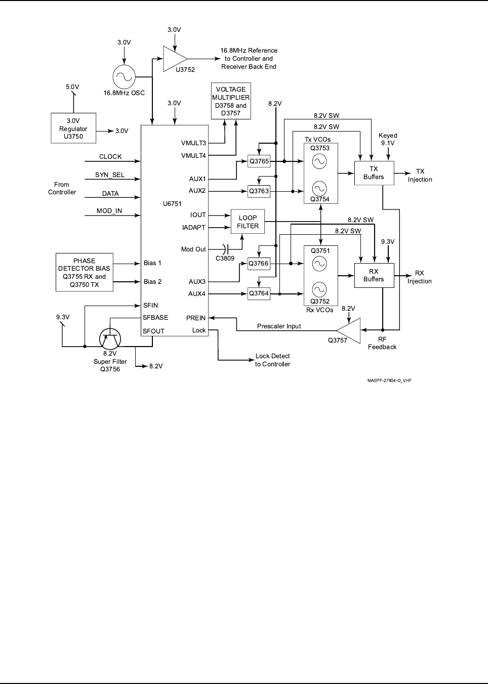
May 25, 2005 6881096C74-B
3-46 Theory of Operation: Frequency Generation Unit (FGU)
Figure 3-35. Frequency Generation Unit Block Diagram (VHF)
3.7.1.1 Reference Oscillator
The radio's frequency stability and accuracy is derived from the 16.8 MHz reference oscillator
(Y3750). The 16.8 MHz reference oscillator circuitry provides a 16.8 MHz reference to the LV Frac-N
(U3751), receiver backend IC (U3000), and the controller section of the XTL 5000 radio. The
reference oscillator circuitry consists of the reference oscillator Y3750 and the inverter/buffer circuitry
containing the active device U3752. Y3750 is a voltage-controlled, temperature-compensated crystal
oscillator (VCTCXO). Circuitry internal to Y3750 compensates for frequency error over temperature.
Warping of the oscillator on frequency is accomplished via a programmable DAC in the LV Frac-N.
The warp voltage is present at pin 25 (WARP) of U3751 and is applied to pin 1 of Y3750. The
16.8 MHz output frequency of Y3750 is capacitor-coupled to pin 23 of the LV Frac-N (U3751) and
also to the inverter/buffer stage U3752. L3754and C3824 at the output of U3752 filter the 16.8 MHz
signal, and R3768 along with C3830 set the appropriate amplitude of the signal for the receiver back-
end and controller sections.
3.7.1.2 LV Frac-N Synthesizer IC
The LV Frac-N IC (U3751) functions include frequency synthesis, modulation control, voltage
multiplication and filtering, and auxiliary logic outputs for VCO selection.
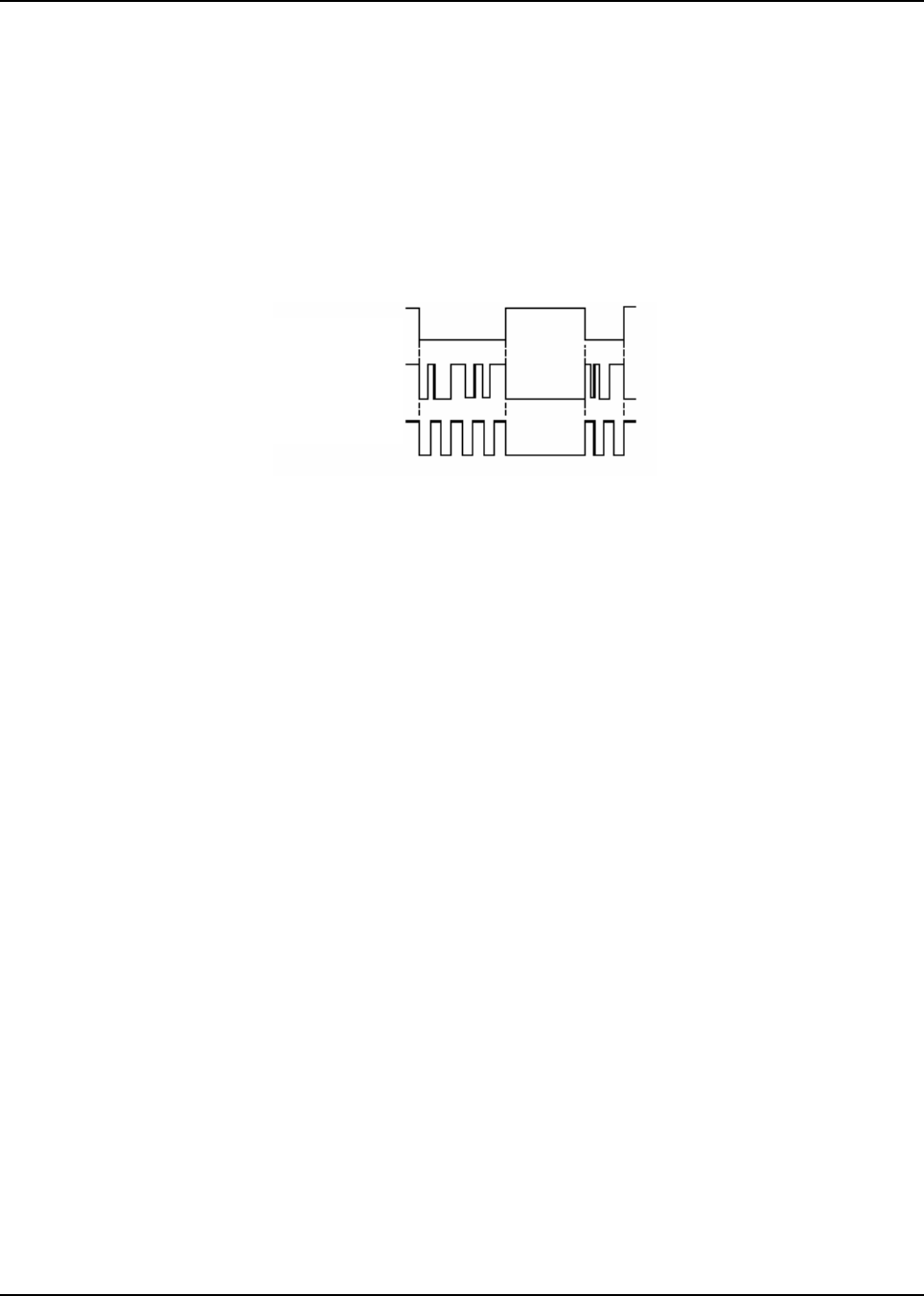
6881096C74-B May 25, 2005
Theory of Operation: Frequency Generation Unit (FGU) 3-47
U3751 is a mixed-mode IC containing digital and analog circuits. Separate power supply inputs are
used for the various functional blocks on the IC. Inductors L3757 and L3756 provide isolation
between supply pin 20 (AVDD - analog supply input) and pin 36 (DVDD - digital supply input)
connected to F3.0v. This 3.0 V DC supply is provided by U3750, a 3-V regulator IC.
All programmable variables on the synthesizer IC, such as the synthesizer frequency; reference-
oscillator warping; adapt-timer duration; modulation-attenuator setting; and auxiliary-control outputs,
which select one of four voltage-controlled oscillators, can be programmed through a serial
peripheral interface (SPI). The SPI is connected to the controller microcomputer via three
programming lines, namely the data (pin 7), clock (pin 8), and the chip enable (pin 9) of U3751
(Figure 3-36).
Figure 3-36. Waveform Representation During Programming of the LV Frac-N IC (VHF)
3.7.1.3 Voltage Multiplier
Pin 12 (VMULT3) and pin 11 (VMULT4) of U3751, together with diode arrays D3757 and D3758 and
their associated capacitors C3763, C3764, C3765 and C3767, form the voltage multiplier. The
voltage multiplier generates 12.0 Vdc from the 3.0-V supply to supply the phase detector and
charge-pump output stage at pin 47 (VCP) of U3751. This voltage multiplier is basically a stacked,
multiple-diode capacitor network driven by two 1.05 MHz, 180 degrees out of phase signals from
pins 12 and 11 of U3751.
3.7.1.4 Superfilter
The superfilter is an active filter that provides a low-noise supply for the VCOs, receiver and
transmitter injection amplifiers. Regulator U0950, located in the controller section, supplies 9.3 Vdc
to the FGU section thru the filtering network consisting of L3752, C3811, C3751, and C3820. This
voltage is applied to pin 30 (SFIN) of U3751 and the emitter of Q3756. The output is a superfiltered
8.2 Vdc at the junction of pin 28 (SFOUT) of U3751 and the collector of Q3756. Filtering is
accomplished with capacitors C3821, C3753, and C3752 at the output of this circuit and C3823 at
pin 26 of U3751.
3.7.1.5 Modulation
To support many voice, data, and signaling protocols, XTL 5000 radios must modulate the
transmitter carrier frequency over a wide audio-frequency range, from less than 10 Hz up to more
than 6 kHz. The LV Frac-N IC supports audio frequencies down to zero Hz by using dual-port
modulation. The audio signal at pin 10 (MODIN) is internally divided into high- and low-frequency
components, which modulate both the synthesizer dividers and the external VCOs through signal
MODOUT (pin 41). The IC is adjusted to achieve flat modulation frequency response during
transmitter modulation balance calibration using a built-in modulation attenuator.
The Digital-to-Analog Converter (DAC) IC (U0900), and switched-capacitor filter (SCF) IC (FL0900)
form the interface between the radio's DSP and the analog input of the LV Frac-N IC.
Pin 9 (Chip Select)
Pin 7 (Data)
Pin 8 (Clock)
MAEPF-27805-O

May 25, 2005 6881096C74-B
3-48 Theory of Operation: Frequency Generation Unit (FGU)
3.7.1.6 Charge Pump Bias
External circuitry connected to pin 39 (Bias 2) and pin 40 (Bias 1) of U3751 determine the current
that is applied to the charge-pump circuitry. During receive mode, resistors R3778, R3763, and
R3758 set the current supplied to pin 40 (Bias 1). Transistor Q3755 and resistors R3779, R3756,
and capacitor C3808 form a circuit that momentarily increases the current to pin 40 (Bias 1) during
receiver programming of U3751. This circuit is activated by pin 46 (ADAPTSW) of U3751 during the
transition of programming U3751 to frequency and effectively decreases the length of time for the
synthesizer to lock on frequency. Similarly, during transmitter mode, resistors R3778, R3763, and
R3776 set the current supplied to pin 39 (Bias 2). Transistor Q3750 and resistors R3759, R3776,
and capacitor C3825 form a circuit that momentarily increases the current to pin 39 (Bias 2) during
transmitter programming of U3751.
3.7.1.7 Loop Filter
The loop filter operates in synchronization with the phase detector of U3751 in two modes, normal
and adapt. In normal mode, the loop filter forms a third-order loop filter consisting of components
R3765, R3773, R3770, C3833, C3810, C3834, C3855 to C3861 and C3881 to C3883.
Pin 43 (IOUT) of U3751 provides the charge-pump current for steering of the control voltage line to
the VCOs. During normal mode, pin 45 (IADAPT) is set to a high impedance and has no effect on the
loop filter. When U3751 is programmed to a new frequency, the IC is initially operated in adapt mode.
In this mode the loop filter is reconfigured for a wider bandwidth allowing the synthesizer to lock
faster. The charge-pump output is supplied through pin 45 (IADAPT) in this mode, and this
reconfigures the loop filter to behave like a second-order filter.
3.7.1.8 Lock Detect
Lock status of the synthesizer loop is provided to the microprocessor by pin 4 (LOCK) of U3751. A
high level (3.0 Vdc) indicates that the loop is stable. A low voltage indicates that the loop is not
locked and will result in a Fail 001 to be displayed on the control head display.
3.7.1.9 Transmitter Injection
The transmit (TX) injection string consists of three amplifier stages (Q3760, Q3759, and Q3758)
whose main purpose is to maintain a constant output to drive the RF power amplifier and supply the
TX feedback signal to the FGU synthesizer loop. The first two stages are powered by the
superfiltered 8.2 Vdc, which is decreased by 0.7 Vdc via the dual diode D3750, resulting in a 7.5 Vdc
supply. The third stage is powered by the keyed 9.1 Vdc and the TX injection string is on only with
keyed 9.1 Vdc activated during transmit mode. The TX VCO output is attenuated 3 dB via resistors
R3840, R3833, and R3839. This output is coupled to the first-stage amplifier Q3760, further
attenuated 3 dB via resistors R3803, R3809, and R3803, and then coupled to the second-stage
amplifier Q3759. This output is tapped to supply the TX feedback signal to the synthesizer prescaler,
and the balance is further attenuated 5 dB via resistors R3818, R3823, and R3824. This output is
coupled to the third- stage amplifier Q3758, further attenuated 3 dB via resistors R3858, R3863, and
R3859, routed to the 7-pole Cow Chebychev low-pass filter C3917 through C3921, L3785, and
L3787 in order to attenuate harmonics. The output is, again, attenuated 3 dB via resistors R3842,
R3834, and R3841 and coupled to the input of the RF power amplifier section. The five sets of
resistive attenuators provide increased isolation between the TX VCO and RF power amplifier.

6881096C74-B May 25, 2005
Theory of Operation: Frequency Generation Unit (FGU) 3-49
3.7.1.10 Receiver Injection
The receiver (RX) injection string is a three-stage amplifier that supplies the RX feedback signal to
the FGU synthesizer loop and supplies the first local oscillator (LO) signal to the RX front-end mixer.
The RX VCO output is attenuated 3 dB via resistors R3825 through R3827 to increase isolation. This
buffered signal is amplified by the first-stage amplifier Q3761, which is supplied by the 8.2-V
superfilter for a gain of approximately 6 dB. Resistors R3790, R3798, R3800, and R3801 bias
Q3761. L3774 serves as a choke inductor; C3779 and C3868 are added for filtering. The output of
Q3761 is attenuated 9.5 dB via resistors R3854, R3865, and R3855. This output is coupled to
Q3769 which gain of approximately 3 dB. The output of Q3769 is split into two paths. The first path
feeds back to the synthesizer prescaler through blocking capacitor C3913. The second path, which
supplies the LO signal to the RX front-end mixer, is attenuated 3 dB via resistors R3857, R3864, and
R3856 to increase isolation. This buffered signal is amplified by the second-stage amplifier Q3762,
which is supplied by the 9.3-V regulator for a gain of approximately 15 dB. Resistors R3843, R3851,
and R3852 biases Q3762. L3783 serves as a choke inductor; C3873, C3870, and C3925 are added
for filtering. The output of Q3762 is passed through blocking capacitor C3759, then, routed to C3804,
L3781, C3786, and L3782 which form a low pass filter and attenuated 1 dB via resistors R3821,
R3794, and R3802 to increase isolation and supply approximately 20 dBm to the LO port of the
mixer.
3.7.1.11 Transmitter VCOs
Transmitter frequencies are generated from two external, discrete, Colpits VCOs, low band (136-
155 MHz) and high band (155-174 MHz), based on Q3753 and Q3754 respectively. The VCOs are
switched On and Off by transistors Q3765 and Q3763, which are controlled by the Frac-N outputs
AUX1 and AUX2 respectively when turned high.
3.7.1.12 Receiver VCOs
The receiver first local oscillator frequencies are generated from two external, discrete, Colpits
VCOs, low band (245.65-264.65) and high band (264.65-283.65), based on Q3751 and Q3752
respectively. The VCOs are switched On and Off by transistors Q3766 and Q3764, which are
controlled by the Frac-N outputs AUX3 and AUX4 respectively when turned high.
3.7.1.13 Prescaler Feedback
RF feedback for the synthesizer loop is provided by prescaler amplifier Q3757. Feedback from both
the transmitter and receiver injection strings are coupled to this amplifier through resistor networks
that both balance and attenuate the levels prior to amplification by Q3757. The output of Q3757 is
coupled to U3751 at pin 32 (PREIN), which is the prescaler input for the synthesizer.
3.7.2 UHF Range 1 (380–470 MHz) Band
The FGU (Figure 3-37 on page 3-50) provides the XTL 5000 radio with a 16.8 MHz reference
frequency, receiver 1st local oscillator, and a modulated transmitter RF carrier that is further
amplified by the power amplifier section of the radio.
The FGU consists of the following:
• Reference oscillator (Y5750)
• Low-voltage Fractional-N (LV Frac-N) synthesizer (U5752)
• Three receiver voltage-controlled oscillators (VCOs)
• Two transmitter VCOs
• Three receiver LO amplifiers (Q5904, Q5902 and Q5906)
• Two transmitter injection amplifiers (Q5828, and Q5829)
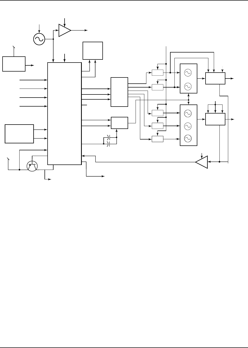
May 25, 2005 6881096C74-B
3-50 Theory of Operation: Frequency Generation Unit (FGU)
Figure 3-37. Frequency Generation Unit Block Diagram (UHF Range 1)
3.7.2.1 Reference Oscillator
The radio's frequency stability and accuracy is derived from the 16.8 MHz reference oscillator
(Y5750). The 16.8 MHz reference oscillator circuitry provides a 16.8 MHz reference to the LV Frac-N
(U5752), receiver back-end IC (U5002), and the controller section of the XTL 5000 radio. The
reference oscillator circuitry consists of the reference oscillator Y5750 and the inverter/buffer circuitry
containing the active device U5751. Y5750 is a voltage-controlled, temperature-compensated crystal
oscillator (VCTCXO). Circuitry internal to Y5750 compensates for frequency error over temperature.
Warping of the oscillator on frequency is accomplished via a programmable DAC in the LV Frac-N.
The warp voltage is present at pin 25 (WARP) of U5752 and is applied to pin 1 of Y5750. The
16.8 MHz output frequency of Y5750 is capacitor-coupled to pin 23 of the LV Frac-N (U5752) and
also to the inverter/buffer stage U5751. L5753 and C5768 at the output of U5751 filter the 16.8 MHz
signal, and R5768 along with C5763 set the appropriate amplitude of the signal for the receiver back-
end and controller sections.
3.7.2.2 LV Frac-N Synthesizer IC
The LV Frac-N IC (U5752) functions include frequency synthesis, modulation control, voltage
multiplication and filtering, and auxiliary logic outputs for VCO selection.
U5752 is a mixed-mode IC containing digital and analog circuits. Separate power supply inputs are
used for the various functional blocks on the IC. Inductors L5755 and L5756 provide isolation
between supply pin 20 (AVDD - analog supply input) and pin 36 (DVDD - digital supply input)
connected to F3.0v. This 3.0 V DC supply is provided by U5750, a 3-V regulator IC.
Bias 1
3.0V
3.0V
3.0V
3.0V
8.2V
Lock Detect
to Controller
Prescaler Input
Q5755 RF
Feedback
8.2V
Bias 2
9.3V
SFIN
SFBASE
SFOUT Lock
PREIN
AUX4
AUX3
Mod Out
IADAPT
IOUT
AUX2
AUX1
VMULT4
VMULT3
5.0V
16.8MHz Reference
to Controller and
Receiver Back End
VOLTAGE
MULTIPLIER
D5750 and
D5751
16.8MHz OSC
8.2V
Super Filter
Q5752
U5751
U5752
3.0V
Regulator
U5750
PHASE
DETECTOR BIAS
Q5750 RX and
Q5751 TX
CLOCK
SYN_SEL
DATA
MOD_IN
From
Controller
NC
A
X0
X1
X2
X3
X4
B
C7.5V
8.2V
Q5706
Q5707
Q5708
Q5709
RX
INJECTION
TX
INJECTION
RX
Injection
TX
Injection
Keyed
9.1V
C5779
C5780
LOOP
FILTER
8.2V SW
8.2V SW
8.2V SW
8.2V SW
Q5825
Q5826
Q5901
Q5903
Q5905
U5753
Q5710 8.2V SW

6881096C74-B May 25, 2005
Theory of Operation: Frequency Generation Unit (FGU) 3-51
All programmable variables on the synthesizer IC, such as the synthesizer frequency; reference-
oscillator warping; adapt-timer duration; modulation-attenuator setting; and auxiliary-control outputs,
which select one of five voltage-controlled oscillators, can be programmed through a serial
peripheral interface (SPI). The SPI is connected to the controller microcomputer via three
programming lines, namely the data (pin 7), clock (pin 8), and the chip enable (pin 9) of U5752
(Figure 3-38).
Figure 3-38. Waveform Representation During Programming of the LV Frac-N IC (UHF Range 1)
3.7.2.3 Voltage Multiplier
Pin 12 (VMULT3) and pin 11 (VMULT4) of U5752, together with diode arrays D5750 and D5751 and
their associated capacitors C5775, C5776, C5777 and C5778, form the voltage multiplier. The
voltage multiplier generates 13.4 Vdc from the 5.0-V supply to supply the phase detector and
charge-pump output stage at pin 47 (VCP) of U5752. This voltage multiplier is basically a stacked,
multiple-diode capacitor network driven by two 1.05 MHz, 180 degrees out of phase signals from
pins 12 and 11 of U5752.
3.7.2.4 Superfilter
The superfilter is an active filter that provides a low-noise supply for the VCOs, receiver and
transmitter injection amplifiers. Regulator U0950, located in the controller section, supplies 9.3 Vdc
to the FGU section thru the filtering network consisting of L5750, C5751, C5753, and C5755. This
voltage is applied to pin 30 (SFIN) of U5752 and the emitter of Q5752. The output is a superfiltered
8.2 Vdc at the junction of pin 28 (SFOUT) of U5752 and the collector of Q5752. Filtering is
accomplished with capacitors C5766, C5769, and C5772 at the output of this circuit and C5770 at
pin 26 of U5752.
3.7.2.5 Modulation
To support many voice, data, and signaling protocols, XTL 5000 radios must modulate the
transmitter carrier frequency over a wide audio-frequency range, from less than 10 Hz up to more
than 6 kHz. The LV Frac-N IC supports audio frequencies down to zero Hz by using dual-port
modulation. The audio signal at pin 10 (MODIN) is internally divided into high- and low-frequency
components, which modulate both the synthesizer dividers and the external VCOs through signal
MODOUT (pin 41). The IC is adjusted to achieve flat modulation frequency response during
transmitter modulation balance calibration using a built-in modulation attenuator.
The Digital-to-Analog Converter (DAC) IC (U0900), and switched-capacitor filter (SCF) IC (FL0900)
form the interface between the radio's DSP and the analog input of the LV Frac-N IC.
Pin 9 (Chip Select)
Pin 7 (Data)
Pin 8 (Clock)
MAEPF-27805-O

May 25, 2005 6881096C74-B
3-52 Theory of Operation: Frequency Generation Unit (FGU)
3.7.2.6 Charge Pump Bias
External circuitry connected to pin 39 (Bias 2) and pin 40 (Bias 1) of U5752 determine the current
that is applied to the charge-pump circuitry. During receive mode, resistors R5754, R5759, and
R5765 set the current supplied to pin 40 (Bias 1). Transistor Q5750 and resistors R5752, R5753,
and capacitor C5759 form a circuit that momentarily increases the current to pin 40 (Bias 1) during
receiver programming of U5752. This circuit is activated by pin 46 (ADAPTSW) of U5752 during the
transition of programming U5752 to frequency and effectively decreases the length of time for the
synthesizer to lock on frequency. Similarly, during transmitter mode, resistors R5764, R5759, and
R5753 set the current supplied to pin 39 (Bias 2). Transistor Q5752 and resistors R5767, R5764,
and capacitor C5762 form a circuit that momentarily increases the current to pin 39 (Bias 2) during
transmitter programming of U5752.
3.7.2.7 Loop Filter
The loop filter operates in synchronization with the phase detector of U5752 in two modes, normal
and adapt. In normal mode, the loop filter forms a third-order loop filter consisting of components
R5772, R5774, R5775, C5781 to C5787, C5790 to C5792, and C5809 to C5812.
Pin 43 (IOUT) of U5752 provides the charge-pump current for steering of the control voltage line to
the VCOs. During normal mode, pin 45 (IADAPT) is set to a high impedance and has no effect on the
loop filter. When U5752 is programmed to a new frequency, the IC is initially operated in adapt mode.
In this mode the loop filter is reconfigured for a wider bandwidth allowing the synthesizer to lock
faster. The charge-pump output is supplied through pin 45 (IADAPT) in this mode, and this
reconfigures the loop filter to behave like a second-order filter.
3.7.2.8 Lock Detect
Lock status of the synthesizer loop is provided to the microprocessor by pin 4 (LOCK) of U5752. A
high level (3.0 Vdc) indicates that the loop is stable. A low voltage indicates that the loop is not
locked and will result in a Fail 001 to be displayed on the control head display.
3.7.2.9 Transmitter Injection
The transmit (TX) injection string consists of three amplifier stages (Q5828, Q5829, and Q5501)
whose main purpose is to maintain a constant output to drive the RF power amplifier chain and
supply the TX feedback signal to the FGU synthesizer loop. The first two stages are powered by the
superfiltered 8.2 Vdc, which is decreased by 0.7 Vdc via the dual diode D5833, resulting in a 7.5 Vdc
supply. The third stage is powered by the keyed 9.1 Vdc and the TX injection string is on only with
keyed 9.1 Vdc activated during transmit mode.
The output of the second stage amplifier Q5829 is tapped via capacitor C5863 to supply the TX
feedback signal to the synthesizer prescalar via the amplifier Q5755.
3.7.2.10 Receiver Injection
The receiver (RX) injection string is a four-stage amplifier that supplies the RX feedback signal to the
FGU synthesizer loop and supplies the first local oscillator (LO) signal to the RX front-end mixer.
Each RX VCO output is attenuated via resistive pads to increase isolation. The VCO signals are
buffered by the RX injection amplifier string Q5904, Q5902 and Q5906. The output of Q5906 is
tapped via C5957 and fed back to the synthesizer prescaler through amplifier Q5755. The main path
at the output of Q5906 is amplified by U5303 to a level of 24 dBm to provide the first LO signal to the
RX front end mixer in the receiver chain.
6881096C74-B May 25, 2005
Theory of Operation: Frequency Generation Unit (FGU) 3-53
3.7.2.11 Transmitter VCOs
Transmitter frequencies are generated from two VCOs, Q5825 and Q5826.
• Q5825 supplies frequencies in the range 380 MHz up to (but not including) 425 MHz.
• Q5826 supplies frequencies in the range from 425 MHz to 470 MHz.
3.7.2.12 Receiver VCOs
Receiver first local-oscillator frequencies are generated from three VCOs, Q5901, Q5903 and
Q5905.
• Q5901 supplies frequencies in the range 489.65 MHz up to (but not including) 519.65 MHz.
• Q5903 supplies frequencies in the range 519.65 MHz up to (but not including) 549.65 MHz.
• Q5905 supplies frequencies in the range 549.65 MHz up to 579.65 MHz.
The RX VCOs operate at frequencies which are 109.65 MHz higher than the radio channel selected
frequency since the receiver is high side injected, and the first IF frequency is 109.65 MHz.
The five VCOs are selected by the following pattern of logic levels on the AUX pins from the
synthesizer chip U5752 (Table 3-11):
3.7.2.13 Prescaler Feedback
RF feedback for the synthesizer loop is provided by prescaler amplifier Q5755. Feedback from both
the transmitter and receiver injection strings are coupled to this amplifier through capacitors C5863
and C5957. The output of Q5755 is coupled to U5752 at pin 32 (PREIN), which is the prescaler input
for the synthesizer.
Table 3-11. VCO AUX Pin Logic UHF Range 1
VCO AUX1 AUX2 AUX3
RX VCO Q5901 0 1 0
RX VCO Q5903 1 1 0
RX VCO Q5905 0 0 1
TX VCO Q5825 0 0 0
TX VCO Q5826 1 0 0
May 25, 2005 6881096C74-B
3-54 Theory of Operation: Frequency Generation Unit (FGU)
3.7.3 UHF Range 2 (450–520 MHz) Band
The FGU (Figure 3-39) provides the XTL 5000 radio with a 16.8 MHz reference frequency, receiver
1st local oscillator, and a modulated transmitter RF carrier that is further amplified by the power
amplifier section of the radio.
The FGU consists of the following:
• Reference oscillator (Y5750)
• Low-voltage Fractional-N (LV Frac-N) synthesizer (U5752)
• Three receiver voltage-controlled oscillators (VCOs)
• Two transmitter VCOs
• Three receiver LO amplifiers (Q5904, Q5902 and Q5906)
• Two transmitter injection amplifiers (Q5828, and Q5829)
Figure 3-39. Frequency Generation Unit Block Diagram (UHF Range 2)
Bias 1
3.0V
3.0V
3.0V
3.0V
8.2V
Lock Detect
to Controller
Prescaler Input
Q5755 RF
Feedback
8.2V
Bias 2
9.3V
SFIN
SFBASE
SFOUT Lock
PREIN
AUX4
AUX3
Mod Out
IADAPT
IOUT
AUX2
AUX1
VMULT4
VMULT3
5.0V
16.8MHz Reference
to Controller and
Receiver Back End
VOLTAGE
MULTIPLIER
D5750 and
D5751
16.8MHz OSC
8.2V
Super Filter
Q5752
U5751
U5752
3.0V
Regulator
U5750
PHASE
DETECTOR BIAS
Q5750 RX and
Q5751 TX
CLOCK
SYN_SEL
DATA
MOD_IN
From
Controller
NC
A
X0
X1
X2
X3
X4
B
C7.5V
8.2V
Q5706
Q5707
Q5708
Q5709
RX
INJECTION
TX
INJECTION
RX
Injection
TX
Injection
Keyed
9.1V
C5779
C5780
LOOP
FILTER
8.2V SW
8.2V SW
8.2V SW
8.2V SW
Q5825
Q5826
Q5901
Q5903
Q5905
U5753
Q5710 8.2V SW
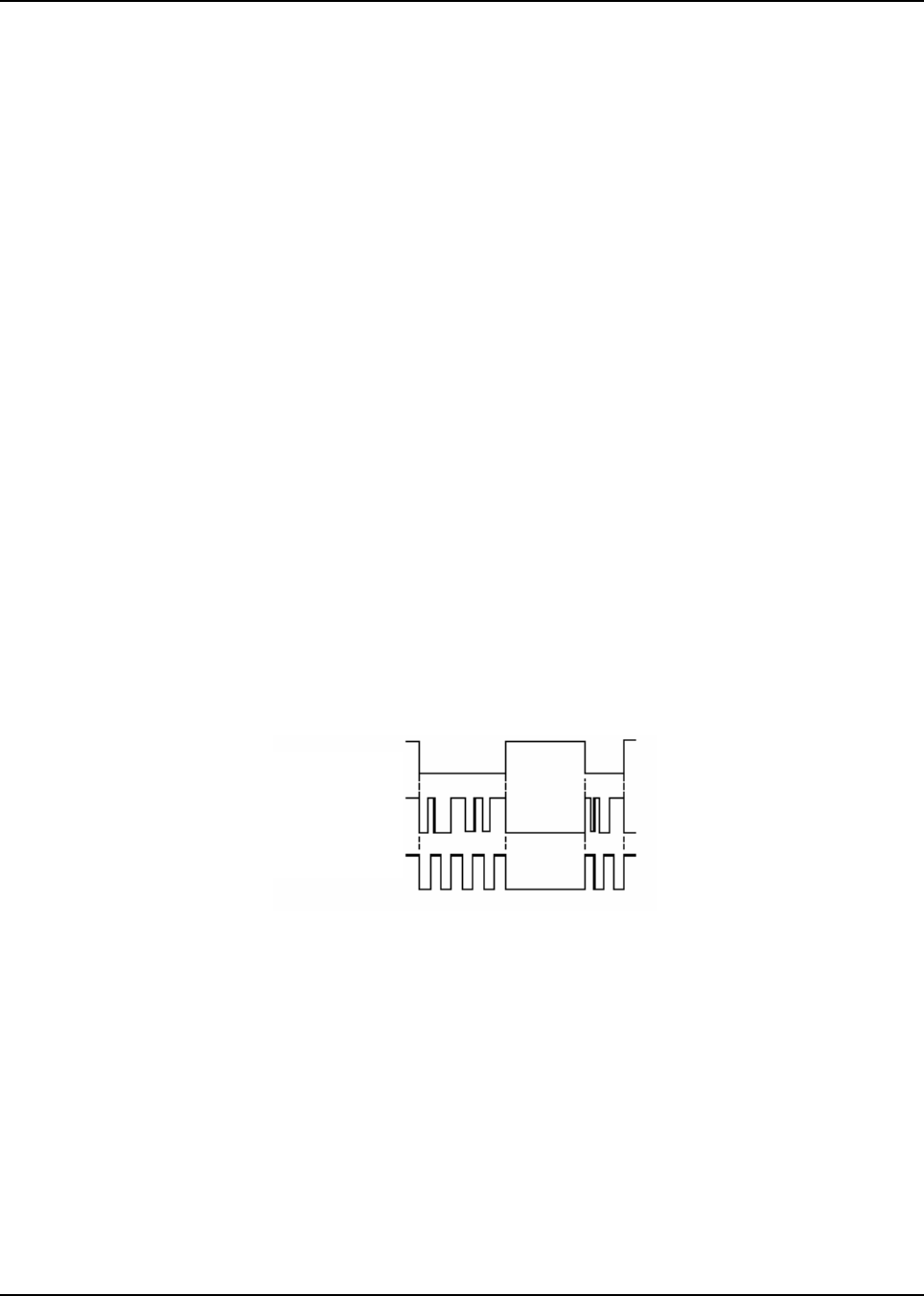
6881096C74-B May 25, 2005
Theory of Operation: Frequency Generation Unit (FGU) 3-55
3.7.3.1 Reference Oscillator
The radio's frequency stability and accuracy is derived from the 16.8 MHz reference oscillator
(Y5750). The 16.8 MHz reference oscillator circuitry provides a 16.8 MHz reference to the LV Frac-N
(U5752), receiver back-end IC (U5002), and the controller section of the XTL 5000 radio. The
reference oscillator circuitry consists of the reference oscillator Y5750 and the inverter/buffer circuitry
containing the active device U5751. Y5750 is a voltage-controlled, temperature-compensated crystal
oscillator (VCTCXO). Circuitry internal to Y5750 compensates for frequency error over temperature.
Warping of the oscillator on frequency is accomplished via a programmable DAC in the LV Frac-N.
The warp voltage is present at pin 25 (WARP) of U5752 and is applied to pin 1 of Y5750. The
16.8 MHz output frequency of Y5750 is capacitor-coupled to pin 23 of the LV Frac-N (U5752) and
also to the inverter/buffer stage U5751. L5753 and C5768 at the output of U5751 filter the 16.8 MHz
signal, and R5768 along with C5763 set the appropriate amplitude of the signal for the receiver back-
end and controller sections.
3.7.3.2 LV Frac-N Synthesizer IC
The LV Frac-N IC (U5752) functions include frequency synthesis, modulation control, voltage
multiplication and filtering, and auxiliary logic outputs for VCO selection.
U5752 is a mixed-mode IC containing digital and analog circuits. Separate power supply inputs are
used for the various functional blocks on the IC. Inductors L5755 and L5756 provide isolation
between supply pin 20 (AVDD - analog supply input) and pin 36 (DVDD - digital supply input)
connected to F3.0v. This 3.0 V DC supply is provided by U5750, a 3-V regulator IC.
All programmable variables on the synthesizer IC, such as the synthesizer frequency; reference-
oscillator warping; adapt-timer duration; modulation-attenuator setting; and auxiliary-control outputs,
which select one of five voltage-controlled oscillators, can be programmed through a serial
peripheral interface (SPI). The SPI is connected to the controller microcomputer via three
programming lines, namely the data (pin 7), clock (pin 8), and the chip enable (pin 9) of U5752
(Figure 3-40).
Figure 3-40. Waveform Representation During Programming of the LV Frac-N IC (UHF Range 2)
3.7.3.3 Voltage Multiplier
Pin 12 (VMULT3) and pin 11 (VMULT4) of U5752, together with diode arrays D5750 and D5751 and
their associated capacitors C5775, C5776, C5777 and C5778, form the voltage multiplier. The
voltage multiplier generates 13.4 Vdc from the 5.0-V supply to supply the phase detector and
charge-pump output stage at pin 47 (VCP) of U5752. This voltage multiplier is basically a stacked,
multiple-diode capacitor network driven by two 1.05 MHz, 180 degrees out of phase signals from
pins 12 and 11 of U5752.
Pin 9 (Chip Select)
Pin 7 (Data)
Pin 8 (Clock)
MAEPF 2 80 O

May 25, 2005 6881096C74-B
3-56 Theory of Operation: Frequency Generation Unit (FGU)
3.7.3.4 Superfilter
The superfilter is an active filter that provides a low-noise supply for the VCOs, receiver and
transmitter injection amplifiers. Regulator U0950, located in the controller section, supplies 9.3 Vdc
to the FGU section thru the filtering network consisting of L5750, C5751, C5753, and C5755. This
voltage is applied to pin 30 (SFIN) of U5752 and the emitter of Q5752. The output is a superfiltered
8.2 Vdc at the junction of pin 28 (SFOUT) of U5752 and the collector of Q5752. Filtering is
accomplished with capacitors C5766, C5769, and C5772 at the output of this circuit and C5770 at
pin 26 of U5752.
3.7.3.5 Modulation
To support many voice, data, and signaling protocols, XTL 5000 radios must modulate the
transmitter carrier frequency over a wide audio-frequency range, from less than 10 Hz up to more
than 6 kHz. The LV Frac-N IC supports audio frequencies down to zero Hz by using dual-port
modulation. The audio signal at pin 10 (MODIN) is internally divided into high- and low-frequency
components, which modulate both the synthesizer dividers and the external VCOs through signal
MODOUT (pin 41). The IC is adjusted to achieve flat modulation frequency response during
transmitter modulation balance calibration using a built-in modulation attenuator.
The Digital-to-Analog Converter (DAC) IC (U0900), and switched-capacitor filter (SCF) IC (FL0900)
form the interface between the radio's DSP and the analog input of the LV Frac-N IC.
3.7.3.6 Charge Pump Bias
External circuitry connected to pin 39 (Bias 2) and pin 40 (Bias 1) of U5752 determine the current
that is applied to the charge-pump circuitry. During receive mode, resistors R5754, R5759, and
R5765 set the current supplied to pin 40 (Bias 1). Transistor Q5750 and resistors R5752, R5753,
and capacitor C5759 form a circuit that momentarily increases the current to pin 40 (Bias 1) during
receiver programming of U5752. This circuit is activated by pin 46 (ADAPTSW) of U5752 during the
transition of programming U5752 to frequency and effectively decreases the length of time for the
synthesizer to lock on frequency. Similarly, during transmitter mode, resistors R5764, R5759, and
R5753 set the current supplied to pin 39 (Bias 2). Transistor Q5752 and resistors R5767, R5764,
and capacitor C5762 form a circuit that momentarily increases the current to pin 39 (Bias 2) during
transmitter programming of U5752.
3.7.3.7 Loop Filter
The loop filter operates in synchronization with the phase detector of U5752 in two modes, normal
and adapt. In normal mode, the loop filter forms a third-order loop filter consisting of components
R5772, R5774, R5775, C5781 to C5787, C5790 to C5792, and C5809 to C5812.
Pin 43 (IOUT) of U5752 provides the charge-pump current for steering of the control voltage line to
the VCOs. During normal mode, pin 45 (IADAPT) is set to a high impedance and has no effect on the
loop filter. When U5752 is programmed to a new frequency, the IC is initially operated in adapt mode.
In this mode the loop filter is reconfigured for a wider bandwidth allowing the synthesizer to lock
faster. The charge-pump output is supplied through pin 45 (IADAPT) in this mode, and this
reconfigures the loop filter to behave like a second-order filter.
3.7.3.8 Lock Detect
Lock status of the synthesizer loop is provided to the microprocessor by pin 4 (LOCK) of U5752. A
high level (3.0 Vdc) indicates that the loop is stable. A low voltage indicates that the loop is not
locked and will result in a Fail 001 to be displayed on the control head display.

6881096C74-B May 25, 2005
Theory of Operation: Frequency Generation Unit (FGU) 3-57
3.7.3.9 Transmitter Injection
The transmit (TX) injection string consists of three amplifier stages (Q5828, Q5829, and Q5501)
whose main purpose is to maintain a constant output to drive the RF power amplifier chain and
supply the TX feedback signal to the FGU synthesizer loop. The first two stages are powered by the
superfiltered 8.2 Vdc, which is decreased by 0.7 Vdc via the dual diode D5833, resulting in a 7.5 Vdc
supply. The third stage is powered by the keyed 9.1 Vdc and the TX injection string is on only with
keyed 9.1 Vdc activated during transmit mode.
The output of the second stage amplifier Q5829 is tapped via capacitor C5863 to supply the TX
feedback signal to the synthesizer prescalar via the amplifier Q5755.
3.7.3.10 Receiver Injection
The receiver (RX) injection string is a four-stage amplifier that supplies the RX feedback signal to the
FGU synthesizer loop and supplies the first local oscillator (LO) signal to the RX front-end mixer.
Each RX VCO output is attenuated via resistive pads to increase isolation. The VCO signals are
buffered by the RX injection amplifier string Q5904, Q5902 and Q5906. The output of Q5906 is
tapped via C5957 and fed back to the synthesizer prescaler through amplifier Q5755. The main path
at the output of Q5906 is amplified by U5303 to a level of 24 dBm to provide the first LO signal to the
RX front end mixer in the receiver chain.
3.7.3.11 Transmitter VCOs
Transmitter frequencies are generated from two VCOs, Q5825 and Q5826.
• Q5826 supplies frequencies in the range 450 MHz up to (but not including) 485 MHz.
• Q5825 supplies frequencies in the range from 485 MHz to 520 MHz.
3.7.3.12 Receiver VCOs
Receiver first local-oscillator frequencies are generated from three VCOs, Q5901, Q5903 and
Q5905.
• Q5905 supplies frequencies in the range 559.65 MHz up to (but not including) 582.65 MHz.
• Q5903 supplies frequencies in the range 582.65 MHz up to (but not including) 605.65 MHz.
• Q5901 supplies frequencies in the range 605.65 MHz up to 629.65 MHz.
The RX VCOs operate at frequencies which are 109.65 MHz higher than the radio channel selected
frequency since the receiver is high side injected, and the first IF frequency is 109.65 MHz.
The five VCOs are selected by the following pattern of logic levels on the AUX pins from the
synthesizer chip U5752 (Table 3-12):
Table 3-12. VCO AUX Pin Logic UHF Range 2
VCO AUX1 AUX2 AUX3
RX VCO Q5905 001
RX VCO Q5903 110
RX VCO Q5901 010
TX VCO Q5826 100
TX VCO Q5825 000
May 25, 2005 6881096C74-B
3-58 Theory of Operation: Frequency Generation Unit (FGU)
3.7.3.13 Prescaler Feedback
RF feedback for the synthesizer loop is provided by prescaler amplifier Q5755. Feedback from both
the transmitter and receiver injection strings are coupled to this amplifier through capacitors C5863
and C5957. The output of Q5755 is coupled to U5752 at pin 32 (PREIN), which is the prescaler input
for the synthesizer.
3.7.4 700–800 MHz Band
The FGU (Figure 3-41) provides the XTL 5000 radio with a 16.8 MHz reference frequency, receiver
1st local oscillator, and a modulated transmitter RF carrier that is further amplified by the power
amplifier section of the radio.
The FGU consists of the following:
• Reference oscillator (Y6750)
• Low-voltage Fractional-N (LV Frac-N) synthesizer (U6751)
• Two receiver voltage-controlled oscillators (VCOs) contained in U6755
• Two transmitter VCOs contained in U6754
• Two receiver LO amplifiers (Q6762 and Q6763)
• Three transmitter injection amplifiers (Q6764, Q6765 and Q6766)
Figure 3-41. Frequency Generation Unit Block Diagram (700–800 MHz)
Bias 1
3.0V
3.0V
3.0V
3.0V
8.2V
8.2V
8.2V
Q6753
Q6755
Q6756
Q6760
Lock Detect
to Controller
Prescaler Input
Q6761 RF
Feedback
RX
INJECTION
TX
INJECTION
RX
Injection
TX
Injection
Keyed
9.1V
U6754
U6755
8.2V
C6783
LOOP
FILTER
Bias 2
9.3V
9.3V
SFIN
SFBASE
SFOUT Lock
PREIN
AUX4
AUX3
Mod Out
IADAPT
IOUT
AUX2
AUX1
VMULT4
VMULT3
5.0V
16.8MHz Reference
to Controller and
Receiver Back End
VOLTAGE
MULTIPLIER
D6751 and
D6752
16.8MHz OSC
8.2V
Super Filter
Q6759
8.2V SW
8.2V SW
8.2V SW
8.2V SW
U6752
U6751
3.0V
Regulator
U6750
PHASE
DETECTOR BIAS
Q6757 RX and
Q6758 TX
CLOCK
SYN_SEL
DATA
MOD_IN
From
Controller
MAEPF-27804-O
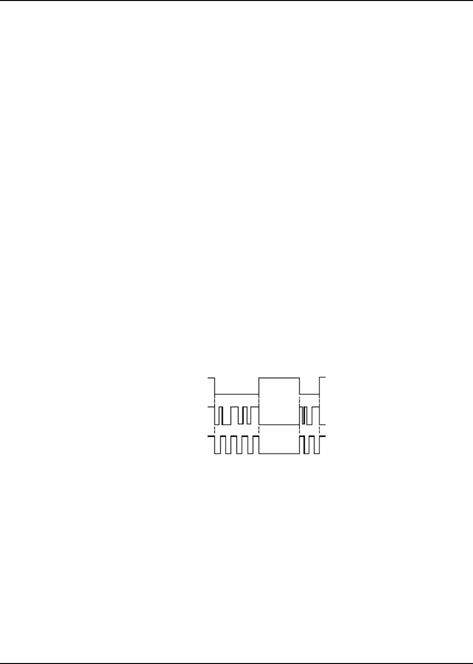
6881096C74-B May 25, 2005
Theory of Operation: Frequency Generation Unit (FGU) 3-59
3.7.4.1 Reference Oscillator
The radio's frequency stability and accuracy is derived from the 16.8 MHz reference oscillator
(Y6750). The 16.8 MHz reference oscillator circuitry provides a 16.8 MHz reference to the LV Frac-N
(U6751), receiver back-end IC (U6000), and the controller section of the XTL 5000 radio. The
reference oscillator circuitry consists of the reference oscillator Y6750 and the inverter/buffer circuitry
containing the active device U6752. Y6750 is a voltage-controlled, temperature-compensated crystal
oscillator (VCTCXO). Circuitry internal to Y6750 compensates for frequency error over temperature.
Warping of the oscillator on frequency is accomplished via a programmable DAC in the LV Frac-N.
The warp voltage is present at pin 25 (WARP) of U6751 and is applied to pin 4 of Y6750. The
16.8 MHz output frequency of Y6750 is capacitor-coupled to pin 24 of the LV Frac-N (U6751) and
also to the inverter/buffer stage U6752. L6756 and C6755 at the output of U6752 filter the 16.8 MHz
signal, and R6757 along with C6759 set the appropriate amplitude of the signal for the receiver back-
end and controller sections.
3.7.4.2 LV Frac-N Synthesizer IC
The LV Frac-N IC (U6751) functions include frequency synthesis, modulation control, voltage
multiplication and filtering, and auxiliary logic outputs for VCO selection.
U6751 is a mixed-mode IC containing digital and analog circuits. Separate power supply inputs are
used for the various functional blocks on the IC. Inductors L6752 and L6753 provide isolation
between supply pin 20 (AVDD - analog supply input) and pin 36 (DVDD - digital supply input)
connected to F3.0v. This 3.0 V DC supply is provided by U6750, a 3-V regulator IC.
All programmable variables on the synthesizer IC, such as the synthesizer frequency; reference-
oscillator warping; adapt-timer duration; modulation-attenuator setting; and auxiliary-control outputs,
which select one of four voltage-controlled oscillators, can be programmed through a serial
peripheral interface (SPI). The SPI is connected to the controller microcomputer via three
programming lines, namely the data (pin 7), clock (pin 8), and the chip enable (pin 9) of U6751
(Figure 3-42).
Figure 3-42. Waveform Representation During Programming of the LV Frac-N IC
3.7.4.3 Voltage Multiplier
Pin 12 (VMULT3) and pin 11 (VMULT4) of U6751, together with diode arrays D6751 and D6752 and
their associated capacitors C6763, C6766, C6769 and C6771, form the voltage multiplier. The
voltage multiplier generates 12.0 Vdc from the 3.0-V supply to supply the phase detector and
charge-pump output stage at pin 47 (VCP) of U6751. This voltage multiplier is basically a stacked,
multiple-diode capacitor network driven by two 1.05 MHz, 180 degrees out of phase signals from
pins 12 and 11 of U6751.
Pin 9 (Chip Select)
Pin 7 (Data)
Pin 8 (Clock)
MAEPF-27805-O

May 25, 2005 6881096C74-B
3-60 Theory of Operation: Frequency Generation Unit (FGU)
3.7.4.4 Superfilter
The superfilter is an active filter that provides a low-noise supply for the VCOs, receiver and
transmitter injection amplifiers. Regulator U0950, located in the controller section, supplies 9.3 Vdc
to the FGU section thru the filtering network consisting of L6755, C6806, C6807, and C6818. This
voltage is applied to pin 30 (SFIN) of U6751 and the emitter of Q6759. The output is a superfiltered
8.2 Vdc at the junction of pin 28 (SFOUT) of U6751 and the collector of Q6759. Filtering is
accomplished with capacitors C6808, C6790, and C6791 at the output of this circuit and C6775 at
pin 26 of U6751.
3.7.4.5 Modulation
To support many voice, data, and signaling protocols, XTL 5000 radios must modulate the
transmitter carrier frequency over a wide audio-frequency range, from less than 10 Hz up to more
than 6 kHz. The LV Frac-N IC supports audio frequencies down to zero Hz by using dual-port
modulation. The audio signal at pin 10 (MODIN) is internally divided into high- and low-frequency
components, which modulate both the synthesizer dividers and the external VCOs through signal
MODOUT (pin 41). The IC is adjusted to achieve flat modulation frequency response during
transmitter modulation balance calibration using a built-in modulation attenuator.
The Digital-to-Analog Converter (DAC) IC (U0900), and switched-capacitor filter (SCF) IC (FL0900)
form the interface between the radio's DSP and the analog input of the LV Frac-N IC.
3.7.4.6 Charge Pump Bias
External circuitry connected to pin 39 (Bias 2) and pin 40 (Bias 1) of U6751 determine the current
that is applied to the charge-pump circuitry. During receive mode, resistors R6768, R6769, and
R6766 set the current supplied to pin 40 (Bias 1). Transistor Q6757 and resistors R6763, R6762,
and capacitor C6795 form a circuit that momentarily increases the current to pin 40 (Bias 1) during
receiver programming of U6751. This circuit is activated by pin 46 (ADAPTSW) of U6751 during the
transition of programming U6751 to frequency and effectively decreases the length of time for the
synthesizer to lock on frequency. Similarly, during transmitter mode, resistors R6768, R6769, and
R6768 set the current supplied to pin 39 (Bias 2). Transistor Q6758 and resistors R6770, R6767,
and capacitor C6794 form a circuit that momentarily increases the current to pin 39 (Bias 2) during
transmitter programming of U6751.
3.7.4.7 Loop Filter
The loop filter operates in synchronization with the phase detector of U6751 in two modes, normal
and adapt. In normal mode, the loop filter forms a third-order loop filter consisting of components
R6764, R6765, R6761, C6776 to C6779, and C6785 to C6789.
Pin 43 (IOUT) of U6751 provides the charge-pump current for steering of the control voltage line to
the VCOs. During normal mode, pin 45 (IADAPT) is set to a high impedance and has no effect on the
loop filter. When U6751 is programmed to a new frequency, the IC is initially operated in adapt mode.
In this mode the loop filter is reconfigured for a wider bandwidth allowing the synthesizer to lock
faster. The charge-pump output is supplied through pin 45 (IADAPT) in this mode, and this
reconfigures the loop filter to behave like a second-order filter.
3.7.4.8 Lock Detect
Lock status of the synthesizer loop is provided to the microprocessor by pin 4 (LOCK) of U6751. A
high level (3.0 Vdc) indicates that the loop is stable. A low voltage indicates that the loop is not
locked and will result in a Fail 001 to be displayed on the control head display.

6881096C74-B May 25, 2005
Theory of Operation: Frequency Generation Unit (FGU) 3-61
3.7.4.9 Transmitter Injection
The transmit (TX) injection string consists of three amplifier stages (Q6764, Q6765, and Q6766)
whose main purpose is to maintain a constant output to drive the RF power amplifier and supply the
TX feedback signal to the FGU synthesizer loop. The first two stages are powered by the
superfiltered 8.2 Vdc, which is decreased by 0.7 Vdc via the dual diode D6750, resulting in a 7.5 Vdc
supply. The third stage is powered by the keyed 9.1 Vdc and the TX injection string is on only with
keyed 9.1 Vdc activated during transmit mode. The TX VCO output is attenuated 3 dB via resistors
R6829 through R6831. This output is coupled to the first-stage amplifier Q6764, further attenuated
3 dB via resistors R6809 through R6811, and then coupled to the second-stage amplifier Q6765.
This output is tapped to supply the TX feedback signal to the synthesizer prescalar, and the balance
is further attenuated 3 dB via resistors R6816 through R6818. This output is coupled to the third-
stage amplifier Q6766, further attenuated 3 dB via resistors R6825 through R6827, and coupled to
the input of the RF power amplifier section. The four sets of resistive attenuators provide increased
isolation between the TX VCO and RF power amplifier.
3.7.4.10 Receiver Injection
The receiver (RX) injection string is a two-stage amplifier that supplies the RX feedback signal to the
FGU synthesizer loop and supplies the first local oscillator (LO) signal to the RX front-end mixer. The
RX VCO output is attenuated 6 dB via resistors R6793 through R6795 to increase isolation. This
buffered signal is amplified by the first-stage amplifier Q6762, which is supplied by the 8.2-V
superfilter for a gain of approximately 10 dB. Resistors R6789, R6790, and R6796 through R6798
bias Q6762 to approximately 5 V and 35 mA. L6757 serves as a choke inductor; C6819 and C821
are added for filtering. The output of Q6762 is split into two paths. The first path feeds back to the
synthesizer prescaler through blocking capacitor C6822. The second path, which supplies the LO
signal to the RX front-end mixer, is attenuated 3 dB via resistors R6799, R6800, and R6824 to
increase isolation. This buffered signal is amplified by the second-stage amplifier Q6763, which is
supplied by the 9.3-V regulator for a gain of approximately 15 dB. Resistor R6801 biases Q6763 to
approximately 4.5 V (±1 V, due to possible part variations). L6758 serves as a choke inductor;
C6823, C6824, and C6826 are added for filtering. The output of Q6763 is passed through blocking
capacitor C6825 and attenuated 3 dB via resistors R6802 through R6804 to increase isolation and
supply approximately 15.5 dBm to the LO port of the mixer.
3.7.4.11 Transmitter VCOs
Transmitter frequencies are generated from two VCOs contained in U6754. U6754 is not serviceable
and should be replaced if it is determined to be non-functional. Transmitter frequencies in the range
of 764 to 776 MHz (repeater talkaround) and 794 to <806 MHz (trunking or repeater mode) can be
generated when Aux1 (pin 48) of U6751 is active high (3.0 Vdc). This 3.0 volts is applied to transistor
switch Q6753 allowing the superfiltered 8.2 Vdc supply to be connected to pin 2 (SWBPOSC1), bias
for the first VCO of U6754. Likewise, transmitter frequencies in the range of 806 to 825 MHz
(trunking or repeater mode) and 851 to 870 MHz (repeater talkaround) can be generated when Aux2
(pin 1) of U6751 is active high (3.0 Vdc). This 3.0 volts is applied to transistor switch Q6755 allowing
the superfiltered 8.2 Vdc supply to be connected to pin 17 (SWBPOSC2), bias for the second VCO
of U6754. Pin 20 (RFOUT) of U6754 is common to both oscillators and couples the oscillator’s
output signal to the first stage of the transmitter injection string. Modulation and frequency steering is
accomplished through pin 8 (Cont_V) of U6754.

May 25, 2005 6881096C74-B
3-62 Theory of Operation: Controller Section
3.7.4.12 Receiver VCOs
Receiver first local-oscillator frequencies are generated from two VCOs in U6755. U6755 is not
serviceable and should be replaced if determined to be non-functional. For receiver frequencies in
the range of 764 to 776 MHz, high-side, first local-oscillator injection of 837.35 to 849.35 MHz (Fc +
73.35 MHz) is generated when Aux3 (pin 2) of U6751 is active high (3.0 Vdc). This 3.0 volts is
applied to transistor switch Q6756 allowing the superfiltered 8.2-V supply to be connected to pin 2
(SWBPOSC1), bias for the first VCO of U6755. For receiver frequencies in the range of 851 to
870 MHz, low-side, first LO injection of 777.65 to 796.65 MHz (Fc - 73.35 MHz) is generated when
Aux4 (pin 3) of U6751 is active high (3.0 Vdc). This 3.0 volts is applied to transistor switch Q6760
allowing the superfiltered 8.2-V supply to be connected to pin 17 (SWBPOSC2), bias of the second
VCO of U6755. Pin 20 (RFOUT) of U6755 is common to both oscillators and couples the oscillator’s
output signal to the first stage of the receiver injection string. Frequency steering is accomplished
through pin 8 (CONT_V) of U6755.
3.7.4.13 Prescaler Feedback
RF feedback for the synthesizer loop is provided by prescaler amplifier Q6761. Feedback from both
the transmitter and receiver injection strings are coupled to this amplifier through resistor networks
that both balance and attenuate the levels prior to amplification by Q6761. The output of Q6761 is
coupled to U6751 at pin 32 (PREIN), which is the prescaler input for the synthesizer.
3.8 Controller Section
The controller section consists of a daughtercard module and associated circuitry to which it
interfaces. It is the central interface between the various subsystems of the radio. Its main task is to
interpret user input, provide user feedback, and schedule events in the radio operation, which
include programming ICs, performing digital signal processing (DSP) on baseband audio and data,
and sending messages to the control head display. Figure 3-43 on page 3-63 illustrates the
components of the controller section.
The DSP section of the microprocessor performs digital vocoder (voice coder-decoder) functions
previously performed by analog circuitry. This includes all tone signaling, trunking signaling, and
conventional analog voice processing.
All analog signal processing is accomplished digitally using the Patriot IC microprocessor (U100).
This microprocessor consists of a microcontroller, as well as a DSP. In addition, it provides a digital
voice plus data capability utilizing IMBE voice-compression algorithms. Vocoder is the general term
used to refer to these DSP-based systems.
6881096C74-B May 25, 2005
Theory of Operation: Controller Section 3-63
Figure 3-43. XTL 5000 Controller Section
The controller consists of digital logic comprised of a microprocessor (the Patriot IC, U100) and
memory consisting of a 512K x 16 SRAM (U103) and a 4M x 16 FLASH ROM (U102). The
microprocessor is a dual-core processor that contains a DSP56600 core and an MCORE
microcontroller with custom peripherals. The term, MCU, refers to the MCORE controller section of
the Patriot IC. The FLASH ROM contains the programs that the Patriot microprocessor executes and
is used to store customer-specific information and radio-personality features that, together,
constitute the codeplug. It allows the controller firmware to be reprogrammed for future software
upgrades or feature enhancements. The SRAM is used for scratchpad memory during program
execution.
The controller performs the programming of all peripheral ICs. This is done via a serial peripheral
interface (SPI) bus and through General-Purpose Input/Outputs (GPIO) from the Patriot IC. ICs
programmed through this interface include the LV Frac-N synthesizer, ABACUS III IC, D/A converter
(DAC), A/-D converter (ADC), and volume digital potentiometer.
In addition to the SPI bus, the controller also maintains two asynchronous serial busses: the SB9600
bus and an RS-232/USB serial bus. The SB9600 bus interfaces the controller section to different
hardware accessories, some of which may be external to the radio, including the control head. The
RS-232/USB bus is used as a common data interface for external devices and for programming/
flashing the radio.
User input is from the control head and is sent to the controller through the SB9600 bus. Feedback to
the user is provided by the control-head display.
The controller schedules the activities of the DSP, including setting operational modes and
parameters. The DSP section of the processor contains an 84K x 24 program RAM, 2K x 24 program
ROM, and 62K x 16 data RAM, which are all integrated into the Patriot IC. The vocoder subsystem
consists of this DSP core, the modulation DAC (U0900), and the voice CODEC (U0200).
From ABACUS (U6000)
To TX Modulation DAC (U0900)
To ABACUS (U6000),
LV-FRAC-N (U6751),
DAC (U0959), ADC (U0953)
BBP TX 2.4MHz CLK: 48kHz FS
BBP RX 1.2MHz CLK: 20kHz FS
SPI (CLK, MOSI, MISO)
512kHz CLK, 8kHz FS
SAP SSI Digital Audio
Encryption Connector
Keyfail
AUDIO
CODEC
U0200
Volume POT
U0206
1.8V
To Memory
1.55V
To PATRIOT CORE
SB9600
(UART B)
USB/RS232
(UART A)
5V SWB+ A+
Mic Speaker
Control Head Rear Accessory Connector
VIP’s
EMERG,
PTT*,
IGNITION
SB9600
Circuit
RS232
XCVR
U0305
USB
XCVR
U0304
RS232 (12V)
SB9600 (5V)
SWB+
RS232 (4-wire)
USB
2.85V
To Audio, PATRIOT,
Power Control, UART
XCVRs, Secure
PATRIOT
1.55V
2.85V
From RF Ref. Oscillator
16.8MHz
32kHz
1.8V
1.8V
56600 DSP
DSP RAM
MCORE
EIM
I/O,
UART’s
8MB
FLASH
512kB
SRAM
SW_B+
SW_A+
9V
Regulator
LM2941T
9.3V
5V
To SB9600
and VIP Circuitry
2.85V
Regulator
LP2951
1.8V
Regulator
LP2951
1.55V
Regulator
LP2951
AUDIO PA
U0204
5V
Regulator
MC78M05
Speaker
PGA’s
U0201, U0202
MAEPF-27893-O
May 25, 2005 6881096C74-B
3-64 Theory of Operation: Controller Section
In receive mode, the ABACUS III IC provides data samples directly to the DSP for processing. In
transmit mode, the DAC provides a serial D/A converter. The data generated by the DSP is filtered
and reconstructed as an analog signal to present a modulation signal to the VCO (voltage-controlled
oscillator) at the LV Frac-N synthesizer. Both the transmit and receive digital data paths between the
DSP and the CODEC are through the Patriot IC BBP (Baseband Interface Port) SSI port.
The CODEC provides A/D conversion of the analog microphone signal and D/A conversion of the
analog speaker output. During transmit, the microphone audio is passed through the gain/filtering
analog circuitry to the CODEC, which translates the analog waveform to serial SSI data. This data is
made available to the DSP through the Serial Audio Port (SAP) of the Patriot IC. Conversely, the
DSP writes speaker data samples to the D/A in the CODEC through the SAP port. The CODEC
provides an analog speaker output audio signal to the audio power amplifier, U0204.
3.8.1 Daughtercard Module
The daughtercard module (Figure 3-44) contains the central processing unit (CPU) of the radio. This
module interfaces with other parts of the main board. This module primarily contains three sections:
• Microprocessor (Patriot IC: U100): consists of a controller and a DSP whose functions are
described above in “3.8. Controller Section” on page 3-62.
• FLASH IC (U102): the firmware storage IC
• SRAM IC (U103): used by the microprocessor to perform its memory operations
NOTE: The three sections of the daughtercard module are highly susceptible to ESD and moisture
damage. Extreme care is advised when handling or servicing the main board.
Figure 3-44. XTL 5000 Daughtercard Module
SAP Digital Audio
SPI
BBP RX
BBP TX
PATRIOT
56600 DSP
MCORE
EIM
I/O,
UART’s
VDD_CORE
VDD_EIM
VDD_I/O
CKIH
CKIL
16-bit
3.0V
1.5V
1.8V
16.8MHz, 1.5V p-p sinewave
32kHz, 2.85V p-p sinewave
8MB
FLASH
1M
SRAM
To Codec
To ABACUS, LV-FRAC-N,
DAC, ADC, Volume POT
From ABACUS
To DAC
GPIO
SB9600
(UART B)
USB/RS232
(UART A)
DSP RAM
MAEPF-27819-O
6881096C74-B May 25, 2005
Theory of Operation: Controller Section 3-65
3.8.2 Controller DC Power Distribution
Figure 3-45 illustrates the controller DC power distribution circuitry.
The A+ power for the radio is derived from the 12-V battery, which is applied to the main board
through connector J0950. This A+ voltage is routed to the control-head connector, J0401, pins 19
and 21, to the control head.
A power FET (Q51) provides the means of controlling the main power source (SWB+) by the on/off
switch. SWB+ is routed back to the main board through connector J0401-17 and out the rear
connector, J2-24.
SW_B+ turns on controller FET switch Q0503, which supplies SW_A+ to regulator U0500. This 9.3-
V regulator powers up the main 5-V controller regulator U0503. The 5-V supply powers on all four
controller regulators:
• U0962 (3.0 V) for the power control section
• U0503 (2.85 V) for the controller and daughtercard I/O
• U0507 (1.85 V) for the memory
• U0502 (1.55 V) for the microprocessor core.
The SW+5-V regulator is the main power source for the controller.
Figure 3-45. B+ Routing for Controller Section
On the secure interface board, U800, Q802, and Q803 provide SWB+ to the encryption module (if
equipped). The SWB+ and UNSWB+ encryption voltages both originate from the secure interface
board and are fed to the encryption module via J0701 and J0501.
It should also be noted that a system reset is provided by the undervoltage detector, U0504. This
device brings the system out of reset on power-up, and provides a system reset to the
microcomputer on power-down.
3V, 2.8V,
1.8V, 1.5V
Regulators
PATRIOT
CORE
U100
PATRIOT
EIM
U100
8MB
FLASH
U102
IMB
SRAM
U103
VIP’s
SB9600
Circuit
RS232
Transceiver
U0305
Audio PA
Digital POT
U0206
5V
Regulator
U0503
FET (Q0952),
Power Ctrl
Loop
VCO RX/FGU
5V Reg
9V
Regulators
U0950, U0951
U0500
Rear Acc’y Conn
(J2/J0402), Radio Turn
On/Off (Q0503 circuit),
Secure IF Board (J0501)
Audio PA
U0204 Control
Head
Secure IF
Board
J0500
SW_A+
FET
Q0503
A+
SW_A+
SW_B+
9.3V - FGU
9.3V - Controller
9.3V - TX
Unsw 5V = 5.0V
Vcc = 3.0V
Vcc2.8 = 2.85V
Vcc1.8 = 1.85V
Vcc1.5 = 1.55V
Vcc5 = 5.0V
ADC
U0953
EMERG
Timer
U0506
Secure IF
Board
J0500
USB
XCVR
U0304
Mic Amp Ckt
U0201, U0202,
Codec-U0200
Patriot I/O
SSI, SPI,
BBP, UARTs
U100
Misc. gates,
buffers, etc.
Modulation
DAC-U0900,
Urchin-U0901
DAC
U0959
Power Control
Digital POT
U0952
MAEPF-27892-O
May 25, 2005 6881096C74-B
3-66 Theory of Operation: Controller Section
The various voltages used by the ICs on the main board are shown in Table 3-13.
3.8.3 Encryption Voltages
The secure interface board produces two voltages sourced by A+ and SW_B+ through J0501, pins
10 and 9, that are used by the encryption module: UNSW_B+_ENC (7 V) and SW_B+_ENC (7 V).
The constant 7 V is generated using U800, Q802, and Q803 and is fed to J0701. At the secure
interface board, the 7 V provides continuous unswitched voltage when the vehicular battery is
connected to the radio and is also switched to provide SWB+ to the encryption module. A 5-V
storage circuit, C810 (0.47-farad capacitor), provides +5 Vdc to the encryption module via J0701, pin
12, to hold encryption keys for a period of three days with no A+ voltage present. The 5 V and 2.85 V
controller supplies are used to provide logic translation between the legacy keyloader data (5 V) and
the universal crypto module (UCM) (3 V). The secure interface board also supplies the UCM chip-
select logic line and the other control lines, clocks, and other components, to the main board
microprocessor.
Table 3-13. Integrated Circuits Voltages
Integrated Circuit UNSW5V SW 5V A+ 3.0 V 2.85 V 9.3 V_T
X1.85 V 1.55 V
Patriot
Microprocessor
U100 U100 U100
Flash U102
SRAM U103
A/D U0953-28
D/A U0959-4
Modulation D/A U0900-3
FL0900-4
Urchin U0901
RS-232 XCVR U0305-16
USB XCVR U0304-7
Audio PA U0204-7
CODEC U200-6
Amplifiers, EPOTs U0201-4
U0202-3
555 Timer U0506-4
SB9600 MUX U606-16
Volume Pot U0206-7
32K Crystal Y0100-5
Modulation MUX U0902-16
Power Control U0956-4
U0957-4
U0960-4
Keyed 9.1 V Switch Q0952
6881096C74-B May 25, 2005
Theory of Operation: Controller Section 3-67
3.8.4 Reset Circuits
The reset circuits consist of the power-on reset (POR*) circuit (Figure 3-46), SW_B+ sense circuit,
and SB9600 bus reset circuit. These circuits allow the microprocessor to recover from an unstable
condition, such as removing battery A+ from the radio while it is on, battery voltage too low, and
miscommunication to remote devices on the SB9600 bus, as well as generally monitoring the power
on/off condition.
Figure 3-46. Power-On Reset Circuit
The SW_B+ and A+ voltage levels are sensed by the comparator circuit consisting of U0604, Q0505,
and R0505, R0506, R0508, and R0509. When SW_B+ goes below 8.5 V or SW_A+ goes below
10 V, U0604-7, SW B+ Sense, goes low. When this occurs, the radio completes its soft power-down
and eventually drives the Soft_Turn_Off line low, which turns off Q0502 and FET Q0503. This turns
off SW_A+ and eventually turns off the 9-V, 5-V, 3-V, 2.85-V, 1.85-V, and 1.55-V regulators.
The POR* circuit consists of a wired-OR circuit of the error output lines from the 2.85-V, 1.85-V, and
1.55-V regulators, which indicates a failure of either of these regulators; and a reset output from a
4.2-V detector IC U0504. When either of the regulators fails or the 5-V supply begins to drop below
4.2 V, POR* is asserted low, resetting the microprocessor U100 at U001, LV_DETECT.
When the radio is operating correctly (A+ > 10 V and SW_B+ > 8.5 V), SW_A+ and VOCON
regulators U0501, U0502, and U05007 are at normal voltage. The POR* line and SW_B+_Sense are
high (2.85 V).
1.85V
Reg. Out
U0507
2.85V
Reg. Out
U0501
1.55V
Reg. Out
U0502
5V
SW_A+
SW_B+
U0604
SW_B+
Soft_Turn_Off
Emergency
Q0505
SW_A+
A+
B+_CNTL
To 9.3V Regulators
(U0500......)
SWB+ _Sense To Microprocessor
To Microprocessor
2.85V
POR
(LV_DETECT)
+
-
MAEPF-27826-O
4.2V
Detector
U05
FET

May 25, 2005 6881096C74-B
3-68 Theory of Operation: Controller Section
The other signal that can cause a processor/radio reset is the SB9600 RESET line. The RESET line
is driven high (5 V) by a remote device that is having problems communicating with the processor.
3.8.5 Power-Up/Power-Down Sequence
The XTL 5000 radio power is cycled via SW_B+ (battery voltage level). This voltage is supplied by
the control head via J0401, pin 17, when the On/Off button is cycled.SW_B+ is derived from the
battery A+ voltage via a power FET in the control head (W5 and W7 models).
3.8.5.1 Power Turn-On
When SW_B+ is active at turn-on time, the voltage turns on Q0501, Q0504, and Q0505, which then
turns on SW_A+ via the power FET Q0503. SW_A+ then supplies all radio power (9.3-V regulators
and controller regulators). SW_A+ is derived the same way SW_B+ is at the control head.
SW_B+ is also sent to the comparator circuit, U0604, which allows the processor to monitor its level
via SW_B+_Sense (active high). When SW_B+ is sensed “on” by the processor, it asserts high an
output line, Soft_Turn_Off, to the wired-OR turn-on circuit at Q0502. This active-high processor
output is required for performing a soft power-down.
3.8.5.2 Power Turn-Off
At turn-off, SW_B+ becomes inactive at the control heads. As this voltage falls below 8.5 V, the
U0604 comparator circuit drives SW_B+_Sense low, telling the processor to power down the radio.
The processor eventually de-asserts low the SOFT_TURN_OFF signal after keeping the wired-OR
turn-on circuit, and thus SW_A+ and all radio power, on long enough to perform a soft power-down,
which includes deaffiliating on a trunked system, saving radio status parameters, etc. Once the
SW_B+ and SOFT_TURN_ON lines are both low, Q0502 and Q0504 turn off, which provides a low
at power FET Q0503. This turns off SW_A+, which removes all radio power.
3.8.5.3 Emergency Power-Up/-Down Sequence
The emergency input is provided to enable the radio transceiver to be activated, regardless of the
state of the control head’s On/Off switch. The emergency input is activated by opening the normally
grounded footswitch connected to either J0401, pin 18, or J0402, pin 28, of the controller. This input
is routed to Q0501 and to the same wired or turn-on circuit and SW_A+ FET.
Under normal configurations, the output of Q0501 goes low to trigger pin 2 of a monostable vibrator
U0506 causing the output pin 3 to go high. This enables the regulators through D0501 and Q0502. It
also enables the EMERG_SENSE line to the MCU through U0508-1. The monostable vibrator is a
timeout timer that holds the regulators on for 300 ms. This delay is required to allow the MCU to
initiate its start-up vectors and poll the EMEG_SENSE line J17 of U0001. The MCU takes control of
the regulators through D0501 and Q0502 by holding SOFT_TURN_OFF high.
The emergency active state depends on the emergency polarity into the timer. Normally with Q0501
present, emergency is active with the footswitch open. Removing Q0501 and adding R0527 causes
the emergency to go active with the switch closed.
3.8.6 MCU and DSP System Clocks
The MCU within the Patriot IC (U100) needs two clocks for proper operation. A 16.8 MHz sine-wave
reference is provided at the CKIH (A6) pin of the Patriot IC. The source of this clock is a 16.8 MHz
oscillator and its associated filtering circuitry. This clock is also provided to the Urchin IC (U0901).
The MCU has the capability of running at higher clock rates, which are programmable and based on
this 16.8 MHz reference. The DSP within the Patriot IC also uses the 16.8 MHz provided at the CKIH
(A6) pin as a reference.
6881096C74-B May 25, 2005
Theory of Operation: Controller Section 3-69
The Patriot IC also requires a 32 kHz square-wave clock, provided at the CKIL (J7) pin. This clock is
generated by a 32 kHz crystal (Y0100), with supporting circuitry for oscillation. This clock is utilized
only for the Patriot IC, and is used for reset capability and other Patriot IC functions.
Four additional clocks are also supplied to the daughtercard: a 20 kHz RX frame-sync clock, a
48 kHz TX frame-sync clock, a 1.2 MHz RX data clock, and a 2.4 MHz TX data clock. The
microprocessor also generates the digital audio bus clocks: a 512 kHz data clock and an 8 kHz
frame-sync clock.
3.8.7 RS-232 USB Bus
The XTL 5000 microcontroller in the Patriot IC (U100) has two internal UARTS that can be
configured for RS-232 data communication: UARTA and UARTB (Figure 3-47).
Figure 3-47. Patriot IC (U100) UART Configuration
UARTA is configured for RS-232 data transmission by default, and its data transmission is routed
through an on-board RS-232 transceiver (U0305) to bring the data voltage levels up to EIA RS-232
standards before the data exits the front and rear of the radio. The U0305 is a two-driver, two-
receiver device, protected against ±15 kV electrostatic discharges.
For data output, UARTA transmits data from the microcontroller at 0-V and 2.85-V levels. This data is
sent on an asynchronous serial bus, which is routed to an on-board RS-232 transceiver (U0305) that
converts these low-voltage levels to -9 V and +9 V signal levels. This RS-232-formatted data is
routed out the front of the radio (J0401-27, J0401-28, J0401-29, J0401-30) and to the rear of the
radio (J0402-7, J0402-8, J0402-9, J0402-10).
For data input, U0305 can accept up to ±30-V signal levels. These high levels are converted inside
the U0305 down to 0-V and 5-V levels. Next these data levels are routed thru a buffer stage (U0303)
which lowers the data to 0-V and 2.85-V levels. This is the required voltage levels for the input into
the microcontroller.
PATRIOT
U100
UART A UART B
MUX
SWITCH
SB9600
Circuit Rear connector
(26-pin) - J2
Front connector
(50-pin) - J0401
USB
XCVR
U0304
RS232
XCVR
U0305
Pins 31, 31, 33, 34
Pins 27, 28, 29, 30
Pins 25, 26
Pins 2, 3, 9, 8
Pins 7, 6, 12
Pins 4, 5, 10, 11
BUS+, BUS-, BUSY, RESET
USB+, USB-, USB_PWR
TXD, RXD, CTS, RTS
Boot_TX, Boot_RX
MAEPF-27702-O
May 25, 2005 6881096C74-B
3-70 Theory of Operation: Controller Section
This radio meets EIA compatibility with external data accessory devices. The naming scheme (see
Table 3-14 and Table 3-15) used for the microcontroller's RS-232 lines sometimes conflict with EIA
RS-232 naming schemes. This is due to the microcontroller's pin names versus I/O direction,
compared to the EIA pin names versus I/O direction. Therefore, a matching naming scheme has
been developed. If the pin is coming from the UART, the pin name has UART in the name. However,
if you want to know how the EIA standard identifies the pin, a chart exists that provides the naming
conversion. The shipping rear data cable automatically routes the pins according to the EIA
standard, so interfacing to external data devices, such as computers, is done correctly. The naming
scheme information is only needed when the rear connector is opened and the wires need to be
identified for connection to a custom device. Note that the correct interfacing of RS-232 lines is
"output line" to "input line". For example, the TX pin of one device connects to the RX pin of the other
device, and the RTS pin of one device connects to the CTS pin of the other device. Never connect
TX to TX, RX to RX, and so on.
Table 3-14. Rear Connector Naming Scheme
Radio Pin
Direction
J2
Pin
No.
J2 Pin Name Pin Alternate
Name
EIA-
Compatible
Name at
Rear Conn.
J2
P2 Rear
Accessory Cable
DB9 (Female) =
DCE Interface
DB9 (Male) Serial
Port Connector =
DTE Interface
Data
Device Pin
Direction
Output 4 UARTA_TX No Change TX_DCE TX_DCE = pin 2 <--> pin 2 = RX_DTE Input
Input 5 UARTA_RX No Change RX_DCE RX_DCE = pin 3 <--> pin 3 = TX_DTE Output
Output 10 UARTA_CTS Becomes RTS RTS_DCE RTS_DCE = pin 8 <--> pin 8 = CTS_DTE Input
Input 11 UARTA_RTS Becomes CTS CTS_DCE CTS_DCE = pin 7 <--> pin 7 = RTS_DTE Output
Note: Connecting to a computer = DTE device
TX to RX and RTS to CTS
Table 3-15. Remote-Mount Interconnect Board Connector Naming Scheme
Radio
Pin
Direc-
tion
J6
Pin
No.
J2 Pin Name
Pin
Alternate
Name
EIA-
Compatible
Name at
Rear Conn.
J2
P2 Rear
Accessory Cable
DB9 (Female) =
DCE Interface
HKN6122 Data
Cable DB9
(Female) = DCE
Interface
DB9 (Male)
Serial Port
Connector =
DTE Interface
Data
Device
Pin
Direc-
tion
Output 2 RS232_RXD Becomes
TX
TX_DCE pin 2 = TX_DCE TX_DCE = pin 2 <--> pin 2 = RX_DTE Input
Input 3 RS232_TXD Becomes
RX
RX_DCE pin 3 = RX_DCE RX_DCE = pin 3 <--> pin 3 = TX_DTE Output
Output 17 RS232_CTS Becomes
RTS
RTS_DCE pin 17 = RTS_DCE RTS_DCE = pin 8 <--> pin 8 = CTS_DTE Input
Input 4 RS232_RTS Becomes
CTS
CTS_DCE pin 4 = CTS_DCE CTS_DCE = pin 7 <--> pin 7 = RTS_DTE Output
Note: Connecting to a computer = DTE device
TX to RX and RTS to CTS

6881096C74-B May 25, 2005
Theory of Operation: Controller Section 3-71
3.8.8 Serial Communications on the External Bus (SB9600)
The SB9600 bus is an asynchronous serial communication bus using a Motorola-proprietary
protocol. It provides a means for the microcontroller within the Patriot IC (U100) to communicate with
other hardware devices. In the radio, it communicates with hardware accessories connected to the
accessory connector and the remote interface board. Serial communications on this external bus
uses three of the four SB9600 lines: BUS+ (J0401-31), BUS- (J0401-32), and BUSY (J0401-33) data
lines originating from the microcontroller's secondary UART.
These three lines are bidirectional; therefore, numerous devices can be in parallel on the bus. All
devices monitor the bus while data is being transmitted at a 9600-baud rate. The transmitted data
includes the address of the device for which the data is intended. Examples of the different types of
data are: Button press/release data, sent to and from the radio's microprocessor; control-head
display data; and the existence of accessories on the bus, such as Siren or VRS. The use of these
accessories requires the existence of SB9600 protocol on one of the radio's data buses.
The microcontroller sends the data transmission from UARTB, onto the bus at 0-V and 2.85-V levels.
Next, the software sets microcontroller SB96_RS232_EN to a logic HIGH. Buffers (U0602 and
U0603) are now powered and the data is changed to the SB9600 format via pull-up and pull-down
logic circuitry. SB96_RS232_EN also sets the data MUX (U0606) to route the new SB9600-
formatted data to the correct lines at the front of the radio (J0401-31, J0401-32, J0401-33, and
J0401-34) and to the rear of the radio (J0402-3, J0402-4, J0402-5, and J0402-6). Since
SB96_RS232_EN is kept HIGH as the default state, the UARTB default function is for SB9600 data
traffic only. This is true for the radio in either dash- or remote-mount configuration.
When the microcontroller sends data onto the bus, the microcontroller monitors the transmitted data
as a collision-detection measure. If a collision is detected as a result of receiving a different data
pattern, the microcontroller will stop transmission and try again; that is, when the RESET line
(J0401-34) is used.
Data bus drivers for the BUS+ and BUS- lines are differentially driven, having BUS- inverted from the
state of BUS+. The drivers are so designed that any of the devices on the bus can drive these lines
to their non-idle state without loading problems.
In a typical data transmission, the microcontroller examines the BUSY line. If the BUSY line is in the
idle state, the microcontroller sets the BUSY line HIGH, and then it transmits using BUS+ and BUS-.
At the end of the transmission, the microcontroller returns the BUSY line to idle.
The idle states for the SB9600 lines are: BUS+ = logic HIGH, BUS- = logic LOW, BUSY = logic LOW,
and RESET = logic LOW.
3.8.9 Serial Peripheral Interface (SPI) Bus
The microcontroller (U100) utilizes an SPI bus for configuring and operating specific ICs in the
controller and RF sections of the radio. The SPI bus is a synchronous serial bus made up of four
lines (see Figure 3-48 on page 3-72). The CLK line is used to control the speed of the data to/from
the IC and the microcontroller. If necessary, this clock speed can be adjusted to a different value for
each IC.
The Data-OUT pin receives a data string from the microcontroller. The Data-IN pin sends a serial
data string to the microcontroller, usually to indicate what the current programmed values are of the
IC. The Chip Select pin is used to select which single IC is currently being programmed. Each ICs
Chip Select pin is hardwired to a specific SPI bus and can only be controlled by that bus. The
microcontroller pulls the ICs chip-select line LOW to enable the IC for receiving configuration data,
for programming, or for sending out its existing configuration state. Additional SPI buses allow chip
selecting to occur in parallel. Therefore, the operations on each SPI bus do not add any delay to the
activities occurring on another SPI bus.
May 25, 2005 6881096C74-B
3-72 Theory of Operation: Controller Section
Figure 3-48. Serial Peripheral Interface (SPI) Block Diagram
The following ICs are controlled and programmed by SPI_A:
• ABACUS III (U6000): Sigma Delta A/D converter and 2nd LO frequency adjust. The
ABACUS III IC has a single pin for both input and output. Therefore, additional circuitry (U0103
and U0105) handles the SPI_MISO or the SPI_MOSI data lines from the microcontroller and
allows a read or write operation to occur with the ABACUS III IC via a single bidirectional data
line.
• A/D (U0953): monitors temperature, source voltage, PA current, feedback-voltage loop,
forward-detected voltage, and reverse-detected voltage
• D/A (U0959) (microcontroller only writes to IC): controls bias stages 1-4, sets current limit,
monitor thermistors, tuner overall RF power, and adjusts RX filter
• LV Frac-N (U6751) (microcontroller only writes to IC): scales the frequency from the VCO,
control RX, and TX feedback loops
• EPOT (U0206) (microcontroller only writes to IC): controls the 32 steps of audio volume (vol=0:
low to 15: high) that is routed to audio PA
3.8.10 Receive Audio
The controller processes all received signals digitally. This requires a unique back-end from a
standard analog radio. This unique functionality is provided by the ABACUS III IC as the interface to
the DSP. The ABACUS III IC (in the receive back-end section of the transceiver) provides a digital
back-end for the receiver. It provides digital output data words at a 20 kHz sampling rate (refer to
section “3.5. Receiver Back-End” for more details on ABACUS III IC operation). This data is passed
to the DSP through the RX Baseband Interface Port (BBP). The SPI bus is used to configure the
operation of the ABACUS III IC and is driven by the Patriot IC. ABACUS_DIN is the data line on
which the RX data words are transferred from ABACUS III IC to the Patriot IC (refer to Figure 3-49
on page 3-73).
PATRIOT
U100
QSCKA
MOSIA
SPICS8
MISOA
SPICS4
SPICS6
SPICS9
SPICS5
SCKA
MOSIA
SCKA
MISOA
MOSIA
SYN_SEL*
ABACUS3_CS*
LV FRAC-N
U6751
ABACUS
U6000
SCKA
MOSIA
MISOA
AD_EN*
A/D
U0953
SCKA
MOSIA
SCKA
EEPOT_3_CS*
MOSIA
DA_EN*
LOG POT
U0206
D/A
U0959
MAEPF-27820-O
6881096C74-B May 25, 2005
Theory of Operation: Controller Section 3-73
Figure 3-49. XTL 5000 RX Signal Path
The ABACUS III data is transferred to the Patriot IC at a 1.2 MHz bit rate, which is a synchronous
clock provided by the ABACUS III IC. The 20 kHz interrupt clock, also provided by the ABACUS III
IC, signals the arrival of a data packet and represents the sampling rate of the received data.
The DSP then processes this data to extract audio and signaling, perform filtering, alert-tone
generation, etc. The DSP performs de-emphasis and discrimination before sending the discriminator
data to the audio CODEC (U0200) via the SAP SSI bus. This bus is the digital audio bus consisting
of the 512 kHz master bit clock (SAP_DCLK), and the 8 kHz frame sync (SAP_FSYNC). These
clocks represent the data bit rate and sampling rate, respectively, for both the transmit and receive
digital audio. For secure messages, the digital signal data must be passed to the secure module for
decryption prior to DSP processing of the speaker data. The DSP transfers the data to and from the
secure module through the SAP SSI port TXD and RXD signals. Configuration and mode control of
the secure module is performed by the MCU through this bus.
The CODEC D/A analog output signal is routed to the RX_FILT_AUDIO line at both J0401 and
J0402/J2 for legacy accessories and special applications products at an amplitude of 100 mV per
kHz of deviation. The signal amplitude is independent of volume setting. This output is also routed to
a multiplex switch, U0210, which is one source of audio to the audio PA speaker output. The
alternate PA source, AUX_RX, is an input from J0401 and is used with vehicular repeater systems
(VRS). The multiplexer output, normally received speaker audio, is routed to a volume control digital
programmable potentiometer, U0206, and then to the audio PA (U0204) input. The audio PA output
then drives the external speaker.
Patriot
U100
SPI
SAP BBP RF IN
SPKR+
SPKR -
CODEC
U0200
ABACUS III
U6000
Volume Pot
U0206
Audio PA
U0204
SCKA
SRDA
SCKA
SC0B
SRDB
SC1B
S PI_SC
SPI_MOSI
SPI_MISO
MCLK
DT
FSR
RO NEG
1.2MHz
RX Data
20kHz
ABA_CLK
ABA_RXD
ABA_FSYNC
(J0401-4)
(J0401-4)
512kHz
TX Data
8kHz
PD
PC
MAEPF-27891-O
May 25, 2005 6881096C74-B
3-74 Theory of Operation: Controller Section
The audio power amplifier (U0204), is a DC-coupled-output, bridge-type amplifier. The gain is
internally fixed at 40 dB. Speaker audio leaves U0204 on pins 4 and 6. For dash-mount radios, the
audio is routed to the speaker via J0402, pins 19, 21, 23, and 25, and then to J2, pins 20 and 26. The
amplifier is biased to one-half of the A+ voltage. An audio isolation transformer must be used if
grounded test equipment, such as an audio analyzer or service monitor, is to be connected to the
speaker outputs.
Normally, R0220 pulls up U0204, pin 8, to SW_B+ to enable the audio PA. When the radio is
squelched, the audio PA is muted by the microprocessor. Q0200 is enabled to provide approximately
4.5 V through a voltage divider (Q0200 and R0222) to U0204, pin 8, which mutes the audio PA.
When SW_B+ is turned off, the voltage from SW_A+ on U0204 falls below 2 V, placing the audio PA
in standby, which turns off the U0204 output transistors to the speaker. Table 3-16 shows the
voltages present at U0204, pin 8, during its various conditions.
3.8.11 Transmit Audio
The mobile microphone connects to the front of the control head through connector P104.
Microphone audio (MIC_HI) enters the main board via J0401, pin 4, and is routed to multiplexer
U0209 (refer to Figure 3-50 on page 3-75). Resistors R0200 and R0204 provide 9.6 Vdc bias voltage
for the microphone's internal circuitry.
The multiplexer allows TX modulation audio to be routed from one of 3 possible sources: mobile
microphone (MIC_HI), AUX_MIC (audio sourced from the J2 rear accessory connector in motorcycle
configuration), or AUX_TX (audio from a VRS). The resulting audio source is then sent to a two-
stage, programmable gain/attenuation circuit comprised of U0201 and U0202. The gain is
accomplished via a programmable digital potentiometer in the amplifier circuit. This gain is
adjustable via CPS and is programmed in ±3 dB steps. After passing through an anti-aliasing filter,
audio is sent to the input of the CODEC (U0200) where it is digitized via its internal A/D converter.
The digital audio data is then sent via the SAP SSI bus to the DSP at the Patriot IC. As with speaker
data samples, the DSP reads the microphone audio samples and processes, pre-emphasizes,
filters, and adds signaling information to this data. As with the received trunking data, low-speed
transmit data is processed by the MCU and returned to the DSP. For secure messages, the digital
signal data can be passed to the secure module prior to DSP processing and modulation. The DSP
transfers the data to and from the secure module through the SAP SSI transmit (TXD) and receive
(RXD) lines.
The speaker outputs must NOT be grounded in any way.
Table 3-16. PA Condition Voltages at U0204, Pin 8
Power Amplifier
Condition
U0204 Pin 8
(Vdc)
Standby 0-2
Mute 3.3-6.4
Enabled 8.5-17
!
C a u t i o n
6881096C74-B May 25, 2005
Theory of Operation: Controller Section 3-75
Figure 3-50. XTL 5000 TX Signal Path
After the DSP has finished its processing, filtering, and signaling on the audio data samples, it then
sends this data to the modulation DAC (U0900) on the BBP SSI port, where it is converted to the
analog modulation signal. The data is clocked over to the modulation DAC at a 2.4 MHz bit rate, with
a frame sync (representing the transmit data sample rate) of 48 kHz. Both of these clocks are
generated by the Urchin IC (U0901).
The modulation DAC audio output signal is sent to a switched capacitor low-pass filter (FL0900) that
performs anti-aliasing filtering. The filter output is sent through a multiplexer switch, U0902, and
finally on to the FGU/LV Frac-N synthesizer for modulation of the RF carrier signal.
3.8.12 Flash Programming
When the radio needs new program code, this can often be done by reflashing the FLASH ROM
(U102) located on the daughtercard. Reflashing is accomplished by using a programming cable
(HKN6155 for Mid Power or HKN6183 for High Power) and the Motorola Customer Programming
Software (CPS) FLASHport tool. The technique to flash the radio is the same as when using CPS or
the TUNER software to change features on your radio. Two data lines are utilized on the
programming cable to allow the computer to communicate with the microcontroller. These two lines
are called BOOT TX (J0401-25), and BOOT RX (J0401-26) (see Figure 3-51).
Figure 3-51. Boot RX and Boot TX Data Lines
Patriot
U100
SPI
SAP BBP
CODEC
U0200
URCHIN Clock
IC
U0901
Modulation DAC
U0900
Gain/Attenuation
Stages (U0201, U202)
Low Pass Filter
FL0900
MODIN
MIC_HI
SCKA
SRDA
SCKA
SCKB
STDB
SC2B
S PI_SC
SPI_MOSI
SPI_MISO
MCLK
DT
FSR
TG
2.4MHz
MOD Data
48kHz
SCK
STD
SFS FM OUT
Input Output
(To LV FRACN)
(J0401-4)
512kHz
TX Data
8kHz
48kHz
2.4MHz
MAEPF-27890-O
Computer
(male) pin 2
(RX_DTE)
Computer
(male) pin 3
(TX_DTE)
9 pin cable
(female) pin 2
(TX_DCE)
9 pin cable
(female) pin 3
(RX_DCE)
Tout
14
13
Rin
Tin
11
12
Rout
RS232 IC
10 pin cable
(female) pin 10
(TX_DCE)
10 pin cable
(female) pin 2
(RX_DCE)
Controlhead
plug P104
or
Remote Mount
faceplate
plug P506
Boot_TX
Boot_RX
MAEPF-27815-O
HKN6155

May 25, 2005 6881096C74-B
3-76 Theory of Operation: Controller Section
The standard method of upgrading a radio's software and communicating between a computer and
the radio microcontroller involves the use of the UART path via the programming cable. The radio is
placed in a bootstrap mode whenever the programming cable is inserted into either the control- head
microphone connector (P104) or the remote-mount interconnect board data connector (P506). This
cable applies SW_B+ to the MIC_HI line (J0401-4), which forward biases Q0404 and asserts the
CABLE_DET* input low to the Patriot microprocessor. This tells the processor to switch MUX U0401
to route the BOOT_TX line to J0401-25, rather than the default mode, which routes KEYFAIL* to the
pin. This allows the level-shifted BOOT_TX data signal to route directly from the processor's UART
port thru U0308 and out J0401-25 to the microphone/programming connector and to the PC.
On the BOOT_RX side, the CABLE_DET* input also drives BOOT_DATA_EN* low, which switches
off buffers U0303-4 and U0303-3, routing the level-shifted BOOT_RX data from J0401-26 and to the
processor's UART port. This data is level-shifted from 5 V to 2.85 V through U0303-2.
When interfacing with CPS, the TUNER software, and during a flash operation, the control-head
display does not go blank. SB9600 messaging continues and, upon removal of the programming
cable, the radio usually undergoes a reset operation as part of the normal cable detection and
removal process.
High power is different from the mid power radios in several ways. High power is always configured
for remote and on the remote TIB there is a GCAI connector instead of a programming port (P104).
The GCAI connector is the only USB port on a high power “brick” and unlike mid power, it shares
these lines with BOOT_RX and BOOT_TX. For this reason, there is no U0401 MUX and Keyfail is
not shared by any other line. The GCAI standard requires that the type of cables are determined by
a one-wire memory device, so “CABLE_DET” is not connected to the MIC_HI line. On all radios the
default condition of the UART is four-wire RS232 either through the rear J2 connector on mid power
or J6 on the TIB of all remote configurations. For this reason, data cables can also be used with
CPS. High power does not have a rear connector so the only way to access USB is through the
GCAI connector. USB is the default condition of the GCAI, but one-wire is always read any time that
a cable is detected.
Programming high power with a GCAI RS232 cable is done the following way. The cable is detected
by grounding GP1O0 on the GCAI connector and in turn the processor reads the one-wire memory
in the same attached cable. If it determines from one-wire that a two-wire RS232 cable is attached,
GCAI_USB-RS232 is lowered to allow 5 volt power on the TIB to supply current to USB_PWR on the
GCAI and to turn off the passive FET Q801 which normally allows power to be supplied to the USB
interface. On the “brick”, GCAI_USB-RS232 line also drives CABLE_DET and BOOT_DATA_EN*.
This line also drives U0303-2, which has now been enabled to receive BOOT_RX on the USB-line.
With USB_PWR off U0308 is allowed to drive the BOOT_TX on the USB+ line.
3.8.13 Reflashing/Upgrading Firmware
The FLASH IC is the firmware storage IC. Programming this IC is accomplished using one of the
following input paths:
• Two-wire RS-232 directly from a computer’s srial port to the radio’s rear connector data cable
HKN6160 (Mid Power only)
• Two-wire RS-232 through an HKN6155 programming cable at the control head’s 10-pin
microphone port (Mid Power only)
• Two-wire RS-232 through an HKN6155 programming cable at the Remote Mount Interconnect
board’s 10-pin flash port (Mid Power only)
• Two-wire RS-232 through an HKN6183 programming cable at the High Power Remote Mount
Interconnect board’s 10-pin GCAI port (High Power only)
6881096C74-B May 25, 2005
Theory of Operation: Controller Section 3-77
For a list of all available programming cables, refer to the table below.
NOTE: In remote-mount configurations, the control head 10-pin microphone port is disabled for any
kind of programming.
NOTE: FLASH IC replacement is not supported as a field repair option. If the FLASH IC is removed,
the radio cannot be reflashed by a customer or radio depot. This is because the FLASH IC
must be hard-boot loaded at the factory to allow the programming of a unique file.
Table 3-17. Programming Cables
Motorola
Part Number Description Application
HKN6155 Programming Flash Cable Used with Tuner software, Customer Programming
Software (CPS), and FLASHport
RVN4185 Customer Programming Software and
Tuner Software
Programming and radio alignment software on CD
HKN6182 High Power GCAI Cable Adapter for
Keyloader
Used for keyloading XTL 5000 High Power
HKN6183 High Power GCAI to RS232
Programming Cable
Used for programming XTL 5000 High Power
HKN6184 High Power GCAI to USB Programming
Cable
Used for programming XTL 5000 High Power
HKN6122 4-wire data cable, J6 remote TIB Used for programming XTL 5000
HKN6160 Cable Kit 6’ Dash Mount Data (RS232) Used for programming XTL 5000 Mid Power
If you choose to reflash the radio (reflash the IC), DO NOT interrupt the
process; otherwise, you might corrupt the FLASH IC and need advanced
technical support to revive your radio.
!
C a u t i o n

May 25, 2005 6881096C74-B
3-78 Theory of Operation: Controller Section
Notes

Chapter 4 Troubleshooting Procedures
4.1 Introduction
This section will aid you in troubleshooting a malfunctioning XTL 5000 radio. It is intended to be
detailed enough to localize the malfunctioning circuit and isolate the defective component.
4.2 Handling Precautions
Complementary metal-oxide semiconductor (CMOS) devices and other high-technology devices, are
used in the XTL 5000 radio. While the attributes of these devices are many, their characteristics
make them susceptible to damage by electrostatic discharge (ESD) or high-voltage charges.
Damage can be latent, resulting in failures occurring weeks or months later. Therefore, special
precautions must be taken to prevent device damage during disassembly, troubleshooting, and
repair. Handling precautions are mandatory for this radio, and are especially important in low-
humidity conditions. DO NOT attempt to disassemble the radio without observing the following
handling precautions.
1. Eliminate static generators (plastics, Styrofoam, etc.) in the work area.
2. Remove nylon or double-knit polyester jackets, roll up long sleeves, and remove or tie back
loose hanging neckties.
3. Store and transport all static-sensitive devices in ESD-protective containers.
4. Disconnect all power from the unit before ESD-sensitive components are removed or inserted
unless otherwise noted.
5. Use a static-safeguarded workstation, which can be accomplished through the use of an anti-
static kit (Motorola part number 01-80386A82). This kit includes a wrist strap, two ground
cords, a static-control table mat and a static-control floor mat.
6. Always wear a conductive wrist strap when servicing this equipment. The Motorola part
number for a replacement wrist strap that connects to the table mat is 42-80385A59.
4.2.1 Parts Replacement and Substitution
Special care should be taken to ensure that a suspected component is actually the one at fault. This
special care will eliminate unnecessary unsoldering and removal of parts, which could damage or
weaken other components or the printed circuit board (PCB) itself.
When damaged parts are replaced, identical parts should be used. If the identical replacement
component is not locally available, check the parts list for the proper Motorola part number and order
the component from the nearest Motorola Communications Parts facility.
Most of the ICs are static-sensitive devices. Do not attempt
to troubleshoot or disassemble a board without first referring
to the following Handling Precautions section.
!
C a u t i o n

May 25, 2005 6881096C74-B
4-2 Troubleshooting Procedures: Handling Precautions
4.2.2 Rigid Circuit Boards
The XTL 5000 radio uses bonded, multi-layer, printed circuit boards. Since the inner layers are not
accessible, special considerations are required when soldering and unsoldering components. The
printed-through holes might interconnect multiple layers of the printed circuit. Therefore, care should
be exercised to avoid pulling the plated circuit out of the hole.
When soldering near module socket pins, be careful to avoid accidentally getting solder in the
socket. Also, be careful not to form solder bridges between module socket pins. Closely examine
your work for shorts caused by solder bridges. When removing modules with metal enclosures, be
sure to unsolder the enclosure ground tabs as well as the module parts.
4.2.3 Heat-Related Precautions
During all repair procedures, heating neighboring components can be minimized by:
• Using upper heat only
• Using the correct size of heat-focus head, which should be approximately the same size as the
carrier being replaced
• Keeping the heat-focus head approximately 1/8 in. (3-6 mm) above the printed circuit board
when removing or replacing the device
4.2.4 Daughtercard Module
The daughtercard module can be removed by desoldering. However, this only should be done as a
last resort since the module cannot be reliably reattached to the main board, except with a new
module, and contains extremely small parts that can be easily lost. Therefore, it is recommended
that when troubleshooting an XTL 5000 radio, avoid removing and replacing large sections for an
expected quick fix.
4.2.4.1 SRAM
Each of the daughtercard module’s three sections are attached to the module using BGA (Ball Grid
Array) solder-attachment technology, and once removed, cannot be reliably reattached. Also,
because of the dense grouping of the solder balls, heating of the part and doing a slight tap to fix
presumed cold-solder joints usually only results in smearing the solder and shorting the solder balls.
4.2.4.2 Testing
The daughtercard module is tested prior to placement on the main board. However, this is done with
proprietary software that is not available outside Motorola. Also, because of the high density of the
solder balls, the pins of the three ICs are not exposed to the outside world for test probing.
Moisture-sensitive devices (MSD) are subject to die-bond (or other
interface) delamination if heated above 185°C. To ensure that
delamination does not occur, the PCB should be baked for eight
hours at 125°C prior to repair if an adjacent MSD could potentially
be exposed to 185°C or greater temperature during repair. Use
0.250 in. as the determining distance between the component being
repaired and the MSD.
!
C a u t i o n
6881096C74-B May 25, 2005
Troubleshooting Procedures: Voltage Measurement and Signal Tracing 4-3
4.3 Voltage Measurement and Signal Tracing
In most situations, the problem circuit may be identified using a DC voltmeter, RF millivoltmeter, and
oscilloscope (preferably with 100 MHz bandwidth or more). The “Recommended Test Equipment,
Service Aids, and Tools” section in the ASTRO Digital XTL 5000 VHF/UHF Range 1/UHF Range 2/
700–800 MHz Mobile Radio Basic Service Manual (6881096C73) outlines the recommended tools
and service aids which would be useful. Of special note are:
• 30-80370E06 Extender Cable which provides an extension cable for VOCON board connector
J501 and command board connector P501
• RPX-4725C Command and Control Service Cable Kit which provides extension cables for
servicing digital and analog circuits
• RPX-4724B RF Service Cable Kit which provides interface cables needed to service the RF
boards
In some cases DC voltages at probe points are shown in red on the schematics. In other areas
diagrams are included to show time-varying signals, which should be present under the indicated
circumstances. It is recommended that a thorough check be made prior to replacement of any IC or
part. If the probe point does not have a signal reasonably close to the indicated one, a check of the
surrounding components should be made prior to replacing any parts.
4.4 Power-Up Self-Check Errors
When the radio is turned on (power-up), the radio performs cursory tests to determine if its basic
electronics and software are in working order. Problems detected during these tests are presented
as error codes on the radio’s display. The presence of an error should prompt the user that a
problem exists and that a service technician should be contacted.
Self-test errors are classified as either fatal or non-fatal. Fatal errors inhibit user operation; non-fatal
errors do not. Table 4-1 will aid in understanding particular power-up error code displays.
When checking a transistor or module, either in or out of
circuit, do not use an ohmmeter having more than 1.5 Vdc
appearing across test leads or use an ohms scale of less than
x100.
Table 4-1. Power-Up Self-Check Error Codes
Error Code Description Error Type Corrective Action
ERROR 01/02 FLASH ROM Codeplug
Checksum
NON-FATAL Re-flash the entire codeplug.
ERROR 01/12 Security Partition
Checksum
NON-FATAL Re-flash the codeplug sections.
ERROR 01/20 ABACUS Tune Failure NON_FATAL • Turn the radio off, then on.
• Re-flash tuning (codeplug).
• Replace ABACUS IC / resolder.
ERROR 01/22 Tuning Codeplug
Checksum
NON-FATAL • Re-flash tuning (codeplug).
• Retune the radio using CPS.
FAIL 01/81 FLASH ROM Checksum FATAL Re-flash the firmware.
FAIL 01/82 FLASH ROM Codeplug
Checksum
FATAL Re-flash the codeplug or
firmware.
!
C a u t i o n
May 25, 2005 6881096C74-B
4-4 Troubleshooting Procedures: Power-Up Self-Check Errors
FAIL 01/88 External RAM Error FATAL • Turn the radio off, then on.
• Hard bootstrap and flash the
firmware.
• Replace the daughtercard.
FAIL 01/90 General Hardware FATAL • Turn the radio off, then on.
• Replace the control head or flex.
FAIL 01/92 Security Partition
Checksum
FATAL Re-flash the codeplug sections.
FAIL 01/93 FlashPORT AUTHENT
CODE Failure
FATAL Re-flash the appropriate base
codeplug to match the radio
feature set.
FAIL 01/98 Internal RAM Failure FATAL • Turn the radio off, then on.
• Hard bootstrap and flash the
firmware.
• Replace the daughtercard.
FAIL 01/AO ABACUS IC Failure/Wrong
ABACUS IC Version
FATAL • Re-flash tuning (codeplug).
• Retune the radio using CPS.
FAIL 01/A2 Tuning Codeplug
Checksum
FATAL • Re-flash tuning (codeplug).
• Retune the radio using CPS.
FAIL 02/81 DSP ROM Checksum FATAL • Turn the radio off, then on.
• Re-flash the DSP firmware
(DSP is processor-dependent).
FAIL 02/88 DSP RAM Error FATAL • Turn the radio off, then on.
• Re-flash the DSP firmware
(DSP is processor-dependent).
FAIL 02/90 General DSP Hardware
Failure
FATAL • Turn the radio off, then on.
• Re-flash the DSP firmware
(DSP is processor-dependent).
• Replace daughtercard.
FAIL 02/CO Wrong Microprocessor
Version
FATAL • Re-flash the firmware.
• Hard bootstrap and flash the
firmware.
• Replace the daughtercard.
ERROR 05/10 Control Head Hardware
Error
NON-FATAL • Turn the radio off, then on.
• Replace the control head or flex.
FAIL 05/81 Control Head ROM
Checksum Error
FATAL Replace the control head.
ERROR 06/10 Aux Control Head
Hardware Error
NON-FATAL • Turn the radio off, then on.
• Replace the control head or flex.
FAIL 06/81 Aux Control Head ROM
Checksum Error
FATAL Replace the auxiliary control
head.
ERROR 08/10 Siren Hardware Error NON-FATAL • Turn the radio off, then on.
• Check the siren cable
connection.
FAIL 08/81 Siren ROM Checksum
Error
FATAL Replace the siren.
ERROR 09/10 Secure Hardware Error NON-FATAL Replace the secure module.
Table 4-1. Power-Up Self-Check Error Codes (Continued)
Error Code Description Error Type Corrective Action
6881096C74-B May 25, 2005
Troubleshooting Procedures: Operational Error Codes 4-5
4.5 Operational Error Codes
During radio operation, the radio performs dynamic tests to determine if the radio is working properly.
Problems detected during these tests are presented as error codes on the radio’s display. The
presence of an error code should prompt a user that a problem exists and that a service technician
should be contacted. Table 4-2 will aid in understanding particular operational error codes.
4.6 VHF (136–174 MHz) Band Main Board Troubleshooting
This information will help you troubleshoot the RF section of the VHF (136–174 MHz) band
XTL 5000 radio. Use this information, along with the theory of operation and troubleshooting charts,
to diagnose and isolate the cause of failures.
Prior to troubleshooting, it is important to review the theory of operation, including specific
precautions and troubleshooting methods. Because much of the radio's circuitry operates at high
frequencies, measurements must be taken very carefully. Notes and cautions are added to the text
to alert you to this need in areas of greatest sensitivity. However, the need for extreme care does
exist in all measurements and tests.
4.6.1 Display Flashes “FAIL 001”
This display indicates a synthesizer "out-of-lock" condition. The following information will help to
trouble shoot the frequency generation unit to the component level. Perform the following checks to
determine the mode of the Fail 001:
1. Determine if the "out-of-lock" condition occurs in either receive mode, transmit mode, or both.
Also, check other frequencies programmed in the unit if available.
FAIL 09/90 Secure Hardware Fatal
Error
FATAL Replace the secure module.
ERROR 12/10 VRS Hardware Error NON-FATAL • Turn the radio off, then on.
• Check the VRS cable
connection.
FAIL 12/81 VRS ROM Checksum Error FATAL Replace the VRS.
ERROR 1C/10 Tone Remote Control
(TRC) Hardware Error
NON-FATAL • Turn the radio off, then on.
• Check the TRC cable
connection.
FAIL 1C/81 TRC ROM Checksum Error FATAL Replace the TRC.
Note:
• Firmware=Radio HOST and DSP software files
• Codeplug=Radio configuration software files.
Table 4-2. Operational Error Codes
Error Code Description Error Type Corrective Action
FAIL 001 Synthesizer Out of Lock/
Radio band mismatch
NON-FATAL • Re-flash the tuning (codeplug)
• Re-flash the entire codeplug.
• Replace the daughtercard.
FAIL 002 Personality Checksum or
System Block Error
NON-FATAL Re-flash the entire codeplug.
Table 4-1. Power-Up Self-Check Error Codes (Continued)
Error Code Description Error Type Corrective Action
May 25, 2005 6881096C74-B
4-6 Troubleshooting Procedures: VHF (136–174 MHz) Band Main Board Troubleshooting
2. To determine if the "out-of-lock" is frequency or VCO dependant, place the unit into RF TEST
Mode, as described in the ASTRO Digital XTL 5000 VHF/UHF Range 1/UHF Range 2/700–
800 MHz Mobile Radio Basic Service Manual (6881096C73) and step through each test
channel. Table 4-3 indicates the frequency and Aux logic level for each test mode channel. In
addition, Table 4-4 provides information about the frequency of operation for each VCO.
3. Continue troubleshooting by using the Fail 001 troubleshooting chart in Chapter 5.
4.6.2 VCO Hybrid Assembly
The VCO hybrid substrate is glued to the carrier board. The hybrid is not a field-repairable assembly.
If a failure is indicated in this assembly, replace the entire carrier board.
Table 4-3. Test Mode Channels
Test
MODE
LV Frac-N
TX Logic
TX Freq
MHz
LV Frac-N
RX Logic
RX Freq
MHz
CHAN 1 AUX 2 136.0125 AUX 3 245.7125
CHAN 2 AUX 2 140.7625 AUX 3 250.4625
CHAN 3 AUX 2 145.5125 AUX 3 255.2125
CHAN 4 AUX 2 150.2625 AUX 3 259.9625
CHAN 5 AUX 2 154.9875 AUX 3 264.5875
CHAN 6 AUX 1 155.0125 AUX 4 264.7125
CHAN 7 AUX 1 159.7625 AUX 4 269.4625
CHAN 8 AUX 1 164.5125 AUX 4 274.2125
CHAN 9 AUX 1 169.2625 AUX 4 278.9625
CHAN 10 AUX 1 173.9875 AUX 4 283.5875
Table 4-4. VCO Frequency and Switching Logic
MODE Frequency
(MHz) AUX1 AUX2 AUX3 AUX4
RX 245.65–
264.65
LOW LOW HIGH LOW
RX 264.65–
283.65
LOW LOW LOW HIGH
TX 155–174 HIGH LOW LOW LOW
TX 136–155 LOW HIGH LOW LOW

6881096C74-B May 25, 2005
Troubleshooting Procedures: VHF (136–174 MHz) Band Main Board Troubleshooting 4-7
4.6.3 Out-of-Lock Condition
The probable cause of an out-of-lock condition is a failure in the synthesizer circuit. If the voltages on
the AUX 1*, AUX 2*, AUX3*, and AUX4* lines do not conform to required output frequency in
Table 4-5, troubleshoot the synthesizer.
If the AUX 1* to AUX 4* voltages are correct but the synthesizer feedback level is not within the
range indicated, troubleshoot the feedback path.
If the AUX 1* to AUX 4* voltages are correct and the synthesizer feedback level is correct but an
out-of-lock condition persists, troubleshoot the synthesizer.
4.6.4 FGU Troubleshooting Aids
The following illustrations are additional service aids for troubleshooting the frequency generation
unit.
•Figure 4-1 on page 4-8 is a block diagram of the DC distribution for the frequency generation
unit.
•Figure 4-2 on page 4-9 is a block diagram of the frequency generation unit.
•Table 4-6 on page 4-9 describes the function of pins on the LV Frac-N IC U3751.
•Figure 4-3 on page 4-11 is a waveform representation during programming of the LV Frac-N IC
U3751.
Table 4-5. AUX Output Frequency Requirements
Frequency
Range AUX 1 AUX 2 AUX 3 AUX 4 Output Frequency
HI LOW LOW LOW 136–155 MHz
LOW HI LOW LOW 155–174 MHz
LOW LOW HI LOW 245.65–264.65 MHz
LOW LOW LOW HIGH 264.65–283.65 MHz
May 25, 2005 6881096C74-B
4-8 Troubleshooting Procedures: VHF (136–174 MHz) Band Main Board Troubleshooting
Figure 4-1. Frequency Generator Unit DC Power Supply Distribution (VHF)
MAEPF-27803-O_VHF
13.8 VDC
from Battery or
Power Supply
Q0503
Switched A+
Switched A+
(SW_A+)
9.3V
Regulated
5.0V
Regulated
8.2V
Regulated
K9.1
3.0V
Regulated
U0950
9.3V Regulator
U0505
5.0V Regulator
U3750
3.0V Regulator
Y3750 16.8
MHz Reference
Oscillator and
U3752 Buffer
Q3756
8.2V Superfilter
Q3753,Q3754
TX VCOs
and
Q3751,Q3752
RX VCOs
U3751
LVFracN
Q3762 3rd
Stage of RX
Injection
Q3761 1st
Stage of RX
Injection
U0951
9.1V TX
Regulator
Q3760 and
Q3759 TX
Injection
Q0952
K9.1 Switch
Q3758 3rd
Ste of TX
Injection
Charge Pump
Bias Q3755 and
Q3750, Prescaler
Amp Q3757
Q3758 3rd
Stage of TX
Injection
Q3769 2nd
Stage of RX
Injection
6881096C74-B May 25, 2005
Troubleshooting Procedures: VHF (136–174 MHz) Band Main Board Troubleshooting 4-9
Figure 4-2. Frequency Generation Unit Block Diagram (VHF)
Table 4-6. LV Frac-N U3751 Pin Descriptions (VHF)
Pin No. Pin Name Description
1AUX2 Auxiliary logic output, high selects Low TX VCO
2AUX3 Auxiliary logic output, high selects Low RX VCO
3AUX4 Auxiliary logic output, high selects High RX VCO
4LOCK Lock detect—logic high indicates in-lock condition
5PD_VDD 3.0-V supply (phase detector)
6GROUND Ground (digital)
7DATA SPI data I/O
8CLK SPI clock
9CEX SPI enable line—active low
10 MODIN Modulation input from controller
11 VMULT4 Multiplier clock output
12 VMULT3 Multiplier clock output

May 25, 2005 6881096C74-B
4-10 Troubleshooting Procedures: VHF (136–174 MHz) Band Main Board Troubleshooting
13 VRO 3.0-V supply for reference oscillator warp circuitry
14 VMULT2 Not used
15 VMULT1 Not used
16 INDMULT Not used
17 — No connection
18 REFSEL Not used
19 FREFOUT Not used
20 AVDD 3.0-V supply (analog)
21 VBPASS Not used
22 GND Ground (analog)
23 XTAL1 16.8 MHz reference oscillator input
24 XTAL2 Not used
25 WARP Reference oscillator warp output
26 SFCAP Superfilter bypass node
27 SFBASE Superfilter control node for Q6759
28 SFOUT Superfilter output
29 — No connection
30 SFIN Superfilter supply input
31 — No connection
32 PREIN Prescalar input
33 GROUND Ground (prescalar)
34 PRE_VDD 3.0-V supply
35 PVREF Not used
36 DVDD 3.0-V supply (digital)
37 TEST1 Not used
38 TEST2 Not used
39 CPB2 Phase detector bias input
40 CPB1 Phase detector bias input
41 MODOUT Modulation output
42 CCOMP Not used
43 IOUT Phase detector normal mode output
44 GND Ground (phase detector)
45 IADAPT Phase detector adapt mode output
46 ADAPTSW Phase detector adapt switch
47 VCP High-voltage supply for phase detector
48 AUX1 Auxiliary logic output, high selects Low TX VCO
Table 4-6. LV Frac-N U3751 Pin Descriptions (VHF) (Continued)
Pin No. Pin Name Description

6881096C74-B May 25, 2005
Troubleshooting Procedures: UHF Range 1 (380–470 MHz) Band Main Board Troubleshooting 4-11
Figure 4-3. Waveform Representation During Programming of the LV Frac-N IC (U3751)
NOTE: The above waveforms are representations only.
4.6.5 No or Low Output Power (TX or RX Injection)
In addition to the schematic and theory of operation, refer to the transmitter injection troubleshooting
flowchart and the receiver injection trouble shooting flowchart in Chapter 5. The charts will guide you
through a sequence of tests and checks designed to isolate problems in the Transmitter or receiver
injection strings.
4.6.6 No or Low Modulation
In addition to the schematic and theory of operation, refer to the transmitter no TX Audio
troubleshooting flowchart in Chapter 5. The chart will guide you through a sequence of tests and
checks designed to isolate problems in the Transmitter Audio section of the FGU.
4.6.7 Troubleshooting the Back-End
Refer to “5.6.4 RX Back-End—Poor SINAD or No Audio (136–174 MHz)—Part 1 of 3” on page 5-18.
4.7 UHF Range 1 (380–470 MHz) Band Main Board Troubleshooting
This information will help you troubleshoot the RF section of the UHF Range 1 (380–470 MHz) band
XTL 5000 radio. Use this information, along with the theory of operation and troubleshooting charts,
to diagnose and isolate the cause of failures.
Prior to troubleshooting, it is important to review the theory of operation, including specific
precautions and troubleshooting methods. Because much of the radio's circuitry operates at high
frequencies, measurements must be taken very carefully. Notes and cautions are added to the text
to alert you to this need in areas of greatest sensitivity. However, the need for extreme care does
exist in all measurements and tests.
4.7.1 Display Flashes “FAIL 001”
This display indicates a synthesizer “out-of-lock” condition. The following information will help to
trouble shoot the frequency generation unit to the component level. Perform the following checks to
determine the mode of the Fail 001:
1. Determine if the “out-of-lock” condition occurs in either receive mode, transmit mode, or both.
Also, check other frequencies programmed in the unit if available.
2. To determine if the “out-of-lock” is frequency or VCO dependant, place the unit into RF TEST
Mode, as described in the ASTRO Digital XTL 5000 VHF/UHF Range 1/UHF Range 2/700–
800 MHz Mobile Radio Basic Service Manual (6881096C73) and step through each test
channel. Table 4-7 on page 4-12 indicates the frequency and Aux logic level for each test
mode channel. In addition, Table 4-8 on page 4-12 provides information about the frequency
of operation for each VCO.
Pin 9 (Chip Select)
Pin 7 (Data)
Pin 8 (Clock)
MAEPF-27805-O

May 25, 2005 6881096C74-B
4-12 Troubleshooting Procedures: UHF Range 1 (380–470 MHz) Band Main Board Troubleshooting
NOTE: The UHF band radios use high-side injection with an IF frequency of 109.65 MHz; therefore,
the receive VCO frequencies are 109.65 MHz higher than the selected radio channel
frequencies.
NOTE: If a failure is indicated in any of the VCOs, whose operation is defined in the table above, then
the respective circuit should be checked to ensure proper bias is being applied to the
transistor. Specifically, the transistor collector pin should be at 8.2 V and base-emitter voltage
should be on the order of 0.8 V. The steering line voltage should be in the range of 2 V for the
lower frequency end of operation, and on the order of 11V at the upper frequency end of
operation. There could be typically +/- 1 V deviation from the above quoted numbers, which
allow for tolerances in the components. A clean, steady, frequency spike should be observed
on a spectrum analyzer of typically -18 dBm at the end of the resistive pad in the collector
circuitry of a properly working VCO.
3. Continue troubleshooting by using the Fail 001 troubleshooting chart in Chapter 5.
Table 4-7. Test Mode Channels UHF Range 1 (AUX 4 is not used for VCO selection in UHF)
Test
Mode
AUX (TX Logic) TX
VCO
TX Freq
(MHz)
AUX (RX Logic) RX
VCO
RX Freq
(MHz)
RX VCO
Freq
(MHz)123 123
Chan 1 000
Q5825380.0250010Q5901380.0750489.7250
Chan 2 000
Q5825391.4750010Q5901391.4250501.0750
Chan 3 000
Q5825408.9750010Q5901408.9250518.5750
Chan 4 000
Q5825424.9375110Q5903424.9875534.6375
Chan 5 100
Q5826425.0250110Q5903425.0750534.7250
Chan 6 100
Q5826436.0250110Q5903436.0750545.7250
Chan 7 100
Q5826455.8750001Q5905455.8250565.4750
Chan 8 100
Q5826469.9375001Q5905469.9875579.5750
Table 4-8. VCO Frequency Calculation and Switching Logic (UHF Range 1)
VCO AUX1 AUX2 AUX3 VCO Frequency
RX VCO Q5901 010
489.65 <= f < 519.65
RX VCO Q5903 110
519.65 <= f < 549.65
RX VCO Q5905 001
549.65 <= f < 579.65
TX VCO Q5825 000
380 <= f < 425
TX VCO Q5826 100
425 <= f <= 470

6881096C74-B May 25, 2005
Troubleshooting Procedures: UHF Range 1 (380–470 MHz) Band Main Board Troubleshooting 4-13
4.7.2 FGU Troubleshooting Aids
The following illustrations are additional service aids for troubleshooting the frequency generation
unit.
•Figure 4-4 is a block diagram of the DC distribution for the frequency generation unit.
•Figure 4-5 on page 4-14 is a block diagram of the frequency generation unit.
•Table 4-9 on page 4-14 describes the function of pins on the LV Frac-N IC U5752.
•Figure 4-6 on page 4-16 is a waveform representation during programming of the LV Frac-N IC
U5752.
Figure 4-4. Frequency Generation Unit DC Power Supply Distribution (UHF Range 1)
13.8 VDC
from Battery or
Power Supply
Audio
PA
Q5503 RFPA
Final
MRF1570
Q5502 RFPA
Driver
MRF1518
U5501 RFPA
Pre-driver
C65
Q0503
Switched A+
Switched A+
(SW_A+)
9.3V
Regulated
9.1V
Regulated
9.3V
Regulated
5.0V
Regulated
5.0V
Regulated
8.2V
Regulated
K9.1
3.0V
Regulated
U0950
9.3V Regulator
U0505
5.0V Regulator
U5301
5.0V
Regulator
U5750
3.0V Regulator
Y5750 16.8
MHz Reference
Oscillator and
U6752 Buffer
Q5752
8.2V Superfilter
Q5825, Q5826 TX VCOs
and
Q5901, Q5903, Q5905
RX VCOs
U5752
LVFracN
U5303 2nd
Stage of RX
Injection
Q5902, Q5904, Q5906
Stages of RX
Injection
U0951
9.1V TX
Regulator
Q5828 and
Q5829 TX
Injection
Q0952
K9.1 Switch
Q5501
TX
Buffer
Charge Pump
Bias Q5750 and
Q5751 , Prescaler
Amp Q5755
U5570
9.3V Regulator
A+
May 25, 2005 6881096C74-B
4-14 Troubleshooting Procedures: UHF Range 1 (380–470 MHz) Band Main Board Troubleshooting
Figure 4-5. Frequency Generation Unit Block Diagram (UHF Range 1)
Table 4-9. LV Frac-N U6751 Pin Descriptions (UHF Range 1)
Pin No. Pin Name Description
1AUX2 Auxiliary logic output
2AUX3 Auxiliary logic output
3AUX4 Auxiliary logic output
4LOCK Lock detect—logic high indicates in-lock condition
5PD_VDD 3.0-V supply (phase detector)
6GROUND Ground (digital)
7DATA SPI data I/O
8CLK SPI clock
9CEX SPI enable line—active low
10 MODIN Modulation input from controller
11 VMULT4 Multiplier clock output
12 VMULT3 Multiplier clock output
13 VRO 3.0-V supply for reference oscillator warp circuitry
14 VMULT2 Not used
Bias 1
3.0V
3.0V
3.0V
3.0V
8.2V
Lock Detect
to Controller
Prescaler Input
Q5755 RF
Feedback
8.2V
Bias 2
9.3V
SFIN
SFBASE
SFOUT Lock
PREIN
AUX4
AUX3
Mod Out
IADAPT
IOUT
AUX2
AUX1
VMULT4
VMULT3
5.0V
16.8MHz Reference
to Controller and
Receiver Back End
VOLTAGE
MULTIPLIER
D5750 and
D5751
16.8MHz OSC
8.2V
Super Filter
Q5752
U5751
U5752
3.0V
Regulator
U5750
PHASE
DETECTOR BIAS
Q5750 RX and
Q5751 TX
CLOCK
SYN_SEL
DATA
MOD_IN
From
Controller
NC
A
X0
X1
X2
X3
X4
B
C7.5V
8.2V
Q5706
Q5707
Q5708
Q5709
RX
INJECTION
TX
INJECTION
RX
Injection
TX
Injection
Keyed
9.1V
C5779
C5780
LOOP
FILTER
8.2V SW
8.2V SW
8.2V SW
8.2V SW
Q5825
Q5826
Q5901
Q5903
Q5905
U5753
Q5710 8.2V SW
6881096C74-B May 25, 2005
Troubleshooting Procedures: UHF Range 1 (380–470 MHz) Band Main Board Troubleshooting 4-15
15 VMULT1 Not used
16 INDMULT Not used
17 — No connection
18 REFSEL Not used
19 FREFOUT Not used
20 AVDD 3.0-V supply (analog)
21 VBPASS Not used
22 GND Ground (analog)
23 XTAL1 16.8 MHz reference oscillator input
24 XTAL2 Not used
25 WARP Reference oscillator warp output
26 SFCAP Superfilter bypass node
27 SFBASE Superfilter control node for Q5752
28 SFOUT Superfilter output
29 — No connection
30 SFIN Superfilter supply input
31 — No connection
32 PREIN Prescalar input
33 GROUND Ground (prescalar)
34 PRE_VDD 3.0-V supply
35 PVREF Not used
36 DVDD 3.0-V supply (digital)
37 TEST1 Not used
38 TEST2 Not used
39 CPB2 Phase detector bias input
40 CPB1 Phase detector bias input
41 MODOUT Modulation output
42 CCOMP Not used
43 IOUT Phase detector normal mode output
44 GND Ground (phase detector)
45 IADAPT Phase detector adapt mode output
46 ADAPTSW Phase detector adapt switch
47 VCP High-voltage supply for phase detector
48 AUX1 Auxiliary logic output
Table 4-9. LV Frac-N U6751 Pin Descriptions (UHF Range 1) (Continued)
Pin No. Pin Name Description

May 25, 2005 6881096C74-B
4-16 Troubleshooting Procedures: UHF Range 1 (380–470 MHz) Band Main Board Troubleshooting
Figure 4-6. Waveform Representation During Programming of the LV Frac-N IC (U5752)
NOTE: The above waveforms are representations only.
4.7.3 Out-of-Lock Condition
The probable cause of an out-of-lock condition is a failure in the synthesizer circuit. If the voltages on
the AUX lines do not conform to Table 4-8 on page 4-12, troubleshoot the synthesizer. If the AUX
pins are correct, but the supply switch (Q5706, Q5707, Q5708, Q5709 or Q5710) to the in question
VCO is not active with 8.2V at the VCO end, then troubleshoot the 3 to 8 multiplexer U5753 or the
switch transistor packages.
If the AUX voltages are correct but the synthesizer feedback level is not within the range indicated at
TP5783 (-6 to -11dBm), troubleshoot the buffer stages after the VCO. If the AUX voltages are correct
and the synthesizer feedback level is correct but an out-of-lock condition persists, troubleshoot the
synthesizer.
4.7.4 No or Low Output Power (TX or RX Injection)
In addition to the schematic and theory of operation, refer to the transmitter injection troubleshooting
flowchart and the receiver injection trouble shooting flowchart in Chapter 5. The charts will guide you
through a sequence of tests and checks designed to isolate problems in the Transmitter or receiver
injection strings.
4.7.5 No or Low Modulation
In addition to the schematic and theory of operation, refer to the transmitter no TX Audio
troubleshooting flowchart in Chapter 5. The chart will guide you through a sequence of tests and
checks designed to isolate problems in the Transmitter Audio section of the FGU.
4.7.6 Troubleshooting the Back-End
Refer to “5.6.18 RX Back-End—Poor SINAD or No Audio (380–470 MHz and 450–520 MHz)—Part 1
of 3” on page 5-32.
Pin 9 (Chip Select)
Pin 7 (Data)
Pin 8 (Clock)
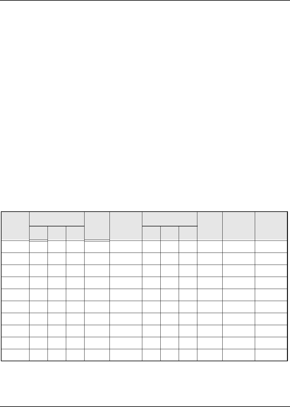
6881096C74-B May 25, 2005
Troubleshooting Procedures: UHF Range 2 (450–520 MHz) Band Main Board Troubleshooting 4-17
4.8 UHF Range 2 (450–520 MHz) Band Main Board Troubleshooting
This information will help you troubleshoot the RF section of the UHF Range 2 (450–520 MHz) band
XTL 5000 radio. Use this information, along with the theory of operation and troubleshooting charts,
to diagnose and isolate the cause of failures.
Prior to troubleshooting, it is important to review the theory of operation, including specific
precautions and troubleshooting methods. Because much of the radio's circuitry operates at high
frequencies, measurements must be taken very carefully. Notes and cautions are added to the text
to alert you to this need in areas of greatest sensitivity. However, the need for extreme care does
exist in all measurements and tests.
4.8.1 Display Flashes “FAIL 001”
This display indicates a synthesizer “out-of-lock” condition. The following information will help to
trouble shoot the frequency generation unit to the component level. Perform the following checks to
determine the mode of the Fail 001:
1. Determine if the “out-of-lock” condition occurs in either receive mode, transmit mode, or both.
Also, check other frequencies programmed in the unit if available.
2. To determine if the “out-of-lock” is frequency or VCO dependant, place the unit into RF TEST
Mode, as described in the ASTRO Digital XTL 5000 VHF/UHF Range 1/UHF Range 2/700–
800 MHz Mobile Radio Basic Service Manual (6881096C73) and step through each test
channel. Table 4-10 indicates the frequency and Aux logic level for each test mode channel.
In addition, Table 4-11 on page 4-18 provides information about the frequency of operation for
each VCO.
Table 4-10. Test Mode Channels UHF Range 2 (AUX 4 is not used for VCO selection in UHF)
Test
Mode
AUX (TX Logic) TX
VCO
TX Freq
(MHz)
AUX (RX Logic) RX
VCO
RX Freq
(MHz)
RX VCO
Freq
(MHz)123 123
Chan 1 100
Q5826450.025001Q5905450.075559.725
Chan 2 100
Q5826455.825001Q5905455.625565.275
Chan 3 100
Q5826463.675001Q5905463.625573.275
Chan 4 100
Q5826473.375110Q5903473.325582.975
Chan 5 100
Q5826484.975110Q5903484.925594.575
Chan 6 000
Q5825485.025110Q5903485.075594.725
Chan 7 000
Q5825490.825110Q5903490.875600.525
Chan 8 000
Q5825496.625010Q5901496.675606.325
Chan 9 000
Q5825508.375010Q5901508.325617.975
Chan 10 000
Q5825519.975010Q5901519.925629.575

May 25, 2005 6881096C74-B
4-18 Troubleshooting Procedures: UHF Range 2 (450–520 MHz) Band Main Board Troubleshooting
NOTE: The UHF band radios use high-side injection with an IF frequency of 109.65 MHz; therefore,
the receive VCO frequencies are 109.65 MHz higher than the selected radio channel
frequencies.
NOTE: If a failure is indicated in any of the VCOs, whose operation is defined in the table above, then
the respective circuit should be checked to ensure proper bias is being applied to the
transistor. Specifically, the transistor collector pin should be at 8.2 V and base-emitter voltage
should be on the order of 0.8 V. The steering line voltage should be in the range of 2 V for the
lower frequency end of operation, and on the order of 11V at the upper frequency end of
operation. There could be typically +/- 1 V deviation from the above quoted numbers, which
allow for tolerances in the components. A clean, steady, frequency spike should be observed
on a spectrum analyzer of typically -18 dBm at the end of the resistive pad in the collector
circuitry of a properly working VCO.
3. Continue troubleshooting by using the Fail 001 troubleshooting chart in Chapter 5.
Table 4-11. VCO Frequency Calculation and Switching Logic (UHF Range 2)
VCO AUX1 AUX2 AUX3 VCO Frequency
RX VCO Q5905 001
559.65 <= f < 582.65
RX VCO Q5903 110
582.65 <= f < 605.65
RX VCO Q5901 010
605.65 <= f < 629.65
TX VCO Q5826 100
450 <= f < 485
TX VCO Q5825 000
485 <= f <= 520
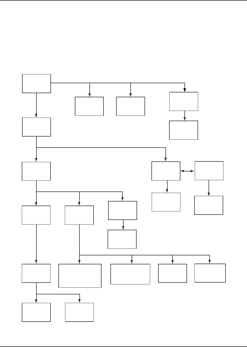
6881096C74-B May 25, 2005
Troubleshooting Procedures: UHF Range 2 (450–520 MHz) Band Main Board Troubleshooting 4-19
4.8.2 FGU Troubleshooting Aids
The following illustrations are additional service aids for troubleshooting the frequency generation
unit.
•Figure 4-7 is a block diagram of the DC distribution for the frequency generation unit.
•Figure 4-8 on page 4-20 is a block diagram of the frequency generation unit.
•Table 4-12 on page 4-20 describes the function of pins on the LV Frac-N IC U5752.
•Figure 4-9 on page 4-22 is a waveform representation during programming of the LV Frac-N IC
U5752.
Figure 4-7. Frequency Generation Unit DC Power Supply Distribution (UHF Range 2)
13.8 VDC
from Battery or
Power Supply
Audio
PA
Q5503 RFPA
Final
MRF1570
Q5502 RFPA
Driver
MRF1518
U5501 RFPA
Pre-driver
C65
Q0503
Switched A+
Switched A+
(SW_A+)
9.3V
Regulated
9.1V
Regulated
9.3V
Regulated
5.0V
Regulated
5.0V
Regulated
8.2V
Regulated
K9.1
3.0V
Regulated
U0950
9.3V Regulator
U0505
5.0V Regulator
U5301
5.0V
Regulator
U5750
3.0V Regulator
Y5750 16.8
MHz Reference
Oscillator and
U6752 Buffer
Q5752
8.2V Superfilter
Q5825, Q5826 TX VCOs
and
Q5901, Q5903, Q5905
RX VCOs
U5752
LVFracN
U5303 2nd
Stage of RX
Injection
Q5902, Q5904, Q5906
Stages of RX
Injection
U0951
9.1V TX
Regulator
Q5828 and
Q5829 TX
Injection
Q0952
K9.1 Switch
Q5501
TX
Buffer
Charge Pump
Bias Q5750 and
Q5751 , Prescaler
Amp Q5755
U5570
9.3V Regulator
A+

May 25, 2005 6881096C74-B
4-20 Troubleshooting Procedures: UHF Range 2 (450–520 MHz) Band Main Board Troubleshooting
Figure 4-8. Frequency Generation Unit Block Diagram (UHF Range 2)
Table 4-12. LV Frac-N U6751 Pin Descriptions (UHF Range 2)
Pin No. Pin Name Description
1AUX2 Auxiliary logic output
2AUX3 Auxiliary logic output
3AUX4 Auxiliary logic output
4LOCK Lock detect—logic high indicates in-lock condition
5PD_VDD 3.0-V supply (phase detector)
6GROUND Ground (digital)
7DATA SPI data I/O
8CLK SPI clock
9CEX SPI enable line—active low
10 MODIN Modulation input from controller
11 VMULT4 Multiplier clock output
12 VMULT3 Multiplier clock output
13 VRO 3.0-V supply for reference oscillator warp circuitry
14 VMULT2 Not used
Bias 1
3.0V
3.0V
3.0V
3.0V
8.2V
Lock Detect
to Controller
Prescaler Input
Q5755 RF
Feedback
8.2V
Bias 2
9.3V
SFIN
SFBASE
SFOUT Lock
PREIN
AUX4
AUX3
Mod Out
IADAPT
IOUT
AUX2
AUX1
VMULT4
VMULT3
5.0V
16.8MHz Reference
to Controller and
Receiver Back End
VOLTAGE
MULTIPLIER
D5750 and
D5751
16.8MHz OSC
8.2V
Super Filter
Q5752
U5751
U5752
3.0V
Regulator
U5750
PHASE
DETECTOR BIAS
Q5750 RX and
Q5751 TX
CLOCK
SYN_SEL
DATA
MOD_IN
From
Controller
NC
A
X0
X1
X2
X3
X4
B
C7.5V
8.2V
Q5706
Q5707
Q5708
Q5709
RX
INJECTION
TX
INJECTION
RX
Injection
TX
Injection
Keyed
9.1V
C5779
C5780
LOOP
FILTER
8.2V SW
8.2V SW
8.2V SW
8.2V SW
Q5825
Q5826
Q5901
Q5903
Q5905
U5753
Q5710 8.2V SW

6881096C74-B May 25, 2005
Troubleshooting Procedures: UHF Range 2 (450–520 MHz) Band Main Board Troubleshooting 4-21
15 VMULT1 Not used
16 INDMULT Not used
17 — No connection
18 REFSEL Not used
19 FREFOUT Not used
20 AVDD 3.0-V supply (analog)
21 VBPASS Not used
22 GND Ground (analog)
23 XTAL1 16.8 MHz reference oscillator input
24 XTAL2 Not used
25 WARP Reference oscillator warp output
26 SFCAP Superfilter bypass node
27 SFBASE Superfilter control node for Q5752
28 SFOUT Superfilter output
29 — No connection
30 SFIN Superfilter supply input
31 — No connection
32 PREIN Prescalar input
33 GROUND Ground (prescalar)
34 PRE_VDD 3.0-V supply
35 PVREF Not used
36 DVDD 3.0-V supply (digital)
37 TEST1 Not used
38 TEST2 Not used
39 CPB2 Phase detector bias input
40 CPB1 Phase detector bias input
41 MODOUT Modulation output
42 CCOMP Not used
43 IOUT Phase detector normal mode output
44 GND Ground (phase detector)
45 IADAPT Phase detector adapt mode output
46 ADAPTSW Phase detector adapt switch
47 VCP High-voltage supply for phase detector
48 AUX1 Auxiliary logic output
Table 4-12. LV Frac-N U6751 Pin Descriptions (UHF Range 2) (Continued)
Pin No. Pin Name Description

May 25, 2005 6881096C74-B
4-22 Troubleshooting Procedures: 700–800 MHz Main Board Troubleshooting
Figure 4-9. Waveform Representation During Programming of the LV Frac-N IC (U5752)
NOTE: The above waveforms are representations only.
4.8.3 Out-of-Lock Condition
The probable cause of an out-of-lock condition is a failure in the synthesizer circuit. If the voltages on
the AUX lines do not conform to Table 4-11 on page 4-18, troubleshoot the synthesizer. If the AUX
pins are correct, but the supply switch (Q5706, Q5707, Q5708, Q5709 or Q5710) to the in question
VCO is not active with 8.2V at the VCO end, then troubleshoot the 3 to 8 multiplexer U5753 or the
switch transistor packages.
If the AUX voltages are correct but the synthesizer feedback level is not within the range indicated at
TP5783 (-6 to -11dBm), troubleshoot the buffer stages after the VCO. If the AUX voltages are correct
and the synthesizer feedback level is correct but an out-of-lock condition persists, troubleshoot the
synthesizer.
4.8.4 No or Low Output Power (TX or RX Injection)
In addition to the schematic and theory of operation, refer to the transmitter injection troubleshooting
flowchart and the receiver injection trouble shooting flowchart in Chapter 5. The charts will guide you
through a sequence of tests and checks designed to isolate problems in the Transmitter or receiver
injection strings.
4.8.5 No or Low Modulation
In addition to the schematic and theory of operation, refer to the transmitter no TX Audio
troubleshooting flowchart in Chapter 5. The chart will guide you through a sequence of tests and
checks designed to isolate problems in the Transmitter Audio section of the FGU.
4.8.6 Troubleshooting the Back-End
Refer to “5.6.18 RX Back-End—Poor SINAD or No Audio (380–470 MHz and 450–520 MHz)—Part 1
of 3” on page 5-32.
4.9 700–800 MHz Main Board Troubleshooting
This information will help you troubleshoot the RF section of the 700–800 MHz XTL 5000 radio. Use
this information, along with the theory of operation and troubleshooting charts, to diagnose and
isolate the cause of failures.
Prior to troubleshooting, it is important to review the theory of operation, including specific
precautions and troubleshooting methods. Because much of the radio's circuitry operates at high
frequencies, measurements must be taken very carefully. Notes and cautions are added to the text
to alert you to this need in areas of greatest sensitivity. However, the need for extreme care does
exist in all measurements and tests.
Pin 9 (Chip Select)
Pin 7 (Data)
Pin 8 (Clock)

6881096C74-B May 25, 2005
Troubleshooting Procedures: 700–800 MHz Main Board Troubleshooting 4-23
4.9.1 Display Flashes “FAIL 001”
This display indicates a synthesizer "out-of-lock" condition. The following information will help to
trouble shoot the frequency generation unit to the component level. Perform the following checks to
determine the mode of the Fail 001:
1. Determine if the "out-of-lock" condition occurs in either receive mode, transmit mode, or both.
Also, check other frequencies programmed in the unit if available.
2. To determine if the "out-of-lock" is frequency or VCO dependant, place the unit into RF TEST
Mode, as described in the ASTRO Digital XTL 5000 VHF/UHF Range 1/UF Range 2/700–
800 MHz Mobile Radio Basic Service Manual (6881096C73) and step through each test
channel. Table 4-13 indicates the frequency and Aux logic level for each test mode channel.
In addition, Table 4-14 provides information about the frequency of operation for each VCO.
Table 4-13. Test Mode Channels (700–800 MHz)
Test
MODE
LV Frac-N
TX Logic
TX
Oscillator
TX Freq
MHz
LV Frac-N
RX Logic
RX
Oscillator
RX Freq
MHz
CHAN 1 AUX 1 U6754 osc1 762.0125 AUX 3 U6755 osc1 762.0625
CHAN 2 AUX 1 U6754 osc1 769.0125 AUX 3 U6755 osc1 769.0625
CHAN 3 AUX 1 U6754 osc1 775.9875 AUX 3 U6755 osc1 775.9375
CHAN 4 AUX 1 U6754 osc1 794.0125 AUX 4 U6755 osc2 851.0625
CHAN 5 AUX 1 U6754 osc1 805.9875 AUX 4 U6755 osc2 860.0625
CHAN 6 AUX 2 U6754 osc2 806.0125 AUX 4 U6755 osc2 860.0625
CHAN 7 AUX 2 U6754 osc2 823.9875 AUX 4 U6755 osc2 869.9375
CHAN 8 AUX 2 U6754 osc2 851.0125 AUX 4 U6755 osc2 851.0625
CHAN 9 AUX 2 U6754 osc2 860.0125 AUX 4 U6755 osc2 860.0625
CHAN 10 AUX 2 U6754 osc2 869.8875 AUX 4 U6755 osc2 869.9375
Table 4-14. VCO Frequency Calculation and Switching Logic (700–800 MHz)
MODE
Radio
Frequency
(MHz)
VCO
Frequency
Formula
VCO
Frequency
(MHz)
AUX
1
AUX
2
AUX
3
AUX
4
Rx 764.0125 -
775.9875
F(U6755 osc1) =
Fc + 73.35 MHz
837.3625 -
849.3375
Low Low HIgh Low
Rx 851.0125 -
868.9875
F(U6755 osc2) =
Fc - 73.35 MHz
777.6625 -
795.6375
Low Low Low HIgh
Tx (TA) 764.0125 -
775.9875
F(U6754 osc1) =
Fc
764.0125 -
775.9875
HIgh Low Low Low
Tx(RPTR) 794.0125 -
805.9875
F(U6754 osc1) =
Fc
794.0125 -
805.9875
HIgh Low Low Low
Tx(RPTR) 806.0125 -
823.9875
F(U6754 osc2) =
Fc
806.0125 -
823.9875
Low HIgh Low Low

May 25, 2005 6881096C74-B
4-24 Troubleshooting Procedures: 700–800 MHz Main Board Troubleshooting
3. Continue troubleshooting by using the Fail 001 troubleshooting chart in Chapter 5.
4.9.2 FGU Troubleshooting Aids
The following illustrations are additional service aids for troubleshooting the frequency generation
unit.
•Figure 4-10 on page 4-25 is a block diagram of the DC distribution for the frequency generation
unit.
•Figure 4-11 on page 4-26 is a block diagram of the frequency generation unit.
•Table 4-15 on page 4-26 describes the function of pins on the LV Frac-N IC U6751.
•Figure 4-12 on page 4-28 is a waveform representation during programming of the LV Frac-N
IC U6751.
Tx (TA) 851.0125 -
868.9875
F(U6754 osc2) =
Fc
851.0125 -
868.9875
Low HIgh Low Low
Tx (TA) = Talkaround Mode
Tx(RPTR) = Repeater or trunked
Table 4-14. VCO Frequency Calculation and Switching Logic (700–800 MHz) (Continued)
MODE
Radio
Frequency
(MHz)
VCO
Frequency
Formula
VCO
Frequency
(MHz)
AUX
1
AUX
2
AUX
3
AUX
4
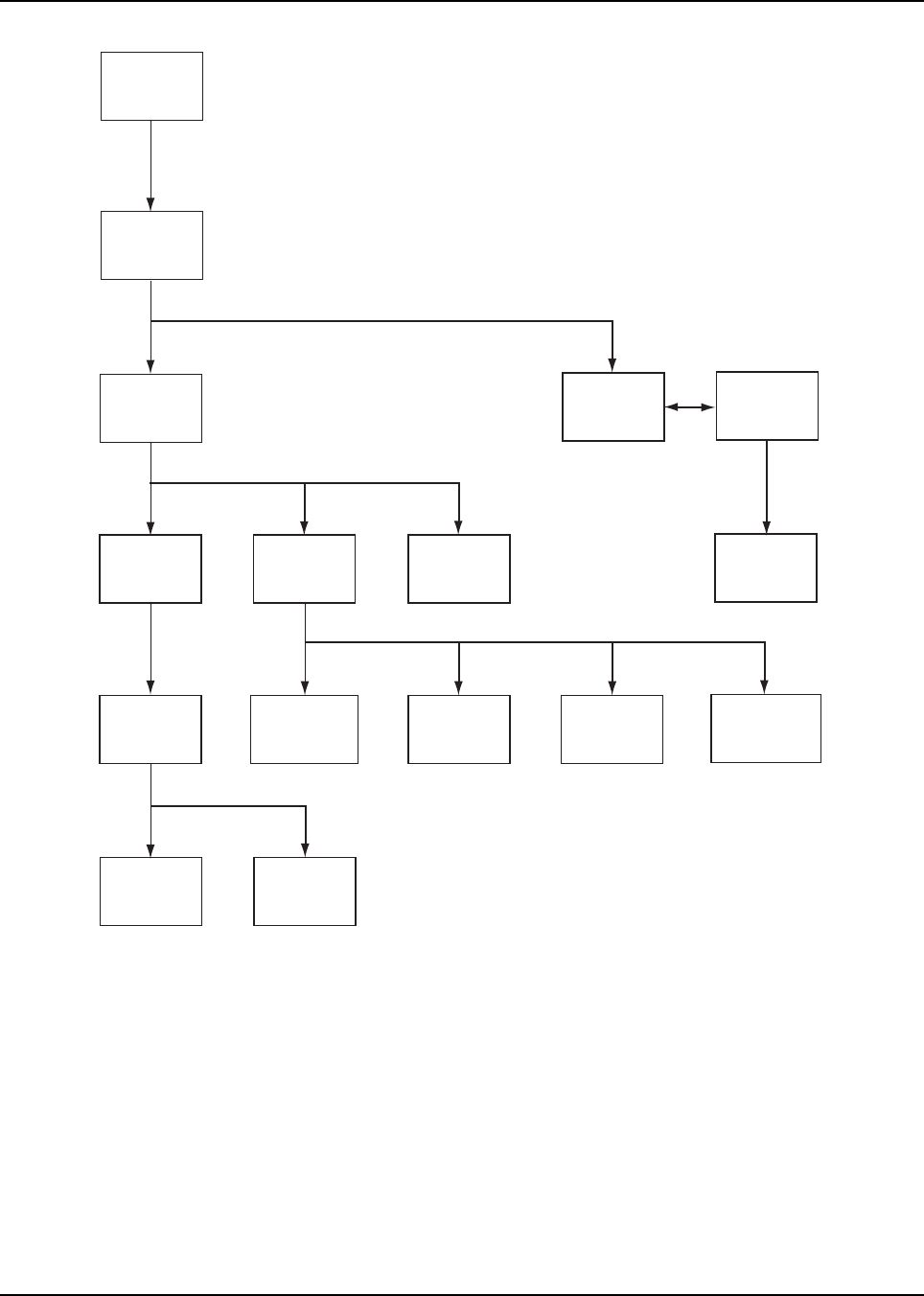
6881096C74-B May 25, 2005
Troubleshooting Procedures: 700–800 MHz Main Board Troubleshooting 4-25
Figure 4-10. Frequency Generation Unit DC Power Supply Distribution (700–800 MHz)
MAEPF-27803-O
13.8 VDC
from Battery or
Power Supply
Q0503
Switched A+
Switched A+
(SW_A+)
9.3V
Regulated
5.0V
Regulated
8.2V
Regulated
K9.1
3.0V
Regulated
U0950
9.3V Regulator
U0505
5.0V Regulator
U6750
3.0V Regulator
Y6750 16.8
MHz Reference
Oscillator and
U6752 Buffer
Q6759
8.2V Superfilter
U6754 TX VCOs
and
U6755 RX VCOs
U6751
LVFracN
Q6763 2nd
Stage of RX
Injection
Q6762 1st
Stage of RX
Injection
U0951
9.1V TX
Regulator
Q6764 and
Q6765 TX
Injection
Q0952
K9.1 Switch
Q6766 3rd
Ste of TX
Injection
Charge Pump
Bias Q6757 and
Q6758, Prescaler
Amp Q6761
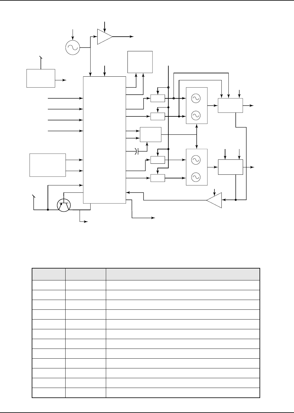
May 25, 2005 6881096C74-B
4-26 Troubleshooting Procedures: 700–800 MHz Main Board Troubleshooting
Figure 4-11. Frequency Generation Unit Block Diagram (700–800 MHz)
Table 4-15. LV Frac-N U6751 Pin Descriptions (700–800 MHz)
Pin No. Pin Name Description
1AUX2 Auxiliary logic output, high selects U6754 OSC2
2AUX3 Auxiliary logic output, high selects U6755 OSC1
3AUX4 Auxiliary logic output, high selects U6755 OSC2
4LOCK Lock detect—logic high indicates in-lock condition
5PD_VDD 3.0-V supply (phase detector)
6GROUND Ground (digital)
7DATA SPI data I/O
8CLK SPI clock
9CEX SPI enable line—active low
10 MODIN Modulation input from controller
11 VMULT4 Multiplier clock output
12 VMULT3 Multiplier clock output
Bias 1
3.0V
3.0V
3.0V
3.0V
8.2V
8.2V
8.2V
Q6753
Q6755
Q6756
Q6760
Lock Detect
to Controller
Prescaler Input
Q6761 RF
Feedback
RX
INJECTION
TX
INJECTION
RX
Injection
TX
Injection
Keyed
9.1V
U6754
U6755
8.2V
C6783
LOOP
FILTER
Bias 2
9.3V
9.3V
SFIN
SFBASE
SFOUT Lock
PREIN
AUX4
AUX3
Mod Out
IADAPT
IOUT
AUX2
AUX1
VMULT4
VMULT3
5.0V
16.8MHz Reference
to Controller and
Receiver Back End
VOLTAGE
MULTIPLIER
D6751 and
D6752
16.8MHz OSC
8.2V
Super Filter
Q6759
8.2V SW
8.2V SW
8.2V SW
8.2V SW
U6752
U6751
3.0V
Regulator
U6750
PHASE
DETECTOR BIAS
Q6757 RX and
Q6758 TX
CLOCK
SYN_SEL
DATA
MOD_IN
From
Controller
MAEPF-27804-O
6881096C74-B May 25, 2005
Troubleshooting Procedures: 700–800 MHz Main Board Troubleshooting 4-27
13 VRO 3.0-V supply for reference oscillator warp circuitry
14 VMULT2 Not used
15 VMULT1 Not used
16 INDMULT Not used
17 — No connection
18 REFSEL Not used
19 FREFOUT Not used
20 AVDD 3.0-V supply (analog)
21 VBPASS Not used
22 GND Ground (analog)
23 XTAL1 16.8 MHz reference oscillator input
24 XTAL2 Not used
25 WARP Reference oscillator warp output
26 SFCAP Superfilter bypass node
27 SFBASE Superfilter control node for Q6759
28 SFOUT Superfilter output
29 — No connection
30 SFIN Superfilter supply input
31 — No connection
32 PREIN Prescalar input
33 GROUND Ground (prescalar)
34 PRE_VDD 3.0-V supply
35 PVREF Not used
36 DVDD 3.0-V supply (digital)
37 TEST1 Not used
38 TEST2 Not used
39 CPB2 Phase detector bias input
40 CPB1 Phase detector bias input
41 MODOUT Modulation output
42 CCOMP Not used
43 IOUT Phase detector normal mode output
44 GND Ground (phase detector)
45 IADAPT Phase detector adapt mode output
46 ADAPTSW Phase detector adapt switch
47 VCP High-voltage supply for phase detector
48 AUX1 Auxiliary logic output, high selects U6754 OSC1
Table 4-15. LV Frac-N U6751 Pin Descriptions (700–800 MHz) (Continued)
Pin No. Pin Name Description
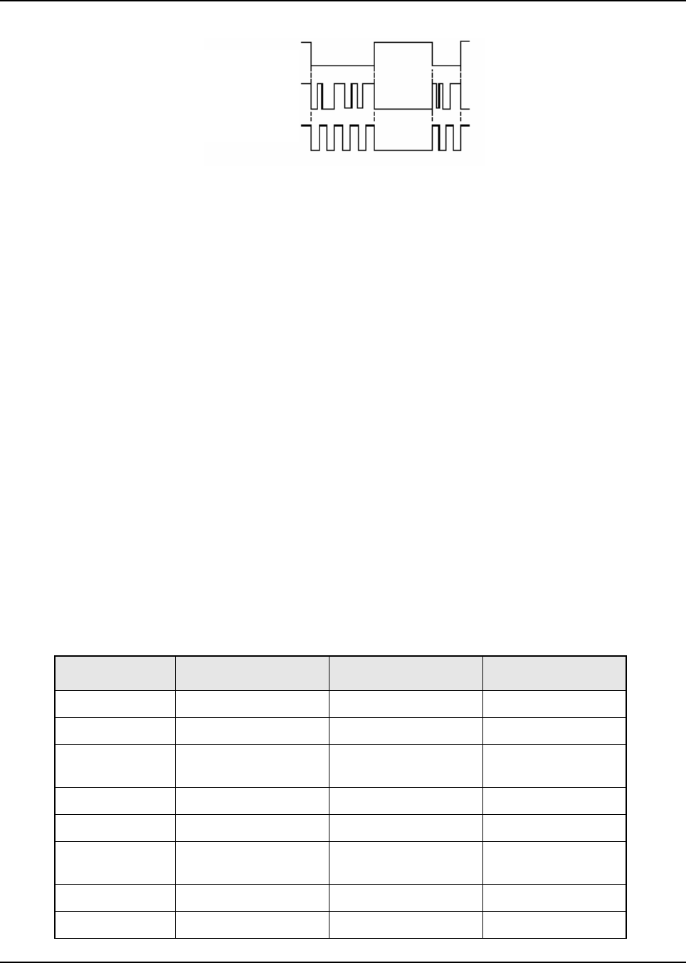
May 25, 2005 6881096C74-B
4-28 Troubleshooting Procedures: Standard Bias Tables
Figure 4-12. Waveform Representation During Programming of the LV Frac-N IC (U6751)
NOTE: The above waveforms are representations only.
4.9.3 No or Low Output Power (TX or RX Injection)
In addition to the schematic and theory of operation, refer to the transmitter injection troubleshooting
flowchart and the receiver injection trouble shooting flowchart in Chapter 5. The charts will guide you
through a sequence of tests and checks designed to isolate problems in the Transmitter or receiver
injection strings.
4.9.4 No or Low Modulation
In addition to the schematic and theory of operation, refer to the transmitter no TX Audio
troubleshooting flowchart in Chapter 5. The chart will guide you through a sequence of tests and
checks designed to isolate problems in the Transmitter Audio section of the FGU.
4.9.5 Troubleshooting the Back-End
Refer to “5.6.36 RX Back-End—Poor SINAD or No Audio (700–800 MHz)—Part 1 of 3” on page 5-
50.
4.10 Standard Bias Tables
Table 4-16, below, outlines some standard supply voltages and system clocks that should be present
during normal operation. These should be checked as a first step to any troubleshooting procedure.
Table 4-16. Standard Operating Bias: Power Lines
Nominal Value Signal Name Range/State Probe Locations
13.8 V A+ (at DC connector) 11.0 to 16.6 V J0401-20, TP0414
13.8 V IGNITION 11.0 to 16.6 V J0401-19, J0401-21
13.8 V SW_A+
(on board only)
11.0 to 16.6 V U0500-4, Q0503
13.8 V SW_B+ (from C.H.) 11.0 to 16.6 V TP0413, J0401-17
2.83 V SW_B+_SENSE No change U0604-7
2.5 V SW_B+_ON_OFF
(on board only)
2 to 3 V Q0505-1, Q0504-1
9.1 V 9.3V_ABACUS No change U0505-1
9.1 V 9.3V No change TP0951, TP0950
Pin 9 (Chip Select)
Pin 7 (Data)
Pin 8 (Clock)
MAEPF-27805-O
6881096C74-B May 25, 2005
Troubleshooting Procedures: Standard Bias Tables 4-29
.
9.18 V 9V No change U0500-5
5 V 5V_ABACUS No change U0505-3
5 V VCC_5 No change J0401-23, U0507-8,
U0503-3, U0502-8,
U0501-8
3 V VCC_3 No change U0962-5
2.85 V LV_DETECT When A+ drops too far
below 9 V, this line goes
to 0 V
U0504-1
2.85 V STO
(at microprocessor)
No change TP0500
2.85 V VCC_2.85 No change U0501-1
1.86 V Vpp No change TP0400
1.85 V VCC_1.8 1.84 to 1.87 V U0507-1
1.55 V VCC_1.55 No change U0502-1
1.42 V VAG No change U0206-1, U0201-3
Note: Do not KEY UP unless the board is inside a chassis.
Table 4-17. Standard Operating Bias: Clock and Control Lines
Nominal Value Signal Name Range/State Probe Locations
(See “Chapter 6
Troubleshooting
Waveforms” on
page 6-1)
SB9600__BUS + Idle=High (4 V to 5 V) J0402-3, J2-2
SB9600__BUS - Idle=Low (0 V) J0402-5, J2-3
SB9600__BUSY Idle=Low (0 V) J0402-4, J2-9
SB9600__RESET Idle=Low (0 V) J0402-6, J2-8
Note: Use chassis as GND when measuring on an oscilloscope.
(See “Chapter 6
Troubleshooting
Waveforms” on
page 6-1)
USB_PWR 5.1 V J0402-12, J2-12
USB_DATA + J0402-11, J2-7
USB_DATA - J402-13, J2-6
Note: Use chassis as GND when measuring on an oscilloscope.
(See “Chapter 6
Troubleshooting
Waveforms” on
page 6-1)
RS232__UARTA_TX Output voltage level is
the same as BOOT TX
TP0407, J2-7
RS232__UARTA_RX Input level depends on
inputting device's levels
TP0408, J2-9
RS232__UARTA_CTS Flow control line—not
used always
TP0409, J2-8
Table 4-16. Standard Operating Bias: Power Lines (Continued)
Nominal Value Signal Name Range/State Probe Locations
May 25, 2005 6881096C74-B
4-30 Troubleshooting Procedures: Standard Bias Tables
RS232__UARTA_RTS Flow control line—not
used always
TP0410, J2-10
Note: Use chassis as GND when measuring on an oscilloscope.
Approx. 0 V Emergency Idle = deactivated =
grounded
J2-15, J0402-28,
TP0403
1.88 V Emergency Activated = ungrounded J2-15, J0402-28,
TP0403
Approx. 0 V Emergency_sense Deactivated U508-4
2.85 V Emergency_sense Activated U508-4
(See “Chapter 6
Troubleshooting
Waveforms” on
page 6-1)
Boot_TX Same as UARTA_TX J0401-26, P502-10
Boot_RX Same as UARTA_RX J0401-25, P502-2
2.85 V Cable_Detect No prog. cable inserted U0402-4
0 V Cable_Detect Prog. cable inserted at
P502
U0402-4
3.5 V Boot_Data_enable No prog. cable inserted
0 V Boot_Data_enable Prog. cable inserted at
P502
U0402-2
0 V Opt_B+_bootsel_Vpp No prog. cable inserted J0401-22, TP0401
8 V Opt_B+_bootsel_Vpp Prog. cable inserted @
P502
J0401-22, TP0401
(See “6.2.5
32 kHz Clock
Waveform” on
page 6-4)
32 kHz U0102-4
(See “6.2.4
16.8 MHz Clock
Waveform” on
page 6-3)
16.8 Mhz C0911 near U0903
Note: Do not KEY UP unless the board is inside a chassis.
Table 4-18. Standard Operating Bias: Audio Lines
Nominal Value Signal Name Range/State Probe Locations
9.2 V Mic_Hi When microphone
connected (expects
80 mV input) (line has
microphone bias)
TP0402, J0401-4
Table 4-17. Standard Operating Bias: Clock and Control Lines (Continued)
Nominal Value Signal Name Range/State Probe Locations
6881096C74-B May 25, 2005
Troubleshooting Procedures: Standard Bias Tables 4-31
9.2 V Mic_Hi When microphone
disconnected
TP0402, J0401-4
13 V to 16 V Mic_Hi When programming
cable inserted
TP0402, J0401-4
Note: Do not press the PTT unless the PCB is inside a chassis even for a moment to check a line.
Permanent RF hardware damage can occur to the board due to no heatsinking.
9.2 V Aux_Mic = [ A(tx) ]
(transmit audio)
Expects 300 mV input
(APCO default)
Expects 80 mV input
(motorcycle use)
J0401-6, J2-23
2.84 V Aux_PTT = [ PTT ] Idle = High
Active = Low
Hard-wired PTT, which
will mute or unmute
Aux_Mic line
J0402-24, J2-16
1.4 Vdc to 25 Vdc
(needs ext. cap)
Aux_TX (audio input) 300 mV line-level
(no mic bias)
J0401-7
0 V Aux_RX (audio input) 300 mV line-level
(Audio PA In)
J0401-8
Note: The Mic_Hi audio overrides Aux_TX/Aux_Mic audio, and the speaker is always muted.
0 V Speaker + Muted (output) J2-21, U204-4
Speaker - Muted (output) J2-20, U204-6
26v peak-to-peak
@volume= 15+
Speaker + Unmuted (output) J2-21, U204-4
Speaker - Unmuted (output) J2-20, U204-6
Note: Never ground speaker lines. They are differential, not single-sided.
Use an oscilloscope probe on "Spk+" and oscilloscope-probe GND on "Spk-".
2.85 V Monitor Idle = High
Activate = Low
J2-22
2.84 V Audio_PA_Enable Q0200-1
1.3 V RX_Filt_Audio = [A(rx) ]
(receive audio/audio
output)
300 mV line-level output J2-21, TP0204
0 V or 5 V Chan_Act = [A(p) ]
(qualified audio
presence)
Idle = Low (0v)
Active = High (5 V)
J2-13
HUB This pin causes the
control head to send
SB9600 message to the
radio, indicating when
HUB is attached
P502-3
Note: Do not KEY UP unless the board is inside a chassis.
Table 4-18. Standard Operating Bias: Audio Lines (Continued)
Nominal Value Signal Name Range/State Probe Locations
May 25, 2005 6881096C74-B
4-32 Troubleshooting Procedures: Standard Bias Tables
Table 4-19. Standard Operating Bias: VIP Lines (Dash Configuration)
Nominal Value Signal Name Range/State Probe Locations
NA VIP_OUT_1_5v Not accessible J0401-13
NA VIP_OUT_2_5v Not accessible J0401-14
NA VIP_IN_1_5v Not accessible J0401-15
NA VIP_IN_2_5v Not accessible J0401-16
SW_B+ level VIP_OUT_1_12v Deactivate = relay
closed
J0401-11, J2-18
0.3 V to 0.5 V Activate = relay open
SW_B+ level VIP_OUT_2_12v Deactivate = relay
closed
J0401-12, J2-19
0.3 V to 0.5 V Activate = relay open
Note: The voltage levels on the microprocessor side are at 2.85 V levels. The microprocessor is
not designed to drive the relay, but instead, is intended to drive the transistors inside the control
head or on the interconnect board. Be careful when changing jumpers.
Note: The impedance of the relay is why the SW_B+ does not damage the VIP line. Never connect
SW_B+ directly to a VIP line.
Table 4-20. Standard Operating Bias: VIP Lines (Standard Remote Configuration)
Nominal Value Signal Name Range/State Probe Locations
VIP_OUT_1_5v Access only by custom
pin-out
J0401-13
VIP_OUT_2_5v Access only by custom
pin-out
J0401-14
5 V VIP_IN_1_5v Idle = deactivate = 5 V
bias
J0401-15
0 V Activate = ground
5 V VIP_IN_2_5v Idle = deactivate = 5 V
bias
J0401-16
0 V Activate = ground
SW_B+ level VIP_OUT_1_12v Deactivate = relay
closed
J0401-11, J2-18
0.3 V to 0.5 V Activate = relay open
SW_B+ level VIP_OUT_2_12v Deactivate = relay
closed
J0401-12, J2-19
0.3 V to 0.5 V Activate = relay open
Note: VIP_IN programmed by CPS. Requires custom pin-out to gain access.
6881096C74-B May 25, 2005
Troubleshooting Procedures: Receiver Front-End (RXFE) 4-33
4.11 Receiver Front-End (RXFE)
This section provides band-specific troubleshooting procedures for the receiver front-end.
4.11.1 VHF (136–174 MHz) Band
Use this information, along with the theory of operation, to diagnose and isolate the cause of failures.
The principle tools needed to troubleshoot a circuit to the component level are the schematic and the
theory of operation.
In addition to the schematic and theory, you can use the troubleshooting flowcharts in "Chapter 5.
Troubleshooting Charts" that will guide you through a sequence of tests and checks designed to
isolate problems.
Prior to troubleshooting, it is important to review the theory of operation including specific
precautions and troubleshooting methods. Because much of the radio’s circuitry operates at a high
frequency, measurements must be taken carefully.
4.11.2 UHF Range 1 (380–470 MHz) Band
Use this information, along with the theory of operation, to diagnose and isolate the cause of failures.
The principle tools needed to troubleshoot a circuit to the component level are the schematic and the
theory of operation.
In addition to the schematic and theory, you can use the troubleshooting flowcharts in "Chapter 5.
Troubleshooting Charts" that will guide you through a sequence of tests and checks designed to
isolate problems.
Prior to troubleshooting, it is important to review the theory of operation including specific
precautions and troubleshooting methods. Because much of the radio’s circuitry operates at
400 MHz, measurements must be taken carefully.
Table 4-21. Standard Operating Bias: VIP Lines (W3 Remote Configuration)
Nominal Value Signal Name Range/State Probe Locations
VIP_OUT_1_5v Access only by custom
pin-out
J0401-13
VIP_OUT_2_5v Access only by custom
pin-out
J0401-14
NA VIP_IN_1_5v Not supported with W3 J0401-15
NA VIP_IN_2_5v Not supported with W3 J0401-16
SW_B+ level VIP_OUT_1_12v Deactivate = relay
closed
J0401-11, J2-18
0.3 V to 0.5 V Activate = relay open
SW_B+ level VIP_OUT_2_12v Deactivate = relay
closed
J0401-12, J2-19
0.3 V to 0.5 V Activate = relay open
Note: When using the W3 control head and interconnect board, the main board VIP_OUT lines are
pass-through-only lines.

May 25, 2005 6881096C74-B
4-34 Troubleshooting Procedures: Power Amplifier Procedures
4.11.3 UHF Range 2 (450–520 MHz) Band
Use this information, along with the theory of operation, to diagnose and isolate the cause of failures.
The principle tools needed to troubleshoot a circuit to the component level are the schematic and the
theory of operation.
In addition to the schematic and theory, you can use the troubleshooting flowcharts in "Chapter 5.
Troubleshooting Charts" that will guide you through a sequence of tests and checks designed to
isolate problems.
Prior to troubleshooting, it is important to review the theory of operation including specific
precautions and troubleshooting methods. Because much of the radio’s circuitry operates at
400 MHz, measurements must be taken carefully.
4.11.4 700–800 MHz Band
Use this information, along with the theory of operation, to diagnose and isolate the cause of failures.
The principle tools needed to troubleshoot a circuit to the component level are the schematic and the
theory of operation.
In addition to the schematic and theory, you can use the troubleshooting flowchart in "Chapter 5.
Troubleshooting Charts" that will guide you through a sequence of tests and checks designed to
isolate problems.
Prior to troubleshooting, it is important to review the theory of operation including specific
precautions and troubleshooting methods. Because much of the radio’s circuitry operates at
800 MHz, measurements must be taken carefully.
4.12 Power Amplifier Procedures
This section provides band-specific troubleshooting procedures for the RF power amplifier (RFPA).
4.12.1 VHF (136–174 MHz) Band
Use this information, along with the theory of operation, to diagnose and isolate the cause of failures.
The principle tools needed to troubleshoot a circuit to the component level are the schematic and the
theory of operation.
Prior to troubleshooting, be sure to review the theory of operation including any precautions and
troubleshooting methods.
4.12.1.1 50-Watt Power Amplifiers
In addition to the schematic and theory, this section includes troubleshooting information that will
help you test and check the circuits to localize and isolate problems.
4.12.1.2 General Troubleshooting and Repair Notes
Most of the common transmitter symptoms are caused by either failure of the power amplifier or a
failure in the control circuitry. The initial troubleshooting effort should be toward isolating the problem
to one of those two areas. If either the control voltage or keyed 9.4 V are zero, then the problem is
likely to be in the control circuit. If those voltages are present, then the problem is more likely in the
power amplifier circuit.
If for diagnostic reasons, a chip component needs to be removed to facilitate testing, such as a
series capacitor removed to allow for signal insertion, then the component(s) returned to the circuit
should be new parts. The application of a soldering iron to many chip components will tend to cause
leaching which could lead to failure.

6881096C74-B May 25, 2005
Troubleshooting Procedures: Power Amplifier Procedures 4-35
After a PA board is replaced, or if any power control circuitry components are replaced, readjust the
power according to instructions in the ASTRO Digital XTL 5000 VHF/UHF Range 1/UHF Range 2/
700–800 MHz Mobile Radio Basic Service Manual.
NOTE: Due to the high frequency of operation, it is imperative that you use specified Motorola parts
when component replacement is necessary. At these frequencies, second and third order
properties of the components are very important and are part of the circuit's design. Substitute
components may not work. It is also critical that you use great care when replacing parts.
Excessive solder or flux, longer than original leads on coax connectors, misorientation of
parts, and other commonly benign imperfections may cause the radio's performance to
degrade.
4.12.2 UHF Range 1 (380–470 MHz) Band
In addition to the schematic (“7.3 HUE4039A/HUE4043A (UHF Range 1) Main Board” on page 7-72)
and theory of operation (“3.6.2 UHF Range 1 (380-470 MHz) Band” on page 3-31), refer to the RFPA
troubleshooting flowcharts in “5.6.23 No TX Audio (380–470 MHz and 450–520 MHz)” on page 5-37.
These flowcharts will guide you through a sequence of tests and checks designed to isolate
problems in the RFPA stages.
See section “4.12.4 700–800 MHz Band” on page 4-35, for more information on troubleshooting the
RF power amplifier circuitry.
4.12.3 UHF Range 2 (450–520 MHz) Band
In addition to the schematic (“7.4 HUE4040A (UHF Range 2) Main Board” on page 7-132) and
theory of operation (“3.6.3 UHF Range 2 (450-520 MHz) Band” on page 3-37), refer to the RFPA
troubleshooting flowcharts in “5.6.23 No TX Audio (380–470 MHz and 450–520 MHz)” on page 5-37.
These flowcharts will guide you through a sequence of tests and checks designed to isolate
problems in the RFPA stages.
See section “4.12.4 700–800 MHz Band” on page 4-35, for more information on troubleshooting the
RF power amplifier circuitry.
4.12.4 700–800 MHz Band
In addition to the schematic ("Chapter 7. Schematics, Component Location Diagrams, and Parts
Lists") and theory of operation ("Chapter 3. Theory of Operation"), refer to the RFPA troubleshooting
flowcharts in "Chapter 5. Troubleshooting Charts". These flowcharts will guide you through a
sequence of tests and checks designed to isolate problems in the RFPA stages.
Use the following information as a guide for troubleshooting the RF power amplifier circuitry:
• Read the theory of operation before troubleshooting.
• To avoid damage to the RFPA, only key the transmitter with the main board installed in the
chassis and the internal screws completely installed and secured with the proper torque setting.
• The chassis eliminator, which allows access to both sides of the main board is useful for
transmitter troubleshooting. Keying the transmitter for an extended period of time while using
the chassis eliminator can cause damage to the radio. Therefore, be sure to cool the radio by
forcing air through the chassis eliminator cooling fins.
• To avoid personal injury from high RF voltages and currents, exercise extreme care while
troubleshooting the transmitter power amplifier.
• Set the A+ supply to 13.6 V with the current limit set to 15 A.
• Calibrate the power meter regularly using the manufacturer's suggested calibration method.

May 25, 2005 6881096C74-B
4-36 Troubleshooting Procedures: Power Amplifier Procedures
• If a component is removed for troubleshooting, replace the removed part, regardless of its
condition, with a new part.
• To reinstall the main board into the chassis, follow the reassembly instruction in the ASTRO
Digital XTL 5000 VHF/UHF Range 1/UHF Range 2/700–800 MHz Mobile Radio Basic Service
Manual.
• Apply new thermal pads if the current thermal pad are damaged. Follow the instructions in the
ASTRO Digital XTL 5000 VHF/UHF Range 1/UHF Range 2/700–800 MHz Mobile Radio Basic
Service Manual.
• Use Motorola-specified parts when component replacement is required.
• When instructed to inspect parts, look for any package damage and/or solder defects.
Chapter 5 Troubleshooting Charts
5.1 Introduction
This chapter contains detailed troubleshooting flowcharts and tables. These should be used as a
guide in determining the problem areas. They are not a substitute for knowledge of circuit operation
and astute troubleshooting techniques. It is advisable to refer to the related detailed circuit
descriptions in the theory of operation chapter prior to troubleshooting a radio.
5.2 List of Troubleshooting Charts
Most troubleshooting flowcharts (see Table 5-1) end by pointing to an IC to replace. Before replacing
any IC, it is good practice to verify power supplies and grounds to the affected IC and trace continuity
to the malfunctioning signal and related circuitry. For example, if a clock signal is not available at a
destination IC, continuity from the source IC should be checked before replacing the source IC.
Table 5-1. List of Troubleshooting Charts
Description Page
VHF (136–174 MHz)
Poor RX Sensitivity or No RX Audio 5-15
RX IF—Poor SINAD or No Audio 5-17
RX Back-End—Poor SINAD or No Audio 5-18
Low or No RX Injection Signal 5-21
Low or No TX Injection Signal 5-22
TX or RX VCO Unlock (Fail 001) 5-23
No Output Power at TX Mode 5-25
No Output Power and IDC < 2A at TX Mode 5-26
UHF Range 1 (380–470 MHz) and UHF Range 2 (450–520 MHz)
No 16.8 MHz Reference Oscillator Frequency 5-27
Poor RX Sensitivity or No RX Audio 5-28
RX IF—Poor SINAD or No Audio 5-30
RX Back-End—Poor SINAD or No Audio 5-32
Low or No RX Injection Signal 5-35
Low or No TX Injection Signal 5-36
No TX Audio 5-37
TX or RX VCO Unlock (Fail 001) 5-38
RF Power Amplifier (RFPA)—No or Low TX Power Output 5-40
May 25, 2005 6881096C74-B
5-2 Troubleshooting Charts: List of Troubleshooting Charts
NOTE: The term µC might be used in some of the following troubleshooting charts;
µC = MCU or microprocesor.
RFPA Power Control—No VGBIAS 5-45
700–800 MHz
No 16.8 MHz Reference Oscillator Frequency 5-46
Poor RX Sensitivity or No RX Audio 5-47
RX IF—Poor SINAD or No Audio 5-49
RX Back-End—Poor SINAD or No Audio 5-50
Low or No RX Injection Signal 5-53
Low or No TX Injection Signal 5-54
No TX Audio 5-55
TX or RX VCO Unlock (Fail 001) 5-56
RF Power Amplifier (RFPA)—No or Low TX Power Output 5-58
RFPA Power Control—No K9.1V 5-63
RFPA Power Control—No VGBIAS 5-64
RFPA Power Control—No or Low TX RFPA_CNTRL 5-65
Table 5-1. List of Troubleshooting Charts (Continued)
Description Page

6881096C74-B May 25, 2005
Troubleshooting Charts: Troubleshooting Tables 5-3
5.3 Troubleshooting Tables
5.3.1 For Mid Power models
This section contains troubleshooting tables that can help you isolate a problem in your radio.
Table 5-2. XTL 5000 Troubleshooting Table (700–800 MHz, 380-470 MHz and 136-174 MHz)
Symptom Check Section Troubleshooting Procedure Component
No TX Modulation Controller Block With 80 mV rms, 1 kHz injected
to the MIC_HI line and CPS mic
gain level set to 0 (default),
check the following levels.
• 80 mVrms at TP0200, U0209-
4, J0401-4.
• 36 mV rms at TP0201.
• 20 mV rms at U0201-1,
TP0202.
• 36 mV rms at U0201-7,
TP0203.
• 36 mV rms at U0200-17.
• > 150 mV rms at U0900-1.
• > 150 mV rms at FL0900-5.
• > 150 mV rms at U0902-14
• > 150 mV rms at R6782
• Absence of signal may indicate
failure with U0209 (MUX), or
U0201 (Op-Amp)
• Absence of signal may indicate
failure with U0209 (MUX), or
U0201 (Op-Amp)
• Absence of signal may indicate
failure with U0202 (EPOT), or
U0201 (Op-Amp)
• Absence of signal may indicate
failure with U0202 (EPOT), or
U0201 (Op-Amp)
• Absence of signal may indicate
failure with U0200 (Codec)
• Absence of signal may indicate
failure with U0901 (Urchin),
U0900 (Modulation DAC), or
U0001 (Microprocessor Board)
• Absence of signal may indicate
failure with U0901 (Urchin), or
FL0900 (Filter)
• Absence of signal may indicate
failure with U0902 (MUX)
• Presence of signal may
indicate a aproblem in RF
section
Flex/Control Head Check that MIC_HI is getting to
controller at VR0412, VR0421,
C0438, C0207, C0234, or R0204
Absence of signal may indicate
failure with flex, control head,
VR0412, or VR0421

May 25, 2005 6881096C74-B
5-4 Troubleshooting Charts: Troubleshooting Tables
No Keyloading Controller Connect proper KVL keyloader
and cable and begin keyloading
by pressing the PTT on the
keyloader
• Check data activity (5 V levels)
on Boot_TX/Keyfail* line -
J0401-25, U0401-5, or C0430.
• Check data activity (5 V levels)
at U0401-6.
• Check data activity (5 V levels)
at J0501-14
• Absence of data may indicate
failure with keyloader, cable,
control head, control head flex,
J0401, or VR0417.
• Absence of signal may indicate
failure with U0401 (MUX) or
Q0404
• Absence of signal may indicate
failure with J0501; Presence of
signal may indicate failure of
secure interface board or UCM/
Secure module, which would
need replacing
Radio Dead, Display
Does Not Light Up
Blown Fuse Check fuse in red lead of power
cable (or green lead if used)
Absence of signal may indicate
failure with J0401, J0402,
VR0412, or VR0402
Controller Section • Check for IGNITION at J0401-
20, J0402-18, VR0402,
VR0412
• Check for A+ at Q0503,
VR0950, J0401-19,21, or
TP0414
• Absence of signal may indicate
failure with J0401, J0402
• Absence of signal may indicate
failure with J0950, J0401
Flex/Control Head Check for SW_B+_CH at J0401-
17, TP0413, or pin 21 of P502
(on control head)
Absence of signal may indicate
failure with flex, control head
Radio Dead, Display
Lights Up
Regulators • Check for SW_B+ at Q0503,
U0500-4, U0950-4, U0951-4
• Check for 9.3 V at U0500-5,
U0950-5, U0951-5.
• Check for 5 V at U0503-5, 3 V
at U0962-3, 2.85 V at U0501-1,
1.85 V at U0507-1, 1.55 V at
U0502-1
• Absence of signal may indicate
failure with Q0503
• Absence of signal may indicate
failure with U0500, U0950, or
U0951 (9 V Regulators)
• Absence of signal may indicate
failure with U0503, U0962,
U0501, U0507, or U0502 (5 V,
3 V, 2.85 V, 1.85 V, and 1.55 V
Regulators)
Flex/Control Head Check for SW_B+_CH at J0401-
17, TP0413, or pin 21 of P502
(on control head)
Absence of signal may indicate
failure with flex, control head
SB9600 Check for logic transitions at
J0401-31 thru 34, J0402-3 thru
6, or U0606-4,7,9,12
Absence of signal may indicate
failure with U0606 MUX),
VR0408, VR0418, Q0610-
Q0613, U0001 (Microprocessor
Board), control-head flex, or rear
accessory flex
Table 5-2. XTL 5000 Troubleshooting Table (700–800 MHz, 380-470 MHz and 136-174 MHz) (Continued)
Symptom Check Section Troubleshooting Procedure Component

6881096C74-B May 25, 2005
Troubleshooting Charts: Troubleshooting Tables 5-5
Radio Dead, Display
Lights Up
Clocks
A+
Check for 32 kHz clock at
U0102-4, and 16.8 MHz clock at
C0106, C0911
Check A+ to the Control Head
J0401-19, 20
Presence of signals may indicate
failure with U0001
(Microprocessor Board).
Absence of signals may indicate
failure with U0102 (Inverter) or
with FGU reference oscillator
circuit
• Absence of voltage F0400 may
be blown.
No RX Audio/
Receive Does not
Unsquelch
Controller Block (Inject 1 kHz tone, 3 kHz
deviation into radio antenna, set
volume to rated audio.
• Check for speaker leads
shorted to ground, or at U0204-
4, 6.
• Check for > 30 mV rms audio
at audio PA input, U0204-1,9.
• Check for > 30 mV rms audio
at U0206-8 or TP0205.
• Check for > 30 mV rms audio
at U0210-6 or U0200-2.
• Check that U0204-8 is >10 V
• Short may indicate failure with
VR0400, VR0412, or U0204
• Presence of signal may
indicate failure with U0204
(Audio PA)
• Presence of signal may
indicate failure with U0206
(Log-POT)
• Presence of signal may
indicate failure with U0210
(MUX); Absence of signal may
indicate failure with U0200
(CODEC), or U0001
(Microprocessor Board)
• Absence of >10V may indicate
failure with Q0200 or U0001
Regulators See description for No VOCON
Powerup
ABACUS Circuit
(380-470 MHz,
450-520 MHz)
• Check for 20 kHz Frame Sync
pulse signal at testpoint FS
(U5002-31)
• Check for 1.2 MHz Clock
square wave at testpoint
CLKOUT (U5002-28)
• Check for random data pattern
at testpoint DOUTA (U5002-29)
• Check for Clock Oscillator at
R5025 (18 MHz)
• Check for Local Oscillator at
C5058 (71.1 MHz or 75.6 MHz)
• Absence of signal causes no
receive. Possible U5002
(ABACUS) failure or U0001
(Microprocessor Board) failure
• Absence of signal causes no
receive. Possible U5002
(ABACUS) failure or U0001
(Microprocessor Board) failure
• Absence of signal causes no
receive. Possible U5002
(ABACUS) failure or U0001
(Microprocessor Board) failure
• Absence of Clock signal
causes no receive. Possible
U5002 (ABACUS), Clock VCO,
or U0001 (Microprocessor
Board) failure
• Absence of LO signal causes
no receive. Possible U5002
(ABACUS), or LO VCO
Table 5-2. XTL 5000 Troubleshooting Table (700–800 MHz, 380-470 MHz and 136-174 MHz) (Continued)
Symptom Check Section Troubleshooting Procedure Component

May 25, 2005 6881096C74-B
5-6 Troubleshooting Charts: Troubleshooting Tables
No RX Audio/
Receive Does not
Unsquelch (cont.)
ABACUS Circuit
(700-800 MHz)
• Check for 20 kHz Frame Sync
pulse signal at testpoint FS
(U6000-31)
• Check for 1.2 MHz Clock
square wave at testpoint
CLKOUT (U6000-28)
• Check for random data pattern
at testpoint DOUTA (U6000-29)
• Check for Clock Oscillator at
R6003 (18 MHz)
• Check for Local Oscillator at
C6026 (71.1 MHz or 75.6 MHz)
• Absence of signal causes no
receive. Possible U6000
(ABACUS) failure or U0001
(Microprocessor Board) failure
• Absence of signal causes no
receive. Possible U6000
(ABACUS) failure or U0001
(Microprocessor Board) failure
• Absence of signal causes no
receive. Possible U6000
(ABACUS) failure or U0001
(Microprocessor Board) failure
• Absence of Clock signal
causes no receive. Possible
U6000 (ABACUS), Clock VCO,
or U0001 (Microprocessor
Board) failure
• Absence of LO signal causes
no receive. Possible U6000
(ABACUS), or LO VCO
Radio Will Not Turn
Off
On/Off Switch
(Control Head)
Check for SW_B+_CH at 0 V at
J0401-17, TP0413
A high voltage may indicate
failure with the control head
Radio Will Not Turn
Off (continued)
Emergency Circuit Check for 0 V at Timer U0506-3,
U0508-2,4
A high voltage may indicate
failure with U0506, or that the
EMERGENCY line is not
grounded by the rear accessory
cable
SW_B+ Sense
Circuit
Check that U0604-7 is low (0 V)
and that SOFT TURN OFF is low
(0 V) at D0501
Absence of this voltage may
indicate failure with U0604 (Op-
Amp) or with U0001
(Microprocessor Board)
Table 5-2. XTL 5000 Troubleshooting Table (700–800 MHz, 380-470 MHz and 136-174 MHz) (Continued)
Symptom Check Section Troubleshooting Procedure Component

6881096C74-B May 25, 2005
Troubleshooting Charts: Troubleshooting Tables 5-7
5.3.2 For High Power models and UHF R2 Mid Power
This section contains troubleshooting tables that can help you isolate a problem in your radio.
Table 5-3. XTL 5000 Troubleshooting Table (136-174 MHz, 380-470 MHz and 450-520 MHz Mid Power)
Symptom Check Section Troubleshooting Procedure Component
No TX Modulation Controller Block With 80 mV rms, 1 kHz injected
to the MIC_HI line and CPS mic
gain level set to 0 (default),
check the following levels.
• 80 mVrms at TP0200, U0209-
4, J0401-57.
• 80 mV rms at TP0201.
• 2.5 Vdc at U0201-8.
• 80 mV rms at U0201-7,
U0201-7, TP0203.
• 36 mV rms at U0200-17.
• > 150 mV rms at U0900-1.
• > 150 mV rms at FL0900-5.
• > 150 mV rms at U0902-14
• > 150 mV rms at R6782
• Absence of signal may indicate
failure with U0209 (MUX), or
U0201 (Op-Amp)
• Absence of signal may indicate
failure with U0209 (MUX), or
U0201 (Op-Amp)
• Absence of DC bias may
indicate failure with U0201
(Op-Amp)
• Absence of signal may indicate
failure with U0202 (EPOT), or
U0201 (Op-Amp)
• Absence of signal may indicate
failure with U0200 (Codec)
• Absence of signal may indicate
failure with U0901 (Urchin),
U0900 (Modulation DAC), or
U0001 (Microprocessor Board)
• Absence of signal may indicate
failure with U0901 (Urchin), or
FL0900 (Filter)
• Absence of signal may indicate
failure with U0902 (MUX)
• Presence of signal may
indicate a aproblem in RF
section
Flex/Control Head Check that MIC_HI is getting to
controller at VR0412, VR0421,
C0438, C0207, C0234, or R0204
Absence of signal may indicate
failure with flex, control head,
VR0412
No Keyloading Controller Connect proper KVL keyloader
and cable and begin keyloading
by pressing the PTT on the
keyloader
• Check data activity (5 V levels)
on Boot_TX/Keyfail* line -
J0401-44.
• Check data activity (5 V levels)
at J0501-14
• Absence of data may indicate
failure with keyloader, cable,
control head, control head flex,
J0401.
• Absence of signal may indicate
failure with J0501; Presence of
signal may indicate failure of
secure interface board or UCM/
Secure module, which would
need replacing

May 25, 2005 6881096C74-B
5-8 Troubleshooting Charts: Troubleshooting Tables
Radio Dead, Display
Does Not Light Up
Blown Fuse Check fuse in red lead of power
cable (or green lead if used)
Absence of signal may indicate
failure with J0401, J0402,
VR0412, or VR0402
Controller Section • Check for IGNITION at J0401-
27, 28
• Check for A+ at Q0503,
VR0950, J0401-19,21, or
TP0414
• Absence of signal may indicate
failure with J0401
• Absence of signal may indicate
failure with J0950, J0401 or
VR0950
Flex/Control Head Check for SW_B+_CH at J0401-
33,34, TP0413, or pin 21 of P502
(on control head)
Absence of signal may indicate
failure with flex, control head
Radio Dead, Display
Lights Up
Regulators • Check for SW_B+ at Q0503,
U0500-4, U0950-4, U0951-4
• Check for 9.3 V at U0500-5,
U0950-5, U0951-5.
• Check for 5 V at U0503-5, 3 V
at U0962-3, 2.85 V at U0501-1,
1.85 V at U0507-1, 1.55 V at
U0502-1
• Absence of signal may indicate
failure with Q0503
• Absence of signal may indicate
failure with U0500, U0950, or
U0951 (9 V Regulators)
• Absence of signal may indicate
failure with U0503, U0962,
U0501, U0507, or U0502 (5 V,
3 V, 2.85 V, 1.85 V, and 1.55 V
Regulators)
Flex/Control Head Check for SW_B+_CH at J0401-
33,34, TP0413, or pin 21 of P502
(on control head)
Absence of signal may indicate
failure with flex, control head
SB9600 Check for logic transitions at
J0401-13 thru 16, or U0606-
4,7,9,12
Absence of signal may indicate
failure with U0606 MUX),
VR0408, VR0418, Q0610-
Q0613, U0001 (Microprocessor
Board), control-head flex, or rear
accessory flex
Radio Dead, Display
Lights Up
Clocks
Remote
Check for 32 kHz clock at
U0102-4, and 16.8 MHz clock at
C0106, C0911
Check for A+ at J6
Presence of signals may indicate
failure with U0001
(Microprocessor Board).
Absence of signals may indicate
failure with U0102 (Inverter) or
with FGU reference oscillator
circuit
Check F0400.
Check the flex.
Table 5-3. XTL 5000 Troubleshooting Table (136-174 MHz, 380-470 MHz and 450-520 MHz Mid Power)
Symptom Check Section Troubleshooting Procedure Component

6881096C74-B May 25, 2005
Troubleshooting Charts: Troubleshooting Tables 5-9
No RX Audio/
Receive Does not
Unsquelch
Controller Block (Inject 1 kHz tone, 3 kHz
deviation into radio antenna, set
volume to rated audio.
• Check for speaker leads
shorted to ground, or at U0204-
4, 6.
• Check for > 30 mV rms audio
at audio PA input, U0204-1,9.
• Check for > 30 mV rms audio
at U0206-8 or TP0205.
• Check for > 30 mV rms audio
at U0210-6 or U0200-2.
• Check that U0204-8 is >10 V
• Short may indicate failure with
VR0400, VR0412, or U0204
• Presence of signal may
indicate failure with U0204
(Audio PA)
• Presence of signal may
indicate failure with U0206
(Log-POT)
• Presence of signal may
indicate failure with U0210
(MUX); Absence of signal may
indicate failure with U0200
(CODEC), or U0001
(Microprocessor Board)
• Absence of >10V may indicate
failure with Q0200 or U0001
Regulators See description for No VOCON
Powerup
ABACUS Circuit
(380-470 MHz,
450-520 MHz)
• Check for 20 kHz Frame Sync
pulse signal at testpoint FS
(U5002-31)
• Check for 1.2 MHz Clock
square wave at testpoint
CLKOUT (U5002-28)
• Check for random data pattern
at testpoint DOUTA (U5002-29)
• Check for Clock Oscillator at
R5025 (18 MHz)
• Check for Local Oscillator at
C5058 (71.1 MHz or 75.6 MHz)
• Absence of signal causes no
receive. Possible U5002
(ABACUS) failure or U0001
(Microprocessor Board) failure
• Absence of signal causes no
receive. Possible U5002
(ABACUS) failure or U0001
(Microprocessor Board) failure
• Absence of signal causes no
receive. Possible U5002
(ABACUS) failure or U0001
(Microprocessor Board) failure
• Absence of Clock signal
causes no receive. Possible
U5002 (ABACUS), Clock VCO,
or U0001 (Microprocessor
Board) failure
• Absence of LO signal causes
no receive. Possible U5002
(ABACUS), or LO VCO
Table 5-3. XTL 5000 Troubleshooting Table (136-174 MHz, 380-470 MHz and 450-520 MHz Mid Power)
Symptom Check Section Troubleshooting Procedure Component

May 25, 2005 6881096C74-B
5-10 Troubleshooting Charts: Troubleshooting Tables
No RX Audio/
Receive Does not
Unsquelch (cont.)
ABACUS Circuit
(700-800 MHz)
• Check for 20 kHz Frame Sync
pulse signal at testpoint FS
(U6000-31)
• Check for 1.2 MHz Clock
square wave at testpoint
CLKOUT (U6000-28)
• Check for random data pattern
at testpoint DOUTA (U6000-29)
• Check for Clock Oscillator at
R6003 (18 MHz)
• Check for Local Oscillator at
C6026 (71.1 MHz or 75.6 MHz)
• Absence of signal causes no
receive. Possible U6000
(ABACUS) failure or U0001
(Microprocessor Board) failure
• Absence of signal causes no
receive. Possible U6000
(ABACUS) failure or U0001
(Microprocessor Board) failure
• Absence of signal causes no
receive. Possible U6000
(ABACUS) failure or U0001
(Microprocessor Board) failure
• Absence of Clock signal
causes no receive. Possible
U6000 (ABACUS), Clock VCO,
or U0001 (Microprocessor
Board) failure
• Absence of LO signal causes
no receive. Possible U6000
(ABACUS), or LO VCO
Radio Will Not Turn
Off
On/Off Switch
(Control Head)
Check for SW_B+_CH at 0 V at
J0401-17, TP0413
A high voltage may indicate
failure with the control head
Radio Will Not Turn
Off (continued)
Emergency Circuit Check for 0 V at Timer U0506-3,
U0508-2,4
A high voltage may indicate
failure with U0506, or that the
EMERGENCY line is not
grounded by the rear accessory
cable
SW_B+ Sense
Circuit
Check that U0604-7 is low (0 V)
and that SOFT TURN OFF is low
(0 V) at D0501
Absence of this voltage may
indicate failure with U0604 (Op-
Amp) or with U0001
(Microprocessor Board)
Table 5-3. XTL 5000 Troubleshooting Table (136-174 MHz, 380-470 MHz and 450-520 MHz Mid Power)
Symptom Check Section Troubleshooting Procedure Component

6881096C74-B May 25, 2005
Troubleshooting Charts: Troubleshooting Tables 5-11
Table 5-4. XTL 5000 Receiver Troubleshooting Table (VHF Band)
Symptom Check Section Troubleshooting Procedure Component
Poor Sensitivity Front-end • Check 2.85 V on pin 4 and 0 V
on pin 5 of U3250
• U3250.
• Check transistors Q3250,
Q3252 VCE levels. Levels
should be
~ 5 V
• Q3250, Q3252 (only Q3252 in
STD mode).
• Using a RF probe, check for 20
dBm on TP6771
• FGU section.
• Verify that all Front-end
components are well soldered
• Visual inspection of soldering.
Back-end • Check for VCE level of 8 V at
IF amplifier
• Q3401.
• Verify that ABACUS is well
soldered
• Visual inspection of U3000
leads soldering.
Check ABACUS for:
• Reference clock 16.8 MHz
• Synthesizer frequency
107.4 MHz or 111.9 MHz
• R3822.
• C3846.
Poor Reception Back-end Check ABACUS DC voltages:
• 2.7-3 V on pins 1, 2, 6, 9, 14,
17, 40
• 5 V at on 39
• U3000.
• Check Second Local Oscillator
for voltage of 0.5-4.7 V
• U3000 pin 38.
• Check second IF for 2.25 MHz • C3047.
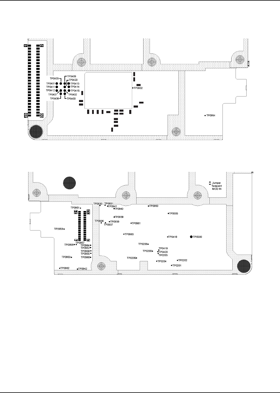
May 25, 2005 6881096C74-B
5-12 Troubleshooting Charts: Troubleshooting Test Points
5.4 Troubleshooting Test Points
The following figures show the location of the main board test points for measuring voltages and
viewing waveforms.
Figure 5-1. Main Board Test Points—Top Side (for Mid Power)
Figure 5-2. Main Board Test Points—Bottom Side (for Mid Power)
MAEPF-27802-O
ID7
ID6 ID5 ID3
ID4
ID2
ID1
ID0
MAEPF-27801-O
6881096C74-B May 25, 2005
Troubleshooting Charts: Board ID Jumper Configuration 5-13
Figure 5-3. Main Board Test Points—Top Side (for High Power)
Figure 5-4. Main Board Test Points—Bottom Side (for High Power)
5.5 Board ID Jumper Configuration
The following jumper table (Table 5-5 on page 5-14) is provided for troubleshooting and determining
what board revision you have. This can be helpful in the event a jumper was placed incorrectly or
was removed during a repair and the radio is not functioning correctly.
This table provides two types of information:
• RF band of the radio
• Overall revision of the main board and controller section
TP0400
TP0401
TP0402
TP0403
TP0407
TP0408
TP0409
TP0410
TP0411
TP0412
TP0413
TP0414
TP0415
TP0950
TP0500
TP0420
TP0200
TP0419
TP0418
TP0206
TP0204
TP0203
TP0205
May 25, 2005 6881096C74-B
5-14 Troubleshooting Charts: Flowcharts
The table indicates what the logic levels are, as well as how they correlate to the placement or
removal of a jumper to accomplish the logic level. This is because some of the board ID resistors are
on Pull-Up I/O pins and some are on Pull-Down I/O pins. Therefore, the placement or removal of a
resistor for a Pull-Up I/O is the opposite of what must be done for the placement or removal of a
resistor for a Pull-Down I/O.
Refer to the troubleshooting testpoints chapter for a general idea of where the board ID pins are
located. Refer to the board layout for the exact location with respect to all nearby components before
attempting to place or remove any jumpers.
5.6 Flowcharts
This section contains the troubleshooting flowcharts that can help you isolate a problem in your
radio.
Table 5-5. Board ID Jumper Configuration
Board ID2
R0103
Pull-Up
Board ID1
R0102
Pull-Up
Board ID0
R0101
Pull-Up
Band
0 = NP 0 = NP 0 = NP <--> 700 / 800_35W
0 = NP 0 = NP 1 = Place <--> VHF_50W
0 = NP 1 = Place 0 = NP <--> UHF_40W
0 = NP 1 = Place 1 = Place <--> UHF_R2_45W
1 = Place 0 = NP 0 = NP <--> UHF_R1_100W
1 = Place 0 = NP 1 = Place <--> VHF_R1_100W
Board
ID7
R0125
Pull-
Down
Board ID6
R0110
Pull-
Down
Board ID5
R0111
Pull-
Down
Board ID4
R0123
Pull-
Down
Board ID3
R0104
Pull-Up
Con-
troller
700-800
MHz
VHF1
50W
UHF1
40W
UHF2
45W
0 = Place 0 = Place 0 = Place 0 = Place 0 = Place <--> Reserved
0 = Place 0 = Place 0 = Place 0 = Place 1 = NP <--> Reserved
0 = Place 0 = Place 0 = Place 1 = NP 0 = Place <--> Reserved REV0/
REVA
0 = Place 0 = Place 0 = Place 1 = NP 1 = NP <--> Reserved
0 = Place 0 = Place 1 = NP 0 = Place 0 = Place <--> Reserved Reserved Reserved Reserved Reserved
0 = Place 0 = Place 1 = NP 0 = Place 1 = NP <--> REV0 REV0 Reserved Reserved Reserved
0 = Place 0 = Place 1 = NP 1 = NP 0 = Place <--> REVA NA Reserved Reserved Reserved
0 = Place 0 = Place 1 = NP 1 = NP 1 = NP <--> REVA NA NA REV0
0 = Place 1 = NP 0 = Place 0 = Place 0 = Place <--> REVB REVA REV0 REVA
Note: NP = Not Placed
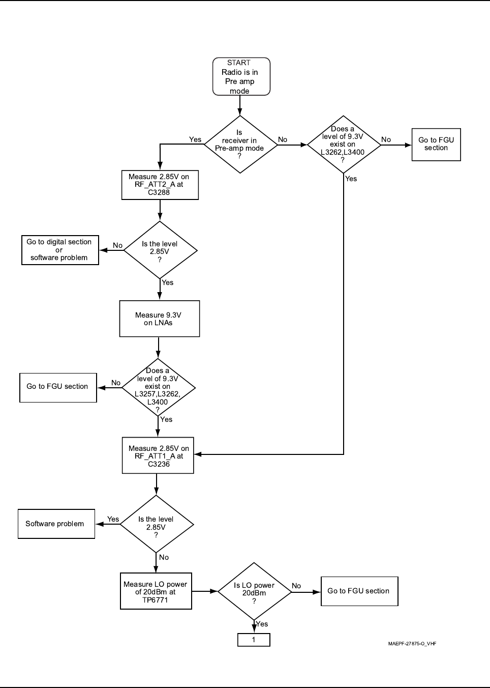
6881096C74-B May 25, 2005
Troubleshooting Charts: Flowcharts 5-15
5.6.1 Poor RX Sensitivity or No RX Audio (136–174 MHz)—Part 1 of 2
Figure 5-5. Poor RX Sensitivity or No RX Audio (136–174 MHz)—Part 1 of 2
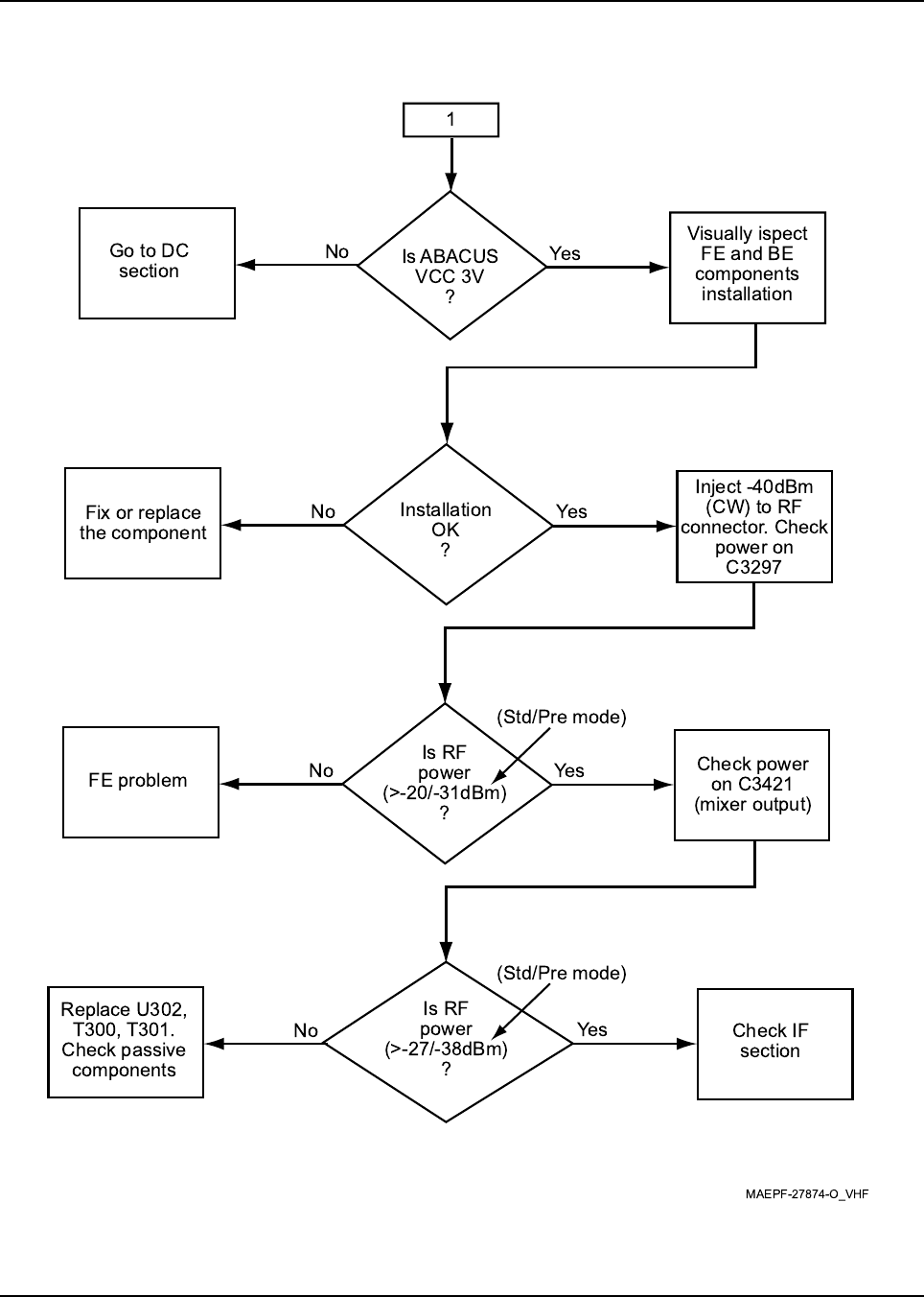
May 25, 2005 6881096C74-B
5-16 Troubleshooting Charts: Flowcharts
5.6.2 Poor RX Sensitivity or No RX Audio (136–174 MHz)—Part 2 of 2
Figure 5-6. Poor RX Sensitivity or No RX Audio (136–174 MHz)—Part 2 of 2
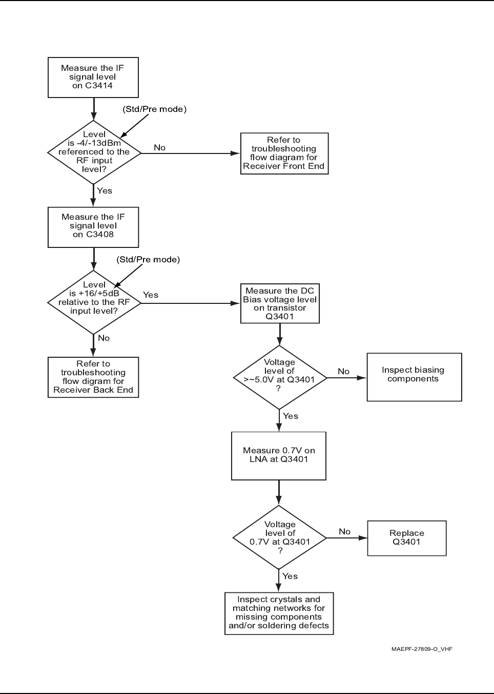
6881096C74-B May 25, 2005
Troubleshooting Charts: Flowcharts 5-17
5.6.3 RX IF—Poor SINAD or No Audio (136–174 MHz)
Figure 5-7. RX IF—Poor SINAD or No Audio (136–174 MHz)
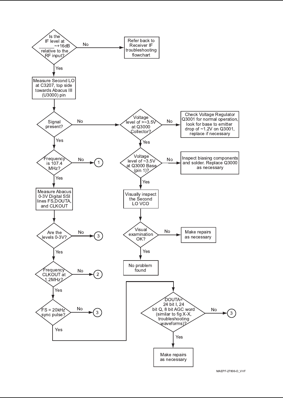
May 25, 2005 6881096C74-B
5-18 Troubleshooting Charts: Flowcharts
5.6.4 RX Back-End—Poor SINAD or No Audio (136–174 MHz)—Part 1 of 3
Figure 5-8. RX Back-End—Poor SINAD or No Audio (136–174 MHz)—Part 1 of 3
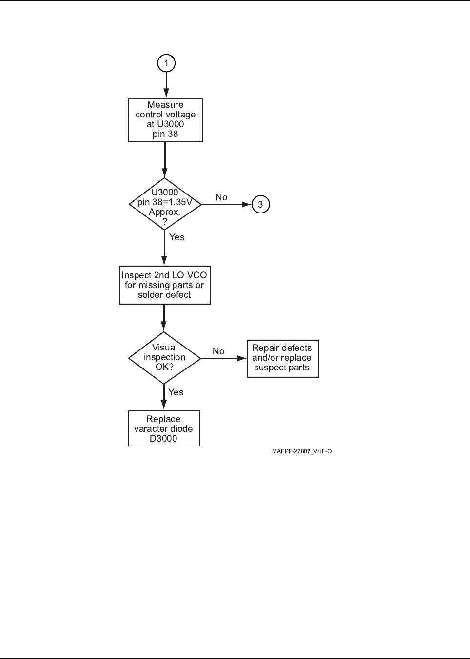
6881096C74-B May 25, 2005
Troubleshooting Charts: Flowcharts 5-19
5.6.5 RX Back-End—Poor SINAD or No Audio (136–174 MHz)—Part 2 of 3
Figure 5-9. RX Back-End—Poor SINAD or No Audio (136–174 MHz)—Part 2 of 3
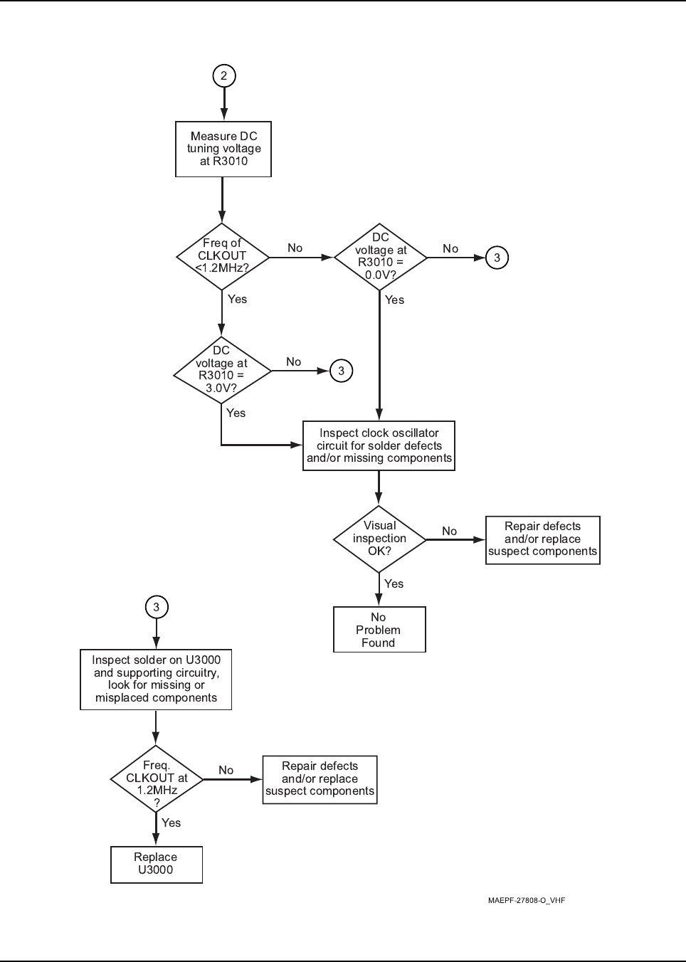
May 25, 2005 6881096C74-B
5-20 Troubleshooting Charts: Flowcharts
5.6.6 RX Back-End—Poor SINAD or No Audio (136–174 MHz)—Part 3 of 3
Figure 5-10. RX Back-End—Poor SINAD or No Audio (136–174 MHz)—Part 3 of 3

6881096C74-B May 25, 2005
Troubleshooting Charts: Flowcharts 5-21
5.6.7 Low or No RX Injection Signal (136–174 MHz)
Figure 5-11. Low or No RX Injection Signal (136–174 MHz)
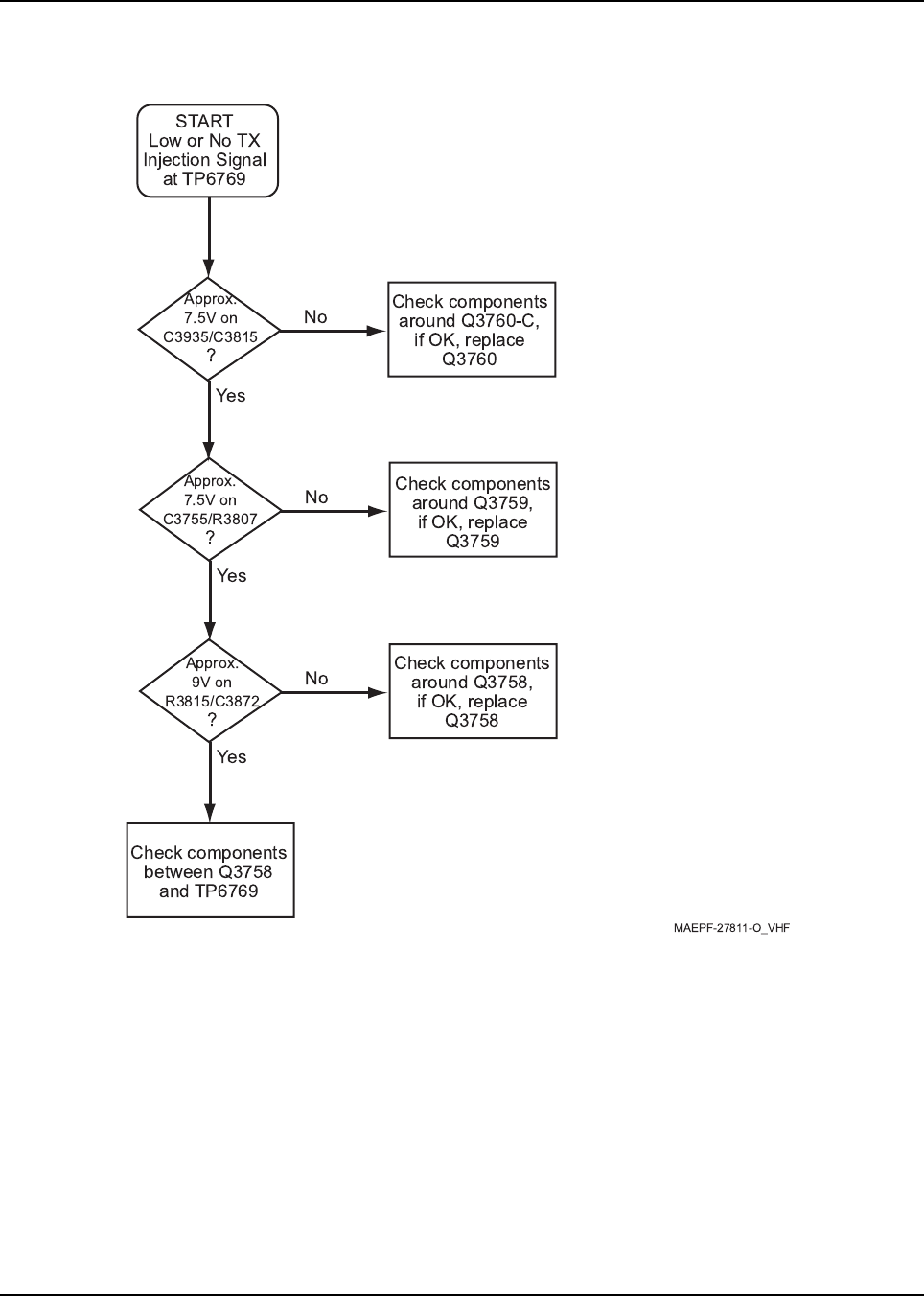
May 25, 2005 6881096C74-B
5-22 Troubleshooting Charts: Flowcharts
5.6.8 Low or No TX Injection Signal (136–174 MHz)
Figure 5-12. Low or No TX Injection Signal (136–174 MHz)
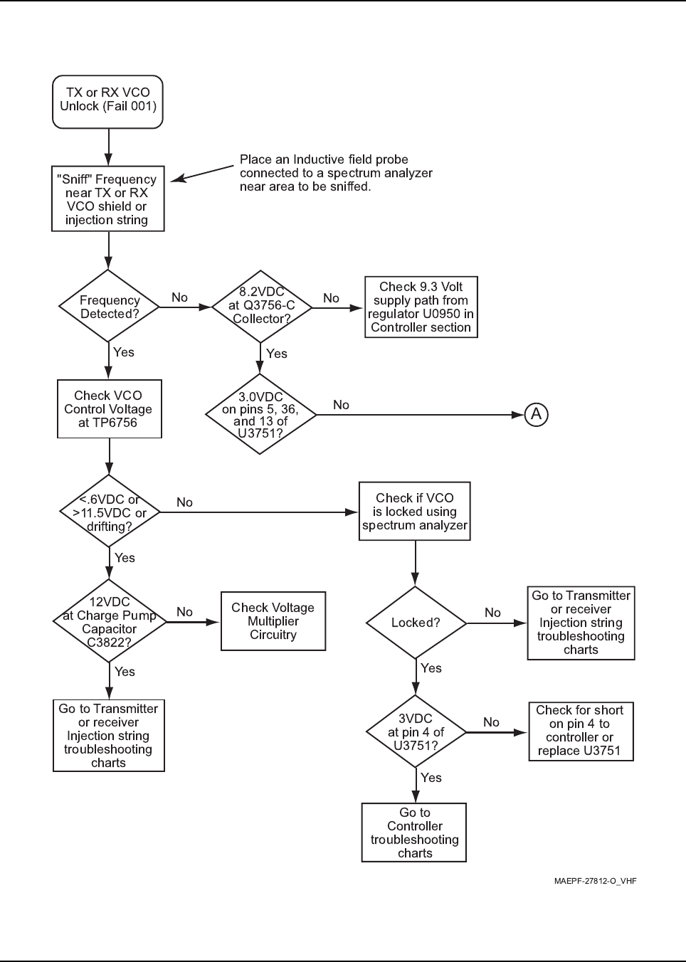
6881096C74-B May 25, 2005
Troubleshooting Charts: Flowcharts 5-23
5.6.9 TX or RX VCO Unlock (Fail 001) (136–174 MHz)—Part 1 of 2
Figure 5-13. TX or RX VCO Unlock (Fail 001) (136–174 MHz)—Part 1 of 2
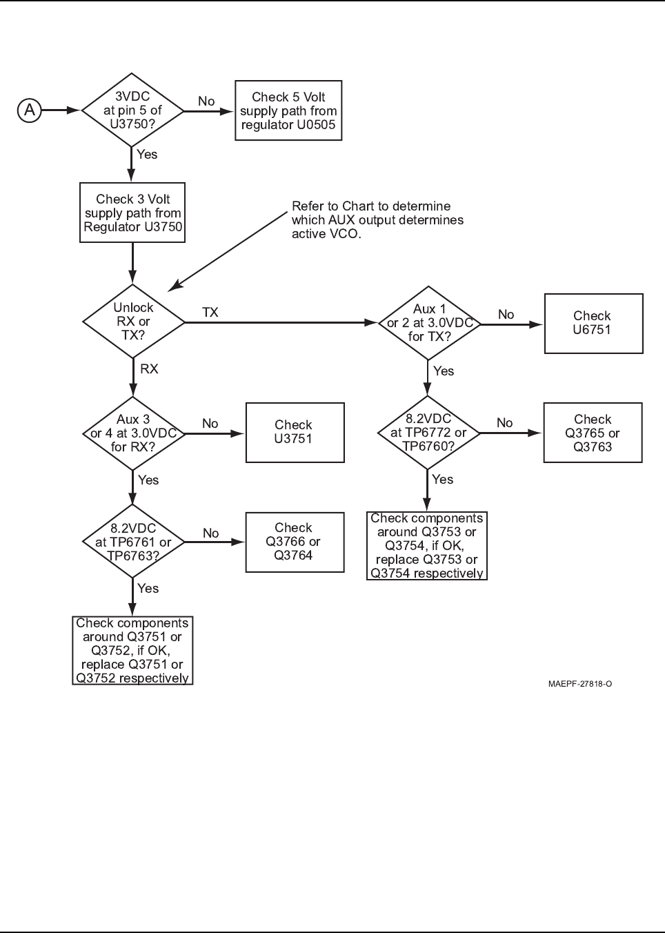
May 25, 2005 6881096C74-B
5-24 Troubleshooting Charts: Flowcharts
5.6.10 TX or RX VCO Unlock (Fail 001) (136–174 MHz)—Part 2 of 2
Figure 5-14. TX or RX VCO Unlock (Fail 001) (136–174 MHz)—Part 2 of 2
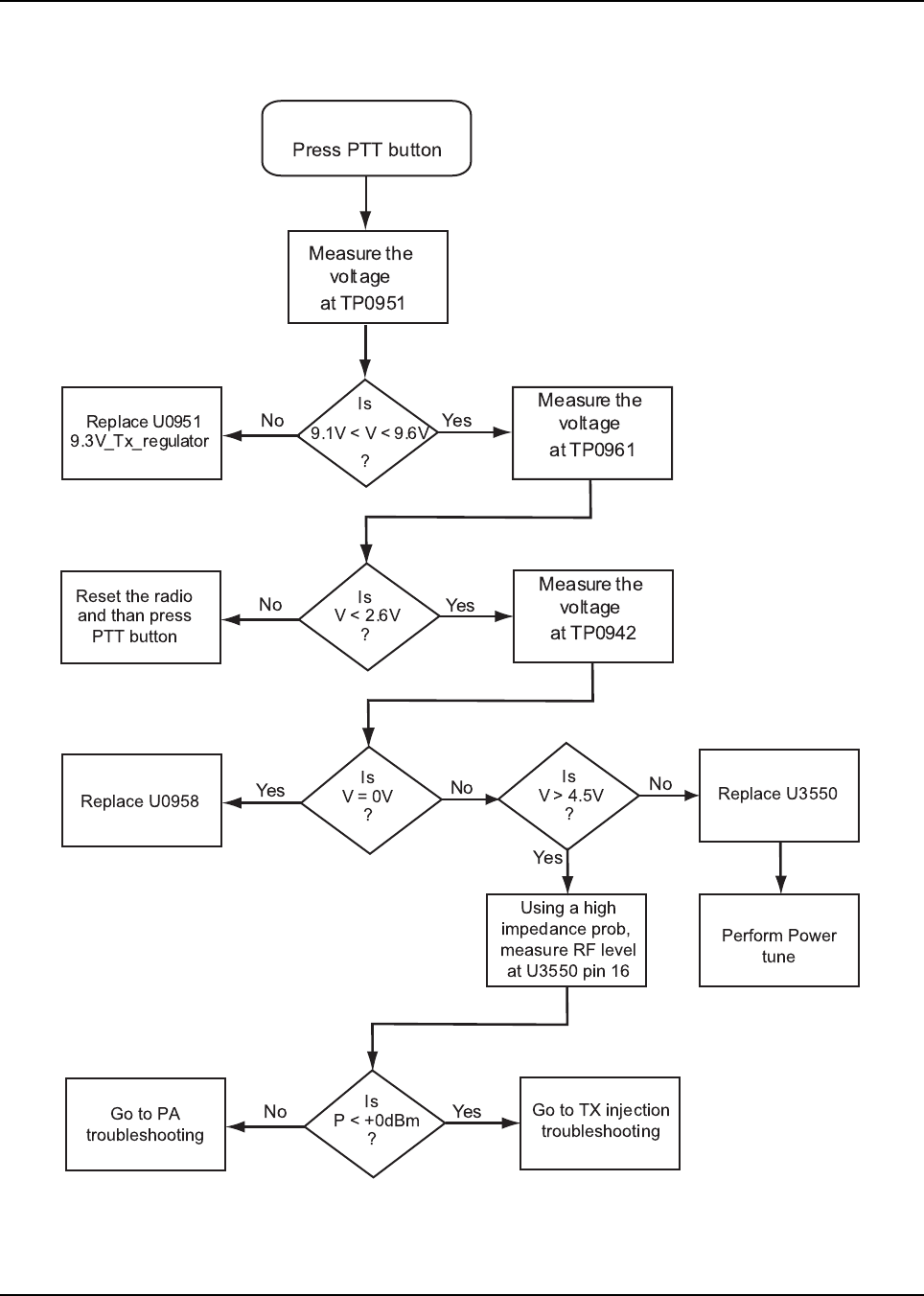
6881096C74-B May 25, 2005
Troubleshooting Charts: Flowcharts 5-25
5.6.11 No Output Power at TX Mode (136–174 MHz)
Figure 5-15. No Output Power at TX Mode (136–174 MHz)
Start
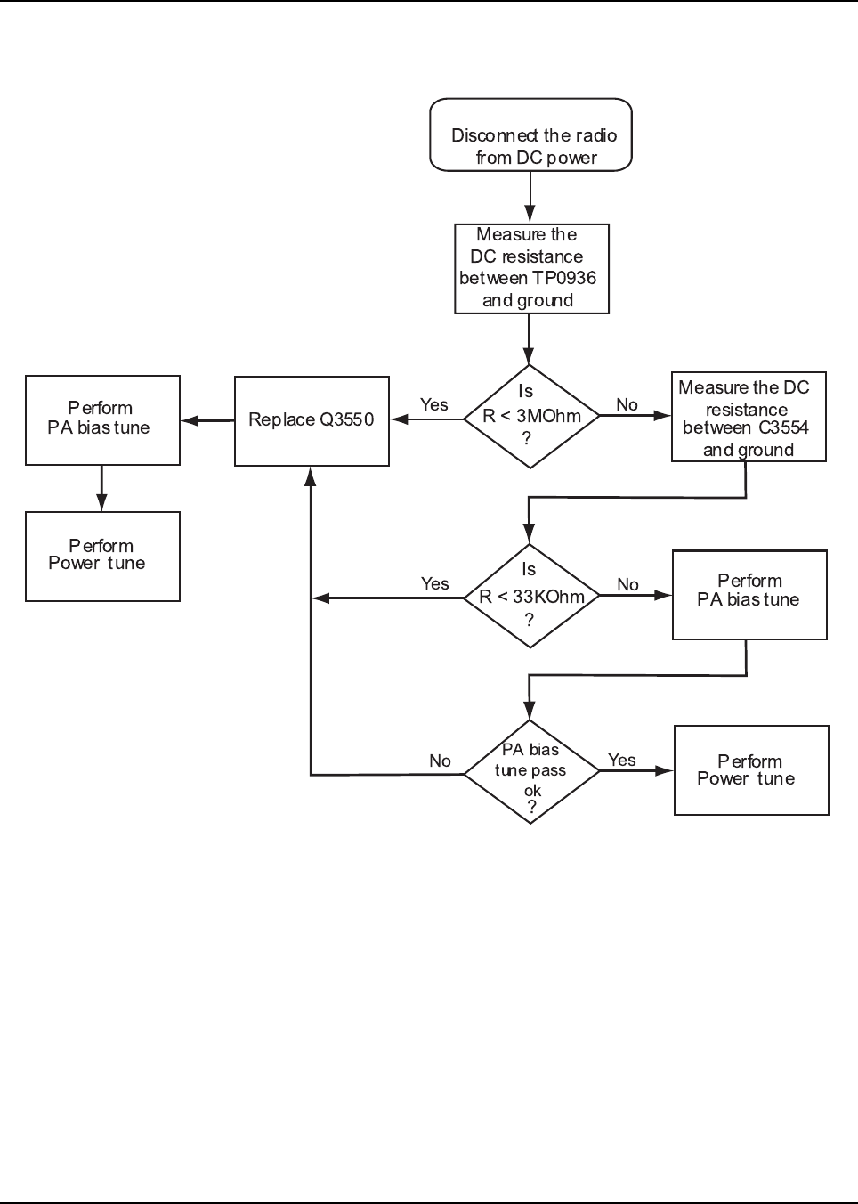
May 25, 2005 6881096C74-B
5-26 Troubleshooting Charts: Flowcharts
5.6.12 No Output Power and IDC < 2A at TX Mode (136–174 MHz)
Figure 5-16. No Output Power and IDC < 2A at TX Mode (136–174 MHz)
Start
6881096C74-B May 25, 2005
Troubleshooting Charts: Flowcharts 5-27
5.6.13 No 16.8 MHz Reference Oscillator Frequency (380–470 MHz and 450–520 MHz)
Figure 5-17. No 16.8 MHz Reference Oscillator Frequency (380–470 MHz and 450–520 MHz)
U5751 DC Voltages
Pin 1
Pin 2
Pin 3
Pin 4
Pin 5
No connection
1.5
Ground
1.5
3
>800mVpp
16.8MHz?
Probe pin 3
of Y5750 for
16.8MHz
START
No 16.8MHz
Reference
No
Yes
>800mVpp
at pin 23
U5752?
No
Yes
Check
C5761
Replace
Y5750
3.0VDC
at pin 4 of
Y5750?
No
Yes
Check 3.0V
regulator path
from U5750
>500mVpp
at pin 2
U5751?
No
Yes
Check C5760
and R5763
>3.0Vpp
at pin 4
U5751?
No
Yes
Check
U5751
>1.4Vpp
at TP5791?
No Check L5753,
C5768, C5763,
R5768 and C5767
Measure 16.8MHz Signals
with Oscilloscope having a
bandwidth >100MHz.
NOTE: L5753 and C5768 filter the
distorted output of U5751 resulting
in a clean sinusoidal 16.8MHz signal.
R5768 and C5763 adjust the amplitude.

May 25, 2005 6881096C74-B
5-28 Troubleshooting Charts: Flowcharts
5.6.14 Poor RX Sensitivity or No RX Audio (380–470 MHz and 450–520 MHz)—Part 1
of 2
Figure 5-18. Poor RX Sensitivity or No RX Audio (380–470 MHz and 450–520 MHz)—Part 1 of 2
Poor Rx
Sensitivity or no
Rx audio
Measure Transceiver
12dB Sinad by injecting
signal at antenna port
Yes
Yes
3kHz FM Deviation
1kHz Audio tone
12 dB Sinad
Sensitivity
< - 117.5 dBm Std.
<-121dBm w/pre-amp
Check RF level at
Mixer LO injection port
at R5388
Receiver
is working
properly
No
Yes
Good?
1
Check preselector circuit and
tuning control voltage.
Tuning control voltage should be:
~ 2V for 380 MHz and
~ 8V for 470 MHz (UHF Range 1)
~ 2.5V for 450 MHz and
~ 7.5V for 520 MHz (UHF Range 2)
No
Yes
LO level
at + 24dBm?
Check RX front-end
tuning
Check Receiver
VCO troubleshooting
flowchart
(LO injection section)
Retune Front-End
filters using tuner
and help screens
No
Yes
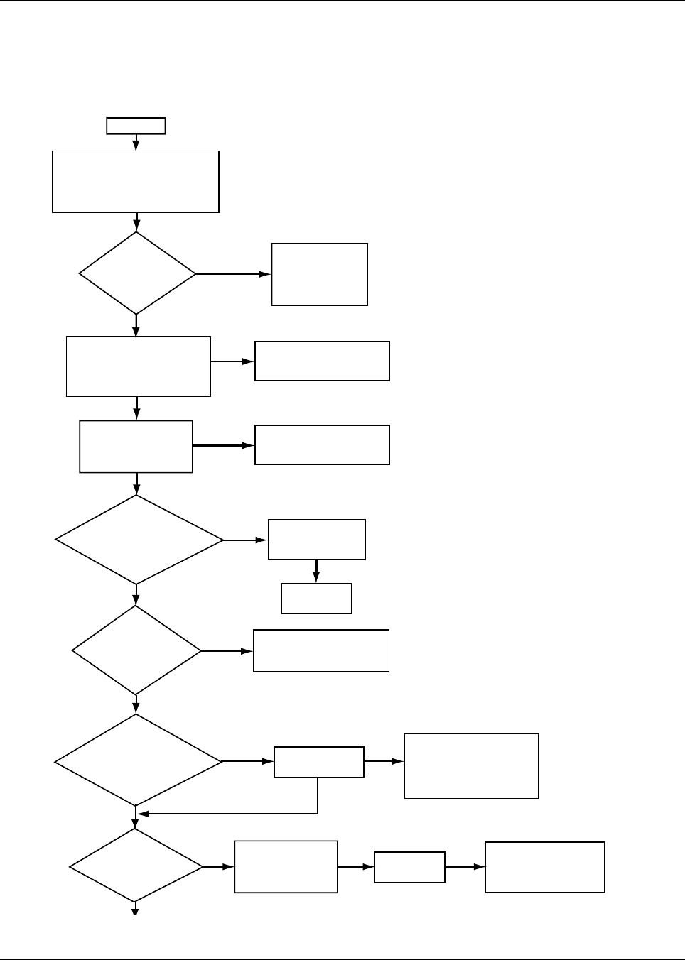
6881096C74-B May 25, 2005
Troubleshooting Charts: Flowcharts 5-29
5.6.15 Poor RX Sensitivity or No RX Audio (380–470 MHz and 450–520 MHz)—Part 2
of 2
Figure 5-19. Poor RX Sensitivity or No RX Audio (380–470 MHz and 450–520 MHz)—Part 2 of 2
1
Inject a standard FM test
signal into the antenna port.
Use a spectrum analyzer and
high-impedance RF probe to
measure the signal at TP5301
<~1dB Loss
relative to Antenna
switch?
Check preselector
insertion loss is
~2.0dB.
Check
U5302 LNA Output
at C5320. RF Level:
~15dB gain at
C5312?
Check
Mixer Input,
TP5303. RF Level:
<~2.5dB Loss at
C5320?
Check
Mixer Output,
TP5304. Freq: 109.65MHz
RF Level: <~7db
Loss from
TP5303
RF Level at
TP5304<~7db
loss from TP5303
3kHz FM Deviation
1kHz Audio tone
Amplitude: -47dBm
Check Output
Network (ON)
troubleshooting
flowchart of
Transceiver
Check bias
voltage at
L5294 for 5V
Replace
part
Fix Image filter.
Is Output Freq
at 109.65MHz?
Check RF level at
Mixer LO injection
port at R5388.
Check at R5388
for correct LO frequency
(based on your
Receiving signal
+109.65MHz)
RF level
at +24dBm
Check Receiver
VCO troubleshooting
flowchart
(LO injection section)
No
Yes
Yes
Yes
Yes
Yes
No
No
No
No No
Check preselector and
tuning voltage.
No
Check preselector Input
at C5304. RF Level
at TP5301 should be
-0.5dB without pre-amp
and +11dB with pre-amp.
Yes
Check Q5252 LNA and
its bypass switch.
No
_
_
_
Yes
Yes
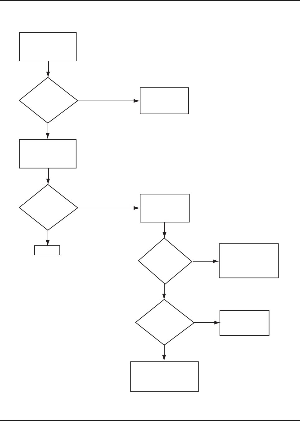
May 25, 2005 6881096C74-B
5-30 Troubleshooting Charts: Flowcharts
5.6.16 RX IF—Poor SINAD or No Audio (380–470 MHz and 450–520 MHz)—Part 1 of 2
Figure 5-20. RX IF—Poor SINAD or No Audio (380–470 MHz and 450–520 MHz)—Part 1 of 2
Level
is -3dB
referenced to
R5412?
No
No
No
Yes
Measure the IF
signal level
(109.65MHz)
at C5403
Measure the IF
signal level
(109.65MHz)
at C5406
Check Y5400
Level
is +20dB
relative to the RF
input level
at C5406?
No
Yes
Voltage
level of 9.0V
at R5404?
Yes
Voltage
level of
0.7V at Q5401
Base
(pin 1)?
Yes
Measure the DC
Bias voltage level
on transistor
Q5401
Replace
Q5401
Inspect biasing
components and
check Voltage
Regulator U0950 for
normal operation
Inspect crystals and
matching networks for
missing components
and/or soldering defects
1
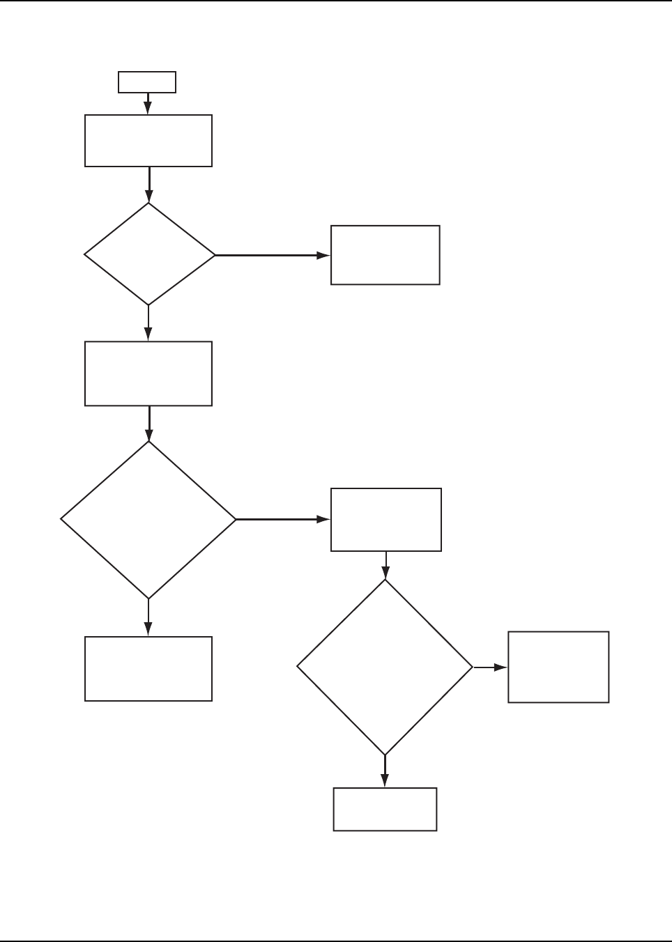
6881096C74-B May 25, 2005
Troubleshooting Charts: Flowcharts 5-31
5.6.17 RX IF—Poor SINAD or No Audio (380–470 MHz and 450–520 MHz)—Part 2 of 2
Figure 5-21. RX IF—Poor SINAD or No Audio (380–470 MHz and 450–520 MHz)—Part 2 of 2
Level
is -3dB
referenced to
C5403?
No
No
Yes
Measure the IF
signal level
(109.65MHz)
at C5403
Measure the IF
signal level
at U5400-3
Check Y5401
No
Yes
U5400-4 > 3V
and U5400-5 < 0.2V
(Without pre-amp)
U5400-4 < 0.2V
and U5400-5 > 3V
(With pre-amp)?
Same as level
at U5400-3
(Without pre-amp)
or -10 dB referenced
to level at U5400-3
(With pre-amp)?
Yes
Refer to
troubleshooting
flow digram for
Receiver Back End
Measure the DC
voltage level
at U5400-4
and U5400-5
Replace
U5400
Troubleshoot
Q5402 and
associated
circuitry
1
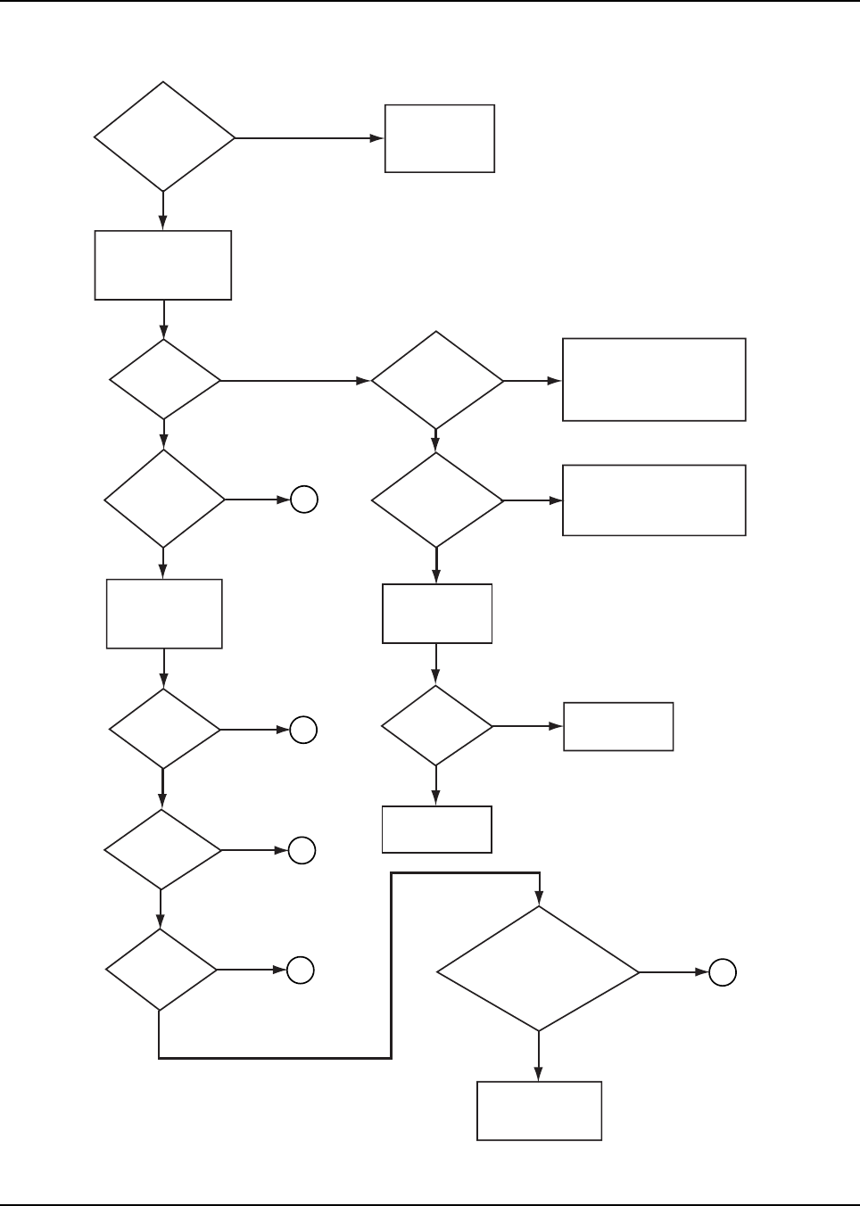
May 25, 2005 6881096C74-B
5-32 Troubleshooting Charts: Flowcharts
5.6.18 RX Back-End—Poor SINAD or No Audio (380–470 MHz and 450–520 MHz)—
Part 1 of 3
Figure 5-22. RX Back-End—Poor SINAD or No Audio (380–470 MHz and 450–520 MHz)—Part 1 of 3
Is the
IF level at
R5034 ~+20dB
relative to the
RF input?
No
No
No
No
No
No
Yes
Yes
Yes Yes
Yes
Signal
present?
Voltage
level of >~4.3V
at Q5002
Collector?
Voltage
level of ~1.7V
at Q5002 Base
(pin 1)?
Measure Second LO
at C5058, top side
towards Abacus III
(U5002) pin
Refer back to
Receiver IF
troubleshooting
flowchart
Measure Abacus
0-3V Digital SSI
lines FS,DOUTA,
and CLKOUT
3
2
3
1
Are the
levels 0-3V?
No
Yes
Yes
Frequency
CLKOUT at
1.2MHz?
No
3
No
FS = 20kHz
sync pulse?
Frequency is
107.4 or 111.9
MHz?
Inspect biasing components
and solder. Replace Q5002
as necessary
Yes
Visually inspect
the Second
LO VCO
Yes
No
Visual
examination
OK?
Make repairs
as necessary
No problem
found
DOUTA=
24 bit I, 24
bit Q, 8 bit AGC word
(similar to fig X-X,
troubleshooting
waveforms)?
Yes
Go on to RX audio
troubleshooting
flowchart
Check Voltage Regulator
U0505 for normal operation,
look for base to emitter
drop of ~0.7V on Q5001,
replace if necessary
6881096C74-B May 25, 2005
Troubleshooting Charts: Flowcharts 5-33
5.6.19 RX Back-End—Poor SINAD or No Audio (380–470 MHz and 450–520 MHz)—
Part 2 of 3
Figure 5-23. RX Back-End—Poor SINAD or No Audio (380–470 MHz and 450–520 MHz)—Part 2 of 3
No
3
3
1
R5013
= 5.0V?
No
Yes
Yes
R5013 = 0.0V?
No
Yes
Freq 2nd LO
VCO <107.4
MHz?
No
Yes
Measure
control voltage
at R5013
Inspect 2nd LO VCO
for missing parts or
solder defect
Yes
No
Visual
inspection
OK?
Repair defects
and/or replace
suspect parts
Replace
varactor diode
D6051
R5013
VOLTS DC
NOMINAL
FREQ (MHz)
0.0
1.6
4.0
5.0
68.0
71.1
75.6
77.0
Freq 2nd LO
VCO <107.4
MHz?
May 25, 2005 6881096C74-B
5-34 Troubleshooting Charts: Flowcharts
5.6.20 RX Back-End — Poor SINAD or No Audio (380–470 MHz and 450–520 MHz)—
Part 3 of 3
Figure 5-24. RX Back-End—Poor SINAD or No Audio (380–470 MHz and 450–520 MHz)—Part 3 of 3
No 3
3
3
2
DC
voltage at
R5022 =
0.0V?
Yes
No
Yes
Freq of
CLKOUT
<18MHz?
No
Yes
DC
voltage at
R5022 =
3.0V?
Measure DC
tuning voltage
(Vt) at R5022
Inspect clock oscillator
circuit for solder defects
and/or missing components
Yes
No
Visual
inspection
OK?
Repair defects
and/or replace
suspect components
Replace
varactor diode
D5003
Inspect solder on U5002
and supporting circuitry,
look for missing or
misplaced components
Yes
No
Visual
inspection
OK?
Repair defects
and/or replace
suspect components
Replace
U5002
6881096C74-B May 25, 2005
Troubleshooting Charts: Flowcharts 5-35
5.6.21 Low or No RX Injection Signal (380–470 MHz and 450–520 MHz)
Figure 5-25. Low or No RX Injection Signal (380–470 MHz and 450–520 MHz)
Approx.
5V on
C5318?
START
Low or No RX
Injection Signal
No
No
Yes
No
Yes
Yes
Approx.
4.5V on
pin 14
of U5303?
5 V
on C5335?
Check RF path
from RX VCO
Check R5324,
R5325, R5326
Check Voltage
Regulator U5301
Check L5299
May 25, 2005 6881096C74-B
5-36 Troubleshooting Charts: Flowcharts
5.6.22 Low or No TX Injection Signal (380–470 MHz and 450–520 MHz)
Figure 5-26. Low or No TX Injection Signal (380–470 MHz and 450–520 MHz)
Approx.
3.4 V on
Q5828-C?
START
Low or No TX
Injection Signal
No
Yes
Check RF path
from TX VCO
Approx.
6.5 V on
Q5501-C?
No
Yes
Check Q5501 and
DC Bias Circuitry;
replace if
necessary
Approx.
3.7 V on
Q5829-C?
No
Yes
Check Q5829 and
DC Bias Circuitry;
replace if
necessary
Check Q5828 and
DC Bias Circuitry;
replace if
necessary
6881096C74-B May 25, 2005
Troubleshooting Charts: Flowcharts 5-37
5.6.23 No TX Audio (380–470 MHz and 450–520 MHz)
Figure 5-27. No TX Audio (380–470 MHz and 450–520 MHz)
1.0Vpp
at R5755 or
TP5792?
No
Yes
0.4Vpp
at
C5780?
No
Yes
Check deviation
tuning or replace
U5752
GOTO
Controller
Section
Check
synthesizer
loop filter
components
NOTE: After the modulated signal is coupled
through C5780 the signal is attenuated to levels
below 2mv making a measurement difficult for
most oscilloscopes.
Inject a 2.0Vpp
1kHz tone into Mic
input and key radio
START
No TX Audio
This Flow chart only checks the modulation
path of the FGU. Readings are typical and
can vary with deviation settings that are
programmed during tuning.
May 25, 2005 6881096C74-B
5-38 Troubleshooting Charts: Flowcharts
5.6.24 TX or RX VCO Unlock (Fail 001) (380–470 MHz and 450–520 MHz)—Part 1 of 2
Figure 5-28. TX or RX VCO Unlock (Fail 001) (380–470 MHz and 450–520 MHz)—Part 1 of 2
Frequency
Detected?
"Sniff" Frequency
near TX or RX
VCO or
infection string
TX or RX VCO
Unlock (Fail 001)
No
Yes
Check VCO
Control Voltage
at TP5796
8.2VDC
at Collector of only
one of Q5706,
Q5707, Q5708,
or Q5709
Q5710?
No
Yes
3.0VDC
on pins 5, 36,
and 13 of
U5752?
Check 9.3 Volt
supply path from
regulator U0950 in
Controller section
<.6VDC or
>11.5VDC or
drifting?
No
No
Yes
Check if VCO
is locked using
spectrum analyzer
13.5VDC
at Charge Pump
Capacitor
C5788?
No
Yes
Check Voltage
Multiplier
Circuitry
Go to
Controller
troubleshooting
charts
Go to Transmitter
or receiver
Injection string
troubleshooting
charts
Place an Inductive field probe
connected to a spectrum analyzer
near area to be sniffed.
Locked?
Yes
3VDC
at pin 4 of
U5752?
No
No
Yes
Check for short
on pin 4 to
controller or
replace U5752
Go to Transmitter
or receiver
Injection string
troubleshooting
charts
A

6881096C74-B May 25, 2005
Troubleshooting Charts: Flowcharts 5-39
5.6.25 TX or RX VCO Unlock (Fail 001) (380–470 MHz and 450–520 MHz)—Part 2 of 2
Figure 5-29. TX or RX VCO Unlock (Fail 001) (380–470 MHz and 450–520 MHz)—Part 2 of 2
Check 3 Volt
supply path from
Regulator U5750
Check 3 Volt
supply path
Check 3 Volt
supply path
Refer to Chart to determine
which AUX output determines
active VCO.
3VDC
at pin 5 of
U5750?
No Check 5 Volt
supply path from
regulator U0505
Unlock
RX or
TX?
TX
RX
Yes
Required
Aux pins
at 3.0VDC
for RX?
No
No
Yes
Check
U5752
Check U5753,
Q5708, Q5709,
and Q5710
Yes
Required
Aux pins
at 3.0VDC
for TX?
No
No
Yes
Check
U5752
Check
U5753, Q5706,
and Q5707
3.0VDC at
E6750?
3.0VDC at
E6750?
Yes
A
May 25, 2005 6881096C74-B
5-40 Troubleshooting Charts: Flowcharts
5.6.26 RF Power Amplifier (RFPA)—No or Low TX Power Output (380–470 MHz and
450–520 MHz)—Part 1 of 5
NOTE: For each flowchart step in which reference is made to a note, be sure to refer to that specific
note (located on page 61 of this flowchart) for guidance in performing the actual
troubleshooting procedure. Also, RFPA DC voltages are shown in Table 5-6 on page 5-44.
Figure 5-30. RF Power Amplifier (RFPA)—No or Low TX Power Output (380–470 MHz and 450–520 MHz)—
Part 1 of 5
Read General
Notes before
proceeding. Read
specific notes as
indicated
Check battery
cable, mic, and
control head
connections
START
Continuous red light
while mic button is
depressed?
GOTO Sythesizer-
No Transmit
Chart
Tune power with
Tuner?
(see help text)
No
Yes
Tune current limit
with Tuner
(see help text)
Yes
No
TX injection power
less than 0.5 mW?
(Note 1)
GOTO Sythesizer-
No or Low Tx
Injection
Chart
Yes
K9.1V
present
at Q0952, pin 1 in
power control section
when transmitter is
keyed?
No
GOTO Power
Control - No K9.1V
Chart for
700-800 MHz
RFPA_CNTRL
voltage (TP5503)
less than 4.8 V when
transmitter is
keyed?
Yes
No
GOTO Power
Control - No or low
RFPA_CNTRLChart
for 700-800 MHz
No
U5501 drain biases
voltages per Table 1?
(Note 3)
Yes
No Check/repair/
replace defective
parts
Yes
No
A
Is U5501,
VCNTRL resistance <
1 kOhms?
(Note 2)
Yes Repair/replace
U5501
No
Is U5501,
RFOUT and VD1
resistance <
1 MOhms?
(Note 4)
Yes Repair/replace
U5501
6881096C74-B May 25, 2005
Troubleshooting Charts: Flowcharts 5-41
5.6.27 RF Power Amplifier (RFPA)—No or Low TX Power Output (380–470 MHz and
450–520 MHz)—Part 2 of 5
Figure 5-31. RF Power Amplifier (RFPA)—No or Low TX Power Output (380–470 MHz and 450–520 MHz)—
Part 2 of 5
Defective parts
in matching network
between Q5502 and
Q5503?
(Note 9)
Repair/replace
defective parts
Yes
No
Defective parts
in matching network
between U5501 and
Q5502?
(Note 5)
Repair/replace
defective parts
Yes
Q5502 bias voltages
as per Table 1?
(Note 6)
No
Is Q5502,
gate resistance <
1 MOhms?
(Note 7)
Yes
Repair/replace
Q5502 and retune
gate bias via
Tuner
(see help text)
No
No
Yes
Is Q5502,
drain resistance <
1 MOhms?
(Note 8)
Yes
No
Q5503 bias
voltages as per Table 1?
(Note 10)
Defective parts
in matching network
between Q5503 and
antenna switch?
(Note 13)
Antenna switch
bias voltages as per
Table 1?
(Note 14)
Repair/replace
defective parts
Is Q5503,
gate resistance <
1 MOhms?
(Note 11)
Yes
No
Is Q5503,
drain resistance <
1 MOhms?
(Note 12)
Yes
No
Repair/replace
defective parts
No
No
Yes
Yes
Yes
No
Repair/replace
Q5502 and retune
gate bias via
Tuner
(see help text)
Check/repair/replace
defective parts or
GOTO Power Control
- No/low VGBIAS
Chart
Repair/replace
Q5503
(see General Notes)
and retune gate bias
via Tuner
(see help text)
B
A
Repair/replace
Q5503
(see General Notes)
and retune gate bias
via Tuner
(see help text)
Check/repair/replace
defective parts or
GOTO Power Control
- No/low VGBIAS
Chart
May 25, 2005 6881096C74-B
5-42 Troubleshooting Charts: Flowcharts
5.6.28 RF Power Amplifier (RFPA)—No or Low TX Power Output (380–470 MHz and
450–520 MHz)—Part 3 of 5
Figure 5-32. RF Power Amplifier (RFPA)—No or Low TX Power Output (380–470 MHz and 450–520 MHz)—
Part 3 of 5
Yes
Defective parts in
antenna switch?
(Note 15)
Repair/replace
defective parts
Defective parts in
harmonic filter?
(Note 16)
No
Yes Repair/replace
defective parts
No
Defective parts in
power detector?
(Note 17)
Yes
Repair/replace
antenna connector
Continuity check
fails from R5713 and
the antenna connector
external coax?
No
Yes
Repair/replace
defective parts
B
Go to the
Controller GPIO
Section
No

6881096C74-B May 25, 2005
Troubleshooting Charts: Flowcharts 5-43
5.6.29 RF Power Amplifier (RFPA)—No or Low TX Power Output (380–470 MHz and
450–520 MHz)—Part 4 of 5
Specific Notes:
1. Remove C5508 and solder the center conductor of a small 50-ohm, coaxial cable to TP5502.
Solder ground to the gold shield track adjacent to TP5502. Attach an RF milliwatt meter, key
the transmitter, and measure TX_INJ power. Then, remove the coaxial cable and replace
C5508. Remove the solder added to shield track.
2. Remove R0977 in the power control section, and measure the resistance between VCNTRL
(TP5503) and ground. Replace R0977.
3. If U5501, VD1, is incorrect, inspect the bias feed circuitry (L5502 and C5505) and interstage
match components (L5503, C5509, and C5507). If U5501, RFOUT, is incorrect, inspect the
bias feed circuitry (L5505 and C5517).
4. Remove L5502 and measure the resistance between VD1 (U5501 pin 14) and ground.
Replace L5502. Remove L5505 and measure the resistance between RFOUT (U5501 pin 6)
and ground. Replace L5505.
5. Inspect C5566, C5516, C5518, and R5511-15.
6. If the Q5502 gate bias is incorrect, inspect the bias feed circuitry (R5516, L5525, C5556, and
R5527). If the bias feed circuitry is functional, then go to the Power Control—No or low
VGBIAS flowchart. If the Q5502 drain bias is incorrect, inspect the bias feed circuitry (L5508,
C5526-27, R5517, E5501, and R5574). Check U5570, Q5770, and associated circutry.
7. Remove R5516 and measure the resistance between Q5502 gate and ground. Replace
R5516.
8. Remove L5508 and measure the resistance between Q5502 drain and ground. Replace
L5508.
9. Inspect C5559-60, C5535, C5538, R5530, R5533-34, and R5536.
10. If the Q5503 pin 7 gate bias is incorrect, inspect the bias feed circuitry (R5520, C5539,
C5557, and R5525). If the gate bias feed circuitry is functional, then go to the Power
Control—No or low VGBIAS flowchart. If the Q5503 pin 6 gate bias is incorrect, inspect the
bias feed circuitry (R5521, C5540, C5558, and R5526). If the bias feed circuitry is functional,
then go to the Power Control—No or low VGBIAS flowchart. If the Q5503 pins 2 and 3
common drain bias is incorrect, inspect the bias feed circuitry (L5510, C5549-50, R5522-23,
and E5502).
11. Remove R5520 and measure the resistance between Q5503 pin 7 gate and ground. Replace
R5520. Remove R5521 and measure the resistance between Q5503 pin 6 gate and ground.
Replace R5521.
12. Remove L5510 and measure the resistance between Q5503 pins 2 and 3 drain and ground.
Replace L5510.
13. Inspect R5535, C5542-43, C5545-48, and C5551-53.
14. If the antenna switch bias voltages are incorrect, inspect R5524, L5701-4, and R5701, as well
as perform diode checks on D5701-3.
15. Inspect the remaining antenna switch parts (C5701-10).
16. Inspect L5706-8, L5712-13, C5708, C5711-14, C5719-20, R5713, and R5718.
17. Inspect D5704, R5707-8, R5702-4, and C5715-16.
May 25, 2005 6881096C74-B
5-44 Troubleshooting Charts: Flowcharts
5.6.30 RF Power Amplifier (RFPA)—No or Low TX Power Output (380–470 MHz and
450–520 MHz)—Part 5 of 5
Table 5-6. RFPA DC Voltages
Description Location Voltage (Vdc)
(380–470 MHz)
Voltage (Vdc)
(450–520 MHz)
A+ = 13.6 Vdc
U5501, VD1 U5501 pin 14 9.0–9.3 9.0–9.3
U5501, RFOUT U5501 pins 6 and 7 9.0–9.3 9.0–9.3
Q5502 Gate Bias R5516/C5525
node
1.8–2.0 1.8–2.1
Q5502 Drain Bias L5508/R5517
Node
9.0–9.3 9.0–9.3
Q5503 Gate Bias 1 R5520/C5539
node
2.0–2.2 1.4–1.9
Q5503 Gate Bias 2 R5521/C5540
node
2.0–2.2 1.4–1.9
Q5503 Drain Bias L5510/R5523
Node
13.0–13.6 13.0–13.6
Antenna Switch Bias
Voltage 1
L5701/C5702
node
~4.7 ~5.95
Antenna Switch Bias
Voltage 2
D5701/D5702
node
~4.0 ~5.0
Antenna Switch Bias
Voltage 3
D5703/R5701
node
~3.3 ~3.3
6881096C74-B May 25, 2005
Troubleshooting Charts: Flowcharts 5-45
5.6.31 RFPA Power Control—No VGBIAS (380–470 MHz and 450–520 MHz)
Figure 5-33. RFPA Power Control—No VGBIAS (380–470 MHz and 450–520 MHz)
Read General
Notes before
proceeding. Read
specific notes as
indicated
START
No
Yes
Repair/replace
U0960
No
No/low
Q5503 pin 7
VGBIAS1?
No/low
Q5503 pin 6
VGBIAS2?
Remove U0960.
TP0937 voltage
2.6-2.8 V?
Yes
Remove U0960.
TP0939 voltage
2.6-2.8 V?
Yes
Remove U0960.
TP0941 voltage
2.0-2.2 V?
No
Repair/replace
U0959. If problem
still not fixed, see
IC communication
in CONTROLLER
section.
Yes
Yes
No
No
May 25, 2005 6881096C74-B
5-46 Troubleshooting Charts: Flowcharts
5.6.32 No 16.8 MHz Reference Oscillator Frequency (700–800 MHz)
Figure 5-34. No 16.8 MHz Reference Oscillator Frequency (700–800 MHz)
MAEPF-27813-O
U6752 DC Voltages
Pin 1
Pin 2
Pin 3
Pin 4
Pin 5
No connection
1.5
Ground
1.5
3
>800mVpp
16.8MHz?
Probe pin 3
of Y6750 for
16.8MHz
START
No 16.8MHz
Reference
No
Yes
>800mVpp
at TP6764?
No
Yes
Check
C6817
Replace
Y6750
3.0VDC
at pin 1 of
Y6750?
No
Yes
Check 3.0V
regulator path
from U6750
>500mVpp
at pin 2
U6752?
No
Yes
Check C6758
and R6756
>3.0Vpp
at pin 4
U6752?
No
Yes
Check
U6752
>1.4Vpp
at TP6762?
No Check L6756,
C6755, C6759,
R6756 and C6760
Measure 16.8MHz Signals
with Oscilloscope having a
bandwidth >100MHz.
NOTE: L6756 and C6755 filter the
distorted output of U6752 resulting
in a clean sinusoidal 16.8MHz signal.
R6757 and C6759 adjust the amplitude.
Check Controller
Section and/or
ABACUS IC
U6000
Yes
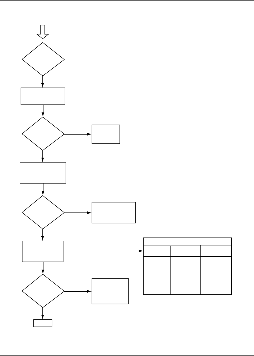
6881096C74-B May 25, 2005
Troubleshooting Charts: Flowcharts 5-47
5.6.33 Poor RX Sensitivity or No RX Audio (700–800 MHz)—Part 1 of 2
Figure 5-35. Poor RX Sensitivity or No RX Audio (700–800 MHz)—Part 1 of 2
MAEPF-27875-O
Poor Rx
Sensitivity or no
Rx audio
Measure Transceiver
Sinad by injection
signal at antenna port
Yes
Yes
3kHz FM Deviation
1kHz Audio tone
Sinad
< - 119.1dBm?
Check RF level at
Mixer LO injection port
(U6251 Pin 3 side 1)
Receiver
is working
properly
No
Yes
Good?
1
Check Q6350,
Q6251, Q6252,
Q6253, Q6254
and make any
necessary repairs
No
Yes
RF level
at ~ 14dBm?
Check RX front-end
filter switching
voltage Table
Check Receiver
VCO troubleshooting
flowchart
(LO injection section)
No
Yes
RX Switching Voltages
Receiving at
700MHz Band
Receiving at
800MHz Band
Test Points
TP6256, 58,
60, 62
TP6255, 57,
59, 61
TP6254
LNA U6250
0V
7.6V
2V
3V
4V
7.6V
5V at Pin 1
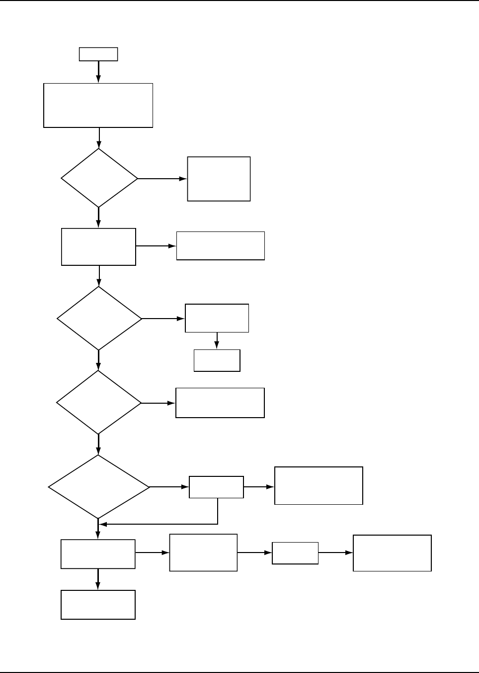
May 25, 2005 6881096C74-B
5-48 Troubleshooting Charts: Flowcharts
5.6.34 Poor RX Sensitivity or No RX Audio (700–800 MHz)—Part 2 of 2
Figure 5-36. Poor RX Sensitivity or No RX Audio (700–800 MHz)—Part 2 of 2
MAEPF-27874-O
1
Inject a standard FM test
signal into the antenna port.
Use a spectrum analyzer and
high-impedance RF probe to
measure the signal at TP6253.
<~1dB Loss
relative to Antenna
switch?
Check LNA Input
(U6250) Pin 3. RF
Level:<~2.5dB Loss
from TP6253
Check
LNA Output
TP6250. RF Level:
~16dB gain from
U6250 Pin
3?
Check
Mixer Input,
TP6251. RF Level:
<~2.5dB Loss from
TP6250?
Check
Mixer Output,
TP6252. Freq: 73.35MHz
RF Level: <~7db
Loss from
TP6251
RF Level at
TP6252<~7db
loss from TP6251
Go to IF Section
Troubleshooting
flowchart
3kHz FM Deviation
1kHz Audio tone
Amplitude: 47dBm
Check Output
Network (ON)
troubleshooting
flowchart of
Transceiver
Check bias
voltage at Pin 1
of U6250 for 5V
Replace
part
Check filter switching
table for proper voltages.
Visually inspect filters
Is Output Freq
at 73.35MHz?
Check RF level at
Mixer LO injection
port. (U6251
Pin 3 side 1)
Check Pin 3 on U6251
for correct LO frequency
(based on your
Receiving signal)
RF level
at ~14dBm
Check Receiver
VCO troubleshooting
flowchart
(LO injection section)
No
Yes
Yes
Yes
Yes
Yes
No
No
No
No No
Check filter switching
table or proper voltages.
Visually inspect filters
No
_
_
_
_
Yes
Yes
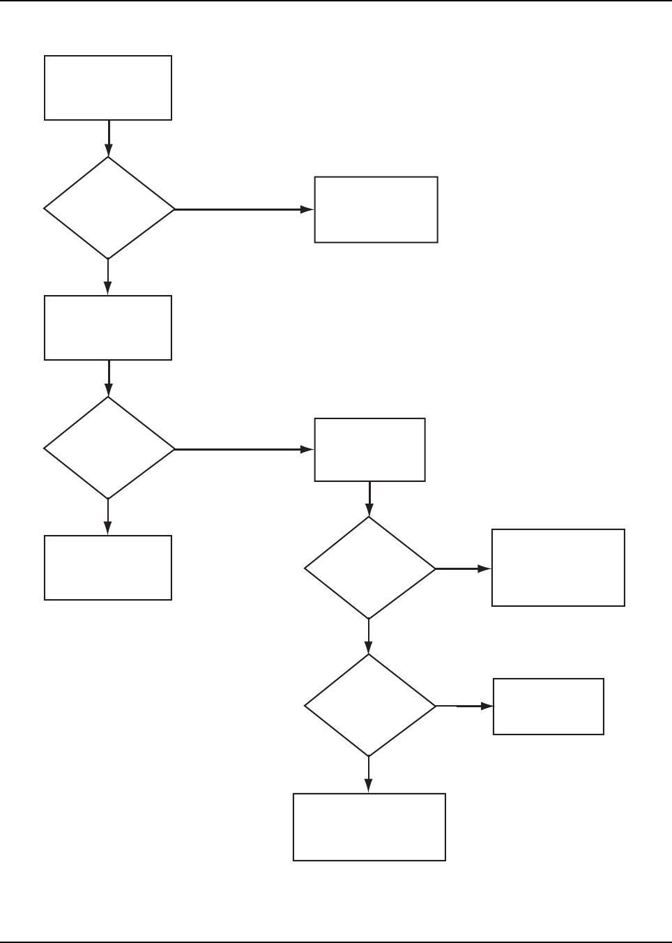
6881096C74-B May 25, 2005
Troubleshooting Charts: Flowcharts 5-49
5.6.35 RX IF—Poor SINAD or No Audio (700–800 MHz)
Figure 5-37. RX IF—Poor SINAD or No Audio (700–800 MHz)
MAEPF-27809-O
Level
is +4dB
referenced to the
RF input
level?
No
No
No
Yes
Measure the IF
signal level
(73.35MHz)
at TP6350
Measure the IF
signal level
(73.35MHz)
at TP6252
Refer to
troubleshooting
flow diagram for
Receiver Front End
Level
is +20dB
relative to the RF
input level?
No
Yes
Voltage
level of
>~5.0V at Q6350
Collector
(pin 3)?
Yes
Voltage
level of
0.7V at Q6350
Base
(pin 1)?
Yes
Refer to
troubleshooting
flow digram for
Receiver Back End
Measure the DC
Bias voltage level
on transistor
Q6350
Replace
Q6350
Inspect biasing
components and
check Voltage
Regulator U0950 for
normal operation
Inspect crystals and
matching networks for
missing components
and/or soldering defects
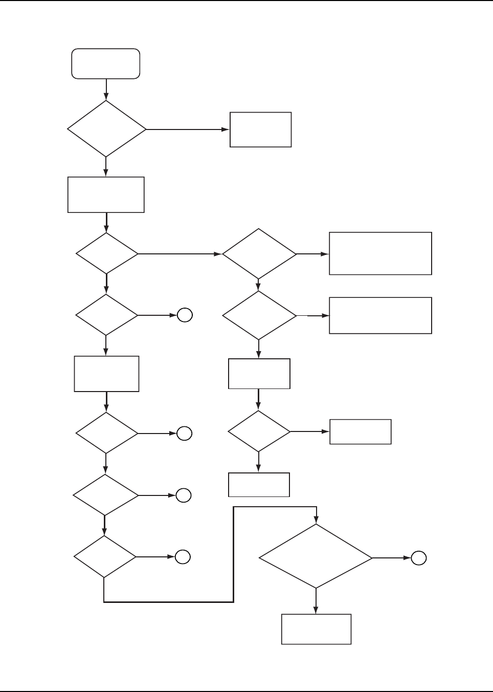
May 25, 2005 6881096C74-B
5-50 Troubleshooting Charts: Flowcharts
5.6.36 RX Back-End—Poor SINAD or No Audio (700–800 MHz)—Part 1 of 3
Figure 5-38. RX Back-End—Poor SINAD or No Audio (700–800 MHz)—Part 1 of 3
MAEPF-27806-O
Is the
IF level at
TP6350~+20dB
relative to the
RF input?
No
No
No
No
No
No
Yes
Yes
Yes Yes
Yes
Signal
present?
Voltage
level of >~3.5V
at Q6000
Collector?
Voltage
level of ~2.15V
at Q6000 Base
(pin 1)?
Measure Second LO
at C6026, top side
towards Abacus III
(U6000) pin
Refer back to
Receiver IF
troubleshooting
flowchart
Measure Abacus
0-3V Digital SSI
lines FS,DOUTA,
and CLKOUT
3
2
3
1
Are the
levels 0-3V?
No
Yes
Yes
Frequency
CLKOUT at
1.2MHz?
No
3
No
FS = 20kHz
sync pulse?
Frequency
is 75.6 or 71.1
MHz?
Inspect biasing components
and solder. Replace Q6000
as necessary
Yes
Visually inspect
the Second
LO VCO
Yes
No
Visual
examination
OK?
Make repairs
as necessary
No problem
found
DOUTA=
24-bit I, 24-bit Q,
8-bit AGC word?
Yes
Go on to RX audio
troubleshooting
flowchart
Check Voltage Regulator
U0505 for normal operation,
look for base to emitter
drop of ~1.2V on Q6001,
replace if necessary
START
Poor SINAD or
No Audio
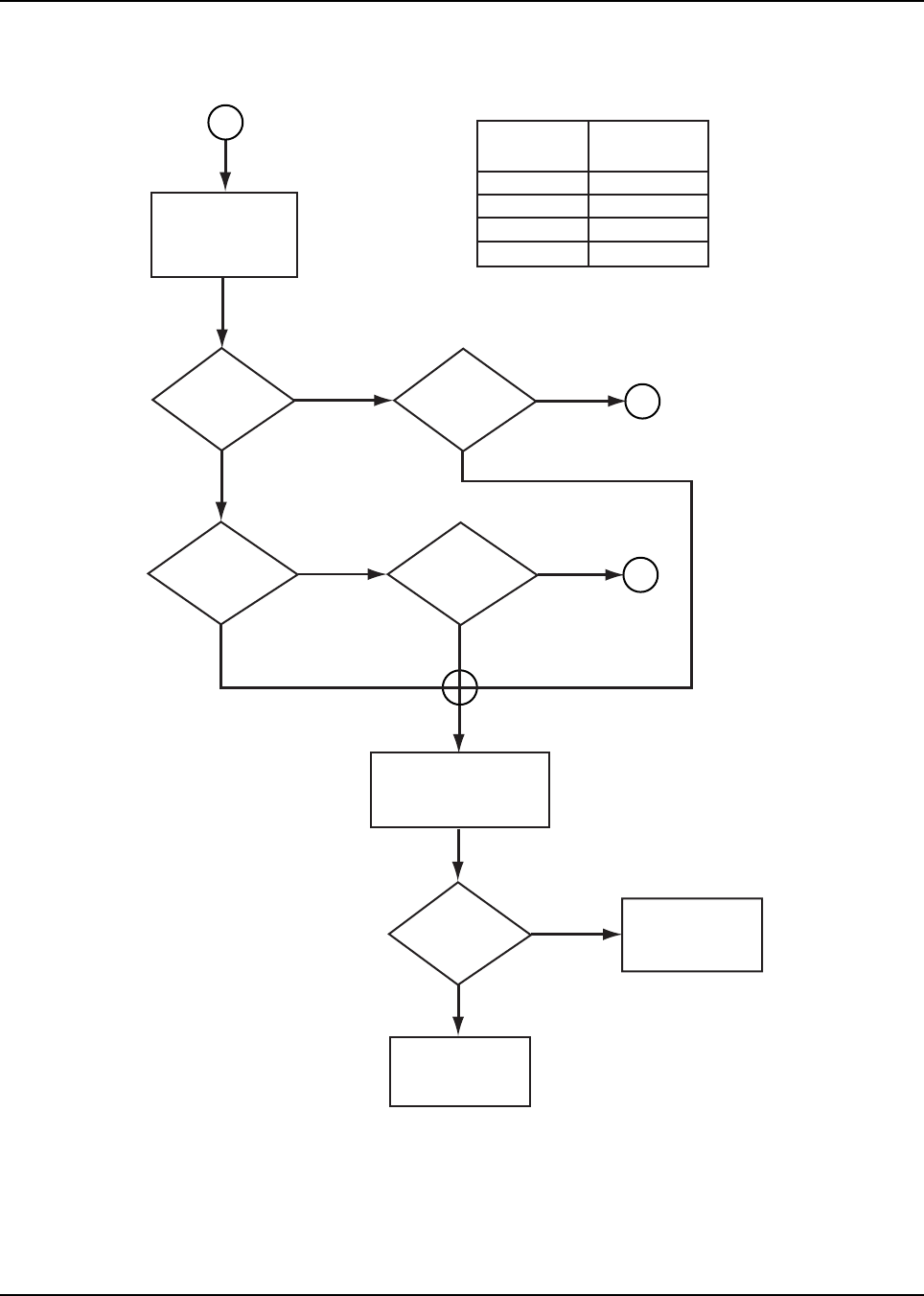
6881096C74-B May 25, 2005
Troubleshooting Charts: Flowcharts 5-51
5.6.37 RX Back-End—Poor SINAD or No Audio (700–800 MHz)—Part 2 of 3
Figure 5-39. RX Back-End—Poor SINAD or No Audio (700–800 MHz)—Part 2 of 3
No
3
3
1
TP6001
= 5.0V?
No
Yes
Yes
TP6001
= 0.0V?
No
Yes
Freq
VCO <71.1
MHz?
No
Yes
Freq
VCO >75.6
MHz?
Measure
control voltage
at TP6001
Inspect 2nd LO VCO
for missing parts or
solder defect
Yes
No
Visual
inspection
OK?
Repair defects
and/or replace
suspect parts
Replace
varacter diode
D6051
MAEPF-27807-O
TP6001
VOLTS DC
NOMINAL
FREQ (MHz)
0.0
1.6
4.0
5.0
68.0
71.1
75.6
77.0
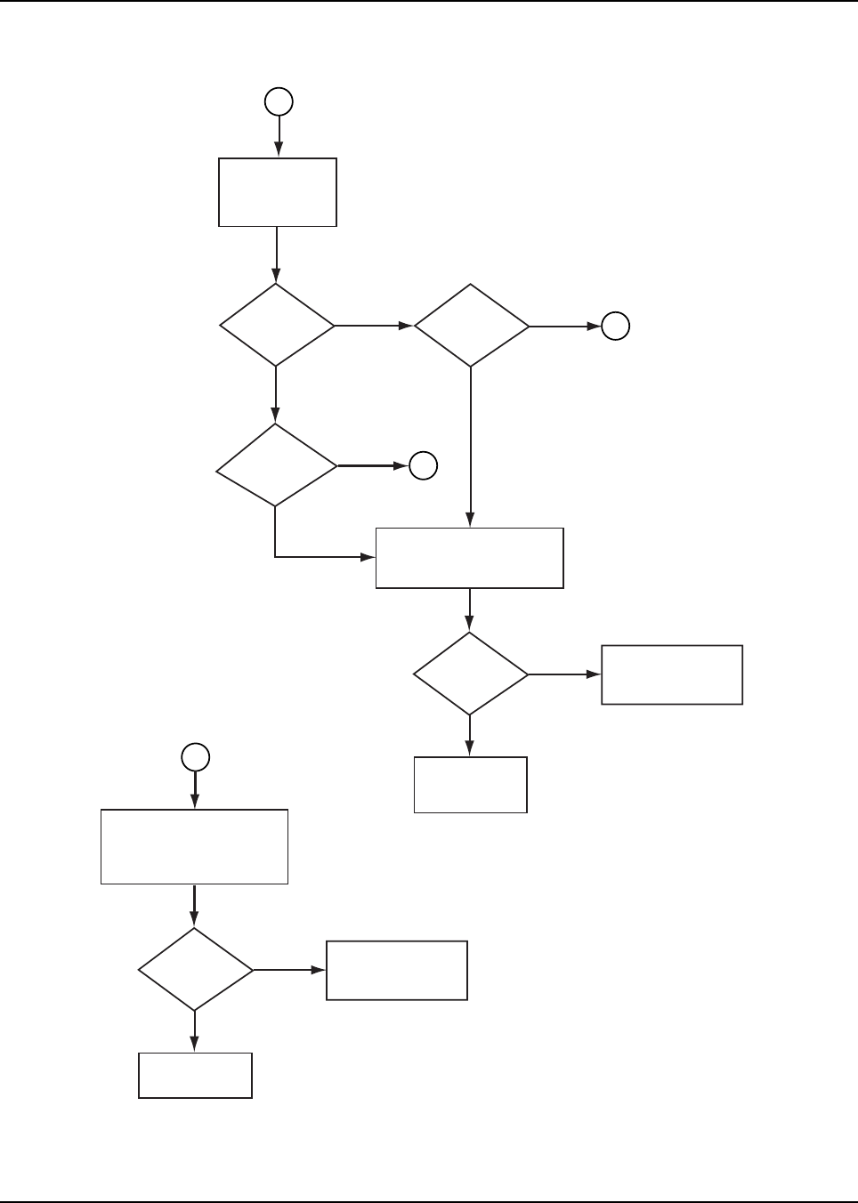
May 25, 2005 6881096C74-B
5-52 Troubleshooting Charts: Flowcharts
5.6.38 RX Back-End—Poor SINAD or No Audio (700–800 MHz)—Part 3 of 3
Figure 5-40. RX Back-End—Poor SINAD or No Audio (700–800 MHz)—Part 3 of 3
No 3
3
3
2
DC
voltage at
R6007 =
0.0V?
Yes
No
Yes
Freq of
CLKOUT
<1.2MHz?
No
Yes
DC
voltage at
R6007 =
3.0V?
Measure DC
tuning voltage
(Vt) at R6007
Inspect clock oscillator
circuit for solder defects
and/or missing components
Yes
No
Visual
inspection
OK?
Repair defects
and/or replace
suspect components
Replace
varacter diode
D6030
Inspect solder on U6000
and supporting circuitry,
look for missing or
misplaced components
Yes
No
Visual
inspection
OK?
Repair defects
and/or replace
suspect components
Replace
U6000
MAEPF-27808-O
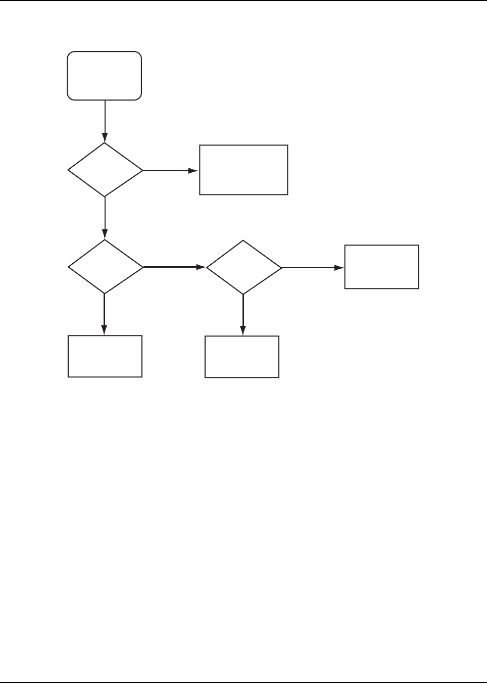
6881096C74-B May 25, 2005
Troubleshooting Charts: Flowcharts 5-53
5.6.39 Low or No RX Injection Signal (700–800 MHz)
Figure 5-41. Low or No RX Injection Signal (700–800 MHz)
MAEPF-27810-O
Approx.
5V on
Q6762-C?
START
Low or No RX
Injection Signal
No
No
Yes
No
Yes
Yes
Approx.
4.5V (–1V) on
Q6763-D?
62
Ohms across
R6801?
Check RF path
from RX VCO
Replace
Q6763
Check Q6762 and
DC Bias Circuitry;
replace if
necessary
Replace R6801
and Q6763
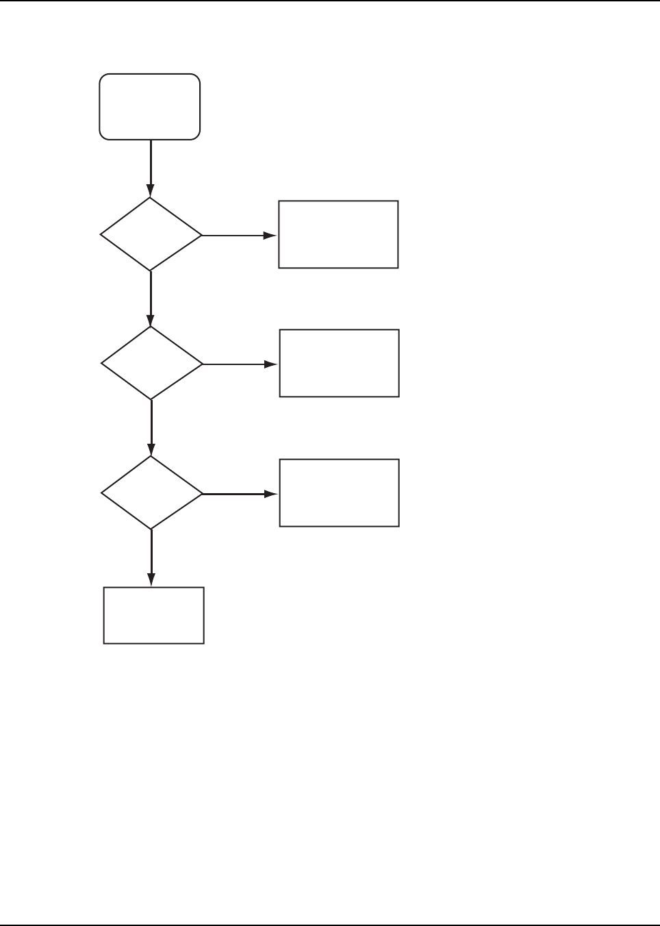
May 25, 2005 6881096C74-B
5-54 Troubleshooting Charts: Flowcharts
5.6.40 Low or No TX Injection Signal (700–800 MHz)
Figure 5-42. Low or No TX Injection Signal (700–800 MHz)
MAEPF-27811-O
Approx.
5.5 - 6V on
Q6764-C?
START
Low or No TX
Injection Signal
No
Yes
Check RF path
from TX VCO
Check Q6764 and
DC Bias Circuitry;
replace if
necessary
Approx.
5.5 - 6V on
Q6765-C?
No
Yes
Check Q6765 and
DC Bias Circuitry;
replace if
necessary
Approx.
8.5 - 9V on
Q6766-C?
No
Yes
Check Q6766 and
DC Bias Circuitry;
replace if
necessary
6881096C74-B May 25, 2005
Troubleshooting Charts: Flowcharts 5-55
5.6.41 No TX Audio (700–800 MHz)
Figure 5-43. No TX Audio (700–800 MHz)
MAEPF-27814-O
1.0Vpp
at R6782 or
VN_T67770?
No
Yes
0.4Vpp
at TP6755 or
C6783?
No
Yes
Check deviation
tuning or replace
U6751
GOTO
Controller
Section
Check
synthesizer
loop filter
components
NOTE: After the modulated signal is coupled
through C6783 the signal is attenuated to levels
below 2mv making a measurement difficult for
most oscilloscopes.
Inject a 2.0Vpp
1kHz tone into Mic
input and key radio
START
No TX Audio
This Flow chart only checks the modulation
path of the FGU. Readings are typical and
can vary with deviation settings that are
programmed during tuning.
May 25, 2005 6881096C74-B
5-56 Troubleshooting Charts: Flowcharts
5.6.42 TX or RX VCO Unlock (Fail 001) (700–800 MHz)—Part 1 of 2
Figure 5-44. TX or RX VCO Unlock (Fail 001) (700–800 MHz)—Part 1 of 2
MAEPF-27812-O
Go to
Controller
troubleshooting
charts
Yes
Frequency
Detected?
"Sniff" Frequency
near TX or RX
VCO shield or
infection string
TX or RX VCO
Unlock (Fail 001)
No
Yes
Check VCO
Control Voltage
at TP6759
8.2VDC
at Q6759
Collector?
No
Yes
3.0VDC
on pins 5, 36,
and 13 of
U6751?
Check 9.3 Volt
supply path from
regulator U0950 in
Controller section
<.6VDC or
>11.5VDC or
drifting?
No
No
Yes
Check if VCO
is locked using
spectrum analyzer
12VDC
at Charge Pump
Capacitor
C6768?
No
Yes
Check Voltage
Multiplier
Circuitry
Check Controller
Section and/or
ABACUS IC
U6000
Go to Transmitter
or receiver
Injection string
troubleshooting
charts
Place an Inductive field probe
connected to a spectrum analyzer
near area to be sniffed.
Locked?
Yes
3VDC
at pin 4 of
U6751?
No
No
Yes
Check for short
on pin 4 to
controller or
replace U6751
Go to Transmitter
or receiver
Injection string
troubleshooting
charts
A
6881096C74-B May 25, 2005
Troubleshooting Charts: Flowcharts 5-57
5.6.43 TX or RX VCO Unlock (Fail 001) (700–800 MHz)—Part 2 of 2
Figure 5-45. TX or RX VCO Unlock (Fail 001) (700–800 MHz)—Part 2 of 2
MAEPF-27818-O
Check 3 Volt
supply path from
Regulator U6750
Refer to Chart to determine
which AUX output determines
active VCO.
3VDC
at pin 5 of
U6750?
No Check 5 Volt
supply path from
regulator U0505
Unlock
RX or
TX?
TX
RX
Yes
Aux 3
or 4 at 3.0VDC
for RX?
No
No
Yes
Check
U6751
Check
U6755
8.2VDC
at TP6753 or
TP6751?
Yes
Check
Q6756 or
Q6760
Aux 1
or 2 at 3.0VDC
for TX?
No
No
Yes
Check
U6751
Check
U6754
8.2VDC
at TP6767 or
TP6761?
Yes
Check
Q6767 or
Q6755
A
May 25, 2005 6881096C74-B
5-58 Troubleshooting Charts: Flowcharts
5.6.44 RF Power Amplifier (RFPA)—No or Low TX Power Output (700–800 MHz)—
Part 1 of 5
NOTE: For each flowchart step in which reference is made to a note, be sure to refer to that specific
note (located on page 61 of this flowchart) for guidance in performing the actual
troubleshooting procedure. Also, RFPA DC voltages are shown in Table 5-7 on page 5-62.
Figure 5-46. RF Power Amplifier (RFPA)—No or Low TX Power Output (700–800 MHz)—Part 1 of 5
Read General
Notes before
proceeding. Read
specific notes as
indicated
Check battery
cable, mic, and
control head
connections
START
Continuous red light
while mic button is
depressed?
GOTO Sythesizer-
No Transmit
Chart ?
Tune power with
Tuner?
(see help text)
No
Yes
Tune current limit
with Tuner
(see help text)
Yes
No
TX injection power
less than 2 mW?
(Note 1)
GOTO Sythesizer-
No or Low Tx
Injection
Chart ?
Yes
K9.1V
present
at Q0952, pin 1 in
power control section
when transmitter is
keyed?
No
GOTO Power
Control - No K9.1V
Chart ?
RFPA_CNTRL
voltage (VN_B6503)
less than 5.0V when
transmitter is
keyed?
Yes
No
GOTO Power
Control - No or low
RFPA_CNTRL
Chart ?
No
U6500 drain biases
voltages per Table 1?
(Note 3)
Yes
No Check/repair/
replace defective
parts
Yes
No
A
Is U6500,
VCNTRL resistance <
1 kOhms?
(Note 2)
Yes Repair/replace
U6500
No
Is U6500,
RFOUT and VD1
resistance <
1 MOhms?
(Note 4)
Yes Repair/replace
U6500
MAEPF-27929-O
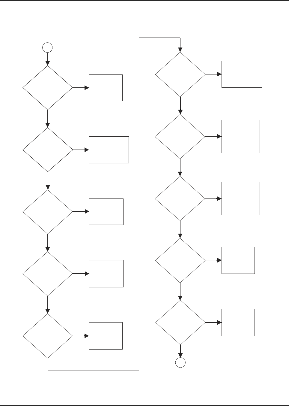
6881096C74-B May 25, 2005
Troubleshooting Charts: Flowcharts 5-59
5.6.45 RF Power Amplifier (RFPA)—No or Low TX Power Output (700–800 MHz)—
Part 2 of 5
Figure 5-47. RF Power Amplifier (RFPA)—No or Low TX Power Output (700–800 MHz)—Part 2 of 5
Defective parts
in matching network
between Q6520 and
Q6540-1?
(Note 9)
Repair/replace
defective parts
Yes
No
Defective parts
in matching network
between Q6500 and
Q6520?
(Note 5)
Repair/replace
defective parts
Yes
Q6520 bias voltages
as per Table 1?
(Note 6)
No
Check/repair/replace
defective parts or
GOTO Power Control
- No/low VGBIAS
Chart
Is Q6520,
gate resistance <
1 MOhms?
(Note 7)
Yes
Repair/replace
Q6520 and retune
gate bias via
Tuner
(see help text)
No
No
Yes
Is Q6520,
drain resistance <
1 MOhms?
(Note 8)
Yes
No
Q6540-1 bias
voltages as per Table 1?
(Note 10)
Defective parts
in matching network
between Q6540-1 and
antenna switch?
(Note 13)
Antenna switch
bias voltages as per
Table 1?
(Note 14)
Repair/replace
defective parts
Is Q6540-1,
gate resistance <
1 MOhms?
(Note 11)
Yes
No
Is Q6540-1,
drain resistance <
1 MOhms?
(Note 12)
Yes
No
Repair/replace
defective parts
No
No
Yes
Yes
Yes
No
Repair/replace
Q6520 and retune
gate bias via
Tuner
(see help text)
Check/repair/replace
defective parts or
GOTO Power Control
- No/low VGBIAS
Chart
Repair/replace both
Q6540 and Q6541
(see General Notes)
and retune gate bias
via Tuner
(see help text)
Repair/replace both
Q6540 and Q6541
(see General Notes)
and retune gate bias
via Tuner
(see help text)
B
A
MAEPF-27930-O

May 25, 2005 6881096C74-B
5-60 Troubleshooting Charts: Flowcharts
5.6.46 RF Power Amplifier (RFPA)—No or Low TX Power Output (700–800 MHz)—
Part 3 of 5
Figure 5-48. RF Power Amplifier (RFPA)—No or Low TX Power Output (700–800 MHz)—Part 3 of 5
Yes
Defective parts in
antenna switch?
(Note 15)
Repair/replace
defective parts
Defective parts in
harmonic filter?
(Note 16)
No
Yes Repair/replace
defective parts
No
Defective parts in
power detector?
(Note 17)
Yes
Repair/replace
antenna connector
Continuity check
fails from R6740 and
the antenna connector
external coax?
No
Yes
Repair/replace
defective parts
B
MAEPF-27931-O
Go to the
Controller GPIO
Section
No

6881096C74-B May 25, 2005
Troubleshooting Charts: Flowcharts 5-61
5.6.47 RF Power Amplifier (RFPA)—No or Low TX Power Output (700–800 MHz)—
Part 4 of 5
Specific Notes:
1. Remove C6501 and solder the center conductor of a small 50-ohm, coaxial cable to
VN_B6500. Solder ground to the gold shield track adjacent to VN_B6500. Attach an RF
milliwatt meter, key the transmitter, and measure TX_INJ power. Then, remove the coaxial
cable and replace C6501. Remove the solder added to shield track.
2. Remove R0977 in the power control section, and measure the resistance between VCNTRL
(VN_B6503) and ground. Replace R0977.
3. If U6500, VD1, is incorrect, inspect the bias feed circuitry (L6501 and C6504) and interstage
match components (L6502, C6506, and C6503). If U6500, RFOUT, is incorrect, inspect the
bias feed circuitry (L6500 and C6500).
4. Remove L6501 and measure the resistance between VD1 (VN_B6501) and ground. Replace
L6501. Remove L6500 and measure the resistance between RFOUT (VN_B6504) and
ground. Replace L6500.
5. Inspect C6502, C6509-11, and R6521-5.
6. If the Q6520 gate bias is incorrect, inspect the bias feed circuitry (R6520 and C6520). If the
bias feed circuitry is functional, then go to the Power Control—No or low VGBIAS flowchart. If
the Q6520 drain bias is incorrect, inspect the bias feed circuitry (L6521, C6521-2, R6526-7,
and L6521-5).
7. Remove R6520 and measure the resistance between Q6520 gate and ground. Replace
R6520.
8. Remove L6521 and measure the resistance between Q6520 drain and ground. Replace
L6521.
9. Inspect C6541-2, C6544-5, C6547-8, C6565-6, R6550-7, and R6559.
10. If the Q6540 gate bias is incorrect, inspect the bias feed circuitry (R6540 and C6540). If the
gate bias feed circuitry is functional, then go to the Power Control—No or low VGBIAS
flowchart. If the Q6541gate bias is incorrect, inspect the bias feed circuitry (R6543 and
C6558). If the bias feed circuitry is functional, then go to the Power Control—No or low
VGBIAS flowchart. If the Q6540-1 common drain bias is incorrect, inspect the bias feed
circuitry (L6542-3, C6559-60, R6544-5, and L6521-5).
11. Remove R6540 and measure the resistance between Q6540 gate and ground. Replace
R6540. Remove R6543 and measure the resistance between Q6541 gate and ground.
Replace R6541.
12. Remove L6542 and measure the resistance between Q6540-1 drain and ground. Replace
L6542.
13. Inspect R6560 and C6549-57.
14. If the antenna switch bias voltages are incorrect, inspect R6547-8, L6700, and L6702-3, as
well as perform diode checks on D6701-2.
15. Inspect the remaining antenna switch parts (C6700-5).
16. Inspect L6720-2 and C6720-1.
17. Inspect D6730, R6730-2, R6735-6, L6730, and C6730-1.
May 25, 2005 6881096C74-B
5-62 Troubleshooting Charts: Flowcharts
5.6.48 RF Power Amplifier (RFPA)—No or Low TX Power Output (700–800 MHz)—
Part 5 of 5
Table 5-7. RFPA DC Voltages
Description Location Voltage (Vdc)
A+ = 13.6 Vdc
U5501, VD1 VN_B6503 9.0–9.3
U5501, RFOUT VN_B6504 9.0–9.3
Q6520 Gate Bias VN_B6520 2.0–2.2
Q6520 Drain Bias L6521/R6526
Node
13.0–13.6
Q6540 Gate Bias VN_B6540 3.5–3.7
Q6541 Gate Bias VN_B6541 3.5–3.7
Q6540/Q6541
Drain Bias
L6542/R6544
Node
13.0–13.6
Antenna Switch Bias
Voltage 1
VN_B6563 ~5.3
Antenna Switch Bias
Voltage 2
VN_T6701 ~1.6
Antenna Switch Bias
Voltage 3
D6701/D6702
Node
~0.8
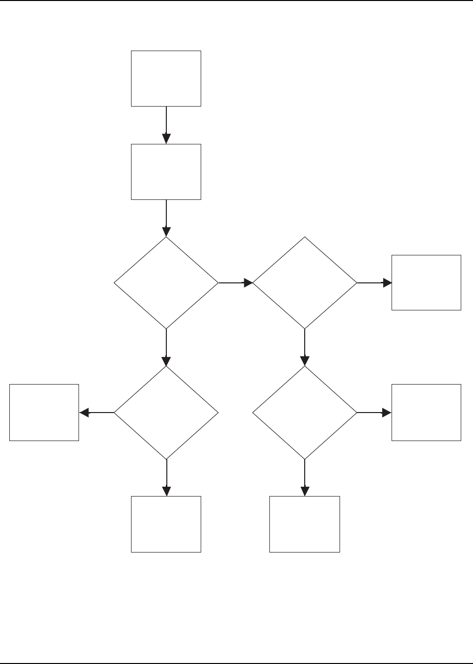
6881096C74-B May 25, 2005
Troubleshooting Charts: Flowcharts 5-63
5.6.49 RFPA Power Control—No K9.1V (700–800 MHz)
Figure 5-49. RFPA Power Control—No K9.1V (700–800 MHz)
Read General
Notes before
proceeding. Read
specific notes as
indicated
START
Is 9.3V present at
Q0952, pin 5?
Yes Is Q0952, pin 4
< 0.5V when mic
button is depressed?
Repair/replace
Q0952
Yes
No
Is K9.1V_EN > 2.0V
when mic button is
depressed?
No
Repair/replace
Q0951
Is A+ present at U0951,
pin 4?
No
Yes
See GPIO in
CONTROLLER
section
Repair/replace
U0951
Yes
Connect battery
cable to supply
13.6V
No
MAEPF-27926-O
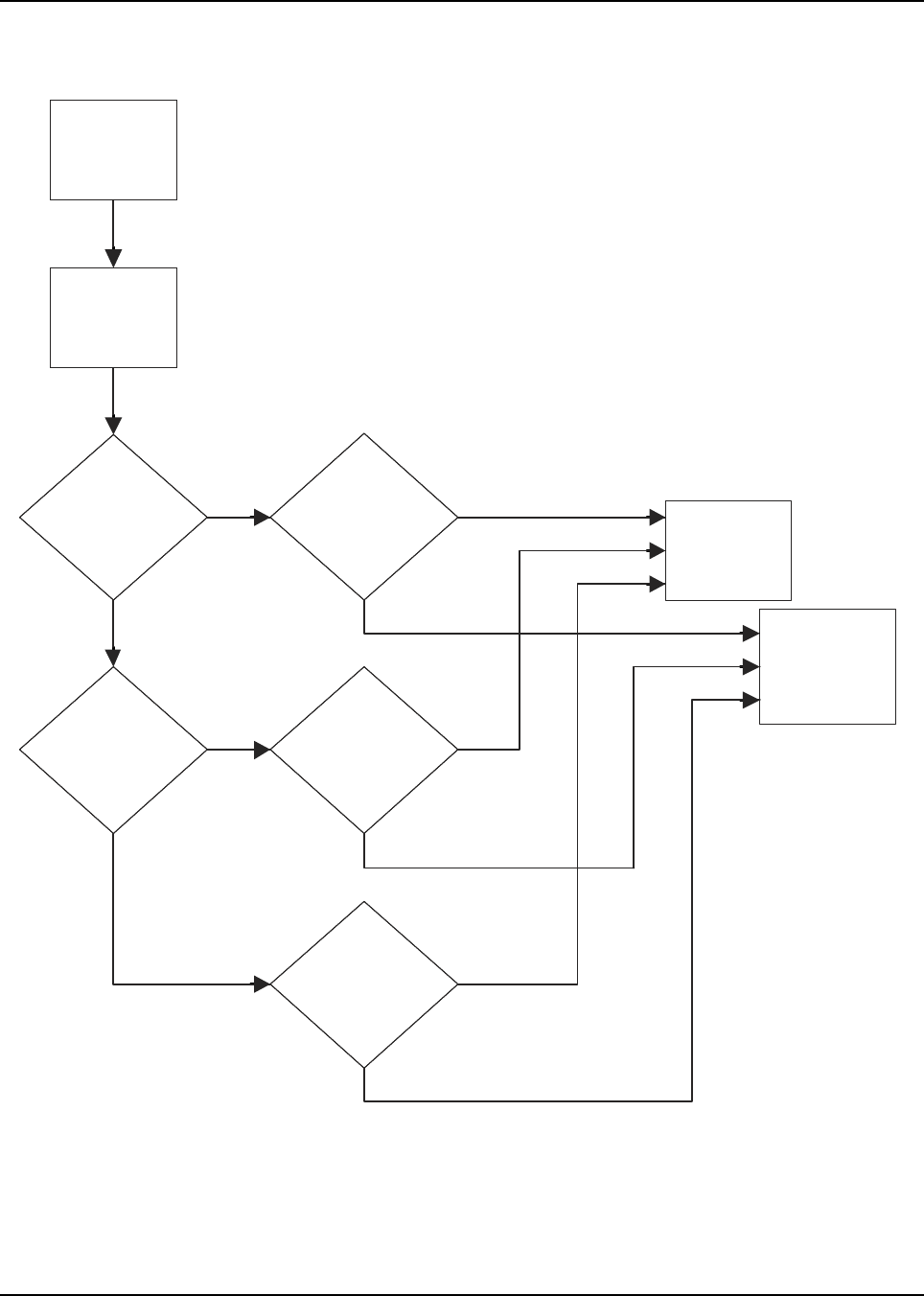
May 25, 2005 6881096C74-B
5-64 Troubleshooting Charts: Flowcharts
5.6.50 RFPA Power Control—No VGBIAS (700–800 MHz)
Figure 5-50. RFPA Power Control—No VGBIAS (700–800 MHz)
Read General
Notes before
proceeding. Read
specific notes as
indicated
START
No
Yes
Repair/replace
U0960
No
No/low Q6540
VGBIAS1?
No/low Q6541
VGBIAS2?
Remove U0960.
TP0937 voltage
2.6-2.8 V?
Yes
Remove U0960.
TP0939 voltage
2.6-2.8 V?
Yes
Remove U0960.
TP0941 voltage
2.0-2.2 V?
No
Repair/replace
U0959. If problem
still not fixed, see
IC communication
in CONTROLLER
section.
Yes
Yes
No
No
MAEPF-27928-O
6881096C74-B May 25, 2005
Troubleshooting Charts: Flowcharts 5-65
5.6.51 RFPA Power Control—No or Low TX RFPA_CNTRL (700–800 MHz)—Part 1 of 2
For each flowchart step in which reference is made to a note, be sure to refer to that specific note
(located on page 66 of this flowchart) for guidance in performing the actual troubleshooting
procedure.
Figure 5-51. RFPA Power Control—No or Low TX RFPA_CNTRL (700–800 MHz)—Part 1 of 2
Read General
Notes before
proceeding, Read
specific notes as
indicated
START
Remove Q0954.
Proper power
restored?
(Note 1)
Remove D0950.
Proper power
restored?
(Note 2)
Yes
No
U0956-3, pin 10
~ 1.5V?
No
Yes
Repair/replace
defective parts or
see
Controller
GPIO section
Repair/replace
defective parts
No VCC3 present at
U0963, pin 5?
(Note 3)
VCC5 present at
U0963, pin 1?
No See
Controller
VCC5 section
Yes
Remove R0974.
VCC3 present at
U0963, pin 5?
(Note 4)
Yes Repair/replace
defective parts
Repair/replace
U0963
No
No
Repair/replace
defective parts
YesYes
A
TP0955 voltage
~ 1.5V?
Repair/replace
defective parts
Yes
A
Remove D0951.
Proper power
restored?
(Note 5)
Repair/replace
defective parts
Yes
No
VFORWARD buffer
functioning properly?
(Note 6)
U0959 functionally
properly?
(Note 7)
No
Repair/replace
defective parts
Yes
Repair/replace
defective parts or
see
Controller
GPIO section
No
MAEPF-27927-O
Go to
Controller
GPIO Section
No
Yes

May 25, 2005 6881096C74-B
5-66 Troubleshooting Charts: Flowcharts
5.6.52 RFPA Power Control—No or Low TX RFPA_CNTRL (700–800 MHz)—Part 2 of 2
Specific Notes:
1. Remove Q0954. If proper power is restored, repair/replace Q0954. If the problem still
persists, check for proper operation of U0958-1, and replace U0958 if not functioning
properly. If U0958-1 operation is correct, refer the controller section in the theory of operation
chapter.
2. Remove D0950. If proper power is restored, inspect R0942-5, R0991, and U0956-4. Replace
D0958.
3. Inspect R0974-5.
4. Remove R0974. Measure U0963, pin 5 voltage. Replace R0974.
5. Inspect the current limit and temperature cutback circuitry (refer to the power control section
in the theory of operation chapter).
6. Adjust the Power Detector Calibration via the Tuner software (see the tuner Help text) and
monitor the output power while the transmitter is keyed. If the circuit is functioning properly,
output power will decrease if the softpot is increased, and output power will increase if the
softpot is decreased. If the circuitry is not functioning properly, then inspect U0952, U0956-2,
R0971-3. If the problem persists, refer to the controller section in the theory of operation
chapter.
7. Retune the Power Detector Calibration if any circuitry is repaired/replaced.
8. Adjust the power via CPS (see the Help text) and monitor output power. If the softpot is
decreased, power will increase; if the softpot is increased, power will decrease. If the circuitry
is not functioning properly, replace U0959 and retune the power via CPS (see the Help text
for complete procedures). If the problem persists, refer to the controller section in the theory
of operation chapter.
Chapter 6 Troubleshooting Waveforms
6.1 Introduction
This chapter contains images of waveforms that might be useful in verifying operation of certain parts
of the circuitry. These waveforms are for reference only; the actual data depicted will vary depending
upon the operating conditions.
Table 6-1. List of Troubleshooting Waveforms
Waveform Page
Power-On Reset Timing 6-2
Power-On to Soft Turn-On Timing 6-2
Power-Down Reset 6-3
16.8 MHz Clock Waveform 6-3
32 kHz Clock Waveform 6-4
DSP SSI Port RX Mode 6-4
DSP SSI Port TX Mode CSQ 6-5
SPI Bus Waveform 6-5
SB9600 Waveform 6-6
SB9600 BUS+ and BUS- Waveforms 6-6
SB9600 BUS+ and RESET Waveforms 6-7
SB9600 BUSY and BUS- Waveforms 6-7
RS-232 RX Waveforms 6-8
RS-232 TX Waveforms 6-8
RS-232 RX/TX Waveforms 6-9
USB Waveforms 6-9
Serial Audio Port Waveforms 6-10
Secure Interface Waveforms 6-10
8 kHz Frame Sync Waveform 6-11
RX Audio Waveforms 6-11
TX Audio Waveforms 6-12
TX and RX 1 kHz Audio Path Sinewave and Chart 6-12
May 25, 2005 6881096C74-B
6-2 Troubleshooting Waveforms: XTL 5000 Waveforms
6.2 XTL 5000 Waveforms
6.2.1 Power-On Reset Timing
6.2.2 Power-On to Soft Turn-On Timing
MAEPF-27853-O
Ch3
Ch1 M5.00ms Ch1 6.0 V
Ch2
U0507 Pin 5
LV_DETECT (POR)
13.8V
Ch1
SWB+
5.00V
2.00V
2.00V
Ch2
MAEPF-27854-O
Ch3
Ch1 M 200ms Ch1 6.0 V
Ch2
U0507 Pin 5
LV_DETECT (POR)
Ch3
TP0500
13.8V
Ch1
SWB+
5.00V
2.00V
2.00V
Ch2
6881096C74-B May 25, 2005
Troubleshooting Waveforms: XTL 5000 Waveforms 6-3
6.2.3 Power-Down Reset
6.2.4 16.8 MHz Clock Waveform
MAEPF-27855-O
Ch3
Ch1 M 10.0ms Ch1 6.0 V
Ch2
U0507 Pin 5
LV_DETECT
Ch3
TP0500
SOFT_TURN_OFF
Ch1
SWB+
13.8V
5.00V
2.00V
2.00V
Ch2
Power-Down Reset
Trace 1 — SWB+
Trace 2 — LV_DETECT — U0507 Pin 5
Trace 3 — SOFT_TURN_OFF — TP0500
MAEPF-27856-O
Ch1 M 25.0ns Ch1 10mV
500mV
C1 Pk-to-Pk
1.70V
C1 Period
59.333ns
Trace 1 — U0903 Pin 3 — 16.8 MHz Clock
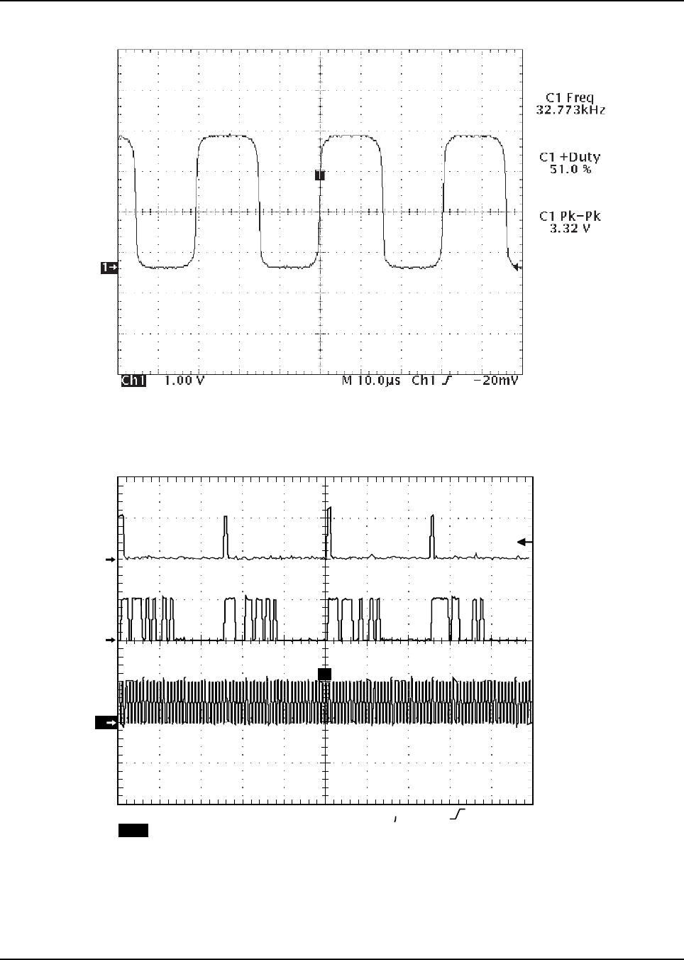
May 25, 2005 6881096C74-B
6-4 Troubleshooting Waveforms: XTL 5000 Waveforms
6.2.5 32 kHz Clock Waveform
6.2.6 DSP SSI Port RX Mode
MAEPF-27857-O
Trace 1 — R428 — 32 kHz Clock
2
Ch3
Ch1
T
1
3
M 20.0us Ch1 2.2 V
Ch1 Freq
18kHz
5.00V
5.00V
5.00V
Ch2
MAEPF-27858-O
DSP SSI Port RX Mode CSQ
Trace 1 — ABACUS_SSI_FSYNC
Trace 2 — ABACUS_SSI_RXD
Trace 3 — ABACUS_SSI_CLK (1.2 MHz)
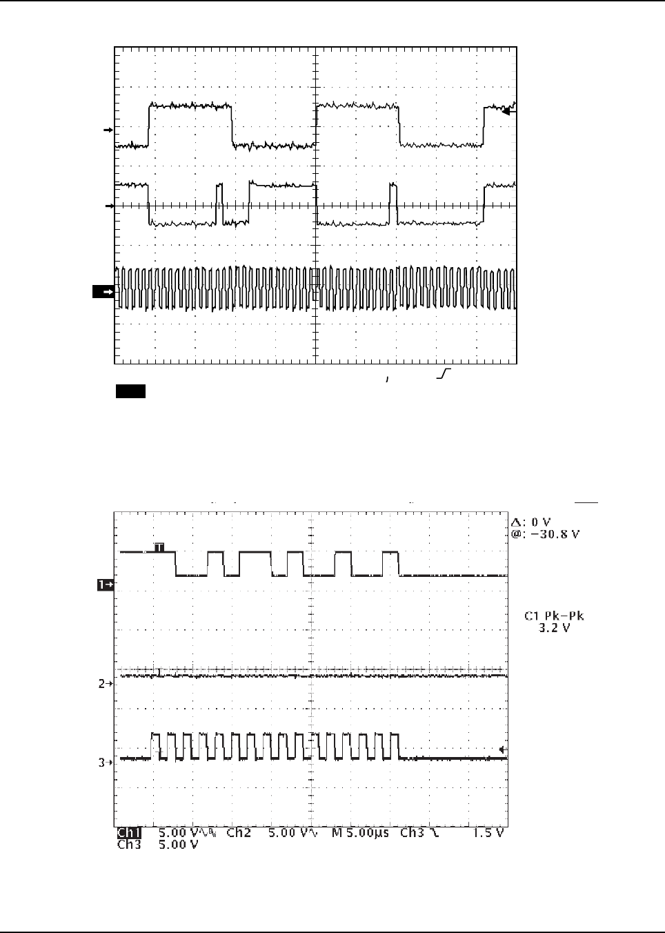
6881096C74-B May 25, 2005
Troubleshooting Waveforms: XTL 5000 Waveforms 6-5
6.2.7 DSP SSI Port TX Mode CSQ
6.2.8 SPI Bus Waveform
T
T
3
Ch1 Ch2
Ch3
2
1
M 5.00us Ch1 2.2 V
Ch1 Freq
~47kHz
5.00V 5.00V
5.00V
MAEPF-27859-O
DSP SSI Port TX Mode CSQ
Trace 1 — DAC_SSI_FSYNC
Trace 2 — DAC_SSI_TXD
Trace 3 — DAC_SSI_CLK (2.4 MHz)
C1 Freq
164.6 kHz
MAEPF-27860-O
Radio Power-Up
Trace 1 — Data
Trace 2 — Chip Select
Trace 3 — Clock
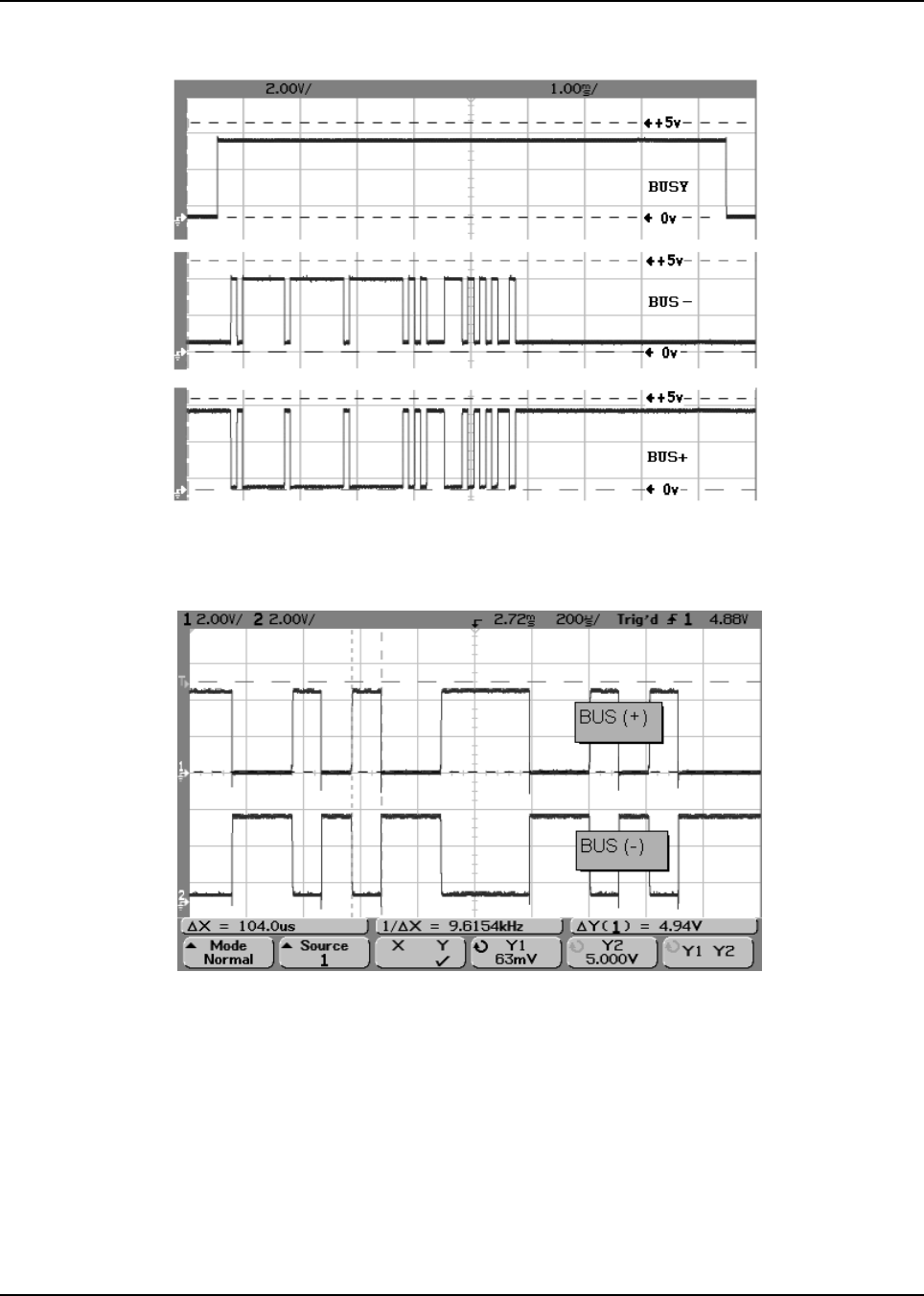
May 25, 2005 6881096C74-B
6-6 Troubleshooting Waveforms: XTL 5000 Waveforms
6.2.9 SB9600 Waveforms
6.2.10 SB9600 BUS+ and BUS- Waveforms
MAEPF-27781-O
MAEPF-27871-O
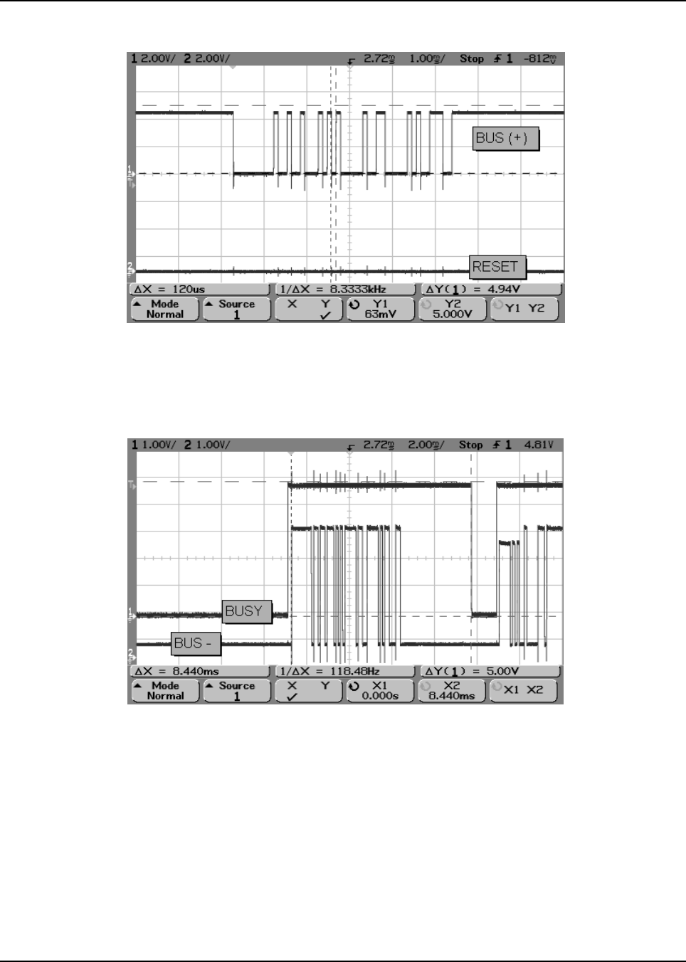
6881096C74-B May 25, 2005
Troubleshooting Waveforms: XTL 5000 Waveforms 6-7
6.2.11 SB9600 BUS+ and RESET Waveforms
6.2.12 SB9600 BUSY and BUS- Waveforms
MAEPF-27872-O
MAEPF-27873-O
May 25, 2005 6881096C74-B
6-8 Troubleshooting Waveforms: XTL 5000 Waveforms
6.2.13 RS-232 RX Waveforms
6.2.14 RS-232 TX Waveforms
X = 2.9us
X = 2.3us
MAEPF-27705-A
+ 12V
- 12V
MAEPF-27706-A
X = 2.7us
X = 3.4us
MAEPF-27707-A
+ 9V
- 9V
MAEPF-27708-A
6881096C74-B May 25, 2005
Troubleshooting Waveforms: XTL 5000 Waveforms 6-9
6.2.15 RS-232 RX/TX Waveforms
6.2.16 USB Waveforms
May 25, 2005 6881096C74-B
6-10 Troubleshooting Waveforms: XTL 5000 Waveforms
6.2.17 Serial Audio Port Waveforms
6.2.18 Secure Interface Waveforms
MAEPF-27864-O
C1 Freq
~8kHz
Transmitting
1 kHz tone at 85mVrms into microphone
Trace 1 — Frame Sync — SAP_FSYNC
Trace 2 — Clock — SAP_DCLK
Trace 3 — Data — SAP_TX
Ch1 Ch2
Ch3
M20.00us Ch3 1.20V
J0501-1
SAP_TX
J0501-2
SAP_RX
J0501-4
SAP_FSYNC
J0501-3
SAP_DCLK
2.00V 2.00V
2.00V
2.00V
MAEPF-27865-O
Ch4
Receiving
1 kHz tone at 3 kHz Dev, -47dBm Secure Mode
Trace 1 — J0501 — 1 - SAP TX
Trace 2 — J0501 — 2 - SAP RX
Trace 3 — J0501 — 3 - SAP DCLK

6881096C74-B May 25, 2005
Troubleshooting Waveforms: XTL 5000 Waveforms 6-11
6.2.19 8 kHz Frame Sync Waveform
6.2.20 RX Audio Waveforms
M100us Ch1 1.20V
1.00V
MAEPF-27866-O
Ch1
C1 High
2.85V
C1 Period
124us
Receiving
1 kHz tone at 3 kHz Dev, -47dBm Secure Mode
Trace 1 — J0501 — 4
2
1
3
4
Ch1 Freq
8 kHz
1K sinewave
MAEPF-27867-O
Ch2, Ch3, Ch4: See 1K sinewave chart
~
~
T
T
T
Receiving
1 kHz tone @ 3 kHz deviation, -60 dBm. Volume set to rated audio.
Trace 1 — SAP_DCLK (8 kHz)
Trace 2 — TP0205
Trace 3 — SPKR_LOW out of U0204
Trace 4 — SPKR_HI out of U0204
Note 3: Actual level is dependent upon volume setting.
May 25, 2005 6881096C74-B
6-12 Troubleshooting Waveforms: XTL 5000 Waveforms
6.2.21 TX Audio Waveforms
6.2.22 TX and RX 1 kHz Audio Path Sinewave and Chart
1
T
2
3
4
T
T
1K sinewave
MAEPF-27868-O
Ch2, Ch3, Ch4: See 1K sinewave chart
Ch1 Freq
8 kHz
~
~
Transmit Audio
1 kHz tone which provides 3 kHz deviation
Trace 1 — SAP_DCLK (8 kHz)
Trace 2 — MODIN R6782
Trace 3 — MIC TP0200
Trace 4 — TP0203
Note 3: Actual level is dependent upon volume setting.
MAEPF-27869-O
Ch1 500uS/Div.
C1 Pk-to-Pk
920mV
C1 Ampl
860mV
C1 Mean
1.408V
Refer to Table 6-2
for test point data
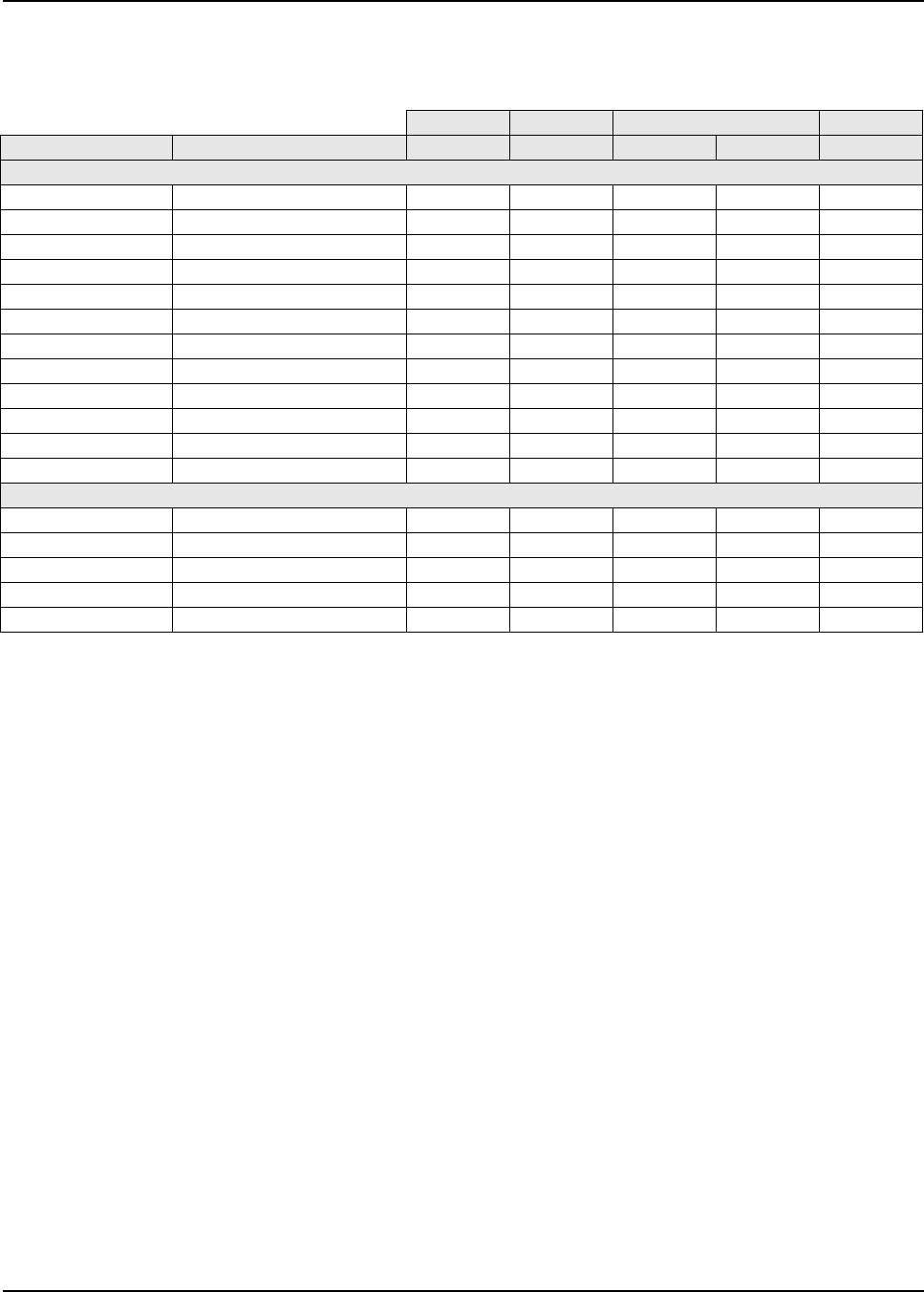
6881096C74-B May 25, 2005
Troubleshooting Waveforms: XTL 5000 Waveforms 6-13
Table 6-2. TX and RX Audio Path Test Points for 1 kHz Sine Wave
(for Mid Power VHF, UHF R1 and 700/800 MHz)
Typical O-Scope Measured mV p-p Volts
Test Point Description mV RMS mV/div LL 1UL 2DC Bias
TX Audio Path
MIC_HI 80 mV RMS input 80 mV 20 226 227 3 to 9
TP0200 MIC_PREAMP_IN 80 mV 20 220 227 1.42
TP0201 Preamp in, attn.-out 43 mV 10 100 122 1.42
U0201-1 1st op amp out 342 mV 10 97 121 1.42
TP0202 2nd op amp in 341 mV 10 97 121 1.42
U0201-7 2nd op amp out 41 mV 10 94 120 1.42
U0201-8 3rd op amp and filter out 40 mV 10 91 119 1.42
U0201-14 4th op amp and filter out 39 mV 10 88 118 1.42
TP0203 CODEC op amp in 38 mV 10 85 117 1.42
U0200-17 Buffered CODEC in 36 mV 10 82 116 1.42
C0904 5 CF Out 150 mV 50 400 700 1.42
R6782 MOD_IN at 3 kHz dev. 3150 mV 50 400 700 1.5
RX Audio Path 4
TP0204 RX_FILT_AUDIO 318 500 849 953 1.42
TP0205 RX_AUDIO_IN 318 500 849 953 1.42
TP0206 AUDIO_PA_IN 39 10 92 130 1/2 A+
SPKR+ NON INVERTED PA out 7.74 Vbtl 52V 9.5Vpp 12.4Vpp 1/2A+
SPKR- INVERTED PA out 7.74 Vbtl 52V 9.5Vpp 12.4Vpp 1/2A+
1 LL = lower limit
2 UL = upper limit
3 Measurement depends on tuning parameters
4 1 kHz tone at 3 kHz deviation, -47 dBm
5 “btl” = bridge to load

May 25, 2005 6881096C74-B
6-14 Troubleshooting Waveforms: XTL 5000 Waveforms
Table 6-3. TX and RX Audio Path Test Points for 1 kHz Sine Wave
(for all High Power and Mid Power R2)
Typical O-Scope Measured mV p-p Volts
Test Point Description mV RMS mV/div LL 1UL 2DC Bias
TX Audio Path
MIC_HI 80 mV RMS input 80 mV 20 226 227 3 to 9
TP0200 MIC_PREAMP_IN 80 mV 20 220 227 2.5
U0201-8 1st op amp out 30 mV 10 0 10 2.5
U0201-7 2nd op amp out 80 mV 10 210 227 2.5
U0201-1 3rd op amp and filter out 80 mV 10 210 227 2.5
U0201-14 4th op amp and filter out 80 mV 10 210 227 2.5
TP0203 CODEC op amp in 36 mV 10 85 117 1.42
U0200-17 Buffered CODEC in 36 mV 10 82 116 1.42
C0904 5 CF Out 150 mV 50 400 700 1.42
R6782 MOD_IN at 3 kHz dev. 3150 mV 50 400 700 1.5
RX Audio Path 4
TP0204 RX_FILT_AUDIO 318 500 849 953 1.42
TP0205 RX_AUDIO_IN 318 500 849 953 1.42
TP0206 AUDIO_PA_IN 39 10 92 130 1/2 A+
SPKR+ NON INVERTED PA out 7.74 Vbtl 52V 9.5Vpp 12.4Vpp 1/2A+
SPKR- INVERTED PA out 7.74 Vbtl 52V 9.5Vpp 12.4Vpp 1/2A+
1 LL = lower limit
2 UL = upper limit
3 Measurement depends on tuning parameters
4 1 kHz tone at 3 kHz deviation, -47 dBm
5 “btl” = bridge to load
Schematics, Component Location Diagrams, and Parts Lists: List of Schematics, Component Location Diagrams, and Parts Lists 7-1
6881096C74-B May 25, 2005
Chapter 7 Schematics, Component Location Diagrams, and Parts Lists
7.1 List of Schematics, Component
Location Diagrams, and Parts
Lists
The following table lists the schematics,
component location diagrams, and parts lists
contained in this chapter.
Table 7-1. List of Schematics, Component Location
Diagrams, and Parts Lists
Figure Title Page
VHF
HUD4022A/HUD4025B Main Board Overall Block
Diagram and Interconnections
7-3
HUD4022A Controller Block Diagram and
Interconnections (Sheet 1 of 2)
7-4
HUD4022A Controller Block Diagram and
Interconnections (Sheet 2 of 2)
7-5
HUD4022A Controller Urchin IC, MUX, and
AD5320 DAC Schematic
7-6
HUD4022A Controller Audio Schematic 7-7
HUD4022A Controller Power Control (Sheet 1 of 2) 7-8
HUD4022A Controller Power Control (Sheet 2 of 2) 7-9
HUD4025B Controller Block Diagram 7-10
HUD4025B Controller Daughter Board Interface 7-11
HUD4025B Controller Urchin IC, MUX and AD5320
DAC
7-12
HUD4025B Controller Audio 7-13
HUD4025B Controller Interface, Secure and Power
Block Diagram
7-14
HUD4025B Controller Power Supply 7-15
HUD4025B USB/RS232 Interface 7-16
HUD4025B SB9600 7-17
HUD4025B Control Head Connector 1 of 2 7-18
HUD4025B Control Head Connector 2 of 2 7-19
HUD4025B Secure Interface Connector Schematic 7-20
HUD4022A/HUD4025B Frequency Generation Unit
Overall Schematic (Sheet 1 of 2)
7-21
HUD4022A/HUD4025B Frequency Generation Unit
Overall Schematic (Sheet 2 of 2)
7-22
HUD4022A/HUD4025B VHF Transmitter VCO
Schematic
7-23
HUD4022A/HUD4025B Frequency Generation Unit
VHF Receive Injection Schematic
7-24
HUD4022A/HUD4025B Frequency Generation Unit
VHF Transmit Injection Schematic
7-25
HUD4022A/HUD4025B Receiver Back-End
Schematic
7-26
HUD4022A/HUD4025B Receiver Front-End
Schematic (Sheet 1 of 2)
7-27
HUD4022A/HUD4025B Receiver Front-End
Schematic (Sheet 2 of 2)
7-28
HUD4022A/HUD4025B Receiver IF Schematic 7-29
HUD4022A RF Power Amplifier (RFPA) Schematic
(Sheet 1 of 2)
7-30
HUD4022A RF Power Amplifier (RF PA) Schematic
(Sheet 2 of 2)
7-31
HUD4025B RF 100W Power Amplifier (RF PA)
Schematic (Sheet 1 of 2)
7-32
HUD4025B RF 100W Power Amplifier (RF PA)
Schematic (Sheet 2 of 2)
7-33
HUD4022A Secure Block Diagram and
Interconnections
7-34
HUD4022A Accessory Connector Schematic 7-35
HUD4022A Power Supply Schematic 7-36
HUD4022A USB/RS232/SB9600 Schematic 7-37
HUD4022A SB9600 Schematic 7-38
HUD4022A USB/RS232/SB9600 VIP Input/Output
Schematic
7-39
HUD4022A Control-Head Connector Schematic 7-40
HUD4022A Interface Connector Schematic 7-41
HUD4022A/HUD4025B Secure Interface Board
Schematic
7-42
HUD4022A Main Board Layout—Side 1 Top 7-43
HUD4022A Main Board Layout—Side 1 Bottom 7-44
Table 7-1. List of Schematics, Component Location
Diagrams, and Parts Lists (Continued)
Figure Title Page
HUD4022A Main Board Layout—Side 2 Top 7-45
HUD4022A Main Board Layout—Side 2 Bottom 7-46
HUD4022A Main Board Parts List 7-47
HUD4025B Main Board Layout—Side 1 Top 7-56
HUD4025B Main Board Layout—Side 1 Bottom 7-57
HUD4025B Main Board Layout—Side 2 Top 7-58
HUD4025B Main Board Layout—Side 2 Bottom 7-59
HUD4025B Main Board Parts List 7-60
UHF Range 1
HUE4039A/HUE4043A Main Board Overall Block
Diagram and Interconnections
7-72
HUE4039A Controller Block Diagram and
Interconnections (Sheet 1 of 2)
7-73
HUE4039A Controller Block Diagram and
Interconnections (Sheet 2 of 2)
7-74
HUE4039AController URCHIN IC, MUX, and
AD5320 DAC Schematic
7-75
HUE4039A Controller Audio Schematic 7-76
HUE4039A Controller Power Control Schematic 7-77
HUE4043A Controller Block Diagram 7-10
HUE4043A Controller Daughter Board Interface 7-11
HUE4043A Controller Urchin IC, MUX and AD5320
DAC
7-12
HUE4043A Controller Audio 7-13
HUE4043A Controller Interface, Secure and Power
Block Diagram
7-14
HUE4043A Controller Power Supply 7-15
HUE4043A USB/RS232 Interface 7-16
HUE4043A SB9600 7-17
HUE4043A Control Head Connector 1 of 2 7-18
HUE4043A Control Head Connector 2 of 2 7-19
HUE4043A Secure Interface Connector Schematic 7-20
Table 7-1. List of Schematics, Component Location
Diagrams, and Parts Lists (Continued)
Figure Title Page
HUE4039A/HUE4043A Frequency Generation Unit
Schematic
7-78
HUE4039A/HUE4043A Receive VCO Schematic 7-79
HUE4039A/HUE4043A Transmit VCO Schematic 7-80
HUE4039A/HUE4043A Receiver Back-End
Schematic
7-81
HUE4039A/HUE4043A Receiver Front-End
Schematic
7-82
HUE4039A/HUE4043A Receiver Mixer Schematic 7-83
HUE4039A/HUE4043A Receiver Preselector
Schematic
7-84
HUE4039A/HUE4043A Receiver IF Schematic 7-85
HUE4039A RF Power Amplifier (RF PA) Schematic 7-86
HUE4039A/HUE4043A Output Network (ON)
Schematic
7-87
HUE4043A RF 100W Power Amplifier (RF PA)
Schematic (Sheet 1 of 2)
7-88
HUE4043A RF 100W Power Amplifier (RF PA)
Schematic (Sheet 2 of 2)
7-89
HUE4039A Secure Block Diagram and
Interconnections
7-90
HUE4039A Rear Accessory Connector Schematic 7-91
HUE4039A Power Supply Schematic 7-92
HUE4039A USB/RS232/SB9600 Schematic 7-93
HUE4039A SB9600 Schematic 7-94
HUE4039A/HUE4043A USB/RS232/SB9600 VIP
Input/Output Schematic
7-95
HUE4039A Control-Head Connector Schematic 7-96
HUE4039A Secure Interface Connector Schematic 7-97
HUE4039A/HUE4043A Secure Interface Board
Schematic
7-98
HUE4039A Main Board Layout—Side 1 Top 7-99
HUE4039A Main Board Layout—Side 1 Middle 7-100
HUE4039A Main Board Layout—Side 1 Bottom 7-101
HUE4039A Main Board Layout—Side 2 Top 7-102
HUE4039A Main Board Layout—Side 2 Middle 7-103
Table 7-1. List of Schematics, Component Location
Diagrams, and Parts Lists (Continued)
Figure Title Page

7-2 Schematics, Component Location Diagrams, and Parts Lists: List of Schematics, Component Location Diagrams, and Parts Lists
May 25, 2005 6881096C74-B
HUE4039A Main Board Layout—Side 2 Bottom 7-104
HUE4039A Main Board Parts List 7-105
HUE4043A Main Board Layout—Side 1 Top 7-116
HUE4043A Main Board Layout—Side 1 Bottom 7-117
HUE4043A Main Board Layout—Side 2 Top 7-118
HUE4043A Main Board Layout—Side 2 Bottom 7-119
HUE4043A Main Board Parts List 7-120
Table 7-1. List of Schematics, Component Location
Diagrams, and Parts Lists (Continued)
Figure Title Page
UHF Range 2
HUE4040A Main Board Overall Block Diagram and
Interconnections
7-132
HUE4040A Controller Block Diagram and
Interconnections (Sheet 1 of 2)
7-133
HUE4040A Controller Block Diagram and
Interconnections (Sheet 2 of 2)
7-134
HUE4040A Controller URCHIN IC, MUX, and
AD5320 DAC Schematic
7-135
HUE4040A Controller Audio Schematic 7-136
HUE4040A Controller Power Control Schematic 7-137
HUE4040A Frequency Generation Unit Schematic 7-138
HUE4040A Receive VCO Schematic 7-139
HUE4040A Transmit VCO Schematic 7-140
HUE4040A Receiver Back-End Schematic 7-141
HUE4040A Receiver Front-End Schematic 7-142
HUE4040A Receiver Mixer Schematic 7-143
HUE4040A Receiver Preselector Schematic 7-144
HUE4040A Receiver IF Schematic 7-145
HUE4040A RF Power Amplifier (RF PA) Schematic 7-146
HUE4040A Output Network (ON) Schematic 7-147
HUE4040A Secure Block Diagram and
Interconnections
7-148
HUE4040A Rear Accessory Connector Schematic 7-149
HUE4040A Power Supply Schematic 7-150
HUE4040A USB/RS232/SB9600 Schematic 7-151
HUE4040A Secure SB9600 Schematic 7-152
HUE4040A Secure Control-Head Connector
Schematic (Sheet 1 of 2)
7-153
HUE4040A Secure Control-Head Connector
Schematic (Sheet 2 of 2)
7-154
HUE4040A Secure Interface Connector Schematic 7-155
HUE4040A Secure Interface Board Schematic 7-156
HUE4040A Main Board Layout—Side 1 Top 7-157
HUE4040A Main Board Layout—Side 1 Middle 7-158
HUE4040A Main Board Layout—Side 1 Bottom 7-159
HUE4040A Main Board Layout—Side 2 Top 7-160
HUE4040A Main Board Layout—Side 2 Middle 7-161
HUE4040A Main Board Layout—Side 2 Bottom 7-162
Table 7-1. List of Schematics, Component Location
Diagrams, and Parts Lists (Continued)
Figure Title Page
HUE4040A Main Board Parts List 7-163
700-800 MHz
HUF4017A Main Board Overall Block Diagram and
Interconnections
7-174
HUF4017A Controller Block Diagram and
Interconnections (Sheet 1 of 3)
7-175
HUF4017A Controller Block Diagram and
Interconnections (Sheet 2 of 3)
7-176
HUF4017A Controller Block Diagram and
Interconnections (Sheet 3 of 3)
7-177
HUF4017A Controller Audio Schematic 7-178
HUF4017A Power, Data, Secure, and Front/Rear
Connector Block Diagrams
7-179
HUF4017A USB/RS232/SB9600 Schematic 7-180
Rear Accessory Connector (J0402) Schematic 7-181
Control-Head Front Connector Schematic 7-182
Controller Power Supply/Emergency Schematic 7-183
Controller RS232/SB9600 Schematic 7-184
Controller VIP Input/Output Schematic 7-185
Controller Secure Interface Connector Schematic 7-186
Secure Interface Board Schematic 7-187
HUF4017A Controller Urchin IC, MUX, and
AD5320 DAC Schematic
7-188
HUF4017A Controller Power Supply Schematic 7-189
HUF4017A Receiver Back-End Schematic 7-190
HUF4017A Receiver Front-End Schematic (Sheet
1 of 2)
7-191
HUF4017A Receiver Front-End Schematic (Sheet
2 of 2)
7-192
HUF4017A Receiver Intermediate Frequency (IF)
Schematic
7-193
HUF4017A RF Power Amplifier (PA) Schematic
(Sheet 1 of 2)
7-194
HUF4017A RF Power Amplifier (PA) Schematic
(Sheet 2 of 2)
7-195
HUF4017A Frequency Generation Unit Overall
Schematic (Sheet 1 of 2)
7-196
HUF4017A Frequency Generation Unit Overall
Schematic (Sheet 2 of 2)
7-197
HUF4017A Frequency Generation Unit 800 MHz
Receive Injection Schematic
7-198
Table 7-1. List of Schematics, Component Location
Diagrams, and Parts Lists (Continued)
Figure Title Page
HUF4017A Frequency Generation Unit 800 MHz
Transmit Injection Schematic
7-199
HUF4017A Main Board Layout—Side 1 Top 7-200
HUF4017A Main Board Layout—Side 1 Middle 7-201
HUF4017A Main Board Layout—Side 1 Bottom 7-202
HUF4017A Main Board Layout—Side 2 Top 7-203
HUF4017A Main Board Layout—Side 2 Middle 7-204
HUF4017A Main Board Layout—Side 2 Bottom 7-205
HUF4017A Daughtercard Module Board Layout 7-206
HUF4017A Main Board Parts List 7-207
Table 7-1. List of Schematics, Component Location
Diagrams, and Parts Lists (Continued)
Figure Title Page
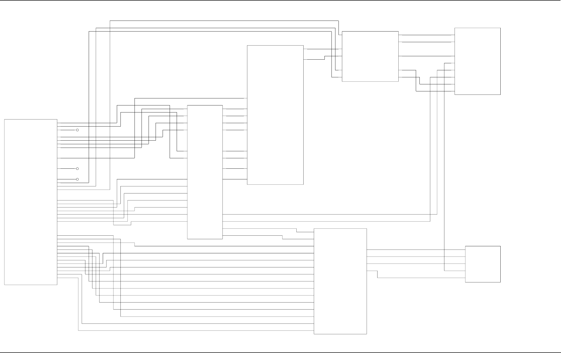
Schematics, Component Location Diagrams, and Parts Lists: HUD4022A/HUD4025B (VHF) Main Board 7-3
6881096C74-B May 25, 2005
7.2 HUD4022A/HUD4025B (VHF) Main Board
Figure 7-1. HUD4022A/HUD4025 Main Board Overall Block Diagram and Interconnections
SHEET 1 OF 23
9.3V_FROM_FGU
9.3V_TO_IF
IF_OUT_IF
LO_IN
RF_ATTN_1_A
RF_ATTN_2_A
RF_IN
73D02970C73-O
SCKA_FGU
SYN_SEL
VCURRENT
VFORWARD
VGBIAS_1
VGBIAS_2
VGBIAS_3
VREVERSE
VTEMP
CLKOUT_1
DOUTA_1
FREF
5V_FROM_CONTR
5V_TO_FGU
5V_TO_IF
FS_1
IF
PC_1
PD_1
PE_1
5V_IF
5V_TO_FE
9.3V_FROM_FE
9.3V_TO_CONTR
IF_IN
IF_OUT
RF_ATTN_2_B
RF_ATTN_2_C
RF_ATTN_3_B
RF_ATTN_3_C
5V_FE
ABACUS3_CS
ABACUS_SSI_CLK
ABACUS_SSI_FSYNC
ABACUS_SSI_RXD
AUX_5V
K9.1V
LOCK_DET
MODIN
MOSIA_ABACUS
MOSIA_FGU
RFPA_CNTRL
RX_ATTEN_1
RX_ATTEN_2
RX_ATTEN_3
RX_FILT_1
SCKA_ABACUS
VFORWARD
VFORWARD_ON
VGBIAS1
VGBIAS2
VGBIAS3
VREVERSE
VREVERSE_ON
VTEMP
16.8_MHZ
5V_ABACUS
9.3V_ABACUS
9.3V_FGU
A+_1
A+_2
A+_3
A+_4
NC
NC
A+_1
A+_2
A+_3
A+_4
K9.1V
K9.1V_FGU
K9.1V_ON
RFPA_CNTRL
RFPA_OUT
TX_INJ
VCURRENT
K9.1
Lock_Det
MOD_IN
PC_2PC_3
PD_2
PD_3
PE_2PE_3
RX_Inj
SPI_CLK
SPI_DATA
SYN_SEL
TX_INJ
NC
RFPA_OUT
RX_IN
VFORWARD_ON
VREVERSE_ON
16_8MHz
16_8_CONT
5V_Reg
9.3V_1 9.3V_2
CLKOUT_2
CLKOUT_3
DOUTA_2
DOUTA_3
FS_2FS_3
B(,1),A(,0)
0
B(,1),A(,1)
0B(,1),A(,0)
B(,1),A(,1)
B(,1),A(,1)
0B(,1),A(,0)
0B(,1),A(,0)
B(,1),A(,0)
0
K9.1V_ON
B(,1),A(,0)
0
B(,1),A(,1)
B(,1),A(,1)
B(,1),A(,1)
0B(,1),A(,0)
B(,1),A(,0)
0
B(,1),A(,0)
0
B(,1),A(,1)
B(,1),A(,0)
0
0B(,1),A(,0)
0B(,1),A(,0)
B(,1),A(,0)0
B(,1),A(,0)
0
B(,1),A(,1)
B(,1),A(,1)
B(,1),A(,1)
B(,1),A(,1)
B(,1),A(,1)
B(,1),A(,0)
0
RFPA
CONTROLLER
FGU Interface EF_FE/IF_ Interface RF_BE_ Interface
RFPA_ Interface
FGU
RX_BE
RX_IF
RX_FE
ON
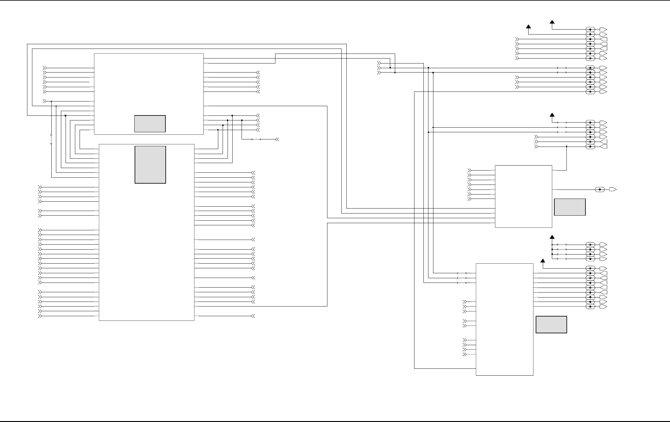
7-4 Schematics, Component Location Diagrams, and Parts Lists: HUD4022A/HUD4025B (VHF) Main Board
May 25, 2005 6881096C74-B
Figure 7-2. HUD4022A Controller Block Diagram and Interconnections (Sheet 1 of 2)
RX_BE_INTERFACE
RFPA_INTERFACE
FGU_INTERFACE
INTERFACE, SECURE, DC SUPPLY
IF0036
MUX_RX
MUX_TX
RX_FILT_AUDIO
SAP_DCLK
SAP_FSYNC
SAP_RX
SAP_TX
SPI_MOSIA
SPI_SCKA
SPKR+
SPKR-
IF0004
AUDIO_PA_EN
AUX_MIC
AUX_RX
AUX_TX
CODEC_PWR_DOWNEEPOT_2_CS*
EEPOT_3_CS*
EEPOT_CS*
EEPOT_INC*
EEPOT_U_D*
MIC_HI
MUX_AUX_TX
MUX_MICATTEN
IF0029
IF0033
A+
IF0022
IF0021
IF0002
IF0001
IF0020
IF0024
9.3V
IF0000
K9.1V_EN
MISOA
MOSIA
PA_EN
PWR_RANGE
RFPA_CNTRL
RX_FILT_1
SCKA
VCURRENT
VFORWARD
VGBIAS_1
VGBIAS_2
VGBIAS_3
VREVERSE
VTEMP
AD_EN
DA_EN
EEPOT_4_CS*
EEPOT_5_CS*
EEPOT_PC_INC*
EEPOT_PC_U_D*
IF0011
16.8_MHZ
AUX_MIC
AUX_TX
DAC_SSI_CLK
DAC_SSI_FSYNC
DAC_SSI_TXD
MIC_TUNE_EN
MODEM_EN
MODIN
RESET
RX_FILT_AUDIO_IN
RX_FILT_AUDIO_OUT
URCHIN_EN
IF0028
IF0017
UTXD1_USB_VPOUT
UTXD2
VIP_IN_1_3V
VIP_IN_2_3V
VIP_OUT_1_3V
VIP_OUT_2_3V
VPP
WAKEUP
IF0009
SPI_SCKB
SPKR+
SPKR-
SSI_INT*
SW_B+_SENSE
UCTS1_USB_FSEN
UCTS2
URTS1_USB_XRXD
URTS2
URXD1_USB_VMIN
URXD2
USB*_RS232_EN
USB_INT*
USB_TXENB
USB_VMOUT
USB_VPIN
NAUTILUS_CS*
NAUTILUS_INT*
ONE_WIRE
PTT*
RIA_USBSUSP
RX_FILT_AUDIO
SAP_DCLK
SAP_FSYNC
SAP_RX
SAP_TX
SB96_RS232*_EN
SOFT_TURN_OFF
SPARE_1
SPARE_2
SPI_MISOB
SPI_MOSIB
BOOT*
BUS_PWR_OUT
CABLE_DET
CHAN_ACT
EMERG_SENSE
ENC_RESET
ENC_SPARE1
ENC_SPARE2
FORCE_FAIL*
IGNITION_SENSE
LHRST_IN
LHRST_OUT
LV_DETECT
MIC_HI
MOD
MONITOR
IF0008
AUX_MIC
AUX_RX
AUX_TX
9.3V_ABACUS
IF0005
IF0023
IF0035
IF0031
IF0013
IF0007
IF0030
IF0019
IF0032
IF0016
IF0010
IF0018
IF0003
IF0025
K9.1V
IF0026
IF0012
IF0027
5V_ABACUS
SPARE_2
SPARE_1
SAP_RX
SAP_FSYNC
SAP_DCLK
8KHZ_DSP_INT
MUX_MICATTEN
EEPOT_PC_INC*
A+_4
A+_3
RX_ATTEN_1RX_ATTEN_1
BUS_PWR_OUT
16.8_MHZ
16.8_MHZ
16.8_MHZ
MIC_TUNE_EN
MODEM_EN
DAC_SSI_TXD
DAC_SSI_CLK
DAC_SSI_FSYNC
URCHIN_EN
RESET
SAP_TX
EEPOT_6_CS*
EEPOT_3_CS*
EEPOT_2_CS* CODEC_PWR_DOWN
AUDIO_PA_EN
ONE_WIRE
MONITOR
MODIN
ABACUS3_CSABACUS3_CS
MUX_TX
MUX_RX
MUX_AUX_TX
EEPOT_U_D*
EEPOT_INC*
EEPOT_1_CS*
VIP_IN_2_3V
VIP_IN_1_3V
CHAN_ACT
SPI_MOSIA
SPI_SCKA
SPI_MISOA
SSI_INT*
ABACUS_SSI_CLK ABACUS_SSI_CLK
AUX_5VAUX_5V
TX_PA_EN
MOSIA
MISOA
KEYED_9.1_EN
EEPOT_PC_U_D*
EEPOT_5_CS*
EEPOT_4_CS*
DA_SEL
AD_SEL
VGBIAS_1
VIP_OUT_2_3V
VIP_OUT_1_3V
VREVERSE
VGBIAS_3
VGBIAS_2
VFORWARD
VCURRENT
SCKA
RX_FILT_1
RFPA_CNTRL
PWR_RANGE
ENC_RESET
EMERG_SENSE
CABLE_DET
BOOT*
SYN_SEL SYN_SEL
LOCK_DET LOCK_DET
A+_2
A+_1
VTEMP
NAUTILUS_INT
NAUTILUS_CS*
MOD
LV_DETECT
LHRST_OUT
LHRST_IN
IGNITION_SENSE
FORCE_FAIL*
ENC_SPARE2
ENC_SPARE1
UCTS1_USB_FSEN
SW_B+_SENSE
SPI_MOSIB
SPI_MISOB
SOFT_TURN_OFF
SPI_SCKB
SB96_RS232*_EN
RIA_USBSUSP
PTT*
USB_TXENB
USB_INT*
USB*_RS232_EN
URXD2
URXD1_USB_VMIN
URTS2
URTS1_USB_XRXD
UCTS2
RX_ATTEN_2RX_ATTEN_2
SCKA_ABACUS
MOSIA_ABACUS
WAKEUP
VPP
UTXD2
UTXD1_USB_VPOUT
USB_VPIN
USB_VMOUT
9.3V_FGU
SCKA_FGU
MOSIA_FGU
ABACUS_SSI_RXDABACUS_SSI_RXD
ABACUS_SSI_FSYNCABACUS_SSI_FSYNC
9.3V_ABACUS
5V_ABACUS
RX_ATTEN_3RX_ATTEN_3
K9.1V
AUDIO
POWER CONTROL
AD5320/SCF Block
MAEPF-27827-O
Part Series
200
Part Series
300
400
500
600
Part Series
900-1
Part Series
900-2
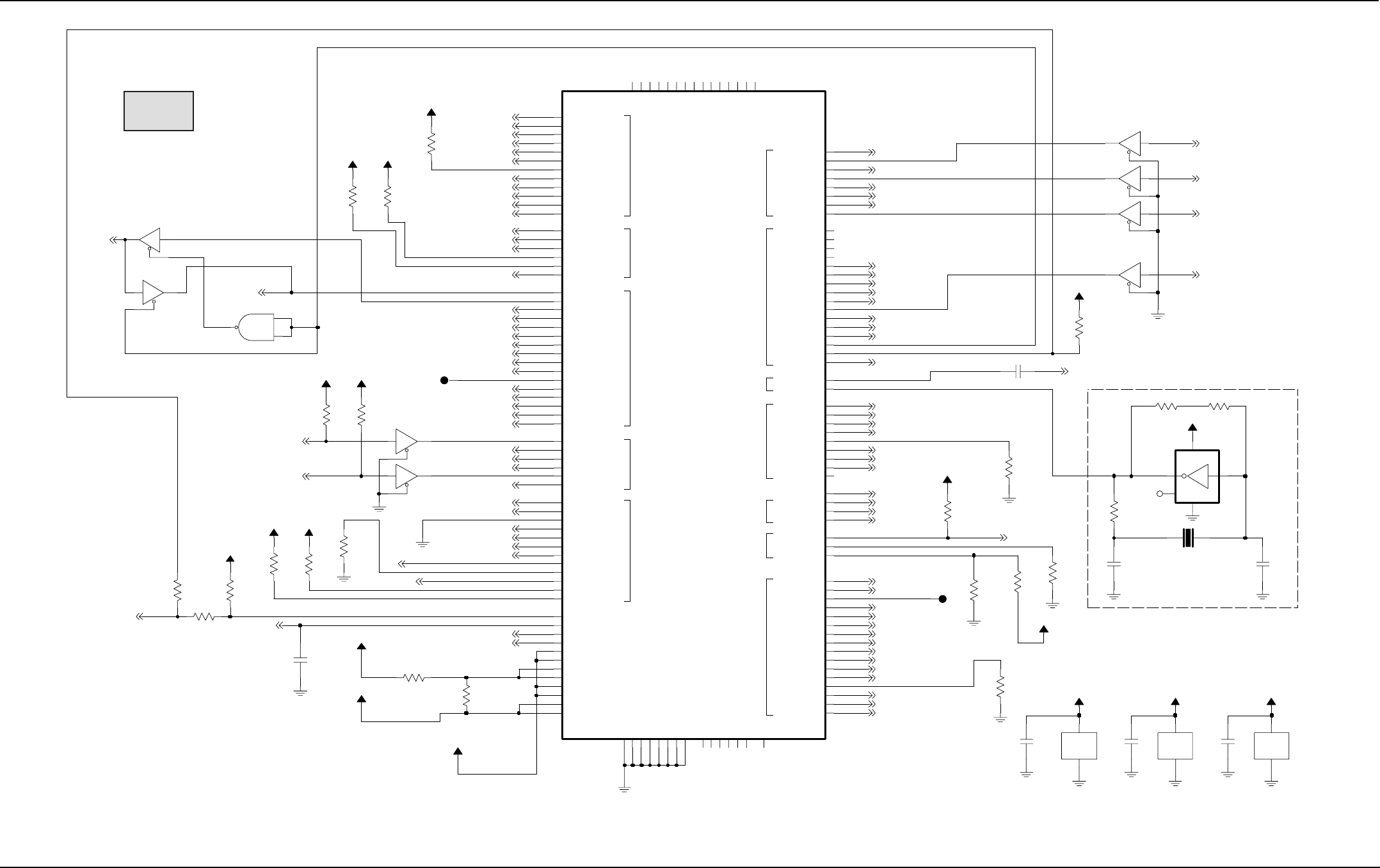
Schematics, Component Location Diagrams, and Parts Lists: HUD4022A/HUD4025B (VHF) Main Board 7-5
6881096C74-B May 25, 2005
Figure 7-3. HUD4022A Controller Block Diagram and Interconnections (Sheet 2 of 2)
NP
For Patriot RAM, R0125 is not placed, R0124 is placed for a 1
For Patriot BRAVO, neither R0124 or R0125 is placed for a 1
32kHz Oscillator Circuit
NP
For Non-HAB: R0114 Placed
R0113, R0115 Not Placed
R0113, R0115 Placed
NP
For HAB: R0114 Not Placed
NP
For Patriot RAM and BRAVO, R0124 is not placed, R0125 is placed for a 0
NP
NP
NP
NP
For Patriot RAM, R0107 NP, R0108 Placed
For Patriot BRAVO, R0108 NP, R0107 Placed
NC
VCC2.85
C0106
100pF
GND
3
2
NC
1
4
VCC 5
10K
U0102
TC7SU04F
12
13
11
R0124
MC74LCX125
U0103-4
VCC2.85VCC2.85
VDD_CORE_2
VDD_EIM_1
F2
G1 VDD_EIM_2
Y18 VDD_IO_1
X18 VDD_IO_2
G18 VPP
VSIM1
N18
P18 VSIM2 VCC2.85
Z6
URTS1_PA13 Z2
URTS2_PB3 Z5
URXD1_PA15 Y3
URXD2_PB1 Y4
UTXD1_PA14 Z3
UTXD2_PB0 Z15
S18 VDD_CORE_1
R18
D1
TOUT4 E1
TOUT5 I1
P17
TOUT6
TOUT7 E2
TOUT8 G2
TOUT9 F1
Y2
UCTS1_PA12
UCTS2_PB2
TOUT1
TOUT10 N17
TOUT11 J1
I2
TOUT12
TOUT13 B1
TOUT14 S17
TOUT15 C2
TOUT2 D2
TOUT3
A2
X2 SRDA
SRDB V2
S2
SRDB2
STBY_PD14
H18
STDA
W2
STDB V1
TOUT0 H1
C1
N2
L1 SPI_CS2_PE4
SPI_CS3_PE6
K2
P2 SPI_CS4_PE7
SPI_CS5_PE11
B4
SPI_CS6_PE0
N1
SPI_CS7_PE1
M2
SPI_CS8_PE2
A3
SPI_CS9_PE3
L18
SPIA_CLK
K1
L2 SPIA_MISO
M1 SPIA_MOSI
SPIB_CLK
P1
SPIB_MISO
R1
SPIB_MOSI
R2
SPI_CS0_PE10
J2
SPI_CS1_PE5
I18
SIM_D1RX_PB11
F17
K17 SIM_D1TX_PB10
E18 SIM_PD0_PB9
SIM_PD1_PB15
B15
SIM_RST0_PB6
V18
SIM_RST1_PB12
G17
SIM_SVEN0_PB8
U18
SIM_SVEN1_PB14
U2
SCKA
W1
T2
SCKB
SCKB2 S1
DSC_TX_PD5 A15
SIM_CLK0_PB7
U17
SIM_CLK1_PB13
L17
SIM_D0RX_PB5
V17
SIM_D0TX_PB4
J17
ROW6 Z10
Y8
ROW7
Z1 SC0A
SC0B T1
SC1A
Y1
SC1B U1
SC2A
X1
SC2B
Y16
RESET_OUT
Y11
Y5
RIA_PA9
Y10
ROW0
ROW1 Z9
ROW2 M17
ROW3 Y9
ROW4 Y6
ROW5
Z8
PC11_OC1
D17
W18 PC12_STO
B16 PC1_USBTXENB
PC8
M18
PC9
J18
PWM*_PE14
Z17 PWM_PE13
K18
RESET_IN
B12
NC6 A5
NC7 B14
B8
NC8
NC9 B7
OC3_PC13
B18
OWIREDAT_PC10 Z18
PA2_USBVPIN
Y7
PC0_UBSVMOUT
A6
A13 NC18
NC19
A14
NC2 A8
NC20
A16
NC21
B2 NC3 B5
NC4 A7
NC5
A11
NC10 B6
NC11 B10
NC12 A17
A9
NC13
NC14 B11
NC15 A12
NC16
B13
NC17
Z12
INT1_PE9
Z13
INT2_PC14
Y14
INT3_PC15
C17
INT4_PA6_OPTSEL1
Z11
INT5_PA7_OPTSEL2
Y12
T17 MOD
MUX_CTRL Z4
NC1
B3
GND12
H17
GND5
I17
GND6
A18
GND7
B17
B9 GND8
GND9
A10
HW_ID
D18
INT0_PE8
Z14
W17
COLUMN6
COLUMN7 R17
DCDA_PA8 Z7
DSC_RX_PD6 C18
DSRA_INT6_PA10 E17
DTRA_INT7_PA11 F18
A4 GND10
GND11
H2
A1
CKIL
CLKSEL_PD15
T18
COLUMN0 X17
COLUMN1 Y15
COLUMN2 Y13
COLUMN3 Y17
COLUMN4 Z16
COLUMN5
VCC1.8
U0001
33C34
CKIH
R0114
0
VCC2.85
3
MC74LCX125
U0104-4
12
13
11
MC74LCX125
U0104-1
2
1
MC74LCX125
2
1
3
18pF
U0103-1
TP0002
1
C0101
U0103-2
MC74LCX125
5
4
6
R0104
10K
R0108
0
VCC2.85
10K
R0120
R0103
10K
VCC2.85
VCC2.85
VCC2.85
VCC2.85
R0122
3.3K
PWR_GND
U0105-2
GND
3
VCC
5
R0107
0
VCC2.85
PWR_GND
U0103-5
GND
7
VCC
14
R0116
10MEG
MC74LCX125
5
4
6
U0104-2
R0101
10K
R0109
10K
R0111
R0117
3.3K
VCC2.85
10MEG
C0105
0.1uF
0.1uF
C0103
PWR_GND
U0104-5
GND
7
VCC
14
0.1uF
C0104
VCC2.85
10K
R0125
VCC2.85
R0123
3.3K
32.768KHz
CC4V Y0100
21
R0105
10K
R0102
10K
R0106
10K
R0119
470K
R0110
10K
VCC2.85
10K
R0121
VCC1.55
TP0005 1
0.1uF
C0102
18pF
R0113
10K
C0100
MC74LCX125
U0104-3
9
10
8
R0115
0
U0105-1
TC7S00FU
1
2
4
VCC2.85
MC74LCX125
U0103-3
9
10
8
HAB_DISABLE
HAB_MOD
16.8_MHZ
16.8_MHZ_PATRIOT
ONE_WIRE
BRD_ID_4
BUS_PWR_OUT
BRD_ID_1
BRD_ID_7
BRD_ID_6
USB*_RS232_EN
MOD MOD*
SPI_MISOA
SPI_MOSIA*
MISO_SEL
SPI_MOSIA
FORCE_FAIL*
SPARE_2
SPARE_1
ABACUS_SSI_FSYNC*
ABACUS_SSI_CLK*
ABACUS_SSI_RXD
LOCK_DET
LOCK_DET*
TX_PA_EN
SSI_INT*
PTT
MONITOR*
PTT*
MONITOR
LV_DETECT
EEPOT_5_CS*
MILL_ID
BRD_ID_2
PWR_RANGE
SW_B+_SENSE
BRD_ID_0
BRD_ID_3
MODEM_EN
ABACUS_SSI_RXD*
DAC_SSI_CLK
ABACUS_SSI_FSYNC
ABACUS_SSI_CLK
SPI_MOSIB
NAUTILUS_CS*
EEPOT_4_CS*
RX_ATTEN_3
SB96_RS232*_EN
32_KHZ
NAUTILUS_INT
RX_ATTEN_2
RX_ATTEN_1
EEPOT_PC_U_D*
EEPOT_PC_INC*
SOFT_TURN_OFF
MUX_MICATTEN
VIP_OUT_2_3V
VPP
SAP_RX
SAP_TX
DA_SEL
ABACUS3_CS
AD_SEL
EEPOT_3_CS*
SYN_SEL
MUX_AUX_TX
SPI_SCKA
EEPOT_U_D*
AUDIO_PA_EN
EEPOT_1_CS*
EEPOT_INC*
EEPOT_2_CS*
SAP_DCLK
SAP_FSYNC
RESET
CODEC_PWR_DOWN
USB_TXENB
8KHZ_DSP_INT
USB_VMOUT
USB_VPIN
CABLE_DET
USB_INT*
SPI_MISOB
SPI_SCKB
MIC_TUNE_EN
UTXD2
UTXD1_USB_VPOUT
URXD2
URXD1_USB_VMIN
URTS2
URTS1_USB_XRXD
UCTS2
UCTS1_USB_FSEN
AUX_5V
MUX_TX
MUX_RX
LHRST_OUT
LHRST_IN
DAC_SSI_TXD
URCHIN_EN
KEYED_9.1_EN
DAC_SSI_FSYNC
ENC_SPARE1
EMERG_SENSE
VIP_OUT_1_3V
VIP_IN_2_3V
RIA_USBSUSP
BRD_ID_5
VIP_IN_1_3V
ENC_SPARE2
WAKEUP
BOOT*
ENC_RESET
IGNITION_SENSE
GP10/EGPT/MISC
INT
QSPI
SAP
SIM
BBP
LAYER1_TIMER
CLKS
UART_A
UART_B
DSC OWIRE
KEYPAD
MAEPF-27828-O
Part Series
100-1
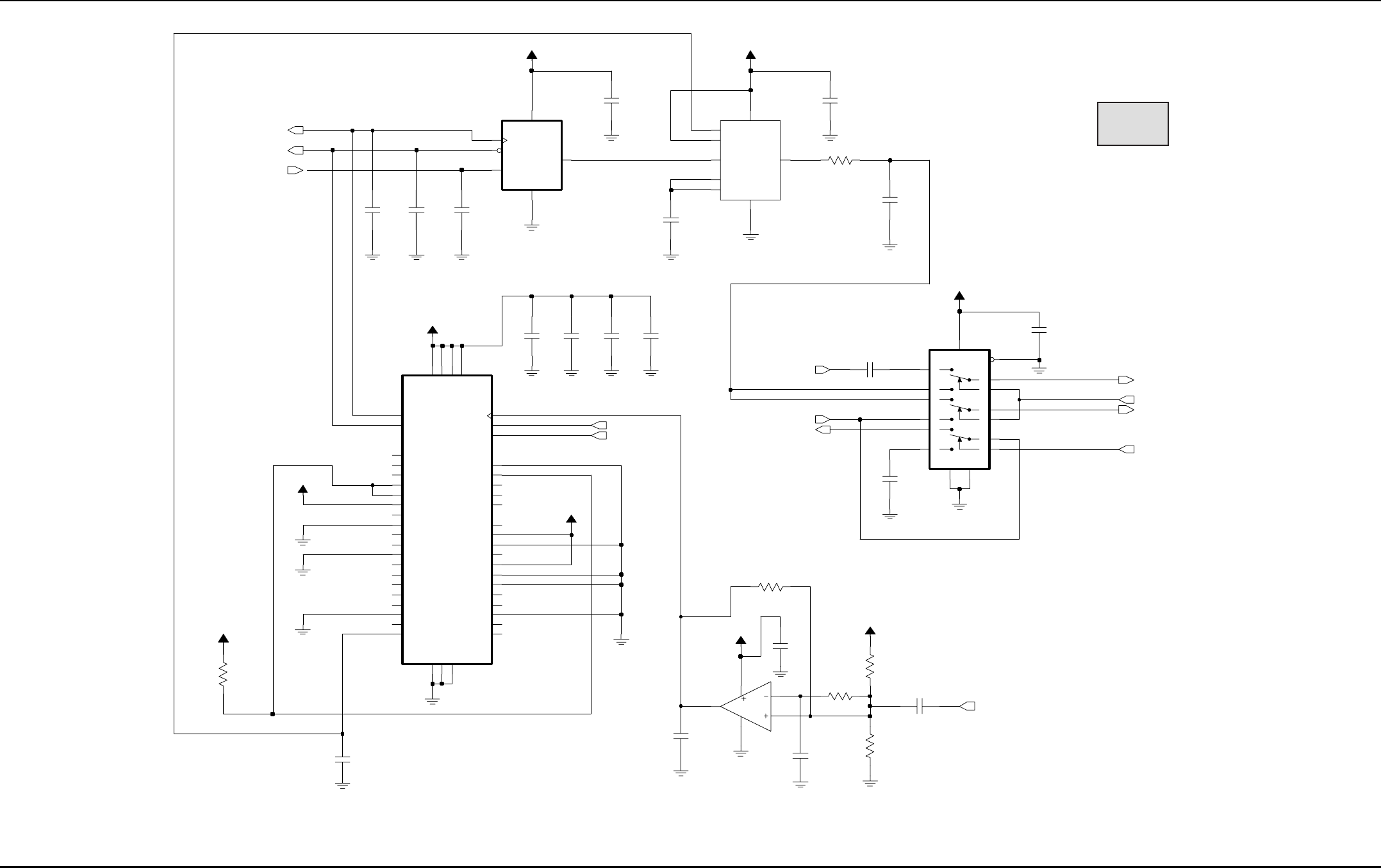
7-6 Schematics, Component Location Diagrams, and Parts Lists: HUD4022A/HUD4025B (VHF) Main Board
May 25, 2005 6881096C74-B
Figure 7-4. HUD4022A Controller Urchin IC, MUX, and AD5320 DAC Schematic
NP
0.1uF
C0901
C0917
100pF
R0903
100K
C0906
VCC2.85
0.1uF
C0918
100pF
VCC2.85
R0904
100K
4DIN
2GND
5SCLK
6SYNC
3
VDD
1
VOUT
AD5320BRT
U0900
VCC2.85
C0910
0.1uF
4
3
1
5
2
R0901
8.2K
LMV7219
U0903
C7
VCC2 E2
VCC3 G4
VCC4
VCC2.85
C0909
0.1uF
B6
NC8 C2
NC9
A6
RESET
E5
TCK B1
TDI
TDO B7
D2
TMS
B3
VCC1
G3 NC29
NC3 A4
NC30
G5
G6 NC31
A7
NC4 B2
NC5 B4
NC6
NC7 B5
F1 NC21
F2 NC22
F3 NC23
F4 NC24
F5 NC25
F6 NC26
F7 NC27
G2 NC28
D3 NC14
D4 NC15
D6 NC16
D7 NC17
E1 NC18
E4 NC19
A2
NC2
E7 NC20
C3
G7 2.4_MHZ
G1 48_MHZ
A1
NC1
C4
NC10 C5
NC11 C6
NC12
D1 NC13
A3
16.8_CLK
C1
ENABLE
A5 GND1
E3 GND2
E6 GND3
JTAG_EN
C0915
VCC2.85
XCR3032XL
U0901
IN
2
6OS
OUT 5
7SHDN
4
VDD
100pF
MAX7414
FL0900
CLK
8
1COM
GND
3
C0905
0.1uF
VCC2.85
R0902
100K
C0904
C0908
0.1uF
VCC2.85
220pF
R0900
100K
0.1uF
C0903
VCC2.85
C0919
C0907
0.1uF
100pF
C0914
33pF
Z1
3
100pF
C0911
14
X
12 X0
X1
13
15
Y
2Y0
1Y1
4
Z
5Z0
A11
10
B
9
C
6
EN
8GND
16
VCC
7VEE
VCC2.85
MC74HC4053
U0902
100pF
C0912
C0902
R0905
100K
0.1uF
0.1uF
C0916
C0913
100pF
MODIN
SCF_OUT
MIC_TUNE_EN
URCHIN_EN
RESET AUX_TX
AUX_MIC
DAC_SSI_CLK
DAC_SSI_TXD
16.8_MHZ_DC
RX_FILT_AUDIO_IN
RX_FILT_AUDIO_OUT
16.8MHZ_SQARE
DAC_SSI_FSYNC
MODEM_EN
16.8_MHZ
AD5320_OUT
MAEPF-27836-O
Part Series
900-1
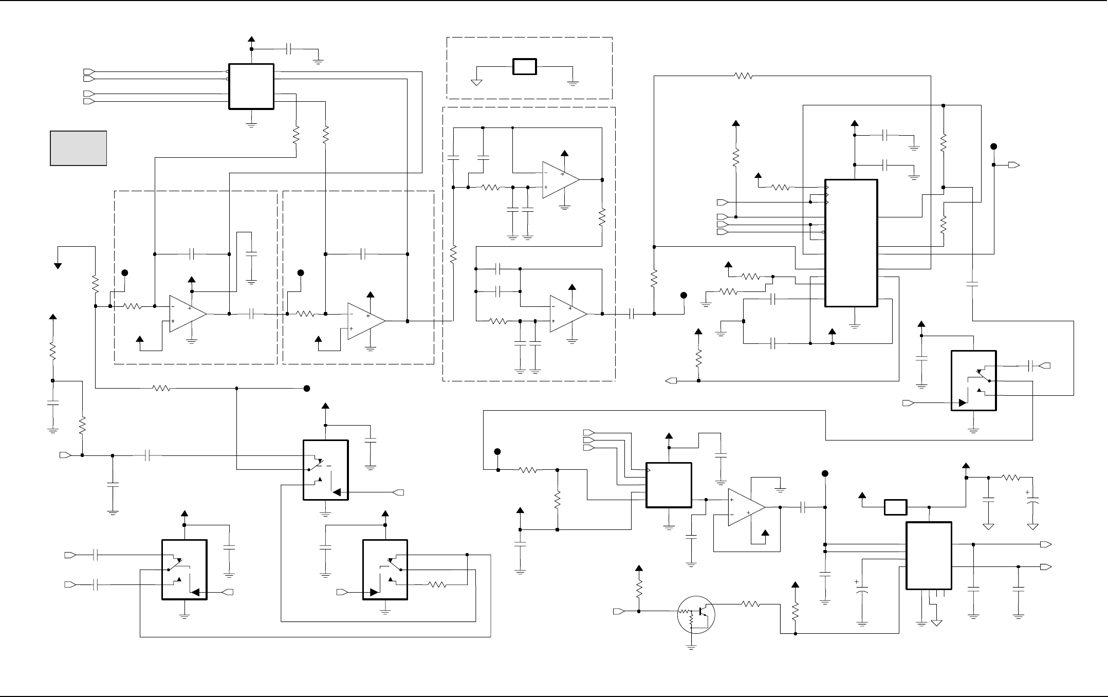
Schematics, Component Location Diagrams, and Parts Lists: HUD4022A/HUD4025B (VHF) Main Board 7-7
6881096C74-B May 25, 2005
Figure 7-5. HUD4022A Controller Audio Schematic
AUDIO_GROUND
NP
-14 dB to +14 dB
-9 dB to +14 dB
Programmable pre-amp stage Programmable pre-amp stage
Anti-aliasing filter
Ground
7 dB Attenuation Stage
UNIVERSAL GROUND
SW_A+
VAG
0.1uF
C0224
R0227
0.1uF
68K
0.1uF
C0216
C0201
VAG
A+_FILT
R0206
100K
C0205
10uF
C0220
150pF
33K
R0228
VAG
10K
C0226
0.1uF
R0222
1IN
4
NC
6
NO
VPOS 2
VCC2.85
NLAST4599
U0210
5
COM
GND
3
R0207
7.5K
R0203
1K
VPOS 2
470pF
C0230
NLAST4599
U0208
5
COM
GND
3
1
IN
4NC
6
NO
0.1uF
C0242
R0208
100K
VCC2.85
C0207
33pF
R0236
9.1K
R0226
36K
R0212
100K
C0240
0.1uF
C0206 470pF
C0235
1uF
1
10uF
C0221
VCC2.85
VCC2.85
TP0200
C0204
4.7uF
A+
10K
VAG
TP0205
1
VCC5
R0221
C0210
0.1uF
1uF
C0208
U0201-4
MC33204
13
12
14
4
11
LM7301
U0207
4
3
1
2
5
3300pF
C0217
4.7uF
Q0200
C0223
R0210
100K
0.1uF
C0239
R0209
10K
560
R0204
COM
5
GND
3
IN
1
NC 4
NO
6
2
VPOS
VCC2.85
U0203
NLAST4599
0.1uF
C0227
VCC2.85
R0235
10K
R0225
10K
150pF
C0228
220pF
C0233
0
R0231
VCC2.85
1K
C0214
VCC2.85
R0200
C0225
0.1uF
VCC2.85
0.1uF
R0224
10K
19 TI_POS
20
VAG
1VAGREF
6
VDD
15 VSS
11 MCLK
10 PDI
3PI
4
PO_NEG 5
PO_POS
2
RO_NEG
17
TG
18 TI_NEG
9BCLKR
12 BCLKT
8DR
13
DT
7FSR
14 FST
16 HB
VCC2.85
MC145483
U0200
7
VCC
R0223
18K
10 GND3
GND4
11
9INV
8M_SS
1NINV
4
OUT1
6
OUT2
3RR
U0204
TDA1519C
2GND1
GND2
5
VREFIN
0.1uF
C0234
6CLK
5DATA
3GND
8IN
4LOAD
2
OUT
7
VDD
1
C0209
0.1uF
LM1971
U0206
C0232
18K
R0220
470pF
C0212
1
0.1uF
47K
TP0206
100pF
R0205
MC33204
6
5
7
4
11
C0211
U0201-3
MC33204
9
10
8
4
11
VCC5
U0201-2
TP0203
1
1K
R0219
VAG
3.3K
R0202
TP0202
1
C0238
220pF
C0203
0.1uF
VCC2.85
220pF
C0231
SIGNAL_CONVERT
SC0001
I1
1I2 2
R0218
1K
100K
VCC2.85
TP0201
1
R0216
0.1uF
C0215
6800pF
C0244
VCC2.85
6800pF
C0243
MC33204
U0201-1
2
3
1
4
11
C0202
0.1uF
TP0204
1
0.1uF
C0213
R0230
C0236
470pF
NO
VPOS 2
9.3V_TX
33K
NLAST4599
U0209
5
COM
GND
3
1
IN
4NC
6
68K
R0229
I1
1I2 2
VCC2.85
SIGNAL_CONVERT
SC0002
W1 4
W2 7
VCC2.85
C0237
220pF
CS1
1
CS2
10
GND
8
INC
9L1 5
6
L2
U_D
2
VDD 3
MIC_PREAMP_OUT
RX_FILT_AUDIO
SPKR+
SPKR-
U0202
MAX5452
AUX_RX*
MIC_HI*
AUX_TX_B
CODEC_OUT_C
RX_AUDIO_IN
MUX_AUX_TX
AUX_MIC*
AUX_TX*
AUX_MIC
AUX_TX
MIC_PREAMP_IN
VOLUME_IN
EEPOT_U_D*
EEPOT_INC*
SPI_SCKA
SPI_MOSIA
EEPOT_3_CS*
MUX_MICATTEN
VOL_OUT*
VOL_OUT
CODEC_OUT
AUX_TX_A
CODEC_OUT_B
MIC_M
MIC_A
MIC_C
MIC_B MIC_E MIC_K
MIC_N
CODEC_OUT_A
MIC_L
MIC_G
MIC_J
MIC_I
MIC_F
MIC_H
EEPOT_CS*
AUX_RX
SAP_FSYNC
SAP_TX
SAP_DCLK
AUDIO_PA_EN
MUX_TX
MUX_RX
EEPOT_2_CS*
MIC_HI
MIC_D
AUDIO_PA_IN
SAP_RX
CODEC_PWR_DOWN
47K
47K
MAEPF-27837-O
Part Series
200

7-8 Schematics, Component Location Diagrams, and Parts Lists: HUD4022A/HUD4025B (VHF) Main Board
May 25, 2005 6881096C74-B
Figure 7-6. HUD4022A/HUD4025B Controller Power Control (Sheet 1 of 2)
REVERSE_POWER
FORWARD_POWER
VTEMP
VCURRENT
A+
VCONTROL
1%
1%
1%
1%
1%
1%
1%1%
1%
1%
1%
1%
TO SHEET 2
73D02970C73-O
SHEET 7 OF 23
AD_EN
TX_DISABLE
LOOP_DISABLE
*C0924*
.047uF
6.2
*R0917*
680
*R0916*
9.3V_TX
1K
R0915
100pF
C0922
100pF
*C0923*
*R0948*
1K
*D0954* 0
R0935
4.7K
*R0933*
R0932
*R0946*
0
100K
C0957 0.1uF
10K
R0998
10K
R0999
VCC3
1.2K
R0997
10K
R0996
20K
R0960
D
G
S
*R0992*
100K
Q0955
3.9K
R0994
1.2K
R0995
*R0986*
0
R0985
0
0
R0984
0
*R0980*
0
R0979
0
R0987
0
R0953
0
R0950
TP0942
TEST_POINT
1
4.7uF
C0945
8.2K
9.3V_TX
20K
*R0942*
*R0943*
10K
R0944
*R0945*
33K
5
VCC
VCC2.85
0.1uF
C0944
2
1
4
U0963
PWR_GND
3
GND
VCC3
NC7SZ125
U0963
C0936
0.1uF
1
2
4
PWR_GND
U0954GND
3
VCC
5
10 VIN7
11 VIN8
1VREF
U0954
MC74VHC1G00
14 TFS
20
VDD
3VIN1
5VIN2
6VIN3
7VIN4
8VIN5
9VIN6
4AGND
19 CONVST
2CREF
13 DGND
17 DIN 16
DOUT
15 RFS
18 SCLK
S
AD7812
U0953
12 A0
4
Q0954
D
G
MC74VHC1G00
U0958
1
2
C0979
9.3V_TX
VCC3
C0980
0.1uF
0.1uF
D0952
1
0.1uF
C0974
TP0958
TEST_POINT
1
TP0952
TEST_POINT
1
TP0956
TEST_POINT
1
1
TP0953
TEST_POINT
TP0955
TEST_POINT 1
TP0954
TEST_POINT
1
TP0961
TEST_POINT
1
TP0964
TEST_POINT
1
TP0963
TEST_POINT
1
TP0962
TEST_POINT
1
*Q0953*
TP0960
TEST_POINT
U0958
PWR_GND
3
GND
5
VCC
VCC3
13
12
14
4
11
9.3V_TX
MC33204
U0955
2
3
1
4
11
LMC6484
U0956
MC33204
U0955
13
12
14
4
11
MC33204
U0955
9
10
8
4
11
MC33204
U0955
6
5
7
4
11
0
R0966
0
R0965
C0976
100pF
C0963
100pF
C0964
100pF
C0965
100pF
VCC3
C0966
100pF
6
5
7
4
11
VCC3
VCC3
9.3V_TX
9.3V_TX
VCC3
9
10
8
4
11
MC33204
U0957
TP09591
MC33204
U0957
TEST_POINT
TEST_POINT
TP0957
1
C0959
0.1uF
*C0962*
9.3V_TX
24K
100pF
R0963
2
3
1
4
11
R0964
24K
100pF
U0956
LMC6484
3
W1 4
W2 7
C0983
CS1
1
CS2
10
GND
8
INC
9L1 5
L2 6
U_D
2
VDD
10K
U0952
MAX5452
10K
R0968
R0978
10K
*R0969*
*R0976*
1K
56K
R0989
10K
R0988
12
14
4
11
5.1K
R0990
U0957
MC33204
13
2.7K
R0981
1K
R0983
2
3
1
4
11
100K
R0982
U0957
MC33204
10K
R0991
10K
R0975
10K
R0974
1uF
C0973
*R0977*
100
8
4
11
C0972
0.1uF
U0956
LMC6484
9
10
D0951
D0950
*R0972*
10K
10K
100pF
C0970
*R0971*
100pF
C0969
*C0971*
C0978
100pF
C0975
100pF
100pF
C0968
100pF
100pF
*C0967*
*R0973*
12K
24K
*R0970*
9.3V_TX
9.3V_TX
9.3V_TX
9.3V_TX
VCC3
7
4
11
A+
U0956
LMC6484
6
5
R0967
VCC3
100K
100K
100K
R0962
0.1uF
VCC3
VCC3
R0961
C0961
C0960
0.1uF
PWR_RANGE
RFPA_CNTRL
EEPOT_5_CS*
PA_EN
VFORWARD
VTEMP
VCURRENT
VREVERSE
MISOA
EEPOT_4_CS*
47K
47K
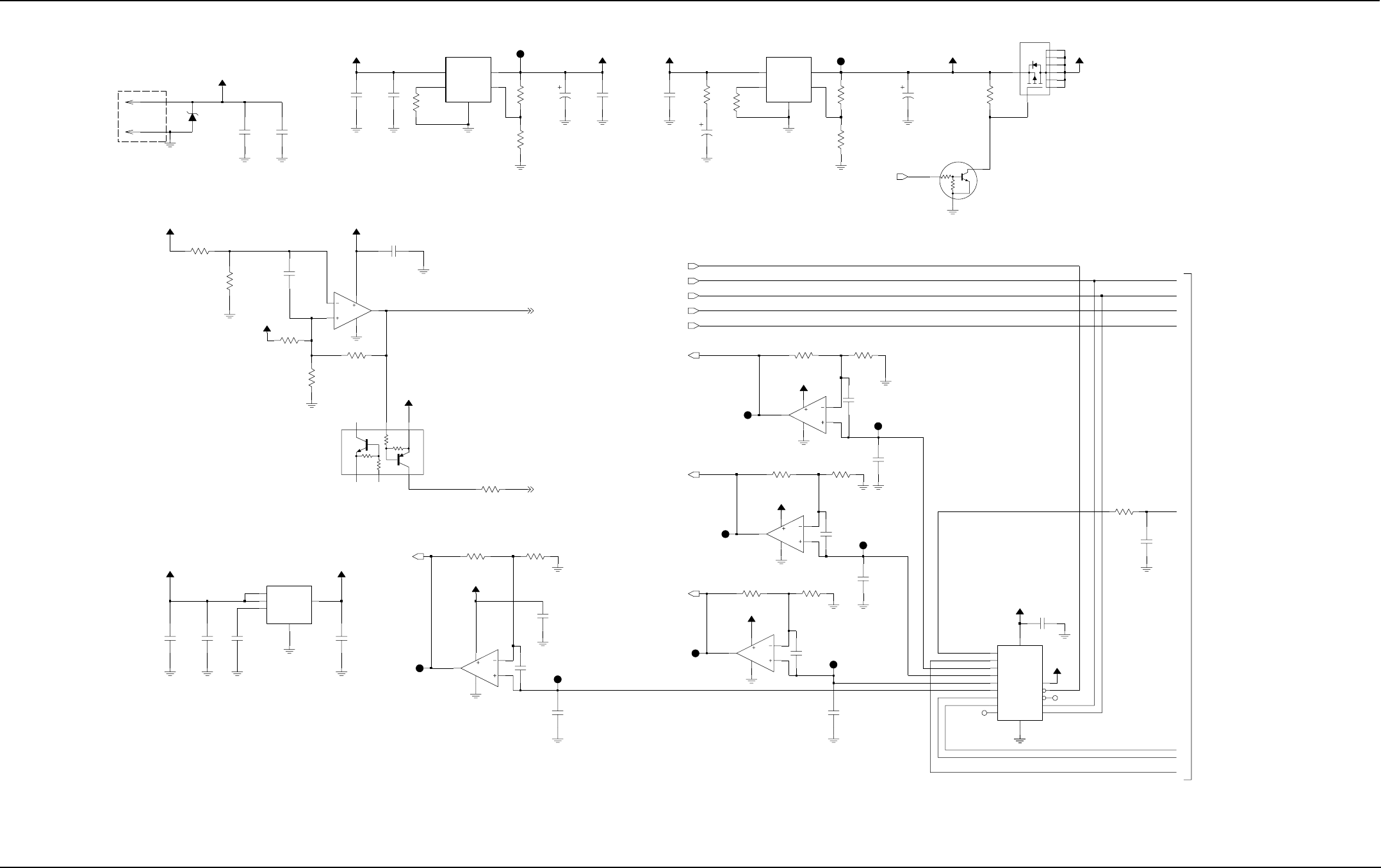
Schematics, Component Location Diagrams, and Parts Lists: HUD4022A/HUD4025B (VHF) Main Board 7-9
6881096C74-B May 25, 2005
Figure 7-7. HUD4022A/HUD4025B Controller Power Control (Sheet 2 of 2)
BATTERY CONNECTOR
9.3V REGULATOR 9.3V_TX_ REGULATOR
1%
1%
1%
1%
1%
1%
1%
1%
TO SHEET 1
*R0937*
30K0
*R0936*
100100
R0924
VCC5
R0923
1
Q0960
1
C0998
100pF
C0997
68pF
LOOP_DISABLE
1K
R0934
470pF
*C0921*
A+
*R0913*
0.1uF
C0920
130K
12K
*R0914*
VCC5
VCC5
*R0912*
3
1TX_DISABLE
5
2
12K
LMV7219
U0965
4
12K
*R0911*
R0910
82K
A+
*C0952*
0.1uF
4VOUT 5
*R0947*
0
U0951
LM2941T
ADJ 1
GND
3
ON_OFF
2
VIN
LM2941T
ADJ 1
GND
3
ON_OFF
2
VIN
4VOUT 5
2.7
U0950
C0985
R0908
SW_A+
0.1uF 0.1uF
C0986
0.1uF
C0987
VCC3
0.1uF
C0984
VCC5
C0940
0.1uF
C0943
.01uF
C0942
1uF
VIN
1VOUT 5
C0941
1uF
U0962
LP3985
BYPASS
4
GND
2
VEN
3
0.1uF
C0937
12
14
4
11
NC
NC
1
MC33204
U0960
13
TP0939
TEST_POINT
1
TP0937
TEST_POINT
1
TP0941
TEST_POINT
1
TP0936
TEST_POINT
1
TP0931
TEST_POINT
1
TP0938
TEST_POINT
1
1
TP0940
TEST_POINT
TP0951
TEST_POINT
1
TP0930
TEST_POINT
TP0950
TEST_POINT
1
15 OUTD
7OUTE
8OUTF
9OUTG
TEMP_1*
10 OUTH
5
REF
12
SCLK
4
VDD
DIN
14 DOUT
3
GND
6
LDAC
2OUTA
PWR_SET*
1OUTB
CURR_LIM_SET*
16 OUTC VCC3
MAX5259
U0959
CS 11
13
100pF
C0935
100pF
C0934
100pF
C0933
30K
*R0941*
0
*R0940*
*R0939*
30K
11
0
*R0938*
U0960
MC33204 9
10
VGBIAS_3*
8
4
U0960
MC33204 6
5
VGBIAS_2*
7
4
11
U0960
MC33204 2
3
VGBIAS_1*
1
VGBIAS_1
4
11
9.3V_TX
9.3V_TX
9.3V_TX
9.3V_TX
100pF
C0930
RX_FILT_1*
20K
R0930 R0931
EEPOT_PC_U_D*
EEPOT_PC_INC*
RX_FILT_1
10K
C0956
22uF
VGBIAS_3
C0951
1uF
100K
9.3V_TX9.3V
Q0951
R0955
1
2
3
6
7
8
4
5
SW_A+
Q0952
C0955
0.1uF
22uF
C0982
R0993
1.2K
K9.1V
VGBIAS_2
7.5K
R0954
MOSIA
DA_EN
0.1uF
C0981
C0954
K9.1V_EN
SCKA
C0950
0.1uF
J0950-2
2
0.1uF
1
2
J0950-1
1
VCC3
24V
VR0950
R0952
1.2K
R0951
7.5K C0953
22uF
47K
47K
10K
10K 10K
10K

7-10 Schematics, Component Location Diagrams, and Parts Lists: HUD4022A/HUD4025B (VHF) Main Board
May 25, 2005 6881096C74-B
Figure 7-8. HUD4025B/HUE4043A Controller Block Diagram
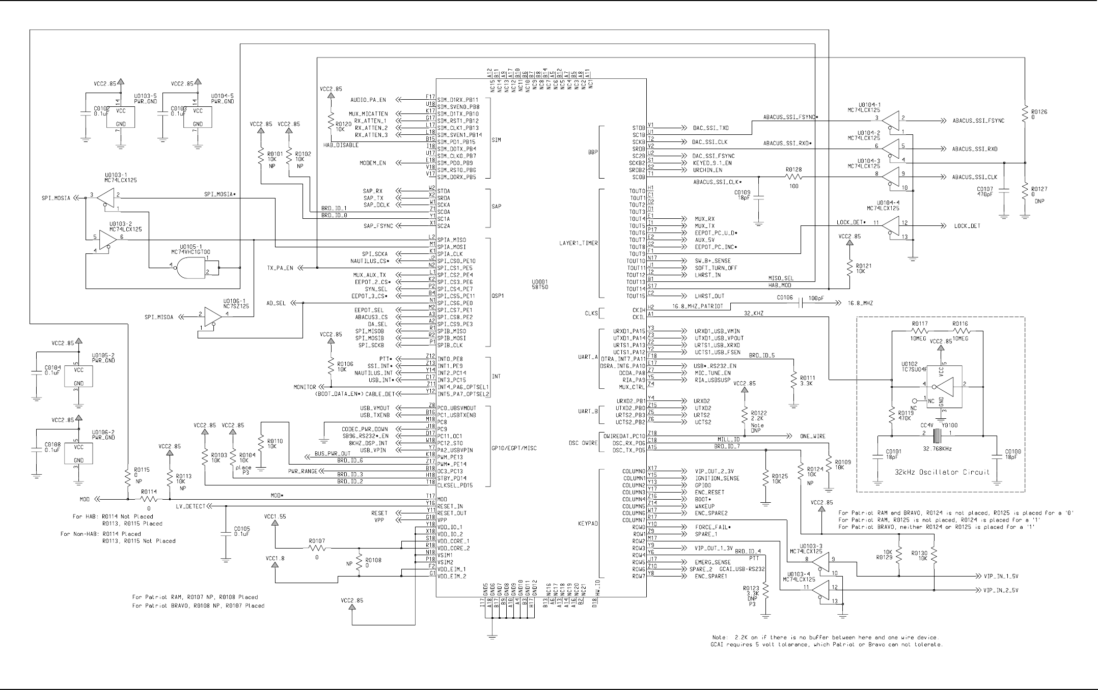
Schematics, Component Location Diagrams, and Parts Lists: HUD4022A/HUD4025B (VHF) Main Board 7-11
6881096C74-B May 25, 2005
Figure 7-9. HUD4025B/HUE4043A Controller Daughter Board Interface
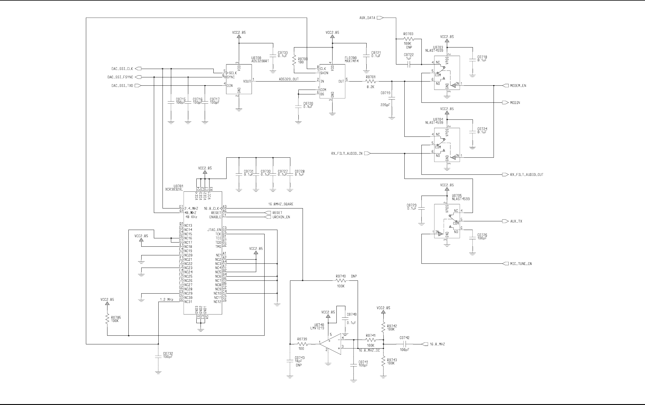
7-12 Schematics, Component Location Diagrams, and Parts Lists: HUD4022A/HUD4025B (VHF) Main Board
May 25, 2005 6881096C74-B
Figure 7-10. HUD4025B/HUE4043A Controller Urchin IC, MUX and AD5320 DAC
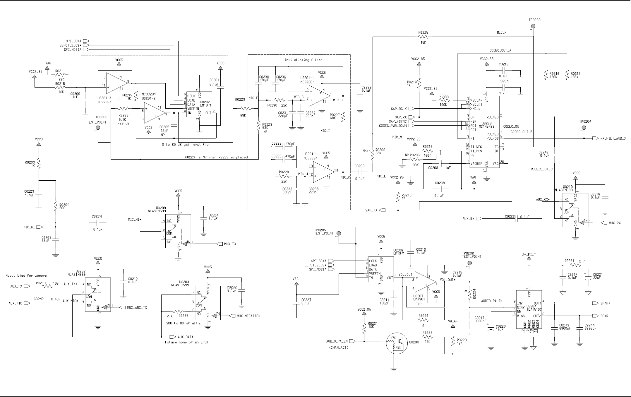
Schematics, Component Location Diagrams, and Parts Lists: HUD4022A/HUD4025B (VHF) Main Board 7-13
6881096C74-B May 25, 2005
Figure 7-11. HUD4025B/HUE4043A Controller Audio
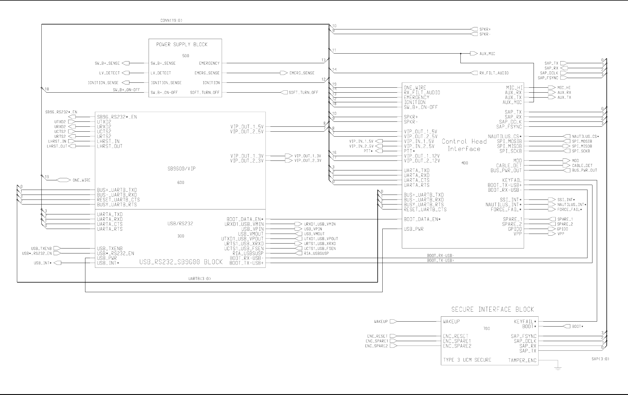
7-14 Schematics, Component Location Diagrams, and Parts Lists: HUD4022A/HUD4025B (VHF) Main Board
May 25, 2005 6881096C74-B
Figure 7-12. HUD4025B/HUE4043A Controller Interface, Secure and Power Block Diagram
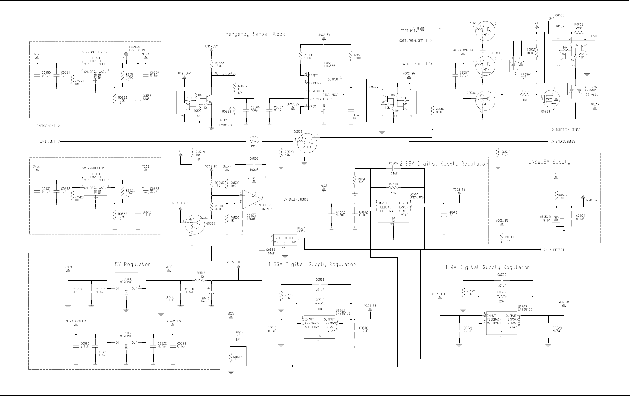
Schematics, Component Location Diagrams, and Parts Lists: HUD4022A/HUD4025B (VHF) Main Board 7-15
6881096C74-B May 25, 2005
Figure 7-13. HUD4025B/HUE4043A Controller Power Supply
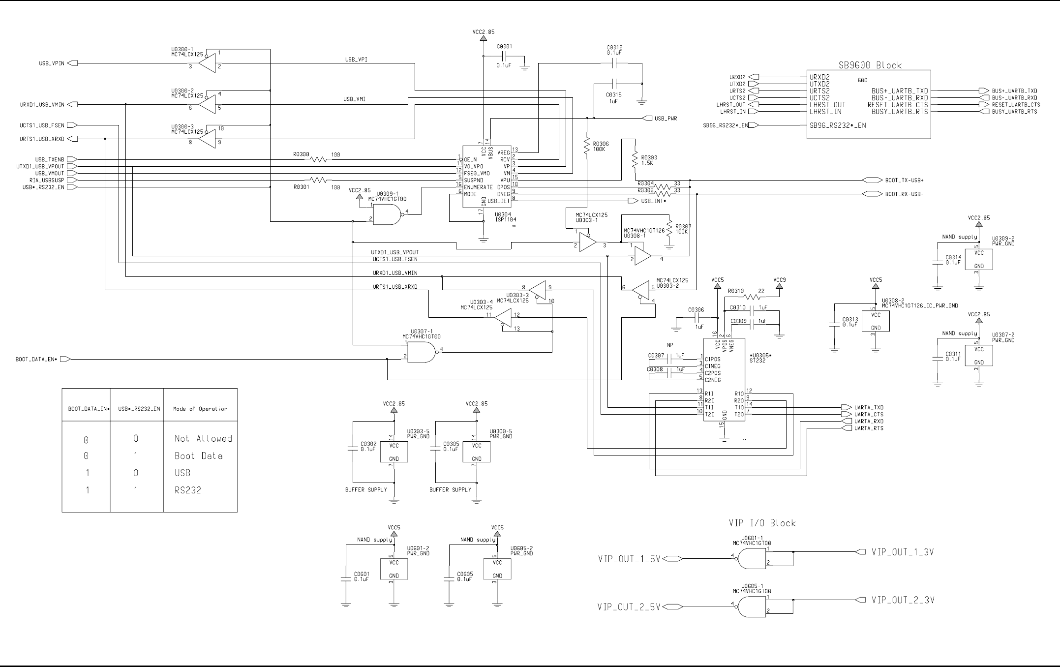
7-16 Schematics, Component Location Diagrams, and Parts Lists: HUD4022A/HUD4025B (VHF) Main Board
May 25, 2005 6881096C74-B
Figure 7-14. HUD4025B/HUE4043A USB/RS232 Interface
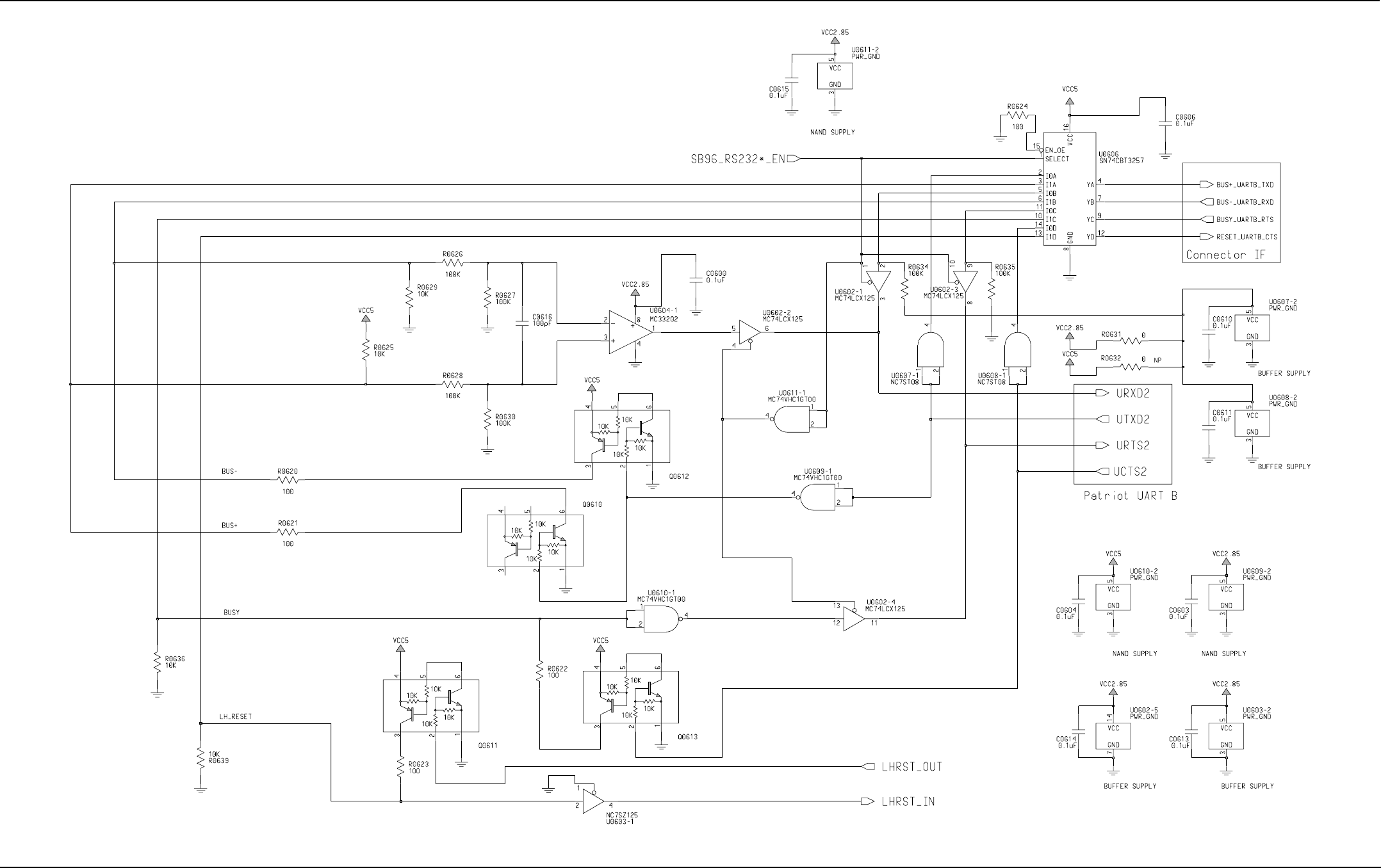
Schematics, Component Location Diagrams, and Parts Lists: HUD4022A/HUD4025B (VHF) Main Board 7-17
6881096C74-B May 25, 2005
Figure 7-15. HUD4025B/HUE4043A SB9600
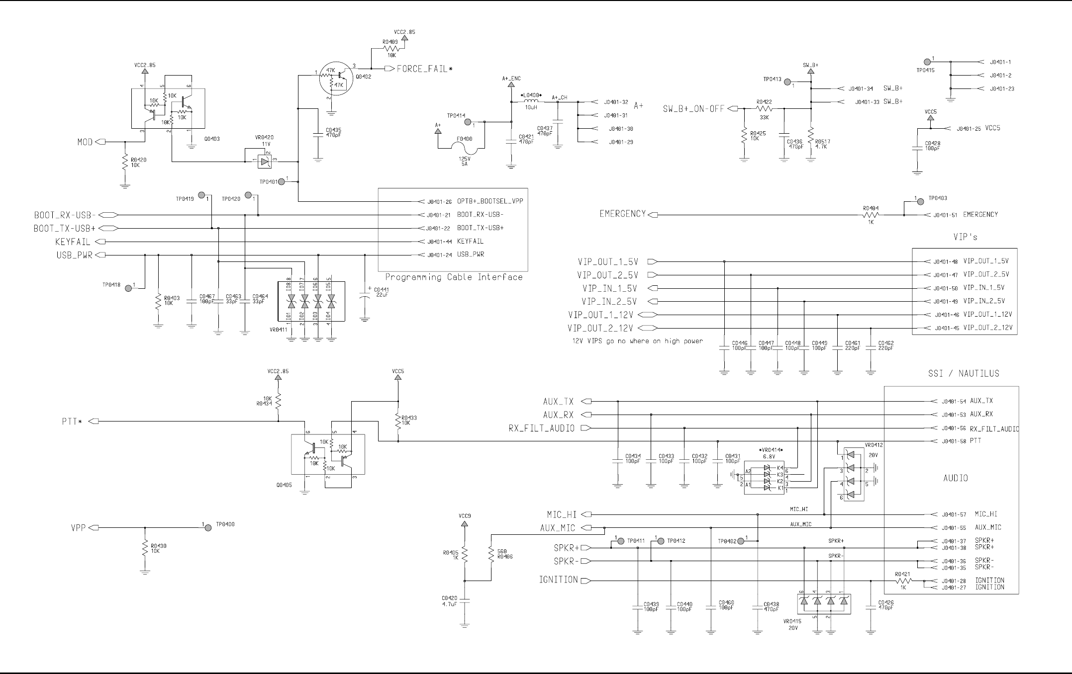
7-18 Schematics, Component Location Diagrams, and Parts Lists: HUD4022A/HUD4025B (VHF) Main Board
May 25, 2005 6881096C74-B
Figure 7-16. HUD4025B/HUE4043A Control Head Connector 1 of 2
Schematics, Component Location Diagrams, and Parts Lists: HUD4022A/HUD4025B (VHF) Main Board 7-19
6881096C74-B May 25, 2005
Figure 7-17. HUD4025B/HUE4043A Control Head Connector 2 of 2
7-20 Schematics, Component Location Diagrams, and Parts Lists: HUD4022A/HUD4025B (VHF) Main Board
May 25, 2005 6881096C74-B
Figure 7-18. HUD4025B/HUE4043A Secure Interface Connector Schematic
Schematics, Component Location Diagrams, and Parts Lists: HUD4022A/HUD4025B (VHF) Main Board 7-21
6881096C74-B May 25, 2005
Figure 7-19. HUD4022A/HUD4025B Frequency Generation Unit Overall Schematic (Sheet 1 of 2)
Rx Buffer
Rx VCO & 1st Buffer
Tx VCO & 1st Buffer Tx Buffers
Tx & Rx Buffers Shields
NP
Millennium FGU
Tx & Rx VCOs Shields
NP
NP
NP
RX 3rd Buffer
TO SHEET 2
73D02970C73-O
SHEET 12 OF 23
1.K
R3881
1.K
R3880
SHIELD
SH3759
1
R3861
820. 820.
R3860
6.2
R3862
C3803
470.p
C3883
100.n
C3882
100.n
470.p
100.n
C3881
C3880
C3827
470.p
R3837
100.
1.u
L3776
10.u
C3879
1
Control_V_Rx RF_OUT
Rx_Buffer_2_EN
SWITCHING1
SWITCHING2
1
TEST_POINT
TP6756
TP6762
1
TP6763
TEST_POINT
1
TEST_POINT
TP67611
TEST_POINT
TEST_POINT
1
TP6760
TEST_POINT
TEST_POINT
TP6772
1
TP6759
1
TP6758
TEST_POINT
1
1
TEST_POINT
TP6757
TEST_POINT
1
TP6764
1
TP6766
1
TP6765
SHIELD
SH3754
R3829
150.
R3830
TO_CAPACITOR
68.
Control_V_Tx
High_VCO_SW
Low_VCO_SW
TX_Buffer_EN
TX_RF_OUT From_TX_VCO
Keyed_9.1
Prescaler_Inj
TX_Buffer_EN
TX_Inj
LINE_B+ LO_INJ_HS
RF_IN
Rx_Buffer_2_EN
100.n
C3861
SH3750
SHIELD
1
L3750
1.0u
NC
NC
R3751
22.
NC
NC
NC
NC
R3770
C3809
5.600n
100.
5.6K
R3762
68.
R3771
IF6765
IF6766
IF6764
IF6767
C3770
C3857
100.n
470.p
1
SH3751
SHIELD
11
SHIELD
SH3753
C3772
F9.3V
SH3752
SHIELD
470.p
C3771
470.p
470.p
470.p
C3776
C3774
C3832
470.p
100.
R3772
R3766
1.K
4.7K
R3752
R3769
100.
Q3757
470.p
C3829
R3765
1.K
100.n
C3856
100.n
C3855
C3812
.022uF
C3834
.047uF
C3810
100n
100.n
C3858
C3833
C3860
100n
100.n100.n
C3859
R3773
51. Q3764
12
5
3
4
12
53
4
Q3766
53
4
Q3763
Q3765
12
D3757
4A1
5A2
6A3
3
K1 2
K2 1
K3
A3
6
K1 3
K2 2
K3 1
D3758
A1
4
A2
5
C3822
10uF
100n
100n
C3764
C3765
C3763 100n
B(,1),A(,1)
B(,1),A(,1)
B(,1),A(,1)
100nC3767
Lock_Det
K9.1
TX_INJ
RX_Inj
B(,1),A(,0)0
B(,1),A(,1)
B(,1),A(,1)
0 B(,1),A(,0)
0 B(,1),A(,0)
B(,1),A(,0)0
0 B(,1),A(,1)
B(,1),A(,1)
B(,1),A(,1)
B(,1),A(,1)
B(,1),A(,1)
B(,1),A(,1)
B(,1),A(,1)
B(,1),A(,0)0
B(,1),A(,1)
B(,1),A(,1)
B(,1),A(,1)
B(,1),A(,1)
B(,1),A(,1)
B(,1),A(,1)
B(,1),A(,1) B(,1),A(,1)
B(,1),A(,0)0
B(,1),A(,1)
B(,1),A(,1)
B(,1),A(,1)
B(,1),A(,1)
B(,1),A(,1)
B(,1),A(,1)
B(,1),A(,1)
B(,1),A(,1)
B(,1),A(,0)0
B(,1),A(,1)
B(,1),A(,1)
B(,1),A(,0)0
B(,1),A(,1)
B(,1),A(,1)
0 B(,1),A(,0)
B(,1),A(,0)0
B(,1),A(,1)
B(,1),A(,1)
12
53
4
7-22 Schematics, Component Location Diagrams, and Parts Lists: HUD4022A/HUD4025B (VHF) Main Board
May 25, 2005 6881096C74-B
Figure 7-20. HUD4022A/HUD4025B Frequency Generation Unit Overall Schematic (Sheet 2 of 2)
3.0 Volt Regulator
DATA
CLOCK
Syn_Sel
NP
TO SHEET 1
NC
B(,1),A(,1)
FS_2
DOUTA_2
CLKOUT_2
PE_2
PD_2
PC_2
FS_3
DOUTA_3
CLKOUT_3
PE_3
PD_3
PC_3
9.3V_2
B(,1),A(,1)
C3813
51.
R3836
100.n
470.p
1
C3825
1
TEST_POINT
TP6754
TP6752
TEST_POINT
1
TP6753
TEST_POINT
1
TP6751
TEST_POINT
1
1
TP6750
TEST_POINT
0.
5V_Reg
TP6755
TEST_POINT
R3785
0.
R3784
47.K
R3779
R3778
22.K
R3776
120.K
R3775
NC
NC
NC
NC
NC
1.5K
NC
NC
NC
NC
NC
NC
NC
NC
NC
IF6762
IF6780
IF6776
IF6778
IF6774
IF6770
IF6772
IF6779
IF6775
IF6777
IF6771
IF6773
IF6769
100K
R3755
100pF
C3824
4
5
VCC
1uH
L3754
TC7SH04
U3752
3GND
2
1
NC
5V_Reg
IF6751
C3826
.01uF
R3750
1K
R3761
10K
F3.0v
L3753
C3766
100n
3
GND
2
VCONT
1
VDD
4
2.2uH
16.8MHz
OSC1672A
Y3750
FOUT
IF6768
L3751
560nH
1uF
C3806
IF6750
100n
C3769
100n
C3768
C3831
1000pF
C3830
1000pF
L3752
560nH
56.K
R3758
15.K
R3756
5V_Reg
0
R3774
IF6752
IF6763
IF6753
IF6756
IF6754
10uF
C3828
F9.3V C3821
.01uF
330.
R3768
L3755
2.2uH
100K
R3753
100K
R3754
1K
R3767
F3.0v
F3.0v
100n
C3762
L3756
2.2uH
2.2uH
L3757
C3807
1uF
100n
C3750
100.n
C3808
47.K
R3759
C3751
100n 470.p
10uF
C3775
.022uF
C3811 C3820
470.p
C3773
10uF
C3823
C3752
100n 100n
Q3756
C3753
4
2
GND
VEN
3
1VIN VOUT 5
U3750
LP3985
BYPASS
R3763
1.K
Q3755
Q3750
VMULT2 14
VMULT3 12
VMULT4 11
13
VRO
WARP 25
XTAL1 23
XTAL2 24
27 SFCAP
26
SFIN
30
SFOUT 28
TEST1 37
TEST2 38
VBPASS
21
VCP 47
VMULT1 15
PD_GND
44
5
PD_VDD
PREIN
32
PRE_GND
33
PRE_VDD 34
PVREF
35
REFSEL
18
SFBASE
INDMULT 16
IOUT 43
4
LOCK
MODIN
10
MODOUT 41
NC1
17
NC2
29
NC3
31
CCOMP
42
CEX
9CLK
8
DATA
7
DGND
6
DVDD 36
FREFOUT 19
IADAPT 45
AGND
22
AUX1 48
AUX2 1
AUX3 2
AUX4 3
AVDD 20
BIAS1
40
BIAS2
39
U3751
63A27
ADAPTSW 46
B(,1),A(,1)
5V_Reg
MOD_IN
B(,1),A(,1)
16_8_CONT
B(,1),A(,1)
B(,1),A(,1)
B(,1),A(,1)
B(,1),A(,1)
B(,1),A(,1)
9.3V_1
B(,1),A(,1)
B(,1),A(,1)B(,1),A(,1)
B(,1),A(,1)
B(,1),A(,1)
16_8MHz
B(,1),A(,1)
B(,1),A(,1)
B(,1),A(,1)
B(,1),A(,1)
B(,1),A(,1)
B(,1),A(,1)
B(,1),A(,1)
B(,1),A(,1)
B(,1),A(,1)
B(,1),A(,1)
B(,1),A(,1) B(,1),A(,1)
B(,1),A(,1)
B(,1),A(,0)0
B(,1),A(,1)
B(,1),A(,0)0
B(,1),A(,1)
B(,1),A(,1)
B(,1),A(,1)
B(,1),A(,1)
B(,1),A(,1)
B(,1),A(,1)
B(,1),A(,1)
B(,1),A(,1)
B(,1),A(,1)
B(,1),A(,1) B(,1),A(,0)0
B(,1),A(,1)
SYN_SEL
SPI_CLK
SPI_DATA
B(,1),A(,0)0
B(,1),A(,1)
0 B(,1),A(,0)
B(,1),A(,1)
B(,1),A(,1)
B(,1),A(,1)
B(,1),A(,0)0
B(,1),A(,1)
B(,1),A(,1)
B(,1),A(,1)
B(,1),A(,1)
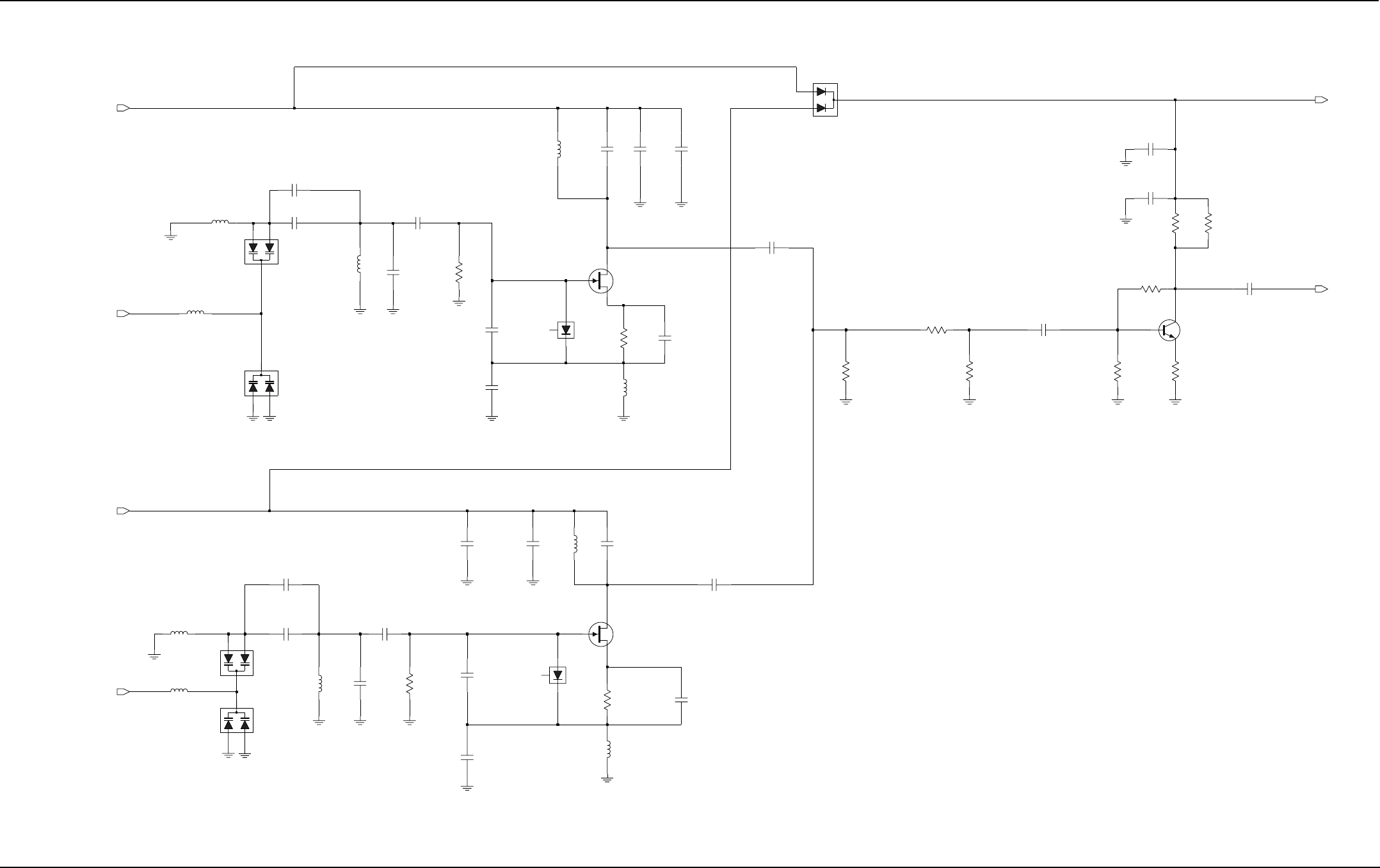
Schematics, Component Location Diagrams, and Parts Lists: HUD4022A/HUD4025B (VHF) Main Board 7-23
6881096C74-B May 25, 2005
Figure 7-21. HUD4022A/HUD4025B VHF Transmitter VCO Schematic
LOW VCO
HIGH VCO
NP
Millennium VHF TX VCO
NP
NP
73D02970C73-O
SHEET 20 OF 23
C3853
L3764
1uH
C3841
B(,1),A(,1)
B(,1),A(,1)
B(,1),A(,1)
B(,1),A(,1)
B(,1),A(,1) TX_RF_OUT
B(,1),A(,1)
Control_V_Tx
B(,1),A(,1)
B(,1),A(,1)
High_VCO_SW
B(,1),A(,1)
TX_Buffer_EN
B(,1),A(,1)
B(,1),A(,1)
B(,1),A(,1)
B(,1),A(,1)
B(,1),A(,1) B(,1),A(,1)
B(,1),A(,1)
B(,1),A(,1)
22.000p
1.p
C3837
6.2p
1
3
D3752
1uH
L3759
2
R3884
620.
C3933
470.p
C3935
10.n
C3934
10.n
300.
R3840
300.
R3839
18.
R3833 C3802
470.p
Y3754
56.n
47n
C3816
Y3753
10.n
C3852
1.8p
1.8p
C3851
C3836
7.5p
C3838
6.2p
C3854
4.7p
C3844
18.p
C3835
C3842
22.000p
7.5p
C3799
7.5p
C3797
8.2p
12.p
1uH
C3794
L3763
C3785
470.p
82.
R3814
D3768
27.K
R3789
D3754
D3769
12
3
R3788
27.K
C3843
18.p
D3753
1uH
D3767
L3761
470.p
C3784
C3783
470.p12.p
C3793
D
S
D3750
Q3754
L3765
1uH
1uH
L3762
Q3753
D
S
82.
R3813
470.p
C3815
1uH
L3760
R3817
1.0u
L3758
C3814
22.
470.p
Q3760
4.7K
R3799
5.6K
R3793
620.
R3808
B(,1),A(,1)
B(,1),A(,1)
Low_VCO_SW
Control_V_Tx
B(,1),A(,1)
B(,1),A(,1)
B(,1),A(,1)
B(,1),A(,1)
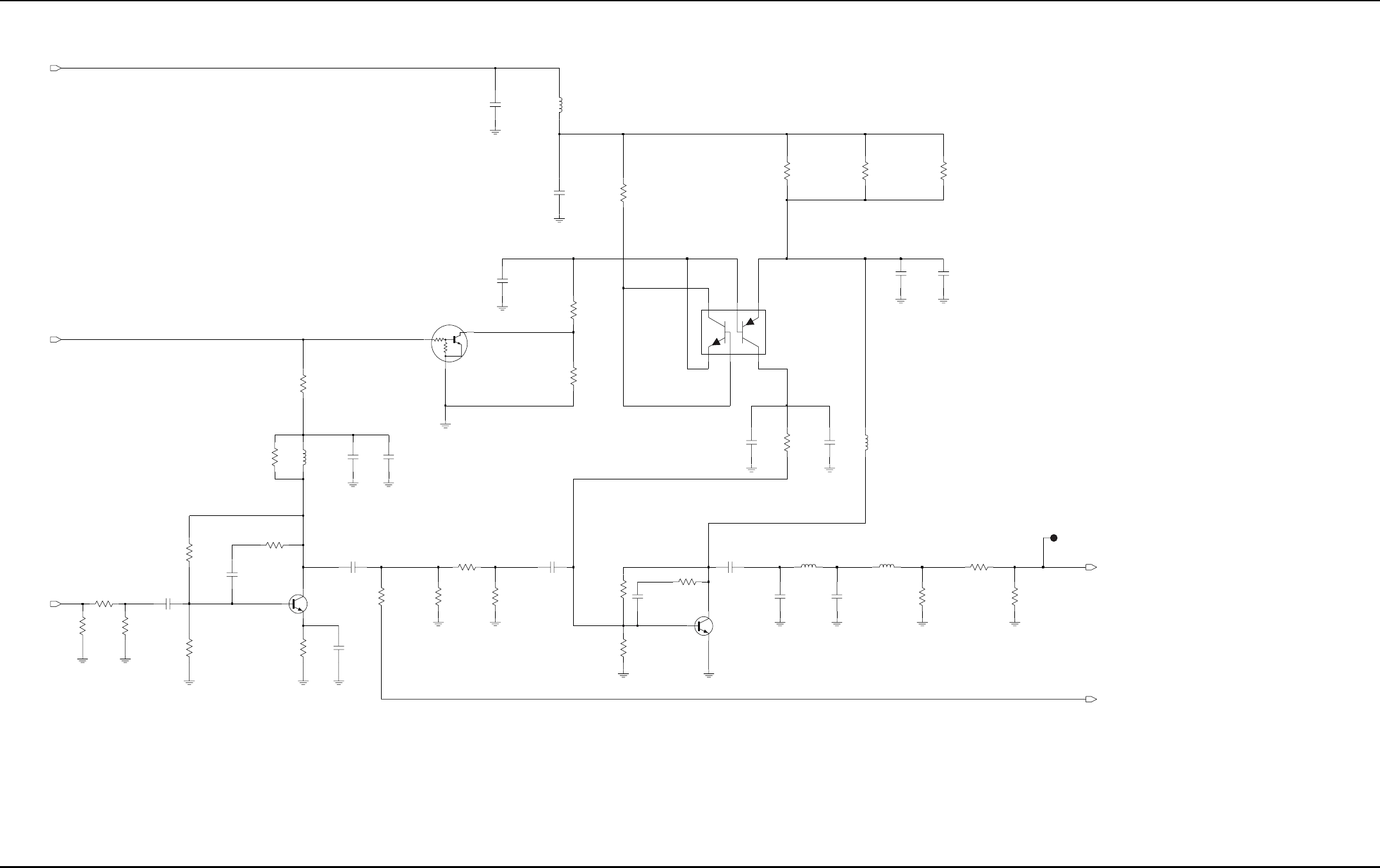
7-24 Schematics, Component Location Diagrams, and Parts Lists: HUD4022A/HUD4025B (VHF) Main Board
May 25, 2005 6881096C74-B
Figure 7-22. HUD4022A/HUD4025B Frequency Generation Unit VHF Receive Injection Schematic
NP
NP
NP
NP
APCO VHF RX Buffer
NP
NP
73D02970C73-O
SHEET 21 OF 23
B(,1),A(,0)
B(,1),A(,1)
B(,1),A(,1)
B(,1),A(,0)0 LO_INJ_HS
0
TO_CAPACITOR
LINE_B+
B(,1),A(,1)
RF_IN
B(,1),A(,1)
B(,1),A(,1)B(,1),A(,1)
B(,1),A(,1)
B(,1),A(,1)
B(,1),A(,1)
470.p
C3930
100n
100.
R3872
C3910
Q3762
B(,1),A(,1)
B(,1),A(,1)
B(,1),A(,1)
B(,1),A(,1)
B(,1),A(,1)
B(,1),A(,1)
Rx_Buffer_2_EN
B(,1),A(,1)
B(,1),A(,1)
B(,1),A(,1)
R3855
100.
Q3769
C3913 C3914
B(,1),A(,1)
L3784
4.700K
R3869
120.n
5.6K
22. 10.n
R3873
C3912
330.
R3870
C3911
R3871
22.n
220.
R3794
10.n
R3868
470.p
470.p
C3915
470.p
R3854
100.
R3864
18.
300.
R3857
68. R3856
300.
27.
R3865
27.
R3852
R3853
0.
R3851
R1
R2
Q3768
Q3767
10.n
100.
R3828
1.0u
C3924
3.3K
L3783
C3925
R3845
270nH
L3775
0.1uF
0.1uF
R3846
4.700K
C3926
R3832
1.K
47.
R3843
470.p
C3869
470.p
470.p
C3873
C3761
470.p
C3870
2.K
10.n
C3877
1TP6771
R3760
820.
TEST_POINT
820.
R3821 R3802
1.K
R3796
R3805
8.2K
470.p
C3759
15.p
C3804 C3786
18.p
L3781 L3782
33.n 6.2
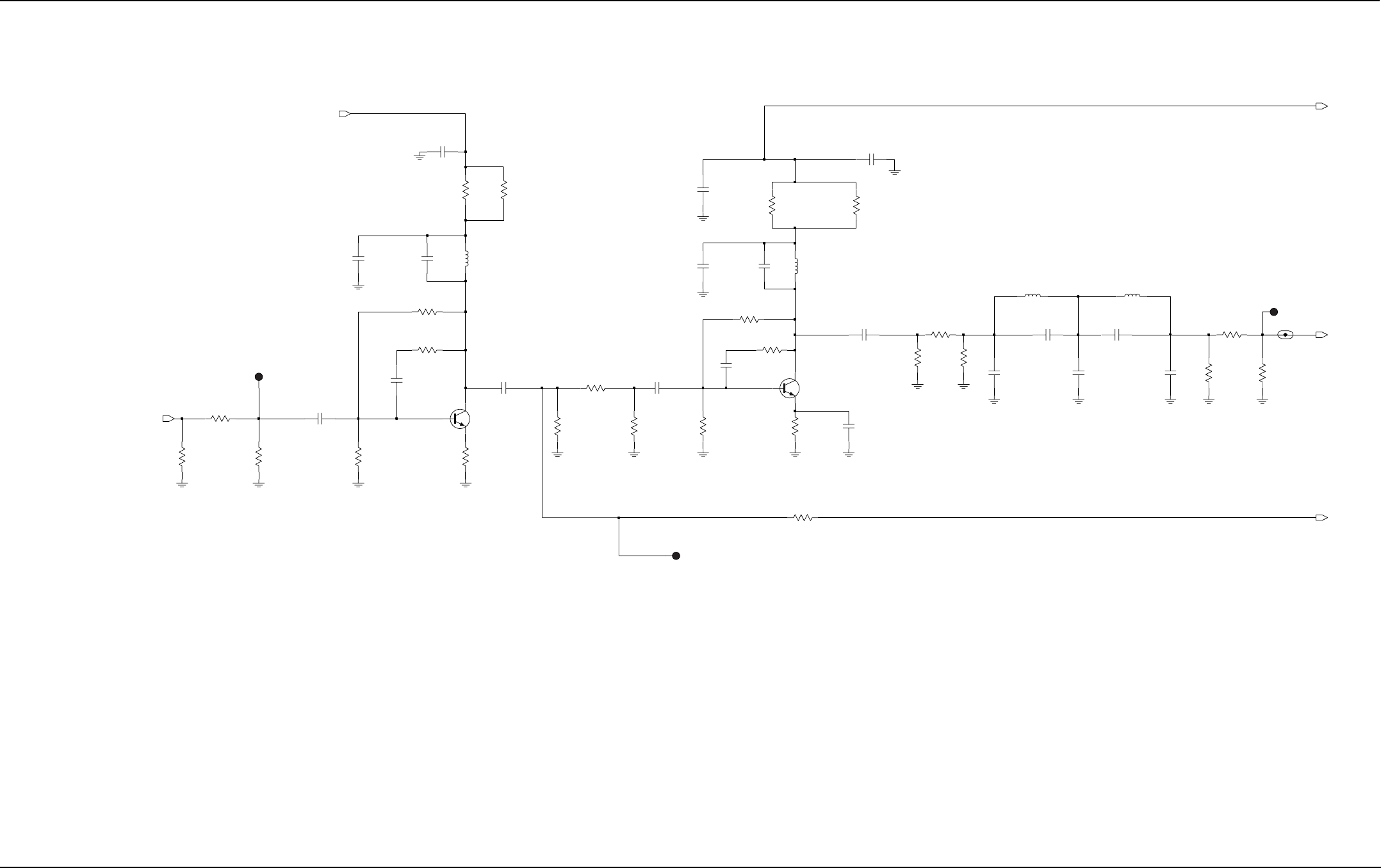
Schematics, Component Location Diagrams, and Parts Lists: HUD4022A/HUD4025B (VHF) Main Board 7-25
6881096C74-B May 25, 2005
Figure 7-23. HUD4022A/HUD4025B Frequency Generation Unit VHF Transmit Injection Schematic
APCO VHF TX Buffers
NP
73D02970C73-O
SHEET 18 OF 23
620.
16.p
R3882
C3790
C3917
470.p
C3921
3.p
3.p
7.5p
C3919
10.p
C3920 C3918
L3785
47.n
L3787
27.n
R3863
R3858
30.
R3859
180. 180.
C3876
R3764
10.n
C3871
10.n
2.K 2.K
R3757
1
TP6767
TP67681
TEST_POINT
TP6769
TEST_POINT
R3835
0.
1
R3842
C3872
100n
300.
18.
300.
82.
R3841
R3816
R3834
R3815
C3757
470.p
82.
18.p
C3875 L3779
120.n
470.p
C3865
180.
R3818
180.
R3824
30.
R3823
C3862
470.p
C3864
470.p
C3863
R3804
18.p 56.n
300.
L3778
300.
R3809
R3803
C3758
470.p
R3820
18.
B(,1),A(,1)
TX_Buffer_EN
B(,1),A(,1)
B(,1),A(,1)
B(,1),A(,1)
B(,1),A(,1)
B(,1),A(,1)
TX_Inj
Keyed_9.1
B(,1),A(,1)
From_TX_VCO
B(,1),A(,1)
B(,1),A(,1)
Prescaler_Inj
B(,1),A(,1)
B(,1),A(,1)
B(,1),A(,1)
B(,1),A(,1)B(,1),A(,1)
B(,1),A(,1)
B(,1),A(,1)
Q3758
B(,1),A(,1)
R3819
180.
15.K
R3791
100n
C3754
100n
C3755
Q3759
R3792
5.6K
620.
R3807
R3795
IF3710
10.K
470.p
C3817
4.7K
R3797
22.
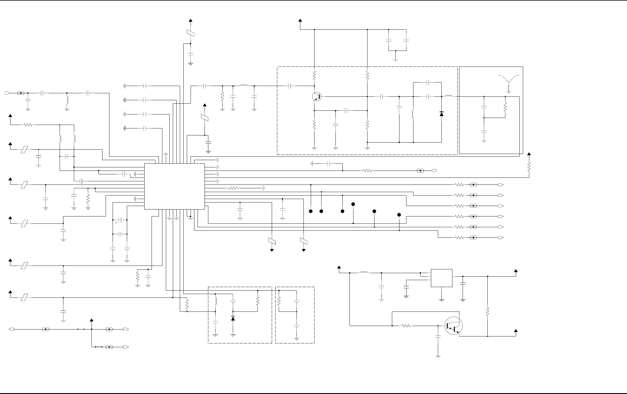
7-26 Schematics, Component Location Diagrams, and Parts Lists: HUD4022A/HUD4025B (VHF) Main Board
May 25, 2005 6881096C74-B
Figure 7-24. HUD4022A/HUD4025B Receiver Back-End Schematic
CLOCK LF
2nd LO VCO
2nd LO LF
CLOCK VCO
SPF_3.5V
RX 2nd LO Shield
#
#
##
#
#
#
#
*
*
NP
NP
NP
NP
NP
DNP
73D02970C73-O
SHEET 13 OF 23
5V_TO_FGU
5V_TO_IF
5V_FROM_CONTR
CLKOUT_1
FS_1
PE_1
PD_1
PC_1
DOUTA_1
B(,1),A(,1)
U3000
AD9874
0
R3023
C3032 39.000p
0
R3022
FS
11
DOUT
1
PE
1
CLKOUT
PD
1
PC
1
C3046
4.7n R3020
51. 20.p
C3028
100.0n
C3027
20.p
L3007
1.p
C3034
C3048
2.p
R3019 0
R3018 0
R3017 0
0
R3015
R3016
0
R3014
0
IF6008_1
IF6009_1
IF6007_1
IF6003_1
IF6005_1
IF6006_1
SH3000
SHIELD
1
IF6017
IF6015
5V
5V
IF6014
10KR3008
3VA
5V
C3041
.01uF
1VOUT 5
C3001
1uF
U3001
LP3985
BYPASS
4
GND
2
VEN
3
VIN
E3000
3VA
3VA
3VA
BK1005HM471
3VA
3VA
3VA
R3007
10K
0.1uF
C3019
R3000
51
VVCO
3VA
3VA
3VA
3VA
VVCO
L3008
100uH
1uF
C3045
1MEG
R3001
Q3001
C3043
2.2uF
0.1uF
C3018
E3008
E3007
BK1005HM471
BK1005HM471
E3005
BK1005HM471
E3006
BK1005HM471
E3004
IF6001
IF6000
C3047
C3033
1.p
L3005
200pF
L3000
10uH
0.1uF
10uH
470.
C3017
R3021
L3002
180.0n
C3016
C3000
12.p
0.1uF
E3003
E3002 C3040
.01uF
Q3000
D3001
D3000
L3004
120.0n
L3006
4.7u
4.7uF
C3006
0.1uF
C3015
C3039
.01uF
68.p
C3002
0.68uF
C3004
0.1uF
C3014
C3005
0.47uF
0.1uF
C3044
12.p
C3030
15.p
C3029
C3026
27pF
C3024
68.p
C3025
47.p
R3010
390
R3006
10K
R3005
10K
R3009
1K
L3003
4.7uH
390.
R3011
15.K
R3003
E3001
0.1uF
C3013
C3038
.01uF
C3037
.01uF
1000pF
C3042
0.1uF
C3012
C3011
0.1uF
0.1uF
C3010
C3009
0.1uF
C3008
0.1uF
C3007
0.1uF
100K
R3002
C3036
.01uF
C3023
100pF
C3022
100pF
0
C3003 R3012
100pF
2200pF
C3020 100pF
C3021
.01uF
R3004
C3035
VDDQ
14
VREFN
12 VREFP
11
18.K
VDDA
9
VDDC
17
VDDD 26
VDDF
6
VDDH 27
VDDI 48
VDDL 40
VDDP 39
LOP 43
MXON
2MXOP
1
PC
23
PD
24
PE 25
13 RREF
SYNCB 33
GNDS1
21
GNDS2 34
IF2N
4
IF2P
5
IFIN 47
IOUTC
15
IOUTL 38
LON 42
GNDC
18
GNDD
22
GNDF
3
GNDH 32
GNDI 45
GNDL 36
GNDP 37
GNDQ
16
CXVM 41
DOUTA 29
DOUTB 30
FREF 35
FS 31
GCN
8GCP
7
GNDA
10
CLKN
20
CLKOUT 28
19 CLKP
CXIF 46
CXVL 44
B(,1),A(,1)
B(,1),A(,1)
B(,1),A(,1)
B(,1),A(,1)
B(,1),A(,0)0
B(,1),A(,1) B(,1),A(,1)
B(,1),A(,1)
B(,1),A(,1)
B(,1),A(,1)
B(,1),A(,1)
B(,1),A(,1)
B(,1),A(,1)
B(,1),A(,1)
B(,1),A(,1)
B(,1),A(,1)
B(,1),A(,1)
B(,1),A(,1)
B(,1),A(,1)
B(,1),A(,1)
B(,1),A(,1)
B(,1),A(,1)
FREF
IF
B(,1),A(,1)
B(,1),A(,1)
B(,1),A(,1)
B(,1),A(,1)
B(,1),A(,1)
B(,1),A(,1) B(,1),A(,1)
B(,1),A(,1)
B(,1),A(,1)
B(,1),A(,0)
0
B(,1),A(,1)
B(,1),A(,1)
B(,1),A(,1)
B(,1),A(,1)
B(,1),A(,1) B(,1),A(,1)
B(,1),A(,1)
B(,1),A(,1)
B(,1),A(,1)
B(,1),A(,1)
B(,1),A(,0)0
B(,1),A(,1)
B(,1),A(,1)
B(,1),A(,0)0
B(,1),A(,1)
B(,1),A(,1)
B(,1),A(,1)
B(,1),A(,1)
B(,1),A(,1)
B(,1),A(,1)
B(,1),A(,0)0
Schematics, Component Location Diagrams, and Parts Lists: HUD4022A/HUD4025B (VHF) Main Board 7-27
6881096C74-B May 25, 2005
Figure 7-25. HUD4022A/HUD4025B Receiver Front-End Schematic (Sheet 1 of 2)
MIXER
Millennium VHF Rx FE
2nd Preselector (Elliptic Filter)
NP
NP
NP
MIXER_IF_OUT
73D02970C73-O
SHEET 16 OF 23
TO SHEET 2
C3283
1.n
C3421
4.3p
330n
L3404
C3258L3255
22n 100.000p
51.
R3270
B(,1),A(,1)
D3258
IO1 IO2
IO3
IO4
4
6
3
B(,1),A(,1)
1
B(,1),A(,1)
2
3B(,1),A(,1)
1 B(,1),A(,1)
2B(,1),A(,1)
T3302
XFMR
XFMR
T3301
4
6
IF6254
IF6256
1
LO_IN
IF_OUT_IF
1
SHIELD
SH3763 SH3762
SHIELD
1
D3257
1
SHIELD
SH3761 SH3760
SHIELD
R3288
62.
L3264
38.13n
C3295
B(,1),A(,1)
38.13n
L3263
62.0p
1.n
C3292
1.n
B(,1),A(,1)
B(,1),A(,1)
C3293C3287
36.p
C3310
24.p
B(,1),A(,1)
C3298
62.0p
B(,1),A(,1)
L3271
38.13n
Q3253
L3267
75.
R3267
3.3n
B(,1),A(,0)
0
C3271
10.n
C3297
7.5p
0 B(,1),A(,0)
L3258
150.0n
B(,1),A(,1)
75.p
C3278
39.p
C3291
18.p
C3279 L3257
L3256
B(,1),A(,1)
15.0n
B(,1),A(,1)
56.n27n
L3265
10.000n
L3254
91.p
C3277
B(,1),A(,1)
C3296
22.0p
L3253
100.0n
B(,1),A(,1)
10.p
C3311
L3251
47n
L3252
18.0n
51.p
C3290
L3259
1.2u
R3252
12.10
R3262
Sector RLS Lib
3.3K
270nH
L3262
10.0
R3251C3269
1.n
B(,1),A(,1)
R3263C3268
B(,1),A(,1)
1.5K100.n
C3275
100.n
C3274
100.n
Sector RLS Lib
R3261
4.7K
B(,1),A(,1)
R3264
1.K
B(,1),A(,1)
62.
R3268
Sector RLS Lib
C3254
470.p
C3253
B(,1),A(,1)
B(,1),A(,1)
470.p
C3252
470.p
470.p
C3251
B(,1),A(,1)
B(,1),A(,1) Q3252
B(,1),A(,1)
B(,1),A(,1)
C3286
1.n
B(,1),A(,1)
B(,1),A(,1)
B(,1),A(,1)
IF6250
9.3V_TO_IF
7-28 Schematics, Component Location Diagrams, and Parts Lists: HUD4022A/HUD4025B (VHF) Main Board
May 25, 2005 6881096C74-B
Figure 7-26. HUD4022A/HUD4025B Receiver Front-End Schematic (Sheet 2 of 2)
5V
9.3V
AGC/Attenuator circuit
NP NP
TO SHEET 1
1.n
5V
5V
5V
C3936
D3256
C3289
100.n
C3288
470.p
10.K
R3265
10.K
R3266
D3254
D3253
IF6786
D3252
C3267
100.n
9.3V_FE
9.3V_FE
100.n
C3312
1.n
C3284
13.p
C3259
B(,1),A(,1)
62.00p
C3300
72.22n
L3273
72.22n
L3272
B(,1),A(,1)
C3299
B(,1),A(,1)
B(,1),A(,1)
62.00p
C3257
39.000p
C3264
39.000p
B(,1),A(,1)
9.1p
C3281
C3280
1.n
C3276
13.p
L3260
38.13n
B(,1),A(,1)
1.n
C3294
B(,1),A(,1)
C3266
1.n
L3269
1.2u
470.p
C3270
1.2u
390.
R3275
B(,1),A(,1)
L3270
1.n
B(,1),A(,1)
B(,1),A(,1)
1.n
C3273
C3260
C3261
1.n
R3269
3.6K
56.K
R3281
3.3K
R3280
7.5K
R3279
RF_ATTN_2_A
56.K
R3278
R3277
3.3K
Q3258
B(,1),A(,1)
Q3257
B(,1),A(,1)
Q3256
B(,1),A(,1)
L3268
B(,1),A(,1)
B(,1),A(,0)0
1.2u
1.2u
B(,1),A(,1)
L3266
R3273
3.9K
470.p
C3256
1.2u
B(,1),A(,1)
L3261
R3274
390.
1.n
C3255
B(,1),A(,1)
B(,1),A(,1)
D3251
C3263
1.n
C3262
470.p
62.
R3255
Q3254
C3303
Q3255
1.n B(,1),A(,1)
10.n
C3265
470.p
C3302
270.0n
L3275
C3301
470.p
R3271
75.
51.
B(,1),A(,1)
C3309
B(,1),A(,1)
R3260
10.n
470.p
C3305
10.n
C3304
R3258
62.
B(,1),A(,1)
B(,1),A(,1)
B(,1),A(,0)0
B(,1),A(,0)0
R3257
620.
B(,1),A(,1)
4.7K
R3259
1.0u
L3276
470.p
C3306
10.n
C3307
R3254
B(,1),A(,1)
10.0n
2.2K
33.
B(,1),A(,1)
L3277
B(,1),A(,1)
R3272
B(,1),A(,1)
10.n
C3308
1.K
R3256
B(,1),A(,1)
IF6258
10K
R3253
5V
C3272
470.p
RFIO1
1
RFIO2
3
B(,1),A(,1)
V1 4
RF_ATTN_1_A
V2 5
B(,1),A(,1)
Q3250
5V
U3250
AT267
GND 2
B(,1),A(,1)
D3255
IF6251
9.3V_FROM_FGU
9.3V_TO_IF
IF6253
IF6257
B(,1),A(,1)
B(,1),A(,1)
RF_IN
5V_FE
470.p
C3282
47K
47K

Schematics, Component Location Diagrams, and Parts Lists: HUD4022A/HUD4025B (VHF) Main Board 7-29
6881096C74-B May 25, 2005
Figure 7-27. HUD4022A/HUD4025B Receiver IF Schematic
IF_TO_ABACUS
Millennium VHF Rx IF
NP
NP
NP
73D02970C73-O
SHEET 15 OF 23
B(,1),A(,1)
B(,1),A(,1)
IF_IN
9.3V_FROM_FE
5V_TO_FE
IF_OUT
9.3V_TO_CONTR
5V_IF
RF_ATTN_3_C
RF_ATTN_2_C
RF_ATTN_3_B
RF_ATTN_2_B
B(,1),A(,1)
B(,1),A(,1) B(,1),A(,1) B(,1),A(,1)
B(,1),A(,1) B(,1),A(,1)
B(,1),A(,1)
B(,1),A(,1)
B(,1),A(,1)
68.000n
L3408
10.n
C3424
D3401
Q3400
C3409
36.p
36.p
C3414
R3413
100.
Q3401
C3406
10.n
D3400
13.p
C3408
L3407
150.n
470.p
C3412C3405
10.n
L3400
270.0n470.p
C3400
C3418
1.n
L3405
330n
4.7p
C3415
TS2_A9E02
Y3401
GND1
1
GND2
2
GND3
4
5GND4
6IN 3
OUT
FREQ
C3420
1.n
330n
L3403
C3416
4.3p
10.
R3407
C3404
10.n
C3411
470.p10.n
C3403
75.
R3409
620.
R3400
R3401
4.7K
L3406
1.0u
C3410
470.p
C3402
10.n
R3402
3.3K
1.5K
C3401
10.n
R3405
4.3p
C3417
6IN 3
OUT
L3401
330n
FREQ
Y3400
TS2_A9E02
GND1
1
GND2
2
GND3
4
5GND4
IF6363IF6360
IF6362IF6359
IF6357
IF6354IF6353
IF6351
IF6350
IF6352
B(,1),A(,1) B(,1),A(,1) 0 B(,1),A(,0) B(,1),A(,1) B(,1),A(,1) B(,1),A(,1)
B(,1),A(,1)
B(,1),A(,1)
7-30 Schematics, Component Location Diagrams, and Parts Lists: HUD4022A/HUD4025B (VHF) Main Board
May 25, 2005 6881096C74-B
Figure 7-28. HUD4022A RF Power Amplifier (RF PA) Schematic (Sheet 1 of 2)
INTERFACE
RFPA/FGU
INTERFACE
RFPA/POWER CONTROL
INTERFACE
1 %
RFPA/OUTPUT NETWORK
73D02970C73-O
SHEET 14 OF 23
TX_INJ
VREVERSE_ON
K9.1V
A+_4
VFORWARD_ON
A+_3
RFPA_OUT
K9.1V_ON
RFPA_CNTRL
VFORWARD
VREVERSE
VCURRENT
VGBIAS3
A+_1
VTEMP
VGBIAS2
A+_2
IF3543
IF3542
IF3541
IF3503
IF3500
K9.1V_FGU
IF3501
VGBIAS1
C3550
5m
470pF
C3535
U3560
R3540
1K
300.1.n
C3564
C3517
R3561
470pF
R3507
62.00p
10.
C3548
62.00p
C3536
1019447
L3549
56pF
56pF
1000pF
C3537
C3563
R3502
C3549
5.6K
NC
IF3510
IF3509
IF3506
100
C3505
.01uF
C3504
R3501
4.22nH
L3502
33pF
3.3pF
C3557
C3555
110pF
470pF
C3551
62pF
C3532
470pF
C3500
68nH
L3501
56
56
R3520
56
56
R3521
R3523
R3522
C3559
17nH
470pF
C3558
L3552
3.3pF
C3556
47pF
C3553
110pF
C3554
62.p62.p
C3552
62pF
L3520
C3533
C3534
22pF
470pF
C3521
18.5nH
Q3550
3.9
R3538
R3536
3.9
R3537
3.9
C3560
IF3505
10.u
0
R3530
R3535
C3503
R3534
33pF
R3533
3.9
3.9
R3532
3.9
3.9
C3562
0.1uF
GND
U3561
100K
R3560
INA138
VPOS
5
VINPOS 3
VINNEG 4
OUT
1
2
C3520
1POS
HEATSINK
10pF
17nH
M3542
2GND2
1GND1
HEATSINK
L3551
M3520
0.1uF
C3561
LM50
2VOUT
1
POS
3
GND
R3550
0.1uF
10
R3551
L3550
1K
1019447
C3522
C3530
470pF
R3524
IF3508
0.1uF
IF3507
Q3530
10
R3531 L3530
1019447
C3531
.01uF
470pF
12.5nH
68nH
L3531
.01uF
C3506
C3501
L3503
C3511C3508
1.n
6
RFIN
16
U3550
1.n
5GND1
4
VG2 3
VG1 2
VD1
14
VCNTRL
1RFOUT2 7
RFOUT1
IF3511
NC4
15 NC3
10 NC2
9
NC1
8
GND4
13 GND3
12 GND2
G2
11
17 EP
30C65
IF3512
IF3513
IF3504
IF3514
IF3502
IF3540
Schematics, Component Location Diagrams, and Parts Lists: HUD4022A/HUD4025B (VHF) Main Board 7-31
6881096C74-B May 25, 2005
Figure 7-29. HUD4022A RF Power Amplifier (RF PA) Schematic (Sheet 2 of 2)
S = 55 mil
S = 45 mil
L = 400 mil
W = 90 mil
W = 20 mil
W = 20 mil
OUTPUT NETWORK/RFPA
INTERFACE
OUTPUT NETWORK/RX FE
INTERFACE
NP NP
73D02970C73-O
SHEET 17 OF 23
R3704 R3701
18.
R3703
18. 18.
1
1.2u
D3705
D3704
L3703
1.2u
1
1.2u
L3704
L3727
L3737
2
25nH
L3726
25nH
L3725
25nH
470pF
L3732
25nH
33
R3700
C3736
11pF
1K
R3702
C3720
C3723
3.9pF
28n
L3724
Sector RLS Lib
L3720
Sector RLS Lib
1
22n
C3735
D3703
12pF
470pF
C3704
C3702
L3702
47nH
470pF
25nH
C3703
C3701
33pF
30pF
L3701
R3733 R3734
240
240
R3736
240
240
R3735
18nH
L3731
18nH
L3730
3
J3700-3
1
J3700-1
2
J3700-2
8.2pF
IF3700
C3731
D3731
C3733
8.2pF
C3732
470pF
100K
R3739
30K
R3738
1.5K
R3737
IF3703
30K
100K
R3730
1.5K
R3731
C3730
R3732
470pF
RFPA_OUT
B(,1),A(,1)
B(,1),A(,1)
B(,1),A(,0)0
B(,1),A(,1)
K9.1V_ON
B(,1),A(,1) B(,1),A(,1)
RX_IN
B(,1),A(,1)B(,1),A(,1)B(,1),A(,1) B(,1),A(,1)
B(,1),A(,1)
B(,1),A(,1)
VFORWARD_ON
B(,1),A(,1)
VREVERSE_ON
B(,1),A(,1)
B(,1),A(,1)
B(,1),A(,1)
B(,1),A(,1)
B(,1),A(,1)
B(,1),A(,1)
B(,1),A(,1)
B(,1),A(,1)
B(,1),A(,1)
B(,1),A(,1)
D3701
B(,1),A(,1)
B(,1),A(,1)
B(,1),A(,1)
L3700
1.2u
470pF
C3700
IF3702
IF3701
D3702
IF3704
C3734 470pF
L3721
25nH 25nH
L3722
39pF
C3721
39pF
C3722
L3723
25nH
SHIELD
1
M3700
D3730
SHIELD
1
M3721
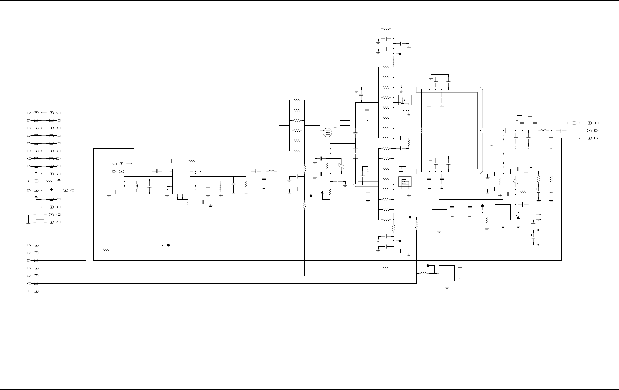
7-32 Schematics, Component Location Diagrams, and Parts Lists: HUD4022A/HUD4025B (VHF) Main Board
May 25, 2005 6881096C74-B
Figure 7-30. HUD4025B RF 100W Power Amplifier (RF PA) Schematic (Sheet 1 of 2)
TP3520
A+
C3502
470pF
C3501
C3506
C3500
R3500
L3500
150nH L3501
6.8nH
470pF
.01uF
470pF 180
U3500
30C65
1
16
14
11
8
9
10
15
RFIN
4
5
12
13
17
6
7
2
3
VCNTRL
VD1
G2
RFOUT1
RF OUT2
VG1
VG2
NC1
GND1
GND2
GND3
GND4
EP
NC2
NC3
NC4
TP3500
IF3506 IF3507
IF3540
IF3514 IF3515
IF3516 IF3517
IF3518 IF3519
IF3520 IF3521
IF3522
IF3523 IF3524
SC3500
SC3501
IF3527
IF3543
AUDIO_A+_1
K9.1V_FGU
TX_INJ
IF3534
IF3535
MOSIA_1
EEPOT_EN_1
AD_EN_1
MISOA_1
PA_EN_1
R3567
SW_A+_RFPA
SW_A+_1
A+_1
A+
A+
A+
0
FGU
INTERFACE
1I1
1I1
IF3505
K9.1V_EN_1
DA_EN_1
SCKA_1
K9.1V_EN_2
DA_EN_2
SCKA_2
MOSIA_2
AD_EN_2
IF3500 IF3501
IF3502 IF3503
IF3504
POWER CONTROL
INTERFACE
CONTROLLER
INTERFACE
EEPOT_EN_2
R3501
0
IF3528
IF3529
IF3530
IF3531
IF3532
IF3533
RFPA_CNTRL
K9.1V
VGBIAS_1
VGBIAS_2
VGBIAS_3
VTEMP
VCURRENT
IF3544
IF3541
IF3542
AUDIO_GND_1
AUDIO_A+_2
AUDIO_GND_2
A+_2
SW_A+_2
MISOA_2
PA_EN_2
2
I2
2
I2
C3505
C3504
.01uF
L3502
150nH
1
R3521
R3520
R3525
R3524
R3523
R3522
20
20
20
20
20
20
C3521
120pF
C3522
C3526
L3520
470pF
C3520
68pF
.01uF
18.5nH
4.7uF
C3503
.01uF *R3503*
5.1K
*R3502*
5.1K
C3525
C3524
*C3523*
C3541
62pF
C3544
91pF
*C3571*
68pF
R3529
0
R3528
0
R3527
10
R3526
1K
L3521
5nH
470pF
470pF
1
0.1uF
L3522
57R01
C3543
91pF
C3540
62pF
*C3570*
68pF
Q3520
M3520
HEATSINK
1POS
S
D
C3579
*C3576*
C3542
C3545
C3551
75pF
C3550
75pF
C3549
75pF
C3548
75pF
R3543
R3542
R3541
R3540
1K
R3547
R3546
R3545
R3544
R3559
33
R3568
7.5
7.5
7.5
7.5
7.5
7.5
7.5
0
0.1uF
470pF
10uF
TP3540
1
M3540
HEATSINK
GND2
GND1
1
1 3 S1S2
2
Q3540
C3546
C3555
75pF
C3554
75pF
C3553
75pF
C3552
75pF
R3551
R3550
R3549
33
R3548
R3555
R3554
R3553
R3552
R3556
7.5
7.5
7.5
7.5
7.5
7.5
7.5 470pF
470pF
7.5
M3541
HEATSINK
GND2
GND1
12
Q3541
C3578
*C3577*
*C3567*
0.1uF
C3566
0.1uF
C3565
0.1uF
C3547
R3558
1K
R3557
R3565
0
1
1
1
1
2
3
U3560
LM50
VOUT
GND POS
1
2
0
0
R3569
10uF
0.1uF
470pF
7.5
*R3566*
3
*U3563*
LM50
VOUT
GND POS
TP3542
TP3541
TP3543
C3575
*C3574* C3563
22uF
C3562
C3561
C3560
C3564
22uF
C3568
10uF
R3563
2.7
R3562
2.7
R3561
R3560
10
R3564
100K
1%
L3543
25nH
470pF
1000pF
470pF
0.1uF
0.1uF
L3544
57R01
5m
1
1
2
3
4
5
VR3500
24V
TP3544
U3561
INA138
OUT VINPOS
VINNEG
GND VPOS
J3500-1
J3500-2
BATTERY
CONNECTOR
A+
NC
NC
C3559
C3558
30pF
*C3557*
56pF
*C3556*
56pF
*C3573*
56pF
C3572
100pF
*L3540*
25nH
L3541
L3542
25nH
L3545
18nH 470pF
25nH
OUTPUT NETWORK
INTERFACE
RX_FE
INTERFACE
IF3536 IF3537
IF3538
IF3539
RX_IN_1 RX_IN_2
RFPA_OUT
K9.1V_ON
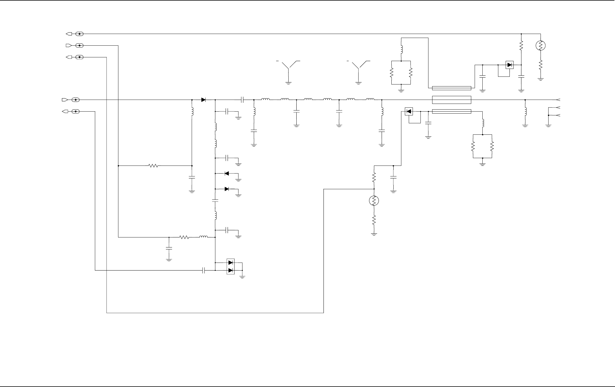
Schematics, Component Location Diagrams, and Parts Lists: HUD4022A/HUD4025B (VHF) Main Board 7-33
6881096C74-B May 25, 2005
Figure 7-31. HUD4025B RF 100W Power Amplifier (RF PA) Schematic (Sheet 2 of 2)
*D3705*
RFPA
INTERFACE
VREVERSE_ON
K9.1V_ON
VFORWARD_ON
RFPA_OUT
RX_IN
IF3704
IF3703
IF3702
IF3701
IF3700
POWER_CONTROL
INTERFACE
C3732
13pF
C3734
C3733
470pF
L3725 L3727
L3726
L3722
L3721 L3723
L3731
24nH
D3701
D3731
R3700
R3737
1.5K
R3739
100K
R3738
10K
R3734
220
R3733
180
33
1
1
*M3721*
SHIELD
*M3700*
SHIELD
S = 40 mil
L = 400 mil
W = 80 mil
S = 50 mil
W = 21.5 mil
W = 21.5 mil
C3730
470pF
C3723
11pF
C3731
13pF
L3730
12nH
L3737
1.2uH
L3724
22nH
D3730
R3730
100K
R3732
1.5K
R3731
10K
R3736
270
R3735
220
11
21 J3700-1
2 J3700-2
3 J3700-3
C3701
C3700
470pF
C3703
470pF
C3702
C3720
3.9pF
C3704
C3722
39pF
C3721
39pF
C3736
470pF
C3735
L3701
25nH
L3700
1.2uH
L3702
47nH
L3732
25nH
L3704
L3720
28nH
D3703
D3702
R3702
470pF
1.2uH
1K
12pF
33pF
470pF 25nH25nH 25nH 25nH 25nH 25nH
30pF
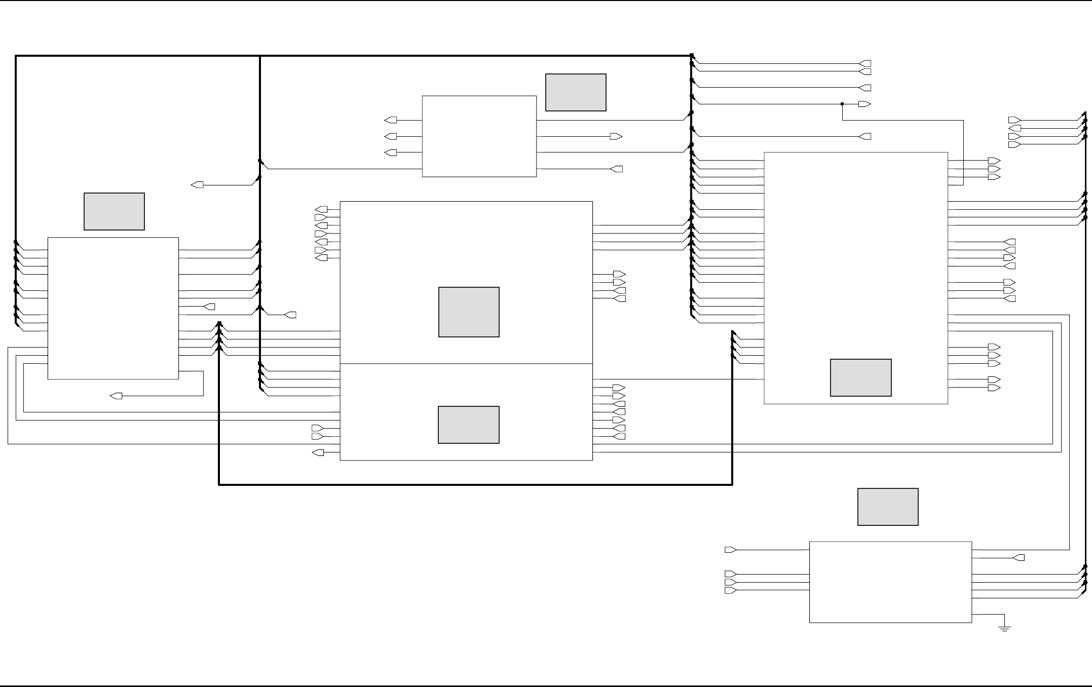
7-34 Schematics, Component Location Diagrams, and Parts Lists: HUD4022A/HUD4025B (VHF) Main Board
May 25, 2005 6881096C74-B
Figure 7-32. HUD4022A Secure Block Diagram and Interconnections
USB_RS232_SB9600 BLOCK
USB/RS232
SECURE INTERFACE BLOCK
10
11
0
2
3
UTXD1_USB_VPOUT
UTXD2
VIP_IN_1_3V
VIP_IN_1_5V
VIP_IN_2_3V
VIP_IN_2_5V
VIP_OUT_1_3V
VIP_OUT_1_5V
VIP_OUT_2_3V
VIP_OUT_2_5V
0
2
UARTA_RTS
UARTA_RXD
UARTA_TXD
UCTS1_USB_FSEN
UCTS2
URTS1_USB_XRXD
URTS2
URXD1_USB_VMIN
URXD2
USB*_RS232_EN
USB+
USB-
USB_INT*
USB_PWR
USB_TXENB
USB_VMOUT
USB_VPIN
14
16
BOOT_DATA_EN*
BOOT_RX
BOOT_TX
BUS+_UARTB_TXD
BUS-_UARTB_RXD
BUSY_UARTB_RTS
LHRST_IN
LHRST_OUT
RESET_UARTB_CTS
RIA_USBSUSP
SB96_RS232*_EN
UARTA_CTS
7
0
2
5
17
2
4
9
12
12
10
2
9
3
3
13
14
19
19
17
3
IGNITIONIGNITION_SENSE
LV_DETECT
SOFT_TURN_OFFSW_B+_ON-OFF
SW_B+_SENSE
0
6
05
SPKR-
SSI_INT*
SW_B+_ON-OFF
UARTA_CTS
UARTA_RTS
UARTA_RXD
UARTA_TXD
VIP_IN_1_5V
VIP_IN_2_5V
VIP_OUT_1_12V
VIP_OUT_1_5V
VIP_OUT_2_12V
VIP_OUT_2_5V
EMERGENCY
EMERG_SENSE
NAUTILUS_INT*
ONE_WIRE
PTT*
RESET_UARTB_CTS
RX_FILT_AUDIO
SAP_DCLK
SAP_FSYNC
SAP_RX
SAP_TX
SPARE_1
SPARE_2
SPI_MISOB
SPI_MOSIB
SPI_SCKB
SPKR+
AUX_TX
BOOT_DATA_EN*
BOOT_RX
BOOT_TX
BUS+_UARTB_TXD
BUS-_UARTB_RXD
BUSY_UARTB_RTS
BUS_PWR_OUT
CABLE_DET
EMERGENCY
FORCE_FAIL*
IGNITION
KEYFAIL
MIC_HI
MOD
NAUTILUS_CS*
1
1
15
1
AUX_MIC
AUX_RX
1
5
0
0
3
16
1
10
15
9
18
SPKR-
UARTA_CTS
UARTA_RTS
UARTA_RXD
UARTA_TXD
USB+
USB-
USB_PWR
VIP_OUT_1_12V
VIP_OUT_2_12V
VPP
12
19
AUX_MIC BUS+_UARTB_TXD
BUS-_UARTB_RXD
BUSY_UARTB_RTS
CHAN_ACT
EMERGENCY
IGNITION
MONITOR
ONE_WIRE
PTT*
RESET_UARTB_CTS
RX_FILT_AUDIO
SPKR+
2
7
0
1
3
13
3
2
8
3
3
2
4
11
18
8
14
1
13
SAP_DCLK
SAP_FSYNC
SAP_RX
SAP_TX
TAMPER_ENC
WAKEUP
0
1
1
6
AUX_MIC
SAP(3:0)
WAKEUP
ENC_SPARE1
ENC_RESET
ENC_SPARE2
BOOT*
MOD
ONE_WIRE
SPARE_1
SPARE_2
2
BOOT*
ENC_RESET
ENC_SPARE1
ENC_SPARE2
KEYFAIL*
SPI_MOSIB
SPI_MISOB
SPI_SCKB
NAUTILUS_CS*
FORCE_FAIL*
CABLE_DET
BOOT_TX
BOOT_RX
VPP
AUX_TX
MIC_HI
CHAN_ACT
BUS_PWR_OUT
NAUTILUS_INT*
SSI_INT*
USB_INT*
MONITOR
PTT*
UARTB(3:0)
SPKR+
SPKR-
CONN(19:0)
SAP_DCLK
SAP_TX
SAP_FSYNC
SAP_RX
SB96_RS232*_EN
AUX_RX
IGNITION_SENSE
SW_B+_SENSE
LV_DETECT
SOFT_TURN_OFF
SW_B+_ON-OFF
VIP_IN_2_3V
VIP_IN_1_3V
VIP_OUT_1_3V
VIP_OUT_2_3V
USB_VMOUT
USB_TXENB
UTXD1_USB_VPOUT
UCTS1_USB_FSEN
URTS1_USB_XRXD
URXD1_USB_VMIN
USB*_RS232_EN
USB_VPIN
RIA_USBSUSP
EMERG_SENSE
UTXD2
URXD2
URTS2
UCTS2
LHRST_OUT
LHRST_IN
RX_FILT_AUDIO
ACCESSORY CONNECTOR
POWER SUPPLY BLOCK
SB9600/VIP
CONTROL HEAD
INTERFACE
TYPE 3 UCM SECURE
MAEPF-27844-O
Part Series
400-1
Part Series
500
Part Series
300
Part Series
700
Part Series
400-2
Part Series
600-1
600-2

Schematics, Component Location Diagrams, and Parts Lists: HUD4022A/HUD4025B (VHF) Main Board 7-35
6881096C74-B May 25, 2005
Figure 7-33. HUD4022A Accessory Connector Schematic
VIP_OUT_2_12V
UARTB_RTS-BUSY
USB+
EMERGENCY
SPKR+
USB_PWR
RX_FILT_AUDIO
SW_B+
CHAN_ACT
UARTA_TXD
SPKR-
ONE_WIRE
MONITOR
PTT*
CTS_DCE (DB9-Pin 7)
RTS_DCE (DB9-Pin 8)
UARTB_RXD-BUS-
UARTA_RXD
UARTB_TXD-BUS+
J0402
UARTB_CTS-RESET
UARTA_RTS
AUX_MIC
TX_DCE (DB9-Pin 2)
RX_DCE (DB9-Pin 3)
UARTA_CTS
VIP_OUT_1_12V
26 PIN CONN
IGNITION
GND
USB-
R0410 100
C0412
100pF
U0400
DTC144EKA
33pF
C0402
*VR0408*
A1
A2
K1
K2
K3
K4
5.6V
J0402-27
J0402-20
220pF
C0415
33pF
C0410
C0464
33pF
J0402-29
220pF
C0417
33pF
C0403
J0402-12
J0402-11
1K
R0405
VR0404
15V
100
R0432
J0402-32
100
R0407
1
J0402-31
0
R0430
TP0420
J0402-30
J0402-9
33pF
C0405
33pF
C0404
TP0418
1
J0402-3
J0402-22
J0402-13
9.3V_TX
J0402-1
J0402-23
C0416
J0402-5
J0402-21
100pF
R0411
10K
3
4
6
J0402-24
VR0402
20V
2
5
1
33pF
J0402-15
J0402-28
C0463
33pF
C0406
J0402-8
470pF
C0465
100pF
C0466
C0419
C0413
100pF
100
100pF
R0408
VR0405
15V
220pF
C0418
R0412 100
C0408
J0402-26
J0402-19
100pF100pF
C0467
560
R0406
33pF
C0400
C0414
220pF
4.7uF
C0420
*VR0410*
A1
2
A2
5
K1 1
K2 3
K3 4
K4 6
5.6V
J0402-4
J0402-17
1
J0402-14
100pF
TP0400
C0401
TP0419
1
VR0400
20V J0402-2
VR0406
15V
J0402-10
R0403
10K
15V
R0435 1K
VR0407
33pF
C0409
C0407
100pF
J0402-16
SW_B+
J0402-25
J0402-18
J0402-6
J0402-7
IO2
IO3
IO4 IO5
IO6
IO7
IO8
VR0411
IO1
USB+ USB+
USB- USB-
IGNITION
VCC5
SPKR+
SPKR-
RX_FILT_AUDIO
CHAN_ACT_CONN
MONITOR
PTT*
EMERGENCY
ONE_WIRE ONE_WIRE_CONN
USB_PWR
VPP
CHAN_ACT
UARTA_CTS
UARTA_RXD
UARTA_RTS
UARTA_TXD
VIP_OUT_1_12V
VIP_OUT_2_12V
BUS+_UARTB_TXD
BUS-_UARTB_RXD
RESET_UARTB_CTS
BUSY_UARTB_RTS
AUX_MIC
47K
47K
MAEPF-27842-O
Part Series
400-1
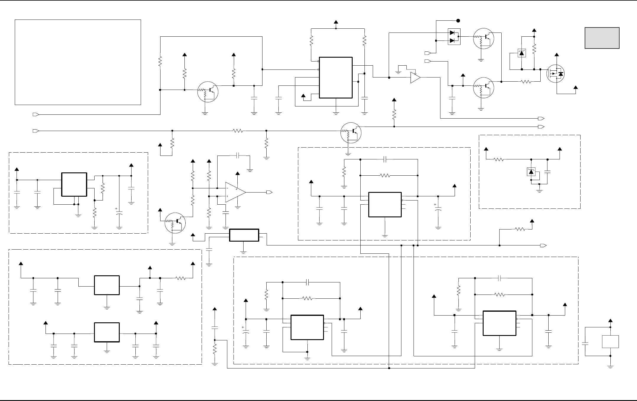
7-36 Schematics, Component Location Diagrams, and Parts Lists: HUD4022A/HUD4025B (VHF) Main Board
May 25, 2005 6881096C74-B
Figure 7-34. HUD4022A Power Supply Schematic
VCC3
Mic Bias Circuit
2.85 / 100 mA
T-Gates, VIPS, SB9600
NP
1.8V Digital Supply Regulator
Audio PA
FILT_B+
Emergency Sense Block
9V Regulator
5.0 / Battery
Battery
VCC5
SOURCED BY:
NP
Battery
VCC5 I/O Ring, EEPOTs
9.3V / 1A
UNSW_5V
Voltage Translation
USB, Codec
DC DISTRIBUTION
SW_B+
V(operating)/mA(max)
A+
VCC5
FILT_B+
VCC1.8, VCC1.55
NP
Emergency Detect/Timer
VCC2.85
9V Regulators
1.86 & 1.55 / 100 mA
SW_B+ Sense Circuit
VOLTAGE
Patriot, EIM, Memory
SUPPLY FOR
5.0 / 500 mA
3.0 / 100 mA
UNSW_5V Supply
5V Regulator
Power Control
9.3V_TX
2.85V Digital Supply Regulator
VCC5
SW_B+
A+
A+
1.8V, 3V Regulators
1.55V Digital Supply Regulator
SW_B+
R0521
VCC2.85
VCC5_FILT
R0505
39K
VCC5
10K
100pF
C0503
4.7uF
C0517
1uF
C0525
0
C0526
.01uF
VCC5
R0527
OUT
A+
UNSW_5V
MC78M05
U0503
2
GND
1IN 3
0.1uF
C0504
Q0503
SW_A+
R0510
C0536
0.1uF
9.3V_ABACUS
43K
VCC5_FILT
33K
R0511
100K
R0500
4.7uF
C0518
R0513
39K
Q0505
10K
R0524
R0503
VCC2.85
UNSW_5V
SW_A+
100K
VCC2.85
Q0504
11V
VR0501
C0507
0.1uF0.1uF
C0524
D0501
U0505
MC78M05
GND
2
IN
1OUT 3
2K
R0509
100K
R0516
5V_ABACUS
UNSW_5V
4.7uF
C0527
UNSW_5V
7.5K
R0528
C0514
150uF
7FEEDBACK
4GND
8INPUT 1
OUTPUT
2
SENSE
3SHUTDOWN
VTAP 6
4
LP2951CD
U0502
5
ERROR
U0604-2
MC33202
6
5
7
8
0.1uF
C0512
1uF
C0532
FEEDBACK
7
GND
4
INPUT
8OUTPUT 1
SENSE 2
SHUTDOWN
3
VTAP 6
SW_B+_ON-OFF
SW_B+_ON-OFF
U0501
LP2951CD
ERROR 5
0.1uF
C0528
0.1uF
C0531
10
R0519
R0507
10K
R0502
390K
A+
4.7uF
C0510
R0531
Q0500
4.7uF
100K
CD
5
GND
3
INPUT
2
NC 4
OUTPUT 1
C0522
U0504
53D46
ON_OFF
2
VIN
4VOUT 5
.01uF
C0506
U0500
LM2941
ADJ 1
GND1
3
GND2
6
100pF
C0502
10K
R0506
C0537
1uF
0
0.1uF
C0516
R0514
Q0501
.01uF
C0519
22uF
C0533
0.1uF
C0520
1.2K
R0529
SW_A+
5.1V
VCC5_FILT
0.1uF
VR0500
C0515
47K
R0520
C0521
4.7uF
R0504
100K
R0508
10K
20K
R0522
A+
VCC2.85
1
C0505
.01uF
C0534
TP0500
0.1uF
C0523
0.1uF
1K
VCC5
THRESHOLD
6
TRIGGER
2
VPOS
8
A+
R0515
U0506
LMC555
CONTRLVOLTAGE
5DISCHARGE 7
GND
1
OUTPUT 3
RESET
4
C0500
VCC9
VCC5
0.1uF
10K
R0518
C0535
VCC9
VCC1.8
2
1
4
VCC2.85
0.1uF
R0523
NC7SZ125
U0508-1
Q0502
100K
C0513
3
GND
5
VCC
150uF
C0529
VCC1.55
U0508-2
PWR_GND
SENSE 2
SHUTDOWN
3
VTAP 6
4.7uF
U0507
LP2951CD
ERROR 5
FEEDBACK
7
GND
4
INPUT
8OUTPUT 1
VCC2.85
UNSW_5V SOFT_TURN_OFF
SW_B+_ON-OFF
R0512
10K
IGNITION_SENSE
IGNITION
SW_B+_SENSE
EMERG_SENSE
EMERGENCY
LV_DETECT
47K
47K
47K
47K
47K
47K
47K
47K
47K
47K
MAEPF-27845-O
Part Series
500
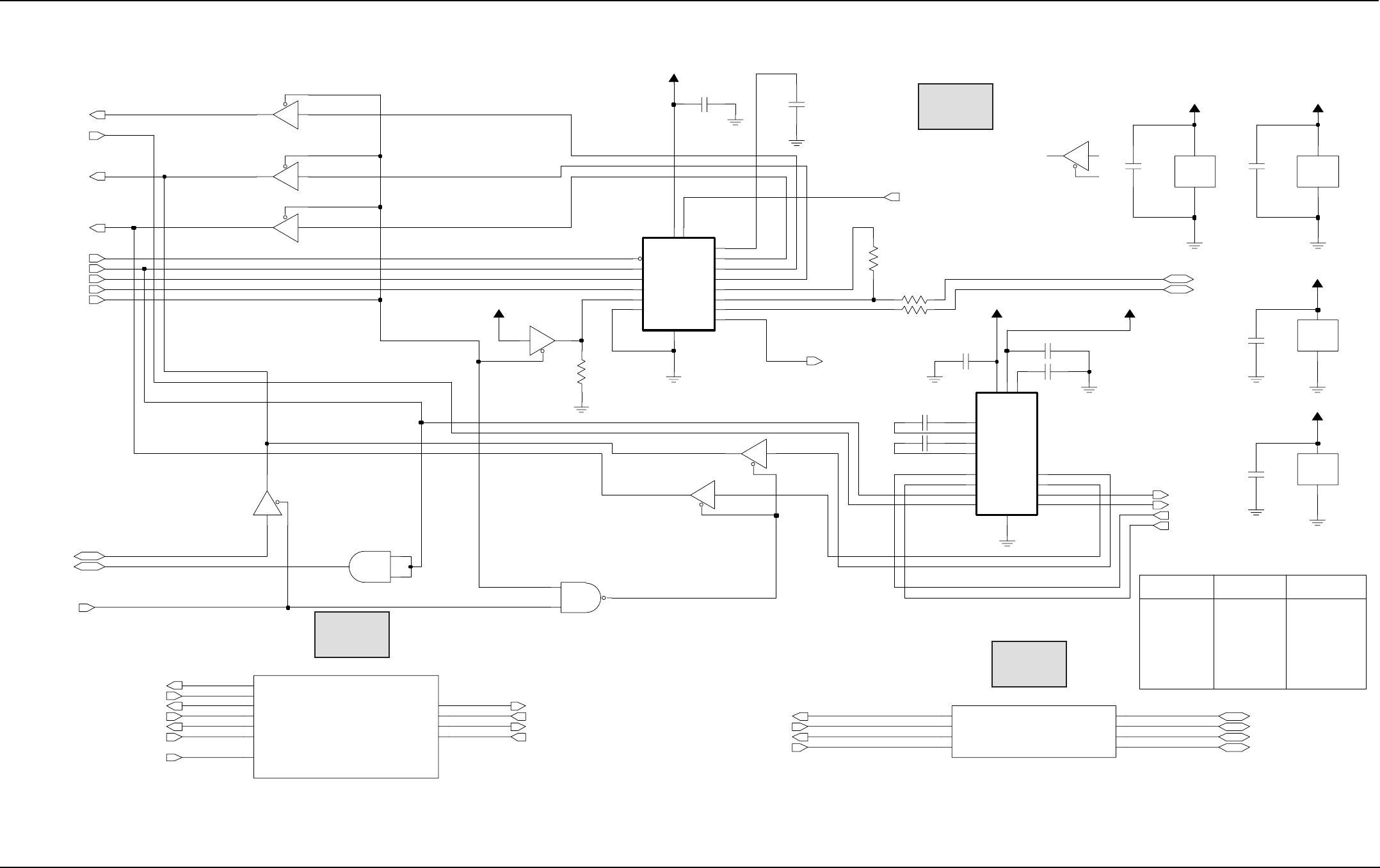
Schematics, Component Location Diagrams, and Parts Lists: HUD4022A/HUD4025B (VHF) Main Board 7-37
6881096C74-B May 25, 2005
Figure 7-35. HUD4022A USB/RS232/SB9600 Schematic
SB9600 Block
NP
VIP I/O Block
BUFFER SUPPLY BUFFER SUPPLY
1
USB*_RS232_EN
0Not Allowed
BOOT_DATA_EN* Mode of Operation
0
0
0
11
1
Boot Data
USB
RS232
R0304
13
11
22
1
2
4
U0300-4
MC74LCX125
12
VCC5
VCC2.85
U0308-1
NC7ST08
C0312
0.1uF
10
8
MC74LCX125
U0303-4
12
13
11
MC74LCX125
U0300-3
9
1.5K
R0303
C0309 0.1uF
U0303-2
MC74LCX125
5
4
6
VCC2.85
VIP_IN_1_3V VIP_IN_1_5V
VIP_IN_2_3V VIP_IN_2_5V
VIP_OUT_1_3V VIP_OUT_1_5V
VIP_OUT_2_3V VIP_OUT_2_5V
U0300-2
MC74LCX125
5
4
6 GND
7
VCC
14
10K
R0307
VCC2.85
PWR_GND
U0300-5
14
VBUS
7
VCC
4
VM
11 VO_VPO 3
VP
15
VPU
13
VREG
DPOS
16 ENUMERATE
12 FSE0_VMO
17 GND
MODE
6
1OE_N 2
RCV
5SUSPND
8
USB_DET
VCC
5
ISP1104
U0304
9
DNEG
10
VCC
5
PWR_GND
U0308-2
GND
3
VNEG 6
VPOS 2
PWR_GND
U0307-2
GND
3
R1O 12
R2I
8R2O 9
T1I
11 T1O 14
T2I
10 T2O 7
VCC 16
U0305
ST3232
3C1NEG
C1POS
1
5C2NEG
4C2POS
GND
15
R1I
1310
8
C0307 0.1uF
22
MC74LCX125
U0303-3
9
R0305 VCC5 VCC9
0.1uF
C0302
7
GND
14
VCC
C0308 0.1uF
U0303-5
PWR_GND
0.1uF
C0311
0.1uF
0.1uF
C0313
C0306
0.1uF
C0310 0.1uF
VCC2.85
C0305
3
MC74LCX125
U0303-1
2
1
3
VCC2.85
1
2
4
MC74LCX125
U0300-1
2
1
URTS2
URXD2
UTXD2
TC7S00FU
U0307-1
C0301
0.1uF
BUS+_UARTB_TXD
BUS-_UARTB_RXD
BUSY_UARTB_RTSLHRST_IN
LHRST_OUT RESET_UARTB_CTS
SB96_RS232*_EN
UCTS2 VIP_OUT_1_5V
BOOT_TX
UTXD1_USB_VPOUT
UTXD1_USB_VPOUT
USB_TXENB
RIA_USBSUSP
USB_INT*
USB_VMI
USB_VPI
USB*_RS232_EN
USB+
USB+
USB_PWR
VIP_IN_1_5V
UARTA_CTS
UARTA_TXD
UARTA_RXD
UARTA_RTS
BOOT_DATA_EN*
UCTS1_USB_FSEN
UCTS1_USB_FSEN
RESET_UARTB_CTS
BUS+_UARTB_TXD
BUS-_UARTB_RXD
BUSY_UARTB_RTS
USB_VMOUT
VIP_OUT_1_3V
VIP_IN_1_3V
VIP_OUT_2_3V
VIP_IN_2_3V
UTXD2
UCTS2
LHRST_IN
LHRST_OUT
URTS2
URXD2
BOOT_RX
USB_VPIN
VIP_OUT_2_5V
VIP_IN_2_5V
URXD1_USB_VMIN
URXD1_USB_VMIN
URTS1_USB_XRXD
URTS1_USB_XRXD
SB96_RS232*_EN
USB-
USB-
MAEPF-27847-O
Part Series
300
Part Series
600-1
Part Series
600-2

7-38 Schematics, Component Location Diagrams, and Parts Lists: HUD4022A/HUD4025B (VHF) Main Board
May 25, 2005 6881096C74-B
Figure 7-36. HUD4022A SB9600 Schematic
NP
BUFFER SUPPLY
NAND SUPPLY
Connector IF
NAND SUPPLY
BUFFER SUPPLY
BUFFER SUPPLY
Patriot UART B
BUFFER SUPPLY
MC74LCX125
U0602-2
5
4
6
0.1uF
C0610
C0614
SB96_RS232*_EN_INV
R0627
100K
0.1uF
C0613
0.1uF
VCC2.85
VCC
Q0610
U0608-2
PWR_GND
3
GND
5
U0607-2
PWR_GND
3
GND
5
VCC
U0602-5
PWR_GND
7
GND
14
VCC
C0604
0.1uF
TC7S00FU
U0609-1
1
2
4
100
R0623
VCC2.85
0.1uF
C0611
0.1uF
C0606
U0610-2
PWR_GND
3
GND
5
VCC
R0628
100K
VCC5
SB96_RS232*_EN_INV
100K
U0602-3
MC74LCX125
9
10
8
R0630
4
MC74LCX125
U0603-2
5
4
6
VCC2.85
VCC5
TC7S00FU
U0610-1
1
2
10K
R0639
VCC2.85
Q0611
10K
10K
R0638
GND
7
VCC
14
R0625
PWR_GND
U0603-5
R0629
10K
100K
VCC2.85
SB96_RS232*_EN_INV
VCC2.85
VCC5
100
R0622
R0634
C0603
U0609-2
PWR_GND
3
GND
5
VCC
0.1uF
R0636
Q0613
2
3
1
8
4
VCC5
10K
2
1
3
MC33202
U0604-1
MC74LCX125
U0602-1
2
1
3
U0603-1
MC74LCX125
0
R0632
R0631 0
R0635
100K
7
YB
9
YC
12
YD
VCC5
VCC5
14 I0D
3I1A
6I1B
10 I1C
13 I1D
1SELECT
16
VCC
4
YA
SN74CBT3257
U0606
15 EN_OE
8GND
2I0A
5I0B
11 I0C
100pF
1
2
4
C0616
100
R0621
NC7ST08
U0608-1
100
R0620
1
2
4
NC7ST08
U0607-1
VCC5
Q0612
U0602-4
MC74LCX125
12
13
11
100K
R0626
C0600
0.1uF
BUS-
BUS+*
BUSY BUSY
LH_RESET
BUS-*
BUS+
BUSY*
LH_RESET*
URXD2
SB96_RS232*_EN
URTS2
UTXD2
LHRST_IN
LHRST_OUT
BUS+_UARTB_TXD
BUSY_UARTB_RTS
RESET_UARTB_CTS
BUS-_UARTB_RXD
UCTS2
10K
10K
10K 10K
10K
10K
10K 10K
10K
10K
10K 10K
10K
10K
10K 10K
MAEPF-27919-O
Part Series
600-1
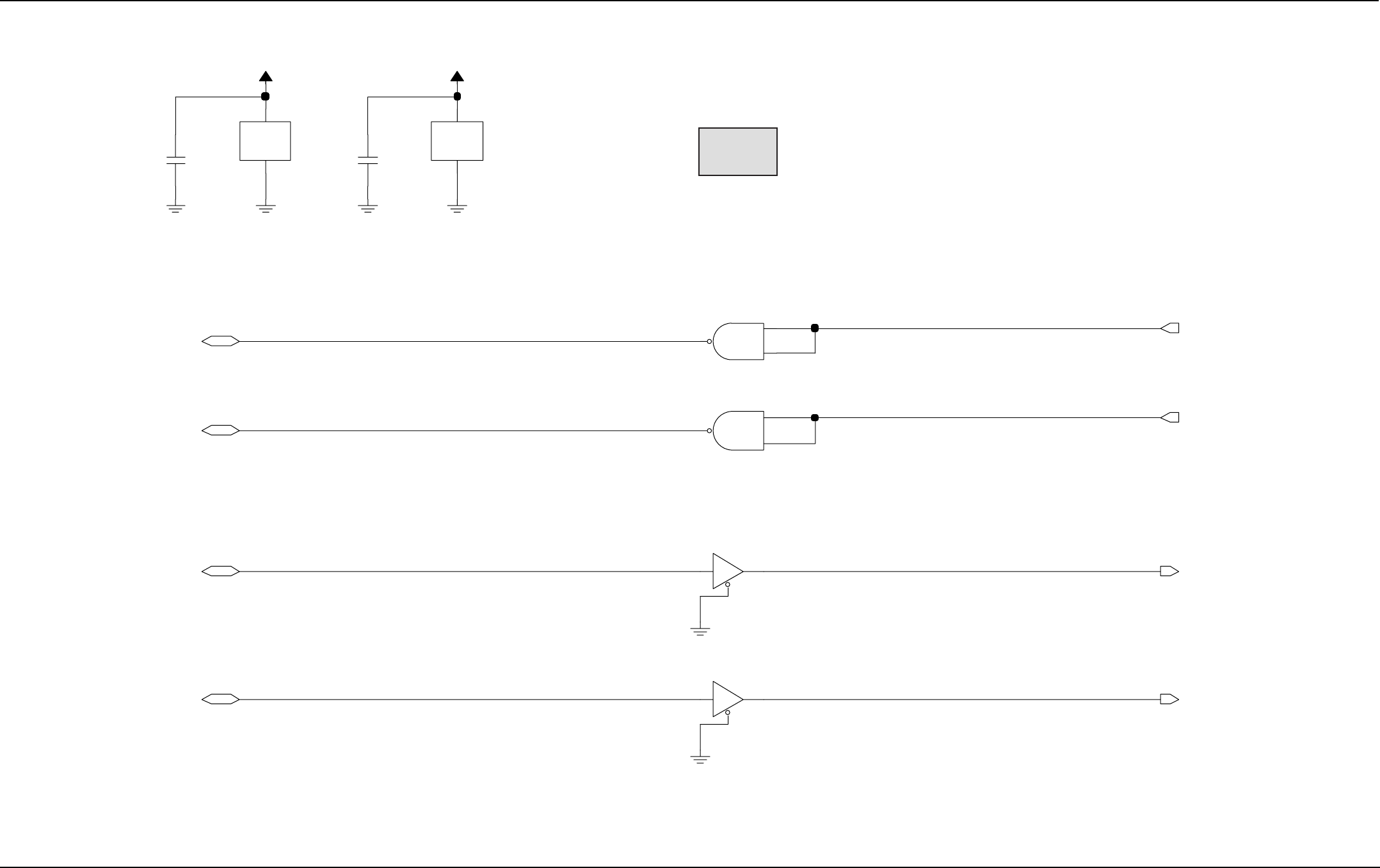
Schematics, Component Location Diagrams, and Parts Lists: HUD4022A/HUD4025B (VHF) Main Board 7-39
6881096C74-B May 25, 2005
Figure 7-37. HUD4022A USB/RS232/SB9600 VIP Input/Output Schematic
4
1
2
4
U0605-1
TC7S00FU
1
2
VCC5
TC7S00FU
U0601-1
0.1uF
VCC5
0.1uF
C0605C0601 GND
5
VCC
U0601-2
PWR_GND
3
GND
5
VCC
8
U0605-2
PWR_GND
3
12
13
11
U0603-3
MC74LCX125
9
10
VIP_IN_1_3V
VIP_IN_2_3V
VIP_IN_1_5V
VIP_OUT_1_3V
VIP_OUT_1_5V
VIP_OUT_2_3V
VIP_OUT_2_5V
VIP_IN_2_5V
U0603-4
MC74LCX125
MAEPF-27848-O
Part Series
600-2

7-40 Schematics, Component Location Diagrams, and Parts Lists: HUD4022A/HUD4025B (VHF) Main Board
May 25, 2005 6881096C74-B
Figure 7-38. HUD4022A Control-Head Connector Schematic
SPARE_1
UARTA_RXD
BUSY
SPI_MOSIB
Interface
SPI_SCKB
OPTB+_BOOTSEL_VPP
AUX_RX
NAUTILUS_CS*
RS232 BUS
VIP_OUT_1_12V
MIC_HI
FOR NEW CH/ACCYs
IGNITION
SW_B+
SSI / NAUTILUS
SPI_MISOB
PTT*
SAP_DCLK
UARTA_CTS
SB9600
NOT USED
NAUTILUS_INT*
LH_RESET
VIP_OUT_2_12V
VIP_IN_2_5V
AUDIO
Programming Cable
AUX_MIC
ONE_WIRE
SPKR-
SAP_RX
BOOT_RX
BUS_PWR_OUT
BUS-
UARTA_RTS
SPARE_2
SAP_FSYNC
SAP_TX
VIPs
UARTA_TXD
VIP_OUT_1_5V
VIP_IN_1_5V
VCC5
A+
SSI_INT
EMERGENCY
RX_FILT_AUDIO
BUS+
BOOT_TX / KEYFAIL*
AUX_TX
VIP_OUT_2_5V
SPKR+
J0401-47
J0401-12
J0401-26
J0401-50
33pF
100
C0424
J0401-13
R0418
C0443
33pF
R0415
100
J0401-37
C0453
33pF
C0452
33pF
15V
C0475
100pF
3
6
4
1
VR0424
Q0403
5
2
J0401-38
J0401-40
C0469
0.1uF
J0401-15
R0431
10K
100pF
C0427
J0401-19
R0409
C0456
33pF
1
K1 3
K2 4
K3 6
K4
10K
5.6V
*VR0417*
2A1
5
A2
J0401-25
1
TP0414
1
NO
6
2
VPOS
TP0401
U0401
NLAST4599
COM
5
3GND
IN 1
NC
4
C0439
J0401-18
100pF
J0401-6
J0401-44
33pF
2
5
1
3
4
6
C0459
VR0412
20V
33pF
J0401-2
J0401-31
VCC2.85
C0422
10K
J0401-20
R0425
C0462
220pF
J0401-33
J0401-48
0.1uF
C0441
VR0425
15V
1
TP0411
1
VR0420
11V
2
3
F0400
125V
5A
C0450
33pF
Q0404
C0437
470pF
J0401-43
VR0413
20V
J0401-11
C0446
100pF
1
C0436
470pF
470pF
TP0408
C0435
J0401-1
C0444
33pF
1K
R0404
A1
A2
K1
K2
K3
K4
5.6V
*VR0414*
C0431
100pF
J0401-30
J0401-24
Q0402
VR0423
15V
1
J0401-46
VCC5
TP0415
1
TP0403
J0401-23
VCC5
C0445
33pF
C0434
100pF 100pF
J0401-32
C0433
R0416
100
33pF
C0432
100pF
100pF
C0454
J0401-9
C0449
J0401-10
J0401-42
C0461
220pF
TP0407
1
33K
R0422
0
R0421
TP0413 1
C0448
100pF
J0401-35
1
C0425
100pF
TP0402
C0442
33pF
3
GND
5
VCC
J0401-3
TP0412
1
U0402-2
PWR_GND
C0477
VCC2.85
100pF
C0428
100pF
J0401-45
C0426
470pF
J0401-22
J0401-14
J0401-34
J0401-36
J0401-16
C0438
33pF
470pF
J0401-21
SW_B+
C0457
J0401-27
J0401-49 J0401-41
33pF
11V
C0458
U0402-1
NC7SZ125
2
1
4VR0421
J0401-39
VCC2.85
100pF
C0478
A+
C0430
100pF
C0451
33pF
VCC5
J0401-4
J0401-7
VR0422
15V
10K
R0420
J0401-8
J0401-5
C0429
100pF
100pF
C0460
C0440
C0447
100pF
100pF
J0401-29
4.7K
R0517
*VR0418*
2A1
5
A2
1
K1 3
K2 4
K3 6
K4
5.6V
100pF
C0476
J0401-17
J0401-28
TP0410
1
C0455
33pF
R0417 100
4.7K
R0419
TP0409
1
C0423
33pF
SPARE_2
SPARE_1
SW_B+_ON-OFF
IGNITION
BUS+_UARTB_TXD
BUS-_UARTB_RXD
BUSY_UARTB_RTS
RESET_UARTB_CTS
C0470
33pF
MIC_HI
RX_FILT_AUDIO
IGNITION_CONN
SPKR- SPKR-
BOOT_RX
EMERGENCY
ONE_WIRE
UARTA_TXD
UARTA_RXD
UARTA_CTS
UARTA_RTS
UARTA_TXD_CH
UARTA_CTS_CH
UARTA_RTS_CH
CABLE_DET
BOOT_DATA_EN*
KEYFAIL
BUS_PWR_OUT
MIC_HI
AUX_MIC AUX_MIC
PTT*
AUX_RX
VIP_IN_2_5V
VIP_IN_1_5V
VIP_OUT_2_5V
VIP_OUT_1_5V
VIP_OUT_1_12V
VIP_OUT_2_12V
AUX_TX
NAUTILUS_CS*
SAP_DCLK
SAP_TX
UARTA_RXD_CH
SAP_RX
SAP_FSYNC
SPI_MOSIB
SPI_SCKB
NAUTILUS_INT*
MOD
BOOT_TX
FORCE_FAIL*
SPKR+ SPKR+
SSI_INT*
SPI_MISOB
10K 10K
10K
10K
47K
47K
47K
47K
MAEPF-27843-O
Part Series
400-2
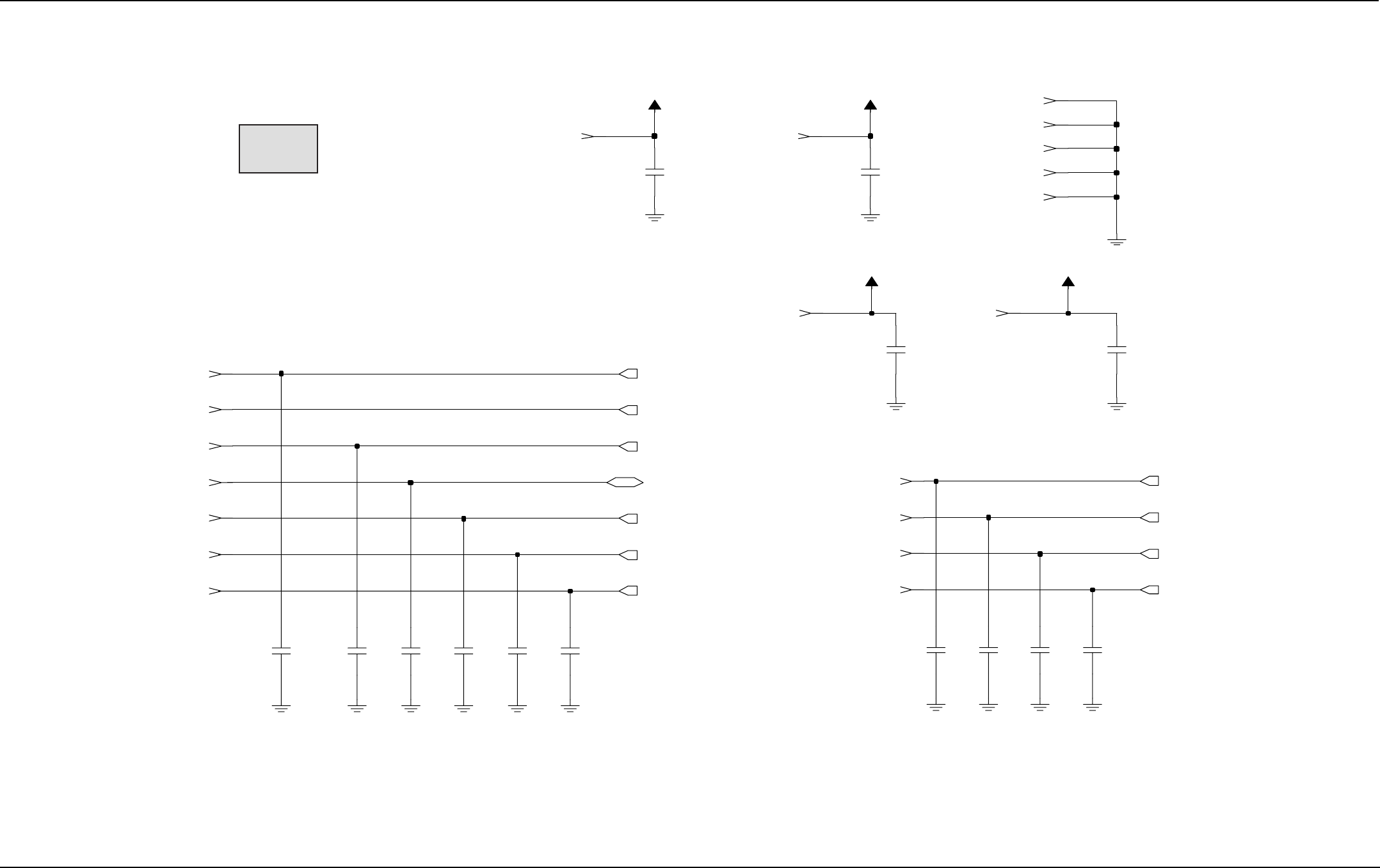
Schematics, Component Location Diagrams, and Parts Lists: HUD4022A/HUD4025B (VHF) Main Board 7-41
6881096C74-B May 25, 2005
Figure 7-39. HUD4022A Interface Connector Schematic
Control / I/O
SAP SSI Audio Bus
100pF
C0700
J0501-8J0501-7
J0501-9
J0501-19
J0501-20
J0501-16
J0501-18
A+
VCC2.85
SW_B+
J0501-13
J0501-4
J0501-10
C0712
100pF
C0711
100pF
C0710
100pF
C0709
100pF
220pF
C0713
220pF
C0714
J0501-17
J0501-1
J0501-5
J0501-6
J0501-11
J0501-14
J0501-3
VCC5
J0501-2
100pF
J0501-12
J0501-15
C0708C0706
100pF 100pF
C0705
100pF
C0704
100pF
C0703
100pF
C0702
100pF
C0701
SAP_TX
TAMPER_ENC
SAP_DCLK
SAP_RX
SAP_FSYNC
WAKEUP
KEYFAIL*
ENC_RESET
ENC_SPARE1
ENC_SPARE2
BOOT*
MAEPF-27846-O
Part Series
700

7-42 Schematics, Component Location Diagrams, and Parts Lists: HUD4022A/HUD4025B (VHF) Main Board
May 25, 2005 6881096C74-B
Figure 7-40. HUD4022A/HUD4025B Secure Interface Board Schematic
11 P501-2
U803-4
12
13
VCC2.85
0.1uF
C811
10K
R806
P501-12
0
R808
J701-13
J701-15 *P501-11*
J701-27
J701-34
J701-12
VCC2.85VCC2.85
J701-36
J701-7
R802
1K
SW_B+
J701-22
J701-24
100K
R807
VCC2.85
J701-16
Q4 8
RESET
12
J701-6
J701-10
U802-2
CLK
13 Q1 11
Q2 10
Q3 9
U803-1
1
2
3
U803-3
9
10
8
P501-9
0.1uF
C809
VCC2.85
PWR_GND
U805-2
GND
3
VCC
5
U805-1
2
1
4
VCC2.85
J701-1
J701-8
A+
J701-19
J701-11
P501-4
J701-3
J701-35
VCC5
0.1uF
SW_B+
100K
C802
R804
4
5
6
VCC2.85
Q802
U802-3
PWR_GND
7
GND
14
VCC
U803-2
RESET
2
PWR_GND
U803-5
GND
7
VCC
14
U802-1
CLK
1Q1 3
Q2 4
Q3 5
Q4 6
J701-20
VCC2.85
J701-17
J701-23
PWR_GND
U804-3
GND
7
VCC
14
J701-4
UNSW_B+_ENC
J701-33
D801
1
2
3
J701-21
Q800
1
3
2
J701-31J701-29
J701-25
R805
10K
R800
10K
J701-32
Q803
47K
47K
P501-17
C803
P501-20
J701-14 A+
0.1uF
P501-7
P501-3
5.6V
VR800
R801
100K
P501-1
P501-10
J701-38
P501-18
2
J701-5
U800
MC33269D
ADJ
1
IN
3OUT
J701-2
VCC5
UNSW_B+_ENC
CLK
11
D
9
Q13
Q* 12
RESET 10
SET
8
J701-39
10uF
VCC2.85
U804-2
C805
1uF
C804
P501-16
J701-30
0.1uF
C808
0.1uF
C807
SW_B+_ENC
0.1uF
C806
U804-1
CLK
3
D
5
Q1
Q* 2
RESET 4
SET
6
3GND
2
1
NC
4
5
VCC
U801
0.1uF
J701-18
C801
0.47
C810
P501-15
SW_B+_ENC
J701-40
J701-26 P501-13
J701-37
J701-9
J701-28
P501-14
P501-19
P501-6
P501-8
P501-5
SAP_TX
SAP_TX
ENC_SEL
TAMPER_ENC TAMPER_ENC
BOOT*
ENC_SPARE2
ENC_SPARE1
ENC_RESET
WAKEUP
SAP_RX
SAP_FSYNC
SAP_DCLK
KEYFAIL*
KEYFAIL*
MAEPF-27914-O
Part Series
800
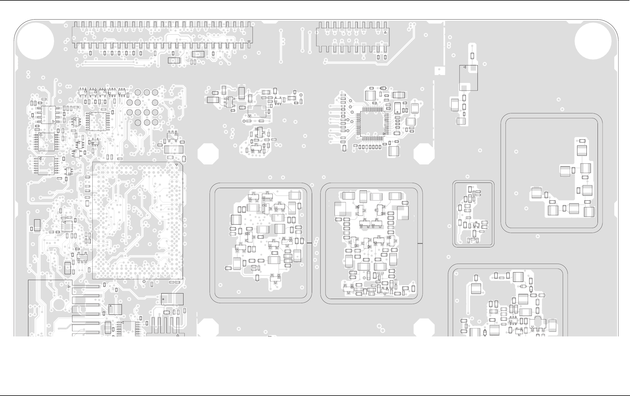
Schematics, Component Location Diagrams, and Parts Lists: HUD4022A/HUD4025B (VHF) Main Board 7-43
6881096C74-B May 25, 2005
Figure 7-41. HUD4022A Main Board Layout—Side 1 Top
C0100
C0101
C0105
C0204
C0207
C0213
C0214 C0217
C0220
C0223
C0243
C0301
C0312
C0428
C0436
C0437
C0442
C0444
C0450
C0452
C0454
C0455
C0458
C0461
C0469
C0502
C0503
C0519
C0536
C0600
C0603
C0604
C0606
C0610
C0611
C0613
C0614
C0616
C0703
C0705
C0953
C0954
C0981
C0984
C0987
C3000
C3002
C3003
C3004
C3006
C3008
C3009
C3010
C3011
C3012
C3013
C3014
C3015
C3019
C3020
C3021
C3022
C3023
C3032
C3033
C3036
C3037
C3038
C3039
C3042
C3047
C3256 C3259
C3260
C3261
C3265
C3266
C3267
C3270
C3273
C3277
C3278
C3279
C3290
C3291
C3296
C3297
C3301
C3302
C3303 C3304
C3305
C3306
C3307
C3309
C3311
C3312
C3408
C3415
C3418 C3420
C3511
C3750
C3766
C3768
C3770
C3777
C3778
C3779
C3780
C3781
C3782
C3783
C3784
C3785
C3787
C3788
C3791 C3792
C3793
C3794
C3795
C3796
C3797
C3798
C3799
C3800
C3803
C3806
C3807
C3808
C3816
C3818
C3819
C3824
C3825
C3826
C3828
C3830
C3831
C3835
C3836
C3837
C3838
C3839
C3840
C3841
C3842
C3843
C3844
C3845
C3846
C3847
C3848
C3849
C3850
C3851
C3852
C3853
C3854
C3868
C3878
C3880
C3910
C3911
C3912
C3913
C3914
C3915
C3916
C3930
C3931
C3932
C3933
C3934
CLKOUT
D3001
D3252
D3253
D3254
D3256
D3750
D3751
D3752
D3753
D3754
D3755
D3756
D3767
D3768
D3769
D3770
D3771
D3772
D3773
DOUT
E3000
E3001
E3003
E3007
E3008
FS
50
49
2
1
J0401 J0501
L3000
L3002
L3004
L3005
L3251
L3252 L3253
L3254
L3256
L3257
L3258
L3261
L3265
L3266
L3268
L3269
L3270
L3275 L3276
L3277
L3405
L3407
L3751
L3753
L3754
L3755
L3758
L3759
L3760
L3761
L3762
L3763
L3764
L3765
L3766
L3767
L3768
L3769
L3770
L3771
L3772
L3773
L3774
L3784
PC
PD
PE
Q0610
Q0611
Q0612
Q0613
Q3254
Q3255
Q3750
Q3751
Q3752
Q3753
Q3754
Q3755
Q3761
Q3769
R0101
R0102
R0103
R0104
R0109
R0110
R0111
R0113
R0114 R0115
R0116
R0117
R0119
R0120
R0121
R0122
R0123
R0124
R0125
R0200 R0204
R0300
R0301
R0303
R0304
R0305
R0307
R0415
R0422
R0425
R0505
R0508
R0509
R0527
R0620
R0621
R0622
R0623
R0624
R0625 R0626
R0627 R0628
R0629
R0630
R0631
R0632
R0634
R0635
R0636 R0638
R0639
R0923
R0951
R0952
R3000
R3002
R3006
R3007
R3008
R3010
R3012
R3014
R3016
R3017
R3018
R3019
R3022
R3254
R3255
R3257
R3258
R3259
R3260
R3271
R3274
R3275
R3750
R3753 R3754
R3755
R3756
R3758
R3759
R3761
R3763
R3767
R3768
R3775
R3776
R3778
R3779
R3786
R3787
R3788 R3789
R3790R3798
R3800
R3801
R3811 R3812
R3813
R3814
R3825
R3827
R3828
R3831
R3833
R3837
R3838
R3839
R3840
R3854
R3855
R3856
R3857
R3864
R3865
R3868
R3869
R3870
R3871
R3872
R3873
SH3750 SH3754
SH3759
SH3761
SH3763
TP0002
TP0400
TP0401
TP0402
TP0407
TP0408
TP0409
TP0410
TP0411
TP0412
TP0413
TP0415
TP6750
TP6755
TP6770
123456789101112131415161718
18 17 16 15 14 13 12 11 10 9 8 7 6 5 4 3 2
A
B
C
D
E
F
G
N
M
L
K
J
I
H
R
S
T
U
V
W
X
P
Z
YY
Z
P
X
W
V
U
T
S
R
H
I
J
K
L
M
N
G
F
E
D
C
B
A
U0001
U0102
10
U0204
59
13
U0304
U0402
U0504
U0508
14
78
U0602
14
78
U0603
1
45
8
U0604 16
9
8
1
U0606
U0607
U0608
4
3
5
U0609
4
3
5
U0610
5
16
9
8
1
U0959
1
37
25 13
U3000
U3750
U3752
Y0100
2
34
5
6
Y3401
2
34
Y3750
Y3751
Y3752
Y3753
Y3754
R3826
TP0403
TP0400
R3015
7-44 Schematics, Component Location Diagrams, and Parts Lists: HUD4022A/HUD4025B (VHF) Main Board
May 25, 2005 6881096C74-B
Figure 7-42. HUD4022A Main Board Layout—Side 1 Bottom
OL 79B02970C81-O
SHOWN FROM SIDE 1
C0001
C0214
C0401
C0406
C0407
C0412
C0413
C0417
C0463
C0464
C0467
C0531
C0532
C0533
C0924
C0952
C0955
C0956
C0957
C0959
C0962
C0963
C0964
C0965
C0966
C0967
C0971
C0972
C0973
C0975 C0976
C0978
C0979
C0980
C0981
C0983
C0984
C0986
C0987
C3255
C3256
C3257
C3259
C3260
C3264
C3272
C3282
C3284
C3299
C3300
C3303
C3306
C3307
C3308
C3312
C3501
C3506
C3508
C3511
C3562
C3563
C3734
C3936
D0952
D3251
D3252
D3255
D3256
J0950
3
2
J3700
L3261
L3266
1
L3272
1
L3273
L3277
L3501
L3503
L3737
M3520
M3542
M3700
M3721
Q0200
3
4
1
Q0503
Q0955
Q3254
Q3255
SS
S
654
SD
G
23
Q3550
R0220
R0222
R0430
R0515
R0531
R0908
R0915
R0916
R0924
R0946
R0947
R0950
R0953
R0954
R0960
R0963
R0964
R0967
R0968
R0969
R0970
R0971 R0972
R0973
R0974
R0975
R0976
R0977
R0978
R0979
R0980
R0981
R0982
R0983
R0984
R0985
R0986
R0987
R0988
R0989
R0990 R0992
R0993
R0994
R0995
R0996
R0997
R0998
R0999
R3254
R3256
R3257
R3259
R3272
R3274
R3502
R3550
R3560
R3561
SC0001
SC0002
TP0954
11
9
U0204
5
U0950
5
U0951
5
6
10
U0952
78
14
U0955
78
14
U0956
7
8
14
U0957
16
9
8
1
U0959
U3250
U3561
VR0405
VR0406
VR0407
VR0501
OL 79B02970C83-O
Schematics, Component Location Diagrams, and Parts Lists: HUD4022A/HUD4025B (VHF) Main Board 7-45
6881096C74-B May 25, 2005
Figure 7-43. HUD4022A Main Board Layout—Side 2 Top
U0305
C0102
C0103
C0104
C0106
C0107
C0201
C0202
C0203
C0205
C0206
C0208
C0209
C0210
C0211
C0212
C0216
C0224
C0225
C0226
C0227
C0228
C0230
C0231
C0232
C0233
C0234
C0235
C0236
C0237
C0238
C0239
C0240
C0242
C0302
C0305
C0306
C0307
C0308
C0309
C0310
C0311
C0313
C0421
C0422
C0423
C0424
C0425
C0426
C0427
C0429
C0430
C0431
C0432
C0433
C0434
C0435
C0438
C0439 C0440
C0441
C0443
C0445
C0446 C0447
C0448
C0449
C0451
C0453
C0456
C0457
C0459
C0460
C0462
C0470
C0475
C0476
C0477
C0478
C0500
C0504
C0506
C0507
C0510
C0512
C0513
C0514
C0515
C0520
C0521
C0522
C0523
C0524
C0525
C0526
C0527
C0528
C0529
C0537
C0601
C0605
C0700
C0701
C0702
C0704
C0706
C0708
C0709
C0710
C0711
C0712
C0713 C0714
C0901
C0902
C0903
C0904
C0905
C0906
C0907
C0908
C0909
C0910
C0911
C0912
C0913
C0914
C0915
C0916
C0917
C0918
C0919
C0944
C0950
C0951
C3001
C3005
C3007
C3016
C3017
C3018
C3024
C3025
C3026
C3027
C3028
C3029
C3030
C3034
C3035
C3040
C3041
C3043
C3044
C3045
C3046
C3048
C3251
C3252
C3253
C3254
C3258
C3268
C3269
C3271
C3274
C3275
C3276
C3280
C3281
C3283
C3286
C3287
C3288
C3289
C3292
C3293
C3294
C3295
C3298
C3310
C3400
C3401
C3402
C3403
C3404
C3405
C3406
C3409
C3410
C3411
C3412
C3414
C3416
C3417
C3421
C3424
C3751
C3752
C3753
C3754
C3755
C3757
C3758
C3759
C3761
C3762
C3763
C3764
C3765
C3767
C3769
C3771
C3772
C3773
C3774
C3775
C3776
C3786
C3790
C3802
C3804
C3809
C3810
C3811
C3812
C3813
C3814
C3815
C3817
C3820
C3821
C3822
C3823
C3827
C3829
C3832
C3833
C3834
C3855
C3856
C3857
C3858
C3859
C3860
C3861
C3862
C3863
C3864
C3865
C3869
C3870
C3871
C3872
C3873
C3875
C3876
C3877
C3879
C3881
C3882
C3883
C3917
C3918
C3919
C3920
C3921
C3924
C3925
C3926
C3935
D0501
D3000
D3257
D3258
D3400
D3401
D3757
D3758
E3002
E3004
E3005
E3006
F0400
FL0900
L400
L3003
L3006
L3007
L3008
L3255
L3259
L3260
L3262
L3263
L3264
L3267
L3271
L3400
L3401 L3403
L3404
L3406
L3408
L3750
L3752
L3756
L3757
L3775
L3776
L3778
L3779
L3781
L3782
L3783
L3785
L3787
Q0402
Q0403
Q0404
Q0500
Q0501
Q0502
Q0504
Q0505
Q3000
Q3001
Q3252
Q3253
Q3256 Q3257
Q3258
Q3400
Q3401
Q3756
Q3757
Q3758
Q3759
Q3760
Q3762
Q3763
Q3764
Q3765
Q3766
Q3767
Q3768
R0105
R0106
R0107 R0108
R0126
R0127
R0201
R0202
R0203
R0205
R0206
R0207
R0208
R0209 R0210
R0212
R0216
R0218
R0219
R0221
R0223
R0224
R0225
R0226
R0227
R0228
R0229
R0230
R0235
R0236
R0403
R0404
R0409
R0411
R0416
R0417
R0418
R0419
R0420
R0421
R0431
R0500
R0502
R0503
R0504
R0507
R0512
R0513
R0514
R0516
R0517
R0518
R0519
R0520
R0521
R0522
R0523
R0524
R0525
R0900
R0901
R0902
R0903
R0904
R0905
R0906
R0907
R3001
R3003
R3004
R3005
R3009
R3011
R3020
R3021
R3023
R3251
R3252
R3261
R3262
R3263
R3264
R3265 R3266
R3267
R3268
R3269
R3270
R3273
R3277
R3278
R3279
R3280
R3281
R3288
R3400
R3401
R3402
R3405
R3407
R3409
R3413
R3751
R3752
R3757
R3760
R3762
R3764
R3765
R3766
R3769
R3770
R3771
R3772
R3773
R3774
R3784
R3785
R3791
R3792
R3793
R3794
R3795
R3796
R3797
R3799
R3802
R3803
R3804
R3805
R3807
R3808
R3809
R3815
R3816
R3817
R3818
R3819
R3820
R3821
R3823
R3824
R3829
R3830
R3832
R3834
R3835
R3836
R3841
R3842
R3843
R3845
R3846
R3851
R3852
R3853
R3858
R3859
R3860
R3861
R3862
R3863
R3880
R3881
R3882
R3884
SH3000
SH3751
SH3752
SH3753
SH3760
SH3762
6
43
T3301
6
4
3
T3302
TP0005
TP0200
TP0201
TP0202
TP0203
TP0204
TP0205
TP0206
TP0418
TP0419
TP0420
TP0500
TP0950
TP0961
TP6751
TP6752
TP6753
TP6754
TP6756
TP6757
TP6758
TP6759
TP6760
TP6761
TP6762
TP6763
TP6764 TP6765
TP6766
TP6767
TP6768
TP6769
TP6771
TP6772
14
7
8
U0103
14
7
8
U0104
4
3
5
U0105
1
20
11 10
U0200
7
8
14
U0201
5
6
10
U0202
4
3
6
U0203
14
5
8
U0206
4
3
6
U0208
4
3
U0209
4
3
6
6
U0210
14
7
8
U0300
14
7
8
U0303
4
3
5
U0307
U0308
U0400
4
3
6U0401
1
4
5
8
U0501
1
4
58
U0502
3
2
1
U0505
1
4
5
8
U0506
1
4
58
U0507
43
5
U0601
43
5
U0605
U0900
G7
G1
A7
A1
U0901
16
8
9
U0902
U0903
U0963
U3001
1
37
25 13
U3751
VR0412
VR0414
VR0417
VR0418
VR0420
VR0421
VR0422
VR0423
VR0424
VR0425
VR0500
2
34
5
6
Y3400
7-46 Schematics, Component Location Diagrams, and Parts Lists: HUD4022A/HUD4025B (VHF) Main Board
May 25, 2005 6881096C74-B
Figure 7-44. HUD4022A Main Board Layout—Side 2 Bottom
C0211
C0215
C0221
C0227
C0244
C0400
C0402
C0403
C0404
C0405
C0408
C0409
C0410
C0414
C0415
C0416
C0418
C0419
C0420
C0465
C0466
C0505
C0512
C0514
C0515
C0516
C0517
C0518
C0527
C0528
C0534
C0535
C0920
C0921
C0922
C0923
C0930
C0933 C0934
C0935
C0936
C0937
C0940
C0941
C0942
C0943 C0945
C0950
C0951
C0960
C0961
C0968
C0969
C0970
C0974
C0982
C0985
C0997
C0998
C3262
C3263
C3500
C3503
C3504
C3505
C3517
C3520 C3521
C3522
C3530
C3531
C3532
C3533
C3534
C3535
C3536
C3537
C3548
C3549
C3550
C3551
C3552 C3553
C3554
C3555
C3556 C3557
C3558
C3559
C3560
C3561
C3564
C3700
C3701
C3702
C3703
C3704
C3720
C3721
C3722
C3723
C3730
C3731
C3732
C3733
C3735
C3736
D0950
D0951
D0954
D3701
D3702
D3703
D3704
D3705
D3730
D3731
32
31
2
J0402
L3502
L3520
L3530
L3531
L3549
L3550
L3551
L3552
L3700
2
1
L3701
L3702
L3703
L3704
L3720
21
L3721
2
1
L3722
21
L3723
L3724
21
L3725
2
1
L3726
21
L3727
L3730
L3731
2
1
L3732
Q0951
45
8
Q0952
Q0953 Q0954
Q0960
Q3250
Q3256 Q3257
1
2
3
Q3530
R0201
R0223
R0231
R0405
R0406
R0407
R0408
R0410
R0412
R0432
R0435
R0506
R0510
R0511
R0512
R0519
R0526
R0528
R0529
R0910
R0911 R0912
R0913
R0914
R0917
R0930
R0931
R0932
R0933
R0934
R0935
R0936
R0937
R0938
R0939
R0940
R0941
R0942
R0943
R0944
R0945
R0948
R0955
R0961
R0962
R0965
R0966
R0991
R3253
R3265 R3266
R3501
R3507
R3520
R3521
R3522
R3523
R3524
R3530
R3531
R3532
R3533
R3534
R3535
R3536
R3537
R3538
R3540
R3551
R3700
R3701
R3702
R3703
R3704
R3730
R3731
R3732
R3733
R3734
R3735
R3736
R3737
R3738
R3739
TP0930
TP0931
TP0936 TP0937
TP0938
TP0939
TP0940
TP0941
TP0942
TP0951
TP0952
TP0953
TP0955
TP0956
TP0957
TP0958
TP0959
TP0960
TP0961
TP0962
TP0963
TP0964
14
5
8
U0206
U0207
1
6
5
U0500
1
4
5
8
U0501
58
3
2
1
U0503
58
11
1
20
10
U0953
4
3
5
U0954
4
3
5
U0958
7
8
14
U0960
U0962
U0965
116
89
U3550
U3560
VR0400
VR0402
VR0404
VR0408
VR0410
4
5
8
VR0411
VR0950
OL 79B02970C82-O
SHOWN FROM SIDE 2
OL 79B02970C84-O
Schematics, Component Location Diagrams, and Parts Lists: HUD4022A/HUD4025B (VHF) Main Board 7-47
6881096C74-B May 25, 2005
HUD4022A (VHF) Main Board Parts List
Reference
Designator
Motorola
Part Number Description
C0001 2311049A78 CAP TANT CHIP 10.0 UF
C0100 2113743N32 CAP CHIP 18.0 PF 5% CO
C0101 2113743N32 CAP CHIP 18.0 PF 5% CO
C0102 2113743M24 CAP CHIP 100000 PF +80
C0103 2113743M24 CAP CHIP 100000 PF +80
C0104 2113743M24 CAP CHIP 100000 PF +80
C0105 2113743M24 CAP CHIP 100000 PF +80
C0106 2113743N50 CAP CHIP 100 PF 5% COG
C0107 2113743L09 CAP CHIP 470 PF 10% X7
C0201 2113743M24 CAP CHIP 100000 PF +80
C0202 2113743M24 CAP CHIP 100000 PF +80
C0203 2113928S04 CAP CER CHIP 0.100UF 1
C0204 2185802B01 CAP 10V 4.7UF
C0205 2113743N54 CAP CHIP 150 PF 5% COG
C0206 2113928E01 CAP CER CHIP 1.0 UF 10
C0207 2113743N38 CAP CHIP 33.0 PF 5% CO
C0208 2113928E01 CAP CER CHIP 1.0 UF 10
C0209 2113743M24 CAP CHIP 100000 PF +80
C0210 2113743M24 CAP CHIP 100000 PF +80
C0211 2113743N50 CAP CHIP 100 PF 5% COG
C0212 2113743M24 CAP CHIP 100000 PF +80
C0213 2113743M24 CAP CHIP 100000 PF +80
C0214 2113741N69 CAP CHIP CL2 X7R 10% 1
C0215 2113928S04 CAP CER CHIP 0.100UF 1
C0216 2113743M24 CAP CHIP 100000 PF +80
C0217 2113743L29 CAP CHIP 3300 PF 10% X
C0220 2311049A57 CAP TANT CHIP A/P 10UF
C0221 2311049C06 CAP TANT CHIP 22 UF 35
C0223 2185802B01 CAP 10V 4.7UF
C0224 2113743M24 CAP CHIP 100000 PF +80
C0225 2113928S04 CAP CER CHIP 0.100UF 1
C0226 2113928S04 CAP CER CHIP 0.100UF 1
C0227 2113743M24 CAP CHIP 100000 PF +80
C0228 2113743N54 CAP CHIP 150 PF 5% COG
C0230 2113743L09 CAP CHIP 470 PF 10% X7
C0231 2113743L01 CAP CHIP 220 PF 10% X7
C0232 2113743L09 CAP CHIP 470 PF 10% X7
C0233 2113743L01 CAP CHIP 220 PF 10% X7
C0234 2113928S04 CAP CER CHIP 0.100UF 1
C0235 2113743L09 CAP CHIP 470 PF 10% X7
C0236 2113743L09 CAP CHIP 470 PF 10% X7
C0237 2113743L01 CAP CHIP 220 PF 10% X7
C0238 2113743L01 CAP CHIP 220 PF 10% X7
C0239 2113743M24 CAP CHIP 100000 PF +80
C0240 2113928S04 CAP CER CHIP 0.100UF 1
C0242 2113928S04 CAP CER CHIP 0.100UF 1
C0243 2113945B01 CAP CER CHP 6800PF
25V
C0244 2113945B01 CAP CER CHP 6800PF
25V
C0301 2113743M24 CAP CHIP 100000 PF +80
C0302 2113743M24 CAP CHIP 100000 PF +80
C0305 2113743M24 CAP CHIP 100000 PF +80
C0306 2113743M24 CAP CHIP 100000 PF +80
C0308 2113743E20 CAP CHIP .10 UF 10%
C0309 2113743E20 CAP CHIP .10 UF 10%
C0310 2113743E20 CAP CHIP .10 UF 10%
C0311 2113743M24 CAP CHIP 100000 PF +80
C0312 2113743M24 CAP CHIP 100000 PF +80
C0313 2113743M24 CAP CHIP 100000 PF +80
C0400 2113743N38 CAP CHIP 33.0 PF 5% CO
C0401 2113743N50 CAP CHIP 100 PF 5% COG
C0402 2113743N38 CAP CHIP 33.0 PF 5% CO
C0403 2113743N38 CAP CHIP 33.0 PF 5% CO
C0404 2113743N38 CAP CHIP 33.0 PF 5% CO
Reference
Designator
Motorola
Part Number Description
C0405 2113743N38 CAP CHIP 33.0 PF 5% CO
C0406 2113743N38 CAP CHIP 33.0 PF 5% CO
C0407 2113743N50 CAP CHIP 100 PF 5% COG
C0408 2113743N50 CAP CHIP 100 PF 5% COG
C0409 2113743N38 CAP CHIP 33.0 PF 5% CO
C0410 2113743N38 CAP CHIP 33.0 PF 5% CO
C0412 2113743N50 CAP CHIP 100 PF 5% COG
C0413 2113743N50 CAP CHIP 100 PF 5% COG
C0414 2113743L01 CAP CHIP 220 PF 10% X7
C0415 2113743L01 CAP CHIP 220 PF 10% X7
C0416 2113743N50 CAP CHIP 100 PF 5% COG
C0417 2113743L01 CAP CHIP 220 PF 10% X7
C0418 2113743L01 CAP CHIP 220 PF 10% X7
C0419 2113743N50 CAP CHIP 100 PF 5% COG
C0420 2185802B01 CAP 10V 4.7UF
C0421 2113741B13 CAP CHIP CL2 X7R REEL
C0422 2113743N38 CAP CHIP 33.0 PF 5% CO
C0423 2113743N38 CAP CHIP 33.0 PF 5% CO
C0424 2113743N38 CAP CHIP 33.0 PF 5% CO
C0425 2113743N50 CAP CHIP 100 PF 5% COG
C0426 2113741B13 CAP CHIP CL2 X7R REEL
C0427 2113743N50 CAP CHIP 100 PF 5% COG
C0428 2113743N50 CAP CHIP 100 PF 5% COG
C0429 2113743N50 CAP CHIP 100 PF 5% COG
C0430 2113743N50 CAP CHIP 100 PF 5% COG
C0431 2113743N50 CAP CHIP 100 PF 5% COG
C0432 2113743N50 CAP CHIP 100 PF 5% COG
C0433 2113743N50 CAP CHIP 100 PF 5% COG
C0434 2113743N50 CAP CHIP 100 PF 5% COG
C0435 2113743L09 CAP CHIP 470 PF 10% X7
C0436 2113741B13 CAP CHIP CL2 X7R REEL
C0437 2113741B13 CAP CHIP CL2 X7R REEL
C0438 2113743L09 CAP CHIP 470 PF 10% X7
C0439 2113743N50 CAP CHIP 100 PF 5% COG
C0440 2113743N50 CAP CHIP 100 PF 5% COG
C0441 2113743M24 CAP CHIP 100000 PF +80
C0442 2113743N38 CAP CHIP 33.0 PF 5% CO
C0443 2113743N38 CAP CHIP 33.0 PF 5% CO
C0444 2113743N38 CAP CHIP 33.0 PF 5% CO
C0445 2113743N38 CAP CHIP 33.0 PF 5% CO
C0446 2113743N50 CAP CHIP 100 PF 5% COG
Reference
Designator
Motorola
Part Number Description
C0447 2113743N50 CAP CHIP 100 PF 5% COG
C0448 2113743N50 CAP CHIP 100 PF 5% COG
C0449 2113743N50 CAP CHIP 100 PF 5% COG
C0450 2113743N38 CAP CHIP 33.0 PF 5% CO
C0451 2113743N38 CAP CHIP 33.0 PF 5% CO
C0452 2113743N38 CAP CHIP 33.0 PF 5% CO
C0453 2113743N38 CAP CHIP 33.0 PF 5% CO
C0454 2113743N38 CAP CHIP 33.0 PF 5% CO
C0455 2113743N38 CAP CHIP 33.0 PF 5% CO
C0456 2113743N38 CAP CHIP 33.0 PF 5% CO
C0457 2113743N38 CAP CHIP 33.0 PF 5% CO
C0458 2113743N38 CAP CHIP 33.0 PF 5% CO
C0459 2113743N38 CAP CHIP 33.0 PF 5% CO
C0460 2113743N50 CAP CHIP 100 PF 5% COG
C0461 2113743L01 CAP CHIP 220 PF 10% X7
C0462 2113743L01 CAP CHIP 220 PF 10% X7
C0463 2113743N38 CAP CHIP 33.0 PF 5% CO
C0464 2113743N38 CAP CHIP 33.0 PF 5% CO
C0465 2113741B13 CAP CHIP CL2 X7R REEL
C0466 2113743N50 CAP CHIP 100 PF 5% COG
C0467 2113743N50 CAP CHIP 100 PF 5% COG
C0469 2113743M24 CAP CHIP 100000 PF +80
C0470 2113743N38 CAP CHIP 33.0 PF 5% CO
C0475 2113743N50 CAP CHIP 100 PF 5% COG
C0476 2113743N50 CAP CHIP 100 PF 5% COG
C0477 2113743N50 CAP CHIP 100 PF 5% COG
C0478 2113743N50 CAP CHIP 100 PF 5% COG
C0500 2113743M24 CAP CHIP 100000 PF +80
C0502 2113743N50 CAP CHIP 100 PF 5% COG
C0503 2113743N50 CAP CHIP 100 PF 5% COG
C0504 2113741N69 CAP CHIP CL2 X7R 10% 1
C0505 2113743L41 CAP CHIP 10000 PF 10%
C0506 2113743L41 CAP CHIP 10000 PF 10%
C0507 2113743M24 CAP CHIP 100000 PF +80
C0510 2185802B01 CAP 10V 4.7UF
C0512 2113743M24 CAP CHIP 100000 PF +80
C0513 2311049A43 CAP TANT CHIP 150 10 6
C0514 2311049A43 CAP TANT CHIP 150 10 6
C0515 2113743M24 CAP CHIP 100000 PF +80
C0516 2113743M24 CAP CHIP 100000 PF +80
C0517 2185802B01 CAP 10V 4.7UF
Reference
Designator
Motorola
Part Number Description
7-48 Schematics, Component Location Diagrams, and Parts Lists: HUD4022A/HUD4025B (VHF) Main Board
May 25, 2005 6881096C74-B
C0518 2185802B01 CAP 10V 4.7UF
C0519 2113743L41 CAP CHIP 10000 PF 10%
C0520 2113743M24 CAP CHIP 100000 PF +80
C0521 2185802B01 CAP 10V 4.7UF
C0522 2185802B01 CAP 10V 4.7UF
C0523 2113743M24 CAP CHIP 100000 PF +80
C0524 2113743M24 CAP CHIP 100000 PF +80
C0525 2113928E01 CAP CER CHIP 1.0 UF 10
C0526 2113743L41 CAP CHIP 10000 PF 10%
C0527 2185802B01 CAP 10V 4.7UF
C0528 2113743M24 CAP CHIP 100000 PF +80
C0529 2185802B01 CAP 10V 4.7UF
C0531 2113741N69 CAP CHIP CL2 X7R 10% 1
C0532 2113741Y32 CAP CER 1,000,000 10%"
C0533 2311049C47 CAP TANT CHIP 22.0UF 1
C0534 2113743M24 CAP CHIP 100000 PF +80
C0535 2113743M24 CAP CHIP 100000 PF +80
C0536 2113743M24 CAP CHIP 100000 PF +80
C0600 2113743M24 CAP CHIP 100000 PF +80
C0601 2113743M24 CAP CHIP 100000 PF +80
C0603 2113743M24 CAP CHIP 100000 PF +80
C0604 2113743M24 CAP CHIP 100000 PF +80
C0605 2113743M24 CAP CHIP 100000 PF +80
C0606 2113743M24 CAP CHIP 100000 PF +80
C0610 2113743M24 CAP CHIP 100000 PF +80
C0611 2113743M24 CAP CHIP 100000 PF +80
C0613 2113743M24 CAP CHIP 100000 PF +80
C0614 2113743M24 CAP CHIP 100000 PF +80
C0616 2113743N50 CAP CHIP 100 PF 5% COG
C0700 2113743N50 CAP CHIP 100 PF 5% COG
C0701 2113743N50 CAP CHIP 100 PF 5% COG
C0702 2113743N50 CAP CHIP 100 PF 5% COG
C0703 2113743N50 CAP CHIP 100 PF 5% COG
C0704 2113743N50 CAP CHIP 100 PF 5% COG
C0705 2113743N50 CAP CHIP 100 PF 5% COG
C0706 2113743N50 CAP CHIP 100 PF 5% COG
C0708 2113743N50 CAP CHIP 100 PF 5% COG
C0709 2113743N50 CAP CHIP 100 PF 5% COG
C0710 2113743N50 CAP CHIP 100 PF 5% COG
C0711 2113743N50 CAP CHIP 100 PF 5% COG
C0712 2113743N50 CAP CHIP 100 PF 5% COG
Reference
Designator
Motorola
Part Number Description
C0713 2113743L01 CAP CHIP 220 PF 10% X7
C0714 2113743L01 CAP CHIP 220 PF 10% X7
C0901 2113743M24 CAP CHIP 100000 PF +80
C0902 2113743M24 CAP CHIP 100000 PF +80
C0903 2113743M24 CAP CHIP 100000 PF +80
C0904 2113743L01 CAP CHIP 220 PF 10% X7
C0905 2113743M24 CAP CHIP 100000 PF +80
C0906 2113743M24 CAP CHIP 100000 PF +80
C0907 2113743M24 CAP CHIP 100000 PF +80
C0908 2113743M24 CAP CHIP 100000 PF +80
C0909 2113743M24 CAP CHIP 100000 PF +80
C0910 2113743M24 CAP CHIP 100000 PF +80
C0911 2113743N50 CAP CHIP 100 PF 5% COG
C0912 2113743N50 CAP CHIP 100 PF 5% COG
C0913 2113743N50 CAP CHIP 100 PF 5% COG
C0914 2113743N38 CAP CHIP 33.0 PF 5% CO
C0915 2113743N50 CAP CHIP 100 PF 5% COG
C0916 2113743M24 CAP CHIP 100000 PF +80
C0917 2113743N50 CAP CHIP 100 PF 5% COG
C0918 2113743N50 CAP CHIP 100 PF 5% COG
C0919 2113743N50 CAP CHIP 100 PF 5% COG
C0920 2113743M24 CAP CHIP 100000 PF +80
C0922 2113743N50 CAP CHIP 100 PF 5% COG
C0923 2113743N50 CAP CHIP 100 PF 5% COG
C0924 2113743E12 CAP CHIP .047 UF 10% X
C0930 2113743N50 CAP CHIP 100 PF 5% COG
C0933 2113743N50 CAP CHIP 100 PF 5% COG
C0934 2113743N50 CAP CHIP 100 PF 5% COG
C0935 2113743N50 CAP CHIP 100 PF 5% COG
C0936 2113743M24 CAP CHIP 100000 PF +80
C0937 2113743M24 CAP CHIP 100000 PF +80
C0940 2113743M24 CAP CHIP 100000 PF +80
C0941 2113743S01 CAP CER CHIP 1.0 UF 10
C0942 2113743S01 CAP CER CHIP 1.0 UF 10
C0943 2113743L41 CAP CHIP 10000 PF 10%
C0944 2113743M24 CAP CHIP 100000 PF +80
C0945 2185802B01 CAP 10V 4.7UF
C0950 2113741N69 CAP CHIP CL2 X7R 10% 1
C0951 2113741Y32 CAP CER 1,000,000 10%"
C0952 2113743E20 CAP CHIP .10 UF 10%
C0953 2311049C47 CAP TANT CHIP 22.0UF 1
Reference
Designator
Motorola
Part Number Description
C0954 2113743E20 CAP CHIP .10 UF 10%
C0955 2113741N69 CAP CHIP CL2 X7R 10% 1
C0956 2311049C06 CAP TANT CHIP 22 UF 35
C0957 2113743M24 CAP CHIP 100000 PF +80
C0959 2113743M24 CAP CHIP 100000 PF +80
C0960 2113743M24 CAP CHIP 100000 PF +80
C0961 2113743M24 CAP CHIP 100000 PF +80
C0963 2113743N50 CAP CHIP 100 PF 5% COG
C0964 2113743N50 CAP CHIP 100 PF 5% COG
C0965 2113743N50 CAP CHIP 100 PF 5% COG
C0966 2113743N50 CAP CHIP 100 PF 5% COG
C0968 2113743N50 CAP CHIP 100 PF 5% COG
C0969 2113743N50 CAP CHIP 100 PF 5% COG
C0970 2113743N50 CAP CHIP 100 PF 5% COG
C0972 2113743E07 CER CHIP CAP .022UF
C0973 2113928E01 CAP CER CHIP 1.0 UF 10
C0974 2113743M24 CAP CHIP 100000 PF +80
C0975 2113743N50 CAP CHIP 100 PF 5% COG
C0976 2113743N50 CAP CHIP 100 PF 5% COG
C0978 2113743N50 CAP CHIP 100 PF 5% COG
C0979 2113743M24 CAP CHIP 100000 PF +80
C0980 2113743M24 CAP CHIP 100000 PF +80
C0981 2113743M24 CAP CHIP 100000 PF +80
C0982 2311049C47 CAP TANT CHIP 22.0UF 1
C0983 2113743N50 CAP CHIP 100 PF 5% COG
C0984 2113743M24 CAP CHIP 100000 PF +80
C0985 2113743M24 CAP CHIP 100000 PF +80
C0986 2113743M24 CAP CHIP 100000 PF +80
C0987 2113743M24 CAP CHIP 100000 PF +80
C0997 2113740F47 CAP CHIP REEL CL1 +/-3
C0998 2113741F01 CAP CHIP CL2 X7R REEL
C3000 2113743N28 CAP CHIP 12.0 PF 5% CO
C3001 2113743S01 CAP CER CHIP 1.0 UF 10
C3002 2113743N46 CAP CHIP 68.0 PF 5% CO
C3003 2113743L25 CAP CHIP 2200 PF 10% X
C3004 2113743B27 CAP CHIP .680 UF 10% X
C3005 2113743A27 CAP CHIP .470 UF 10% 1
C3007 2113928N01 CAP CER CHIP 0.1UF 10%
C3008 2113928N01 CAP CER CHIP 0.1UF 10%
C3009 2113928N01 CAP CER CHIP 0.1UF 10%
C3010 2113928N01 CAP CER CHIP 0.1UF 10%
Reference
Designator
Motorola
Part Number Description
C3011 2113928N01 CAP CER CHIP 0.1UF 10%
C3012 2113928N01 CAP CER CHIP 0.1UF 10%
C3013 2113928N01 CAP CER CHIP 0.1UF 10%
C3014 2113928N01 CAP CER CHIP 0.1UF 10%
C3016 2113928N01 CAP CER CHIP 0.1UF 10%
C3017 2113928N01 CAP CER CHIP 0.1UF 10%
C3018 2113928N01 CAP CER CHIP 0.1UF 10%
C3019 2113928N01 CAP CER CHIP 0.1UF 10%
C3020 2113743N50 CAP CHIP 100 PF 5% COG
C3021 2113743N50 CAP CHIP 100 PF 5% COG
C3022 2113743N50 CAP CHIP 100 PF 5% COG
C3023 2113743N50 CAP CHIP 100 PF 5% COG
C3024 2113743N46 CAP CHIP 68.0 PF 5% CO
C3025 2113743N42 CAP CHIP 47.0 PF 5% CO
C3026 2113743N36 CAP CHIP 27.0 PF 5% CO
C3027 2113743N33 CAP CHIP 20.0 PF 5% CO
C3028 2113743N33 CAP CHIP 20.0 PF 5% CO
C3029 2113743N30 CAP CHIP 15.0 PF 5% CO
C3030 2113743N28 CAP CHIP 12.0 PF 5% CO
C3032 2113740L32 CAP 39.0 PF 50V 2.0 %
C3035 2113743L41 CAP CHIP 10000 PF 10%
C3036 2113743L41 CAP CHIP 10000 PF 10%
C3037 2113743L41 CAP CHIP 10000 PF 10%
C3038 2113743L41 CAP CHIP 10000 PF 10%
C3039 2113743L41 CAP CHIP 10000 PF 10%
C3040 2113743L41 CAP CHIP 10000 PF 10%
C3041 2113743L41 CAP CHIP 10000 PF 10%
C3042 2113743L17 CAP CHIP 1000 PF 10% X
C3043 2113743F18 CAP CHIP 2.2 UF 16V +8
C3044 2113743E20 CAP CHIP .10 UF 10%
C3045 2113743A31 CAP CHIP 1.0 UF 10% X7
C3046 2113743L33 CAP CHIP 4700 PF 10% X
C3047 2113740F58 CAP CHIP REEL CL1 +/-3
C3048 2113743N09 CAP CHIP 2.0 PF +-.25P
C3251 2113740F67 CAP CHIP CL1 +/-30 470
C3252 2113740F67 CAP CHIP CL1 +/-30 470
C3253 2113740F67 CAP CHIP CL1 +/-30 470
C3254 2113740F67 CAP CHIP CL1 +/-30 470
C3255 2113741F25 CAP CHIP CL2 X7R REEL
C3256 2113740F67 CAP CHIP CL1 +/-30 470
C3257 2113740L37 CAP 62.0 PF 50V 2.0 %
Reference
Designator
Motorola
Part Number Description
Schematics, Component Location Diagrams, and Parts Lists: HUD4022A/HUD4025B (VHF) Main Board 7-49
6881096C74-B May 25, 2005
C3258 2113740L42 CAP 100.0 PF 50V 2.0 %
C3259 2113740L21 CAP 13.0 PF 50V 2.0 %
C3260 2113741F25 CAP CHIP CL2 X7R REEL
C3261 2113741F25 CAP CHIP CL2 X7R REEL
C3262 2113740F67 CAP CHIP CL1 +/-30 470
C3263 2113741F25 CAP CHIP CL2 X7R REEL
C3264 2113740L32 CAP 39.0 PF 50V 2.0 %
C3265 2113741F25 CAP CHIP CL2 X7R REEL
C3266 2113741F25 CAP CHIP CL2 X7R REEL
C3267 2113743K15 CER CHIP CAP .100UF
C3268 2113743K15 CER CHIP CAP .100UF
C3269 2113741F25 CAP CHIP CL2 X7R REEL
C3270 2113740F67 CAP CHIP CL1 +/-30 470
C3271 2113741F49 CAP CHIP CL2 X7R REEL
C3272 2113740F67 CAP CHIP CL1 +/-30 470
C3273 2113741F25 CAP CHIP CL2 X7R REEL
C3274 2113743K15 CER CHIP CAP .100UF
C3275 2113743K15 CER CHIP CAP .100UF
C3277 2113740L41 CAP 91.0 PF 50V 2.0 %
C3278 2113740L39 CAP 75.0 PF 50V 2.0 %
C3279 2113740L24 CAP 18.0 PF 50V 2.0 %
C3280 2113741F25 CAP CHIP CL2 X7R REEL
C3282 2113740F67 CAP CHIP CL1 +/-30 470
C3283 2113741F25 CAP CHIP CL2 X7R REEL
C3284 2113741F25 CAP CHIP CL2 X7R REEL
C3286 2113741F25 CAP CHIP CL2 X7R REEL
C3287 2113740L31 CAP 36.0 PF 50V 2.0 %
C3288 2113740F67 CAP CHIP CL1 +/-30 470
C3289 2113743K15 CER CHIP CAP .100UF
C3290 2113740L35 CAP 51.0 PF 50V 2.0 %
C3291 2113740F41 CAP CHIP REEL CL1 +/-3
C3292 2113741F25 CAP CHIP CL2 X7R REEL
C3293 2113741F25 CAP CHIP CL2 X7R REEL
C3294 2113741F25 CAP CHIP CL2 X7R REEL
C3295 2113740L37 CAP 62.0 PF 50V 2.0 %
C3296 2113740L26 CAP 22.0 PF 50V 2.0 %
C3297 2113740L15 CAP CER CHIP 7.5 PF +-
C3298 2113740L37 CAP 62.0 PF 50V 2.0 %
C3299 2113740L32 CAP 39.0 PF 50V 2.0 %
C3300 2113740L37 CAP 62.0 PF 50V 2.0 %
C3301 2113740F67 CAP CHIP CL1 +/-30 470
Reference
Designator
Motorola
Part Number Description
C3302 2113740F67 CAP CHIP CL1 +/-30 470
C3303 2113741F49 CAP CHIP CL2 X7R REEL
C3304 2113741F49 CAP CHIP CL2 X7R REEL
C3305 2113740F67 CAP CHIP CL1 +/-30 470
C3306 2113740F67 CAP CHIP CL1 +/-30 470
C3307 2113741F49 CAP CHIP CL2 X7R REEL
C3308 2113741F49 CAP CHIP CL2 X7R REEL
C3309 2113741F49 CAP CHIP CL2 X7R REEL
C3310 2113740L27 CAP 24.0 PF 50V 2.0 %
C3311 2113740L18 CAP CER CHIP 10.0 PF +
C3312 2113743K15 CER CHIP CAP .100UF
C3400 2113740F67 CAP CHIP CL1 +/-30 470
C3401 2113741F49 CAP CHIP CL2 X7R REEL
C3402 2113741F49 CAP CHIP CL2 X7R REEL
C3403 2113741F49 CAP CHIP CL2 X7R REEL
C3404 2113741F49 CAP CHIP CL2 X7R REEL
C3405 2113741F49 CAP CHIP CL2 X7R REEL
C3406 2113741F49 CAP CHIP CL2 X7R REEL
C3409 2113740L31 CAP 36.0 PF 50V 2.0 %
C3410 2113740F67 CAP CHIP CL1 +/-30 470
C3411 2113740F67 CAP CHIP CL1 +/-30 470
C3412 2113740F67 CAP CHIP CL1 +/-30 470
C3414 2113740L31 CAP 36.0 PF 50V 2.0 %
C3415 2113740F19 CAP CHIP REEL CL1 +/-3
C3416 2113740L09 CAP CER CHIP 4.3 PF +-
C3417 2113740L09 CAP CER CHIP 4.3 PF +-
C3418 2113741F25 CAP CHIP CL2 X7R REEL
C3420 2113741F25 CAP CHIP CL2 X7R REEL
C3421 2113740L09 CAP CER CHIP 4.3 PF +-
C3424 2113741F49 CAP CHIP CL2 X7R REEL
C3500 2113743L09 CAP CHIP 470 PF 10% X7
C3501 2113743L41 CAP CHIP 10000 PF 10%
C3503 2113743N38 CAP CHIP 33.0 PF 5% CO
C3504 2113743N38 CAP CHIP 33.0 PF 5% CO
C3505 2113743L41 CAP CHIP 10000 PF 10%
C3506 2113743L41 CAP CHIP 10000 PF 10%
C3508 2113743L17 CAP CHIP 1000 PF 10% X
C3511 2113743L17 CAP CHIP 1000 PF 10% X
C3517 2113743L09 CAP CHIP 470 PF 10% X7
C3520 2113743N26 CAP CHIP 10.0 PF 5% CO
C3521 2113743N34 CAP CHIP 22.0 PF 5% CO
Reference
Designator
Motorola
Part Number Description
C3522 2113743L09 CAP CHIP 470 PF 10% X7
C3530 2113741N69 CAP CHIP CL2 X7R 10% 1
C3531 2111078B59 CAP CHIP RF 470 5 NPO
C3532 2111078B37 CAP CHIP RF 62 5 NPO 1
C3533 2111078B37 CAP CHIP RF 62 5 NPO 1
C3534 2111078B59 CAP CHIP RF 470 5 NPO
C3535 2113743L09 CAP CHIP 470 PF 10% X7
C3536 2113740G50 CAP CERAMIC CHIP 62
PF
C3537 2111078B36 CAP CHIP RF 56 5 NPO 1
C3548 2113740G50 CAP CERAMIC CHIP 62
PF
C3549 2111078B36 CAP CHIP RF 56 5 NPO 1
C3550 2113741N69 CAP CHIP CL2 X7R 10% 1
C3551 2111078B59 CAP CHIP RF 470 5 NPO
C3552 2111078B40 CAP CHIP RF 82 5 NPO 1
C3553 2111078B40 CAP CHIP RF 82 5 NPO 1
C3554 2111078B40 CAP CHIP RF 82 5 NPO 1
C3555 2111078B40 CAP CHIP RF 82 5 NPO 1
C3556 2111078B01 CAP CHIP RF 3.3 .25 NP
C3557 2111078B01 CAP CHIP RF 3.3 .25 NP
C3558 2111078B34 CAP CHIP RF 47 5 NPO 1
C3559 2111078B59 CAP CHIP RF 470 5 NPO
C3560 2311049C06 CAP TANT CHIP 22 UF 35
C3561 2113932E20 CAP CER CHP .10 UF 10%
C3562 2113932E20 CAP CER CHP .10 UF 10%
C3563 2113743L17 CAP CHIP 1000 PF 10% X
C3564 2113743L17 CAP CHIP 1000 PF 10% X
C3700 2113743L09 CAP CHIP 470 PF 10% X7
C3701 2111078B27 CAP CHIP RF 30 5 NPO 1
C3702 2113743N38 CAP CHIP 33.0 PF 5% CO
C3703 2113743L09 CAP CHIP 470 PF 10% X7
C3704 2113743N28 CAP CHIP 12.0 PF 5% CO
C3720 2111078B03 CAP CHIP RF 3.9 .25 NP
C3721 2111078B32 CAP CHIP RF 39 5 NPO 1
C3722 2111078B32 CAP CHIP RF 39 5 NPO 1
C3723 2111078B14 CAP CHIP RF 11 5 NPO 1
C3730 2113743L09 CAP CHIP 470 PF 10% X7
C3731 2113743N24 CAP CHIP 8.2 PF + -.5P
C3732 2113743N24 CAP CHIP 8.2 PF + -.5P
C3733 2113743L09 CAP CHIP 470 PF 10% X7
Reference
Designator
Motorola
Part Number Description
C3734 2111078B59 CAP CHIP RF 470 5 NPO
C3735 2113743L09 CAP CHIP 470 PF 10% X7
C3736 2113743L09 CAP CHIP 470 PF 10% X7
C3750 2113743E20 CAP CHIP .10 UF 10%
C3751 2113743E20 CAP CHIP .10 UF 10%
C3752 2113743E20 CAP CHIP .10 UF 10%
C3753 2113743E20 CAP CHIP .10 UF 10%
C3754 2113743E20 CAP CHIP .10 UF 10%
C3755 2113743E20 CAP CHIP .10 UF 10%
C3757 2113740F67 CAP CHIP CL1 +/-30 470
C3758 2113740F67 CAP CHIP CL1 +/-30 470
C3759 2113740F67 CAP CHIP CL1 +/-30 470
C3761 2113740F67 CAP CHIP CL1 +/-30 470
C3762 2113743E20 CAP CHIP .10 UF 10%
C3763 2113743E20 CAP CHIP .10 UF 10%
C3764 2113743E20 CAP CHIP .10 UF 10%
C3765 2113743E20 CAP CHIP .10 UF 10%
C3766 2113743E20 CAP CHIP .10 UF 10%
C3767 2113743E20 CAP CHIP .10 UF 10%
C3768 2113743E20 CAP CHIP .10 UF 10%
C3769 2113743E20 CAP CHIP .10 UF 10%
C3770 2113740F67 CAP CHIP CL1 +/-30 470
C3771 2113740F67 CAP CHIP CL1 +/-30 470
C3772 2113740F67 CAP CHIP CL1 +/-30 470
C3773 2113740F67 CAP CHIP CL1 +/-30 470
C3774 2113740F67 CAP CHIP CL1 +/-30 470
C3775 2113740F67 CAP CHIP CL1 +/-30 470
C3776 2113740F67 CAP CHIP CL1 +/-30 470
C3777 2113740F67 CAP CHIP CL1 +/-30 470
C3778 2113740F67 CAP CHIP CL1 +/-30 470
C3779 2113740F67 CAP CHIP CL1 +/-30 470
C3780 2113740F67 CAP CHIP CL1 +/-30 470
C3781 2113740F67 CAP CHIP CL1 +/-30 470
C3782 2113740F67 CAP CHIP CL1 +/-30 470
C3783 2113740F67 CAP CHIP CL1 +/-30 470
C3784 2113740F67 CAP CHIP CL1 +/-30 470
C3785 2113740F67 CAP CHIP CL1 +/-30 470
C3786 2113743N32 CAP CHIP 18.0 PF 5% CO
C3787 2113740F32 CAP CHIP REEL CL1 +/-3
C3788 2113740F31 CAP CHIP REEL CL1 +/-3
C3790 2113740F67 CAP CHIP CL1 +/-30 470
Reference
Designator
Motorola
Part Number Description
7-50 Schematics, Component Location Diagrams, and Parts Lists: HUD4022A/HUD4025B (VHF) Main Board
May 25, 2005 6881096C74-B
C3791 2113740F29 CAP CHIP REEL CL1 +/-3
C3792 2113740F29 CAP CHIP REEL CL1 +/-3
C3793 2113740F29 CAP CHIP REEL CL1 +/-3
C3794 2113740F29 CAP CHIP REEL CL1 +/-3
C3796 2113740F25 CAP CHIP REEL CL1 +/-3
C3797 2113740F25 CAP CHIP REEL CL1 +/-3
C3798 2113740L15 CAP CER CHIP 7.5 PF +-
C3799 2113740L15 CAP CER CHIP 7.5 PF +-
C3800 2113740F67 CAP CHIP CL1 +/-30 470
C3802 2113740F67 CAP CHIP CL1 +/-30 470
C3803 2113740F67 CAP CHIP CL1 +/-30 470
C3804 2113743N30 CAP CHIP 15.0 PF 5% CO
C3806 2113743S01 CAP CER CHIP 1.0 UF 10
C3807 2113743S01 CAP CER CHIP 1.0 UF 10
C3808 2113928N01 CAP CER CHIP 0.1UF 10%
C3809 2113740B88 CAP CHIP 5600PF 5%
C3810 2113743E20 CAP CHIP .10 UF 10%
C3811 2113932E07 CAP CER CHP .022 UF 10
C3813 2113740F67 CAP CHIP CL1 +/-30 470
C3814 2113740F67 CAP CHIP CL1 +/-30 470
C3815 2113740F67 CAP CHIP CL1 +/-30 470
C3816 2113741F49 CAP CHIP CL2 X7R REEL
C3817 2113740F67 CAP CHIP CL1 +/-30 470
C3818 2113740L09 CAP CER CHIP 4.3 PF +-
C3820 2113743T19 CAP 10UF 16V CER 3225
C3821 2113743T19 CAP 10UF 16V CER 3225
C3822 2113743T19 CAP 10UF 16V CER 3225
C3823 2113743T19 CAP 10UF 16V CER 3225
C3824 2113743N50 CAP CHIP 100 PF 5% COG
C3825 2113928N01 CAP CER CHIP 0.1UF 10%
C3826 2113743L41 CAP CHIP 10000 PF 10%
C3827 2113740F67 CAP CHIP CL1 +/-30 470
C3828 2113743L41 CAP CHIP 10000 PF 10%
C3829 2113740F67 CAP CHIP CL1 +/-30 470
C3830 2113743L17 CAP CHIP 1000 PF 10% X
C3831 2113743L17 CAP CHIP 1000 PF 10% X
C3832 2113740F67 CAP CHIP CL1 +/-30 470
C3833 2113743E20 CAP CHIP .10 UF 10%
C3834 2113743E12 CAP CHIP .047 UF 10% X
C3835 2113740L15 CAP CER CHIP 7.5 PF +-
C3836 2113740L15 CAP CER CHIP 7.5 PF +-
Reference
Designator
Motorola
Part Number Description
C3837 2113740L13 CAP CER CHIP 6.2 PF +-
C3838 2113740L13 CAP CER CHIP 6.2 PF +-
C3839 2113740F33 CAP CHIP REEL CL1 +/-3
C3840 2113740F33 CAP CHIP REEL CL1 +/-3
C3841 2113740L26 CAP 22.0 PF 50V 2.0 %
C3842 2113740L26 CAP 22.0 PF 50V 2.0 %
C3843 2113740F33 CAP CHIP REEL CL1 +/-3
C3844 2113740F33 CAP CHIP REEL CL1 +/-3
C3845 2113740L13 CAP CER CHIP 6.2 PF +-
C3846 2113740L13 CAP CER CHIP 6.2 PF +-
C3847 2113740L13 CAP CER CHIP 6.2 PF +-
C3848 2113740L13 CAP CER CHIP 6.2 PF +-
C3849 2113740L13 CAP CER CHIP 6.2 PF +-
C3850 2113740L14 CAP CER CHIP 6.8 PF +-
C3854 2113740F19 CAP CHIP REEL CL1 +/-3
C3855 2104263L01 CAPACITOR 0.1UF FILM
C3856 2104263L01 CAPACITOR 0.1UF FILM
C3857 2104263L01 CAPACITOR 0.1UF FILM
C3858 2104263L01 CAPACITOR 0.1UF FILM
C3859 2104263L01 CAPACITOR 0.1UF FILM
C3860 2104263L01 CAPACITOR 0.1UF FILM
C3861 2104263L01 CAPACITOR 0.1UF FILM
C3862 2113740F67 CAP CHIP CL1 +/-30 470
C3863 2113740F33 CAP CHIP REEL CL1 +/-3
C3864 2113740F67 CAP CHIP CL1 +/-30 470
C3865 2113740F67 CAP CHIP CL1 +/-30 470
C3868 2113743E20 CAP CHIP .10 UF 10%
C3869 2113740F67 CAP CHIP CL1 +/-30 470
C3870 2113740F67 CAP CHIP CL1 +/-30 470
C3871 2113741F49 CAP CHIP CL2 X7R REEL
C3872 2113743E20 CAP CHIP .10 UF 10%
C3873 2113740F67 CAP CHIP CL1 +/-30 470
C3876 2113741F49 CAP CHIP CL2 X7R REEL
C3878 2113741F49 CAP CHIP CL2 X7R REEL
C3879 2113743T19 CAP 10UF 16V CER 3225
C3881 2104263L01 CAPACITOR 0.1UF FILM
C3882 2104263L01 CAPACITOR 0.1UF FILM
C3883 2104263L01 CAPACITOR 0.1UF FILM
C3910 2113743E20 CAP CHIP .10 UF 10%
C3911 2113741F49 CAP CHIP CL2 X7R REEL
C3912 2113741F49 CAP CHIP CL2 X7R REEL
Reference
Designator
Motorola
Part Number Description
C3913 2113740F67 CAP CHIP CL1 +/-30 470
C3914 2113740F67 CAP CHIP CL1 +/-30 470
C3915 2113740F67 CAP CHIP CL1 +/-30 470
C3916 2113740F67 CAP CHIP CL1 +/-30 470
C3917 2113740F32 CAP CHIP REEL CL1 +/-3
C3918 2113740L18 CAP CER CHIP 10.0 PF +
C3919 2113740L15 CAP CER CHIP 7.5 PF +-
C3920 2113740F14 CAP CHIP REEL CL1 +/-3
C3921 2113740F14 CAP CHIP REEL CL1 +/-3
C3924 2113741F49 CAP CHIP CL2 X7R REEL
C3925 2113743A19 CAP CHIP .100 UF 10% X
C3926 2113743A19 CAP CHIP .100 UF 10% X
C3930 2113740F67 CAP CHIP CL1 +/-30 470
C3931 2113741F49 CAP CHIP CL2 X7R REEL
C3932 2113741F49 CAP CHIP CL2 X7R REEL
C3933 2113740F67 CAP CHIP CL1 +/-30 470
C3934 2113741F49 CAP CHIP CL2 X7R REEL
C3935 2113741F49 CAP CHIP CL2 X7R REEL
C3936 2113741F25 CAP CHIP CL2 X7R REEL
D0501 4805218N57 DIODE DUAL
D0950 4813833C02 DIODE DUAL 70V ’5B’ CO
D0951 4813833C02 DIODE DUAL 70V ’5B’ CO
D0952 4813833C02 DIODE DUAL 70V ’5B’ CO
D0954 4813833C02 DIODE DUAL 70V ’5B’ CO
D3000 4809877C13 DIODE VARACTOR
ISV305
D3001 4805656W28 DIODE VARACTOR
18PF@1V
D3251 4808115L23 DIODE,PIN,SMP1322,,,,1"
D3252 4808115L23 DIODE,PIN,SMP1322,,,,1"
D3253 4808115L23 DIODE,PIN,SMP1322,,,,1"
D3254 4808115L23 DIODE,PIN,SMP1322,,,,1"
D3255 4808115L17 PIN DIODE
D3256 4813825A19 DIODE SCHOTTKY BAR-
RIER
D3258 4802245J92 QUAD CROSSOVER RING
MI
D3400 4813833B24 DIODE SCHOTTKY DL
SERI
D3701 4802482J02 PIN DIODE SMD
D3702 4802482J02 PIN DIODE SMD
D3703 4880154K06 DIODE PIN SCHOTTKY
Reference
Designator
Motorola
Part Number Description
D3704 4802482J02 PIN DIODE SMD
D3705 4802482J02 PIN DIODE SMD
D3730 4813825A05 DIODE 30V HOT CARRIER
D3731 4813825A05 DIODE 30V HOT CARRIER
D3750 4813833C02 DIODE DUAL 70V ’5B’ CO
D3751 4813833C02 DIODE DUAL 70V ’5B’ CO
D3752 4805649Q13 DIODE VCTR ISV 228
D3753 4805649Q13 DIODE VCTR ISV 228
D3754 4805649Q13 DIODE VCTR ISV 228
D3755 4813825A08 DIODE 70V HOT CARRIER
D3756 4813825A08 DIODE 70V HOT CARRIER
D3757 4802233J09 DIODE TRIPLE SOT25-RH
D3758 4802233J09 DIODE TRIPLE SOT25-RH
D3767 4813825A08 DIODE 70V HOT CARRIER
D3768 4813825A08 DIODE 70V HOT CARRIER
D3769 4805649Q13 DIODE VCTR ISV 228
D3770 4805649Q13 DIODE VCTR ISV 228
D3771 4805649Q13 DIODE VCTR ISV 228
D3772 4805649Q13 DIODE VCTR ISV 228
D3773 4805649Q13 DIODE VCTR ISV 228
E3000 2480640Z01 SURFACE MOUNT FER-
RITE
E3001 2480640Z01 SURFACE MOUNT FER-
RITE
E3002 2480640Z01 SURFACE MOUNT FER-
RITE
E3003 2480640Z01 SURFACE MOUNT FER-
RITE
E3004 2480640Z01 SURFACE MOUNT FER-
RITE
E3005 2480640Z01 SURFACE MOUNT FER-
RITE
E3006 2480640Z01 SURFACE MOUNT FER-
RITE
E3007 2480640Z01 SURFACE MOUNT FER-
RITE
E3008 2480640Z01 SURFACE MOUNT FER-
RITE
F0400 6583049X16 FUSE 5A FAST ACT
FL0900 9185130D01 FLTR SW CAP 3 POLE
BUT
J0401 0985722E01 CONN 50 POS FM SMT
RTA
Reference
Designator
Motorola
Part Number Description
Schematics, Component Location Diagrams, and Parts Lists: HUD4022A/HUD4025B (VHF) Main Board 7-51
6881096C74-B May 25, 2005
J0402 0985631E01 CONNECTOR FEMALE 32
PI
J0501 0985473E01 CONN SECURE 20 POS
FM
J0950 0905902V07 CONNECTOR DC
J3700 0905901V11 RF CONNECTOR,RF,,F,,,,"
L3000 2405769X05 COIL INDUCTOR
L3002 2462587N56 CHIP IND 180 NH 5%
L3003 2462587N76 CHIP IND 4700 NH 5%
L3004 2462587N76 CHIP IND 4700 NH 5%
L3005 2405769X05 COIL INDUCTOR
L3006 2413923A05 IND CHIP 120 NH 2%
L3007 2413926N24 IND CER CHIP 100.0 NH
L3008 2462587L50 CHIP IND 100000 NH 10%
L3251 2413923A32 IND CHIP 18 NH 2%
L3252 2413923A24 IND CHIP 47 NH 2%
L3253 2413923A04 IND CHIP 100 NH 2%
L3254 2413923A36 IND CHIP 10 NH 2%
L3255 2413923A20 IND CHIP 22 NH 2%
L3256 2413923A01 IND CHIP 56 NH 2%
L3257 2413923A35 IND CHIP 15 NH 2%
L3258 2413923A06 IND CHIP 150 NH 2%
L3259 2462587N69 CHIP IND 1200 NH 5%
L3260 2460591M77 COIL AIR WOUND INDUC
3
L3261 2462587N69 CHIP IND 1200 NH 5%
L3262 2462587Q40 IND CHIP 270 NH 10%
L3263 2460591M77 COIL AIR WOUND INDUC
3
L3264 2460591M77 COIL AIR WOUND INDUC
3
L3265 2413923A21 IND CHIP 27 NH 2%
L3266 2462587N69 CHIP IND 1200 NH 5%
L3268 2462587N69 CHIP IND 1200 NH 5%
L3269 2462587N69 CHIP IND 1200 NH 5%
L3270 2462587N69 CHIP IND 1200 NH 5%
L3271 2460591M77 COIL AIR WOUND INDUC
3
L3272 2460591P75 COIL AIR WOUND INDUC
7
L3273 2460591P75 COIL AIR WOUND INDUC
7
L3275 2462587Q40 IND CHIP 270 NH 10%
Reference
Designator
Motorola
Part Number Description
L3276 2462587T30 IND CHIP 1000NH 5%
LOW
L3277 2462587T03 IND CHIP 10NH 10% LOW
L3400 2462587Q40 IND CHIP 270 NH 10%
L3401 2462587T59 IND CHIP 330NH 2% LOW
L3403 2462587T59 IND CHIP 330NH 2% LOW
L3404 2462587T59 IND CHIP 330NH 2% LOW
L3405 2462587T59 IND CHIP 330NH 2% LOW
L3406 2462587T30 IND CHIP 1000NH 5%
LOW
L3408 2462587T13 IND CHIP 68NH 5% LOW P
L3501 2462587T13 IND CHIP 68NH 5% LOW P
L3502 2460591A01 COIL AIR WOUND INDUC
4
L3503 2462587T13 IND CHIP 68NH 5% LOW P
L3520 2484562T05 COIL SURFACE MOUNT
AIR
L3530 7686135U02 FLTR,EMI"
L3531 2484562T04 COIL SURFACE MOUNT
AIR
L3549 7686135U02 FLTR,EMI"
L3550 7686135U02 FLTR,EMI"
L3551 2460592A01 COIL AW 2 TURN 17 NH
L3552 2460592A01 COIL AW 2 TURN 17 NH
L3700 2462587N69 CHIP IND 1200 NH 5%
L3701 2485873L02 ENCAPSULATED AIR
WOUND
L3702 2408384A05 47NH 5% COILCRAFT
1812
L3703 2462587N69 CHIP IND 1200 NH 5%
L3704 2462587N69 CHIP IND 1200 NH 5%
L3720 2484562T17 COIL SURFACE MNT AIR
W
L3721 2485873L02 ENCAPSULATED AIR
WOUND
L3722 2485873L02 ENCAPSULATED AIR
WOUND
L3723 2485873L02 ENCAPSULATED AIR
WOUND
L3724 2484562T16 COIL SURFACE MNT AIR
W
L3725 2485873L02 ENCAPSULATED AIR
WOUND
Reference
Designator
Motorola
Part Number Description
L3726 2485873L02 ENCAPSULATED AIR
WOUND
L3727 2485873L02 ENCAPSULATED AIR
WOUND
L3730 2488428L09 IDCTR,CHIP,18NH,5%,1.9"
L3731 2488428L09 IDCTR,CHIP,18NH,5%,1.9"
L3732 2485873L02 ENCAPSULATED AIR
WOUND
L3737 2462587N69 CHIP IND 1200 NH 5%
L3750 2462587T30 IND CHIP 1000NH 5%
LOW
L3751 2462587Q44 IND CHIP 560 NH 10%
L3752 2462587Q44 IND CHIP 560 NH 10%
L3753 2462587Q20 IND CHIP 2,200 NH 20%"
L3754 2462587Q47 IND CHIP 1,000 NH 10%"
L3755 2462587Q20 IND CHIP 2,200 NH 20%"
L3756 2462587Q20 IND CHIP 2,200 NH 20%"
L3757 2462587Q20 IND CHIP 2,200 NH 20%"
L3758 2462587T30 IND CHIP 1000NH 5%
LOW
L3759 2462587T30 IND CHIP 1000NH 5%
LOW
L3760 2462587T30 IND CHIP 1000NH 5%
LOW
L3761 2462587T30 IND CHIP 1000NH 5%
LOW
L3762 2462587T30 IND CHIP 1000NH 5%
LOW
L3763 2462587T30 IND CHIP 1000NH 5%
LOW
L3764 2462587T30 IND CHIP 1000NH 5%
LOW
L3765 2462587T30 IND CHIP 1000NH 5%
LOW
L3766 2462587T30 IND CHIP 1000NH 5%
LOW
L3767 2462587T30 IND CHIP 1000NH 5%
LOW
L3768 2462587T30 IND CHIP 1000NH 5%
LOW
L3769 2462587T30 IND CHIP 1000NH 5%
LOW
L3770 2462587T30 IND CHIP 1000NH 5%
LOW
L3771 2462587T30 IND CHIP 1000NH 5%
LOW
Reference
Designator
Motorola
Part Number Description
L3772 2462587T30 IND CHIP 1000NH 5%
LOW
L3773 2462587T30 IND CHIP 1000NH 5%
LOW
L3774 2409377M13 IDCTR,CHIP,56NH,5%,600
"
L3775 2462587Q40 IND CHIP 270 NH 10%
L3776 2462587T30 IND CHIP 1000NH 5%
LOW
L3778 2409377M13 IDCTR,CHIP,56NH,5%,600
"
L3779 2409377M19 IDCTR,CHIP,120NH,5%,30
"
L3781 2409377M10 IDCTR,CHIP,33NH,5%,600
"
L3782 2409377M08 IDCTR,CHIP,22NH,5%,700
"
L3783 2462587T30 IND CHIP 1000NH 5%
LOW
L3784 2409377M19 IDCTR,CHIP,120NH,5%,30
"
L3785 2409377M12 IDCTR,CHIP,47NH,5%,600
"
L3787 2409377M09 IDCTR,CHIP,27NH,5%,600
"
L400 2485821C07 IDCTR,CHIP"
M3520 2685838C01 HEATSINK PLD1.5
TRANSI
M3542 2685837C04 HEATSINK TRANSISTOR
CA
Q0200 4880048M01 TSTR NPN DIG 47K/47K
Q0402 4880048M01 TSTR NPN DIG 47K/47K
Q0403 4805723X03 TRANS DUAL NPN-PNP
UMD
Q0404 4880048M01 TSTR NPN DIG 47K/47K
Q0500 4880048M01 TSTR NPN DIG 47K/47K
Q0501 4880048M01 TSTR NPN DIG 47K/47K
Q0502 4880048M01 TSTR NPN DIG 47K/47K
Q0503 4813821A09 TSTR P-CH 60V 12A _295
Q0504 4880048M01 TSTR NPN DIG 47K/47K
Q0505 4880048M01 TSTR NPN DIG 47K/47K
Q0610 4805723X03 TRANS DUAL NPN-PNP
UMD
Q0611 4805723X03 TRANS DUAL NPN-PNP
UMD
Reference
Designator
Motorola
Part Number Description
7-52 Schematics, Component Location Diagrams, and Parts Lists: HUD4022A/HUD4025B (VHF) Main Board
May 25, 2005 6881096C74-B
Q0612 4805723X03 TRANS DUAL NPN-PNP
UMD
Q0613 4805723X03 TRANS DUAL NPN-PNP
UMD
Q0951 4880048M01 TSTR NPN DIG 47K/47K
Q0952 4885844C01 XSTR FET
Q0954 4809579E16 TSTR MOSFET N-CHAN
TN0
Q0955 4809579E16 TSTR MOSFET N-CHAN
TN0
Q0960 4805723X03 TRANS DUAL NPN-PNP
UMD
Q3000 4805218N63 RF TRANS SOT 323
BFQ67
Q3001 4805128M19 TSTR SOT23 MMBTA13
RH
Q3250 4880048M01 TSTR NPN DIG 47K/47K
Q3252 4804188K01 TSTR NPN RF NE85634
Q3253 4805921T11 XSTR DUAL PNP
Q3254 4805921T11 XSTR DUAL PNP
Q3255 4804188K01 TSTR NPN RF NE85634
Q3256 4813824A10 TSTR NPN 40V .2A GEN P
Q3257 4813824A10 TSTR NPN 40V .2A GEN P
Q3258 4813824A10 TSTR NPN 40V .2A GEN P
Q3400 4805921T11 XSTR DUAL PNP
Q3401 4804188K01 TSTR NPN RF NE85634
Q3530 4886212B01 LDMOS PWR TSTR
MRF1518
Q3550 4813828C45 TSTR VHF 50W 12.5 VOLT
Q3750 4813824A10 TSTR NPN 40V .2A GEN P
Q3751 4880141L06 TSTR NC MOS FET
SOT23
Q3752 4880141L06 TSTR NC MOS FET
SOT23
Q3753 4880141L06 TSTR NC MOS FET
SOT23
Q3754 4880141L06 TSTR NC MOS FET
SOT23
Q3755 4813824A10 TSTR NPN 40V .2A GEN P
Q3756 4813824A17 XSTR PNP40V .2A GENP
B
Q3757 4809527E41 TRANSISTOR UHF
PRF949
Q3758 4809527E41 TRANSISTOR UHF
PRF949
Reference
Designator
Motorola
Part Number Description
Q3759 4809527E41 TRANSISTOR UHF
PRF949
Q3760 4809527E41 TRANSISTOR UHF
PRF949
Q3761 4809527E41 TRANSISTOR UHF
PRF949
Q3762 4804188K14 TSTR,RF
POWER,SLCN,NPN"
Q3763 4805921T04 XISTOR FMC1 RH
REELED
Q3764 4805921T04 XISTOR FMC1 RH
REELED
Q3765 4805921T04 XISTOR FMC1 RH
REELED
Q3766 4805921T04 XISTOR FMC1 RH
REELED
Q3767 4805921T11 XSTR DUAL PNP
Q3768 4880048M03 TRST NPN DIG 47K/47K
Q3769 4809527E41 TRANSISTOR UHF
PRF949
R0101 0662057M98 RES. CHIP 10K 5% 20X40
R0105 0662057M98 RES. CHIP 10K 5% 20X40
R0106 0662057M98 RES. CHIP 10K 5% 20X40
R0107 0662057M01 RES. CHIP 0 5% 20X40
R0109 0662057M98 RES. CHIP 10K 5% 20X40
R0111 0662057M86 RES. CHIP 3300 5% 20X4
R0114 0662057M01 RES. CHIP 0 5% 20X40
R0116 0662057B46 CHIP RES 10.0 MEG
OHMS
R0117 0662057B46 CHIP RES 10.0 MEG
OHMS
R0119 0662057N39 RES. CHIP 470K 5% 20X4
R0120 0662057M98 RES. CHIP 10K 5% 20X40
R0121 0662057M98 RES. CHIP 10K 5% 20X40
R0122 0662057M86 RES. CHIP 3300 5% 20X4
R0123 0662057M86 RES. CHIP 3300 5% 20X4
R0125 0662057M98 RES. CHIP 10K 5% 20X40
R0126 0662057M01 RES. CHIP 0 5% 20X40
R0200 0662057M74 RES. CHIP 1000 5% 20X4
R0201 0662057M01 RES. CHIP 0 5% 20X40
R0202 0662057M86 RES. CHIP 3300 5% 20X4
R0203 0662057M74 RES. CHIP 1000 5% 20X4
R0204 0662057M68 RES. CHIP 560 5% 20X40
R0205 0662057N15 RES. CHIP 47K 5% 20X40
Reference
Designator
Motorola
Part Number Description
R0207 0662057M95 RES. CHIP 7500 5% 20X4
R0208 0662057N23 RES. CHIP 100K 5% 20X4
R0209 0662057M98 RES. CHIP 10K 5% 20X40
R0210 0662057N23 RES. CHIP 100K 5% 20X4
R0212 0662057N23 RES. CHIP 100K 5% 20X4
R0216 0662057N23 RES. CHIP 100K 5% 20X4
R0218 0662057M74 RES. CHIP 1000 5% 20X4
R0219 0662057M74 RES. CHIP 1000 5% 20X4
R0220 0662057N05 RES. CHIP 18K 5% 20X40
R0221 0662057M98 RES. CHIP 10K 5% 20X40
R0222 0662057M98 RES. CHIP 10K 5% 20X40
R0224 0662057M01 RES. CHIP 0 5% 20X40
R0225 0662057M98 RES. CHIP 10K 5% 20X40
R0226 0662057N12 RES. CHIP 36K 5% 20X40
R0227 0662057N19 RES. CHIP 68K 5% 20X40
R0228 0662057N11 RES. CHIP 33K 5% 20X40
R0229 0662057N19 RES. CHIP 68K 5% 20X40
R0230 0662057N11 RES. CHIP 33K 5% 20X40
R0231 0662057C13 CHIP RES 2.7 OHMS 5%
R0235 0662057M98 RES. CHIP 10K 5% 20X40
R0236 0662057M97 RES. CHIP 9100 5% 20X4
R0300 0662057M50 RES. CHIP 100 5% 20X40
R0301 0662057M50 RES. CHIP 100 5% 20X40
R0303 0662057M78 RES. CHIP 1500 5% 20X4
R0304 0662057M34 RES. CHIP 22 5% 20X40
R0305 0662057M34 RES. CHIP 22 5% 20X40
R0307 0662057M98 RES. CHIP 10K 5% 20X40
R0403 0662057M98 RES. CHIP 10K 5% 20X40
R0404 0662057M74 RES. CHIP 1000 5% 20X4
R0405 0662057M74 RES. CHIP 1000 5% 20X4
R0406 0662057M68 RES. CHIP 560 5% 20X40
R0407 0662057M50 RES. CHIP 100 5% 20X40
R0408 0662057M50 RES. CHIP 100 5% 20X40
R0409 0662057M98 RES. CHIP 10K 5% 20X40
R0410 0662057M50 RES. CHIP 100 5% 20X40
R0411 0662057M98 RES. CHIP 10K 5% 20X40
R0412 0662057M50 RES. CHIP 100 5% 20X40
R0415 0662057M50 RES. CHIP 100 5% 20X40
R0416 0662057M50 RES. CHIP 100 5% 20X40
R0417 0662057M50 RES. CHIP 100 5% 20X40
R0418 0662057M50 RES. CHIP 100 5% 20X40
Reference
Designator
Motorola
Part Number Description
R0419 0662057M90 RES. CHIP 4700 5% 20X4
R0420 0662057M98 RES. CHIP 10K 5% 20X40
R0421 0662057M01 RES. CHIP 0 5% 20X40
R0422 0662057V15 RES CHIP 33K 1% 1/16W
R0425 0662057M98 RES. CHIP 10K 5% 20X40
R0430 0662057M01 RES. CHIP 0 5% 20X40
R0431 0662057M98 RES. CHIP 10K 5% 20X40
R0432 0662057M50 RES. CHIP 100 5% 20X40
R0435 0662057M74 RES. CHIP 1000 5% 20X4
R0500 0662057N23 RES. CHIP 100K 5% 20X4
R0502 0662057N37 RES. CHIP 390K 5% 20X4
R0503 0662057N23 RES. CHIP 100K 5% 20X4
R0504 0662057N23 RES. CHIP 100K 5% 20X4
R0505 0662057M98 RES. CHIP 10K 5% 20X40
R0506 0662057M98 RES. CHIP 10K 5% 20X40
R0507 0662057M98 RES. CHIP 10K 5% 20X40
R0508 0662057M98 RES. CHIP 10K 5% 20X40
R0509 0662057M81 RES. CHIP 2000 5% 20X4
R0510 0662057V18 RES CHIP 43K 1% 1/16W
R0511 0662057V15 RES CHIP 33K 1% 1/16W
R0512 0662057V02 RES CHIP 10K 1% 1/16W
R0513 0662057V17 RES CHIP 39K 1% 1/16W
R0514 0662057M01 RES. CHIP 0 5% 20X40
R0515 0662057M74 RES. CHIP 1000 5% 20X4
R0516 0662057N23 RES. CHIP 100K 5% 20X4
R0517 0662057M90 RES. CHIP 4700 5% 20X4
R0518 0662057M98 RES. CHIP 10K 5% 20X40
R0519 0662057C27 CHIP RES 10 OHMS 5%
R0520 0662057N15 RES. CHIP 47K 5% 20X40
R0521 0662057V17 RES CHIP 39K 1% 1/16W
R0522 0662057V10 RES CHIP 20K 1% 1/16W
R0523 0662057N23 RES. CHIP 100K 5% 20X4
R0525 0662057M50 RES. CHIP 100 5% 20X40
R0526 0662057M50 RES. CHIP 100 5% 20X40
R0528 0662057M95 RES. CHIP 7500 5% 20X4
R0529 0662057M76 RES. CHIP 1200 5% 20X4
R0531 0662057N23 RES. CHIP 100K 5% 20X4
R0620 0662057M50 RES. CHIP 100 5% 20X40
R0621 0662057M50 RES. CHIP 100 5% 20X40
R0622 0662057M50 RES. CHIP 100 5% 20X40
R0623 0662057M50 RES. CHIP 100 5% 20X40
Reference
Designator
Motorola
Part Number Description
Schematics, Component Location Diagrams, and Parts Lists: HUD4022A/HUD4025B (VHF) Main Board 7-53
6881096C74-B May 25, 2005
R0624 0662057M50 RES. CHIP 100 5% 20X40
R0625 0662057M98 RES. CHIP 10K 5% 20X40
R0626 0662057N23 RES. CHIP 100K 5% 20X4
R0627 0662057N23 RES. CHIP 100K 5% 20X4
R0628 0662057N23 RES. CHIP 100K 5% 20X4
R0629 0662057M98 RES. CHIP 10K 5% 20X40
R0630 0662057N23 RES. CHIP 100K 5% 20X4
R0631 0662057M01 RES. CHIP 0 5% 20X40
R0634 0662057N23 RES. CHIP 100K 5% 20X4
R0635 0662057N23 RES. CHIP 100K 5% 20X4
R0636 0662057M98 RES. CHIP 10K 5% 20X40
R0638 0662057M98 RES. CHIP 10K 5% 20X40
R0639 0662057M98 RES. CHIP 10K 5% 20X40
R0901 0662057M96 RES. CHIP 8200 5% 20X4
R0902 0662057N23 RES. CHIP 100K 5% 20X4
R0903 0662057N23 RES. CHIP 100K 5% 20X4
R0904 0662057N23 RES. CHIP 100K 5% 20X4
R0905 0662057N23 RES. CHIP 100K 5% 20X4
R0906 0662057M50 RES. CHIP 100 5% 20X40
R0907 0662057M50 RES. CHIP 100 5% 20X40
R0908 0662057C13 CHIP RES 2.7 OHMS 5%
R0910 0662057V25 RES CHIP 82K 1% 1/16W
R0911 0662057V04 RES CHIP 12K 1% 1/16W
R0912 0662057V04 RES CHIP 12K 1% 1/16W
R0913 0662057V30 RES CHIP 130K 1% 1/16W
R0914 0662057V04 RES CHIP 12K 1% 1/16W
R0915 0662057M74 RES. CHIP 1000 5% 20X4
R0916 0662057M66 RES. CHIP 470 5% 20X40
R0917 0662057M21 RES. CHIP 6.2 5% 20X40
R0923 0662057M50 RES. CHIP 100 5% 20X40
R0924 0662057M50 RES. CHIP 100 5% 20X40
R0930 0662057N06 RES. CHIP 20K 5% 20X40
R0931 0662057M98 RES. CHIP 10K 5% 20X40
R0932 0662057M86 RES. CHIP 3300 5% 20X4
R0933 0662057M90 RES. CHIP 4700 5% 20X4
R0934 0662057M74 RES. CHIP 1000 5% 20X4
R0936 0662057M01 RES. CHIP 0 5% 20X40
R0938 0662057M01 RES. CHIP 0 5% 20X40
R0940 0662057M01 RES. CHIP 0 5% 20X40
R0942 0662057N05 RES. CHIP 18K 5% 20X40
R0943 0662057N06 RES. CHIP 20K 5% 20X40
Reference
Designator
Motorola
Part Number Description
R0944 0662057M98 RES. CHIP 10K 5% 20X40
R0945 0662057N37 RES. CHIP 390K 5% 20X4
R0947 0662057M87 RES. CHIP 3600 5% 20X4
R0948 0662057M74 RES. CHIP 1000 5% 20X4
R0950 0662057M01 RES. CHIP 0 5% 20X40
R0951 0662057U98 RES CHIP 7.5K 1% 1/16W
R0952 0662057U78 RES CHIP 1.2K 1% 1/16W
R0953 0662057M01 RES. CHIP 0 5% 20X40
R0954 0662057U98 RES CHIP 7.5K 1% 1/16W
R0955 0662057N23 RES. CHIP 100K 5% 20X4
R0960 0662057N06 RES. CHIP 20K 5% 20X40
R0961 0662057N23 RES. CHIP 100K 5% 20X4
R0962 0662057N23 RES. CHIP 100K 5% 20X4
R0963 0662057N05 RES. CHIP 18K 5% 20X40
R0964 0662057M86 RES. CHIP 3300 5% 20X4
R0965 0662057M01 RES. CHIP 0 5% 20X40
R0966 0662057M01 RES. CHIP 0 5% 20X40
R0967 0662057V27 RES CHIP 100K 1% 1/16W
R0968 0662057V02 RES CHIP 10K 1% 1/16W
R0971 0662057N03 RES. CHIP 15K 5% 20X40
R0972 0662057U93 RES CHIP 4.7K 1% 1/16W
R0973 0662057N05 RES. CHIP 18K 5% 20X40
R0974 0662057V02 RES CHIP 10K 1% 1/16W
R0975 0662057V02 RES CHIP 10K 1% 1/16W
R0976 0662057M78 RES. CHIP 1500 5% 20X4
R0977 0662057M54 RES. CHIP 150 5% 20X40
R0978 0662057M98 RES. CHIP 10K 5% 20X40
R0979 0662057M01 RES. CHIP 0 5% 20X40
R0981 0662057M84 RES. CHIP 2700 5% 20X4
R0982 0662057N23 RES. CHIP 100K 5% 20X4
R0983 0662057M74 RES. CHIP 1000 5% 20X4
R0984 0662057M01 RES. CHIP 0 5% 20X40
R0985 0662057M01 RES. CHIP 0 5% 20X40
R0987 0662057M01 RES. CHIP 0 5% 20X40
R0988 0662057M98 RES. CHIP 10K 5% 20X40
R0989 0662057N17 RES. CHIP 56K 5% 20X40
R0990 0662057M91 RES. CHIP 5100 5% 20X4
R0991 0662057M98 RES. CHIP 10K 5% 20X40
R0992 0662057N23 RES. CHIP 100K 5% 20X4
R0993 0662057U78 RES CHIP 1.2K 1% 1/16W
R0994 0662057M91 RES. CHIP 5100 5% 20X4
Reference
Designator
Motorola
Part Number Description
R0995 0662057U78 RES CHIP 1.2K 1% 1/16W
R0996 0662057M98 RES. CHIP 10K 5% 20X40
R0997 0662057U78 RES CHIP 1.2K 1% 1/16W
R0998 0662057V02 RES CHIP 10K 1% 1/16W
R0999 0662057V02 RES CHIP 10K 1% 1/16W
R3000 0662057M43 RES. CHIP 51 5% 20X40
R3001 0662057N47 RES. CHIP 1.0 MEG 5% 2
R3002 0662057N23 RES. CHIP 100K 5% 20X4
R3003 0662057N03 RES. CHIP 15K 5% 20X40
R3004 0662057N05 RES. CHIP 18K 5% 20X40
R3005 0662057M98 RES. CHIP 10K 5% 20X40
R3006 0662057M98 RES. CHIP 10K 5% 20X40
R3007 0662057M98 RES. CHIP 10K 5% 20X40
R3008 0662057M98 RES. CHIP 10K 5% 20X40
R3009 0662057M74 RES. CHIP 1000 5% 20X4
R3010 0662057M64 RES. CHIP 390 5% 20X40
R3011 0662057M64 RES. CHIP 390 5% 20X40
R3012 0662057M01 RES. CHIP 0 5% 20X40
R3014 0662057M01 RES. CHIP 0 5% 20X40
R3015 0662057M01 RES. CHIP 0 5% 20X40
R3016 0662057M01 RES. CHIP 0 5% 20X40
R3017 0662057M01 RES. CHIP 0 5% 20X40
R3018 0662057M01 RES. CHIP 0 5% 20X40
R3019 0662057M01 RES. CHIP 0 5% 20X40
R3020 0662057M43 RES. CHIP 51 5% 20X40
R3021 0662057M66 RES. CHIP 470 5% 20X40
R3022 0662057M01 RES. CHIP 0 5% 20X40
R3251 0662057A01 CHIP RES 10 OHMS 5%
R3252 0662057R04 RES CHIP 12.1 .1W 1%
R3253 0662057M98 RES. CHIP 10K 5% 20X40
R3254 0662057A57 CHIP RES 2200 OHMS 5%
R3255 0662057A20 CHIP RES 62 OHMS 5%
R3256 0662057A49 CHIP RES 1000 OHMS 5%
R3257 0662057A44 CHIP RES 620 OHMS 5%
R3258 0662057A20 CHIP RES 62 OHMS 5%
R3259 0662057M90 RES. CHIP 4700 5% 20X4
R3260 0662057A18 CHIP RES 51 OHMS 5%
R3261 0662057M90 RES. CHIP 4700 5% 20X4
R3262 0662057M86 RES. CHIP 3300 5% 20X4
R3263 0662057M78 RES. CHIP 1500 5% 20X4
R3264 0662057M74 RES. CHIP 1000 5% 20X4
Reference
Designator
Motorola
Part Number Description
R3265 0662057M98 RES. CHIP 10K 5% 20X40
R3266 0662057M98 RES. CHIP 10K 5% 20X40
R3268 0662057A20 CHIP RES 62 OHMS 5%
R3269 0662057N17 RES. CHIP 56K 5% 20X40
R3270 0662057A18 CHIP RES 51 OHMS 5%
R3271 0662057A22 CHIP RES 75 OHMS 5%
R3272 0662057A13 CHIP RES 33 OHMS 5%
R3273 0662057M88 RES. CHIP 3900 5% 20X4
R3274 0662057M64 RES. CHIP 390 5% 20X40
R3275 0662057M64 RES. CHIP 390 5% 20X40
R3277 0662057M86 RES. CHIP 3300 5% 20X4
R3278 0662057N17 RES. CHIP 56K 5% 20X40
R3279 0662057M95 RES. CHIP 7500 5% 20X4
R3280 0662057M86 RES. CHIP 3300 5% 20X4
R3281 0662057M87 RES. CHIP 3600 5% 20X4
R3288 0662057A20 CHIP RES 62 OHMS 5%
R3400 0662057A44 CHIP RES 620 OHMS 5%
R3401 0662057M90 RES. CHIP 4700 5% 20X4
R3402 0662057M86 RES. CHIP 3300 5% 20X4
R3405 0662057M78 RES. CHIP 1500 5% 20X4
R3407 0662057A01 CHIP RES 10 OHMS 5%
R3409 0662057A22 CHIP RES 75 OHMS 5%
R3413 0662057A25 CHIP RES 100 OHMS 5%
R3501 0662057M50 RES. CHIP 100 5% 20X40
R3502 0662057M92 RES. CHIP 5600 5% 20X4
R3507 0662057C13 CHIP RES 2.7 OHMS 5%
R3520 0662057M44 RES. CHIP 56 5% 20X40
R3521 0662057M44 RES. CHIP 56 5% 20X40
R3522 0662057M44 RES. CHIP 56 5% 20X40
R3523 0662057M44 RES. CHIP 56 5% 20X40
R3524 0662057C75 CHIP RES 1000 OHMS 5%
R3530 0611077A01 RES CHIP JUMPER
R3531 0680195M01 RES CHIP 10 OHMS 5% .5
R3532 0655087A24 3.9 OHM 5% 1/16W
R3533 0655087A24 3.9 OHM 5% 1/16W
R3534 0655087A24 3.9 OHM 5% 1/16W
R3535 0655087A24 3.9 OHM 5% 1/16W
R3536 0655087A24 3.9 OHM 5% 1/16W
R3537 0655087A24 3.9 OHM 5% 1/16W
R3538 0655087A24 3.9 OHM 5% 1/16W
R3540 0662057C75 CHIP RES 1000 OHMS 5%
Reference
Designator
Motorola
Part Number Description
7-54 Schematics, Component Location Diagrams, and Parts Lists: HUD4022A/HUD4025B (VHF) Main Board
May 25, 2005 6881096C74-B
R3550 0685934D01 RES FIXED CHIP (CUR-
REN
R3551 0680195M01 RES CHIP 10 OHMS 5% .5
R3560 0662057V27 RES CHIP 100K 1% 1/16W
R3561 0662057M61 RES. CHIP 300 5% 20X40
R3700 0680194M13 RES 33 OHMS 5% 1W
R3701 0662057M32 RES. CHIP 18 5% 20X40
R3702 0662057M74 RES. CHIP 1000 5% 20X4
R3703 0662057M32 RES. CHIP 18 5% 20X40
R3704 0662057M32 RES. CHIP 18 5% 20X40
R3730 0680149M02 THERMISTOR CHIP 100K
O
R3731 0662057N10 RES. CHIP 30K 5% 20X40
R3732 0662057M78 RES. CHIP 1500 5% 20X4
R3733 0662057M59 RES. CHIP 240 5% 20X40
R3734 0662057M59 RES. CHIP 240 5% 20X40
R3735 0662057M59 RES. CHIP 240 5% 20X40
R3736 0662057M59 RES. CHIP 240 5% 20X40
R3737 0662057M78 RES. CHIP 1500 5% 20X4
R3738 0662057N10 RES. CHIP 30K 5% 20X40
R3739 0680149M02 THERMISTOR CHIP 100K
O
R3750 0662057M74 RES. CHIP 1000 5% 20X4
R3751 0662057M34 RES. CHIP 22 5% 20X40
R3752 0662057M50 RES. CHIP 100 5% 20X40
R3753 0662057N23 RES. CHIP 100K 5% 20X4
R3754 0662057N23 RES. CHIP 100K 5% 20X4
R3755 0662057N23 RES. CHIP 100K 5% 20X4
R3756 0662057N03 RES. CHIP 15K 5% 20X40
R3757 0662057M81 RES. CHIP 2000 5% 20X4
R3758 0662057N17 RES. CHIP 56K 5% 20X40
R3759 0662057N15 RES. CHIP 47K 5% 20X40
R3761 0662057M98 RES. CHIP 10K 5% 20X40
R3762 0662057M92 RES. CHIP 5600 5% 20X4
R3763 0662057M74 RES. CHIP 1000 5% 20X4
R3793 0662057M92 RES. CHIP 5600 5% 20X4
R3794 0662057M21 RES. CHIP 6.2 5% 20X40
R3795 0662057M98 RES. CHIP 10K 5% 20X40
R3797 0662057M90 RES. CHIP 4700 5% 20X4
R3798 0662057M74 RES. CHIP 1000 5% 20X4
R3799 0662057M90 RES. CHIP 4700 5% 20X4
R3800 0662057A23 CHIP RES 82 OHMS 5%
Reference
Designator
Motorola
Part Number Description
R3801 0662057A23 CHIP RES 82 OHMS 5%
R3802 0662057M72 RES. CHIP 820 5% 20X40
R3803 0662057M61 RES. CHIP 300 5% 20X40
R3804 0662057M61 RES. CHIP 300 5% 20X40
R3807 0662057A44 CHIP RES 620 OHMS 5%
R3808 0662057A44 CHIP RES 620 OHMS 5%
R3809 0662057M32 RES. CHIP 18 5% 20X40
R3811 0662057A21 CHIP RES 68 OHMS 5%
R3812 0662057A21 CHIP RES 68 OHMS 5%
R3813 0662057A23 CHIP RES 82 OHMS 5%
R3814 0662057A23 CHIP RES 82 OHMS 5%
R3815 0662057A23 CHIP RES 82 OHMS 5%
R3816 0662057A23 CHIP RES 82 OHMS 5%
R3817 0662057M34 RES. CHIP 22 5% 20X40
R3818 0662057M56 RES. CHIP 180 5% 20X40
R3819 0662057M56 RES. CHIP 180 5% 20X40
R3820 0662057M34 RES. CHIP 22 5% 20X40
R3821 0662057M72 RES. CHIP 820 5% 20X40
R3823 0662057M37 RES. CHIP 30 5% 20X40
R3824 0662057M56 RES. CHIP 180 5% 20X40
R3825 0662057M32 RES. CHIP 18 5% 20X40
R3826 0662057M61 RES. CHIP 300 5% 20X40
R3827 0662057M61 RES. CHIP 300 5% 20X40
R3828 0662057M50 RES. CHIP 100 5% 20X40
R3829 0662057M46 RES. CHIP 68 5% 20X40
R3831 0662057M21 RES. CHIP 6.2 5% 20X40
R3832 0662057M74 RES. CHIP 1000 5% 20X4
R3833 0662057M32 RES. CHIP 18 5% 20X40
R3834 0662057M32 RES. CHIP 18 5% 20X40
R3835 0662057M01 RES. CHIP 0 5% 20X40
R3836 0662057M43 RES. CHIP 51 5% 20X40
R3838 0662057M81 RES. CHIP 2000 5% 20X4
R3839 0662057M61 RES. CHIP 300 5% 20X40
R3840 0662057M61 RES. CHIP 300 5% 20X40
R3841 0662057M61 RES. CHIP 300 5% 20X40
R3842 0662057M61 RES. CHIP 300 5% 20X40
R3845 0662057M86 RES. CHIP 3300 5% 20X4
R3846 0662057M90 RES. CHIP 4700 5% 20X4
R3851 0662057A11 CHIP RES 27 OHMS 5%
R3852 0662057A11 CHIP RES 27 OHMS 5%
R3854 0662057M50 RES. CHIP 100 5% 20X40
Reference
Designator
Motorola
Part Number Description
R3855 0662057M50 RES. CHIP 100 5% 20X40
R3856 0662057M61 RES. CHIP 300 5% 20X40
R3857 0662057M61 RES. CHIP 300 5% 20X40
R3858 0662057M56 RES. CHIP 180 5% 20X40
R3859 0662057M56 RES. CHIP 180 5% 20X40
R3860 0662057M72 RES. CHIP 820 5% 20X40
R3861 0662057M72 RES. CHIP 820 5% 20X40
R3862 0662057M21 RES. CHIP 6.2 5% 20X40
R3863 0662057M37 RES. CHIP 30 5% 20X40
R3864 0662057M32 RES. CHIP 18 5% 20X40
R3865 0662057M46 RES. CHIP 68 5% 20X40
R3868 0662057M92 RES. CHIP 5600 5% 20X4
R3869 0662057M90 RES. CHIP 4700 5% 20X4
R3870 0662057M62 RES. CHIP 330 5% 20X40
R3871 0662057A33 CHIP RES 220 OHMS 5%
R3872 0662057A25 CHIP RES 100 OHMS 5%
R3873 0662057A09 CHIP RES 22 OHMS 5%
R3880 0662057A49 CHIP RES 1000 OHMS 5%
R3881 0662057A49 CHIP RES 1000 OHMS 5%
R3882 0662057A44 CHIP RES 620 OHMS 5%
R3884 0662057A44 CHIP RES 620 OHMS 5%
SH3750 2602641Y02 SHIELD,ARIANE VCO"
SH3751 2602660J02 SHLD 18.13 X 11.14
SH3752 2602660J02 SHLD 18.13 X 11.14
SH3753 2602660J02 SHLD 18.13 X 11.14
SH3754 2602641Y02 "SHIELD,ARIANE VCO"
SH3759 2602660J02 SHLD 18.13 X 11.14
SH3760 2689589U01 VCO SHIELD
SH3762 2605782V04 SHLD
SH3763 2605782V04 SHLD
T3301 2580541Z02 BALUN TRANSFORMER
(NEW
T3302 2580541Z02 BALUN TRANSFORMER
(NEW
U0001 5185633C34 MODULE RAM/MEMORY
U0102 5185623B01 HIGH SPEED CMOS
INVERT
U0103 5113837A15 IC 3.3V QUAD BUFFER
U0104 5113837A15 IC 3.3V QUAD BUFFER
U0105 5109522E17 IC SNGL NAND TC7S00FU
U0200 5105109Z38 3 VOLT LINEAR PCM
CODE
Reference
Designator
Motorola
Part Number Description
U0201 5113819A14 IC QD OP AMP _33204_
U0202 5185353D35 IC DUAL EPOT 256 TAP
U0203 5162852A79 IC MOS TTL SPDT ANA-
LOG
U0204 5185794L01 AUDIO AMP TAPE AND
REE
U0206 5185143E67 INTEGRATED CIRCUITS
U0208 5162852A79 IC MOS TTL SPDT ANA-
LOG
U0209 5162852A79 IC MOS TTL SPDT ANA-
LOG
U0210 5162852A79 IC MOS TTL SPDT ANA-
LOG
U0300 5113837A15 IC 3.3V QUAD BUFFER
U0303 5113837A15 IC 3.3V QUAD BUFFER
U0304 5187970L15 IC USB TRANS FULL-
SPEE
U0305 5185353D94 IC RS232 TRANSCEIVER
U0307 5113805B65 IC 2 INPUT NAND
U0308 5109522E74 IC 2INPUT AND GATE
U0400 4880048M01 TSTR NPN DIG 47K/47K
U0401 5162852A79 IC MOS TTL SPDT ANA-
LOG
U0402 5109522E53 IC,BFR,1BITS,NC7SZ125P
"
U0500 5183308X01 IC, LM2941, TO DRPOUT"
U0501 5185353D55 IC VOLTAGE REGULA-
TOR 1
U0502 5185353D55 IC VOLTAGE REGULA-
TOR 1
U0503 5113816A07 REG 5V POS 500MA
MC78M
U0504 5185353D46 IF 4.3V VOLTAGE DETECT
U0505 5113816A07 REG 5V POS 500MA
MC78M
U0506 5185143E57 CMOS TIMER-LMC555CM
U0507 5185353D55 IC VOLTAGE REGULA-
TOR 1
U0508 5109522E53 IC,BFR,1BITS,NC7SZ125P
"
U0601 5109522E17 IC SNGL NAND TC7S00FU
U0602 5113837A15 IC 3.3V QUAD BUFFER
U0603 5113837A15 IC 3.3V QUAD BUFFER
U0604 5113818A14 IC DL OP AMP RAIL TO R
Reference
Designator
Motorola
Part Number Description
Schematics, Component Location Diagrams, and Parts Lists: HUD4022A/HUD4025B (VHF) Main Board 7-55
6881096C74-B May 25, 2005
U0605 5109522E17 IC SNGL NAND TC7S00FU
U0606 5105109Z31 IC QUAD 2:1 MUX/DEMUX
U0607 5109522E74 IC 2INPUT AND GATE
U0608 5109522E74 IC 2INPUT AND GATE
U0609 5109522E17 IC SNGL NAND TC7S00FU
U0610 5109522E17 IC SNGL NAND TC7S00FU
U0900 5185368C83 IC 12 BIT DAC
U0901 5185143E43 IC 23 MACROCELL CPLD
U0902 5113805B39 IC MUX/DEMUX, TRIP 2-
C"
U0903 5185143E68 INTEGRATED CIRCUITS
U0950 5105625U25 IC 9.3V REG 2941
U0951 5105625U25 IC 9.3V REG 2941
U0952 5185353D35 IC DUAL EPOT 256 TAP
U0953 5185143E16 IC ANALOG TO DIGITAL C
U0954 5109522E17 IC SNGL NAND TC7S00FU
U0955 5113819A14 IC QD OP AMP _33204_
U0956 5185956E24 IC,OP AMP,2PER
PKG,RAI"
U0957 5113819A14 IC QD OP AMP _33204_
U0958 5109522E17 IC SNGL NAND TC7S00FU
U0959 5185143E05 IC DAC OCTAL 8 BIT
U0960 5113819A14 IC QD OP AMP _33204_
U0962 5185353D14 IC SOT23-5 HI PRECISIO
U0963 5109522E53 IC,BFR,1BITS,NC7SZ125P
"
U0965 5185143E68 INTEGRATED CIRCUITS
U3000 5185963A85 IC-ABACUS III-LP
U3001 5185353D14 IC SOT23-5 HI PRECISIO
U3250 5185130C83 IC 15DB DIGITAL ATTEUA
U3550 5185130C65 IC VHF/UHF/800 MHZ LDM
U3560 5185963A15 IC TEMPERTURE SEN-
SOR 1
U3561 5185353D92 IC CURRENT SHUNT
MONIT
U3750 5185353D14 IC SOT23-5 HI PRECISIO
U3751 5185963A27 IC TESTED AT25016 48 P
U3752 5105492X03 IC SNG HI SPD L-MOS NO
VR0400 4805656W09 DIODE QUAD 20 VOLT
ZEN
VR0402 4805656W09 DIODE QUAD 20 VOLT
ZEN
Reference
Designator
Motorola
Part Number Description
VR0404 4805656W10 DIODE DUAL 15 VOLT
ZEN
VR0405 4805656W10 DIODE DUAL 15 VOLT
ZEN
VR0406 4805656W10 DIODE DUAL 15 VOLT
ZEN
VR0407 4805656W10 DIODE DUAL 15 VOLT
ZEN
VR0408 4813832C75 TRANS SUP QUAD 6.8 V
VR0410 4813832C75 TRANS SUP QUAD 6.8 V
VR0411 4805656W39 QUAD ESD SUPPRES-
SOR AR
VR0412 4805656W09 DIODE QUAD 20 VOLT
ZEN
VR0414 4813832C75 TRANS SUP QUAD 6.8 V
VR0417 4813832C75 TRANS SUP QUAD 6.8 V
VR0418 4813832C75 TRANS SUP QUAD 6.8 V
VR0420 4813830A24 DIODE 11V 5% 225MW
MMB
VR0421 4813830A24 DIODE 11V 5% 225MW
MMB
VR0422 4805656W10 DIODE DUAL 15 VOLT
ZEN
VR0423 4805656W10 DIODE DUAL 15 VOLT
ZEN
VR0424 4805656W10 DIODE DUAL 15 VOLT
ZEN
VR0425 4805656W10 DIODE DUAL 15 VOLT
ZEN
VR0500 4813830A14 DIODE 5.1V 5% 225MW
MM
VR0501 4813830A24 DIODE 11V 5% 225MW
MMB
VR0950 4813832C77 TRANS SUP. 24V HIGH
PW
Y0100 4809995L05 XTAL QUARTZ 32.768KHZ
Y3400 4885230C01 109.65MHZ FILTER 3RD O
Y3401 4885230C01 109.65MHZ FILTER 3RD O
Y3750 5185143E07 IC 16.8 MHZ REF OSC .8
Y3751 2484562T11 COIL SURF MNT AIR
WOUN
Y3752 2484562T11 COIL SURF MNT AIR
WOUN
Y3753 2413923A24 IND CHIP 47 NH 2%
Y3754 2413923A01 IND CHIP 56 NH 2%
Reference
Designator
Motorola
Part Number Description
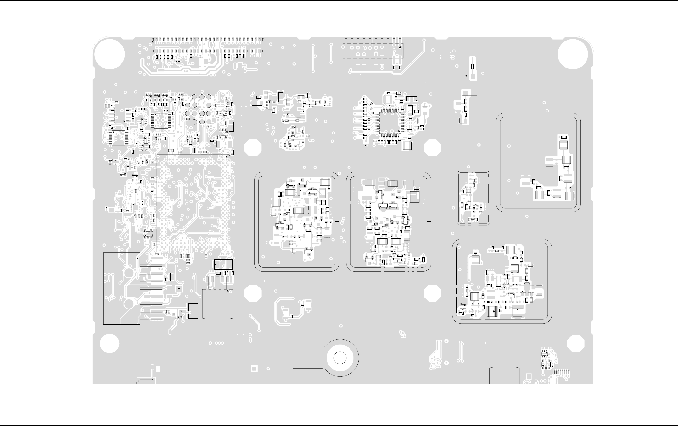
7-56 Schematics, Component Location Diagrams, and Parts Lists: HUD4022A/HUD4025B (VHF) Main Board
May 25, 2005 6881096C74-B
Figure 7-45. HUD4025B Main Board Layout—Side 1 Top
4
C0436
C0437
C0442
C0444
C0446
C0448
C0450
C0452
C0455
C0457
C0458
C0461
C0463
C0476
C0477
59
60
2J0401
R0415
R0421
C0703
C0705
J0501
C0100
C0101
C0202
C0207
C0212
C0223
C0224
C0234
C0242
C0420
C0502
C0503
C0600
C0603 C0604
C0606
C0610
C0611
C0613
C0614
C0616
Q0508
Q0610
Q0611
Q0612
Q0613
R0116
R0117
R0119
R0120
R0124
R0125 R0200
R0204
R0205
R0213
R0310
R0404
R0405
R0406
R0422
R0430
R0505
R0508
R0509
R0517
R0532
R0620
R0621
R0622
R0623
R0624
R0625
R0626
R0627
R0628
R0629
R0630
R0631
R0632
R0634
R0635
R0636
R0639
TP0400
TP0401
TP0402
TP0403
TP0407
TP0408
TP0409
TP0410
TP0411
TP0412
TP0413
TP0414
TP0415
123456789101112131415161718
1817161514131211109 8 7 6 5 4 3 2
A
B
C
D
E
F
G
N
M
L
K
J
I
H
R
S
T
U
V
W
X
P
Z
YY
Z
P
X
W
V
U
T
S
R
H
I
J
K
L
M
N
G
F
E
D
C
B
A
U0001
U0102
43
6
U0203
43
6
U0208
43
6
U0209
14
7
8
U0602
1
4
58
U0604
16 9
8
1U0606
U0607
U0608
4
3
5
U0609
4
3
5
U0610
Y0100
M3520
C0921
C0991
Q0960
6
U
16 9
8
1U0959
U0962
U0965
C3501
C3505
L3500
L3502
C3255
C3256
C3257
C3259
C3260
C3261
C3264
C3265
C3266
C3267
C3270
C3272
C3273
C3282
C3284
C3299
C3300
C3301
C3302
C3303
C3304
C3305
C3306
C3307
C3308
C3309
C3312
C3936
D3251
D3252
D3253
D3254
D3255
D3256
L3261
L3266
L3268
L3269
L3270
1
L3272
1
L3273
L3275 L3276
L3277
Q3254 Q3255
R3254
R3255
R3256
R3257
R3258
R3259
R3260
R3271
R3272
R3274
R3275
SH3761
U3250
C3277
C3278 C3279
C3290
C3291
C3296
C3297
C3311
L3251
L3252
L3253
L3254
L3256
L3257
L3258
L3265
SH3763
C3408
C3415
C3418
C3420
L3405
L3407
23
4
5
6Y3401
C3000
C3002
C3003
C3004
C3006
C3008
C3009
C3010
C3011
C3012
C3013
C3014
C3015
C3019
C3020
C3021
C3022
C3023
C3032
C3033
C3036
C3037
C3038
C3039
C3042
C3047
CLKOUT
D3001
DOUT
E3000
E3001
E3003
E3007
E3008
FS
L3000
L3002
L3004
L3005
PC
PD
PE
R3000
R3002
R3006
R3007
R3008
R3010
R3012
R3014
R3015
R3016
R3017
R3018
R3019
R3022
1
37
25
13
U3000
C3750
C3766
C3768
C3806
C3807
C3808
C3824
C3825
C3826 C3828
C3830
C3831
L3751
L3753
L3754
L3755
Q3750
Q3755
R3750
R3753 R3754
R3755
R3756
R3758
R3759
R3761
R3763
R3767
R3768
R3775 R3776
R3778
R3779
TP6750
TP6755
U3750
U3752
2
3
4Y3750
C3910
C3911
C3912
C3913
C3914
C3915
C3930
L3784
Q3769
R3828
R3854
R3855
R3856
R3857
R3864 R3865
R3868
R3869
R3870
R3871
R3872
R3873
SH3759
C3777
C3778
C3779
C3780
C3781
C3782
C3787
C3788
C3791 C3792
C3795
C3796
C3798
C3800
C3803
C3818
C3819
C3839
C3840
C3845
C3846
C3847
C3848
C3849
C3850
C3868
C3878
C3880
C3916
C3931
C3932
D3751
D3755
D3756
D3770
D3771
D3772
D3773
L3766
L3767
L3768
L3769
L3770
L3771
L3772
L3773
L3774
Q3751
Q3752
Q3761
R3786
R3787
R3790
R3798
R3800
R3801
R3811 R3812
R3825
R3826
R3827
R3831
R3837
R3838
SH3754
TP6770
Y3751
Y3752
C3770
C3783
C3784
C3785
C3793
C3794
C3797
C3799 C3816
C3835
C3836
C3837
C3838
C3841
C3842
C3843
C3844
C3851 C3852
C3853
C3854
C3933
C3934
D3750
D3752
D3753
D3754
D3767
D3768
D3769
L3758
L3759
L3760
L3761
L3762
L3763
L3764
L3765
Q3753
Q3754
R3788 R3789
R3813
R3814
R3833
R3839
R3840
SH3750
Y3753
Y3754
C0105
C0214
C0217
C0220
C0243
C0531
C0532
C0533
C0553
C0554
Q0200
R0101
R0102
R0106
R0110
R0123
R0220
R0222
R0224
R0431
R0434
R0435
R0445
R0551
R0552
R0553
11
10
9
U0204
6
5
U0550
C0204
C0213
C0301
C0312
C0314
C0315
C0471
C0519
C0615
D0401
D0402
Q0406
R0103
R0104
R0109
R0111
R0113
R0114
R0115
R0121 R0122
R0300
R0301
R0303
R0304
R0305
R0441
R0442
R0527
5
9
13
U0304
4
3
5
U0309
43
5
U0401
U0504
4
35
U0611
F2
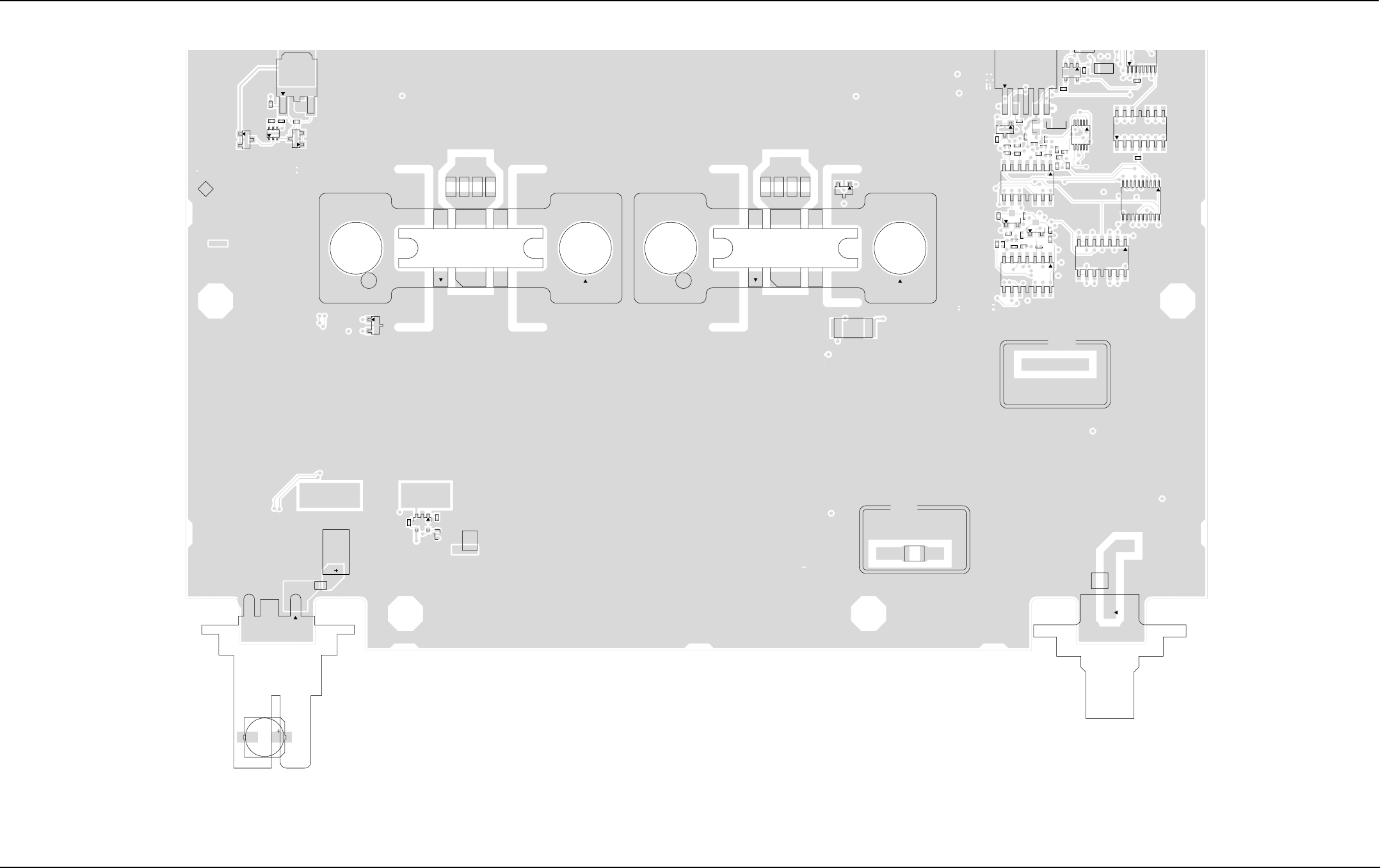
Schematics, Component Location Diagrams, and Parts Lists: HUD4022A/HUD4025B (VHF) Main Board 7-57
6881096C74-B May 25, 2005
Figure 7-46. HUD4025B Main Board Layout—Side 1 Bottom
C0536
3
4
1
Q0503
Q0507
R0515
R0530 R0531
SC3500
SC3501
VR0501
VR0502
C3562
C3563
C3566
C3568
C3574
J3500
R3562
R3564
U3561
C3734
M3700
3
2
J3700
L3737
M3540
M3541
SS
S
654
SD
G
23
Q3540
SS
S
6
5
4
SD
G
23
Q3541
R3541
R3542
R3543
R3544
R3550
R3551
R3552
R3553
R3700
U3560
U3563
M3721
C0922
C0968
C0969
C0970
C0975
C0976
C0983
D0950
D0951
R0915
R0935
R0978 R0990
R0994
7
814
U0957
7
814
U0955
11
1
20
10
U0953
C0900
C0923
C0937
C0940
C0943
C0955
C0962
C0967
C0981
C0990
D0954
R0902
R0903
R0908
R0924
R0948
R0963
R0964
R0965
R0967
R0968
R0970
R0973
R0980
R0986
5
U0951
10
6
5
U0952
7
814
U0956
8
1U0959
7
8
14
U0960
U0962

7-58 Schematics, Component Location Diagrams, and Parts Lists: HUD4022A/HUD4025B (VHF) Main Board
May 25, 2005 6881096C74-B
Figure 7-47. HUD4025B Main Board Layout—Side 2 Top
C0431
C0432
C0433 C0434
C0438
C0447
C0449
C0460
C0462
VR0412
VR0414
C0475
C0478
C0479
C0423
C0440
L0400
VR0415
VR0423
VR0426
C0422
C0424
R0417
VR0418
VR0422
C0428
C0464
R0416 R0418
C0441
VR0411
C0454
4
5
8
VR0424
C0435
C0439
C0443
C0445
C0451
C0453
C0456
C0459
C0467
C0470
VR0425
Q0403
R0420
VR0420
C0426
Q0405
R0433
R0524
C3751
C3752
C3753
C3762
C3763
C3764
C3765
C3767
C3769
C3773
C3775
C3811
C3813
C3820
C3821
C3822
C3823
D3757
D3758
L3752
L3756
L3757
Q3756
R3774
R3784
R3785
R3836
TP6751
TP6752
TP6753
TP6754
TP6766
1
37
25
13
U3751
C0520
C0521
C0522
C0523
C0700 C0701
C0702
C0704
C0706
C0708 C0709
C0710 C0711
C0712
C0713
C0714
3
2
1
U0505
C3404
D3400
R3407
R3413
C3400
C3402
C3405
C3410
C3412
L3400
R3402 R3400
2
3
456
Y3400
C3409
C3417
D3401
L3401 Q3401
L3406
C3414
Q3400
C3401
C3403
C3406
C3411
C3416
C3424 L3403
L3408
R3401
R3405 R3409
C3258
C3421
D3258
L3255
L3404
R3270
1
SH3760
6
4
3
T3301
64
3
T3302
C3268
C3269
C3283
D3257
Q3252
R3251
R3263
R3267
C3252
C3271
C3274
C3276
C3280
C3281
C3287
C3293
C3294
C3295
L3260
L3263
L3267
L3271
R3261
R3262
R3264
R3288
SH3762
C3251
C3253
C3254
C3275
C3286
C3292
C3298
C3310
L3259
L3262
L3264
Q3253
R3252
R3268
C3262
C3263
C3288
C3289
C3869
C3873
C3925
L3775
Q3250
Q3256 Q3257
Q3258
Q3768
R3253
R3265 R3266
R3269
R3273
R3277 R3278
R3280
R3832
R3852
R3279
R3281
C3870
C3924
Q3767
R3843
R3846
R3851
R3853
C3759
C3761
C3786
C3804
C3877
C3926
L3781
L3782
L3783
Q3762 R3760
R3794
R3796
R3802
R3805
R3821
R3845
SH3752
TP6771
C3001
C3007
C3016
C3018
C3040
C3041
C3043
C3045
E3002
E3004
E3005
E3006
L3008
Q3001
R3001
R3005
R3023
U3001
C3005
C3017
C3024
C3025 C3026
C3027
C3028
C3029
C3030
C3034
C3035
C3044
C3046
C3048
D3000
L3003
L3006
L3007
Q3000
R3003
R3004
R3009
R3011
R3020
R3021
SH3000
C0107
C0109
C0504
R0127
R0507
VR0500
C0306
C0421
F0400
R0128 14
7
8
U0104 16
18
9
U0305
C0201
C0507
Q0402
Q0505
R0409
R0425
Q0502
Q0504
TP0200
14
58U0202
U0603
C3812
L3776
TP6756
C3810
C3857
C3861
C3881
C3882
C3883
C3855
R3829
R3830
C3809
C3827
C3829
C3833
C3834
C3856
C3858
C3859
C3860
Q3757
R3751
R3752
R3762
R3765
R3766 R3769
R3770
R3771
R3772
R3773
R3860
R3861
R3862 R3880
R3881
TP6764 TP6765
C3771 C3772
C3774
C3776
C3832
C3879
L3750
Q3763
Q3764
Q3765
Q3766
TP6757
TP6758
TP6759
TP6760
TP6761
TP6762
TP6763
TP6772
C3500
C3502
C3503 C3504
C3506
C3520
C3521
L3501
L3520
R3500
R3501
R3502
R3503
R3523
TP3500
TP3520
1
16
8
9
U3500
C3522
C3526 3
R3520
R3521
R3522
R3524
R3525
R3526
R3529
Q3520
C3523
C3524
C3525
L3522
R3527
R3528
R3567
C
R0901
R0910
R0911
R0912
R0913
R
R0934
T
3
2
1
U0966
C0205
C0230
C0231
C0236
C0237
C0239
R0223
R0229
R0230
R0235 R0236
7
814
U0201
C0104
C0106
C0307
C0308
C0309
C0524
C0719
R0500
R0502
R0701
R0703
TP0500
4
3
5
U0105
1
4
58
U0506
C0103 C0310
C0525
C0722
Q0501
14
7
8
U0103
C0200
C0203
C0208
C0232
C0233
C0235
C0238
C0240
C0311
C0313
C0500
R0208
R0210
R0211
R0212
R0215
R0216
R0218
R0219
R0227
R0228
R0306
R0307
R0503
R0523
TP0204
11
10
U0200
7
8
U0300
14
7
8
U0303
43
5
U0307
4
32
U0308
C0209
C0216
C0226
Q0506
R0206 R0209
R0225
TP0203
TP0419
TP0420
1
20
4
3
6
U0210
5
C0102
C0108
C0529
C0601 C0715
C0716
C0717
C0718
C0720
C0721
C0724
C0726
C0727
C0728
C0729 C0730
C0732
C0733
C0740
C0741
C0742
C0743
FL0700
R0126
R0129
R0130
R0221
R0700
R0705
R0739
R0740
R0741
R0742
R0743
TP0950
U0106
43
5
U0601
U0700 G7
G1
A7
A1
U0701
43
6
U0703
43
6
U0704
43
6
U0705
U0740
C0302
C0305
C0510
C0517
C0518
C0526 C0528
C0535
C0537
C0550
C0551
C0605
C0731
Q0500
R0107
R0108
R0403
R0443
R0444
R0504
R0514
R0516
R0519
R0520 R0521 R0522
TP0206
TP0418
14
3
2
1
U0503
1
4
58
U0507
43
5
U0605
C0210
C0211
C0215
C0221
C0227
C0244 C0505
C0506
C0512
C0513
C0514
C0515
C0516
C0527
C0534
R0201
R0231
R0506
R0510
R0511
R0512
R0513
R0518
R0526
R0528
R0529
TP0205
14
58
U0206
U0207
6
5
U0500
1
4
58
U0501
1
4
58
U0502
C3754
C3757
C3790
C3864
C3865
C3872
C3875
C3876
C3917
C3918
C3919
C3920
C3921
L3779
L3785
L3787
Q3758
R3764
R3791
R3795
R3815
R3816
R3818
R3819
R3823
R3824 R3834
R3841
R3842
R3858
R3859
R3863
SH3751
TP6769
C3755
C3758
C3802
C3814
C3815
C3817
C3862
C3863
C3871
C3935
L3778
Q3759
Q3760
R3757
R3792
R3793
R3797
R3799
R3803
R3804
R3807
R3808
R3809
R3817
R3820
R3835
R3882
R3884
SH3753
TP6767
TP6768
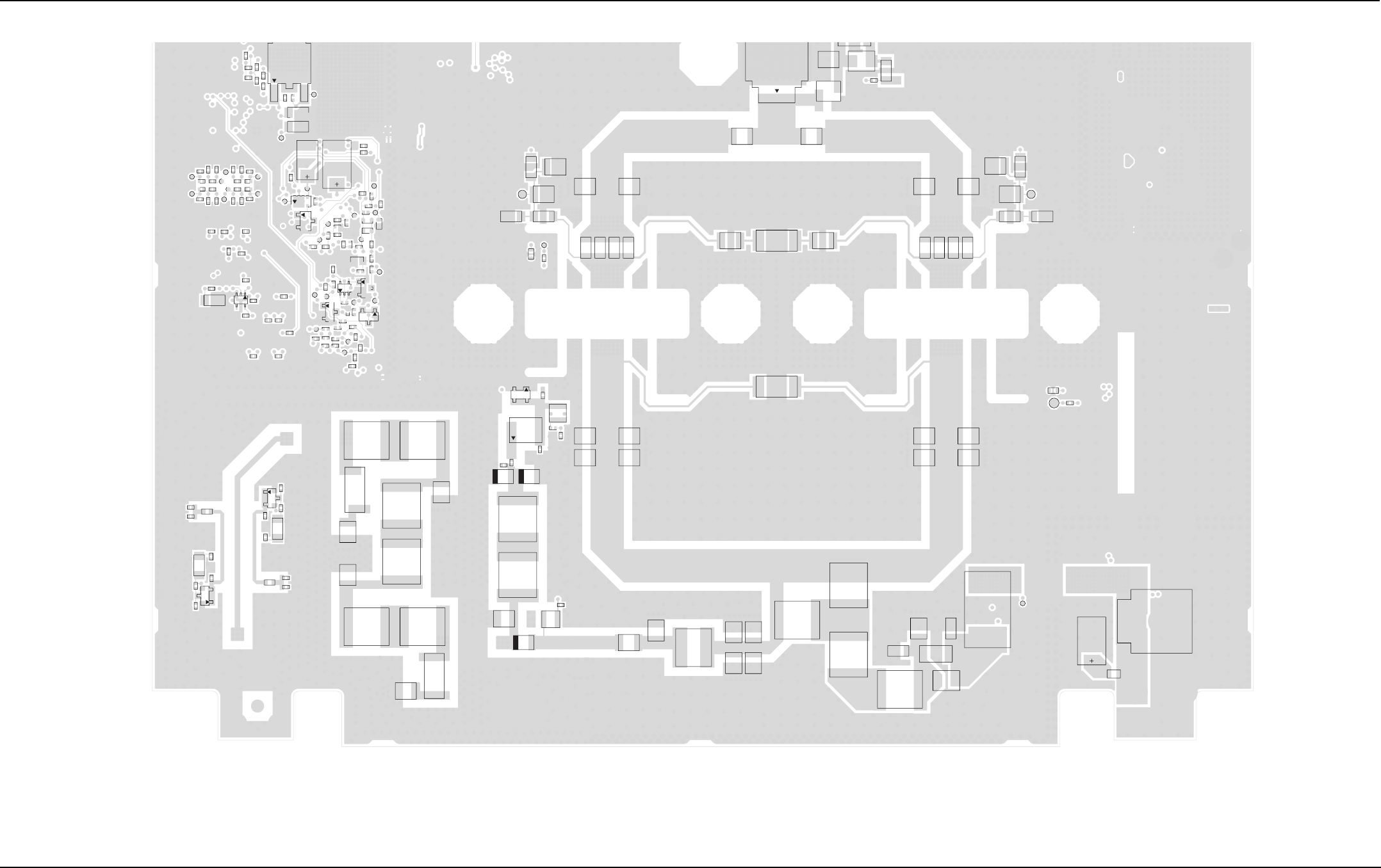
Schematics, Component Location Diagrams, and Parts Lists: HUD4022A/HUD4025B (VHF) Main Board 7-59
6881096C74-B May 25, 2005
Figure 7-48. HUD4025B Main Board Layout—Side 2 Bottom
C3720
C3721
C3722
C3723
L3720
21
L3721
21
L3722
21
L3723
L3724
21
L3725
21
L3726
21
L3727
C3558
C3559
C3572 C3573
C3700
C3701
D3701 L3545
L3700
21
L3701 21
L3732
C3560
C3561
C3575
2
L3540
2
1L3541 2
1L3542
2
1L3543
L3544
R3560
R3561
TP3544
C3564
R3563
VR3500
C3552
C3553
C3554
C3555
C3567
R3566
TP3543
R3559
C3548
C3549
C3550
C3551
C3702
C3703
C3704
C3735
C3736
D3702
D3703
D3705
L3702
L3704
R3702
C3556 C3557
1
C3730
C3731
C3732
D3730
D3731
L3730
L3731
R3730
R3731
R3732
R3733
R3734
R3735
R3736
R3737
R3738
R3739 C3733
C3542
C3543
C3565
C3570
C3576
C3579
R3540
R3545
R3546
R3547
R3548
R3565
R3568
TP3540
TP3542
Q3520
C3523
L3521
L3522
R3528
R3567
C3540 C3541
C3545 C3546
R3549
C3544 C3547
C3571
C3577
C3578
R3554
R3555
R3556
R3557
R3558
R3569
TP3541
C0920
C0941
C0942
C0956
C0982
C0988
C0989
R
0901
R0910
R0911
R0912
R
0913 R0914
R0954
R0993
TP0901
TP0902
3
2
1
U0966
C0936
C0945
C0961
C0963
C0964
C0965
C0966
C0979
R0950
R0953
R0962
4
3
5
U0954
C0960 R0961
R0966
R0979
R0987
C0901
C0902
C0903 C0904
C0930
C0933C0934
C0935
C0984
C0985
C0986
C0987
R0930
R0931
R0936
R0937
R0938
R0939
R0940
R0941
TP0930
TP0931
TP0936
TP0937
TP0938
TP0939
TP0940
TP0941
C0924
C0952
C0957
C0959
C0971
C0972
C0973
C0974 C0978
C0980
D0952
Q0951
4
5
8
Q0952
Q0954
Q0955
R0900
R0916
R0917
R0932
R0933
R0942
R0943
R0944
R0945
R0946
R0947
R0955
R0960
R0971
R0972
R0974
R0975
R0976
R0977
R0981
R0982
R0983
R0984
R0985
R0988
R0989
R0991
R0992
R0995
R0996
R0998
R0999
R1000
TP0900
TP0942
TP0951
TP0952
TP0953
TP0954
TP0955
TP0956
TP0957
TP0958
TP0959
TP0960
TP0961
TP0962
TP0963
TP0964
43
5
U0958
R0997
7-60 Schematics, Component Location Diagrams, and Parts Lists: HUD4022A/HUD4025B (VHF) Main Board
May 25, 2005 6881096C74-B
HUD4025B (VHF) Main Board Parts List
Reference
Designator
Motorola
Part Number Description
C0100 2113743N32 CAP CHIP 18.0 PF 5%
COG
C0101 2113743N32 CAP CHIP 18.0 PF 5%
COG
C0102 2113743M24 CAP CHIP 100000 PF +80-
20% Y5V
C0103 2113743M24 CAP CHIP 100000 PF +80-
20% Y5V
C0104 2113743M24 CAP CHIP 100000 PF +80-
20% Y5V
C0105 2113743M24 CAP CHIP 100000 PF +80-
20% Y5V
C0106 2113743N50 CAP CHIP 100 PF 5% COG
C0107 2113743L09 CAP CHIP 470 PF 10%
X7R
C0108 2113743M24 CAP CHIP 100000 PF +80-
20% Y5V
C0109 2113743N32 CAP CHIP 18.0 PF 5%
COG
C0200 2113928E01 CAP CER CHIP 1.0 UF 10
% 10V
C0201 2113743M24 CAP CHIP 100000 PF +80-
20% Y5V
C0202 2113743M24 CAP CHIP 100000 PF +80-
20% Y5V
C0203 2113928S04 CAP CER CHIP 0.100UF
10V 0402
C0204 2185802B01 CAP 10V 4.7UF
C0207 2113743N38 CAP CHIP 33.0 PF 5%
COG
C0208 2113928E01 CAP CER CHIP 1.0 UF 10
% 10V
C0209 2113743M24 CAP CHIP 100000 PF +80-
20% Y5V
C0210 2113743M24 CAP CHIP 100000 PF +80-
20% Y5V
C0211 2113743N50 CAP CHIP 100 PF 5% COG
C0212 2113743M24 CAP CHIP 100000 PF +80-
20% Y5V
C0213 2113743M24 CAP CHIP 100000 PF +80-
20% Y5V
C0214 2113741N69 CAP CHIP CL2 X7R 10%
100000
C0215 2113928S04 CAP CER CHIP 0.100UF
10V 0402
C0216 2113743M24 CAP CHIP 100000 PF +80-
20% Y5V
C0217 2113743L29 CAP CHIP 3300 PF 10%
X7R
C0220 2311049A57 CAP TANT CHIP A/P 10UF
10% 16V
C0221 2311049C06 CAP TANT CHIP 22 UF
35V 20%
C0223 2185802B01 CAP 10V 4.7UF
C0224 2113743M24 CAP CHIP 100000 PF +80-
20% Y5V
C0226 2113928S04 CAP CER CHIP 0.100UF
10V 0402
C0227 2113743M24 CAP CHIP 100000 PF +80-
20% Y5V
C0230 2113743L09 CAP CHIP 470 PF 10%
X7R
C0231 2113743L01 CAP CHIP 220 PF 10%
X7R
C0232 2113743L09 CAP CHIP 470 PF 10%
X7R
C0233 2113743L01 CAP CHIP 220 PF 10%
X7R
C0234 2113928S04 CAP CER CHIP 0.100UF
10V 0402
C0235 2113743L09 CAP CHIP 470 PF 10%
X7R
C0236 2113743L09 CAP CHIP 470 PF 10%
X7R
C0237 2113743L01 CAP CHIP 220 PF 10%
X7R
C0238 2113743L01 CAP CHIP 220 PF 10%
X7R
C0239 2113743M24 CAP CHIP 100000 PF +80-
20% Y5V
C0240 2113928S04 CAP CER CHIP 0.100UF
10V 0402
C0242 2113928S04 CAP CER CHIP 0.100UF
10V 0402
C0243 2113945B01 CAP CER CHIP 6800 PF
25V 10%
C0244 2113945B01 CAP CER CHIP 6800 PF
25V 10%
C0301 2113743M24 CAP CHIP 100000 PF +80-
20% Y5V
Reference
Designator
Motorola
Part Number Description
C0302 2113743M24 CAP CHIP 100000 PF +80-
20% Y5V
C0305 2113743M24 CAP CHIP 100000 PF +80-
20% Y5V
C0306 2113928E01 CAP CER CHIP 1.0 UF 10
% 10V
C0308 2113928E01 CAP CER CHIP 1.0 UF 10
% 10V
C0309 2113928E01 CAP CER CHIP 1.0 UF 10
% 10V
C0310 2113928E01 CAP CER CHIP 1.0 UF 10
% 10V
C0311 2113743M24 CAP CHIP 100000 PF +80-
20% Y5V
C0312 2113743M24 CAP CHIP 100000 PF +80-
20% Y5V
C0313 2113743M24 CAP CHIP 100000 PF +80-
20% Y5V
C0314 2113743M24 CAP CHIP 100000 PF +80-
20% Y5V
C0315 2113928E01 CAP CER CHIP 1.0 UF 10
% 10V
C0420 2185802B01 CAP 10V 4.7UF
C0421 2113741B13 CAP CHIP CL2 X7R REEL
470
C0422 2113743N38 CAP CHIP 33.0 PF 5%
COG
C0423 2113743N38 CAP CHIP 33.0 PF 5%
COG
C0424 2113743N38 CAP CHIP 33.0 PF 5%
COG
C0426 2113741B13 CAP CHIP CL2 X7R REEL
470
C0428 2113743N50 CAP CHIP 100 PF 5% COG
C0431 2113743N50 CAP CHIP 100 PF 5% COG
C0432 2113743N50 CAP CHIP 100 PF 5% COG
C0433 2113743N50 CAP CHIP 100 PF 5% COG
C0434 2113743N50 CAP CHIP 100 PF 5% COG
C0435 2113743L09 CAP CHIP 470 PF 10%
X7R
C0436 2113741B13 CAP CHIP CL2 X7R REEL
470
C0437 2113741B13 CAP CHIP CL2 X7R REEL
470
C0438 2113743L09 CAP CHIP 470 PF 10%
X7R
Reference
Designator
Motorola
Part Number Description
C0439 2113743N50 CAP CHIP 100 PF 5% COG
C0440 2113743N50 CAP CHIP 100 PF 5% COG
C0441 2311049C47 CAP TANT CHIP 22.0UF
10% 16V
C0442 2113743N38 CAP CHIP 33.0 PF 5%
COG
C0443 2113743N38 CAP CHIP 33.0 PF 5%
COG
C0444 2113743N38 CAP CHIP 33.0 PF 5%
COG
C0445 2113743N38 CAP CHIP 33.0 PF 5%
COG
C0446 2113743N50 CAP CHIP 100 PF 5% COG
C0447 2113743N50 CAP CHIP 100 PF 5% COG
C0448 2113743N50 CAP CHIP 100 PF 5% COG
C0449 2113743N50 CAP CHIP 100 PF 5% COG
C0450 2113743N38 CAP CHIP 33.0 PF 5%
COG
C0451 2113743N38 CAP CHIP 33.0 PF 5%
COG
C0452 2113743N38 CAP CHIP 33.0 PF 5%
COG
C0453 2113743N38 CAP CHIP 33.0 PF 5%
COG
C0454 2113743N38 CAP CHIP 33.0 PF 5%
COG
C0455 2113743N38 CAP CHIP 33.0 PF 5%
COG
C0456 2113743N38 CAP CHIP 33.0 PF 5%
COG
C0457 2113743N38 CAP CHIP 33.0 PF 5%
COG
C0458 2113743N38 CAP CHIP 33.0 PF 5%
COG
C0459 2113743N38 CAP CHIP 33.0 PF 5%
COG
C0460 2113743N50 CAP CHIP 100 PF 5% COG
C0461 2113743L01 CAP CHIP 220 PF 10%
X7R
C0462 2113743L01 CAP CHIP 220 PF 10%
X7R
C0463 2113743N38 CAP CHIP 33.0 PF 5%
COG
C0464 2113743N38 CAP CHIP 33.0 PF 5%
COG
C0467 2113743N50 CAP CHIP 100 PF 5% COG
Reference
Designator
Motorola
Part Number Description
Schematics, Component Location Diagrams, and Parts Lists: HUD4022A/HUD4025B (VHF) Main Board 7-61
6881096C74-B May 25, 2005
C0470 2113743N38 CAP CHIP 33.0 PF 5%
COG
C0471 2113743N50 CAP CHIP 100 PF 5% COG
C0475 2113743N50 CAP CHIP 100 PF 5% COG
C0476 2113743N50 CAP CHIP 100 PF 5% COG
C0477 2113743N50 CAP CHIP 100 PF 5% COG
C0478 2113743N50 CAP CHIP 100 PF 5% COG
C0479 2113743N50 CAP CHIP 100 PF 5% COG
C0500 2113743N50 CAP CHIP 100 PF 5% COG
C0502 2113743N50 CAP CHIP 100 PF 5% COG
C0503 2113743N50 CAP CHIP 100 PF 5% COG
C0504 2113741N69 CAP CHIP CL2 X7R 10%
100000
C0505 2113743L41 CAP CHIP 10000 PF 10%
X7R
C0506 2113743L41 CAP CHIP 10000 PF 10%
X7R
C0507 2113743M24 CAP CHIP 100000 PF +80-
20% Y5V
C0510 2185802B01 CAP 10V 4.7UF
C0512 2113743M24 CAP CHIP 100000 PF +80-
20% Y5V
C0513 2311049A43 CAP TANT CHIP 150 10 6
C0514 2311049A43 CAP TANT CHIP 150 10 6
C0515 2113743M24 CAP CHIP 100000 PF +80-
20% Y5V
C0516 2113743M24 CAP CHIP 100000 PF +80-
20% Y5V
C0517 2185802B01 CAP 10V 4.7UF
C0518 2185802B01 CAP 10V 4.7UF
C0519 2113743L41 CAP CHIP 10000 PF 10%
X7R
C0520 2113743M24 CAP CHIP 100000 PF +80-
20% Y5V
C0521 2185802B01 CAP 10V 4.7UF
C0522 2185802B01 CAP 10V 4.7UF
C0523 2113743M24 CAP CHIP 100000 PF +80-
20% Y5V
C0524 2113743M24 CAP CHIP 100000 PF +80-
20% Y5V
C0525 2113928E01 CAP CER CHIP 1.0 UF 10
% 10V
C0526 2113743L41 CAP CHIP 10000 PF 10%
X7R
Reference
Designator
Motorola
Part Number Description
C0527 2185802B01 CAP 10V 4.7UF
C0528 2113743M24 CAP CHIP 100000 PF +80-
20% Y5V
C0529 2185802B01 CAP 10V 4.7UF
C0531 2113741N69 CAP CHIP CL2 X7R 10%
100000
C0532 2113741Y32 CAP CER 1,000,000 10%
50V
C0533 2311049C47 CAP TANT CHIP 22.0UF
10% 16V
C0534 2113743M24 CAP CHIP 100000 PF +80-
20% Y5V
C0535 2113743M24 CAP CHIP 100000 PF +80-
20% Y5V
C0550 2113741N69 CAP CHIP CL2 X7R 10%
100000
C0551 2113741Y32 CAP CER 1,000,000 10%
50V
C0553 2311049C47 CAP TANT CHIP 22.0UF
10% 16V
C0554 2113743E20 CAP CHIP .10 UF 10%
C0600 2113743M24 CAP CHIP 100000 PF +80-
20% Y5V
C0601 2113743M24 CAP CHIP 100000 PF +80-
20% Y5V
C0603 2113743M24 CAP CHIP 100000 PF +80-
20% Y5V
C0604 2113743M24 CAP CHIP 100000 PF +80-
20% Y5V
C0605 2113743M24 CAP CHIP 100000 PF +80-
20% Y5V
C0606 2113743M24 CAP CHIP 100000 PF +80-
20% Y5V
C0610 2113743M24 CAP CHIP 100000 PF +80-
20% Y5V
C0611 2113743M24 CAP CHIP 100000 PF +80-
20% Y5V
C0613 2113743M24 CAP CHIP 100000 PF +80-
20% Y5V
C0614 2113743M24 CAP CHIP 100000 PF +80-
20% Y5V
C0615 2113743M24 CAP CHIP 100000 PF +80-
20% Y5V
C0616 2113743N50 CAP CHIP 100 PF 5% COG
C0700 2113743N50 CAP CHIP 100 PF 5% COG
C0701 2113743N50 CAP CHIP 100 PF 5% COG
Reference
Designator
Motorola
Part Number Description
C0702 2113743N50 CAP CHIP 100 PF 5% COG
C0703 2113743N50 CAP CHIP 100 PF 5% COG
C0704 2113743N50 CAP CHIP 100 PF 5% COG
C0705 2113743N50 CAP CHIP 100 PF 5% COG
C0706 2113743N50 CAP CHIP 100 PF 5% COG
C0708 2113743N50 CAP CHIP 100 PF 5% COG
C0709 2113743N50 CAP CHIP 100 PF 5% COG
C0710 2113743N50 CAP CHIP 100 PF 5% COG
C0711 2113743N50 CAP CHIP 100 PF 5% COG
C0712 2113743N50 CAP CHIP 100 PF 5% COG
C0713 2113743L01 CAP CHIP 220 PF 10%
X7R
C0714 2113743L01 CAP CHIP 220 PF 10%
X7R
C0715 2113743N50 CAP CHIP 100 PF 5% COG
C0716 2113743N50 CAP CHIP 100 PF 5% COG
C0717 2113743N50 CAP CHIP 100 PF 5% COG
C0718 2113743M24 CAP CHIP 100000 PF +80-
20% Y5V
C0719 2113743L01 CAP CHIP 220 PF 10%
X7R
C0720 2113743M24 CAP CHIP 100000 PF +80-
20% Y5V
C0721 2113743M24 CAP CHIP 100000 PF +80-
20% Y5V
C0722 2113928E01 CAP CER CHIP 1.0 UF 10
% 10V
C0724 2113743M24 CAP CHIP 100000 PF +80-
20% Y5V
C0726 2113743N50 CAP CHIP 100 PF 5% COG
C0727 2113743M24 CAP CHIP 100000 PF +80-
20% Y5V
C0728 2113743M24 CAP CHIP 100000 PF +80-
20% Y5V
C0729 2113743M24 CAP CHIP 100000 PF +80-
20% Y5V
C0730 2113743M24 CAP CHIP 100000 PF +80-
20% Y5V
C0731 2113743M24 CAP CHIP 100000 PF +80-
20% Y5V
C0732 2113743N50 CAP CHIP 100 PF 5% COG
C0733 2113743M24 CAP CHIP 100000 PF +80-
20% Y5V
C0740 2113743M24 CAP CHIP 100000 PF +80-
20% Y5V
Reference
Designator
Motorola
Part Number Description
C0741 2113743N50 CAP CHIP 100 PF 5% COG
C0742 2113743N50 CAP CHIP 100 PF 5% COG
C0903 2113743N26 CAP CHIP 10.0 PF 5%
COG
C0920 2113743M24 CAP CHIP 100000 PF +80-
20% Y5V
C0922 2113743N50 CAP CHIP 100 PF 5% COG
C0923 2113743N50 CAP CHIP 100 PF 5% COG
C0936 2113743M24 CAP CHIP 100000 PF +80-
20% Y5V
C0937 2113743M24 CAP CHIP 100000 PF +80-
20% Y5V
C0940 2113743M24 CAP CHIP 100000 PF +80-
20% Y5V
C0941 2113743S01 CAP CER CHIP 1.0 UF
10% 16V
C0942 2113743S01 CAP CER CHIP 1.0 UF
10% 16V
C0943 2113743L41 CAP CHIP 10000 PF 10%
X7R
C0945 2185802B01 CAP 10V 4.7UF
C0955 2113741N69 CAP CHIP CL2 X7R 10%
100000
C0956 2311049C06 CAP TANT CHIP 22 UF
35V 20%
C0957 2113743M24 CAP CHIP 100000 PF +80-
20% Y5V
C0959 2113743M24 CAP CHIP 100000 PF +80-
20% Y5V
C0960 2113743M24 CAP CHIP 100000 PF +80-
20% Y5V
C0961 2113743M24 CAP CHIP 100000 PF +80-
20% Y5V
C0963 2113743N50 CAP CHIP 100 PF 5% COG
C0964 2113743N50 CAP CHIP 100 PF 5% COG
C0965 2113743N50 CAP CHIP 100 PF 5% COG
C0966 2113743N50 CAP CHIP 100 PF 5% COG
C0968 2113743N50 CAP CHIP 100 PF 5% COG
C0969 2113743N50 CAP CHIP 100 PF 5% COG
C0970 2113743N50 CAP CHIP 100 PF 5% COG
C0972 2113743E20 CAP CHIP .10 UF 10%
C0973 2113928E01 CAP CER CHIP 1.0 UF 10
% 10V
C0974 2113743M24 CAP CHIP 100000 PF +80-
20% Y5V
Reference
Designator
Motorola
Part Number Description
7-62 Schematics, Component Location Diagrams, and Parts Lists: HUD4022A/HUD4025B (VHF) Main Board
May 25, 2005 6881096C74-B
C0975 2113743N50 CAP CHIP 100 PF 5% COG
C0976 2113743N50 CAP CHIP 100 PF 5% COG
C0978 2113743N50 CAP CHIP 100 PF 5% COG
C0979 2113743M24 CAP CHIP 100000 PF +80-
20% Y5V
C0980 2113743M24 CAP CHIP 100000 PF +80-
20% Y5V
C0981 2113743M24 CAP CHIP 100000 PF +80-
20% Y5V
C0982 2311049C47 CAP TANT CHIP 22.0UF
10% 16V
C0983 2113743N50 CAP CHIP 100 PF 5% COG
C0984 2113743M24 CAP CHIP 100000 PF +80-
20% Y5V
C0985 2113743M24 CAP CHIP 100000 PF +80-
20% Y5V
C0986 2113743M24 CAP CHIP 100000 PF +80-
20% Y5V
C0987 2113743M24 CAP CHIP 100000 PF +80-
20% Y5V
C0988 2113743M24 CAP CHIP 100000 PF +80-
20% Y5V
C0989 2113743M24 CAP CHIP 100000 PF +80-
20% Y5V
C0990 2185802B01 CAP 10V 4.7UF
C0991 2185802B01 CAP 10V 4.7UF
C3000 2113743N28 CAP CHIP 12.0 PF 5%
COG
C3001 2113743S01 CAP CER CHIP 1.0 UF
10% 16V
C3002 2113743N46 QAP CHIP 68.0 PF 5%
COG
C3003 2113743L25 CAP CHIP 2200 PF 10%
X7R
C3004 2113743B27 CAP CHIP .680 UF 10%
X7R
C3005 2113743A27 CAP CHIP .470 UF 10%
16V
C3007 2113928N01 CAP CER CHIP 0.1UF 10%
6.3
C3008 2113928N01 CAP CER CHIP 0.1UF 10%
6.3
C3009 2113928N01 CAP CER CHIP 0.1UF 10%
6.3
C3010 2113928N01 CAP CER CHIP 0.1UF 10%
6.3
Reference
Designator
Motorola
Part Number Description
C3011 2113928N01 CAP CER CHIP 0.1UF 10%
6.3
C3012 2113928N01 CAP CER CHIP 0.1UF 10%
6.3
C3013 2113928N01 CAP CER CHIP 0.1UF 10%
6.3
C3014 2113928N01 CAP CER CHIP 0.1UF 10%
6.3
C3016 2113928N01 CAP CER CHIP 0.1UF 10%
6.3
C3017 2113928N01 CAP CER CHIP 0.1UF 10%
6.3
C3018 2113928N01 CAP CER CHIP 0.1UF 10%
6.3
C3019 2113928N01 CAP CER CHIP 0.1UF 10%
6.3
C3020 2113743N50 CAP CHIP 100 PF 5% COG
C3021 2113743N50 CAP CHIP 100 PF 5% COG
C3022 2113743N50 CAP CHIP 100 PF 5% COG
C3023 2113743N50 CAP CHIP 100 PF 5% COG
C3024 2113743N46 QAP CHIP 68.0 PF 5%
COG
C3025 2113743N42 CAP CHIP 47.0 PF 5%
COG
C3026 2113743N36 CAP CHIP 27.0 PF 5%
COG
C3027 2113743N33 CAP CHIP 20.0 PF 5%
COG
C3028 2113743N33 CAP CHIP 20.0 PF 5%
COG
C3029 2113743N30 CAP CHIP 15.0 PF 5%
COG
C3030 2113743N28 CAP CHIP 12.0 PF 5%
COG
C3032 2113740L32 CAP 39.0 PF 50V 2.0 %
C3035 2113743L41 CAP CHIP 10000 PF 10%
X7R
C3036 2113743L41 CAP CHIP 10000 PF 10%
X7R
C3037 2113743L41 CAP CHIP 10000 PF 10%
X7R
C3038 2113743L41 CAP CHIP 10000 PF 10%
X7R
C3039 2113743L41 CAP CHIP 10000 PF 10%
X7R
Reference
Designator
Motorola
Part Number Description
C3040 2113743L41 CAP CHIP 10000 PF 10%
X7R
C3041 2113743L41 CAP CHIP 10000 PF 10%
X7R
C3042 2113743L17 CAP CHIP 1000 PF 10%
X7R
C3043 2113743F18 CAP CHIP 2.2 UF 16V +80-
20%
C3044 2113743E20 CAP CHIP .10 UF 10%
C3045 2113743A31 CAP CHIP 1.0 UF 10% X7R
C3046 2113743L33 CAP CHIP 4700 PF 10%
X7R
C3047 2113740F58 CAP CHIP REEL CL1 +/-30
200
C3048 2113743N09 CAP CHIP 2.0 PF +-.25PF
COG
C3251 2113740F67 CAP CHIP CL1 +/-30 470
5%
C3252 2113740F67 CAP CHIP CL1 +/-30 470
5%
C3253 2113740F67 CAP CHIP CL1 +/-30 470
5%
C3254 2113740F67 CAP CHIP CL1 +/-30 470
5%
C3255 2113741F25 CAP CHIP CL2 X7R REEL
1000
C3256 2113740F67 CAP CHIP CL1 +/-30 470
5%
C3257 2113740L37 CAP 62.0 PF 50V 2.0 %
C3258 2113740L42 CAP 100.0 PF 50V 2.0 %
C3259 2113740L21 CAP 13.0 PF 50V 2.0 %
C3260 2113741F25 CAP CHIP CL2 X7R REEL
1000
C3261 2113741F25 CAP CHIP CL2 X7R REEL
1000
C3262 2113740F67 CAP CHIP CL1 +/-30 470
5%
C3263 2113741F25 CAP CHIP CL2 X7R REEL
1000
C3264 2113740L32 CAP 39.0 PF 50V 2.0 %
C3265 2113741F25 CAP CHIP CL2 X7R REEL
1000
C3266 2113741F25 CAP CHIP CL2 X7R REEL
1000
C3267 2113743K15 CER CHIP CAP .100UF
C3268 2113743K15 CER CHIP CAP .100UF
Reference
Designator
Motorola
Part Number Description
C3269 2113741F25 CAP CHIP CL2 X7R REEL
1000
C3270 2113740F67 CAP CHIP CL1 +/-30 470
5%
C3271 2113741F49 CAP CHIP CL2 X7R REEL
10000
C3272 2113740F67 CAP CHIP CL1 +/-30 470
5%
C3273 2113741F25 CAP CHIP CL2 X7R REEL
1000
C3274 2113743K15 CER CHIP CAP .100UF
C3275 2113743K15 CER CHIP CAP .100UF
C3277 2113740L41 CAP 91.0 PF 50V 2.0 %
C3278 2113740L39 CAP 75.0 PF 50V 2.0 %
C3279 2113740L24 CAP 18.0 PF 50V 2.0 %
C3280 2113741F25 CAP CHIP CL2 X7R REEL
1000
C3282 2113740F67 CAP CHIP CL1 +/-30 470
5%
C3283 2113741F25 CAP CHIP CL2 X7R REEL
1000
C3284 2113741F25 CAP CHIP CL2 X7R REEL
1000
C3286 2113741F25 CAP CHIP CL2 X7R REEL
1000
C3287 2113740L31 CAP 36.0 PF 50V 2.0 %
C3288 2113740F67 CAP CHIP CL1 +/-30 470
5%
C3289 2113743K15 CER CHIP CAP .100UF
C3290 2113740L35 CAP 51.0 PF 50V 2.0%
C3291 2113740F41 CAP CHIP REEL CL1 +/-30
39
C3292 2113741F25 CAP CHIP CL2 X7R REEL
1000
C3293 2113741F25 CAP CHIP CL2 X7R REEL
1000
C3294 2113741F25 CAP CHIP CL2 X7R REEL
1000
C3295 2113740L37 CAP 62.0 PF 50V 2.0 %
C3296 2113740L26 CAP 22.0 PF 50V 2.0 %
C3297 2113740L15 CAP CER CHIP 7.5 PF +-
0.1PF
C3298 2113740L37 CAP 62.0 PF 50V 2.0 %
C3299 2113740L32 CAP 39.0 PF 50V 2.0 %
C3300 2113740L37 CAP 62.0 PF 50V 2.0 %
Reference
Designator
Motorola
Part Number Description
Schematics, Component Location Diagrams, and Parts Lists: HUD4022A/HUD4025B (VHF) Main Board 7-63
6881096C74-B May 25, 2005
C3301 2113740F67 CAP CHIP CL1 +/-30 470
5%
C3302 2113740F67 CAP CHIP CL1 +/-30 470
5%
C3303 2113741F49 CAP CHIP CL2 X7R REEL
10000
C3304 2113741F49 CAP CHIP CL2 X7R REEL
10000
C3305 2113740F67 CAP CHIP CL1 +/-30 470
5%
C3306 2113740F67 CAP CHIP CL1 +/-30 470
5%
C3307 2113741F49 CAP CHIP CL2 X7R REEL
10000
C3308 2113741F49 CAP CHIP CL2 X7R REEL
10000
C3309 2113741F49 CAP CHIP CL2 X7R REEL
10000
C3310 2113740L27 CAP 24.0 PF 50V 2.0 %
C3311 2113740L18 CAP CER CHIP 10.0 PF +/-
.25PF
C3312 2113743K15 CER CHIP CAP .100UF
C3400 2113740F67 CAP CHIP CL1 +/-30 470
5%
C3401 2113741F49 CAP CHIP CL2 X7R REEL
10000
C3402 2113741F49 CAP CHIP CL2 X7R REEL
10000
C3403 2113741F49 CAP CHIP CL2 X7R REEL
10000
C3404 2113741F49 CAP CHIP CL2 X7R REEL
10000
C3405 2113741F49 CAP CHIP CL2 X7R REEL
10000
C3406 2113741F49 CAP CHIP CL2 X7R REEL
10000
C3409 2113740L31 CAP 36.0 PF 50V 2.0 %
C3410 2113740F67 CAP CHIP CL1 +/-30 470
5%
C3411 2113740F67 CAP CHIP CL1 +/-30 470
5%
C3412 2113740F67 CAP CHIP CL1 +/-30 470
5%
C3414 2113740L31 CAP 36.0 PF 50V 2.0 %
C3415 2113740F19 CAP CHIP REEL CL1 +/-30
4.7
Reference
Designator
Motorola
Part Number Description
C3416 2113740L09 CAP CER CHIP 4.3 PF +-
0.1PF
C3417 2113740L09 CAP CER CHIP 4.3 PF +-
0.1PF
C3418 2113741F25 CAP CHIP CL2 X7R REEL
1000
C3420 2113741F25 CAP CHIP CL2 X7R REEL
1000
C3421 2113740L10 CAP CER CHIP 4.7 PF +-
0.1PF
C3424 2113741F49 CAP CHIP CL2 X7R REEL
10000
C3500 2113743L09 CAP CHIP 470 PF 10%
X7R
C3501 2113743L41 CAP CHIP 10000 PF 10%
X7R
C3502 2113743L09 CAP CHIP 470 PF 10%
X7R
C3503 2113743L41 CAP CHIP 10000 PF 10%
X7R
C3504 2113743L41 CAP CHIP 10000 PF 10%
X7R
C3505 2113743L41 CAP CHIP 10000 PF 10%
X7R
C3506 2113743L09 CAP CHIP 470 PF 10%
X7R
C3520 2113743N46 QAP CHIP 68.0 PF 5%
COG
C3521 2113743N52 CAP CHIP 120 PF 5% COG
C3522 2113743L09 CAP CHIP 470 PF 10%
X7R
C3524 2113741N69 CAP CHIP CL2 X7R 10%
100000
C3525 2111078B59 CAP CHIP RF 470 5 NPO
100V
C3526 2185802B01 CAP 10V 4.7UF
C3540 2111078B37 CAP CHIP RF 62 5 NPO
100V
C3541 2111078B37 CAP CHIP RF 62 5 NPO
100V
C3542 2111078B59 CAP CHIP RF 470 5 NPO
100V
C3543 2111078B41 CAP CHIP RF 91 5 NPO
100V
C3544 2111078B41 CAP CHIP RF 91 5 NPO
100V
Reference
Designator
Motorola
Part Number Description
C3545 2111078B59 CAP CHIP RF 470 5 NPO
100V
C3546 2111078B59 CAP CHIP RF 470 5 NPO
100V
C3547 2111078B59 CAP CHIP RF 470 5 NPO
100V
C3548 2111078B39 CAP CHIP RF 75 5 NPO
100V +/-5%
C3549 2111078B39 CAP CHIP RF 75 5 NPO
100V +/-5%
C3550 2111078B39 CAP CHIP RF 75 5 NPO
100V +/-5%
C3551 2111078B39 CAP CHIP RF 75 5 NPO
100V +/-5%
C3552 2111078B39 CAP CHIP RF 75 5 NPO
100V +/-5%
C3553 2111078B39 CAP CHIP RF 75 5 NPO
100V +/-5%
C3554 2111078B39 CAP CHIP RF 75 5 NPO
100V +/-5%
C3555 2111078B39 CAP CHIP RF 75 5 NPO
100V +/-5%
C3558 2111078B27 CAP CHIP RF 30 5 NPO
100V
C3559 2111078B59 CAP CHIP RF 470 5 NPO
100V
C3560 2111078B59 CAP CHIP RF 470 5 NPO
100V
C3561 2113741N69 CAP CHIP CL2 X7R 10%
100000
C3562 2113743L17 CAP CHIP 1000 PF 10%
X7R
C3563 2311049C06 CAP TANT CHIP 22 UF
35V 20%
C3564 2311049C06 CAP TANT CHIP 22 UF
35V 20%
C3565 2113743E20 CAP CHIP .10 UF 10%
C3566 2113743E20 CAP CHIP .10 UF 10%
C3568 2380090M24 CAP ALU 10 20 50V SURF
MT
C3572 2111078B42 CAP CHIP RF 100 5 NPO
100V
C3575 2113741N69 CAP CHIP CL2 X7R 10%
100000
C3578 2113743T19 CAP 10UF 16V CER 3225
X5R
Reference
Designator
Motorola
Part Number Description
C3579 2113743T19 CAP 10UF 16V CER 3225
X5R
C3700 2113743L09 CAP CHIP 470 PF 10%
X7R
C3701 2111078B27 CAP CHIP RF 30 5 NPO
100V
C3702 2113743N38 CAP CHIP 33.0 PF 5%
COG
C3703 2113743L09 CAP CHIP 470 PF 10%
X7R
C3704 2113743N28 CAP CHIP 12.0 PF 5%
COG
C3720 2111078B03 CAP CHIP RF 3.9 .25 NPO
100V
C3721 2111078B32 CAP CHIP RF 39 5 NPO
100V
C3722 2111078B32 CAP CHIP RF 39 5 NPO
100V
C3723 2111078B14 CAP CHIP RF 11 5 NPO
100V
C3730 2113743L09 CAP CHIP 470 PF 10%
X7R
C3731 2113743N29 CAP 13PF 20X40
C3732 2113743N29 CAP 13PF 20X40
C3733 2113743L09 CAP CHIP 470 PF 10%
X7R
C3734 2111078B59 CAP CHIP RF 470 5 NPO
100V
C3735 2113743L09 CAP CHIP 470 PF 10%
X7R
C3736 2113743L09 CAP CHIP 470 PF 10%
X7R
C3750 2113743E20 CAP CHIP .10 UF 10%
C3751 2113743E20 CAP CHIP .10 UF 10%
C3752 2113743E20 CAP CHIP .10 UF 10%
C3753 2113743E20 CAP CHIP .10 UF 10%
C3754 2113743E20 CAP CHIP .10 UF 10%
C3755 2113743E20 CAP CHIP .10 UF 10%
C3757 2113740F67 CAP CHIP CL1 +/-30 470
5%
C3758 2113740F67 CAP CHIP CL1 +/-30 470
5%
C3759 2113740F67 CAP CHIP CL1 +/-30 470
5%
C3761 2113740F67 CAP CHIP CL1 +/-30 470
5%
Reference
Designator
Motorola
Part Number Description
7-64 Schematics, Component Location Diagrams, and Parts Lists: HUD4022A/HUD4025B (VHF) Main Board
May 25, 2005 6881096C74-B
C3762 2113743E20 CAP CHIP .10 UF 10%
C3763 2113743E20 CAP CHIP .10 UF 10%
C3764 2113743E20 CAP CHIP .10 UF 10%
C3765 2113743E20 CAP CHIP .10 UF 10%
C3766 2113743E20 CAP CHIP .10 UF 10%
C3767 2113743E20 CAP CHIP .10 UF 10%
C3768 2113743E20 CAP CHIP .10 UF 10%
C3769 2113743E20 CAP CHIP .10 UF 10%
C3770 2113740F67 CAP CHIP CL1 +/-30 470
5%
C3771 2113740F67 CAP CHIP CL1 +/-30 470
5%
C3772 2113740F67 CAP CHIP CL1 +/-30 470
5%
C3773 2113740F67 CAP CHIP CL1 +/-30 470
5%
C3774 2113740F67 CAP CHIP CL1 +/-30 470
5%
C3775 2113740F67 CAP CHIP CL1 +/-30 470
5%
C3776 2113740F67 CAP CHIP CL1 +/-30 470
5%
C3777 2113740F67 CAP CHIP CL1 +/-30 470
5%
C3778 2113740F67 CAP CHIP CL1 +/-30 470
5%
C3779 2113740F67 CAP CHIP CL1 +/-30 470
5%
C3780 2113740F67 CAP CHIP CL1 +/-30 470
5%
C3781 2113740F67 CAP CHIP CL1 +/-30 470
5%
C3782 2113740F67 CAP CHIP CL1 +/-30 470
5%
C3783 2113740F67 CAP CHIP CL1 +/-30 470
5%
C3784 2113740F67 CAP CHIP CL1 +/-30 470
5%
C3785 2113740F67 CAP CHIP CL1 +/-30 470
5%
C3786 2113743N32 CAP CHIP 18.0 PF 5%
COG
C3787 2113740F32 CAP CHIP REEL CL1 +/-30
16
C3788 2113740F31 CAP CHIP REEL CL1 +/-30
15
Reference
Designator
Motorola
Part Number Description
C3790 2113740F67 CAP CHIP CL1 +/-30 470
5%
C3791 2113740F29 CAP CHIP REEL CL1 +/-30
12
C3792 2113740F29 CAP CHIP REEL CL1 +/-30
12
C3793 2113740F29 CAP CHIP REEL CL1 +/-30
12
C3794 2113740F29 CAP CHIP REEL CL1 +/-30
12
C3796 2113740F25 CAP CHIP REEL CL1 +/-30
8.2
C3797 2113740F25 CAP CHIP REEL CL1 +/-30
8.2
C3798 2113740L15 CAP CER CHIP 7.5 PF +-
0.1PF
C3799 2113740L15 CAP CER CHIP 7.5 PF +-
0.1PF
C3800 2113740F67 CAP CHIP CL1 +/-30 470
5%
C3802 2113740F67 CAP CHIP CL1 +/-30 470
5%
C3803 2113740F67 CAP CHIP CL1 +/-30 470
5%
C3804 2113743N30 CAP CHIP 15.0 PF 5%
COG
C3806 2113743S01 CAP CER CHIP 1.0 UF
10% 16V
C3807 2113743S01 CAP CER CHIP 1.0 UF
10% 16V
C3808 2113928N01 CAP CER CHIP 0.1UF 10%
6.3
C3809 2113740B88 CAP CHIP 5600PF 5%
C3810 2113743E20 CAP CHIP .10 UF 10%
C3811 2113932E07 CAP CER CHP .022 UF
10% 16V
C3813 2113740F67 CAP CHIP CL1 +/-30 470
5%
C3814 2113740F67 CAP CHIP CL1 +/-30 470
5%
C3815 2113740F67 CAP CHIP CL1 +/-30 470
5%
C3816 2113741F49 CAP CHIP CL2 X7R REEL
10000
C3817 2113740F67 CAP CHIP CL1 +/-30 470
5%
Reference
Designator
Motorola
Part Number Description
C3818 2113740L09 CAP CER CHIP 4.3 PF +-
0.1PF
C3820 2113743T19 CAP 10UF 16V CER 3225
X5R
C3821 2113743T19 CAP 10UF 16V CER 3225
X5R
C3822 2113743T19 CAP 10UF 16V CER 3225
X5R
C3823 2113743T19 CAP 10UF 16V CER 3225
X5R
C3824 2113743N50 CAP CHIP 100 PF 5% COG
C3825 2113928N01 CAP CER CHIP 0.1UF 10%
6.3
C3826 2113743L41 CAP CHIP 10000 PF 10%
X7R
C3827 2113740F67 CAP CHIP CL1 +/-30 470
5%
C3828 2113743L41 CAP CHIP 10000 PF 10%
X7R
C3829 2113740F67 CAP CHIP CL1 +/-30 470
5%
C3830 2113743L17 CAP CHIP 1000 PF 10%
X7R
C3831 2113743L17 CAP CHIP 1000 PF 10%
X7R
C3832 2113740F67 CAP CHIP CL1 +/-30 470
5%
C3833 2113743E20 CAP CHIP .10 UF 10%
C3834 2113743E12 CAP CHIP .047 UF 10%
X7R
C3835 2113740L15 CAP CER CHIP 7.5 PF +-
0.1PF
C3836 2113740L15 CAP CER CHIP 7.5 PF +-
0.1PF
C3837 2113740L13 CAP CER CHIP 6.2 PF +-
0.1PF
C3838 2113740L13 CAP CER CHIP 6.2 PF +-
0.1PF
C3839 2113740F33 CAP CHIP REEL CL1 +/-30
18
C3840 2113740F33 CAP CHIP REEL CL1 +/-30
18
C3841 2113740L26 CAP 22.0 PF 50V 2.0 %
C3842 2113740L26 CAP 22.0 PF 50V 2.0 %
C3843 2113740F33 CAP CHIP REEL CL1 +/-30
18
Reference
Designator
Motorola
Part Number Description
C3844 2113740F33 CAP CHIP REEL CL1 +/-30
18
C3845 2113740L13 CAP CER CHIP 6.2 PF +-
0.1PF
C3846 2113740L13 CAP CER CHIP 6.2 PF +-
0.1PF
C3847 2113740L13 CAP CER CHIP 6.2 PF +-
0.1PF
C3848 2113740L13 CAP CER CHIP 6.2 PF +-
0.1PF
C3849 2113740L13 CAP CER CHIP 6.2 PF +-
0.1PF
C3850 2113740L14 CAP CER CHIP 6.8 PF +-
0.1PF
C3854 2113740F19 CAP CHIP REEL CL1 +/-30
4.7
C3855 2104263L01 CAPACITOR 0.1UF FILM
C3856 2104263L01 CAPACITOR 0.1UF FILM
C3857 2104263L01 CAPACITOR 0.1UF FILM
C3858 2104263L01 CAPACITOR 0.1UF FILM
C3859 2104263L01 CAPACITOR 0.1UF FILM
C3860 2104263L01 CAPACITOR 0.1UF FILM
C3861 2104263L01 CAPACITOR 0.1UF FILM
C3862 2113740F67 CAP CHIP CL1 +/-30 470
5%
C3863 2113740F33 CAP CHIP REEL CL1 +/-30
18
C3864 2113740F67 CAP CHIP CL1 +/-30 470
5%
C3865 2113740F67 CAP CHIP CL1 +/-30 470
5%
C3868 2113743E20 CAP CHIP .10 UF 10%
C3869 2113740F67 CAP CHIP CL1 +/-30 470
5%
C3870 2113740F67 CAP CHIP CL1 +/-30 470
5%
C3871 2113741F49 CAP CHIP CL2 X7R REEL
10000
C3872 2113743E20 CAP CHIP .10 UF 10%
C3873 2113740F67 CAP CHIP CL1 +/-30 470
5%
C3876 2113741F49 CAP CHIP CL2 X7R REEL
10000
C3878 2113741F49 CAP CHIP CL2 X7R REEL
10000
Reference
Designator
Motorola
Part Number Description
Schematics, Component Location Diagrams, and Parts Lists: HUD4022A/HUD4025B (VHF) Main Board 7-65
6881096C74-B May 25, 2005
C3879 2113743T19 CAP 10UF 16V CER 3225
X5R
C3881 2104263L01 CAPACITOR 0.1UF FILM
C3882 2104263L01 CAPACITOR 0.1UF FILM
C3883 2104263L01 CAPACITOR 0.1UF FILM
C3910 2113743E20 CAP CHIP .10 UF 10%
C3911 2113741F49 CAP CHIP CL2 X7R REEL
10000
C3912 2113741F49 CAP CHIP CL2 X7R REEL
10000
C3913 2113740F67 CAP CHIP CL1 +/-30 470
5%
C3914 2113740F67 CAP CHIP CL1 +/-30 470
5%
C3915 2113740F67 CAP CHIP CL1 +/-30 470
5%
C3916 2113740F67 CAP CHIP CL1 +/-30 470
5%
C3917 2113740F32 CAP CHIP REEL CL1 +/-30
16
C3918 2113740L18 CAP CER CHIP 10.0 PF +/-
.25PF
C3919 2113740L15 CAP CER CHIP 7.5 PF +-
0.1PF
C3920 2113740F14 CAP CHIP REEL CL1 +/-30
3.0
C3921 2113740F14 CAP CHIP REEL CL1 +/-30
3.0
C3924 2113741F49 CAP CHIP CL2 X7R REEL
10000
C3925 2113743A19 CAP CHIP .100 UF 10%
X7R
C3926 2113743A19 CAP CHIP .100 UF 10%
X7R
C3930 2113740F67 CAP CHIP CL1 +/-30 470
5%
C3931 2113741F49 CAP CHIP CL2 X7R REEL
10000
C3932 2113741F49 CAP CHIP CL2 X7R REEL
10000
C3933 2113740F67 CAP CHIP CL1 +/-30 470
5%
C3934 2113741F49 CAP CHIP CL2 X7R REEL
10000
C3935 2113741F49 CAP CHIP CL2 X7R REEL
10000
Reference
Designator
Motorola
Part Number Description
C3936 2113741F25 CAP CHIP CL2 X7R REEL
1000
D0402 4805218N57 DIODE DUAL
D0950 4813833C02 DIODE DUAL 70V ‘5B’
COMM CATH
D0951 4813833C02 DIODE DUAL 70V ‘5B’
COMM CATH
D0952 4813833C02 DIODE DUAL 70V ‘5B’
COMM CATH
D0954 4813833C02 DIODE DUAL 70V ‘5B’
COMM CATH
D3000 4809877C13 DIODE VARACTOR
ISV305 SMD
D3001 4805656W28 DIODE VARACTOR
18PF@1V +6PF@4V
D3251 4808115L23 DIODE,PIN,SMP1322,,,,10
0MA,1V,.25W,
D3252 4808115L23 DIODE,PIN,SMP1322,,,,10
0MA,1V,.25W,
D3253 4808115L23 DIODE,PIN,SMP1322,,,,10
0MA,1V,.25W,
D3254 4808115L23 DIODE,PIN,SMP1322,,,,10
0MA,1V,.25W,
D3255 4808115L17 PIN DIODE
D3256 4813825A19 DIODE SCHOTTKY BAR-
RIER SERIES
D3258 4802245J92 QUAD CROSSOVER RING
MIXER DIODES
D3400 4813833B24 DIODE SCHOTIK Y DL
SERIES 30V
D3701 4802482J02 PIN DIODE SMD
D3702 4802482J02 PIN DIODE SMD
D3703 4880154K06 DIODE PIN SCHOTTKY
D3730 4813825A05 DIODE 30V HOT CARRIER
MMBD301L
D3731 4813825A05 DIODE 30V HOT CARRIER
MMBD301L
D3750 4813833C02 DIODE DUAL 70V ‘5B’
COMM CATH
D3751 4813833C02 DIODE DUAL 70V ‘5B’
COMM CATH
D3752 4805649Q13 DIODE VCTR ISV 228
D3753 4805649Q13 DIODE VCTR ISV 228
D3754 4805649Q13 DIODE VCTR ISV 228
D3755 4813825A08 DIODE 70V HOT CARRIER
MMBD701L
Reference
Designator
Motorola
Part Number Description
D3756 4813825A08 DIODE 70V HOT CARRIER
MMBD701L
D3757 4802233J09 DIODE TRIPLE SOT25-RH
D3758 4802233J09 DIODE TRIPLE SOT25-RH
D3767 4813825A08 DIODE 70V HOT CARRIER
MMBD701L
D3768 4813825A08 DIODE 70V HOT CARRIER
MMBD701L
D3769 4805649Q13 DIODE VCTR ISV 228
D3770 4805649Q13 DIODE VCTR ISV 228
D3771 4805649Q13 DIODE VCTR ISV 228
D3772 4805649Q13 DIODE VCTR ISV 228
D3773 4805649Q13 DIODE VCTR ISV 228
E3000 2480640Z01 SURFACE MOUNT FER-
RITE BEAD
E3001 2480640Z01 SURFACE MOUNT FER-
RITE BEAD
E3002 2480640Z01 SURFACE MOUNT FER-
RITE BEAD
E3003 2480640Z01 SURFACE MOUNT FER-
RITE BEAD
E3004 2480640Z01 SURFACE MOUNT FER-
RITE BEAD
E3005 2480640Z01 SURFACE MOUNT FER-
RITE BEAD
E3006 2480640Z01 SURFACE MOUNT FER-
RITE BEAD
E3007 2480640Z01 SURFACE MOUNT FER-
RITE BEAD
E3008 2480640Z01 SURFACE MOUNT FER-
RITE BEAD
F0400 6583049X16 FUSE 5A FAST ACT
FL0700 9185130D01 FLTR SW CAP 3 POLE
BUTTERW
J0401 0964495H01 CONN, 60 PIN RECEPT
J0501 0985473E01 CONN SECURE 20 POS
FM SMT RT ANG
J3500 0905902V07 CONNECTOR DC
J3700 0905901V11 CONNECTOR RF
L0400 2485821C07 IND RF 10UH
L3000 2405769X05 COIL INDUCTOR
L3002 2462587N56 CHIP IND 180 NH 5%
L3003 2462587N76 CHIP IND 4700 NH 5%
L3004 2462587N76 CHIP IND 4700 NH 5%
Reference
Designator
Motorola
Part Number Description
L3005 2405769X05 COIL INDUCTOR
L3006 2413923A05 IND CHIP 120 NH 2%
L3007 2413926N24 IND CER CHIP 100.0 NH
5%
L3008 2462587L50 FERRITE INDUCTOR
100UH
L3251 2413923A32 IND CHIP 18 NH 2%
L3252 2413923A24 IND CHIP 47 NH 2%
L3253 2413923A04 IND CHIP 100 NH 2%
L3254 2413923A36 IND CHIP 10 NH 2%
L3255 2413923A20 IND CHIP 22 NH 2%
L3256 2413923A01 IND CHIP 56 NH 2%
L3257 2413923A35 IND CHIP 15 NH 2%
L3258 2413923A06 IND CHIP 150 NH 2%
L3259 2462587N69 CHIP IND 1200 NH 5%
L3260 2460591M77 COIL AIR WOUND INDUC
38.13
L3261 2462587N69 CHIP IND 1200 NH 5%
L3262 2462587Q40 IND CHIP 270 NH 10%
L3263 2460591M77 COIL AIR WOUND INDUC
38.13
L3264 2460591M77 COIL AIR WOUND INDUC
38.13
L3265 2413923A21 IND CHIP 27 NH 2%
L3266 2462587N69 CHIP IND 1200 NH 5%
L3268 2462587N69 CHIP IND 1200 NH 5%
L3269 2462587N69 CHIP IND 1200 NH 5%
L3270 2462587N69 CHIP IND 1200 NH 5%
L3271 2460591M77 COIL AIR WOUND INDUC
38.13
L3272 2460591P75 COIL AIR WOUND INDUC
72.22
L3273 2460591P75 COIL AIR WOUND INDUC
72.22
L3275 2462587Q40 IND CHIP 270 NH 10%
L3276 2462587T30 IND CHIP 1000NH 5%
LOW PRO
L3277 2462587T03 IND CHIP 10NH 10% LOW
PRO
L3400 2462587Q40 IND CHIP 270 NH 10%
L3401 2462587T59 IND CHIP 330NH 2% LOW
PRO
L3403 2462587T59 IND CHIP 330NH 2% LOW
PRO
Reference
Designator
Motorola
Part Number Description
7-66 Schematics, Component Location Diagrams, and Parts Lists: HUD4022A/HUD4025B (VHF) Main Board
May 25, 2005 6881096C74-B
L3404 2462587T59 IND CHIP 330NH 2% LOW
PRO
L3405 2462587T59 IND CHIP 330NH 2% LOW
PRO
L3406 2462587T30 IND CHIP 1000NH 5%
LOW PRO
L3408 2462587T13 IND CHIP 68NH 5% LOW
PRO
L3500 2462587T17 IND CHIP 150NH 5% LOW
PRO
L3501 2462587V21 CHIP IND 6.8 NH 5% 0805
L3502 2462587T17 IND CHIP 150NH 5% LOW
PRO
L3520 2484562T05 COIL SURFACE MOUNT
AIR WOUND
L3521 2484562T02 COIL SURFACE MOUNT
AIR WOUND
L3522 2484657R01 INDUCTOR BEAD CHIP
L3541 2485873L02 ENCAPSULATED AIR
WOUND 25NH
L3542 2485873L02 ENCAPSULATED AIR
WOUND 25NH
L3543 2485873L02 ENCAPSULATED AIR
WOUND 25NH
L3544 2484657R01 INDUCTOR BEAD CHIP
L3545 2485873L01 ENCAPSULATED AIR
WOUND COIL
L3700 2462587N69 CHIP IND 1200 NH 5%
L3701 2485873L02 ENCAPSULATED AIR
WOUND 25NH
L3702 2408384A05 47NH 5% COILCRAFT
1812SMS-47NJ
L3704 2462587N69 CHIP IND 1200 NH 5%
L3720 2484562T17 COIL SURFACE MNT AIR
WOUND
L3721 2485873L02 ENCAPSULATED AIR
WOUND 25NH
L3722 2485873L02 ENCAPSULATED AIR
WOUND 25NH
L3723 2485873L02 ENCAPSULATED AIR
WOUND 25NH
L3724 2484562T16 COIL SURFACE MNT AIR
WOUND
L3725 2485873L02 ENCAPSULATED AIR
WOUND 25NH
Reference
Designator
Motorola
Part Number Description
L3726 2485873L02 ENCAPSULATED AIR
WOUND 25NH
L3727 2485873L02 ENCAPSULATED AIR
WOUND 25NH
L3730 2488428L07 COIL 12 NH
L3731 2409377M30 IDCTR,CHIP,24NH,5%,700
MA,.135OHM,SM
L3732 2485873L02 ENCAPSULATED AIR
WOUND 25NH
L3737 2462587N69 CHIP IND 1200 NH 5%
L3750 2462587T30 IND CHIP 1000NH 5%
LOW PRO
L3751 2462587Q44 IND CHIP 560 NH 10%
L3752 2462587Q44 IND CHIP 560 NH 10%
L3753 2462587Q20 IND CHIP 2,200 NH 20%
L3754 2462587Q47 IND CHIP 1,000 NH 10%
L3755 2462587Q20 IND CHIP 2,200 NH 20%
L3756 2462587Q20 IND CHIP 2,200 NH 20%
L3757 2462587Q20 IND CHIP 2,200 NH 20%
L3758 2462587T30 IND CHIP 1000NH 5%
LOW PRO
L3759 2462587T30 IND CHIP 1000NH 5%
LOW PRO
L3760 2462587T30 IND CHIP 1000NH 5%
LOW PRO
L3761 2462587T30 IND CHIP 1000NH 5%
LOW PRO
L3762 2462587T30 IND CHIP 1000NH 5%
LOW PRO
L3763 2462587T30 IND CHIP 1000NH 5%
LOW PRO
L3764 2462587T30 IND CHIP 1000NH 5%
LOW PRO
L3765 2462587T30 IND CHIP 1000NH 5%
LOW PRO
L3766 2462587T30 IND CHIP 1000NH 5%
LOW PRO
L3767 2462587T30 IND CHIP 1000NH 5%
LOW PRO
L3768 2462587T30 IND CHIP 1000NH 5%
LOW PRO
L3769 2462587T30 IND CHIP 1000NH 5%
LOW PRO
L3770 2462587T30 IND CHIP 1000NH 5%
LOW PRO
Reference
Designator
Motorola
Part Number Description
L3771 2462587T30 IND CHIP 1000NH 5%
LOW PRO
L3772 2462587T30 IND CHIP 1000NH 5%
LOW PRO
L3773 2462587T30 IND CHIP 1000NH 5%
LOW PRO
L3774 2409377M13 IDCTR,CHIP,56NH,5%,600
MA,.31OHM,SM,
L3775 2462587Q40 IND CHIP 270 NH 10%
L3776 2462587T30 IND CHIP 1000NH 5%
LOW PRO
L3778 2409377M13 IDCTR,CHIP,56NH,5%,600
MA,.31OHM,SM,
L3779 2409377M19 IDCTR,CHIP,120NH,5%,30
0MA,.65OHM,SM
L3781 2409377M10 IDCTR,CHIP,33NH,5%,600
MA,.22OHM,SM,
L3782 2409377M08 IDCTR,CHIP,22NH,5%,700
MA,.19OHM,SM,
L3783 2462587T30 IND CHIP 1000NH 5%
LOW PRO
L3784 2409377M19 IDCTR,CHIP,120NH,5%,30
0MA,.65OHM,SM
L3785 2409377M12 IDCTR,CHIP,47NH,5%,600
MA,.28OHM,SM,
L3787 2409377M09 IDCTR,CHIP,27NH,5%,600
MA,.22OHM,SM,
M3520 2685838C01 HEATSINK PLD1.5 TRAN-
SISTOR ASSY
M3540 2685837C06 HEATSINK, CARRIER
XTSR ASSY, VHF
M3541 2685837C06 HEATSINK, CARRIER
XTSR ASSY, VHF
PCB 8485930F02 PCB, MAIN VHF HP
Q0200 4880048M01 TSTR NPN DIG 47K/47K
Q0402 4880048M01 TSTR NPN DIG 47K/47K
Q0403 4805723X03 TRANS DUAL NPN-PNP
UMD3N ROHM
Q0405 4805723X03 TRANS DUAL NPN-PNP
UMD3N ROHM
Q0500 4880048M01 TSTR NPN DIG 47K/47K
Q0501 4805723X03 TRANS DUAL NPN-PNP
UMD3N ROHM
Q0502 4880048M01 TSTR NPN DIG 47K/47K
Q0503 4813970A66 XSTR,FET GP PWR,MOS-
FET,P-CH,ENHN
Reference
Designator
Motorola
Part Number Description
Q0504 4880048M01 TSTR NPN DIG 47K/47K
Q0505 4880048M01 TSTR NPN DIG 47K/47K
Q0506 4880048M01 TSTR NPN DIG 47K/47K
Q0507 4805723X03 TRANS DUAL NPN-PNP
UMD3N ROHM
Q0508 4805723X03 TRANS DUAL NPN-PNP
UMD3N ROHM
Q0610 4805723X03 TRANS DUAL NPN-PNP
UMD3N ROHM
Q0611 4805723X03 TRANS DUAL NPN-PNP
UMD3N ROHM
Q0612 4805723X03 TRANS DUAL NPN-PNP
UMD3N ROHM
Q0613 4805723X03 TRANS DUAL NPN-PNP
UMD3N ROHM
Q0951 4880048M01 TSTR NPN DIG 47K/47K
Q0952 4885844C01 XSTR FET
Q0954 4809579E16 TSTR MOSFET N-CHAN
TN0200T
Q0955 4809579E16 TSTR MOSFET N-CHAN
TN0200T
Q0960 4805723X03 TRANS DUAL NPN-PNP
UMD3N ROHM
Q3000 4805218N63 RF TRANS SOT 323
BFQ67W
Q3001 4805128M19 TSTR SOT23 MMBTA13
RH
Q3250 4880048M01 TSTR NPN DIG 47K/47K
Q3252 4804188K01 TSTR NPN RF NE85634
Q3253 4805921T11 XSTR DUAL PNP
Q3254 4805921T11 XSTR DUAL PNP
Q3255 4804188K01 TSTR NPN RF NE85634
Q3256 4813824A10 TSTR NPN 40V .2A GEN
PURP
Q3257 4813824A10 TSTR NPN 40V .2A GEN
PURP
Q3258 4813824A10 TSTR NPN 40V .2A GEN
PURP
Q3400 4805921T11 XSTR DUAL PNP
Q3401 4804188K01 TSTR NPN RF NE85634
Q3520 4864006H01 TRANSISTOR, RF POWER
Q3540 4813976A05 TSTR, VHF 50 W, 12.5 V
LDMOS
Q3541 4813976A05 TSTR, VHF 50 W, 12.5 V
LDMOS
Reference
Designator
Motorola
Part Number Description
Schematics, Component Location Diagrams, and Parts Lists: HUD4022A/HUD4025B (VHF) Main Board 7-67
6881096C74-B May 25, 2005
Q3750 4813824A10 TSTR NPN 40V .2A GEN
PURP
Q3751 4880141L06 TSTR NC MOS FET
SOT23 TGR MMBF
Q3752 4880141L06 TSTR NC MOS FET
SOT23 TGR MMBF
Q3753 4880141L06 TSTR NC MOS FET
SOT23 TGR MMBF
Q3754 4880141L06 TSTR NC MOS FET
SOT23 TGR MMBF
Q3755 4813824A10 TSTR NPN 40V .2A GEN
PURP
Q3756 4813824A17 XSTR PNP40V .2A GENP
B=100-300
Q3757 4809527E41 TRANSISTOR UHF
PRF949 SC75
Q3758 4809527E41 TRANSISTOR UHF
PRF949 SC75
Q3759 4809527E41 TRANSISTOR UHF
PRF949 SC75
Q3760 4809527E41 TRANSISTOR UHF
PRF949 SC75
Q3761 4809527E41 TRANSISTOR UHF
PRF949 SC75
Q3762 4804188K14 TSTR RF POWER SLCN
NPN SM SOT-89
Q3763 4885316E10 XSTR,DUAL DIGI-
TAL,IMD6AT108
Q3764 4885316E10 XSTR,DUAL DIGI-
TAL,IMD6AT108
Q3765 4885316E10 XSTR,DUAL DIGI-
TAL,IMD6AT108
Q3766 4885316E10 XSTR,DUAL DIGI-
TAL,IMD6AT108
Q3767 4805921T11 XSTR DUAL PNP
Q3768 4880048M03 TRST NPN DIG 47K/47K
Q3769 4809527E41 TRANSISTOR UHF
PRF949 SC75
R0101 0662057M98 RES. CHIP 10K 5% 20X40
R0103 0662057M98 RES. CHIP 10K 5% 20X40
R0104 0662057M98 RES. CHIP 10K 5% 20X40
R0106 0662057M98 RES. CHIP 10K 5% 20X40
R0107 0662057M01 RES. CHIP 0 5% 20X40
R0109 0662057M98 RES. CHIP 10K 5% 20X40
R0110 0662057M98 RES. CHIP 10K 5% 20X40
R0111 0662057M86 RES CHIP 3300 5% 20X40
Reference
Designator
Motorola
Part Number Description
R0114 0662057M01 RES. CHIP 0 5% 20X40
R0116 0662057B46 CHIP RES 10.0 MEG
OHMS 5%
R0117 0662057B46 CHIP RES 10.0 MEG
OHMS 5%
R0119 0662057N39 RES. CHIP 470K 5%
20X40
R0120 0662057M98 RES. CHIP 10K 5% 20X40
R0121 0662057M98 RES. CHIP 10K 5% 20X40
R0125 0662057M98 RES. CHIP 10K 5% 20X40
R0126 0662057M01 RES. CHIP 0 5% 20X40
R0128 0662057M50 RES. CHIP 100 5% 20X40
R0129 0662057M98 RES. CHIP 10K 5% 20X40
R0130 0662057M98 RES. CHIP 10K 5% 20X40
R0200 0662057M74 RES. CHIP 1000 5%
20X40
R0201 0662057M01 RES. CHIP 0 5% 20X40
R0204 0662057M68 RES CHIP 560 5% 20X40
R0205 0662057N09 RES. CHIP 27K 5% 20X40
R0208 0662057N23 RES. CHIP 100K 5%
20X40
R0209 0662057N07 RES. CHIP 22K 5% 20X40
R0210 0662057N23 RES. CHIP 100K 5%
20X40
R0211 0662057N11 RES. CHIP 33K 5% 20X40
R0212 0662057N23 RES. CHIP 100K 5%
20X40
R0213 0662057M50 RES. CHIP 100 5% 20X40
R0215 0662057M98 RES. CHIP 10K 5% 20X40
R0216 0662057N23 RES. CHIP 100K 5%
20X40
R0218 0662057M74 RES. CHIP 1000 5%
20X40
R0219 0662057M74 RES. CHIP 1000 5%
20X40
R0220 0662057N05 RES. CHIP 18K 5% 20X40
R0221 0662057M98 RES. CHIP 10K 5% 20X40
R0222 0662057M98 RES. CHIP 10K 5% 20X40
R0224 0662057M01 RES. CHIP 0 5% 20X40
R0225 0662057M98 RES. CHIP 10K 5% 20X40
R0227 0662057N19 RES. CHIP 68K 5% 20X40
R0228 0662057N11 RES. CHIP 33K 5% 20X40
R0229 0662057N19 RES. CHIP 68K 5% 20X40
Reference
Designator
Motorola
Part Number Description
R0230 0662057N11 RES. CHIP 33K 5% 20X40
R0231 0662057C13 CHIP RES 2.7 OHMS 5%
R0235 0662057M74 RES. CHIP 1000 5%
20X40
R0236 0662057M97 RES CHIP 9100 5% 20X40
R0300 0662057M50 RES. CHIP 100 5% 20X40
R0301 0662057M50 RES. CHIP 100 5% 20X40
R0303 0662057M78 RES. CHIP 1500 5%
20X40
R0304 0662057M34 RES. CHIP 22 5% 20X40
R0305 0662057M34 RES. CHIP 22 5% 20X40
R0306 0662057N23 RES. CHIP 100K 5%
20X40
R0307 0662057N23 RES. CHIP 100K 5%
20X40
R0310 0662057M34 RES. CHIP 22 5% 20X40
R0403 0662057M98 RES. CHIP 10K 5% 20X40
R0404 0662057M74 RES. CHIP 1000 5%
20X40
R0405 0662057M74 RES. CHIP 1000 5%
20X40
R0406 0662057M68 RES CHIP 560 5% 20X40
R0409 0662057M98 RES. CHIP 10K 5% 20X40
R0415 0662057M50 RES. CHIP 100 5% 20X40
R0416 0662057M50 RES. CHIP 100 5% 20X40
R0417 0662057M50 RES. CHIP 100 5% 20X40
R0418 0662057M50 RES. CHIP 100 5% 20X40
R0420 0662057M98 RES. CHIP 10K 5% 20X40
R0421 0662057M74 RES. CHIP 1000 5%
20X40
R0422 0662057V15 RES CHIP 33K 1% 1/16W
R0425 0662057M98 RES. CHIP 10K 5% 20X40
R0431 0662057N23 RES. CHIP 100K 5%
20X40
R0433 0662057M98 RES. CHIP 10K 5% 20X40
R0434 0662057M98 RES. CHIP 10K 5% 20X40
R0435 0662057M74 RES. CHIP 1000 5%
20X40
R0441 0662057M82 RES. CHIP 2200 5%
20X40
R0443 0662057N23 RES. CHIP 100K 5%
20X40
R0445 0662057M50 RES. CHIP 100 5% 20X40
Reference
Designator
Motorola
Part Number Description
R0500 0662057N23 RES. CHIP 100K 5%
20X40
R0502 0662057N37 RES CHIP 390K 5% 20X40
R0503 0662057B47 CHIP RES 0 OHMS +-.050
OHMS
R0504 0662057N23 RES. CHIP 100K 5%
20X40
R0505 0662057M98 RES. CHIP 10K 5% 20X40
R0506 0662057M98 RES. CHIP 10K 5% 20X40
R0507 0662057M98 RES. CHIP 10K 5% 20X40
R0508 0662057M86 RES CHIP 3300 5% 20X40
R0509 0662057M74 RES. CHIP 1000 5%
20X40
R0510 0662057V18 RES CHIP 43K 1% 1/16W
R0511 0662057V15 RES CHIP 33K 1% 1/16W
R0512 0662057V02 RES CHIP 10K 1% 1/16W
R0513 0662057V17 RES CHIP 39K 1% 1/16W
R0514 0662057M01 RES. CHIP 0 5% 20X40
R0515 0662057M98 RES. CHIP 10K 5% 20X40
R0516 0662057N23 RES. CHIP 100K 5%
20X40
R0517 0662057M90 RES. CHIP 4700 5%
20X40
R0518 0662057M98 RES. CHIP 10K 5% 20X40
R0519 0662057C27 CHIP RES 10 OHMS 5%
R0520 0662057N15 RES. CHIP 47K 5% 20X40
R0521 0662057V17 RES CHIP 39K 1% 1/16W
R0522 0662057V10 RES CHIP 20K 1% 1/16W
R0523 0662057N23 RES. CHIP 100K 5%
20X40
R0526 0662057M50 RES. CHIP 100 5% 20X40
R0528 0662057U98 RES CHIP 7.5K 1% 1/16W
R0529 0662057U78 RES CHIP 1.2K 1% 1/16W
R0530 0662057N35 RES. CHIP 330K 5%
20X40
R0531 0662057N23 RES. CHIP 100K 5%
20X40
R0532 0662057M86 RES CHIP 3300 5% 20X40
R0551 0662057U98 RES CHIP 7.5K 1% 1/16W
R0552 0662057U78 RES CHIP 1.2K 1% 1/16W
R0553 0662057M50 RES. CHIP 100 5% 20X40
R0620 0662057M50 RES. CHIP 100 5% 20X40
R0621 0662057M50 RES. CHIP 100 5% 20X40
Reference
Designator
Motorola
Part Number Description
7-68 Schematics, Component Location Diagrams, and Parts Lists: HUD4022A/HUD4025B (VHF) Main Board
May 25, 2005 6881096C74-B
R0622 0662057M50 RES. CHIP 100 5% 20X40
R0623 0662057M50 RES. CHIP 100 5% 20X40
R0624 0662057M50 RES. CHIP 100 5% 20X40
R0625 0662057M98 RES. CHIP 10K 5% 20X40
R0626 0662057N23 RES. CHIP 100K 5%
20X40
R0627 0662057N23 RES. CHIP 100K 5%
20X40
R0628 0662057N23 RES. CHIP 100K 5%
20X40
R0629 0662057M98 RES. CHIP 10K 5% 20X40
R0630 0662057N23 RES. CHIP 100K 5%
20X40
R0631 0662057M01 RES. CHIP 0 5% 20X40
R0634 0662057N23 RES. CHIP 100K 5%
20X40
R0635 0662057N23 RES. CHIP 100K 5%
20X40
R0636 0662057M98 RES. CHIP 10K 5% 20X40
R0639 0662057M98 RES. CHIP 10K 5% 20X40
R0700 0662057M50 RES. CHIP 100 5% 20X40
R0701 0662057M96 RES. CHIP 8200 5%
20X40
R0705 0662057N23 RES. CHIP 100K 5%
20X40
R0739 0662057M50 RES. CHIP 100 5% 20X40
R0741 0662057N23 RES. CHIP 100K 5%
20X40
R0742 0662057N23 RES. CHIP 100K 5%
20X40
R0743 0662057N23 RES. CHIP 100K 5%
20X40
R0901 0662057V25 RES CHIP 82K 1% 1/16
R0903 0662057M01 RES. CHIP 0 5% 20X40
R0908 0662057C13 CHIP RES 2.7 OHMS 5%
R0911 0662057V06 RES CHIP 14K 1% 1/16W
R0912 0662057V06 RES CHIP 14K 1% 1/16W
R0913 0662057V43 RES CHIP 330K 1%
R0914 0662057V06 RES CHIP 14K 1% 1/16W
R0915 0662057M74 RES. CHIP 1000 5%
20X40
R0917 0662057M01 RES. CHIP 0 5% 20X40
R0924 0662057M50 RES. CHIP 100 5% 20X40
R0930 0662057N06 RES. CHIP 20K 5% 20X40
Reference
Designator
Motorola
Part Number Description
R0931 0662057M98 RES. CHIP 10K 5% 20X40
R0932 0662057M01 RES. CHIP 0 5% 20X40
R0934 0662057M74 RES. CHIP 1000 5%
20X40
R0935 0662057M01 RES. CHIP 0 5% 20X40
R0936 0662057M01 RES. CHIP 0 5% 20X40
R0938 0662057M01 RES. CHIP 0 5% 20X40
R0940 0662057M98 RES. CHIP 10K 5% 20X40
R0941 0662057N10 RES. CHIP 30K 5% 20X40
R0942 0662057N03 RES. CHIP 15K 5% 20X40
R0943 0662057N07 RES. CHIP 22K 5% 20X40
R0944 0662057M98 RES. CHIP 10K 5% 20X40
R0945 0662057N37 RES CHIP 390K 5% 20X40
R0947 0662057M01 RES. CHIP 0 5% 20X40
R0948 0662057M66 RES. CHIP 470 5% 20X40
R0950 0662057M01 RES. CHIP 0 5% 20X40
R0953 0662057M01 RES. CHIP 0 5% 20X40
R0954 0662057U98 RES CHIP 7.5K 1% 1/16W
R0955 0662057N23 RES. CHIP 100K 5%
20X40
R0960 0662057N06 RES. CHIP 20K 5% 20X40
R0961 0662057N23 RES. CHIP 100K 5%
20X40
R0962 0662057N23 RES. CHIP 100K 5%
20X40
R0963 0662057N16 RES. CHIP 51K 5% 20X40
R0964 0662057N08 RES CHIP 24K 5% 20X40
R0965 0662057M01 RES. CHIP 0 5% 20X40
R0966 0662057M01 RES. CHIP 0 5% 20X40
R0967 0662057V27 RES CHIP 100K 1% 1/1 6W
R0968 0662057V02 RES CHIP 10K 1% 1/16W
R0971 0662057V02 RES CHIP 10K 1% 1/16W
R0972 0662057V02 RES CHIP 10K 1% 1/16W
R0973 0662057N09 RES. CHIP 27K 5% 20X40
R0974 0662057V02 RES CHIP 10K 1% 1/16W
R0975 0662057V02 RES CHIP 10K 1% 1/16W
R0976 0662057M74 RES. CHIP 1000 5%
20X40
R0977 0662057M50 RES. CHIP 100 5% 20X40
R0978 0662057M98 RES. CHIP 10K 5% 20X40
R0979 0662057M01 RES. CHIP 0 5% 20X40
Reference
Designator
Motorola
Part Number Description
R0981 0662057M84 RES. CHIP 2700 5%
20X40
R0982 0662057N23 RES. CHIP 100K 5%
20X40
R0983 0662057M74 RES. CHIP 1000 5%
20X40
R0984 0662057M01 RES. CHIP 0 5% 20X40
R0985 0662057M01 RES. CHIP 0 5% 20X40
R0987 0662057M01 RES. CHIP 0 5% 20X40
R0988 0662057M98 RES. CHIP 10K 5% 20X40
R0989 0662057N17 RES. CHIP 56K 5% 20X40
R0990 0662057M91 RES CHIP 5100 5% 20X40
R0992 0662057N09 RES. CHIP 27K 5% 20X40
R0993 0662057U78 RES CHIP 1.2K 1% 1/16W
R0994 0662057M88 RES. CHIP 3900 5%
20X40
R0995 0662057U78 RES CHIP 1.2K 1% 1/16W
R0996 0662057M98 RES. CHIP 10K 5% 20X40
R0997 0662057U78 RES CHIP 1.2K 1% 1/16W
R0998 0662057V02 RES CHIP 10K 1% 1/16W
R0999 0662057V01 RES CHIP 9.1K 1% 1/16W
R1000 0662057M98 RES. CHIP 10K 5% 20X40
R3000 0662057M43 RES. CHIP 51 5% 20X40
R3001 0662057N47 RES. CHIP 1.0 MEG 5%
20X40
R3002 0662057N23 RES. CHIP 100K 5%
20X40
R3003 0662057N03 RES. CHIP 15K 5% 20X40
R3004 0662057N05 RES. CHIP 18K 5% 20X40
R3005 0662057M98 RES. CHIP 10K 5% 20X40
R3006 0662057M98 RES. CHIP 10K 5% 20X40
R3007 0662057M98 RES. CHIP 10K 5% 20X40
R3008 0662057M98 RES. CHIP 10K 5% 20X40
R3009 0662057M74 RES. CHIP 1000 5%
20X40
R3010 0662057M64 RES. CHIP 390 5% 20X40
R3011 0662057M64 RES. CHIP 390 5% 20X40
R3012 0662057M01 RES. CHIP 0 5% 20X40
R3014 0662057M01 RES. CHIP 0 5% 20X40
R3015 0662057M01 RES. CHIP 0 5% 20X40
R3016 0662057M01 RES. CHIP 0 5% 20X40
R3017 0662057M01 RES. CHIP 0 5% 20X40
R3018 0662057M01 RES. CHIP 0 5% 20X40
Reference
Designator
Motorola
Part Number Description
R3019 0662057M01 RES. CHIP 0 5% 20X40
R3020 0662057M43 RES. CHIP 51 5% 20X40
R3021 0662057M66 RES. CHIP 470 5% 20X40
R3022 0662057M01 RES. CHIP 0 5% 20X40
R3251 0662057A01 CHIP RES 10 OHMS 5%
R3252 0662057R02 RES CHIP 10 .1W 1%
R3253 0662057M98 RES. CHIP 10K 5% 20X40
R3254 0662057A57 CHIP RES 2200 OHMS 5%
R3255 0662057A20 CHIP RES 62 OHMS 5%
R3256 0662057A49 CHIP RES 1000 OHMS 5%
R3257 0662057A44 CHIP RES 620 OHMS 5%
R3258 0662057A20 CHIP RES 62 OHMS 5%
R3259 0662057M90 RES. CHIP 4700 5%
20X40
R3260 0662057A18 CHIP RES 51 OHMS 5%
R3261 0662057M90 RES. CHIP 4700 5%
20X40
R3262 0662057M86 RES CHIP 3300 5% 20X40
R3263 0662057M78 RES. CHIP 1500 5%
20X40
R3264 0662057M74 RES. CHIP 1000 5%
20X40
R3265 0662057M98 RES. CHIP 10K 5% 20X40
R3266 0662057M98 RES. CHIP 10K 5% 20X40
R3268 0662057A20 CHIP RES 62 OHMS 5%
R3269 0662057N17 RES. CHIP 56K 5% 20X40
R3270 0662057A18 CHIP RES 51 OHMS 5%
R3271 0662057A22 CHIP RES 75 OHMS 5%
R3272 0662057A13 CHIP RES 33 OHMS 5%
R3273 0662057M88 RES. CHIP 3900 5%
20X40
R3274 0662057M64 RES. CHIP 390 5% 20X40
R3275 0662057M64 RES. CHIP 390 5% 20X40
R3277 0662057M86 RES CHIP 3300 5% 20X40
R3278 0662057N17 RES. CHIP 56K 5% 20X40
R3279 0662057M95 RES. CHIP 7500 5%
20X40
R3280 0662057M86 RES CHIP 3300 5% 20X40
R3281 0662057M87 RES. CHIP 3600 5%
20X40
R3288 0662057A20 CHIP RES 62 OHMS 5%
R3400 0662057A44 CHIP RES 620 OHMS 5%
Reference
Designator
Motorola
Part Number Description
Schematics, Component Location Diagrams, and Parts Lists: HUD4022A/HUD4025B (VHF) Main Board 7-69
6881096C74-B May 25, 2005
R3401 0662057M90 RES. CHIP 4700 5%
20X40
R3402 0662057M86 RES CHIP 3300 5% 20X40
R3405 0662057M78 RES. CHIP 1500 5%
20X40
R3407 0662057A01 CHIP RES 10 OHMS 5%
R3409 0662057A22 CHIP RES 75 OHMS 5%
R3413 0662057A25 CHIP RES 100 OHMS 5%
R3500 0662057M56 RES. CHIP 180 5% 20X40
R3501 0611077A01 RES CHIP JUMPER
R3520 0662057M33 RES CHIP 20 5% 20X40
R3521 0662057M33 RES CHIP 20 5% 20X40
R3522 0662057M33 RES CHIP 20 5% 20X40
R3523 0662057M33 RES CHIP 20 5% 20X40
R3524 0662057M33 RES CHIP 20 5% 20X40
R3525 0662057M33 RES CHIP 20 5% 20X40
R3526 0662057C75 CHIP RES 1000 OHMS 5%
R3527 0680195M01 RES CHIP 10 OHMS 5%
.5W
R3528 0611077A01 RES CHIP JUMPER
R3529 0611077A01 RES CHIP JUMPER
R3540 0611077A74 RES CHIP 1000 5 1/8
R3541 0611077A23 RES CHIP 7.5 5 1/8W
R3542 0611077A23 RES CHIP 7.5 5 1/8W
R3543 0611077A23 RES CHIP 7.5 5 1/8W
R3544 0611077A23 RES CHIP 7.5 5 1/8W
R3545 0611077A23 RES CHIP 7.5 5 1/8W
R3546 0611077A23 RES CHIP 7.5 5 1/8W
R3547 0611077A23 RES CHIP 7.5 5 1/8W
R3548 0611077A23 RES CHIP 7.5 5 1/8W
R3549 0680194M13 RES 33 OHMS 5% 1W
R3550 0611077A23 RES CHIP 7.5 5 1/8W
R3551 0611077A23 RES CHIP 7.5 5 1/8W
R3552 0611077A23 RES CHIP 7.5 5 1/8W
R3553 0611077A23 RES CHIP 7.5 5 1/8W
R3554 0611077A23 RES CHIP 7.5 5 1/8W
R3555 0611077A23 RES CHIP 7.5 5 1/8W
R3556 0611077A23 RES CHIP 7.5 5 1/8W
R3557 0611077A23 RES CHIP 7.5 5 1/8W
R3558 0611077A74 RES CHIP 1000 5 1/8
R3559 0680194M13 RES 33 OHMS 5% 1W
Reference
Designator
Motorola
Part Number Description
R3560 0680195M01 RES CHIP 10 OHMS 5%
.5W
R3561 0685934D02 RES,,5MOHM,1%,3W,SM,,
180PPM
R3562 0662057C13 CHIP RES 2.7 OHMS 5%
R3563 0662057C13 CHIP RES 2.7 OHMS 5%
R3564 0662057V27 RES CHIP 100K 1% 1/1 6W
R3565 0662057M01 RES. CHIP 0 5% 20X40
R3567 0662057M01 RES. CHIP 0 5% 20X40
R3568 0611077A01 RES CHIP JUMPER
R3569 0611077A01 RES CHIP JUMPER
R3700 0680194M13 RES 33 OHMS 5% 1W
R3702 0662057M74 RES. CHIP 1000 5%
20X40
R3730 0680149M02 THERMISTOR CHIP 100K
OHM
R3731 0662057M98 RES. CHIP 10K 5% 20X40
R3732 0662057M78 RES. CHIP 1500 5%
20X40
R3733 0662057M56 RES. CHIP 180 5% 20X40
R3734 0662057M58 RES. CHIP 220 5% 20X40
R3735 0662057M58 RES. CHIP 220 5% 20X40
R3736 0662057M60 RES. CHIP 270 5% 20X40
R3737 0662057M78 RES. CHIP 1500 5%
20X40
R3738 0662057M98 RES. CHIP 10K 5% 20X40
R3739 0680149M02 THERMISTOR CHIP 100K
OHM
R3750 0662057M74 RES. CHIP 1000 5%
20X40
R3751 0662057M34 RES. CHIP 22 5% 20X40
R3752 0662057M50 RES. CHIP 100 5% 20X40
R3753 0662057N23 RES. CHIP 100K 5%
20X40
R3754 0662057N23 RES. CHIP 100K 5%
20X40
R3755 0662057N23 RES. CHIP 100K 5%
20X40
R3756 0662057N03 RES. CHIP 15K 5% 20X40
R3757 0662057M81 RES. CHIP 2000 5%
20X40
R3758 0662057N17 RES. CHIP 56K 5% 20X40
R3759 0662057N15 RES. CHIP 47K 5% 20X40
R3761 0662057M98 RES. CHIP 10K 5% 20X40
Reference
Designator
Motorola
Part Number Description
R3762 0662057M92 RES. CHIP 5600 5%
20X40
R3763 0662057M74 RES. CHIP 1000 5%
20X40
R3764 0662057M81 RES. CHIP 2000 5%
20X40
R3765 0662057M74 RES. CHIP 1000 5%
20X40
R3766 0662057M90 RES. CHIP 4700 5%
20X40
R3767 0662057M74 RES. CHIP 1000 5%
20X40
R3768 0662057M62 RES. CHIP 330 5% 20X40
R3769 0662057A49 CHIP RES 1000 OHMS 5%
R3770 0662057M50 RES. CHIP 100 5% 20X40
R3771 0662057M46 RES. CHIP 68 5% 20X40
R3772 0662057M50 RES. CHIP 100 5% 20X40
R3773 0662057M43 RES. CHIP 51 5% 20X40
R3774 0662057M01 RES. CHIP 0 5% 20X40
R3775 0662057M78 RES. CHIP 1500 5%
20X40
R3776 0662057N25 RES. CHIP 120K 5%
20X40
R3778 0662057N07 RES. CHIP 22K 5% 20X40
R3779 0662057N15 RES. CHIP 47K 5% 20X40
R3784 0662057B47 CHIP RES 0 OHMS +-.050
OHMS
R3786 0662057A83 CHIP RES 27K OHMS 5%
R3787 0662057A83 CHIP RES 27K OHMS 5%
R3788 0662057A83 CHIP RES 27K OHMS 5%
R3789 0662057A83 CHIP RES 27K OHMS 5%
R3790 0662057M94 RES. CHIP 6800 5%
20X40
R3791 0662057N03 RES. CHIP 15K 5% 20X40
R3792 0662057M92 RES. CHIP 5600 5%
20X40
R3793 0662057M92 RES. CHIP 5600 5%
20X40
R3794 0662057M21 RES CHIP 6.2 5% 20X40
R3795 0662057M98 RES. CHIP 10K 5% 20X40
R3797 0662057M90 RES. CHIP 4700 5%
20X40
R3798 0662057M74 RES. CHIP 1000 5%
20X40
Reference
Designator
Motorola
Part Number Description
R3799 0662057M90 RES. CHIP 4700 5%
20X40
R3800 0662057A23 CHIP RES 82 OHMS 5%
R3801 0662057A23 CHIP RES 82 OHMS 5%
R3802 0662057M72 RES. CHIP 820 5% 20X40
R3803 0662057M61 RES. CHIP 300 5% 20X40
R3804 0662057M61 RES. CHIP 300 5% 20X40
R3807 0662057A44 CHIP RES 620 OHMS 5%
R3808 0662057A44 CHIP RES 620 OHMS 5%
R3809 0662057M32 RES. CHIP 18 5% 20X40
R3811 0662057A21 CHIP RES 68 OHMS 5%
R3812 0662057A21 CHIP RES 68 OHMS 5%
R3813 0662057A23 CHIP RES 82 OHMS 5%
R3814 0662057A23 CHIP RES 82 OHMS 5%
R3815 0662057A23 CHIP RES 82 OHMS 5%
R3816 0662057A23 CHIP RES 82 OHMS 5%
R3817 0662057M34 RES. CHIP 22 5% 20X40
R3818 0662057M56 RES. CHIP 180 5% 20X40
R3819 0662057M56 RES. CHIP 180 5% 20X40
R3820 0662057M34 RES. CHIP 22 5% 20X40
R3821 0662057M72 RES. CHIP 820 5% 20X40
R3823 0662057M37 20X40 30 OMH 5% CHIP
RESISTOR
R3824 0662057M56 RES. CHIP 180 5% 20X40
R3825 0662057M32 RES. CHIP 18 5% 20X40
R3826 0662057M61 RES. CHIP 300 5% 20X40
R3827 0662057M61 RES. CHIP 300 5% 20X40
R3828 0662057M50 RES. CHIP 100 5% 20X40
R3829 0662057M46 RES. CHIP 68 5% 20X40
R3831 0662057M21 RES CHIP 6.2 5% 20X40
R3832 0662057M74 RES. CHIP 1000 5%
20X40
R3833 0662057M32 RES. CHIP 18 5% 20X40
R3834 0662057M32 RES. CHIP 18 5% 20X40
R3835 0662057M01 RES. CHIP 0 5% 20X40
R3836 0662057M43 RES. CHIP 51 5% 20X40
R3838 0662057M81 RES. CHIP 2000 5%
20X40
R3839 0662057M61 RES. CHIP 300 5% 20X40
R3840 0662057M61 RES. CHIP 300 5% 20X40
R3841 0662057M56 RES. CHIP 180 5% 20X40
R3842 0662057M56 RES. CHIP 180 5% 20X40
Reference
Designator
Motorola
Part Number Description
7-70 Schematics, Component Location Diagrams, and Parts Lists: HUD4022A/HUD4025B (VHF) Main Board
May 25, 2005 6881096C74-B
R3843 0662057M37 20X40 30 OMH 5% CHIP
RESISTOR
R3845 0662057M86 RES CHIP 3300 5% 20X40
R3846 0662057M90 RES. CHIP 4700 5%
20X40
R3851 0662057A11 CHIP RES 27 OHMS 5%
R3852 0662057A11 CHIP RES 27 OHMS 5%
R3854 0662057M50 RES. CHIP 100 5% 20X40
R3855 0662057M50 RES. CHIP 100 5% 20X40
R3856 0662057M61 RES. CHIP 300 5% 20X40
R3857 0662057M61 RES. CHIP 300 5% 20X40
R3858 0662057M56 RES. CHIP 180 5% 20X40
R3859 0662057M56 RES. CHIP 180 5% 20X40
R3860 0662057M72 RES. CHIP 820 5% 20X40
R3861 0662057M72 RES. CHIP 820 5% 20X40
R3862 0662057M21 RES CHIP 6.2 5% 20X40
R3863 0662057M37 20X40 30 OMH 5% CHIP
RESISTOR
R3864 0662057M32 RES. CHIP 18 5% 20X40
R3865 0662057M46 RES. CHIP 68 5% 20X40
R3868 0662057M92 RES. CHIP 5600 5%
20X40
R3869 0662057M90 RES. CHIP 4700 5%
20X40
R3870 0662057M62 RES. CHIP 330 5% 20X40
R3871 0662057A33 CHIP RES 220 OHMS 5%
R3872 0662057A25 CHIP RES 100 OHMS 5%
R3873 0662057A09 CHIP RES 22 OHMS 5%
R3880 0662057A49 CHIP RES 1000 OHMS 5%
R3881 0662057A49 CHIP RES 1000 OHMS 5%
R3882 0662057A44 CHIP RES 620 OHMS 5%
R3884 0662057A44 CHIP RES 620 OHMS 5%
SH3750 2687874V01 SHIELD,RFI/EMI,NI-
AG,33.3MMLG,28.3M
SH3751 2602660J02 SHLD 18.13 X 11.14
SH3752 2602660J02 SHLD 18.13 X 11.14
SH3753 2602660J02 SHLD 18.13 X 11.14
SH3754 2687874V01 SHIELD,RFI/EMI,NI-
AG,33.3MMLG,28.3M
SH3759 2602660J02 SHLD 18.13 X 11.14
SH3760 2689589U01 VCO SHEILD
SH3762 2605782V04 SHLD
SH3763 2605782V04 SHLD
Reference
Designator
Motorola
Part Number Description
T3301 2580541Z02 BALUN TRANSFORMER
(NEW)
T3302 2580541Z02 BALUN TRANSFORMER
(NEW)
U0001 0105958T50 XTL5000 DAUGHTER BD
W/ BRAVO
U0102 5185623B01 HIGH SPEED CMOS
INVERTER
U0103 5113837A15 IC 3.3V QUAD BUFFER
U0104 5113837A15 IC 3.3V QUAD BUFFER
U0105 5113805B78 IC 1 GATE 2 INPUT NAND
U0106 5109522E53 IC SNGL BUF
NC7S125P5X SC70
U0200 5105109Z38 3 VOLT LINEAR PCM
CODEC FILTER
U0201 5113819A14 IC QD OP AMP _33204_
U0202 5185143E67 IC LM1971-62 DB LOG
POT
U0203 5162852A79 IC MOS TTL SPDT ANA-
LOG SC70
U0204 5185794L01 AUDIO AMP TAPE AND
REEL
U0206 5185143E67 IC LM1971-62 DB LOG
POT
U0208 5162852A79 IC MOS TTL SPDT ANA-
LOG SC70
U0209 5162852A79 IC MOS TTL SPDT ANA-
LOG SC70
U0210 5162852A79 IC MOS TTL SPDT ANA-
LOG SC70
U0300 5113837A15 IC 3.3V QUAD BUFFER
U0303 5113837A15 IC 3.3V QUAD BUFFER
U0304 5187970L15 IC USB TRANS FULL-
SPEED
U0305 5185353D94 IC RS232 TRANSCEIVER
U0307 5113805B78 IC 1 GATE 2 INPUT NAND
U0308 5113805B88 IC HCMOS NON-INV
BUFFER W/TTL
U0309 5113805B78 IC 1 GATE 2 INPUT NAND
U0401 5189290U41 PRPHL INTFC,PRPHL
INTFC,,,MAX3370
U0500 5183308X01 IC, LM2941, TO DRPOUT
RGTR
U0501 5185353D55 IC VOLTAGE REGULA-
TOR 100MZ ADJ
Reference
Designator
Motorola
Part Number Description
U0502 5185353D55 IC VOLTAGE REGULA-
TOR 100MZ ADJ
U0503 5113816A07 REG 5V POS 500MA
MC78M05BDTRK
U0504 5185353D46 IF 4.3V VOLTAGE DETEC-
TOR
U0505 5113816A07 REG 5V POS 500MA
MC78M05BDTRK
U0506 5185143E57 CMOS TIMER-LMC555CM
U0507 5185353D55 IC VOLTAGE REGULA-
TOR 100MZ ADJ
U0550 5183308X01 IC, LM2941, TO DRPOUT
RGTR
U0601 5113805B78 IC 1 GATE 2 INPUT NAND
U0602 5113837A15 IC 3.3V QUAD BUFFER
U0603 5109522E53 IC SNGL BUF
NC7S125P5X SC70
U0604 5113818A14 IC DL OP AMP RAIL TO
RAIL
U0605 5113805B78 IC 1 GATE 2 INPUT NAND
U0606 5105109Z31 IC QUAD 2:1 MUX/DEMUX
U0607 5109522E74 IC 2-INPUT AND GATE
U0608 5109522E74 IC 2-INPUT AND GATE
U0609 5113805B78 IC 1 GATE 2 INPUT NAND
U0610 5113805B78 IC 1 GATE 2 INPUT NAND
U0611 5113805B78 IC 1 GATE 2 INPUT NAND
U0700 5185368C83 IC 12 BIT DAC
U0701 5164015H66 IC, 64 MACROCELL CPLD
U0703 5162852A79 IC MOS TTL SPDT ANA-
LOG SC70
U0704 5162852A79 IC MOS TTL SPDT ANA-
LOG SC70
U0705 5162852A79 IC MOS TTL SPDT ANA-
LOG SC70
U0740 5185143E68 IC LM7219 HIGH SPEED
COMPARATOR
U0951 5183308X01 IC, LM2941, TO DRPOUT
RGTR
U0952 5185956E99 IC, DUAL DIGITAL POTEN-
TIOMETER, 256-TAP SPI
U0953 5185143E16 IC ANALOG TO DIGITAL
CONVERTER
U0954 5113805B78 IC 1 GATE 2 INPUT NAND
U0955 5113819A14 IC QD OP AMP _33204_
Reference
Designator
Motorola
Part Number Description
U0956 5185956E24 QUAD OP AMP RAIL TO
RAIL 14
U0957 5113819A14 IC QD OP AMP _33204_
U0958 5113805B78 IC 1 GATE 2 INPUT NAND
U0959 5185143E05 IC DAC OCTAL 8 BIT
U0960 5113819A14 IC QD OP AMP _33204_
U0962 5185353D14 IC SOT23-5 HI PRECISION
REG 3V
U0965 5185143E68 IC LM7219 HIGH SPEED
COMPARATOR
U0966 5113816A07 REG 5V POS 500MA
MC78M05BDTRK
U3000 5185963A85 IC-ABACUS III-LP
U3001 5185353D14 IC SOT23-5 HI PRECISION
REG 3V
U3250 5185130C83 IC 15DB DIGITAL ATTEUA-
TOR SOT25 PKG
U3500 5185130C65 IC VHF/UHF/800 MHZ
LDMOS DRIVER
U3560 5185963A15 IC TEMPERTURE SEN-
SOR 1M50C
U3561 5185353D92 IC CURRENT SHUNT
MONITOR
U3750 5185353D14 IC SOT23-5 HI PRECISION
REG 3V
U3751 5185963A27 IC TESTED AT25016 48
PIN GFP
U3752 5105492X03 IC SNG HI SPD L-MOS
NOT GATE
VR0411 4805656W39 QUAD ESD SUPPRES-
SOR ARRAY -41206ESD
VR0412 4805656W09 DIODE QUAD 20 VOLT
ZENER
VR0414 4813832C75 DIODE ZENER QU O
VR0415 4805656W09 DIODE QUAD 20 VOLT
ZENER
VR0418 4813832C75 DIODE ZENER QU O
VR0420 4813830A24 DIODE 11V 5% 225MW
MMBZ5241B_
VR0422 4805656W10 DIODE DUAL 15 VOLT
ZENER
VR0423 4805656W10 DIODE DUAL 15 VOLT
ZENER
VR0424 4805656W10 DIODE DUAL 15 VOLT
ZENER
Reference
Designator
Motorola
Part Number Description

Schematics, Component Location Diagrams, and Parts Lists: HUD4022A/HUD4025B (VHF) Main Board 7-71
6881096C74-B May 25, 2005
VR0425 4805656W10 DIODE DUAL 15 VOLT
ZENER
VR0426 4813832C75 DIODE ZENER QU O
VR0500 4813830A14 DIODE 5.1V 5% 225MW
MMBZ5231B_
VR0501 4805656W10 DIODE DUAL 15 VOLT
ZENER
VR0502 4813830A75 DIODE DUAL COM
ANODE
VR3500 4813832C77 TRANS SUP .24V HIGH
PWR
Y0100 4809995L05 XTAL QUARTZ 32.768KHZ
CC4V-T1
Y3400 4885230C01 109.65MHZ FILTER 3RD
OVERTONE
Y3401 4885230C01 109.65MHZ FILTER 3RD
OVERTONE
Y3750 5185143E07 IC 16.8 MHZ REF OSC .8
PPM
Y3751 2484562T11 COIL SURF MNT AIR
WOUND
Y3752 2484562T11 COIL SURF MNT AIR
WOUND
Y3753 2413923A24 IND CHIP 47 NH 2%
Y3754 2413923A01 IND CHIP 56 NH 2%
Reference
Designator
Motorola
Part Number Description
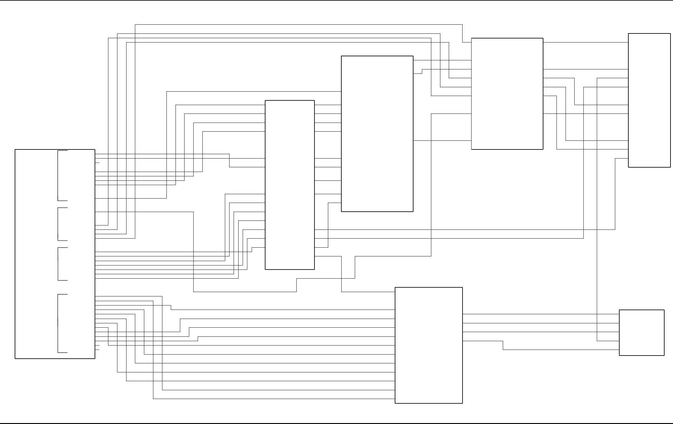
7-72 Schematics, Component Location Diagrams, and Parts Lists: HUE4039A/HUE4043A (UHF Range 1) Main Board
May 25, 2005 6881096C74-B
7.3 HUE4039A/HUE4043A (UHF Range 1) Main Board
Figure 7-49. HUE4039A/HUE4043A Main Board Overall Block Diagram and Interconnections
RFPA_OU T
SWITCH_BIAS
TX_IN J
VCURRENT
VFORWARD
VFORWARD_ON
VGBIAS1
VGBIAS2
VGBIAS3
VREVERSE
VREVERSE_ON
VTEMP
RF_ATTN_1_A
RF_ATTN_2_A
RF_ATTN_3_A
RF_IN
RX_FILT_1_A
RX_Inj_SW
RFPA_OU T
RX_IN
SWITCH_BIAS
VFORWARD_ON
VREVERSE_ON
A+_1
A+_2
K9.1V
RFPA_CNTR L
9.3V_FROM_BE
9.3V_FROM_FE
9.3V_TO_CONT R
IF_INIF_OUT
RF_ATTN_1_B
RF_ATTN_1_C
RF_ATTN_2_B
RF_ATTN_2_C
RF_ATTN_3_B
RF_ATTN_3_C
RX_FILT_ 1R X_FILT_1_A
9.3V_TO_IF
IF_OUT_IF
LO_IN
VGBIAS_3
VREVERSE
VTEMP
5V_FROM_CONTR
5V_TO_FGU
5V_TO_IF
9.3V_FROM_FGU
9.3V_TO_IF
CLKOUT_1
DOUTA_1
FREF
FS_1
IF
PC_1
PD_1
PE_1
5V_IF
MODIN
MOSIA_ABACUS
MOSIA_FGU
RFPA_CNTRL
RX_ATTEN_1
RX_ATTEN_2
RX_ATTEN_3
RX_FILT_1
SCKA_ABACUS
SCKA_FGU
SYN_SEL
VCURRENT
VFORWARD
VGBIAS_1
VGBIAS_2
TX_INJ
16.8_MHZ
5V_ABACUS
9.3V_ABACUS
9.3V_FGU
A+_1
A+_2
A+_3
A+_4
ABACUS3_CS
ABACUS_SSI_CLK
ABACUS_SSI_FSYNC
ABACUS_SSI_RXD
AUX_5V
K9.1V
LOCK_DET
DOUTA_2DOUTA_3
FS_ 2FS_ 3
Lock_Det
MOD_IN
PC_2
PC_3
PD_2
PD_3
PE_2PE_ 3
RX_Inj
RX_Inj_SW
SPI_CLK
SPI_DATA
SYN_SEL
16_8MHz
16_8_CONT
5V_Reg
9.3V_1 9.3V_2
CLKOUT_ 2CLKOUT_3
RF_FE/IF_Interface
RF_BE_Interface
FGU_Interface
RFPA_Interface
CONTROLLER
RX_BE
RX_IF
RFPA
RX_FE
OUTPUT NETWORK
FGU
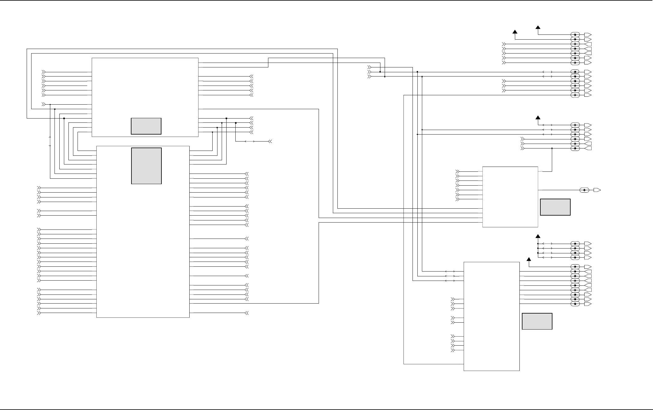
Schematics, Component Location Diagrams, and Parts Lists: HUE4039A/HUE4043A (UHF Range 1) Main Board 7-73
6881096C74-B May 25, 2005
Figure 7-50. HUE4039A Controller Block Diagram and Interconnections (Sheet 1 of 2)
RX_BE_INTERFACE
RFPA_INTERFACE
FGU_INTERFACE
INTERFACE, SECURE, DC SUPPLY
IF0036
MUX_RX
MUX_TX
RX_FILT_AUDIO
SAP_DCLK
SAP_FSYNC
SAP_RX
SAP_TX
SPI_MOSIA
SPI_SCKA
SPKR+
SPKR-
IF0004
AUDIO_PA_EN
AUX_MIC
AUX_RX
AUX_TX
CODEC_PWR_DOWNEEPOT_2_CS*
EEPOT_3_CS*
EEPOT_CS*
EEPOT_INC*
EEPOT_U_D*
MIC_HI
MUX_AUX_TX
MUX_MICATTEN
IF0029
IF0033
A+
IF0022
IF0021
IF0002
IF0001
IF0020
IF0024
9.3V
IF0000
K9.1V_EN
MISOA
MOSIA
PA_EN
PWR_RANGE
RFPA_CNTRL
RX_FILT_1
SCKA
VCURRENT
VFORWARD
VGBIAS_1
VGBIAS_2
VGBIAS_3
VREVERSE
VTEMP
AD_EN
DA_EN
EEPOT_4_CS*
EEPOT_5_CS*
EEPOT_PC_INC*
EEPOT_PC_U_D*
IF0011
16.8_MHZ
AUX_MIC
AUX_TX
DAC_SSI_CLK
DAC_SSI_FSYNC
DAC_SSI_TXD
MIC_TUNE_EN
MODEM_EN
MODIN
RESET
RX_FILT_AUDIO_IN
RX_FILT_AUDIO_OUT
URCHIN_EN
IF0028
IF0017
UTXD1_USB_VPOUT
UTXD2
VIP_IN_1_3V
VIP_IN_2_3V
VIP_OUT_1_3V
VIP_OUT_2_3V
VPP
WAKEUP
IF0009
SPI_SCKB
SPKR+
SPKR-
SSI_INT*
SW_B+_SENSE
UCTS1_USB_FSEN
UCTS2
URTS1_USB_XRXD
URTS2
URXD1_USB_VMIN
URXD2
USB*_RS232_EN
USB_INT*
USB_TXENB
USB_VMOUT
USB_VPIN
NAUTILUS_CS*
NAUTILUS_INT*
ONE_WIRE
PTT*
RIA_USBSUSP
RX_FILT_AUDIO
SAP_DCLK
SAP_FSYNC
SAP_RX
SAP_TX
SB96_RS232*_EN
SOFT_TURN_OFF
SPARE_1
SPARE_2
SPI_MISOB
SPI_MOSIB
BOOT*
BUS_PWR_OUT
CABLE_DET
CHAN_ACT
EMERG_SENSE
ENC_RESET
ENC_SPARE1
ENC_SPARE2
FORCE_FAIL*
IGNITION_SENSE
LHRST_IN
LHRST_OUT
LV_DETECT
MIC_HI
MOD
MONITOR
IF0008
AUX_MIC
AUX_RX
AUX_TX
9.3V_ABACUS
IF0005
IF0023
IF0035
IF0031
IF0013
IF0007
IF0030
IF0019
IF0032
IF0016
IF0010
IF0018
IF0003
IF0025
K9.1V
IF0026
IF0012
IF0027
5V_ABACUS
SPARE_2
SPARE_1
SAP_RX
SAP_FSYNC
SAP_DCLK
8KHZ_DSP_INT
MUX_MICATTEN
EEPOT_PC_INC*
A+_4
A+_3
RX_ATTEN_1RX_ATTEN_1
BUS_PWR_OUT
16.8_MHZ
16.8_MHZ
16.8_MHZ
MIC_TUNE_EN
MODEM_EN
DAC_SSI_TXD
DAC_SSI_CLK
DAC_SSI_FSYNC
URCHIN_EN
RESET
SAP_TX
EEPOT_6_CS*
EEPOT_3_CS*
EEPOT_2_CS* CODEC_PWR_DOWN
AUDIO_PA_EN
ONE_WIRE
MONITOR
MODIN
ABACUS3_CSABACUS3_CS
MUX_TX
MUX_RX
MUX_AUX_TX
EEPOT_U_D*
EEPOT_INC*
EEPOT_1_CS*
VIP_IN_2_3V
VIP_IN_1_3V
CHAN_ACT
SPI_MOSIA
SPI_SCKA
SPI_MISOA
SSI_INT*
ABACUS_SSI_CLK ABACUS_SSI_CLK
AUX_5VAUX_5V
TX_PA_EN
MOSIA
MISOA
KEYED_9.1_EN
EEPOT_PC_U_D*
EEPOT_5_CS*
EEPOT_4_CS*
DA_SEL
AD_SEL
VGBIAS_1
VIP_OUT_2_3V
VIP_OUT_1_3V
VREVERSE
VGBIAS_3
VGBIAS_2
VFORWARD
VCURRENT
SCKA
RX_FILT_1
RFPA_CNTRL
PWR_RANGE
ENC_RESET
EMERG_SENSE
CABLE_DET
BOOT*
SYN_SEL SYN_SEL
LOCK_DET LOCK_DET
A+_2
A+_1
VTEMP
NAUTILUS_INT
NAUTILUS_CS*
MOD
LV_DETECT
LHRST_OUT
LHRST_IN
IGNITION_SENSE
FORCE_FAIL*
ENC_SPARE2
ENC_SPARE1
UCTS1_USB_FSEN
SW_B+_SENSE
SPI_MOSIB
SPI_MISOB
SOFT_TURN_OFF
SPI_SCKB
SB96_RS232*_EN
RIA_USBSUSP
PTT*
USB_TXENB
USB_INT*
USB*_RS232_EN
URXD2
URXD1_USB_VMIN
URTS2
URTS1_USB_XRXD
UCTS2
RX_ATTEN_2RX_ATTEN_2
SCKA_ABACUS
MOSIA_ABACUS
WAKEUP
VPP
UTXD2
UTXD1_USB_VPOUT
USB_VPIN
USB_VMOUT
9.3V_FGU
SCKA_FGU
MOSIA_FGU
ABACUS_SSI_RXDABACUS_SSI_RXD
ABACUS_SSI_FSYNCABACUS_SSI_FSYNC
9.3V_ABACUS
5V_ABACUS
RX_ATTEN_3RX_ATTEN_3
K9.1V
AUDIO
POWER CONTROL
AD5320/SCF Block
MAEPF-27827-O
Part Series
200
Part Series
300
400
500
600
Part Series
900-1
Part Series
900-2
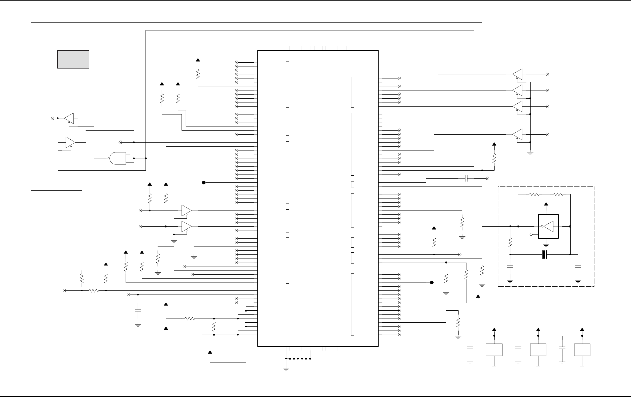
7-74 Schematics, Component Location Diagrams, and Parts Lists: HUE4039A/HUE4043A (UHF Range 1) Main Board
May 25, 2005 6881096C74-B
Figure 7-51. HUE4039A Controller Block Diagram and Interconnections (Sheet 2 of 2)
NP
For Patriot RAM, R0125 is not placed, R0124 is placed for a 1
For Patriot BRAVO, neither R0124 or R0125 is placed for a 1
32kHz Oscillator Circuit
NP
For Non-HAB: R0114 Placed
R0113, R0115 Not Placed
R0113, R0115 Placed
NP
For HAB: R0114 Not Placed
NP
For Patriot RAM and BRAVO, R0124 is not placed, R0125 is placed for a 0
NP
NP
NP
NP
For Patriot RAM, R0107 NP, R0108 Placed
For Patriot BRAVO, R0108 NP, R0107 Placed
NC
VCC2.85
C0106
100pF
GND
3
2
NC
1
4
VCC 5
10K
U0102
TC7SU04F
12
13
11
R0124
MC74LCX125
U0103-4
VCC2.85VCC2.85
VDD_CORE_2
VDD_EIM_1
F2
G1 VDD_EIM_2
Y18 VDD_IO_1
X18 VDD_IO_2
G18 VPP
VSIM1
N18
P18 VSIM2 VCC2.85
Z6
URTS1_PA13 Z2
URTS2_PB3 Z5
URXD1_PA15 Y3
URXD2_PB1 Y4
UTXD1_PA14 Z3
UTXD2_PB0 Z15
S18 VDD_CORE_1
R18
D1
TOUT4 E1
TOUT5 I1
P17
TOUT6
TOUT7 E2
TOUT8 G2
TOUT9 F1
Y2
UCTS1_PA12
UCTS2_PB2
TOUT1
TOUT10 N17
TOUT11 J1
I2
TOUT12
TOUT13 B1
TOUT14 S17
TOUT15 C2
TOUT2 D2
TOUT3
A2
X2 SRDA
SRDB V2
S2
SRDB2
STBY_PD14
H18
STDA
W2
STDB V1
TOUT0 H1
C1
N2
L1 SPI_CS2_PE4
SPI_CS3_PE6
K2
P2 SPI_CS4_PE7
SPI_CS5_PE11
B4
SPI_CS6_PE0
N1
SPI_CS7_PE1
M2
SPI_CS8_PE2
A3
SPI_CS9_PE3
L18
SPIA_CLK
K1
L2 SPIA_MISO
M1 SPIA_MOSI
SPIB_CLK
P1
SPIB_MISO
R1
SPIB_MOSI
R2
SPI_CS0_PE10
J2
SPI_CS1_PE5
I18
SIM_D1RX_PB11
F17
K17 SIM_D1TX_PB10
E18 SIM_PD0_PB9
SIM_PD1_PB15
B15
SIM_RST0_PB6
V18
SIM_RST1_PB12
G17
SIM_SVEN0_PB8
U18
SIM_SVEN1_PB14
U2
SCKA
W1
T2
SCKB
SCKB2 S1
DSC_TX_PD5 A15
SIM_CLK0_PB7
U17
SIM_CLK1_PB13
L17
SIM_D0RX_PB5
V17
SIM_D0TX_PB4
J17
ROW6 Z10
Y8
ROW7
Z1 SC0A
SC0B T1
SC1A
Y1
SC1B U1
SC2A
X1
SC2B
Y16
RESET_OUT
Y11
Y5
RIA_PA9
Y10
ROW0
ROW1 Z9
ROW2 M17
ROW3 Y9
ROW4 Y6
ROW5
Z8
PC11_OC1
D17
W18 PC12_STO
B16 PC1_USBTXENB
PC8
M18
PC9
J18
PWM*_PE14
Z17 PWM_PE13
K18
RESET_IN
B12
NC6 A5
NC7 B14
B8
NC8
NC9 B7
OC3_PC13
B18
OWIREDAT_PC10 Z18
PA2_USBVPIN
Y7
PC0_UBSVMOUT
A6
A13 NC18
NC19
A14
NC2 A8
NC20
A16
NC21
B2 NC3 B5
NC4 A7
NC5
A11
NC10 B6
NC11 B10
NC12 A17
A9
NC13
NC14 B11
NC15 A12
NC16
B13
NC17
Z12
INT1_PE9
Z13
INT2_PC14
Y14
INT3_PC15
C17
INT4_PA6_OPTSEL1
Z11
INT5_PA7_OPTSEL2
Y12
T17 MOD
MUX_CTRL Z4
NC1
B3
GND12
H17
GND5
I17
GND6
A18
GND7
B17
B9 GND8
GND9
A10
HW_ID
D18
INT0_PE8
Z14
W17
COLUMN6
COLUMN7 R17
DCDA_PA8 Z7
DSC_RX_PD6 C18
DSRA_INT6_PA10 E17
DTRA_INT7_PA11 F18
A4 GND10
GND11
H2
A1
CKIL
CLKSEL_PD15
T18
COLUMN0 X17
COLUMN1 Y15
COLUMN2 Y13
COLUMN3 Y17
COLUMN4 Z16
COLUMN5
VCC1.8
U0001
33C34
CKIH
R0114
0
VCC2.85
3
MC74LCX125
U0104-4
12
13
11
MC74LCX125
U0104-1
2
1
MC74LCX125
2
1
3
18pF
U0103-1
TP0002
1
C0101
U0103-2
MC74LCX125
5
4
6
R0104
10K
R0108
0
VCC2.85
10K
R0120
R0103
10K
VCC2.85
VCC2.85
VCC2.85
VCC2.85
R0122
3.3K
PWR_GND
U0105-2
GND
3
VCC
5
R0107
0
VCC2.85
PWR_GND
U0103-5
GND
7
VCC
14
R0116
10MEG
MC74LCX125
5
4
6
U0104-2
R0101
10K
R0109
10K
R0111
R0117
3.3K
VCC2.85
10MEG
C0105
0.1uF
0.1uF
C0103
PWR_GND
U0104-5
GND
7
VCC
14
0.1uF
C0104
VCC2.85
10K
R0125
VCC2.85
R0123
3.3K
32.768KHz
CC4V Y0100
21
R0105
10K
R0102
10K
R0106
10K
R0119
470K
R0110
10K
VCC2.85
10K
R0121
VCC1.55
TP0005 1
0.1uF
C0102
18pF
R0113
10K
C0100
MC74LCX125
U0104-3
9
10
8
R0115
0
U0105-1
TC7S00FU
1
2
4
VCC2.85
MC74LCX125
U0103-3
9
10
8
HAB_DISABLE
HAB_MOD
16.8_MHZ
16.8_MHZ_PATRIOT
ONE_WIRE
BRD_ID_4
BUS_PWR_OUT
BRD_ID_1
BRD_ID_7
BRD_ID_6
USB*_RS232_EN
MOD MOD*
SPI_MISOA
SPI_MOSIA*
MISO_SEL
SPI_MOSIA
FORCE_FAIL*
SPARE_2
SPARE_1
ABACUS_SSI_FSYNC*
ABACUS_SSI_CLK*
ABACUS_SSI_RXD
LOCK_DET
LOCK_DET*
TX_PA_EN
SSI_INT*
PTT
MONITOR*
PTT*
MONITOR
LV_DETECT
EEPOT_5_CS*
MILL_ID
BRD_ID_2
PWR_RANGE
SW_B+_SENSE
BRD_ID_0
BRD_ID_3
MODEM_EN
ABACUS_SSI_RXD*
DAC_SSI_CLK
ABACUS_SSI_FSYNC
ABACUS_SSI_CLK
SPI_MOSIB
NAUTILUS_CS*
EEPOT_4_CS*
RX_ATTEN_3
SB96_RS232*_EN
32_KHZ
NAUTILUS_INT
RX_ATTEN_2
RX_ATTEN_1
EEPOT_PC_U_D*
EEPOT_PC_INC*
SOFT_TURN_OFF
MUX_MICATTEN
VIP_OUT_2_3V
VPP
SAP_RX
SAP_TX
DA_SEL
ABACUS3_CS
AD_SEL
EEPOT_3_CS*
SYN_SEL
MUX_AUX_TX
SPI_SCKA
EEPOT_U_D*
AUDIO_PA_EN
EEPOT_1_CS*
EEPOT_INC*
EEPOT_2_CS*
SAP_DCLK
SAP_FSYNC
RESET
CODEC_PWR_DOWN
USB_TXENB
8KHZ_DSP_INT
USB_VMOUT
USB_VPIN
CABLE_DET
USB_INT*
SPI_MISOB
SPI_SCKB
MIC_TUNE_EN
UTXD2
UTXD1_USB_VPOUT
URXD2
URXD1_USB_VMIN
URTS2
URTS1_USB_XRXD
UCTS2
UCTS1_USB_FSEN
AUX_5V
MUX_TX
MUX_RX
LHRST_OUT
LHRST_IN
DAC_SSI_TXD
URCHIN_EN
KEYED_9.1_EN
DAC_SSI_FSYNC
ENC_SPARE1
EMERG_SENSE
VIP_OUT_1_3V
VIP_IN_2_3V
RIA_USBSUSP
BRD_ID_5
VIP_IN_1_3V
ENC_SPARE2
WAKEUP
BOOT*
ENC_RESET
IGNITION_SENSE
GP10/EGPT/MISC
INT
QSPI
SAP
SIM
BBP
LAYER1_TIMER
CLKS
UART_A
UART_B
DSC OWIRE
KEYPAD
MAEPF-27828-O
Part Series
100-1
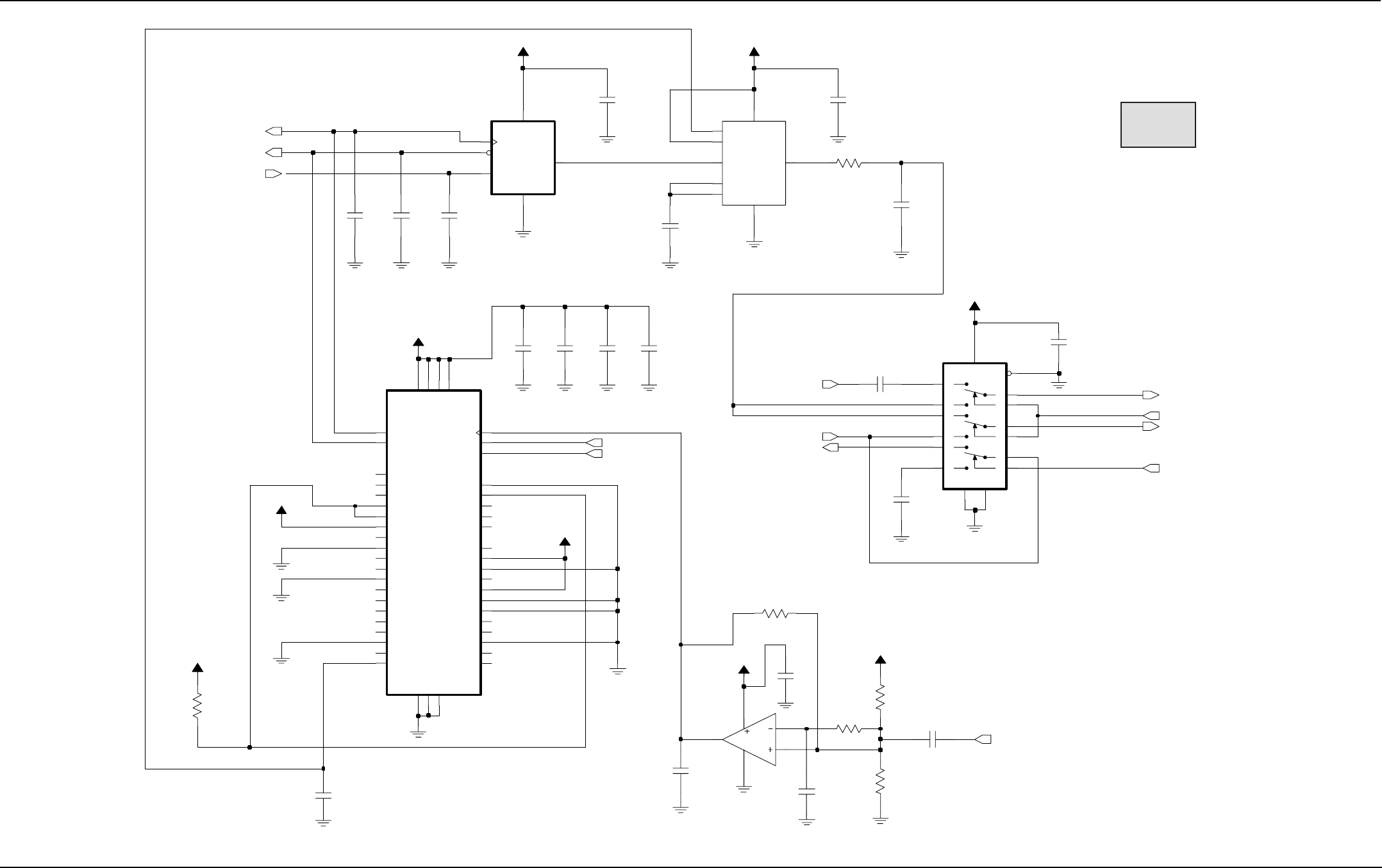
Schematics, Component Location Diagrams, and Parts Lists: HUE4039A/HUE4043A (UHF Range 1) Main Board 7-75
6881096C74-B May 25, 2005
Figure 7-52. HUE4039A Controller Urchin IC, MUX, and AD5320 DAC Schematic
NP
0.1uF
C0901
C0917
100pF
R0903
100K
C0906
VCC2.85
0.1uF
C0918
100pF
VCC2.85
R0904
100K
4DIN
2GND
5SCLK
6SYNC
3
VDD
1
VOUT
AD5320BRT
U0900
VCC2.85
C0910
0.1uF
4
3
1
5
2
R0901
8.2K
LMV7219
U0903
C7
VCC2 E2
VCC3 G4
VCC4
VCC2.85
C0909
0.1uF
B6
NC8 C2
NC9
A6
RESET
E5
TCK B1
TDI
TDO B7
D2
TMS
B3
VCC1
G3 NC29
NC3 A4
NC30
G5
G6 NC31
A7
NC4 B2
NC5 B4
NC6
NC7 B5
F1 NC21
F2 NC22
F3 NC23
F4 NC24
F5 NC25
F6 NC26
F7 NC27
G2 NC28
D3 NC14
D4 NC15
D6 NC16
D7 NC17
E1 NC18
E4 NC19
A2
NC2
E7 NC20
C3
G7 2.4_MHZ
G1 48_MHZ
A1
NC1
C4
NC10 C5
NC11 C6
NC12
D1 NC13
A3
16.8_CLK
C1
ENABLE
A5 GND1
E3 GND2
E6 GND3
JTAG_EN
C0915
VCC2.85
XCR3032XL
U0901
IN
2
6OS
OUT 5
7SHDN
4
VDD
100pF
MAX7414
FL0900
CLK
8
1COM
GND
3
C0905
0.1uF
VCC2.85
R0902
100K
C0904
C0908
0.1uF
VCC2.85
220pF
R0900
100K
0.1uF
C0903
VCC2.85
C0919
C0907
0.1uF
100pF
C0914
33pF
Z1
3
100pF
C0911
14
X
12 X0
X1
13
15
Y
2Y0
1Y1
4
Z
5Z0
A11
10
B
9
C
6
EN
8GND
16
VCC
7VEE
VCC2.85
MC74HC4053
U0902
100pF
C0912
C0902
R0905
100K
0.1uF
0.1uF
C0916
C0913
100pF
MODIN
SCF_OUT
MIC_TUNE_EN
URCHIN_EN
RESET AUX_TX
AUX_MIC
DAC_SSI_CLK
DAC_SSI_TXD
16.8_MHZ_DC
RX_FILT_AUDIO_IN
RX_FILT_AUDIO_OUT
16.8MHZ_SQARE
DAC_SSI_FSYNC
MODEM_EN
16.8_MHZ
AD5320_OUT
MAEPF-27836-O
Part Series
900-1

7-76 Schematics, Component Location Diagrams, and Parts Lists: HUE4039A/HUE4043A (UHF Range 1) Main Board
May 25, 2005 6881096C74-B
Figure 7-53. HUE4039A Controller Audio Schematic
AUDIO_GROUND
NP
-14 dB to +14 dB
-9 dB to +14 dB
Programmable pre-amp stage Programmable pre-amp stage
Anti-aliasing filter
Ground
7 dB Attenuation Stage
UNIVERSAL GROUND
SW_A+
VAG
0.1uF
C0224
R0227
0.1uF
68K
0.1uF
C0216
C0201
VAG
A+_FILT
R0206
100K
C0205
10uF
C0220
150pF
33K
R0228
VAG
10K
C0226
0.1uF
R0222
1IN
4
NC
6
NO
VPOS 2
VCC2.85
NLAST4599
U0210
5
COM
GND
3
R0207
7.5K
R0203
1K
VPOS 2
470pF
C0230
NLAST4599
U0208
5
COM
GND
3
1
IN
4NC
6
NO
0.1uF
C0242
R0208
100K
VCC2.85
C0207
33pF
R0236
9.1K
R0226
36K
R0212
100K
C0240
0.1uF
C0206 470pF
C0235
1uF
1
10uF
C0221
VCC2.85
VCC2.85
TP0200
C0204
4.7uF
A+
10K
VAG
TP0205
1
VCC5
R0221
C0210
0.1uF
1uF
C0208
U0201-4
MC33204
13
12
14
4
11
LM7301
U0207
4
3
1
2
5
3300pF
C0217
4.7uF
Q0200
C0223
R0210
100K
0.1uF
C0239
R0209
10K
560
R0204
COM
5
GND
3
IN
1
NC 4
NO
6
2
VPOS
VCC2.85
U0203
NLAST4599
0.1uF
C0227
VCC2.85
R0235
10K
R0225
10K
150pF
C0228
220pF
C0233
0
R0231
VCC2.85
1K
C0214
VCC2.85
R0200
C0225
0.1uF
VCC2.85
0.1uF
R0224
10K
19 TI_POS
20
VAG
1VAGREF
6
VDD
15 VSS
11 MCLK
10 PDI
3PI
4
PO_NEG 5
PO_POS
2
RO_NEG
17
TG
18 TI_NEG
9BCLKR
12 BCLKT
8DR
13
DT
7FSR
14 FST
16 HB
VCC2.85
MC145483
U0200
7
VCC
R0223
18K
10 GND3
GND4
11
9INV
8M_SS
1NINV
4
OUT1
6
OUT2
3RR
U0204
TDA1519C
2GND1
GND2
5
VREFIN
0.1uF
C0234
6CLK
5DATA
3GND
8IN
4LOAD
2
OUT
7
VDD
1
C0209
0.1uF
LM1971
U0206
C0232
18K
R0220
470pF
C0212
1
0.1uF
47K
TP0206
100pF
R0205
MC33204
6
5
7
4
11
C0211
U0201-3
MC33204
9
10
8
4
11
VCC5
U0201-2
TP0203
1
1K
R0219
VAG
3.3K
R0202
TP0202
1
C0238
220pF
C0203
0.1uF
VCC2.85
220pF
C0231
SIGNAL_CONVERT
SC0001
I1
1I2 2
R0218
1K
100K
VCC2.85
TP0201
1
R0216
0.1uF
C0215
6800pF
C0244
VCC2.85
6800pF
C0243
MC33204
U0201-1
2
3
1
4
11
C0202
0.1uF
TP0204
1
0.1uF
C0213
R0230
C0236
470pF
NO
VPOS 2
9.3V_TX
33K
NLAST4599
U0209
5
COM
GND
3
1
IN
4NC
6
68K
R0229
I1
1I2 2
VCC2.85
SIGNAL_CONVERT
SC0002
W1 4
W2 7
VCC2.85
C0237
220pF
CS1
1
CS2
10
GND
8
INC
9L1 5
6
L2
U_D
2
VDD 3
MIC_PREAMP_OUT
RX_FILT_AUDIO
SPKR+
SPKR-
U0202
MAX5452
AUX_RX*
MIC_HI*
AUX_TX_B
CODEC_OUT_C
RX_AUDIO_IN
MUX_AUX_TX
AUX_MIC*
AUX_TX*
AUX_MIC
AUX_TX
MIC_PREAMP_IN
VOLUME_IN
EEPOT_U_D*
EEPOT_INC*
SPI_SCKA
SPI_MOSIA
EEPOT_3_CS*
MUX_MICATTEN
VOL_OUT*
VOL_OUT
CODEC_OUT
AUX_TX_A
CODEC_OUT_B
MIC_M
MIC_A
MIC_C
MIC_B MIC_E MIC_K
MIC_N
CODEC_OUT_A
MIC_L
MIC_G
MIC_J
MIC_I
MIC_F
MIC_H
EEPOT_CS*
AUX_RX
SAP_FSYNC
SAP_TX
SAP_DCLK
AUDIO_PA_EN
MUX_TX
MUX_RX
EEPOT_2_CS*
MIC_HI
MIC_D
AUDIO_PA_IN
SAP_RX
CODEC_PWR_DOWN
47K
47K
MAEPF-27837-O
Part Series
200
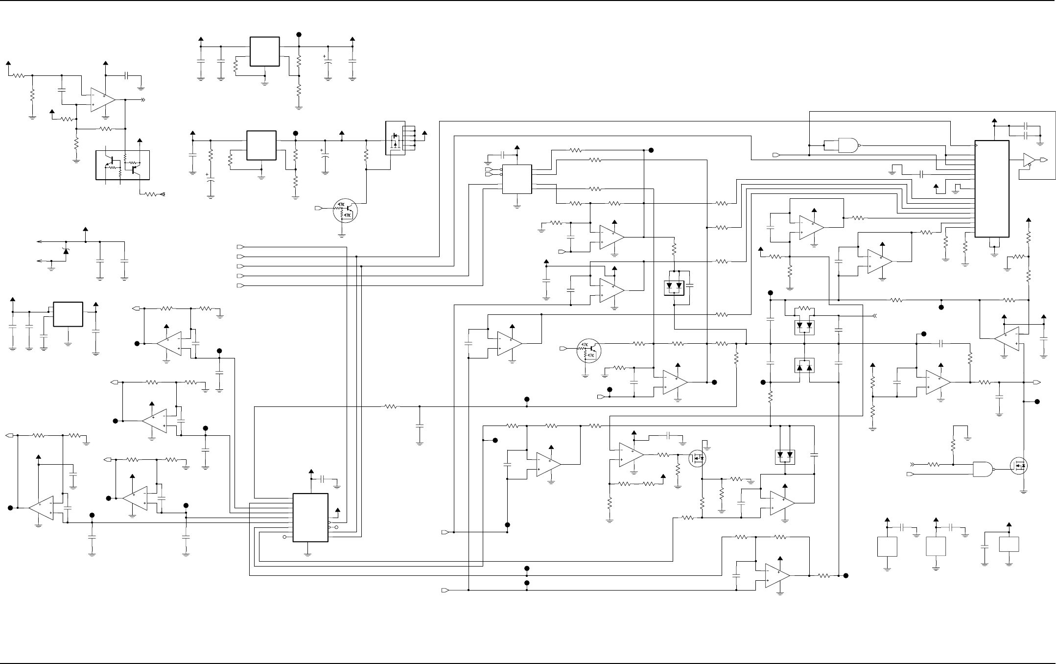
Schematics, Component Location Diagrams, and Parts Lists: HUE4039A/HUE4043A (UHF Range 1) Main Board 7-77
6881096C74-B May 25, 2005
Figure 7-54. HUE4039A Controller Power Control Schematic
NU
VCC3
5.1K
R0990
9.3V_TX
10K
R0988
100pF
U0959
C0998
U0956-3
TP0956
100K
R0982
C0941
1uF
10K
R0991
10K
0.1uF
C0954
R0947
C0997
68pF
100pF
C0933
VCC5
Q0960
0
R0987
C0976
100pF
100K
100pF
C0935
C0980
R0962
TP0942
0.1uF
1uF
C0973
TP0938
U0957-3
1.2K
R0997
100pF
C0922
R0952
1.2K
R0960
U0950
VCC2.85
20K
R0977
0.1uF
C0981
9.3V_TX
VCC3
100
100pF
C0923
U0951
U0956-2
VCC3
U0957-1
A+
U0963-1
10K
R0944
0.1uF
C0985
VCC3
VCC3
0.1uF
C0974
U0960-1
SW_A+
R0912
12K
U0962
C0969
9.3V_TX
VCC5
100pF
J0950-1
C0964
100pF
C0987
VCC3
0.1uF
R0984
Q0954
0
Q0951
R0955
100K
C0937
0.1uF
TP0930
U0953
TP0931
10K
R0974
TP0963
R0972
4.7K
100pF
C0975
0.1uF
C0972
VCC3
9.3V_TX
C0944
0.1uF
C0986
0
0.1uF
R0938
C0951
1uF
C0963
100pF
D0951
TP0952
C0960
0.1uF
TP0940
R0924
100
100pF
C0978
U0965
C0965
100pF
0
R0950
TP0955
TP0958
C0983
100pF
100pF
C0934
U0958-2
TP0939
C0940
0.1uF
0.1uF
C0950
56K
R0989
R0964
24K
8.2K
R0942
0
R0965
U0960-4
VCC3
Q0952
VCC3
TP0954
0.1uF
C0979
4.7uF
C0945
R0951
7.5K
9.3V_TX
R1002
2.7
100K
R0992
C0955
0.1uF
C0936
0.1uF
0
R0985
U0963-2
0
R0966
10K
R0999
0.1uF
R0998
C0961
10K
VCC3
C0942
1uF
R0936
0
100pF
C0930
U0956-4
9.3V_TX
R0923
100
10K
D0954
R0968
U0960-2
U0958-1
VCC3
Q0955
R0979
3.9K
R0994
TP0950
0
U0957-2
1K
R0934
C0957
0.1uF
10K
9.3V_TX
R0973
R0931
30K
Q0953
R0954
U0957-4
7.5K
TP0941
22uF
C0982
R0976
1K
0
R0953
K9.1V
9.3V
9.3V_TX
U0952
J0950-2
D0952
R0961
100K
0.1uF
C0984
24V
VR0950
TP0957
U0954-2
U0956-1
R0995
TP0962 1.2K
20K
R0930
C0966
100pF
D0950
C0956
22uF
2K
R0983
100K
R0967
9.3V_TX
VCC3
U0955-2
1.2K
R0993
R0913
130K
R0910
82K
SW_A+
.01uF
TP0951
C0943
TP0964
R0940
TP0936
TP0961
0
U0955-4
TP0960
VCC39.3V_TX
U0955-1
A+
9.3V_TX
1K
R0948
TP0959
U0960-3
100pF
15K
R0971
C0967
0.1uF
C0952
100K
R0980
R0946
0
0
R0986
33K
R0978
10K
R0945
C0959
0.1uF
0.1uF
C0920
TP0937
R0970
24K
R0963
24K
U0955-3
15K
R0941
30K
R0943
R0939
30K
30K
R0937
470pF
C0962
C0921
100pF
100pF
C0971
9.3V_TX
VCC3
C0953
22uF
R0911
12K
10K
R0975
R0914
12K
10K
10K
10K
9.3V_TX
0
R0935
VCC5
10K
R0969
100pF
C0970
4.7K
R0933
9.3V_TX
3.3K
R0932
10K
R0996
A+
U0954-1
2.7K
R0981
C0968
9.3V_TX
VCC3
100pF
TP0953
NU
1%
1%
1%
1%
1%
BATTERY CONNECTOR
1%
VCONTROL
1%
REVERSE_POWER
A+
FORWARD_POWER
1%
1%
VCURRENT
1%
1%
1%
1%
VTEMP
1%
NU
NU
NU
NU
NU
NU
NU
NU
NU
NU
LOOP_DISABLE
TX_DISABLE
TX_DISABLE
LOOP_DISABLE
RFPA_CNTRL
TEMP_1*
RX_FILT_1
TEMP_2*
PA_EN
MOSIA
AD_EN
MISOA
K9.1V_EN
SCKA
VGBIAS_2*
VGBIAS_3*
VGBIAS_3
VGBIAS_2
VGBIAS_1
RX_FILT_1*
DA_EN
PWR_SET*
CURR_LIM_SET*
EEPOT_PC_INC*
EEPOT_PC_U_D*
VCURRENT
VTEMP
VGBIAS_1*
PWR_RANGE
EEPOT_5_CS*
VFORWARD
EEPOT_4_CS*
VREVERSE
NU NU
NU
NU
NU
NU
NU
9.3V_TX_ REGULATOR
9.3V REGULATOR
VDD
OUTC
15 OUTD
7OUTE
8OUTF
9OUTG
10 OUTH
5
REF
12
SCLK
4
11
CS
13
DIN
14 DOUT
3
GND
6
LDAC
2OUTA
1OUTB
16
11
9
10
8
4
9
10
8
4
11
ADJ 1
GND
3
ON_OFF
2
VIN
4VOUT 5
ADJ 1
GND
3
ON_OFF
2
VIN
4VOUT 5
6
5
7
4
11
2
3
1
4
11
2
1
4
2
3
1
4
11
VEN
3
VIN
1
VOUT
5
BYPASS
4
GND
2
1
D
G
S
NC
5VIN2
6VIN3
7VIN4
8VIN5
9VIN6
10 VIN7
11 VIN8
1VREF
13
DGND
17 DIN 16
DOUT
15 RFS
18 SCLK
14 TFS
20
VDD
3VIN1
12 A0
4
AGND
19 CONVST
2CREF
1
5
2
4
3
3
GND
5
VCC
NC
13
12
14
4
11
1
2
3
6
7
8
4
5
3
GND
5
VCC
13
12
14
4
11
1
2
4
6
5
7
4
11
D
G
S
6
5
7
4
11
13
12
14
4
11
U_D
2
VDD
3
W1 4
W2 7
CS1
1
CS2
10
GND
8
INC
9L1 5
L2 6
2
11
GND
3
VCC
5
2
3
1
4
4
11
6
5
7
13
12
14
4
11
2
3
1
4
11
11
9
10
8
4
9
10
8
4
11
1
2
4
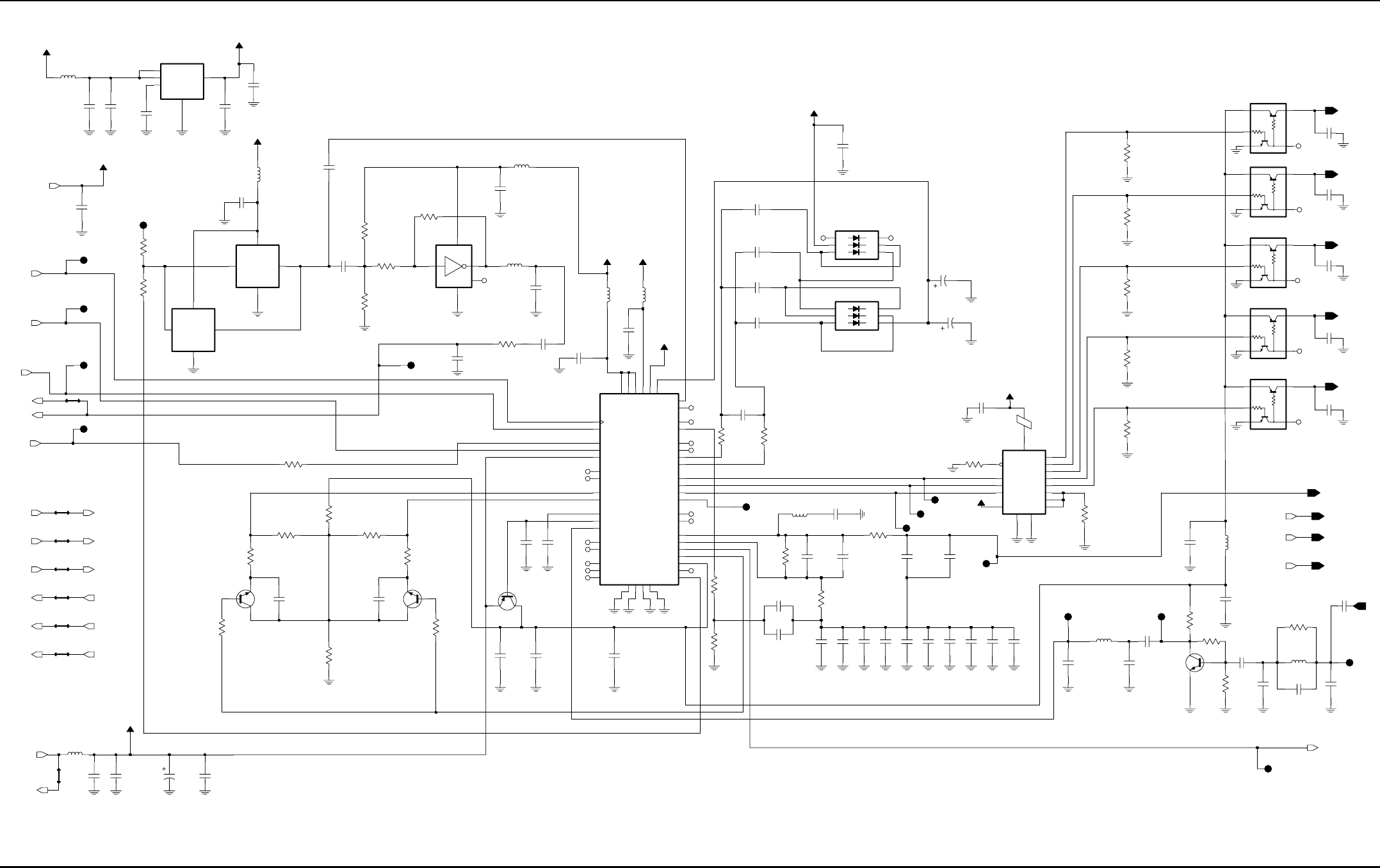
7-78 Schematics, Component Location Diagrams, and Parts Lists: HUE4039A/HUE4043A (UHF Range 1) Main Board
May 25, 2005 6881096C74-B
Figure 7-55. HUE4039A/HUE4043A Frequency Generation Unit
NU
NU
G
G
G
G
G
G
G
G
NC
NC
RX_Inj_SW
5V_Reg
F3.0v
TX_INJ
RX_Inj
NC
NC
NC
NC
F3.0V
NC
Feedback
RX_High_Switch
RX_Mid_Switch
NC
NC
NC
NC
RX_Low_Switch
TX_High_Switch
TX_Low_Switch
Steer_Line
NC
NC
NC
NC
NC
NC
F3.0V
F3.0v
5V_Reg
NC
NC
NC
NC
F3.0V
F3.0V
F3.0v
4.7K
4.7K
4.7K
4.7K
4.7K
A
Syn_Sel
CLOCK
DATA
NC
5V_Reg
47K
R5786
F9.3V
47K
R5785
3.0 Volt Regulator
47K
R5782
R5784
47K
R5783
220pF
47K
C5816
C5817
C5815
220pF
C5812
220pF
C5811
0.1uF 0.1uF
0.1uF
C5810
C5813
470pF
L5760
12uH
C5809
0.1uF
TP5783
1VCON
4
VCC
3
OUT
2
TP5760
R5781
Y05751
16.8MHz
6.8pF
C5808
GND
180
33pF
L5757
15.0nH
10pF
C5763
.047uF
C5795
10pF
C5794
C5781
C5762
0.1uF
C5799
10pF
C5800
220pF
Q5709
Q5710
Q5708
Q5707
Q5 70 6
R5771
150 150
R5773
2
X6
5
X5
1
X4
22pF
C5774
VEE
7
VCC
16
GND
8
U5753
4
X7
330pF
X3 12
X2 15
X1 14
X0 13
X
3
EN
6
9C
B
10 A
11
330pF
C5807
330pF
C5806
1K
C5805
E6750
0.1uF
R5777
C5793
R5776
R5770
1K
C5796
220pF
1.8K
TP5793
R5769
0
TP5794
TP5795
TP5791
TP5792
TP5796
TP5799
TP5798
TP5797
TP5789
TP5787
TP5790
R5766
100K
100pF
C5768
5
L5753
1uH
U5751
VCC
.01uF
4
NC 1
2
GND
3
C5754
TP5788
R5751
C5758
10K
2.2uH
0.1uF
Y5750
16.8MHz
VDD
4
VCONT
L5752
1
2
GND
FOUT 3
560nH
L5751
C5780
1uF
C5752
.0015uF
C5773
C5779
.0015uF
0.1uF
0.1uF
C5760
1000pF
C5765
C5767
560nH
L5750
1000pF
R5767
47K
R5765
5.1K
R5752
47K
47K
R5764
47K
0
R5754 R5775
100
R5755
C5802
R5779
12K
15.0nH
220pF
L5759
0.1uF
C5778
C5777
0.1uF
C5776
0.1uF
0.1uF
C5789
C5775
C5788
4.7uF
4.7uF
AUX2
48
AUX1
22 AGND
46
ADAPTSW
CLK
9CEX
42 CCOMP
39 BIAS2
40 BIAS1
20
AVDD
3
AUX4
2
AUX3
1
4
43
IOUT
16
INDMULT
45
IADAPT
19
FREFOUT
36
DVDD
6DGND
7DATA
8
PREIN
PD_VDD 5
44 PD_GND
31 NC3
29 NC2
17 NC1
41
MODOUT
10 MODIN
LOCK
SFOUT
30 SFIN
26 SFCAP
27 SFBASE
18 REFSEL
35 PVREF
34
PRE_VDD
33 PRE_GND
32
VMULT4
12
VMULT3
14
VMULT2
15
VMULT1
47
VCP
21 VBPASS
38
TEST2
37
TEST1
28
24
XTAL2
23
XTAL1
25
WARP
VRO 13
11
U5752
1
K3
2
K2
3
K1
6A3
5A2
4A1
A3
6A2
5A1
4
D5750
D5751
K3 1
K2 2
K1 3
Q5751
Q5750
2K
R5759
R5758
82
R5774
3.3K
C5785
0.1uF
0.1uF
0.1uF
C5784
C5783
0.1uF
0.1uF
C5787
.022uF
C5786 C5790
0.1uF
C5782
0.1uF
C5791
GND
2
4BYPASS
R5772
750
U5750
5
VOUT
VIN
1
3VEN
Q5755
820
R5778
2.7K
R5780
10pF
C5801
Q5752
0.1uF
C5769
0.1uF
C5772
100pF
L5758
C5798
10uF 1uH
10uF
C5770 C5797
39pF
330pF
C5764
C5804
330pF
C5803
C5751 C5755
.022uF
C5756
10uF
C5753
39pF
5.1K
0.1uF
R5753
C5759
0.1uF
C5750
0.1uF
C5757
1uF
L5755
2.2uH
C5771
2.2uH
L5756
0.1uF
R5763
1K
R5761
100K
R5762
100K
2.2uH
L5754
R5768
100
C5761
.01uF
10uF
C5766 0.1uF
C5792
NU
NU
R5750
1K
RX_Inj_SW
TX_INJ
SYN_SEL
9.3V_1
5V_Reg
MOD_IN
16_8_CONT
16_8MHz
CLKOUT_2
DOUTA_2
FS_2
CLKOUT_3
DOUTA_3
FS_3
9.3V_2
PD_2
PE_2
PC_3
PD_3
PE_3
RX_Inj
Lock_Det
PC_2
SPI_DATA
SPI_CLK
NU
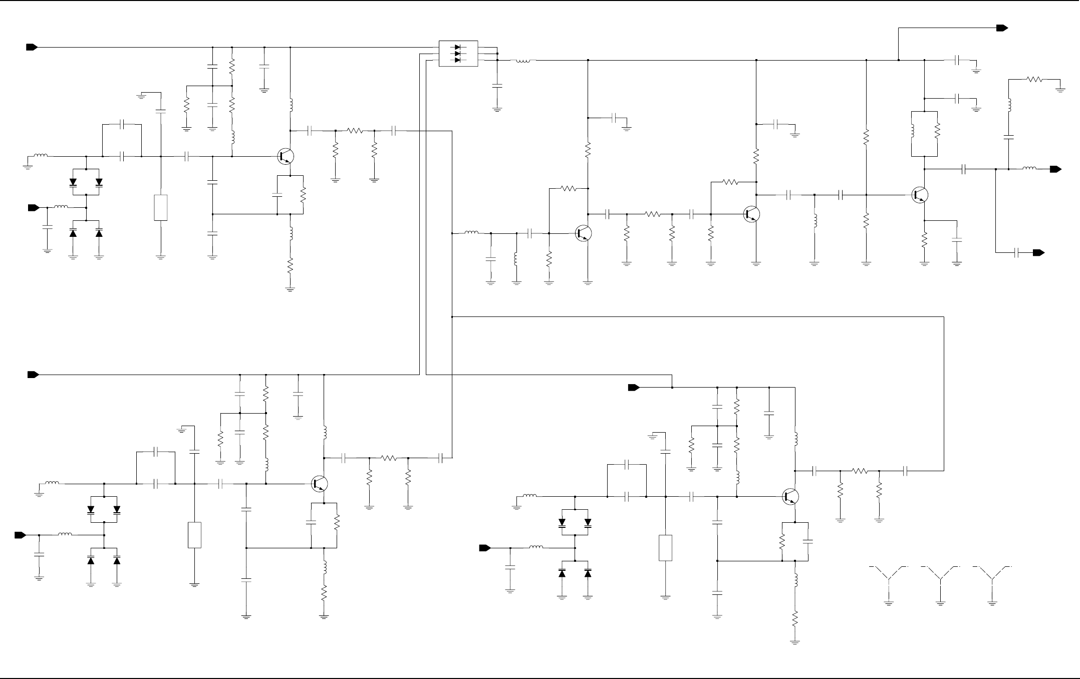
Schematics, Component Location Diagrams, and Parts Lists: HUE4039A/HUE4043A (UHF Range 1) Main Board 7-79
6881096C74-B May 25, 2005
Figure 7-56. HUE4039A/HUE4043A Receive VCO Schematic
G
G
G
G
G
G
G
IN
1
OUT
2
K1
K2
K3
A1
A2
A3
IN
1
OUT
2
IN
1
OUT
2
270nH
C5911
9.1pF
Q5904
2K
R5927
220
R5950 C5956
220pF
R5937
330
150nH
L5900
R5914
820
8.2pF
C5927
R5930
51
Q5906
C5945
220pF
R5934
33
15
R5941
D5901
470
R5911
220pF
C5949
C5947
4.7pF
D5911
Q5901
R5948
75
18nH
C5920
0.1uF
0.1uF
C5958
L5918
33
R5910
D5906
C5951
100pF
C5961
C5912
8.2pF
0.5pF
C5905
5.1pF 220pF
C5919
D5907
C5928
D5904
5.1pF
L5907
L5916
150nH
D5909
150nH
330nH
L5905
Y5900
3.3pF
C5960
R5918
100
D5910
C5900
0.1uF
D5908
2K
R5912
Q5903
D5903
18nH
L5909
SH5902
C5938
C5931
1.8pF
5.1pF
R5921
220pF
C5935
33
2.7K
R5922
C5930
220pF
C5957
3pF
C5906
L5919
1.6pF
C5959
12nH
R5929
100pF
100pF
12K
C5925
100pF
C5941
1.6K
R5916
R5931
75
220pF
C5913
220pF
C5914
75
L5917
12nH
R5919
R5923
470
220pF
C5901
C5948
0.1uF
330nH
L5915
C5932
220pF
L5901
330nH
330nH
L5914
C5946
220pF
360
R5940
1.6K
C5922
R5924
4.7pF
L5921
27nH
5.6pF
C5943
R5909
C5908
100pF
15
L5902
18nH
R5917
270
R5904
12K
D5912
L5920
C5950
100pF
0.1uF
C5936
C5923
1.5pF C5940
5.1pF
D5900
220nH
L5922
D5905
4.7K
R5938
R5933
2.7K
Q5905
Y5901
R5928
R5926
270
820
R5939
4.7K
R5903
2K
3.9pF
C5942
330nH
L5908
SH5900 SH5901
R5902
220
L5911
D5902
18nH
0.1uF
C5916
R5935
470
R5900
2K
6.8pF
0.1uF
C5915
4.7pF
C5933
15
R5949
C5944
220pF
C5917
4.3pF
C5939
2.7pF
C5937
100pF
C5921
5.1pF
C5907
0.1uF
C5904
220pF
R5905
C5929
330nH
100
R5920
L5913
R5932
75
Y5902
75
5.6pF
5.1pF
C5926
C5910
R5915
270
L5906
150nH
330nH
L5912
C5909
100pF Q5902
L5904
330nH
L5910
330nH
C5924
5.1pF
NU
NU
NU
NU
NU
NU
BFQ67
BFQ67
NE68519
LOW RANGE 489.65 MHz to 519.65 MHz
MID RANGE 519.65 MHz to 549.65 MHz HIGH RANGE 549.65 MHz to 579.65 MHz
590 MHz
665 MHz
BFQ67
NE68519
NE68519
625 MHz
RX_Mid_Switch
RX_Inj
RX_Inj_SW
Steer_Line
Steer_Line
RX_Low_Switch
RX_High_Switch
Steer_Line
Feedback
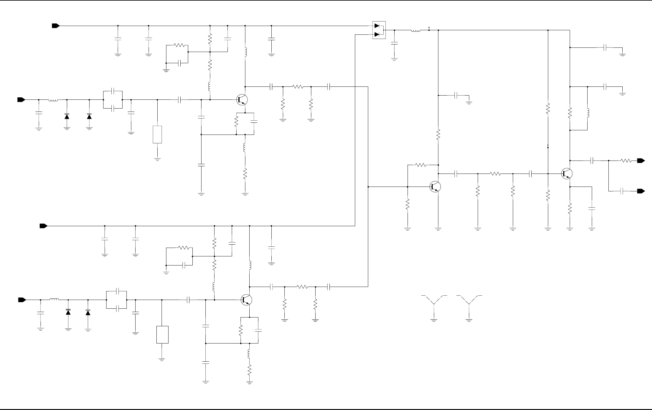
7-80 Schematics, Component Location Diagrams, and Parts Lists: HUE4039A/HUE4043A (UHF Range 1) Main Board
May 25, 2005 6881096C74-B
Figure 7-57. HUE4039A/HUE4043A Transmit VCO Schematic
G
1
IN
2
OUT
2OUT 1
IN
D5827
270nH
C5836
330pF
L5832
220
R5825
2.4K
330pF
R5850
270
C5860
0.1uF
R5827
11pF
Steer_Line
C5843
R5838
C5840
C5853
100
SH5820
330pF
15pF
C5850
18pF
C5827
51
TX_INJ
R5832
TP5826
TP5825
R5839
33
Q5826
L5825
15nH
SH5821
330pF
C5834
15
R5849
D5831
390nH
L5826
330pF
C5862
Q5828
L5830
270nH
C5847
220pF
C5841
U5826
330pF
18pF
C5845
C5855
C5835
9.1pF
330pF
5.1pF
D5832
C5848
100pF
C5846
C5859
100pF
C5825
330pF
51
R5840
12pF
C5829
TX_High_Switch
U5825
R5841
100
R5833
270
C5856
R5845
2.7K
R5846
0.1uF
12K
R5852
4.7K
R5851
C5837
0.1uF
R5828
4.7K
Q5825
470
0.1uF
C5831
33
100
R5831
C5861
0.1uF
R5842
C5858
18pF
L5833
220nH
L5831
180nH
0.1uF
C5844
330pF
C5826
D5828
360
R5854
270
R5834
L5828
15nH
3.9K
R5826
C5828
15pF
L5829
C5863
3pF
220pF
270nH
C5842
C5833
2.2pF
R5829
R5837
100
1K
1K
R5853
Steer_Line
C5832
0.1uF
20pF
C5854
R5855
R5848
820
0
R5843
220
12pF
C5852 C5857
390nH
L5827
TX_Low_Switch
12pF
18pF
C5839
Feedback
12pF
C5830
L5834
Q5829
180nH
R5830
1.3K
C5849
6.8pF
D5833
C5838
C5851
20pF
0.1uF
580 MHz
BFQ67
515 MHz
BFQ67
BFQ67
BFQ67
1SV232 1SV229
NU NU
11
HIGH RANGE 425 MHz to 470 MHz
LOW RANGE 380 MHz to 425 MHz
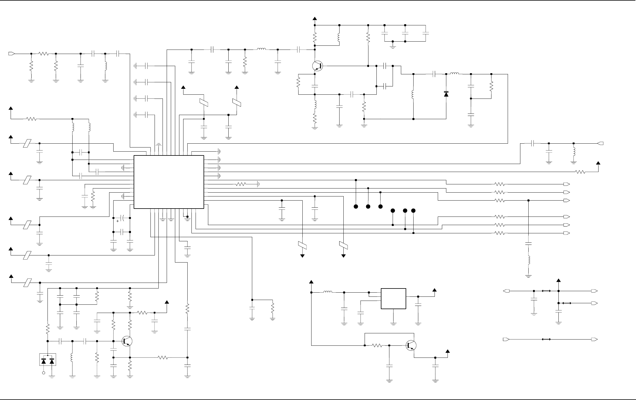
Schematics, Component Location Diagrams, and Parts Lists: HUE4039A/HUE4043A (UHF Range 1) Main Board 7-81
6881096C74-B May 25, 2005
Figure 7-58. HUE4039A/HUE4043A Receiver Back-End Schematic
3VA
0.1uF
C5041
0.1uF
C5061
C5051
1000pF
68pF
C5046
NU
100K
R5003
C5070
100pF
R5006
330
PD
C5037
0.1uF
C5003
.01uF
E5003
15pF
R5001
0
0.1uF
C5007
E5002
C5022
L5053
CLKOUT
100nH
10K
R5005
L5007
4.7uH
R5035
1MEG
E5008
6.8K
R5028
100pF
C5068 VVCO
Q5002
C5058
D5002
R5025
1000pF
1uF
1K
C5045
E5005
R5031
470
VVCO
1MEG
R5033
0
1uF
R5017
R5032
1.2K
C5025
PC
0.1uF
C5024
L5002
150nH
C5073
1uF
R5051
91
C5015
.01uF
E5009
C5011
2.2uF
100nH
L5012
L5006
100nH
51pF
C5049
3VA
E5006
Q5001
100pF
R5014 0
C5008
C5012
0.1uF
2200pF
L5015
C5072
C5067
100pF
1uH
20K
0.1uF
C5006
R5029
C5005
3VA
C5023
0.1uF
4.7uF
C5016
0.1uF
DOUTA
C5038
VVCO
3VA
4.3pF
L5001
100uH
39pF
C5034
C5027
18pF
L5013
8.2nH
0
R5034
0.1uF
C5062
1uF
C5063
.01uF
C5064
R5022
270
100
R5027
100pF
3VA
R5023
200K
C5010
C5059
27pF
C5033
120pF
15pF
C5057
R5018 0
C5030
0.1uF
3VA
E5001
C5066
1000pF
1000pF
C5020
D5003
0
C5021
.01uF
R5016
U5002
10uH
L5003
3VA
3VA
PE
C5002
12pF
.01uF
E5007
C5040
C5050
10uF
C5004
C5017
.01uF
C5060
0.1uF
220pF
R5019 0
C5069
150pF
150nH
L5008
0.1uF
C5044
1MEG
R5008
5V
1uH
L5010
R5010
18K
9.1pF
C5048
U5001
0.1uF
C5065
R5026
22
R5011
15K
100pF
.01uF
C5019
C5014
R5030
33K
C5071
15pF
22pF
5V
C5056
5V
0.1uF
C5026
R5002
E5004
470
220pF
C5028
C5029
220pF
R5050
27
R5000
51
3VA
3VA
680
R5013
10uH
L5004
R5020
10K
200pF
C5009
FS
Q5003
0.1uF
3VA
C5032
0
10uF
C5018
R5015
C5001
0.1uF
C5013
100pF
1000pF
C5052
13pF
C5039
NU
NU
NU
NU
NU NU
NU
NU
NU
NU
NU
NC
27
VDDI 48
VDDL 40
VDDP 39
VDDQ
14
VREFN
12 VREFP
11
24
PE 25
13 RREF
SYNCB 33
VDDA
9
VDDC
17
VDDD 26
VDDF
6
VDDH
47
IOUTC
15
IOUTL 38
LON 42
LOP 43
MXON
2MXOP
1
PC
23
PD
45
GNDL 36
GNDP 37
GNDQ
16
GNDS1
21
GNDS2 34
IF2N
4
IF2P
5
IFIN
31
GCN
8GCP
7
GNDA
10
GNDC
18
GNDD
22
GNDF
3
GNDH 32
GND I
28
19 CLKP
CXIF 46
CXVL 44
CXVM 41
DOUTA 29
DOUTB 30
FREF 35
FS
CLKN
20
CLKOUT
GND
2
VEN
3
VIN
1VOUT 5
BYPASS
4
CLKOUT_1
5V_TO_FGU
IF
5V_TO_IF
5V_FROM_CONTR
PD_1
PE_1
PC_1
DOUTA_1
FS_1
9.3V_FROM_FGU 9.3V_TO_IF
FREF
2nd LO VCO
SPF_4.3V
CLOCK VCO
2nd LO LF
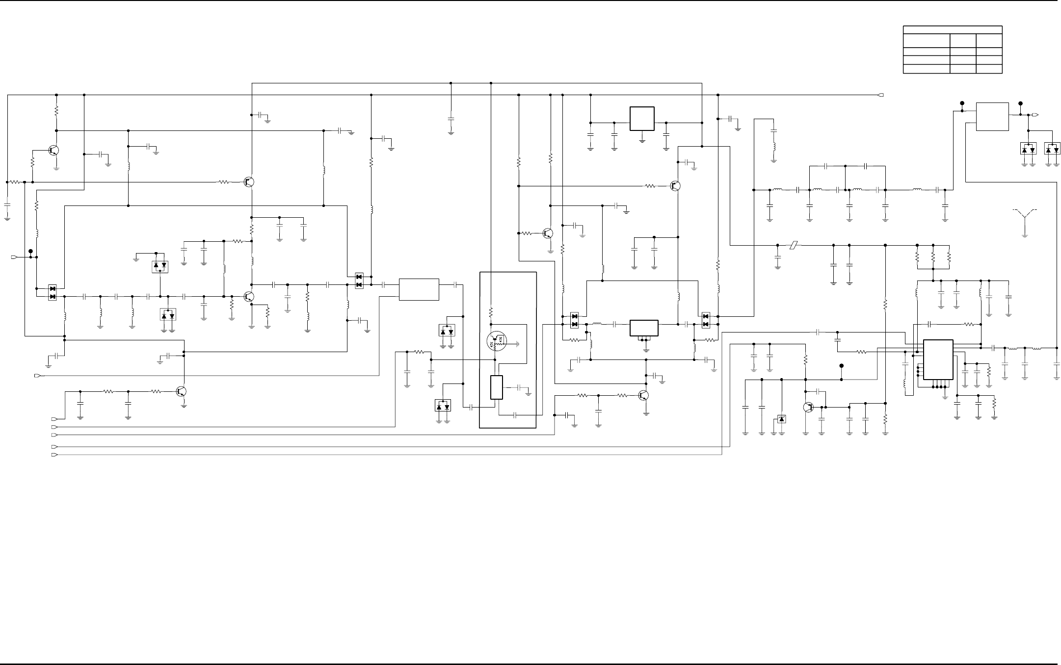
7-82 Schematics, Component Location Diagrams, and Parts Lists: HUE4039A/HUE4043A (UHF Range 1) Main Board
May 25, 2005 6881096C74-B
Figure 7-59. HUE4039A/HUE4043A Receiver Front-End Schematic
22nH
D5300
390nH
L5287
D5313
L5293
L5289
390nH
C5357
220pF
220pF
C5304
D5306
NU
5.6V
15
R5324
C5291
.01uF
L5305
15nH
.01uF
C5302
C5294
.01uF
.033uF
C5335
C5324
220pF
10K
R5301
C5305
220pF
1K
R5318
4.7K
R5314
C5290
220pF
L5304
27nH
TP5301
220pF
C5300
220pF
C5280
C5310
470pF
C5345
220pF
SH5250
82nH
L5288
NU
15
R5326
U5301
C5311
.01uF
8.2nH
L5307
220pF
C5338
L5308
Q5250
15nH
220pF
C5306
5.6pF
C5339
R5310
1K
C5316
470pF
Q5255
L5282
18nH
L5297
27nH
C5362
220pF
27nH
L5301
.01uF
C5303
220pF
C5307
L5296
.033uF
C5356
1uH
D5305
TP5303
220pF
C5321
68
L5302
R5308
.033uF
12nH
C5360
Q5258
C5283
8.2pF
9.1pF
C5331
L5299
L5298
22nH
NU
120
R5321
220pF
C5312
220pF
C5363
C5325
.033uF
L5284
18nH
C5308
220pF
NU
470pF
C5333
C5361
220pF
4.7pF
C5299
.01uF
C5285
C5367
220pF
4.7K
R5313
Q5254
R5307
22K
18pF
C5347
R5315
1K
15
C5320
220pF
R5325
D5302
3.9pF
TP5302
C5295
U5303
1K
220pF
R5302
D5304
C5296
R5312
10K
TP5304
100pF
.01uF
C5282
C5329
.01uF
L5281
390nH
C5301
R5327
180
82nH
NU
1K
R5329
18pF
C5328
L5283
4.7K
R5303
C5288
8.2pF
L5303
C5326
12pF
1K
68nH
R5317
R5309
27
R5305
4.7K
.033uF
R5322
2.4K
C5351
C5366
C5318
4.7uF
.01uF
1000pF
C5313
U5300
.01uF
C5287
12K
R5323
.033uF
C5337
C5353
5.6K
220pF
NU
R5328
470
R5319
Q5251
C5323
.033uF
R5306
15K
.01uF
C5322
C5368
1000pF
D5281
.033uF
C5350
C5330
220pF C5352
220pF
NU
Q5257
C5309
.01uF
1000pF
C5364
C5293
2pF
220pF
220pF
C5289
11pF
C5358
C5348
8.2pF
C5349
R5311
Q5252
10K
D5311
C5340
1uH
L5290
L5300
220pF
27nH 9.1pF
C5336
D5282
C5334
220pF
C5292
220pF
3.6pF
Q5256
C5332
Q5253
9.1pF
C5343
22pF
R5332
1.5K
C5344
C5365
220pF
1K
R5304
L5280
1uH
1.5K
R5334
47pF
C5354
U5302
R5336
00
R5335
100pF
C5327
.01uF
C5284
.01uF
C5314
.01uF
C5319
R5316
D5307
1K
R5333
390nH
L5292
47
D5280
C5341
3.6pF
C5355
10pF
L5306
8.2nH
.033uF
L5294
39nH
C5346
C5297
2.7pF
47
R5330
NU
C5359
1.5pF
C5342
9.1pF
L5285
68nH
C5315
4.7uF
220pF
C5317
L5295
390nH
L5286
47nH
1uH
L5291
R5300
4.7K
NU
NU
NU
NU
NU
IF_OUT_IF
RF_ATTN_2_A
9.3V_TO_IF
9.3V_TO_IF
9.3V_TO_IF
9.3V_TO_IF
RX_Inj_SW
RF_ATTN_3_A
RF_ATTN_1_A
RX_FILT_1_A
RF_IN
TO_1st_MIXER
LO_IN
RX switching voltages
Preselector Ref Des = 5250 - 5279
TP6256, 58, 60, 62
0V
2.3V
TP6254
Second LNA
AGC/Attenuator circuit
RX Receive
800 MHz
3V
Test points 700 MHz
4.3V
7.7V
TP6255, 57, 59, 61
HPF to remove VHF
RX Receive
7.7V
image filter and IF suck-out
Mixer Ref Des = 5380 - 5399
IN 3
OUT
2
GND
1
RFIN
16 RFOUT1 6
RFOUT2 7
VCNTRL
1
VD 1
14 2
VG1
VG2 3
GND1
4
GND2
5
GND3
12
GND4
13
NC1
8
NC2
9
NC3
10
NC4
15
EP
17
G2
11
1RFIO1
3RFIO2
4
V1 5
V2
2
GND
FE_CNTL_1
RF_IN_1 RF_OUT_1
1GND1
2GND2
4GND3
5GND4
3RFIN 6
RFOUT
IF
LO
MIXER_RF_IN
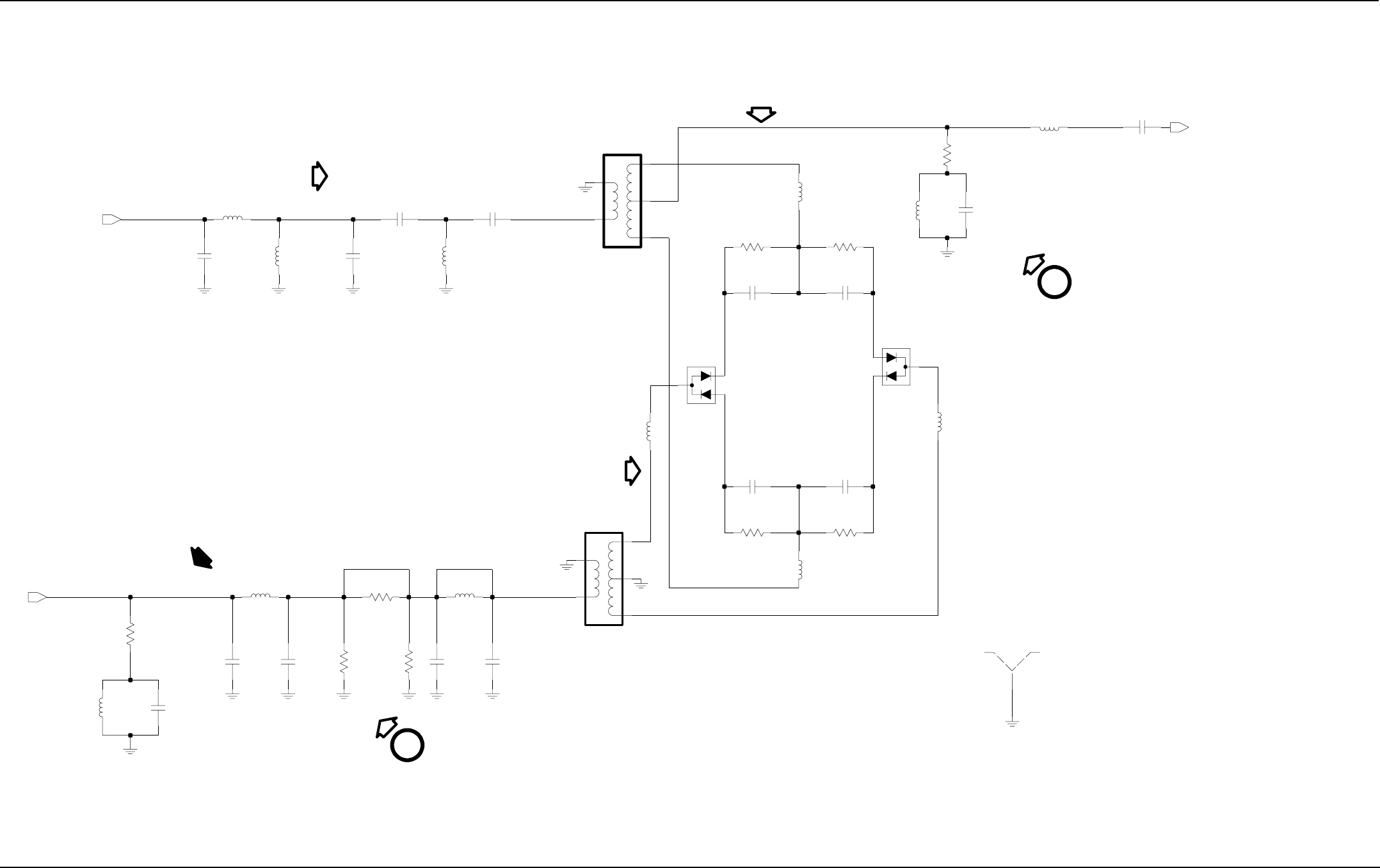
Schematics, Component Location Diagrams, and Parts Lists: HUE4039A/HUE4043A (UHF Range 1) Main Board 7-83
6881096C74-B May 25, 2005
Figure 7-60. HUE4039A/HUE4043A Receiver Mixer Schematic
E
L5380
6.8nH
C5379
9.1pF
C5375
3.9pF 470
NU
R5380
NU
R5381
10
L5389
10nH
R5387
47
33pF
68nH
C5386
L5388
D5381
68nH
L5390
L5381
8.2nH
R5388
0
L5392
12nH
C5374
2.4pF
R5385
180
C5388
.01uF
180
R5386
.01uF
6.8nH
L5384 180
C5385
3.3nH
R5384
NU
L5383
C5383
.01uF
C5382
.01uF
L5385
10nH
6.2pF
C5378
10nH
L5387
NU
10nH
L5386
D5380
180
R5383
1
2
3
4
5
33pF
C5391
NU
T5380
C5381
5.6pF
T5381
1
2
3
4
5
6.8pF
C5390
15pF
6.8pF
C5377
C5380
NU
C5389
12pF
L5382
12nH
470
R5382
NU
SH5380
NU
1
I
F
delete,.
PROVIDE A 109.65MHz I-F SIGNAL.
RECEIVE SYNTHESIZER ARE MIXED TO
INJECTION SIGNAL GENERATED BY TH
THE RECEIVER INPUT SIGNAL AND THE
+24.5 dBm I/P from the injection amp
B
LO
SIGNAL
INJECTION
HIGH SIDE
RECEIVED RF
MIXER_RF_IN
A
I. F.
109.65 MHz
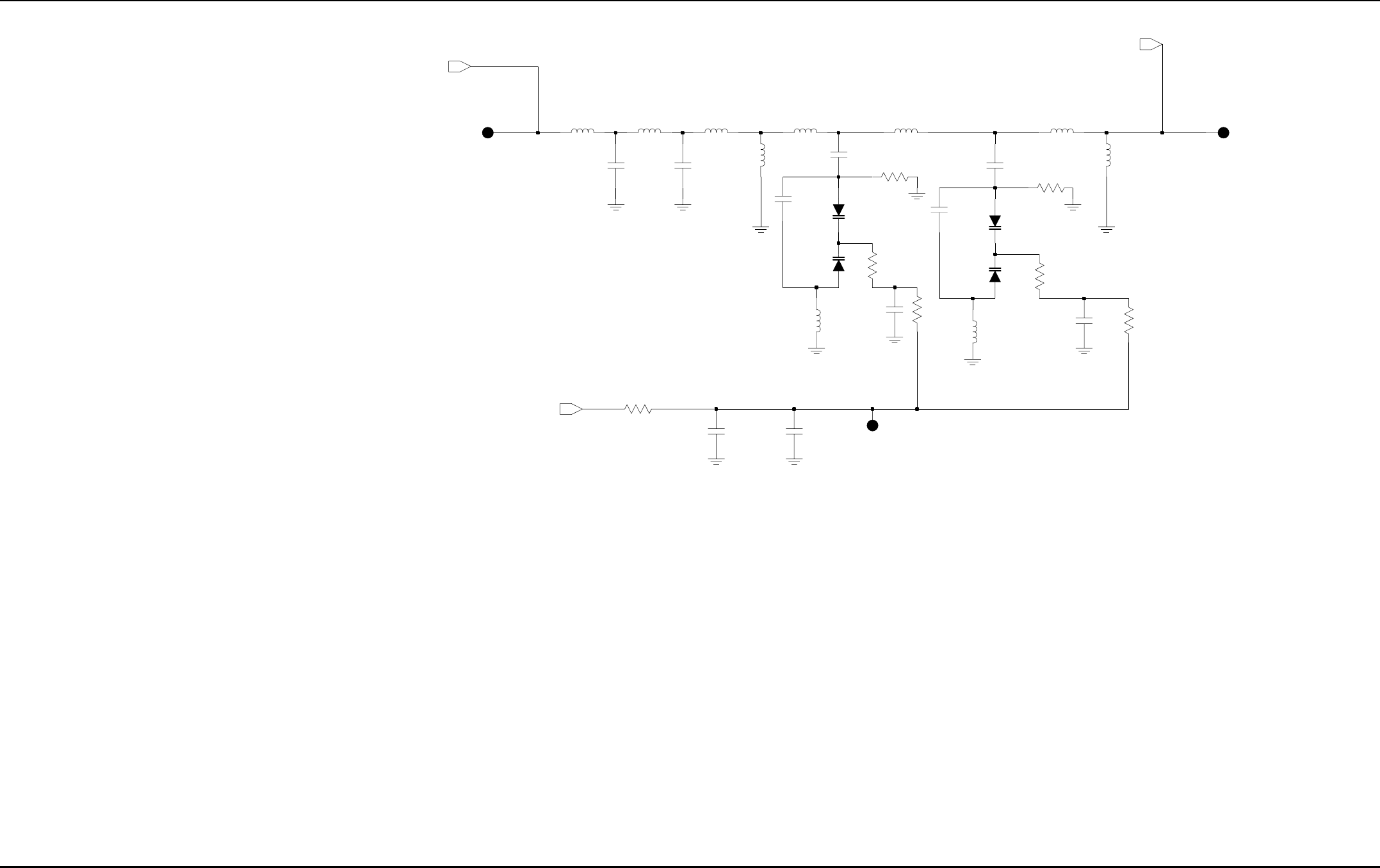
7-84 Schematics, Component Location Diagrams, and Parts Lists: HUE4039A/HUE4043A (UHF Range 1) Main Board
May 25, 2005 6881096C74-B
Figure 7-61. HUE4039A/HUE4043A Receiver Preselector Schematic
5nH
L5250
47K
R5251
C5257
C5258
6.8pF
L5257
39nH
6.8pF
L5237
22nH
L5258
22nH
TP5252
TP5251
TP5250
R5252 R5255
1K
1K
220pF
C5251 C5259
R5256
4.7K
C5256
.01uF
220pF
220pF
C5253
47K
R5250
47K
R5254
R5253
47K
D5252
1pF
NU
D5253
8.2pF
C5254
C5255
D5250
L5254
12.5nH
D5251
1pF
C5250
NU
8.2pF
C5252 5nH
L5256
12.5nH
L5252
8nH
L5255
L5251
82nH
L5253
8nH
RF_IN_1
RF_OUT_1
FE_CNTL_1
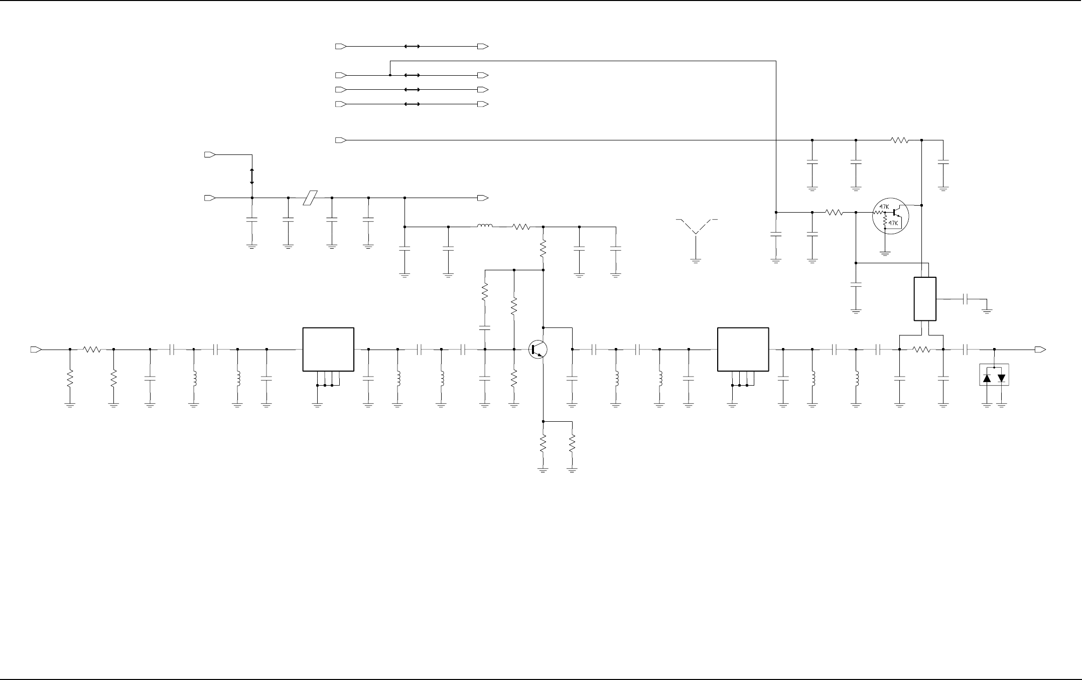
Schematics, Component Location Diagrams, and Parts Lists: HUE4039A/HUE4043A (UHF Range 1) Main Board 7-85
6881096C74-B May 25, 2005
Figure 7-62. HUE4039A/HUE4043A Receiver IF Schematic
220nH 0.5pF
L5411 C5422
R5400
680
D5400
C5427
0.1uF
330
R5403
C5413
1.8pF 390nH
L5402
1.8pF
C5417 C5409
0.5pF
C5424
.01uF
L5408
C5403
13pF
1uH
220pF
C5431
SH5400
27K
R5401
0
R5404
C5410
1.8pF
2.7pF
C5405
390nH
L5403
0.1uF
C5401
C5423
C5419
.01uF
220pF
C5421
.01uF
L5406
220nH
15pF
C5407
C5433
.01uF
Q5402
U5400
C5408
3pF
109.65MHz
Y5401
0.5pF
C5411 L5404
270nH
10K
R5405
8.2pF
C5414
220pF
C5425
220nH
220pF
L5407
0.1uF
C5429 C5430
Y5400
109.65MHz
R5402
6.8K
C5406
16pF
C5432
0.1uF
C5404
R5412
01 5pF
C5418
1.8pF
2.7pF
C5415
2.7pF
C5412
390nH
L5400 L5401
390nH
C5416
0.5pF
220pF
C5400
C5428
220pF
0
R5415R5414
0
1MEG
R5413
1MEG
1K
R5406
R5411
C5426
0.1uF
C5402
0.1uF
Q5401 R5407
0
C5420
.01uF
E5400
NU NU
NU
NU
NU
NU
NU
NU NU NU NU
1
2
GND
3RFIO1
1RFIO2
4
V1 5
V2
GND1
1
GND2
2
GND3
4
5GND4
6IN 3
OUT
6IN 3
OUT
GND1
1
GND2
2
GND3
4
5GND4
IF_TO_ABACUS
IF_OUT
9.3V_FROM_FE
RF_ATTN_1_C
9.3V_TO_CONTR
O
O
O
O
O
O
O
O
O
O
O
O
O
O
O
O
O
O
O
O
O
C
C
C
C
C
C
C
C
C
C
C
C
C
C
C
C
C
C
C
C
C
C
C
C
C
C
C
C
C
C
C
C
C
C
C
C
C
C
C
C
C
C
C
C
C
C
C
C
C
C
C
C
C
C
C
C
C
C
C
C
O
O
O
O
CO
O
O
O
N
N
ON
O
O
O
ON
N
N
N
N
N
N
T
T
T
T
T
T
T
T
TR
R
R
R
R
R
R
R
R
R
R
R
R
R
R
R
R
T
T
T
T
T
T
T
T
T
T
R
R
R
R
R
R
R
R
TR
T
T
T
T
T
T
T
T
T
T
9
9
R
9
R
R
R
R
9
9
9
9
9
9
9
9
9
9
9
9
9
9
9
9
9
9
9
9
9
9
9
9
9
9
9
9
3
3
3
3
3
3
3
3
3
3
3
3
3
3V
3V
3V
V
V
V
V
V
V
V
V
V
V
V
V
V
V
V
V
3
3
3
3
3
3
3
3
3
3
V
V
V
V
V
V
V
V
3V
3V
3V
3
3
3
3
3
3
3
3
V
V
V
V
V
V
V
T
T
T
T
T
O
O
O
O
O
O
O
O
O
O
O
O
O
O
O
O
O
O
O
O
O
O
O
O
O
T
T
TO
O
9.3V_FROM_BE
IF_IN
5V_IF
RF_ATTN_3_C
RF_ATTN_2_C
RF_ATTN_3_B
RF_ATTN_2_B
RF_ATTN_1_B
RX_FILT_1 RX_FILT_1_A
Going to Frontend
Coming From Abacus
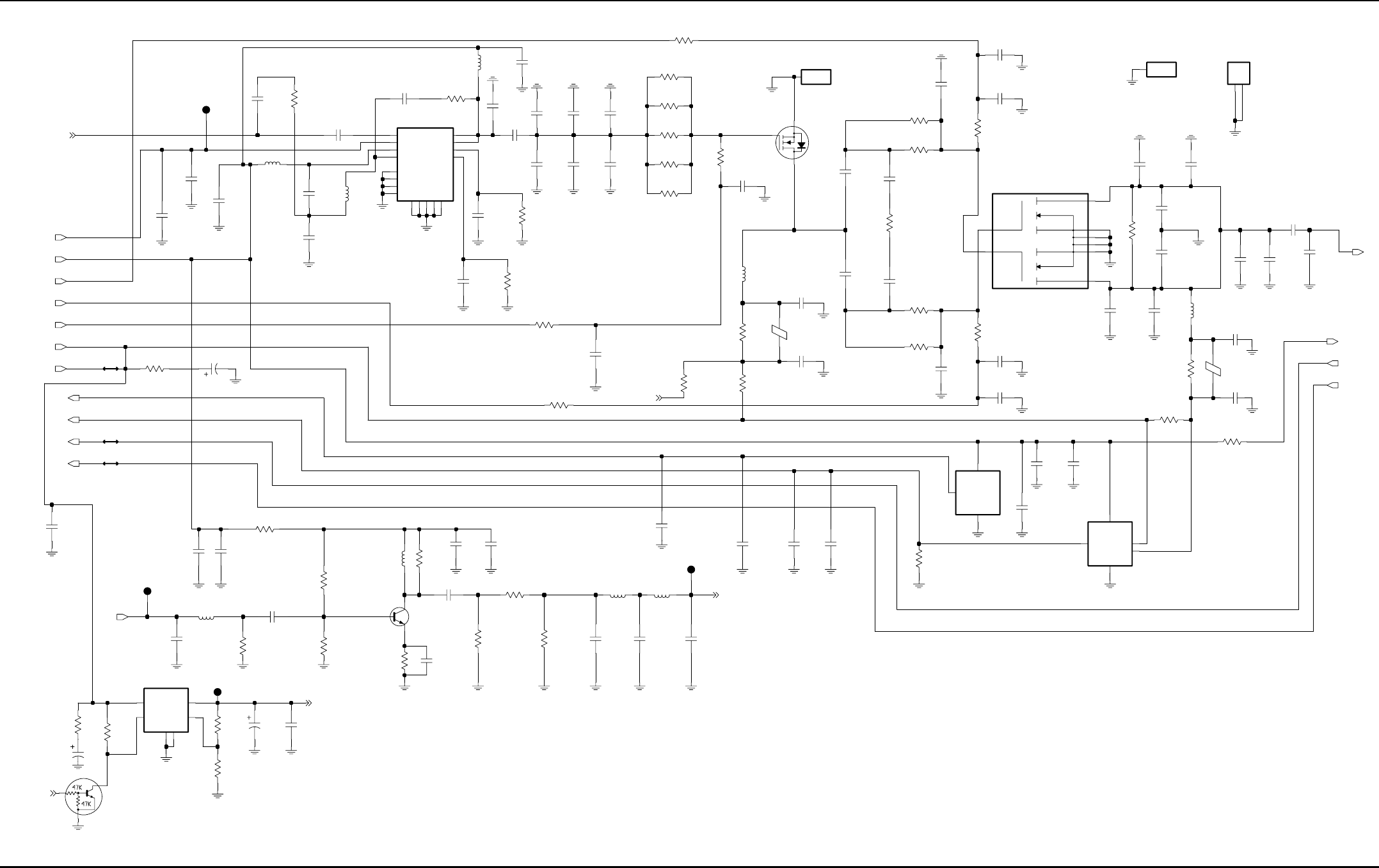
7-86 Schematics, Component Location Diagrams, and Parts Lists: HUE4039A/HUE4043A (UHF Range 1) Main Board
May 25, 2005 6881096C74-B
Figure 7-63. HUE4039A RF Power Amplifier (RF PA) Schematic
390nH
L5502
2.2
R5514
TP5503
30pF
C5545
R5525
1K
51
.01uF
R5516
NU
C5558
C5521
33pF
M5502
7.5pF
C5566
Q5503
2.2
R5513
390nH
R5511
L5505
180
R5529
2.2
.033uF
C5503
C5565
R5527
.033uF
1K
.01uF
C5575
.01uF
C5577
R5574
0
C5546
100pF
C5509
30pF
U5501
C5520
6pF
R5521
1K
0.1uF
C5544
C5571
10uF
0.1uF
C5573
C5570
0.1uF
TP5501
C5543
30pF
M5503
L5506
22nH
Q5502
C5548
12pF
C5526
0.1uF
1K
R5504
NU
E5502
C5517
0.1uF
22uF
C5572
C5579
220pF
C5568
7.5pF
C5505
0.1uF
C5527
100pF
2.7pF
C5502
C5569
7.5pF
R5537
0
C5552
13pF
.022uF
0.1uF
C5515
2K
NU
C5541
C5576
R5508
C5578
220pF
100K
220pF
C5550
R5519
220nH
L5504
0.1uF
C5567
220pF
R5534
5.1
C5539
Q5570
100pF
33K
R5571
U5570
R5570
2.7
22nH
L5507
TP5570
L5510
17nH
C5540
100pF
100pF
100pF
C5559 C5532
C5560
100pF
NU
NU
NU
NU
C5513
.022uF
100pF
C5553
U5502
68pF
C5535
C5551
7.5pF
220pF
C5504
R5501
150
NU
C5547
12pF
C5511
.033uF
1.2K
R5573
7.5K
R5572
220pF
C5516
C5524
6pF
33pF
1K
C5518
C5549
R5526
100pF
5.1
R5530
12nH
L5503
R5505
150
5.1
R5533
220pF
C5508
E5501
5.1
R5536
82
R5506
C5556
.01uF
0.1uF
C5510
C5542
30pF
C5563
9.1pF
NU
2.7
R5532
TP5502
C5531
R5520
1K
100pF
220pF
NU
C5514
R5512
R5531
10
2.2
C5554
.01uF
R5524
33
C5501
10uF
C5555
220pF
C5538
68pF
R5510
82
L5508
12.5nH
100
R5507
18nH
L5501
U5503
R5502
.01uF
6.8K
C5557
C5506
10pF
R5535
R5523
10
10
0
NU
R5518
4.7pF
Q5501
C5507
10
R5517
56pF
C5512
10pF
NU
NU
M5501
C5519
150
R5528 12pF
C5523
2.2
R5515
R5503
4.7K
7.5pF
NU
NU
C5522
R5522
220pF
C5525
NU
5m
R5509
1.8K
NU NU
RFPA/OUTPUT
NETWORK
INTERFACE
INTERFACE
RFPA/FGU
RFPA/POWER CONTROL
INTERFACE
A+_1
DRV_9.3V
K9.1V
DRV_9.3V
VCURRENT
VTEMP
VFORWARD_ON
TX_INJ
RFPA_CNTRL
K9.1V RFPA_OUT
VGBIAS2
VGBIAS1
VFORWARD
VREVERSE
VREVERSE_ON
A+_2
SWITCH_BIAS
PA_INJ
PA_INJ
VGBIAS3
GND1
1
2GND2
S4
2D1
3D2
6
G1
7
G2
1S1
5S2
8S3
4
16 RFOUT1 6
RFOUT2 7
VCNTRL
1
VD1
14 VG1 2
VG2 3
4
GND2
5
GND3
12
GND4
13
NC1
8
NC2
9
NC3
10
NC4
15
RFIN
17 EP
G2
11
GND1
1POS
1
3GND1
6GND2
ON_OFF
2
VIN
4VOUT 5
ADJ
3
GND
1
POS
2VOUT
VINNEG 4
VINPOS 3
VPOS
5
2
GND
OUT
1
1POS
Schematics, Component Location Diagrams, and Parts Lists: HUE4039A/HUE4043A (UHF Range 1) Main Board 7-87
6881096C74-B May 25, 2005
Figure 7-64. HUE4039A/HUE4043A Output Network (ON) Schematic
470nH
L5701
L5706
17nH
150nH
L5702 7.5pF
L5705
470nH
C5717
R5707
1.5K
R5709
270
R5705
220pF
C5715
R5706
270
270
R5708
270
220pF
C5707
1pF
C5704
ANT
5nH
FWD
J5701-1
L5713
R5702
J5701-2
1.5K
C5706
L5708
17nH
C5701
6.8pF
C5721
NU
220pF
NU
6.8pF
33
SH5701
30K
R5711
R5701
SH5703
NU
47pF
C5709
1.5pF
C5705
D5704
C5710
68pF
D5702
NU
SH5704
1.8pF
C5719
220pF
C5702
REV
220pF
C5718
7.5pF
C5720
11pF
C5713
100pF
D5701
SH5702
NU
C5708
75K
R5710
5nH
L5712
3.3K
R5713
D5703
L5707
17nH
L5704
17nH
L5703
17nH
C5716
7.5pF
C5714
3.9pF
C5711
3.9pF
C5722
1.5pF
NU
30K
R5703
100K
R5712
220pF
C5703
J5701-3
3.9pF
D5705
R5704
C5712
100K
2
1
1111
3
V
FORWARD_ON
RX_IN
VREVERSE_ON
RFPA_OUT
SWITCH_BIAS
W = 27.5 mil
INTERFACE
W = 27.5 mil
S = 35 mil
W = 90 mil
S = 35 mil
OUTPUT NETWORK/RX FE
L = 510 mil
OUTPUT NETWORK/RFPA
INTERFACE
7-88 Schematics, Component Location Diagrams, and Parts Lists: HUE4039A/HUE4043A (UHF Range 1) Main Board
May 25, 2005 6881096C74-B
Figure 7-65. HUE4043A RF 100W Power Amplifier (RF PA) Schematic (Sheet 1 of 2)
PA_INJ
1TP5510
C5509
6pF
C5508
12pF
C5507
6pF
R5508
150
R5506
150
C5501
220pF
C5500
.033uF
C5504
2.7pF
C5502
.033uF
*C5503*
220pF
C5506
.033uF
R5507
L5500
220nH
C5505
10pF
C5512
56pF 39
R5500
150
U5500
30C65
1
16
14
11
8
9
10
15
RFIN
4
5
12
13
17
6
7
2
3
VCNTRL
VD1
G2
RFOUT1
RF OUT2
VG1
VG2
NC1
GND1
GND2
GND3
GND4
EP
NC2
NC3
NC4
IF5506 IF5507
IF5534
IF5508 IF5509
IF5510 IF5511
IF5512 IF5513
IF5514 IF5515
IF5516
IF5517 IF5518
SC5500
SC5501
IF5521
IF5519
AUDIO_A+_1
TX_INJ
IF5533
MOSIA_1
EEPOT_EN_1
AD_EN_1
MISOA_1
PA_EN_1
R5585
SW_A+_1
A+_1
A+_1
A+
A+
0
FGU
INTERFACE
1I1
1I1
IF5505
K9.1V_EN_1
DA_EN_1
SCKA_1
IF5500 IF5501
IF5502 IF5503
IF5504
CONTROLLER
INTERFACE
IF5522
IF5523
IF5524
IF5525
IF5526
IF5527
RFPA_CNTRL
K9.1V
VGBIAS_1
VGBIAS_2
VGBIAS_3
VTEMP
VCURRENT
IF5520
IF5535
IF5536
AUDIO_GND_1
AUDIO_A+_2
AUDIO_GND_2
A+_2
SW_A+_2
2
I2
2
I2
S
D
C5572
0.1uF
C5573
0.1uF
C5549
47pF
*C5597*
18pF
*C5596*
18pF
C5546
43pF
C5540
15pF
C5531
47pF
C5514
.01uF
C5519
39pF
C5513
01uF
L5512
180nH
C5511
100pF
L5511
6.8nH
L5510
150nH
L5513
3.9nH
C5530
47pF
L5520
18.5nH
R5526
1K R5527
20
R5528
0
L5521
57R01
C5541
15pF
C5547
47pF
C5576
43pF
C5545
47pF
C5543
43pF
C5538
15pF
C5539
15pF
C5544
47pF
*C5591*
18pF
*C5590*
18pF
*C5592*
18pF
*C5594*
18pF
*C5595*
18pF
*R5583*
10
*C5593*
18pF
C5548
43pF
1
2
3
*U5563*
LM50
VOUT
GND POS
1
2
3
U5560
LM50
VOUT
GND POS
C5567
C5569
22uF
C5571
C5578
22uF
C5566
10pF
C5565
36pF
C5564
39pF
C5561
10pF
*C5588*
7.5pF
*C5579*
7.5pF
C5589
6.8pF
C5560
36pF
C5559
39pF
C5556
10pF
C5555
36pF
C5554
39pF
C5553
10pF
C5552
36pF
C5551
39pF
C5577
100pF
C5557
100pF
C5575
10uF
R5577
2.7
R5576
2.7
R5575
R5574
10
R5581
1K
R5503
150
*R5502*
1K
R5505
180
R5504
6.8K
R5501
4.7K
R5556
3.3
R5566
10
R5547
3.3
R5546
1K
*R5567*
33
R5568
33
R5562
33
R5573
33
R5565
0
*R5564*
0
*R5570*
0
R5571
0
*C5574*
0.1uF
R5579
0
R5578
100K
1%
L5543
17nH
100pF
100pF
C5568
0.1uF
*C5563*
3.3pF
C5542
100pF
C5532
100pF
C5533
24pF
*C5534*
100pF
*C5601*
22pF
*C5535*
100pF
*C5598*
22pF C5536
24pF
C5537
100pF
C5521
100pF
C5522
0.1uF C5526
10.0uF
C5527
10.0uF
C5515
.01uF
R5510
0
C5516
8.2pF
C5529
4.7uF
C5525
100pF
C5523
39pF
C5518
39pF
C5520
100pF
C5517
100pF
R5511
100
R5525
11
R5524
11
R5523
11
R5522
11
R5521
11
R5520
11
L5514
6.8nH
L5501
18nH
L5503
22nH
L5502
22nH
C5524
100pF
C5510
.01uF
C5602
10uF
C5587
3.3pF
C5584
3.3pF
*C5586*
3.3pF
C5578
100pF
*C5585*
3.3pF
*C5562*
3.3pF
C5550
100pF
C5603
10uF
L5544
57R01
5m
R5584
33
R5557
4.3
R5552
4.3
R5551
4.3
R5550
4.3 *R5563*
0
*R5572*
0
R5549
4.3
R5548
4.3
R5545
4.3
*R5541*
0
R5544
4.3
R5543
4.3
R5542
4.3
*R5540*
0
R5553
4.3
R5554
4.3
R5555
4.3
R5558
4.3
R5559
4.3
R5560
4.3
*R5580*
0
R5582
33
R5586
33
R5587
33
1
1
1
1
1
2
3
4
5
VR5500
24V
TP5544
TP5541
TP5542
TP5543
1TP5502
1
1
TP5503
U5561
INA138
OUT VINPOS
VINNEG
GND VPOS
J5500-1
J5500-2
BATTERY
CONNECTOR
A+
NC
NC
OUTPUT NETWORK
INTERFACE
RX_FE
INTERFACE
IF5528 IF5529
IF5530
IF5531
RX_IN_1 RX_IN_2
RFPA_OUT
SWITCH_BIAS_1
IF5532
SWITCH_BIAS_2
Q5540
Q5541
1TP5540
Q5520
1TP5520
A+
M5520
HEATSINK
1POS
M5541
HEATSINK
213
GND1
GND2
GND3
5 S2
1 S1
M5540
HEATSINK
213
GND1
GND2
GND3
K9.1V_EN_2
DA_EN_2
SCKA_2
MOSIA_2
AD_EN_2
POWER CONTROL
INTERFACE
EEPOT_EN_2
MISOA_2
PA_EN_2
*SH5500*
SHIELD
PA_INJ
Q5501
TP5500
TP5501
1
1
Schematics, Component Location Diagrams, and Parts Lists: HUE4039A/HUE4043A (UHF Range 1) Main Board 7-89
6881096C74-B May 25, 2005
Figure 7-66. HUE4043A RF 100W Power Amplifier (RF PA) Schematic (Sheet 2 of 2)
C5704
100pF
C5703
C5702
100pF
C5701
100pF
C5709
C5708
C5707
C5706
C5705
D5706
C5714
3.9pF
C5713
11pF
C5712
3.9pF
C5711
3.9pF
C5719
1.8pF
C5718
100pF
C5717
33pF
C5716
39pF
C5715
100pF
C5724
C5723
100pF
*C5722*
1.5pF
*C5721*
6.8pF
C5720
7.5pF
R5704
100K
R5703
0
R5702
1.5K
R5708
36
R5707
82
R5706
82
R5705
100
*R5713*
3.3K
R5710
75K
L5704
17nH
L5703
17nH
L5701
470nH
L5702
150nH
R5709
1.5K
L5708
L5717
470nH
L5707L5706
L5705
470nH
L5714
15nH
L5713
5nH
R5712
100K
R5711
0
L5716
L5712
5nH
L5715
12nH
1.8pF
D5709
100pF
470nH
82pF
43pF
D5707
*M5702*
7.5pF
POS
1
*M5701*
POS
1
*M5700*
POS
1
17nH
17nH
17nH
100pF
3pF
D5704
D5705
1 J5701-1
2 J5701-2
3 J5701-3
*SH5701*
SHIELD
1
*SH5702*
SHIELD
1
*SH5703*
SHIELD
1
*SH5704*
SHIELD
1
IF5701
IF5702
IF5703
IF5704
IF5705
IF5706
VREVERSE_ON
VFORWARD_ON
RFPA_OUT
SWITCH_BIAS_1
RX_IN
SWITCH_BIAS_2
RFPA
INTERFACE
POWER CONTROL
INTERFACE
S = 27.5 mil
L = 617.5 mil
W = 80 mil
S = 37.5 mil
W = 20 mil
W = 20 mil
7-90 Schematics, Component Location Diagrams, and Parts Lists: HUE4039A/HUE4043A (UHF Range 1) Main Board
May 25, 2005 6881096C74-B
Figure 7-67. HUE4039A Secure Block Diagram and Interconnections
USB_RS232_SB9600 BLOCK
USB/RS232
SECURE INTERFACE BLOCK
10
11
0
2
3
UTXD1_USB_VPOUT
UTXD2
VIP_IN_1_3V
VIP_IN_1_5V
VIP_IN_2_3V
VIP_IN_2_5V
VIP_OUT_1_3V
VIP_OUT_1_5V
VIP_OUT_2_3V
VIP_OUT_2_5V
0
2
UARTA_RTS
UARTA_RXD
UARTA_TXD
UCTS1_USB_FSEN
UCTS2
URTS1_USB_XRXD
URTS2
URXD1_USB_VMIN
URXD2
USB*_RS232_EN
USB+
USB-
USB_INT*
USB_PWR
USB_TXENB
USB_VMOUT
USB_VPIN
14
16
BOOT_DATA_EN*
BOOT_RX
BOOT_TX
BUS+_UARTB_TXD
BUS-_UARTB_RXD
BUSY_UARTB_RTS
LHRST_IN
LHRST_OUT
RESET_UARTB_CTS
RIA_USBSUSP
SB96_RS232*_EN
UARTA_CTS
7
0
2
5
17
2
4
9
12
12
10
2
9
3
3
13
14
19
19
17
3
IGNITIONIGNITION_SENSE
LV_DETECT
SOFT_TURN_OFFSW_B+_ON-OFF
SW_B+_SENSE
0
6
05
SPKR-
SSI_INT*
SW_B+_ON-OFF
UARTA_CTS
UARTA_RTS
UARTA_RXD
UARTA_TXD
VIP_IN_1_5V
VIP_IN_2_5V
VIP_OUT_1_12V
VIP_OUT_1_5V
VIP_OUT_2_12V
VIP_OUT_2_5V
EMERGENCY
EMERG_SENSE
NAUTILUS_INT*
ONE_WIRE
PTT*
RESET_UARTB_CTS
RX_FILT_AUDIO
SAP_DCLK
SAP_FSYNC
SAP_RX
SAP_TX
SPARE_1
SPARE_2
SPI_MISOB
SPI_MOSIB
SPI_SCKB
SPKR+
AUX_TX
BOOT_DATA_EN*
BOOT_RX
BOOT_TX
BUS+_UARTB_TXD
BUS-_UARTB_RXD
BUSY_UARTB_RTS
BUS_PWR_OUT
CABLE_DET
EMERGENCY
FORCE_FAIL*
IGNITION
KEYFAIL
MIC_HI
MOD
NAUTILUS_CS*
1
1
15
1
AUX_MIC
AUX_RX
1
5
0
0
3
16
1
10
15
9
18
SPKR-
UARTA_CTS
UARTA_RTS
UARTA_RXD
UARTA_TXD
USB+
USB-
USB_PWR
VIP_OUT_1_12V
VIP_OUT_2_12V
VPP
12
19
AUX_MIC BUS+_UARTB_TXD
BUS-_UARTB_RXD
BUSY_UARTB_RTS
CHAN_ACT
EMERGENCY
IGNITION
MONITOR
ONE_WIRE
PTT*
RESET_UARTB_CTS
RX_FILT_AUDIO
SPKR+
2
7
0
1
3
13
3
2
8
3
3
2
4
11
18
8
14
1
13
SAP_DCLK
SAP_FSYNC
SAP_RX
SAP_TX
TAMPER_ENC
WAKEUP
0
1
1
6
AUX_MIC
SAP(3:0)
WAKEUP
ENC_SPARE1
ENC_RESET
ENC_SPARE2
BOOT*
MOD
ONE_WIRE
SPARE_1
SPARE_2
2
BOOT*
ENC_RESET
ENC_SPARE1
ENC_SPARE2
KEYFAIL*
SPI_MOSIB
SPI_MISOB
SPI_SCKB
NAUTILUS_CS*
FORCE_FAIL*
CABLE_DET
BOOT_TX
BOOT_RX
VPP
AUX_TX
MIC_HI
CHAN_ACT
BUS_PWR_OUT
NAUTILUS_INT*
SSI_INT*
USB_INT*
MONITOR
PTT*
UARTB(3:0)
SPKR+
SPKR-
CONN(19:0)
SAP_DCLK
SAP_TX
SAP_FSYNC
SAP_RX
SB96_RS232*_EN
AUX_RX
IGNITION_SENSE
SW_B+_SENSE
LV_DETECT
SOFT_TURN_OFF
SW_B+_ON-OFF
VIP_IN_2_3V
VIP_IN_1_3V
VIP_OUT_1_3V
VIP_OUT_2_3V
USB_VMOUT
USB_TXENB
UTXD1_USB_VPOUT
UCTS1_USB_FSEN
URTS1_USB_XRXD
URXD1_USB_VMIN
USB*_RS232_EN
USB_VPIN
RIA_USBSUSP
EMERG_SENSE
UTXD2
URXD2
URTS2
UCTS2
LHRST_OUT
LHRST_IN
RX_FILT_AUDIO
ACCESSORY CONNECTOR
POWER SUPPLY BLOCK
SB9600/VIP
CONTROL HEAD
INTERFACE
TYPE 3 UCM SECURE
MAEPF-27844-O
Part Series
400-1
Part Series
500
Part Series
300
Part Series
700
Part Series
400-2
Part Series
600-1
600-2
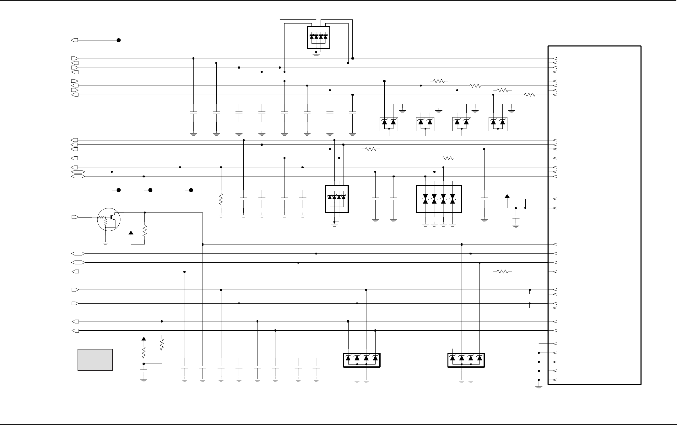
Schematics, Component Location Diagrams, and Parts Lists: HUE4039A/HUE4043A (UHF Range 1) Main Board 7-91
6881096C74-B May 25, 2005
Figure 7-68. HUE4039A Rear Accessory Connector Schematic
VIP_OUT_2_12V
UARTB_RTS-BUSY
USB+
EMERGENCY
SPKR+
USB_PWR
RX_FILT_AUDIO
SW_B+
CHAN_ACT
UARTA_TXD
SPKR-
ONE_WIRE
MONITOR
PTT*
CTS_DCE (DB9-Pin 7)
RTS_DCE (DB9-Pin 8)
UARTB_RXD-BUS-
UARTA_RXD
UARTB_TXD-BUS+
J0402
UARTB_CTS-RESET
UARTA_RTS
AUX_MIC
TX_DCE (DB9-Pin 2)
RX_DCE (DB9-Pin 3)
UARTA_CTS
VIP_OUT_1_12V
26 PIN CONN
IGNITION
GND
USB-
R0410 100
C0412
100pF
U0400
DTC144EKA
33pF
C0402
*VR0408*
A1
A2
K1
K2
K3
K4
5.6V
J0402-27
J0402-20
220pF
C0415
33pF
C0410
C0464
33pF
J0402-29
220pF
C0417
33pF
C0403
J0402-12
J0402-11
1K
R0405
VR0404
15V
100
R0432
J0402-32
100
R0407
1
J0402-31
0
R0430
TP0420
J0402-30
J0402-9
33pF
C0405
33pF
C0404
TP0418
1
J0402-3
J0402-22
J0402-13
9.3V_TX
J0402-1
J0402-23
C0416
J0402-5
J0402-21
100pF
R0411
10K
3
4
6
J0402-24
VR0402
20V
2
5
1
33pF
J0402-15
J0402-28
C0463
33pF
C0406
J0402-8
470pF
C0465
100pF
C0466
C0419
C0413
100pF
100
100pF
R0408
VR0405
15V
220pF
C0418
R0412 100
C0408
J0402-26
J0402-19
100pF100pF
C0467
560
R0406
33pF
C0400
C0414
220pF
4.7uF
C0420
*VR0410*
A1
2
A2
5
K1 1
K2 3
K3 4
K4 6
5.6V
J0402-4
J0402-17
1
J0402-14
100pF
TP0400
C0401
TP0419
1
VR0400
20V J0402-2
VR0406
15V
J0402-10
R0403
10K
15V
R0435 1K
VR0407
33pF
C0409
C0407
100pF
J0402-16
SW_B+
J0402-25
J0402-18
J0402-6
J0402-7
IO2
IO3
IO4 IO5
IO6
IO7
IO8
VR0411
IO1
USB+ USB+
USB- USB-
IGNITION
VCC5
SPKR+
SPKR-
RX_FILT_AUDIO
CHAN_ACT_CONN
MONITOR
PTT*
EMERGENCY
ONE_WIRE ONE_WIRE_CONN
USB_PWR
VPP
CHAN_ACT
UARTA_CTS
UARTA_RXD
UARTA_RTS
UARTA_TXD
VIP_OUT_1_12V
VIP_OUT_2_12V
BUS+_UARTB_TXD
BUS-_UARTB_RXD
RESET_UARTB_CTS
BUSY_UARTB_RTS
AUX_MIC
47K
47K
MAEPF-27842-O
Part Series
400-1
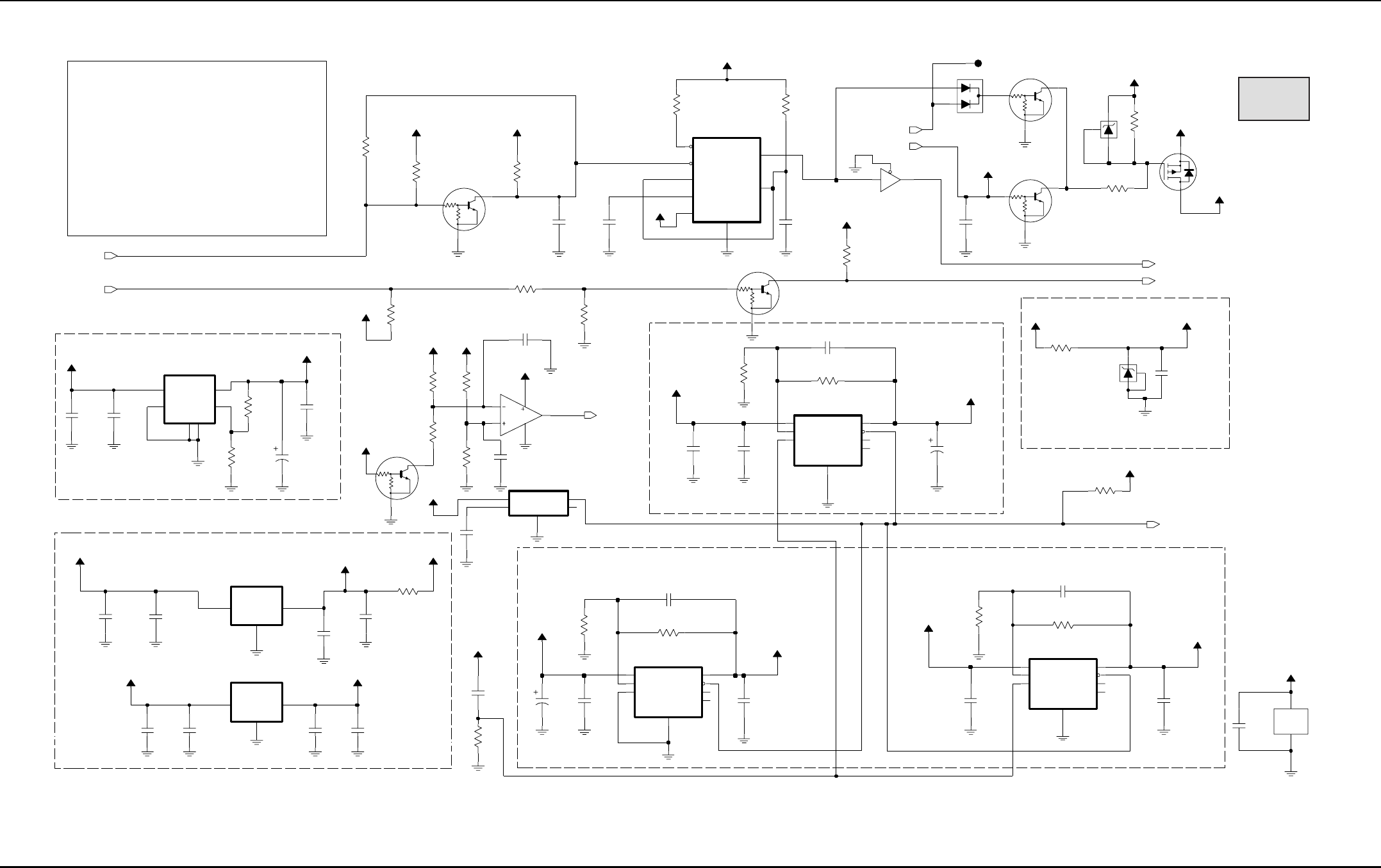
7-92 Schematics, Component Location Diagrams, and Parts Lists: HUE4039A/HUE4043A (UHF Range 1) Main Board
May 25, 2005 6881096C74-B
Figure 7-69. HUE4039A Power Supply Schematic
VCC3
Mic Bias Circuit
2.85 / 100 mA
T-Gates, VIPS, SB9600
NP
1.8V Digital Supply Regulator
Audio PA
FILT_B+
Emergency Sense Block
9V Regulator
5.0 / Battery
Battery
VCC5
SOURCED BY:
NP
Battery
VCC5 I/O Ring, EEPOTs
9.3V / 1A
UNSW_5V
Voltage Translation
USB, Codec
DC DISTRIBUTION
SW_B+
V(operating)/mA(max)
A+
VCC5
FILT_B+
VCC1.8, VCC1.55
NP
Emergency Detect/Timer
VCC2.85
9V Regulators
1.86 & 1.55 / 100 mA
SW_B+ Sense Circuit
VOLTAGE
Patriot, EIM, Memory
SUPPLY FOR
5.0 / 500 mA
3.0 / 100 mA
UNSW_5V Supply
5V Regulator
Power Control
9.3V_TX
2.85V Digital Supply Regulator
VCC5
SW_B+
A+
A+
1.8V, 3V Regulators
1.55V Digital Supply Regulator
SW_B+
R0521
VCC2.85
VCC5_FILT
R0505
39K
VCC5
10K
100pF
C0503
4.7uF
C0517
1uF
C0525
0
C0526
.01uF
VCC5
R0527
OUT
A+
UNSW_5V
MC78M05
U0503
2
GND
1IN 3
0.1uF
C0504
Q0503
SW_A+
R0510
C0536
0.1uF
9.3V_ABACUS
43K
VCC5_FILT
33K
R0511
100K
R0500
4.7uF
C0518
R0513
39K
Q0505
10K
R0524
R0503
VCC2.85
UNSW_5V
SW_A+
100K
VCC2.85
Q0504
11V
VR0501
C0507
0.1uF0.1uF
C0524
D0501
U0505
MC78M05
GND
2
IN
1OUT 3
2K
R0509
100K
R0516
5V_ABACUS
UNSW_5V
4.7uF
C0527
UNSW_5V
7.5K
R0528
C0514
150uF
7FEEDBACK
4GND
8INPUT 1
OUTPUT
2
SENSE
3SHUTDOWN
VTAP 6
4
LP2951CD
U0502
5
ERROR
U0604-2
MC33202
6
5
7
8
0.1uF
C0512
1uF
C0532
FEEDBACK
7
GND
4
INPUT
8OUTPUT 1
SENSE 2
SHUTDOWN
3
VTAP 6
SW_B+_ON-OFF
SW_B+_ON-OFF
U0501
LP2951CD
ERROR 5
0.1uF
C0528
0.1uF
C0531
10
R0519
R0507
10K
R0502
390K
A+
4.7uF
C0510
R0531
Q0500
4.7uF
100K
CD
5
GND
3
INPUT
2
NC 4
OUTPUT 1
C0522
U0504
53D46
ON_OFF
2
VIN
4VOUT 5
.01uF
C0506
U0500
LM2941
ADJ 1
GND1
3
GND2
6
100pF
C0502
10K
R0506
C0537
1uF
0
0.1uF
C0516
R0514
Q0501
.01uF
C0519
22uF
C0533
0.1uF
C0520
1.2K
R0529
SW_A+
5.1V
VCC5_FILT
0.1uF
VR0500
C0515
47K
R0520
C0521
4.7uF
R0504
100K
R0508
10K
20K
R0522
A+
VCC2.85
1
C0505
.01uF
C0534
TP0500
0.1uF
C0523
0.1uF
1K
VCC5
THRESHOLD
6
TRIGGER
2
VPOS
8
A+
R0515
U0506
LMC555
CONTRLVOLTAGE
5DISCHARGE 7
GND
1
OUTPUT 3
RESET
4
C0500
VCC9
VCC5
0.1uF
10K
R0518
C0535
VCC9
VCC1.8
2
1
4
VCC2.85
0.1uF
R0523
NC7SZ125
U0508-1
Q0502
100K
C0513
3
GND
5
VCC
150uF
C0529
VCC1.55
U0508-2
PWR_GND
SENSE 2
SHUTDOWN
3
VTAP 6
4.7uF
U0507
LP2951CD
ERROR 5
FEEDBACK
7
GND
4
INPUT
8OUTPUT 1
VCC2.85
UNSW_5V SOFT_TURN_OFF
SW_B+_ON-OFF
R0512
10K
IGNITION_SENSE
IGNITION
SW_B+_SENSE
EMERG_SENSE
EMERGENCY
LV_DETECT
47K
47K
47K
47K
47K
47K
47K
47K
47K
47K
MAEPF-27845-O
Part Series
500
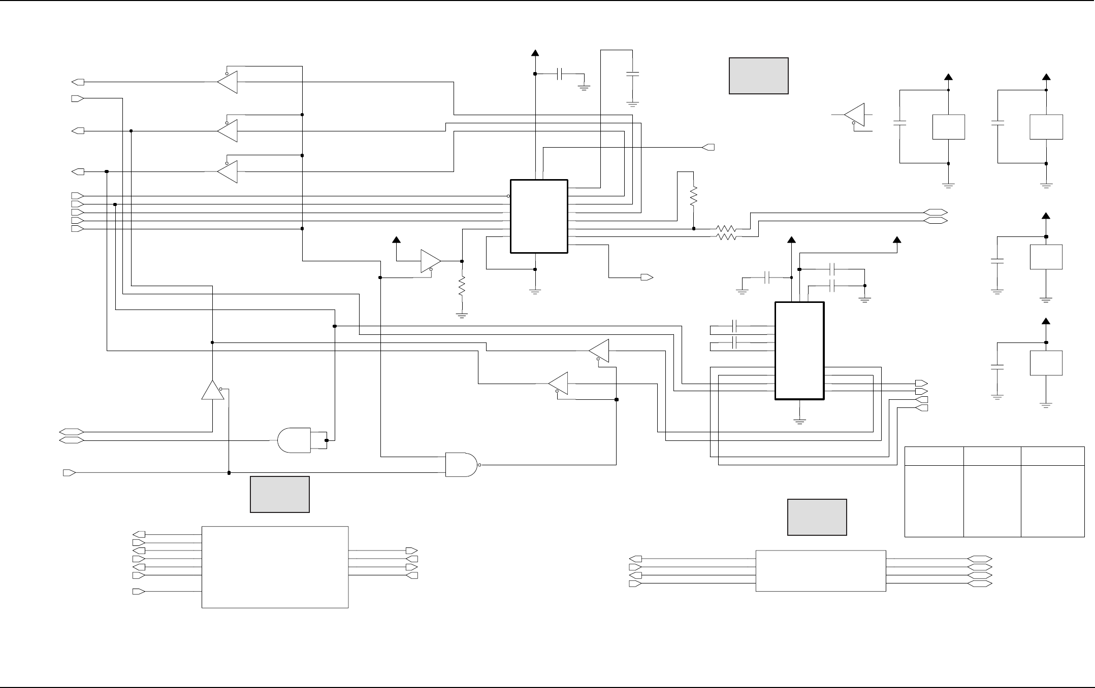
Schematics, Component Location Diagrams, and Parts Lists: HUE4039A/HUE4043A (UHF Range 1) Main Board 7-93
6881096C74-B May 25, 2005
Figure 7-70. HUE4039A USB/RS232/SB9600 Schematic
SB9600 Block
NP
VIP I/O Block
BUFFER SUPPLY BUFFER SUPPLY
1
USB*_RS232_EN
0Not Allowed
BOOT_DATA_EN* Mode of Operation
0
0
0
11
1
Boot Data
USB
RS232
R0304
13
11
22
1
2
4
U0300-4
MC74LCX125
12
VCC5
VCC2.85
U0308-1
NC7ST08
C0312
0.1uF
10
8
MC74LCX125
U0303-4
12
13
11
MC74LCX125
U0300-3
9
1.5K
R0303
C0309 0.1uF
U0303-2
MC74LCX125
5
4
6
VCC2.85
VIP_IN_1_3V VIP_IN_1_5V
VIP_IN_2_3V VIP_IN_2_5V
VIP_OUT_1_3V VIP_OUT_1_5V
VIP_OUT_2_3V VIP_OUT_2_5V
U0300-2
MC74LCX125
5
4
6 GND
7
VCC
14
10K
R0307
VCC2.85
PWR_GND
U0300-5
14
VBUS
7
VCC
4
VM
11 VO_VPO 3
VP
15
VPU
13
VREG
DPOS
16 ENUMERATE
12 FSE0_VMO
17 GND
MODE
6
1OE_N 2
RCV
5SUSPND
8
USB_DET
VCC
5
ISP1104
U0304
9
DNEG
10
VCC
5
PWR_GND
U0308-2
GND
3
VNEG 6
VPOS 2
PWR_GND
U0307-2
GND
3
R1O 12
R2I
8R2O 9
T1I
11 T1O 14
T2I
10 T2O 7
VCC 16
U0305
ST3232
3C1NEG
C1POS
1
5C2NEG
4C2POS
GND
15
R1I
1310
8
C0307 0.1uF
22
MC74LCX125
U0303-3
9
R0305 VCC5 VCC9
0.1uF
C0302
7
GND
14
VCC
C0308 0.1uF
U0303-5
PWR_GND
0.1uF
C0311
0.1uF
0.1uF
C0313
C0306
0.1uF
C0310 0.1uF
VCC2.85
C0305
3
MC74LCX125
U0303-1
2
1
3
VCC2.85
1
2
4
MC74LCX125
U0300-1
2
1
URTS2
URXD2
UTXD2
TC7S00FU
U0307-1
C0301
0.1uF
BUS+_UARTB_TXD
BUS-_UARTB_RXD
BUSY_UARTB_RTSLHRST_IN
LHRST_OUT RESET_UARTB_CTS
SB96_RS232*_EN
UCTS2 VIP_OUT_1_5V
BOOT_TX
UTXD1_USB_VPOUT
UTXD1_USB_VPOUT
USB_TXENB
RIA_USBSUSP
USB_INT*
USB_VMI
USB_VPI
USB*_RS232_EN
USB+
USB+
USB_PWR
VIP_IN_1_5V
UARTA_CTS
UARTA_TXD
UARTA_RXD
UARTA_RTS
BOOT_DATA_EN*
UCTS1_USB_FSEN
UCTS1_USB_FSEN
RESET_UARTB_CTS
BUS+_UARTB_TXD
BUS-_UARTB_RXD
BUSY_UARTB_RTS
USB_VMOUT
VIP_OUT_1_3V
VIP_IN_1_3V
VIP_OUT_2_3V
VIP_IN_2_3V
UTXD2
UCTS2
LHRST_IN
LHRST_OUT
URTS2
URXD2
BOOT_RX
USB_VPIN
VIP_OUT_2_5V
VIP_IN_2_5V
URXD1_USB_VMIN
URXD1_USB_VMIN
URTS1_USB_XRXD
URTS1_USB_XRXD
SB96_RS232*_EN
USB-
USB-
MAEPF-27847-O
Part Series
300
Part Series
600-1
Part Series
600-2
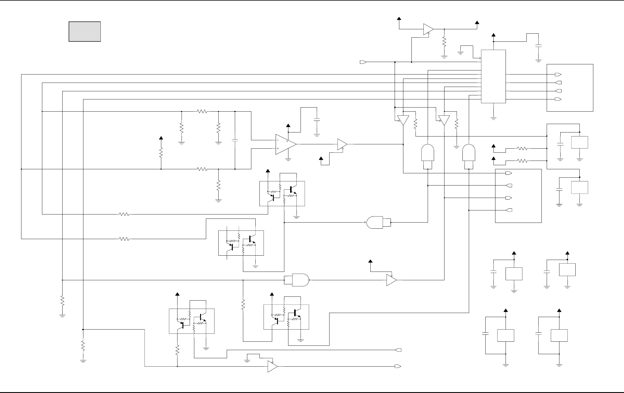
7-94 Schematics, Component Location Diagrams, and Parts Lists: HUE4039A/HUE4043A (UHF Range 1) Main Board
May 25, 2005 6881096C74-B
Figure 7-71. HUE4039A SB9600 Schematic
NP
BUFFER SUPPLY
NAND SUPPLY
Connector IF
NAND SUPPLY
BUFFER SUPPLY
BUFFER SUPPLY
Patriot UART B
BUFFER SUPPLY
MC74LCX125
U0602-2
5
4
6
0.1uF
C0610
C0614
SB96_RS232*_EN_INV
R0627
100K
0.1uF
C0613
0.1uF
VCC2.85
VCC
Q0610
U0608-2
PWR_GND
3
GND
5
U0607-2
PWR_GND
3
GND
5
VCC
U0602-5
PWR_GND
7
GND
14
VCC
C0604
0.1uF
TC7S00FU
U0609-1
1
2
4
100
R0623
VCC2.85
0.1uF
C0611
0.1uF
C0606
U0610-2
PWR_GND
3
GND
5
VCC
R0628
100K
VCC5
SB96_RS232*_EN_INV
100K
U0602-3
MC74LCX125
9
10
8
R0630
4
MC74LCX125
U0603-2
5
4
6
VCC2.85
VCC5
TC7S00FU
U0610-1
1
2
10K
R0639
VCC2.85
Q0611
10K
10K
R0638
GND
7
VCC
14
R0625
PWR_GND
U0603-5
R0629
10K
100K
VCC2.85
SB96_RS232*_EN_INV
VCC2.85
VCC5
100
R0622
R0634
C0603
U0609-2
PWR_GND
3
GND
5
VCC
0.1uF
R0636
Q0613
2
3
1
8
4
VCC5
10K
2
1
3
MC33202
U0604-1
MC74LCX125
U0602-1
2
1
3
U0603-1
MC74LCX125
0
R0632
R0631 0
R0635
100K
7
YB
9
YC
12
YD
VCC5
VCC5
14 I0D
3I1A
6I1B
10 I1C
13 I1D
1SELECT
16
VCC
4
YA
SN74CBT3257
U0606
15 EN_OE
8GND
2I0A
5I0B
11 I0C
100pF
1
2
4
C0616
100
R0621
NC7ST08
U0608-1
100
R0620
1
2
4
NC7ST08
U0607-1
VCC5
Q0612
U0602-4
MC74LCX125
12
13
11
100K
R0626
C0600
0.1uF
BUS-
BUS+*
BUSY BUSY
LH_RESET
BUS-*
BUS+
BUSY*
LH_RESET*
URXD2
SB96_RS232*_EN
URTS2
UTXD2
LHRST_IN
LHRST_OUT
BUS+_UARTB_TXD
BUSY_UARTB_RTS
RESET_UARTB_CTS
BUS-_UARTB_RXD
UCTS2
10K
10K
10K 10K
10K
10K
10K 10K
10K
10K
10K 10K
10K
10K
10K 10K
MAEPF-27919-O
Part Series
600-1
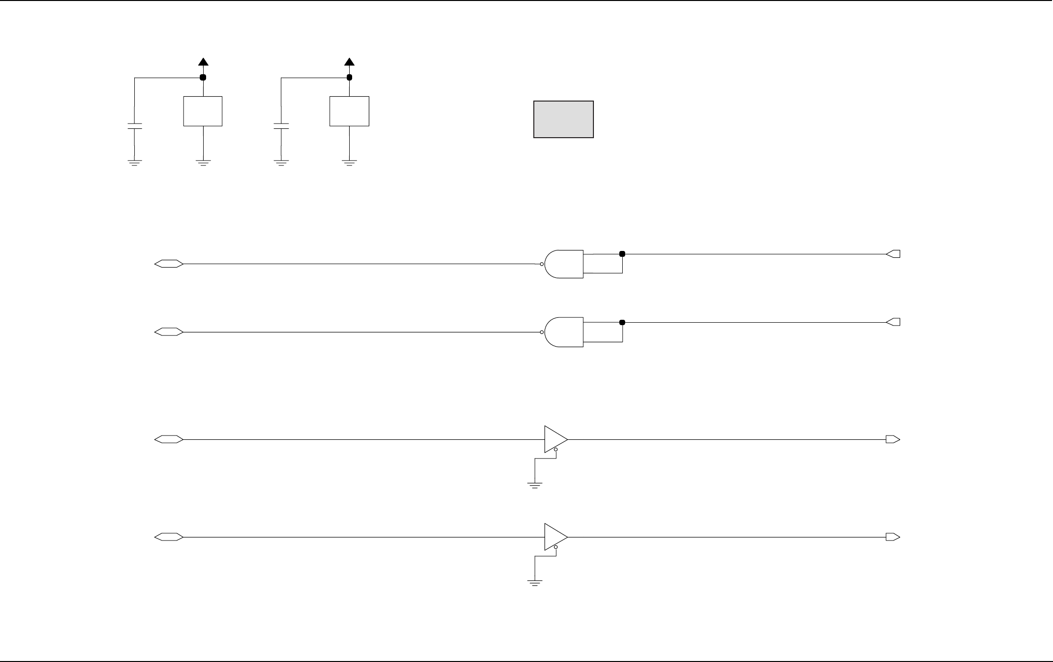
Schematics, Component Location Diagrams, and Parts Lists: HUE4039A/HUE4043A (UHF Range 1) Main Board 7-95
6881096C74-B May 25, 2005
Figure 7-72. HUE4039A USB/RS232/SB9600 VIP Input/Output Schematic
4
1
2
4
U0605-1
TC7S00FU
1
2
VCC5
TC7S00FU
U0601-1
0.1uF
VCC5
0.1uF
C0605C0601 GND
5
VCC
U0601-2
PWR_GND
3
GND
5
VCC
8
U0605-2
PWR_GND
3
12
13
11
U0603-3
MC74LCX125
9
10
VIP_IN_1_3V
VIP_IN_2_3V
VIP_IN_1_5V
VIP_OUT_1_3V
VIP_OUT_1_5V
VIP_OUT_2_3V
VIP_OUT_2_5V
VIP_IN_2_5V
U0603-4
MC74LCX125
MAEPF-27848-O
Part Series
600-2
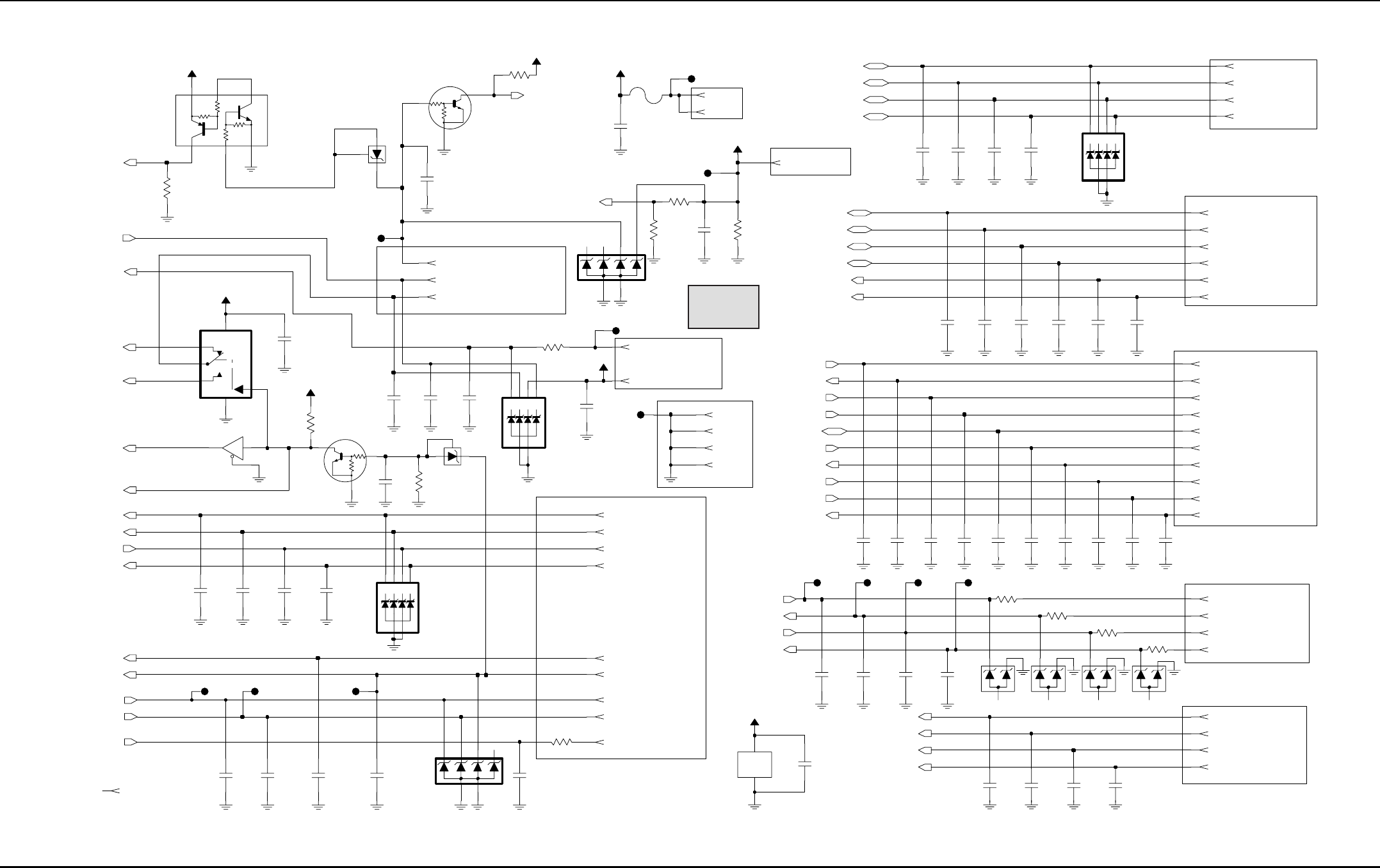
7-96 Schematics, Component Location Diagrams, and Parts Lists: HUE4039A/HUE4043A (UHF Range 1) Main Board
May 25, 2005 6881096C74-B
Figure 7-73. HUE4039A Control-Head Connector Schematic
SPARE_1
UARTA_RXD
BUSY
SPI_MOSIB
Interface
SPI_SCKB
OPTB+_BOOTSEL_VPP
AUX_RX
NAUTILUS_CS*
RS232 BUS
VIP_OUT_1_12V
MIC_HI
FOR NEW CH/ACCYs
IGNITION
SW_B+
SSI / NAUTILUS
SPI_MISOB
PTT*
SAP_DCLK
UARTA_CTS
SB9600
NOT USED
NAUTILUS_INT*
LH_RESET
VIP_OUT_2_12V
VIP_IN_2_5V
AUDIO
Programming Cable
AUX_MIC
ONE_WIRE
SPKR-
SAP_RX
BOOT_RX
BUS_PWR_OUT
BUS-
UARTA_RTS
SPARE_2
SAP_FSYNC
SAP_TX
VIPs
UARTA_TXD
VIP_OUT_1_5V
VIP_IN_1_5V
VCC5
A+
SSI_INT
EMERGENCY
RX_FILT_AUDIO
BUS+
BOOT_TX / KEYFAIL*
AUX_TX
VIP_OUT_2_5V
SPKR+
J0401-47
J0401-12
J0401-26
J0401-50
33pF
100
C0424
J0401-13
R0418
C0443
33pF
R0415
100
J0401-37
C0453
33pF
C0452
33pF
15V
C0475
100pF
3
6
4
1
VR0424
Q0403
5
2
J0401-38
J0401-40
C0469
0.1uF
J0401-15
R0431
10K
100pF
C0427
J0401-19
R0409
C0456
33pF
1
K1 3
K2 4
K3 6
K4
10K
5.6V
*VR0417*
2A1
5
A2
J0401-25
1
TP0414
1
NO
6
2
VPOS
TP0401
U0401
NLAST4599
COM
5
3GND
IN 1
NC
4
C0439
J0401-18
100pF
J0401-6
J0401-44
33pF
2
5
1
3
4
6
C0459
VR0412
20V
33pF
J0401-2
J0401-31
VCC2.85
C0422
10K
J0401-20
R0425
C0462
220pF
J0401-33
J0401-48
0.1uF
C0441
VR0425
15V
1
TP0411
1
VR0420
11V
2
3
F0400
125V
5A
C0450
33pF
Q0404
C0437
470pF
J0401-43
VR0413
20V
J0401-11
C0446
100pF
1
C0436
470pF
470pF
TP0408
C0435
J0401-1
C0444
33pF
1K
R0404
A1
A2
K1
K2
K3
K4
5.6V
*VR0414*
C0431
100pF
J0401-30
J0401-24
Q0402
VR0423
15V
1
J0401-46
VCC5
TP0415
1
TP0403
J0401-23
VCC5
C0445
33pF
C0434
100pF 100pF
J0401-32
C0433
R0416
100
33pF
C0432
100pF
100pF
C0454
J0401-9
C0449
J0401-10
J0401-42
C0461
220pF
TP0407
1
33K
R0422
0
R0421
TP0413 1
C0448
100pF
J0401-35
1
C0425
100pF
TP0402
C0442
33pF
3
GND
5
VCC
J0401-3
TP0412
1
U0402-2
PWR_GND
C0477
VCC2.85
100pF
C0428
100pF
J0401-45
C0426
470pF
J0401-22
J0401-14
J0401-34
J0401-36
J0401-16
C0438
33pF
470pF
J0401-21
SW_B+
C0457
J0401-27
J0401-49 J0401-41
33pF
11V
C0458
U0402-1
NC7SZ125
2
1
4VR0421
J0401-39
VCC2.85
100pF
C0478
A+
C0430
100pF
C0451
33pF
VCC5
J0401-4
J0401-7
VR0422
15V
10K
R0420
J0401-8
J0401-5
C0429
100pF
100pF
C0460
C0440
C0447
100pF
100pF
J0401-29
4.7K
R0517
*VR0418*
2A1
5
A2
1
K1 3
K2 4
K3 6
K4
5.6V
100pF
C0476
J0401-17
J0401-28
TP0410
1
C0455
33pF
R0417 100
4.7K
R0419
TP0409
1
C0423
33pF
SPARE_2
SPARE_1
SW_B+_ON-OFF
IGNITION
BUS+_UARTB_TXD
BUS-_UARTB_RXD
BUSY_UARTB_RTS
RESET_UARTB_CTS
C0470
33pF
MIC_HI
RX_FILT_AUDIO
IGNITION_CONN
SPKR- SPKR-
BOOT_RX
EMERGENCY
ONE_WIRE
UARTA_TXD
UARTA_RXD
UARTA_CTS
UARTA_RTS
UARTA_TXD_CH
UARTA_CTS_CH
UARTA_RTS_CH
CABLE_DET
BOOT_DATA_EN*
KEYFAIL
BUS_PWR_OUT
MIC_HI
AUX_MIC AUX_MIC
PTT*
AUX_RX
VIP_IN_2_5V
VIP_IN_1_5V
VIP_OUT_2_5V
VIP_OUT_1_5V
VIP_OUT_1_12V
VIP_OUT_2_12V
AUX_TX
NAUTILUS_CS*
SAP_DCLK
SAP_TX
UARTA_RXD_CH
SAP_RX
SAP_FSYNC
SPI_MOSIB
SPI_SCKB
NAUTILUS_INT*
MOD
BOOT_TX
FORCE_FAIL*
SPKR+ SPKR+
SSI_INT*
SPI_MISOB
10K 10K
10K
10K
47K
47K
47K
47K
MAEPF-27843-O
Part Series
400-2
Schematics, Component Location Diagrams, and Parts Lists: HUE4039A/HUE4043A (UHF Range 1) Main Board 7-97
6881096C74-B May 25, 2005
Figure 7-74. HUE4039A Secure Interface Connector Schematic
Control / I/O
SAP SSI Audio Bus
100pF
C0700
J0501-8J0501-7
J0501-9
J0501-19
J0501-20
J0501-16
J0501-18
A+
VCC2.85
SW_B+
J0501-13
J0501-4
J0501-10
C0712
100pF
C0711
100pF
C0710
100pF
C0709
100pF
220pF
C0713
220pF
C0714
J0501-17
J0501-1
J0501-5
J0501-6
J0501-11
J0501-14
J0501-3
VCC5
J0501-2
100pF
J0501-12
J0501-15
C0708C0706
100pF 100pF
C0705
100pF
C0704
100pF
C0703
100pF
C0702
100pF
C0701
SAP_TX
TAMPER_ENC
SAP_DCLK
SAP_RX
SAP_FSYNC
WAKEUP
KEYFAIL*
ENC_RESET
ENC_SPARE1
ENC_SPARE2
BOOT*
MAEPF-27846-O
Part Series
700
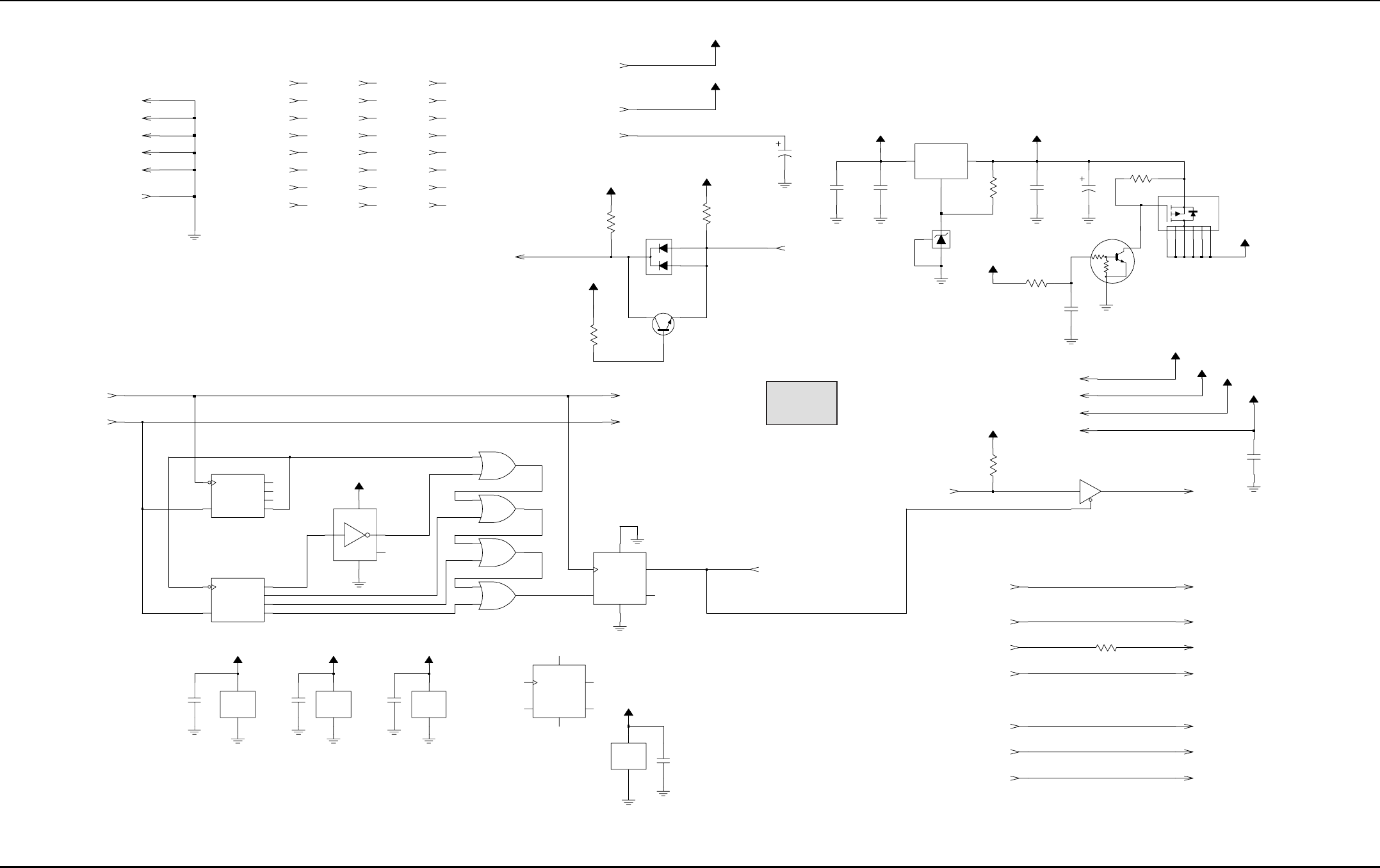
7-98 Schematics, Component Location Diagrams, and Parts Lists: HUE4039A/HUE4043A (UHF Range 1) Main Board
May 25, 2005 6881096C74-B
Figure 7-75. HUE4039A/HUE4043A Secure Interface Board Schematic
11 P501-2
U803-4
12
13
VCC2.85
0.1uF
C811
10K
R806
P501-12
0
R808
J701-13
J701-15 *P501-11*
J701-27
J701-34
J701-12
VCC2.85VCC2.85
J701-36
J701-7
R802
1K
SW_B+
J701-22
J701-24
100K
R807
VCC2.85
J701-16
Q4 8
RESET
12
J701-6
J701-10
U802-2
CLK
13 Q1 11
Q2 10
Q3 9
U803-1
1
2
3
U803-3
9
10
8
P501-9
0.1uF
C809
VCC2.85
PWR_GND
U805-2
GND
3
VCC
5
U805-1
2
1
4
VCC2.85
J701-1
J701-8
A+
J701-19
J701-11
P501-4
J701-3
J701-35
VCC5
0.1uF
SW_B+
100K
C802
R804
4
5
6
VCC2.85
Q802
U802-3
PWR_GND
7
GND
14
VCC
U803-2
RESET
2
PWR_GND
U803-5
GND
7
VCC
14
U802-1
CLK
1Q1 3
Q2 4
Q3 5
Q4 6
J701-20
VCC2.85
J701-17
J701-23
PWR_GND
U804-3
GND
7
VCC
14
J701-4
UNSW_B+_ENC
J701-33
D801
1
2
3
J701-21
Q800
1
3
2
J701-31J701-29
J701-25
R805
10K
R800
10K
J701-32
Q803
47K
47K
P501-17
C803
P501-20
J701-14 A+
0.1uF
P501-7
P501-3
5.6V
VR800
R801
100K
P501-1
P501-10
J701-38
P501-18
2
J701-5
U800
MC33269D
ADJ
1
IN
3OUT
J701-2
VCC5
UNSW_B+_ENC
CLK
11
D
9
Q13
Q* 12
RESET 10
SET
8
J701-39
10uF
VCC2.85
U804-2
C805
1uF
C804
P501-16
J701-30
0.1uF
C808
0.1uF
C807
SW_B+_ENC
0.1uF
C806
U804-1
CLK
3
D
5
Q1
Q* 2
RESET 4
SET
6
3GND
2
1
NC
4
5
VCC
U801
0.1uF
J701-18
C801
0.47
C810
P501-15
SW_B+_ENC
J701-40
J701-26 P501-13
J701-37
J701-9
J701-28
P501-14
P501-19
P501-6
P501-8
P501-5
SAP_TX
SAP_TX
ENC_SEL
TAMPER_ENC TAMPER_ENC
BOOT*
ENC_SPARE2
ENC_SPARE1
ENC_RESET
WAKEUP
SAP_RX
SAP_FSYNC
SAP_DCLK
KEYFAIL*
KEYFAIL*
MAEPF-27914-O
Part Series
800
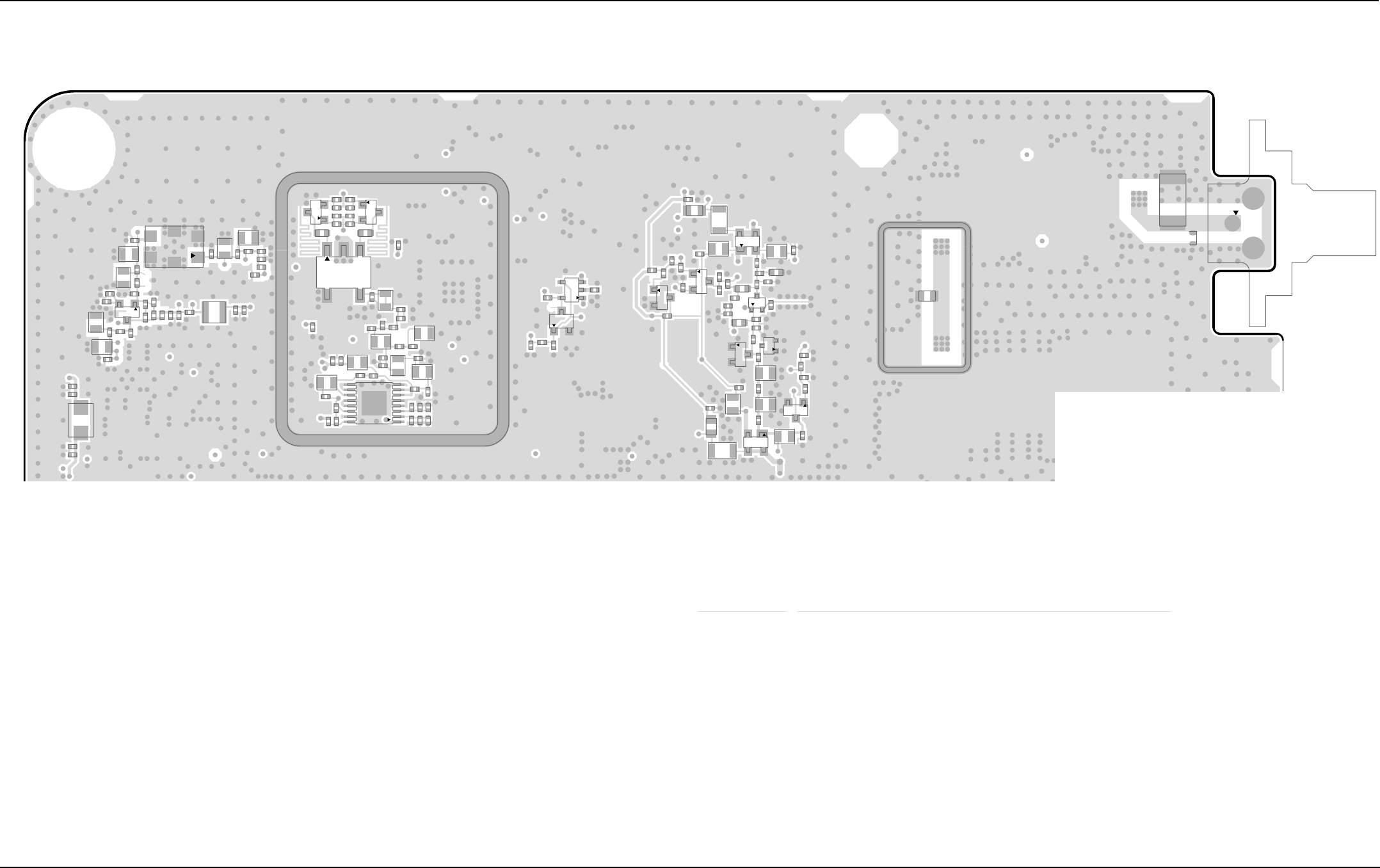
Schematics, Component Location Diagrams, and Parts Lists: HUE4039A/HUE4043A (UHF Range 1) Main Board 7-99
6881096C74-B May 25, 2005
Figure 7-76. HUE4039A Main Board Layout—Side 1 Top
C5280
C5305
C5329
C5333
C5343
C5345
C5350
C5351
C5352
C5353
C5354
C5355
C5356
C5357
C5358
C5359
C5362
C5365
C5366
C5374
C5375
C5378
C5380
C5381
C5382
C5383 C5385
C5388
C5400
C5401
C5402
C5403
C5404
C5405
C5406
C5408
C5410
C5411
C5412
C5413
C5414
C5417
C5418
C5425
C5426
C5427
C5428
C5429
C5430
D5380
D5381
E5400
L5302
L5305
L5306
L5307
L5380
L5383
L5385
L5389
L5392
L5400
L5401
L5403
L5404
L5406
L5407
L5408
Q5257
Q5401
R5311
R5321
R5327
R5328
R5329
R5333
R5380 R5381
R5382
R5383
R5384 R5385
R5386
R5388
R5400
R5401 R5402
R5403
R5404
R5411
R5412
R5413
R5414
R5415
SH5250
1
54
3
T5380 U5300
1
16
8
9U5303
4
3
2
5
61
Y5400
C5282
C5283
C5284
C5285
C5287
C5288
C5289
C5290
C5291
C5292
C5293
C5294
C5295
C5296
C5297
C5299
C5300
C5301
C5302
C5363
C5364
C5722
D5280
D5300
D5302
D5311
L5280
L5281
L5282
L5283
L5284
L5285
L5286
L5287
L5288 L5289
L5290
Q5250
Q5251
Q5252
Q5253
R5300
R5301
R5302
R5303
R5304
R5305
R5306
R5307
R5308
R5309
R5310
R5330
R5332
SH5701
TP5301
C5303 3
2
J5701
R5710
R5713
C5708
C5719
SH5703
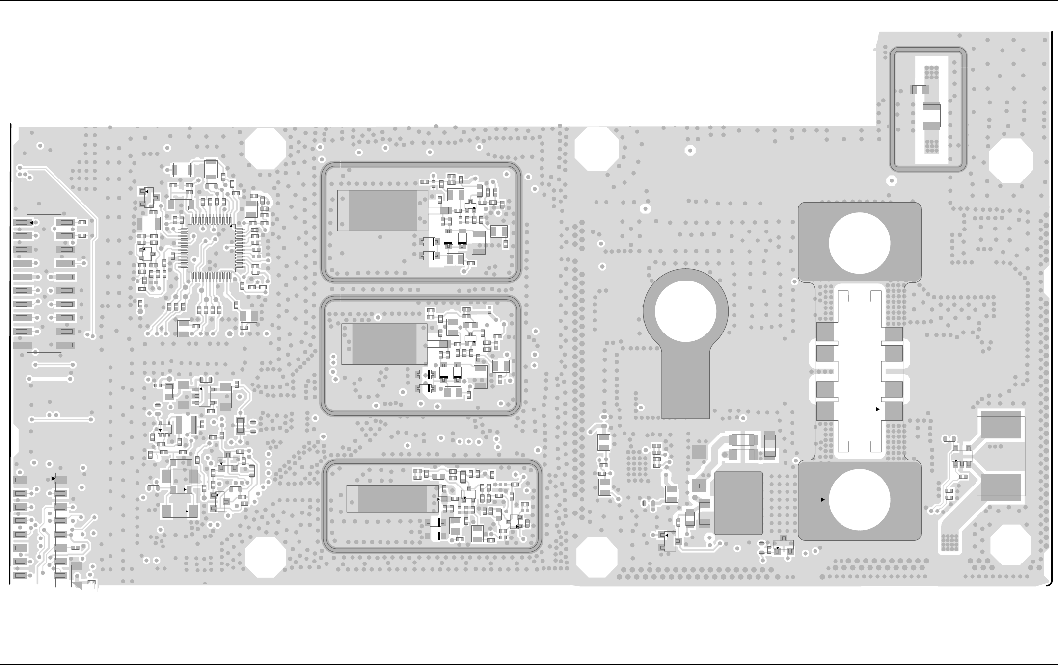
7-100 Schematics, Component Location Diagrams, and Parts Lists: HUE4039A/HUE4043A (UHF Range 1) Main Board
May 25, 2005 6881096C74-B
Figure 7-77. HUE4039A Main Board Layout—Side 1 Middle
C5505
C5513
C5515
C5517
C5541
L5502
L5503
L5505
M5501
M5502
Q5503
R5508
R5509
U5502
C5507
C5509
C5570
C5572
Q5570
R5570
R5571
C5526
R5518
R5574
C0436
C0461
21
R0422
C5750
C5752
C5754
C5757
C5758 C5759
C5760
C5761
C5762
C5765
C5768
C5771
C5815
C5817
L5751
L5753
L5755
Q5750
Q5751
R5750 R5751
R5752
R5753
R5754
R5758
R5759
R5761
R5762
R5763
R5764
R5765
R5766
R5767
TP5788 U5750
U5751
2
34
Y5750
Y05751
C0703
C0705
J0501
C5002
C5005
C5007
C5008
C5009
C5010
C5012
C5013
C5015
C5016
C5017
C5019
C5020
C5021
C5022
C5023
C5024
C5026
C5027
C5028
C5030
C5046
C5051
C5052
C5061
C5064
C5065
C5066
C5067
C5068
C5069
C5070
C5071 CLKOUT
D5003
DOUTA
E5001
E5006
E5007
FS
L5002
L5003
L5004
L5012
L5013
L5015
PC
PD
PE
Q5003
R5000
R5001
R5003
R5005
R5014
R5015
R5016
R5017
R5018
R5019
R5020
R5025
R5026
R5027
R5028
R5030
R5031
R5032
R5033
R5034
R5035
1
37
25 13
U5002
C5826
C5829
C5830
C5831
C5834
C5835
C5838
C5840
C5842
C5844
C5846C5847
C5850
C5851 C5854
C5859
C5860
C5861
C5862
C5863
C5900
C5901
C5904
C5905 C5906
C5907
C5908
C5910
C5911
C5912
C5913
C5914
C5915
C5916
C5917
C5920
C5922
C5923
C5924
C5925
C5926
C5927
C5928
C5929
C5930 C5931
D5828
D5832
D5901
D5902
D5903
D5904
D5905
D5906
D5909
D5910
L5826
L5828
L5830
L5832
L5834
L5900
L5901
L5902
L5904
L5905
L5906
L5908
L5909
L5912
L5913
Q5826
Q5829
Q5901
Q5903
R5826
R5828
R5830
R5832
R5834
R5838
R5840
R5842
R5851
R5852
R5853
R5854
R5855
R5900
R5903
R5904
R5905
R5909
R5910
R5911
R5912
R5915
R5916
R5918
R5919
R5920
R5922
R5923
R5948
SH5820
SH5901
SH5902
U5826
Y5900
Y5901
C5544
C5708
C5719
R5519
R5522
SH5703
U5503
M5503
C5577
C5578
C5579
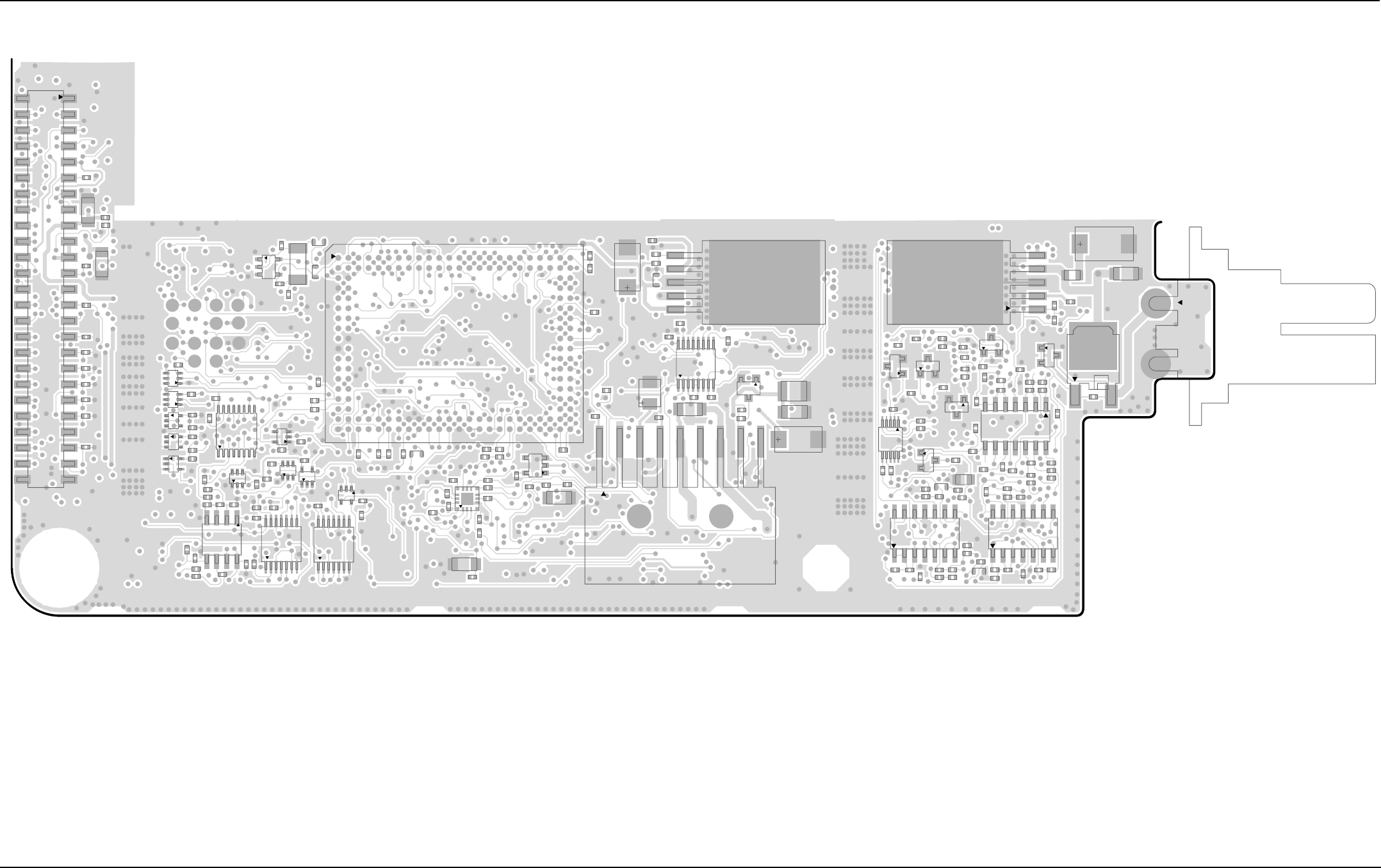
Schematics, Component Location Diagrams, and Parts Lists: HUE4039A/HUE4043A (UHF Range 1) Main Board 7-101
6881096C74-B May 25, 2005
Figure 7-78. HUE4039A Main Board Layout—Side 1 Bottom
VR0407
C0401
C0406
C0407
C0412
C0467
R0430
VR0406
5
U0951
C0413
C0417
C0463
C0464
C0952
C0957
C0959
C0962
C0963
C0964
C0965
C0966 C0967
C0971
C0972
C0973
C0975
C0976
C0978
C0979
C0980
C0983
D0952
Q0955
R0515
R0946
R0947
R0950
R0953
R0954
R0960
R0963
R0964
R0967
R0968
R0969
R0970
R0971
R0972
R0973
R0974
R0975 R0976
R0977
R0978
R0979
R0980
R0981 R0982
R0983
R0984
R0985
R0986
R0987
R0988
R0989
R0990
R0992
R0993
R0994
R0996
R0997
R0998
R0999
TP0954
5
610
U0952
7
8
14
U0955
7
8
14
U0956
7
8
14
U0957
VR0405
VR0501
C0955
C0956
J0950
3
4
1
Q0503
R0531
R0907
SC0001
SC0002
C0100
C0101
C0105
C0204
C0207
C0213
C0214
C0217
C0220
C0223
C0243
C0301
C0312
C0469
C0502
C0503
C0519
C0531
C0532
C0533
C0536
C0600
C0603 C0604
C0606
C0610
C0611
C0613
C0614
C0616
C0953
C0954
C0981
C0984
C0986
C0987
Q0200
Q0610
Q0611
Q0612
Q0613
R0101
R0102
R0103
R0104
R0109
R0110
R0111
R0113
R0114
R0115
R0116
R0117
R0119
R0120
R0121
R0122
R0123
R0124
R0125
R0200
R0204
R0220
R0222
R0303
R0304
R0305
R0307
R0505
R0508
R0509
R0527
R0620
R0621
R0622
R0623
R0625
R0626
R0627
R0628
R0629
R0630
R0631
R0632
R0634
R0635
R0636
R0638
R0639
R0951
R0952
R0995
TP0002
TP0400
TP0401
TP0402
TP0403
TP0407
TP0408
TP0409
TP0410
TP0411
TP0412
TP0413
TP0414
TP0415
123456789101112131415161718
18 17 16 15 14 13 12 11 10 9 8 7 6 5 4 3 2
A
B
C
D
E
F
G
N
M
L
K
J
I
H
R
S
T
U
V
W
X
P
Z
YY
Z
P
X
W
V
U
T
S
R
H
I
J
K
L
M
N
G
F
E
D
C
B
A
U0001
U0102
11
10
9
U0204
5
9
13
U0304
U0402
U0504
U0508
14
7
8
U0602
14
7
8
U0603
1
4
58
U0604
16 9
8
1
U0606
U0607U0608U0609
U0610
5
U0950
16 9
8
1
U0959
Y0100
R0624
C0428
C0437
C0442
C0444
C0450
C0452
C0454
C0455
C0458
50 49
J0401
R0415
R0425
R0300
R0301
R0923
R0924
C0436
C0461
21
R0422
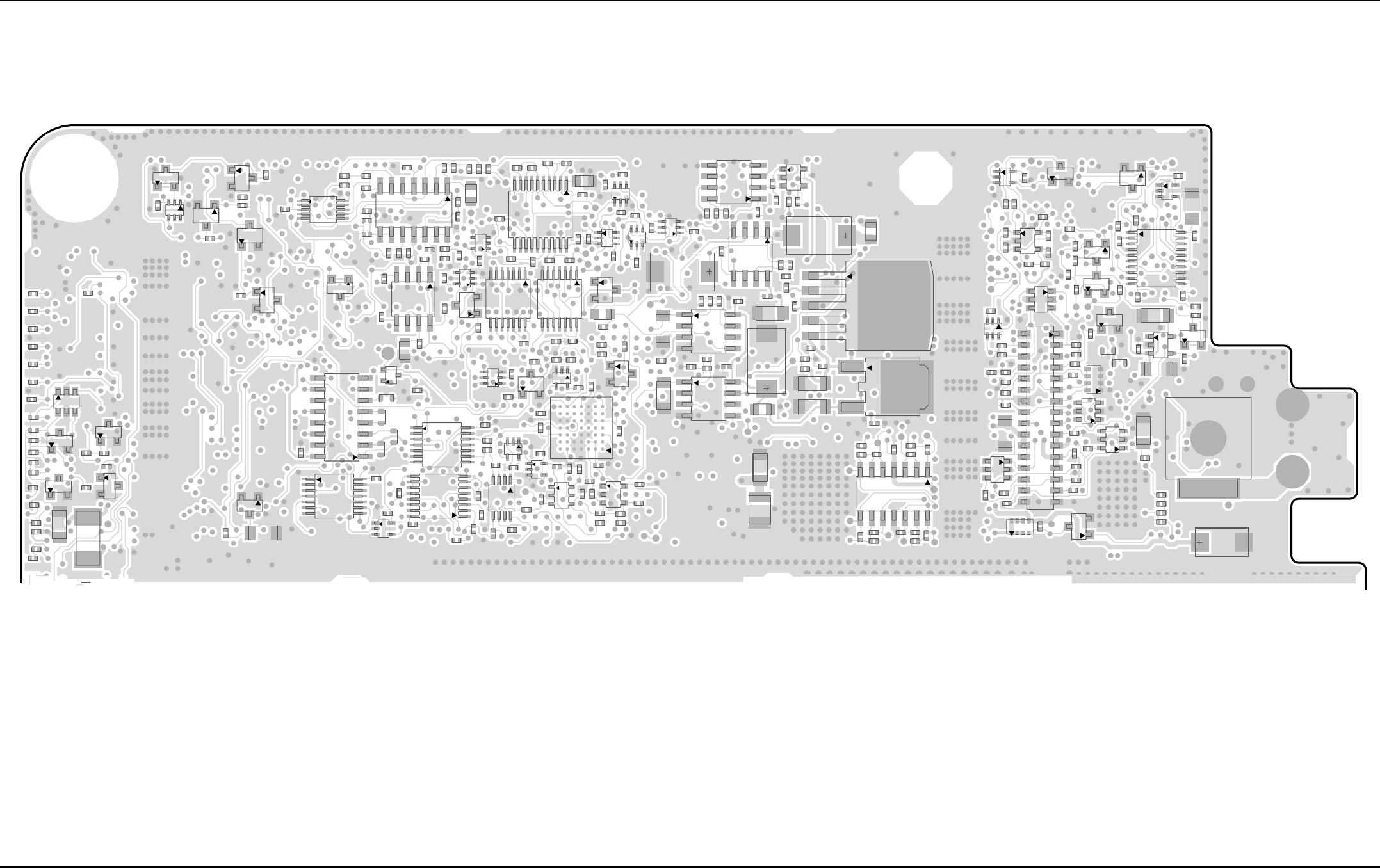
7-102 Schematics, Component Location Diagrams, and Parts Lists: HUE4039A/HUE4043A (UHF Range 1) Main Board
May 25, 2005 6881096C74-B
Figure 7-79. HUE4039A Main Board Layout—Side 2 Top
C0102
C0103
C0104
C0106
C0201
C0202
C0203
C0205
C0206
C0208
C0209
C0210
C0211
C0212
C0215
C0216
C0221
C0224
C0225
C0226
C0227
C0228
C0230
C0231
C0232
C0233
C0234
C0235
C0236
C0237
C0238
C0239
C0240
C0242
C0244
C0302 C0305
C0306
C0307
C0308
C0309
C0310
C0311
C0313
C0400
C0402
C0403
C0404
C0405
C0408
C0409
C0410
C0414
C0415
C0416
C0418
C0419
C0420
C0422
C0423 C0424
C0425
C0426
C0427
C0429
C0430
C0435
C0441
C0443
C0445
C0451
C0453
C0456
C0457
C0459
C0465
C0466
C0470
C0475
C0476
C0477
C0478
C0500
C0504
C0505
C0506
C0507
C0510
C0512
C0513
C0514
C0515
C0516
C0517
C0518
C0524
C0525
C0526
C0527
C0528
C0529
C0534
C0535
C0537
C0601
C0605
C0901
C0902
C0903
C0904
C0905
C0906
C0907
C0908
C0909
C0910
C0911
C0912
C0913
C0914
C0915
C0916
C0917
C0918
C0919
C0920
C0921
C0922
C0923
C0930
C0933
C0934
C0935
C0936
C0937
C0940
C0941
C0942
C0943
C0944
C0945
C0950
C0951
C0960
C0961
C0968
C0969
C0970
C0974
C0982
C0985
C0997
C0998
D0501
D0950
D0951
D0954
F0400
FL0900 32 31
2
J0402
Q0402
Q0403 Q0404
Q0500
Q0501
Q0502
Q0504
Q0505
Q0951
4
5
8
Q0952
Q0953
Q0954
Q0960
R0105
R0106
R0107
R0108
R0202
R0203
R0205
R0206
R0207
R0208
R0209
R0210
R0212
R0216
R0218
R0219
R0221
R0223
R0224
R0225
R0226
R0227
R0228
R0229
R0230
R0231
R0235
R0236
R0403
R0404
R0405
R0406
R0407
R0408
R0409
R0410
R0411
R0412
R0416
R0417
R0418
R0419
R0420
R0421
R0431
R0432
R0435
R0500
R0502
R0503
R0504
R0506
R0201
R0507
R0510
R0526
R0511
R0512
R0513
R0514
R0516
R0517
R0518
R0519
R0520 R0521
R0525
R0522
R0523
R0528
R0529
R0900
R0901
R0907
R0906
R0902 R0903
R0904
R0905
R0910
R0911 R0912
R0913
R0914
R0930
R0931
R0932
R0933
R0934
R0935
R0936
R0937
R0938
R0939
R0940
R0941
R0942
R0943
R0944
R0945
R0948
R0955
R0961
R0962
R0965
R0966
R0991
TP0005
TP0200
TP0201
TP0202
TP0203
TP0204
TP0205
TP0206
TP0418
TP0419
TP0420
TP0500
TP0930
TP0931
TP0936
TP0937
TP0938
TP0939
TP0940
TP0941
TP0942
TP0950
TP0951
TP0952
TP0953
TP0955
TP0956
TP0957
TP0958
TP0959
TP0960
TP0961
TP0962
TP0963
TP0964
14
78
U0103
14
78
U0104
U0105
1
20
11
10
U0200
7
8
14
U0201
56
10
U0202
43
6
U0203
1
4
5
8
U0206
U0207
4
3
6U0208
4
3
6
U0209
4
3
6
U0210
14
7
8
U0300
14
7
8
U0303
16 1
8
9
U0305
U0307
U0308
U0400
43
6
U0401
1
6
5
U0500
1
4
58
U0501
1
45
8
U0502
3
2
1
U0503
1
4
58
U0506
1
45
8
U0507
U0601
U0605
U0900
G7 G1
A7 A1
U0901
16
8
9
U0902
U0903
11
120
10
U0953
U0954
U0958
7
814
U0960
U0962
U0963
U0965
VR0400
VR0402
VR0404
VR0408
VR0410
4
5
8
VR0411
VR0418
VR0420
VR0421
VR0422
VR0423
VR0424
VR0425
VR0500
VR0950
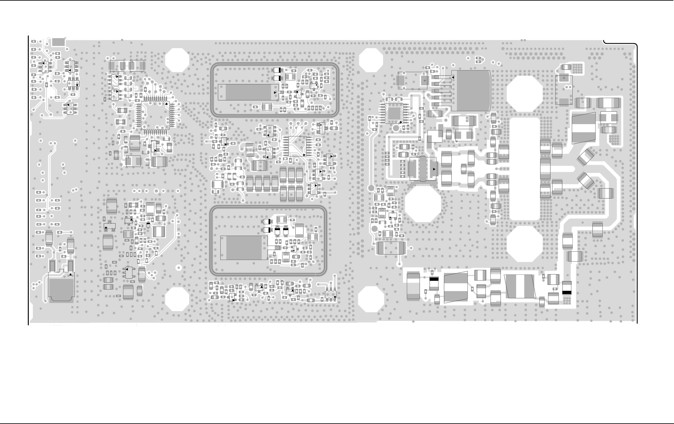
Schematics, Component Location Diagrams, and Parts Lists: HUE4039A/HUE4043A (UHF Range 1) Main Board 7-103
6881096C74-B May 25, 2005
Figure 7-80. HUE4039A Main Board Layout—Side 2 Middle
C5531 C5532
C5535
C5538
C5539
C5540
C5557
C5559
C5560
L5508
R5520 R5521
R5525
R5531
R5534
R5536
R5530
R5533
C5527
C5558
C5566
C5568
C5569
R5526
R5537
C5567
C0425
C0431
C0432
C0433 C0434
C0438
C0439
C0440
C0446
C0447
C0448
C0449
C0460
C0462
C0520
C0521
C0522
C0523
C0700 C0701
C0702
C0704
C0706
C0708 C0709
C0710 C0711
C0712
C0713
C0714
C5001
C5003
C5004 C5006
C5011
C5014
C5018
C5025
C5029
C5032
C5033
C5034
C5037
C5038
C5039
C5040
C5041
C5044
C5045
C5048
C5049
C5050
C5056
C5057 C5058
C5059
C5060
C5062
C5063
C5072
C5073
C5501
C5502
C5503
C5504
C5506
C5508
C5510
C5511
C5512
C5514
C5516
C5518
C5519
C5520
C5521
C5522
C5523
C5524
C5525
C5542
C5543
C5545
C5546
C5547
C5548
C5549
C5550
C5551
C5552
C5553
C5554
C5555
C5556
C5563
C5565
C5701
C5702
C5703
C5704
C5705
C5706
C5707
C5709
C5710
C5751 C5753
C5755
C5756 C5763
C5764
C5766
C5767
C5769
C5770
C5772
C5773
C5774
C5775
C5776
C5777
C5778
C5779
C5780
C5781
C5782
C5783
C5784
C5785
C5786
C5787
C5788
C5789
C5790
C5791
C5792
C5793
C5794
C5795
C5796
C5797
C5798
C5799
C5800
C5801
C5802
C5803
C5804
C5805
C5806
C5807
C5808
C5809
C5810
C5811
C5812
C5813
C5816
C5825
C5827
C5828
C5832
C5833
C5836
C5837
C5839
C5841
C5843
C5845
C5848
C5849
C5852
C5853
C5855
C5856
C5857
C5858
C5909
C5919
C5921
C5932
C5933
C5935
C5936
C5937
C5938
C5939
C5940
C5941
C5942
C5943
C5944
C5945
C5946
C5947
C5948
C5949
C5950
C5951
C5956
C5957
C5958 C5959
C5960
C5961
D5002
D5701
D5702
D5703
D5750
D5751
D5827
D5831
D5833
D5900
D5907
D5908
D5911
D5912
E5002
E5003
E5004
E5005
E5008
E5009
E5502
E6750
L5001
L5006
L5007
L5008
L5010
L5053
L5501
L5504
L5506
L5507
L5510
L5701
L5702
L5703
L5704
L5705
L5750
L5752
L5754
L5756
L5757
L5758
L5759
L5760
L5825
L5827
L5829 L5831
L5833
L5907
L5910
L5911
L5914
L5915
L5916
L5917
L5918
L5919
L5920
L5921
L5922
Q5001
Q5002
Q5501
1
23
Q5502
Q5706
Q5707
Q5708
Q5709
Q5710
Q5752
Q5755
Q5825
Q5828
Q5902
Q5904
Q5905
Q5906
R0524
R5002
R5006
R5008
R5010
R5011
R5013
R5022
R5023
R5029
R5050
R5051
R5501
R5502
R5503
R5504
R5505
R5506
R5507
R5510
R5511
R5512
R5513
R5514
R5515
R5516
R5523
R5524
R5527
R5528
R5529
R5532
R5535
R5701
R5755
R5768
R5769
R5770
R5771
R5772
R5773
R5774
R5775
R5776
R5777
R5778
R5779
R5780
R5781
R5825
R5827
R5829
R5831
R5833
R5837
R5839
R5841
R5843
R5845
R5846
R5848
R5849
R5850
R5902
R5914
R5917
R5921
R5924
R5926
R5927
R5928
R5929
R5930
R5931
R5932
R5933
R5934
R5935
R5937
R5938
R5939
R5940
R5941
R5949
R5950
SH5821
SH5900
TP5501
TP5502
TP5503
TP5760
TP5783
TP5787
TP5789
TP5790
TP5791
TP5792
TP5793
TP5794
TP5795
TP5796
TP5797
TP5798
TP5799
3
2
1
U0505
U5001
1
16
8
9
U5501
1
37
25 13
U5752
16
8
9
U5753
U5825
VR0412
VR0413
VR0414
VR0417
Y5902
E5501
R5517
U5570
C5571
TP5570
C5573
C5575
C5576
R5572
R5573
R5785 R5786
R5784
R5783 R5782
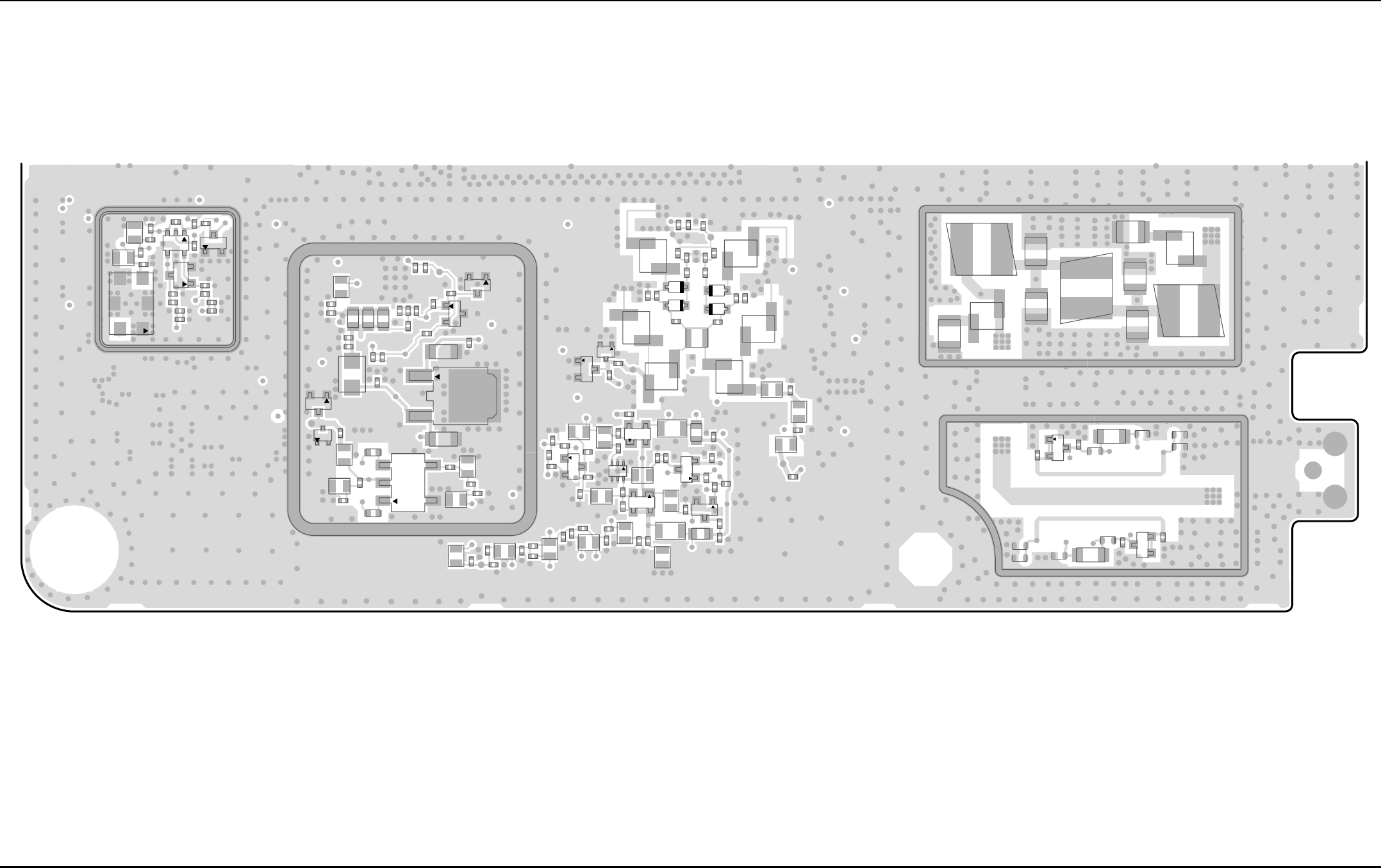
7-104 Schematics, Component Location Diagrams, and Parts Lists: HUE4039A/HUE4043A (UHF Range 1) Main Board
May 25, 2005 6881096C74-B
Figure 7-81. HUE4039A Main Board Layout—Side 2 Bottom
C5250
C5251
C5252
C5253
C5254
C5255
C5256
C5257
C5258
C5259
C5304
C5306
C5307
C5308
C5309
C5310
C5311
C5312
C5313
C5314
C5315
C5316
C5317
C5318
C5319
C5320
C5321
C5322
C5323
C5324
C5325
C5326
C5327
C5328
C5330
C5331
C5332
C5334
C5335
C5336
C5337
C5338
C5339
C5340
C5341
C5342
C5344
C5346
C5347
C5348
C5349
C5360
C5361
C5367
C5368
C5377
C5379
C5386
C5389
C5390
C5391
C5407
C5409
C5415
C5416
C5419
C5420
C5421
C5422
C5423
C5424
C5431
C5432
C5433
C5711
C5712
C5713
C5714
C5715
C5716
C5717
C5718
C5720
C5721
D5250
D5251
D5252
D5253
D5281
D5282
D5304
D5305
D5306
D5307
D5313
D5400
D5704
D5705
L5237
L5250
L5251
L5252
L5253
L5254
L5255
L5256
L5257
L5258
L5291
L5292
L5293
L5294
L5295
L5296
L5297
L5298
L5299
L5300
L5301
L5303
L5304
L5308
L5381
L5382
L5384
L5386
L5387
L5388
L5390
L5402
L5411
L5706
L5707
L5708
L5712
L5713
Q5254
Q5255
Q5256
Q5258
Q5402
R5250
R5251
R5252
R5253
R5254
R5255
R5256
R5312
R5313
R5314
R5315
R5316
R5317
R5318
R5319
R5322
R5323
R5324
R5325
R5326
R5334
R5335
R5336
R5387
R5405
R5406
R5407
R5702
R5703
R5704
R5705
R5706
R5707
R5708
R5709
R5711
R5712
SH5380
SH5400 SH5702
SH5704
15
4
3
T5381
TP5250
TP5251
TP5252
TP5302
TP5303
TP5304
3
2
1
U5301
3
45
U5302
U5400
43
2
5
6
1
Y5401
Schematics, Component Location Diagrams, and Parts Lists: HUE4039A/HUE4043A (UHF Range 1) Main Board 7-105
6881096C74-B May 25, 2005
HUE4039A Main Board Parts List
Reference
Designator
Motorola
Part Number Description
C0100 2113743N32 CAP CHIP 18.0 PF 5% COG
C0101 2113743N32 CAP CHIP 18.0 PF 5% COG
C0102 2113743M24 CAP CHIP 100000 PF +80-
20% Y5V
C0103 2113743M24 CAP CHIP 100000 PF +80-
20% Y5V
C0104 2113743M24 CAP CHIP 100000 PF +80-
20% Y5V
C0105 2113743M24 CAP CHIP 100000 PF +80-
20% Y5V
C0106 2113743N50 CAP CHIP 100 PF 5% COG
C0201 2113743M24 CAP CHIP 100000 PF +80-
20% Y5V
C0202 2113743M24 CAP CHIP 100000 PF +80-
20% Y5V
C0203 2113928S04 CAP CER CHIP 0.100UF 10V
0402
C0204 2185802B01 CAP 10V 4.7UF
C0205 2113743N54 CAP CHIP 150 PF 5% COG
C0206 2113928E01 CAP CER CHIP 1.0 UF 10 %
10V
C0207 2113743N38 CAP CHIP 33.0 PF 5% COG
C0208 2113928E01 CAP CER CHIP 1.0 UF 10%
10V
C0209 2113743M24 CAP CHIP 100000 PF +80-
20% Y5V
C0210 2113743M24 CAP CHIP 100000 PF +80-
20% Y5V
C0211 2113743N50 CAP CHIP 100 PF 5% COG
C0212 2113743M24 CAP CHIP 100000 PF +80-
20% Y5V
C0213 2113743M24 CAP CHIP 100000 PF +80-
20% Y5V
C0214 2113741N69 CAP CHIP CL2 X7R 10%
100000
C0215 2113928S04 CAP CER CHIP 0.100UF 10V
0402
C0216 2113743M24 CAP CHIP 100000 PF +80-
20% Y5V
C0217 2113743L29 CAP CHIP 3300 PF 10% X7R
C0220 2311049A57 CAP TANT CHIP A/P 10UF
10% 16V
C0221 2311049A78 CAP TANT CHIP 10.0 UF 10%
50V
C0223 2185802B01 CAP 10V 4.7UF
C0224 2113743M24 CAP CHIP 100000 PF +80-
20% Y5V
C0225 2113928S04 CAP CER CHIP 0.100UF 10V
0402
C0226 2113928S04 CAP CER CHIP 0.100UF 10V
0402
C0227 2113743M24 CAP CHIP 100000 PF +80-
20% Y5V
C0228 2113743N54 CAP CHIP 150 PF 5% COG
C0230 2113743L09 CAP CHIP 470 PF 10% X7R
C0231 2113743L01 CAP CHIP 220 PF 10% X7R
C0232 2113743L09 CAP CHIP 470 PF 10% X7R
C0233 2113743L01 CAP CHIP 220 PF 10% X7R
C0234 2113928S04 CAP CER CHIP 0.100UF 10V
0402
C0235 2113743L09 CAP CHIP 470 PF 10% X7R
C0236 2113743L09 CAP CHIP 470 PF 10% X7R
C0237 2113743L01 CAP CHIP 220 PF 10% X7R
C0238 2113743L01 CAP CHIP 220 PF 10% X7R
C0239 2113743M24 CAP CHIP 100000 PF +80-
20% Y5V
C0240 2113928S04 CAP CER CHIP 0.100UF 10V
0402
C0242 2113928S04 CAP CER CHIP 0.100UF 10V
0402
C0243 2113945B01 CAP CER CHIP 6800 PF 25V
10%
C0244 2113945B01 CAP CER CHIP 6800 PF 25V
10%
C0301 2113743M24 CAP CHIP 100000 PF +80-
20% Y5V
C0302 2113743M24 CAP CHIP 100000 PF +80-
20% Y5V
C0305 2113743M24 CAP CHIP 100000 PF +80-
20% Y5V
C0306 2113743M24 CAP CHIP 100000 PF +80-
20% Y5V
C0308 2113743E20 CAP CHIP .10 UF 10%
C0309 2113743E20 CAP CHIP .10 UF 10%
C0310 2113743E20 CAP CHIP .10 UF 10%
C0311 2113743M24 CAP CHIP 100000 PF +80-
20% Y5V
C0312 2113743M24 CAP CHIP 100000 PF +80-
20% Y5V
Reference
Designator
Motorola
Part Number Description
C0313 2113743M24 CAP CHIP 100000 PF +80-
20% Y5V
C0400 2113743N38 CAP CHIP 33.0 PF 5% COG
C0401 2113743N50 CAP CHIP 100 PF 5% COG
C0402 2113743N38 CAP CHIP 33.0 PF 5% COG
C0403 2113743N38 CAP CHIP 33.0 PF 5% COG
C0404 2113743N38 CAP CHIP 33.0 PF 5% COG
C0405 2113743N38 CAP CHIP 33.0 PF 5% COG
C0406 2113743N38 CAP CHIP 33.0 PF 5% COG
C0407 2113743N50 CAP CHIP 100 PF 5% COG
C0408 2113743N50 CAP CHIP 100 PF 5% COG
C0409 2113743N38 CAP CHIP 33.0 PF 5% COG
C0410 2113743N38 CAP CHIP 33.0 PF 5% COG
C0412 2113743N50 CAP CHIP 100 PF 5% COG
C0413 2113743N50 CAP CHIP 100 PF 5% COG
C0414 2113743L01 CAP CHIP 220 PF 10% X7R
C0415 2113743L01 CAP CHIP 220 PF 10% X7R
C0416 2113743N50 CAP CHIP 100 PF 5% COG
C0417 2113743L01 CAP CHIP 220 PF 10% X7R
C0418 2113743L01 CAP CHIP 220 PF 10% X7R
C0419 2113743N50 CAP CHIP 100 PF 5% COG
C0420 2185802B01 CAP 10V 4.7UF
C0422 2113743N38 CAP CHIP 33.0 PF 5% COG
C0423 2113743N38 CAP CHIP 33.0 PF 5% COG
C0424 2113743N38 CAP CHIP 33.0 PF 5% COG
C0425 2113743N50 CAP CHIP 100 PF 5% COG
C0426 2113741B13 CAP CHIP CL2 X7R REEL 470
C0427 2113743N50 CAP CHIP 100 PF 5% COG
C0428 2113743N50 CAP CHIP 100 PF 5% COG
C0429 2113743N50 CAP CHIP 100 PF 5% COG
C0430 2113743N50 CAP CHIP 100 PF 5% COG
C0431 2113743N50 CAP CHIP 100 PF 5% COG
C0432 2113743N50 CAP CHIP 100 PF 5% COG
C0433 2113743N50 CAP CHIP 100 PF 5% COG
C0434 2113743N50 CAP CHIP 100 PF 5% COG
C0435 2113743L09 CAP CHIP 470 PF 10% X7R
C0436 2113741B13 CAP CHIP CL2 X7R REEL 470
C0437 2113741B13 CAP CHIP CL2 X7R REEL 470
C0438 2113743L09 CAP CHIP 470 PF 10% X7R
C0439 2113743N50 CAP CHIP 100 PF 5% COG
C0440 2113743N50 CAP CHIP 100 PF 5% COG
Reference
Designator
Motorola
Part Number Description
C0441 2113743M24 CAP CHIP 100000 PF +80-
20% Y5V
C0442 2113743N38 CAP CHIP 33.0 PF 5% COG
C0443 2113743N38 CAP CHIP 33.0 PF 5% COG
C0444 2113743N38 CAP CHIP 33.0 PF 5% COG
C0445 2113743N38 CAP CHIP 33.0 PF 5% COG
C0446 2113743N50 CAP CHIP 100 PF 5% COG
C0447 2113743N50 CAP CHIP 100 PF 5% COG
C0448 2113743N50 CAP CHIP 100 PF 5% COG
C0449 2113743N50 CAP CHIP 100 PF 5% COG
C0450 2113743N38 CAP CHIP 33.0 PF 5% COG
C0451 2113743N38 CAP CHIP 33.0 PF 5% COG
C0452 2113743N38 CAP CHIP 33.0 PF 5% COG
C0453 2113743N38 CAP CHIP 33.0 PF 5% COG
C0454 2113743N38 CAP CHIP 33.0 PF 5% COG
C0455 2113743N38 CAP CHIP 33.0 PF 5% COG
C0456 2113743N38 CAP CHIP 33.0 PF 5% COG
C0457 2113743N38 CAP CHIP 33.0 PF 5% COG
C0458 2113743N38 CAP CHIP 33.0 PF 5% COG
C0459 2113743N38 CAP CHIP 33.0 PF 5% COG
C0460 2113743N50 CAP CHIP 100 PF 5% COG
C0461 2113743L01 CAP CHIP 220 PF 10% X7R
C0462 2113743L01 CAP CHIP 220 PF 10% X7R
C0463 2113743N38 CAP CHIP 33.0 PF 5% COG
C0464 2113743N38 CAP CHIP 33.0 PF 5% COG
C0465 2113741B13 CAP CHIP CL2 X7R REEL 470
C0466 2113743N50 CAP CHIP 100 PF 5% COG
C0467 2113743N50 CAP CHIP 100 PF 5% COG
C0469 2113743M24 CAP CHIP 100000 PF +80-
20% Y5V
C0470 2113743N38 CAP CHIP 33.0 PF 5% COG
C0475 2113743N50 CAP CHIP 100 PF 5% COG
C0476 2113743N50 CAP CHIP 100 PF 5% COG
C0477 2113743N50 CAP CHIP 100 PF 5% COG
C0478 2113743N50 CAP CHIP 100 PF 5% COG
C0500 2113743M24 CAP CHIP 100000 PF +80-
20% Y5V
C0502 2113743N50 CAP CHIP 100 PF 5% COG
C0503 2113743N50 CAP CHIP 100 PF 5% COG
C0504 2113741N69 CAP CHIP CL2 X7R 10%
100000
C0505 2113743L41 CAP CHIP 10000 PF 10% X7R
Reference
Designator
Motorola
Part Number Description
7-106 Schematics, Component Location Diagrams, and Parts Lists: HUE4039A/HUE4043A (UHF Range 1) Main Board
May 25, 2005 6881096C74-B
C0506 2113743L41 CAP CHIP 10000 PF 10% X7R
C0507 2113743M24 CAP CHIP 100000 PF +80-
20% Y5V
C0510 2185802B01 CAP 10V 4.7UF
C0512 2113743M24 CAP CHIP 100000 PF +80-
20% Y5V
C0513 2311049A43 CAP TANT CHIP 150 10 6
C0514 2311049A43 CAP TANT CHIP 150 10 6
C0515 2113743M24 CAP CHIP 100000 PF +80-
20% Y5V
C0516 2113743M24 CAP CHIP 100000 PF +80-
20% Y5V
C0517 2185802B01 CAP 10V 4.7UF
C0518 2185802B01 CAP 10V 4.7UF
C0519 2113743L41 CAP CHIP 10000 PF 10% X7R
C0520 2113743M24 CAP CHIP 100000 PF +80-
20% Y5V
C0521 2185802B01 CAP 10V 4.7UF
C0522 2185802B01 CAP 10V 4.7UF
C0523 2113743M24 CAP CHIP 100000 PF +80-
20% Y5V
C0524 2113743M24 CAP CHIP 100000 PF +80-
20% Y5V
C0525 2113928E01 CAP CER CHIP 1.0 UF 10 %
10V
C0526 2113743L41 CAP CHIP 10000 PF 10% X7R
C0527 2185802B01 CAP 10V 4.7UF
C0528 2113743M24 CAP CHIP 100000 PF +80-
20% Y5V
C0529 2185802B01 CAP 10V 4.7UF
C0531 2113741N69 CAP CHIP CL2 X7R 10%
100000
C0532 2113741Y32 CAP CER 1,000,000 10% 50V
C0533 2311049C47 CAP TANT CHIP 22.0UF 10%
16V
C0534 2113743M24 CAP CHIP 100000 PF +80-
20% Y5V
C0535 2113743M24 CAP CHIP 100000 PF +80-
20% Y5V
C0536 2113743M24 CAP CHIP 100000 PF +80-
20% Y5V
C0600 2113743M24 CAP CHIP 100000 PF +80-
20% Y5V
C0601 2113743M24 CAP CHIP 100000 PF +80-
20% Y5V
Reference
Designator
Motorola
Part Number Description
C0603 2113743M24 CAP CHIP 100000 PF +80-
20% Y5V
C0604 2113743M24 CAP CHIP 100000 PF +80-
20% Y5V
C0605 2113743M24 CAP CHIP 100000 PF +80-
20% Y5V
C0606 2113743M24 CAP CHIP 100000 PF +80-
20% Y5V
C0610 2113743M24 CAP CHIP 100000 PF +80-
20% Y5V
C0611 2113743M24 CAP CHIP 100000 PF +80-
20% Y5V
C0613 2113743M24 CAP CHIP 100000 PF +80-
20% Y5V
C0614 2113743M24 CAP CHIP 100000 PF +80-
20% Y5V
C0616 2113743N50 CAP CHIP 100 PF 5% COG
C0700 2113743N50 CAP CHIP 100 PF 5% COG
C0701 2113743N50 CAP CHIP 100 PF 5% COG
C0702 2113743N50 CAP CHIP 100 PF 5% COG
C0703 2113743N50 CAP CHIP 100 PF 5% COG
C0704 2113743N50 CAP CHIP 100 PF 5% COG
C0705 2113743N50 CAP CHIP 100 PF 5% COG
C0706 2113743N50 CAP CHIP 100 PF 5% COG
C0708 2113743N50 CAP CHIP 100 PF 5% COG
C0709 2113743N50 CAP CHIP 100 PF 5% COG
C0710 2113743N50 CAP CHIP 100 PF 5% COG
C0711 2113743N50 CAP CHIP 100 PF 5% COG
C0712 2113743N50 CAP CHIP 100 PF 5% COG
C0713 2113743L01 CAP CHIP 220 PF 10% X7R
C0714 2113743L01 CAP CHIP 220 PF 10% X7R
C0901 2113743M24 CAP CHIP 100000 PF +80-
20% Y5V
C0902 2113743M24 CAP CHIP 100000 PF +80-
20% Y5V
C0903 2113743M24 CAP CHIP 100000 PF +80-
20% Y5V
C0904 2113743L01 CAP CHIP 220 PF 10% X7R
C0905 2113743M24 CAP CHIP 100000 PF +80-
20% Y5V
C0906 2113743M24 CAP CHIP 100000 PF +80-
20% Y5V
C0907 2113743M24 CAP CHIP 100000 PF +80-
20% Y5V
Reference
Designator
Motorola
Part Number Description
C0908 2113743M24 CAP CHIP 100000 PF +80-
20% Y5V
C0909 2113743M24 CAP CHIP 100000 PF +80-
20% Y5V
C0910 2113743M24 CAP CHIP 100000 PF +80-
20% Y5V
C0911 2113743N50 CAP CHIP 100 PF 5% COG
C0912 2113743N50 CAP CHIP 100 PF 5% COG
C0913 2113743N50 CAP CHIP 100 PF 5% COG
C0914 2113743N38 CAP CHIP 33.0 PF 5% COG
C0915 2113743N50 CAP CHIP 100 PF 5% COG
C0916 2113743M24 CAP CHIP 100000 PF +80-
20% Y5V
C0917 2113743N50 CAP CHIP 100 PF 5% COG
C0918 2113743N50 CAP CHIP 100 PF 5% COG
C0919 2113743N50 CAP CHIP 100 PF 5% COG
C0920 2113743M24 CAP CHIP 100000 PF +80-
20% Y5V
C0922 2113743N50 CAP CHIP 100 PF 5% COG
C0930 2113743N50 CAP CHIP 100 PF 5% COG
C0933 2113743N50 CAP CHIP 100 PF 5% COG
C0934 2113743N50 CAP CHIP 100 PF 5% COG
C0935 2113743N50 CAP CHIP 100 PF 5% COG
C0936 2113743M24 CAP CHIP 100000 PF +80-
20% Y5V
C0937 2113743M24 CAP CHIP 100000 PF +80-
20% Y5V
C0940 2113743M24 CAP CHIP 100000 PF +80-
20% Y5V
C0941 2113743S01 CAP CER CHIP 1.0 UF 10%
16V
C0942 2113743S01 CAP CER CHIP 1.0 UF 10%
16V
C0943 2113743L41 CAP CHIP 10000 PF 10% X7R
C0944 2113743M24 CAP CHIP 100000 PF +80-
20% Y5V
C0945 2185802B01 CAP 10V 4.7UF
C0950 2113741N69 CAP CHIP CL2 X7R 10%
100000
C0951 2113741Y32 CAP CER 1,000,000 10% 50V
C0952 2113743E20 CAP CHIP .10 UF 10%
C0953 2311049C47 CAP TANT CHIP 22.0UF 10%
16V
C0954 2113743E20 CAP CHIP .10 UF 10%
Reference
Designator
Motorola
Part Number Description
C0955 2113741N69 CAP CHIP CL2 X7R 10%
100000
C0956 2311049C06 CAP TANT CHIP 22 UF 35V
20%
C0957 2113743M24 CAP CHIP 100000 PF +80-
20% Y5V
C0959 2113743M24 CAP CHIP 100000 PF +80-
20% Y5V
C0960 2113743M24 CAP CHIP 100000 PF +80-
20% Y5V
C0961 2113743M24 CAP CHIP 100000 PF +80-
20% Y5V
C0963 2113743N50 CAP CHIP 100 PF 5% COG
C0964 2113743N50 CAP CHIP 100 PF 5% COG
C0965 2113743N50 CAP CHIP 100 PF 5% COG
C0966 2113743N50 CAP CHIP 100 PF 5% COG
C0968 2113743N50 CAP CHIP 100 PF 5% COG
C0969 2113743N50 CAP CHIP 100 PF 5% COG
C0970 2113743N50 CAP CHIP 100 PF 5% COG
C0972 2113743E20 CAP CHIP .10 UF 10%
C0973 2113928E01 CAP CER CHIP 1.0 UF 10 %
10V
C0974 2113743M24 CAP CHIP 100000 PF +80-
20% Y5V
C0975 2113743N50 CAP CHIP 100 PF 5% COG
C0976 2113743N50 CAP CHIP 100 PF 5% COG
C0978 2113743N50 CAP CHIP 100 PF 5% COG
C0979 2113743M24 CAP CHIP 100000 PF +80-
20% Y5V
C0980 2113743M24 CAP CHIP 100000 PF +80-
20% Y5V
C0981 2113743M24 CAP CHIP 100000 PF +80-
20% Y5V
C0982 2311049C47 CAP TANT CHIP 22.0UF 10%
16V
C0983 2113743N50 CAP CHIP 100 PF 5% COG
C0984 2113743M24 CAP CHIP 100000 PF +80-
20% Y5V
C0985 2113743M24 CAP CHIP 100000 PF +80-
20% Y5V
C0986 2113743M24 CAP CHIP 100000 PF +80-
20% Y5V
C0987 2113743M24 CAP CHIP 100000 PF +80-
20% Y5V
C0997 2113740F47 CAP CHIP REEL CL1 +/-30 68
Reference
Designator
Motorola
Part Number Description
Schematics, Component Location Diagrams, and Parts Lists: HUE4039A/HUE4043A (UHF Range 1) Main Board 7-107
6881096C74-B May 25, 2005
C0998 2113741F01 CAP CHIP CL2 X7R REEL 100
C5001 2113928N01 CAP CER CHIP 0.1UF 10%
6.3
C5002 2113743N28 CAP CHIP 12.0 PF 5% COG
C5003 2113743L41 CAP CHIP 10000 PF 10% X7R
C5004 2113928N01 CAP CER CHIP 0.1UF 10%
6.3
C5005 2113928N01 CAP CER CHIP 0.1UF 10%
6.3
C5006 2113928N01 CAP CER CHIP 0.1UF 10%
6.3
C5007 2113743N30 CAP CHIP 15.0 PF 5% COG
C5008 2113743L25 CAP CHIP 2200 PF 10% X7R
C5009 2113740F58 CAP CHIP REEL CL1 +/-30
200
C5010 2113743N50 CAP CHIP 100 PF 5% COG
C5011 2113743F18 CAP CHIP 2.2 UF 16V +80-
20%
C5012 2113743N50 CAP CHIP 100 PF 5% COG
C5013 2113743N50 CAP CHIP 100 PF 5% COG
C5014 2113743L41 CAP CHIP 10000 PF 10% X7R
C5015 2113743L41 CAP CHIP 10000 PF 10% X7R
C5017 2113743L41 CAP CHIP 10000 PF 10% X7R
C5018 2113743T19 CAP 10UF 16V CER 3225 X5R
C5019 2113743N50 CAP CHIP 100 PF 5% COG
C5020 2113743L17 CAP CHIP 1000 PF 10% X7R
C5021 2113743L41 CAP CHIP 10000 PF 10% X7R
C5022 2113928N01 CAP CER CHIP 0.1UF 10%
6.3
C5023 2113928N01 CAP CER CHIP 0.1UF 10%
6.3
C5025 2113743S01 CAP CER CHIP 1.0 UF 10%
16V
C5026 2113928N01 CAP CER CHIP 0.1UF 10%
6.3
C5030 2113928N01 CAP CER CHIP 0.1UF 10%
6.3
C5032 2113928N01 CAP CER CHIP 0.1UF 10%
6.3
C5033 2113743N52 CAP CHIP 120 PF 5% COG
C5034 2113743N40 CAP CHIP 39.0 PF 5% COG
C5037 2113928N01 CAP CER CHIP 0.1UF 10%
6.3
C5039 2113743N29 CAP 13PF 20X40
Reference
Designator
Motorola
Part Number Description
C5040 2113743L41 CAP CHIP 10000 PF 10% X7R
C5041 2113928N01 CAP CER CHIP 0.1UF 10%
6.3
C5044 2113743A19 CAP CHIP .100 UF 10% X7R
C5045 2113743A31 CAP CHIP 1.0 UF 10% X7R
C5048 2113743N25 CAP CHIP 9.1 PF + -.5PF
COG
C5050 2113743T19 CAP 10UF 16V CER 3225 X5R
C5051 2113743L17 CAP CHIP 1000 PF 10% X7R
C5052 2113743L17 CAP CHIP 1000 PF 10% X7R
C5056 2113743N34 CAP CHIP 22.0 PF 5% COG
C5057 2113743N30 CAP CHIP 15.0 PF 5% COG
C5058 2113743L17 CAP CHIP 1000 PF 10% X7R
C5059 2113743N36 CAP CHIP 27.0 PF 5% COG
C5060 2113743L01 CAP CHIP 220 PF 10% X7R
C5061 2113928N01 CAP CER CHIP 0.1UF 10%
6.3
C5062 2113928N01 CAP CER CHIP 0.1UF 10%
6.3
C5063 2113743A31 CAP CHIP 1.0 UF 10% X7R
C5064 2113743L41 CAP CHIP 10000 PF 10% X7R
C5065 2113928N01 CAP CER CHIP 0.1UF 10%
6.3
C5066 2113743L17 CAP CHIP 1000 PF 10% X7R
C5067 2113743N50 CAP CHIP 100 PF 5% COG
C5068 2113743N50 CAP CHIP 100 PF 5% COG
C5069 2113743N54 CAP CHIP 150 PF 5% COG
C5070 2113743N50 CAP CHIP 100 PF 5% COG
C5071 2113743N30 CAP CHIP 15.0 PF 5% COG
C5072 2113928N01 CAP CER CHIP 0.1UF 10%
6.3
C5073 2113743A31 CAP CHIP 1.0 UF 10% X7R
C5251 2113743L01 CAP CHIP 220 PF 10% X7R
C5252 2113743N24 CAP CHIP 8.2 PF + -.5PF
COG
C5253 2113743L01 CAP CHIP 220 PF 10% X7R
C5255 2113743N24 CAP CHIP 8.2 PF + -.5PF
COG
C5256 2113743L01 CAP CHIP 220 PF 10% X7R
C5257 2113743N22 CAP CHIP 6.8 PF + -.5PF
COG
C5258 2113743N22 CAP CHIP 6.8 PF + -.5PF
COG
Reference
Designator
Motorola
Part Number Description
C5259 2113743L41 CAP CHIP 10000 PF 10% X7R
C5280 2113743L01 CAP CHIP 220 PF 10% X7R
C5282 2113743L41 CAP CHIP 10000 PF 10% X7R
C5283 2113743N24 CAP CHIP 8.2 PF + -.5PF
COG
C5284 2113743L41 CAP CHIP 10000 PF 10% X7R
C5285 2113743N18 CAP CHIP 4.7 PF +-.25PF
COG
C5287 2113743L41 CAP CHIP 10000 PF 10% X7R
C5288 2113743N24 CAP CHIP 8.2 PF + -.5PF
COG
C5289 2113743L01 CAP CHIP 220 PF 10% X7R
C5290 2113743L01 CAP CHIP 220 PF 10% X7R
C5291 2113743L41 CAP CHIP 10000 PF 10% X7R
C5292 2113743L01 CAP CHIP 220 PF 10% X7R
C5293 2113743N09 CAP CHIP 2.0 PF +-.25PF
COG
C5294 2113743L41 CAP CHIP 10000 PF 10% X7R
C5295 2113743N16 CAP CHIP 3.9 PF +-.25PF
COG
C5296 2113743L01 CAP CHIP 220 PF 10% X7R
C5297 2113743N12 CAP CHIP 2.7 PF +-.25PF
COG
C5299 2113743L41 CAP CHIP 10000 PF 10% X7R
C5300 2113743L01 CAP CHIP 220 PF 10% X7R
C5301 2113743L41 CAP CHIP 10000 PF 10% X7R
C5302 2113743L41 CAP CHIP 10000 PF 10% X7R
C5303 2113743L41 CAP CHIP 10000 PF 10% X7R
C5304 2113743L01 CAP CHIP 220 PF 10% X7R
C5305 2113743L01 CAP CHIP 220 PF 10% X7R
C5306 2113743L01 CAP CHIP 220 PF 10% X7R
C5307 2113743L01 CAP CHIP 220 PF 10% X7R
C5308 2113743L01 CAP CHIP 220 PF 10% X7R
C5309 2113743L41 CAP CHIP 10000 PF 10% X7R
C5310 2113743L01 CAP CHIP 220 PF 10% X7R
C5311 2113743L41 CAP CHIP 10000 PF 10% X7R
C5312 2113743L01 CAP CHIP 220 PF 10% X7R
C5313 2113743L41 CAP CHIP 10000 PF 10% X7R
C5314 2113743L41 CAP CHIP 10000 PF 10% X7R
C5315 2185802B01 CAP 10V 4.7UF
C5316 2113743L09 CAP CHIP 470 PF 10% X7R
C5317 2113743L01 CAP CHIP 220 PF 10% X7R
Reference
Designator
Motorola
Part Number Description
C5318 2185802B01 CAP 10V 4.7UF
C5319 2113743L41 CAP CHIP 10000 PF 10% X7R
C5320 2113743L01 CAP CHIP 220 PF 10% X7R
C5321 2113743L01 CAP CHIP 220 PF 10% X7R
C5322 2113743L41 CAP CHIP 10000 PF 10% X7R
C5323 2113743L50 CAP CHIP 33000 PF 10%
C5324 2113743L01 CAP CHIP 220 PF 10% X7R
C5325 2113743L50 CAP CHIP 33000 PF 10%
C5326 2113743N28 CAP CHIP 12.0 PF 5% COG
C5327 2113743N50 CAP CHIP 100 PF 5% COG
C5328 2113743N32 CAP CHIP 18.0 PF 5% COG
C5329 2113743N50 CAP CHIP 100 PF 5% COG
C5331 2113743N25 CAP CHIP 9.1 PF + -.5PF
COG
C5332 2113743N15 CAP CHIP 3.6 PF +-.25PF
COG
C5334 2113743L01 CAP CHIP 220 PF 10% X7R
C5335 2113743L50 CAP CHIP 33000 PF 10%
C5336 2113743N25 CAP CHIP 9.1 PF + -.5PF
COG
C5337 2113743L50 CAP CHIP 33000 PF 10%
C5338 2113743L01 CAP CHIP 220 PF 10% X7R
C5339 2113743N20 CAP CHIP 5.6 PF + -.5PF
COG
C5340 2113743L01 CAP CHIP 220 PF 10% X7R
C5341 2113743N15 CAP CHIP 3.6 PF +-.25PF
COG
C5342 2113743N25 CAP CHIP 9.1 PF + -.5PF
COG
C5343 2113743N34 CAP CHIP 22.0 PF 5% COG
C5344 2113743N25 CAP CHIP 9.1 PF + -.5PF
COG
C5345 2113743L09 CAP CHIP 470 PF 10% X7R
C5346 2113743L50 CAP CHIP 33000 PF 10%
C5347 2113743N32 CAP CHIP 18.0 PF 5% COG
C5348 2113743L01 CAP CHIP 220 PF 10% X7R
C5349 2113743N24 CAP CHIP 8.2 PF + -.5PF
COG
C5350 2113743L50 CAP CHIP 33000 PF 10%
C5351 2113743L50 CAP CHIP 33000 PF 10%
C5352 2113743L01 CAP CHIP 220 PF 10% X7R
C5353 2113743L01 CAP CHIP 220 PF 10% X7R
C5354 2113743N42 CAP CHIP 47.0 PF 5% COG
Reference
Designator
Motorola
Part Number Description

7-108 Schematics, Component Location Diagrams, and Parts Lists: HUE4039A/HUE4043A (UHF Range 1) Main Board
May 25, 2005 6881096C74-B
C5355 2113743N26 CAP CHIP 10.0 PF 5% COG
C5356 2113743L50 CAP CHIP 33000 PF 10%
C5357 2113743L01 CAP CHIP 220 PF 10% X7R
C5358 2113743N27 CAP CHIP 11.0 PF 5% COG
C5360 2113743L50 CAP CHIP 33000 PF 10%
C5361 2113743L01 CAP CHIP 220 PF 10% X7R
C5362 2113743L01 CAP CHIP 220 PF 10% X7R
C5363 2113743L01 CAP CHIP 220 PF 10% X7R
C5364 2113743L17 CAP CHIP 1000 PF 10% X7R
C5365 2113743L01 CAP CHIP 220 PF 10% X7R
C5366 2113743L17 CAP CHIP 1000 PF 10% X7R
C5367 2113743L01 CAP CHIP 220 PF 10% X7R
C5368 2113743L17 CAP CHIP 1000 PF 10% X7R
C5374 2113743N11 CAP CHIP 2.4 PF +-.25PF
COG
C5375 2113743N16 CAP CHIP 3.9 PF +-.25PF
COG
C5377 2113743N30 CAP CHIP 15.0 PF 5% COG
C5379 2113743N25 CAP CHIP 9.1 PF + -.5PF
COG
C5380 2113743N22 CAP CHIP 6.8 PF + -.5PF
COG
C5382 2113743L41 CAP CHIP 10000 PF 10% X7R
C5383 2113743L41 CAP CHIP 10000 PF 10% X7R
C5385 2113743L41 CAP CHIP 10000 PF 10% X7R
C5386 2113743N38 CAP CHIP 33.0 PF 5% COG
C5388 2113743L41 CAP CHIP 10000 PF 10% X7R
C5389 2113743N28 CAP CHIP 12.0 PF 5% COG
C5390 2113743N22 CAP CHIP 6.8 PF + -.5PF
COG
C5391 2113743N38 CAP CHIP 33.0 PF 5% COG
C5400 2113743L01 CAP CHIP 220 PF 10% X7R
C5401 2113743M24 CAP CHIP 100000 PF +80-
20% Y5V
C5402 2113928N01 CAP CER CHIP 0.1UF 10%
6.3
C5403 2113743N29 CAP 13PF 20X40
C5404 2113743N30 CAP CHIP 15.0 PF 5% COG
C5405 2113743N12 CAP CHIP 2.7 PF +-.25PF
COG
C5406 2113743N31 CAP 16PF 20X40
C5407 2113743N30 CAP CHIP 15.0 PF 5% COG
Reference
Designator
Motorola
Part Number Description
C5408 2113743N13 CAP CHIP 3.0 PF +-.25PF
COG
C5409 2113743N69 CAP CHIP 1.8PF 16V +/-.25PF
C5410 2113743N69 CAP CHIP 1.8PF 16V +/-.25PF
C5412 2113743N12 CAP CHIP 2.7 PF +-.25PF
COG
C5413 2113743N69 CAP CHIP 1.8PF 16V +/-.25PF
C5414 2113743N24 CAP CHIP 8.2 PF + -.5PF
COG
C5415 2113743N12 CAP CHIP 2.7 PF +-.25PF
COG
C5418 2113743N69 CAP CHIP 1.8PF 16V +/-.25PF
C5419 2113743L01 CAP CHIP 220 PF 10% X7R
C5420 2113743L41 CAP CHIP 10000 PF 10% X7R
C5423 2113743L41 CAP CHIP 10000 PF 10% X7R
C5424 2113743L41 CAP CHIP 10000 PF 10% X7R
C5425 2113743L01 CAP CHIP 220 PF 10% X7R
C5426 2113743M24 CAP CHIP 100000 PF +80-
20% Y5V
C5427 2113743M24 CAP CHIP 100000 PF +80-
20% Y5V
C5428 2113743L01 CAP CHIP 220 PF 10% X7R
C5431 2113743L01 CAP CHIP 220 PF 10% X7R
C5433 2113743L41 CAP CHIP 10000 PF 10% X7R
C5501 2311049A78 CAP TANT CHIP 10.0 UF 10%
50V
C5502 2113743N12 CAP CHIP 2.7 PF +-.25PF
COG
C5503 2113743L50 CAP CHIP 33000 PF 10%
C5504 2113743L01 CAP CHIP 220 PF 10% X7R
C5505 2113743E20 CAP CHIP .10 UF 10%
C5506 2113743N26 CAP CHIP 10.0 PF 5% COG
C5507 2113743N18 CAP CHIP 4.7 PF +-.25PF
COG
C5508 2113743L01 CAP CHIP 220 PF 10% X7R
C5509 2113743N50 CAP CHIP 100 PF 5% COG
C5510 2113743E20 CAP CHIP .10 UF 10%
C5512 2113743N44 CAP CHIP 56.0 PF 5% COG
C5513 2113743L48 CAP CHIP 22,000 PF 10%
C5515 2113743L48 CAP CHIP 22,000 PF 10%
C5516 2113743L01 CAP CHIP 220 PF 10% X7R
C5517 2113743E20 CAP CHIP .10 UF 10%
C5518 2113743N38 CAP CHIP 33.0 PF 5% COG
Reference
Designator
Motorola
Part Number Description
C5520 2113743N62 CAP CHIP 6.0PF 16V .5PF
COG
C5523 2113743N28 CAP CHIP 12.0 PF 5% COG
C5524 2113743N62 CAP CHIP 6.0PF 16V .5PF
COG
C5525 2113743L01 CAP CHIP 220 PF 10% X7R
C5526 2113741N69 CAP CHIP CL2 X7R 10%
100000
C5527 2113740A55 CAP CHIP REEL CL1 +/-30
100
C5535 2111078B38 CAP CHIP RF 68 5 NPO 100V
C5538 2111078B38 CAP CHIP RF 68 5 NPO 100V
C5539 2113740A55 CAP CHIP REEL CL1 +/-30
100
C5540 2113740A55 CAP CHIP REEL CL1 +/-30
100
C5541 2113932E20 CAP CER CHP .10 UF 10%
16V
C5542 2111078B27 CAP CHIP RF 30 5 NPO 100V
C5543 2111078B27 CAP CHIP RF 30 5 NPO 100V
C5544 2113932E20 CAP CER CHP .10 UF 10%
16V
C5545 2111078B27 CAP CHIP RF 30 5 NPO 100V
C5546 2111078B27 CAP CHIP RF 30 5 NPO 100V
C5547 2111078B15 CAP CHIP RF 12 5 NPO 100V
C5548 2111078B15 CAP CHIP RF 12 5 NPO 100V
C5549 2111078B42 CAP CHIP RF 100 5 NPO
100V
C5550 2113741N69 CAP CHIP CL2 X7R 10%
100000
C5551 2111078B10 CAP CHIP RF 7.5 .25 NPO
100V
C5552 2111078B16 CAP CHIP RF 13 5 NPO 100V
C5553 2111078B42 CAP CHIP RF 100 5 NPO
100V
C5554 2113743L41 CAP CHIP 10000 PF 10% X7R
C5555 2113743L01 CAP CHIP 220 PF 10% X7R
C5556 2113743L41 CAP CHIP 10000 PF 10% X7R
C5557 2113743L41 CAP CHIP 10000 PF 10% X7R
C5558 2113743L41 CAP CHIP 10000 PF 10% X7R
C5559 2111078B42 CAP CHIP RF 100 5 NPO
100V
C5560 2111078B42 CAP CHIP RF 100 5 NPO
100V
Reference
Designator
Motorola
Part Number Description
C5565 2113743L50 CAP CHIP 33000 PF 10%
C5566 2113743N23 CAP CHIP 7.5 PF + -.5PF
COG
C5570 2113741N69 CAP CHIP CL2 X7R 10%
100000
C5571 2311049A78 CAP TANT CHIP 10.0 UF 10%
50V
C5572 2311049C47 CAP TANT CHIP 22.0UF 10%
16V
C5573 2113741N69 CAP CHIP CL2 X7R 10%
100000
C5575 2113743L41 CAP CHIP 10000 PF 10% X7R
C5576 2113743L01 CAP CHIP 220 PF 10% X7R
C5577 2113743L41 CAP CHIP 10000 PF 10% X7R
C5578 2113743L01 CAP CHIP 220 PF 10% X7R
C5579 2113743L01 CAP CHIP 220 PF 10% X7R
C5701 2113743L01 CAP CHIP 220 PF 10% X7R
C5702 2113743L01 CAP CHIP 220 PF 10% X7R
C5703 2113743L01 CAP CHIP 220 PF 10% X7R
C5704 2113743L01 CAP CHIP 220 PF 10% X7R
C5705 2111078A06 CAP CHIP RF 1.5 .25 NPO
100V
C5706 2111078B09 CAP CHIP RF 6.8 .25 NPO
100V
C5707 2111078A01 CAP CHIP RF 1 .25 NPO 100V
C5708 2111078B42 CAP CHIP RF 100 5 NPO
100V
C5709 2111078B34 CAP CHIP RF 47 5 NPO 100V
C5710 2113743N46 QAP CHIP 68.0 PF 5% COG
C5711 2111078B03 CAP CHIP RF 3.9 .25 NPO
100V
C5712 2111078B03 CAP CHIP RF 3.9 .25 NPO
100V
C5713 2111078B14 CAP CHIP RF 11 5 NPO 100V
C5714 2111078B03 CAP CHIP RF 3.9 .25 NPO
100V
C5715 2113743L01 CAP CHIP 220 PF 10% X7R
C5716 2113743N23 CAP CHIP 7.5 PF + -.5PF
COG
C5717 2113743N23 CAP CHIP 7.5 PF + -.5PF
COG
C5718 2113743L01 CAP CHIP 220 PF 10% X7R
C5719 2111078A09 CAP CHIP RF 1.8 .25 NPO
100V
Reference
Designator
Motorola
Part Number Description
Schematics, Component Location Diagrams, and Parts Lists: HUE4039A/HUE4043A (UHF Range 1) Main Board 7-109
6881096C74-B May 25, 2005
C5720 2111078B10 CAP CHIP RF 7.5 .25 NPO
100V
C5750 2113932E20 CAP CER CHP .10 UF 10%
16V
C5751 2113932E07 CAP CER CHP .022 UF 10%
16V
C5752 2113743S01 CAP CER CHIP 1.0 UF 10%
16V
C5753 2113743K15 CER CHIP CAP .100UF
C5754 2113743L41 CAP CHIP 10000 PF 10% X7R
C5755 2311049A57 CAP TANT CHIP A/P 10UF
10% 16V
C5756 2113743N40 CAP CHIP 39.0 PF 5% COG
C5757 2113743S01 CAP CER CHIP 1.0 UF 10%
16V
C5758 2113932E20 CAP CER CHP .10 UF 10%
16V
C5759 2113743E20 CAP CHIP .10 UF 10%
C5760 2113743L17 CAP CHIP 1000 PF 10% X7R
C5761 2113743L41 CAP CHIP 10000 PF 10% X7R
C5762 2113743E20 CAP CHIP .10 UF 10%
C5763 2113743N38 CAP CHIP 33.0 PF 5% COG
C5764 2113743N40 CAP CHIP 39.0 PF 5% COG
C5765 2113932E20 CAP CER CHP .10 UF 10%
16V
C5766 2113743T19 CAP 10UF 16V CER 3225 X5R
C5767 2113743L17 CAP CHIP 1000 PF 10% X7R
C5768 2113743N50 CAP CHIP 100 PF 5% COG
C5769 2113743K15 CER CHIP CAP .100UF
C5770 2113743T19 CAP 10UF 16V CER 3225 X5R
C5771 2113932E20 CAP CER CHP .10 UF 10%
16V
C5772 2113743K15 CER CHIP CAP .100UF
C5773 2113932E20 CAP CER CHP .10 UF 10%
16V
C5774 2113743N34 CAP CHIP 22.0 PF 5% COG
C5775 2113932E20 CAP CER CHP .10 UF 10%
16V
C5776 2113932E20 CAP CER CHP .10 UF 10%
16V
C5777 2113932E20 CAP CER CHP .10 UF 10%
16V
C5778 2113932E20 CAP CER CHP .10 UF 10%
16V
Reference
Designator
Motorola
Part Number Description
C5779 2185419D10 CAP CER SUPER L/D
0.0015UF
C5780 2185419D10 CAP CER SUPER L/D
0.0015UF
C5781 2113743E12 CAP CHIP .047 UF 10% X7R
C5782 2185419D06 CAP CER SUPER L/D 0.1UF
C5783 2113743E20 CAP CHIP .10 UF 10%
C5784 2185419D06 CAP CER SUPER L/D 0.1UF
C5785 2185419D06 CAP CER SUPER L/D 0.1UF
C5786 2113743E20 CAP CHIP .10 UF 10%
C5787 2185419D06 CAP CER SUPER L/D 0.1UF
C5788 2311049J11 CAP TANT CHIP 4.7 10 16
C5789 2311049J11 CAP TANT CHIP 4.7 10 16
C5790 2113932E07 CAP CER CHP .022 UF 10%
16V
C5791 2185419D06 CAP CER SUPER L/D 0.1UF
C5792 2185419D06 CAP CER SUPER L/D 0.1UF
C5793 2113928N01 CAP CER CHIP 0.1UF 10%
6.3
C5794 2113743N26 CAP CHIP 10.0 PF 5% COG
C5795 2113743N26 CAP CHIP 10.0 PF 5% COG
C5796 2113743L01 CAP CHIP 220 PF 10% X7R
C5797 2113743T19 CAP 10UF 16V CER 3225 X5R
C5798 2113743N50 CAP CHIP 100 PF 5% COG
C5799 2113743L01 CAP CHIP 220 PF 10% X7R
C5800 2113743N26 CAP CHIP 10.0 PF 5% COG
C5801 2113743N26 CAP CHIP 10.0 PF 5% COG
C5802 2113743L01 CAP CHIP 220 PF 10% X7R
C5803 2113743L05 CAP CHIP 330 PF 10% X7R
C5804 2113743L05 CAP CHIP 330 PF 10% X7R
C5805 2113743L05 CAP CHIP 330 PF 10% X7R
C5806 2113743L05 CAP CHIP 330 PF 10% X7R
C5807 2113743L05 CAP CHIP 330 PF 10% X7R
C5809 2185419D06 CAP CER SUPER L/D 0.1UF
C5810 2185419D06 CAP CER SUPER L/D 0.1UF
C5811 2185419D06 CAP CER SUPER L/D 0.1UF
C5812 2185419D06 CAP CER SUPER L/D 0.1UF
C5813 2113741F17 CAP CHIP CL2 X7R REEL 470
C5816 2113743L01 CAP CHIP 220 PF 10% X7R
C5817 2113743L01 CAP CHIP 220 PF 10% X7R
C5825 2113743L05 CAP CHIP 330 PF 10% X7R
C5826 2113743L05 CAP CHIP 330 PF 10% X7R
Reference
Designator
Motorola
Part Number Description
C5827 2113743N30 CAP CHIP 15.0 PF 5% COG
C5828 2113743N30 CAP CHIP 15.0 PF 5% COG
C5829 2113743N28 CAP CHIP 12.0 PF 5% COG
C5830 2113743N28 CAP CHIP 12.0 PF 5% COG
C5831 2113928S04 CAP CER CHIP 0.100UF 10V
0402
C5832 2113928S04 CAP CER CHIP 0.100UF 10V
0402
C5833 2113743N10 CAP CHIP 2.2 PF +-.25PF
COG
C5834 2113743L05 CAP CHIP 330 PF 10% X7R
C5835 2113743N19 CAP CHIP 5.1 PF + -.5PF
COG
C5836 2113743L05 CAP CHIP 330 PF 10% X7R
C5837 2113928S04 CAP CER CHIP 0.100UF 10V
0402
C5838 2113928S04 CAP CER CHIP 0.100UF 10V
0402
C5839 2113743N32 CAP CHIP 18.0 PF 5% COG
C5840 2113743N27 CAP CHIP 11.0 PF 5% COG
C5841 2113743L01 CAP CHIP 220 PF 10% X7R
C5842 2113743L01 CAP CHIP 220 PF 10% X7R
C5843 2113928S04 CAP CER CHIP 0.100UF 10V
0402
C5844 2113928S04 CAP CER CHIP 0.100UF 10V
0402
C5845 2113743N25 CAP CHIP 9.1 PF + -.5PF
COG
C5846 2113743N50 CAP CHIP 100 PF 5% COG
C5847 2113743L05 CAP CHIP 330 PF 10% X7R
C5848 2113743L05 CAP CHIP 330 PF 10% X7R
C5849 2113743N22 CAP CHIP 6.8 PF + -.5PF
COG
C5850 2113743N32 CAP CHIP 18.0 PF 5% COG
C5851 2113743N33 CAP CHIP 20.0 PF 5% COG
C5852 2113743N28 CAP CHIP 12.0 PF 5% COG
C5853 2113743L05 CAP CHIP 330 PF 10% X7R
C5854 2113743N33 CAP CHIP 20.0 PF 5% COG
C5855 2113743N32 CAP CHIP 18.0 PF 5% COG
C5856 2113928S04 CAP CER CHIP 0.100UF 10V
0402
C5857 2113743N28 CAP CHIP 12.0 PF 5% COG
C5858 2113743N32 CAP CHIP 18.0 PF 5% COG
Reference
Designator
Motorola
Part Number Description
C5859 2113743N50 CAP CHIP 100 PF 5% COG
C5860 2113743L05 CAP CHIP 330 PF 10% X7R
C5861 2113928S04 CAP CER CHIP 0.100UF 10V
0402
C5862 2113743L05 CAP CHIP 330 PF 10% X7R
C5863 2113743N13 CAP CHIP 3.0 PF +-.25PF
COG
C5900 2113928S04 CAP CER CHIP 0.100UF 10V
0402
C5901 2113743L01 CAP CHIP 220 PF 10% X7R
C5904 2113928S04 CAP CER CHIP 0.100UF 10V
0402
C5905 2113743N19 CAP CHIP 5.1 PF + -.5PF
COG
C5906 2113743N08 CAP CHIP 1.6 PF +-.25PF
COG
C5907 2113743N19 CAP CHIP 5.1 PF + -.5PF
COG
C5908 2113743N50 CAP CHIP 100 PF 5% COG
C5909 2113743N50 CAP CHIP 100 PF 5% COG
C5910 2113743N20 CAP CHIP 5.6 PF + -.5PF
COG
C5911 2113743N25 CAP CHIP 9.1 PF + -.5PF
COG
C5912 2113743N24 CAP CHIP 8.2 PF + -.5PF
COG
C5913 2113743L01 CAP CHIP 220 PF 10% X7R
C5914 2113743L01 CAP CHIP 220 PF 10% X7R
C5915 2113743N22 CAP CHIP 6.8 PF + -.5PF
COG
C5916 2113928S04 CAP CER CHIP 0.100UF 10V
0402
C5917 2113743L01 CAP CHIP 220 PF 10% X7R
C5919 2113743L01 CAP CHIP 220 PF 10% X7R
C5920 2113928S04 CAP CER CHIP 0.100UF 10V
0402
C5921 2113743N12 CAP CHIP 2.7 PF +-.25PF
COG
C5922 2113743N18 CAP CHIP 4.7 PF +-.25PF
COG
C5923 2113743Q07 CAP CHIP 1.5 PF +/-1PF
20*40
C5924 2113743N19 CAP CHIP 5.1 PF + -.5PF
COG
C5925 2113743N50 CAP CHIP 100 PF 5% COG
Reference
Designator
Motorola
Part Number Description
7-110 Schematics, Component Location Diagrams, and Parts Lists: HUE4039A/HUE4043A (UHF Range 1) Main Board
May 25, 2005 6881096C74-B
C5926 2113743N19 CAP CHIP 5.1 PF + -.5PF
COG
C5927 2113743N24 CAP CHIP 8.2 PF + -.5PF
COG
C5928 2113743N19 CAP CHIP 5.1 PF + -.5PF
COG
C5929 2113743L01 CAP CHIP 220 PF 10% X7R
C5930 2113743L01 CAP CHIP 220 PF 10% X7R
C5931 2113743N19 CAP CHIP 5.1 PF + -.5PF
COG
C5932 2113743L01 CAP CHIP 220 PF 10% X7R
C5933 2113928S04 CAP CER CHIP 0.100UF 10V
0402
C5935 2113743L01 CAP CHIP 220 PF 10% X7R
C5936 2113928S04 CAP CER CHIP 0.100UF 10V
0402
C5937 2113743N50 CAP CHIP 100 PF 5% COG
C5938 2113743Q08 CAP CHIP 1.8PF +/-1PF 20*40
C5939 2113743N17 CAP CHIP 4.3 PF +-.25PF
COG
C5940 2113743N19 CAP CHIP 5.1 PF + -.5PF
COG
C5941 2113743N50 CAP CHIP 100 PF 5% COG
C5942 2113743N16 CAP CHIP 3.9 PF +-.25PF
COG
C5943 2113743N20 CAP CHIP 5.6 PF + -.5PF
COG
C5944 2113743N18 CAP CHIP 4.7 PF +-.25PF
COG
C5945 2113743L01 CAP CHIP 220 PF 10% X7R
C5946 2113743L01 CAP CHIP 220 PF 10% X7R
C5947 2113743N18 CAP CHIP 4.7 PF +-.25PF
COG
C5948 2113928S04 CAP CER CHIP 0.100UF 10V
0402
C5949 2113743L01 CAP CHIP 220 PF 10% X7R
C5950 2113743N50 CAP CHIP 100 PF 5% COG
C5951 2113743N50 CAP CHIP 100 PF 5% COG
C5956 2113743L01 CAP CHIP 220 PF 10% X7R
C5957 2113743N13 CAP CHIP 3.0 PF +-.25PF
COG
C5958 2113928S04 CAP CER CHIP 0.100UF 10V
0402
C5959 2113743N50 CAP CHIP 100 PF 5% COG
Reference
Designator
Motorola
Part Number Description
C5960 2113743N14 CAP CHIP 3.3 PF +-.25PF
COG
D0501 4805218N57 DIODE DUAL
D0950 4813833C02 DIODE DUAL 70V '5B' COMM
CATH
D0951 4813833C02 DIODE DUAL 70V '5B' COMM
CATH
D0952 4813833C02 DIODE DUAL 70V '5B' COMM
CATH
D5002 4809877C13 DIODE VARACTOR ISV305
SMD
D5003 4805649Q13 DIODE VCTR ISV 228
D5250 4862824C01 DIODE VARACTOR
D5251 4862824C01 DIODE VARACTOR
D5252 4862824C01 DIODE VARACTOR
D5253 4862824C01 DIODE VARACTOR
D5280 4880154K03 DIODE DUAL SCHOTTKY
MIXER
D5281 4880154K03 DIODE DUAL SCHOTTKY
MIXER
D5282 4880154K03 DIODE DUAL SCHOTTKY
MIXER
D5300 4880154K06 DIODE PIN SCHOTTKY
D5302 4880154K06 DIODE PIN SCHOTTKY
D5304 4880154K06 DIODE PIN SCHOTTKY
D5305 4880154K06 DIODE PIN SCHOTTKY
D5380 4882290T04 DIODE SI HOT CARRIER
HSMS 2812
D5381 4882290T04 DIODE SI HOT CARRIER
HSMS 2812
D5400 4880154K03 DIODE DUAL SCHOTTKY
MIXER
D5701 4802482J02 PIN DIODE SMD
D5702 4802482J02 PIN DIODE SMD
D5703 4802482J02 PIN DIODE SMD
D5704 4813825A05 DIODE 30V HOT CARRIER
MMBD301L
D5705 4813825A05 DIODE 30V HOT CARRIER
MMBD301L
D5750 4802233J09 DIODE TRIPLE SOT25-RH
D5751 4802233J09 DIODE TRIPLE SOT25-RH
D5827 4862824C03 DIODE VARACTOR
D5828 4862824C03 DIODE VARACTOR
D5831 4862824C03 DIODE VARACTOR
Reference
Designator
Motorola
Part Number Description
D5832 4862824C01 DIODE VARACTOR
D5833 4813833C02 DIODE DUAL 70V '5B' COMM
CATH
D5900 4802233J09 DIODE TRIPLE SOT25-RH
D5901 4862824C01 DIODE VARACTOR
D5902 4862824C01 DIODE VARACTOR
D5903 4862824C01 DIODE VARACTOR
D5904 4862824C01 DIODE VARACTOR
D5905 4862824C01 DIODE VARACTOR
D5906 4862824C01 DIODE VARACTOR
D5907 4862824C01 DIODE VARACTOR
D5908 4862824C01 DIODE VARACTOR
D5909 4862824C01 DIODE VARACTOR
D5910 4862824C01 DIODE VARACTOR
D5911 4862824C01 DIODE VARACTOR
D5912 4862824C01 DIODE VARACTOR
E5001 2480640Z01 SURFACE MOUNT FERRITE
BEAD
E5002 2480640Z01 SURFACE MOUNT FERRITE
BEAD
E5003 2480640Z01 SURFACE MOUNT FERRITE
BEAD
E5004 2480640Z01 SURFACE MOUNT FERRITE
BEAD
E5005 2480640Z01 SURFACE MOUNT FERRITE
BEAD
E5006 2480640Z01 SURFACE MOUNT FERRITE
BEAD
E5007 2480640Z01 SURFACE MOUNT FERRITE
BEAD
E5008 2480640Z01 SURFACE MOUNT FERRITE
BEAD
E5009 2480640Z01 SURFACE MOUNT FERRITE
BEAD
E5400 2484657R01 INDUCTOR BEAD CHIP
E5501 2484657R01 INDUCTOR BEAD CHIP
E5502 2484657R01 INDUCTOR BEAD CHIP
E6750 2480640Z01 SURFACE MOUNT FERRITE
BEAD
F0400 6583049X16 FUSE 5A FAST ACT
FL0900 9185130D01 FLTR SW CAP 3 POLE
BUTTERW
J0401 0985722E01 CONN 50 POS FM SMT
RTANG
Reference
Designator
Motorola
Part Number Description
J0402 0985631E01 CONNECTOR FEMALE 32
PIN ACCY
J0501 0985473E01 CONN SECURE 20 POS FM
SMT RT ANG
J0950 0905902V07 CONNECTOR DC
J5701 0905901V11 CONNECTOR RF
L5001 2462587L50 FERRITE INDUCTOR 100UH
L5002 2462587V36 CHIP IND 150 NH 5% 0805
L5003 2405769X05 COIL INDUCTOR
L5004 2405769X05 COIL INDUCTOR
L5006 2462587V34 CHIP IND 100 NH 5% 0805
L5007 2462587N76 CHIP IND 4700 NH 5%
L5008 2485209F02 INDUCTOR 150NH 2%
L5010 2462587Q47 IND CHIP 1,000 NH 10%
L5012 2462587V34 CHIP IND 100 NH 5% 0805
L5015 2462587T30 IND CHIP 1000NH 5% LOW
PRO
L5053 2413926G19 IND 100 NH 5%
L5237 2462587V26 CHIP IND 22 NH 5% 0805
L5250 2484562T02 COIL SURFACE MOUNT AIR
WOUND
L5251 2484562T03 COIL SURFACE MOUNT AIR
WOUND
L5252 2484562T04 COIL SURFACE MOUNT AIR
WOUND
L5253 2462587X52 IND CHIP LO-PRO 82.0 NH
5%
L5254 2484562T04 COIL SURFACE MOUNT AIR
WOUND
L5255 2484562T03 COIL SURFACE MOUNT AIR
WOUND
L5256 2484562T02 COIL SURFACE MOUNT AIR
WOUND
L5257 2462587V29 CHIP IND 39 NH 5% 0805
L5258 2462587V26 CHIP IND 22 NH 5% 0805
L5280 2462587T30 IND CHIP 1000NH 5% LOW
PRO
L5281 2462587V59 IND CHIP 390 NH 5%
L5282 2462587V25 CHIP IND 18 NH 5% 0805
L5283 2462587V33 CHIP IND 82 NH 5% 0805
L5284 2462587V25 CHIP IND 18 NH 5% 0805
L5285 2413926N22 IND CER CHIP 68.0 NH 5%
L5286 2413926N20 IND CER CHIP 47.0 NH 5%
Reference
Designator
Motorola
Part Number Description
Schematics, Component Location Diagrams, and Parts Lists: HUE4039A/HUE4043A (UHF Range 1) Main Board 7-111
6881096C74-B May 25, 2005
L5287 2413926N16 IND CER CHIP 22.0 NH 5%
L5288 2462587V33 CHIP IND 82 NH 5% 0805
L5289 2462587V59 IND CHIP 390 NH 5%
L5290 2462587T30 IND CHIP 1000NH 5% LOW
PRO
L5291 2462587T30 IND CHIP 1000NH 5% LOW
PRO
L5292 2462587V59 IND CHIP 390 NH 5%
L5293 2462587V59 IND CHIP 390 NH 5%
L5294 2462587V29 CHIP IND 39 NH 5% 0805
L5295 2462587V59 IND CHIP 390 NH 5%
L5296 2462587T30 IND CHIP 1000NH 5% LOW
PRO
L5297 2462587V27 CHIP IND 27 NH 5% 0805
L5298 2462587V26 CHIP IND 22 NH 5% 0805
L5299 2484657R01 INDUCTOR BEAD CHIP
L5300 2462587V27 CHIP IND 27 NH 5% 0805
L5301 2462587V27 CHIP IND 27 NH 5% 0805
L5302 2462587V23 CHIP IND 12 NH 5% 0805
L5303 2462587V32 CHIP IND 68 NH 5% 0805
L5304 2462587V27 CHIP IND 27 NH 5% 0805
L5305 2462587V24 CHIP IND 15 NH 5% 0805
L5306 2462587V22 CHIP IND 8.2 NH 5% 0805
L5307 2462587V22 CHIP IND 8.2 NH 5% 0805
L5308 2462587V24 CHIP IND 15 NH 5% 0805
L5380 2462587V21 CHIP IND 6.8 NH 5% 0805
L5381 2462587V22 CHIP IND 8.2 NH 5% 0805
L5384 2462587V21 CHIP IND 6.8 NH 5% 0805
L5385 2413926N12 IND CER CHIP 10.0 MH 5%
L5386 2413926N12 IND CER CHIP 10.0 MH 5%
L5387 2413926N12 IND CER CHIP 10.0 MH 5%
L5388 2462587V32 CHIP IND 68 NH 5% 0805
L5389 2413926N12 IND CER CHIP 10.0 MH 5%
L5390 2462587V32 CHIP IND 68 NH 5% 0805
L5392 2462587V23 CHIP IND 12 NH 5% 0805
L5400 2462587V59 IND CHIP 390 NH 5%
L5401 2462587V59 IND CHIP 390 NH 5%
L5402 2462587V59 IND CHIP 390 NH 5%
L5403 2462587V59 IND CHIP 390 NH 5%
L5404 2462587V52 IND CHIP 270NH 5%
L5406 2462587V38 CHIP IND 220 NH 5% 0805
Reference
Designator
Motorola
Part Number Description
L5407 2462587V38 CHIP IND 220 NH 5% 0805
L5408 2462587N68 CHIP IND 1000 NH
L5411 2462587V38 CHIP IND 220 NH 5% 0805
L5501 2462587V25 CHIP IND 18 NH 5% 0805
L5502 2462587V59 IND CHIP 390 NH 5%
L5503 2462587V23 CHIP IND 12 NH 5% 0805
L5504 2462587V38 CHIP IND 220 NH 5% 0805
L5505 2462587V59 IND CHIP 390 NH 5%
L5506 2462587V26 CHIP IND 22 NH 5% 0805
L5507 2462587V26 CHIP IND 22 NH 5% 0805
L5508 2484562T04 COIL SURFACE MOUNT AIR
WOUND
L5510 2460592A01 COIL AW 2 TURN 17 NH
L5701 2462587N61 CHIP IND 470 NH
L5702 2462587N55 CHIP IND 150 NH
L5703 2460592A01 COIL AW 2 TURN 17 NH
L5704 2460592A01 COIL AW 2 TURN 17 NH
L5705 2462587N61 CHIP IND 470 NH
L5706 2460592A01 COIL AW 2 TURN 17 NH
L5707 2460592A01 COIL AW 2 TURN 17 NH
L5708 2460592A01 COIL AW 2 TURN 17 NH
L5712 2484562T02 COIL SURFACE MOUNT AIR
WOUND
L5713 2484562T02 COIL SURFACE MOUNT AIR
WOUND
L5750 2462587Q44 IND CHIP 560 NH 10%
L5751 2462587Q44 IND CHIP 560 NH 10%
L5752 2462587Q20 IND CHIP 2,200 NH 20%
L5753 2462587N68 CHIP IND 1000 NH
L5754 2462587Q20 IND CHIP 2,200 NH 20%
L5755 2462587Q20 IND CHIP 2,200 NH 20%
L5756 2462587Q20 IND CHIP 2,200 NH 20%
L5757 2413926H14 IND CHIP 15.0 NH 5%
L5758 2462587T30 IND CHIP 1000NH 5% LOW
PRO
L5759 2413926H14 IND CHIP 15.0 NH 5%
L5760 2462587P25 CHIP IND 12000 NH 5%
L5825 2462587V24 CHIP IND 15 NH 5% 0805
L5826 2462587V59 IND CHIP 390 NH 5%
L5827 2462587V59 IND CHIP 390 NH 5%
L5828 2462587V24 CHIP IND 15 NH 5% 0805
L5829 2413926N29 IND CER CHIP 270.0 NH 5%
Reference
Designator
Motorola
Part Number Description
L5830 2413926N29 IND CER CHIP 270.0 NH 5%
L5831 2413926N27 COIL 30X60 INDUCTOR 180.0
NH
L5832 2413926N29 IND CER CHIP 270.0 NH 5%
L5833 2413926N28 IND CER CHIP 220.0MH 5%
L5834 2413926N27 COIL 30X60 INDUCTOR 180.0
NH
L5900 2413926N26 COIL 30X60 INDUCTOR 150.0
NH
L5901 2462587V40 IND CHIP 330 NH 10%
L5902 2462587T37 IND CHIP 18NH 5% LOW PRO
L5904 2462587V40 IND CHIP 330 NH 10%
L5905 2462587V40 IND CHIP 330 NH 10%
L5906 2413926N26 COIL 30X60 INDUCTOR 150.0
NH
L5907 2413926N26 COIL 30X60 INDUCTOR 150.0
NH
L5908 2462587V40 IND CHIP 330 NH 10%
L5909 2462587T37 IND CHIP 18NH 5% LOW PRO
L5910 2462587V40 IND CHIP 330 NH 10%
L5911 2462587T37 IND CHIP 18NH 5% LOW PRO
L5912 2462587V40 IND CHIP 330 NH 10%
L5913 2462587V40 IND CHIP 330 NH 10%
L5914 2462587V40 IND CHIP 330 NH 10%
L5915 2462587V40 IND CHIP 330 NH 10%
L5916 2413926N26 COIL 30X60 INDUCTOR 150.0
NH
L5917 2413926N13 ND CER CHIP 12.0 NH 5%
L5918 2413926N15 IND CER CHIP 18.0 NH 5%
L5919 2413926N13 ND CER CHIP 12.0 NH 5%
L5922 2413926N28 IND CER CHIP 220.0MH 5%
M5501 2685838C01 HEATSINK PLD1.5
TRANSISTOR ASSY
M5502 2685837C04 HEATSINK TRANSISTOR
CARRIER
PCB 8485314E01 PCB MILLENNIUM UHF
Q0200 4880048M01 TSTR NPN DIG 47K/47K
Q0402 4880048M01 TSTR NPN DIG 47K/47K
Q0403 4805723X03 TRANS DUAL NPN-PNP
UMD3N ROHM
Q0404 4880048M01 TSTR NPN DIG 47K/47K
Q0500 4880048M01 TSTR NPN DIG 47K/47K
Q0501 4880048M01 TSTR NPN DIG 47K/47K
Reference
Designator
Motorola
Part Number Description
Q0502 4880048M01 TSTR NPN DIG 47K/47K
Q0503 4813821A09 TSTR P-CH 60V 12A _2955_
Q0504 4880048M01 TSTR NPN DIG 47K/47K
Q0505 4880048M01 TSTR NPN DIG 47K/47K
Q0610 4805723X03 TRANS DUAL NPN-PNP
UMD3N ROHM
Q0611 4805723X03 TRANS DUAL NPN-PNP
UMD3N ROHM
Q0612 4805723X03 TRANS DUAL NPN-PNP
UMD3N ROHM
Q0613 4805723X03 TRANS DUAL NPN-PNP
UMD3N ROHM
Q0951 4880048M01 TSTR NPN DIG 47K/47K
Q0952 4885844C01 XSTR FET
Q0954 4809579E16 TSTR MOSFET N-CHAN
TN0200T
Q0955 4809579E16 TSTR MOSFET N-CHAN
TN0200T
Q0960 4805723X03 TRANS DUAL NPN-PNP
UMD3N ROHM
Q5001 4813824A10 TSTR NPN 40V .2A GEN
PURP
Q5002 4805218N63 RF TRANS SOT 323 BFQ67W
Q5003 4805218N63 RF TRANS SOT 323 BFQ67W
Q5250 4813824A10 TSTR NPN 40V .2A GEN
PURP
Q5251 4813824A10 TSTR NPN 40V .2A GEN
PURP
Q5252 4805218N63 RF TRANS SOT 323 BFQ67W
Q5253 4813824A17 XSTR PNP40V .2A GENP
B=100-300
Q5254 4813824A10 TSTR NPN 40V .2A GEN
PURP
Q5255 4813824A10 TSTR NPN 40V .2A GEN
PURP
Q5256 4813824A17 XSTR PNP40V .2A GENP
B=100-300
Q5257 4880048M01 TSTR NPN DIG 47K/47K
Q5258 4813824A17 XSTR PNP40V .2A GENP
B=100-300
Q5401 4805218N55 TRANSISTOR 3 LEAD BFQ67
Q5402 4880048M01 TSTR NPN DIG 47K/47K
Q5501 4805218N63 RF TRANS SOT 323 BFQ67W
Q5502 4886212B01 LDMOS PWR TSTR MRF
1518
Reference
Designator
Motorola
Part Number Description

7-112 Schematics, Component Location Diagrams, and Parts Lists: HUE4039A/HUE4043A (UHF Range 1) Main Board
May 25, 2005 6881096C74-B
Q5503 4813828C44 TSTR UHF 70W 12.5 VOLTS
LDMOS
Q5570 4880048M01 TSTR NPN DIG 47K/47K
Q5706 4805921T04 XISTOR FMC1 RH REELED
Q5707 4805921T04 XISTOR FMC1 RH REELED
Q5708 4805921T04 XISTOR FMC1 RH REELED
Q5709 4805921T04 XISTOR FMC1 RH REELED
Q5710 4805921T04 XISTOR FMC1 RH REELED
Q5750 4813824A10 TSTR NPN 40V .2A GEN
PURP
Q5751 4813824A10 TSTR NPN 40V .2A GEN
PURP
Q5752 4813824A17 XSTR PNP40V .2A GENP
B=100-300
Q5755 4805218N63 RF TRANS SOT 323 BFQ67W
Q5825 4805218N63 RF TRANS SOT 323 BFQ67W
Q5826 4805218N63 RF TRANS SOT 323 BFQ67W
Q5828 4805218N63 RF TRANS SOT 323 BFQ67W
Q5829 4805218N63 RF TRANS SOT 323 BFQ67W
Q5901 4805793Y01 TRANS MINI SOT NPN LOW
NOISE
Q5902 4805218N63 RF TRANS SOT 323 BFQ67W
Q5903 4805793Y01 TRANS MINI SOT NPN LOW
NOISE
Q5904 4805218N63 RF TRANS SOT 323 BFQ67W
Q5905 4805793Y01 TRANS MINI SOT NPN LOW
NOISE
Q5906 4805218N63 RF TRANS SOT 323 BFQ67W
R0102 0662057M98 RES. CHIP 10K 5% 20X40
R0104 0662057M98 RES. CHIP 10K 5% 20X40
R0105 0662057M98 RES. CHIP 10K 5% 20X40
R0106 0662057M98 RES. CHIP 10K 5% 20X40
R0107 0662057M01 RES. CHIP 0
R0109 0662057M98 RES. CHIP 10K 5% 20X40
R0110 0662057M98 RES. CHIP 10K 5% 20X40
R0114 0662057M01 RES. CHIP 0
R0116 0662057B46 CHIP RES 10.0 MEG OHMS
5%
R0117 0662057B46 CHIP RES 10.0 MEG OHMS
5%
R0119 0662057N39 RES. CHIP 470K 5% 20X40
R0120 0662057M98 RES. CHIP 10K 5% 20X40
R0121 0662057M98 RES. CHIP 10K 5% 20X40
Reference
Designator
Motorola
Part Number Description
R0122 0662057M86 RES CHIP 3300 5% 20X40
R0125 0662057M98 RES. CHIP 10K 5% 20X40
R0200 0662057M74 RES. CHIP 1000 5% 20X40
R0201 0662057M01 RES. CHIP 0
R0202 0662057M86 RES CHIP 3300 5% 20X40
R0203 0662057M74 RES. CHIP 1000 5% 20X40
R0204 0662057M68 RES CHIP 560 5% 20X40
R0205 0662057N15 RES. CHIP 47K 5% 20X40
R0207 0662057M95 RES. CHIP 7500 5% 20X40
R0208 0662057N23 RES. CHIP 100K 5% 20X40
R0209 0662057M98 RES. CHIP 10K 5% 20X40
R0210 0662057N23 RES. CHIP 100K 5% 20X40
R0212 0662057N23 RES. CHIP 100K 5% 20X40
R0216 0662057N23 RES. CHIP 100K 5% 20X40
R0218 0662057M74 RES. CHIP 1000 5% 20X40
R0219 0662057M74 RES. CHIP 1000 5% 20X40
R0220 0662057N05 RES. CHIP 18K 5% 20X40
R0221 0662057M98 RES. CHIP 10K 5% 20X40
R0222 0662057M98 RES. CHIP 10K 5% 20X40
R0224 0662057M01 RES. CHIP 0
R0225 0662057M98 RES. CHIP 10K 5% 20X40
R0226 0662057N12 RES. CHIP 36K 5% 20X40
R0227 0662057N19 RES. CHIP 68K 5% 20X40
R0228 0662057N11 RES. CHIP 33K 5% 20X40
R0229 0662057N19 RES. CHIP 68K 5% 20X40
R0230 0662057N11 RES. CHIP 33K 5% 20X40
R0231 0662057C13 CHIP RES 2.7 OHMS 5%
R0235 0662057M98 RES. CHIP 10K 5% 20X40
R0236 0662057M97 RES CHIP 9100 5% 20X40
R0300 0662057M50 RES. CHIP 100 5% 20X40
R0301 0662057M50 RES. CHIP 100 5% 20X40
R0303 0662057M78 RES. CHIP 1500 5% 20X40
R0304 0662057M34 RES. CHIP 22 5% 20X40
R0305 0662057M34 RES. CHIP 22 5% 20X40
R0307 0662057M98 RES. CHIP 10K 5% 20X40
R0403 0662057M98 RES. CHIP 10K 5% 20X40
R0404 0662057M74 RES. CHIP 1000 5% 20X40
R0405 0662057M74 RES. CHIP 1000 5% 20X40
R0406 0662057M68 RES CHIP 560 5% 20X40
R0407 0662057M50 RES. CHIP 100 5% 20X40
R0408 0662057M50 RES. CHIP 100 5% 20X40
Reference
Designator
Motorola
Part Number Description
R0409 0662057M98 RES. CHIP 10K 5% 20X40
R0410 0662057M50 RES. CHIP 100 5% 20X40
R0411 0662057M98 RES. CHIP 10K 5% 20X40
R0412 0662057M50 RES. CHIP 100 5% 20X40
R0415 0662057M50 RES. CHIP 100 5% 20X40
R0416 0662057M50 RES. CHIP 100 5% 20X40
R0417 0662057M50 RES. CHIP 100 5% 20X40
R0418 0662057M50 RES. CHIP 100 5% 20X40
R0419 0662057M90 RES. CHIP 4700 5% 20X40
R0420 0662057M98 RES. CHIP 10K 5% 20X40
R0421 0662057M01 RES. CHIP 0
R0422 0662057V15 RES CHIP 33K 1% 1/16W
R0425 0662057M98 RES. CHIP 10K 5% 20X40
R0430 0662057M01 RES. CHIP 0
R0431 0662057M98 RES. CHIP 10K 5% 20X40
R0432 0662057M50 RES. CHIP 100 5% 20X40
R0435 0662057M74 RES. CHIP 1000 5% 20X40
R0500 0662057N23 RES. CHIP 100K 5% 20X40
R0502 0662057N37 RES CHIP 390K 5% 20X40
R0503 0662057N23 RES. CHIP 100K 5% 20X40
R0504 0662057N23 RES. CHIP 100K 5% 20X40
R0505 0662057M98 RES. CHIP 10K 5% 20X40
R0506 0662057M98 RES. CHIP 10K 5% 20X40
R0507 0662057M98 RES. CHIP 10K 5% 20X40
R0508 0662057M98 RES. CHIP 10K 5% 20X40
R0509 0662057M81 RES. CHIP 2000 5% 20X40
R0510 0662057V18 RES CHIP 43K 1% 1/16W
R0511 0662057V15 RES CHIP 33K 1% 1/16W
R0512 0662057V02 RES CHIP 10K 1% 1/16W
R0513 0662057V17 RES CHIP 39K 1% 1/16W
R0514 0662057M01 RES. CHIP 0
R0515 0662057M74 RES. CHIP 1000 5% 20X40
R0516 0662057N23 RES. CHIP 100K 5% 20X40
R0517 0662057M90 RES. CHIP 4700 5% 20X40
R0518 0662057M98 RES. CHIP 10K 5% 20X40
R0519 0662057C27 CHIP RES 10 OHMS 5%
R0520 0662057N15 RES. CHIP 47K 5% 20X40
R0521 0662057V17 RES CHIP 39K 1% 1/16W
R0522 0662057V10 RES CHIP 20K 1% 1/16W
R0523 0662057N23 RES. CHIP 100K 5% 20X40
R0528 0662057M95 RES. CHIP 7500 5% 20X40
Reference
Designator
Motorola
Part Number Description
R0529 0662057M76 RES. CHIP 1200 5% 20X40
R0531 0662057N23 RES. CHIP 100K 5% 20X40
R0620 0662057M50 RES. CHIP 100 5% 20X40
R0621 0662057M50 RES. CHIP 100 5% 20X40
R0622 0662057M50 RES. CHIP 100 5% 20X40
R0623 0662057M50 RES. CHIP 100 5% 20X40
R0624 0662057M50 RES. CHIP 100 5% 20X40
R0625 0662057M98 RES. CHIP 10K 5% 20X40
R0626 0662057N23 RES. CHIP 100K 5% 20X40
R0627 0662057N23 RES. CHIP 100K 5% 20X40
R0628 0662057N23 RES. CHIP 100K 5% 20X40
R0629 0662057M98 RES. CHIP 10K 5% 20X40
R0630 0662057N23 RES. CHIP 100K 5% 20X40
R0631 0662057M01 RES. CHIP 0
R0634 0662057N23 RES. CHIP 100K 5% 20X40
R0635 0662057N23 RES. CHIP 100K 5% 20X40
R0636 0662057M98 RES. CHIP 10K 5% 20X40
R0638 0662057M98 RES. CHIP 10K 5% 20X40
R0639 0662057M98 RES. CHIP 10K 5% 20X40
R0901 0662057M96 RES. CHIP 8200 5% 20X40
R0902 0662057N23 RES. CHIP 100K 5% 20X40
R0903 0662057N23 RES. CHIP 100K 5% 20X40
R0904 0662057N23 RES. CHIP 100K 5% 20X40
R0905 0662057N23 RES. CHIP 100K 5% 20X40
R0906 0662057M50 RES. CHIP 100 5% 20X40
R0907 0662057M50 RES. CHIP 100 5% 20X40
R0910 0662057V25 RES CHIP 82K 1% 1/16
R0911 0662057V04 RES CHIP 12K 1% 1/16W
R0912 0662057V04 RES CHIP 12K 1% 1/16W
R0913 0662057V30 RES CHIP 130K 1% 1/16W
R0914 0662057V04 RES CHIP 12K 1% 1/16W
R0923 0662057M50 RES. CHIP 100 5% 20X40
R0924 0662057M50 RES. CHIP 100 5% 20X40
R0930 0662057N06 RES. CHIP 20K 5% 20X40
R0931 0662057M98 RES. CHIP 10K 5% 20X40
R0932 0662057M86 RES CHIP 3300 5% 20X40
R0933 0662057M90 RES. CHIP 4700 5% 20X40
R0934 0662057M74 RES. CHIP 1000 5% 20X40
R0935 0662057M01 RES. CHIP 0
R0936 0662057M01 RES. CHIP 0
R0938 0662057M01 RES. CHIP 0
Reference
Designator
Motorola
Part Number Description
Schematics, Component Location Diagrams, and Parts Lists: HUE4039A/HUE4043A (UHF Range 1) Main Board 7-113
6881096C74-B May 25, 2005
R0940 0662057M01 RES. CHIP 0
R0942 0662057M96 RES. CHIP 8200 5% 20X40
R0943 0662057N03 RES. CHIP 15K 5% 20X40
R0944 0662057M98 RES. CHIP 10K 5% 20X40
R0945 0662057N11 RES. CHIP 33K 5% 20X40
R0947 0662057V02 RES CHIP 10K 1% 1/16W
R0950 0662057M01 RES. CHIP 0
R0951 0662057U98 RES CHIP 7.5K 1% 1/16W
R0952 0662057U78 RES CHIP 1.2K 1% 1/16W
R0953 0662057M01 RES. CHIP 0
R0954 0662057U98 RES CHIP 7.5K 1% 1/16W
R0955 0662057N23 RES. CHIP 100K 5% 20X40
R0960 0662057N06 RES. CHIP 20K 5% 20X40
R0961 0662057N23 RES. CHIP 100K 5% 20X40
R0962 0662057N23 RES. CHIP 100K 5% 20X40
R0963 0662057N08 RES CHIP 24K 5% 20X40
R0964 0662057N08 RES CHIP 24K 5% 20X40
R0965 0662057M01 RES. CHIP 0
R0966 0662057M01 RES. CHIP 0
R0967 0662057V27 RES CHIP 100K 1% 1/1 6W
R0968 0662057V02 RES CHIP 10K 1% 1/16W
R0971 0662057V07 RES CHIP 15K 1% 1/16W
R0972 0662057U93 RES CHIP 4.7K 1% 1/16W
R0973 0662057N17 RES. CHIP 56K 5% 20X40
R0974 0662057V02 RES CHIP 10K 1% 1/16W
R0975 0662057V02 RES CHIP 10K 1% 1/16W
R0976 0662057M74 RES. CHIP 1000 5% 20X40
R0977 0662057M50 RES. CHIP 100 5% 20X40
R0978 0662057M98 RES. CHIP 10K 5% 20X40
R0979 0662057M01 RES. CHIP 0
R0981 0662057M84 RES. CHIP 2700 5% 20X40
R0982 0662057N23 RES. CHIP 100K 5% 20X40
R0983 0662057M81 RES. CHIP 2000 5% 20X40
R0984 0662057M01 RES. CHIP 0
R0985 0662057M01 RES. CHIP 0
R0987 0662057M01 RES. CHIP 0
R0988 0662057M98 RES. CHIP 10K 5% 20X40
R0989 0662057N17 RES. CHIP 56K 5% 20X40
R0990 0662057M91 RES CHIP 5100 5% 20X40
R0991 0662057M98 RES. CHIP 10K 5% 20X40
R0992 0662057V27 RES CHIP 100K 1% 1/1 6W
Reference
Designator
Motorola
Part Number Description
R0993 0662057U78 RES CHIP 1.2K 1% 1/16W
R0994 0662057M88 RES. CHIP 3900 5% 20X40
R0995 0662057U78 RES CHIP 1.2K 1% 1/16W
R0996 0662057M98 RES. CHIP 10K 5% 20X40
R0997 0662057U78 RES CHIP 1.2K 1% 1/16W
R0998 0662057V02 RES CHIP 10K 1% 1/16W
R0999 0662057V02 RES CHIP 10K 1% 1/16W
R1000 0662057M50 RES. CHIP 100 5% 20X40
R1001 0662057M50 RES. CHIP 100 5% 20X40
R1002 0662057C13 CHIP RES 2.7 OHMS 5%
R5000 0662057M43 RES. CHIP 51 5% 20X40
R5001 0662057M01 RES. CHIP 0
R5002 0662057M66 RES. CHIP 470 5% 20X40
R5003 0662057N23 RES. CHIP 100K 5% 20X40
R5005 0662057M98 RES. CHIP 10K 5% 20X40
R5006 0662057M62 RES. CHIP 330 5% 20X40
R5010 0662057N05 RES. CHIP 18K 5% 20X40
R5011 0662057N03 RES. CHIP 15K 5% 20X40
R5013 0662057M70 RES. CHIP 680 5% 20X40
R5014 0662057M01 RES. CHIP 0
R5015 0662057M01 RES. CHIP 0
R5016 0662057M01 RES. CHIP 0
R5017 0662057M01 RES. CHIP 0
R5018 0662057M01 RES. CHIP 0
R5019 0662057M01 RES. CHIP 0
R5020 0662057M98 RES. CHIP 10K 5% 20X40
R5022 0662057M60 RES. CHIP 270 5% 20X40
R5023 0662057N30 RES. CHIP 200K 5% 20X40
R5025 0662057M74 RES. CHIP 1000 5% 20X40
R5026 0662057M34 RES. CHIP 22 5% 20X40
R5027 0662057M50 RES. CHIP 100 5% 20X40
R5028 0662057M94 RES. CHIP 6800 5% 20X40
R5029 0662057N06 RES. CHIP 20K 5% 20X40
R5030 0662057N11 RES. CHIP 33K 5% 20X40
R5031 0662057M66 RES. CHIP 470 5% 20X40
R5032 0662057M76 RES. CHIP 1200 5% 20X40
R5034 0662057M01 RES. CHIP 0
R5050 0662057M36 RES CHIP 27 5% 20X4
R5051 0662057M49 RES CHIP 91 5% 20X40
R5250 0662057N15 RES. CHIP 47K 5% 20X40
R5251 0662057N15 RES. CHIP 47K 5% 20X40
Reference
Designator
Motorola
Part Number Description
R5252 0662057M74 RES. CHIP 1000 5% 20X40
R5253 0662057N15 RES. CHIP 47K 5% 20X40
R5254 0662057N15 RES. CHIP 47K 5% 20X40
R5255 0662057M74 RES. CHIP 1000 5% 20X40
R5256 0662057M90 RES. CHIP 4700 5% 20X40
R5300 0662057M90 RES. CHIP 4700 5% 20X40
R5301 0662057M98 RES. CHIP 10K 5% 20X40
R5302 0662057C75 CHIP RES 1000 OHMS 5%
R5303 0662057M90 RES. CHIP 4700 5% 20X40
R5304 0662057M74 RES. CHIP 1000 5% 20X40
R5305 0662057M90 RES. CHIP 4700 5% 20X40
R5306 0662057N03 RES. CHIP 15K 5% 20X40
R5307 0662057N07 RES. CHIP 22K 5% 20X40
R5308 0662057M46 RES. CHIP 68 5% 20X40
R5309 0662057M36 RES CHIP 27 5% 20X4
R5310 0662057C75 CHIP RES 1000 OHMS 5%
R5311 0662057M98 RES. CHIP 10K 5% 20X40
R5312 0662057M98 RES. CHIP 10K 5% 20X40
R5313 0662057M90 RES. CHIP 4700 5% 20X40
R5314 0662057M90 RES. CHIP 4700 5% 20X40
R5315 0662057M74 RES. CHIP 1000 5% 20X40
R5316 0662057C75 CHIP RES 1000 OHMS 5%
R5317 0662057M74 RES. CHIP 1000 5% 20X40
R5318 0662057C75 CHIP RES 1000 OHMS 5%
R5319 0662057M66 RES. CHIP 470 5% 20X40
R5322 0662057M83 RES. CHIP 2400 5% 20X40
R5323 0662057N01 RES CHIP 12K 5% 20X40
R5324 0662057C31 CHIP RES 15 OHMS 5%
R5325 0662057C31 CHIP RES 15 OHMS 5%
R5326 0662057C31 CHIP RES 15 OHMS 5%
R5327 0662057M56 RES. CHIP 180 5% 20X40
R5330 0662057M42 RES. CHIP 47 5% 20X40
R5332 0662057M78 RES. CHIP 1500 5% 20X40
R5333 0662057M42 RES. CHIP 47 5% 20X40
R5334 0662057M78 RES. CHIP 1500 5% 20X40
R5383 0662057M56 RES. CHIP 180 5% 20X40
R5384 0662057M56 RES. CHIP 180 5% 20X40
R5385 0662057M56 RES. CHIP 180 5% 20X40
R5386 0662057M56 RES. CHIP 180 5% 20X40
R5387 0662057M42 RES. CHIP 47 5% 20X40
R5388 0662057M01 RES. CHIP 0
Reference
Designator
Motorola
Part Number Description
R5400 0662057M70 RES. CHIP 680 5% 20X40
R5401 0662057N09 RES. CHIP 27K 5% 20X40
R5402 0662057M94 RES. CHIP 6800 5% 20X40
R5403 0662057M62 RES. CHIP 330 5% 20X40
R5404 0662057M01 RES. CHIP 0
R5405 0662057M98 RES. CHIP 10K 5% 20X40
R5406 0662057M74 RES. CHIP 1000 5% 20X40
R5412 0662057M01 RES. CHIP 0
R5414 0662057M01 RES. CHIP 0
R5415 0662057M01 RES. CHIP 0
R5501 0662057A29 CHIP RES 150 OHMS 5%
R5502 0662057M94 RES. CHIP 6800 5% 20X40
R5503 0662057M90 RES. CHIP 4700 5% 20X40
R5505 0662057A29 CHIP RES 150 OHMS 5%
R5506 0662057M48 RES. CHIP 82 5% 20X40
R5507 0662057M50 RES. CHIP 100 5% 20X40
R5510 0662057M48 RES. CHIP 82 5% 20X40
R5511 0662057M10 RES CHIP 2.2 5% 20X40
R5512 0662057M10 RES CHIP 2.2 5% 20X40
R5513 0662057M10 RES CHIP 2.2 5% 20X40
R5514 0662057M10 RES CHIP 2.2 5% 20X40
R5515 0662057M10 RES CHIP 2.2 5% 20X40
R5516 0662057C44 CHIP RES 51 OHMS 5%
R5517 0680195M01 RES CHIP 10 OHMS 5% .5W
R5519 0662057N23 RES. CHIP 100K 5% 20X40
R5520 0662057C75 CHIP RES 1000 OHMS 5%
R5521 0662057C75 CHIP RES 1000 OHMS 5%
R5522 0685934D01 RES FIXED CHIP (CURRENT
SENSOR)
R5523 0680195M01 RES CHIP 10 OHMS 5% .5W
R5524 0680194M13 RES 33 OHMS 5% 1W
R5525 0662057C75 CHIP RES 1000 OHMS 5%
R5526 0662057C75 CHIP RES 1000 OHMS 5%
R5527 0662057C75 CHIP RES 1000 OHMS 5%
R5528 0662057M54 RES. CHIP 150 5% 20X40
R5529 0662057M56 RES. CHIP 180 5% 20X40
R5530 0662057C20 CHIP RES 5.1 OHMS 5%
R5532 0662057C13 CHIP RES 2.7 OHMS 5%
R5533 0662057C20 CHIP RES 5.1 OHMS 5%
R5534 0662057C20 CHIP RES 5.1 OHMS 5%
R5535 0680195M01 RES CHIP 10 OHMS 5% .5W
Reference
Designator
Motorola
Part Number Description
7-114 Schematics, Component Location Diagrams, and Parts Lists: HUE4039A/HUE4043A (UHF Range 1) Main Board
May 25, 2005 6881096C74-B
R5536 0662057C20 CHIP RES 5.1 OHMS 5%
R5570 0662057C13 CHIP RES 2.7 OHMS 5%
R5571 0662057N11 RES. CHIP 33K 5% 20X40
R5572 0662057U98 RES CHIP 7.5K 1% 1/16W
R5573 0662057U78 RES CHIP 1.2K 1% 1/16W
R5574 0611077A01 RES CHIP JUMPER
R5701 0680194M13 RES 33 OHMS 5% 1W
R5702 0662057A53 CHIP RES 1500 OHMS 5%
R5703 0662057A84 CHIP RES 30K OHMS 5%
R5704 0680149M02 THERMISTOR CHIP 100K
OHM
R5705 0662057A35 CHIP RES 270 OHMS 5%
R5706 0662057A35 CHIP RES 270 OHMS 5%
R5707 0662057A35 CHIP RES 270 OHMS 5%
R5708 0662057A35 CHIP RES 270 OHMS 5%
R5709 0662057A53 CHIP RES 1500 OHMS 5%
R5710 0662057A94 CHIP RES 75K OHMS 5%
R5711 0662057A84 CHIP RES 30K OHMS 5%
R5712 0680149M02 THERMISTOR CHIP 100K
OHM
R5750 0662057M74 RES. CHIP 1000 5% 20X40
R5751 0662057M98 RES. CHIP 10K 5% 20X40
R5752 0662057N15 RES. CHIP 47K 5% 20X40
R5753 0662057M91 RES CHIP 5100 5% 20X40
R5754 0662057N15 RES. CHIP 47K 5% 20X40
R5755 0662057M01 RES. CHIP 0
R5758 0662057M86 RES CHIP 3300 5% 20X40
R5759 0662057M81 RES. CHIP 2000 5% 20X40
R5761 0662057N23 RES. CHIP 100K 5% 20X40
R5762 0662057N23 RES. CHIP 100K 5% 20X40
R5763 0662057M74 RES. CHIP 1000 5% 20X40
R5764 0662057N15 RES. CHIP 47K 5% 20X40
R5765 0662057M91 RES CHIP 5100 5% 20X40
R5766 0662057N23 RES. CHIP 100K 5% 20X40
R5767 0662057N15 RES. CHIP 47K 5% 20X40
R5768 0662057M50 RES. CHIP 100 5% 20X40
R5769 0662057M01 RES. CHIP 0
R5771 0662057M54 RES. CHIP 150 5% 20X40
R5772 0662057M71 RES CHIP 750 5% 20X40
R5773 0662057M54 RES. CHIP 150 5% 20X40
R5774 0662057M48 RES. CHIP 82 5% 20X40
Reference
Designator
Motorola
Part Number Description
R5775 0662057M50 RES. CHIP 100 5% 20X40
R5776 0662057M74 RES. CHIP 1000 5% 20X40
R5777 0662057M74 RES. CHIP 1000 5% 20X40
R5778 0662057M72 RES. CHIP 820 5% 20X40
R5779 0662057N01 RES CHIP 12K 5% 20X40
R5780 0662057M84 RES. CHIP 2700 5% 20X40
R5782 0662057N15 RES. CHIP 47K 5% 20X40
R5783 0662057N15 RES. CHIP 47K 5% 20X40
R5784 0662057N15 RES. CHIP 47K 5% 20X40
R5785 0662057N15 RES. CHIP 47K 5% 20X40
R5786 0662057N15 RES. CHIP 47K 5% 20X40
R5825 0662057M83 RES. CHIP 2400 5% 20X40
R5826 0662057M88 RES. CHIP 3900 5% 20X40
R5827 0662057M60 RES. CHIP 270 5% 20X40
R5828 0662057M66 RES. CHIP 470 5% 20X40
R5829 0662057M74 RES. CHIP 1000 5% 20X40
R5830 0662057M77 RES. CHIP 1300 5% 20X40
R5831 0662057M38 RES. CHIP 33 5% 20X40
R5832 0662057M38 RES. CHIP 33 5% 20X40
R5833 0662057M60 RES. CHIP 270 5% 20X40
R5834 0662057M60 RES. CHIP 270 5% 20X40
R5837 0662057M50 RES. CHIP 100 5% 20X40
R5838 0662057M50 RES. CHIP 100 5% 20X40
R5839 0662057M43 RES. CHIP 51 5% 20X40
R5840 0662057M43 RES. CHIP 51 5% 20X40
R5841 0662057M50 RES. CHIP 100 5% 20X40
R5842 0662057M50 RES. CHIP 100 5% 20X40
R5843 0662057M58 RES. CHIP 220 5% 20X40
R5845 0662057M84 RES. CHIP 2700 5% 20X40
R5846 0662057N01 RES CHIP 12K 5% 20X40
R5848 0662057M72 RES. CHIP 820 5% 20X40
R5849 0662057M30 RES. CHIP 15 5% 20X40
R5850 0662057M58 RES. CHIP 220 5% 20X40
R5851 0662057M90 RES. CHIP 4700 5% 20X40
R5852 0662057M90 RES. CHIP 4700 5% 20X40
R5853 0662057M74 RES. CHIP 1000 5% 20X40
R5854 0662057M63 RES CHIP 360 5% 20X40
R5855 0662057M01 RES. CHIP 0
R5900 0662057M81 RES. CHIP 2000 5% 20X40
R5902 0662057M58 RES. CHIP 220 5% 20X40
R5903 0662057M81 RES. CHIP 2000 5% 20X40
Reference
Designator
Motorola
Part Number Description
R5904 0662057M60 RES. CHIP 270 5% 20X40
R5905 0662057M50 RES. CHIP 100 5% 20X40
R5909 0662057M30 RES. CHIP 15 5% 20X40
R5910 0662057M38 RES. CHIP 33 5% 20X40
R5911 0662057M66 RES. CHIP 470 5% 20X40
R5912 0662057M81 RES. CHIP 2000 5% 20X40
R5914 0662057M72 RES. CHIP 820 5% 20X40
R5915 0662057M60 RES. CHIP 270 5% 20X40
R5916 0662057M79 RES CHIP 1600 5% 20X40
R5917 0662057N01 RES CHIP 12K 5% 20X40
R5918 0662057M50 RES. CHIP 100 5% 20X40
R5919 0662057M47 RES CHIP 75 5% 20X40
R5921 0662057M84 RES. CHIP 2700 5% 20X40
R5922 0662057M38 RES. CHIP 33 5% 20X40
R5923 0662057M66 RES. CHIP 470 5% 20X40
R5924 0662057M79 RES CHIP 1600 5% 20X40
R5926 0662057M72 RES. CHIP 820 5% 20X40
R5927 0662057M81 RES. CHIP 2000 5% 20X40
R5928 0662057M60 RES. CHIP 270 5% 20X40
R5929 0662057N01 RES CHIP 12K 5% 20X40
R5930 0662057M43 RES. CHIP 51 5% 20X40
R5931 0662057M47 RES CHIP 75 5% 20X40
R5932 0662057M47 RES CHIP 75 5% 20X40
R5933 0662057M84 RES. CHIP 2700 5% 20X40
R5934 0662057M38 RES. CHIP 33 5% 20X40
R5935 0662057M66 RES. CHIP 470 5% 20X40
R5937 0662057M62 RES. CHIP 330 5% 20X40
R5938 0662057M90 RES. CHIP 4700 5% 20X40
R5939 0662057M90 RES. CHIP 4700 5% 20X40
R5940 0662057M63 RES CHIP 360 5% 20X40
R5948 0662057M47 RES CHIP 75 5% 20X40
R5949 0662057M30 RES. CHIP 15 5% 20X40
R5950 0662057M58 RES. CHIP 220 5% 20X40
SH5400 2685882A01 SHLD VCO TANK
T5380 2584600T01 BALUN RF
T5381 2584600T01 BALUN RF
U0001 5185633C34 MODULE RAM/MEMORY
U0102 5185623B01 HIGH SPEED CMOS
INVERTER
U0103 5113837A15 IC 3.3V QUAD BUFFER
U0104 5113837A15 IC 3.3V QUAD BUFFER
Reference
Designator
Motorola
Part Number Description
U0105 5109522E17 IC SNGL NAND TC7S00FU
U0200 5105109Z38 3 VOLT LINEAR PCM CODEC
FILTER
U0201 5113819A14 IC QD OP AMP _33204_
U0202 5185353D35 IC DUAL EPOT 256 TAP
U0203 5162852A79 IC MOS TTL SPDT ANALOG
SC70
U0204 5185794L01 AUDIO AMP TAPE AND REEL
U0206 5185143E67 IC LM1971-62 DB LOG POT
U0208 5162852A79 IC MOS TTL SPDT ANALOG
SC70
U0209 5162852A79 IC MOS TTL SPDT ANALOG
SC70
U0210 5162852A79 IC MOS TTL SPDT ANALOG
SC70
U0300 5113837A15 IC 3.3V QUAD BUFFER
U0303 5113837A15 IC 3.3V QUAD BUFFER
U0304 5187970L15 IC USB TRANS FULL-SPEED
U0305 5185353D94 IC RS232 TRANSCEIVER
U0307 5113805B65 IC 2 INPUT NAND
U0308 5109522E74 IC 2-INPUT AND GATE
U0400 4880048M01 TSTR NPN DIG 47K/47K
U0401 5162852A79 IC MOS TTL SPDT ANALOG
SC70
U0402 5109522E53 IC SNGL BUF NC7S125P5X
SC70
U0500 5183308X01 IC, LM2941, TO DRPOUT
RGTR
U0501 5185353D55 IC VOLTAGE REGULATOR
100MZ ADJ
U0502 5185353D55 IC VOLTAGE REGULATOR
100MZ ADJ
U0503 5113816A07 REG 5V POS 500MA
MC78M05BDTRK
U0504 5185353D46 IF 4.3V VOLTAGE DETECTOR
U0505 5113816A07 REG 5V POS 500MA
MC78M05BDTRK
U0506 5185143E57 CMOS TIMER-LMC555CM
U0507 5185353D55 IC VOLTAGE REGULATOR
100MZ ADJ
U0508 5109522E53 IC SNGL BUF NC7S125P5X
SC70
U0601 5109522E17 IC SNGL NAND TC7S00FU
U0602 5113837A15 IC 3.3V QUAD BUFFER
Reference
Designator
Motorola
Part Number Description
Schematics, Component Location Diagrams, and Parts Lists: HUE4039A/HUE4043A (UHF Range 1) Main Board 7-115
6881096C74-B May 25, 2005
U0603 5113837A15 IC 3.3V QUAD BUFFER
U0604 5113818A14 IC DL OP AMP RAIL TO RAIL
U0605 5109522E17 IC SNGL NAND TC7S00FU
U0606 5105109Z31 IC QUAD 2:1 MUX/DEMUX
U0607 5109522E74 IC 2-INPUT AND GATE
U0608 5109522E74 IC 2-INPUT AND GATE
U0609 5109522E17 IC SNGL NAND TC7S00FU
U0610 5109522E17 IC SNGL NAND TC7S00FU
U0900 5185368C83 IC 12 BIT DAC
U0901 5185143E43 IC 23 MACROCELL CPLD
U0902 5113805B39 IC MUX/DEMUX, TRIP 2-CH
ANALOG
U0903 5185143E68 IC LM7219 HIGH SPEED
COMPARATOR
U0950 5105625U25 IC 9.3V REG 2941
U0951 5105625U25 IC 9.3V REG 2941
U0952 5185353D35 IC DUAL EPOT 256 TAP
U0953 5185143E16 IC ANALOG TO DIGITAL
CONVERTER
U0954 5109522E17 IC SNGL NAND TC7S00FU
U0955 5113819A14 IC QD OP AMP _33204_
U0956 5185956E24 QUAD OP AMP RAIL TO RAIL
14
U0957 5113819A14 IC QD OP AMP _33204_
U0958 5109522E17 IC SNGL NAND TC7S00FU
U0959 5185143E05 IC DAC OCTAL 8 BIT
U0960 5113819A14 IC QD OP AMP _33204_
U0962 5185353D14 IC SOT23-5 HI PRECISION
REG 3V
U0963 5109522E53 IC SNGL BUF NC7S125P5X
SC70
U0965 5185143E68 IC LM7219 HIGH SPEED
COMPARATOR
U5001 5185353D14 IC SOT23-5 HI PRECISION
REG 3V
U5002 5185963A85 IC-ABACUS III-LP
U5300 5185130C83 IC 15DB DIGITAL
ATTEUATOR SOT25 PKG
U5301 5113816A07 REG 5V POS 500MA
MC78M05BDTRK
U5302 5186258W01 IC GAAS RF GAIN STAGE
U5303 5185130C65 IC VHF/UHF/800 MHZ LDMOS
DRIVER
Reference
Designator
Motorola
Part Number Description
U5400 5185963A87 IC ATTENUATOR
U5501 5185130C65 IC VHF/UHF/800 MHZ LDMOS
DRIVER
U5502 5185963A15 IC TEMPERTURE SENSOR
1M50C
U5503 5185353D92 IC CURRENT SHUNT
MONITOR
U5570 5183308X01 IC, LM2941, TO DRPOUT
RGTR
U5750 5185353D14 IC SOT23-5 HI PRECISION
REG 3V
U5751 5105492X03 IC SNG HI SPD L-MOS NOT
GATE
U5752 5185963A27 IC TESTED AT25016 48 PIN
GFP
U5753 5113805B87 IC MUX/DEMUX DUAL 4
CHAN ANALOG
U5825 4885757E03 RESONATOR 4MMX4MM
COPPER DIELECTRIC
COAXIAL
U5826 4885757E02 RESONATOR 4MM X 4MM
COPPER DIELECTRIC
VR0400 4805656W09 DIODE QUAD 20 VOLT
ZENER
VR0402 4805656W09 DIODE QUAD 20 VOLT
ZENER
VR0404 4805656W10 DIODE DUAL 15 VOLT
ZENER
VR0405 4805656W10 DIODE DUAL 15 VOLT
ZENER
VR0406 4805656W10 DIODE DUAL 15 VOLT
ZENER
VR0407 4805656W10 DIODE DUAL 15 VOLT
ZENER
VR0408 4813832C75 DIODE ZENER QU O
VR0410 4813832C75 DIODE ZENER QU O
VR0411 4805656W39 QUAD ESD SUPPRESSOR
ARRAY -41206ESD
VR0412 4805656W09 DIODE QUAD 20 VOLT
ZENER
VR0414 4813832C75 DIODE ZENER QU O
VR0417 4813832C75 DIODE ZENER QU O
VR0418 4813832C75 DIODE ZENER QU O
VR0420 4813830A24 DIODE 11V 5% 225MW
MMBZ5241B_
Reference
Designator
Motorola
Part Number Description
VR0421 4813830A24 DIODE 11V 5% 225MW
MMBZ5241B_
VR0422 4805656W10 DIODE DUAL 15 VOLT
ZENER
VR0423 4805656W10 DIODE DUAL 15 VOLT
ZENER
VR0424 4805656W10 DIODE DUAL 15 VOLT
ZENER
VR0425 4805656W10 DIODE DUAL 15 VOLT
ZENER
VR0500 4813830A14 DIODE 5.1V 5% 225MW
MMBZ5231B_
VR0501 4813830A24 DIODE 11V 5% 225MW
MMBZ5241B_
VR0950 4813832C77 TRANS SUP .24V HIGH PWR
Y0100 4809995L05 XTAL QUARTZ 32.768KHZ
CC4V-T1
Y5400 4885230C01 109.65MHZ FILTER 3RD
OVERTONE
Y5401 4885230C01 109.65MHZ FILTER 3RD
OVERTONE
Y5750 5185143E07 IC 16.8 MHZ REF OSC .8 PPM
Y5900 4885593E04 RESONATOR 6MMX6MM
COPPER DIELECTRIC
COAXIAL
Y5901 4885593E05 RESONATOR 6MMX6MM
COPPER DIELECTRIC
COAXIAL
Y5902 4885593E06 RESONATOR 6MMX6MM
COPPER DIELECTRIC
COAXIAL
Reference
Designator
Motorola
Part Number Description
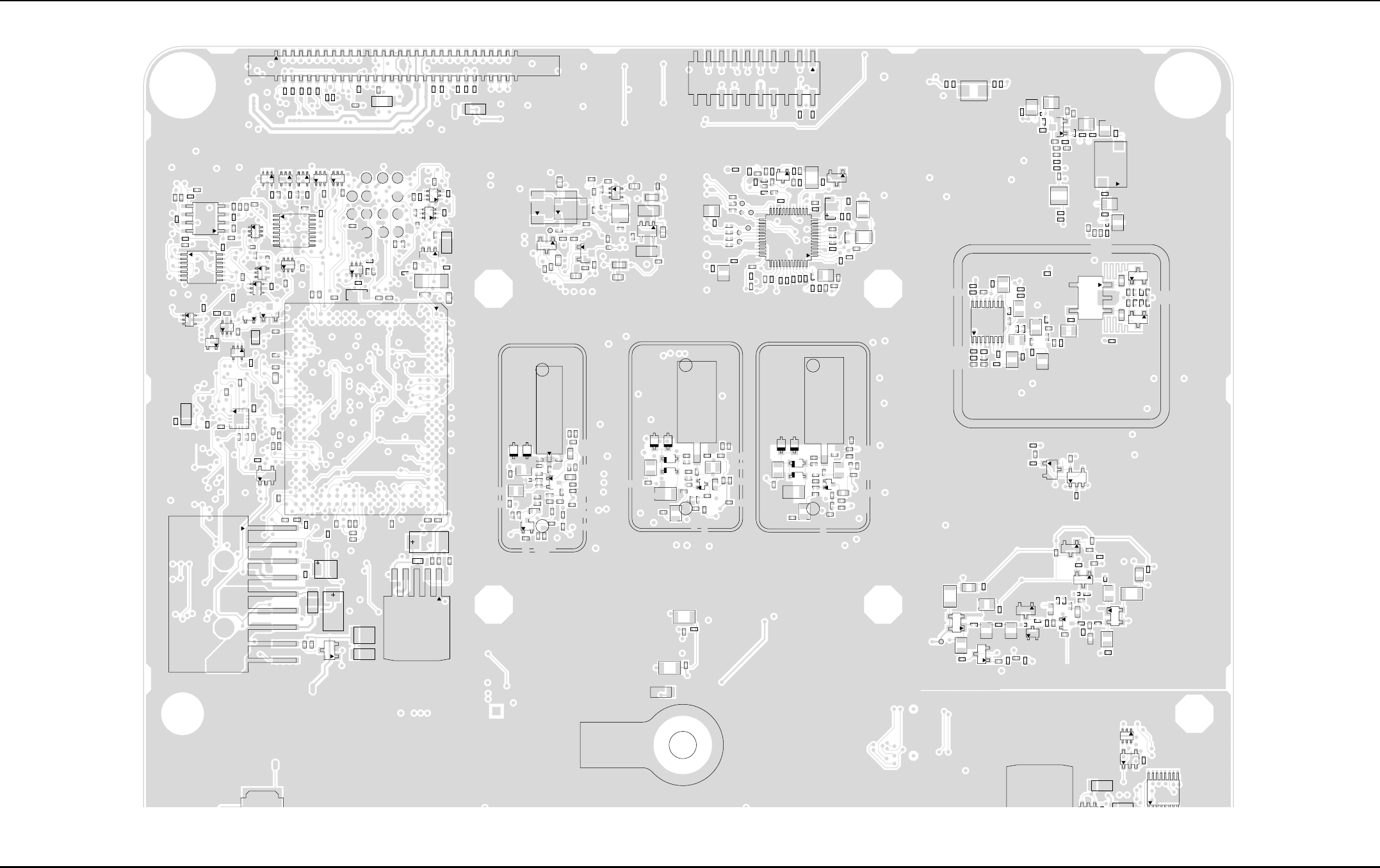
7-116 Schematics, Component Location Diagrams, and Parts Lists: HUE4039A/HUE4043A (UHF Range 1) Main Board
May 25, 2005 6881096C74-B
Figure 7-82. HUE4043A Main Board Layout—Side 1 Top
C0100
C0101
C0105
C0202
C0204
C0207
C0212
C0213
C0214
C0217
C0220
C0223
C0224
C0234
C0242
C0243
C0301
C0312
C0314
C0315
C0420
C0471
C0502
C0503
C0519
C0531
C0532
C0533
C0553
C0554
C0600
C0603
C0604
C0606
C0610
C0611
C0613
C0614
C0615
C0616
D0401
D0402
Q0200
Q0406
Q0508
Q0610
Q0611
Q0612
Q0613
R0101
R0102
R0103
R0104
R0106
R0109
R0110
R0111 R0113
R0114
R0115
R0116
R0117
R0119
R0120
R0121 R0122
R0123
R0124
R0125
R0200
R0204
R0205
R0213
R0220
R0222
R0224
R0300
R0301
R0303
R0304
R0305
R0310
R0404
R0405
R0406
R0422
R0430
R0431
R0434
R0435
R0441
R0442
R0445
R0505
R0508
R0509
R0517
R0527
R0532
R0551
R0552
R0553
R0620
R0621
R0622
R0623
R0624
R0625
R0626 R0627
R0628
R0629
R0630
R0631
R0632
R0634 R0635
R0636
R0639
TP0400
TP0401
TP0402
TP0403
TP0407
TP0408
TP0409
TP0410
TP0411
TP0412
TP0413
TP0414
TP0415
123456789101112131415161718
1817161514131211109 8 7 6 5 4 3 2
A
B
C
D
E
F
G
N
M
L
K
J
I
H
R
S
T
U
V
W
X
P
Z
YY
Z
P
X
W
V
U
T
S
R
H
I
J
K
L
M
N
G
F
E
D
C
B
A
U0001
U0102
43
6
U0203
43
6U0208
43
6
U0209
5
9
13
U0304
4
3
5
U0309
43
5
U0401
U0504
6
5
U0550
14
7
8
U0602
1
4
58
U0604
16 9
8
1U0606
U0607
U0608
4
3
5
U0609
4
3
5
U0610
4
3
5
U0611
Y0100
2
C5510
C5515
C5524
C5529
L5510
L5512
M5520
11
10
9
U0204
C0436
C0437
C0442
C0444
C0446
C0448
C0450
C0452
C0455
C0457
C0458
C0461
C0463
C0476
C0477
59
60
2J0401
R0415
R0421
C0703
C0705
J0501
C5002
C5005
C5007
C5008
C5009
C5010
C5012
C5013
C5015
C5016
C5017
C5019
C5020
C5021
C5022
C5023
C5024
C5026
C5027
C5028
C5030
C5046
C5051
C5052
C5061
C5064
C5065
C5066
C5067
C5068
C5069
C5070
C5071
CLKOUT
D5003
DOUTA
E5001
E5006
E5007
FS
L5002
L5003
L5004
L5012
L5013
L5015
PC
PD
PE
Q5003
R5000
R5001
R5003
R5005
R5014
R5015
R5016
R5017
R5018
R5019
R5020
R5025
R5026
R5027
R5028
R5030
R5031
R5032
R5033
R5034
R5035
1
37
25
13
U5002
C5750
C5752
C5754
C5757
C5758 C5759
C5760
C5761
C5762
C5765
C5768
C5771
C5815
C5817
L5751
L5753
L5755
Q5750
Q5751
R5750R5751
R5752
R5753
R5754
R5758
R5759
R5761
R5762
R5763
R5764
R5765
R5766
R5767
TP5788
U5750
U5751
2
3
4Y5750
Y05751
C5400
C5401
C5402
C5403
C5404
C5405
C5406
C5408
C5410
C5411
C5412
C5413
C5414
C5417
C5418
C5425
C5426
C5427
C5428
C5429
C5430
E5400
L5400
L5401
L5403
L5404
L5406
L5407
L5408
Q5401
R5400
R5401
R5402
R5403
R5404
R5411
R5412
R5413
R5414
R5415
SH5250
2
3
456
Y5400
C0921
C
C0990
C0991
Q0960
6
U
16 9
8
1U0959
U0962
U0965
C5280
C5329
C5333
C5343
C5345
C5350
C5351
C5352
C5353
C5354
C5355
C5356
C5357
C5358
C5359
C5362
C5374
C5375 C5378
C5380
C5381
C5382
C5383
C5385
C5388
D5380
D5381
L5302
L5305
L5306
L5307
L5380
L5383
L5385
L5389
L5392
R5321
R5327
R5328
R5329
R5380
R5381
R5382
R5383 R5384
R5385
R5386
R5388
15
43
T5380
1
16
8
9
U5303
C5305
C5365
C5366
Q5257
R5311
R5333
U5300
C5282
C5283
C5284
C5285
C5287
C5288
C5289
C5290
C5291
C5292
C5293
C5294
C5295
C5296
C5297
C5299
C5300
C5301
C5302
C5303
C5363
C5364
D5280
D5300
D5302
D5311
L5280
L5281
L5282
L5283
L5284
L5285
L5286
L5287
L5288 L5289
L5290
Q5250
Q5251
Q5252
Q5253
R5300
R5301
R5302
R5303
R5304
R5305
R5306
R5307
R5308
R5309
R5310
R5330
R5332
TP5301
C5900
C5901
C5904
C5905
C5906
C5907
C5908
C5910
C5911
C5912
C5913
C5914
C5915
D5901
D5902
D5903
D5904
L5900
L5901
L5902
L5904
L5905
Q5901
R5900
R5903
R5904
R5905
R5909
R5910
R5911
R5948
SH5901
Y5900
C5916
C5917
C5920
C5922
C5923
C5924
C5925
C5926
C5927
C5928
C5929
C5930
C5931
D5905
D5906
D5909
D5910
L5906
L5908
L5909
L5912
L5913
Q5903
R5912
R5915
R5916
R5918
R5919 R5920
R5922
R5923
SH5902
Y5901
C5826
C5829
C5830
C5831
C5834
C5835
C5838
C5840
C5842
C5844
C5846
C5847
C5850
C5851
C5854
C5859
C5860
C5861
C5862
C5863
D5828
D5832
L5826
L5828
L5830
L5832
L5834
Q5826
Q5829
R5826
R5828
R5830
R5832
R5834
R5838
R5840
R5842
R5851
R5852
R5853
R5854
R5855
SH5820
U5826
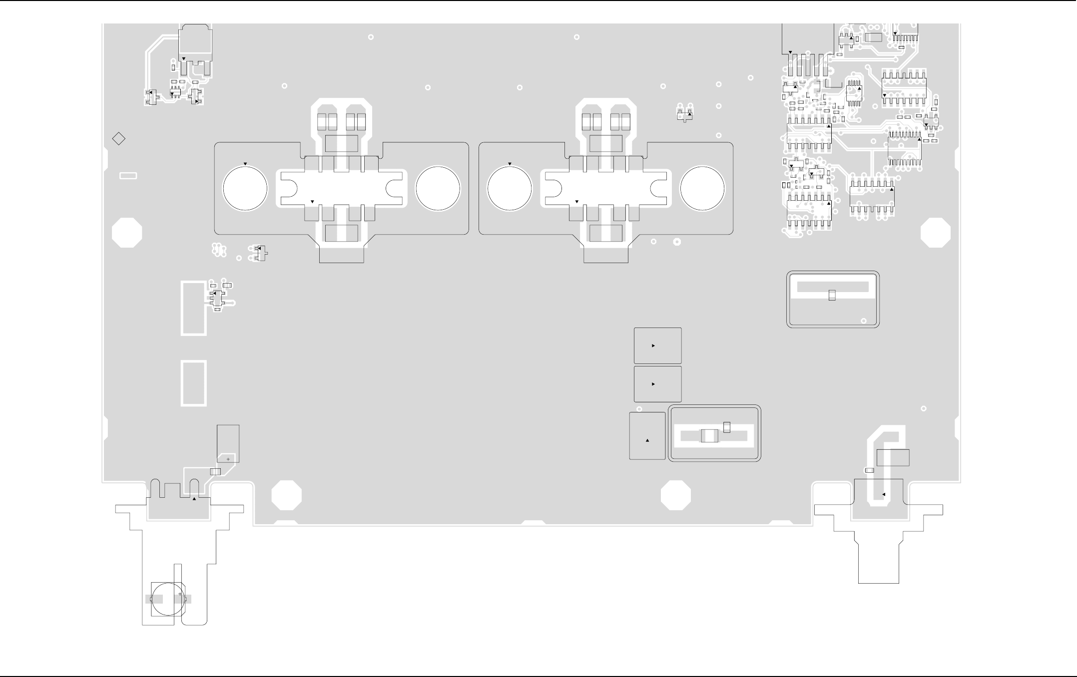
Schematics, Component Location Diagrams, and Parts Lists: HUE4039A/HUE4043A (UHF Range 1) Main Board 7-117
6881096C74-B May 25, 2005
Figure 7-83. HUE4043A Main Board Layout—Side 1 Bottom
C0536
C5571
C5572
M5541
3
1
Q0503
Q0507
Q5541
R0515
R0530 R0531
R5554
R5555
R5556
R5559
R5560
R5573
R5578
SC5500
SC5501
U5561
U5563
VR0501
VR0502
2
C5708
C5719
1
M5700
1
M5701
1
M5702
SH5703
M5540
Q5540
R5544
R5545
R5547
R5550
R5551
R5562
U5560
3
2
J5701
R5710
R5713
C5722
SH5701
C5569
C5575
J5500
R5576
C0905
R0909
R0918
R0919
R0920
R0921
R0922
R0923
11
1
20
10
U0953
14
U0955
7
8
14 U0960
U0970
C0922
C0968
C0969
C0970
C0975
C0976
C0983
D0950
D0951
R0915
R0935
R0978
R0990
R0994
7
8
7
814
U0957
C0940
C0943
C0981
C0990
5
U0951
8
1
U0959
U0962
C0900
C0923
C0955
C0962
C0967
D0954
R0902
R0903
R0908
R0924
R0948
R0963
R0964
R0965
R0967
R0968
R0970
R0973
R0980
R0986
10
6
5
U0952
7U0956
814
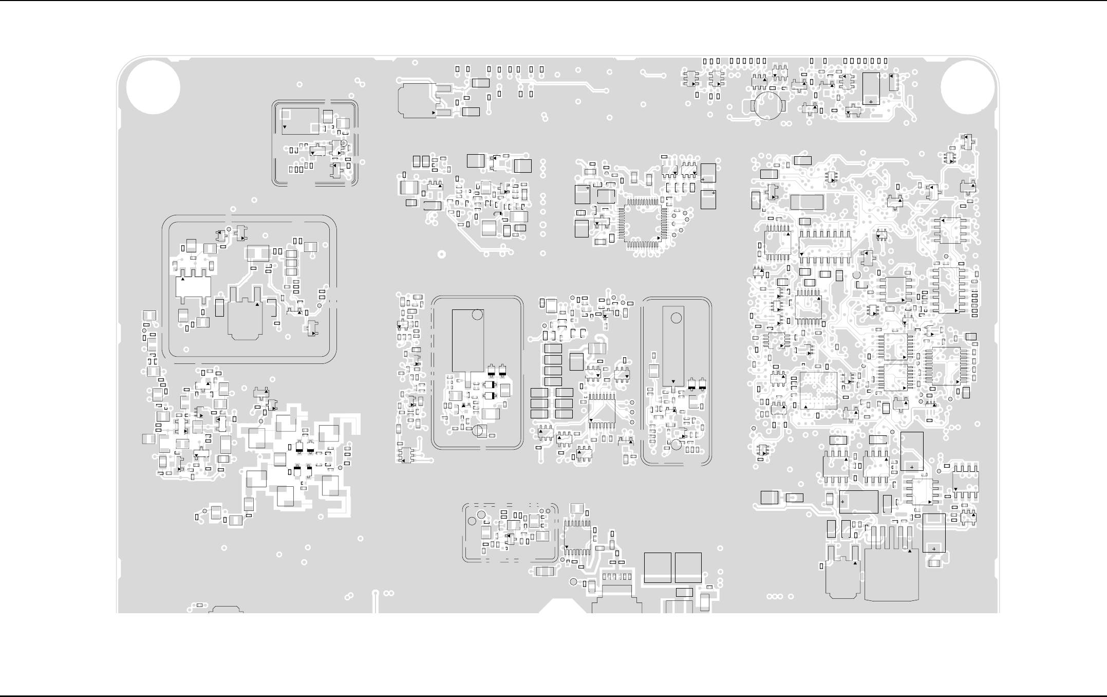
7-118 Schematics, Component Location Diagrams, and Parts Lists: HUE4039A/HUE4043A (UHF Range 1) Main Board
May 25, 2005 6881096C74-B
Figure 7-84. HUE4043A Main Board Layout—Side 2 Top
C0201
C0507
Q0402
Q0403
Q0502
Q0504
Q0505
R0409
R0420
R0425
14
5
8
U0202
U0603
VR0420
C0421
C0426
C0504
F0400
Q0405
R0433
R0507
R0524
VR0500
C0107 C0306
R0127
14
7
8
U0104 16
18
9
U0305
C0200
C0205
C0230
C0231
C0236
C0237
R0211
R0215
R0223
R0229
R0230
TP0200
C0103
C0104
C0307
C0308
C0309
C0310
C0524
R0500
14
7
8
U0103
C0109 R0128
R0703
4
3
5
U0105
Q0501
R0502
R0523
11
10
U0200
8
7
8
1
4
58
U0506
C0203
C0232
C0233
C0235
C0238
C0239
C0500
R0210 R0219
R0228
R0235 R0236
R0306
R0307
R0503
7
814
U0201
5
4
32
U0308
C0311
C0313
R0227
43
5
U0307
C0525
TP0500
C0208
C0209
C0216
C0226
C0240
Q0506
R0206
R0208
R0209
R0212
R0216
R0218
TP0204
TP0419
1
20
4
3
6
14
7
U0300
14
U0303
R0225
TP0203
TP0420
U0210
C5522
C5526
C5527
R5527
R552
8
R5585
R
0
R
R0934
2
C5407
C5409
C5415
C5416
C5419
C5420 C5421
C5422
C5423
C5424
C5431
C5432
C5433
D5400
L5402
L5411
Q5402
R5405 R5406
R5407
R5420
SH5400
U5400
23
4
5
6Y5401
C5311
C5315
C5318
C5323
C5324
C5325
C5330
C5334
C5335
C5337
C5338
C5340
C5346
C5348
C5360
C5361
C5377
C5379
C5386
C5390
C5391
D5282
D5306
D5307
L5299
L5303
L5382
L5384
L5387
L5388
L5390
Q5258
R5319
R5322 R5323
R5324
R5325
R5326
R5387
15
43
T5381
TP5302
TP5304 3
2
1
U5301
SH5380
C5250
C5251
C5252
C5253
C5254
C5255
C5256
C5257
C5258
C5259
C5304
C5306
C5307
C5308
C5309
C5310
C5312
C5313
C5314
C5316
C5317
C5319
C5320
C5321
C5322
C5326
C5327
C5328
C5331
C5332
C5336
C5339
C5341
C5342
C5344
C5347
C5349
C5367
C5368
C5389
D5250
D5251
D5252
D5253
D5281
D5304
D5305
D5313
L5237
L5250
L5251
L5252
L5253
L5254
L5255
L5256
L5258
L5291
L5292
L5293
L5294
L5295
L5296
L5297
L5298
L5300
L5301
L5304
L5308
L5381
L5386 Q5254
Q5255
Q5256 R5250
R5251
R5252
R5253
R5254
R5255 R5256
R5312
R5313
R5314
R5315
R5316
R5317
R5318
R5334
R5335
R5336
TP5250
TP5251
TP5252
TP5303
3
4
5
U5302
L5257
C0520
C0521
C0522
C0523
C0700 C0701
C0702
C0704
C0706
C0708 C0709
C0710 C0711
C0712
C0713
C0714
3
2
1
U0505 C0422
C0423
C0424
C0428
C0431
C0432
C0433 C0434
C0435
C0438
C0439
C0440
C0441
C0443
C0445
C0447
C0449
C0451
C0453
C0454
C0456
C0459
C0460
C0462
C0464
C0467
C0470
C0475
C0478
C0479
L0400
R0416
R0417
R0418
4
5
8
VR0411
VR0412
VR0414
VR0415
VR0418
VR0422
VR0423
VR0424
VR0425
VR0426
C5751 C5753
C5755
C5756C5763
C5764
C5766
C5767
C5769
C5770
C5772
C5773
C5774
C5775
C5776
C5777
C5778
C5788
C5789
C5816
D5750 D5751
L5750
L5752
L5754
L5756
Q5752
R5755
R5768
R5771
R5773
TP5760
TP5787
TP5789
TP5790
TP5791
TP5792
TP5799
1
37
25
13
U5752
C5001
C5003
C5004
C5006
C5011
C5014
C5018
C5025
C5029
C5032
C5033
C5034
C5037
C5038
C5039
C5040
C5041
C5044
C5045
C5048
C5049
C5050
C5056
C5057 C5058
C5059
C5060
C5062
C5063
C5072
C5073
D5002
E5002
E5003
E5004
E5005
E5008
E5009
L5001
L5006 L5007
L5008
L5010
L5053
Q5001
Q5002
R5002
R5006
R5008
R5010
R5011
R5013
R5022
R5023
R5029
R5050
R5051
U5001
C5909
C5919
C5921
C5932
C5937
C5948
C5949
C5950
C5951
C5956
C5957
C5958
C5959
C5960
C5961
D5900
L5916
L5917
L5918
L5919
L5920
L5921
L5922
Q5902
Q5904
Q5906
R5902
R5914
R5917
R5921
R5926 R5929
R5933
R5937
R5938
R5939
R5940
R5941
R5949
R5950
C5936
C5938
C5939
C5940
C5941
C5942
C5943
C5944
C5945
C5946
C5947
D5907
D5908
D5911
D5912
L5907
L5910
L5911
L5914
L5915
Q5905
R5924
R5927
R5928
R5930
R5931
R5932
R5934
R5935
SH5900
Y5902
C5933 C5935
C5500
C5501
C5502
C5503
C5504
C5505
C5506
C5507
C5508
C5509
C5512
L5500
L5501
L5502
L5503
Q5501
R5500
R5501
R5502
R5503
R5504
R5505
R5506
R5507
R5508
SH5500
TP5500
TP5501
TP5502
TP5503
C5511
C5513
C5514
C5516
C5517
C5518 C5519
C5520
C5523
C5525
L5511
L5513
L5514
3
R5510
R5511
R5520
R5521
R5522
R5523
R5524
R5525
R5526
TP5510
TP5520
1
16
8
9
U5500
C5779
C5780
C5781
C5782
C5783
C5784
C5785
C5786
C5787
C5790
C5791
C5792
C5793
C5794
C5795
C5796
C5797
C5798 C5799
C5800
C5801
C5802
C5803
C5804
C5805C5806
C5807
C5808
C5809
C5810
C5811
C5812
C5813
C5856
D5833
E6750
L5757
L5758
L5759
L5760
L5833
Q5706
Q5707
Q5708
Q5709
Q5710
Q5755
R5769
R5770
R5772 R5774
R5775
R5776
R5777
R5778
R5779
R5780
R5781
R5782
R5783
R5784 R5785
R5786
TP5783
TP5793
TP5794
TP5795
TP5796
TP5797
TP5798
16
8
9
U5753
C5825
C5827
C5828
C5832
C5833
C5836
C5837
C5839
C5841
C5843
C5845
C5848
C5849
C5852
C5853
C5855
C5857
C5858
D5827
D5831
L5825
L5827
L5829L5831
Q5825
Q5828
R5825
R5827
R5829
R5831
R5833
R5837
R5839
R5841
R5843
R5845
R5846
R5848
R5849
R5850
SH5821
U5825
C0302 C0305
C0510
C0513
C0529
C0537
C0605
C0728
C0731
Q0500
R0107
R0108
R0221
R0403
R0443
R0444
R0504
R0514
R0516
R0520
TP0206
TP0418
43
5
U0605
G7
G1
A7
A1
U0701
C0102
C0106
C0108
C0601
C0715
C0716
C0717
C0718
C0719
C0720
C0721
C0722
C0724
C0726
C0727
C0729 C0730
C0732
C0733
C0740
C0741
C0742
C0743
FL0700
R0126
R0129
R0130
R0700
R0701
R0705
R0739
R0740
R0741
R0742 R0743
TP0950
U0106
43
5
U0601
U0700
43
6
U0703
43
6
U0704
43
6
U0705
U0740
C0518 C0535
C0550
C0551
R0519
6
5
U0500
3
2
1
U0503
C0210
C0211
C0215
C0221
C0227
C0244
C0505
C0506
C0512
C0514
C0515
C0516
C0517
C0526
C0527
C0528
C0534
R0201
R0231
R0506
R0510
R0511
R0512
R0513
R0518
R0521 R0522
R0526
R0528 R0529
TP0205
14
58
U0206
U0207
1
4
58
U0501
1
4
58
U0502
1
4
58
U0507
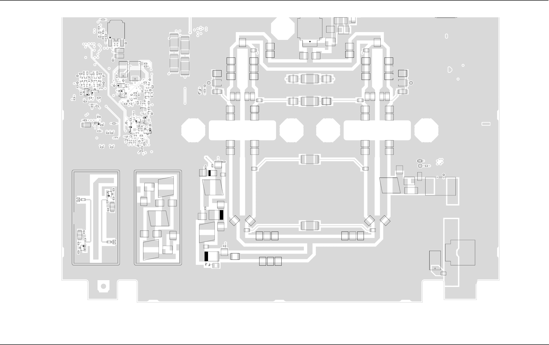
Schematics, Component Location Diagrams, and Parts Lists: HUE4039A/HUE4043A (UHF Range 1) Main Board 7-119
6881096C74-B May 25, 2005
Figure 7-85. HUE4043A Main Board Layout—Side 2 Bottom
C5711
C5712
C5713
C5714
C5720
C5721
L5706
L5707
L5708
L5712
L5713
SH5702
C5551
C5552
C5553
C5554
C5555
C5556
C5562
C5578
C5579
C5584
C5585 C5588
C5589
C5701
C5702
C5703
C5704
C5705
C5706
C5707
C5709
C5723
C5724
D5706
D5707
D5709
L5701
L5702
L5703
L5704
L5705
L5716
L5717 R5564
R5565
C5559
C5560
C5561
C5563
C5564
C5565
C5566
C5567
C5568
C5570
C5574
C5586
C5587
L5543
L5544
R5567
R5568
R5570
R5571
R5574
R5575
R5577
R5580
TP5543
TP5544
VR5500
C5521
C5530 C5531
C5534
C5535
C5536
C5537
C5540
C5546
C5547
C5548
C5549
C5557
C5577
C5594
C5595
C5596
C5598
C5603
L5520
L5521
R5527
5
528
R5541
R5552
R5553
R5557
R5558
R5566 R5572
R5581
R5583
TP5541
C5532
C5533
C5538 C5539
C5590
C5591
C5592
C5593
C5601
R5540
R5582R5584
R5586 R5587
C5543
C5544 C5545
C5573
C5576
C5602
R5542
R5543
R5546
R5548
R5549
R5563
R5579
TP5540
TP5542
C5541
C5550
C5597
C5542
C5715
C5716
C5717
C5718
D5704
D5705
L5714
L5715
R5702
R5703
R5704
R5705
R5706
R5707
R5708
R5709
R5711
R5712
SH5704
C0920
C0941
C0942
C0956
C0982
C0988
C0989
R0901
R0910
R0911
R0912
R0913 R0914
R0934
TP0901
TP0902
3
2
1
U0966
R0954
R0993
TP0900
C0924
C0952
C0959
C0971
C0972
C0980
Q0951
4
5
8
Q0952
R0942
R0943
R0944
R0945
R0947
R0955
R0971
R0972
R0974
R0975
R0976
R0984
R0985
R0991
R1000
TP0951
TP0952
TP0954 TP0955
TP0958
TP0960
TP0961
C0957
C0963
C0966
C0973
C0974
C0978
C0979
D0952
Q0954
Q0955
R0900
R0916
R0917
R0932
R0933
R0946
R0950
R0953
R0960
R0977
R0981
R0982
R0983 R0988
R0989
R0992
R0995
R0996
R0997
R0998
TP0953
TP0956
TP0957
TP0959
TP0962
TP0963
TP0964
43
5
U0958
R0999
TP0942
C0901
C0902
C0903
C0904
C0906
C0930
C0933
C0934
C0935
C0936
C0937
C0945
C0960
C0961
C0964C0965
C0984
C0985
C0986 C0987
Q0970
Q0971
R0904
R0905
R0906
R0907
R0930
R0931
R0936
R0937
R0938
R0939
R0940
R0941
R0961
R0962
R0966
R0979
R0987
TP0930
TP0931
TP0936
TP0937
TP0938
TP0939
TP0940
TP0941
4
3
5
U0954
6
5
20
Q5520
7-120 Schematics, Component Location Diagrams, and Parts Lists: HUE4039A/HUE4043A (UHF Range 1) Main Board
May 25, 2005 6881096C74-B
HUE4043A Main Board Parts List
Reference
Designator
Motorola
Part Number Description
C0100 2113743N32 CAP CHIP 18.0 PF 5% COG
C0101 2113743N32 CAP CHIP 18.0 PF 5% COG
C0102 2113743M24 CAP CHIP 100000 PF +80-
20% Y5V
C0103 2113743M24 CAP CHIP 100000 PF +80-
20% Y5V
C0104 2113743M24 CAP CHIP 100000 PF +80-
20% Y5V
C0105 2113743M24 CAP CHIP 100000 PF +80-
20% Y5V
C0106 2113743N50 CAP CHIP 100 PF 5% COG
C0107 2113743L09 CAP CHIP 470 PF 10% X7R
C0108 2113743M24 CAP CHIP 100000 PF +80-
20% Y5V
C0109 2113743N32 CAP CHIP 18.0 PF 5% COG
C0200 2113928E01 CAP CER CHIP 1.0 UF 10 %
10V
C0201 2113743M24 CAP CHIP 100000 PF +80-
20% Y5V
C0202 2113743M24 CAP CHIP 100000 PF +80-
20% Y5V
C0203 2113928S04 CAP CER CHIP 0.100UF 10V
0402
C0204 2185802B01 CAP 10V 4.7UF
C0207 2113743N38 CAP CHIP 33.0 PF 5% COG
C0208 2113928E01 CAP CER CHIP 1.0 UF 10 %
10V
C0209 2113743M24 CAP CHIP 100000 PF +80-
20% Y5V
C0210 2113743M24 CAP CHIP 100000 PF +80-
20% Y5V
C0211 2113743N50 CAP CHIP 100 PF 5% COG
C0212 2113743M24 CAP CHIP 100000 PF +80-
20% Y5V
C0213 2113743M24 CAP CHIP 100000 PF +80-
20% Y5V
C0214 2113741N69 CAP CHIP CL2 X7R 10%
100000
C0215 2113928S04 CAP CER CHIP 0.100UF 10V
0402
C0216 2113743M24 CAP CHIP 100000 PF +80-
20% Y5V
C0217 2113743L29 CAP CHIP 3300 PF 10% X7R
C0220 2311049A57 CAP TANT CHIP A/P 10UF
10% 16V
C0221 2311049C06 CAP TANT CHIP 22 UF 35V
20%
C0223 2185802B01 CAP 10V 4.7UF
C0224 2113743M24 CAP CHIP 100000 PF +80-
20% Y5V
C0226 2113928S04 CAP CER CHIP 0.100UF 10V
0402
C0227 2113743M24 CAP CHIP 100000 PF +80-
20% Y5V
C0230 2113743L09 CAP CHIP 470 PF 10% X7R
C0231 2113743L01 CAP CHIP 220 PF 10% X7R
C0232 2113743L09 CAP CHIP 470 PF 10% X7R
C0233 2113743L01 CAP CHIP 220 PF 10% X7R
C0234 2113928S04 CAP CER CHIP 0.100UF 10V
0402
C0235 2113743L09 CAP CHIP 470 PF 10% X7R
C0236 2113743L09 CAP CHIP 470 PF 10% X7R
C0237 2113743L01 CAP CHIP 220 PF 10% X7R
C0238 2113743L01 CAP CHIP 220 PF 10% X7R
C0239 2113743M24 CAP CHIP 100000 PF +80-
20% Y5V
C0240 2113928S04 CAP CER CHIP 0.100UF 10V
0402
C0242 2113928S04 CAP CER CHIP 0.100UF 10V
0402
C0243 2113945B01 CAP CER CHIP 6800 PF 25V
10%
C0244 2113945B01 CAP CER CHIP 6800 PF 25V
10%
C0301 2113743M24 CAP CHIP 100000 PF +80-
20% Y5V
C0302 2113743M24 CAP CHIP 100000 PF +80-
20% Y5V
C0305 2113743M24 CAP CHIP 100000 PF +80-
20% Y5V
C0306 2113928E01 CAP CER CHIP 1.0 UF 10 %
10V
C0308 2113928E01 CAP CER CHIP 1.0 UF 10 %
10V
C0309 2113928E01 CAP CER CHIP 1.0 UF 10 %
10V
C0310 2113928E01 CAP CER CHIP 1.0 UF 10 %
10V
Reference
Designator
Motorola
Part Number Description
C0311 2113743M24 CAP CHIP 100000 PF +80-
20% Y5V
C0312 2113743M24 CAP CHIP 100000 PF +80-
20% Y5V
C0313 2113743M24 CAP CHIP 100000 PF +80-
20% Y5V
C0314 2113743M24 CAP CHIP 100000 PF +80-
20% Y5V
C0315 2113928E01 CAP CER CHIP 1.0 UF 10 %
10V
C0420 2185802B01 CAP 10V 4.7UF
C0421 2113741B13 CAP CHIP CL2 X7R REEL 470
C0422 2113743N38 CAP CHIP 33.0 PF 5% COG
C0423 2113743N38 CAP CHIP 33.0 PF 5% COG
C0424 2113743N38 CAP CHIP 33.0 PF 5% COG
C0426 2113741B13 CAP CHIP CL2 X7R REEL 470
C0428 2113743N50 CAP CHIP 100 PF 5% COG
C0431 2113743N50 CAP CHIP 100 PF 5% COG
C0432 2113743N50 CAP CHIP 100 PF 5% COG
C0433 2113743N50 CAP CHIP 100 PF 5% COG
C0434 2113743N50 CAP CHIP 100 PF 5% COG
C0435 2113743L09 CAP CHIP 470 PF 10% X7R
C0436 2113741B13 CAP CHIP CL2 X7R REEL 470
C0437 2113741B13 CAP CHIP CL2 X7R REEL 470
C0438 2113743L09 CAP CHIP 470 PF 10% X7R
C0439 2113743N50 CAP CHIP 100 PF 5% COG
C0440 2113743N50 CAP CHIP 100 PF 5% COG
C0441 2311049C47 CAP TANT CHIP 22.0UF 10%
16V
C0442 2113743N38 CAP CHIP 33.0 PF 5% COG
C0443 2113743N38 CAP CHIP 33.0 PF 5% COG
C0444 2113743N38 CAP CHIP 33.0 PF 5% COG
C0445 2113743N38 CAP CHIP 33.0 PF 5% COG
C0446 2113743N50 CAP CHIP 100 PF 5% COG
C0447 2113743N50 CAP CHIP 100 PF 5% COG
C0448 2113743N50 CAP CHIP 100 PF 5% COG
C0449 2113743N50 CAP CHIP 100 PF 5% COG
C0450 2113743N38 CAP CHIP 33.0 PF 5% COG
C0451 2113743N38 CAP CHIP 33.0 PF 5% COG
C0452 2113743N38 CAP CHIP 33.0 PF 5% COG
C0453 2113743N38 CAP CHIP 33.0 PF 5% COG
C0454 2113743N38 CAP CHIP 33.0 PF 5% COG
Reference
Designator
Motorola
Part Number Description
C0455 2113743N38 CAP CHIP 33.0 PF 5% COG
C0456 2113743N38 CAP CHIP 33.0 PF 5% COG
C0457 2113743N38 CAP CHIP 33.0 PF 5% COG
C0458 2113743N38 CAP CHIP 33.0 PF 5% COG
C0459 2113743N38 CAP CHIP 33.0 PF 5% COG
C0460 2113743N50 CAP CHIP 100 PF 5% COG
C0461 2113743L01 CAP CHIP 220 PF 10% X7R
C0462 2113743L01 CAP CHIP 220 PF 10% X7R
C0463 2113743N38 CAP CHIP 33.0 PF 5% COG
C0464 2113743N38 CAP CHIP 33.0 PF 5% COG
C0467 2113743N50 CAP CHIP 100 PF 5% COG
C0470 2113743N38 CAP CHIP 33.0 PF 5% COG
C0471 2113743N50 CAP CHIP 100 PF 5% COG
C0475 2113743N50 CAP CHIP 100 PF 5% COG
C0476 2113743N50 CAP CHIP 100 PF 5% COG
C0477 2113743N50 CAP CHIP 100 PF 5% COG
C0478 2113743N50 CAP CHIP 100 PF 5% COG
C0479 2113743N50 CAP CHIP 100 PF 5% COG
C0500 2113743N50 CAP CHIP 100 PF 5% COG
C0502 2113743N50 CAP CHIP 100 PF 5% COG
C0503 2113743N50 CAP CHIP 100 PF 5% COG
C0504 2113741N69 CAP CHIP CL2 X7R 10%
100000
C0505 2113743L41 CAP CHIP 10000 PF 10% X7R
C0506 2113743L41 CAP CHIP 10000 PF 10% X7R
C0507 2113743M24 CAP CHIP 100000 PF +80-
20% Y5V
C0510 2185802B01 CAP 10V 4.7UF
C0512 2113743M24 CAP CHIP 100000 PF +80-
20% Y5V
C0513 2311049A43 CAP TANT CHIP 150 10 6
C0514 2311049A43 CAP TANT CHIP 150 10 6
C0515 2113743M24 CAP CHIP 100000 PF +80-
20% Y5V
C0516 2113743M24 CAP CHIP 100000 PF +80-
20% Y5V
C0517 2185802B01 CAP 10V 4.7UF
C0518 2185802B01 CAP 10V 4.7UF
C0519 2113743L41 CAP CHIP 10000 PF 10% X7R
C0520 2113743M24 CAP CHIP 100000 PF +80-
20% Y5V
C0521 2185802B01 CAP 10V 4.7UF
Reference
Designator
Motorola
Part Number Description
Schematics, Component Location Diagrams, and Parts Lists: HUE4039A/HUE4043A (UHF Range 1) Main Board 7-121
6881096C74-B May 25, 2005
C0522 2185802B01 CAP 10V 4.7UF
C0523 2113743M24 CAP CHIP 100000 PF +80-
20% Y5V
C0524 2113743M24 CAP CHIP 100000 PF +80-
20% Y5V
C0525 2113928E01 CAP CER CHIP 1.0 UF 10 %
10V
C0526 2113743L41 CAP CHIP 10000 PF 10% X7R
C0527 2185802B01 CAP 10V 4.7UF
C0528 2113743M24 CAP CHIP 100000 PF +80-
20% Y5V
C0529 2185802B01 CAP 10V 4.7UF
C0531 2113741N69 CAP CHIP CL2 X7R 10%
100000
C0532 2113741Y32 CAP CER 1,000,000 10% 50V
C0533 2311049C47 CAP TANT CHIP 22.0UF 10%
16V
C0534 2113743M24 CAP CHIP 100000 PF +80-
20% Y5V
C0535 2113743M24 CAP CHIP 100000 PF +80-
20% Y5V
C0536 2113743N50 CAP CHIP 100 PF 5% COG
C0550 2113741N69 CAP CHIP CL2 X7R 10%
100000
C0551 2113741Y32 CAP CER 1,000,000 10% 50V
C0553 2311049C47 CAP TANT CHIP 22.0UF 10%
16V
C0554 2113743E20 CAP CHIP .10 UF 10%
C0600 2113743M24 CAP CHIP 100000 PF +80-
20% Y5V
C0601 2113743M24 CAP CHIP 100000 PF +80-
20% Y5V
C0603 2113743M24 CAP CHIP 100000 PF +80-
20% Y5V
C0604 2113743M24 CAP CHIP 100000 PF +80-
20% Y5V
C0605 2113743M24 CAP CHIP 100000 PF +80-
20% Y5V
C0606 2113743M24 CAP CHIP 100000 PF +80-
20% Y5V
C0610 2113743M24 CAP CHIP 100000 PF +80-
20% Y5V
C0611 2113743M24 CAP CHIP 100000 PF +80-
20% Y5V
C0613 2113743M24 CAP CHIP 100000 PF +80-
20% Y5V
Reference
Designator
Motorola
Part Number Description
C0614 2113743M24 CAP CHIP 100000 PF +80-
20% Y5V
C0615 2113743M24 CAP CHIP 100000 PF +80-
20% Y5V
C0616 2113743N50 CAP CHIP 100 PF 5% COG
C0700 2113743N50 CAP CHIP 100 PF 5% COG
C0701 2113743N50 CAP CHIP 100 PF 5% COG
C0702 2113743N50 CAP CHIP 100 PF 5% COG
C0703 2113743N50 CAP CHIP 100 PF 5% COG
C0704 2113743N50 CAP CHIP 100 PF 5% COG
C0705 2113743N50 CAP CHIP 100 PF 5% COG
C0706 2113743N50 CAP CHIP 100 PF 5% COG
C0708 2113743N50 CAP CHIP 100 PF 5% COG
C0709 2113743N50 CAP CHIP 100 PF 5% COG
C0710 2113743N50 CAP CHIP 100 PF 5% COG
C0711 2113743N50 CAP CHIP 100 PF 5% COG
C0712 2113743N50 CAP CHIP 100 PF 5% COG
C0713 2113743L01 CAP CHIP 220 PF 10% X7R
C0714 2113743L01 CAP CHIP 220 PF 10% X7R
C0715 2113743N50 CAP CHIP 100 PF 5% COG
C0716 2113743N50 CAP CHIP 100 PF 5% COG
C0717 2113743N50 CAP CHIP 100 PF 5% COG
C0718 2113743M24 CAP CHIP 100000 PF +80-
20% Y5V
C0719 2113743L01 CAP CHIP 220 PF 10% X7R
C0720 2113743M24 CAP CHIP 100000 PF +80-
20% Y5V
C0721 2113743M24 CAP CHIP 100000 PF +80-
20% Y5V
C0722 2113928E01 CAP CER CHIP 1.0 UF 10 %
10V
C0724 2113743M24 CAP CHIP 100000 PF +80-
20% Y5V
C0726 2113743N50 CAP CHIP 100 PF 5% COG
C0727 2113743M24 CAP CHIP 100000 PF +80-
20% Y5V
C0728 2113743M24 CAP CHIP 100000 PF +80-
20% Y5V
C0729 2113743M24 CAP CHIP 100000 PF +80-
20% Y5V
C0730 2113743M24 CAP CHIP 100000 PF +80-
20% Y5V
C0731 2113743M24 CAP CHIP 100000 PF +80-
20% Y5V
Reference
Designator
Motorola
Part Number Description
C0732 2113743N50 CAP CHIP 100 PF 5% COG
C0733 2113743M24 CAP CHIP 100000 PF +80-
20% Y5V
C0740 2113743M24 CAP CHIP 100000 PF +80-
20% Y5V
C0741 2113743N50 CAP CHIP 100 PF 5% COG
C0742 2113743N50 CAP CHIP 100 PF 5% COG
C0903 2113743N26 CAP CHIP 10.0 PF 5% COG
C0905 2113743M24 CAP CHIP 100000 PF +80-
20% Y5V
C0920 2113743M24 CAP CHIP 100000 PF +80-
20% Y5V
C0922 2113743N50 CAP CHIP 100 PF 5% COG
C0923 2113743N50 CAP CHIP 100 PF 5% COG
C0936 2113743M24 CAP CHIP 100000 PF +80-
20% Y5V
C0937 2113743M24 CAP CHIP 100000 PF +80-
20% Y5V
C0940 2113743M24 CAP CHIP 100000 PF +80-
20% Y5V
C0941 2113743S01 CAP CER CHIP 1.0 UF 10%
16V
C0942 2113743S01 CAP CER CHIP 1.0 UF 10%
16V
C0943 2113743L41 CAP CHIP 10000 PF 10% X7R
C0945 2185802B01 CAP 10V 4.7UF
C0952 2113743E20 CAP CHIP .10 UF 10%
C0955 2113741N69 CAP CHIP CL2 X7R 10%
100000
C0956 2311049C06 CAP TANT CHIP 22 UF 35V
20%
C0957 2113743M24 CAP CHIP 100000 PF +80-
20% Y5V
C0959 2113743M24 CAP CHIP 100000 PF +80-
20% Y5V
C0960 2113743M24 CAP CHIP 100000 PF +80-
20% Y5V
C0961 2113743M24 CAP CHIP 100000 PF +80-
20% Y5V
C0963 2113743N50 CAP CHIP 100 PF 5% COG
C0964 2113743N50 CAP CHIP 100 PF 5% COG
C0965 2113743N50 CAP CHIP 100 PF 5% COG
C0966 2113743N50 CAP CHIP 100 PF 5% COG
C0968 2113743N50 CAP CHIP 100 PF 5% COG
C0969 2113743N50 CAP CHIP 100 PF 5% COG
Reference
Designator
Motorola
Part Number Description
C0970 2113743N50 CAP CHIP 100 PF 5% COG
C0972 2113743E20 CAP CHIP .10 UF 10%
C0973 2113928E01 CAP CER CHIP 1.0 UF 10 %
10V
C0974 2113743M24 CAP CHIP 100000 PF +80-
20% Y5V
C0975 2113743N50 CAP CHIP 100 PF 5% COG
C0976 2113743N50 CAP CHIP 100 PF 5% COG
C0978 2113743N50 CAP CHIP 100 PF 5% COG
C0979 2113743M24 CAP CHIP 100000 PF +80-
20% Y5V
C0980 2113743M24 CAP CHIP 100000 PF +80-
20% Y5V
C0981 2113743M24 CAP CHIP 100000 PF +80-
20% Y5V
C0982 2311049C47 CAP TANT CHIP 22.0UF 10%
16V
C0983 2113743N50 CAP CHIP 100 PF 5% COG
C0984 2113743M24 CAP CHIP 100000 PF +80-
20% Y5V
C0985 2113743M24 CAP CHIP 100000 PF +80-
20% Y5V
C0986 2113743M24 CAP CHIP 100000 PF +80-
20% Y5V
C0987 2113743M24 CAP CHIP 100000 PF +80-
20% Y5V
C0988 2113743M24 CAP CHIP 100000 PF +80-
20% Y5V
C0989 2113743M24 CAP CHIP 100000 PF +80-
20% Y5V
C0990 2185802B01 CAP 10V 4.7UF
C0991 2185802B01 CAP 10V 4.7UF
C5001 2113928N01 CAP CER CHIP 0.1UF 10%
6.3
C5002 2113743N28 CAP CHIP 12.0 PF 5% COG
C5003 2113743L41 CAP CHIP 10000 PF 10% X7R
C5004 2113928N01 CAP CER CHIP 0.1UF 10%
6.3
C5005 2113928N01 CAP CER CHIP 0.1UF 10%
6.3
C5006 2113928N01 CAP CER CHIP 0.1UF 10%
6.3
C5007 2113743N30 CAP CHIP 15.0 PF 5% COG
C5008 2113743L25 CAP CHIP 2200 PF 10% X7R
Reference
Designator
Motorola
Part Number Description
7-122 Schematics, Component Location Diagrams, and Parts Lists: HUE4039A/HUE4043A (UHF Range 1) Main Board
May 25, 2005 6881096C74-B
C5009 2113740F58 CAP CHIP REEL CL1 +/-30
200
C5010 2113743N50 CAP CHIP 100 PF 5% COG
C5011 2113743F18 CAP CHIP 2.2 UF 16V +80-
20%
C5012 2113743N50 CAP CHIP 100 PF 5% COG
C5013 2113743N50 CAP CHIP 100 PF 5% COG
C5014 2113743L41 CAP CHIP 10000 PF 10% X7R
C5015 2113743L41 CAP CHIP 10000 PF 10% X7R
C5017 2113743L41 CAP CHIP 10000 PF 10% X7R
C5018 2113743T19 CAP 10UF 16V CER 3225 X5R
C5019 2113743N50 CAP CHIP 100 PF 5% COG
C5020 2113743L17 CAP CHIP 1000 PF 10% X7R
C5021 2113743L41 CAP CHIP 10000 PF 10% X7R
C5022 2113928N01 CAP CER CHIP 0.1UF 10%
6.3
C5023 2113928N01 CAP CER CHIP 0.1UF 10%
6.3
C5025 2113743S01 CAP CER CHIP 1.0 UF 10%
16V
C5026 2113928N01 CAP CER CHIP 0.1UF 10%
6.3
C5030 2113928N01 CAP CER CHIP 0.1UF 10%
6.3
C5032 2113928N01 CAP CER CHIP 0.1UF 10%
6.3
C5033 2113743N52 CAP CHIP 120 PF 5% COG
C5034 2113743N40 CAP CHIP 39.0 PF 5% COG
C5037 2113928N01 CAP CER CHIP 0.1UF 10%
6.3
C5039 2113743N29 CAP 13PF 20X40
C5040 2113743L41 CAP CHIP 10000 PF 10% X7R
C5041 2113928N01 CAP CER CHIP 0.1UF 10%
6.3
C5044 2113743A19 CAP CHIP .100 UF 10% X7R
C5045 2113743A31 CAP CHIP 1.0 UF 10% X7R
C5048 2113743N25 CAP CHIP 9.1 PF + -.5PF
COG
C5050 2113743T19 CAP 10UF 16V CER 3225 X5R
C5051 2113743L17 CAP CHIP 1000 PF 10% X7R
C5052 2113743L17 CAP CHIP 1000 PF 10% X7R
C5056 2113743N34 CAP CHIP 22.0 PF 5% COG
C5057 2113743N30 CAP CHIP 15.0 PF 5% COG
Reference
Designator
Motorola
Part Number Description
C5058 2113743L17 CAP CHIP 1000 PF 10% X7R
C5059 2113743N36 CAP CHIP 27.0 PF 5% COG
C5060 2113743L01 CAP CHIP 220 PF 10% X7R
C5061 2113928N01 CAP CER CHIP 0.1UF 10%
6.3
C5062 2113928N01 CAP CER CHIP 0.1UF 10%
6.3
C5063 2113743A31 CAP CHIP 1.0 UF 10% X7R
C5064 2113743L41 CAP CHIP 10000 PF 10% X7R
C5065 2113928N01 CAP CER CHIP 0.1UF 10%
6.3
C5066 2113743L17 CAP CHIP 1000 PF 10% X7R
C5067 2113743N50 CAP CHIP 100 PF 5% COG
C5068 2113743N50 CAP CHIP 100 PF 5% COG
C5069 2113743N54 CAP CHIP 150 PF 5% COG
C5070 2113743N50 CAP CHIP 100 PF 5% COG
C5071 2113743N30 CAP CHIP 15.0 PF 5% COG
C5072 2113928N01 CAP CER CHIP 0.1UF 10%
6.3
C5073 2113743A31 CAP CHIP 1.0 UF 10% X7R
C5251 2113743L01 CAP CHIP 220 PF 10% X7R
C5252 2113743N24 CAP CHIP 8.2 PF + -.5PF
COG
C5253 2113743L01 CAP CHIP 220 PF 10% X7R
C5255 2113743N24 CAP CHIP 8.2 PF + -.5PF
COG
C5256 2113743L01 CAP CHIP 220 PF 10% X7R
C5257 2113743N22 CAP CHIP 6.8 PF + -.5PF
COG
C5258 2113743N22 CAP CHIP 6.8 PF + -.5PF
COG
C5259 2113743L41 CAP CHIP 10000 PF 10% X7R
C5280 2113743L01 CAP CHIP 220 PF 10% X7R
C5282 2113743L41 CAP CHIP 10000 PF 10% X7R
C5283 2113743N24 CAP CHIP 8.2 PF + -.5PF
COG
C5284 2113743L41 CAP CHIP 10000 PF 10% X7R
C5285 2113743N18 CAP CHIP 4.7 PF +-.25PF
COG
C5287 2113743L41 CAP CHIP 10000 PF 10% X7R
C5288 2113743N24 CAP CHIP 8.2 PF + -.5PF
COG
C5289 2113743L01 CAP CHIP 220 PF 10% X7R
Reference
Designator
Motorola
Part Number Description
C5290 2113743L01 CAP CHIP 220 PF 10% X7R
C5291 2113743L41 CAP CHIP 10000 PF 10% X7R
C5292 2113743L01 CAP CHIP 220 PF 10% X7R
C5293 2113743N09 CAP CHIP 2.0 PF +-.25PF
COG
C5294 2113743L41 CAP CHIP 10000 PF 10% X7R
C5295 2113743N16 CAP CHIP 3.9 PF +-.25PF
COG
C5296 2113743L01 CAP CHIP 220 PF 10% X7R
C5297 2113743N12 CAP CHIP 2.7 PF +-.25PF
COG
C5299 2113743L41 CAP CHIP 10000 PF 10% X7R
C5300 2113743L01 CAP CHIP 220 PF 10% X7R
C5301 2113743L41 CAP CHIP 10000 PF 10% X7R
C5302 2113743L41 CAP CHIP 10000 PF 10% X7R
C5303 2113743L41 CAP CHIP 10000 PF 10% X7R
C5304 2113743L01 CAP CHIP 220 PF 10% X7R
C5305 2113743L01 CAP CHIP 220 PF 10% X7R
C5306 2113743L01 CAP CHIP 220 PF 10% X7R
C5307 2113743L01 CAP CHIP 220 PF 10% X7R
C5308 2113743L01 CAP CHIP 220 PF 10% X7R
C5309 2113743L41 CAP CHIP 10000 PF 10% X7R
C5310 2113743L01 CAP CHIP 220 PF 10% X7R
C5311 2113743L41 CAP CHIP 10000 PF 10% X7R
C5312 2113743L01 CAP CHIP 220 PF 10% X7R
C5313 2113743L41 CAP CHIP 10000 PF 10% X7R
C5314 2113743L41 CAP CHIP 10000 PF 10% X7R
C5315 2185802B01 CAP 10V 4.7UF
C5316 2113743L09 CAP CHIP 470 PF 10% X7R
C5317 2113743L01 CAP CHIP 220 PF 10% X7R
C5318 2185802B01 CAP 10V 4.7UF
C5319 2113743L41 CAP CHIP 10000 PF 10% X7R
C5320 2113743L01 CAP CHIP 220 PF 10% X7R
C5321 2113743L01 CAP CHIP 220 PF 10% X7R
C5322 2113743L41 CAP CHIP 10000 PF 10% X7R
C5323 2113743L50 CAP CHIP 33000 PF 10%
C5324 2113743L01 CAP CHIP 220 PF 10% X7R
C5325 2113743L50 CAP CHIP 33000 PF 10%
C5326 2113743N28 CAP CHIP 12.0 PF 5% COG
C5327 2113743N50 CAP CHIP 100 PF 5% COG
C5328 2113743N32 CAP CHIP 18.0 PF 5% COG
Reference
Designator
Motorola
Part Number Description
C5329 2113743N50 CAP CHIP 100 PF 5% COG
C5331 2113743N25 CAP CHIP 9.1 PF + -.5PF
COG
C5332 2113743N15 CAP CHIP 3.6 PF +-.25PF
COG
C5334 2113743L01 CAP CHIP 220 PF 10% X7R
C5335 2113743L50 CAP CHIP 33000 PF 10%
C5336 2113743N25 CAP CHIP 9.1 PF + -.5PF
COG
C5337 2113743L50 CAP CHIP 33000 PF 10%
C5338 2113743L01 CAP CHIP 220 PF 10% X7R
C5339 2113743N20 CAP CHIP 5.6 PF + -.5PF
COG
C5340 2113743L01 CAP CHIP 220 PF 10% X7R
C5341 2113743N15 CAP CHIP 3.6 PF +-.25PF
COG
C5342 2113743N25 CAP CHIP 9.1 PF + -.5PF
COG
C5343 2113743N34 CAP CHIP 22.0 PF 5% COG
C5344 2113743N25 CAP CHIP 9.1 PF + -.5PF
COG
C5345 2113743L09 CAP CHIP 470 PF 10% X7R
C5346 2113743L50 CAP CHIP 33000 PF 10%
C5347 2113743N32 CAP CHIP 18.0 PF 5% COG
C5348 2113743L01 CAP CHIP 220 PF 10% X7R
C5349 2113743N24 CAP CHIP 8.2 PF + -.5PF
COG
C5350 2113743L50 CAP CHIP 33000 PF 10%
C5351 2113743L50 CAP CHIP 33000 PF 10%
C5352 2113743L01 CAP CHIP 220 PF 10% X7R
C5353 2113743L01 CAP CHIP 220 PF 10% X7R
C5354 2113743N42 CAP CHIP 47.0 PF 5% COG
C5355 2113743N26 CAP CHIP 10.0 PF 5% COG
C5356 2113743L50 CAP CHIP 33000 PF 10%
C5357 2113743L01 CAP CHIP 220 PF 10% X7R
C5358 2113743N27 CAP CHIP 11.0 PF 5% COG
C5360 2113743L50 CAP CHIP 33000 PF 10%
C5361 2113743L01 CAP CHIP 220 PF 10% X7R
C5362 2113743L01 CAP CHIP 220 PF 10% X7R
C5363 2113743L01 CAP CHIP 220 PF 10% X7R
C5364 2113743L17 CAP CHIP 1000 PF 10% X7R
C5365 2113743L01 CAP CHIP 220 PF 10% X7R
C5366 2113743L17 CAP CHIP 1000 PF 10% X7R
Reference
Designator
Motorola
Part Number Description
Schematics, Component Location Diagrams, and Parts Lists: HUE4039A/HUE4043A (UHF Range 1) Main Board 7-123
6881096C74-B May 25, 2005
C5367 2113743L01 CAP CHIP 220 PF 10% X7R
C5368 2113743L17 CAP CHIP 1000 PF 10% X7R
C5374 2113743N11 CAP CHIP 2.4 PF +-.25PF
COG
C5375 2113743N16 CAP CHIP 3.9 PF +-.25PF
COG
C5377 2113743N30 CAP CHIP 15.0 PF 5% COG
C5379 2113743N25 CAP CHIP 9.1 PF + -.5PF
COG
C5380 2113743N22 CAP CHIP 6.8 PF + -.5PF
COG
C5382 2113743L41 CAP CHIP 10000 PF 10% X7R
C5383 2113743L41 CAP CHIP 10000 PF 10% X7R
C5385 2113743L41 CAP CHIP 10000 PF 10% X7R
C5386 2113743N38 CAP CHIP 33.0 PF 5% COG
C5388 2113743L41 CAP CHIP 10000 PF 10% X7R
C5389 2113743N28 CAP CHIP 12.0 PF 5% COG
C5390 2113743N22 CAP CHIP 6.8 PF + -.5PF
COG
C5391 2113743N38 CAP CHIP 33.0 PF 5% COG
C5400 2113743L01 CAP CHIP 220 PF 10% X7R
C5401 2113743M24 CAP CHIP 100000 PF +80-
20% Y5V
C5402 2113928N01 CAP CER CHIP 0.1UF 10%
6.3
C5403 2113743N29 CAP 13PF 20X40
C5404 2113743N30 CAP CHIP 15.0 PF 5% COG
C5405 2113743N12 CAP CHIP 2.7 PF +-.25PF
COG
C5406 2113743N31 CAP 16PF 20X40
C5407 2113743N30 CAP CHIP 15.0 PF 5% COG
C5408 2113743N13 CAP CHIP 3.0 PF +-.25PF
COG
C5409 2113743N69 CAP CHIP 1.8PF 16V +/-.25PF
C5410 2113743N69 CAP CHIP 1.8PF 16V +/-.25PF
C5412 2113743N12 CAP CHIP 2.7 PF +-.25PF
COG
C5413 2113743N69 CAP CHIP 1.8PF 16V +/-.25PF
C5414 2113743N24 CAP CHIP 8.2 PF + -.5PF
COG
C5415 2113743N12 CAP CHIP 2.7 PF +-.25PF
COG
C5418 2113743N69 CAP CHIP 1.8PF 16V +/-.25PF
C5419 2113743L01 CAP CHIP 220 PF 10% X7R
Reference
Designator
Motorola
Part Number Description
C5420 2113743L41 CAP CHIP 10000 PF 10% X7R
C5423 2113743L41 CAP CHIP 10000 PF 10% X7R
C5424 2113743L41 CAP CHIP 10000 PF 10% X7R
C5425 2113743L01 CAP CHIP 220 PF 10% X7R
C5426 2113743M24 CAP CHIP 100000 PF +80-
20% Y5V
C5427 2113743M24 CAP CHIP 100000 PF +80-
20% Y5V
C5428 2113743L01 CAP CHIP 220 PF 10% X7R
C5431 2113743L01 CAP CHIP 220 PF 10% X7R
C5433 2113743L41 CAP CHIP 10000 PF 10% X7R
C5500 2113743L50 CAP CHIP 33000 PF 10%
C5501 2113743L01 CAP CHIP 220 PF 10% X7R
C5504 2113743N12 CAP CHIP 2.7 PF +-.25PF
COG
C5505 2113743N26 CAP CHIP 10.0 PF 5% COG
C5506 2113743L50 CAP CHIP 33000 PF 10%
C5507 2113743N62 CAP CHIP 6.0PF 16V .5PF
COG
C5508 2113743N28 CAP CHIP 12.0 PF 5% COG
C5509 2113743N62 CAP CHIP 6.0PF 16V .5PF
COG
C5510 2113743L41 CAP CHIP 10000 PF 10% X7R
C5511 2113743N50 CAP CHIP 100 PF 5% COG
C5512 2113743N44 CAP CHIP 56.0 PF 5% COG
C5513 2113743L41 CAP CHIP 10000 PF 10% X7R
C5514 2113743L41 CAP CHIP 10000 PF 10% X7R
C5515 2113743L41 CAP CHIP 10000 PF 10% X7R
C5516 2113743N24 CAP CHIP 8.2 PF + -.5PF
COG
C5517 2113743N50 CAP CHIP 100 PF 5% COG
C5518 2113743N40 CAP CHIP 39.0 PF 5% COG
C5519 2113743N40 CAP CHIP 39.0 PF 5% COG
C5520 2113743N50 CAP CHIP 100 PF 5% COG
C5521 2111078B42 CAP CHIP RF 100 5 NPO
100V
C5522 2113741N69 CAP CHIP CL2 X7R 10%
100000
C5523 2113743N40 CAP CHIP 39.0 PF 5% COG
C5524 2113743N50 CAP CHIP 100 PF 5% COG
C5525 2113743N50 CAP CHIP 100 PF 5% COG
C5526 2109822S04 CAP CHIP CER 10UF 35V
2220
Reference
Designator
Motorola
Part Number Description
C5527 2109822S04 CAP CHIP CER 10UF 35V
2220
C5529 2185802B01 CAP 10V 4.7UF
C5530 2111078B34 CAP CHIP RF 47 5 NPO 100V
C5531 2111078B34 CAP CHIP RF 47 5 NPO 100V
C5532 2111078B42 CAP CHIP RF 100 5 NPO
100V
C5533 2111078B23 CAP CHIP RF 24 5 NPO 100V
C5536 2111078B23 CAP CHIP RF 24 5 NPO 100V
C5537 2111078B42 CAP CHIP RF 100 5 NPO
100V
C5538 2111078B18 CAP CHIP RF 15 5 NPO 100V
C5539 2111078B18 CAP CHIP RF 15 5 NPO 100V
C5540 2111078B18 CAP CHIP RF 15 5 NPO 100V
C5541 2111078B18 CAP CHIP RF 15 5 NPO 100V
C5542 2111078B42 CAP CHIP RF 100 5 NPO
100V
C5543 2111078B33 CAP CHIP RF 43 5 NPO 100V
C5544 2111078B34 CAP CHIP RF 47 5 NPO 100V
C5545 2111078B34 CAP CHIP RF 47 5 NPO 100V
C5546 2111078B33 CAP CHIP RF 43 5 NPO 100V
C5547 2111078B34 CAP CHIP RF 47 5 NPO 100V
C5548 2111078B33 CAP CHIP RF 43 5 NPO 100V
C5549 2111078B34 CAP CHIP RF 47 5 NPO 100V
C5550 2111078B42 CAP CHIP RF 100 5 NPO
100V
C5551 2111078B32 CAP CHIP RF 39 5 NPO 100V
C5552 2111078B31 CAP CHIP RF 36 5 NPO 100V
C5553 2111078B13 CAP CHIP RF 10 .5 NPO 100V
C5554 2111078B32 CAP CHIP RF 39 5 NPO 100V
C5555 2111078B31 CAP CHIP RF 36 5 NPO 100V
C5556 2111078B13 CAP CHIP RF 10 .5 NPO 100V
C5557 2111078B42 CAP CHIP RF 100 5 NPO
100V
C5559 2111078B32 CAP CHIP RF 39 5 NPO 100V
C5560 2111078B31 CAP CHIP RF 36 5 NPO 100V
C5561 2111078B13 CAP CHIP RF 10 .5 NPO 100V
C5564 2111078B32 CAP CHIP RF 39 5 NPO 100V
C5565 2111078B31 CAP CHIP RF 36 5 NPO 100V
C5566 2111078B13 CAP CHIP RF 10 .5 NPO 100V
C5567 2111078B42 CAP CHIP RF 100 5 NPO
100V
Reference
Designator
Motorola
Part Number Description
C5568 2113741N69 CAP CHIP CL2 X7R 10%
100000
C5569 2311049C06 CAP TANT CHIP 22 UF 35V
20%
C5570 2311049C06 CAP TANT CHIP 22 UF 35V
20%
C5571 2113743N50 CAP CHIP 100 PF 5% COG
C5572 2113743E20 CAP CHIP .10 UF 10%
C5573 2113743E20 CAP CHIP .10 UF 10%
C5575 2380090M24 CAP ALU 10 20 50V SURF MT
C5576 2111078B33 CAP CHIP RF 43 5 NPO 100V
C5577 2111078B42 CAP CHIP RF 100 5 NPO
100V
C5578 2111078B42 CAP CHIP RF 100 5 NPO
100V
C5584 2111078B01 CAP CHIP RF 3.3 .25 NPO
100V
C5587 2111078B01 CAP CHIP RF 3.3 .25 NPO
100V
C5589 2111078B09 CAP CHIP RF 6.8 .25 NPO
100V
C5602 2113743T19 CAP 10UF 16V CER 3225 X5R
C5603 2113743T19 CAP 10UF 16V CER 3225 X5R
C5701 2113740F51 CAP CHIP REEL CL1 +/-30
100
C5702 2113743N50 CAP CHIP 100 PF 5% COG
C5703 2113743N50 CAP CHIP 100 PF 5% COG
C5704 2113743N50 CAP CHIP 100 PF 5% COG
C5705 2111078A16 CAP CHIP RF 3.0 .25 NPO
100V
C5706 2111078B10 CAP CHIP RF 7.5 .25 NPO
100V
C5707 2111078A09 CAP CHIP RF 1.8 .25 NPO
100V
C5708 2111078B42 CAP CHIP RF 100 5 NPO
100V
C5709 2111078B33 CAP CHIP RF 43 5 NPO 100V
C5711 2111078B03 CAP CHIP RF 3.9 .25 NPO
100V
C5712 2111078B03 CAP CHIP RF 3.9 .25 NPO
100V
C5713 2111078B14 CAP CHIP RF 11 5 NPO 100V
C5714 2111078B03 CAP CHIP RF 3.9 .25 NPO
100V
C5715 2113743N50 CAP CHIP 100 PF 5% COG
Reference
Designator
Motorola
Part Number Description
7-124 Schematics, Component Location Diagrams, and Parts Lists: HUE4039A/HUE4043A (UHF Range 1) Main Board
May 25, 2005 6881096C74-B
C5716 2113743N40 CAP CHIP 39.0 PF 5% COG
C5717 2113743N38 CAP CHIP 33.0 PF 5% COG
C5718 2113743N50 CAP CHIP 100 PF 5% COG
C5719 2111078A09 CAP CHIP RF 1.8 .25 NPO
100V
C5720 2111078B10 CAP CHIP RF 7.5 .25 NPO
100V
C5723 2113743N50 CAP CHIP 100 PF 5% COG
C5724 2113743N48 CAP CHIP 82.0 PF 5% COG
C5750 2113932E20 CAP CER CHP .10 UF 10%
16V
C5751 2113932E07 CAP CER CHP .022 UF 10%
16V
C5752 2113743S01 CAP CER CHIP 1.0 UF 10%
16V
C5753 2113743K15 CER CHIP CAP .100UF
C5754 2113743L41 CAP CHIP 10000 PF 10% X7R
C5755 2311049A57 CAP TANT CHIP A/P 10UF
10% 16V
C5756 2113743N40 CAP CHIP 39.0 PF 5% COG
C5757 2113743S01 CAP CER CHIP 1.0 UF 10%
16V
C5758 2113932E20 CAP CER CHP .10 UF 10%
16V
C5759 2113743E20 CAP CHIP .10 UF 10%
C5760 2113743L17 CAP CHIP 1000 PF 10% X7R
C5761 2113743L41 CAP CHIP 10000 PF 10% X7R
C5762 2113743E20 CAP CHIP .10 UF 10%
C5763 2113743N38 CAP CHIP 33.0 PF 5% COG
C5764 2113743N40 CAP CHIP 39.0 PF 5% COG
C5765 2113932E20 CAP CER CHP .10 UF 10%
16V
C5766 2113743T19 CAP 10UF 16V CER 3225 X5R
C5767 2113743L17 CAP CHIP 1000 PF 10% X7R
C5768 2113743N50 CAP CHIP 100 PF 5% COG
C5769 2113743K15 CER CHIP CAP .100UF
C5770 2113743T19 CAP 10UF 16V CER 3225 X5R
C5771 2113932E20 CAP CER CHP .10 UF 10%
16V
C5772 2113743K15 CER CHIP CAP .100UF
C5773 2113932E20 CAP CER CHP .10 UF 10%
16V
C5774 2113743N34 CAP CHIP 22.0 PF 5% COG
Reference
Designator
Motorola
Part Number Description
C5775 2113932E20 CAP CER CHP .10 UF 10%
16V
C5776 2113932E20 CAP CER CHP .10 UF 10%
16V
C5777 2113932E20 CAP CER CHP .10 UF 10%
16V
C5778 2113932E20 CAP CER CHP .10 UF 10%
16V
C5779 2185419D10 CAP CER SUPER L/D
0.0015UF
C5780 2185419D10 CAP CER SUPER L/D
0.0015UF
C5781 2113743E12 CAP CHIP .047 UF 10% X7R
C5782 2185419D06 CAP CER SUPER L/D 0.1UF
C5783 2113743E20 CAP CHIP .10 UF 10%
C5784 2185419D06 CAP CER SUPER L/D 0.1UF
C5785 2185419D06 CAP CER SUPER L/D 0.1UF
C5786 2113743E20 CAP CHIP .10 UF 10%
C5787 2185419D06 CAP CER SUPER L/D 0.1UF
C5788 2311049J11 CAP TANT CHIP 4.7 10 16
C5789 2311049J11 CAP TANT CHIP 4.7 10 16
C5790 2113932E07 CAP CER CHP .022 UF 10%
16V
C5791 2185419D06 CAP CER SUPER L/D 0.1UF
C5792 2185419D06 CAP CER SUPER L/D 0.1UF
C5793 2113928N01 CAP CER CHIP 0.1UF 10%
6.3
C5794 2113743N26 CAP CHIP 10.0 PF 5% COG
C5795 2113743N26 CAP CHIP 10.0 PF 5% COG
C5796 2113743L01 CAP CHIP 220 PF 10% X7R
C5797 2113743T19 CAP 10UF 16V CER 3225 X5R
C5798 2113743N50 CAP CHIP 100 PF 5% COG
C5799 2113743L01 CAP CHIP 220 PF 10% X7R
C5800 2113743N26 CAP CHIP 10.0 PF 5% COG
C5801 2113743N26 CAP CHIP 10.0 PF 5% COG
C5802 2113743L01 CAP CHIP 220 PF 10% X7R
C5803 2113743L05 CAP CHIP 330 PF 10% X7R
C5804 2113743L05 CAP CHIP 330 PF 10% X7R
C5805 2113743L05 CAP CHIP 330 PF 10% X7R
C5806 2113743L05 CAP CHIP 330 PF 10% X7R
C5807 2113743L05 CAP CHIP 330 PF 10% X7R
C5809 2185419D06 CAP CER SUPER L/D 0.1UF
C5810 2185419D06 CAP CER SUPER L/D 0.1UF
Reference
Designator
Motorola
Part Number Description
C5811 2185419D06 CAP CER SUPER L/D 0.1UF
C5812 2185419D06 CAP CER SUPER L/D 0.1UF
C5813 2113741F17 CAP CHIP CL2 X7R REEL 470
C5816 2113743L01 CAP CHIP 220 PF 10% X7R
C5817 2113743L01 CAP CHIP 220 PF 10% X7R
C5825 2113743L05 CAP CHIP 330 PF 10% X7R
C5826 2113743L05 CAP CHIP 330 PF 10% X7R
C5827 2113743N30 CAP CHIP 15.0 PF 5% COG
C5828 2113743N30 CAP CHIP 15.0 PF 5% COG
C5829 2113743N28 CAP CHIP 12.0 PF 5% COG
C5830 2113743N28 CAP CHIP 12.0 PF 5% COG
C5831 2113928S04 CAP CER CHIP 0.100UF 10V
0402
C5832 2113928S04 CAP CER CHIP 0.100UF 10V
0402
C5833 2113743N10 CAP CHIP 2.2 PF +-.25PF
COG
C5834 2113743L05 CAP CHIP 330 PF 10% X7R
C5835 2113743N19 CAP CHIP 5.1 PF + -.5PF
COG
C5836 2113743L05 CAP CHIP 330 PF 10% X7R
C5837 2113928S04 CAP CER CHIP 0.100UF 10V
0402
C5838 2113928S04 CAP CER CHIP 0.100UF 10V
0402
C5839 2113743N32 CAP CHIP 18.0 PF 5% COG
C5840 2113743N27 CAP CHIP 11.0 PF 5% COG
C5841 2113743L01 CAP CHIP 220 PF 10% X7R
C5842 2113743L01 CAP CHIP 220 PF 10% X7R
C5843 2113928S04 CAP CER CHIP 0.100UF 10V
0402
C5844 2113928S04 CAP CER CHIP 0.100UF 10V
0402
C5845 2113743N25 CAP CHIP 9.1 PF + -.5PF
COG
C5846 2113743N50 CAP CHIP 100 PF 5% COG
C5847 2113743L05 CAP CHIP 330 PF 10% X7R
C5848 2113743L05 CAP CHIP 330 PF 10% X7R
C5849 2113743N22 CAP CHIP 6.8 PF + -.5PF
COG
C5850 2113743N32 CAP CHIP 18.0 PF 5% COG
C5851 2113743N33 CAP CHIP 20.0 PF 5% COG
C5852 2113743N28 CAP CHIP 12.0 PF 5% COG
Reference
Designator
Motorola
Part Number Description
C5853 2113743L05 CAP CHIP 330 PF 10% X7R
C5854 2113743N33 CAP CHIP 20.0 PF 5% COG
C5855 2113743N32 CAP CHIP 18.0 PF 5% COG
C5856 2113928S04 CAP CER CHIP 0.100UF 10V
0402
C5857 2113743N28 CAP CHIP 12.0 PF 5% COG
C5858 2113743N32 CAP CHIP 18.0 PF 5% COG
C5859 2113743N50 CAP CHIP 100 PF 5% COG
C5860 2113743L05 CAP CHIP 330 PF 10% X7R
C5861 2113928S04 CAP CER CHIP 0.100UF 10V
0402
C5862 2113743L05 CAP CHIP 330 PF 10% X7R
C5863 2113743N13 CAP CHIP 3.0 PF +-.25PF
COG
C5900 2113928S04 CAP CER CHIP 0.100UF 10V
0402
C5901 2113743L01 CAP CHIP 220 PF 10% X7R
C5904 2113928S04 CAP CER CHIP 0.100UF 10V
0402
C5905 2113743N19 CAP CHIP 5.1 PF + -.5PF
COG
C5906 2113743N08 CAP CHIP 1.6 PF +-.25PF
COG
C5907 2113743N19 CAP CHIP 5.1 PF + -.5PF
COG
C5908 2113743N50 CAP CHIP 100 PF 5% COG
C5909 2113743N50 CAP CHIP 100 PF 5% COG
C5910 2113743N20 CAP CHIP 5.6 PF + -.5PF
COG
C5911 2113743N25 CAP CHIP 9.1 PF + -.5PF
COG
C5912 2113743N24 CAP CHIP 8.2 PF + -.5PF
COG
C5913 2113743L01 CAP CHIP 220 PF 10% X7R
C5914 2113743L01 CAP CHIP 220 PF 10% X7R
C5915 2113743N22 CAP CHIP 6.8 PF + -.5PF
COG
C5916 2113928S04 CAP CER CHIP 0.100UF 10V
0402
C5917 2113743L01 CAP CHIP 220 PF 10% X7R
C5919 2113743L01 CAP CHIP 220 PF 10% X7R
C5920 2113928S04 CAP CER CHIP 0.100UF 10V
0402
C5921 2113743N12 CAP CHIP 2.7 PF +-.25PF
COG
Reference
Designator
Motorola
Part Number Description
Schematics, Component Location Diagrams, and Parts Lists: HUE4039A/HUE4043A (UHF Range 1) Main Board 7-125
6881096C74-B May 25, 2005
C5922 2113743N18 CAP CHIP 4.7 PF +-.25PF
COG
C5923 2113743Q07 CAP CHIP 1.5 PF +/-1PF
20*40
C5924 2113743N19 CAP CHIP 5.1 PF + -.5PF
COG
C5925 2113743N50 CAP CHIP 100 PF 5% COG
C5926 2113743N19 CAP CHIP 5.1 PF + -.5PF
COG
C5927 2113743N24 CAP CHIP 8.2 PF + -.5PF
COG
C5928 2113743N19 CAP CHIP 5.1 PF + -.5PF
COG
C5929 2113743L01 CAP CHIP 220 PF 10% X7R
C5930 2113743L01 CAP CHIP 220 PF 10% X7R
C5931 2113743N19 CAP CHIP 5.1 PF + -.5PF
COG
C5932 2113743L01 CAP CHIP 220 PF 10% X7R
C5933 2113928S04 CAP CER CHIP 0.100UF 10V
0402
C5935 2113743L01 CAP CHIP 220 PF 10% X7R
C5936 2113928S04 CAP CER CHIP 0.100UF 10V
0402
C5937 2113743N50 CAP CHIP 100 PF 5% COG
C5938 2113743Q08 CAP CHIP 1.8PF +/-1PF 20*40
C5939 2113743N17 CAP CHIP 4.3 PF +-.25PF
COG
C5940 2113743N19 CAP CHIP 5.1 PF + -.5PF
COG
C5941 2113743N50 CAP CHIP 100 PF 5% COG
C5942 2113743N16 CAP CHIP 3.9 PF +-.25PF
COG
C5943 2113743N20 CAP CHIP 5.6 PF + -.5PF
COG
C5944 2113743N18 CAP CHIP 4.7 PF +-.25PF
COG
C5945 2113743L01 CAP CHIP 220 PF 10% X7R
C5946 2113743L01 CAP CHIP 220 PF 10% X7R
C5947 2113743N18 CAP CHIP 4.7 PF +-.25PF
COG
C5948 2113928S04 CAP CER CHIP 0.100UF 10V
0402
C5949 2113743L01 CAP CHIP 220 PF 10% X7R
C5950 2113743N50 CAP CHIP 100 PF 5% COG
C5951 2113743N50 CAP CHIP 100 PF 5% COG
Reference
Designator
Motorola
Part Number Description
C5956 2113743L01 CAP CHIP 220 PF 10% X7R
C5957 2113743N13 CAP CHIP 3.0 PF +-.25PF
COG
C5958 2113928S04 CAP CER CHIP 0.100UF 10V
0402
C5959 2113743N50 CAP CHIP 100 PF 5% COG
C5960 2113743N14 CAP CHIP 3.3 PF +-.25PF
COG
D0402 4805218N57 DIODE DUAL
D0950 4813833C02 DIODE DUAL 70V ‘5B’ COMM
CATH
D0951 4813833C02 DIODE DUAL 70V ‘5B’ COMM
CATH
D0952 4813833C02 DIODE DUAL 70V ‘5B’ COMM
CATH
D0954 4813833C02 DIODE DUAL 70V ‘5B’ COMM
CATH
D5002 4809877C13 DIODE VARACTOR ISV305
SMD
D5003 4805649Q13 DIODE VCTR ISV 228
D5250 4862824C01 DIODE VARACTOR
D5251 4862824C01 DIODE VARACTOR
D5252 4862824C01 DIODE VARACTOR
D5253 4862824C01 DIODE VARACTOR
D5280 4880154K03 DIODE DUAL SCHOTTKY
MIXER
D5281 4880154K03 DIODE DUAL SCHOTTKY
MIXER
D5282 4880154K03 DIODE DUAL SCHOTTKY
MIXER
D5300 4880154K06 DIODE PIN SCHOTTKY
D5302 4880154K06 DIODE PIN SCHOTTKY
D5304 4880154K06 DIODE PIN SCHOTTKY
D5305 4880154K06 DIODE PIN SCHOTTKY
D5380 4882290T04 DIODE SI HOT CARRIER
HSMS 2812
D5381 4882290T04 DIODE SI HOT CARRIER
HSMS 2812
D5400 4880154K03 DIODE DUAL SCHOTTKY
MIXER
D5704 4805218N57 DIODE DUAL
D5705 4805218N57 DIODE DUAL
D5706 4880121R01 PWR PIN DIODE SMD TAPE
& REEL
Reference
Designator
Motorola
Part Number Description
D5707 4880121R01 PWR PIN DIODE SMD TAPE
& REEL
D5709 4802482J02 PIN DIODE SMD
D5750 4802233J09 DIODE TRIPLE SOT25-RH
D5751 4802233J09 DIODE TRIPLE SOT25-RH
D5827 4862824C03 DIODE VARACTOR
D5828 4862824C03 DIODE VARACTOR
D5831 4862824C03 DIODE VARACTOR
D5832 4862824C01 DIODE VARACTOR
D5833 4813833C02 DIODE DUAL 70V ‘5B’ COMM
CATH
D5900 4802233J09 DIODE TRIPLE SOT25-RH
D5901 4862824C01 DIODE VARACTOR
D5902 4862824C01 DIODE VARACTOR
D5903 4862824C01 DIODE VARACTOR
D5904 4862824C01 DIODE VARACTOR
D5905 4862824C01 DIODE VARACTOR
D5906 4862824C01 DIODE VARACTOR
D5907 4862824C01 DIODE VARACTOR
D5908 4862824C01 DIODE VARACTOR
D5909 4862824C01 DIODE VARACTOR
D5910 4862824C01 DIODE VARACTOR
D5911 4862824C01 DIODE VARACTOR
D5912 4862824C01 DIODE VARACTOR
E5001 2480640Z01 SURFACE MOUNT FERRITE
BEAD
E5002 2480640Z01 SURFACE MOUNT FERRITE
BEAD
E5003 2480640Z01 SURFACE MOUNT FERRITE
BEAD
E5004 2480640Z01 SURFACE MOUNT FERRITE
BEAD
E5005 2480640Z01 SURFACE MOUNT FERRITE
BEAD
E5006 2480640Z01 SURFACE MOUNT FERRITE
BEAD
E5007 2480640Z01 SURFACE MOUNT FERRITE
BEAD
E5008 2480640Z01 SURFACE MOUNT FERRITE
BEAD
E5009 2480640Z01 SURFACE MOUNT FERRITE
BEAD
E5400 2484657R01 INDUCTOR BEAD CHIP
Reference
Designator
Motorola
Part Number Description
E6750 2480640Z01 SURFACE MOUNT FERRITE
BEAD
F0400 6583049X16 FUSE 5A FAST ACT
FL0700 9185130D01 FLTR SW CAP 3 POLE
BUTTERW
J0401 0964495H01 CONN, 60 PIN RECEPT
J0501 0985473E01 CONN SECURE 20 POS FM
SMT RT ANG
J5500 0905902V07 CONNECTOR DC
J5701 0905901V11 CONNECTOR RF
L0400 2485821C07 IND RF 10UH
L5001 2462587L50 FERRITE INDUCTOR 100UH
L5002 2462587V36 CHIP IND 150 NH 5% 0805
L5003 2405769X05 COIL INDUCTOR
L5004 2405769X05 COIL INDUCTOR
L5006 2462587V34 CHIP IND 100 NH 5% 0805
L5007 2462587N76 CHIP IND 4700 NH 5%
L5008 2485209F02 INDUCTOR 150NH 2%
L5010 2462587Q47 IND CHIP 1,000 NH 10%
L5012 2462587V34 CHIP IND 100 NH 5% 0805
L5015 2462587T30 IND CHIP 1000NH 5% LOW
PRO
L5053 2413926G19 IND 100 NH 5%
L5237 2462587V26 CHIP IND 22 NH 5% 0805
L5250 2484562T02 COIL SURFACE MOUNT AIR
WOUND
L5251 2484562T03 COIL SURFACE MOUNT AIR
WOUND
L5252 2484562T04 COIL SURFACE MOUNT AIR
WOUND
L5253 2462587X52 IND CHIP LO-PRO 82.0 NH
5%
L5254 2484562T04 COIL SURFACE MOUNT AIR
WOUND
L5255 2484562T03 COIL SURFACE MOUNT AIR
WOUND
L5256 2484562T02 COIL SURFACE MOUNT AIR
WOUND
L5257 2462587V29 CHIP IND 39 NH 5% 0805
L5258 2462587V26 CHIP IND 22 NH 5% 0805
L5280 2462587T30 IND CHIP 1000NH 5% LOW
PRO
L5281 2462587V59 IND CHIP 390 NH 5%
L5282 2462587V25 CHIP IND 18 NH 5% 0805
Reference
Designator
Motorola
Part Number Description
7-126 Schematics, Component Location Diagrams, and Parts Lists: HUE4039A/HUE4043A (UHF Range 1) Main Board
May 25, 2005 6881096C74-B
L5283 2462587V33 CHIP IND 82 NH 5% 0805
L5284 2462587V25 CHIP IND 18 NH 5% 0805
L5285 2413926N22 IND CER CHIP 68.0 NH 5%
L5286 2413926N20 IND CER CHIP 47.0 NH 5%
L5287 2413926N16 IND CER CHIP 22.0 NH 5%
L5288 2462587V33 CHIP IND 82 NH 5% 0805
L5289 2462587V59 IND CHIP 390 NH 5%
L5290 2462587T30 IND CHIP 1000NH 5% LOW
PRO
L5291 2462587T30 IND CHIP 1000NH 5% LOW
PRO
L5292 2462587V59 IND CHIP 390 NH 5%
L5293 2462587V59 IND CHIP 390 NH 5%
L5294 2462587V29 CHIP IND 39 NH 5% 0805
L5295 2462587V59 IND CHIP 390 NH 5%
L5296 2462587T30 IND CHIP 1000NH 5% LOW
PRO
L5297 2462587V27 CHIP IND 27 NH 5% 0805
L5298 2462587V26 CHIP IND 22 NH 5% 0805
L5299 2484657R01 INDUCTOR BEAD CHIP
L5300 2462587V27 CHIP IND 27 NH 5% 0805
L5301 2462587V27 CHIP IND 27 NH 5% 0805
L5302 2462587V23 CHIP IND 12 NH 5% 0805
L5303 2462587V32 CHIP IND 68 NH 5% 0805
L5304 2462587V27 CHIP IND 27 NH 5% 0805
L5305 2462587V24 CHIP IND 15 NH 5% 0805
L5306 2462587V22 CHIP IND 8.2 NH 5% 0805
L5307 2462587V22 CHIP IND 8.2 NH 5% 0805
L5308 2462587V24 CHIP IND 15 NH 5% 0805
L5380 2462587V21 CHIP IND 6.8 NH 5% 0805
L5381 2462587V22 CHIP IND 8.2 NH 5% 0805
L5384 2462587V21 CHIP IND 6.8 NH 5% 0805
L5385 2413926N12 IND CER CHIP 10.0 MH 5%
L5386 2413926N12 IND CER CHIP 10.0 MH 5%
L5387 2413926N12 IND CER CHIP 10.0 MH 5%
L5388 2462587V32 CHIP IND 68 NH 5% 0805
L5389 2413926N12 IND CER CHIP 10.0 MH 5%
L5390 2462587V32 CHIP IND 68 NH 5% 0805
L5392 2462587V23 CHIP IND 12 NH 5% 0805
L5400 2462587V59 IND CHIP 390 NH 5%
L5401 2462587V59 IND CHIP 390 NH 5%
Reference
Designator
Motorola
Part Number Description
L5402 2462587V59 IND CHIP 390 NH 5%
L5403 2462587V59 IND CHIP 390 NH 5%
L5404 2462587V52 IND CHIP 270NH 5%
L5406 2462587V38 CHIP IND 220 NH 5% 0805
L5407 2462587V38 CHIP IND 220 NH 5% 0805
L5408 2462587N68 CHIP IND 1000 NH 5%
L5411 2462587V38 CHIP IND 220 NH 5% 0805
L5500 2462587V38 CHIP IND 220 NH 5% 0805
L5501 2462587V25 CHIP IND 18 NH 5% 0805
L5502 2462587V26 CHIP IND 22 NH 5% 0805
L5503 2462587V26 CHIP IND 22 NH 5% 0805
L5510 2462587T17 IND CHIP 150NH 5% LOW
PRO
L5511 2462587V21 CHIP IND 6.8 NH 5% 0805
L5512 2462587T18 IND CHIP 180NH 5% LOW
PRO
L5513 2488428L03 IDCTR,CHIP,3.9NH,5%,2.2A,.
054OHM,SM
L5514 2488428L04 IDCTR,CHIP,6.8NH,5%,2.4A,.
054OHM,SM
L5520 2484562T05 COIL SURFACE MOUNT AIR
WOUND
L5521 2484657R01 INDUCTOR BEAD CHIP
L5543 2460592A01 COIL AW 2 TURN 17 NH
L5544 2484657R01 INDUCTOR BEAD CHIP
L5701 2462587N61 CHIP IND 470 NH 5%
L5702 2462587V36 CHIP IND 150 NH 5% 0805
L5703 2460592A01 COIL AW 2 TURN 17 NH
L5704 2460592A01 COIL AW 2 TURN 17 NH
L5705 2462587N61 CHIP IND 470 NH 5%
L5706 2460592A01 COIL AW 2 TURN 17 NH
L5707 2460592A01 COIL AW 2 TURN 17 NH
L5708 2460592A01 COIL AW 2 TURN 17 NH
L5712 2484562T02 COIL SURFACE MOUNT AIR
WOUND
L5713 2484562T02 COIL SURFACE MOUNT AIR
WOUND
L5714 2488428L08 IND CHIP WW 15NH 5% 1.9A
1608
L5715 2488428L07 COIL 12 NH
L5716 2462587N61 CHIP IND 470 NH 5%
L5717 2462587N61 CHIP IND 470 NH 5%
L5750 2462587Q44 IND CHIP 560 NH 10%
Reference
Designator
Motorola
Part Number Description
L5751 2462587Q44 IND CHIP 560 NH 10%
L5752 2462587Q20 IND CHIP 2,200 NH 20%
L5753 2462587N68 CHIP IND 1000 NH 5%
L5754 2462587Q20 IND CHIP 2,200 NH 20%
L5755 2462587Q20 IND CHIP 2,200 NH 20%
L5756 2462587Q20 IND CHIP 2,200 NH 20%
L5757 2413926H14 IND CHIP 15.0 NH 5%
L5758 2462587T30 IND CHIP 1000NH 5% LOW
PRO
L5759 2413926H14 IND CHIP 15.0 NH 5%
L5760 2462587P25 CHIP IND 12000 NH 5%
L5825 2462587V24 CHIP IND 15 NH 5% 0805
L5826 2462587V59 IND CHIP 390 NH 5%
L5827 2462587V59 IND CHIP 390 NH 5%
L5828 2462587V24 CHIP IND 15 NH 5% 0805
L5829 2413926N29 IND CER CHIP 270.0 NH 5%
L5830 2413926N29 IND CER CHIP 270.0 NH 5%
L5831 2413926N27 COIL 30X60 INDUCTOR 180.0
NH
L5832 2413926N29 IND CER CHIP 270.0 NH 5%
L5833 2413926N28 IND CER CHIP 220.0MH 5%
L5834 2413926N27 COIL 30X60 INDUCTOR 180.0
NH
L5900 2413926N26 COIL 30X60 INDUCTOR 150.0
NH
L5901 2462587V40 IND CHIP 330 NH 10%
L5902 2462587T37 IND CHIP 18NH 5% LOW PRO
L5904 2462587V40 IND CHIP 330 NH 10%
L5905 2462587V40 IND CHIP 330 NH 10%
L5906 2413926N26 COIL 30X60 INDUCTOR 150.0
NH
L5907 2413926N26 COIL 30X60 INDUCTOR 150.0
NH
L5908 2462587V40 IND CHIP 330 NH 10%
L5909 2462587T37 IND CHIP 18NH 5% LOW PRO
L5910 2462587V40 IND CHIP 330 NH 10%
L5911 2462587T37 IND CHIP 18NH 5% LOW PRO
L5912 2462587V40 IND CHIP 330 NH 10%
L5913 2462587V40 IND CHIP 330 NH 10%
L5914 2462587V40 IND CHIP 330 NH 10%
L5915 2462587V40 IND CHIP 330 NH 10%
Reference
Designator
Motorola
Part Number Description
L5916 2413926N26 COIL 30X60 INDUCTOR 150.0
NH
L5917 2413926N13 ND CER CHIP 12.0 NH 5%
L5918 2413926N15 IND CER CHIP 18.0 NH 5%
L5919 2413926N13 ND CER CHIP 12.0 NH 5%
L5922 2413926N28 IND CER CHIP 220.0MH 5%
M5520 2685838C01 HEATSINK PLD1.5
TRANSISTOR ASSY
M5540 2664488H02 HEATSINK, CARRIER
TRANS, UHF100 ASSY
M5541 2664488H02 HEATSINK, CARRIER
TRANS, UHF100 ASSY
PCB 8485931F01 PCB, HP UHF 100W
Q0200 4880048M01 TSTR NPN DIG 47K/47K
Q0402 4880048M01 TSTR NPN DIG 47K/47K
Q0403 4805723X03 TRANS DUAL NPN-PNP
UMD3N ROHM
Q0405 4805723X03 TRANS DUAL NPN-PNP
UMD3N ROHM
Q0500 4880048M01 TSTR NPN DIG 47K/47K
Q0501 4805723X03 TRANS DUAL NPN-PNP
UMD3N ROHM
Q0502 4880048M01 TSTR NPN DIG 47K/47K
Q0503 4813970A66 XSTR,FET GP
PWR,MOSFET,P-CH,ENHN
Q0504 4880048M01 TSTR NPN DIG 47K/47K
Q0505 4880048M01 TSTR NPN DIG 47K/47K
Q0506 4880048M01 TSTR NPN DIG 47K/47K
Q0507 4805723X03 TRANS DUAL NPN-PNP
UMD3N ROHM
Q0508 4805723X03 TRANS DUAL NPN-PNP
UMD3N ROHM
Q0610 4805723X03 TRANS DUAL NPN-PNP
UMD3N ROHM
Q0611 4805723X03 TRANS DUAL NPN-PNP
UMD3N ROHM
Q0612 4805723X03 TRANS DUAL NPN-PNP
UMD3N ROHM
Q0613 4805723X03 TRANS DUAL NPN-PNP
UMD3N ROHM
Q0951 4880048M01 TSTR NPN DIG 47K/47K
Q0952 4885844C01 XSTR FET
Q0954 4809579E16 TSTR MOSFET N-CHAN
TN0200T
Reference
Designator
Motorola
Part Number Description
Schematics, Component Location Diagrams, and Parts Lists: HUE4039A/HUE4043A (UHF Range 1) Main Board 7-127
6881096C74-B May 25, 2005
Q0955 4809579E16 TSTR MOSFET N-CHAN
TN0200T
Q0960 4805723X03 TRANS DUAL NPN-PNP
UMD3N ROHM
Q0970 4809579E16 TSTR MOSFET N-CHAN
TN0200T
Q0971 4809579E16 TSTR MOSFET N-CHAN
TN0200T
Q5001 4813824A10 TSTR NPN 40V .2A GEN
PURP
Q5002 4805218N63 RF TRANS SOT 323 BFQ67W
Q5003 4805218N63 RF TRANS SOT 323 BFQ67W
Q5250 4813824A10 TSTR NPN 40V .2A GEN
PURP
Q5251 4813824A10 TSTR NPN 40V .2A GEN
PURP
Q5252 4805218N63 RF TRANS SOT 323 BFQ67W
Q5253 4813824A17 XSTR PNP40V .2A GENP
B=100-300
Q5254 4813824A10 TSTR NPN 40V .2A GEN
PURP
Q5255 4813824A10 TSTR NPN 40V .2A GEN
PURP
Q5256 4813824A17 XSTR PNP40V .2A GENP
B=100-300
Q5257 4880048M01 TSTR NPN DIG 47K/47K
Q5258 4813824A17 XSTR PNP40V .2A GENP
B=100-300
Q5401 4805218N55 TRANSISTOR 3 LEAD BFQ67
Q5402 4880048M01 TSTR NPN DIG 47K/47K
Q5501 4805218N63 RF TRANS SOT 323 BFQ67W
Q5520 4864006H01 TRANSISTOR, RF POWER
Q5540 6415033C02 SUBSTRATE, ALUMINA,
ASSEMBLY
Q5541 6415033C02 SUBSTRATE, ALUMINA,
ASSEMBLY
Q5706 4885316E10 XSTR,DUAL
DIGITAL,IMD6AT108
Q5707 4885316E10 XSTR,DUAL
DIGITAL,IMD6AT108
Q5708 4885316E10 XSTR,DUAL
DIGITAL,IMD6AT108
Q5709 4885316E10 XSTR,DUAL
DIGITAL,IMD6AT108
Q5710 4885316E10 XSTR,DUAL
DIGITAL,IMD6AT108
Reference
Designator
Motorola
Part Number Description
Q5750 4813824A10 TSTR NPN 40V .2A GEN
PURP
Q5751 4813824A10 TSTR NPN 40V .2A GEN
PURP
Q5752 4813824A17 XSTR PNP40V .2A GENP
B=100-300
Q5755 4805218N63 RF TRANS SOT 323 BFQ67W
Q5825 4805218N63 RF TRANS SOT 323 BFQ67W
Q5826 4805218N63 RF TRANS SOT 323 BFQ67W
Q5828 4805218N63 RF TRANS SOT 323 BFQ67W
Q5829 4805218N63 RF TRANS SOT 323 BFQ67W
Q5901 4805793Y01 TRANS MINI SOT NPN LOW
NOISE
Q5902 4805218N63 RF TRANS SOT 323 BFQ67W
Q5903 4805793Y01 TRANS MINI SOT NPN LOW
NOISE
Q5904 4805218N63 RF TRANS SOT 323 BFQ67W
Q5905 4805793Y01 TRANS MINI SOT NPN LOW
NOISE
Q5906 4805218N63 RF TRANS SOT 323 BFQ67W
R0103 0662057M98 RES. CHIP 10K 5% 20X40
R0104 0662057M98 RES. CHIP 10K 5% 20X40
R0106 0662057M98 RES. CHIP 10K 5% 20X40
R0107 0662057M01 RES. CHIP 0 5% 20X40
R0109 0662057M98 RES. CHIP 10K 5% 20X40
R0110 0662057M98 RES. CHIP 10K 5% 20X40
R0111 0662057M86 RES CHIP 3300 5% 20X40
R0114 0662057M01 RES. CHIP 0 5% 20X40
R0116 0662057B46 CHIP RES 10.0 MEG OHMS
5%
R0117 0662057B46 CHIP RES 10.0 MEG OHMS
5%
R0119 0662057N39 RES. CHIP 470K 5% 20X40
R0120 0662057M98 RES. CHIP 10K 5% 20X40
R0121 0662057M98 RES. CHIP 10K 5% 20X40
R0125 0662057M98 RES. CHIP 10K 5% 20X40
R0126 0662057M01 RES. CHIP 0 5% 20X40
R0128 0662057M50 RES. CHIP 100 5% 20X40
R0129 0662057M98 RES. CHIP 10K 5% 20X40
R0130 0662057M98 RES. CHIP 10K 5% 20X40
R0200 0662057M74 RES. CHIP 1000 5% 20X40
R0201 0662057M01 RES. CHIP 0 5% 20X40
R0204 0662057M68 RES CHIP 560 5% 20X40
Reference
Designator
Motorola
Part Number Description
R0205 0662057N09 RES. CHIP 27K 5% 20X40
R0208 0662057N23 RES. CHIP 100K 5% 20X40
R0209 0662057N07 RES. CHIP 22K 5% 20X40
R0210 0662057N23 RES. CHIP 100K 5% 20X40
R0211 0662057N11 RES. CHIP 33K 5% 20X40
R0212 0662057N23 RES. CHIP 100K 5% 20X40
R0213 0662057M50 RES. CHIP 100 5% 20X40
R0215 0662057M98 RES. CHIP 10K 5% 20X40
R0216 0662057N23 RES. CHIP 100K 5% 20X40
R0218 0662057M74 RES. CHIP 1000 5% 20X40
R0219 0662057M74 RES. CHIP 1000 5% 20X40
R0220 0662057N05 RES. CHIP 18K 5% 20X40
R0221 0662057M98 RES. CHIP 10K 5% 20X40
R0222 0662057M98 RES. CHIP 10K 5% 20X40
R0224 0662057M01 RES. CHIP 0 5% 20X40
R0225 0662057M98 RES. CHIP 10K 5% 20X40
R0227 0662057N19 RES. CHIP 68K 5% 20X40
R0228 0662057N11 RES. CHIP 33K 5% 20X40
R0229 0662057N19 RES. CHIP 68K 5% 20X40
R0230 0662057N11 RES. CHIP 33K 5% 20X40
R0231 0662057C13 CHIP RES 2.7 OHMS 5%
R0235 0662057M74 RES. CHIP 1000 5% 20X40
R0236 0662057M97 RES CHIP 9100 5% 20X40
R0300 0662057M50 RES. CHIP 100 5% 20X40
R0301 0662057M50 RES. CHIP 100 5% 20X40
R0303 0662057M78 RES. CHIP 1500 5% 20X40
R0304 0662057M38 RES. CHIP 33 5% 20X40
R0305 0662057M38 RES. CHIP 33 5% 20X40
R0306 0662057N23 RES. CHIP 100K 5% 20X40
R0307 0662057N23 RES. CHIP 100K 5% 20X40
R0310 0662057M34 RES. CHIP 22 5% 20X40
R0403 0662057M98 RES. CHIP 10K 5% 20X40
R0404 0662057M74 RES. CHIP 1000 5% 20X40
R0405 0662057M74 RES. CHIP 1000 5% 20X40
R0406 0662057M68 RES CHIP 560 5% 20X40
R0409 0662057M98 RES. CHIP 10K 5% 20X40
R0415 0662057M50 RES. CHIP 100 5% 20X40
R0416 0662057M50 RES. CHIP 100 5% 20X40
R0417 0662057M50 RES. CHIP 100 5% 20X40
R0418 0662057M50 RES. CHIP 100 5% 20X40
R0420 0662057M98 RES. CHIP 10K 5% 20X40
Reference
Designator
Motorola
Part Number Description
R0421 0662057M74 RES. CHIP 1000 5% 20X40
R0422 0662057V15 RES CHIP 33K 1% 1/16W
R0425 0662057M98 RES. CHIP 10K 5% 20X40
R0431 0662057N23 RES. CHIP 100K 5% 20X40
R0433 0662057M98 RES. CHIP 10K 5% 20X40
R0434 0662057M98 RES. CHIP 10K 5% 20X40
R0435 0662057M74 RES. CHIP 1000 5% 20X40
R0441 0662057M82 RES. CHIP 2200 5% 20X40
R0443 0662057N23 RES. CHIP 100K 5% 20X40
R0445 0662057M50 RES. CHIP 100 5% 20X40
R0500 0662057N23 RES. CHIP 100K 5% 20X40
R0502 0662057N37 RES CHIP 390K 5% 20X40
R0503 0662057B47 CHIP RES 0 OHMS +-.050
OHMS
R0504 0662057N23 RES. CHIP 100K 5% 20X40
R0505 0662057M98 RES. CHIP 10K 5% 20X40
R0506 0662057M98 RES. CHIP 10K 5% 20X40
R0507 0662057M98 RES. CHIP 10K 5% 20X40
R0508 0662057M86 RES CHIP 3300 5% 20X40
R0509 0662057M74 RES. CHIP 1000 5% 20X40
R0510 0662057V18 RES CHIP 43K 1% 1/16W
R0511 0662057V15 RES CHIP 33K 1% 1/16W
R0512 0662057V02 RES CHIP 10K 1% 1/16W
R0513 0662057V17 RES CHIP 39K 1% 1/16W
R0514 0662057M01 RES. CHIP 0 5% 20X40
R0515 0662057M98 RES. CHIP 10K 5% 20X40
R0516 0662057N23 RES. CHIP 100K 5% 20X40
R0517 0662057M90 RES. CHIP 4700 5% 20X40
R0518 0662057M98 RES. CHIP 10K 5% 20X40
R0519 0662057C27 CHIP RES 10 OHMS 5%
R0520 0662057N15 RES. CHIP 47K 5% 20X40
R0521 0662057V17 RES CHIP 39K 1% 1/16W
R0522 0662057V10 RES CHIP 20K 1% 1/16W
R0523 0662057N23 RES. CHIP 100K 5% 20X40
R0526 0662057M50 RES. CHIP 100 5% 20X40
R0528 0662057U98 RES CHIP 7.5K 1% 1/16W
R0529 0662057U78 RES CHIP 1.2K 1% 1/16W
R0530 0662057N35 RES. CHIP 330K 5% 20X40
R0531 0662057N23 RES. CHIP 100K 5% 20X40
R0532 0662057M86 RES CHIP 3300 5% 20X40
R0551 0662057U98 RES CHIP 7.5K 1% 1/16W
Reference
Designator
Motorola
Part Number Description
7-128 Schematics, Component Location Diagrams, and Parts Lists: HUE4039A/HUE4043A (UHF Range 1) Main Board
May 25, 2005 6881096C74-B
R0552 0662057U78 RES CHIP 1.2K 1% 1/16W
R0553 0662057M50 RES. CHIP 100 5% 20X40
R0620 0662057M50 RES. CHIP 100 5% 20X40
R0621 0662057M50 RES. CHIP 100 5% 20X40
R0622 0662057M50 RES. CHIP 100 5% 20X40
R0623 0662057M50 RES. CHIP 100 5% 20X40
R0624 0662057M50 RES. CHIP 100 5% 20X40
R0625 0662057M98 RES. CHIP 10K 5% 20X40
R0626 0662057N23 RES. CHIP 100K 5% 20X40
R0627 0662057N23 RES. CHIP 100K 5% 20X40
R0628 0662057N23 RES. CHIP 100K 5% 20X40
R0629 0662057M98 RES. CHIP 10K 5% 20X40
R0630 0662057N23 RES. CHIP 100K 5% 20X40
R0631 0662057M01 RES. CHIP 0 5% 20X40
R0634 0662057N23 RES. CHIP 100K 5% 20X40
R0635 0662057N23 RES. CHIP 100K 5% 20X40
R0636 0662057M98 RES. CHIP 10K 5% 20X40
R0639 0662057M98 RES. CHIP 10K 5% 20X40
R0700 0662057M50 RES. CHIP 100 5% 20X40
R0701 0662057M96 RES. CHIP 8200 5% 20X40
R0705 0662057N23 RES. CHIP 100K 5% 20X40
R0739 0662057M50 RES. CHIP 100 5% 20X40
R0741 0662057N23 RES. CHIP 100K 5% 20X40
R0742 0662057N23 RES. CHIP 100K 5% 20X40
R0743 0662057N23 RES. CHIP 100K 5% 20X40
R0901 0662057V25 RES CHIP 82K 1% 1/16
R0903 0662057M01 RES. CHIP 0 5% 20X40
R0904 0662057M96 RES. CHIP 8200 5% 20X40
R0905 0662057N07 RES. CHIP 22K 5% 20X40
R0906 0662057N07 RES. CHIP 22K 5% 20X40
R0907 0662057M96 RES. CHIP 8200 5% 20X40
R0908 0662057C13 CHIP RES 2.7 OHMS 5%
R0909 0662057M98 RES. CHIP 10K 5% 20X40
R0911 0662057V06 RES CHIP 14K 1% 1/16W
R0912 0662057V06 RES CHIP 14K 1% 1/16W
R0913 0662057V43 RES CHIP 330K 1%
R0914 0662057V06 RES CHIP 14K 1% 1/16W
R0915 0662057M74 RES. CHIP 1000 5% 20X40
R0917 0662057M01 RES. CHIP 0 5% 20X40
R0918 0662057U86 RES CHIP 2.4K 1% 1/16W
R0919 0662057U99 RES CHIP 8.2K 1% 1/16W
Reference
Designator
Motorola
Part Number Description
R0920 0662057N07 RES. CHIP 22K 5% 20X40
R0921 0662057U99 RES CHIP 8.2K 1% 1/16W
R0922 0662057N57 CHIP RES 4.7M 5% 20X40
R0924 0662057M50 RES. CHIP 100 5% 20X40
R0930 0662057N06 RES. CHIP 20K 5% 20X40
R0931 0662057M98 RES. CHIP 10K 5% 20X40
R0932 0662057M01 RES. CHIP 0 5% 20X40
R0934 0662057M74 RES. CHIP 1000 5% 20X40
R0935 0662057M01 RES. CHIP 0 5% 20X40
R0936 0662057M01 RES. CHIP 0 5% 20X40
R0938 0662057M01 RES. CHIP 0 5% 20X40
R0940 0662057M98 RES. CHIP 10K 5% 20X40
R0941 0662057N10 RES. CHIP 30K 5% 20X40
R0942 0662057N03 RES. CHIP 15K 5% 20X40
R0943 0662057N15 RES. CHIP 47K 5% 20X40
R0944 0662057M98 RES. CHIP 10K 5% 20X40
R0945 0662057N37 RES CHIP 390K 5% 20X40
R0947 0662057V02 RES CHIP 10K 1% 1/16W
R0948 0662057M01 RES. CHIP 0 5% 20X40
R0950 0662057M01 RES. CHIP 0 5% 20X40
R0953 0662057M01 RES. CHIP 0 5% 20X40
R0954 0662057U98 RES CHIP 7.5K 1% 1/16W
R0955 0662057N23 RES. CHIP 100K 5% 20X40
R0960 0662057N06 RES. CHIP 20K 5% 20X40
R0961 0662057N23 RES. CHIP 100K 5% 20X40
R0962 0662057N23 RES. CHIP 100K 5% 20X40
R0963 0662057N09 RES. CHIP 27K 5% 20X40
R0964 0662057N06 RES. CHIP 20K 5% 20X40
R0965 0662057M01 RES. CHIP 0 5% 20X40
R0966 0662057M01 RES. CHIP 0 5% 20X40
R0967 0662057V27 RES CHIP 100K 1% 1/1 6W
R0968 0662057V02 RES CHIP 10K 1% 1/16W
R0971 0662057V07 RES CHIP 15K 1% 1/16W
R0972 0662057U93 RES CHIP 4.7K 1% 1/16W
R0973 0662057M98 RES. CHIP 10K 5% 20X40
R0974 0662057V02 RES CHIP 10K 1% 1/16W
R0975 0662057V02 RES CHIP 10K 1% 1/16W
R0976 0662057M74 RES. CHIP 1000 5% 20X40
R0977 0662057M50 RES. CHIP 100 5% 20X40
R0978 0662057M98 RES. CHIP 10K 5% 20X40
R0979 0662057M01 RES. CHIP 0 5% 20X40
Reference
Designator
Motorola
Part Number Description
R0981 0662057M84 RES. CHIP 2700 5% 20X40
R0982 0662057N23 RES. CHIP 100K 5% 20X40
R0983 0662057M74 RES. CHIP 1000 5% 20X40
R0984 0662057M01 RES. CHIP 0 5% 20X40
R0985 0662057M01 RES. CHIP 0 5% 20X40
R0987 0662057M01 RES. CHIP 0 5% 20X40
R0988 0662057M98 RES. CHIP 10K 5% 20X40
R0989 0662057N17 RES. CHIP 56K 5% 20X40
R0990 0662057M91 RES CHIP 5100 5% 20X40
R0991 0662057N15 RES. CHIP 47K 5% 20X40
R0992 0662057M84 RES. CHIP 2700 5% 20X40
R0993 0662057U78 RES CHIP 1.2K 1% 1/16W
R0994 0662057M88 RES. CHIP 3900 5% 20X40
R0995 0662057U78 RES CHIP 1.2K 1% 1/16W
R0996 0662057M98 RES. CHIP 10K 5% 20X40
R0997 0662057U78 RES CHIP 2.4K 1% 1/16W
R0998 0662057V01 RES CHIP 9.1K 1% 1/16W
R0999 0662057V01 RES CHIP 9.1K 1% 1/16W
R1000 0662057M98 RES. CHIP 10K 5% 20X40
R5000 0662057M43 RES. CHIP 51 5% 20X40
R5001 0662057M01 RES. CHIP 0 5% 20X40
R5002 0662057M66 RES. CHIP 470 5% 20X40
R5003 0662057N23 RES. CHIP 100K 5% 20X40
R5005 0662057M98 RES. CHIP 10K 5% 20X40
R5006 0662057M62 RES. CHIP 330 5% 20X40
R5010 0662057N05 RES. CHIP 18K 5% 20X40
R5011 0662057N03 RES. CHIP 15K 5% 20X40
R5013 0662057M70 RES. CHIP 680 5% 20X40
R5014 0662057M01 RES. CHIP 0 5% 20X40
R5015 0662057M01 RES. CHIP 0 5% 20X40
R5016 0662057M01 RES. CHIP 0 5% 20X40
R5017 0662057M01 RES. CHIP 0 5% 20X40
R5018 0662057M01 RES. CHIP 0 5% 20X40
R5019 0662057M01 RES. CHIP 0 5% 20X40
R5020 0662057M98 RES. CHIP 10K 5% 20X40
R5022 0662057M60 RES. CHIP 270 5% 20X40
R5023 0662057N30 RES. CHIP 200K 5% 20X40
R5025 0662057M74 RES. CHIP 1000 5% 20X40
R5026 0662057M34 RES. CHIP 22 5% 20X40
R5027 0662057M50 RES. CHIP 100 5% 20X40
R5028 0662057M94 RES. CHIP 6800 5% 20X40
Reference
Designator
Motorola
Part Number Description
R5029 0662057N06 RES. CHIP 20K 5% 20X40
R5030 0662057N11 RES. CHIP 33K 5% 20X40
R5031 0662057M66 RES. CHIP 470 5% 20X40
R5032 0662057M76 RES. CHIP 1200 5% 20X40
R5034 0662057M01 RES. CHIP 0 5% 20X40
R5050 0662057M36 RES CHIP 27 5% 20X4
R5051 0662057M49 RES CHIP 91 5% 20X40
R5250 0662057N15 RES. CHIP 47K 5% 20X40
R5251 0662057N15 RES. CHIP 47K 5% 20X40
R5252 0662057M74 RES. CHIP 1000 5% 20X40
R5253 0662057N15 RES. CHIP 47K 5% 20X40
R5254 0662057N15 RES. CHIP 47K 5% 20X40
R5255 0662057M74 RES. CHIP 1000 5% 20X40
R5256 0662057M90 RES. CHIP 4700 5% 20X40
R5300 0662057M90 RES. CHIP 4700 5% 20X40
R5301 0662057M98 RES. CHIP 10K 5% 20X40
R5302 0662057C75 CHIP RES 1000 OHMS 5%
R5303 0662057M90 RES. CHIP 4700 5% 20X40
R5304 0662057M74 RES. CHIP 1000 5% 20X40
R5305 0662057M90 RES. CHIP 4700 5% 20X40
R5306 0662057N03 RES. CHIP 15K 5% 20X40
R5307 0662057N07 RES. CHIP 22K 5% 20X40
R5308 0662057M46 RES. CHIP 68 5% 20X40
R5309 0662057M36 RES CHIP 27 5% 20X4
R5310 0662057C75 CHIP RES 1000 OHMS 5%
R5311 0662057M98 RES. CHIP 10K 5% 20X40
R5312 0662057M98 RES. CHIP 10K 5% 20X40
R5313 0662057M90 RES. CHIP 4700 5% 20X40
R5314 0662057M90 RES. CHIP 4700 5% 20X40
R5315 0662057M74 RES. CHIP 1000 5% 20X40
R5316 0662057C75 CHIP RES 1000 OHMS 5%
R5317 0662057M74 RES. CHIP 1000 5% 20X40
R5318 0662057C75 CHIP RES 1000 OHMS 5%
R5319 0662057M66 RES. CHIP 470 5% 20X40
R5322 0662057M83 RES. CHIP 2400 5% 20X40
R5323 0662057N01 RES CHIP 12K 5% 20X40
R5324 0662057C31 CHIP RES 15 OHMS 5%
R5325 0662057C31 CHIP RES 15 OHMS 5%
R5326 0662057C31 CHIP RES 15 OHMS 5%
R5327 0662057M56 RES. CHIP 180 5% 20X40
R5330 0662057M42 RES. CHIP 47 5% 20X40
Reference
Designator
Motorola
Part Number Description
Schematics, Component Location Diagrams, and Parts Lists: HUE4039A/HUE4043A (UHF Range 1) Main Board 7-129
6881096C74-B May 25, 2005
R5332 0662057M78 RES. CHIP 1500 5% 20X40
R5333 0662057M42 RES. CHIP 47 5% 20X40
R5334 0662057M78 RES. CHIP 1500 5% 20X40
R5383 0662057M56 RES. CHIP 180 5% 20X40
R5384 0662057M56 RES. CHIP 180 5% 20X40
R5385 0662057M56 RES. CHIP 180 5% 20X40
R5386 0662057M56 RES. CHIP 180 5% 20X40
R5387 0662057M42 RES. CHIP 47 5% 20X40
R5388 0662057M01 RES. CHIP 0 5% 20X40
R5400 0662057M70 RES. CHIP 680 5% 20X40
R5401 0662057N09 RES. CHIP 27K 5% 20X40
R5402 0662057M94 RES. CHIP 6800 5% 20X40
R5403 0662057M62 RES. CHIP 330 5% 20X40
R5404 0662057M01 RES. CHIP 0 5% 20X40
R5405 0662057M98 RES. CHIP 10K 5% 20X40
R5406 0662057M74 RES. CHIP 1000 5% 20X40
R5412 0662057M01 RES. CHIP 0 5% 20X40
R5414 0662057M01 RES. CHIP 0 5% 20X40
R5415 0662057M01 RES. CHIP 0 5% 20X40
R5420 0662057M96 RES. CHIP 8200 5% 20X40
R5500 0662057A29 CHIP RES 150 OHMS 5%
R5501 0662057M90 RES. CHIP 4700 5% 20X40
R5503 0662057M54 RES. CHIP 150 5% 20X40
R5504 0662057M94 RES. CHIP 6800 5% 20X40
R5505 0662057M56 RES. CHIP 180 5% 20X40
R5506 0662057M54 RES. CHIP 150 5% 20X40
R5507 0662057M40 RES. CHIP 39 5% 20X40
R5508 0662057M54 RES. CHIP 150 5% 20X40
R5510 0611077A01 RES CHIP JUMPER
R5511 0662057M50 RES. CHIP 100 5% 20X40
R5520 0662057M27 RES. CHIP 11 5% 20X40
R5521 0662057M27 RES. CHIP 11 5% 20X40
R5522 0662057M27 RES. CHIP 11 5% 20X40
R5523 0662057M27 RES. CHIP 11 5% 20X40
R5524 0662057M27 RES. CHIP 11 5% 20X40
R5525 0662057M27 RES. CHIP 11 5% 20X40
R5526 0662057C75 CHIP RES 1000 OHMS 5%
R5527 0680195M08 RES CHIP 20 OHMS 5% .5W
R5528 0611077A01 RES CHIP JUMPER
R5542 0611077A17 RES CHIP 4.3 5 1/8W
R5543 0611077A17 RES CHIP 4.3 5 1/8W
Reference
Designator
Motorola
Part Number Description
R5544 0611077A17 RES CHIP 4.3 5 1/8W
R5545 0611077A17 RES CHIP 4.3 5 1/8W
R5546 0611077A74 RES CHIP 1000 5 1/8
R5547 0680194M54 RES 3.30 OHMS 5% 1W
R5548 0611077A17 RES CHIP 4.3 5 1/8W
R5549 0611077A17 RES CHIP 4.3 5 1/8W
R5550 0611077A17 RES CHIP 4.3 5 1/8W
R5551 0611077A17 RES CHIP 4.3 5 1/8W
R5552 0611077A17 RES CHIP 4.3 5 1/8W
R5553 0611077A17 RES CHIP 4.3 5 1/8W
R5554 0611077A17 RES CHIP 4.3 5 1/8W
R5555 0611077A17 RES CHIP 4.3 5 1/8W
R5556 0680194M54 RES 3.30 OHMS 5% 1W
R5557 0611077A17 RES CHIP 4.3 5 1/8W
R5558 0611077A17 RES CHIP 4.3 5 1/8W
R5559 0611077A17 RES CHIP 4.3 5 1/8W
R5560 0611077A17 RES CHIP 4.3 5 1/8W
R5562 0680194M13 RES 33 OHMS 5% 1W
R5565 0662057C01 CHIP RES 0 OHMS +.050
OHMS
R5566 0680194M01 RES 10 OHMS 5% 1W
R5568 0680194M13 RES 33 OHMS 5% 1W
R5571 0662057C01 CHIP RES 0 OHMS +.050
OHMS
R5573 0680194M13 RES 33 OHMS 5% 1W
R5574 0680195M01 RES CHIP 10 OHMS 5% .5W
R5575 0685934D02 RES,,5MOHM,1%,3W,SM,,180
PPM
R5576 0662057C13 CHIP RES 2.7 OHMS 5%
R5577 0662057C13 CHIP RES 2.7 OHMS 5%
R5578 0662057V27 RES CHIP 100K 1% 1/1 6W
R5579 0662057M01 RES. CHIP 0 5% 20X40
R5581 0611077A74 RES CHIP 1000 5 1/8
R5582 0680194M13 RES 33 OHMS 5% 1W
R5584 0680194M13 RES 33 OHMS 5% 1W
R5585 0662057M01 RES. CHIP 0 5% 20X40
R5586 0680194M13 RES 33 OHMS 5% 1W
R5587 0680194M13 RES 33 OHMS 5% 1W
R5702 0662057M78 RES. CHIP 1500 5% 20X40
R5703 0662057M01 RES. CHIP 0 5% 20X40
R5704 0680149M02 THERMISTOR CHIP 100K
OHM
Reference
Designator
Motorola
Part Number Description
R5705 0662057M50 RES. CHIP 100 5% 20X40
R5706 0662057M48 RES. CHIP 82 5% 20X40
R5707 0662057M48 RES. CHIP 82 5% 20X40
R5708 0662057M39 RES. CHIP 36 5% 20X40
R5709 0662057M78 RES. CHIP 1500 5% 20X40
R5710 0662057A94 CHIP RES 75K OHMS 5%
R5711 0662057M01 RES. CHIP 0 5% 20X40
R5712 0680149M02 THERMISTOR CHIP 100K
OHM
R5750 0662057M74 RES. CHIP 1000 5% 20X40
R5751 0662057M98 RES. CHIP 10K 5% 20X40
R5752 0662057N15 RES. CHIP 47K 5% 20X40
R5753 0662057M91 RES CHIP 5100 5% 20X40
R5754 0662057N15 RES. CHIP 47K 5% 20X40
R5755 0662057M01 RES. CHIP 0 5% 20X40
R5758 0662057M86 RES CHIP 3300 5% 20X40
R5759 0662057M81 RES. CHIP 2000 5% 20X40
R5761 0662057N23 RES. CHIP 100K 5% 20X40
R5762 0662057N23 RES. CHIP 100K 5% 20X40
R5763 0662057M74 RES. CHIP 1000 5% 20X40
R5764 0662057N15 RES. CHIP 47K 5% 20X40
R5765 0662057M91 RES CHIP 5100 5% 20X40
R5766 0662057N23 RES. CHIP 100K 5% 20X40
R5767 0662057N15 RES. CHIP 47K 5% 20X40
R5768 0662057M50 RES. CHIP 100 5% 20X40
R5769 0662057M01 RES. CHIP 0 5% 20X40
R5771 0662057M54 RES. CHIP 150 5% 20X40
R5772 0662057M71 RES CHIP 750 5% 20X40
R5773 0662057M54 RES. CHIP 150 5% 20X40
R5774 0662057M48 RES. CHIP 82 5% 20X40
R5775 0662057M50 RES. CHIP 100 5% 20X40
R5776 0662057M74 RES. CHIP 1000 5% 20X40
R5777 0662057M74 RES. CHIP 1000 5% 20X40
R5778 0662057M72 RES. CHIP 820 5% 20X40
R5779 0662057N01 RES CHIP 12K 5% 20X40
R5780 0662057M84 RES. CHIP 2700 5% 20X40
R5782 0662057N15 RES. CHIP 47K 5% 20X40
R5783 0662057N15 RES. CHIP 47K 5% 20X40
R5784 0662057N15 RES. CHIP 47K 5% 20X40
R5785 0662057N15 RES. CHIP 47K 5% 20X40
R5786 0662057N15 RES. CHIP 47K 5% 20X40
Reference
Designator
Motorola
Part Number Description
R5825 0662057M83 RES. CHIP 2400 5% 20X40
R5826 0662057M88 RES. CHIP 3900 5% 20X40
R5827 0662057M60 RES. CHIP 270 5% 20X40
R5828 0662057M66 RES. CHIP 470 5% 20X40
R5829 0662057M74 RES. CHIP 1000 5% 20X40
R5830 0662057M77 RES. CHIP 1300 5% 20X40
R5831 0662057M38 RES. CHIP 33 5% 20X40
R5832 0662057M38 RES. CHIP 33 5% 20X40
R5833 0662057M60 RES. CHIP 270 5% 20X40
R5834 0662057M60 RES. CHIP 270 5% 20X40
R5837 0662057M50 RES. CHIP 100 5% 20X40
R5838 0662057M50 RES. CHIP 100 5% 20X40
R5839 0662057M43 RES. CHIP 51 5% 20X40
R5840 0662057M43 RES. CHIP 51 5% 20X40
R5841 0662057M50 RES. CHIP 100 5% 20X40
R5842 0662057M50 RES. CHIP 100 5% 20X40
R5843 0662057M58 RES. CHIP 220 5% 20X40
R5845 0662057M84 RES. CHIP 2700 5% 20X40
R5846 0662057N01 RES CHIP 12K 5% 20X40
R5848 0662057M72 RES. CHIP 820 5% 20X40
R5849 0662057M30 RES. CHIP 15 5% 20X40
R5850 0662057M58 RES. CHIP 220 5% 20X40
R5851 0662057M90 RES. CHIP 4700 5% 20X40
R5852 0662057M90 RES. CHIP 4700 5% 20X40
R5853 0662057M74 RES. CHIP 1000 5% 20X40
R5854 0662057M63 RES CHIP 360 5% 20X40
R5855 0662057M01 RES. CHIP 0 5% 20X40
R5900 0662057M81 RES. CHIP 2000 5% 20X40
R5902 0662057M58 RES. CHIP 220 5% 20X40
R5903 0662057M81 RES. CHIP 2000 5% 20X40
R5904 0662057M60 RES. CHIP 270 5% 20X40
R5905 0662057M50 RES. CHIP 100 5% 20X40
R5909 0662057M30 RES. CHIP 15 5% 20X40
R5910 0662057M38 RES. CHIP 33 5% 20X40
R5911 0662057M66 RES. CHIP 470 5% 20X40
R5912 0662057M81 RES. CHIP 2000 5% 20X40
R5914 0662057M72 RES. CHIP 820 5% 20X40
R5915 0662057M60 RES. CHIP 270 5% 20X40
R5916 0662057M79 RES CHIP 1600 5% 20X40
R5917 0662057N01 RES CHIP 12K 5% 20X40
R5918 0662057M50 RES. CHIP 100 5% 20X40
Reference
Designator
Motorola
Part Number Description
7-130 Schematics, Component Location Diagrams, and Parts Lists: HUE4039A/HUE4043A (UHF Range 1) Main Board
May 25, 2005 6881096C74-B
R5919 0662057M47 RES CHIP 75 5% 20X40
R5921 0662057M84 RES. CHIP 2700 5% 20X40
R5922 0662057M38 RES. CHIP 33 5% 20X40
R5923 0662057M66 RES. CHIP 470 5% 20X40
R5924 0662057M79 RES CHIP 1600 5% 20X40
R5926 0662057M72 RES. CHIP 820 5% 20X40
R5927 0662057M81 RES. CHIP 2000 5% 20X40
R5928 0662057M60 RES. CHIP 270 5% 20X40
R5929 0662057N01 RES CHIP 12K 5% 20X40
R5930 0662057M43 RES. CHIP 51 5% 20X40
R5931 0662057M47 RES CHIP 75 5% 20X40
R5932 0662057M47 RES CHIP 75 5% 20X40
R5933 0662057M84 RES. CHIP 2700 5% 20X40
R5934 0662057M38 RES. CHIP 33 5% 20X40
R5935 0662057M66 RES. CHIP 470 5% 20X40
R5937 0662057M62 RES. CHIP 330 5% 20X40
R5938 0662057M90 RES. CHIP 4700 5% 20X40
R5939 0662057M90 RES. CHIP 4700 5% 20X40
R5940 0662057M63 RES CHIP 360 5% 20X40
R5948 0662057M47 RES CHIP 75 5% 20X40
R5949 0662057M30 RES. CHIP 15 5% 20X40
R5950 0662057M58 RES. CHIP 220 5% 20X40
SH5400 2685882A01 SHLD VCO TANK
T5380 2584600T01 BALUN RF
T5381 2584600T01 BALUN RF
U0001 0105958T50 XTL5000 DAUGHTER BD W/
BRAVO
U0102 5185623B01 HIGH SPEED CMOS
INVERTER
U0103 5113837A15 IC 3.3V QUAD BUFFER
U0104 5113837A15 IC 3.3V QUAD BUFFER
U0105 5113805B78 IC 1 GATE 2 INPUT NAND
U0106 5109522E53 IC SNGL BUF NC7S125P5X
SC70
U0200 5105109Z38 3 VOLT LINEAR PCM CODEC
FILTER
U0201 5113819A14 IC QD OP AMP _33204_
U0202 5185143E67 IC LM1971-62 DB LOG POT
U0203 5162852A79 IC MOS TTL SPDT ANALOG
SC70
U0204 5185794L01 AUDIO AMP TAPE AND REEL
U0206 5185143E67 IC LM1971-62 DB LOG POT
Reference
Designator
Motorola
Part Number Description
U0208 5162852A79 IC MOS TTL SPDT ANALOG
SC70
U0209 5162852A79 IC MOS TTL SPDT ANALOG
SC70
U0210 5162852A79 IC MOS TTL SPDT ANALOG
SC70
U0300 5113837A15 IC 3.3V QUAD BUFFER
U0303 5113837A15 IC 3.3V QUAD BUFFER
U0304 5187970L15 IC USB TRANS FULL-SPEED
U0305 5185941F54 IC, RS232 TRANSCEIVER
U0307 5113805B78 IC 1 GATE 2 INPUT NAND
U0308 5113805B88 IC HCMOS NON-INV BUFFER
W/TTL
U0309 5113805B78 IC 1 GATE 2 INPUT NAND
U0401 5189290U41 PRPHL INTFC,PRPHL
INTFC,,,MAX3370
U0500 5183308X01 IC, LM2941, TO DRPOUT
RGTR
U0501 5185353D55 IC VOLTAGE REGULATOR
100MZ ADJ
U0502 5185353D55 IC VOLTAGE REGULATOR
100MZ ADJ
U0503 5113816A07 REG 5V POS 500MA
MC78M05BDTRK
U0504 5185353D46 IF 4.3V VOLTAGE DETECTOR
U0505 5113816A07 REG 5V POS 500MA
MC78M05BDTRK
U0506 5185143E57 CMOS TIMER-LMC555CM
U0507 5185353D55 IC VOLTAGE REGULATOR
100MZ ADJ
U0550 5183308X01 IC, LM2941, TO DRPOUT
RGTR
U0601 5113805B78 IC 1 GATE 2 INPUT NAND
U0602 5113837A15 IC 3.3V QUAD BUFFER
U0603 5109522E53 IC SNGL BUF NC7S125P5X
SC70
U0604 5113818A14 IC DL OP AMP RAIL TO RAIL
U0605 5113805B78 IC 1 GATE 2 INPUT NAND
U0606 5105109Z31 IC QUAD 2:1 MUX/DEMUX
U0607 5109522E74 IC 2-INPUT AND GATE
U0608 5109522E74 IC 2-INPUT AND GATE
U0609 5113805B78 IC 1 GATE 2 INPUT NAND
U0610 5113805B78 IC 1 GATE 2 INPUT NAND
U0611 5113805B78 IC 1 GATE 2 INPUT NAND
Reference
Designator
Motorola
Part Number Description
U0700 5185368C83 IC 12 BIT DAC
U0701 5164015H66 IC, 64 MACROCELL CPLD
U0703 5162852A79 IC MOS TTL SPDT ANALOG
SC70
U0704 5162852A79 IC MOS TTL SPDT ANALOG
SC70
U0705 5162852A79 IC MOS TTL SPDT ANALOG
SC70
U0740 5185143E68 IC LM7219 HIGH SPEED
COMPARATOR
U0951 5183308X01 IC, LM2941, TO DRPOUT
RGTR
U0952 5185956E99 IC, DUAL DIGITAL
POTENTIOMETER, 256-TAP
SPI
U0953 5185143E16 IC ANALOG TO DIGITAL
CONVERTER
U0954 5113805B78 IC 1 GATE 2 INPUT NAND
U0955 5113819A14 IC QD OP AMP _33204_
U0956 5185956E24 QUAD OP AMP RAIL TO RAIL
14
U0957 5113819A14 IC QD OP AMP _33204_
U0958 5113805B78 IC 1 GATE 2 INPUT NAND
U0959 5185143E05 IC DAC OCTAL 8 BIT
U0960 5113819A14 IC QD OP AMP _33204_
U0962 5185353D14 IC SOT23-5 HI PRECISION
REG 3V
U0965 5185143E68 IC LM7219 HIGH SPEED
COMPARATOR
U0966 5113816A07 REG 5V POS 500MA
MC78M05BDTRK
U0970 5185143E68 IC LM7219 HIGH SPEED
COMPARATOR
U5001 5185353D14 IC SOT23-5 HI PRECISION
REG 3V
U5002 5185963A85 IC-ABACUS III-LP
U5300 5185130C83 IC 15DB DIGITAL
ATTEUATOR SOT25 PKG
U5301 5113816A07 REG 5V POS 500MA
MC78M05BDTRK
U5302 5186258W01 IC GAAS RF GAIN STAGE
U5303 5185130C65 IC VHF/UHF/800 MHZ LDMOS
DRIVER
U5400 5185963A87 IC ATTENUATOR
Reference
Designator
Motorola
Part Number Description
U5500 5185130C65 IC VHF/UHF/800 MHZ LDMOS
DRIVER
U5560 5185963A15 IC TEMPERTURE SENSOR
1M50C
U5561 5185353D92 IC CURRENT SHUNT
MONITOR
U5750 5185353D14 IC SOT23-5 HI PRECISION
REG 3V
U5751 5105492X03 IC SNG HI SPD L-MOS NOT
GATE
U5752 5185963A27 IC TESTED AT25016 48 PIN
GFP
U5753 5113805B87 IC MUX/DEMUX DUAL 4
CHAN ANALOG
U5825 4885757E03 RESONATOR 4MMX4MM
COPPER DIELECTRIC
COAXIAL
U5826 4885757E02 RESONATOR 4MM X 4MM
COPPER DIELECTRIC
VR0411 4805656W39 QUAD ESD SUPPRESSOR
ARRAY -41206ESD
VR0412 4805656W09 DIODE QUAD 20 VOLT
ZENER
VR0414 4813832C75 DIODE ZENER QU O
VR0415 4805656W09 DIODE QUAD 20 VOLT
ZENER
VR0418 4813832C75 DIODE ZENER QU O
VR0420 4813830A24 DIODE 11V 5% 225MW
MMBZ5241B_
VR0422 4805656W10 DIODE DUAL 15 VOLT
ZENER
VR0423 4805656W10 DIODE DUAL 15 VOLT
ZENER
VR0424 4805656W10 DIODE DUAL 15 VOLT
ZENER
VR0425 4805656W10 DIODE DUAL 15 VOLT
ZENER
VR0426 4813832C75 DIODE ZENER QU O
VR0500 4813830A14 DIODE 5.1V 5% 225MW
MMBZ5231B_
VR0501 4805656W10 DIODE DUAL 15 VOLT
ZENER
VR0502 4813830A75 DIODE DUAL COM ANODE
VR5500 4813832C77 TRANS SUP .24V HIGH PWR
Y0100 4809995L05 XTAL QUARTZ 32.768KHZ
CC4V-T1
Reference
Designator
Motorola
Part Number Description

Schematics, Component Location Diagrams, and Parts Lists: HUE4039A/HUE4043A (UHF Range 1) Main Board 7-131
6881096C74-B May 25, 2005
Note: For optimum performance, diodes, transistors and
integrated circuits must be ordered by MOTOROLA part
numbers.
Y5400 4885230C01 109.65MHZ FILTER 3RD
OVERTONE
Y5401 4885230C01 109.65MHZ FILTER 3RD
OVERTONE
Y5750 5185143E07 IC 16.8 MHZ REF OSC .8 PPM
Y5900 4885593E04 RESONATOR 6MMX6MM
COPPER DIELECTRIC
COAXIAL R
Y5901 4885593E05 RESONATOR 6MMX6MM
COPPER DIELECTRIC
COAXIAL
Y5902 4885593E06 RESONATOR 6MMX6MM
COPPER DIELECTRIC
COAXIAL
Reference
Designator
Motorola
Part Number Description
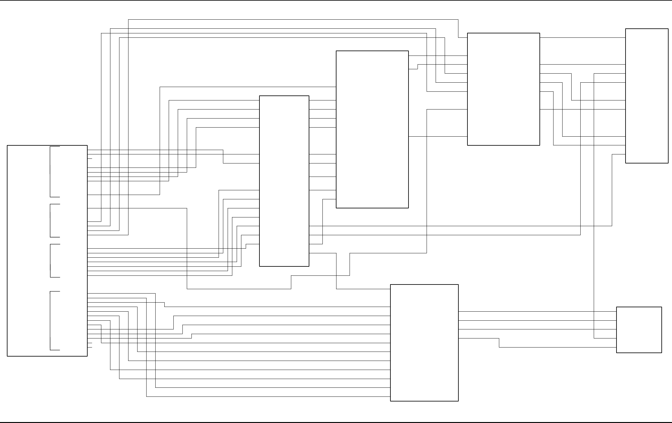
7-132 Schematics, Component Location Diagrams, and Parts Lists: HUE4040A (UHF Range 2) Main Board
May 25, 2005 6881096C74-B
7.4 HUE4040A (UHF Range 2) Main Board
Figure 7-86. HUE4040 Main Board Overall Block Diagram and Interconnections
RFPA_OUT
SWITCH_BIAS
TX_INJ
VCURRENT
VFORWARD
VFORWARD_ON
VGBIAS1
VGBIAS2
VGBIAS3
VREVERSE
VREVERSE_ON
VTEMP
RF_ATTN_1_A
RF_ATTN_2_A
RF_ATTN_3_A
RF_IN
RX_FILT_1_A
RX_Inj_SW
RFPA_OUT
RX_IN
SWITCH_BIAS
VFORWARD_ON
VREVERSE_ON
A+_1
A+_2
K9.1V
RFPA_CNTRL
9.3V_FROM_BE
9.3V_FROM_FE
9.3V_TO_CONTR
IF_IN
IF_OUT
RF_ATTN_1_B
RF_ATTN_1_C
RF_ATTN_2_B
RF_ATTN_2_C
RF_ATTN_3_B
RF_ATTN_3_C
RX_FILT_1 RX_FILT_1_A
9.3V_TO_IF
IF_OUT_IF
LO_IN
VGBIAS_3
VREVERSE
VTEMP
5V_FROM_CONTR
5V_TO_FGU
5V_TO_IF
9.3V_FROM_FGU
9.3V_TO_IF
CLKOUT_1
DOUTA_1
FREF
FS_1
IF
PC_1
PD_1
PE_1
5V_IF
MODIN
MOSIA_ABACUS
MOSIA_FGU
RFPA_CNTRL
RX_ATTEN_1
RX_ATTEN_2
RX_ATTEN_3
RX_FILT_1
SCKA_ABACUS
SCKA_FGU
SYN_SEL
VCURRENT
VFORWARD
VGBIAS_1
VGBIAS_2
TX_INJ
16.8_MHZ
5V_ABACUS
9.3V_ABACUS
9.3V_FGU
A+_1
A+_2
A+_3
A+_4
ABACUS3_CS
ABACUS_SSI_CLK
ABACUS_SSI_FSYNC
ABACUS_SSI_RXD
AUX_5V
K9.1V
LOCK_DET
DOUTA_2DOUTA_3
FS_2
FS_3
Lock_Det
MOD_IN
PC_2
PC_3
PD_2
PD_3
PE_2PE_3
RX_Inj
RX_Inj_SW
SPI_CLK
SPI_DATA
SYN_SEL
16_8MHz
16_8_CONT
5V_Reg
9.3V_1 9.3V_2
CLKOUT_2CLKOUT_3
RF_FE/IF_Interface
RF_BE_Interface
FGU_Interface
RFPA_Interface
CONTROLLER
RX_BE
RX_IF
RFPA
RX_FE
OUTPUT NETWORK
FGU
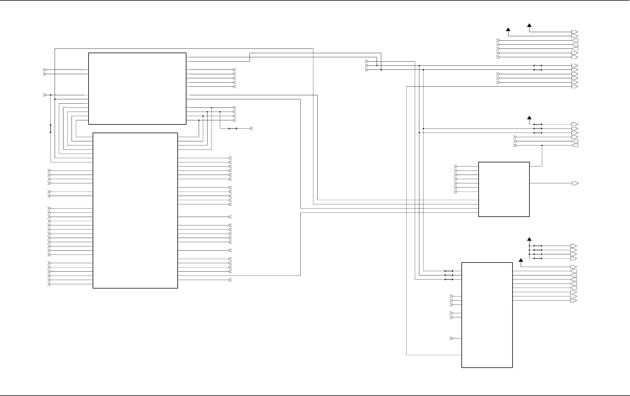
Schematics, Component Location Diagrams, and Parts Lists: HUE4040A (UHF Range 2) Main Board 7-133
6881096C74-B May 25, 2005
Figure 7-87. HUE4040A Controller Block Diagram and Interconnections (Sheet 1 of 2)
16.8_MHZ
AUX_DATA
AUX_TX
DAC_SSI_CLK
DAC_SSI_FSYNC
DAC_SSI_TXD
MIC_TUNE_EN
MODEM_EN
MODIN
RESET
RX_FILT_AUDIO_IN
RX_FILT_AUDIO_OUT
URCHIN_EN
SAP_RX
SAP_TX
SPI_MOSIA
SPI_SCKA
SPKR+
SPKR-
AUDIO_PA_EN AUX_DATA
AUX_MIC
AUX_RX
AUX_TX
CODEC_PWR_DOWNEEPOT_2_CS*
EEPOT_3_CS*
MIC_HI
MUX_AUX_TX
MUX_MICATTEN
MUX_RX
MUX_TX
RX_FILT_AUDIO
SAP_DCLK
SAP_FSYNC
A+
K9.1V
9.3V
5V_ABACUS
9.3V_ABACUS
URXD1_USB_VMIN
URXD2
USB*_RS232_EN
USB_INT*
USB_TXENB
USB_VMOUT
USB_VPIN
UTXD1_USB_VPOUT
UTXD2
VIP_IN_1_5V
VIP_IN_2_5V
VIP_OUT_1_3V
VIP_OUT_2_3V
VPP
WAKEUP
SAP_TX
SB96_RS232*_EN
SOFT_TURN_OFF
SPARE_1
SPARE_2
SPI_MISOB
SPI_MOSIB
SPI_SCKB
SPKR+
SPKR-
SSI_INT*
SW_B+_SENSE
UCTS1_USB_FSEN
UCTS2
URTS1_USB_XRXD
URTS2
IGNITION_SENSE
LHRST_IN
LHRST_OUT
LV_DETECT
MIC_HI
MOD
MONITOR
NAUTILUS_CS*
NAUTILUS_INT*
ONE_WIRE
PTT*
RIA_USBSUSP
RX_FILT_AUDIO
SAP_DCLK
SAP_FSYNC
SAP_RX
AUX_MIC
AUX_RX
AUX_TX
BOOT*
BUS_PWR_OUT
CABLE_DET
CHAN_ACT
EMERG_SENSE
ENC_RESET
ENC_SPARE1
ENC_SPARE2
FORCE_FAIL*
VFORWARD
VGBIAS_1
VGBIAS_2
VGBIAS_3
VREVERSE
VTEMP
AD_EN
DA_EN
EPOT_ENABLE*
K9.1V_EN
MISOA
MOSIA
PA_EN
PWR_RANGE
RFPA_CNTRL
RX_FILT_1
SCKA
VCURRENT
BUS_PWR_OUT
SPARE_2
SPARE_1
RESET
SAP_TX
SAP_RX
SAP_FSYNC
SAP_DCLK
8KHZ_DSP_INT
MUX_MICATTEN
A+_4
A+_3
RX_ATTEN_1
RX_ATTEN_1
ONE_WIRE
MONITOR
MODIN
16.8_MHZ
16.8_MHZ
16.8_MHZ
MIC_TUNE_EN
MODEM_EN
DAC_SSI_TXD
DAC_SSI_C LK
DAC_SSI_FSYNC
URCHIN_EN
MUX_TX
MUX_RX
MUX_AUX_TX
EEPOT_3_CS*
EEPOT_2_CS* CODEC_PWR_DOWN
AUDIO_PA_EN
SPI_MOSIA
SPI_SCKA
SPI_MISOA
SSI_INT*
ABACUS_SSI_CLK ABACUS_SSI_CLK
AUX_5V
AUX_5V
ABACUS3_CS
ABACUS3_CS
MOSIA
MISOA
KEYED_9.1_EN
EEPOT_4_CS*
DA_SEL
AD_SEL
VGBIAS_1
VIP_OUT_2_3V
VIP_OUT_1_3V
VIP_IN_2_5V
VIP_IN_1_5V
CHAN_ACT
VREVERSE
VGBIAS_3
VGBIAS_2
VFORWARD
VCURRENT
SCKA
RX_FILT_1
RFPA_CNTRL
PWR_RANGE
TX_PA_EN
ENC_RESET
EMERG_SENSE
CABLE_DET
BOOT*
SYN_SEL SYN_SEL
LOCK_DET LOCK_DET
A+_2
A+_1
VTEMP
NAUTILUS_INT
NAUTILUS_CS*
MOD
LV_DETECT
LHRST_OUT
LHRST_IN
IGNITION_SENSE
FORCE_FAIL*
ENC_SPARE2
ENC_SPARE1
UCTS1_USB_FSEN
SW_B+_SENSE
SPI_MOSIB
SPI_MISOB
SOFT_TURN_OFF
SPI_SCKB
SB96_RS232*_EN
RIA_USBSUSP
PTT*
USB_TXENB
USB_INT*
USB*_RS232_EN
URXD2
URXD1_USB_VMIN
URTS2
URTS1_USB_XRXD
UCTS2
RX_ATTEN_2
RX_ATTEN_2
SCKA_ABACUS
MOSIA_ABACUS
WAKEUP
VPP
UTXD2
UTXD1_USB_VPOUT
USB_VPIN
USB_VMOUT
9.3V_FGU
SCKA_FGU
MOSIA_FGU
ABACUS_SSI_RXD
ABACUS_SSI_RXD
ABACUS_SSI_FSYNC
ABACUS_SSI_FSYNC
9.3V_ABACUS
5V_ABACUS
RX_ATTEN_3
RX_ATTEN_3
K9.1V
INTERFACE, SECURE, DC SUPPLY
AUDIO
RFPA_INTERFACE
POWER CONTROL
FGU_INTERFACE
AD5320/SCF Block
RX_BE_INTERFACE
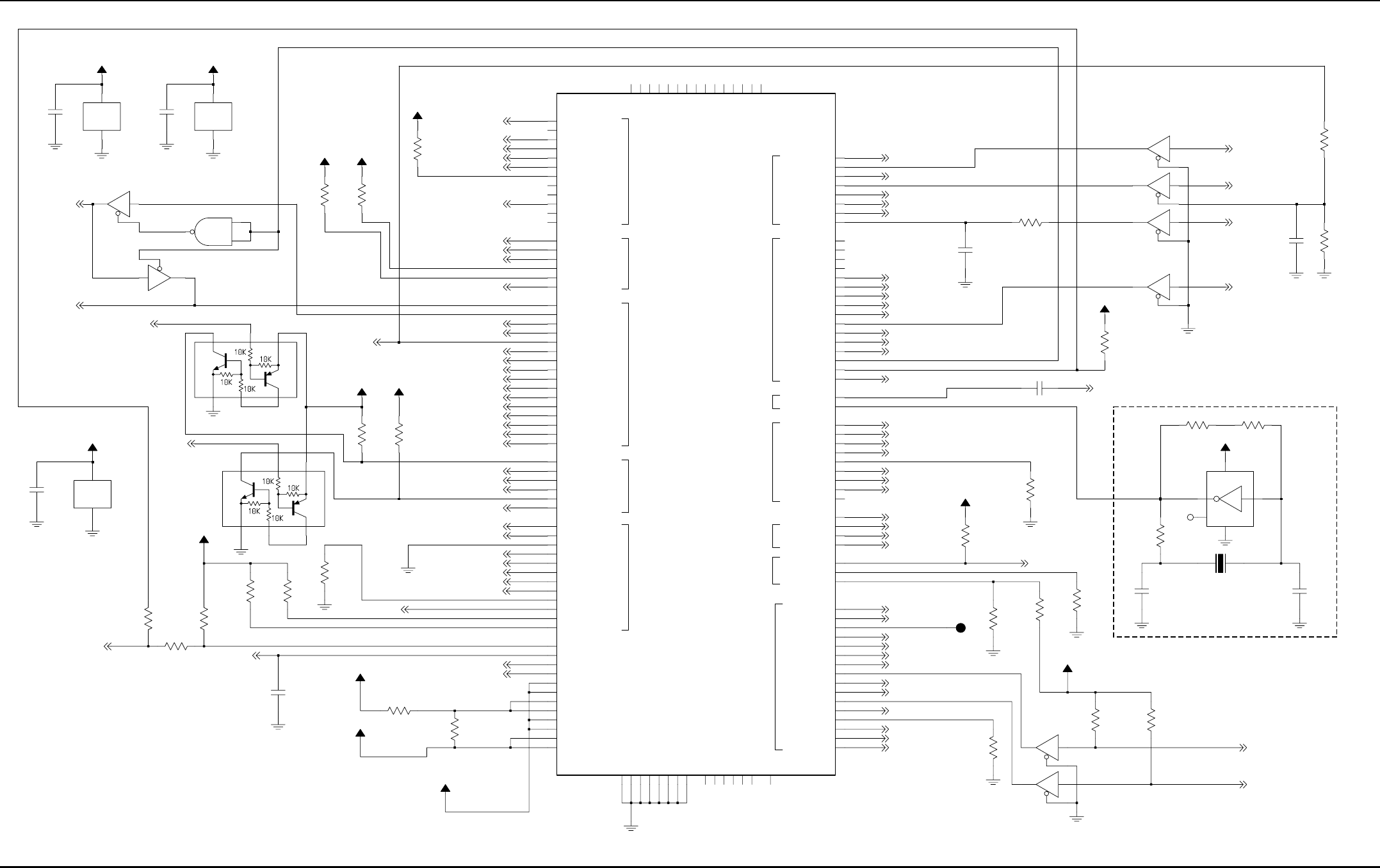
7-134 Schematics, Component Location Diagrams, and Parts Lists: HUE4040A (UHF Range 2) Main Board
May 25, 2005 6881096C74-B
Figure 7-88. HUE4040A Controller Block Diagram and Interconnections (Sheet 2 of 2)
For Patriot BRAVO, neither R0124 or R0125 is placed for a ’1’
NU
NU
NU
R0113, R0115 Placed
For Patriot RAM and BRAVO, R0124 is not placed, R0125 is placed for a ’0
’
NU
For Non-HAB: R0114 Placed
NU
NU
For HAB: R0114 Not Placed
32kHz Oscillator Circuit
Different from high power
For Patriot RAM, R0125 is not placed, R0124 is placed for a ’1’
NU
R0113, R0115 Not Placed
NU
NU
NU
For Patriot BRAVO, R0108 Not Placed, R0107 Placed
For Patriot RAM, R0107 Not Placed, R0108 Placed
0.1uF
C0105
VCC2.85
1NC
4
5
VCC
U0102
3
GND
2
10K
R0124
U0103-4
12
13
11
C0101
18pF
10K
R0109
VCC2.85
12
13
11
Q0102
2
1
3
U0104-4
U0104-1
R0120
10K
VCC2.85
R0103
C0103
0.1uF
U0103-3
9
10
8
14
VCC
U0104-5
7
GND
R0121
10K
R0111
3.3K
10MEG 10MEG
10K
R0102
R0117
7
GND
14
VCC
U0103-5
C0107
470pF
R0127
0
R0110
10K
10K
10K
R0128
100
VCC2.85
470K
R0119
R0126
0
18pF
C0100
10K
R0113
0
R0115
U0103-1
2
1
3
VSIM2
P18
VCC2.85
VDD_CORE_1
S18
VDD_CORE_2
R18
F2 VDD_EIM_1
VDD_EIM_2
G1
VDD_IO_1
Y18
VDD_IO_2
X18
VPP P
G18
N18 VSIM1
UCTS1_PA12 Y2
Z6
UCTS2_PB2
Z2
URTS1_PA13
Z5
URTS2_PB3
Y3
URXD1_PA15
Y4
URXD2_PB1
Z3
UTXD1_PA14
Z15
UTXD2_PB0
D2
TOUT2 D1
TOUT3 E1
TOUT4 I1
TOUT5
TOUT6 P17
E2
TOUT7 G2
TOUT8 F1
TOUT9
H1
TOUT0
TOUT1 C1
N17
TOUT10 J1
TOUT11
TOUT12 I2
B1
TOUT13 S17
TOUT14 C2
TOUT15
A3 SPI_CS8_PE 2
A2 SPI_CS9_PE3
SRDA
X2
V2
SRDB
SRDB2 S2
H18 STBY_PD14
W2 STDA
V1
STDB
J2 SPI_CS0_PE10
N2 SPI_CS1_PE5
SPI_CS2_PE4
L1
K2 SPI_CS3_PE6
SPI_CS4_PE7
P2
B4 SPI_CS5_PE11
N1 SPI_CS6_PE 0
M2 SPI_CS7_PE 1
U18 SIM_SVEN0_PB8
L18 SIM_SVEN1_PB14
K1 SPIA_CLK
SPIA_MISO
L2
SPIA_MOSI
M1
P1 SPIB_CLK
R1 SPIB_MISO
R2 SPIB_MOSI
V17 SIM_D0RX_PB5
I18 SIM_D0TX_PB4
F17 SIM_D1RX_PB11
SIM_D1TX_PB10
K17
SIM_PD0_PB9
E17
B15 SIM_PD1_PB15
V18 SIM_RST0_PB6
G17 SIM_RST1_PB12
X1 SC2A
U2
SC2B
W1 SCKA
SCKB T2
S1
SCKB2
A15
DSC_TX_PD5
U17 SIM_CLK0_PB7
L17 SIM_CLK1_PB13
ROW3 Y6
ROW4 J17
ROW5 Z10
ROW6
ROW7 Y8
SC0A
Z1
T1
SC0B
Y1 SC1A
U1
SC1B
K18 PWM_PE13
Y16 RESET_IN
Y11 RESET_OUT
RIA_PA9 Y5
ROW0 Y10
Z9
ROW1 M17
ROW2 Y9
Y7 PA2_USBVPIN
Z8 PC0_UBSVMOUT
D17 PC11_OC1
PC12_STO
W18
PC1_USBTXENB
B16
M18 PC8
J18 PC9
Z17 PWM*_PE14
A7
NC4
B12
NC5
A5
NC6
B14
NC7
NC8 B8
B7
NC9
B18 OC3_PC13
Z18
OWIREDAT_PC10
B13 NC16
A6 NC17
NC18
A13
A14 NC19
A8
NC2
A16 NC20
B2 NC21
B5
NC3
T17
Z4
MUX_CTRL
A11
NC1
B6
NC10
B10
NC11
A17
NC12
NC13 A9
B11
NC14
A12
NC15
D18 HW_ID
Z12 INT0_PE8
Z13 INT1_PE9
Y14 INT2_PC14
C17 INT3_PC15
Z11 INT4_PA6_OPTSEL1
Y12 INT5_PA7_OPTSEL2
MOD
GND10
A4
B3 GND11
H17 GND12
I17 GND5
A18 GND6
B17 GND7
GND8
B9
A10 GND9
Z16
COLUMN4 Z14
COLUMN5
COLUMN6 W17
R17
COLUMN7
Z7
DCDA_PA8
C18
DSC_RX_PD6
E17
DSRA_INT6_PA10
F18
DTRA_INT7_PA11
H2
CKIH
CKIL A1
T18 CLKSEL_PD15
X17
COLUMN0 Y15
COLUMN1 Y13
COLUMN2 Y17
COLUMN3
U0001
VCC2.85
R0107
0R0108
0
TP0002
VCC2.85
U0103-2
5
4
6
R0116
21
5
4
6
Y0100
32.768KHz
U0104-2
10K
R0101
100pF
*C0108*
10K
R0106
VCC2.85
R0125
C0102
0.1uF
R0105
Q0101
5
2
3
6
4
1
10K
R0129 R0130
U0105-2
3
GND
5
VCC
10K
10K
10K
0.1uF
VCC2.85
VCC1.55
C0104
2.2K
R0122
VCC1.8
VCC2.85
VCC2.85
0
R0114
VCC2.85
R0123
3.3K
R0104
100pF
C0106
4
VCC2.85
U0104-3
9
10
8
U0105-1
1
2
NC
TX_PA_EN
ABACUS_SSI_CLK*
32_KHZ
PTT*
BRD_ID_4
VIP_IN_2_5V
VIP_IN_1_5V
PTT
MONITOR
MONITOR*
EEPOT_2_CS*
VCC2.85
SPI_MOSIA
FORCE_FAIL*
SPARE_2
SPARE_1
HAB_DISABLE
HAB_MOD
16.8_MHZ
16.8_MHZ_PATRIOT
ONE_WIRE
BUS_PWR_OUT
BRD_ID_1
BRD_ID_7
SSI_INT*
LV_DETECT
BRD_ID_6
USB*_RS232_EN
MOD MOD*
SPI_MISOA
SPI_MOSIA*
MISO_SEL
SW_B+_SENSE
BRD_ID_0
BRD_ID_3
MODEM_EN
ABACUS_SSI_RXD*
DAC_SSI_CLK
ABACUS_SSI_FSYNC
ABACUS_SSI_CLK
ABACUS_SSI_FSYNC*
ABACUS_SSI_RXD
LOCK_DET
LOCK_DET*
SB96_RS232*_EN
NAUTILUS_INT
RX_ATTEN_2
RX_ATTEN_1
EEPOT_PC_U_D*
EEPOT_PC_INC*
SOFT_TURN_OFF
MUX_MICATTEN
MILL_ID
BRD_ID_2
PWR_RANGE
SAP_RX
SAP_TX
DA_SEL
ABACUS3_CS
AD_SEL
EEPOT_3_CS*
SYN_SEL
MUX_AUX_TX
SPI_SCKA
AUDIO_PA_EN
SAP_DCLK
SAP_FSYNC
RESET
CODEC_PWR_DOWN
USB_TXENB
8KHZ_DSP_INT
USB_VMOUT
USB_VPIN
CABLE_DET
USB_INT*
SPI_MISOB
SPI_SCKB
MIC_TUNE_EN
SPI_MOSIB
NAUTILUS_CS*
EEPOT_4_CS*
RX_ATTEN_3
UTXD2
UTXD1_USB_VPOUT
URXD2
URXD1_USB_VMIN
URTS2
URTS1_USB_XRXD
UCTS2
UCTS1_USB_FSEN
AUX_5V
MUX_TX
MUX_RX
LHRST_OUT
LHRST_IN
DAC_SSI_TXD
URCHIN_EN
KEYED_9.1_EN
DAC_SSI_FSYNC
ENC_SPARE1
EMERG_SENSE
VIP_OUT_1_3V
RIA_USBSUSP
BRD_ID_5
ENC_SPARE2
WAKEUP
BOOT*
ENC_RESET
IGNITION_SENSE
VIP_OUT_2_3V V
VPP
NU
NU
DSC OWIRE
KEYPAD
UART_B
UART_A
INT
QSP1
SAP
SIM
BBP
LAYER1_TIMER
CLKS
GP10/EGPT/MISC
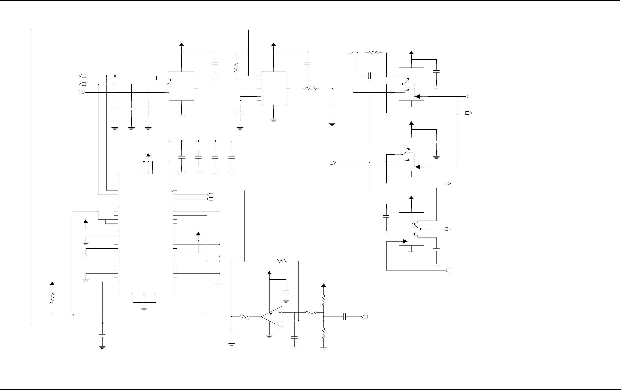
Schematics, Component Location Diagrams, and Parts Lists: HUE4040A (UHF Range 2) Main Board 7-135
6881096C74-B May 25, 2005
Figure 7-89. HUE4040A Controller Urchin IC, MUX, and AD5320 DAC Schematic
NU
C0915
100pF
COM
1
3
GND
2IN
OS
6
5
OUT
SHDN
7
VDD
4
FL0900
8CLK
100pF
C0715
VCC2.85
1uF
C0722
0.1uF
0.1uF
C0909
C0903
VCC2.85
0.1uF
C0908
C0904
220pF
C0906
0.1uF
NU
R0703
100
0.1uF
C0910
8.2K
R0901
VCC2.85
100K
R0900
C0912
100pF
100K
R0905
C0918
VCC2.85
100pF C0902
0.1uF
0.1uF
C0729
VCC2.85
100pF
C0913
100K
R0903
5
COM
GND
3
1IN
4
NC
6
NO
2
VPOS
VCC2.85
C0724
0.1uF
U0905
2
VPOS
VCC2.85
U0904
COM
5
3
GND
IN 1
4NC
NO
6
5
GND
3
IN 1
NC
4
NO
6
2
VPOS
VCC2.85
U0902
COM
C0901
0.1uF R0906
100
VCC2.85
VCC2.85
100K
R0902
0.1uF
C0907
2
C0919
100pF
U0903
4
3
1
5
18pF
C0914
100
R0739
B7
TDO
TMS D2
VCC1 B3
VCC2 C7
VCC3 E2
VCC4 G4
VCC2.85
NC5 B2
NC6 B4
B5
NC7
NC8 B6
NC9 C2
RESET A6
TCK E5
TDI B1
NC26
F6
NC27
F7
NC28
G2
NC29
G3
A4
NC3
G5 NC30
NC31
G6
NC4 A7
NC19
E4
NC2 A2
NC20
E7
NC21
F1
NC22
F2
NC23
F3
NC24
F4
NC25
F5
NC11 C5
NC12 C6
NC13
D1
NC14
D3
NC15
D4
NC16
D6
NC17
D7
NC18
E1
GND1
A5
GND2
E3
GND3
E6
C3
JTAG_EN
2.4_MHZ
G7
48_MHZ
G1
NC1 A1
NC10 C4
U0901
16.8_CLK A3
ENABLE C1
100K
R0904
DIN
4
GND
2
SCLK
5
SYNC
6
VDD
3
VOUT 1
U0900
C0911
100pF
MODIN
MODEM_EN
AUX_DATA
16.8MHZ_SQARE
C0905
0.1uF
RESET
DAC_SSI_CLK
DAC_SSI_TXD
16.8_MHZ_DC
SCF_OUT
AUX_TX
RX_FILT_AUDIO_IN
MIC_TUNE_EN
RX_FILT_AUDIO_OUT
DAC_SSI_FSYNC
16.8_MHZ
AD5320_OUT
URCHIN_EN
NU
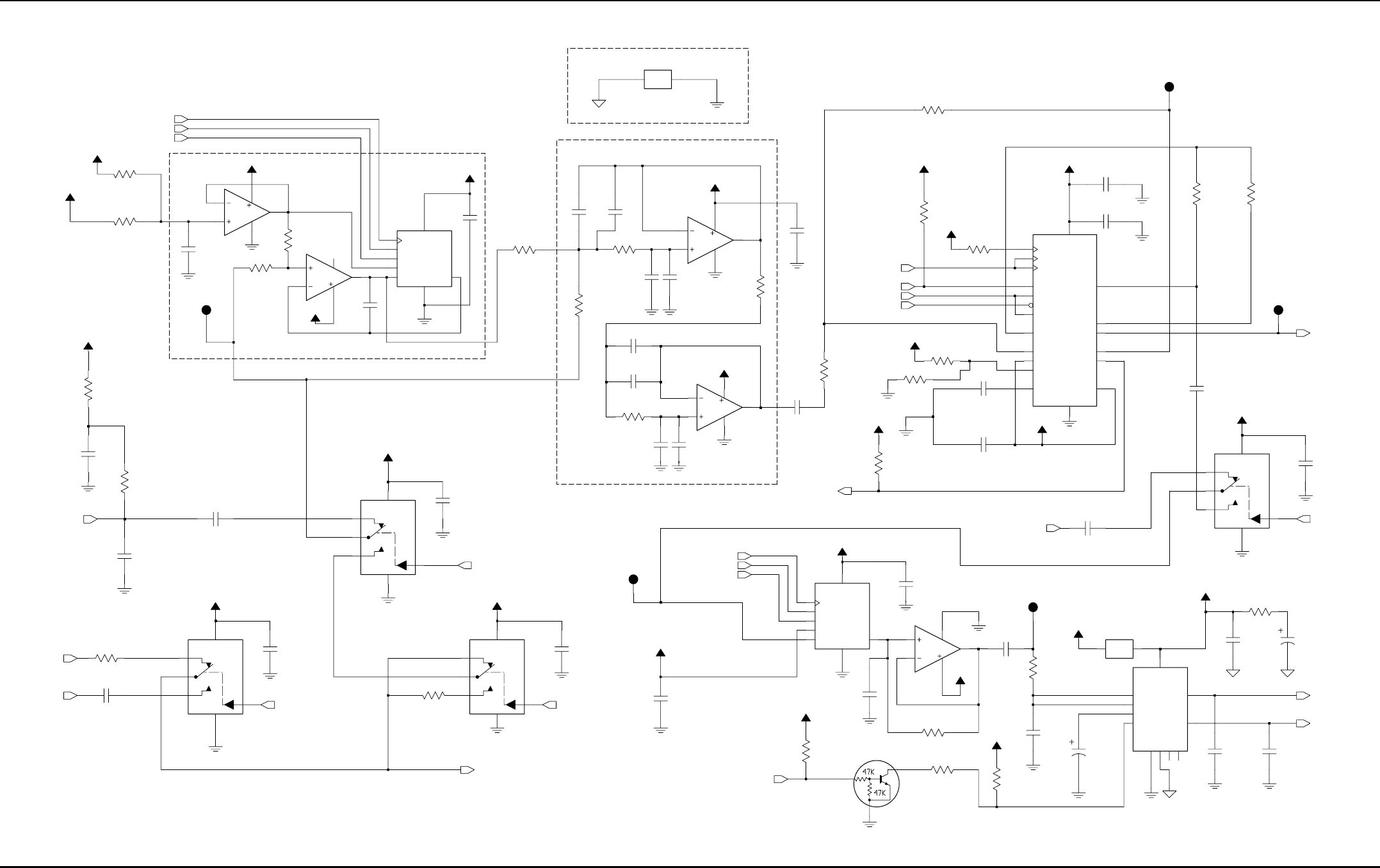
7-136 Schematics, Component Location Diagrams, and Parts Lists: HUE4040A (UHF Range 2) Main Board
May 25, 2005 6881096C74-B
Figure 7-90. HUE4040A Controller Audio Schematic
NU
Ground
NU
NU
-20 dB
0.1uF
C0239
0
R0201
0.1uF
C0210
3300pF
C0217
68K
TP0200 R0223
0.1uF
C0234
C0211
100pF
CLK
DATA
5
3
GND
IN
8
LOAD
4
OUT 2
7
VDD
VREFIN
1
VCC5
U0202
6
R0236
9.1K
VCC2.85
R0212
100K
1K
R0219
C0209
0.1uF
470pF
C0232
VCC5
R0221
10K
C0216
TP0205
0.1uF
68K
R0229
C0212
0.1uF
C0227
SW_A+
0.1uF
VAG
TP0203
6800pF
C0244
VCC2.85
6800pF
C0243
C0213
470pF
0.1uF
33K
R0230
C0236
3
1
IN
4NC
6
NO
VPOS
2
9.3V_TX
VCC5
U0209
5
COM
GND
100K
R0208
68K
R0227
10uF
C0221
C0238
220pF
VCC5
COM
5
GND
3
IN 1
NC
4
NO
6
2
VPOS
U0203
R0210
100K
VCC2.85
C0207
33pF
2.7
R0231
5DATA
3
GND
8IN
4LOAD
2
OUT
7
VDD
1VREFIN
VCC5
1
2
5
U0206
6CLK
NU
U0207
4
3
SC0002
I1
1I2 2
C0237
220pF
C0202
0.1uF
TP0204
VCC2.85
R0225
10K
A+
220pF
C0233
R0216
100K
Q0200
5
COM
GND
3
1
IN
4NC
6
NO
VPOS
2
VCC5
U0210
33K
R0228
VAG
560
R0204
0.1uF
C0224
TP0206
R0205
27K
0.1uF
C0242
VCC2.85
R0200
1K
0.1uF
C0214
100
R0213
1K VCC2.85
R0220
R0218
C0215
18K
0.1uF
4.7uF
C0240
0.1uF
9
10
8
4
11
VCC2.85
C0223
0.1uF
U0201-3
6
5
7
4
11
C0201
U0201-2
VCC5
150pF
C0205
4
OUT1
6
OUT2
3RR
7
VCC
R0235
1K
2GND1
GND2
5
10 GND3
GND4
11
9INV
8M_SS
1NINV
U0204
14
4
11
A+_FILT
1uF
C0208
VCC5
U0201-4
13
12
VCC5
R0211
33K
R0215
10K
VPOS
2
VCC2.85
VAG
C0200
1uF
U0208
5
COM
GND
3
1
IN
4NC
6
NO
10K
C0226
0.1uF
R0222
470pF
C0230
470pF
C0235
R0209
22K
C0203
0.1uF
220pF
C0231
17
TG
18 TI_NEG
19 TI_POS
20
VAG
1VAGREF
6
VDD
15
VSS
14 FST
16 HB
11 MCLK
10 PDI
3PI
4
PO_NEG 5
PO_POS
2
RO_NEG
U0200
9BCLKR
12 BCLKT
8DR
13
DT
7FSR
U0201-1
2
3
1
4
11
SC0001
I1
1I2 2
4.7uF
C0204
R0206
100K
C0220
R0224
0
VCC5
10uF
SPI_SCKA
SPI_MOSIA
EEPOT_2_CS*
MIC_F
RX_FILT_AUDIO
SPKR+
SPKR-
VOL_OUT*
RX_AUDIO_IN
RX_AUDIO_IN
MIC_L
VOL_OUT
CODEC_OUT
AUX_DATA
AUX_DATA
AUX_RX*
MIC_HI*
MUX_AUX_TX
AUX_MIC*
AUX_TX*
AUX_MIC
AUX_TX
CODEC_OUT_B
MIC_M
MIC_K
MIC_N
CODEC_OUT_A
SPI_SCKA
SPI_MOSIA
EEPOT_3_CS*
MUX_MICATTEN
AUDIO_PA_EN
MUX_TX
MUX_RX
MIC_HI
MIC_G
MIC_J
MIC_I
MIC_H
AUX_RX
AUDIO_PA_IN
SAP_RX
CODEC_PWR_DOWN
SAP_FSYNC
SAP_TX
SAP_DCLK
NU
Anti-aliasing filter
0 to 60 dB gain amplifier
MIC_PREAMP_IN
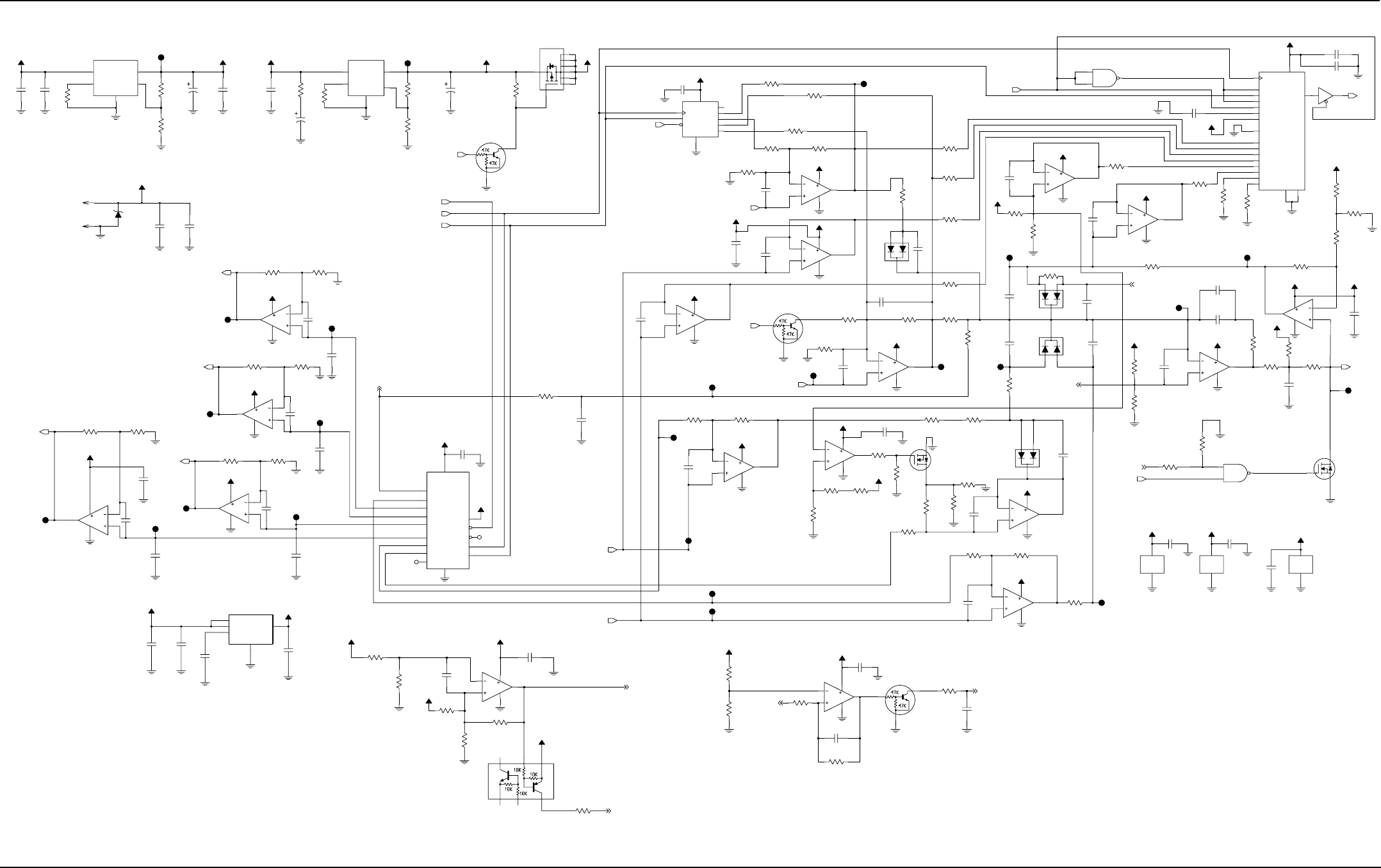
Schematics, Component Location Diagrams, and Parts Lists: HUE4040A (UHF Range 2) Main Board 7-137
6881096C74-B May 25, 2005
Figure 7-91. HUE4040A Controller Power Control Schematic
S
VTEMP
1%
1%
1%
REVERSE_POWER
A+
FORWARD_POWER
1%
1%
VCURRENT
1%
1%
1%
1%
1%
1%
1%
9.3V_TX_ REGULATOR
1%
1%
1%
1%
1%
1%
9.3V REGULATOR
VCONTROL
1%
BATTERY CONNECTOR
1%
Q0955
D
G
*R0911*
12K
R0975
10K
U0950
1
ADJ
3
GND
2ON_OFF
4VIN 5
VOUT
VCC5
VCC5
*R0914*
12K
100
*R0977*
100pF
9.3V_TX
VCC3
30K
C0933
VCC3
R0937
0.1uF
C0955
11
9.3V_TX
TP0959
U0955-1
2
31
4
TP0936
TP0962
R0957
10K
100K
6
5
74
11
R0946
TP0951
U0960-2
TP0964
C0968
100pF
TP0961
33K
*R0945*
10K
VCC5
R0949
TP0931
0.1uF
C0957
R0974
10K
130K
82K
R0910
*R0913*
K9.1V
C0953
R0995
1.2K
22uF
C0921
470pF
C0969
100pF
VCC5
R0987
0
VCC3 D0952
VCC
5
TP0955
U0958-2
GND
3
6
57
4
11
1.2K
R0952
9.3V_TX
U0957-2
NC
C0981
0.1uF
100pF
C0964
9.3V
TP0953
.01uF
C0943
100pF
C0983
C0934
100pF
0.1uF
0.1uF
C0959
C0920
R0970
24K
C0900
680
1000pF
1K
*R0916*
VCC5
9.3V_TX
9.3V_TX
R0915
2.7
R0908
R0996
10K
0.1uF
C0936
A+
0.1uF
R0969
10K
GND
3
VCC
5
C0984
2.7K
U0963-2
*R0973*
9.3V_TX
R0981
VCC3
12K
24K
R0964
12K
4
3
1
5
2
R0956
NC
U0967
VCC3
TP0938
68pF
C0997 VCC3
C0979
0.1uF
U0965
4
31
5
2
9.3V_TX
11
VREF
1
TP0958
20
VIN1
3
VIN2
5
VIN3
6
VIN4
7
VIN5
8
VIN6
9
VIN7
10
VIN8
19
CREF
2
DGND
13
DIN
17 DOUT
16
RFS
15
SCLK
18
TFS
14
VDD
5
VOUT
U0953
A0
12
AGND
4
CONVST
U0962
4BYPASS
2
GND
3VEN
1VIN
R0993
1.2K
22uF
C0956
100K
A+
VCC3
9.3V_TX
VCC3
R0967
R0989
56K C0944
0.1uF
R0988
10K
OUTH
10
REF 5
SCLK 12
VDD
4
9.3V_TX
LDAC 6
OUTA
2
OUTB
1
OUTC
16
OUTD
15
OUTE
7
OUTF
8
OUTG
9
U0959
CS 11
DIN 13
DOUT
14
GND
3
100pF
C0998
R0961
J0950-2 2
100K
R0938
0
R0935
0
7.5K
R0951
10K
*R0992*
9.3V_TX
1.2K
TP0940
R0997
C0974
0.1uF
12K
SW_A+
*R0912*
R0994
3.9K
R0979
0
R0966
0
C0971
100pF
R0998
10K
U0960-3
9
10
84
11
*R0917*
0
U0955-2
6
5
7
4
11
R0968
VCC3
20K
10K
R0930
R0936
0
10K
R0978
C0985
0.1uF
C0962
100pF
D0950
100pF
C0966
11
VCC3
Q0960
8
4
5
U0960-4
13
12
14 4
Q0952
1
2
3
6
7
TP0954
0.1uF
D0954
C0987
0.1uF
C0950
C0986
0.1uF
U0957-4
13
12 14
4
11
D0951
R0950
0
0
9
10 8
4
11
SW_A+
R0986
*R0943*
U0955-3
3
GND
5
VCC
15K
U0954-2
24K
R0963
9
10
8
4
11
TP0930
9.3V_TX
U0957-3
Q0956
C0990
.033uF
100
R0924
0
*R0947*
100pF
C0965
replace,1
C0954
0.1uF
TP0963
C0922
100pF
TP0939
NU
NU
NU
NU
NU
C0930
100pF
U0951
1
ADJ
3
GND
2ON_OFF
4VIN 5
VOUT
0.1uF
C0961
0
VCC3
Q0954
D
G
S
R0984
1uF
C0951
100pF
C0963
TP0952
NU
0.1uF
*C0952*
R0944
10K
4
11
TP0942
U0956-1
2
3
1
3
14
11
C0973
1uF
1
24
U0960-1
2
U0958-1
4
11
0.1uF
C0972
U0956-3
9
10 8
C0923
TP0956
100pF
4
11
R0982
100K
U0957-1
2
3
1
U0954-1
1
2
4
R0954
7.5K
R0999
10K
VCC3
NU
NU
R0980
0
*R0933*
4.7K
TP0960
Q0953
R0983
1K
9.3V_TX
C0945 4.7uF
R0959
10K
4.7K
*R0972* VCC3
C0975
100pF
5.1K
9.3V_TX
20K
R0990
VCC2.85
R0960
VCC3
1uF
C0942
C0978
100pF
100pF
C0967
100K
R0955
Q0951
4
100pF
C0976
U0963-1
2
1
C0980
0.1uF
VCC3
0.1uF
C0960
R0965
0
C0970
100pF
0.1uF
C0940
0
R0948
R0940
5
VDD
10
W1
3
W2
9.3V_TX
1K
2
A1
1
B1
9
B2
6CLK
8CS
4
GND
7SDI
U0952
R0939
30K
18K
*R0942*
R0934
1K
10K
0.1uF
R0958
C0941
C0989
1
1uF
0.1uF
J0950-1
TP0941
C0937
C0982
22uF
1K
0
*R0976*
U0955-4
13
12 14
4
11
R0932
R0953
0
10K
*R0971*
9.3V_TX
C0991
0.1uF
100
R0923
R0991
10K
7
4
11
R0985
0
A+
U0956-2
6
5
30K
U0956-4
13
12
14 4
11
9.3V_TX
R0941
10K
R0931
R0962
C0935
100pF
100K
*C0924*
.047uF
TP0950
TP0957
VR0950
24V
TP0937
VCC5
RFPA_CNTRL
V_REF
PWR_SET
PWR_SET*
PWR_SET
V_REF
TX_DISABLE
LOOP_DISABLE
LOOP_DISABLE
TX_DISABLE
RX_FILT_1
TEMP_2
AD_EN
MISOA
TEMP_1
K9.1V_EN
SCKA
PA_EN
MOSIA
VGBIAS_2
VGBIAS_3
VGBIAS_3
VGBIAS_2
VGBIAS_1
RX_FILT_1
CURR_LIM_SET
VCURRENT
VTEMP
VGBIAS_1
PWR_RANGE
DA_EN
VFORWARD
EPOT_ENABLE*
VREVERSE
NU
NU
NU
NU
NU
NU
NU
NU
NU
NU NU
NU
NU
NU
NU
NU
NU
NU
NU
NU NU
NU
NU
NU
NU
NU
NU
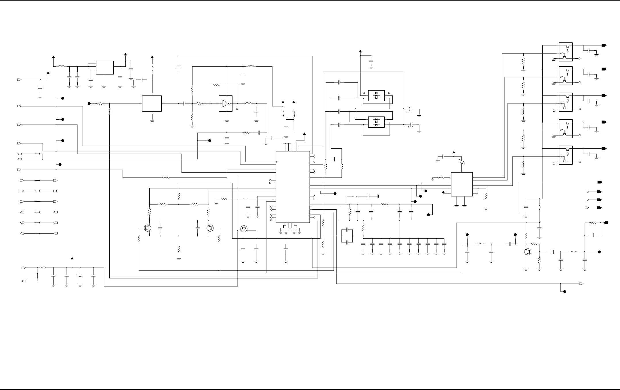
7-138 Schematics, Component Location Diagrams, and Parts Lists: HUE4040A (UHF Range 2) Main Board
May 25, 2005 6881096C74-B
Figure 7-92. HUE4040A Frequency Generation Unit
Syn_Sel
A
4.7K
4.7K
4.7K
4.7K
4.7K
5V_Reg
0.1uF
C5776
10uF
C5766
F3.0v
1K
R5777
47K
47K
R5786
47K
R5783
F3.0v
R5784
Q5710
1000pF
C5760
NC
150
R5771
C5774
22pF
Q5709
820
R5778
NC
C5756
39pF
RX_Mid_Switch
F3.0v
R5775
R5759
2K
100
C5812
0.1uF
C5801
10pF
750
R5772
X1 15
X2 12
X3
X4 1
X5 5
X6 2
X7 4
NC
B
C
9
6EN
8
GND
16
VCC
7
VEE
3X
13
X0 14
U5753
11 A
10
TP5760
TP5799
TP5789
Q5706
NC
R5780
2.7K
C5751
.022uF
VIN VOUT 5
5V_Reg
1K
R5763
U5750
BYPASS
4
2
GND
VEN
3
1
TP5795
C5799
220pF
L5756
2.2uH
NC
0.1uF
C5750
C5785
0.1uF L5759
8.2nH
.0015uF
C5779
C5810
0.1uF
R5758
3.3K
0
R5769
R5785
47K
R5782
47K
C5752
1uF
C5773
0.1uF
470pF
C5813
NC
C5768
100pF
1pF
Steer_Line
100K
R5766
NU
C5808
C5761
33pF
.01uF
NC
E6750
C5763
C5803
330pF
NC
NC
4.7uF
C5788
C5784
0.1uF 0.1uF
C5811
2
K2 1
K3
5.1K
R5753
D5751
4A1
5A2
6A3
3
K1
NC
C5770
10uF
Q5707
C5759
TP5798
560nH
NC
0.33uF
NC
L5750
L5751
560nH
C5795
10pF
C5758
0.1uF
47K
R5754
47K
R5764
L5758
1uH
2.2uH
L5752
R5787
220K
NC
R5751
10K
Q5755
F3.0v
TX_High_Switch
C5762 Q5751
0.33uF
C5809
NC
R5765
0.1uF
5.1K
4.7uF
NC
TP5794
Feedback
C5789
C5772
0.1uF
12uH
L5760
TP5788
C5794
10pF
C5778
0.1uF
TP5791
RX_Inj_SW
C5782
0.1uF
TP5790
NC
220pF
C5796
0.1uF
C5777
C5753
0.1uF
R5774
82
C5754
TX_Low_Switch
.01uF
NC
TP5787
R5768
C5771
0.1uF
100
VRO
WARP 25
XTAL1 23
XTAL2 24
R5773
150
TEST1 37
TEST2 38
VBPASS
21
VCP 47
VMULT1 15
VMULT2 14
VMULT3 12
VMULT4 11
13
PRE_GND
33 PRE_VDD 34
PVREF
35
REFSEL
18
SFBASE
27 SFCAP
26
SFIN
30
SFOUT 28
MODIN
10
MODOUT 41
NC1
17
NC2
29
NC3
31
PD_GND
44
5
PD_VDD
PREIN
32
DATA
7
DGND
6
DVDD 36
FREFOUT 19
IADAPT 45
INDMULT 16
IOUT 43
4
LOCK
AUX3 2
AUX4 3
AVDD 20
BIAS1
40
BIAS2
39
CCOMP
42
CEX
9CLK
8
U5752
ADAPTSW 46
AGND
22
AUX1 48
AUX2 1
.047uF
C5781
R5770
330pF
NU
1.8K
2.2uH
C5805
RX_Inj
NC
L5754
Q5750
C5806
330pF
C5807
330pF
47K
R5767
TP5783
TP5793
NC
K3 1
C5787
0.1uF
D5750
A1
4
A2
5
A3
6
K1 3
K2 2
220pF
C5816
100pF
C5798
1K
R5776
C5791
0.1uF
U5751
3
GND
2
1
NC
4
5
VCC
NC
TP5797
.0015uF
C5780
F3.0v
TP5792
C5755
10uF
C5769
0.1uF
R5779
R5755
12K
F9.3V
0
39pF
C5764
TX_INJ
C5765
C5790
0.1uF
.022uF
330pF
C5804
47K
R5752
NC
100K
R5762
0.1uF
C5783
Q5752
Q5708
F3.0v
C5775
0.1uF
0.1uF
2.2uH
L5755
C5793
220pF
RX_High_Switch
C5817
0.1uF
C5800
10pF
L5757
C5792
C5797
10nH
F3.0v
10uF
GND
2
1VCONT
4
VDD
1uF
C5757
16.8MHz
Y5750
3
FOUT
100K
R5761
5V_Reg
TP5796
1uH
L5753
NU
C5815
220pF
C5767
1000pF
R5788
C5786
NC
RX_Low_Switch
51
0.1uF
R5750
1K
RX_Inj_SW
9.3V_2
PE_2
PD_2
PC_2
Lock_Det
RX_Inj
TX_INJ
DOUTA_3
SYN_SEL
CLKOUT_3
PE_3
PD_3
PC_3
SPI_DATA
SPI_CLK
9.3V_1
5V_Reg
16_8MHz
16_8_CONT
MOD_IN
FS_2
DOUTA_2
CLKOUT_2
FS_3
CLOCK
DATA
3.0 Volt Regulator

Schematics, Component Location Diagrams, and Parts Lists: HUE4040A (UHF Range 2) Main Board 7-139
6881096C74-B May 25, 2005
Figure 7-93. HUE4040A Receive VCO Schematic
BFQ67
700 MHz
C5915
3.9pF
NE68519-T1-A
NE68519-T1-A
BFQ67
BFQ67
665 MHz
NE68519-T1-A
730 MHz
1.6K
150nH
L5907
R5924
0.1uF
C5958
RX_High_Switch
R5910
5.1pF
C5927
33
C5951
Q5906
100pF
Q5904
1.2pF
C5906
C5920
0.1uF
220
R5950
R5937
330
R5918
100
R5914
820
33
C5900
0.1uF
R5922
1.6K
R5912
Q5903
R5934
33
L5909
2K
R5916
18nH
IN
1
OUT
2
150nH
L5900
C5928
Y5901
4.7pF
C5922
D5903
NU
3.3pF
R5904
SH5902
100pF
C5959
270
1.5pF
C5938
220pF
C5919
D5904
150nH
D5901
L5916
D5909
R5926
100pF
820
330nH
C5908
4.7pF
C5931
L5901
2.7K
R5921
360
R5940
5.6pF
Steer_Line
C5944
L5913
330nH
R5932
5.6pF
C5943
D5906
75
18nH
D5907
L5902
3.3pF
C5926
C5911
4.3pF
2K
R5927
OUT
2
C5925
100pF
C5917
Y5900
IN
1
220pF
220pF
C5956
1.5pF
C5960
R5930
51
Q5901
D5911
C5957
1pF
RX_Mid_Switch
D5905
R5933
2.7K
330nH
L5905
Q5905
R5929
Steer_Line
RX_Inj_SW
RX_Low_Switch
12K
C5941
D5902
100pF
C5921
22pF
C5913
C5905
3.3pF
D5910
220pF
220pF
C5945
3.9pF
L5917
15nH
220pF
C5901
C5912
C5930
220pF
330nH
L5915
10nH
L5919
C5910
2.7pF
0.1uF
C5904
220nH
L5922
C5946
220pF
330nH
L5912
C5909
100pF
4.7K
R5938
R5903
1.6K
75
R5909
C5940
5.1pF
R5935
470
12K
R5917
330nH
L5908
220
R5941
L5920
270nH
100pF
470
R5911
C5949
C5950
220pF
R5942
100
5.6pF
L5904
330nH
K1
K2
K3
C5947
D5900
A1
A2
A3
75
R5948
SH5900
NU
R5923
470
D5908
C5948
0.1uF
C5937
100pF
0.1uF
C5916
5.1pF
C5907
R5900
2K
C5929
220pF
C5933
0.1uF
100
R5905
220pF
C5935
Steer_Line
C5932
220pF
R5931
75
220pF
C5914
L5918
6.8nH
L5906
150nH
R5919
75
D5912
3.3pF
C5939
IN
1
OUT
2
C5936
0.1uF
Y5902
C5923
1.5pF
330nH
L5914
R5915
270
R5939
4.7K
75
R5920
Q5902
3.9pF
C5942
RX_Inj
L5910
330nH
C5924
5.1pF
R5928
SH5901
NU
270
R5902
220
15
R5949
Feedback
18nH
L5911
NU
NU
MID RANGE 582.65 MHz to 605.65 MHz
HIGH RANGE 605.65 MHz to 629.65 MHz
LOW RANGE 559.65 MHz to 582.65 MHz
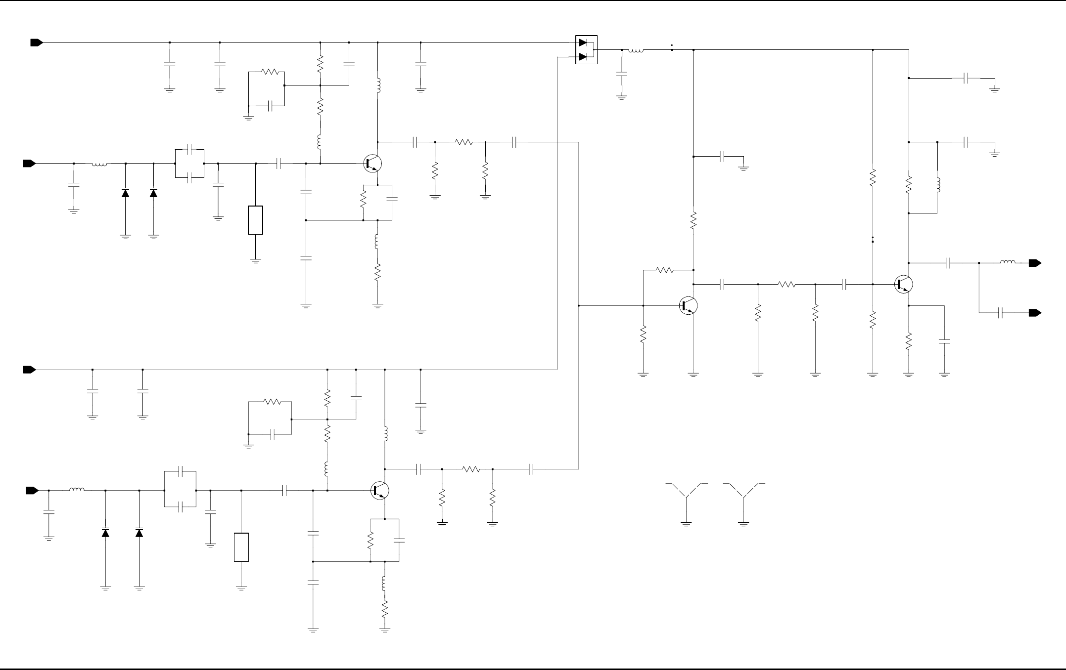
7-140 Schematics, Component Location Diagrams, and Parts Lists: HUE4040A (UHF Range 2) Main Board
May 25, 2005 6881096C74-B
Figure 7-94. HUE4040A Transmit VCO Schematic
Q5826
BFQ67
BFQ67
BFQ67
610 MHz
1SV229
640 MHz
BFQ67
1SV229
R5839
TP5826
TP5825
51
R5832
33
390nH
L5825
C5858
D5827
L5833
10pF
C5832 220nH
0.1uF
0.1uF
330pF
C5844
3.9pF
C5826
360
C5835
270
R5854
D5832
R5834
L5835
18nH
330pF
C5836
180nH
L5832
2.7K
R5825
220
R5850
330pF
C5860
270
R5827
C5840
R5838
100
9.1pF
SH5820
NU
Steer_Line
15pF
C5827 100
R5841
220
R5843
100pF
C5859
TX_High_Switch
C5857
12pF
C5830
16pF
15
Feedbac
k
0.1uF
C5843
R5849
330pF
Steer_Line
Q5828
C5862
R5840
51
0.1uF
12K
C5856
12pF
R5846
0.1uF
C5837
C5852
R5851
4.7K
C5853
330pF
C5831
0.1uF
33
R5831
C5839
5.6pF
Q5829
L5834
180nH
D5831
R5852
L5826
390nH
C5850
4.7K
TX_INJ
9.1pF
R5828
270
NU
Q5825
330pF
SH5821
39nH
L5828
C5834
R5826
2.7K
L5827
390nH
330pF
C5825
L5829
270nH
L5830
220pF
C5842
220pF
270nH
R5837
C5841
100
R5829
1.6K
C5851
C5845
9.1pF
18pF
13pF
C5828
1.2pF
C5863
1.8pF
C5833
TX_Low_Switch
C5829
16pF
180nH
L5831
330pF
C5848
270
R5833
2.7K
R5845
2K
R5830
470
R5853
C5854
15pF
C5847
330pF
9.1pF
C5849
D5833
IN
1
OUT
2
C5838
0.1uF
R5848
Y5800
R5842
820
C5861
100
IN
1
OUT
2
0.1uF
C5855
Y5801
16pF
C5846
D5828
4.7pF
LOW RANGE 450 MHz to 485 MHz
HIGH RANGE 485 MHz to 520 MHz
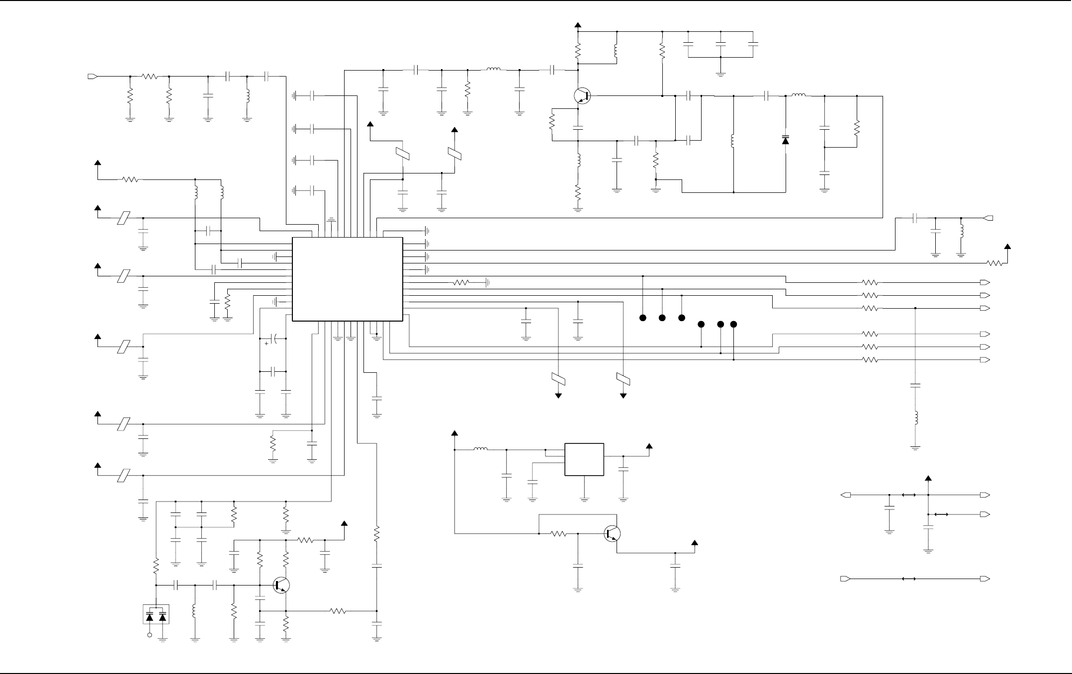
Schematics, Component Location Diagrams, and Parts Lists: HUE4040A (UHF Range 2) Main Board 7-141
6881096C74-B May 25, 2005
Figure 7-95. HUE4040A Receiver Back-End Schematic
C5018
10uF
0
R5015
0.1uF
C5001
100pF
C5013
C5052
1000pF
22
R5026
3VA
15K
R5011
.01uF
C5014
15pF
C5071
33K
R5030
22pF
C5056
R5050
27
3VA
3VA
3VA
PE
12pF
C5002
E5007
5V
0
R5018
5V
C5026
0.1uF
R5002
470
E5004
R5013
51
R5000
R5020
680
10K
L5004
10uH
C5009
200pF
.01uF
C5040
Q5003
0.1uF
C5032
C5048
9.1pF
3VA
3VEN
1VIN 5
VOUT
LP3985
U5001
4BYPASS
2
GND
C5065
0.1uF
C5006
0.1uF
10uF
C5050
.01uF
C5017
C5004
0.1uF
C5060
220pF
C5016
4.7uF
0
R5019
150pF
C5069
L5008
150nH
13pF
R5008
1MEG
C5039
L5010
1uH
100pF
C5019
5V
C5028
220pF
220pF
C5029
C5063
1uF C5064
.01uF
270
R5022
R5027
100
91
R5051
100pF
C5010
200K
R5023
C5033
27pF
C5059
15pF
120pF
C5057
C5030
E5009
E5001
0.1uF
3VA
1000pF
C5066
C5020
1000pF
D5003
FS
12 VREFN
11 VREFP
.01uF
C5021
17 VDDC
26
VDDD
6VDDF
27
VDDH
48
VDDI
40
VDDL 39
VDDP
14 VDDQ
2MXON
1MXOP
23 PC
24 PD
25
PE
RREF
13
33
SYNCB
9VDDA
34
GNDS2
4IF2N
5IF2P
47
IFIN
15 IOUTC
38
IOUTL
42
LON
43
LOP
22 GNDD
3GNDF
32
GNDH
45
GNDI
36
GNDL
37
GNDP
16 GNDQ
21 GNDS1
29
DOUTA
30
DOUTB
35
FREF
31
FS
8GCN
7GCP
10 GNDA
18 GNDC
U5002
20 CLKN
28
CLKOUT
CLKP
19
46
CXIF
44
CXVL
41
CXVM
3VA
AD9874
2200pF
L5003
10uH
C5008
1uH
0.1uF
C5072
C5067
L5015
20K
R5029
100pF
100pF
0.1uF
3VA
C5068
0.1uF
C5005
C5023
1000pF
C5051
DOUTA
0.1uF
4.3pF
C5044
3VA
C5038
100uH
L5001
18K
R5010
18pF
C5027
8.2nH
L5013
R5034
0
C5062
0.1uF
1uF
C5025
1.2K
R5032
0.1uF
PC
L5002
C5024
C5073
150nH
0.1uF
C5022
1uF
.01uF
C5015
VVCO
CLKOUT
Q5002
E5006
NC
3VA
D5002
Q5001
R5016 0
0
R5014
100pF
C5012
6.8K
E5008
0.1uF
3VA
R5028
C5041
C5061
0.1uF
NU
NU
NU
C5046
68pF
R5003
100K
100pF
C5070
330
R5006
2.2uF
C5011
L5012
100nH
100nH
L5006
C5049
51pF C5034
39pF
1MEG
R5033
0
R5017
C5037
PD
C5003
0.1uF
.01uF
0
R5001
E5003
15pF
C5007
E5002
L5053
100nH
R5005 10K
4.7uH
L5007
1MEG
R5035
C5058
1000pF
R5025
1K
1uF
C5045
E5005
VVCO
VVCO
CLKOUT_1
5V_TO_FGU
470
R5031
IF
5V_TO_IF
5V_FROM_CONTR
PD_1
PE_1
PC_1
DOUTA_1
FS_1
9.3V_FROM_FGU 9.3V_TO_IF
FREF
NU
NU
NU
NU
NU
NU
NU
NU
NU
NU
SPF_4.3V
CLOCK VCO
2nd LO LF
2nd LO VCO
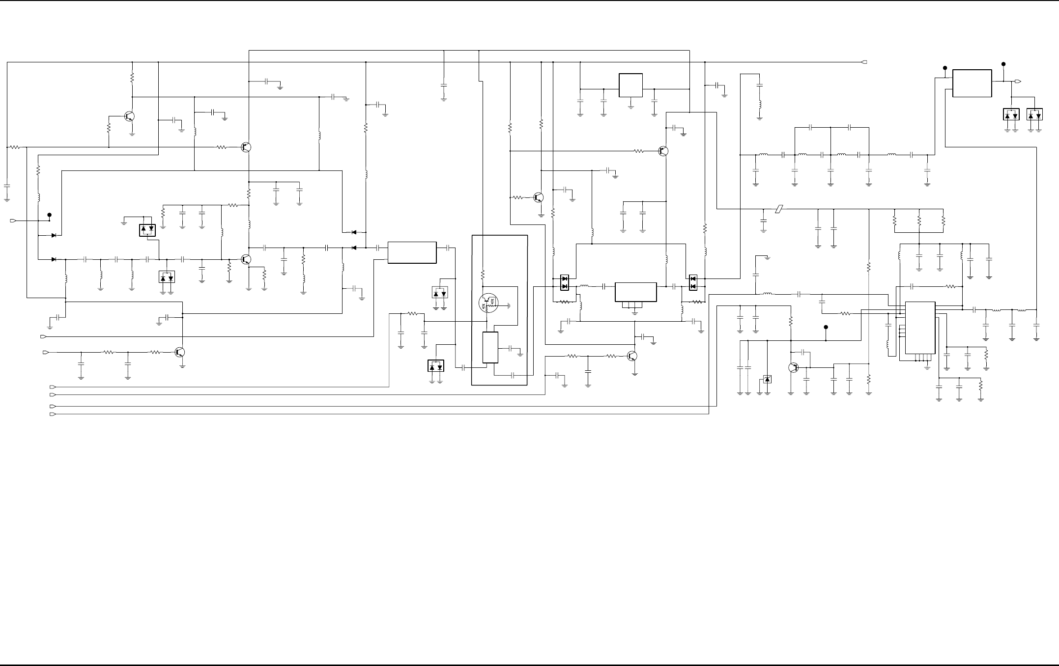
7-142 Schematics, Component Location Diagrams, and Parts Lists: HUE4040A (UHF Range 2) Main Board
May 25, 2005 6881096C74-B
Figure 7-96. HUE4040A Receiver Front-End Schematic
Second LNA
RX_FE
Ref Des = 5280 - 5379
AGC/Attenuator circuit
Image filter and IF suck-out
Mixer
Ref Des = 5380 - 5399
HPF to remove VHF
Preselector
Ref Des = 5250 - 5279
C5351
.033uF
D5304
NU
1000pF
C5364
D5280
C5341
2.7pF
TP5303
220pF
.033uF
C5335
.033uF
C5324
C5360
C5328
Q5258
220pF
18pF
R5303
C5296
4.7K
C5317
C5315
4.7uF
1K
220pF
220pF
C5312
R5317
220pF
C5363
.033uF
C5325
C5308
220pF
R5305
4.7K Q5256
C5293
2pF
.01uF
C5282
C5294
.01uF
D5313
L5288
NU
NU
R5301
82nH
C5305
220pF
10K L5283
22nH
C5283
8.2pF
4.3pF
C5370
220pF
C5340
22nH
L5300
FE_CNTL_1
RF_IN_1 RF_OUT_1
120
R5321
L5304
22nH
NU
18nH
220pF
C5300
L5284
Q5255
.01uF
C5302
D5302 1K
R5318
C5285
4.7pF
C5299
.01uF
L5307
C5367
220pF
8.2pF
4.7nH
10pF
C5288
68nH
L5303
C5326
C5290
220pF
220pF
C5306
TP5301
6.8pF
C5339
D5300
C5333
22nH
NU
470pF
L5282
18nH
L5287
C5310
220pF
R5326
U5301
2
GND
1IN 3
OUT
15
C5311
.01uF
4.7K
NU
R5314
L5299
L5298
22nH
C5291
.01uF
L5305
15nH
R5315
1K
.033uF
C5356
D5305
.033uF
C5323
R5306
12K
.01uF
C5303
L5289
390nH
C5357
220pF
220pF
C5304
1uH
L5296
TP5304
R5312
10K
C5321
1K
220pF
C5316
470pF
R5310
5.6V
R5324
D5306
NU
15
C5320
12pF
L5293
390nH
NU
.01uF
C5284
.01uF
C5314
22nH
220pF
L5297
22nH
L5301
C5362
RFOUT1
6
RFOUT2 7
VCNTRL
1
VD1
14 2
VG1
VG2 3
GND2
5
GND3
12
GND4
13
NC1
8
NC2
9
NC3
10
NC4
15
RFIN
16
EP
17
G2
11
GND1
4
U5303
220pF
C5307
C5280
Q5257
470pF
C5345
220pF
C5361
220pF
2
GND
1
RFIO1
3
RFIO2
4
V1
5
V2
U5300
4.7K
R5313
C5331
D5303
9.1pF
8.2nH
L5308
Q5250
22pF
C5347
R5325
15
Q5251
C5297
1.5pF
.01uF
C5322
C5295
4.7pF
TP5302
1K
R5302
NU
C5313
.01uF
C5344
9.1pF
R5332
1.5K
.01uF
C5287
L5309
5.6nH
12nH
L5302
R5327
180
NU
NU
1K
R5329
Q5252
1uH
L5290
47pF
C5354
1
GND1
2
GND2
4
GND3
5
GND4
3RFIN 6
RFOUT
U5302
R5309
27
C5334
220pF
220pF
L5294
39nH 220pF
C5289
C5348
C5366
C5318
4.7uF
Q5253
1000pF
C5343
22pF
D5307
1K
R5316
L5292
NU
C5330
220pF
390nH
Q5254
NU
C5338
NU
R5307
22K
220pF
C5353
5.6K
220pF
10pF
NU
R5328
0
C5355
R5335
NU
R5336
R5319
NU 0
C5327
470
2.4K
100pF
R5337
R5322
22K
C5368
1000pF
D5281
.033uF
C5350
220pF
C5365
1K
R5304
.01uF
1.5K
R5334
C5309
IF
LO
MIXER_RF_IN
47
R5333
R5300
4.7K
C5332
2.7pF
D5301
R5308
68
L5281
390nH
C5358
C5301
.01uF
C5349
10pF
R5311
6.8pF
R5330 10K
1.5pF
47
NU
C5359
D5311
.01uF
C5319
L5285
100nH
L5280
1uH
C5342
9.1pF
390nH
NU
33nH
L5295
NU
L5286
L5306
4.7nH
1uH
L5291
.033uF
C5346
220pF
C5352
15K
R5323
.033uF
C5337
9.1pF
C5336
D5282
C5292
220pF
RF_IN
C5329
100pF
9.3V_TO_IF
9.3V_TO_IF
9.3V_TO_IF
9.3V_TO_IF
RX_Inj_SW
IF_OUT_IF
LO_IN
RF_ATTN_3_A
RF_ATTN_1_A
RF_ATTN_2_A
TO_1st_MIXER
RX_FILT_1_A
NU
NU
NU
NU
NU NU NU
NU
NU
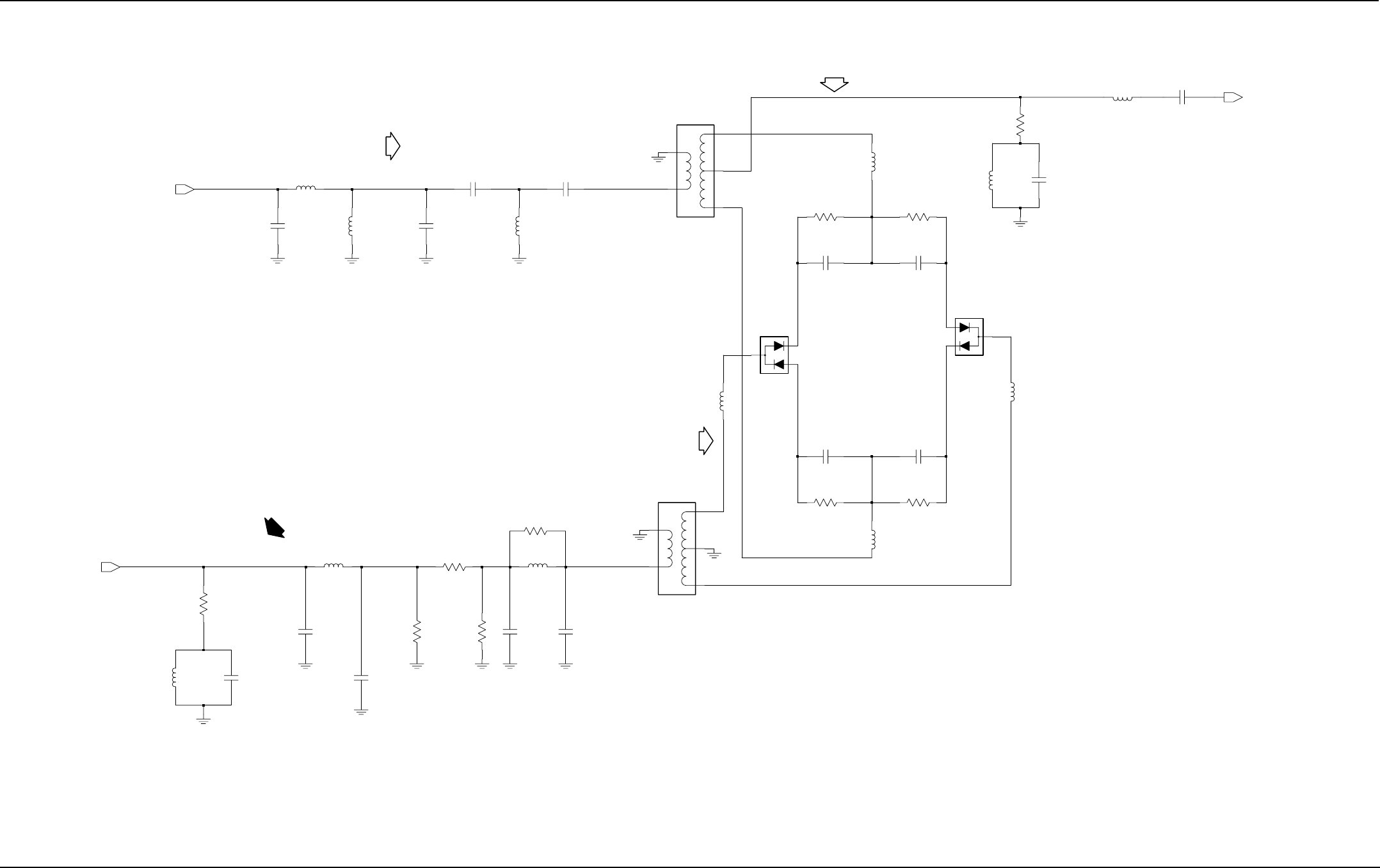
Schematics, Component Location Diagrams, and Parts Lists: HUE4040A (UHF Range 2) Main Board 7-143
6881096C74-B May 25, 2005
Figure 7-97. HUE4040A Receiver Mixer Schematic
SIGNAL
INJECTION
5.6pF
HIGH SIDE
1
2
3
4
5
NU
C5381
replace,2585040Y01
*T5381*
C5377
12pF
5.1pF
9.1pF
C5380
L5382
12nH
C5389
R5382
NU
NU
470
6.8pF
C5390
L5380
12nH
C5379
8.2pF
C5375
9.1pF
R5380
470
0
NU
R5381
L5389
8.2nH
R5387
47
C5386
33pF
L5388
68nH
D5381
8.2nH
L5390
L5381
68nH
12nH
R5388
51
9.1pF
L5392
NU
NU
NU
C5374
R5385
180
C5388
.01uF
R5386
180
8.2nH
L5384
C5385
.01uF
R5384
180
L5383
3.3nH
C5383
.01uF
NU
C5382
.01uF
8.2nH
C5378
L5385
L5387
NU
6.2pF
L5386
6.8nH
D5380
6.8nH
R5383
180
4
5
33pF
C5391
1
2
3
LO
MIXER_RF_IN
IF
replace,2585040Y01
*T5380*
0
R5389
I. F.
109.65 MHz
THE RECEIVER INPUT SIGNAL AND THE INJECTION SIGNAL
GENERATED BY THE RECEIVE SYNTHESIZER ARE MIXED
TO PROVIDE A 109.65MHz I-F SIGNAL.
+24.5 dBm I/P from the injection amp
RECEIVED RF
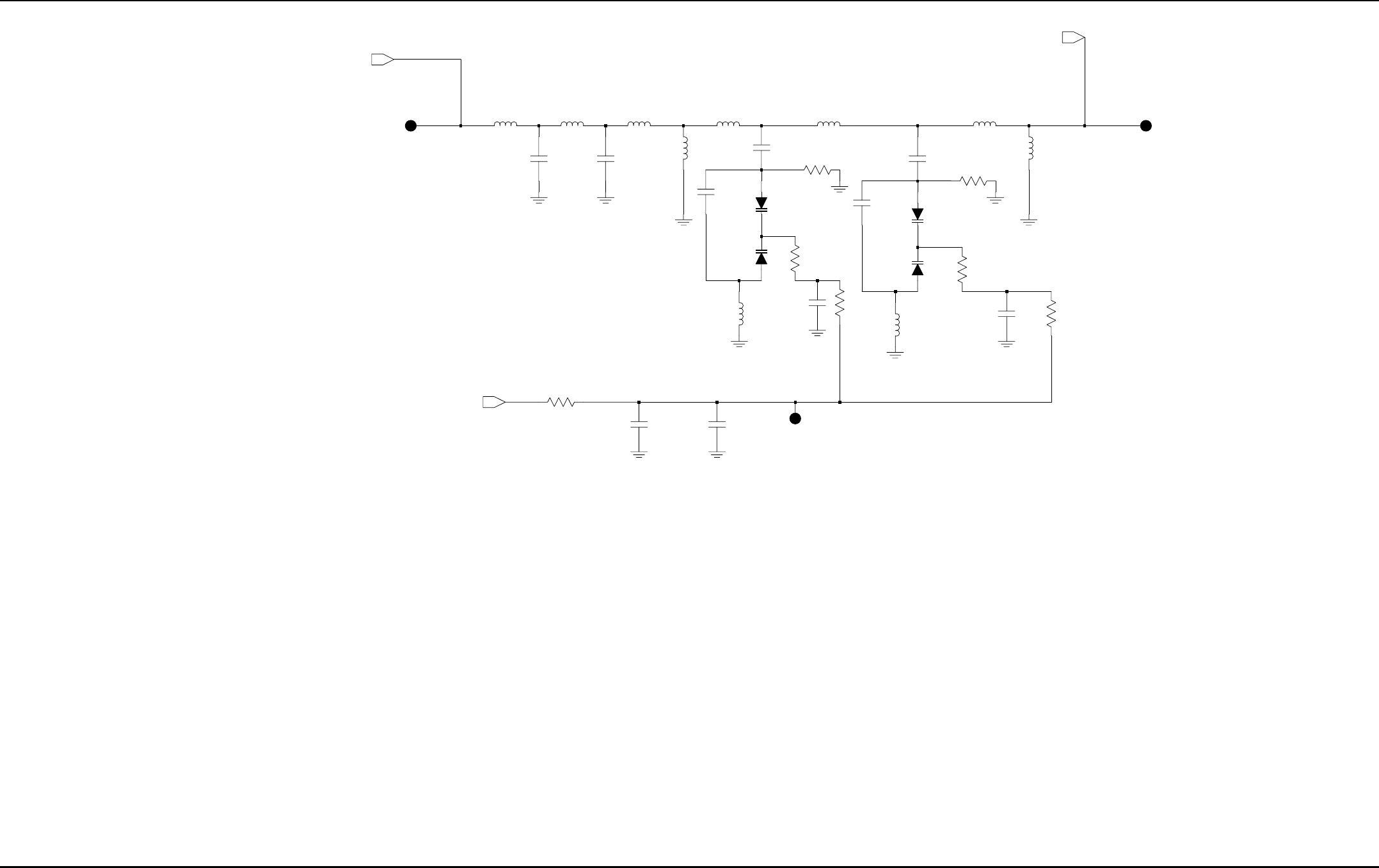
7-144 Schematics, Component Location Diagrams, and Parts Lists: HUE4040A (UHF Range 2) Main Board
May 25, 2005 6881096C74-B
Figure 7-98. HUE4040A Receiver Preselector Schematic
TP5251
TP5250
TP525
2
R5252
R5255
1K
1K
220pF
C5251
R5256
4.7
.01uF
C5259
220pF
C5256
220pF
C5253
47K
R5250
47K
R5254
R5253
47K
D5252
NU
D5253
C5254
1pF
C5255
5.6pF
L5254
12.5nH
D5250
C5250
NU
D5251
C5252
1pF
L5256
5.6pF
12.5nH
L5252
5nH
8nH
L5255
82nH
L5253
8nH
L5251
5nH
L5250
47K
R5251
4.7pF
C5257
4.7pF
C5258
L5257
39nH
L5237
22nH
RF_IN_1
RF_OUT_1
FE_CNTL_1
L5258
22nH
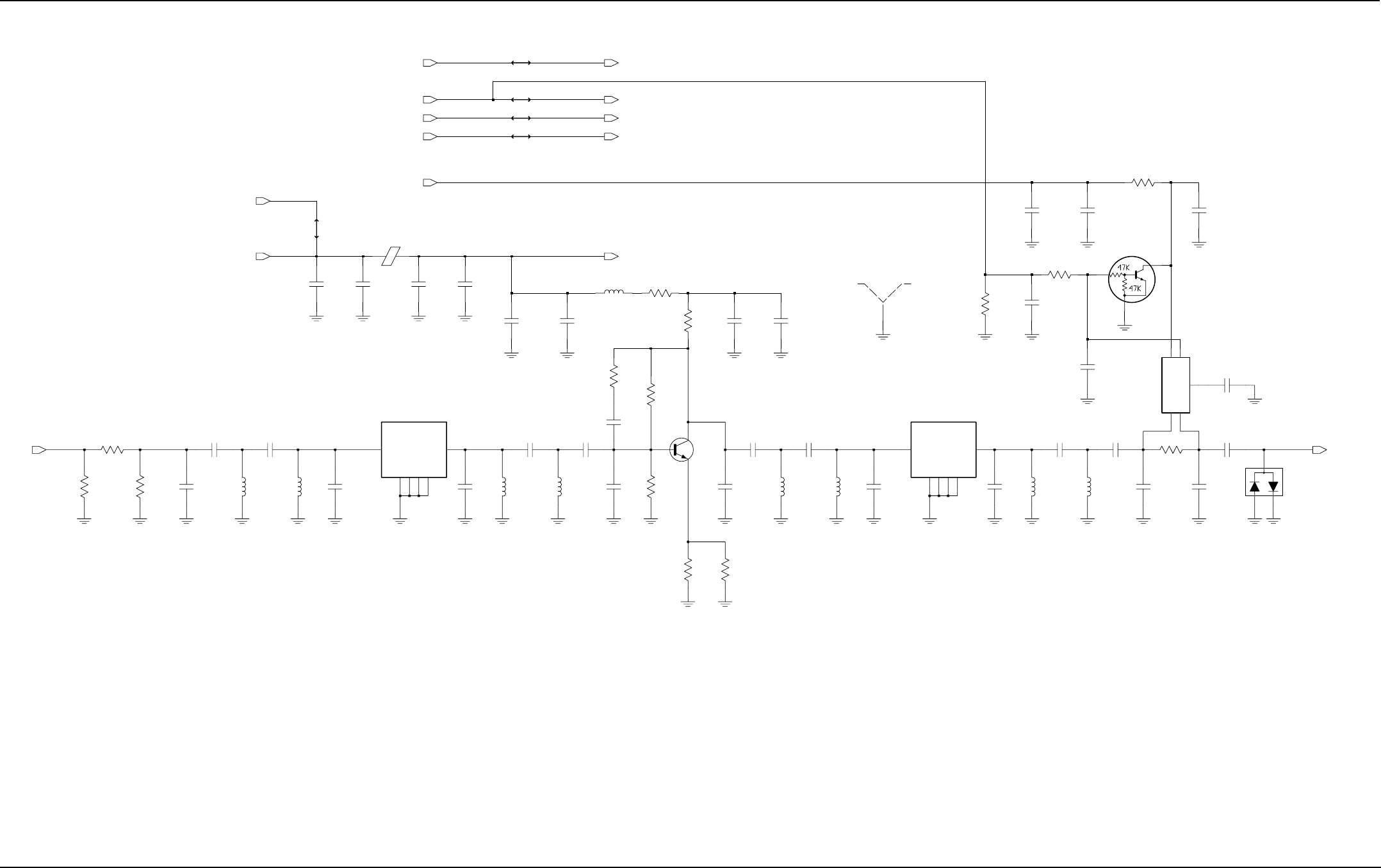
Schematics, Component Location Diagrams, and Parts Lists: HUE4040A (UHF Range 2) Main Board 7-145
6881096C74-B May 25, 2005
Figure 7-99. HUE4040A Receiver IF Schematic
Going to Frontend
IF_TO_ABACUS
Coming From Abacus
R5406
1K
C5410
C5405
2.7pF
1.8pF
R5402
6.8K
0
R5407
.01uF
C5420
NU
E5400
C5431
220pF
SH5400
L5407
C5404
15pF
C5429
220nH
NU
NU
220pF
NU
0.1uF
C5430
OUT 3
3pF
C5408 Y5401
109.65MHz
1
GND1
2
GND2
4
GND3
GND4
5
IN
6
390nH
0.1uF
L5403
C5401
R5414 R5415
0
0
L5406
15pF
220nH
0.1uF
C5407
0.1uF
C5402
C5426
C5424
0.5pF
C5416
.01uF
220pF
NU
220pF
C5428
C5400
0.1uF
C5427
270nH
L5404 1.8pF
C5409
NU
C5417
0.5pF
C5412
2.7pF
L5400
390nH
L5411
390nH
L5401
220nH
C5422
C5406
NU
0.5pF
16pF
NU
C5432
0.1uF
L5408
1uH
13pF
C5403
0
R5412
C5418
C5415
2.7pF
1.8pF
Q5401
NU
R5413
1MEG
NU
1MEG
R5411
8.2K
R5408
C5423
.01uF
C5419
220pF
R5401
27K
0
R5404
GND4
5
IN
6OUT 3
109.65MHz
Y5400
1
GND1
2
GND2
4
GND3
C5411
0.5pF
R5400
NU
680
D5400
R5405
10K
C5414
8.2pF
C5425
220pF
R5403
330
1.8pF
C5413 L5402
390nH
.01uF
C5433
V1
4
V2
5
Q5402
U5400 GND 2
RFIO1
3
RFIO2
1
IF_OUT
9.3V_FROM_FE
RF_ATTN_1_C
9.3V_TO_CONTR
9.3V_FROM_BE
IF_IN
5V_IF
RF_ATTN_3_C
RF_ATTN_2_C
RF_ATTN_3_B
RF_ATTN_2_B
RF_ATTN_1_B
RX_FILT_1 RX_FILT_1_A
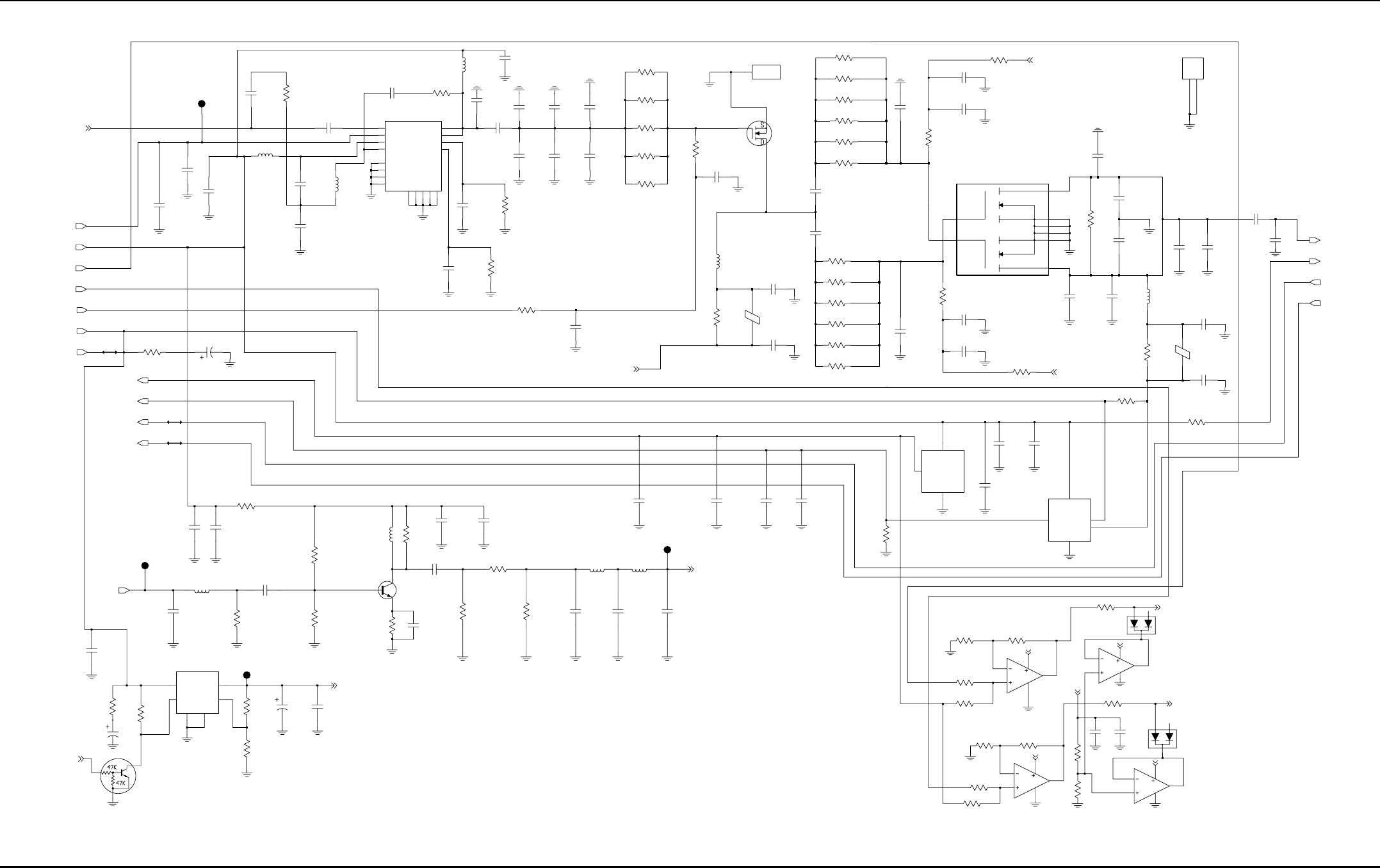
7-146 Schematics, Component Location Diagrams, and Parts Lists: HUE4040A (UHF Range 2) Main Board
May 25, 2005 6881096C74-B
Figure 7-100. HUE4040A RF Power Amplifier (RF PA) Schematic
RFPA/OUTPUT NETWORK
RFPA/FGU
INTERFACE
INTERFACE
INTERFACE
RFPA/POWER CONTROL
2.2
390nH
L5505
R5513
C5548
M5501
POS
1
12pF
R5514
2.2
TP5503
R5532
2.7
R5511
2.2
180
R5529
NU
0
R5537
R5533
18nH
L5506
2.7pF
15
220pF
C5555
C5502
5.1pF
C5524
C5525
220pF
100pF
C5553
R5525
1K
100pF
C5527
VOUT
3.9pF
C5507
U5570
1
ADJ
GND1
3
GND2
6
2ON_OFF
4VIN 5
R5502
6.8K
1K
R5526
220pF
C5578
82
R5506
20pF
C5560
L5504
220nH
R5523
10
TP5501
C5572
22uF
C5550
C5541
0.1uF
7.5pF
C5568
0.1uF
R5509
NU
TP5502
NU
1.8K
C5539
100pF
33
R5524
150
R5501
NU
220pF
C5514
10uF
C5501
C5513
.022uF
C5546
27pF
51pF
C5538
0.1uF
C5570
0.1uF
C5544
L5508
12.5nH
15
15
R5545
R5544
POS
1
VOUT
2
U5502
GND
3
R5512
2.2
.01uF
C5554
C5576
220pF
.01uF
C5557
0.1uF
C5517
82
R5510
C5551
10pF
C5575
.01uF
Q5502
7.5pF
C5522
NU
2K
R5508
15
R5541
NU
15
R5539
15
R5538
15
R5536
33pF
C5521
NU
7.5pF
C5569
.01uF
C5556
C5506
E5501
10pF
C5511
C5543
NU
.033uF
1K 30pF
2.2
R5527
R5503
R5515
4.7K C5512
56pF
L5502
390nH
E5502
15
R5543
R5542
15
.01uF
C5677
C5518
R5534
15
27pF
L5510
L5507
18nH
C5519
17nH
NU
NU
10pF
R5540
15
15
R5530
51pF
C5579
220pF
C5535
220pF
C5504
R5507
100
L5501
18nH
4.7pF
C5552
30pF
C5542
5
S3 8
S4 4
C5545
27pF
D1 2
D2 3
G1
6
G2
7
S1 1
S2
C5558
Q5503
R5528
150
.01uF
C5526
0.1uF
C5571
C5573
0.1uF
10uF
R5535
10
1K
R5520
100pF
C5549
0.1uF
C5505
C5509
100pF
C5565
.033uF
100pF
C5540
C5516
220pF
R5519
100K
NU
220pF
C5567
U5503
GND
2
1OUT 4
VINNEG
3
VINPOS
5
VPOS
.033uF
5m
R5522
C5503
.022uF
C5515
R5572
7.5K
10
Q5501
1K
R5517
NU
R5504
R5505
L5503
8.2nH
R5570
150
TP5570
2.7
0.1uF
C5510
C5563
9.1pF
NU
M5502
1
GND1
GND2
2
C5566
6.2pF
6
RFOUT1 7
RFOUT2
1VCNTRL
14 VD1 2
VG1 3
VG2
Q5570
5
GND2
12
GND3
13
GND4
8NC 1
9NC 2
10 NC 3
15 NC 4
16 RFIN
U5501
EP
17
11 G2
4
GND1
5.1pF
C5520
1K
R5521
C5523
10pF
R5571
33K
20pF
C5559
R5573
1.2K
51
R5516
DRV_9.3V
A+_1
C5508
220pF
VFORWARD_ON
VREVERSE_ON
K9.1V
VGBIAS1
VGBIAS1_SUM
VGBIAS2_SUM
VGBIAS2
VCURRENT
VTEMP
RFPA_OUT
K9.1V
RFPA_CNTRL
DRV_9.3V
SWITCH_BIAS
PA_INJ
TX_INJ
PA_INJ
VGBIAS3
VFORWARD
VREVERSE
A+_2
1%
1%
U5504-2
6
5
7
4
11
15K
15K
R5552
R5550
15K
2K
R5551
R5546
43K
D5501
R5557
R5556
2K
6.8K
R5548
R5549
R5554 43K
15K
43K
R5553
R5547
15K
9
10
8
4
11
D5502
2
3
1
4
11
U5504-3
U5504-1
15K
R5555
U5504-4
13
12
14
4
11
C5681
.01uF
C5580
220pF
K9.1V
K9.1V
K9.1V
VGBIAS1_SUM
VGBIAS2_SUM
K9.1V
DEFAULT_NET_TYPE
K9.1V
Schematics, Component Location Diagrams, and Parts Lists: HUE4040A (UHF Range 2) Main Board 7-147
6881096C74-B May 25, 2005
Figure 7-101. HUE4040A Output Network (ON) Schematic
W = 27.5 mil
S = 35 mil
L = 510 mil
W = 90 mil
S = 35 mil
W = 27.5 mil
1.5K
C5708
R5702
NU
SH5702
100pF
L5702
150nH
NU
SH5701
33
R5701
L5701
470nH
220pF
R5707
270
C5715
L5704
R5705
270
17nH
17nH
C5717
L5703
1.5K
7.5pF
R5709
17nH
L5708
C5702
220pF
C5716
7.5pF
C5719
1.8pF
D5701
FWD
R5712
100K
C5703
220pF
5nH
L5712
NU
SH5703
C5709
47pF
R5710
75K
ANT
1pF
C5707
D5703
J5701-11
3.3pF
C5711
NU
1.5pF
C5722
NU
C5721
6.8pF
C5712
D5705
3.9pF
J5701-22
R5704
100K
1.5pF
D5704
C5705
68pF
C5710
D5702
L5707
R5713
3.3K
17nH
R5706
270
C5704
R5708
270
220pF
REV
SH5704
NU
5nH
L5713
3.3pF
C5714
C5718
220pF
C5720
7.5pF
C5713
11pF
R5703
30K
5.1pF
C5701
220pF
C5706
L5705
J5701-
3
3
470nH
L5706
R5711
30K
VFORWARD_ON
17nH
RX_IN
VREVERSE_ON
RFPA_OUT
SWITCH_BIAS
OUTPUT NETWORK/RFPA
INTERFACE
OUTPUT NETWORK/RX FE
INTERFACE
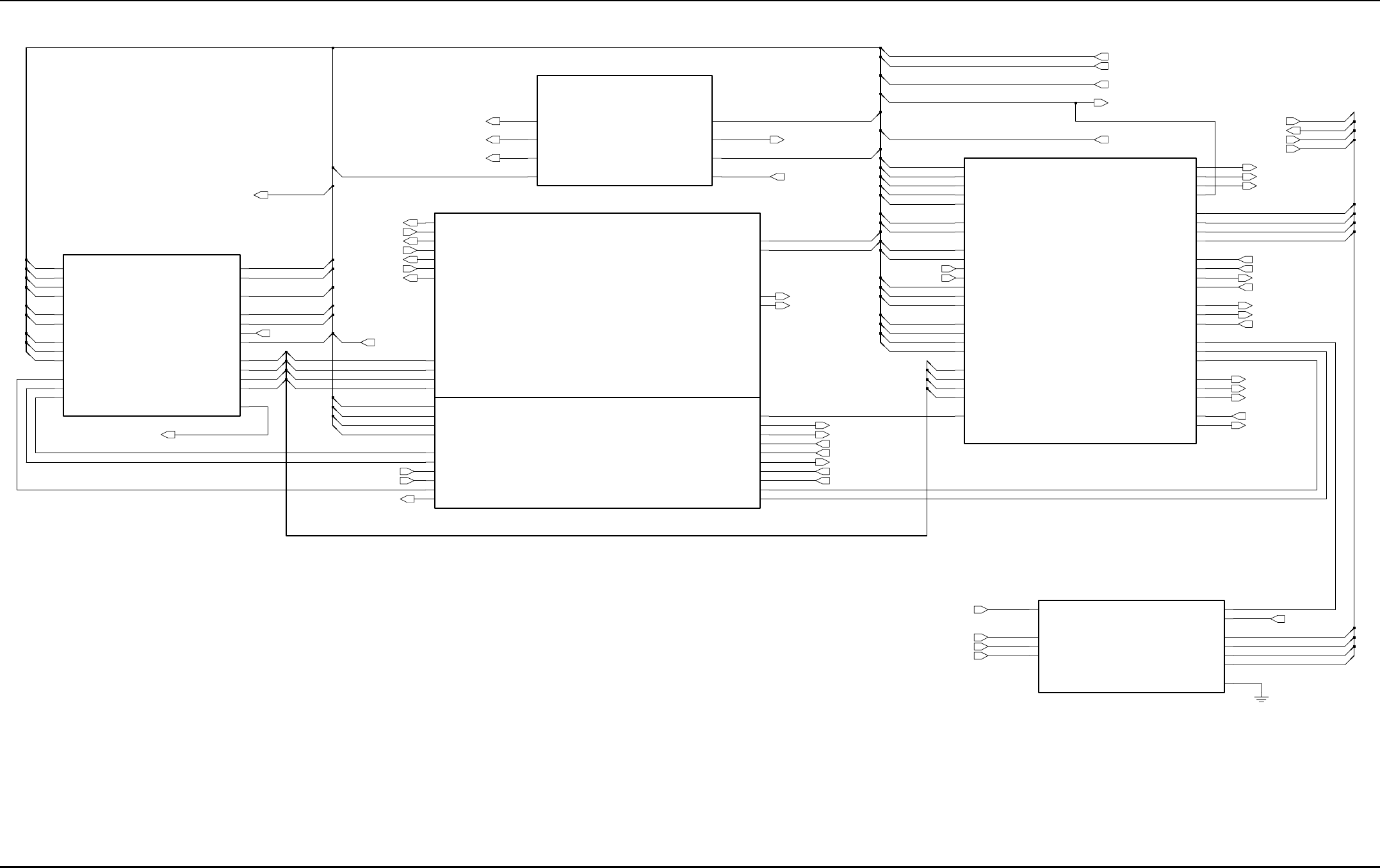
7-148 Schematics, Component Location Diagrams, and Parts Lists: HUE4040A (UHF Range 2) Main Board
May 25, 2005 6881096C74-B
Figure 7-102. HUE4040A Secure Block Diagram and Interconnections
3
2
8
00
0
ENC_RESET
ENC_SPARE1
ENC_SPARE2
KEYFAIL*
SAP_DCLK
SAP_FSYNC
SAP_RX
SAP_TX
TAMPER_ENC
WAKEUP
3
17
11
0
2
12
2
BOOTA*
0
1
1
13
11
VIP_IN_1_5V
VIP_IN_2_5V
VIP_OUT_1_12V
VIP_OUT_1_5V
VIP_OUT_2_12V
VIP_OUT_2_5V
2
SAP_FSYNIC
SAP_RX
SAP_TX
SPARE_1
SPARE_2
SPI_MISOB
SPI_MOSIB
SPI_SCKB
SPKR+
SPKR-
SSI_INT*
SW_B+_ON-OFF
UARTA_CTS
UARTA_RTS
UARTA_RXD
UARTA_TXD
BUS-_UARTB_RXD
BUSY_UARTB_RTS
BUS_PWR_OUT
CABLE_DET
EMERGENCY
FORCE_FAIL*
IGNITION
KEYFAIL
MIC_HI
MOD
NAUTILUS_CS*
NAUTILUS_INT*
ONE_WIRE
PTT*
RESET_UARTB_CTS
RX_FILT_AUDIO
SAP_DCLK
0
05
AUX_MIC
AUX_RX
AUX_TX
BOOT_DATA_EN*
BOOT_RX
BOOT_TX
BUS+_UARTB_TXD
URXD2
USB*_RS232_EN
USB+
USB-
USB_INT*
USB_PWR
USB_TXENB
USB_VMOUT
USB_VPIN
UTXD1_USB_VPOUT
UTXD2
VIP_OUT_1_3V
VIP_OUT_1_5V
VIP_OUT_2_3V
VIP_OUT_2_5V
BUS+_UARTB_TXD
BUS-_UARTB_RXD
BUSY_UARTB_RTS
LHRST_IN
LHRST_OUT
RESET_UARTB_CTS
RIA_USBSUSP
SB96_RS232*_EN
UARTA_CTS
UARTA_RTS
UARTA_RXD
UARTA_TXD
UCTS1_USB_FSEN
UCTS2
URTS1_USB_XRXD
URTS2
URXD1_USB_VMIN
EMERGENCY
EMERG_SENSE
IGNITION
IGNITION_SENSE
LV_DETECT
SOFT_TURN_OFF
SW_B+_ON-OFF
SW_B+_SENSE
16
BOOT_DATA_EN*
BOOT_RX
BOOT_TX
3
1
1
10
7
2
2
1
3
3
2 2
10
9
13
3
0
1
14
19
19
16
UARTA_CTS
UARTA_RTS
UARTA_RXD
UARTA_TXD
USB+
USB-
USB_PWR
VIP_OUT_1_12V
VIP_OUT_2_12V
VPP
7
AUX_MIC BUS+_UARTB_TXD
BUS-_UARTB_RXD
BUSY_UARTB_RTS
CHAN_ACT
EMERGENCY
IGNITION
MONITOR
ONE_WIRE
PTT*
RESET_UARTB_CTS
RX_FILT_AUDIO
SPKR+
SPKR-
9
12
12
18
19
3
3
13
14
1
14
0
2
83
17
10
15
9
1
5
18
SAP(3:0)
WAKEUP
ENC_SPARE1
ENC_RESET
ENC_SPARE2
BOOT*
MOD
ONE_WIRE
SPARE_1
SPARE_2
15
1
5
FORCE_FAIL*
CABLE_DET
BOOT_TX
BOOT_RX
VPP
AUX_TX
MIC_HI
CHAN_ACT
BUS_PWR_OUT
NAUTILUS_INT*
SSI_INT*
USB_INT*
MONITOR
PTT*
UARTB(3:0)
AUX_MIC
SPKR+
SPKR-
CONN(19:0)
SAP_DCLK
SAP_TX
SAP_FSYNC
SAP_RX
SB96_RS232*_EN
AUX_RX
SPI_MOSIB
SPI_MISOB
SPI_SCKB
NAUTILUS_CS*
IGNITION_SENSE
SW_B+_SENSE
LV_DETECT
SOFT_TURN_OFF
SW_B+_ON-OFF
VIP_IN_2_5V
VIP_IN_1_5V
VIP_OUT_1_3V
VIP_OUT_2_3V
USB_VMOUT
USB_TXENB
UTXD1_USB_VPOUT
UCTS1_USB_FSEN
URTS1_USB_XRXD
URXD1_USB_VMIN
USB*_RS232_EN
USB_VPIN
RIA_USBSUSP
EMERG_SENSE
UTXD2
URXD2
URTS2
UCTS2
LHRST_OUT
LHRST_IN
RX_FILT_AUDIO
Control Head
Interface
USB_RS232
SB9600/VIP
USB_RS232_SB9600 BLOCK
Accessory Connector
SECURE INTERFACE BLOCK
POWER SUPPLY BLOCK
TYPE 3 UCM SECURE
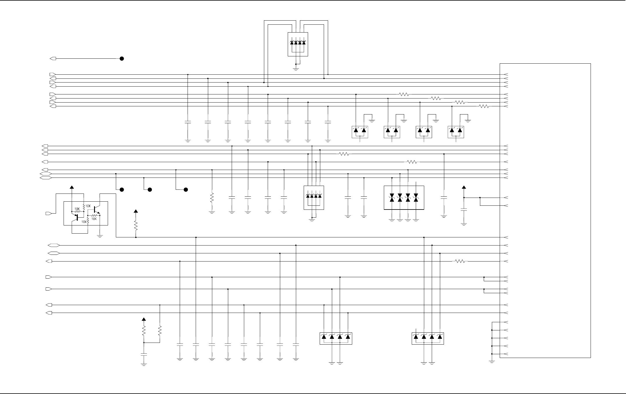
Schematics, Component Location Diagrams, and Parts Lists: HUE4040A (UHF Range 2) Main Board 7-149
6881096C74-B May 25, 2005
Figure 7-103. HUE4040A Rear Accessory Connector Schematic
UARTA_TXD
SPKR-
ONE_WIRE
MONITOR
PTT*
CTS_DCE (DB9-Pin 7)
RTS_DCE (DB9-Pin 8)
UARTB_RXD-BUS-
UARTB_CTS-RESET
UARTA_RTS
SW_B+
CHAN_ACT
UARTA_RXD
UARTB_TXD-BUS+
AUX_MIC
TX_DCE (DB9-Pin 2)
RX_DCE (DB9-Pin 3)
USB_PWR
SPKR+
EMERGENCY
GND
RX_FILT_AUDIO
IGNITION
J0402
26 PIN
CONNECTOR
UARTA_CTS
USB+
UARTB_RTS-BUSY
USB-
VIP_OUT_2_12V
VIP_OUT_1_12V
J0402-27
220pF
9.3V_TX
J0402-1
C0415
J0402-13
J0402-15
C0410
33pF
C0463
J0402-28
33pF
J0402-6
J0402-12
C0417
220pF
C0403
33pF
VR0405
3
12
J0402-31
15V
J0402-10
10K
R0403
3
12
1K
R0435
15V
VR0407
J0402-32
C0409
33pF
R0407 100
J0402-9
C0405
33pF
TP0400
100pF
C0401
25
1346
23
6
4
1
20V
VR0400
Q0400
5
TP0420
C0402
33pF
0
J0402-30
R0430
J0402-22
100pF
C0407
4.7uF
SW_B+
2
A1
5
A2
1
K1
3
K2
4
K3
6
K4
C0420
VR0410
6.8V
J0402-17
3
12
J0402-2
TP0419
15V
VR0406
J0402-18
J0402-16
J0402-25
R0411
J0402-7
10K
J0402-29
33pF
C0464
33pF
4IO4 5
IO5
6
IO6
7
IO7
8
IO8
C0406
VR0411
1
IO1
2
IO2
3
IO3
J0402-8
VCC5
J0402-24
C0466
100pF
C0413
100pF
100pF 220pF
C0419
R0412
C0418
J0402-26
100
C0408
100pF
100
R0408
J0402-19
C0467
100pF
R0406
560
C0400
33pF
220pF
C0414
J0402-4
A1
5
A2
1
K1
3
K2
4
K3
6
K4
J0402-14
VR0408
6.8V
2
J0402-20
J0402-23
C0416
100pF
J0402-5
J0402-21
C0465
470pF
J0402-11
3
12
R0405
1K
15V
VR0404
R0432 100
J0402-3
C0404
33pF
TP0418
100
R0410
100pF
C0412
25
1346
VCC2.85
USB-
USB- U SB-
IGNITION
CHAN_ACT
CHAN_ACT_CONN
20V
VR0402
SPKR-
RX_FILT_AUDIO
MONITOR
PTT*
EMERGENCY
ONE_WIRE ONE_WIRE_CONN
USB_PWR
USB+ U SB+ USB+
VPP
UARTA_CTS
UARTA_RXD
UARTA_RTS
UARTA_TXD
SPKR+
VIP_OUT_1_12V
VIP_OUT_2_12V
BUS+_UARTB_TXD
BUS-_UARTB_RXD
RESET_UARTB_CTS
BUSY_UARTB_RTS
AUX_MIC
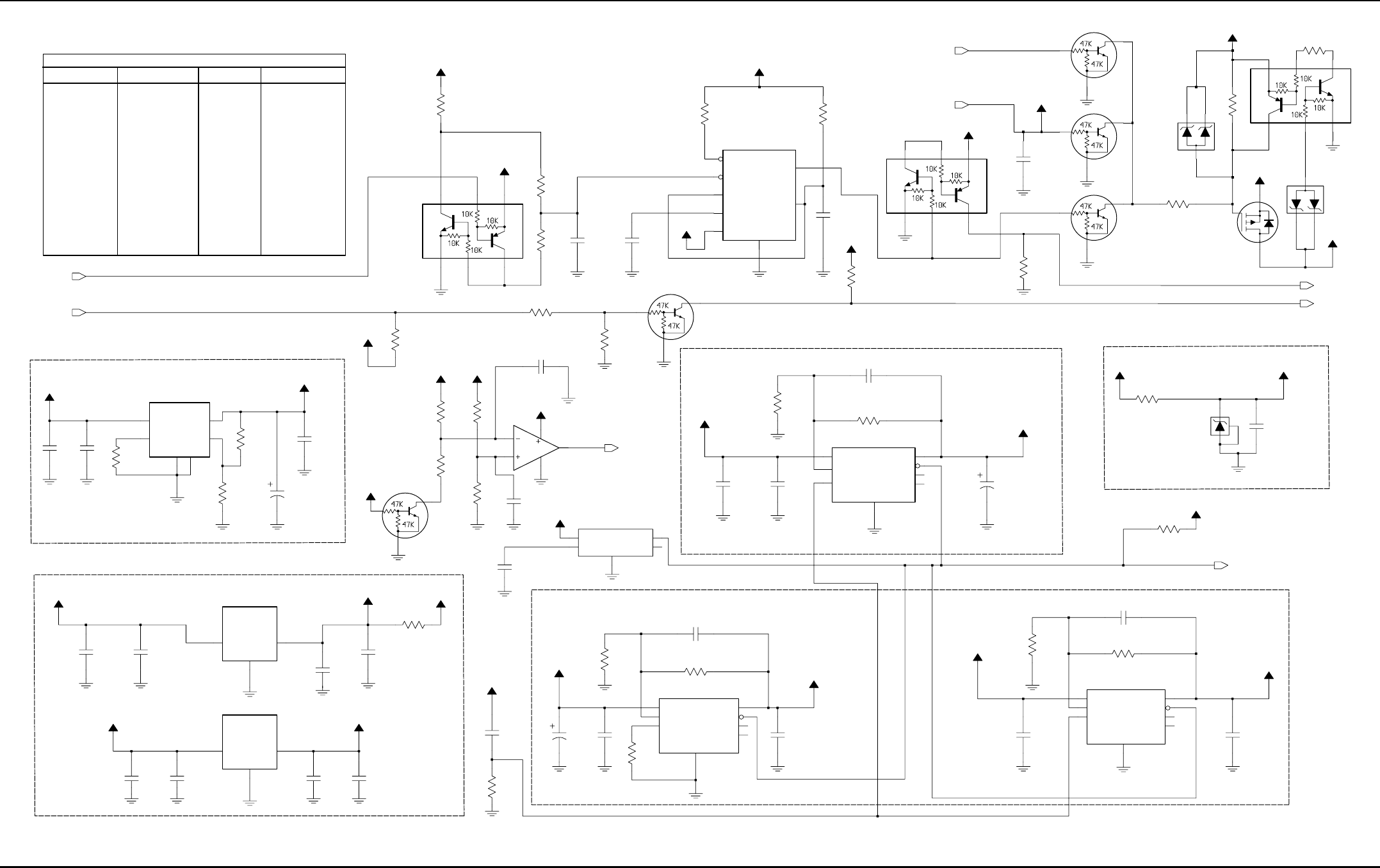
7-150 Schematics, Component Location Diagrams, and Parts Lists: HUE4040A (UHF Range 2) Main Board
May 25, 2005 6881096C74-B
Figure 7-104. HUE4040A Power Supply Schematic
SW_B+
5.0 / Battery
SW_B+
VCC5
FILT_B+
Mic Bias Circuit
USB, Codec
Power Control
Battery
VCC5
NU
SOURCED BY:
VCC3
2.85 / 100 mA
VCC5
NU
VCC1.8, VCC1.55 Patriot, EIM, Memory
5.0 / 500 mA
VOLTAGE
9.3V_TX
Emergency Detect/Timer
VCC2.85
9V Regulators
1.86 & 1.55 / 100 mA
SW_B+ Sense Circuit
Audio PA
FILT_B+ Battery
VCC5 I/O Ring, EEPOTs
9.3V / 1A
UNSW_5V
Voltage Translation
A+
1.8V, 3V Regulators
T-Gates, VIPS, SB9600
Inverted
Non Inverted
3.0 / 100 mA
NU
A+
A+
SUPPLY FOR:
DC DISTRIBUTION
SW_B+
V(operating)/mA(max)
1K
VCC9
OUTPUT 1
SENSE 2
SHUTDOWN
3
VTAP 6
R0515
U0507
ERROR 5
FEEDBACK
7
GND
4
INPUT
8
C0506
VCC2.85
UNSW_5V
.01uF
.01uF
VCC2.85
C0505
10K
VCC1.8
0.1uF
C0520
R0512
ADJ 1
GND1
3
GND2
6
ON_OFF
2
VIN
4VOUT 5
U0500
0.1uF
C0524
VCC9
0.1uF
C0516
100K
R0531
NC 4
OUTPUT 1
C0522
4.7uF
U0504
CD
5
GND
3
INPUT
2
A+
UNSW_5V
SW_A+
C0514
150uF
1.2K
R0529
100pF
C0502
10K
R0506
C0537
1uF
R0514
0
0
R0503
100K
R0516
OUTPUT 3
RESET
4
THRESHOLD
6
TRIGGER
2
VPOS
8
U0506
CONTRLVOLTAGE
5DISCHARGE 7
GND
1
100K
R0500
VCC5_FILT
U0505
GND
2
IN
1OUT 3
1K
R0509
A+
VCC2.85
20K
R0522
0.1uF
C0534 VCC2.85
0.1uF
C0523
VCC5_FILT
UNSW_5V
SW_A+
VCC5
20V
VR0502
330K
R0530
0.1uF
Q0507
Q0504
SW_B+_ON-OFF
C0507
R0511
9.3V_ABACUS
R0525
33K
R0532
3.3K
R0526
100
Q0503
100
3.3K
C0510
R0508
Q0500
4.7uF
.01uF
C0519
22uF
C0533
Q0501
5
23
64
1
R0521
A+
39K
100pF
C0503
0.1uF
C0500
1uF
C0532
SW_B+_ON-OFF
.01uF
R0527
0
R0523
C0526
C0513
100K R0502
390K
150uF
R0518
C0512
10K
R0528
SW_A+
0.1uF
C0527
7.5K
VCC5
5V_ABACUS
UNSW_5V
4.7uF
43K
R0510
15V
VR0501
10K
R0505
U0503
2
GND
1IN 3
OUT
C0504
4
1
0.1uF
Q0508
5
23
6
Q0506
VCC2.85
5.1V
VCC5_FILT
VR0500
C0515
0.1uF
47K
R0520
C0521
4.7uF
R0504
100K
8INPUT 1
OUTPUT
2
SENSE
3SHUTDOWN
VTAP 6
VCC5
U0502
5
ERROR
7FEEDBACK
4
GND
U0604-2
6
5
7
8
4INPUT
8OUTPUT 1
SENSE 2
SHUTDOWN
3VTAP 6
A+
U0501
ERROR 5
FEEDBACK
7
GND
4
VCC5
0.1uF
C0528
0.1uF
C0531
10
R0519
10K
UNSW_5V
R0507
VCC1.55
4.7uF
C0518
R0513
39K
R0524
Q0505
10K
C0525
4.7uF
C0517
1uF
C0535
Q0502
C0529
VCC2.85
0.1uF
EMERGENCY
EMERG_SENSE
4.7uF
IGNITION
SW_B+_SENSE
SW_B+_ON-OFF
SOFT_TURN_OFF
IGNITION_SENSE
LV_DETECT
Emergency Sense Block
5V Regulator
9V Regulator
1.55V Digital Supply Regulator
2.85V Digital Supply Regulator
1.8V Digital Supply Regulator
UNSW_5V Supply
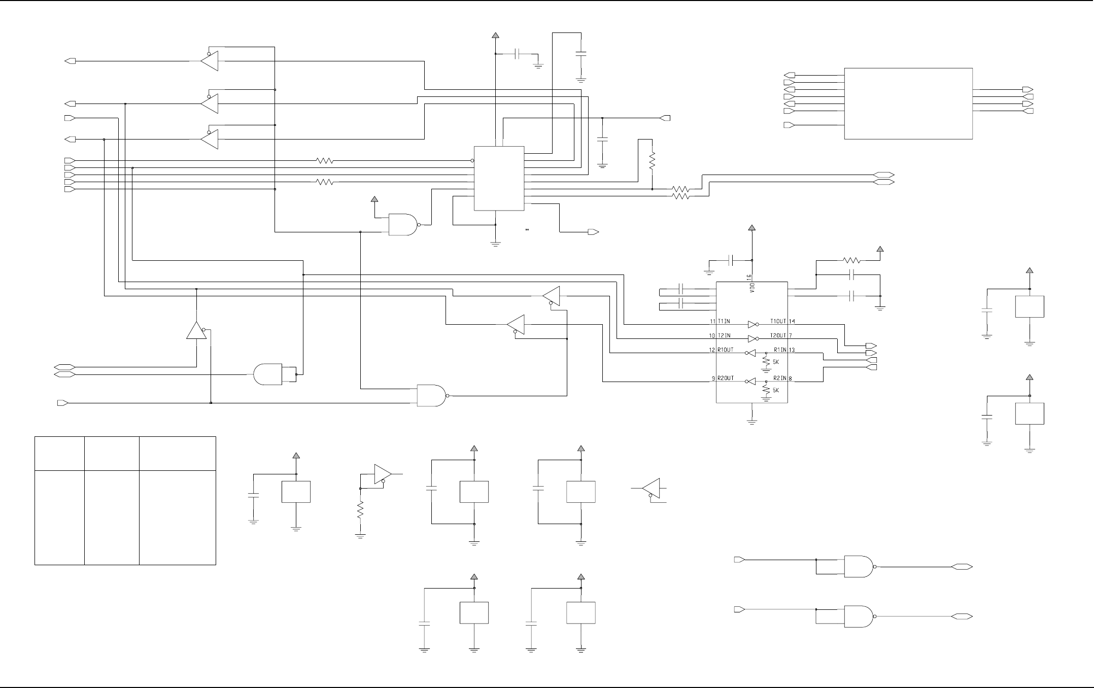
Schematics, Component Location Diagrams, and Parts Lists: HUE4040A (UHF Range 2) Main Board 7-151
6881096C74-B May 25, 2005
Figure 7-105. HUE4040A USB/RS232/SB9600 Schematic
2
4
LMS202E
U0305
VPOS
VNEG
2
6
C1NEG
3
1C1POS
C2NEG
5C2POS
4
5
1DN
G
USB_VPI
USB*_RS232_EN
USB+
USB+
USB_PWR
BOOT_TX
UTXD1_USB_VPOUT
VIP_OUT_1_5V
USB_TXENB
RIA_USBSUSP
VIP_OUT_2_5V
USB_VMI
UARTA_RXD
UARTA_RTS
BOOT_DATA_EN*
UCTS1_USB_FSEN
UCTS1_USB_FSEN
RESET_UARTB_CTS
BUS+_UARTB_TXD
BUS-_UARTB_RXD
BUSY_UARTB_RTS
USB_VMOUT
USB_INT*
BUFFER SUPPLY
1
Not Allowed
Mode of OperationBOOT_DATA_EN* USB*_RS232_EN
00
0
01
1
Boot Data
USB
RS232
SB9600 Block
NP
1
BUFFER SUPPLY
URTS2
URXD2
UTXD2
VCC2.85
5
4
6
BUS+_UARTB_TXD
BUS-_UARTB_RXD
BUSY_UARTB_RTSLHRST_IN
LHRST_OUT RESET_UARTB_CTS
SB96_RS232*_EN
UCTS2
PWR_GND
U0309-2
GND
3
VCC
5
MC74LCX125
U0303-2
U0303-3
MC74LCX125
9
10
8
VCC5
MC74VHC1GT00
U0309-1
$V
1
MC74LCX125
U0300-4
12
13
11
VCC5
NC7ST08
U0308-1
1
2
4U0307-1
MC74VHC1GT00
1
2
4
1
2
4
33R0305
1
2
4
U0605-1
MC74VHC1GT00
C0312
MC74VHC1GT00
U0601-1
0.1uF
PWR_GND
U0303-5
GND
7
VCC
41
22R0310
$V
USB_DET 8
S
U
BV 4
1
C
C
V7
VM 4
VO_VPO
11 VP 3
VPU 15
VREG 13
DPOS 10
ENUMERATE
16
FSE0_VMO
12
DN
G
7
1
6MODE
OE_N
1RCV 2
SUSPND
5
C0306
U0304
ISP1104
DNEG 9
1uF
VCC5
1uFC0310
C0305
VCC9
U0303-1
MC74LCX125
2
1
3
VCC2.85
VCC2.85
0.1uF
12
13
11
C0314
U0303-4
MC74LCX125 0.1uF
9
10
8
R0303
1.5K
5
4
6
U0300-3
MC74LCX125
10K
MC74LCX125
U0300-2
PWR_GND
7
GND
4
1
VCC
R0307
3
GND
5
VCC
VCC2.85
U0300-5
U0601-2
PWR_GND
3
GND
5
VCC
U0605-2
PWR_GND
1uFC0307
3
GND
5
VCC
0.1uF
C0301
U0308-2
PWR_GND
C0605
0.1uF
C0601
0.1uF
$V
1uF
C0315
$V
$V
R0301 100
R0300 100
C0302
0.1uF
VCC5
1uFC0308
33
U0300-1
MC74LCX125
2
1
3
R0304
C0311
0.1uF
C0313
0.1uF
VCC2.85
VCC2.85
GND
5
VCC
1uFC0309
VIP_OUT_1_3V
VIP_OUT_2_3V
U0307-2
PWR_GND
3
UTXD2
UCTS2
LHRST_IN
LHRST_OUT
URTS2
URXD2
BOOT_RX
USB_VPIN
URXD1_USB_VMIN
URXD1_USB_VMIN
URTS1_USB_XRXD
URTS1_USB_XRXD
SB96_RS232*_EN
USB-
USB-
UARTA_CTS
UARTA_TXD

7-152 Schematics, Component Location Diagrams, and Parts Lists: HUE4040A (UHF Range 2) Main Board
May 25, 2005 6881096C74-B
Figure 7-106. HUE4040A Secure SB9600 Schematic
NU
VCC5
1
2
4
R0628
100K
U0608-1
3
GND
5
VCC
100
R0621
3
GND
5
VCC
U0608-2
7
GND
14
VCC
U0607-2
VCC2.85
U0602-5
Q0610
U0603-2
GND
3
VCC
5
12
13
11
VCC5
VCC5
2
1
4
U0602-4
100K
U0603-1
R0634
0.1uF
C0606
R0627
100K
C0613
0.1uF
C0604
0.1uF
U0604-1
2
3
1
8
4
R0629
10K
VCC5
R0636
Q0613
10K
5
VCC
Q0612
10K
U0610-2
3
GND
VCC2.85
R0625
100K
R0626
C0600
0.1uF
0.1uF
C0611
100
R0622
VCC2.85
C0603
U0609-2
3
GND
5
VCC
0.1uF
U0602-2
5
4
6
0.1uF
C0610
R0632
0
VCC2.85
U0611-2
GND
3
VCC
5
U0611-1
1
2
4
R0630
100K
100
R0623
VCC5
U0610-1
1
2
4
VCC2.85
9
10
8
Q0611
U0602-1
2
1
3
U0602-3
10K
R0639
100
R0620
U0607-1
1
2
4
VCC5
100
R0624
C0615
0.1uF
VCC2.85
VCC
4
YA
7
YB
9
YC
12
YD
VCC5
I0B
11 I0C
14 I0D
3I1A
6I1B
10 I1C
13 I1D
1SELECT
16
U0606
15 EN_OE
8
GND
2I0A
5
C0616
100pF R0631
0
R0635
100K
0.1uF
C0614
U0609-1 1
2
4
LHRST_IN
SB96_RS232*_EN
URXD2
URTS2
UTXD2
LHRST_OUT
BUS+_UARTB_TXD
BUSY_UARTB_RTS
RESET_UARTB_CTS
BUS-_UARTB_RXD
UCTS2
NAND SUPPLY
Connector IF
BUFFER SUPPLY
BUFFER SUPPLY
Patriot UART B
BUFFER SUPPLY
NAND SUPPLY NAND SUPPLY
BUFFER SUPPLY
BUSY*
LH_RESET*
BUSY
LH_RESET
BUS+*
BUS-*
BUS-
BUS+
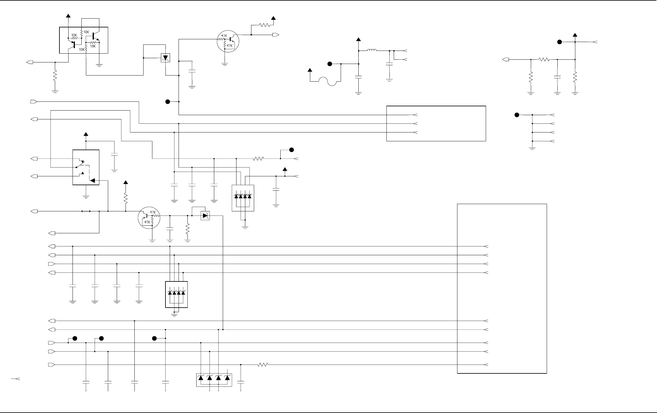
Schematics, Component Location Diagrams, and Parts Lists: HUE4040A (UHF Range 2) Main Board 7-153
6881096C74-B May 25, 2005
Figure 7-107. HUE4040A Secure Control-Head Connector Schematic (Sheet 1 of 2)
Programming Cable Interface
AUDIO
RX_FILT_AUDIO
BOOT_RX
GND
SPKR-
PTT*
IGNITION
EMERGENCY
NOT USED
MIC_HI
SPKR+
AUX_RX
SW_B+
AUX_MIC
BOOT_TX / KEYFAIL*
VCC5
A+
AUX_TX
OPTB+_BOOTSEL_VPP
C0427
J0401-1
100pF
1K
R0404
100pF
10K
C0428
TP0414
R0425
2
VPOS
TP0401
U0401
COM
5
3GND
IN 1
NC
4
NO
6
TP0413
10K
R0409
R0419
J0401-7
1
K1 3
K2 4
K3 6
K4
4.7K
VR0414
2A1
5
A2
100pF
6.8V
TP0402
C0431
6
K4
4.7K
R0517
6.8V
VR0417
2
A1
5
A2
1
K1
3
K2
4
K3
C0441
0.1uF
L0400
10uH
C0433
100pF
C0460
100pF
J0401-5
VR0421
11V
C0421
J0401-50
470pF
10K
R0420
J0401-8
C0429
100pF
VCC5
VCC5
A+
J0401-4
J0401-2
J0401-20
R0431
10K
VR0412
20V
25
1
3
46
100pF
Q0404
C0425
J0401-17
J0401-21
0
R0421
C0435
470pF C0436
470pF
TP0412
J0401-3
C0439
VCC2.85
100pF
33K
R0422
J0401-18
470pF
VCC2.85
J0401-25
C0437
J0401-19
J0401-43 C0440
100pF
C0434
100pF
TP0411
J0401-10
J0401-9
C0432
100pF
J0401-26
J0401-23
TP0403
J0401-6
Q0402
C0426
470pF
J0401-22
J0401-49
C0438
5
2
3
6
4
1
SW_B+
470pF
1
Q0403
A+_ENC
VR0420
11V
2
3
F0400
125V
5A
C0430
100pF
TP0415
BOOT_R X
EMERGENCY
A+_CH
SW_B+_ON-OFF
IGNITION
BOOT_DATA_EN*
PTT*
VCC2.85
AUX_TX
AUX_MIC AUX_MIC
AUX_RX
CABLE_DET
KEYFAIL
MIC_HI
MIC_HI
RX_FILT_AUDI O
IGNITION_CONN
SPKR- SPKR-
MOD
BOOT_T X
FORCE_FAIL*
SPKR+
SPKR+
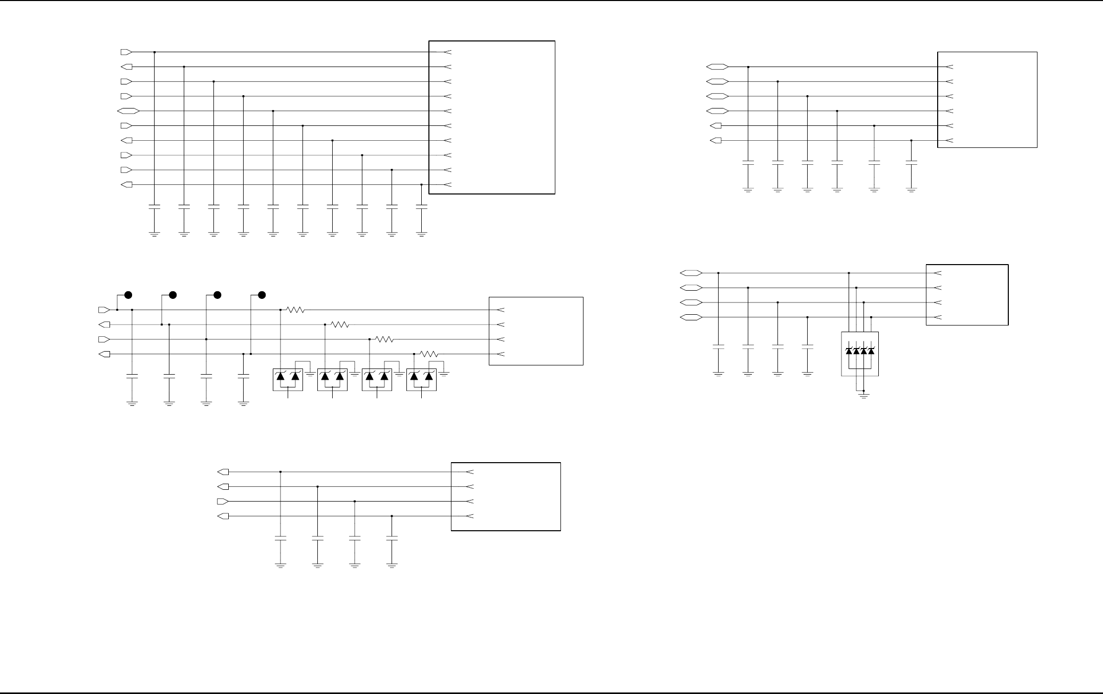
7-154 Schematics, Component Location Diagrams, and Parts Lists: HUE4040A (UHF Range 2) Main Board
May 25, 2005 6881096C74-B
Figure 7-108. HUE4040A Secure Control-Head Connector Schematic (Sheet 2 of 2)
SAP_RX
SAP_DCLK
SAP_FSYNC
SSI_INT
SPI_SCKB
SPI_MISOB
SPI_MOSIB
NAUTILUS_INT*
DCE_TXD
DCE_RXD
DCE_CTS
DCE_RTS
SAP_TX
VIP_OUT_2_12V
BUS-
BUS+
NAUTILUS_CS*
VIP_OUT_1_12V
BUSY
LH_RESET
BUS_PWR_OUT
ONE_WIRE
SPARE_1
SPARE_2
VIP_OUT_2_5V
VIP_IN_1_5V
VIP_OUT_1_5V
VIP_IN_2_5V
C0462C0461
220pF220pF100pF
C0449
100pF
C0448
100pF
C0447
100pF
C0446
33pF
C0445
33pF
C0444
J0401-14
K4
6
J0401-16
6.8V
A1
2
A2
5
K1
1
K2
3
K3
4
VR0418
C0477
100pF
J0401-32
C0476
100pF
C0475
J0401-31
J0401-48
100pF
J0401-47
100
R0418
J0401-46
100
R0417
100
R0416
100
R0415
12
12
15V
VR0423
3
15V
VR0422
3
33pF
C0443
33pF
C0442
33pF
C0423
33pF
C0424
J0401-34
TP0408
J0401-33
TP0407
J0401-30
J0401-28
J0401-29
J0401-27
J0401-12
J0401-11
C0459
33pF
C0450
33pF
J0401-15
J0401-13
33pF
C0456
33pF
C0455
C0478
100pF
33pF
C0452
33pF
C0451
J0401-41
J0401-42
J0401-24
J0401-37
J0401-39
J0401-36
J0401-38
J0401-45
3
12
J0401-35
3
12
15V
VR0425
15V
VR0424
33pF
C0458
33pF
C0457
33pF
C0470
33pF
C0422
33pF
C0454
33pF
C0453
TP0409 TP0410
J0401-40
BUS+_UARTB_TXD
BUS-_UARTB_RXD
BUSY_UARTB_RTS
RESET_UARTB_CTS
J0401-44
UARTA_RXD
UARTA_RTS
UARTA_TXD
UARTA_CTS
BUS_PWR_OUT
SPARE_1
SPARE_2
ONE_WIRE
VIP_IN_2_5V
VIP_OUT_2_5V
VIP_OUT_1_5V
VIP_IN_1_5V
VIP_OUT_1_12V
VIP_OUT_2_12V
SAP_FSYNC
SAP_DCLK
SAP_TX
NAUTILUS_CS*
SPI_MOSIB
SPI_SCKB
SAP_RX
SPI_MISOB
SSI_INT*
NAUTILUS_INT*
UARTA_TXD_CH
UARTA_RXD_CH
UARTA_CTS_CH
UARTA_RTS_CH
VIPs
SB9600
SSI / NAUTILUS
RS232 BUS
FOR NEW CH/ACCYs
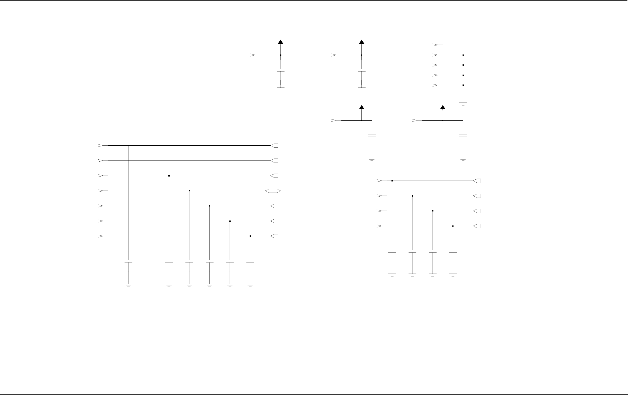
Schematics, Component Location Diagrams, and Parts Lists: HUE4040A (UHF Range 2) Main Board 7-155
6881096C74-B May 25, 2005
Figure 7-109. HUE4040A Secure Interface Connector Schematic
100pF
C0700
C0712
100pF
C0711
100pF
C0710
100pF
C0709
100pF
220pF
C0713
220pF
C0714
100pF
C0708
C0706
100pF
100pF
C0705
100pF
C0704
100pF
C0703
100pF
C0702
100pF
C0701
J0501-16
J0501-13
J0501-17
J0501-11
J0501-14
J0501-12
J0501-15
J0501-19
J0501-20
J0501-18
J0501-4
J0501-1
J0501-5
J0501-6
J0501-3
J0501-2
SAP_TX
TAMPER_ENC
SAP_DCLK
SAP_RX
SAP_FSYNC
WAKEUP
KEYFAIL*
ENC_RESET
ENC_SPARE1
ENC_SPARE2
BOOT*
Control / I/O
J0501-8J0501-7
A+_ENC SW_B+
VCC5
SAP SSI Audio Bus
J0501-10
VCC2.85
J0501-9

7-156 Schematics, Component Location Diagrams, and Parts Lists: HUE4040A (UHF Range 2) Main Board
May 25, 2005 6881096C74-B
Figure 7-110. HUE4040A Secure Interface Board Schematic
11 P501-2
U803-4
12
13
VCC2.85
0.1uF
C811
10K
R806
P501-12
0
R808
J701-13
J701-15 *P501-11*
J701-27
J701-34
J701-12
VCC2.85VCC2.85
J701-36
J701-7
R802
1K
SW_B+
J701-22
J701-24
100K
R807
VCC2.85
J701-16
Q4 8
RESET
12
J701-6
J701-10
U802-2
CLK
13 Q1 11
Q2 10
Q3 9
U803-1
1
2
3
U803-3
9
10
8
P501-9
0.1uF
C809
VCC2.85
PWR_GND
U805-2
GND
3
VCC
5
U805-1
2
1
4
VCC2.85
J701-1
J701-8
A+
J701-19
J701-11
P501-4
J701-3
J701-35
VCC5
0.1uF
SW_B+
100K
C802
R804
4
5
6
VCC2.85
Q802
U802-3
PWR_GND
7
GND
14
VCC
U803-2
RESET
2
PWR_GND
U803-5
GND
7
VCC
14
U802-1
CLK
1Q1 3
Q2 4
Q3 5
Q4 6
J701-20
VCC2.85
J701-17
J701-23
PWR_GND
U804-3
GND
7
VCC
14
J701-4
UNSW_B+_ENC
J701-33
D801
1
2
3
J701-21
Q800
1
3
2
J701-31J701-29
J701-25
R805
10K
R800
10K
J701-32
Q803
47K
47K
P501-17
C803
P501-20
J701-14 A+
0.1uF
P501-7
P501-3
5.6V
VR800
R801
100K
P501-1
P501-10
J701-38
P501-18
2
J701-5
U800
MC33269D
ADJ
1
IN
3OUT
J701-2
VCC5
UNSW_B+_ENC
CLK
11
D
9
Q13
Q* 12
RESET 10
SET
8
J701-39
10uF
VCC2.85
U804-2
C805
1uF
C804
P501-16
J701-30
0.1uF
C808
0.1uF
C807
SW_B+_ENC
0.1uF
C806
U804-1
CLK
3
D
5
Q1
Q* 2
RESET 4
SET
6
3GND
2
1
NC
4
5
VCC
U801
0.1uF
J701-18
C801
0.47
C810
P501-15
SW_B+_ENC
J701-40
J701-26 P501-13
J701-37
J701-9
J701-28
P501-14
P501-19
P501-6
P501-8
P501-5
SAP_TX
SAP_TX
ENC_SEL
TAMPER_ENC TAMPER_ENC
BOOT*
ENC_SPARE2
ENC_SPARE1
ENC_RESET
WAKEUP
SAP_RX
SAP_FSYNC
SAP_DCLK
KEYFAIL*
KEYFAIL*
MAEPF-27914-O
Part Series
800
Schematics, Component Location Diagrams, and Parts Lists: HUE4040A (UHF Range 2) Main Board 7-157
6881096C74-B May 25, 2005
Figure 7-111. HUE4040A Main Board Layout—Side 1 Top
03
8485912F01
REV A
C5280
C5282
C5283
C5284
C5285
C5287
C5288
C5289
C5290
C5291
C5292
C5293
C5294
C5295
C5296
C5297
C5299
C5300
C5301
C5302
C5303
C5305
C5329
C5333
C5343
C5345
C5350
C5351
C5352C5353
C5354
C5355
C5356
C5357
C5358
C5359
C5362
C5363
C5364
C5365
C5366
C5370
C5374
C5375
C5378
C5380
C5381
C5382
C5383
C5385
C5388
C5400
C5401
C5402
C5403
C5404
C5405
C5406
C5408
C5410
C5411
C5412
C5413
C5414
C5417
C5418
C5425
C5426
C5427
C5428
C5429
C5430
C5722
D5280
D5300
D5301 D5302
D5303
D5311
D5380
D5381
E5400
3
2
J5701
L5280
L5281
L5282
L5283
L5284
L5285
L5286
L5287
L5288 L5289
L5290
L5302
L5305
L5306
L5307
L5309
L5380
L5383
L5385
L5389
L5392
L5400
L5401
L5403
L5404
L5406
L5407
L5408
Q5250
Q5251
Q5252
Q5253
Q5257
Q5401
R5300
R5301
R5302
R5303
R5304
R5305
R5306
R5307
R5308
R5309
R5310
R5311
R5321
R5327
R5328R5329
R5330
R5332
R5333 R5337
R5380
R5381
R5382
R5383
R5384
R5385
R5386
R5388
R5400
R5401 R5402
R5403
R5404
R5411
R5412
R5413
R5414
R5415
R5710
R5713
SH5701
15
43
T5380
TP5301
U5300
1
16
8
9
U5303
2
3
456
Y5400
7-158 Schematics, Component Location Diagrams, and Parts Lists: HUE4040A (UHF Range 2) Main Board
May 25, 2005 6881096C74-B
Figure 7-112. HUE4040A Main Board Layout—Side 1 Middle
C0703
C0705
C5002
C5005
C5007
C5008
C5009
C5010
C5012
C5013
C5015
C5016
C5017
C5019
C5020
C5021
C5022
C5023
C5024
C5026
C5027
C5028
C5030
C5046
C5051
C5052
C5061
C5064
C5065
C5066
C5067
C5068
C5069
C5070
C5071
C5505
C5507
C5509 C5513
C5515
C5517
C5526
C5541
C5544
C5570 C5572
C5578
C5579
C5677
C5708
C5719
C5750
C5752
C5754
C5757
C5758
C5759
C5760 C5761
C5762
C5765
C5768
C5771
C5815
C5817
C5826
C5829
C5830
C5831
C5834
C5835
C5838
C5840
C5842
C5844
C5846
C5847
C5850
C5851
C5854
C5859
C5860
C5861
C5862
C5863
C5900
C5901
C5904
C5905 C5906
C5907
C5908
C5910
C5911
C5912
C5913
C5914
C5915
C5916
C5917
C5920
C5922
C5923
C5924
C5925
C5926
C5927
C5928
C5929
C5930 C5931
CLKOUT
D5003
D5501
D5502
D5828
D5832
D5901
D5902
D5903
D5904
D5905
D5906
D5909
D5910
DOUTA
E5001
E5006
E5007
FS
J0501
L5002
L5003
L5004
L5012
L5013
L5015
L5502
L5503
L5505
L5751
L5753
L5755
L5826
L5828
L5830
L5832
L5834
L5835
L5900
L5901
L5902
L5904
L5905
L5906
L5908
L5909
L5912
L5913
M5501
M5502
PC
PD
PE
Q5003
Q5503
Q5570
Q5750
Q5751
Q5826
Q5829
Q5901
Q5903
R5000
R5001
R5003
R5005
R5014
R5015
R5016
R5017
R5018
R5019
R5020
R5025
R5026
R5027
R5028
R5030
R5031
R5032
R5033
R5034
R5035
R5508
R5509 R5517
R5519
R5522
R5538
R5539
R5540
R5541
R5543
R5545
R5546
R5547
R5548
R5549
R5550
R5551
R5552
R5553
R5554
R5555
R5556
R5557
R5570
R5571
R5750 R5751
R5752
R5753
R5754
R5758
R5759
R5761
R5762
R5763
R5764
R5765
R5766
R5767
R5787
R5826
R5828
R5830
R5832
R5834
R5838
R5840
R5842
R5851
R5852
R5853
R5854
R5900
R5903
R5904
R5905
R5909
R5910
R5911
R5912
R5915
R5916
R5918
R5919
R5920
R5922
R5923
R5948
SH5703
SH5820 SH5901
SH5902
TP5788
1
37
25
13
U5002
U5502
U5503
7
814
U5504
U5750
U5751
2
34
Y5750
Y5801
Y5900
Y5901

Schematics, Component Location Diagrams, and Parts Lists: HUE4040A (UHF Range 2) Main Board 7-159
6881096C74-B May 25, 2005
Figure 7-113. HUE4040A Main Board Layout—Side 1 Bottom
C0100
C0101
C0105
C0108
C0200
C0204
C0207
C0213
C0214
C0217
C0220
C0223
C0243
C0301
C0312
C0314
C0315
C0401
C0406
C0407
C0412
C0413
C0417
C0428
C0436
C0437
C0442
C0444
C0450
C0452
C0454
C0455
C0458
C0461
C0463
C0464
C0467
C0502
C0503
C0519
C0531
C0532
C0533
C0600
C0603 C0604
C0606
C0610
C0611
C0613
C0614
C0615
C0616
C0900
C0924
C0952
C0953
C0954
C0955
C0956
C0957
C0959
C0962 C0963
C0964
C0965
C0966 C0967
C0971
C0972
C0973
C0975
C0976
C0978
C0979
C0980
C0981
C0983
C0984
C0986
C0987
D0952
50 49
21
J0401
J0950
Q0200
3
4
1
Q0503
Q0506
Q0507
Q0508
Q0610
Q0611
Q0612
Q0613
Q0955
R0101R0102
R0103
R0104
R0109
R0110
R0111R0532
R0113
R0114R0115
R0116
R0117
R0119
R0120
R0121 R0122
R0123
R0124
R0125
R0200
R0204
R0211
R0215
R0220
R0222
R0300
R0301
R0303
R0304
R0305
R0415
R0422
R0425
R0430
R0505
R0508
R0509
R0515
R0517
R0530
R0531
R0620
R0621
R0622
R0623
R0624
R0625
R0626
R0627
R0628
R0629
R0630
R0631
R0632
R0634
R0635
R0636
R0639
R0908
R0915
R0916
R0923
R0924
R0946
R0947
R0950
R0951
R0952
R0953
R0954
R0960
R0963
R0964
R0967
R0968
R0969
R0970
R0971
R0972
R0973
R0974
R0975 R0976
R0977
R0978
R0979
R0980
R0981 R0982
R0983
R0984
R0985
R0986
R0987
R0988
R0989
R0990
R0992
R0993
R0994
R0995
R0996
R0997
R0998
R0999
SC0001
SC0002
TP0002
TP0400
TP0401
TP0402
TP0403
TP0407
TP0408
TP0409
TP0410
TP0411
TP0412
TP0413
TP0414
TP0415
TP0954
123456789101112131415161718
18171615141312111098765432
A
B
C
D
E
F
G
N
M
L
K
J
I
H
R
S
T
U
V
W
X
P
Z
YY
Z
P
X
W
V
U
T
S
R
H
I
J
K
L
M
N
G
F
E
D
C
B
A
U0001
U0102
11
10
9
U0204
5
9
13
U0304
4
3
5
U0309
U0504
14
7
8
U0602 U0603
1
4
58
U0604
16 9
8
1
U0606
U0607
U0608
4
3
5
U0609
4
3
5
U0610
43
5
U0611
5
U0950
5
U0951
10
6
5
U0952
7
8
14
U0955
7
8
14
U0956
7
814
U0957
16 9
8
1
U0959
VR0405
VR0406
VR0407
VR0501 VR0502
Y0100
7-160 Schematics, Component Location Diagrams, and Parts Lists: HUE4040A (UHF Range 2) Main Board
May 25, 2005 6881096C74-B
Figure 7-114. HUE4040A Main Board Layout—Side 2 Top
C0102
C0103
C0104
C0106
C0107
C0201
C0202
C0203
C0205
C0208
C0209
C0210
C0211
C0212
C0215
C0216 C0221
C0224
C0226
C0227
C0230
C0231
C0232
C0233
C0234
C0235
C0236
C0237 C0238
C0239
C0240
C0242
C0244
C0302
C0305
C0306
C0307
C0308
C0309
C0310
C0311
C0313
C0400
C0402
C0403
C0404 C0405
C0408
C0409
C0410
C0414
C0415
C0416
C0418
C0419
C0420
C0421
C0422
C0423 C0424
C0425
C0426
C0427
C0429 C0430
C0435
C0441
C0443
C0445
C0449
C0451
C0453
C0456
C0457
C0459
C0465
C0466
C0470
C0475
C0476
C0477
C0478
C0500
C0504
C0505
C0506
C0507
C0510
C0512
C0513
C0514
C0515
C0516
C0517
C0518
C0524
C0525
C0526
C0527
C0528
C0529
C0534
C0535
C0537
C0601
C0605
C0715
C0722
C0724
C0729
C0901
C0902
C0903
C0904
C0905
C0906
C0907
C0908
C0909
C0910
C0911
C0912
C0913
C0914
C0915
C0918
C0919
C0920
C0921
C0922
C0923
C0930
C0933
C0934
C0935
C0936
C0937
C0940
C0941
C0942
C0943
C0944
C0945
C0950 C0951
C0960
C0961
C0968
C0969
C0970
C0974
C0982
C0985
C0989
C0990
C0991
C0997
C0998
D0950
D0951
D0954
F0400
FL0900
32
31
2
J0402
L0400
Q0101
Q0102
Q0400
Q0402
Q0403 Q0404
Q0500
Q0501
Q0502
Q0504
Q0505
Q0951
4
5
8
Q0952
Q0953
Q0954
Q0956
Q0960
R0105
R0106
R0107
R0108
R0126
R0127
R0128
R0129
R0130
R0201
R0205
R0206
R0208
R0209
R0210
R0212
R0213
R0216
R0218
R0219
R0221
R0223
R0224
R0225
R0227
R0228
R0229
R0230
R0231
R0235
R0236
R0307
R0310
R0403
R0404
R0405
R0406
R0407
R0408
R0409
R0410
R0411
R0412
R0416
R0417
R0418
R0419
R0420
R0421
R0431
R0432
R0435
R0500
R0502
R0503
R0504
R0506
R0507
R0510
R0511
R0512
R0513
R0514
R0516
R0518
R0519
R0520
R0521
R0522
R0523
R0524
R0525
R0526
R0527
R0528
R0529
R0703
R0739
R0900
R0901
R0902 R0903
R0904
R0905
R0906
R0910
R0911
R0912
R0913 R0914
R0917
R0930
R0931
R0932
R0933
R0934
R0935
R0936
R0937
R0938
R0939
R0940
R0941
R0942
R0943
R0944
R0945
R0948
R0949
R0955
R0956
R0957
R0958
R0959
R0961
R0962
R0965
R0966
R0991
TP0200
TP0203
TP0204 TP0205 TP0206
TP0418
TP0419
TP0420
TP0930
TP0931
TP0936
TP0937
TP0938
TP0939
TP0940
TP0941
TP0942
TP0950
TP0951
TP0952
TP0953
TP0955
TP0956
TP0957
TP0958
TP0959
TP0960
TP0961
TP0962
TP0963
TP0964
14
78
U0103
14
7
8
U0104
4
3
5
U0105
1
20
11
10
U0200
7
814
U0201
14
58
U0202
43
6
U0203
1
45
8
U0206
U0207
4
3
6U0208
4
3
6U0209
4
3
6
U0210
14
7
8
U0300
14
7
8
U0303
16
1
8
9
U0305
43
5
U0307
U0308
43
6
U0401
1
6
5
U0500
1
4
58
U0501
14
58
U0502
3
2
1
U0503
1
4
58
U0506
1
45
8
U0507
4
3
5
U0601
4
3
5
U0605
U0900
G7 G1
A7 A1
U0901
43
6
U0902
U0903
4
3
6
U0904
4
3
6
U0905
11
120
10
U0953
4
3
5
U0954
4
3
5
U0958
7
814
U0960
U0962
U0963
U0965
U0967
VR0400
VR0402
VR0404
VR0408
VR0410
4
58
VR0411
VR0418
VR0420
VR0421
VR0422
VR0423
VR0424
VR0425
VR0500
VR0950

Schematics, Component Location Diagrams, and Parts Lists: HUE4040A (UHF Range 2) Main Board 7-161
6881096C74-B May 25, 2005
Figure 7-115. HUE4040A Main Board Layout—Side 2 Middle
C0431
C0432
C0433 C0434
C0438
C0439
C0440
C0446
C0447
C0448
C0449
C0460
C0462
C0520
C0521
C0522
C0523
C0700 C0701
C0702
C0704
C0706
C0708 C0709
C0710 C0711
C0712
C0713
C0714
C5001
C5003
C5004 C5006
C5011
C5014
C5018
C5025
C5029
C5032
C5033
C5034
C5037
C5038
C5039
C5040
C5041
C5044
C5045
C5048
C5049
C5050
C5056
C5057 C5058
C5059
C5060
C5062
C5063
C5072
C5073
C5501
C5502
C5503
C5504
C5506
C5508
C5510
C5511
C5512
C5514
C5516
C5518
C5519
C5520
C5521
C5522
C5523
C5524
C5525
C5527
C5535C5538
C5539
C5540
C5542C5543
C5545C5546
C5548
C5549
C5550
C5551
C5552
C5553
C5554
C5555
C5556
C5557
C5558
C5559 C5560
C5563
C5565
C5566
C5567
C5568
C5569
C5571
C5573
C5575
C5576
C5580
C5681
C5701
C5702
C5703
C5704
C5705
C5706
C5707
C5709
C5710
C5751
C5753
C5755
C5756
C5763
C5764
C5766
C5767
C5769
C5770
C5772
C5773
C5774
C5775
C5776
C5777
C5778
C5779
C5780
C5781
C5782
C5783
C5784
C5785
C5786
C5787
C5788
C5789
C5790
C5791
C5792
C5793
C5794
C5795
C5796
C5797
C5798
C5799
C5800
C5801
C5803
C5804
C5805
C5806
C5807
C5808
C5809
C5810
C5811
C5812
C5813
C5816
C5825
C5827
C5828
C5832
C5833
C5836
C5837
C5839
C5841
C5843
C5845
C5848
C5849
C5852
C5853
C5855
C5856
C5857
C5858
C5909
C5919
C5921
C5932
C5933
C5935
C5936
C5937
C5938
C5939
C5940
C5941
C5942
C5943
C5944
C5945
C5946
C5947
C5948
C5949
C5950
C5951
C5956
C5957
C5958 C5959
C5960
D5002
D5701
D5702
D5703
D5750D5751
D5827
D5831
D5833
D5900
D5907
D5908
D5911
D5912
E5002
E5003
E5004
E5005
E5008
E5009
E5501
E5502
E6750
L5001
L5006
L5007
L5008
L5010
L5053
L5501
L5504
L5506
L5507
L5508
L5510
L5701
L5702
L5703
L5704
L5705
L5750
L5752
L5754
L5756
L5757
L5758
L5759
L5760
L5825
L5827
L5829
L5831
L5833
L5907
L5910
L5911
L5914
L5915
L5916
L5917
L5918
L5919
L5920
L5922
Q5001
Q5002
Q5501
1
2
3
Q5502
Q5706 Q5707
Q5708
Q5709
Q5710
Q5752
Q5755
Q5825
Q5828
Q5902 Q5904
Q5905
Q5906
R5002
R5006
R5008
R5010
R5011
R5013
R5022
R5023
R5029
R5050
R5051
R5501
R5502
R5503
R5504
R5505
R5506
R5507
R5510
R5511
R5512
R5513
R5514
R5515
R5516
R5520
R5521
R5523
R5524
R5525
R5526
R5527
R5528
R5529
R5530
R5532
R5533
R5534
R5535
R5536
R5537
R5542
R5544
R5572
R5573
R5701
R5755
R5768
R5769
R5770
R5771
R5772
R5773
R5774
R5775
R5776
R5777
R5778
R5779
R5780 R5782
R5783
R5784
R5785
R5786
R5788
R5825
R5827
R5829
R5831
R5833
R5837
R5839
R5841
R5843
R5845
R5846
R5848
R5849
R5850
R5902
R5914
R5917
R5921
R5924
R5926
R5927
R5928
R5929
R5930
R5931
R5932
R5933
R5934
R5935
R5937
R5938
R5939
R5940
R5941
R5942
R5949
R5950
SH5821
SH5900
TP5501
TP5502
TP5503
TP5570
TP5760
TP5783
TP5787
TP5789
TP5790
TP5791
TP5792
TP5793
TP5794
TP5795
TP5796
TP5797
TP5798
TP5799
3
2
1
U0505
U5001
1
16
8
9
U5501
1
6
5
U5570
1
37
25
13
U5752
16
8
9
U5753
VR0412
VR0414
VR0417
Y5800
Y5902
7-162 Schematics, Component Location Diagrams, and Parts Lists: HUE4040A (UHF Range 2) Main Board
May 25, 2005 6881096C74-B
Figure 7-116. HUE4040A Main Board Layout—Side 2 Bottom
C5250
C5251
C5252
C5253
C5254
C5255
C5256
C5257
C5258
C5259
C5304
C5306
C5307
C5308
C5309
C5310
C5311
C5312
C5313
C5314
C5315
C5316
C5317
C5318
C5319
C5320
C5321
C5322
C5323
C5324
C5325
C5326
C5327
C5328
C5330
C5331
C5332
C5334
C5335
C5336
C5337
C5338
C5339
C5340
C5341
C5342
C5344
C5346
C5347
C5348
C5349
C5360
C5361
C5367
C5368
C5377
C5379
C5386
C5389
C5390
C5391
C5407
C5409
C5415
C5416
C5419
C5420
R5408
C5422
C5423
C5424
C5431
C5432
C5433
C5711
C5712
C5713
C5714
C5715
C5716
C5717
C5718
C5720
C5721
D5250
D5251
D5252
D5253
D5281
D5282
D5304
D5305
D5306
D5307
D5313
D5400
D5704
D5705
L5237
L5250
L5251
L5252
L5253
L5254
L5255
L5256
L5257
L5258
L5291
L5292
L5293
L5294
L5295
L5296
L5297
L5298
L5299
L5300
L5301
L5303
L5304
L5308
L5381
L5382
L5384
L5386
L5387
L5388
L5390
L5402
L5411
L5706
L5707
L5708 L5712
L5713
Q5254
Q5255
Q5256
Q5258
Q5402
R5250
R5251
R5252
R5253
R5254
R5255
R5256
R5312
R5313
R5314
R5315
R5316 R5317
R5318
R5319
R5322
R5323
R5324
R5325
R5326
R5334
R5335
R5336
R5387
R5405
R5406
R5407
R5702
R5703
R5704
R5705
R5706
R5707
R5708
R5709
R5711 R5712
SH5400 SH5702
SH5704
15
4
3
T5381
TP5250
TP5251
TP5252
TP5302
TP5303
TP5304
3
2
1
U5301
34
5
U5302
U5400
2
3
4
5
6
Y5401
Schematics, Component Location Diagrams, and Parts Lists: HUE4040A (UHF Range 2) Main Board 7-163
6881096C74-B May 25, 2005
HUE4040A Main Board Parts List
Reference
Designator
Motorola
Part Number Description
C0001 2380090M24 CAP ALU 10 20 50V SURF MT
C0100 2113743N32 CAP CHIP 18.0 PF 5% COG
C0101 2113743N32 CAP CHIP 18.0 PF 5% COG
C0102 2113743M24 CAP CHIP 100000 PF +80-
20% Y5V
C0103 2113743M24 CAP CHIP 100000 PF +80-
20% Y5V
C0104 2113743M24 CAP CHIP 100000 PF +80-
20% Y5V
C0105 2113743M24 CAP CHIP 100000 PF +80-
20% Y5V
C0106 2113743N50 CAP CHIP 100 PF 5% COG
C0107 2113743L09 CAP CHIP 470 PF 10% X7R
C0108 2113743N50 CAP CHIP 100 PF 5% COG
C0200 2113743A31 CAP CHIP 1.0 UF 10% X7R
C0201 2113743M24 CAP CHIP 100000 PF +80-
20% Y5V
C0202 2113743M24 CAP CHIP 100000 PF +80-
20% Y5V
C0203 2113928S04 CAP CER CHIP 0.100UF 10V
0402
C0204 2185802B01 CAP 10V 4.7UF
C0207 2113743N38 CAP CHIP 33.0 PF 5% COG
C0208 2113743A31 CAP CHIP 1.0 UF 10% X7R
C0209 2113743M24 CAP CHIP 100000 PF +80-
20% Y5V
C0210 2113743M24 CAP CHIP 100000 PF +80-
20% Y5V
C0211 2113743N50 CAP CHIP 100 PF 5% COG
C0212 2113743M24 CAP CHIP 100000 PF +80-
20% Y5V
C0213 2113743M24 CAP CHIP 100000 PF +80-
20% Y5V
C0214 2113741N69 CAP CHIP CL2 X7R 10%
100000
C0215 2113928S04 CAP CER CHIP 0.100UF 10V
0402
C0216 2113743M24 CAP CHIP 100000 PF +80-
20% Y5V
C0217 2113743L29 CAP CHIP 3300 PF 10% X7R
C0220 2311049A57 CAP TANT CHIP A/P 10UF
10% 16V
C0221 2311049A78 CAP TANT CHIP 10.0 UF 10%
50V
C0223 2185802B01 CAP 10V 4.7UF
C0224 2113743M24 CAP CHIP 100000 PF +80-
20% Y5V
C0226 2113928S04 CAP CER CHIP 0.100UF 10V
0402
C0227 2113743M24 CAP CHIP 100000 PF +80-
20% Y5V
C0230 2113743L09 CAP CHIP 470 PF 10% X7R
C0231 2113743L01 CAP CHIP 220 PF 10% X7R
C0232 2113743L09 CAP CHIP 470 PF 10% X7R
C0233 2113743L01 CAP CHIP 220 PF 10% X7R
C0234 2113928S04 CAP CER CHIP 0.100UF 10V
0402
C0235 2113743L09 CAP CHIP 470 PF 10% X7R
C0236 2113743L09 CAP CHIP 470 PF 10% X7R
C0237 2113743L01 CAP CHIP 220 PF 10% X7R
C0238 2113743L01 CAP CHIP 220 PF 10% X7R
C0239 2113743M24 CAP CHIP 100000 PF +80-
20% Y5V
C0240 2113928S04 CAP CER CHIP 0.100UF 10V
0402
C0242 2113928S04 CAP CER CHIP 0.100UF 10V
0402
C0243 2113945B01 CAP CER CHP 6800PF 25V
10%
C0244 2113945B01 CAP CER CHP 6800PF 25V
10%
C0301 2113743M24 CAP CHIP 100000 PF +80-
20% Y5V
C0302 2113743M24 CAP CHIP 100000 PF +80-
20% Y5V
C0305 2113743M24 CAP CHIP 100000 PF +80-
20% Y5V
C0306 2113743A31 CAP CHIP 1.0 UF 10% X7R
C0308 2113743A31 CAP CHIP 1.0 UF 10% X7R
C0309 2113743A31 CAP CHIP 1.0 UF 10% X7R
C0310 2113743A31 CAP CHIP 1.0 UF 10% X7R
C0311 2113743M24 CAP CHIP 100000 PF +80-
20% Y5V
C0312 2113743M24 CAP CHIP 100000 PF +80-
20% Y5V
C0313 2113743M24 CAP CHIP 100000 PF +80-
20% Y5V
Reference
Designator
Motorola
Part Number Description
C0314 2113743M24 CAP CHIP 100000 PF +80-
20% Y5V
C0315 2113743A31 CAP CHIP 1.0 UF 10% X7R
C0400 2113743N38 CAP CHIP 33.0 PF 5% COG
C0401 2113743N50 CAP CHIP 100 PF 5% COG
C0402 2113743N38 CAP CHIP 33.0 PF 5% COG
C0403 2113743N38 CAP CHIP 33.0 PF 5% COG
C0404 2113743N38 CAP CHIP 33.0 PF 5% COG
C0405 2113743N38 CAP CHIP 33.0 PF 5% COG
C0406 2113743N38 CAP CHIP 33.0 PF 5% COG
C0407 2113743N50 CAP CHIP 100 PF 5% COG
C0408 2113743N50 CAP CHIP 100 PF 5% COG
C0409 2113743N38 CAP CHIP 33.0 PF 5% COG
C0410 2113743N38 CAP CHIP 33.0 PF 5% COG
C0412 2113743N50 CAP CHIP 100 PF 5% COG
C0413 2113743N50 CAP CHIP 100 PF 5% COG
C0414 2113743L01 CAP CHIP 220 PF 10% X7R
C0415 2113743L01 CAP CHIP 220 PF 10% X7R
C0416 2113743N50 CAP CHIP 100 PF 5% COG
C0417 2113743L01 CAP CHIP 220 PF 10% X7R
C0418 2113743L01 CAP CHIP 220 PF 10% X7R
C0419 2113743N50 CAP CHIP 100 PF 5% COG
C0420 2185802B01 CAP 10V 4.7UF
C0421 2113741B13 CAP CHIP CL2 X7R REEL 470
C0422 2113743N38 CAP CHIP 33.0 PF 5% COG
C0423 2113743N38 CAP CHIP 33.0 PF 5% COG
C0424 2113743N38 CAP CHIP 33.0 PF 5% COG
C0425 2113743N50 CAP CHIP 100 PF 5% COG
C0426 2113741B13 CAP CHIP CL2 X7R REEL 470
C0427 2113743N50 CAP CHIP 100 PF 5% COG
C0428 2113743N50 CAP CHIP 100 PF 5% COG
C0429 2113743N50 CAP CHIP 100 PF 5% COG
C0430 2113743N50 CAP CHIP 100 PF 5% COG
C0431 2113743N50 CAP CHIP 100 PF 5% COG
C0432 2113743N50 CAP CHIP 100 PF 5% COG
C0433 2113743N50 CAP CHIP 100 PF 5% COG
C0434 2113743N50 CAP CHIP 100 PF 5% COG
C0435 2113743L09 CAP CHIP 470 PF 10% X7R
C0436 2113741B13 CAP CHIP CL2 X7R REEL 470
C0437 2113741B13 CAP CHIP CL2 X7R REEL 470
C0438 2113743L09 CAP CHIP 470 PF 10% X7R
Reference
Designator
Motorola
Part Number Description
C0439 2113743N50 CAP CHIP 100 PF 5% COG
C0440 2113743N50 CAP CHIP 100 PF 5% COG
C0441 2113743M24 CAP CHIP 100000 PF +80-
20% Y5V
C0442 2113743N38 CAP CHIP 33.0 PF 5% COG
C0443 2113743N38 CAP CHIP 33.0 PF 5% COG
C0444 2113743N38 CAP CHIP 33.0 PF 5% COG
C0445 2113743N38 CAP CHIP 33.0 PF 5% COG
C0446 2113743N50 CAP CHIP 100 PF 5% COG
C0447 2113743N50 CAP CHIP 100 PF 5% COG
C0448 2113743N50 CAP CHIP 100 PF 5% COG
C0449 2113743N50 CAP CHIP 100 PF 5% COG
C0450 2113743N38 CAP CHIP 33.0 PF 5% COG
C0451 2113743N38 CAP CHIP 33.0 PF 5% COG
C0452 2113743N38 CAP CHIP 33.0 PF 5% COG
C0453 2113743N38 CAP CHIP 33.0 PF 5% COG
C0454 2113743N38 CAP CHIP 33.0 PF 5% COG
C0455 2113743N38 CAP CHIP 33.0 PF 5% COG
C0456 2113743N38 CAP CHIP 33.0 PF 5% COG
C0457 2113743N38 CAP CHIP 33.0 PF 5% COG
C0458 2113743N38 CAP CHIP 33.0 PF 5% COG
C0459 2113743N38 CAP CHIP 33.0 PF 5% COG
C0460 2113743N50 CAP CHIP 100 PF 5% COG
C0461 2113743L01 CAP CHIP 220 PF 10% X7R
C0462 2113743L01 CAP CHIP 220 PF 10% X7R
C0463 2113743N38 CAP CHIP 33.0 PF 5% COG
C0464 2113743N38 CAP CHIP 33.0 PF 5% COG
C0465 2113741B13 CAP CHIP CL2 X7R REEL 470
C0466 2113743N50 CAP CHIP 100 PF 5% COG
C0467 2113743N50 CAP CHIP 100 PF 5% COG
C0470 2113743N38 CAP CHIP 33.0 PF 5% COG
C0475 2113743N50 CAP CHIP 100 PF 5% COG
C0476 2113743N50 CAP CHIP 100 PF 5% COG
C0477 2113743N50 CAP CHIP 100 PF 5% COG
C0478 2113743N50 CAP CHIP 100 PF 5% COG
C0500 2113743M24 CAP CHIP 100000 PF +80-
20% Y5V
C0502 2113743N50 CAP CHIP 100 PF 5% COG
C0503 2113743N50 CAP CHIP 100 PF 5% COG
C0504 2113741N69 CAP CHIP CL2 X7R 10%
100000
Reference
Designator
Motorola
Part Number Description
7-164 Schematics, Component Location Diagrams, and Parts Lists: HUE4040A (UHF Range 2) Main Board
May 25, 2005 6881096C74-B
C0505 2113743L41 CAP CHIP 10000 PF 10% X7R
C0506 2113743L41 CAP CHIP 10000 PF 10% X7R
C0507 2113743M24 CAP CHIP 100000 PF +80-
20% Y5V
C0510 2185802B01 CAP 10V 4.7UF
C0512 2113743M24 CAP CHIP 100000 PF +80-
20% Y5V
C0513 2311049A43 CAP TANT CHIP 150 10 6
C0514 2311049A43 CAP TANT CHIP 150 10 6
C0515 2113743M24 CAP CHIP 100000 PF +80-
20% Y5V
C0516 2113743M24 CAP CHIP 100000 PF +80-
20% Y5V
C0517 2185802B01 CAP 10V 4.7UF
C0518 2185802B01 CAP 10V 4.7UF
C0519 2113743L41 CAP CHIP 10000 PF 10% X7R
C0520 2113743M24 CAP CHIP 100000 PF +80-
20% Y5V
C0521 2185802B01 CAP 10V 4.7UF
C0522 2185802B01 CAP 10V 4.7UF
C0523 2113743M24 CAP CHIP 100000 PF +80-
20% Y5V
C0524 2113743M24 CAP CHIP 100000 PF +80-
20% Y5V
C0525 2113928E01 CAP CER CHIP 1.0 UF 10 %
10V
C0526 2113743L41 CAP CHIP 10000 PF 10% X7R
C0527 2185802B01 CAP 10V 4.7UF
C0528 2113743M24 CAP CHIP 100000 PF +80-
20% Y5V
C0529 2185802B01 CAP 10V 4.7UF
C0531 2113741N69 CAP CHIP CL2 X7R 10%
100000
C0532 2113741Y32 CAP CER 1,000,000 10% 50V
C0533 2311049C47 CAP TANT CHIP 22.0UF 10%
16V
C0534 2113743M24 CAP CHIP 100000 PF +80-
20% Y5V
C0535 2113743M24 CAP CHIP 100000 PF +80-
20% Y5V
C0600 2113743M24 CAP CHIP 100000 PF +80-
20% Y5V
C0601 2113743M24 CAP CHIP 100000 PF +80-
20% Y5V
Reference
Designator
Motorola
Part Number Description
C0603 2113743M24 CAP CHIP 100000 PF +80-
20% Y5V
C0604 2113743M24 CAP CHIP 100000 PF +80-
20% Y5V
C0605 2113743M24 CAP CHIP 100000 PF +80-
20% Y5V
C0606 2113743M24 CAP CHIP 100000 PF +80-
20% Y5V
C0610 2113743M24 CAP CHIP 100000 PF +80-
20% Y5V
C0611 2113743M24 CAP CHIP 100000 PF +80-
20% Y5V
C0613 2113743M24 CAP CHIP 100000 PF +80-
20% Y5V
C0614 2113743M24 CAP CHIP 100000 PF +80-
20% Y5V
C0615 2113743M24 CAP CHIP 100000 PF +80-
20% Y5V
C0616 2113743N50 CAP CHIP 100 PF 5% COG
C0700 2113743N50 CAP CHIP 100 PF 5% COG
C0701 2113743N50 CAP CHIP 100 PF 5% COG
C0702 2113743N50 CAP CHIP 100 PF 5% COG
C0703 2113743N50 CAP CHIP 100 PF 5% COG
C0704 2113743N50 CAP CHIP 100 PF 5% COG
C0705 2113743N50 CAP CHIP 100 PF 5% COG
C0706 2113743N50 CAP CHIP 100 PF 5% COG
C0708 2113743N50 CAP CHIP 100 PF 5% COG
C0709 2113743N50 CAP CHIP 100 PF 5% COG
C0710 2113743N50 CAP CHIP 100 PF 5% COG
C0711 2113743N50 CAP CHIP 100 PF 5% COG
C0712 2113743N50 CAP CHIP 100 PF 5% COG
C0713 2113743L01 CAP CHIP 220 PF 10% X7R
C0714 2113743L01 CAP CHIP 220 PF 10% X7R
C0715 2113743N50 CAP CHIP 100 PF 5% COG
C0722 2113743A31 CAP CHIP 1.0 UF 10% X7R
C0724 2113743M24 CAP CHIP 100000 PF +80-
20% Y5V
C0729 2113743M24 CAP CHIP 100000 PF +80-
20% Y5V
C0900 2113743L17 CAP CHIP 1000 PF 10% X7R
C0901 2113743M24 CAP CHIP 100000 PF +80-
20% Y5V
C0902 2113743M24 CAP CHIP 100000 PF +80-
20% Y5V
Reference
Designator
Motorola
Part Number Description
C0903 2113743M24 CAP CHIP 100000 PF +80-
20% Y5V
C0904 2113743L01 CAP CHIP 220 PF 10% X7R
C0905 2113743M24 CAP CHIP 100000 PF +80-
20% Y5V
C0906 2113743M24 CAP CHIP 100000 PF +80-
20% Y5V
C0907 2113743M24 CAP CHIP 100000 PF +80-
20% Y5V
C0908 2113743M24 CAP CHIP 100000 PF +80-
20% Y5V
C0909 2113743M24 CAP CHIP 100000 PF +80-
20% Y5V
C0910 2113743M24 CAP CHIP 100000 PF +80-
20% Y5V
C0911 2113743N50 CAP CHIP 100 PF 5% COG
C0912 2113743N50 CAP CHIP 100 PF 5% COG
C0913 2113743N50 CAP CHIP 100 PF 5% COG
C0915 2113743N50 CAP CHIP 100 PF 5% COG
C0918 2113743N50 CAP CHIP 100 PF 5% COG
C0919 2113743N50 CAP CHIP 100 PF 5% COG
C0920 2113743M24 CAP CHIP 100000 PF +80-
20% Y5V
C0922 2113743N50 CAP CHIP 100 PF 5% COG
C0930 2113743N50 CAP CHIP 100 PF 5% COG
C0933 2113743N50 CAP CHIP 100 PF 5% COG
C0934 2113743N50 CAP CHIP 100 PF 5% COG
C0935 2113743N50 CAP CHIP 100 PF 5% COG
C0936 2113743M24 CAP CHIP 100000 PF +80-
20% Y5V
C0937 2113743M24 CAP CHIP 100000 PF +80-
20% Y5V
C0940 2113743M24 CAP CHIP 100000 PF +80-
20% Y5V
C0941 2113743S01 CAP CER CHIP 1.0 UF 10%
16V
C0942 2113743S01 CAP CER CHIP 1.0 UF 10%
16V
C0943 2113743L41 CAP CHIP 10000 PF 10% X7R
C0944 2113743M24 CAP CHIP 100000 PF +80-
20% Y5V
C0945 2185802B01 CAP 10V 4.7UF
C0950 2113741N69 CAP CHIP CL2 X7R 10%
100000
C0951 2113741Y32 CAP CER 1,000,000 10% 50V
Reference
Designator
Motorola
Part Number Description
C0952 2113743E20 CAP CHIP .10 UF 10%
C0953 2311049C47 CAP TANT CHIP 22.0UF 10%
16V
C0954 2113743E20 CAP CHIP .10 UF 10%
C0955 2113741N69 CAP CHIP CL2 X7R 10%
100000
C0956 2311049C06 CAP TANT CHIP 22 UF 35V
20%
C0957 2113743M24 CAP CHIP 100000 PF +80-
20% Y5V
C0959 2113743M24 CAP CHIP 100000 PF +80-
20% Y5V
C0960 2113743M24 CAP CHIP 100000 PF +80-
20% Y5V
C0961 2113743M24 CAP CHIP 100000 PF +80-
20% Y5V
C0963 2113743N50 CAP CHIP 100 PF 5% COG
C0964 2113743N50 CAP CHIP 100 PF 5% COG
C0965 2113743N50 CAP CHIP 100 PF 5% COG
C0966 2113743N50 CAP CHIP 100 PF 5% COG
C0968 2113743N50 CAP CHIP 100 PF 5% COG
C0969 2113743N50 CAP CHIP 100 PF 5% COG
C0970 2113743N50 CAP CHIP 100 PF 5% COG
C0972 2113743E20 CAP CHIP .10 UF 10%
C0973 2113928E01 CAP CER CHIP 1.0 UF 10 %
10V
C0974 2113743M24 CAP CHIP 100000 PF +80-
20% Y5V
C0975 2113743N50 CAP CHIP 100 PF 5% COG
C0976 2113743N50 CAP CHIP 100 PF 5% COG
C0978 2113743N50 CAP CHIP 100 PF 5% COG
C0979 2113743M24 CAP CHIP 100000 PF +80-
20% Y5V
C0980 2113743M24 CAP CHIP 100000 PF +80-
20% Y5V
C0981 2113743M24 CAP CHIP 100000 PF +80-
20% Y5V
C0982 2311049C47 CAP TANT CHIP 22.0UF 10%
16V
C0983 2113743N50 CAP CHIP 100 PF 5% COG
C0984 2113743M24 CAP CHIP 100000 PF +80-
20% Y5V
C0985 2113743M24 CAP CHIP 100000 PF +80-
20% Y5V
Reference
Designator
Motorola
Part Number Description
Schematics, Component Location Diagrams, and Parts Lists: HUE4040A (UHF Range 2) Main Board 7-165
6881096C74-B May 25, 2005
C0986 2113743M24 CAP CHIP 100000 PF +80-
20% Y5V
C0987 2113743M24 CAP CHIP 100000 PF +80-
20% Y5V
C0989 2113743M24 CAP CHIP 100000 PF +80-
20% Y5V
C0990 2113743L50 CAP CHIP 33000 PF 10%
C0991 2113743M24 CAP CHIP 100000 PF +80-
20% Y5V
C0997 2113740F47 CAP CHIP REEL CL1 +/-30 68
C0998 2113741F01 CAP CHIP CL2 X7R REEL 100
C5001 2113928N01 CAP CER CHIP 0.1UF 10%
6.3
C5002 2113743N28 CAP CHIP 12.0 PF 5% COG
C5003 2113743L41 CAP CHIP 10000 PF 10% X7R
C5004 2113928N01 CAP CER CHIP 0.1UF 10%
6.3
C5005 2113928N01 CAP CER CHIP 0.1UF 10%
6.3
C5006 2113928N01 CAP CER CHIP 0.1UF 10%
6.3
C5007 2113743N30 CAP CHIP 15.0 PF 5% COG
C5008 2113743L25 CAP CHIP 2200 PF 10% X7R
C5009 2113740F58 CAP CHIP REEL CL1 +/-30
200
C5010 2113743N50 CAP CHIP 100 PF 5% COG
C5011 2113743F18 CAP CHIP 2.2 UF 16V +80-
20%
C5012 2113743N50 CAP CHIP 100 PF 5% COG
C5013 2113743N50 CAP CHIP 100 PF 5% COG
C5014 2113743L41 CAP CHIP 10000 PF 10% X7R
C5015 2113743L41 CAP CHIP 10000 PF 10% X7R
C5017 2113743L41 CAP CHIP 10000 PF 10% X7R
C5018 2113743T19 CAP 10UF 16V CER 3225 X5R
C5019 2113743N50 CAP CHIP 100 PF 5% COG
C5020 2113743L17 CAP CHIP 1000 PF 10% X7R
C5021 2113743L41 CAP CHIP 10000 PF 10% X7R
C5022 2113928N01 CAP CER CHIP 0.1UF 10%
6.3
C5023 2113928N01 CAP CER CHIP 0.1UF 10%
6.3
C5025 2113743S01 CAP CER CHIP 1.0 UF 10%
16V
Reference
Designator
Motorola
Part Number Description
C5026 2113928N01 CAP CER CHIP 0.1UF 10%
6.3
C5030 2113928N01 CAP CER CHIP 0.1UF 10%
6.3
C5032 2113928N01 CAP CER CHIP 0.1UF 10%
6.3
C5033 2113743N52 CAP CHIP 120 PF 5% COG
C5034 2113743N40 CAP CHIP 39.0 PF 5% COG
C5037 2113928N01 CAP CER CHIP 0.1UF 10%
6.3
C5039 2113743N29 CAP CHIP 13.0 PF 5% COG
C5040 2113743L41 CAP CHIP 10000 PF 10% X7R
C5041 2113928N01 CAP CER CHIP 0.1UF 10%
6.3
C5044 2113743A19 CAP CHIP .100 UF 10% X7R
C5045 2113743A31 CAP CHIP 1.0 UF 10% X7R
C5048 2113743N25 CAP CHIP 9.1 PF + -.5PF
COG
C5050 2113743T19 CAP 10UF 16V CER 3225 X5R
C5051 2113743L17 CAP CHIP 1000 PF 10% X7R
C5052 2113743L17 CAP CHIP 1000 PF 10% X7R
C5056 2113743N34 CAP CHIP 22.0 PF 5% COG
C5057 2113743N30 CAP CHIP 15.0 PF 5% COG
C5058 2113743L17 CAP CHIP 1000 PF 10% X7R
C5059 2113743N36 CAP CHIP 27.0 PF 5% COG
C5060 2113743L01 CAP CHIP 220 PF 10% X7R
C5061 2113928N01 CAP CER CHIP 0.1UF 10%
6.3
C5062 2113928N01 CAP CER CHIP 0.1UF 10%
6.3
C5063 2113743A31 CAP CHIP 1.0 UF 10% X7R
C5064 2113743L41 CAP CHIP 10000 PF 10% X7R
C5065 2113928N01 CAP CER CHIP 0.1UF 10%
6.3
C5066 2113743L17 CAP CHIP 1000 PF 10% X7R
C5067 2113743N50 CAP CHIP 100 PF 5% COG
C5068 2113743N50 CAP CHIP 100 PF 5% COG
C5069 2113743N54 CAP CHIP 150 PF 5% COG
C5070 2113743N50 CAP CHIP 100 PF 5% COG
C5071 2113743N30 CAP CHIP 15.0 PF 5% COG
C5072 2113928N01 CAP CER CHIP 0.1UF 10%
6.3
C5073 2113743A31 CAP CHIP 1.0 UF 10% X7R
Reference
Designator
Motorola
Part Number Description
C5251 2113743L01 CAP CHIP 220 PF 10% X7R
C5252 2113743N20 CAP CHIP 5.6 PF + -.5PF
COG
C5253 2113743L01 CAP CHIP 220 PF 10% X7R
C5255 2113743N20 CAP CHIP 5.6 PF + -.5PF
COG
C5256 2113743L01 CAP CHIP 220 PF 10% X7R
C5257 2113743N18 CAP CHIP 4.7 PF +-.25PF
COG
C5258 2113743N18 CAP CHIP 4.7 PF +-.25PF
COG
C5259 2113743L41 CAP CHIP 10000 PF 10% X7R
C5280 2113743L01 CAP CHIP 220 PF 10% X7R
C5282 2113743L41 CAP CHIP 10000 PF 10% X7R
C5283 2113743N24 CAP CHIP 8.2 PF + -.5PF
COG
C5284 2113743L41 CAP CHIP 10000 PF 10% X7R
C5285 2113743N18 CAP CHIP 4.7 PF +-.25PF
COG
C5287 2113743L41 CAP CHIP 10000 PF 10% X7R
C5288 2113743N24 CAP CHIP 8.2 PF + -.5PF
COG
C5289 2113743L01 CAP CHIP 220 PF 10% X7R
C5290 2113743L01 CAP CHIP 220 PF 10% X7R
C5291 2113743L41 CAP CHIP 10000 PF 10% X7R
C5292 2113743L01 CAP CHIP 220 PF 10% X7R
C5294 2113743L41 CAP CHIP 10000 PF 10% X7R
C5295 2113743N18 CAP CHIP 4.7 PF +-.25PF
COG
C5296 2113743L01 CAP CHIP 220 PF 10% X7R
C5297 2113743N07 CAP CHIP 1.5 PF +-.25PF
COG
C5299 2113743L41 CAP CHIP 10000 PF 10% X7R
C5300 2113743L01 CAP CHIP 220 PF 10% X7R
C5301 2113743L41 CAP CHIP 10000 PF 10% X7R
C5302 2113743L41 CAP CHIP 10000 PF 10% X7R
C5303 2113743L41 CAP CHIP 10000 PF 10% X7R
C5304 2113743L01 CAP CHIP 220 PF 10% X7R
C5305 2113743L01 CAP CHIP 220 PF 10% X7R
C5306 2113743L01 CAP CHIP 220 PF 10% X7R
C5307 2113743L01 CAP CHIP 220 PF 10% X7R
C5308 2113743L01 CAP CHIP 220 PF 10% X7R
C5309 2113743L41 CAP CHIP 10000 PF 10% X7R
Reference
Designator
Motorola
Part Number Description
C5310 2113743L01 CAP CHIP 220 PF 10% X7R
C5311 2113743L41 CAP CHIP 10000 PF 10% X7R
C5312 2113743L01 CAP CHIP 220 PF 10% X7R
C5314 2113743L41 CAP CHIP 10000 PF 10% X7R
C5315 2185802B01 CAP 10V 4.7UF
C5316 2113743L09 CAP CHIP 470 PF 10% X7R
C5317 2113743L01 CAP CHIP 220 PF 10% X7R
C5318 2185802B01 CAP 10V 4.7UF
C5319 2113743L41 CAP CHIP 10000 PF 10% X7R
C5320 2113743N28 CAP CHIP 12.0 PF 5% COG
C5321 2113743L01 CAP CHIP 220 PF 10% X7R
C5322 2113743L41 CAP CHIP 10000 PF 10% X7R
C5323 2113743L50 CAP CHIP 33000 PF 10%
C5324 2113743L01 CAP CHIP 220 PF 10% X7R
C5325 2113743L50 CAP CHIP 33000 PF 10%
C5326 2113743N26 CAP CHIP 10.0 PF 5% COG
C5327 2113743N50 CAP CHIP 100 PF 5% COG
C5328 2113743N32 CAP CHIP 18.0 PF 5% COG
C5329 2113743N50 CAP CHIP 100 PF 5% COG
C5331 2113743N25 CAP CHIP 9.1 PF + -.5PF
COG
C5332 2113743N12 CAP CHIP 2.7 PF +-.25PF
COG
C5334 2113743L01 CAP CHIP 220 PF 10% X7R
C5335 2113743L50 CAP CHIP 33000 PF 10%
C5336 2113743N25 CAP CHIP 9.1 PF + -.5PF
COG
C5337 2113743L50 CAP CHIP 33000 PF 10%
C5338 2113743L01 CAP CHIP 220 PF 10% X7R
C5339 2113743N22 CAP CHIP 6.8 PF + -.5PF
COG
C5340 2113743L01 CAP CHIP 220 PF 10% X7R
C5341 2113743N12 CAP CHIP 2.7 PF +-.25PF
COG
C5342 2113743N25 CAP CHIP 9.1 PF + -.5PF
COG
C5343 2113743N34 CAP CHIP 22.0 PF 5% COG
C5344 2113743N25 CAP CHIP 9.1 PF + -.5PF
COG
C5345 2113743L09 CAP CHIP 470 PF 10% X7R
C5346 2113743L50 CAP CHIP 33000 PF 10%
C5347 2113743N34 CAP CHIP 22.0 PF 5% COG
Reference
Designator
Motorola
Part Number Description
7-166 Schematics, Component Location Diagrams, and Parts Lists: HUE4040A (UHF Range 2) Main Board
May 25, 2005 6881096C74-B
C5348 2113743L01 CAP CHIP 220 PF 10% X7R
C5349 2113743N22 CAP CHIP 6.8 PF + -.5PF
COG
C5350 2113743L50 CAP CHIP 33000 PF 10%
C5351 2113743L50 CAP CHIP 33000 PF 10%
C5352 2113743L01 CAP CHIP 220 PF 10% X7R
C5353 2113743L01 CAP CHIP 220 PF 10% X7R
C5354 2113743N42 CAP CHIP 47.0 PF 5% COG
C5356 2113743L50 CAP CHIP 33000 PF 10%
C5357 2113743L01 CAP CHIP 220 PF 10% X7R
C5358 2113743N26 CAP CHIP 10.0 PF 5% COG
C5360 2113743L50 CAP CHIP 33000 PF 10%
C5361 2113743L01 CAP CHIP 220 PF 10% X7R
C5362 2113743L01 CAP CHIP 220 PF 10% X7R
C5363 2113743L01 CAP CHIP 220 PF 10% X7R
C5364 2113743L17 CAP CHIP 1000 PF 10% X7R
C5365 2113743L01 CAP CHIP 220 PF 10% X7R
C5366 2113743L17 CAP CHIP 1000 PF 10% X7R
C5367 2113743L01 CAP CHIP 220 PF 10% X7R
C5368 2113743L17 CAP CHIP 1000 PF 10% X7R
C5370 2113743N17 CAP CHIP 4.3 PF +-.25PF
COG
C5374 2113743N25 CAP CHIP 9.1 PF + -.5PF
COG
C5375 2113743N25 CAP CHIP 9.1 PF + -.5PF
COG
C5377 2113743N28 CAP CHIP 12.0 PF 5% COG
C5379 2113743N24 CAP CHIP 8.2 PF + -.5PF
COG
C5382 2113743L41 CAP CHIP 10000 PF 10% X7R
C5383 2113743L41 CAP CHIP 10000 PF 10% X7R
C5385 2113743L41 CAP CHIP 10000 PF 10% X7R
C5386 2113743N38 CAP CHIP 33.0 PF 5% COG
C5388 2113743L41 CAP CHIP 10000 PF 10% X7R
C5389 2113743N25 CAP CHIP 9.1 PF + -.5PF
COG
C5390 2113743N22 CAP CHIP 6.8 PF + -.5PF
COG
C5391 2113743N38 CAP CHIP 33.0 PF 5% COG
C5400 2113743L01 CAP CHIP 220 PF 10% X7R
C5401 2113743M24 CAP CHIP 100000 PF +80-
20% Y5V
Reference
Designator
Motorola
Part Number Description
C5402 2113928N01 CAP CER CHIP 0.1UF 10%
6.3
C5403 2113743N29 CAP CHIP 13.0 PF 5% COG
C5404 2113743N30 CAP CHIP 15.0 PF 5% COG
C5405 2113743N12 CAP CHIP 2.7 PF +-.25PF
COG
C5406 2113743N31 CAP CHIP 16.0 PF 5% COG
C5407 2113743N30 CAP CHIP 15.0 PF 5% COG
C5408 2113743N13 CAP CHIP 3.0 PF +-.25PF
COG
C5409 2104801Z12 CAP CER NPO 1.8PF 16V
1005 SMD
C5410 2104801Z12 CAP CER NPO 1.8PF 16V
1005 SMD
C5412 2113743N12 CAP CHIP 2.7 PF +-.25PF
COG
C5413 2104801Z12 CAP CER NPO 1.8PF 16V
1005 SMD
C5414 2113743N24 CAP CHIP 8.2 PF + -.5PF
COG
C5415 2113743N12 CAP CHIP 2.7 PF +-.25PF
COG
C5418 2104801Z12 CAP CER NPO 1.8PF 16V
1005 SMD
C5419 2113743L01 CAP CHIP 220 PF 10% X7R
C5420 2113743L41 CAP CHIP 10000 PF 10% X7R
C5423 2113743L41 CAP CHIP 10000 PF 10% X7R
C5424 2113743L41 CAP CHIP 10000 PF 10% X7R
C5425 2113743L01 CAP CHIP 220 PF 10% X7R
C5426 2113743M24 CAP CHIP 100000 PF +80-
20% Y5V
C5427 2113743M24 CAP CHIP 100000 PF +80-
20% Y5V
C5428 2113743L01 CAP CHIP 220 PF 10% X7R
C5431 2113743L01 CAP CHIP 220 PF 10% X7R
C5433 2113743L41 CAP CHIP 10000 PF 10% X7R
C5501 2311049A78 CAP TANT CHIP 10.0 UF 10%
50V
C5502 2113743N12 CAP CHIP 2.7 PF +-.25PF
COG
C5503 2113743L50 CAP CHIP 33000 PF 10%
C5504 2113743L01 CAP CHIP 220 PF 10% X7R
C5505 2113743E20 CAP CHIP .10 UF 10%
C5506 2113743N26 CAP CHIP 10.0 PF 5% COG
Reference
Designator
Motorola
Part Number Description
C5507 2113743N16 CAP CHIP 3.9 PF +-.25PF
COG
C5508 2113743L01 CAP CHIP 220 PF 10% X7R
C5509 2113743N50 CAP CHIP 100 PF 5% COG
C5510 2113743E20 CAP CHIP .10 UF 10%
C5512 2113743N44 CAP CHIP 56.0 PF 5% COG
C5513 2113743L48 CAP CHIP 22,000 PF 10%
C5515 2113743L48 CAP CHIP 22,000 PF 10%
C5516 2113743L01 CAP CHIP 220 PF 10% X7R
C5517 2113743E20 CAP CHIP .10 UF 10%
C5518 2113743N36 CAP CHIP 27.0 PF 5% COG
C5520 2113743N19 CAP CHIP 5.1 PF + -.5PF
COG
C5523 2113743N26 CAP CHIP 10.0 PF 5% COG
C5524 2113743N19 CAP CHIP 5.1 PF + -.5PF
COG
C5525 2113743L01 CAP CHIP 220 PF 10% X7R
C5526 2113741N69 CAP CHIP CL2 X7R 10%
100000
C5527 2113740A55 CAP,CHIP,100PF,,+5%,-
5%,50V-DC,0805
C5535 2111078B35 CAP CHIP RF 51 5 NPO 100V
C5538 2111078B35 CAP CHIP RF 51 5 NPO 100V
C5539 2113740A55 CAP,CHIP,100PF,,+5%,-
5%,50V-DC,0805
C5540 2113740A55 CAP,CHIP,100PF,,+5%,-
5%,50V-DC,0805
C5541 2113743E20 CAP CHIP .10 UF 10%
C5542 2111078B27 CAP CHIP RF 30 5 NPO 100V
C5543 2111078B27 CAP CHIP RF 30 5 NPO 100V
C5544 2113743E20 CAP CHIP .10 UF 10%
C5545 2111078B25 CAP CHIP RF 27 5 NPO 100V
C5546 2111078B25 CAP CHIP RF 27 5 NPO 100V
C5548 2111078B15 CAP CHIP RF 12 5 NPO 100V
C5549 2111078B42 CAP CHIP RF 100 5 NPO
100V
C5550 2113741N69 CAP CHIP CL2 X7R 10%
100000
C5551 2111078B13 CAP CHIP RF 10 .5 NPO 100V
C5552 2111078B05 CAP CHIP RF 4.7 .25 NPO
100V
C5553 2111078B42 CAP CHIP RF 100 5 NPO
100V
Reference
Designator
Motorola
Part Number Description
C5554 2113743L41 CAP CHIP 10000 PF 10% X7R
C5555 2113743L01 CAP CHIP 220 PF 10% X7R
C5556 2113743L41 CAP CHIP 10000 PF 10% X7R
C5557 2113743L41 CAP CHIP 10000 PF 10% X7R
C5558 2113743L41 CAP CHIP 10000 PF 10% X7R
C5559 2111078B21 CAP CHIP RF 20 5 NPO 100V
C5560 2111078B21 CAP CHIP RF 20 5 NPO 100V
C5565 2113743L50 CAP CHIP 33000 PF 10%
C5566 2113743N21 CAP CHIP 6.2 PF + -.5PF
COG
C5570 2113741N69 CAP CHIP CL2 X7R 10%
100000
C5571 2311049A78 CAP TANT CHIP 10.0 UF 10%
50V
C5572 2311049C47 CAP TANT CHIP 22.0UF 10%
16V
C5573 2113741N69 CAP CHIP CL2 X7R 10%
100000
C5575 2113743L41 CAP CHIP 10000 PF 10% X7R
C5576 2113743L01 CAP CHIP 220 PF 10% X7R
C5578 2113743L01 CAP CHIP 220 PF 10% X7R
C5579 2113743L01 CAP CHIP 220 PF 10% X7R
C5580 2113743L01 CAP CHIP 220 PF 10% X7R
C5677 2113743L41 CAP CHIP 10000 PF 10% X7R
C5681 2113743L41 CAP CHIP 10000 PF 10% X7R
C5701 2113743L01 CAP CHIP 220 PF 10% X7R
C5702 2113743L01 CAP CHIP 220 PF 10% X7R
C5703 2113743L01 CAP CHIP 220 PF 10% X7R
C5704 2113743L01 CAP CHIP 220 PF 10% X7R
C5705 2111078A06 CAP CHIP RF 1.5 .25 NPO
100V
C5706 2111078B06 CAP CHIP RF 5.1 .25 NPO
100V
C5707 2111078A01 CAP CHIP RF 1 .25 NPO 100V
C5708 2111078B42 CAP CHIP RF 100 5 NPO
100V
C5709 2111078B34 CAP CHIP RF 47 5 NPO 100V
C5710 2113743N46 CAP CHIP 68.0 PF 5% COG
C5711 2111078B01 CAP CHIP RF 3.3 .25 NPO
100V
C5712 2111078B03 CAP CHIP RF 3.9 .25 NPO
100V
C5713 2111078B14 CAP CHIP RF 11 5 NPO 100V
Reference
Designator
Motorola
Part Number Description
Schematics, Component Location Diagrams, and Parts Lists: HUE4040A (UHF Range 2) Main Board 7-167
6881096C74-B May 25, 2005
C5714 2111078B01 CAP CHIP RF 3.3 .25 NPO
100V
C5715 2113743L01 CAP CHIP 220 PF 10% X7R
C5716 2113743N23 CAP CHIP 7.5 PF + -.5PF
COG
C5717 2113743N23 CAP CHIP 7.5 PF + -.5PF
COG
C5718 2113743L01 CAP CHIP 220 PF 10% X7R
C5719 2111078A09 CAP CHIP RF 1.8 .25 NPO
100V
C5720 2111078B10 CAP CHIP RF 7.5 .25 NPO
100V
C5750 2113743E20 CAP CHIP .10 UF 10%
C5751 2113743E07 CER CHIP CAP .022UF
C5752 2113743S01 CAP CER CHIP 1.0 UF 10%
16V
C5753 2113743K15 CER CHIP CAP .100UF
C5754 2113743L41 CAP CHIP 10000 PF 10% X7R
C5755 2311049A57 CAP TANT CHIP A/P 10UF
10% 16V
C5756 2113743N40 CAP CHIP 39.0 PF 5% COG
C5757 2113743S01 CAP CER CHIP 1.0 UF 10%
16V
C5758 2113743E20 CAP CHIP .10 UF 10%
C5759 2113743A24 CAP CHIP .330 UF 10% 16V
C5760 2113743L17 CAP CHIP 1000 PF 10% X7R
C5761 2113743L41 CAP CHIP 10000 PF 10% X7R
C5762 2113743A24 CAP CHIP .330 UF 10% 16V
C5763 2113743N38 CAP CHIP 33.0 PF 5% COG
C5764 2113743N40 CAP CHIP 39.0 PF 5% COG
C5765 2113743E20 CAP CHIP .10 UF 10%
C5766 2113743T19 CAP 10UF 16V CER 3225 X5R
C5767 2113743L17 CAP CHIP 1000 PF 10% X7R
C5768 2113743N50 CAP CHIP 100 PF 5% COG
C5769 2113743K15 CER CHIP CAP .100UF
C5770 2113743T19 CAP 10UF 16V CER 3225 X5R
C5771 2113743E20 CAP CHIP .10 UF 10%
C5772 2113743K15 CER CHIP CAP .100UF
C5773 2113743E20 CAP CHIP .10 UF 10%
C5774 2113743N34 CAP CHIP 22.0 PF 5% COG
C5775 2113743E20 CAP CHIP .10 UF 10%
C5776 2113743E20 CAP CHIP .10 UF 10%
C5777 2113743E20 CAP CHIP .10 UF 10%
Reference
Designator
Motorola
Part Number Description
C5778 2113743E20 CAP CHIP .10 UF 10%
C5779 2185419D10 CAP CER SUPER L/D
0.0015UF
C5780 2185419D10 CAP CER SUPER L/D
0.0015UF
C5781 2113743E12 CAP CHIP .047 UF 10% X7R
C5782 2185419D06 CAP CER SUPER L/D 0.1UF
C5783 2113743E20 CAP CHIP .10 UF 10%
C5784 2185419D06 CAP CER SUPER L/D 0.1UF
C5785 2185419D06 CAP CER SUPER L/D 0.1UF
C5786 2113743E20 CAP CHIP .10 UF 10%
C5787 2185419D06 CAP CER SUPER L/D 0.1UF
C5788 2311049J11 CAP TANT CHIP 4.7 10 16
C5789 2311049J11 CAP TANT CHIP 4.7 10 16
C5790 2113743E07 CER CHIP CAP .022UF
C5791 2185419D06 CAP CER SUPER L/D 0.1UF
C5792 2185419D06 CAP CER SUPER L/D 0.1UF
C5793 2113928N01 CAP CER CHIP 0.1UF 10%
6.3
C5794 2113743N26 CAP CHIP 10.0 PF 5% COG
C5795 2113743N26 CAP CHIP 10.0 PF 5% COG
C5796 2113743L01 CAP CHIP 220 PF 10% X7R
C5797 2113743T19 CAP 10UF 16V CER 3225 X5R
C5798 2113743N50 CAP CHIP 100 PF 5% COG
C5799 2113743L01 CAP CHIP 220 PF 10% X7R
C5800 2113743N26 CAP CHIP 10.0 PF 5% COG
C5801 2113743N26 CAP CHIP 10.0 PF 5% COG
C5803 2113743L05 CAP CHIP 330 PF 10% X7R
C5804 2113743L05 CAP CHIP 330 PF 10% X7R
C5805 2113743L05 CAP CHIP 330 PF 10% X7R
C5806 2113743L05 CAP CHIP 330 PF 10% X7R
C5807 2113743L05 CAP CHIP 330 PF 10% X7R
C5809 2185419D06 CAP CER SUPER L/D 0.1UF
C5810 2185419D06 CAP CER SUPER L/D 0.1UF
C5811 2185419D06 CAP CER SUPER L/D 0.1UF
C5812 2185419D06 CAP CER SUPER L/D 0.1UF
C5813 2113741F17 CAP CHIP CL2 X7R REEL 470
C5816 2113743L01 CAP CHIP 220 PF 10% X7R
C5817 2113743L01 CAP CHIP 220 PF 10% X7R
C5825 2113743L05 CAP CHIP 330 PF 10% X7R
C5826 2113743L05 CAP CHIP 330 PF 10% X7R
Reference
Designator
Motorola
Part Number Description
C5827 2113743N30 CAP CHIP 15.0 PF 5% COG
C5828 2113743N29 CAP CHIP 13.0 PF 5% COG
C5829 2113743N31 CAP CHIP 16.0 PF 5% COG
C5830 2113743N31 CAP CHIP 16.0 PF 5% COG
C5831 2113928S04 CAP CER CHIP 0.100UF 10V
0402
C5832 2113928S04 CAP CER CHIP 0.100UF 10V
0402
C5833 2113743Q08 CAP CHIP 1.8 PF +/-.1PF
20*40
C5834 2113743L05 CAP CHIP 330 PF 10% X7R
C5835 2113743N16 CAP CHIP 3.9 PF +-.25PF
COG
C5836 2113743L05 CAP CHIP 330 PF 10% X7R
C5837 2113928S04 CAP CER CHIP 0.100UF 10V
0402
C5838 2113928S04 CAP CER CHIP 0.100UF 10V
0402
C5839 2113743N20 CAP CHIP 5.6 PF + -.5PF
COG
C5840 2113743N25 CAP CHIP 9.1 PF + -.5PF
COG
C5841 2113743L01 CAP CHIP 220 PF 10% X7R
C5842 2113743L01 CAP CHIP 220 PF 10% X7R
C5843 2113928S04 CAP CER CHIP 0.100UF 10V
0402
C5844 2113928S04 CAP CER CHIP 0.100UF 10V
0402
C5845 2113743N25 CAP CHIP 9.1 PF + -.5PF
COG
C5846 2113743N18 CAP CHIP 4.7 PF +-.25PF
COG
C5847 2113743L05 CAP CHIP 330 PF 10% X7R
C5848 2113743L05 CAP CHIP 330 PF 10% X7R
C5849 2113743N25 CAP CHIP 9.1 PF + -.5PF
COG
C5850 2113743N25 CAP CHIP 9.1 PF + -.5PF
COG
C5851 2113743N32 CAP CHIP 18.0 PF 5% COG
C5852 2113743N28 CAP CHIP 12.0 PF 5% COG
C5853 2113743L05 CAP CHIP 330 PF 10% X7R
C5854 2113743N30 CAP CHIP 15.0 PF 5% COG
C5855 2113743N31 CAP CHIP 16.0 PF 5% COG
C5856 2113928S04 CAP CER CHIP 0.100UF 10V
0402
Reference
Designator
Motorola
Part Number Description
C5857 2113743N28 CAP CHIP 12.0 PF 5% COG
C5858 2113743N26 CAP CHIP 10.0 PF 5% COG
C5859 2113743N50 CAP CHIP 100 PF 5% COG
C5860 2113743L05 CAP CHIP 330 PF 10% X7R
C5861 2113928S04 CAP CER CHIP 0.100UF 10V
0402
C5862 2113743L05 CAP CHIP 330 PF 10% X7R
C5863 2113743N05 CAP CHIP 1.2 PF +-.25PF
COG
C5900 2113928S04 CAP CER CHIP 0.100UF 10V
0402
C5901 2113743L01 CAP CHIP 220 PF 10% X7R
C5904 2113928S04 CAP CER CHIP 0.100UF 10V
0402
C5905 2113743N14 CAP CHIP 3.3 PF +-.25PF
COG
C5906 2113743Q05 CAP CHIP 1.2 PF +/-.1PF
20*40
C5907 2113743N19 CAP CHIP 5.1 PF + -.5PF
COG
C5908 2113743N50 CAP CHIP 100 PF 5% COG
C5909 2113743N50 CAP CHIP 100 PF 5% COG
C5910 2113743N12 CAP CHIP 2.7 PF +-.25PF
COG
C5911 2113743N17 CAP CHIP 4.3 PF +-.25PF
COG
C5912 2113743N16 CAP CHIP 3.9 PF +-.25PF
COG
C5913 2113743L01 CAP CHIP 220 PF 10% X7R
C5914 2113743L01 CAP CHIP 220 PF 10% X7R
C5915 2113743N16 CAP CHIP 3.9 PF +-.25PF
COG
C5916 2113928S04 CAP CER CHIP 0.100UF 10V
0402
C5917 2113743L01 CAP CHIP 220 PF 10% X7R
C5919 2113743L01 CAP CHIP 220 PF 10% X7R
C5920 2113928S04 CAP CER CHIP 0.100UF 10V
0402
C5921 2113743N34 CAP CHIP 22.0 PF 5% COG
C5922 2113743N14 CAP CHIP 3.3 PF +-.25PF
COG
C5923 2113743Q07 CAP CHIP 1.5 PF +/-.1PF
20*40
C5924 2113743N19 CAP CHIP 5.1 PF + -.5PF
COG
Reference
Designator
Motorola
Part Number Description
7-168 Schematics, Component Location Diagrams, and Parts Lists: HUE4040A (UHF Range 2) Main Board
May 25, 2005 6881096C74-B
C5925 2113743N50 CAP CHIP 100 PF 5% COG
C5926 2113743N14 CAP CHIP 3.3 PF +-.25PF
COG
C5927 2113743N19 CAP CHIP 5.1 PF + -.5PF
COG
C5928 2113743N18 CAP CHIP 4.7 PF +-.25PF
COG
C5929 2113743L01 CAP CHIP 220 PF 10% X7R
C5930 2113743L01 CAP CHIP 220 PF 10% X7R
C5931 2113743N18 CAP CHIP 4.7 PF +-.25PF
COG
C5932 2113743L01 CAP CHIP 220 PF 10% X7R
C5933 2113928S04 CAP CER CHIP 0.100UF 10V
0402
C5935 2113743L01 CAP CHIP 220 PF 10% X7R
C5936 2113928S04 CAP CER CHIP 0.100UF 10V
0402
C5937 2113743N50 CAP CHIP 100 PF 5% COG
C5938 2113743Q07 CAP CHIP 1.5 PF +/-.1PF
20*40
C5939 2113743N14 CAP CHIP 3.3 PF +-.25PF
COG
C5940 2113743N19 CAP CHIP 5.1 PF + -.5PF
COG
C5941 2113743N50 CAP CHIP 100 PF 5% COG
C5942 2113743N16 CAP CHIP 3.9 PF +-.25PF
COG
C5943 2113743N20 CAP CHIP 5.6 PF + -.5PF
COG
C5944 2113743N20 CAP CHIP 5.6 PF + -.5PF
COG
C5945 2113743L01 CAP CHIP 220 PF 10% X7R
C5946 2113743L01 CAP CHIP 220 PF 10% X7R
C5947 2113743N20 CAP CHIP 5.6 PF + -.5PF
COG
C5948 2113928S04 CAP CER CHIP 0.100UF 10V
0402
C5949 2113743L01 CAP CHIP 220 PF 10% X7R
C5950 2113743N50 CAP CHIP 100 PF 5% COG
C5951 2113743N50 CAP CHIP 100 PF 5% COG
C5956 2113743L01 CAP CHIP 220 PF 10% X7R
C5957 2113743Q03 CAP CHIP 1.0 PF +/-.1PF
20*40
C5958 2113928S04 CAP CER CHIP 0.100UF 10V
0402
Reference
Designator
Motorola
Part Number Description
C5959 2113743N50 CAP CHIP 100 PF 5% COG
C5960 2113743Q07 CAP CHIP 1.5 PF +/-.1PF
20*40
D0950 4813833C02 DIODE DUAL 70V '5B' COMM
CATH
D0951 4813833C02 DIODE DUAL 70V '5B' COMM
CATH
D0952 4813833C02 DIODE DUAL 70V '5B' COMM
CATH
D5002 4809877C13 DIODE VARACTOR ISV305
SMD
D5003 4805649Q13 DIODE VCTR ISV 228
D5250 4862824C01 DIODE VARACTOR
D5251 4862824C01 DIODE VARACTOR
D5252 4862824C01 DIODE VARACTOR
D5253 4862824C01 DIODE VARACTOR
D5280 4880154K03 DIODE DUAL SCHOTTKY
MIXER
D5281 4880154K03 DIODE DUAL SCHOTTKY
MIXER
D5282 4880154K03 DIODE DUAL SCHOTTKY
MIXER
D5300 4808115L23 DIODE,PIN,SMP1322,,,,100M
A,1V,.25W,
D5301 4808115L23 DIODE,PIN,SMP1322,,,,100M
A,1V,.25W,
D5302 4808115L23 DIODE,PIN,SMP1322,,,,100M
A,1V,.25W,
D5303 4808115L23 DIODE,PIN,SMP1322,,,,100M
A,1V,.25W,
D5380 4882290T04 DIODE SI HOT CARRIER
HSMS 2812
D5381 4882290T04 DIODE SI HOT CARRIER
HSMS 2812
D5400 4880154K03 DIODE DUAL SCHOTTKY
MIXER
D5501 4813833C02 DIODE DUAL 70V '5B' COMM
CATH
D5502 4813833C02 DIODE DUAL 70V '5B' COMM
CATH
D5701 4802482J02 PIN DIODE SMD
D5702 4802482J02 PIN DIODE SMD
D5703 4802482J02 PIN DIODE SMD
D5704 4813825A05 DIODE 30V HOT CARRIER
MMBD301L
Reference
Designator
Motorola
Part Number Description
D5705 4813825A05 DIODE 30V HOT CARRIER
MMBD301L
D5750 4802233J09 DIODE TRIPLE SOT25-RH
D5751 4802233J09 DIODE TRIPLE SOT25-RH
D5827 4862824C01 DIODE VARACTOR
D5828 4862824C01 DIODE VARACTOR
D5831 4862824C01 DIODE VARACTOR
D5832 4862824C01 DIODE VARACTOR
D5833 4813833C02 DIODE DUAL 70V '5B' COMM
CATH
D5900 4802233J09 DIODE TRIPLE SOT25-RH
D5901 4862824C01 DIODE VARACTOR
D5902 4862824C01 DIODE VARACTOR
D5903 4862824C01 DIODE VARACTOR
D5904 4862824C01 DIODE VARACTOR
D5905 4862824C01 DIODE VARACTOR
D5906 4862824C01 DIODE VARACTOR
D5907 4862824C01 DIODE VARACTOR
D5908 4862824C01 DIODE VARACTOR
D5909 4862824C01 DIODE VARACTOR
D5910 4862824C01 DIODE VARACTOR
D5911 4862824C01 DIODE VARACTOR
D5912 4862824C01 DIODE VARACTOR
E5001 2480640Z01 SURFACE MOUNT FERRITE
BEAD
E5002 2480640Z01 SURFACE MOUNT FERRITE
BEAD
E5003 2480640Z01 SURFACE MOUNT FERRITE
BEAD
E5004 2480640Z01 SURFACE MOUNT FERRITE
BEAD
E5005 2480640Z01 SURFACE MOUNT FERRITE
BEAD
E5006 2480640Z01 SURFACE MOUNT FERRITE
BEAD
E5007 2480640Z01 SURFACE MOUNT FERRITE
BEAD
E5008 2480640Z01 SURFACE MOUNT FERRITE
BEAD
E5009 2480640Z01 SURFACE MOUNT FERRITE
BEAD
E5400 2484657R01 INDUCTOR BEAD CHIP
E5501 2484657R01 INDUCTOR BEAD CHIP
Reference
Designator
Motorola
Part Number Description
E5502 2484657R01 INDUCTOR BEAD CHIP
E6750 2480640Z01 SURFACE MOUNT FERRITE
BEAD
F0400 6583049X16 FUSE 5A FAST ACT
FL0900 9185130D01 FLTR SW CAP 3 POLE
BUTTERW
J0401 0985722E01 CONN 50 POS FM SMT
RTANG
J0402 0985631E01 CONNECTOR FEMALE 32
PIN ACCY
J0501 0985473E01 CONN SECURE 20 POS FM
SMT RT ANG
J0950 0905902V07 CONNECTOR DC
J5701 0905901V11 RF
CONNECTOR,RF,,F,,,,,,,CON
N RF
L0400 2485821C07 IND RF 10UH
L5001 2462587L50 CHIP IND 100000 NH 10%
L5002 2462587V36 CHIP IND 150 NH 5% 0805
L5003 2405769X05 COIL INDUCTOR
L5004 2405769X05 COIL INDUCTOR
L5006 2462587V34 CHIP IND 100 NH 5% 0805
L5007 2462587N76 CHIP IND 4700 NH 5%
L5008 2485209F02 IDCTR,COIL,150UH,2%,,,,,,ID
CTR 150N
L5010 2462587Q47 IDCTR,CHIP,1UH,10%,50MA,,
FERR,,,,45
L5012 2462587V34 CHIP IND 100 NH 5% 0805
L5015 2462587T30 IND CHIP 1000NH 5% LOW
PRO
L5053 2413926G19 IND 100 NH 5%
L5237 2462587V26 CHIP IND 22 NH 5% 0805
L5250 2484562T02 COIL SURFACE MOUNT AIR
WOUND
L5251 2484562T03 COIL SURFACE MOUNT AIR
WOUND
L5252 2484562T04 COIL SURFACE MOUNT AIR
WOUND
L5253 2462587X52 IND CHIP LO-PRO 82.0 NH
5%
L5254 2484562T04 COIL SURFACE MOUNT AIR
WOUND
L5255 2484562T03 COIL SURFACE MOUNT AIR
WOUND
Reference
Designator
Motorola
Part Number Description
Schematics, Component Location Diagrams, and Parts Lists: HUE4040A (UHF Range 2) Main Board 7-169
6881096C74-B May 25, 2005
L5256 2484562T02 COIL SURFACE MOUNT AIR
WOUND
L5257 2462587V29 CHIP IND 39 NH 5% 0805
L5258 2462587V26 CHIP IND 22 NH 5% 0805
L5280 2462587T30 IND CHIP 1000NH 5% LOW
PRO
L5281 2462587V59 IND CHIP 390 NH 5%
L5282 2462587V25 CHIP IND 18 NH 5% 0805
L5283 2462587V26 CHIP IND 22 NH 5% 0805
L5284 2462587V25 CHIP IND 18 NH 5% 0805
L5285 2413926N24 IND CER CHIP 100.0 NH 5%
L5286 2413926N18 IND CER CHIP 33.0 NH 5%
L5287 2413926N16 IND CER CHIP 22.0 NH 5%
L5289 2462587V59 IND CHIP 390 NH 5%
L5290 2462587T30 IND CHIP 1000NH 5% LOW
PRO
L5294 2462587V29 CHIP IND 39 NH 5% 0805
L5297 2462587V26 CHIP IND 22 NH 5% 0805
L5298 2462587V26 CHIP IND 22 NH 5% 0805
L5299 2484657R01 INDUCTOR BEAD CHIP
L5300 2462587V26 CHIP IND 22 NH 5% 0805
L5301 2462587V26 CHIP IND 22 NH 5% 0805
L5302 2462587V23 CHIP IND 12 NH 5% 0805
L5303 2462587V32 CHIP IND 68 NH 5% 0805
L5304 2462587V26 CHIP IND 22 NH 5% 0805
L5305 2462587V24 CHIP IND 15 NH 5% 0805
L5306 2413926N08 IND CER CHIP 4.7 NH +/- 0.3
NH
L5307 2413926N08 IND CER CHIP 4.7 NH +/- 0.3
NH
L5308 2462587V22 CHIP IND 8.2 NH 5% 0805
L5309 2413926N09 IND CER CHIP 5.6 NH +/- 0.3
NH
L5380 2462587V23 CHIP IND 12 NH 5% 0805
L5381 2462587V22 CHIP IND 8.2 NH 5% 0805
L5384 2462587V22 CHIP IND 8.2 NH 5% 0805
L5385 2413926N11 IND CER CHIP 8.2 NH 5%
L5386 2413926N10 IND CER CHIP 6.8 NH 5%
L5387 2413926N10 IND CER CHIP 6.8 NH 5%
L5388 2462587V32 CHIP IND 68 NH 5% 0805
L5389 2413926N11 IND CER CHIP 8.2 NH 5%
L5390 2462587V32 CHIP IND 68 NH 5% 0805
Reference
Designator
Motorola
Part Number Description
L5400 2462587V59 IND CHIP 390 NH 5%
L5401 2462587V59 IND CHIP 390 NH 5%
L5402 2462587V59 IND CHIP 390 NH 5%
L5403 2462587V59 IND CHIP 390 NH 5%
L5404 2462587V52 IND CHIP 270NH 5 %
L5406 2462587V38 CHIP IND 220 NH 5% 0805
L5407 2462587V38 CHIP IND 220 NH 5% 0805
L5408 2462587N68 CHIP IND 1000 NH 5%
L5411 2462587V38 CHIP IND 220 NH 5% 0805
L5501 2462587V25 CHIP IND 18 NH 5% 0805
L5502 2462587V59 IND CHIP 390 NH 5%
L5503 2462587V22 CHIP IND 8.2 NH 5% 0805
L5504 2462587V38 CHIP IND 220 NH 5% 0805
L5505 2462587V59 IND CHIP 390 NH 5%
L5506 2462587V25 CHIP IND 18 NH 5% 0805
L5507 2462587V25 CHIP IND 18 NH 5% 0805
L5508 2484562T04 COIL SURFACE MOUNT AIR
WOUND
L5510 2460592A01 COIL AW 2 TURN 17 NH
L5701 2462587N61 CHIP IND 470 NH 5%
L5702 2462587N55 CHIP IND 150 NH 5%
L5703 2460592A01 COIL AW 2 TURN 17 NH
L5704 2460592A01 COIL AW 2 TURN 17 NH
L5705 2462587N61 CHIP IND 470 NH 5%
L5706 2460592A01 COIL AW 2 TURN 17 NH
L5707 2460592A01 COIL AW 2 TURN 17 NH
L5708 2460592A01 COIL AW 2 TURN 17 NH
L5712 2484562T02 COIL SURFACE MOUNT AIR
WOUND
L5713 2484562T02 COIL SURFACE MOUNT AIR
WOUND
L5750 2462587Q44 IND CHIP 560 NH 10%
L5751 2462587Q44 IND CHIP 560 NH 10%
L5752 2462587Q20 IND CHIP 2,200 NH 20%
L5753 2462587N68 CHIP IND 1000 NH 5%
L5754 2462587Q20 IND CHIP 2,200 NH 20%
L5755 2462587Q20 IND CHIP 2,200 NH 20%
L5756 2462587Q20 IND CHIP 2,200 NH 20%
L5757 2413926H12 IND CHIP 10.0 NH 5%
L5758 2462587T30 IND CHIP 1000NH 5% LOW
PRO
L5759 2413926H11 IND CHIP 8.2 NH 5%
Reference
Designator
Motorola
Part Number Description
L5760 2462587P25 CHIP IND 12000 NH 5%
L5825 2462587V41 IND CHIP 390 NH 10%
L5826 2462587V59 IND CHIP 390 NH 5%
L5827 2462587V59 IND CHIP 390 NH 5%
L5828 2462587V29 CHIP IND 39 NH 5% 0805
L5829 2413926N29 IND CER CHIP 270.0 NH 5%
L5830 2413926N29 IND CER CHIP 270.0 NH 5%
L5831 2413926N27 IND CER CHIP 180.0 NH 5%
L5832 2413926N27 IND CER CHIP 180.0 NH 5%
L5833 2413926N28 IND CER CHIP 220.0 NH 5%
L5834 2413926N27 IND CER CHIP 180.0 NH 5%
L5835 2413926N15 IND CER CHIP 18.0 NH 5%
L5900 2413926N26 IND CER CHIP 150.0 NH 5%
L5901 2462587V40 IND CHIP 330 NH 10%
L5902 2462587T37 IND CHIP 18NH 5% LOW PRO
L5904 2462587V40 IND CHIP 330 NH 10%
L5905 2462587V40 IND CHIP 330 NH 10%
L5906 2413926N26 IND CER CHIP 150.0 NH 5%
L5907 2413926N26 IND CER CHIP 150.0 NH 5%
L5908 2462587V40 IND CHIP 330 NH 10%
L5909 2462587T37 IND CHIP 18NH 5% LOW PRO
L5910 2462587V40 IND CHIP 330 NH 10%
L5911 2462587T37 IND CHIP 18NH 5% LOW PRO
L5912 2462587V40 IND CHIP 330 NH 10%
L5913 2462587V40 IND CHIP 330 NH 10%
L5914 2462587V40 IND CHIP 330 NH 10%
L5915 2462587V40 IND CHIP 330 NH 10%
L5916 2413926N26 IND CER CHIP 150.0 NH 5%
L5917 2413926N14 IND CER CHIP 15.0 NH 5%
L5918 2413926N10 IND CER CHIP 6.8 NH 5%
L5919 2413926N12 IND CER CHIP 10.0 NH 5%
L5922 2413926N28 IND CER CHIP 220.0 NH 5%
M5501 2685838C01 HEATSINK PLD1.5
TRANSISTOR ASSY
M5502 2664487H01 ASSY,HEATSINK/
TRANSISTOR,,,,HT SINK
PCB 8485912F01 PCB MILL UHF R2
Q0101 4805723X03 TRANS DUAL NPN-PNP
UMD3N ROHM
Q0102 4805723X03 TRANS DUAL NPN-PNP
UMD3N ROHM
Q0200 4880048M01 TSTR NPN DIG 47K/47K
Reference
Designator
Motorola
Part Number Description
Q0400 4805723X03 TRANS DUAL NPN-PNP
UMD3N ROHM
Q0402 4880048M01 TSTR NPN DIG 47K/47K
Q0403 4805723X03 TRANS DUAL NPN-PNP
UMD3N ROHM
Q0404 4880048M01 TSTR NPN DIG 47K/47K
Q0500 4880048M01 TSTR NPN DIG 47K/47K
Q0501 4805723X03 TRANS DUAL NPN-PNP
UMD3N ROHM
Q0502 4880048M01 TSTR NPN DIG 47K/47K
Q0503 4813821A09 TSTR P-CH 60V 12A _2955_
Q0504 4880048M01 TSTR NPN DIG 47K/47K
Q0505 4880048M01 TSTR NPN DIG 47K/47K
Q0506 4880048M01 TSTR NPN DIG 47K/47K
Q0507 4805723X03 TRANS DUAL NPN-PNP
UMD3N ROHM
Q0508 4805723X03 TRANS DUAL NPN-PNP
UMD3N ROHM
Q0610 4805723X03 TRANS DUAL NPN-PNP
UMD3N ROHM
Q0611 4805723X03 TRANS DUAL NPN-PNP
UMD3N ROHM
Q0612 4805723X03 TRANS DUAL NPN-PNP
UMD3N ROHM
Q0613 4805723X03 TRANS DUAL NPN-PNP
UMD3N ROHM
Q0951 4880048M01 TSTR NPN DIG 47K/47K
Q0952 4885844C01 XSTR FET
Q0954 4809579E16 TSTR MOSFET N-CHAN
TN0200T
Q0955 4809579E16 TSTR MOSFET N-CHAN
TN0200T
Q0956 4880048M01 TSTR NPN DIG 47K/47K
Q0960 4805723X03 TRANS DUAL NPN-PNP
UMD3N ROHM
Q5001 4813824A10 TSTR NPN 40V .2A GEN
PURP
Q5002 4805218N63 RF TRANS SOT 323 BFQ67W
Q5003 4805218N63 RF TRANS SOT 323 BFQ67W
Q5250 4813824A10 TSTR NPN 40V .2A GEN
PURP
Q5251 4813824A10 TSTR NPN 40V .2A GEN
PURP
Q5252 4805218N63 RF TRANS SOT 323 BFQ67W
Reference
Designator
Motorola
Part Number Description
7-170 Schematics, Component Location Diagrams, and Parts Lists: HUE4040A (UHF Range 2) Main Board
May 25, 2005 6881096C74-B
Q5253 4813824A17 XSTR PNP40V .2A GENP
B=100-300
Q5255 4813824A10 TSTR NPN 40V .2A GEN
PURP
Q5256 4813824A17 XSTR PNP40V .2A GENP
B=100-300
Q5257 4880048M01 TSTR NPN DIG 47K/47K
Q5258 4813824A17 XSTR PNP40V .2A GENP
B=100-300
Q5401 4805218N55 TRANSISTOR 3 LEAD BFQ67
Q5402 4880048M01 TSTR NPN DIG 47K/47K
Q5501 4805218N63 RF TRANS SOT 323 BFQ67W
Q5502 4813976A03 TSTR, 450 MHZ, 8W, 7.5V,
PLD 1.5
Q5503 4813976A06 TSTR, UHF 70 W, 12.5 V
LDMOS
Q5570 4880048M01 TSTR NPN DIG 47K/47K
Q5706 4805921T04 XISTOR FMC1 RH REELED
Q5707 4805921T04 XISTOR FMC1 RH REELED
Q5708 4805921T04 XISTOR FMC1 RH REELED
Q5709 4805921T04 XISTOR FMC1 RH REELED
Q5710 4805921T04 XISTOR FMC1 RH REELED
Q5750 4813824A10 TSTR NPN 40V .2A GEN
PURP
Q5751 4813824A10 TSTR NPN 40V .2A GEN
PURP
Q5752 4813824A17 XSTR PNP40V .2A GENP
B=100-300
Q5755 4805218N63 RF TRANS SOT 323 BFQ67W
Q5825 4805218N63 RF TRANS SOT 323 BFQ67W
Q5826 4805218N63 RF TRANS SOT 323 BFQ67W
Q5828 4805218N63 RF TRANS SOT 323 BFQ67W
Q5829 4805218N63 RF TRANS SOT 323 BFQ67W
Q5901 4805793Y10 XSTR,BIP RF SMALL
SIGNAL,SLCN,NPN,N
Q5902 4805218N63 RF TRANS SOT 323 BFQ67W
Q5903 4805793Y10 XSTR,BIP RF SMALL
SIGNAL,SLCN,NPN,N
Q5904 4805218N63 RF TRANS SOT 323 BFQ67W
Q5905 4805793Y10 XSTR,BIP RF SMALL
SIGNAL,SLCN,NPN,N
Q5906 4805218N63 RF TRANS SOT 323 BFQ67W
R0101 0662057M98 RES. CHIP 10K 5% 20X40
R0102 0662057M98 RES. CHIP 10K 5% 20X40
Reference
Designator
Motorola
Part Number Description
R0104 0662057M98 RES. CHIP 10K 5% 20X40
R0105 0662057M98 RES. CHIP 10K 5% 20X40
R0106 0662057M98 RES. CHIP 10K 5% 20X40
R0107 0662057M01 RES. CHIP 0 5% 20X40
R0109 0662057M98 RES. CHIP 10K 5% 20X40
R0110 0662057M98 RES. CHIP 10K 5% 20X40
R0111 0662057M86 RES. CHIP 3300 5% 20X40
R0114 0662057M01 RES. CHIP 0 5% 20X40
R0116 0662057B46 CHIP RES 10.0 MEG OHMS
5%
R0117 0662057B46 CHIP RES 10.0 MEG OHMS
5%
R0119 0662057N39 RES. CHIP 470K 5% 20X40
R0120 0662057M98 RES. CHIP 10K 5% 20X40
R0121 0662057M98 RES. CHIP 10K 5% 20X40
R0122 0662057M82 RES. CHIP 2200 5% 20X40
R0125 0662057M98 RES. CHIP 10K 5% 20X40
R0126 0662057M01 RES. CHIP 0 5% 20X40
R0128 0662057M50 RES. CHIP 100 5% 20X40
R0129 0662057M98 RES. CHIP 10K 5% 20X40
R0130 0662057M98 RES. CHIP 10K 5% 20X40
R0200 0662057M74 RES. CHIP 1000 5% 20X40
R0201 0662057M01 RES. CHIP 0 5% 20X40
R0204 0662057M68 RES. CHIP 560 5% 20X40
R0205 0662057N09 RES. CHIP 27K 5% 20X40
R0208 0662057N23 RES. CHIP 100K 5% 20X40
R0209 0662057N07 RES. CHIP 22K 5% 20X40
R0210 0662057N23 RES. CHIP 100K 5% 20X40
R0212 0662057N23 RES. CHIP 100K 5% 20X40
R0213 0662057M50 RES. CHIP 100 5% 20X40
R0215 0662057M98 RES. CHIP 10K 5% 20X40
R0216 0662057N23 RES. CHIP 100K 5% 20X40
R0218 0662057M74 RES. CHIP 1000 5% 20X40
R0219 0662057M74 RES. CHIP 1000 5% 20X40
R0220 0662057N05 RES. CHIP 18K 5% 20X40
R0221 0662057M98 RES. CHIP 10K 5% 20X40
R0222 0662057M98 RES. CHIP 10K 5% 20X40
R0224 0662057M01 RES. CHIP 0 5% 20X40
R0225 0662057M98 RES. CHIP 10K 5% 20X40
R0227 0662057N19 RES. CHIP 68K 5% 20X40
R0228 0662057N11 RES. CHIP 33K 5% 20X40
Reference
Designator
Motorola
Part Number Description
R0229 0662057N19 RES. CHIP 68K 5% 20X40
R0230 0662057N11 RES. CHIP 33K 5% 20X40
R0231 0662057C13 CHIP RES 2.7 OHMS 5%
R0235 0662057M74 RES. CHIP 1000 5% 20X40
R0236 0662057M97 RES. CHIP 9100 5% 20X40
R0300 0662057M50 RES. CHIP 100 5% 20X40
R0301 0662057M50 RES. CHIP 100 5% 20X40
R0303 0662057M78 RES. CHIP 1500 5% 20X40
R0304 0662057M34 RES. CHIP 22 5% 20X40
R0305 0662057M34 RES. CHIP 22 5% 20X40
R0307 0662057M98 RES. CHIP 10K 5% 20X40
R0310 0662057M34 RES. CHIP 22 5% 20X40
R0403 0662057M98 RES. CHIP 10K 5% 20X40
R0404 0662057M74 RES. CHIP 1000 5% 20X40
R0405 0662057M74 RES. CHIP 1000 5% 20X40
R0406 0662057M68 RES. CHIP 560 5% 20X40
R0407 0662057M50 RES. CHIP 100 5% 20X40
R0408 0662057M50 RES. CHIP 100 5% 20X40
R0409 0662057M98 RES. CHIP 10K 5% 20X40
R0410 0662057M50 RES. CHIP 100 5% 20X40
R0411 0662057M98 RES. CHIP 10K 5% 20X40
R0412 0662057M50 RES. CHIP 100 5% 20X40
R0415 0662057M50 RES. CHIP 100 5% 20X40
R0416 0662057M50 RES. CHIP 100 5% 20X40
R0417 0662057M50 RES. CHIP 100 5% 20X40
R0418 0662057M50 RES. CHIP 100 5% 20X40
R0419 0662057M90 RES. CHIP 4700 5% 20X40
R0420 0662057M98 RES. CHIP 10K 5% 20X40
R0421 0662057M01 RES. CHIP 0 5% 20X40
R0422 0662057V15 RES CHIP 33K 1% 1/16W
R0425 0662057M98 RES. CHIP 10K 5% 20X40
R0430 0662057M01 RES. CHIP 0 5% 20X40
R0431 0662057M98 RES. CHIP 10K 5% 20X40
R0432 0662057M50 RES. CHIP 100 5% 20X40
R0435 0662057M74 RES. CHIP 1000 5% 20X40
R0500 0662057N23 RES. CHIP 100K 5% 20X40
R0502 0662057N37 RES. CHIP 390K 5% 20X40
R0503 0662057B47 CHIP RES 0 OHMS +-.050
OHMS
R0504 0662057N23 RES. CHIP 100K 5% 20X40
R0505 0662057M98 RES. CHIP 10K 5% 20X40
Reference
Designator
Motorola
Part Number Description
R0506 0662057M98 RES. CHIP 10K 5% 20X40
R0507 0662057M98 RES. CHIP 10K 5% 20X40
R0508 0662057M86 RES. CHIP 3300 5% 20X40
R0509 0662057M74 RES. CHIP 1000 5% 20X40
R0510 0662057V18 RES CHIP 43K 1% 1/16W
R0511 0662057V15 RES CHIP 33K 1% 1/16W
R0512 0662057V02 RES CHIP 10K 1% 1/16W
R0513 0662057V17 RES CHIP 39K 1% 1/16W
R0514 0662057M01 RES. CHIP 0 5% 20X40
R0515 0662057M74 RES. CHIP 1000 5% 20X40
R0516 0662057N23 RES. CHIP 100K 5% 20X40
R0517 0662057M90 RES. CHIP 4700 5% 20X40
R0518 0662057M98 RES. CHIP 10K 5% 20X40
R0519 0662057C27 CHIP RES 10 OHMS 5%
R0520 0662057N15 RES. CHIP 47K 5% 20X40
R0521 0662057V17 RES CHIP 39K 1% 1/16W
R0522 0662057V10 RES CHIP 20K 1% 1/16W
R0523 0662057N23 RES. CHIP 100K 5% 20X40
R0525 0662057M50 RES. CHIP 100 5% 20X40
R0526 0662057M50 RES. CHIP 100 5% 20X40
R0528 0662057M95 RES. CHIP 7500 5% 20X40
R0529 0662057M76 RES. CHIP 1200 5% 20X40
R0530 0662057N35 RES. CHIP 330K 5% 20X40
R0531 0662057N23 RES. CHIP 100K 5% 20X40
R0532 0662057M86 RES. CHIP 3300 5% 20X40
R0620 0662057M50 RES. CHIP 100 5% 20X40
R0621 0662057M50 RES. CHIP 100 5% 20X40
R0622 0662057M50 RES. CHIP 100 5% 20X40
R0623 0662057M50 RES. CHIP 100 5% 20X40
R0624 0662057M50 RES. CHIP 100 5% 20X40
R0625 0662057M98 RES. CHIP 10K 5% 20X40
R0626 0662057N23 RES. CHIP 100K 5% 20X40
R0627 0662057N23 RES. CHIP 100K 5% 20X40
R0628 0662057N23 RES. CHIP 100K 5% 20X40
R0629 0662057M98 RES. CHIP 10K 5% 20X40
R0630 0662057N23 RES. CHIP 100K 5% 20X40
R0631 0662057M01 RES. CHIP 0 5% 20X40
R0634 0662057N23 RES. CHIP 100K 5% 20X40
R0635 0662057N23 RES. CHIP 100K 5% 20X40
R0636 0662057M98 RES. CHIP 10K 5% 20X40
R0639 0662057M98 RES. CHIP 10K 5% 20X40
Reference
Designator
Motorola
Part Number Description
Schematics, Component Location Diagrams, and Parts Lists: HUE4040A (UHF Range 2) Main Board 7-171
6881096C74-B May 25, 2005
R0739 0662057M50 RES. CHIP 100 5% 20X40
R0901 0662057M96 RES. CHIP 8200 5% 20X40
R0902 0662057N23 RES. CHIP 100K 5% 20X40
R0903 0662057N23 RES. CHIP 100K 5% 20X40
R0904 0662057N23 RES. CHIP 100K 5% 20X40
R0905 0662057N23 RES. CHIP 100K 5% 20X40
R0906 0662057M50 RES. CHIP 100 5% 20X40
R0908 0662057C13 CHIP RES 2.7 OHMS 5%
R0910 0662057V25 RES CHIP 82K 1% 1/16W
R0911 0662057V04 RES CHIP 12K 1% 1/16W
R0912 0662057V04 RES CHIP 12K 1% 1/16W
R0913 0662057V30 RES CHIP 130K 1% 1/16W
R0914 0662057V04 RES CHIP 12K 1% 1/16W
R0915 0662057M74 RES. CHIP 1000 5% 20X40
R0917 0662057M01 RES. CHIP 0 5% 20X40
R0923 0662057M50 RES. CHIP 100 5% 20X40
R0924 0662057M50 RES. CHIP 100 5% 20X40
R0930 0662057N06 RES. CHIP 20K 5% 20X40
R0931 0662057M98 RES. CHIP 10K 5% 20X40
R0932 0662057M01 RES. CHIP 0 5% 20X40
R0934 0662057M74 RES. CHIP 1000 5% 20X40
R0935 0662057M01 RES. CHIP 0 5% 20X40
R0936 0662057M01 RES. CHIP 0 5% 20X40
R0938 0662057M01 RES. CHIP 0 5% 20X40
R0940 0662057M01 RES. CHIP 0 5% 20X40
R0942 0662057M96 RES. CHIP 8200 5% 20X40
R0943 0662057N03 RES. CHIP 15K 5% 20X40
R0944 0662057M98 RES. CHIP 10K 5% 20X40
R0945 0662057N11 RES. CHIP 33K 5% 20X40
R0947 0662057V02 RES CHIP 10K 1% 1/16W
R0949 0662057V02 RES CHIP 10K 1% 1/16W
R0950 0662057M01 RES. CHIP 0 5% 20X40
R0951 0662057U98 RES CHIP 7.5K 1% 1/16W
R0952 0662057U78 RES CHIP 1.2K 1% 1/16W
R0953 0662057M01 RES. CHIP 0 5% 20X40
R0954 0662057U98 RES CHIP 7.5K 1% 1/16W
R0955 0662057N23 RES. CHIP 100K 5% 20X40
R0956 0662057V04 RES CHIP 12K 1% 1/16W
R0957 0662057V02 RES CHIP 10K 1% 1/16W
R0959 0662057V02 RES CHIP 10K 1% 1/16W
R0960 0662057N06 RES. CHIP 20K 5% 20X40
Reference
Designator
Motorola
Part Number Description
R0961 0662057N23 RES. CHIP 100K 5% 20X40
R0962 0662057N23 RES. CHIP 100K 5% 20X40
R0963 0662057N08 RES. CHIP 24K 5% 20X40
R0964 0662057N08 RES. CHIP 24K 5% 20X40
R0965 0662057M01 RES. CHIP 0 5% 20X40
R0966 0662057M01 RES. CHIP 0 5% 20X40
R0967 0662057V27 RES CHIP 100K 1% 1/16W
R0968 0662057V02 RES CHIP 10K 1% 1/16W
R0971 0662057V07 RES CHIP 15K 1% 1/16W
R0972 0662057U93 RES CHIP 4.7K 1% 1/16W
R0973 0662057N17 RES. CHIP 56K 5% 20X40
R0974 0662057V02 RES CHIP 10K 1% 1/16W
R0975 0662057V02 RES CHIP 10K 1% 1/16W
R0976 0662057M74 RES. CHIP 1000 5% 20X40
R0977 0662057M50 RES. CHIP 100 5% 20X40
R0978 0662057M98 RES. CHIP 10K 5% 20X40
R0979 0662057M01 RES. CHIP 0 5% 20X40
R0981 0662057M84 RES. CHIP 2700 5% 20X40
R0982 0662057N23 RES. CHIP 100K 5% 20X40
R0983 0662057M74 RES. CHIP 1000 5% 20X40
R0984 0662057M01 RES. CHIP 0 5% 20X40
R0985 0662057M01 RES. CHIP 0 5% 20X40
R0987 0662057M01 RES. CHIP 0 5% 20X40
R0988 0662057M98 RES. CHIP 10K 5% 20X40
R0989 0662057N17 RES. CHIP 56K 5% 20X40
R0990 0662057M91 RES. CHIP 5100 5% 20X40
R0991 0662057M98 RES. CHIP 10K 5% 20X40
R0992 0662057V27 RES CHIP 100K 1% 1/16W
R0993 0662057U78 RES CHIP 1.2K 1% 1/16W
R0994 0662057M88 RES. CHIP 3900 5% 20X40
R0995 0662057U78 RES CHIP 1.2K 1% 1/16W
R0996 0662057M98 RES. CHIP 10K 5% 20X40
R0997 0662057U78 RES CHIP 1.2K 1% 1/16W
R0998 0662057V02 RES CHIP 10K 1% 1/16W
R0999 0662057V02 RES CHIP 10K 1% 1/16W
R5000 0662057M43 RES CHIP 51 5 20X40
R5001 0662057M01 RES. CHIP 0 5% 20X40
R5002 0662057M66 RES. CHIP 470 5% 20X40
R5003 0662057N23 RES. CHIP 100K 5% 20X40
R5005 0662057M98 RES. CHIP 10K 5% 20X40
R5006 0662057M62 RES. CHIP 330 5% 20X40
Reference
Designator
Motorola
Part Number Description
R5010 0662057N05 RES. CHIP 18K 5% 20X40
R5011 0662057N03 RES. CHIP 15K 5% 20X40
R5013 0662057M70 RES. CHIP 680 5% 20X40
R5014 0662057M01 RES. CHIP 0 5% 20X40
R5015 0662057M01 RES. CHIP 0 5% 20X40
R5016 0662057M01 RES. CHIP 0 5% 20X40
R5017 0662057M01 RES. CHIP 0 5% 20X40
R5018 0662057M01 RES. CHIP 0 5% 20X40
R5019 0662057M01 RES. CHIP 0 5% 20X40
R5020 0662057M98 RES. CHIP 10K 5% 20X40
R5022 0662057M60 RES. CHIP 270 5% 20X40
R5023 0662057N30 RES. CHIP 200K 5% 20X40
R5025 0662057M74 RES. CHIP 1000 5% 20X40
R5026 0662057M34 RES. CHIP 22 5% 20X40
R5027 0662057M50 RES. CHIP 100 5% 20X40
R5028 0662057M94 RES. CHIP 6800 5% 20X40
R5029 0662057N06 RES. CHIP 20K 5% 20X40
R5030 0662057N11 RES. CHIP 33K 5% 20X40
R5031 0662057M66 RES. CHIP 470 5% 20X40
R5032 0662057M76 RES. CHIP 1200 5% 20X40
R5034 0662057M01 RES. CHIP 0 5% 20X40
R5050 0662057M36 RES. CHIP 27 5% 20X40
R5051 0662057M49 RES. CHIP 91 5% 20X40
R5250 0662057N15 RES. CHIP 47K 5% 20X40
R5251 0662057N15 RES. CHIP 47K 5% 20X40
R5252 0662057M74 RES. CHIP 1000 5% 20X40
R5253 0662057N15 RES. CHIP 47K 5% 20X40
R5254 0662057N15 RES. CHIP 47K 5% 20X40
R5255 0662057M74 RES. CHIP 1000 5% 20X40
R5256 0662057M90 RES. CHIP 4700 5% 20X40
R5300 0662057M90 RES. CHIP 4700 5% 20X40
R5301 0662057M98 RES. CHIP 10K 5% 20X40
R5302 0662057C75 CHIP RES 1000 OHMS 5%
R5303 0662057M90 RES. CHIP 4700 5% 20X40
R5304 0662057M74 RES. CHIP 1000 5% 20X40
R5305 0662057M90 RES. CHIP 4700 5% 20X40
R5306 0662057N01 RES CHIP 12K 5% 20X40
R5308 0662057M46 RES. CHIP 68 5% 20X40
R5309 0662057M36 RES. CHIP 27 5% 20X40
R5310 0662057C75 CHIP RES 1000 OHMS 5%
R5311 0662057M98 RES. CHIP 10K 5% 20X40
Reference
Designator
Motorola
Part Number Description
R5313 0662057M90 RES. CHIP 4700 5% 20X40
R5315 0662057M74 RES. CHIP 1000 5% 20X40
R5317 0662057M74 RES. CHIP 1000 5% 20X40
R5319 0662057M66 RES. CHIP 470 5% 20X40
R5322 0662057M83 RES. CHIP 2400 5% 20X40
R5323 0662057N03 RES. CHIP 15K 5% 20X40
R5324 0662057C31 CHIP RES 15 OHMS 5%
R5325 0662057C31 CHIP RES 15 OHMS 5%
R5326 0662057C31 CHIP RES 15 OHMS 5%
R5327 0662057M56 RES. CHIP 180 5% 20X40
R5330 0662057M42 RES. CHIP 47 5% 20X40
R5332 0662057M78 RES. CHIP 1500 5% 20X40
R5333 0662057M42 RES. CHIP 47 5% 20X40
R5334 0662057M78 RES. CHIP 1500 5% 20X40
R5337 0662057N07 RES. CHIP 22K 5% 20X40
R5381 0662057M01 RES. CHIP 0 5% 20X40
R5383 0662057M56 RES. CHIP 180 5% 20X40
R5384 0662057M56 RES. CHIP 180 5% 20X40
R5385 0662057M56 RES. CHIP 180 5% 20X40
R5386 0662057M56 RES. CHIP 180 5% 20X40
R5387 0662057M42 RES. CHIP 47 5% 20X40
R5389 0662057M01 RES. CHIP 0 5% 20X40
R5400 0662057M70 RES. CHIP 680 5% 20X40
R5401 0662057N09 RES. CHIP 27K 5% 20X40
R5402 0662057M94 RES. CHIP 6800 5% 20X40
R5403 0662057M62 RES. CHIP 330 5% 20X40
R5404 0662057M01 RES. CHIP 0 5% 20X40
R5405 0662057M98 RES. CHIP 10K 5% 20X40
R5406 0662057M74 RES. CHIP 1000 5% 20X40
R5408 0662057M96 RES. CHIP 8200 5% 20X40
R5412 0662057M01 RES. CHIP 0 5% 20X40
R5414 0662057M01 RES. CHIP 0 5% 20X40
R5415 0662057M01 RES. CHIP 0 5% 20X40
R5501 0662057A29 CHIP RES 150 OHMS 5%
R5502 0662057M94 RES. CHIP 6800 5% 20X40
R5503 0662057M90 RES. CHIP 4700 5% 20X40
R5505 0662057A29 CHIP RES 150 OHMS 5%
R5506 0662057M48 RES. CHIP 82 5% 20X40
R5507 0662057M50 RES. CHIP 100 5% 20X40
R5510 0662057M48 RES. CHIP 82 5% 20X40
R5511 0662057M10 RES. CHIP 2.2 5% 20X40
Reference
Designator
Motorola
Part Number Description

7-172 Schematics, Component Location Diagrams, and Parts Lists: HUE4040A (UHF Range 2) Main Board
May 25, 2005 6881096C74-B
R5512 0662057M10 RES. CHIP 2.2 5% 20X40
R5513 0662057M10 RES. CHIP 2.2 5% 20X40
R5514 0662057M10 RES. CHIP 2.2 5% 20X40
R5515 0662057M10 RES. CHIP 2.2 5% 20X40
R5516 0662057C44 CHIP RES 51 OHMS 5%
R5517 0680195M01 RES CHIP 10 OHMS 5% .5W
R5519 0662057N23 RES. CHIP 100K 5% 20X40
R5520 0662057C75 CHIP RES 1000 OHMS 5%
R5521 0662057C75 CHIP RES 1000 OHMS 5%
R5522 0685934D01 RES FIXED CHIP (CURRENT
SENOR)
R5523 0680195M01 RES CHIP 10 OHMS 5% .5W
R5524 0680194M13 RES 33 OHMS 5% 1W
R5525 0662057C75 CHIP RES 1000 OHMS 5%
R5526 0662057C75 CHIP RES 1000 OHMS 5%
R5527 0662057C75 CHIP RES 1000 OHMS 5%
R5528 0662057M54 RES. CHIP 150 5% 20X40
R5529 0662057M56 RES. CHIP 180 5% 20X40
R5530 0611077A30 RES CHIP 15 5 1/8W
R5532 0662057C13 CHIP RES 2.7 OHMS 5%
R5533 0611077A30 RES CHIP 15 5 1/8W
R5534 0611077A30 RES CHIP 15 5 1/8W
R5535 0680195M01 RES CHIP 10 OHMS 5% .5W
R5536 0611077A30 RES CHIP 15 5 1/8W
R5538 0611077A30 RES CHIP 15 5 1/8W
R5539 0611077A30 RES CHIP 15 5 1/8W
R5540 0611077A30 RES CHIP 15 5 1/8W
R5541 0611077A30 RES CHIP 15 5 1/8W
R5542 0611077A30 RES CHIP 15 5 1/8W
R5543 0611077A30 RES CHIP 15 5 1/8W
R5544 0611077A30 RES CHIP 15 5 1/8W
R5545 0611077A30 RES CHIP 15 5 1/8W
R5546 0662057N03 RES. CHIP 15K 5% 20X40
R5547 0662057N03 RES. CHIP 15K 5% 20X40
R5548 0662057M81 RES. CHIP 2000 5% 20X40
R5549 0662057N14 RES. CHIP 43K 5% 20X40
R5550 0662057N03 RES. CHIP 15K 5% 20X40
R5551 0662057M81 RES. CHIP 2000 5% 20X40
R5552 0662057N03 RES. CHIP 15K 5% 20X40
R5553 0662057N03 RES. CHIP 15K 5% 20X40
R5554 0662057N14 RES. CHIP 43K 5% 20X40
Reference
Designator
Motorola
Part Number Description
R5555 0662057N03 RES. CHIP 15K 5% 20X40
R5556 0662057V18 RES CHIP 43K 1% 1/16W
R5557 0662057M94 RES. CHIP 6800 5% 20X40
R5570 0662057C13 CHIP RES 2.7 OHMS 5%
R5571 0662057N11 RES. CHIP 33K 5% 20X40
R5572 0662057U98 RES CHIP 7.5K 1% 1/16W
R5573 0662057U78 RES CHIP 1.2K 1% 1/16W
R5701 0680194M13 RES 33 OHMS 5% 1W
R5702 0662057A53 CHIP RES 1500 OHMS 5%
R5703 0662057A84 CHIP RES 30K OHMS 5%
R5704 0680149M02 THERMISTOR CHIP 100K
OHM
R5705 0662057A35 CHIP RES 270 OHMS 5%
R5706 0662057A35 CHIP RES 270 OHMS 5%
R5707 0662057A35 CHIP RES 270 OHMS 5%
R5708 0662057A35 CHIP RES 270 OHMS 5%
R5709 0662057A53 CHIP RES 1500 OHMS 5%
R5710 0662057A94 CHIP RES 75K OHMS 5%
R5711 0662057A84 CHIP RES 30K OHMS 5%
R5712 0680149M02 THERMISTOR CHIP 100K
OHM
R5750 0662057M74 RES. CHIP 1000 5% 20X40
R5751 0662057M98 RES. CHIP 10K 5% 20X40
R5752 0662057N15 RES. CHIP 47K 5% 20X40
R5753 0662057M91 RES. CHIP 5100 5% 20X40
R5754 0662057N15 RES. CHIP 47K 5% 20X40
R5755 0662057M01 RES. CHIP 0 5% 20X40
R5758 0662057M86 RES. CHIP 3300 5% 20X40
R5759 0662057M81 RES. CHIP 2000 5% 20X40
R5761 0662057N23 RES. CHIP 100K 5% 20X40
R5762 0662057N23 RES. CHIP 100K 5% 20X40
R5763 0662057M74 RES. CHIP 1000 5% 20X40
R5764 0662057N15 RES. CHIP 47K 5% 20X40
R5765 0662057M91 RES. CHIP 5100 5% 20X40
R5766 0662057N23 RES. CHIP 100K 5% 20X40
R5767 0662057N15 RES. CHIP 47K 5% 20X40
R5768 0662057M50 RES. CHIP 100 5% 20X40
R5769 0662057M01 RES. CHIP 0 5% 20X40
R5771 0662057M54 RES. CHIP 150 5% 20X40
R5772 0662057M71 RES. CHIP 750 5% 20X40
R5773 0662057M54 RES. CHIP 150 5% 20X40
Reference
Designator
Motorola
Part Number Description
R5774 0662057M48 RES. CHIP 82 5% 20X40
R5775 0662057M50 RES. CHIP 100 5% 20X40
R5776 0662057M74 RES. CHIP 1000 5% 20X40
R5777 0662057M74 RES. CHIP 1000 5% 20X40
R5778 0662057M72 RES. CHIP 820 5% 20X40
R5779 0662057N01 RES CHIP 12K 5% 20X40
R5780 0662057M84 RES. CHIP 2700 5% 20X40
R5782 0662057N15 RES. CHIP 47K 5% 20X40
R5783 0662057N15 RES. CHIP 47K 5% 20X40
R5784 0662057N15 RES. CHIP 47K 5% 20X40
R5785 0662057N15 RES. CHIP 47K 5% 20X40
R5786 0662057N15 RES. CHIP 47K 5% 20X40
R5787 0662057N31 RES. CHIP 220K 5% 20X40
R5788 0662057M43 RES CHIP 51 5 20X40
R5825 0662057M84 RES. CHIP 2700 5% 20X40
R5826 0662057M84 RES. CHIP 2700 5% 20X40
R5827 0662057C61 CHIP RES 270 OHMS 5%
R5828 0662057C61 CHIP RES 270 OHMS 5%
R5829 0662057M79 RES. CHIP 1600 5% 20X40
R5830 0662057M81 RES. CHIP 2000 5% 20X40
R5831 0662057M38 RES. CHIP 33 5% 20X40
R5832 0662057M38 RES. CHIP 33 5% 20X40
R5833 0662057M60 RES. CHIP 270 5% 20X40
R5834 0662057M60 RES. CHIP 270 5% 20X40
R5837 0662057M50 RES. CHIP 100 5% 20X40
R5838 0662057M50 RES. CHIP 100 5% 20X40
R5839 0662057M43 RES CHIP 51 5 20X40
R5840 0662057M43 RES CHIP 51 5 20X40
R5841 0662057M50 RES. CHIP 100 5% 20X40
R5842 0662057M50 RES. CHIP 100 5% 20X40
R5843 0662057M58 RES. CHIP 220 5% 20X40
R5845 0662057M84 RES. CHIP 2700 5% 20X40
R5846 0662057N01 RES CHIP 12K 5% 20X40
R5848 0662057M72 RES. CHIP 820 5% 20X40
R5849 0662057M30 RES. CHIP 15 5% 20X40
R5850 0662057M58 RES. CHIP 220 5% 20X40
R5851 0662057M90 RES. CHIP 4700 5% 20X40
R5852 0662057M90 RES. CHIP 4700 5% 20X40
R5853 0662057M66 RES. CHIP 470 5% 20X40
R5854 0662057M63 RES. CHIP 360 5% 20X40
R5900 0662057M81 RES. CHIP 2000 5% 20X40
Reference
Designator
Motorola
Part Number Description
R5902 0662057M58 RES. CHIP 220 5% 20X40
R5903 0662057M79 RES. CHIP 1600 5% 20X40
R5904 0662057M60 RES. CHIP 270 5% 20X40
R5905 0662057M50 RES. CHIP 100 5% 20X40
R5909 0662057M47 RES. CHIP 75 5% 20X40
R5910 0662057M38 RES. CHIP 33 5% 20X40
R5911 0662057C67 CHIP RES 470 OHMS 5%
R5912 0662057M79 RES. CHIP 1600 5% 20X40
R5914 0662057M72 RES. CHIP 820 5% 20X40
R5915 0662057M60 RES. CHIP 270 5% 20X40
R5916 0662057M81 RES. CHIP 2000 5% 20X40
R5917 0662057N01 RES CHIP 12K 5% 20X40
R5918 0662057M50 RES. CHIP 100 5% 20X40
R5919 0662057M47 RES. CHIP 75 5% 20X40
R5921 0662057M84 RES. CHIP 2700 5% 20X40
R5922 0662057M38 RES. CHIP 33 5% 20X40
R5923 0662057C67 CHIP RES 470 OHMS 5%
R5924 0662057M79 RES. CHIP 1600 5% 20X40
R5926 0662057M72 RES. CHIP 820 5% 20X40
R5927 0662057M81 RES. CHIP 2000 5% 20X40
R5928 0662057M60 RES. CHIP 270 5% 20X40
R5929 0662057N01 RES CHIP 12K 5% 20X40
R5930 0662057M43 RES CHIP 51 5 20X40
R5931 0662057M47 RES. CHIP 75 5% 20X40
R5932 0662057M47 RES. CHIP 75 5% 20X40
R5933 0662057M84 RES. CHIP 2700 5% 20X40
R5934 0662057M38 RES. CHIP 33 5% 20X40
R5935 0662057C67 CHIP RES 470 OHMS 5%
R5937 0662057M62 RES. CHIP 330 5% 20X40
R5938 0662057M90 RES. CHIP 4700 5% 20X40
R5939 0662057M90 RES. CHIP 4700 5% 20X40
R5940 0662057M63 RES. CHIP 360 5% 20X40
R5941 0662057M58 RES. CHIP 220 5% 20X40
R5942 0662057M50 RES. CHIP 100 5% 20X40
R5948 0662057M47 RES. CHIP 75 5% 20X40
R5949 0662057M30 RES. CHIP 15 5% 20X40
R5950 0662057M58 RES. CHIP 220 5% 20X40
SH5400 2685882A01 SHIELD VCO TANK
T5380 2584600T01 BALUN RF
T5381 2584600T01 BALUN RF
Reference
Designator
Motorola
Part Number Description
Schematics, Component Location Diagrams, and Parts Lists: HUE4040A (UHF Range 2) Main Board 7-173
6881096C74-B May 25, 2005
Note: For optimum performance, diodes, transistors and
integrated circuits must be ordered by MOTOROLA part
numbers.
U0001 0105958T50 XTL5000 DAUGHTER BD W/
BRAVO
U0102 5185623B01 HIGH SPEED CMOS
INVERTER
U0103 5113837A15 IC 3.3V QUAD BUFFER
U0104 5113837A15 IC 3.3V QUAD BUFFER
U0105 5113805B78 IC 1 GATE 2 INPUT NAND
U0200 5105109Z38 3 VOLT LINEAR PCM CODEC
FILTER
U0201 5113819A14 IC QD OP AMP _33204_
U0202 5185143E67 INTEGRATED CIRCUITS
U0203 5162852A79 IC MOS TTL SPDT ANALOG
SC70
U0204 5185794L01 AUDIO AMP TAPE AND REEL
U0206 5185143E67 INTEGRATED CIRCUITS
U0208 5162852A79 IC MOS TTL SPDT ANALOG
SC70
U0209 5162852A79 IC MOS TTL SPDT ANALOG
SC70
U0210 5162852A79 IC MOS TTL SPDT ANALOG
SC70
U0300 5113837A15 IC 3.3V QUAD BUFFER
U0303 5113837A15 IC 3.3V QUAD BUFFER
U0304 5187970L15 IC USB TRANS FULL-SPEED
U0305 5185353D94 IC RS232 TRANSCEIVER
U0307 5113805B78 IC 1 GATE 2 INPUT NAND
U0308 5109522E74 IC 2INPUT AND GATE
U0309 5113805B78 IC 1 GATE 2 INPUT NAND
U0401 5162852A79 IC MOS TTL SPDT ANALOG
SC70
U0500 5183308X01 IC, LM2941, TO DRPOUT
RGTR
U0501 5185353D55 IC VOLTAGE REGULATOR
100MZ ADJ
U0502 5185353D55 IC VOLTAGE REGULATOR
100MZ ADJ
U0503 5113816A07 REG 5V POS 500MA
MC78M05BDTRK
U0504 5185353D46 IF 4.3V VOLTAGE DETECTOR
U0505 5113816A07 REG 5V POS 500MA
MC78M05BDTRK
U0506 5185143E57 CMOS TIMER-LMC555CM
U0507 5185353D55 IC VOLTAGE REGULATOR
100MZ ADJ
Reference
Designator
Motorola
Part Number Description
U0601 5113805B78 IC 1 GATE 2 INPUT NAND
U0602 5113837A15 IC 3.3V QUAD BUFFER
U0603 5109522E53 IC,BFR,1BITS,NC7SZ125P5X,
,3 STATE O
U0604 5113818A14 IC DL OP AMP RAIL TO RAIL
U0605 5113805B78 IC 1 GATE 2 INPUT NAND
U0606 5105109Z31 IC QUAD 2:1 MUX/DEMUX
U0607 5109522E74 IC 2INPUT AND GATE
U0608 5109522E74 IC 2INPUT AND GATE
U0609 5113805B78 IC 1 GATE 2 INPUT NAND
U0610 5113805B78 IC 1 GATE 2 INPUT NAND
U0611 5113805B78 IC 1 GATE 2 INPUT NAND
U0900 5185368C83 IC 12 BIT DAC
U0901 5164015H66 IC,CPLD,EEPROM,,,SM,BGA
48,64MC,1500
U0902 5162852A79 IC MOS TTL SPDT ANALOG
SC70
U0903 5185143E68 INTEGRATED CIRCUITS
U0904 5162852A79 IC MOS TTL SPDT ANALOG
SC70
U0905 5162852A79 IC MOS TTL SPDT ANALOG
SC70
U0950 5105625U25 IC 9.3V REG 2941
U0951 5105625U25 IC 9.3V REG 2941
U0952 5185956E99 IC,POT,DUAL 256 TAP
DIGITAL 50K SP
U0953 5185143E16 IC ANALOG TO DIGITAL
CONVERTER
U0954 5113805B78 IC 1 GATE 2 INPUT NAND
U0955 5113819A14 IC QD OP AMP _33204_
U0956 5185956E24 IC,OP AMP,2PER PKG,RAIL-
RAIL,DIFF,,
U0957 5113819A14 IC QD OP AMP _33204_
U0958 5113805B78 IC 1 GATE 2 INPUT NAND
U0959 5185143E05 IC DAC OCTAL 8 BIT
U0960 5113819A14 IC QD OP AMP _33204_
U0962 5185353D14 IC SOT23-5 HI PRECISION
REG 3V
U0963 5109522E53 IC,BFR,1BITS,NC7SZ125P5X,
,3 STATE O
U0965 5185143E68 INTEGRATED CIRCUITS
U0967 5185143E68 INTEGRATED CIRCUITS
Reference
Designator
Motorola
Part Number Description
U5001 5185353D14 IC SOT23-5 HI PRECISION
REG 3V
U5002 5185963A85 IC-ABACUS III-LP
U5300 5185130C83 IC 15DB DIGITAL
ATTEUATOR SOT25 PKG
U5301 5113816A07 REG 5V POS 500MA
MC78M05BDTRK
U5302 5186258W01 IC GAAS RF GAIN STAGE
U5303 5185130C65 IC VHF/UHF/800 MHZ LDMOS
DRIVER
Reference
Designator
Motorola
Part Number Description
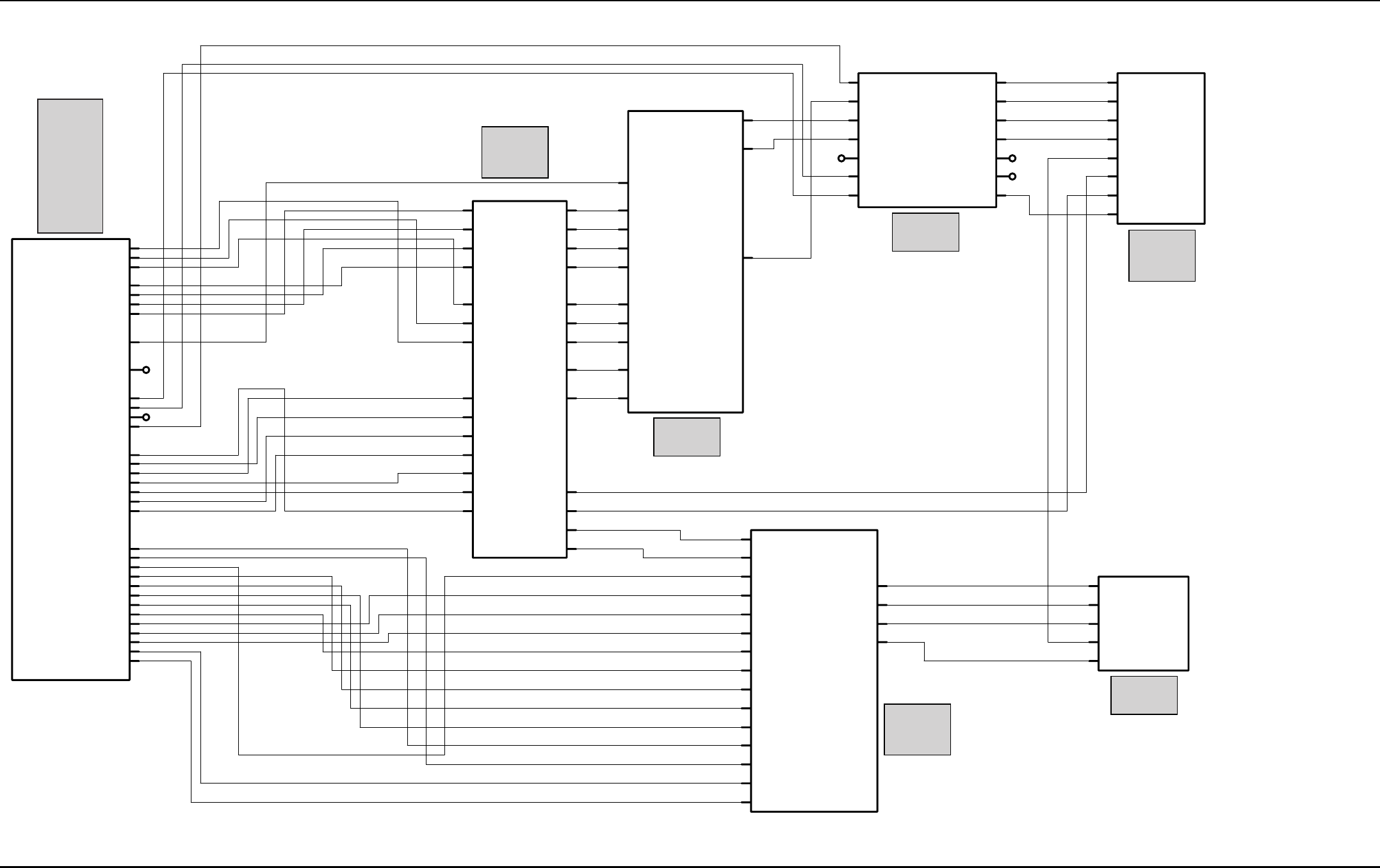
7-174 Schematics, Component Location Diagrams, and Parts Lists: HUF4017A (700-800 MHz) Main Board
May 25, 2005 6881096C74-B
7.5 HUF4017A (700-800 MHz) Main Board
Figure 7-117. HUF4017A Main Board Overall Block Diagram and Interconnections
VCURRENT
VFORWARD
VGBIAS_1
VGBIAS_2
VGBIAS_3
VREVERSE
VTEMP
ABACUS_SSI_FSYNC
ABACUS_SSI_RXD
AUX_5V
K9.1V
LOCK_DET
MODIN
MOSIA_ABACUS
MOSIA_FGU
RFPA_CNTRL
RX_ATTEN_1
RX_ATTEN_2
RX_ATTEN_3
RX_FILT_1
SCKA_ABACUS
SCKA_FGU
SYN_SEL
RF_IN
NC
NC
16.8_MHZ
5V_ABACUS
9.3V_ABACUS
9.3V_FGU
A+_1
A+_2
A+_3
A+_4
ABACUS3_CS
ABACUS_SSI_CLK
PE_3
RX_Inj
SPI_CLK
SPI_DATA
SYN_SEL
TX_INJ
NC
5V_FE
9.3V_FROM_FGU
9.3V_TO_IF
FE_FILTER
IF_OUT_IF
LO_IN
RF_ATTN_1_A
9.3V_1 9.3V_2
CLKOUT_2CLKOUT_3
DOUTA_2DOUTA_3
FS_2FS_3
K9.1
Lock_Det
MOD_IN
PC_2PC_3
PD_2PD_3
PE_2
9.3V_TO_CONTR
FE_FILTER_1
FE_FILTER_2
IF_INIF_OUT
RF_ATTN_1_BRF_ATTN_1_C
RF_ATTN_2_BRF_ATTN_2_C
RF_ATTN_3_BRF_ATTN_3_C
16_8MHz
16_8_CONT
5V_AUX_55V_AUX_6
5V_Reg
NC
5V_FROM_CONTR
5V_TO_FGU
5V_TO_IF
CLKOUT_1
DOUTA_1
FE_FILTER_3
FE_FILTER_4
FREF
FS_1
IF
PC_1
PD_1
PE_1
5V_IF
5V_TO_FE
9.3V_FROM_FE
VGBIAS1
VGBIAS2
VGBIAS3
VREVERSE
VREVERSE_ON
VTEMP
NC
RFPA_OUT
RX_IN
SWITCH_BIAS
VFORWARD_ON
VREVERSE_ON
A+_1
A+_2
A+_3
A+_4
K9.1V
K9.1V_FGU
RFPA_CNTRL
RFPA_OUT
SWITCH_BIAS
TX_INJ
VCURRENT
VFORWARD
VFORWARD_ON
RF_BE_InterfaceRF_FE/IF_InterfaceFGU InterfaceRFPA Interface
CONTROLLER
RFPA
RX_FE
RX_IF
RX_BE
FGU
ON
MAEPF-27833-O
Part Series
100
200
300
400
500
600
700
900
Part Series
6700
6800
Part Series
6000
Part Series
6300 Part Series
6200-1
6200-2
Part Series
6200-1
6200-2
Part Series
6500-2
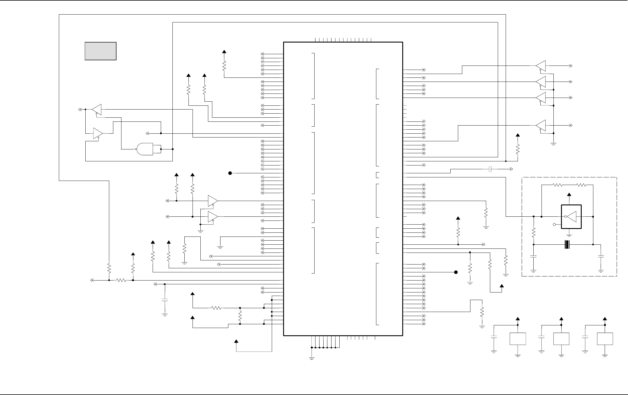
Schematics, Component Location Diagrams, and Parts Lists: HUF4017A (700-800 MHz) Main Board 7-175
6881096C74-B May 25, 2005
Figure 7-118. HUF4017A Controller Block Diagram and Interconnections (Sheet 1 of 3)
NP
For Patriot RAM, R0125 is not placed, R0124 is placed for a 1
For Patriot BRAVO, neither R0124 or R0125 is placed for a 1
32kHz Oscillator Circuit
NP
For Non-HAB: R0114 Placed
R0113, R0115 Not Placed
R0113, R0115 Placed
NP
For HAB: R0114 Not Placed
NP
For Patriot RAM and BRAVO, R0124 is not placed, R0125 is placed for a 0
NP
NP
NP
NP
For Patriot RAM, R0107 NP, R0108 Placed
For Patriot BRAVO, R0108 NP, R0107 Placed
NC
VCC2.85
C0106
100pF
GND
3
2
NC
1
4
VCC 5
10K
U0102
TC7SU04F
12
13
11
R0124
MC74LCX125
U0103-4
VCC2.85VCC2.85
VDD_CORE_2
VDD_EIM_1
F2
G1 VDD_EIM_2
Y18 VDD_IO_1
X18 VDD_IO_2
G18 VPP
VSIM1
N18
P18 VSIM2 VCC2.85
Z6
URTS1_PA13 Z2
URTS2_PB3 Z5
URXD1_PA15 Y3
URXD2_PB1 Y4
UTXD1_PA14 Z3
UTXD2_PB0 Z15
S18 VDD_CORE_1
R18
D1
TOUT4 E1
TOUT5 I1
P17
TOUT6
TOUT7 E2
TOUT8 G2
TOUT9 F1
Y2
UCTS1_PA12
UCTS2_PB2
TOUT1
TOUT10 N17
TOUT11 J1
I2
TOUT12
TOUT13 B1
TOUT14 S17
TOUT15 C2
TOUT2 D2
TOUT3
A2
X2 SRDA
SRDB V2
S2
SRDB2
STBY_PD14
H18
STDA
W2
STDB V1
TOUT0 H1
C1
N2
L1 SPI_CS2_PE4
SPI_CS3_PE6
K2
P2 SPI_CS4_PE7
SPI_CS5_PE11
B4
SPI_CS6_PE0
N1
SPI_CS7_PE1
M2
SPI_CS8_PE2
A3
SPI_CS9_PE3
L18
SPIA_CLK
K1
L2 SPIA_MISO
M1 SPIA_MOSI
SPIB_CLK
P1
SPIB_MISO
R1
SPIB_MOSI
R2
SPI_CS0_PE10
J2
SPI_CS1_PE5
I18
SIM_D1RX_PB11
F17
K17 SIM_D1TX_PB10
E18 SIM_PD0_PB9
SIM_PD1_PB15
B15
SIM_RST0_PB6
V18
SIM_RST1_PB12
G17
SIM_SVEN0_PB8
U18
SIM_SVEN1_PB14
U2
SCKA
W1
T2
SCKB
SCKB2 S1
DSC_TX_PD5 A15
SIM_CLK0_PB7
U17
SIM_CLK1_PB13
L17
SIM_D0RX_PB5
V17
SIM_D0TX_PB4
J17
ROW6 Z10
Y8
ROW7
Z1 SC0A
SC0B T1
SC1A
Y1
SC1B U1
SC2A
X1
SC2B
Y16
RESET_OUT
Y11
Y5
RIA_PA9
Y10
ROW0
ROW1 Z9
ROW2 M17
ROW3 Y9
ROW4 Y6
ROW5
Z8
PC11_OC1
D17
W18 PC12_STO
B16 PC1_USBTXENB
PC8
M18
PC9
J18
PWM*_PE14
Z17 PWM_PE13
K18
RESET_IN
B12
NC6 A5
NC7 B14
B8
NC8
NC9 B7
OC3_PC13
B18
OWIREDAT_PC10 Z18
PA2_USBVPIN
Y7
PC0_UBSVMOUT
A6
A13 NC18
NC19
A14
NC2 A8
NC20
A16
NC21
B2 NC3 B5
NC4 A7
NC5
A11
NC10 B6
NC11 B10
NC12 A17
A9
NC13
NC14 B11
NC15 A12
NC16
B13
NC17
Z12
INT1_PE9
Z13
INT2_PC14
Y14
INT3_PC15
C17
INT4_PA6_OPTSEL1
Z11
INT5_PA7_OPTSEL2
Y12
T17 MOD
MUX_CTRL Z4
NC1
B3
GND12
H17
GND5
I17
GND6
A18
GND7
B17
B9 GND8
GND9
A10
HW_ID
D18
INT0_PE8
Z14
W17
COLUMN6
COLUMN7 R17
DCDA_PA8 Z7
DSC_RX_PD6 C18
DSRA_INT6_PA10 E17
DTRA_INT7_PA11 F18
A4 GND10
GND11
H2
A1
CKIL
CLKSEL_PD15
T18
COLUMN0 X17
COLUMN1 Y15
COLUMN2 Y13
COLUMN3 Y17
COLUMN4 Z16
COLUMN5
VCC1.8
U0001
33C34
CKIH
R0114
0
VCC2.85
3
MC74LCX125
U0104-4
12
13
11
MC74LCX125
U0104-1
2
1
MC74LCX125
2
1
3
18pF
U0103-1
TP0002
1
C0101
U0103-2
MC74LCX125
5
4
6
R0104
10K
R0108
0
VCC2.85
10K
R0120
R0103
10K
VCC2.85
VCC2.85
VCC2.85
VCC2.85
R0122
3.3K
PWR_GND
U0105-2
GND
3
VCC
5
R0107
0
VCC2.85
PWR_GND
U0103-5
GND
7
VCC
14
R0116
10MEG
MC74LCX125
5
4
6
U0104-2
R0101
10K
R0109
10K
R0111
R0117
3.3K
VCC2.85
10MEG
C0105
0.1uF
0.1uF
C0103
PWR_GND
U0104-5
GND
7
VCC
14
0.1uF
C0104
VCC2.85
10K
R0125
VCC2.85
R0123
3.3K
32.768KHz
CC4V Y0100
21
R0105
10K
R0102
10K
R0106
10K
R0119
470K
R0110
10K
VCC2.85
10K
R0121
VCC1.55
TP0005 1
0.1uF
C0102
18pF
R0113
10K
C0100
MC74LCX125
U0104-3
9
10
8
R0115
0
U0105-1
TC7S00FU
1
2
4
VCC2.85
MC74LCX125
U0103-3
9
10
8
HAB_DISABLE
HAB_MOD
16.8_MHZ
16.8_MHZ_PATRIOT
ONE_WIRE
BRD_ID_4
BUS_PWR_OUT
BRD_ID_1
BRD_ID_7
BRD_ID_6
USB*_RS232_EN
MOD MOD*
SPI_MISOA
SPI_MOSIA*
MISO_SEL
SPI_MOSIA
FORCE_FAIL*
SPARE_2
SPARE_1
ABACUS_SSI_FSYNC*
ABACUS_SSI_CLK*
ABACUS_SSI_RXD
LOCK_DET
LOCK_DET*
TX_PA_EN
SSI_INT*
PTT
MONITOR*
PTT*
MONITOR
LV_DETECT
EEPOT_5_CS*
MILL_ID
BRD_ID_2
PWR_RANGE
SW_B+_SENSE
BRD_ID_0
BRD_ID_3
MODEM_EN
ABACUS_SSI_RXD*
DAC_SSI_CLK
ABACUS_SSI_FSYNC
ABACUS_SSI_CLK
SPI_MOSIB
NAUTILUS_CS*
EEPOT_4_CS*
RX_ATTEN_3
SB96_RS232*_EN
32_KHZ
NAUTILUS_INT
RX_ATTEN_2
RX_ATTEN_1
EEPOT_PC_U_D*
EEPOT_PC_INC*
SOFT_TURN_OFF
MUX_MICATTEN
VIP_OUT_2_3V
VPP
SAP_RX
SAP_TX
DA_SEL
ABACUS3_CS
AD_SEL
EEPOT_3_CS*
SYN_SEL
MUX_AUX_TX
SPI_SCKA
EEPOT_U_D*
AUDIO_PA_EN
EEPOT_1_CS*
EEPOT_INC*
EEPOT_2_CS*
SAP_DCLK
SAP_FSYNC
RESET
CODEC_PWR_DOWN
USB_TXENB
8KHZ_DSP_INT
USB_VMOUT
USB_VPIN
CABLE_DET
USB_INT*
SPI_MISOB
SPI_SCKB
MIC_TUNE_EN
UTXD2
UTXD1_USB_VPOUT
URXD2
URXD1_USB_VMIN
URTS2
URTS1_USB_XRXD
UCTS2
UCTS1_USB_FSEN
AUX_5V
MUX_TX
MUX_RX
LHRST_OUT
LHRST_IN
DAC_SSI_TXD
URCHIN_EN
KEYED_9.1_EN
DAC_SSI_FSYNC
ENC_SPARE1
EMERG_SENSE
VIP_OUT_1_3V
VIP_IN_2_3V
RIA_USBSUSP
BRD_ID_5
VIP_IN_1_3V
ENC_SPARE2
WAKEUP
BOOT*
ENC_RESET
IGNITION_SENSE
GP10/EGPT/MISC
INT
QSPI
SAP
SIM
BBP
LAYER1_TIMER
CLKS
UART_A
UART_B
DSC OWIRE
KEYPAD
MAEPF-27828-O
Part Series
100-1

7-176 Schematics, Component Location Diagrams, and Parts Lists: HUF4017A (700-800 MHz) Main Board
May 25, 2005 6881096C74-B
Figure 7-119. HUF4017A Controller Block Diagram and Interconnections (Sheet 2 of 3)
SPI_SCKA
SPI_SCKB
AD_SEL
NC2
VCC1.8
VIP_IN_1_3V
NC4
VIP_IN_2_3V
VIP_OUT_1_3V
BRD_ID_4
NC5
ENC_SPARE1
SSI_INT
MONITOR
UART, GPIO (3.0V)
Layer 1 timer, QSPI (3.0V)
Patriot Core (1.8V)
Layer 1 timer, QSPI (3.0V)
Ext Interupt/Keypad
EIM (1.8V)
Place all 0.1uF caps close to patriot supply pins
Clock Amplifier
Sim, SAP, Bottom Conn. (3.0V)
EIM MODULE
UART, SIM (3.0V)
CYPRESS 8 MBit RAM
MILL_ID
ONE_WIRE
HAB_DISABLE
BRD_ID_5
Intel 4M x 16 Burst Flash
EEPOT_3_CS*
BRD_ID_7
USB*_RS232_EN
MIC_TUNE_EN
EEPOT_5_CS*
DAC_SSI_TXD
DAC_SSI_CLK
URCHIN_EN
DAC_SSI_FSYNC
MODEM_EN
BRD_ID_2
HAB_MOD
SW_B+_SENSE
VCC1.55
BUS_PWR_OUT
VIP_OUT_2_3V
VCC3
MUX_MICATTEN
GPP (3.0V))
PWR_RANGE
BRD_ID_1
BRD_ID_0
EEPOT_PC_U_D*
EEPOT_PC_INC*
BRD_ID_6
LHRST_IN
BRD_ID_3
PATRIOT
17
7
6
TP0101
1
12
7
10
9
0.1uF
C103
18
16
20
C113
0.1uF
11
2
TP0103
1
11
19 7
9
10
16
13
D100
1
32
VDD_EIM_FILT
4
11
14
VDD_IO_FILT
C100
100pF
7
0
22
TP0105
1
5
8
14
10
17
8
15
E103
BLM21A121S
20
9
3
16
4
19
0
TP0102
1
2
1
13
12
3
7
C102
0.1uF
0.1uF
6
WDOG
1310
22
3
C110
STBY_PD14
STROBE P15
D12
TCK
E12
TDI A14
TDO
A13 TEST
C13
TMS
E11
TRST
F9
PSTAT3
H8
PWM_PE13 K5
PWM_PE14
L13
RAMBKUP
K4 RESET_IN F16
RESET_OUT
SIZ0 M15
SIZ1 N15
E16
P1
PGAD6_PF6_MD22
N1
PGAD7_PF7_MD23
M4
PGAD8_PF8_MD24
M3
PGAD9_PF9_MD25
M2
L12
PSTAT0 N16
PSTAT1 M14
PSTAT2 L11
L3
PGAD13_PF13_MD29
L1
PGAD14_PF14_MD30
L2
PGAD15_PF15_MD31
K2
PGAD1_PF1_MD17
R1
PGAD2_PF2_MD18
N3
PGAD3_PF3_MD19
M5
PGAD4_PF4_MD20
P2
PGAD5_PF5_MD21
PC11_OC1_USBCLK
D5 PC12_STO
K13 PC1_USB_TXENB
H13
PC8_UTXD1_UTXD2 H12
PC9_URXD1_URXD2
PGAD0_PF0_MD16
M6
PGAD10_PF10_MD26
M1
PGAD11_PF11_MD27
L4
PGAD12_PF12_MD28
M16
J1 MOD
G13 MUX_CTL
J2 OC3_PC13_FRAME_TICK
K6
PA2
PAGE0
T1
PAGE1
R2
K14 PC0_USB_EOP
H14
DSP_AT
E10
DSP_DE
L5 K1VSS
K3VDD
N2
K7 KV1_2VDD
L6 KV2_3VSS
F10
MCU_DE
MLB_TSCA L14
MLB_TSCD
ANALOG_TEST C4
A6 CKIH
J7 CKIL
F15
CKOH_SCC_CLK
M12
CKO_PA3
D11
CLKSEL_PD15
T2
0.1uF
MISC_BLOCK
U100-3
1
C104
0.1uF
TP0114
1
32
C106
8
D101
0.1uF
C105
10
21
14
VDD_IO_FILT
8
R106
100K
UTXD1_PA14_USB_VOUT_ITXD_TDO
F12
UTXD2_PB0
17
19
18
STDA
E9
STDB
G12
UCTS1_PA12_USB_FSEN_IOE_MCU_DE
C15
UCTS2_PB2
L16 URTS1_PA13_USBXRXD_IPWR_RESET_IN_IC2A
D14 URTS2_PB3
K12 URXD1_PA15_USB_SE0_IRXD_TDI
B16 URXD2_PB1
K11
SPICS5_PE11
C5 SPICS6_PE0
D6 SPICS7_PE1
F7 SPICS8_PE2
SPICS9_PE3
E6
J10 SRDA
B12 SRDB
B10 SRDB2_PC4_OC2
J11
SCKA
C11 SCKB
D10 SCKB2_PC5_OC3
F4
SDI_D_C_PE5_SPICS1
B1
SPICS0_PE10
E3
SPICS2_PE4 D2
SPICS3_PE6 E2
SPICS4_PE11
B6
QSCKB
D15
RIA_PA9_USBSUSP_IPMODEOTLO+TCK_DSCEN_SCKA
G10
SC0A_PC7
A11
SC0B_PC2
G16
SC1A_PC6
A12
SC1B
K16 SC2A
B11 SC2B_PC3
J15
DCDA_PA18_IPMODEOTHI_DSP_DE_SC2A
D16
DSRA_PA10_IRE_TRST_INT6_STDA
F13 DTRA_PA11_IPMODEIN_TMS_INT7_SRDA
D7 MISOA
D3 MISOB
C6
MOSIA
F5
MOSIB
C7
QSCKA
E4
SERIAL_PORTS_BLOCK
*U100-2*
E14
100pF
C107
5
23
OE P16
R_W* N11
N14
SEB_PA5
P14
SQE
1
R5
D6
D7 P5
D8 N5
T4
D9
R13
EB0 M13
EB1
T16
ECB_PA4_CCM_MCU_CLK
N13
LBA
P4
D12
D13 N4
D14 T3
R3
D15
D2 M7
T6
D3
D4 R6
T5
D5
CS2 T14
CS3 N12
CS4 R14
CS5 T11
P7
D0
D1 N7
J8
D10
D11 R4
M9 A5
A6
P10
P12 A7
N9 A8
R10 A9
T15
BURSTCLK
CS0 R15
CS1 R11
N8 A19
M10 A2
K8 A20
L7 A21
A22_PA1_DSP_DBG_XDW
T7
R7 A23_PA0_DSP_DBG_YDW
T12 A3
P13 A4
L10 A11
T10 A12
R9 A13
L9 A14
K9 A15
J9 A16
L8 A17
M8 A18
12
U100-1
EIM_BLOCK
R12 A0
T13 A1
P9 A10
11
13
TP0126
1
6
5
VDD_EIM_FILT
C112
0.1uF
1
TP0115
1
9
TP0118
0
9 4
0.1uF
C117
C111
0.1uF
14
15
4
15
3
14
15
5
TP0119
1
1
100pF
C115
12
3
3
111
C109
0.1uF
10
E101
0.1uF
7
15
14
C116
8
2
15
4
1
VDD_EIM
9
6
13
TP0130
1
TP0112
Q5VSS
H15
VCCA A7
2
1
18
H2
Q1_2VDD
K1 Q2VSS Q3VDD K3
Q4VDD R8
Q5VDD G15
Q6VDD C10C9 Q6VSS
Q4VSS
T8
H1VSS
C8
H2VDD B7
H2VSS
B5
I1VDD A4
I1VSS
C2
I2VDD A1
I2VSS
C1
H3 Q1VSS
C2VDD A16B13 C2VSS K10
D1VDD
K15 D1VSS C12
E1VDD
D9 E1VSS
GNDA
A5
H1VDD D8
A5VSS
L15
B1VDD H9
B1VSS
H16
G9
B2VDD_B3VDD B2VSS
F14
G14 B2VSSA
C1VDD E15
C1VSS
E13
A1VSS
N6
A2VDD P6
A2VSS
P8
A3VDD T9
A3VSS
P11
A4VDD N10
A4VSS
M11
A5VDD R16
IC_PWR_GND
U100-5
A1VDD P3
6
12
0
2
TOUT2 B8
TOUT3 A9
TOUT4_PD0 B4
TOUT5_PD1 B3
TOUT6_PD2 A3
TOUT7_PD3 B2
TOUT8_PD4 A2
D4
TOUT9_PD12
TOUT0 A10
TOUT1 B9
TOUT10_PD13 C3
TOUT11_PD7 G8
TOUT12_PD8 E8
TOUT13_PD9 F8
TOUT14_PD10 A8
TOUT15_PD11 E7
C14 SIM_D1RX_PB11 SIM_D1TX_PB10 B15
SIM_PD0_PB9
J14
SIM_PD1_PB15_DSP_DBG_PAW
B14
SIM_RST0_PB6 J12
SIM_RST1_PB12_TIO0 F11
SIM_SVEN0_PB8 J13
SIM_SVEN1_PB14_TIO2_DSP_DBG_XDW D13
ROW4
G1
ROW5
G7
ROW6
H7
ROW7
H1
SIM_CLK0_PB7 J16
SIM_CLK1_PB13_TIO1_DSP_DBG_YDW A15
SIM_D0RX_PB5
H10 SIM_D0TX_PB4 H11
INT3_PC15
J3
INT4_PA6_IC1A
C16
INT5_PA7_IC1B
G11
F6
ROW0
F1
ROW1
H4
ROW2
H6
ROW3
G2
COLUMN5
E1
COLUMN6
H5
COLUMN7
G3
DSC_RX_PD6
E5
G6
DSC_TX_PD5
INT0_PE8
J6
INT1_PE9
J5
INT2_PC14
J4
SIM_INT_TOUT_BLOCK
U100-4
COLUMN0
D1
COLUMN1
G5
COLUMN2
F3
COLUMN3
G4
COLUMN4_PE12_IC2B
F2
VDD_CORE
6
VDD_IO
D6
VCC1
VCC2 E1
11
1
2
13
G6
IO7 B1
IO8 C1
IO9
A6
NC1
NC2 E3
G2
NC3 H1
NC4 H6
NC5
F2
IO13 F1
IO14 G1
IO15
C6
IO2 D5
IO3 E5
IO4 F5
IO5 F6
IO6
EN_WE
G5
D1 GND1
E6 GND2
B6
IO0 C5
IO1
C2
IO10 D2
IO11 E2
IO12
C4 A6
D4 A7
H2 A8
H3 A9
B2 EN_BHE
A1 EN_BLE
B5 EN_CE
EN_OE
A2
F3 A14
F4 A15
E4 A16
D3 A17
A5 A2
B3 A3
B4 A4
C3 A5
*U103*
A3 A0
A4 A1
H4 A10
H5 A11
G3 A12
G4 A13
12
5
VDD_EIM_FILT
CY62147V
23
8
1
VDD_EIM_FILT
5
VDD_CORE_FILT
21
TP0113
WAIT D3
WP
D6
E102
G2 GND3
G8 GND4
RESET
B5
VCC1 A4
G4
VCC2
VCCQ1 E1
VCCQ2 G6
VPP A5
D7 G1
D8 G7
D9 F6
EN_CE
E7
F8 EN_OE
EN_WE
C5
A3 GND1
F1 GND2
D13 F3
D14 F2
D15 E2
D2 E5
G5
D3
D4 E4
D5 G3
D6 E3
A9
B2
ADV
C4
B4 CLK
D0 F7
E6
D1
D10 F5
D11 F4
D12 D5
A21
C3
A22
D7
A3
B8
A4
A8
B7 A5
A6
A7
A7
C7
A8
A2
A14
D2
A15
D1
A16
D4
A17
B6
A6 A18
A19
C6
A2
C8
A20
B3
WHITECLIFF
A0
E8
A1
D8
C2 A10
A11
A1
A12
B1
A13
C1
4*U102*
16.8_MHZ
8KHZ_DSP_INT
MOD
LV_DETECT
MUX_CTRL
VDD_IO_FILT
VDD_CORE_FILT
VDD_EIM_FILT
PTT
EEPOT_2_CS*
EEPOT_INC* EEPOT_U_D*
UTXD1_USB_VPOUT
USB_VMOUT
USB_TXENB
SB96_RS232*_EN
32_KHZ
FORCE_FAIL*
EMERG_SENSE
SPARE2_ENC
RX_ATTEN_2
CABLE_DET
NAUTILUS_INT
MUX_RX
MUX_TX
AUX_5V
LOCK_DET
SOFT_TURN_OFF
MISO_SEL
LHRST_OUT
IGNITION_SENSE
VIP_OUT_3
ENC_RESET
BOOT*
WAKEUP
SAP_RX
USB_INT
RX_ATTEN_3
EEPOT_1_CS*
RX_ATTEN_1
EEPOT_4_CS*
AUDIO_PA_EN
TOUT0
TOUT1
TOUT2
TOUT3
VPP
PD15
CODEC_PWR_DOWN
RESET
RESET
SPI_MISOA
MORTABLE
USB_VPIN
NAUTILUS_CS*
TX_PA_EN
PE4
SPI_MOSIB
URTS1_USB_XRXD UCTS1_USB_FSEN
RIA_USBSUSP
URXD1_USB_VMIN
URXD2
SPI_MOSIA
DATA(15:0)
ADDR(23:0)
ABACUS3_CS
DA_SEL
SYN_SEL
ABACUS_SSI_FSYNC
ABACUS_SSI_CLK
UCTS2
UTXD2
KEYED_9.1_EN
SAP_FSYNC
SAP_DCLK
SAP_TX
ABACUS_SSI_RXD
URTS2
SPI_MISOB
KEY PAD I/O
LAYER 1 TIMERSINT ERRUPTS
DSC AND ONE_WIRE
SIM
REAL TIME TRACE JTAG
GPIO
MISCELLANEOUS
DSP TRACE
CCM / WDOG / EGPT / CLK
SECONDARY UART
PRIMARY UART
SAP
BBP
MOSPI
MAEPF-27912-O
Part Series
100-2
Schematics, Component Location Diagrams, and Parts Lists: HUF4017A (700-800 MHz) Main Board 7-177
6881096C74-B May 25, 2005
Figure 7-120. HUF4017A Controller Block Diagram and Interconnections (Sheet 3 of 3)
RX_BE_INTERFACE
RFPA_INTERFACE
FGU_INTERFACE
INTERFACE, SECURE, DC SUPPLY
IF0036
MUX_RX
MUX_TX
RX_FILT_AUDIO
SAP_DCLK
SAP_FSYNC
SAP_RX
SAP_TX
SPI_MOSIA
SPI_SCKA
SPKR+
SPKR-
IF0004
AUDIO_PA_EN
AUX_MIC
AUX_RX
AUX_TX
CODEC_PWR_DOWNEEPOT_2_CS*
EEPOT_3_CS*
EEPOT_CS*
EEPOT_INC*
EEPOT_U_D*
MIC_HI
MUX_AUX_TX
MUX_MICATTEN
IF0029
IF0033
A+
IF0022
IF0021
IF0002
IF0001
IF0020
IF0024
9.3V
IF0000
K9.1V_EN
MISOA
MOSIA
PA_EN
PWR_RANGE
RFPA_CNTRL
RX_FILT_1
SCKA
VCURRENT
VFORWARD
VGBIAS_1
VGBIAS_2
VGBIAS_3
VREVERSE
VTEMP
AD_EN
DA_EN
EEPOT_4_CS*
EEPOT_5_CS*
EEPOT_PC_INC*
EEPOT_PC_U_D*
IF0011
16.8_MHZ
AUX_MIC
AUX_TX
DAC_SSI_CLK
DAC_SSI_FSYNC
DAC_SSI_TXD
MIC_TUNE_EN
MODEM_EN
MODIN
RESET
RX_FILT_AUDIO_IN
RX_FILT_AUDIO_OUT
URCHIN_EN
IF0028
IF0017
UTXD1_USB_VPOUT
UTXD2
VIP_IN_1_3V
VIP_IN_2_3V
VIP_OUT_1_3V
VIP_OUT_2_3V
VPP
WAKEUP
IF0009
SPI_SCKB
SPKR+
SPKR-
SSI_INT*
SW_B+_SENSE
UCTS1_USB_FSEN
UCTS2
URTS1_USB_XRXD
URTS2
URXD1_USB_VMIN
URXD2
USB*_RS232_EN
USB_INT*
USB_TXENB
USB_VMOUT
USB_VPIN
NAUTILUS_CS*
NAUTILUS_INT*
ONE_WIRE
PTT*
RIA_USBSUSP
RX_FILT_AUDIO
SAP_DCLK
SAP_FSYNC
SAP_RX
SAP_TX
SB96_RS232*_EN
SOFT_TURN_OFF
SPARE_1
SPARE_2
SPI_MISOB
SPI_MOSIB
BOOT*
BUS_PWR_OUT
CABLE_DET
CHAN_ACT
EMERG_SENSE
ENC_RESET
ENC_SPARE1
ENC_SPARE2
FORCE_FAIL*
IGNITION_SENSE
LHRST_IN
LHRST_OUT
LV_DETECT
MIC_HI
MOD
MONITOR
IF0008
AUX_MIC
AUX_RX
AUX_TX
9.3V_ABACUS
IF0005
IF0023
IF0035
IF0031
IF0013
IF0007
IF0030
IF0019
IF0032
IF0016
IF0010
IF0018
IF0003
IF0025
K9.1V
IF0026
IF0012
IF0027
5V_ABACUS
SPARE_2
SPARE_1
SAP_RX
SAP_FSYNC
SAP_DCLK
8KHZ_DSP_INT
MUX_MICATTEN
EEPOT_PC_INC*
A+_4
A+_3
RX_ATTEN_1RX_ATTEN_1
BUS_PWR_OUT
16.8_MHZ
16.8_MHZ
16.8_MHZ
MIC_TUNE_EN
MODEM_EN
DAC_SSI_TXD
DAC_SSI_CLK
DAC_SSI_FSYNC
URCHIN_EN
RESET
SAP_TX
EEPOT_6_CS*
EEPOT_3_CS*
EEPOT_2_CS* CODEC_PWR_DOWN
AUDIO_PA_EN
ONE_WIRE
MONITOR
MODIN
ABACUS3_CSABACUS3_CS
MUX_TX
MUX_RX
MUX_AUX_TX
EEPOT_U_D*
EEPOT_INC*
EEPOT_1_CS*
VIP_IN_2_3V
VIP_IN_1_3V
CHAN_ACT
SPI_MOSIA
SPI_SCKA
SPI_MISOA
SSI_INT*
ABACUS_SSI_CLK ABACUS_SSI_CLK
AUX_5VAUX_5V
TX_PA_EN
MOSIA
MISOA
KEYED_9.1_EN
EEPOT_PC_U_D*
EEPOT_5_CS*
EEPOT_4_CS*
DA_SEL
AD_SEL
VGBIAS_1
VIP_OUT_2_3V
VIP_OUT_1_3V
VREVERSE
VGBIAS_3
VGBIAS_2
VFORWARD
VCURRENT
SCKA
RX_FILT_1
RFPA_CNTRL
PWR_RANGE
ENC_RESET
EMERG_SENSE
CABLE_DET
BOOT*
SYN_SEL SYN_SEL
LOCK_DET LOCK_DET
A+_2
A+_1
VTEMP
NAUTILUS_INT
NAUTILUS_CS*
MOD
LV_DETECT
LHRST_OUT
LHRST_IN
IGNITION_SENSE
FORCE_FAIL*
ENC_SPARE2
ENC_SPARE1
UCTS1_USB_FSEN
SW_B+_SENSE
SPI_MOSIB
SPI_MISOB
SOFT_TURN_OFF
SPI_SCKB
SB96_RS232*_EN
RIA_USBSUSP
PTT*
USB_TXENB
USB_INT*
USB*_RS232_EN
URXD2
URXD1_USB_VMIN
URTS2
URTS1_USB_XRXD
UCTS2
RX_ATTEN_2RX_ATTEN_2
SCKA_ABACUS
MOSIA_ABACUS
WAKEUP
VPP
UTXD2
UTXD1_USB_VPOUT
USB_VPIN
USB_VMOUT
9.3V_FGU
SCKA_FGU
MOSIA_FGU
ABACUS_SSI_RXDABACUS_SSI_RXD
ABACUS_SSI_FSYNCABACUS_SSI_FSYNC
9.3V_ABACUS
5V_ABACUS
RX_ATTEN_3RX_ATTEN_3
K9.1V
AUDIO
POWER CONTROL
AD5320/SCF Block
MAEPF-27827-O
Part Series
200
Part Series
300
400
500
600
Part Series
900-1
Part Series
900-2

7-178 Schematics, Component Location Diagrams, and Parts Lists: HUF4017A (700-800 MHz) Main Board
May 25, 2005 6881096C74-B
Figure 7-121. HUF4017A Controller Audio Schematic
AUDIO_GROUND
NP
-14 dB to +14 dB
-9 dB to +14 dB
Programmable pre-amp stage Programmable pre-amp stage
Anti-aliasing filter
Ground
7 dB Attenuation Stage
UNIVERSAL GROUND
SW_A+
VAG
0.1uF
C0224
R0227
0.1uF
68K
0.1uF
C0216
C0201
VAG
A+_FILT
R0206
100K
C0205
10uF
C0220
150pF
33K
R0228
VAG
10K
C0226
0.1uF
R0222
1IN
4
NC
6
NO
VPOS 2
VCC2.85
NLAST4599
U0210
5
COM
GND
3
R0207
7.5K
R0203
1K
VPOS 2
470pF
C0230
NLAST4599
U0208
5
COM
GND
3
1
IN
4NC
6
NO
0.1uF
C0242
R0208
100K
VCC2.85
C0207
33pF
R0236
9.1K
R0226
36K
R0212
100K
C0240
0.1uF
C0206 470pF
C0235
1uF
1
10uF
C0221
VCC2.85
VCC2.85
TP0200
C0204
4.7uF
A+
10K
VAG
TP0205
1
VCC5
R0221
C0210
0.1uF
1uF
C0208
U0201-4
MC33204
13
12
14
4
11
LM7301
U0207
4
3
1
2
5
3300pF
C0217
4.7uF
Q0200
C0223
R0210
100K
0.1uF
C0239
R0209
10K
560
R0204
COM
5
GND
3
IN
1
NC 4
NO
6
2
VPOS
VCC2.85
U0203
NLAST4599
0.1uF
C0227
VCC2.85
R0235
10K
R0225
10K
150pF
C0228
220pF
C0233
0
R0231
VCC2.85
1K
C0214
VCC2.85
R0200
C0225
0.1uF
VCC2.85
0.1uF
R0224
10K
19 TI_POS
20
VAG
1VAGREF
6
VDD
15 VSS
11 MCLK
10 PDI
3PI
4
PO_NEG 5
PO_POS
2
RO_NEG
17
TG
18 TI_NEG
9BCLKR
12 BCLKT
8DR
13
DT
7FSR
14 FST
16 HB
VCC2.85
MC145483
U0200
7
VCC
R0223
18K
10 GND3
GND4
11
9INV
8M_SS
1NINV
4
OUT1
6
OUT2
3RR
U0204
TDA1519C
2GND1
GND2
5
VREFIN
0.1uF
C0234
6CLK
5DATA
3GND
8IN
4LOAD
2
OUT
7
VDD
1
C0209
0.1uF
LM1971
U0206
C0232
18K
R0220
470pF
C0212
1
0.1uF
47K
TP0206
100pF
R0205
MC33204
6
5
7
4
11
C0211
U0201-3
MC33204
9
10
8
4
11
VCC5
U0201-2
TP0203
1
1K
R0219
VAG
3.3K
R0202
TP0202
1
C0238
220pF
C0203
0.1uF
VCC2.85
220pF
C0231
SIGNAL_CONVERT
SC0001
I1
1I2 2
R0218
1K
100K
VCC2.85
TP0201
1
R0216
0.1uF
C0215
6800pF
C0244
VCC2.85
6800pF
C0243
MC33204
U0201-1
2
3
1
4
11
C0202
0.1uF
TP0204
1
0.1uF
C0213
R0230
C0236
470pF
NO
VPOS 2
9.3V_TX
33K
NLAST4599
U0209
5
COM
GND
3
1
IN
4NC
6
68K
R0229
I1
1I2 2
VCC2.85
SIGNAL_CONVERT
SC0002
W1 4
W2 7
VCC2.85
C0237
220pF
CS1
1
CS2
10
GND
8
INC
9L1 5
6
L2
U_D
2
VDD 3
MIC_PREAMP_OUT
RX_FILT_AUDIO
SPKR+
SPKR-
U0202
MAX5452
AUX_RX*
MIC_HI*
AUX_TX_B
CODEC_OUT_C
RX_AUDIO_IN
MUX_AUX_TX
AUX_MIC*
AUX_TX*
AUX_MIC
AUX_TX
MIC_PREAMP_IN
VOLUME_IN
EEPOT_U_D*
EEPOT_INC*
SPI_SCKA
SPI_MOSIA
EEPOT_3_CS*
MUX_MICATTEN
VOL_OUT*
VOL_OUT
CODEC_OUT
AUX_TX_A
CODEC_OUT_B
MIC_M
MIC_A
MIC_C
MIC_B MIC_E MIC_K
MIC_N
CODEC_OUT_A
MIC_L
MIC_G
MIC_J
MIC_I
MIC_F
MIC_H
EEPOT_CS*
AUX_RX
SAP_FSYNC
SAP_TX
SAP_DCLK
AUDIO_PA_EN
MUX_TX
MUX_RX
EEPOT_2_CS*
MIC_HI
MIC_D
AUDIO_PA_IN
SAP_RX
CODEC_PWR_DOWN
47K
47K
MAEPF-27837-O
Part Series
200
Schematics, Component Location Diagrams, and Parts Lists: HUF4017A (700-800 MHz) Main Board 7-179
6881096C74-B May 25, 2005
Figure 7-122. HUF4017A Power, Data, Secure, and Front/Rear Connector Block Diagrams
USB_RS232_SB9600 BLOCK
USB/RS232
SECURE INTERFACE BLOCK
10
11
0
2
3
UTXD1_USB_VPOUT
UTXD2
VIP_IN_1_3V
VIP_IN_1_5V
VIP_IN_2_3V
VIP_IN_2_5V
VIP_OUT_1_3V
VIP_OUT_1_5V
VIP_OUT_2_3V
VIP_OUT_2_5V
0
2
UARTA_RTS
UARTA_RXD
UARTA_TXD
UCTS1_USB_FSEN
UCTS2
URTS1_USB_XRXD
URTS2
URXD1_USB_VMIN
URXD2
USB*_RS232_EN
USB+
USB-
USB_INT*
USB_PWR
USB_TXENB
USB_VMOUT
USB_VPIN
14
16
BOOT_DATA_EN*
BOOT_RX
BOOT_TX
BUS+_UARTB_TXD
BUS-_UARTB_RXD
BUSY_UARTB_RTS
LHRST_IN
LHRST_OUT
RESET_UARTB_CTS
RIA_USBSUSP
SB96_RS232*_EN
UARTA_CTS
7
0
2
5
17
2
4
9
12
12
10
2
9
3
3
13
14
19
19
17
3
IGNITIONIGNITION_SENSE
LV_DETECT
SOFT_TURN_OFFSW_B+_ON-OFF
SW_B+_SENSE
0
6
05
SPKR-
SSI_INT*
SW_B+_ON-OFF
UARTA_CTS
UARTA_RTS
UARTA_RXD
UARTA_TXD
VIP_IN_1_5V
VIP_IN_2_5V
VIP_OUT_1_12V
VIP_OUT_1_5V
VIP_OUT_2_12V
VIP_OUT_2_5V
EMERGENCY
EMERG_SENSE
NAUTILUS_INT*
ONE_WIRE
PTT*
RESET_UARTB_CTS
RX_FILT_AUDIO
SAP_DCLK
SAP_FSYNC
SAP_RX
SAP_TX
SPARE_1
SPARE_2
SPI_MISOB
SPI_MOSIB
SPI_SCKB
SPKR+
AUX_TX
BOOT_DATA_EN*
BOOT_RX
BOOT_TX
BUS+_UARTB_TXD
BUS-_UARTB_RXD
BUSY_UARTB_RTS
BUS_PWR_OUT
CABLE_DET
EMERGENCY
FORCE_FAIL*
IGNITION
KEYFAIL
MIC_HI
MOD
NAUTILUS_CS*
1
1
15
1
AUX_MIC
AUX_RX
1
5
0
0
3
16
1
10
15
9
18
SPKR-
UARTA_CTS
UARTA_RTS
UARTA_RXD
UARTA_TXD
USB+
USB-
USB_PWR
VIP_OUT_1_12V
VIP_OUT_2_12V
VPP
12
19
AUX_MIC BUS+_UARTB_TXD
BUS-_UARTB_RXD
BUSY_UARTB_RTS
CHAN_ACT
EMERGENCY
IGNITION
MONITOR
ONE_WIRE
PTT*
RESET_UARTB_CTS
RX_FILT_AUDIO
SPKR+
2
7
0
1
3
13
3
2
8
3
3
2
4
11
18
8
14
1
13
SAP_DCLK
SAP_FSYNC
SAP_RX
SAP_TX
TAMPER_ENC
WAKEUP
0
1
1
6
AUX_MIC
SAP(3:0)
WAKEUP
ENC_SPARE1
ENC_RESET
ENC_SPARE2
BOOT*
MOD
ONE_WIRE
SPARE_1
SPARE_2
2
BOOT*
ENC_RESET
ENC_SPARE1
ENC_SPARE2
KEYFAIL*
SPI_MOSIB
SPI_MISOB
SPI_SCKB
NAUTILUS_CS*
FORCE_FAIL*
CABLE_DET
BOOT_TX
BOOT_RX
VPP
AUX_TX
MIC_HI
CHAN_ACT
BUS_PWR_OUT
NAUTILUS_INT*
SSI_INT*
USB_INT*
MONITOR
PTT*
UARTB(3:0)
SPKR+
SPKR-
CONN(19:0)
SAP_DCLK
SAP_TX
SAP_FSYNC
SAP_RX
SB96_RS232*_EN
AUX_RX
IGNITION_SENSE
SW_B+_SENSE
LV_DETECT
SOFT_TURN_OFF
SW_B+_ON-OFF
VIP_IN_2_3V
VIP_IN_1_3V
VIP_OUT_1_3V
VIP_OUT_2_3V
USB_VMOUT
USB_TXENB
UTXD1_USB_VPOUT
UCTS1_USB_FSEN
URTS1_USB_XRXD
URXD1_USB_VMIN
USB*_RS232_EN
USB_VPIN
RIA_USBSUSP
EMERG_SENSE
UTXD2
URXD2
URTS2
UCTS2
LHRST_OUT
LHRST_IN
RX_FILT_AUDIO
ACCESSORY CONNECTOR
POWER SUPPLY BLOCK
SB9600/VIP
CONTROL HEAD
INTERFACE
TYPE 3 UCM SECURE
MAEPF-27844-O
Part Series
400-1
Part Series
500
Part Series
300
Part Series
700
Part Series
400-2
Part Series
600-1
600-2
7-180 Schematics, Component Location Diagrams, and Parts Lists: HUF4017A (700-800 MHz) Main Board
May 25, 2005 6881096C74-B
Figure 7-123. HUF4017A USB/RS232/SB9600 Schematic
SB9600 Block
NP
VIP I/O Block
BUFFER SUPPLY BUFFER SUPPLY
1
USB*_RS232_EN
0Not Allowed
BOOT_DATA_EN* Mode of Operation
0
0
0
11
1
Boot Data
USB
RS232
R0304
13
11
22
1
2
4
U0300-4
MC74LCX125
12
VCC5
VCC2.85
U0308-1
NC7ST08
C0312
0.1uF
10
8
MC74LCX125
U0303-4
12
13
11
MC74LCX125
U0300-3
9
1.5K
R0303
C0309 0.1uF
U0303-2
MC74LCX125
5
4
6
VCC2.85
VIP_IN_1_3V VIP_IN_1_5V
VIP_IN_2_3V VIP_IN_2_5V
VIP_OUT_1_3V VIP_OUT_1_5V
VIP_OUT_2_3V VIP_OUT_2_5V
U0300-2
MC74LCX125
5
4
6 GND
7
VCC
14
10K
R0307
VCC2.85
PWR_GND
U0300-5
14
VBUS
7
VCC
4
VM
11 VO_VPO 3
VP
15
VPU
13
VREG
DPOS
16 ENUMERATE
12 FSE0_VMO
17 GND
MODE
6
1OE_N 2
RCV
5SUSPND
8
USB_DET
VCC
5
ISP1104
U0304
9
DNEG
10
VCC
5
PWR_GND
U0308-2
GND
3
VNEG 6
VPOS 2
PWR_GND
U0307-2
GND
3
R1O 12
R2I
8R2O 9
T1I
11 T1O 14
T2I
10 T2O 7
VCC 16
U0305
ST3232
3C1NEG
C1POS
1
5C2NEG
4C2POS
GND
15
R1I
1310
8
C0307 0.1uF
22
MC74LCX125
U0303-3
9
R0305 VCC5 VCC9
0.1uF
C0302
7
GND
14
VCC
C0308 0.1uF
U0303-5
PWR_GND
0.1uF
C0311
0.1uF
0.1uF
C0313
C0306
0.1uF
C0310 0.1uF
VCC2.85
C0305
3
MC74LCX125
U0303-1
2
1
3
VCC2.85
1
2
4
MC74LCX125
U0300-1
2
1
URTS2
URXD2
UTXD2
TC7S00FU
U0307-1
C0301
0.1uF
BUS+_UARTB_TXD
BUS-_UARTB_RXD
BUSY_UARTB_RTSLHRST_IN
LHRST_OUT RESET_UARTB_CTS
SB96_RS232*_EN
UCTS2 VIP_OUT_1_5V
BOOT_TX
UTXD1_USB_VPOUT
UTXD1_USB_VPOUT
USB_TXENB
RIA_USBSUSP
USB_INT*
USB_VMI
USB_VPI
USB*_RS232_EN
USB+
USB+
USB_PWR
VIP_IN_1_5V
UARTA_CTS
UARTA_TXD
UARTA_RXD
UARTA_RTS
BOOT_DATA_EN*
UCTS1_USB_FSEN
UCTS1_USB_FSEN
RESET_UARTB_CTS
BUS+_UARTB_TXD
BUS-_UARTB_RXD
BUSY_UARTB_RTS
USB_VMOUT
VIP_OUT_1_3V
VIP_IN_1_3V
VIP_OUT_2_3V
VIP_IN_2_3V
UTXD2
UCTS2
LHRST_IN
LHRST_OUT
URTS2
URXD2
BOOT_RX
USB_VPIN
VIP_OUT_2_5V
VIP_IN_2_5V
URXD1_USB_VMIN
URXD1_USB_VMIN
URTS1_USB_XRXD
URTS1_USB_XRXD
SB96_RS232*_EN
USB-
USB-
MAEPF-27847-O
Part Series
300
Part Series
600-1
Part Series
600-2
Schematics, Component Location Diagrams, and Parts Lists: HUF4017A (700-800 MHz) Main Board 7-181
6881096C74-B May 25, 2005
Figure 7-124. Rear Accessory Connector (J0402) Schematic
VIP_OUT_2_12V
UARTB_RTS-BUSY
USB+
EMERGENCY
SPKR+
USB_PWR
RX_FILT_AUDIO
SW_B+
CHAN_ACT
UARTA_TXD
SPKR-
ONE_WIRE
MONITOR
PTT*
CTS_DCE (DB9-Pin 7)
RTS_DCE (DB9-Pin 8)
UARTB_RXD-BUS-
UARTA_RXD
UARTB_TXD-BUS+
J0402
UARTB_CTS-RESET
UARTA_RTS
AUX_MIC
TX_DCE (DB9-Pin 2)
RX_DCE (DB9-Pin 3)
UARTA_CTS
VIP_OUT_1_12V
26 PIN CONN
IGNITION
GND
USB-
R0410 100
C0412
100pF
U0400
DTC144EKA
33pF
C0402
*VR0408*
A1
A2
K1
K2
K3
K4
5.6V
J0402-27
J0402-20
220pF
C0415
33pF
C0410
C0464
33pF
J0402-29
220pF
C0417
33pF
C0403
J0402-12
J0402-11
1K
R0405
VR0404
15V
100
R0432
J0402-32
100
R0407
1
J0402-31
0
R0430
TP0420
J0402-30
J0402-9
33pF
C0405
33pF
C0404
TP0418
1
J0402-3
J0402-22
J0402-13
9.3V_TX
J0402-1
J0402-23
C0416
J0402-5
J0402-21
100pF
R0411
10K
3
4
6
J0402-24
VR0402
20V
2
5
1
33pF
J0402-15
J0402-28
C0463
33pF
C0406
J0402-8
470pF
C0465
100pF
C0466
C0419
C0413
100pF
100
100pF
R0408
VR0405
15V
220pF
C0418
R0412 100
C0408
J0402-26
J0402-19
100pF100pF
C0467
560
R0406
33pF
C0400
C0414
220pF
4.7uF
C0420
*VR0410*
A1
2
A2
5
K1 1
K2 3
K3 4
K4 6
5.6V
J0402-4
J0402-17
1
J0402-14
100pF
TP0400
C0401
TP0419
1
VR0400
20V J0402-2
VR0406
15V
J0402-10
R0403
10K
15V
R0435 1K
VR0407
33pF
C0409
C0407
100pF
J0402-16
SW_B+
J0402-25
J0402-18
J0402-6
J0402-7
IO2
IO3
IO4 IO5
IO6
IO7
IO8
VR0411
IO1
USB+ USB+
USB- USB-
IGNITION
VCC5
SPKR+
SPKR-
RX_FILT_AUDIO
CHAN_ACT_CONN
MONITOR
PTT*
EMERGENCY
ONE_WIRE ONE_WIRE_CONN
USB_PWR
VPP
CHAN_ACT
UARTA_CTS
UARTA_RXD
UARTA_RTS
UARTA_TXD
VIP_OUT_1_12V
VIP_OUT_2_12V
BUS+_UARTB_TXD
BUS-_UARTB_RXD
RESET_UARTB_CTS
BUSY_UARTB_RTS
AUX_MIC
47K
47K
MAEPF-27842-O
Part Series
400-1
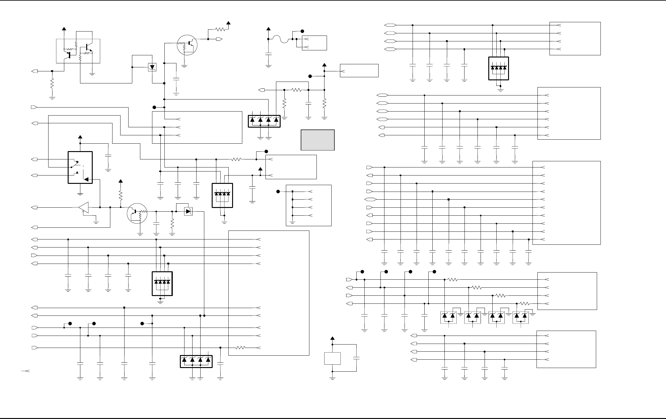
7-182 Schematics, Component Location Diagrams, and Parts Lists: HUF4017A (700-800 MHz) Main Board
May 25, 2005 6881096C74-B
Figure 7-125. Control-Head Front Connector Schematic
SPARE_1
UARTA_RXD
BUSY
SPI_MOSIB
Interface
SPI_SCKB
OPTB+_BOOTSEL_VPP
AUX_RX
NAUTILUS_CS*
RS232 BUS
VIP_OUT_1_12V
MIC_HI
FOR NEW CH/ACCYs
IGNITION
SW_B+
SSI / NAUTILUS
SPI_MISOB
PTT*
SAP_DCLK
UARTA_CTS
SB9600
NOT USED
NAUTILUS_INT*
LH_RESET
VIP_OUT_2_12V
VIP_IN_2_5V
AUDIO
Programming Cable
AUX_MIC
ONE_WIRE
SPKR-
SAP_RX
BOOT_RX
BUS_PWR_OUT
BUS-
UARTA_RTS
SPARE_2
SAP_FSYNC
SAP_TX
VIPs
UARTA_TXD
VIP_OUT_1_5V
VIP_IN_1_5V
VCC5
A+
SSI_INT
EMERGENCY
RX_FILT_AUDIO
BUS+
BOOT_TX / KEYFAIL*
AUX_TX
VIP_OUT_2_5V
SPKR+
J0401-47
J0401-12
J0401-26
J0401-50
33pF
100
C0424
J0401-13
R0418
C0443
33pF
R0415
100
J0401-37
C0453
33pF
C0452
33pF
15V
C0475
100pF
3
6
4
1
VR0424
Q0403
5
2
J0401-38
J0401-40
C0469
0.1uF
J0401-15
R0431
10K
100pF
C0427
J0401-19
R0409
C0456
33pF
1
K1 3
K2 4
K3 6
K4
10K
5.6V
*VR0417*
2A1
5
A2
J0401-25
1
TP0414
1
NO
6
2
VPOS
TP0401
U0401
NLAST4599
COM
5
3GND
IN 1
NC
4
C0439
J0401-18
100pF
J0401-6
J0401-44
33pF
2
5
1
3
4
6
C0459
VR0412
20V
33pF
J0401-2
J0401-31
VCC2.85
C0422
10K
J0401-20
R0425
C0462
220pF
J0401-33
J0401-48
0.1uF
C0441
VR0425
15V
1
TP0411
1
VR0420
11V
2
3
F0400
125V
5A
C0450
33pF
Q0404
C0437
470pF
J0401-43
VR0413
20V
J0401-11
C0446
100pF
1
C0436
470pF
470pF
TP0408
C0435
J0401-1
C0444
33pF
1K
R0404
A1
A2
K1
K2
K3
K4
5.6V
*VR0414*
C0431
100pF
J0401-30
J0401-24
Q0402
VR0423
15V
1
J0401-46
VCC5
TP0415
1
TP0403
J0401-23
VCC5
C0445
33pF
C0434
100pF 100pF
J0401-32
C0433
R0416
100
33pF
C0432
100pF
100pF
C0454
J0401-9
C0449
J0401-10
J0401-42
C0461
220pF
TP0407
1
33K
R0422
0
R0421
TP0413 1
C0448
100pF
J0401-35
1
C0425
100pF
TP0402
C0442
33pF
3
GND
5
VCC
J0401-3
TP0412
1
U0402-2
PWR_GND
C0477
VCC2.85
100pF
C0428
100pF
J0401-45
C0426
470pF
J0401-22
J0401-14
J0401-34
J0401-36
J0401-16
C0438
33pF
470pF
J0401-21
SW_B+
C0457
J0401-27
J0401-49 J0401-41
33pF
11V
C0458
U0402-1
NC7SZ125
2
1
4VR0421
J0401-39
VCC2.85
100pF
C0478
A+
C0430
100pF
C0451
33pF
VCC5
J0401-4
J0401-7
VR0422
15V
10K
R0420
J0401-8
J0401-5
C0429
100pF
100pF
C0460
C0440
C0447
100pF
100pF
J0401-29
4.7K
R0517
*VR0418*
2A1
5
A2
1
K1 3
K2 4
K3 6
K4
5.6V
100pF
C0476
J0401-17
J0401-28
TP0410
1
C0455
33pF
R0417 100
4.7K
R0419
TP0409
1
C0423
33pF
SPARE_2
SPARE_1
SW_B+_ON-OFF
IGNITION
BUS+_UARTB_TXD
BUS-_UARTB_RXD
BUSY_UARTB_RTS
RESET_UARTB_CTS
C0470
33pF
MIC_HI
RX_FILT_AUDIO
IGNITION_CONN
SPKR- SPKR-
BOOT_RX
EMERGENCY
ONE_WIRE
UARTA_TXD
UARTA_RXD
UARTA_CTS
UARTA_RTS
UARTA_TXD_CH
UARTA_CTS_CH
UARTA_RTS_CH
CABLE_DET
BOOT_DATA_EN*
KEYFAIL
BUS_PWR_OUT
MIC_HI
AUX_MIC AUX_MIC
PTT*
AUX_RX
VIP_IN_2_5V
VIP_IN_1_5V
VIP_OUT_2_5V
VIP_OUT_1_5V
VIP_OUT_1_12V
VIP_OUT_2_12V
AUX_TX
NAUTILUS_CS*
SAP_DCLK
SAP_TX
UARTA_RXD_CH
SAP_RX
SAP_FSYNC
SPI_MOSIB
SPI_SCKB
NAUTILUS_INT*
MOD
BOOT_TX
FORCE_FAIL*
SPKR+ SPKR+
SSI_INT*
SPI_MISOB
10K 10K
10K
10K
47K
47K
47K
47K
MAEPF-27843-O
Part Series
400-2
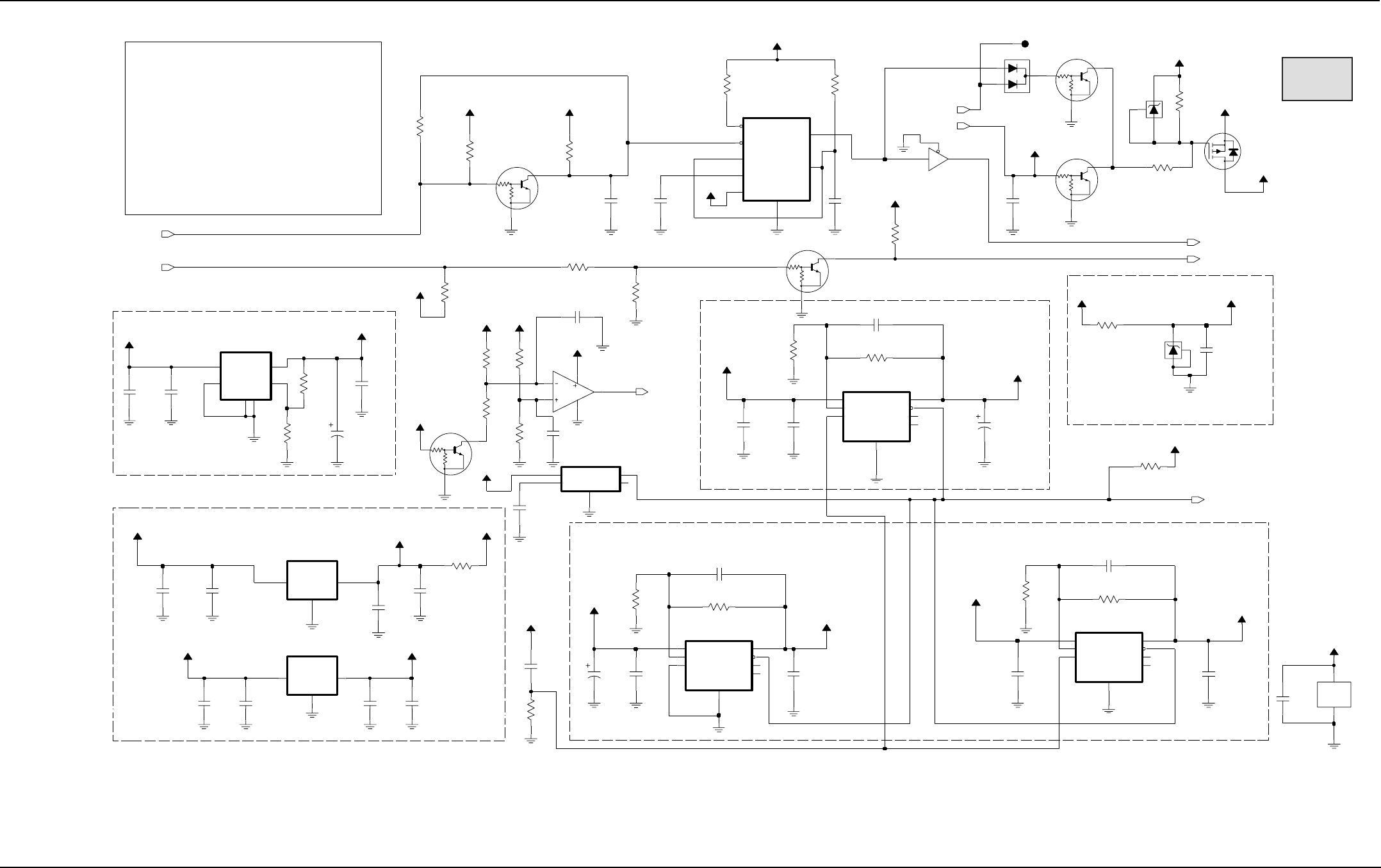
Schematics, Component Location Diagrams, and Parts Lists: HUF4017A (700-800 MHz) Main Board 7-183
6881096C74-B May 25, 2005
Figure 7-126. Controller Power Supply and Emergency Schematic
VCC3
Mic Bias Circuit
2.85 / 100 mA
T-Gates, VIPS, SB9600
NP
1.8V Digital Supply Regulator
Audio PA
FILT_B+
Emergency Sense Block
9V Regulator
5.0 / Battery
Battery
VCC5
SOURCED BY:
NP
Battery
VCC5 I/O Ring, EEPOTs
9.3V / 1A
UNSW_5V
Voltage Translation
USB, Codec
DC DISTRIBUTION
SW_B+
V(operating)/mA(max)
A+
VCC5
FILT_B+
VCC1.8, VCC1.55
NP
Emergency Detect/Timer
VCC2.85
9V Regulators
1.86 & 1.55 / 100 mA
SW_B+ Sense Circuit
VOLTAGE
Patriot, EIM, Memory
SUPPLY FOR
5.0 / 500 mA
3.0 / 100 mA
UNSW_5V Supply
5V Regulator
Power Control
9.3V_TX
2.85V Digital Supply Regulator
VCC5
SW_B+
A+
A+
1.8V, 3V Regulators
1.55V Digital Supply Regulator
SW_B+
R0521
VCC2.85
VCC5_FILT
R0505
39K
VCC5
10K
100pF
C0503
4.7uF
C0517
1uF
C0525
0
C0526
.01uF
VCC5
R0527
OUT
A+
UNSW_5V
MC78M05
U0503
2
GND
1IN 3
0.1uF
C0504
Q0503
SW_A+
R0510
C0536
0.1uF
9.3V_ABACUS
43K
VCC5_FILT
33K
R0511
100K
R0500
4.7uF
C0518
R0513
39K
Q0505
10K
R0524
R0503
VCC2.85
UNSW_5V
SW_A+
100K
VCC2.85
Q0504
11V
VR0501
C0507
0.1uF0.1uF
C0524
D0501
U0505
MC78M05
GND
2
IN
1OUT 3
2K
R0509
100K
R0516
5V_ABACUS
UNSW_5V
4.7uF
C0527
UNSW_5V
7.5K
R0528
C0514
150uF
7FEEDBACK
4GND
8INPUT 1
OUTPUT
2
SENSE
3SHUTDOWN
VTAP 6
4
LP2951CD
U0502
5
ERROR
U0604-2
MC33202
6
5
7
8
0.1uF
C0512
1uF
C0532
FEEDBACK
7
GND
4
INPUT
8OUTPUT 1
SENSE 2
SHUTDOWN
3
VTAP 6
SW_B+_ON-OFF
SW_B+_ON-OFF
U0501
LP2951CD
ERROR 5
0.1uF
C0528
0.1uF
C0531
10
R0519
R0507
10K
R0502
390K
A+
4.7uF
C0510
R0531
Q0500
4.7uF
100K
CD
5
GND
3
INPUT
2
NC 4
OUTPUT 1
C0522
U0504
53D46
ON_OFF
2
VIN
4VOUT 5
.01uF
C0506
U0500
LM2941
ADJ 1
GND1
3
GND2
6
100pF
C0502
10K
R0506
C0537
1uF
0
0.1uF
C0516
R0514
Q0501
.01uF
C0519
22uF
C0533
0.1uF
C0520
1.2K
R0529
SW_A+
5.1V
VCC5_FILT
0.1uF
VR0500
C0515
47K
R0520
C0521
4.7uF
R0504
100K
R0508
10K
20K
R0522
A+
VCC2.85
1
C0505
.01uF
C0534
TP0500
0.1uF
C0523
0.1uF
1K
VCC5
THRESHOLD
6
TRIGGER
2
VPOS
8
A+
R0515
U0506
LMC555
CONTRLVOLTAGE
5DISCHARGE 7
GND
1
OUTPUT 3
RESET
4
C0500
VCC9
VCC5
0.1uF
10K
R0518
C0535
VCC9
VCC1.8
2
1
4
VCC2.85
0.1uF
R0523
NC7SZ125
U0508-1
Q0502
100K
C0513
3
GND
5
VCC
150uF
C0529
VCC1.55
U0508-2
PWR_GND
SENSE 2
SHUTDOWN
3
VTAP 6
4.7uF
U0507
LP2951CD
ERROR 5
FEEDBACK
7
GND
4
INPUT
8OUTPUT 1
VCC2.85
UNSW_5V SOFT_TURN_OFF
SW_B+_ON-OFF
R0512
10K
IGNITION_SENSE
IGNITION
SW_B+_SENSE
EMERG_SENSE
EMERGENCY
LV_DETECT
47K
47K
47K
47K
47K
47K
47K
47K
47K
47K
MAEPF-27845-O
Part Series
500
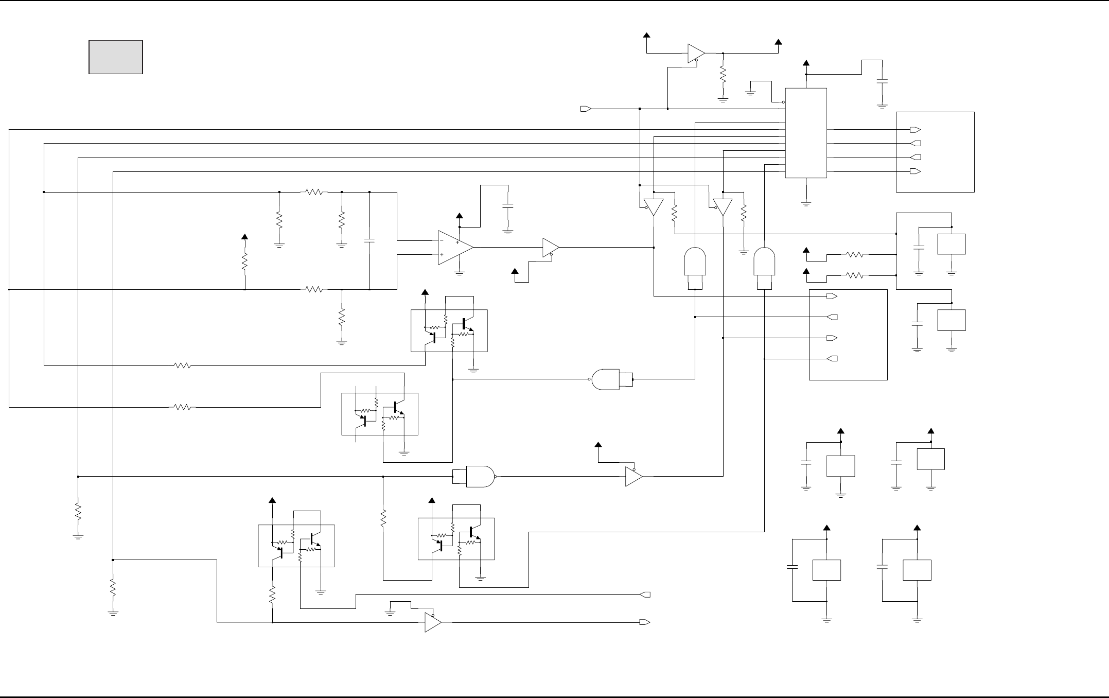
7-184 Schematics, Component Location Diagrams, and Parts Lists: HUF4017A (700-800 MHz) Main Board
May 25, 2005 6881096C74-B
Figure 7-127. Controller RS232/SB9600 Schematic
NP
BUFFER SUPPLY
NAND SUPPLY
Connector IF
NAND SUPPLY
BUFFER SUPPLY
BUFFER SUPPLY
Patriot UART B
BUFFER SUPPLY
MC74LCX125
U0602-2
5
4
6
0.1uF
C0610
C0614
SB96_RS232*_EN_INV
R0627
100K
0.1uF
C0613
0.1uF
VCC2.85
VCC
Q0610
U0608-2
PWR_GND
3
GND
5
U0607-2
PWR_GND
3
GND
5
VCC
U0602-5
PWR_GND
7
GND
14
VCC
C0604
0.1uF
TC7S00FU
U0609-1
1
2
4
100
R0623
VCC2.85
0.1uF
C0611
0.1uF
C0606
U0610-2
PWR_GND
3
GND
5
VCC
R0628
100K
VCC5
SB96_RS232*_EN_INV
100K
U0602-3
MC74LCX125
9
10
8
R0630
4
MC74LCX125
U0603-2
5
4
6
VCC2.85
VCC5
TC7S00FU
U0610-1
1
2
10K
R0639
VCC2.85
Q0611
10K
10K
R0638
GND
7
VCC
14
R0625
PWR_GND
U0603-5
R0629
10K
100K
VCC2.85
SB96_RS232*_EN_INV
VCC2.85
VCC5
100
R0622
R0634
C0603
U0609-2
PWR_GND
3
GND
5
VCC
0.1uF
R0636
Q0613
2
3
1
8
4
VCC5
10K
2
1
3
MC33202
U0604-1
MC74LCX125
U0602-1
2
1
3
U0603-1
MC74LCX125
0
R0632
R0631 0
R0635
100K
7
YB
9
YC
12
YD
VCC5
VCC5
14 I0D
3I1A
6I1B
10 I1C
13 I1D
1SELECT
16
VCC
4
YA
SN74CBT3257
U0606
15 EN_OE
8GND
2I0A
5I0B
11 I0C
100pF
1
2
4
C0616
100
R0621
NC7ST08
U0608-1
100
R0620
1
2
4
NC7ST08
U0607-1
VCC5
Q0612
U0602-4
MC74LCX125
12
13
11
100K
R0626
C0600
0.1uF
BUS-
BUS+*
BUSY BUSY
LH_RESET
BUS-*
BUS+
BUSY*
LH_RESET*
URXD2
SB96_RS232*_EN
URTS2
UTXD2
LHRST_IN
LHRST_OUT
BUS+_UARTB_TXD
BUSY_UARTB_RTS
RESET_UARTB_CTS
BUS-_UARTB_RXD
UCTS2
10K
10K
10K 10K
10K
10K
10K 10K
10K
10K
10K 10K
10K
10K
10K 10K
MAEPF-27919-O
Part Series
600-1
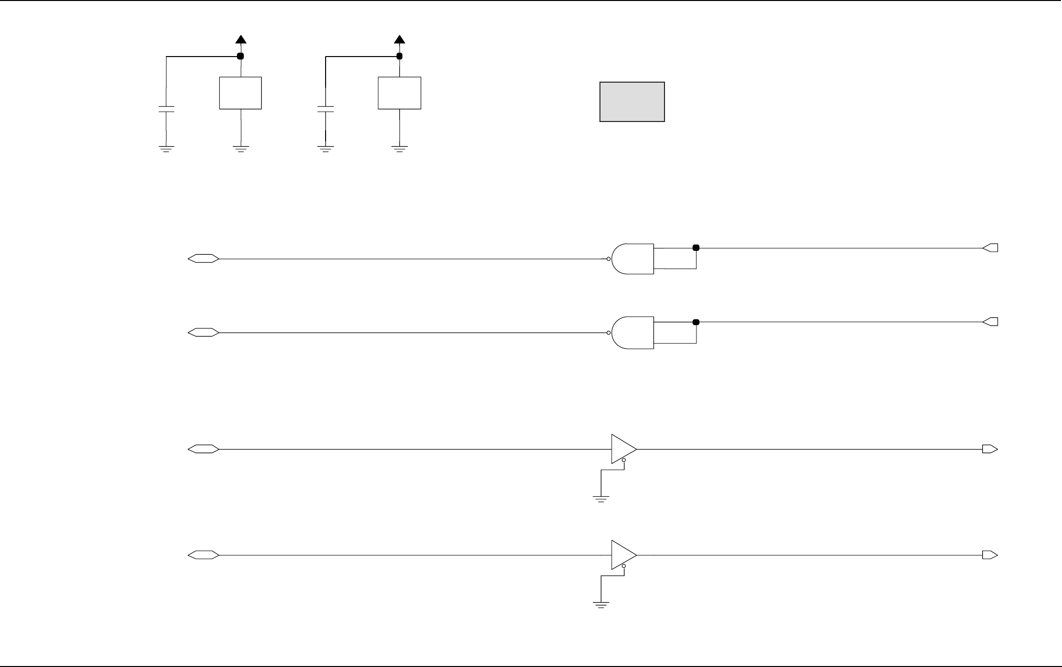
Schematics, Component Location Diagrams, and Parts Lists: HUF4017A (700-800 MHz) Main Board 7-185
6881096C74-B May 25, 2005
Figure 7-128. Controller VIP Input/Output Schematic
4
1
2
4
U0605-1
TC7S00FU
1
2
VCC5
TC7S00FU
U0601-1
0.1uF
VCC5
0.1uF
C0605C0601 GND
5
VCC
U0601-2
PWR_GND
3
GND
5
VCC
8
U0605-2
PWR_GND
3
12
13
11
U0603-3
MC74LCX125
9
10
VIP_IN_1_3V
VIP_IN_2_3V
VIP_IN_1_5V
VIP_OUT_1_3V
VIP_OUT_1_5V
VIP_OUT_2_3V
VIP_OUT_2_5V
VIP_IN_2_5V
U0603-4
MC74LCX125
MAEPF-27848-O
Part Series
600-2
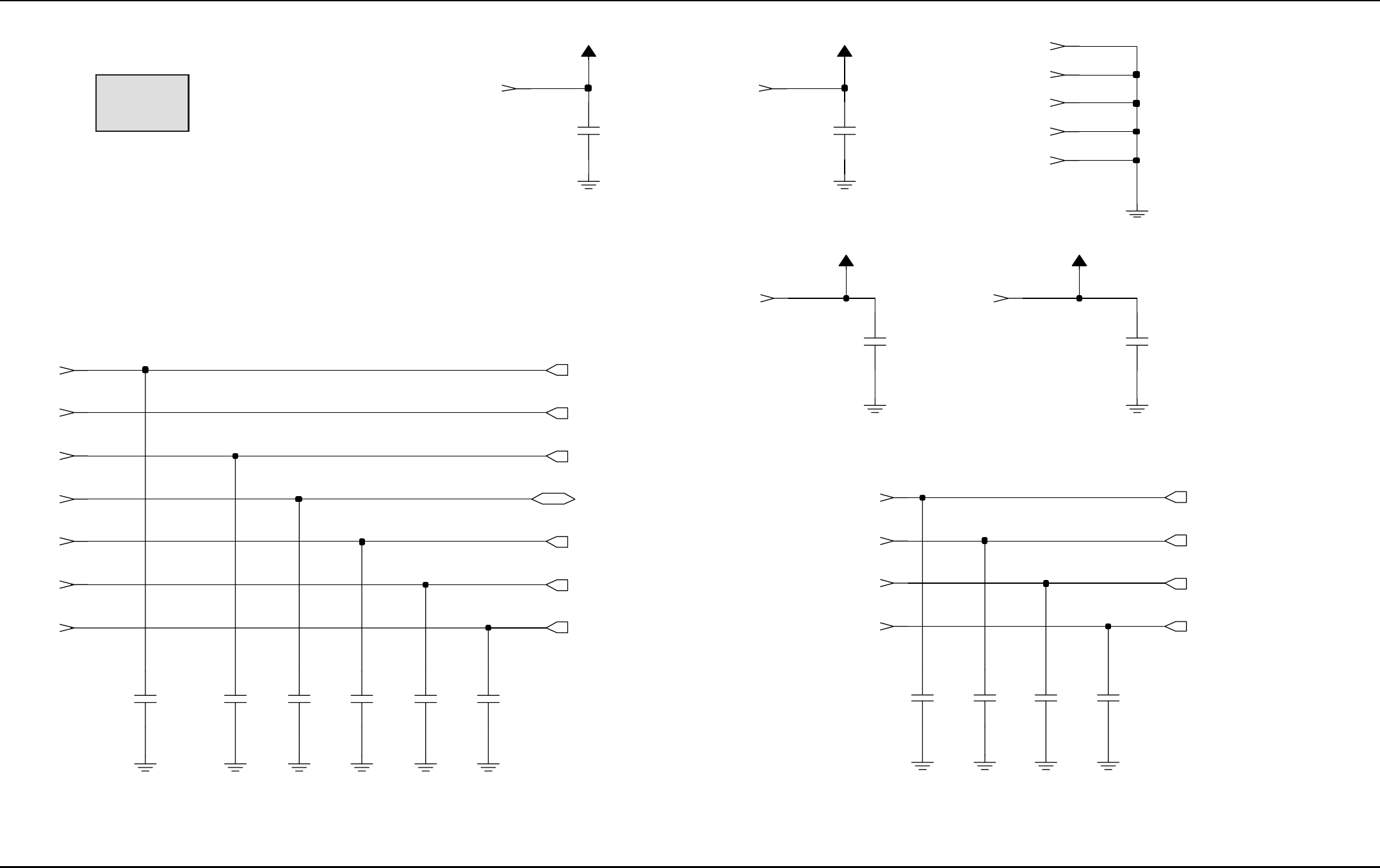
7-186 Schematics, Component Location Diagrams, and Parts Lists: HUF4017A (700-800 MHz) Main Board
May 25, 2005 6881096C74-B
Figure 7-129. Controller Secure Interface Connector Schematic
Control / I/O
SAP SSI Audio Bus
100pF
C0700
J0501-8J0501-7
J0501-9
J0501-19
J0501-20
J0501-16
J0501-18
A+
VCC2.85
SW_B+
J0501-13
J0501-4
J0501-10
C0712
100pF
C0711
100pF
C0710
100pF
C0709
100pF
220pF
C0713
220pF
C0714
J0501-17
J0501-1
J0501-5
J0501-6
J0501-11
J0501-14
J0501-3
VCC5
J0501-2
100pF
J0501-12
J0501-15
C0708C0706
100pF 100pF
C0705
100pF
C0704
100pF
C0703
100pF
C0702
100pF
C0701
SAP_TX
TAMPER_ENC
SAP_DCLK
SAP_RX
SAP_FSYNC
WAKEUP
KEYFAIL*
ENC_RESET
ENC_SPARE1
ENC_SPARE2
BOOT*
MAEPF-27846-O
Part Series
700
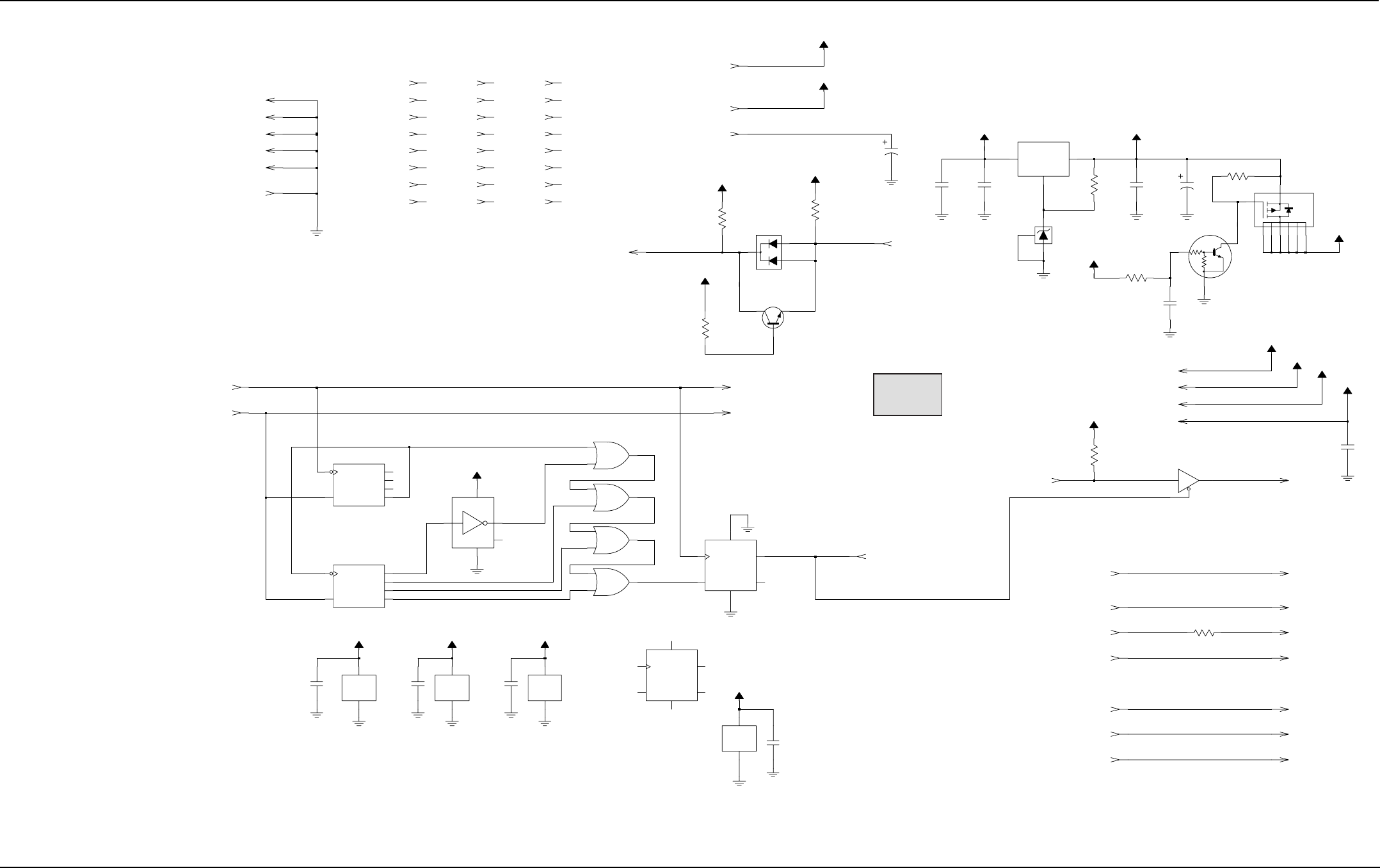
Schematics, Component Location Diagrams, and Parts Lists: HUF4017A (700-800 MHz) Main Board 7-187
6881096C74-B May 25, 2005
Figure 7-130. Secure Interface Board Schematic
11 P501-2
U803-4
12
13
VCC2.85
0.1uF
C811
10K
R806
P501-12
0
R808
J701-13
J701-15 *P501-11*
J701-27
J701-34
J701-12
VCC2.85VCC2.85
J701-36
J701-7
R802
1K
SW_B+
J701-22
J701-24
100K
R807
VCC2.85
J701-16
Q4 8
RESET
12
J701-6
J701-10
U802-2
CLK
13 Q1 11
Q2 10
Q3 9
U803-1
1
2
3
U803-3
9
10
8
P501-9
0.1uF
C809
VCC2.85
PWR_GND
U805-2
GND
3
VCC
5
U805-1
2
1
4
VCC2.85
J701-1
J701-8
A+
J701-19
J701-11
P501-4
J701-3
J701-35
VCC5
0.1uF
SW_B+
100K
C802
R804
4
5
6
VCC2.85
Q802
U802-3
PWR_GND
7
GND
14
VCC
U803-2
RESET
2
PWR_GND
U803-5
GND
7
VCC
14
U802-1
CLK
1Q1 3
Q2 4
Q3 5
Q4 6
J701-20
VCC2.85
J701-17
J701-23
PWR_GND
U804-3
GND
7
VCC
14
J701-4
UNSW_B+_ENC
J701-33
D801
1
2
3
J701-21
Q800
1
3
2
J701-31J701-29
J701-25
R805
10K
R800
10K
J701-32
Q803
47K
47K
P501-17
C803
P501-20
J701-14 A+
0.1uF
P501-7
P501-3
5.6V
VR800
R801
100K
P501-1
P501-10
J701-38
P501-18
2
J701-5
U800
MC33269D
ADJ
1
IN
3OUT
J701-2
VCC5
UNSW_B+_ENC
CLK
11
D
9
Q13
Q* 12
RESET 10
SET
8
J701-39
10uF
VCC2.85
U804-2
C805
1uF
C804
P501-16
J701-30
0.1uF
C808
0.1uF
C807
SW_B+_ENC
0.1uF
C806
U804-1
CLK
3
D
5
Q1
Q* 2
RESET 4
SET
6
3GND
2
1
NC
4
5
VCC
U801
0.1uF
J701-18
C801
0.47
C810
P501-15
SW_B+_ENC
J701-40
J701-26 P501-13
J701-37
J701-9
J701-28
P501-14
P501-19
P501-6
P501-8
P501-5
SAP_TX
SAP_TX
ENC_SEL
TAMPER_ENC TAMPER_ENC
BOOT*
ENC_SPARE2
ENC_SPARE1
ENC_RESET
WAKEUP
SAP_RX
SAP_FSYNC
SAP_DCLK
KEYFAIL*
KEYFAIL*
MAEPF-27914-O
Part Series
800

7-188 Schematics, Component Location Diagrams, and Parts Lists: HUF4017A (700-800 MHz) Main Board
May 25, 2005 6881096C74-B
Figure 7-131. HUF4017A Controller Urchin IC, MUX, and AD5320 DAC Schematic
NP
0.1uF
C0901
C0917
100pF
R0903
100K
C0906
VCC2.85
0.1uF
C0918
100pF
VCC2.85
R0904
100K
4DIN
2GND
5SCLK
6SYNC
3
VDD
1
VOUT
AD5320BRT
U0900
VCC2.85
C0910
0.1uF
4
3
1
5
2
R0901
8.2K
LMV7219
U0903
C7
VCC2 E2
VCC3 G4
VCC4
VCC2.85
C0909
0.1uF
B6
NC8 C2
NC9
A6
RESET
E5
TCK B1
TDI
TDO B7
D2
TMS
B3
VCC1
G3 NC29
NC3 A4
NC30
G5
G6 NC31
A7
NC4 B2
NC5 B4
NC6
NC7 B5
F1 NC21
F2 NC22
F3 NC23
F4 NC24
F5 NC25
F6 NC26
F7 NC27
G2 NC28
D3 NC14
D4 NC15
D6 NC16
D7 NC17
E1 NC18
E4 NC19
A2
NC2
E7 NC20
C3
G7 2.4_MHZ
G1 48_MHZ
A1
NC1
C4
NC10 C5
NC11 C6
NC12
D1 NC13
A3
16.8_CLK
C1
ENABLE
A5 GND1
E3 GND2
E6 GND3
JTAG_EN
C0915
VCC2.85
XCR3032XL
U0901
IN
2
6OS
OUT 5
7SHDN
4
VDD
100pF
MAX7414
FL0900
CLK
8
1COM
GND
3
C0905
0.1uF
VCC2.85
R0902
100K
C0904
C0908
0.1uF
VCC2.85
220pF
R0900
100K
0.1uF
C0903
VCC2.85
C0919
C0907
0.1uF
100pF
C0914
33pF
Z1
3
100pF
C0911
14
X
12 X0
X1
13
15
Y
2Y0
1Y1
4
Z
5Z0
A11
10
B
9
C
6
EN
8GND
16
VCC
7VEE
VCC2.85
MC74HC4053
U0902
100pF
C0912
C0902
R0905
100K
0.1uF
0.1uF
C0916
C0913
100pF
MODIN
SCF_OUT
MIC_TUNE_EN
URCHIN_EN
RESET AUX_TX
AUX_MIC
DAC_SSI_CLK
DAC_SSI_TXD
16.8_MHZ_DC
RX_FILT_AUDIO_IN
RX_FILT_AUDIO_OUT
16.8MHZ_SQARE
DAC_SSI_FSYNC
MODEM_EN
16.8_MHZ
AD5320_OUT
MAEPF-27836-O
Part Series
900-1
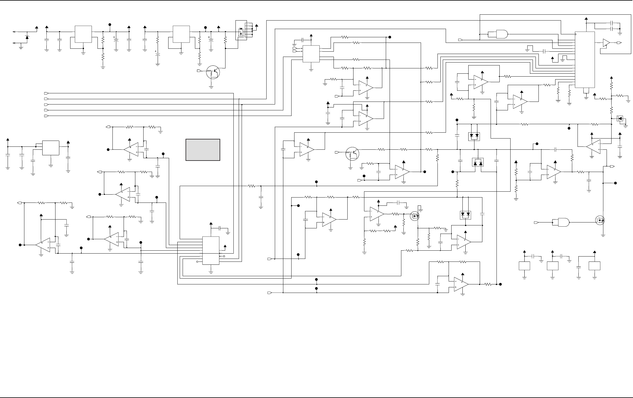
Schematics, Component Location Diagrams, and Parts Lists: HUF4017A (700-800 MHz) Main Board 7-189
6881096C74-B May 25, 2005
Figure 7-132. HUF4017A Controller Power Supply Schematic
1%
1%
1%
1%
1%
1%
1%
9.3V_TX_ REGULATOR
1%
1%
1%
1%
9.3V REGULATOR
1%
VTEMP
BATTERY CONNECTOR
1%
N/P
N/P
1%
VCONTROL
1%
A+
FORWARD_POWER
REVERSE_POWER
1%
VCURRENT
1%
R0948
10K
30K
*R0939*
0
*R0936*
R0978
10K
C0959
0.1uF
U0956-2
LMC6484
6
5
7
4
11
VCC3
U0957-1
MC33204
2
3
1
4
11
A+
R0990
C0973
5.1K
1uF
VR09515.6V
U0960-2
MC33204 6
5
7
4
11
C0974
9.3V_TX
VCC3
R0975
9.3V_TX
0.1uF
13
12
14
4
11
10K
100K
R0992
MC33204
U0960-4
9.3V_TX
NC
100pF
C0933
C0940
0.1uF
2
4
0.1uF
C0950
TC7S00FU
U0958-1
1
D0950
*Q0953*
C0966
100pF
R0907
0
VCC3
0.1uF
A+
1
C0936
VCC5
TP0937
0.1uF
0
R0987
C0960
VCC3
9.3V_TX
0.1uF
C0987
56K
R0989
14
4
11
7.5K
R0954
U0957-4
MC33204
13
12
0.1uF
C0937
100pF
VCC3
VIN3
7VIN4
8VIN5
9VIN6
10 VIN7
11 VIN8
1VREF
C0965
DIN 16
DOUT
15 RFS
18 SCLK
14 TFS
20
VDD
3VIN1
5VIN2
6
AD7812
U0953
12 A0
4AGND
19 CONVST
2CREF
13 DGND
17
TP0930 1
PWR_GND
U0954-2
GND
3
VCC
5
U0960-3
MC33204 9
10
8
4
11
9.3V_TX
9
10
8
4
11
K9.1V
TP0938 1
MC33204
U0957-3
1.2K
R0997
9OUTG
10 OUTH
5
REF
12
SCLK
4
VDD
3GND
6
LDAC
2OUTA
1OUTB
16 OUTC
15 OUTD
7OUTE
8OUTF
MAX5259
U0959
11
CS
13
DIN
14 DOUT
0.1uF
1
2
3
6
7
8
4
5
VCC3
*C0952*
2
3
1
4
11
Q0952
0.1uF
9.3V_TX
U0956-1
LMC6484
C0972
100pF
C0930
4
11
C0942
1uF
9.3V_TX
VCC3
MC33204
U0955-2
6
5
7
10K
R0996
NC
0.1uF
C0979
*R0947*
0
U0963-2
PWR_GND
3
GND
5
VCC
*R0972*
10K
100pF
C0975
BYPASS
4
GND
2
VEN
3
VIN
1VOUT 5
*C0962*
SW_A+
U0962
LP3985
100pF
G
D
S
100pF
C0978
*R0941*
Q0954
1
4
30K
13
12
14
4
11
NC7SZ125
U0963-1
2
R0982
LMC6484
U0956-4
100K
R0962
100K
TP0942
1
10K
R0991
R0995
*R0937*
1.2K
1
30K
TP0931
1
TP0955
Q0955
D
G
S
3.9K
R0994
0.1uF
C0954
MC33204
U0957-2
6
5
7
4
11
TP0939
1
9L1 5
L2 6
U_D
2
VDD 3
W1 4
W2 7
U0952
MAX5452
CS1
1
CS2
10
GND
8
INC
D0952
C0951
1uF
1
C0963
100pF
TP0952
1
10K
R0999
100K
TP0941
R0952
1.2K
R0955
J0950-1 1
10K
R0988
VCC3
9.3V_TX
A+
1.2K
R0993
0
*R0986*
0
*R0980*
SW_A+
*R0943*
20K
R0963
24K
100pF
C0968
0
*R0940*
TP0961
1
*R0945*
33K
100K
*R0946*
0.1uF
9.3V_TX
C0957
*R0971*
10K
20K
R0930
U0956-3
LMC6484
9
10
8
4
11
1
22uF
C0982
12
14
4
11
VCC3
TP0954
MC33204
U0955-4
13
9.3V
0
R0953
VCC3
100K
R0967
0.1uF
9.3V_TX
J0950-2 2
C0955
0
R0985
24V
VR0950
TP0957
1
0
R0966
100pF
*C0971*
C0961 0.1uF
10K
R0998
0
R0984
0
R0950
100pF
2K
R0983
*C0967*
Q0951
10K
R0931
C0980
C0985
0.1uF
TP0962
1
0.1uF
MC33204
U0955-3
9
10
8
4
11
22uF
VCC3
TP0958
1
C0953
C0983
100pF
1
10K
R0974
R0979
TP0963
TP0950
1
0
LM2941T
ADJ 1
GND
3
ON_OFF
2
VIN
4VOUT 5
20K
R0960
U0950
R0977
VCC2.85
VCC3
9.3V_TX
100
0.1uF
C0986
0.1uF
C0944
100pF
C0970
2
4
C0941
1uF
1
U0954-1
TC7S00FU
1
1K
TP0956
TP0960
1
R0976
2
3
1
4
11
9.3V_TX
2
3
1
4
11
MC33204
U0955-1
9.3V_TX
U0960-1
MC33204
3
GND
5
VCC
100pF
C0934
100K
U0958-2
PWR_GND
C0984
R0961
R0981
0.1uF
9.3V_TX
2.7K
*R0973*
30K
TP0953
1
VCC3
D0951
10uF
TP0959
1
C0956
LM2941T
ADJ 1
GND
3
ON_OFF
2
VIN
4VOUT 5
C0976
100pF
U0951
100pF
C0935
10K
R0944
*R0938*
*R0969*
VCC3
0
10K
.01uF
1
TP0951
1
C0943
TP0936 1
TP0964
24K
*R0970*
7.5K
1
R0951
C0945
TP0940
VCC3
4.7uF
C0969
0.1uF
C0981
100pF
100pF
24K
C0964
R0964
*R0942*
8.2K
9.3V_TX
0
R0965
R0968
10K
TEMP_2*
MISOA
RFPA_CNTRL
TEMP_1*
RX_FILT_1
K9.1V_EN
SCKA
PA_EN
MOSIA
AD_EN
VGBIAS_3*
VGBIAS_3
VGBIAS_2
VGBIAS_1
RX_FILT_1*
CURR_LIM_SET*
EEPOT_PC_INC*
EEPOT_PC_U_D*
VCURRENT
VTEMP
VGBIAS_1*
VGBIAS_2*
PWR_RANGE
EEPOT_5_CS*
DA_EN
PWR_SET*
VFORWARD
EEPOT_4_CS*
VREVERSE
47K
47K
47K
47K
MAEPF-27920-O
Part Series
900-2
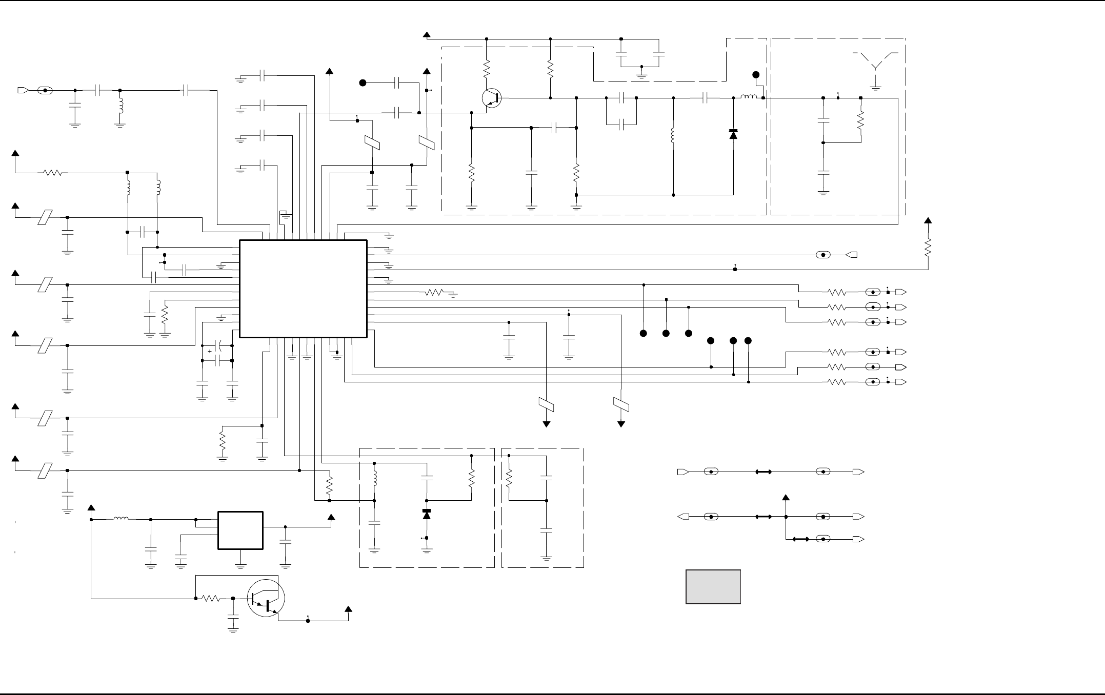
7-190 Schematics, Component Location Diagrams, and Parts Lists: HUF4017A (700-800 MHz) Main Board
May 25, 2005 6881096C74-B
Figure 7-133. HUF4017A Receiver Back-End Schematic
NO PLACE
To Controller Pin
#
#
#*
*
#
CLOCK LF
SPF_3.5V
From IF Section
2nd LO VCO
2nd LO LF
RX 2nd LO Shield
CLOCK VCO
#
#
#
#
#
270nH
E6001
BK1005HM471
0.1uF
C6019
L6004
VN_T6007
VN_T6008
VN_T6009
0.1uF
C6018
C6030
L6002
10uH
TP6001
1
.01uF
VN_B6002
VN_T6013,VN_B6005
VN_T6010
VN_B6004, VN_T6011,
VN_T6004, VN_T6001
1uF
C6068
IF6007
0.1uF
C6022
BYPASS
2GND
3VEN
1VIN 5
VOUT
IF6006
LP3985
U6002
4
R6021
10K
68pF
C6051
R6001
1MEG
10K
R6020
C6010
E6007
.01uF
C6023
0.1uF
FS
VN_T6005
VN_T6012
VN_B6001,
VN_T6003
IF6003
C6031
68pF
0
R6014
CLKOUT
0
R6011
R6009
24K
C6005
10K
R6005
C6012
100pF
5V
100pF
R6003
.01uF
C6024
10K
E6008
BK1005HM471
TP6000
0.1uF
C6025
E6000
BK1005HM471
VN_T6006
VN_B6000,VN_T6002
VN_B6003
68
R6006
10K
R6008
100pF
C6006
C6032
0.1uF
E6005
BK1005HM471
3VA
E6003
2.2uF
C6091
IF6009
BK1005HM471
E6006
VVCO
5V
3VA
51pF
C6052
5V
3VA
Q6000
C6026
3VA
IF6017
27pF
IF6005
330
R6004
3pF
*C6061*
D6051
C6016
0.1uF
0
R6022
3VA
DOUTA
0.47uF
C6057
C6054
12pF
E6002
390
R6007
0.1uF
C6060
E6004
SHIELD
*SH6000*
1
IF6013
C6096
0.1uF
220nH
L6000
0
R6015
200pF
.01uF
C6011
C6003
48
VDDI
40
VDDL 39
VDDP
14 VDDQ
12 VREFN
11 VREFP 25
PE
RREF
13
33
SYNCB
9VDDA
17 VDDC
26
VDDD
6VDDF
27
VDDH
15 IOUTC
38
IOUTL
42
LON
43
LOP
2MXON
1MXOP
23 PC
24 PD
36
GNDL
37
GNDP
16 GNDQ
21 GNDS1
34
GNDS2
4IF2N
5IF2P
47
IFIN
8GCN
7GCP
10 GNDA
18 GNDC
22 GNDD
3GNDF
32
GNDH
45
GNDI
CLKP
19
46
CXIF
44
CXVL
41
CXVM
29
DOUTA
30
DOUTB
35
FREF
31
FS
AD9874
U6000
20 CLKN
28
CLKOUT
C6056
0.1uF
C6021
1000pF
IF6001
.01uF
C6002
0.1uF
*C6015*
27pF
C6001
3VA
C6084
1uF
0.68uF
IF6008
IF6015
C6033
3VA
PC
0.1uF
IF6000
C6017
C6059
0.1uF
3VA
51
R6000
R6019
2.7uH
L6005
1K
L6001
10uH
IF6012
IF6014
0
R6012
30pF
C6000
8.2pF
C6055
0
R6016
4.7uF
*C6058*
.01uF
C6020
3VA
.01uF
C6067
C6064
0.1uF
PD
0
R6013
3VA
Q6001
VVCO
PE
C6007
2200pF
L6003
4.7uH
D6030
100pF
C6013
C6053
9.1pF
R6002
100K
100uH
L6012
3VA
5V_TO_IF
5V_TO_FGU5V_FROM_CONTR
CLKOUT_1
PD_1
PE_1
PC_1
DOUTA_1
FS_1
FREF
FE_FILTER_3 FE_FILTER_4
IF
MAEPF-27838-O
Part Series
6000
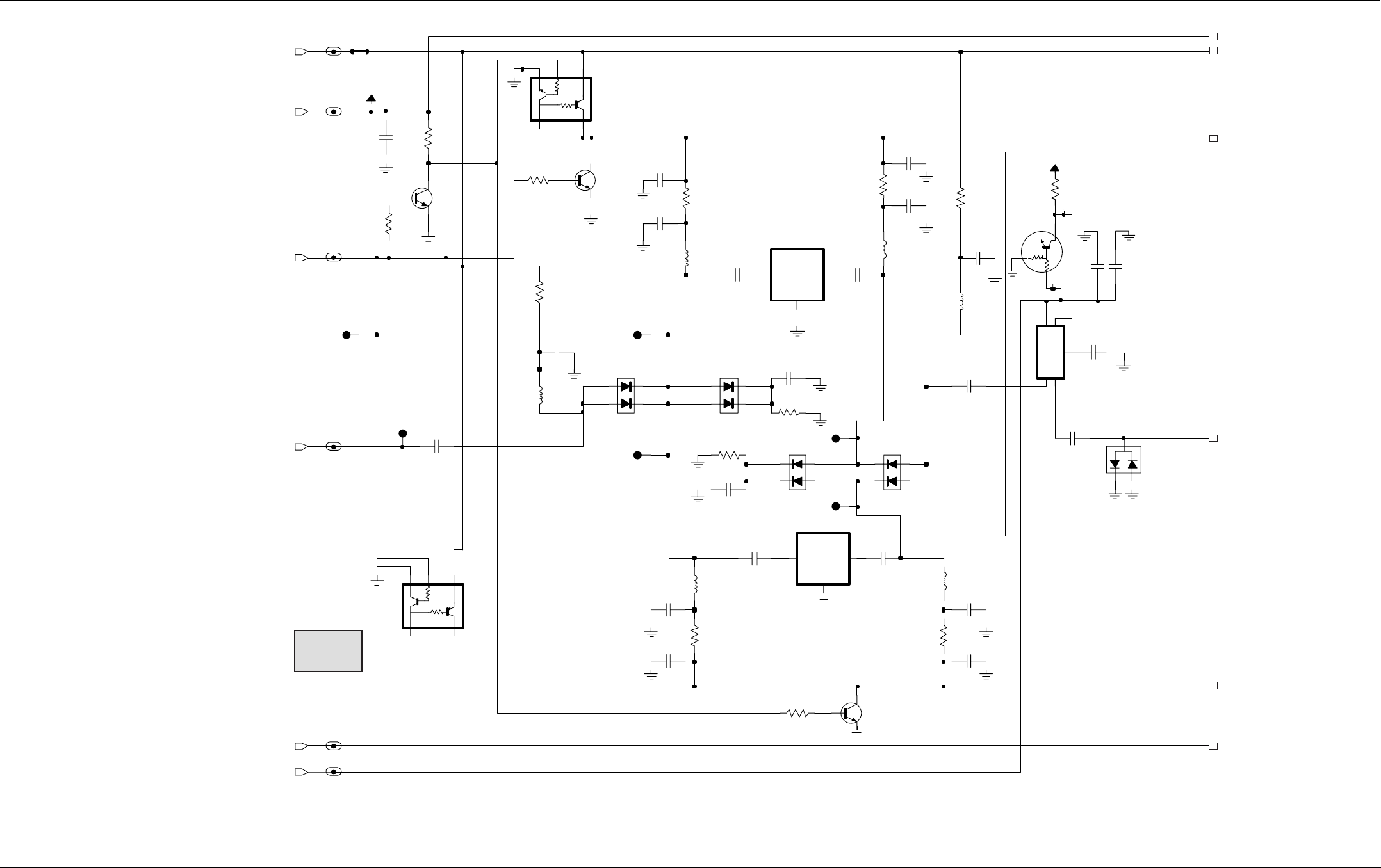
Schematics, Component Location Diagrams, and Parts Lists: HUF4017A (700-800 MHz) Main Board 7-191
6881096C74-B May 25, 2005
Figure 7-134. HUF4017A Receiver Front-End Schematic (Sheet 1 of 2)
5V
AGC/Attenuator circuit
9.3V
AUX
.01uF
C6259
TP6253
1
R6256
200
C6265
.01uF
C6267
.01uF
VN_B6262
VN_B6261
VN_B6252
VN_B6254
.01uF
C6283
C6293
39pF
IF6254
1K
R6276
1
C6270
47pF
1uH
L6256
TP6258
IF6252
.01uF
C6286
.01uF
Q6255
C6278
IF6253
D6250
2
3
1
IF6251
D6258
Q6254
R6255
1K
VN_B6259,VN_B6260
VN_B6251
3GND
2
IN
1OUT
D6253
03S10
B6250
.01uF
C6287
1K
R6258
TP6254 1
.01uF
C6253
R6254
200
Q6252
VN_B6256
22nH
L6262
D6252
3
IN
2OUT 1
.01uF
C6260
B6251
MD365
GND
22K
R6252
.01uF
C6269
C6279
.01uF
R6253
1K
L6259
1uH
L6263
22nH
.01uF
C6263
Q6250
C6273
47pF
.01uF
C6282
5V
1
TP6257 1
1
TP6256
C6254
TP6255
.01uF
2
GND
1RFIO1
3RFIO2
4
V1 5
V2
R6259
200
AT266
U6252
22nH
L6253
22K
R6257
R6282
10K
C6299
1000pF
C6298
470pF
47pF
C6296
.01uF
C6252
R6277
200
C6262
.01uF
IF6257
.01uF
C6275
1K
R6251
D6251
22nH
5V
IF6258
L6254
Q6253
R6250
Q6251
22K
RF_ATTN_1_A
9.3V_TO_IF
9.3V_TO_IF
LO_IN
FE_FILTER FE_FILTER
FE_FILTER
5V_FE
9.3V_FROM_FGU
RF_IN
47K
47K
6
1
2
3
4
5
MAEPF-27839-O
Part Series
6200-1

7-192 Schematics, Component Location Diagrams, and Parts Lists: HUF4017A (700-800 MHz) Main Board
May 25, 2005 6881096C74-B
Figure 7-135. HUF4017A Receiver Front-End Schematic (Sheet 2 of 2)
7.7V
RX Receive
700 MHz
TP6256, 58, 60, 62
LNA Output
TP6255, 57, 59, 61
3V
MIXER_RF_IN
Test points 800 MHz
RX Receive
7.7V
RX switching voltages
TP6254
MIXER_IF_OUT
4.3V
0V
2.3V
TP6250
1
TP6261 1
1K
R6275
D6256
.01uF
C6257
7.5nH
L6258
D6257
VN_B6258
.01uF
C6255
2GND2
GND4
4
5
IF
LO
3
RF
1
C6276
.01uF
MA4EX951H-1225
U6251
IF6256
22nH
L6261
TP6259
C6250
.01uF
.01uF
1
VN_B6253
VN_B6255
C6277
TP6262
1uH
L6257
1
TP6252
3.9pF
C6288
22nH
C6264
L6251
0.1uF
C6289
0.1uF
1.5K
R6278
200
R6272
R6270
1K
IF6250
TP6251
1
200
R6269
B6253
MD365
GND
3
IN
2OUT 1
C6256
C6281
.01uF
.01uF
C6295
1000pF
C6284
.01uF
C6285
.01uF
TP6260 1
D6254 C6268
.01uF
C6274
.01uF
0
*R6279*
.01uF
C6266
47pF
C6272
200
R6268
C6251
.01uF
1K
R6267
22nH
L6260
C6297
9.1pF
R6280
1.5K
R6281
5.1
R6271
1K
L6255
1uH
GND2
3RF_IN 6
RF_OUT
1
VBC
10pF
C6271
AM50_0011
U6250
2GND0
4GND1
5
68nH
L6252
D6255
.01uF
C6258
R6273
200
C6280
.01uF
L6250
22nH
.01uF
GND
2
IN
1OUT
C6261
03S10
B6252
3
9.3V_TO_IF
9.3V_TO_IF
9.3V_TO_IF
IF_OUT_IF
6
1
2
3
4
5
MAEPF-27840-O
Part Series
6200-2
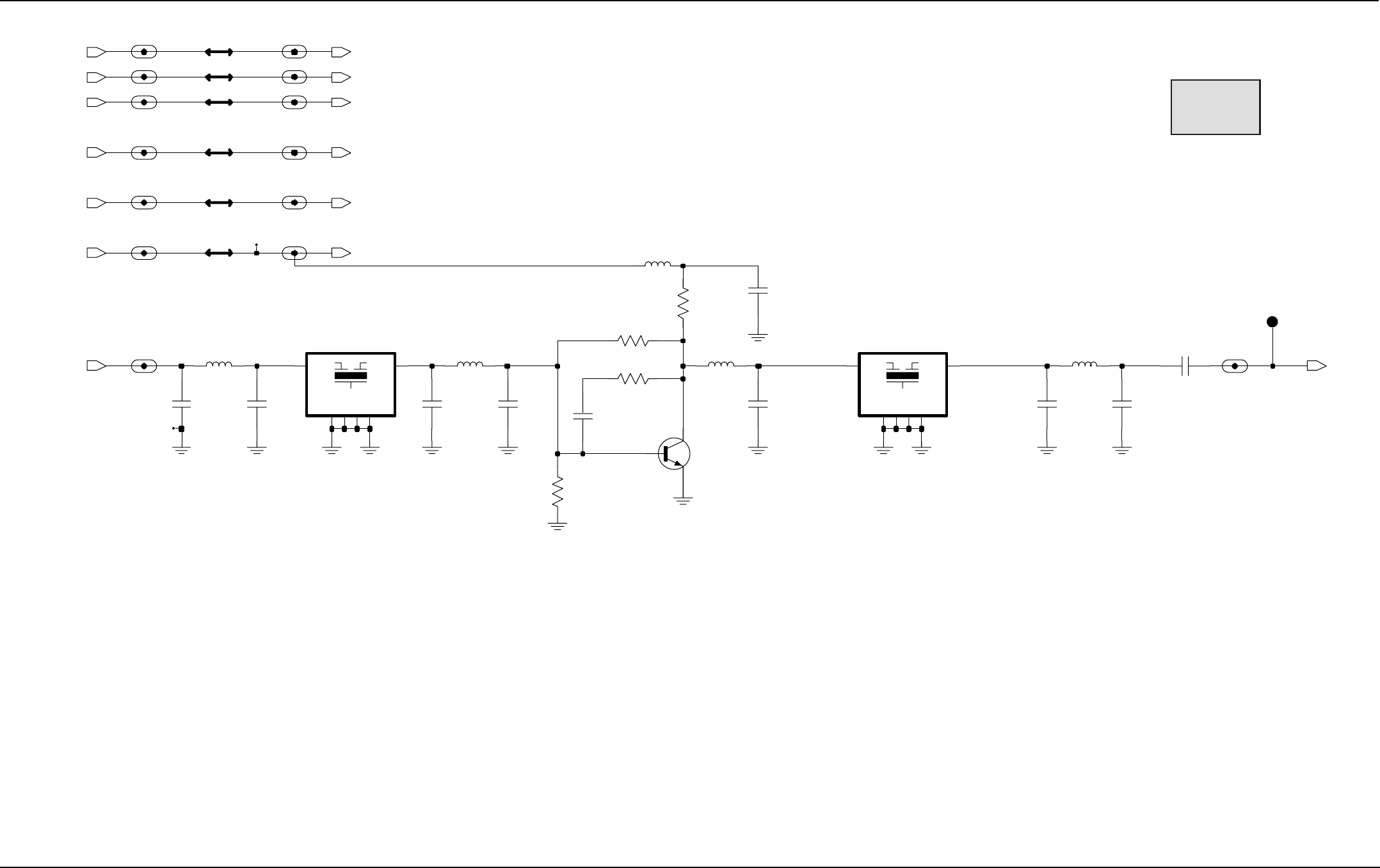
Schematics, Component Location Diagrams, and Parts Lists: HUF4017A (700-800 MHz) Main Board 7-193
6881096C74-B May 25, 2005
Figure 7-136. HUF4017A Receiver Intermediate Frequency (IF) Schematic
Going to Frontend
IF_TO_ABACUS
NO PLACE
Coming From Abacus
NO PLACE
IF6360
IF6357
GND1
6
GND2
2
GND3
3
5GND4
1IN 4
OUT
73E16.5A
B6350
R6353
1K
L6351
680nH
IF6358
IF6363
IF6356
4pF
C6351
IF6350
C6358
0.1uF
IF6354
L6352
1.2uH
VN_T6350
VN_T6351
1uH
L6355
0.1uF
C6354
10pF
C6353
820 TP6350
1
R6354
IF6361
2.2pF
5.6pF
C6352 *C6357*
4pF
C6356
IF6362
L6350
750nH
Q6350
8.2pF
IF6355
*C6350*
IF6351
1pF
C6355
GND2
2
GND3
3
5GND4
1IN 4
OUT
B6351
73E16.5A
6GND1
L6353
IF6353
750nH
R6350
10K
IF6352
IF6359
C6359
0.1uF
RF_ATTN_1_B
5V_TO_FE
9.3V_FROM_FE
R6352
39K
IF_IN IF_OUT
9.3V_TO_CONTR
FE_FILTER_2 FE_FILTER_1
5V_IF
RF_ATTN_3_C
RF_ATTN_1_C
RF_ATTN_2_C
RF_ATTN_3_B
RF_ATTN_2_B
MAEPF-27841-O
Part Series
6300

7-194 Schematics, Component Location Diagrams, and Parts Lists: HUF4017A (700-800 MHz) Main Board
May 25, 2005 6881096C74-B
Figure 7-137. HUF4017A RF Power Amplifier (PA) Schematic (Sheet 1 of 2)
RFPA/FGU
INTERFACE
RFPA/POWER CONTROL
INTERFACE
3
VG2
10uF
C6563
10 NC3
15 NC4
16 RFIN 6
RFOUT1 7
RFOUT2
1VCNTRL
14 VD1 2
VG1
EP
17
11 G2
4GND1
5GND2
12 GND3
13 GND4
8NC1
9NC2
U6500
30C65
IF6513
18.5nH
L6521
.01uF
C6508
IF6512
C6501
39pF Q6520
8.2
150nH
L6500
R6523
POS
1
IF6501
M6520
HEATSINK
IF6507
.01uF
C6507
R6524
8.2
IF6500
IF6514
VN_B6501
0
R6527
IF6502
R6521
8.2
L6502
7.5nH
10
R6549
10
R6526
VN_B6520
IF6503
IF6508
L6522
57R01
0.1uF
C6523
0.1uF
C6524
0.1uF
100pF
*C6525*
1K
R6520
C6503
C6521
39pF
VN_B6540
R6522
8.2
VN_B6503
IF6510
VN_B6502,VN_B6561,VN_B6564,VN_B6565
VN_B6500
.01uF
C6504
IF6505
C6509
IF6504
0.1uF
12pF
39pF
C6522
C6506
C6502
39pF
15pF
IF6509
C6520
IF6511
IF6506
.01uF
C6500
5.6pF
C6511
L6501
150nH
8.2
R6525
C6510
12pF
VN_B6560
VN_B6504
A+_3
A+_4
K9.1V
VGBIAS2
A+_1
VGBIAS3
RFPA_CNTRL
VTEMP
VFORWARD
VREVERSE
A+_2
VCURRENT
TX_INJ
K9.1V_FGU
VGBIAS1
6
7
8
9
1
2
3
4
5
MAEPF-27834-O
Part Series
6500-1
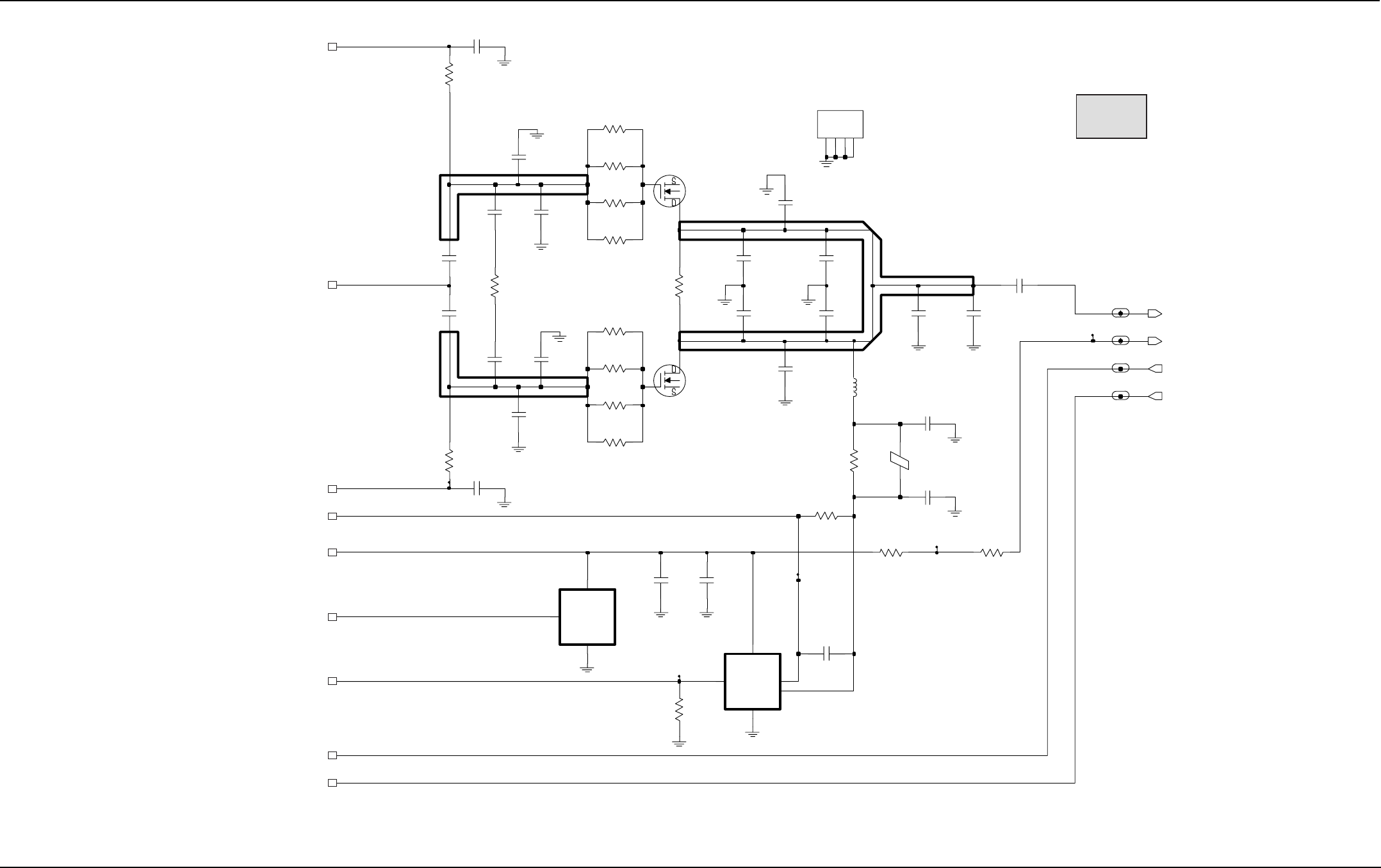
Schematics, Component Location Diagrams, and Parts Lists: HUF4017A (700-800 MHz) Main Board 7-195
6881096C74-B May 25, 2005
Figure 7-138. HUF4017A RF Power Amplifier (PA) Schematic (Sheet 2 of 2)
1%
RFPA/OUTPUT NETWORK
INTERFACE
C6557
39pF
IF6543
13pF
C6549
1K
R6543 L6543
57R01
C6545
12pF
R6550
2
C6559
39pF
R6553
2
GND
3POS 1
VOUT
2
3.3pF
LM50
U6540
2
R6555
C6556
IF6540
VN_B6541
11pF
C6541
R6552
2
L6542
C6562
0.1uF
17nH
33
R6559
C6554
VN_B6566
13pF
5.1pF
C6553
C6560
0.1uF
VINPOS
5
VPOS
R6547
33
INA138
U6541
GND
2
1OUT 4
VINNEG
3
C6558
39pF
33
R6548
Q6540
12pF
C6544
VN_B6521
R6545
5m
2
R6554
IF6542
39pF
C6565
Q6541
11pF
C6548
10pF
C6555
33
R6560
HEATSINK
GND1
1
GND2
2
GND3
3
4GND4
C6561
M6542
0.1uF
R6551
2
*C6564*
39pF
12pF
C6552
2
R6556
5.1pF
C6551
R6557
R6540
2
R6546
1K
12pF
C6547
100K
C6566
VN_B6562
VN_B6563
C6550
39pF
12pF
IF6541
C6540
39pF
C6542
12pF
10
R6544
SWITCH_BIAS
RFPA_OUT
VFORWARD_ON
VREVERSE_ON
6
7
8
9
1
2
3
4
5
MAEPF-27835-O
Part Series
6500-2
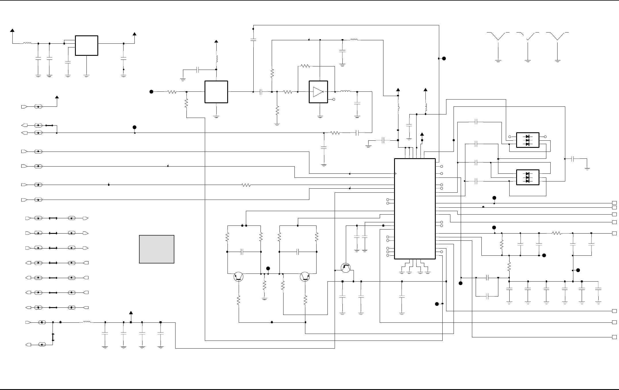
7-196 Schematics, Component Location Diagrams, and Parts Lists: HUF4017A (700-800 MHz) Main Board
May 25, 2005 6881096C74-B
Figure 7-139. HUF4017A Frequency Generation Unit Overall Schematic (Sheet 1 of 2)
*NP*
Syn_Sel
3.0 Volt Regulator
CLOCK
DATA
0.1uF
C6785
R6756
1K
2
1
NC
4
5
VCC
L6755
560nH
TC7SH04
U6752
3GND
0
R6782
NC
C6807
0.1uF
R6770
IF6762
47K
IF6780
C6768
10uF
NC
C6794
0.47uF
C6783
TP6756
1
.0012uF
0.1uF
C6789
NC
IF6768
7.5K
R6768
C6787
0.1uF
47K
R6763
F3.0v
IF6777
IF6779
C6751
1uF
IF6754
C6758
1000pF
TP6764
1
NC
NC
7.5K
R6762
1
TP6762
1
TP6755
1
TP6758
1
TP6752 1
TP6760
0.1uF
C6776
C6769
C6795
0.47uF
.047uF
510
R6761
100K
R6752
NC
NC
C6750
0.1uF
IF6751
C6808
10uF
F9.3V
IF6770
L6751
2.2uH
0.1uF
C6764
NC
C6777
IF6774
0.1uF
C6791
.022uF
2.2uH
L6752
2.2uH
L6750
100pF
C6755
Q6759
TP6768
1
TP6770 1
TP6771
1
IF6771
D6752
4A1
5A2
6A3
3
K1 2
K2 1
K3
IF6776
C6839
.01uF
SHIELD
*E6752*
1
IF6752
5
A3
6
K1 3
K2 2
K3 1
NC
VOUT 5
D6751
A1
4
A2
U6750
LP3985
BYPASS
4
2GND
VEN
3
1VIN
C6786
C6778
0.1uF
33pF
C6759
.047uF
Q6757
1.5K
R6764
*E6751*
1
IF6756
SHIELD SHIELD
*E6753*
1
0.1uF
C6765
IF6769
560nH
39pF
C6813
L6761
0.1uF
C6753
100K
R6755
IF6784
IF6763
C6817
NC
C6775
.01uF
10uF
R6765
180
100
R6757
C6780
39pF
IF6753
NC
0.1uF
C6757
.022uF
C6779
C6788
IF6775
R6760
3.3K
0.1uF
IF6783
C6766
0.1uF
F3.0v
C6763
0.1uF
100K
R6753
5V_Reg
F3.0v
IF6778
10K
R6766 R6767
IF6772
C6806
36K
NC
.022uF
R6754
1K
VN_T6772
5V_Reg
VN_T6770
VN_T6760
VN_T6757
VN_T6759
VN_T6771
Q6758
VN_B6769
NC
2K
1uH
L6756
R6769
0.1uF
F3.0v
C6790
F3.0v
VCONT
1
VDD 4
C6781
1200pF
16.8MHz
OSC1672A
Y6750
FOUT 3
GND
2
L6753
2.2uH
C6760
1000pF
VMULT1 15
VMULT2 14
VMULT3 12
VMULT4 11
13
VRO
WARP 25
XTAL1 23
XTAL2 24
SFBASE
27 SFCAP
26
SFIN
30
SFOUT 28
TEST1 37
TEST2 38
VBPASS
21
VCP 47
NC3
31
PD_GND
44
5
PD_VDD
PREIN
32
PRE_GND
33
PRE_VDD 34
PVREF
35
REFSEL
18 IADAPT 45
INDMULT 16
IOUT 43
4
LOCK
MODIN
10
MODOUT 41
NC1
17
NC2
29
40
BIAS2
39
CCOMP
42
CEX
9CLK
8
DATA
7
DGND
6
DVDD 36
FREFOUT 19
ADAPTSW 46
AGND
22
AUX1 48
AUX2 1
AUX3 2
AUX4 3
AVDD 20
BIAS1
VN_T6751, VN_T6769,
VN_T6763, VN_T6755, VN_T6752
U6751
63A27
C6818
IF6773
10uF
1uF
C6837
R6758
10K
VN_T6756,VN_T6767
C6771
NC
NC
IF6750
0.1uF
NC
39pF
VN_T6762
VN_T6754
VN_B6766
VN_T6761
NC
C6782
VN_T6773
VN_T6768
VN_B6759,VN_T6750
CLKOUT_3
PE_3
PD_3
5V_AUX_6
9.3V_1
FS_3FS_2
CLKOUT_2
PE_2
PD_2
PC_2
5V_AUX_5
9.3V_2
16_8_CONT
SYN_SEL
SPI_DATA
SPI_CLK
MOD_IN
16_8MHz
DOUTA_2
PC_3
DOUTA_3
5V_Reg
6
7
8
1
2
3
4
5
MAEPF-27829-O
Part Series
6700-1
6800-1
Schematics, Component Location Diagrams, and Parts Lists: HUF4017A (700-800 MHz) Main Board 7-197
6881096C74-B May 25, 2005
Figure 7-140. HUF4017A Frequency Generation Unit Overall Schematic (Sheet 2 of 2)
IF6766
NC
D6750
150
R6779
From_RX_VCO
RX_FDB
RX_INJ
VS1
VS2
F9.3V
C6792
10uF
TP6754
1
GND6
7
GND7
9
GND8
10
GND9
11
RF_OUT 20
SWBPOS1 2
SWBPOS2 17
GND17
21
GND18
22
GND2
3
GND3
4
GND4
5
GND5
6
12
GND11
13
GND12
14
GND13
15
GND14
16
GND15
18
GND16
19
U6755
06G61
700-800MHz
CONT_V
8
GND1
1
GND10
IF6767
NC
L6754
1uH
3
4
Q6753
3
1
2
5
TP6767
1
1
C6767
39pF
TP6751
1
TP6753
TP6750
1
39pF
C6784
Q6761
Q6760
1
2
5
3
4
C6773
39pF
C6802
39pF
2
1
TP6769
1
1
TP6757 1
TP6766
1
TP6763
TP6759
1
TP6761
1
R6774
330
IF6764
150
R6780 R6828
150
8.0V
From_TX_VCO
TX_8 V
TX_FDBK
TX_INJ
R6778
1.5K
IF6765
39pF
2
5
3
4
C6798
Q6756
6
1
C6801
39pF
10K
R6775
39pF
C6797
NC
VN_B6752
VN_B6771
VN_B6772
R6792
10
1
2
5
3
4
C6761
Q6755
39pF
NC
240
R6791
51
R6777
VN_T6766
20
SWBPOS1 2
SWBPOS2 17
VN_T6753
GND4
5
GND5
6
GND6
7
GND7
9
GND8
10
GND9
11
RF_OUT
GND15
18
GND16
19
GND17
21
GND18
22
GND2
3
GND3
4
CONT_V
8
GND1
1
GND10
12
GND11
13
GND12
14
GND13
15
GND14
16
U6754
06G62
700-800MHz
K9.1
Lock_Det
RX_Inj
TX_INJ
RECEIVER INJECTION STRING
TX INJECTION STRING
6
7
8
1
2
3
4
5
MAEPF-27830-O
Part Series
6700-1
6800-1
7-198 Schematics, Component Location Diagrams, and Parts Lists: HUF4017A (700-800 MHz) Main Board
May 25, 2005 6881096C74-B
Figure 7-141. HUF4017A Frequency Generation Unit 800 MHz Receive Injection Schematic
C6821
.01uF
C6824
39pF
R6800
18
39pF
C6820
4.7K
R6797
R6790
300
R6804
300
R6802
300
L6757
3.3nH
150
C6822
R6795
C6825
39pF 39pF
R6796
0.1uF
C6823
1K
300
R6799
R6793
150
39pF
R6794
39
39pF
C6841
C6840
R6824
300
Q6762
.01uF
C6826
R6803
18
R6789
12nH
L6758
2GND2
4GND3
5GND4
3RFIN 6
RFOUT
300
Q6763
MAALSS0017
1GND1
62
R6801
R6798
300
C6819
VS1
RX_FDB
VS2
From_RX_VCO
RX_INJ
39pF
MAEPF-27831-O
Part Series
6700-3
6800-3
Schematics, Component Location Diagrams, and Parts Lists: HUF4017A (700-800 MHz) Main Board 7-199
6881096C74-B May 25, 2005
Figure 7-142. HUF4017A Frequency Generation Unit 800 MHz Transmit Injection Schematic
R6810
18
39pF
C6827
Q6766
R6805
5.6K
R6806
1K
R6807
150
R6808
10
8.2nH
C6828
39pF L6760
C6832
39pF
C6833
.01uF
R6823
360
R6827
300
3pF
C6836
10
R6815
1K
R6813
39pF
C6831
150
R6814
C6834
39pF
R6817
18
R6811
300300
R6809
L6763
8.2nH
Q6765
R6819
15K
300
R6818
R6820
10K
R6826
18
R6816
300
R6812
5.6K
82
R6821
C6830
TP6765
18
39pF
C6829
R6831
R6825
39pF
.01uF
300
300
C6838
82
R6829
300
R6833
Q6764
R6830
C6835
TX_FDBK
8.0V
From_TX_VCO
TX_8V
TX_INJ
39pF
MAEPF-27832-O
Part Series
6700-4
6800-4

7-200 Schematics, Component Location Diagrams, and Parts Lists: HUF4017A (700-800 MHz) Main Board
May 25, 2005 6881096C74-B
Figure 7-143. HUF4017A Main Board Layout—Side 1 Top
C0401
C0406
C0407
C0412
C0413
C0417
C0463
C0464
C0467
C0952
C0955
C0956
C0957
C0959
C0962
C0963
C0964
C0965
C0966
C0967
C0971
C0972
C0973
C0975 C0976
C0978
C0979
C0980
C0983
D0952
J0950
3
4
1
Q0503
Q0955
R0430
R0515
R0531
R0907
R0946
R0947
R0950
R0953
R0954
R0960
R0963
R0964
R0967 R0968
R0969
R0970
R0971 R0972
R0973
R0974
R0975
R0976
R0977
R0978
R0979
R0980
R0981
R0982
R0983
R0984
R0985
R0986
R0987
R0988
R0989
R0990 R0992
R0993
R0994
R0996
R0997
R0998
R0999
SC0001
SC0002
TP0954
5
U0951
5
6
10
U0952
814
U0955
U0956
7
814
7
7
8
14
U0957
VR951
VR0405
VR0406
VR0407
VR0501
C0214
C0220
C0243
C0531
C0532
C0533
C0981
C0984
C0986
C0987
Q0200
R0220
R0222
R0951
R0952
R0995
11
9
5
U0950
16
9
81
U0959
1
18
17
16
15
14
13
12
11
10
9
8
7
6
5
4
3
2
18
17
16
15
14
13
12
11
10
9
8
7
6
5
4
3
2
Y
ZP
XWVUTSRH
I
J
K
L
M
NGFEDCBA
Y
ZP
XWVUTSRH
I
J
K
L
M
NGFEDCBA
U0001
C0100
C0204
C0207
C0213
C0223
C0301
C0312
C0428
C0436
C0437
C0442
C0444
C0450
C0452
C0454
C0455
C0458
C0461
C0469
C0502
C0503
C0519
C0536
C0600
C0603
C0604
C0606
C0610
C0611
C0613
C0614
C0616
50
49
J0401
Q0610
Q0611
Q0612
Q0613
R0103
R0104
R0109
R0110
R0111
R0113
R0114 R0115
R0116
R0117
R0119
R0120
R0121
R0122
R0124
R0125
R0200 R0204
R0303
R0304
R0305
R0307
R0415
R0422
R0425
R0505
R0508
R0509
R0527
R0620
R0621
R0622
R0623
R0625 R0626
R0627 R0628
R0629
R0630
R0631
R0632
R0634
R0635
R0636 R0638
R0639
TP0400
TP0401
TP0402
TP0403
TP0407
TP0408
TP0409
TP0410
TP0411
TP0412
TP0413
TP0414
TP0415
U0102
5
913
U0304
U0402
U0504
U0508
14
7
8
U0602
7
8
U0603
14 4
5
8
U0604
16
9
81
11
1
U0606
U0607 U0608 U0609
U0610
Y0100
C0105
C0217
C0953
C0954
R0101 R0102
R0123
TP0002
10
U0204
C0101
2
1
MAEPF-27849-O
SIDE 1 - TOP PORTION OF CIRCUIT BOARD
Schematics, Component Location Diagrams, and Parts Lists: HUF4017A (700-800 MHz) Main Board 7-201
6881096C74-B May 25, 2005
Figure 7-144. HUF4017A Main Board Layout—Side 1 Middle
C6562
C6564
C6705
M6520
M6542
M6700
Q6540
Q6541
R6545
R6546
R6560
U6541 C6500
C6504
C6507
C6508
L6500
L6501
R6547
C0461
C6750
C6751
C6753
C6755
C6757
C6758
C6765
C6794
C6795 C6817
C6837
C6839
2
J0501
L6752
L6756
L6761
Q6757
Q6758
R6752
R6753
R6754
R6755
R6756
R6758
R6760
R6762
R6763
R6766
R6767
R6768
R6769
R6770
TP6752
TP6770
TP6771
U6750
U6752
17
22
16
11
10
6
5
17
22
16
11
10
6
5
U6754
U6755
23
4
Y6750 1
C0703
C0705
C6000
C6001
C6002
C6003
C6005
C6006
C6007
C6011
C6012 C6013
C6020
C6021
C6022
C6023
C6026
C6030
C6031
C6032
C6033
C6058
C6059
C6060
C6096
CLKOUT
D6030
DOUTA
E6006
E6007
E6008
FS
L6000
L6001
L6002
L6003
PD
PC
PE
R6000
R6002
R6005
R6007
R6011
R6012
R6013
R6014
R6015
R6016
R6020
R6021
R6022
1
37 25
13
U6000
C6015
MAEPF-27850-O
SIDE 1 - MIDDLE PORTION OF CIRCUIT BOARD
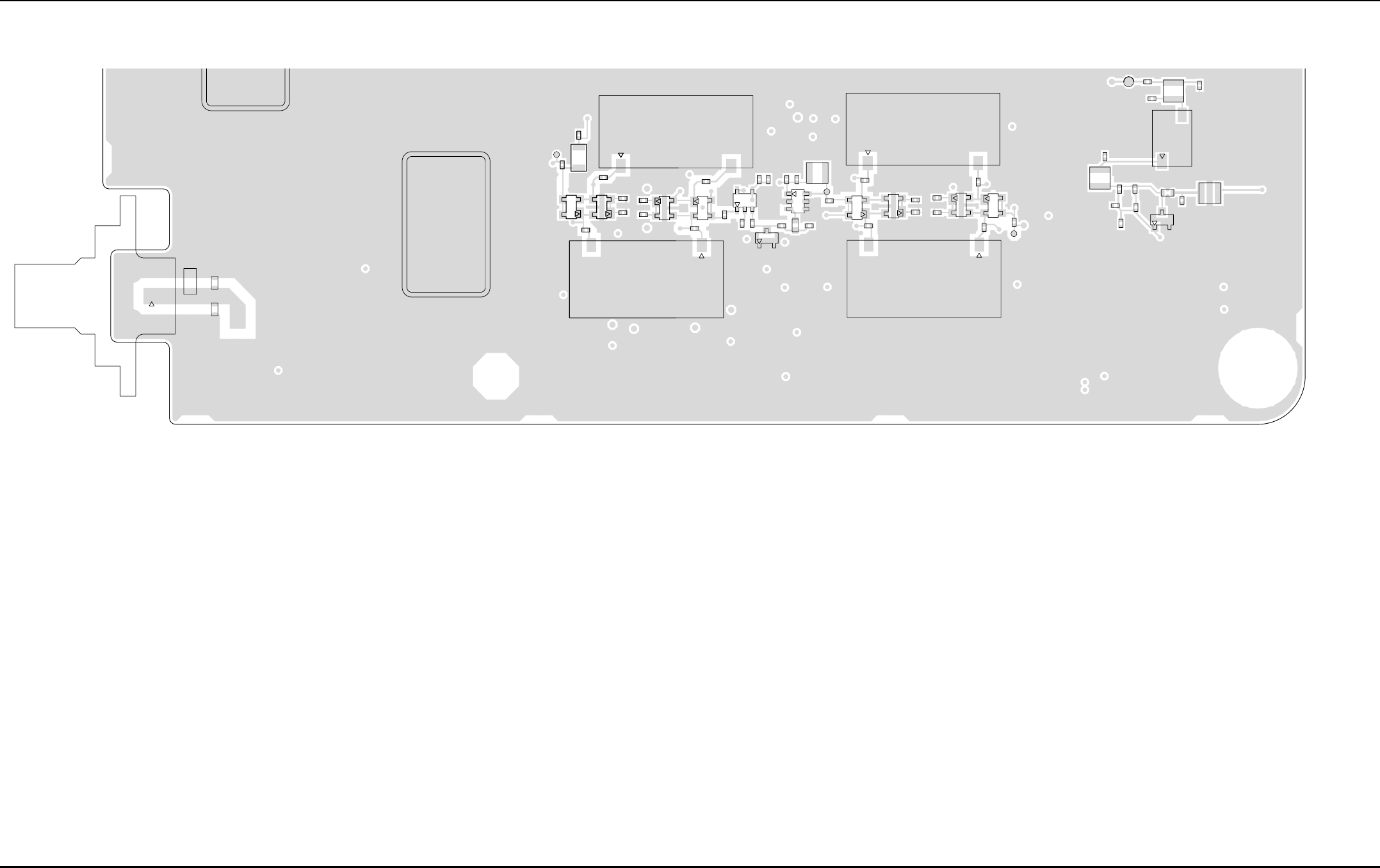
7-202 Schematics, Component Location Diagrams, and Parts Lists: HUF4017A (700-800 MHz) Main Board
May 25, 2005 6881096C74-B
Figure 7-145. HUF4017A Main Board Layout—Side 1 Bottom
C6734
C6735
3
2
J6700
M6721
R6740
3
2
2
B6251
C6262
C6267
C6269
C6273
C6275
C6278
D6250
D6251
D6252
L6259
R6255
R6258
TP6253
MAEPF-27851-O
5
6
4
3
2
1
B6351
C6353
C6354
C6355
C6356
C6357
C6358
C6359
L6352
L6353
L6355
Q6350
R6350 R6352
R6353
R6354
TP6350
B6250 3
2
3
3
2
B6252
B6253
C6257
C6258
C6263
C6264
C6268
C6270
C6271
C6272
C6274
C6276
C6277
C6279 C6288
C6289
C6293
C6295
C6296
C6298
C6299
D6253
D6254
D6255
D6256
D6257
D6258
L6252
L6258
R6270
R6271
TP6250
TP6251
3
46
U6250
U6252
SIDE 1 - BOTTOM PORTION OF CIRCUIT BOARD
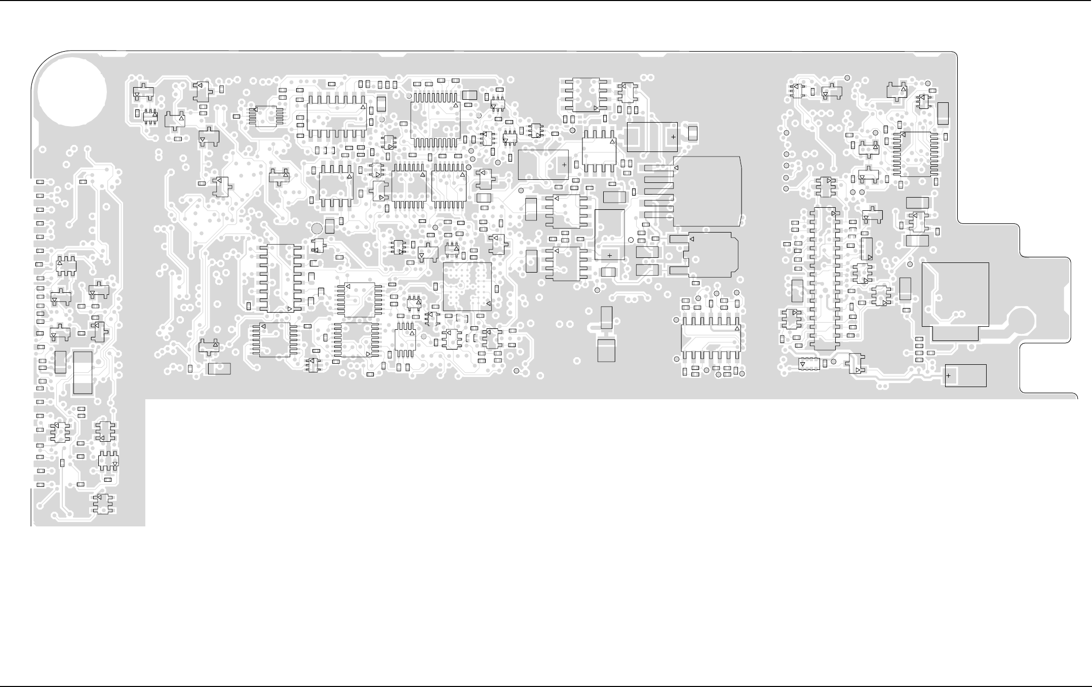
Schematics, Component Location Diagrams, and Parts Lists: HUF4017A (700-800 MHz) Main Board 7-203
6881096C74-B May 25, 2005
Figure 7-146. HUF4017A Main Board Layout—Side 2 Top
C0102
C0103
C0104
C0106
C0201
C0202
C0203
C0205
C0206
C0208
C0209
C0210
C0212
C0216
C0224
C0225
C0226
C0228
C0230
C0231
C0232
C0233
C0234
C0235
C0236
C0237
C0238
C0239
C0240
C0242
C0302 C0305
C0306
C0307
C0308
C0309
C0310
C0311
C0313
C0422
C0423 C0424
C0425
C0426
C0427
C0429 C0430
C0431 C0432
C0433 C0434
C0435
C0438
C0439
C0440
C0441
C0443
C0445
C0446
C0447
C0448
C0449
C0451
C0453
C0456
C0457
C0459
C0460
C0462
C0470
C0475
C0476
C0477
C0478
C0500
C0504
C0506
C0507
C0510
C0513
C0524
C0525
C0526 C0528
C0529
C0537
C0601
C0605
C0901
C0902
C0903
C0904
C0905
C0906
C0907
C0908
C0909
C0910
C0911
C0912
C0913
C0914
C0915
C0916
C0917
C0918
C0919
C0944
D0501
F0400
FL0900
Q0402
Q0403 Q0404
Q0500
Q0501
Q0502
Q0504
Q0505
R0105
R0106
R0107
R0108
R0202
R0203
R0205
R0206
R0207
R0208
R0209
R0210
R0212
R0216
R0218
R0219
R0221
R0224
R0225
R0226
R0227
R0228
R0229
R0230
R0235
R0236
R0403
R0404
R0409
R0411
R0416
R0417
R0418
R0419
R0420
R0421
R0431
R0500
R0502
R0503
R0504
R0507
R0512
R0513
R0514
R0516
R0517
R0518
R0520 R0521 R0522
R0523
R0524
R0900
R0901
R0902 R0903
R0904
R0905
TP0005
TP0200
TP0201
TP0202
TP0203
TP0204
TP0205
TP0206
TP0418
TP0419
TP0420
TP0500
TP0950
14
7
8
U0103
14
7
8
U0104
U0105
1
20
11 10
U0200
7
8
14
U0201
5
610
U0202
U0203
5
8
4
3
6
4
3
6
4
3
6
U0208
U0209
U0210
14
7
8
U0300
14
7
8
U0303
16
18
9
U0305
U0307
U0308
U0400
4
3
6
U0401
1
4
58
1
4
58
U0502
1
4
5
8
U0506
U0507
U0601
U0605
U0900
G7
G1
A7
A1
U0901
16
8
9
U0902
U0903
U0963
VR0412
VR0413
VR0414
VR0417
VR0418
VR0420
VR0421
VR0422
VR0423
VR0424
VR0425
VR0500
C0211
C0215
C0221
C0227
C0244
C0400
C0402
C0403
C0404 C0405
C0408
C0409
C0410
C0414
C0415
C0416
C0418
C0419
C0420
C0465
C0466
C0505
C0512
C0514
C0515
C0516
C0517
C0518
C0527
C0534
C0535
C0930
C0933
C0934
C0935
C0936
C0937
C0940
C0941
C0942
C0943 C0945
C0950
C0951
C0960
C0961
C0968
C0969
C0970
C0974
C0982
C0985
D0950
D0951
32
31
2
J0402
Q0951
4
5
8
Q0952
Q0953
Q0954
R0223
R0231
R0405
R0406
R0407
R0408
R0410
R0412
R0432
R0435
R0506
R0510
R0511
R0518
R0519
R0528
R0529
R0930
R0931
R0936
R0937
R0938
R0939
R0940
R0941
R0942
R0943
R0944
R0945
R0955
R0961
R0962
R0965
R0966
R0991
R1000
TP0930
TP0931
TP0936
TP0937
TP0938
TP0939
TP0940
TP0941
TP0942
TP0951
TP0952
TP0953
TP0955
TP0956
TP0957
TP0958
TP0959
TP0960
TP0961
TP0962
TP0963
TP0964
14
U0206
U0207
1
6
5
U0500
1
4
5
8
U0501
3
2
1
U0503
1
11
1
20
10
U0953 U0954
U0958
7
814
U0960
U0962
VR0400
VR0402
VR0404
VR0408
VR0410
4
8
VR0411
VR0950
MAEPF-27852-O
SIDE 2 - TOP PORTION OF CIRCUIT BOARD

7-204 Schematics, Component Location Diagrams, and Parts Lists: HUF4017A (700-800 MHz) Main Board
May 25, 2005 6881096C74-B
Figure 7-147. HUF4017A Main Board Layout—Side 2 Middle
MAEPF 27M
C0431 C0432
C0433 C0434
C0438
C0439
C0440
C0446
C0447
C0448
C0449
C0460
C0462
C0520
C0521
C0522
C0523
C0700 C0701
C0702
C0704
C0706
C0708 C0709
C0710 C0711
C0712
C0713
C0714
C6010
C6016
C6017
C6018 C6019
C6024
C6025
C6051
C6052
C6053
C6054
C6055
C6056
C6057
C6061
C6064
C6067
C6068
C6084
C6091
C6759
C6760
C6761
C6763
C6764
C6766
C6767
C6768
C6769
C6771
C6773
C6775
C6776
C6777
C6778
C6779
C6780
C6781
C6782
C6783
C6784
C6785
C6786
C6787
C6788
C6789
C6790
C6791
C6792
C6797
C6798
C6801
C6802
C6806 C6807
C6808
C6813
C6818
C6819
C6820 C6821
C6822
C6823
C6824
C6825
C6826
C6827
C6828
C6829
C6830
C6831
C6832
C6833
C6834
C6835
C6836
C6838
C6840
C6841
D6051
D6750
D6751 D6752
E6000
E6001
E6002
E6003
E6004
E6005
E6751 E6752
E6753
L6004
L6005
L6012
L6750
L6751
L6753
L6754
L6755
L6757
L6758
L6760
L6763
Q6000
Q6001
Q6753
Q6755
Q6756
Q6759
Q6760
Q6761
Q6762
3
45
Q6763
Q6764
Q6765
Q6766
R0524
R6001
R6003
R6004
R6006
R6008
R6009
R6019
R6757
R6761
R6764
R6765
R6774
R6775
R6777
R6778
R6779
R6780
R6782
R6789
R6790
R6791
R6792
R6793
R6794
R6795
R6796 R6797
R6798
R6799
R6800
R6801
R6802
R6803
R6804
R6805
R6806
R6807
R6808
R6809
R6810
R6811
R6812
R6813
R6814
R6815
R6816
R6817
R6818
R6819
R6820
R6821
R6823
R6824
R6825
R6826
R6827
R6828
R6829
R6830
R6831
R6833
SH6000
TP6000
TP6001
TP6750
TP6751
TP6753
TP6754
TP6755
TP6756
TP6757
TP6758
TP6759
TP6760
TP6761
TP6762
TP6763
TP6764
TP6765
TP6766
TP6767
TP6768
TP6769
3
2
1
U0505
U6002
1
37
25 13
U6751
VR0412
VR0413
VR0414
VR0417
C6502
C6509
C6510
C6511
C6520
C6521
C6540
C6541
C6542
C6544 C6545
C6547
C6548
C6549 C6550
C6551
C6552
C6553
C6554
C6555
C6556
C6557
C6560
C6561
C6565
C6566
C6700
C6701
C6703
C6704
D6702
L6521
L6700
L6702
L6703
1
2
3
Q6520
R6520
R6521
R6522
R6523
R6524
R6525
R6540
R6543
R6548
R6550
R6551
R6552
R6553
R6554
R6555
R6556
R6557
R6559
U6540
C6559
C6563
D6701
L6542 L6543
R6544
R6527
L6522
R6526
C6558
C6524C6522
C6525
C6523
R6549
C6501
C6503
C6506
L6502
116
89
U6500
SIDE 2 - MIDDLE PORTION OF CIRCUIT BOARD
MAEPF-27909-O
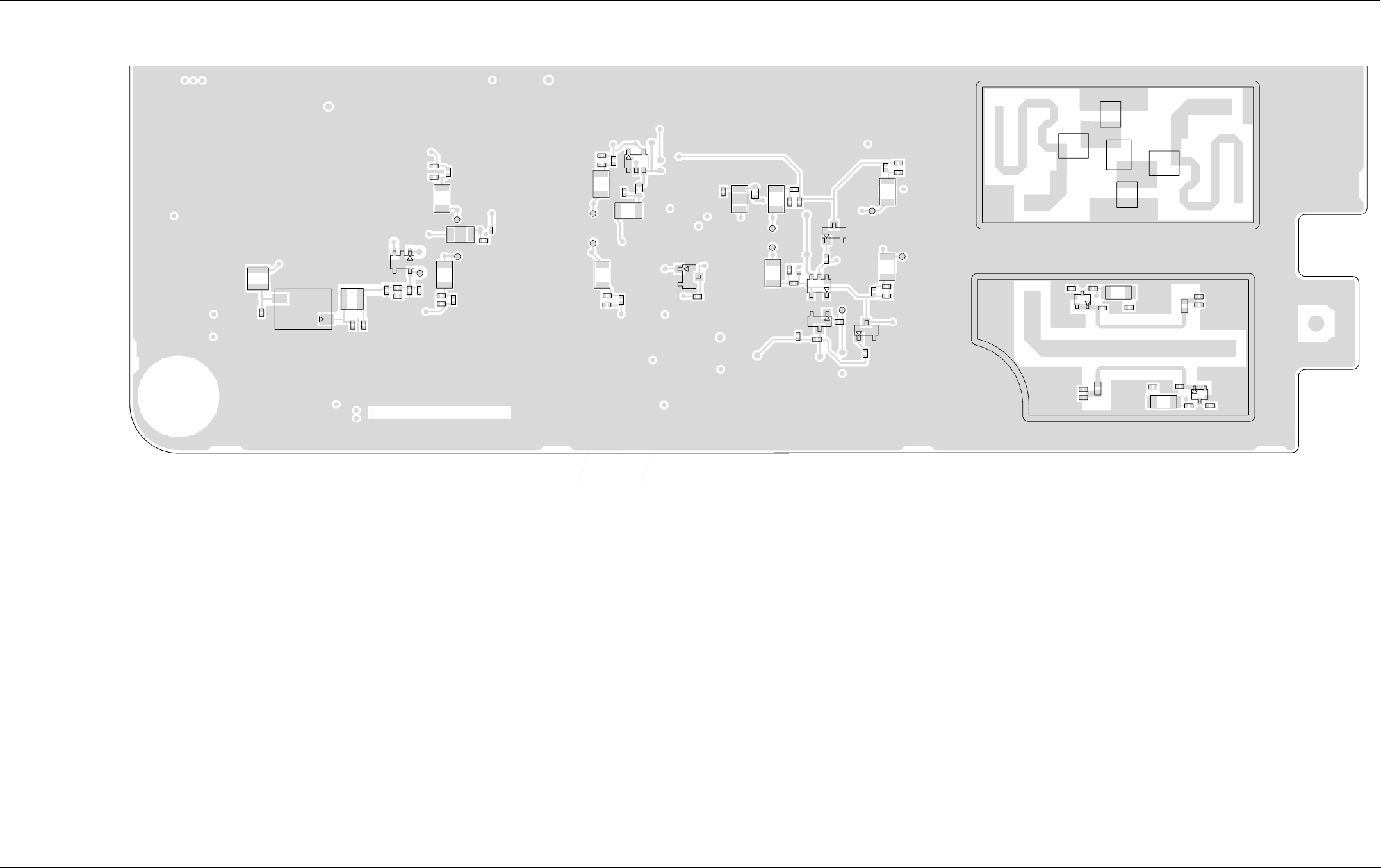
Schematics, Component Location Diagrams, and Parts Lists: HUF4017A (700-800 MHz) Main Board 7-205
6881096C74-B May 25, 2005
Figure 7-148. HUF4017A Main Board Layout—Side 2 Bottom
8485429D01 REV O
C6250
C6255
C6261
C6265
C6280
C6284
L6250
L6253
L6255
L6256
L6260
L6263
Q6252
Q6255
R6253
R6267
R6268
R6269
R6276
R6282
TP6257
TP6258
TP6259
TP6260
5
6
4
3
2
1
B6350
C6251
C6256
C6266
C6281
C6285
C6297
C6350
C6351
C6352
L6251
L6257
L6261
L6350
L6351
R6272
R6273
R6275
R6278
R6279
R6280
R6281
TP6252
TP6261
TP6262
U6251
C6252
C6253
C6259
C6260
C6254
C6282
C6283
C6286
C6287
C6720
C6721
C6730
C6731
C6732
C6733
D6730
D6731
L6254
L6262
L6720
L6721
L6722
L6730
L6731
M6720
Q6250
Q6251
Q6253
Q6254
R6250
R6251
R6252
R6254
R6256
R6257
R6259
R6277
R6731
R6732
R6733
R6734
R6735
R6736
R6737
R6730
R6738
R6739
SH6730
TP6254
TP6255
TP6256
MAEPF-27910-O
SIDE 2 - BOTTOM PORTION OF CIRCUIT BOARD
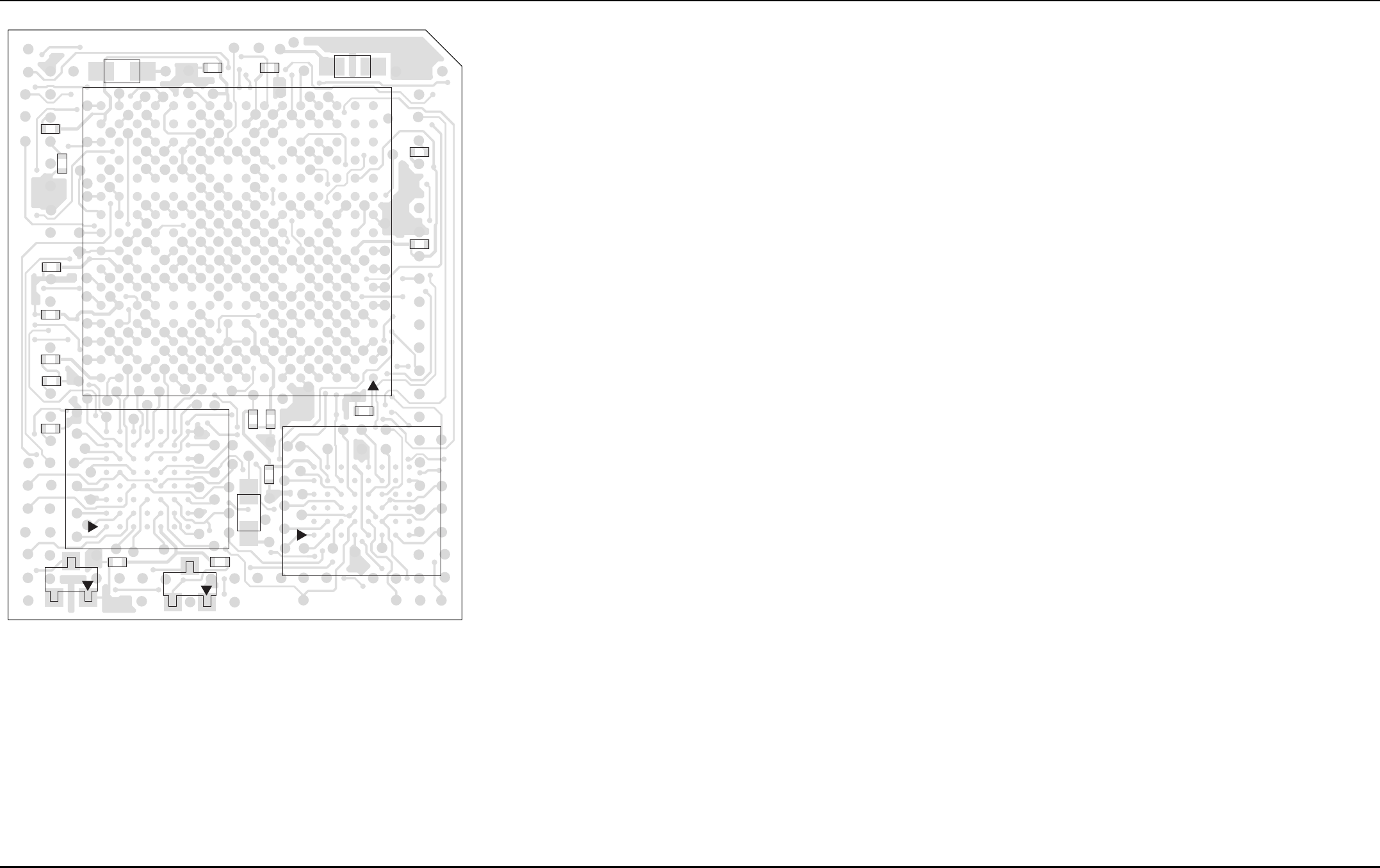
7-206 Schematics, Component Location Diagrams, and Parts Lists: HUF4017A (700-800 MHz) Main Board
May 25, 2005 6881096C74-B
Figure 7-149. HUF4017A Daughtercard Module Board Layout
O
C100
C102
C103
C104
C105
C106
C107
C109
C110
C111
C112
C113
C115
C116
C117
D100
D101
E101
E102
E103
R100
R106
A1
A16
T1
T16
U100
G1A1
A8 G8
U102
A1
A6
H1
H6
U103
MAEPF-27911-O

Schematics, Component Location Diagrams, and Parts Lists: HUF4017A (700-800 MHz) Main Board 7-207
6881096C74-B May 25, 2005
HUF4017A Main Board Parts List
Reference
Designator
Motorola
Part Number Description
B6250 9102603S10 FILTER 860.5 MHZ
B6251 9185503C01 FILTER CERAMIC 770
MHZ
B6252 9102603S10 FILTER 860.5 MHZ
B6253 9185503C01 FILTER CERAMIC 770
MHZ
B6350 9185116C01 FILTER CRYSTAL
B6351 9185116C01 FILTER CRYSTAL
C0001 2380090M24 CAP ALU 10 20 50V SURF
MT
C0100 2113743N32 CAP CHIP 18.0 PF 5%
COG
C0101 2113743N32 CAP CHIP 18.0 PF 5%
COG
C0102 2113743M24 CAP CHIP 100000 PF +80-
20% Y5V
C0103 2113743M24 CAP CHIP 100000 PF +80-
20% Y5V
C0104 2113743M24 CAP CHIP 100000 PF +80-
20% Y5V
C0105 2113743M24 CAP CHIP 100000 PF +80-
20% Y5V
C0106 2113743N50 CAP CHIP 100 PF 5% COG
C0201 2113743M24 CAP CHIP 100000 PF +80-
20% Y5V
C0202 2113743M24 CAP CHIP 100000 PF +80-
20% Y5V
C0203 2113743M24 CAP CHIP 100000 PF +80-
20% Y5V
C0204 2185802B01 CAP 10V 4.7UF
C0205 2113743N54 CAP CHIP 150 PF 5% COG
C0206 2113928E01 CAP CER CHIP 1.0 UF 10
% 10V
C0207 2113743N38 CAP CHIP 33.0 PF 5%
COG
C0208 2113928E01 CAP CER CHIP 1.0 UF 10
% 10V
C0209 2113743M24 CAP CHIP 100000 PF +80-
20% Y5V
C0210 2113743M24 CAP CHIP 100000 PF +80-
20% Y5V
C0211 2113743N50 CAP CHIP 100 PF 5% COG
C0212 2113743M24 CAP CHIP 100000 PF +80-
20% Y5V
C0213 2113743M24 CAP CHIP 100000 PF +80-
20% Y5V
C0214 2113741N69 CAP CHIP CL2 X7R 10%
100000
C0215 2113743M24 CAP CHIP 100000 PF +80-
20% Y5V
C0216 2113743M24 CAP CHIP 100000 PF +80-
20% Y5V
C0217 2113743L29 CAP CHIP 3300 PF 10%
X7R
C0220 2311049A57 CAP TANT CHIP A/P 10UF
10% 16V
C0221 2311049A78 CAP TANT CHIP 10.0 UF
10% 50V
C0223 2185802B01 CAP 10V 4.7UF
C0224 2113743M24 CAP CHIP 100000 PF +80-
20% Y5V
C0225 2113743M24 CAP CHIP 100000 PF +80-
20% Y5V
C0226 2113743M24 CAP CHIP 100000 PF +80-
20% Y5V
C0227 2113743M24 CAP CHIP 100000 PF +80-
20% Y5V
C0228 2113743N54 CAP CHIP 150 PF 5% COG
C0230 2113743L09 CAP CHIP 470 PF 10%
X7R
C0231 2113743L01 CAP CHIP 220 PF 10%
X7R
C0232 2113743L09 CAP CHIP 470 PF 10%
X7R
C0233 2113743L01 CAP CHIP 220 PF 10%
X7R
C0234 2113743M24 CAP CHIP 100000 PF +80-
20% Y5V
C0235 2113743L09 CAP CHIP 470 PF 10%
X7R
C0236 2113743L09 CAP CHIP 470 PF 10%
X7R
C0237 2113743L01 CAP CHIP 220 PF 10%
X7R
C0238 2113743L01 CAP CHIP 220 PF 10%
X7R
C0239 2113743M24 CAP CHIP 100000 PF +80-
20% Y5V
C0240 2113743M24 CAP CHIP 100000 PF +80-
20% Y5V
C0242 2113743M24 CAP CHIP 100000 PF +80-
20% Y5V
C0243 2113945B01 CAP CER CHIP 6800 PF
25V 10%
C0244 2113945B01 CAP CER CHIP 6800 PF
25V 10%
C0301 2113743M24 CAP CHIP 100000 PF +80-
20% Y5V
C0302 2113743M24 CAP CHIP 100000 PF +80-
20% Y5V
C0305 2113743M24 CAP CHIP 100000 PF +80-
20% Y5V
Reference
Designator
Motorola
Part Number Description
C0306 2113743M24 CAP CHIP 100000 PF +80-
20% Y5V
C0307 NOTPLACED 64AM DUMMY PART
NUMBER
C0308 2113743E20 CAP CHIP .10 UF 10%
C0309 2113743E20 CAP CHIP .10 UF 10%
C0310 2113743E20 CAP CHIP .10 UF 10%
C0311 2113743M24 CAP CHIP 100000 PF +80-
20% Y5V
C0312 2113743M24 CAP CHIP 100000 PF +80-
20% Y5V
C0313 2113743M24 CAP CHIP 100000 PF +80-
20% Y5V
C0400 2113743N38 CAP CHIP 33.0 PF 5%
COG
C0401 2113743N50 CAP CHIP 100 PF 5% COG
C0402 2113743N38 CAP CHIP 33.0 PF 5%
COG
C0403 2113743N38 CAP CHIP 33.0 PF 5%
COG
C0404 2113743N38 CAP CHIP 33.0 PF 5%
COG
C0405 2113743N38 CAP CHIP 33.0 PF 5%
COG
C0406 2113743N38 CAP CHIP 33.0 PF 5%
COG
C0407 2113743N50 CAP CHIP 100 PF 5% COG
C0408 2113743N50 CAP CHIP 100 PF 5% COG
C0409 2113743N38 CAP CHIP 33.0 PF 5%
COG
C0410 2113743N38 CAP CHIP 33.0 PF 5%
COG
C0412 2113743N50 CAP CHIP 100 PF 5% COG
C0413 2113743N50 CAP CHIP 100 PF 5% COG
C0414 2113743L01 CAP CHIP 220 PF 10%
X7R
C0415 2113743L01 CAP CHIP 220 PF 10%
X7R
C0416 2113743N50 CAP CHIP 100 PF 5% COG
C0417 2113743L01 CAP CHIP 220 PF 10%
X7R
C0418 2113743L01 CAP CHIP 220 PF 10%
X7R
C0419 2113743N50 CAP CHIP 100 PF 5% COG
C0420 2185802B01 CAP 10V 4.7UF
C0422 2113743N38 CAP CHIP 33.0 PF 5%
COG
C0423 2113743N38 CAP CHIP 33.0 PF 5%
COG
C0424 2113743N38 CAP CHIP 33.0 PF 5%
COG
C0425 2113743N50 CAP CHIP 100 PF 5% COG
Reference
Designator
Motorola
Part Number Description
C0426 2113741B13 CAP CHIP CL2 X7R REEL
470
C0427 2113743N50 CAP CHIP 100 PF 5% COG
C0428 2113743N50 CAP CHIP 100 PF 5% COG
C0429 2113743N50 CAP CHIP 100 PF 5% COG
C0430 2113743N50 CAP CHIP 100 PF 5% COG
C0431 2113743N50 CAP CHIP 100 PF 5% COG
C0432 2113743N50 CAP CHIP 100 PF 5% COG
C0433 2113743N50 CAP CHIP 100 PF 5% COG
C0434 2113743N50 CAP CHIP 100 PF 5% COG
C0435 2113743L09 CAP CHIP 470 PF 10%
X7R
C0436 2113741B13 CAP CHIP CL2 X7R REEL
470
C0437 2113741B13 CAP CHIP CL2 X7R REEL
470
C0438 2113743L09 CAP CHIP 470 PF 10%
X7R
C0439 2113743N50 CAP CHIP 100 PF 5% COG
C0440 2113743N50 CAP CHIP 100 PF 5% COG
C0441 2113743M24 CAP CHIP 100000 PF +80-
20% Y5V
C0442 2113743N38 CAP CHIP 33.0 PF 5%
COG
C0443 2113743N38 CAP CHIP 33.0 PF 5%
COG
C0444 2113743N38 CAP CHIP 33.0 PF 5%
COG
C0445 2113743N38 CAP CHIP 33.0 PF 5%
COG
C0446 2113743N50 CAP CHIP 100 PF 5% COG
C0447 2113743N50 CAP CHIP 100 PF 5% COG
C0448 2113743N50 CAP CHIP 100 PF 5% COG
C0449 2113743N50 CAP CHIP 100 PF 5% COG
C0450 2113743N38 CAP CHIP 33.0 PF 5%
COG
C0451 2113743N38 CAP CHIP 33.0 PF 5%
COG
C0452 2113743N38 CAP CHIP 33.0 PF 5%
COG
C0453 2113743N38 CAP CHIP 33.0 PF 5%
COG
C0454 2113743N38 CAP CHIP 33.0 PF 5%
COG
C0455 2113743N38 CAP CHIP 33.0 PF 5%
COG
C0456 2113743N38 CAP CHIP 33.0 PF 5%
COG
C0457 2113743N38 CAP CHIP 33.0 PF 5%
COG
C0458 2113743N38 CAP CHIP 33.0 PF 5%
COG
Reference
Designator
Motorola
Part Number Description
7-208 Schematics, Component Location Diagrams, and Parts Lists: HUF4017A (700-800 MHz) Main Board
May 25, 2005 6881096C74-B
C0459 2113743N38 CAP CHIP 33.0 PF 5%
COG
C0460 2113743N50 CAP CHIP 100 PF 5% COG
C0461 2113743L01 CAP CHIP 220 PF 10%
X7R
C0462 2113743L01 CAP CHIP 220 PF 10%
X7R
C0463 2113743N38 CAP CHIP 33.0 PF 5%
COG
C0464 2113743N38 CAP CHIP 33.0 PF 5%
COG
C0465 2113741B13 CAP CHIP CL2 X7R REEL
470
C0466 2113743N50 CAP CHIP 100 PF 5% COG
C0467 2113743N50 CAP CHIP 100 PF 5% COG
C0469 2113743M24 CAP CHIP 100000 PF +80-
20% Y5V
C0470 2113743N38 CAP CHIP 33.0 PF 5%
COG
C0475 2113743N50 CAP CHIP 100 PF 5% COG
C0476 2113743N50 CAP CHIP 100 PF 5% COG
C0477 2113743N50 CAP CHIP 100 PF 5% COG
C0478 2113743N50 CAP CHIP 100 PF 5% COG
C0500 2113743M24 CAP CHIP 100000 PF +80-
20% Y5V
C0502 2113743N50 CAP CHIP 100 PF 5% COG
C0503 2113743N50 CAP CHIP 100 PF 5% COG
C0504 2113741N69 CAP CHIP CL2 X7R 10%
100000
C0505 2113743L41 CAP CHIP 10000 PF 10%
X7R
C0506 2113743L41 CAP CHIP 10000 PF 10%
X7R
C0507 2113743M24 CAP CHIP 100000 PF +80-
20% Y5V
C0510 2185802B01 CAP 10V 4.7UF
C0512 2113743M24 CAP CHIP 100000 PF +80-
20% Y5V
C0513 2311049A43 CAP TANT CHIP 150 10 6
C0514 2311049A43 CAP TANT CHIP 150 10 6
C0515 2113743M24 CAP CHIP 100000 PF +80-
20% Y5V
C0516 2113743M24 CAP CHIP 100000 PF +80-
20% Y5V
C0517 2185802B01 CAP 10V 4.7UF
C0518 2185802B01 CAP 10V 4.7UF
C0519 2113743L41 CAP CHIP 10000 PF 10%
X7R
C0520 2113743M24 CAP CHIP 100000 PF +80-
20% Y5V
C0521 2185802B01 CAP 10V 4.7UF
C0522 2185802B01 CAP 10V 4.7UF
Reference
Designator
Motorola
Part Number Description
C0523 2113743M24 CAP CHIP 100000 PF +80-
20% Y5V
C0524 2113743M24 CAP CHIP 100000 PF +80-
20% Y5V
C0525 2113928E01 CAP CER CHIP 1.0 UF 10
% 10V
C0526 2113743L41 CAP CHIP 10000 PF 10%
X7R
C0527 2185802B01 CAP 10V 4.7UF
C0528 2113743M24 CAP CHIP 100000 PF +80-
20% Y5V
C0529 2185802B01 CAP 10V 4.7UF
C0531 2113741N69 CAP CHIP CL2 X7R 10%
100000
C0532 2113741Y32 CAP CER 1,000,000 10%
50V
C0533 2311049C47 CAP TANT CHIP 22.0UF
10% 16V
C0534 2113743M24 CAP CHIP 100000 PF +80-
20% Y5V
C0535 2113743M24 CAP CHIP 100000 PF +80-
20% Y5V
C0536 2113743M24 CAP CHIP 100000 PF +80-
20% Y5V
C0537 NOTPLACED 64AM DUMMY PART
NUMBER
C0600 2113743M24 CAP CHIP 100000 PF +80-
20% Y5V
C0601 2113743M24 CAP CHIP 100000 PF +80-
20% Y5V
C0603 2113743M24 CAP CHIP 100000 PF +80-
20% Y5V
C0604 2113743M24 CAP CHIP 100000 PF +80-
20% Y5V
C0605 2113743M24 CAP CHIP 100000 PF +80-
20% Y5V
C0606 2113743M24 CAP CHIP 100000 PF +80-
20% Y5V
C0610 2113743M24 CAP CHIP 100000 PF +80-
20% Y5V
C0611 2113743M24 CAP CHIP 100000 PF +80-
20% Y5V
C0613 2113743M24 CAP CHIP 100000 PF +80-
20% Y5V
C0614 2113743M24 CAP CHIP 100000 PF +80-
20% Y5V
C0616 2113743N50 CAP CHIP 100 PF 5% COG
C0700 2113743N50 CAP CHIP 100 PF 5% COG
C0701 2113743N50 CAP CHIP 100 PF 5% COG
C0702 2113743N50 CAP CHIP 100 PF 5% COG
C0703 2113743N50 CAP CHIP 100 PF 5% COG
C0704 2113743N50 CAP CHIP 100 PF 5% COG
C0705 2113743N50 CAP CHIP 100 PF 5% COG
Reference
Designator
Motorola
Part Number Description
C0706 2113743N50 CAP CHIP 100 PF 5% COG
C0708 2113743N50 CAP CHIP 100 PF 5% COG
C0709 2113743N50 CAP CHIP 100 PF 5% COG
C0710 2113743N50 CAP CHIP 100 PF 5% COG
C0711 2113743N50 CAP CHIP 100 PF 5% COG
C0712 2113743N50 CAP CHIP 100 PF 5% COG
C0713 2113743L01 CAP CHIP 220 PF 10%
X7R
C0714 2113743L01 CAP CHIP 220 PF 10%
X7R
C0901 2113743M24 CAP CHIP 100000 PF +80-
20% Y5V
C0902 2113743M24 CAP CHIP 100000 PF +80-
20% Y5V
C0903 2113743M24 CAP CHIP 100000 PF +80-
20% Y5V
C0904 2113743L01 CAP CHIP 220 PF 10%
X7R
C0905 2113743M24 CAP CHIP 100000 PF +80-
20% Y5V
C0906 2113743M24 CAP CHIP 100000 PF +80-
20% Y5V
C0907 2113743M24 CAP CHIP 100000 PF +80-
20% Y5V
C0908 2113743M24 CAP CHIP 100000 PF +80-
20% Y5V
C0909 2113743M24 CAP CHIP 100000 PF +80-
20% Y5V
C0910 2113743M24 CAP CHIP 100000 PF +80-
20% Y5V
C0911 2113743N50 CAP CHIP 100 PF 5% COG
C0912 2113743N50 CAP CHIP 100 PF 5% COG
C0913 2113743N50 CAP CHIP 100 PF 5% COG
C0914 2113743N38 CAP CHIP 33.0 PF 5%
COG
C0915 2113743N50 CAP CHIP 100 PF 5% COG
C0916 2113743M24 CAP CHIP 100000 PF +80-
20% Y5V
C0917 2113743N50 CAP CHIP 100 PF 5% COG
C0918 2113743N50 CAP CHIP 100 PF 5% COG
C0919 2113743N50 CAP CHIP 100 PF 5% COG
C0930 2113743N50 CAP CHIP 100 PF 5% COG
C0933 2113743N50 CAP CHIP 100 PF 5% COG
C0934 2113743N50 CAP CHIP 100 PF 5% COG
C0935 2113743N50 CAP CHIP 100 PF 5% COG
C0936 2113743M24 CAP CHIP 100000 PF +80-
20% Y5V
C0937 2113743M24 CAP CHIP 100000 PF +80-
20% Y5V
C0940 2113743M24 CAP CHIP 100000 PF +80-
20% Y5V
C0941 2113743S01 CAP CER CHIP 1.0 UF
10% 16V
Reference
Designator
Motorola
Part Number Description
C0942 2113743S01 CAP CER CHIP 1.0 UF
10% 16V
C0943 2113743L41 CAP CHIP 10000 PF 10%
X7R
C0944 2113743M24 CAP CHIP 100000 PF +80-
20% Y5V
C0945 2185802B01 CAP 10V 4.7UF
C0950 2113741N69 CAP CHIP CL2 X7R 10%
100000
C0951 2113741Y32 CAP CER 1,000,000 10%
50V
C0952 NOTPLACED 64AM DUMMY PART
NUMBER
C0953 2311049C47 CAP TANT CHIP 22.0UF
10% 16V
C0954 2113743E20 CAP CHIP .10 UF 10%
C0955 2113741N69 CAP CHIP CL2 X7R 10%
100000
C0956 2311049A78 CAP TANT CHIP 10.0 UF
10% 50V
C0957 2113743M24 CAP CHIP 100000 PF +80-
20% Y5V
C0959 2113743M24 CAP CHIP 100000 PF +80-
20% Y5V
C0960 2113743M24 CAP CHIP 100000 PF +80-
20% Y5V
C0961 2113743M24 CAP CHIP 100000 PF +80-
20% Y5V
C0962 NOTPLACED 64AM DUMMY PART
NUMBER
C0963 2113743N50 CAP CHIP 100 PF 5% COG
C0964 2113743N50 CAP CHIP 100 PF 5% COG
C0965 2113743N50 CAP CHIP 100 PF 5% COG
C0966 2113743N50 CAP CHIP 100 PF 5% COG
C0967 NOTPLACED 64AM DUMMY PART
NUMBER
C0968 2113743N50 CAP CHIP 100 PF 5% COG
C0969 2113743N50 CAP CHIP 100 PF 5% COG
C0970 2113743N50 CAP CHIP 100 PF 5% COG
C0971 NOTPLACED 64AM DUMMY PART
NUMBER
C0972 2113743E20 CAP CHIP .10 UF 10%
C0973 2113928E01 CAP CER CHIP 1.0 UF 10
% 10V
C0974 2113743M24 CAP CHIP 100000 PF +80-
20% Y5V
C0975 2113743N50 CAP CHIP 100 PF 5% COG
C0976 2113743N50 CAP CHIP 100 PF 5% COG
C0978 2113743N50 CAP CHIP 100 PF 5% COG
C0979 2113743M24 CAP CHIP 100000 PF +80-
20% Y5V
C0980 2113743M24 CAP CHIP 100000 PF +80-
20% Y5V
Reference
Designator
Motorola
Part Number Description
Schematics, Component Location Diagrams, and Parts Lists: HUF4017A (700-800 MHz) Main Board 7-209
6881096C74-B May 25, 2005
C0981 2113743M24 CAP CHIP 100000 PF +80-
20% Y5V
C0982 2311049C47 CAP TANT CHIP 22.0UF
10% 16V
C0983 2113743N50 CAP CHIP 100 PF 5% COG
C0984 2113743M24 CAP CHIP 100000 PF +80-
20% Y5V
C0985 2113743M24 CAP CHIP 100000 PF +80-
20% Y5V
C0986 2113743M24 CAP CHIP 100000 PF +80-
20% Y5V
C0987 2113743M24 CAP CHIP 100000 PF +80-
20% Y5V
C6000 2113743N37 CAP CHIP 30.0 PF 5%
COG
C6001 2113743N36 CAP CHIP 27.0 PF 5%
COG
C6002 2113743L41 CAP CHIP 10000 PF 10%
X7R
C6003 2113740F58 CAP CHIP REEL CL1 +/-30
200
C6005 2113743N50 CAP CHIP 100 PF 5% COG
C6006 2113743N50 CAP CHIP 100 PF 5% COG
C6007 2113743L25 CAP CHIP 2200 PF 10%
X7R
C6010 2113743L41 CAP CHIP 10000 PF 10%
X7R
C6011 2113743L41 CAP CHIP 10000 PF 10%
X7R
C6012 2113743N50 CAP CHIP 100 PF 5% COG
C6013 2113743N50 CAP CHIP 100 PF 5% COG
C6015 NOTPLACED 64AM DUMMY PART
NUMBER
C6016 2113928N01 CAP CER CHIP 0.1UF 10%
6.3
C6017 2113928N01 CAP CER CHIP 0.1UF 10%
6.3
C6018 2113928N01 CAP CER CHIP 0.1UF 10%
6.3
C6019 2113928N01 CAP CER CHIP 0.1UF 10%
6.3
C6020 2113743L41 CAP CHIP 10000 PF 10%
X7R
C6021 2113743L17 CAP CHIP 1000 PF 10%
X7R
C6022 2113928N01 CAP CER CHIP 0.1UF 10%
6.3
C6023 2113928N01 CAP CER CHIP 0.1UF 10%
6.3
C6024 2113743L41 CAP CHIP 10000 PF 10%
X7R
C6025 2113928N01 CAP CER CHIP 0.1UF 10%
6.3
Reference
Designator
Motorola
Part Number Description
C6026 2113743N36 CAP CHIP 27.0 PF 5%
COG
C6030 2113743L41 CAP CHIP 10000 PF 10%
X7R
C6031 2113743N46 QAP CHIP 68.0 PF 5%
COG
C6032 2113928N01 CAP CER CHIP 0.1UF 10%
6.3
C6033 2113743B27 CAP CHIP .680 UF 10%
X7R
C6051 2113743N46 QAP CHIP 68.0 PF 5%
COG
C6052 2113743N43 CAP CHIP 51.0 PF 5%
COG
C6053 2113743N25 CAP CHIP 9.1 PF + -.5PF
COG
C6054 2113743N28 CAP CHIP 12.0 PF 5%
COG
C6055 2113743N24 CAP CHIP 8.2 PF + -.5PF
COG
C6056 2113743E20 CAP CHIP .10 UF 10%
C6057 2113743A27 CAP CHIP .470 UF 10%
16V
C6058 NOTPLACED 64AM DUMMY PART
NUMBER
C6059 2113928N01 CAP CER CHIP 0.1UF 10%
6.3
C6060 2113928N01 CAP CER CHIP 0.1UF 10%
6.3
C6061 NOTPLACED 64AM DUMMY PART
NUMBER
C6064 2113928N01 CAP CER CHIP 0.1UF 10%
6.3
C6067 2113743L41 CAP CHIP 10000 PF 10%
X7R
C6068 2113743S01 CAP CER CHIP 1.0 UF
10% 16V
C6084 2113743A31 CAP CHIP 1.0 UF 10% X7R
C6091 2113743F18 CAP CHIP 2.2 UF 16V +80-
20%
C6096 2113928N01 CAP CER CHIP 0.1UF 10%
6.3
C6250 2113743L41 CAP CHIP 10000 PF 10%
X7R
C6251 2113743L41 CAP CHIP 10000 PF 10%
X7R
C6252 2113743L41 CAP CHIP 10000 PF 10%
X7R
C6253 2113743L41 CAP CHIP 10000 PF 10%
X7R
C6254 2113743L41 CAP CHIP 10000 PF 10%
X7R
Reference
Designator
Motorola
Part Number Description
C6255 2113743L41 CAP CHIP 10000 PF 10%
X7R
C6256 2113743L41 CAP CHIP 10000 PF 10%
X7R
C6257 2113743L41 CAP CHIP 10000 PF 10%
X7R
C6258 2113743L41 CAP CHIP 10000 PF 10%
X7R
C6259 2113743L41 CAP CHIP 10000 PF 10%
X7R
C6260 2113743L41 CAP CHIP 10000 PF 10%
X7R
C6261 2113743L41 CAP CHIP 10000 PF 10%
X7R
C6262 2113743L41 CAP CHIP 10000 PF 10%
X7R
C6263 2113743L41 CAP CHIP 10000 PF 10%
X7R
C6264 2113743M24 CAP CHIP 100000 PF +80-
20% Y5V
C6265 2113743L41 CAP CHIP 10000 PF 10%
X7R
C6266 2113743L41 CAP CHIP 10000 PF 10%
X7R
C6267 2113743L41 CAP CHIP 10000 PF 10%
X7R
C6268 2113743L41 CAP CHIP 10000 PF 10%
X7R
C6269 2113743L41 CAP CHIP 10000 PF 10%
X7R
C6270 2113743N42 CAP CHIP 47.0 PF 5%
COG
C6271 2113743N26 CAP CHIP 10.0 PF 5%
COG
C6272 2113743N42 CAP CHIP 47.0 PF 5%
COG
C6273 2113743N42 CAP CHIP 47.0 PF 5%
COG
C6274 2113743L41 CAP CHIP 10000 PF 10%
X7R
C6275 2113743L41 CAP CHIP 10000 PF 10%
X7R
C6276 2113743L41 CAP CHIP 10000 PF 10%
X7R
C6277 2113743L41 CAP CHIP 10000 PF 10%
X7R
C6278 2113743L41 CAP CHIP 10000 PF 10%
X7R
C6279 2113743L41 CAP CHIP 10000 PF 10%
X7R
C6280 2113743L41 CAP CHIP 10000 PF 10%
X7R
Reference
Designator
Motorola
Part Number Description
C6281 2113743L41 CAP CHIP 10000 PF 10%
X7R
C6282 2113743L41 CAP CHIP 10000 PF 10%
X7R
C6283 2113743L41 CAP CHIP 10000 PF 10%
X7R
C6284 2113743L41 CAP CHIP 10000 PF 10%
X7R
C6285 2113743L41 CAP CHIP 10000 PF 10%
X7R
C6286 2113743L41 CAP CHIP 10000 PF 10%
X7R
C6287 2113743L41 CAP CHIP 10000 PF 10%
X7R
C6288 2113743N16 CAP CHIP 3.9 PF +-.25PF
COG
C6289 2113743M24 CAP CHIP 100000 PF +80-
20% Y5V
C6293 2113743N40 CAP CHIP 39.0 PF 5%
COG
C6295 2113743L17 CAP CHIP 1000 PF 10%
X7R
C6296 2113743N42 CAP CHIP 47.0 PF 5%
COG
C6297 2113743N25 CAP CHIP 9.1 PF + -.5PF
COG
C6298 2113743L09 CAP CHIP 470 PF 10%
X7R
C6299 2113743L17 CAP CHIP 1000 PF 10%
X7R
C6350 NOTPLACED 64AM DUMMY PART
NUMBER
C6351 2113743N58 CAP CHIP 4.0PF 16V
.25PF COG
C6352 2113743N20 CAP CHIP 5.6 PF + -.5PF
COG
C6353 2113743N26 CAP CHIP 10.0 PF 5%
COG
C6354 2113928N01 CAP CER CHIP 0.1UF 10%
6.3
C6355 2113743Q03 CAP CHIP 1.0 PF +/-.1PF
20*40
C6356 2113743N58 CAP CHIP 4.0PF 16V
.25PF COG
C6357 NOTPLACED 64AM DUMMY PART
NUMBER
C6358 2113928N01 CAP CER CHIP 0.1UF 10%
6.3
C6359 2113928N01 CAP CER CHIP 0.1UF 10%
6.3
C6500 2113743L41 CAP CHIP 10000 PF 10%
X7R
Reference
Designator
Motorola
Part Number Description
7-210 Schematics, Component Location Diagrams, and Parts Lists: HUF4017A (700-800 MHz) Main Board
May 25, 2005 6881096C74-B
C6501 2113743N40 CAP CHIP 39.0 PF 5%
COG
C6502 2113743N40 CAP CHIP 39.0 PF 5%
COG
C6503 2113743N50 CAP CHIP 100 PF 5% COG
C6504 2113743L41 CAP CHIP 10000 PF 10%
X7R
C6506 2113743N30 CAP CHIP 15.0 PF 5%
COG
C6507 2113743L41 CAP CHIP 10000 PF 10%
X7R
C6508 2113743L41 CAP CHIP 10000 PF 10%
X7R
C6509 2113743N28 CAP CHIP 12.0 PF 5%
COG
C6510 2113743N28 CAP CHIP 12.0 PF 5%
COG
C6511 2113743N20 CAP CHIP 5.6 PF + -.5PF
COG
C6520 2113743N40 CAP CHIP 39.0 PF 5%
COG
C6521 2111078B32 CAP CHIP RF 39 5 NPO
100V
C6522 2113741N69 CAP CHIP CL2 X7R 10%
100000
C6523 2113741N69 CAP CHIP CL2 X7R 10%
100000
C6524 2113741N69 CAP CHIP CL2 X7R 10%
100000
C6525 NOTPLACED 64AM DUMMY PART
NUMBER
C6540 2113743N40 CAP CHIP 39.0 PF 5%
COG
C6541 2111078B14 CAP CHIP RF 11 5 NPO
100V
C6542 2111078B15 CAP CHIP RF 12 5 NPO
100V
C6544 2111078B15 CAP CHIP RF 12 5 NPO
100V
C6545 2111078B15 CAP CHIP RF 12 5 NPO
100V
C6547 2111078B15 CAP CHIP RF 12 5 NPO
100V
C6548 2111078B14 CAP CHIP RF 11 5 NPO
100V
C6549 2111078B16 CAP CHIP RF 13 5 NPO
100V
C6550 2111078B15 CAP CHIP RF 12 5 NPO
100V
C6551 2111078B06 CAP CHIP RF 5.1 .25 NPO
100V
C6552 2111078B15 CAP CHIP RF 12 5 NPO
100V
Reference
Designator
Motorola
Part Number Description
C6553 2111078B06 CAP CHIP RF 5.1 .25 NPO
100V
C6554 2111078B16 CAP CHIP RF 13 5 NPO
100V
C6555 2111078B13 CAP CHIP RF 10 .5 NPO
100V
C6556 2111078B01 CAP CHIP RF 3.3 .25 NPO
100V
C6557 2111078B32 CAP CHIP RF 39 5 NPO
100V
C6558 2113743N40 CAP CHIP 39.0 PF 5%
COG
C6559 2111078B32 CAP CHIP RF 39 5 NPO
100V
C6560 2113741N69 CAP CHIP CL2 X7R 10%
100000
C6561 2113743E20 CAP CHIP .10 UF 10%
C6562 2113743E20 CAP CHIP .10 UF 10%
C6563 2311049A78 CAP TANT CHIP 10.0 UF
10% 50V
C6564 NOTPLACED 64AM DUMMY PART
NUMBER
C6565 2113740B39 CAP CHIP REEL CL1 +/-30
39
C6566 2113740B39 CAP CHIP REEL CL1 +/-30
39
C6700 2113743N40 CAP CHIP 39.0 PF 5%
COG
C6701 2111078B32 CAP CHIP RF 39 5 NPO
100V
C6703 2111078B20 CAP CHIP RF 18 5 NPO
100V
C6704 2111078B32 CAP CHIP RF 39 5 NPO
100V
C6705 2111078B32 CAP CHIP RF 39 5 NPO
100V
C6720 2111078B05 CAP CHIP RF 4.7 .25 NPO
100V
C6721 2111078B05 CAP CHIP RF 4.7 .25 NPO
100V
C6730 2113743N40 CAP CHIP 39.0 PF 5%
COG
C6731 2113743N19 CAP CHIP 5.1 PF + -.5PF
COG
C6732 2113743N19 CAP CHIP 5.1 PF + -.5PF
COG
C6733 2113743N40 CAP CHIP 39.0 PF 5%
COG
C6734 2113951A07 CAP NPO 0.70PF +/-.1PF
250V HI FREQ
C6735 2113951A07 CAP NPO 0.70PF +/-.1PF
250V HI FREQ
C6750 2113743E20 CAP CHIP .10 UF 10%
Reference
Designator
Motorola
Part Number Description
C6751 2113743S01 CAP CER CHIP 1.0 UF
10% 16V
C6753 2113743E20 CAP CHIP .10 UF 10%
C6755 2113743N50 CAP CHIP 100 PF 5% COG
C6757 2113743E20 CAP CHIP .10 UF 10%
C6758 2113743L17 CAP CHIP 1000 PF 10%
X7R
C6759 2113743N38 CAP CHIP 33.0 PF 5%
COG
C6760 2113743L17 CAP CHIP 1000 PF 10%
X7R
C6761 2113743N40 CAP CHIP 39.0 PF 5%
COG
C6763 2113743E20 CAP CHIP .10 UF 10%
C6764 2113743E20 CAP CHIP .10 UF 10%
C6765 2113743E20 CAP CHIP .10 UF 10%
C6766 2113743E20 CAP CHIP .10 UF 10%
C6767 2113743N40 CAP CHIP 39.0 PF 5%
COG
C6768 2113743T19 CAP 10UF 16V CER 3225
X5R
C6769 2113743E20 CAP CHIP .10 UF 10%
C6771 2113743E20 CAP CHIP .10 UF 10%
C6773 2113743N40 CAP CHIP 39.0 PF 5%
COG
C6775 2113743T19 CAP 10UF 16V CER 3225
X5R
C6776 2113743E12 CAP CHIP .047 UF 10%
X7R
C6777 2113743E07 CER CHIP CAP .022UF
C6778 2113743E12 CAP CHIP .047 UF 10%
X7R
C6779 2113743E07 CER CHIP CAP .022UF
C6780 2113743N40 CAP CHIP 39.0 PF 5%
COG
C6781 NOTPLACED 64AM DUMMY PART
NUMBER
C6782 2113743N40 CAP CHIP 39.0 PF 5%
COG
C6783 2185419D08 CAP CER SUPER L/D
0.0012UF
C6784 2113743N40 CAP CHIP 39.0 PF 5%
COG
C6785 2185419D06 CAP CER SUPER L/D
0.1UF
C6786 2185419D06 CAP CER SUPER L/D
0.1UF
C6787 2185419D06 CAP CER SUPER L/D
0.1UF
C6788 2185419D06 CAP CER SUPER L/D
0.1UF
C6789 2185419D06 CAP CER SUPER L/D
0.1UF
Reference
Designator
Motorola
Part Number Description
C6790 2113743K15 CER CHIP CAP .100UF
C6791 2113743K15 CER CHIP CAP .100UF
C6792 2113743T19 CAP 10UF 16V CER 3225
X5R
C6794 2113743A27 CAP CHIP .470 UF 10%
16V
C6795 2113743A27 CAP CHIP .470 UF 10%
16V
C6797 2113743N40 CAP CHIP 39.0 PF 5%
COG
C6798 2113743N40 CAP CHIP 39.0 PF 5%
COG
C6801 2113743N40 CAP CHIP 39.0 PF 5%
COG
C6802 2113743N40 CAP CHIP 39.0 PF 5%
COG
C6806 2113743E07 CER CHIP CAP .022UF
C6807 2113743K15 CER CHIP CAP .100UF
C6808 2113743T19 CAP 10UF 16V CER 3225
X5R
C6813 2113743N40 CAP CHIP 39.0 PF 5%
COG
C6817 2113743L41 CAP CHIP 10000 PF 10%
X7R
C6818 2113743T19 CAP 10UF 16V CER 3225
X5R
C6819 2113743N40 CAP CHIP 39.0 PF 5%
COG
C6820 2113743N40 CAP CHIP 39.0 PF 5%
COG
C6821 2113743L41 CAP CHIP 10000 PF 10%
X7R
C6822 2113743N40 CAP CHIP 39.0 PF 5%
COG
C6823 2113743E20 CAP CHIP .10 UF 10%
C6824 2113743N40 CAP CHIP 39.0 PF 5%
COG
C6825 2113743N40 CAP CHIP 39.0 PF 5%
COG
C6826 2113743L41 CAP CHIP 10000 PF 10%
X7R
C6827 2113743N40 CAP CHIP 39.0 PF 5%
COG
C6828 2113743N40 CAP CHIP 39.0 PF 5%
COG
C6829 2113743N40 CAP CHIP 39.0 PF 5%
COG
C6830 2113743N40 CAP CHIP 39.0 PF 5%
COG
C6831 2113743N40 CAP CHIP 39.0 PF 5%
COG
C6832 2113743N40 CAP CHIP 39.0 PF 5%
COG
Reference
Designator
Motorola
Part Number Description

Schematics, Component Location Diagrams, and Parts Lists: HUF4017A (700-800 MHz) Main Board 7-211
6881096C74-B May 25, 2005
C6833 2113743L41 CAP CHIP 10000 PF 10%
X7R
C6834 2113743N40 CAP CHIP 39.0 PF 5%
COG
C6835 2113743N40 CAP CHIP 39.0 PF 5%
COG
C6836 2113743N13 CAP CHIP 3.0 PF +-.25PF
COG
C6837 2113743S01 CAP CER CHIP 1.0 UF
10% 16V
C6838 2113743L41 CAP CHIP 10000 PF 10%
X7R
C6839 2113743L41 CAP CHIP 10000 PF 10%
X7R
C6840 2113743N40 CAP CHIP 39.0 PF 5%
COG
C6841 2113743N40 CAP CHIP 39.0 PF 5%
COG
D0501 4805218N57 DIODE DUAL
D0950 4813833C02 DIODE DUAL 70V '5B'
COMM CATH
D0951 4813833C02 DIODE DUAL 70V '5B'
COMM CATH
D0952 4813833C02 DIODE DUAL 70V '5B'
COMM CATH
D6030 4805656W28 DIODE VARACTOR
18PF@1V +6PF@4V
D6051 4809877C13 DIODE VARACTOR
ISV305 SMD
D6250 4880154K06 DIODE PIN SCHOTTKY
D6251 4880154K06 DIODE PIN SCHOTTKY
D6252 4880154K06 DIODE PIN SCHOTTKY
D6253 4880154K06 DIODE PIN SCHOTTKY
D6254 4880154K06 DIODE PIN SCHOTTKY
D6255 4880154K06 DIODE PIN SCHOTTKY
D6256 4880154K06 DIODE PIN SCHOTTKY
D6257 4880154K06 DIODE PIN SCHOTTKY
D6258 4880154K03 DIODE DUAL SCHOTTKY
MIXER
D6701 4802482J02 PIN DIODE SMD
D6702 4802482J02 PIN DIODE SMD
D6730 4805218N57 DIODE DUAL
D6731 4805218N57 DIODE DUAL
D6750 4813833C02 DIODE DUAL 70V '5B'
COMM CATH
D6751 4802233J09 DIODE TRIPLE SOT25-RH
D6752 4802233J09 DIODE TRIPLE SOT25-RH
E6000 2480640Z01 SURFACE MOUNT
FERRITE BEAD
E6001 2480640Z01 SURFACE MOUNT
FERRITE BEAD
E6002 2480640Z01 SURFACE MOUNT
FERRITE BEAD
Reference
Designator
Motorola
Part Number Description
E6003 2480640Z01 SURFACE MOUNT
FERRITE BEAD
E6004 2480640Z01 SURFACE MOUNT
FERRITE BEAD
E6005 2480640Z01 SURFACE MOUNT
FERRITE BEAD
E6006 2480640Z01 SURFACE MOUNT
FERRITE BEAD
E6007 2480640Z01 SURFACE MOUNT
FERRITE BEAD
E6008 2480640Z01 SURFACE MOUNT
FERRITE BEAD
E6751 NOTPLACED 64AM DUMMY PART
NUMBER
E6752 NOTPLACED 64AM DUMMY PART
NUMBER
E6753 NOTPLACED 64AM DUMMY PART
NUMBER
F0400 6583049X16 FUSE 5A FAST ACT
FL0900 9185130D01 FLTR SW CAP 3 POLE
BUTTERW
J0401 0985722E01 CONN 50 POS FM SMT
RTANG
J0402 0985631E01 CONNECTOR FEMALE 32
PIN ACCY
J0501 0985473E01 CONN SECURE 20 POS
FM SMT RT ANG
J0950 0905902V07 CONNECTOR DC
J6700 0905901V11 CONNECTOR RF
L6000 2462587N57 CHIP IND 220 NH 5%
L6001 2405769X05 COIL INDUCTOR
L6002 2405769X05 COIL INDUCTOR
L6003 2462587N76 CHIP IND 4700 NH 5%
L6004 2404574Z34 INDUCTOR 270 NH 2%
0805 WIREWOUND
L6005 2462587N73 WIREWOUND INDUCTOR
2700 NH 5% 1008
L6012 2462587L50 FERRITE INDUCTOR
100UH
L6250 2462587T38 IND CHIP 22NH 5% LOW
PRO
L6251 2462587T38 IND CHIP 22NH 5% LOW
PRO
L6252 2462587N51 CHIP IND 68 NH 5%
L6253 2462587T38 IND CHIP 22NH 5% LOW
PRO
L6254 2462587T38 IND CHIP 22NH 5% LOW
PRO
L6255 2462587T30 IND CHIP 1000NH 5%
LOW PRO
L6256 2462587T30 IND CHIP 1000NH 5%
LOW PRO
Reference
Designator
Motorola
Part Number Description
L6257 2462587T30 IND CHIP 1000NH 5%
LOW PRO
L6258 2488428L05 IND CHIP WW 7.5NH 5%
2.1A 1608
L6259 2462587T30 IND CHIP 1000NH 5%
LOW PRO
L6260 2462587T38 IND CHIP 22NH 5% LOW
PRO
L6261 2462587T38 IND CHIP 22NH 5% LOW
PRO
L6262 2462587T38 IND CHIP 22NH 5% LOW
PRO
L6263 2462587T38 IND CHIP 22NH 5% LOW
PRO
L6350 2462587N65 CHIP IND 750 NH 5%
L6351 2462587N64 CHIP IND 680 NH 5%
L6352 2462587N69 CHIP IND 1200 NH 5%
L6353 2462587N65 CHIP IND 750 NH 5%
L6355 2462587N68 CHIP IND 1000 NH 5%
L6500 2462587T17 IND CHIP 150NH 5% LOW
PRO
L6501 2462587T17 IND CHIP 150NH 5% LOW
PRO
L6502 2488428L05 IND CHIP WW 7.5NH 5%
2.1A 1608
L6521 2484562T04 COIL SURFACE MOUNT
AIR WOUND
L6522 2484657R01 INDUCTOR BEAD CHIP
L6542 2460592A01 COIL AW 2 TURN 17 NH
L6543 2484657R01 INDUCTOR BEAD CHIP
L6700 2462587T17 IND CHIP 150NH 5% LOW
PRO
L6702 2462587T17 IND CHIP 150NH 5% LOW
PRO
L6703 2462587V60 IND CHIP 43 NH 5%
L6720 2484562T21 COIL AIR WOUND ENCAP
SPRING AUTO INSERT
L6721 2484562T21 COIL AIR WOUND ENCAP
SPRING AUTO INSERT
L6722 2484562T21 COIL AIR WOUND ENCAP
SPRING AUTO INSERT
L6730 2488428L09 IND CHIP WW 18 NH 5%
1.9A 1608
L6731 2488428L06 COILCRAFT 0603HC
L6750 2462587Q20 IND CHIP 2,200 NH 20%
L6751 2462587Q20 IND CHIP 2,200 NH 20%
L6752 2462587Q20 IND CHIP 2,200 NH 20%
L6753 2462587Q20 IND CHIP 2,200 NH 20%
L6754 2462587T30 IND CHIP 1000NH 5%
LOW PRO
L6755 2462587Q44 IND CHIP 560 NH 10%
L6756 2462587Q47 IND CHIP 1,000 NH 10%
L6757 2462587V20 CHIP IND 3.3 NH 5% 0805
Reference
Designator
Motorola
Part Number Description
L6758 2462587V23 CHIP IND 12 NH 5% 0805
L6760 2462587V22 CHIP IND 8.2 NH 5% 0805
L6761 2462587Q44 IND CHIP 560 NH 10%
L6763 2462587V22 CHIP IND 8.2 NH 5% 0805
M6520 2685838C01 HEATSINK PLD1.5
TRANSISTOR ASSY
M6542 2685837C03 HEATSINK TRANSISTOR
CARRIER
M6700 NOTPLACED 64AM DUMMY PART
NUMBER
M6720 2685059F01 SHIELD,FLTR,,,,,,,SHIELD
HAR FLTR
M6721 NOTPLACED 64AM DUMMY PART
NUMBER
PCB 8485429D01 MAIN BOARD
Q0200 4880048M01 TSTR NPN DIG 47K/47K
Q0402 4880048M01 TSTR NPN DIG 47K/47K
Q0403 4805723X03 TRANS DUAL NPN-PNP
UMD3N ROHM
Q0404 4880048M01 TSTR NPN DIG 47K/47K
Q0500 4880048M01 TSTR NPN DIG 47K/47K
Q0501 4880048M01 TSTR NPN DIG 47K/47K
Q0502 4880048M01 TSTR NPN DIG 47K/47K
Q0503 4813821A09 TSTR P-CH 60V 12A
_2955_
Q0504 4880048M01 TSTR NPN DIG 47K/47K
Q0505 4880048M01 TSTR NPN DIG 47K/47K
Q0610 4805723X03 TRANS DUAL NPN-PNP
UMD3N ROHM
Q0611 4805723X03 TRANS DUAL NPN-PNP
UMD3N ROHM
Q0612 4805723X03 TRANS DUAL NPN-PNP
UMD3N ROHM
Q0613 4805723X03 TRANS DUAL NPN-PNP
UMD3N ROHM
Q0951 4880048M01 TSTR NPN DIG 47K/47K
Q0952 4885844C01 XSTR FET
Q0953 NOTPLACED 64AM DUMMY PART
NUMBER
Q0954 4809579E16 TSTR MOSFET N-CHAN
TN0200T
Q0955 4809579E16 TSTR MOSFET N-CHAN
TN0200T
Q6000 4805218N63 RF TRANS SOT 323
BFQ67W
Q6001 4805128M19 TSTR SOT23 MMBTA13
RH
Q6250 4813824A10 TSTR NPN 40V .2A GEN
PURP
Q6251 4805921T04 XISTOR FMC1 RH
REELED
Q6252 4805921T04 XISTOR FMC1 RH
REELED
Reference
Designator
Motorola
Part Number Description
7-212 Schematics, Component Location Diagrams, and Parts Lists: HUF4017A (700-800 MHz) Main Board
May 25, 2005 6881096C74-B
Q6253 4813824A10 TSTR NPN 40V .2A GEN
PURP
Q6254 4813824A10 TSTR NPN 40V .2A GEN
PURP
Q6255 4880048M01 TSTR NPN DIG 47K/47K
Q6350 4805218N55 TRANSISTOR 3 LEAD
BFQ67
Q6520 4813828A09 TSTR 8W 450MHZ 7.5V
Q6540 4813828C46 TSTR 1 GHZ 45W TO270
T&R
Q6541 4813828C46 TSTR 1 GHZ 45W TO270
T&R
Q6753 4805921T04 XISTOR FMC1 RH
REELED
Q6755 4805921T04 XISTOR FMC1 RH
REELED
Q6756 4805921T04 XISTOR FMC1 RH
REELED
Q6757 4813824A10 TSTR NPN 40V .2A GEN
PURP
Q6758 4813824A10 TSTR NPN 40V .2A GEN
PURP
Q6759 4813824A17 XSTR PNP40V .2A GENP
B=100-300
Q6760 4805921T04 XISTOR FMC1 RH
REELED
Q6761 4809527E41 TRANSISTOR UHF
PRF949 SC75
Q6762 4809527E41 TRANSISTOR UHF
PRF949 SC75
Q6763 5186258W01 IC GAAS RF GAIN STAGE
Q6764 4809527E41 TRANSISTOR UHF
PRF949 SC75
Q6765 4809527E41 TRANSISTOR UHF
PRF949 SC75
Q6766 4809527E41 TRANSISTOR UHF
PRF949 SC75
R0101 NOTPLACED 64AM DUMMY PART
NUMBER
R0102 NOTPLACED 64AM DUMMY PART
NUMBER
R0103 NOTPLACED 64AM DUMMY PART
NUMBER
R0104 0662057M98 RES. CHIP 10K 5% 20X40
R0105 0662057M98 RES. CHIP 10K 5% 20X40
R0106 0662057M98 RES. CHIP 10K 5% 20X40
R0107 0662057M01 RES. CHIP 0 5% 20X40
R0108 NOTPLACED 64AM DUMMY PART
NUMBER
R0109 0662057M98 RES. CHIP 10K 5% 20X40
R0110 0662057M98 RES. CHIP 10K 5% 20X40
R0111 NOTPLACED 64AM DUMMY PART
NUMBER
Reference
Designator
Motorola
Part Number Description
R0113 NOTPLACED 64AM DUMMY PART
NUMBER
R0114 0662057M01 RES. CHIP 0 5% 20X40
R0115 NOTPLACED 64AM DUMMY PART
NUMBER
R0116 0662057B46 CHIP RES 10.0 MEG
OHMS 5%
R0117 0662057B46 CHIP RES 10.0 MEG
OHMS 5%
R0119 0662057N39 RES. CHIP 470K 5%
20X40
R0120 0662057M98 RES. CHIP 10K 5% 20X40
R0121 0662057M98 RES. CHIP 10K 5% 20X40
R0122 0662057M86 RES CHIP 3300 5% 20X40
R0123 0662057M86 RES CHIP 3300 5% 20X40
R0124 NOTPLACED 64AM DUMMY PART
NUMBER
R0125 0662057M98 RES. CHIP 10K 5% 20X40
R0200 0662057M74 RES. CHIP 1000 5%
20X40
R0202 0662057M86 RES CHIP 3300 5% 20X40
R0203 0662057M74 RES. CHIP 1000 5%
20X40
R0204 0662057M68 RES CHIP 560 5% 20X40
R0205 0662057N15 RES. CHIP 47K 5% 20X40
R0206 NOTPLACED 64AM DUMMY PART
NUMBER
R0207 0662057M95 RES. CHIP 7500 5%
20X40
R0208 0662057N23 RES. CHIP 100K 5%
20X40
R0209 0662057M98 RES. CHIP 10K 5% 20X40
R0210 0662057N23 RES. CHIP 100K 5%
20X40
R0212 0662057N23 RES. CHIP 100K 5%
20X40
R0216 0662057N23 RES. CHIP 100K 5%
20X40
R0218 0662057M74 RES. CHIP 1000 5%
20X40
R0219 0662057M74 RES. CHIP 1000 5%
20X40
R0220 0662057N05 RES. CHIP 18K 5% 20X40
R0221 0662057M98 RES. CHIP 10K 5% 20X40
R0222 0662057M98 RES. CHIP 10K 5% 20X40
R0223 0662057N05 RES. CHIP 18K 5% 20X40
R0224 0662057M98 RES. CHIP 10K 5% 20X40
R0225 0662057M98 RES. CHIP 10K 5% 20X40
R0226 0662057N12 RES. CHIP 36K 5% 20X40
R0227 0662057N19 RES. CHIP 68K 5% 20X40
R0228 0662057N11 RES. CHIP 33K 5% 20X40
R0229 0662057N19 RES. CHIP 68K 5% 20X40
Reference
Designator
Motorola
Part Number Description
R0230 0662057N11 RES. CHIP 33K 5% 20X40
R0231 0662057C01 CHIP RES 0 OHMS +.050
OHMS
R0235 0662057M98 RES. CHIP 10K 5% 20X40
R0236 0662057M97 RES CHIP 9100 5% 20X40
R0303 0662057M78 RES. CHIP 1500 5%
20X40
R0304 0662057M34 RES. CHIP 22 5% 20X40
R0305 0662057M34 RES. CHIP 22 5% 20X40
R0307 0662057M98 RES. CHIP 10K 5% 20X40
R0403 0662057M98 RES. CHIP 10K 5% 20X40
R0404 0662057M74 RES. CHIP 1000 5%
20X40
R0405 0662057M74 RES. CHIP 1000 5%
20X40
R0406 0662057M68 RES CHIP 560 5% 20X40
R0407 0662057M50 RES. CHIP 100 5% 20X40
R0408 0662057M50 RES. CHIP 100 5% 20X40
R0409 0662057M98 RES. CHIP 10K 5% 20X40
R0410 0662057M50 RES. CHIP 100 5% 20X40
R0411 0662057M98 RES. CHIP 10K 5% 20X40
R0412 0662057M50 RES. CHIP 100 5% 20X40
R0415 0662057M50 RES. CHIP 100 5% 20X40
R0416 0662057M50 RES. CHIP 100 5% 20X40
R0417 0662057M50 RES. CHIP 100 5% 20X40
R0418 0662057M50 RES. CHIP 100 5% 20X40
R0419 0662057M90 RES. CHIP 4700 5%
20X40
R0420 0662057M98 RES. CHIP 10K 5% 20X40
R0421 0662057M01 RES. CHIP 0 5% 20X40
R0422 0662057V15 RES CHIP 33K 1% 1/16W
R0425 0662057M98 RES. CHIP 10K 5% 20X40
R0430 0662057M01 RES. CHIP 0 5% 20X40
R0431 0662057M98 RES. CHIP 10K 5% 20X40
R0432 0662057M50 RES. CHIP 100 5% 20X40
R0435 0662057M74 RES. CHIP 1000 5%
20X40
R0500 0662057N23 RES. CHIP 100K 5%
20X40
R0502 0662057N37 RES CHIP 390K 5% 20X40
R0503 0662057N23 RES. CHIP 100K 5%
20X40
R0504 0662057N23 RES. CHIP 100K 5%
20X40
R0505 0662057M98 RES. CHIP 10K 5% 20X40
R0506 0662057M98 RES. CHIP 10K 5% 20X40
R0507 0662057M98 RES. CHIP 10K 5% 20X40
R0508 0662057M98 RES. CHIP 10K 5% 20X40
R0509 0662057M81 RES. CHIP 2000 5%
20X40
R0510 0662057V18 RES CHIP 43K 1% 1/16W
R0511 0662057V15 RES CHIP 33K 1% 1/16W
Reference
Designator
Motorola
Part Number Description
R0512 0662057V02 RES CHIP 10K 1% 1/16W
R0513 0662057V17 RES CHIP 39K 1% 1/16W
R0514 0662057M01 RES. CHIP 0 5% 20X40
R0515 0662057M74 RES. CHIP 1000 5%
20X40
R0516 0662057N23 RES. CHIP 100K 5%
20X40
R0517 0662057M90 RES. CHIP 4700 5%
20X40
R0518 0662057M98 RES. CHIP 10K 5% 20X40
R0519 0662057C27 CHIP RES 10 OHMS 5%
R0520 0662057N15 RES. CHIP 47K 5% 20X40
R0521 0662057V17 RES CHIP 39K 1% 1/16W
R0522 0662057V10 RES CHIP 20K 1% 1/16W
R0523 0662057N23 RES. CHIP 100K 5%
20X40
R0524 NOTPLACED 64AM DUMMY PART
NUMBER
R0527 NOTPLACED 64AM DUMMY PART
NUMBER
R0528 0662057M95 RES. CHIP 7500 5%
20X40
R0529 0662057M76 RES. CHIP 1200 5% 20X40
R0531 0662057N23 RES. CHIP 100K 5%
20X40
R0620 0662057M50 RES. CHIP 100 5% 20X40
R0621 0662057M50 RES. CHIP 100 5% 20X40
R0622 0662057M50 RES. CHIP 100 5% 20X40
R0623 0662057M50 RES. CHIP 100 5% 20X40
R0625 0662057M98 RES. CHIP 10K 5% 20X40
R0626 0662057N23 RES. CHIP 100K 5%
20X40
R0627 0662057N23 RES. CHIP 100K 5%
20X40
R0628 0662057N23 RES. CHIP 100K 5%
20X40
R0629 0662057M98 RES. CHIP 10K 5% 20X40
R0630 0662057N23 RES. CHIP 100K 5%
20X40
R0631 0662057M01 RES. CHIP 0 5% 20X40
R0632 NOTPLACED 64AM DUMMY PART
NUMBER
R0634 0662057N23 RES. CHIP 100K 5%
20X40
R0635 0662057N23 RES. CHIP 100K 5%
20X40
R0636 0662057M98 RES. CHIP 10K 5% 20X40
R0638 0662057M98 RES. CHIP 10K 5% 20X40
R0639 0662057M98 RES. CHIP 10K 5% 20X40
R0900 NOTPLACED 64AM DUMMY PART
NUMBER
Reference
Designator
Motorola
Part Number Description
Schematics, Component Location Diagrams, and Parts Lists: HUF4017A (700-800 MHz) Main Board 7-213
6881096C74-B May 25, 2005
R0901 0662057M96 RES. CHIP 8200 5%
20X40
R0902 0662057N23 RES. CHIP 100K 5%
20X40
R0903 0662057N23 RES. CHIP 100K 5%
20X40
R0904 0662057N23 RES. CHIP 100K 5%
20X40
R0905 0662057N23 RES. CHIP 100K 5%
20X40
R0907 0662057C01 CHIP RES 0 OHMS +.050
OHMS
R0930 0662057N06 RES. CHIP 20K 5% 20X40
R0931 0662057M98 RES. CHIP 10K 5% 20X40
R0936 0662057M98 RES. CHIP 10K 5% 20X40
R0937 0662057N10 RES. CHIP 30K 5% 20X40
R0938 0662057M98 RES. CHIP 10K 5% 20X40
R0939 0662057N10 RES. CHIP 30K 5% 20X40
R0940 0662057M01 RES. CHIP 0 5% 20X40
R0941 NOTPLACED 64AM DUMMY PART
NUMBER
R0942 0662057M96 RES. CHIP 8200 5%
20X40
R0943 0662057N06 RES. CHIP 20K 5% 20X40
R0944 0662057M98 RES. CHIP 10K 5% 20X40
R0945 0662057N11 RES. CHIP 33K 5% 20X40
R0946 NOTPLACED 64AM DUMMY PART
NUMBER
R0947 0662057M01 RES. CHIP 0 5% 20X40
R0948 NOTPLACED 64AM DUMMY PART
NUMBER
R0950 0662057M01 RES. CHIP 0 5% 20X40
R0951 0662057U98 RES CHIP 7.5K 1% 1/16W
R0952 0662057U78 RES CHIP 1.2K 1% 1/16W
R0953 0662057M01 RES. CHIP 0 5% 20X40
R0954 0662057U98 RES CHIP 7.5K 1% 1/16W
R0955 0662057N23 RES. CHIP 100K 5%
20X40
R0960 0662057N06 RES. CHIP 20K 5% 20X40
R0961 0662057N23 RES. CHIP 100K 5%
20X40
R0962 0662057N23 RES. CHIP 100K 5%
20X40
R0963 0662057N08 RES CHIP 24K 5% 20X40
R0964 0662057N08 RES CHIP 24K 5% 20X40
R0965 0662057M01 RES. CHIP 0 5% 20X40
R0966 0662057M01 RES. CHIP 0 5% 20X40
R0967 0662057V27 RES CHIP 100K 1% 1/1 6W
R0968 0662057V02 RES CHIP 10K 1% 1/16W
R0969 NOTPLACED 64AM DUMMY PART
NUMBER
Reference
Designator
Motorola
Part Number Description
R0970 NOTPLACED 64AM DUMMY PART
NUMBER
R0971 0662057V02 RES CHIP 10K 1% 1/16W
R0972 0662057V02 RES CHIP 10K 1% 1/16W
R0973 0662057N01 RES CHIP 12K 5% 20X40
R0974 0662057V02 RES CHIP 10K 1% 1/16W
R0975 0662057V02 RES CHIP 10K 1% 1/16W
R0976 0662057M74 RES. CHIP 1000 5%
20X40
R0977 0662057M50 RES. CHIP 100 5% 20X40
R0978 0662057M98 RES. CHIP 10K 5% 20X40
R0979 0662057M01 RES. CHIP 0 5% 20X40
R0980 NOTPLACED 64AM DUMMY PART
NUMBER
R0981 0662057M84 RES. CHIP 2700 5%
20X40
R0982 0662057N23 RES. CHIP 100K 5%
20X40
R0983 0662057M81 RES. CHIP 2000 5%
20X40
R0984 0662057M01 RES. CHIP 0 5% 20X40
R0985 0662057M01 RES. CHIP 0 5% 20X40
R0986 NOTPLACED 64AM DUMMY PART
NUMBER
R0987 0662057M01 RES. CHIP 0 5% 20X40
R0988 0662057M98 RES. CHIP 10K 5% 20X40
R0989 0662057N17 RES. CHIP 56K 5% 20X40
R0990 0662057M91 RES CHIP 5100 5% 20X40
R0991 0662057M98 RES. CHIP 10K 5% 20X40
R0992 0662057V27 RES CHIP 100K 1% 1/1 6W
R0993 0662057U78 RES CHIP 1.2K 1% 1/16W
R0994 0662057M88 RES. CHIP 3900 5%
20X40
R0995 0662057U78 RES CHIP 1.2K 1% 1/16W
R0996 0662057M98 RES. CHIP 10K 5% 20X40
R0997 0662057U78 RES CHIP 1.2K 1% 1/16W
R0998 0662057V02 RES CHIP 10K 1% 1/16W
R0999 0662057V02 RES CHIP 10K 1% 1/16W
R6000 0662057M43 RES. CHIP 51 5% 20X40
R6001 0662057N47 RES. CHIP 1.0 MEG 5%
20X40
R6002 0662057N23 RES. CHIP 100K 5%
20X40
R6003 0662057M98 RES. CHIP 10K 5% 20X40
R6004 0662057M62 RES. CHIP 330 5% 20X40
R6005 0662057M98 RES. CHIP 10K 5% 20X40
R6006 0662057M46 RES. CHIP 68 5% 20X40
R6007 0662057M64 RES. CHIP 390 5% 20X40
R6008 0662057M98 RES. CHIP 10K 5% 20X40
R6009 0662057N08 RES CHIP 24K 5% 20X40
R6011 0662057M01 RES. CHIP 0 5% 20X40
R6012 0662057M01 RES. CHIP 0 5% 20X40
Reference
Designator
Motorola
Part Number Description
R6013 0662057M01 RES. CHIP 0 5% 20X40
R6014 0662057M01 RES. CHIP 0 5% 20X40
R6015 0662057M01 RES. CHIP 0 5% 20X40
R6016 0662057M01 RES. CHIP 0 5% 20X40
R6019 0662057M74 RES. CHIP 1000 5%
20X40
R6020 0662057M98 RES. CHIP 10K 5% 20X40
R6021 0662057M98 RES. CHIP 10K 5% 20X40
R6022 0662057M01 RES. CHIP 0 5% 20X40
R6250 0662057N07 RES. CHIP 22K 5% 20X40
R6251 0662057M74 RES. CHIP 1000 5%
20X40
R6252 0662057N07 RES. CHIP 22K 5% 20X40
R6253 0662057A49 CHIP RES 1000 OHMS 5%
R6254 0662057M57 RES CHIP 200 5% 20X40
R6255 0662057M74 RES. CHIP 1000 5%
20X40
R6256 0662057M57 RES CHIP 200 5% 20X40
R6257 0662057N07 RES. CHIP 22K 5% 20X40
R6258 0662057M74 RES. CHIP 1000 5%
20X40
R6259 0662057M57 RES CHIP 200 5% 20X40
R6267 0662057A49 CHIP RES 1000 OHMS 5%
R6268 0662057M57 RES CHIP 200 5% 20X40
R6269 0662057M57 RES CHIP 200 5% 20X40
R6270 0662057M74 RES. CHIP 1000 5%
20X40
R6271 0662057M74 RES. CHIP 1000 5%
20X40
R6272 0662057M57 RES CHIP 200 5% 20X40
R6273 0662057M57 RES CHIP 200 5% 20X40
R6275 0662057A49 CHIP RES 1000 OHMS 5%
R6276 0662057A49 CHIP RES 1000 OHMS 5%
R6277 0662057M57 RES CHIP 200 5% 20X40
R6278 0662057M78 RES. CHIP 1500 5%
20X40
R6279 NOTPLACED 64AM DUMMY PART
NUMBER
R6280 0662057M78 RES. CHIP 1500 5%
20X40
R6281 0662057M19 RES. CHIP 5.1 5% 20X40
R6282 0662057M98 RES. CHIP 10K 5% 20X40
R6350 0662057M98 RES. CHIP 10K 5% 20X40
R6352 0662057N13 RES. CHIP 39K 5% 20X40
R6353 0662057M74 RES. CHIP 1000 5%
20X40
R6354 0662057A47 CHIP RES 820 OHMS 5%
R6520 0662057C75 CHIP RES 1000 OHMS 5%
R6521 0662057M24 RES CHIP 8.2 5% 20X40
R6522 0662057M24 RES CHIP 8.2 5% 20X40
R6523 0662057M24 RES CHIP 8.2 5% 20X40
R6524 0662057M24 RES CHIP 8.2 5% 20X40
Reference
Designator
Motorola
Part Number Description
R6525 0662057M24 RES CHIP 8.2 5% 20X40
R6526 0680195M01 RES CHIP 10 OHMS 5%
.5W
R6527 0611077A01 RES CHIP JUMPER
R6540 0662057C75 CHIP RES 1000 OHMS 5%
R6543 0662057C75 CHIP RES 1000 OHMS 5%
R6544 0680195M01 RES CHIP 10 OHMS 5%
.5W
R6545 0685934D01 RES FIXED CHIP
(CURRENT SENOR)
R6546 0662057V27 RES CHIP 100K 1% 1/1 6W
R6547 0680194M13 RES 33 OHMS 5% 1W
R6548 0680194M13 RES 33 OHMS 5% 1W
R6549 0662057C27 CHIP RES 10 OHMS 5%
R6550 0662057B55 CHIP RES 2.0 OHMS 5%
R6551 0662057B55 CHIP RES 2.0 OHMS 5%
R6552 0662057B55 CHIP RES 2.0 OHMS 5%
R6553 0662057B55 CHIP RES 2.0 OHMS 5%
R6554 0662057B55 CHIP RES 2.0 OHMS 5%
R6555 0662057B55 CHIP RES 2.0 OHMS 5%
R6556 0662057B55 CHIP RES 2.0 OHMS 5%
R6557 0662057B55 CHIP RES 2.0 OHMS 5%
R6559 0611077A38 RES CHIP 33 5 1/8W
R6560 0611077A38 RES CHIP 33 5 1/8W
R6730 0680149M02 THERMISTOR CHIP 100K
OHM
R6731 0662057M98 RES. CHIP 10K 5% 20X40
R6732 0662057M78 RES. CHIP 1500 5%
20X40
R6733 0662057M55 RES CHIP 160 OHM 5%
R6734 0662057M55 RES CHIP 160 OHM 5%
R6735 0662057M56 RES. CHIP 180 5% 20X40
R6736 0662057M56 RES. CHIP 180 5% 20X40
R6737 0662057M78 RES. CHIP 1500 5%
20X40
R6738 0662057M98 RES. CHIP 10K 5% 20X40
R6739 0680149M02 THERMISTOR CHIP 100K
OHM
R6740 0611077A98 RES CHIP 10K 5 1/8W
R6752 0662057N23 RES. CHIP 100K 5%
20X40
R6753 0662057N23 RES. CHIP 100K 5%
20X40
R6754 0662057M74 RES. CHIP 1000 5%
20X40
R6755 0662057N23 RES. CHIP 100K 5%
20X40
R6756 0662057M74 RES. CHIP 1000 5%
20X40
R6757 0662057M50 RES. CHIP 100 5% 20X40
R6758 0662057M98 RES. CHIP 10K 5% 20X40
R6760 0662057M86 RES CHIP 3300 5% 20X40
Reference
Designator
Motorola
Part Number Description
7-214 Schematics, Component Location Diagrams, and Parts Lists: HUF4017A (700-800 MHz) Main Board
May 25, 2005 6881096C74-B
R6761 0662057M67 RES. CHIP 510 5% 20X40
R6762 0662057M95 RES. CHIP 7500 5%
20X40
R6763 0662057N15 RES. CHIP 47K 5% 20X40
R6764 0662057M78 RES. CHIP 1500 5%
20X40
R6765 0662057M56 RES. CHIP 180 5% 20X40
R6766 0662057M98 RES. CHIP 10K 5% 20X40
R6767 0662057N12 RES. CHIP 36K 5% 20X40
R6768 0662057M95 RES. CHIP 7500 5%
20X40
R6769 0662057M81 RES. CHIP 2000 5%
20X40
R6770 0662057N15 RES. CHIP 47K 5% 20X40
R6774 0662057M62 RES. CHIP 330 5% 20X40
R6775 0662057M98 RES. CHIP 10K 5% 20X40
R6777 0662057M43 RES. CHIP 51 5% 20X40
R6778 0662057M78 RES. CHIP 1500 5%
20X40
R6779 0662057M54 RES. CHIP 150 5% 20X40
R6780 0662057M54 RES. CHIP 150 5% 20X40
R6782 0662057M01 RES. CHIP 0 5% 20X40
R6789 0662057A36 CHIP RES 300 OHMS 5%
R6790 0662057A36 CHIP RES 300 OHMS 5%
R6791 0662057M59 RES CHIP 240 5% 20X40
R6792 0662057M26 RES. CHIP 10 5% 20X40
R6793 0662057M54 RES. CHIP 150 5% 20X40
R6794 0662057M40 RES. CHIP 39 5% 20X40
R6795 0662057M54 RES. CHIP 150 5% 20X40
R6796 0662057M74 RES. CHIP 1000 5%
20X40
R6797 0662057M90 RES. CHIP 4700 5%
20X40
R6798 0662057A36 CHIP RES 300 OHMS 5%
R6799 0662057M61 RES. CHIP 300 5% 20X40
R6800 0662057M32 RES. CHIP 18 5% 20X40
R6801 0683962T44 RES CHIP 62 5-1
R6802 0662057M61 RES. CHIP 300 5% 20X40
R6803 0662057M32 RES. CHIP 18 5% 20X40
R6804 0662057M61 RES. CHIP 300 5% 20X40
R6805 0662057M92 RES. CHIP 5600 5%
20X40
R6806 0662057M74 RES. CHIP 1000 5%
20X40
R6807 0662057C55 CHIP RES 150 OHMS 5%
R6808 0662057M26 RES. CHIP 10 5% 20X40
R6809 0662057M61 RES. CHIP 300 5% 20X40
R6810 0662057M32 RES. CHIP 18 5% 20X40
R6811 0662057M61 RES. CHIP 300 5% 20X40
R6812 0662057M92 RES. CHIP 5600 5%
20X40
Reference
Designator
Motorola
Part Number Description
R6813 0662057M74 RES. CHIP 1000 5%
20X40
R6814 0662057C55 CHIP RES 150 OHMS 5%
R6815 0662057M26 RES. CHIP 10 5% 20X40
R6816 0662057M61 RES. CHIP 300 5% 20X40
R6817 0662057M32 RES. CHIP 18 5% 20X40
R6818 0662057M61 RES. CHIP 300 5% 20X40
R6819 0662057N03 RES. CHIP 15K 5% 20X40
R6820 0662057M98 RES. CHIP 10K 5% 20X40
R6821 0662057A23 CHIP RES 82 OHMS 5%
R6823 0662057M63 RES CHIP 360 5% 20X40
R6824 0662057M61 RES. CHIP 300 5% 20X40
R6825 0662057M61 RES. CHIP 300 5% 20X40
R6826 0662057M32 RES. CHIP 18 5% 20X40
R6827 0662057M61 RES. CHIP 300 5% 20X40
R6828 0662057M54 RES. CHIP 150 5% 20X40
R6829 0662057M61 RES. CHIP 300 5% 20X40
R6830 0662057M61 RES. CHIP 300 5% 20X40
R6831 0662057M32 RES. CHIP 18 5% 20X40
R6833 0662057A23 CHIP RES 82 OHMS 5%
SH6000 NOTPLACED 64AM DUMMY PART
NUMBER
SH6730 NOTPLACED 64AM DUMMY PART
NUMBER
U0001 5185633C34 MODULE RAM/MEMORY
U0102 5185623B01 HIGH SPEED CMOS
INVERTER
U0103 5113837A15 IC 3.3V QUAD BUFFER
U0104 5113837A15 IC 3.3V QUAD BUFFER
U0105 5109522E17 IC SNGL NAND TC7S00FU
U0200 5105109Z38 3 VOLT LINEAR PCM
CODEC FILTER
U0201 5113819A14 IC QD OP AMP _33204_
U0202 5185353D35 IC DUAL EPOT 256 TAP
U0203 5162852A79 IC MOS TTL SPDT
ANALOG SC70
U0204 5185794L01 AUDIO AMP TAPE AND
REEL
U0206 5185143E67 IC LM1971-62 DB LOG
POT
U0207 5109731C15 IC OP AMP SNGL OPA237
SOT23
U0208 5162852A79 IC MOS TTL SPDT
ANALOG SC70
U0209 5162852A79 IC MOS TTL SPDT
ANALOG SC70
U0210 5162852A79 IC MOS TTL SPDT
ANALOG SC70
U0300 5113837A15 IC 3.3V QUAD BUFFER
U0303 5113837A15 IC 3.3V QUAD BUFFER
U0304 5187970L15 IC USB TRANS FULL-
SPEED
Reference
Designator
Motorola
Part Number Description
U0305 5185353D94 IC RS232 TRANSCEIVER
U0307 5109522E17 IC SNGL NAND TC7S00FU
U0308 5109522E74 IC 2-INPUT AND GATE
U0400 4880048M01 TSTR NPN DIG 47K/47K
U0401 5162852A79 IC MOS TTL SPDT
ANALOG SC70
U0402 5109522E53 IC SNGL BUF
NC7S125P5X SC70
U0500 5183308X01 IC, LM2941, TO DRPOUT
RGTR
U0501 5185353D55 IC VOLTAGE REGULATOR
100MZ ADJ
U0502 5185353D55 IC VOLTAGE REGULATOR
100MZ ADJ
U0503 5113816A07 REG 5V POS 500MA
MC78M05BDTRK
U0504 5185353D46 IF 4.3V VOLTAGE
DETECTOR
U0505 5113816A07 REG 5V POS 500MA
MC78M05BDTRK
U0506 5185143E57 CMOS TIMER-LMC555CM
U0507 5185353D55 IC VOLTAGE REGULATOR
100MZ ADJ
U0508 5109522E53 IC SNGL BUF
NC7S125P5X SC70
U0601 5109522E17 IC SNGL NAND TC7S00FU
U0602 5113837A15 IC 3.3V QUAD BUFFER
U0603 5113837A15 IC 3.3V QUAD BUFFER
U0604 5113818A14 IC DL OP AMP RAIL TO
RAIL
U0605 5109522E17 IC SNGL NAND TC7S00FU
U0606 5105109Z31 IC QUAD 2:1 MUX/DEMUX
U0607 5109522E74 IC 2-INPUT AND GATE
U0608 5109522E74 IC 2-INPUT AND GATE
U0609 5109522E17 IC SNGL NAND TC7S00FU
U0610 5109522E17 IC SNGL NAND TC7S00FU
U0900 5185368C83 IC 12 BIT DAC
U0901 5185143E43 IC 23 MACROCELL CPLD
U0902 5113805B39 IC MUX/DEMUX, TRIP 2-
CH ANALOG
U0903 5185143E68 IC LM7219 HIGH SPEED
COMPARATOR
U0950 5105625U25 IC 9.3V REG 2941
U0951 5105625U25 IC 9.3V REG 2941
U0952 5185353D35 IC DUAL EPOT 256 TAP
U0953 5185143E16 IC ANALOG TO DIGITAL
CONVERTER
U0954 5109522E17 IC SNGL NAND TC7S00FU
U0955 5113819A14 IC QD OP AMP _33204_
U0956 5185956E24 QUAD OP AMP RAIL TO
RAIL 14
U0957 5113819A14 IC QD OP AMP _33204_
Reference
Designator
Motorola
Part Number Description
U0958 5109522E17 IC SNGL NAND TC7S00FU
U0959 5185143E05 IC DAC OCTAL 8 BIT
U0960 5113819A14 IC QD OP AMP _33204_
U0962 5185353D14 IC SOT23-5 HI PRECISION
REG 3V
U0963 5109522E53 IC SNGL BUF
NC7S125P5X SC70
U6000 5185963A85 IC-ABACUS III-LP
U6002 5185353D14 IC SOT23-5 HI PRECISION
REG 3V
U6250 5186377E03 MMIC LNA 700-1000 MHZ
U6251 5185353D39 IC DOUBLE BALANCED
MIXER 700/800MHZ
U6252 5185963A87 IC ATTENUATOR
U6500 5185130C65 IC VHF/UHF/800 MHZ
LDMOS DRIVER
U6540 5185963A15 IC TEMPERTURE
SENSOR 1M50C
U6541 5185353D92 IC CURRENT SHUNT
MONITOR
U6750 5185353D14 IC SOT23-5 HI PRECISION
REG 3V
U6751 5185963A27 IC TESTED AT25016 48
PIN GFP
U6752 5105492X03 IC SNG HI SPD L-MOS
NOT GATE
U6754 0180706G62 MILLENNIUM TRANSMIT
VCO 700/800 MHZ
U6755 0180706G61 MILLENNIUM RECEIVER
VCO 700/800 MHZ
VR0400 4805656W09 DIODE QUAD 20 VOLT
ZENER
VR0402 4805656W09 DIODE QUAD 20 VOLT
ZENER
VR0404 4805656W10 DIODE DUAL 15 VOLT
ZENER
VR0405 4805656W10 DIODE DUAL 15 VOLT
ZENER
VR0406 4805656W10 DIODE DUAL 15 VOLT
ZENER
VR0407 4805656W10 DIODE DUAL 15 VOLT
ZENER
VR0408 4813832C75 DIODE ZENER QU O
VR0410 4813832C75 DIODE ZENER QU O
VR0411 4805656W39 QUAD ESD
SUPPRESSOR ARRAY -
41206ESD
VR0412 4805656W09 DIODE QUAD 20 VOLT
ZENER
VR0413 NOTPLACED 64AM DUMMY PART
NUMBER
VR0414 4813832C75 DIODE ZENER QU O
VR0417 4813832C75 DIODE ZENER QU O
Reference
Designator
Motorola
Part Number Description

Schematics, Component Location Diagrams, and Parts Lists: HUF4017A (700-800 MHz) Main Board 7-215
6881096C74-B May 25, 2005
VR0418 4813832C75 DIODE ZENER QU O
VR0420 4813830A24 DIODE 11V 5% 225MW
MMBZ5241B_
VR0421 4813830A24 DIODE 11V 5% 225MW
MMBZ5241B_
VR0422 4805656W10 DIODE DUAL 15 VOLT
ZENER
VR0423 4805656W10 DIODE DUAL 15 VOLT
ZENER
VR0424 4805656W10 DIODE DUAL 15 VOLT
ZENER
VR0425 4805656W10 DIODE DUAL 15 VOLT
ZENER
VR0500 4813830A14 DIODE 5.1V 5% 225MW
MMBZ5231B_
VR0501 4813830A24 DIODE 11V 5% 225MW
MMBZ5241B_
VR0950 4813832C77 TRANS SUP .24V HIGH
PWR
VR0951 NOTPLACED 64AM DUMMY PART
NUMBER
Y0100 4809995L05 XTAL QUARTZ 32.768KHZ
CC4V-T1
Y6750 5185143E07 IC 16.8 MHZ REF OSC .8
PPM
* 1085674C03 PASTE/NC-SMQ230
* 5405569Y02 LBL BARCODE APC
* 5405569Y03 LABEL BARCODE
* 1105033S02 RIBBON LABEL LT. PACK
LABEL
* 1105033S13 RIBBON LBL
Reference
Designator
Motorola
Part Number Description

7-216 Schematics, Component Location Diagrams, and Parts Lists: HUF4017A (700-800 MHz) Main Board
May 25, 2005 6881096C74-B
Notes

Interconnect Boards Schematics, Component Location Diagrams, and Parts Lists: List of Interconnect Board Schematics and Component Location Diagrams 8-1
6881096C74-B May 25, 2005
Chapter 8 Interconnect Boards Schematics, Component Location Diagrams, and Parts Lists
8.1 List of Interconnect Board Schematics and Component Location Diagrams
The following table lists the remote interconnect boards schematics and component location diagrams
contained in this chapter.
Note: HLN6883A/B (Standard W4, W5, W7, and W9 control heads)
HLN6884A (Motorcycle W4, W5, and W7 control heads
HLN6885A/B (W3 control head only)
HLN6915B (W3 control head only)
HLN6902C (Standard W4, W5, W7, and W9 control heads)
HLN6901C (W3 control head only)
The motorcycle signal-routing diagram (Figure 8.6, on page 8-21) also is included in this chapter.
8.2 W3 Hand-Held Control Head (HHCH) Interconnect Board
The HLN6885 (W3 option) interface board has additional electronics to facilitate the power-control requirements
of the Hand-Held Control Head (HHCH). The circuit is based around a D-flop (U601), which remembers the
condition of the power switch. It controls a power MOSFET that switches power to SWB+ from the unswitched
A+ supply. Unlike the other control heads, shorting the MIC_HI_J5 to ground toggles the condition of power ON/
OFF. When the radio is On, the MIC_HI line is normally 9 V and, when the PTT is pressed, a typical microphone
will bias between 4 and 6 V, so the threshold on a comparator (U602-2) is set to about 2.5 V for the ON/OFF
condition. When the power is Off, bias is supplied by R609 through CR601 to allow the ON/OFF circuit to work.
The other half of CR601 is to block the normal microphone phantom power from loading this circuit down when
the radio is off.
Regulator U603 between the SWB+ line and J5-22 (SW_B+_REG_J5) keeps alternator whine from coupling
onto the MIC_HI line when supplying power to the control head during transmit.
An RC time constant resets the D-flop to a known condition of Off each time a power source is actively applied
to A+. Another comparator (U602-1) monitors the condition of a reset line on J5. J5-4 needs to be grounded for
the D-flop to be allowed to toggle to the On condition. This is normally accomplished when the HHCH is
connected to the J5 connector, either directly or through a remote "Y" cable.
Ignition sense is accomplished through Q606, which allows Q602 to be biased on when the IGN line is high.
This allows the radio to be turned off by the ignition switch of the vehicle without losing the memory of the last
ON/OFF condition, which is maintained by the D-flop and A+.
Another feature of the HHCH is POTT: Power-on-to-Transmit. If the D-flop is off, pressing the PTT button
causes the MIC_HI line to momentarily go low enough to turn the radio on. It is assumed that no one would
press the PTT unless they had the desire to transmit. This is useful if the operator has difficulty finding the On
button in an emergency. The way to defeat this option, to prevent unintentional power-On, is to add Q605, R613
and R614.
Another difference from the other control heads is that the HHCH does not have internal VIP transistors for
accessories, such as for horn and lights. This is facilitated by Q604 and Q603 on the interconnect board.
The final difference is protection from reverse current from SWB+ back to the A+ source by using a blocking
diode CR600. For this reason, devices connected to SWB+ can be as much as 0.8 V lower than the A+ supply
source.
Table 8-1. List of Interconnect Board Schematics and
Component Location Diagrams
Figure Title Page
Remote Interconnect Board Schematic (HLN6883A/B, HLN6884A,
HLN6885A/B) - for mid power
8-2
Remote Interconnect Board Component Location Diagram
(HLN6883A/B, HLN6884A, HLN6885A/B) - for mid power
8-3
Remote Interconnect Board Schematic ( HLN6915B) - for mid power 8-9
Remote Interconnect Board Component Location Diagram
(HLN6915B) - for mid power
8-10
Remote Interconnect Board Schematic (HLN6901C, HLN6902C) - for
high power
8-13
Remote Interconnect Board Component Location Diagram
(HLN6901C, HLN6902C) - for high power
8-14
Secure Interface Board Component Location Diagram—Side 1 8-20
Secure Interface Board Component Location Diagram—Side 2 8-20
Motorcycle Signal-Routing Diagram 8-21
8-2 Interconnect Boards Schematics, Component Location Diagrams, and Parts Lists: Remote Interconnect Boards (Mid Power Only)
May 25, 2005 6881096C74-B
8.3 Remote Interconnect Boards (Mid Power Only)
Figure 8-1. HLN6883A/B, HLN6884A, HLN6885A/B Remote Interconnect Board Schematic (for Mid Power only)
NP
*
NP
NP
PTTb-VIP_IN1_AS_J5
FIL_AUD_SHLD_J5
IGNITION_J5
RESET_B+_J5
NP
NP
NP
NP
NP
NP
NP
NP
NP
*
DIG_GND
NP NP
MC
NP
NP
NP
NP
NP
NP
NP
NP
SW_B+
MIC_PTT*/PROG_RESET
MIC_HI/PROG_MOD_CNTRL
SNET_KID/PROG_VPP
SNET_KEY/PROG_TXD
NP
(DCE_TX)
(DCE_RX)
P502-32
Keyed Slot
UN_SW5V-NC_MILL
NP
NP
NP
NP
NP
NP
NP
(DCE_CTS)
(DCE_RTS)
NP
NP
NP
NP
0.5A
NP
MIC_LO
HUB-PROG_BUSY
SNET_WE*/PROG_RXD
(DCE_RTS) (UARTA_CTS)
NP
NP
15V
DIG_GND
NP
*
NP
NP
NP
NP
NP
(DCE_TX) (UARTA_TX)
(DCE_RX) (UARTA_RX)
(DCE_CTS) (UARTA_RTS)
0.1uF
*J6-23*
SWB+
C798*
SWB+
*J6-24*
0.1uF
C793
0
JU11
0
JU10
*J6-7*
0
0
JU638
JU610
0
0
JU650
JU611
VR610
VR605
18V 18V
*J6-5*
470pF
C755
470pF
C759*
VR601
18V
0.1uF
C777
VR611
18V
U600-2
6
57
8
4
15V
VR615
JU655
0
JU674
18V
VR621
0
0
JU673
0
JU636
0
JU634
JU632
0
P502-5
P502-8
JU654
0
Q
2
Q*
4
RESET
6
SET
P506-1
U601-1*
3CLK
5D
1
0.1uF
C796*
*J5-16*
*J5-15*
D600*
*J5-14*
U601-3*
PWR_GND
7
GND
14
VCC
P506-8
APlus
18V
VR613
C732*
470pF470pF
C761*C766*
470pF
P502-2
18V
VR623
5.6V
VR675
VR673
18V
18V
VR674
P502-27
P502-10
P506-2
JU635
D602*
*J5-4*
0
*J5-5*
C797*
0.1uF
R624*
100K
*J5-9*
C773
100K
R615*
470pF
0
JU630
470pF
C774
VR619
18V
18V
VR618
470pF
C760*C781*
470pF470pF
C783*
C763*
470pF
0
JU652
*J5-2*
*J6-2*
0
JU616*
0
R671*
JU628
JU12
10K
SWB+
0
P506-9
P502-25
P502-29
P502-24
P506-5
P502-15
*J5-17*
UNSWB+
0.1uF
*C794*
0
*J5-13*
JU672
31
8
4
VR620
18V
U602-1*
2
0
JU700
0
JU679
0
JU678
0
JU800
*J6-8*
JU645
*J6-6*
0
0
R601
JU618*
Q603*
G
10K DD
G
SS
Q604*
*J5-7*
*J5-6*
1K
R621*
P502-16
APlus
C758
470pF
470pF
C753*
10.0uF
C789*
47K
0
R609*
VR602
18V
JU656
P502-14
18V
VR612
P502-38
P502-22
P502-21
P502-3
P502-7
P502-6
P502-12
P502-13
7
8
4
JU657
0
U602-2*
6_
+
+
_
+
+
5
JU513
0
0
JU608
JU607
0
*J6-18*
Q606*
D
G
S
0
JU658
100K
R625*
SWB+
P502-35
VR603
18V
*R608*
P502-26
*C786*
0
0.1uF
31
8
4
C776
0.1uF
U600-1
2
15V
VR614
P506-4
18V
VR624
P502-1
0
JU615*
0
JU606
0
JU622
0
JU627*
P502-4
P502-28
P502-23
0
JU629
0
*J6-16*
0
JU605
JU602*
*J5-25*
*J5-24*
*J5-22*
P502-19
P502-33
*C785*
P502-20
0.1uF
CR600*
R675*
47K
*J5-21*
JU625
00
JU624
JU512
GND
0
GS1
CLIP
GND
CLIP
GS2
VSS
TP1
VOLTAGE
P502-18
VREFLIM
VREFLIM
VR671*
VR609
18V
C754
18V
VR606
470pF
18V
VR600
VR622
18V
C792*
1uF
*J5-10*
P506-7
R600
1K
15K
R604
10K
R607
0
Q605
D
G
S
JU621
SWB+
P502-31
*J6-4*
R620*
150
R623*
1K
0.1uF
*C795*
*J6-19*
VSS
*J6-20*
JU613
JU600
0
0
18V
VR625*
JU603
0
UNSWB+
P506-3
47K
R610*
VR627*
18V
VR672*
18V
0
JU671
F600
1K
4.7K
R676*
4.7K
R613
*Q602*
R614
P502-36
0
JU614*
ADJ
1
IN 3
OUT
2
P506-10
APlus
APlus
U603*
MC33269D
0
JU631
10K
R605
JU675
0
0.1uF
1K
R678*
C778
100K
JU651
R674*
470pF
0
P502-34
C772
P502-9
*J6-13*
*J6-25*
VR617
15V
P506-6
470pF
C779
JU676*
0
0
JU601
47K
R672*
*J5-12*
Q13
Q* 12
RESET
10
SET
8
UNSWB+
*J5-11*
U601-2*
CLK
11
D
9
18V
VR608
*J6-21*
VREFLIM
R619*
47K
C757
470pF
47K
R622*
470pF
C770*
C750
470pF
JU617
0
470pF
*J5-23*
VR607
18V
C768
10
0
R670*
JU644
C762*
C756
470pF
VR604
18V
470pF
*J5-18*
100K
0
R616*
8.2K
R618
JU642
JU633
0
D605*
JU677
0
0
JU637
*J5-3*
*J5-19*
0
JU619
*J5-1*
C780
470pF
VREFLIM
APlus P502-17
C790
*J5-8*
C767
470pF
P502-37
470pF R602
10K
0
100K
JU653
R612*
JU620
*J5-20*
R603
0
*J6-22*
10K
R673*
10K
*J6-17*
*J6-15*
*J6-14*
*J6-12*
*J6-1*
C751
470pF
*J6-3*
JU641
0
470pF
470pF
C752
C764*
P502-30
15V
VR616
0
JU604
P502-11
0
JU609
470pF
470pF
C769*
0
C771*
0
JU612
10.0uF
JU623
JU643
C791*
0
R617*
100K
D603*
R606
10K
C765
470pF
JU626*
0
JU640
0
*J6-9*
*J6-11*
*J6-10*
rs232_RTS
Vip_Out_2_Rear
SW_B+
CR601*
rs232_CTS
DET-DISC_AUD_AS
FLT_Audio_J6
DET_AUDIO-VIP_in1_Mill-SPARE_2alt_J6
FLT_AUDIO_J5
DET_AUDIO-VIP_IN1_J5
MIC_HI_J5
MIC_LO MIC_LO
A+ A+
IGN
BOOT_TXD-SNET_KEY
Vip_Out_1_Rear
Spare-2_Rear
Spare-1_Rear
RS232_CTS-SPARE_2_J6
BUS+ BUS+
Flt_Audio
VIP_IN1_Mill-Spare2_alt-9_6_AS
Pttb-AS_Vip_in1
EMERGENCY_J5
rs232_RXD
rs232_TXD
PTT*-Pwr_on_reset
ANA_GND
DIG_GND
Busy_J6
BOOT_VPP-SNET_KID
HUB-PROB_BUSY_AS
BOOT_RXD-SNET_WE*
AUD_SHIELD-RS232_RXD_J6
SPARE_2_J5
BUS- BUS-
RESET
RESET
VIP_IN2
VIP_IN2
EMERG
SPKR_HI
SPKR_HI SPKR_HI
SPKR_LO
SPKR_LO
SPKR_LO
BUSY BUSY
RX_AUDIO_J5
MIC_hi_J6
MIC_lo_J6
ANA_GND-J6
TX_Audio_J6
RS232_RTS_J6
Bus+_J6
RX_Audio_J6
Bus-_J6
IGN-RS232_TXD_J6
Shld_J6
DIG_GND
Emergency_J6
PTTb-VIP_in1_AS_J6
AUX_RX
ANA_GND
DIG_GND
BUS_SHLD_J5
SW_B+_REG_J5
AUX_TX
SW_5V
VIP_IN2_P502
MIC_HI-MOD_Cntrl
SPARE_1_J5
TX_AUDIO_J5
Sw_B+_J6
A+_J6
Reset_J6
SPARE-1_J6 _
+
+
_
+
+
MAEPF-27907-O
NP
NP
NP
Interconnect Boards Schematics, Component Location Diagrams, and Parts Lists: Remote Interconnect Boards (Mid Power Only) 8-3
6881096C74-B May 25, 2005
Figure 8-2. HLN6883A/B, HLN6884A, HLN6885A/B Remote Interconnect Board Component Location Diagram (for Mid Power only)
C732
C750
C751
C752
C753
C754
C755
C756
C757
C758
C759
C760
C761
C762
C763
C764
C765
C766
C767
C768
C769
C770
C771
C772
C773
C774
C776
C777
C778
C779
C780
C781
C783
C785
C786
C789
C790
C791
C792
C793
C794
C795
C796
C797
C798
CR600
CR601
D600
D602
D603
D605
F600
GS1GS2
JU10
JU11
JU12
JU512
JU513
JU600
JU601
JU602
JU603
JU604
JU605
JU606
JU607
JU608
JU609
JU610
JU611
JU612
JU613
JU614
JU615
JU616
JU617
JU618
JU619
JU620
JU621
JU622
JU623
JU624
JU625
JU626
JU627
JU628
JU629
JU630
JU631
JU632
JU633
JU634
JU635
JU636
JU637
JU638
JU640
JU641
JU642
JU643
JU644
JU645
JU650
JU651
JU652
JU653
JU654
JU655
JU656
JU657
JU658
JU671
JU672
JU673
JU674
JU675
JU676
JU677
JU678
JU679JU700
JU800
P502
3
4
1
Q602
Q603
Q604
Q605
Q606
R600
R601
R602
R603
R604
R605
R606
R607
R608
R609
R610
R612
R613
R614
R615
R616
R617
R618
R619
R620
R621
R622
R623
R624
R625
R670
R671
R672 R673
R674
R675
R676
R678
TP1 1
4
58
U600
7
8
14
U601
1
4
58
U602
3
2
1
U603
VR600
VR601
VR602
VR603
VR604
VR605
VR606
VR607
VR608
VR609
VR610
VR611
VR612
VR613
VR614
VR615
VR616
VR617
VR618
VR619
VR620
VR621 VR622
VR623
VR624
VR625
VR627
VR671
VR672
VR673
VR674
VR675
MAEPF-27908-O

8-4 Interconnect Boards Schematics, Component Location Diagrams, and Parts Lists: Remote Interconnect Boards (Mid Power Only)
May 25, 2005 6881096C74-B
HLN6883A/B Remote Interconnect Board (Standard)
Parts List
Reference
Designator
Motorola
Part Number Description
PCB 8485919E01 PCB INTERCONNECT
HLN6883B
- 1010041C22 SOLDER PASTE
- 1105033S02 RIBBON LABEL LT. PACK
LABEL
- 1105033S13 RIBBON LBL
- 5405569Y02 LBL BARCODE APC
- 5405569Y03 LABEL BARCODE
HD001 0300139581 SCR MCH 4-40X5/16
PHLPAN STL
HD002 0300139581 SCR MCH 4-40X5/16
PHLPAN STL
HD003 0300139581 SCR MCH 4-40X5/16
PHLPAN STL
HD004 0300139581 SCR MCH 4-40X5/16
PHLPAN STL
JU12 0611077A01 RES CHIP JUMPER
JU512 0611077A01 RES CHIP JUMPER
JU513 0611077A01 RES CHIP JUMPER
JU600 0611077A01 RES CHIP JUMPER
JU601 0611077A01 RES CHIP JUMPER
JU603 0611077A01 RES CHIP JUMPER
JU604 0611077A01 RES CHIP JUMPER
JU606 0611077A01 RES CHIP JUMPER
JU607 0611077A01 RES CHIP JUMPER
JU608 0611077A01 RES CHIP JUMPER
JU609 0611077A01 RES CHIP JUMPER
JU613 0611077A01 RES CHIP JUMPER
JU619 0611077A01 RES CHIP JUMPER
JU620 0611077A01 RES CHIP JUMPER
JU621 0611077A01 RES CHIP JUMPER
JU622 0611077A01 RES CHIP JUMPER
JU623 0611077A01 RES CHIP JUMPER
JU628 0611077A01 RES CHIP JUMPER
JU629 0611077A01 RES CHIP JUMPER
JU631 0611077A01 RES CHIP JUMPER
JU632 0611077A01 RES CHIP JUMPER
JU633 0611077A01 RES CHIP JUMPER
JU634 0611077A01 RES CHIP JUMPER
JU635 0611077A01 RES CHIP JUMPER
JU637 0611077A01 RES CHIP JUMPER
JU638 0611077A01 RES CHIP JUMPER
JU640 0611077A01 RES CHIP JUMPER
JU641 0611077A01 RES CHIP JUMPER
JU642 0611077A01 RES CHIP JUMPER
JU650 0611077A01 RES CHIP JUMPER
JU654 0611077A01 RES CHIP JUMPER
JU656 0611077A01 RES CHIP JUMPER
JU657 0611077A01 RES CHIP JUMPER
JU672 0611077A01 RES CHIP JUMPER
JU673 0611077A01 RES CHIP JUMPER
JU678 0611077A01 RES CHIP JUMPER
JU679 0611077A01 RES CHIP JUMPER
R608 0611077A01 RES CHIP JUMPER
R618 0611077A96 RES CHIP 8200 5 1/8
J5 0980159P02 CONNECTOR 25-PIN
J6 0980159P02 CONNECTOR 25-PIN
C750 2113740B65 CAP CHIP REEL CL1 +/-30
470
C751 2113740B65 CAP CHIP REEL CL1 +/-30
470
C752 2113740B65 CAP CHIP REEL CL1 +/-30
470
C754 2113740B65 CAP CHIP REEL CL1 +/-30
470
C755 2113740B65 CAP CHIP REEL CL1 +/-30
470
C756 2113740B65 CAP CHIP REEL CL1 +/-30
470
C757 2113740B65 CAP CHIP REEL CL1 +/-30
470
C758 2113740B65 CAP CHIP REEL CL1 +/-30
470
C765 2113740B65 CAP CHIP REEL CL1 +/-30
470
C767 2113740B65 CAP CHIP REEL CL1 +/-30
470
C768 2113740B65 CAP CHIP REEL CL1 +/-30
470
C772 2113740B65 CAP CHIP REEL CL1 +/-30
470
C773 2113740B65 CAP CHIP REEL CL1 +/-30
470
Reference
Designator
Motorola
Part Number Description
C774 2113740B65 CAP CHIP REEL CL1 +/-30
470
C779 2113740B65 CAP CHIP REEL CL1 +/-30
470
C780 2113740B65 CAP CHIP REEL CL1 +/-30
470
C790 2113740B65 CAP CHIP REEL CL1 +/-30
470
P506 2880068M01 HEADER MIC
P502 2885361E01 CONN 38 PIN MALE (RM
CH)
VR675 4805656W03 DIODE DUAL 5.6V ZENER
VR614 4805656W10 DIODE DUAL 15 VOLT
ZENER
VR615 4805656W10 DIODE DUAL 15 VOLT
ZENER
VR616 4805656W10 DIODE DUAL 15 VOLT
ZENER
VR617 4805656W10 DIODE DUAL 15 VOLT
ZENER
VR600 4813830C31 DIODE 18V 'J3'
MMSZ5248BT1
VR601 4813830C31 DIODE 18V 'J3'
MMSZ5248BT1
VR602 4813830C31 DIODE 18V 'J3'
MMSZ5248BT1
VR603 4813830C31 DIODE 18V 'J3'
MMSZ5248BT1
VR604 4813830C31 DIODE 18V 'J3'
MMSZ5248BT1
VR605 4813830C31 DIODE 18V 'J3'
MMSZ5248BT1
VR606 4813830C31 DIODE 18V 'J3'
MMSZ5248BT1
VR607 4813830C31 DIODE 18V 'J3'
MMSZ5248BT1
VR608 4813830C31 DIODE 18V 'J3'
MMSZ5248BT1
VR609 4813830C31 DIODE 18V 'J3'
MMSZ5248BT1
VR610 4813830C31 DIODE 18V 'J3'
MMSZ5248BT1
VR611 4813830C31 DIODE 18V 'J3'
MMSZ5248BT1
VR612 4813830C31 DIODE 18V 'J3'
MMSZ5248BT1
Reference
Designator
Motorola
Part Number Description
VR613 4813830C31 DIODE 18V 'J3'
MMSZ5248BT1
VR618 4813830C31 DIODE 18V 'J3'
MMSZ5248BT1
VR619 4813830C31 DIODE 18V 'J3'
MMSZ5248BT1
VR620 4813830C31 DIODE 18V 'J3'
MMSZ5248BT1
VR621 4813830C31 DIODE 18V 'J3'
MMSZ5248BT1
VR622 4813830C31 DIODE 18V 'J3'
MMSZ5248BT1
VR623 4813830C31 DIODE 18V 'J3'
MMSZ5248BT1
VR673 4813830C31 DIODE 18V 'J3'
MMSZ5248BT1
VR674 4813830C31 DIODE 18V 'J3'
MMSZ5248BT1
C732 NOTPLACED
C753 NOTPLACED
C759 NOTPLACED
C760 NOTPLACED
C761 NOTPLACED
C762 NOTPLACED
C763 NOTPLACED
C764 NOTPLACED
C766 NOTPLACED
C769 NOTPLACED
C770 NOTPLACED
C771 NOTPLACED
C776 NOTPLACED
C777 NOTPLACED
C778 NOTPLACED
C781 NOTPLACED
C783 NOTPLACED
C785 NOTPLACED
C786 NOTPLACED
C789 NOTPLACED
C791 NOTPLACED
C792 NOTPLACED
C793 NOTPLACED
C794 NOTPLACED
C795 NOTPLACED
Reference
Designator
Motorola
Part Number Description

Interconnect Boards Schematics, Component Location Diagrams, and Parts Lists: Remote Interconnect Boards (Mid Power Only) 8-5
6881096C74-B May 25, 2005
HLN6884A Remote Interconnect Board (Motorcycle)
Parts List
C796 NOTPLACED
C797 NOTPLACED
C798 NOTPLACED
CR600 NOTPLACED
CR601 NOTPLACED
D600 NOTPLACED
D602 NOTPLACED
D603 NOTPLACED
D605 NOTPLACED
F600 NOTPLACED
GS1 NOTPLACED
GS2 NOTPLACED
JU10 NOTPLACED
JU11 NOTPLACED
JU602 NOTPLACED
JU605 NOTPLACED
JU610 NOTPLACED
JU611 NOTPLACED
JU612 NOTPLACED
JU614 NOTPLACED
JU615 NOTPLACED
JU616 NOTPLACED
JU617 NOTPLACED
JU618 NOTPLACED
JU624 NOTPLACED
JU625 NOTPLACED
JU626 NOTPLACED
JU627 NOTPLACED
JU630 NOTPLACED
JU636 NOTPLACED
JU643 NOTPLACED
JU644 NOTPLACED
JU645 NOTPLACED
JU651 NOTPLACED
JU652 NOTPLACED
JU653 NOTPLACED
JU655 NOTPLACED
JU658 NOTPLACED
JU671 NOTPLACED
JU674 NOTPLACED
JU675 NOTPLACED
Reference
Designator
Motorola
Part Number Description
JU676 NOTPLACED
JU677 NOTPLACED
JU700 NOTPLACED
JU800 NOTPLACED
Q602 NOTPLACED
Q603 NOTPLACED
Q604 NOTPLACED
Q605 NOTPLACED
Q606 NOTPLACED
R600 NOTPLACED
R601 NOTPLACED
R602 NOTPLACED
R603 NOTPLACED
R604 NOTPLACED
R605 NOTPLACED
R606 NOTPLACED
R607 NOTPLACED
R609 NOTPLACED
R610 NOTPLACED
R612 NOTPLACED
R613 NOTPLACED
R614 NOTPLACED
R615 NOTPLACED
R616 NOTPLACED
R617 NOTPLACED
R619 NOTPLACED
R620 NOTPLACED
R621 NOTPLACED
R622 NOTPLACED
R623 NOTPLACED
R624 NOTPLACED
R625 NOTPLACED
R670 NOTPLACED
R671 NOTPLACED
R672 NOTPLACED
R673 NOTPLACED
R674 NOTPLACED
R675 NOTPLACED
R676 NOTPLACED
R678 NOTPLACED
U600 NOTPLACED
Reference
Designator
Motorola
Part Number Description
U601 NOTPLACED
U602 NOTPLACED
U603 NOTPLACED
VR624 NOTPLACED
VR625 NOTPLACED
VR627 NOTPLACED
VR671 NOTPLACED
VR672 NOTPLACED
Reference
Designator
Motorola
Part Number Description
PCB 8485919E01 PCB INTERCONNECT
HLN6884A
- 1010041C22 SOLDER PASTE
- 1105033S02 RIBBON LABEL LT. PACK
LABEL
- 1105033S13 RIBBON LBL
- 5405569Y02 LBL BARCODE APC
- 5405569Y03 LABEL BARCODE
HD001 0300139581 SCR MCH 4-40X5/16
PHLPAN STL
HD002 0300139581 SCR MCH 4-40X5/16
PHLPAN STL
JU12 0611077A01 RES CHIP JUMPER
JU512 0611077A01 RES CHIP JUMPER
JU513 0611077A01 RES CHIP JUMPER
JU600 0611077A01 RES CHIP JUMPER
JU601 0611077A01 RES CHIP JUMPER
JU603 0611077A01 RES CHIP JUMPER
JU604 0611077A01 RES CHIP JUMPER
JU606 0611077A01 RES CHIP JUMPER
JU607 0611077A01 RES CHIP JUMPER
JU608 0611077A01 RES CHIP JUMPER
JU609 0611077A01 RES CHIP JUMPER
JU619 0611077A01 RES CHIP JUMPER
JU620 0611077A01 RES CHIP JUMPER
JU621 0611077A01 RES CHIP JUMPER
JU622 0611077A01 RES CHIP JUMPER
JU623 0611077A01 RES CHIP JUMPER
JU631 0611077A01 RES CHIP JUMPER
Reference
Designator
Motorola
Part Number Description
JU632 0611077A01 RES CHIP JUMPER
JU633 0611077A01 RES CHIP JUMPER
JU634 0611077A01 RES CHIP JUMPER
JU635 0611077A01 RES CHIP JUMPER
JU637 0611077A01 RES CHIP JUMPER
JU638 0611077A01 RES CHIP JUMPER
JU640 0611077A01 RES CHIP JUMPER
JU641 0611077A01 RES CHIP JUMPER
JU642 0611077A01 RES CHIP JUMPER
JU651 0611077A01 RES CHIP JUMPER
JU654 0611077A01 RES CHIP JUMPER
JU656 0611077A01 RES CHIP JUMPER
JU657 0611077A01 RES CHIP JUMPER
JU672 0611077A01 RES CHIP JUMPER
JU673 0611077A01 RES CHIP JUMPER
JU678 0611077A01 RES CHIP JUMPER
JU679 0611077A01 RES CHIP JUMPER
R608 0611077A74 RES CHIP 1000 5 1/8
R618 0611077A96 RES CHIP 8200 5 1/8
J5 0980159P02 CONNECTOR 25-PIN
C750 2113740B65 CAP CHIP REEL CL1 +/-30
470
C751 2113740B65 CAP CHIP REEL CL1 +/-30
470
C752 2113740B65 CAP CHIP REEL CL1 +/-30
470
C754 2113740B65 CAP CHIP REEL CL1 +/-30
470
C755 2113740B65 CAP CHIP REEL CL1 +/-30
470
C756 2113740B65 CAP CHIP REEL CL1 +/-30
470
C757 2113740B65 CAP CHIP REEL CL1 +/-30
470
C758 2113740B65 CAP CHIP REEL CL1 +/-30
470
C765 2113740B65 CAP CHIP REEL CL1 +/-30
470
C767 2113740B65 CAP CHIP REEL CL1 +/-30
470
C768 2113740B65 CAP CHIP REEL CL1 +/-30
470
C772 2113740B65 CAP CHIP REEL CL1 +/-30
470
Reference
Designator
Motorola
Part Number Description

8-6 Interconnect Boards Schematics, Component Location Diagrams, and Parts Lists: Remote Interconnect Boards (Mid Power Only)
May 25, 2005 6881096C74-B
C773 2113740B65 CAP CHIP REEL CL1 +/-30
470
C774 2113740B65 CAP CHIP REEL CL1 +/-30
470
C779 2113740B65 CAP CHIP REEL CL1 +/-30
470
C780 2113740B65 CAP CHIP REEL CL1 +/-30
470
C790 2113740B65 CAP CHIP REEL CL1 +/-30
470
P506 2880068M01 HEADER MIC
P502 2885361E01 CONN 38 PIN MALE (RM
CH)
VR675 4805656W03 DIODE DUAL 5.6V ZENER
VR614 4805656W10 DIODE DUAL 15 VOLT
ZENER
VR615 4805656W10 DIODE DUAL 15 VOLT
ZENER
VR616 4805656W10 DIODE DUAL 15 VOLT
ZENER
VR617 4805656W10 DIODE DUAL 15 VOLT
ZENER
VR600 4813830C31 DIODE 18V 'J3'
MMSZ5248BT1
VR601 4813830C31 DIODE 18V 'J3'
MMSZ5248BT1
VR602 4813830C31 DIODE 18V 'J3'
MMSZ5248BT1
VR603 4813830C31 DIODE 18V 'J3'
MMSZ5248BT1
VR604 4813830C31 DIODE 18V 'J3'
MMSZ5248BT1
VR605 4813830C31 DIODE 18V 'J3'
MMSZ5248BT1
VR606 4813830C31 DIODE 18V 'J3'
MMSZ5248BT1
VR607 4813830C31 DIODE 18V 'J3'
MMSZ5248BT1
VR608 4813830C31 DIODE 18V 'J3'
MMSZ5248BT1
VR609 4813830C31 DIODE 18V 'J3'
MMSZ5248BT1
VR610 4813830C31 DIODE 18V 'J3'
MMSZ5248BT1
VR611 4813830C31 DIODE 18V 'J3'
MMSZ5248BT1
Reference
Designator
Motorola
Part Number Description
VR612 4813830C31 DIODE 18V 'J3'
MMSZ5248BT1
VR613 4813830C31 DIODE 18V 'J3'
MMSZ5248BT1
VR618 4813830C31 DIODE 18V 'J3'
MMSZ5248BT1
VR619 4813830C31 DIODE 18V 'J3'
MMSZ5248BT1
VR620 4813830C31 DIODE 18V 'J3'
MMSZ5248BT1
VR621 4813830C31 DIODE 18V 'J3'
MMSZ5248BT1
VR622 4813830C31 DIODE 18V 'J3'
MMSZ5248BT1
VR623 4813830C31 DIODE 18V 'J3'
MMSZ5248BT1
VR673 4813830C31 DIODE 18V 'J3'
MMSZ5248BT1
VR674 4813830C31 DIODE 18V 'J3'
MMSZ5248BT1
C732 NOTPLACED 64AM DUMMY PART
NUMBER
C753 NOTPLACED
C759 NOTPLACED
C760 NOTPLACED
C761 NOTPLACED
C762 NOTPLACED
C763 NOTPLACED
C764 NOTPLACED
C766 NOTPLACED
C769 NOTPLACED
C770 NOTPLACED
C771 NOTPLACED
C776 NOTPLACED
C777 NOTPLACED
C778 NOTPLACED
C781 NOTPLACED
C783 NOTPLACED
C785 NOTPLACED
C786 NOTPLACED
C789 NOTPLACED
C791 NOTPLACED
C792 NOTPLACED
C793 NOTPLACED
Reference
Designator
Motorola
Part Number Description
C794 NOTPLACED
C795 NOTPLACED
C796 NOTPLACED
C797 NOTPLACED
C798 NOTPLACED
CR600 NOTPLACED
CR601 NOTPLACED
D600 NOTPLACED
D602 NOTPLACED
D603 NOTPLACED
D605 NOTPLACED
F600 NOTPLACED
GS1 NOTPLACED
GS2 NOTPLACED
J6 NOTPLACED
JU10 NOTPLACED
JU11 NOTPLACED
JU602 NOTPLACED
JU605 NOTPLACED
JU610 NOTPLACED
JU611 NOTPLACED
JU612 NOTPLACED
JU613 NOTPLACED
JU614 NOTPLACED
JU615 NOTPLACED
JU616 NOTPLACED
JU617 NOTPLACED
JU618 NOTPLACED
JU624 NOTPLACED
JU625 NOTPLACED
JU626 NOTPLACED
JU627 NOTPLACED
JU628 NOTPLACED
JU629 NOTPLACED
JU630 NOTPLACED
JU636 NOTPLACED
JU643 NOTPLACED
JU644 NOTPLACED
JU645 NOTPLACED
JU650 NOTPLACED
JU652 NOTPLACED
Reference
Designator
Motorola
Part Number Description
JU653 NOTPLACED
JU655 NOTPLACED
JU658 NOTPLACED
JU671 NOTPLACED
JU674 NOTPLACED
JU675 NOTPLACED
JU676 NOTPLACED
JU677 NOTPLACED
JU700 NOTPLACED
JU800 NOTPLACED
Q602 NOTPLACED
Q603 NOTPLACED
Q604 NOTPLACED
Q605 NOTPLACED
Q606 NOTPLACED
R600 NOTPLACED
R601 NOTPLACED
R602 NOTPLACED
R603 NOTPLACED
R604 NOTPLACED
R605 NOTPLACED
R606 NOTPLACED
R607 NOTPLACED
R609 NOTPLACED
R610 NOTPLACED
R612 NOTPLACED
R613 NOTPLACED
R614 NOTPLACED
R615 NOTPLACED
R616 NOTPLACED
R617 NOTPLACED
R619 NOTPLACED
R620 NOTPLACED
R621 NOTPLACED
R622 NOTPLACED
R623 NOTPLACED
R624 NOTPLACED
R625 NOTPLACED
R670 NOTPLACED
R671 NOTPLACED
R672 NOTPLACED
Reference
Designator
Motorola
Part Number Description
Interconnect Boards Schematics, Component Location Diagrams, and Parts Lists: Remote Interconnect Boards (Mid Power Only) 8-7
6881096C74-B May 25, 2005
HLN6885A/B Remote Interconnect Board (W3 Hand-Held
Control Head) Parts List
R673 NOTPLACED
R674 NOTPLACED
R675 NOTPLACED
R676 NOTPLACED
R678 NOTPLACED
U600 NOTPLACED
U601 NOTPLACED
U602 NOTPLACED
U603 NOTPLACED
VR624 NOTPLACED
VR625 NOTPLACED
VR627 NOTPLACED
VR671 NOTPLACED
VR672 NOTPLACED
Reference
Designator
Motorola
Part Number Description
PCB 8485919E01 PCB INTERCONNECT
HLN6885B
- 1010041C22 SOLDER PASTE
- 1105033S02 RIBBON LABEL LT. PACK
LABEL
- 1105033S13 RIBBON LBL
- 5405569Y02 LBL BARCODE APC
- 5405569Y03 LABEL BARCODE
HD001 0300139581 SCR MCH 4-40X5/16
PHLPAN STL
HD002 0300139581 SCR MCH 4-40X5/16
PHLPAN STL
HD003 0300139581 SCR MCH 4-40X5/16
PHLPAN STL
HD004 0300139581 SCR MCH 4-40X5/16
PHLPAN STL
JU512 0611077A01 RES CHIP JUMPER
JU513 0611077A01 RES CHIP JUMPER
JU600 0611077A01 RES CHIP JUMPER
JU602 0611077A01 RES CHIP JUMPER
JU604 0611077A01 RES CHIP JUMPER
JU606 0611077A01 RES CHIP JUMPER
Reference
Designator
Motorola
Part Number Description
JU607 0611077A01 RES CHIP JUMPER
JU608 0611077A01 RES CHIP JUMPER
JU609 0611077A01 RES CHIP JUMPER
JU613 0611077A01 RES CHIP JUMPER
JU616 0611077A01 RES CHIP JUMPER
JU618 0611077A01 RES CHIP JUMPER
JU619 0611077A01 RES CHIP JUMPER
JU620 0611077A01 RES CHIP JUMPER
JU621 0611077A01 RES CHIP JUMPER
JU622 0611077A01 RES CHIP JUMPER
JU623 0611077A01 RES CHIP JUMPER
JU626 0611077A01 RES CHIP JUMPER
JU632 0611077A01 RES CHIP JUMPER
JU633 0611077A01 RES CHIP JUMPER
JU634 0611077A01 RES CHIP JUMPER
JU635 0611077A01 RES CHIP JUMPER
JU637 0611077A01 RES CHIP JUMPER
JU638 0611077A01 RES CHIP JUMPER
JU640 0611077A01 RES CHIP JUMPER
JU641 0611077A01 RES CHIP JUMPER
JU642 0611077A01 RES CHIP JUMPER
JU650 0611077A01 RES CHIP JUMPER
JU652 0611077A01 RES CHIP JUMPER
JU654 0611077A01 RES CHIP JUMPER
JU656 0611077A01 RES CHIP JUMPER
JU672 0611077A01 RES CHIP JUMPER
JU673 0611077A01 RES CHIP JUMPER
JU676 0611077A01 RES CHIP JUMPER
JU678 0611077A01 RES CHIP JUMPER
JU679 0611077A01 RES CHIP JUMPER
R608 0611077A01 RES CHIP JUMPER
R670 0611077A26 RES CHIP 10 5 1/8W
R620 0611077A54 RES CHIP 150 5 1/8W
R621 0611077A74 RES CHIP 1000 5 1/8
R623 0611077A74 RES CHIP 1000 5 1/8
R676 0611077A74 RES CHIP 1000 5 1/8
R678 0611077A74 RES CHIP 1000 5 1/8
R618 0611077A96 RES CHIP 8200 5 1/8
R671 0611077A98 RES CHIP 10K 5 1/8W
R673 0611077A98 RES CHIP 10K 5 1/8W
R609 0611077B15 RES CHIP 47K 5 1/8W
Reference
Designator
Motorola
Part Number Description
R610 0611077B15 RES CHIP 47K 5 1/8W
R619 0611077B15 RES CHIP 47K 5 1/8W
R622 0611077B15 RES CHIP 47K 5 1/8W
R672 0611077B15 RES CHIP 47K 5 1/8W
R675 0611077B15 RES CHIP 47K 5 1/8W
R612 0611077B23 RES CHIP 100K 5 1/8W
R615 0611077B23 RES CHIP 100K 5 1/8W
R616 0611077B23 RES CHIP 100K 5 1/8W
R617 0611077B23 RES CHIP 100K 5 1/8W
R624 0611077B23 RES CHIP 100K 5 1/8W
R625 0611077B23 RES CHIP 100K 5 1/8W
R674 0611077B23 RES CHIP 100K 5 1/8W
J5 0980159P02 CONNECTOR 25-PIN
J6 0980159P02 CONNECTOR 25-PIN
C789 2109822S06 CAP CHIP CER 10UF 16V
C791 2109822S06 CAP CHIP CER 10UF 16V
C792 2109822S09 CAP CERAMIC CHIP 1UF
20 50V
C732 2113740B65 CAP CHIP REEL CL1 +/-30
470
C750 2113740B65 CAP CHIP REEL CL1 +/-30
470
C751 2113740B65 CAP CHIP REEL CL1 +/-30
470
C752 2113740B65 CAP CHIP REEL CL1 +/-30
470
C753 2113740B65 CAP CHIP REEL CL1 +/-30
470
C754 2113740B65 CAP CHIP REEL CL1 +/-30
470
C755 2113740B65 CAP CHIP REEL CL1 +/-30
470
C756 2113740B65 CAP CHIP REEL CL1 +/-30
470
C757 2113740B65 CAP CHIP REEL CL1 +/-30
470
C758 2113740B65 CAP CHIP REEL CL1 +/-30
470
C759 2113740B65 CAP CHIP REEL CL1 +/-30
470
C760 2113740B65 CAP CHIP REEL CL1 +/-30
470
C761 2113740B65 CAP CHIP REEL CL1 +/-30
470
Reference
Designator
Motorola
Part Number Description
C762 2113740B65 CAP CHIP REEL CL1 +/-30
470
C763 2113740B65 CAP CHIP REEL CL1 +/-30
470
C764 2113740B65 CAP CHIP REEL CL1 +/-30
470
C765 2113740B65 CAP CHIP REEL CL1 +/-30
470
C766 2113740B65 CAP CHIP REEL CL1 +/-30
470
C767 2113740B65 CAP CHIP REEL CL1 +/-30
470
C768 2113740B65 CAP CHIP REEL CL1 +/-30
470
C769 2113740B65 CAP CHIP REEL CL1 +/-30
470
C770 2113740B65 CAP CHIP REEL CL1 +/-30
470
C771 2113740B65 CAP CHIP REEL CL1 +/-30
470
C772 2113740B65 CAP CHIP REEL CL1 +/-30
470
C773 2113740B65 CAP CHIP REEL CL1 +/-30
470
C774 2113740B65 CAP CHIP REEL CL1 +/-30
470
C779 2113740B65 CAP CHIP REEL CL1 +/-30
470
C780 2113740B65 CAP CHIP REEL CL1 +/-30
470
C781 2113740B65 CAP CHIP REEL CL1 +/-30
470
C783 2113740B65 CAP CHIP REEL CL1 +/-30
470
C790 2113740B65 CAP CHIP REEL CL1 +/-30
470
C785 2113741N69 CAP CHIP CL2 X7R 10%
100000
C786 2113741N69 CAP CHIP CL2 X7R 10%
100000
C794 2113741N69 CAP CHIP CL2 X7R 10%
100000
C795 2113741N69 CAP CHIP CL2 X7R 10%
100000
C796 2113741N69 CAP CHIP CL2 X7R 10%
100000
Reference
Designator
Motorola
Part Number Description

8-8 Interconnect Boards Schematics, Component Location Diagrams, and Parts Lists: Remote Interconnect Boards (Mid Power Only)
May 25, 2005 6881096C74-B
C797 2113741N69 CAP CHIP CL2 X7R 10%
100000
C798 2113741N69 CAP CHIP CL2 X7R 10%
100000
P506 2880068M01 HEADER MIC
P502 2885361E01 CONN 38 PIN MALE (RM
CH)
CR600 4805218N57 DIODE DUAL
CR601 4805218N57 DIODE DUAL
D602 4805218N57 DIODE DUAL
D603 4805218N57 DIODE DUAL
D605 4805218N57 DIODE DUAL
VR675 4805656W03 DIODE DUAL 5.6V ZENER
VR614 4805656W10 DIODE DUAL 15 VOLT
ZENER
VR615 4805656W10 DIODE DUAL 15 VOLT
ZENER
VR616 4805656W10 DIODE DUAL 15 VOLT
ZENER
VR617 4805656W10 DIODE DUAL 15 VOLT
ZENER
VR671 4805656W10 DIODE DUAL 15 VOLT
ZENER
Q603 4809579E16 TSTR MOSFET N-CHAN
TN0200T
Q604 4809579E16 TSTR MOSFET N-CHAN
TN0200T
Q606 4809579E16 TSTR MOSFET N-CHAN
TN0200T
Q602 4813821A09 TSTR P-CH 60V 12A
_2955_
VR600 4813830C31 DIODE 18V 'J3'
MMSZ5248BT1
VR601 4813830C31 DIODE 18V 'J3'
MMSZ5248BT1
VR602 4813830C31 DIODE 18V 'J3'
MMSZ5248BT1
VR603 4813830C31 DIODE 18V 'J3'
MMSZ5248BT1
VR604 4813830C31 DIODE 18V 'J3'
MMSZ5248BT1
VR605 4813830C31 DIODE 18V 'J3'
MMSZ5248BT1
VR606 4813830C31 DIODE 18V 'J3'
MMSZ5248BT1
Reference
Designator
Motorola
Part Number Description
VR607 4813830C31 DIODE 18V 'J3'
MMSZ5248BT1
VR608 4813830C31 DIODE 18V 'J3'
MMSZ5248BT1
VR609 4813830C31 DIODE 18V 'J3'
MMSZ5248BT1
VR610 4813830C31 DIODE 18V 'J3'
MMSZ5248BT1
VR611 4813830C31 DIODE 18V 'J3'
MMSZ5248BT1
VR612 4813830C31 DIODE 18V 'J3'
MMSZ5248BT1
VR613 4813830C31 DIODE 18V 'J3'
MMSZ5248BT1
VR618 4813830C31 DIODE 18V 'J3'
MMSZ5248BT1
VR619 4813830C31 DIODE 18V 'J3'
MMSZ5248BT1
VR620 4813830C31 DIODE 18V 'J3'
MMSZ5248BT1
VR621 4813830C31 DIODE 18V 'J3'
MMSZ5248BT1
VR622 4813830C31 DIODE 18V 'J3'
MMSZ5248BT1
VR623 4813830C31 DIODE 18V 'J3'
MMSZ5248BT1
VR624 4813830C31 DIODE 18V 'J3'
MMSZ5248BT1
VR625 4813830C31 DIODE 18V 'J3'
MMSZ5248BT1
VR627 4813830C31 DIODE 18V 'J3'
MMSZ5248BT1
VR672 4813830C31 DIODE 18V 'J3'
MMSZ5248BT1
VR673 4813830C31 DIODE 18V 'J3'
MMSZ5248BT1
VR674 4813830C31 DIODE 18V 'J3'
MMSZ5248BT1
U601 5113806A05 IC FLIP-FLOP,DUAL D
U603 5113816A19 IC ADJ LO DROPOUT POS
REG .8A
U602 5113818A06 IC LOW PWR SING SPLY
MC33172DR
C776 NOTPLACED 64AM DUMMY PART
NUMBER
C777 NOTPLACED
C778 NOTPLACED
Reference
Designator
Motorola
Part Number Description
C793 NOTPLACED
D600 NOTPLACED
F600 NOTPLACED
GS1 NOTPLACED
GS2 NOTPLACED
JU10 NOTPLACED
JU11 NOTPLACED
JU12 NOTPLACED
JU601 NOTPLACED
JU603 NOTPLACED
JU605 NOTPLACED
JU610 NOTPLACED
JU611 NOTPLACED
JU612 NOTPLACED
JU614 NOTPLACED
JU615 NOTPLACED
JU617 NOTPLACED
JU624 NOTPLACED
JU625 NOTPLACED
JU627 NOTPLACED
JU628 NOTPLACED
JU629 NOTPLACED
JU630 NOTPLACED
JU631 NOTPLACED
JU636 NOTPLACED
JU643 NOTPLACED
JU644 NOTPLACED
JU645 NOTPLACED
JU651 NOTPLACED
JU653 NOTPLACED
JU655 NOTPLACED
JU657 NOTPLACED
JU658 NOTPLACED
JU671 NOTPLACED
JU674 NOTPLACED
JU675 NOTPLACED
JU677 NOTPLACED
JU700 NOTPLACED
JU800 NOTPLACED
Q605 NOTPLACED
R600 NOTPLACED
Reference
Designator
Motorola
Part Number Description
R601 NOTPLACED
R602 NOTPLACED
R603 NOTPLACED
R604 NOTPLACED
R605 NOTPLACED
R606 NOTPLACED
R607 NOTPLACED
R613 NOTPLACED
R614 NOTPLACED
U600 NOTPLACED
Reference
Designator
Motorola
Part Number Description

Interconnect Boards Schematics, Component Location Diagrams, and Parts Lists: Remote Interconnect Boards (Mid Power Only) 8-9
6881096C74-B May 25, 2005
Figure 8-3. HLN6915B Remote Interconnect Board Schematic (for Mid Power only)

8-10 Interconnect Boards Schematics, Component Location Diagrams, and Parts Lists: Remote Interconnect Boards (Mid Power Only)
May 25, 2005 6881096C74-B
Figure 8-4. HLN6915B Remote Interconnect Board Component Location Diagram (for Mid Power only)
C670
C743
C776
C777
C778
C785
C786
C789
C790
C791
C792
C793
C794
C795
C796
C797
C798
CR600
D600
D602
D603
D605
F600
GS1GS2
JU12
JU512
JU513
JU600
JU601
JU602
JU603
JU605
JU610
JU611
JU612
JU613
JU615
JU618
JU619
JU620
JU622
JU623
JU624
JU626
JU627
JU628
JU629
JU630
JU633
JU635
JU636
JU637
JU638
JU640
JU641
JU642
JU643
JU644
JU645
JU652
JU653
JU655
JU656
JU657
JU658
JU671
JU672
JU673
JU674
JU675
JU676
JU678
JU701
3
4
1
Q602
Q603
Q604
Q605
Q606
R600
R603
R604
R605
R606
R607
R609
R610
R612
R613
R614
R615
R616
R617
R618
R619
R620
R621
R622
R623
R624
R625
R670
R671
R672 R673
R674
R675
R676
R678
1
4
58
U600
7
8
14
U601
1
4
58
U602
3
2
1
U603
VR600
VR601
VR605
VR608
VR614
VR623
VR624
VR625
VR627
VR671
VR672
VR673
VR674
VR675
VR676
C732
C750
C752
C753
C754
C757
C758
C760
C761
C766
C773
C781
C783
CR601
JU10
JU608
JU631
JU632
JU654
JU679JU700
R608
TP1
VR603
VR604
VR610
VR611
VR612
VR613
VR616
VR618
VR619
VR620
VR621
C751
C755
C756
C759
C762
C763
C764
C765
C767
C768
C769
C770
C771
C772
C779
C780
JU11
JU604
JU606
JU607
JU609
JU614
JU616
JU617
JU621
JU625
JU650
JU651
JU677
JU800
P502
R601
R602
VR602
VR606
VR607
VR609
VR617
VR622
C774
JU634
VR615
Interconnect Boards Schematics, Component Location Diagrams, and Parts Lists: Remote Interconnect Boards (Mid Power Only) 8-11
6881096C74-B May 25, 2005
HLN6915B Remote Interconnect Board (W3 Hand-Held
Control Head) Parts List
Reference
Designator
Motorola
Part Number Description
PCB 8464613H01 PWB,INTFC,INTER-
CONN,,4 LAYER
- 1010041C22 SOLDER PASTE
- 1105033S02 RIBBON LABEL LT. PACK
LABEL
- 1105033S13 RIBBON LBL
- 5405569Y02 LBL BARCODE APC
- 5405569Y03 LBL BARCODE
HD001 0300139581 SCR MCH 4-40X5/16 PHL-
PAN STL
HD002 0300139581 SCR MCH 4-40X5/16 PHL-
PAN STL
HD003 0300139581 SCR MCH 4-40X5/16 PHL-
PAN STL
HD004 0300139581 SCR MCH 4-40X5/16 PHL-
PAN STL
JU512 0611077A01 RES CHIP JUMPER
JU606 0611077A01 RES CHIP JUMPER
JU608 0611077A01 RES CHIP JUMPER
JU613 0611077A01 RES CHIP JUMPER
JU618 0611077A01 RES CHIP JUMPER
JU634 0611077A01 RES CHIP JUMPER
JU633 0611077A01 RES CHIP JUMPER
JU632 0611077A01 RES CHIP JUMPER
JU626 0611077A01 RES CHIP JUMPER
JU623 0611077A01 RES CHIP JUMPER
JU622 0611077A01 RES CHIP JUMPER
JU621 0611077A01 RES CHIP JUMPER
JU620 0611077A01 RES CHIP JUMPER
JU619 0611077A01 RES CHIP JUMPER
R608 0611077A01 RES CHIP JUMPER
JU701 0611077A01 RES CHIP JUMPER
JU679 0611077A01 RES CHIP JUMPER
JU678 0611077A01 RES CHIP JUMPER
JU676 0611077A01 RES CHIP JUMPER
JU673 0611077A01 RES CHIP JUMPER
JU672 0611077A01 RES CHIP JUMPER
JU656 0611077A01 RES CHIP JUMPER
JU654 0611077A01 RES CHIP JUMPER
JU652 0611077A01 RES CHIP JUMPER
JU650 0611077A01 RES CHIP JUMPER
JU642 0611077A01 RES CHIP JUMPER
JU641 0611077A01 RES CHIP JUMPER
JU640 0611077A01 RES CHIP JUMPER
JU638 0611077A01 RES CHIP JUMPER
JU637 0611077A01 RES CHIP JUMPER
JU635 0611077A01 RES CHIP JUMPER
JU616 0611077A01 RES CHIP JUMPER
JU609 0611077A01 RES CHIP JUMPER
JU607 0611077A01 RES CHIP JUMPER
JU604 0611077A01 RES CHIP JUMPER
JU513 0611077A01 RES CHIP JUMPER
JU602 0611077A01 RES CHIP JUMPER
JU600 0611077A01 RES CHIP JUMPER
R620 0611077A54 RES CHIP 150 5 1/8W
R621 0611077A74 RES CHIP 1000 5 1/8
R623 0611077A74 RES CHIP 1000 5 1/8
R676 0611077A74 RES CHIP 1000 5 1/8
R678 0611077A74 RES CHIP 1000 5 1/8
R618 0611077A96 RES CHIP 8200 5 1/8
R671 0611077A98 RES CHIP 10K 5 1/8W
R673 0611077A98 RES CHIP 10K 5 1/8W
R609 0611077B15 RES CHIP 47K 5 1/8W
R610 0611077B15 RES CHIP 47K 5 1/8W
R622 0611077B15 RES CHIP 47K 5 1/8W
R672 0611077B15 RES CHIP 47K 5 1/8W
R675 0611077B15 RES CHIP 47K 5 1/8W
R619 0611077B15 RES CHIP 47K 5 1/8W
R615 0611077B23 RES CHIP 100K 5 1/8W
R674 0611077B23 RES CHIP 100K 5 1/8W
R625 0611077B23 RES CHIP 100K 5 1/8W
R616 0611077B23 RES CHIP 100K 5 1/8W
R617 0611077B23 RES CHIP 100K 5 1/8W
R624 0611077B23 RES CHIP 100K 5 1/8W
J5 0980159P02 CONNECTOR 25-PIN
J6 0980159P02 CONNECTOR 25-PIN
C789 2108607Y03 10 UF/35V, 1210, Y5V,
CERAMIC CAPAC
C791 2108607Y03 10 UF/35V, 1210, Y5V,
CERAMIC CAPAC
Reference
Designator
Motorola
Part Number Description
C792 2109822S09 CAP CERAMIC CHIP 1UF
20 50V
C732 2113740B65 CAP CHIP REEL CL1 30
470
C750 2113740B65 CAP CHIP REEL CL1 30
470
C753 2113740B65 CAP CHIP REEL CL1 30
470
C752 2113740B65 CAP CHIP REEL CL1 30
470
C751 2113740B65 CAP CHIP REEL CL1 30
470
C754 2113740B65 CAP CHIP REEL CL1 30
470
C756 2113740B65 CAP CHIP REEL CL1 30
470
C758 2113740B65 CAP CHIP REEL CL1 30
470
C779 2113740B65 CAP CHIP REEL CL1 30
470
C774 2113740B65 CAP CHIP REEL CL1 30
470
C773 2113740B65 CAP CHIP REEL CL1 30
470
C772 2113740B65 CAP CHIP REEL CL1 30
470
C771 2113740B65 CAP CHIP REEL CL1 30
470
C770 2113740B65 CAP CHIP REEL CL1 30
470
C769 2113740B65 CAP CHIP REEL CL1 30
470
C768 2113740B65 CAP CHIP REEL CL1 30
470
C767 2113740B65 CAP CHIP REEL CL1 30
470
C790 2113740B65 CAP CHIP REEL CL1 30
470
C783 2113740B65 CAP CHIP REEL CL1 30
470
C781 2113740B65 CAP CHIP REEL CL1 30
470
C780 2113740B65 CAP CHIP REEL CL1 30
470
C766 2113740B65 CAP CHIP REEL CL1 30
470
Reference
Designator
Motorola
Part Number Description
C765 2113740B65 CAP CHIP REEL CL1 30
470
C764 2113740B65 CAP CHIP REEL CL1 30
470
C763 2113740B65 CAP CHIP REEL CL1 30
470
C762 2113740B65 CAP CHIP REEL CL1 30
470
C761 2113740B65 CAP CHIP REEL CL1 30
470
C760 2113740B65 CAP CHIP REEL CL1 30
470
C759 2113740B65 CAP CHIP REEL CL1 30
470
C757 2113740B65 CAP CHIP REEL CL1 30
470
C755 2113740B65 CAP CHIP REEL CL1 30
470
C670 2113741N69 CAP CHIP CL2 X7R 10%
100000
C743 2113741N69 CAP CHIP CL2 X7R 10%
100000
C785 2113741N69 CAP CHIP CL2 X7R 10%
100000
C794 2113741N69 CAP CHIP CL2 X7R 10%
100000
C797 2113741N69 CAP CHIP CL2 X7R 10%
100000
C798 2113741N69 CAP CHIP CL2 X7R 10%
100000
C796 2113741N69 CAP CHIP CL2 X7R 10%
100000
P506 2880068M01 HEADER MIC
P502 2885361E01 CONN 38 PIN MALE (RM
CH)
CR600 4805218N57 DIODE DUAL
D602 4805218N57 DIODE DUAL
D603 4805218N57 DIODE DUAL
CR601 4805218N57 DIODE DUAL
VR675 4805656W03 DIODE DUAL 5.6V ZENER
VR614 4805656W10 DIODE DUAL 15 VOLT
ZENER (GALAXY) I600
VR617 4805656W10 DIODE DUAL 15 VOLT
ZENER (GALAXY) I600
VR671 4805656W10 DIODE DUAL 15 VOLT
ZENER (GALAXY) I600
Reference
Designator
Motorola
Part Number Description
8-12 Interconnect Boards Schematics, Component Location Diagrams, and Parts Lists: Remote Interconnect Boards (Mid Power Only)
May 25, 2005 6881096C74-B
VR616 4805656W10 DIODE DUAL 15 VOLT
ZENER (GALAXY) I600
VR615 4805656W10 DIODE DUAL 15 VOLT
ZENER (GALAXY) I600
Q602 4813821A09 TSTR P-CH 60V 12A
_2955_
VR600 4813830C31 DIODE 18V ‘J3’
MMSZ5248BT1
VR602 4813830C31 DIODE 18V ‘J3’
MMSZ5248BT1
VR604 4813830C31 DIODE 18V ‘J3’
MMSZ5248BT1
VR606 4813830C31 DIODE 18V ‘J3’
MMSZ5248BT1
VR608 4813830C31 DIODE 18V ‘J3’
MMSZ5248BT1
VR674 4813830C31 DIODE 18V ‘J3’
MMSZ5248BT1
VR673 4813830C31 DIODE 18V ‘J3’
MMSZ5248BT1
VR672 4813830C31 DIODE 18V ‘J3’
MMSZ5248BT1
VR627 4813830C31 DIODE 18V ‘J3’
MMSZ5248BT1
VR625 4813830C31 DIODE 18V ‘J3’
MMSZ5248BT1
VR624 4813830C31 DIODE 18V ‘J3’
MMSZ5248BT1
VR623 4813830C31 DIODE 18V ‘J3’
MMSZ5248BT1
VR622 4813830C31 DIODE 18V ‘J3’
MMSZ5248BT1
VR621 4813830C31 DIODE 18V ‘J3’
MMSZ5248BT1
VR620 4813830C31 DIODE 18V ‘J3’
MMSZ5248BT1
VR619 4813830C31 DIODE 18V ‘J3’
MMSZ5248BT1
VR618 4813830C31 DIODE 18V ‘J3’
MMSZ5248BT1
VR613 4813830C31 DIODE 18V ‘J3’
MMSZ5248BT1
VR612 4813830C31 DIODE 18V ‘J3’
MMSZ5248BT1
VR611 4813830C31 DIODE 18V ‘J3’
MMSZ5248BT1
Reference
Designator
Motorola
Part Number Description
VR610 4813830C31 DIODE 18V ‘J3’
MMSZ5248BT1
VR609 4813830C31 DIODE 18V ‘J3’
MMSZ5248BT1
VR607 4813830C31 DIODE 18V ‘J3’
MMSZ5248BT1
VR605 4813830C31 DIODE 18V ‘J3’
MMSZ5248BT1
VR603 4813830C31 DIODE 18V ‘J3’
MMSZ5248BT1
VR601 4813830C31 DIODE 18V ‘J3’
MMSZ5248BT1
Q603 4885316E17 XSTR,POWER MOSFET
30V,2.5A,SINGLE
Q606 4885316E17 XSTR,POWER MOSFET
30V,2.5A,SINGLE
Q604 4885316E17 XSTR,POWER MOSFET
30V,2.5A,SINGLE
U601 5113806A05 IC FLIP-FLOP,DUAL D
U603 5113816A19 IC ASJ LO DROPOUT POS
REG .8A
U602 5113818A06 IC LOW PWR SING SPLY
MC33172DR
C776 NOTPLACED 64AM DUMMY PART NUM-
BER
C777 NOTPLACED 64AM DUMMY PART NUM-
BER
C778 NOTPLACED 64AM DUMMY PART NUM-
BER
C786 NOTPLACED 64AM DUMMY PART NUM-
BER
C793 NOTPLACED 64AM DUMMY PART NUM-
BER
C795 NOTPLACED 64AM DUMMY PART NUM-
BER
D600 NOTPLACED 64AM DUMMY PART NUM-
BER
D605 NOTPLACED 64AM DUMMY PART NUM-
BER
F600 NOTPLACED 64AM DUMMY PART NUM-
BER
GS1 NOTPLACED 64AM DUMMY PART NUM-
BER
GS2 NOTPLACED 64AM DUMMY PART NUM-
BER
JU10 NOTPLACED 64AM DUMMY PART NUM-
BER
Reference
Designator
Motorola
Part Number Description
JU11 NOTPLACED 64AM DUMMY PART NUM-
BER
JU12 NOTPLACED 64AM DUMMY PART NUM-
BER
JU601 NOTPLACED 64AM DUMMY PART NUM-
BER
JU603 NOTPLACED 64AM DUMMY PART NUM-
BER
JU605 NOTPLACED 64AM DUMMY PART NUM-
BER
JU610 NOTPLACED 64AM DUMMY PART NUM-
BER
JU611 NOTPLACED 64AM DUMMY PART NUM-
BER
JU612 NOTPLACED 64AM DUMMY PART NUM-
BER
JU614 NOTPLACED 64AM DUMMY PART NUM-
BER
JU615 NOTPLACED 64AM DUMMY PART NUM-
BER
JU617 NOTPLACED 64AM DUMMY PART NUM-
BER
JU624 NOTPLACED 64AM DUMMY PART NUM-
BER
JU625 NOTPLACED 64AM DUMMY PART NUM-
BER
JU627 NOTPLACED 64AM DUMMY PART NUM-
BER
JU628 NOTPLACED 64AM DUMMY PART NUM-
BER
JU629 NOTPLACED 64AM DUMMY PART NUM-
BER
JU630 NOTPLACED 64AM DUMMY PART NUM-
BER
JU631 NOTPLACED 64AM DUMMY PART NUM-
BER
JU636 NOTPLACED 64AM DUMMY PART NUM-
BER
JU643 NOTPLACED 64AM DUMMY PART NUM-
BER
JU644 NOTPLACED 64AM DUMMY PART NUM-
BER
JU645 NOTPLACED 64AM DUMMY PART NUM-
BER
JU651 NOTPLACED 64AM DUMMY PART NUM-
BER
Reference
Designator
Motorola
Part Number Description
JU653 NOTPLACED 64AM DUMMY PART NUM-
BER
JU655 NOTPLACED 64AM DUMMY PART NUM-
BER
JU657 NOTPLACED 64AM DUMMY PART NUM-
BER
JU658 NOTPLACED 64AM DUMMY PART NUM-
BER
JU671 NOTPLACED 64AM DUMMY PART NUM-
BER
JU674 NOTPLACED 64AM DUMMY PART NUM-
BER
JU675 NOTPLACED 64AM DUMMY PART NUM-
BER
JU677 NOTPLACED 64AM DUMMY PART NUM-
BER
JU700 NOTPLACED 64AM DUMMY PART NUM-
BER
JU800 NOTPLACED 64AM DUMMY PART NUM-
BER
Q605 NOTPLACED 64AM DUMMY PART NUM-
BER
R600 NOTPLACED 64AM DUMMY PART NUM-
BER
R601 NOTPLACED 64AM DUMMY PART NUM-
BER
R602 NOTPLACED 64AM DUMMY PART NUM-
BER
R603 NOTPLACED 64AM DUMMY PART NUM-
BER
R604 NOTPLACED 64AM DUMMY PART NUM-
BER
R605 NOTPLACED 64AM DUMMY PART NUM-
BER
R606 NOTPLACED 64AM DUMMY PART NUM-
BER
R607 NOTPLACED 64AM DUMMY PART NUM-
BER
R612 NOTPLACED 64AM DUMMY PART NUM-
BER
R613 NOTPLACED 64AM DUMMY PART NUM-
BER
R614 NOTPLACED 64AM DUMMY PART NUM-
BER
R670 NOTPLACED 64AM DUMMY PART NUM-
BER
U600 NOTPLACED 64AM DUMMY PART NO.
Reference
Designator
Motorola
Part Number Description
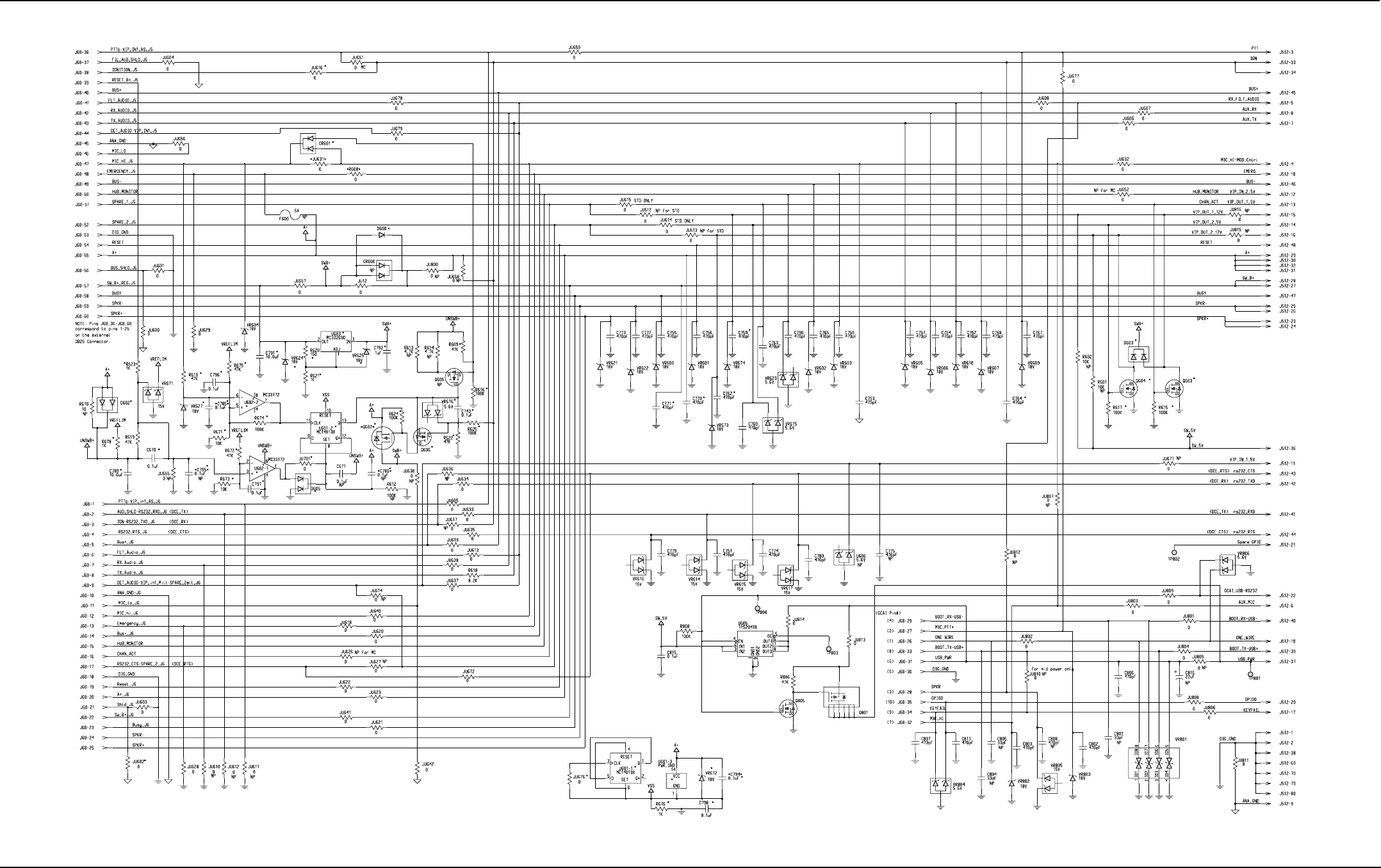
Interconnect Boards Schematics, Component Location Diagrams, and Parts Lists: Remote Interconnect Board (High Power Only) 8-13
6881096C74-B May 25, 2005
8.4 Remote Interconnect Board (High Power Only)
Figure 8-5. HLN6901C, HLN6902C Remote Interconnect Board Schematic (for High Power only)
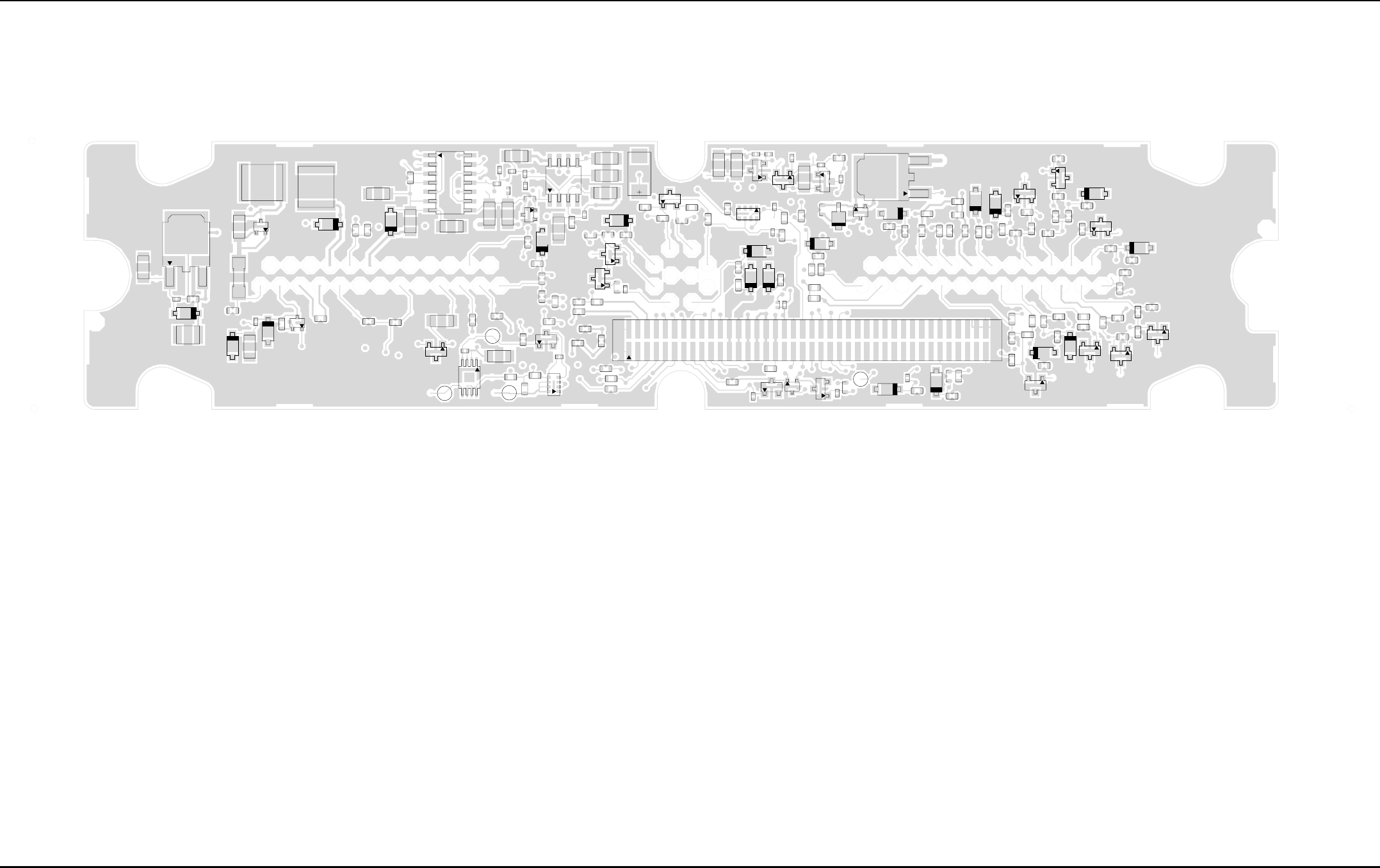
8-14 Interconnect Boards Schematics, Component Location Diagrams, and Parts Lists: Remote Interconnect Board (High Power Only)
May 25, 2005 6881096C74-B
Figure 8-6. HLN6901C, HLN6902C Remote Interconnect Board Component Location Diagram (for High Power only)
C769
C792
JU657
R620
R621
3
2
1
U603
VR625
C767
C785
C815
CR601
F600
JU604
JU616
JU629
JU630
JU631
JU650
JU651
JU652
JU656
JU677
JU678
JU679
JU805
JU809
JU813
JU814
4
5
8
Q801
Q805
R608
R610
R623
R806
R808
TP800
TP801
TP803 U605
VR604
VR627
VR671
C786
C789
C791
C794
C798
D602
JU600
JU601
JU676
R670
R671
R674
R676
7
814
U601
VR624
VR672
C671
C795
D605
JU655
JU701
JU812
R612
R619
R672
R673
R675
R678
14
58
U602
VR609
C670
C796
C797
C803
C805
C807
C808
C816
2
JU606
JU607
JU608
JU632
JU642
JU802
JU803
JU806
JU807
JU808
JU811
VR802
VR804
VR805
VR806
C773
C801
C802
C804
C806
C813
JU810
Q605
R609
R613
R614
R616
VR676
4
58
VR801
C750
C753
C772
JU618
JU628
JU640
JU804
R601
R602
VR603
VR621
VR622
VR803
C743
CR600
D600
JU12
JU658
JU801
JU815
4
Q606
R622
R624
R625 3
1
Q602
C751
C752
C768
C774
C775
C779
JU605
JU612
JU613
JU617
JU619
JU633
JU634
JU635
JU636
JU637
JU671 JU674
U606
VR607
VR610
VR614
VR615
VR616
C756
C759
C762
C763
C765
C770
C771
C780
C790
JU512
JU513
JU602
JU603
JU611
JU615
JU620
JU622
JU623
JU626
JU627
JU672
JU800
VR601
VR602
VR617
VR623
VR673
VR674
VR675
C755
JU621
JU641
VR600
C754
C757
C764
D603
79
J512
JU610
JU614
JU638
JU816 Q603
Q604
R615
R617
R618
TP802
VR605
VR606
80

Interconnect Boards Schematics, Component Location Diagrams, and Parts Lists: Remote Interconnect Board (High Power Only) 8-15
6881096C74-B May 25, 2005
HLN6902C Remote Interconnect Board (Standard)
Parts List
Reference
Designator
Motorola
Part Number Description
PCB 8464334H01 PCB,INTFC,6
LAYER,INTERCONN
- 1085674C03 PASTE/NC-SMQ230
- 1105033S02 RIBBON LABEL LT. PACK
LABEL
- 1105033S13 RIBBON LBL
- 5405569Y02 LBL BARCODE APC
- 5405569Y03 LBL BARCODE
JU12 0662057B47 CHIP RES 0 OHMS +.050
OHMS
JU600 0662057B47 CHIP RES 0 OHMS +.050
OHMS
JU601 0662057B47 CHIP RES 0 OHMS +.050
OHMS
JU603 0662057B47 CHIP RES 0 OHMS +.050
OHMS
JU607 0662057B47 CHIP RES 0 OHMS +.050
OHMS
JU613 0662057B47 CHIP RES 0 OHMS +.050
OHMS
JU615 0662057B47 CHIP RES 0 OHMS +.050
OHMS
JU620 0662057B47 CHIP RES 0 OHMS +.050
OHMS
JU622 0662057B47 CHIP RES 0 OHMS +.050
OHMS
JU635 0662057B47 CHIP RES 0 OHMS +.050
OHMS
JU634 0662057B47 CHIP RES 0 OHMS +.050
OHMS
JU633 0662057B47 CHIP RES 0 OHMS +.050
OHMS
JU632 0662057B47 CHIP RES 0 OHMS +.050
OHMS
JU631 0662057B47 CHIP RES 0 OHMS +.050
OHMS
JU629 0662057B47 CHIP RES 0 OHMS +.050
OHMS
JU628 0662057B47 CHIP RES 0 OHMS +.050
OHMS
JU626 0662057B47 CHIP RES 0 OHMS +.050
OHMS
JU623 0662057B47 CHIP RES 0 OHMS +.050
OHMS
JU657 0662057B47 CHIP RES 0 OHMS +.050
OHMS
JU656 0662057B47 CHIP RES 0 OHMS +.050
OHMS
JU652 0662057B47 CHIP RES 0 OHMS +.050
OHMS
JU650 0662057B47 CHIP RES 0 OHMS +.050
OHMS
JU642 0662057B47 CHIP RES 0 OHMS +.050
OHMS
JU641 0662057B47 CHIP RES 0 OHMS +.050
OHMS
JU640 0662057B47 CHIP RES 0 OHMS +.050
OHMS
JU638 0662057B47 CHIP RES 0 OHMS +.050
OHMS
JU637 0662057B47 CHIP RES 0 OHMS +.050
OHMS
R608 0662057B47 CHIP RES 0 OHMS +.050
OHMS
JU814 0662057B47 CHIP RES 0 OHMS +.050
OHMS
JU813 0662057B47 CHIP RES 0 OHMS +.050
OHMS
JU811 0662057B47 CHIP RES 0 OHMS +.050
OHMS
JU809 0662057B47 CHIP RES 0 OHMS +.050
OHMS
JU808 0662057B47 CHIP RES 0 OHMS +.050
OHMS
JU806 0662057B47 CHIP RES 0 OHMS +.050
OHMS
JU804 0662057B47 CHIP RES 0 OHMS +.050
OHMS
JU803 0662057B47 CHIP RES 0 OHMS +.050
OHMS
JU802 0662057B47 CHIP RES 0 OHMS +.050
OHMS
JU801 0662057B47 CHIP RES 0 OHMS +.050
OHMS
JU679 0662057B47 CHIP RES 0 OHMS +.050
OHMS
JU678 0662057B47 CHIP RES 0 OHMS +.050
OHMS
Reference
Designator
Motorola
Part Number Description
JU677 0662057B47 CHIP RES 0 OHMS +.050
OHMS
JU672 0662057B47 CHIP RES 0 OHMS +.050
OHMS
JU621 0662057B47 CHIP RES 0 OHMS +.050
OHMS
JU619 0662057B47 CHIP RES 0 OHMS +.050
OHMS
JU614 0662057B47 CHIP RES 0 OHMS +.050
OHMS
JU608 0662057B47 CHIP RES 0 OHMS +.050
OHMS
JU606 0662057B47 CHIP RES 0 OHMS +.050
OHMS
JU605 0662057B47 CHIP RES 0 OHMS +.050
OHMS
JU604 0662057B47 CHIP RES 0 OHMS +.050
OHMS
R618 0662057M96 RES. CHIP 8200 5% 20X40
R806 0662057N15 RES. CHIP 47K 5% 20X40
R808 0662057N23 RES. CHIP 100K 5%
20X40
J60 0964649H01 CONN,CUST,F,60CONT
C750 2113740F67 CAP CHIP CL1 30 470 5%
C754 2113740F67 CAP CHIP CL1 30 470 5%
C753 2113740F67 CAP CHIP CL1 30 470 5%
C752 2113740F67 CAP CHIP CL1 30 470 5%
C751 2113740F67 CAP CHIP CL1 30 470 5%
C755 2113740F67 CAP CHIP CL1 30 470 5%
C773 2113740F67 CAP CHIP CL1 30 470 5%
C772 2113740F67 CAP CHIP CL1 30 470 5%
C769 2113740F67 CAP CHIP CL1 30 470 5%
C768 2113740F67 CAP CHIP CL1 30 470 5%
C767 2113740F67 CAP CHIP CL1 30 470 5%
C765 2113740F67 CAP CHIP CL1 30 470 5%
C763 2113740F67 CAP CHIP CL1 30 470 5%
C757 2113740F67 CAP CHIP CL1 30 470 5%
C756 2113740F67 CAP CHIP CL1 30 470 5%
C813 2113740F67 CAP CHIP CL1 30 470 5%
C807 2113740F67 CAP CHIP CL1 30 470 5%
C806 2113740F67 CAP CHIP CL1 30 470 5%
C803 2113740F67 CAP CHIP CL1 30 470 5%
C802 2113740F67 CAP CHIP CL1 30 470 5%
Reference
Designator
Motorola
Part Number Description
C790 2113740F67 CAP CHIP CL1 30 470 5%
C780 2113740F67 CAP CHIP CL1 30 470 5%
C779 2113740F67 CAP CHIP CL1 30 470 5%
C774 2113740F67 CAP CHIP CL1 30 470 5%
C815 2113741N69 CAP CHIP CL2 X7R 10%
100000
J512 2864447H01 CONN,TERMNL,PLG,80
PIN,KYD
VR623 4805656W03 DIODE DUAL 5.6V ZENER
VR675 4805656W03 DIODE DUAL 5.6V ZENER
VR804 4805656W03 DIODE DUAL 5.6V ZENER
VR806 4805656W03 DIODE DUAL 5.6V ZENER
VR614 4805656W10 DIODE DUAL 15 VOLT
ZENER (GALAXY) I600
VR615 4805656W10 DIODE DUAL 15 VOLT
ZENER (GALAXY) I600
VR617 4805656W10 DIODE DUAL 15 VOLT
ZENER (GALAXY) I600
VR805 4805656W10 DIODE DUAL 15 VOLT
ZENER (GALAXY) I600
VR616 4805656W10 DIODE DUAL 15 VOLT
ZENER (GALAXY) I600
VR801 4805656W39 QUAD ESD SUPPRES-
SOR ARRAY
Q805 4809579E16 TSTR MOSFET N-CHAN
TN0200T
VR600 4813830C31 DIODE 18V ‘J3’
MMSZ5248BT1
VR601 4813830C31 DIODE 18V ‘J3’
MMSZ5248BT1
VR602 4813830C31 DIODE 18V ‘J3’
MMSZ5248BT1
VR604 4813830C31 DIODE 18V ‘J3’
MMSZ5248BT1
VR606 4813830C31 DIODE 18V ‘J3’
MMSZ5248BT1
VR609 4813830C31 DIODE 18V ‘J3’
MMSZ5248BT1
VR621 4813830C31 DIODE 18V ‘J3’
MMSZ5248BT1
VR673 4813830C31 DIODE 18V ‘J3’
MMSZ5248BT1
VR803 4813830C31 DIODE 18V ‘J3’
MMSZ5248BT1
VR802 4813830C31 DIODE 18V ‘J3’
MMSZ5248BT1
Reference
Designator
Motorola
Part Number Description
8-16 Interconnect Boards Schematics, Component Location Diagrams, and Parts Lists: Remote Interconnect Board (High Power Only)
May 25, 2005 6881096C74-B
VR674 4813830C31 DIODE 18V ‘J3’
MMSZ5248BT1
VR622 4813830C31 DIODE 18V ‘J3’
MMSZ5248BT1
VR610 4813830C31 DIODE 18V ‘J3’
MMSZ5248BT1
VR607 4813830C31 DIODE 18V ‘J3’
MMSZ5248BT1
VR605 4813830C31 DIODE 18V ‘J3’
MMSZ5248BT1
VR603 4813830C31 DIODE 18V ‘J3’
MMSZ5248BT1
Q801 4885844C01 XSTR FET
U605 5164015H50 IC,SW,BIDIREC-
TIONAL,TPS2041B,SM,SO
I
C670 NOTPLACED 64AM DUMMY PART NUM-
BER
C671 NOTPLACED 64AM DUMMY PART NUM-
BER
C743 NOTPLACED 64AM DUMMY PART NUM-
BER
C759 NOTPLACED 64AM DUMMY PART NUM-
BER
C762 NOTPLACED 64AM DUMMY PART NUM-
BER
C764 NOTPLACED 64AM DUMMY PART NUM-
BER
C770 NOTPLACED 64AM DUMMY PART NUM-
BER
C771 NOTPLACED 64AM DUMMY PART NUM-
BER
C775 NOTPLACED 64AM DUMMY PART NUM-
BER
C785 NOTPLACED 64AM DUMMY PART NUM-
BER
C786 NOTPLACED 64AM DUMMY PART NUM-
BER
C789 NOTPLACED 64AM DUMMY PART NUM-
BER
C791 NOTPLACED 64AM DUMMY PART NUM-
BER
C792 NOTPLACED 64AM DUMMY PART NUM-
BER
C794 NOTPLACED 64AM DUMMY PART NUM-
BER
Reference
Designator
Motorola
Part Number Description
C795 NOTPLACED 64AM DUMMY PART NUM-
BER
C796 NOTPLACED 64AM DUMMY PART NUM-
BER
C797 NOTPLACED 64AM DUMMY PART NUM-
BER
C798 NOTPLACED 64AM DUMMY PART NUM-
BER
C801 NOTPLACED 64AM DUMMY PART NUM-
BER
C804 NOTPLACED 64AM DUMMY PART NUM-
BER
C805 NOTPLACED 64AM DUMMY PART NUM-
BER
C808 NOTPLACED 64AM DUMMY PART NUM-
BER
C816 NOTPLACED 64AM DUMMY PART NUM-
BER
CR600 NOTPLACED 64AM DUMMY PART NUM-
BER
CR601 NOTPLACED 64AM DUMMY PART NUM-
BER
D600 NOTPLACED 64AM DUMMY PART NUM-
BER
D602 NOTPLACED 64AM DUMMY PART NUM-
BER
D603 NOTPLACED 64AM DUMMY PART NUM-
BER
D605 NOTPLACED 64AM DUMMY PART NUM-
BER
F600 NOTPLACED 64AM DUMMY PART NUM-
BER
JU512 NOTPLACED 64AM DUMMY PART NUM-
BER
JU513 NOTPLACED 64AM DUMMY PART NUM-
BER
JU602 NOTPLACED 64AM DUMMY PART NUM-
BER
JU610 NOTPLACED 64AM DUMMY PART NUM-
BER
JU611 NOTPLACED 64AM DUMMY PART NUM-
BER
JU612 NOTPLACED 64AM DUMMY PART NUM-
BER
JU616 NOTPLACED 64AM DUMMY PART NUM-
BER
Reference
Designator
Motorola
Part Number Description
JU617 NOTPLACED 64AM DUMMY PART NUM-
BER
JU618 NOTPLACED 64AM DUMMY PART NUM-
BER
JU627 NOTPLACED 64AM DUMMY PART NUM-
BER
JU630 NOTPLACED 64AM DUMMY PART NUM-
BER
JU636 NOTPLACED 64AM DUMMY PART NUM-
BER
JU651 NOTPLACED 64AM DUMMY PART NUM-
BER
JU655 NOTPLACED 64AM DUMMY PART NUM-
BER
JU658 NOTPLACED 64AM DUMMY PART NUM-
BER
JU671 NOTPLACED 64AM DUMMY PART NUM-
BER
JU674 NOTPLACED 64AM DUMMY PART NUM-
BER
JU676 NOTPLACED 64AM DUMMY PART NUM-
BER
JU701 NOTPLACED 64AM DUMMY PART NUM-
BER
JU800 NOTPLACED 64AM DUMMY PART NUM-
BER
JU805 NOTPLACED 64AM DUMMY PART NUM-
BER
JU807 NOTPLACED 64AM DUMMY PART NUM-
BER
JU810 NOTPLACED 64AM DUMMY PART NUM-
BER
JU812 NOTPLACED 64AM DUMMY PART NUM-
BER
JU815 NOTPLACED 64AM DUMMY PART NUM-
BER
JU816 NOTPLACED 64AM DUMMY PART NUM-
BER
Q602 NOTPLACED 64AM DUMMY PART NUM-
BER
Q603 NOTPLACED 64AM DUMMY PART NUM-
BER
Q604 NOTPLACED 64AM DUMMY PART NUM-
BER
Q605 NOTPLACED 64AM DUMMY PART NUM-
BER
Reference
Designator
Motorola
Part Number Description
Q606 NOTPLACED 64AM DUMMY PART NUM-
BER
R601 NOTPLACED 64AM DUMMY PART NUM-
BER
R602 NOTPLACED 64AM DUMMY PART NUM-
BER
R609 NOTPLACED 64AM DUMMY PART NUM-
BER
R610 NOTPLACED 64AM DUMMY PART NUM-
BER
R612 NOTPLACED 64AM DUMMY PART NUM-
BER
R613 NOTPLACED 64AM DUMMY PART NUM-
BER
R614 NOTPLACED 64AM DUMMY PART NUM-
BER
R615 NOTPLACED 64AM DUMMY PART NUM-
BER
R616 NOTPLACED 64AM DUMMY PART NUM-
BER
R617 NOTPLACED 64AM DUMMY PART NUM-
BER
R619 NOTPLACED 64AM DUMMY PART NUM-
BER
R620 NOTPLACED 64AM DUMMY PART NUM-
BER
R621 NOTPLACED 64AM DUMMY PART NUM-
BER
R622 NOTPLACED 64AM DUMMY PART NUM-
BER
R623 NOTPLACED 64AM DUMMY PART NUM-
BER
R624 NOTPLACED 64AM DUMMY PART NUM-
BER
R625 NOTPLACED 64AM DUMMY PART NUM-
BER
R670 NOTPLACED 64AM DUMMY PART NUM-
BER
R671 NOTPLACED 64AM DUMMY PART NUM-
BER
R672 NOTPLACED 64AM DUMMY PART NUM-
BER
R673 NOTPLACED 64AM DUMMY PART NUM-
BER
R674 NOTPLACED 64AM DUMMY PART NUM-
BER
Reference
Designator
Motorola
Part Number Description
Interconnect Boards Schematics, Component Location Diagrams, and Parts Lists: Remote Interconnect Board (High Power Only) 8-17
6881096C74-B May 25, 2005
HLN6901C Remote Interconnect Board (W3 Hand-Held
Control Head) Parts List
R675 NOTPLACED 64AM DUMMY PART NUM-
BER
R676 NOTPLACED 64AM DUMMY PART NUM-
BER
R678 NOTPLACED 64AM DUMMY PART NUM-
BER
U601 NOTPLACED 64AM DUMMY PART NUM-
BER
U602 NOTPLACED 64AM DUMMY PART NUM-
BER
U603 NOTPLACED 64AM DUMMY PART NUM-
BER
U606 NOTPLACED 64AM DUMMY PART NUM-
BER
VR624 NOTPLACED 64AM DUMMY PART NUM-
BER
VR625 NOTPLACED 64AM DUMMY PART NUM-
BER
VR627 NOTPLACED 64AM DUMMY PART NUM-
BER
VR671 NOTPLACED 64AM DUMMY PART NUM-
BER
VR672 NOTPLACED 64AM DUMMY PART NUM-
BER
VR676 NOTPLACED 64AM DUMMY PART NUM-
BER
Reference
Designator
Motorola
Part Number Description
PCB 8464334H01 PCB,INTFC,6
LAYER,INTERCONN
- 1085674C03 PASTE/NC-SMQ230
- 1105033S02 RIBBON LABEL LT. PACK
LABEL
- 1105033S13 RIBBON LBL
- 5405569Y02 LBL BARCODE APC
- 5405569Y03 LBL BARCODE
R621 0611077A74 RES CHIP 1000 5 1/8
R623 0611077A74 RES CHIP 1000 5 1/8
R676 0611077A74 RES CHIP 1000 5 1/8
R678 0611077A74 RES CHIP 1000 5 1/8
Reference
Designator
Motorola
Part Number Description
JU512 0662057B47 CHIP RES 0 OHMS +-.050
OHMS
JU513 0662057B47 CHIP RES 0 OHMS +-.050
OHMS
JU600 0662057B47 CHIP RES 0 OHMS +-.050
OHMS
JU602 0662057B47 CHIP RES 0 OHMS +-.050
OHMS
JU607 0662057B47 CHIP RES 0 OHMS +-.050
OHMS
JU613 0662057B47 CHIP RES 0 OHMS +-.050
OHMS
JU618 0662057B47 CHIP RES 0 OHMS +-.050
OHMS
JU620 0662057B47 CHIP RES 0 OHMS +-.050
OHMS
JU622 0662057B47 CHIP RES 0 OHMS +-.050
OHMS
JU640 0662057B47 CHIP RES 0 OHMS +-.050
OHMS
JU638 0662057B47 CHIP RES 0 OHMS +-.050
OHMS
JU637 0662057B47 CHIP RES 0 OHMS +-.050
OHMS
JU635 0662057B47 CHIP RES 0 OHMS +-.050
OHMS
JU634 0662057B47 CHIP RES 0 OHMS +-.050
OHMS
JU633 0662057B47 CHIP RES 0 OHMS +-.050
OHMS
JU632 0662057B47 CHIP RES 0 OHMS +-.050
OHMS
JU626 0662057B47 CHIP RES 0 OHMS +-.050
OHMS
JU623 0662057B47 CHIP RES 0 OHMS +-.050
OHMS
JU678 0662057B47 CHIP RES 0 OHMS +-.050
OHMS
JU677 0662057B47 CHIP RES 0 OHMS +-.050
OHMS
JU676 0662057B47 CHIP RES 0 OHMS +-.050
OHMS
JU672 0662057B47 CHIP RES 0 OHMS +-.050
OHMS
JU656 0662057B47 CHIP RES 0 OHMS +-.050
OHMS
Reference
Designator
Motorola
Part Number Description
JU652 0662057B47 CHIP RES 0 OHMS +-.050
OHMS
JU650 0662057B47 CHIP RES 0 OHMS +-.050
OHMS
JU642 0662057B47 CHIP RES 0 OHMS +-.050
OHMS
JU641 0662057B47 CHIP RES 0 OHMS +-.050
OHMS
JU809 0662057B47 CHIP RES 0 OHMS +-.050
OHMS
JU808 0662057B47 CHIP RES 0 OHMS +-.050
OHMS
JU806 0662057B47 CHIP RES 0 OHMS +-.050
OHMS
JU804 0662057B47 CHIP RES 0 OHMS +-.050
OHMS
JU803 0662057B47 CHIP RES 0 OHMS +-.050
OHMS
JU802 0662057B47 CHIP RES 0 OHMS +-.050
OHMS
JU801 0662057B47 CHIP RES 0 OHMS +-.050
OHMS
JU701 0662057B47 CHIP RES 0 OHMS +-.050
OHMS
JU679 0662057B47 CHIP RES 0 OHMS +-.050
OHMS
R608 0662057B47 CHIP RES 0 OHMS +-.050
OHMS
JU814 0662057B47 CHIP RES 0 OHMS +-.050
OHMS
JU813 0662057B47 CHIP RES 0 OHMS +-.050
OHMS
JU811 0662057B47 CHIP RES 0 OHMS +-.050
OHMS
JU621 0662057B47 CHIP RES 0 OHMS +-.050
OHMS
JU619 0662057B47 CHIP RES 0 OHMS +-.050
OHMS
JU616 0662057B47 CHIP RES 0 OHMS +-.050
OHMS
JU608 0662057B47 CHIP RES 0 OHMS +-.050
OHMS
JU606 0662057B47 CHIP RES 0 OHMS +-.050
OHMS
JU605 0662057B47 CHIP RES 0 OHMS +-.050
OHMS
Reference
Designator
Motorola
Part Number Description
JU604 0662057B47 CHIP RES 0 OHMS +-.050
OHMS
R620 0662057M54 RES. CHIP 150 5% 20X40
R618 0662057M96 RES. CHIP 8200 5% 20X40
R671 0662057M98 RES. CHIP 10K 5% 20X40
R673 0662057M98 RES. CHIP 10K 5% 20X40
R609 0662057N15 RES. CHIP 47K 5% 20X40
R610 0662057N15 RES. CHIP 47K 5% 20X40
R622 0662057N15 RES. CHIP 47K 5% 20X40
R675 0662057N15 RES. CHIP 47K 5% 20X40
R806 0662057N15 RES. CHIP 47K 5% 20X40
R672 0662057N15 RES. CHIP 47K 5% 20X40
R619 0662057N15 RES. CHIP 47K 5% 20X40
R615 0662057N23 RES. CHIP 100K 5%
20X40
R624 0662057N23 RES. CHIP 100K 5%
20X40
R616 0662057N23 RES. CHIP 100K 5%
20X40
R617 0662057N23 RES. CHIP 100K 5%
20X40
R625 0662057N23 RES. CHIP 100K 5%
20X40
R808 0662057N23 RES. CHIP 100K 5%
20X40
R674 0662057N23 RES. CHIP 100K 5%
20X40
J60 0964649H01 CONN,CUST,F,60CONT
C789 2109822S04 CAP CHIP CER 10UF 35V
C791 2109822S04 CAP CHIP CER 10UF 35V
C792 2109822S09 CAP CERAMIC CHIP 1UF
20 50V
C750 2113740F67 CAP CHIP CL1 +/-30 470
5%
C768 2113740F67 CAP CHIP CL1 +/-30 470
5%
C767 2113740F67 CAP CHIP CL1 +/-30 470
5%
C765 2113740F67 CAP CHIP CL1 +/-30 470
5%
C764 2113740F67 CAP CHIP CL1 +/-30 470
5%
C763 2113740F67 CAP CHIP CL1 +/-30 470
5%
Reference
Designator
Motorola
Part Number Description
8-18 Interconnect Boards Schematics, Component Location Diagrams, and Parts Lists: Remote Interconnect Board (High Power Only)
May 25, 2005 6881096C74-B
C762 2113740F67 CAP CHIP CL1 +/-30 470
5%
C759 2113740F67 CAP CHIP CL1 +/-30 470
5%
C757 2113740F67 CAP CHIP CL1 +/-30 470
5%
C756 2113740F67 CAP CHIP CL1 +/-30 470
5%
C813 2113740F67 CAP CHIP CL1 +/-30 470
5%
C807 2113740F67 CAP CHIP CL1 +/-30 470
5%
C806 2113740F67 CAP CHIP CL1 +/-30 470
5%
C803 2113740F67 CAP CHIP CL1 +/-30 470
5%
C802 2113740F67 CAP CHIP CL1 +/-30 470
5%
C790 2113740F67 CAP CHIP CL1 +/-30 470
5%
C780 2113740F67 CAP CHIP CL1 +/-30 470
5%
C779 2113740F67 CAP CHIP CL1 +/-30 470
5%
C774 2113740F67 CAP CHIP CL1 +/-30 470
5%
C773 2113740F67 CAP CHIP CL1 +/-30 470
5%
C772 2113740F67 CAP CHIP CL1 +/-30 470
5%
C771 2113740F67 CAP CHIP CL1 +/-30 470
5%
C770 2113740F67 CAP CHIP CL1 +/-30 470
5%
C769 2113740F67 CAP CHIP CL1 +/-30 470
5%
C751 2113740F67 CAP CHIP CL1 +/-30 470
5%
C752 2113740F67 CAP CHIP CL1 +/-30 470
5%
C753 2113740F67 CAP CHIP CL1 +/-30 470
5%
C755 2113740F67 CAP CHIP CL1 +/-30 470
5%
C754 2113740F67 CAP CHIP CL1 +/-30 470
5%
Reference
Designator
Motorola
Part Number Description
C670 2113741N69 CAP CHIP CL2 X7R 10%
100000
C743 2113741N69 CAP CHIP CL2 X7R 10%
100000
C794 2113741N69 CAP CHIP CL2 X7R 10%
100000
C815 2113741N69 CAP CHIP CL2 X7R 10%
100000
C798 2113741N69 CAP CHIP CL2 X7R 10%
100000
C797 2113741N69 CAP CHIP CL2 X7R 10%
100000
C796 2113741N69 CAP CHIP CL2 X7R 10%
100000
C785 2113741N69 CAP CHIP CL2 X7R 10%
100000
JU631 2113928H09 CAP,CHIP,1UF,,+10%,-
10%,10V-DC,0603
J512 2864447H01 CONN,TERMNL,PLG,80
PIN,KYD
CR601 4805218N57 DIODE DUAL
D603 4805218N57 DIODE DUAL
D602 4805218N57 DIODE DUAL
VR623 4805656W03 DIODE DUAL 5.6V ZENER
VR675 4805656W03 DIODE DUAL 5.6V ZENER
VR806 4805656W03 DIODE DUAL 5.6V ZENER
VR804 4805656W03 DIODE DUAL 5.6V ZENER
VR614 4805656W10 DIODE DUAL 15 VOLT
ZENER (GALAXY) I600
VR616 4805656W10 DIODE DUAL 15 VOLT
ZENER (GALAXY) I600
VR615 4805656W10 DIODE DUAL 15 VOLT
ZENER (GALAXY) I600
VR617 4805656W10 DIODE DUAL 15 VOLT
ZENER (GALAXY) I600
VR805 4805656W10 DIODE DUAL 15 VOLT
ZENER (GALAXY) I600
VR671 4805656W10 DIODE DUAL 15 VOLT
ZENER (GALAXY) I600
VR801 4805656W39 QUAD ESD SUPPRES-
SOR ARRAY
Q602 4813821A09 TSTR P-CH 60V 12A
_2955_
VR600 4813830C31 DIODE 18V ‘J3’
MMSZ5248BT1
Reference
Designator
Motorola
Part Number Description
VR604 4813830C31 DIODE 18V ‘J3’
MMSZ5248BT1
VR606 4813830C31 DIODE 18V ‘J3’
MMSZ5248BT1
VR609 4813830C31 DIODE 18V ‘J3’
MMSZ5248BT1
VR621 4813830C31 DIODE 18V ‘J3’
MMSZ5248BT1
VR624 4813830C31 DIODE 18V ‘J3’
MMSZ5248BT1
VR803 4813830C31 DIODE 18V ‘J3’
MMSZ5248BT1
VR802 4813830C31 DIODE 18V ‘J3’
MMSZ5248BT1
VR674 4813830C31 DIODE 18V ‘J3’
MMSZ5248BT1
VR673 4813830C31 DIODE 18V ‘J3’
MMSZ5248BT1
VR672 4813830C31 DIODE 18V ‘J3’
MMSZ5248BT1
VR627 4813830C31 DIODE 18V ‘J3’
MMSZ5248BT1
VR625 4813830C31 DIODE 18V ‘J3’
MMSZ5248BT1
VR622 4813830C31 DIODE 18V ‘J3’
MMSZ5248BT1
VR610 4813830C31 DIODE 18V ‘J3’
MMSZ5248BT1
VR607 4813830C31 DIODE 18V ‘J3’
MMSZ5248BT1
VR605 4813830C31 DIODE 18V ‘J3’
MMSZ5248BT1
VR603 4813830C31 DIODE 18V ‘J3’
MMSZ5248BT1
VR601 4813830C31 DIODE 18V ‘J3’
MMSZ5248BT1
VR602 4813830C31 DIODE 18V ‘J3’
MMSZ5248BT1
D600 4813833A20 DIODE CHOTTLKY 1A 40V
Q603 4885316E17 XSTR,POWER MOSFET
30V,2.5A,SINGLE
Q604 4885316E17 XSTR,POWER MOSFET
30V,2.5A,SINGLE
Q805 4885316E17 XSTR,POWER MOSFET
30V,2.5A,SINGLE
Q606 4885316E17 XSTR,POWER MOSFET
30V,2.5A,SINGLE
Reference
Designator
Motorola
Part Number Description
Q801 4885844C01 XSTR FET
U601 5113806A05 IC FLIP-FLOP,DUAL D
U603 5113816A19 IC ASJ LO DROPOUT POS
REG .8A
U602 5113818A06 IC LOW PWR SING SPLY
MC33172DR
U605 5164015H50 IC,SW,BIDIREC-
TIONAL,TPS2041B,SM,SO
I
C671 NOTPLACED 64AM DUMMY PART NUM-
BER
C775 NOTPLACED 64AM DUMMY PART NUM-
BER
C786 NOTPLACED 64AM DUMMY PART NUM-
BER
C795 NOTPLACED 64AM DUMMY PART NUM-
BER
C801 NOTPLACED 64AM DUMMY PART NUM-
BER
C804 NOTPLACED 64AM DUMMY PART NUM-
BER
C805 NOTPLACED 64AM DUMMY PART NUM-
BER
C808 NOTPLACED 64AM DUMMY PART NUM-
BER
C816 NOTPLACED 64AM DUMMY PART NUM-
BER
CR600 NOTPLACED 64AM DUMMY PART NUM-
BER
D605 NOTPLACED 64AM DUMMY PART NUM-
BER
F600 NOTPLACED 64AM DUMMY PART NUM-
BER
JU12 NOTPLACED 64AM DUMMY PART NUM-
BER
JU601 NOTPLACED 64AM DUMMY PART NUM-
BER
JU603 NOTPLACED 64AM DUMMY PART NUM-
BER
JU610 NOTPLACED 64AM DUMMY PART NUM-
BER
JU611 NOTPLACED 64AM DUMMY PART NUM-
BER
JU612 NOTPLACED 64AM DUMMY PART NUM-
BER
JU614 NOTPLACED 64AM DUMMY PART NUM-
BER
Reference
Designator
Motorola
Part Number Description
Interconnect Boards Schematics, Component Location Diagrams, and Parts Lists: Remote Interconnect Board (High Power Only) 8-19
6881096C74-B May 25, 2005
JU615 NOTPLACED 64AM DUMMY PART NUM-
BER
JU617 NOTPLACED 64AM DUMMY PART NUM-
BER
JU627 NOTPLACED 64AM DUMMY PART NUM-
BER
JU628 NOTPLACED 64AM DUMMY PART NUM-
BER
JU629 NOTPLACED 64AM DUMMY PART NUM-
BER
JU630 NOTPLACED 64AM DUMMY PART NUM-
BER
JU636 NOTPLACED 64AM DUMMY PART NUM-
BER
JU651 NOTPLACED 64AM DUMMY PART NUM-
BER
JU655 NOTPLACED 64AM DUMMY PART NUM-
BER
JU657 NOTPLACED 64AM DUMMY PART NUM-
BER
JU658 NOTPLACED 64AM DUMMY PART NUM-
BER
JU671 NOTPLACED 64AM DUMMY PART NUM-
BER
JU674 NOTPLACED 64AM DUMMY PART NUM-
BER
JU800 NOTPLACED 64AM DUMMY PART NUM-
BER
JU805 NOTPLACED 64AM DUMMY PART NUM-
BER
JU807 NOTPLACED 64AM DUMMY PART NUM-
BER
JU810 NOTPLACED 64AM DUMMY PART NUM-
BER
JU812 NOTPLACED 64AM DUMMY PART NUM-
BER
JU815 NOTPLACED 64AM DUMMY PART NUM-
BER
JU816 NOTPLACED 64AM DUMMY PART NUM-
BER
Q605 NOTPLACED 64AM DUMMY PART NUM-
BER
R601 NOTPLACED 64AM DUMMY PART NUM-
BER
R602 NOTPLACED 64AM DUMMY PART NUM-
BER
Reference
Designator
Motorola
Part Number Description
R612 NOTPLACED 64AM DUMMY PART NUM-
BER
R613 NOTPLACED 64AM DUMMY PART NUM-
BER
R614 NOTPLACED 64AM DUMMY PART NUM-
BER
R670 NOTPLACED 64AM DUMMY PART NUM-
BER
U606 NOTPLACED 64AM DUMMY PART NUM-
BER
Reference
Designator
Motorola
Part Number Description
8-20 Interconnect Boards Schematics, Component Location Diagrams, and Parts Lists: Remote Interconnect Board (High Power Only)
May 25, 2005 6881096C74-B
8.5 Secure Interface Board
Figure 8-7. Secure Interface Board Component Location Diagram—Side 1
Figure 8-8. Secure Interface Board Component Location Diagram—Side 2
C801
C802
C803
C804
C805
C806
C807
C808
C809
C810
D801
4039
2
1
J701
Q800
4
5
8
Q802
Q803
R800
R801
R802
R804
R805
R806
R807
R808
3
2
1
U800
U801
7
8
14
U802
U803
7
8
14
U804
U805
VR800
PLACE PAD
HERE
MAEPF-27915-O
C811
P501
8485869E01 REV O
MAEPF-27916-O

Interconnect Boards Schematics, Component Location Diagrams, and Parts Lists: Remote Interconnect Board (High Power Only) 8-21
6881096C74-B May 25, 2005
8.6 Motorcycle Signal Routing
Figure 8-9. Motorcycle Signal-Routing Diagram
Mic Hi
Gnd
Spkr +
PTT 1
Hub 1
Spkr -
31 JU512
16
20
15
13
12
8
7
6
6
5
4
3
2
1
23
16
18
1, 14
26
11
Hub 8Hub 18 VIP out 1 12V
JU14
33
JU6
4
Vip In 3
Vip Out 2
Vip In 1 17
19 3Hub 2
PTT 2
25
35
Mic Hi
12 6
2
4
Mic Hi
Potato
Mic with
DB9
Mic Hi
Motorcycle
Control Head
HC05
uP sb9600 sb9600
Aux PTT
INTO
Aux
Mic
19, 21
23, 25
29
24
16
MAEPF-27906-O
1, 2, 14,
31, 32
Patriot
uP
Motorcycle
Remote
Cable
Motorcycle
Interconnect
Board
Millennium
Remote
Mount
Flex
Millennium
Control
Head
50-pin
J401
Millennium
VOCON
Board
Millennium
26-pin
D Rear
Accessory
AS+
DB15 to
Millennium
DB26
Adapter
AS+
15-pin
Rear
Accessory
Motorcycle
Kit
J2000
6-pin
Molex
Handlebar/
Headset
Rear
Accessory
Header
J402
Rear
Accessory
Flex
DB25
Control
Head
Connector
J5 P502
28-pin
Control
Head
Header
J103
DB9
Microphone
Connector
J3
PTT 1 - Detected by radio via INTO.
HUB 1 - Detected by control head or HUB input. Sent to radio via sb9600.
PTT 2 - Detected by control head on Vip In 1. Sent to radio via sb9600.
HUB 2 - Detected by control head on Vip In 3. Sent to radio via sb9600.

8-22 Interconnect Boards Schematics, Component Location Diagrams, and Parts Lists: Remote Interconnect Board (High Power Only)
May 25, 2005 6881096C74-B
Notes
Flex Cable Pin-Out Lists: List of Flex Cables 9-1
6881096C74-B May 25, 2005
Chapter 9 Flex Cable Pin-Out Lists
9.1 List of Flex Cables
This chapter lists the pin-out assignments for the following flex cables:
• Mid Power Dash (Table 9-1 on page 9-1)
• Mid Power Rear Accessory (Table 9-2 on page 9-1)
• Mid Power Remote (Table 9-3 on page 9-2)
• High Power Remote (Table 9-4 on page 9-3)
9.2 Flex Cables
Table 9-1. Mid Power Dash Flex Cable J103 to P0401 Pin-Out List
Signal
J103
26-Pin
(Female)
P0401
50-Pin
(Male)
GND 3, 6 <--> 1, 2, 49, 50
SW B+ 4 <--> 17
A+ 5 <--> 19, 21
VIP OUT 2_5v 7 <--> 14
VIP OUT 1_5v 8 <--> 13
"BOOT_TX / Keyfail 9 <--> 25
BUS - 10 <--> 32
IGN 11 <--> 20
VIP OUT 1_12v 18 <--> 11
VIP OUT 2_12v 19 <--> 12
"OPT_B+ BOOT_SEL VPP" 20 <--> 22
"BOOT_RX / KVL_ATT" 21 <--> 26
BUS + 22 <--> 31
RESET 23 <--> 34
BUSY 25 <--> 33
MIC HI 27 <--> 4
NC Remaining pins <--> Remaining pins
Table 9-2. Mid Power Rear Accessory Flex Cable J2 to P0402 Pin-Out List
Signal
J2
26-Pin
(Female)
P0402
32-Pin
(Female)
GND 1, 14 <--> 1, 2, 14, 31, 32
BUS+ 2 <--> 3
BUS- 3 <--> 5
TX_DCE 4 <--> 7
RX_DCE 5 <--> 9
USB - 6 <--> 13
USB + 7 <--> 11
RESET 8 <--> 4
BUSY 9 <--> 6
RTS_DCE 10 <--> 8
CTS_DCE 11 <--> 10
USB PWR 12 <--> 12
CHAN ACTIVITY 13 <--> 15
Emergency 15 <--> 28
PTT*= AUX PTT 16 <--> 24
ONE WIRE 17 <--> 27
VIP OUT 1 18 <--> 16
VIP OUT 2 19 <--> 17
Spkr + 20 <--> 19, 21
RX_filt_audio 21 <--> 30
MONITOR / HUB 22 <--> 26
Aux_Mic 23 <--> 29
SW B+ 24 <--> 20, 22
IGN 25 <--> 18
Spkr - 26 <--> 23, 25

9-2 Flex Cable Pin-Out Lists: Flex Cables
May 25, 2005 6881096C74-B
Table 9-3. Mid Power Remote Flex Cable P502 to J0401 Pin-Out List
Signal
P502
38-Pin
(Male)
J0401
50-Pin
(Male)
Signal
NC 1 <--> 15 VIP_IN_1_5v
NC 2 <--> NC NC
EMERG 3 <--> 18 Emergency
NC 4 <--> NC NC
FLT Audio 5 <--> 5 RX_FILT_AUDIO
MIC_HI 6 <--> 4MIC_HI
MIC_lo=GND 7 <--> 1, 2, 49, 50 GND
RX Audio 8 <--> 8AUX_RX
BUSY
(sb9600)"
9<--> 33 BUSY
(*UARTB_RTS)"
GND 10 <--> 1, 2, 49, 50 GND
RESET
(sb9600)"
11 <--> 34 RESET
(*UARTB_CTS)"
TX Audio 12 <--> 7AUX_TX
NC 13 <--> NC NC
SPARE_1 14 <--> 13 VIP_OUT_1_5v
prog:RXD (SNET-WE)" 15 <--> 26 Boot RX
prog:VPP
(SNET-KID)"
16 <--> 22 OPT_B+
boot_sel"
VIP_OUT_2
(share with SPARE_2)"
17 <--> 12 VIP_OUT_2_12v
VIP_OUT_1
(share with SPARE_1)"
18 <--> 11 VIP_OUT_1_12v
RS232_RXD
TX_DCE"
19 <--> 27 UART A_TX
( TX_DCE )"
RS232--TXD
RX_DCE"
20 <--> 28 UART A_RX
( RX_DCE )"
IGN 21 <--> 20 Ignition
BUS-
(sb9600)"
22 <--> 32 BUS -
(*UARTB_RX)"
prog:TXD
(SNET-KEY)"
23 <--> 25 Boot TX / Keyfail"
PTTb / AS_VIP_IN_1 24 <--> 3PTT*
BUS+
(sb9600)"
25 <--> 31 BUS +
(*UARTB_TX)"
RS232--CTS
RTS_DCE"
26 <--> 29 UART A_CTS
( RTS_DCE )"
SPARE_2 27 <--> 14 VIP_OUT_2_5v
GND 28 <--> 1, 2, 49, 50 GND
NC 29 <--> NC NC
A+ 30 <--> 19, 21 A+
SWB+ 31 <--> 17 SW_B+
NOTCH 32 <--> 43 NOTCH
RS232--RTS
CTS_DCE"
33 <--> 30 UART A_RTS
( CTS_DCE )"
SPK_LO 34 <--> 10 SPKR -
SPK_HI 35 <--> 9 SPKR +
NC 36 <--> NC NC
SW_5v 37 <--> 23 SW 5v (VCC 5)"
VIP_IN_2 38 <--> 16 VIP_IN_2_5v
NC NC <--> 6NC
NC NC <--> 24 ONE-wire
NC NC <--> 35 sap tx
NC NC <--> 36 sap rx
NC NC <--> 37 sap dclk
NC NC <--> 38 sap fsync
NC NC <--> 39 nautilus cs*
NC NC <--> 40 nautilus int*
NC NC <--> 41 spi mosi
NC NC <--> 42 spi miso
NC NC <--> 44 spi clk
NC NC <--> 45 ssi int*
NC NC <--> 46 BUS_PWR_OUT
NC NC <--> 47 Future Expansion
NC NC <--> 48 Future Expansion
Table 9-3. Mid Power Remote Flex Cable P502 to J0401 Pin-Out List (Continued)
Signal
P502
38-Pin
(Male)
J0401
50-Pin
(Male)
Signal
Flex Cable Pin-Out Lists: Flex Cables 9-3
6881096C74-B May 25, 2005
Table 9-4. High Power Remote Flex Cable P0401 to J512 Pin-Out List
Signal
P0401
60-Pin
(Male)
J512
80-Pin
(Female)
GND 1,2,23,52,59,60 <--> 1,2,9,38,69,70,79,80
PTT 58 <--> 3
MIC_HI 57 <--> 4
RX_FILT_AUDIO 56 <--> 5
AUX_MIC 55 <--> 6
AUX_TX 54 <--> 7
AUX_RX 53 <--> 8
EMERGENCY 51 <--> 10
VIP IN 1 (5V) / NAUT
STATUS
50 <--> 11
VIP IN 2 (5V) / NAUT CONF
DONE
49 <--> 12
VIP OUT 1 (5V) / NAUT
CONFIG
48 <--> 13
VIP OUT 2 (5V) / NAUT
RESET
47 <--> 14
VIP OUT 1 (12V) 46 <--> 15
VIP OUT 2 (12V) 45 <--> 16
KEYFAIL 44 <--> 17
BUS_PWR_OUT 43 <--> 18
ONE-WIRE 42 <--> 19
GPIO0 41 <--> 20
SPARE GPIO 40 <--> 21
GCAI_USB-RS232 39 <--> 22
SPK+ 37, 38 <--> 23, 24
SPK- 35, 36 <--> 25, 26
SW_B+ 33, 34 <--> 27, 28
A+ 29, 30, 31, 32 <--> 29, 30, 31, 32
IGNITION 27, 28 <--> 33, 34
OPTB+ 26 <--> 35
SW_5V 25 <--> 36
VBUS_PWR_IN 24 <--> 37
BOOT TX-USB+ 22 <--> 39
BOOT RX-USB- 21 <--> 40
TX_DCE 20 <--> 41
RX_DCE 19 <--> 42
RTS_DCE 18 <--> 43
CTS_DCE 17 <--> 44
BUS+ 16 <--> 45
BUS- 15 <--> 46
LH_BUSY 14 <--> 47
LH_RESET 13 <--> 48
SAP-TX (SRDA) PATRIOT 12 <--> 57
SAP-RX (STDA) PATRIOT 11 <--> 58
SAP-DCLK 10 <--> 59
SAP-FSYNC 9 <--> 60
NAUTILUS-CS 8 <--> 61
NAUTILUS-INT 7 <--> 62
SPI-MOSI 6 <--> 63
SPI-MISO 5 <--> 64
SPI-CLK 4 <--> 65
SSI_INT 3 <--> 66
NC Remaining Pins <--> Remaining Pins
Table 9-4. High Power Remote Flex Cable P0401 to J512 Pin-Out List (Continued)
Signal
P0401
60-Pin
(Male)
J512
80-Pin
(Female)

9-4 Flex Cable Pin-Out Lists: Flex Cables
May 25, 2005 6881096C74-B
Notes
Appendix A Secure Modules
A.1 Universal Crypto Module Kits
The secure modules are designed to digitally encrypt and decrypt voice and ASTRO data in ASTRO
Digital XTL 5000 mobile radios. Tab le A- 1 contains the Universal Crypto Module (UCM) kits and their
corresponding algorithms for secure-equipped XTL 5000 radios.
A.1.1 Secure Interface Boards
Table A-2 contains the secure interface board kits, which are used in conjunction with the UCM kits.
Every secure-equipped radio must contain one of the two secure interface board kits, which is paired
with one of the UCM kits. Refer to Chapter 8. Interconnect Boards Schematics, Component Location
Diagrams, and Parts Lists for illustrations showing the board component locations.
NOTE: The secure modules and secure interface boards are NOT serviceable. The information
contained in this section is only meant to help determine whether a problem is due to the
secure module or the radio itself.
The secure module uses a custom encryption IC and an encryption key variable to perform its
encode/decode function. The encryption key variable is loaded into the secure module, via the
radio’s microphone connector, from a hand-held key-variable loader (KVL). The encryption IC
corresponds to the particular encryption algorithm purchased. The encryption algorithms and their
corresponding kit numbers are listed in Table A-1.
NOTE: When ordering replacement secure modules, make sure that the kit and board numbers of
the module that is ordered are the same as those of the module that is being replaced.
Table A-1. UCM Kit Listing
Kit Number Description
NNTN4006 DES, DES-XL, DES-OFB ENCRYPTION KIT–UCM
NTN9837 DES, DES-XL, DES-OFB WITH DVP-XL ENCRYPTION KIT–UCM
NTN9838 DVI-XL ENCRYPTION KIT–UCM
NTN9839 DVP-XL ENCRYPTION KIT–UCM
Table A-2. Secure Interface Board Kits
Kit Number Description
HLN6876 Secure Interface Board, 3-day key retention
HLN6877 Secure Interface Board, 30-second key retention

May 25, 2005 6881096C74-B
A-2 Secure Modules: Circuit Description
A.2 Circuit Description
The secure module operates from three power supplies (UNSW_B+, SW_B+, and KG_BACKUP).
The SW_B+ is turned on and off by the radio’s on/off switch. The UNSW_B+ provides power to the
secure module as long as the radio battery is in place.
Key variables are loaded into the secure module through connectorJ0501, pin 14, on the secure
interface board. Up to 16 keys (depending on the type of encryption module) can be stored in the
module at a time. The key can be infinite key retention or 3 day key retention, depending on how the
code plug is setup.
The radio’s host processor communicates with the secure module on the Synchronous Secure
Interface (SSI) bus. The host processor is the master on this bus, while the secure module is a slave
on the bus. The SSI bus consists of four signal lines. A communications failure between the host
processor and the secure module will be indicated as an “ERROR 09/10” message on the radio
display.
The secure interface board is a module that serves as the interface between the main board and the
UCM. It plugs into the main board at 20-pin connector J0501 and interfaces to the UCM at 40-pin
connector J0701. The board itself contains the following circuitry:
• Logic shifting between the keyloader and the UCM on the keyfail data line (5 V to 3 V)
• Regulators that supply the encryption SW_B+ and UNSW_B+ voltages
• Three-day key-retention capacitor
• Logic circuitry to generate the UCM chip-select signal needed for communication.
A.3 Troubleshooting Secure Operations
Refer to the ASTRO Digital XTL 5000 Mobile Radio Basic Service Manual (6881096C73) for
disassembly and reassembly information. A key-variable loader (KVL) and oscilloscope are needed
to troubleshoot the secure module.
NOTE: The secure modules and secure interface boards are not serviceable. If either module is
found to be defective, it must be replaced.
A.3.1 Error 09/10, Error 09/90
The radio automatically performs a self test on every power-up. Should the radio fail the self tests,
the display will show “ERROR 09/10” or “ERROR 09/90” accompanied by a short beep. If the display
shows “ERROR 09/10” or “ERROR 09/90,” the radio failed the secure power-up tests and the host
microcontroller was unable to communicate with the secure module via the SSI bus. Turn the radio
off and back on. If the radio still does not pass the self tests, then a problem exists with the secure
operations of the radio.
A.3.2 Error S03
“ERROR 03” occurs when the secure interface board is missing, if there is a poor connection, or the
secure interface board is defective. Corrective action includes checking for poor connections and
replacing the secure interface board.
A.3.3 Keyload
When the keyloading cable is attached to the XTL 5000 radio and “KEYLOADING” is not displayed
on the display, the radio has not entered KEYLOAD mode. For troubleshooting a “KEYLOAD” failure,
see the associated troubleshooting chart in this manual.
NOTE: A keyloader must be used that has the ability to keyload an XTL 5000 radio. The keyloader
must be either a KVL-3000 or later model key-variable loader.

Appendix B Replacement Parts Ordering
B.1 Basic Ordering Information
When ordering replacement parts or equipment information, the complete identification number
should be included. This applies to all components, kits, and chassis. If the component part number
is not known, the order should include the number of the chassis or kit of which it is a part, and
sufficient description of the desired component to identify it.
Crystal orders should specify the crystal type number, crystal and carrier frequency, and the model
number in which the part is used.
B.2 Motorola Online
Motorola Online users can access our online catalog at
https://www.motorola.com/businessonline
To register for online access, please call 800-814-0601 (for U.S. and Canada Service Centers only).
International customers can obtain assistance at https://businessonline.motorola.com.
B.3 Mail Orders
Send written orders to the following addresses:
* The Radio Products and Services Division (RPSD) was formerly known as the Customer Care and
Services Division (CCSD) and/or the Accessories and Aftermarket Division (AAD).
B.4 Telephone Orders
Radio Products and Services Division*
(United States and Canada)
7:00 AM to 7:00 PM (Central Standard Time)
Monday through Friday (Chicago, U.S.A.)
1-800-422-4210
1-847-538-8023 (International Orders)
U.S. Federal Government Markets Division (USFGMD)
1-800-826-1913 Federal Government Parts - Credit Cards Only
8:30 AM to 5:00 PM (Eastern Standard Time)
Replacement Parts/
Test Equipment/Manuals/
Crystal Service Items:
Motorola Inc.
Radio Products and Services
Division*
Attention: Order Processing
2200 Galvin Drive
Elgin, IL 60123
U.S.A.
Federal Government Orders:
Motorola Inc.
U.S. Federal Government
Markets Division
Attention: Order Processing
7230 Parkway Drive
Landover, MD 21076
U.S.A.
International Orders:
Motorola Inc.
Radio Products and Services
Division*
Attention: Order Processing
2200 Galvin Drive
Elgin, IL 60123
U.S.A.

May 25, 2005 6881096C74-B
B-2 Replacement Parts Ordering Fax Orders
B.5 Fax Orders
Radio Products and Services Division*
(United States and Canada)
1-800-622-6210
847-576-3023 (International)
USFGMD
(Federal Government Orders)
1-800-526-8641 (For Parts and Equipment Purchase Orders)
B.6 Parts Identification
Radio Products and Services Division*
(United States and Canada)
1-800-422-4210, menu 3
B.7 Product Customer Service
Customer Response Center
(Non-technical Issues)
1-800-247-2346
FAX:1-800-247-2347
* The Radio Products and Services Division (RPSD) was formerly known as the Customer Care and
Services Division (CCSD) and/or the Accessories and Aftermarket Division (AAD).

Glossary Glossary
This glossary contains an alphabetical listing of terms and their definitions that are applicable to
ASTRO portable and mobile subscriber radio products.
Term Definition
A/D See analog-to-digital conversion.
ABACUS IC A custom integrated circuit providing a digital receiver intermediate
frequency (IF) backend.
ADC See analog-to-digital converter.
ADDAG See Analog-to-Digital, Digital-to-Analog and Glue.
ALC See automatic level control.
analog Refers to a continuously variable signal or a circuit or device designed
to handle such signals. See also digital.
Analog-to-Digital,
Digital-to-Analog
and Glue
An integrated circuit designed to be an interface between the radio’s
DSP, which is digital, and the analog transmitter and receiver ICs.
analog-to-digital
conversion
Conversion of an instantaneous dc voltage level to a corresponding
digital value. See also D/A.
analog-to-digital
converter
A device that converts analog signals into digital data. See also DAC.
automatic level
control
A circuit in the transmit RF path that controls RF power amplifier output,
provides leveling over frequency and voltage, and protects against high
VSWR.
band Frequencies allowed for a specific purpose.
BBP See baseband interface port.
baseband interface
port
Synchronous serial interface to the transceiver board used to transfer
transmit and receive audio data.
BGA See ball grid array.
ball grid array A type of IC package characterized by solder balls arranged in a grid
that are located on the underside of the package.
CODEC See coder/decoder.
codeplug A memory chip inside a device that contains various programmable
parameters, including frequencies, time-out timer, and so on.

May 25, 2005 6881096C74-B
Glossary-2
coder/decoder A device that encodes or decodes a signal.
CPS See Customer Programming Software.
Customer
Programming
Software
Software with a graphical user interface containing the feature set of an
ASTRO radio. See also RSS.
D/A See digital-to-analog conversion.
DAC See digital-to-analog converter.
default A pre-defined set of parameters.
digital Refers to data that is stored or transmitted as a sequence of discrete
symbols from a finite set; most commonly this means binary data
represented using electronic or electromagnetic signals. See also
analog.
digital-to-analog
conversion
Conversion of a digital signal to a voltage that is proportional to the input
value. See also A/D.
digital-to-analog
converter
A device that converts digital data into analog signals. See also ADC.
Digital Private Line A type of digital communications that utilizes privacy call, as well as
memory channel and busy channel lock out to enhance communication
efficiency.
digital signal
processor
A microcontroller specifically designed for performing the mathematics
involved in manipulating analog information, such as sound, that has
been converted into a digital form. DSP also implies the use of a data
compression technique.
digital signal
processor code
Object code executed by the Digital Signal Processor in an ASTRO
subscriber radio. The DSP is responsible for computation-intensive
tasks, such as decoding ASTRO signaling.
DPL See Digital Private Line. See also PL.
DSP See digital signal processor.
DSP code See digital signal processor code.
DTMF See dual tone multi-frequency.
dual tone multi-
frequency
The system used by touch-tone telephones. DTMF assigns a specific
frequency, or tone, to each key so that it can easily be identified by a
microprocessor.
EPOT Electrically Programmable Digital Potentiometer.
EEPROM See Electrically Erasable Programmable Read-Only Memory.
Term Definition

6881096C74-B May 25, 2005
Glossary-3
Electrically Erasable
Programmable
Read-Only Memory
A special type of PROM that can be erased by exposing it to an
electrical charge. An EEPROM retains its contents even when the
power is turned off.
EME Electromagnetic Emissions.
ESD Electrostatic Discharge.
FCC Federal Communications Commission.
FET Field-Effect Transistor.
firmware Code executed by an embedded processor such as the Host or DSP in
a subscriber radio. This type of code is typically resident in non-volatile
memory and as such is more difficult to change than code executed
from RAM.
FGU See frequency generation unit.
flash A non-volatile memory device similar to an EEPROM. Flash memory
can be erased and reprogrammed in blocks instead of one byte at a
time.
FLASHcode A 13-digit code which uniquely identifies the System Software Package
and Software Revenue Options that are enabled in a particular
subscriber radio. FLASHcodes are only applicable for radios which are
upgradeable through the FLASHport process.
FLASHport®A Motorola term that describes the ability of a radio to change memory.
Every FLASHport radio contains a FLASHport EEPROM memory chip
that can be software written and rewritten to, again and again.
FMR See Florida Manual Revision.
Florida Manual
Revision
A publication that provides supplemental information for its parent
publication before it is revised and reissued.
frequency Number of times a complete electromagnetic-wave cycle occurs in a
fixed unit of time (usually one second).
frequency
generation unit
This unit generates ultra-stable, low-phase noise master clock and other
derived synchronization clocks that are distributed throughout the
communication network.
General-Purpose
Input/Output
Pins whose function is programmable.
GPIO See General-Purpose Input/Output.
host code Object code executed by the host processor in an ASTRO subscriber
radio. The host is responsible for control-oriented tasks such as
decoding and responding to user inputs.
IC See integrated circuit.
Term Definition

May 25, 2005 6881096C74-B
Glossary-4
IF Intermediate Frequency.
IMBE A sub-band, voice-encoding algorithm used in ASTRO digital voice.
inbound signaling
word
Data transmitted on the control channel from a subscriber unit to the
central control unit.
integrated circuit An assembly of interconnected components on a small semiconductor
chip, usually made of silicon. One chip can contain millions of
microscopic components and perform many functions.
ISW See inbound signaling word.
key-variable loader A device used to load encryption keys into a radio.
kHz See kilohertz.
kilohertz One thousand cycles per second. Used especially as a radio-frequency
unit.
KVL See key-variable loader.
LCD See liquid-crystal display.
LED See light emitting diode.
light emitting diode An electronic device that lights up when electricity is passed through it.
liquid-crystal display An LCD uses two sheets of polarizing material with a liquid-crystal
solution between them. An electric current passed through the liquid
causes the crystals to align so that light cannot pass through them.
LO Local oscillator.
low-speed
handshake
150-baud digital data sent to the radio during trunked operation while
receiving audio.
LSH See low-speed handshake.
Master In Slave Out SPI data line from a peripheral to the MCU.
Master Out Slave In SPI data line from the MCU to a peripheral.
MCU See microcontroller unit.
MDC Motorola Digital Communications.
MDI MCU/DSP Interface internal to the Patriot IC.
MHz See Megahertz.
Megahertz One million cycles per second. Used especially as a radio-frequency
unit.
Term Definition

6881096C74-B May 25, 2005
Glossary-5
microcontroller unit Also written as µC. A microprocessor that contains RAM and ROM
components, as well as communications and programming components
and peripherals.
microprocessor core The central processing unit of the microprocessor and DSP IC and
powered by a lower voltage supply than the logic I/O section.
MISO See Master In Slave Out.
MOSI See Master Out Slave In.
multiplexer An electronic device that combines several signals for transmission on
some shared medium (e.g., a telephone wire).
MUX See multiplexer.
NiCd Nickel-cadmium.
NiMH Nickel-metal-hydride.
OMPAC See over-molded pad-array carrier.
open architecture A controller configuration that utilizes a microprocessor with extended
ROM, RAM, and EEPROM.
oscillator An electronic device that produces alternating electric current and
commonly employs tuned circuits and amplifying components.
OSW See outbound signaling word.
OTAR See over-the-air rekeying.
outbound signaling
word
Data transmitted on the control channel from the central controller to the
subscriber unit.
over-molded pad-
array carrier
A Motorola custom IC package, distinguished by the presence of solder
balls on the bottom pads.
over-the-air rekeying Allows the dispatcher to remotely reprogram the encryption keys in the
radio.
PA Power amplifier.
paging One-way communication that alerts the receiver to retrieve a message.
Patriot IC A dual-core processor that contains an MCU and a DSP in one IC
package.
PC Board Printed Circuit Board. Also referred to as a PCB.
phase-locked loop A circuit in which an oscillator is kept in phase with a reference, usually
after passing through a frequency divider.
PL See private-line tone squelch.
Term Definition

May 25, 2005 6881096C74-B
Glossary-6
PLL See phase-locked loop.
private-line tone
squelch
A continuous sub-audible tone that is transmitted along with the carrier.
See also DPL.
Programmable
Read-Only Memory
A memory chip on which data can be written only once. Once data has
been written onto a PROM, it remains there forever.
PROM See Programmable Read-Only Memory.
PTT See Push-to-Talk.
Push-to-Talk The switch or button usually located on the left side of the radio which,
when pressed, causes the radio to transmit. When the PTT is released,
the unit returns to receive operation.
radio frequency The portion of the electromagnetic spectrum between audio sound and
infrared light (approximately 10 kHz to 10 GHz).
radio frequency
power amplifier
Amplifier having one or more active devices to amplify radio signals.
Radio Interface Box A service aid used to enable communications between a radio and the
programming software.
Radio Service
Software
DOS-based software containing the feature set of an ASTRO radio. See
also CPS.
random access
memory
A type of computer memory that can be accessed randomly; that is, any
byte of memory can be accessed without touching the preceding bytes.
RAM See random access memory.
read-only memory A type of computer memory on which data has been prerecorded. Once
data has been written onto a ROM chip, it cannot be removed and can
only be read.
real-time clock A module that keeps track of elapsed time even when a computer is
turned off.
receiver Electronic device that amplifies RF signals. A receiver separates the
audio signal from the RF carrier, amplifies it, and converts it back to the
original sound waves.
registers Short-term data-storage circuits within the microcontroller unit or
programmable logic IC.
repeater Remote transmit/receive facility that re-transmits received signals in
order to improve communications range and coverage (conventional
operation).
repeater/talkaround A conventional radio feature that permits communication through a
receive/transmit facility, which re-transmits received signals in order to
improve communication range and coverage.
Term Definition

6881096C74-B May 25, 2005
Glossary-7
RESET Reset line: an input to the microcontroller that restarts execution.
RF See radio frequency.
RF PA See radio frequency power amplifier.
RIB See Radio Interface Box.
ROM See read-only memory.
RPCIC Regulator/power control IC.
RPT/TA See repeater/talkaround.
RSS See Radio Service Software.
RTC See real-time clock.
RX Receive.
RX DATA Recovered digital data line.
SAP See Serial Audio CODEC Port.
Serial Audio CODEC
Port
SSI to and from the GCAP II IC CODEC used to transfer transmit and
receive audio data.
Serial
Communication
Interface Input Line
A full-duplex (receiver/transmitter) asynchronous serial interface.
SCI IN See Serial Communication Interface Input Line.
Serial Peripheral
Interface
How the microcontroller communicates to modules and ICs through the
CLOCK and DATA lines.
signal An electrically transmitted electromagnetic wave.
Signal Qualifier
mode
An operating mode in which the radio is muted, but still continues to
analyze receive data to determine RX signal type.
softpot See software potentiometer.
software Computer programs, procedures, rules, documentation, and data
pertaining to the operation of a system.
software
potentiometer
A computer-adjustable electronic attenuator.
spectrum Frequency range within which radiation has specific characteristics.
SPI See Serial Peripheral Interface.
squelch Muting of audio circuits when received signal levels fall below a pre-
determined value. With carrier squelch, all channel activity that exceeds
the radio’s preset squelch level can be heard.
Term Definition

May 25, 2005 6881096C74-B
Glossary-8
SRAM See static RAM.
SRIB Smart Radio Interface Box. See RIB.
SSI See Synchronous Serial Interface.
Standby mode An operating mode in which the radio is muted but still continues to
monitor data.
static RAM A type of memory used for volatile, program/data memory that does not
need to be refreshed.
Synchronous Serial
Interface
DSP interface to peripherals that consists of a clock signal line, a frame
synchronization signal line, and a data line.
system central
controllers
Main control unit of the trunked dispatch system; handles ISW and
OSW messages to and from subscriber units (See ISW and OSW).
system select The act of selecting the desired operating system with the system-select
switch (also, the name given to this switch).
thin small-outline
package
A type of dynamic random-access memory (DRAM) package that is
commonly used in memory applications.
time-out timer A timer that limits the length of a transmission.
TOT See time-out timer.
transceiver Transmitter-receiver. A device that both transmits and receives analog
or digital signals. Also abbreviated as XCVR.
transmitter Electronic equipment that generates and amplifies an RF carrier signal,
modulates the signal, and then radiates it into space.
TSOP See thin small-outline package.
TX Transmit.
UART See also Universal Asynchronous Receiver Transmitter.
UCM Universal Crypto Module.
UHF Ultra-High Frequency.
Universal
Asynchronous
Receiver Transmitter
A microchip with programming that controls a computer's interface to its
attached serial devices.
Universal Serial Bus An external bus standard that supports data transfer rates of 12 Mbps.
Urchin IC A programmable logic device configured to supply a 2.8 V, 48 kHz
square wave at 2% duty cycle and a 2.8 V, 2.4 MHz square wave at
50% duty cycle to the TX modulation DAC using a 16.8 MHz reference
input.These clock signals are used by the DAC to convert the digital
SSI audio into an analog modulation waveform.
Term Definition

6881096C74-B May 25, 2005
Glossary-9
USB See Universal Serial Bus.
VCO See voltage-controlled oscillator.
vector sum excited
linear predictive
coding
A voice-encoding technique used in ASTRO digital voice.
VHF Very-High Frequency.
VIP Vehicle Interface Port.
VOCON See vocoder/controller.
vocoder An electronic device for synthesizing speech by implementing a
compression algorithm particular to voice. See also voice encoder.
vocoder/controller A PC board that contains an ASTRO radio’s microcontroller, DSP,
memory, audio and power functions, and interface support circuitry.
voice encoder The DSP-based system for digitally processing analog signals, and
includes the capabilities of performing voice compression algorithms or
voice encoding. See also vocoder.
voltage-controlled
oscillator
An oscillator in which the frequency of oscillation can be varied by
changing a control voltage.
Term Definition

May 25, 2005 6881096C74-B
Glossary-10
Notes

Index-i
6881096C74-B May 25, 2005
Index Index
Numerics
1st local oscillator (LO)
136-174 MHz band .............................................. 3-49
380-470 MHz band .............................................. 3-52
450-520 MHz band .............................................. 3-57
700-800 MHz band .............................................. 3-61
2nd local oscillator (LO)
136-174 MHz band .............................................. 3-21
380-470 MHz band .............................................. 3-23
450-520 MHz band .............................................. 3-24
700-800 MHz band .............................................. 3-26
700-800 MHz radio specifications ............................. xlvii
A
ABACUS III IC
2nd LO, receiver back-end
136-174 MHz band ........................................... 3-21
380-470 MHz band ........................................... 3-23
450-520 MHz band ........................................... 3-24
700-800 MHz band ........................................... 3-26
receiver back-end
136-174 MHz band ........................................... 3-20
380-470 MHz band ........................................... 3-22
450-520 MHz band ........................................... 3-23
700-800 MHz band ........................................... 3-25
sampling clock oscillator, receiver back-end
136-174 MHz band ........................................... 3-21
380-470 MHz band ........................................... 3-23
450-520 MHz band ........................................... 3-24
700-800 MHz band ........................................... 3-26
amplifier, power, troubleshooting
136-174 MHz band .............................................. 4-34
380-470 MHz band .............................................. 4-35
450-520 MHz band .............................................. 4-35
700-800 MHz band .............................................. 4-35
analog mode of operation ........................................ 2-12
antenna switch
136-174 MHz band .............................................. 3-29
380-470 MHz band .............................................. 3-34
450-520 MHz band .............................................. 3-39
700-800 MHz band .............................................. 3-43
assembly
control-head ........................................................... 2-2
RF board ................................................................ 3-1
ASTRO mode of operation ...................................... 2-13
attenuator
step (136-174 MHz band) .................................... 3-14
switchable (380-470 MHz band) .......................... 3-16
switchable (450-520 MHz band) .......................... 3-18
B
B+ power routing, controller ..................................... 3-65
back-end receiver section
136-174 MHz band
ABACUS III IC .................................................. 3-20
IF ...................................................................... 3-20
overview ............................................................. 2-8
380-470 MHz band
ABACUS III IC .................................................. 3-22
IF filter .............................................................. 3-22
overview ............................................................. 2-9
theory of operation ........................................... 3-21
450-520 MHz band
ABACUS III IC .................................................. 3-23
IF filter .............................................................. 3-23
theory of operation ........................................... 3-23
700-800 MHz band
ABACUS III IC .................................................. 3-25
IF filter .............................................................. 3-25
overview ............................................................. 2-9
theory of operation ........................................... 3-24
bias tables, standard ............................................... 4-28
board layouts, listing .................................................. 7-1
C
chart, model
mobile
700-800 MHz ....................................................... xlii
UHF Range 1 .........................................xxxiv, xxxvi
UHF Range 2 ...................................................xxxix
VHF ........................................................... xxix, xxxi
motorcycle
700-800 MHz ........................................................ xli
UHF Range 1 ..........................................xxxii, xxxiii
UHF Range 2 ................................................. xxxviii
VHF ..................................................................xxviii
charts
troubleshooting
introduction ......................................................... 5-1
list ....................................................................... 5-1
circuit protection, transmitter ................................... 2-10
component
location diagrams listing
interconnect boards ............................................ 8-1
main board ......................................................... 7-1
parts list
main board
136-174 MHz band .............................. 7-47, 7-60
380-470 MHz band .......................... 7-105, 7-120
450-520 MHz band ..................................... 7-163
700-800 MHz band ..................................... 7-207
remote interconnect board
motorcycle ...................................................... 8-5
standard ................................................. 8-4, 8-19
W3 hand-held control head .......... 8-7, 8-11, 8-17
table ................................................................... 7-1
control-head assembly
description ............................................................. 2-2
ignition sense circuits ............................................. 2-7
power supplies ....................................................... 2-7
vehicle interface ports
connections
input ................................................................ 2-6
output .............................................................. 2-6
dash-mount configuration ................................... 2-2
DEK interface with radio ..................................... 2-7
description .......................................................... 2-2
remote-mount

Index-ii
May 25, 2005 6881096C74-B
plus DEK configuration ................................... 2-4
standard configuration .................................... 2-2
W3 configuration ............................................. 2-4
VIP input connections ......................................... 2-6
controller
analog mode of operation .................................... 2-12
ASTRO mode of operation ................................... 2-13
components and circuitry ..................................... 2-13
daughtercard module ........................................... 3-64
DC power distribution ........................................... 3-65
DSP system clock ................................................ 3-68
encryption voltages .............................................. 3-66
external bus serial communications ..................... 3-71
MCU system clock ............................................... 3-68
power-up/power-down sequence ......................... 3-68
receive audio ........................................................ 3-72
reset circuits ......................................................... 3-67
SPI bus ................................................................ 3-71
theory of operation ............................................... 3-62
copyrights
computer software ......................................................ii
document ...................................................................ii
D
daughtercard module
overview ............................................................... 2-13
theory of operation ............................................... 3-64
troubleshooting ...................................................... 4-2
DC power distribution
136-174 MHz band .............................................. 3-13
380-470 MHz band .............................................. 3-12
450-520 MHz band .............................................. 3-12
700-800 MHz band .............................................. 3-13
introduction .......................................................... 3-12
DSP system clock .................................................... 3-68
E
encryption
errors
09/10 ..................................................................A-2
09/90 ..................................................................A-2
keyload failure ....................................................A-2
S03 .....................................................................A-2
self-test ...............................................................A-2
secure
interface board
kits ..................................................................A-1
schematics .................................................... 8-20
module circuit description ...................................A-2
universal crypto module kits ...................................A-1
voltages, controller ............................................... 3-66
errors
09/10 ......................................................................A-2
09/90 ......................................................................A-2
operational codes ................................................... 4-5
power-up self-check ............................................... 4-3
S03 .........................................................................A-2
external bus serial communications, controller ........ 3-71
F
filter
harmonic
136-174 MHz band ........................................... 3-29
380-470 MHz band ........................................... 3-34
450-520 MHz band ........................................... 3-39
700-800 MHz band ........................................... 3-43
highpass, receiver front-end (380-470 MHz band) .. 3-
16
highpass, receiver front-end (450-520 MHz band) .. 3-
17
loop
136-174 MHz band ........................................... 3-48
380-470 MHz band ........................................... 3-52
450-520 MHz band ........................................... 3-56
700-800 MHz band ........................................... 3-60
preselector, receiver front-end
136-174 MHz band ........................................... 3-14
380-470 MHz band ........................................... 3-16
450-520 MHz band ........................................... 3-18
700-800 MHz band ........................................... 3-19
receiver back-end IF
380-470 MHz band ........................................... 3-22
450-520 MHz band ........................................... 3-23
700-800 MHz band ........................................... 3-25
firmware, reflashing ................................................. 3-76
flash programming ................................................... 3-75
flex cables pin-out assignments ................................ 9-1
flowcharts, troubleshooting ...................................... 5-14
136-174MHz band
low or no RX injection signal ............................ 5-21
low or no TX injection signal ............................ 5-22
no output power and IDC ................................. 5-26
no output power at TX mode ............................ 5-25
poor RX sensitivity or no RX audio .................. 5-15
RX back-end-poor SINAD or no audio ............. 5-18
RX IF-poor SINAD or no audio ......................... 5-17
TX or RX VCO unlock (Fail 001) ...................... 5-23
380-470 MHz and 450-520 MHz bands
low or no RX injection signal ............................ 5-35
low or no TX injection signal ............................ 5-36
no 16.8 MHz reference oscillator frequency ..... 5-27
no TX audio ...................................................... 5-37
poor RX sensitivity or no RX audio .................. 5-28
RFPA power control-no VGBIAS ...................... 5-45
RFPA-no or low TX power output ..................... 5-40
RX back-end-poor SINAD or no audio ............. 5-32
RX IF-poor SINAD or no audio ......................... 5-30
TX or RX VCO unlock (Fail 001) ...................... 5-38
700-800 MHz band
low or no RX injection signal ............................ 5-53
low or no TX injection signal ............................ 5-54
no 16.8 MHz reference ..................................... 5-46
no TX audio ...................................................... 5-55
poor RX sensitivity or no RX audio .................. 5-47
RFPA power control-no K9.1V ......................... 5-63
RFPA power control-no or low TX RFPA_CNTRL 5-
65
RFPA power control-no VGBIAS ...................... 5-64
RFPA-no or low TX power output ..................... 5-58
RX back-end-poor SINAD or no audio ............. 5-50
RX IF-poor SINAD or no audio ......................... 5-49
TX or RX VCO unlock (Fail 001) ...................... 5-56
frequency generation unit (FGU)

Index-iii
6881096C74-B May 25, 2005
136-174 MHz band
charge pump bias ............................................. 3-48
description ........................................................ 2-10
lock detect ........................................................ 3-48
loop filter ........................................................... 3-48
LV Frac-N synthesizer ...................................... 3-46
modulation ........................................................ 3-47
prescaler feedback ........................................... 3-49
receiver injection .............................................. 3-49
receiver VCOs .................................................. 3-49
reference oscillator ........................................... 3-46
superfilter .......................................................... 3-47
transmitter injection .......................................... 3-48
transmitter VCOs .............................................. 3-49
voltage multiplier ............................................... 3-47
380-470 MHz band
charge pump bias ............................................. 3-52
description ........................................................ 2-11
lock detect ........................................................ 3-52
loop filter ........................................................... 3-52
LV Frac-N synthesizer ...................................... 3-50
modulation ........................................................ 3-51
prescaler feedback ........................................... 3-53
receiver injection .............................................. 3-52
receiver VCOs .................................................. 3-53
reference oscillator ........................................... 3-50
superfilter .......................................................... 3-51
transmitter injection .......................................... 3-52
transmitter VCOs .............................................. 3-53
voltage multiplier ............................................... 3-51
450-520 MHz band
charge pump bias ............................................. 3-56
lock detect ........................................................ 3-56
loop filter ........................................................... 3-56
LV Frac-N synthesizer ...................................... 3-55
modulation ........................................................ 3-56
prescaler feedback ........................................... 3-58
receiver injection .............................................. 3-57
receiver VCOs .................................................. 3-57
reference oscillator ........................................... 3-55
superfilter .......................................................... 3-56
transmitter injection .......................................... 3-57
transmitter VCOs .............................................. 3-57
voltage multiplier ............................................... 3-55
700-800 MHz band
charge pump bias ............................................. 3-60
description ........................................................ 2-11
lock detect ........................................................ 3-60
loop filter ........................................................... 3-60
LV Frac-N synthesizer ...................................... 3-59
modulation ........................................................ 3-60
prescaler feedback ........................................... 3-62
receiver injection .............................................. 3-61
receiver VCOs .................................................. 3-62
reference oscillator ........................................... 3-59
superfilter .......................................................... 3-60
transmitter injection .......................................... 3-61
transmitter VCOs .............................................. 3-61
voltage multiplier ............................................... 3-59
description ............................................................ 3-45
theory of operation
136-174 MHz band ........................................... 3-45
380-470 MHz band ........................................... 3-49
450-520 MHz band ........................................... 3-54
700-800 MHz band ........................................... 3-58
front-end receiver section
136-174 MHz band
low-noise amplifier (LNA) ................................. 3-14
mixer ................................................................ 3-15
overview ............................................................. 2-8
PIN diode switches ........................................... 3-14
preselector filters .............................................. 3-14
step attenuator ................................................. 3-14
theory of operation ........................................... 3-13
380-470 MHz band
first low-noise amplifier ..................................... 3-16
highpass filter ................................................... 3-16
image filter ........................................................ 3-16
low-noise amplifier (LNA) ................................. 3-16
mixer ................................................................ 3-16
overview ............................................................. 2-8
preselector filters .............................................. 3-16
switchable attenuator ....................................... 3-16
theory of operation ........................................... 3-15
450-520 MHz band
first low-noise amplifier ..................................... 3-17
highpass filter ................................................... 3-17
image filter ........................................................ 3-18
low-noise amplifier (LNA) ................................. 3-18
mixer ................................................................ 3-18
preselector filters .............................................. 3-18
switchable attenuator ....................................... 3-18
theory of operation ........................................... 3-17
700-800 MHz band
low-noise amplifier (LNA) ................................. 3-19
mixer ................................................................ 3-20
overview ............................................................. 2-9
preselector filters .............................................. 3-19
theory of operation ........................................... 3-19
functional blocks, radio .............................................. 2-1
G
glossary of terms ........................................... Glossary-1
H
handling precautions ................................................. 4-1
harmonic filter
136-174 MHz band .............................................. 3-29
380-470 MHz band .............................................. 3-34
450-520 MHz band .............................................. 3-39
700-800 MHz band .............................................. 3-43
highpass filter, receiver front-end
380-470 MHz band .............................................. 3-16
450-520 MHz band .............................................. 3-17
I
IF
filter
receiver back-end
380-470 MHz band ....................................... 3-22
450-520 MHz band ....................................... 3-23
700-800 MHz band ....................................... 3-25
receiver back-end (136-174 MHz band) .............. 3-20
receiver section, overview ..................................... 2-8

Index-iv
May 25, 2005 6881096C74-B
ignition sense circuits, control-head assembly .......... 2-7
image filter, receiver front-end (380-470 MHz band) 3-16
image filter, receiver front-end (450-520 MHz band) 3-18
interconnect board
remote
board layout ......................................8-3, 8-10, 8-14
schematic ...........................................8-2, 8-9, 8-13
W3 hand-held ......................................................... 8-1
interface board, secure ............................................ 8-20
introduction, manual .................................................. 1-1
J
jumper configuration, board ID ................................ 5-13
K
keyload failure ...........................................................A-2
kits, universal crypto module (UCM) ..........................A-1
L
list
component location diagrams
interconnect boards ............................................ 8-1
main board ......................................................... 7-1
flex cables .............................................................. 9-1
schematics
interconnect boards ............................................ 8-1
main board ......................................................... 7-1
troubleshooting charts ............................................ 5-1
waveforms .............................................................. 6-1
local oscillator
1st
136-174 MHz band ........................................... 3-49
380-470 MHz band ........................................... 3-52
450-520 MHz band ........................................... 3-57
700-800 MHz band ........................................... 3-61
2nd
136-174 MHz band ........................................... 3-21
380-470 MHz band ........................................... 3-23
450-520 MHz band ........................................... 3-24
700-800 MHz band ........................................... 3-26
low-noise amplifier (LNA), receiver front-end
136-174 MHz band .............................................. 3-14
380-470 MHz band .............................................. 3-16
450-520 MHz band .............................................. 3-18
700-800 MHz band .............................................. 3-19
low-noise amplifier, first, receiver front-end, 380-470
MHz band ......................................................... 3-16
low-noise amplifier, first, receiver front-end, 450-520
MHz band ......................................................... 3-17
M
main board
136-174 MHz band
major sections .................................................... 3-1
theory of operation
FGU .............................................................. 3-45
power distribution .......................................... 3-13
receiver front-end .......................................... 3-13
RFPA ................................................... 3-26, 3-28
transmitter ..................................................... 3-26
troubleshooting ................................................... 4-5
380-470 MHz band
major sections .................................................... 3-6
theory of operation
FGU .............................................................. 3-49
power distribution ......................................... 3-12
receiver back-end ......................................... 3-21
receiver front-end ......................................... 3-15
RFPA ................................................... 3-31, 3-33
transmitter ..................................................... 3-31
troubleshooting ..................................................4-11
450-520 MHz band
major sections .................................................... 3-6
theory of operation
FGU .............................................................. 3-54
power distribution ......................................... 3-12
receiver back-end ......................................... 3-23
receiver front-end ......................................... 3-17
RFPA ............................................................ 3-37
transmitter ..................................................... 3-37
troubleshooting ................................................. 4-17
700-800 MHz band
major sections .................................................. 3-10
theory of operation
FGU .............................................................. 3-58
power distribution ......................................... 3-13
receiver back-end ......................................... 3-24
receiver front-end ......................................... 3-19
RFPA ............................................................ 3-41
transmitter ..................................................... 3-41
troubleshooting ................................................. 4-22
flash programming ............................................... 3-75
receive audio ....................................................... 3-72
reflash firmware ................................................... 3-76
RS-232 USB bus ................................................. 3-69
theory of operation
controller .......................................................... 3-62
power distribution ............................................. 3-12
receiver ............................................................ 3-13
transmitter ........................................................ 3-26
transmit audio ...................................................... 3-74
manual
introduction ............................................................ 1-1
notations ................................................................ 1-1
organization ........................................................... 1-1
revisions ..................................................................... ii
MCU system clock ................................................... 3-68
mixer, receiver front-end
136-174 MHz band .............................................. 3-15
380-470 MHz band .............................................. 3-16
450-520 MHz band .............................................. 3-18
700-800 MHz band .............................................. 3-20
mobile model chart
700-800 MHz .......................................................... xlii
UHF Range 1 .............................................xxxiv, xxxvi
UHF Range 2 .......................................................xxxix
VHF ............................................................... xxix, xxxi
mode
analog .................................................................. 2-12
ASTRO ................................................................ 2-13
model chart

Index-v
6881096C74-B May 25, 2005
mobile
700-800 MHz ....................................................... xlii
UHF Range 1 .........................................xxxiv, xxxvi
UHF Range 2 .................................................. xxxix
VHF ........................................................... xxix, xxxi
motorcycle
700-800 MHz ........................................................ xli
UHF Range 1 ..........................................xxxii, xxxiii
UHF Range 2 .................................................xxxviii
VHF ..................................................................xxviii
model numbering scheme ....................................... xxvii
motorcycle
model chart
700-800 MHz ........................................................ xli
UHF Range 1 ..........................................xxxii, xxxiii
UHF Range 2 .................................................xxxviii
VHF ..................................................................xxviii
signal-routing diagram ......................................... 8-21
N
notations, manual ...................................................... 1-1
O
ON (output network)
136-174 MHz band
antenna switch ................................................. 3-29
harmonic filter ................................................... 3-29
power detector .................................................. 3-29
theory of operation ........................................... 3-29
380-470 MHz band
antenna switch ................................................. 3-34
harmonic filter ................................................... 3-34
power detector .................................................. 3-35
theory of operation ........................................... 3-34
450-520 MHz band
antenna switch ................................................. 3-39
harmonic filter ................................................... 3-39
power detector .................................................. 3-39
theory of operation ........................................... 3-38
700-800 MHz band
antenna switch ................................................. 3-43
harmonic filter ................................................... 3-43
power detector .................................................. 3-43
theory of operation ........................................... 3-42
transmitter ............................................................ 2-10
operational error codes .............................................. 4-5
ordering replacement parts ........................................B-1
organization, manual ................................................. 1-1
oscillator, local
1st
136-174 MHz band ........................................... 3-49
380-470 MHz band ........................................... 3-52
450-520 MHz band ........................................... 3-57
700-800 MHz band ........................................... 3-61
2nd
136-174 MHz band ........................................... 3-21
380-470 MHz band ........................................... 3-23
450-520 MHz band ........................................... 3-24
700-800 MHz band ........................................... 3-26
oscillator, reference
136-174 MHz band .............................................. 3-46
380-470 MHz band .............................................. 3-50
450-520 MHz band .............................................. 3-55
700-800 MHz band .............................................. 3-59
out-of-lock condition, VCO ........................................ 4-7
overview, radio .......................................................... 2-1
P
parts
list
main board
136-174 MHz band .............................. 7-47, 7-60
380-470 MHz band .......................... 7-105, 7-120
450-520 MHz band ..................................... 7-163
700-800 MHz band ..................................... 7-207
remote interconnect board
motorcycle ...................................................... 8-5
standard ................................................. 8-4, 8-19
W3 hand-held control head .......... 8-7, 8-11, 8-17
lists table ................................................................ 7-1
ordering replacement ............................................. B-1
replacement and substitution ................................. 4-1
PIN diode switches (136-174 MHz band) ................ 3-14
pin-out assignments, flex cables ............................... 9-1
power amplifier
136-174 MHz
theory of operation .................................. 3-26, 3-28
troubleshooting ................................................. 4-34
380-470 MHz
theory of operation .................................. 3-31, 3-33
troubleshooting ................................................. 4-35
450-520 MHz
theory of operation ........................................... 3-37
troubleshooting ................................................. 4-35
700-800 MHz
theory of operation ........................................... 3-41
troubleshooting ................................................. 4-35
description ........................................................... 2-10
power control
theory of operation
136-174 MHz band ........................................... 3-30
380-470 MHz band ........................................... 3-35
450-520 MHz band ........................................... 3-39
700-800 MHz band ........................................... 3-43
transmitter ............................................................ 2-10
power detector, ON
136-174 MHz band .............................................. 3-29
380-470 MHz band .............................................. 3-35
450-520 MHz band .............................................. 3-39
700-800 MHz band .............................................. 3-43
power distribution
controller .............................................................. 3-65
DC
136-174 MHz band ........................................... 3-13
380-470 MHz band ........................................... 3-12
450-520 MHz band ........................................... 3-12
700-800 MHz band ........................................... 3-13
introduction ....................................................... 3-12
power routing, controller B+ .................................... 3-65
power supplies, control-head assembly .................... 2-7
power-up self-check errors ........................................ 4-3
power-up/power-down sequence, controller ........... 3-68
precautions

Index-vi
May 25, 2005 6881096C74-B
handling ................................................................. 4-1
heat-related ............................................................ 4-2
preselector filters, receiver front-end
136-174 MHz band .............................................. 3-14
380-470 MHz band .............................................. 3-16
450-520 MHz band .............................................. 3-18
700-800 MHz band .............................................. 3-19
programming flash ................................................... 3-75
publications, related ................................................... xxii
R
radio
136-174 MHz band
back-end receiver ............................................... 2-8
DC power distribution ....................................... 3-13
frequency generation unit ................................. 2-10
front-end receiver section ................................... 2-8
receiver ............................................................... 2-8
transmitter .......................................................... 2-9
380-470 MHz band
back-end receiver section .................................. 2-9
DC power distribution ....................................... 3-12
frequency generation unit ................................. 2-11
front-end receiver section ................................... 2-8
IF receiver section .............................................. 2-8
receiver ............................................................... 2-8
transmitter .......................................................... 2-9
450-520 MHz band
DC power distribution ....................................... 3-12
700-800 MHz band
back-end receiver section .................................. 2-9
DC power distribution ....................................... 3-13
frequency generation unit ................................. 2-11
front-end receiver section ................................... 2-9
receiver ............................................................... 2-9
transmitter ........................................................ 2-10
control-head assembly ........................................... 2-2
controller
B+ power routing .............................................. 3-65
DSP system clock ............................................ 3-68
MCU system clock ............................................ 3-68
power-up/power-down sequence ..................... 3-68
serial peripheral interface (SPI) bus ................. 3-71
theory of operation ........................................... 3-62
daughtercard module theory of operation ............ 3-64
functional blocks .................................................... 2-1
overview ................................................................. 2-1
power amplifier assembly ..................................... 2-10
power-up/power-down sequence ......................... 3-68
RF board
receiver back-end circuitry ................................ 3-20
theory of operation ............................................. 3-1
specifications
700-800 MHz ..................................................... xlvii
UHF Range 1 ...................................................... xlv
UHF Range 2 ..................................................... xlvi
VHF .................................................................... xliv
troubleshooting
precautions
handling .......................................................... 4-1
heat-related ..................................................... 4-2
procedures ......................................................... 4-1
waveforms .......................................................... 6-2
receive audio, controller .......................................... 3-72
receiver
136-174 MHz band
back-end
ABACUS III IC .............................................. 3-20
description ...................................................... 2-8
IF .................................................................. 3-20
introduction ................................................... 3-20
front-end
description ...................................................... 2-8
introduction ................................................... 3-13
low-noise amplifier (LNA) ............................. 3-14
mixer ............................................................. 3-15
PIN diode switches ....................................... 3-14
preselector filters .......................................... 3-14
step attenuator .............................................. 3-14
troubleshooting ............................................. 4-33
radios ................................................................. 2-8
380-470 MHz band
back-end
ABACUS III IC .............................................. 3-22
description ...................................................... 2-9
IF filter ........................................................... 3-22
introduction ................................................... 3-21
front-end
description ...................................................... 2-8
first low-noise amplifier (LNA) ....................... 3-16
highpass filter ............................................... 3-16
image filter .................................................... 3-16
introduction ................................................... 3-15
low-noise amplifier (LNA) ............................. 3-16
mixer ............................................................. 3-16
preselector filters .......................................... 3-16
switchable attenuator .................................... 3-16
troubleshooting ............................................. 4-33
IF section, description ........................................ 2-8
radios ................................................................. 2-8
450-520 MHz band
back-end
ABACUS III IC .............................................. 3-23
IF filter ........................................................... 3-23
introduction ................................................... 3-23
front-end
first low-noise amplifier (LNA) ....................... 3-17
highpass filter ............................................... 3-17
image filter .................................................... 3-18
introduction ................................................... 3-17
low-noise amplifier (LNA) ............................. 3-18
mixer ............................................................. 3-18
preselector filters .......................................... 3-18
switchable attenuator .................................... 3-18
troubleshooting ............................................. 4-34
700-800 MHz band
back-end
ABACUS III IC .............................................. 3-25
description ...................................................... 2-9
IF filter ........................................................... 3-25
introduction ................................................... 3-24
front-end ........................................................... 3-19
description ...................................................... 2-9

Index-vii
6881096C74-B May 25, 2005
low-noise amplifier (LNA) .............................. 3-19
mixer ............................................................. 3-20
preselector filters .......................................... 3-19
troubleshooting ............................................. 4-34
radios .................................................................. 2-9
back-end, introduction .......................................... 3-20
front-end, introduction .......................................... 3-13
primary components ............................................... 2-8
reflashing firmware .................................................. 3-76
related publications .................................................... xxii
remote interconnect board
layout ...................................................8-3, 8-10, 8-14
schematic ...............................................8-2, 8-9, 8-13
troubleshooting ...................................................... 8-1
replacement parts, ordering .......................................B-1
reset circuits, controller ............................................ 3-67
RF board theory of operation ..................................... 3-1
RF exposure compliance information ............................ii
RFPA
136-174 MHz band
driver stage ..............................................3-27, 3-28
final stage ................................................ 3-27, 3-29
first stage ................................................. 3-27, 3-28
theory of operation ..................................3-26, 3-28
380-470 MHz band
driver stage ..............................................3-32, 3-33
final stage ................................................ 3-32, 3-34
first stage ................................................. 3-32, 3-33
theory of operation ..................................3-31, 3-33
450-520 MHz band
driver stage ....................................................... 3-38
final stage ......................................................... 3-38
first stage .......................................................... 3-37
theory of operation ........................................... 3-37
700-800 MHz band
driver stage ....................................................... 3-42
final stage ......................................................... 3-42
first stage .......................................................... 3-42
theory of operation ........................................... 3-41
stages, transmitter ................................................ 2-10
rigid circuit boards, troubleshooting ........................... 4-2
RS-232 USB bus ..................................................... 3-69
S
safety information, product ............................................ii
sampling clock oscillator, ABACUS III IC
136-174 MHz band .............................................. 3-21
380-470 MHz band .............................................. 3-23
450-520 MHz band .............................................. 3-24
700-800 MHz ....................................................... 3-26
SB9600 serial communications ............................... 3-71
schematics
listing
interconnect boards ............................................ 8-1
main board ......................................................... 7-1
main board layouts
700-800 MHz (HUF4017A) ............................. 7-174
listing .................................................................. 7-1
UHF Range 1 (HUE4039A) .............................. 7-72
UHF Range 2 (HUE4040A) ............................ 7-132
VHF (HUD4022A) ............................................... 7-3
secure
interface board
board layouts .................................................... 8-20
kits ...................................................................... A-1
operations
errors .................................................................. A-2
keyload failure .................................................... A-2
signal tracing procedures .......................................... 4-3
signal-routing diagram, motorcycle ......................... 8-21
specifications, radio
700-800 MHz .........................................................xlvii
UHF Range 1 .......................................................... xlv
UHF Range 2 ......................................................... xlvi
VHF ........................................................................ xliv
SPI bus, controller ................................................... 3-71
standard bias tables ................................................ 4-28
step attenuator (136-174 MHz band) ...................... 3-14
T
terms, glossary of .......................................... Glossary-1
test points, troubleshooting ..................................... 5-12
theory of operation
136-174 MHz band
frequency generation unit (FGU)
charge pump bias ......................................... 3-48
introduction ................................................... 3-45
lock detect .................................................... 3-48
loop filter ....................................................... 3-48
LV Frac-N synthesizer .................................. 3-46
modulation .................................................... 3-47
prescaler feedback ....................................... 3-49
receiver injection ........................................... 3-49
receiver VCOs .............................................. 3-49
reference oscillator ....................................... 3-46
superfilter ...................................................... 3-47
transmitter injection ...................................... 3-48
transmitter VCOs .......................................... 3-49
voltage multiplier ........................................... 3-47
major board sections .......................................... 3-1
receiver
back-end ....................................................... 3-20
front-end ....................................................... 3-13
transmitter
introduction ................................................... 3-26
ON (output network) ..................................... 3-29
power control ................................................ 3-30
power control loop ........................................ 3-30
protection mechanisms ................................. 3-31
RFPA ................................................... 3-26, 3-28
380-470 MHz band
frequency generation unit (FGU)
charge pump bias ......................................... 3-52
introduction ................................................... 3-49
lock detect .................................................... 3-52
loop filter ....................................................... 3-52
LV Frac-N synthesizer .................................. 3-50
modulation .................................................... 3-51
prescaler feedback ....................................... 3-53
receiver injection ........................................... 3-52
receiver VCOs .............................................. 3-53
reference oscillator ....................................... 3-50
superfilter ...................................................... 3-51

Index-viii
May 25, 2005 6881096C74-B
transmitter injection ....................................... 3-52
transmitter VCOs .......................................... 3-53
voltage multiplier ........................................... 3-51
major board sections .......................................... 3-6
receiver
back-end ....................................................... 3-21
front-end ....................................................... 3-15
transmitter
introduction ................................................... 3-31
ON (output network) ..................................... 3-34
power control ................................................ 3-35
power control loop ........................................ 3-36
protection mechanisms ................................. 3-37
RFPA ................................................... 3-31, 3-33
450-520 MHz band
frequency generation unit (FGU)
charge pump bias ......................................... 3-56
introduction ................................................... 3-54
lock detect ..................................................... 3-56
loop filter ....................................................... 3-56
LV Frac-N synthesizer .................................. 3-55
modulation .................................................... 3-56
prescaler feedback ....................................... 3-58
receiver injection ........................................... 3-57
receiver VCOs .............................................. 3-57
reference oscillator ....................................... 3-55
superfilter ...................................................... 3-56
transmitter injection ....................................... 3-57
transmitter VCOs .......................................... 3-57
voltage multiplier ........................................... 3-55
major board sections .......................................... 3-6
receiver
back-end ....................................................... 3-23
front-end ....................................................... 3-17
transmitter
introduction ................................................... 3-37
ON (output network) ..................................... 3-38
power control ................................................ 3-39
power control loop ........................................ 3-40
protection mechanisms ................................. 3-41
RFPA ............................................................ 3-37
700-800 MHz band
frequency generation unit (FGU)
charge pump bias ......................................... 3-60
introduction ................................................... 3-58
lock detect ..................................................... 3-60
loop filter ....................................................... 3-60
LV Frac-N synthesizer .................................. 3-59
modulation .................................................... 3-60
prescaler feedback ....................................... 3-62
receiver injection ........................................... 3-61
receiver VCOs .............................................. 3-62
reference oscillator ....................................... 3-59
superfilter ...................................................... 3-60
transmitter injection ....................................... 3-61
transmitter VCOs .......................................... 3-61
voltage multiplier ........................................... 3-59
introduction ....................................................... 3-41
major board sections ........................................ 3-10
receiver
back-end ....................................................... 3-24
front-end ....................................................... 3-19
transmitter
ON (output network) ..................................... 3-42
power control ................................................ 3-43
power control loop ........................................ 3-44
protection mechanisms ................................. 3-45
RFPA ............................................................ 3-41
control head
W4, W5, W7 ....................................................... 2-2
controller
description ........................................................ 3-62
DSP system clock ............................................ 3-68
MCU system clock ........................................... 3-68
power-up/power-down sequence ..................... 3-68
serial peripheral interface (SPI) bus ................. 3-71
daughtercard module ........................................... 3-64
receive audio ....................................................... 3-72
RF board description ............................................. 3-1
trademark information ................................................... ii
transmit audio, main board ...................................... 3-74
transmitter
136-174 MHz band
50-Watt
ON (output network)
antenna switch .......................................... 3-29
harmonic filter ........................................... 3-29
introduction ............................................... 3-29
power detector .......................................... 3-29
power control ................................................ 3-30
RFPA
driver stage ...................................... 3-27, 3-28
final stage ......................................... 3-27, 3-29
first stage ......................................... 3-27, 3-28
introduction ...................................... 3-26, 3-28
components ........................................................ 2-9
power control
power control loop ........................................ 3-30
protection mechanisms ................................. 3-31
theory of operation ........................................... 3-26
380-470 MHz band
40-Watt
ON (output network)
antenna switch .......................................... 3-34
harmonic filter ........................................... 3-34
introduction ............................................... 3-34
power detector .......................................... 3-35
power control ................................................ 3-35
RFPA
driver stage ...................................... 3-32, 3-33
final stage ......................................... 3-32, 3-34
first stage ......................................... 3-32, 3-33
introduction ...................................... 3-31, 3-33
components ........................................................ 2-9
power control
power control loop ........................................ 3-36
protection mechanisms ................................. 3-37
theory of operation ........................................... 3-31
450-520 MHz band
45-Watt
ON (output network)

Index-ix
6881096C74-B May 25, 2005
antenna switch .......................................... 3-39
harmonic filter ............................................ 3-39
introduction ................................................ 3-38
power detector .......................................... 3-39
power control ................................................ 3-39
RFPA
driver stage ............................................... 3-38
final stage .................................................. 3-38
first stage ................................................... 3-37
introduction ................................................ 3-37
power control
power control loop ........................................ 3-40
protection mechanisms ................................. 3-41
theory of operation ........................................... 3-37
700-800 MHz band
35-Watt
ON (output network)
antenna switch .......................................... 3-43
harmonic filter ............................................ 3-43
power detector .......................................... 3-43
RFPA
driver stage ............................................... 3-42
final stage .................................................. 3-42
first stage ................................................... 3-42
introduction ................................................ 3-41
components ...................................................... 2-10
power control
power control loop ........................................ 3-44
protection mechanisms ................................. 3-45
theory of operation ........................................... 3-41
circuit protection ................................................... 2-10
description ............................................................ 3-26
ON (output network) ............................................. 2-10
power control ....................................................... 2-10
primary components ............................................... 2-9
RFPA .................................................................... 2-10
troubleshooting
board ID jumper configuration .............................. 5-13
charts
introduction ......................................................... 5-1
list ....................................................................... 5-1
daughtercard module ............................................. 4-2
FGU troubleshootong aids
136-174 MHz band ............................................. 4-7
380-470 MHz band ........................................... 4-13
450-520 MHz band ........................................... 4-19
700-800 MHz band ........................................... 4-24
flowcharts
136-174 MHz band
low or no RX injection signal ......................... 5-21
low or no TX injection signal ......................... 5-22
no output power and IDC .............................. 5-26
no output power at TX mode ........................ 5-25
poor RX sensitivity or no RX audio ............... 5-15
RX back-end-poor SINAD or no audio .......... 5-18
RX IF-poor SINAD or no audio ..................... 5-17
TX or RX VCO unlock (Fail 001) ................... 5-23
380-470 MHz and 450-520 MHz bands
low or no RX injection signal ......................... 5-35
low or no TX injection signal ......................... 5-36
no 16.8 MHz reference oscillator frequency . 5-27
no TX audio .................................................. 5-37
poor RX sensitivity or no RX audio ............... 5-28
RFPA power control-no VGBIAS .................. 5-45
RFPA-no or low TX power output ................. 5-40
RX back-end-poor SINAD or no audio ......... 5-32
RX IF-poor SINAD or no audio ..................... 5-30
TX or RX VCO unlock (Fail 001) .................. 5-38
700-800 MHz band
low or no RX injection signal ........................ 5-53
low or no TX injection signal ......................... 5-54
no 16.8 MHz reference oscillator frequency . 5-46
no TX audio .................................................. 5-55
poor RX sensitivity or no RX audio ............... 5-47
RFPA power control-no K9.1V ..................... 5-63
RFPA power control-no or low TX RFPA_CNTRL
5-65
RFPA power control-no VGBIAS .................. 5-64
RFPA-no or low TX power output ................. 5-58
RX back-end-poor SINAD or no audio ......... 5-50
RX IF-poor SINAD or no audio ..................... 5-49
TX or RX VCO unlock (Fail 001) .................. 5-56
operational error codes .......................................... 4-5
parts replacement and substitution ........................ 4-1
power-up self-check errors .................................... 4-3
precautions
handling .............................................................. 4-1
heat-related ........................................................ 4-2
procedures
136-174 MHz band
main board ...................................................... 4-5
power amplifier ............................................. 4-34
receiver front-end ......................................... 4-33
380-470 MHz band
main board .....................................................4-11
power amplifier ............................................. 4-35
receiver front-end ......................................... 4-33
450-520 MHz band
main board .................................................... 4-17
power amplifier ............................................. 4-35
receiver front-end ......................................... 4-34
700-800 MHz band
main board .................................................... 4-22
power amplifier ............................................. 4-35
receiver front-end ......................................... 4-34
signal tracing ...................................................... 4-3
standard bias tables ......................................... 4-28
voltage measurement procedures ...................... 4-3
remote interconnect board
layout ................................................ 8-3, 8-10, 8-14
schematic ........................................... 8-2, 8-9, 8-13
rigid circuit boards .................................................. 4-2
schematics
main board
700-800 MHz (HUF4017A) ......................... 7-174
listing .............................................................. 7-1
UHF Range 1 (HUE4039A) .......................... 7-72
UHF Range 2 (HUE4040A) ........................ 7-132
VHF (HUD4022A) ........................................... 7-3
remote interconnect board ................. 8-2, 8-9, 8-13
secure operations
errors .................................................................. A-2

Index-x
May 25, 2005 6881096C74-B
keyload failure ....................................................A-2
table ....................................................................... 5-3
test points ............................................................. 5-12
waveforms .............................................................. 6-2
U
UHF Range 1 radio specifications .............................. xlv
UHF Range 2 radio specifications ............................. xlvi
universal crypto module (UCM) kits ...........................A-1
V
VCO (voltage-controlled oscillator assembly)
out-of-lock condition ............................................... 4-7
vehicle interface ports
connections
input .................................................................... 2-6
output ................................................................. 2-6
dash-mount control-head configuration ................. 2-2
DEK interface with radio ........................................ 2-7
description ............................................................. 2-2
remote-mount
control-head configuration .................................. 2-2
plus DEK configuration ....................................... 2-4
W3 control-head configuration ........................... 2-4
VIP input connections ............................................ 2-6
VHF radio specifications ............................................ xliv
voltage-controlled oscillator (VCO) assembly
out-of-lock condition ............................................... 4-7
W
W3 hand-held interconnect board ............................. 8-1
warranty information ..................................................xxiii
waveforms
listing ...................................................................... 6-1
troubleshooting ...................................................... 6-2

6881096C74-B
*6881096C74*
MOTOROLA, the Stylized M Logo, ASTRO and FLASHport are
registered in the U.S. Patent and Trademark Office. All other
product or service names are the property of their respective owners.
© Motorola, Inc. 2005.
All rights reserved. Printed in U.S.A.
Motorola, Inc.
8000 West Sunrise Boulevard
Ft. Lauderdale, FL 33322
