XTS Series/XTS4000 Detailed Service Manual 6871620L01 C XTS4000
User Manual: -XTS Series/XTS4000 Detailed service manual 6871620L01-C
Open the PDF directly: View PDF ![]() .
.
Page Count: 210 [warning: Documents this large are best viewed by clicking the View PDF Link!]
- 6871620L01-C_DSM_XTS4000_print.pdf
- 6871620L01_DSfront.pdf
- Letter_blank.pdf
- 6871620L01-C_DSM_XTS4000_final.pdf
- Foreword
- Document History
- Table of Contents
- Foreword ii
- Document History iii
- List of Figures vii
- List of Tables ix
- Commercial Warranty xi
- Chapter 1 Introduction 1-1
- Chapter 2 Radio Power 2-1
- Chapter 3 Theory of Operation 3-1
- Chapter 4 Troubleshooting Procedures 4-1
- Chapter 5 Troubleshooting Charts 5-1
- Chapter 6 Troubleshooting Waveforms 6-1
- Chapter 7 Troubleshooting Tables 7-1
- Chapter 8 Schematics, Board Overlays, and Parts Lists - VHF 8-1
- Chapter 9 Schematics, Board Overlays, and Parts Lists - UHF 9-1
- Appendix A Replacement Parts Ordering A-1
- Appendix B Motorola Service Centers B-1
- Glossary Glossary-1
- Index Index-1
- List of Figures
- List of Tables
- Related Publications
- Commercial Warranty
- Chapter 1 Introduction
- Chapter 2 Radio Power
- Chapter 3 Theory of Operation
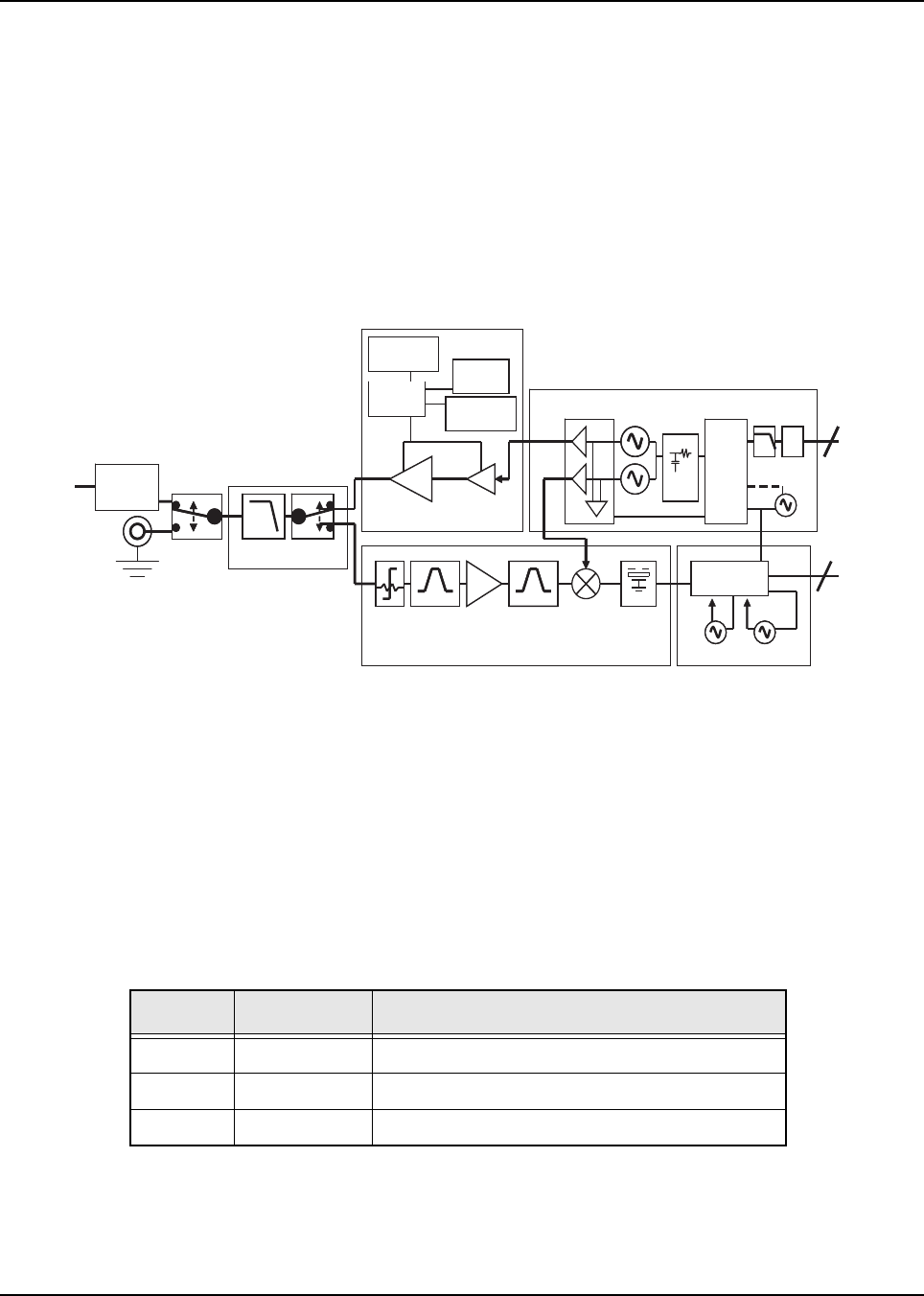
- 3.1 Transceiver Section
- 3.2 VOCON Section
- 3.3 Encryption Module
- Chapter 4 Troubleshooting Procedures
- Chapter 5 Troubleshooting Charts
- 5.1 List of Troubleshooting Charts
- 5.2 Main Troubleshooting Flowchart
- 5.3 Power-Up Failure
- 5.4 DC Supply Failure
- 5.5 Display Failure
- 5.6 Volume Set Error
- 5.7 Button Test
- 5.8 Top/Side Button Test
- 5.9 VCO TX/RX Unlock
- 5.10 VOCON TX Audio
- 5.11 VOCON RX Audio
- 5.12 RX RF
- 5.13 TX RF
- 5.14 Keyload Failure
- 5.15 Secure Hardware Failure
- Chapter 6 Troubleshooting Waveforms
- Chapter 7 Troubleshooting Tables
- Chapter 8 Schematics, Board Overlays, and Parts Lists - VHF
- Chapter 9 Schematics, Board Overlays, and Parts Lists - UHF
- Appendix A Replacement Parts Ordering
- Appendix B Motorola Service Centers
- Glossary
- Index
- Letter_blank.pdf
- 6871620L01_DSback.pdf
COLOR CHORDS 7
ASTRO®
XTSTM 4000
Portable Radio
Detailed Service Manual

Title Page ASTRO® XTS™ 4000
Digital Portable Radios
Detailed Service Manual
Motorola, Inc.
1301 E. Algonquin Rd.
Schaumburg, IL 60196-1078 U.S.A. 6871620L01-C

Foreword
The information contained in this manual relates to all ASTRO® XTS™ 4000 digital portable radios, unless otherwise
specified. This manual provides sufficient information to enable qualified service shop technicians to troubleshoot and
repair an ASTRO XTS 4000 digital portable radio to the component level.
For details on the operation of the radio or level 1 or 2 maintenance procedures, refer to the applicable manuals, which are
available separately. A list of related publications is provided in the section, “Related Publications,” on page x.
Product Safety and RF Exposure Compliance
ATTENTION!
This radio is restricted to occupational use only to satisfy FCC RF energy exposure requirements.
Before using this product, read the RF energy awareness information and operating instructions in the
Product Safety and RF Exposure booklet enclosed with your radio (Motorola Publication part number
6881095C98) to ensure compliance with RF energy exposure limits.
For a list of Motorola-approved antennas, batteries, and other accessories, visit the following web site
which lists approved accessories: http://www.motorola.com/governmentandenterprise
Manual Revisions
Changes which occur after this manual is printed are described in FMRs (Florida Manual Revisions). These FMRs provide
complete replacement pages for all added, changed, and deleted items, including pertinent parts list data, schematics, and
component layout diagrams. To obtain FMRs, contact the Customer Care and Services Division (refer to “Appendix A
Replacement Parts Ordering”).
Computer Software Copyrights
The Motorola products described in this manual may include copyrighted Motorola computer programs stored in
semiconductor memories or other media. Laws in the United States and other countries preserve for Motorola certain
exclusive rights for copyrighted computer programs, including, but not limited to, the exclusive right to copy or reproduce in
any form the copyrighted computer program. Accordingly, any copyrighted Motorola computer programs contained in the
Motorola products described in this manual may not be copied, reproduced, modified, reverse-engineered, or distributed in
any manner without the express written permission of Motorola. Furthermore, the purchase of Motorola products shall not
be deemed to grant either directly or by implication, estoppel, or otherwise, any license under the copyrights, patents or
patent applications of Motorola, except for the normal non-exclusive license to use that arises by operation of law in the
sale of a product.
Document Copyrights
No duplication or distribution of this document or any portion thereof shall take place without the express written permission
of Motorola. No part of this manual may be reproduced, distributed, or transmitted in any form or by any means, electronic
or mechanical, for any purpose without the express written permission of Motorola.
Disclaimer
The information in this document is carefully examined, and is believed to be entirely reliable. However, no responsibility is
assumed for inaccuracies. Furthermore, Motorola reserves the right to make changes to any products herein to improve
readability, function, or design. Motorola does not assume any liability arising out of the applications or use of any product
or circuit described herein; nor does it cover any license under its patent rights nor the rights of others.
Trademarks
MOTOROLA, the Stylized M logo, and ASTRO are registered in the US Patent & Trademark Office. All other product or
service names are the property of their respective owners.
© 2007–2008 by Motorola, Inc.
Before using this product, read the operating instructions
for safe usage contained in the Product Safety and RF
Exposure booklet enclosed with your radio.
!
C a u t i o n
6871620L01-C May 28, 2008
Document History iii
Document History
The following major changes have been implemented in this manual since the previous edition:
Edition Description Date
6871620L01-A Initial edition Mar 2007
6871620L01-B Added UHF info Jan 2008
6871620L01-C Added Parts List for NUE7350B May 2008

iv Table of Contents
May 28, 2008 6871620L01-C
Table of Contents
Foreword.........................................................................................................ii
Product Safety and RF Exposure Compliance ............................................................................................ii
Manual Revisions ........................................................................................................................................ii
Computer Software Copyrights....................................................................................................................ii
Document Copyrights ..................................................................................................................................ii
Disclaimer ....................................................................................................................................................ii
Trademarks..................................................................................................................................................ii
Document History .........................................................................................iii
List of Figures ..............................................................................................vii
List of Tables .................................................................................................ix
Commercial Warranty ...................................................................................xi
Limited Warranty.........................................................................................................................................xi
Chapter 1 Introduction ......................................................................... 1-1
1.1 General .......................................................................................................................................... 1-1
1.2 Notations Used in This Manual ...................................................................................................... 1-2
1.3 General Repair Procedures and Techniques.................................................................................1-3
Chapter 2 Radio Power ........................................................................ 2-1
2.1 General .......................................................................................................................................... 2-1
2.2 DC Power Routing–Transceiver Section ....................................................................................... 2-2
2.3 DC Power Routing—VOCON Section ........................................................................................... 2-2
Chapter 3 Theory of Operation............................................................ 3-1
3.1 Transceiver Section ....................................................................................................................... 3-2
3.2 VOCON Section........................................................................................................................... 3-13
3.3 Encryption Module ....................................................................................................................... 3-29

Table of Contents v
6871620L01-C May 28, 2008
Chapter 4 Troubleshooting Procedures ............................................. 4-1
4.1 Handling Precautions..................................................................................................................... 4-1
4.2 Recommended Service Tools........................................................................................................ 4-2
4.3 Voltage Measurement and Signal Tracing..................................................................................... 4-3
4.4 Standard Bias Table ...................................................................................................................... 4-4
4.5 Power-Up Self-Check Errors ......................................................................................................... 4-5
4.6 Power-Up Self-Check Diagnostics and Repair (Not for Field Use)................................................ 4-6
Chapter 5 Troubleshooting Charts ..................................................... 5-1
5.1 List of Troubleshooting Charts....................................................................................................... 5-1
5.2 Main Troubleshooting Flowchart.................................................................................................... 5-2
5.3 Power-Up Failure........................................................................................................................... 5-3
5.4 DC Supply Failure.......................................................................................................................... 5-6
5.5 Display Failure ............................................................................................................................. 5-10
5.6 Volume Set Error ......................................................................................................................... 5-13
5.7 Button Test .................................................................................................................................. 5-14
5.8 Top/Side Button Test ................................................................................................................... 5-15
5.9 VCO TX/RX Unlock ..................................................................................................................... 5-16
5.10 VOCON TX Audio........................................................................................................................ 5-17
5.11 VOCON RX Audio ....................................................................................................................... 5-19
5.12 RX RF .......................................................................................................................................... 5-21
5.13 TX RF .......................................................................................................................................... 5-26
5.14 Keyload Failure............................................................................................................................ 5-29
5.15 Secure Hardware Failure............................................................................................................. 5-30
Chapter 6 Troubleshooting Waveforms ............................................. 6-1
6.1 List of Waveforms .......................................................................................................................... 6-1
6.2 24.576 MHz Clock ......................................................................................................................... 6-2
6.3 16.8 MHz Buffer Input and Output ................................................................................................. 6-3
6.4 32.768 kHz Clock Outputs ............................................................................................................. 6-4
6.5 Receive Serial Audio Port (SAP) ................................................................................................... 6-5
6.6 Receive Baseband Interface Port (RX BBP) ................................................................................. 6-6
6.7 Transmit Baseband Interface Port (TX BBP)................................................................................. 6-7
Chapter 7 Troubleshooting Tables ..................................................... 7-1
7.1 List of Board and IC Signals .......................................................................................................... 7-1
Chapter 8 Schematics, Board Overlays, and Parts Lists – VHF....... 8-1
8.1 List of Schematics and Boards Overlays .......................................................................................8-1
8.2 List of Partslist ............................................................................................................................... 8-1
8.3 General Section ............................................................................................................................. 8-2
8.4 Transceiver (RF) Section............................................................................................................... 8-5
8.5 VOCON Section........................................................................................................................... 8-12
8.6 Main Board (NUD7115B ) Parts List............................................................................................8-18

vi Table of Contents
May 28, 2008 6871620L01-C
Chapter 9 Schematics, Board Overlays, and Parts Lists – UHF ...... 9-1
9.1 List of Schematics and Boards Overlays .......................................................................................9-1
9.2 List of Partslist................................................................................................................................ 9-1
9.3 General Section ............................................................................................................................. 9-2
9.4 Transceiver (RF) Section ............................................................................................................... 9-5
9.5 VOCON Section........................................................................................................................... 9-13
9.6 Main Board (NUE7350A) Parts List .............................................................................................9-18
9.7 Main Board (NUE7350B) Parts List .............................................................................................9-28
Appendix A Replacement Parts Ordering..............................................A-1
A.1 Basic Ordering Information ............................................................................................................A-1
A.2 Motorola Online..............................................................................................................................A-1
A.3 Mail Orders ....................................................................................................................................A-1
A.4 Telephone Orders ..........................................................................................................................A-1
A.5 Fax Orders .....................................................................................................................................A-2
A.6 Parts Identification .........................................................................................................................A-2
A.7 Product Customer Service .............................................................................................................A-2
Appendix B Motorola Service Centers...................................................B-1
B.1 Servicing Information .....................................................................................................................B-1
B.2 Motorola Service Center ................................................................................................................B-1
B.3 Motorola Federal Technical Center................................................................................................B-1
B.4 Motorola Canadian Technical Logistics Center .............................................................................B-1
Glossary......................................................................................... Glossary-1
Index..................................................................................................... Index-1

List of Figures vii
6871620L01-C May 28, 2008
List of Figures
Figure 2-1. DC Power Distribution – VHF/ UHF Radio............................................................................ 2-1
Figure 3-1. XTS 4000 Overall Block Diagram ......................................................................................... 3-1
Figure 3-2. RF Transceiver Block Diagram ............................................................................................. 3-2
Figure 3-3. Receiver Block Diagram ....................................................................................................... 3-4
Figure 3-4. Abacus III (AD9864) Functional Block Diagram (from data sheet) ....................................... 3-6
Figure 3-5. Transmitter Block Diagram ................................................................................................... 3-7
Figure 3-6. VOCON Section Connections............................................................................................. 3-13
Figure 3-7. Patriot EIM and Memory Block Diagram............................................................................. 3-18
Figure 3-8. CE Connector ..................................................................................................................... 3-23
Figure 3-9. Control Top Flex.................................................................................................................. 3-25
Figure 3-10. VOCON Transmit Audio Path ............................................................................................. 3-26
Figure 3-11. VOCON Receive Audio Path .............................................................................................. 3-27
Figure 3-12. Radio ON/OFF Circuitry...................................................................................................... 3-28
Figure 6-1. 24.576 MHz Clock Waveform ............................................................................................... 6-2
Figure 6-2. 16.8 MHz Buffer Input and Output Waveforms ..................................................................... 6-3
Figure 6-3. 32.768 kHz Clock Outputs Waveforms ................................................................................. 6-4
Figure 6-4. Receive Serial Audio Port (SAP) Waveforms ....................................................................... 6-5
Figure 6-5. Receive Baseband Interface Port (RX BBP) Waveforms ..................................................... 6-6
Figure 6-6. Transmit Baseband Interface Port (TX BBP) Waveforms ..................................................... 6-7
Figure 8-1. Main Board Layout (NUD7115B) – Side 1 ............................................................................ 8-2
Figure 8-2. Main Board Layout (NUD7115B) – Side 2 ............................................................................ 8-3
Figure 8-3. VHF Main Board Overall Schematic .....................................................................................8-4
Figure 8-4. VHF Transceiver (RF) Board Overall Circuit Schematic....................................................... 8-5
Figure 8-5. VHF Transceiver (RF) Antenna Switch and Harmonic Filter Circuits ................................... 8-6
Figure 8-6. VHF Transceiver (RF) Receiver Front End Circuit................................................................ 8-7
Figure 8-7. VHF Transceiver (RF) Receiver Back End Circuit ................................................................ 8-8
Figure 8-8. VHF Transceiver (RF) Transmitter Circuit ............................................................................ 8-9
Figure 8-9. VHF Frequency Generation Unit (Synthesizer) Circuit – 1 of 2 .......................................... 8-10
Figure 8-10. VHF Frequency Generation Unit (VCO) Circuit – 2 of 2 ..................................................... 8-11
Figure 8-11. VOCON: Overall Circuit Schematic ....................................................................................8-12
Figure 8-12. VOCON: Audio, Connector Interface Circuits ..................................................................... 8-13
Figure 8-13. VOCON: Controller and Memory Circuits ........................................................................... 8-14
Figure 8-14. VOCON: DC Power, Clocks and ON/OFF Circuit............................................................... 8-15
Figure 8-15. VOCON: Audio and Accessory Interface Circuits............................................................... 8-16
Figure 8-16. VOCON: Miscellaneous Circuits......................................................................................... 8-17
Figure 9-1. Main Board Layout (NUE7350A/B) – Side 1......................................................................... 9-2
Figure 9-2. Main Board Layout (NUE7350A/B) – Side 2......................................................................... 9-3
Figure 9-3. UHF Main Board Overall Schematic.....................................................................................9-4
Figure 9-4. UHF Transceiver (RF) Board Overall Circuit Schematic....................................................... 9-5
Figure 9-5. UHF Transceiver (RF) Antenna Switch and Harmonic Filter Circuits ................................... 9-6
Figure 9-6. UHF Transceiver (RF) Receiver Front End Circuit ............................................................... 9-7
Figure 9-7. UHF Transceiver (RF) Receiver Back End Circuit................................................................ 9-8
Figure 9-8. UHF Transceiver (RF) Transmitter Circuit ............................................................................ 9-9
Figure 9-9. UHF Frequency Generation Unit (Synthesizer) Circuit – 1 of 3 .......................................... 9-10
Figure 9-10. UHF Frequency Generation Unit (TX VCO) Circuit – 2 of 3 ............................................... 9-11
Figure 9-11. UHF Frequency Generation Unit (RX VCO) Circuit – 3 of 3 ............................................... 9-12
Figure 9-12. VOCON: Overall Circuit Schematic ....................................................................................9-13
Figure 9-13. VOCON: Audio, Connector Interface Circuits ..................................................................... 9-14

viii List of Figures
May 28, 2008 6871620L01-C
Figure 9-14. VOCON: Controller and Memory Circuits ........................................................................... 9-15
Figure 9-15. VOCON: DC Power, Clocks and ON/OFF Circuit ............................................................... 9-16
Figure 9-16. VOCON: Audio and Accessory Interface Circuits ............................................................... 9-17

List of Tables ix
6871620L01-C May 28, 2008
List of Tables
Table 1-1. Lead Free Solder Wire Part Number List.............................................................................. 1-3
Table 1-2. Lead Free Solder Paste Part Number List............................................................................ 1-3
Table 2-1. Conventional Batteries.......................................................................................................... 2-1
Table 2-2. Transceiver Voltage Regulators............................................................................................ 2-2
Table 2-3. VOCON Section DC Power Distribution ............................................................................... 2-3
Table 3-1. Battery Connector M1705..................................................................................................... 3-2
Table 3-2. Transceiver – VOCON Interface Signals .............................................................................. 3-3
Table 3-3. Power Control IC (U104) Pin Descriptions............................................................................ 3-9
Table 3-4. Option-Select Functions ..................................................................................................... 3-23
Table 3-5. ON/OFF Operation Truth Table........................................................................................... 3-29
Table 3-6. Encryption Module Software Kits and Algorithms ............................................................... 3-29
Table 4-1. Recommended Service Tools ............................................................................................... 4-2
Table 4-2. Standard Operating Bias....................................................................................................... 4-4
Table 4-3. Power-Up Self-Check Error Codes .......................................................................................4-5
Table 4-4. Power-Up Self-Check Diagnostic Actions............................................................................. 4-6
Table 5-1. Troubleshooting Charts List .................................................................................................. 5-1
Table 6-1. List of Waveforms ................................................................................................................. 6-1
Table 7-1. List of Tables of Board and IC Signals .................................................................................. 7-1
Table 7-2. J1 Mainboard to Keypad Flex and Display Module............................................................... 7-2
Table 7-3. J2 Mainboard to UCM, CE and Audio Jack Board................................................................ 7-4
Table 7-4. J3 Mainboard to Top and Side Control Flex.......................................................................... 7-5
Table 7-5. U1410 FLASH Pinouts.......................................................................................................... 7-6
Table 7-6. U1409 SRAM Pinouts ........................................................................................................... 7-8
Table 7-7. U1401 Patriot MCU/DSP IC Pinouts................................................................................... 7-10
Table 7-8. U1304 MAKO Pinouts......................................................................................................... 7-19
Table 8-1. List of Mainboard Schematics and Board Overlays.............................................................. 8-1
Table 8-2. List of Partslist....................................................................................................................... 8-1
Table 9-1. List of Mainboard Schematics and Board Overlays.............................................................. 9-1
Table 9-2. List of Partslist....................................................................................................................... 9-1

xList of Tables
May 28, 2008 6871620L01-C
Related Publications
XTS 4000 Digital Portable Radio User Guide.............................................................................6871618L01
XTS 4000 Digital Portable Radios Basic Service Manual ..........................................................6871619L01
XTS 4000 Digital Portable Radio User Guide (CD) ....................................................................PMLN5057_
Chassis Eliminator Leaflet .........................................................................................................6871568M01
6871620L01-C May 28, 2008
Commercial Warranty xi
Commercial Warranty
Limited Warranty
MOTOROLA COMMUNICATION PRODUCTS
I. What This Warranty Covers And For How Long
MOTOROLA INC. (“MOTOROLA”) warrants the MOTOROLA manufactured Communication
Products listed below (“Product”) against defects in material and workmanship under normal use and
service for a period of time from the date of purchase as scheduled below:
Motorola, at its option, will at no charge either repair the Product (with new or reconditioned parts),
replace it (with a new or reconditioned Product), or refund the purchase price of the Product during
the warranty period provided it is returned in accordance with the terms of this warranty. Replaced
parts or boards are warranted for the balance of the original applicable warranty period. All replaced
parts of Product shall become the property of MOTOROLA.
This express limited warranty is extended by MOTOROLA to the original end user purchaser only
and is not assignable or transferable to any other party. This is the complete warranty for the Product
manufactured by MOTOROLA. MOTOROLA assumes no obligations or liability for additions or
modifications to this warranty unless made in writing and signed by an officer of MOTOROLA.
Unless made in a separate agreement between MOTOROLA and the original end user purchaser,
MOTOROLA does not warrant the installation, maintenance or service of the Product.
MOTOROLA cannot be responsible in any way for any ancillary equipment not furnished by
MOTOROLA which is attached to or used in connection with the Product, or for operation of the
Product with any ancillary equipment, and all such equipment is expressly excluded from this
warranty. Because each system which may use the Product is unique, MOTOROLA disclaims
liability for range, coverage, or operation of the system as a whole under this warranty.
II. General Provisions
This warranty sets forth the full extent of MOTOROLA’s responsibilities regarding the Product.
Repair, replacement or refund of the purchase price, at MOTOROLA’s option, is the exclusive
remedy. THIS WARRANTY IS GIVEN IN LIEU OF ALL OTHER EXPRESS WARRANTIES. IMPLIED
WARRANTIES, INCLUDING WITHOUT LIMITATION, IMPLIED WARRANTIES OF
MERCHANTABILITY AND FITNESS FOR A PARTICULAR PURPOSE, ARE LIMITED TO THE
DURATION OF THIS LIMITED WARRANTY. IN NO EVENT SHALL MOTOROLA BE LIABLE FOR
DAMAGES IN EXCESS OF THE PURCHASE PRICE OF THE PRODUCT, FOR ANY LOSS OF
USE, LOSS OF TIME, INCONVENIENCE, COMMERCIAL LOSS, LOST PROFITS OR SAVINGS
OR OTHER INCIDENTAL, SPECIAL OR CONSEQUENTIAL DAMAGES ARISING OUT OF THE
USE OR INABILITY TO USE SUCH PRODUCT, TO THE FULL EXTENT SUCH MAY BE
DISCLAIMED BY LAW.
ASTRO XTS 4000 Digital Portable Units One (1) Year
Product Accessories One (1) Year

May 28, 2008 6871620L01-C
xii Commercial Warranty
III. State Law Rights
SOME STATES DO NOT ALLOW THE EXCLUSION OR LIMITATION OF INCIDENTAL OR
CONSEQUENTIAL DAMAGES OR LIMITATION ON HOW LONG AN IMPLIED WARRANTY
LASTS, SO THE ABOVE LIMITATION OR EXCLUSIONS MAY NOT APPLY.
This warranty gives specific legal rights, and there may be other rights which may vary from state to
state.
IV. How To Get Warranty Service
You must provide proof of purchase (bearing the date of purchase and Product item serial number)
in order to receive warranty service and, also, deliver or send the Product item, transportation and
insurance prepaid, to an authorized warranty service location. Warranty service will be provided by
Motorola through one of its authorized warranty service locations. If you first contact the company
which sold you the Product, it can facilitate your obtaining warranty service. You can also call
Motorola at 1-888-567-7347 US/Canada.
V. What This Warranty Does Not Cover
A. Defects or damage resulting from use of the Product in other than its normal and customary
manner.
B. Defects or damage from misuse, accident, water, or neglect.
C. Defects or damage from improper testing, operation, maintenance, installation, alteration,
modification, or adjustment.
D. Breakage or damage to antennas unless caused directly by defects in material workmanship.
E. A Product subjected to unauthorized Product modifications, disassemblies or repairs
(including, without limitation, the addition to the Product of non-Motorola supplied equipment)
which adversely affect performance of the Product or interfere with Motorola's normal
warranty inspection and testing of the Product to verify any warranty claim.
F. Product which has had the serial number removed or made illegible.
G. Rechargeable batteries if:
• any of the seals on the battery enclosure of cells are broken or show evidence of
tampering.
• the damage or defect is caused by charging or using the battery in equipment or service
other than the Product for which it is specified.
H. Freight costs to the repair depot.
I. A Product which, due to illegal or unauthorized alteration of the software/firmware in the
Product, does not function in accordance with MOTOROLA’s published specifications or the
FCC type acceptance labeling in effect for the Product at the time the Product was initially
distributed from MOTOROLA.
J. Scratches or other cosmetic damage to Product surfaces that does not affect the operation of
the Product.
K. Normal and customary wear and tear.

6871620L01-C May 28, 2008
Commercial Warranty xiii
VI. Patent And Software Provisions
MOTOROLA will defend, at its own expense, any suit brought against the end user purchaser to the
extent that it is based on a claim that the Product or parts infringe a United States patent, and
MOTOROLA will pay those costs and damages finally awarded against the end user purchaser in
any such suit which are attributable to any such claim, but such defense and payments are
conditioned on the following:
A. that MOTOROLA will be notified promptly in writing by such purchaser of any notice of such
claim;
B. that MOTOROLA will have sole control of the defense of such suit and all negotiations for its
settlement or compromise; and
C. should the Product or parts become, or in MOTOROLA’s opinion be likely to become, the
subject of a claim of infringement of a United States patent, that such purchaser will permit
MOTOROLA, at its option and expense, either to procure for such purchaser the right to
continue using the Product or parts or to replace or modify the same so that it becomes
noninfringing or to grant such purchaser a credit for the Product or parts as depreciated and
accept its return. The depreciation will be an equal amount per year over the lifetime of the
Product or parts as established by MOTOROLA.
MOTOROLA will have no liability with respect to any claim of patent infringement which is based
upon the combination of the Product or parts furnished hereunder with software, apparatus or
devices not furnished by MOTOROLA, nor will MOTOROLA have any liability for the use of ancillary
equipment or software not furnished by MOTOROLA which is attached to or used in connection with
the Product. The foregoing states the entire liability of MOTOROLA with respect to infringement of
patents by the Product or any parts thereof.
Laws in the United States and other countries preserve for MOTOROLA certain exclusive rights for
copyrighted MOTOROLA software such as the exclusive rights to reproduce in copies and distribute
copies of such Motorola software. MOTOROLA software may be used in only the Product in which
the software was originally embodied and such software in such Product may not be replaced,
copied, distributed, modified in any way, or used to produce any derivative thereof. No other use
including, without limitation, alteration, modification, reproduction, distribution, or reverse
engineering of such MOTOROLA software or exercise of rights in such MOTOROLA software is
permitted. No license is granted by implication, estoppel or otherwise under MOTOROLA patent
rights or copyrights.
VII. Governing Law
This Warranty is governed by the laws of the State of Illinois, USA.

May 28, 2008 6871620L01-C
xiv Commercial Warranty
Notes

6871620L01-C May 28, 2008
Introduction: General 1-1
Chapter 1 Introduction
1.1 General
This manual includes all the information needed to maintain peak product performance and
maximum working time for the ASTRO XTS 4000 radio. This detailed level of service (component
level) is typical of the service performed by some service centers, self-maintained customers, and
distributors.
Use this manual in conjunction with the ASTRO XTS 4000 Digital Portable Radios Basic Service
Manual (Motorola part number 6871619L01), which can help in troubleshooting a problem to a
particular printed circuit (PC) board.
Conduct the basic performance checks outlined in the basic service manual first to verify the need to
analyze the radio and to help pinpoint the functional problem area. In addition, you will become
familiar with the radio test mode of operation, which is a helpful tool. If any basic receive or transmit
parameters fail to be met, the radio should be aligned according to the radio alignment procedure.
Included in other areas of this manual are functional block diagrams, detailed theory of operation,
troubleshooting charts and waveforms, schematics, and parts lists. You should become familiar with
these sections to aid in determining circuit problems. Also included are component location diagrams
to aid in locating individual circuit components and some IC diagrams, which identify some
convenient probe points.
“Chapter 3, Theory of Operation,” on page 3-1, contains detailed descriptions of the operations of
many circuits. Once you locate the problem area, review the troubleshooting flowchart for that circuit
to fix the problem.
May 28, 2008 6871620L01-C
1-2 Introduction: Notations Used in This Manual
1.2 Notations Used in This Manual
Throughout the text in this publication, you will notice the use of warnings, cautions, and notes.
These notations are used to emphasize that safety hazards exist, and care must be taken and
observed.
NOTE: An operational procedure, practice, or condition that is essential to emphasize.
CAUTION indicates a potentially hazardous situation which, if
not avoided, might result in equipment damage.
WARNING indicates a potentially hazardous situation
which, if not avoided, could result in death or injury.
DANGER indicates an imminently hazardous
situation which, if not avoided, will result in death or
injury.
!
C a u t i o n
!
W A R N I N G
!
D A N G E R
!
6871620L01-C May 28, 2008
Introduction: General Repair Procedures and Techniques 1-3
1.3 General Repair Procedures and Techniques
Any rework or repair on Environmentally Preferred Products must be done using the appropriate
lead-free solder wire and lead-free solder paste as stated in the following table:
Parts Replacement and Substitution
When damaged parts are replaced, identical parts should be used. If the identical replacement
component is not locally available, check the parts list for the proper Motorola part number and order
the component from the nearest Motorola Radio Products and Solutions Organization listed in
Appendix A of this manual.
1.3.1 Rigid Circuit Boards
The family of radios uses bonded, multi-layer, printed circuit boards. Since the inner layers are not
accessible, some special considerations are required when soldering and unsoldering components.
The through-plated holes may interconnect multiple layers of the printed circuit. Therefore, care
should be exercised to avoid pulling the plated circuit out of the hole.
When soldering near the connector pins:
• avoid accidentally getting solder in the connector.
• be careful not to form solder bridges between the connector pins
• closely examine your work for shorts due to solder bridges.
NOTE Environmentally Preferred Products (EPP) (refer to the marking on the printed circuit
boards — examples shown below) were developed and assembled using environmen-
tally preferred components and solder assembly techniques to comply with the Euro-
pean Union’s Restriction of Hazardous Substances (ROHS) Directive 2002/95/EC
and Waste Electrical and Electronic Equipment (WEEE) Directive 2002/96/EC. To
maintain product compliance and reliability, use only the Motorola specified parts in this
manual.
Table 1-1. Lead Free Solder Wire Part Number List
Motorola
Part Number Alloy Flux Type Flux Content
by Weight
Melting
Point
Supplier Part
number Diameter Weight
1088929Y01 95.5Sn/3.8Ag/0.7Cu RMA Version 2.7-3.2% 217C 52171 0.015” 1lb spool
Table 1-2. Lead Free Solder Paste Part Number List
Motorola Part
Number
Manufacturer Part
Number Viscosity Type Composition & Percent Metal Liquid
Temperature
1085674C03 NC-SMQ230 900-1000KCPs
Brookfield (5rpm)
Type 3
(-325/+500)
(95.5%Sn-3.8%Ag-0.7%Cu)
89.3%
217°C

May 28, 2008 6871620L01-C
1-4 Introduction: General Repair Procedures and Techniques
1.3.2 Chip Components
Use the RLN4062 Hot-Air Repair Station for chip component replacement. Adjust the temperature
control to 390 °C (735 °F), and adjust the airflow to a minimum setting. Airflow can vary due to
component density.
•To remove a chip component:
1. Use a hot-air hand piece and position the nozzle of the hand piece approximately 0.3 cm
(1/8”) above the component to be removed.
2. Begin applying the hot air. Once the solder reflows, remove the component using a pair
of tweezers.
3. Using a solder wick and a soldering iron or a power desoldering station, remove the
excess solder from the pads.
•To replace a chip component using a soldering iron:
1. Select the appropriate micro-tipped soldering iron and apply fresh solder to one of the
solder pads.
2. Using a pair of tweezers, position the new chip component in place while heating the
fresh solder.
3. Once solder wicks onto the new component, remove the heat from the solder.
4. Heat the remaining pad with the soldering iron and apply solder until it wicks to the
component. If necessary, touch up the first side. All solder joints should be smooth and
shiny.
•To replace a chip component using hot air:
1. Use the hot-air hand piece and reflow the solder on the solder pads to smooth it.
2. Apply a drop of solder paste flux to each pad.
3. Using a pair of tweezers, position the new component in place.
4. Position the hot-air hand piece approximately 0.3 cm (1/8” ) above the component and
begin applying heat.
5. Once the solder wicks to the component, remove the heat and inspect the repair. All
joints should be smooth and shiny.
NOTE Parts U1401 and U1304 are not field repairable. For failures relating to U1401 and
U1304, the mainboard has to be replaced.

6871620L01-C May 28, 2008
Introduction: General Repair Procedures and Techniques 1-5
1.3.3 Shields
Removing and replacing shields is recommended to be done with the Air Blower,
BOSCH GHG 600-3 or equivalent.
•To remove the shield:
1. Place the circuit board in the circuit board holder.
2. Add solder paste flux around the base of the shield.
3. Position the heat-focus head onto the shield.
4. Turn on the heater and wait until the shield lifts off the circuit board.
5. Once the shield is off, turn off the heat, and grab the part with a pair of tweezers.
6. Remove the circuit board from the circuit board holder.
•To replace the shield:
1. Add solder to the shield if necessary, using a micro-tipped soldering iron.
2. Next, rub the soldering iron tip along the edge of the shield to smooth out any excess
solder. Use solder wick and a soldering iron to remove excess solder from the solder
pads on the circuit board.
3. Place the circuit board back in the circuit board holder.
4. Place the shield on the circuit board using a pair of tweezers.
5. Position the heat-focus head over the shield.
6. Turn on the heater and wait for the solder to reflow.
7. Once complete, turn off the heat, raise the heat-focus head and wait approximately one
minute for the part to cool.
8. Remove the circuit board and inspect the repair. No cleaning should be necessary.

May 28, 2008 6871620L01-C
1-6 Introduction
Notes
6871620L01-C May 28, 2008
Radio Power: General 2-1
Chapter 2 Radio Power
This chapter provides a detailed circuit description of the power distribution of an ASTRO XTS 4000
radio.
2.1 General
In the ASTRO XTS 4000 radio, power (B+) is distributed to two sections: the transceiver (RF) section
and the VOCON section (see Figure 2-1.)
Power for the radio is provided through a battery supplying a nominal 7.5 Vdc directly to the
mainboard. The following battery types and capacities are available:
Figure 2-1. DC Power Distribution – VHF/ UHF Radio
B+ from the battery is electrically switched to most of the radio. The electrical switching of B+
supports a keep-alive mode. Under software control, even when the radio is turned off, power
remains on until the MCU completes its power-down, at which time the radio is physically powered
down.
Table 2-1. Conventional Batteries
Part Number Description
NNTN6944 630mAH Li-Ion Battery
BATTERY
7.5 Volts
(Nominal)
BATT Fuse
RAW B+
(to XCVR)
XB+ FB+
UNSW_B+ 5V_MISC
SW_B+
FET
V5A
FET
MAKO
V5R
V3DV3A
5 Volts
5 Volts
Analog Circuits
SW_B+_
(control signal)
3.8V(VSW1)
VCC5
5 Volts
Digital
Circuits V2
2.9 Volts
Digital
Circuits
1.55
Volts
Patriot
1.875
Volts
Patriot
5 Volts
3 Volts
RF Circuits
3 Volts
RF Circuits
May 28, 2008 6871620L01-C
2-2 Radio Power: DC Power Routing–Transceiver Section
2.2 DC Power Routing–Transceiver Section
NOTE: Refer to Table 8.1, “List of Schematics and Boards Overlays,” on page 8-1 for a listing of
schematics showing the transceiver board DC power routing components.
Contact M1705, the B-plus assembly, connects the battery to the mainboard. Capacitors C20 and
C24 provide protection against momentary breaks at the B-plus connector due to contact bounce
when the radio is dropped.
VHF/ UHF: Components C4, C6 and E101 forms a power-line filter for signal RAWB+, which
supplies battery voltage to the transmitter PA.
Transistor Q1301, controlled by signal FET_ENX from the MAKO IC, turns on XSWB+2, which
supplies to the 5-V linear regulator, U1 and TX_ALC block.
Fuse F901 and filter E1104, C1128 and C1129 supply fused B-plus to the VOCON section. In turn,
the VOCON section supplies VSW1, regulated 3.8 Vdc, from the MAKO (Audio, Power & Accessory
Interface IC) switching regulator to the XCVR. VSW1 supplies to the 3V linear regulators in the
transceiver section. The XCVR regulated power supplies are summarized in Table 2-2.
2.3 DC Power Routing—VOCON Section
NOTE: Refer to Table 8.1, “List of Schematics and Boards Overlays,” on page 8-1 for a listing of
schematics showing the VOCON section DC power routing components.
UNSW_B+, or unswitched B+, is routed to Q1301, Q1302 and the MAKO on the VOCON section.
The ON/OFF circuitry block is made up of Q9906, U9901, U9902, U9918, U9903 and Q9904. The
ON_OFF signal triggers the ON/OFF circuitry block which pulls the MECH_SW pin of the MAKO low,
enabling the routing of SWB+ to the XCVR and VOCON sections and the encryption module. SW B+
and UNSW B+ are also supplied to the encryption module through connector J701.
Transistor Q9906 is also under the control of the microcontroller unit (MCU) via V2_FIL from MAKO.
This allows the MCU detect the pressing of the ON/OFF button and to follow an orderly power-down
sequence when it senses that SWB+ is off. This sense is provided through MECH_SW.
Table 2-2. Transceiver Voltage Regulators
Ref.
Desig.
IC
Name
Output
Signal Name Description
U1 LP2989 V5A Regulated 5.0 Vdc
U2 LP3985 V3D Regulated 3.0 Vdc digital
U3 LP3985 V3A Regulated 3.0 Vdc analog for synthesizer

6871620L01-C May 28, 2008
Radio Power: DC Power Routing—VOCON Section 2-3
The digital circuits in the VOCON section are powered from regulators located in the MAKO IC
(U1304). The MAKO IC provides five supplies: VSW1, V2, V1.55, V1.875 and VCC5. These
regulators are software programmable except for VCC5. Table 2-3 lists the supply voltages and the
circuits that use these voltages.
Table 2-3. VOCON Section DC Power Distribution
Supply
Name
Output
Voltage Supply Type Unprogrammed
Output Voltage Circuits Supplied
UNSW_B+ 9 to 6 Vdc
7.5 Vdc
nominal
Battery N/A MAKO IC
5V Misc. Regulator
SW_B+ 9 to 6 Vdc
7.5 Vdc
nominal
Battery N/A MAKO
XCVR 5V Regulator
CE Interface
Encryption Module
VCC5 5Vdc Linear
Regulator
N/A MAKO Int. / ext. microphone
bias
MAKO Audio preamplifier
VSW1 3.8 Vdc Switching
regulator
software
progammable
3.2 Vdc 3-V regulators (XCVR)
VSW2 input
V2 input
V1.875 1.875 Vdc Switching
regulator
software
progammable
1.9 Vdc Patriot core
FLASH IC
SRAM
Display module
V2 2.9 Vdc Linear
regulator
software
programmable
2.775 Vdc Patriot I/O ring
Display module
16.8 MHz buffer
V1.55 1.55 Vdc Linear
regulator
N/A Patriot core

May 28, 2008 6871620L01-C
2-4 Radio Power
Notes
6871620L01-C May 28, 2008
Theory of Operation: General 3-1
Chapter 3 Theory of Operation
This chapter provides a detailed circuit description of the ASTRO XTS 4000 mainboard (contains RF
transceiver and VOCON sections). When reading the theory of operation, refer to the appropriate
schematic and component location diagrams located in the back of this manual. This detailed theory
of operation can help isolate the problem to a particular component.
The ASTRO XTS 4000 digital portable radio is a microcontroller-based transceiver incorporating a
digital signal processor (DSP). The microcontroller handles the general radio control, monitors
status, and processes commands input from the keypad or other user controls. The DSP processes
the typical analog signals, and generates the standard signaling digitally to provide compatibility with
existing analog systems. In addition, the DSP provides digital modulation techniques, utilizing voice
encoding techniques with error correction schemes. This provides the user with enhanced range and
audio quality, all in a reduced bandwidth channel requirement. It allows embedded signaling, which
can mix system information and data with digital voice to support a multitude of system features.
The ASTRO XTS 4000 radio (see Figure 3-1) consists of the following:
• Band-dependent mainboard (contains RF Transceiver and VOCON sections)
• Front Flip Assembly (containing Display, Keypad and Encryption Module)
• Radio Chassis Assembly (containing Audio Jack, CE Interface Connector and Controls)
Figure 3-1. XTS 4000 Overall Block Diagram
Front Flip
Assembly
Main & CID
Display
Keypad
Encryption Module
Earpiece
Speaker,
Microphone, Haptic
Device
Radio
Chassis
Assembly
CE Interface
Audio Jack
Controls
J1
60
J2
J3
16
30
Battery
M1705
3
M1704
Antenna
1
VOCON
Section
RF
TRANSCEIVER
Section
MAINBOARD
Front Flip
Assembly
Main & CID
Display
Keypad
Encryption Module
Earpiece
Speaker,
Microphone, Haptic
Device
Radio
Chassis
Assembly
CE Interface
Connector
Audio Jack
Controls
J1
60
J2
J3
16
30
Battery
M1705
3
M1704
Antenna
1
VOCON
Section
RF
TRANSCEIVER
Section
MAINBOARD
May 28, 2008 6871620L01-C
3-2 Theory of Operation: Transceiver Section
3.1 Transceiver Section
The transceiver (XCVR) section performs the transmitter and receiver functions necessary to
translate between voice and data from the VOCON section and the modulated radio-frequency (RF)
carrier at the antenna. The transceiver section contains all the radio’s RF circuits for the following
major components:
• Receiver
• Transmitter
• Frequency Generation Unit (FGU)
Figure 3-2 illustrates the transceiver board block diagram.
Figure 3-2. RF Transceiver Block Diagram
3.1.1 Connections
This section describes the various connections to and from the transceiver section.
3.1.1.1 Battery Connector M1705
Battery connector M1705 consists of three gold-plated contacts on the printed circuit board that mate
with the battery. Signal descriptions are in Table 3-1.
Table 3-1. Battery Connector M1705
Pin No. Signal Description
1 POS Battery positive terminal, nominally 7.5 Vdc
2 DATA Battery status, from battery to VOCON section
3 NEG Battery negative terminal, tied to PCB GROUND
Harmonic
Filter
Antenna
Switch
Antenna
Matching
Network
50-Ohm
RF Jack
J1704
Power Amp
Q107
Tx Driver
U102
Current
Sense
PCIC
U104 2
nd
Thermal
Cutback
Step
Attenuator
U701
Post-
Selector
Filter
RX LNA
Q430
Mixer
U470
Crystal Filter
FL490
2
nd
LO Sample
Clk
A-D
VCO Buffer
Tx VCO
Rx VCO
Loop
Filter
FractN
U202 Reference
Oscillator Y200
Tx
Rx
FGU
Tx SSI
from
VOCON
Section
3
3
Rx SSI
to
VOCON
Section
Thermistor
U103
LPF
FL200
DAC
U203
ABACUS III
U500
Pre-
Selector
Filter
-
Current
Sense
PCIC
U104 2
nd
Thermal
Cutback
-
A-D
U302 (VHF)
Rx VCO
Tx
3
Thermistor
U103
ABACUS III
U500
-
To Antenna
6871620L01-C May 28, 2008
Theory of Operation: Transceiver Section 3-3
3.1.1.2 Transceiver and VOCON Section Interface
The transceiver and VOCON section interface is a digital interface carrying DC power, control, and
data between the XCVR and VOCON sections.
Table 3-2 lists the interface connections, their signals, and functions. SPI refers to serial peripheral
interface, which is the control bus from the microprocessor. SSI is the serial synchronous interface
bus for data to and from the DSP. There is a RX SSI bus for demodulated data from the receiver and
a TX SSI bus for modulation data to the transmitter.
3.1.1.3 Antenna Contact M1704
Antenna contact M1704 is a surface mount, leaf spring contact which comes into contact with the
antenna pin on the radio chassis assembly. This contact routes the RF power to/from the transceiver
to the antenna.
Table 3-2. Transceiver – VOCON Interface Signals
VOCON Signal XCVR
Signal
XCVR
I/O Type Description
XRFUNSWB+1 FUB+ O dc Fused B+ to VOCON
XLOCK LOCK O status FGU lock detect
XTX_DATA TXTD O ssi TX SSI data
XSSI_CLK RXCK O ssi RX SSI clock
XSSI_FSYNC RXFS O ssi RX SSI frame sync
X16.8MHz F168 O RF 16.8 MHz reference clock
XSWB+2 XCVR_SWB+ I dc Switch control
XTX_SSFS TXFS I ssi TX SSI frame sync
XTS_SSCK TXCK I ssi TX SSI clock
XRX_DATA RXDO O ssi RX SSI data
XABACUS3_CS ABCS I ssi SPI Abacus chip select
XRF_VSW1 VSW1 I dc Regulated 3.8 V
XRF_SCKA SPCK I spi SPI clock
XRF_BAT_STAT DATA O dc Battery status
XRF_MOSIA MOSI I/O spi SPI data I/O
XFN_PC_SEL USEL I spi SPI universal chip select
XRF_POR RSTL I/O control asynchronous reset, active low
May 28, 2008 6871620L01-C
3-4 Theory of Operation: Transceiver Section
3.1.1.4 Power Conditioning Components
DC power-conditioning components include zener diodes, capacitors, ferrite beads, a power
inductor, and the fuse. Diode VR3 provides over-voltage protection. Ferrite beads (designated
E1104, etc.) and capacitors suppress electromagnetic interference from the transceiver. The
power-line filter consisting of C4, C6, C20 and C24, suppresses digital noise from the VOCON
section switching power supplies that could degrade the transmitter spectral purity.
Pass transistor Q1301 switches the battery voltage to the transceiver when control signal SWB+ or
XSWB+2 from the VOCON section is asserted high. This increases the transceiver’s immunity to
conducted interference that might be present on SWB+ or XSWB+2, such as from switching voltage
regulators on the VOCON section.
The gold plated perimeter of the PC Board surfaces are critical to the GROUNDing of the radio
system. The front flip assembly and radio chassis assembly sandwiches the PC Board to create a
clam-like shielding design for the radio. The arrangement creates a good GROUNDing connection
for the entire radio assembly. The radio GROUNDing is a necessary electrical reference point to
complete the antenna circuit path. Shields SH01 through SH11 appear on the schematic to show
their connection to GROUND.
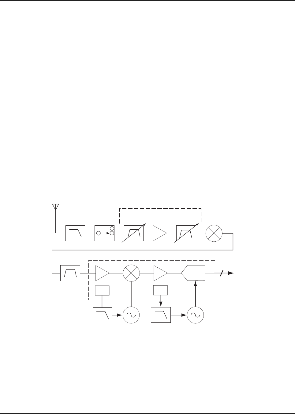
3.1.2 Receiver
The XTS 4000 transceiver has a dual-conversion superheterodyne receiver. Figure 3-3 illustrates
the major receiver components:
• Receiver Front End
• Receiver Back End
Figure 3-3. Receiver Block Diagram
3.1.2.1 Receiver Front End
NOTE: Refer to Table 8.1, “List of Schematics and Boards Overlays,” on page 8-1 for a listing of
receiver front end schematics.
The receiver front end tunes to the desired channel and down converts the RF signal to the first
intermediate frequency (IF). Channel selection is by way of a tunable local oscillator, RXLO, from the
FGU.
RF Input
RX Front End
Harmonic
Filter
ADC
LO CKO
RX_SSI_ DATA
to VOCON Section
XTAL
Filter
ABACUS III - RX Back End
Antenna
Switch LNA
Tuneable
Post-Selector
Filter
Tuneable
Pre-Selector
Filter 1st
Mixer
1st LO
3
MAEPF-27278-B

6871620L01-C May 28, 2008
Theory of Operation: Transceiver Section 3-5
The receiver front end consists of a pre-selector filter, an RF amplifier, a post-selector filter, mixer,
and an IF crystal filter. A switchable attenuator is also inserted between the antenna switch and the
pre-selector filter. The RF amplifier is a discrete RF transistor with associated circuitry. The mixer is a
double-balanced, active mixer IC, coupled by transformers. The receiver (RX) local oscillator (LO) is
provided by the FGU.
3.1.2.1.1 Pre-Selector and Post-Selector Filters
VHF/ UHF: The receiver front end uses two discrete, tunable, bandpass filters to achieve its required
out-of-band rejection. The pre-selector filter precedes the RF amplifier, while the post-selector filter
follows the RF amplifier. DAC2, from the PCIC, is used to simultaneously tune both the pre-selector
and post-selector filters by applying voltage to the varactors.
3.1.2.1.2 LNA (Low-Noise Amplifier)
The XTS 4000 radio uses a discrete transistor for the low-noise amplifier Q430. A feedback network
between the collector and base improves stability and gain balance across the frequency band. Input
and output LC networks match the LNA impedance to 50 ohms.
A diode limiter D703 protects the amplifier damage by strong input signals.
3.1.2.1.3 Mixer
The mixer U470 down-converts the received RF to the first intermediate frequency (IF). The I
F is 44.85 MHz (VHF) and 73.35 MHz (UHF). High-side LO injection is used for the VHF whereas
low-side LO injection is used for the UHF. Transformers are used as baluns to convert signals from
single-ended to balanced at pins RFN and RFP. An output transformer converts the balanced signal
at pins IFN and IFP to a single-ended output.
3.1.2.1.4 IF Filter (Crystal Filter)
The IF filter FL490 is a leadless, surface-mount, 3-pole, quartz crystal filter. This narrow bandpass
filter gives the radio its adjacent-channel and alternate-channel rejection performance.
An input LC network matches the filter impedance to 50 ohms. The output match for the filter
matches the IF Filter output port to the ABACUS III input.
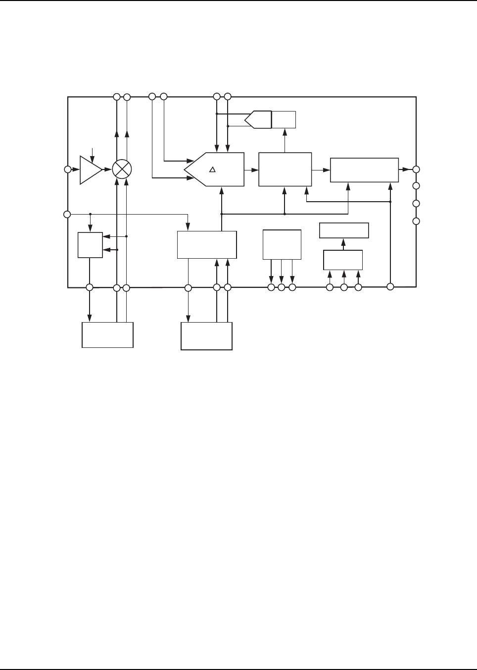
3.1.2.2 Receiver Back End
The receiver back end, which consists of the Abacus III (AD9864 IF digitizing subsystem) IC and its
associated circuitry, processes the down-converted IF signal to produce digital data for final
processing by the VOCON DSP.
NOTE: Refer to Table 8.1, “List of Schematics and Boards Overlays,” on page 8-1 for a listing of
receiver back end schematics.
3.1.2.2.1 Abacus III IC U500
The AD9864 (see Figure 3-4 on page 3-6) is a general-purpose, IF subsystem that digitizes a
low-level 10–300 MHz IF input with a bandwidth up to 270 kHz. The output of the Abacus III IC is SSI
data to the VOCON.
The signal chain of the AD9864 consists of a low-noise amplifier, a mixer, a bandpass sigma-delta
A/D converter, and a decimation filter with programmable decimation factor. An automatic gain
control (AGC) circuit provides the AD9864 with 12 dB of continuous gain adjustment. The high
dynamic range and inherent anti-aliasing provided by the bandpass sigma-delta converter allow the
AD9864 to cope with blocking signals 80 dB stronger than the desired signal.
May 28, 2008 6871620L01-C
3-6 Theory of Operation: Transceiver Section
Auxiliary blocks include frequency synthesizers for the second LO and sampling clock LO, as well as
an SPI port. The second LO uses a discrete external loop filter and VCO. The clock oscillator has an
external loop filter and resonator.
Figure 3-4. Abacus III (AD9864) Functional Block Diagram (from data sheet)
Input signal RXIF is the 44.85 MHz (VHF) and 73.35 MHz (UHF) IF from crystal filter FL490 in the
receiver front end.
VHF: Components L491 and C491 match the input impedance of the ABACUS III to the IF Filter.
UHF: Components C584 and C491 match the input impedance of the ABACUS III to the IF Filter.
3.1.2.2.2 Second Local Oscillator
The second LO is controlled by the Abacus LO synthesizer, which mixes with IFIN to produce a
2.25 MHz final IF. The external VCO consists of Q550 and its bias network and frequency-
determining elements. Signal FREF is the 16.8 MHz reference from the FGU. Darlington transistor
Q551 with C583 and R552 form an active power-line filter.
The second LO frequency is 42.6 MHz (VHF) and 71.1 MHZ (UHF) by default, or 47.1 MHz (VHF)
and 75.6 MHz (UHF) in special cases as needed to avoid radio self-quieters. The loop filter is
composed of R551, C551, C552, and C553.
3.1.2.2.3 Sampling Clock Oscillator
The Abacus sampling clock synthesizer operates at 18 MHz = 8 x 2.25 MHz. The VCO uses an
internal transistor and external resonator. The resonator is composed of L570, C573, and D570.
The loop filter is composed of R571, C570, C571, and C572.
DAC AGC
LNA
IFIN
FREF
LO
Synth.
Samp. Clock
Synthesizer
Voltage/
Current
Reference
Control Logic
SPI
Decimation
Filter
M
ADC
AD9864
-16dB
......=13-26MHz
DOUTA
DOUTB
FS
CLKOUT
LO VCO and
Loop Filter
CLK VCO and
Loop Filter
IOUTL
LOP
LON
IOUTC
CLKP
CLKN
VREFP
RREF
VREFN
PC
PD
PE
SYNCB
MXOP
MXON
IF2P
IF2N
GCP
GCN
Formatting/SSI
MAEPF-27412a-O
6871620L01-C May 28, 2008
Theory of Operation: Transceiver Section 3-7
3.1.3 Transmitter
The transmitter takes modulated RF from the FGU and amplifies it to the radio's rated output power
to produce the modulated transmitter carrier at the antenna.
NOTE: Refer to Table 8.1, “List of Schematics and Boards Overlays,” on page 8-1 for a listing of
transmitter-related schematics that will aid in the following discussion.
The transmitter (see Figure 3-5) consists of an RF driver IC that receives its input signal from the
voltage-controlled oscillator (VCO) and a high-power output transistor. Transmitter power is
controlled by a power-control IC (PCIC) that senses the total current drawn by the transmit gain
stages and adjusts PA control voltages to maintain a constant power level. The signal passes
through an antenna switch and harmonic filter to the antenna.
Figure 3-5. Transmitter Block Diagram
3.1.3.1 Power Distribution
To minimize voltage drop to the power amplifiers, net RAWB+ connects to power module Q107 and
the second stage of driver amplifier U102 through components having minimal series resistance –
ferrite beads and chokes only. During receive, no RF or DC bias is applied, and leakage current
through U102 and Q107 is less than 100 microamps.
At a transmitter power of 2 Watts, the radio consumes approximately 1100 mA.
3.1.3.2 Driver Amplifier
The driver amplifier IC (U102) contains two LDMOS FET amplifier stages and two internal resistor
bias networks. Pin 16 is the RF input. Modulated RF from the FGU, at a level of +3 dBm ±2 dB, is
coupled through a blocking capacitor to the gate of FET-1. An LC interstage matching network
connects the first stage output VD1 to the second stage input G2. The RF output from the drain of
FET-2 is pin 6 (RFOUT1). Gain control is provided by a voltage applied to pin 1 (VCNTRL). Typical
output power is about +26 dBm (400 mW) with VCNTRL at 4.5 V.
L101 and C102 are the interstage matching network; capacitor C111 is a DC block.
VHF: Components C112–C115 and L103–L104 match the output impedance to maximize power
transfer to Q107.
UHF: Components C114 and L113 match the output impedance to maximize power transfer to Q107.
RAWB+
Sense
Resistor
Driver
Amplifier
Modulated
RF from FGU
Power
Amplifier
Antenna
Switch
Harmonic
Filter
INT
Secondary
Cutback PCIC
RFIN
RAWB+
Antenna

May 28, 2008 6871620L01-C
3-8 Theory of Operation: Transceiver Section
3.1.3.3 Power Amplifier Transistor Q107
The power amplifier transistor, Q107, is an LDMOS FET housed in a high-power, surface-mount
package. To prevent thermal damage, it is essential that the heat sink of the power module be held in
place against the radio chassis. The input impedance-matching network uses discrete inductors and
capacitors. The low-pass output matching network uses lumped LCs. Drain bias is applied through
E101, R130 and L105. Gain is dynamically controlled by adjusting the gate bias. The gate is
insulated from the drain and source so that gate bias current is essentially zero. Gate bias is applied
through R102, R105, and R106.
VHF: The input and output impedance-matching networks consist of C112–C115, C120–C124,
L103–L104, L106–L108.
UHF: The input and output impedance-matching networks consist of C114, C120–C122, C124,
C141, L108 and L113.
3.1.3.4 Antenna Switch
NOTE: Refer to Table 8.1, “List of Schematics and Boards Overlays,” on page 8-1 for a listing of
schematics that will aid in the following discussion.
The antenna switch is a single-pole, double-throw, positive-intrinsic-negative (PIN) diode, transmit/
receive (T/R) antenna switch. Forward DC bias (via Q104) turn the diodes ON, reverse or zero bias
turns them OFF.
VHF: PIN diodes D707 and D717 form a narrow-band, quarter-wave, T/R switch.
UHF: PIN diodes D701 and D702 form a narrow-band, quarter-wave, T/R switch.
In transmit mode, both diodes are forward-biased, and the signal goes from the transmitter to the
antenna through the low resistance of the series PIN diode, while the low resistance of the shunt
diode shorts the receiver. In receive mode, neither diode is biased and both behave as small-value
capacitors, creating a high blocking impedance, in effect disconnecting the transmitter circuitry from
the antenna.
3.1.3.5 Harmonic Filter
The harmonic filter is a high-power, low-loss, low-pass filter. Its purpose is to suppress transmitter
harmonics. The filter also improves receiver out-of-band rejection. Shield SH07 must be in place to
achieve the required stop band rejection. The harmonic filter uses discrete components.
VHF: The pass band is up to 190 MHz, and the stop band is above 260 MHz.
UHF: The pass band is up to 490 MHz, and the stop band is above 760 MHz.
6871620L01-C May 28, 2008
Theory of Operation: Transceiver Section 3-9
3.1.3.6 Power-Control IC (PCIC) U104
The PCIC, U104, contains all of the digital, and most of the analog, circuits needed to control the
transmitter power amplifier. Host control is through a 3-wire, smart SPI interface. Pin descriptions are
shown in Table 3-3.
Table 3-3. Power Control IC (U104) Pin Descriptions
Pin Name Description
1 RFIN Detector voltage input to ALC
2 T1 Test point
3 CI External capacitor for integrator time constant
4 INT Integrator output; control voltage to amplifiers
5 CJ External capacitor for PA rise and fall times
6, 7 VL, CL External capacitor for PA rise and fall times
8 GND1 GROUND
9 F168 Reference clock input, 2.1 MHz
10, 13 QX, CQX External capacitor for voltage multiplier
11, 12 Q, CQ External capacitor for voltage multiplier
14 V10 Voltage multiplier output
15 VG Internal band-gap reference voltage
16 V45 Regulated 4.5 Vdc output
17 V5EXT Power supply input for internal voltage regulator
18 VAR2 Buffered D/A output
19 VLIM Test point for internal D/A No.2 voltage
20 VAR1 Buffered D/A output
21 RS Asynchronous reset input
22 NA Spare pin
23 RX RX/TX mode control-bit output
24 VAR3 Buffered D/A output
25 GND2 GROUND
26 CLK SPI clock input
27 BPOS Power supply input
28 DATA SPI data input/output
29 CEX SPI chip select input
30 TEMP Temperature sensor input
31 RSET External resistor; used to set the temperature cutback rate
32 ANO Switched BPOS output

May 28, 2008 6871620L01-C
3-10 Theory of Operation: Transceiver Section
3.1.3.6.1 Power and Control
Since U104 is powered from switched B+, it makes its own regulated 4.5 Vdc to power the internal
logic. The supply input is V5EXT at pin 17, and the output is V45 at pin 16. RX at pin 23 is the control
signal to the antenna switch control circuit.
3.1.3.6.2 Voltage Multiplier
The PCIC contains an internal voltage multiplier. This multiplier produces signal V10 (pin 14), a 10-V
supply for the PCIC D/A converters (DACs). This enables the DACs outputs to reach 8 V. The FREF
signal is a 2.1 MHz clock used to switch the multiplier. The voltage multiplier is not used in the radio.
3.1.3.6.3 Automatic Level Control (ALC)
In TX mode, the PCIC disables the receiver, turns on the transmitter, and controls the TX power
level. The automatic level control (ALC) circuit operates as follows:
The power level is set by programming an internal DAC to a calibrated reference voltage. D/A
settings for the power set points were determined during radio tuning and stored in Flash ROM. An
internal op-amp compares the D/A reference voltage to the detector voltage at pin 1(RFIN) and
produces an error signal output. This signal is buffered by another op-amp, configured as a low-pass
filter, or integrator, to produce the INT output at pin 4 (TP104). This signal drives the base of voltage
follower Q101.
Transistor Q101 supplies current to drive the gain control pins of amplifiers U102 and Q107.
Resistors R105 and R106 determine the voltage ratio between U102 pin 2 (VCNTRL) and the Q107
gate. Transient response during key-up and key-down is controlled by the power amplifier rise and
fall times. External capacitors at pins CI, CJ, and CL, along with internal programmable resistors,
determine the ALC time constants.
3.1.3.6.4 Temperature Cut Back
The PCIC contains a temperature cut-back circuit to protect the power amplifier (PA) from thermal
damage that might result from incorrect assembly of the radio. External sensor U103 is a linear
temperature-to-voltage transducer, placed near the hottest spot in the radio: power module Q107.
The output is a DC voltage at pin 2 (VOUT) proportional to the temperature at pin 3 (GND). VOUT is
750 mV at 25°C and increases by 10 mV/°C. The PCIC temperature cut-back threshold is
programmed to correspond to 85 or 90°C. Above this threshold, the ALC gradually cuts back the
transmitter until it is fully turned off at 110°C. The slope of cut-back versus temperature is set by
external resistor R111. Diode D104 clamps TEMP to a voltage not much less than VG (pin 15), about
1.3 V, to improve the transient response of the cut-back circuit. A secondary temperature cut back
circuitry is also included for enhanced thermal protection due to the small form factor of the radio.
Q102 along with RT150 and the surrounding support circuitry realizes the circuit. This extra
protection acts independently of the cut-back circuit within the PCIC and ensures the radio's
conformance to thermal safety limits.
3.1.3.6.5 D/A Outputs
In RX mode, the PCIC shuts down the transmitter, turns on the receiver, and tunes the RX front-end
pre-selector filters.
Signal VAR2 supplies the voltage used to tune both front-end pre-selector and post-selector filters.
The voltage range varies from 0.8 V to 2.2 V across the VHF band.

6871620L01-C May 28, 2008
Theory of Operation: Transceiver Section 3-11
3.1.4 Frequency Generation Unit (FGU)
The frequency-generation function is performed by several ICs; multiple, discrete, voltage-controlled
oscillators (VCOs); and associated circuitry.
VHF: The reference oscillator provides a frequency standard to the fractional-N frequency
synthesizer (FracN) IC, which controls the VCOs and VCO buffer IC (VCOBIC). The VCOBIC
amplifies the VCO signal to the correct level for the next stage.
UHF: The reference oscillator provides a frequency standard to the fractional-N frequency
synthesizer (FracN) IC, which controls the VCOs and VCO discreet buffer. The buffer amplifies the
VCO signal to the correct level for the next stage.
Two VCOs are employed – one to generate the first LO and the other to generate the transmit-
injection signals.
NOTE: Refer to Table 8.1, “List of Schematics and Boards Overlays,” on page 8-1 for a listing of
FGU-related schematics that will aid in the following discussion.
3.1.4.1 Reference Oscillator Y200
The radio's frequency stability and accuracy derive from the Voltage-Controlled Temperature-
Compensated Crystal Oscillator (VCTCXO), Y200. This 16.8 MHz oscillator is controlled by the
voltage from the WARP pin of the FracN (fractional-N frequency synthesizer) IC, U202, that can be
programmed through a serial peripheral interface (SPI). The oscillator output at pin 3 is coupled
through capacitor C234 to the FracN synthesizer reference oscillator input and through C236 to the
non-invertive input of the op-amp, U201.
Op-amp U201 buffers the 16.8 MHz output to the VOCON section. Components L205 and C214
form a low-pass filter to reduce harmonics of the 16.8 MHz.
The Digital-to-Analog Converter (DAC) IC, U203, and Switched Capacitors Filter (SCF) IC, FL200,
form the interface between radio's DSP and the analog modulation input of the FracN IC.
3.1.4.2 Fractional-N Frequency Synthesizer (FracN) IC U202
The FracN IC, U202, is a mixed-mode, Motorola-proprietary, CMOS, fractional-N frequency
synthesizer with built-in dual-port modulation. The XTS 4000 radio uses a low-voltage version of the
device, sometimes called LVFracN, for compatibility with the 3 V logic used throughout the radio.
The FracN IC incorporates frequency division and comparison circuitry to keep the VCO signals
stable. The FracN IC is controlled by the MCU through a serial bus. All of the synthesizer circuitry is
enclosed in rigid metal cans on the transceiver board to reduce interference effects.
Separate power supply inputs are used for the various functional blocks on the IC. Inductors L203
and L204 provide isolation between supply pins 20 (AVDD) and 36 (DVDD) connected to V3A. Host
control is through a three-wire, smart SPI interface (pins 7, 8, and 9) with a bi-directional data pin.
FracN functions include frequency synthesis, reference clock generation, modulation control, voltage
multiplication and filtering, and auxiliary logic outputs.
3.1.4.2.1 Synthesizer
Frequency synthesis functions include a dual-modulus prescaler, a phase detector, a programmable
loop divider and its control logic, a charge pump, and a lock detector output. Fractional-N synthesizer
IC principles of operation are covered in detail in the manufacturers' literature. No similar discussion
will be attempted here.
3.1.4.2.2 Clocks
U202, pin 23 (XTAL1), is the 16.8 MHz reference oscillator input from the VCTCXO (Y200).

May 28, 2008 6871620L01-C
3-12 Theory of Operation: Transceiver Section
3.1.4.2.3 Modulation
To support many voice, data, and signaling protocols, XTS 4000 radios must modulate the
transmitter carrier frequency over a wide audio frequency range, from less than 10 Hz up to more
than 6 kHz. The FracN supports audio frequencies down to zero Hz by using dual-port modulation.
The audio signal at pin 10 (MODIN) is internally divided into high- and low-frequency components,
which modify both the synthesizer dividers and the external VCOs through signal MODOUT (pin 41).
The IC is adjusted to achieve flat modulation frequency response during transmitter modulation
balance calibration using a built-in modulation attenuator.
3.1.4.2.4 Voltage Multiplier and Superfilter
Pins 12 (VMULT3) and 11 (VMULT4) together with diode arrays D201 and D202 and their associated
capacitors form the voltage multiplier. The voltage multiplier generates 11.5 Vdc to supply the phase
detector and charge-pump output stage at pin 47 (VCP).
The superfilter is an active filter that provides a low-noise supply for the VCOs and VCOBIC. The
input is regulated 5 Vdc from V5A at pin 30 (SFIN). The output is superfiltered voltage FSF at pin 28
(SFOUT).
The output from pin 15 (VMULT1) is used as a clock for the SCF IC, FL200.
3.1.4.3 Loop Filter
The components connected to pins 43 (IOUT) and 45 (IADAPT) form a 3rd-order, RC low-pass filter.
Current from the charge-pump output, IOUT, is transformed to voltage VCTRL, which modulates the
VCOs. Extra current is supplied by IADAPT for rapid phase-lock acquisition during frequency
changes. The lock detector output pin 4 (LOCK) goes to a logic “1” to indicate when the phased-lock
loop is in lock.
3.1.4.4 VCO Buffer IC (VCOBIC) – VHF only
The VCOBIC (U302) is an analog IC containing two NPN transistors for use as oscillators, an
active-bias circuit, transmitter and receiver buffer amplifiers, and switching circuitry. The VCOBIC
has three RF outputs:
• TX_OUT (pin 10) – the modulated transmitter carrier
• RX_OUT (pin 8) – the receiver first LO
• PRESC_OUT (pin 12) – connected to FracN pin 32 (PREIN) through a matching circuit
Transmit/receive control is a single 5.0 Vdc logic input, TRB_IN (pin 19). When TRB_IN is low, the
receiver buffer is active and the transmitter circuits are disabled. The converse is also true.
The VCOs in VHF radios use the VCOBIC internal transistors and implement the active bias via
resistors R304 and R305. Bias to TX_OUT is supplied through resistor R313. Components L309 and
C316 form a matching circuit for the TX_OUT impedance. C315 acts as a DC block, and resistors
R314, R315, and R316 attenuate an output signal to an optimum level for the PA.
L312 form a low-pass bias supply filter for the RX_OUT. L310 and C317 are the RX_OUT
impedance-matching circuit. C322 is a DC block, and resistors R317 and R318 attenuate an output
signal to an optimum level for the mixer IC.
An NPN/PNP-packaged transistor, Q310, together with the supporting components R310 and C330,
form the 3.3 Vdc-to-5 Vdc logic-level shifter between the AUX3 pin of the FracN IC, U202, and
VCOBIC, U302.
6871620L01-C May 28, 2008
Theory of Operation: VOCON Section 3-13
3.2 VOCON Section
This section provides a detailed circuit description of the ASTRO XTS 4000 VOCON section.
The VOCON section (see see Figure 3-6) is divided into the following sections:
• Controller and Memory
• Audio and Power
• Accessory and CE Interface Connector Support
3.2.1 Connections
The VOCON section (see Figure 3-6) contains three functional blocks and three connector symbols.
Figure 3-6. VOCON Section Connections
The functional blocks consist of the following:
•Controller and Memory: The Patriot (U1401), the dual-core processor with the microcontroller
unit (MCU) and a digital signal processor (DSP), the 4MB SRAM (U1409) and 8MB Flash
(U1410) memory devices.
•Audio and Power: The MAKO IC (U1304), a 5Vdc linear regulator (U1101), an audio switch IC
(U20) and a single-ended gain stage (U9904)
•Accessory and CE Interface Connector Support: The MAKO IC (U1304), ESD protection
circuitry, and CE connector interface circuitry.
NOTE: Refer to Table 8.1, “List of Schematics and Boards Overlays,” on page 8-1 for a listing of
VOCON schematics that will aid in the following discussion.
MAKO
SSI
SPI
RTC
DA or AD
Converter
DC Regulators
Accessory
Interface
Audio P.A.
Voice Codec
Power
Management
CONTROLLER AND MEMORY
FLASH
8 MBytes
Dual-Core
Processor
MCU and DSP
SRAM
4 MBytes
Loud Speaker
Audio Jack
30 pins
CE
Connector
30 pins
VOCON
Encryption
Module
30 pins
XCVR
Display &
Keypad
60 pins
Controls &
Buttons
16 pins
Earpiece
60 pins
I/O

May 28, 2008 6871620L01-C
3-14 Theory of Operation: VOCON Section
3.2.1.1 Connector J1 (Display and Keypad)
This is a 60-pin connector that mates with the Front-Flip flex on the front housing. The 60
connections on the connector J1 consists of Display (control and data) lines (28), Keypad lines (15),
Earpiece audio lines (2), DC supplies and radio GROUND connections.
3.2.1.2 Connector J2 (Encryption Module, CE Interface Connection and Audio Jack
Connection)
This 30-pin connector mates with the UCM-CE-Audio Jack flex and provides the connections from
the VOCON section to the Encryption Module, the CE Accessory Interface and the 2.5mm Audio
Jack.
Two voltages are provided to the encryption module: UNSWB+ and SWB+. The SAP SSI lines, serial
communication data lines and general purpose I/O lines from the Patriot IC are routed through this
connector.
Connections to the CE accessory connector, which include serial data communication and UCM are
present at pins 18 and 17.
The external audio jack consists of a microphone, audio jack interrupt, PTT line and single-ended
audio.
3.2.1.3 Connector J3 (Buttons and Controls Connection)
This 16-pin connector mates the VOCON section (on the mainboard) to the volume controls and
user buttons (PTT, EMERGENCY, SECURE mode and programmable buttons etc.).
3.2.2 Controller and Memory
The controller and memory section contains the following components:
• Patriot IC (U1401)
• Static RAM (SRAM) IC (U1409)
• Flash memory IC (U1410)
The Patriot IC acts as both the microcontroller unit (MCU) and the digital signal processor (DSP) for
the radio. The MCU controls receive/transmit frequencies, power levels, display programming, user
interface (PTT, keypad, menu select, etc.), and programming of ICs, as well as other functions. The
DSP performs voice encoding and decoding, audio filtering, volume control, PL/DPL encode and
alert-tone generation, squelch control, and receiver/transmitter filtering, as well as other functions.
The Patriot IC executes a stored program located in the Flash memory device. The SRAM, a volatile
device, is used as working memory and shares the address and data bus with the Flash memory
device.
NOTE: Refer to Table 8.1, “List of Schematics and Boards Overlays,” on page 8-1 for a listing of
VOCON schematics that will aid in the following discussion.
3.2.2.1 Patriot IC U1401
The Patriot IC U1401 is a dual-core processor that contains both a 32-bit microcontroller unit (MCU)
and a 16-bit digital signal processor (DSP) in one IC package. It comes in a 256-pin, ball-grid array
(BGA) package with 0.3mm pitch solder balls. The dual-core processor is supplied with two voltages:
1.875 V and 1.55 V. The 1.55 V supply is used as the core voltage while the 1.875V is used as the
interface to the memory devices and display module. Most of the pins on the Patriot IC operate from
the 2.9 V supply.

6871620L01-C May 28, 2008
Theory of Operation: VOCON Section 3-15
Two main clocks are provided to the Patriot IC. The CKIH pin (C1402) is provided a 16.8 MHz sine
wave. This is the most important clock since it is internally used to generate the clocks for both the
MCU and DSP cores, as well as most of the peripherals. A 3 V peak-to-peak 32 kHz square wave
(32 kHz test point) is generated by the oscillator Y1301 and the buffer U1301, and supplied to the
CKIL pin on the Patriot IC. While not as widely used as the 16.8 MHz clock, the 32 kHz clock is
needed by some components in the Patriot including the reset circuitry.
3.2.2.1.1 Microcontroller Unit (MCU)
The MCU portion of the Patriot IC has 16k x 32 bits of internal RAM and 28k x 32 bits of internal
ROM, which is used for the bootstrapping code. The MCU has several peripherals including an
External Interface Module (EIM), the Multiple Queue Serial Peripheral Interface (MQSPI), two
Universal Asynchronous Receiver/Transmitter (UART) modules, and the One-Wire Interface
module. The MCU communicates internally to the DSP through the MCU/DSP Interface (MDI).
External Interface Module (EIM)
The External Interface Module (EIM) is the MCU interface to the SRAM U1409 and Flash Memory
U410, as well as the display module. The EIM lines include 24 external address lines, 16 external bi-
directional data lines, 6 chip selects lines, read/write line, and output enable line among others. All of
the EIM lines operate at 1.875-V logic levels, and the EIM operates at the MCU clock speed.
Multiple Queue Serial Peripheral Interface (MQSPI)
The Multiple Queue Serial Peripheral Interface (MQSPI) is the MCUs programming interface to other
ICs. The Patriot IC has two independent SPI busses, and each has its own clock line (test points
SCKA and SCKB), data-out line (test points MOSIA and MOSIB), and data-in line (test points MISOA
and MISOB). There are 10 SPI chip selects (SPICS) that are programmable to either SPI A, the
transceiver board SPI bus, or to SPI B, the dedicated VOCON SPI bus.
The devices on the SPI A bus include the PCIC and FracN IC on the SPICS4 (R1118), the Abacus III
IC on SPICS5 (R1119), and an analog-to-digital converter (ADC) on SPICS6 (R1120). One SPI B
chip select is used for the MAKO IC (U1304). All of the SPI module lines operate at GPIO voltage
logic levels.
Universal Asynchronous Receiver/Transmitter (UART)
The Patriot IC has two Universal Asynchronous Receiver/Transmitter (UART) modules. UART1
handles the RS232 lines while UART 2 is connected to the SB9600 lines. Each UART has a receive
data line (URXD), a transmit data line (UTXD), and hardware flow control signals (RTS–request to
send) and (CTS–clear to send). All UART lines operate at GPIO voltage logic levels. The translation
to 5 V logic levels for the accessory side connector is discussed in the MAKO section.
One-Wire Interface
The MCU has a One-Wire Interface module that is used to communicate to a One-Wire device like a
USB cable or a smart battery using the Dallas Semiconductor protocol. This module uses a GPIO
voltage logic level.

May 28, 2008 6871620L01-C
3-16 Theory of Operation: VOCON Section
3.2.2.1.2 Digital Signal Processor (DSP)
The DSP portion of the Patriot IC has 84k x 24 bits of program RAM and 62k x 16 bits of data RAM.
The DSP has its own set of peripherals including the Baseband Interface Port (BBP), the DSP Timer
module, and the Serial Audio CODEC Port (SAP). Additionally, the DSP shares some peripherals
with the MCU, including the USB interface and the General Purpose Input/Output module (GPIO).
Baseband Interface Port (BBP)
The Baseband Interface Port (BBP) module is the DSP’s serial synchronous interface (SSI) to the
transceiver section. The BBP has independent sections for the receiver and the transmitter. The
receiver BBP pins include the receive data pin SRDB (R1110), the receive clock signal pin SC0B
(R1109), and the receive frame synchronization (sync) signal pin SC1B (R1111). The transmitter's
BBP pins include the transmit data pin STDB (R1113), the transmit clock signal pin either SCKB
(R1112), and the transmit frame sync signal pin either SC2B (R1114). All BBP lines use GPIO
voltage logic levels.
DSP Timer Module
While the BBP receive clock and frame sync signals are supplied by the Abacus III IC from the
transceiver section, the BBP transmit clock and frame sync signals are generated by the DSP Timer.
The BBP receive clock, connected to the DSP Timer input pin T10, is reference used to generate the
BBP transmit clock and frame sync signals. These two signals, along with the BBP transmit data
signal, are connected to the DAC on the transceiver section.
Serial Audio CODEC Port (SAP)
The Serial Audio CODEC Port (SAP) module is the DSP’s serial synchronous interface (SSI) to the
audio CODEC on the MAKO IC. The SAP also interfaces with the encryption module.
The SAP interface consists of four signals including the SAP clock line pin SCKA (component
R1410), the SAP frame sync line pin SC2A (component R1411), the SAP receive data line pin SRDA
(component U1408), and the transmit data line pin STDA (component R1338).
The SAP clock is generated by the dual-core processor U1401, and is a 256 kHz, 2.9 V peak-to-
peak square wave. The SAP frame sync signal is generated by the dual-core processor U1401, and
is an 8 kHz, 2.9 V peak-to-peak square wave.
Universal Serial Bus (USB)
The Patriot IC USB peripheral, shared by the MCU and the DSP, provides the required buffering and
protocol to communicate on the Universal Serial Bus. The Patriot IC supports USB slave
functionality.
For receive data, the USB differentially decoded data comes from the MAKO IC
USB2_OE_RCV_RTS pin into the Patriot URTS1 pin, while the single-ended USB data positive
signal goes to pin PA2_USB_VPIN, and the single-ended USB data minus signal goes to pin
URXD1. The two data lines are used to detect the single-ended zero state.
For transmit data, the USB data comes out of the Patriot IC UTXD1 pin and goes to MAKO IC
USB1_DAT_TXD pin. The USB transmit single-ended zero signal is generated from the Patriot IC
PC0_USB_VMOUT pin.

6871620L01-C May 28, 2008
Theory of Operation: VOCON Section 3-17
General-Purpose Input/Output (GPIO) Module
The General-Purpose Input/Output (GPIO) module is shared by the MCU and the DSP. This module
consists of four 16-pin bi-directional ports and a 15 pin bi-directional port. While some of the pins on
these ports are being used for other functions (UART, SPI, SAP, BBP, and Interrupt pins), the
remaining pins can be programmed to become GPIOs that can be used by either the DSP or the
MCU. Each GPIO pin has up to 8 alternate output functions and up to 4 alternate input functions.
This allows for the GPIO pins to be routed internally to pertinent Patriot IC modules. Additionally, the
GPIO module adds selectable edge-triggered or level-sensitive interrupt functionality to the GPIO
pins. Some examples of GPIO pins include the Display module backlight brightness control signals
(DISP_BRIGHT1 and DISP_BRIGHT2), the Keypad backlight enable signal (KP_BLEN) and the Flip
Assembly Open/Close Sense Signal (FLIP_SENSE).
3.2.2.2 Static RAM (SRAM) U1409
The static RAM (SRAM) IC U1409 is an asynchronous, 4 MB, CMOS device that is capable of 70 ns
access speed. It is supplied with 1.875 volts. The SRAM has its 19 address lines and 16 data lines
connected to the EIM of the Patriot IC through the Address(23:0) and Data(15:0) busses.
The SRAM has an active-high chip select CE2 that is tied directly to the 1.875 V supply and an
active-low chip select EN_CE that is connected to the EIM CS2_N pin. When the SRAM EN_CE pin
is not asserted, the SRAM is in standby mode, which reduces current consumption.
Two other control signals from the EIM that change the mode of the SRAM are the read/write signal,
R/W, and the output enable signal, OE. The R/W of the EIM is connected to the SRAM EN_WE pin,
while the OE signal from the EIM is connected to the SRAM EN_OE pin. The SRAM is in read mode
when the EN_WE pin is not asserted and the EN_OE pin is asserted. The SRAM is in write mode
when the EN_WE pin is asserted, regardless of the state of the EN_OE pin.
The other SRAM pins are the lower-byte enable pin EN_BLE and the upper-byte enable pin
EN_BHE. These pins are used to determine which byte (BLE controls data lines 0-7 and BHE
controls data lines 8-15) is being used when there is a read or a write request from the Patriot IC.
The EN_BLE pin is controlled by the EIM EB1_N signal, while the EN_BHE pin is controlled by the
EB0_N signal.
3.2.2.3 FLASH Memory U1410
The Flash memory IC is an 8 MB CMOS device with simultaneous read/write or simultaneous read/
erase operation capabilities with 70 ns access speed. It is supplied with 1.875 volts. The Flash
memory has its 23 address lines and 16 data lines connected to the EIM of the Patriot IC through the
Address(23:0) and Data(15:0) busses. The Flash memory contains host firmware, DSP firmware,
codeplug data and the transceiver section's tuning values. The Flash memory IC is not field
repairable.
The RESET_OUT of the Patriot IC is at a GPIO voltage logic level. Components D1401 and R1437
are used to convert the voltage down to a 1.875 V logic level, and this 1.875 V reset signal is fed to
the Flash RESET pin. When this pin is asserted (active low logic), the Flash is in reset mode. In this
mode, the internal circuitry powers down, and the outputs become high-impedance connections.
The Flash active-low chip select pin, EN_CE, is connected to the active-low CS0_N pin (CS0 test
point) of the EIM. When the EN_CE is not asserted, the Flash is in standby mode, which reduces
current consumption.
May 28, 2008 6871620L01-C
3-18 Theory of Operation: VOCON Section
Several other active-low control pins determine what mode the Flash memory is in: the address valid
pin ADV that is connected to the EIM LBA_N signal, the output enable pin EN_OE that is connected
to the EIM OE_N signal, and the write enable pin EN_WE that is connected to the EIM EB1_N
signal. For read mode, the ADV and EN_OE pins are asserted while the EN_WE pin is not asserted.
When the EN_WE is asserted and the EN_OE pin is unasserted, the Flash operates in the write
mode.
Figure 3-7 illustrates the EIM and memory ICs block diagram.
Figure 3-7. Patriot EIM and Memory Block Diagram
3.2.3 Audio and Power
The audio and power section contains the following components:
• MAKO IC U1304
• 5 V regulator U1101
• Audio Switch U20
• Single-ended Audio Gain stage U9904
The MAKO IC contains a CODEC, amplification, filtering and multiplexing capability for receive and
transmit audio, voltage regulators, an analog-to-digital converter (ADC), and a real-time clock (RTC).
The MAKO IC is programmed by the Patriot IC.
The MAKO IC also contains an audio preamplifier and an audio power amplifier to condition the
received audio signal. Programmable preamplifiers also sets the gain of the microphone audio
signal. These devices internal to the MAKO are programmed by the Patriot IC.
NOTE: Refer to Table 8.1, “List of Schematics and Boards Overlays,” on page 8-1 for a listing of audio
and power-related schematics that will aid in the following discussion.
Dual-Core
Processor
U1401
Flash
U1410
SRAM
U1409
RESET_OUT
LBA_N
CS0_N
EB1_N
OE_N
A(23:0)
D(15:0)
EB0_N
CS2_N
RW_N
Voltage
Translator RESET
ADV
EN_CE
EN_WE
EN_OE
A(22:0)
D(15:0)
A(18:0)
D(15:0)
EN_OE
LB
UB
CS1
EN_WE
CSO
A(23:1)
A(19:1)
CS2
R_W
MAEPF-27414-B

6871620L01-C May 28, 2008
Theory of Operation: VOCON Section 3-19
3.2.3.1 MAKO IC U1304
The MAKO IC is a mixed-signal (analog and digital) IC that provides control, audio, and voltage
regulation functionality. It comes in a 176-pin, ball-grid array (BGA) package with 0.8 mm pitch solder
balls. The MAKO IC is supplied with switched battery voltage UNSW_B+ (R1309).
3.2.3.1.1 Voltage Regulation
The MAKO IC contains several voltage regulators that are used in the design of the VOCON section:
VSW1, V2, VCC5, V1.55 and V1.875. The VSW1 regulator is a programmable switching regulator
that uses the switched battery voltage as its input. The output voltage of VSW1 (R1319) is
programmable by the Patriot IC U1401 through the SPI bus. The initial output of VSW1 is 3.2 volts,
which is then programmed to 3.8 volts. The VSW1 voltage is supplied to the RF transceiver section
and to the input pins of the V2 regulator.
The V2 regulator is a SPI programmable linear regulator that uses VSW1 as its supply. The initial
output of V2 (L1302) is 2.775 volts, which is then programmed to 2.9 volts for the VOCON section.
The V2 voltage is supplied to the Patriot IC (I/O ring - SPI, BBP, SAP, UART, GPIO, etc.), the display
module via connector J1, and the many discrete components that interface with the Patriot IC and
the MAKO IC.
The VCC5 regulator is a fixed linear regulator that outputs 5Vdc. VCC5 is used by the accessory I/O
lines and the audio switch U20.
The V1.55 is a SPI programmable linear regulator. V1.55 is used by the Patriot MCU Core. The
V1.875 is a SPI programmable linear regulator. V1.875 is used by the EIM, Memory, Display and I/O
ring.
3.2.3.1.2 MCU Interface
The MAKO IC has a four-wire, SPI connection to the Patriot IC (SPI B). The SPI B clock is connected
to the SPI_CLK pin (SCKB). The SPI B MOSI line is connected to the SPI_DI pin. The SPI B MISO
line is connected to the SPI_DO pin. The MAKO SPI B chip-select signal is connected to the SPI_CS
pin (R1334). Through this interface, the Patriot IC can program the voltage regulators, the CODEC,
the transmit and receive audio filters and amplifiers, as well as read information from the ADC and
the real-time clock.
The MAKO IC has an 10-bit ADC with 11 channels. Some of the ADC channels are used for general
purpose voltage monitoring: Emergency Button (ATOD_2), board type (ATOD_5) and the board
identification voltage (ATOD_6). Battery voltage is also monitored by the ADC. The Patriot IC
activates and reads the A/D values through the SPI bus.
3.2.3.1.3 Audio Circuitry
A 16-bit CODEC, internal to the MAKO IC and programmable by the Patriot IC through the SPI bus,
converts microphone audio into a digital bit stream for processing by the DSP. The CODEC also
converts receive audio data that was processed by the DSP into an analog audio signal for
amplification to a speaker. The CODEC interfaces to the DSP through the 4-wire SAP bus. The
CODEC clock, which is 256 kHz is supplied to the DCLK pin. The CODEC 8 kHz CODEC frame
synchronization signal is supplied to the FSYNC pin. The CODEC transmit data signal is on the TX
pin, while the CODEC receive data signal is on the RX pin. For the CODEC to operate with those
clock and frame sync signals, a 24.576MHz clock, generated by Y1302 is supplied to the MAKO IC.
The MAKO IC contains internal amplification, filtering, and multiplexing functionality for both receive
and transmit audio. These functions are Patriot IC-programmable through the SPI bus. The input for
the internal microphone audio (C1350) is the INT_MIC_P pin, while the input for the external
microphone audio (C1347) is the EXT_MIC_P pin.

May 28, 2008 6871620L01-C
3-20 Theory of Operation: VOCON Section
The MAKO contains two internal audio power amplifiers for internal and external speaker routing and
the outputs are available at pins INT_SPKR_P and INT_SPKR_M (internal speaker) and
EXT_SPKR_P and EXT_SPKR_M (external speaker). Section 3.2.5.2 on page 3-27 details the
audio routings to the various transducers. The audio routing selection is controlled by the Patriot IC.
3.2.3.2 5 V Regulator U1101
The 5 V regulator, U1101, uses UNSW_B+ as its input voltage. This regulator supplies 5Vdc to the
keypad circuitry, the radio ON/OFF circuitry and the display backlight control circuitry.
3.2.3.3 Audio Switch U20
The audio switch U20 is a single-pole, double-throw analog switch that switches amplified audio from
the MAKO external speaker terminals (EXT_SPKR_P and EXT_SPKR_M) to the earpiece (on the
flip assembly) or the single ended audio gain stage for the 2.5mm audio jack earpiece. The U20 is
supplied from VCC5.
3.2.3.4 Single-Ended Audio Gain Stage U9904
U9904 is the single-ended audio gain stage for the 2.5mm audio jack earpiece. It consists of a non-
inverting operational amplifier and DC biasing circuitry. One of the outputs of the audio switch (U20)
is channelled to U9904.
3.2.4 Accessory and CE Interface Connector Support
The accessory and CE interface connector support section consists of the following:
• MAKO IC U1304
• ESD protection circuitry
• CE connector interface circuitry
The MAKO IC contains a RS232 and USB transceiver, switching logic between RS232 and boot data
path, One-Wire side connector support, and several supporting circuitry. The MAKO IC is
programmed by the Patriot IC.
ESD protection devices include zener diodes and low-capacitance ESD suppressors.
CE interface connector circuitry includes current-limiting resistors and noise-suppressing shunt
capacitors.
3.2.4.1 MAKO IC U1304
See Figure 8-14, “VOCON: DC Power, Clocks and ON/OFF Circuit,” on page 8-15 for schematic
details of the following discussion.
The MAKO IC U1304 also contains the circuitry and blocks to support radio accessories and test/
programming service aids. The block supports many functions including radio CE connector
interface, bi-directional logic level translation, boot data path control, USB transceiver and One Wire
option detect support.

6871620L01-C May 28, 2008
Theory of Operation: VOCON Section 3-21
3.2.4.1.1 Radio CE Connector Interface, Logic Level Translation, and Boot Data Path Control
The MAKO IC facilitates the interface to the radio's CE connector. Some of the CE connector lines
are at 5 V logic levels, so the MAKO IC converts those lines to GPIO voltage logic levels to interface
to the Patriot IC, as well as the encryption module. These lines include the SB9600 bus busy line
LH_BUSY, the RS 232 CTS and RTS lines, the RS232 data-out line, and the RS232 data-in line.
Another function that the MAKO IC provides with these lines is boot data path control. The boot data
path is as follows: boot data-in is multiplexed onto the RS232 data-out line while the boot data-out is
multiplexed with the SB9600 data line. This alternate data path is used only to Flash code into a
radio for the first time. The Patriot IC, through the SPI bus, controls this feature.
3.2.4.1.2 USB Transceiver
The USB transceiver, internal to the MAKO IC, is capable of transmitting and receiving serial data at
a rate of 12 megabits per second. The differential USB data comes from the CE connector, through
the 33-ohm resistors R1206 and R1207, and then to the USB1_DP and USB1_DM pins on the
MAKO IC. The USB receive interface from the MAKO IC to the Patriot IC is as follows: USB1_DP
routed to USB1_DAT_TXD, USB1_DM routed to USB2_SE0_VM_RXD.
The USB transmitter is enabled when the RS232_USB and USB_TXENAB signals are both driven
low by the Patriot IC. The single-ended data is output from the Patriot IC on the UTXD1_USB_VPO
pin and goes to the MAKO USB1_DAT_TXD pin. The data is driven out differentially on the
USB1_DP and USB1_DM, which go to the CE connector. The Patriot IC sends the single-ended
zero signal from pin USB_VMO to the MAKO IC USB1_SE0 pin.
When a USB cable is attached, pin CTS_CABLE_DET_5V is driven low and goes through level
translation in U701 and the output of CTS_CABLE_DET_3V is pulsed low and sent to the dual-core
processor. This line controls the USB and RS232 modes so that the data that is on those lines are
routed to the USB transceiver when a cable is detected. If a USB cable is not detected,
CTS_CABLE_DET_3V is high, the USB transceiver is put in suspend mode and the DP and DM pins
can now handle 5V tolerance for RS232 mode of operation.
3.2.4.1.3 One-Wire Support
New options and accessories that attach to the CE connector are identified by the Patriot IC using
the One-Wire protocol. The Option Select 2 pin on the CE connector also serves as the One-Wire
data pin. This signal is connected to the ONE_WIRE_OPT pin. This pin is connected to the dual-core
processor one-wire bus (ONE_WIRE_UP) through the MAKO IC internal isolation switch which is
controlled by the SPI commands sent from the dual-core processor. This isolation is needed to
prevent possible contention on the One-Wire bus when a smart battery is attached to the radio.
These new accessories are to GROUND pin CTS, of the CE connector. When this occurs, the MAKO
IC pin ONE_WIRE_OPT is asserted and the Patriot IC detects the change. The Patriot IC then
instructs the MAKO IC (via SPI) to connect the CE connector One-Wire line to the Patriot IC One-
Wire bus. In the case of the USB cable, the Patriot IC reads the One-Wire data from the cable and,
upon determining that a USB cable is attached, programs the MAKO IC for USB mode.
3.2.4.1.4 Watchdog Timer
The watchdog timer is a 125ms counter that is integrated into the MAKO IC and used during the
power down sequence. The MAKO IC will begin the power down sequence when a low-to-high
transition occurs on MECH_SW pin. Once this transition occurs, the MAKO IC begins the watchdog
timer. Upon expiration of the timer, the RESETX pin is asserted and all MAKO regulators are
shutdown. The dual-core processor can refresh the watchdog timer so that the software has enough
time to complete its tasks before the power is taken away completely.

May 28, 2008 6871620L01-C
3-22 Theory of Operation: VOCON Section
3.2.4.1.5 24.576 MHz Reference Generation for MAKO
The 24.576 MHz reference is required by the MAKO IC for the CODEC time base and the SSI clock
generator module internal to the MAKO IC. The clock is generated by crystal oscillator Y1302 and
load capacitors C1316 and C1317.
3.2.4.1.6 SSI Clock and Frame Sync Generator
The MAKO IC generates the SSI clock and frame sync signals for the SAP bus used by the Patriot
IC and encryption module. These signals are generated from the 24.576 MHz reference. The SSI
clock output pin is labeled SSI_CLK, and the frequency is 512 kHz. The SSI frame sync output pin is
SSI_SYNC, and the frequency is 8 kHz. These signals are not active when the MAKO IC comes out
of reset, so they are programmed by the Patriot IC through the SPI bus.
3.2.4.2 ESD Protection Circuitry
See Figure 8-12, “VOCON: Audio, Connector Interface Circuits,” on page 8-13 for schematic details
of the following discussion.
Several components on the VOCON section protect the circuitry from ESD. The CE connector signal
lines have ESD protection components on them since they are exposed. These protection
components include:
• 5.6-V zeners VR1301 on the BAT_STATUS line, 5.6-V zener diode on reset line (UHF), VR1202
and VR1203 on the RS232 and USB data lines
• 6.8V zeners on the OPT_SEL lines, the ONE_WIRE line and the Audio Jack lines
• 12V zeners on the MAKO audio outputs
Spark Gaps are also present on the mainboard layout as a back-up defense mechanism against
ESD.
3.2.4.3 Radio CE Interface Connector Circuitry
See Figure 8-12, “VOCON: Audio, Connector Interface Circuits,” on page 8-13 for schematic details
of the following discussion.
An important circuit in the CE interface connector is the Option Select 2 (OPT_SEL2) line
comparator. The opamp (U1201) is used as a comparator for the option select 2 line. The voltage
divider network of R1227 and R1229 determines the comparator threshold. The remaining
components on the CE interface connector consist of current-limiting serial resistors and noise-
suppressing shunt capacitors.
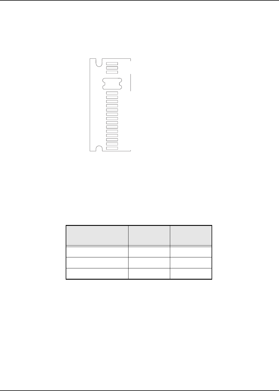
6871620L01-C May 28, 2008
Theory of Operation: VOCON Section 3-23
3.2.4.3.1 Radio CE Connector and Option Selects
The CE connector is located on the bottom side of the radio. It is the external port or interface to the
outside and is used for programming and interfacing to external accessories. The CE connector
connects to the VOCON section at connector J2 via a flex circuit (UCM-CE-Audio Jack Flex) that is
routed inside the external housing. Pin assignments on the CE connector are shown in Figure 3-8.
Figure 3-8. CE Connector
Most of the signals are extensions of circuits described in other areas of this manual. However, there
are two option select pins (see Table 3-4) used to configure special modes: Option Select 1 and
Option Select 2. These pins are controlled by accessories connected to the universal connector.
Table 3-4 outlines their functions as defined at the universal connector.
3.2.4.4 Dual Display Module
The XTS4000 radio has a dual display module within the front-flip assembly of the radio. The dual
display consists of a main display and a caller identification CID display. The main display is a 130 x
130 dot matrix liquid crystal display (LCD) whereas the CID display is a 112 x 32 dot matrix LCD. The
display module uses chip on film technology and is not field repairable.
3.2.4.5 Keypad
The keypad on the XTS4000 radio is a 3 x 3 Menu Keypad (with 4-way navigation button) and a 3 x
4 alphanumeric keypad. This keypad is realized through a flex circuit design which is housed within
the front-flip assembly of the radio. The keypad is connected to the VOCON section through
connector J1.
Table 3-4. Option-Select Functions
Function Option
Select 1
Option
Select 2
External PTT 00
No Function (Normal) 11
External Speaker 01
1
3
4
17
CE_GND
CE_NC1
CE_OPTB+_VPP
CE_RS232_TX_USB+
CE_RS232_RX_USB
CE_RTS
CE_CTS
CE_LH_DATA_KEYFAIL
CE_EXT_MIC
CE_NC3
CE_NC4
CE_OPT_SEL1
CE_OPT_SEL2
CE_EXTSPKR
CE_SPKRCOM
CE_NC5
CE_NC2

May 28, 2008 6871620L01-C
3-24 Theory of Operation: VOCON Section
The keypad lines are read through a row and column matrix made up of 7 row lines (UC_KP_ROW0
to UC_KP_ROW6) and 3 column lines (UC_KP_COLUMN0 to UC_KP_COLUMN2). A separate line
connects the ON/OFF button on the keypad to the ON/OFF Circuitry on the VOCON section
(UC_KP_ONOFF)
Keypad backlighting is supplied by the 5V Misc Regulator (U1101) and the backlight is controlled by
the Patriot IC GPIO KP_BLEN.
3.2.4.6 Buttons and Controls
The XTS4000 radio has the following buttons and controls:
• PTT button (PTT)
• Clear/ Secure mode button (P1)
• Emergency button (P2)
• Programmable button (P3)
• Volume Controls (VOL)
The P1, P2 and P3 buttons are connected to a resistor divider network, biased between V2 and
GROUND. The network, made up of R9913, R9914 and R9915 provides a DC voltage level,
controlled by whichever button is pressed, to pin 3 of buffer U1305. The output of buffer U1305 goes
to the MAKO ATOD_2 pin. The Patriot IC reads the MAKO A/D value through the SPI bus and uses
the read data to determine which button was pressed.
The PTT button is connected to the Patriot IC INT0 Interrupt pin for fast action of the Patriot IC to
execute the PTT operation.
Volume controls for the radio are set by up and down controls. These controls share the
UC_KP_COLUMN0, UC_KP_COLUMN1 and UC_KP_ROW7 lines. The Patriot IC uses these three
lines to determine whether the volume up or volume down button was pressed.
Figure 3-9 shows the buttons and controls implementation.
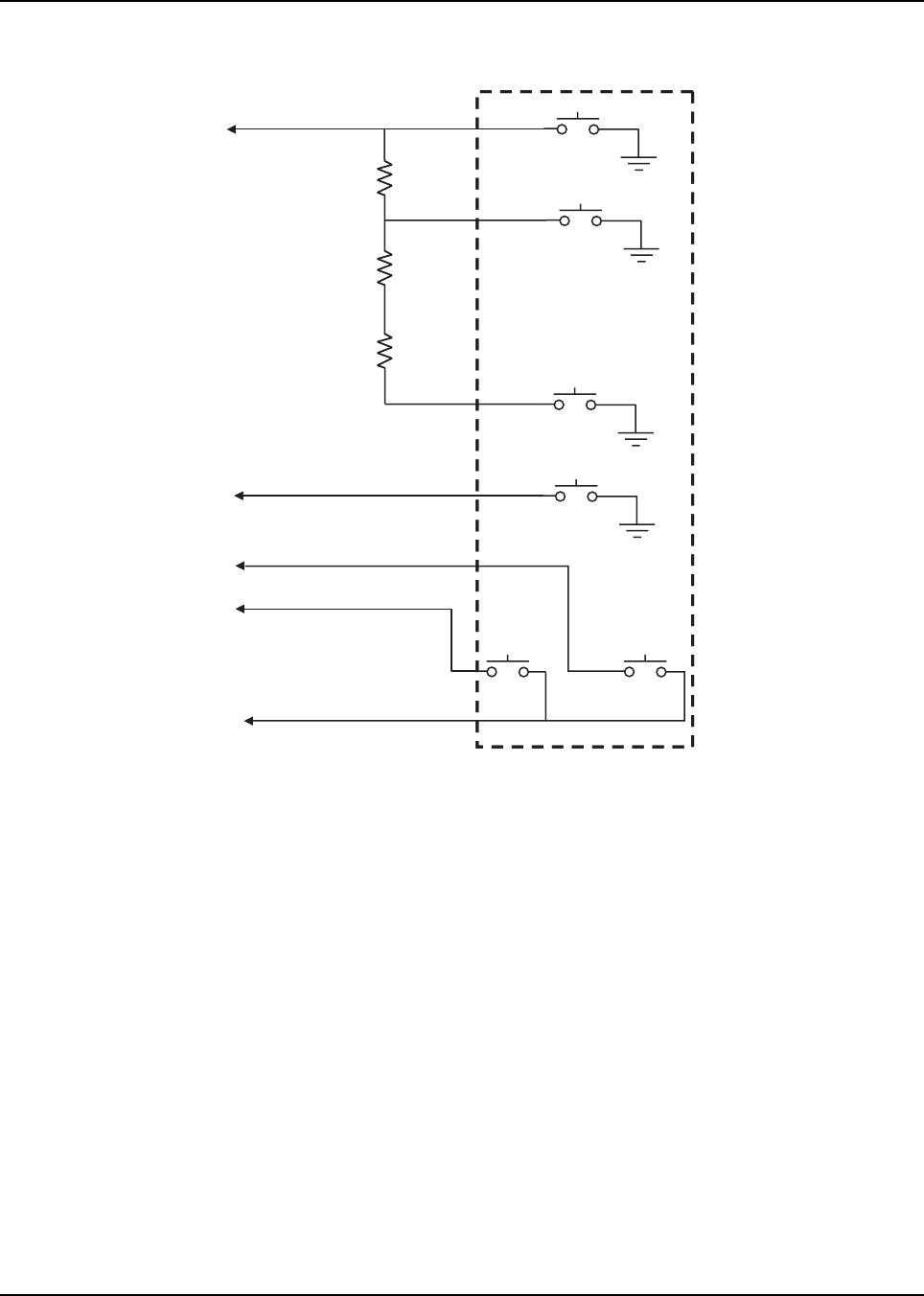
6871620L01-C May 28, 2008
Theory of Operation: VOCON Section 3-25
Figure 3-9. Control Top Flex
3.2.4.7 System Clocks
The Patriot is supplied with two clocks:
1. The first clock, a 16.8 MHz sine wave, comes from the RF transceiver portion of the radio. It
is conditioned by the clock buffer circuit, which includes Q1402, R1416, R1417, R1418,
R1415, C1402, C1403 and C1404.
2. The other clock supplied to Patriot is a 32.768 kHz square wave. This clock is generated by
the external 32.768kHz crystal Y1301, and a clock buffer circuit that includes U1302, R1304,
R1305 and C1303. This signal is supplied to the CKIL pin on the dual-core processor.
3.2.5 VOCON Audio Paths
This section describes the VOCON transmit and receive audio paths. See Figure 8-15 and
Figure 8-16 on page 8-16 and page 8-17 for schematic details of the following discussion.
UC_EMERG EMERGENCY
Button
CLEAR/SECURE
Button
Programmable
Button
INT_PTT PTT Button
UC_KP_ROW7
UC_KP_COLUMN0
UC_KP_COLUMN1
VOLUME Up
Button
VOLUME Down
Button
R9913 91K
R9914 68K
R9915 150K
Top Control Flex
UC_EMERG EMERGENCY
Button
CLEAR/SECURE
Button
Programmable
Button
INT_PTT PTT Button
UC_KP_ROW7
UC_KP_COLUMN0
UC_KP_COLUMN1
VOLUME Up
Button
VOLUME Down
Button
R9913 91K
R9914 68K
R9915 150K
Top Control Flex
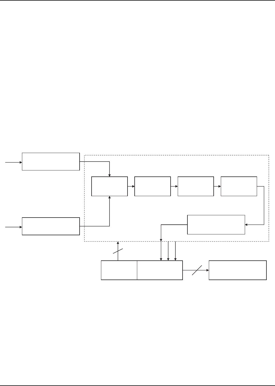
May 28, 2008 6871620L01-C
3-26 Theory of Operation: VOCON Section
3.2.5.1 Transmit Audio Path
The single-ended internal microphone audio enters the VOCON section through the 30 pin
connector (J2), and the internal microphone bias is set by circuitry that includes R1324, R1325,
C1349, C1350 and C1351. The internal microphone signal is connected to the INT_MIC_P pin,
which is the input terminal on the MAKO IC internal op-amp G1 after the signal is multiplexed. The
gain is programmed by the dual-core processor via SPI lines.
The external microphone audio enters the VOCON section through the 30 pin connector J2 as well
and the external microphone bias is set by circuitry that includes R1322, R1323, C1346, C1347 and
C1348. The external microphone signal is connected to the EXT_MIC_P pin, which is an input
terminal on the MAKO IC internal op-amp G1 after the signal is multiplexed. The gain is programmed
by dual-core processor via SPI lines.
The dual-core processor, through the SPI bus, programs a multiplexer internal to the MAKO IC to
select one of the microphone signals. Then, the selected microphone signal goes through the G1
pre-amplifier stage and on to a programmable gain amplifier (G2) before it goes to the CODEC for A/
D conversion. The resulting digital data is filtered and sent to the DSP on the CODEC_TX line from
the MAKO IC VC_TX3V pin. After additional filtering and processing, the DSP sends the data out
from the STDB pin, labeled TX_SSI_DATA to the RF transceiver section.
Figure 3-10. VOCON Transmit Audio Path
INTERNAL MIC BIAS
R1324, R1325, C1349,
C1360, C1351
EXTERNAL MIC BIAS
R1322, R1323, C1346,
C1347, C1348
MUX Pre-amp
G1 Gain = 15 dB
Amp G2
Gain = -30 to 0 dB
CODEC
A/D 16-Bit
HPF = 200 Hz
& LPF = 3.4 kHz cutoff
RF D/A
U201
Patriot
SAP / BBP
Patriot
SPIB
INT_MIC_P
EXT_MIC_P
CODEC_TX
CODEC_FSYNC
CODEC_DCLK
3
TX_SSI_FSYNC
TX_SSI_CLK
TX_DATA
MAKO_CS
SPI_MISOB
SPI_MOSIB
SCKB
4
MAKO IC
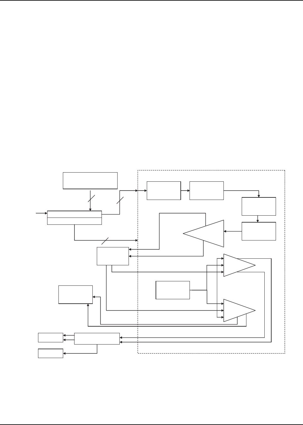
6871620L01-C May 28, 2008
Theory of Operation: VOCON Section 3-27
3.2.5.2 Receive Audio Path
Refer to Figure 3-11. The receive audio data comes from the Abacus III IC (DOUTA) to the dual-core
processor SRDB pin. The DSP decodes the data and sends it out through the CODEC_RX line to
the MAKO IC VC_RX pin. The CODEC filters, adds digital programmable gain G1, then converts the
digital data into an analog audio signal, which in turn is sent to programmable attenuator G3. The
signal is then sent through an internal programmable differential preamplifier (G4). The preamplifier
outputs are on pins VC_OUT_P and VC_OUT_M of the MAKO IC.
This output from the preamp is first filtered through the circuitries R1326, R1327, C1355, C1356 and
C1357, and then sent back to two independent internal BTL differential power amplifiers, G5 & G6, of
the MAKO IC. The power amplifiers are programmed to a fixed gain through the dual-core processor
SPI lines and PA control registers.
The dual-core processor selects whether the amplified audio is routed to the internal speaker or the
external speaker through the SPI lines based upon which amplifier is turned on as shown in the PA
control block. The output audio is routed on MAKO IC pins INT_SPKR_P and INT_SPKR_M for
internal and EXT_SPKR_P and EXT_SPKR_M for external speaker lines. The external audio is then
routed to an audio switch (U20) where it switches the audio between the flip earpiece and the audio
jack earpiece. The logic behind the audio routing is set by the Patriot IC (depending on the user's
operating mode).
Figure 3-11. VOCON Receive Audio Path
ABACUS III
Patriot SAP / BBP
Patriot SPIB
Digital
LPF = 3.4 kHz
CODEC
16-Bit
D/A
G1 Digital Gain
= 0 or 1 dB
G3
Attenuator
= -52 to 0 dB
G4
Preamp =
0 to 10 dB
HP & LP
Filter = 22kHz,
200 Hz
Internal Speaker
PA Control
G5
EXT PA
G6
INT PA
Audio Switch
Earpiece
Audio Jack
RX_SSI_FSYNC
RX_SSI_CLK
RX_DATA
CODEC_RX
CODEC_FSYNC
CODEC_DCLK
MAKO_CS
SPI_MISOB
SPI_MOSIB
SCKB
VC_OUT_P
VC_OUT_M
MAKO IC
PA_IN_M
PA_IN_P
33
4
May 28, 2008 6871620L01-C
3-28 Theory of Operation: VOCON Section
3.2.6 Radio Power-Up/Power-Down Sequence
The radio power up sequence begins with pressing the Power On button on the keypad. When the
button is pressed, the mechanical switch MECH_SW pin will be pulled low. If "MECH_SW = "0", and
BAT_7V5 pin is above the "Power Up Threshold", then MAKO IC will pull the FET_ENX pin to
GROUND, thus driving the gate of external P-MOSFET to low, enabling the P-MOSFETs (Q1301
and Q1302) to supply power to the MAKO IC as well as the RF transceiver section (UNSW_B+
supplies B+ to the VOCON section, SW_B+ and RF transceiver section, RFSW_B+).
With SW_B+ enabled, the VSW1 switched regulator will be ready and subsequently, other MAKO
regulators such as V1.875, V1.55, V2 and VCC5 are sequentially enabled and provide power to all
MAKO internal blocks and external systems including the microprocessor (Patriot), memory ICs and
radio RF circuits. The RESETX pin is asserted low for an additional 32ms once all DC regulators are
stable. It is then de-asserted, allowing the microprocessor to start.
In order to power-down the radio, the ON/OFF button has to be pressed for a specified
(programmable) duration (default setting set to 3 seconds). The ON/OFF circuitry will then pull
MECH_SW to high (MECH_SW = 1) and the MAKO IC starts an internal 125ms watchdog timer and
sets the shutdown interrupt flag which causes the INT_X interrupt output pin to assert low. The
microprocessor then determines (via SPI register access) that it must initiate the power-down
sequence. The watchdog timer will be refresh by the microprocessor via SPI to prevent it from timing
out. Upon expiration of the watch dog timer, MAKO will assert RESETX to turn-off all DC regulators
and de-asserts the FET_ENX pin which removes the SW_B+ and RFSW_B+ supplies, thus killing all
power to the radio.
Figure 3-12 and Table 3-5 show the radio ON/OFF circuitry and the radio ON/OFF operation truth
table. The truth table shown is based on a 3 second long press duration for radio power-off criteria.
Figure 3-12. Radio ON/OFF Circuitry
R1
R2
V2_FIL
R9922
1K
Q9906
ON_OFF_det
ON_OFF
5V_Misc
5V_Misc 5V_Misc
5V_Misc
5V_Misc
R9923
10K
C9953
0.10uF 0.10uF
0.10uF
0.10uF
0.10uF
0.10uF
0.10uF
Inverter
C9952 R9960
0
C9951
MECH_SW
D Flip-flop
C9969
C9954
U9918-1
U9918-2
C9980
Q9905
R9925
R9924
10K
10K
Patriot_ONOFF
R9926
1K
ON/OFF Circuitry
GPIO
1
2
4
OR Gate
U9902
U9901
GND VCC
4
1
1
2
2
3
4
35
GND VCC
GND
VCC
GND VCC
OUTY
INB
INA
R9927
30K
PR
D
CP
CLR
U9903
Q
Q‘
5
3
4
6
1
2
7
8
5
3
PWR_GND
AND Gate
6871620L01-C May 28, 2008
Theory of Operation: Encryption Module 3-29
3.3 Encryption Module
The encryption module connects directly to the VOCON section and interfaces directly with the
vocoder digital circuitry. It contains an independent microcontroller to perform digital, numerical,
encryption algorithms.
The encryption module is designed to digitally encrypt and decrypt voice and ASTRO data in ASTRO
XTS 4000 radios.
NOTE: The encryption modules are NOT serviceable. The information contained in this section is
only intended to help determine whether a problem is due to a encryption module or the radio
itself.
The encryption module uses a custom encryption IC and an encryption key variable to perform its
encode/decode function. The encryption key variable is loaded into the encryption module, via the
radio's CE connector, from a hand-held, key variable loader (KVL). The encryption IC corresponds to
the particular encryption algorithm purchased. Table 3-6 lists the encryption algorithms and their
corresponding kit numbers.
The encryption module operates from two power supplies (UNSW_B+ and SW_B+). The SW_B+ is
turned on and off by the radio's On/Off switch. The UNSW_B+ provides power to the encryption
module as long as the radio battery is in place.
Key variables are loaded into the encryption module. Depending on the type of encryption module,
up to 16 keys can be stored in the module at a time. The key can be infinite key retention or
30-seconds key retention, depending on how the codeplug is set up.
The radio' s host processor communicates with the encryption module on the Synchronous Serial
Interface (SSI) bus. The SSI bus consists of five signal lines. A communication failure between the
host processor and the secure module will be indicated as an ERROR 09/10 message on the
display.
To troubleshoot the encryption module, refer to the flowcharts in Chapter 5 “Troubleshooting Charts.”
Table 3-5. ON/OFF Operation Truth Table
Condition INVERTER
O/P (Pin 4)
AND GATE
INB (Pin 1)
AND GATE
INB (Pin 2)
AND GATE
O/P (Pin 4)
OR GATE
(Pin 1)
OR GATE
(Pin 2)
OR GATE
(Pin 4)
Mech
SW
Initial State00100000
Press ON11111011
Press<3 Sec11000001
Press=3 Sec11000110
Press>3 Sec11111110
Table 3-6. Encryption Module Software Kits and Algorithms
Software
Kit Number Algorithm
NNTN7056 ADP, AES
NNTN7057 ADP, DES-XL, OFB
NNTN7058 ADP, DVP-XL


6871620L01-C May 28, 2008
Troubleshooting Procedures: Handling Precautions 4-1
Chapter 4 Troubleshooting Procedures
The purpose of this chapter is to aid in troubleshooting problems with the ASTRO XTS 4000 radio. It
is intended to be detailed enough to localize the malfunctioning circuit and isolate the defective
component. It also contains a listing of service tools recommended for PC board repair at the
component level.
4.1 Handling Precautions
Complementary metal-oxide semiconductor (CMOS) devices, and other high-technology devices,
are used in this family of radios. While the attributes of these devices are many, their characteristics
make them susceptible to damage by electrostatic discharge (ESD) or high-voltage charges.
Damage can be latent, resulting in failures occurring weeks or months later. Therefore, special
precautions must be taken to prevent device damage during disassembly, troubleshooting, and
repair. Handling precautions are mandatory for this radio, and are especially important in low-
humidity conditions. DO NOT attempt to disassemble the radio without observing the following
handling precautions.
1. Eliminate static generators (plastics, Styrofoam, etc.) in the work area.
2. Remove nylon or double-knit polyester jackets, roll up long sleeves, and remove or tie back
loose-hanging neckties.
3. Store and transport all static-sensitive devices in ESD-protective containers.
4. Disconnect all power from the unit before ESD-sensitive components are removed or inserted
unless otherwise noted.
5. Use a static-safeguarded workstation, which can be accomplished through the use of an
anti-static kit. This kit includes a wrist strap, two GROUND cords, a static-control table mat
and a static-control floor mat.
Most of the ICs are static sensitive devices. Do not attempt to
disassemble the radio or troubleshoot a board without first
referring to the following Handling Precautions section.
!
C a u t i o n
May 28, 2008 6871620L01-C
4-2 Troubleshooting Procedures: Recommended Service Tools
4.2 Recommended Service Tools
Table 4-1 lists recommended service tools that can be used for PC board repairs at the component
level. For listings of additional service tools, service aids, and test equipment that are recommended
for all levels of service, refer to the XTS 4000 Basic Service Manual (see “ Related Publications” on
page x).
Table 4-1. Recommended Service Tools
Motorola
Part Number Description Application
RLN4062 Hot-air workstation, 120V Tool for hot-air soldering/desoldering of
surface-mounted integrated circuits
0180302E51 Master lens system
6684253C72 Straight prober
6680384A98 Brush
0180303E45 SMD tool kit (included with
R1319A)
R1319 ChipMaster (110 V) Surface-mount removal and assembly of
surface-mounted integrated circuits and/or
rework station shields. Includes 5 nozzles.
R1321 ChipMaster (220 V)
6680309B53 Rework equipment catalog Contains application notes, procedures,
and technical references used to rework
equipment
0182297T15 XTS 4000 Keyload Cable Used to load encryption key into radio.
Connects to radio's CE connector and
key-variable loader (KVL).
NKN1027 RS232 Cable Kit Connects radio to RLN-4460 Portable Test
Set for radio performance checks, and to
serial port on personal computer for CPS
programming and tuner alignments.
NKN1029 USB Cable Kit Connects radio to RLN-4460 Portable Test
Set for radio performance checks, and to
Universal Serial Bus (USB) port on
personal computer for CPS programming
and tuner alignments.
NNTN7151 Housing Eliminator Fixture that allows radio’s internal board to
be mounted externally. Provides easy
access to electronic circuits, required for
board-level troubleshooting.
NNTN7152 Regulated Battery Eliminator,
XTS 4000
Used in place of battery to connect radio
to an external power supply.
NNTN7153 SMA Conversion RF Adapter Adapts radio’s antenna port to RF cabling
of test equipment.
6871620L01-C May 28, 2008
Troubleshooting Procedures: Voltage Measurement and Signal Tracing 4-3
4.3 Voltage Measurement and Signal Tracing
It is always a good idea to check the battery voltage under load. This can be done by checking the
OPT_B+_VPP pin at the radio CE connector (pin 3). The battery voltage should remain at or above
7.0 Vdc. If the battery voltage is less than 7.0 Vdc, then it should be recharged or replaced as
necessary prior to analyzing the radio.
In most instances, the problem circuit may be identified using a multimeter, an RF millivoltmeter,
oscilloscope (preferably with 100 MHz bandwidth or more), and a spectrum analyzer.
RLN4460 Portable Test Set Used for radio performance checks.
Connects to radio’s CE connector and
allows remote switching and signal
injection/outputs for test equipment
measurements.
RVN4181 Customer Programming Software
(CPS) and Tuner Software
CPS allows customer-specific
programming of modes and features.
Tuner software required to perform
alignment of radio parameters. Can be
used for XTS 5000, XTS 4000 and
XTS 2500 products.
NOTE Parts U1401 and U1304 are not field repairable. For failures relating to U1401
and U1304, the mainboard has to be replaced.
When checking a transistor or module, either in or out of
circuit, do not use an ohmmeter having more than 1.5 Vdc
appearing across test leads or use an ohms scale of less than
x100.
Table 4-1. Recommended Service Tools (Continued)
Motorola
Part Number Description Application
!
C a u t i o n
May 28, 2008 6871620L01-C
4-4 Troubleshooting Procedures: Standard Bias Table
4.4 Standard Bias Table
Table 4-2 outlines some standard supply voltages and system clocks which should be present under
normal operation. These should be checked as a first step to any troubleshooting procedure.
Table 4-2. Standard Operating Bias
Signal Name Nominal Value Tolerance VOCON Board Source
24.576 MHz 24.576 MHz ±1000 ppm C1317
32.768 kHz 32.768 kHz ±400 ppm C1303
GATED_32_kHz 32.768 kHz ±400 ppm C1301
CKIH 16.8 MHz C1402
X_16.8 MHz 16.8 MHz R1418
POR 3.0 Vdc ±5% R1121
RESET_OUT 3.0 Vdc ±5% R1105
VSW1 3.85 Vdc ±5% R1319
RAWB+ 7.5 Vdc 6.0-9.0 Vdc C20
V2 2.9 Vdc ±5% C1324
BAT_7V5 7.5 Vdc 6.0-9.0 Vdc R1309
UNSW_B+ 7.5 Vdc 6.0-9.0 Vdc C1129
SW_B+ 7.5 Vdc 6.0-9.0 Vdc C1343
VCC5 5.0 Vdc ±5% C1319
V1.55 1.55 Vdc ±5% C1328
6871620L01-C May 28, 2008
Troubleshooting Procedures: Power-Up Self-Check Errors 4-5
4.5 Power-Up Self-Check Errors
Each time the radio is turned on, the MCU and DSP perform a series of internal diagnostics. These
diagnostics consist of checking such programmable devices as the FLASH ROMs, and SRAM
devices.
Problems detected during the power-up self-check routines are presented as error codes on the
radio’s display. For non-display radios, the problem is presented at power up by a single, low-
frequency tone. Table 4-3 lists possible error codes, a description of each error code, and a
recommended corrective action.
Table 4-3. Power-Up Self-Check Error Codes
Error
Code Description Corrective Action
01/02 FLASH ROM codeplug Checksum Non-Fatal Error Reprogram the codeplug
01/12 Security Partition Checksum Non-Fatal Error Send radio to depot
01/20 ABACUS Tune Failure Non-Fatal Error Turn radio off, then on
01/22 Tuning Codeplug Checksum Non-Fatal Error Send radio to depot
01/81 Host ROM Checksum Fatal Error Send radio to depot
01/82 FLASH ROM Codeplug Checksum Fatal Error Reprogram the codeplug
01/88 External RAM Fatal Error — Note: Not a checksum error Send radio to depot
01/90 General Hardware Failure Fatal Error Turn radio off, then on
01/92 Security Partition Checksum Fatal Error Send radio to depot
01/93 FLASHport Authentication Code Failure Send radio to depot
01/98 Internal RAM Fail Fatal Error Send radio to depot
01/A2 Tuning Codeplug Checksum Fatal Error Send radio to depot
02/81 DSP ROM Checksum Fatal Error Send radio to depot
02/88 DSP RAM Fatal Error — Note: Not a checksum error Turn radio off, then on
02/90 General DSP Hardware Failure (DSP startup message not
received correctly)
Turn radio off, then on
09/10 Secure Hardware Failure Turn radio off, then on
09/90 Secure Hardware Fatal Error Turn radio off, then on
May 28, 2008 6871620L01-C
4-6 Troubleshooting Procedures: Power-Up Self-Check Diagnostics and Repair (Not for Field Use)
4.6 Power-Up Self-Check Diagnostics and Repair (Not for Field Use)
Table 4-4 lists additional action items that can be used for the diagnosis and resolution of the error
codes listed in Table 4-3 on page 4-5.
Table 4-4. Power-Up Self-Check Diagnostic Actions
Error
Code Diagnostic Actions
01/02 This non-fatal error will likely recover if the radio's power is cycled. In the event that this
does not resolve the issue, the radio should be reflashed. As a last resort, the FLASH
ROM U1410 should be replaced.
01/12 The radio should be sent to the depot for reflashing of the security codeplug.
01/20 Cycling radio power should resolve this issue.
01/22 The radio should be sent to the depot for reflash of the tuning codeplug followed by
retuning of the radio.
01/81 The radio should be sent to the depot for reflashing of the host code.
01/82 The radio should be sent to the depot for reflashing of the radio codeplug.
01/88 Reflashing of the radio should first be performed. If this fails to resolve the issue, then
replacement of the SRAM U1409 is necessary.
01/90 Cycle power to radio. Continued failure indicates a likely IC failure (MAKO, PCIC,
ABACUS). In this event, radio should be sent to the depot for isolation and repair of the
problem IC.
01/92 The radio should be sent to the depot for reprogramming of the security codeplug.
01/93 The radio should be sent to the depot for reflashing of the host code.
01/98 Send radio to the depot for replacement of the SRAM U1409.
01/A2 The radio should be sent to the depot for reflashing of the tuning codeplug followed by
re-tuning of the radio.
02/81 The radio should be sent to the depot for examination and/or replacement of either the
FLASH U1410, or the PATRIOT MCU/DSP U1401.
02/88 Cycle power to the radio. If this does not fix the problem, then the radio should be sent
to the depot for reflashing of the DSP code. Continued failure requires examination and/
or replacement of the SRAM U1409.
02/90 Cycle power to the radio. If this fails to fix the problem, then the radio should be sent to
the depot for reflashing of the DSP code. Continued failure may require replacement of
U1401, the PATRIOT MCU/DSP.
09/10 Cycle power to the radio. If this fails then follow instructions in the secure hardware
failure troubleshooting flowchart.
09/90 Cycle power to the radio. If this fails then follow instructions in the secure hardware
failure troubleshooting flowchart.
6871620L01-C May 28, 2008
Troubleshooting Charts: List of Troubleshooting Charts 5-1
Chapter 5 Troubleshooting Charts
This section contains detailed troubleshooting flowcharts. These charts should be used as a guide in
determining the problem areas. They are not a substitute for knowledge of circuit operation and
astute troubleshooting techniques. It is advisable to refer to the related detailed circuit descriptions in
the theory of operation sections prior to troubleshooting a radio.
5.1 List of Troubleshooting Charts
Most troubleshooting charts (see Table 5-1) end up by pointing to an IC to replace. It is not always
noted, but it is good practice to verify supplies and GROUNDs to the affected IC and to trace
continuity to the malfunctioning signal and related circuitry before replacing any IC. For
instance, if a clock signal is not available at a destination, continuity from the source IC should be
checked before replacing the source IC.
Table 5-1. Troubleshooting Charts List
Chart Title Page No.
Main Troubleshooting Flowchart 5-2
Power-Up Failure 5-3
DC Supply Failure 5-6
Display Failure 5-10
Volume Set Error 5-13
Button Test 5-14
Top/Side Button Test 5-15
VCO TX/RX Unlock 5-16
VOCON TX Audio 5-17
VOCON RX Audio 5-19
RX RF 5-21
TX RF 5-26
Keyload Failure 5-29
Secure Hardware Failure 5-30
May 28, 2008 6871620L01-C
5-2 Troubleshooting Charts: Main Troubleshooting Flowchart
5.2 Main Troubleshooting Flowchart
Start
Is TX
Deviation
OK?
Go to
TX RF
flowchart
Go to
VOCON
RX Audio
flowchart
Receive
Audio?
Good
SINAD?
Buttons
Functional?
End
Go to either
Display Failure or
Power-Up Failure
flowchart
See Button
Test flowchart
Yes Yes
Yes
Yes
Yes
Yes
Yes
No
No
No
No
No
No
No
Good
power-up
Self-Test?
Error
Message?
See Table 4-3:
Power-up Self-
Check Error
Codes
Is there
TX Power?
Go to
TX RF
flowchart
6871620L01-C May 28, 2008
Troubleshooting Charts: Power-Up Failure 5-3
5.3 Power-Up Failure–Page 1
Verify Standard
Bias in
Table 4-2
Standard
Bias OK?
Probe
32.768 kHz
Clock at C1303
Verify intergrity
of C1305 &
C1306
Signal
Present?
Signal may appear
for a very short period
of time (50 ms). Use
an oscilloscope with
trigger to capture signal
Isolate and
Repair Problem
See DC Supply
Failure flowchart
Radio
Power-Up
Failure
1
2
No
Yes
No
Yes
May 28, 2008 6871620L01-C
5-4 Troubleshooting Charts: Power-Up Failure
Power-Up Failure–Page 2
Signal may
appear for a very
short period of
time (50ms). Use
an oscilloscope
with trigger to
capture signal
Probe
16.8 MHz
Signal at R1416
Investigate
16.8 MHz
Reference
Oscillator
Signal
greater than
1 Vp-p
Check
16.8 MHz
Signal at
C1402
This signal may
contain harmonics
and, therefore, may
not appear as a
perfect sinewave
Signal
greater than
1 Vp-p
Investigate
Clock Buffer
Components and
Isolate Problem
Refer Board to
Service Depot for
Reflash, Patriot,
SRAM, and
FLASH Analysis
No
No
Yes
Yes
1
6871620L01-C May 28, 2008
Troubleshooting Charts: Power-Up Failure 5-5
Power-Up Failure–Page 3
2
Components
OK ?
Replace
Problem
Component
Fixed? End
Replace
Y 1301
Fixed? Replace
Mainboard
Yes
Yes
Yes
No
No
No
May 28, 2008 6871620L01-C
5-6 Troubleshooting Charts: DC Supply Failure
5.4 DC Supply Failure–Page 1
NOTE: Since the failure of a critical voltage supply might cause the radio to automatically power
down, supply voltages should first be probed with a multimeter. If all the board voltages
are absent, then the voltage test point should be retested using a rising-edge-triggered
oscilloscope. If the voltage is still absent, then another voltage should be tested using the
oscilloscope. If that voltage is present, then the original voltage supply in question is
defective and requires investigation of associated circuitry.
Voltage =
5 Vdc
Yes
Problem With
DC Power
Disctribution
Check voltage at
pin 4, U1101
Voltage =
UNSW_B+ Check continuity of
Fuse F901
No Fuse OK? Replace Fuse
No
Yes
Check battery
connection for
good contact
Yes
Check voltage at
pin 5, U1101
Check D4,
VR1209, R1133
C1141
No
Components
OK?
Replace problem
components
No
Yes
Replace U1101
1
6871620L01-C May 28, 2008
Troubleshooting Charts: DC Supply Failure 5-7
DC Supply Failure–Page 2
Check voltage at pin
1,2,3,6,7 & 8 of Q1302
Voltage =
SWB+
7.5V +/-
20% ?
No
Yes
Check voltage at
R1311
(FET_ENX)
Voltage =
GND?
Check voltage at
R1320
No Replace Mainboard
Yes
Voltage =
SWB+?
No Check L1307,
L1308, R1320,
R1321, C1342 &
C1343
Component
= OK?
Replace problem
components
No
Check voltage at
C1337
Yes
Replace Q1302
Voltage =
?
No
Replace Mainboard
Yes
2
1
May 28, 2008 6871620L01-C
5-8 Troubleshooting Charts: DC Supply Failure
DC Supply Failure–Page 3
Check voltage at
R1319
Voltage =
3.8 Vdc +/-
5%?
Check L1306 &
C1333
Component
OK?
No
Yes No
Replace problem
components
Check R1318
Yes
Component
OK?
Check voltage
,
at L1304
Voltage =
1.875 Vdc
+/- 5%?
Check L1304,
C1330 & C1331
Component
OK?
No
Yes
Replace problem
components
No
Check voltage at
L1303
Yes
Yes
No
ReFLASH HOST
C Code Fixed ? END
Replace Mainboard
No
Voltage =
1.55 Vdc
+/- 5%?
Check L1303,
C1328 & C1329 Component
OK?
2
3
Replace problem
components
No
Yes
3
Check voltage, V2
at L1302
Yes
No
Yes
Voltage =
2.9 Vdc +/-
5%?
Check L1302,
C1324 & C1325 Component
OK?
Replace problem
components
No
Yes
3
Check voltage at
L1301
Voltage =
5.0 Vdc +/ -
5%?
Check L1301,
C1318, C1319 &
VR1206
Component
OK?
Replace problem
components
No
YES
3
4
Yes
No
No
Yes
3
Replace problem
components
6871620L01-C May 28, 2008
Troubleshooting Charts: DC Supply Failure 5-9
DC Supply Failure–Page 4
4
Check voltage at
C14
Voltage =
5.0 Vdc +/ -
5%?
Check Q4, E5, D1,
C10, C11, C12,
C14, Q1301 &
R1709
Component
OK?
Replace problem
components
No
Yes
No
Yes
Replace U1
Check voltage at
C27
Voltage =
3.0 Vdc +/-
5%?
Check L10, D3,
C25, C26, C27,
C28 & C30
Component
OK?
Replace problem
components
No
Yes
No
Yes
Replace U3
Check voltage at
C17
Voltage =
3.0 Vdc +/-
5%?
Check D2, C15,
C16, C17 & C9
Component
OK? Replace problem
components
No
Yes
No
Yes
Replace U2
END
May 28, 2008 6871620L01-C
5-10 Troubleshooting Charts: Display Failure
5.5 Display Failure–Page 1
Replace defective Display Module
in Front-Flip Assembly
Check integrity of
E1102 & E1103
-2.775 V< pin 24 <3.1 V?
-1.8 V< pin54 <1.96 V?
No Display
(Main or/and
CID Display)
Problem
Resolved?
No
No
Yes
Yes
Replace
E1102 or E1103
Verify V2 or V1.875
using
DC Supply Failure
flowchart
E1102 OK?
E1103 OK?
No
Yes
Check DC
on J1 pin 24
& pin 54
1
Test Display operation with
a known working
Front Flip Assembly
(with Working Display Module)
6871620L01-C May 28, 2008
Troubleshooting Charts: Display Failure 5-11
Display Failure–Page 2
J1-25 = 0V?
J1-37 = 1.875V?
J1-42 = 1.875V?
J1-44 = 0C?
Check DC at
J1-25, J1-37,
J1-42 & J1-44
No Yes
YesNo
No Yes
Yes
No
No
No
No
No
Yes
Yes
Yes
Yes
1
Problem
Resolved?
Problem
Resolved?
Problem
Resolved?
Problem
Resolved?
Probe signals at
J1-19, J1-23,
J1-39, J1-58
& J1-60
Check RESET
at J1, pin 33
Verify Signal
Path Integrity
and correct
Verify Signal
Path Integrity
and correct
Verify Signal
Path Integrity
and correct
Verify Signal
Path Integrity
and correct
Probe Display Date Lines
(J1-13, J1-15, J1-27, J1-29,
J1-35, J1-36, J1-38, J1-40,
J1-45, J1-47, J1-49, J1-51,
J1-53, J1-55, J1-57 & J1-59)
3
Any Digital data
or activity? End
End
End
End
V = 2.9V
+/- 20%?*
* per Standard Bias Table
Any Digital data
or activity?
May 28, 2008 6871620L01-C
5-12 Troubleshooting Charts: Display Failure
Display Failure–Page 3
Low-
Level Pulses
Present?
Check Active
Low Status on
RESET (J1-33)
Use an oscilloscope to check for
a low-level (0V) pulse occurrence
during power-on initialization period.
No
Yes
3
Check 60-pin Display
and Keypad Flex.
Replace if neccessary
Replace Mainboard
6871620L01-C May 28, 2008
Troubleshooting Charts: Volume Set Error 5-13
5.6 Volume Set Error
Volume
Set Error
Verify operation
of volume
Buttom Test
flow chart
Volume
button OK?
Refer to “No
Receive Audio”
flow chart
Yes
No
Yes
No
Yes
No
Using a voltmeter,
measure voltage at
C1106. The value
should be V2
Voltage
Functional? Replace
Mainboard
Replace Mainboard
to Top and Side
Control Flex J(3)
Volume
pot OK?
Replace
Volume control
button flex
Verify contact
with circuit
board
Any Digital data
or activity?
Synopsis
This chart relates to failure in the volume
button. Basic failure modes are as follows:
1) Bad connection
2) Defective volume control button
3) Detective MAKO IC U1304
4) Problem in receive audio circuit
May 28, 2008 6871620L01-C
5-14 Troubleshooting Charts: Button Test
5.7 Button Test
End Key s
correct?
Check signal
path integrity of
button in question
Button Test
Place radio in Test Mode.
Press Clear/Secure Button
so display reads CH TEST.
This places the radio in
Button Test Mode.
Then, press the orange
(Emergency) Button to
verify codes displayed
as shown in the Button
Table at right
No
Yes
This chat relates to a failure in the button functions.
Basic Failure modes are as follows:
1) Failure in Keypad Flex & Connectors within the
Front Flip Assembly
2) Failure in Top Control Flex & Connectors within the
Radio Chassis Assembly
3) Bad connections
4) Defective Patriot IC
Synopsis
Button Table
Button
PTT
Emergency Button
Clear/ Secure Button
Volume Up Button
Volume Down Button
Programmable Button
Code
1/ 0-1
3/ 0-1
96/ 0-1
80/ 0-1
81/ 0-1
98/ 0-1
* Note: The Button Test applies to all buttons
on the radio EXCEPT the ON/OFF button
on the keypad. This button solely serves
radio Power-Up/ Power-Down functionality.
ON/OFF
1 .,? 2ABC 3DEF
4GHI 5JKL 6MNO
7PRS 8TUV 9XYZ
128/0-1
132/0-1 133/0-1
97/0-1
135/0-1
131/0-1
130/0-1
136/0-1
129/0-1 134/0-1
49/0-1 50/0-1 51/0-1
*
0 #
55/0-1 56/0-1 57/0-1
58/0-1 48/0-1 59/0-1
52/0-1 53/0-1 54/0-1
ON/OFF
1 .,? 2ABC2ABC 3DEF3DEF
4GHI4GHI 5JKL5JKL 6MNO6MNO
7PRS 8TUV8TUV 9XYZ9XYZ
128/0-1
132/0-1 133/0-1
97/0-1
135/0-1
131/0-1
130/0-1
136/0-1
129/0-1 134/0-1
49/0-1 50/0-1 51/0-1
**
00 ##
55/0-1 56/0-1 57/0-1
58/0-1 48/0-1 59/0-1
52/0-1 53/0-1 54/0-1
6871620L01-C May 28, 2008
Troubleshooting Charts: Top/Side Button Test 5-15
5.8 Top/Side Button Test
Verify operation
of zone knob
using Button Test
flowchart
Top/Side Button
Test
Yes
Using RSS, verify
problem button is
enabled for
function
No
Button check
OK?
Buttons
enabled?
Using a voltmeter, measure the
voltage at U1305 pin 3 while
depressing the following buttons:
Emergency, Side Button 1,
Side Button 2, and Side Button 3.
The probe points are as follows:
Emergency Button 0.03V
Clear/Secure Button 1.40V
Programmable Button 2.20V
No Button Pressed 2.85V
Synopsis
This chart relates ro a failure in
reading the buttons: Emergency,
Side Button 1, Side Button 2, or
SIde Button 3.
Basic failure modes are as follows:
1) Failure in controls flex circuit
2) Bad connection
3) Defective Switch
4) Defective A/D port in GCAP II
Yes
Yes
No
Use RSS
to enable
button
Levels
Correct?
Replace U1305
No
No Verify physical
operation of
buttons
Buttons
OK? Replace Radio
Chassis Assembly
No
Verify connections
and Control Top/ PTT
flex circuit and repair
as necessary
Yes
Problem
Fixed? End
Yes
Replace
U1304
May 28, 2008 6871620L01-C
5-16 Troubleshooting Charts: VCO TX/RX Unlock
5.9 VCO TX/RX Unlock
VCO TX/RX
unlock
<0.6Vdc
>11.0Vdc or
drifting?
3V at C27?
Yes
Yes
Yes
No
No
No
No
No
Yes
Yes
Yes
Frequency
detected?
VCO locked?
No
Yes
No
5V at C14?
Check
VOCON Section
Check control
voltage at
Vctrl TESTPOINT
Check parts
around U1. If
OK, replace U1
Aux. line 3
high for TX
or low for RX
(VHF)?
Is unit
VHF?
Yes
Check parts
around U302.
If OK, replace
U302
Is pin 19
of VCOBIC
low for RX and
4.5V for TX?
Check parts
around Q310. If
OK, replace Q310
No
No
Yes
Yes
Aux. 3
for TX
and aux 2
for RX
(UHF)?
Is unit
UHF?
Yes
Check parts
around Q253 and
Q273.
If OK, replace
Q253 and Q273
Is Q273 = 4.5V
for TX and
Q253 = 4.5V for RX?
Check parts
around U3. If
OK, replace U3
Remove
VCO shield
Check parts
around U202. If
OK, replace U202
"Sniff"
frequency near
VCO shield
Check if VCO
is locked using
spectrum analyzer
Sniff: Using an inductive field probe
as an antenna to measure
frequency. Place the probe
approximately 1/2 inch away
from components to be sniffed.
6871620L01-C May 28, 2008
Troubleshooting Charts: VOCON TX Audio 5-17
5.10 VOCON TX Audio–Page 1
Inject a 200 mV
rms 1.0 kHz tone
to the test box
Audio In port
Repair connections
and/or replace flex
Connections
OK?
Problem
with Mic path
components?
No Problem
found.
End
Replace
appropriate
component
Is FM
deviation approx.
3.0 kHz?
Connect an
RLN4460A audio
test box (or equivalent)
to the radio CE
Connector
Radio has no
Transmitter Deviation
(VOCON Evaluation)
Inspect UCM-CE-Audiojack
Flex and Flex Connectors
(from Front Flip Assembly
to Mainboard)
Yes
No
Yes
Yes
No
12
No
Probe at
C1347
Verify Integrity
of Mic path up
to C1347
Is
1 kHz Signal
present?
No
Yes
May 28, 2008 6871620L01-C
5-18 Troubleshooting Charts: VOCON TX Audio
VOCON TX Audio–Page 2
Replace
Mainboard
Check
UCM-CE-Audiojack
Flex and Flex
Connectors
Go to
TX RF
flowchart
Clock
and Frame Sync
present?
Data
present at
CODEC_TX?
Use an oscilloscope to check the
SSI audio signals from the MAKO
(U1304). The following test points
are used for data collection:
CODEC_DCLK (R1335): 512 kHz Square Wave Clock
CODEC_TX (R1337): Audio Data Words
CODEC_FSYNC (R1336): 8 kHz Frame Sync Pulse
No
Yes
Yes
End
Problem
Resolved?
Yes
1
2
1
No
No
End
Repair connections
and/or
replace flex
Connections
OK?
Problem
Solved?
No
Yes
No
Yes
6871620L01-C May 28, 2008
Troubleshooting Charts: VOCON RX Audio 5-19
5.11 VOCON RX Audio–Page 1
Probe R1336 for
Frame Sync Signal,
Compare with
RX SAP waveform,
Trace 1
Frame
Sync
Present?
Replace
Mainboard
Probe R1338 for
Data, Compare
with RX SAP
waveform, Trace 2
Signal
Present?
THD <3%?
Clock
Present?
Probe R1335
for Clock Signal,
Compare with
RX SAP
waveform, Trace 3
Go to
RX RF
flowchart
Data
Present?
Check
Distortion of
Signal at C1355
Replace
Mainboard
Check Preamp
Output Signal at
C1355*
NoNo
No
No
No
Yes
Yes
Yes
Yes
1
Yes
Bad SINAD
Bad 20db Quieting
No Recovered Audio
Inject Standard
Input into
RF Jack J1704
A standard input is an
RF signal with a 1 kHz
tone modulated with 3 kHz
deviation in a 25 kHz channel.
* Note: The Preamp output signal
should be checked differently
across C1355.
May 28, 2008 6871620L01-C
5-20 Troubleshooting Charts: VOCON RX Audio
VOCON RX Audio–Page 2
Signal
Present?
Check Audio PA output
signal at VR1201
pins 1 & 4 (differential)
No
No
Yes
Yes
1
Distortion
>3%?
Check DC level,
V at R1328.
If V=7.50 +/- 1V,
then replace U1304.
Otherwise, verify R1328.
Check connector J2.
If no problems were found
on connector J2, check
UCM-CE-Audiojack flex.
6871620L01-C May 28, 2008
Troubleshooting Charts: RX RF 5-21
5.12 RX RF–Page 1
Frequency OK?
VHF: 44.85 MHz
UHF: 73.35 MHz
Inject a standard FM test signal into the
RF Jack J1704. Use SMA Conversion
RF Adapter NNTN7153A to inject the
test signal into RF Jack. Use CPS to
ensure that attenuator feature is disabled.
Use a spectrum analyzer and
high-impedance RF probe to
measure the IF signal
VHF: between L472 and L490
UHF: before L490
No
No
Yes
Yes
Poor RX
sensitivity or
no RX audio
Check
RXLO
Replace
bad part
Verify
SMA Conversion RF Adapter,
measure insertion loss
Visual
inspection
OK?
No
Yes
Bad RF Jack.
Replace mainboard
(Jack is not
serviceable)
Loss
< 0.2 db?
Replace
adapter
No
Yes
Inspect
RF Jack J1704
Measure RF
input level
at J1704 pin 3
Measure RF levels at C410,
compute SW_FL loss
RF level
about
-47 dBm?
No
Yes
SW_FL
loss < 2 dB?
Check
SW_FL
Yes
No
IF
level about
-38 dBm?
1
2
3 kHz FM deviation,
1 kHz rate, -47 dBm
May 28, 2008 6871620L01-C
5-22 Troubleshooting Charts: RX RF
RX RF–Page 2
Q551-c
= 5.0 Vdc?
No
No
No
Yes
Yes
Yes
Repair
Defects
Visual
examination
OK?
Check Voltage
Regulator U1
Q551-e
= 3.7 Vdc?
No
Yes
Replace
Q551
Replace
Q550
Remove SH11 and
inspect 2nd LO VCO
Signal
Present?
Remove SH04 and measure
2nd LO at C560 on
PCB side 2
No
No
Yes
Yes
LO Freq.
OK?
VHF: 42.6 MHz
UHF: 71.1 MHz
Measure
RX_SSI_CLK (R1123)
RX_SSI_FSYNC (R1125)
RX_SSI_DATA (R1124)
Observe
0 to 3 Vdc
digital signals
Measure
bit clock rate (Fbit)
at RX_SSI_CLK
Levels
OK?
1
3
5
No
Yes
RX_SSI_FSYNC =
20 kHz sync pulse
Fbit =
1.2 MHz? 4
No
Yes
No
Yes
RX_SSI_FSYNC
OK?
RX_SSI_DATA =
24-bit I, 24-bit Q,
8-bit AGC. AGC
varies with RF level
Go to
VOCON RX
AUDIO flowchart
RX_SSI_DATA
OK?
5
5
2nd LO, VHF: 42.6 MHz, UHF: 71.1 MHz
about 356 mVpp
2nd LO DC bias
6871620L01-C May 28, 2008
Troubleshooting Charts: RX RF 5-23
RX RF–Page 3
TP551
= 0 Vdc?
No
No
Yes
Yes
Repair
defects
Measure RF levels at
first preselector filter and
compute filter loss.
I/P C410, O/P L480
No
Yes
Loss < 3 db?
Measure RF levels at LNA
and compute LNA gain.
VHF: I/P L480, O/P C434
UHF: I/P L480, O/P C436
Measure RF levels at
second preselector filter and
compute filter loss.
VHF: I/P C450, O/P C455
UHF: I/P C426, O/P C427
Gain
about
+12 dB?
2
6
No
Yes
Measure RF and IF level at mixer
and compute mixer conversion gain.
VHF: RF I/P C470, IF O/P between
L472 & L490
UHF: RF I/P C470, IF O/P L490
Loss
< 3 dB? 8
No
Yes
Measure
control voltage
at TP551
No
Yes
Fvco
too low?
VHF: < 42.6 MHz
UHF: < 71.1 MHz
Remove SH11
and
inspect second LO VCO
TP551
= 5 Vdc?
3
5
5
No
Yes
Replace
Varactor D550
Check
LNA
Check
mixer
Visual
examination
OK?
No
Yes
Measure IF level at XTAL filter
and compute XTAL filter loss.
I/P between L472 & L490,
VHF: O/P C491
UHF: O/P C584
Mixer
gain about
3 dB?
No
Yes
No problem
found
Loss
< 4 dB? 7
TP551
(Vdc)
2nd LO
at C560
(MHz)
Fvco
1.10
3.10
42.6
47.1
VHF UHF
71.1
75.6
May 28, 2008 6871620L01-C
5-24 Troubleshooting Charts: RX RF
RX RF–Page 4
Yes
Fbit
< 1.2 MHz?
Measure
tuning voltage
(Vt) at R572
No
No
No
Yes
Yes
Vt= 3 Vdc?
Repair
defects
Replace
Varactor D570
Replace
Abacus
U500
Repair
defects
Visual
examination
OK?
4
Visual
examination
OK?
Inspect
components
surrounding
U500
No
Yes
5
5
No
Yes
Inspect clock
oscillator circuit at
U500-19, 20
Vt = 0 Vdc? 5
Clock
synthesizer
6871620L01-C May 28, 2008
Troubleshooting Charts: RX RF 5-25
RX RF–Page 5
Measure preselector filter
tuning voltage dac2 at
VHF: C413
UHF: C420
Replace IF filter.
VHF/ UHF: FL490
Repair
defects
68
Visual
inspection
OK?
Check IF filter and
LC matching networks.
No
Yes
Check discrete
preselector filters.
Replace
PCIC
Dac
voltages
OK?
Tune the radio across several
channels. Measure dac2,
proportional to frequency.
No
Yes
7
VHF
136
174
0.9
2.1
Band F (MHz) dac2 (Vdc)
UHF
380
470
0.9
3.1
May 28, 2008 6871620L01-C
5-26 Troubleshooting Charts: TX RF
5.13 TX RF–Page 1
No
Yes
No or low
TX power
Check
FGU
Frequency
OK?
No
Yes
Check
FGU
Level
about
3 dBm?
Measure RF level
at Q107 pin 1
Use a spectrum analyzer
and high-impedance RF
probe. Measure TXRF
at C101
Level about
+20 dBm?
No
No
Yes
Yes
Power 2W?
END
Measure RF Power at
RF Jack J1704
(via a Power Meter)
1
2
6871620L01-C May 28, 2008
Troubleshooting Charts: TX RF 5-27
TX RF–Page 2
RAWB+
about
7.2 Vdc?
Measure
RAWB+
at Q107-drain
No
No
No
Yes
Yes
Yes
Check
continuity
V.gate
VHF: about 3 to
4 Vdc?
UHF: 3 Vdc?
Check
continuity
DC bias is OK,
control is OK,
RFIN is OK,
PA has low gain
Replace
Q107
Measure RF
level at
pin 6 of Q107
No
Yes
Remove SH08
and check for
parts off pad
Level
about
+35 dBm?
Check parts under SH06.
If all parts are OK,
replace U102.
Measure gate bias
at C127
7.2 Vdc?
Measure
DC Level
at U102-6
No
No
Yes
Yes
7.2 Vdc?
Check
continuity
Check
continuity
Measure
Vgate at TP111,
normally 4 to
5 Vdc
Measure
DC Level at
U102-14
DC bias is OK,
control is OK,
RFIN is OK, driver
has low gain
Vgate
> 4 Vdc?
2
1
3
May 28, 2008 6871620L01-C
5-28 Troubleshooting Charts: TX RF
TX RF–Page 3
INT > 5 Vdc?
Vgate at TP111
is low (< 4 Vdc)
Measure INT
at TP104
Yes
No
No
Yes
Yes
No
Replace
Q101
INT is low.
Measure VLIM at
PCIC U104 pin 19
PCIC is
programmed.
Measure TEMP
at R135
Bad PCIC
Replace U104
VLIM
about 2 to
3 Vdc?
No
Yes
Measure
RFIN at
C128
TEMP
< 1.0 Vdc at
25C?
RFIN is low, INT
is low, bad PCIC,
replace U104
< 0.5 Vdc?
Low output power,
RFIN is high, check
Secoondary Cutback
circuit (Q102, RT150,
R120, R121, R122).
Repair defects.
Repair temperature
sensor circuit
(U103 & R135)
3
6871620L01-C May 28, 2008
Troubleshooting Charts: Keyload Failure 5-29
5.14 Keyload Failure
No
No
Yes
Yes
No
Keyload Failure
"KEYLOAD"
message
displayed?
With KVL attached to radio
and radio on, initiate a keyload
by pressing PTT on the
keyloader and look for activity
on testpoint LHDATA_KEYFAIL
Yes
Verify connection
across the
UCM-CE-Audio
Jack flex
Repair
connection
Correct
equipment?
Obtain correct
KVL and
cable
No
Verify and repair
connection of CE_CTS,
CE_RS232DIN_USB-,
and CE_OPT_SEL2 signals
from KVL to connector J2
Verify the use of the correct secure kit and key loader:
With KVL attached to
radio and radio on,
verify display
message "KEYLOAD"
Activity?
Verify connection
of testpoint
LHDATA_KEYFAIL
to R1354
Yes
No Good
connection?
Repair
connection
Replace
secure
module
Yes
Good
connection?
Replace
Mainboard
This failure relates to secure-
equipped radios and indicates a
failure to load key with the KVL
indicated by the message
"KEYFAIL" and key-fail tone.
Typical failure modes would be:
1) Open between UCM-CE-Audiojack
which places radio in Keyload mode.
2) Use of wrong KVL or KVL cable
for XTS 4000 radio.
3) Failure of secure module.
Synopsis
XTS 4000 UCM Kits:
Software Kits:
NNTN7056 - ADP, AES
NNTN7057 - ADP, DES-XL, OFB
NNTN7058 - ADP, DVP-XL
Use KVL - 3000 or later model Keyloader. Use with
cable 0182297T15.
May 28, 2008 6871620L01-C
5-30 Troubleshooting Charts: Secure Hardware Failure
5.15 Secure Hardware Failure
Yes
No
Yes
No
No
No
Fail
09/10 or 09/90
Secure Hardware
Failure
Connections
good?
Repair
connections
Yes Replace
secure
module
Verify electrical activity
at the following signals
at power up:
Connections
good?
Repair
opens
No
Yes Is
known good
module
available?
Replace module
with known good
one and retest
Verify connections
to secure module
through J2
Signals
good?
Yes
Replace
secure
module
Radio
functions with
known good
module?
Replace
Mainboard
This failure relates to secure-equipped
radios and indicates a power-up self-test failure
for the secure module. More specifically this
failure indicates a failure in communications
between the DSP and secure module. The
secure module is not considered field repairable
so troubleshooting is limited to verifying a
problem with the module and replacing.
Typical failure modes would be:
1) Open between secure module and VOCON
section at connector J2.
2) Failure of the SSI bus that the DSP uses to
communicate with the secure module.
3) Failure to get proper supplies and grounds
to J2.
Synopsis
Use ohmmeter to electrically
verify the following signal
connections to source IC:
Signal @ J2 Source
ENC_SSI_DI R1338
ENC_SSI_DO R1337
ENC_SSI_CLK R1335
RESET_ENC R1406
Verify bias of following signals:
Signal @ J701 Nominal Bias
FU_B+ 7.5VDC+/-1.0VDC
SW_B+ 7.5VDC+/-1.0VDC
GND GND Signal @ J701 Source
ENC_SSI_DI R1338
ENC_SSI_CLK R1335
6871620L01-C May 28, 2008
Troubleshooting Waveforms: List of Waveforms 6-1
Chapter 6 Troubleshooting Waveforms
This chapter contains images of waveforms that might be useful in verifying operation of certain parts
of the circuitry. These waveforms are for reference only; the actual data depicted will vary depending
on operating conditions.
6.1 List of Waveforms
Table 6-1 lists each waveform and the page on which the waveform can be found.
Table 6-1. List of Waveforms
Waveform Page No.
24.576 MHz Clock 6-2
16.8 MHz Buffer Input and Output 6-3
32.768 kHz Clock Outputs 6-4
Receive Serial Audio Port (SAP) 6-5
Receive Baseband Interface Port (RX BBP) 6-6
Transmit Baseband Interface Port (TX BBP) 6-7
May 28, 2008 6871620L01-C
6-2 Troubleshooting Waveforms: 24.576 MHz Clock
6.2 24.576 MHz Clock
24.576 MHz clock from Y1302.
Trace 1 (Channel 2): Trace recorded at C1317.
Figure 6-1. 24.576 MHz Clock Waveform
6871620L01-C May 28, 2008
Troubleshooting Waveforms: 16.8 MHz Buffer Input and Output 6-3
6.3 16.8 MHz Buffer Input and Output
Trace 1 (Channel 2): Buffer input at R1416.
Trace 2 (Channel 3): Buffer output at C1402.
Figure 6-2. 16.8 MHz Buffer Input and Output Waveforms
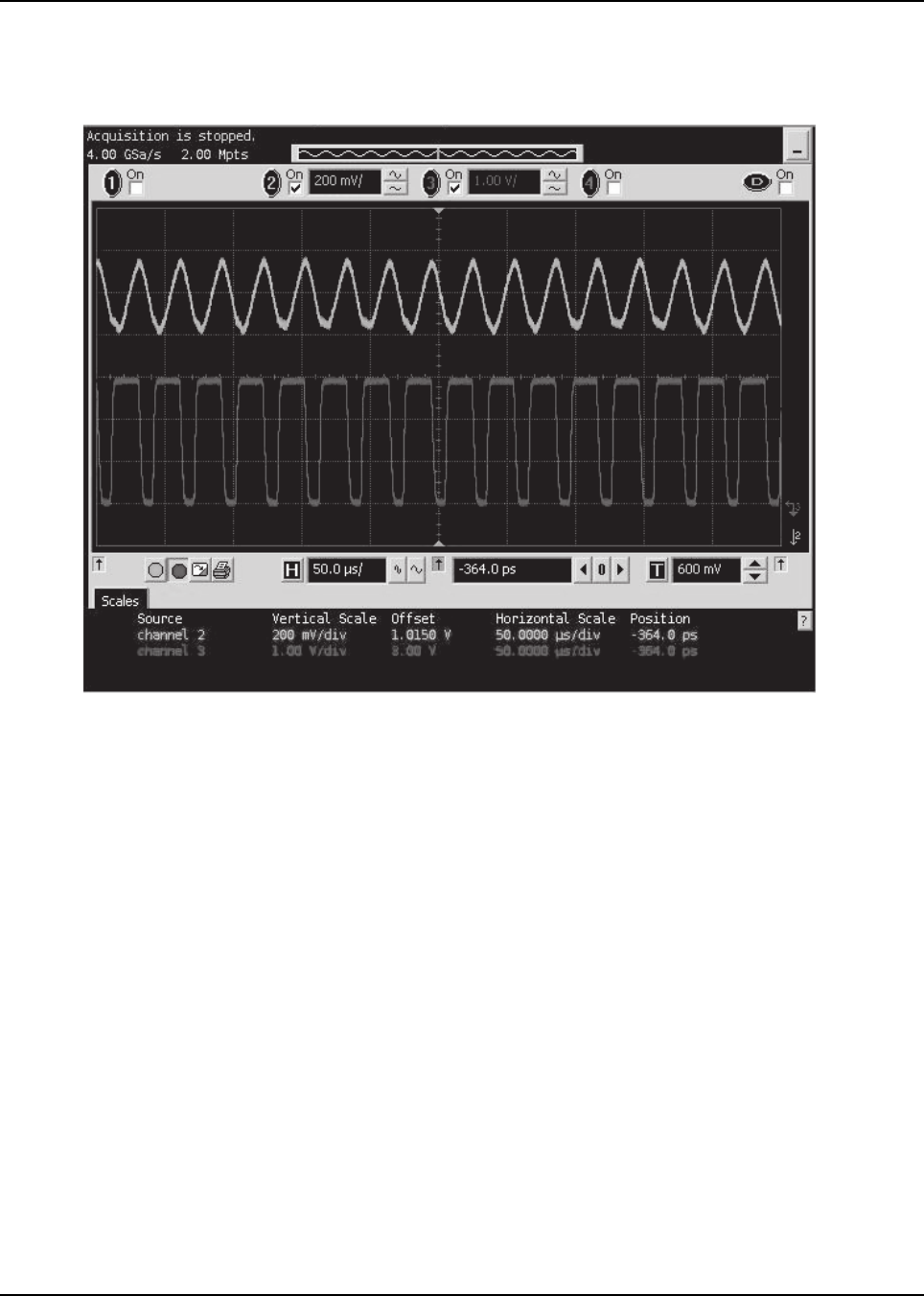
May 28, 2008 6871620L01-C
6-4 Troubleshooting Waveforms: 32.768 kHz Clock Outputs
6.4 32.768 kHz Clock Outputs
Trace 1 (Channel 2): Output at C1303 (from Y1301).
Trace 2 (Channel 3): Output at C1301 (to Patriot IC CKIL input).
Figure 6-3. 32.768 kHz Clock Outputs Waveforms
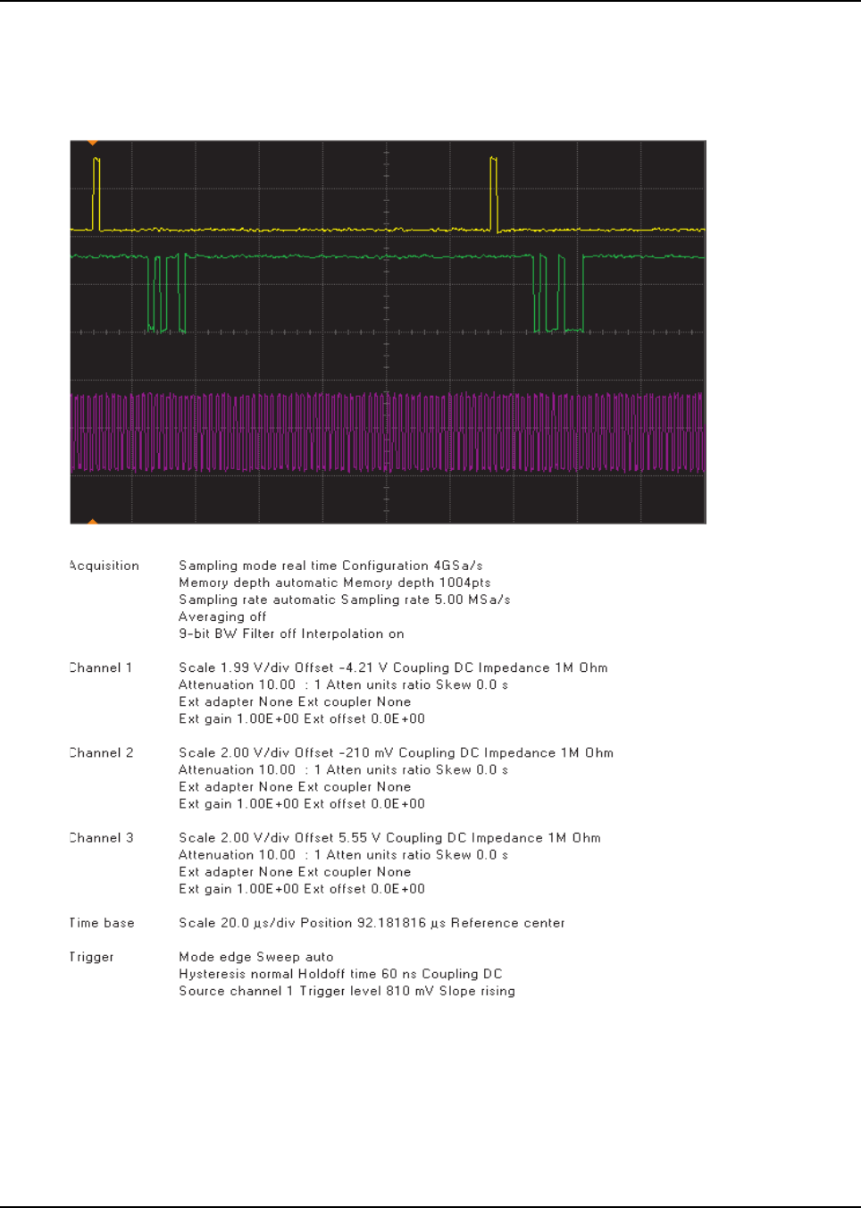
6871620L01-C May 28, 2008
Troubleshooting Waveforms: Receive Serial Audio Port (SAP) 6-5
6.5 Receive Serial Audio Port (SAP)
Trace 1: 8 kHz frame sync at R1336 (each word is 13 bits after failing edge of FSYNC).
Trace 2: SAP data at R1338 (audio data from MAKO IC CODEC to Patriot IC DSP).
Note: Transmit is identical, except data acquired at R1337.
Trace 3: 512 kHz bit clock at R1335.
Figure 6-4. Receive Serial Audio Port (SAP) Waveforms
MAEPF-27494-O
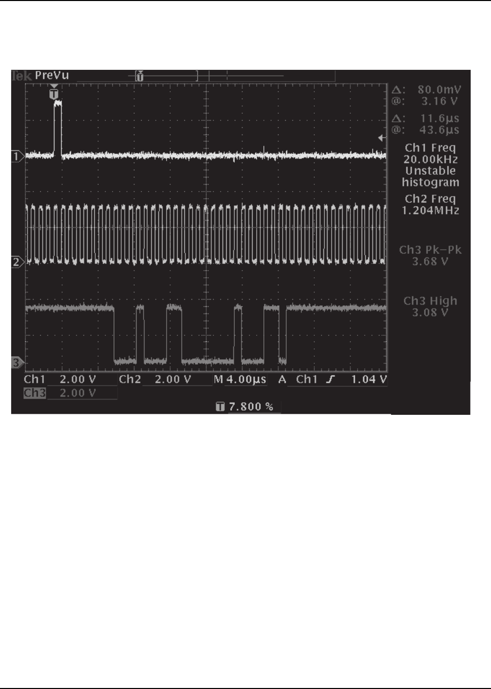
May 28, 2008 6871620L01-C
6-6 Troubleshooting Waveforms: Receive Baseband Interface Port (RX BBP)
6.6 Receive Baseband Interface Port (RX BBP)
Trace 1: BBP RX frame sync signal at R1111.
Trace 2: BBP RX clock signal at R1109.
Trace 3: BBP RX data signal at R1110.
Figure 6-5. Receive Baseband Interface Port (RX BBP) Waveforms
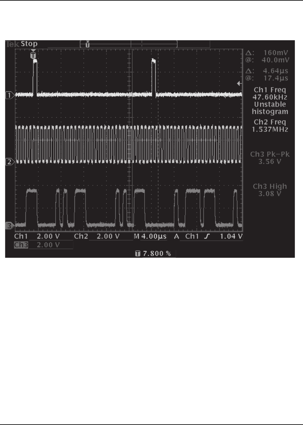
6871620L01-C May 28, 2008
Troubleshooting Waveforms: Transmit Baseband Interface Port (TX BBP) 6-7
6.7 Transmit Baseband Interface Port (TX BBP)
Trace 1: BBP TX frame sync signal at R1114.
Trace 2: BBP TX clock signal at R1112.
Trace 3: BBP TX data signal at R1113.
Figure 6-6. Transmit Baseband Interface Port (TX BBP) Waveforms

May 28, 2008 6871620L01-C
6-8 Troubleshooting Waveforms
Notes
6871620L01-C May 28, 2008
Troubleshooting Tables: List of Board and IC Signals 7-1
Chapter 7 Troubleshooting Tables
7.1 List of Board and IC Signals
Due to the nature of the schematic-generating program, signal names might be different when they
are not directly connected to the same point. The tables in this chapter provide a cross reference to
the various pinouts for these signals. Table 7-1 lists and provides links to each of the tables in this
chapter.
Table 7-1. List of Tables of Board and IC Signals
Table No. Table Name Page No.
7-2 J1 Mainboard to Keypad Flex and Display Module 7-2
7-3 J2 Mainboard to UCM, CE and Audio Jack Board 7-4
7-4 J3 Mainboard to Top and Side Control Flex 7-5
7-5 U1410 FLASH Pinouts 7-6
7-6 U1409 SRAM Pinouts 7-8
7-7 U1401 Patriot MCU/DSP IC Pinouts 7-10
7-8 U1304 MAKO Pinouts 7-19
May 28, 2008 6871620L01-C
7-2 Troubleshooting Tables: List of Board and IC Signals
Table 7-2. J1 Mainboard to Keypad Flex and Display Module
J1 Pin
No. Description To/From
Accessible
on
Mainboard?
1 GND GROUND No
2 GND GROUND No
3 GND GROUND No
4 UC_KP_ROW6 C1107 Yes
5 NC No Connect No
6 UC_KP_ROW5 C1108 Yes
7 NC No Connect No
8 UC_KP_ROW4 C1109 Yes
9 GND GROUND No
10 UC_KP_ROW3 C1110 Yes
11 GND GROUND No
12 UC_KP_ROW2 C1111 Yes
13 COV_D14 E1124 Yes
14 UC_KP_ROW1 C1112 Yes
15 COV_D13 E1123 Yes
16 UC_KP_ROW0 C1113 Yes
17 GND GROUND No
18 UC_KP_COLUMN2 C1114 Yes
19 DISP_REG_SEL_A1 E1126 Yes
20 UC_KP_COLUMN1 C1115 Yes
21 VOUT No Connect No
22 UC_KP_COLUMN0 C1116 Yes
23 DISP_CS_SUB E1127 Yes
24 V2.9 E1103 Yes
25 DISP_CS_MAIN R9902 Yes
26 FLIP_SENSE R1106 Yes
27 COV_D3 E1113 Yes
28 KP_PROG_BUTTON R9914 Yes
29 COV_D4 E1114 Yes
30 UC_KP_LEDK R9909 Yes
6871620L01-C May 28, 2008
Troubleshooting Tables: List of Board and IC Signals 7-3
31 DISP_ID No Connect No
32 UC_KP_5V1 5V_MISC Yes
33 DISP_RESET D1000 Yes
34 UC_KP_ONOFF R9923 Yes
35 COV_D0 E1110 Yes
36 COV_D5 E1115 Yes
37 E_SUB R9917 Yes
38 COV_D6 E1116 Yes
39 E_MAIN R1467 Yes
40 COV_D7 E1117 Yes
41 GND GROUND No
42 IM0 R9904 Yes
43 GND GROUND No
44 IM1 R9919 Yes
45 COV_D12 E1122 Yes
46 LEDK R9912 Yes
47 COV_D11 E1121 Yes
48 LEDA 5V_MISC Yes
49 COV_D10 E1120 Yes
50 EAR+ Pin 5 of U20 Yes
51 COV_D8 E1118 Yes
52 EAR- Pin 7 of U20 Yes
53 COV_D9 E1119 Yes
54 DISP_V1.875 C9970 Yes
55 COV_D1 E1111 Yes
56 DISP_V2.9 E1103 Yes
57 COV_D2 E1112 Yes
58 DISP_R_W E1129 Yes
59 COV_D15 E1125 Yes
60 DISP_REG_SEL_A0 E1130 Yes
Table 7-2. J1 Mainboard to Keypad Flex and Display Module (Continued)
J1 Pin
No. Description To/From
Accessible
on
Mainboard?

May 28, 2008 6871620L01-C
7-4 Troubleshooting Tables: List of Board and IC Signals
Table 7-3. J2 Mainboard to UCM, CE and Audio Jack Board
J2
Pin No. Description To/From
Accessible
on
Mainboard?
1 GND GROUND No
2FU_B+ F901 Yes
3 GND GROUND No
4 UC_KEYFAIL_LH_BDMDATA R1344 Yes
5 UC_WAKEUP Pin N3 of U1401 No
6SW_B+ C1118 Yes
7 UC_INT_MIC C73 Yes
8 UC_INT_SPKR+ C72 Yes
9 UC_INT_SPKR- C71 Yes
10 V_VIBE R735 Yes
11 UC_UCM_SS R1101 Yes
12 UC_ENC_SSI_CLK R1335 Yes
13 UC_ENC_SSI_DI R1338 Yes
14 UC_ENC_SSI_DO R1337 Yes
15 CE_OPT_SEL2 OPTSEL2 (TP) Yes
16 CE_OPTB+_VPP OPTB+_VPP (TP) Yes
17 CE_RS232DOUT_USB+ RS232DOUT (TP) Yes
18 CE_RS232DOUT_USB- RS232DIN (TP) Yes
19 CE_CTS CTS (TP) Yes
20 CE_RTS RTS (TP) Yes
21 CE_OPT_SEL1 C55 Yes
22 UC_RESET_ENC R1406 Yes
23 CE_LHDATA_KEYFAIL LHDATA_KEYFAIL (TP) Yes
24 CE_SPKRCOM SPKR_COM (TP) Yes
25 CE_SPKR+ SPK+ (TP) Yes
26 AUD_JACK_MIC EXT_MIC (TP) Yes
27 AUD_JACK_SPKR_OUT R9999 Yes
28 AUD_JACK_PTT C53 Yes
29 AUD_JACK_INT R9998 Yes
30 GND GROUND No
6871620L01-C May 28, 2008
Troubleshooting Tables: List of Board and IC Signals 7-5
Table 7-4. J3 Mainboard to Top and Side Control Flex
J3 Pin
No. Description To/From
Accessible
on
Mainboard?
1 UC_EMERG R9913 Yes
2 SECURE R9914 Yes
3 SIDE_BUTTON R9914 Yes
4 UC_INT_PTT C1220 Yes
5 UC_KP_ROW7 C1106 Yes
6 UC_KP_COLUMN1 C1115 Yes
7 UC_KP_COLUMN2 C1114 Yes
8 GND GROUND No
9 GND GROUND No
10 GND GROUND No
11 GND GROUND No
12 GND GROUND No
13 GND GROUND No
14 GND GROUND No
15 GND GROUND No
16 GND GROUND No
May 28, 2008 6871620L01-C
7-6 Troubleshooting Tables: List of Board and IC Signals
Table 7-5. U1410 FLASH Pinouts
U1410
Pin No. Description To/From Comment
Accessible
on
Mainboard?
B4 CLK No
E7 EN_CE No
F8 EN_OE No
C5 EN_WE No
D6 WP GROUND No
C4 ADV No
B5 RESET D1401, pin 2 1.875V Yes
E8 Address 0 E1126 Yes
D8 Address 1 No
C8 Address 2 No
B8 Address 3 No
A8 Address 4 No
B7 Address 5 No
A7 Address 6 No
C7 Address 7 No
A2 Address 8 No
B2 Address 9 No
C2 Address 10 No
A1 Address 11 No
B1 Address 12 No
C1 Address 13 No
D2 Address 14 No
D1 Address 15 No
D4 Address 16 No
B6 Address 17 No
A6 Address 18 No
C6 Address 19 No
B3 Address 20 No
C3 Address 21 No
D7 Address 22 R1423 Yes

6871620L01-C May 28, 2008
Troubleshooting Tables: List of Board and IC Signals 7-7
A3 GND GROUND No
F1 GND GROUND No
G2 GND GROUND No
G8 GND GROUND No
E2 Data 15 E1110 Yes
F2 Data 14 E1111 Yes
F3 Data 13 E1112 Yes
D5 Data 12 E1113 Yes
F4 Data 11 E1114 Yes
F5 Data 10 E1115 Yes
F6 Data 9 E1116 Yes
G7 Data 8 E1117 Yes
G1 Data 7 E1118 Yes
E3 Data 6 E1119 Yes
G3 Data 5 E1120 Yes
E4 Data 4 E1121 Yes
G5 Data 3 E1122 Yes
E5 Data 2 E1123 Yes
E6 Data 1 E1124 Yes
F7 Data 0 E1125 Yes
D3 WAIT E1126 Yes
A5 VPP Pin 1 of D1402 1.875V Yes
G6 VCCQ2 C1431 1.875V Yes
E1 VCCQ1 C1431 1.875V Yes
G4 VCC2 C1431 1.875V Yes
A4 VCC1 C1431 1.875V Yes
Table 7-5. U1410 FLASH Pinouts (Continued)
U1410
Pin No. Description To/From Comment
Accessible
on
Mainboard?
May 28, 2008 6871620L01-C
7-8 Troubleshooting Tables: List of Board and IC Signals
Table 7-6. U1409 SRAM Pinouts
U1409
Pin No. Description To/From Comment
Accessible
on
Mainboard?
A1 EN_BLE No
A2 EN_OE No
B2 EN_BHE No
B5 EN_CE No
G5 EN_WE No
A6 CE2 R1422 1.875V Yes
A3 Address 0 E1130 Yes
A4 Address 1 E1126 Yes
A5 Address 2 No
B3 Address 3 No
B4 Address 4 No
C3 Address 5 No
C4 Address 6 No
D4 Address 7 No
H2 Address 8 No
H3 Address 9 No
H4 Address 10 No
H5 Address 11 No
G3 Address 12 No
G4 Address 13 No
F3 Address 14 No
F4 Address 15 No
E4 Address 16 No
D3 Address 17 No
H1 Address 18 R1421 Yes
D1 VSS GROUND No
E6 VSSQ GROUND No
H6 NC2 R1708 Yes
G2 NC1 R1438 Yes
E3 DNU R9990 Yes
6871620L01-C May 28, 2008
Troubleshooting Tables: List of Board and IC Signals 7-9
G1 Data 15 E1125 Yes
F1 Data 14 E1124 Yes
F2 Data 13 E1123 Yes
E2 Data 12 E1122 Yes
D2 Data 11 E1121 Yes
C2 Data 10 E1120 Yes
C1 Data 9 E1119 Yes
B1 Data 8 E1118 Yes
G6 Data 7 E1117 Yes
F6 Data 6 E1116 Yes
F5 Data 5 E1115 Yes
E5 Data 4 E1114 Yes
D5 Data 3 E1113 Yes
C6 Data 2 E1112 Yes
C5 Data 1 E1111 Yes
B6 Data 0 E1110 Yes
D6 VCCQ R1440 1.875V Yes
E1 VCC R1440 1.875V Yes
Table 7-6. U1409 SRAM Pinouts (Continued)
U1409
Pin No. Description To/From Comment
Accessible
on
Mainboard?
May 28, 2008 6871620L01-C
7-10 Troubleshooting Tables: List of Board and IC Signals
Table 7-7. U1401 Patriot MCU/DSP IC Pinouts
U1401
Pin No. Description To/From Comment
Accessible
on
Mainboard?
N22 Not Connect No
R20 Not Connect No
C18 Not Connect No
C16 SIM_PD1_PB15_DSP_DB
G_PAW
R1401 2.89V Yes
M2 ONE_WIRE_UP R1339 Yes
C3 32K_SEL Pin 6 of U1301 Yes
U2 INT_PTT R1215 Active Low Yes
U3 MAKO_INT*MAKO_INT (TP)*MAKO Interrupt Yes
T7 OPT_SEL1_IN Pin 1 of U1201 Yes
V4 Not Connect No Connect No
G21 INT4_PA6_OPTION_SELE
CT_1_IC1A
Pin 2 of U1406 Yes
G22 INT45_PA7_OPTION_SEL
ECT_2_IC1B
Pin 9 of U1201 Yes
R4 KP_ROW0 C1113 Yes
R3 KP_ROW1 C1112 Yes
R7 KP_ROW2 C1111 Yes
T8 KP_ROW3 C1110 Yes
T4 KP_ROW4 C1109 Yes
T2 KP_ROW5 C1108 Yes
T3 KP_ROW6 C1107 Yes
U4 KP_ROW7 C1106 Yes
M3 KP_COL0 C1116 Yes
N4 KP_COL1 C1115 Yes
N22 KP_COL2 C1114 Yes
N7 ENC_RESET R1406 Yes
P3 BOOT*R1403 Yes
N3 WAKEUP Pin 5 of J2 No
P4 SPARE2_ENC_PTT R1404 Yes
P7 COV_DISP_ID No Connect No
B7 VIBRATE_CONT R731 Yes
6871620L01-C May 28, 2008
Troubleshooting Tables: List of Board and IC Signals 7-11
D8 HAB_MOD R1221 Yes
G8 MISOA_SEL Pin 2 of U1406 Yes
B8 Patriot_ONOFF R9924 Yes
G4 ON_OFF_det R9922 Yes
G2 FLIP_SENSE R1106 Yes
G3 LOCK_DET R1122 Yes
H7 DISP_BRIGHT2 C1104 Yes
F4 Not Connect No
F3 KP_BLEN R9911 Yes
E4 GPIO Pin 2 of U9918 Yes
E3 Not Connect No
C9 Not Connect No
D9 Not Connect No
D10 Not Connect No
C10 Not Connect No
C4 DISP_BRIGHT1 R9905 Yes
D17 Not Connect No
C17 RS232_USB*R1341 Yes
D18 RX_SSI_CLK R1109 1.204 MHz Yes
C19 OPT_SEL2_OUT R1231 Yes
P17 Not Connect No
N21 Not Connect No
P20 Not Connect No
N20 Not Connect No
G16 Q7VDD V1.55 1.55V Yes
G11 Q6VDD V1.55 1.55V Yes
N17 Q2_Q8VDD V1.55 1.55V Yes
U12 Q4VDD V1.55 1.55V Yes
M7 Q3_Q1VDD V2 1.55V Yes
G17 PVDD V2 2.89V Yes
Table 7-7. U1401 Patriot MCU/DSP IC Pinouts (Continued)
U1401
Pin No. Description To/From Comment
Accessible
on
Mainboard?

May 28, 2008 6871620L01-C
7-12 Troubleshooting Tables: List of Board and IC Signals
H17 LVDD V2 2.89V Yes
L7 KVDD V2 2.89V Yes
R8 J2VDD V2 2.89V Yes
N8 J1VDD V2 2.89V Yes
J7 I2VDD V2 2.89V Yes
G7 I1VDD V2 2.89V Yes
G9 H2VDD V2 2.89V Yes
G10 H1VDD V2 2.89V Yes
G13 EVDD V2 2.89V Yes
T17 DVDD V2 2.89V Yes
G15 C2VDD V2 2.89V Yes
J17 C1VDD V2 2.89V Yes
M17 B2VDD V2 2.89V Yes
R17 B1VDD V2 2.89V Yes
U17 A5VDD V1.875 1.875V Yes
U15 A4VDD V1.875 1.875V Yes
U13 A3VDD V1.875 1.875V Yes
U9 A2VDD V1.875 1.875V Yes
U8 A1VDD V1.875 1.875V Yes
C2 VCCA V1.55 1.55V Yes
D2 GNDA GROUND No
T10 A1VSS GROUND No
T11 A2VSS GROUND No
T14 A3VSS GROUND No
U16 A4VSS GROUND No
T15 A5VSS GROUND No
N16 B1VSS GROUND No
K16 B2VSS GROUND No
J16 C1VSS GROUND No
H13 C2VSS GROUND No
Table 7-7. U1401 Patriot MCU/DSP IC Pinouts (Continued)
U1401
Pin No. Description To/From Comment
Accessible
on
Mainboard?
6871620L01-C May 28, 2008
Troubleshooting Tables: List of Board and IC Signals 7-13
P16 DVSS GROUND No
H12 EVSS GROUND No
H10 H1VSS GROUND No
H8 H2VSS GROUND No
J8 I1VSS GROUND No
L8 I2VSS GROUND No
P8 J1VSS GROUND No
T9 J2VSS GROUND No
H9 VSS1 GROUND No
L16 VSS2 GROUND No
H16 LVSS GROUND No
H15 PVSS GROUND No
M8 K_QVSS GROUND No
T12 Q4VSS GROUND No
M16 Q2_Q8VSS GROUND No
H11 Q6VSS GROUND No
H14 Q7VSS GROUND No
U20 URXD1_USB_VMI Pin C9 of U1304 No
T21 URTS1_XRXD URTS1_XRXD (TP)*Yes
H22 AUDIO_JACK_PTT C53 Yes
F21 URXD2 Pin 4 of U1306 Yes
B20 BSY_IN_RTS Pin C12 of U1304 No
B13 RX_SSI_DATA R1124 Data from
Abacus to DSP
Yes
B12 TX_SSI_CLK R1112 1.537 Mhz Yes
C12 TX_SSI_FSYNC R1114 Yes
T22 CODEC_TX R1337 TX Audio to
DSP
Yes
P21 CODEC_DCLK R1335 512 kHz Yes
T20 CODEC_FSYNC R1336 8 kHz Pulse Yes
D7 SPI_MISOA Pin 4 of U1404 SPI A Data Out No
Table 7-7. U1401 Patriot MCU/DSP IC Pinouts (Continued)
U1401
Pin No. Description To/From Comment
Accessible
on
Mainboard?
May 28, 2008 6871620L01-C
7-14 Troubleshooting Tables: List of Board and IC Signals
H2 SPI_MISOB Pin C6 of U1304 SPI B Data Out No
C7 ABACUS3_CS Pin 25 of U500 Yes
C6 AD_CS R1120 Yes
C5 EEPROM_SEL No Connect No
B4 ADTRIG Pin B11 of U1304 No
D5 AUDIO_SW C1216 Yes
K7 UNI_SEL R1118 Yes
K3 Not Connect No Connect No
K8 MAKO_CE R1334 Yes
J4 D_REG_SEL No Connect No
J3 D_CS No Connect No
H3 SCKB Pin E6 of U1304 SPI B Clock No
H4 SPI_MOSIB Pin B6 of U1304 SPI B Data No
C8 SCKA R1115 SPI A Clock Yes
D6 MOSIA Pin 2 of U1405 SPI A Data Yes
M21 UCM_SS_BRAVO R1101 Yes
M22 OPT_SEL1_OUT C1221 Yes
R21 CODEC_RX R1338 RX Audio from
DSP
Yes
C13 RX_SSI_FSYNC R1111 Yes
D13 RX_SSI_CLK R1109 1.204 MHz Yes
G12 TX_SSI_DATA R1113 Yes
B21 BSY_OUT_CTS Pin E11 of U1304 Yes
F20 UTXD2 Pin E9 of U1304 Yes
G20 USB_SUSP No Connect No
H21 BOOT_NORM R1342 Yes
H20 AUDIO_JACK_INT R9998 Yes
J21 UCTS1_USB_SPEED Pin B10 of U1304 No
T16 UTXD1_USB_VPO UTXD1_USB_VPO (TP)*Yes
Y22 CKO CKO (TP)*Yes
R16 USB_VMO Pin D8 of U1304 No
Table 7-7. U1401 Patriot MCU/DSP IC Pinouts (Continued)
U1401
Pin No. Description To/From Comment
Accessible
on
Mainboard?

6871620L01-C May 28, 2008
Troubleshooting Tables: List of Board and IC Signals 7-15
U22 USB_TXENAB Pin B8 of U1304 No
B3 CODEC_FSYNC R1411 Yes
L20 NC No Connect No
Y3 MAKO_RESET C1425 Yes
K20 NC No Connect No
W4 OC3_PC13_FRAME_TICK R1412 Yes
D3 CKIH_VOCON C1402 16.8 MHz Yes
V3 GATED_32_KHZ C1301 32.768 kHz
Square Wave
Yes
J20 NC No Connect No
U7 MOD R1224 Yes
D14 TEST No Connect No
K4 MMC_OD_EN No Connect No
L3 MMC_CMD No Connect No
L20 MMC_DAT No Connect No
L4 MMC_CLK No Connect No
D22 CLKGPS R1466 Yes
D21 PECLREF R1465 Yes
C22 MAG R1464 Yes
C21 SIGN R1463 Yes
E21 CLKACQ R1462 Yes
C20 NC No Connect No
D19 NC No Connect No
E20 NC No Connect No
B11 ONE_WIRE_EN No Connect No
K17 KVL_USB_DET Pin D10 of U1304 No
K21 16out 16out (TP)*Yes
Y22 BAT_BUS_EN No Connect No
W3 USB_ENUM No Connect No
L17 RESET Pin 1 of D1401 Yes
AA2 USB_VPI Pin B9 of U1304 No
Table 7-7. U1401 Patriot MCU/DSP IC Pinouts (Continued)
U1401
Pin No. Description To/From Comment
Accessible
on
Mainboard?
May 28, 2008 6871620L01-C
7-16 Troubleshooting Tables: List of Board and IC Signals
L21 BL_FREQ No Connect No
L22 NC No Connect No
G14 DSP_DE DSP_DE (TP)*JTAG Yes
C14 MCU_DE MCU_DE (TP)*JTAG Yes
D15 TCK TCK (TP)*JTAG Yes
C15 TMS TMS (TP)*JTAG Yes
D16 TRST TRST (TP)*JTAG Yes
B16 TDO TDO (TP)*JTAG Yes
B17 TDI TDI (TP)*JTAG Yes
Y17 Address 0 E1130 Yes
AA17 Address 1 E1126 Yes
AB17 Address 2 No
AB16 Address 3 No
AB21 Address 4 No
Y16 Address 5 No
AA15 Address 6 No
AA19 Address 7 No
Y15 Address 8 No
Y14 Address 9 No
Y13 Address 10 No
AA14 Address 11 No
AB13 Address 12 No
AA13 Address 13 No
Y13 Address 14 No
AB12 Address 15 No
AA12 Address 16 No
AB11 Address 17 No
AA11 Address 18 No
Y11 Address 19 No
Y10 Address 20 No
Table 7-7. U1401 Patriot MCU/DSP IC Pinouts (Continued)
U1401
Pin No. Description To/From Comment
Accessible
on
Mainboard?

6871620L01-C May 28, 2008
Troubleshooting Tables: List of Board and IC Signals 7-17
AA10 Address 21 No
U11 Address 22 No
U10 Address 23 No
AB3 Data 15 E1125 Yes
AA3 Data 14 E1124 Yes
AB4 Data 13 E1123 Yes
AA4 Data 12 E1122 Yes
Y5 Data 11 E1121 Yes
AA5 Data 10 E1120 Yes
AA6 Data 9 E1119 Yes
Y6 Data 8 E1118 Yes
Y7 Data 7 E1117 Yes
AA7 Data 6 E1116 Yes
AB7 Data 5 E1115 Yes
AB8 Data 4 E1114 Yes
AA8 Data 3 E1113 Yes
Y8 Data 2 E1112 Yes
Y9 Data 1 E1111 Yes
AA9 Data 0 E1110 Yes
Y18 R_W_N E1129 Yes
U14 CS5 R1467 Yes
Y19 CS4_N No Connect No
AA20 CS3_N E1127 Yes
AB20 CS2_N Pin B4 of U1409 No
AA16 CS1_N No Connect No
AA21 CS0_N Pin E7 of U1410 No
U21 OE_N Pin A2 of U1409 No
V21 EB1_N Pin A1 of U1409 No
AA18 EB0_N Pin B2 of U1409 No
V20 SEB_N_PA5 No Connect No
Table 7-7. U1401 Patriot MCU/DSP IC Pinouts (Continued)
U1401
Pin No. Description To/From Comment
Accessible
on
Mainboard?

May 28, 2008 6871620L01-C
7-18 Troubleshooting Tables: List of Board and IC Signals
W20 ECB_N_PA4 Pin D3 of U1410 No
W21 SOE_N_PE15 No Connect No
AA22 LBA_N Pin C4 of U1410 No
Y21 BURSTCLK Pin B4 of U1410 No
* (TP) = Test Point
Table 7-7. U1401 Patriot MCU/DSP IC Pinouts (Continued)
U1401
Pin No. Description To/From Comment
Accessible
on
Mainboard?
6871620L01-C May 28, 2008
Troubleshooting Tables: List of Board and IC Signals 7-19
Table 7-8. U1304 MAKO Pinouts
U1304
Pin No. Description To/From Comment
Accessible
on
Mainboard?
B1 XTAL32_OUT C1305 32.768 kHz
Square Wave
Yes
C1 XTAL32_IN C1306 Yes
F3 BAT_RTC No Connect No
C2 VSAVE C1307 Yes
D1 BAT_7V5 R1309 Yes
D2 BAT_3V6 C1308 Yes
D3 REG_3V6 C1308 Yes
B2 BAT_TYPE GROUND No
G4 HV_BG C1309 Yes
E2 FET_ENX R1311 Yes
F4 EMERG_PB No Connect No
E4 MECH_SW MECH_SW (TP)* Active Low Yes
B3 SW_TYPE R1370 Yes
B4 IGN_X No Connect No
C5 RESETX C1425 Yes
F5 GATED_32K_CLK R1314 Yes
D5 INT_X MAKO_INT (TP)* MAKO Interrupt Yes
A12 XOUT C1316 24.576 MHz Yes
A13 XIN C1317 24.576 MHz Yes
D4 TCXO_SEL_16_24 GROUND No
M1 TCXO_IN CKIH_VOCON 16.8 MHz Yes
P5 GND1 GROUND No
M7 GND2 GROUND No
J4 GND3 GROUND No
G5 GND4 GROUND No
K9 GND5 GROUND No
L4 GND6 GROUND No
D14 GND7 GROUND No
H5 GND8 GROUND No
D9 GND9 GROUND No
D12 VBUS2 No Connect No
C13 VBUS2_CMD No Connect No

May 28, 2008 6871620L01-C
7-20 Troubleshooting Tables: List of Board and IC Signals
F11 VBUS2_SENS No Connect No
H10 VBUS1 No Connect No
C14 VBUS1_CMD No Connect No
E12 VBUS1_SENS No Connect No
B13 VBUS_SUPPLY No Connect No
K4 V08_O VCC5 5V Yes
K3 V08_I SWB+ Battery Voltage
Level +/- 5%
Yes
L9 V10_GND GROUND No
M6 V10_O C1321 Yes
J10 V10_I C1333 Yes
L1 V09_O C1322 Yes
P6 V07_O C1323 Yes
P3 V06_O V2 2.89V Yes
N5 V04_O C1326 Yes
P4 V03_O V1.55 1.55V Yes
N4 V02_O V1.875 1.875V Yes
F12 SW5_VOUT No Connect No
G11 SW5_PHASE No Connect No
E13 SW5_SUMCOMP No Connect No
E14 SW5_VSENSE No Connect No
F13 SW5_VDDHV No Connect No
D13 SW5_VDD No Connect No
L14 SW2_GND GROUND No
J13 SW2_VOUT VSW2 1.875V Yes
J14 SW2_LX VSW2 1.875V Yes
K14 SW2_VCCS VSW1 3.8V Yes
J12 SW2_VCC R1317 Yes
H14 SW1_GND GROUND No
H12 SW1_VOUT VSW1 3.8V Yes
F14 SW1_PHASE L1306 229.682 kHz
Square Wave
Yes
H13 SW1_DH No Connect No
Table 7-8. U1304 MAKO Pinouts (Continued)
U1304
Pin No. Description To/From Comment
Accessible
on
Mainboard?
6871620L01-C May 28, 2008
Troubleshooting Tables: List of Board and IC Signals 7-21
G14 SW1_SUMCOMP_DL C1337 229.682 kHz
Square Wave
Yes
J11 SW1_VSEN_BST No Connect No
H11 SW1_VSEN_BUK C1336 Yes
G12 SW1_VDDHV C1341 Yes
G13 SW1_VDD C1335 Yes
A2 PGLDO3 C1307 Yes
C3 PGLDO2 GROUND No
B14 NC6 No Connect No
M5 NC5 No Connect No
P14 NC4 No Connect No
P14 NC3 No Connect No
A14 NC2 No Connect No
A1 NC1 No Connect No
B11 AD_TRIG Pin B4 of U1401 No
A11 TX_RX No Connect No
L2 MIC_BIAS R1324 5V Yes
K2 INT_MIC_P C1350 AC Mic signal Yes
K1 INT_MIC_M C1352 AC Mic signal Yes
J2 EXT_MIC_P C1347 AC Mic signal
(Accessory)
Yes
J1 EXT_MIC_M C1353 AC Mic signal
(Accessory)
Yes
J3 VCM1 C1354 Yes
H3 VC_OUT_P R1326 Yes
H2 VC_OUT_M R1327 Yes
E3 BPLUS UNSW_B+ Battery Voltage
Level
Yes
E1 PA_BPLUS R1328 Yes
G3 PA_IN_M C1357 Yes
G2 PA_IN_P C1356 Yes
F1 INT_SPKR_P C72 Yes
F2 INT_SPKR_M C71 Yes
H1 EXT_SPKR_P SPK+ (TP)* Yes
Table 7-8. U1304 MAKO Pinouts (Continued)
U1304
Pin No. Description To/From Comment
Accessible
on
Mainboard?
May 28, 2008 6871620L01-C
7-22 Troubleshooting Tables: List of Board and IC Signals
G1 EXT_SPKR_M SPK_COM (TP)* Yes
H4 VCM2 C1362 Yes
A4 VREF C1363 Yes
E8 VFUSE GROUND No
A3 TEST GROUND No
C4 SCAN_EN GROUND No
N1 PWR_CTRL No Connect No
M2 FE_TUNE2 No Connect No
L3 FE_TUNE1 No Connect No
K13 ATOD_8 No Connect No
K12 ATOD_7 No Connect No
K11 ATOD_6 R1329 Yes
L13 ATOD_5 R1331 Yes
L12 ATOD_4 R1351 Yes
M14 ATOD_3 No Connect No
L11 ATOD_2 Pin 1 of U1305 Yes
M13 ATOD_1 No Connect No
M14 ATOD_0 V2 2.89V Yes
M12 ADC_VREF C1365 Yes
L10 VMES C1364 Yes
A5 BBP_CLK R1112 Yes
B5 BBP_SYNC R1114 Yes
E6 SPI_CLK SCKB SPI B Clock No
D6 SPI_CS R1334 Yes
B6 SPI_DI SPI_MOSIB SPI B Data to
MAKO
No
C6 SPI_DO SPI_MISOB SPI B Data
From MAKO
Yes
E7 CODEC_DCLK R1335 Yes
D7 CODEC_FSYNC R1336 Yes
B7 VC_TX No Connect No
M4 CODEC_TX R1337 TX Audio to
DSP
Yes
Table 7-8. U1304 MAKO Pinouts (Continued)
U1304
Pin No. Description To/From Comment
Accessible
on
Mainboard?

6871620L01-C May 28, 2008
Troubleshooting Tables: List of Board and IC Signals 7-23
A7 CODEC_RX R1338 RX Audio from
DSP
Yes
N3 UCM_SS R1101 Yes
A6 LOGIC_VDD V2 2.89V Yes
B8 USB_TXENAB Pin U22 of U1401 No
C8 UTXD1_USB_VPO UTXD1_USB_VPO (TP)* Yes
D8 USB_VMO Pin R16 of U1401 No
A9 URTS1_XRXD URTS1_XRXD (TP)* Yes
B9 USB_VPI Pin AA2 of U1401 No
C9 URXD1_USB_VMI Pin U20 of U1401 No
E9 UTXD2 Pin F20 of U1401 No
A10 UCM_KF_MAKO R1344 Yes
B10 UCTS_USB_SPEED Pin J21 of U1401 No
C10 USB_INTX No Connect No
P2 RXDIN_3V R1345 Yes
J5 TXDO_BDI_UP_3V R1343 Yes
C7 BOOT_NORM R1342 Yes
A8 RS232_USB R1341 Yes
L5 APCO R1340 Yes
N8 SB96D_BDO_KF_3V R1344 Yes
L7 ONE_WIRE_UP R1339 Yes
K6 TXDO_BDI_ENC_3V R1343 Yes
N2 RXDIN_ENC_3V R1345 Yes
M3 RTS_FILLSEN_3V No Connect No
C12 BUSY_IN_RTS Pin B20 of U1401 No
E11 BUSY_OUT_CTS Pin B21 of U1401 No
D10 KVL_USB_DET Pin K17 of U1401 No
F10 OPT_GPIO0 No Connect No
C11 OPT_GPIO1 No Connect No
G10 OPT_GPIO2 No Connect No
D11 OPT_GPIO3 No Connect No
B12 OPTION_INTX No Connect No
N11 OPTB_SEL3 No Connect No
Table 7-8. U1304 MAKO Pinouts (Continued)
U1304
Pin No. Description To/From Comment
Accessible
on
Mainboard?
May 28, 2008 6871620L01-C
7-24 Troubleshooting Tables: List of Board and IC Signals
P12 OPTB_SEL2 No Connect No
K8 OPTB_SEL1 No Connect No
P11 OPTB_SEL0 No Connect No
N10 OPTA_SEL3 No Connect No
M9 OPTA_SEL2 No Connect No
K7 OPTA_SEL1 No Connect No
P10 OPTA_SEL0 No Connect No
P13 CTS R1356 Clear to Send Yes
M11 RTS R1349 Request to
Send
Yes
N12 RS232_DI_USB- R1350 RS232 Data In /
USB Data -
Yes
M10 RS232_DO_USB+ R1347 RS232 Data Out
/ USB Data +
Yes
L8 BAT_STATUS R1351 Battery Bar
Status
Yes
M8 ONE_WIRE_2 No Connect No
P9 ONE_WIRE_OPT R1353 Yes
N9 LHDATA_KEYFAIL R1354 Longhorn Data Yes
N13 SB9600_BUSY R1348 Yes
L6 USB_CONNECT No Connect No
P8 USB2_DM No Connect No
N7 USB2_DP No Connect No
P7 USB1_DM R1357 Yes
N6 USB1_DP R1358 Yes
* (TP) = Test Point
Table 7-8. U1304 MAKO Pinouts (Continued)
U1304
Pin No. Description To/From Comment
Accessible
on
Mainboard?
6871620L01-C May 28, 2008
Schematics, Board Overlays, and Parts Lists – VHF: List of Schematics and Boards Overlays 8-1
Chapter 8 Schematics, Board Overlays, and Parts Lists – VHF
This chapter contains the schematics, board overlays, and parts lists
for the VHF XTS 4000 radio. Use them in conjunction with the theory
of operation and the troubleshooting procedures, charts, and
waveforms to isolate a problem to the component level.
The following tables list the pages where the schematics and board
overlays for the XTS 4000 radio are found.
8.1 List of Schematics and Boards Overlays
8.2 List of Partslist
Table 8-1. List of Mainboard Schematics and Board Overlays
Board Schematic/Board Layout Page No.
General Section
Main Board Layout (NUD7115B) – Side 1 8-2
Main Board Layout (NUD7115B) – Side 2 8-3
Main Board Overall Schematic 8-4
Transceiver (RF) Section
Transceiver (RF) Board Overall Circuit Schematic 8-5
Antenna Switch and Harmonic Filter Circuits 8-6
Receiver Front End Circuit 8-7
Receiver Back End Circuit 8-8
Transmitter Circuits 8-9
Frequency Generation Unit (Synthesizer) Circuit 8-10
Frequency Generation Unit (VCO) Circuit 8-11
VOCON Section
Overall Circuit Schematic 8-12
Audio, Connector Interface Circuit 8-13
Controller and Memory Circuits 8-14
DC Power, Clocks and ON/OFF Circuit 8-15
Audio, and Accessory Interface Circuit 8-16
Miscellaneous Circuits 8-17
Table 8-2. List of Partslist
PCB Board Main Page No.
VHF Main Board Parts List (NUD7115B) 8-18
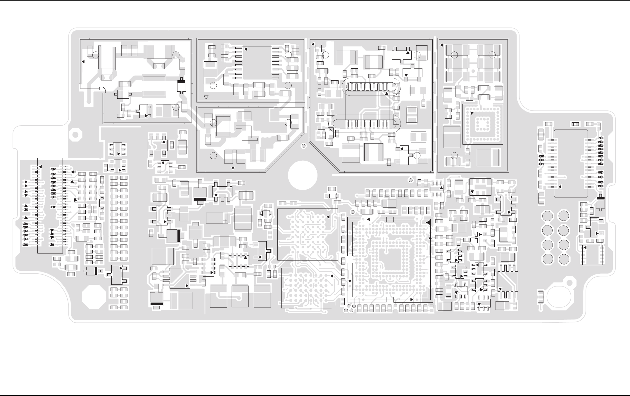
8-2 Schematics, Board Overlays, and Parts Lists – VHF: General Section
May 28, 2008 6871620L01-C
8.3 General Section
Figure 8-1. Main Board Layout (NUD7115B) – Side 1
16out
C9
C10
C11
C12
C13
C14
C15
C16
C17
C25
C26
C27
C28
C30
C52
C53
C54
C55
C56
C57
C71 C72 C73
C101
C102
C103
C104
C105
C106
C107
C108
C110
C111
C112
C113
C114 C115
C116
C120
C121
C122
C123 C124
C125
C209
C210
C213
C214
C217
C218
C219
C220
C222
C224 C225
C226
C227
C229
C230
C231
C232
C233
C234
C235
C236
C241
C242
C250
C301
C302
C303
C304
C305
C306
C307
C308
C309
C310
C313
C314
C315
C316
C317
C318
C320
C321
C322
C330
C333
C350C351
C704
C705
C706
C707
C709
C710
C711
C712
C713
C715
C716
C717
C720
C1101
C1107
C1108
C1109
C1110
C1111 C1112
C1113
C1114
C1115
C1116
C1117
C1118
C1119
C1120
C1123
C1124
C1125
C1126
C1130
C1131
C1132
C1133
C1134
C1135
C1136
C1138
C1140
C1141
C1142
C1202
C1310
C1312 C1313
C1314
C1340
C1342
C1343
C1370
C1402
C1403
C1404
C1407
C1408
C1409
C1410
C1411
C1412
C1413
C1414
C1416
C1417
C1418
C1419
C1420
C1421
C1422
C1424
C1425
C1427
C1428
C1429
C1430
C1431
C1432
C1433
C1440
C1441
C1442
C1443
C1444
C1445
C1446
C1447
C1448
C1449
C1450
C1451
C1452
C1453
C1454
C1455
C1456
C1457
C1458
C1459
C1460
C1719
C1722
C9966
C9968
C9970
C9975
C9980
CKO
D1
D2
D3
D4
D301
D302
D303
D701
D702
D703
D1000
D1301
D1401
D1402 DSP_DE
E5
E104
E501
E1102
E1103
E1110
E1111
E1112
E1113
E1114
E1115
E1116
E1117
E1118
E1119
E1120
E1121
E1122
E1123
E1124
E1125
E1126
E1127
E1129
E1130
E1401
E1402
E1403
E1404
E1405
E1406
E1407
E1408
E1409
E1410
E1411
E1412
E1413
E1414
E1415
E1416
E1417
E1420
E1421
E1422
E1432 E1433
E1434
E1435
E1436
E1437
E1438
E1439
E1440
E1441
E1500
E1501
E1502
E1503
E1504
E1505
E1506
E1507
2
60
59
J1
30 16
15
J2
L10
L101
L102
L103
L104
L106
L107
L108
L202
L203
L205
L207
L208
L301
L302
L303
L304
L305
L306
L307
L308
L309
L310
L311
L312
L313
L702
L703
L704
L705
L1307
L1308
2
M1001
2
M1002
2
M1003
2
M1004
MAKO_INT MAKO_RESET
MCU_DE
PRESC
Q310
4
58
Q1301
4
58
Q1302
Q1402
2
3
Q9906
Q9950
Q9951
R109
R201
R202
R204
R205
R207
R208
R210
R212
R213
R215
R217
R301
R302
R303
R304
R305
R306
R307
R310
R313
R314
R315
R316
R317 R318
R319
R701
R703
R731
R733
R735
R1101
R1102
R1103 R1105
R1106
R1107
R1108
R1109
R1110
R1111
R1112
R1113
R1114
R1115
R1116
R1117
R1118
R1119
R1120
R1121
R1122
R1123
R1124
R1125
R1133
R1209
R1308
R1310
R1311
R1335
R1336
R1337
R1338
R1341
R1344
R1346
R1401
R1403
R1404
R1405
R1406
R1409
R1410
R1411
R1412
R1415
R1416
R1417
R1418
R1419
R1420
R1421
R1422 R1423
R1424 R1437
R1438
R1439
R1440
R1449
R1462
R1463
R1464
R1465
R1466
R1467 R1704
R1706
R1709
R9901
R9902
R9903
R9904
R9916
R9917
R9918
R9919
R9922
R9931
R9934
R9961
R9990
R9998
R9999
8
7
5
4
3
SH06
6
5
4
3
2
SH07
2
6
4
SH08
32
5
8
6
4
7
SH09
4
11
10
7
5
SH10
TCK
TDI TDO
TMS
TRST
4
58
U1
U2
U3
16
8
9
U102
5
3
4
U201
A10
K10
A1
K1
U202
11 20
10
U302
U701
4
3
6
U702
4
58
U1101
U1306
C2
AA2
AA22 C22
U1401
U1404
U1405
4U1406
U1408
A1
A6
H1
H6
U1409
G1 A1
A8G8
U1410
106
5
U9904
U9905
U9907
U9908
U9910
U9911
U9912
U9913
U9914
U9915
U9918
URTS1_XRXD
UTXD1_USB_VPO
VR4
VR51
VR1209
Vctrl
43
2
Y200
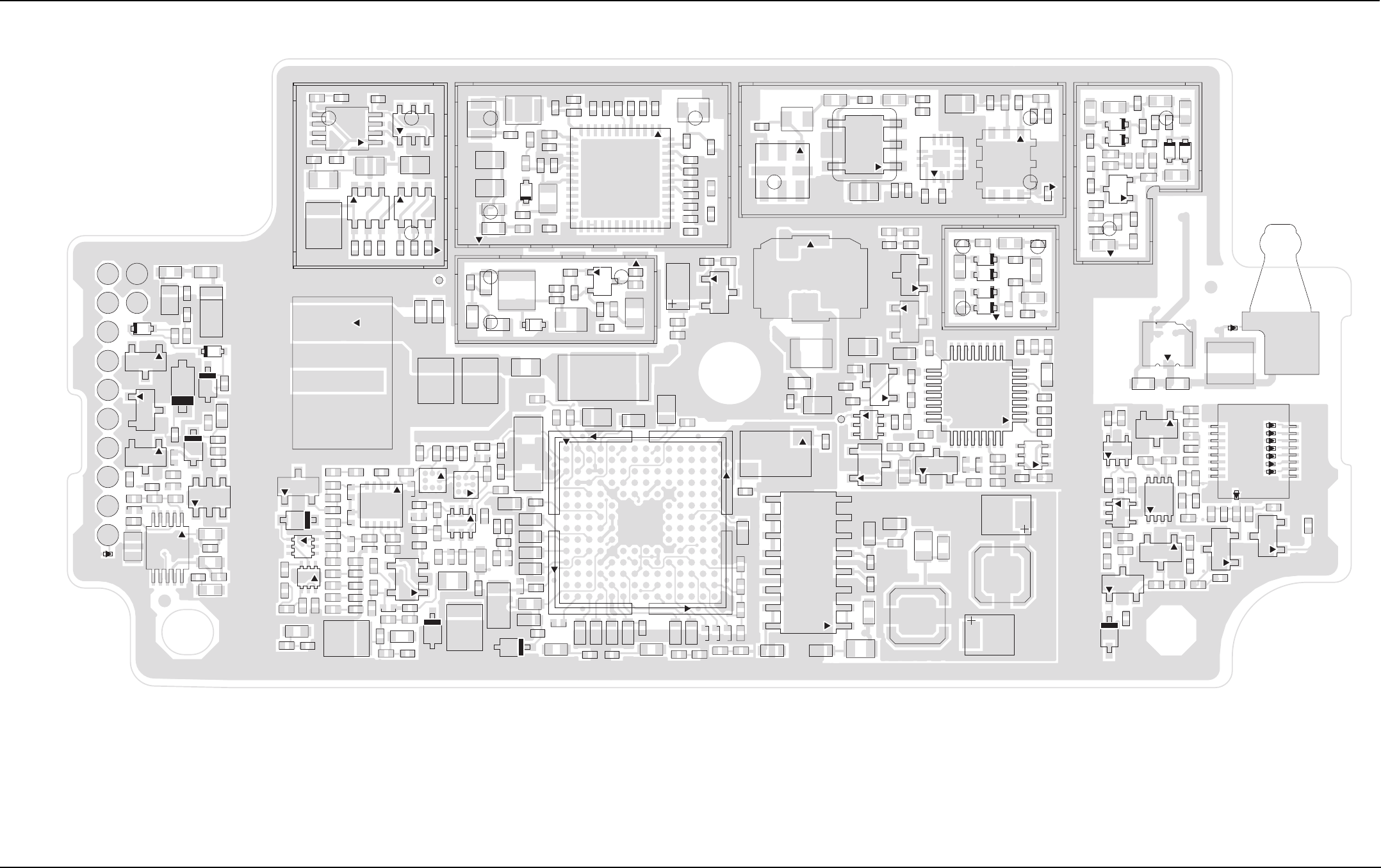
Schematics, Board Overlays, and Parts Lists – VHF: General Section 8-3
6871620L01-C May 28, 2008
Figure 8-2. Main Board Layout (NUD7115B) – Side 2
C4
C6
C20
C21 C22
C24
C117
C118
C119
C127
C128
C129
C130
C131
C132
C133
C134
C135
C136
C137
C140
C144
C201
C202
C203
C204
C205
C206
C207
C208
C211
C215
C221
C337
C410
C411
C413
C414 C416
C417 C420
C432
C433
C434
C435
C436
C450
C451
C452 C455
C456
C470
C471
C472
C473
C474
C475
C476
C477
C478
C479
C480
C481
C482
C490
C491
C501
C505
C506
C507
C509
C511
C512
C513
C514
C527
C535
C539
C540
C541
C542
C544
C546
C547
C548
C550
C551
C552
C553
C554
C555
C556
C557
C560
C561
C562
C570
C571
C572
C573
C574
C581
C582
C583
C1102
C1104
C1105
C1106
C1128
C1129
C1139
C1209
C1210
C1211
C1212
C1213
C1214
C1215
C1216
C1217
C1218
C1219
C1220
C1221
C1222
C1223
C1224
C1225
C1232
C1301
C1302
C1303
C1304
C1305
C1306
C1307
C1308
C1309
C1315 C1316
C1317
C1318
C1319
C1320
C1321
C1322
C1323
C1324
C1325
C1326
C1327
C1328
C1329
C1330
C1331
C1332
C1333
C1335
C1336
C1337 C1338
C1339
C1341
C1345
C1346
C1347
C1348
C1349 C1350
C1351
C1352
C1353
C1354
C1355
C1356
C1357
C1362
C1363
C1364
C1365
C1367
C1368
C9901
C9950
C9951
C9952
C9953
C9954
C9956
C9969
CTS
D104
D201
D202
D411
D412
D413
D414
D451
D452
D453
D454
D550
D570
D1202
D1205
D1207
D1222
D1223
E101
E105
E500
E1104
E1201
E1418
E1419
E1430
E1431
E1442
E1443
E1444
E1445
EXT_MIC
F901
FL200
23
567
FL490
GND
16
9
8
J3
3
J1704
L20
L105
L201
L204
L410
L411
L412
L413
L415
L430
L431
L432
L433
L450
L451
L452
L453
L454
L470
L471
L472
L474
L480
L490
L491
L501
L502
L551
L552
L553
L570
L1204
L1205
L1301
L1302
L1303 L1304
L1305
L1306
LHDATA_KEYFAIL
2
M1009
2
M1010
2
M1011
2
M1012
M1704
32
M1705
MECH_SW
OPTB+_VPP
OPTSEL_2
Q4
Q101
Q102
Q104
3
2
4Q107
2
3
Q200
Q430
Q550
Q551
1
6
3
4
Q1201
1
6
3
4Q1202
16
1
8
9
Q1304
Q9901
Q9902
Q9903
Q9904
Q9905
R102 R105
R106
R111
R117
R118
R119
R120
R121
R122
R130
R135
R136
R216
R218
R401
R411
R412
R430 R431
R432
R433
R434
R435
R451
R452
R470
R501
R511
R519
R533
R551
R552
R553
R554
R555
R556
R571
R572
R1126
R1127
R1201
R1202
R1203
R1204
R1205
R1206
R1207
R1210
R1212
R1213
R1214
R1215
R1216
R1217
R1218
R1219
R1220
R1221
R1223
R1224
R1225
R1226
R1227
R1228
R1229
R1230
R1231
R1239
R1241
R1301
R1302
R1303
R1304
R1305
R1306
R1307
R1309
R1314
R1315
R1317
R1318
R1319
R1320
R1321
R1322 R1323
R1324
R1325
R1326
R1327
R1328
R1329 R1330 R1331R1332
R1334
R1339
R1340
R1342
R1343
R1345
R1347
R1348
R1349
R1350
R1351
R1352
R1353
R1354 R1355
R1356
R1357
R1358
R1370
R1371
R1402
R1596
R1708
R9905
R9906 R9907
R9908
R9909
R9910
R9911
R9912
R9913
R9914
R9915
R9920
R9921
R9923
R9924
R9925
R9926
R9927
R9930
R9932
R9933
R9960
R9996 R9997
R10000
R10001
RS232DIN
RS232DOUT
RT150
RTS
10
8
6
7
4
SH01
5
8
7
3
SH02
2
3
5
4
SH03
6
7
2
54
3
SH04
4
3
6
2
5
SH05
5
2
46
3
SH11
SPK+
SPK_COM
3
46
T470
3
4
6
T471
TP111
TP551
10
6
5
U20
U103
25
9
17
U104
U203
12
10
97
6
4
3
U470
1
37
25
13
U500
106
5
U1201
U1301
C1
C3
A3
U1302
C1
C3 A3
U1303
P1 A1
A14
P14
U1304
5
3
4
U1305
4
U9901
U9902
U9903
U9916
U9917
VR3
VR1201
VR1202
VR1203
VR1204
VR1205
VR1206
VR1208
VR1301
VR9901
Y1301
43
2
Y1302
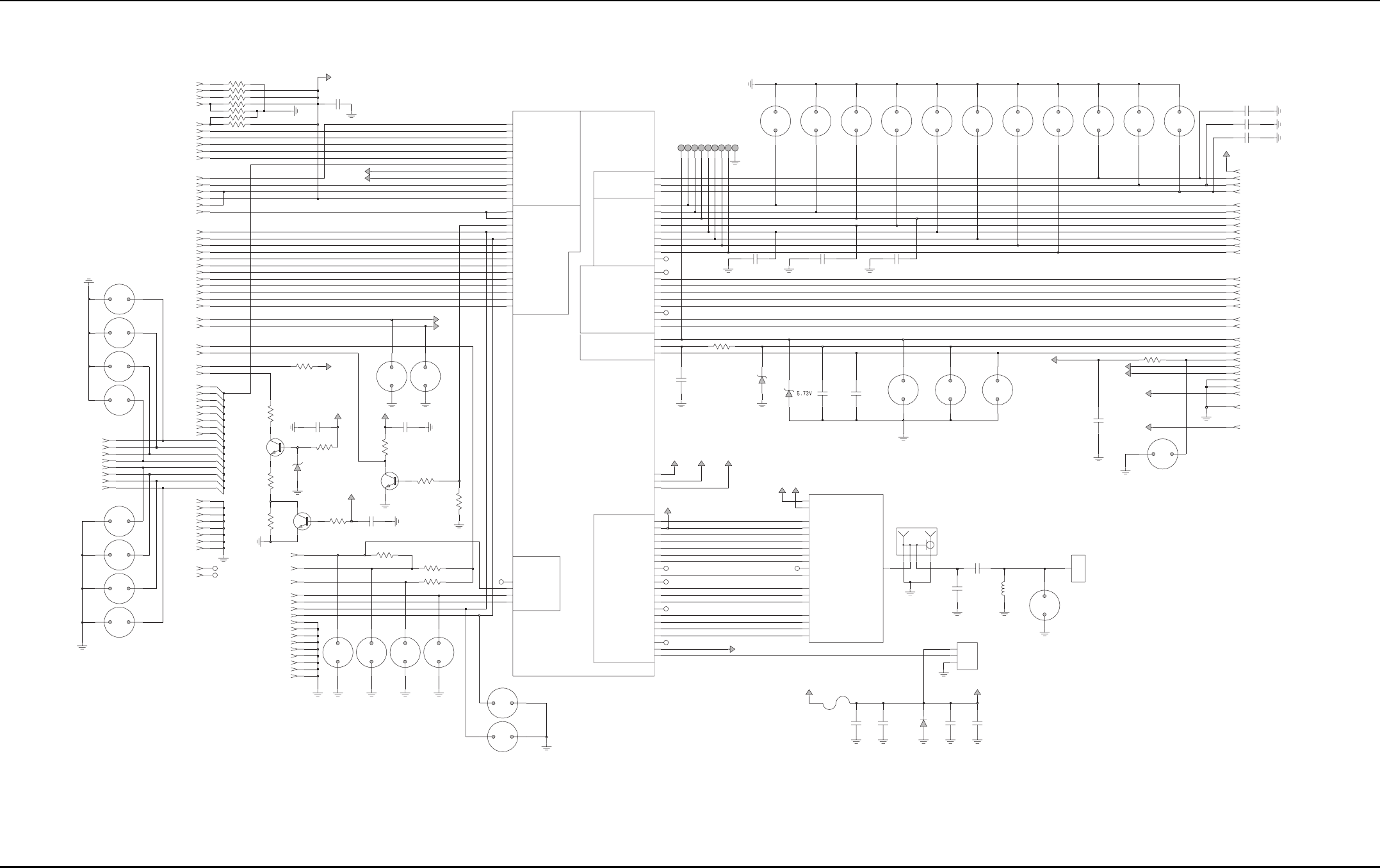
8-4 Schematics, Board Overlays, and Parts Lists – VHF: General Section
May 28, 2008 6871620L01-C
Figure 8-3. VHF Main Board Overall Schematic
Spring Contact
eciveD citpaH dna enohporciM ,rekaepS
,yalpsiD DIC ,yalpsiD niaM oT
dapyeK dna eceipraE
slortnoC/snottuB
oidaR oT
50ohm RF Jack
Testpoints
NU
NU
Antenna Leaf
Battery Contact
eludoM noitpyrcnE ,ecafretnI EC oT
NU
21
F901
24V
3A
J1-7 7
7041E
PAG_KRAPS
E1501
SPARK_GAP
12
R9909
10K
Q9903
18
PAG_KRAPS
2141E
21
R9912
0
J1-18
14
0
J2-1212
1000pF
C1104
J2-14
R9918
28
J2-1515
1000pF
DISP_V1.875
J2-28
RAWB+
J3-13 13
C56
J2-22
J1-6 6
22K
R9911
J2-88
J2-1313
U9907
SPARK_GAP
1
2
5
1000pF
C9901
SPARK_GAP
E1502
12
J2-5
46
CLIP
M1704
GND
1
1
NC
J1-46
1K
R9908
1K
5V_Misc
R9905
XTX_SSFS
J1-55 55
C21
2.2pF
XLOCK
XRFUNSWB+1
XRF_AD_CS*
XRF_BAT_STAT
XRF_MISOA
XRF_MOSIA
XRF_POR*
XRF_SCKA
XRF_TX_INHIBIT
XRF_VSW1
XRX_DATA
XSSI_CLK
XSSI_FSYNC
XSWB+2
XTX_DATA
XTX_SSCK
UC_KP_ROW1
UC_KP_ROW2
UC_KP_ROW3
UC_KP_ROW4
UC_KP_ROW5
UC_KP_ROW6
UC_KP_ROW7
UC_MONITOR
UC_RESET_ENC
UC_TX_INHIBIT
UC_UCM_SS
UC_WAKEUP
X16.8MHz
XABACUS3_CS*
XFN_PC_SEL*
XIFGND1
UC_ENC_SSI_CLK
UC_ENC_SSI_DI
UC_ENC_SSI_DO
UC_INT_MIC
UC_INT_PTT
UC_INT_SPKR+
UC_INT_SPKR-
UC_KEYFAIL_LH_BDMDATA
UC_KP_5V1
UC_KP_5V2
UC_KP_BL_EN
UC_KP_COLUMN0
UC_KP_COLUMN1
UC_KP_COLUMN2
UC_KP_ONOFF
UC_KP_ROW0
DISP_BRIGHT2
DISP_CS_SUB
DISP_DATA(15:0)
DISP_ID
DISP_MAIN_EN
DISP_REG_SEL_A0
DISP_REG_SEL_A1
DISP_RESET
DISP_R_W
DISP_V1.875
DISP_V2.9
EXT_SPKR+
EXT_SPKR-
FLIP_SENSE
UC_BOOT_ENC
UC_EMERG
EXT_SPKR+
AUDIO_SW
AUD_JACK_INT
AUD_JACK_MIC
AUD_JACK_PTT
CE_CTS
CE_LHDATA_KEYFAIL
CE_OPTB+_VPP
CE_OPT_SEL1
CE_OPT_SEL2
CE_RS232DIN_USB-
CE_RS232DOUT_USB+
CE_RTS
CE_SB9600_BUSY
DISP_BRIGHT1
C4
2
J3-5 5
.01uF
J1-33 33
5041E
PAG_KRAPS
1
J3-9 9
14
6
2
E1444
SPARK_GAP
12
J2-2020
SPARK_GAP
E1445
1
FU_B+
J1-26 26
J1-52 52
L20
52.29nH
J3-16 16
J3-11 11
9141E
PAG_KRAPS
12
J3-1 1
J1-36 36
21
J2-1616
PAG_KRAPS
6041E
6141E
PAG_KRAPS
12
C54
1000pF
10uF
1
J1-1 1
C24
J1-38 38
CIM_TXE
12
J3-14 14
R9903
SPARK_GAP
U9908
25
5V_Misc
J2-2626
NC
J1-25
C55
11
6.8V
VR4
12
1000pF
PAG_KRAPS
4041E
21
SPARK_GAP
E1443
43
NC
TUOD232SR
1
29
J1-30 30
J1-43
E1442
SPARK_GAP
12
J1-29
2
J1-37 37
NC
3
SPARK_GAP
E1507
1
49
CE_SPKR+
R9902 1K
12
J1-48 48
J1-49
J1-19 19
FU_B+
U9917
SPARK_GAP
R9998 100
J2-2121
J1-20 20
0R9999
LIAFYEK_ATADHL
1
J1-45 45
STR
1
NC
18
J2-2222
30
9041E
PAG_KRAPS
21
J2-18
58
J2-77
J2-30
Q9902
J1-58
1000pFC71
J2-2525
NC
1KR9919
VR3
8
27K
R9910
V_VIBE
J2-66
J3-8
J1-17 17
5
NC
SW_B+
C22
J2-2929
J1-32 32
15pF
J1-50 50
2
DISP_BRIGHT1
CE_SPKRCOM
2_LESTPO
1
SPARK_GAP
12
C53
1000pF
7
J1-12 12
E1503
10
J1-5 5
J1-51 51
J1-8 8
J1-10
1
J2-44
J1-60 60
NC
DNG
J3-3 3
910pF
C9966
2
3041E
PAG_KRAPS
21
24
PAG_KRAPS
8041E
1
13
J1-9 9
J2-24
R9904
J1-13
2
J1-23 23
13
1K
J1-59 59
1141E
PAG_KRAPS
1
22
8
J1-3 3
9
J1-47 47
J1-22
10
J2-9
J2-2323
Q9901
C6
J3-15 15
J2-1717
1000pF
C1102
1000pF
POS
J1-31 31
NC
EAR+
CONTACT
M1705
2
DATA
3
NEG
1
J2-33
J3-6 6
1
SPARK_GAP
E1417
12
RXFS
SPCK
TXCK
TXFS
TXINH
TXTD
USEL
VSW1
XCVR_SWB+
STC
NID232SR
1
ABCS
ANT
F168
FUB+
LOCK
MOSI
RAWB+
RSTL
RXCK
RXDOJ3-10 10
EXT_SPKR-
R9917 1K
21
FU_B+
J1-35 35
150K
J1-21
R9915
28
J1-44 44
2.4V
VR9901
J1-16 16
4
J1-28
68
R9907
1000pF
RAWB+
SPARK_GAP
E1500
12
C72
1000pFC73
C
3
1G
2
2G
4
J2-1010
C52
J1704
A
1
12
AUD_JACK_SPK_out
1000pF
27
NC
9
DISP_BRIGHT2
PAG_KRAPS
5141E
J1-40 40
EAR-
J2-27
PPV_+BTPO
1
DISP_BRIGHT1
J1-41 41
J2-1919
DISP_BRIGHT2
J1-14 14
15
VSW1
J3-4 4
J3-7 7
J1-4 4
J2-1111
1
E1504
SPARK_GAP
12
J2-1
J3-12 12
VR51
J1-57 57
C20
10uF
11
NC
J1-34 34
1000pF
C57
J1-11
J1-2 2
R9906
30
12
R9916
12
PAG_KRAPS
4141E
J1-15 15 12
SPARK_GAP
U9916
2
J1-42 42
PAG_KRAPS
0141E
1
J1-53 53
0
R9901
2
FU_B+
3141E
PAG_KRAPS
21
12
E1506
SPARK_GAP
1
1000pF
SPARK_GAP
E1505
68K
C9970
54
J3-2 2
R9914
27
J1-56 56
J1-54
J1-24 24
J1-27
R9913 91K
AUDIO_SW
J1-39 39
DISP_DATA(15:0)
F168
SCKA
RSTL
MOSIA
BS
LOCK
USEL
ABCS
TXFS
TXCK
TXTD
SWB+
RXFS
RXCK
RXDO
VSW1
DISPLAY
AUDIO
CE
KEYPAD
UCM
AUDIO
JACK
VOCON
XCVR
XCVR
TOP/VOLUME
CONTROL
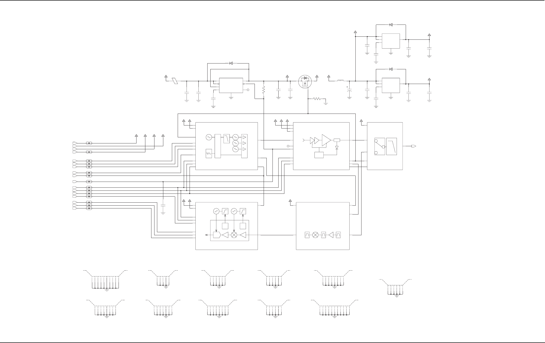
Schematics, Board Overlays, and Parts Lists – VHF: Transceiver (RF) Section 8-5
6871620L01-C May 28, 2008
8.4 Transceiver (RF) Section
Figure 8-4. VHF Transceiver (RF) Board Overall Circuit Schematic
XCVR DC Regulators
ECAFRETNI NOCOV / RVCX
1VIN 5
VOUT
VSW1_filtered
VSW1
LP3985
U3
4BYPASS
2DNG
3VEN
C11
0.10uF
VSW1
RAWB+
ANT
RXRF
TX5V
TXRF
V5A
VAR3
R1709
100K
C16
.01uF
XB+
MBRM140T3
D3
NTR1P02T1
Q4
C26
2
NC
5
OUTPUT
6SENSE
8SHUTDOWN
NC
.01uF
LP2989
U1
LP2989IMMX-5.0
1BYPASS
7
ERROR
3DNG
4INPUT
D2
MBRM140T3
V5A
C13
XB+
USEL
V5A
VAR2
VAR3
XB+
.01uF
MOSI
POUT
RAWB+
RSTL
SPCK TX5V
TXINH
TXRF
BYPASS
4
DNG
2
VEN
3
VIN
1VOUT 5
U2
LP3985
E5
V3AV5A
C17
1.0uF
BK1005HM471
1000pF
C9
MBRM140T3
D1
V3D
1000pF
NC
RAWB+
C10
1.0uF
C15
10uF
C30
C12
10uF
1000pF
C1719
2.2 uF min.
XB+
100K
R1708
CLKOUT
DOUTA
FREF
FS
PC
PD
PE
RXIF
V3D
V5A
V5A
C28
1000pF
V3D V5R
CLK
CSX
DATA
F168
LOCK
RXLO
SCEN
SSCK
SSFS
SSTD
TXRF
V3A
V5A
C25
1.0uF
L10
100uH
DAC2
LOIN
RXIF RXIN
V5R
C27
V5A
V5R
1.0uF
2
3
4
5
6
5
6
7
8
9
01
1
7
8
1
2
11
3
4
1
2
3
4
5
6
5
6
1
2
3
4
5
6
6
7
8
1
2
3
4
5
6
1
2
3
4
5
5
6
7
1
2
3
4
4
5
1
2
3
4
5
6
7
8
1
2
3
7
8
9
0
1
1
2
3
4
SH01 SHIELD
(RECEIVER BACK-END)
SH03 SHIELD
(RECEIVER RF PRE-FILTER)
SH05 SHIELD
(FGU (SYNTHESIZER 2)) SH09 SHIELD
(FGU (SYNTHESIZER 1))
SH10 SHIELD
(FGU (VCO))
SH11 SHIELD
(RECEIVER 2ND LO VCO)
SH06 SHIELD
(TRANSMIT PRE-DRIVER STAGE)
SH08 SHIELD
(TRANSMIT POWER STAGE)
SH07 SHIELD
(HARMONIC FILTER &
ANTENNA SWITCH)
SH04 SHIELD
(RECEIVER MIXER & IF FILTER)
SH02 SHIELD
(RECEIVER LOW-NOISE
AMPLIFIER & RF POST FILTER)
1
2
3
4
5
6
V3A
FUB+
10uF
C14
V5A
RXIF
RXLO
RSTL
VSW1
XCVR_SWB+
LOCK
TXFS
TXFS
TXCK
TXCK
TXTD
TXTD
F168
FUB+
RAWB+
TXH TXH
RXDO
RXDO
RXFS
RXFS
RXCK
RXCK
ANT
ABCS
ABCS
USEL
USEL
USEL
SPCK
SPCK
SPCK
SPCK
MOSI
MOSI
MOSI
MOSI
LOCK
FGU
A200,A300
RX_BE
A500
LOCKO
ADC
SW_FL
A700
TX_ALC
RX_FE
A100
A400
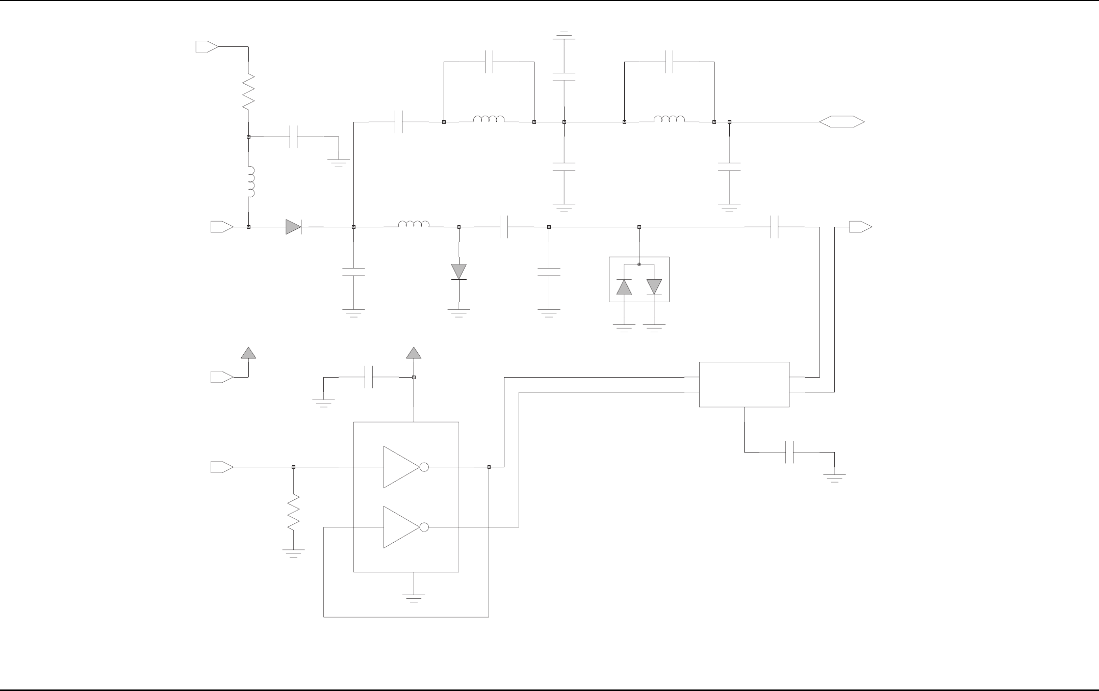
8-6 Schematics, Board Overlays, and Parts Lists – VHF: Transceiver (RF) Section
May 28, 2008 6871620L01-C
Figure 8-5. VHF Transceiver (RF) Antenna Switch and Harmonic Filter Circuits
D702
HSMP_389Z
HSMP_389Z
D701
L704
43.41nH
L703
33.47nH
C704
910pF
1uH
L702
100K A2
3
DNG
2CCV 5
Y1 6
Y2 4
R703
U702
NC7WZ04
A1
1
0.10uF
C717
C716
1000pF
U701
2DNG
1
RFIO1 3
RFIO2
4V1
5V2
AT267
V5A
C720
11pF
DH50037
D703
1000pF
C715
V5A
1000pF
L705 C712
10pF
52.29nH
C709
5.6pF
C706
2.7pF
C713
C705
24pF
16pF
C707
20pF
C710
18pF
C711
V5A
220
0.100W
R701
ANT
RXRF
TXRF
TX5V
VAR3
ATH
ATH
ATL
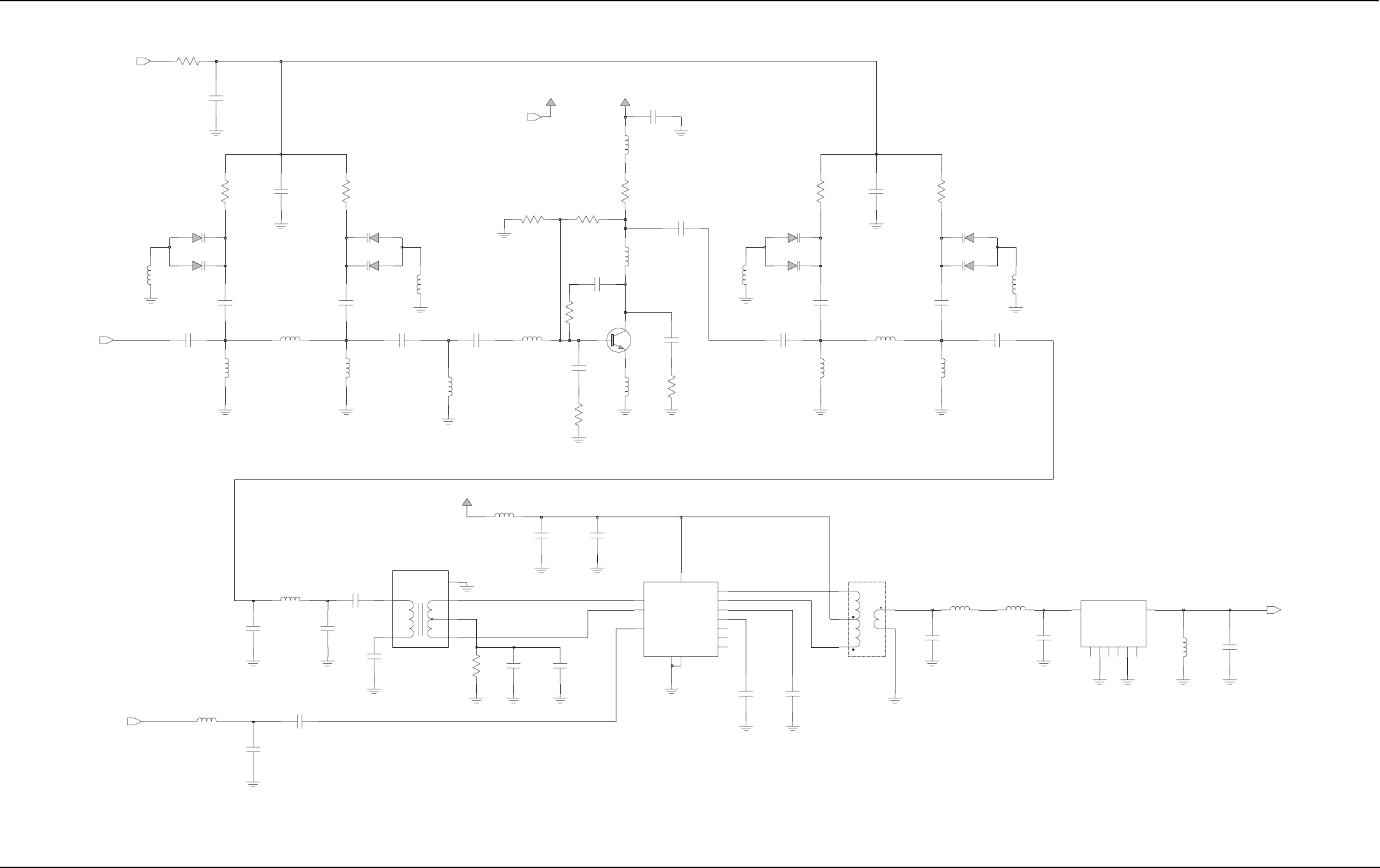
Schematics, Board Overlays, and Parts Lists – VHF: Transceiver (RF) Section 8-7
6871620L01-C May 28, 2008
Figure 8-6. VHF Transceiver (RF) Receiver Front End Circuit
C473
NU
120pF
910pF
R452
C414
100K
L412
27nH
15nH
L453
0.1uF
C420 3.3K
R432
1K
R401
L470
22nH
L472
180nH
BFQ67W
Q430
R430
10
15nH
L415
2.2pF
C476
V5R
C479
R412
100K
4
2
3
V5R
0.1uF
T470
XFMR
5
NC
6
1
22nH
L433
C491
13pF
22
R434
C435
6.8pF
220nH
L480
100K
R411
L490
820nH
82nH
L410
24pF
.01uF
C481
C416
330pF
C472
L432
100nH
D411
1SV305
7
RFN
4
RFP
5
C433
0.1uF
DDVB
DNG
11
1DNG
31
IFN 8
IFP 9
LOIN
10 NC1 3
NC2 6
NC3
U470
MX2072A
12
BBP
BDIV 2
1
100nH
L431
910pF
C480
27nH
L451
330pF
C477
C455
L474
0.27uH
24pF
33nH
L471
L454
15nH
D452
1SV305
V5R
1000pF
C432
4.7uF
C475
24pF
L430
C450
51nH
1SV305
D412
820nH
L491
120pF
C452
100
R470
1SV305
D414
T471
XFMR
4
6
1
2
3
120pF
C413
4.7uF
C411 C451
120pF
L413
27nH
24pF
C410
6DNG
IN
1OUT 5
L411
15nH
FL490
MFI44Q2
1DNG
2
32DNG
43DNG
4DNG
6
5DNG
7
8
8.2pF
C436
C434
0.1uF
1SV305
D451
C478
16pF
0.1uF
C456
.01uF
C482
100K
R433
16pF
C470
R451
100K
1SV305
D453D413
1SV305
C417
0.1uF
C471
L450
82nH
C490
18pF
D454
1SV305
27nH
L452
10
910pF
C474
R435
100K
LOIN
MX_IN
RX
IF
R431
V5R
R
XIN
DAC2
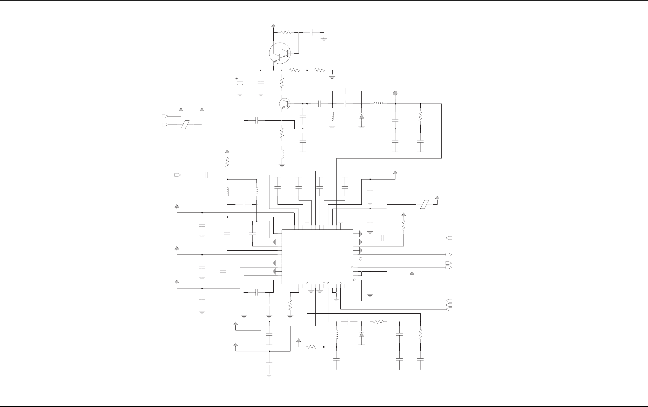
8-8 Schematics, Board Overlays, and Parts Lists – VHF: Transceiver (RF) Section
May 28, 2008 6871620L01-C
Figure 8-7. VHF Transceiver (RF) Receiver Back End Circuit
845C
OLFI
zHM 1.74 ot 6.24
OKC
zHM 81
2
55R
FD3V
Fu740.
375C
K0
01
Fp86
505C
Fp001
055C
Fp81
645C
Fu10.
0
7
5D
97
2
V
S
1
445C
Fp001
115C
Fu10.
285C
K01
915R
Fu01.0
115R
165C
K001
Fu7.4
Fu1.0
175C
11 PFERV
005E
17
4MH5001KB
62
DDDV
6FDDV
72
HDDV
48
VDDI
40
VDDL 39
VDDP
14 VDDQ
21 NFERV
1POXM
23 PC
24 PD
52
EP
RREF
13
33
BCNYS
9ADDV
17 VDDC
4N2FI
5P2FI
47
IFIN
15 IOUTC
38
IOUTL
42
LON
43
LOP
2NOXM
3FDNG
23
HDNG
45
GNDI
63
LDNG
37
GNDP
16 GNDQ
21 GNDS1
43
2SDNG
03
BTUOD
53
FERF
13
SF
8NCG
7PCG
01 ADNG
18 GNDC
22 GNDD
20 CLKN
82
TUOKLC
CLKP
19
46
CXIF
44
CXVL
41
CXVM
92
ATUOD
4689DA
005U
Fu10.
FD3V
725C
FD3V
145C
Fu01.0
Fp0022
705C
355L
Hu2.2
905C
Fu740.
K21
455R
FD3V
215C
Fp001
Fu1
0.
265
C
055D
65YBB
655R
026
Fp001
755C
245C
Fu10.
415C
Fu01.0
7
0C6
4
93112
35
5C
Fu3
3.0
385C
Fu10.
Fp001
105C
105R
74
FD3V
1
075C
Fu1.0
105E
S106A11MLB
TNIOP_TSET
155PT
V01
Fu1.0
V61
Fu01.0
045C
935C
40B6493112
40A37
155
Q
53
S
6493
1
12
Fu
0.1
255C
475C
F
u
10
.
155R
K1
.1
K
00
1
335R
53
S
64
9
3112
155C
Fu0.1
275R
K01
FD3V
Fu10.
745C
315C
F
u1
0
.
K81
A5V
3
55R
FD3V
A5V
FD3V
205L
Hu01
075L
Hu9.3
175R
K
8
.
1
455C
A5V
Fp81
Hu7
.4
1
55L
655C
Fp86
055Q
W76QFB
Fp051
185C
Hn033
FD3V
Fu10.
535C
255L
Fu01.0
605C
CN
275C
FD3V
Fp22
Fu330.
065C
5
55C
Fp15
Hu01
105
L
FD3V
555R
063
pddv
VD3
FIXR
lvxc
lddv
iddv
ATUOD
UOKLCT
SF
74V
fixc
NKLC
PKLC
mvxc
nifi
CTUOI
LTUOI
nol
POL
CP
DP
EP
VA5
FERF
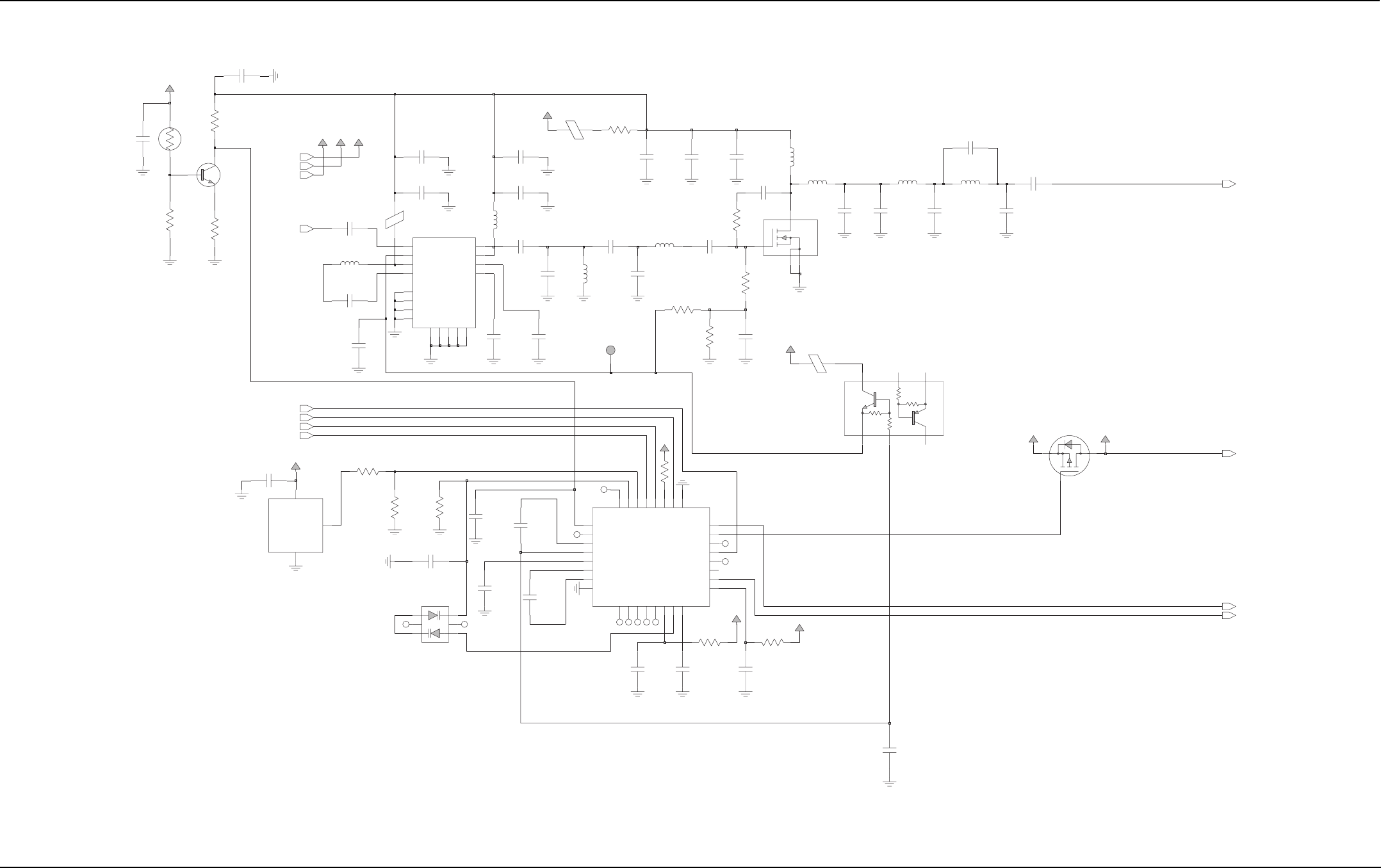
Schematics, Board Overlays, and Parts Lists – VHF: Transceiver (RF) Section 8-9
6871620L01-C May 28, 2008
Figure 8-8. VHF Transceiver (RF) Transmitter Circuit
NU
NU
47K
C114
13pF
910pF
C104
910pF
C127
C108
C122
.01uF
910pF
C128
27pF
1.65nH
TEST_POINT
TP111
1
L107 C125
470pF
27pF
C120
BLM21PG221SN1
E101 470pF
C119
R109
UNSW_B+
C103
.01uF
R119
0
2S
4
V5A
23.75nH
L105
Q107
4816698H02
D3
G
1
1S
2
C134
.01uF
910pF
V5A
V5A
CN
C105
R117
NTR1P02T1
Q104
NC
UNSW_B+
10
33nH
L103
RAWB+
C111
910pF
C110
XB+
470pF
NC
C102
56pF
0.1uF
C116
C117
1uF
R106
NC
TX5V
1uH
RAWB+
CN
L102
11.03nH
30pF
C113 L104
L106
CN
22nH
R111
470K
C131
.015uF
9
10pF
C137
1
4
27pF
C121
Q101
2
5
6
3
0.1uF
C132
18pF
C124
RAWB+
6
RFOUT1 7
RFOUT2
1VCNTRL
14 VD1 2
VG1 3
VG2
52DNG
21 3DNG
31 4DNG
8NC1
9NC2
10 NC3
NC4
15
16 RFIN
U102
SRFIC5668
PE
71
G2
11
41DNG
5.1pF
C107
C112
NC
910pF
6.8nH
L101
K2 6
NC1
2NC2 5
CN
RT150
33.0K
MBD330DWT1
D104
A1
1
A2
4
K1
3
910pF
C101
10K
R105
23.75nH
L108
C133
1uF
7.5pF
C123
C144
910pF
R121
390
CN
RAWB+
0
C130
470pF
R118
R136
24
VAR3
GV
51
6VL 19
VLIM
0
R135
23
RXT1
2
03
PMET
01V
41
54V
61
17
V5EXT
20
VAR1
VAR2 18
52
2DNG
INT
4
22
NA
Q
11 XQ
01
1RFIN
21
RS
TESR 13
5CJ
CL
7
62
KLC
QC
21
31 XQC 82
ATAD
9861F
GND1
8
5185765B26
H99S4
U104
ONA 23
72
SOPB
92
XEC
CI
3
C129
E105
1500pFU103
3SOPDNG 1
2
VOUT
0.15
R130
LM50
NC
C140
910pF
R102
1K
C106
910pF
NC
.01uF
C118
TX5V
BLM11A601S
E104
C135
910pF
82pF
C115
Q102
R120
1K
C136
910pF
TVDD
Vc
R122
110
TX5V
RAWB+
RXH
POUT
POUT
V5A
VAR2
MOSI
USEL
SPCK
RSTL
VAR3
XB+
TXRF
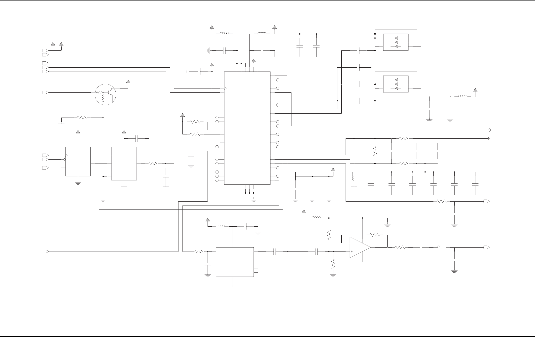
8-10 Schematics, Board Overlays, and Parts Lists – VHF: Transceiver (RF) Section
May 28, 2008 6871620L01-C
Figure 8-9. VHF Frequency Generation Unit (Synthesizer) Circuit – 1 of 2
C230
3
1
5
2
NC
330pF
R216
U201
LMH6723
4
8.2K
R208
100pF
C229
C235 33K
100pF
C201
0.10uF
C205
0.10uF
V3A
V3A
100pF
C214
0.1uF
A3 6
K1
3
K2
2
K3
1
NC
C225
D202
4
A1
A2 5
C234
L207
2
1
.01uF
1uH
V3A
2.2uH
L202
.01uF
C231
2K
NC
R202
C206
10uF
V5A
0.10uF
C250
C219
2000pF
V5A
C213
1000pF
C220
NC
33K
R201
10uF
10K
R218
VSF
NC
NC
C218
.047uF
V3A
VSF
220pF
C337
2.2uH
L203
C209
220
R210
NC
0.10uF
C211
1000pF
NC
0.10uF
.047uF
NC
C236
V3A
C217
U203
AD5320BRT
DIN
4
DNG
2
SCLK
5
SYNC
6
DDV 3
VOUT 1
NC3
NC4 8
OUPUT 3
CCV 4
1VCONT
Y200
DSA321SD
16.8MHz
2DNG
NC1 5
6
NC2 7
A1 4
A2 5
A3 6
3K1
2K2
K3
1
D201
680
R217
0.1uF
R1
R2
Q200
NC
C227
CLK
COM
1
3DNG
2IN
OS
6
5
OUT
SHDN
7
DDV 4
10uF
FL200
MAX7414
8
C232
VMULT1 K4
VMULT2 K3
VMULT3 K1
VMULT4 J1
2K
ORV
J10
WARP
XTAL1 K9
XTAL2 K10
TEST1 A9
A8
TEST2
G6 VBYPASS
PCV 2A
DDV 4D
7K
1DDV 01C
2DDV 01A
3DDV
NC3
F7
PREIN
D10
PVREF
B10
REFSEL
G5
SFBASE
G10 SFCAP
H10
SFIN
E10
SFOUT G7
IADAPT A4
INDMULT K5
IOUT A5
E1
LOCK
MODIN
H1
A6
MODOUT
NC1
G4
NC2
F10
A7 CPB2
DATA
F1
G1 EN_CEX
FREFOUT K6
4E DNG
8K 1DNG
7E 2DNG
5D 3DNG
ADAPTSW A3
AUX1 A1
AUX2 B1
AUX3 C1
D1
AUX4
CCOMP
D6
F4 CLK_CLK
D7 CPB1
V3A
U202
35U92
C242
0.1uF
R212
82
V5A
2.2uH
L208
C210
0.10uF
NC
1uH
L205
0.1uF
C241
V3A
0.10uF
C221
L201
0.1uF
C226
2.2uH
NC
R204
82K
R215
10K
C203
2.2uF
V5A
4700pF
C222
2.2uH
L204
C224
0.1uF
10K
R213
NC
C208
0.10uF
C202
0.10uF
NC
NC
NC
0.10uF
C233
0.10uF
C204
43K
0.10uF
NC
R205
NC
V3A
C215
C207
0.10uF
VCP
S
CEN
CLK
CSX
R207
100
S
STD
S
SCK
S
SFS
D
ATA
LOCK
VCTR
L
PRESC
AUX3
F168
V5A
V3A
Schematics, Board Overlays, and Parts Lists – VHF: Transceiver (RF) Section 8-11
6871620L01-C May 28, 2008
Figure 8-10. VHF Frequency Generation Unit (VCO) Circuit – 2 of 2
VSF
NU
NU
1
VSF_VCO
R318
68VSF
Vctrl
330pF
R304
C310
R306
10K
820nH
220
160
L302
R313
C314
330pF
L308
D303 C304
27nH
330pF
C333
15pF
C303
15
18pF
R315
C307
1pF
VSF_VCO
D301
330
R319
R314
470
R301
150nH
L311
30
C351
C1722
1000pF
C309
VSF_VCO
R305
10K
TX_OUT
13
TX_SWITCH
41
SREFFUB_CCV 81
CIGOL_CCV
330pF
RX_IADJ 8
RX_OUT
7
RX_SWITCH
3SUPER_FLTR
TRB_IN
19
16 TX_BASE
TX_EMITTER
15
1TX_IADJ 10
COLL_RFIN
20 FLIP_IN
11 SREFFUB_DNG
9GALF_DNG
71 CIGOL_DNG
12
PRESC_OUT
RX_BASE
5
6RX_EMITTER
2
U302
VCOBIC
50U56
4
820nH
2.2pF
L301
0.1uF
C313
C321
18
R317
R303
L307
33
1.5pF
39nH
C308
R302
C317
2.2pF
VSF_VCO
33
18.29nH
L305
C330
330pF
R307
180
100nH
6
3
1
4
L310
Q310
2
5
1
820nH
L313
1pF
C320
PRESC
D302
5.6K
NC
VSF_VCO
VSF_VCO
R310
330pF
C322
820nH
L303
3.3pF
820nH
C305
NC
L312
18pF
C316
C306
1.8pF
330pF
C315
C301
12pF
470
R316
C302
15pF
C350
L304
47nH
L309
820nH
11.87nH
L306
AUX3
330pF
C318
PRESC
VCTRL
RXLO
TXRF
8-12 Schematics, Board Overlays, and Parts Lists – VHF: VOCON Section
May 28, 2008 6871620L01-C
8.5 VOCON Section
Figure 8-11. VOCON: Overall Circuit Schematic
Encryption
Interface
Earpiece
NU
Audio Jack Microphone
AUDIO JACK
Main & CID
Keypad
Interface
I
nterface
XCVR / VOCON
NU
Interface
Interface
Buttons / Controls
S
peaker,
CE
Interface
NU
Module
Interface
Interface
E1104
BLM11P600S
M
icrophone
Display
Interface
1K
R1116
R1122
10K
C1126
470pF
910pF
R1117 1K
C1111
V2
R1111 1K
C1134
33pF
12
4
UTXD2
VIBRATE_CONT
WAKEUP
SPARK_GAP
E1420
SSI_DO_ENC
TX_SSI_CLK
TX_SSI_DATA
TX_SSI_FSYNC
UCM_SS_BRAVO
UCTS1_USB_SPEED*
UNI_SEL*
URTS1_XRXD
URXD1_USB_VMI
URXD2
USB_ENUM
USB_SUSP
USB_TXENAB
USB_VMO
USB_VPI
UTXD1_USB_VPO
OPT_SEL2_IN
OPT_SEL2_OUT
RED_LED
RESET
RS232_USB*
RX_SSI_CLK
RX_SSI_DATA
RX_SSI_FSYNC
SCKA
SCKB
SPARE2_ENC_PTT
SPI_MISOA
SPI_MISOB
SPI_MOSIA
SPI_MOSIB
SSI_DI_ENC
HAB_MOD
INT_PTT
KP_BLEN
KP_COL(2:0)
KP_ROW(7:0)
KVL_USB_DET*
LOCK_DET
MAKO_CE
MAKO_INT*
MAKO_RESET
MOD
ONE_WIRE_EN*
ONE_WIRE_UP
OPTB+_VPP
OPT_SEL1_IN
OPT_SEL1_OUT
CODEC_RX
CODEC_TX
DISP_BRIGHT1
DISP_BRIGHT2
DISP_CS_SUB
DISP_DATA(15:0)
DISP_ID
DISP_MAIN_EN
DISP_REG_SEL_A0
DISP_REG_SEL_A1
DISP_R_W
EEPROM_SEL*
ENC_RESET
FLIP_SENSE
GATED_32_KHZ
GREEN_LED
ABACUS3_CS
ADTRIG
AD_CS*
AUDIO_JACK_INT
AUDIO_JACK_PTT
AUDIO_SW
BATTERY_ID
BAT_BUS_EN
BL_FREQ
BOOT*
BOOT_NORM*
BSY_IN_RTS
BSY_OUT_CTS*
CKIH
CODEC_DCLK
CODEC_FSYNC
R1103
16_8MHZ
32K_SEL
D1000
12
E1102
BLM11A601S
SW_B+
5
SPARK_GAP
E1438
21
910pF
C1202
470pF
V2
C1135
3
910pF
C1119
E1435
SPARK_GAP
21
UNSW_B+
SPARK_GAP
E1436
21
2
MECH_SW
910pF
C1115
C1125
BLM11A601S
E1103
470pF
1KR1110
6
R1115 1K
UNSW_B+
R1102
UNSW_B+
R1108 1K
12
0R1101
3199U
PAG_KRAPS
0
R1106
IF30_CTRL
IF23_CTRL
NC
V1.875
910pF
C1107
V2
R1107
10K
C1117
470pF
V2
IF25_CTRL
E1421
SPARK_GAP
12
IF31_CTRL
470pF
NC
C1118
0
CN
2
IF27_CTRL
TX_SSI_CLK
TX_SSI_FSYNC
UCM_KF_MAKO
UCM_SS
UCTS_USB_SPEED
UNSW_B+
URTS1_XRXD
URXD1_USB_VMI
URXD2
USB_TXENAB
USB_VMO
USB_VPI
UTXD1_USB_VPO
UTXD2
VPP_EN
VSW1
MAKO_CE
MAKO_INT*
MAKO_RESET
ONE_WIRE_OPT
ONE_WIRE_UP
POR
RFSW_B+
RS232_DI_USB-
RS232_DO_USB+
RS232_USB*
RTS
SB9600_BUSY
SCKB
SPI_MISOB
SPI_MOSIB
SW_B+
BSY_OUT_CTS
CODEC_DCLK
CODEC_FSYNC
CODEC_RX
CODEC_TX
CTS
EMERG
EXT_MIC
EXT_SPKR_NEG
EXT_SPKR_POS
GATED_32_KHZ
INT_MIC
INT_SPKR_NEG
INT_SPKR_POS
KVL_USB_DET
LHDATA_KEYFAIL
10K
16_8MHZ
32K_SEL
ADTRIG
BAT_STATUS
BOOT_NORM*
BSY_IN_RTS
2
NC
R1125
1KR1109
C1133
33pF
V2_FIL
6
VSW1
10K
R1124
R1118
CN
UNSW_B+
1
100
0
IF21_CTRL
IF18_CTRL
470pF
C1130
NC
IF29_CTRL
NC
C1129
1uF
910pF
C1123 C1120
910pF
3
R1114 100
IF28_CTRL
E1422
SPARK_GAP
12
PAG_KRAPS
4199U
12
IF26_CTRL
C1106
910pF
CN
0
7
R1105 10K
NC
E1437
SPARK_GAP
21
NC
To XCVR
IF24_CTRL
7
IF33_CTRL
4
SW_B+
910pF
SPARK_GAP
E1434
21
C1114
33pF
C1131
12
P
AG_
KR
AP
S
219
9U
12
PAG_KRAPS
019
9
U
12
C1136
33pF
0341E
12
7
PAG_KRAPS
2341E
910pF
C1139
PA
G
_KRA
P
S
VIBRATE_CONT
5
R1119 100
910pF
C1109
OPT_SEL1_IN
OPT_SEL1_OUT
OPT_SEL2_IN
OPT_SEL2_OUT
RS232_DI_USB-
RS232_DO_USB+
RTS
UC_EMERG
UC_INT_PTT
UC_MONITOR
VPP_EN
EXT_SPKR
EXT_SPKR+
EXT_SPKR-
EXT_SPKR_NEG
HAB_MOD
INT_MIC
INT_MIC_OUT
INT_PTT
INT_SPKR
INT_SPKR+
INT_SPKR-
INT_SPKR_NEG
LHDATA_KEYFAIL
LH_BUSY
MOD
ONE_WIRE_OPT
OPTB+_VPP
12
CE_CTS
CE_LHDATA_KEYFAIL
CE_OPTB+_VPP
CE_OPT_SEL1
CE_OPT_SEL2
CE_RS232DIN_USB-
CE_RS232DOUT_USB+
CE_RTS
CE_SB9600_BUSY
CTS
EMERG
EXT_MIC
EXT_MIC_OUT
1
PAG_KRAPS
0441E
NC
910pF
C1113
910pF
5199U
PAG_KRAPS
12
C1116
12
1
3
4
1341E
PAG_KRAPS
1
2
3341E
PAG_KRAPS
2
IF22_CTRL
NC
C1108
910pF
R1120 0
R1113
910pF
1
1K
910pF
C1110
C1101
1441E
PAG_KRAPS
12
5
IF19_CTRL
C1105
910pF
0
6
.01uF
E1439
SPARK_GAP
21
5V_Misc
C1124
IF17_CTRL
ON_OFF
TO BATTERY
NC
IF34_CTRL
10K
R1123
1K
IF32_CTRL
R1121
470pF
C1138 C1132
33pF
NC
C1112
910pF
R1112 100
NC
0
C1128
910pF
R9961
12
DIGITAL
DIGITAL
UC_BOOT_ENC
AUDIO_SW
AUD_JACK_PTT
AUD_JACK_INT
DIGITAL_SPIA
DIGITAL_SPIA
CLK
1199
U
PAG_KRAPS
DIGITAL
UC_RESET_ENC
DISP_R_W
DISP_REG_SEL_A1
DISP_REG_SEL_A0
DISP_MAIN_EN
DISP_ID
DIGITAL
DISP_DATA(15:0)
DISP_CS_SUB
DISP_BRIGHT2
DIGITAL_SPI DISP_BRIGHT1
SSI_AUDIO
UC_ENC_SSI_DO
UC_ENC_SSI_DI
SSI_AUDIO
SSI_AUDIO
SSI_AUDIO
UC_ENC_SSI_CLK
X16.8MHz
CLK
DIGITAL
DIGITAL RX_SSI_DATA
SSI_RF_RX RX_SSI_CLK
DIGITAL
DIGITAL
DIGITAL
DIGITAL
)0:7(WOR_PK
)0:2(LOC_PK
UC_KP_BL_EN
CLK
DIGITAL
DIGITAL
TX_SSI_FSYNCSSI_RF_TX
TX_SSI_DATASSI_RF_TX
TX_SSI_CLKSSI_RF_TX
DIGITAL_SPI
SPI_MOSIADIGITAL_SPI
DIGITAL_SPIB
DIGITAL_SPIA
DIGITAL_SPI
SCKADIGITAL_SPIA
SSI_RF_RX RX_SSI_FSYNC
SSI_RF_RX
DISP_V2.9
DISP_RESET
DIGITAL
UC_WAKEUP
DC_20
DIGITAL
DIGITAL
DIGITAL
DIGITAL
DIGITAL
DIGITAL
DIGITAL
DIGITAL
DIGITAL_SPIA
DIGITAL
UC_KP_COLUMN1 DIGITAL
UC_KP_COLUMN2 DIGITAL
UC_KP_ROW3 DIGITAL
UC_KP_ROW2 DIGITAL
UC_KP_ROW1 DIGITAL
UC_KP_ROW0 DIGITAL
XRF_SCKA
XFN_PC_SEL*
XRF_AD_CS*
UC_INT_SPKR+
UC_KP_ONOFF
EXT_SPKR+
EXT_SPKR-
DISP_V1.875
UNSW_B+
XSWB+2
UC_KP_COLUMN0
CE_OPT_SEL1
CE_OPT_SEL2
CE_OPTB+_VPP
CE_SB9600_BUSY
CE_CTS
CE_RTS
AUD_JACK_MIC
UC_INT_MIC
UC_INT_PTT
CONTROLLER_IO(7:0)
UC_EMERG
UC_MONITOR
XRF_VSW1
XRX_DATA
XSSI_CLK
XTX_SSCK
XSSI_FSYNC
XTX_DATA
XRF_MOSIA
DIGITAL
XRF_BAT_STAT
VSW1
CE_RS232DOUT_USB+
CE_RS232DIN_USB-
CE_LHDATA_KEYFAIL
UC_INT_SPKR-
DIGITAL
DIFF_PAIR
DIFF_PAIR
DIGITAL
DIGITAL
DIGITAL
DIGITAL
UC_UCM_SS
XIFGND1
XRFUNSWB+1
UC_KP_5V1
UC_KP_5V2
FLIP_SENSE
UC_KP_ROW7 DIGITAL
XTX_SSFS
XABACUS3_CS*
XRF_POR*
XRF_MISOA
DIGITAL
UC_KEYFAIL_LH_BDMDATA
XLOCK
UC_KP_ROW4 DIGITAL
UC_KP_ROW5 DIGITAL
UC_KP_ROW6 DIGITAL
AUDIO
DATA
EXT AUDIO
BUTTONS
AUDIO I/O CONTROLLER I/O
MAKO I/O
CONNECTOR BLOCK
MAKO IC
BLOCK
SECURE I/O
CONNECTOR I/O
AUDIO I/O
COMMUNICATION I/O
MAKO I/O
RF I/O
SPI_MISOA
SECURE I/O
KEYPAD &
DISPLAY I/O
CONTROLLER
& MEMORY
BLOCK
RF I/O
COMMUNICATION I/O
MAKO I/O
UNIVERSAL CONNECTOR I/O
Schematics, Board Overlays, and Parts Lists – VHF: VOCON Section 8-13
6871620L01-C May 28, 2008
Figure 8-12. VOCON: Audio, Connector Interface Circuits
5
2
3
6
4
1
,
NU
NU
For HAB only
MAKO AUDIO
NU
V2
Q1202
EMD3
R1225
100K
VR1204
2
3
1
9.1V
33pF
C1214C1213
470pF
3
6
4
1
EMD3
Q1201
5
2
150K
1%
R1229
560
R1204
270nH
3
12
L1205
5.6V
VR1202
R1227
100K
R1212
10K
10K
1%
SW_B+
R1219
V2
10K
R1220
R1213
68
VR1203
3
12
CN
470pF
C1209
5.6V
R1210
1K
270nH
L1204
33pF
C1212
R1217
390
R1216
220
R1218
47K
R1215 4.7K
C1222
R1205
CN
100pF
R1203
1K
390
33
R1207
R1206 33
C1221
470pF
C1219 470pF
C1220
0.10uF
C1215
470pF
R1202 180
470pF
C1217
K3
4
K4
6
V2
VR1201
A1 2
A2
5
K1
1
K2
3
470pF
12.6V
Place close to Connector
C1210
R1201 100
V2
R1231
100
BLM11A601S
E1201
C1223
0.10uF
V2
R1214 100
D1205
1
2
V2
C1225
13V
R1230
0.10uF
C1224
V2
100K
V2
0.10uF
R1226
20K
R1228
20K
D1202
1
2
10K
For HAB =no place
R1221
For HAB =no place
0
R1223
For HAB only
V2
V2
R1224
R1596
0.10uF
C1218
delete,.
100pF
C1232
no place
D1222
R1241
0
4VNEG
10 VPOS
R1239 2INNEGA
8INNEGB
3INPOSA
7INPOSB
1
OUTA
9
OUTB
5
SDA 6
SDB
V2
LMV712LDX
U1201
1G DNGTC
D1207
12
MECH_SW_b
6.8V
VR1208
VR1205
6.8V
OPT_SEL1_OUT
OPTION SELECT & PTT
CE_OPTB+_VPP
UC_INT_PTT
CE_OPT_SEL2
CE_OPT_SEL1
D1223
VPP_EN
OS2O
OPTB+_VPP
MOD
OPT_SEL2_OUT
OPT_SEL2_IN
OPT_SEL1_IN
INT_PTT
ONE_WIRE_OPT
ONE_WIRE_OPT
INT_MIC_OUT
EXT_MIC_OUT
AUDIO SIGNALS
EXT_SPKR+
EXT_SPKR-
INT_SPKR+ INT_SPKR
INT_SPKR
INT_SPKR- INT_SPKR_NEG
INT_SPKR_NEG
EXT_SPKR
EXT_SPKR
HAB_MO
D
RTS
CTS
INT_MIC
LHDATA_KEYFAIL
RS232_DI_USB-
RS232_DO_USB+
LH_BUSY
USBN
USBP
EXT_SPKR_NEG EXT_SPKR_NEG
EMERG
EXT_MIC
CE_CTS
CE_RS232DOUT_USB+
CE_RS232DIN_USB-
U
SB/RS232/SB9600
CE_LHDATA_KEYFAIL
CE_SB9600_BUSY
CE_RTS
UC_EMERG
10K
10K
10K
10K
10K
10K
10K
10K
8-14 Schematics, Board Overlays, and Parts Lists – VHF: VOCON Section
May 28, 2008 6871620L01-C
Figure 8-13. VOCON: Controller and Memory Circuits
8MB
JTAG
NU
FLASH
SRAM 4MB
NU
Patriot Underfilm
NU
DECALP TON
NU
V2
E1118
BK1005HM471
KP_BLEN
C1444
BK1005HM471
E1127
14
82pFC1453
C1441
NC
M1003
1188983Y01
PIN1
1PIN2 2
NC
PIN1
1PIN2 2
NC
13
Reserved for Mobile/Portable classification
NC
12
M1001
1188983Y01
2SS
V
6
1
L
C1411
0.10uF
DDV4Q
21U
SSV4Q
21T
DDV6Q
1
1
G
SSV6Q
11
H
D
D
V7Q
61G
SSV7Q
41H
AC
C
V
2
C
9H
1SSV
8M
SSVQ_K
71
H
D
D
V
L
S
S
V
L
6
1H
71G
DDVPSSVP
51H
71
N
D
D
V8Q
_2
Q
61
M
S
S
V
8
Q
_
2
Q
DDV
1
Q_3
Q
7M
SSV1I
8J
DDV
2
I
7J
SSV2I
8L
8N
D
D
V
1J
8P
SS
V
1J
D
D
V
2J
8
R
S
S
V
2J
9T
D
DVK
7L
31G
D
D
V
E
2
1H
SSVE
AD
N
G
2
D
D
D
V
1
H
01G
S
S
V
1H
01H
D
DV2H
9
G
SSV2H
8
H
DDV1I
7G
D
D
V2B
71M
SSV2B
61K
DDV1C
7
1J
SSV1C
6
1J
D
D
V
2C
51G
31H
SSV
2
C
71T
D
D
V
D
6
1
P
S
S
V
D
D
D
V3A
31
U
SSV3A
4
1T
D
D
V4A
51
U
SSV4A
61U
DDV
5
A
7
1
U
SSV5A
51T
DDV
1
B
7
1
R
SSV1B
6
1
N
IC_PWR_GND
U1401-5
D
DV
1
A
8
U
S
S
V1A
0
1T
D
D
V2A
9
U
SSV2A
1
1T
C1420
0.10uF
CN
1
13
11
V2
NC
C1409
.015uF
1188983Y01
M1004
1PIN1 2
PIN2
NC
10
NC
15
4
11
1PIN1 2
PIN2
NC
15
NC
14
NC
1188983Y01
M1002
1.0uF
16
15
0
7
C1402
CKIH_VOCON
9
R1424
C1416
4.7uF
10
NC
OKC
1
82pFC1455
NC
NC
1
1
82pFC1458
1
4.7K
R1437
BK1005HM471
E1116
KCT
12
V2
82pFC1446
BK1005HM471
E1114
NC
0
R1706
E1129
E1120
BK1005HM471
BK1005HM471
NC
20
4
C1447 82pF
100K
1
15
7
R1412
11
8
R1439
82pFC1451
NC
V2
NC
BK1005HM471
E1115
NC
BLM11A601S
E1401
0.10uF
7
C1430
1
R1420
0
3
30K
R1417
82pF
18
11
C1456
2
R1402 0
V1.875
COV_DISP_ID
C1418
1.0uF
GPIO
20
9
V2
C1413
.015uF
0
0
5
V2
E1122
BK1005HM471
NC
17
R9990
BK1005HM471
E1125
NC
4
NC
C1442
NC
CN
C1450 82pF
2
8
33K
R1418
DISP_BRIGHT1
E1130 BK1005HM471
7
C1443
C1459 82pF
9
0.10uF
C1408
0
10
ED_PSD
1
8
0.10uF
C1410
0
R1411
17
V2
14
U1408-1
74VHC125
2
A
1
EO
4
Y
C1454 82pF
82pFC1460
11
9
14
V1.875
13
VCC
5
ON_OFF_det
100pF
C1419
12
0
PWR_GND
U1408-2
GND
3
82pFC1448
82pFC1449
0
V1.875
5
0.10uF
C1432
1
100pF
NC
0.10uF
6
C1407
CCV
1E
6D
QCCV
SSV
1D
6E
QSSV
C1424
IO4
E5
IO5
F5
IO6
F6
IO7
G6
IO8
B1
IO9
C1
NC1
G2
H6
NC2
IO10
C2
IO11
D2
IO12
E2
IO13
F2
IO14
F1
IO15
G1
IO2
C6
IO3
D5
DNU
E3
EN_BHE
B2
EN_BLE
A1
EN_CE
B5
EN_OE
A2
EN_WE
G5
IO0
B6
IO1
C5
A3
B3
A4
B4
A5
C3
A6
C4
A7
D4
A8
H2
A9
H3
CE2
A6
A12
G3
A13
G4
A14
F3
A15
F4
A16
E4
A17
D3
H1
A18
A2
A5
U1409
CY62157DV18
A3
A0
A1
A4
A10
H4
A11
H5
C1440
RES
R1467
0
13
7
6
9
16
URTS2_PB3
B20
U20
URXD1_PA15_USB_VMIN_TDI
URXD2_PB1
F21
T16
UTXD1_PA14_USB_VPOUT_ITXD_TDO
UTXD2_PB0
F20
7
V2
SRDA
SRDB
B13
SRDB2_PC4_OC2
C11
STDA
R21
STDB
G12
J21
UCTS1_PA12_USB_FSEN_MCU_DE
UCTS2_PB2
B21
T21
URTS1_PA13_USBXRXD_IPWR_RESET_IN_IC2A
SPICS2_PE4
K8
SPICS3_PE6
K3
K7
SPICS4_PE7
SPICS5_PE11
C7
SPICS6_PE0_DMAC_D3
C6
SPICS7_PE1_DMAC_D4
C5
SPICS8_PE2_DMAC_D6
B4
SPICS9_PE3_DMAC_D7
D5
T22
SC1B
C13
SC2A
T20
C12
SC2B_PC3
SCKA
P21
SCKB
B12
D11
SCKB2_PC5
SDI_D_C_PE5_SPICS1
J4
SPICS0_PE10
J3
MOSIA
D6
MOSIB
H4
QSCKA
C8
H3
QSCKB
G20
RIA_PA9_USBSUSP_TCK_SCKA_UTXD1
M21
SC0A_PC7_DMAC_D1_DMAC_SCK
SC0B_PC2
D13
M22
SC1A_PC6_DMAC_D0_DMAC_MOSI
U1401-2
SERIAL_PORTS_BLOCK
INDY/BRAVO
H21
DCDA_PA8_DSP_DE_SC2A
H20
DSRA_PA10_TRST_STDA_URXD1_INT6
H22
DTRA_PA11_TMS_SRDA_INT7
MISOA
D7
MISOB
H2
NC
5187943V03
C1403
R1409
10K
NC
0.10uF
0.10uF
C1422
8
6
15
3
11
C1457 82pF
E1124
BK1005HM471
4
C1445 82pF
2
3
BK1005HM471
E1121
PWR_GND
U1405-2
GND
3
VCC
5
Patriot_ONOFF
74VHC125
2
A
1
EO
4
Y
5
14
4
3
20
U1405-1
BK1005HM471
E1113
4
V2
100pF
C1425
1
V2
1
5
8
10
NC
8
IDT
BLM11A601S
E1402
10
1
6
NC
19
BK1005HM471
E1110
47
R1416
0
R1440
11
7
8
19
C1429
16out
C1433
470pF
0.10uF
R1405
N_EO
12U
R_W_N
Y18
5AP_N_BES
02V
12W
51EP_N_EOS
BK1005HM471
E1126
D6
AA7
Y7
D7
D8
Y6
D9
AA6
81AA
N_0BE 12V
N_1BE
02W
4AP_N_BCE
22AA
N_ABL
D12
AA4
AB4
D13
D14
AA3
D15
AB3
Y8
D2
D3
AA8
D4
AB8
D5
AB7
CS2_N
AB20
CS3_N
AA20
Y19
CS4_N U14
CS5
D0
AA9
D1
Y9
AA5
D10 Y5
D11
A5
Y16
AA15
A6
AA19
A7
A8
Y15
A9
Y14
KLCTSRUB
12Y
CS0_N
AA21
CS1_N
AA16
A19
Y11
A2
AB17
Y10
A20
A21
AA10
U11
A22_PA1_DSP_DBG_XDW
A23_PA0_DSP_DBG_YDW
U10
AB16
A3
A4
AB21
A11
AA14
A12
AB13
AA13
A13
A14
Y13
A15
AB12
AA12
A16
AB11
A17
A18
AA11
EIM_BLOCK
U1401-1
INDY/BRAVO
A0
Y17
AA17
A1
T13
A10
1
10
9
5187943V03
MAKO_RESET
V2
4
C1452 82pF
R1438
0
13
390
R1415
NC
NC
12
BK1005HM471
E1112
ODT
1
3
NC
V2
TSRT
1
0
R1421
2
A
1
EO
4
Y
7
100K
R1466
74VHC125
U1404-1
15
9
NC
12
0.10uF
C1431
C1421
100K
R1463
.015uF
15
BK1005HM471
E1119
12
1
0
10
13
R1419
0
21
6
12
KP_BLEN
V1.875
4
D1401
BK1005HM471
E1123
6
B5
RESET
4A
1CCV 4G
2CCV 1E
1QCCV 6G
2QCCV 5A
PPV
WAIT
D3
D6
WP
F6
D9
E7
EN_CE
F8
EN_OE
C5
EN_WE
3A
1DNG
1F
2DNG
2G
3DNG
8G
4DNG
E2
D15
E5
D2 G5
D3 E4
D4 G3
D5 E3
D6 G1
D7 G7
D8
ADV
B4
CLK
D0
F7
E6
D1
F5
D10 F4
D11 D5
D12
D13
F3
F2
D14
D7
B8
A3
A8
A4
B7
A5
A7
A6
C7
A7
A2
A8
A9
B2
C4
D4
A16
B6
A17
A6
A18
C6
A19
C8
A2
B3
A20
C3
A21
A22
E8
A0
D8
A1
C2
A10
A1
A11
B1
A12
C1
A13
D2
A14
D1
A15
14
13
28F320
U1410
100pF
V2
18
8
delete,.
C1427
TOUT8_PD4 G3
TOUT9_PD12
BK1005HM471
E1117
TOUT14_PD10_DMAC_RS B7
TOUT15_PD11_DMAC_D2
D9
TOUT2 C9
TOUT3 E3
TOUT4_PD0 E4
TOUT5_PD1 F3
TOUT6_PD2 F4
TOUT7_PD3 H7
SIM_SVEN0_PB8
D17
SIM_SVEN1_PB14_DSP_DBG_XDW
C10
TOUT0 D10
TOUT1
G2
TOUT10_PD13 G4
TOUT11_PD7 B8
TOUT12_PD8_DMAC_D5 G8
TOUT13_PD9 D8
SIM_D0RX_PB5
N20
SIM_D0TX_PB4
SIM_D1RX_PB11
C18 C19
SIM_D1TX_PB10
R20
SIM_PD0_PB9
C16
SIM_PD1_PB15_DSP_DBG_PAW
P20
SIM_RST0_PB6
D18
SIM_RST1_PB12_TIN0
P17
ROW2_PG10
T8
ROW3_PG11
T4
ROW4_PG12
T2
ROW5_PG13
T3
ROW6_PG14
U4
ROW7_PG15
N21
SIM_CLK0_PB7
C17
SIM_CLK1_PB13_DSPYDW
N22
INT3_PC15
G21
INT4_PA6_OPTION_SELECT_1_IC1A
G22
INT5_PA7_OPTION_SELECT_2_IC1B
M2
OWIRE_DAT_PA10 PD5_DMAC_D0
C4
C3
PD6_DMAC_D1
R4
ROW0_PG8
R3
ROW1_PG9
R7
COLUMN3_PG3
P3
COLUMN4_PG4_IC2B_SPICS6
N3
COLUMN5_PG5_MOSIA_SPICS7
P4
COLUMN6_PG6_QSCKA_SPICS8
P7
COLUMN7_PG7_SPICS9_URTS1
U2
INT0_PE8
U3
INT1_PE9
T7
INT2_PC14
V4
U1401-4
SIM_INT_TOUT_BLOCK
5187943V03
M3
COLUMN0_PG0
N4
COLUMN1_PG1
N2
COLUMN2_PG2
N7
100pF
C1404
1
3
14
3
2
C1428
no place
ED_UCM
2
23
100pF
9
100K
R1464R1465
22
17
3
100K
NC
0
R1406
18
V1.875
0
6
C1414
0.10uF
C1417
5
14
2
0.10uF
3
GND
5
VCC
100K
R1462
not placed for HAB
U1404-2
PWR_GND
5
13
DISP_BRIGHT2
R1401
10K
1
11
NC
21
6
DISP_BRIGHT1
21
NC
MAKO_RESET
R1410 0
12
DNG
3
2
NC
1
4
CCV
5
2
1
2
U1406
MC74HC1GU04D
6
D1402
5
0
R1422
1.0uF
NC
TRST
WDOG_N
K20
23
V2
22
C1412
STBY_PD14
K17
D15
TCK
B17
TDI B16
TDO
TEST
D14
E20
TIME_MARK
C15
TMS
D16
PC9_URXD1_URXD2
L21
PECLREF
D21
PWM_PE13_DMAC_CS
W3
PWM_PE14_DMAC_D4
Y2
PWRCTL
D19
RESET_IN
Y3
RESET_OUT
L17
C21
SIGN
MUX_CTL
J20
OC3_PC13_FRAME_TICK
W4
PA2_USB_VPIN
AA2
PC0_USB_VMOUT
R16
PC11_OC1_USBCLK_DMAC_D3
L20 PC12_STO_DMAC_D5
B3 PC1_USB_TXENB
U22 PC8_UTXD1_UTXD2
L22
G14
DSP_DE
MAG
C22
C14
MCU_DE
MMC_CLK
L4
L3
MMC_CMD
L2
MMC_DAT
K4
MMC_OD_EN
MOD
U7
AGCDAT
C20
CKIH
D3
CKIL
V3
CKOH_SCC_CLK
K21
Y22
CKO_PA3
E21
CLKACQ
D22
CLKGPS
CLKSEL_PD15
B11
U1401-3
MISC_BLOCK
5187943V03
NC
10
R1403 0
11
5
12
3
1
0
R1404
NC
DISP_BRIGHT2
Q1402
2
5
COV_DISP_ID
19
16 7
0
R1423
R1449
2
BK1005HM471
E1111
2
0
0
15
2
4
SMT
1
V1.55
NC
NC
3
DISP_DATA(15:0)
COV_D13
COV_D12
COV_D11
COV_D10
COV_D9
COV_D8
DATA(15:0)
P_CS3
P_R_W
DISP_R_W
COV_D14
COV_D15
DIGITAL_NOISY
COV_D7
P_CS5
DISP_ID
DISP_REG_SEL_A0
COV_D5
COV_D4
COV_D3
COV_D2
COV_D1
COV_D0
COV_D6
CODEC_TX
SSI_AUDIO SRDA
SPI_MOSIA
DIGITAL_SPIA
SPI_MISOA
SCKB
DC_10
V2_R1414_1
DC_10
V2_E1402_1
CLK
CKO_PA3
CLK
CKIH
DISP_BRIGHT1
DISP_BRIGHT2
KP_BLEN
RESET
SUB_LTNOC
CS2
)0:32(sserddA
SSI_DI_ENC
SSI_DO_ENC
MAKO_RESET
DIGITAL_SPIB
SPI_MISOB
DIGITAL_SPIA SCKA
MOSIA
DIGITAL_SPIB SPI_MOSIB
DIGITAL_SPIB
DIGITAL_NOISY
DISP_REG_SEL_A1
DISP_CS_SUB
DISP_MAIN_EN
V2_R1414_1
DC_10
32K_SEL
CODEC_RX
SSI_AUDIO
DIGITAL_SPIB AUDIO_SW
ADTRIG
FLIP_SENSE
RS232_USB*
VIBRATE_CONT
KP_ROW(7:0)
ROW6_PG14
ROW5_PG13
ROW4_PG12
ROW3_PG11
ROW2_PG10
ROW1_PG9
ROW0_PG8
D_MOSIB
D_SCKB
D_CS*
D_REG_SEL
DC_10
V1_55V_R1407_1 DC_10PATRIOT_1_55V
DC_10
V2_C1446_1
USB_ENUM
LOCK_DET
BAT_BUS_EN
ROW7_PG15
EEPROM_SEL*
ONE_WIRE_EN*
KVL_USB_DET*
ONE_WIRE_UP
KP_COL(2:0)
COLUMN0_PG0
COLUMN1_PG1
COLUMN2_PG2
DC_10
V2_C1438_1
MISOA_SEL
BL_FREQ
USB_TXENAB
USB_VMO
DC_10
VSW2_E1401 PATRIOT_VSW2
DC_10 PATRIOT_V2
ENC_RESET
USB_VPI
GREEN_LED
SSI_RF_TX
TX_SSI_FSYNC
SCKA_SAP SSI_AUDIO
CODEC_DCLK
CODEC_FSYNC
SSI_AUDIO
SSI_AUDIOSC2A
DIGITAL_SPIA AD_CS*
OPT_SEL2_OUT
HAB_DISABLE
BATTERY_ID
INT_PTT
MAKO_INT*
OPT_SEL1_IN
OPT_SEL2_IN
SPARE2_ENC_PTT
WAKEUP
BOOT*
GATED_32_KHZ
CLK
MOD
HAB_MOD
RX_SSI_FSYNC
SDI_D_C_PE5_SPICS1
DIGITAL_SPIB
SPI_CS0_PE10
DIGITAL_SPIB
DIGITAL_SPIB MAKO_CE
DIGITAL_SPIB
DIGITAL_SPIA UNI_SEL*
DIGITAL_SPIA ABACUS3_CS
RED_LED
SSI_RF_TX
TX_SSI_DATA
UCTS1_USB_SPEED*
BSY_OUT_CTS*
UTXD1_USB_VPO
UTXD2
OPTB+_VPPBSY_IN_RTS
URXD1_USB_VMI
URTS1_XRXD
AUDIO_JACK_PTT
URXD2
RX_SSI_DATA
SSI_RF_RX
SSI_RF_TX
TX_SSI_CLK
ADRS_BUS
ADRS_BUS
ADRS_BUS
ADRS_BUS
ADRS_BUS
ADRS_BUS
ADRS_BUS
ADRS_BUS
ADRS_BUS
ADRS_BUS
ADRS_BUS
ADRS_BUS
ADRS_BUS
ADRS_BUS
ADRS_BUS
ADRS_BUS
ADRS_BUS
ADRS_BUS
ADRS_BUS
ADRS_BUS
ADRS_BUS
ADRS_BUS
ADRS_BUS
ADRS_BUS
BOOT_NORM*
AUDIO_JACK_INT
USB_SUSP
UCM_SS_BRAVO
SSI_RF_RX
RX_SSI_CLK
OPT_SEL1_OUT
SSI_RF_RX
SIM
DSC AND ONE_WIRE
INTERRUPTS LAYER 1 TIMERS
KEY PAD I/0
PRIMARY UART
SECONDARY UART
BBP
SAP
MQSPI
JTAG
REAL TIME TRACE
GPIO
CCM/WDOG/EGPT/CLK
MISCELLANEOUS
GPS
MMC
Schematics, Board Overlays, and Parts Lists – VHF: VOCON Section 8-15
6871620L01-C May 28, 2008
Figure 8-14. VOCON: DC Power, Clocks and ON/OFF Circuit
MAKO ANALOG CORE (3V)
ON/OFF Circuitry
(2.2V NOT USED)
V_2.775 (NOT USED)
USB INTERNAL
Place close to Driver
NOT USED
MAKO Underfilm
V7_LDO (NOT USED)
(Not Used)
Placed for evaluation
NU
VSW2
CN
R1304
2MEG
C1301
470pF
C1319
1.0uF
MAKO_INT
1
CN
5V_Misc
L1304
560nH
TEST_POINT
1.0uF
C1345
SW_B+
5V_Misc
R1317 0.1
0.10uF
C9952
UNSW_B+
C1340
10uF
10pF
Y1301
CC4V
32.768KHz
21
C1303
3
GND
5
VCC
5V_Misc
NC
GPIO
U9918-2
PWR_GND
OUT
1
IN
R1307
47K
NC
24.576MHz
XTAL
Y1302
2
DNG
4
1DNG
3
C1315
.01uF
R1371
V1.55
V2
NC
CN
100K
V2
V1.875
2.2uF
C1312
LMC6035ITLX
U1303-2
A2
A3
A1
B1
B3
ON_OFF
R9926
1K
C1342
10uF
560nH
NC
C1317
L1302
R9922
1K
33pF
1.0uF
VSW1
C1323
R1310
47K
C9951
0.10uF
O
N_OFF_det
C1325
.01uF
10K
V2_FIL
Q9904
CN
R1303
1.0uF
C1335
F11
VBUS_SUPPLY
B13
C2
VSAVE
A13
XIN
A12
XOUT
C1
XTAL32_IN
B1
XTAL32_OUT
L9
V10_I
J10
V10_O
M6
VBUS1
H10
VBUS1_CMD
C14
VBUS1_SENS
E12
VBUS2
D12
VBUS2_CMD
C13
VBUS2_SENS
N4
V03_O
P4
V04_O
N5
V06_O
P3
V07_O
P6
V08_I
K3
V08_O
K4
V09_O
L1
V10_GND
E13
SW5_VDD
D13
SW5_VDDHV
F13
SW5_VOUT
F12
SW5_VSENSE
E14
B3
SW_TYPE
TCXO_IN
M1
D4
TCXO_SEL_16_24
V02_O
J11
SW1_VSEN_BUK
H11
SW2_GND
L14
SW2_LX
J14
SW2_VCC
J12
SW2_VCCS
K14
SW2_VOUT
J13
SW5_PHASE
G11
SW5_SUMCOMP
RESETX
SW1_DH
H13
SW1_GND
H14
SW1_PHASE
F14
SW1_SUMCOMP_DL
G14
SW1_VDD
G13
SW1_VDDHV
G12
SW1_VOUT
H12
SW1_VSEN_BST
41A
3CN
1P
4CN
41P
5M
5CN
6CN
41B
PGLDO2
C3
PGLDO3
A2
D3
REG_3V6
C5
41D
8DNG
5H
9DNG
9D
G4
HV_BG
B4
IGN_X
D5
INT_X
E4
MECH_SW
1CN
1A
2CN
FET_ENX
F5
GATED_32K_CLK
1DNG
5P
2DNG
7M
3DNG
4J
4DNG
5G
5DNG
9K
6DNG
4L
7DNG
D2
BAT_3V6
D1
BAT_7V5
F3
BAT_RTC
B2
BAT_TYPE
F4
EMERG_PB
E2
U1304-1
PWR_MNGR_BLOCK
Q1301
Q
5
3
Q*
CCV
8
100
R1314
U9903
NL17SZ74
CLR
6
1
CP
D
2
DNG
4
PR
7
C1302
0.10uF
NC
R1321
R1308
56K
0.1
INB
1
OUTY
4
CCV
5
10K
R9924
U9902
TC7S08FU
DNG
3
INA
2
1.0uF
C1321
NC
CN
MECH_SW
NC
NC
0
R1315
1.0uF
CKIH_VOCON
.01uF
C1338
.01uF
C1329
33pF C1318
0.10uF
C1316
560nH
C9980
100
NC
L1308
1000pF
R1318
S2C
SYNC_EN
DDV
V2
MAKO_32KHZ
C1337
D2C
D2D
DNG
IN
S1A
S1B
S2A
S2B
Q1304
CBOOT D1A
D1B
D2A
D2B
2.2uF
C1320
C1308
2.2uF
1000pF
C1309
V2
0.10uF
C9950
0
0.10uF
R1370
RFSW_B+
C1304
1PIN1 2
PIN2
R1301
1K
PIN2 2
N
C
NC
1188983Y01
M1010
M1009
1188983Y01
PIN1
1
R9925
10K
C1327
.01uF
SW_B+ VSAVE
Q1302
VCC5
VR1206
6.8V
L1301
560nH
C1310
.01uF
L1306
C1326
1.0uF
1.0uF
C1324
22uH
0.10uF
2
NC
NC
5V_Misc
C9953
SPARK_GAP
E1418
1
NC
R1305
2MEG
1188983Y01
M1012
1PIN1 2
PIN2
N
C
M1011
1188983Y01
PIN1
1PIN2 2
N
C
NC
330pF
N
C
NC
2.2uF
C1307
C1314
3
D
NG
2
1
NC
4
5
C
C
V
MC74HC1GU04D
U9901
Patriot_ONOFF
R1309
0
NC
UNSW_B+
560nH
L1307
0.10uF
C9969
0
R1320
R1302
10uF
C1343
VSW1
0.10uF
C9954
0.1uF
C1341
NC
L1305
22uH
U9918-1
NC7SZ32
1
2
4
0
R9960
5.6pF
C1305
C1331
.01uF
Q9905
NC
47K
R9920
R1
R2
Q9906
SW_B+
V2
C1333
47uF
0
R1319
MECH_SW_b
R9923
10K
NC
VSAVE
560nH
L1303
C1336
0.1uF
R9921
47K
R1306
47K
330pF
CN
C1313
C3
C1
B1
B3
5V_Misc
C1306
5.6pF
NC
LMC6035ITLX
U1302-1
C2
NC
W
S_HC
EM
1
NC
C1339
.01uF
D1301
R9927
30K
2.2uF
5V_Misc
MECH_SW
C1328
R1311
0
47uF
C1332
CCV
C1322
1.0uF
NC7SB3157
A
4
B0
3
1
B1
DNG
2
SEL
6
5
2.2uF
C1330
U1301
MECH_SW
DC_I4N
DC_I4N
GATED_32_KHZ
32K_SEL
MAKO_32KHZ
DC_I2
CLK
DC_I0
DC_I0
DC_I2
DC_I2
VPP_EN
POR
SW_B+
MAKO_32KHZ
DC_I5
VSW1
DC_I0
DC_I0
DC_I2
DC_I2
ANALOG
32_KHZ
DIGITAL
MAKO_INT*
MAKO_RESET
UNSW_B+
8-16 Schematics, Board Overlays, and Parts Lists – VHF: VOCON Section
May 28, 2008 6871620L01-C
Figure 8-15. VOCON: Audio and Accessory Interface Circuits
Ground Connection
MIC_BIAS (5V)
C1346
VCC5
NC
SW_B+
10uF
VCC5
C1364
100pF
C1351
100pF
C1354
V2
V2
V2
0.1uF
NC
2.2K
R1323
1
C1363
0.1uF
5
VCC
NC
NC
URTS1_XRXD
U1306-2
PWR_GND
3
GND
0
R1343
NC
R1352
4.7K
NC
V2
V2
V2
R1326
330
R1325
2.2K
R1348
10K
UNSW_B+
VCC5
V2
NC
C1355
.022uF
100
R1337
V2
VCC5
NC
NC
0
R1334
0
R1344
R1342
10K
10K
R1330
C1370
0.10uF
10K
R135410K
R1339
R1350
470K
C1352
1.0uF
R1345
0
2.7K
V2
NC
10K
R1353 R1355
100
R1336
R1357
0
NC
0.1uF
C1362
C1357
.068uF
C1356
.068uF
C1367
0.10uF
V2
NC
R1335 100
NC
NC
NC
R1328 0
NC
R1327
330
NC
6.8K
R1329
UTXD1_USB_VPO
1
10K
R1356
NC
0
R1358
R1351 100
20K
R1331
C1347
NC
NC
1.0uF
100pF
C1348
U1306-1
74VHC125
A
2
EO
1
Y
4
R1322
390
10K
R1341
20K
R1332
100pF
C1365
47K
R1346
R1347
470K
NC
VCM1
J3
H4
VCM2
VC_OUT_M
H2 VC_OUT_P
H3
E8
VFUSE
VMES
L10
A4
VREF
MIC_BIAS
L2
E1
PA_BPLUS
G3
PA_IN_M
G2
PA_IN_P
N1
PWR_CTRL C4
SCAN_EN A3
TEST
TX_RX
A11
G1
EXT_SPKR_M
H1
EXT_SPKR_P
L3
FE_TUNE1 M2
FE_TUNE2
INT_MIC_M
K1 INT_MIC_P
K2
F2
INT_SPKR_M
F1
INT_SPKR_P
ATOD_4
L12
ATOD_5
L13
ATOD_6
K11
ATOD_7
K12
ATOD_8
K13
BPLUS
E3
EXT_MIC_M
J1 EXT_MIC_P
J2
U1304-3
ADC_VREF
M12
AD_TRIG
B11
ATOD_0
N14
ATOD_1
M13
ATOD_2
L11
ATOD_3
M14
LM7301 4
3
1
2
5
PA_CODEC_A2D_BLOCK
A7
VC_RX
B7
VC_TX
M4
VC_TX3V
U1305
USB2_DM
P8
N7
USB2_DP
A9
USB2_OE_RCV_RTS
C9
USB2_SE0_VM_RXD
USB_CONNECT
L6
C10
USB_INTX
E7
VC_DCLK
D7
VC_FSYNC
E9
UART2_TXD
N3
UCM_SS
C8
USB1_DAT_TXD
USB1_DM
P7
USB1_DP
N6
B8
USB1_OE
D8
USB1_SE0
B9
USB2_DAT_VP
E6
SPI_CLK
D6
SPI_CS
B6
SPI_DI
C6
SPI_DO
TXDO_BDI_5V
M10
K6
TXDO_BDI_ENC_3V
J5
TXDO_BDI_UP_3V
A10
UART2_RXD_OD
M3
RTS_FILLSEN_3V
RTS_FILLSEN_5V
M11
P2
RXDIN_3V
RXDIN_5V
N12
N2
RXDIN_ENC_3V
N8
SB96D_BDO_KF_3V
SB96_BDO_KF_5V
N9
SB96_BUS_BUSY
N13
P12
OPTB_SEL2 N11
OPTB_SEL3OPTION_INTX
B12
F10
OPT_GPIO0
C11
OPT_GPIO1
G10
OPT_GPIO2
D11
OPT_GPIO3
A8
RS232_USB_X
ONE_WIRE_BATT
L8
L7
ONE_WIRE_UP
P10
OPTA_SEL0 K7
OPTA_SEL1 M9
OPTA_SEL2 N10
OPTA_SEL3 P11
OPTB_SEL0 K8
OPTB_SEL1
C12
BUSY_IN
E11
BUSY_OUT
D10
CABLE_DET_3V
CTS_CABLE_DET_5V
P13
B10
CTS_X
A6
LOGIC_VDD
ONE_WIRE_1
P9
ONE_WIRE_2
M8
DIGITAL_BLOCK
U1304-2
L5
APCO
A5
BBP_CLK
B5
BBP_SYNC
C7
BOOT_NORM_X
C1350
.018uF
R1349
470K
390
R1324
R1340
10K
5.6V
VR1301
NC
NC
R1338 100
NC
V2
NC
C1349
10uF
1.0uF
C1353
VCC5
100pF
NC
RS232_DI_USB-
RS232_DO_USB+
USB_DM
USB_DP
ANALOG
URXD2_1
C1368
MAKO_CE
CODEC_DCLK
CODEC_RX
INT_MIC
EXT_MIC
CODEC_FSYNC
CODEC_TX
UCM_KF_MAKO
AUDIO_B
RTS
ANALOG
VC_FSYNC
VC_RX
VC_TX3V
SB9600_BUSY
LHDATA_KEYFAIL
CTS
BAT_STATUS
BAT_STATUS_1
ONE_WIRE_OPT
GND
URXD2
Board_type
Board_ID
TX_SSI_CLK
TX_SSI_FSYNC
BOOT_NORM*
BSY_IN_RTS
BSY_OUT_CTS
KVL_USB_DET
UCTS_USB_SPEED
ONE_WIRE_UP
RS232_USB*
SCKB
MAKO_CS
SPI_MOSIB
SPI_MISOB
UTXD2
UCM_SS
UTXD1_USB_VPO
USB_TXENAB
USB_VMO
USB_VPI
URTS1_XRXD
URXD1_USB_VMI
VC_DCLK
ADTRIG
EXT_SPKR_NEG
EXT_SPKR_POS
INT_SPKR_NEG
INT_SPKR_POS
ANALOG_S
DC_I0
ADC_VREFVMES
EMERG
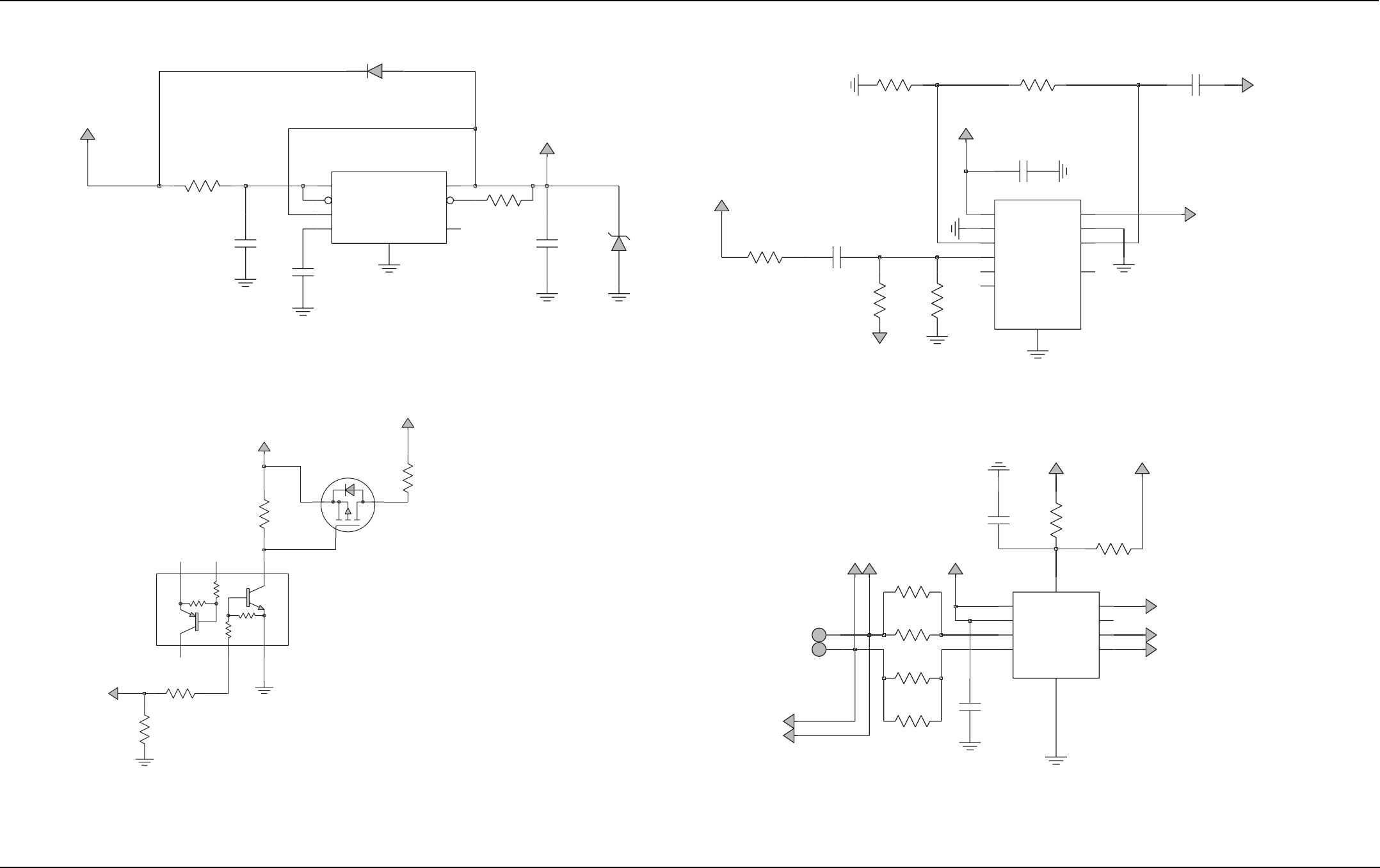
Schematics, Board Overlays, and Parts Lists – VHF: VOCON Section 8-17
6871620L01-C May 28, 2008
Figure 8-16. VOCON: Miscellaneous Circuits
UNSW_B+
5V_Misc
C1141
10uF
100K
R1133
R1209
RES
0
2.2uF
C1142
C1140
.01uF
1
ERROR
7
3
DNG
INPUT
4
NC
2
OUTPUT
5
SENSE
6SHUTDOWN
8
U1101
LP2989
LP2989IMMX-5.0
BYPASS
MBRM140T3
D4
VR1209
6.8V
V5A
3
INPOSA
7
INPOSB
1
OUTA
9
OUTB
5
SDA 6
SDBVNEG
4
10
VPOS
LMV712LDX
U9904
1G
DNGTC
2
INNEGA
8
INNEGB
C9975
4.7uF
C9968
0.10uF
R9930
V5A
A
JACKin
AUD_JACK_SPK_out
1.0uF
C9956
510
R9931
V5A
1K
R9932
39K
100K 10K
R9933 R9934
5V Misc. Regulator
Audio Jack Single-Ended Audio Gain Stage
Q9950
R1704
VIBRATE_CONT
V_VIBE
100K
R731
0
R735
2
5
6
3
1
4
0
U9905
R733
VSW1
100K
NU
NU
NU
NU
CE_SPKRCOM
-RK
P
S_T
X
E
CE_SPKR+
1000pF
C1216
WS
_
O
IDU
A
+RKPS_TXE
SPK+
1
SPK_COM 1
NC2
2
NO1
NO2
10
CCV 1
VCC5
EAR+
EAR-
COM1
3
9COM2
DNG
6
IN1
4
IN2
8
NC1
5
7
U20
NLAS4684
C1211
V5A
0
R9996
R9997
R1127
33
AJACKin
R1126
R10000
R10001
33
Haptic Device Supply Driver Audio Switch
8-18 Schematics, Board Overlays, and Parts Lists – VHF: Main Board (NUD7115B ) Parts List
May 28, 2008 6871620L01-C
8.6 Main Board (NUD7115B ) Parts
List
Ref. Des. Part Number Description
C4 2113945L49 CAP,FXD,.01UF,+5%,-5%,
50V-DC,0603,X7R,-55DEG
CMIN,125DEG CMAX,P
C6 2113944C51 CAP CER CHP 1000.OPF
50V 5
C9 2113945A09 CAP CER CHP 1000PF 50V
10%
C10 2113945A09 CAP CER CHP 1000PF 50V
10%
C11 2113946K02 CAP CER CHP 0.10UF 16V
C12 2113955E37 CAP,FXD,10UF,+10%,-10%,
16V-DC,1210,X7R,-55DEG
CMIN,125DEG CMAX
C13 2113945B02 CAP CER CHP 10,000PF
25V 10%
C14 2113955E37 CAP,FXD,10UF,+10%,-10%,
16V-DC,1210,X7R,-55DEG
CMIN,125DEG CMAX
C15 2113946E02 CAP CER CHP 1.0UF 16V
10%
C16 2113945B02 CAP CER CHP 10,000PF
25V 10%
C17 2113946E02 CAP CER CHP 1.0UF 16V
10%
C20 2113955E37 CAP,FXD,10UF,+10%,-10%,
16V-DC,1210,X7R,-55DEG
CMIN,125DEG CMAX
C21 2113944C14 CAP CER CHP 2.2PF 50V
+/- 0.25PF
C22 2113944C32 CAP CER CHP 15.0PF 50V
5%
C24 2113955E37 CAP,FXD,10UF,+10%,-10%,
16V-DC,1210,X7R,-55DEG
CMIN,125DEG CMAX
C25 2113946E02 CAP CER CHP 1.0UF 16V
10%
C26 2113945B02 CAP CER CHP 10,000PF
25V 10%
C27 2113946E02 CAP CER CHP 1.0UF 16V
10%
C28 2113945A09 CAP CER CHP 1000PF 50V
10%
C30 2313960B57 CAP,FXD,10UF,+10%,-10%,
6.3V-DC,SM,-55DEG CMIN,
125DEG CMAX, 137MA
C52 2113945A09 CAP CER CHP 1000PF 50V
10%
C53 2113945A09 CAP CER CHP 1000PF 50V
10%
C54 2113945A09 CAP CER CHP 1000PF 50V
10%
C55 2113945A09 CAP CER CHP 1000PF 50V
10%
C56 2113945A09 CAP CER CHP 1000PF 50V
10%
C57 2113945A09 CAP CER CHP 1000PF 50V
10%
C71 2113945A09 CAP CER CHP 1000PF 50V
10%
C72 2113945A09 CAP CER CHP 1000PF 50V
10%
C73 2113945A09 CAP CER CHP 1000PF 50V
10%
C101 2113945A58 CAP,FXD,910PF,+10%,
-10%,50V-DC,0402,X7R,
-55DEG CMIN,125DEG
CMAX
C102 2113944C39 CAP CER CHP 56.0PF 50V
5%
C103 2113945B02 CAP CER CHP 10,000PF
25V 10%
C104 2113945A58 CAP,FXD,910PF,+10%,
-10%,50V-DC,0402,X7R,
-55DEG CMIN,125DEG
CMAX
C105 2113945A58 CAP,FXD,910PF,+10%,
-10%,50V-DC,0402,X7R,
-55DEG CMIN,125DEG
CMAX
C106 2113945A58 CAP,FXD,910PF,+10%,
-10%,50V-DC,0402,X7R,
-55DEG CMIN,125DEG
CMAX
C107 2113945A58 CAP,FXD,910PF,+10%,
-10%,50V-DC,0402,X7R,
-55DEG CMIN,125DEG
CMAX
C108 2113945B02 CAP CER CHP 10,000PF
25V 10%
Ref. Des. Part Number Description
C110 2113945A58 CAP,FXD,910PF,+10%,
-10%,50V-DC,0402,X7R,
-55DEG CMIN,125DEG
CMAX
C111 2113944C06 CAP CER CHP 470.0PF
50V 5%
C112 2113944C70 CAP,FXD,5.1PF,.25PF+/-,
50V-DC,0603,C0G,-55DEG
CMIN,125DEG CMAX
C113 2113944C82 CAP,FXD,30PF,+5%,-5%,
50V-DC,0603,C0G,-55DEG
CMIN,125DEG CMAX,PB
C114 2113944C78 CAP,FXD,13PF,+5%,-5%,
50V-DC,0603,C0G,-55DEG
CMIN,125DEG CMAX,PB
C115 2113944C43 CAP CER CHP 82.0PF 50V
5%
C116 2113945C31 CAP,FXD,.1UF,+10%,-10%,
50V-DC,0603,X7R,-55DEG
CMIN,125DEG CMAX
C117 2113955C31 CAP,FXD,1UF,+10%,-10%,
16V-DC,X7R,-55DEG
CMIN,125DEG CMAX,
LEAD-
C118 2113945B02 CAP CER CHP 10,000PF
25V 10%
C119 2113944C06 CAP CER CHP 470.0PF
50V 5%
C120 2113944F52 CAP,FXD,27PF,+5%,-5%,
50V-DC,0805,C0G,-55DEG
CMIN,125DEG CMAX,PB
C121 2113944F52 CAP,FXD,27PF,+5%,-5%,
50V-DC,0805,C0G,-55DEG
CMIN,125DEG CMAX,PB
C122 2113944F52 CAP,FXD,27PF,+5%,-5%,
50V-DC,0805,C0G,-55DEG
CMIN,125DEG CMAX,PB
C123 2113944C74 CAP,FXD,7.5PF,.25PF+/-,
50V-DC,0603,C0G,-55DEG
CMIN,125DEG CMAX
C124 2113944F48 CAP,FXD,18PF,+5%,-5%,
50V-DC,0805,C0G,-55DEG
CMIN,125DEG CMAX,PB
C125 2113944C06 CAP CER CHP 470.0PF
50V 5%
C127 2113945A58 CAP,FXD,910PF,+10%,
-10%,50V-DC,0402,X7R,
-55DEG CMIN,125DEG
CMAX
Ref. Des. Part Number Description
C128 2113945A58 CAP,FXD,910PF,+10%,
-10%,50V-DC,0402,X7R,
-55DEG CMIN,125DEG
CMAX
C129 2113945A10 CAP CER CHP 1500PF 50V
10%
C130 2113945A05 CAP CER CHP 470PF 50V
10%
C131 2113946A01 CAP CER CHP 0.015UF
16V 10%
C132 2113945C31 CAP,FXD,.1UF,+10%,-10%,
50V-DC,0603,X7R,-55DEG
CMIN,125DEG CMAX
C133 2113955C31 CAP,FXD,1UF,+10%,-10%,
16V-DC,X7R,-55DEG
CMIN,125DEG CMAX,
LEAD-
C134 2113945B02 CAP CER CHP 10,000PF
25V 10%
C135 2113945A58 CAP,FXD,910PF,+10%,
-10%,50V-DC,0402,X7R,
-55DEG CMIN,125DEG
CMAX
C136 2113945A58 CAP,FXD,910PF,+10%,
-10%,50V-DC,0402,X7R,
-55DEG CMIN,125DEG
CMAX
C137 2113945A58 CAP,FXD,910PF,+10%,
-10%,50V-DC,0402,X7R,
-55DEG CMIN,125DEG
CMAX
C140 2113945A58 CAP,FXD,910PF,+10%,
-10%,50V-DC,0402,X7R,
-55DEG CMIN,125DEG
CMAX
C144 2113945A58 CAP,FXD,910PF,+10%,
-10%,50V-DC,0402,X7R,
-55DEG CMIN,125DEG
CMAX
C201 2113946K02 CAP CER CHP 0.10UF 16V
C202 2113946K02 CAP CER CHP 0.10UF 16V
C203 2113946N03 CAP CER CHP 2.2UF 16V
C204 2113946K02 CAP CER CHP 0.10UF 16V
C205 2113946K02 CAP CER CHP 0.10UF 16V
C206 2113955E37 CAP,FXD,10UF,+10%,-10%,
16V-DC,1210,X7R,-55DEG
CMIN,125DEG CMAX
C207 2113946K02 CAP CER CHP 0.10UF 16V
Ref. Des. Part Number Description
Schematics, Board Overlays, and Parts Lists – VHF: Main Board (NUD7115B ) Parts List 8-19
6871620L01-C May 28, 2008
C208 2113946K02 CAP CER CHP 0.10UF 16V
C209 2113946K02 CAP CER CHP 0.10UF 16V
C210 2113946K02 CAP CER CHP 0.10UF 16V
C211 2113946K02 CAP CER CHP 0.10UF 16V
C213 2113945A09 CAP CER CHP 1000PF 50V
10%
C214 2113944A40 CAP CER CHP 100.0PF
50V 5%
C215 2113946K02 CAP CER CHP 0.10UF 16V
C217 2113945C27 CAP,FXD,.047UF,+10%,
-10%,50V-DC,0603,X7R,
-55DEG CMIN,125DEG
CMA
C218 2113945C27 CAP,FXD,.047UF,+10%,
-10%,50V-DC,0603,X7R,
-55DEG CMIN,125DEG
CMA
C219 2109720D20 CAP CHIP LOW DIST 2000
SOV
C220 2113955E37 CAP,FXD,10UF,+10%,-10%,
16V-DC,1210,X7R,-55DEG
CMIN,125DEG CMAX
C221 2113946K02 CAP CER CHP 0.10UF 16V
C222 2113945L41 CAP,FXD,4700PF,+5%,-5%,
50V-DC,0603,X7R,-55DEG
CMIN,125DEG CMAX
C224 2185419D06 CAP CER SUPER L/D
0.1UF
C225 2185419D06 CAP CER SUPER L/D
0.1UF
C226 2185419D06 CAP CER SUPER L/D
0.1UF
C227 2185419D06 CAP CER SUPER L/D
0.1UF
C229 2113944A40 CAP CER CHP 100.0PF
50V 5%
C230 2113945A03 CAP CER CHP 330PF 50V
10%
C231 2113945B02 CAP CER CHP 10,000PF
25V 10%
C232 2113955E37 CAP,FXD,10UF,+10%,-10%,
16V-DC,1210,X7R,-55DEG
CMIN,125DEG CMAX
C233 2113946K02 CAP CER CHP 0.10UF 16V
C234 2113945B02 CAP CER CHP 10,000PF
25V 10%
Ref. Des. Part Number Description
C235 2113944A40 CAP CER CHP 100.0PF
50V 5%
C236 2113945A09 CAP CER CHP 1000PF 50V
10%
C241 2185419D06 CAP CER SUPER L/D
0.1UF
C242 2185419D06 CAP CER SUPER L/D
0.1UF
C250 2113946K02 CAP CER CHP 0.10UF 16V
C301 2113944A26 CAP CER CHP 12.0PF 50V
5%
C302 2113944A27 CAP CER CHP 15.0PF 50V
5%
C303 2113944A28 CAP CER CHP 18.0PF 50V
5%
C304 2113944A27 CAP CER CHP 15.0PF 50V
5%
C305 2113944A13 CAP CER CHP 3.3PF 50V
+/- 0.25PF
C306 2188881Y12 CAPACITOR CERAMIC
NPO HIGH FREQUENCY
16 VOLT (REPLACES
2104801Z12)
C307 2113944V03 CAP,FXD,1PF,.1PF+/-,
50V-DC,0402,C0G,-55DEG
CMIN,125DEG CMAX,PB
C308 2113944A05 CAP CER CHP 1.5PF 50V
+/- 0.25PF
C309 2113945A03 CAP CER CHP 330PF 50V
10%
C310 2113945A03 CAP CER CHP 330PF 50V
10%
C313 2113945C31 CAP,FXD,.1UF,+10%,-10%,
50V-DC,0603,X7R,-55DEG
CMIN,125DEG CMAX
C314 2113945A03 CAP CER CHP 330PF 50V
10%
C315 2113945A03 CAP CER CHP 330PF 50V
10%
C316 2113944A28 CAP CER CHP 18.0PF 50V
5%
C317 2113944V11 CAP,FXD,2.2PF,.1PF+/-,
50V-DC,0402,C0G,-55DEG
CMIN,125DEG CMAX
C318 2113945A03 CAP CER CHP 330PF 50V
10%
Ref. Des. Part Number Description
C320 2113944V03 CAP,FXD,1PF,.1PF+/-,
50V-DC,0402,C0G,-55DEG
CMIN,125DEG CMAX,PB
C321 2113944V11 CAP,FXD,2.2PF,.1PF+/-,
50V-DC,0402,C0G,-55DEG
CMIN,125DEG CMAX
C322 2113945A03 CAP CER CHP 330PF 50V
10%
C330 2113945A03 CAP CER CHP 330PF 50V
10%
C333 2113945A03 CAP CER CHP 330PF 50V
10%
C337 2113945A01 CAP CER CHP 220PF 50V
10,
C350 NOT PLACED –
C351 NOT PLACED –
C410 2113944A81 CAP,FXD,24PF,+5%,-5%,
50V-DC,0402,C0G,-55DEG
CMIN,125DEG CMAX,PB
C411 2113944A41 CAP CER CHP 120.0PF
50V 5%
C413 2113946D07 CAP,CHIP,4.7UF,+10%,
-10%,6.3V-DC,0603,X5R,
-55DEG CMIN,85DEG CMA
C414 2113944A41 CAP CER CHP 120.0PF
50V 5%
C416 2113944A81 CAP,FXD,24PF,+5%,-5%,
50V-DC,0402,C0G,-55DEG
CMIN,125DEG CMAX,PB
C417 2113946B04 CAP CER CHP 0.10UF 10V
10%
C420 2113946B04 CAP CER CHP 0.10UF 10V
10%
C432 2113945A09 CAP CER CHP 1000PF 50V
10%
C433 2113946B04 CAP CER CHP 0.10UF 10V
10%
C434 2113946B04 CAP CER CHP 0.10UF 10V
10%
C435 2113944A21 CAP CER CHP 6.8PF 50V
+/- 0.5PF
C436 2113944A23 CAP CER CHP 8.2PF 50V
+/- 0.5PF
C450 2113944A81 CAP,FXD,24PF,+5%,-5%,
50V-DC,0402,C0G,-55DEG
CMIN,125DEG CMAX,PB
Ref. Des. Part Number Description
C451 2113944A41 CAP CER CHP 120.0PF
50V 5%
C452 2113944A41 CAP CER CHP 120.0PF
50V 5%
C455 2113944A81 CAP,FXD,24PF,+5%,-5%,
50V-DC,0402,C0G,-55DEG
CMIN,125DEG CMAX,PB
C456 2113946B04 CAP CER CHP 0.10UF 10V
10%
C470 2113944A79 CAP,FXD,16PF,+5%,-5%,
50V-DC,0402,C0G,-55DEG
CMIN,125DEG CMAX,PB
C471 NOT PLACED –
C472 2113945A03 CAP CER CHP 330PF 50V
10%
C473 2113945A58 CAP,FXD,910PF,+10%,
-10%,50V-DC,0402,X7R,
-55DEG CMIN,125DEG
CMAX
C474 2113945A58 CAP,FXD,910PF,+10%,
-10%,50V-DC,0402,X7R,
-55DEG CMIN,125DEG
CMAX
C475 2113946F03 CAP CER CHP 4.7UF 6.3V
10%
C476 2113944A09 CAP CER CHP 2.2PF 50V
+/- 0.25PF
C477 2113945A03 CAP CER CHP 330PF 50V
10%
C478 2113944A79 CAP,FXD,16PF,+5%,-5%,
50V-DC,0402,C0G,-55DEG
CMIN,125DEG CMAX,PB
C479 2113946B04 CAP CER CHP 0.10UF 10V
10%
C480 2113945A58 CAP,FXD,910PF,+10%,
-10%,50V-DC,0402,X7R,
-55DEG CMIN,125DEG
CMAX
C481 2113945B02 CAP CER CHP 10,000PF
25V 10%
C482 2113945B02 CAP CER CHP 10,000PF
25V 10%
C490 2113944A28 CAP CER CHP 18.0PF 50V
5%
C491 2113944A78 CAP,FXD,13PF,+5%,-5%,
50V-DC,0402,C0G,-55DEG
CMIN,125DEG CMAX,PB
Ref. Des. Part Number Description
8-20 Schematics, Board Overlays, and Parts Lists – VHF: Main Board (NUD7115B ) Parts List
May 28, 2008 6871620L01-C
C501 2113944A40 CAP CER CHP 100.0PF
50V 5%
C505 2113944A40 CAP CER CHP 100.0PF
50V 5%
C506 2113946K02 CAP CER CHP 0.10UF 16V
C507 2113945A11 CAP CER CHP 2200PF 50V
10%
C509 2113946B02 CAP CER CHP 0.047UF
10V 10,
C511 2113944A40 CAP CER CHP 100.0PF
50V 5%
C512 2113944A40 CAP CER CHP 100.0PF
50V 5%
C513 2113945B02 CAP CER CHP 10,000PF
25V 10%
C514 2113946K02 CAP CER CHP 0.10UF 16V
C527 2113946K02 CAP CER CHP 0.10UF 16V
C535 2113945B02 CAP CER CHP 10,000PF
25V 10%
C539 2113946B04 CAP CER CHP 0.10UF 10V
10%
C540 2113946K02 CAP CER CHP 0.10UF 16V
C541 2113945B02 CAP CER CHP 10,000PF
25V 10%
C542 2113945B02 CAP CER CHP 10,000PF
25V 10%
C544 2113945B02 CAP CER CHP 10,000PF
25V 10%
C546 2113945B02 CAP CER CHP 10,000PF
25V 10%
C547 2113945B02 CAP CER CHP 10,000PF
25V 10%
C548 2113946B02 CAP CER CHP 0.047UF
10V 10,
C550 2113944A28 CAP CER CHP 18.0PF 50V
5%
C551 2113946S35 CAP CER CHP 1.0UF 16V
10%
C552 2113946S35 CAP CER CHP 1.0UF 16V
10%
C553 2113946C07 CAP,FXD,.33UF,+10%,
-10%,10V-DC,0603,X5R,
-55DEG CMIN,85DEG
CMAX
C554 2113944A28 CAP CER CHP 18.0PF 50V
5%
Ref. Des. Part Number Description
C555 2113944A85 CAP,FXD,51PF,+5%,-5%,
50V-DC,0402,C0G,-55DEG
CMIN,125DEG CMAX,PB
C556 2113944A36 CAP CER CHP 68.0PF 50V
5%
C557 2113944A40 CAP CER CHP 100.0PF
50V 5%
C560 2113944A29 CAP CER CHP 22.0PF 50V
5%
C561 2313960B30 CAP,FXD,4.7UF,+10%,
-10%,10V-DC,SM,-55DEG
CMIN,125DEG
CMAX,122MA
C562 2113945B02 CAP CER CHP 10,000PF
25V 10%
C570 2113945G91 CAP,FXD,.1UF,+10%,-10%,
50V-DC,0805,X7R,-55DEG
CMIN,125DEG CMAX
C571 2113945G91 CAP,FXD,.1UF,+10%,-10%,
50V-DC,0805,X7R,-55DEG
CMIN,125DEG CMAX
C572 2113945C25 CAP,FXD,.033UF,+10%,
-10%,50V-DC,0603,X7R,
-55DEG CMIN,125DEG
CMA
C573 2113944A36 CAP CER CHP 68.0PF 50V
5%
C574 2113945B02 CAP CER CHP 10,000PF
25V 10%
C581 2113944A42 CAP CER CHP 150.0PF
50V 5%
C582 2113946K02 CAP CER CHP 0.10UF 16V
C583 2113945B02 CAP CER CHP 10,000PF
25V 10%
C704 2113945A58 CAP,FXD,910PF,+10%,
-10%,50V-DC,0402,X7R,
-55DEG CMIN,125DEG
CMAX
C705 2113944C81 CAP,FXD,24PF,+5%,-5%
,50V-DC,0603,C0G,-55DEG
CMIN,125DEG CMAX,PB
C706 2113944C30 CAP CER CHP 10.0PF 50V
+/- 0.5PF
C707 2113944C79 CAP,FXD,16PF,+5%,-5%,
50V-DC,0603,C0G,-55DEG
CMIN,125DEG CMAX,PB
C709 2113944C24 CAP CER CHP 5.6PF 50V
+/- 0.5PF
Ref. Des. Part Number Description
C710 2113944C80 CAP,FXD,20PF,+5%,-5%,
50V-DC,0603,C0G,-55DEG
CMIN,125DEG CMAX,PB
C711 2113944C33 CAP CER CHP 18.0PF 50V
5%
C712 2113945A09 CAP CER CHP 1000PF 50V
10%
C713 2113944A11 CAP CER CHP 2.7PF 50V
+/- 0.25PF
C715 2113945A09 CAP CER CHP 1000PF 50V
10%
C716 2113945A09 CAP CER CHP 1000PF 50V
10%
C717 2113946K02 CAP CER CHP 0.10UF 16V
C720 2113944C77 CAP,FXD,11PF,+5%,-5%,
50V-DC,0603,C0G,-55DEG
CMIN,125DEG CMAX,PB
C1101 2113945A58 CAP,FXD,910PF,+10%,
-10%,50V-DC,0402,X7R,
-55DEG CMIN,125DEG
CMAX
C1102 2113945A09 CAP CER CHP 1000PF 50V
10%
C1104 2113945A09 CAP CER CHP 1000PF 50V
10%
C1105 2113945A58 CAP,FXD,910PF,+10%,
-10%,50V-DC,0402,X7R,
-55DEG CMIN,125DEG
CMAX
C1106 2113945A58 CAP,FXD,910PF,+10%,
-10%,50V-DC,0402,X7R,
-55DEG CMIN,125DEG
CMAX
C1107 2113945A58 CAP,FXD,910PF,+10%,
-10%,50V-DC,0402,X7R,
-55DEG CMIN,125DEG
CMAX
C1108 2113945A58 CAP,FXD,910PF,+10%,
-10%,50V-DC,0402,X7R,
-55DEG CMIN,125DEG
CMAX
C1109 2113945A58 CAP,FXD,910PF,+10%,
-10%,50V-DC,0402,X7R,
-55DEG CMIN,125DEG
CMAX
C1110 2113945A58 CAP,FXD,910PF,+10%,
-10%,50V-DC,0402,X7R,
-55DEG CMIN,125DEG
CMAX
Ref. Des. Part Number Description
C1111 2113945A58 CAP,FXD,910PF,+10%,
-10%,50V-DC,0402,X7R,
-55DEG CMIN,125DEG
CMAX
C1112 2113945A58 CAP,FXD,910PF,+10%,
-10%,50V-DC,0402,X7R,
-55DEG CMIN,125DEG
CMAX
C1113 2113945A58 CAP,FXD,910PF,+10%,
-10%,50V-DC,0402,X7R,
-55DEG CMIN,125DEG
CMAX
C1114 2113945A58 CAP,FXD,910PF,+10%,
-10%,50V-DC,0402,X7R,
-55DEG CMIN,125DEG
CMAX
C1115 2113945A58 CAP,FXD,910PF,+10%,
-10%,50V-DC,0402,X7R,
-55DEG CMIN,125DEG
CMAX
C1116 2113945A58 CAP,FXD,910PF,+10%,
-10%,50V-DC,0402,X7R,
-55DEG CMIN,125DEG
CMAX
C1117 2113945A05 CAP CER CHP 470PF 50V
10%
C1118 2113945A05 CAP CER CHP 470PF 50V
10%
C1119 2113945A58 CAP,FXD,910PF,+10%,
-10%,50V-DC,0402,X7R,
-55DEG CMIN,125DEG
CMAX
C1120 2113945A58 CAP,FXD,910PF,+10%,
-10%,50V-DC,0402,X7R,
-55DEG CMIN,125DEG
CMAX
C1123 2113945A58 CAP,FXD,910PF,+10%,
-10%,50V-DC,0402,X7R,
-55DEG CMIN,125DEG
CMAX
C1124 2113945B02 CAP CER CHP 10,000PF
25V 10%
C1125 2113945A05 CAP CER CHP 470PF 50V
10%
C1126 2113945A05 CAP CER CHP 470PF 50V
10%
C1128 2113945A58 CAP,FXD,910PF,+10%,
-10%,50V-DC,0402,X7R,
-55DEG CMIN,125DEG
CMAX
Ref. Des. Part Number Description
Schematics, Board Overlays, and Parts Lists – VHF: Main Board (NUD7115B ) Parts List 8-21
6871620L01-C May 28, 2008
C1129 2113955C31 CAP,FXD,1UF,+10%,-10%,
16V-DC,X7R,-55DEG
CMIN,125DEG CMAX,
LEAD-
C1130 2113945A05 CAP CER CHP 470PF 50V
10%
C1131 2113944A31 CAP CER CHP 33.0PF 50V
5%
C1132 2113944A31 CAP CER CHP 33.0PF 50V
5%
C1133 2113944A31 CAP CER CHP 33.0PF 50V
5%
C1134 2113944A31 CAP CER CHP 33.0PF 50V
5%
C1135 2113945A05 CAP CER CHP 470PF 50V
10%
C1136 2113944A31 CAP CER CHP 33.0PF 50V
5%
C1138 2113945A05 CAP CER CHP 470PF 50V
10%
C1139 2113945A58 CAP,FXD,910PF,+10%,
-10%,50V-DC,0402,X7R,
-55DEG CMIN,125DEG
CMAX
C1140 2113945B02 CAP CER CHP 10,000PF
25V 10%
C1141 2113946F05 CAP,CHIP,10UF,+10%,
-10%,6.3V-DC,0805,X5R,
-55DEG CMIN,85DEG
CMAX
C1142 2113956C43 CAP,FXD,2.2UF,+10%
,-10%,10V-DC,0805,X5R
,-55DEG CMIN,85DEG
CMAX
C1202 2113945A58 CAP,FXD,910PF,+10%,
-10%,50V-DC,0402,X7R,
-55DEG CMIN,125DEG
CMAX
C1209 2113945A05 CAP CER CHP 470PF 50V
10%
C1210 2113945A05 CAP CER CHP 470PF 50V
10%
C1211 NOT PLACED –
C1212 2113944A31 CAP CER CHP 33.0PF 50V
5%
C1213 2113945A05 CAP CER CHP 470PF 50V
10%
Ref. Des. Part Number Description
C1214 2113944A31 CAP CER CHP 33.0PF 50V
5%
C1215 2113945A05 CAP CER CHP 470PF 50V
10%
C1216 2113945A09 CAP CER CHP 1000PF 50V
10%
C1217 2113945A05 CAP CER CHP 470PF 50V
10%
C1218 2113946K02 CAP CER CHP 0.10UF 16V
C1219 2113946K02 CAP CER CHP 0.10UF 16V
C1220 2113945A05 CAP CER CHP 470PF 50V
10%
C1221 2113945A05 CAP CER CHP 470PF 50V
10%
C1222 2113944A40 CAP CER CHP 100.0PF
50V 5%
C1223 2113946K02 CAP CER CHP 0.10UF 16V
C1224 2113946K02 CAP CER CHP 0.10UF 16V
C1225 2113946K02 CAP CER CHP 0.10UF 16V
C1232 2113944A40 CAP CER CHP 100.0PF
50V 5%
C1301 2113945A05 CAP CER CHP 470PF 50V
10%
C1302 2113946K02 CAP CER CHP 0.10UF 16V
C1303 2113944A25 CAP CER CHP 10.0PF 50V
+/- 0.5PF
C1304 2113946K02 CAP CER CHP 0.10UF 16V
C1305 2113944A19 CAP CER CHP 5.6PF 50V
+/- 0.5PF
C1306 2113944A19 CAP CER CHP 5.6PF 50V
+/- 0.5PF
C1307 2113946F01 CAP CER CHP 2.2UF 6.3V
10%
C1308 2113946F01 CAP CER CHP 2.2UF 6.3V
10%
C1309 2113945A09 CAP CER CHP 1000PF 50V
10%
C1310 2113945B02 CAP CER CHP 10,000PF
25V 10%
C1312 2113946G01 CAP CER CHP 2.2UF 16V
10%
C1313 2113945A03 CAP CER CHP 330PF 50V
10%
C1314 2113945A03 CAP CER CHP 330PF 50V
10%
Ref. Des. Part Number Description
C1315 2113945B02 CAP CER CHP 10,000PF
25V 10%
C1316 2113944A31 CAP CER CHP 33.0PF 50V
5%
C1317 2113944A31 CAP CER CHP 33.0PF 50V
5%
C1318 2113945B02 CAP CER CHP 10,000PF
25V 10%
C1319 2113946D02 CAP CER CHP 1.0UF 6.3V
10%
C1320 2113946G01 CAP CER CHP 2.2UF 16V
10%
C1321 2113946D02 CAP CER CHP 1.0UF 6.3V
10%
C1322 2113946D02 CAP CER CHP 1.0UF 6.3V
10%
C1323 2113946D02 CAP CER CHP 1.0UF 6.3V
10%
C1324 2113946D02 CAP CER CHP 1.0UF 6.3V
10%
C1325 2113945B02 CAP CER CHP 10,000PF
25V 10%
C1326 2113946D02 CAP CER CHP 1.0UF 6.3V
10%
C1327 2113945B02 CAP CER CHP 10,000PF
25V 10%
C1328 2113946D05 CAP,CHIP,2.2UF,+10%,
-10%,6.3V-DC,0603,X5R,
-55DEG CMIN,85DEG CMA
C1329 2113945B02 CAP CER CHP 10,000PF
25V 10%
C1330 2113946D05 CAP,CHIP,2.2UF,+10%,
-10%,6.3V-DC,0603,X5R,
-55DEG CMIN,85DEG CMA
C1331 2113945B02 CAP CER CHP 10,000PF
25V 10%
C1332 2371572L01 POSCAD 47UF
C1333 2371572L01 POSCAD 47UF
C1335 2113946D02 CAP CER CHP 1.0UF 6.3V
10%
C1336 2113945C31 CAP,FXD,.1UF,+10%,-10%,
50V-DC,0603,X7R,-55DEG
CMIN,125DEG CMAX
C1337 2113945A09 CAP CER CHP 1000PF 50V
10%
Ref. Des. Part Number Description
C1338 2113946D02 CAP CER CHP 1.0UF 6.3V
10%
C1339 2113945B02 CAP CER CHP 10,000PF
25V 10%
C1340 2113955E37 CAP,FXD,10UF,+10%,-10%,
16V-DC,1210,X7R,-55DEG
CMIN,125DEG CMAX
C1341 2113945C31 CAP,FXD,.1UF,+10%,-10%,
50V-DC,0603,X7R,-55DEG
CMIN,125DEG CMAX
C1342 2113955E37 CAP,FXD,10UF,+10%,-10%,
16V-DC,1210,X7R,-55DEG
CMIN,125DEG CMAX
C1343 2113955E37 CAP,FXD,10UF,+10%,-10%,
16V-DC,1210,X7R,-55DEG
CMIN,125DEG CMAX
C1345 2113946D02 CAP CER CHP 1.0UF 6.3V
10%
C1346 2113955E37 CAP,FXD,10UF,+10%,-10%,
16V-DC,1210,X7R,-55DEG
CMIN,125DEG CMAX
C1347 2113946E02 CAP CER CHP 1.0UF 16V
10%
C1348 2113944A40 CAP CER CHP 100.0PF
50V 5%
C1349 2113955E37 CAP,FXD,10UF,+10%,-10%,
16V-DC,1210,X7R,-55DEG
CMIN,125DEG CMAX
C1350 2113945C21 CAP,FXD,.018UF,+10%,
-10%,50V-DC,0603,X7R,
-55DEG CMIN,125DEG
CMA
C1351 2113944A40 CAP CER CHP 100.0PF
50V 5%
C1352 2113946D02 CAP CER CHP 1.0UF 6.3V
10%
C1353 2113946D02 CAP CER CHP 1.0UF 6.3V
10%
C1354 2113945D04 CAP CER CHP 100,000PF
25V 10%
C1355 2113946A02 CAP CER CHP 0.022UF
16V 10,
C1356 2113946B03 CAP CER CHP 0.068UF
10V 10
C1357 2113946B03 CAP CER CHP 0.068UF
10V 10
Ref. Des. Part Number Description
8-22 Schematics, Board Overlays, and Parts Lists – VHF: Main Board (NUD7115B ) Parts List
May 28, 2008 6871620L01-C
C1362 2113945D04 CAP CER CHP 100,000PF
25V 10%
C1363 2113945D04 CAP CER CHP 100,000PF
25V 10%
C1364 2113944A40 CAP CER CHP 100.0PF
50V 5%
C1365 2113944A40 CAP CER CHP 100.0PF
50V 5%
C1367 2113946K02 CAP CER CHP 0.10UF 16V
C1368 2113944A40 CAP CER CHP 100.0PF
50V 5%
C1370 2113946K02 CAP CER CHP 0.10UF 16V
C1402 2113946E02 CAP CER CHP 1.0UF 16V
10%
C1403 2113946K02 CAP CER CHP 0.10UF 16V
C1404 2113944A40 CAP CER CHP 100.0PF
50V 5%
C1407 2113944A40 CAP CER CHP 100.0PF
50V 5%
C1408 2113946K02 CAP CER CHP 0.10UF 16V
C1409 2113946A01 CAP CER CHP 0.015UF
16V 10%
C1410 2113946K02 CAP CER CHP 0.10UF 16V
C1411 2113946K02 CAP CER CHP 0.10UF 16V
C1412 2113946E02 CAP CER CHP 1.0UF 16V
10%
C1413 2113946A01 CAP CER CHP 0.015UF
16V 10%
C1414 2113946K02 CAP CER CHP 0.10UF 16V
C1416 2113946F03 CAP CER CHP 4.7UF 6.3V
10%
C1417 2113946K02 CAP CER CHP 0.10UF 16V
C1418 2113946E02 CAP CER CHP 1.0UF 16V
10%
C1419 2113944A40 CAP CER CHP 100.0PF
50V 5%
C1420 2113946K02 CAP CER CHP 0.10UF 16V
C1421 2113946A01 CAP CER CHP 0.015UF
16V 10%
C1422 2113946K02 CAP CER CHP 0.10UF 16V
C1424 2113946K02 CAP CER CHP 0.10UF 16V
C1425 2113944A40 CAP CER CHP 100.0PF
50V 5%
Ref. Des. Part Number Description
C1427 2113944A40 CAP CER CHP 100.0PF
50V 5%
C1428 2113944A40 CAP CER CHP 100.0PF
50V 5%
C1429 2113944A48 CAP CER CHP 470.0 PF
50V 5%
C1430 2113946K02 CAP CER CHP 0.10UF 16V
C1431 2113946K02 CAP CER CHP 0.10UF 16V
C1432 2113946K02 CAP CER CHP 0.10UF 16V
C1433 2113946K02 CAP CER CHP 0.10UF 16V
C1440 NOT PLACED –
C1441 NOT PLACED –
C1442 NOT PLACED –
C1443 NOT PLACED –
C1444 NOT PLACED –
C1445 2113944A38 CAP CER CHP 82.0PF 50V
5%
C1446 2113944A38 CAP CER CHP 82.0PF 50V
5%
C1447 2113944A38 CAP CER CHP 82.0PF 50V
5%
C1448 2113944A38 CAP CER CHP 82.0PF 50V
5%
C1449 2113944A38 CAP CER CHP 82.0PF 50V
5%
C1450 2113944A38 CAP CER CHP 82.0PF 50V
5%
C1451 2113944A38 CAP CER CHP 82.0PF 50V
5%
C1452 2113944A38 CAP CER CHP 82.0PF 50V
5%
C1453 2113944A38 CAP CER CHP 82.0PF 50V
5%
C1454 2113944A38 CAP CER CHP 82.0PF 50V
5%
C1455 2113944A38 CAP CER CHP 82.0PF 50V
5%
C1456 2113944A38 CAP CER CHP 82.0PF 50V
5%
C1457 2113944A38 CAP CER CHP 82.0PF 50V
5%
C1458 2113944A38 CAP CER CHP 82.0PF 50V
5%
Ref. Des. Part Number Description
C1459 2113944A38 CAP CER CHP 82.0PF 50V
5%
C1460 2113944A38 CAP CER CHP 82.0PF 50V
5%
C1719 2113945A09 CAP CER CHP 1000PF 50V
10%
C1722 2113945A09 CAP CER CHP 1000PF 50V
10%
C9901 2113945A09 CAP CER CHP 1000PF 50V
10%
C9950 2113945Y02 CAP,FXD,.1UF,+10%,-10%,
16V-DC,0402,X7R,-55DEG
CMIN,125DEG CMAX
C9951 2113945Y02 CAP,FXD,.1UF,+10%,-10%,
16V-DC,0402,X7R,-55DEG
CMIN,125DEG CMAX
C9952 2113945Y02 CAP,FXD,.1UF,+10%,-10%,
16V-DC,0402,X7R,-55DEG
CMIN,125DEG CMAX
C9953 2113945Y02 CAP,FXD,.1UF,+10%,-10%,
16V-DC,0402,X7R,-55DEG
CMIN,125DEG CMAX
C9954 2113945Y02 CAP,FXD,.1UF,+10%,-10%,
16V-DC,0402,X7R,-55DEG
CMIN,125DEG CMAX
C9956 2113946E02 CAP CER CHP 1.0UF 16V
10%
C9966 2113945A58 CAP,FXD,910PF,+10%,
-10%,50V-DC,0402,X7R,
-55DEG CMIN,125DEG
CMAX
C9968 2113946K02 CAP CER CHP 0.10UF 16V
C9969 2113945Y02 CAP,FXD,.1UF,+10%,-10%,
16V-DC,0402,X7R,-55DEG
CMIN,125DEG CMAX
C9970 2113945A09 CAP CER CHP 1000PF 50V
10%
C9975 2113946D07 CAP,CHIP,4.7UF,+10%,
-10%,6.3V-DC,0603,X5R,
-55DEG CMIN,85DEG CMA
C9980 2113945Y02 CAP,FXD,.1UF,+10%,-10%,
16V-DC,0402,X7R,-55DEG
CMIN,125DEG CMAX
D1 4813978M15 DIODE,RECT,RM140,SM,
1A,40V,SHTK,PB-FREE
D2 4813978M15 DIODE,RECT,RM140,SM,
1A,40V,SHTK,PB-FREE
Ref. Des. Part Number Description
D3 4813978M15 DIODE,RECT,RM140,SM,
1A,40V,SHTK,PB-FREE
D4 4813978M15 DIODE,RECT,RM140,SM,
1A,40V,SHTK,PB-FREE
D104 4813978A26 DIODE ARRAY,DET,
SOT-363/SC-88,30V,.12W,2
D201 4815011H01 DIODE TRIPLE
D202 4815011H01 DIODE TRIPLE
D301 4885094Y01 DIODE VARACTOR ISV228
W18
D302 4885094Y01 DIODE VARACTOR ISV228
W18
D303 4885094Y01 DIODE VARACTOR ISV228
W18
D411 4815096H01 VARACTOR DIODE
1SV305
D412 4815096H01 VARACTOR DIODE
1SV305
D413 4815096H01 VARACTOR DIODE
1SV305
D414 4815096H01 VARACTOR DIODE
1SV305
D451 4815096H01 VARACTOR DIODE
1SV305
D452 4815096H01 VARACTOR DIODE
1SV305
D453 4815096H01 VARACTOR DIODE
1SV305
D454 4815096H01 VARACTOR DIODE
1SV305
D550 4805656W41 DIODE VARACTOR 40PFV
15PFV
D570 4805656W87 DIODE,VCTR, @ 15V,
1SV279,SOD-523/SC-79
D701 4871607L01 PIN DIODE SMD
D702 4871607L01 PIN DIODE SMD
D703 4808115L27 DIODE,PIN,DH50037,SM,S
OT-323,30V
D1000 4888722V01 DIODE,RB520S,SM,
SOD-523/SC-79,200MA,
30V PB FREE
D1202 4813978A25 SCHOTTKY 30V SOD-323
T&R PB FREE
D1205 4813977C23 DIODE,ZEN,MMSZ5243,SM
,SOD-123,13V, 10MA,.5W,
ZEN,PB-FREE
Ref. Des. Part Number Description
Schematics, Board Overlays, and Parts Lists – VHF: Main Board (NUD7115B ) Parts List 8-23
6871620L01-C May 28, 2008
D1207 4813978A25 SCHOTTKY 30V SOD-323
T&R PB FREE
D1222 4888722V01 DIODE,RB520S,SM,
SOD-523/SC-79,200MA,
30V,PB FREE
D1223 4888722V01 DIODE,RB520S,SM,
SOD-523/SC-79,200MA,
30V,PB FREE
D1301 4805129M90 DIODE SOT PKGD
D1401 4888722V01 DIODE,RB520S,SM,
SOD-523/SC-79,200MA,
30V,PB FREE
D1402 4888722V01 DIODE,RB520S,SM,
SOD-523/SC-79,200MA,
30V,PB FREE
E5 2480640Z01 SURFACE MOUNT
FERRITE BEAD
E101 7686949J14 FLTR,FERRITE BEAD,2A,
SM,0805,CHIP,220OHM
E104 2480574F01 IND FERRITE CHIP 60OHM
0603
E105 2480640Z01 SURFACE MOUNT
FERRITE BEAD
E500 2480640Z01 SURFACE MOUNT
FERRITE BEAD
E501 2480574F01 IND FERRITE CHIP 60OHM
0603
E1102 2480574F01 IND FERRITE CHIP 60OHM
0603
E1103 2480574F01 IND FERRITE CHIP 60OHM
0603
E1104 2462586G33 INDUCTOR CHIP FERRITE
BEADS
E1110 2480640Z01 SURFACE MOUNT
FERRITE BEAD
E1111 2480640Z01 SURFACE MOUNT
FERRITE BEAD
E1112 2480640Z01 SURFACE MOUNT
FERRITE BEAD
E1113 2480640Z01 SURFACE MOUNT
FERRITE BEAD
E1114 2480640Z01 SURFACE MOUNT
FERRITE BEAD
E1115 2480640Z01 SURFACE MOUNT
FERRITE BEAD
E1116 2480640Z01 SURFACE MOUNT
FERRITE BEAD
Ref. Des. Part Number Description
E1117 2480640Z01 SURFACE MOUNT
FERRITE BEAD
E1118 2480640Z01 SURFACE MOUNT
FERRITE BEAD
E1119 2480640Z01 SURFACE MOUNT
FERRITE BEAD
E1120 2480640Z01 SURFACE MOUNT
FERRITE BEAD
E1121 2480640Z01 SURFACE MOUNT
FERRITE BEAD
E1122 2480640Z01 SURFACE MOUNT
FERRITE BEAD
E1123 2480640Z01 SURFACE MOUNT
FERRITE BEAD
E1124 2480640Z01 SURFACE MOUNT
FERRITE BEAD
E1125 2480640Z01 SURFACE MOUNT
FERRITE BEAD
E1126 2480640Z01 SURFACE MOUNT
FERRITE BEAD
E1127 2480640Z01 SURFACE MOUNT
FERRITE BEAD
E1129 2480640Z01 SURFACE MOUNT
FERRITE BEAD
E1130 2480640Z01 SURFACE MOUNT
FERRITE BEAD
E1201 2480574F01 IND FERRITE CHIP 60OHM
0603
E1401 2480574F01 IND FERRITE CHIP 60OHM
0603
E1402 2480574F01 IND FERRITE CHIP 60OHM
0603
F901 6515076H01 FUSE CHIP SMT 0603FA3-
R
FL200 9116848H01 FLTR SW CAP 3 POLE
BUTTERW, W18
FL490 9171859L01 CRYSTAL FILTER
J1 0970312N01 CONN,BTB,RCPT,60CONT,
.4MM,GLD,1 STACK HGT
J2 0987817K04 30PIN RECPT MATING
CNTCR 1.5MM
J3 0987817K02 RECP 0.5 PITCH 16 CKT
J1704 0971876L01 MINIATURE INTERFACE
COAXIAL SWITCH
Ref. Des. Part Number Description
L10 2489669V01 IDCTR,WW,100UH,5%,
40MA,10OHM,20 Q,10MHZ
SRF,SM,1210,PB-FREE
L20 2460591E81 COIL AIR WOUND INDUC
52.29
L101 2414017N10 IDCTR,CHIP,6.8NH,5%,
600MA,.22OHM,CER,12
Q,2.7GHZ SRF,SM,0603
L102 2414032D30 IDCTR,WW,1UH,5%,320MA
,2.8OHM,CER,28 Q,
340MHZ SRF,SM,LEAD-FR
L103 2414017N18 IDCTR,CHIP,33NH,5%,
600MA,.71OHM,CER,15 Q,
1.1GHZ SRF,SM,0603
L104 2414017N16 IDCTR,CHIP,22NH,5%,
600MA,.54OHM,CER,13 Q,
1.3GHZ SRF,SM,0603
L105 2479990E01 COIL AIR WOUND/GREEN
CLR 23.75
L106 2479990B01 AIR WND COIL/GREEN
COLOR 11.03
L107 2415428H01 AIR WOUND INDUCTOR
L108 2479990E01 COIL AIR WOUND/GREEN
CLR 23.75
L201 2414017Q20 IDCTR,FXD,2.2UH,20%,
30MA,.65OHM,FERR,45 Q,
50MHZ SRF,SM,0805
L202 2414017Q20 IDCTR,FXD,2.2UH,20%,
30MA,.65OHM,FERR,45 Q,
50MHZ SRF,SM,0805
L203 2414017Q20 IDCTR,FXD,2.2UH,20%,
30MA,.65OHM,FERR,45 Q,
50MHZ SRF,SM,0805
L204 2414017Q20 IDCTR,FXD,2.2UH,20%,
30MA,.65OHM,FERR,45 Q,
50MHZ SRF,SM,0805
L205 2414017Q47 IDCTR,FXD,1UH,10%,
50MA,.45OHM,FERR,45 Q,
75MHZ SRF,SM,0805,PB
L207 2414017Q47 IDCTR,FXD,1UH,10%,
50MA, .45OHM,FERR,45 Q,
75MHZ SRF,SM,0805,PB
L208 2414017Q20 IDCTR,FXD,2.2UH,20%,
30MA,.65OHM,FERR,45
Q,50MHZ SRF,SM,0805
L301 2415718H37 CHIP INDUCTOR
L302 2415718H37 CHIP INDUCTOR
Ref. Des. Part Number Description
L303 2415718H37 CHIP INDUCTOR
L304 2415718H37 CHIP INDUCTOR
L305 2460591D12 COIL AIR WOUND INDUC
18.29
L306 2460591C03 COIL AIR WOUND INDUC
11.87
L307 2414032B48 IDCTR,WW,39NH,5%,1A,
.15OHM,CER,50 Q,1.5GHZ
SRF,SM,PB-FREE
L308 2414032B46 IDCTR,WW,27NH,5%,1A,
.13OHM,CER,50 Q,1.5GHZ
SRF,SM,PB-FREE
L309 2415429H30 CHIP INDUCTOR
L310 2415429H36 CHIP INDUCTOR
L311 2415429H39 CHIP INDUCTOR
L312 2415718H37 CHIP INDUCTOR
L313 2415718H37 CHIP INDUCTOR
L410 2415429H35 CHIP INDUCTOR
L411 2415429H18 CHIP INDUCTOR
L412 2415429H24 CHIP INDUCTOR
L413 2415429H24 CHIP INDUCTOR
L415 2415429H18 CHIP INDUCTOR
L430 2415427H42 CHIP INDUCTOR
L431 2415427H46 CHIP INDUCTOR
L432 2415427H46 CHIP INDUCTOR
L433 2415427H31 CHIP INDUCTOR
L450 2415429H35 CHIP INDUCTOR
L451 2415429H24 CHIP INDUCTOR
L452 2415429H24 CHIP INDUCTOR
L453 2415429H18 CHIP INDUCTOR
L454 2415429H18 CHIP INDUCTOR
L470 2415427H31 CHIP INDUCTOR
L471 2414017G13 IDCTR,CHIP,33NH,5%,
300MA,.65OHM,CER,8 Q,
SM,0603,PB-FREE
L472 2414017N27 IDCTR,CHIP,180NH,5%,
150MA,2.7OHM,CER,11 Q,
500MHZ SRF,SM,0603
L474 2414017Q40 IDCTR,FXD,270NH,10%,
250MA,.5OHM,FERR,20 Q,
150MHZ SRF,SM,0805
L480 2415429H43 CHIP INDUCTOR
Ref. Des. Part Number Description
8-24 Schematics, Board Overlays, and Parts Lists – VHF: Main Board (NUD7115B ) Parts List
May 28, 2008 6871620L01-C
L490 2414015B32 IDCTR,FXD,820NH,2%,
180MA,2.35OHM,CER,23
Q, 300MHZ SRF,SM,0805
L491 2414015B32 IDCTR,FXD,820NH,2%,
180MA,2.35OHM,CER,23
Q,300MHZ SRF,SM,0805
L501 2466505A01 COIL INDUCTOR
L502 2466505A01 COIL INDUCTOR
L551 2414032B76 IDCTR,WW,4.7UH,5%,
330MA,4OHM,CER,20
Q,60MHZ SRF,SM,LEAD
L552 2414015B26 IDCTR,FXD,330NH,2%,
310MA,1.4OHM,CER,48 Q,
600MHZ SRF,SM,0805
L553 2414017Q51 IDCTR,FXD,2.2UH,10%,
30MA,.65OHM,FERR,45 Q,
50MHZ SRF,SM,0805
L570 2414017Q54 IDCTR,FXD,3.9UH,10%,
30MA,.9OHM,FERR,45 Q,
38MHZ SRF,SM,0805,P
L702 2414032D30 IDCTR,WW,1UH,5%,320MA
,2.8OHM,CER,28 Q,
340MHZ SRF,SM,LEAD-FR
L703 2460591G24 COIL AIR WOUND INDUC
33.47
L704 2460591D81 COIL AIR WOUND INDUC
43.41
L705 2460591E81 COIL AIR WOUND INDUC
52.29
L1204 2415429H45 CHIP INDUCTOR
L1205 2415429H45 CHIP INDUCTOR
L1301 2464675H01 IDCTR,WW,560NH,5%,
550MA
L1302 2464675H01 IDCTR,WW,560NH,5%,
550MA
L1303 2464675H01 IDCTR,WW,560NH,5%,
550MA
L1304 2464675H01 IDCTR,WW,560NH,5%,
550MA
L1305 2471189M01 SHIELDED SMT POWER
INDUCTORS
L1306 2471189M01 SHIELDED SMT POWER
INDUCTORS
L1307 2464675H01 IDCTR,WW,560NH,5%,
550MA
L1308 2464675H01 IDCTR,WW,560NH,5%,
550MA
Ref. Des. Part Number Description
M1001 1188983Y01 ADHESIVE, CORNER
UNDERFILL DIE CUT
M1002 1188983Y01 ADHESIVE, CORNER
UNDERFILL DIE CUT
M1003 1188983Y01 ADHESIVE, CORNER
UNDERFILL DIE CUT
M1004 1188983Y01 ADHESIVE, CORNER
UNDERFILL DIE CUT
M1009 1188983Y01 ADHESIVE, CORNER
UNDERFILL DIE CUT
M1010 1188983Y01 ADHESIVE, CORNER
UNDERFILL DIE CUT
M1011 1188983Y01 ADHESIVE, CORNER
UNDERFILL DIE CUT
M1012 1188983Y01 ADHESIVE, CORNER
UNDERFILL DIE CUT
M1704 4271868L01 CLIP, ANTENNA
M1705 3971751L01 CONNECTOR, B-PLUS
PCB 8416742H03 BOARD, PC, MAIN
Q4 4813970A59 P-CH FET 1.0A 20V SOT-23
T&R
Q101 4871006L02 MUN53XX NPN/PNP
DIGITAL TRANSISTOR
Q102 4813973A08 XSTR,BIP GP SS,NPN,
T2222,SM,SOT-23,SMT,
40V,.225W,600MA,300MHZ
Q104 4813970A59 P-CH FET 1.0A 20V SOT-23
T&R
Q107 4816698H02 TRANSISTOR,FET RF
POWER,N-CHANNEL,
RD12MVP1-T122,SM,60V,
MOD,XSTR,FET RF
PWR,VHF
Q200 4813973A42 XSTR,BIP GP SS,NPN,
SM,SC-59,SMT,50V
,.23W,100MA,PB-FREE
Q310 4871006L01 MUN53XX NPN/PNP
DIGITAL TRANSISTOR
Q430 4805218N63 RF TRANS SOT 323
BFQ67W
Q550 4805218N63 RF TRANS SOT 323
BFQ67W
Q551 4813973A04 XSTR,BIP GP SS,NPN,
TA13,SM,SOT-23,SMT,30V,
.225W,300MA,125MHZ,P
Q1201 4809939C31 TSTR DUAL NPN/PNP
EMD3T
Ref. Des. Part Number Description
Q1202 4809939C31 TSTR DUAL NPN/PNP
EMD3T
Q1301 4813970A62 XSTR,FET GP PWR
,MOSFET,P-CH,ENHN,CF,
-20V,1.3W,PB-FREE
Q1302 4813970A62 XSTR,FET GP PWR,
MOSFET,P-CH,ENHN,CF,
-20V,1.3W,PB-FREE
Q1304 5185956E76 IC,CONV,SM,SO16,0-30
VINPUT RANGE,6.5A,3.8V,
HI SPD SWTH DR
Q1402 4805793Y10 XSTR,BIP RF SMALL
SIGNAL,SLCN,NPN,NE685
19-A,SM,SMT,125W,1
Q9901 4813973M07 XSTR,BIP GP SS,NPN,
T3904,SM,SOT-23,SMT,
40V,.225W,200MA,300MHZ
Q9902 4813973M07 XSTR,BIP GP SS,NPN,
T3904,SM,SOT-23,SMT,
40V,.225W,200MA,300MHZ
Q9903 4813973A08 XSTR,BIP GP SS,NPN,
T2222,SM,SOT-23,SMT,
40V,.225W,600MA,300MHZ
Q9904 4813973M07 XSTR,BIP GP SS,NPN,
T3904,SM,SOT-23,SMT,
40V,.225W,200MA,300MHZ
Q9905 4813973A08 XSTR,BIP GP SS,NPN,
T2222,SM,SOT-23,SMT,
40V,.225W,600MA,300MHZ
Q9906 4813973A42 XSTR,BIP GP SS,NPN,
SM,SC-59,SMT,50V,
.23W,100MA,PB-FREE
Q9950 4813970A59 P-CH FET 1.0A 20V SOT-23
T&R
Q9951 NOT PLACED –
R102 0613952Q73 CER CHIP RES 1000 OHM
5 0402
R105 0613952R01 CER CHIP RES 10K OHM
5% 0402
R106 0613952R17 CER CHIP RES 47K OHM
5% 0402
R109 NOT PLACED –
R111 0613952R41 CER CHIP RES 470K OHM
5% 0402
R117 0613952Q25 CER CHIP RES 10.0 OHM 5
0402
Ref. Des. Part Number Description
R118 0613952R66 CER CHIP RES 0.0 +/-0.050
OHM
R119 0613952R66 CER CHIP RES 0.0 +/-0.050
OHM
R120 0613952Q49 CER CHIP RES 100 OHM 5
0402
R121 0613952Q62 CER CHIP RES 360 OHM 5
0402
R122 0613952Q25 CER CHIP RES 10.0 OHM 5
0402
R130 0671856L01 POWER METAL STRIP
RESISTOR 0.15 OHM
R135 0613952R66 CER CHIP RES 0.0 +/-0.050
OHM
R136 NOT PLACED –
R201 0613952R13 CER CHIP RES 33K OHM
5% 0402
R202 0613952Q80 CER CHIP RES 2000 OHM
5 0402
R204 0613952R23 CER CHIP RES 82K OHM
5% 0402
R205 0613952R16 CER CHIP RES 43K OHM 5
0402
R207 0613952Q49 CER CHIP RES 100 OHM 5
0402
R208 0613952R13 CER CHIP RES 33K OHM
5% 0402
R210 0613952Q57 CER CHIP RES 220 OHM 5
0402
R212 0613952Q47 CER CHIP RES 82.0 OHM
5% 0402
R213 0613952R01 CER CHIP RES 10K OHM
5% 0402
R215 0613952R01 CER CHIP RES 10K OHM
5% 0402
R216 0613952Q95 CER CHIP RES 8200 OHM
5 0402
R217 0613952Q69 CER CHIP RES 680 OHM 5
0402
R218 0613952R01 CER CHIP RES 10K OHM
5% 0402
R301 0613952Q36 CER CHIP RES 30.0 OHM 5
0402
R302 0613952Q37 CER CHIP RES 33.0 OHM 5
0402
Ref. Des. Part Number Description
Schematics, Board Overlays, and Parts Lists – VHF: Main Board (NUD7115B ) Parts List 8-25
6871620L01-C May 28, 2008
R303 0613952Q37 CER CHIP RES 33.0 OHM 5
0402
R304 0613952R01 CER CHIP RES 10K OHM
5% 0402
R305 0613952R01 CER CHIP RES 10K OHM
5% 0402
R306 0613952Q57 CER CHIP RES 220 OHM 5
0402
R307 0613952Q55 CER CHIP RES 180 OHM 5
0402
R310 0613952Q91 CER CHIP RES 5600 OHM
5 0402
R313 0613952Q54 CER CHIP RES 160 OHM 5
0402
R314 0613952Q65 CER CHIP RES 470 OHM 5
0402
R315 0613952Q29 CER CHIP RES 15.0 OHM 5
0402
R316 0613952Q65 CER CHIP RES 470 OHM 5
0402
R317 0613952Q31 CER CHIP RES 18.0 OHM 5
0402
R318 0613952Q45 CER CHIP RES 68.0 OHM 5
0402
R319 0613952Q61 CER CHIP RES 330 OHM 5
0402
R401 0613952Q73 CER CHIP RES 1000 OHM
5 0402
R411 0613952R25 CER CHIP RES 100K OHM
5% 0402
R412 0613952R25 CER CHIP RES 100K OHM
5% 0402
R430 0613952Q25 CER CHIP RES 10.0 OHM 5
0402
R431 0613952R25 CER CHIP RES 100K OHM
5% 0402
R432 0613952Q85 CER CHIP RES 3300 OHM
5 0402
R433 0613952R25 CER CHIP RES 100K OHM
5% 0402
R434 0613952Q33 CER CHIP RES 22.0 OHM 5
0402
R435 0613952Q25 CER CHIP RES 10.0 OHM 5
0402
R451 0613952R25 CER CHIP RES 100K OHM
5% 0402
Ref. Des. Part Number Description
R452 0613952R25 CER CHIP RES 100K OHM
5% 0402
R470 0613952Q49 CER CHIP RES 100 OHM 5
0402
R501 0613952Q41 CER CHIP RES 47.0 OHM 5
0402
R511 0613952R25 CER CHIP RES 100K OHM
5% 0402
R519 0613952R01 CER CHIP RES 10K OHM
5% 0402
R533 0613952R25 CER CHIP RES 100K OHM
5% 0402
R551 0613952Q74 RES,MF,1.1KOHM,5%,
.0625W,SM,0402,200PPM/
CEL,PB-FREE
R552 0613952R25 CER CHIP RES 100K OHM
5% 0402
R553 0613952R07 CER CHIP RES 18K OHM
5% 0402
R554 0613952R03 CER CHIP RES 12K OHM
5% 0402
R555 0613952Q62 CER CHIP RES 360 OHM 5
0402
R556 0613952Q68 CER CHIP RES 620 OHM 5
0402
R571 0613952H79 CER CHIP RES 1800 OHM
5% 0603
R572 0613952R01 CER CHIP RES 10K OHM
5% 0402
R701 0613958H57 CER CHIP RES 220 OHM
5% 0805
R703 0613952R25 CER CHIP RES 100K OHM
5% 0402
R731 0613952R66 CER CHIP RES 0.0 +/-0.050
OHM
R733 0613952R25 CER CHIP RES 100K OHM
5% 0402
R735 0613952G67 CER CHIP RES 0.0 +/-0.050
OHM
R10000 0613952H37 CER CHIP RES 33.0 OHM
5% 0603
R10001 0613952H37 CER CHIP RES 33.0 OHM
5% 0603
R1101 0613952R66 CER CHIP RES 0.0 +/-0.050
OHM
R1102 NOT PLACED –
Ref. Des. Part Number Description
R1103 NOT PLACED –
R1105 0613952R01 CER CHIP RES 10K OHM
5% 0402
R1106 0613952R66 CER CHIP RES 0.0 +/-0.050
OHM
R1107 0613952R01 CER CHIP RES 10K OHM
5% 0402
R1108 0613952Q73 CER CHIP RES 1000 OHM
5 0402
R1109 0613952Q73 CER CHIP RES 1000 OHM
5 0402
R1110 0613952Q73 CER CHIP RES 1000 OHM
5 0402
R1111 0613952Q73 CER CHIP RES 1000 OHM
5 0402
R1112 0613952Q49 CER CHIP RES 100 OHM 5
0402
R1113 0613952Q73 CER CHIP RES 1000 OHM
5 0402
R1114 0613952Q49 CER CHIP RES 100 OHM 5
0402
R1115 0613952Q73 CER CHIP RES 1000 OHM
5 0402
R1116 0613952Q73 CER CHIP RES 1000 OHM
5 0402
R1117 0613952Q73 CER CHIP RES 1000 OHM
5 0402
R1118 0613952Q49 CER CHIP RES 100 OHM 5
0402
R1119 0613952Q49 CER CHIP RES 100 OHM 5
0402
R1120 0613952R66 CER CHIP RES 0.0 +/-0.050
OHM
R1121 0613952Q73 CER CHIP RES 1000 OHM
5 0402
R1122 0613952R01 CER CHIP RES 10K OHM
5% 0402
R1123 0613952R01 CER CHIP RES 10K OHM
5% 0402
R1124 0613952R01 CER CHIP RES 10K OHM
5% 0402
R1125 0613952R01 CER CHIP RES 10K OHM
5% 0402
R1126 NOT PLACED –
R1127 NOT PLACED –
Ref. Des. Part Number Description
R1133 0613952R25 CER CHIP RES 100K OHM
5% 0402
R1201 0613952Q49 CER CHIP RES 100 OHM 5
0402
R1202 0613952Q55 CER CHIP RES 180 OHM 5
0402
R1203 0613952Q63 CER CHIP RES 390 OHM 5
0402
R1204 0613952Q67 CER CHIP RES 560 OHM 5
0402
R1205 0613952Q73 CER CHIP RES 1000 OHM
5 0402
R1206 0613952Q37 CER CHIP RES 33.0 OHM 5
0402
R1207 0613952Q37 CER CHIP RES 33.0 OHM 5
0402
R1209 0613952R66 CER CHIP RES 0.0 +/-0.050
OHM
R1210 0613952Q73 CER CHIP RES 1000 OHM
5 0402
R1212 0613952R25 CER CHIP RES 100K OHM
5% 0402
R1213 0613952Q45 CER CHIP RES 68.0 OHM 5
0402
R1214 0613952Q49 CER CHIP RES 100 OHM 5
0402
R1215 0613952Q89 CER CHIP RES 4700 OHM
5 0402
R1216 0613952Q63 CER CHIP RES 390 OHM 5
0402
R1217 0613952Q57 CER CHIP RES 220 OHM 5
0402
R1218 0613952R17 CER CHIP RES 47K OHM
5% 0402
R1219 0613952R01 CER CHIP RES 10K OHM
5% 0402
R1220 0613952R01 CER CHIP RES 10K OHM
5% 0402
R1221 0613952N01 CER CHIP RES 10.0K OHM
1 0402
R1223 NOT PLACED –
R1224 0613952R66 CER CHIP RES 0.0 +/-0.050
OHM
R1225 0613952R25 CER CHIP RES 100K OHM
5% 0402
Ref. Des. Part Number Description
8-26 Schematics, Board Overlays, and Parts Lists – VHF: Main Board (NUD7115B ) Parts List
May 28, 2008 6871620L01-C
R1226 0613952R08 CER CHIP RES 20K OHM 5
0402
R1227 0613952N01 CER CHIP RES 10.0K OHM
1 0402
R1228 0613952R08 CER CHIP RES 20K OHM 5
0402
R1229 0613952P18 CER CHIP RES 150K OHM
1 0402
R1230 0613952R25 CER CHIP RES 100K OHM
5% 0402
R1231 0613952Q49 CER CHIP RES 100 OHM 5
0402
R1239 NOT PLACED –
R1241 0613952R66 CER CHIP RES 0.0 +/-0.050
OHM
R1301 0613952Q73 CER CHIP RES 1000 OHM
5 0402
R1302 NOT PLACED –
R1303 0613952R01 CER CHIP RES 10K OHM
5% 0402
R1304 0613952R56 CER CHIP RES 2.0M OHM
5 0402
R1305 0613952R56 CER CHIP RES 2.0M OHM
5 0402
R1306 0613952R17 CER CHIP RES 47K OHM
5% 0402
R1307 0613952R17 CER CHIP RES 47K OHM
5% 0402
R1308 0613952R19 CER CHIP RES 56K OHM
5% 0402
R1309 0613952R66 CER CHIP RES 0.0 +/-0.050
OHM
R1310 0613952R17 CER CHIP RES 47K OHM
5% 0402
R1311 0613952R66 CER CHIP RES 0.0 +/-0.050
OHM
R1314 0613952Q49 CER CHIP RES 100 OHM 5
0402
R1315 0613952R66 CER CHIP RES 0.0 +/-0.050
OHM
R1317 0688044N04 RES,METAL STRIP, 0.1
OHM, 1%,0.125W,SMD,
0805,75PPM/CEL,PKG
R1318 0613952Q49 CER CHIP RES 100 OHM 5
0402
Ref. Des. Part Number Description
R1319 0613952G67 CER CHIP RES 0.0 +/-0.050
OHM
R1320 0613952G67 CER CHIP RES 0.0 +/-0.050
OHM
R1321 0688044N04 RES,METAL STRIP,
0.1 OHM, 1%,0.125W,SMD,
0805,75PPM/CEL,PKG
R1322 0613952Q63 CER CHIP RES 390 OHM 5
0402
R1323 0613952Q81 CER CHIP RES 2200 OHM
5 0402
R1324 0613952Q63 CER CHIP RES 390 OHM 5
0402
R1325 0613952Q81 CER CHIP RES 2200 OHM
5 0402
R1326 0613952Q61 CER CHIP RES 330 OHM 5
0402
R1327 0613952Q61 CER CHIP RES 330 OHM 5
0402
R1328 0613952R66 CER CHIP RES 0.0 +/-0.050
OHM
R1329 0613952Q93 CER CHIP RES 6800 OHM
5 0402
R1330 0613952R01 CER CHIP RES 10K OHM
5% 0402
R1331 0613952R08 CER CHIP RES 20K OHM 5
0402
R1332 0613952R08 CER CHIP RES 20K OHM 5
0402
R1334 0613952R66 CER CHIP RES 0.0 +/-0.050
OHM
R1335 0613952Q49 CER CHIP RES 100 OHM 5
0402
R1336 0613952Q49 CER CHIP RES 100 OHM 5
0402
R1337 0613952Q49 CER CHIP RES 100 OHM 5
0402
R1338 0613952Q49 CER CHIP RES 100 OHM 5
0402
R1339 0613952R01 CER CHIP RES 10K OHM
5% 0402
R1340 0613952R01 CER CHIP RES 10K OHM
5% 0402
R1341 0613952R01 CER CHIP RES 10K OHM
5% 0402
Ref. Des. Part Number Description
R1342 0613952R01 CER CHIP RES 10K OHM
5% 0402
R1343 0613952R66 CER CHIP RES 0.0 +/-0.050
OHM
R1344 0613952R66 CER CHIP RES 0.0 +/-0.050
OHM
R1345 0613952R66 CER CHIP RES 0.0 +/-0.050
OHM
R1346 0613952R17 CER CHIP RES 47K OHM
5% 0402
R1347 0613952R41 CER CHIP RES 470K OHM
5% 0402
R1348 0613952R01 CER CHIP RES 10K OHM
5% 0402
R1349 0613952R41 CER CHIP RES 470K OHM
5% 0402
R1350 0613952R41 CER CHIP RES 470K OHM
5% 0402
R1351 0613952Q49 CER CHIP RES 100 OHM 5
0402
R1352 0613952Q89 CER CHIP RES 4700 OHM
5 0402
R1353 NOT PLACED –
R1354 0613952R01 CER CHIP RES 10K OHM
5% 0402
R1355 0613952R01 CER CHIP RES 10K OHM
5% 0402
R1356 0613952R01 CER CHIP RES 10K OHM
5% 0402
R1357 0613952R66 CER CHIP RES 0.0 +/-0.050
OHM
R1358 0613952R66 CER CHIP RES 0.0 +/-0.050
OHM
R1370 0613952R66 CER CHIP RES 0.0 +/-0.050
OHM
R1371 0613952R25 CER CHIP RES 100K OHM
5% 0402
R1401 0613952R01 CER CHIP RES 10K OHM
5% 0402
R1402 0613952R66 CER CHIP RES 0.0 +/-0.050
OHM
R1403 0613952R66 CER CHIP RES 0.0 +/-0.050
OHM
R1404 0613952R66 CER CHIP RES 0.0 +/-0.050
OHM
R1405 NOT PLACED –
Ref. Des. Part Number Description
R1406 0613952R66 CER CHIP RES 0.0 +/-0.050
OHM
R1409 0613952R01 CER CHIP RES 10K OHM
5% 0402
R1410 0613952R66 CER CHIP RES 0.0 +/-0.050
OHM
R1411 0613952R66 CER CHIP RES 0.0 +/-0.050
OHM
R1412 0613952R25 CER CHIP RES 100K OHM
5% 0402
R1415 0613952Q63 CER CHIP RES 390 OHM 5
0402
R1416 0613952Q41 CER CHIP RES 47.0 OHM 5
0402
R1417 0613952R12 CER CHIP RES 30K OHM 5
0402
R1418 0613952R13 CER CHIP RES 33K OHM
5% 0402
R1419 NOT PLACED –
R1420 0613952G67 CER CHIP RES 0.0 +/-0.050
OHM
R1421 0613952R66 CER CHIP RES 0.0 +/-0.050
OHM
R1422 0613952R66 CER CHIP RES 0.0 +/-0.050
OHM
R1423 0613952R66 CER CHIP RES 0.0 +/-0.050
OHM
R1424 0613952R66 CER CHIP RES 0.0 +/-0.050
OHM
R1437 0613952Q89 CER CHIP RES 4700 OHM
5 0402
R1438 0613952R66 CER CHIP RES 0.0 +/-0.050
OHM
R1439 NOT PLACED –
R1440 0613952R66 CER CHIP RES 0.0 +/-0.050
OHM
R1449 NOT PLACED –
R1462 0613952R25 CER CHIP RES 100K OHM
5% 0402
R1463 0613952R25 CER CHIP RES 100K OHM
5% 0402
R1464 0613952R25 CER CHIP RES 100K OHM
5% 0402
R1465 0613952R25 CER CHIP RES 100K OHM
5% 0402
Ref. Des. Part Number Description
Schematics, Board Overlays, and Parts Lists – VHF: Main Board (NUD7115B ) Parts List 8-27
6871620L01-C May 28, 2008
R1466 0613952R25 CER CHIP RES 100K OHM
5% 0402
R1467 0613952R66 CER CHIP RES 0.0 +/-0.050
OHM
R1596 NOT PLACED –
R1704 0613952R25 CER CHIP RES 100K OHM
5% 0402
R1706 0613952R66 CER CHIP RES 0.0 +/-0.050
OHM
R1708 0613952R25 CER CHIP RES 100K OHM
5% 0402
R1709 0613952R25 CER CHIP RES 100K OHM
5% 0402
R9901 0613952G67 CER CHIP RES 0.0 +/-0.050
OHM
R9902 0613952Q73 CER CHIP RES 1000 OHM
5 0402
R9903 NOT PLACED –
R9904 0613952Q73 CER CHIP RES 1000 OHM
5 0402
R9905 0613952Q73 CER CHIP RES 1000 OHM
5 0402
R9906 0613952Q36 CER CHIP RES 30.0 OHM 5
0402
R9907 0613952Q45 CER CHIP RES 68.0 OHM 5
0402
R9908 0613952Q73 CER CHIP RES 1000 OHM
5 0402
R9909 0613952R01 CER CHIP RES 10K OHM
5% 0402
R9910 0613952R11 CER CHIP RES 27K OHM
5% 0402
R9911 0613952R09 CER CHIP RES 22K OHM
5% 0402
R9912 0613952R66 CER CHIP RES 0.0 +/-0.050
OHM
R9913 0613952R24 CER CHIP RES 91K OHM 5
0402
R9914 0613952R21 CER CHIP RES 68K OHM
5% 0402
R9915 0613952R29 CER CHIP RES 150K OHM
5% 0402
R9916 NOT PLACED –
R9917 0613952Q73 CER CHIP RES 1000 OHM
5 0402
Ref. Des. Part Number Description
R9918 NOT PLACED –
R9919 0613952Q73 CER CHIP RES 1000 OHM
5 0402
R9920 0613952R17 CER CHIP RES 47K OHM
5% 0402
R9921 0613952R17 CER CHIP RES 47K OHM
5% 0402
R9922 0613952Q73 CER CHIP RES 1000 OHM
5 0402
R9923 0613952R01 CER CHIP RES 10K OHM
5% 0402
R9924 0613952R01 CER CHIP RES 10K OHM
5% 0402
R9925 0613952R01 CER CHIP RES 10K OHM
5% 0402
R9926 0613952Q73 CER CHIP RES 1000 OHM
5 0402
R9927 0613952R12 CER CHIP RES 30K OHM 5
0402
R9930 0613952Q66 CER CHIP RES 510 OHM 5
0402
R9931 0613952R15 CER CHIP RES 39K OHM
5% 0402
R9932 0613952Q73 CER CHIP RES 1000 OHM
5 0402
R9933 0613952R25 CER CHIP RES 100K OHM
5% 0402
R9934 0613952R01 CER CHIP RES 10K OHM
5% 0402
R9960 0613952R66 CER CHIP RES 0.0 +/-0.050
OHM
R9961 0613952R66 CER CHIP RES 0.0 +/-0.050
OHM
R9990 0613952R66 CER CHIP RES 0.0 +/-0.050
OHM
R9996 NOT PLACED –
R9997 0613952R66 CER CHIP RES 0.0 +/-0.050
OHM
R9998 0613952Q49 CER CHIP RES 100 OHM 5
0402
R9999 0613952G67 CER CHIP RES 0.0 +/-0.050
OHM
RT150 0680590Z01 THERMISTOR_33K
SH01 2671728L01 SHIELD, BOTTOM BACK
END 1
Ref. Des. Part Number Description
SH02 2671818L01 SHIELD, BOTTOM FRONT
END 1
SH03 2671819L01 SHIELD, BOTTOM FRONT
END 2
SH04 2671820L01 SHIELD, BOTTOM MIXER
SH05 2671821L01 SHIELD, BOTTOM
SYNTHESIZER
SH06 2671822L01 SHIELD, TOP DRIVER
SH07 2671823L01 SHIELD, TOP HARMONIC
FILTER
SH08 2671824L01 SHIELD, TOP PA
SH09 2671825L01 SHIELD, TOP
SYNTHESIZER
SH10 2671826L01 SHIELD, TOP VCO
SH11 2671817L01 SHIELD, BOTTOM BACK
END 2
T470 2515396H01 BALUN, TRANSFORMER
T471 2516320H01 XFMR SMALL SIGNAL
SURFACE MT
U1 5188493T01 IC,VREG/SWG,LP2989,
SM,IC MINI SO-8 HI PRCN
REG 5V
U2 5185941F35 IC, VREG, NOPB
U3 5185941F35 IC, VREG, NOPB
U20 5171025M01 DUAL SPDT ANALOG
SWITCHES, LOW R
U102 5115678H01 VHF/UHF/800/900 MHZ
LDMOS DRIVER IC
U103 5115022H01 IC TEMPERATURE
SENSOR
U104 5185765B26 IC PWR CTRL IN MOS20
U201 5116411H01 IC,OP AMP,
U202 5116245H01 CC LVFRACN
U203 5185941F40 IC, 12 BIT DAC
U302 5105750U56 IC PKG DIE VCO BUFFER
U470 5164015H81 IC,MXR,DBL BAL
GILBERT,CELL,SM
U500 5102495J14 IC,IF,IF DIGITILIZING
SUBSYSTEM IC,AD9864,
QFN
U701 5185941F45 ATTEN,VAR,14.4DBMIN,
15.6DBMAX,0-2000
MHZFREQ, 50OHM,PCMT,
SOT
Ref. Des. Part Number Description
U702 5116349H01 DUAL INVERTER IC
U1101 5188493T01 IC,VREG/SWG,LP2989,
SM,IC MINI SO-8 HI PRCN
REG 5V
U1201 5171304L01 DUAL OP AMP, LOW
POWER, LOW NOISE
U1301 5188691V01 IC,MUX/DEMUX,
NC7SB3157P6X,SM,
SC70-6,1PER PKG,BUS,PB
FREE
U1302 5115453H01 RAIL TO RAIL OUTPUT,
8 PIN BGA
U1303 5115453H01 RAIL TO RAIL OUTPUT,
8 PIN BGA
U1304*5185143E77 IC, MAKO ASIC, CMOS
PWR MGMT
U1305 5185941F22 IC,OPAMP,SGL,OPA237,
SOT23,NOPB
U1306 5114000B39 IC,BFR,1PER PKG,SM,
SOT-353,PB-FREE
U1401*5187943V03 IC,PGM,1.2.3C,BRAVO
CGISS ROM3 12X12 PAT
OSP
U1404 5114000B39 IC,BFR,1PER PKG,SM,
SOT-353,PB-FREE
U1405 5114000B39 IC,BFR,1PER PKG,SM,
SOT-353,PB-FREE
U1406 5114000A48 IC,INVTR,1GU04,1PER
PKG, SOT-353,PB-FREE
U1408 5114000B39 IC,BFR,1PER PKG,SM,
SOT-353,PB-FREE
U1409 5171905L01 IIC,SRAM,32MB,2MX16,
70NS,SM,BGA48,1
U1410 5185956E69 IC,DRAM,64MB,60NS,IC
1.8V 64
U9901 5114000A48 IC,INVTR,1GU04,1PER
PKG,SOT-353,PB-FREE
U9902 5109522E99 IC, SINGLE AND GATE
TC7S08FU
U9903 5114007M28 IC,F-F/D,1PER PKG,
17SZ74,N-I,SM,SOIC8,
PB-FREE
U9904 5171304L01 DUAL OP AMP, LOW
POWER, LOW NOISE
U9905 4871006L01 MUN53XX NPN/PNP
DIGITAL TRANSISTOR
Ref. Des. Part Number Description

8-28 Schematics, Board Overlays, and Parts Lists – VHF: Main Board (NUD7115B ) Parts List
May 28, 2008 6871620L01-C
U9918 5114007A47 IC,OR,17SZ32,1PER PKG,
SOT-353,PB FREE
VR3 4815155H01 RECTIFIER
VR4 4809788E21 DIODE, ZENER, SOD-323,
SMD, W18 COMPLIANT
VR51 4805656W99 ZENER DIODE 5.6V
VR1201 4813979P12 DIODE ARRAY,TRANSIENT
PROTECTION,SM,
SOT-457,12V,.225W, ZEN,
4,PB
VR1202 4813977A43 PB-FREE, NOT
COMPLETELY ENRICHED
VR1203 4813977A43 PB-FREE, NOT
COMPLETELY ENRICHED
VR1204 4813977M18 DIODE,ZEN,MBZ5239,SM,
SOT-23,9.1V,10MA, .225W,
ZEN,PB-FREE
VR1205 4809788E21 DIODE, ZENER, SOD-323,
SMD, W18 COMPLIANT
VR1206 4809788E21 DIODE, ZENER, SOD-323,
SMD, W18 COMPLIANT
VR1208 4809788E21 DIODE, ZENER, SOD-323,
SMD, W18 COMPLIANT
VR1209 4809788E21 DIODE, ZENER, SOD-323,
SMD, W18 COMPLIANT
VR1301 4813977M11 DIODE,ZEN,MBZ5232,SM,
SOT-23,5.6V,10MA, .225W,
ZEN,PB-FREE
VR9901 4815821H01 ZENER VOLTAGE
REGULATOR 2.4V 200MW
Y200 4816748H01 CRYSTAL OSCILLATOR
Y1301 4809995L05 XTAL QUARTZ 32.768KHZ
CC4V-T1
Y1302 4864005H01 RESONATOR, CRYSTAL
24.576 MHZ
NOTE * Parts U1401 and U1304 are not field
repairable. For failures relating to U1401 and
U1304, the mainboard has to be replaced.
Ref. Des. Part Number Description
6871620L01-C May 28, 2008
Schematics, Board Overlays, and Parts Lists – UHF: List of Schematics and Boards Overlays 9-1
Chapter 9 Schematics, Board Overlays, and Parts Lists – UHF
This chapter contains the schematics, board overlays, and parts lists
for the UHF XTS 4000 radio. Use them in conjunction with the theory
of operation and the troubleshooting procedures, charts, and
waveforms to isolate a problem to the component level.
The following tables list the pages where the schematics and board
overlays for the XTS 4000 radio are found.
9.1 List of Schematics and Boards Overlays
9.2 List of Partslist
Table 9-1. List of Mainboard Schematics and Board Overlays
Board Schematic/Board Layout Page No.
General Section
Main Board Layout (NUE7350A/B) – Side 1 9-2
Main Board Layout (NUE7350A/B) – Side 2 9-3
Main Board Overall Schematic 9-4
Transceiver (RF) Section
Transceiver (RF) Board Overall Circuit Schematic 9-5
Antenna Switch and Harmonic Filter Circuits 9-6
Receiver Front End Circuit 9-7
Receiver Back End Circuit 9-8
Transmitter Circuits 9-9
Frequency Generation Unit (Synthesizer) Circuit 9-10
Frequency Generation Unit (TX VCO) Circuit 9-11
Frequency Generation Unit (RX VCO) Circuit 9-12
VOCON Section
Overall Circuit Schematic 9-13
Audio, Connector Interface Circuit 9-14
Controller and Memory Circuits 9-15
DC Power, Clocks and ON/OFF Circuit 9-16
Audio, and Accessory Interface Circuit 9-17
Table 9-2. List of Partslist
PCB Board Main Page No.
UHF Main Board Parts List (NUE7350A) 9-18
UHF Main Board Parts List (NUE7350B) 9-28
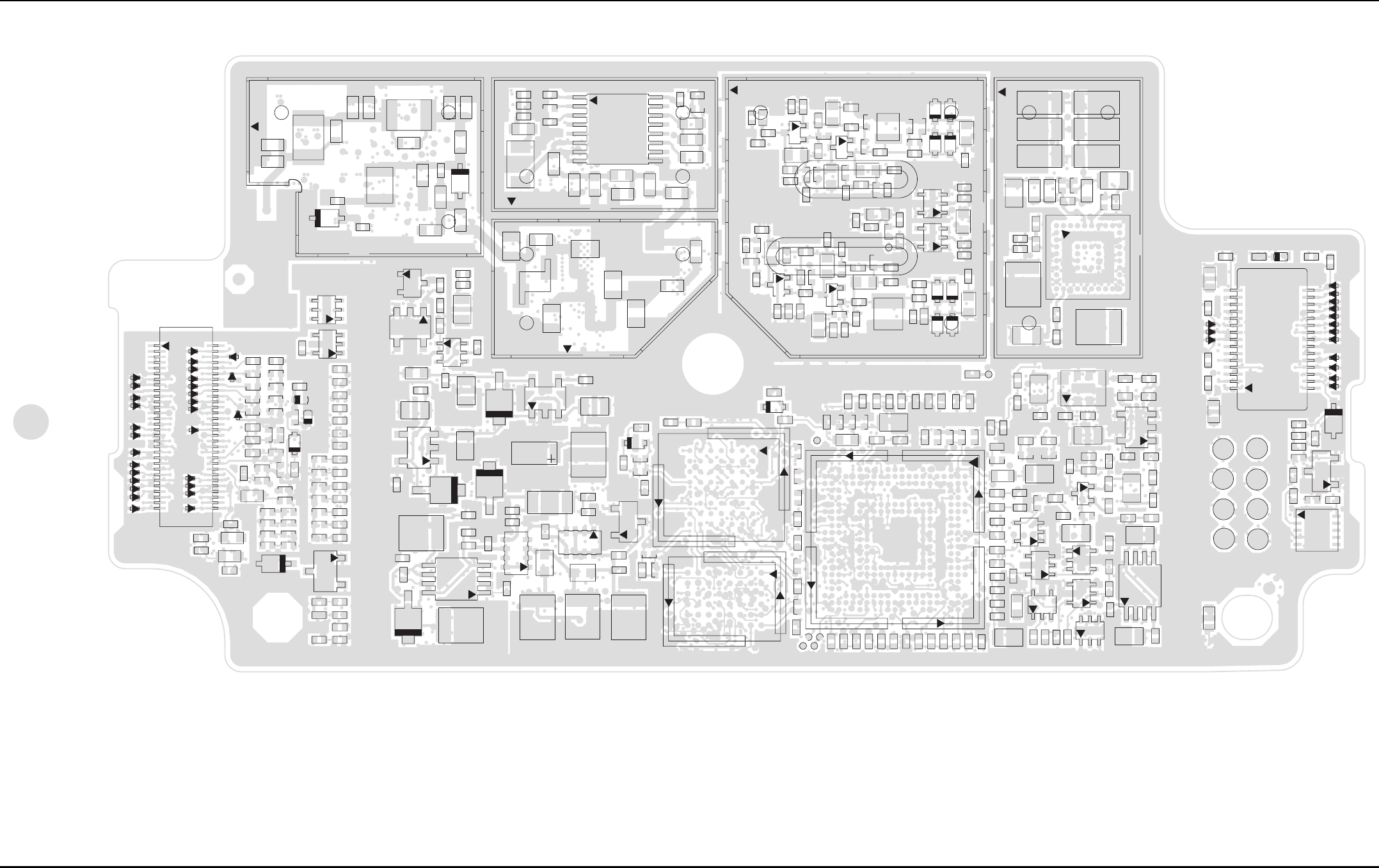
9-2 Schematics, Board Overlays, and Parts Lists – UHF: General Section
May 28, 2008 6871620L01-C
9.3 General Section
Figure 9-1. Main Board Layout (NUE7350A/B) – Side 1
E1434
E1436
E1437
E1438
E1439
E1500
E1501
E1502
E1503
E1504
E1505
E1506
E1507
E1420
E1421
E1422
E1432
E1435
E1441
2
60
59
J1
U9907
U9908
U9910
U9911
U9913
U9914
U9915
C1101
C1107
C1108
C1109C1110
C1111
C1112
C1113
C1114
C1115 C1116
C1119
C1120
C1123
C1124
C1202
C1440
C1441
C1442
C1443
C1444
C1445
C1446
C1447
C1449
C1453
C1457
C1458
C1459
C1460
C9970
C9980
D1000
E1102
E1103
E1110
E1111
E1112
E1113
E1114
E1115
E1116
E1117
E1118
E1119
E1120
E1121
E1122
E1123
E1124
E1125
E1126
E1127
E1129
E1130
E1433
E1440
2
3
Q9906
Q9951
R1103
R1105
R1106
R1449
R1467
R9901
R9902
R9903
R9904
R9916
R9917
R9918
R9919
R9922
R9961
U9912
U9918
VR52
VR53
VR1209
C15
C1430
2
M1005
2
M1006
R1424 R1440
G1 A1
A8
G8
U1410
C25
C30
C1313
C1431
C1432
C1433
D1301
D1402
L10
R1311
R1706
U2
C9
C17
C704
C717
C724
D2
D703
U701
4
3
6
U702
C27
C28
E501
U3
C26
D3
D4
C716 C723
R701
R703
C707
C709
C710
C720
C721
L703
L704
6
C125 C705
C706
C711
C712
C713
C718
C719 C722
D701
D702
L702
L705
L706
5
4
3
2
SH07
C101
C102
C103
C104
C105
C106
C107
C108
C110
C111
C112
C114
C145
E103 E104
L101
L102
L103
L113
R137
R138
8
7
5
4
3
SH06
16
8
9
U102
C116
C120
C121
C122
C123
C124
C141
L108
2
6
4
SH08
R109
C16
C251
C252
C253
C269
C271
C272
C273
C274
C275 C276
C277
C278
C279
C280
C281
C282
C283
C284
C285
C286
C287
C288
C292
C293
C294
C295
C296
D251
D252
D253
D254
D271
D272
D273
D274
L209
L251
L252
L270
L271
L272
L273
L274
L275
L276
L278
Q253
Q271
Q272
Q273
R270
R271
R272
R277
R278
R279
R280
R284
R286
11
10
7SH10
C254
C256
C257
C258
C266
L253
L254
L255
R256
R262
R263
5
C259
C260 C261
C262
C263
C264
C265
C267
C268
L256
L257
L258
Q251
Q252
R253
R257
R260 R261
R269
4
C255
C289
C290
C291
L277
R252
R265
R266
TP203
C224 C225
C226
C227
C241
C242
2
8
C210
C217
C218
C219
C220
C222
C230
C231
C232
C250
L203
L207
R204R205
R210
R212
R217
R220
R221
3
5
6
4
7
SH09
A10
K10
A1
K1
U202
D1401
R1403
R1437
C12
C14
C1719
D1
R1709
4
58
U1
C10
C11
C13
C1314
C1340
E5
L1307
4
5
8Q1301
C1117
C1310
C1312
4
58
Q1302
R1310
C1118
C1125
C1126
C1342
C1343
L1308
R1121
R1308
2
M1007
2
M1008
A1
A6
H1
H6
U1409
C1407
C1425
C1428
C1429
2
M1004
R1101
R1102
R1335
R1338
R1410
R1411
R1412
R1421
R1422
R1423
R1438
R1439
R1462
R1463
R1464
R1465
R1466
R9990
TP1301
TP1302
TP1408
TP1409
AA2
AA22 2
M1001
M1002
M1003
C22
U1401
E1401
R1404
R1405
TP1304
2C2
C1133
C1135
C1136
C1138
C1413
C1414
C1417
C1418
C1419
C1420
C1421
R1111
R1115
R1116
R1118
R1119
R1120
R1122 R1125
R1406
C229
C1130
L208
R213
R267
R1108
TP201 43
2
Y200
C233 C235
L202
R215
C1370
C1412
E1402
R1337
R1344
R1409
C1131
C1132
C1134
C1402
C1404
C1408
C1409
C1410
C1411
C1424
Q1402
R1107
R1112
R1113
R1114
R1117
R1341
R1401
R1415
R1416
U1404
U1405
U1408
C1140
C1142
C1422 R1133
R1209
R1346
U1306
4U1406
U9905
4
58
U1101
C9975
C209
C214
C1403
C1416
R202
R207
R1109R1110
R1123R1124
R1417
R1418
R1419
R1704
C213
C1141
L205
R731
C1427
R1336
R1420
C234
C236
R201
R208
5
3
4
U201
C54
C71 C72 C73
E1411
E1412
E1413
R735
R9999
TP1403
TP1404
TP1407
TP1410
TP1401
TP1402
TP1405
TP1406
C55
C56
C58
E1403
E1404
E1405
E1406
E1407
E1408
E1409
E1410
E1414
E1415
E1416
E1417
30 16
15
J2
VR51
C52
C53
C57
C9966
C9968
Q9950
R733
R9931
R9934
R9998
106
5
U9904
VR4
2
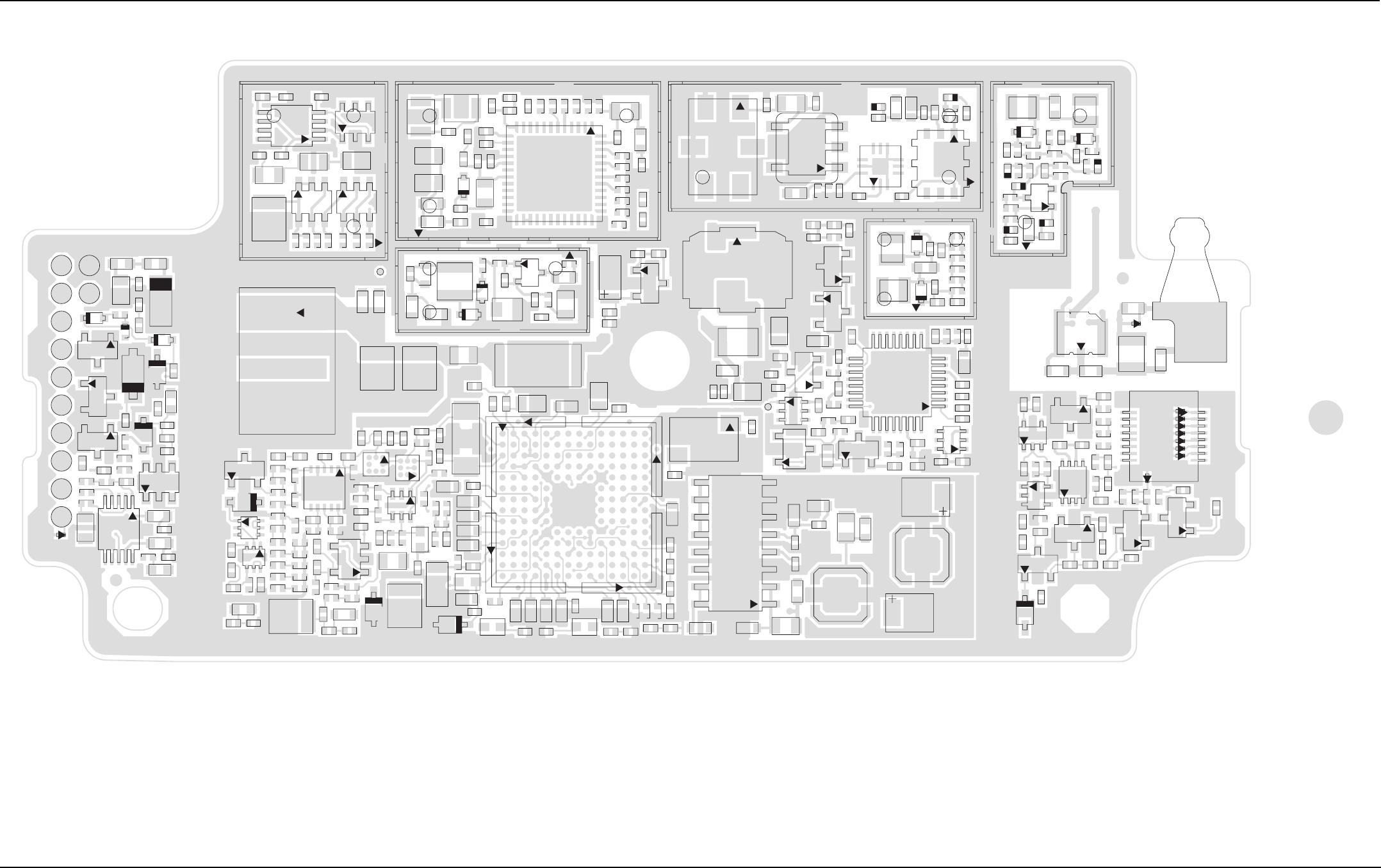
Schematics, Board Overlays, and Parts Lists – UHF: General Section 9-3
6871620L01-C May 28, 2008
Figure 9-2. Main Board Layout (NUE7350A/B) – Side 2
C21 C22
C29
C1102
C1104
C1105
C1106
C1217
C9901
C9950
C9951
C9952
C9953
C9954
C9969
E1419
E1430
E1431
E1442
E1443
E1444
E1445
16 9
8
J3
L20
M1704
Q9901
Q9902
Q9903
Q9904
Q9905
R22
R1210
R1212
R1402
R9905
R9906
R9907
R9908 R9909
R9910
R9911
R9912
R9913
R9914
R9915
R9920
R9921
R9923
R9924
R9925
R9926
R9927
R9960
4
U9901
U9902
U9903
U9916
U9917
VR9901
3
J1704
C421
C422
C423
C424
C425
C426
C427
C428
C430
C432
C434
C436
C456
C457
C483
C484
D451
D453
L431
L432
L450
L451
L452
L480
L481
L482
Q430
R421
R431
R432
R433
R434
5
7
3
SH02
8
C470
C471
C472
C473
C474
C475
C476
C477
C479
C480
C481
C482
C490
5
6
4
3
2
1
FL490
L470
L471
L474
L490
L492
R470
6
7
5
4
3
SH04
3
46
T470
3
46
T471
12
10
97
6
4
3
U470
2
C410
C411
C412
C413
C414
C415
C416
C417
C419
D411
D413
L410
L412
L413
R411
R412
2
3
5
4SH03
C127
C147
Q4
R102
R105
R106
U103
C117
C118
C119
C146
L105
3
2
4
Q107
C128
C129
C130
C131
C132
C133
C134
C135
C136
C137
C140
C144
C148
C149
C418
C420
C429
D104
E105
Q101
Q102
Q104
2
3
Q200
R111
R117
R118
R119
R120
R121
R122
R135
R136
R218
R401
R451
R452
R1708
RT150
TP111
25
9
17
U104
C1332
C1333
L1305
L1306
C1335
C1336
C1337
C1338 C1339
R1317
R1318
R1319
R1320
R1321
16
1
8
9
Q1304
C1308
C1316
C1317
2
M1012
R1334
A14
43
2
Y1302
C1321
C1323
C1341
C1345
C1364
C1365
R1329
R1330
R1331 R1332
R1347
R1348
R1350
R1357
R1358
2
M1009
P14
C1326
C1327
L1304
C1324
C1328
C1329
C1330
C1331
2
M1010
U1304
P1
C1209
C1212
C1213
C1214
C1215
C1220
C1221
C1222
C1224
C1225
C1232
C1301
C1302
C1303
C1304
C1305
C1306
C1315
C1325
C1346
C1347
C1348
C1349 C1350
C1351
C1367
C1368
D1207
L1204
L1302
32
M1705
6
3
4
Q1201
6
3
4
Q1202
R1201
R1202
R1203
R1204
R1205
R1215
R1216
R1217
R1218
R1219
R1220
R1221
R1223
R1224
R1225
R1226
R1227
R1228
R1229
R1230
R1231
R1301R1302
R1304
R1305
R1306
R1307
R1314
R1322
R1323
R1324
R1325
R1339
R1340
R1342
R1343
R1349
R1353
R1354R1355
R1596
106
5
U1201
U1301
C1
C3 A3
U1302
C1
C3 A3
U1303
5
34
U1305
VR1204
VR1208
Y1301
C1309
C1318
C1319
C1320
C1322
C1352
C1353
C1354
C1355
C1356
C1357
C1362
L1301
L1303
R1303
R1315
R1326
R1327
R1328
R1345
R1356
VR1207
2
M1011
A1
C20
C1307 C1363
E101
R130
R1309
R1370
R1371
C561
C583
Q551
R552
R553
R554
C4
C6 C24
C551
C552
C553
C554
C555
C556
C557
C560
C562
D550
D551
L551
L552
L553
Q550
R551
R555
R556
5
2
46
3
SH11
TP551
C493
C501
C505
C506
C507
C509
C511
C513
C535
C539
C540
C541
C542
C544
C546
C547
C548
C584
E500
L571
R471
R533
6
7
4
SH01
1
37
25
13
U500
C512
C514
C527
C570
C571
C572
C573
C574
C581
C582
D570
L501
L502
L570
R501
R511
R519
R571
R572
10
8
C200
C201
C202
C203
C204
C205
C206
C207
C208
C211
C215
C221
C337
D201
D202
FL200
L201
L204
R216
4
3
6
2
5
SH05
U203
E1418
TP1001
TP1002
TP1004
TP1005
TP1007
TP1008
TP1009
TP1010
TP1011
TP1303
C1210
C1211
C1216
C1219
C1223
C1233
C1234
C9956
D1202
L1205
R1206
R1207
R1213
R1214
R9930
R9932
R9933
R9996
R9997
R10000
R10001
10
6
5
U20
VR1201
C1128 C1139
C1218
D1205
D1222 D1223
E1104
E1201
F901
R1241
R1351 R1352
VR3
VR1202
VR1203
VR1205
VR1206
VR1301
C1129
R1239
TP1003
TP1006
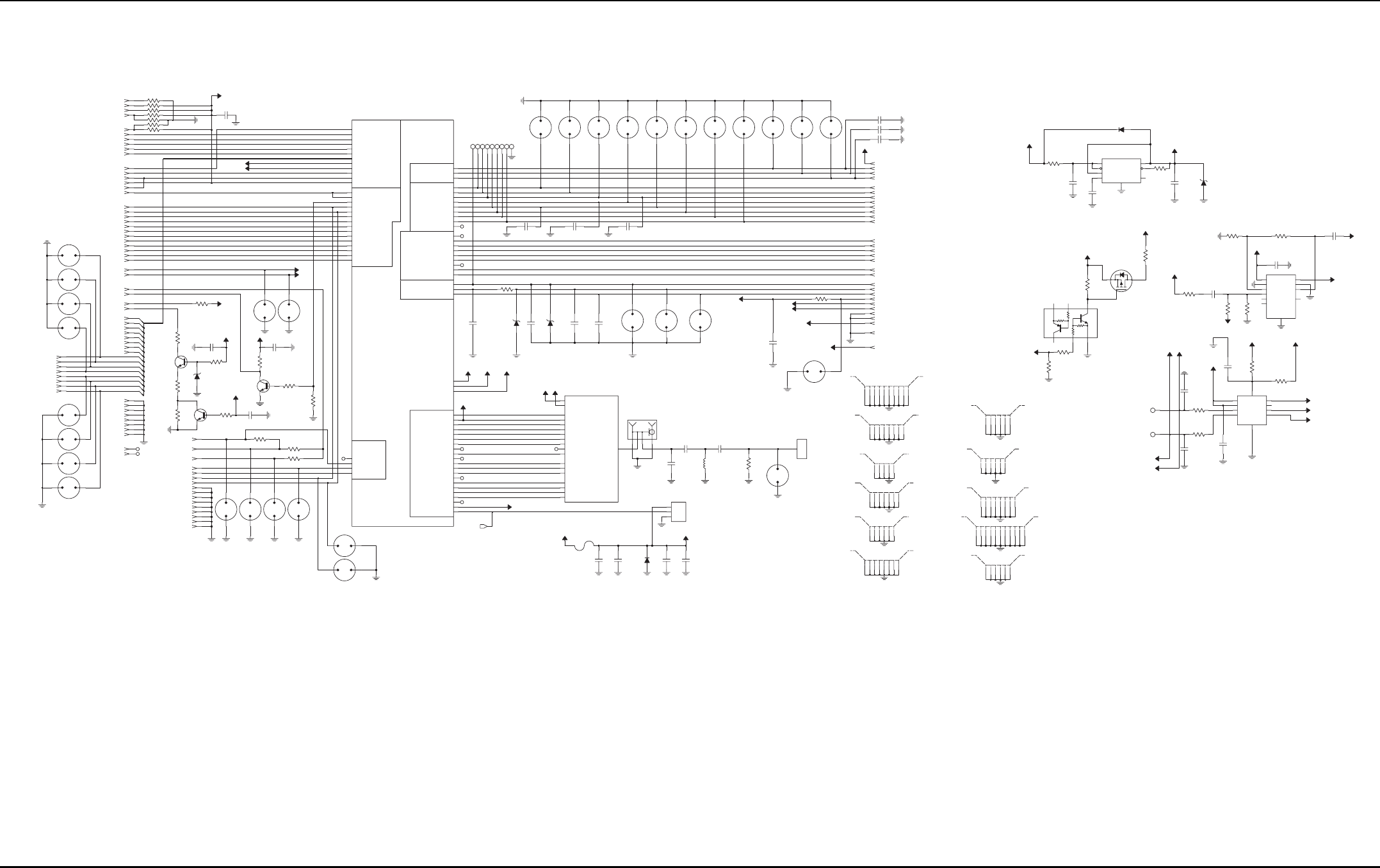
9-4 Schematics, Board Overlays, and Parts Lists – UHF: General Section
May 28, 2008 6871620L01-C
Figure 9-3. UHF Main Board Overall Schematic
DISP & KEYPAD
19J1-19
44
32
J1-33
J1-44
J1-32
37
J1-10
J1-37
J1-24
18
J1-18
J1-31
J1-6
25J1-25
J1-39
J1-16
J1-14
J1-54
J1-22
J1-23
12
J1-12
8
6
J1-8
J1-21
J1-60
J1-58
20
42
J1-20
J1-42
J1-56
21
39
23
31
58
60
24
33
54
56
22
16
14
10
J1-40
J1-46
J1-27
J1-30
J1-57
J1-52
J1-55
J1-34
J1-4
J1-38
27
29
J1-48
J1-29
J1-26
J1-28
4
J1-35
J1-36
J1-50
34
26
52
30
48
35
55
50
28
46
57
36
38
40
13
J1-13
45
J1-45
SPARK_GAP
E1502
12
53
J1-53
E1503
SPARK_GAP 12
49
J1-49
J1-15
12
E1501
SPARK_GAP
J1-51
12
SPARK_GAP
E1500
J1-59
47
J1-47
51
15
59
E1506
SPARK_GAP
12
12
SPARK_GAP
E1507
12
SPARK_GAP
E1505
E1504
SPARK_GAP
12
J1-17
J1-41
J1-3
J1-2
J1-11
NC
NC
1
J1-1
J1-43
9
J1-9
5J1-5
7J1-7
11
41
43
17
3
2
TOP CONTROL
DISP_BRIGHT2
J3-3
J3-6
J3-9
J3-8
5V_Misc
R9906
30
12
J3-12
14
R9905
1K
10
9
11
10
9
8
7
6
5
4
3
2
1
13
J3-11
0
R9912
J3-14
6
8
Q9901
68
R9907
2.4V
VR9901
J3-16
J3-15
2
15
7
J3-4
1
11
4
100pF
C1104
13
14
15
16
5
J3-13
DISP_BRIGHT1
12
Q9902
3
J3-1
J3-5
J3-2
0
R9901
R9908
1K
Q9903
J3-10
J3-7
C1102
100pF
0
DISP_DATA(15:0)
DIGITAL_NOISY
R9915
R9914 68K
21
SPARK_GAP
E1445
2
E1444
SPARK_GAP
1
E1443 12
SPARK_GAP
91K
R9913
12
E1442
SPARK_GAP
12
U9917
SPARK_GAP
SPARK_GAP
U9916 12
150K
U9907
SPARK_GAP
12
2
SPARK_GAP
U9908
1
100pF
C9901
NC
22K
R9911
R9910
5V_Misc
27K
10K
R9909
EAR+
EAR-
NU
NU
NU
R9903
DISP_BRIGHT2
R9919 1K
1K
1K
1K
R9904
R9917
R9918
C9970
100pF
R9902
R9916
DISP_BRIGHT1
DISP_V1.875
DIGITAL
UC_KP_ROW2
UC_KP_ROW3
UC_KP_ROW4
UC_KP_ROW5
UC_KP_ROW6
DISPLAY
KEYPAD
UC_KP_5V2
UC_KP_BL_EN
UC_KP_COLUMN0
UC_KP_COLUMN1
UC_KP_COLUMN2
UC_KP_ONOFF
UC_KP_ROW0
UC_KP_ROW1
DISP_CS_SUB
DISP_DATA(15:0)
DISP_ID
DISP_MAIN_EN
DISP_REG_SEL_A0
DISP_REG_SEL_A1
DISP_RESET
DISP_R_W
DISP_V1.875
DISP_V2.9
FLIP_SENSE
DISP_BRIGHT1
DISP_BRIGHT2
UC_RESET_ENC
UC_TX_INHIBIT
UC_UCM_SS
UC_WAKEUP
UC_ENC_SSI_DI
UC_ENC_SSI_DO
UC_INT_MIC
UC_INT_SPKR+
UC_INT_SPKR-
UC_KEYFAIL_LH_BDMDATA
AUDIO
CE
UCMAUDIO
JACK
UC_BOOT_ENC
UC_ENC_SSI_CLK
AUD_JACK_INT
AUD_JACK_MIC
AUD_JACK_PTT
CE_CTS
CE_LHDATA_KEYFAIL
CE_OPTB+_VPP
CE_OPT_SEL1
CE_OPT_SEL2
CE_RS232DIN_USB-
CE_RS232DOUT_USB+
CE_RTS
CE_SB9600_BUSY
NC
NC
NC C54
100pF 100pF
C56
C55
100pF
R9998
4809788E21
6.8V
VR4
100pF
C57
100
VR51
5.73V
C52
100pF
C58
100pF
C53
470pF
E1416
SPARK_GAP
12
SPARK_GAP
E1415
12
SPARK_GAP
E1414
1
2
AUD_JACK_SPK_out SW_B+
CE_SPKR+
R9999 0
FU_B+
330pF
C9966
DC_I5
CE_SPKRCOM
E1417
12
SPARK_GAP
NU
Antenna Clip
10pF
C29
2113944C30 1
CLIP
M1704
GND
C21
1.6pF
A
1C
3
G1
2
G2
4
J1704
2460591D12
L20
18.29nH
1K
R22
0613952H73
C22
2113944C17
E1419
SPARK_GAP
12
3.0pF
FU_B+
TXFS
TXINH
TXTD
USEL
VSW1
XCVR_SWB+
ABCS
ANT
XCVR
F168
FUB+
LOCK
MOSI
RAWB+
RSTL
RXCK
RXDO
RXFS
SPCK
TXCK
RAWB+
FU_B+
NC
NC
NC
VSW1
NC
NC
LOCK
USEL
ABCS
F168
RXDO
VSW1
SCKA
RSTL
MOSIA
BS
BS
TXFS
TXCK
TXTD
SWB+
RXFS
RXCK
AUDIO_SW
EXT_SPKR-
EXT_SPKR+
UC_KP_ROW7
UC_MONITOR
TOP/VOLUME
CONTROL
UC_INT_PTT
UC_EMERG
XRFUNSWB+1
XRF_AD_CS*
XRF_BAT_STAT
XRF_MISOA
XRF_MOSIA
XRF_POR*
XRF_SCKA
XRF_TX_INHIBIT
XRF_VSW1
XRX_DATA
XSSI_CLK
XSSI_FSYNC
XSWB+2
XTX_DATA
XTX_SSCK
XTX_SSFS
X16.8MHz
XABACUS3_CS*
XFN_PC_SEL*
XIFGND1
XLOCK
XCVR
EXT_SPKR+
EXT_SPKR-
VOCON
AUDIO_SW
FU_B+
.01uFC4
VR3
4815155H01
C24
10uF
2113944C45
C6 100pF
6515076H01
F901
24V
3A
10uF
C20
Battery Contact
RAWB+
CONTACT
M1705
2DATA
3NEG
1POS
1
TP1002
1
TP1006
1TP1004
TP1003
1
1TP1008
TP1005
1
TP1001
1
TP1007
1
TP1009
1
SPARK_GAP
E1406
SPARK_GAP
E1404
SPARK_GAP
E1408
E1413
SPARK_GAP
SPARK_GAP
E1412
E1407
SPARK_GAP
E1411
SPARK_GAP
E1409
SPARK_GAP
SPARK_GAP
E1410
E1405
SPARK_GAP
E1403
SPARK_GAP
21
2
1
21
21
21
21
21
21
21
2
1
21
V_VIBE
100pF
C71
100pF
C73
C72 100pF
CE_UCM_SPK
J2-1515
J2-55
J2-3030
10
J2-1212
J2-10
J2-1414
J2-1717
J2-2424
1J2-1
J2-44
J2-1919
J2-2828
J2-1818
25
J2-2727
J2-25
J2-2626
8J2-99 J2-8
21 J2-21
J2-2020
J2-2929
22 J2-22
J2-22
13 J2-13
J2-66
16 J2-16
J2-2323
J2-1111
J2-77
3 J2-3
8
9
10
2671728L01
SHIELD
SH01
1
2
3
4
5
6
7
2671818L01
SHIELD
SH02
1
2
3
4
5
6
7
8
SHIELD
SH03
1
2
3
4
5
2671819L01
3
4
5
6
7
SH04
SHIELD
2671685M01
1
2
3
4
5
6
2671821L01
SHIELD
SH05
1
2
1
2
3
4
5
6
7
8
2671822L01
SHIELD
SH06
4
5
6
2671817L01
SHIELD
SH11
1
2
36
7
8
9
10
SH10
SHIELD
2671826L01
1
2
11
3
4
5
SHIELD
SH09
1
2
3
4
5
6
7
8
2671825L01
6
2671824L01
SHIELD
SH08
1
2
3
4
5
SH07
SHIELD
2671823L01
1
2
3
4
5
6
R731
0
U9905
25
6
3
1
4
MUN5313DW1T1G
Rb=Re=47K
R1704
100K
VIBRATE_CONT
DC_20
R733
100K
VSW1
Q9950
R735
V_VIBE
0
R9930
510
AJACKin
C9956
1.0uF
EAR+
AJACKin
EAR-
470pF
C1233
470pF
C1234
33
0613952H37
R10000
TP1011 1
33
R10001
CE_SPKR+
1
TP1010
CE_SPKRCOM
C1216
100pF
4
8
3
9
NU
NU
AUDIO_SW
C1211
0.10uF
0
R9996
R9997
0
DIGITAL_SPIB
VCC
COM2
6
GND
IN1
IN2 5
NC1 7
NC2
2
NO1 10
NO2
1
NLAS4684
U20
COM1
EXT_SPKR-
EXT_SPKR+
VCC5 V5A
V5A
R9931
39K R9932
1K
C9975
4.7uF
4.7uF
AUD_JACK_SPK_out
V5A
5V_Misc
6.8V
VR1209
10uF
C1141
C1142
2.2uF
.01uF
C1140
8SHUTDOWN
LP2989IMMX-5.0
1BYPASS
7
ERROR
3
GND
4INPUT
2
NC
5
OUTPUT
6SENSE
LP2989
U1101
R1133
100K
UNSW_B+
0
R1209
D4
MBRM140T3
V5A
R9934
10K
R9933
100K
5
6
4VNEG
VPOS
10
CTGND
G1
INNEGA
2
INNEGB
8INPOSA
3
INPOSB
7
1
9
U9904
LMV712LDX
C9968
0.10uF
SDA
SDB
OUTA
OUTB
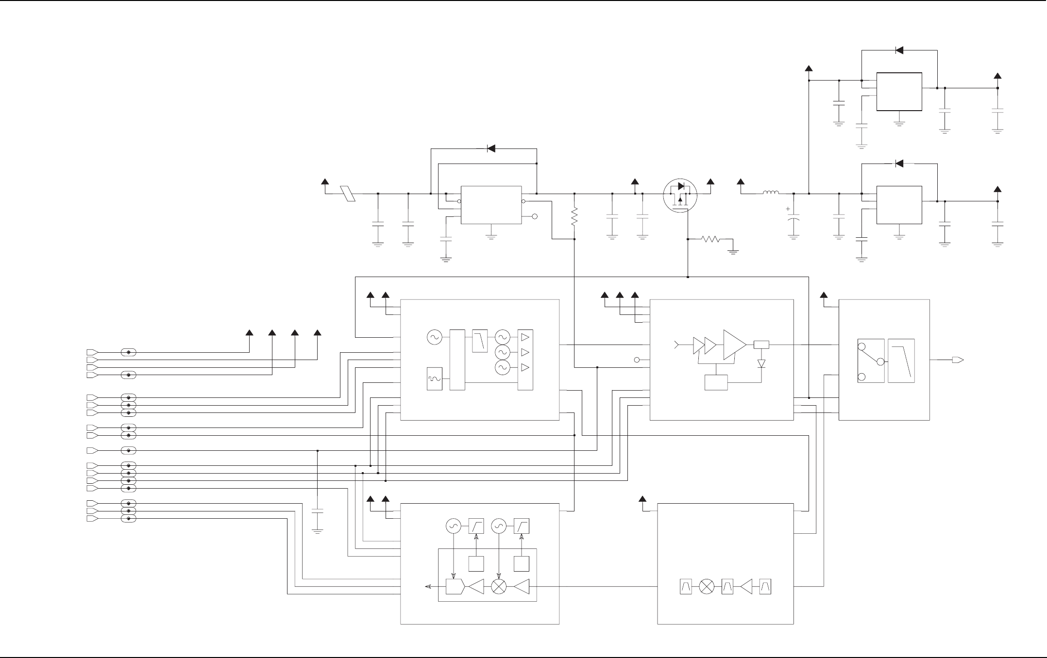
Schematics, Board Overlays, and Parts Lists – UHF: Transceiver (RF) Section 9-5
6871620L01-C May 28, 2008
9.4 Transceiver (RF) Section
Figure 9-4. UHF Transceiver (RF) Board Overall Circuit Schematic
RSTL
VSW1
XCVR_SWB+
LOCK
TXFS
TXCK
TXTD
F168
FUB+
RAWB+
RXDO
RXFS
RXCK
ABCS
USEL
SPCK
MOSI
RAWB+
VSW1XB+ FUB+
TXFS
TXCK
TXTD
USEL
SPCK
MOSI
LOCK LOCK
SCEN
SSCK
SSFS
SSTD
V3A
V5A
CLK
CSX
DATA
V3AV5A
A500 RX_BE
CLKOUT
DOUTA
ADC
CKO LO
FREF
FS
PC
PD
PE
RXIF
V3D
V5A
V5A V3D
ABCS
SPCK
MOSI
100pF
C1719
RXDO
RXFS
RXCK
USEL
SPCK
MOSI
V5R
V5R
RXIF
A400
RX_FE
DAC2
LOIN
RXIN
RXIF
TXRF
USEL A100
TX_ALC
V5A
XB+
MOSI
SPCK
RAWB+
RSTL
TXINH
XB+RAWB+ V5A
NC
VAR2
TX5V
VAR3
POUT
RXLO
RXRF
TX5V
TXRF
V5A
VAR3 A700
SW_FL
ANT
V5A
TXH
ANT
C17
1.0uF 100pF
C9
LP3985
BYPASS
4
GND
2
VEN
3
VIN
1VOUT 5
V3D
U2
L10
100uH
100K
R1708
VSW1
C16
.01uF
NTR1P02T1
Q4
V5A
1.0uF
C15
C10
100pF
V5R
100K
R1709 C30
10uF
10uF
C14
F168
RXLO
A200, A300
FGU
TXRF
SENSE
SHUTDOWN
BYPASS
ERROR
GND
INPUT
NC
OUTPUT
.01uF
C13
6
8
1
7
3
4
2
5
NC
LP2989IMMX-5.0
LP2989
U1
MBRM140T3
D1
C11
0.10uF
BK1005HM471
E5
2.2 uF min.
C12
10uF
XB+
TXH
VEN
1VIN5
VOUT
LP3985
U3
4BYPASS
2GND
3
.01uF
C26
C25
1.0uF
MBRM140T3
D3
VSW1_filtered
C27
1.0uF
C28
100pF
D2
MBRM140T3
V3A
9-6 Schematics, Board Overlays, and Parts Lists – UHF: Transceiver (RF) Section
May 28, 2008 6871620L01-C
Figure 9-5. UHF Transceiver (RF) Antenna Switch and Harmonic Filter Circuits
R701
0.100W
220
0.10uF
C724 C704
2113944A40
100pF
2415429H47
L702
390nH
TX5V
390nH
L706
2415429H47
100pF
C719
2113944A40
D701
HSMP_389Z
TXRF
V5A
V5A
100K
R703
1A1
3A2
2
GND
5
VCC
6
Y1
4
Y2
0.10uF
NC7WZ04
U702
C717 V5A
ATH
VAR3
L705
2460591D12
18.29nH
5.6pF
C711
2113944C24 HSMP_389Z
D702
2113944A40
C723
100pF
1.3pF
C722
2113951C13
1.6pF
2113944C11
C706
100pF
2113944C45
C705
2113944C15
C718
2.4pF 4.3pF
2113944C21
C720
1.8pF
2113944C12
C709
2.4pF
C707
2113944C21
4.3pF
C710
2113944C15
2460591D23
3.3pF
2113944C18
C721
17.24nH
L704
17.24nH
2460591D23
L703
RXRF
ANT
D703
MMBD352
100pF
2113944A40
C712
5.1pF
C713
2113944A18
ATH
ATL V2
5
U701
AT267
GND
2
RFIO1
1
RFIO2
3
V1
4
100pF
C716
Schematics, Board Overlays, and Parts Lists – UHF: Transceiver (RF) Section 9-7
6871620L01-C May 28, 2008
Figure 9-6. UHF Transceiver (RF) Receiver Front End Circuit
3.3pF
2115153H15
C410
D413
4815096H01
3.3pF
C416
2115153H15
L410
2415429H39
150nH
2115153H03
C414
1.0pF
2113946B04
C418
0.1uF
12pF
C415
2115153H35
C412
2115153H35
12pF
22pF
C419
2115153H41
18.9nH
2416201H02
L413
5.6K
R411
L412
18.9nH
2416201H02
10pF
C411
1.0pF
C413
4815096H01
D411
RXIN
4.7uF
2113946D07
C420
1K
R401
DAC2
NP
V5R
2113946B04
C456
0.1uF
2.2K
R433
10pF
2115153H27
C417
4.7uF
C483
2113946D07
0613952Q91
R412
5.6K
V5R
6.2K
R421
0613952Q92
750
R434
0613952Q70
C432
2113944A23
8.2pF
R431
0613952Q81
2.2K
4805585Q19
BFS520
Q430
C434
56pF
R432
0613952Q69
680
2414017P13
L432
10nH
100nH
L431
2414017P25
22nH
L480
2414017P17
0613952R66
R482
0
0.1uF
C457
2113946B04
2113944A80
20pF
C484
5.6K
0.1uF
C429
R451
150nH
D451
L450
22nH
2414017P17
L481
2115153H35
C421
7pF
C430
2115153H31
3.3pF
C426
2115153H15
7.5pF
C436
2115153H03
1.0pF
C422
18.9nH
L451
12pF
2115153H03
C423
1.0pF
2115153H15
C427
3.3pF
L452
18.9nH
D453
5.6K
R452
2115153H41
C428
22pF
2115153H35
C424
12pF
7pF
C425
2115153H31
V5R
C476
2113944M01
2pF
27nH
L471
2414017P18 100pF
C477
LOIN
NP
1.5nH
2414017P03
L470 C472
2113944A40
100pF
C470
6
1
6.8pF
C471
2113944A21
100pF
C473
2113944A40
MX_IN
NC
4
2
3
T470
XFMR
5
.01uF
C474
2113945B02
4.7uF
C475
2113946D07
75
R470
0613952Q46
100pF
C480
V5R
2415429H43
L474
220nH
C479
2113946B04
0.1uF
NC1
NC2
NC3
RFN
RFP BBP
BDIV
BVDD
GND
GND1
IFN
IFP
LOIN
U470
MX2072A
3
6
7
4
512
2
1
11
13
8
9
10
.01uF
C482
.01uF
C481
T471
XFMR
4
6
1
2
3
2115153H21
C490
5.6pF420nH
L492
2471851L18
2414017K33
L490
680nH
OUT 4
FL490
TS3-73E01
GND1
2
3GND2
5GND3
GND4
6
IN
1
R471
0613952G67
0
3.6pF
C493
2115153H16
RXIF
9-8 Schematics, Board Overlays, and Parts Lists – UHF: Transceiver (RF) Section
May 28, 2008 6871620L01-C
Figure 9-7. UHF Transceiver (RF) Receiver Back End Circuit
V3DF
V5A
E501
BLM11A601S
V3D
V5A
V3DF
V3DF
0
R501
2115153H24
C584
7.5pF
2414017Q46
L571
0.82uH .01uF
C547
2113945B02
RXIF
V3DF
C501
100pF
C509
.047uF
2200pF
C507
C548
V3DF
.047uF
C506
0.10uF
V3DF
C505
100pF
220pF
C581
2113944B02
10uH
L501
10uHL502
R554
10K
0613952R01
73A04
Q551
C583
.01uF
56K
R552
R553
10K
.01uF
C562
2113945B02
V5A
C561
2313960B30
4.7uF
0613952H55
R555
180
V47 71.1 to 75.6MHz
IFLO
C554
2113944A79
16pF 4.7uH
L551
2414032B76
2113944A34
C556
56pF
2414015B26
L552
330nH
2414017Q51
L553
2.2uH
Q550
BFQ67W
4805218N63
2113944A34
C557
56pF
2113944A20
C555
6.2pF
4815096H01
D550
1SV305
0613952Q61
R556
330
4815096H01
1SV305
D551
1
2113944A28
C560
18pF
LOP
2113946C07
C553
0.33uF
C552
2113946S35
1.0uF 1.0uF
2113946S35
C551
TEST_POINT
TP551
1.1K
0613952Q74
R551
C541
.01uF
.01uF
C544 C542
.01uF
.01uF
C546
vddp
cxvl
vddl
vddi
cxif
cxvm
ifin
lon 16V
0.10uF
C540
V5A
V3DF
E500
BK1005HM471
IOUTL
C539
2113946B02
10V
.047uF
100K
R533
C535
.01uF
V3DF
V3DF
0.10uF
C527
DOUTA
CLKOUT
FS
PC
PD
PE
FREF
CKO
18 MHz
C571
0.1uF
R571
1.8K
C572
.033uF
C570
0.1uF
D570
1SV279
R572
10K
L570
3.9uH
68pF
C573
.01uF
C574
CLKN
CLKP
IOUTC
0.10uF
C582
V3DF
10K
R519
V3DF
C514
0.10uF
C513
.01uF
100pF
C511
100pF
C512 R511
100K
VREFN
VREFP
VDDC
VDDD
VDDF
VDDH
VDDI
VDDL
VDDP
VDDQ
MXON
MXOP
PC
PD
PE
RREF
SYNCB
VDDA
GNDS2
IF2N
IF2P
IFIN
IOUTC
IOUTL
LON
LOP
GNDD
GNDF
GNDH
GNDI
GNDL
GNDP
GNDQ
GNDS1
DOUTA
DOUTB
FREF
FS
GCN
GCP
GNDA
GNDC
CLKN
CLKOUT
CLKP
CXIF
CXVL
CXVM
AD9864
U500
17
14
23
24
13
15
22
16
21
18
20
19
26
27
25
33
34
32
36
29
30
35
31
28
NC
12
11
6
48
40
39
2
1
9
4
5
47
38
42
43
3
45
37
8
7
10
46
44
41
Schematics, Board Overlays, and Parts Lists – UHF: Transceiver (RF) Section 9-9
6871620L01-C May 28, 2008
Figure 9-8. UHF Transceiver (RF) Transmitter Circuit
Vc
BLM21PG221SN1
E101
RAWB+
RT150
33.0K
100pF
C137
TX5V
100
0613952Q49
R120
Q102
RAWB+
V5A
XB+
0613952Q62
R121
360
10
0613952Q25
R122
TXRF
V5A RAWB+
XB+
L101
2414017G09
15nH
100pF
C101
2113944C45
C102
100pF
100pF
C105
RFIN RFOUT1
RFOUT2VCNTRL
VD1 VG1
VG2
GND1
GND2
GND3
GND4
NC1
NC2
NC3
NC4
U102
SRFIC5668
EP
G2
15
16 6
71
14 2
311
4
5
12
13
8
9
10
17
BLM11A601S
E104
100pF
C104
C103
.01uF
0.10uF C145
C108
.01uF
100pF C110
R1180
30
31
26
28
25
32
27
29
NC
VL VLIM
TEMP
V10
V45
V5EXT
VAR1
VAR2
VAR3
VG
NA
Q
QX
RFIN
RS
RSET
RXT1
CLK
CQ
CQX DATA
F168
GND1
GND2
INT
5185765B26
H99S4
U104
ANO
BPOS
CEX
CI
CJ
CL
6
2
4
1
7
8
3
5
NC
C131
.015uF
C130
470pF
C129
1500pF
NP
R136 R111
470K
C128
100pF
C140
100pF
0
R135
MOSI
USEL
SPCK
RSTL
C135
100pF
GND POS
VOUT
LM50
U103
V5A
31
2
E103
BLM18PG121SN1
100pF
C111
2414032D18
L102
180nH
2479990E01
23.75nH
L105
C146
0.10uF
0.1
R130
C117
1uF 100pF
2113944C45
C119
.01uF
C118
TVDD
NP
1
TEST_POINT
TP111
100pF
C106
L103
33nH
100pF
C107
C112
5.1pF
NP R102
47
2113944C37
C114
39pF
R105
0613952G67
R138
18K
0
0613952H53
R109
150
0.10uF
C147
2414017G07
10nH
L113
R106
10K
0
R137
0613952G67
100pF
C127
NP
0.1uF
C116
D3
G
1
S1
2
S2
4
NP
6.8pF
2171741M05
C120 C122
27pF
C121
6.8pF
C141
39pF 15pF
C124
100pF
C125
2113944C45
L108
2415428H04
5.4nH
C123
2113944C16
2.7pF
POUT
POUT
Q107
4816698H03
0.10uF
C148
RAWB+
2
5
6
3
1
4
Rb=4.7K, Re=inf
MUN5316DW1T1G
Q101
E105
RAWB+
19
17
20
18
24
22
21
23
NC
NC
15
14
16
11
10
12
13
9
NC
UNSW_B+
NC
NC
NC
R119
0
NC
0.1uF
C132
1uF
C133
C134
.01uF
UNSW_B+
0.10uF
C149
10
R117
100pF
C144
TX5V
VAR2
VAR3
TX5V
V5A
NTR1P02T1
Q104
NC NCNC2 5
D104
A1
1
A2
4
K1
3
K2 6
NC1
2
MBD330DWT1
RXH
C136
100pF
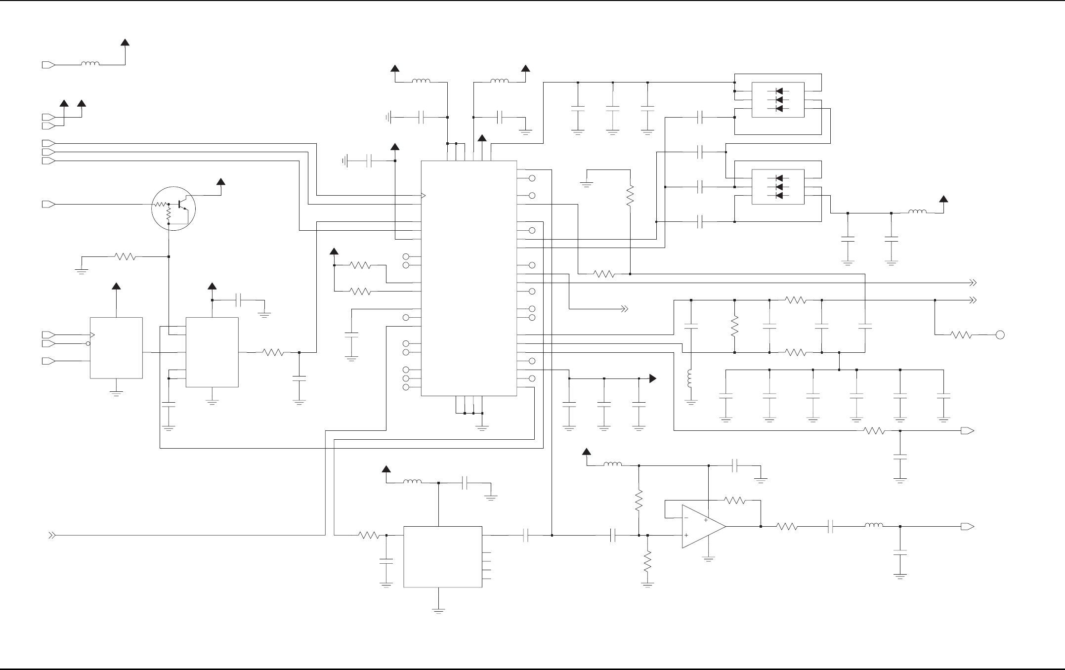
9-10 Schematics, Board Overlays, and Parts Lists – UHF: Transceiver (RF) Section
May 28, 2008 6871620L01-C
Figure 9-9. UHF Frequency Generation Unit (Synthesizer) Circuit – 1 of 3
V5A
2416307H01
L209
680nH
VSF_VCO
V3A
CLK
CSX
VSF
SCEN
DATA
V5A
V3A
R1
R2
Q200
4813973A42
V3A
3
AD5320BRT
U203
V3A
R218
10K
4DIN
2GND
5SCLK
6SYNC
VDD
1
VOUT
SSFS
SSTD
SSCK
3
IN
2
6OS
OUT 5
7SHDN
4
VDD
MAX7414
FL200
CLK
8
1COM
GND
C221
0.10uF
V3A
R216
8.2K
0.10uF
C215
VSF
C337
220pF
56K
R205
C220
10uF
R204
62K
NC
NC
NC
NC
NC
NC
NC
G6
F10
F7
D10
B10
G5
G10
H10
E10
H1
G4
D7
A7
F1
G1
D6
F4
NC
D5
E4
K8
E7
L208
2.2uH C233
0.10uF
4
VCC
VCONT
1
GND
2
5
NC1
NC2 6
NC3 7
8
NC4
3
OUTPUT
16.8MHz
1XTV168000VAA
Y200
V3A
10K
R215
C235
100pF 33K
R208
C236
1000pF
.01uF
C234
R201
33K
L202
2.2uH
V5A
XTAL2
VDD3
VMULT1
VMULT2
VMULT3
VMULT4
VRO
WARP
XTAL1
SFOUT
TEST1
TEST2
VBYPASS
VCP
VDD
VDD1
VDD2
NC2
NC3
PREIN
PVREF
REFSEL
SFBASE
SFCAP
SFIN
GND3
IADAPT
INDMULT
IOUT
LOCK
MODIN
MODOUT
NC1
CPB1
CPB2
DATA
EN_CEX
FREFOUT
GND
GND1
GND2
ADAPTSW
AUX1
AUX2
AUX3
AUX4
CCOMP
CLK_CLK
35U92
U202
V5A
A10
K2
A2
D4
K7
C10
0.10uF
C211
V3A
2.2uH
L204
0.10uF
C210
C250
0.10uF
L203
2.2uH
V5A
V3A
NC
NC
K10
K4
K3
K1
J1
J10
K9
G7
A9
A8
A4
K5
A5
E1
A6
K6
A3
A1
B1
C1
D1
NC
NC
NC
NC
NC
NC
NC
8.2K
R220
R221
AUX2
6.8K
C207
0.10uF 10uF
C206 C200
100pF
VCP
0.10uF
C208
0.10uF
C205
0.10uF
C201
0.10uF
C202
K1
K2
K3
A1
A2
A3
A1
A2
A3
K1
K2
K3
3
2
1
4
5
6
D202
5
6
3
2
1
D201
4
V3A
L201
2.2uH
2.2uF
C203
C204
0.10uF
1TP201
TEST_POINT
AUX3
VCTRL
C227
0.1uF0.1uF
C224
0.1uF
C225
0.1uF
C226
0.1uF
C242 C241
0.1uF
C229
100pF
10K
R213
LOCK
F168
1K
R267
C222
4700pF 2000pF
C219C218
.033uF.047uF
C217
R217
332
R210
332
182
R212
L207
1uH
2
1
C231
.01uF 10uF
C232
VSF
C230
100pF
R202
2K
2
LMH6723
U201
4
3
1
5
C209
0.10uF
L205
1uH
100
R207
C214
100pF
C213
1000pF
PRESC
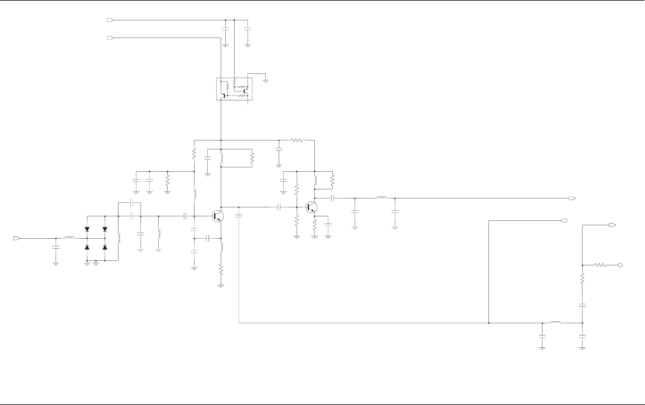
Schematics, Board Overlays, and Parts Lists – UHF: Transceiver (RF) Section 9-11
6871620L01-C May 28, 2008
Figure 9-10. UHF Frequency Generation Unit (TX VCO) Circuit – 2 of 3
TX VCO
VCTRL
VSF_VCO
AUX3
2113946B04
C292
0.1uF
100pF
C294
4815055H01
Q273
47K
10K
47K
4.7K
UMC5NT2G
C279
0.1uF
2113946B04
2113944A43
180pF
C280 0613952Q95
R270
8.2K
D273
4815002H01
R271
9.1K
0613952Q96
D274
4815002H01
C273
680nH
2416307H01
L274
D272
4815002H01
1.5pF
2113944A05
L275
2416307H01
680nH
2416307H01
680nH
L270
2113944A43
C278
180pF
36nH
2415427H37
L271
C274
2113944A25
10pF
2113944A43
C281 180pF
D271
4815002H01
4871915M01
Q271
IDCTR
L272
2471911M01
8.9nH
7.5pF
C272
2113944A22
C271
2113944A22
7.5pF
2416307H01
L273
680nH
100
0613952Q49
R284
12pF
2113944A26
C275
82pF
2113944A38
C277
2113944A24
C276
9.1pF
1.5pF
R272
100
0613952Q49
C285
2113944A05
180pF
C284
2113944A43
0613952Q67
R286
560
C283
0.1uF
2113946B04
C282
2.0pF
2113944A08
NP
2113944A43
C286
180pF
680nH
2416307H01
L276
56
R277
200
0613952Q56
R280
0662057M44
2113944A43
C287
C288
1.5pF
180pF
2113944A05
R279
0613952Q91
5.6K
4885061Y01
Q272
0613952Q95
R278 8.2K
2415427H41
L278
47nH
C293
3.0pF
2113944A12
Tx_VCO_Out
TXRF
PRES_RX_IN
TEST_POINT
TP2031
R266
200
PRESC
C291
100pF
51
R265
0613952Q42
2113944A40
C290
2113944A27
15pF
2415429H12
8.2nH
L277
2113944A32
C289
39pF
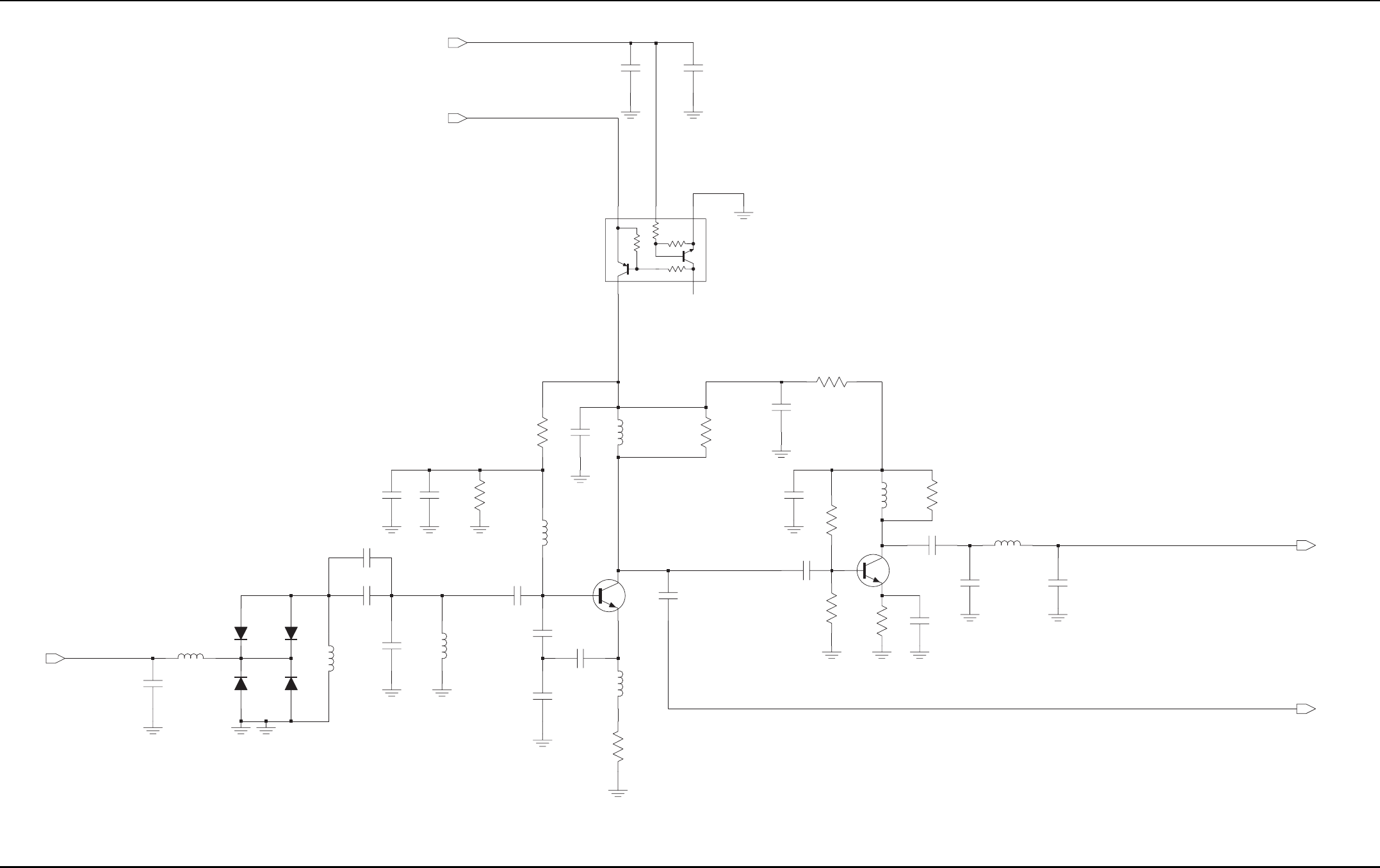
9-12 Schematics, Board Overlays, and Parts Lists – UHF: Transceiver (RF) Section
May 28, 2008 6871620L01-C
Figure 9-11. UHF Frequency Generation Unit (RX VCO) Circuit – 3 of 3
VCTRL
C295
2113944A42
150pF
4815002H01
D251
L251
680nH
2416307H01
4815002H01
D252 D254
4815002H01
D253
4815002H01
C257
2113944A80
L252
2415427H37
20pF
36nH
2113944A42
68pF
C259
2113944A36
C255
150pF
4871915M01
Q251
C251
2113944A23
8.2pF 680nH
2416307H01
L254
180
0613952Q55
R256
2471912M01
L253
IDCTR
11.7nH
C256
15pF
2113944A27
15pF
C258
2113944A27
R252
0613952Q96
9.1K
2113944A26
C252
12pF
C254
2113946B04
0.1uF
1.5pF
C253
2113944A05 L255
2416307H01
680nH
0613952Q96
9.1K
R253
2113944A42
2416307H01
150pFC261
680nH
L256
C260
2113944A73
8pF
C263
150pF
2113944A42
R257
0613952Q43
56
2.2pF
2113944A09
C264
0.1uF
C262
2113946B04
100
0613952Q49
R269
NP
150pF
C266
2113944A42
100pF
2113944A40
C265
2113944A79
C268
16pF
2113944A23
8.2pF
C267
R262
0613952Q85
3.3K
4885061Y01
Q252
0613952Q88
4.3KR260
2416307H01
L257 680nH
2415427H33
L258
24nH
R261
100
0662057M50
R263
0613952Q56
200
Rx_VCO_Out
RXLO
PRES_RX_IN
100pF
C296 0.1uF
C269
2113946B04
VSF_VCO
AUX2
4815055H01
UMC5NT2G
4.7K
47K
47K
10K
Q253
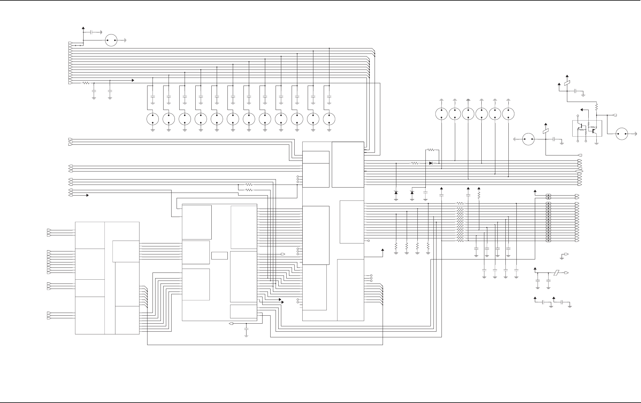
Schematics, Board Overlays, and Parts Lists – UHF: VOCON Section 9-13
6871620L01-C May 28, 2008
9.5 VOCON Section
Figure 9-12. VOCON: Overall Circuit Schematic
UC_KP_COLUMN0
UC_KP_COLUMN1
UC_KP_COLUMN2
UC_KP_ROW3
UC_KP_ROW2
UC_KP_ROW1
UC_KP_ROW0
UC_KP_ONOFF
UC_KP_5V1
UC_KP_5V2
FLIP_SENSE
UC_KP_ROW7
UC_KP_ROW4
UC_KP_ROW5
UC_KP_ROW6
UC_KP_BL_EN
KEYPAD
Interface
C1202
100pF
0
R1106
100pF
C1123
5V_Misc
E1422
SPARK_GAP
1
C1101
100pF 2
ON_OFF
12
12
SPARK_GAP
U9914
E1441
SPARK_GAP
E1431
SPARK_GAP
12
U9913
SPARK_GAP
12
E1433
SPARK_GAP
12
12
U9911
SPARK_GAP
12
SPARK_GAP
E1432
12
SPARK_GAP
E1440
SPARK_GAP
U9912
12
U9915
SPARK_GAP
1
2
2
SPARK_GAP
E1430
1
SPARK_GAP
U9910
1
2
100pF 100pF
C1115
C1111
100pF
C1110
100pF100pF
C1108 C1114
100pF100pF
100pF
C1109
2113944A40
C1105 100pF
100pF
C1112
100pF
C1106
100pF
C1107 C1113 C1116
DIGITAL
DIGITAL
DIGITAL
DIGITAL
DIGITAL
DIGITAL
DIGITAL
DIGITAL
DIGITAL
DIGITAL
DIGITAL
6305 17 42
0
12
KP_ROW(7:0)
KP_COL(2:0)
NC
WAKEUP
SPARE2_ENC_PTT
SSI_DI_ENC
SSI_DO_ENC
UCM_SS_BRAVO
ENC_RESET
SECURE I/O
BOOT*
AUDIO_JACK_INT
AUDIO_JACK_PTT
AUDIO_SW
NC
NC
DIGITAL
DIGITAL
DIGITAL
RESET
DISP_REG_SEL_A0
DISP_REG_SEL_A1
DISP_R_W
FLIP_SENSE
KP_BLEN
KEYPAD &
DISPLAY I/O
KP_COL(2:0)
KP_ROW(7:0)
DISP_BRIGHT1
DISP_BRIGHT2
DISP_CS_SUB
DISP_DATA(15:0)
DISP_ID
DISP_MAIN_EN
NU
C1125
470pF
V2
5.73V
VR52
R1105 10K
VR53
5.73V
C1124
.01uF
R1103
0
4888722V01
D1000
DIGITAL
DIGITAL_SPI
DIGITAL
UNSW_B+
SSI_AUDIO
DIGITAL
UCM
Interface
UNSW_B+
UC_ENC_SSI_DI
UC_WAKEUP
UC_RESET_ENC
UC_BOOT_ENC
UC_ENC_SSI_DO
UC_UCM_SS
UC_ENC_SSI_CLK
UC_KEYFAIL_LH_BDMDATA
AudJackMic
EARPIECE
VIBR
CE
SPKR,MIC
Interface
Interface
Interface
PROGRAMMABLE
BUTTONS
Interface
EXT_SPKR+
EXT_SPKR-
UC_INT_SPKR+
CE_OPT_SEL1
CE_OPT_SEL2
CE_OPTB+_VPP
CE_SB9600_BUSY
CE_CTS
CE_RTS
AUD_JACK_MIC
UC_INT_MIC
UC_INT_PTT
UC_EMERG
UC_MONITOR
CE_RS232DOUT_USB+
CE_RS232DIN_USB-
CE_LHDATA_KEYFAIL
UC_INT_SPKR-
UC_EMERG
UC_INT_PTT
UC_MONITOR
EXT_SPKR+
EXT_SPKR-
INT_MIC_OUT
INT_SPKR+
AUDIO
DATA
EXT AUDIO
BUTTONS
INT_SPKR-
CE_CTS
CE_LHDATA_KEYFAIL
CE_OPTB+_VPP
CE_OPT_SEL1
CE_OPT_SEL2
CE_RS232DIN_USB-
CE_RS232DOUT_USB+
CE_RTS
CE_SB9600_BUSY
EXT_MIC_OUT
OPT_SEL1_OUT
OPT_SEL2_IN
OPT_SEL2_OUT
RS232_DI_USB-
RS232_DO_USB+
RTS
VPP_EN
EXT_SPKR_NEG
HAB_MOD
INT_MIC
INT_PTT
INT_SPKR
INT_SPKR_NEG
LHDATA_KEYFAIL
CONNECTOR
BLOCK
MAKO I/O
CONTROLLER I/OAUDIO I/O
LH_BUSY
MOD
ONE_WIRE_OPT
OPTB+_VPP
OPT_SEL1_IN
CTS
EMERG
EXT_MIC
EXT_SPKR
7
1
2
3
5
6
4
0
CONTROLLER_IO(7:0)
DIGITAL
DIFF_PAIR
DIFF_PAIR
DIGITAL
DIGITAL
DIGITAL
DIGITAL
UTXD2
VPP_EN
VSW1
SPI_MISOB
SPI_MOSIB
SW_B+
TX_SSI_CLK
TX_SSI_FSYNC
UCM_KF_MAKO
UCM_SS
UCTS_USB_SPEED
UNSW_B+
URTS1_XRXD
URXD1_USB_VMI
URXD2
USB_TXENAB
USB_VMO
USB_VPI
UTXD1_USB_VPO
INT_SPKR_POS
KVL_USB_DET
LHDATA_KEYFAIL
MAKO_CE
MAKO_INT*
MAKO_RESET
ONE_WIRE_OPT
ONE_WIRE_UP
POR
RFSW_B+
RS232_DI_USB-
RS232_DO_USB+
RS232_USB*
RTS
SB9600_BUSY
SCKB
BAT_STATUS
BOOT_NORM*
BSY_IN_RTS
BSY_OUT_CTS
CODEC_DCLK
CODEC_FSYNC
CODEC_RX
CODEC_TX
CTS
EMERG
MAKO IC
BLOCK
AUDIO I/O CONNECTOR I/O
MAKO I/O
RF I/O
SECURE I/O
COMMUNICATION I/O
EXT_MIC
EXT_SPKR_NEG
EXT_SPKR_POS
GATED_32_KHZ
INT_MIC
INT_SPKR_NEG
16_8MHZ
32K_SEL
ADTRIG
100pF
C1139
DIGITAL
XRF_BAT_STAT
NC
NC
SW_B+
UNSW_B+
SSI_AUDIO
SSI_AUDIO
CLK
CLK
DIGITAL_SPIB
DIGITAL_SPIB
DIGITAL_SPIB
SSI_AUDIO
NC
NC
NC
VSW1
DIGITAL
DIGITAL
DIGITAL
DIGITAL
DIGITAL
DIGITAL
DIGITAL
DIGITAL
DIGITAL
DIGITAL
DIGITAL
DIGITAL
DIGITAL
DIGITAL
DIGITAL
NUR1102
0R1101
URXD1_USB_VMI
URXD2
USB_ENUM
USB_SUSP
USB_TXENAB
USB_VMO
USB_VPI
UTXD1_USB_VPO
UTXD2
SCKB
SPI_MISOB
SPI_MOSIB
UCTS1_USB_SPEED*
URTS1_XRXD
MAKO_INT*
MAKO_RESET
ONE_WIRE_EN*
ONE_WIRE_UP
RS232_USB*
GATED_32_KHZ
KVL_USB_DET*
MAKO_CE
BOOT_NORM*
BSY_IN_RTS
BSY_OUT_CTS*
COMMUNICATION I/O
MAKO I/O
CONTROLLER
& MEMORY
BLOCK
CODEC_DCLK
CODEC_FSYNC
CODEC_RX
CODEC_TX
16_8MHZ
32K_SEL
ADTRIG
BATTERY_ID
BAT_BUS_EN
VIBRATE_CONT
SCKA
SPI_MISOA
SPI_MOSIA
TX_SSI_CLK
TX_SSI_DATA
TX_SSI_FSYNC
UNI_SEL*
MOD
OPTB+_VPP
OPT_SEL1_IN
OPT_SEL1_OUT
OPT_SEL2_IN
OPT_SEL2_OUT
RED_LED
RX_SSI_CLK
RX_SSI_DATA
RX_SSI_FSYNC
EEPROM_SEL*
GREEN_LED
HAB_MOD
INT_PTT
LOCK_DET
BL_FREQ
RF I/O
CKIH
ABACUS3_CS
AD_CS*
UNIVERSAL CONNECTOR I/O
7
4
NC
5
2
NC
NC
6
0
3
1
VIBRATE_CONT
NC
DC_20
CLK
DIGITAL_SPIA
DIGITAL_SPIA
DIGITAL_SPIA
DIGITAL_SPIASPI_MOSIA
DIGITAL_SPI
TX_SSI_FSYNC
SSI_RF_TX
TX_SSI_CLK
SSI_RF_TX
SSI_RF_RX
DIGITAL
SCKA
DIGITAL_SPIA
SSI_RF_TX
SSI_RF_RX
SSI_RF_RX
RX_SSI_CLK
RX_SSI_DATA
RX_SSI_FSYNC
TX_SSI_DATA
SPI_MISOA
10K
R1124
10K
R1123
R1125
10K
R1122 10K
R1114
R1116
R1120
R1115
R1109
R1113
R1111
R1110
R1121
R1112
R1119
R1108
R1117
R1118
100
1K
0
1K
1K
1K
1K
1K
1K
1K
100
1K
100
100
V2
C1126
470pF
R1107
10K
V2
DC_10
33pF
C1136
C1133
33pF 33pF
C1131
33pF
C1134
33pF
C1132
470pF
C1138
470pF
C1130
470pF
C1135
NU
C1118
100pF
C1117
100pF
SW_B+
UNSW_B+
C1129
1uF
E1104
BLM11P600S
UNSW_B+
C1128
100pF
TO BATTERY
XIFGND1
XRFUNSWB+1
VSW1
IF24_CTRL
IF33_CTRL
IF34_CTRL
IF18_CTRL
IF32_CTRL
IF27_CTRL
IF30_CTRL
IF23_CTRL
IF22_CTRL
IF25_CTRL
IF19_CTRL
IF31_CTRL
IF28_CTRL
IF17_CTRL
IF29_CTRL
IF26_CTRL
IF21_CTRL
Interface
XCVR
DISPLAY
Interface
To XCVR
DISP_RESET
DISP_MAIN_EN
DISP_R_W
DISP_ID
DISP_V1.875
XSWB+2
DISP_REG_SEL_A0
XRX_DATA
XSSI_CLK
XTX_SSCK
XSSI_FSYNC
XTX_DATA
XRF_MOSIA
XRF_SCKA
XFN_PC_SEL*
XRF_AD_CS*
DISP_BRIGHT2
DISP_BRIGHT1
DISP_DATA(15:0)
DISP_CS_SUB
XRF_VSW1
X16.8MHz
DISP_REG_SEL_A1
XTX_SSFS
XABACUS3_CS*
XRF_POR*
XRF_MISOA
XLOCK
E1421
SPARK_GAP
12
V1.875
BLM11A601S
E1102
C1119
100pF
V2_FIL
NC
BLM11A601S
E1103
100pF
C1120
R9961
0
MECH_SW
6
V2
Not Placed
NC
NC
SPARK_GAP
E1420
4
MUN5313DW1T1G
Q9951
2
5
3
1
DISP_V2.9
12
SPARK_GAP
E1434
SPARK_GAP
E1438
E1439
SPARK_GAP
2
E1437
SPARK_GAP
1
21
21
21
21
21
E1435
SPARK_GAP
SPARK_GAP
E1436
Interface
AUDIO JACK
AUD_JACK_INT
AUD_JACK_PTT
AUDIO_SW
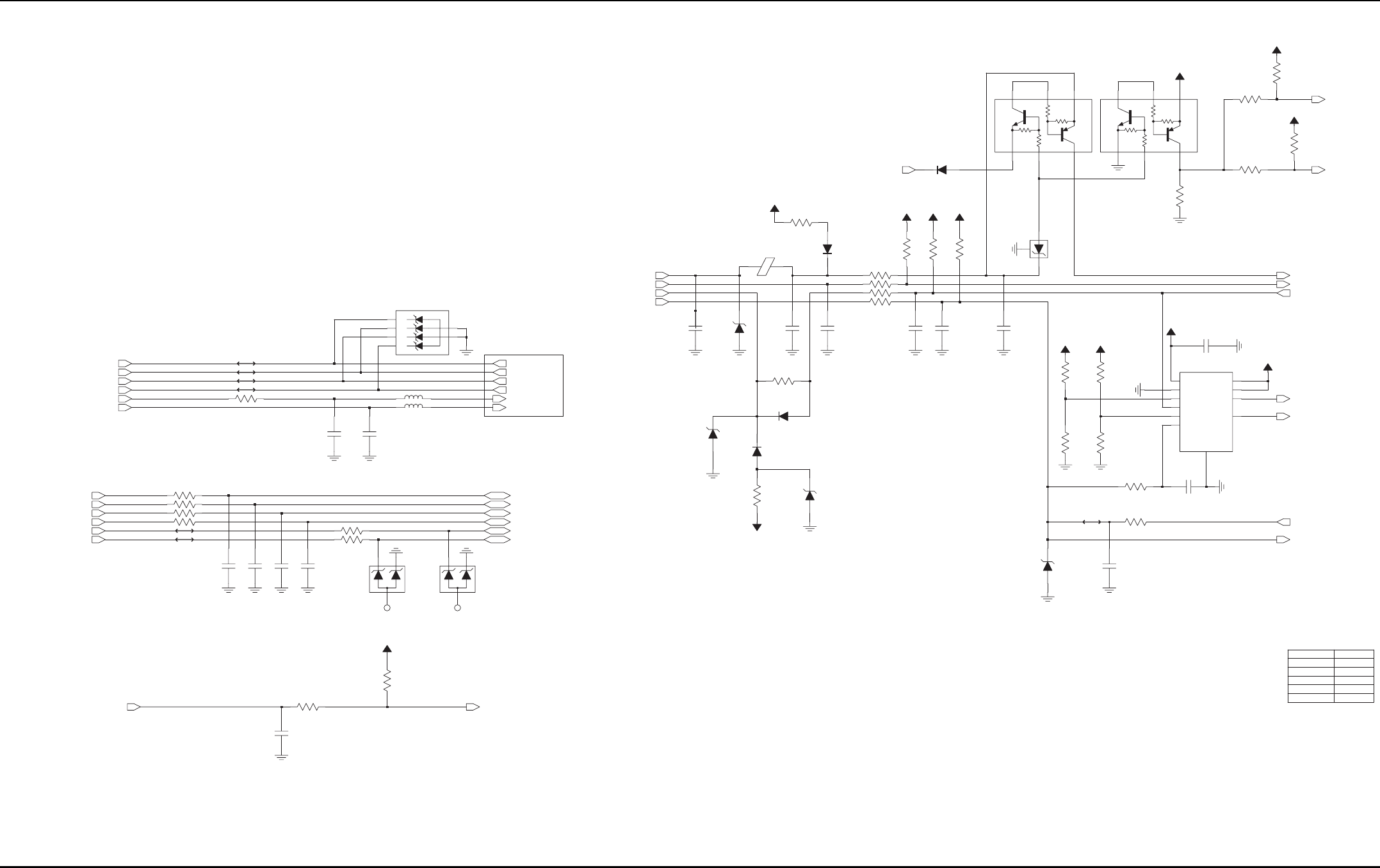
9-14 Schematics, Board Overlays, and Parts Lists – UHF: VOCON Section
May 28, 2008 6871620L01-C
Figure 9-13. VOCON: Audio, Connector Interface Circuits
INT_MIC_OUT
EXT_MIC_OUT
EXT_SPKR+
AUDIO SIGNALS
EXT_SPKR-
INT_SPKR+
INT_SPKR-
CE_CTS
CE_RS232DOUT_USB+
CE_RS232DIN_USB-
CE_LHDATA_KEYFAIL
USB/RS232/SB9600
CE_SB9600_BUSY
CE_RTS
180
R1202
R1204 560
R1203
R1205 1K
USBN
USBP
390
470pF
C1213
33pF
C1212 C1214
33pF 470pF
C1215
R1207 33
33R1206
NC
3
12
VR1202
5.6V 5.6V
3
12
VR1203
NC
R1212
100K
V2
EMERG
C1217
470pF
1K
R1210
UC_EMERG
100
INT_SPKR_NEG
EXT_SPKR
INT_SPKR
EXT_SPKR_NEG
R1201
470pF
C1210
C1209
470pF
L1204 270nH
270nH
L1205
2415429H45
5
A2
1K1
3K2
4K3
6K4
VR1201
Place close to Connector
12.6V
2
A1
MAKO AUDIO
INT_SPKR_NEG
EXT_SPKR
EXT_SPKR_NEG
EXT_MIC
INT_SPKR
INT_MIC
LH_BUSY
RTS
CTS
LHDATA_KEYFAIL
RS232_DI_USB-
RS232_DO_USB+
CE_OPTB+_VPP
OPTION SELECT & PTT
CE_OPT_SEL2
CE_OPT_SEL1
UC_INT_PTT
0.10uF
C1218
1
2
D1205
13V
D1223
5.73V
VR1206 D1222
NU
VR1205
6.8V
4809788E21
MECH_SW_b
R1241
0
NU
R1239
0
0.10uF
C1219 C1220
470pF
68
R1213
SW_B+
E1201
BLM11A601S
1
2
D1202
R1214
R1215
R1217
R1216
30
4.7K
390
220
R1218
47K
R1220
10K
V2
0.10uF
C1223
C1222
100pF
R1219
10K
470pF
C1221
V2
V2
12
D1207
VPP_EN
NU
V2
For HAB =no place
10K
R1221
For HAB only
R1223
V2
MOD
HAB_MOD
NU
For HAB only
0
For HAB =no place
R1224
R1596
V2
100K
R1225
2
3
6
4
1
EMD3
Q1202
5
Q1201
EMD3
10K
10K
10K 10K 10K
10K
10K
10K
5
2
3
6
4
1
2
3
1
VR1204
9.1V
ONE_WIRE_OPT
V2
V2
20K
R1226 R1227
1%
10K
100K
R1230
C1232
100pF
1%
150K
R1229
6.8V
VR1208
100
R1231
20K
R1228
OS2O
0.10uF
C1225
OPT_SEL2_IN
OPT_SEL2_OUT
ONE_WIRE_OPT
OPT_SEL1_IN
V2
OUTB 9
SDA 5
SDB 6
VNEG
4VPOS
10
LMV712LDX
CTGND
G1
INNEGA
2
INNEGB
8INPOSA
3
INPOSB
7
OUTA 1
U1201
V2 C1224
0.10uF
OPT_SEL1_OUT
INT_PTT
OPTB+_VPP
VSW1
VSW2
VCC5
VREF
V2
GLOBAL NAME
2.89 Vdc
DC Power Supply
VOLTAGE
Designators
2.89 Vdc
5.0 Vdc
3.8 Vdc
1.875 Vdc
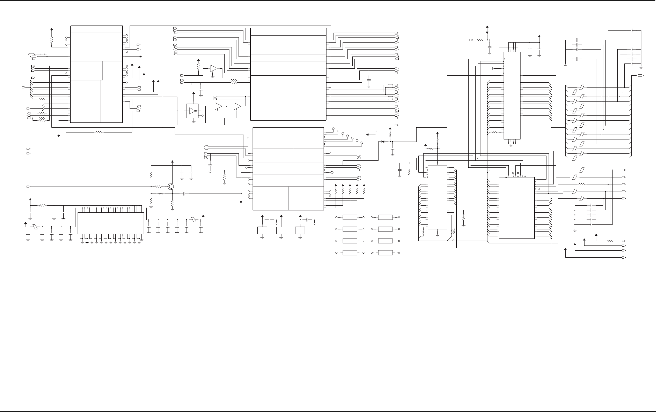
Schematics, Board Overlays, and Parts Lists – UHF: VOCON Section 9-15
6871620L01-C May 28, 2008
Figure 9-14. VOCON: Controller and Memory Circuits
5
NC
NC
H7
G3
D8
B7
D9
C9
E3
E4
F3
F4
C10
D10
G2
G4
B8
G8
NC
NC
NC
NC
TOUT8_PD4
TOUT9_PD12
TOUT14_PD10_DMAC_RS
TOUT15_PD11_DMAC_D2
TOUT2
TOUT3
TOUT4_PD0
TOUT5_PD1
TOUT6_PD2
TOUT7_PD3
TOUT0
TOUT1
TOUT10_PD13
TOUT11_PD7
TOUT12_PD8_DMAC_D5
TOUT13_PD9
ROW2_PG10
ROW3_PG11
ROW4_PG12
ROW5_PG13
ROW6_PG14
ROW7_PG15
INT3_PC15
INT4_PA6_OPTION_SELECT_1_IC1A
INT5_PA7_OPTION_SELECT_2_IC1B
ROW0_PG8 KEY PAD I/O
INTERRUPTS LAYER 1 TIMERS
ROW1_PG9
COLUMN4_PG4_IC2B_SPICS6
COLUMN5_PG5_MOSIA_SPICS7
COLUMN6_PG6_QSCKA_SPICS8
COLUMN7_PG7_SPICS9_URTS1
INT0_PE8
INT1_PE9
INT2_PC14
COLUMN0_PG0
COLUMN1_PG1
COLUMN2_PG2
COLUMN3_PG3
SIM_SVEN0_PB8
SIM_SVEN1_PB14_DSP_DBG_XDW
SIM_D0RX_PB5
SIM
DSC AND ONE_WIRE
SIM_D0TX_PB4
SIM_D1TX_PB10
SIM_D1RX_PB11
SIM_PD0_PB9
SIM_PD1_PB15_
DSP_DBG_PAW
SIM_RST0_PB6
SIM_RST1_PB12_TIN0
SIM_CLK0_PB7
SIM_CLK1_PB13_DSPYDW
OWIRE_DAT_PA10 PD5_DMAC_D0
PD6_DMAC_D1
SIM_INT_TOUT_BLOCK
U1401-4 5187943V03
P17
D17
N20
C19
P20
D18
N21
C17
C4
NC
NC
NC
NC
NC
R1401
not placed for HAB
10K
NC
V2
N22
C18
R20
C16
NC
NC
ADD R1415 FOR COVERT
NU
3
5
1
R1404 0
0
R1403
1
R1405
2
6
4
0
2
0
7
0
R1402
32K_SEL
KP_ROW(7:0)
ROW6_PG14
ROW5_PG13
ROW4_PG12
ROW3_PG11
ROW2_PG10
ROW1_PG9
ROW0_PG8
ONE_WIRE_UP
KP_COL(2:0)
HAB_DISABLE
BATTERY_ID
INT_PTT
MAKO_INT*
OPT_SEL1_IN
OPT_SEL2_IN
SPARE2_ENC_PTT
WAKEUP
BOOT*
NC
R7
T8
T4
T2
T3
U4
V4
G21
G22
M2
C3
R4
R3
N7
P3
N3
P4
P7
U2
U3
T7
M3
N4
N2
R1406
0
COV_DISP_ID
ROW7_PG15
COLUMN0_PG0
COLUMN1_PG1
COLUMN2_PG2
SSI_AUDIO
VIBRATE_CONT
MISOA_SEL
ENC_RESET
HAB_MOD
FLIP_SENSE
LOCK_DET
GPIO
Patriot_ONOFF
R1409
10K
DISP_BRIGHT2
DISP_BRIGHT1
ON_OFF_det
KP_BLEN
CODEC_TX
DC_10
V2_R1414_1
RS232_USB*
GREEN_LED
TX_SSI_FSYNC
CODEC_DCLK
CODEC_FSYNC
OPT_SEL2_OUT
RED_LED
BSY_IN_RTS
URXD1_USB_VMI
URTS1_XRXD
AUDIO_JACK_PTT
URXD2
RX_SSI_DATA
TX_SSI_CLK
100pF
C1407
1.0uF
C1412
0.10uF
C1411
V2
C1409
.015uF
C1408
0.10uF
E1402
BLM11A601S
C1410
0.10uF
V2_E1402_1
DC_10
C2
M7
U12
G11
G16
L7
H17
G17
N17
G7
J7
N8
R8
T17
G13
G10
G9
R17
M17
J17
G15
U9
U13
U15
U17
U8
PATRIOT_1_55V DC_10
DC_10 PATRIOT_V2
VCCA
VSS1
H9
L16 VSS2
Q2_Q8VSS
M16
Q3_Q1VDD
Q4VDD
T12 Q4VSS
Q6VDD
H11 Q6VSS
Q7VDD
H14 Q7VSS
T9 J2VSS
KVDD
K_QVSS
M8
LVDD
H16 LVSS
PVDD
H15 PVSS
Q2_Q8VDD
H8 H2VSS
I1VDD
J8 I1VSS
I2VDD
L8 I2VSS
J1VDD
J1VSS
P8
J2VDD
DVDD
DVSS
P16
EVDD
EVSS
H12
D2 GNDA
H1VDD
H10 H1VSS
H2VDD
B1VDD
N16 B1VSS
B2VDD
K16 B2VSS
C1VDD
J16 C1VSS
C2VDD
C2VSS
H13
A2VDD
T11 A2VSS
A3VDD
T14 A3VSS
A4VDD
U16 A4VSS
A5VDD
T15 A5VSS
U1401-5
IC_PWR_GND
A1VDD
T10 A1VSS
0
R1420
1.0uF
C1418
V1.875
C1421
.015uF
E1401
BLM11A601S
V1.55
0.10uF
C1414
C1419
100pF
C1413
.015uF
C1417
0.10uF 0.10uF
C1420
4.7uF
C1416
CKIH
V1_55V_R1407_1
DC_10
VSW2_E1401
DC_10 PATRIOT_VSW2
NU
R1419
100pF
C1404
R1418
33K
R1416
47
R1415
390
R1417
30K
1.0uF
C1402
C1403
0.10uF
23
1
Q1402
C1425
100pF
MAKO_RESET
USB_TXENAB
USB_VMO
GATED_32_KHZ
MOD
NC
NC
NC
100K
R1412
D14
L3
L2
K4
U7
J20
L4
V3
NC
NC
NC
CLK
NC K20
Y3
L20
B3
U22
W4
R16
Y22
D3
NC
TP1408
1
CLK
CKO_PA3
CLK C15
D16
D15
B17
B16
G14
C14
TEST
MMC_CMD
MMC_DAT
MMC_OD_EN
MOD
MUX_CTL
MMC_CLK
CKIL
MMC
TIME_MARK E20
D19
PWRCTL
SIGN C21
D21
PECLREF
CLKACQ E21
CLKGPS D22
C22
MAG
AGCDAT C20
GPS
TDO
TMS
TRST
WDOG_N
RESET_IN RESET_OUT
STBY_PD14
TCK
TDI
PC11_OC1_USBCLK_DMAC_D3
PC12_STO_DMAC_D5
PC1_USB_TXENB
PC8_UTXD1_UTXD2
PC9_URXD1_URXD2
PWM_PE13_DMAC_CS
PWM_PE14_DMAC_D4
OC3_PC13_FRAME_TICK
PA2_USB_VPIN
PC0_USB_VMOUT
CKO_PA3
CLKSEL_PD15
DSP_DE
MCU_DE
CKIHCKOH_SCC_CLK
5187943V03
GPIO
CCM/WDOG/EGPT/CLK
MISCELLANEOUS
JTAG
MISC_BLOCK
U1401-3
REAL TIME TRACE
NC
NC
NC
V2 V2 V2
V2
V2
100K
R1463
R1466
100K 100K
R1462
R1464
100K
R1465
100K
RESET
USB_ENUM
BAT_BUS_EN
ONE_WIRE_EN*
KVL_USB_DET*
BL_FREQ
USB_VPI
Reserved for Mobile/Portable classification
NC
L17
K17
L22
L21
W3
Y2
AA2
B11
K21 TP1409
1
SPI_MOSIA
SCKB
SCKA
SPI_MOSIB
AUDIO_SW
ADTRIG
D_MOSIB
D_SCKB
D_CS*
D_REG_SEL
EEPROM_SEL*
AD_CS*
MAKO_CE
UNI_SEL*
ABACUS3_CS
JTAG
TP1403
1
TP1406
1
1TP1404
TP1401
1
TP1407
1
1TP1402
MAKO_RESET
TP1405
1
TP1410
1
V1.875
R1437
4.7K
470pF
C1429
1
D1401
2
NU
R1439
V2 R1440
0
V1.875
V2_R1414_1
DC_10
F6
G6
B1
C1
G2
H6
E2
F2
F1
G1
C6
D5
E5
F5
B6
C5
C2
D2
E3
2
8
4
10
11
0
3
6
5
15
1
13
14
12
7
9
B5
A2
G5
C3
C4
D4
H2
H3
A6
B2
F3
F4
E4
D3
H1
A5
B3
B4
A3
A4
H4
H5
G3
G4
A1
9
2
16
12
1
4
13
5
11
15
7
14
3
10
8
18
17
6
19
R1421
0
D1
E6
M1008
1188983Y01
1188983Y01
M1007
M1001
1188983Y01 1188983Y01
M1005
M1003
1188983Y01
M1006
1188983Y01
1188983Y01
M1004
1188983Y01
M1002
NOT PLACED
NC
NC
NC
NC
NC
NC
NC
NC
NC
NC
NC
NC NC
NC
NC
NC
PIN1
1PIN2 2
1PIN1 2
PIN2
PIN1
1PIN2 21
PIN1 2
PIN2
2
PIN1
1PIN2
PIN1
1PIN2 2
2
PIN2
1PIN1
2
PIN2
1PIN1
UNDERFILM
GND
3
VCC
PWR_GND
U1404-2
C1422
0.10uF
3
GND
5
VCC
CKIH_VOCON
U1405-2
PWR_GND
V2
3
GND
5
VCC
U1408-2
PWR_GND
V2
0.10uF
C1424
V2
V2_C1446_1
DC_10
V2_C1438_1
DC_10
RAM
R1422
0
0.10uF
C1430
VSS
VSSQ
IO6
IO7
IO8
IO9
NC1
NC2
E1
VCC
VCCQ D6
IO12
IO13
IO14
IO15
IO2
IO3
IO4
IO5
EN_BLE
EN_CE
EN_OE
EN_WE
IO0
IO1
IO10
IO11
A5
A6
A7
A8
A9
CE2
DNU
EN_BHE
A14
A15
A16
A17
A18
A2
A3
A4
U1409
A0
A1
A10
A11
A12
A13
CY62157DV18
0R1438
R1706
0
21 20
0
R9990 6
12
14
9
3
8
5
11
10
15
7
13
4
0
1
2
CONTL_BUS
Address(23:0)
ADRS_BUS
ADRS_BUS
ADRS_BUS
ADRS_BUS
ADRS_BUS
ADRS_BUS
ADRS_BUS
ADRS_BUS
ADRS_BUS
ADRS_BUS
ADRS_BUS
ADRS_BUS
ADRS_BUS
ADRS_BUS
ADRS_BUS
ADRS_BUS
ADRS_BUS
ADRS_BUS
ADRS_BUS
ADRS_BUS
ADRS_BUS
ADRS_BUS
ADRS_BUS
ADRS_BUS
ECB_N_PA4
LBA_N
OE_N
R_W_N
SEB_N_PA5
SOE_N_PE15
D4
D5
D6
D7
D8
D9
EB0_N
EB1_N
D11
D12
D13
D14
D15
D2
D3
CS0_N
CS1_N
CS2_N
CS3_N
CS4_N
CS5
D0
D1
D10
A4
A5
A6
A7
A8
A9
BURSTCLK
A18
A19
A2
A20
A21
A22_PA1_DSP_DBG_XDW
A23_PA0_DSP_DBG_YDW
A3
A10
A11
A12
A13
A14
A15
A16
A17
INDY/BRAVO
U1401-1
EIM_BLOCK
5187943V03
A0
A1
12
4
1
19
11
0
5
2
3
23
6
16
20
18
9
7
21
14
17
8
22
1
15
0
13
10
AB16
AB21
Y16
AA15
AA19
Y15
Y14
AB11
AA11
Y11
AB17
Y10
AA10
U11
U10
AA17
T13
AA14
AB13
AA13
Y13
AB12
AA12
Y17
NC
NC
NC
W20
AA22
U21
Y18
V20
W21
AB7
AA7
Y7
Y6
AA6
AA18
V21
AA5
Y5
AA4
AB4
AA3
AB3
Y8
AA8
AB8
AA21
AA16
AB20
AA20
Y19
U14
AA9
Y9
Y21
P_CS5
P_CS3
P_R_W
CS2
BK1005HM471
BK1005HM471
BK1005HM471
RES
BK1005HM471
BK1005HM471
BK1005HM471
BK1005HM471
BK1005HM471
BK1005HM471
BK1005HM471
BK1005HM471
BK1005HM471
BK1005HM471
BK1005HM471
BK1005HM471
BK1005HM471
BK1005HM471
BK1005HM471
BK1005HM471
BK1005HM471
NOT PLACED
33pF
33pF
C1441
0
R1467
C1444 33pF
E1127
33pF
C1442
C1440
E1130
33pF
C1443
E1129
4
1
E1110
14
E1111
E1118
5
6
8
E1119
7
E1124
2
10
9
E1122
E1113
13
E1115
E1120
E1114
E1121
3
E1125
E1123
0
12
15
E1112
E1116
E1117
11
1
0
4
5
2
7
8
11
3
9
13
12
14
10
6
15
13
18
14
8
7
1
15
4
2
16
21
12
17
23
3
10
22
19
11
0
R1423
20
6
9
5
A7
C7
A2
B2
C6
C8
B3
C3
D7
B8
A8
B7
A1
B1
C1
D2
D1
D4
B6
A6
E8
D8
C2
A3
F1
G2
G8
FLASH
V1.875
D1402
1
2
VCCQ1 E1
VCCQ2 G6
VPP A5
WAIT
WP
D6 EN_WE
C5
GND1
GND2
GND3
GND4
RESET
B5
VCC1 A4
VCC2 G4
D4
D5
D6
D7
D8
D9
EN_CE
E7
EN_OE
F8
D10
D11
D12
D13
D14
D15
D2
D3
A6
A7
A8
A9
ADV
C4
CLK
B4
D0
D1
A19
A2
A20
A21
A22
A3
A4
A5
A11
A12
A13
A14
A15
A16
A17
A18
U1410
28F320
A0
A1
A10
R1424
0
0.10uF
C1433
OPTB+_VPP
D3
E4
G3
E3
G1
G7
F6
F5
F4
D5
F3
F2
E2
E5
G5
F7
E6
DATA(15:0)
E1126
DISP_REG_SEL_A0
DISP_R_W
DIGITAL_NOISY
DISP_REG_SEL_A1
DISP_CS_SUB
DISP_MAIN_EN
DISP_DATA(15:0)
9
8
14
3
10
2
1
13
11
0
6
4
12
15
7
5
COV_D7
DIGITAL_NOISY
COV_D6
COV_D3
COV_D5
COV_D1
COV_D0
COV_D4
COV_D2
COV_D12
COV_D10
COV_D9
COV_D8
COV_D15
COV_D14
COV_D13
COV_D11
NOT PLACED
82pF
82pF
82pF
C1457
C1458
C1460
82pF
C1459
82pF
C1453
NOT PLACED
82pF
82pF
C1445
82pF
C1449
C1447 82pF
C1446
C1432
0.10uF
V1.875
0.10uF
C1431
DISP_ID
DISP_BRIGHT1
DISP_BRIGHT2
KP_BLEN
NU
DISP_BRIGHT1
DISP_BRIGHT2
KP_BLEN
COV_DISP_ID
R1449
CODEC_RX
RX_SSI_FSYNC
TX_SSI_DATA
UCTS1_USB_SPEED*
BSY_OUT_CTS*
UTXD1_USB_VPO
UTXD2
BOOT_NORM*
AUDIO_JACK_INT
USB_SUSP
UCM_SS_BRAVO
RX_SSI_CLK
OPT_SEL1_OUT
100pF
no place
C1428
T16
J21
G20
H21
H20
F20
G12
B21
C13
D13 SSI_RF_TX
SSI_RF_RX
SSI_RF_RX
R21
M21
M22 SSI_AUDIO
DIGITAL_SPIA
DIGITAL_SPIB
DIGITAL_SPIB
DIGITAL_SPIB
DIGITAL_SPIA
DIGITAL_SPIBSDI_D_C_PE5_SPICS1
DIGITAL_SPIBSPI_CS0_PE10
DIGITAL_SPIB
DIGITAL_SPIB
DIGITAL_SPIA
DIGITAL_SPIA
K8
K3
K7
C7
C6
C5
B4
D5
J4
J3
D6
H4
C8
H3
SPICS2_PE4
SPICS3_PE6
SPICS4_PE7
SPICS5_PE11
SPICS6_PE0_DMAC_D3
SPICS7_PE1_DMAC_D4
SPICS8_PE2_DMAC_D6
SPICS9_PE3_DMAC_D7
SDI_D_C_PE5_SPICS1
SPICS0_PE10
MOSIA
MQSPI
MOSIB
QSCKA
QSCKB
MISOA
MISOB
R1411 0
0
R1410
B20
U20
F21
T22
B13
C11
T21
T20
C12
P21
B12
D11
H22
SI_AUDIO
SSI_RF_TX
SSI_AUDIO
SSI_AUDIO
SSI_RF_RX
SSI_RF_TX
1Y
4
74VHC125
U1408-1
A
2
OE
V2
SCKAS_AP
SC2A
V2
D7
H2
NC
2
1
NC
4
5
VCC
MC74HC1GU04D
U1406
3GND
100pF
C1427
A
2
OE
1Y
4
U1404-1
74VHC125
2
OE
1Y
4
74VHC125
U1405-1
A
DIGITAL_SPIA
SPI_MISOA DIGITAL_SPIB
SPI_MISOB
MOSIA
SRDA STDA
SC2A
SCKA
SAP
SC0A_PC7_DMAC_D1_DMAC_SCK
SC1A_PC6_DMAC_D0_DMAC_MOSI
SRDA
SRDB
SRDB2_PC4_OC2
STDB
SC1B
SC2B_PC3
SCKB
SCKB2_PC5
BBP
SC0B_PC2
5187943V03
INDY/BRAVO
SERIAL_PORTS_BLOCK
U1401-2
URTS2_PB3
URXD2_PB1 UTXD2_PB0
UCTS2_PB2
SECONDARY UART
URXD1_PA15_USB_VMIN_TDIUTXD1_PA14_USB_VPOUT_ITXD_TDO
UCTS1_PA12_USB_FSEN_MCU_DE
URTS1_PA13_USBXRXD_IPWR_
RESET_IN_IC2A
PRIMARY UART
RIA_PA9_USBSUSP_TCK_SCKA_UTXD1
DCDA_PA8_DSP_DE_SC2A
DSRA_PA10_TRST_STDA_URXD1_INT6
DTRA_PA11_TMS_SRDA_INT7
V2
SSI_DI_ENC
SSI_DO_ENC
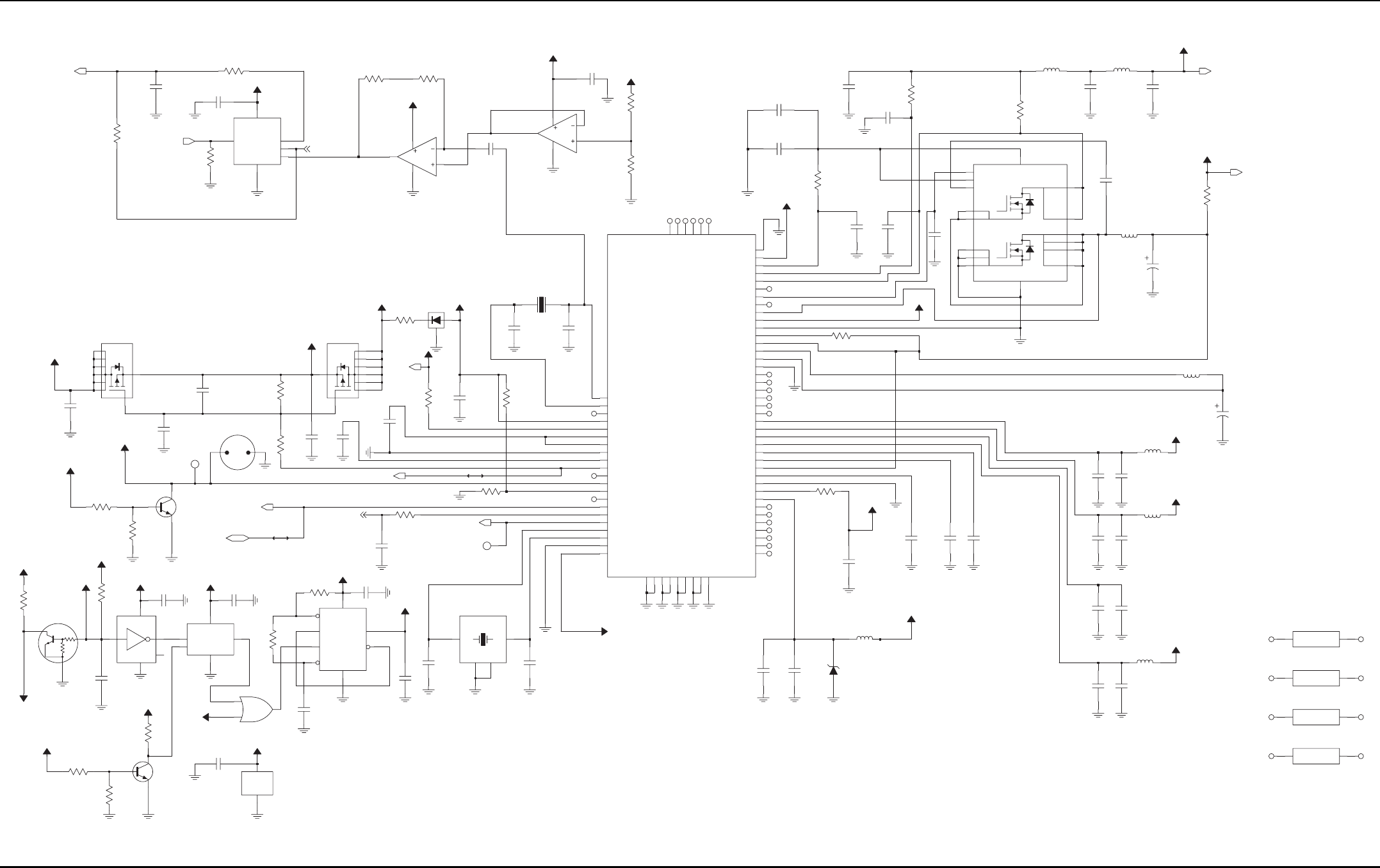
9-16 Schematics, Board Overlays, and Parts Lists – UHF: VOCON Section
May 28, 2008 6871620L01-C
Figure 9-15. VOCON: DC Power, Clocks and ON/OFF Circuit
0.10uF
C1302
1K
R1301
B1 1
2GND
6
VCC
5
NC7SB3157
U1301
4
A3
B0
10K
R1303
V2
32K_SEL
MAKO_32KHZ
NU
470pF
C1301
R1302
GATED_32_KHZ
SEL
MAKO_32KHZ
R1305
2MEG
V2
2MEG
R1304
C1
B1
B3
U1302-1
LMC6035ITLX C2
C3 10pF
C1303
U1303-2
LMC6035ITLX A2
A3
A1
B1
B3
0.10uF
C1304
V2
V2
47K
R1307
47K
R1306
NC3
NC4
NC5
NC6
NC1
NC2
NC
NC
NC
NC
NC
P14
M5
B14
A1
A14
P1 NC
ON_OFF_det
4813973A42
Q9906
R2
R1
V2_FIL
1K
R9922
R9924
10K
R9925
10K
Q9905
Patriot_ONOFF
1K
R9926
5V_Misc
U9901
MC74HC1GU04D
C9950
0.10uF
GND
3
2
NC 1
4
VCC
5V_Misc
ON_OFF
5V_Misc
R9923
10K
5
0.10uF
C9953
R9921
47K
Q9904
MECH_SW
47K
R9920
MECH_SW
1
Q1301
1
TP1303
MECH_SW_b
C1314
100pF
100pF
C1313
C1312
2.2uF
E1418
SPARK_GAP
2
.01uF
C1310
0
R1311
47K
R1310
C1309
1000pF
Q1302UNSW_B+
C1308
2.2uF
VPP_EN
C1307
2.2uF
UNSW_B+
VSAVE
SW_B+
0
R1309
R1308
56K D1301
UNSW_B+
CC4V
Y1301
2
32.768KHz
1
5.6pF
C1305
5.6pF
C1306
100K
R1371
NC
NC
NC
CLK
DC_I2
DC_I2
ANALOG
DIGITAL
R1370
0
1
TP1304
TEST_POINT
32_KHZ
MAKO_INT*
Placed for evaluation
.01uF
C1315
100
R1314
MAKO_32KHZ
1
2
4
NC7SZ32
U9918-1
ON/OFF Circuitry
5V_Misc
0.10uF
C9980
PWR_GND
U9918-2
GND
3
VCC
5
GPIO
TC7S08FU
U9902
3GND
2INA
1INB 4
OUTY
5
VCC
30K
R9927
C9952
0.10uF
5V_Misc
POR
MAKO_RESET
00.10uF
C9951
R9960
MECH_SW
5V_Misc
3
8
VCC
6CLR
CP
1
2D
4GND
7PR
5
Q
Q*
NL17SZ74
U9903
0.10uF
C9954
0.10uF
C9969
33pF
C1316
GND
GND1
OUT IN1
Y1302
XTAL
24.576MHz
2
4
3
C1317
33pF
CKIH_VOCON
D9
P5
M7
J4
G5
K9
L4
D14
H5
VBUS_SUPPLY
VSAVE
XIN
XOUT
XTAL32_IN
XTAL32_OUT
V10_I
V10_O
VBUS1
VBUS1_CMD
VBUS1_SENS
VBUS2
VBUS2_CMD
VBUS2_SENS
V03_O
V04_O
V06_O
V07_O
V08_I
V08_O
V09_O
V10_GND
SW5_VDD
SW5_VDDHV
SW5_VOUT
SW5_VSENSE
SW_TYPE
TCXO_IN
TCXO_SEL_16_24
V02_O
SW1_VSEN_BUK
SW2_GND
SW2_LX
SW2_VCC
SW2_VCCS
SW2_VOUT
SW5_PHASE
SW5_SUMCOMP
SW1_DH
SW1_GND
SW1_PHASE
SW1_SUMCOMP_DL
SW1_VDD
SW1_VDDHV
SW1_VOUT
SW1_VSEN_BST
PGLDO2
PGLDO3
REG_3V6
RESETX
GND8
GND9
HV_BG
IGN_X
INT_X
MECH_SW
GND1
GND2
GND3
GND4
GND5
GND6
GND7
BAT_3V6
BAT_7V5
BAT_RTC
BAT_TYPE
EMERG_PB
FET_ENX
GATED_32K_CLK
PWR_MNGR_BLOCK
U1304-1
C2
A13
A12
C1
B1
B3
M1
D4
D3
C5
G4
B4
D5
E4
F5
D2
D1
F3
B2
F4
E2
NC
NC
NC
NC
NC
NC
NC
C1320
2.2uF
0
R1315 SW_B+
DC_I5
M6
H10
C14
E12
D12
C13
F11
B13
N5
P3
P6
K3
K4
L1
L9
J10
F13
F12
E14
N4
P4
L14
J14
J12
K14
J13
G11
E13
D13
H14
F14
G14
G13
G12
H12
J11
H11
C3
A2
H13
DC_I4N
DC_I0
DC_I0
DC_I0
DC_I0
NC
NC
NC
NC
NC
NC
DC_I4N
DC_I2
DC_I2
NC
NC
DC_I2
VSAVE
1.0uF
C1338
C1339
.01uF
Place close to Driver
0.1uF
C1336
R1318
100
1.0uF
C1335
C1340
10uF
C1341
0.1uF
R1320
0
560nH
L1308
SW_B+
L1307
560nH
0688044N04
R1321
0.1
10uF
C1343
10uF
C1342
SW_B+
VSW1
0
R1319
VSW1
C1345
1.0uF
47uF
C1333
2475119M01
L1306
22uH
D1A
D1B
D2A
D2B
D2C
D2D
VDD
Q1304
S1A
S1B
SYNC_EN
IN
CBOOT
S2A
S2B
S2C
GND
C1337 1000pF
R1317
0688044N04
0.1
VSW1
RFSW_B+
VR1207
6.8V
4809788E21
1.0uF
C1319
.01uF
C1318
560nH
L1301
VCC5
USB INTERNAL NOT USED
V7_LDO (NOT USED)
(Not Used) MAKO ANALOG CORE (3V)
C1323
1.0uF
1.0uF
C1322
C1321
1.0uF
560nH
L1304
.01uF
C1331
C1330
2.2uF
V1.875
L1303
560nH
V1.55
2.2uF
C1328 C1329
.01uF
V_2.775 (NOT USED) V2
C1327
.01uF
1.0uF
C1326
560nH
L1302
.01uF
C1325
C1324
1.0uF
22uH
L1305
2475119M01 (2.2V NOT USED)
VSW2
C1332
47uF
NC
NC
NC
NC
1188983Y01
M1012
NC
NC
NC
NC
1188983Y01
M1011
M1009
1188983Y01
1188983Y01
M1010
UNDERFILM
1PIN1 2
PIN2
PIN2 2
PIN1
1
1PIN1 2
PIN2
PIN1
1PIN2 2
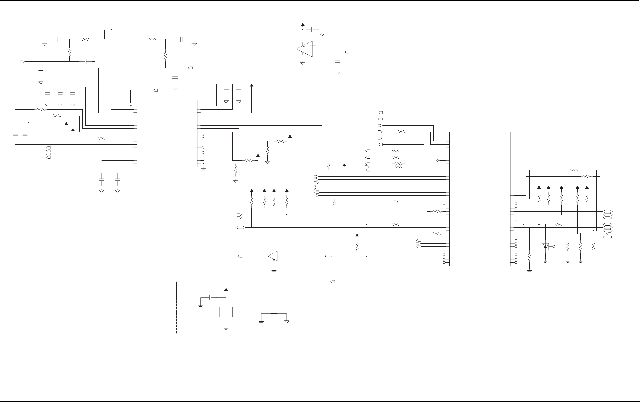
Schematics, Board Overlays, and Parts Lists – UHF: VOCON Section 9-17
6871620L01-C May 28, 2008
Figure 9-16. VOCON: Audio and Accessory Interface Circuits
C1357
.068uF
C1356
.068uF
EXT_SPKR_NEG
EXT_SPKR_POS
INT_SPKR_NEG
INT_SPKR_POS
C1353
1.0uF 0.1uF
C1354
R1327
330
C1355
.022uF
C1352
1.0uF
R1326
330
UNSW_B+
SW_B+
C1348
100pF
EXT_MIC
C1346
10uF
2.2K
R1323
R1322
390
1.0uF
C1347
MIC_BIAS (5V)
C1350
.018uF
R1325
2.2K
390
R1324 C1349
10uF
INT_MIC
C1351
100pF
ADTRIG
NC
R1328 0
H4
H2
H3
A4
E1
G3
G2
A11
J3
H1
K1
K2
F2
F1
L2
E3
J1
J2
G1
B11
AUDIO_B
ANALOG_S
DC_I0VCM2
VC_OUT_M
VC_OUT_P
VFUSE
VMES
VREF
PA_BPLUS
PA_IN_M
PA_IN_P
PWR_CTRL
SCAN_EN
TEST
TX_RX
VCM1
EXT_SPKR_P
FE_TUNE1
FE_TUNE2
INT_MIC_M
INT_MIC_P
INT_SPKR_M
INT_SPKR_P
MIC_BIAS
ATOD_5
ATOD_6
ATOD_7
ATOD_8
BPLUS
EXT_MIC_M
EXT_MIC_P
EXT_SPKR_M
U1304-3
ADC_VREF
AD_TRIG
ATOD_0
ATOD_1
ATOD_2
ATOD_3
ATOD_4
PA_CODEC_A2D_BLOCK
NC
NC
NC
NC
E8
L10
N1
C4
A3
L3
M2
L13
K11
K12
K13
M12
N14
M13
L11
M14
L12
NC
ANALOG
ANALOG
0.1uF
C1363C1362
0.1uF
C1364
100pF 100pF
C1365
V2
ADC_VREFVMES
Board_type
Board_ID
V2
10K
R1330
6.8K
R1329
20K
R1331
20K
R1332
V2
BOOT_NORM*
ONE_WIRE_UP
RS232_USB*
V2
10K
R1339 10K
R1341
V2V2
10K
R1342
R1340
10K
V2
UTXD2
UTXD1_USB_VPO
USB_TXENAB
USB_VMO
USB_VPI
URTS1_XRXD
URXD1_USB_VMI
1
TP1302
V2
1
TP1301
CODEC_DCLK
CODEC_RX
CODEC_FSYNC
CODEC_TX
UCM_SS
MAKO_CE
TX_SSI_CLK
TX_SSI_FSYNC
SCKB
SPI_MOSIB
SPI_MISOB
R1337 100
R1338 100
R1336 100
0
R1334
100
R1335
VC_FSYNC
VC_RX
VC_TX3V
VC_DCLK
47K
R1346
V2
0
R1344
BSY_IN_RTS
BSY_OUT_CTS
KVL_USB_DET
UCTS_USB_SPEED
A7
B7
M4
A9
C9
C10
E7
D7
E9
N3
C8
B8
D8
B9
E6
D6
B6
C6
K6
J5
A10
M3
P2
N2
N8
B12
F10
C11
G10
D11
A8
L7
C12
E11
D10
B10
A6
L5
A5
B5
C7
NC
NC
NC
NC
0
R1345
0
R1343
NC
NC
NC
MAKO_CS
VC_FSYNC
VC_RX
VC_TX
VC_TX3V
USB2_DAT_VP
USB2_DM
USB2_DP
USB2_OE_RCV_RTS
USB2_SE0_VM_RXD
USB_CONNECT
USB_INTX
VC_DCLK
UART2_RXD_OD
UART2_TXD
UCM_SS
USB1_DAT_TXD
USB1_DM
USB1_DP
USB1_OE
USB1_SE0
SPI_CLK
SPI_CS
SPI_DI
SPI_DO
TXDO_BDI_5V
TXDO_BDI_ENC_3V
TXDO_BDI_UP_3V
RTS_FILLSEN_3V
RTS_FILLSEN_5V
RXDIN_3V
RXDIN_5V
RXDIN_ENC_3V
SB96D_BDO_KF_3V
SB96_BDO_KF_5V
SB96_BUS_BUSY
OPTB_SEL2
OPTB_SEL3OPTION_INTX
OPT_GPIO0
OPT_GPIO1
OPT_GPIO2
OPT_GPIO3
RS232_USB_X
ONE_WIRE_BATT
ONE_WIRE_UP
OPTA_SEL0
OPTA_SEL1
OPTA_SEL2
OPTA_SEL3
OPTB_SEL0
OPTB_SEL1
BUSY_IN
BUSY_OUT
CABLE_DET_3V
CTS_CABLE_DET_5V
CTS_X
LOGIC_VDD
ONE_WIRE_1
ONE_WIRE_2
DIGITAL_BLOCK
U1304-2
APCO
BBP_CLK
BBP_SYNC
BOOT_NORM_X
P8
N7
L6
P7
N6
N13
M10
M11
N12
N9
P12
N11
L8
P10
K7
M9
N10
P11
K8
P13
P9
M8
NC
NC
NC
NC
NC
NC
NC
NC
NC
NC
NC
NC
5.6V
VR1301 NC
R1347
470K
R1352
4.7K
USB_DM
USB_DP
VCC5 VCC5
VCC5V2VCC5
NP
R1353
2.7K
R1351
100
0
R1358
10K
R1356
R1355
10K
10K
R1354
R1357
0
BAT_STATUS_1
RS232_DI_USB-
RS232_DO_USB+
RTS
SB9600_BUSY
LHDATA_KEYFAIL
CTS
BAT_STATUS
ONE_WIRE_OPT
R1348
10K
R1350
470K
R1349
470K
C1368
100pF
EMERG
VCC5
1
5
U1305
LM7301 4
3
C1367
0.10uF
2
Ground Connection
V2
3
GND
5
VCC
U1306-2
PWR_GND
C1370
0.10uF
GND
UCM_KF_MAKO
Y
4
U1306-1
74VHC125
A
2
OE
1
URXD2_1
URXD2
9-18 Schematics, Board Overlays, and Parts Lists – UHF: Main Board (NUE7350A) Parts List
May 28, 2008 6871620L01-C
9.6 Main Board (NUE7350A) Parts
List
Ref. Des. Part Number Description
C4 2113945L49 CAP,FXD,.01UF,+5%,-5%,
50V-DC,0603,X7R,-55DEG
CMIN,125DEG CMAX,P
C6 2113944C45 CAP CER CHP 100.0PF
50V 5%
C9 2113944A40 CAP CER CHP 100.0PF
50V 5%
C10 2113944A40 CAP CER CHP 100.0PF
50V 5%
C11 2113946K02 CAP CER CHP 0.10UF 16V
C12 2113955E37 CAP,FXD,10UF,+10%,-10%,
16V-DC,1210,X7R,-55DEG
CMIN,125DEG CMAX
C13 2113945B02 CAP CER CHP 10,000PF
25V 10%
C14 2113955E37 CAP,FXD,10UF,+10%,-10%,
16V-DC,1210,X7R,-55DEG
CMIN,125DEG CMAX
C15 2113946E02 CAP CER CHP 1.0UF 16V
10%
C16 2113945B02 CAP CER CHP 10,000PF
25V 10%
C17 2113946E02 CAP CER CHP 1.0UF 16V
10%
C20 2113955E37 CAP,FXD,10UF,+10%,-10%,
16V-DC,1210,X7R,-55DEG
CMIN,125DEG CMAX
C21 NOT PLACED –
C22 2113944C17 CAP CER CHP 3.0PF 50V
+/- 0.25PF
C24 2113955E37 CAP,FXD,10UF,+10%,-10%,
16V-DC,1210,X7R,-55DEG
CMIN,125DEG CMAX
C25 2113946E02 CAP CER CHP 1.0UF 16V
10%
C26 2113945B02 CAP CER CHP 10,000PF
25V 10%
C27 2113946E02 CAP CER CHP 1.0UF 16V
10%
C28 2113944A40 CAP CER CHP 100.0PF
50V 5%
C29 2113944C30 CAP CER CHP 10.0PF 50V
+/- 0.5PF
C30 2313960B57 CAP,FXD,10UF,+10%,-10%,
6.3V-DC,SM,-55DEG CMIN,
125DEG CMAX,137MA
C52 2113944A40 CAP CER CHP 100.0PF
50V 5%
C53 2113944A48 CAP CER CHP 470.0 PF
50V 5%
C54 2113944A40 CAP CER CHP 100.0PF
50V 5%
C55 2113944A40 CAP CER CHP 100.0PF
50V 5%
C56 2113944A40 CAP CER CHP 100.0PF
50V 5%
C57 2113944A40 CAP CER CHP 100.0PF
50V 5%
C58 2113944A40 CAP CER CHP 100.0PF
50V 5%
C71 2113944A40 CAP CER CHP 100.0PF
50V 5%
C72 2113944A40 CAP CER CHP 100.0PF
50V 5%
C73 2113944A40 CAP CER CHP 100.0PF
50V 5%
C101 2113944A40 CAP CER CHP 100.0PF
50V 5%
C102 2113944C45 CAP CER CHP 100.0PF
50V 5%
C103 2113945B02 CAP CER CHP 10,000PF
25V 10%
C104 2113944A40 CAP CER CHP 100.0PF
50V 5%
C105 2113944A40 CAP CER CHP 100.0PF
50V 5%
C106 2113944A40 CAP CER CHP 100.0PF
50V 5%
C107 2113944A40 CAP CER CHP 100.0PF
50V 5%
C108 2113945B02 CAP CER CHP 10,000PF
25V 10%
C110 2113944A40 CAP CER CHP 100.0PF
50V 5%
C111 2113944C45 CAP CER CHP 100.0PF
50V 5%
C112 NOT PLACED –
C114 2113944C37 CAP CER CHP 39.0PF 50V
5%
Ref. Des. Part Number Description
C116 NOT PLACED –
C117 2113955C31 CAP,FXD,1UF,+10%,-10%,
16V-DC,X7R,-55DEG
CMIN,125DEG CMAX,
LEAD-
C118 2113945B02 CAP CER CHP 10,000PF
25V 10%
C119 2113944C45 CAP CER CHP 100.0PF
50V 5%
C120 2171741M05 HIGH Q CAP, 6.8 PF
C121 2171741M05 HIGH Q CAP, 6.8 PF
C122 2171741M02 HIGH Q CAP
C123 2113944C16 CAP CER CHP 2.7PF 50V
+/- 0.25PF
C124 2171741M07 HIGH Q CAP, 15 PF
C125 2113944C45 CAP CER CHP 100.0PF
50V 5%
C127 2113944A40 CAP CER CHP 100.0PF
50V 5%
C128 2113944A40 CAP CER CHP 100.0PF
50V 5%
C129 2113945A10 CAP CER CHP 1500PF 50V
10%
C130 2113945A05 CAP CER CHP 470PF 50V
10%
C131 2113946A01 CAP CER CHP 0.015UF
16V 10%
C132 2113945C31 CAP,FXD,.1UF,+10%,-10%,
50V-DC,0603,X7R,-55DEG
CMIN,125DEG CMAX
C133 2113955C31 CAP,FXD,1UF,+10%,-10%,
16V-DC,X7R,-55DEG
CMIN,125DEG CMAX,
LEAD-
C134 2113945B02 CAP CER CHP 10,000PF
25V 10%
C135 2113944A40 CAP CER CHP 100.0PF
50V 5%
C136 2113944A40 CAP CER CHP 100.0PF
50V 5%
C137 2113944A40 CAP CER CHP 100.0PF
50V 5%
C140 2113944A40 CAP CER CHP 100.0PF
50V 5%
C141 2171741M06 HIGH Q CAP, 39 PF
Ref. Des. Part Number Description
C144 2113944A40 CAP CER CHP 100.0PF
50V 5%
C145 2113946K02 CAP CER CHP 0.10UF 16V
C146 2113946K02 CAP CER CHP 0.10UF 16V
C147 2113946K02 CAP CER CHP 0.10UF 16V
C148 2113946K02 CAP CER CHP 0.10UF 16V
C149 2113946K02 CAP CER CHP 0.10UF 16V
C200 2113944A40 CAP CER CHP 100.0PF
50V 5%
C201 2113946K02 CAP CER CHP 0.10UF 16V
C202 2113946K02 CAP CER CHP 0.10UF 16V
C203 2113946N03 CAP CER CHP 2.2UF 16V
C204 2113946K02 CAP CER CHP 0.10UF 16V
C205 2113946K02 CAP CER CHP 0.10UF 16V
C206 2113955E37 CAP,FXD,10UF,+10%,-10%,
16V-DC,1210,X7R,-55DEG
CMIN,125DEG CMAX
C207 2113946K02 CAP CER CHP 0.10UF 16V
C208 2113946K02 CAP CER CHP 0.10UF 16V
C209 2113946K02 CAP CER CHP 0.10UF 16V
C210 2113946K02 CAP CER CHP 0.10UF 16V
C211 2113946K02 CAP CER CHP 0.10UF 16V
C213 2113945A09 CAP CER CHP 1000PF 50V
10%
C214 2113944A40 CAP CER CHP 100.0PF
50V 5%
C215 2113946K02 CAP CER CHP 0.10UF 16V
C217 2113945C27 CAP,FXD,.047UF,+10%,
-10%,50V-DC,0603,X7R,
-55DEG CMIN,125DEG
CMA
C218 2113945C25 CAP,FXD,.033UF,+10%,
-10%,50V-DC,0603,X7R,
-55DEG CMIN,125DEG
CMA
C219 2171115L01 CHIP MONOLITHIC
CERAMIC CAPACITOR
C220 2113955E37 CAP,FXD,10UF,+10%,-10%,
16V-DC,1210,X7R,-55DEG
CMIN,125DEG CMAX
C221 2113946K02 CAP CER CHP 0.10UF 16V
C222 2113945L41 CAP,FXD,4700PF,+5%,-5%,
50V-DC,0603,X7R,-55DEG
CMIN,125DEG CMAX
Ref. Des. Part Number Description
Schematics, Board Overlays, and Parts Lists – UHF: Main Board (NUE7350A) Parts List 9-19
6871620L01-C May 28, 2008
C224 2185419D06 CAP CER SUPER L/D
0.1UF
C225 2185419D06 CAP CER SUPER L/D
0.1UF
C226 2185419D06 CAP CER SUPER L/D
0.1UF
C227 2185419D06 CAP CER SUPER L/D
0.1UF
C229 2113944A40 CAP CER CHP 100.0PF
50V 5%
C230 2113944A40 CAP CER CHP 100.0PF
50V 5%
C231 2113945B02 CAP CER CHP 10,000PF
25V 10%
C232 2113955E37 CAP,FXD,10UF,+10%,-10%,
16V-DC,1210,X7R,-55DEG
CMIN,125DEG CMAX
C233 2113946K02 CAP CER CHP 0.10UF 16V
C234 2113945B02 CAP CER CHP 10,000PF
25V 10%
C235 2113944A40 CAP CER CHP 100.0PF
50V 5%
C236 2113945A09 CAP CER CHP 1000PF 50V
10%
C241 2185419D06 CAP CER SUPER L/D
0.1UF
C242 2185419D06 CAP CER SUPER L/D
0.1UF
C250 2113946K02 CAP CER CHP 0.10UF 16V
C251 2113944A23 CAP CER CHP 8.2PF 50V
+/- 0.5PF
C252 2113944A26 CAP CER CHP 12.0PF 50V
5%
C253 2113944A05 CAP CER CHP 1.5PF 50V
+/- 0.25PF
C254 2113946B04 CAP CER CHP 0.10UF 10V
10%
C255 2113944A42 CAP CER CHP 150.0PF
50V 5%
C256 2113944A27 CAP CER CHP 15.0PF 50V
5%
C257 2113944A80 CAP,FXD,20PF,+5%,-5%,
50V-DC,0402,C0G,-55DEG
CMIN,125DEG CMAX,PB
C258 2113944A27 CAP CER CHP 15.0PF 50V
5%
Ref. Des. Part Number Description
C259 2113944A36 CAP CER CHP 68.0PF 50V
5%
C260 2113944A73 CAP,FXD,8PF,.5PF+/-,
50V-DC,0402,C0G,-55DEG
CMIN,125DEG CMAX,PB
C261 2113944A42 CAP CER CHP 150.0PF
50V 5%
C262 2113946B04 CAP CER CHP 0.10UF 10V
10%
C263 2113944A42 CAP CER CHP 150.0PF
50V 5%
C264 2113944A09 CAP CER CHP 2.2PF 50V
+/- 0.25PF
C265 2113944A40 CAP CER CHP 100.0PF
50V 5%
C266 2113944A42 CAP CER CHP 150.0PF
50V 5%
C267 2113944A23 CAP CER CHP 8.2PF 50V
+/- 0.5PF
C268 2113944A79 CAP,FXD,16PF,+5%,-5%,
50V-DC,0402,C0G,-55DEG
CMIN,125DEG CMAX,PB
C269 2113946B04 CAP CER CHP 0.10UF 10V
10%
C271 2113944A22 CAP CER CHP 7.5PF 50V
+/- 0.5PF
C272 2113944A22 CAP CER CHP 7.5PF 50V
+/- 0.5PF
C273 2113944A05 CAP CER CHP 1.5PF 50V
+/- 0.25PF
C274 2113944A25 CAP CER CHP 10.0PF 50V
+/- 0.5PF
C275 2113944A26 CAP CER CHP 12.0PF 50V
5%
C276 2113944A24 CAP CER CHP 9.1PF 50V
+/- 0.5PF
C277 2113944A38 CAP CER CHP 82.0PF 50V
5%
C278 2113944A43 CAP CER CHP 180.0PF
50V 5%
C279 2113946B04 CAP CER CHP 0.10UF 10V
10%
C280 2113944A43 CAP CER CHP 180.0PF
50V 5%
C281 2113944A43 CAP CER CHP 180.0PF
50V 5%
Ref. Des. Part Number Description
C282 2113944A08 CAP CER CHP 2.0PF 50V
+/- 0.25PF
C283 2113946B04 CAP CER CHP 0.10UF 10V
10%
C284 2113944A43 CAP CER CHP 180.0PF
50V 5%
C285 2113944A05 CAP CER CHP 1.5PF 50V
+/- 0.25PF
C286 2113944A43 CAP CER CHP 180.0PF
50V 5%
C287 2113944A43 CAP CER CHP 180.0PF
50V 5%
C288 2113944A05 CAP CER CHP 1.5PF 50V
+/- 0.25PF
C289 2113944A32 CAP CER CHP 39.0PF 50V
5%
C290 2113944A27 CAP CER CHP 15.0PF 50V
5%
C291 2113944A40 CAP CER CHP 100.0PF
50V 5%
C292 2113946B04 CAP CER CHP 0.10UF 10V
10%
C293 2113944A12 CAP CER CHP 3.0PF 50V
+/- 0.25PF
C294 2113944A40 CAP CER CHP 100.0PF
50V 5%
C295 2113944A42 CAP CER CHP 150.0PF
50V 5%
C296 2113944A40 CAP CER CHP 100.0PF
50V 5%
C337 2113945A01 CAP CER CHP 220PF 50V
10,
C410 2115153H15 CAP, CERAMIC, COG
C411 2115153H27 CAP, CERAMIC, COG
C412 2115153H35 CAP, CERAMIC, COG
C413 2115153H03 CAP, CERAMIC, COG
C414 2115153H03 CAP, CERAMIC, COG
C415 2115153H35 CAP, CERAMIC, COG
C416 2115153H15 CAP, CERAMIC, COG
C417 2115153H27 CAP, CERAMIC, COG
C418 2113946B04 CAP CER CHP 0.10UF 10V
10%
C419 2115153H41 CAP,CERAMIC
CHIP,22PF,+1%,-1%,50V-
Ref. Des. Part Number Description
C420 2113946D07 CAP,CHIP,4.7UF,+10%,
-10%,6.3V-DC,0603,X5R,
-55DEG CMIN,85DEG CMA
C421 2115153H35 CAP, CERAMIC, COG
C422 2115153H03 CAP, CERAMIC, COG
C423 2115153H03 CAP, CERAMIC, COG
C424 2115153H35 CAP, CERAMIC, COG
C425 2115153H31 CAP, CERAMIC, COG
C426 2115153H15 CAP, CERAMIC, COG
C427 2115153H15 CAP, CERAMIC, COG
C428 2115153H41 CAP,CERAMIC CHIP,22PF,
+1%,-1%,50V-
C429 2113946B04 CAP CER CHP 0.10UF 10V
10%
C430 2115153H31 CAP, CERAMIC, COG
C432 2113944A23 CAP CER CHP 8.2PF 50V
+/- 0.5PF
C434 2113944A34 CAP CER CHP 56.0PF 50V
5%
C436 2113944A22 CAP CER CHP 7.5PF 50V
+/- 0.5PF
C456 2113946B04 CAP CER CHP 0.10UF 10V
10%
C457 2113946B04 CAP CER CHP 0.10UF 10V
10%
C470 NOT PLACED –
C471 2113944A21 CAP CER CHP 6.8PF 50V
+/- 0.5PF
C472 2113944A40 CAP CER CHP 100.0PF
50V 5%
C473 2113944A40 CAP CER CHP 100.0PF
50V 5%
C474 2113945B02 CAP CER CHP 10,000PF
25V 10%
C475 2113946D07 CAP,CHIP,4.7UF,+10%,
-10%,6.3V-DC,0603,X5R,
-55DEG CMIN,85DEG CMA
C476 2113944M01 CAP,FXD,2PF,.1PF+/-,
50V-DC,0603,C0G,-55DEG
CMIN,125DEG CMAX,PB
C477 2113944A40 CAP CER CHP 100.0PF
50V 5%
C479 2113946B04 CAP CER CHP 0.10UF 10V
10%
Ref. Des. Part Number Description
9-20 Schematics, Board Overlays, and Parts Lists – UHF: Main Board (NUE7350A) Parts List
May 28, 2008 6871620L01-C
C480 2113944A40 CAP CER CHP 100.0PF
50V 5%
C481 2113945B02 CAP CER CHP 10,000PF
25V 10%
C482 2113945B02 CAP CER CHP 10,000PF
25V 10%
C483 NOT PLACED –
C484 2113944A80 CAP,FXD,20PF,+5%,-5%,
50V-DC,0402,C0G,-55DEG
CMIN,125DEG CMAX,PB
C490 2115153H21 CAP, CERAMIC, COG
C493 2115153H16 CAP, CERAMIC, COG
C501 2113944A40 CAP CER CHP 100.0PF
50V 5%
C505 2113944A40 CAP CER CHP 100.0PF
50V 5%
C506 2113946K02 CAP CER CHP 0.10UF 16V
C507 2113945A11 CAP CER CHP 2200PF 50V
10%
C509 2113946B02 CAP CER CHP 0.047UF
10V 10,
C511 2113944A40 CAP CER CHP 100.0PF
50V 5%
C512 2113944A40 CAP CER CHP 100.0PF
50V 5%
C513 2113945B02 CAP CER CHP 10,000PF
25V 10%
C514 2113946K02 CAP CER CHP 0.10UF 16V
C527 2113946K02 CAP CER CHP 0.10UF 16V
C535 2113945B02 CAP CER CHP 10,000PF
25V 10%
C539 2113946B02 CAP CER CHP 0.047UF
10V 10,
C540 2113946K02 CAP CER CHP 0.10UF 16V
C541 2113945B02 CAP CER CHP 10,000PF
25V 10%
C542 2113945B02 CAP CER CHP 10,000PF
25V 10%
C544 2113945B02 CAP CER CHP 10,000PF
25V 10%
C546 2113945B02 CAP CER CHP 10,000PF
25V 10%
C547 2113945B02 CAP CER CHP 10,000PF
25V 10%
Ref. Des. Part Number Description
C548 2113946B02 CAP CER CHP 0.047UF
10V 10,
C551 2113946S35 CAP CER CHP 1.0UF 16V
10%
C552 2113946S35 CAP CER CHP 1.0UF 16V
10%
C553 2113946C07 CAP,FXD,.33UF,+10%,
-10%,10V-DC,0603,X5R,
-55DEG CMIN,85DEG
CMAX
C554 2113944A79 CAP,FXD,16PF,+5%,-5%,
50V-DC,0402,C0G,-55DEG
CMIN,125DEG CMAX,PB
C555 2113944A20 CAP CER CHP 6.2PF 50V
+/- 0.5PF
C556 2113944A34 CAP CER CHP 56.0PF 50V
5%
C557 2113944A34 CAP CER CHP 56.0PF 50V
5%
C560 2113944A28 CAP CER CHP 18.0PF 50V
5%
C561 2313960B30 CAP,FXD,4.7UF,+10%,
-10%,10V-DC,SM,-55DEG
CMIN,125DEG
CMAX,122MA
C562 2113945B02 CAP CER CHP 10,000PF
25V 10%
C570 2113945G91 CAP,FXD,.1UF,+10%,-10%,
50V-DC,0805,X7R,-55DEG
CMIN,125DEG CMAX
C571 2113945G91 CAP,FXD,.1UF,+10%,-10%,
50V-DC,0805,X7R,-55DEG
CMIN,125DEG CMAX
C572 2113945C25 CAP,FXD,.033UF,+10%,
-10%,50V-DC,0603,X7R,
-55DEG CMIN,125DEG
CMA
C573 2113944A36 CAP CER CHP 68.0PF 50V
5%
C574 2113945B02 CAP CER CHP 10,000PF
25V 10%
C581 2113944B02 CAP CER CHP 220.0PF
25V 5%
C582 2113946K02 CAP CER CHP 0.10UF 16V
C583 2113945B02 CAP CER CHP 10,000PF
25V 10%
C584 2115153H24 CAP, CERAMIC, COG
Ref. Des. Part Number Description
C704 2113944A40 CAP CER CHP 100.0PF
50V 5%
C705 2113944C45 CAP CER CHP 100.0PF
50V 5%
C706 2113944C11 CAP CER CHP 1.6PF 50V
+/- 0.25PF
C707 2113944C21 CAP CER CHP 4.3PF 50V
+/- 0.25PF
C709 2113944C12 CAP CER CHP 1.8PF 50V
+/- 0.25PF
C710 2113944C15 CAP CER CHP 2.4PF 50V
+/- 0.25PF
C711 2113944C24 CAP CER CHP 5.6PF 50V
+/- 0.5PF
C712 2113944A40 CAP CER CHP 100.0PF
50V 5%
C713 2113944A18 CAP CER CHP 5.1PF 50V
+/- 0.5PF
C716 2113944A40 CAP CER CHP 100.0PF
50V 5%
C717 2113946K02 CAP CER CHP 0.10UF 16V
C718 2113944C15 CAP CER CHP 2.4PF 50V
+/- 0.25PF
C719 2113944A40 CAP CER CHP 100.0PF
50V 5%
C720 2113944C21 CAP CER CHP 4.3PF 50V
+/- 0.25PF
C721 2113944C18 CAP CER CHP 3.3PF 50V
+/- 0.25PF
C722 2113951C13 CAP,FXD,1.3PF,.05PF+/-,
250V-DC,0603,C0G,-55DEG
CMIN,125DEG CMA
C723 2113944A40 CAP CER CHP 100.0PF
50V 5%
C724 2113946K02 CAP CER CHP 0.10UF 16V
C1101 2113944A40 CAP CER CHP 100.0PF
50V 5%
C1102 2113944A40 CAP CER CHP 100.0PF
50V 5%
C1104 2113944A40 CAP CER CHP 100.0PF
50V 5%
C1105 2113944A40 CAP CER CHP 100.0PF
50V 5%
C1106 2113944A40 CAP CER CHP 100.0PF
50V 5%
Ref. Des. Part Number Description
C1107 2113944A40 CAP CER CHP 100.0PF
50V 5%
C1108 2113944A40 CAP CER CHP 100.0PF
50V 5%
C1109 2113944A40 CAP CER CHP 100.0PF
50V 5%
C1110 2113944A40 CAP CER CHP 100.0PF
50V 5%
C1111 2113944A40 CAP CER CHP 100.0PF
50V 5%
C1112 2113944A40 CAP CER CHP 100.0PF
50V 5%
C1113 2113944A40 CAP CER CHP 100.0PF
50V 5%
C1114 2113944A40 CAP CER CHP 100.0PF
50V 5%
C1115 2113944A40 CAP CER CHP 100.0PF
50V 5%
C1116 2113944A40 CAP CER CHP 100.0PF
50V 5%
C1117 2113944A40 CAP CER CHP 100.0PF
50V 5%
C1118 2113944A40 CAP CER CHP 100.0PF
50V 5%
C1119 2113944A40 CAP CER CHP 100.0PF
50V 5%
C1120 2113944A40 CAP CER CHP 100.0PF
50V 5%
C1123 2113944A40 CAP CER CHP 100.0PF
50V 5%
C1124 2113945B02 CAP CER CHP 10,000PF
25V 10%
C1125 2113945A05 CAP CER CHP 470PF 50V
10%
C1126 2113945A05 CAP CER CHP 470PF 50V
10%
C1128 2113944A40 CAP CER CHP 100.0PF
50V 5%
C1129 2113955C31 CAP,FXD,1UF,+10%,-10%,
16V-DC,X7R,-55DEG
CMIN,125DEG CMAX,
LEAD-
C1130 2113945A05 CAP CER CHP 470PF 50V
10%
C1131 2113944A31 CAP CER CHP 33.0PF 50V
5%
Ref. Des. Part Number Description
Schematics, Board Overlays, and Parts Lists – UHF: Main Board (NUE7350A) Parts List 9-21
6871620L01-C May 28, 2008
C1132 2113944A31 CAP CER CHP 33.0PF 50V
5%
C1133 2113944A31 CAP CER CHP 33.0PF 50V
5%
C1134 2113944A31 CAP CER CHP 33.0PF 50V
5%
C1135 2113945A05 CAP CER CHP 470PF 50V
10%
C1136 2113944A31 CAP CER CHP 33.0PF 50V
5%
C1138 2113945A05 CAP CER CHP 470PF 50V
10%
C1139 2113944A40 CAP CER CHP 100.0PF
50V 5%
C1140 2113945B02 CAP CER CHP 10,000PF
25V 10%
C1141 2113946F05 CAP,CHIP,10UF,+10%,
-10%,6.3V-DC,0805,X5R,
-55DEG CMIN,85DEG
CMAX
C1142 2113956C43 CAP,FXD,2.2UF,+10%,
-10%,10V-DC,0805,X5R
,-55DEG CMIN,85DEG
CMAX
C1202 2113944A40 CAP CER CHP 100.0PF
50V 5%
C1209 2113945A05 CAP CER CHP 470PF 50V
10%
C1210 2113945A05 CAP CER CHP 470PF 50V
10%
C1211 NOT PLACED –
C1212 2113944A31 CAP CER CHP 33.0PF 50V
5%
C1213 2113945A05 CAP CER CHP 470PF 50V
10%
C1214 2113944A31 CAP CER CHP 33.0PF 50V
5%
C1215 2113945A05 CAP CER CHP 470PF 50V
10%
C1216 2113944A40 CAP CER CHP 100.0PF
50V 5%
C1217 2113945A05 CAP CER CHP 470PF 50V
10%
C1218 2113946K02 CAP CER CHP 0.10UF 16V
C1219 2113946K02 CAP CER CHP 0.10UF 16V
Ref. Des. Part Number Description
C1220 2113945A05 CAP CER CHP 470PF 50V
10%
C1221 2113945A05 CAP CER CHP 470PF 50V
10%
C1222 2113944A40 CAP CER CHP 100.0PF
50V 5%
C1223 2113946K02 CAP CER CHP 0.10UF 16V
C1224 2113946K02 CAP CER CHP 0.10UF 16V
C1225 2113946K02 CAP CER CHP 0.10UF 16V
C1232 2113944A40 CAP CER CHP 100.0PF
50V 5%
C1233 2113944A48 CAP CER CHP 470.0 PF
50V 5%
C1234 2113944A48 CAP CER CHP 470.0 PF
50V 5%
C1301 2113945A05 CAP CER CHP 470PF 50V
10%
C1302 2113946K02 CAP CER CHP 0.10UF 16V
C1303 2113944A25 CAP CER CHP 10.0PF 50V
+/- 0.5PF
C1304 2113946K02 CAP CER CHP 0.10UF 16V
C1305 2113944A19 CAP CER CHP 5.6PF 50V
+/- 0.5PF
C1306 2113944A19 CAP CER CHP 5.6PF 50V
+/- 0.5PF
C1307 2113946F01 CAP CER CHP 2.2UF 6.3V
10%
C1308 2113946F01 CAP CER CHP 2.2UF 6.3V
10%
C1309 2113945A09 CAP CER CHP 1000PF 50V
10%
C1310 2113945B02 CAP CER CHP 10,000PF
25V 10%
C1312 2113946G01 CAP CER CHP 2.2UF 16V
10%
C1313 2113944A40 CAP CER CHP 100.0PF
50V 5%
C1314 2113944A40 CAP CER CHP 100.0PF
50V 5%
C1315 2113945B02 CAP CER CHP 10,000PF
25V 10%
C1316 2113944A31 CAP CER CHP 33.0PF 50V
5%
C1317 2113944A31 CAP CER CHP 33.0PF 50V
5%
Ref. Des. Part Number Description
C1318 2113945B02 CAP CER CHP 10,000PF
25V 10%
C1319 2113946D02 CAP CER CHP 1.0UF 6.3V
10%
C1320 2113946G01 CAP CER CHP 2.2UF 16V
10%
C1321 2113946D02 CAP CER CHP 1.0UF 6.3V
10%
C1322 2113946D02 CAP CER CHP 1.0UF 6.3V
10%
C1323 2113946D02 CAP CER CHP 1.0UF 6.3V
10%
C1324 2113946D02 CAP CER CHP 1.0UF 6.3V
10%
C1325 2113945B02 CAP CER CHP 10,000PF
25V 10%
C1326 2113946D02 CAP CER CHP 1.0UF 6.3V
10%
C1327 2113945B02 CAP CER CHP 10,000PF
25V 10%
C1328 2113946D05 CAP,CHIP,2.2UF,+10%,
-10%,6.3V-DC,0603,X5R,
-55DEG CMIN,85DEG CMA
C1329 2113945B02 CAP CER CHP 10,000PF
25V 10%
C1330 2113946D05 CAP,CHIP,2.2UF,+10%,
-10%,6.3V-DC,0603,X5R,
-55DEG CMIN,85DEG CMA
C1331 2113945B02 CAP CER CHP 10,000PF
25V 10%
C1332 2371572L01 POSCAD 47UF
C1333 2371572L01 POSCAD 47UF
C1335 2113946D02 CAP CER CHP 1.0UF 6.3V
10%
C1336 2113945C31 CAP,FXD,.1UF,+10%,-10%,
50V-DC,0603,X7R,-55DEG
CMIN,125DEG CMAX
C1337 2113945A09 CAP CER CHP 1000PF 50V
10%
C1338 2113946D02 CAP CER CHP 1.0UF 6.3V
10%
C1339 2113945B02 CAP CER CHP 10,000PF
25V 10%
C1340 2113955E37 CAP,FXD,10UF,+10%,-10%,
16V-DC,1210,X7R,-55DEG
CMIN,125DEG CMAX
Ref. Des. Part Number Description
C1341 2113945C31 CAP,FXD,.1UF,+10%,-10%,
50V-DC,0603,X7R,-55DEG
CMIN,125DEG CMAX
C1342 2113955E37 CAP,FXD,10UF,+10%,-10%,
16V-DC,1210,X7R,-55DEG
CMIN,125DEG CMAX
C1343 2113955E37 CAP,FXD,10UF,+10%,-10%,
16V-DC,1210,X7R,-55DEG
CMIN,125DEG CMAX
C1345 2113946D02 CAP CER CHP 1.0UF 6.3V
10%
C1346 2113955E37 CAP,FXD,10UF,+10%,-10%,
16V-DC,1210,X7R,-55DEG
CMIN,125DEG CMAX
C1347 2113946E02 CAP CER CHP 1.0UF 16V
10%
C1348 2113944A40 CAP CER CHP 100.0PF
50V 5%
C1349 2113955E37 CAP,FXD,10UF,+10%,-10%,
16V-DC,1210,X7R,-55DEG
CMIN,125DEG CMAX
C1350 2113945C21 CAP,FXD,.018UF,+10%,
-10%,50V-DC,0603,X7R,
-55DEG CMIN,125DEG
CMA
C1351 2113944A40 CAP CER CHP 100.0PF
50V 5%
C1352 2113946D02 CAP CER CHP 1.0UF 6.3V
10%
C1353 2113946D02 CAP CER CHP 1.0UF 6.3V
10%
C1354 2113945D04 CAP CER CHP 100,000PF
25V 10%
C1355 2113946A02 CAP CER CHP 0.022UF
16V 10,
C1356 2113946B03 CAP CER CHP 0.068UF
10V 10
C1357 2113946B03 CAP CER CHP 0.068UF
10V 10
C1362 2113945D04 CAP CER CHP 100,000PF
25V 10%
C1363 2113945D04 CAP CER CHP 100,000PF
25V 10%
C1364 2113944A40 CAP CER CHP 100.0PF
50V 5%
C1365 2113944A40 CAP CER CHP 100.0PF
50V 5%
Ref. Des. Part Number Description
9-22 Schematics, Board Overlays, and Parts Lists – UHF: Main Board (NUE7350A) Parts List
May 28, 2008 6871620L01-C
C1367 2113946K02 CAP CER CHP 0.10UF 16V
C1368 2113944A40 CAP CER CHP 100.0PF
50V 5%
C1370 2113946K02 CAP CER CHP 0.10UF 16V
C1402 2113946E02 CAP CER CHP 1.0UF 16V
10%
C1403 2113946K02 CAP CER CHP 0.10UF 16V
C1404 2113944A40 CAP CER CHP 100.0PF
50V 5%
C1407 2113944A40 CAP CER CHP 100.0PF
50V 5%
C1408 2113946K02 CAP CER CHP 0.10UF 16V
C1409 2113946A01 CAP CER CHP 0.015UF
16V 10%
C1410 2113946K02 CAP CER CHP 0.10UF 16V
C1411 2113946K02 CAP CER CHP 0.10UF 16V
C1412 2113946E02 CAP CER CHP 1.0UF 16V
10%
C1413 2113946A01 CAP CER CHP 0.015UF
16V 10%
C1414 2113946K02 CAP CER CHP 0.10UF 16V
C1416 2113946F03 CAP CER CHP 4.7UF 6.3V
10%
C1417 2113946K02 CAP CER CHP 0.10UF 16V
C1418 2113946E02 CAP CER CHP 1.0UF 16V
10%
C1419 2113944A40 CAP CER CHP 100.0PF
50V 5%
C1420 2113946K02 CAP CER CHP 0.10UF 16V
C1421 2113946A01 CAP CER CHP 0.015UF
16V 10%
C1422 2113946K02 CAP CER CHP 0.10UF 16V
C1424 2113946K02 CAP CER CHP 0.10UF 16V
C1425 2113944A40 CAP CER CHP 100.0PF
50V 5%
C1427 2113944A40 CAP CER CHP 100.0PF
50V 5%
C1428 2113944A40 CAP CER CHP 100.0PF
50V 5%
C1429 2113944A48 CAP CER CHP 470.0 PF
50V 5%
C1430 2113946K02 CAP CER CHP 0.10UF 16V
C1431 2113946K02 CAP CER CHP 0.10UF 16V
Ref. Des. Part Number Description
C1432 2113946K02 CAP CER CHP 0.10UF 16V
C1433 2113946K02 CAP CER CHP 0.10UF 16V
C1440 NOT PLACED –
C1441 NOT PLACED –
C1442 NOT PLACED –
C1443 NOT PLACED –
C1444 NOT PLACED –
C1445 NOT PLACED –
C1446 NOT PLACED –
C1447 NOT PLACED –
C1449 NOT PLACED –
C1453 NOT PLACED –
C1457 NOT PLACED –
C1458 NOT PLACED –
C1459 NOT PLACED –
C1460 NOT PLACED –
C1719 2113944A40 CAP CER CHP 100.0PF
50V 5%
C9901 2113944A40 CAP CER CHP 100.0PF
50V 5%
C9950 2113946K02 CAP CER CHP 0.10UF 16V
C9951 2113945Y02 CAP,FXD,.1UF,+10%,-10%,
16V-DC,0402,X7R,-55DEG
CMIN,125DEG CMAX
C9952 2113945Y02 CAP,FXD,.1UF,+10%,-10%,
16V-DC,0402,X7R,-55DEG
CMIN,125DEG CMAX
C9953 2113945Y02 CAP,FXD,.1UF,+10%,-10%,
16V-DC,0402,X7R,-55DEG
CMIN,125DEG CMAX
C9954 2113945Y02 CAP,FXD,.1UF,+10%,-10%,
16V-DC,0402,X7R,-55DEG
CMIN,125DEG CMAX
C9956 2113946E02 CAP CER CHP 1.0UF 16V
10%
C9966 2113945A03 CAP CER CHP 330PF 50V
10%
C9968 2113946K02 CAP CER CHP 0.10UF 16V
C9969 2113945Y02 CAP,FXD,.1UF,+10%,-10%,
16V-DC,0402,X7R,-55DEG
CMIN,125DEG CMAX
C9970 2113944A40 CAP CER CHP 100.0PF
50V 5%
Ref. Des. Part Number Description
C9975 2113946D07 CAP,CHIP,4.7UF,+10%,
-10%,6.3V-DC,0603,X5R,
-55DEG CMIN,85DEG CMA
C9980 2113945Y02 CAP,FXD,.1UF,+10%,-10%,
16V-DC,0402,X7R,-55DEG
CMIN,125DEG CMAX
D1 4813978M15 DIODE,RECT,RM140,SM,
1A,40V,SHTK,PB-FREE
D2 4813978M15 DIODE,RECT,RM140,SM,
1A,40V,SHTK,PB-FREE
D3 4813978M15 DIODE,RECT,RM140,SM,
1A,40V,SHTK,PB-FREE
D4 4813978M15 DIODE,RECT,RM140,SM,
1A,40V,SHTK,PB-FREE
D104 4813978A26 DIODE ARRAY,DET,
SOT-363/SC-88,30V,.12W,2
D201 4815011H01 DIODE TRIPLE
D202 4815011H01 DIODE TRIPLE
D251 4815002H01 VARACTOR DIODE
D252 4815002H01 VARACTOR DIODE
D253 4815002H01 VARACTOR DIODE
D254 4815002H01 VARACTOR DIODE
D271 4815002H01 VARACTOR DIODE
D272 4815002H01 VARACTOR DIODE
D273 4815002H01 VARACTOR DIODE
D274 4815002H01 VARACTOR DIODE
D411 4815096H01 VARACTOR DIODE
1SV305
D413 4815096H01 VARACTOR DIODE
1SV305
D451 4815096H01 VARACTOR DIODE
1SV305
D453 4815096H01 VARACTOR DIODE
1SV305
D550 4815096H01 VARACTOR DIODE
1SV305
D551 4815096H01 VARACTOR DIODE
1SV305
D570 4805656W87 DIODE,VCTR, @ 15V,
1SV279,SOD-523/SC-79
D701 4871607L01 PIN DIODE SMD
D702 4871607L01 PIN DIODE SMD
Ref. Des. Part Number Description
D703 4813974A19 DIODE ARRAY,MXR, SM,
SOT-323,7V,.2W, SHTK,2,
PB-FREE
D1000 4888722V01 DIODE,RB520S,SM,
SOD-523/SC-79,200MA,
30V,PB FREE
D1202 4813978A25 SCHOTTKY 30V SOD-323
T&R PB FREE
D1205 4813977C23 DIODE,ZEN,MMSZ5243,SM
,SOD-123,13V,10MA,
.5W,ZEN,PB-FREE
D1207 4813978A25 SCHOTTKY 30V SOD-323
T&R PB FREE
D1222 4888722V01 DIODE,RB520S,SM,
SOD-523/SC-79,200MA,
30V,PB FREE
D1223 4888722V01 DIODE,RB520S,SM,
SOD-523/SC-79,200MA,
30V,PB FREE
D1301 4805129M90 DIODE SOT PKGD
D1401 4888722V01 DIODE,RB520S,SM,
SOD-523/SC-79,200MA,
30V,PB FREE
D1402 4888722V01 DIODE,RB520S,SM,
SOD-523/SC-79,200MA,
30V,PB FREE
E5 2480640Z01 SURFACE MOUNT
FERRITE BEAD
E101 7686949J14 FLTR,FERRITE BEAD,2A,
SM,0805,CHIP, 220OHM
E103 7686949J15 FLTR,FERR,2A,SM,0603
E104 2480574F01 IND FERRITE CHIP 60OHM
0603
E105 2480640Z01 SURFACE MOUNT
FERRITE BEAD
E500 2480640Z01 SURFACE MOUNT
FERRITE BEAD
E501 2480574F01 IND FERRITE CHIP 60OHM
0603
E1102 2480574F01 IND FERRITE CHIP 60OHM
0603
E1103 2480574F01 IND FERRITE CHIP 60OHM
0603
E1104 2462586G33 INDUCTOR CHIP FERRITE
BEADS
E1110 2480640Z01 SURFACE MOUNT
FERRITE BEAD
Ref. Des. Part Number Description
Schematics, Board Overlays, and Parts Lists – UHF: Main Board (NUE7350A) Parts List 9-23
6871620L01-C May 28, 2008
E1111 2480640Z01 SURFACE MOUNT
FERRITE BEAD
E1112 2480640Z01 SURFACE MOUNT
FERRITE BEAD
E1113 2480640Z01 SURFACE MOUNT
FERRITE BEAD
E1114 2480640Z01 SURFACE MOUNT
FERRITE BEAD
E1115 2480640Z01 SURFACE MOUNT
FERRITE BEAD
E1116 2480640Z01 SURFACE MOUNT
FERRITE BEAD
E1117 2480640Z01 SURFACE MOUNT
FERRITE BEAD
E1118 2480640Z01 SURFACE MOUNT
FERRITE BEAD
E1119 2480640Z01 SURFACE MOUNT
FERRITE BEAD
E1120 2480640Z01 SURFACE MOUNT
FERRITE BEAD
E1121 2480640Z01 SURFACE MOUNT
FERRITE BEAD
E1122 2480640Z01 SURFACE MOUNT
FERRITE BEAD
E1123 2480640Z01 SURFACE MOUNT
FERRITE BEAD
E1124 2480640Z01 SURFACE MOUNT
FERRITE BEAD
E1125 2480640Z01 SURFACE MOUNT
FERRITE BEAD
E1126 2480640Z01 SURFACE MOUNT
FERRITE BEAD
E1127 2480640Z01 SURFACE MOUNT
FERRITE BEAD
E1129 2480640Z01 SURFACE MOUNT
FERRITE BEAD
E1130 2480640Z01 SURFACE MOUNT
FERRITE BEAD
E1201 2480574F01 IND FERRITE CHIP 60OHM
0603
E1401 2480574F01 IND FERRITE CHIP 60OHM
0603
E1402 2480574F01 IND FERRITE CHIP 60OHM
0603
F901 6515076H01 FUSE CHIP SMT TR/
1608FF 3A
Ref. Des. Part Number Description
FL200 9116848H01 FLTR SW CAP 3 POLE
BUTTERW, W18
FL490 9185924B01 FILTER, 73.35 MHZ 3-POLE
CRYST
J1 0970312N01 CONN,BTB,RCPT,60CONT,
.4MM,GLD,1 STACK HGT
J2 0987817K04 30PIN RECPT MATING
CNTCR 1.5MM
J3 0987817K02 RECP 0.5 PITCH 16 CKT
J1704 0971876L01 MINIATURE INTERFACE
COAXIAL SWITCH
L10 2489669V01 IDCTR,WW,100UH,5%,
40MA,10OHM,20 Q,10MHZ
SRF,SM,1210,PB-FREE
L20 2460591D12 COIL AIR WOUND INDUC
18.29
L101 2414017G09 IDCTR,CHIP,15NH,5%,
300MA,.45OHM,CER,8 Q,
SM,0603,PB-FREE
L102 2414032D18 IDCTR,WW,180NH,5%,700
MA,.43OHM,CER,35 Q,
780MHZ SRF,SM,PB-FR
L103 NOT PLACED –
L105 2479990E01 COIL AIR WOUND/GREEN
CLR 23.75
L108 2415428H04 AIR WOUND INDUCTOR
L113 2414017G07 IDCTR,CHIP,10NH,5%,
300MA,.35OHM,CER,8 Q,
SM,0603,PB-FREE
L201 2414017Q20 IDCTR,FXD,2.2UH,20%,
30MA, .65OHM,FERR,45 Q
,50MHZ SRF,SM,0805
L202 2414017Q20 IDCTR,FXD,2.2UH,20%,
30MA,.65OHM,FERR,45 Q,
50MHZ SRF,SM,0805
L203 2414017Q20 IDCTR,FXD,2.2UH,20%,
30MA,.65OHM,FERR,45 Q,
50MHZ SRF,SM,0805
L204 2414017Q20 IDCTR,FXD,2.2UH,20%,
30MA,.65OHM,FERR,45 Q,
50MHZ SRF,SM,0805
L205 2414017Q47 IDCTR,FXD,1UH,10%,
50MA,.45OHM,FERR,45 Q,
75MHZ SRF,SM,0805,PB
L207 2414017Q47 IDCTR,FXD,1UH,10%,
50MA,.45OHM,FERR,45 Q,
75MHZ SRF,SM,0805,PB
Ref. Des. Part Number Description
L208 2414017Q20 IDCTR,FXD,2.2UH,20%,
30MA,.65OHM,FERR,45 Q,
50MHZ SRF,SM,0805
L209 2416307H01 IDCTR,WW,680NH,5%,060
3
L251 2416307H01 IDCTR,WW,680NH,5%,060
3
L252 2415427H37 CHIP INDUCTOR
L253 2471912M01 11.7NH,SQUARE AIR
WOUND INDUCTORS
L254 2416307H01 IDCTR,WW,680NH,5%,060
3
L255 2416307H01 IDCTR,WW,680NH,5%,060
3
L256 2416307H01 IDCTR,WW,680NH,5%,060
3
L257 2416307H01 IDCTR,WW,680NH,5%,060
3
L258 2415427H33 CHIP INDUCTOR
L270 2416307H01 IDCTR,WW,680NH,5%,060
3
L271 2415427H37 CHIP INDUCTOR
L272 2471911M01 SQUARE AIR CORE
INDUCTORS
L273 2416307H01 IDCTR,WW,680NH,5%,060
3
L274 2416307H01 IDCTR,WW,680NH,5%,060
3
L275 2416307H01 IDCTR,WW,680NH,5%,060
3
L276 2416307H01 IDCTR,WW,680NH,5%,060
3
L277 2415429H12 CHIP INDUCTOR
L278 2415427H41 CHIP INDUCTOR
L410 2415429H39 CHIP INDUCTOR
L412 2416201H02 WIRE WOUND IDCTR,19NJ
L413 2416201H02 WIRE WOUND IDCTR,19NJ
L431 2414017P25 IDCTR,CHIP,100NH,5%,
100MA,5.5OHM,CER,8 Q,
650MHZ SRF,SM,0402
L432 2414017P13 IDCTR,CHIP,10NH,5%,
300MA,.46OHM,CER,9 Q,
2.5GHZ SRF,SM,0402,P
L450 2415429H39 CHIP INDUCTOR
L451 2416201H02 WIRE WOUND IDCTR,19NJ
Ref. Des. Part Number Description
L452 2416201H02 WIRE WOUND IDCTR,19NJ
L470 2414017P03 IDCTR,CHIP,1.5NH,300MA,
.13OHM,CER,8 Q,6GHZ
SRF,SM,0402,PB-F
L471 2414017P18 IDCTR,CHIP,27NH,5%,
300MA,1.04OHM,CER,9 Q,
1.5GHZ SRF,SM,0402
L474 2415429H43 CHIP INDUCTOR
L480 2414017P17 IDCTR,CHIP,22NH,5%,
300MA,.88OHM,CER,9 Q,
1.8GHZ SRF,SM,0402,P
L481 2414017P17 IDCTR,CHIP,22NH,5%,
300MA,.88OHM,CER,9 Q ,
1.8GHZ SRF,SM,0402,P
L490 2414017K33 IDCTR,CHIP,680NH,5%,
50MA,5.5OHM,CER,11 Q,
120MHZ SRF,SM,0805
L492 2471851L18 CHIP INDUCTOR
L501 2466505A01 COIL INDUCTOR
L502 2466505A01 COIL INDUCTOR
L551 2414032B76 IDCTR,WW,4.7UH,5%,
330MA,4OHM,CER,20 Q,
60MHZ SRF,SM,PB-FREE
L552 2414015B26 IDCTR,FXD,330NH,2%,
310MA,1.4OHM,CER,48 Q,
600MHZ SRF,SM,0805
L553 2414017Q51 IDCTR,FXD,2.2UH,10%,
30MA,.65OHM,FERR,45 Q,
50MHZ SRF,SM,0805
L570 2414017Q54 IDCTR,FXD,3.9UH,10%,
30MA,.9OHM,FERR,45 Q,
38MHZ SRF,SM,0805,P
L571 2414017Q46 IDCTR,FXD,820NH,10%,
150MA,1OHM,FERR,25 Q,
100MHZ SRF,SM,0805
L702 2415429H47 CHIP INDUCTOR
L703 2460591D23 COIL AIR WOUND INDUC
17.24
L704 2460591D23 COIL AIR WOUND INDUC
17.24
L705 2460591D12 COIL AIR WOUND INDUC
18.29
L706 2415429H47 CHIP INDUCTOR
L1204 2415429H45 CHIP INDUCTOR
L1205 2415429H45 CHIP INDUCTOR
Ref. Des. Part Number Description
9-24 Schematics, Board Overlays, and Parts Lists – UHF: Main Board (NUE7350A) Parts List
May 28, 2008 6871620L01-C
L1301 2464675H01 IDCTR,WW,560NH,5%,
550MA
L1302 2464675H01 IDCTR,WW,560NH,5%,
550MA
L1303 2464675H01 IDCTR,WW,560NH,5%,
550MA
L1304 2464675H01 IDCTR,WW,560NH,5%,
550MA
L1305 2475119M01 INDUCTOR,POWER,22UH,
SMT POWER INDUCTOR
L1306 2475119M01 INDUCTOR,POWER,22UH,
SMT POWER INDUCTOR
L1307 2464675H01 IDCTR,WW,560NH,5%,
550MA
L1308 2464675H01 IDCTR,WW,560NH,5%,
550MA
M1001 1188983Y01 ADHESIVE, CORNER
UNDERFILL DIE CUT
M1002 1188983Y01 ADHESIVE, CORNER
UNDERFILL DIE CUT
M1003 1188983Y01 ADHESIVE, CORNER
UNDERFILL DIE CUT
M1004 1188983Y01 ADHESIVE, CORNER
UNDERFILL DIE CUT
M1005 NOT PLACED –
M1006 NOT PLACED –
M1007 NOT PLACED –
M1008 NOT PLACED –
M1009 1188983Y01 ADHESIVE, CORNER
UNDERFILL DIE CUT
M1010 1188983Y01 ADHESIVE, CORNER
UNDERFILL DIE CUT
M1011 1188983Y01 ADHESIVE, CORNER
UNDERFILL DIE CUT
M1012 1188983Y01 ADHESIVE, CORNER
UNDERFILL DIE CUT
M1704 4271868L01 CLIP, ANTENNA
M1705 3971751L02 CONNECTOR, B-PLUS
PASTE 1085674C03 PASTE/NC-SMQ230
PCB 8471997L01 PCB
Q4 4813970A59 P-CH FET 1.0A 20V SOT-23
T&R
Q101 4871006L02 MUN53XX NPN/PNP
DIGITAL TRANSISTOR
Ref. Des. Part Number Description
Q102 4813973A08 XSTR,BIP GP SS,NPN,
T2222,SM,SOT-23,SMT,
40V,.225W,600MA,300MHZ
Q104 4813970A59 P-CH FET 1.0A 20V SOT-23
T&R
Q107 4816698H03 MITSUBISHI RD09MUP2-
T112 UHF RFPA
Q200 4813973A42 XSTR,BIP GP SS,NPN,
SM,SC-59,SMT,50V,
.23W,100MA,PB-FREE
Q251 4871915M01 XSTR,BIP RF SML
SGNL,NPN,SM,4.5GHZ
Q252 4885061Y01 XSTR NPN 6V 30UA
12GHZ PB-FREE
Q253 4815055H01 TSTR DUAL NPN/PNP
UMH 5
Q271 4871915M01 XSTR,BIP RF SML
SGNL,NPN,SM,4.5GHZ
Q272 4885061Y01 XSTR NPN 6V 30UA
12GHZ PB-FREE
Q273 4815055H01 TSTR DUAL NPN/PNP
UMH 5
Q430 4805585Q19 TRANSISTOR
Q550 4805218N63 RF TRANS SOT 323
BFQ67W
Q551 4813973A04 XSTR,BIP GP SS,NPN,
TA13,SM,SOT-23,SMT,30V,
.225W,300MA,125MHZ,P
Q1201 4809939C31 TSTR DUAL NPN/PNP
EMD3T
Q1202 4809939C31 TSTR DUAL NPN/PNP
EMD3T
Q1301 4813970A62 XSTR,FET GP PWR,
MOSFET,P-CH,ENHN,CF,
-20V,1.3W,PB-FREE
Q1302 4813970A62 XSTR,FET GP PWR,
MOSFET,P-CH,ENHN,CF,
-20V,1.3W,PB-FREE
Q1304 5185956E76 IC,CONV,SM,SO16,0-30
VINPUT RANGE,6.5A,
3.8V,HI SPD SWTH DR
Q1402 4885061Y01 XSTR NPN 6V 30UA
12GHZ PB-FREE
Q9901 4813973M07 XSTR,BIP GP SS,NPN,
T3904,SM,SOT-23,SMT,
40V,.225W,200MA,300MHZ
Ref. Des. Part Number Description
Q9902 4813973M07 XSTR,BIP GP SS,NPN,
T3904,SM,SOT-23,SMT,
40V,.225W,200MA,300MHZ
Q9903 4813973A08 XSTR,BIP GP SS,NPN,
T2222,SM,SOT-23,SMT,
40V,.225W,600MA,300MHZ
Q9904 4813973M07 XSTR,BIP GP SS,NPN,
T3904,SM,SOT-23,SMT,
40V,.225W,200MA,300MHZ
Q9905 4813973A08 XSTR,BIP GP SS,NPN,
T2222,SM,SOT-23,SMT,
40V,.225W,600MA,300MHZ
Q9906 4813973A42 XSTR,BIP GP SS,NPN,
SM,SC-59,SMT,50V, .23W,
100MA,PB-FREE
Q9950 4813970A59 P-CH FET 1.0A 20V SOT-23
T&R
Q9951 NOT PLACED –
R22 0613952H73 CER CHIP RES 1000 OHM
5% 0603
R102 0613952Q41 CER CHIP RES 47.0 OHM 5
0402
R105 0613952R07 CER CHIP RES 18K OHM
5% 0402
R106 0613952R01 CER CHIP RES 10K OHM
5% 0402
R109 0613952H53 CER CHIP RES 150 OHM
5% 0603
R111 0613952R41 CER CHIP RES 470K OHM
5% 0402
R117 0613952Q25 CER CHIP RES 10.0 OHM 5
0402
R118 0613952R66 CER CHIP RES 0.0 +/-0.050
OHM
R119 0613952R66 CER CHIP RES 0.0 +/-0.050
OHM
R120 0613952Q49 CER CHIP RES 100 OHM 5
0402
R121 0613952Q62 CER CHIP RES 360 OHM 5
0402
R122 0613952Q25 CER CHIP RES 10.0 OHM 5
0402
R130 0615043C01 RES POWER METAL
STRIP W18 COMPLIANT
R135 0613952R66 CER CHIP RES 0.0 +/-0.050
OHM
R136 NOT PLACED –
Ref. Des. Part Number Description
R137 0613952G67 CER CHIP RES 0.0 +/-0.050
OHM
R138 0613952G67 CER CHIP RES 0.0 +/-0.050
OHM
R201 0613952R13 CER CHIP RES 33K OHM
5% 0402
R202 0613952Q80 CER CHIP RES 2000 OHM
5 0402
R204 0613952R20 CER CHIP RES 62K OHM 5
0402
R205 0613952R19 CER CHIP RES 56K OHM
5% 0402
R207 0613952Q49 CER CHIP RES 100 OHM 5
0402
R208 0613952R13 CER CHIP RES 33K OHM
5% 0402
R210 0613952L51 CER CHIP RES 332 OHM
1% 0402
R212 0613952L26 CER CHIP RES 182 OHM
1% 0402
R213 0613952R01 CER CHIP RES 10K OHM
5% 0402
R215 0613952R01 CER CHIP RES 10K OHM
5% 0402
R216 0613952Q95 CER CHIP RES 8200 OHM
5 0402
R217 0613952L51 CER CHIP RES 332 OHM
1% 0402
R218 0613952R01 CER CHIP RES 10K OHM
5% 0402
R220 0613952Q95 CER CHIP RES 8200 OHM
5 0402
R221 0613952Q93 CER CHIP RES 6800 OHM
5 0402
R252 0613952Q96 CER CHIP RES 9100 OHM
5 0402
R253 0613952Q96 CER CHIP RES 9100 OHM
5 0402
R256 0613952Q55 CER CHIP RES 180 OHM 5
0402
R257 0613952Q43 CER CHIP RES 56.0 OHM 5
0402
R260 0613952Q88 CER CHIP RES 4300 OHM
5 0402
R261 NOT PLACED –
Ref. Des. Part Number Description
Schematics, Board Overlays, and Parts Lists – UHF: Main Board (NUE7350A) Parts List 9-25
6871620L01-C May 28, 2008
R262 0613952Q85 CER CHIP RES 3300 OHM
5 0402
R263 0613952Q56 CER CHIP RES 200 OHM 5
0402
R265 0613952Q42 CER CHIP RES 51.0 OHM 5
0402
R266 0613952Q56 CER CHIP RES 200 OHM 5
0402
R267 0613952Q73 CER CHIP RES 1000 OHM
5 0402
R269 0613952Q49 CER CHIP RES 100 OHM 5
0402
R270 0613952Q95 CER CHIP RES 8200 OHM
5 0402
R271 0613952Q96 CER CHIP RES 9100 OHM
5 0402
R272 0613952Q49 CER CHIP RES 100 OHM 5
0402
R277 NOT PLACED –
R278 0613952Q95 CER CHIP RES 8200 OHM
5 0402
R279 0613952Q91 CER CHIP RES 5600 OHM
5 0402
R280 0613952Q56 CER CHIP RES 200 OHM 5
0402
R284 0613952Q49 CER CHIP RES 100 OHM 5
0402
R286 0613952Q67 CER CHIP RES 560 OHM 5
0402
R401 0613952Q73 CER CHIP RES 1000 OHM
5 0402
R411 0613952Q91 CER CHIP RES 5600 OHM
5 0402
R412 0613952Q91 CER CHIP RES 5600 OHM
5 0402
R421 0613952Q92 CER CHIP RES 6200 OHM
5 0402
R431 0613952Q81 CER CHIP RES 2200 OHM
5 0402
R432 0613952Q69 CER CHIP RES 680 OHM 5
0402
R433 0613952Q81 CER CHIP RES 2200 OHM
5 0402
R434 0613952Q70 CER CHIP RES 750 OHM 5
0402
Ref. Des. Part Number Description
R451 0613952Q91 CER CHIP RES 5600 OHM
5 0402
R452 0613952Q91 CER CHIP RES 5600 OHM
5 0402
R470 0613952Q46 CER CHIP RES 75.0 OHM 5
0402
R471 0613952G67 CER CHIP RES 0.0 +/-0.050
OHM
R482 0613952R66 CER CHIP RES 0.0 +/-0.050
OHM
R501 0613952R66 CER CHIP RES 0.0 +/-0.050
OHM
R511 0613952R25 CER CHIP RES 100K OHM
5% 0402
R519 0613952R01 CER CHIP RES 10K OHM
5% 0402
R533 0613952R25 CER CHIP RES 100K OHM
5% 0402
R551 0613952Q74 RES,MF,1.1KOHM,5%,
.0625W,SM,0402,200PPM/
CEL,PB-FREE
R552 0613952R19 CER CHIP RES 56K OHM
5% 0402
R553 0613952R01 CER CHIP RES 10K OHM
5% 0402
R554 0613952R01 CER CHIP RES 10K OHM
5% 0402
R555 0613952H55 CER CHIP RES 180 OHM
5% 0603
R556 0613952Q61 CER CHIP RES 330 OHM 5
0402
R571 0613952H79 CER CHIP RES 1800 OHM
5% 0603
R572 0613952R01 CER CHIP RES 10K OHM
5% 0402
R701 0613958H57 CER CHIP RES 220 OHM
5% 0805
R703 0613952R25 CER CHIP RES 100K OHM
5% 0402
R731 0613952R66 CER CHIP RES 0.0 +/-0.050
OHM
R733 0613952R25 CER CHIP RES 100K OHM
5% 0402
R735 0613952G67 CER CHIP RES 0.0 +/-0.050
OHM
Ref. Des. Part Number Description
R1101 0613952R66 CER CHIP RES 0.0 +/-0.050
OHM
R1102 NOT PLACED –
R1103 NOT PLACED –
R1105 0613952R01 CER CHIP RES 10K OHM
5% 0402
R1106 0613952R66 CER CHIP RES 0.0
+/-0.050 OHM
R1107 0613952R01 CER CHIP RES 10K OHM
5% 0402
R1108 0613952Q73 CER CHIP RES 1000 OHM
5 0402
R1109 0613952Q73 CER CHIP RES 1000 OHM
5 0402
R1110 0613952Q73 CER CHIP RES 1000 OHM
5 0402
R1111 0613952Q73 CER CHIP RES 1000 OHM
5 0402
R1112 0613952Q49 CER CHIP RES 100 OHM 5
0402
R1113 0613952Q73 CER CHIP RES 1000 OHM
5 0402
R1114 0613952Q49 CER CHIP RES 100 OHM 5
0402
R1115 0613952Q73 CER CHIP RES 1000 OHM
5 0402
R1116 0613952Q73 CER CHIP RES 1000 OHM
5 0402
R1117 0613952Q73 CER CHIP RES 1000 OHM
5 0402
R1118 0613952Q49 CER CHIP RES 100 OHM 5
0402
R1119 0613952Q49 CER CHIP RES 100 OHM 5
0402
R1120 0613952R66 CER CHIP RES 0.0 +/-0.050
OHM
R1121 0613952Q73 CER CHIP RES 1000 OHM
5 0402
R1122 0613952R01 CER CHIP RES 10K OHM
5% 0402
R1123 0613952R01 CER CHIP RES 10K OHM
5% 0402
R1124 0613952R01 CER CHIP RES 10K OHM
5% 0402
R1125 0613952R01 CER CHIP RES 10K OHM
5% 0402
Ref. Des. Part Number Description
R1133 0613952R25 CER CHIP RES 100K OHM
5% 0402
R1201 0613952Q49 CER CHIP RES 100 OHM 5
0402
R1202 0613952Q55 CER CHIP RES 180 OHM 5
0402
R1203 0613952Q63 CER CHIP RES 390 OHM 5
0402
R1204 0613952Q67 CER CHIP RES 560 OHM 5
0402
R1205 0613952Q73 CER CHIP RES 1000 OHM
5 0402
R1206 0613952Q37 CER CHIP RES 33.0 OHM 5
0402
R1207 0613952Q37 CER CHIP RES 33.0 OHM 5
0402
R1209 0613952R66 CER CHIP RES 0.0 +/-0.050
OHM
R1210 0613952Q73 CER CHIP RES 1000 OHM
5 0402
R1212 0613952R25 CER CHIP RES 100K OHM
5% 0402
R1213 0613952Q45 CER CHIP RES 68.0 OHM 5
0402
R1214 0613952Q36 CER CHIP RES 30.0 OHM 5
0402
R1215 0613952Q89 CER CHIP RES 4700 OHM
5 0402
R1216 0613952Q63 CER CHIP RES 390 OHM 5
0402
R1217 0613952Q57 CER CHIP RES 220 OHM 5
0402
R1218 0613952R17 CER CHIP RES 47K OHM
5% 0402
R1219 0613952R01 CER CHIP RES 10K OHM
5% 0402
R1220 0613952R01 CER CHIP RES 10K OHM
5% 0402
R1221 0613952N01 CER CHIP RES 10.0K OHM
1 0402
R1223 NOT PLACED –
R1224 0613952R66 CER CHIP RES 0.0 +/-0.050
OHM
R1225 0613952R25 CER CHIP RES 100K OHM
5% 0402
Ref. Des. Part Number Description

9-26 Schematics, Board Overlays, and Parts Lists – UHF: Main Board (NUE7350A) Parts List
May 28, 2008 6871620L01-C
R1226 0613952R08 CER CHIP RES 20K OHM 5
0402
R1227 0613952N01 CER CHIP RES 10.0K OHM
1 0402
R1228 0613952R08 CER CHIP RES 20K OHM 5
0402
R1229 0613952P18 CER CHIP RES 150K OHM
1 0402
R1230 0613952R25 CER CHIP RES 100K OHM
5% 0402
R1231 0613952Q49 CER CHIP RES 100 OHM 5
0402
R1239 NOT PLACED –
R1241 0613952R66 CER CHIP RES 0.0 +/-0.050
OHM
R1301 0613952Q73 CER CHIP RES 1000 OHM
5 0402
R1302 NOT PLACED –
R1303 0613952R01 CER CHIP RES 10K OHM
5% 0402
R1304 0613952R56 CER CHIP RES 2.0M OHM
5 0402
R1305 0613952R56 CER CHIP RES 2.0M OHM
5 0402
R1306 0613952R17 CER CHIP RES 47K OHM
5% 0402
R1307 0613952R17 CER CHIP RES 47K OHM
5% 0402
R1308 0613952R19 CER CHIP RES 56K OHM
5% 0402
R1309 0613952R66 CER CHIP RES 0.0 +/-0.050
OHM
R1310 0613952R17 CER CHIP RES 47K OHM
5% 0402
R1311 0613952R66 CER CHIP RES 0.0 +/-0.050
OHM
R1314 0613952Q49 CER CHIP RES 100 OHM 5
0402
R1315 0613952R66 CER CHIP RES 0.0 +/-0.050
OHM
R1317 0688044N04 RES,METAL STRIP,
0.1 OHM,1%,0.125W,SMD,
0805,75PPM/CEL,PKG
R1318 0613952Q49 CER CHIP RES 100 OHM 5
0402
Ref. Des. Part Number Description
R1319 0613952G67 CER CHIP RES 0.0 +/-0.050
OHM
R1320 0613952G67 CER CHIP RES 0.0 +/-0.050
OHM
R1321 0688044N04 RES,METAL STRIP, 0.1
OHM, 1%,0.125W,SMD,
0805,75PPM/CEL,PKG
R1322 0613952Q63 CER CHIP RES 390 OHM 5
0402
R1323 0613952Q81 CER CHIP RES 2200 OHM
5 0402
R1324 0613952Q63 CER CHIP RES 390 OHM 5
0402
R1325 0613952Q81 CER CHIP RES 2200 OHM
5 0402
R1326 0613952Q61 CER CHIP RES 330 OHM 5
0402
R1327 0613952Q61 CER CHIP RES 330 OHM 5
0402
R1328 0613952R66 CER CHIP RES 0.0 +/-0.050
OHM
R1329 0613952Q93 CER CHIP RES 6800 OHM
5 0402
R1330 0613952R01 CER CHIP RES 10K OHM
5% 0402
R1331 0613952R08 CER CHIP RES 20K OHM 5
0402
R1332 0613952R08 CER CHIP RES 20K OHM 5
0402
R1334 0613952R66 CER CHIP RES 0.0 +/-0.050
OHM
R1335 0613952Q49 CER CHIP RES 100 OHM 5
0402
R1336 0613952Q49 CER CHIP RES 100 OHM 5
0402
R1337 0613952Q49 CER CHIP RES 100 OHM 5
0402
R1338 0613952Q49 CER CHIP RES 100 OHM 5
0402
R1339 0613952R01 CER CHIP RES 10K OHM
5% 0402
R1340 0613952R01 CER CHIP RES 10K OHM
5% 0402
R1341 0613952R01 CER CHIP RES 10K OHM
5% 0402
Ref. Des. Part Number Description
R1342 0613952R01 CER CHIP RES 10K OHM
5% 0402
R1343 0613952R66 CER CHIP RES 0.0 +/-0.050
OHM
R1344 0613952R66 CER CHIP RES 0.0 +/-0.050
OHM
R1345 0613952R66 CER CHIP RES 0.0 +/-0.050
OHM
R1346 0613952R17 CER CHIP RES 47K OHM
5% 0402
R1347 0613952R41 CER CHIP RES 470K OHM
5% 0402
R1348 0613952R01 CER CHIP RES 10K OHM
5% 0402
R1349 0613952R41 CER CHIP RES 470K OHM
5% 0402
R1350 0613952R41 CER CHIP RES 470K OHM
5% 0402
R1351 0613952Q49 CER CHIP RES 100 OHM 5
0402
R1352 0613952Q89 CER CHIP RES 4700 OHM
5 0402
R1353 NOT PLACED –
R1354 0613952R01 CER CHIP RES 10K OHM
5% 0402
R1355 0613952R01 CER CHIP RES 10K OHM
5% 0402
R1356 0613952R01 CER CHIP RES 10K OHM
5% 0402
R1357 0613952R66 CER CHIP RES 0.0 +/-0.050
OHM
R1358 0613952R66 CER CHIP RES 0.0 +/-0.050
OHM
R1370 0613952R66 CER CHIP RES 0.0 +/-0.050
OHM
R1371 0613952R25 CER CHIP RES 100K OHM
5% 0402
R1401 0613952R01 CER CHIP RES 10K OHM
5% 0402
R1402 0613952R66 CER CHIP RES 0.0 +/-0.050
OHM
R1403 0613952R66 CER CHIP RES 0.0 +/-0.050
OHM
R1404 0613952R66 CER CHIP RES 0.0 +/-0.050
OHM
R1405 NOT PLACED –
Ref. Des. Part Number Description
R1406 0613952R66 CER CHIP RES 0.0 +/-0.050
OHM
R1409 0613952R01 CER CHIP RES 10K OHM
5% 0402
R1410 0613952R66 CER CHIP RES 0.0 +/-0.050
OHM
R1411 0613952R66 CER CHIP RES 0.0 +/-0.050
OHM
R1412 0613952R25 CER CHIP RES 100K OHM
5% 0402
R1415 0613952Q63 CER CHIP RES 390 OHM 5
0402
R1416 0613952Q41 CER CHIP RES 47.0 OHM 5
0402
R1417 0613952R12 CER CHIP RES 30K OHM 5
0402
R1418 0613952R13 CER CHIP RES 33K OHM
5% 0402
R1419 NOT PLACED –
R1420 0613952G67 CER CHIP RES 0.0 +/-0.050
OHM
R1421 0613952R66 CER CHIP RES 0.0 +/-0.050
OHM
R1422 0613952R66 CER CHIP RES 0.0 +/-0.050
OHM
R1423 0613952R66 CER CHIP RES 0.0 +/-0.050
OHM
R1424 0613952R66 CER CHIP RES 0.0 +/-0.050
OHM
R1437 0613952Q89 CER CHIP RES 4700 OHM
5 0402
R1438 0613952R66 CER CHIP RES 0.0 +/-0.050
OHM
R1439 NOT PLACED –
R1440 0613952R66 CER CHIP RES 0.0 +/-0.050
OHM
R1449 NOT PLACED –
R1462 0613952R25 CER CHIP RES 100K OHM
5% 0402
R1463 0613952R25 CER CHIP RES 100K OHM
5% 0402
R1464 0613952R25 CER CHIP RES 100K OHM
5% 0402
R1465 0613952R25 CER CHIP RES 100K OHM
5% 0402
Ref. Des. Part Number Description
Schematics, Board Overlays, and Parts Lists – UHF: Main Board (NUE7350A) Parts List 9-27
6871620L01-C May 28, 2008
R1466 0613952R25 CER CHIP RES 100K OHM
5% 0402
R1467 0613952R66 CER CHIP RES 0.0 +/-0.050
OHM
R1596 NOT PLACED –
R1704 0613952R25 CER CHIP RES 100K OHM
5% 0402
R1706 0613952R66 CER CHIP RES 0.0 +/-0.050
OHM
R1708 0613952R25 CER CHIP RES 100K OHM
5% 0402
R1709 0613952R25 CER CHIP RES 100K OHM
5% 0402
R9901 0613952G67 CER CHIP RES 0.0 +/-0.050
OHM
R9902 0613952Q73 CER CHIP RES 1000 OHM
5 0402
R9903 NOT PLACED –
R9904 0613952Q73 CER CHIP RES 1000 OHM
5 0402
R9905 0613952Q73 CER CHIP RES 1000 OHM
5 0402
R9906 0613952Q36 CER CHIP RES 30.0 OHM 5
0402
R9907 0613952Q45 CER CHIP RES 68.0 OHM 5
0402
R9908 0613952Q73 CER CHIP RES 1000 OHM
5 0402
R9909 0613952R01 CER CHIP RES 10K OHM
5% 0402
R9910 0613952R11 CER CHIP RES 27K OHM
5% 0402
R9911 0613952R09 CER CHIP RES 22K OHM
5% 0402
R9912 0613952R66 CER CHIP RES 0.0 +/-0.050
OHM
R9913 0613952R24 CER CHIP RES 91K OHM 5
0402
R9914 0613952R21 CER CHIP RES 68K OHM
5% 0402
R9915 0613952R29 CER CHIP RES 150K OHM
5% 0402
R9916 NOT PLACED –
R9917 0613952Q73 CER CHIP RES 1000 OHM
5 0402
Ref. Des. Part Number Description
R9918 NOT PLACED –
R9919 0613952Q73 CER CHIP RES 1000 OHM
5 0402
R9920 0613952R17 CER CHIP RES 47K OHM
5% 0402
R9921 0613952R17 CER CHIP RES 47K OHM
5% 0402
R9922 0613952Q73 CER CHIP RES 1000 OHM
5 0402
R9923 0613952R01 CER CHIP RES 10K OHM
5% 0402
R9924 0613952R01 CER CHIP RES 10K OHM
5% 0402
R9925 0613952R01 CER CHIP RES 10K OHM
5% 0402
R9926 0613952Q73 CER CHIP RES 1000 OHM
5 0402
R9927 0613952R12 CER CHIP RES 30K OHM 5
0402
R9930 0613952Q66 CER CHIP RES 510 OHM 5
0402
R9931 0613952R15 CER CHIP RES 39K OHM
5% 0402
R9932 0613952Q73 CER CHIP RES 1000 OHM
5 0402
R9933 0613952R25 CER CHIP RES 100K OHM
5% 0402
R9934 0613952R01 CER CHIP RES 10K OHM
5% 0402
R9960 0613952R66 CER CHIP RES 0.0 +/-0.050
OHM
R9961 0613952R66 CER CHIP RES 0.0 +/-0.050
OHM
R9990 0613952R66 CER CHIP RES 0.0 +/-0.050
OHM
R9996 NOT PLACED –
R9997 0613952R66 CER CHIP RES 0.0 +/-0.050
OHM
R9998 0613952Q49 CER CHIP RES 100 OHM 5
0402
R9999 0613952G67 CER CHIP RES 0.0 +/-0.050
OHM
R10000 0613952H37 CER CHIP RES 33.0 OHM
5% 0603
R10001 0613952H37 CER CHIP RES 33.0 OHM
5% 0603
Ref. Des. Part Number Description
RT150 0680590Z01 THERMISTOR_33K
SH01 2671728L01 SHIELD, BOTTOM BACK
END 1
SH02 2671818L01 SHIELD, BOTTOM FRONT
END 1
SH03 2671819L01 SHIELD, BOTTOM FRONT
END 2
SH04 2671685M01 SHIELD, BOTTOM MIXER
U1
SH05 2671821L01 SHIELD, BOTTOM
SYNTHESIZER
SH06 2671822L01 SHIELD, TOP DRIVER
SH07 2671823L01 SHIELD, TOP HARMONIC
FILTER
SH08 2671824L01 SHIELD, TOP PA
SH09 2671825L01 SHIELD, TOP
SYNTHESIZER
SH10 2671826L01 SHIELD, TOP VCO
SH11 2671817L01 SHIELD, BOTTOM BACK
END 2
T470 2515396H01 BALUN, TRANSFORMER
T471 2516320H01 XFMR SMALL SIGNAL
SURFACE MT
U1 5188493T01 IC,VREG/SWG,LP2989,
SM,MINI SO-8 HI PRCN
REG 5V
U2 5185941F35 IC, VREG, NOPB
U3 5185941F35 IC, VREG, NOPB
U20 5171025M01 DUAL SPDT ANALOG
SWITCHES, LOW R
U102 5115678H01 VHF/UHF/800/900 MHZ
LDMOS DRIVER IC
U103 5115022H01 IC TEMPERATURE
SENSOR
U104 5185765B26 IC PWR CTRL IN MOS20
U201 5116411H01 IC,OP AMP,
U202 5116245H01 CC LVFRACN
U203 5185941F40 IC, 12 BIT DAC
U470 5164015H81 IC,MXR,DBL BAL
GILBERT,CELL,SM
U500 5102495J14 IC,IF,IF DIGITILIZING
SUBSYSTEM IC,AD9864,
QFN
Ref. Des. Part Number Description
U701 5185941F45 ATTEN,VAR,14.4DBMIN,
15.6DBMAX,0-2000
MHZFREQ,50OHM,PCMT,
SOT
U702 5116349H01 DUAL INVERTER IC
U1101 5188493T01 IC,VREG/SWG,LP2989,
SM,MINI SO-8 HI PRCN
REG 5V
U1201 5171304L01 DUAL OP AMP, LOW
POWER, LOW NOISE
U1301 5188691V01 IC,MUX/DEMUX,
NC7SB3157P6X,SM,
SC70-6,1PER PKG,BUS,
PB FREE
U1302 5115453H01 RAIL TO RAIL OUTPUT,
8 PIN BGA
U1303 5115453H01 RAIL TO RAIL OUTPUT,
8 PIN BGA
U1304 5185143E77 IC, MAKO ASIC, CMOS
PWR MGMT
U1305 5185941F22 IC,OPAMP,SGL,OPA237,
SOT23,NOPB
U1306 5114000B39 IC,BFR,1PER PKG,SM,
SOT-353,PB-FREE
U1401 5171266M01 BRAVO IC
U1404 5114000B39 IC,BFR,1PER
PKG,SM,SOT-353,PB-FREE
U1405 5114000B39 IC,BFR,1PER
PKG,SM,SOT-353,PB-FREE
U1406 5114000A48 IC,INVTR,1GU04,1PER
PKG,SOT-353,PB-FREE
U1408 5114000B39 IC,BFR,1PER
PKG,SM,SOT-353,PB-FREE
U1409 5175358M01 IC,SRAM,32MB,2MBX16,
70NS
U1410 5185956E69 IC,DRAM,64MB,60NS,IC
1.8V 64
U9901 5114000A48 IC,INVTR,1GU04,1PER
PKG, SOT-353,PB-FREE
U9902 5102495J14 IC, SINGLE AND GATE
TC7S08FU
U9903 5114007M28 IC,F-F/D,1PER PKG,
17SZ74,N-I,SM,SOIC8,
PB-FREE
U9904 5171304L01 DUAL OP AMP, LOW
POWER, LOW NOISE
Ref. Des. Part Number Description
9-28 Schematics, Board Overlays, and Parts Lists – UHF: Main Board (NUE7350B) Parts List
May 28, 2008 6871620L01-C
9.7 Main Board (NUE7350B) Parts
List
U9905 4871006L01 MUN53XX NPN/PNP
DIGITAL TRANSISTOR
U9918 5114007A47 IC,OR,17SZ32,1PER
PKG,SOT-353,PB FREE
VR3 4815155H01 RECTIFIER
VR4 4809788E21 DIODE, ZENER, SOD-323,
SMD, W18 COMPLIANT
VR51 4805656W99 ZENER DIODE 5.6V
VR52 4805656W99 ZENER DIODE 5.6V
VR53 4805656W99 ZENER DIODE 5.6V
VR1201 4813979P12 DIODE ARRAY,TRANSIENT
PROTECTION,SM,
SOT-457,12V,.225W,ZEN,
4,PB
VR1202 4813977A43 PB-FREE, NOT
COMPLETELY ENRICHED
VR1203 4813977A43 PB-FREE, NOT
COMPLETELY ENRICHED
VR1204 4813977M18 DIODE,ZEN,MBZ5239,SM,
SOT-23,9.1V,10MA,
.225W,ZEN,PB-FREE
VR1205 NOT PLACED –
VR1206 4805656W99 ZENER DIODE 5.6V
VR1207 4809788E21 DIODE, ZENER, SOD-323,
SMD, W18 COMPLIANT
VR1208 4809788E21 DIODE, ZENER, SOD-323,
SMD, W18 COMPLIANT
VR1209 4809788E21 DIODE, ZENER, SOD-323,
SMD, W18 COMPLIANT
VR1301 4813977M11 DIODE,ZEN,MBZ5232,SM,
SOT-23,5.6V,10MA,.225W,
ZEN,PB-FREE
VR9901 4815821H01 ZENER VOLTAGE
REGULATOR 2.4V 200MW
Y200 4816748H01 CRYSTAL OSCILLATOR
Y1301 4809995L05 XTAL QUARTZ 32.768KHZ
CC4V-T1
Y1302 4864005H01 RESONATOR, CRYSTAL
24.576 MHZ
NOTE * Parts U1401 and U1304 are not field
repairable. For failures relating to U1401 and
U1304, the mainboard has to be replaced.
Ref. Des. Part Number Description
Ref. Des. Part Number Description
C4 2113945L49 CAP,FXD,.01UF,+5%,-5%,
50V-DC,0603,X7R,-55DEG
CMIN,125DEG CMAX,P
C6 2113944C45 CAP CER CHP 100.0PF
50V 5%
C9 2113944A40 CAP CER CHP 100.0PF
50V 5%
C10 2113944A40 CAP CER CHP 100.0PF
50V 5%
C11 2113946K02 CAP CER CHP 0.10UF 16V
C12 2113955E37 CAP,FXD,10UF,+10%,-10%,
16V-DC,1210,X7R,-55DEG
CMIN,125DEG CMAX
C13 2113945B02 CAP CER CHP 10,000PF
25V 10%
C14 2113955E37 CAP,FXD,10UF,+10%,-10%,
16V-DC,1210,X7R,-55DEG
CMIN,125DEG CMAX
C15 2113946E02 CAP CER CHP 1.0UF 16V
10%
C16 2113945B02 CAP CER CHP 10,000PF
25V 10%
C17 2113946E02 CAP CER CHP 1.0UF 16V
10%
C20 2113955E37 CAP,FXD,10UF,+10%,-10%,
16V-DC,1210,X7R,-55DEG
CMIN,125DEG CMAX
C21 NOT PLACED –
C22 2113944C17 CAP CER CHP 3.0PF 50V
+/- 0.25PF
C24 2113955E37 CAP,FXD,10UF,+10%,-10%,
16V-DC,1210,X7R,-55DEG
CMIN,125DEG CMAX
C25 2113946E02 CAP CER CHP 1.0UF 16V
10%
C26 2113945B02 CAP CER CHP 10,000PF
25V 10%
C27 2113946E02 CAP CER CHP 1.0UF 16V
10%
C28 2113944A40 CAP CER CHP 100.0PF
50V 5%
C29 2113944C30 CAP CER CHP 10.0PF 50V
+/- 0.5PF
C30 2313960B57 CAP,FXD,10UF,+10%,-10%,
6.3V-DC,SM,-55DEG CMIN,
125DEG CMAX,137MA
C52 2113944A40 CAP CER CHP 100.0PF
50V 5%
C53 2113944A48 CAP CER CHP 470.0 PF
50V 5%
C54 2113944A40 CAP CER CHP 100.0PF
50V 5%
C55 2113944A40 CAP CER CHP 100.0PF
50V 5%
C56 2113944A40 CAP CER CHP 100.0PF
50V 5%
C57 2113944A40 CAP CER CHP 100.0PF
50V 5%
C58 2113944A40 CAP CER CHP 100.0PF
50V 5%
C71 2113944A40 CAP CER CHP 100.0PF
50V 5%
C72 2113944A40 CAP CER CHP 100.0PF
50V 5%
C73 2113944A40 CAP CER CHP 100.0PF
50V 5%
C101 2113944A40 CAP CER CHP 100.0PF
50V 5%
C102 2113944C45 CAP CER CHP 100.0PF
50V 5%
C103 2113945B02 CAP CER CHP 10,000PF
25V 10%
C104 2113944A40 CAP CER CHP 100.0PF
50V 5%
C105 2113944A40 CAP CER CHP 100.0PF
50V 5%
C106 2113944A40 CAP CER CHP 100.0PF
50V 5%
C107 2113944A40 CAP CER CHP 100.0PF
50V 5%
C108 2113945B02 CAP CER CHP 10,000PF
25V 10%
C110 2113944A40 CAP CER CHP 100.0PF
50V 5%
C111 2113944C45 CAP CER CHP 100.0PF
50V 5%
C112 NOT PLACED –
C114 2113944C37 CAP CER CHP 39.0PF 50V
5%
Ref. Des. Part Number Description
C116 NOT PLACED –
C117 2113955C31 CAP,FXD,1UF,+10%,-10%,
16V-DC,X7R,-55DEG
CMIN,125DEG CMAX,
LEAD-
C118 2113945B02 CAP CER CHP 10,000PF
25V 10%
C119 2113944C45 CAP CER CHP 100.0PF
50V 5%
C120 2171741M05 HIGH Q CAP, 6.8 PF
C121 2171741M05 HIGH Q CAP, 6.8 PF
C122 2171741M02 HIGH Q CAP
C123 2113944C16 CAP CER CHP 2.7PF 50V
+/- 0.25PF
C124 2171741M07 HIGH Q CAP, 15 PF
C125 2113944C45 CAP CER CHP 100.0PF
50V 5%
C127 2113944A40 CAP CER CHP 100.0PF
50V 5%
C128 2113944A40 CAP CER CHP 100.0PF
50V 5%
C129 2113945A10 CAP CER CHP 1500PF 50V
10%
C130 2113945A05 CAP CER CHP 470PF 50V
10%
C131 2113946A01 CAP CER CHP 0.015UF
16V 10%
C132 2113945C31 CAP,FXD,.1UF,+10%,-10%,
50V-DC,0603,X7R,-55DEG
CMIN,125DEG CMAX
C133 2113955C31 CAP,FXD,1UF,+10%,-10%,
16V-DC,X7R,-55DEG
CMIN,125DEG CMAX,
LEAD-
C134 2113945B02 CAP CER CHP 10,000PF
25V 10%
C135 2113944A40 CAP CER CHP 100.0PF
50V 5%
C136 2113944A40 CAP CER CHP 100.0PF
50V 5%
C137 2113944A40 CAP CER CHP 100.0PF
50V 5%
C140 2113944A40 CAP CER CHP 100.0PF
50V 5%
C141 2171741M06 HIGH Q CAP, 39 PF
Ref. Des. Part Number Description
Schematics, Board Overlays, and Parts Lists – UHF: Main Board (NUE7350B) Parts List 9-29
6871620L01-C May 28, 2008
C144 2113944A40 CAP CER CHP 100.0PF
50V 5%
C145 2113946K02 CAP CER CHP 0.10UF 16V
C146 2113946K02 CAP CER CHP 0.10UF 16V
C147 2113946K02 CAP CER CHP 0.10UF 16V
C148 2113946K02 CAP CER CHP 0.10UF 16V
C149 2113946K02 CAP CER CHP 0.10UF 16V
C200 2113944A40 CAP CER CHP 100.0PF
50V 5%
C201 2113946K02 CAP CER CHP 0.10UF 16V
C202 2113946K02 CAP CER CHP 0.10UF 16V
C203 2113946N03 CAP CER CHP 2.2UF 16V
C204 2113946K02 CAP CER CHP 0.10UF 16V
C205 2113946K02 CAP CER CHP 0.10UF 16V
C206 2113955E37 CAP,FXD,10UF,+10%,-10%,
16V-DC,1210,X7R,-55DEG
CMIN,125DEG CMAX
C207 2113946K02 CAP CER CHP 0.10UF 16V
C208 2113946K02 CAP CER CHP 0.10UF 16V
C209 2113946K02 CAP CER CHP 0.10UF 16V
C210 2113946K02 CAP CER CHP 0.10UF 16V
C211 2113946K02 CAP CER CHP 0.10UF 16V
C213 2113945A09 CAP CER CHP 1000PF 50V
10%
C214 2113944A40 CAP CER CHP 100.0PF
50V 5%
C215 2113946K02 CAP CER CHP 0.10UF 16V
C217 2113945C27 CAP,FXD,.047UF,+10%,
-10%,50V-DC,0603,X7R,
-55DEG CMIN,125DEG
CMA
C218 2113945C25 CAP,FXD,.033UF,+10%,
-10%,50V-DC,0603,X7R,
-55DEG CMIN,125DEG
CMA
C219 2171115L01 CHIP MONOLITHIC
CERAMIC CAPACITOR
C220 2113955E37 CAP,FXD,10UF,+10%,-10%,
16V-DC,1210,X7R,-55DEG
CMIN,125DEG CMAX
C221 2113946K02 CAP CER CHP 0.10UF 16V
C222 2113945L41 CAP,FXD,4700PF,+5%,-5%,
50V-DC,0603,X7R,-55DEG
CMIN,125DEG CMAX
Ref. Des. Part Number Description
C224 2185419D06 CAP CER SUPER L/D
0.1UF
C225 2185419D06 CAP CER SUPER L/D
0.1UF
C226 2185419D06 CAP CER SUPER L/D
0.1UF
C227 2185419D06 CAP CER SUPER L/D
0.1UF
C229 2113944A40 CAP CER CHP 100.0PF
50V 5%
C230 2113944A40 CAP CER CHP 100.0PF
50V 5%
C231 2113945B02 CAP CER CHP 10,000PF
25V 10%
C232 2113955E37 CAP,FXD,10UF,+10%,-10%,
16V-DC,1210,X7R,-55DEG
CMIN,125DEG CMAX
C233 2113946K02 CAP CER CHP 0.10UF 16V
C234 2113945B02 CAP CER CHP 10,000PF
25V 10%
C235 2113944A40 CAP CER CHP 100.0PF
50V 5%
C236 2113945A09 CAP CER CHP 1000PF 50V
10%
C241 2185419D06 CAP CER SUPER L/D
0.1UF
C242 2185419D06 CAP CER SUPER L/D
0.1UF
C250 2113946K02 CAP CER CHP 0.10UF 16V
C251 2113944A23 CAP CER CHP 8.2PF 50V
+/- 0.5PF
C252 2113944A26 CAP CER CHP 12.0PF 50V
5%
C253 2113944A05 CAP CER CHP 1.5PF 50V
+/- 0.25PF
C254 2113946B04 CAP CER CHP 0.10UF 10V
10%
C255 2113944A42 CAP CER CHP 150.0PF
50V 5%
C256 2113944A27 CAP CER CHP 15.0PF 50V
5%
C257 2113944A80 CAP,FXD,20PF,+5%,-5%,
50V-DC,0402,C0G,-55DEG
CMIN,125DEG CMAX,PB
C258 2113944A27 CAP CER CHP 15.0PF 50V
5%
Ref. Des. Part Number Description
C259 2113944A36 CAP CER CHP 68.0PF 50V
5%
C260 2113944A73 CAP,FXD,8PF,.5PF+/-,
50V-DC,0402,C0G,-55DEG
CMIN,125DEG CMAX,PB
C261 2113944A42 CAP CER CHP 150.0PF
50V 5%
C262 2113946B04 CAP CER CHP 0.10UF 10V
10%
C263 2113944A42 CAP CER CHP 150.0PF
50V 5%
C264 2113944A09 CAP CER CHP 2.2PF 50V
+/- 0.25PF
C265 2113944A40 CAP CER CHP 100.0PF
50V 5%
C266 2113944A42 CAP CER CHP 150.0PF
50V 5%
C267 2113944A23 CAP CER CHP 8.2PF 50V
+/- 0.5PF
C268 2113944A79 CAP,FXD,16PF,+5%,-5%,
50V-DC,0402,C0G,-55DEG
CMIN,125DEG CMAX,PB
C269 2113946B04 CAP CER CHP 0.10UF 10V
10%
C271 2113944A22 CAP CER CHP 7.5PF 50V
+/- 0.5PF
C272 2113944A22 CAP CER CHP 7.5PF 50V
+/- 0.5PF
C273 2113944A05 CAP CER CHP 1.5PF 50V
+/- 0.25PF
C274 2113944A25 CAP CER CHP 10.0PF 50V
+/- 0.5PF
C275 2113944A26 CAP CER CHP 12.0PF 50V
5%
C276 2113944A24 CAP CER CHP 9.1PF 50V
+/- 0.5PF
C277 2113944A38 CAP CER CHP 82.0PF 50V
5%
C278 2113944A43 CAP CER CHP 180.0PF
50V 5%
C279 2113946B04 CAP CER CHP 0.10UF 10V
10%
C280 2113944A43 CAP CER CHP 180.0PF
50V 5%
C281 2113944A43 CAP CER CHP 180.0PF
50V 5%
Ref. Des. Part Number Description
C282 2113944A08 CAP CER CHP 2.0PF 50V
+/- 0.25PF
C283 2113946B04 CAP CER CHP 0.10UF 10V
10%
C284 2113944A43 CAP CER CHP 180.0PF
50V 5%
C285 2113944A05 CAP CER CHP 1.5PF 50V
+/- 0.25PF
C286 2113944A43 CAP CER CHP 180.0PF
50V 5%
C287 2113944A43 CAP CER CHP 180.0PF
50V 5%
C288 2113944A05 CAP CER CHP 1.5PF 50V
+/- 0.25PF
C289 2113944A32 CAP CER CHP 39.0PF 50V
5%
C290 2113944A27 CAP CER CHP 15.0PF 50V
5%
C291 2113944A40 CAP CER CHP 100.0PF
50V 5%
C292 2113946B04 CAP CER CHP 0.10UF 10V
10%
C293 2113944A12 CAP CER CHP 3.0PF 50V
+/- 0.25PF
C294 2113944A40 CAP CER CHP 100.0PF
50V 5%
C295 2113944A42 CAP CER CHP 150.0PF
50V 5%
C296 2113944A40 CAP CER CHP 100.0PF
50V 5%
C337 2113945A01 CAP CER CHP 220PF 50V
10,
C410 2115153H14 CAP, CERAMIC, COG
C411 2115153H27 CAP, CERAMIC, COG
C412 2115153H36 CAP, CERAMIC, COG
C413 2115153H03 CAP, CERAMIC, COG
C414 2115153H03 CAP, CERAMIC, COG
C415 2115153H36 CAP, CERAMIC, COG
C416 2115153H14 CAP, CERAMIC, COG
C417 2115153H27 CAP, CERAMIC, COG
C418 2113946B04 CAP CER CHP 0.10UF 10V
10%
C419 2115153H41 CAP,CERAMIC
CHIP,22PF,+1%,-1%,50V-
Ref. Des. Part Number Description
9-30 Schematics, Board Overlays, and Parts Lists – UHF: Main Board (NUE7350B) Parts List
May 28, 2008 6871620L01-C
C420 2113946D07 CAP,CHIP,4.7UF,+10%,
-10%,6.3V-DC,0603,X5R,
-55DEG CMIN,85DEG CMA
C421 2115153H36 CAP, CERAMIC, COG
C422 2115153H03 CAP, CERAMIC, COG
C423 2115153H03 CAP, CERAMIC, COG
C424 2115153H36 CAP, CERAMIC, COG
C425 2115153H31 CAP, CERAMIC, COG
C426 2115153H14 CAP, CERAMIC, COG
C427 2115153H14 CAP, CERAMIC, COG
C428 2115153H41 CAP,CERAMIC CHIP,22PF,
+1%,-1%,50V-
C429 2113946B04 CAP CER CHP 0.10UF 10V
10%
C430 2115153H31 CAP, CERAMIC, COG
C432 2113944A23 CAP CER CHP 8.2PF 50V
+/- 0.5PF
C434 2113944A34 CAP CER CHP 56.0PF 50V
5%
C436 2113944A22 CAP CER CHP 7.5PF 50V
+/- 0.5PF
C456 2113946B04 CAP CER CHP 0.10UF 10V
10%
C457 2113946B04 CAP CER CHP 0.10UF 10V
10%
C470 NOT PLACED –
C471 2113944A21 CAP CER CHP 6.8PF 50V
+/- 0.5PF
C472 2113944A40 CAP CER CHP 100.0PF
50V 5%
C473 2113944A40 CAP CER CHP 100.0PF
50V 5%
C474 2113945B02 CAP CER CHP 10,000PF
25V 10%
C475 2113946D07 CAP,CHIP,4.7UF,+10%,
-10%,6.3V-DC,0603,X5R,
-55DEG CMIN,85DEG CMA
C476 2113944M01 CAP,FXD,2PF,.1PF+/-,
50V-DC,0603,C0G,-55DEG
CMIN,125DEG CMAX,PB
C477 2113944A40 CAP CER CHP 100.0PF
50V 5%
C479 2113946B04 CAP CER CHP 0.10UF 10V
10%
Ref. Des. Part Number Description
C480 2113944A40 CAP CER CHP 100.0PF
50V 5%
C481 2113945B02 CAP CER CHP 10,000PF
25V 10%
C482 2113945B02 CAP CER CHP 10,000PF
25V 10%
C483 NOT PLACED –
C484 2113944A80 CAP,FXD,20PF,+5%,-5%,
50V-DC,0402,C0G,-55DEG
CMIN,125DEG CMAX,PB
C490 2115153H21 CAP, CERAMIC, COG
C493 2115153H16 CAP, CERAMIC, COG
C501 2113944A40 CAP CER CHP 100.0PF
50V 5%
C505 2113944A40 CAP CER CHP 100.0PF
50V 5%
C506 2113946K02 CAP CER CHP 0.10UF 16V
C507 2113945A11 CAP CER CHP 2200PF 50V
10%
C509 2113946B02 CAP CER CHP 0.047UF
10V 10,
C511 2113944A40 CAP CER CHP 100.0PF
50V 5%
C512 2113944A40 CAP CER CHP 100.0PF
50V 5%
C513 2113945B02 CAP CER CHP 10,000PF
25V 10%
C514 2113946K02 CAP CER CHP 0.10UF 16V
C527 2113946K02 CAP CER CHP 0.10UF 16V
C535 2113945B02 CAP CER CHP 10,000PF
25V 10%
C539 2113946B02 CAP CER CHP 0.047UF
10V 10,
C540 2113946K02 CAP CER CHP 0.10UF 16V
C541 2113945B02 CAP CER CHP 10,000PF
25V 10%
C542 2113945B02 CAP CER CHP 10,000PF
25V 10%
C544 2113945B02 CAP CER CHP 10,000PF
25V 10%
C546 2113945B02 CAP CER CHP 10,000PF
25V 10%
C547 2113945B02 CAP CER CHP 10,000PF
25V 10%
Ref. Des. Part Number Description
C548 2113946B02 CAP CER CHP 0.047UF
10V 10,
C551 2113946S35 CAP CER CHP 1.0UF 16V
10%
C552 2113946S35 CAP CER CHP 1.0UF 16V
10%
C553 2113946C07 CAP,FXD,.33UF,+10%,
-10%,10V-DC,0603,X5R,
-55DEG CMIN,85DEG
CMAX
C554 2113944A79 CAP,FXD,16PF,+5%,-5%,
50V-DC,0402,C0G,-55DEG
CMIN,125DEG CMAX,PB
C555 2113944A20 CAP CER CHP 6.2PF 50V
+/- 0.5PF
C556 2113944A34 CAP CER CHP 56.0PF 50V
5%
C557 2113944A34 CAP CER CHP 56.0PF 50V
5%
C560 2113944A28 CAP CER CHP 18.0PF 50V
5%
C561 2313960B30 CAP,FXD,4.7UF,+10%,
-10%,10V-DC,SM,-55DEG
CMIN,125DEG
CMAX,122MA
C562 2113945B02 CAP CER CHP 10,000PF
25V 10%
C570 2113945G91 CAP,FXD,.1UF,+10%,-10%,
50V-DC,0805,X7R,-55DEG
CMIN,125DEG CMAX
C571 2113945G91 CAP,FXD,.1UF,+10%,-10%,
50V-DC,0805,X7R,-55DEG
CMIN,125DEG CMAX
C572 2113945C25 CAP,FXD,.033UF,+10%,
-10%,50V-DC,0603,X7R,
-55DEG CMIN,125DEG
CMA
C573 2113944A36 CAP CER CHP 68.0PF 50V
5%
C574 2113945B02 CAP CER CHP 10,000PF
25V 10%
C581 2113944B02 CAP CER CHP 220.0PF
25V 5%
C582 2113946K02 CAP CER CHP 0.10UF 16V
C583 2113945B02 CAP CER CHP 10,000PF
25V 10%
C584 2115153H24 CAP, CERAMIC, COG
Ref. Des. Part Number Description
C704 2113944A40 CAP CER CHP 100.0PF
50V 5%
C705 2113944C45 CAP CER CHP 100.0PF
50V 5%
C706 2113944C11 CAP CER CHP 1.6PF 50V
+/- 0.25PF
C707 2113944C21 CAP CER CHP 4.3PF 50V
+/- 0.25PF
C709 2113944C12 CAP CER CHP 1.8PF 50V
+/- 0.25PF
C710 2113944C15 CAP CER CHP 2.4PF 50V
+/- 0.25PF
C711 2113944C24 CAP CER CHP 5.6PF 50V
+/- 0.5PF
C712 2113944A40 CAP CER CHP 100.0PF
50V 5%
C713 2113944A18 CAP CER CHP 5.1PF 50V
+/- 0.5PF
C716 2113944A40 CAP CER CHP 100.0PF
50V 5%
C717 2113946K02 CAP CER CHP 0.10UF 16V
C718 2113944C15 CAP CER CHP 2.4PF 50V
+/- 0.25PF
C719 2113944A40 CAP CER CHP 100.0PF
50V 5%
C720 2113944C21 CAP CER CHP 4.3PF 50V
+/- 0.25PF
C721 2113944C18 CAP CER CHP 3.3PF 50V
+/- 0.25PF
C722 2113951C13 CAP,FXD,1.3PF,.05PF+/-,
250V-DC,0603,C0G,-55DEG
CMIN,125DEG CMA
C723 2113944A40 CAP CER CHP 100.0PF
50V 5%
C724 2113946K02 CAP CER CHP 0.10UF 16V
C1101 2113944A40 CAP CER CHP 100.0PF
50V 5%
C1102 2113944A40 CAP CER CHP 100.0PF
50V 5%
C1104 2113944A40 CAP CER CHP 100.0PF
50V 5%
C1105 2113944A40 CAP CER CHP 100.0PF
50V 5%
C1106 2113944A40 CAP CER CHP 100.0PF
50V 5%
Ref. Des. Part Number Description
Schematics, Board Overlays, and Parts Lists – UHF: Main Board (NUE7350B) Parts List 9-31
6871620L01-C May 28, 2008
C1107 2113944A40 CAP CER CHP 100.0PF
50V 5%
C1108 2113944A40 CAP CER CHP 100.0PF
50V 5%
C1109 2113944A40 CAP CER CHP 100.0PF
50V 5%
C1110 2113944A40 CAP CER CHP 100.0PF
50V 5%
C1111 2113944A40 CAP CER CHP 100.0PF
50V 5%
C1112 2113944A40 CAP CER CHP 100.0PF
50V 5%
C1113 2113944A40 CAP CER CHP 100.0PF
50V 5%
C1114 2113944A40 CAP CER CHP 100.0PF
50V 5%
C1115 2113944A40 CAP CER CHP 100.0PF
50V 5%
C1116 2113944A40 CAP CER CHP 100.0PF
50V 5%
C1117 2113944A40 CAP CER CHP 100.0PF
50V 5%
C1118 2113944A40 CAP CER CHP 100.0PF
50V 5%
C1119 2113944A40 CAP CER CHP 100.0PF
50V 5%
C1120 2113944A40 CAP CER CHP 100.0PF
50V 5%
C1123 2113944A40 CAP CER CHP 100.0PF
50V 5%
C1124 2113945B02 CAP CER CHP 10,000PF
25V 10%
C1125 2113945A05 CAP CER CHP 470PF 50V
10%
C1126 2113945A05 CAP CER CHP 470PF 50V
10%
C1128 2113944A40 CAP CER CHP 100.0PF
50V 5%
C1129 2113955C31 CAP,FXD,1UF,+10%,-10%,
16V-DC,X7R,-55DEG
CMIN,125DEG CMAX,
LEAD-
C1130 2113945A05 CAP CER CHP 470PF 50V
10%
C1131 2113944A31 CAP CER CHP 33.0PF 50V
5%
Ref. Des. Part Number Description
C1132 2113944A31 CAP CER CHP 33.0PF 50V
5%
C1133 2113944A31 CAP CER CHP 33.0PF 50V
5%
C1134 2113944A31 CAP CER CHP 33.0PF 50V
5%
C1135 2113945A05 CAP CER CHP 470PF 50V
10%
C1136 2113944A31 CAP CER CHP 33.0PF 50V
5%
C1138 2113945A05 CAP CER CHP 470PF 50V
10%
C1139 2113944A40 CAP CER CHP 100.0PF
50V 5%
C1140 2113945B02 CAP CER CHP 10,000PF
25V 10%
C1141 2113946F05 CAP,CHIP,10UF,+10%,
-10%,6.3V-DC,0805,X5R,
-55DEG CMIN,85DEG
CMAX
C1142 2113956C43 CAP,FXD,2.2UF,+10%,
-10%,10V-DC,0805,X5R
,-55DEG CMIN,85DEG
CMAX
C1202 2113944A40 CAP CER CHP 100.0PF
50V 5%
C1209 2113945A05 CAP CER CHP 470PF 50V
10%
C1210 2113945A05 CAP CER CHP 470PF 50V
10%
C1211 NOT PLACED –
C1212 2113944A31 CAP CER CHP 33.0PF 50V
5%
C1213 2113945A05 CAP CER CHP 470PF 50V
10%
C1214 2113944A31 CAP CER CHP 33.0PF 50V
5%
C1215 2113945A05 CAP CER CHP 470PF 50V
10%
C1216 2113944A40 CAP CER CHP 100.0PF
50V 5%
C1217 2113945A05 CAP CER CHP 470PF 50V
10%
C1218 2113946K02 CAP CER CHP 0.10UF 16V
C1219 2113946K02 CAP CER CHP 0.10UF 16V
Ref. Des. Part Number Description
C1220 2113945A05 CAP CER CHP 470PF 50V
10%
C1221 2113945A05 CAP CER CHP 470PF 50V
10%
C1222 2113944A40 CAP CER CHP 100.0PF
50V 5%
C1223 2113946K02 CAP CER CHP 0.10UF 16V
C1224 2113946K02 CAP CER CHP 0.10UF 16V
C1225 2113946K02 CAP CER CHP 0.10UF 16V
C1232 2113944A40 CAP CER CHP 100.0PF
50V 5%
C1233 2113944A48 CAP CER CHP 470.0 PF
50V 5%
C1234 2113944A48 CAP CER CHP 470.0 PF
50V 5%
C1301 2113945A05 CAP CER CHP 470PF 50V
10%
C1302 2113946K02 CAP CER CHP 0.10UF 16V
C1303 2113944A25 CAP CER CHP 10.0PF 50V
+/- 0.5PF
C1304 2113946K02 CAP CER CHP 0.10UF 16V
C1305 2113944A19 CAP CER CHP 5.6PF 50V
+/- 0.5PF
C1306 2113944A19 CAP CER CHP 5.6PF 50V
+/- 0.5PF
C1307 2113946F01 CAP CER CHP 2.2UF 6.3V
10%
C1308 2113946F01 CAP CER CHP 2.2UF 6.3V
10%
C1309 2113945A09 CAP CER CHP 1000PF 50V
10%
C1310 2113945B02 CAP CER CHP 10,000PF
25V 10%
C1312 2113946G01 CAP CER CHP 2.2UF 16V
10%
C1313 2113944A40 CAP CER CHP 100.0PF
50V 5%
C1314 2113944A40 CAP CER CHP 100.0PF
50V 5%
C1315 2113945B02 CAP CER CHP 10,000PF
25V 10%
C1316 2113944A31 CAP CER CHP 33.0PF 50V
5%
C1317 2113944A31 CAP CER CHP 33.0PF 50V
5%
Ref. Des. Part Number Description
C1318 2113945B02 CAP CER CHP 10,000PF
25V 10%
C1319 2113946D02 CAP CER CHP 1.0UF 6.3V
10%
C1320 2113946G01 CAP CER CHP 2.2UF 16V
10%
C1321 2113946D02 CAP CER CHP 1.0UF 6.3V
10%
C1322 2113946D02 CAP CER CHP 1.0UF 6.3V
10%
C1323 2113946D02 CAP CER CHP 1.0UF 6.3V
10%
C1324 2113946D02 CAP CER CHP 1.0UF 6.3V
10%
C1325 2113945B02 CAP CER CHP 10,000PF
25V 10%
C1326 2113946D02 CAP CER CHP 1.0UF 6.3V
10%
C1327 2113945B02 CAP CER CHP 10,000PF
25V 10%
C1328 2113946D05 CAP,CHIP,2.2UF,+10%,
-10%,6.3V-DC,0603,X5R,
-55DEG CMIN,85DEG CMA
C1329 2113945B02 CAP CER CHP 10,000PF
25V 10%
C1330 2113946D05 CAP,CHIP,2.2UF,+10%,
-10%,6.3V-DC,0603,X5R,
-55DEG CMIN,85DEG CMA
C1331 2113945B02 CAP CER CHP 10,000PF
25V 10%
C1332 2371572L01 POSCAD 47UF
C1333 2371572L01 POSCAD 47UF
C1335 2113946D02 CAP CER CHP 1.0UF 6.3V
10%
C1336 2113945C31 CAP,FXD,.1UF,+10%,-10%,
50V-DC,0603,X7R,-55DEG
CMIN,125DEG CMAX
C1337 2113945A09 CAP CER CHP 1000PF 50V
10%
C1338 2113946D02 CAP CER CHP 1.0UF 6.3V
10%
C1339 2113945B02 CAP CER CHP 10,000PF
25V 10%
C1340 2113955E37 CAP,FXD,10UF,+10%,-10%,
16V-DC,1210,X7R,-55DEG
CMIN,125DEG CMAX
Ref. Des. Part Number Description
9-32 Schematics, Board Overlays, and Parts Lists – UHF: Main Board (NUE7350B) Parts List
May 28, 2008 6871620L01-C
C1341 2113945C31 CAP,FXD,.1UF,+10%,-10%,
50V-DC,0603,X7R,-55DEG
CMIN,125DEG CMAX
C1342 2113955E37 CAP,FXD,10UF,+10%,-10%,
16V-DC,1210,X7R,-55DEG
CMIN,125DEG CMAX
C1343 2113955E37 CAP,FXD,10UF,+10%,-10%,
16V-DC,1210,X7R,-55DEG
CMIN,125DEG CMAX
C1345 2113946D02 CAP CER CHP 1.0UF 6.3V
10%
C1346 2113955E37 CAP,FXD,10UF,+10%,-10%,
16V-DC,1210,X7R,-55DEG
CMIN,125DEG CMAX
C1347 2113946E02 CAP CER CHP 1.0UF 16V
10%
C1348 2113944A40 CAP CER CHP 100.0PF
50V 5%
C1349 2113955E37 CAP,FXD,10UF,+10%,-10%,
16V-DC,1210,X7R,-55DEG
CMIN,125DEG CMAX
C1350 2113945C21 CAP,FXD,.018UF,+10%,
-10%,50V-DC,0603,X7R,
-55DEG CMIN,125DEG
CMA
C1351 2113944A40 CAP CER CHP 100.0PF
50V 5%
C1352 2113946D02 CAP CER CHP 1.0UF 6.3V
10%
C1353 2113946D02 CAP CER CHP 1.0UF 6.3V
10%
C1354 2113945D04 CAP CER CHP 100,000PF
25V 10%
C1355 2113946A02 CAP CER CHP 0.022UF
16V 10,
C1356 2113946B03 CAP CER CHP 0.068UF
10V 10
C1357 2113946B03 CAP CER CHP 0.068UF
10V 10
C1362 2113945D04 CAP CER CHP 100,000PF
25V 10%
C1363 2113945D04 CAP CER CHP 100,000PF
25V 10%
C1364 2113944A40 CAP CER CHP 100.0PF
50V 5%
C1365 2113944A40 CAP CER CHP 100.0PF
50V 5%
Ref. Des. Part Number Description
C1367 2113946K02 CAP CER CHP 0.10UF 16V
C1368 2113944A40 CAP CER CHP 100.0PF
50V 5%
C1370 2113946K02 CAP CER CHP 0.10UF 16V
C1402 2113946E02 CAP CER CHP 1.0UF 16V
10%
C1403 2113946K02 CAP CER CHP 0.10UF 16V
C1404 2113944A40 CAP CER CHP 100.0PF
50V 5%
C1407 2113944A40 CAP CER CHP 100.0PF
50V 5%
C1408 2113946K02 CAP CER CHP 0.10UF 16V
C1409 2113946A01 CAP CER CHP 0.015UF
16V 10%
C1410 2113946K02 CAP CER CHP 0.10UF 16V
C1411 2113946K02 CAP CER CHP 0.10UF 16V
C1412 2113946E02 CAP CER CHP 1.0UF 16V
10%
C1413 2113946A01 CAP CER CHP 0.015UF
16V 10%
C1414 2113946K02 CAP CER CHP 0.10UF 16V
C1416 2113946F03 CAP CER CHP 4.7UF 6.3V
10%
C1417 2113946K02 CAP CER CHP 0.10UF 16V
C1418 2113946E02 CAP CER CHP 1.0UF 16V
10%
C1419 2113944A40 CAP CER CHP 100.0PF
50V 5%
C1420 2113946K02 CAP CER CHP 0.10UF 16V
C1421 2113946A01 CAP CER CHP 0.015UF
16V 10%
C1422 2113946K02 CAP CER CHP 0.10UF 16V
C1424 2113946K02 CAP CER CHP 0.10UF 16V
C1425 2113944A40 CAP CER CHP 100.0PF
50V 5%
C1427 2113944A40 CAP CER CHP 100.0PF
50V 5%
C1428 2113944A40 CAP CER CHP 100.0PF
50V 5%
C1429 2113944A48 CAP CER CHP 470.0 PF
50V 5%
C1430 2113946K02 CAP CER CHP 0.10UF 16V
C1431 2113946K02 CAP CER CHP 0.10UF 16V
Ref. Des. Part Number Description
C1432 2113946K02 CAP CER CHP 0.10UF 16V
C1433 2113946K02 CAP CER CHP 0.10UF 16V
C1440 NOT PLACED –
C1441 NOT PLACED –
C1442 NOT PLACED –
C1443 NOT PLACED –
C1444 NOT PLACED –
C1445 NOT PLACED –
C1446 NOT PLACED –
C1447 NOT PLACED –
C1449 NOT PLACED –
C1453 NOT PLACED –
C1457 NOT PLACED –
C1458 NOT PLACED –
C1459 NOT PLACED –
C1460 NOT PLACED –
C1719 2113944A40 CAP CER CHP 100.0PF
50V 5%
C9901 2113944A40 CAP CER CHP 100.0PF
50V 5%
C9950 2113946K02 CAP CER CHP 0.10UF 16V
C9951 2113945Y02 CAP,FXD,.1UF,+10%,-10%,
16V-DC,0402,X7R,-55DEG
CMIN,125DEG CMAX
C9952 2113945Y02 CAP,FXD,.1UF,+10%,-10%,
16V-DC,0402,X7R,-55DEG
CMIN,125DEG CMAX
C9953 2113945Y02 CAP,FXD,.1UF,+10%,-10%,
16V-DC,0402,X7R,-55DEG
CMIN,125DEG CMAX
C9954 2113945Y02 CAP,FXD,.1UF,+10%,-10%,
16V-DC,0402,X7R,-55DEG
CMIN,125DEG CMAX
C9956 2113946E02 CAP CER CHP 1.0UF 16V
10%
C9966 2113945A03 CAP CER CHP 330PF 50V
10%
C9968 2113946K02 CAP CER CHP 0.10UF 16V
C9969 2113945Y02 CAP,FXD,.1UF,+10%,-10%,
16V-DC,0402,X7R,-55DEG
CMIN,125DEG CMAX
C9970 2113944A40 CAP CER CHP 100.0PF
50V 5%
Ref. Des. Part Number Description
C9975 2113946D07 CAP,CHIP,4.7UF,+10%,
-10%,6.3V-DC,0603,X5R,
-55DEG CMIN,85DEG CMA
C9980 2113945Y02 CAP,FXD,.1UF,+10%,-10%,
16V-DC,0402,X7R,-55DEG
CMIN,125DEG CMAX
D1 4813978M15 DIODE,RECT,RM140,SM,
1A,40V,SHTK,PB-FREE
D2 4813978M15 DIODE,RECT,RM140,SM,
1A,40V,SHTK,PB-FREE
D3 4813978M15 DIODE,RECT,RM140,SM,
1A,40V,SHTK,PB-FREE
D4 4813978M15 DIODE,RECT,RM140,SM,
1A,40V,SHTK,PB-FREE
D104 4813978A26 DIODE ARRAY,DET,
SOT-363/SC-88,30V,.12W,2
D201 4815011H01 DIODE TRIPLE
D202 4815011H01 DIODE TRIPLE
D251 4815002H01 VARACTOR DIODE
D252 4815002H01 VARACTOR DIODE
D253 4815002H01 VARACTOR DIODE
D254 4815002H01 VARACTOR DIODE
D271 4815002H01 VARACTOR DIODE
D272 4815002H01 VARACTOR DIODE
D273 4815002H01 VARACTOR DIODE
D274 4815002H01 VARACTOR DIODE
D411 4815096H01 VARACTOR DIODE
1SV305
D413 4815096H01 VARACTOR DIODE
1SV305
D451 4815096H01 VARACTOR DIODE
1SV305
D453 4815096H01 VARACTOR DIODE
1SV305
D550 4815096H01 VARACTOR DIODE
1SV305
D551 4815096H01 VARACTOR DIODE
1SV305
D570 4805656W87 DIODE,VCTR, @ 15V,
1SV279,SOD-523/SC-79
D701 4871607L01 PIN DIODE SMD
D702 4871607L01 PIN DIODE SMD
Ref. Des. Part Number Description
Schematics, Board Overlays, and Parts Lists – UHF: Main Board (NUE7350B) Parts List 9-33
6871620L01-C May 28, 2008
D703 4813974A19 DIODE ARRAY,MXR, SM,
SOT-323,7V,.2W, SHTK,2,
PB-FREE
D1000 4888722V01 DIODE,RB520S,SM,
SOD-523/SC-79,200MA,
30V,PB FREE
D1202 4813978A25 SCHOTTKY 30V SOD-323
T&R PB FREE
D1205 4813977C23 DIODE,ZEN,MMSZ5243,SM
,SOD-123,13V,10MA,
.5W,ZEN,PB-FREE
D1207 4813978A25 SCHOTTKY 30V SOD-323
T&R PB FREE
D1222 4888722V01 DIODE,RB520S,SM,
SOD-523/SC-79,200MA,
30V,PB FREE
D1223 4888722V01 DIODE,RB520S,SM,
SOD-523/SC-79,200MA,
30V,PB FREE
D1301 4805129M90 DIODE SOT PKGD
D1401 4888722V01 DIODE,RB520S,SM,
SOD-523/SC-79,200MA,
30V,PB FREE
D1402 4888722V01 DIODE,RB520S,SM,
SOD-523/SC-79,200MA,
30V,PB FREE
E5 2480640Z01 SURFACE MOUNT
FERRITE BEAD
E101 7686949J14 FLTR,FERRITE BEAD,2A,
SM,0805,CHIP, 220OHM
E103 7686949J15 FLTR,FERR,2A,SM,0603
E104 2480574F01 IND FERRITE CHIP 60OHM
0603
E105 2480640Z01 SURFACE MOUNT
FERRITE BEAD
E500 2480640Z01 SURFACE MOUNT
FERRITE BEAD
E501 2480574F01 IND FERRITE CHIP 60OHM
0603
E1102 2480574F01 IND FERRITE CHIP 60OHM
0603
E1103 2480574F01 IND FERRITE CHIP 60OHM
0603
E1104 2462586G33 INDUCTOR CHIP FERRITE
BEADS
E1110 2480640Z01 SURFACE MOUNT
FERRITE BEAD
Ref. Des. Part Number Description
E1111 2480640Z01 SURFACE MOUNT
FERRITE BEAD
E1112 2480640Z01 SURFACE MOUNT
FERRITE BEAD
E1113 2480640Z01 SURFACE MOUNT
FERRITE BEAD
E1114 2480640Z01 SURFACE MOUNT
FERRITE BEAD
E1115 2480640Z01 SURFACE MOUNT
FERRITE BEAD
E1116 2480640Z01 SURFACE MOUNT
FERRITE BEAD
E1117 2480640Z01 SURFACE MOUNT
FERRITE BEAD
E1118 2480640Z01 SURFACE MOUNT
FERRITE BEAD
E1119 2480640Z01 SURFACE MOUNT
FERRITE BEAD
E1120 2480640Z01 SURFACE MOUNT
FERRITE BEAD
E1121 2480640Z01 SURFACE MOUNT
FERRITE BEAD
E1122 2480640Z01 SURFACE MOUNT
FERRITE BEAD
E1123 2480640Z01 SURFACE MOUNT
FERRITE BEAD
E1124 2480640Z01 SURFACE MOUNT
FERRITE BEAD
E1125 2480640Z01 SURFACE MOUNT
FERRITE BEAD
E1126 2480640Z01 SURFACE MOUNT
FERRITE BEAD
E1127 2480640Z01 SURFACE MOUNT
FERRITE BEAD
E1129 2480640Z01 SURFACE MOUNT
FERRITE BEAD
E1130 2480640Z01 SURFACE MOUNT
FERRITE BEAD
E1201 2480574F01 IND FERRITE CHIP 60OHM
0603
E1401 2480574F01 IND FERRITE CHIP 60OHM
0603
E1402 2480574F01 IND FERRITE CHIP 60OHM
0603
F901 6515076H01 FUSE CHIP SMT TR/
1608FF 3A
Ref. Des. Part Number Description
FL200 9116848H01 FLTR SW CAP 3 POLE
BUTTERW, W18
FL490 9185924B01 FILTER, 73.35 MHZ 3-POLE
CRYST
J1 0970312N01 CONN,BTB,RCPT,60CONT,
.4MM,GLD,1 STACK HGT
J2 0987817K04 30PIN RECPT MATING
CNTCR 1.5MM
J3 0987817K02 RECP 0.5 PITCH 16 CKT
J1704 0971876L01 MINIATURE INTERFACE
COAXIAL SWITCH
L10 2489669V01 IDCTR,WW,100UH,5%,
40MA,10OHM,20 Q,10MHZ
SRF,SM,1210,PB-FREE
L20 2460591D12 COIL AIR WOUND INDUC
18.29
L101 2414017G09 IDCTR,CHIP,15NH,5%,
300MA,.45OHM,CER,8 Q,
SM,0603,PB-FREE
L102 2414032D18 IDCTR,WW,180NH,5%,700
MA,.43OHM,CER,35 Q,
780MHZ SRF,SM,PB-FR
L103 NOT PLACED –
L105 2479990E01 COIL AIR WOUND/GREEN
CLR 23.75
L108 2415428H04 AIR WOUND INDUCTOR
L113 2414017G07 IDCTR,CHIP,10NH,5%,
300MA,.35OHM,CER,8 Q,
SM,0603,PB-FREE
L201 2414017Q20 IDCTR,FXD,2.2UH,20%,
30MA, .65OHM,FERR,45 Q
,50MHZ SRF,SM,0805
L202 2414017Q20 IDCTR,FXD,2.2UH,20%,
30MA,.65OHM,FERR,45 Q,
50MHZ SRF,SM,0805
L203 2414017Q20 IDCTR,FXD,2.2UH,20%,
30MA,.65OHM,FERR,45 Q,
50MHZ SRF,SM,0805
L204 2414017Q20 IDCTR,FXD,2.2UH,20%,
30MA,.65OHM,FERR,45 Q,
50MHZ SRF,SM,0805
L205 2414017Q47 IDCTR,FXD,1UH,10%,
50MA,.45OHM,FERR,45 Q,
75MHZ SRF,SM,0805,PB
L207 2414017Q47 IDCTR,FXD,1UH,10%,
50MA,.45OHM,FERR,45 Q,
75MHZ SRF,SM,0805,PB
Ref. Des. Part Number Description
L208 2414017Q20 IDCTR,FXD,2.2UH,20%,
30MA,.65OHM,FERR,45 Q,
50MHZ SRF,SM,0805
L209 2416307H01 IDCTR,WW,680NH,5%,060
3
L251 2416307H01 IDCTR,WW,680NH,5%,060
3
L252 2415427H37 CHIP INDUCTOR
L253 2471912M01 11.7NH,SQUARE AIR
WOUND INDUCTORS
L254 2416307H01 IDCTR,WW,680NH,5%,060
3
L255 2416307H01 IDCTR,WW,680NH,5%,060
3
L256 2416307H01 IDCTR,WW,680NH,5%,060
3
L257 2416307H01 IDCTR,WW,680NH,5%,060
3
L258 2415427H33 CHIP INDUCTOR
L270 2416307H01 IDCTR,WW,680NH,5%,060
3
L271 2415427H37 CHIP INDUCTOR
L272 2471911M01 SQUARE AIR CORE
INDUCTORS
L273 2416307H01 IDCTR,WW,680NH,5%,060
3
L274 2416307H01 IDCTR,WW,680NH,5%,060
3
L275 2416307H01 IDCTR,WW,680NH,5%,060
3
L276 2416307H01 IDCTR,WW,680NH,5%,060
3
L277 2415429H12 CHIP INDUCTOR
L278 2415427H41 CHIP INDUCTOR
L410 2415429H39 CHIP INDUCTOR
L412 2471912M03 SQUARE AIR CORE
INDUCTORS
L413 2471912M03 SQUARE AIR CORE
INDUCTORS
L431 2414017P25 IDCTR,CHIP,100NH,5%,
100MA,5.5OHM,CER,8 Q,
650MHZ SRF,SM,0402
L432 2414017P13 IDCTR,CHIP,10NH,5%,
300MA,.46OHM,CER,9 Q,
2.5GHZ SRF,SM,0402,P
Ref. Des. Part Number Description
9-34 Schematics, Board Overlays, and Parts Lists – UHF: Main Board (NUE7350B) Parts List
May 28, 2008 6871620L01-C
L450 2415429H39 CHIP INDUCTOR
L451 2471912M03 SQUARE AIR CORE
INDUCTORS
L452 2471912M03 SQUARE AIR CORE
INDUCTORS
L470 2414017P03 IDCTR,CHIP,1.5NH,300MA,
.13OHM,CER,8 Q,6GHZ
SRF,SM,0402,PB-F
L471 2414017P18 IDCTR,CHIP,27NH,5%,
300MA,1.04OHM,CER,9 Q,
1.5GHZ SRF,SM,0402
L474 2415429H43 CHIP INDUCTOR
L480 2414017P17 IDCTR,CHIP,22NH,5%,
300MA,.88OHM,CER,9 Q,
1.8GHZ SRF,SM,0402,P
L481 2414017P17 IDCTR,CHIP,22NH,5%,
300MA,.88OHM,CER,9 Q ,
1.8GHZ SRF,SM,0402,P
L490 2414017K33 IDCTR,CHIP,680NH,5%,
50MA,5.5OHM,CER,11 Q,
120MHZ SRF,SM,0805
L492 2471851L18 CHIP INDUCTOR
L501 2466505A01 COIL INDUCTOR
L502 2466505A01 COIL INDUCTOR
L551 2414032B76 IDCTR,WW,4.7UH,5%,
330MA,4OHM,CER,20 Q,
60MHZ SRF,SM,PB-FREE
L552 2414015B26 IDCTR,FXD,330NH,2%,
310MA,1.4OHM,CER,48 Q,
600MHZ SRF,SM,0805
L553 2414017Q51 IDCTR,FXD,2.2UH,10%,
30MA,.65OHM,FERR,45 Q,
50MHZ SRF,SM,0805
L570 2414017Q54 IDCTR,FXD,3.9UH,10%,
30MA,.9OHM,FERR,45 Q,
38MHZ SRF,SM,0805,P
L571 2414017Q46 IDCTR,FXD,820NH,10%,
150MA,1OHM,FERR,25 Q,
100MHZ SRF,SM,0805
L702 2415429H47 CHIP INDUCTOR
L703 2460591D23 COIL AIR WOUND INDUC
17.24
L704 2460591D23 COIL AIR WOUND INDUC
17.24
L705 2460591D12 COIL AIR WOUND INDUC
18.29
L706 2415429H47 CHIP INDUCTOR
Ref. Des. Part Number Description
L1204 2415429H45 CHIP INDUCTOR
L1205 2415429H45 CHIP INDUCTOR
L1301 2464675H01 IDCTR,WW,560NH,5%,
550MA
L1302 2464675H01 IDCTR,WW,560NH,5%,
550MA
L1303 2464675H01 IDCTR,WW,560NH,5%,
550MA
L1304 2464675H01 IDCTR,WW,560NH,5%,
550MA
L1305 2475119M01 INDUCTOR,POWER,22UH,
SMT POWER INDUCTOR
L1306 2475119M01 INDUCTOR,POWER,22UH,
SMT POWER INDUCTOR
L1307 2464675H01 IDCTR,WW,560NH,5%,
550MA
L1308 2464675H01 IDCTR,WW,560NH,5%,
550MA
M1001 1188983Y01 ADHESIVE, CORNER
UNDERFILL DIE CUT
M1002 1188983Y01 ADHESIVE, CORNER
UNDERFILL DIE CUT
M1003 1188983Y01 ADHESIVE, CORNER
UNDERFILL DIE CUT
M1004 1188983Y01 ADHESIVE, CORNER
UNDERFILL DIE CUT
M1005 NOT PLACED –
M1006 NOT PLACED –
M1007 NOT PLACED –
M1008 NOT PLACED –
M1009 1188983Y01 ADHESIVE, CORNER
UNDERFILL DIE CUT
M1010 1188983Y01 ADHESIVE, CORNER
UNDERFILL DIE CUT
M1011 1188983Y01 ADHESIVE, CORNER
UNDERFILL DIE CUT
M1012 1188983Y01 ADHESIVE, CORNER
UNDERFILL DIE CUT
M1704 4271868L01 CLIP, ANTENNA
M1705 3971751L02 CONNECTOR, B-PLUS
PASTE 1085674C03 PASTE/NC-SMQ230
PCB 8471997L03 BOARD, PC, UHF1 MAIN
Q4 4813970A59 P-CH FET 1.0A 20V SOT-23
T&R
Ref. Des. Part Number Description
Q101 4871006L02 MUN53XX NPN/PNP
DIGITAL TRANSISTOR
Q102 4813973A08 XSTR,BIP GP SS,NPN,
T2222,SM,SOT-23,SMT,
40V,.225W,600MA,300MHZ
Q104 4813970A59 P-CH FET 1.0A 20V SOT-23
T&R
Q107 4816698H03 MITSUBISHI RD09MUP2-
T112 UHF RFPA
Q200 4813973A42 XSTR,BIP GP SS,NPN,
SM,SC-59,SMT,50V,
.23W,100MA,PB-FREE
Q251 4871915M01 XSTR,BIP RF SML
SGNL,NPN,SM,4.5GHZ
Q252 4885061Y01 XSTR NPN 6V 30UA
12GHZ PB-FREE
Q253 4815055H01 TSTR DUAL NPN/PNP
UMH 5
Q271 4871915M01 XSTR,BIP RF SML
SGNL,NPN,SM,4.5GHZ
Q272 4885061Y01 XSTR NPN 6V 30UA
12GHZ PB-FREE
Q273 4815055H01 TSTR DUAL NPN/PNP
UMH 5
Q430 4805585Q19 TRANSISTOR
Q550 4805218N63 RF TRANS SOT 323
BFQ67W
Q551 4813973A04 XSTR,BIP GP SS,NPN,
TA13,SM,SOT-23,SMT,30V,
.225W,300MA,125MHZ,P
Q1201 4809939C31 TSTR DUAL NPN/PNP
EMD3T
Q1202 4809939C31 TSTR DUAL NPN/PNP
EMD3T
Q1301 4813970A62 XSTR,FET GP PWR,
MOSFET,P-CH,ENHN,CF,
-20V,1.3W,PB-FREE
Q1302 4813970A62 XSTR,FET GP PWR,
MOSFET,P-CH,ENHN,CF,
-20V,1.3W,PB-FREE
Q1304 5185956E76 IC,CONV,SM,SO16,0-30
VINPUT RANGE,6.5A,
3.8V,HI SPD SWTH DR
Q1402 4885061Y01 XSTR NPN 6V 30UA
12GHZ PB-FREE
Ref. Des. Part Number Description
Q9901 4813973M07 XSTR,BIP GP SS,NPN,
T3904,SM,SOT-23,SMT,
40V,.225W,200MA,300MHZ
Q9902 4813973M07 XSTR,BIP GP SS,NPN,
T3904,SM,SOT-23,SMT,
40V,.225W,200MA,300MHZ
Q9903 4813973A08 XSTR,BIP GP SS,NPN,
T2222,SM,SOT-23,SMT,
40V,.225W,600MA,300MHZ
Q9904 4813973M07 XSTR,BIP GP SS,NPN,
T3904,SM,SOT-23,SMT,
40V,.225W,200MA,300MHZ
Q9905 4813973A08 XSTR,BIP GP SS,NPN,
T2222,SM,SOT-23,SMT,
40V,.225W,600MA,300MHZ
Q9906 4813973A42 XSTR,BIP GP SS,NPN,
SM,SC-59,SMT,50V, .23W,
100MA,PB-FREE
Q9950 4813970A59 P-CH FET 1.0A 20V SOT-23
T&R
Q9951 NOT PLACED –
R22 0613952H73 CER CHIP RES 1000 OHM
5% 0603
R102 0613952Q41 CER CHIP RES 47.0 OHM 5
0402
R105 0613952R07 CER CHIP RES 18K OHM
5% 0402
R106 0613952R01 CER CHIP RES 10K OHM
5% 0402
R109 0613952H53 CER CHIP RES 150 OHM
5% 0603
R111 0613952R41 CER CHIP RES 470K OHM
5% 0402
R117 0613952Q25 CER CHIP RES 10.0 OHM 5
0402
R118 0613952R66 CER CHIP RES 0.0 +/-0.050
OHM
R119 0613952R66 CER CHIP RES 0.0 +/-0.050
OHM
R120 0613952Q49 CER CHIP RES 100 OHM 5
0402
R121 0613952Q62 CER CHIP RES 360 OHM 5
0402
R122 0613952Q25 CER CHIP RES 10.0 OHM 5
0402
R130 0615043C01 RES POWER METAL
STRIP W18 COMPLIANT
Ref. Des. Part Number Description
Schematics, Board Overlays, and Parts Lists – UHF: Main Board (NUE7350B) Parts List 9-35
6871620L01-C May 28, 2008
R135 0613952R66 CER CHIP RES 0.0 +/-0.050
OHM
R136 NOT PLACED –
R137 0613952G67 CER CHIP RES 0.0 +/-0.050
OHM
R138 0613952G67 CER CHIP RES 0.0 +/-0.050
OHM
R201 0613952R13 CER CHIP RES 33K OHM
5% 0402
R202 0613952Q80 CER CHIP RES 2000 OHM
5 0402
R204 0613952R20 CER CHIP RES 62K OHM 5
0402
R205 0613952R19 CER CHIP RES 56K OHM
5% 0402
R207 0613952Q49 CER CHIP RES 100 OHM 5
0402
R208 0613952R13 CER CHIP RES 33K OHM
5% 0402
R210 0613952L51 CER CHIP RES 332 OHM
1% 0402
R212 0613952L26 CER CHIP RES 182 OHM
1% 0402
R213 0613952R01 CER CHIP RES 10K OHM
5% 0402
R215 0613952R01 CER CHIP RES 10K OHM
5% 0402
R216 0613952Q95 CER CHIP RES 8200 OHM
5 0402
R217 0613952L51 CER CHIP RES 332 OHM
1% 0402
R218 0613952R01 CER CHIP RES 10K OHM
5% 0402
R220 0613952Q87 CER CHIP RES 3900 OHM
5 0402
R221 0613952Q86 CER CHIP RES 3600 OHM
5 0402
R252 0613952Q96 CER CHIP RES 9100 OHM
5 0402
R253 0613952Q96 CER CHIP RES 9100 OHM
5 0402
R256 0613952Q55 CER CHIP RES 180 OHM 5
0402
R257 0613952Q43 CER CHIP RES 56.0 OHM 5
0402
Ref. Des. Part Number Description
R260 0613952Q88 CER CHIP RES 4300 OHM
5 0402
R261 NOT PLACED –
R262 0613952Q85 CER CHIP RES 3300 OHM
5 0402
R263 0613952Q56 CER CHIP RES 200 OHM 5
0402
R265 0613952Q42 CER CHIP RES 51.0 OHM 5
0402
R266 0613952Q56 CER CHIP RES 200 OHM 5
0402
R267 0613952Q73 CER CHIP RES 1000 OHM
5 0402
R269 0613952Q49 CER CHIP RES 100 OHM 5
0402
R270 0613952Q95 CER CHIP RES 8200 OHM
5 0402
R271 0613952Q96 CER CHIP RES 9100 OHM
5 0402
R272 0613952Q49 CER CHIP RES 100 OHM 5
0402
R277 NOT PLACED –
R278 0613952Q95 CER CHIP RES 8200 OHM
5 0402
R279 0613952Q91 CER CHIP RES 5600 OHM
5 0402
R280 0613952Q56 CER CHIP RES 200 OHM 5
0402
R284 0613952Q49 CER CHIP RES 100 OHM 5
0402
R286 0613952Q67 CER CHIP RES 560 OHM 5
0402
R401 0613952Q73 CER CHIP RES 1000 OHM
5 0402
R411 0613952Q91 CER CHIP RES 5600 OHM
5 0402
R412 0613952Q91 CER CHIP RES 5600 OHM
5 0402
R421 0613952Q92 CER CHIP RES 6200 OHM
5 0402
R431 0613952Q81 CER CHIP RES 2200 OHM
5 0402
R432 0613952Q69 CER CHIP RES 680 OHM 5
0402
R433 0613952Q81 CER CHIP RES 2200 OHM
5 0402
Ref. Des. Part Number Description
R434 0613952Q70 CER CHIP RES 750 OHM 5
0402
R451 0613952Q91 CER CHIP RES 5600 OHM
5 0402
R452 0613952Q91 CER CHIP RES 5600 OHM
5 0402
R470 0613952Q46 CER CHIP RES 75.0 OHM 5
0402
R471 0613952G67 CER CHIP RES 0.0 +/-0.050
OHM
R482 0613952R66 CER CHIP RES 0.0 +/-0.050
OHM
R501 0613952R66 CER CHIP RES 0.0 +/-0.050
OHM
R511 0613952R25 CER CHIP RES 100K OHM
5% 0402
R519 0613952R01 CER CHIP RES 10K OHM
5% 0402
R533 0613952R25 CER CHIP RES 100K OHM
5% 0402
R551 0613952Q74 RES,MF,1.1KOHM,5%,
.0625W,SM,0402,200PPM/
CEL,PB-FREE
R552 0613952R19 CER CHIP RES 56K OHM
5% 0402
R553 0613952R01 CER CHIP RES 10K OHM
5% 0402
R554 0613952R01 CER CHIP RES 10K OHM
5% 0402
R555 0613952H55 CER CHIP RES 180 OHM
5% 0603
R556 0613952Q61 CER CHIP RES 330 OHM 5
0402
R571 0613952H79 CER CHIP RES 1800 OHM
5% 0603
R572 0613952R01 CER CHIP RES 10K OHM
5% 0402
R701 0613958H57 CER CHIP RES 220 OHM
5% 0805
R703 0613952R25 CER CHIP RES 100K OHM
5% 0402
R731 0613952R66 CER CHIP RES 0.0 +/-0.050
OHM
R733 0613952R25 CER CHIP RES 100K OHM
5% 0402
Ref. Des. Part Number Description
R735 0613952G67 CER CHIP RES 0.0 +/-0.050
OHM
R1101 0613952R66 CER CHIP RES 0.0 +/-0.050
OHM
R1102 NOT PLACED –
R1103 NOT PLACED –
R1105 0613952R01 CER CHIP RES 10K OHM
5% 0402
R1106 0613952R66 CER CHIP RES 0.0
+/-0.050 OHM
R1107 0613952R01 CER CHIP RES 10K OHM
5% 0402
R1108 0613952Q73 CER CHIP RES 1000 OHM
5 0402
R1109 0613952Q73 CER CHIP RES 1000 OHM
5 0402
R1110 0613952Q73 CER CHIP RES 1000 OHM
5 0402
R1111 0613952Q73 CER CHIP RES 1000 OHM
5 0402
R1112 0613952Q49 CER CHIP RES 100 OHM 5
0402
R1113 0613952Q73 CER CHIP RES 1000 OHM
5 0402
R1114 0613952Q49 CER CHIP RES 100 OHM 5
0402
R1115 0613952Q73 CER CHIP RES 1000 OHM
5 0402
R1116 0613952Q73 CER CHIP RES 1000 OHM
5 0402
R1117 0613952Q73 CER CHIP RES 1000 OHM
5 0402
R1118 0613952Q49 CER CHIP RES 100 OHM 5
0402
R1119 0613952Q49 CER CHIP RES 100 OHM 5
0402
R1120 0613952R66 CER CHIP RES 0.0 +/-0.050
OHM
R1121 0613952Q73 CER CHIP RES 1000 OHM
5 0402
R1122 0613952R01 CER CHIP RES 10K OHM
5% 0402
R1123 0613952R01 CER CHIP RES 10K OHM
5% 0402
R1124 0613952R01 CER CHIP RES 10K OHM
5% 0402
Ref. Des. Part Number Description
9-36 Schematics, Board Overlays, and Parts Lists – UHF: Main Board (NUE7350B) Parts List
May 28, 2008 6871620L01-C
R1125 0613952R01 CER CHIP RES 10K OHM
5% 0402
R1133 0613952R25 CER CHIP RES 100K OHM
5% 0402
R1201 0613952Q49 CER CHIP RES 100 OHM 5
0402
R1202 0613952Q55 CER CHIP RES 180 OHM 5
0402
R1203 0613952Q63 CER CHIP RES 390 OHM 5
0402
R1204 0613952Q67 CER CHIP RES 560 OHM 5
0402
R1205 0613952Q73 CER CHIP RES 1000 OHM
5 0402
R1206 0613952Q37 CER CHIP RES 33.0 OHM 5
0402
R1207 0613952Q37 CER CHIP RES 33.0 OHM 5
0402
R1209 0613952R66 CER CHIP RES 0.0 +/-0.050
OHM
R1210 0613952Q73 CER CHIP RES 1000 OHM
5 0402
R1212 0613952R25 CER CHIP RES 100K OHM
5% 0402
R1213 0613952Q45 CER CHIP RES 68.0 OHM 5
0402
R1214 0613952Q36 CER CHIP RES 30.0 OHM 5
0402
R1215 0613952Q89 CER CHIP RES 4700 OHM
5 0402
R1216 0613952Q63 CER CHIP RES 390 OHM 5
0402
R1217 0613952Q57 CER CHIP RES 220 OHM 5
0402
R1218 0613952R17 CER CHIP RES 47K OHM
5% 0402
R1219 0613952R01 CER CHIP RES 10K OHM
5% 0402
R1220 0613952R01 CER CHIP RES 10K OHM
5% 0402
R1221 0613952N01 CER CHIP RES 10.0K OHM
1 0402
R1223 NOT PLACED –
R1224 0613952R66 CER CHIP RES 0.0 +/-0.050
OHM
Ref. Des. Part Number Description
R1225 0613952R25 CER CHIP RES 100K OHM
5% 0402
R1226 0613952R08 CER CHIP RES 20K OHM 5
0402
R1227 0613952N01 CER CHIP RES 10.0K OHM
1 0402
R1228 0613952R08 CER CHIP RES 20K OHM 5
0402
R1229 0613952P18 CER CHIP RES 150K OHM
1 0402
R1230 0613952R25 CER CHIP RES 100K OHM
5% 0402
R1231 0613952Q49 CER CHIP RES 100 OHM 5
0402
R1239 NOT PLACED –
R1241 0613952R66 CER CHIP RES 0.0 +/-0.050
OHM
R1301 0613952Q73 CER CHIP RES 1000 OHM
5 0402
R1302 NOT PLACED –
R1303 0613952R01 CER CHIP RES 10K OHM
5% 0402
R1304 0613952R56 CER CHIP RES 2.0M OHM
5 0402
R1305 0613952R56 CER CHIP RES 2.0M OHM
5 0402
R1306 0613952R17 CER CHIP RES 47K OHM
5% 0402
R1307 0613952R17 CER CHIP RES 47K OHM
5% 0402
R1308 0613952R19 CER CHIP RES 56K OHM
5% 0402
R1309 0613952R66 CER CHIP RES 0.0 +/-0.050
OHM
R1310 0613952R17 CER CHIP RES 47K OHM
5% 0402
R1311 0613952R66 CER CHIP RES 0.0 +/-0.050
OHM
R1314 0613952Q49 CER CHIP RES 100 OHM 5
0402
R1315 0613952R66 CER CHIP RES 0.0 +/-0.050
OHM
R1317 0688044N04 RES,METAL STRIP,
0.1 OHM,1%,0.125W,SMD,
0805,75PPM/CEL,PKG
Ref. Des. Part Number Description
R1318 0613952Q49 CER CHIP RES 100 OHM 5
0402
R1319 0613952G67 CER CHIP RES 0.0 +/-0.050
OHM
R1320 0613952G67 CER CHIP RES 0.0 +/-0.050
OHM
R1321 0688044N04 RES,METAL STRIP, 0.1
OHM, 1%,0.125W,SMD,
0805,75PPM/CEL,PKG
R1322 0613952Q63 CER CHIP RES 390 OHM 5
0402
R1323 0613952Q81 CER CHIP RES 2200 OHM
5 0402
R1324 0613952Q63 CER CHIP RES 390 OHM 5
0402
R1325 0613952Q81 CER CHIP RES 2200 OHM
5 0402
R1326 0613952Q61 CER CHIP RES 330 OHM 5
0402
R1327 0613952Q61 CER CHIP RES 330 OHM 5
0402
R1328 0613952R66 CER CHIP RES 0.0 +/-0.050
OHM
R1329 0613952Q93 CER CHIP RES 6800 OHM
5 0402
R1330 0613952R01 CER CHIP RES 10K OHM
5% 0402
R1331 0613952R08 CER CHIP RES 20K OHM 5
0402
R1332 0613952R08 CER CHIP RES 20K OHM 5
0402
R1334 0613952R66 CER CHIP RES 0.0 +/-0.050
OHM
R1335 0613952Q49 CER CHIP RES 100 OHM 5
0402
R1336 0613952Q49 CER CHIP RES 100 OHM 5
0402
R1337 0613952Q49 CER CHIP RES 100 OHM 5
0402
R1338 0613952Q49 CER CHIP RES 100 OHM 5
0402
R1339 0613952R01 CER CHIP RES 10K OHM
5% 0402
R1340 0613952R01 CER CHIP RES 10K OHM
5% 0402
Ref. Des. Part Number Description
R1341 0613952R01 CER CHIP RES 10K OHM
5% 0402
R1342 0613952R01 CER CHIP RES 10K OHM
5% 0402
R1343 0613952R66 CER CHIP RES 0.0 +/-0.050
OHM
R1344 0613952R66 CER CHIP RES 0.0 +/-0.050
OHM
R1345 0613952R66 CER CHIP RES 0.0 +/-0.050
OHM
R1346 0613952R17 CER CHIP RES 47K OHM
5% 0402
R1347 0613952R41 CER CHIP RES 470K OHM
5% 0402
R1348 0613952R01 CER CHIP RES 10K OHM
5% 0402
R1349 0613952R41 CER CHIP RES 470K OHM
5% 0402
R1350 0613952R41 CER CHIP RES 470K OHM
5% 0402
R1351 0613952Q49 CER CHIP RES 100 OHM 5
0402
R1352 0613952Q89 CER CHIP RES 4700 OHM
5 0402
R1353 NOT PLACED –
R1354 0613952R01 CER CHIP RES 10K OHM
5% 0402
R1355 0613952R01 CER CHIP RES 10K OHM
5% 0402
R1356 0613952R01 CER CHIP RES 10K OHM
5% 0402
R1357 0613952R66 CER CHIP RES 0.0 +/-0.050
OHM
R1358 0613952R66 CER CHIP RES 0.0 +/-0.050
OHM
R1370 0613952R66 CER CHIP RES 0.0 +/-0.050
OHM
R1371 0613952R25 CER CHIP RES 100K OHM
5% 0402
R1401 0613952R01 CER CHIP RES 10K OHM
5% 0402
R1402 0613952R66 CER CHIP RES 0.0 +/-0.050
OHM
R1403 0613952R66 CER CHIP RES 0.0 +/-0.050
OHM
Ref. Des. Part Number Description
Schematics, Board Overlays, and Parts Lists – UHF: Main Board (NUE7350B) Parts List 9-37
6871620L01-C May 28, 2008
R1404 0613952R66 CER CHIP RES 0.0 +/-0.050
OHM
R1405 NOT PLACED –
R1406 0613952R66 CER CHIP RES 0.0 +/-0.050
OHM
R1409 0613952R01 CER CHIP RES 10K OHM
5% 0402
R1410 0613952R66 CER CHIP RES 0.0 +/-0.050
OHM
R1411 0613952R66 CER CHIP RES 0.0 +/-0.050
OHM
R1412 0613952R25 CER CHIP RES 100K OHM
5% 0402
R1415 0613952Q63 CER CHIP RES 390 OHM 5
0402
R1416 0613952Q41 CER CHIP RES 47.0 OHM 5
0402
R1417 0613952R12 CER CHIP RES 30K OHM 5
0402
R1418 0613952R13 CER CHIP RES 33K OHM
5% 0402
R1419 NOT PLACED –
R1420 0613952G67 CER CHIP RES 0.0 +/-0.050
OHM
R1421 0613952R66 CER CHIP RES 0.0 +/-0.050
OHM
R1422 0613952R66 CER CHIP RES 0.0 +/-0.050
OHM
R1423 0613952R66 CER CHIP RES 0.0 +/-0.050
OHM
R1424 0613952R66 CER CHIP RES 0.0 +/-0.050
OHM
R1437 0613952Q89 CER CHIP RES 4700 OHM
5 0402
R1438 0613952R66 CER CHIP RES 0.0 +/-0.050
OHM
R1439 NOT PLACED –
R1440 0613952R66 CER CHIP RES 0.0 +/-0.050
OHM
R1449 NOT PLACED –
R1462 0613952R25 CER CHIP RES 100K OHM
5% 0402
R1463 0613952R25 CER CHIP RES 100K OHM
5% 0402
Ref. Des. Part Number Description
R1464 0613952R25 CER CHIP RES 100K OHM
5% 0402
R1465 0613952R25 CER CHIP RES 100K OHM
5% 0402
R1466 0613952R25 CER CHIP RES 100K OHM
5% 0402
R1467 0613952R66 CER CHIP RES 0.0 +/-0.050
OHM
R1596 NOT PLACED –
R1704 0613952R25 CER CHIP RES 100K OHM
5% 0402
R1706 0613952R66 CER CHIP RES 0.0 +/-0.050
OHM
R1708 0613952R25 CER CHIP RES 100K OHM
5% 0402
R1709 0613952R25 CER CHIP RES 100K OHM
5% 0402
R9901 0613952G67 CER CHIP RES 0.0 +/-0.050
OHM
R9902 0613952Q73 CER CHIP RES 1000 OHM
5 0402
R9903 NOT PLACED –
R9904 0613952Q73 CER CHIP RES 1000 OHM
5 0402
R9905 0613952Q73 CER CHIP RES 1000 OHM
5 0402
R9906 0613952Q36 CER CHIP RES 30.0 OHM 5
0402
R9907 0613952Q45 CER CHIP RES 68.0 OHM 5
0402
R9908 0613952Q73 CER CHIP RES 1000 OHM
5 0402
R9909 0613952R01 CER CHIP RES 10K OHM
5% 0402
R9910 0613952R11 CER CHIP RES 27K OHM
5% 0402
R9911 0613952R09 CER CHIP RES 22K OHM
5% 0402
R9912 0613952R66 CER CHIP RES 0.0 +/-0.050
OHM
R9913 0613952R24 CER CHIP RES 91K OHM 5
0402
R9914 0613952R21 CER CHIP RES 68K OHM
5% 0402
R9915 0613952R29 CER CHIP RES 150K OHM
5% 0402
Ref. Des. Part Number Description
R9916 NOT PLACED –
R9917 0613952Q73 CER CHIP RES 1000 OHM
5 0402
R9918 NOT PLACED –
R9919 0613952Q73 CER CHIP RES 1000 OHM
5 0402
R9920 0613952R17 CER CHIP RES 47K OHM
5% 0402
R9921 0613952R17 CER CHIP RES 47K OHM
5% 0402
R9922 0613952Q73 CER CHIP RES 1000 OHM
5 0402
R9923 0613952R01 CER CHIP RES 10K OHM
5% 0402
R9924 0613952R01 CER CHIP RES 10K OHM
5% 0402
R9925 0613952R01 CER CHIP RES 10K OHM
5% 0402
R9926 0613952Q73 CER CHIP RES 1000 OHM
5 0402
R9927 0613952R12 CER CHIP RES 30K OHM 5
0402
R9930 0613952Q66 CER CHIP RES 510 OHM 5
0402
R9931 0613952R15 CER CHIP RES 39K OHM
5% 0402
R9932 0613952Q73 CER CHIP RES 1000 OHM
5 0402
R9933 0613952R25 CER CHIP RES 100K OHM
5% 0402
R9934 0613952R01 CER CHIP RES 10K OHM
5% 0402
R9960 0613952R66 CER CHIP RES 0.0 +/-0.050
OHM
R9961 0613952R66 CER CHIP RES 0.0 +/-0.050
OHM
R9990 0613952R66 CER CHIP RES 0.0 +/-0.050
OHM
R9996 NOT PLACED –
R9997 0613952R66 CER CHIP RES 0.0 +/-0.050
OHM
R9998 0613952Q49 CER CHIP RES 100 OHM 5
0402
R9999 0613952G67 CER CHIP RES 0.0 +/-0.050
OHM
Ref. Des. Part Number Description
R10000 0613952H37 CER CHIP RES 33.0 OHM
5% 0603
R10001 0613952H37 CER CHIP RES 33.0 OHM
5% 0603
RT150 0680590Z01 THERMISTOR_33K
SH01 2671728L01 SHIELD, BOTTOM BACK
END 1
SH02 2671818L01 SHIELD, BOTTOM FRONT
END 1
SH03 2671819L01 SHIELD, BOTTOM FRONT
END 2
SH04 2671685M01 SHIELD, BOTTOM MIXER
U1
SH05 2671821L01 SHIELD, BOTTOM
SYNTHESIZER
SH06 2671822L01 SHIELD, TOP DRIVER
SH07 2671823L01 SHIELD, TOP HARMONIC
FILTER
SH08 2671824L01 SHIELD, TOP PA
SH09 2671825L01 SHIELD, TOP
SYNTHESIZER
SH10 2671826L01 SHIELD, TOP VCO
SH11 2671817L01 SHIELD, BOTTOM BACK
END 2
T470 2515396H01 BALUN, TRANSFORMER
T471 2516320H01 XFMR SMALL SIGNAL
SURFACE MT
U1 5188493T01 IC,VREG/SWG,LP2989,
SM,MINI SO-8 HI PRCN
REG 5V
U2 5185941F35 IC, VREG, NOPB
U3 5185941F35 IC, VREG, NOPB
U20 5171025M01 DUAL SPDT ANALOG
SWITCHES, LOW R
U102 5115678H01 VHF/UHF/800/900 MHZ
LDMOS DRIVER IC
U103 5115022H01 IC TEMPERATURE
SENSOR
U104 5185765B26 IC PWR CTRL IN MOS20
U201 5116411H01 IC,OP AMP,
U202 5116245H01 CC LVFRACN
U203 5185941F40 IC, 12 BIT DAC
U470 5164015H81 IC,MXR,DBL BAL
GILBERT,CELL,SM
Ref. Des. Part Number Description
9-38 Schematics, Board Overlays, and Parts Lists – UHF: Main Board (NUE7350B) Parts List
May 28, 2008 6871620L01-C
U500 5102495J14 IC,IF,IF DIGITILIZING
SUBSYSTEM IC,AD9864,
QFN
U701 5185941F45 ATTEN,VAR,14.4DBMIN,
15.6DBMAX,0-2000
MHZFREQ,50OHM,PCMT,
SOT
U702 5116349H01 DUAL INVERTER IC
U1101 5188493T01 IC,VREG/SWG,LP2989,
SM,MINI SO-8 HI PRCN
REG 5V
U1201 5171304L01 DUAL OP AMP, LOW
POWER, LOW NOISE
U1301 5188691V01 IC,MUX/DEMUX,
NC7SB3157P6X,SM,
SC70-6,1PER PKG,BUS,
PB FREE
U1302 5115453H01 RAIL TO RAIL OUTPUT,
8 PIN BGA
U1303 5115453H01 RAIL TO RAIL OUTPUT,
8 PIN BGA
U1304 5185143E77 IC, MAKO ASIC, CMOS
PWR MGMT
U1305 5185941F22 IC,OPAMP,SGL,OPA237,
SOT23,NOPB
U1306 5114000B39 IC,BFR,1PER PKG,SM,
SOT-353,PB-FREE
U1401 5171266M01 BRAVO IC
U1404 5114000B39 IC,BFR,1PER
PKG,SM,SOT-353,PB-FREE
U1405 5114000B39 IC,BFR,1PER
PKG,SM,SOT-353,PB-FREE
U1406 5114000A48 IC,INVTR,1GU04,1PER
PKG,SOT-353,PB-FREE
U1408 5114000B39 IC,BFR,1PER
PKG,SM,SOT-353,PB-FREE
U1409 5175358M01 IC,SRAM,32MB,2MBX16,
70NS
U1410 5185956E69 IC,DRAM,64MB,60NS,IC
1.8V 64
U9901 5114000A48 IC,INVTR,1GU04,1PER
PKG, SOT-353,PB-FREE
U9902 5102495J14 IC, SINGLE AND GATE
TC7S08FU
U9903 5114007M28 IC,F-F/D,1PER PKG,
17SZ74,N-I,SM,SOIC8,
PB-FREE
Ref. Des. Part Number Description
U9904 5171304L01 DUAL OP AMP, LOW
POWER, LOW NOISE
U9905 4871006L01 MUN53XX NPN/PNP
DIGITAL TRANSISTOR
U9918 5114007A47 IC,OR,17SZ32,1PER
PKG,SOT-353,PB FREE
VR3 4815155H01 RECTIFIER
VR4 4809788E21 DIODE, ZENER, SOD-323,
SMD, W18 COMPLIANT
VR51 4805656W99 ZENER DIODE 5.6V
VR52 4805656W99 ZENER DIODE 5.6V
VR53 4805656W99 ZENER DIODE 5.6V
VR1201 4813979P12 DIODE ARRAY,TRANSIENT
PROTECTION,SM,
SOT-457,12V,.225W,ZEN,
4,PB
VR1202 4813977A43 PB-FREE, NOT
COMPLETELY ENRICHED
VR1203 4813977A43 PB-FREE, NOT
COMPLETELY ENRICHED
VR1204 4813977M18 DIODE,ZEN,MBZ5239,SM,
SOT-23,9.1V,10MA,
.225W,ZEN,PB-FREE
VR1205 NOT PLACED –
VR1206 4805656W99 ZENER DIODE 5.6V
VR1207 4809788E21 DIODE, ZENER, SOD-323,
SMD, W18 COMPLIANT
VR1208 4809788E21 DIODE, ZENER, SOD-323,
SMD, W18 COMPLIANT
VR1209 4809788E21 DIODE, ZENER, SOD-323,
SMD, W18 COMPLIANT
VR1301 4813977M11 DIODE,ZEN,MBZ5232,SM,
SOT-23,5.6V,10MA,.225W,
ZEN,PB-FREE
VR9901 4815821H01 ZENER VOLTAGE
REGULATOR 2.4V 200MW
Y200 4816748H01 CRYSTAL OSCILLATOR
Y1301 4809995L05 XTAL QUARTZ 32.768KHZ
CC4V-T1
Y1302 4864005H01 RESONATOR, CRYSTAL
24.576 MHZ
Ref. Des. Part Number Description

6871620L01-C May 28, 2008
Replacement Parts Ordering Basic Ordering Information A-1
Appendix A Replacement Parts Ordering
A.1 Basic Ordering Information
When ordering replacement parts or equipment information, the complete identification number
should be included. This applies to all components, kits, and chassis. If the component part number
is not known, the order should include the number of the chassis or kit of which it is a part, and
sufficient description of the desired component to identify it.
Crystal orders should specify the crystal type number, crystal and carrier frequency, and the model
number in which the part is used.
A.2 Motorola Online
Motorola Online users can access our online catalog at
https://www.motorola.com/businessonline
To register for online access, please call 1-800-422-4210 (for U.S. and Canada Service Centers
only). International customers can obtain assistance at https://www.motorola.com/businessonline
A.3 Mail Orders
Mail orders are only accepted by the US Federal Government Markets Division (USFGMD).
Motorola
7031 Columbia Gateway Drive
3rd Floor – Order Processing
Columbia, MD 21046
U.S.A.
A.4 Telephone Orders
Radio Products and Solutions Organization*
(United States and Canada)
7:00 AM to 7:00 PM (Central Standard Time)
Monday through Friday (Chicago, U.S.A.)
1-800-422-4210
1-847-538-8023 (United States and Canada)
U.S. Federal Government Markets Division (USFGMD)
1-877-873-4668
8:30 AM to 5:00 PM (Eastern Standard Time)

May 28, 2008 6871620L01-C
A-2 Replacement Parts Ordering: Fax Orders
A.5 Fax Orders
Radio Products and Solutions Organization*
(United States and Canada)
1-800-622-6210
1-847-576-3023 (United States and Canada)
USFGMD
(Federal Government Orders)
1-800-526-8641 (For Parts and Equipment Purchase Orders)
A.6 Parts Identification
Radio Products and Solutions Organization*
(United States and Canada)
1-800-422-4210
A.7 Product Customer Service
Radio Products and Solutions Organisation (United States and Canada)
1-800-927-2744
* The Radio Products and Solutions Organization (RPSO) was formerly known as the Radio
Products Services Division (RPSD) and/or the Accessories and Aftermarket Division (AAD).

6871620L01-C May 28, 2008
Motorola Service Centers: Servicing Information B-1
Appendix B Motorola Service Centers
B.1 Servicing Information
If a unit requires further complete testing, knowledge and/or details of component level
troubleshooting or service than is customarily performed at the basic level, please send the radio to
a Motorola Service Center as listed below.
B.2 Motorola Service Center
45D Butterfield Trail
El Paso, TX 79906
Tel: 1-800-227-6772
B.3 Motorola Federal Technical Center
4395 Nicole Drive
Lanham, MD 20706
Tel: 1-800-969-6680
Fax: 1-800-784-4133
B.4 Motorola Canadian Technical Logistics Center
Motorola Canada Ltd.
8133 Warden Avenue
Markham, Ontario, L6G 1B3
Tel: 1-800-543-3222
Fax: 1-888-331-9872 or 1-905-948-5970

May 28, 2008 6871620L01-C
B-2 Motorola Service Centers
Notes

6871620L01-C May 28, 2008
Glossary Glossary-1
Glossary Glossary
This glossary contains an alphabetical listing of terms and their definitions that are applicable to
ASTRO portable and mobile subscriber radio products. All terms do not necessarily apply to all
radios, and some terms are merely generic in nature.
Term Definition
A/D See analog-to-digital conversion.
Abacus IC A custom integrated circuit providing a digital receiver intermediate
frequency (IF) backend.
ADC See analog-to-digital converter.
ALC See automatic level control.
analog Refers to a continuously variable signal or a circuit or device designed
to handle such signals. See also digital.
Analog-to-Digital,
Digital-to-Analog
and Glue
An integrated circuit designed to be an interface between the radio’s
DSP, which is digital, and the analog transmitter and receiver ICs.
analog-to-digital
conversion
Conversion of an instantaneous dc voltage level to a corresponding
digital value. See also D/A.
analog-to-digital
converter
A device that converts analog signals into digital data. See also DAC.
automatic level
control
A circuit in the transmit RF path that controls RF power amplifier output,
provides leveling over frequency and voltage, and protects against high
VSWR.
band Frequencies allowed for a specific purpose.
BBP See baseband interface port.
baseband interface
port
Synchronous serial interface to the transceiver section used to transfer
transmit and receive audio data.
BGA See ball grid array.
ball grid array A type of IC package characterized by solder balls arranged in a grid
that are located on the underside of the package.
CE interface
connector
Radio accessory connector used for communication with a computer for
radio programming and radio servicing.
CID Caller ID Dispaly.

May 28, 2008 6871620L01-C
Glossary-2 Glossary
CODEC See coder/decoder.
codeplug Firmware that contains the unique personality for a system or device. A
codeplug is programmable and allows changes to system and unit
parameters. See also firmware.
coder/decoder A device that encodes or decodes a signal.
CPS See Customer Programming Software.
Customer
Programming
Software
Software with a graphical user interface containing the feature set of an
ASTRO radio. See also RSS.
D/A See digital-to-analog conversion.
DAC See digital-to-analog converter.
Data communication
equipment
Definition for device (such as radio) data communications using the
RS232 protocol. The correct data communication wiring requires the
device’s TX pins (output) to connect to the RX pins (input) and the RTS
pins (output) to connect to the CTS pins (input). It is incorrect to attach
device pins having the same name to each other.
Data terminal
equipment
Data terminal equipment; for example, a computer.
DCE See Data communication equipment.
default A pre-defined set of parameters.
digital Refers to data that is stored or transmitted as a sequence of discrete
symbols from a finite set; most commonly this means binary data
represented using electronic or electromagnetic signals. See also
analog.
digital-to-analog
conversion
Conversion of a digital signal to a voltage that is proportional to the input
value. See also A/D.
digital-to-analog
converter
A device that converts digital data into analog signals. See also ADC.
Digital Private-Line A type of digital communication that utilizes privacy call, as well as
memory channel and busy channel lock-out to enhance communication
efficiency.
digital signal
processor
A microcontroller specifically designed for performing the mathematics
involved in manipulating analog information, such as sound, that has
been converted into a digital form. DSP also implies the use of a data
compression technique.
Term Definition

6871620L01-C May 28, 2008
Glossary Glossary-3
digital signal
processor code
Object code executed by the Digital Signal Processor in an ASTRO
subscriber radio. The DSP is responsible for computation-intensive
tasks, such as decoding ASTRO signaling.
DPL See Digital Private-Line. See also PL.
DSP See digital signal processor.
DSP code See digital signal processor code.
DTE See Data terminal equipment.
DTMF See dual tone multi-frequency.
dual tone multi-
frequency
The system used by touch-tone telephones. DTMF assigns a specific
frequency, or tone, to each key so that it can easily be identified by a
microprocessor.
EEPOT Electrically Programmable Digital Potentiometer.
EEPROM See Electrically Erasable Programmable Read-Only Memory.
Electrically Erasable
Programmable
Read-Only Memory
A special type of PROM that can be erased by exposing it to an
electrical charge. An EEPROM retains its contents even when the
power is turned off.
FCC Federal Communications Commission.
firmware Code executed by an embedded processor such as the Host or DSP in
a subscriber radio. This type of code is typically resident in non-volatile
memory and as such is more difficult to change than code executed
from RAM.
FGU See frequency generation unit.
flash A non-volatile memory device similar to an EEPROM. Flash memory
can be erased and reprogrammed in blocks instead of one byte at a
time.
FLASHcode A 13-digit code which uniquely identifies the System Software Package
and Software Revenue Options that are enabled in a particular
subscriber radio. FLASHcodes are only applicable for radios which are
upgradeable through the FLASHport process.
FLASHport A Motorola term that describes the ability of a radio to change memory.
Every FLASHport radio contains a FLASHport EEPROM memory chip
that can be software written and rewritten to, again and again.
FMR See Florida Manual Revision.
Florida Manual
Revision
A document that provides interim updates to a publication until the
entire publication can be updated and reissued.
Term Definition

May 28, 2008 6871620L01-C
Glossary-4 Glossary
frequency Number of times a complete electromagnetic-wave cycle occurs in a
fixed unit of time (usually one second).
frequency
generation unit
This unit generates ultra-stable, low-phase noise master clock and other
derived synchronization clocks that are distributed throughout the
communication network.
General-Purpose
Input/Output
Pins whose function is programmable.
GPIO See General-Purpose Input/Output.
host code Object code executed by the host processor in an ASTRO subscriber
radio. The host is responsible for control-oriented tasks such as
decoding and responding to user inputs.
IC See integrated circuit.
IF Intermediate Frequency.
IMBE A sub-band, voice-encoding algorithm used in ASTRO digital voice.
inbound signaling
word
Data transmitted on the control channel from a subscriber unit to the
central control unit.
integrated circuit An assembly of interconnected components on a small semiconductor
chip, usually made of silicon. One chip can contain millions of
microscopic components and perform many functions.
ISW See inbound signaling word.
keep-alive mode A software-controlled operational mode in which power for the radio
remains on after the On/Off/volume control knob is turned off to allow
the microcontroller unit to complete its power-down sequence. Then,
the radio completely powers off.
key-variable loader A device used to load encryption keys into a radio.
kHz See kilohertz.
kilohertz One thousand cycles per second. Used especially as a radio-frequency
unit.
KVL See key-variable loader.
LCD See liquid-crystal display.
LED See LiIon.
light emitting diode An electronic device that lights up when electricity is passed through it.
LiIon Lithium-ion.
Term Definition

6871620L01-C May 28, 2008
Glossary Glossary-5
liquid-crystal display An LCD uses two sheets of polarizing material with a liquid-crystal
solution between them. An electric current passed through the liquid
causes the crystals to align so that light cannot pass through them.
LO Local oscillator.
low-speed
handshake
150-baud digital data sent to the radio during trunked operation while
receiving audio.
LSH See low-speed handshake.
Master In Slave Out SPI data line from a peripheral to the MCU.
Master Out Slave In SPI data line from the MCU to a peripheral.
MCU See microcontroller unit.
MDC Motorola Digital Communications.
MDI MCU/DSP Interface internal to the Patriot IC.
MHz See Megahertz.
Megahertz One million cycles per second. Used especially as a radio-frequency
unit.
microcontroller unit Also written as µC. A microprocessor that contains RAM and ROM
components, as well as communications and programming components
and peripherals.
MISO See Master In Slave Out.
MOSI See Master Out Slave In.
multiplexer An electronic device that combines several signals for transmission on
some shared medium (e.g., a telephone wire).
MUX See multiplexer.
NiCd Nickel-cadmium.
NiMH Nickel-metal-hydride.
OMPAC See over-molded pad-array carrier.
open architecture A controller configuration that utilizes a microprocessor with extended
ROM, RAM, and EEPROM.
oscillator An electronic device that produces alternating electric current and
commonly employs tuned circuits and amplifying components.
OSW See outbound signaling word.
OTAR See over-the-air rekeying.
Term Definition

May 28, 2008 6871620L01-C
Glossary-6 Glossary
outbound signaling
word
Data transmitted on the control channel from the central controller to the
subscriber unit.
over-molded pad-
array carrier
A Motorola custom IC package, distinguished by the presence of solder
balls on the bottom pads.
over-the-air rekeying Allows the dispatcher to remotely reprogram the encryption keys in the
radio.
PA Power amplifier.
paging One-way communication that alerts the receiver to retrieve a message.
Patriot IC A dual-core processor that contains an MCU and a DSP in one IC
package.
PC Board Printed Circuit Board. Also referred to as a PCB.
phase-locked loop A circuit in which an oscillator is kept in phase with a reference, usually
after passing through a frequency divider.
PL See private-line tone squelch.
PLL See phase-locked loop.
private-line tone
squelch
A continuous sub-audible tone that is transmitted along with the carrier.
See also DPL.
Programmable
Read-Only Memory
A memory chip on which data can be written only once. Once data has
been written onto a PROM, it remains there forever.
PROM See Programmable Read-Only Memory.
PTT See Push-to-Talk.
Push-to-Talk The switch or button usually located on the left side of the radio which,
when pressed, causes the radio to transmit. When the PTT is released,
the unit returns to receive operation.
radio frequency The portion of the electromagnetic spectrum between audio sound and
infrared light (approximately 10 kHz to 10 GHz).
radio frequency
power amplifier
Amplifier having one or more active devices to amplify radio signals.
Radio Interface Box A service aid used to enable communications between a radio and the
programming software.
Radio Service
Software
DOS-based software containing the feature set of an ASTRO radio. See
also CPS.
RAM See random access memory.
random access
memory
A type of computer memory that can be accessed randomly; that is, any
byte of memory can be accessed without touching the preceding bytes.
Term Definition

6871620L01-C May 28, 2008
Glossary Glossary-7
read-only memory A type of computer memory on which data has been prerecorded. Once
data has been written onto a ROM chip, it cannot be removed and can
only be read.
real-time clock A module that keeps track of elapsed time even when a computer is
turned off.
receiver Electronic device that amplifies RF signals. A receiver separates the
audio signal from the RF carrier, amplifies it, and converts it back to the
original sound waves.
registers Short-term data-storage circuits within the microcontroller unit or
programmable logic IC.
repeater Remote transmit/receive facility that re-transmits received signals in
order to improve communications range and coverage (conventional
operation).
repeater/talkaround A conventional radio feature that permits communication through a
receive/transmit facility, which re-transmits received signals in order to
improve communication range and coverage.
RESET Reset line: an input to the microcontroller that restarts execution.
RF See radio frequency.
RF PA See radio frequency power amplifier.
RIB See Radio Interface Box.
ROM See read-only memory.
RPCIC Regulator/power control IC.
RSS See Radio Service Software.
RTC See real-time clock.
RX Receive.
RX DATA Recovered digital data line.
SAP See Serial Audio CODEC Port.
SCI IN See Serial Communication Interface Input Line.
Serial Audio CODEC
Port
SSI to and from the GCAP II IC CODEC used to transfer transmit and
receive audio data.
Serial
Communication
Interface Input Line
A full-duplex (receiver/transmitter) asynchronous serial interface.
Serial Input/Output
IC
An integrated circuit that provides SB9600 serial and power-control
functions.
Term Definition

May 28, 2008 6871620L01-C
Glossary-8 Glossary
Serial Peripheral
Interface
How the microcontroller communicates to modules and ICs through the
CLOCK and DATA lines.
signal An electrically transmitted electromagnetic wave.
Signal Qualifier
mode
An operating mode in which the radio is muted, but still continues to
analyze receive data to determine RX signal type.
SIO IC See Serial Input/Output IC.
Smart Radio
Interface Box
A service aid containing microcontroller buffered RAM that enhances
the speed and capability of programming a radio with programming
software.
softpot See software potentiometer.
software Computer programs, procedures, rules, documentation, and data
pertaining to the operation of a system.
software
potentiometer
A computer-adjustable electronic attenuator.
spectrum Frequency range within which radiation has specific characteristics.
SPI See Serial Peripheral Interface.
squelch Muting of audio circuits when received signal levels fall below a pre-
determined value. With carrier squelch, all channel activity that exceeds
the radio’s preset squelch level can be heard.
SRAM See static RAM.
SRIB See Smart Radio Interface Box.
SSI See Synchronous Serial Interface.
Standby mode An operating mode in which the radio is muted but still continues to
monitor data.
static RAM A type of memory used for volatile, program/data memory that does not
need to be refreshed.
Synchronous Serial
Interface
DSP interface to peripherals that consists of a clock signal line, a frame
synchronization signal line, and a data line.
system central
controllers
Main control unit of the trunked dispatch system; handles ISW and
OSW messages to and from subscriber units (See ISW and OSW).
system select The act of selecting the desired operating system with the system-select
switch (also, the name given to this switch).
talkaround A conventional radio feature that lets you bypass the repeater and
connect directly to another radio. The transmit and receive frequencies
are the same.
Term Definition

6871620L01-C May 28, 2008
Glossary Glossary-9
thin small-outline
package
A type of dynamic random-access memory (DRAM) package that is
commonly used in memory applications.
time-out timer A timer that limits the length of a transmission.
TOT See time-out timer.
transceiver Transmitter-receiver. A device that both transmits and receives analog
or digital signals. Also abbreviated as XCVR.
transmitter Electronic equipment that generates and amplifies an RF carrier signal,
modulates the signal, and then radiates it into space.
TSOP See thin small-outline package.
TX Transmit.
UART See also Universal Asynchronous Receiver Transmitter.
UHF Ultra-High Frequency.
Universal
Asynchronous
Receiver Transmitter
A microchip with programming that controls a computer's interface to its
attached serial devices.
Universal Serial Bus An external bus standard that supports data transfer rates of 12 Mbps.
USB See Universal Serial Bus.
VCO See voltage-controlled oscillator.
vector sum excited
linear predictive
coding
A voice-encoding technique used in ASTRO digital voice.
VHF Very-High Frequency.
VIP Vehicle Interface Port.
VOCON See vocoder/controller.
vocoder An electronic device for synthesizing speech by implementing a
compression algorithm particular to voice. See also voice encoder.
vocoder/controller A PC board that contains an ASTRO radio’s microcontroller, DSP,
memory, audio and power functions, and interface support circuitry.
voice encoder The DSP-based system for digitally processing analog signals, and
includes the capabilities of performing voice compression algorithms or
voice encoding. See also vocoder.
voltage-controlled
oscillator
An oscillator in which the frequency of oscillation can be varied by
changing a control voltage.
VSELP See vector sum excited linear predictive coding.
Term Definition

May 28, 2008 6871620L01-C
Glossary-10 Glossary
Notes

Index Index-1
6871620L01-C May 28, 2008
Index Index
Numerics
24.576 MHz reference generation, MAKO IC 3-22
5-volt regulator U1101, VOCON 3-20
A
Abacus III IC U500 3-5
algorithms, encryption module 3-29
amplifier
audio switch U20 3-20
driver U102 3-7
power transistor 3-8
antenna contact M1704 3-3
antenna switch, transmitter 3-8
audio
circuitry, GCAP II IC U501 3-19
components, VOCON section 3-18
single-ended gain stage U9904 3-20
switch U20 3-20
audio path
receive 3-27
transmit 3-26
audio, power and accessory interface
See MAKO IC
automatic level control (ALC), PCIC 3-10
B
baseband interface port (BBP) 3-16
battery
connector J3 3-2
types and capacities 2-1
block diagram
Abacus III IC U500 3-6
overall 3-1
power distribution
UHF 2-1
VHF 2-1
receiver 3-4
transceiver 3-2
board overlays
main board
UHF 9-2
VHF 8-2
mainboard list 8-1, 9-1
transceiver list 8-1, 9-1
VOCON section list 8-1, 9-1
boot data path control, MAKO IC 3-21
buttons and controls, VOCON section 3-24
C
caution symbol meaning 1-2
CE interface connector 3-1
charts, 5-10
charts, troubleshooting
button test 5-14
DC supply failure 5-6
keyload failure 5-29
list 5-1
main 5-2
power-up failure 5-3
secure hardware failure 5-30
top/side button test 5-15
VCO Tx/Rx unlock 5-16
VOCON
Rx audio 5-19
Rx RF 5-21
Tx audio 5-17
Tx RF 5-26
volume set error 5-13
components
block diagram 3-1
controller (VOCON) 3-14
encryption module 3-29
keypad module 3-23
connections
transceiver 3-2
connector
CE interface connector 3-1
J1 (display and keypad) 3-14
J2 (encryption module, CE interface connection and
audio jack connection) 3-14
J3 (buttons and controls connections) 3-14
controller components, VOCON section 3-14
crystal filter (IF filter), receiver front end 3-5
customer service A-2
D
D/A outputs, PCIC 3-10
danger symbol meaning 1-2
detailed theory
transceiver (RF) section 3-2
VOCON section 3-13
digital signal processor (DSP)
baseband interface port (BBP) 3-16
detailed theory 3-16
serial audio CODEC port (SAP) 3-16
timer module 3-16
universal serial bus (USB) 3-16
driver amplifier U102 3-7
dual display module
VOCON section 3-23
E
encryption
module 3-29
module algorithms 3-29
errors, power-up self-check 4-5
ESD protection circuitry, VOCON section 3-22
external interface module (EIM) 3-15
F
Flash memory IC U1410 3-17
flipper IC U301
logic level translation 3-21
FracN IC U202 3-11

Index-2 Index
May 28, 2008 6871620L01-C
frequency generator unit (FGU)
FracN IC U202 3-11
loop filter 3-12
reference oscillator Y200 3-11
VCO buffer IC (VCOBIC) U200 3-12
G
gain
audio
single-ended U9904 3-20
GCAP II IC U501
audio circuitry 3-19
MCU interface 3-19
voltage regulation 3-19
glossary Glossary-1
H
handling precautions, troubleshooting 4-1
harmonic filter, transmitter 3-8
I
IC
Abacus III U500 3-5
driver amplifier U102 3-7
Flash memory U1410 3-17
FracN U202 3-11
MAKO U1304 3-19, 3-20
Patriot U401 3-14
power-control (PCIC) U104 3-9
static RAM (SRAM) U1409 3-17
IF filter (crystal filter), receiver front end 3-5
interconnections
VOCON section 3-13
interface support components, VOCON section 3-20
K
keep-alive mode 2-1
key variable loader (KVL) 3-29
keypad
VOCON section 3-23
keypad module
description 3-23
KVL (key variable loader) 3-29
L
LNA, receiver front end 3-5
logic level translation, flipper IC 3-21
loop filter, FGU 3-12
M
main board overlays
UHF 9-2
VHF 8-2
MAKO
power routing 2-2
MAKO IC
24.576 MHz reference generation 3-22
boot data path control 3-21
one-wire support 3-21
radio ce connector 3-21
SSI clock and frame sync generator 3-22
USB transceiver 3-21
watchdog timer 3-21
MAKO IC U1304
detailed theory 3-19, 3-20
manual
notations 1-2
MCU interface, GCAP II IC U501 3-19
memory components, VOCON section 3-14
microcontroller unit (MCU)
description 3-15
external interface module (EIM) 3-15
multiple queue serial peripheral interface
(MQSPI) 3-15
one-way interface 3-15
universal asynchronous receiver/transmitter
(UART) 3-15
mixer, receiver front end 3-5
mode, keep-alive 2-1
module
encryption 3-29
keypad 3-23
multiple queue serial peripheral interface (MQSPI) 3-15
N
notations in manual 1-2
O
one-way interface 3-15
one-wire support, MAKO IC 3-21
option selects, universal connector 3-23
ordering replacement parts A-1
oscillator
reference Y200, FGU 3-11
sampling clock 3-6
second local 3-6
voltage-controlled (VCO) 3-7
overview
keypad module 3-23
VOCON section 3-13
P
parts, ordering replacement A-1
partslist
NUD7115A 8-1
NUE7350A 9-1
Patriot IC U401
description 3-14
digital signal processor (DSP) 3-16
microcontroller unit (MCU) 3-15
PCIC (power-control IC) U104
automatic level control (ALC) 3-10
D/A outputs 3-10

Index Index-3
6871620L01-C May 28, 2008
detailed theory 3-9
purpose 3-7
temperature cut back 3-10
voltage multiplier 3-10
voltage regulator 3-10
power
amplifier transistor 3-8
components, VOCON section 3-18
conditioning components, transceiver 3-4
power control IC U104 See PCIC (power control IC)
U104
power distribution
block diagram
UHF 2-1
VHF 2-1
keep-alive mode 2-1
radio 2-1
transceiver section 2-2
transmitter 3-7
VOCON section 2-2
power-up self-check
diagnostics and repair 4-6
errors 4-5
power-up/power-down sequence 3-28
pre-selectorand post-selector filters, receiver front
end 3-5
R
radio
keep-alive mode 2-1
power distribution 2-1
power-up/power-down sequence 3-28
radio ce connector
interface circuitry, VOCON section 3-22
location 3-23
radio ce connector, MAKO IC 3-21
receive audio path, VOCON section 3-27
receiver
back end
Abacus III IC U500 3-5
detailed theory 3-5
sampling clock oscillator 3-6
second LO 3-6
block diagram 3-4
front end
detailed theory 3-4
IF filter (crystal filter) 3-5
low-noise amplifier (LNA) 3-5
mixer 3-5
pre-selector and post-selector filters 3-5
reference oscillator Y200, FGU 3-11
replacement parts, ordering A-1
S
sampling clock oscillator 3-6
schematics
mainboard list 8-1, 9-1
transceiver (RF) board 8-5, 9-5
transceiver board list 8-1, 9-1
VOCON section list 8-1, 9-1
second LO (local oscillator) 3-6
serial audio CODEC port (SAP) 3-16
service tools, recommended 4-2
signal tracing, troubleshooting 4-3
SSI clock and frame sync generator, MAKO IC 3-22
standard supply voltages 4-4
static RAM (SRAM) IC U1409 3-17
symbols
caution 1-2
danger 1-2
warning 1-2
system clocks
troubleshooting 4-4
VOCON section 3-25
T
temperature cut back, PCIC 3-10
terms and definitions Glossary-1
timer module, DSP 3-16
tools, recommended service 4-2
transceiver
antenna contact M1704 3-3
battery connector J3 3-2
block diagram 3-2
connections 3-2
detailed theory 3-2
power conditioning 3-4
power distribution diagram 2-2
schematics 8-5, 9-5
VOCON section interface 3-3
voltage regulators 2-2
transmit audio path, VOCON section 3-26
transmitter
antenna switch 3-8
driver amplifier U102 3-7
harmonic filter 3-8
introduction 3-7
PCIC (power-control IC) U104 3-9
power amplifier transistor 3-8
power distribution 3-7
power-control IC (PCIC) 3-7
troubleshooting
button test 5-14
charts listing 5-1
DC supply failure 5-6
display failure 5-10
handling precautions 4-1
keyload failure 5-29
main chart 5-2
power-up failure 5-3
power-up self-check
diagnostics and repair 4-6
errors 4-5
secure hardware failure 5-30
service tools 4-2
signal tracing 4-3
standard supply voltages 4-4
system clocks 4-4
top/side button test 5-15
VCO Tx/Rx unlock 5-16
VOCON
Rx audio 5-19
Rx RF 5-21
Tx audio 5-17

Index-4 Index
May 28, 2008 6871620L01-C
Tx RF 5-26
voltage measurement 4-3
volume set error 5-13
troubleshooting waveforms
16.8 MHz buffer input and output 6-3
24.576 MHz clock 6-2
32.768 kHz clock outputs 6-4
list 6-1
receive baseband interface port (BBP) 6-6
RX serial audio port (SAP) 6-5
transmit baseband interface port (BBP) 6-7
U
UHF R2 2-2
universal asynchronous receiver/transmitter
(UART) 3-15
universal connector
option selects 3-23
universal serial bus (USB) 3-16
USB transceiver, MAKO IC 3-21
V
VCO (voltage-controlled oscillator) 3-7
VCO buffer IC (VCOBIC) U200, FGU 3-12
VOCON section
5-volt regulator U1101 3-20
audio
components 3-18
single-ended gain stage U9904 3-20
switch U20 3-20
buttons and controls 3-24
connector J1 (display and keypad) 3-14
connector J2 (encryption module, CE interface
connection and audio jack connection) 3-14
connector J3 (buttons and controls connections) 3-14
controller components 3-14
dual display
module 3-23
ESD protection circuitry 3-22
Flash memory IC U1410 3-17
interconnections 3-13
interface support components 3-20
keypad 3-23
MAKO IC U1304 3-19, 3-20
memory components 3-14
overview 3-13
Patriot IC U401 3-14
power components 3-18
power distribution 2-2
radio ce interface connector circuitry 3-22
receive audio path 3-27
static RAM (SRAM) IC U1409 3-17
system clocks 3-25
transmit audio path 3-26
VOCON section interface 3-3
voltage
measurement, troubleshooting 4-3
multiplier, PCIC 3-10
regulation, GCAP II IC U501 3-19
regulator, PCIC 3-10
regulators, transceiver 2-2
voltage-controlled oscillator (VCO) 3-7
voltages, standard supply 4-4
W
warning symbol meaning 1-2
watchdog timer, MAKO IC 3-21
waveforms, troubleshooting
16.8 MHz buffer input and output 6-3
24.576 MHz clock 6-2
32.768 kHz clock outputs 6-4
list 6-1
receive baseband interface port (BBP) 6-6
RX serial audio port (SAP) 6-5
transmit baseband interface port (BBP) 6-7

Motorola, Inc.
1301, E. Algonquin Rd.
Schaumburg, IL 60196-1078, U.S.A.
MOTOROLA, the Stylized M Logo, ASTRO,
and SmartZone are registered in the U.S.
Patent & Trademark Office.
All other product or service names are the
property of their respective owners.
© Motorola, Inc. 2007-2008.
All rights reserved. Printed in U.S.A.
*6871620L01*
6871620L01-C
