RRV3748 XVDV575
User Manual: XVDV575
Open the PDF directly: View PDF ![]() .
.
Page Count: 102 [warning: Documents this large are best viewed by clicking the View PDF Link!]
- XV-DV575
- <グラフィック>
- CONTENTS
- CONTENTS
- 1. SERVICE PRECAUTIONS
- 1.1 NOTES ON SOLDERING
- 1.2 CAUTION
- 1.3 WHEN REPLACING DVD MECHA ASSY
- 1.4 DISC REMOVAL METHOD AT NO POWER SUPPLY
- 2. SPECIFICATIONS
- 2.1 SPECIFICATIONS, DISC/CONTENT FORMAT AND ACCESORRIES
- 2.2 PANEL FACILITIES
- 3. BASIC ITEMS FOR SERVICE
- 3.1 CHECK POINTS AFTER SERVICING
- 3.2 PCB LOCATIONS
- 3.3 JIGS LIST
- 4. BLOCK DIAGRAM
- 4.1 OVERALL WIRING CONNECTION DIAGRAM
- 4.2 OVERALL BLOCK DIAGRAM
- 4.3 DVD LOADER/DECODER BLOCK DIAGRAM
- 5. DIAGNOSIS
- 5.1 METHOD FOR DIAGNOSING DEGRADATION OF THE LDS ON THE PICKUP
- 5.2 DVD TROUBLE SHOOTING
- 5.3 CIRCUIT DESCRIPTION OF DIGITAL AMP SECTION
- 5.4 SPECIFICATIONS OF PROTECTION CIRCUITS FOR DIGITAL AMP SECTION
- 6. SERVICE MODE
- 6.1 TEST MODE
- 6.2 DISPLAY SPECIFICATIONS OF THE TEST MODE
- 6.3 FUNCTIONAL SPECIFICATIONS OF THE SHORTCUT KEY
- 6.4 SPECIFICATIONS OF MODEL INFORMATION DISPLAY
- 6.5 FUNCTIONAL SPECIFICATIONS OF THE SERVICE MODE
- 6.6 SERVICE TEST MODE
- 6.7 DISPLAY SPECIFICATIONS OF DSP ERROR
- 7. DISASSEMBLY
- 8. EACH SETTING AND ADJUSTMENT
- 8.1 ID NUMBER AND ID DATA SETTING
- 9. EXPLODED VIEWS AND PARTS LIST
- 9.1 PACKING SECTION
- 9.2 EXTERIOR SECTION
- 9.3 DVD MECHA ASSY
- 10. SCHEMATIC DIAGRAM
- 10.1 08 DVDM ASSY (1/2)
- 10.2 08 DVDM ASSY (2/2)
- 10.3 SYSMAIN ASSY (1/5)
- 10.4 SYSMAIN ASSY (2/5)
- 10.5 SYSMAIN ASSY (3/5)
- 10.6 SYSMAIN ASSY (4/5)
- 10.7 SYSMAIN ASSY (5/5)
- 10.8 COMPLEX ASSY
- 10.9 EUROSCART ASSY
- 10.10 DSP ASSY (XV-DV575, XV-DV580 ONLY)
- 10.11 POWER SUPPLY UNIT
- 10.12 WAVEFORMS
- 11. PCB CONNECTION DIAGRAM
- 11.1 EUROSCART ASSY
- 11.2 08 DVDM ASSY
- 11.3 SYSMAIN ASSY
- 11.4 COMPLEX ASSY
- 11.5 POWER SUPPLY UNIT
- 11.6 DSP ASSY (XV-DV575, XV-DV580 ONLY)
- 12. PCB PARTS LIST
ORDER NO.
PIONEER CORPORATION 4-1, Meguro 1-chome, Meguro-ku, Tokyo 153-8654, Japan
PIONEER ELECTRONICS (USA) INC. P.O. Box 1760, Long Beach, CA 90801-1760, U.S.A.
PIONEER EUROPE NV Haven 1087, Keetberglaan 1, 9120 Melsele, Belgium
PIONEER ELECTRONICS ASIACENTRE PTE. LTD. 253 Alexandra Road, #04-01, Singapore 159936
PIONEER CORPORATION
2008
2008 Printed in Japan
XV-DV575
RRV3748
DVD/CD RECEIVER
XV-DV575
XV-DV580
XV-DV385K
XV-DV395K
THIS MANUAL IS APPLICABLE TO THE FOLLOWING MODEL(S) AND TYPE(S).
Model Type Power Requirement
Regional restriction
codes
(Region No.)
Remarks
XV-DV575 WYXJ5 AC 220 V to 240 V 2
XV-DV580 WYXJ5 AC 220 V to 240 V 2
XV-DV580 WVXJ5 AC 220 V to 240 V 2
XV-DV385K WSXJ5 AC 220 V to 240 V 5
XV-DV395K WSXJ5 AC 220 V to 240 V 5
For details, refer to "Important Check Points for good servicing".
T-IZK APR.
2XV-DV575
12 3 4
A
B
C
D
E
F
12 3 4
SAFETY INFORMATION
LABEL CHECK
Name label
This service manual is intended for qualified service technicians ; it is not meant for the casual
do-it-yourselfer. Qualified technicians have the necessary test equipment and tools, and have been
trained to properly and safely repair complex products such as those covered by this manual.
Improperly performed repairs can adversely affect the safety and reliability of the product and may
void the warranty. If you are not qualified to perform the repair of this product properly and safely, you
should not risk trying to do so and refer the repair to a qualified service technician.
WARNING !
THE AEL (ACCESSIBLE EMISSION LEVEL) OF THE LASER POWER OUTPUT IS LESS THAN CLASS 1
BUT THE LASER COMPONENT IS CAPABLE OF EMITTING RADIATION EXCEEDING THE LIMIT FOR
CLASS 1.
A SPECIALLY INSTRUCTED PERSON SHOULD DO SERVICING OPERATION OF THE APPARATUS.
LASER DIODE CHARACTERISTICS
FOR DVD : MAXIMUM OUTPUT POWER : 5 mW
WAVELENGTH : 650 nm
FOR CD : MAXIMUM OUTPUT POWER : 5 mW
WAVELENGTH : 780 nm
Additional Laser Caution
∗ : See page 24.
1.
• Laser diode is driving with Q307 (650 nm LD) and Q308
(780 nm LD) on the 08 DVDM Assy.
Therefore, when short-circuit between the emitter and
collector of these transistors or the base voltage is supplied
for transistors turn on, the laser oscillates. (failure mode)
• In the test mode ∗ , there is the mode that the laser oscillates
except for the disc judgment and playback. LD ON mode in
the test mode oscillates with the laser forcibly.
2. When the cover is open, close viewing through the objective
lens with the naked eye will cause exposure to the laser beam.
VRW2257
3
XV-DV575
56 7 8
56 7 8
A
B
C
D
E
F
[Important Check Points for Good Servicing]
In this manual, procedures that must be performed during repairs are marked with the below symbol.
Please be sure to confirm and follow these procedures.
1. Product safety
Please conform to product regulations (such as safety and radiation regulations), and maintain a safe servicing environment by
following the safety instructions described in this manual.
1 Use specified parts for repair.
Use genuine parts. Be sure to use important parts for safety.
2 Do not perform modifications without proper instructions.
Please follow the specified safety methods when modification(addition/change of parts) is required due to interferences such as
radio/TV interference and foreign noise.
3 Make sure the soldering of repaired locations is properly performed.
When you solder while repairing, please be sure that there are no cold solder and other debris.
Soldering should be finished with the proper quantity. (Refer to the example)
4 Make sure the screws are tightly fastened.
Please be sure that all screws are fastened, and that there are no loose screws.
5 Make sure each connectors are correctly inserted.
Please be sure that all connectors are inserted, and that there are no imperfect insertion.
6 Make sure the wiring cables are set to their original state.
Please replace the wiring and cables to the original state after repairs.
In addition, be sure that there are no pinched wires, etc.
7 Make sure screws and soldering scraps do not remain inside the product.
Please check that neither solder debris nor screws remain inside the product.
8 There should be no semi-broken wires, scratches, melting, etc. on the coating of the power cord.
Damaged power cords may lead to fire accidents, so please be sure that there are no damages.
If you find a damaged power cord, please exchange it with a suitable one.
9 There should be no spark traces or similar marks on the power plug.
When spark traces or similar marks are found on the power supply plug, please check the connection and advise on secure
connections and suitable usage. Please exchange the power cord if necessary.
a Safe environment should be secured during servicing.
When you perform repairs, please pay attention to static electricity, furniture, household articles, etc. in order to prevent injuries.
Please pay attention to your surroundings and repair safely.
2. Adjustments
To keep the original performance of the products, optimum adjustments and confirmation of characteristics within specification.
Adjustments should be performed in accordance with the procedures/instructions described in this manual.
4. Cleaning
For parts that require cleaning, such as optical pickups, tape deck heads, lenses and mirrors used in projection monitors, proper
cleaning should be performed to restore their performances.
3. Lubricants, Glues, and Replacement parts
Use grease and adhesives that are equal to the specified substance.
Make sure the proper amount is applied.
5. Shipping mode and Shipping screws
To protect products from damages or failures during transit, the shipping mode should be set or the shipping screws should be
installed before shipment. Please be sure to follow this method especially if it is specified in this manual.

4XV-DV575
12 3 4
A
B
C
D
E
F
12 3 4
CONTENTS
SAFETY INFORMATION..........................................................................................................................................................2
1. SERVICE PRECAUTIONS ....................................................................................................................................................5
1.1 NOTES ON SOLDERING ...............................................................................................................................................5
1.2 CAUTION ........................................................................................................................................................................5
1.3 WHEN REPLACING DVD MECHA ASSY ......................................................................................................................6
1.4 DISC REMOVAL METHOD AT NO POWER SUPPLY ....................................................................................................6
2. SPECIFICATIONS .................................................................................................................................................................7
2.1 SPECIFICATIONS, DISC/CONTENT FORMAT AND ACCESORRIES ..........................................................................7
2.2 PANEL FACILITIES .........................................................................................................................................................8
3. BASIC ITEMS FOR SERVICE.............................................................................................................................................11
3.1 CHECK POINTS AFTER SERVICING..........................................................................................................................11
3.2 PCB LOCATIONS .........................................................................................................................................................12
3.3 JIGS LIST .....................................................................................................................................................................13
4. BLOCK DIAGRAM...............................................................................................................................................................14
4.1 OVERALL WIRING CONNECTION DIAGRAM ............................................................................................................14
4.2 OVERALL BLOCK DIAGRAM.......................................................................................................................................16
4.3 DVD LOADER/DECODER BLOCK DIAGRAM .............................................................................................................18
5. DIAGNOSIS.........................................................................................................................................................................19
5.1 METHOD FOR DIAGNOSING DEGRADATION OF THE LDS ON THE PICKUP ........................................................19
5.2 DVD TROUBLE SHOOTING.........................................................................................................................................20
5.3 CIRCUIT DESCRIPTION OF DIGITAL AMP SECTION................................................................................................22
5.4 SPECIFICATIONS OF PROTECTION CIRCUITS FOR DIGITAL AMP SECTION .......................................................23
6. SERVICE MODE .................................................................................................................................................................24
6.1 TEST MODE .................................................................................................................................................................24
6.2 DISPLAY SPECIFICATIONS OF THE TEST MODE.....................................................................................................25
6.3 FUNCTIONAL SPECIFICATIONS OF THE SHORTCUT KEY .....................................................................................26
6.4 SPECIFICATIONS OF MODEL INFORMATION DISPLAY ...........................................................................................27
6.5 FUNCTIONAL SPECIFICATIONS OF THE SERVICE MODE ......................................................................................28
6.6 SERVICE TEST MODE ................................................................................................................................................29
6.7 DISPLAY SPECIFICATIONS OF DSP ERROR ............................................................................................................32
7. DISASSEMBLY....................................................................................................................................................................33
8. EACH SETTING AND ADJUSTMENT ................................................................................................................................41
8.1 ID NUMBER AND ID DATA SETTING...........................................................................................................................41
9. EXPLODED VIEWS AND PARTS LIST...............................................................................................................................44
9.1 PACKING SECTION .....................................................................................................................................................44
9.2 EXTERIOR SECTION...................................................................................................................................................46
9.3 DVD MECHA ASSY ......................................................................................................................................................48
10. SCHEMATIC DIAGRAM ....................................................................................................................................................50
10.1 08 DVDM ASSY (1/2)..................................................................................................................................................50
10.2 08 DVDM ASSY (2/2)..................................................................................................................................................52
10.3 SYSMAIN ASSY (1/5).................................................................................................................................................54
10.4 SYSMAIN ASSY (2/5).................................................................................................................................................56
10.5 SYSMAIN ASSY (3/5).................................................................................................................................................58
10.6 SYSMAIN ASSY (4/5).................................................................................................................................................60
10.7 SYSMAIN ASSY (5/5).................................................................................................................................................62
10.8 COMPLEX ASSY........................................................................................................................................................64
10.9 EUROSCART ASSY ...................................................................................................................................................66
10.10 DSP ASSY (XV-DV575, XV-DV580 ONLY) ...............................................................................................................68
10.11 POWER SUPPLY UNIT.............................................................................................................................................70
10.12 WAVEFORMS ...........................................................................................................................................................72
11. PCB CONNECTION DIAGRAM ........................................................................................................................................74
11.1 EUROSCART ASSY ...................................................................................................................................................75
11.2 08 DVDM ASSY ..........................................................................................................................................................76
11.3 SYSMAIN ASSY .........................................................................................................................................................78
11.4 COMPLEX ASSY........................................................................................................................................................82
11.5 POWER SUPPLY UNIT...............................................................................................................................................84
11.6 DSP ASSY (XV-DV575, XV-DV580 ONLY) .................................................................................................................86
12. PCB PARTS LIST ..............................................................................................................................................................87
5
XV-DV575
56 7 8
56 7 8
A
B
C
D
E
F
1. SERVICE PRECAUTIONS
1.1 NOTES ON SOLDERING
1.2 CAUTION
• For environmental protection, lead-free solder is used on the printed circuit boards mounted in this unit.
Be sure to use lead-free solder and a soldering iron that can meet specifications for use with lead-free solders for repairs
accompanied by reworking of soldering.
• Compared with conventional eutectic solders, lead-free solders have higher melting points, by approximately 40 °C.
Therefore, for lead-free soldering, the tip temperature of a soldering iron must be set to around 373 °C in general, although
the temperature depends on the heat capacity of the PC board on which reworking is required and the weight of the tip of
the soldering iron.
Do NOT use a soldering iron whose tip temperature cannot be controlled.
Compared with eutectic solders, lead-free solders have higher bond strengths but slower wetting times and higher melting
temperatures (hard to melt/easy to harden).
The following lead-free solders are available as service parts:
• Parts numbers of lead-free solder:
GYP1006 1.0 in dia.
GYP1007 0.6 in dia.
GYP1008 0.3 in dia.
NOTES ON BTL DRIVE
As a signal to drive the BTL is output from the negative speaker terminal, DO NOT short-circuit between the negative
speaker terminal and ground, such as the chassis.
Do not short-circuit between the plus speaker terminal and ground, such as the chassis, too.
Negative Speaker Terminal
Ground (Chassis)
Do not short-circuit
6XV-DV575
12 3 4
A
B
C
D
E
F
12 3 4
1.3 WHEN REPLACING DVD MECHA ASSY
1.4 DISC REMOVAL METHOD AT NO POWER SUPPLY
Fig. 1
Short circuit using a
soldering iron.
Pickup PCB
[ Removing the DVD MECHA Assy ]
Before removing Pickup PCB and DVD PCB connector, short circuit the position shown in Fig. 1 usinga soldering iron.
If you remove the DVD MECHA Assy with no soldering, the Laser may be damaged.
[ Installing the DVD MECHA Assy ]
Remove all the soldering on the short circuit position after the connection of Pickup PCB and DVD PCB connector.
NOTE
• Be sure to use lead-free solder and a soldering iron.
• When Soldering/Removing of solder, use the draw in equipment over the Pickup Unit to prevent the Flux smoke from it.
Fig. 1
1. Slide the Rack Loading (White) toward the arrow direction by using a minus driver to release the lock.
(Refer to Fig. 1)
2. Manually open the Tray.
NOTE:
Please strongly pushing Rack Loading (White) to release the lock because the tray doesn't go out easily.
Tray open
Minus screwdriver
Bottom view
Rack Loading (White)
7
XV-DV575
56 7 8
56 7 8
A
B
C
D
E
F
2. SPECIFICATIONS
2.1 SPECIFICATIONS, DISC/CONTENT FORMAT AND ACCESORRIES
Power cord
(WYXJ5, WSXJ5 : ADG1127)
(WVXJ5 : ADG7108)
Video cable (yellow plugs)
(L = 1.5 m) (XDE3046)
FM antenna
(ADH7030)
AM loop antenna
(ATB7013) Remote control
(XV-DV575, XV-DV580 : XXD3159)
(XV-DV385K, XV-DV395K : XXD3156)
AA/R6 dry cell
batteries
(to confirm
system operation)
HOME
MENU
PLAYLIST
STANDBY
/ON
SHIFT
LINE
TOP MENU
F.S.SURR SOUND
CLEAR
MUTE
SLEEP
DISPLAY
123 1
2
3
456
789
0
ADVANCED
TUNE
ST
ST
USB
SUBTITLE
AUDIO
ZOOM
ANGLE
MENU
SR +
OPEN/CLOSE
INPUT CHANNEL VOLUME
DVD/CD
TUNER
(FM/AM)
SOUND
RETRIEVER
VOLUME
TV CONTROL
SETUP
RETURN
TEST TONEMCACC
SURROUND
TUNE
ENTER
Microphone
(for Auto MCACC setup)
(XV-DV575, XV-DV580
: APM7008)
• Amplifier section
RMS Power Output:
Front, Center, Surround . . . . 60 W per channel
(1 kHz, 10 % T.H.D., 4 Ω)
Subwoofer . . . . .60 W (100 Hz, 10 % T.H.D., 4 Ω)
• Disc section
Type . . . . . . . DVD system, Video CD/Super VCD
system and Compact Disc digital audio system
Wow and Flutter . . . . . . . .Limit of measurement
(±0.001 % W.PEAK) or less (JEITA)
• FM tuner section
Frequency range. . . . . . . . 87.5 MHz to 108 MHz
Antenna. . . . . . . . . . . . . . . . . . 75 Ω, unbalanced
• AM tuner section
Frequency range. . . . . . . . . 531 kHz to 1602 kHz
Antenna. . . . . . . . . . . . . . . . . . . . . .Loop antenna
• Miscellaneous
Power
requirements. . . AC 220 V to 240 V, 50 Hz/60 Hz
Power consumption. . . . . . . . . . . . . . . . . . . 50 W
Power consumption in standby. . . . . . . . .0.42 W
Dimensions (XV-DV575, XV-DV580)
. . . . . . . 420 mm (W) x 60 mm (H) x 335 mm (D)
Dimensions (XV-DV385K, XV-DV395K)
. . . . . . . 420 mm (W) x 60 mm (H) x 339 mm (D)
Weight (XV-DV575, XV-DV580). . . . . . . . . 2.8 kg
Weight (XV-DV385K, XV-DV395K) . . . . . . 2.7 kg
• Accessories (DVD/CD receiver)
Remote control. . . . . . . . . . . . . . . . . . . . . . . . . . 1
AA/R6 dry cell batteries . . . . . . . . . . . . . . . . . . . 2
(to confirm system operation)
Video cable (yellow plugs) . . . . . . . . . . . . . . . . . 1
AM loop antenna . . . . . . . . . . . . . . . . . . . . . . . . 1
FM antenna . . . . . . . . . . . . . . . . . . . . . . . . . . . . 1
Microphone (for Auto MCACC setup). . . . . . . . . 1
Power cord. . . . . . . . . . . . . . . . . . . . . . . . . . . . . 1
Setup Guide
Operating instructions
Disc/content format playback
compatibility
This player is compatible with a wide range of
disc types (media) and formats. Playable discs
will generally feature one of the following logos
on the disc and/or disc packaging. Note
however that some disc types, such as
recordable CD and DVD, may be in an
unplayable format.
See the Disc compatibility table below for more
information.
• This unit will play DVD+R/+RW discs.
• is a trademark of FUJIFILM Corporation.
• is a trademark of DVD Format/Logo
Licensing Corporation.
• Also compatible with KODAK Picture CD.
This player supports the IEC’s Super VCD
standard for superior picture quality, dual
soundtracks, and widescreen support.
DVD-Video DVD-R DVD-RW
Video CD
Fujicolor CD
CD-RWCD-RAudio CD
Super Video CD (Super VCD)
Manufactured under license from Dolby
Laboratories.“Dolby”,“Pro Logic” and the
double-D symbol are trademarks of Dolby
Laboratories.
Manufactured under license under U.S. Patent
#'s: 5,451,942; 5,956,674; 5,974,380; 5,978,762;
6,487,535 & other U.S. and worldwide patents
issued & pending. DTS and DTS Digital Surround
are registered trademarks and the DTS logos and
Symbol are trademarks of DTS, Inc. c 1996-2007
DTS, Inc. All Rights Reserved.
8XV-DV575
12 3 4
A
B
C
D
E
F
12 3 4
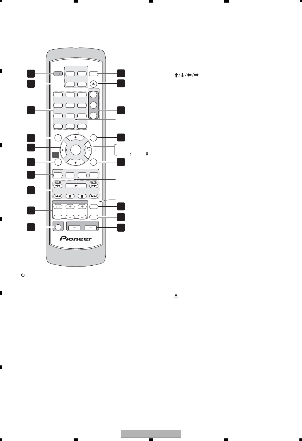
2.2 PANEL FACILITIES
Front panel
XV-DV575
XV-DV580
XV-DV385K
XV-DV395K
1
Opens/closes the disc tray.
2
Selects the DVD/CD function and starts/
pauses/resumes playback.
3
Stops playback.
4
Selects the USB function and starts/pauses
playback.
5VOLUME +/– buttons
6
Switches the system on or into standby.
7
8
9
See Display below.
10
Disc tray
Remote Sensor
Display
PHONES jack
Connect headphones.
11 USB interface
Connect a USB device for playback (see USB
playback).
COMPATIBLE
10 11
4 61 2 3
789
5
OPEN/CLOSE
DVD/CD
USB
STANDBY/ON
9
XV-DV575
56 7 8
56 7 8
A
B
C
D
E
F
Display
1DTS
Lights during playback of a DTS source.
2SOUND
Lights when the Sound Retriever is active.
3SURR.
Lights when one of the Advanced surround
listening modes is selected.
F.SURR.
Lights when one of the Front Stage
Surround Advance mode is selected.
4RPT and RPT-1
RPT lights during repeat play. RPT-1 lights
during repeat one-track play.
5REC MODE
Lights when Recording mode is on.
6PGM
Lights during program play.
7 Tuner indicators
– Lights when a broadcast is being
received.
– Lights when a stereo FM broadcast is
being received in auto stereo mode.
– Lights when FM mono reception is
selected.
– Lights when in one of the RDS
display or search modes.
8RDM
Lights during random play.
9 kHz/MHz
Indicates the frequency unit shown in the
character display (kHz for AM, MHz for FM).
10 Character display
11
Lights when sleep timer is active.
12
Lights during playback.
13 ∂ PL II
Lights during Dolby Pro Logic II decoding.
14 ∂ D
Lights during playback of a Dolby Digital
source.
SOUND
DTS F.SURR.
∂
PL
∂
D
REC MODE
RPT -1
kHz PGM
MHz RDM
1 6
12 89 7
43
1113
2
14 10
5
10 XV-DV575
12 3 4
A
B
C
D
E
F
12 3 4
8
See Basic playback controls, Disc
playback features and USB playback
for an explanation of these
controls.
9
These control Pioneer flat screen TVs.
10 SHIFT
Press to access the controls highlighted in
green.
11 SOUND RETRIEVER –Press to restore CD
quality sound to compressed audio sources.
12 OPEN/CLOSE
Opens/closes the disc tray.
13
Playback controls
TV CONTROL buttons
PLAYLIST buttons
Add tracks (during playback), or select a
playlist (while stopped).
14 MENU – Press to display a USB menu, or
the Navigator.
SHIFT+SR+– Sets the interlocking with the
connected flat screen TV.
15 RETURN – Returns to a previous menu
screen.
SHIFT+TEST TONE– Outputs the test tone
(for speaker setup).
16 SLEEP
Press to set the sleep timer.
17 MUTE
Mutes the sound (press again to cancel).
18VOLUME +/–
Adjusts the volume.
Remote control
1 STANDBY/ON
Switches the system on or into standby.
2
Selects the source you want to listen to (DVD/
CD,TUNER,USB,LINE).
3
DVD controls
CLEAR
Clears an entry.
DISPLAY
Displays/changes disc information shown
on-screen or to display RDS
information.
SHIFT+AUDIO
Selects audio channel/language.
SHIFT+SUBTITLE
Displays/changes the subtitles.
SHIFT+ANGLE
Changes camera angle during DVD multi-
angle scene playback.
SHIFT+ZOOM
Changes the screen zoom level.
4TOP MENU–Displays the top menu of a
DVD disc in the play position — this may
be the same as pressing MENU.
SHIFT+SETUP – Use to make various
system and surround sound settings.
5
– Use the cursor buttons to
navigate on-screen displays and menus.
ENTER – Selects an option or executes a
command.
TUNE +/– – Tunes the radio.
ST +/– – Selects station presets when
listening to the radio.
6
screen menu for Initial Settings, Play Mode
functions, etc.
SHIFT+MCACC – Starts the Auto MCACC
setup. (XV-DV575, XV-DV580)
7
Function select buttons
Number buttons, CLEAR, DISPLAY and
Cursor, ENTER and tuning buttons
HOME MENU – Displays (or exits) the on-
Sound controls
F.S.SURR – Selects Front Stage Surround
Advance mode.
SURROUND – Selects a Surround mode
or switches to stereo playback.
ADVANCED – Selects a Pioneer original
surround mode.
SOUND – Accesses the sound menu to
adjust the tone, bass and treble, etc. .
HOME
MENU
PLAYLIST
STANDBY
/ON
SHIFT
LINE
TOP MENU
F.S .
SURR
SOUND
CLEAR
MUTE
SLEEP
DISPLAY
123
1
2
3
456
789
0
ADVANCED
TUNE
ST
ST
USB
SUBTITLE
AUDIO
ZOOM
ANGLE
SLEEP
MENU
SR +
OPEN/CLOSE
INPUT CHANNEL VOLUME
DVD CD TUNER
(FM/AM) SOUND
RETRIEVER
VOLUME
TV CONTROL
SETUP
RETURN
TEST TONEMCACC
SURROUND
V. ENHEXT PWR
TUNE
ENTER
1
2
3
8
9
4
7
11
12
14
13
15
16
17
18
5
6
10
ECHO
KARAOKE
SHIFT+KARAOKE
SHIFT+SLEEP
FRT. SURR/EXT PWR
MP3 EXP/V. ENH
(XV-DV385K)
(XV-DV395K)
(XV-DV385K)
(XV-DV395K)
(XV-DV385K)
(XV-DV395K)
LINE OUT
(XV-DV385K)
(XV-DV395K)
SHIFT+ECHO
SHIFT+ SHIFT+
11
XV-DV575
56 7 8
56 7 8
A
B
C
D
E
F
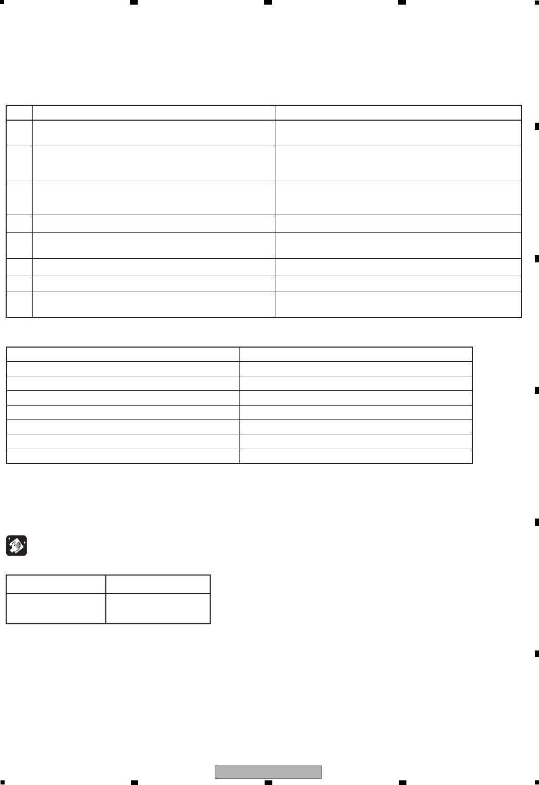
3. BASIC ITEMS FOR SERVICE
3.1 CHECK POINTS AFTER SERVICING
Check points after servicing (HTZ and system audio)
Cleaning
To keep the product quality after servicing, confirm recommended check points shown below.
See the table below for the items to be checked regarding video and audio:
Item to be checked regarding video Item to be checked regarding audio
Block noise Distortion
Horizontal noise Noise
Dot noise Volume too low
Disturbed image (video jumpiness) Volume too high
Too dark Volume fluctuating
Too bright Sound interrupted
Mottled color
No. Procedures Check points
1 Confirm the firmware version on Service Mode. The version of the firmware must be latest.
Update firmware to the latest one, if it is not the latest.
2
Confirm whether the customer complain has been solved. If the
customer complain occurs with the specific disc, use it for the
operation check.
The customer complain must not be reappeared.
Video, audio and operations must be normal.
3
Confirm playback error rates at the innermost and outermost
tracks by using the following disc.
DVD test disc (GGV1025)
The error rates must be less than 5.0e-4.
4 Play back a CD. (track search) Audio and operations must be normal.
5Play back a DVD.
(Menu operation, Title/chapter search) Video, audio and operations must be normal.
6 Check the tuner (AM and FM) operations. Audio and operations must be normal.
7 Check the sound from headphone output. Sound must be normal, without noise.
8 Check the appearance of the product. No scratches or dirt on its appearance after receiving it for service.
Before shipping out the product, be sure to clean the following positions by using the prescribed cleaning tools:
Position to be cleaned Cleaning tools
Pickup lens Cleaning liquid : GEM1004
Cleaning paper : GED-008
12 XV-DV575
12 3 4
A
B
C
D
E
F
12 3 4
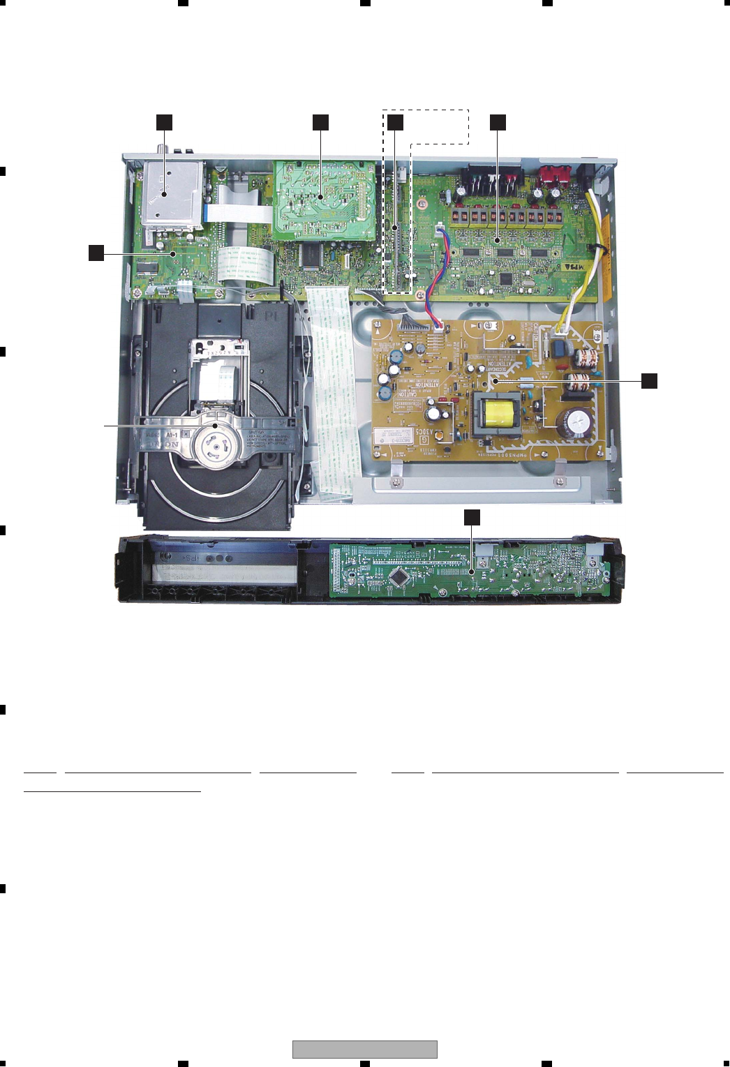
3.2 PCB LOCATIONS
1..08 DVDM ASSY AWM8118
(XV-DV575, XV-DV580)
1..08 DVDM ASSY AWM8105
(XV-DV385K, XV-DV395K)
1..DSP ASSY AWX8706
(XV-DV575, XV-DV580 ONLY )
1..SYSMAIN ASSY XWM3392
(XV-DV575)
1..SYSMAIN ASSY XWM3395
(XV-DV580)
1..SYSMAIN ASSY XWM3391
(XV-DV385K)
1..SYSMAIN ASSY XWM3394
(XV-DV395K)
1..COMPLEX ASSY XWM3429
(XV-DV575, XV-DV580)
1..COMPLEX ASSY XWM3428
(XV-DV385K, XV-DV395K)
NSP 1..NHTS JACK ASSY AWM8034
2..EUROSCART ASSY AWU8291
> 1..POWER SUPPLY UNIT XWR3018
1..FM/AM TUNER UNIT AXX7248
1..DVD MECHA ASSY A2ZX01A650
(for service)
Mark No. Description Part No. Mark No. Description Part No.
LIST OF ASSEMBLIES
NOTES:
-
Parts marked by “NSP” are generally unavailable because they are not in our Master Spare Parts List.
-
The > mark found on some component parts indicates the importance of the safety factor of the part.
Therefore, when replacing, be sure to use parts of identical designation.
XV-DV575, XV-DV580 ONLY
A
08 DVDM
ASSY
DVD MECHA
ASSY
D
EUROSCART ASSY
G
FM/AM TUNER UNIT EDSP ASSY
CCOMPLEX ASSY
BSYSMAIN ASSY
FPOWER
SUPPLY
UNIT
13
XV-DV575
56 7 8
56 7 8
A
B
C
D
E
F
3.3 JIGS LIST
Service Remote Control Unit GGF1381
DVD Test Disc (DVD-Video) GGV1025
Adjustment, diagnosis
Name Jig No. Remarks
Check of DVD-Video
CD Test Disc STD-905 Check of CD
DVD Data Disc GGV1309 ID data setting
Jigs list
Daifree GEM1036 (ZLX-ME413A)
GYA1001 (ZLB-PN397B)
Lubricating oil
Name Lubricants and Glues No. Remarks
Refer to "9.3 DVD MECHA ASSY"
Refer to "9.3 DVD MECHA ASSY"
GEM1018Grease Refer to "9.3 DVD MECHA ASSY"
Speaker Cable with terminal SDS1174 (FL/WHITE)
SDS1175 (FR/RED), SDS1176 (SL/BLUE)
SDS1177 (SR/GRAY), SDS6050 (C/GREEN)
For checking audio at the SP terminal
Lubricants and Glues list
14 XV-DV575
12 3 4
A
B
C
D
E
F
12 3 4
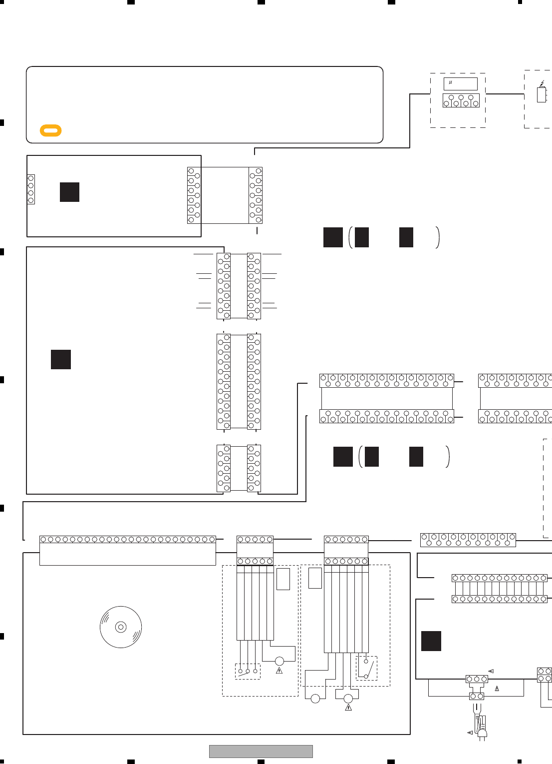
4. BLOCK DIAGRAM
4.1 OVERALL WIRING CONNECTION DIAGRAM
JCV9B07
DED012
(SW PCB)
PCB640
M
6
5
4
3
2
1
GND(SW)
FEED MOTOR (+)
SPINDLE MOTOR (+)
SPINDLE MOTOR (-)
FEED MOTOR (-)
PICK UP INNER LIMIT SWITCH
SW2
M2601 BCZ3B03
M2602
ESE22MH24 CD2301
2H062102
M
(LOADING MOTOR PCB)
SSS-13-2
SW1
GND(SW)
SW-2(CLOSE)
SW-1(OPEN)
LOADING MOTOR(-)
LOADING MOTOR(+)
DED003
PCB610
BCZ3B52
M2603
CD2302
2H052601
M
5
4
3
2
1
312
2
1
3
2
1
4
5
6
9
7
8
10
13
11
12
2
3
4
5
1
14
13
11
10
9
8
12
7
6
15
20
21
18
19
22
23
16
17
7
8
99
7
8
5
6
4
5
6
4
1
2
3
1
2
3
18
15
16
17
11
12
13
14
19
18
15
16
13
14
19
17
11
12
10
9
88
10
9
6
5
4
7
6
5
4
7
3
2
1
3
2
1
2
1
2
1
3
4
5
3
4
5
6
7
8
6
7
8
9
10
11
9
10
11
13
12
13
12
8
9
10
11
12 534
12534
24
365142
365 142
1
26
5
4
3
3
2
1
4
5
6
9
7
8
10
13
11
12
10
9
8
715
16
13
14
1917
18
11
12
13
4
5
2610
9
8
7
12
11
14
13
42610812 14
15 17
1816 22
19
20
21 23
24
27
26
25
16 182220 24 26
135 1191372115 2523 271917
3
2
1
4
7
6
5
246
15
10
10
8
14
12
9
8
13
14
11
12
53171115913
1
3
4
5
6
7
2
3
4
1
2
75
6
312
CN3
CN1CN2
CN966
CN901 CN5533
CN701 CN5531
CN5532CN951
CN965
CN964
CN1001
JA931
CN5603
CN9000
CN5701
CN5501
JA4602
TRAVERSE MECHA ASSY
KM200NA13
B3P-VHB2P-VH
CKS5045-
XKP3088-XKM3008-
XKP3054- XKM3005-
XKP3053- XKM3004-
KM200NA13
AKP1318-
CN19604S-11C
9604S-07C
GP1FAV51RK
DVD MECHA ASSY (A2ZX01A650)
AC POWER CORD
XDX3068 (OTHERS)
XDX3069 (KU ONLY )
LIVE
NEUTRAL
NC
+B
GND
AC_DET
SW10.5V
EV5.0V
SW6.8V
GND
SW5.0V
SW3.3V(A)
Pwr-ctr
SW3.3V(B)
GND
FL DC-
FL DC+
-25.5V
24P FFC
GNDD
E
VCC
VREF
F
VR780
VRCOM
VR650
A
B
RF
SW
C
D
FOCS DRV
TRKG RTN
TRKG DRV
(NC) VSHF
GNDD
LD(650)
PD
LD(780)
GNDD
V+3D
GNDD
GNDD
OPTIN(5V)
DVDIN(3.3V)
GNDD
GNDD
B to B
GNDD
GNDD
GNDD
B to B
SDTO
CDTO
DAUX
BDTO
GNDD
GNDD
GNDD
FDTO
LCKO
GNDD
GNDD
GNDD
BCKO
GNDD
GNDD
GNDD
GNDD
MCLK
DIR ERR
DSP MODE
DIR RST
DIR CS
DIR DO
DEC_MUTE
DSP HREQ
DSP RST
DSP SS
BUSY
B to B
DSP DO
DSP CK
DSP DI
TXR
GND
RDS
VSM
5P FFC
VKN1595
6P FFC
VKN1596
LOAD-
LOAD+
OPEN
GND
CLOSE
FOCS RTN
SW (GND)
LIMIT SW
SLD-
SLD+
SPD-
SPD+
HDMI OUTPUT
V+3D
GNDD
GNDD
DATA2-
DATA2+
DATA1-
DATA1+
DATA1 SH
DATA2 SH
AC_DET
EV5.0V
SW10.5V
SW5.0V
GND
SW6.8V
Pwr-ctr
SW3.3V(A)
SW3.3V(B)
-25.5V
FL DC+
FL DC-
PG
GND
DATA0+
CLOCK-
CLOCK+
DATA0-
HOT PLUG DET
HDMISDA
HDMISCL
NC
CEC
CLOCK SH
DATA SH
+5V
DDC/CEC GND
ALR
A
TRKUP
OPTIN(5V)
GNDD
DVDIN(3.3V)
GNDD
GNDD
GNDD
USBN
GNDD
DVDPOWER
XDVDRST
XREADY
SCLK
SDATA
MDATA
ACK
GNDD
DVDMUTE
VDET
MIC/GNDD
V+5
V+5
3R3V
V+6R8
V+6R8
GNDM
GNDM
GNDD
DOUT
GNDD
USBP
3R3V
GNDD
GNDD
GNDD
GNDD
BDTO
DAUX
CDTO
SDTO
GNDD
FDTO
VKN1258
CN968
VKN1617
(XDD3290)
27P FFC
LCKO
BCKO
MCLK
GNDD
GNDD
GNDD
GNDD
GNDD
GNDD
GNDD
TRKUP
DVDPOWER
USBN
GNDD
XDVDRST
XREADY
SCLK
SDATA
MDATA
ACK
GNDD
VDET
DVDMUTE
MIC/GNDD
V+5
V+5
3R3V
3R3V
V+6R8
V+6R8
GNDM
GNDM
GNDD
GNDD
DOUT
GNDD
USBP
SQUEEZE
VSEL2
VSEL1
ASPECT
SC
GNDD
P/XI
SY
GNDD
GNDD
CY/G
GNDD
GNDD
CB/B
CN967
VKN1607
(XDD3263)
VKN1248
17P FFC
V
VSEL1
VSEL2
P/XI
SQUEEZE
GNDD
SC
ASPECT
GNDD
GNDD
CB/B
CY/G
GNDD
SY
GNDD
V
DIR DO
DIR ERR
DIR RST
DIR CS
DSP MODE
BUSY
DSP HREQ
DSP SS
DSP RST
DSP CK
DSP DO
DSP DI
DEC_MUTE
TXR
VSM
RDS
GND
AM
FM
DO
DI
CE
GND
TXL
CLK
+9V
11P FFC
(XDD3266)
+9V
CLK
CE
DI
DO
TXL
GND
WDD
WEN/DI
VSS
VCC
RST
WCLK
DOWNLOAD
-COM
NC
OPT IN
k When ordering service parts, be sure to refer to "EXPLODED VIEWS and PARTS
LIST" or "PCB PARTS LIST".
k The > mark found on some component parts indicates the importance of the safety
factor of the part. Therefore, when replacing, be sure to use parts of identical
designation.
k : The power supply is shown with the marked box.
08 DVDM ASSY
(XV-DV575,XV-DV580 : AWM8118)
(XV-DV385K,XV-DV395K : AWM8105)
DSP ASSY
(XV-DV575, XV-DV580
ONLY : AWX8706)
E
FM/AM TUNER
UNIT
(AXX7248)
G
POWER SUPPLY UN
(XWR3018)
F
SYSMAIN ASSY
(XV-DV575 : XWM3392)
(XV-DV580 : XWM3395)
(XV-DV385K : XWM3391)
(XV-DV395K : XWM3394)
B1/5- B5/5
B
A1/2- A2/2
A
(XV-DV57
XV-DV580
15
XV-DV575
56 7 8
56 7 8
A
B
C
D
E
F
Vout
GND
Vcc
2
1
2
1
6
9
7
8
10
13
11
12
12
11
5
8
9
6
7
10
1
2
3
4
6
9
7
8
10
13
11
12
15
1614
1917
18
13
12 12
13
9
10
11
10
9
11
5
6
7
8
6
8
5
7
1
24
35
68
7
12
11
10
9
16
15
14
13 17
1
2
3
412
175
6
11
10
9
16
15
14
13
8
7
3
2
11
4
3
2
4
3
24
7
6
5
246
15
1610
1610
8
14
12
9
8
13
14
11
12
17
53711 1715913
19
20
2523
24
27
26
29
2818
21
22
2220
2523
24
27
26
19 29
2818
21
2323 20
21
3
7
2
312
1
6
4
5
20
21
22
20
21
22
19
17
18
19
17
18
14
15
16
14
15
16
12
11
17
18
15
16
19
13
14
13
12
11
13
12
11
10
9
8
10
9
8
7
6
5
7
6
52
10
4
3
9
6
5
7
8
2
3
4
2
3
4
11
1
CN2CN3201
JA5901
5902
CN3211
CN5901
CN5605
JA403
CN451 CN461
JA5931
JA4602
JA451
B2P-VH
B2P-VH
MIC (MAIN)
XKN3012
JA3921
MIC (SUB)
AKN7003-
XKN3012
JA3922
HEAD PHONE
GP1UE274XKC1
AKE7121
9607S-29F
CN9002
CN9001
CN3111
AKB7114
XKB3062
CN3112
XKB3069-
9604S-23C CKS3388-
XKN3015
GP1FAV51RKBF
XKB3054-
AC POWER CORD
XDX3067-
+B
GND
+B
GND
GND
SW3.3V(A)
Pwr-ctr
SW3.3V(B)
GND
FL DC-
FL DC+
-25.5V
USB
USB_DP2
USB_DM2
REMOCON
SW-
SW+
XKB3086
JA602
RL-
FL+
FL-
RL+
C+
C-
6ch SP OUT
FR+
RR-
RR+
FR-
GND
Pwr-ctr
SW3.3V(A)
SW3.3V(B)
-25.5V
FL DC+
FL DC-
PG13KA-F07
GND
HOT PLUG DET
HDMISDA
HDMISCL
NC
+5V
DDC/CEC GND
ACLK_LFE
ABCK_ARS
ALRCK_CENTER
ASDAT0_ALS
GNDD
GNDD
GNDD
GNDD
GNDD GNDD
ACLK_LFE
GNDD
(XDD3264-)
13P FFC
ABCK_ARS
GNDD
ALRCK_CENTER
GNDD
ASDAT0_ALS
GNDD
KEY1
KEY2
NC
CN5902
9607S-27F
(XDD3260-)
GNDUSB
GNDUSB
V5USB
V5USB
VE+5
FLDC-
GNDD
VFDP
GNDD
FLDC+
(XV-DV385K, XV-395K)29P FFC
(XDD3261-)
KEY1
KEY2
9604S-27C (XV-DV575, XV-DV580)
9604S-29C (XV-DV385K, XV-395K)
NC
USB_DP2
GNDUSB
V5USB
V5USB
REMOCON
VE+5
FLDC-
GNDD
VFDP
GNDD
FLDC+
FLCS
USB_DM2
GNDUSB
SQUEEZE
VSEL2
VSEL1
ASPECT
SC
GNDD
SY
VKN1417
GNDD
GNDD
CY/G
GNDD
GNDD
CB/B
CR/R
GNDD
CN962
ASDAT1_AL
ASDAT2_AR
GNDD
GNDD
VKN1244
ASDAT1_AL
GNDD
ASDAT2_AR
GNDD
(XDD3263)
17P FFC
V
VSEL1
VSEL2
SQUEEZE
GNDD
SC
ASPECT
GNDD
CR/R
GNDD
GNDD
CB/B
CY/G
GNDD
SY
GNDD
V
S_Y
(XV-DV575, XV-DV580)27P FFC
HP_R
HP_L
MIC SW
MIC
GNDA
HPMUTE
HP_DET
FLCS
V+10
FLCK
FLDATA
GNDA
GNDA
LINEOUT_R
RUS,EU
AUDIO OUT
GNDA
FLDATA
V+10
FLCK
HP_R
HP_L
MIC
MIC SW
GNDA
HPMUTE
GNDA
HP_DET
TVIN_L
TVIN_R
LINEOUT_L
AUDIO IN
OUTPUT
VIDEO
COMPOSITE
S_Y
23P FFC (XDD3267-)
NC
GND
SR PLUS
OPT IN
S_C
GND
GND
GND
DVDPOWER
GND
VSEL2
GND
GND
TVOUT_L
SCART_R
SCART_L
TVMUTE
V+5
MCACC
RKN1004
JA4901 V+10
TVOUT_R
VSEL1
SQEEZE
V
GND
V
GND
RR
DVDPOWER
S_C
GG
GND
GND
G
NC
R/C
BLANK
GND
GND
GND
GND
V/Y
BB
VSEL2
V+5
GND
SCART_L
SCART_R
GND
TVOUT_R
TVOUT_L
TVMUTE
R IN
B
L OUT
GND
GND
L IN
SQUEEZE
NC
GND
VSEL1
V+10
SQEEZE EURO CONNECTOR
R OUT
M8118)
AWM8105)
R SUPPLY UNIT
8)
COMPLEX ASSY
(XV-DV575, XV-DV580 : XWM3429)
(XV-DV385K, XV-DV395K : XWM3428)
C
EURO
SCART
ASSY
(AWU8291)
D
(XV-DV575,
XV-DV580)
(XV-DV575,
XV-DV580)
(XV-DV385K, XV-DV395K)
(XV-DV385K, XV-DV395K)
16 XV-DV575
12 3 4
A
B
C
D
E
F
12 3 4
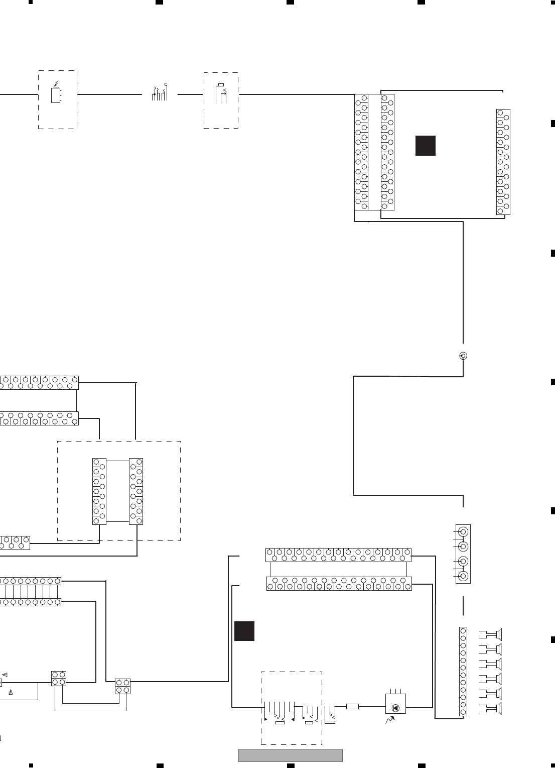
4.2 OVERALL BLOCK DIAGRAM
HP SEL
FL DRIVER
SYSTEM
µ-com
ADMCK1
SDA
SCL
MUTE
+B
VE+5
FL
VF
VFDP
PCON
w/o DSP : Mastering
with DSP : Slave
HP
USB
V+3R3
VE+5
V+10
V+6R8
EV5.0V
SW 3.3V(A)
SW10.5V
SW5.0V
SW6.8V
SW 3.3V(B)
FL DC +/-
PWR CONT
(from SYST
RESET
PDN
SD
OTW
LRCKO
MCKO
BCKO
D ATA 0
Selector
NON-DSP model : Necessity
DSP model : Unnecessary
(The A/D side, the
NON-DSP mode : Short
DSP model : Opening
DIR
AK4117VF
ASPDIF (DSP model only)
ADDAT
MCK0
24.576M
74HCU04
1.25V
OPT IN
FL
KEY
Sub Mic Main
Mic
V+6R8
5V REG
V+5USB
USB POWER
USB DP
USB DM
To BE IC
TUNER
A/D
AK5358AET
TUNER
LINE
ADLRCK
ADBCK
ADDATA
12.288M
74HCU04
SCART
9V
NON-DSP model only
MCACC
SCART(EU,RUSSIA model only)
LINE
MCACC
(DSP model only)
ADMCK0
DSP model : Opening
NON-DSP model : Short
ALRCK
MCDAT
ACLK
A/D
AK5358AET
(NON-DSP
model only)
ALRCK
ALCK
ABCK
ASDAT1
ASDAT0
ASDAT2
DOUT
MIC
Video
AMP
BE
MT1389FE/S
27MHz
•AUDIO PROCESSING
-Audio Decode
-Bass Management
-Virtual Surround
-Preset EQ
etc.
• Build-in HDMI TRANSMITER
Y/G , Cb/B , Cr/R
Y , C
V
64M
SDRAM
16M
FLASH
64k
EEPROM
MOTOR
DRIVER
ORION
LOADER
MECHA
HDMI OUT
Y , Cb , Cr
Y , C
V
G , B , R
V+3
USB
POWER
CONTROL
V+10
V+3R3
(NON-DSP
model only)
REMOCON SENSOR
EEPROM
V+5
V+6R5
V+5
V+5
V+3
V+5
V+3
V+3
V+5
coil
VU+
V+10
V+3
IC5901
IC3921
IC601
IC801
IC201
IC101
IC401
IC781
IC771
IC4961
IC4004 IC4005
IC5501
IC5502
IC4001
COMPLEX ASSY
C
POWER SUPPLY UNIT
F
08 DVDM ASSY
A
SYSMAIN ASSY
B
FM/AM TUNER
UNIT
G
17
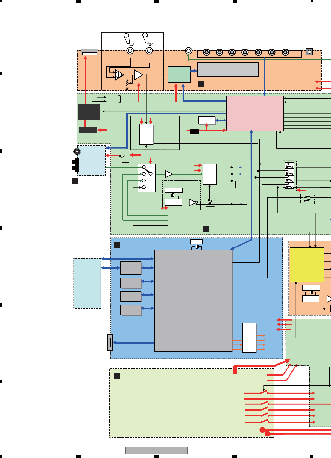
XV-DV575
56 7 8
56 7 8
A
B
C
D
E
F
NOTES for destination
• NON-DSP model : 385K, 395K, 170 , 171, 270, 272
• DSP model : 373, 575, 580, 777
• EU model : 575, 580
• RUSSIA model : 385K, 395K
• KU model : /KU
• IBD model : /LF,/NA,/ GDR, /NT, /TD, /WL, YP
• Japan : /JJ
Composite
Component Video
(KU,IBD model only)
SCART
(EU,RUSSIA model only)
G , B , R
Y , C
V
Y, Cb, Cr
SCART
LINE
Scart
Circuit
HP AMP
LPF
FRONT R
CENTER
SUB WOOFER
REAR L
REAR R
+B
V+3R3
MODULATOR
TAS5508
• 8ch PWM
modulator
-Volume
-Tone
-EQ
-Bass/Treble
POWER
STAGE
TAS5122
RESET
PWMA P
PWMB P
SD
PWMA M
PWMB M
ch7 ch8 PWM
HP SEL
LINE-IN
LINE-OUT
(EU,RUSSIA model only)
SDA
SCL
AC IN
MUTE
FL DC +/-
VFDP
PCON
SR+ INPUT
(Except 170,171,270,272)
V+3R3
VE+5
V+10
V+6R8
PWR CONT
(from SYSTEM U-COM)
RESET
PDN
SD
OTW
DVDPOWER
(from SYSTEM U-COM)
VE+
V+5
SW
SW
LRCKO
MCKO
BCKO
D ATA 0
r
SP model : Necessity
odel : Unnecessary
(The A/D side, the short, and data open to the clock.)
NON-DSP mode : Short
DSP model : Opening
DIR
AK4117VF
DSP
DSPC56371AF18
Level Shifter
TC74VHC08FTS1
MCKO
LRCKO
BCKO
FDTI
D ATA 0
ASDAT2
ASDAT1
DSP model only)
ADDAT
LRCK0
BCKO
MCK0
24.576M
74HCU04
3.3V
1.25V
OPT IN
ASDAT3
KEY
FRONT L
(DSP model only)
DIGTAL OPT IN
(DSP model only)
D2-Terminal
(JAPAN model only)
V+3
MCACC MIC
(DSP model only)
MCACC
(DSP model only)
V+5V
V+3R3
P. C O
NFIG
from DVDMAIN
REMOCON SENSOR
V+3
IC801
IC951
IC601
IC801
IC3201
IC3301
IC3401
IC3901
IC3131
05
EUROSCART ASSY
D
DSP ASSY
E
18 XV-DV575
12 3 4
A
B
C
D
E
F
12 3 4
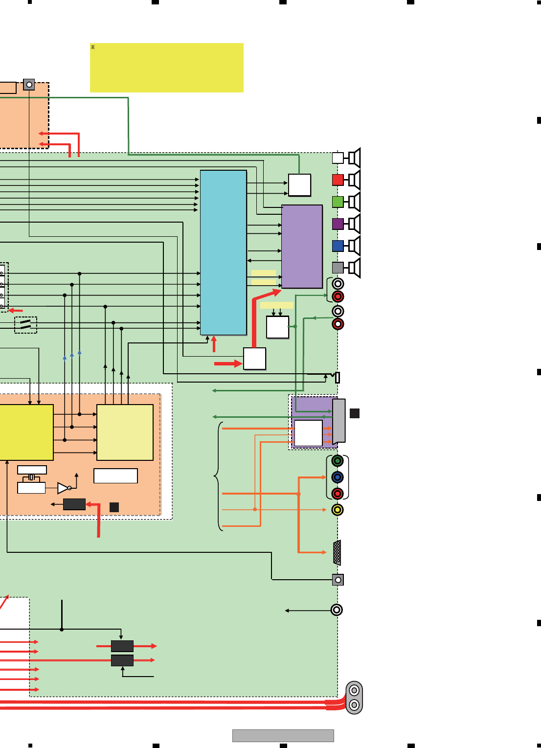
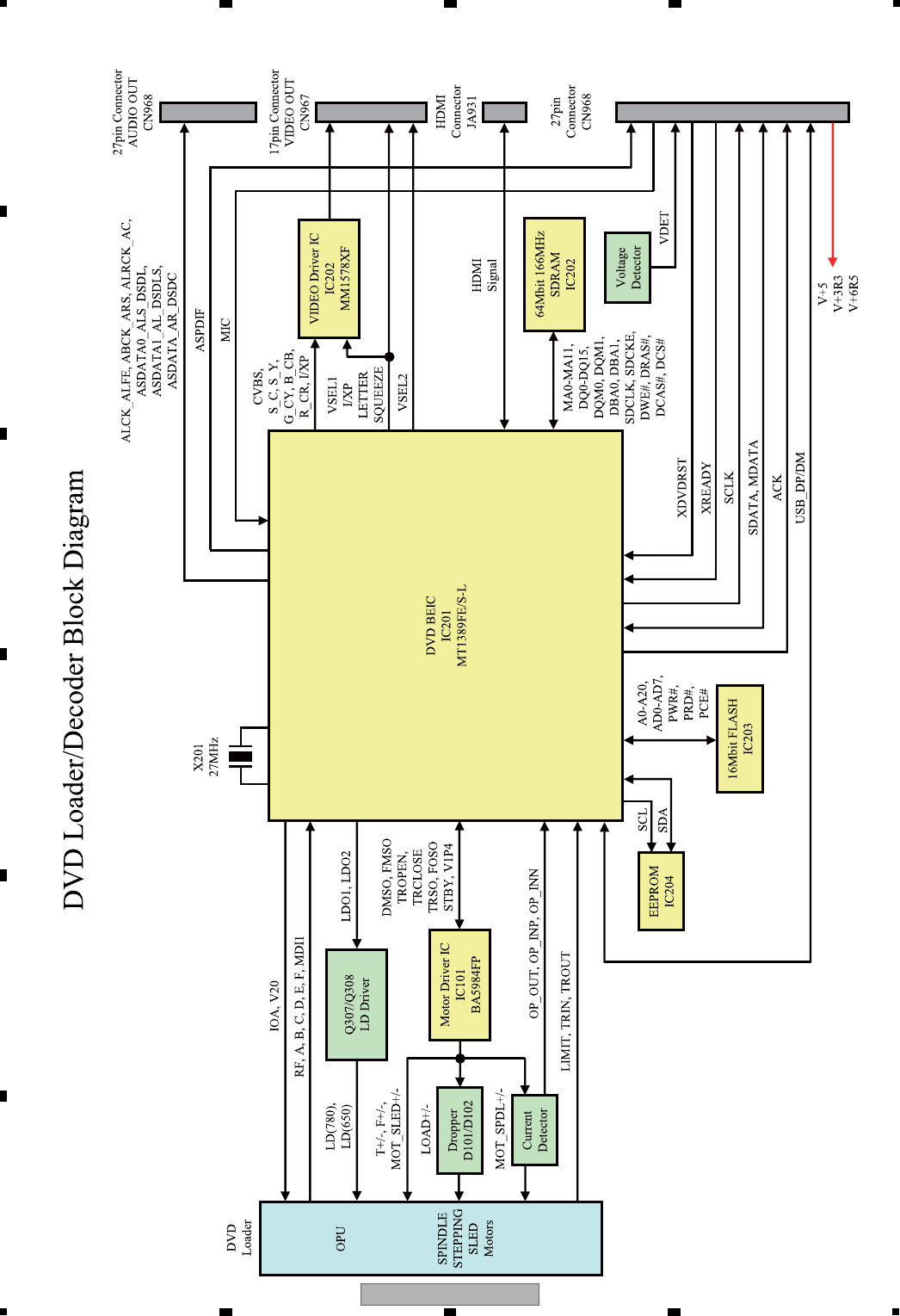
4.3 DVD LOADER/DECODER BLOCK DIAGRAM
19
XV-DV575
56 7 8
56 7 8
A
B
C
D
E
F
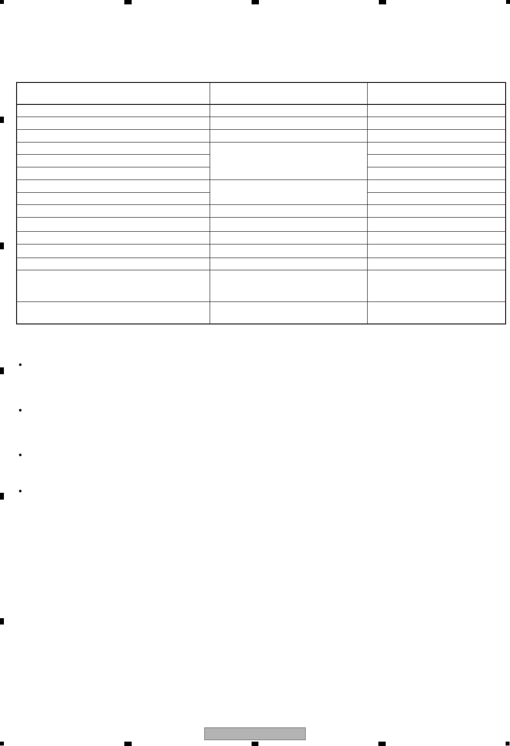
5. DIAGNOSIS
5.1 METHOD FOR DIAGNOSING DEGRADATION OF THE LDS ON THE PICKUP
Q304
Q305
Q307
Q308
L308
L309
R305
CN101
CN102
R313
CN104
R321
R322
R325
R326
C309
R152
R153
R154
C140
C141
R373
C372
R372
R374
R375
R371
R314
C1
CONTACT
SIDE
SIDE
CONTACT
UP SIDE
C
R157
R156
D
D
E
1
1
1
20151051
15 15
R321
R322
R325
R326
Case when this diagnosis is required :
When playback of any disc, including a test disc (DVD: GGV1025, CD: STD-905), cannot be performed
How to diagnose
In the case mentioned above, degradation of the laser diodes (LDs) mounted on the Pickup PCB is suspected.
Measure the voltage between the two ends of one of the resistors mentioned below.
Measure the voltage between the two ends of R322 or R325 on the 08 DVDM
Assy. If the voltage is 0.4 V or higher, the 650-nm LD is degraded.
No playback of a DVD :
Measure the voltage between the two ends of R321 or R326 on the 08 DVDM
Assy. If the voltage is 0.4 V or higher, the 780-nm LD is degraded.
No playback of a CD :
If the measurements show degradation
of an LD, replace the DVD MECHA
Assy.
SIDE A
A
08 DVDM ASSY
20 XV-DV575
12 3 4
A
B
C
D
E
F
12 3 4
5.2 DVD TROUBLE SHOOTING
No. Symptoms Diagnosis Contents Possible Defective Points
1 The power is not turned on. Are wires of output connector (POWER SUPPLY Unit) and CN968 (08
DVDM Assy) disconnected or damaged ? Connector / cable
Check that the following voltage is output :
CN968-pin 24 or pin 25 (08 DVDM Assy): 3.3 V
POWER SUPPLY Unit
2An opening screen is not
displayed on the monitor
(The FL display lights. The
mechanism does not work.)
Are the signals output from IC201-pin 97 (MDATA) and pin 98 (SCLK)
on the 08 DVDM Assy ? (in the range of 0 - 3 V)
08 DVDM Assy
DVD IC (IC201)
Are the signals input into IC5501-pin 50 (MDATA) and pin 51 (SCLK) on
the SYSMAIN Assy ? (in the range of 0 - 3V)
SYSMAIN Assy
UCOM (IC5501)
Check that the following voltage are output :
Q1302-collector on the SYSMAIN Assy: 5V
POWER SUPPLY Unit /
SYSMAIN Assy Q1302
Is a resonator (X201: 27 MHz) on the 08 DVDM Assy oscillating ?
08 DVDM Assy
Crystal resonator (X201)
DVD IC (IC201)
•
Is a signal input into IC203-pin26 (PCE#) on the 08 DVDM Assy ?
(Is a signal "H" for 80 ms and then "L" after the power is turned on ?)
-> Communication with flash ROM.
• Are the signals input into IC202-pin 16 (DWE#), pin 19 (DCS#)
and pin 38 (SDCLK) on the 08 DVDM Assy ?
(Is a signal fluctuating ?)
-> Communication with SDRAM
08 DVDM Assy
DVD IC (IC201)
Flash ROM (IC203)
SDRAM (IC202)
Is a signal output from IC203-pin 28 (PRD#) on the 08 DVDM Assy?
(Is a signal fluctuating for several hundred ms after the power is turned
on ?)
08 DVDM Assy
Flash ROM (IC203)
Is a signal input into IC5501-pin 67 (DVD ACK) on the SYSMAIN
Assy ? (Is a signal fluctuating ?)
-> Communication with FL Control IC
08 DVDM Assy
DVD IC (IC201)
SYSMAIN Assy
UCOM (IC5501)
Is a signal output from IC5501-pin 78 (XREADY) on the SYSMAIN Assy
? (Is a signal fluctuating in the range of 0-5V ?)
SYSMAIN Assy
UCOM (IC5501)
Are the signals output from IC5501-pin 49 (SDATA) on the SYSMAIN
Assy ? (in the range of 0-5V)
08 DVDM Assy
DVD IC (IC201)
SYSMAIN Assy
UCOM (IC5501)
Are the signals of IC204-pin 5 (SDA) and pin 6 (SCL) on the 08 DVDM
Assy fluctuating for one or two seconds after the power is turned? 08 DVDM Assy
EEPROM (IC204)
3An opening screen is not
displayed on the monitor
(The FL display lights. The
mechanism works.)
Check the video signal path between DVD IC (08 DVDM Assy IC201)
and video-out terminal (see the block diagram)
08 DVDM Assy
Video circuit after DVD IC
(IC201)
Symptoms that may occur when any of the following ICs is in failure
IC Symptoms
EEP ROM
(08 DVDM Assy : IC204)
User's data cannot be stored in memory.
The ID number is lost.
Flash ROM
(08 DVDM Assy : IC203)
The power cannot be turned on.
Downloading of the firmware cannot be performed.
DVD IC
(08 DVDM Assy : IC201)
Any kind of symptoms (no power, a failure in any of the servo, video and audio systems, USB etc.) may be
generated, because the DVD processing is performed by a single chip.
64M SDRAM
(08 DVDM Assy : IC202)
No power.
Block noise is generated during playback.
21
XV-DV575
56 7 8
56 7 8
A
B
C
D
E
F
No. Symptoms Diagnosis Contents Possible Defective Points
4 A tray cannot be opened.
(An opening screen is
displayed on the monitor)
Does the voltage of CN965-pin 3 and pin 5 on the 08 DVDM Assy
change normally ?
Pin 3 (CLOSE (TRIN)): Tray is fully closed: "L"
Pin 5 (OPEN (TROUT)): Tray is fully opened: "L"
DVD MECHA Assy
Switch (SW1)
Is the signal input into IC101-pin 1 (TROPEN) on the 08 DVDM Assy?
At open: 3.3 V, At close: 0 V
08 DVDM Assy
DVD IC (IC201)
Are the signals output from CN965-pin 5 and pin 4 on the 08 DVDM Assy ?
Pin 5: Approx. 5 V during opening tray approx. 1 V during closing tray.
Pin 4: Approx. 0 V during opening tray approx. 6 V during closing tray.
08 DVDM Assy
FTS Driver IC (IC101)
Are wires of CN964 and CN965 on the 08 DVDM Assy disconnected or
damaged ? Connector / cable
Does the voltage of CN964-pin 5 on the 08 DVDM Assy change to 0 V
by pressing the Push switch. Push switch (SW2)
5 Playback impossible
(no focusing)
Are the signals output from IC101-pin 16 (F+) and pin 15 (F–) on the 08
DVDM Assy ?
08 DVDM Assy
FTS Driver IC (IC101)
Does 650-nm LD emit light ?
Does a pickup lens move up / down ?
Does an actuator spring bend ?
Pickup
Are plastic parts damaged ? Or is a shaft detached ?
Is the turntable detached or tilted ? Mechanism section (motor)
Is flexible cable of CN965 on the 08 DVDM Assy disconnected or
damaged ? Flexible cable / connector
Is signal output from IC201-pin 41 (FOSO) on the 08 DVDM Assy ?
(Device control of about 1.4 V is output usually. It is fluctuated by about
250 mV with focus up / down.)
08 DVDM Assy
DVD IC (IC201)
6 Playback impossible
(Spindle does not turn)
Are the signals output from IC101-pin 12 (MOT_SPDL–) and pin 11
(MOT_SPDL+) on the 08 DVDM Assy ?
Is pin 21 (STBY) fixed LOW ? (pin 21 is High at playback: 3 V)
08 DVDM Assy
FTS Driver IC (IC101)
Is there any part detached from the spindle motor ?
Or Is there any foreign object lodged in it ?
Mechanism section
(Spindle motor)
Are wires of CN964 on the 08 DVDM Assy disconnected or damaged ? Flexible cable / connector
Is signal output from IC201-pin 36 (DMSO) on the 08 DVDM Assy ? 08 DVDM Assy
DVD IC (IC201)
7 Playback impossible
(Playback stops)
Does 650-nm LD deteriorate ?
If the voltage at each both ends of R322 and R325 on the 08 DVDM
Assy is 0.4 V or more, the 650-nm LD is definitely deteriorated.
650-nm LD deteriorated.
(When playback of a DVD is
impossible)
Does 780-nm LD deteriorate ?
If the voltage at each both ends of R321 and R326 on the 08 DVDM
Assy is 0.4 V or more, the 780-nm LD is definitely deteriorated.
780-nm LD deteriorated.
(When playback of a CD is
impossible)
Are there scratches or dirt on the disc ? Disc
8 Picture disturbance during
playback
(block noise, freeze, other)
Are there scratches or dirt on the disc ?
Is there a problem with the format of the disc ?
Check the video signals.
Composite video signal (IC401-pin 23)
S video signal (IC401-pin 21, pin 26)
RGB video signal (IC401-pin 16, pin 18, pin 20)
Disc
9 No sound
(Picture is normal)
Check the waveform (ALCK: IC201-pin 231), (ALRCK: IC201-pin 227),
(ABCK : IC201-pin 230), (ASDATA0/1/2: IC201-pin 226/225/223).
Check the waveform (ASPDIF: IC201-pin 215)
08 DVDM Assy
DVD IC (IC201)
08 DVDM Assy
DVD IC (IC201)
Video IC (IC401)
22 XV-DV575
12 3 4
A
B
C
D
E
F
12 3 4
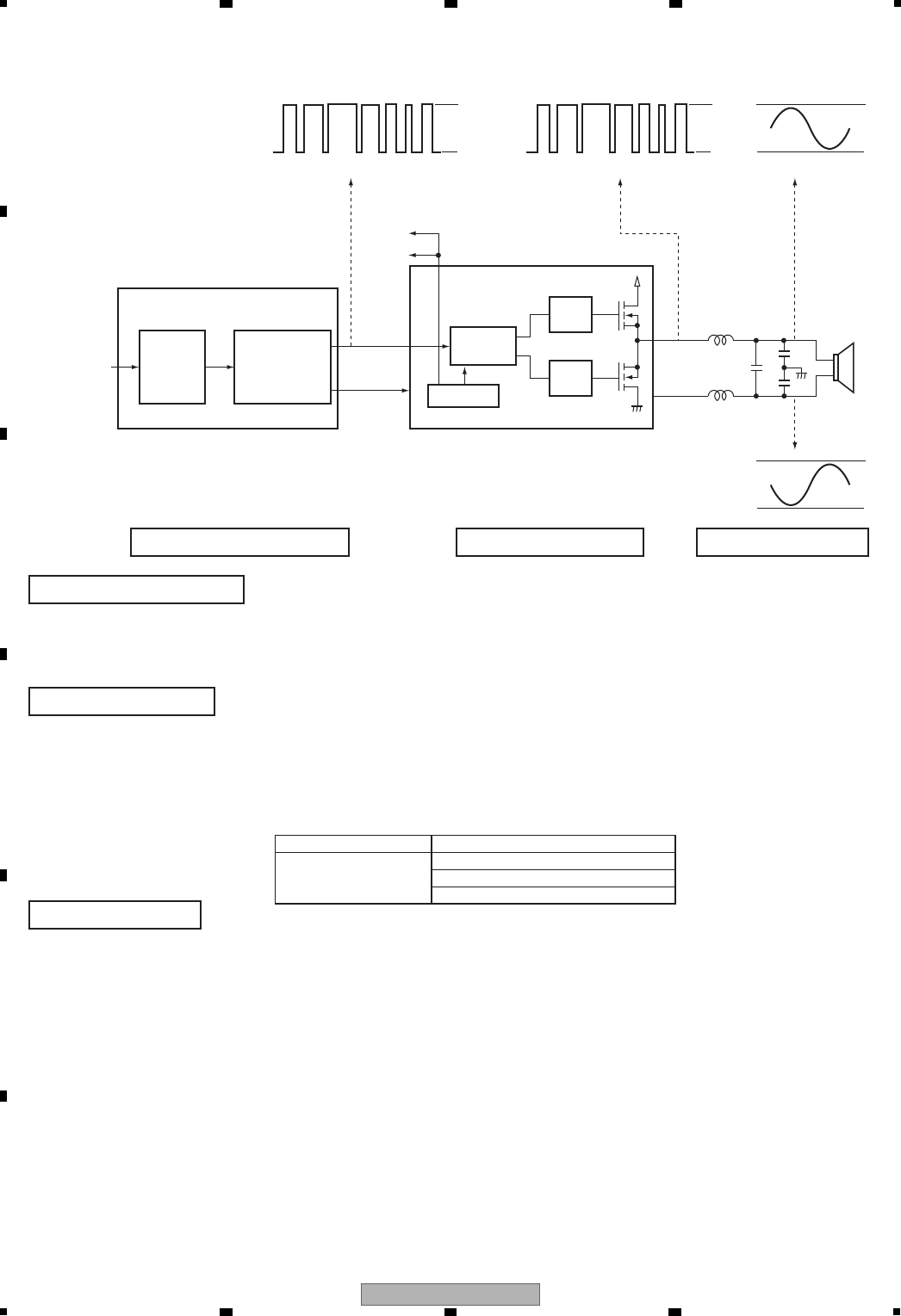
5.3 CIRCUIT DESCRIPTION OF DIGITAL AMP SECTION
Filter
and
Volume
Timing
Control
Gate
Drive
XSD
To UCOM
PCM Signal
From
DVD or ADC
3.3 V
0 V
TAS5508BPAG
PWM Processor section
PWM Processor section
Power Stage section
Power Stage section
Output LPF section
Output LPF section
TAS5122DCA
XOTW
Protection
PCM -> PWM Gate
Drive
20 V
0 V 0 V
0 V
The PCM signals output from the DVD decoder or AD converter are input to this section, and their volume and sound quality
are digitally adjusted. At the output stage, after conversion from PCM to PWM, the signals are output to the Power stage.
In this section, timing is controlled so that the MOSFETs on the high and low sides will not be turned on simultaneously. The
voltage of the PWM signals are raised to drive the gates of the MOSFET, and the PWM signals to drive the speakers are
output from the MOSFET at the output stage. Detection and protection functions against short-circuiting of the output
signals and temperature exceeding the standard value are also provided.
The carrier elements, high-frequency signals that are unnecessary for these speakers, are eliminated. The signals passed
through the LPF will become sine-wave signals, as shown in the figure above.
Power Stage ICs No. Protection Enable State
IC3201 SD_AB (pin 23) => L
IC3301 SD_CD (pin 24) => L
IC3401 OTW (pin 25) => L
IC3101 IC3201, IC3301, IC3401
*1 XSD : SD_AB (pin 23), SD_CD (pin 24)
*2 XOTW : OTW (pin 25)
*1
*2
If the detection and protection work, the ports of the power stage ICs become the following state.

23
XV-DV575
56 7 8
56 7 8
A
B
C
D
E
F
5.4 SPECIFICATIONS OF PROTECTION CIRCUITS FOR DIGITAL AMP SECTION
The protection circuits for the Digital Amplifier are activated, following the specifications shown below. The error indication on
the FL display shows the reason a protection circuit was activated.
Upon diagnosis of the Digital Amplifier, refer to the specifications for the protection circuits here and the overview of the Digital
Amplifier circuitry.
1. Overview
The system microcomputer monitors the ports for shutdown requests (pin 23: SD_AB and pin 24: SD_CD) and the ports for
abnormal-temperature detection (pin 25: /OTW) of the Power Stage ICs (IC3201, IC3301, and IC3401). As soon as any
abnormality is detected, it shuts the unit down.
To notify the user of the possibility of a too high a volume, when the unit is turned on the next time, the volume level will be set
to 0, and an error message will be displayed on the FL display.
2. Ports on the system microcomputer to be used for detection
Pin 77: SHUTDOWN
Low voltage at this pin means overcurrent or voltage too low (= V+B27) at a Power Stage IC.
Pin 79: XOTW
Low voltage at this pin means the temperature at the Power Stage ICs exceeded 125 °C.
Note: As one Power Stage IC is provided with two channels, three Power Stage ICs (in total 6 channels) are mounted in
this unit. For abnormality detection, the unit implements a logical OR operation regarding these three ICs.
Therefore, which IC is abnormal cannot be known directly. To find which IC is abnormal, it is required to check the
PWM outputs (pins 35, 38, 47, 50) of the each power stage ICs (IC3201, IC3301, IC3401).
3. Detection timing
Start : Detection starts 500 ms after the PWRCONT port (pin 84) of the system microcomputer becomes active by your
pressing the STANDBY/ON key.
Finish : When the STANDBY/ON key is pressed again (when the power-off process starts).
4. Operation of the protection circuits
The following three protection circuits are activated when the conditions shown below are met:
Overcurrent detection: Indication on the FL display: OC ERROR
Conditions: If the SHUTDOWN ports, which are monitored every 10 ms, become low 7 times in succession
Abnormal temperature detection 1: Indication on the FL display: OVERTEMP
Conditions: If the XOTW ports, which are monitored every 10 ms, become low in succession for one minute.
Abnormal temperature detection 2: Indication on the FL display: OVERTEMP
(Prerequisite: The XOTW ports, which are monitored every 10 ms, become low three times in succession.)
Conditions: The above prerequisite is upheld, and the conditions for an overcurrent detection are met.
Abnormal temperature detection 3: Indication on the FL display: OVERTEMP
Conditions: The PCONFIG ports (pin 21), which are monitored every 30 ms, become more than 2 Vrms more than 45 %
in one minute.
5. Process when the protection circuits are activated
The unit is shut down within 30 ms after abnormality detection then the volume level is set to 0. The unit can be turned on
immediately after the shutdown.

24 XV-DV575
12 3 4
A
B
C
D
E
F
12 3 4
6. SERVICE MODE
6.1 TEST MODE
Test Mode Functional Specification
1 Test mode entry
In the power ON state, press the [ESC] key and [TEST] key in order of the Test mode remote control unit.
• OSD displays test mode.
2 LD ON
Enter the test mode.
DVD : Press the [TEST] and [1] keys in order, and turn on the laser diode (650 nm).
CD : Press the [TEST] and [4] keys in order, and turn on the laser diode (780 nm).
3 Release the Test mode
• Turn off the power.
• Press the [ESC] key of the remote control unit and reset it.
25
XV-DV575
56 7 8
56 7 8
A
B
C
D
E
F
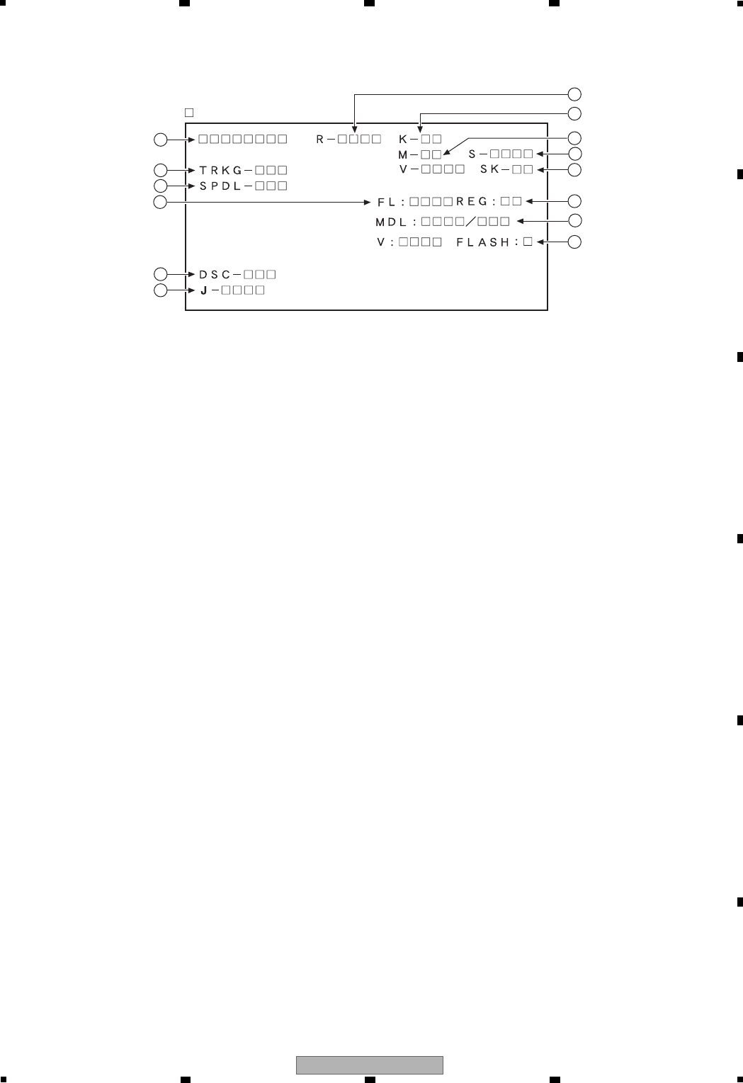
6.2 DISPLAY SPECIFICATIONS OF THE TEST MODE
Character in bold : Item name
: Information display
1
5
6
10
11
8
9
3
2
12
15
13
14
1 Address indication
The address being traced is displayed in number.
(as for the DVD, indication of decimal number is possible.)
DVD : ID indication (hexadecimal number, 8 digits)
[* * * * * * * *]
CD : ID indication [* * * * * * * *]
2 Code indication of remote control unit [R – * * * *]
In case of double code, display a 2nd code.
3 Main unit keycode indication [K – * *]
5 Tracking status [TRKG – * * *]
Tracking on : [ON]
Tracking off : [OFF]
6 Spindle status [SPDL – * * *]
CLV : [CLV]
Off : [OFF]
7 Mechanism (loading) position value [M – * *]
Unknown : [01] or [41]
Open state : [04]
Close state : [08]
During opening : [12]
During closing : [22]
8 Slider position [S – * * * *]
In Side Switch ON : [01]
In Side Switch OFF : [00]
9 Output video system [V – * * * *]
NTSC system : [NTSC]
PAL system : [PAL]
Automatic setting : [AUTO]
Scart terminal output [SK – * *]
(Display only the WY model which can do the output
setting of scart terminal.)
VIDEO : [00]
S-VIDEO : [01]
RGB : [02]
a Disc sensing [DSC – * * *]
The type of discs loaded is displayed.
[DVD], [CD ]
b Jitter value [J – * * * *]
Note: Don't use it.
c Version of the FL controller [FL: * * * *]
Note: Don't use it.
d Region setting of the player [REG: *]
Setting value : [1] to [6]
e Destination setting of the FL controller
[MDL: * * * * / * * *]
Four characters in the front represent code 01.
Three characters in the back represent the destination
code.
f Version of the flash ROM [V: * *. * *]
Flash ROM size [FLASH = * *]
7
J: Japan, K: North America, R: General Area,
LB: Taiwan, WY: Europe, TH: Thai, RAM: China
26 XV-DV575
12 3 4
A
B
C
D
E
F
12 3 4
6.3 FUNCTIONAL SPECIFICATIONS OF THE SHORTCUT KEY
Service mode indication (ESC + CHP/TIM keys)
ID Address
The error rate is always displayed in exponential notation, e.g., *.* * e - *, for both DVDs and CDs.
EDC/ID/AV 1 error history (ID Address, EDC/ID Error, last eight errors)
Calculation of the average error rate (ESC + "5" [Test mode remote control unit] keys)
The average of the last eight error rates is calculated and indicated in exponential notation. After the calculation is completed, "OK" or "NG" is
displayed. If "NG" is displayed, the disc tray will open (for both DVDs and CDs)
For DVDs: OK with 5.0e-4 or less, for CDs: OK with 7.6e-3 or less
Indication of model information (ESC + CHAP keys)
For details, see 6.4.
Region confirmation mode (ESC + A.MON [Test mode remote control unit] + "1"-"6" [Test mode remote control unit] keys)
After you press the A.MON key while holding the ESC key pressed and then input the region number, if the number is different from that set in
the unit, an error message is displayed, and the tray opens.
Command Contents Conditions Remote Control Key Name
Memory clear and region / revision indication CLEAR (*1)
Average value measurement of DVD error rate 5 (*1)
CD error rate measurement 5 (*1)
Scart terminal output : VIDEO
Models equipped with Scart terminal
AUDIO
Scart terminal output : S-VIDEO SUBTITLE
Scart terminal output : RGB ANGLE
Progressive OFF Only for progressive models
Only for HDMI models
R_SKIP
Progressive ONF_SKIP
FL indication of ID number STEREO (*1)
ZOOM ON (x4) ZOOM
Service mode indication (error rate indication, etc.) CHP/TIM (*1)
Model information indication CHAP (*1)
Title search Input mode IN
Title No. input
Search execution
SIDE A (*1)
Numbers (*1)
PLAY (*1)
Region confimation mode A.MON (*1)
Numbers (*1)
Only during normal playback, the following shortcut keys can be assigned by pressing a required key after pressing the ESC
key of the remote control unit. To quit, press the ESC key
*1 : Test mode remote control unit
HDMI Resolution : 1920 x 1080p PROGRAM
27
XV-DV575
56 7 8
56 7 8
A
B
C
D
E
F
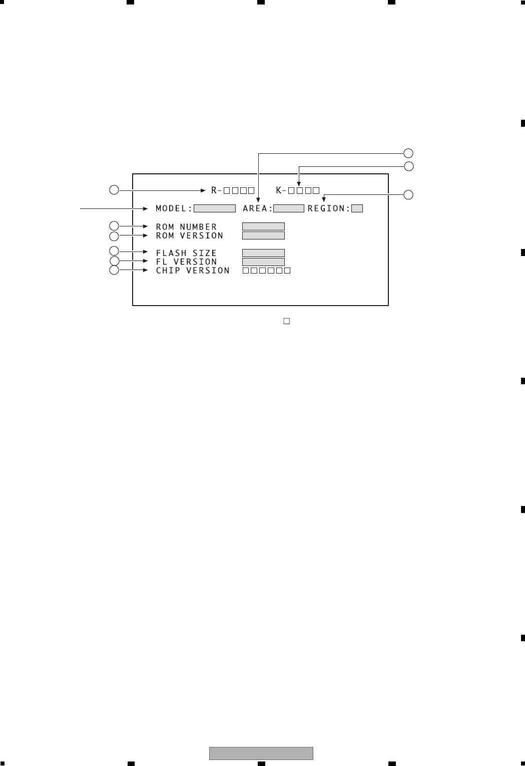
6.4 SPECIFICATIONS OF MODEL INFORMATION DISPLAY
• Display contents
Character in bold : Item name
: Information display
1
2
3
4
5
6
7
9
10
1 Destination indication
Display it according to model information set from the FL controller.
2 Region No.
3 Part number
4 ROM version
5 Flash size
6 FL controller version
7 CHIP VERSION
9 Remote control code
a Key code of Main unit
To display model information : Press the ESC key then the CHAP key.
To close the model information display : Press the ESC key.
Don't care.
28 XV-DV575
12 3 4
A
B
C
D
E
F
12 3 4
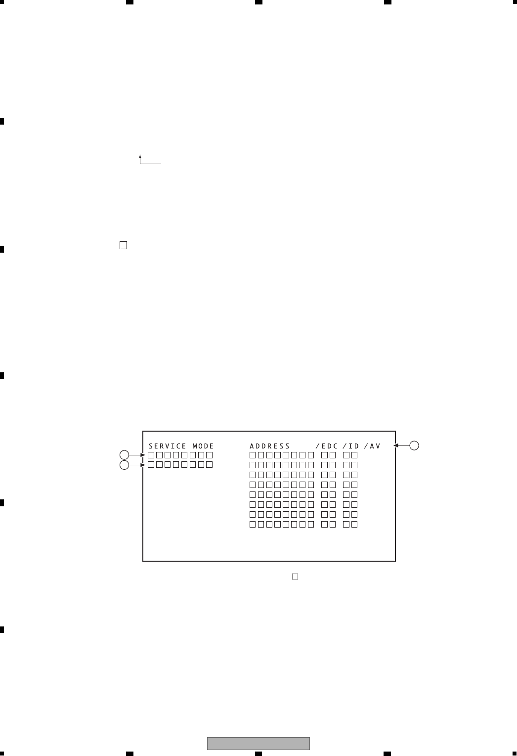
6.5 FUNCTIONAL SPECIFICATIONS OF THE SERVICE MODE
• Display during Service Mode
To enter Service Mode, press the CHP/TIM key while holding the ESC key pressed.
To quit, press the ESC key.
Service mode display
1 ID Address
2 Error rate (always displayed), in exponential notation
ERROR RATE : ∗ ∗ ∗ ∗ ∗ ∗ ∗
( ∗ ∗ ∗ ∗ )
• Calculation of the average error rate
For DVDs: OK with 5.0e-4 or less, for CDs: OK with 7.6e-3 or less
3 EDC/ID error history (ID Address, EDC/ID errors, last eight errors)
Note:
∗ Error of AV1 is not supported in this player.
Number of error
Indication plan contents
Character in bold : Item name
: Information display
1
2
3
ex) For DVDs
• Step 1
""e -
""e -6 : OK
""e -5 : OK
""e -4 : Refer to Step 2
""e -3 : NG
""e -2 : NG
• Step 2
""e -4
3.0e -4 : OK
4.0e -4 : OK
5.0e -4 : OK
6.0e -4 : NG
7.0e -4 : NG
29
XV-DV575
56 7 8
56 7 8
A
B
C
D
E
F
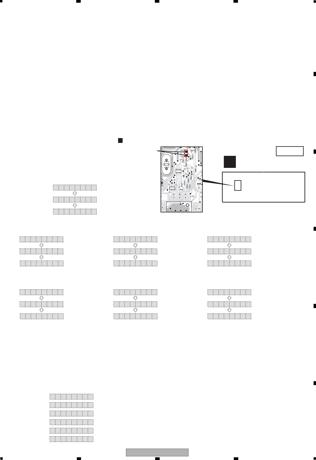
6.6 SERVICE TEST MODE
30
31 50
C5539
C
R5525
R5535
R5537
R5538
R5546
R5547
R5534
R5533 R5532
R5541
R5542
C
R5544
C5714
2
0
C5712
Q491
R491
X5701
STEST
UTEST
30
VE+5
V+5
V+10
• Emergency shut down will not happen even if breakdown happens in the Service Test mode. (Just ignore it)
• POWER ON in test mode can be done in less than 1 minute even when emergency shut down happens when error is
detected.
• Total power on time can be checked.
W E L C O M E
[After NORMAL POWER OFF]
[display]
V O L 0
V DD VS E R
P R T C T C TTE
[After AMP error]
[display]
V O L 0
V DD VS E R
[For DSP Model Only]
[Function]
(Digital input for Japan and IBD model, SCART for Europe)
DVD/CD
[display]
D V D P R R R
[After DVD error]
[display]
V O L 0
V DD VS E R
E E P E
[After EEPROM error]
[display]
V O L 0
V DD VS E R
O V E R T E M P O C E R R 1
[After ABNORMAL TEMP. DETECTION]
[display]
V O L 0
V DD VS E R
V DD VS E R
USB S BU VS E R
LINE1 N 1L VS E R
(Analog input for Japan and IBD model, digital for Europe)
LINE(2) N 2L VS E R
(Europe only, analog input)
LINE(3) N 3L VS E R
TUNER T X VS E R
[After OVERCURRENT DETECTION1]
[display]
V O L 0
O C E R R 2
V DD VS E R
[After OVERCURRENT DETECTION2]
[display]
V O L 0
V DD VS E R
1. Configuration and conditions during checking
• AC power on when the STEST port (pin 43) is set to HIGH (5 V).
∗ Initial function is DVD/CD.
• AC power on by pressing the STOP key and POWER key on the front panel at the same time.
The set will automatically power on and the following display will appear.
• The FL display during TEST MODE entry is different depending on whether NORMAL POWER OFF occurred before
entering the TEST MODE or EMERGENCY SHUT DOWN occurred due to error detection.
∗ Either POWER OFF or AC OFF to get out from TEST MODE.
∗ When the TEST MODE is released, only the RAM which stores the error status will be initialized.
(RAM that can be set by the user will not initialized.)
2. Switching to the Test Mode
• Basically, operation is the same as the NORMAL MODE.
However, the following display will be indicated when function is changed to show that the TEST MODE is in operation.
3. Operation
SIDE A
SYSMAIN ASSY
B
Service Test Mode connecting point
Connecting
point
30 XV-DV575
12 3 4
A
B
C
D
E
F
12 3 4
[For NON-DSP Model Only]
[Function]
(Europe)
DVD/CD
[display]
V DD VS E R
USB S BU VS E R
LINE1 N 1L VS E R
(general Line function)
LINE(2) N 2L VS E R
TUNER T X VS E R
• BREAKDOWN CATEGORY: Depends on the error displayed during POWER ON.
[Only for models without DSP]
• When function is switched to LINE 2 (LINE for areas beside Europe, Japan), SURROUND mode will switch to
X-STEREO (5CH STEREO) just for the TEST MODE. (NORMAL MODE: 2CH STEREO)
At this point, sound checking can't be done using HP.
(HP operation cannot be guaranteed for X-STEREO (5CH STEREO))
All functions, other than LINE2 (LINE for areas besides Europe) can be used for sound checking using HP.
[Models with DSP]
• Change the ADV mode to X-STEREO (5 ch STEREO) mode for multi CH output.
Protect circuit is operating.
1. Depending on the different power supply abnormalities, V+10, V+5, V+3R3 short-circuit occured or V+10, V+5, V+3R3
has exceeded the stipulated standardized values.
2. In the system microP (PDC175A, PDC176A) somewhere, the XPROTECT line has either shorted to ground or has
been disconnected.
4. Errors
P R T C T E
Abnormal DVD.
1. Depending on the power supply abnormalities, V+6R8, V+5V, V+3 short-circuit occured or V+6R8, V+5V, V+3 has
exceeded the stipulated standardized values.
2. In the system microP (PDC175A, PDC176A) somewhere, the VDET line has either short to ground or disconnected.
D V D P R CT T
1. Communication line to the EEPROM could either be disconnected or short.
2. The EEPROM IC itself could be faulty.
E E P E RR
• If error display does not come on again when POWER ON in the NORMAL MODE, this could mean that the speaker
terminal is short.
• If error display comes on, the following conditions are some possibilities:
1. In the AMP Block, either one or more of the digital amp IC has broken down.
2. Short-circuit occurred somewhere between the faulty IC(s) and speaker terminal.
3. The XSD SHUTDOWN line has either short to ground or disconnected somewhere between the faulty digital amp IC
and system microP (PDC175A, PDC176A).
O C E 1RR
• The error is mainly caused by the short circuit at the POWER SUPPLY Unit .
• The error will also occur when V+BSW is too low.
O C E 2RR
31
XV-DV575
56 7 8
56 7 8
A
B
C
D
E
F
• No abnormality if "OVERTEMP" display does not come on when POWER ON in the NORMAL MODE again.
(The TEMP could have just gone up temporarily. Try reducing the volume)
• When the "OVERTEMP" display comes on again, the following conditions are some possibilities:
1. In the AMP Block, either one or more of the digital amp IC has broken down.
2. The XOTW line has either short to ground or disconnected somewhere between the faulty digital amp IC(s) and
system microP (PDC175A, PDC176A).
O V E PMETR
• If STOP key is pushed continuously for 8 sec during POWER ON, the total POWER ON time will come on after the system
microp version display.
5. Total Power on Time Display
• During POWER ON, you can switch between DSP error display <=> Normal display when the SOUND key on the remote
control is pressed.
6. DSP Error Display (for models with DSP only)
P D C 1 7 5 A
System microP version
POWER ON TIME
Approx. 3 seconds later
1 0 3H 0 M
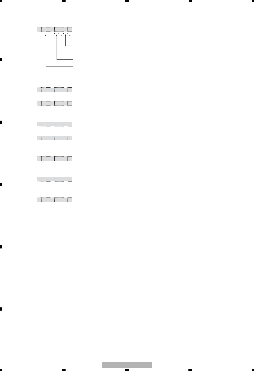
32 XV-DV575
12 3 4
A
B
C
D
E
F
12 3 4
6.7 DISPLAY SPECIFICATIONS OF DSP ERROR
Press "SOUND" button in service test mode to show DSP error message displays.
Press "SOUND" again to select normal service test mode.
This means that the usual function of "SOUND" is not effective in the service test mode.
_ _ _ _ - U M 9
[FL display]
- U MREID
ERR.0 Cannot receive data from the DIR
--> Probably due to faulty DIR or bad connection
- U MRESD
ERR.1 Cannot receive data from the DSP
--> Faulty communication between DIR and DSP
--> Probably due to faulty DSP or connection on the circuit board
- U MQERH
ERR.2 No HREQ return value
--> Probably due to faulty DSP
- U MGNSD
ERR.3 DSP error message
--> Faulty communication between the DIR and DSP
--> Probably due to faulty DSP
- MTUMD
ERR.4 DECMUTE on all the time
--> Faulty communication between the DIR and DSP
--> Probably due to faulty DSP
- 9KOSD
NO ERR
(the source is 88.2/96 kHz.)
96 kHz source play
-KOSD
NO ERR
(the source is not 88.2/96 kHz.)
No abnormality
[Example]
96k (This character is displayed while the source is 88.2 or 96 kHz PCM)
DSP MUTE (This character is displayed while DSPMUTE is active)
DIR UNLOCK (This character is displayed while DIR is UNLOCK)
Space
The name of an error is displayed by four characters.
DSP error message mode
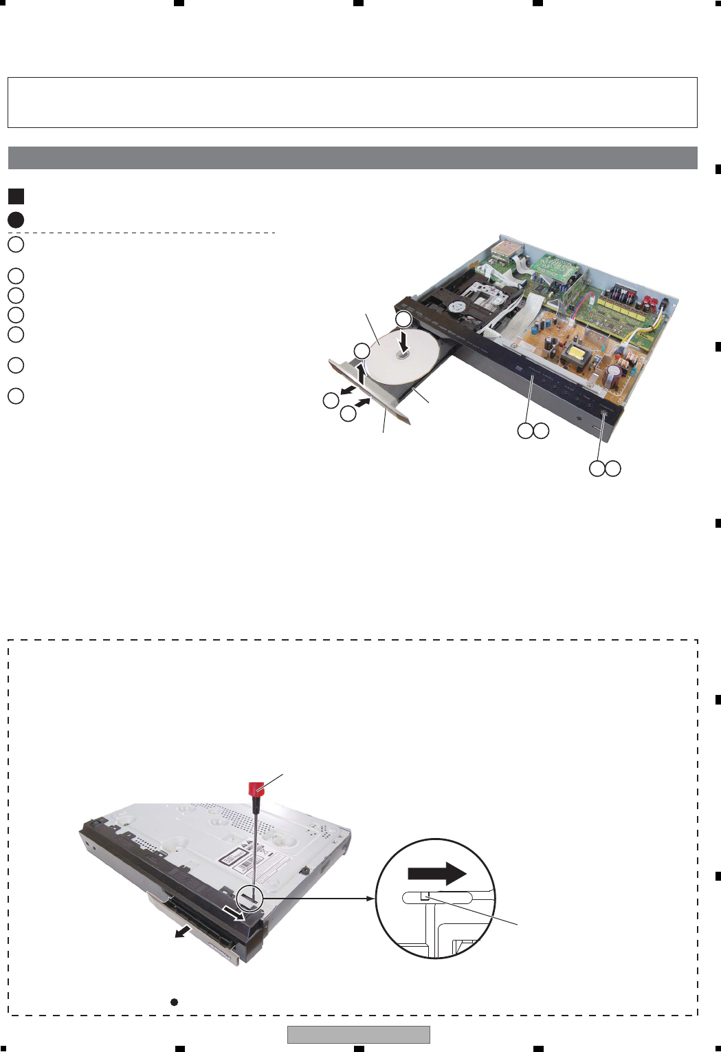
33
XV-DV575
56 7 8
56 7 8
A
B
C
D
E
F
7. DISASSEMBLY
Bonnet, Tray Panel
1
Tray panel
Test disc
Tray
How to open the tray when the power cannot be on
Disassembly
Note 1: Do NOT look directly into the pickup lens. The laser beam may cause eye injury.
Note 2: Even if the unit shown in the photos and illustrations in this manual may differ from your product, the procedures
described here are common.
Bottom view
Press the u STANDBY/ON button to turn on the
power.
1
Remove the bonnet by removing the nine screws.
1
Press the h OPEN/CLOSE button to open the tray.
2
Remove the tray panel.
3
Set the test disc.
4
Press the h OPEN/CLOSE button to close the tray.
(Test disc is clamped.)
5
Press the u STANDBY/ON button to turn off the
power.
6
Pull out the Power cord.
7
4
3
25
61
52
1. Slide the rack, loading (White) toward the arrow direction by using a minus screwdriver to release the lock.
2. Manually open the tray.
NOTE:
Please strongly pushing rack, loading (White) to release the lock because the tray doesn't go out easily.
Rack, loading (White)
Tray open
Minus screwdriver
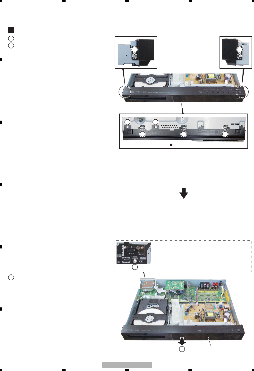
34 XV-DV575
12 3 4
A
B
C
D
E
F
12 3 4
Front Panel Section
2
Remove the two screws.
1
Unhook the five hooks.
2
Remove the front panel section.
3
1 1
A
2
2 2
2 2
3
Note A: Do not use an electric screwdriver.
If the screws are over-tightened, the
screw threads may be damaged.
Front panel section
Bottom view
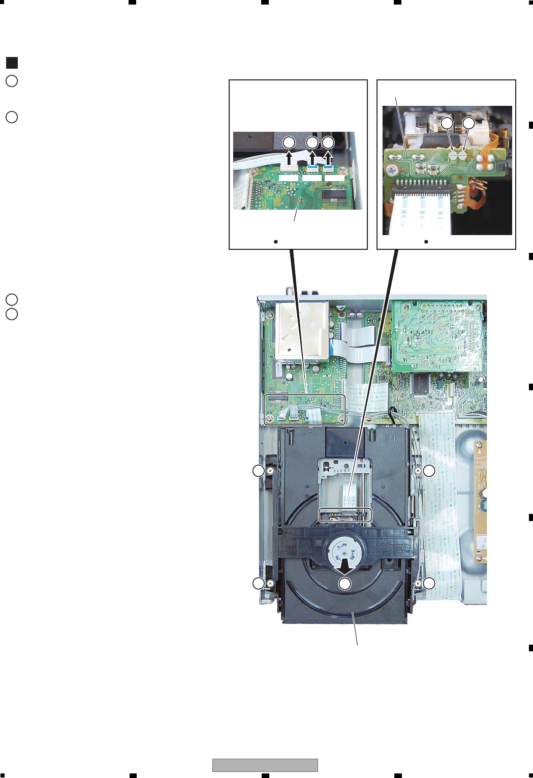
35
XV-DV575
56 7 8
56 7 8
A
B
C
D
E
F
DVD MECHA Assy
3
Short-circuit two positions soldering.
1
Disconnect the three flexible cables.
2
Remove the four screws.
3
Remove the DVD MECHA Assy.
4
1
Pickup PCB
08 DVDM Assy
CN966 CN964 CN965
DVD MECHA Assy
Rear viewRear view
1
Note: After replacement, connect the flexible cable,
then remove the soldered joint (open).
2 2 2
3
3
3
3
4
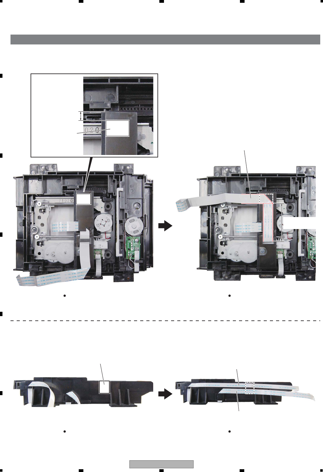
36 XV-DV575
12 3 4
A
B
C
D
E
F
12 3 4
Arrangement of The Flexible Cables
Double sided tape
(ZTB-500-10)
Length: 15 mm
5 mm
from the edge
Flexible cable
Length: 50 mm
Double sided tape
(ZTB-500-10)
Length: 20 mm
Bottom view Bottom view
Right view Right view
Flexible cable for PICKUP
Flexible cable for LOADING
Flexible cable for FEED

37
XV-DV575
56 7 8
56 7 8
A
B
C
D
E
F
Removal of DVD MECHA Assy Parts
Fig. 1-A
Tray
Push to Sag
Push to Sag
LOADER Assy
Fig. 2-A
Tray
LOADER Assy
Fig. 1-B
Insulator (R)
TRAVERSE Assy
LOADER SUB Assy
Fig. 2-B
Check Lock
TRAVERSE Assy
Rack Loading
LOADER Assy (Bottom Side)
Holder Traverse
Fig. 2-C
LOADER Assy
Check Hook
Loading Belt
LOADING SUB Assy
Gear Pulley
Fig. 3-A
LOADING MOTOR PCB Assy
• Screw Torque: 2.0 ± 0.3 kgf•cm
• Screw Torque: 2.5 ± 0.3 kgf•cm (Screw 1)
• Screw Torque: 1.0 ± 0.3 kgf•cm (Screw 2)
Loading Motor
NOTE
Disassemble only the DVD MECHA Assy parts listed here.
Minute adjustments are needed if the disassembly is done.
If the repair is needed except listed parts, replace the DVD
MECHA Assy.
1: TRAY (Refer to Fig. 1-A)
1. Set the Tray opened. (Refer to the DISC REMOVAL
METHOD AT NO POWER SUPPLY)
2. Unlock the 2 supports 1 and draw it while sagging the
Tray.
NOTE
1. In case of the TRAVERSE Assy, install it from (1) to (4)
in order. (Refer to Fig. 2-B)
2. In case of the TRAVERSE Assy installation, hook the
wire on the LOADER Assy as shown Fig. 2-C.
3: LOADING MOTOR PCB Assy / LOADING BELT
(Refer to Fig. 3-A)
1. Remove the Loading Belt.
2. Remove the screw 1.
3. Remove the LOADING MOTOR PCB Assy.
4. Remove the 2 screws 2.
5. Remove the Loading Motor.
6. Remove the Gear Pulley.
NOTE
1. In case of the Tray installation, install them as the circled
section of Fig. 1-B so that the each markers are met.
2: TRAVERSE ASSY (Refer to Fig. 2-A)
1. Remove the screw 1.
2. Unlock the 2 supports 2.
3. Remove the Insulator (R) from the LOADER SUB Assy.
4. Remove the TRAVERSE Assy.
1
1
2
2
1
22

38 XV-DV575
12 3 4
A
B
C
D
E
F
12 3 4
NOTE
1. In case of the Pulley Motor installation, check if the
value of the Fig. 3-B is correct.
2. When installing the wire of the LOADING MOTOR PCB
Assy, install it correctly as Fig. 3-C.
Manual soldering conditions
• Soldering temperature: 320 ± 20 °C
• Soldering time: Within 3 seconds
• Soldering combination: Sn - 3.0 Ag - 0.5 Cu
3. When installing the LOADING MOTOR PCB Assy, install
itcorrectly as Fig. 3-D.
4. In case of the LOADING MOTOR PCB Assy installation,
hook the wire on the LOADER SUB Assy as shown Fig.
3-E.
4: RACK LOADING / MAIN GEAR / PULLEY GEAR
(Refer to Fig. 4-A)
1. Unlock the support 2 and remove the Gear Pulley.
2. Remove the Gear Main.
3. Press down the catcher 1 and slide the Rack Loading.
NOTE
1. In case of the Rack Loading installation, hook the Rack
Loading on the LOADER SUB Assy as shown Fig. 4-B.
2. When installing the Gear Main, take care the direction
of up or down as shown Fig. 4-C.
5: CLAMPER ASSY (Refer to Fig. 5-A)
1. Press the Clamper and rotate the Plate Clamper
clockwise, then unlock the 3 supports 1.
2. Remove the Plate Clamper, Magnet Clamper and
Clamper.
BROWN (1)
WHITE (2)
Fig. 3-B
7.0 ± 0.1 mm
Safety surface for pressing
of the insert.
Loading Motor
Pulley Motor
Check Hook
LOADING MOTOR PCB Assy
LOADING MOTOR PCB Assy Fig. 3-C
Fig. 3-E
Check Hook
Fig. 3-D
Rack Loading
BA
The Lever should be position
between A and B.
Check Hook
Rack Loading
LOADING SUB Assy
Gear Main
Gear Pulley
Fig. 4-A
Fig. 4-B
Rack Loading
Check Hook
Fig. 4-C
Main Gear
Up Side
Down Side
Plate Clamper
Magnet Clamper
Fig. 5-A
Main Frame
Clamper
LOADER SUB Assy (Bottom Side)
1
1
1
1
2

39
XV-DV575
56 7 8
56 7 8
A
B
C
D
E
F
NOTE
1. In case of the Clamper Assy installation, install correctly
as Fig. 5-B.
NOTE
1. In case of the Insulator (F) installation, install correctly
as Fig. 6-B.
6: HOLDER TRAVERSE/INSULATOR (F)/INSULATOR (R)
(Refer to Fig. 6-A)
1. Remove the Holder Traverse.
2. Remove the 2 Insulator (F).
3. Remove the Insulator (R).
7: SW PCB ASSY/GEAR MIDDLE/GEAR FEED/
RACK FEED ASSY/FEED MOTOR
(Refer to Fig. 7-A)
1. Unlock the support 1.
2. Remove the Gear Middle.
3. Remove the screw 2.
4. Remove the Rack Feed Assy.
5. Remove the screw 3.
6. Remove the SW PCB Assy.
7. Remove the screw 4.
8. Remove the Gear Feed.
9. Remove the 2 screws 5.
10. Remove the Feed Motor.
11. Remove the Gear Motor.
NOTE
1. When installing the Rack Feed Assy, push both ends to
align the teeth as shown Fig. 7-B. Then install it.
2. In case of the Gear Motor installation, check if the value
of the Fig. 7-C is correct.
3. When installing the wire of the SW PCB Assy, install it
correctly as Fig. 7-D.
Manual soldering conditions
• Soldering temperature: 320 ± 20 °C
• Soldering time: Within 3 seconds
• Soldering combination: Sn - 3.0 Ag - 0.5 Cu
4. After the assembly of the TRAVERSE Assy, hook the
wire on the TRAVERSE Assy as shown Fig. 7-E.
15
5
4
2
3
Holder Traverse
Insulator (F)
TRAVERSE Assy
Insulator (F)
Insulator (R)
Fig. 5-B
Plate Clamper
Clamper
Fig. 6-A
Fig. 6-B
Traverse Holder
Insulator (F)
Gear Middle
Gear Motor
Feed Motor
• Screw Torque: 1.3 ± 0.3 kgf•cm (Screw 2)
• Screw Torque: 3.0 ± 0.3 kgf•cm (Screw 3)
• Screw Torque: 1.0 ± 0.3 kgf•cm (Screw 4, 5)
SW PCB Assy
Rack Feed Assy
Gear Feed
Fig. 7-A
TRAVERSE Assy
[OK] [NG]
Fig. 7-B
Rack Feed Assy
Push
Push
Fig. 7-C
8.0 ± 0.2 mm
Safety surface for pressing
of the insert.
Feed Motor
Gear Motor
Check Lock
Pickup lens
GEM1004
GED-008
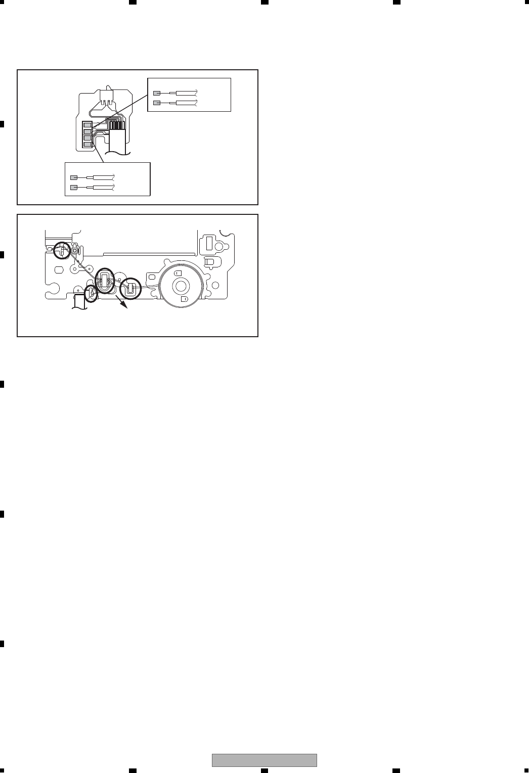
40 XV-DV575
12 3 4
A
B
C
D
E
F
12 3 4
TRAVERSE Assy
• Loosen the wire in the direcion of the arrow.
Check Hook
Fig. 7-E
~ FEED MOTOR ~
WHITE (4)
BROWN (3)
~ SPINDLE MOTOR ~
YELLOW (2)
GREEN (1)
Fig. 7-D
SW PCB Assy

41
XV-DV575
56 7 8
56 7 8
A
B
C
D
E
F
8. EACH SETTING AND ADJUSTMENT
8.1 ID NUMBER AND ID DATA SETTING
This display appears when the PLAY key is pressed in Step 4.
Enter a 9-digit number to compare. The number is also
displayed on the FL display.
6
By pressing the CLEAR key without having input a number, the
unit returns to Step 2 without doing anything else. Each press
of this key after a number has been input deletes one digit.
7
After entering all 9 digits, if you press the PLAY key, the unit
compares the numbers input in Steps 2 and 6, and only if the
numbers match, that number is set as the ID. Then the unit
automatically enters ID DATA Input Mode. If the numbers do not
match, the disc tray is opened, and the unit exits ID Number
Input Mode.
8
[Player's ID Number Setting]
ID Number ?
0 0 0 0 0 0 0 0 1
Compare
∗ ∗ ∗ ∗ ∗ ∗ ∗ ∗ ∗
Input ID Number !
6
[Player's ID Number Setting]
ID Number ?
0 0 0 0 0 0 0 0 1
Compare
0 0 0 0 0 0 0 0 1
<PLAY> Enter
Input ID Number !
8
Input ID Number !
After entering all 9 digits, if you press the SEARCH key, the
unit unconditionally sets the input number as the ID number.
Then the unit automatically enters Player's Data Input Mode.
(The SEARCH key is not accepted after all 9 digits have been
entered.)
5
[Player's ID Number Setting]
ID Number ?
0 0 0 0 0 0 0 0 1
<PLAY> Compare Mode
<SEARCH> Enter
4
5
Caution:
For the DVD players compatible with DVD-RW, for playback of a DVD-RW disc (CPRM) and for the DVD players possessing
HDMI output, for HDCP process, it is necessary that an individual ID number and ID data are set for each player. If the ID
number and ID data be not properly set in the manner described below, future operations cannot be guaranteed. The ID
number is written on the yellow label at the rear panel of the player.
If there is no yellow label, before downloading FLASH ROM, take note of the ID number set following the procedures
outlined in "ID Number Confirmation Mode" on the next page.
Note: Enter ID numbers while the unit is in Stop mode so that the values set will be immediately written to the flash ROM.
Note: If you press the PLAY button before inputting a 9-digit ID
number, the unit returns to Step 6 without doing anything
else.
To enter ID Number Input Mode, with no ID number set, such as
in a case of immediately after upgrading the firmware, press the
ESC key then the STEREO key.
Note: If a previous ID number and ID data, such as a factory-
preset ID number and ID data, are maintained, the unit
enters ID Number Confirmation Mode when the above keys
are pressed. However, if only an ID number is maintained,
the unit enters ID Data Input Mode.
ID Number Input Mode
[Player's ID Number Setting]
ID Number ?
- - - - - - - - -
<CLEAR> Exit
Input ID Number !
1
Enter a 9-digit ID number. The ID number is also displayed on
the FL display.
2
By pressing the CLEAR key without having input a number, you
can exit this mode. Each press of this key after a number has
been input deletes one digit.
3
After entering all 9 digits, if you press the PLAY key, the unit
enters Compare mode. Enter the same ID number again. Only
if your two input numbers match, the ID number is set. Compare
mode helps eliminate mistyping of the ID number.
4
2
3
Note: If you press the PLAY button before inputting a 9-digit ID
number, the unit returns to Step 2 without doing anything
else.
Setting an ID number or ID data is required in the
following case:
If "No NUM" or "NO DATA" is displayed on the FL display
for a few seconds immediately after the power to the player
is turned on or during Stop mode.
JIGS AND MEASURING INSTRUMENTS
DVD Data Disc
[GGV1309]
Service Remote Control Unit
[GGF1381]
42 XV-DV575
12 3 4
A
B
C
D
E
F
12 3 4
To enter ID Number Confirmation Mode after the ID number and
the ID data are set, press the ESC key then the STEREO key.
ID Number Confirmation Mode
1
The ID number already set is displayed.
(It is also displayed on the FL display.)
2
Enter a 9-digit number for comparison. This is not required
when you only wish to check the ID number visually.
(The number is also displayed on the FL display.)
3
By pressing the CLEAR key without having input a number, you
can exit this mode. Each press of this key after a number has
been input deletes one digit.
4
After entering all 9 digits, if you press the PLAY key, the unit
compares the number entered in Step 2 with the ID number
set, and only if the numbers match, the unit automatically exits
ID Number Confirmation Mode. If an ID data has not been
entered, the unit enters ID DATA Input Mode. If the numbers do
not match, the disc tray is opened, and the unit exits ID Number
Confirmation Mode.
5
After entering all 9 digits, if you press the STOP key, the unit
compares the number entered in Step 3 with the ID number
set, and only if the numbers match, the unit automatically
deletes the ID number and exits this mode. If the numbers do
not match, the disc tray is opened, and the unit exits this mode.
(The STOP key is not accepted after all 9 digits have been
entered.)
6
[Player's ID Number Setting]
ID Number ?
0 0 0 0 0 0 0 0 1
Compare
∗ ∗ ∗ ∗ ∗ ∗ ∗ ∗ ∗
<CLEAR> Exit
Input ID Number !
3
2
4
[Player's ID Number Setting]
ID Number ?
0 0 0 0 0 0 0 0 1
Compare
0 0 0 0 0 0 0 0 1
<PLAY> Enter
<STOP> Memory Clear
Input ID Number !
5
6
Note: If you press the PLAY button before inputting a 9-digit ID
number, the unit returns to Step 4 without doing anything
else.
• Indication of an ID number already set
An ID number already set is displayed in the following cases:
1) When the ESC key then the CLEAR key are pressed, user
settings are cleared, then the ID number set is displayed on
the screen. In this case, the ID number is not displayed on the
FL display.
2) When the unit enters ID Number Confirmation Mode by your
pressing the ESC key then the CLEAR key, the ID number set
is displayed. In this case, the ID number is also displayed on
the FL display.
If you only need to confirm the ID number, you can exit
this mode by pressing the CLEAR key or turning off the power.
• Indication when no ID number is set
If no ID number is set, the message "No NUM" flashes on the
screen and FL display for a few seconds after the power is turned
on or during Stop mode.
43
XV-DV575
56 7 8
56 7 8
A
B
C
D
E
F
To enter ID DATA Input Mode, with the ID number set, press the
ESC key then the STEREO key.
ID DATA Input Mode
NOTE: Be sure to use a specified DVD (ID) DATA DISC.
1When writing of the data read from the disc to flash ROM is
completed, "Rom Write OK!" is displayed. After seeing this
message, you can exit this mode by pressing the CLEAR key.
5
If the data cannot be read from the disc, the unit will be exited
ID Data Input Mode and proceed to the display of “Pioneer”
logo.
6
When the STEREO key is pressed, the unit enters ID DATA
Input Mode.
2
If the DVD DATA DISC is loaded in this mode, the unit
automatically starts reading the data.
(If the DVD DATA DISC has already been loaded, the unit does
not start reading the data. In this case, open then close the
tray.)
3
To exit this mode, press the CLEAR key. While data are being
read from the DVD DATA DISC, you cannot exit this mode.
4
[Player's ID Number Setting]
ID Number ?
[ 0 0 0 0 0 0 0 0 1 ]
Compare
> ∗ ∗ ∗ ∗ ∗ ∗ ∗ ∗ ∗
<CLEAR> Exit
<STEREO> ID Data Setting Mode
Input ID Number !
2
[Player's Data Input Mode]
<CLEAR> Exit
Insert The ID Data Disc !
4
[Player's Data Input Mode]
Rom Write OK!
<CLEAR> Exit
5
Note: Whether or not the data have been written to flash ROM can
be confirmed by watching for the message "Rom Write OK!"
being displayed after the disc is read.
• Indication when the data have not been set
If no ID data are set after the ID number is changed, the message
"NO DATA" flashes on the screen and FL display for a few seconds
after the power is turned on or during Stop mode.
44 XV-DV575
12 3 4
A
B
C
D
E
F
12 3 4
9. EXPLODED VIEWS AND PARTS LIST
9.1 PACKING SECTION
NOTES:
-
Parts marked by “NSP” are generally unavailable because they are not in our Master Spare Parts List.
-
The > mark found on some component parts indicates the importance of the safety factor of the part.
Therefore, when replacing, be sure to use parts of identical designation.
-
Screws adjacent to b mark on product are used for disassembly.
-
For the applying amount of lubricants or glue, follow the instructions in this manual.
(In the case of no amount instructions, apply as you think it appropriate.)
Joint
1/2
for XV-DV580/WVXJ5
XV-DV575/WYXJ5,
XV-DV580/WYXJ5
only
for
XV-DV575/WYXJ5, XV-DV580/WYXJ5,
XV-DV385K/WSXJ5, XV-DV395K/WSXJ5
XV-DV575 and
XV-DV580 only
1/2
2/2
2/2
XV-DV580/WVXJ5
only
XV-DV575/WYXJ5,
XV-DV580/WYXJ5
only
XV-DV585K/WSXJ5,
XV-DV595K/WSXJ5
only
XV-DV585K/WSXJ5,
XV-DV595K/WSXJ5
only
XV-DV580/WVXJ5
only
45
XV-DV575
56 7 8
56 7 8
A
B
C
D
E
F
(1) PACKING SECTION PARTS LIST
(2) CONTRAST TABLE
XV-DV575/WYXJ5, XV-DV580/WYXJ5, WVXJ5, XV-DV385K/WSXJ5 and XV-DV395K/WSXJ5 are constructed the
same except for the following:
Mark No. Description Part No.
>1Power Cord See Contrast table (2)
2 Video Cable XDE3046
3 FM Antenna ADH7030
4 AM Loop Antenna ATB7013
5 Microphone See Contrast table (2)
(for Audio MCACC setup)
6 Remote Control See Contrast table (2)
7 Battery Cover AZN8018
NSP 8 Dry Cell Battery (AA/R6) XEX3002
9Label (WEEE) ARW7322
10 Operating Instructions See Contrast table (2)
(English, French)
11 Operating Instructions See Contrast table (2)
(German, Italian)
12 Operating Instructions See Contrast table (2)
(Dutch, Spanish)
13 Operating Instructions See Contrast table (2)
(English)
14 Operating Instructions See Contrast table (2)
(Russian)
15 Setup Guide (English, French) See Contrast table (2)
16 Setup Guide (German, Italian) See Contrast table (2)
17 Setup Guide (Dutch, Spanish) See Contrast table (2)
18 Setup Guide (English) See Contrast table (2)
19 Setup Guide (Russian) See Contrast table (2)
NSP 20 Warranty Card EU ARY7111
NSP 21 Polyethylene Bag AHG7117
(0.06 x 230 x 340)
22 Packing Sheet AHG7053
23 Pad L WHTS XHA3177
24 Pad R WHTS XHA3178
25 Packing Case See Contrast table (2)
Mark No. Description Part No.
Mark No. Symbol and Description XV-DV575
/WYXJ5
XV-DV580
/WYXJ5
XV-DV580
/WVXJ5
XV-DV385K
/WSXJ5
XV-DV395K
/WSXJ5
>1Power Cord ADG1127 ADG1127 ADG7108 ADG1127 ADG1127
5 Microphone (for Audio MCACC setup) APM7008 APM7008 APM7008 Not used Not used
6 Remote Control XXD3159 XXD3159 XXD3159 XXD3156 XXD3156
10 Operating Instructions (English, French) XRE3182 XRE3182 Not used Not used Not used
11 Operating Instructions (German, Italian) XRC3335 XRC3335 Not used Not used Not used
12 Operating Instructions (Dutch, Spanish) XRC3336 XRC3336 Not used Not used Not used
13 Operating Instructions (English) Not used Not used XRB3094 Not used Not used
14 Operating Instructions (Russian) Not used Not used Not used XRC3333 XRC3333
15 Setup Guide (English, English) XRE3181 XRE3178 Not used Not used Not used
16 Setup Guide (German, Italian) XRC3334 XRC3346 Not used Not used Not used
17 Setup Guide (Dutch, Spanish) XRC3344 XRC3349 Not used Not used Not used
18 Setup Guide (English) Not used Not used XRB3099 Not used Not used
19 Setup Guide (Russian) Not used Not used Not used XRC3343 XRC3345
25 Packing Case XHD3789 XHD3821 XHD3821 XHD3787 XHD3788
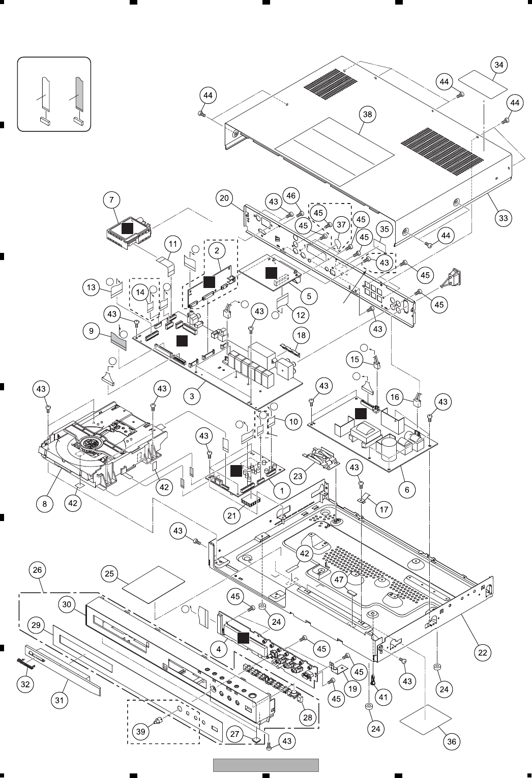
46 XV-DV575
12 3 4
A
B
C
D
E
F
12 3 4
9.2 EXTERIOR SECTION
CONTACT SIDE
NON-CONTACT
SIDE
A
D
F
E
G
A
B
A
D
F
F
D
B
G
G
B
C
E
E
C
C
Refer to
"9.3 DVD MECHA ASSY".
XV-DV385K,
XV-DV395K only
XV-DV385K,
XV-DV395K only
* Part No. 21 (Heat sink WHTS)
should be replaced each time
a new IC (08 DVDM ASSY IC201)
is being replaced.
*
XV-DV385K,
XV-DV395K
only
XV-DV575,
XV-DV580 only
XV-DV575,
XV-DV580 only
XV-DV575,
XV-DV580
only
47
XV-DV575
56 7 8
56 7 8
A
B
C
D
E
F
(1) EXTERIOR SECTION PARTS LIST
(2) CONTRAST TABLE
XV-DV575/WYXJ5, XV-DV580/WYXJ5, WVXJ5, XV-DV385K/WSXJ5 and XV-DV395K/WSXJ5 are constructed the
same except for the following:
Mark No. Description Part No.
1 08 DVDM Assy See Contrast table (2)
2 DSP Assy See Contrast table (2)
3 SYSMAIN Assy See Contrast table (2)
4 COMPLEX Assy See Contrast table (2)
5 EUROSCART Assy AWU8291
>6 POWER SUPPLY Unit XWR3018
7 FM/AM TUNER Unit AXX7248
8 DVD MECHA Assy A2ZX01A650
9 FFC/60V (J1904) See Contrast table (2)
10 17P FFC/60V (J1905) XDD3263
11 11P FFC/60V (J1908) XDD3266
12 23P FFC/60V (J1909) XDD3267
13 27P FFC/60V (J1907) XDD3290
14 13P FFC/60V (J1906) See Contrast table (2)
15 Cable Assy (J1901) XDX3067
>16 Cable Assy (J1903) XDX3068
17 Earth Spring W5.1 ABH7240
18 GND Plate W5.1 ABH7241
19 Ground Plate WHTS XBH3018
20 Rear Panel WHTS See Contrast table (2)
21 Heatsink WHTS XNH3049
NSP 22 Chassis WHTS XNA3061
23 Radiation Plate XNG3183
NSP 24 Spacer AEB7092
NSP 25 Guide Sheet XAK3603
26 F/P Assy WHTS See Contrast table (2)
27 Rubber Foot VEB1325
28 Button WHTS XAD3264
NSP 29 Display Window WHTS See Contrast table (2)
NSP 30 Front Panel WHTS See Contrast table (2)
31 Tray Panel WHTS See Contrast table (2)
32 Pioneer Name Plate XAM3009
33 Bonnet WHTS XZN3201
34 Laser Caution VRW2257
NSP 35 ID Label Assy VXW1012
NSP 36 Name Label WHTS See Contrast table (2)
37 Control Label See Contrast table (2)
NSP 38 POP Getter WHTS See Contrast table (2)
39 MIC KnobSee Contrast table (2)
40 • • • • •
41 Locking Card Spacer AEC7372
NSP 42 Double Sided Tape • • • • •
43 ScrewBBZ30P080FNI
44 ScrewBBZ30P080FTB
45 ScrewBPZ30P080FNI
46 ScrewBSZ30P060FTC
NSP 47 Spacer XEB3115
Mark No. Description Part No.
Mark No. Symbol and Description XV-DV575
/WYXJ5
XV-DV580
/WYXJ5
XV-DV580
/WVXJ5
XV-DV385K
/WSXJ5
XV-DV395K
/WSXJ5
1 08 DVDM Assy AWM8118 AWM8118 AWM8118 AWM8105 AWM8105
2 DSP Assy AWX8706 AWX8706 AWX8706 Not used Not used
3 SYSMAIN Assy XWM3392 XWM3395 XWM3395 XWM3391 XWM3394
4 COMPLEX Assy XWM3429 XWM3429 XWM3429 XWM3428 XWM3428
9 27P FFC/60V (J1904) XDD3261 XDD3261 XDD3261 Not used Not used
9 29P FFC/60V (J1904) Not used Not used Not used XDD3260 XDD3260
14 13P FFC/60V (J1906) Not used Not used Not used XDD3264 XDD3264
20 Rear Panel WHTS XNC3572 XNC3574 XNC3574 XNC3564 XNC3571
26 F/P Assy WHTS XXG3370 XXG3371 XXG3371 XXG3368 XXG3369
NSP 29 Display Window WHTS XAK3602 XAK3602 XAK3602 XAK3600 XAK3600
NSP 30 Front Panel WHTS XMB3328 XMB3329 XMB3329 XMB3326 XMB3327
31 Tray Panel WHTS XAK3604 XAK3604 XAK3604 XAK3601 XAK3601
NSP 36 Name Label WHTS XAL3296 XAL3297 XAL3297 XAL3294 XAL3295
37 Control Label XAX3620 XAX3620 XAX3620 Not used Not used
NSP 38 POP Getter WHTS XAX3677 XAX3700 XAX3700 XAX3676 XAX3686
39 MIC KnobNot used Not used Not used XAA3029 XAA3029
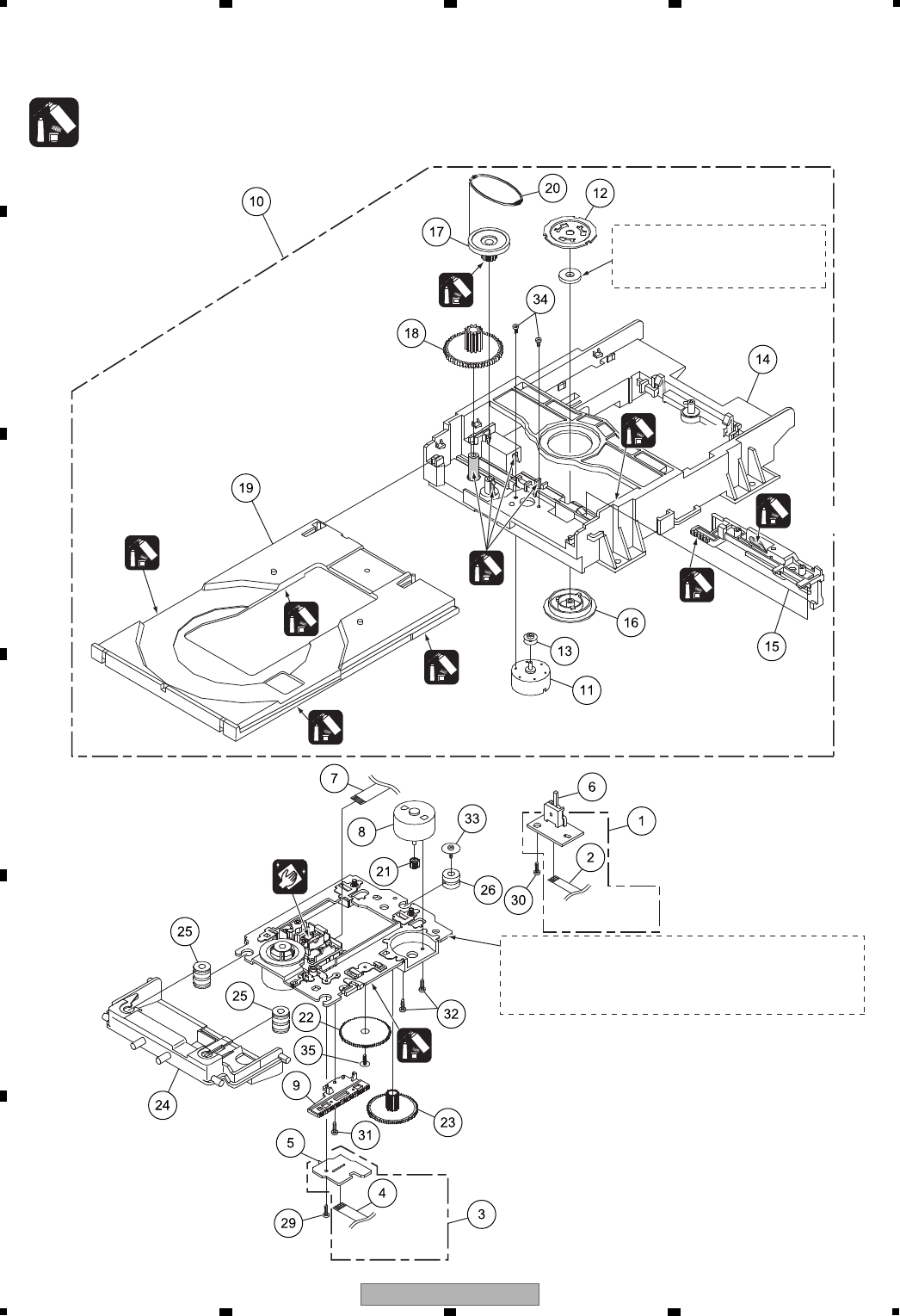
48 XV-DV575
12 3 4
A
B
C
D
E
F
12 3 4
9.3 DVD MECHA ASSY
Grease
GEM1018
Pickup lens
GEM1004
GED-008
To
08 DVDM Assy
CN964
To
08 DVDM Assy
CN965
To
08 DVDM Assy
CN966
Do not replace the parts.
Because, minute adjustments are needed if this condition
is disassembled further more.
If the repair is needed, replace the DVD MECHA Assy.
Cannot supply separately.
If the repair is needed, replace
the LOADER SUB Assy.
Daifree
GEM1036
Daifree
GEM1036
Lubricating oil
GYA1001
Lubricating oil
GYA1001
Lubricating oil
GYA1001
Lubricating oil
GYA1001
Lubricating oil
GYA1001
PCB640
(SW PCB Assy)
PCB610
(LOADING MOTOR PCB Assy)
SW2
SW1
Lubricating oil
GYA1001
Lubricating oil
GYA1001
Note :
Check if the correct grease is applied for each position.

49
XV-DV575
56 7 8
56 7 8
A
B
C
D
E
F
DVD MECHA ASSY PARTS LIST
Mark No. Description Part No.
1 LOADING MOTOR PCB Assy A2ZX01A610
2 Cord Jumper (5P) 12C1053601
3 SW PCB Assy A2ZX01A640
4 Cord Jumper (6P) 12C1063201
5Switch (SW2) 0500101036
6Switch (SW1) 0515S32003
7 Cord Jumper (24P) 122F003101
8 FEED Motor 1515T98006
9 Feed Rack Assy 92AAA0017A
10 LOADER SUB Assy 92AAA0024A
11 LOADING Motor 1515S98004
12 Plate, Clamper 92P000023A
13 Pulley, Motor 92P100097A
14 Frame, Main 92P100119A
15 Rack, Loading 92P100121A
16 Clamper 92P100122A
17 Gear, Pulley 92P100123A
18 Gear, Main 92P100124A
19 Tray 92P100151A
20 Belt, Loading 92P200015A
21 Gear, Motor 92P100088A
22 Gear, Feed 92P100116A
23 Gear, Middle 92P100117A
24 Holder, Traverse 92P100125A
25 Insulator (F) 92P200013A
26 Insulator (R) 92P200016A
27 • • • • •
28 • • • • •
29 Screw, Bind (2 x 8) 811022080U
30 Screw, Tap tite (P)(2.6 x 8) 811022680U
31 Screw, T-tite (B)(M1.7 x 5.0 P3) 813381750U
32 Screw, Pan (M1.7 x 2.3 P3) 814011723U
33 Screw, Tap tite (P)(2 x 8) 816112080U
34 Screw, Pan (M1.7 x 3 P3) 814011730U
35 Screw, Gear Feed 92P700007A
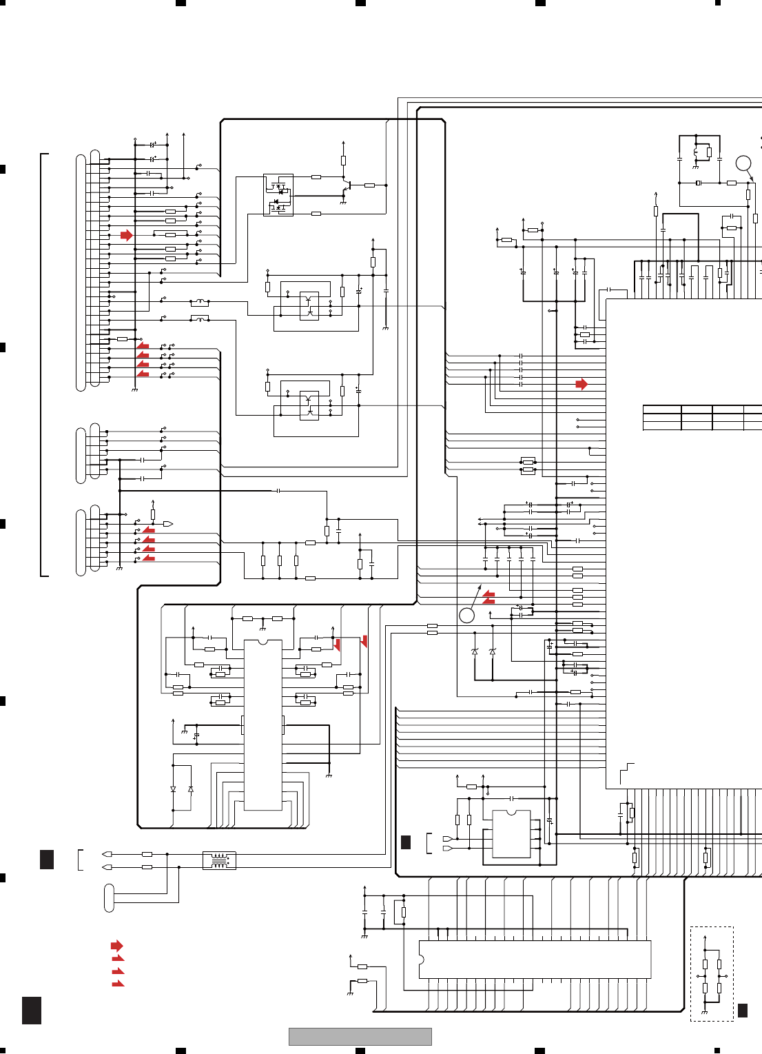
50 XV-DV575
12 3 4
A
B
C
D
E
F
12 3 4
10. SCHEMATIC DIAGRAM
10.1 08 DVDM ASSY (1/2)
A4
A12
A15
A18
A4
A2
A17
A18
AD6
FMSO
A6
RF
AD2
AD3
A7
A14
PRD#
AD1
A8
A0
A7
A8
A5
AD7
A19
A16
A1
A6
A9
DMSO
A20
A10
AD0
A2
A11
AD5
A13
A5
A3
A19
A3
AD4
A15
A14
A13
A12
A11
A10
A9
A20
A1
PRD#
AD0
AD1
AD2
AD3
AD4
A16
D
A
B
C
E
F
MDI1
LDO2
TROPEN
LDO1
PCE#
PWR#
PCE#
PWR#
MOT_SLED+
MOT_SLED-
F-
F+
MOT_SPDL-
MOT_SPDL+
T-
T+
FMSO
DMSO
FOSO
STBY
IOA
TRSO
FOSO
TRIN
TROUT
PWR#
PCE#
MOT_SLED-
MOT_SLED+
MOT_SPDL+
F
E
D
C
IOA
RF
B
A
MOT_SPDL-
LOAD+
LOAD-
IOA
MDI1
LOAD-
LOAD+
TROUT
TRIN
LDO1
LDO2
TRSO
TROPEN
TRCLOSE
T-
F+
F-
T+
GNDD
R601
NM
R322
4.7
GNDD
GNDD
R310
NM
R603
NM
NM
C221
R326
4.7
47u/16
C310
R604
NM
L761
VTH1047-A
1L1S
2
L1
3
L2 4L2S
47u/16
C309
R325
4.7
V+5V
V+3R3
V20
V1P4
V+3R3
R321
4.7
V1P4
C320
NM
R602
NM
V+1R8
USBP
USBN
V+1R8
V+3D
R208
0
V+3R3
R219
10k
R218
10k
S-24CS64A0I
IC204
A0
1
A1
2
A2
3
GND
45
SDA
6
SCL
7
WP
8
VCC
C290
0.1u/16
C289
1u/10
C295
1000p/50
R282
NM
GNDD
V+3D
R284
10k
R285
NM
GNDD
V+3D
UM5K1N
Q305
1
G1
2
S
3
G2
4
D2
5
D1
V+5S
Q304
2SC4081(QR)
R313
100k
R318
100k
R315
10k
R314
10k
GNDD
GNDD
V+5S V20
V+6R5
GNDM
C101
NM
R101
0
V1P4
C102 NM
R111
0
C111
NM
C112 NM
GNDM
C132 NM
C122 NM
R121
0
C121
NM
V1P4
C131
NM
R131
0
GNDD
C151
0.1u/16
R151
680k
R152
150k
R154
150k
HN1A01F(YGR)
Q308
E1
1
B1
2
C2
3
E2
4
5
B2
6
C1
HN1A01F(YGR)
Q307
E1
1
B1
2
C2
3
E2
4
5
B2
6
C1
S
R141
10k
R142
10k
GNDM
R155
680k
V1P4
V+3R3
C152
C153
CN953
NM
1
2
VKN2045-A
CN966
1
2
3
4
5
6
7
8
9
10
11
12
13
14
15
16
17
18
19
20
21
22
23
24
R761
0
R762
0
SCL
SDA
R769 0
R770 0
D102
RR264M-400
D101
RR264M-400
100u/16
C103
NM
CN101
1
2
3
4
5
6
7
8
9
10
11
12
13
14
15
16
17
18
19
20
21
22
23
24
CN104
NM
1
CLOSE
2
GND
3
OPEN
4
LOAD+
5
LOAD-
CN965
VKN1573-A
1
2
3
4
5
NM
CN102
1
SPD+
2
SPD-
3
SLD+
4
SLD-
5
6
VKN1574-A
CN964
1
2
3
4
5
6
IC101
BA5984FP
FWD
1
OPIN1(+)
2
OPIN1(-)
3
OPOUT1
4
5OPIN2(+)
6OPIN2(-)
7OPOUT2
29 GND2
9VOL(-)
10 VOL(+)
11 VO2(-)
12 VO2(+)
13 VO1(-)
14 VO1(+)
8
VCC
15
V04(+)
17
V03(+)
18
V03(-)
19
GND1
20
BIAS
21
MUTE
22
OPOUT3
23
OPIN3(-)
24
OPIN3(+)
25
OPOUT4
26
OPIN4(-)
27
OPIN4(+)
28
REV
16
V04(-)
30
GND3
IC203
AYW7242-A
A15
1
A14
2
A13
3
A12
4
5
A11
6
A10
7
A9
8
A8
9
A19
10
NC10
11
/WE
12
/RESET
13
NC13
14
NC14
15
RY_/BY
16
A18
17
A17
18
A7
19
A6
20
A5
21
A4
22
A3
23
A2
24
A1
25
A0
26
/CE
27
VSS_27
28
/OE
29
DQ0
30
DQ8
31
DQ1
32
DQ9
33
DQ2
34
DQ10
35
DQ3
36
DQ11
37
VCC_37
38
DQ4
39
DQ12
40
DQ5
41
DQ13
42
DQ6
43
DQ14
44
DQ7
45
DQ15_A-1
46
VSS_46
47
/BYTE
48
A16
R153
3.3
R156
3.3
R157
3.3
OSN
1
RFGC
2
IREF
3
AVDD3
4
AGND
5
DVDA
6
DVDB
7
DVDC
8
DVDD
9
DVDRFIP
10
MA
11
MB
12
MC
13
MD
14
SA
15
SB
16
SC
17
SD
18
MDI1
19
MDI2
20
LDO2
21
LDO1
22
SVDD3
23
CSO
24
RFLVL
25
SGND
26
V2REFO
27
V20
28
VREFO
29
FEO
30
TEO
31
TEZISLV
32
OP_OUT
33
OP_INN
34
OP_INP
35
DMO
36
FMO
37
TROPENP/WM
38
PWMOUT1
39
TRO
40
FOO
41
AGND18_D
42
AVDD18_DM/PLL
43
USB_DP
44
USB_DM
45
VDD33_USB
46
VSS33_USB
47
PA D _ VRT
48
VDD18_USB
49
VSS18_USB
50
USB_XTALO
51
USB_XTALI
52
FG
53
IOA22
54
DVDD18_1
55
IOA2
56
IOA3
57
IOA4
58
IOA5
59
IOA6
60
IOA7
61
HIGHA0
62
IOA18
63
IOA19
64
DVDD3_1
65
IOWR#
66
A16
67
HIGHA7
68
HIGHA6
69
HIGHA5
70
HIGHA4
71
HIGHA3
72
HIGHA2
73
HIGHA1
74
IOA20
75
IOCS#
76
IOA1
77
IOOE#
78
AD0
79
AD1
80
DVSS18
81
AD2
82
AD3
83
RFVDD18238
XTALO 239
XTALI 240
JITFO 241
JITFN242
PLLVSS 243
PLLVDD3 244
LPFON245
LPFIP 246
LPFIN247
LPFOP 248
ADCVDD3 249
ADCVSS 250
RFVDD3 251
RFRPDC 252
RFRPAC 253
HRFZC 254
CRTPLP 255
RFGND256
OSP
R103
12k
R113
12k
R114
12k
R104
10k
R134
27k
R124
27k
R123
33k
R133
33k
D761
UDZS3R9(B)
D762
UDZS3R9(B)
LIMIT
3.3V
1.8V
to PICK UP
FOCS
TRKG
(NC)
PD
VREF
SW
A
TRKG
LD
VCC
GNDD
VRCOM
VR650
GNDD
VR780
E
RF
(Side type)
LD
D
F
B
FOCS
C
GNDD
to LOAD ASSY
to SLED/SPINDLE
MOTOR
/TNI
/TPI
(780)
(650)
VSHF
DRV
RTN
DRV
RTN
A-Side
B-Side
A-Side
B-Side
A-Side
B-Side
C254
1000p/50
R253
680
220u/4
C201
C210
2200p/50
C2680.1u/16
R232
NM
R254 750k
C208
0.1u/16
C343 1u/10
C220
0.1u/16
C345 1u/10
C265
22p/50
R609 10k
R238NM
NM
C214
C347 1u/10
47u/16
C206
C346 1u/10
C200
0.1u/16
C273 0.1u/16
R768NM
R251
100k
C205 0.1u/16
C207
0.1u/16
R252
0
R233
NM
X201
VSS1172-A
R204 22k
C211
270p/50
C212
270p/50
R217 NM
C267
1000p/50
C209
0.015u/16
C344 1u/10
R767 NM
C213 0.1u/16
R239 NM
C217
0.1u/16
47u/16
C203
R255
100k
C204 0.1u/16
220u/4
C202
L308NM
L309 NM
C260
0.1u/16
R631 6.8
C271
0.1u/16
C272
0.1u/16
C601
0.1u/16
R256
15k
C606
0.1u/16
4.7u/16
C605
R611 5.1k
C371
0.1u/16
C372
0.1u/16
100u/16
C373
NM
C374
R375 NM
R374 NM
R372 NM
R371 NM
R373 NM
47u/16
C215
C269
0.033u/10
C264
0.1u/16
C266
0.1u/16
R304
NM
C140
NM
C141
NM
C603 0.1u/16
R207
NM
R200
NM
R305
10k
C251
10p/50
C252 10p/50
10u/16
C602
10u/16
C607
C608
1000p/50
C216 0.1u/16
C619
2200p/50
2200p/50
C258
0.047u/16
C259
0.047u/16
L251 NM
R636
0
LIMIT SW
SW(GND)
R201 12k
R202 8.2k
R205 15k
R206 15k
(F)
(F)
(F)
(F)
(F)
(F)
(F)
(F)
(F)
(F)
(F)
(F)
C248C249 R24
AWM8105 0.1u 470p 33
AWM8118NMNMNM
A2/2
A2/2
A2/2
0
12
A1/2
To DVD LOADER
: FOCUS SERVO LOOP LINE
: TRACKING SERVO LOOP LINE
: STEPPING SERVO LOOP LINE
(F)
(RF) : RF SIGNAL ROUTE
(T)
(S)
(RF)
(T)
(T)
(F)
(F)
(S)
(S)
(S)
(S)
(T)
(F)
(T)
(F)
(RF)

51
XV-DV575
56 7 8
56 7 8
A
B
C
D
E
F
MA1
DQ3
DQ7
MA3
S_C
DQ15
G_CY
DQ4
DQ9
S_Y
SCLK
DQ13
DQ8
DQ5
DRAS#
ACK
DQ11
DQ2
XREADY
DCS#
DQ12
DQ10
MA2
DQ0
DQ6
DQ14
DBA0
DBA1
MA0
B_CB
MA10
DQ8
M D ATA
DQ1
MA2
DQM0
DCAS#
R_CR
CVBS
DWE#
A11
A10
A9
A20
A1
PRD#
AD0
AD1
AD2
AD3
AD4
AD5
AD6
AD7
A17
A0
DQM0
DQ7
DQ4
DQ1
DQ0
DQ15
DQ14
DQ12
LETTER
DQ6
DQ3
DQ11
DQ13
DQ2
DQ5
DQ10
DQ9
MA3
MA5
MA6
MA7
MA8
MA9
MA11
MA4
VSEL1
SDCLK
SDCKE
PCE#
STBY
TRCLOSE
MA5
MA7
MA8
MA11
MA9
SDCKE
SDCLK
DQM1
MA0
MA10
MA1
MA4
MA6
DQM1
VSEL2
I/XP
SQUEEZE
RXD
TXD
V+3D
R601
NM
2
1
4
36
5
8
7
GNDD
R228NM
V+3DR
V+3DR
GNDD
R603
NM
2
1
4
36
5
8
7
R604
NM
GNDD
R229
33
V+5V
CN204
NM
1
2
3
4
GNDD
V+3R3
R602
NM
XDVDRST
IC601
TC7SH08FUS1
4
2
5
3
1
V+3R3
GNDD
R627
0
R628
0
C620
R629
NM
TRKUP
AUDIO
VIDEO
SYS
V+3R3A
V+3R3A
R979
0
R978
0
GNDA
R980
0
GNDD
MIC
IC202
K4S641632K-UC75
VDD1
1
DQ0
2
VDDQ1
3
DQ1
4
5
DQ2
6
VSSQ1
7
DQ3
8
DQ4
9
VDDQ2
10
DQ5
11
DQ6
12
VSSQ2
13
DQ7
14
VDD2
15
LDQM
16
WE
17
CAS
18
RAS
19
CS
20
BA0
21
BA1
22
A10/AP
23
A0
24
A1
25
A2
26
A3
27
VDD3
28
VSS1
29
A4
30
A5
31
A6
32
A7
33
A8
34
A9
35
A11
36
N.C
37
CKE
38
CLK
39
UDQM
40
N.C/RFU
41
VSS2
42
DQ8
43
VDDQ3
44
DQ9
45
DQ10
46
VSSQ3
47
DQ11
48
DQ12
49
VDDQ4
50
DQ13
51
DQ14
52
VSSQ4
53
DQ15
54
VSS3
SCL
SDA
*R240 33
V+3R3
*L241
QTL1013-A
R247
NM
MT1389FE/S-L
IC201
HIGHA4
71
HIGHA3
72
HIGHA2
73
HIGHA1
74
IOA20
75
IOCS#
76
IOA1
77
IOOE#
78
AD0
79
AD1
80
DVSS18
81
AD2
82
AD3
83
AD4
84
AD5
85
AD6
86
IOA21
87
ALE
88
AD7
89
DVSS33_1
90
A17
91
IOA0
92
DVDD18_2
93
UWR#
94
URD#
95
DVDD3_2
96
UP1_2
97
UP1_3
98
UP1_4
99
UP1_5
100
UP1_6
101
UP1_7
102
UP3_0
103
UP3_1
104
UP3_4
105
UP3_5
106
ICE
107
PRST#
108
IR
109
GPIO22
110
DQM0
111
GPIO21
112
RD7
113
RD6
114
RD5
115
RD4
116
RD3
117
DVDD3_3
118
RD2
119
RD1
120
RD0
121
RD15
122
RD14
123
RD13
124
RD12
125
RD11
126
RD10
127
RD9
128
RD8129
GPIO20 130
DVDD3_4 131
DQM1 132
RWE# 133
CAS# 134
RAS# 135
RCS# 136
BA0 137
BA1 138
RA10 139
RA0 140
RA1 141
DVDD18_3 142
RA2 143
RA3 144
145
DVDD3_5
146
RCLK
147
CKE
148
DVSS33_2
149
RA11
150
RA9
151
RA8
152
RA7
153
RA6
154
RA5
155
RA4
156
DVDD3_6
157
GPIO4
158
159
160
161
162
163
164
165
166
167
168
169
170
171
172
173
174
175
176
177
178
179
180
181
182
R
183
B
184
DACVSSA
185
G
186
DACVDDA
187
CVBS
188
DACVSSB
189
C
190
DACVDDB
191
Y
192
DACVSSC
193
FS 194
VREF 195
DACVDDC 196
TS_DATA0 197
TS_DATA1 198
TS_DATA2 199
TS_DATA3 200
TS_DATA4 201
TS_DATA5 202
TS_DATA6 203
TS_DATA7 204
TS_VALID 205
TS_CLK 206
TS_SYNC207
DVDD3_7 208
TS_ERROR 209
TS_PWM210
GPIO9 211
GPIO10 212
DVDD18_5 213
GPIO11 214
GPIO12 215
SPDIF 216
APLLVDD3 217
APLLCAP 218
APLLVSS 219
ADACVSS2 220
ADACVSS1 221
ARF 222
ARS 223
AR 224
AVCM 225
AL 226
ALS 227
ALF 228
ADACVDD2 229
ADACVDD1 230
CH8231
CH7 232
ADACVSS3 233
ADACVDD3 234
SADCVDD18235
SADCVSS18236
RFGND18237
RFVDD18238
XTALO 239
XTALI 240
JITFO 241
JITFN242
PLLVSS 243
PLLVDD3 244
LPFON245
LPFIP 246
LPFIN247
LPFOP 248
ADCVDD3 249
ADCVSS 250
RFVDD3
AKP7224-A
JA931
1
2
3
4
5
6
7
8
9
10
11
12
13
14
15
16
17
18
19
*IC241
TC7SH08FUS1
INB
1
INA
2
GND
3
OUTY
4
5
VCC
LIMIT
3.3V
1.8V
3.3V
DOWNLOAD
1.8V
3.3V
ASPDIF
DWE#
XAMUTE
ASDAT2_AR_DSDC
ASDAT1_AL_DSDLS
ASDAT0_ALS_DSDL
ALRCK_AC
DBA0
DRAS#
DCAS#
DBA1
DCS#
XMMUTE
DSDR
SDATA
DSDRS
ABCK_ARS
ACLK_ALFE
DSDLFE
DSDPCM
C250
0.1u/16
C282
1u/10
C244
0.1u/16
C254
1000p/50
R224
33
R253
680
C233
0.1u/16
C225
0.1u/16
C232
0.1u/16
R221
33
220u/4
C237
C247
0.1u/16
R254 750k
R259
33
C230
0.1u/16
22p/50
R260 33
R261 33
R281
0
R236 NM
C224 0.1u/16
R225 33
R226 33
R251
100k
R252
0
R233
NM
X201
VSS1172-A
C243
0.1u/16
220u/4
C281
C231
0.1u/16
C229
0.1u/16
R227 33
R613
NM
R614
NM
R235
NM
C227 220p/50
R220 NM
C245
1u/10
R213 10k
R212 10k
C246
0.1u/16
R237 NM
R249 NM
R626 NM
C239 0.1u/16
10u/16
C241
C260
0.1u/16
R631 6.8
*R246 33
*R245 33
*R244 33
*R241 33
*R242 33
R624 10k
R625 10k
R24833
R279 2.2k
4.7u/16
C262
0.1u/16
C266
0.1u/16
R622 NM
R623 NM
0.1u/16
R231 33
R612NM
R203 33k
R209
0
R632
NM
*R243 10
C251
10p/50
C252 10p/50
220u/4
C618
47u/16C616
C614
100p/50
C240
0.01u/16
C226
0.01u/16
C283
0.01u/16
C284
0.01u/16
C285
0.01u/16
C286
0.01u/16
C287
0.01u/16
C288
0.01u/16
C261
0.1u/16
C619
0.1u/16
C617
0.1u/16
C242
1500p/50
C258
0.047u/16
C259
0.047u/16
R620
33
R605 NM
L251 NM
R636
0
*C2480.1u/16
*C249 470p/16
R615 33
220u/4C223
C2280.1u/16
R637 NM
R222 10k
R223 NMR210 NM
R618
51k
(F)
HDMI Block
C248C249 R240 R241 R242 R243 R244 R245 R246 L241 IC241
05 0.1u 470p 33 33 33 10 33 33 33 QTL1013A TC7SH08FUS1
18NMNMNMNMNMNMNMNMNMNMNM
A2/2
A2/2
A2/2
A2/2
A2/2
A2/2
0
1
4
3
13
2
5
A1/2
A1/2
08 DVDM ASSY
(XV-DV575, XV-DV580 : AWM8118)
(XV-DV385K, XV-DV395K : AWM8105)
: VIDEO SIGNAL ROUTE (S_Y)
: VIDEO SIGNAL ROUTE(C/V)
(S_Y)
: VIDEO SIGNAL ROUTE (S_C)
: AUDIO DATA SIGNAL ROUTE
(S_C)
: VIDEO SIGNAL ROUTE (R/Cr)
(R/Cr)
: VIDEO SIGNAL ROUTE (G/Y)
(G/Y)
: VIDEO SIGNAL ROUTE (B/Cb)
(B/Cb)
(AD)
(C/V)
(AD)
(AD)
(S_Y)
(S_C)
(C/V)
(G/Y)
(B/Cb)
(R/Cr)
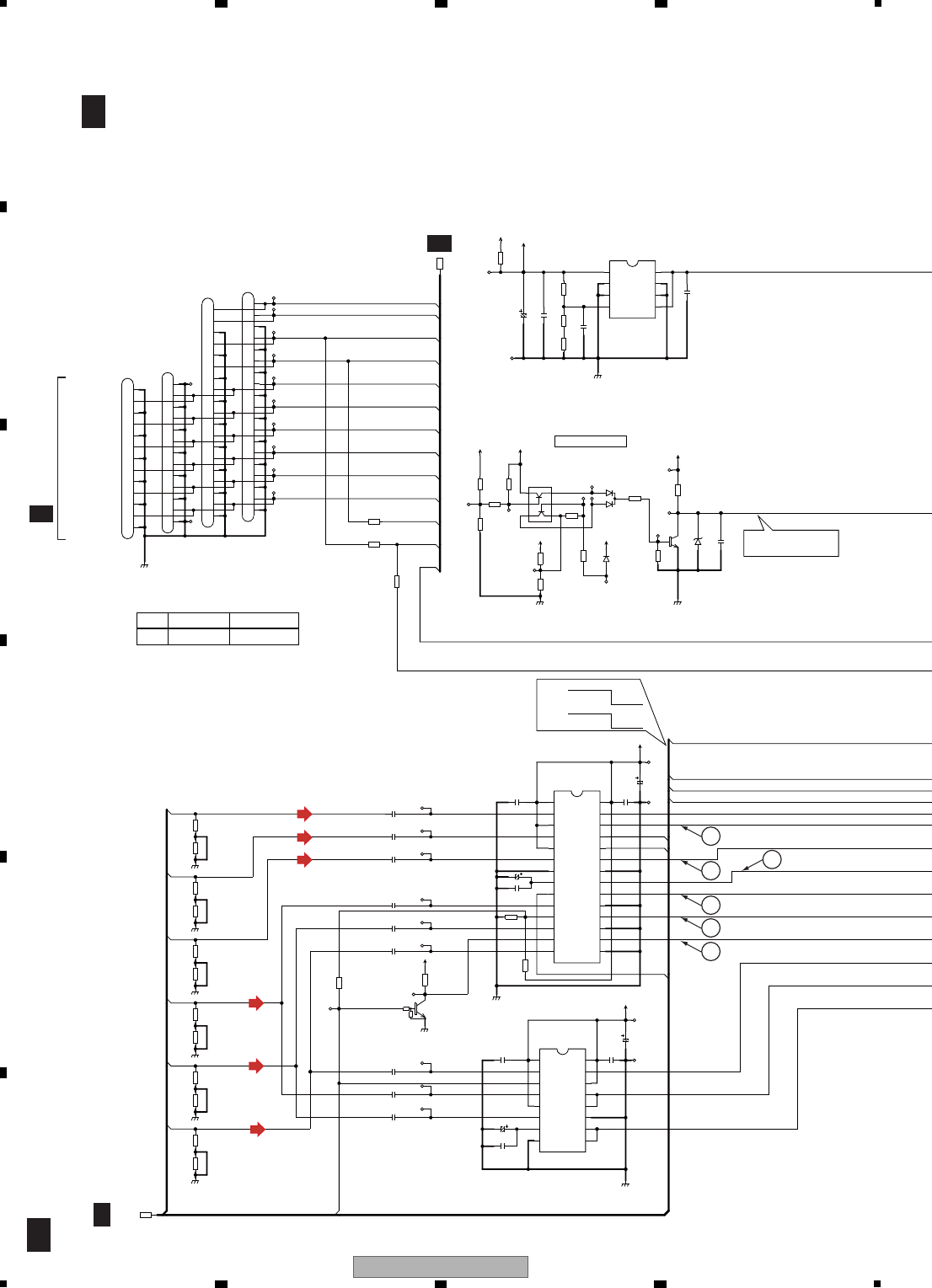
52 XV-DV575
12 3 4
A
B
C
D
E
F
12 3 4
10.2 08 DVDM ASSY (2/2)
I/XP
SQUEEZE
VSEL2
VSEL1
S_C
CVBS
S_Y
VSEL1
R_CR
G_CY
B_CB
ACLK_ALFE
ABCK_ARS
ALRCK_AC
ASDAT0_ALS_DSDL
ASDAT1_AL_DSDLS
ASDAT2_AR_DSDC
DSDPCM
DSDLFE
XMMUTE
DSDR
DSDRS
XAMUTE
ASPDIF
C711
1u/10
C712
470p/16
R712
NM
R713
NM
R714
NM
GNDD
C713
2.2u/10
NM
C714
MM1661JH
IC711
VOUT
1
NC1
2
GND
3
CN
45
CONT
6
NC2
7
NC3
8
VIN
100u/16
C404
GNDD
C403
NM
C405
0.1u/16
IC401
MM1758XF
VCC1
1
CIN
2
MUTE1
3
CVBSIN
4
5YCMIX
6YIN
7GND1
8
BIAS
9I/P
10 CYIN
11 CLP
12 CbIN
13 MUTE2
14 CrIN15
GND2_1
16
CrOUT
17
GND2_2
18
CbOUT
19
GND2_3
20
CYOUT
21
YOUT
22
GND2_4
23
CVBSOUT
24
S2
25
S1
26
COUT
27
S-DCOUT
28
VCC2
R404
NM
C402
R405
NM
V+5V
100u/16
C401
R414
150
R412
150
C414
1u/10
R435
NM
C412
1u/10
R411
150
R432
NM
R433
NM
C413
1u/10
GNDD
GNDD
GNDD
GNDD
R431
NM
R416
150
C464
NM
GNDD
R415
150
R436
NM
R413
150
C465
NM
R434
NM
GNDD
C466
NM
R401
10k
V+5V
GNDD
NM
Q401
NM
C451
GNDD
C455
NM
NM
C454
V+5V
NM
IC451
VCC1
1
CIN
2
MUTE1
3
VIN
4
5MODED1
6YIN
7BIAS
8
GND1 9
YSAG
10
YOUT
11
GND2
12
VSAG
13
VOUT
14
MODE2
15
COUT
16
VCC2
C452
NM
GNDD
GNDD
D801
UDZS4R7(B)
V+3R3
R801
470
V+5
V+6R5
C453
NM
AUDIO
VIDEO
R715
0
V+1R8
AVD18
C801
0.1u/16
C411
0.1u/16
C415
0.1u/16
C416
0.1u/16
R406
0
R521
0
Q801
2SC4081(QR)
R802
47k
D802
DAN202U
HN1A01FU(YGR)
Q802
1
2
34
5
6
D811
1SS352
V+5
R804
22k
R805
47k
V+6R5
R806
1k
R807
1.5k
GNDD
R809
2.7k
R808
220
R810
22k
R811
47k
R803
8.2k
R523
NM
R524
NM
VKN1472-A
*CN962
1
2
3
4
5
6
7
8
9
10
11
12
13
NM
CN951
1
2
3
4
5
6
7
8
9
10
11
12
13
NM
CN961
1
2
3
4
5
6
7
8
9
10
11
12
13
14
15
16
17
18
19
NM
CN952
1
GNDD
2
ALCK_ALFE
3
GNDD
4
ABCK_ARS
5
GNDD
6
ALRCK_AC
7
GNDD
8
ASDAT0_ALS_DSDL
9
GNDD
10
ASDAT1_AL_DSDLS
11
GNDD
12
ASDAT2_AR_DSDC
13
GNDD
14
DSDR
15
GNDD
16
DSDRS
17
GNDD
18
DSDLFE
19
DSDPCM
RGB
V
S
V+RGB
VSEL1
VSEL2
*2
*2
VOLTAGE DETECT
A-Side
B-Side
A-Side
B-Side
AWM8105 AWM8118
CN962 VKN1472-A NM
I/XP
LETTER
SQUEEZE
0.1u/16
(F)
(F) (F) (F) (F) (F)
EXTRA VIDEO OUT
ABNORAMAL : < 1.6 V, 3.6 V <
NORMAL : 3.3 V
A2/2
CN5605
B3/5
A2/2 08 DVDM ASSY
(XV-DV575, XV-DV580 : AWM8118)
(XV-DV385K, XV-DV395K : AWM8105)
(S_C)
(S_Y)
(G)
(B)
(R)
(C/V)
A1/2
A1/2
7
8
6
9
10
11
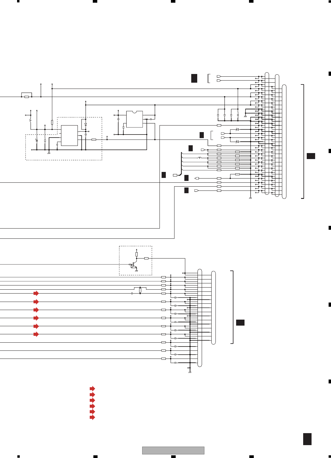
53
XV-DV575
56 7 8
56 7 8
A
B
C
D
E
F
XREADY
SDATA
MDATA
ACK
SCLK
R711
NM
NM
IC751
VO
1
NC
2
GND
3
CN
4
5
CONT
6
SUB
7
VIN
R751
NM
D751
NM
GNDM
GNDD
R903 3.3k
R902 0
R904 6.8k
R905 3.3k
R906 6.8k
R907 470
R916 22k
R909 6.8k
R9083.3k
R917 22k
R910 220
R911 220
GNDD
C751
NM
C752
NM
C753
NM
NM
C754
V+5V
L751
CTF1395-A
V+5S
R912 0
R913 0
R914 10k
DTC114YUA
Q481
GNDD
R481
1k
V+5V
R921
0
R922 0
R923 0
R924 0
R403 0
R421 0
C406
0.1u/16 C421
NM
R422
0C422
NM
C423
NM
R423
0
C424
NM
R424
0
C425
NM
R425
0
C426
NM
R426
0
C474
NM
R474
NM
R475
NMC475
NM
C476
NM
R476
NM
GNDD
L901
CTF1334-A
R901
0
V+6R5
USBP
USBN
XDVDRST
V+3R3
V+5HD
V+5
TRKUP
IC771
NJM2872BF05
Vin 1
GND2
34
5
Vout C771
1u/10
C772
C773
MIC R919 0
R918
NM
D934
D935
NM
SCL
SDA
R752
0
NM
CN901
1
2
3
4
5
6
7
8
9
10
11
12
13
14
15
16
17
18
19
20
21
22
23
24
25
26
27
28
29
NM
CN963
1
2
3
4
5
6
7
8
9
10
11
12
13
14
15
16
17
18
19
20
21
22
23
24
25
26
27
28
29
VKN1583-A
CN968
1
2
3
4
5
6
7
8
9
10
11
12
13
14
15
16
17
18
19
20
21
22
23
24
25
26
27
NM
CN902
1
2
3
4
5
6
7
8
9
10
11
12
13
14
15
16
17
18
19
20
21
22
23
VKN1577-A
CN967
1
2
3
4
5
6
7
8
9
10
11
12
13
14
15
16
17
C701
NM
C702
NM
C703
NM
C704
NM
SYS
PROGRESSIVE
P/XI
G/GNDD
GNDD
GNDD
SQUEEZE
GNDD
GNDD
GNDD
V
GNDD
VSEL2
GNDD
CY/G
ASPECT
VSEL1
R
Cb/B
Cr/R
SY
B/GNDD
SC
GNDD
GNDD
ACK
TRKUP
3R3V
SCL
GNDM
USBN
XREADY
GNDD
V+5
3R3V
GNDD
USBP
SCLK
MIC/GNDD
6R8V
GNDD
GNDD
SDATA
VDET
6R8V
DOUT
DVDPOWER
MDATA
DVDMUTE
V+5
GNDM
SDA
GNDD
XDVDRST
A-Side
B-Side
A-Side
B-Side
B-Side
/SUB_INT
R402
10k
CONTROL
NOISE_BYPASS
2.2u/10
0.1u/16
NM
A2/2
CN5603
B3/5
CN9000
B3/5
: VIDEO SIGNAL ROUTE (S_Y)
: VIDEO SIGNAL ROUTE(C/V)
(S_Y)
: VIDEO SIGNAL ROUTE (S_C)
(S_C)
(B)
(G)
(R)
(S_Y)
(C/V)
(S_C)
: VIDEO SIGNAL ROUTE (R)
(R)
: VIDEO SIGNAL ROUTE (G)
(G)
: VIDEO SIGNAL ROUTE (B)
(B)
(C/V)
A1/2
A1/2
A1/2
A1/2 A1/2
A1/2
54 XV-DV575
12 3 4
A
B
C
D
E
F
12 3 4
10.3 SYSMAIN ASSY (1/5)
LC875CB2A
AUDIO
DOUT
XFLAG
XTVMUTE
REMOCON
VDET
XAMUTE
UCOM
DVDPOWER
37
23
25
46
24
45
41
38
99
47
100
20
98
ASDAT3
ASDAT2
ADDATA
ASDAT1
LRCKO
D ATA 0
BCKO
MCKO
29
28
30
27
25
23
24
22
21
20
19
17
69
7
6
3
4
1
2
20
33
35
32
34
35
33
38
37
41
45
47
46
49
50
48
51
86
DSPMUTE
72
84
4
72
52
61
60
57
58
62
64
65
67
66
68
69
68
60
58
71
70 57
74
78
77
79
80
22
DSP
UCOM
99
98
100
93
86
84
85
83
82
3-B1
13 12 9
10
11 6
7
83
4
52119
1815
16
17 13
14 12 10 911 6875
4384
75
216
91
2
3
E
BC
30
32
31
33
35
34
2829 2627
37
36
38
40
41
39
44
42
43
45
46
47
50
48
49
51 5352 54 55
25 24 2223 21 20
5756 5859 60 61
19 1817 16 15 14 13
62 63 6664 65 67 68
12 11 910 78
69 70 71 72 73 74
56 4321
7675 787977 80
100
99
96
97
98
93
94
95
92
91
90
87
88
89
86
85
84
82
81
83
7
6
5
4
3
2
1
XKM3004-
XKM3005- XKM3008
GNDD
GNDD
RT3N22NRT1N241M
STBY
STBY
V+3R3
RAB4C221J
220
STBY
GNDD
0.01
0.01
0.1
RAB4C221J
220
220
**
**
1M
10k
RAB4C221J
220
0.01
VE+5
**
**
0.1
10k
0.01
10MHz
220
ASS7034
VU+5 0.1/16
220
GNDD
STBY
RT1N431M
10/50
0.01
220
220
47k
2.2K GNDD RAB4C221J
220
1000p
4.7k
RT3N22N
RT1P241M
STBY
V+3R3
GNDD
*1
RAB4C221J
220
RAB4C221J
220
STBY
STBY
STBY
STBY
0.1/16
*1
*1
GNDD
*1
RAB4C221J
GNDD
220
10k
10k
STBY
PDC176A/A8
STBY
VE+5
0.1/16
RAB4C221J
220
220
220
220
220
0.01
0.01
RAB4C221J
220
15K
0.1
*1
0.01
1000p
10k
STBY
220
220
220
RAB4C221J
220
RAB4C221J
STBY
*2
STBY
220
RAB4C221J GNDD
STBY
STBY
*2
0.1
VE+5 VU+5
0
GNDD
STBY
9604S-07C
VE+5
RAB4C221J
220
100k
100/10
VE+5
CN5532
CN5531 CN5533
Q5532
R5530
Q5535
R5527
R5525
C5519
C5522
C5521
R5522
R5521
R5516
R5515
R5514
R5513
R5518
R5519
C5517
R5517
C5518
R5520
C5508
R5569
X5501
C5509
R5507
C5525
C5524
Q5525
C5504
R5506
R5505
R5510
R5508R5501
C1207
R5528
Q5534
Q5533
R5541
R5544
R5542
R5532
R5535
R5534
R5533
R5537
R5538
C5539
R5548
R5543
R5546
R5547
R5512 IC5501
R5545
C5555
R5557
R5562
R5564
R5565
C5569
C5577
C5589
R5531
R5597
C5578
R5583
R5585
R5584
C5579
R5582
R5581
R5566
R5570
R5577
C1206
C5501
R5502
R5509
C5597
CN5501
R5598
R5590
R5574
C5502
DSP RST
DSP CK
DSP DO
DSP DI
DEC_MUTE
DIR RST
DIR DO
DIR CS
DSP HREQ
DSP MODE
DIR ERR
DSP SS
OPTIN(5V)
DVDIN(3.3V)
BUSY
BDTO
GNDD
DAUX
GNDD
CDTO
GNDD
SDTO
GNDD
FDTO
GNDD
LCKO
GNDD
GNDD
BCKO
GNDD
GNDD
MCLK
XV-DV575, XV-DV580
(1/2)
(RN1903) (DTC124EUA)
GNDD
GNDD
GNDD
GNDD
V+3D
GNDD
GNDD
GNDD
GNDD
*1
DESTINATION
MODEL
(DTC143EUA)
RESET
(RN1903) (2/2)
(DTA124EUA)
*1
ACDET
PWRCONT
STEST
UTEST
INPUTSELA
INPUTSELB
DSPMUTE
DASDA
DASCK
DSPHREQ
XDEC MUTE
NC
BUSY
VDD4
VSS4
UTEST
STEST
XFLAG
XDSPSS
XDSPRST
DATASEL
SCLK
NC
NC
DSPCK
XTVMUTE
NC
DSPDO
DSPDI
XPROTECT
PCONFIG
ADMD
XRECMUTE
XADPDN
DSPMODE
SDATA
TXCE
MDATA
VDD2
VSS2
EEP_DO
EEP_CS
NC
EEP_SK
KEY2
DIRERR
KEY1
VDET
MODEL
SIMUKE
VDD1
IBD(DSP)
EU,KU,J, PDC175A/A8
LC875BJ0A
RUS,IBD
(XV-DV385K, XV-DV395K)
(XV-DV575, XV-DV580)
TXODATA
TXCLK
NC
RDSPOW
RDSDATA
TXIDATA
DVDACK
SHORT for
TEST POINT
CF1
CF2
VSS1
XT2
XRESET
XT1
REMOCON
DIRDO
-COM
XDIRRST
XDIRCS
DTSMIX
PWRCONT
EEP_DI
KEY1
XDAPDN
XDARST
USBPOWER
XDAMUTE
DVDPOWER
RDSCLK
P_ON
ACDET
FLCLK
FANCONT
XFLCS
FLDAT
FLASHDO
FLASHCLK
VSS3
NC
HPDET
HPSEL
UTESTMODE
(DMUTECHECK)
PLC_CONT
VDD3
FLASHE/D
MIC_DET
SR+TX
XHPMUTE
XADPDN(MIC)
SHUTDWN
SR+RX
XREADY
XDVDRST
XOTW
CHASSIS GND
XPROTECT
WEN/DI
DOWNLOAD
NC
VCC
VSS
WCLK
RST
WDD
-COM
*1
B1/5
CN951
ECN701
ECN901
E
15K
47K
82K
47K
15K
47K
82K
-
-
-
47K
47K
-
47K
47K
-
R5516
R5514
R5515
R5513
XWM
SHORT
3391 3394
** XV-DV385K/WSXJ5
4 TALL
XV-DV395K/WSXJ5
3392
(DSP)4 TALL
3395
(DSP)SHORT
XV-DV575/WYXJ5 XV-DV580/WYXJ5/WVXJ5
R5571 1K
R5502
*2 XV-DV385K,
XV-DV395K
100K STBY
STBY
XV-DV575,
XV-DV580
R5544
R5598
R5543
STBY
220
STBY
0
STBY
0
R5537
R5538
R5531
R5522
220
220
22k
220
R5542 220
*1 XV-DV580
XV-DV575
STBY
STBY
0
STBY
STBY
XV-DV395K
XV-DV385K
B2/5,3/5
B2/5,3/5
B3/5
B3/5
B3/5
B3/5
B3/5
B3/5

55
XV-DV575
56 7 8
56 7 8
A
B
C
D
E
F
(MA111)
DVDPOWER
V+3
V+3R3 V+6R8V+10
USBPOWER
V+5VV+5 VE+5
SROUT
REMOCON
V+3
REMOUT
312
45
2
3
1
6
7
8
E
C
B
B
E
C
13
10
11
12
9
E
BC
8
7
5
6
3
2
1
4
CB
E
E
BC
E
BC
E
BC
C
B
E
3
5
7
2
1
4
6
GNDD
STBY
220
0.1/16
GP1FAV51RKBF
STBY
100/16
0.1/16
CTF1379-
V+5
GNDM
CHASSIS_GND
GNDD
STBY
GNDD GNDD
RT1N141-11
100/10
0.01
0.1
LAU-TA
22
STBY
1
4.7k
2SC4154(BFG)
10k 2SC4154(EFG)
1
STBY
V+3
47k
CH
47p
470k
1SS352 0.056
GNDD
VU+5 VE+5
560
47k
10k
0.1
2SA1577(QR)
V+5V
GNDD
0.1/16
V+3R3 V+6R8V+10
47k
S-93C46BD0I-J8T1
GNDD
UDZS4R7(B)
STBY
STBY
1.8k
RT1N241M
V+5V
GNDD
V+5 VE+5
RT1N241M
VE+5
39k
GNDD
MC2846-11
1k
4.7k
VE+5
STBY
47K
2SA1602A(EF)
3.9k
3.3k
RT3N22M
STBY
1000p
1000p
FLDC+
VFDP
FLDC-
0.1
3.9k
GNDD
0.1
V+3R3
47k
V+6R8
2SA1602A(EF)
V+5
V+10
PG13KA-07
0.1
GNDD
V+3
0 10k 3.9k
2SA1602A(EF)
100k
RT3N22M
GNDD
1k 10k
1SS352 100k 2SA1602A(EF)
V+10
V+3R3
STBY
V+10 V+6R8
V+5
2.7k
RT1N241M
3.3k
47k
VE+5
2SA1602A(EF)
RT1P241M
100
1.8k
1SS352
1SS352
100k
GNDD
VE+5
220p
220p
1.8k
220p
VE+5
QTL1013
XKN3015
C4612
R4609
C4613
JA4602
R4610
C4614
C4615
L4603
C1505
C1501
C1502
D1501
C1301
R1307 Q1303
C1201
R1204
R5558
C5558
D1201
R1202
R1306
R1304
R1303
C1204
R1201
C1205
Q1302
C5557
R5559
IC5502
D1417
C1415
D1415
R1415
R1404
Q5941
D5942 R5947
D5941 R5946
C1413
R1403
R1402
R1401
Q1402
D1403
Q5932
C5601
R1001
C5603
C1211
R1302
C1210
R1301
CN1001
C1209
R5948R5949 R5945
Q5942
R5944
R5940
Q5932
R5934 R5935
D5933 R5933 Q5935
D1416
R5938
Q5931
R5939
R5937
R5936
Q5934
D5936
Q5936
R5931
D5931
R5942
C5932
C5931
C5936
L5933
L5931
L5932
L5934 JA5931
(D)
(DIGITAL OPT IN)OPT IN
(DTC114EUA)
(2SC4081(QR))
(2SC4081(QR))
DO
com FL DRIVER
com
STBY
INPUT SELECTOR
GND
DI
SK EEPROM
CS
(DTC124EUA)
TEST
NC
VCC
(DTC124EUA)
SR OUT
(DTC124EUA)
(1/2)
FL
-25.5V
FL DC+
FL DC-
Pwr-ctr
GND
A/D
DATA SELECTOR
DSP
SW3.3V(A)
GND
SW3.3V(B)
SW6.8V
(2SA1576A(QR))
MODULATOR
FTS DRIVER
USB BUS
HDMI
MIC
SW10.5V
EV5.0V
AC_DET
SW5.0V
SUPPLY
AUDIO BUFFER
SCART
TX
SCART POWER
(MA111)
(1SS355)
:1SS352
CKSR**-
STBY
CAPACITOR
: 1608 Size
CCSR**-
: 2125 Size
CKSQ**-
RS1/16S-
(2SA1576A(QR))
Chip Size
RESISTOR
: 2125 Size
RS1/10S-
: 1608 Size
(2/2)
(2SA1576A(QR))
PROTECT
(2SA1576A(QR))
(DTA124EUA)
SR PLUS L5931-L5934:
SR PLUS
B1/5
B1/5 SYSMAIN ASSY
(XV-DV575 : XWM3392) (XV-DV580 : XWM3395)
(XV-DV385K : XWM3391) (XV-DV395K : XWM3394)
CN3
F
XV-DV575, XV-DV580
B3/5
B3/5
B3/5
B4/5
56 XV-DV575
12 3 4
A
B
C
D
E
F
12 3 4
10.4 SYSMAIN ASSY (2/5)
++
--
SCART_R
SCART_L
RECMUTE
LINE_IN_R
LINE_IN_L
SCLK
LRCLK
SDATA1
SDATA3
PLCCONT
SDATA4
SDATA2
XSD_1
SCL
XOTW_1
PWRCONT
XRST
XMUTE
XPDN
SDA
PCON
XHPSEL
MCLK
V+5
UCOM
V+10
66
61
48
62
65
32
LRCKO
BCKO
ASDAT3
ASDAT2
ASDAT1
DATA0
93
77
84
79
28
27
70
71
DSPMUTE
82
21
MCKO
11
9
10
7
8
5
6
2
3
4
8
7
5
6
2
4
3
1
10
9
11
12
14
13
15
16
1
1
1
2
2
1
2
3
E
CB
74
8
1
2
2
3
1
4
5
6
8
7
14
16
15
13
12
11
9
10
GND
VSM
RDS
+9V
TXR
GND
TXL
CLK
DI
DO
HN1C01FU
HN1C01FU
VSSA
CIN
FLOUT
T1
MODE
VSSD
VDDA
MPXINXI
VDDD
(2/2)
VREF
RDSDATA
XO
RST
QUAL RDSCLK
4.322MHz
CE
RECMUTE
CHASSIS GND
PLCCONT
PWRCONT
HH
LH
(1/2) RDS
(1/2)
(1/2)
MCACC
XV-DV575,
XV-DV580
(2/2)
(2/2)
RDS DATA
INPUTSELB
INPUTSELA
Y2
Y0
Y3
Y1
Y(Rch)
Main:TC4052BFN
VSS
INH
VEE
SCART
LINE
VDD
X2
X(Lch)
X1
X0
A
B
X3
(2/2)
HL
L
L
BA
INPUT
SELECTOR
AUDIO
from Ucom PART
MCACC
TUNER
FUNCTION
(1/2)
C5704
C5705
C5701
C5703
C5709
C5702
R5719
R5705
C5707
C5708
R5718
R5717
R5716
Q5703
C5716
C5713
C5719
R5710
IC5701
C5715
C5720
X5701 C5714
C5712
CN5701
R5712
R5715
R5713
R5714
Q5707
JA4901
Q4006
R4006
C4016
C4015
C4012 R4012
C4011 R4011
R4003
KN4001 R4002
R4082
C4911
C4909
C4905
R4913
R4914
C4904
R4908
R4907
L4901
R4911
R4910
C4910
C4902
R4902
IC4901
D4901
C4903
R4906
R4905 C4908
C4907
R4903
C4906
C4901
R4016
R4018
C4020
C4019
R4017
R4015
R4020 R4019
R9001
R9002
C4004
R4915
R4022
R4014 R4013
D4902D4903
R4010
C4001
IC4001
C9001
C4002
C9002
R4027
C4003
C4022
Q4005
C4024
R4039
R4021
R4026 R4025
R4081R4001
R4007
R4009
Q4005
C4021
C4023
GNDD
STBY
STBY
STBY
100p
100p
STBY
STBY
CH
CH
STBY
1000p
47/35
STBY
STBY
STBY
STBY
(RT3CLLM(EF))
560p
4700p
CH
10/50
STBY
LC72725KM
GNDD
0.01
47/35
CH
ASS7004 27p
27p
9604S-11C
*1
STBY
*1
STBY
(RT3CLLM(EF))
V+10
GNDD
RKN1004
GNDD
RT1N241M
10k
10/50
VE+5 10/50
10/50 22k
STBY
22k10/50
STBY STBY
1M
1M STBY
10/50
10/50
470p
100k
4.7k
V+10
CH33p
4.7k
33k
CTF1379
1100
6.8k
100p
100k
CH
NJM4565M
UDZS5R1(B)
V+5
VREF+5
33p
33k
100 1
NJM4565M
47/35
3.9k
V+10
0.1
1
22k
22k
10/50
*2 *2
10/50
22k
22k
VREF VREF
STBY
STBY
VREF+5
47k
VREF
220K
STBY
GNDD
22k 22k
VREF
UDZS3R9(B)
UDZS3R9(B)
HN1A01FU(YGR)
1K
VREF
Sub:HEF4052BT
STBY
STBY
0.01
STBY
47K
STBY
0.1
V+10
15k
*3
220K
*
1k 1k
STBY
V+5
1K
HN1A01FU(YGR)
VREF
15K
0.1
V+5
47/35
V+10
2-B1
2-B1
2-B1
2-B1
2-B1
2-B1
2-B1
2-B1
2-B1
2-B1
2-A1
2-A1
2-A1
2-B1
2-A1
2-A1
2-A1
2-A1
2-A1
2-A1
2-A1
B2/5
CN1
G
B2/5 SYSMAIN ASSY
(XV-DV575 : XWM3392)
(XV-DV580 : XWM3395)
(XV-DV385K : XWM3391)
(XV-DV395K : XWM3394)
*1
R5712
R5713
R4020
R4019
2.7k12K
2.7k10K
XV-DV575,
XV-DV580
XV-DV575,
XV-DV580
XV-DV575,
XV-DV580
XV-DV575,
XV-DV580
XV-DV385K,
XV-DV395K
XV-DV385K,
XV-DV395K
XV-DV385K,
XV-DV395K
C4024
*2
*3
47/35V220/6.3V
XV-DV385K,
XV-DV395K
(AD)
B4/5
B1/5,3/5
B3/5
57
XV-DV575
56 7 8
56 7 8
A
B
C
D
E
F
MIC
V+3R3
AUDIO
MCDATA
ABCK
ALRCK
ACLK
DATA0
64
6
ADDATA
ALRCK
LRCKO
ADLRCK
ASDAT0
52
MCKO
ACLK
ABCK
ADMCK1
ADBCK
BCKO
85
34
ADMCK1
ADMCK0
ADDATA
ADLRCK
ADMCK0
ADBCK
4
8
6
7
5
9
11
10
12
13
2
1
3
8
7
5
6
2
4
3
1
43
51
2
4
1
3
2
14
16
15
9
10
12
11
14
15
13
16
5
6
7
8
PDN
SCLK
MCLK
DGND
VD
SDTO
LRCK
CKS1
VA
VCOM
AGND
DIF
CAPACITOR
CKS2
AINR CKS0
AINL
MIC A/D
GND
from DIR
RDSPOW
RDSCLK
DATASEL
DATA SELECTOR
NrVC
Vout
GND
Vin
GND
*
RESISTOR
Chip Size
*6
from DIR
ST
VCC
from DIR
XADPDN(MIC)
XADPDN
*5
VCC
SDTO
VD
VAMCLK
LRCK
DGNDto DIR
*
VCOM
AGND
CKS1
PDN
SCLK
DIF
AINR
AINL
CKS0
CKS2
A/D
from DVD,DSP PART
CKSR**-
: 1608 Size
CCSR**-
: 2125 Size
CKSQ**-
RS1/16S-
: 2125 Size
RS1/10S-
: 1608 Size
C4965
C4962
C4966
C4961
C4963
C4964
R4967
R4969
C4968
R4968
R4965
D4962
R4966
IC4961
C4967
D4961
R4063
R4062
R4061
R4083IC4005
C4056
R4024 C4026
C4029
C4028
R4056
C4027
R4028
R4046
C4045
R4045
C4046
R4058
R4057
R4066 L4066
R4085
R4067
R4065
R4064
C4064
R4084
C4057
X4004
R4055
R4054
R4053
C4052
IC4004 R4052
R4090
C4048
R4073
R4049
R4023
IC4002
C4025
C4041
C4043
C4042
C4044
R4041
R4059
R4060
R4048
0.1
V+3R3
1
2.2
2.2
STBY
0.1
GNDD
3.3k
0.01
100
RAB4C101J
220
1.8k
22/25
V+5
1K
UDZS3R9(B) UDZS3R9(B)
AK5358AET
V+5
GNDD
220
*
220
220
TC74VHC157FTS1
27p
1k 10/50
GNDD
2.2
0.1
100
220k
0.1
STBY
V+3R3
STBY
0.1
10/50
100
*
100
220
STBY
0.1
*
V+3R3
GNDD
CH
27p
12.288MHz
CH
VSS1140
1M
100
TC7WU04FU
100
0.1 *
0
3.3k
0.01
RAB4C101J-T
100
1k
VREF
NJM2872BF25
10/50
V+5
10/50
0.1
2.2/50
0.1
STBY
V+5
1.8k
AK5358AET
B2/5
XV-DV575,
XV-DV580
XV-DV575,
XV-DV580
XV-DV575,
XV-DV580
XV-DV575,
XV-DV580
XV-DV575,
XV-DV580
XV-DV575,
XV-DV580
XV-DV575,
XV-DV580XV-DV575,
XV-DV580
XV-DV575,
XV-DV580
XV-DV575,
XV-DV580
XV-DV385K,
XV-DV395K
XV-DV385K,
XV-DV395K
XV-DV385K,
XV-DV395K
XV-DV385K,
XV-DV395K
R4085
R4084
×
×
C4024
R4090
220/6.3
×
47/35
0
0
0
×
×
R4083
R4060
×
0
R4057
R4058
R4059
0
0
×
0
0
×
?
*5
*
?
*6 ×
×
(AD)
(AD)
(AD)
(AD)
(AD)
(AD)
: AUDIO DATA SIGNAL ROUTE
B1/5,3/5
B3/5
58 XV-DV575
12 3 4
A
B
C
D
E
F
12 3 4
10.5 SYSMAIN ASSY (3/5)
GNDA
HPMUTE
HP_DET
MIC SW
MIC
ASDAT1_AL
ASDAT2_AR
ASDAT0_ALS
ALRCK_CENTER
ABCK_ARS
GNDD
GNDD
GNDD
GNDD
GNDD
ACLK_LFE
GNDD
GNDD
V+10
FLDATA
GNDA
GNDA
FLCK
HP_L
HP_R
GNDD
FLDC+
FLCS
FLDC-
GNDD
VFDP
USB_DM2
GNDUSB
GNDUSB
V5USB
REMOCON
VE+5
V5USB
NC
USB_DP2
KEY1
KEY2
VDET
MIC/GNDD
DVDMUTE
TRKUP
ACK
MDATA
SDATA
SCLK
GNDD
GNDD
XREADY
DVDPOWER
XDVDRST
GNDD
DOUT
USBP
USBN
CAPACITOR
CKSR**-
:2125Size
CKSQ**-
RS1/16S-
:1608Size
CCSR**-
Chip Size
RESISTOR
RS1/10S-
:1608Size
:2125Size
GNDM
V+6R8
GNDM
GNDD
GNDD
*1
3R3V
3R3V
V+5
V+6R8
V+5
USB POWER CONTROL
26
28
25
27
26
25
27
29
2
1
4
3
5
6
9
10
7
8
13
12
11
20
18
19
22
23
21
24
18
22
20
24
23
21
19
16
13
12
17
16
15
14
12
14
17
15
13
5
6
7
11
10
9
8
10
5
6
11
9
8
7
4
1
2
3
2
3
4
1
2
3
4
1
9
6
7
5
8
12
10
11
13
15
14
17
16
C
E
B
1
2
3
5
4
19
18
21
20
22
23
24
25
26
27
13 2
UCOM
83
74
ASDAT2
ASDAT1
ASDAT0
ABCK
ALRCK
ACLK
1
3
2
19
69
67
50
49
51
78
80
MCDATA
86
CTL
XFLAG
C4951
L4951
C4952
R4951
R4953
L4952 R4952
R4954 C4953
CN5605
R5605
C5606 C4954
C1208
C5602
CN9001CN9002 C5604
CN5603
C5605
R9000
Q4951
R4955
C773 C771 C772
IC771
R771
C781
C783
C782
R772
L772
IC781
D782D781
100/16
CTF1346-
100/16
STBY
47k
CTF1346- 47k
STBY STBY
GNDD
VKN1244-A
STBY
CHASSIS_GND
GNDD
100
1000p STBY
GNDD
V+10
FLDC+
470p
VFDP 1000P
VE+5
FLDC-
V+5USB
9604S-29C
9604S-27C 0.1
GNDD
VKN1258-
0.1
GNDD
1.8k
RT1N241M
VE+5
0.1/16 1/16 STBY
100k
AAT4618IGV-0.5-1
220
ATL7002-
10/50
STBY
2.2
GNDD
GNDM
V+6R8
V+3
V+5V
V+5USB
NJM2845DL1-05
STBY STBY
V+6R8
MIC HP_L
HP_R
UCOM
REMOUT
V+5USB
USBN
USBP
XAMUTE
VDET
DVDPOWER
USBP
USBN
DOUT
AUDIO
UCOM
V+5USB
USBPOWER
XFLAG
OUT IN
B3/5
CN5901
C
CN962
A2/2
CN968
A2/2
XV-DV575, XV-DV580
XV-DV575,
XV-DV580
XV-DV385K, XV-DV395K
XV-DV385K,
XV-DV395K
XV-DV385K,
XV-DV395K
R9000
0
STBY
*1
B1/5,2/5
B1/5
B1/5
B1/5
B2/5
B1/5,2/5
B1/5,2/5
B1/5
B1/5
B4/5
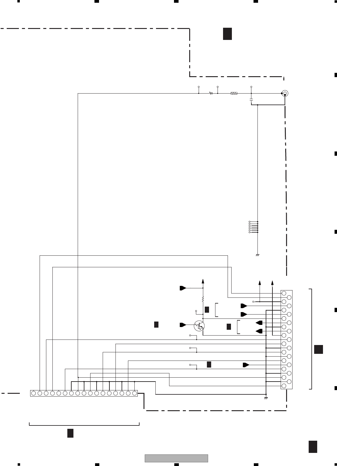
59
XV-DV575
56 7 8
56 7 8
A
B
C
D
E
F
SQUEEZE
ASPECT
P/XI
VSEL1
VSEL2
GNDD
V
GNDD
SC
SY
GNDD
CY/G
GNDD
Cb/B
GNDD
GNDD
Cr/R
S_Y
GND
from u-com 81p
GND
R
GND
S_C
DVDPOWER
V
(DTC124EUA)
SCART_L
GND
G
GND
VSEL2
V+5
B
TVMUTE
SCART_R
TVOUT_L
GND
TVOUT_R
V+10
SQEEZE
VSEL1
COMPOSITE
VIDEO
OUTPUT
34521117101269813 1614 1715
1
2
5
8
3
4
7
6
B
E
12
11
10
9
15
14
13
C
19
20
17
18
21
16
23
22
1
2
21
2
1
1
2
SY
SC
VSEL2
V
VSEL1
SQUEEZE
CN9000
R491
Q491
CN451
C427 R421
C421
JA403
VKN1248-
GNDD
VE+5
RT1N241M
10k
9604S-23C
V+5V+10
GNDD
(F)
1000/6.3 75
STBY
XKB3069-
DVDPOWER
XTVMUTE
VE+5
SCART_L
LINE_OUT_L
SCART_R
LINE_OUT_R
B3/5
CN461
D
CN967
A2/2
B
3/5
SYSMAIN ASSY
(XV-DV575 : XWM3392)
(XV-DV580 : XWM3395)
(XV-DV385K : XWM3391)
(XV-DV395K : XWM3394)
B1/5
B1/5
B4/5
B2/5
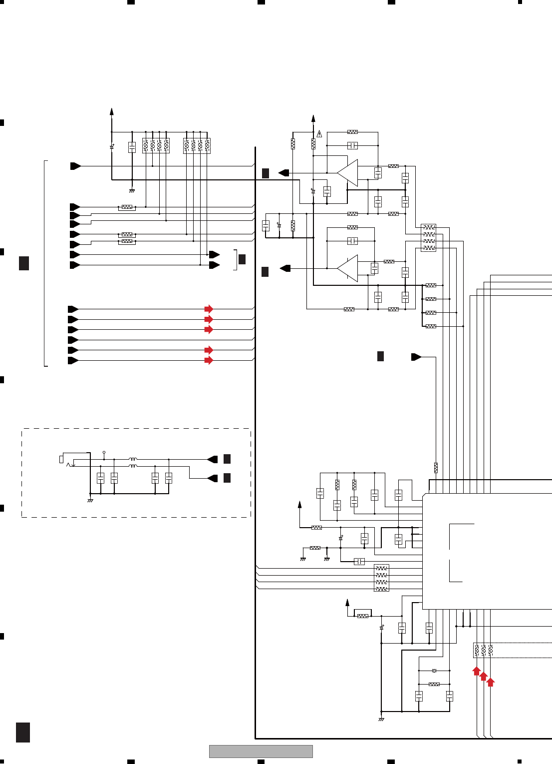
60 XV-DV575
12 3 4
A
B
C
D
E
F
12 3 4
10.6 SYSMAIN ASSY (4/5)
SROUT
PLCCONT
LRCLK
SCLK
S D ATA 3
S D ATA 2
S D ATA 4
S D ATA 1
XSD_1
XOTW_1
SCL
XMUTE
SDA
XPDN
MCLK
HP_R
XSD
XOTW
XRST
XHPSEL HP_L
+
-
+
-
PCB Binder:VEF1040
PLC_CONT
SR OUT
STBY
DVSS
XTL_OUT
XTL_IN
RESERVED
RESERVED
RESERVED
SCL
SDA
/MUTE
DVDD
/HP_SEL
/PDN
/RESET
VR_DPLL
OSC_CAP
LCRCK
AVSS
AVSS
RESERVED
MCLK
PWM_HPPR
PWM_HPMR
PWM_HPPL
VRD_PLL
AVSS_PLL
AVDD_PLL
VBGAP
PLL_FLTM
PLL_FLTP
PWM_HPML
PWM_P_6
PWM_M_6
PWM_P_5
VRA_PLL
PLL_FLT_RET
PWM_M_5
(2/2)
(NJM4565M)
(2/2)
(1/2)
(NJM4565M)
(1/2)
1817 19 20 21 2322 24 2625
2
1
4
16
15
14
13
12
9
11
10
8
7
5
6
4
3
2
1
6364 6062 61 5759 5856 55
SCL
SDA
LRCLK
PLCCONT
SROUT
LRCLK
SDATA4
SDATA1
SDATA2
SDATA3
XMUTE
SCL
SDA
XPDN
XHPSEL
XMUTE
XRST
TAS5508
SCLK
PWM_M_6
PWM_HPML
PWM_HPPL
PWM_HPPR
PWM_P_6
PWM_P_5
PWM_HPMR
PWM_M_5
XRST
XPDN
XHPSEL
C3113
R3105
C3111
C3110
C3114
R3106
X3101
R3107
C3112
JA5981
C5981
L5982
C5982
C5983
C5984
L5981
R3154
R3155
R3104
R3113
C3108
C3109
C3107
R3103
C3106
C3104
C3105
C3103
R3102
R3101
C3102
C3101
IC3131
R3912
R3908
C3908
C3904
C3912
C3902
C3924
R3924
C3922
C3906
R3910
R3906
IC3901
R3907
R3916
R3914
R3913
R3915
R3901
R3153
C3152
C3151
R3151
R3152
R3911
C3921
C3923
C3907
C3903 C3901
C3911
R3923
R3921
R3909
C5905
R3905
IC3901
18p/50
GNDD
STBY
10/10
0.1/16
15p/50
1M
13.5MHz
ASS7062
47
0.1/16
GNDD
RKN1004
STBY
STBY
STBY
STBY
STBY
STBY
STBY
STBY
V+3R3 220
GNDD GNDA
1000p/50
3.3
10/10
4.7
0.1/16
0.1/16
V+3R3
0.1/16
0.01/50
220
220
0.1/16
0.01/50
0.22/16
TA S 5 5 0 8BPAG
47
18k
5.6k
560p/50
680p/50
STBY
680p/50
5.6k
0.1/16
10/16
180p/50
10k
18k
NJM4565MD
18k 5.6k
4.7k
4.7k
4.7k
4.7k
4.7k
STBY
GNDD
STBY
0.1/16
10k
2.2k
V+3R3
10/25
0.1/25
560p/50
680p/50 680p/50
STBY
10k
8.2
180p/50
5.6k
NJM4565MD
18k
V+BSW
B4/5
(AD)
(AD)
(AD)
(AD)
(AD)
(AD)
(AD)
(AD)
B2/5 B
5/5
B3/5
B2/5
B3/5
B2/5
B1/5
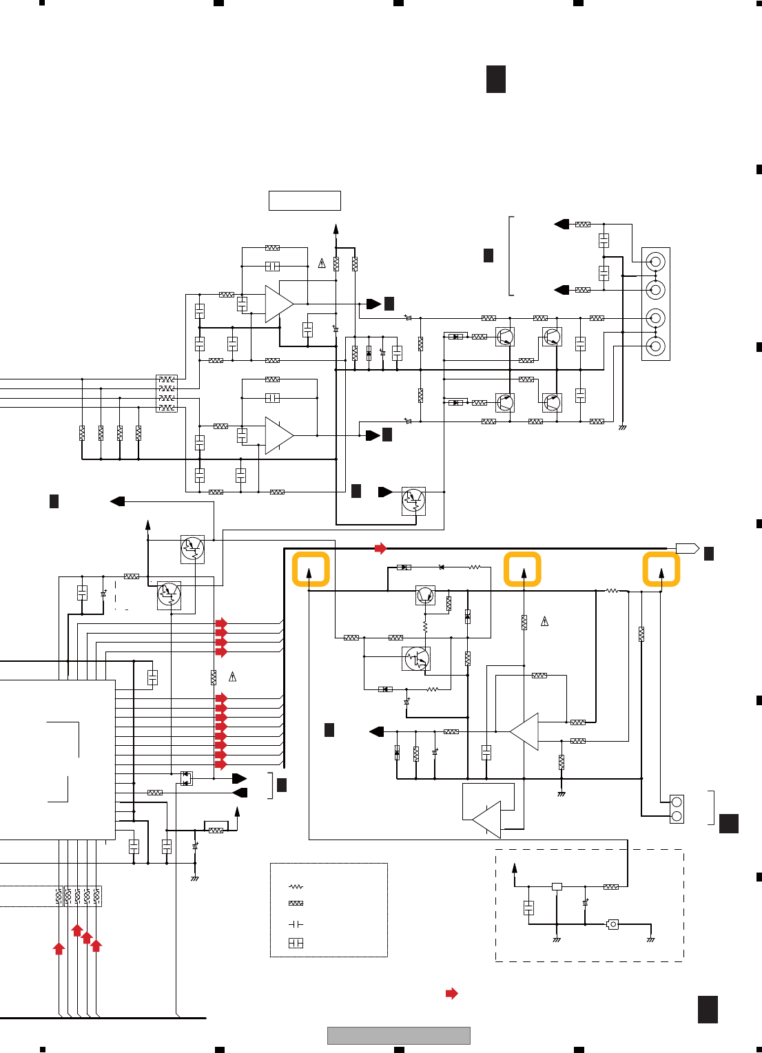
61
XV-DV575
56 7 8
56 7 8
A
B
C
D
E
F
XSD
VALID
PCON
PWRCONTRECMUTE
LINE_OUT_R
LINE_OUT_L LINE_IN_R
LINE_IN_L
OUT
COM
IN
+
-
+
+
-
+
-
-
capacitor
2125 size CKSQ**
1608 size CCSR**
CKSR**
resistor
1608 size RS1/16S***
2125 size RS1/10S***
3216 size RS1/8S***
STBY
AKB7114
CN3111
GAIN AMP
XKB3062
CN3112
AUDIO IN/OUT
VNF1084-
KN3101
SCLK
SDIN4
SDIN3
VR_DIG
DVSS
DVSS
SIND2
SDIN1
NC
DVSS
/BKND_ERR
DVDD (DAP202U)
PWM_M_1
VALID
PWM_P_7
PWM_M_8
PWM_P_8
PWM_M_2
PWM_P_1
PWM_M_7
PWM_M_3
PWM_P_2
DVDD_PWM
DVSS_PWM
PWM_M_4
PWM_P_3
VR_PWM
PWM_P_4
(DTA124EUA)
(DTA124EUA)
(2/2)
(2/2)
(NJM4565M)
(1/2)
(1/2)
(1/2) GND
+B
(2/2)
(2/2)
LINEOUT_L
LINEOUT_R
(NJM4565M)
(1/2) TVIN_L
TVIN_R
27 283129 30 32
23
1
33
35
34
37
36
38
40
39
42
41
43
44
45
46
48
47
5354 52 51 50 49 E
B
B
C
E
E
C
B
C
B
E
C
1
2
C
B
E
1
2
2
5
4
3
6
1
SDATA3
SDATA2
SDATA4
SCLK
SDATA1
XPDN
PWM_M_3
PWM_M_2
PWM_M_1
PWM_P_2
PWM_P_1
PWM_P_4
PWM_M_4
PWM_P_3
PWM_M_7
PWM_M_8
PWM_P_7
PWM_P_8
PWM
R3108
C3115
C3117
C3116
C3172
C3171
IC3171
R3171
R3109
R3110 D3101
R3114
C3118
IC3191
D3191
R3197
C3191
R3196
D3132
C3131
R3137
R3134
C3119
C3120
R3111
Q3604
Q3901
C3604
R3136
Q3132
R3133
R3132
D3131
R3131
Q3131
D3133 D3134 R3135
R3608
C3608
R3627
R3625
R3626
R3628
C3602
R3606
R3601 R3607
C3601C3603
R3612
C3614
Q3602
IC3601
C3606
R3610
D3603
C3622
R3624
C3610
R3614
D3602
R3617
C3624
C3607
R3611
C3623
C3613
C3621
R3613
D3601
R3618
C3609
CN3201
C3192
R3195
R3193
IC3191
R3194
R3192
R3199
R3198
R3191
R3616
Q3601
R3630
R3631
R3620
C3612
Q3603
Q3601
R3632
R3615 R3629
C3611
Q3603
R3619
IC3601
R3605
C3605
R3623
R3621
R3609
R3142
C1342 C3141
R3141
47
0.47/10
10/10
0.1/16
GNDD
0.1/16
GNDD
10/25
CHASSIS_GND
NJM78L05UA
V+5V
330
STBY
STBY
MC2846-11
0.1/16
V+3R3
UDZS4.7(B)
STBY
10K
2.2k
10k
STBY
STBY
STBY
0.1/16
10/10
RT1P241M
22
V+3R3
STBY
820p/50
STBY
2SA1036K(QR)
RT1N431M
1k
12k
47k
V+BSW1SS352 UDZS15(B)
4.7k
330p/50
10K
STBY
STBY
STBY
STBY
820p/50
4.7k
4.7k 4.7k
820p/50
820p/50
STBY
10/16
RT1P241M
NJM4565MD
330p/50
10K
10K
STBY
10/16
UDZS12(B)
47k
STBY 4.7k
0.1/16
330p/50
STBY
4.7k
0.1/25
10/25
47k
STBY 4.7k
10/16
BA10358FGNDD
B2P-VH
0.1/25
10K
100k
10K
2.2k
100k
BA10358F
UDZS18(B)
8.2
ACN7112
STBY
V+B
1k
0.1(2W)
V+25
8201k 220
GNDD
(2/2)
IMX9
4.7k
4.7k
820p/50
(2/2)
IMX9
820p/50
(2/2)
IMX9
1k 820 (2/2)
IMX9
220
330
NJM4565MD 330p/50
10K
2.2k
8.2
V+BSW
220p/50 220p/50
330
B4/5
CN2
F
B4/5 SYSMAIN ASSY
(XV-DV575 : XWM3392)
(XV-DV580 : XWM3395)
(XV-DV385K : XWM3391)
(XV-DV395K : XWM3394)
: AUDIO DATA SIGNAL ROUTE
(AD)
(AD)
(AD)
(AD)
(AD)
(AD)
(AD)
(AD)
(AD)
(AD)
(AD)
(AD)
(AD)
(AD)
(AD)
(AD)
(AD)
(AD)
B2/5
B2/5
B2/5
B2/5
B2/5
B3/5
B3/5
B5/5
62 XV-DV575
12 3 4
A
B
C
D
E
F
12 3 4
10.7 SYSMAIN ASSY (5/5)
PWM_P_2
PWM_M_2
PWM_P_4
PWM_M_4
PWM_P_1
PWM_M_1
PWM_M_3
PWM_P_3
XSD
XOTW
VALID
XOTW
VALID
XSD
PWM
27
2829
30
22
25
24
21
20
23
26
16
17
15
14
19
18
7
12
13
10
11
8
9
6
5
2
4
3
1
28
25
24
27
26
20
18
19
22
21
23
11
17
16
14
15
12
13
32
33
31
34
35
36
37
32
38
39
40
41
42
43
41
44
45
48
46
47
50
49 4
32
1
51
52
54
53
55
56
29
31
30
33
32
34
35
37
36
39
3814
32
41
40
44
42
43
46
45
5
9
6
10
8
7
4
3
2
1
47
48
50
49
52
51
32
14
54
53
55
56
R3323
C3301
R3325
C3323
C3321
C3325
R3327
C3333
C3331
R3331
C3345
R3335 C3337
R3301
R3303
R3302
C3303
R3304
R3305
R3309
C3304
R3308
R3306
C3302
R3307
IC3301
R3324 R3223
R3201
R3202
C3201
R3203
R3204
C3203
R3205
R3209
C3341
R3311
C3311
R3341
R3343
C3315
C3327
C3335
C3343
C3313
R3317
R3313
R3316
C3317 C3316
L3301
R3312
C3312
C3342
R3342
R3344 L3302
C3332
C3334
C3339
R3333
R3337
C3347
R3336
C3346
C3338
R3332
C3344
R3318
C3314 R3314
C3318
C3328
R3328
C3336
R3326
C3326
C3324
R3225
C3221
C3223
C3225
C3340
R3334
R3338
C3348
R3227
C3215
C3227
C3231
C3233
C3241
R3215
C3211
R3241
R3243
C3243
C3217
C3235
L3201
C3213
R3217
R3213
R3216
C3212 R3212
C3216
R3231
R3235
C3245
C3237 C3239
R3233
R3237
C3247
R3208
C3204
R3207
C3202
R3206
R3224
IC3201
C3242
R3242
R3244
C3244
R3214
C3218
C3228
C32323
C3234
L3202
R3218
C3214
R3226
R3228C3224
C3226
C3236
R3236
C3246
R3232
C3238C3240
C3248
R3234
R3238
GNDD
YB
1/16
V+BSW
820
820
0.01/50
1000/25
YB
V+B
1000p/50
3.3
YB
YB
CFTLA474J50
0.1/25
4.7K
0.01/50
1
STBY
STBY
STBY
STBY
0.1/16
220
STBY
YB
10K 0.1/16
4.7K
YB 100
1/16
47K
TAS5122DCA
YB
GNDD
V+BSW
YB
1/16
STBY
STBY
STBY
220
0.1/16
10K
STBY
YB
0.1/50YB
330p/50
YB
YB
1.5
2.7
0.033/50
0.1/25
YB
YB
18
18
YB
0.47/50
ATH7019
330p/50 0.1/50YB 2.7
0.033/50
1.5
YB
1.5
0.033/50
10
330p/50
0.1/50YB
YB
YB
330p/50
2.7
YB
18
18
0.033/50
YB
10
ATH7019
YB 0.01/50
0.1/25
4.7K
YB 1
STBY STBY
0.1/25
4.7K
10.01/50
YB
0.1/50 2.7
0.1/25
1.5
YB
YB
3.3
1000p/50
0.47/50
CFTLA474J50
820
820
YB
0.01/50
YB
YB
V+BSW
820
820
1000/25
V+B
0.01/50
1000p/50
YB
V+B
YB 0.01/50
0.1/25
4.7K
YB 1
STBY STBY
0.1/50
YB
3.3
YB
1.5
0.1/25
2.7
0.033/50
YB
0.47/50
YB
CFTLA474J50
330p/50
YB
YB
330p/50 0.1/50 YB
YB
18
18
2.7
0.033/50
YB
0.1/25
10
ATH7019
0.1/50
330p/50
YB
1.5
YB
1.5
2.7
0.033/50YB
ATH7019
0.1/25
4.7K
0.01/50
1YB 0.01/50
4.7K
YB 1
STBY
4.7K
YB
0.1/16
47K
100
YB
TAS5122DCA
1/16
YB
YB
330p/50
YB
0.1/50
18
18
0.033/50
2.7
YB
0.1/25
0.1/25
CFTLA474J50
YB
10
820
820
1.5
YB
3.3 0.01/50
1000p/50
0.47/50
YB
0.1/25
V+BSW
YB
YB
V+B
STBY
4.7K
0.01/50
1YB
0.01/50
4.7K
YB
STBY
1
AMPLIFIER
FL/RL
AMPLIFIER
FR/RR
LAYOUT NOTE :
L325X L335X L345X are PCB track inductors approx.
50mm long and 1mm wide
GND
GREG
GVDD
GND
BST_D
GND
/RESET_CD GND
/OTW
/SD_CD
/SD_AB
DP
DM
OUT_D
PVDD_D
PVDD_D
OUT_D
GND
CP
DREG_RTN
M3
CM
PVDD_C
PVDD_C
OUT_C
OUT_C
M1
DREG
M2
BST_B
BST_C
PVDD_B
/RESET_AB
AM
AP
GND
GND
GND
OUT_A
OUT_B
BM
BP PVDD_B
OUT_B
GVDD
PVDD_A
PVDD_A
DGND OUT_A
GND
GND
DVDD
GND
GREG BST_A
GND
/SD_CD
GND
GVDD
PVDD_D
PVDD_D
BST_D
GND
GND
GREG
/OTW
CP OUT_C
/SD_AB
DP
DM
/RESET_CD
CM
GND
GND
OUT_C
OUT_D
OUT_D
DREG
BP
BM OUT_B
PVDD_B
PVDD_B
DREG_RTN
M3
M2
M1 BST_B
BST_C
PVDD_C
PVDD_C
/RESET_AB
AM GND
OUT_B
AP
GND
DGND
GND
GND
PVDD_A
OUT_A
OUT_A
GND
GND
GREG
GND
GVDD
BST_A
DVDD PVDD_A
B5/5
(FR)
(FR)
(RL)
(FL)
(RL)
(FL)
(RR)
(RR)
1
2
12
1
2
12
B4/5
B4/5
B5/5
B4/5
B4/5
B5/5
B4/5
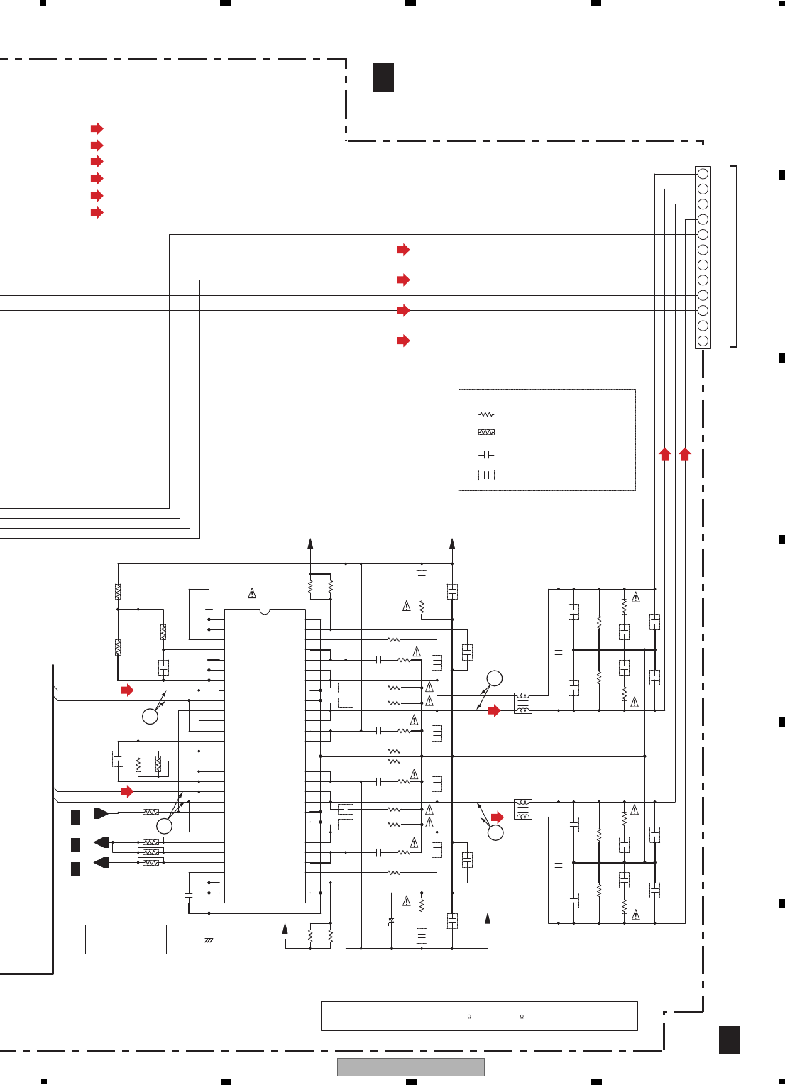
63
XV-DV575
56 7 8
56 7 8
A
B
C
D
E
F
PWM_P_7
PWM_M_7
PWM_P_8
PWM_M_8
XSD
VALID
XOTW
28
27
29
30
23
22
25
24
26
21
20
31
32
33
34
35
37
36
19
16
17
14
15
18
38
39
41
40
42
43
12
13
10
11
8
9
7
45
44
46
47
48
50
49
1
5
3
2
6
4
52
51
54
53
55
56
32
14
2
4
3
1
2
1
3
4
7
8
6
9
5
12
10
11
C3401
R3425
R3423
C3423
C3421
C3425
R3427
C3431
C3433
R3435
R3431
C3445
C3437
R3401
R3402
R3403
R3404
C3403
R3405
R3409 C3404
R3415
C3441
R3443
R3441
C3415
C3427
R3411
C3411
C3443
C3413
R3417
C3417
R3413
C3416
C3412
C3442
R3442
R3444
R3412
R3406
R3408R3407
C3402
C3444
R3418
C3418
C3428
C3414 R3414
R3428
IC3401
R3426
R3424
C3426
C3424
C3439
C3435
R3433
R3437
C3447
L3401
C3432
L3402
R3436
C3434
R3432
C3438
C3446
C3440
C3436
R3434
R3438
C3448
CN3211
GNDD
820
820
0.01/50
1/16 YB
V+BSW
1000/25
YB
1000p/50
3.3
YB
V+B
0.1/25
4.7K
1
YB
CFTLA474J50
0.01/50
STBY
STBY
STBY
STBY
220
0.1/16
10K
STBY
YB
0.1/16
0.1/50
330p/50
YB
YB
YB 2.7
1.5
0.033/50
YB
18
18
330p/50 0.1/50
0.1/50
YB 2.7
0.033/50
1.5
YB
1.5
0.033/50
330p/50
YB
YB
330p/50
2.7
YB
YB
18
18
0.033/50
YB
4.7K
100
47K
1/16
0.1/50 2.7
YB
1.5
YB
3.3
1000p/50
YB
TAS5122DCA
820
820
YB
0.01/50
YB
V+BSWV+B
0.47/50
ATH7019
YB
0.1/25
YB
0.01/50
0.1/25
4.7K
YB
YB
1
STBY
10
10
ATH7019
YB
0.1/25
4.7K
10.01/50
STBY
YB
0.1/25
0.47/50
CFTLA474J50
YB 0.01/50
0.1/25
4.7K
YB
STBY
1
YB
AKE7121-
AMPLIFIER
C/SW
RR+
RR-
FR-
FR+
RL+
FL-
FL+
RL-
C+
C-
SW+
SW-
R3211~R3214,R3311~R3314,R3411~R3414 : ACN7148-(2.7 )(SUB:ACN7141-(2.7 ))
NOTICE
(2W)
GND
GREG
GNDGND
BST_D
GVDD
/RESET_CD
DP
DM
/SD_CD
/OTW
/SD_AB
PVDD_D
PVDD_D
OUT_D
OUT_D
GND
GND
M1
CM
CP
M3
DREG_RTN
M2
DREG
OUT_C
OUT_C
PVDD_C
PVDD_C
BST_B
BST_C
PVDD_B
GND
/RESET_AB
AM
AP
BM
BP PVDD_B
OUT_B
OUT_B
GND
GND
OUT_A
GND
DVDD
GND
GND
GREG
DGND
PVDD_A
OUT_A
BST_A
PVDD_A
GVDD
GND
1608 size CCSR**
CKSR**
capacitor
1608 size RS1/16S***
2125 size CKSQ**
2125 size RS1/10S***
3216 size RS1/8S***
resistor
B5/5
B5/5 SYSMAIN ASSY
(XV-DV575 : XWM3392) (XV-DV580 : XWM3395)
(XV-DV385K : XWM3391) (XV-DV395K : XWM3394)
To 6ch SP
: AUDIO DATA SIGNAL ROUTE (Rear Lch)
(RL)
: AUDIO DATA SIGNAL ROUTE (Rear Rch)
(RR)
: AUDIO DATA SIGNAL ROUTE (Front Lch)
(FL)
: AUDIO DATA SIGNAL ROUTE (Front Rch)
(FR)
: AUDIO DATA SIGNAL ROUTE (Sub woofer ch)
(SW)
: AUDIO DATA SIGNAL ROUTE (Center ch)
(C)
(FR)
(RL)
(FL)
(RR)
(C)
(SW)
(C)
(SW)
(C)
(SW)
1
2
12
B4/5
B5/5
B4/5
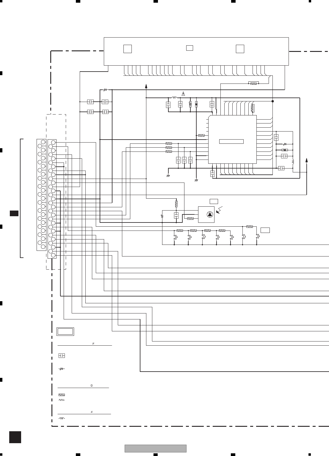
64 XV-DV575
12 3 4
A
B
C
D
E
F
12 3 4
10.8 COMPLEX ASSY
SG1
SG2 GR2
GR1
SG5
SG3
SG4
SG7
SG6
SG8
SG9
SG11
SG10
SG12
SG13
SG14
SG15
GR4
GR3
GR5
GR8
GR6
GR7
GR9
SG17
SG16
SG18
VEE
GR10
F-
GR7
GR5
GR1
GR6
GR2
GR4
GR3
GR8
GR10
GR9
SG17
SG18
SG16
SG15
SG13
SG14
SG12
SG10
SG11
SG8
SG9
SG7
SG6
SG5
SG3
SG4
SG2
SG1
FL
F+
Vout
GND
Vcc
F-
9G
5G
6G
3G
4G
7G
10G
1G
8G
2G
P18
P17
P15
P16
P14
P13
P12
P10
P11
P8
P9
P7
P6
P4
P5
P1
P2
P3
F+
26
27 27
29
28
26
20
21
19
22
23
24
25 25
24
19
22
23
20
21
13
17
16
15
14
18
17
16
14
15
18
13
6
11
9
8
7
12
10
6
11
7
12
10
9
8
2
3
4
5
11
2
3
4
5
12 13 14 15
7
10
9
11
6
8
4
5
3
2
44
1
43 42 41
181716 2119 20 22
28
26
27
24
25
23
29
30
31
32
383940 3537 36
33
34
1128711965141513 16 17 2019 22 23 24 2726 3029 32 33 3735 40393845
CN5902 CN5901
S5962
S5963
S5965
S5966
S5964
R5962
C5952
C5951
R5954
R5963 R5964 R5965
R5951
5902
S5991
S5967
R5966
C5921
C5922
C5920
C5915
R5903
R5902
R5901
R5904
L5902
C5916
C5917
D5902
C5918
IC5901
R5910
C5919
C5904 C5903
C5906 C5905
C5907
V5901
C5911
C5912
C5913
L5901
D5901
C5914
R5909
9607S-27F 9607S-29F
STBY STBY
VSG1024
VSG1024
VSG1024
VSG1024
1k
100
47/10
0.022
1.2k 1.5k 1.8k
GP1UE274XKC1
47
VSG1024
VSG1024
VSG1024
1k
CHASSIS_GND
220p
220p
GNDD
0.01/50
220p
220
220
220
82k
0.022/50
10
0.022/50
LAU100J
STBY
AL
47/35
VFDP
PT6315
STBY
STBY
STBY STBY
AL
47/35
0.022
0.022
AL
LAU220J
STBY
47/6.3
STBY
VE+5
STBY
VSS
VDD
VSS
VDD
VEE
(AAV7107-)
AAV7104-
FL SPACER
AEB7367 AEB7367
FL SPACER
RS1/10S***J
ALL INDUCTORS ARE IN H
LAU***J-TA
RS1/16S***J
ALL RESISTORS ARE IN
AT : CEAT**M**
UNLESS OTHERWISE SPECIFIED
CKSRYB**K50
JQ : CEJQ**M**
AL : CEAL**M**
ALL CAPACITORS ARE IN F
NOTES
MIC
HPMUTE
MIC SW
GNDA
FLCK
FLDATA
GNDA
HP_DET
GNDA
HP_L
HP_R
VFDP
GNDD
FLCS
V+10
FLDC+
GNDD
V5USB
GNDUSB
GNDUSB
FLDC-
REMOCON
VE+5
V5USB
KEY1
KEY2
NC
USB_DM2
USB_DP2
VOL DOWNVOL UP FM/AM /PAUSE
STOP
SR
/CLOSE
PLAY POWER ONOPEN
KEY
STBY
FL DRIVER
FL
C
CN9001
B3/5
XV-DV385K,
XV-DV395K
XV-DV575,
XV-DV580
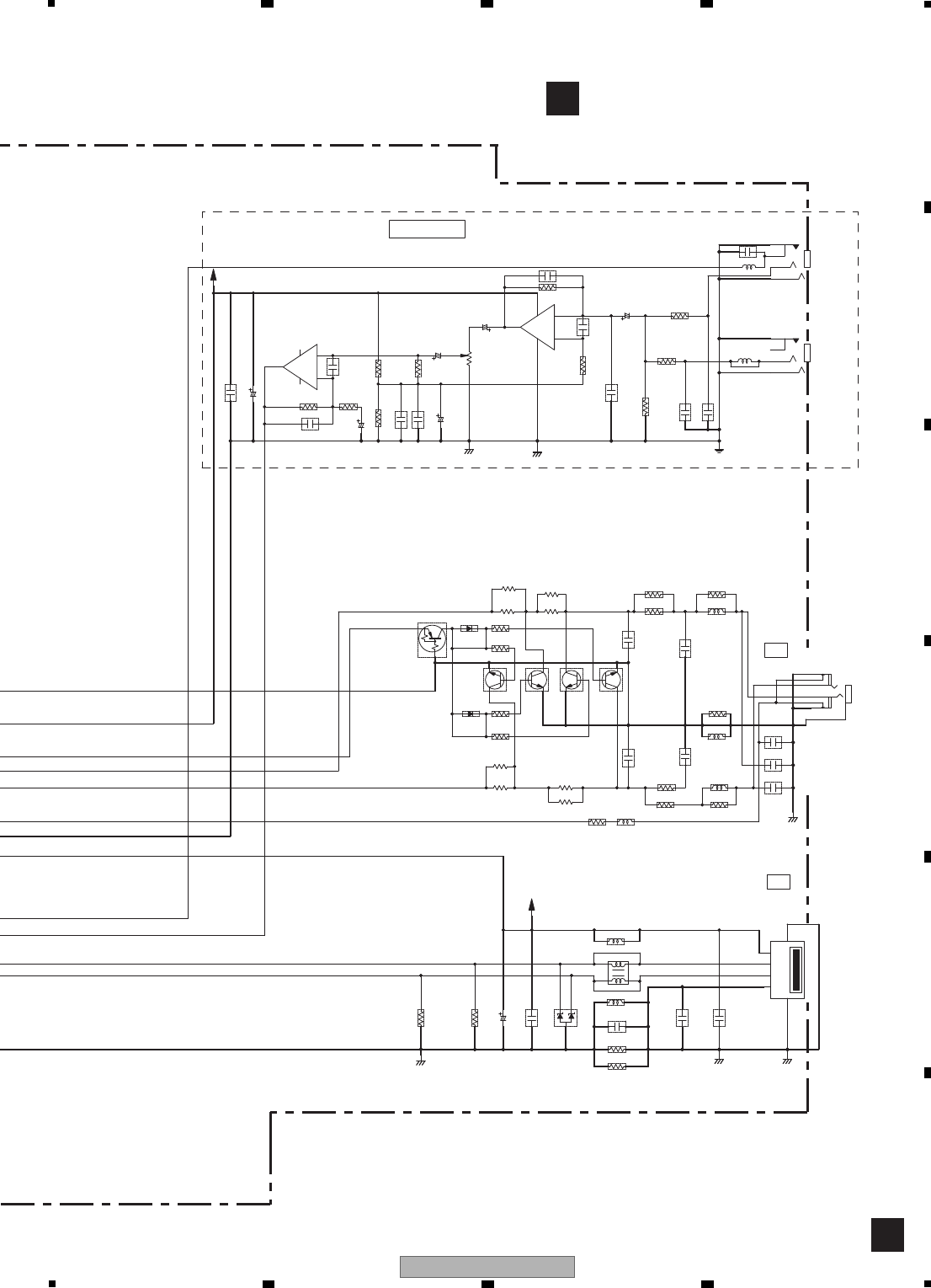
65
XV-DV575
56 7 8
56 7 8
A
B
C
D
E
F
-
+
+
-
3
12
43 4
6
C2 B2 EE
E2
B
CC
7
86
5
4
2
13
3
4
1
82
21
1
3
2
5
B2
C2
1
5
2
3
4
B
E2
7
6
1
3
2
4
1
2
3
4
R604
C602
R605
C601
D601
R603
R602
C603
L602
C604
C605
R5974
R5982
R5972
R5980
R5978
R5976
D5972
Q5973
Q5973
Q5971 R5975
D5971 R5977
R5973
R5979
R5971
R5981
C3937
C3938
C3935
C3936
R3931 R3930
C3931
R3929
C3932
C3933
C3934
IC3921
R3928
R3927
C3930
VR3921
IC3921
L603
L601
JA602
R5990 L5974
R5986
C5972
R5984
R5988
C5974
L5972
C5979
C5978
Q5974 Q5974
L5973
R5989
C5977
C5971
C5973
JA5901
R5985
R5983R5987
L5971
C3926
R3923
C3921
C3922
JA3922
R3926 C3927
R3922
L3922
C3928
C3929
R3925
R3921
C3925
L3921
JA3921
C3939
GNDUSB
STBY
STBY
220/6.3
0.1
STBY
STBY
GNDUSBCHASSIS_GND
UMZU6.2N
STBY
STBY
0.1
STBY
V5USB
68
68
68
68
IMX9
2.2k
2.2k
STBY
IMX9
RT1P241M
2.2k
STBY 2.2k
68
68
68
68
0.1
JQ-TS CHASSIS_GNDGNDA
2.2/50
STBY
12k
1200p
1.5k
CH
47/16
3.3k
0.1
100pF
AT- T S
STBY
NJM4565MD
3.3k
47k
2.2/50
AT- T S
XCS3007
NJM4565MD
AT- T S
2.2/50
STBY
STBY
XKB3056
CTF1306
68
68
68
1000p
STBY
CTF1306
0.047/25
GNDD
STBY
STBY
IMX9 IMX9
STBY
STBY
0.01/50
1000p
68CTF1306
0.047/25
AKN7005-
68STBY
STBY
STBY
XKN3012
GNDC
100pFCH
100pF
CH
10k
3.3k
STBY
STBY
VA+10 680p
47K
CH
2.2/50
JQ-TS 3.3k
XKN3012
CTF1306
0.022 CH
GND
(2/2)
(1/2)
(2/2)
(1/2)
+5V
D-
D+
USB
(1/2) (2/2)
HP
(SUB)
MIC AMP
(MAIN)
C
C
COMPLEX ASSY
(XV-DV575, XV-DV580 : XWM3429)
(XV-DV385K, XV-DV395K : XWM3428)
XV-DV385K,
XV-DV395K
66 XV-DV575
12 3 4
A
B
C
D
E
F
12 3 4
10.9 EUROSCART ASSY
(2/2)
(1/2)
S_Y
GND
R
S_C
GND
V
DVDPOWER
V+5
VSEL2
G
GND
B
GND
GND
TVOUT_L
TVMUTE
SCART_R
SCART_L
GND
(1/2) (2/2)
L
H
L
H
TVOUT_R
VSEL1
SQEEZE
V+10
R465
C469
R463 Q461
R461
R462
Q461
CN461
C465
Q472 Q463
C464
R464
Q462
R472
R471 Q462
R470
R466
R467
R468
R469
C470
C474
C476
D474
C473
IC472
C472
C475
D473
D472
C471
IC471
D471
Q492
E
B
CB2
20
18
22
19
23
21
17
14
12
16
13
11
15
10
8
6
9
7
5
E
B
C2
E2 B
EB
C
C
B2
E2
C2
C
E
6
5
4
1
3
2
6
5
4
1
3
2
1
2
3
4
4.7k
GNDD
STBY
RT3WLMM
56k
1.2k
RT3WLMM
22k
CKS3388
GNDD
STBY
RT1N241M RT1P441M
0.1
4.7k
RT3WLMM
22k
560 RT3WLMM
GNDD
V+5
820
10k
1.2k
1.2k
1k
0.1
0.1
GNDD
0.1
DAN202U
V+10
DAP202U
0.1 MM1507XN-TRB
0.1
V+5
0.1
DAN202U
10/50
MM1505XN-TRB
V+5
DAP202U
V+5
V+10
V+5
GNDD
RT1P241M
BLACK
SQUEEZE
CN451
3/5
B
D
D
EURO SCART ASSY
(AWU8291)
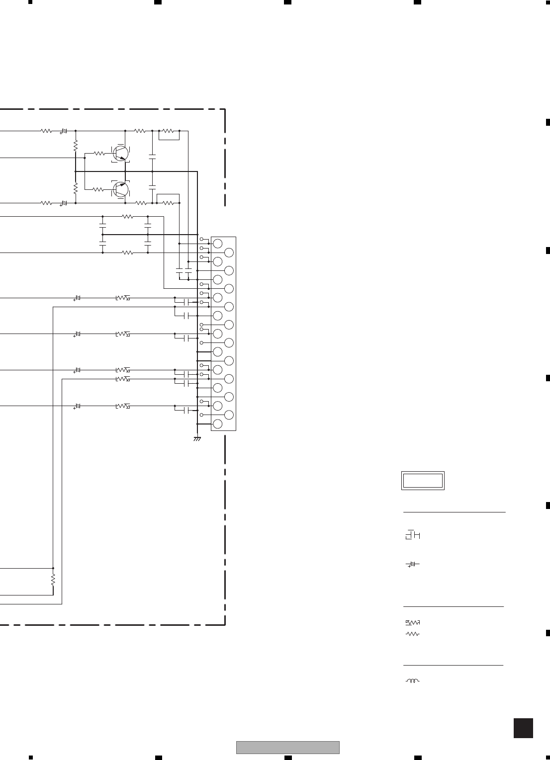
67
XV-DV575
56 7 8
56 7 8
A
B
C
D
E
F
LCYA***J2520
RS1/10S***J
RS1/16S***J
ALL INDUCTORS ARE IN μH
V/Y
GND
NC
V/Y
GND
R/C
SQUEEZE
B
G
BLANK
GND
GND
GND
BLANK
R/C
NC
G
L IN
GND
B
GND
NC
SQUEEZE
EURO CONNECTOR
L OUT
R IN
R OUT
GND
AT : CEAT**M**
ALL RESISTORS ARE IN Ω
AL : CEAL**M**
UNLESS OTHERWISE SPECIFIED
ALL CAPACITORS ARE IN μF
JQ : CEJQ**M**
CKSRYB**K50
NOTES
(2/2)
(1/2)
R473
R478
C492
C480
R477
C479
R476
C491
C490
C489
C478
R475
C477
R474
C488
C487
R495
C495
R496
C496
C493
C494
C486C485
R482
R481
C482
R484
R494
Q493
Q493
R488
JA451
C484
R486
C483
R483
R493
C481R485R487
21
20
18
19
17
16
14
15
13
12
11
10
9
8
7
6
5
4
3
1
2
C2
B2
E2
E
B
C
56k
75
1000/6.3
GNDD
47p
(F)
47p
75
470/6.3 75
75(F)
(F)
(F) 47p
47p
470/6.3
75(F)
470/6.3
0.1
47p
STBY
STBYSTBY
330
330
STBY
CH
100p
CH
100p
XKB3054-
1k
1k
10/50
4.7k
47k
IMX9
IMX9
STBY
470
330p
CH
330p
47k
4.7k
10/50
CH
STBY
470
D
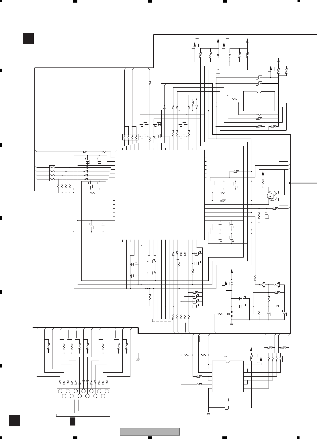
68 XV-DV575
12 3 4
A
B
C
D
E
F
12 3 4
10.10 DSP ASSY (XV-DV575, XV-DV580 ONLY)
DSDO
DECM
DSRT
DSSS
BUSY
HREQ
DSMD
DRDO
DRCS
DRRT
DICS
DRCS
DIRT
DRRT
DRCK
SCK
DIDI
DSDI
DSDI
SCK
ERR
FDTO
CDTO
SDTO
BDTO
FDTI
DSDI
DSDO
SCK
HREQ
DSSS
OSC
MC
DSRT
DSMD
DECM
BCKOLCKO
BUSY
MCLK
CN951
R959
R960
R957
R958
R956
R955
R953
R954
C952
C951
R963
R964
R966 R967 IC951
L952
R969
R968
R965
C808
C807
C806
C805
R804
R802
R806
R805
R803
C804
R807
C803
C802
C801
R801
R837
TP1 TP3
TP2
TP5
TP4
R811
R815
R812
R814
R816
R818
IC802
R810
C811
C812
C813
R817
C816
C817
C810
L801
R813
C815
L802
R820
C819
C820
R821
X801
R822
R823
IC802 IC802
C809
C814
C821
C822
C823
C824
IC801
R826
C826
R827
C827
R824
C825
R825
Q801
R829
R836
R834
R833
R832
C832 C830
C833 C831
C828
C829
R828
R856
R855
R857
R854
R852
R851
L804
R842
C835
L803
C834
R841
IC851
C851
C852
L851
R858
XKP3053
100k
100k
100k
100k
100k
GNDD
100k
100k
100k
GNDD
stby
0.1
YB
100
100
stby stby
V3D
74VHC08
RAB4C101J
QTL1013
V38
stby stby
100
YB
0.1
CH
470p
0.1
YB
470p
CH
RAB4C101J
100
10k
10k
10k
10k
47k
stby
YB
1
0.1
YB
CH
470p
47
47
RAB4C470J
100
100
CH
47 TC7WU04FU
GNDD
100
47k
100
100
220p
stby
220p
10k
CH
470p
CH YB
0.1
stby
1
YB
QTL1013
YB
4.7k
0.1
V37
V3D
QTL1013
stby
CH 5p
CH 5p
24.576MHz
470
1M
XSS3003
100
TC7WU04FU TC7WU04FU
CH
470p
470p
YB
0.1
CH
stby
YB
1
DSP
DSPC56371AF180
stby
0
YB
stby
stby
YB
100
0.01
RT1N241
1
47k
CH
470p YB
1
47
CH
470p
YB
0.1 stby
47
47
0.1
YB
47
V3D
10k
10k 10k
10k
stby
2.2k
47
ATL7002
ATL7002
GNDD
V11
stby
stby
stby
V1R2
V36
YB
ROM
PDC136A8
0.1
stby
stby
V3R
0
stby
V3D
V3D
13
12
3
4
5
6
9
10
7
8
11
2
1
6
7
5
8
10
9
4
312
11
1
2
14
13
25
24
23
22
21
17
18
19
20
15
16
12
13
10
14
9
11
7
8
5
4
6
3
2
1
80777879
4
53
8
44
71
826
8
27
26
28
29
30
31
34
32
33
37
36
35
38
39
40
44
41
43
42
45
46
50
51
52
47
49
48E
B
C
54
56
57
53
58
59
55
747576 717273 6970 68
60
6467 66 65 63 62 61
1
4
3
2
5
8
6
7
DIR RST
DSP HREQ
DSP MODE
DIR ERR
DEC MUTE
DSP RST
DSP DI
DSP SS
DSP DO
DSP CK
DIR CS
DIR DO
BUSY
3YGND
2Y
2B 3B
3A
2A
1Y 4A
4Y
1B
1A Vcc
4B
Level Shifter
5V 3.3V
VDDIO
GNDIO
PF10
SCAN
PF9
PF0
PF1
GNDSP
VDDIO
PF5
PF4
PF8
GNDCO
PF6
PF7
PF3
PF2
SDO0
SDO1
VDDCO
SDO3
SDO2
VDDIO
GNDIO
SDI0
SDI1
SCKT
FST
FSR
JTAG
(3/3)
(2/3) (1/3)
GNDCO
PB1
PB0
TDO
VDDCO
TDI
MOSI
TMS
TCK
SS
SCK
MISO
GNDPA
VDDPA
HREQ
VDDPP
PINIT
EXTAL
VDDPD
GNDPP
GNDPD
VDDCO
MODA
MODB
MODC
RESET
MODD
MUTE
COMMOUT0
SDI1_1
SDI0_1
COMMOUT1
MCK_STD
GNDCO
SCKT_1
GNDIO
VDDIO
SCKR
BUSY
VDDCO
PC2
HCKT
PE2
96DTS
GNDCO
VDDIO
GNDIO
PE5
FST_1
PE1
PE0
/HOLD
Vcc
/W
Q
/S
DVss
C
CN5532
1/5
B
E
E
DSP ASSY
(XV-DV575, XV-DV580 ONLY : AWX8706)
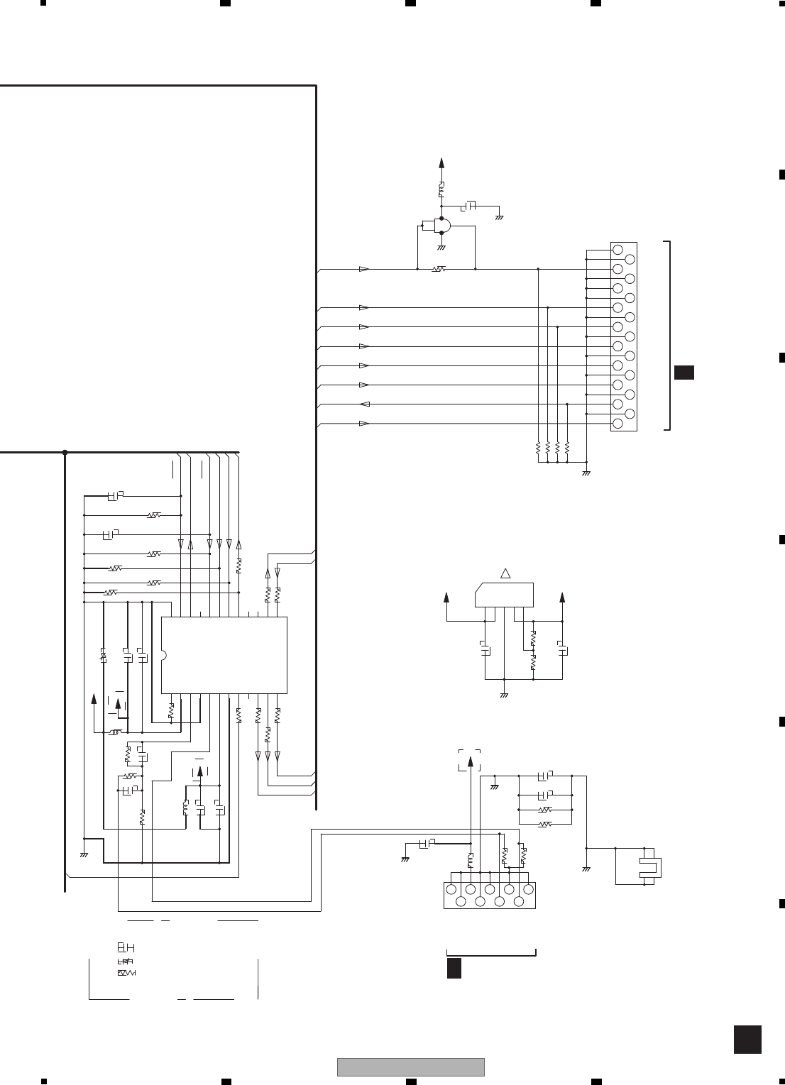
69
XV-DV575
56 7 8
56 7 8
A
B
C
D
E
F
OSC
BCKO
FDTI
LCKO
DAUX
MCLK
ERR
DRDO
DRCK
DIDI
DIRT
DICS
BDTO
DAUX
FDTO
CDTO
SDTO
LCKO
BCKO
MD
MCLK
C907
L901
R904
CN901
R903
KN901
R603
C601
R601
R611
C603
L603
R617
C617
C616
C615
C606
L602
C607
R605
R610
R607
R606
IC601
R616
R620
R621
R619
C614
C611
R618
R604
R608
R612
R905
R906
C904
C905
C901
C906
R901 R902
IC901
R755
IC650
R650
L650
CN701
C650
GNDD GNDD
stby
XKP3088
ATL7002
stby
GCH
100k
VNE1948
470
stby
470
stby
0.01
QTL1013
12k
V31
V3D
stby
stby
0.1
YB
QTL1013
YB
0.1
stby
V32
47
47
100
100
AK4117VF
10k
stby
stby
YB
1000p
stby
stby
YB
0.1
47
150
100
STBY
GNDD
stby
stby
stby
stby
V3D
YB
1
GNDD
1
33k
YB
V3D
22k
V1R2
BD00KA5WFP
RAB4C104J
100k
GNDD
GNDD
TC7SH08
V3D
0.1YB
GNDD
XKP3054
QTL1013
2
6
4
8
9
5
7
3
1
1
4
3
2
5
7
6
9
8
10
11
12
24
23
22
21
20
19
18
15
16
17
14
13
1423 5
16
18
19
17
15
10
13
14
11
12
5
6
4
3
9
8
7
2
1
5
3
4
2
1
UNLESS OTHERWISE NOTED
RS1/16S***
CEVW***
NOTES:
NOINDICATED
CKSRYB***
CCSRCH***
PARTS IS...
GNDD
V+3D
GNDD
GNDD
GNDD
GNDD
DVDIN(3.3V)
OPTIN(5V)
GNDD
R
AVDD
RX1
NC
DVSS
DVDD
RX0
LRCK
XTI
XTO
BICK
SDTO
AVSS
PDN
INT0
INT1
CSN
CCLK
CDTI
UOUT
CDTO
NC
DAUX
MCKO
Vcc
CTL
GND
ADJ
OUT
F%
!
BDTO
GNDD
DAUX
FDTO
SDTO
CDTO
GNDD
GNDD
GNDD
GNDD
GNDD
GNDD
BCKO
LCKO
GNDD
GNDD
GNDD
MCLK
GNDD
CN5533
1/5
B
CN5531
1/5
B
E
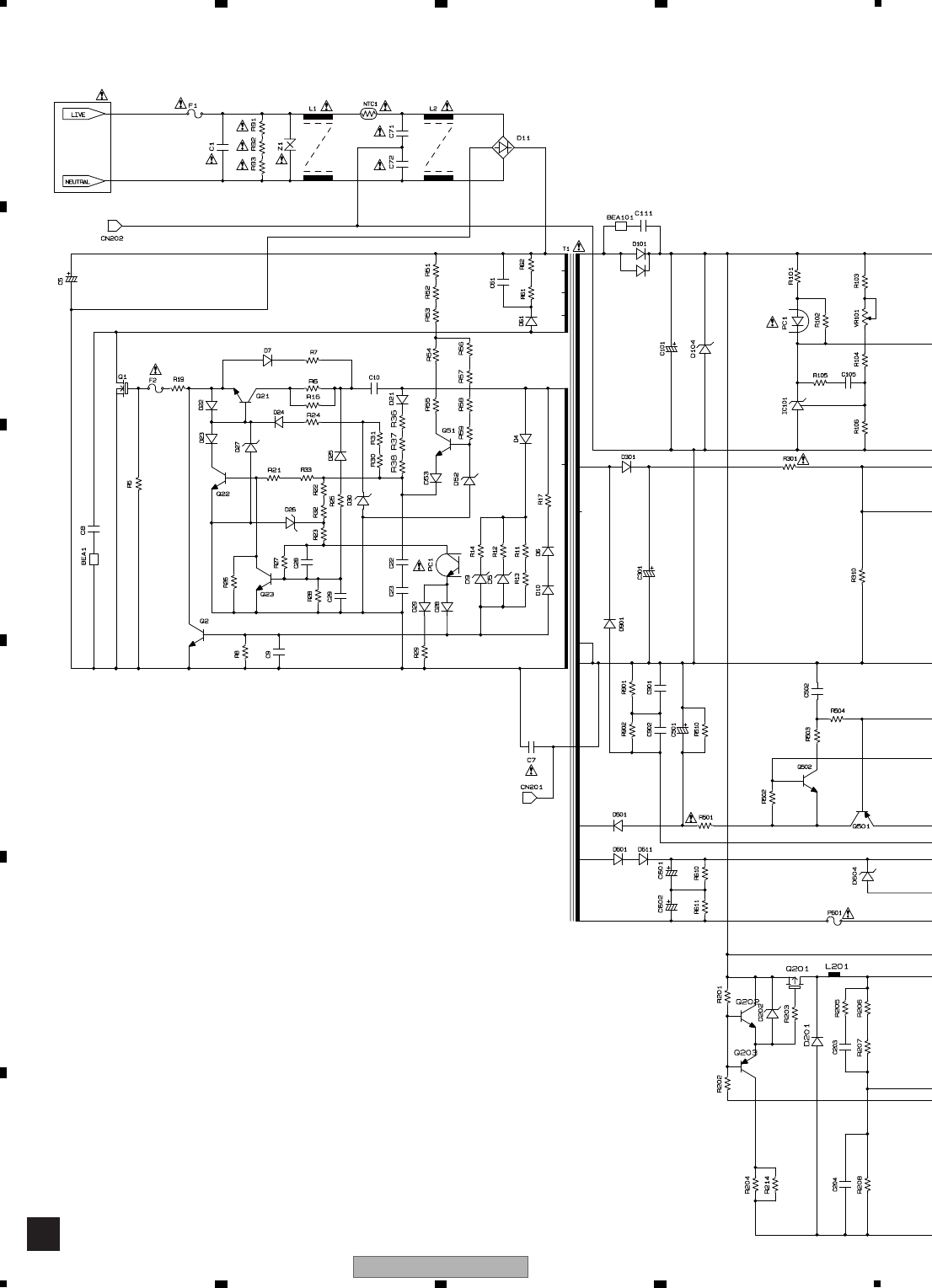
70 XV-DV575
12 3 4
A
B
C
D
E
F
12 3 4
10.11 POWER SUPPLY UNIT
AC
IN
F
CN1
71
XV-DV575
56 7 8
56 7 8
A
B
C
D
E
F
CN3201
B4/5
CN1001
B1/5
F
F
POWER SUPPLY UNIT
(XWR3018)
CN2
CN3
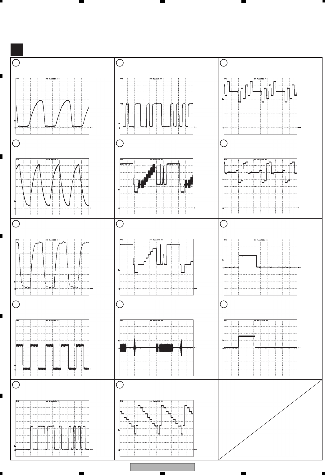
72 XV-DV575
12 3 4
A
B
C
D
E
F
12 3 4
10.12 WAVEFORMS
08 DVDM ASSY
A
GND GND GND
GND
GND
GND
GND
GND
GND
GND
GND
GND
GND
GND
Note : The encircled numbers denote measuring point in the schematic diagram.
X201 [XTALO]
V: 0.5 V/div. H: 10 ns/div.
It must be mesured by High-impedance probe.
0IC201 - pin 215 [ASPDIF]
V: 1 V/div. H: 200 ns/div.
It must be mesured by High-impedance probe.
5IC401 - pin 18 [CbOUT]
V: 0.5 V/div. H: 10 μs/div.
Playing DVD-REF-A1 Tr.2 Cp.19, Progressive output
10
IC401 - pin 16 [CrOUT]
V: 0.5 V/div. H: 10 μs/div.
Playing DVD-REF-A1 Tr.2 Cp.19, Progressive output
11
IC201 - pin 38 [TROPEN]
V: 2 V/div. H: 500 ms/div.
Tray closing
12
IC201 - pin 202 [TRCLOSE]
V: 2 V/div. H: 500 ms/div.
Tray opening
13
IC201 - pin 231 [ACLK]
V: 0.5 V/div. H: 10 ns/div.
It must be mesured by High-impedance probe.
1IC401 - pin 23 [CVBSOUT]
V: 0.5 V/div. H: 10 μs/div.
Playing DVD-REF-A1 Tr.2 Cp.1
6
IC201 - pin 230 [ABCK]
V: 0.5 V/div. H: 50 ns/div.
It must be mesured by High-impedance probe.
2IC401 - pin 21 [YOUT]
V: 0.5 V/div. H: 10 μs/div.
Playing DVD-REF-A1 Tr.2 Cp.1
7
IC201 - pin 227 [ALRCK]
V: 1 V/div. H: 5 μs/div.
It must be mesured by High-impedance probe.
3IC401 - pin 26 [COUT]
V: 0.5 V/div. H: 10 μs/div.
Playing DVD-REF-A1 Tr.2 Cp.1
8
IC201 - pin 226, 225, 223 [ASDATA0/1/2]
V: 1 V/div. H: 500 ns/div.
It must be mesured by High-impedance probe.
4IC401 - pin 20 [CYOUT]
V: 0.5 V/div. H: 10 μs/div.
Playing DVD-REF-A1 Tr.2 Cp.19, Progressive output
9
73
XV-DV575
56 7 8
56 7 8
A
B
C
D
E
F
SYSMAIN ASSY
B
GNDGND
IC3201, IC3301, IC3401 [PWM_M, PWM_P]
V: 1 V/div. H: 2 μsec/div.
1IC3201, IC3301, IC3401 [OUT_A, B, C, D]
V: 5 V/div. H: 2 μsec/div.
2
74 XV-DV575
12 3 4
A
B
C
D
E
F
12 3 4
11. PCB CONNECTION DIAGRAM
NOTE FOR PCB DIAGRAMS :
1. Part numbers in PCB diagrams match those in the schematic
diagrams.
2. A comparison between the main parts of PCB and schematic
diagrams is shown below.
3. The parts mounted on this PCB include all necessary parts for
several destinations.
For further information for respective destinations, be sure to
check with the schematic diagram.
4. View point of PCB diagrams.
Symbol In PCB
Diagrams
Symbol In Schematic
Diagrams Part Name
BCE
D
D
G
G
S
S
BCE
BCE
DGS
BCEBCE
BCE
Transistor
Transistor
with resistor
Field effect
transistor
Resistor array
3-terminal
regulator
Capacitor
Connector
P.C.Board Chip Part
SIDE A
SIDE B
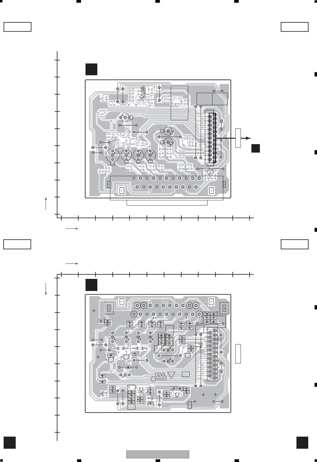
75
XV-DV575
56 7 8
56 7 8
A
B
C
D
E
F
11.1 EUROSCART ASSY
0 1020304050607080 90 100 110
0
10
20
30
40
50
60
70
80
90
X
X
Y
Y
0 1020304050607080 90 100 110
0
10
20
30
40
50
60
70
80
90
123
FCICT
R
W204
JA451
C477
C480
C482
C481
C471
C478
C479
CN461
CN461
W108
W110
W109
W112
W107
W102
W106
W104
W111
W103
W101
W203
W201
W202
GNDD
V+10
GNDD
VSEL2
VSEL1
SQEEZE
GNDD
V+10
V+5
GNDD
V+5
AWU8291
EUROSCART ASSY
1/4
PRODUCTION CODE
SIDE
CONTA C T
PNE-1B1
GNDD
GNDD
GNDD
1
2
20
21
1
6
3
4
1
6
3
4
NP
23 1
20 10
LF
R
R468
Q463
R472
R469
Q461
R463
R462
R473
C469
C465
R464
C464
R471
R465
C470
Q462
R466
R461
R467
R470
C494 C493
C495
C496
D474
D473
D472
C491
C492
R477
R478
C472
IC471
C489
R482
R493
R481
R486
C488
R474
C473
IC472
C475
C474
R496
R494
Q493
R484
C476
D471
C490
C487
R485
R475 R476
C483
C484
C485
C486
R495
R487
R483
R488
Q472
Q492
GNDD
V+10
V+5
V+5
V+10
GNDD
SQEEZE
VSEL1
VSEL2
GNDD
GNDD
DVDPOWER
1.VSEL1
2.SQEEZE
3.V+10
4.TVOUT_R
5.GND
6.TVOUT_L
7.TVMUTE
8.SCART_R
9.GND
10.SCART_L
11.V+5
12.VSEL2
13.B
14.GND
15.G
16.GND
17.R
18.
19.S_C
20.GND
21.V
22.GND
23.S_Y
C
B2
E2
1/4
E
B
C2
PNE-1B1
GNDD
GNDD
EUROSCART ASSY
AWU8291
SIDE A
D
SIDE A
D
SIDE B SIDE B
EUROSCART ASSY
D
EUROSCART ASSY
D
(ANP7569-B)
(ANP7569-B)
CN451
B
CN461CN461
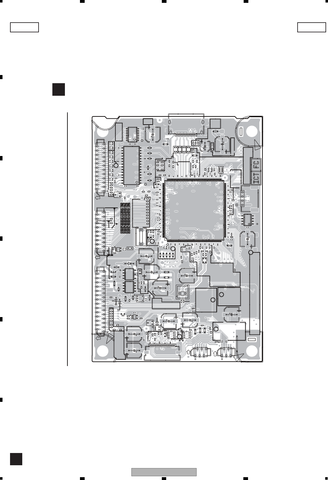
76 XV-DV575
12 3 4
A
B
C
D
E
F
12 3 4
11.2 08 DVDM ASSY
SIDE A SIDE A
A
A
08 DVDM ASSY
(ANP7631-A)
1/2
R402
R403
D751
R217
R411
R412
R413
R414
CN204
R415
R222
R416
R225
R226R227
R228
R229
R611
Q481
R421 R422 R423 R424
R618
IC751
R425
R232
R426
R237
R620
R238R239
R622
R623
R431
C201
R432
R626
R433
R627
C203
R434
R628
C204
R241
R435
R629
C205
R242
R436
R243
C207
R244
R245
R246
R248
R249
C402 C403
X201
C406
C213
C214
IC771
R251
R252
C216
R253
C217
C601
R256 C603
R259
C411
C412
C606
C413
C220
C414
C221
C415
C416
R260
C224
C225
C228
C229
C614
C421 C422 C423
C617
C230
C424
C231
C425
C619
C232
C426
C233
C234
C620
C239
R279
C628
C242
R474
R281
R475
C245
R476
C247
R284
R481
C251 C252
C452 C453
C454
C261
C455
C264
C266
C268
Q304
C269
Q305
Q307
Q308
C271
C272
C474
L308
C281
C475
L309
IC201
C476
IC204
IC401
C290
IC601
L901
R305
L932
L933
L934
L935
R310
CN101
CN102
R313
CN104
R315
R318
IC451
L751
R321
R322
R325
R901
R326
R902
R903
R711
R905
R712
R713
R907
R714
R908
L761
R715
R910
R911
R912
R913
R914
R918
R919
CN901
CN902
R921
C309
R152
R922
R153
R923
R154 R924
R155
C310 C320
C711
C712
C713
C714
R751
R752
C140
C141
R373
JA931
R959
R767
C343
R768
C344
R769
C345
C346
C153
C347
R960
R961R962
R770
CN951
CN953
R972
R973
R974
R975
R976
R977
R978
R979
C751
C752
C371
C372
C373
C374
C951
C952
C771
C772
C773
IC711
D934
R200
D935
R201
R202
R204
R205
R206
A
A
B
C
B
C
AWM
A30C5
[[ G ]]
LF
R372
R374
R375
R371
R314
R761
R762
R521
L251
C103
C753
CONTACT
SIDE
SIDE
CONTACT
UP SIDE
CONTACT SIDE SIDE EDISTCATNOCTCATNOC
A
BC
D
164
82156
129
192
256
193
R636()
R157
R156
C249
C248
IC241
R247
R240
L241
R523
R524
D
D
CN952(19)
(13)
8
R637
1
1
E
1
5
1
1
E
1
1
1
1 5 10 15 20 25 30 35 40 45 50 55 60
65 70 75 8085 90 95 100 105 110 115 120 125
130 135 140 145 150 155 160 165 170 175 180185 190
195 200 205 210 215 220 225 230 235 240 245 250 255
1
5
15 10
152025
1
5
1
1
1
1
15
1015
511015
1
1
5
5151
2010
25
20151051
5151
2010
15 15
15
10
1
5
5151
10
Q481
IC751
IC771
Q305
Q304
Q307
Q308
IC201
IC204
IC401
IC601
IC451
IC711
IC241
IC Q
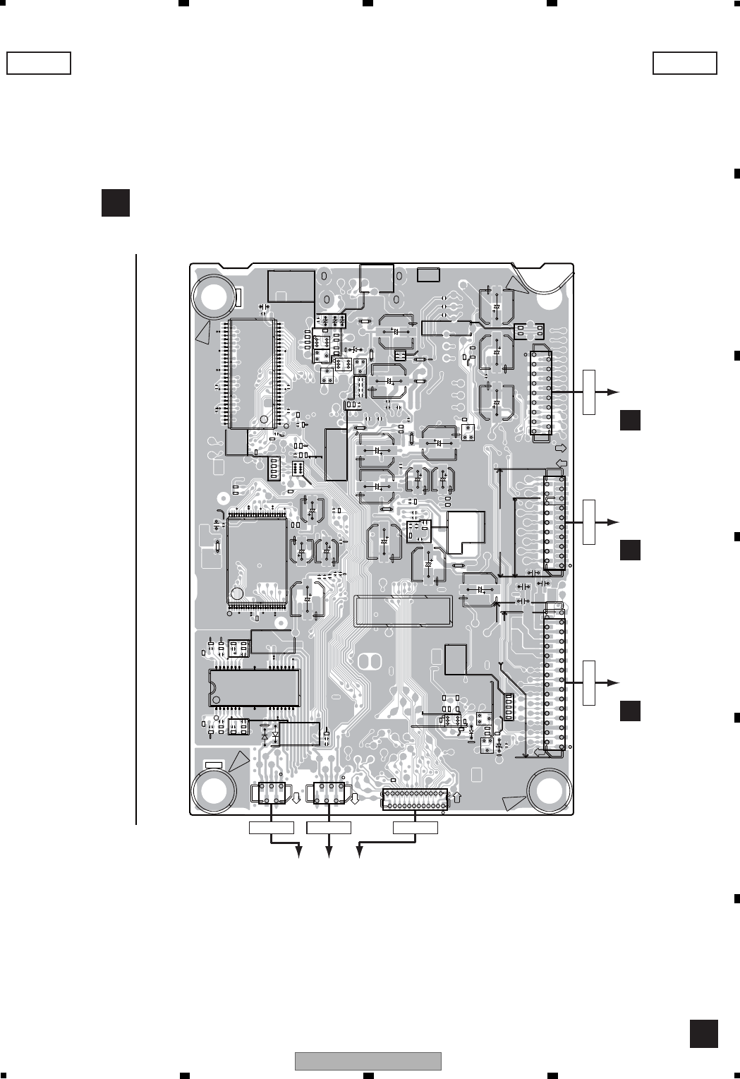
77
XV-DV575
56 7 8
56 7 8
A
B
C
D
E
F
R401
R404
R405
R406
R212
R213
R218
R219
R601 R602
R603 R604
R605
R220
R221
R609
R224
R801
R612
R613
R614
R615
R616
R617
R231
R233
R235
R236
R624
C200
R625
C202
C206
C208
C209
R631
C401
R632
R633
R634
C210
C404
C211
C405
C212
C215
R254
R255
C602
C605
C607
C608
C223
R261
C801
C226
C227
C611
C612
C613
C616 C618
C237
C621
C622
C623
C624
C625
C626
C627
C240
C241
C243 C244
R282
C246
R285
C250
C254
C258
C259
C451
C260
C262
C265
C267
C464
C465
C466
C273
C282
IC202
C283
IC203
C284C285
D801
C286
C287
C288
C289
C295
D811
R101
Q933
R103
Q934
R104
Q935
Q936
VA901
VA902
VA903
R304
R111R113
R114
R121
R123
R124
R131 R133
R134
R904
R906
R909
C101C102
R141R142
R916
R917
C111
C112
R151
C121 C122
C131
C132
C151
C152
R963
R964
R965
R966
R967
R968
R969
R970
R971
Q401
CN962
CN963
CN964CN965
C754
IC101
C953
Q801
Q621
D933
R203
R207
R208
R209
LF
PC
CN966
CN967
CN968
(29)
(27)
R635
R808
R806
R809
R810
R807
R811
Q802
D802
R804
R805
R803
R802
R980
A
B
C
D
SIDECONTACT CONTACT SIDE SIDECONTACT
SIDECONTACT CONTACT SIDE
CONTACT
SIDE
D101
D102
R210
R223
CN961
C703
C701
C702
C704
(13)
(19)
1
1510 15 20 25
30354045
50
1
5
10
15
20
25
30
35
40
45
E
1
1 E
E
0151
15
2025
29
30
1
15 15
10 20
E
1
1
15
10
5151
2010
25
15 15
5151
10
5151
2010
5151
10
SIDE BSIDE B
A
A
08 DVDM ASSY
CN5603
B
CN968
(ANP7631-A)
CN965
To DVD LOADER
CN964 CN966
CN962
CN9000
B
CN5605
B
CN967
IC Q
IC202
IC203
Q933
Q934
Q935
Q936
Q401
IC101
Q801
Q621
Q802
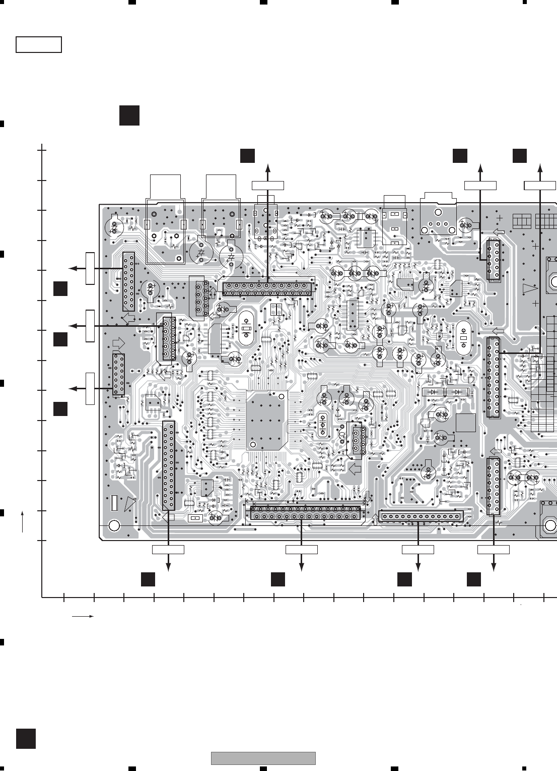
78 XV-DV575
12 3 4
A
B
C
D
E
F
12 3 4
11.3 SYSMAIN ASSY
0 1020304050607080 90 100 110 120 130 140 150 160
0
10
20
30
40
50
60
70
80
90
100
110
120
130
X
Y
7
1
1
80
30
51
31
100
50
81
14
85
1
13
9
11
19
113
NP
16
1
9
8
NP
18
916
1
11
14
5
8
18
916
8
1
5
4
NP
13
54
916
18
18
916
123
1
9
127
113
13
54
1
29
117
-1
999
888
777
666
555
444
333
222
111
000
1
01234
0123
0
01
C5524
C5508
C1501
C1502
R5510
R5508
L1501
C1505
R5515 R5513
C5525
C5597
Q5525
R5514
R5516
CN5501
R5597
R5509
C1201
R1204
R1301
R1415
C1413
R1401
R1402
R1403
R1404
Q1413
D1415
C1415
R1302
R1304
R1303
D1501
R1001
C5519
R5519
Q1302
Q1301
R5557
C5555
X5501
R5517
R5507
C5502
R5521
R5581
R5583
R5506
R5582
R5512
C5501
C5509
C5539
C5579
C5577
R5574
L4066
IC5501
R5501
C5517
R5518
R5525
R5527
R5535
R5537
R5538
R5546
R5547
R5548
R5565
R5564
C5557
IC5502
C5558
R5558
R5562
R5559
R5575 R5576
R5584
C5589
L5934 L5933
L5932
L5931
D5931
R5931
R5940
D5933
R5933
R5942
Q5935
R5935
R5934
R5938
Q5931 R5937
Q5934
R5939
R5936
R5943
R5528
R5530
CN5532
CN5533
CN5531
Q1304
Q1303
CN1001
R5534
R5533 R5532
R5531
C4612
C4613
L4603
C4614
C4615
R4609
R4610
JA4602
R1306
R1307
R5541
R5545
R5566
R5570
R5577
R5598
R5590
C5578
C5504
C5521
C5522
R5522
R5542
R5543
Q5531
JA5931
Q5532
R5505
R5569
C5518
R5544
Q1201
R1202
D1201
R1201 C1204
C1301
Q5932
Q5533
Q1202
D1416 D1417
C5931
C5932 C5936
Q5936
D5936
Q1402
R5585
R5571
Q5941
D5941
R5946
D5942
R5947
R5502
D1403
Q5534
Q5535
Q5942
R5944
R5949
R5945
R5948
C5716
R4967
C5714
C5720
C5715
C5707
C5708
C5701
C5709
R5705
C5703
C5702
R5719
C5704
C5705
R4968
R4969
C4968
C4966
C4965
C5712
R5710
C5719
IC5701
C5713
Q5703
R5716
R5717
R5718
IC4961
C4964
C4963
C4962
C4961
R5707
R5713
R5715
R5714
R5712
CN5701
D4961
D4962
R4966
C4967
R4908
C4909
R4914
C4911
R4020
R4019
C4020
R4905
C4908
C4903
R4906
R4907
C4904
C4910
R4911
L4901
C4905
R4913
C4019
R4085
R4066
R4063
C4907
IC4901
D4901
R4910
JA4901
R4065
R4061
R4062
C4901
C4906
C4902
R4902
R4903
R4084
C4064
R4064
IC4005
R4083
R4915
Q4006
R4006
R4017
R4018
R4016
C4016
R4003
C4057
C4056
X4004
R4014
C4012
R4012
R4015
C4015
R4056
R4055
C4022
R4010
R4022
C4004
D4902
D4903
C4011
R4011
R4013
R4090
R4053
R4054
C4052
IC4004
C4026
R4024
R4040
Q4005
R4073
R4052
R4058
R4046
C4027
C4028
C4029
R4026
R4002
KN4
C4048
R4049
R4057
C4046
C4045
R4045
R4028
IC4002
R4025
C4024
R4027
R4021
R4007
C4002
IC4001
C4001
R4048
IC4003
R4060
R4059
C4043
C4044
C4042
C4041
R4041
C4025
R4023
R4039
R4009 C4003
R4001
C4023
C4021
Q491
R491
CN451
JA403
CN401
C425
C424
R424 C429
C426
R426
R425
L422
L421
C430
JA402
C431
R421
C421
C427
CN5603
CN5605
C772
C771
C773
C782
C781
C783
R771
L772
IC771
R772
D781
D782
IC781
C5605
C5604
C5603
C5602
C5601
C4954
L4952
R4954
C4952
R4953
L4951
C4953
C4951
Q4951
R4955 C5606
R4952
R4951
X5701
L420
C9001
CN9001
R9000
102
CN9000
C9002
R9001
R9002
R4965
C1211
C1210
C1209
C1208
R5605
C1206
C1205
C1207
R5520
R4067
FLDC-
B
3R3V
V+5USB
STEST
V+5VV+3
D
UTEST
100
00
1
22
33
44
55
66
77
88
99
XW
1.AC_DET
30
V+6R8
GNDD
V+5USB
VU+5
V+3R3
V+3R3
V+5
GNDD
V+6R8
2.SW10.5V
3.EV5.0V
4.SW5.0V
5.SW6.8V 6.GNDD
7.SW3.3V(B)
8.SW3.3V(A)
9.PWR-CTR
10.GNDM
11.FLDC-
12.FLDC+
13.-25.5V
1.GNDD
2.DVDIN(3.3V)
3.GNDD
4.OPTIN(3.3V)
5.GNDD
6.GNDD
7.V+3D
8.GNDD
9.GNDD
1.GNDD
2.GNDD
3.MCLK
4.GNDD
5.GNDD
6.GNDD
7.BCK0
8.GNDD
9.LCK0
10.GNDD
11.FDT0
12.GNDD
13.SDT0
14.GNDD
15.CDT0
16.GNDD
17.DAUX
18.GNDD
19.BDT0
1.GNDD
2.ASDAT2_AR
3.GNDD
4.ASDAT1_AL
5.GNDD
6.ASDAT0_ALS
7.GNDD
8.ALRCK_C
9.GNDD
10.ABCK_ARS
11.GNDD
12.ACLK_LFE
13.GNDD
1.P/XI
2.SQUEEZE
3.VSEL2
4.VSEL1
5.ASPECT
6.SC 7.GNDD
8.V
9.GNDD
10.SY
11.GNDD
12.CY/G
13.GNDD
14.Cb/B
15.GNDD
16.Cr/R
17.GNDD
1.NC
2.DVDMUTE
3.VDET
4.MIC 5.GNDD
6.ACK
7.MDATA
8.SDATA
9.SCLK
10.XREADY
11.XDVDRST
12.DVDPOWER
13.GNDD
14.USBN
15.USBP
16.GNDD
17.DOUT
18,19.GNDD
20,21.GNDM
22,23.V+6R8
24,25.3R3V
26,27.V+5
4.Cr
3.GND
2.I/P
1.ASPECT
5.GND
6.Cb
7.GND
8.Y
9.GND
1.CE
2.DI
3.CLK
4.DO
5.GND
6.TXL 7.+9V
8.TXR
9.VSM
10.RDS
11.GND
1
DVDPOWER
V+6R8
VFDP
V+3R3
VE+5
USBN
USBP
V+3R3
V+5
VREF
VDET
VE+5
GNDD
VE+5
V+5
V+10
VREF
VREF
V+10
SIDE A
B
CN901
E
CN5533
CN461
D
CN451
CN951
E
CN5532
CN3
F
CN1001
CN5901
C
CN9001
CN968
A
CN5603
CN962
A
CN5605
CN967
A
CN9000
CN1
G
CN5701
CN70
E
CN5531
SYSMAIN ASSY
B
79
XV-DV575
56 7 8
56 7 8
A
B
C
D
E
F
150 160 170 180 190 200 210 220 230 240 250 260 270 280 290 300 310 320
13
9
19
NP
8
5
4
1
1
8
5
4
41
85
1
64
16
17 32
33 48
49
56 29
28
1 1 28
29 56 29
28
1
NP
-A1
999
888
777
666
555
444
333
222
111
000
A30C5/C7
[[ G ]]
1
0123456789
0123
0
01
C
B
A
R1001 KN1001
R5943
CN5532
CN5533
CN5531
Q5941
D5941
R5946
D5942
R5947
Q5942
R5944
R5949
R5945
R5948
R4065
R4084
Q4006
R4006
R4003
R4002
KN4001
R4081
R4082
R4001
C4954
L4952
R4954
C4952
R4953
L4951
C4953
C4951
R4952
R4951
Q3601
Q3602
D3603
R3196
C3192
D3191
R3197
C3191
R3195
R3194
R3193
R3192
IC3191
R3191
C3610
C3609
C3624 C3623
C3622 C3621
C3611
C3606
C3605
R3629
R3611
R3608
R3607
R3616R3615 R3617
R3613
R3609
R3621
R3605
R3601
R3906
R3908
R3907
R3901
C3902
C3904
C3922
R3910
C3908
R3905
C3923
C3905
R3909
C3921
R3911
R3921
R3923
R3924
IC3901
R3912
C3924
C3906
C3901
C3903
C3907
R3623 R3624
C3608
C3604
C3602
R3606
R3610
R3612
C3607
C3603
C3601
C3142
D3601
IC3601
R3614
R3618
C3612
R3630
CN3111
R3199
D3602
C3614
C3613
R3108
R3107
R3155
R3154
R3152
R3153
R3151
R3198
CN3201
C3141
R3141 R3142
C3118
C3119
C3120
R3111
R3110
C3115
R3109
C3116
C3117
C3114
C3113
R3106
X3101
C3112
C3110
R3105
C3111
R3113
R3103
C3108
C3107
C3109
C3106
C3103 C3104
C3105
R3102
R3101
C3102
C3101
IC3101
C3151
C3152
CN3211
R3423
R3409
R3407
R3418
R3406
R3416
C3404
C3427
R3408
C3401
C3425
L3402
C3412
C3426
R3405
R3436
C3423
C3439
R3411
C3415
L3401
R3434
R3426
R3403
R3438
R3431
R3412
R3432
IC3401
R3401
R3415
R3413
C3421
R3402
R3414
C3432
R3425
R3427
R3424
R3428
C3416
R3435
C3437
C3403
R3417
C3418
C3414 C3411C3413
R3437
C3428
C3431
C3438C3440
C3417
R3433
C3424
C3402
R3307
C3323
R3308
C3301
C3325
C3327
R3306
C3304
L3302
R3336
C3339
R3305
C3312
C3326
R3323
R3318
C3318
C3313 C3311
C3316
R3328
C3337
R3335
C3302
R3333
C3328
C3340
C3338
R3303
R3312
R3331R3338
C3315
R3332
R3314
C3321
R3325
R3316
R3313
R3315
IC3301
R3301
C3332
R3327
R3302
L3301
R3334
R3326
R3337
C3331
C3324
C3317
R3324
C3314
C3303
R3317
R3311
R3309
R3225
R3224
R3201
C3203
C3231
R3237
R3233
R3231
R3235
C3239 C3237
R3223
C3223
C3225
R3227
C3221
C3227
R3226
R3209
R3228
C3226
C3224
R3202
R3203
R3208
R3207
C3204
C3201
R3206
R3205
R3232
C3238
R3236
C3240
R3238
R3234
C3232
Q3604
L3201
L3202
C3202 C3228
C3214
R3214
R3218
C3218
R3216
C3216
R3217
C3217
R3212
C3212
R3213
C3213 C3211
R3211
C3215
R3215
IC3201
R3112
R3104
C3911
C3912
R3304
R3204
R3404
C3444 C3442 C3443
R3913
C3441
R3441
C3341
R3443
C3343
R3442
R3343
Q3603
R3444
R3625
R3132
R3131
Q3131
Q3132
R3341
R3626
R3627
R3628
R3914
Q3901
R3344
R3342
C3342C3344
D3101
R3114
R3133
R3134
R3136
D3131
KN3001
C3233
C3234
C3235
C3236
C3333
C3334
C3335
C3336
C3433
C3434
C3435
C3436
R3915
R3916
R3619
R3620
R3631
R3632
C5984
R3241
R3243
R3242
R3244
C3241C3243C3242C3244
C5983
L5981
L5982
C5981
C5982
JA5981
D3132
R3137
100
101
C3131
CN3112
D3134
D3133
R3135
A
FE
C
D
SW- SL-
SW+ SL+C- FL-
C+ FL+ SR- SR+ FR- FR+
LOUT RIN
LIN
ROUT
2.+B
1.GND
1
0
56
9
6
5
4
8
7
1
2
ICT FC
000
111
222
333
444
555
666
777
888
999
XWM
LF
PRODUCTION CODE
SYS MAIN ASSY 1/2
3
V+3R3
V+5
V+3R3
1.GNDD
2.DVDIN(3.3V)
3.GNDD
4.OPTIN(3.3V)
5.GNDD
6.GNDD
7.V+3D
8.GNDD
9.GNDD
1.GNDD
2.GNDD
3.MCLK
4.GNDD
5.GNDD
6.GNDD
7.BCK0
8.GNDD
9.LCK0
10.GNDD
11.FDT0
12.GNDD
13.SDT0
14.GNDD
15.CDT0
16.GNDD
17.DAUX
18.GNDD
19.BDT0
HP_R
HP_L
SIDE A
B
901
3
CN951
5532
CN701
E
CN5531
CN2
F
CN3201
(XNP3130-B)
80 XV-DV575
12 3 4
A
B
C
D
E
F
12 3 4
150160170180190200210220230240250260270280290300310320
1
13 9
1
119
1
LF
1
2
3
LF
C3245
C3246
C3247
C3248
C3345
C3346
C3347
C3348
C3445
C3446
C3447
C3448
SIDE B
B
SYSMAIN ASSY
B
CN5
CN5531
81
XV-DV575
56 7 8
56 7 8
A
B
C
D
E
F
0102030405060708090100110120130140150160
0
10
20
30
40
50
60
70
80
90
100
110
120
130
X
Y
71
1
13 9
1
119
13 1
11 1
123
19
1
27
1
13
129
1
17
F
SIDE B
B
(XNP3130-B)
CN5533 CN451
CN5532 CN1001 CN9001 CN5603
CN5605 CN9000CN5701
CN5531
82 XV-DV575
12 3 4
A
B
C
D
E
F
12 3 4
11.4 COMPLEX ASSY
0 1020304050607080 90 100 110 120 130 140
0
10
20
30
40
50
60
70
X
Y
0 1020304050607080 90 100 110 120 130 140 1
0
10
20
30
40
50
60
70
X
Y
W102
CN5901
V5901
IC5902
W103
L5902
W120
C5918
W101 C5952
L5901
C5913
W114
W113
W100
W106
W104
W105
CN5902
S5967 S5966
VR3921
C3930
C3937
C5907
W107
W115
W116
13.GNDD
1/4
14.VFDP
15.GNDD
16.FLDC
17.FLCS
18.V+10
GNDD
GNDD
23.GNDA
24.HP_R
VEE
4.USB_DP2
3.GNDD
1.KEY1
25.HP_DET
26.HP_MUTE
27.GNDA
Production Code
GNDD
GNDD
20.MIC
21.GNDA
27
19.FLCK
GNDD
OPEN/CLOSE DVD/CD
22.HP_L
COMPLEX ASSY
SIDE
1
CONTA C T
FLDC
9.V5USB
10.VE+5
GNDA
5.USB_DM2
6.GNDUSB
7.GNDUSB
8.V5USB
V+10
29
2.KEY2
11.REMOCON
28.FLDATA
29.MICSW
V+10
VFDP
12.FLDC
45
1
1
29
1
0
1234567890
123
0
0
1
C
B
A
LF
1
27
33
34
44
1
23
2212
11
R5903
C5916
D5902
C5922
C5915
C5919
C5914
D5901
C5917
R5904
R5951
C5911
C5951
R5901
R5902
C5920
C5921
C5912
R5954
R604
R605
C5904
C5906
R5966
R5965
IC5901
39
C5903
C5905
R3928
7.GNDUSB
6.GNDUSB
1.KEY1
2.KEY2
8.V5USB
XWM3429-
XWM3428-
5.USB_DM2
28.MICSW
29.MIC
10.VE+5
9.V5USB
27.GNDA
11.REMOCON
26.HP_MUTE
22.HP_L
21.GNDA
24.HP_R
23.GNDA
25.HP_DET
12.FLDC
13.GNDD
14.VFDP
15.GNDD
16.FLDC
17.FLCS
18.V+10
19.FLCK
20.FLDATA
3.GNDD
4.USB_DP2
SIDE A
C
SIDE B
CN9001
B
CN5901
CN5901
COMPLEX ASSY
C
COMPLEX ASSY
C
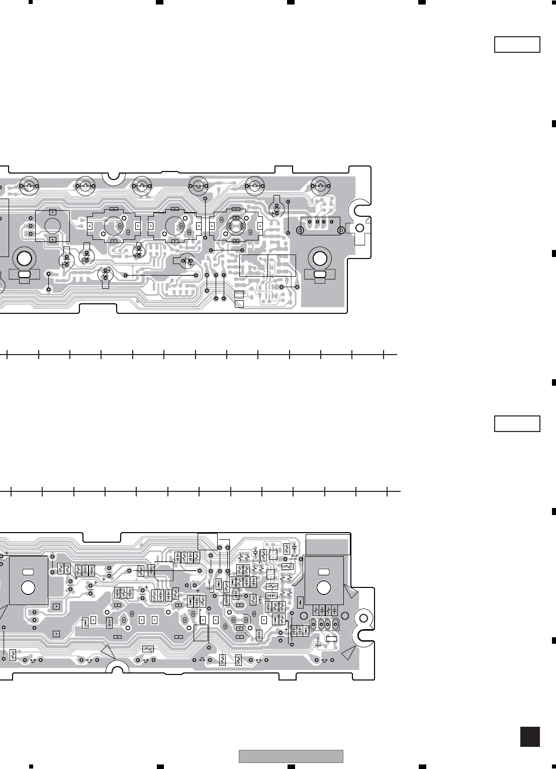
83
XV-DV575
56 7 8
56 7 8
A
B
C
D
E
F
130 140 150 160 170 180 190 200 210 220 230 240 250
130 140 150 160 170 180 190 200 210 220 230 240 250
C3925
S5964
JA3922
C3935
W111
W110
W109 W117
C3931
S5991
JA602
JA5901
W112
JA3921
S5962
S5963
C3929
C602
W108
W118
S5965
S5966
VR3921
C3930
W107
W119
GNDD
DVD/CD
XWM3429-
USB
STOP
GNDUSB
+ VOL
XWM3428-
GNDD
GNDD
- VOL
V+10
ON/OFF
FCICT
C7
[[ G ]]
NP
85
R5983
R5976
C5978
L601
R5973
C3928
C3926
C3921
R3925
R3931
C3934
R3930
C3936
L5974
C3932
L5973
L3922
R5964
C601
L602
C5972
R5984
R5986
C5974
R5988
R5990
L5972
R5974
R5972
Q5971
D601
C3938
C604
L603
R3926
Q5974
IC3921
R5963
R3923
R5962
R5989
C5977
C5979
L3921
Q5973
R3921
R3922
R5981
C3922
C3927
C3939
C5973
R5985
C605
R603
C603
R5987
L5971
R602
R5978
R5977
D5971
R5975
R5965
D5972
R5982
R5979
R5971
R3929
C3933
R5980
R3927
R3928
C5971
NP
1 4
SIDE A
SIDE B
C
(XNP3131-B)
(XNP3131-B)
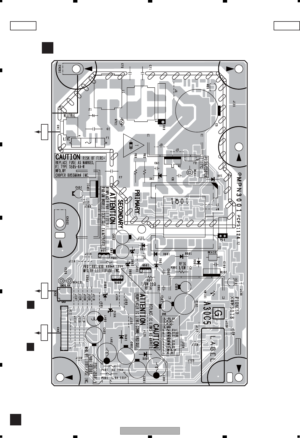
84 XV-DV575
12 3 4
A
B
C
D
E
F
12 3 4
11.5 POWER SUPPLY UNIT
SIDE ASIDE A
POWER SUPPLY UNIT
F
F
CN3201
B
CN2
CN1001
B
CN3
To AC POWER CORD
CN1
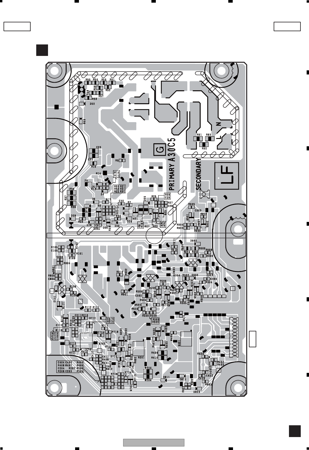
85
XV-DV575
56 7 8
56 7 8
A
B
C
D
E
F
SIDE BSIDE B
POWER SUPPLY UNIT
F
F
CN3
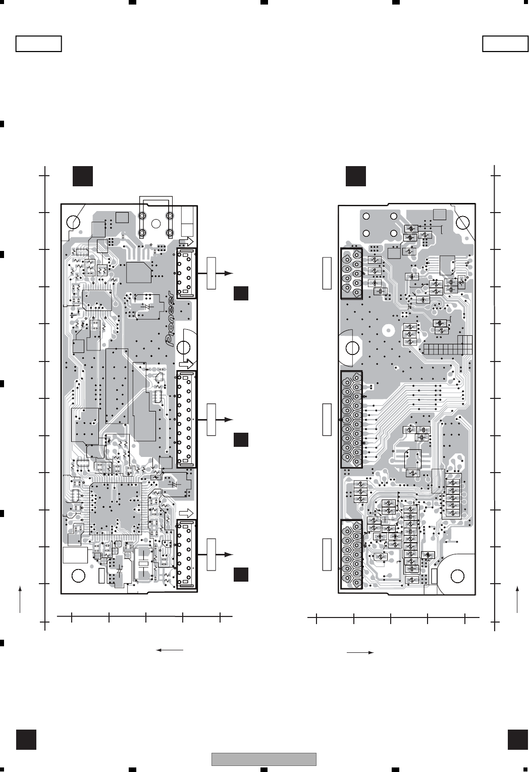
86 XV-DV575
12 3 4
A
B
C
D
E
F
12 3 4
11.6 DSP ASSY (XV-DV575, XV-DV580 ONLY)
E E
SIDE A SIDE B
10
0
20
30
40
50
60
20 30 40 50 60 70 80 90 100 110 120
X
Y
Y
10
020 30 40 50 60 70 80 90 100 110 120
X
20
30
40
50
60
(ANP7570-C)(ANP7570-C)
19
1
1
9
1
13
13
54
R858
R755
C615
R604
R617 C617
C616
L603
C606
C607
C611
C614
R616
IC901
CN701
901
R610
CN901
C901
IC601
R818
IC802
C816
C819
X801
C820
R810
C817
R821
R822
C808
C810
C807
C809
C815
C814
C806
C805
C821
C822
R823
C823
C824
R824
C825
R825
C804
C803
R802
C826
C827
R829
C802 R801
C801
IC801
R836
C832
C830
R834
R833
R832
C828
C833
C831
C829
R855
R857
R852
R851
L851
C835
L803
R841
C834
R620
R963
R967
R964
R837
R965
R958
R960
R611
C603
CN951
R618
R966
R968
R969
R621
C906
L650
C650
R650
IC650
1
24
12
ICTFC
1
LF
A
1
13
A
5
3
2
4
KN
61
60
41
40
2120 180
5
18
4
Production Code
19 191
17
8
14
13
1
R814
R605
R607
R606
L602
R612
C907
L901
R906
R903
R901
C904
C905
R601
C601
R608
R904
R905
R815
R902
R820
R816
R811
C812
C811
R817
C813
R813
L801
L802
R803
R804
R805
R806
R807 R826
R827
R828
R854
R856
IC851
C852
C851
R842
L804
R953
R954
R955
IC951
C951
C952
L952
R956
R812
R957
R959
R603
R619
Q801
9
7
8
0
1
2
3
4
5
6
7
8
99
8
7
6
5
4
3
2
1
0
LF
AWX8
58
1
4
DSP ASS'Y
E
DSP ASSY
E
DSP ASSY
E
CN5533
B
CN901
CN5531
B
CN701
CN5532
B
CN951
CN951 CN701 CN901
87
XV-DV575
56 7 8
56 7 8
A
B
C
D
E
F
12. PCB PARTS LIST
CONTRAST OF PCB ASSEMBLIES
AWM8118 and AWM8105 are constructed the same except for the following:
XWM3392 and XWM3395 are constructed the same except for the following:
XWM3391 and XWM3394 are constructed the same except for the following:
-
Meaning of the figures and others in the parentheses in the parts list.
Example) IC 301 is on the point (face A, 91 of x-axis, and 111 of y-axis) of the corresponding PC board.
IC 301 (A, 91, 111) IC NJM2068V
5 6 2 1
1 R 0
R 5 0
5 6 1
4 7 3
NOTES:
-
Parts marked by “NSP” are generally unavailable because they are not in our Master Spare Parts List.
-
The > mark found on some component parts indicates the importance of the safety factor of the part.
Therefore, when replacing, be sure to use parts of identical designation.
-
When ordering resistors, first convert resistance values into code form as shown in the following examples.
Ex.1 When there are 2 effective digits (any digit apart from 0), such as 560 ohm and 47 k ohm (tolerance is shown by J = 5%,
and K = 10%).
560 Ω → 56 × 10
1
→ 561 ...................................................................RD1/4PU J
47 kΩ → 47 × 10
3
→ 473 ...................................................................RD1/4PU J
0.5 Ω → R50 .................................................................................................RN2H K
1 Ω → 1R0 .................................................................................................RS1P K
Ex.2 When there are 3 effective digits (such as in high precision metal film resistors).
5.62 kΩ → 562 × 10
1
→ 5621 .................................................................RN1/4PC F
Mark No. Description Part No.
LIST OF ASSEMBLIES
1..08 DVDM ASSY (XV-DV575, XV-DV580) AWM8118
1..08 DVDM ASSY (XV-DV385K, XV-DV395K)AWM8105
1..DSP ASSY (XV-DV575, XV-DV580 ONLY) AWX8706
1..SYSMAIN ASSY (XV-DV575) XWM3392
1..SYSMAIN ASSY (XV-DV580) XWM3395
1..SYSMAIN ASSY (XV-DV385K) XWM3391
1..SYSMAIN ASSY (XV-DV395K) XWM3394
1..COMPLEX ASSY (XV-DV575, XV-DV580) XWM3429
1..COMPLEX ASSY (XV-DV385K, XV-DV395K) XWM3428
NSP 1..NHTS JACK ASSY AWM8034
2..EUROSCART ASSY AWU8291
>1..POWER SUPPLY UNIT XWR3018
1..FM/AM TUNER UNIT AXX7248
Mark No. Description Part No.
A08 DVDM ASSY
Mark Symbol and Description AWM8118 AWM8105
IC241 Not used TC7SH08FUS1
L241 CHIP SOLID INDUCTOR Not used QTL1013
CN962 13P FFC CONNECTOR Not used VKN1472
C248 Not used CKSSYB104K16
C249 Not used CCSSCH471J16
R240-R242, R244-R246 Not used RS1/16SS330J
R243 Not used RS1/16SS100J
BSYSMAIN ASSY (XV-DV575/XV-DV580)
Mark Symbol and Description XWM3392 XWM3395
R5514 Not used RS1/16S473J
R5516 RS1/16S473J Not used
BSYSMAIN ASSY (XV-DV385K/XV-DV395K)
Mark Symbol and Description XWM3391 XWM3394
R5516 RS1/16S473J Not used

88 XV-DV575
12 3 4
A
B
C
D
E
F
12 3 4
XWM3429 and XWM3428 are constructed the same except for the following:
PCB PARTS LIST FOR XV-DV575/WYXJ5 UNLESS OTHER WISE NOTED
CCOMPLEX ASSY
Mark Symbol and Description XWM3429 XWM3428
IC3921 Not used NJM4565MD
L3921 INDUCTOR Not used CTF1306
VR3921 VARIABLE (10K-X1) Not used XCS3007
CN5902 27P FFC CONNECTOR 9607S-27F Not used
CN5901 29P FFC CONNECTOR Not used 9607S-29F
JA3921, JA3922 MIC JACK Not used XKN3012
R3921, R3922, R3928, R3929 Not used RS1/16S332J
R3925, R3927 Not used RS1/16S473J
R3926 Not used RS1/16S103J
R3930 Not used RS1/16S152J
R3931 Not used RS1/16S123J
C3921, C3922, C3933 Not used CCSRCH101J50
C3925, C3935 Not used CEJQ2R2M50
C3928 Not used CCSRCH681J50
C3929, C3930 Not used CEAT2R2M50
C3931 Not used CEAT470M16
C3932, C3938 Not used CKSRYB104K16
C3936 Not used CKSRYB122K50
C3939 Not used CKSRYB223K16
Mark No. Description Part No.
A08 DVDM ASSY
SEMICONDUCTORS
IC 101 BA5984FP
IC 201 MT1389FE/S-L
IC 202 K4S641632K-UC75
IC 203 AYW7242
IC 204 S-24CS64A0I
IC 401 MM1758XF
IC 601 TC7SH08FUS1
IC 711 MM1661JH
IC 771 NJM2872BF05
Q 304,801 2SC4081
Q 305 UM5K1N
Q 307,308 HN1A01F
Q 481,933 DTC114YUA
Q 621 2SK2034
Q 802 HN1A01FU
Q934 UMB1N
D 101,102 RR264M-400
D 761,762 UDZS3R9(B)
D 801 UDZS4R7(B)
D 802 DAN202U
D 811 1SS352
D 933 UDZS5R1(B)
MISCELLANEOUS
L 751 INDUCTOR CTF1395
L 761 COIL VTH1047
L 901 INDUCTOR CTF1334
L 932-935 COIL ATH7022
JA 931 HDMI CONNECTOR AKP7224
X 201 CRYSTAL RESONATOR (27MHZ) VSS1172
CN 964 06P CONNECTOR VKN1574
CN 965 05P CONNECTOR VKN1573
CN 966 CONNECTOR VKN2045
CN 967 17P CONNECTOR VKN1577
CN 968 27P CONNECTOR VKN1583
RESISTORS
R 103,113,114,201 RS1/16SS1202F
R 104 RS1/16SS1002F
R 123,133 RS1/16SS3302F
R 124,134 RS1/16SS2702F
R 153,156,157 RS1/8SQ3R3J
R 202 RS1/16SS8201F
R 205,206 RS1/16SS1502F
R 208,209,281,634 RS1/10S0R0J
R 221,225 RAB4CQ330J
R 279 RS1/16SS2201F
R 411-416 RS1/16SS1500F
R 617 RS1/16SS2701F
R 636 RS1/16S0R0J
R 715,752,902 RS1/10S0R0J
R 978-980 RS1/10S0R0J
Other Resistors RS1/16SS###J
CAPACITORS
C 103,373,401,404 CEVW101M16
C 151,200,204,205 CKSSYB104K16
C 152,153,210 CKSSYB222K50
C 201,202,223,237 CEVW221M4
C 203,206,215,309 CEVW470M16
C 207,208,213,216 CKSSYB104K16
C 209 CKSSYB153K16
C 211,212 CCSSCH271J50
C 217,220,224,225 CKSSYB104K16
C 226,240,283-288 CKSSYB103K16
Mark No. Description Part No.

89
XV-DV575
56 7 8
56 7 8
A
B
C
D
E
F
C 227 CCSSCH221J50
C 228-234,239,243 CKSSYB104K16
C 241,602,607,952 CEVW100M16
C 242 CKSSYB152K50
C 244,246,247,250 CKSSYB104K16
C 245,282,289 CKSRYB105K10
C 251,252 CCSSCH100D50
C 254,267,295,608 CKSSYB102K50
C 258,259 CKSSYB473K16
C 260,261,264,266 CKSSYB104K16
C 262,605 CEVW4R7M16
C 265 CCSSCH220J50
C 268,271-273,290 CKSSYB104K16
C 269 CKSSYB333K10
C 281,618 CEVW221M4
C 310,616,627 CEVW470M16
C 343-347,412-414 CKSRYB105K10
C 371,372,402,405 CKSSYB104K16
C 406,601,603,606 CKSSYB104K16
C 411,415,416 CKSRYB104K16
C 611 CKSSYB562K25
C 612,613,617 CKSSYB104K16
C 614 CCSSCH101J50
C 619-621,623,625 CKSSYB104K16
C 622,624,626 CKSSYB102K50
C 628,773,801,951 CKSSYB104K16
C 711,771 CKSRYB105K10
C 712 CCSSCH471J16
C 713,772 CKSQYB225K10
BSYSMAIN ASSY (XV-DV575)
MISCELLANEOUS
>IC 771 (A,121,39) LOAD SWITCHING AAT4618IGV-0.5-1
>IC 781 (A,134,40) REGULATOR IC NJM2845DL1-05
IC 3101 (A,237,20) 8CH PWM PROCESSOR IC TAS5508BPAG
IC 3191 (A,182,94) OP-AMP IC BA10358F
>IC 3201 (A,267,44) DIGITAL AMP IC TAS5122DCA
>IC 3301 (A,237,44) DIGITAL AMP IC TAS5122DCA
>IC 3401 (A,207,44) DIGITAL AMP IC TAS5122DCA
IC 3601 (A,306,95) DUAL OP-AMP NJM4565MD
IC 3901 (A,206,16) DUAL OP-AMP NJM4565MD
IC 4001 (A,96,75) IC TC4052BFN
>IC 4002 (A,113,70) REGULATOR IC NJM2872BF25
IC 4003 (A,114,85) AD CONVERTER IC AK5358AET
IC 4901 (A,101,101) DUAL OP-AMP NJM4565MD
IC 5501 (A,68,40) SYSTEM CONTROL MICON PDC175A
IC 5502 (A,30,46) EEPROM S-93C46BD0I-J8T1
IC 5701 (A,50,67) RDS DECORDER IC LC72725KM
Q 491 (A,76,79) TRANSISTOR RT1N241M
Q 1301 (A,128,16) TRANSISTOR(SC-70) 2SA1602A
Q 1302 (A,24,35) TRANSISTOR 2SA1577
Q 1303 (A,133,18) TRANSISTOR 2SC4154
Q 1304 (A,19,31) TRANSISTOR 2SC4154
Q 1402 (A,132,25) TRANSISTOR(SC-70) 2SA1602A
Q 1413 (A,130,29) TRANSISTOR RT1N241M
Q 3131 (A,181,35) TRANSISTOR 2SA1036K
Q 3132 (A,189,34) DIGITAL TR(SC-70) RT1N431M
Mark No. Description Part No.
Q 3601 (A,296,95) TRANSISTOR IMX9
Q 3602 (A,300,79) DIGITAL TR(SC-70) RT1P241M
Q 3603 (A,289,93) TRANSISTOR IMX9
Q 3604 (A,269,27) DIGITAL TR(SC-70) RT1P241M
Q 4005 (A,99,83) CHIP TRANSISTOR HN1A01FU
Q 4006 (A,151,31) TRANSISTOR RT1N241M
Q 4951 (A,65,15) TRANSISTOR RT1N241M
Q 5525 (A,103,40) DIGITAL TR(SC-70) RT1N431M
Q 5531 (A,136,54) TRANSISTOR RT3N22M
Q 5532 (A,131,58) TRANSISTOR RT1N241M
Q 5533 (A,130,54) DIGITAL TR(SC-70) RT1P241M
Q 5703 (A,41,68) CHIP TRANSISTOR HN1C01FU
Q 5931 (A,86,99) TRANSISTOR RT1N241M
Q 5932 (A,78,98) TRANSISTOR RT3N22M
Q 5934 (A,82,103) TRANSISTOR(SC-70) 2SA1602A
Q 5935 (A,74,94) TRANSISTOR(SC-70) 2SA1602A
Q 5936 (A,78,103) DIGITAL TR(SC-70) RT1P241M
D 1403 (A,127,13) DIODE MC2846-11
D 1415 (A,134,30) DIODE UDZS4R7(B)
D 3101 (A,264,26) DIODE MC2846-11
D 3131 (A,184,39) DIODE UDZS18(B)
D 3133 (A,181,42) DIODE 1SS352
D 3134 (A,183,42) DIODE UDZS15(B)
D 3191 (A,198,26) DIODE UDZS4R7(B)
D 3603 (A,313,81) DIODE UDZS12(B)
D 4901 (A,82,109) DIODE UDZS5R1(B)
D 4902 (A,92,98) DIODE UDZS3R9(B)
D 4903 (A,89,99) DIODE UDZS3R9(B)
D 5931 (A,78,107) DIODE 1SS352
D 5933 (A,66,98) DIODE 1SS352
D 5936 (A,74,99) DIODE 1SS352
L 772 (A,124,45) CHIP SOLID INDUCTOR ATL7002
L 1501 (A,93,33) AXIAL INDUCTOR LAU220J
L 3201 (A,284,68) INDUCTORS ATH7019
L 3202 (A,267,68) INDUCTORS ATH7019
L 3301 (A,251,68) INDUCTORS ATH7019
L 3302 (A,234,68) INDUCTORS ATH7019
L 3401 (A,218,68) INDUCTORS ATH7019
L 3402 (A,201,68) INDUCTORS ATH7019
L 4603 (A,132,101) INDUCTOR CTF1379
L 4901 (A,115,97) INDUCTOR CTF1379
L 4951 (A,156,17) INDUCTOR CTF1346
L 4952 (A,151,17) INDUCTOR CTF1346
L 5931 (A,74,107) CHIP SOLID INDUCTOR QTL1013
L 5932 (A,74,102) CHIP SOLID INDUCTOR QTL1013
L 5933 (A,62,103) CHIP SOLID INDUCTOR QTL1013
L 5934 (A,62,98) CHIP SOLID INDUCTOR QTL1013
JA 403 (A,52,114) JACK XKB3069
JA 4602 (A,125,114) OPT. LINK IN GP1FAV51RKBF
JA 4901 (A,110,111) JACK RKN1004
JA 5931 (A,67,112) MINI JACK(4P) /W SW XKN3015
X 3101 (A,254,16) CRYSTAL RESONATOR ASS7062
(13.5 MHz)
X 5501 (A,86,41) CERAMIC RESONATOR ASS7034
(10 MHz)
X 5701 (A,61,73) CRYSTAL RESONATOR ASS7004
(4.332 MHz)
CN 451 (A,54,83) CONNECTOR 9604S-23C
CN 1001 (A,107,8) CONNECTOR ASS'Y PG13KA-F07
CN 3111 (A,279,114) PIN JACK(4P) AKB7114
Mark No. Description Part No.

90 XV-DV575
12 3 4
A
B
C
D
E
F
12 3 4
CN 3201 (A,176,61) 2P CONNECTOR B2P-VH
CN 3211 (A,225,114) 6CH SPEAKER JACK(V0) AKE7121
CN 5501 (A,100,30) CONNECTOR 9604S-07C
CN 5531 (A,144,66) 19P PLUG XKM3005
CN 5532 (A,144,26) 13P PLUG XKM3004
CN 5533 (A,144,99) 9P PLUG XKM3008
CN 5603 (A,36,12) 27P CONNECTOR VKN1258
CN 5701 (A,36,61) CONNECTOR 9604S-11C
CN 9000 (A,23,78) 17P CONNECTOR VKN1248
CN 9002 CONNECTOR 9604S-27C
102 (A,44,8) PCB BINDER VEF1040
101 (A,312,49) PCB BINDER VEF1040
RESISTORS
R 421 (A,51,99) RS1/10S75R0F
R 491 (A,75,75) RS1/16S103J
R 771 (A,124,47) RS1/16S221J
R 772 (A,128,46) RS1/16S104J
R 1301 (A,132,15) RS1/16S473J
R 1302 (A,129,18) RS1/16S392J
R 1303 (A,23,33) RS1/16S473J
R 1304 (A,23,31) RS1/10S561J
R 1306 (A,18,35) RS1/16S103J
R 1307 (A,129,20) RS1/16S472J
R 1401 (A,129,21) RS1/16S392J
R 1402 (A,134,21) RS1/16S332J
R 1403 (A,132,23) RS1/16S473J
R 1404 (A,135,26) RS1/16S393J
R 1415 (A,129,24) RS1/16S182J
R 3101 (A,226,12) RS1/16S221J
R 3102 (A,229,12) RS1/16S221J
R 3103 (A,263,10) RS1/16S4R7J
R 3104 (A,243,11) RAB4C221J
R 3106 (A,248,17) RS1/16S105J
R 3107 (A,249,20) RAB4C470J
R 3108 (A,249,24) RAB4C470J
R 3111 (A,227,26) RS1/16S220J
R 3112 (A,225,16) RS1/16S470J
R 3113 (A,225,13) RS1/16S3R3J
R 3114 (A,267,26) RS1/16S103J
R 3131 (A,181,39) RS1/16S473J
R 3132 (A,185,37) RS1/10S123J
R 3133 (A,188,37) RS1/16S102J
R 3134 (A,188,39) RS1/16S222J
R 3135 (A,185,42) RS1/16S102J
R 3141 (A,285,98) RS1/16S331J
R 3142 (A,291,99) RS1/16S331J
R 3151 (A,190,12) RAB4C103J
R 3152 (A,178,29) RAB4C222J
R 3191 (A,186,98) RESISTOR (0.1OHM,2W) ACN7112
R 3192 (A,186,95) RS1/16S103J
R 3193 (A,185,87) RS1/16S103J
R 3194 (A,188,92) RS1/16S104J
R 3195 (A,183,87) RS1/16S104J
R 3196 (A,188,88) RS1/16S222J
R 3197 (A,189,84) RS1/16S103J
>R 3199 (A,186,88) RS1/16S8R2J
R 3204 (A,270,31) RS1/16S221J
R 3205 (A,265,32) RS1/16S103J
R 3206 (A,261,34) RS1/16S101J
Mark No. Description Part No.
R 3207 (A,261,33) RS1/16S473J
R 3208 (A,261,36) RS1/16S472J
>R 3211 (A,275,58) RESISTOR (2.7 OHM) ACN7148
>R 3212 (A,261,58) RESISTOR (2.7 OHM) ACN7148
>R 3213 (A,273,58) RESISTOR (2.7 OHM) ACN7148
>R 3214 (A,259,58) RESISTOR (2.7 OHM) ACN7148
R 3215 (A,278,62) CHIP RESISTOR RS1/8S1R5J
R 3216 (A,264,62) CHIP RESISTOR RS1/8S1R5J
R 3217 (A,269,62) CHIP RESISTOR RS1/8S1R5J
R 3218 (A,255,62) CHIP RESISTOR RS1/8S1R5J
R 3223 (A,278,37) RS1/10S821J
R 3224 (A,255,37) RS1/10S821J
R 3225 (A,280,37) RS1/10S821J
R 3226 (A,253,37) RS1/10S821J
>R 3227 (A,286,84) RS1/10S3R3J
>R 3228 (A,270,84) RS1/10S3R3J
R 3231 (A,250,98) RS1/10S472J
R 3232 (A,250,101) RS1/10S472J
R 3233 (A,251,94) RS1/10S472J
R 3234 (A,250,109) RS1/10S472J
>R 3235 (A,252,97) RS1/16S1R0J
>R 3236 (A,256,97) RS1/16S1R0J
>R 3237 (A,252,94) RS1/16S1R0J
>R 3238 (A,250,106) RS1/16S1R0J
>R 3241 (A,276,56) RS1/10S180J
>R 3242 (A,262,56) RS1/10S180J
>R 3243 (A,272,56) RS1/10S180J
>R 3244 (A,258,56) RS1/10S180J
R 3304 (A,241,31) RS1/16S221J
R 3305 (A,235,32) RS1/16S103J
R 3306 (A,231,34) RS1/16S101J
R 3307 (A,231,33) RS1/16S473J
R 3308 (A,231,36) RS1/16S472J
>R 3311 (A,245,58) RESISTOR (2.7 OHM) ACN7148
>R 3312 (A,231,58) RESISTOR (2.7 OHM) ACN7148
>R 3313 (A,243,58) RESISTOR (2.7 OHM) ACN7148
>R 3314 (A,229,58) RESISTOR (2.7 OHM) ACN7148
R 3315 (A,248,62) CHIP RESISTOR RS1/8S1R5J
R 3316 (A,234,62) CHIP RESISTOR RS1/8S1R5J
R 3317 (A,239,62) CHIP RESISTOR RS1/8S1R5J
R 3318 (A,225,62) CHIP RESISTOR RS1/8S1R5J
R 3323 (A,248,37) RS1/10S821J
R 3324 (A,225,37) RS1/10S821J
R 3325 (A,250,37) RS1/10S821J
R 3326 (A,223,37) RS1/10S821J
>R 3327 (A,253,84) RS1/10S3R3J
>R 3328 (A,237,84) RS1/10S3R3J
R 3331 (A,223,92) RS1/10S472J
R 3332 (A,237,92) RS1/10S472J
R 3333 (A,227,92) RS1/10S472J
R 3334 (A,213,92) RS1/10S472J
>R 3335 (A,220,92) RS1/16S1R0J
>R 3336 (A,240,92) RS1/16S1R0J
>R 3337 (A,230,92) RS1/16S1R0J
>R 3338 (A,210,92) RS1/16S1R0J
>R 3341 (A,246,56) RS1/10S180J
>R 3342 (A,232,56) RS1/10S180J
>R 3343 (A,242,56) RS1/10S180J
>R 3344 (A,228,56) RS1/10S180J
Mark No. Description Part No.

91
XV-DV575
56 7 8
56 7 8
A
B
C
D
E
F
R 3404 (A,211,31) RS1/16S221J
R 3405 (A,205,32) RS1/16S103J
R 3406 (A,201,34) RS1/16S101J
R 3407 (A,201,33) RS1/16S473J
R 3408 (A,201,36) RS1/16S472J
>R 3411 (A,215,58) RESISTOR (2.7 OHM) ACN7148
>R 3412 (A,201,58) RESISTOR (2.7 OHM) ACN7148
>R 3413 (A,213,58) RESISTOR (2.7 OHM) ACN7148
>R 3414 (A,199,58) RESISTOR (2.7 OHM) ACN7148
R 3415 (A,218,62) CHIP RESISTOR RS1/8S1R5J
R 3416 (A,204,62) CHIP RESISTOR RS1/8S1R5J
R 3417 (A,209,62) CHIP RESISTOR RS1/8S1R5J
R 3418 (A,195,62) CHIP RESISTOR RS1/8S1R5J
R 3423 (A,218,37) RS1/10S821J
R 3424 (A,195,37) RS1/10S821J
R 3425 (A,220,37) RS1/10S821J
R 3426 (A,193,37) RS1/10S821J
>R 3427 (A,220,84) RS1/10S3R3J
>R 3428 (A,204,84) RS1/10S3R3J
R 3431 (A,199,98) RS1/10S472J
R 3432 (A,199,105) RS1/10S472J
R 3433 (A,199,102) RS1/10S472J
R 3434 (A,199,108) RS1/10S472J
>R 3435 (A,197,99) RS1/16S1R0J
>R 3436 (A,197,105) RS1/16S1R0J
>R 3437 (A,197,102) RS1/16S1R0J
>R 3438 (A,197,108) RS1/16S1R0J
>R 3441 (A,216,56) RS1/10S180J
>R 3442 (A,202,56) RS1/10S180J
>R 3443 (A,212,56) RS1/10S180J
>R 3444 (A,198,56) RS1/10S180J
R 3601 (A,312,85) RAB4C472J
R 3605 (A,304,85) RS1/16S472J
R 3606 (A,304,105) RS1/16S472J
R 3607 (A,308,88) RS1/16S472J
R 3608 (A,308,102) RS1/16S472J
R 3609 (A,303,89) RS1/16S103J
R 3610 (A,303,101) RS1/16S103J
R 3611 (A,307,88) RS1/16S103J
R 3612 (A,307,102) RS1/16S103J
R 3613 (A,300,90) RS1/16S473J
R 3614 (A,300,100) RS1/16S473J
R 3615 (A,299,90) RS1/16S102J
R 3616 (A,299,100) RS1/16S102J
R 3617 (A,299,93) RS1/16S472J
R 3618 (A,299,97) RS1/16S472J
R 3619 (A,286,92) RS1/16S221J
R 3620 (A,286,95) RS1/16S221J
>R 3621 (A,315,90) RS1/16S8R2J
R 3623 (A,313,90) RS1/16S222J
R 3629 (A,297,90) RS1/16S821J
R 3630 (A,297,100) RS1/16S821J
R 3631 (A,292,92) RS1/16S472J
R 3632 (A,292,95) RS1/16S472J
R 3901 (A,216,17) RAB4C472J
R 3905 (A,213,12) RS1/16S562J
R 3906 (A,213,23) RS1/16S562J
R 3907 (A,213,13) RS1/16S562J
R 3908 (A,213,21) RS1/16S562J
R 3909 (A,209,11) RS1/16S183J
Mark No. Description Part No.
R 3910 (A,209,22) RS1/16S183J
R 3911 (A,209,14) RS1/16S183J
R 3912 (A,209,17) RS1/16S183J
R 3913 (A,220,15) RS1/16S472J
R 3914 (A,219,20) RS1/16S472J
R 3915 (A,219,15) RS1/16S472J
R 3916 (A,220,19) RS1/16S472J
>R 3921 (A,202,16) RS1/16S8R2J
R 3923 (A,200,16) RS1/16S103J
R 3924 (A,200,13) RS1/16S103J
R 4006 (A,156,30) RS1/16S103J
R 4009 (A,95,85) RS1/16S102J
R 4010 (A,103,80) RS1/16S102J
R 4011 (A,91,68) RS1/16S223J
R 4012 (A,102,71) RS1/16S223J
R 4013 (A,91,69) RS1/16S223J
R 4014 (A,102,68) RS1/16S223J
R 4015 (A,88,78) RS1/16S223J
R 4016 (A,103,76) RS1/16S223J
R 4017 (A,90,78) RS1/16S223J
R 4018 (A,104,74) RS1/16S223J
R 4019 (A,101,62) RS1/16S103J
R 4020 (A,100,68) RS1/16S103J
R 4021 (A,95,83) RS1/16S224J
R 4022 (A,103,84) RS1/16S224J
R 4023 (A,91,85) RS1/16S102J
R 4024 (A,104,80) RS1/16S102J
R 4027 (A,91,74) RS1/16S473J
R 4028 (A,115,73) RS1/16S224J
R 4039 (A,92,93) RS1/16S153J
R 4040 (A,103,82) RS1/16S153J
R 4048 (A,117,92) RS1/16S182J
R 4049 (A,125,92) RAB4C101J
R 4058 (A,111,92) RS1/16S0R0J
R 4059 (A,110,89) RS1/16S0R0J
R 4073 (A,114,92) RS1/16S332J
R 4081 (A,171,22) RS1/16S105J
R 4082 (A,173,23) RS1/16S105J
R 4083 (A,126,89) RS1/16S0R0J
R 4084 (A,138,85) RS1/16S0R0J
R 4085 (A,137,79) RS1/16S0R0J
R 4090 (A,123,71) RS1/16S0R0J
R 4609 (A,125,100) RS1/16S221J
R 4902 (A,107,95) RS1/16S104J
R 4903 (A,96,104) RS1/16S392J
R 4905 (A,95,96) RS1/16S101J
R 4906 (A,95,99) RS1/16S333J
R 4907 (A,104,95) RS1/16S333J
R 4908 (A,94,101) RS1/16S472J
R 4910 (A,111,96) RS1/16S682J
R 4911 (A,107,92) RS1/16S101J
R 4913 (A,115,96) RS1/16S104J
R 4914 (A,107,96) RS1/16S472J
R 4915 (A,103,77) RS1/16S473J
R 4951 (A,159,17) RS1/16S473J
R 4952 (A,153,16) RS1/16S473J
R 4955 (A,62,16) RS1/16S182J
R 5501 (A,85,25) RAB4C221J
R 5505 (A,86,28) RS1/16S221J
Mark No. Description Part No.

92 XV-DV575
12 3 4
A
B
C
D
E
F
12 3 4
R 5506 (A,86,29) RS1/16S221J
R 5507 (A,86,31) RS1/16S221J
R 5508 (A,86,32) RS1/16S222J
R 5509 (A,90,29) RS1/16S0R0J
R 5510 (A,98,41) RS1/16S473J
R 5515 (A,90,25) RS1/16S473J
R 5516 (A,90,24) RS1/16S473J
R 5517 (A,105,49) RAB4C221J
R 5518 (A,98,50) RS1/16S105J
R 5519 (A,106,29) RS1/16S103J
R 5520 (A,103,29) RS1/16S103J
R 5521 (A,108,41) RS1/16S221J
R 5522 (A,109,49) RAB4C221J
R 5527 (A,83,55) RAB4C221J
R 5528 (A,136,57) RS1/16S472J
R 5531 (A,64,19) RS1/16S223J
R 5537 (A,71,60) RS1/16S221J
R 5538 (A,69,59) RS1/16S221J
R 5541 (A,68,67) RAB4C221J
R 5542 (A,64,58) RAB4C221J
R 5546 (A,72,74) RS1/16S103J
R 5547 (A,70,73) RS1/16S103J
R 5548 (A,49,55) RAB4C221J
R 5557 (A,49,48) RAB4C221J
R 5558 (A,34,47) RS1/16S473J
R 5559 (A,26,46) RS1/16S473J
R 5562 (A,49,45) RS1/16S221J
R 5564 (A,49,44) RS1/16S221J
R 5565 (A,49,42) RS1/16S221J
R 5566 (A,49,40) RAB4C221J
R 5569 (A,91,52) RS1/16S221J
R 5570 (A,49,36) RAB4C221J
R 5574 (A,67,19) RS1/16S104J
R 5577 (A,50,29) RAB4C221J
R 5581 (A,53,25) RS1/16S221J
R 5582 (A,60,23) RS1/16S221J
R 5583 (A,61,23) RS1/16S103J
R 5584 (A,63,23) RS1/16S221J
R 5590 (A,71,19) RAB4C221J
R 5597 (A,70,16) RS1/16S153J
R 5598 (A,79,21) RAB4C221J
R 5712 (A,27,66) RS1/16S123J
R 5713 (A,27,71) RS1/16S123J
R 5931 (A,78,105) RS1/16S182J
R 5933 (A,70,98) RS1/16S104J
R 5934 (A,69,95) RS1/16S102J
R 5935 (A,71,95) RS1/16S103J
R 5936 (A,82,105) RS1/16S182J
R 5937 (A,87,102) RS1/16S473J
R 5938 (A,82,100) RS1/16S272J
R 5939 (A,82,99) RS1/16S332J
R 5940 (A,74,101) RS1/16S101J
R 5942 (A,74,97) RS1/16S104J
R 9000 (A,42,30) RS1/16S0R0J
CAPACITORS
C 427 (A,56,92) ELECT. CAPACITOR CEAT102M6R3
C 771 (A,121,34) CKSQYB105K16
C 773 (A,121,37) CKSRYB104K16
C 781 (A,127,42) CEAT100M50
Mark No. Description Part No.
C 782 (A,136,49) CKSQYB225K10
C 1205 (A,24,14) CKSRYB104K16
C 1207 (A,77,13) CKSRYB102K50
C 1208 (A,83,17) CCSRCH471J50
C 1209 (A,113,21) CKSRYB104K16
C 1210 (A,116,16) CKSRYB104K16
C 1211 (A,113,14) CKSRYB104K16
C 1301 (A,18,33) CKSRYB105K6R3
C 1501 (A,90,44) CKSRYB103K50
C 1502 (A,97,44) CKSRYB104K16
C 1505 (A,87,46) CEAT101M10
C 3101 (A,229,14) CKSRYB224K16
C 3102 (A,228,12) CKSRYB103K50
C 3103 (A,228,8) CKSRYB104K16
C 3104 (A,232,8) CKSRYB104K16
C 3105 (A,231,12) CKSRYB103K50
C 3106 (A,234,10) CKSRYB104K16
C 3107 (A,236,10) CKSRYB104K16
C 3108 (A,249,9) CEVW100M10
C 3109 (A,237,10) CKSRYB102K50
C 3110 (A,244,14) CKSRYB104K16
C 3111 (A,257,9) CEVW100M10
C 3112 (A,245,15) CKSRYB104K16
C 3113 (A,247,15) CCSRCH180J50
C 3114 (A,248,15) CCSRCH150J50
C 3115 (A,245,26) CKSRYB474K10
C 3116 (A,246,26) CKSRYB104K16
C 3117 (A,255,25) CEVW100M10
C 3118 (A,231,28) CKSRYB104K16
C 3119 (A,227,23) CKSRYB104K16
C 3120 (A,224,25) CEVW100M10
C 3141 (A,285,99) CCSRCH221J50
C 3142 (A,288,99) CCSRCH221J50
C 3151 (A,175,46) CKSRYB104K16
C 3192 (A,186,92) CKSRYB104K25
C 3201 (A,276,38) CKSQYB105K16
C 3202 (A,258,38) CKSQYB105K16
C 3203 (A,267,33) CKSRYB104K16
C 3204 (A,261,37) CKSRYB104K16
C 3211 (A,279,57) CKSQYB104K50
C 3212 (A,265,57) CKSQYB104K50
C 3213 (A,269,57) CKSQYB104K50
C 3214 (A,255,57) CKSQYB104K50
C 3215 (A,275,63) CKSRYB333K50
C 3216 (A,261,63) CKSRYB333K50
C 3217 (A,273,63) CKSRYB333K50
C 3218 (A,259,63) CKSRYB333K50
C 3221 (A,278,89) ELECT. CAPACITOR CEAT102M25
C 3223 (A,284,84) CKSRYB103K50
C 3224 (A,267,84) CKSRYB103K50
C 3225 (A,273,84) CKSRYB102K50
C 3226 (A,256,84) CKSRYB102K50
C 3227 (A,276,47) CKSRYB104K25
C 3228 (A,257,47) CKSRYB104K25
C 3231 (A,276,83) CFTLA474J50
C 3232 (A,259,83) CFTLA474J50
C 3233 (A,238,100) CKSRYB104K25
C 3234 (A,240,106) CKSRYB104K25
C 3235 (A,240,100) CKSRYB104K25
Mark No. Description Part No.

93
XV-DV575
56 7 8
56 7 8
A
B
C
D
E
F
C 3236 (A,243,106) CKSRYB104K25
C 3237 (A,255,97) CKSRYB103K50
C 3238 (A,258,97) CKSRYB103K50
C 3239 (A,255,94) CKSRYB103K50
C 3240 (A,250,104) CKSRYB103K50
C 3241 (A,277,54) CKSRYB331K50
C 3242 (A,263,54) CKSRYB331K50
C 3243 (A,271,54) CKSRYB331K50
C 3244 (A,257,54) CKSRYB331K50
C 3301 (A,246,38) CKSQYB105K16
C 3302 (A,228,38) CKSQYB105K16
C 3303 (A,237,33) CKSRYB104K16
C 3304 (A,231,37) CKSRYB104K16
C 3311 (A,249,57) CKSQYB104K50
C 3312 (A,235,57) CKSQYB104K50
C 3313 (A,239,57) CKSQYB104K50
C 3314 (A,225,57) CKSQYB104K50
C 3315 (A,245,63) CKSRYB333K50
C 3316 (A,231,63) CKSRYB333K50
C 3317 (A,243,63) CKSRYB333K50
C 3318 (A,229,63) CKSRYB333K50
C 3321 (A,262,89) ELECT. CAPACITOR CEAT102M25
C 3323 (A,251,84) CKSRYB103K50
C 3324 (A,234,84) CKSRYB103K50
C 3325 (A,240,84) CKSRYB102K50
C 3326 (A,223,84) CKSRYB102K50
C 3327 (A,246,47) CKSRYB104K25
C 3328 (A,227,47) CKSRYB104K25
C 3331 (A,243,83) CFTLA474J50
C 3332 (A,226,83) CFTLA474J50
C 3333 (A,222,100) CKSRYB104K25
C 3334 (A,229,105) CKSRYB104K25
C 3335 (A,225,100) CKSRYB104K25
C 3336 (A,226,105) CKSRYB104K25
C 3337 (A,217,92) CKSRYB103K50
C 3338 (A,243,92) CKSRYB103K50
C 3339 (A,233,92) CKSRYB103K50
C 3340 (A,207,92) CKSRYB103K50
C 3341 (A,247,54) CKSRYB331K50
C 3342 (A,233,54) CKSRYB331K50
C 3343 (A,241,54) CKSRYB331K50
C 3344 (A,227,54) CKSRYB331K50
C 3401 (A,216,38) CKSQYB105K16
C 3402 (A,198,38) CKSQYB105K16
C 3403 (A,207,33) CKSRYB104K16
C 3404 (A,201,37) CKSRYB104K16
C 3411 (A,219,57) CKSQYB104K50
C 3412 (A,205,57) CKSQYB104K50
C 3413 (A,209,57) CKSQYB104K50
C 3414 (A,195,57) CKSQYB104K50
C 3415 (A,215,63) CKSRYB333K50
C 3416 (A,201,63) CKSRYB333K50
C 3417 (A,213,63) CKSRYB333K50
C 3418 (A,199,63) CKSRYB333K50
C 3421 (A,196,89) ELECT. CAPACITOR CEAT102M25
C 3423 (A,218,84) CKSRYB103K50
C 3424 (A,201,84) CKSRYB103K50
C 3425 (A,207,84) CKSRYB102K50
C 3426 (A,190,82) CKSRYB102K50
Mark No. Description Part No.
C 3427 (A,216,47) CKSRYB104K25
C 3428 (A,197,47) CKSRYB104K25
C 3431 (A,210,83) CFTLA474J50
C 3432 (A,193,83) CFTLA474J50
C 3433 (A,208,100) CKSRYB104K25
C 3434 (A,214,105) CKSRYB104K25
C 3435 (A,210,100) CKSRYB104K25
C 3436 (A,211,105) CKSRYB104K25
C 3437 (A,195,99) CKSRYB103K50
C 3438 (A,195,105) CKSRYB103K50
C 3439 (A,195,102) CKSRYB103K50
C 3440 (A,195,108) CKSRYB103K50
C 3441 (A,217,54) CKSRYB331K50
C 3442 (A,203,54) CKSRYB331K50
C 3443 (A,211,54) CKSRYB331K50
C 3444 (A,197,54) CKSRYB331K50
C 3601 (A,305,85) CCSRCH821J50
C 3602 (A,305,105) CCSRCH821J50
C 3603 (A,308,85) CCSRCH821J50
C 3604 (A,308,105) CCSRCH821J50
C 3605 (A,303,87) CCSRCH331J50
C 3606 (A,303,102) CCSRCH331J50
C 3607 (A,307,85) CCSRCH331J50
C 3608 (A,307,105) CCSRCH331J50
C 3609 (A,299,85) CEVW100M16
C 3610 (A,300,106) CEVW100M16
C 3611 (A,296,90) CCSRCH821J50
C 3612 (A,296,100) CCSRCH821J50
C 3621 (A,312,102) CEVW100M25
C 3622 (A,313,95) CEVW100M16
C 3623 (A,310,97) CKSRYB104K25
C 3624 (A,310,94) CKSRYB104K16
C 3901 (A,212,15) CCSRCH681J50
C 3902 (A,212,19) CCSRCH681J50
C 3903 (A,214,15) CCSRCH681J50
C 3904 (A,214,19) CCSRCH681J50
C 3905 (A,211,12) CCSRCH181J50
C 3906 (A,211,22) CCSRCH181J50
C 3907 (A,211,15) CCSRCH561J50
C 3908 (A,211,19) CCSRCH561J50
C 3921 (A,215,8) CEVW100M25
C 3922 (A,223,8) CEVW100M16
C 3923 (A,202,20) CKSRYB104K25
C 3924 (A,202,13) CKSRYB104K16
C 4001 (A,97,69) CKSRYB103K50
C 4011 (A,95,65) CEAT100M50
C 4012 (A,112,64) CEAT100M50
C 4015 (A,87,72) CEAT100M50
C 4016 (A,105,71) CEAT100M50
C 4019 (A,105,64) CEAT100M50
C 4020 (A,118,62) CEAT100M50
C 4021 (A,97,93) CKSRYB104K16
C 4022 (A,101,93) CKSRYB104K16
C 4023 (A,96,89) ELECT. CAPACITOR CEAT470M35
C 4024 (A,125,59) ELECT. CAPACITOR CEAT470M35
C 4025 (A,90,89) CEAT100M50
C 4026 (A,102,89) CEAT100M50
C 4027 (A,116,71) CKSRYB104K16
C 4028 (A,111,73) CKSRYB104K16
Mark No. Description Part No.

94 XV-DV575
12 3 4
A
B
C
D
E
F
12 3 4
C 4029 (A,109,69) CKSQYB225K10
C 4041 (A,119,78) CEAT100M50
C 4042 (A,114,78) CKSRYB104K16
C 4043 (A,108,78) CEAT2R2M50
C 4044 (A,112,78) CKSRYB104K16
C 4045 (A,121,84) CEAT100M50
C 4046 (A,124,87) CKSRYB104K16
C 4048 (A,115,92) CKSRYB103K50
C 4613 (A,135,101) CKSRYB104K16
C 4614 (A,133,105) CEAT101M16
C 4615 (A,132,100) CKSRYB104K16
C 4901 (A,91,106) CKSRYB104K16
C 4902 (A,107,93) CCSRCH101J50
C 4903 (A,95,98) CCSRCH330J50
C 4904 (A,104,96) CCSRCH330J50
C 4905 (A,115,94) CCSRCH471J50
C 4906 (A,93,104) CKSQYB105K16
C 4907 (A,94,108) ELECT. CAPACITOR CEAT470M35
C 4908 (A,100,96) CKSQYB105K16
C 4909 (A,86,108) CEAT100M50
C 4910 (A,111,94) CKSQYB105K16
C 4911 (A,104,108) CEAT100M50
C 4951 (A,158,21) CEAT101M16
C 4952 (A,149,21) CEAT101M16
C 5502 (A,94,46) CEAT101M10
C 5504 (A,88,24) CKSRYB103K50
C 5508 (A,88,29) CKSRYB103K50
C 5509 (A,83,35) CKSRYB104K16
C 5517 (A,82,42) CKSRYB103K50
C 5518 (A,82,44) CKSRYB104K16
C 5519 (A,103,32) CKSRYB103K50
C 5521 (A,106,45) CKSRYB104K16
C 5522 (A,106,41) CKSRYB103K50
C 5524 (A,101,44) CEAT100M50
C 5539 (A,69,57) CKSRYB104K16
C 5555 (A,54,48) CKSRYB104K16
C 5557 (A,33,42) CKSRYB104K16
C 5558 (A,35,47) CCSRCH470J50
C 5577 (A,53,30) CKSRYB103K50
C 5578 (A,53,28) CKSRYB103K50
C 5579 (A,66,19) CKSRYB102K50
C 5589 (A,67,23) CKSRYB104K16
C 5601 (A,135,11) CKSRYB102K50
C 5602 (A,86,16) CKSRYB102K50
C 5603 (A,135,8) CKSRYB102K50
C 5604 (A,97,17) CKSRYB104K16
C 5605 (A,98,17) CKSRYB104K16
C 5606 (A,78,17) CKSRYB102K50
C 5701 (A,30,56) CCSRCH101J50
C 5703 (A,38,56) CCSRCH101J50
C 5707 (A,38,64) CKSRYB102K50
C 5708 (A,42,62) ELECT. CAPACITOR CEAT470M35
C 5712 (A,56,71) CCSRCH270J50
C 5713 (A,45,71) CKSRYB472K50
C 5714 (A,56,68) CCSRCH270J50
C 5715 (A,55,65) CKSRYB103K50
C 5716 (A,45,63) CCSRCH561J50
C 5719 (A,52,77) CEAT100M50
C 5720 (A,58,61) ELECT. CAPACITOR CEAT470M35
Mark No. Description Part No.
C 5931 (A,74,105) CCSRCH221J50
C 5932 (A,74,104) CCSRCH221J50
C 5936 (A,82,107) CCSRCH221J50
BSYSMAIN ASSY (XV-DV385K)
MISCELLANEOUS
>IC 771 (A,121,39) LOAD SWITCHING AAT4618IGV-0.5-1
>IC 781 (A,134,40) REGULATOR IC NJM2845DL1-05
IC 3101 (A,237,20) 8CH PWM PROCESSOR IC TAS5508BPAG
IC 3191 (A,182,94) OP-AMP IC BA10358F
>IC 3201 (A,267,44) DIGITAL AMP IC TAS5122DCA
>IC 3301 (A,237,44) DIGITAL AMP IC TAS5122DCA
>IC 3401 (A,207,44) DIGITAL AMP IC TAS5122DCA
IC 3601 (A,306,95) DUAL OP-AMP NJM4565MD
IC 3901 (A,206,16) DUAL OP-AMP NJM4565MD
IC 4001 (A,96,75) IC TC4052BFN
IC 4003 (A,114,85) AD CONVERTER IC AK5358AET
IC 4004 (A,125,68) IC TC7WU04FU
IC 4005 (A,131,84) IC TC74VHC157FTS1
IC 4961 (A,48,18) AD CONVERTER IC AK5358AET
IC 5501 (A,68,40) SYSTEM CONTROL MICON PDC176A
IC 5502 (A,30,46) EEPROM S-93C46BD0I-J8T1
IC 5701 (A,50,67) RDS DECORDER IC LC72725KM
Q 491 (A,76,79) TRANSISTOR RT1N241M
Q 1301 (A,128,16) TRANSISTOR(SC-70) 2SA1602A
Q 1302 (A,24,35) TRANSISTOR 2SA1577
Q 1303 (A,133,18) TRANSISTOR 2SC4154
Q 1304 (A,19,31) TRANSISTOR 2SC4154
Q 1402 (A,132,25) TRANSISTOR(SC-70) 2SA1602A
Q 1413 (A,130,29) TRANSISTOR RT1N241M
Q 3131 (A,181,35) TRANSISTOR 2SA1036K
Q 3132 (A,189,34) DIGITAL TR(SC-70) RT1N431M
Q 3601 (A,296,95) TRANSISTOR IMX9
Q 3602 (A,300,79) DIGITAL TR(SC-70) RT1P241M
Q 3603 (A,289,93) TRANSISTOR IMX9
Q 3604 (A,269,27) DIGITAL TR(SC-70) RT1P241M
Q 4005 (A,99,83) CHIP TRANSISTOR HN1A01FU
Q 4006 (A,151,31) TRANSISTOR RT1N241M
Q 4951 (A,65,15) TRANSISTOR RT1N241M
Q 5525 (A,103,40) DIGITAL TR(SC-70) RT1N431M
Q 5703 (A,41,68) CHIP TRANSISTOR HN1C01FU
Q 5931 (A,86,99) TRANSISTOR RT1N241M
Q 5932 (A,78,98) TRANSISTOR RT3N22M
Q 5934 (A,82,103) TRANSISTOR(SC-70) 2SA1602A
Q 5935 (A,74,94) TRANSISTOR(SC-70) 2SA1602A
Q 5936 (A,78,103) DIGITAL TR(SC-70) RT1P241M
D 1403 (A,127,13) DIODE MC2846-11
D 1415 (A,134,30) DIODE UDZS4R7(B)
D 3101 (A,264,26) DIODE MC2846-11
D 3131 (A,184,39) DIODE UDZS18(B)
D 3133 (A,181,42) DIODE 1SS352
D 3134 (A,183,42) DIODE UDZS15(B)
D 3191 (A,198,26) DIODE UDZS4R7(B)
D 3603 (A,313,81) DIODE UDZS12(B)
D 4961 (A,50,12) DIODE UDZS3R9(B)
D 4962 (A,50,14) DIODE UDZS3R9(B)
D 5931 (A,78,107) DIODE 1SS352
D 5933 (A,66,98) DIODE 1SS352
Mark No. Description Part No.

95
XV-DV575
56 7 8
56 7 8
A
B
C
D
E
F
D 5936 (A,74,99) DIODE 1SS352
L 772 (A,124,45) CHIP SOLID INDUCTOR ATL7002
L 1501 (A,93,33) AXIAL INDUCTOR LAU220J
L 3201 (A,284,68) INDUCTORS ATH7019
L 3202 (A,267,68) INDUCTORS ATH7019
L 3301 (A,251,68) INDUCTORS ATH7019
L 3302 (A,234,68) INDUCTORS ATH7019
L 3401 (A,218,68) INDUCTORS ATH7019
L 3402 (A,201,68) INDUCTORS ATH7019
L 4951 (A,156,17) INDUCTOR CTF1346
L 4952 (A,151,17) INDUCTOR CTF1346
L 5931 (A,74,107) CHIP SOLID INDUCTOR QTL1013
L 5932 (A,74,102) CHIP SOLID INDUCTOR QTL1013
L 5933 (A,62,103) CHIP SOLID INDUCTOR QTL1013
L 5934 (A,62,98) CHIP SOLID INDUCTOR QTL1013
JA 403 (A,52,114) JACK XKB3069
JA 5931 (A,67,112) MINI JACK(4P) /W SW XKN3015
X 3101 (A,254,16) CRYSTAL RESONATOR ASS7062
(13.5 MHz)
X 4004 (A,133,65) CRYSTAL RESONATOR VSS1140
(12.288 MHz)
X 5501 (A,86,41) CERAMIC RESONATOR ASS7034
(10 MHz)
X 5701 (A,61,73) CRYSTAL RESONATOR ASS7004
(4.332 MHz)
CN 451 (A,54,83) CONNECTOR 9604S-23C
CN 1001 (A,107,8) CONNECTOR ASS'Y PG13KA-F07
CN 3111 (A,279,114) PIN JACK(4P) AKB7114
CN 3201 (A,176,61) 2P CONNECTOR B2P-VH
CN 3211 (A,225,114) 6CH SPEAKER JACK(V0) AKE7121
CN 5501 (A,100,30) CONNECTOR 9604S-07C
CN 5603 (A,36,12) 27P CONNECTOR VKN1258
CN 5605 (A,17,62) 13P CONNECTOR VKN1244
CN 5701 (A,36,61) CONNECTOR 9604S-11C
CN 9000 (A,23,78) 17P CONNECTOR VKN1248
CN 9001 (A,98,11) CONNECTOR 9604S-29C
102 (A,44,8) PCB BINDER VEF1040
101 (A,312,49) PCB BINDER VEF1040
RESISTORS
R 421 (A,51,99) RS1/10S75R0F
R 491 (A,75,75) RS1/16S103J
R 771 (A,124,47) RS1/16S221J
R 772 (A,128,46) RS1/16S104J
R 1301 (A,132,15) RS1/16S473J
R 1302 (A,129,18) RS1/16S392J
R 1303 (A,23,33) RS1/16S473J
R 1304 (A,23,31) RS1/10S561J
R 1306 (A,18,35) RS1/16S103J
R 1307 (A,129,20) RS1/16S472J
R 1401 (A,129,21) RS1/16S392J
R 1402 (A,134,21) RS1/16S332J
R 1403 (A,132,23) RS1/16S473J
R 1404 (A,135,26) RS1/16S393J
R 1415 (A,129,24) RS1/16S182J
R 3101 (A,226,12) RS1/16S221J
R 3102 (A,229,12) RS1/16S221J
R 3103 (A,263,10) RS1/16S4R7J
R 3104 (A,243,11) RAB4C221J
R 3106 (A,248,17) RS1/16S105J
Mark No. Description Part No.
R 3107 (A,249,20) RAB4C470J
R 3108 (A,249,24) RAB4C470J
R 3111 (A,227,26) RS1/16S220J
R 3112 (A,225,16) RS1/16S470J
R 3113 (A,225,13) RS1/16S3R3J
R 3114 (A,267,26) RS1/16S103J
R 3131 (A,181,39) RS1/16S473J
R 3132 (A,185,37) RS1/10S123J
R 3133 (A,188,37) RS1/16S102J
R 3134 (A,188,39) RS1/16S222J
R 3135 (A,185,42) RS1/16S102J
R 3141 (A,285,98) RS1/16S331J
R 3142 (A,291,99) RS1/16S331J
R 3151 (A,190,12) RAB4C103J
R 3152 (A,178,29) RAB4C222J
R 3191 (A,186,98) RESISTOR (0.1OHM,2W) ACN7112
R 3192 (A,186,95) RS1/16S103J
R 3193 (A,185,87) RS1/16S103J
R 3194 (A,188,92) RS1/16S104J
R 3195 (A,183,87) RS1/16S104J
R 3196 (A,188,88) RS1/16S222J
R 3197 (A,189,84) RS1/16S103J
>R 3199 (A,186,88) RS1/16S8R2J
R 3204 (A,270,31) RS1/16S221J
R 3205 (A,265,32) RS1/16S103J
R 3206 (A,261,34) RS1/16S101J
R 3207 (A,261,33) RS1/16S473J
R 3208 (A,261,36) RS1/16S472J
>R 3211 (A,275,58) RESISTOR (2.7 OHM) ACN7148
>R 3212 (A,261,58) RESISTOR (2.7 OHM) ACN7148
>R 3213 (A,273,58) RESISTOR (2.7 OHM) ACN7148
>R 3214 (A,259,58) RESISTOR (2.7 OHM) ACN7148
R 3215 (A,278,62) CHIP RESISTOR RS1/8S1R5J
R 3216 (A,264,62) CHIP RESISTOR RS1/8S1R5J
R 3217 (A,269,62) CHIP RESISTOR RS1/8S1R5J
R 3218 (A,255,62) CHIP RESISTOR RS1/8S1R5J
R 3223 (A,278,37) RS1/10S821J
R 3224 (A,255,37) RS1/10S821J
R 3225 (A,280,37) RS1/10S821J
R 3226 (A,253,37) RS1/10S821J
>R 3227 (A,286,84) RS1/10S3R3J
>R 3228 (A,270,84) RS1/10S3R3J
R 3231 (A,250,98) RS1/10S472J
R 3232 (A,250,101) RS1/10S472J
R 3233 (A,251,94) RS1/10S472J
R 3234 (A,250,109) RS1/10S472J
>R 3235 (A,252,97) RS1/16S1R0J
>R 3236 (A,256,97) RS1/16S1R0J
>R 3237 (A,252,94) RS1/16S1R0J
>R 3238 (A,250,106) RS1/16S1R0J
>R 3241 (A,276,56) RS1/10S180J
>R 3242 (A,262,56) RS1/10S180J
>R 3243 (A,272,56) RS1/10S180J
>R 3244 (A,258,56) RS1/10S180J
R 3304 (A,241,31) RS1/16S221J
R 3305 (A,235,32) RS1/16S103J
R 3306 (A,231,34) RS1/16S101J
R 3307 (A,231,33) RS1/16S473J
R 3308 (A,231,36) RS1/16S472J
>R 3311 (A,245,58) RESISTOR (2.7 OHM) ACN7148
Mark No. Description Part No.

96 XV-DV575
12 3 4
A
B
C
D
E
F
12 3 4
>R 3312 (A,231,58) RESISTOR (2.7 OHM) ACN7148
>R 3313 (A,243,58) RESISTOR (2.7 OHM) ACN7148
>R 3314 (A,229,58) RESISTOR (2.7 OHM) ACN7148
R 3315 (A,248,62) CHIP RESISTOR RS1/8S1R5J
R 3316 (A,234,62) CHIP RESISTOR RS1/8S1R5J
R 3317 (A,239,62) CHIP RESISTOR RS1/8S1R5J
R 3318 (A,225,62) CHIP RESISTOR RS1/8S1R5J
R 3323 (A,248,37) RS1/10S821J
R 3324 (A,225,37) RS1/10S821J
R 3325 (A,250,37) RS1/10S821J
R 3326 (A,223,37) RS1/10S821J
>R 3327 (A,253,84) RS1/10S3R3J
>R 3328 (A,237,84) RS1/10S3R3J
R 3331 (A,223,92) RS1/10S472J
R 3332 (A,237,92) RS1/10S472J
R 3333 (A,227,92) RS1/10S472J
R 3334 (A,213,92) RS1/10S472J
>R 3335 (A,220,92) RS1/16S1R0J
>R 3336 (A,240,92) RS1/16S1R0J
>R 3337 (A,230,92) RS1/16S1R0J
>R 3338 (A,210,92) RS1/16S1R0J
>R 3341 (A,246,56) RS1/10S180J
>R 3342 (A,232,56) RS1/10S180J
>R 3343 (A,242,56) RS1/10S180J
>R 3344 (A,228,56) RS1/10S180J
R 3404 (A,211,31) RS1/16S221J
R 3405 (A,205,32) RS1/16S103J
R 3406 (A,201,34) RS1/16S101J
R 3407 (A,201,33) RS1/16S473J
R 3408 (A,201,36) RS1/16S472J
>R 3411 (A,215,58) RESISTOR (2.7 OHM) ACN7148
>R 3412 (A,201,58) RESISTOR (2.7 OHM) ACN7148
>R 3413 (A,213,58) RESISTOR (2.7 OHM) ACN7148
>R 3414 (A,199,58) RESISTOR (2.7 OHM) ACN7148
R 3415 (A,218,62) CHIP RESISTOR RS1/8S1R5J
R 3416 (A,204,62) CHIP RESISTOR RS1/8S1R5J
R 3417 (A,209,62) CHIP RESISTOR RS1/8S1R5J
R 3418 (A,195,62) CHIP RESISTOR RS1/8S1R5J
R 3423 (A,218,37) RS1/10S821J
R 3424 (A,195,37) RS1/10S821J
R 3425 (A,220,37) RS1/10S821J
R 3426 (A,193,37) RS1/10S821J
>R 3427 (A,220,84) RS1/10S3R3J
>R 3428 (A,204,84) RS1/10S3R3J
R 3431 (A,199,98) RS1/10S472J
R 3432 (A,199,105) RS1/10S472J
R 3433 (A,199,102) RS1/10S472J
R 3434 (A,199,108) RS1/10S472J
>R 3435 (A,197,99) RS1/16S1R0J
>R 3436 (A,197,105) RS1/16S1R0J
>R 3437 (A,197,102) RS1/16S1R0J
>R 3438 (A,197,108) RS1/16S1R0J
>R 3441 (A,216,56) RS1/10S180J
>R 3442 (A,202,56) RS1/10S180J
>R 3443 (A,212,56) RS1/10S180J
>R 3444 (A,198,56) RS1/10S180J
R 3601 (A,312,85) RAB4C472J
R 3605 (A,304,85) RS1/16S472J
R 3606 (A,304,105) RS1/16S472J
Mark No. Description Part No.
R 3607 (A,308,88) RS1/16S472J
R 3608 (A,308,102) RS1/16S472J
R 3609 (A,303,89) RS1/16S103J
R 3610 (A,303,101) RS1/16S103J
R 3611 (A,307,88) RS1/16S103J
R 3612 (A,307,102) RS1/16S103J
R 3613 (A,300,90) RS1/16S473J
R 3614 (A,300,100) RS1/16S473J
R 3615 (A,299,90) RS1/16S102J
R 3616 (A,299,100) RS1/16S102J
R 3617 (A,299,93) RS1/16S472J
R 3618 (A,299,97) RS1/16S472J
R 3619 (A,286,92) RS1/16S221J
R 3620 (A,286,95) RS1/16S221J
>R 3621 (A,315,90) RS1/16S8R2J
R 3623 (A,313,90) RS1/16S222J
R 3629 (A,297,90) RS1/16S821J
R 3630 (A,297,100) RS1/16S821J
R 3631 (A,292,92) RS1/16S472J
R 3632 (A,292,95) RS1/16S472J
R 3901 (A,216,17) RAB4C472J
R 3905 (A,213,12) RS1/16S562J
R 3906 (A,213,23) RS1/16S562J
R 3907 (A,213,13) RS1/16S562J
R 3908 (A,213,21) RS1/16S562J
R 3909 (A,209,11) RS1/16S183J
R 3910 (A,209,22) RS1/16S183J
R 3911 (A,209,14) RS1/16S183J
R 3912 (A,209,17) RS1/16S183J
R 3913 (A,220,15) RS1/16S472J
R 3914 (A,219,20) RS1/16S472J
R 3915 (A,219,15) RS1/16S472J
R 3916 (A,220,19) RS1/16S472J
>R 3921 (A,202,16) RS1/16S8R2J
R 3923 (A,200,16) RS1/16S103J
R 3924 (A,200,13) RS1/16S103J
R 4006 (A,156,30) RS1/16S103J
R 4009 (A,95,85) RS1/16S102J
R 4010 (A,103,80) RS1/16S102J
R 4011 (A,91,68) RS1/16S223J
R 4012 (A,102,71) RS1/16S223J
R 4013 (A,91,69) RS1/16S223J
R 4014 (A,102,68) RS1/16S223J
R 4015 (A,88,78) RS1/16S223J
R 4016 (A,103,76) RS1/16S223J
R 4017 (A,90,78) RS1/16S223J
R 4018 (A,104,74) RS1/16S223J
R 4019 (A,101,62) RS1/16S272J
R 4020 (A,100,68) RS1/16S272J
R 4021 (A,95,83) RS1/16S224J
R 4022 (A,103,84) RS1/16S224J
R 4023 (A,91,85) RS1/16S102J
R 4024 (A,104,80) RS1/16S102J
R 4025 (A,116,67) RS1/16S102J
R 4026 (A,116,66) RS1/16S102J
R 4027 (A,91,74) RS1/16S473J
R 4039 (A,92,93) RS1/16S153J
R 4040 (A,103,82) RS1/16S153J
R 4048 (A,117,92) RS1/16S182J
Mark No. Description Part No.

97
XV-DV575
56 7 8
56 7 8
A
B
C
D
E
F
R 4049 (A,125,92) RAB4C101J
R 4052 (A,121,67) RS1/16S0R0J
R 4053 (A,121,70) RS1/16S101J
R 4054 (A,124,71) RS1/16S101J
R 4055 (A,128,71) RS1/16S105J
R 4056 (A,128,65) RS1/16S101J
R 4057 (A,109,86) RS1/16S0R0J
R 4060 (A,112,92) RS1/16S0R0J
R 4061 (A,130,89) RS1/16S221J
R 4062 (A,126,88) RS1/16S221J
R 4063 (A,128,80) RS1/16S221J
R 4065 (A,138,84) RS1/16S221J
R 4066 (A,134,79) RS1/16S101J
R 4067 (A,137,82) RS1/16S101J
R 4073 (A,114,92) RS1/16S332J
R 4081 (A,171,22) RS1/16S105J
R 4082 (A,173,23) RS1/16S105J
R 4915 (A,103,77) RS1/16S473J
R 4951 (A,159,17) RS1/16S473J
R 4952 (A,153,16) RS1/16S473J
R 4955 (A,62,16) RS1/16S182J
R 4965 (A,42,18) RS1/16S221J
R 4966 (A,54,10) RS1/16S102J
R 4967 (A,47,12) RS1/16S332J
R 4968 (A,46,10) RS1/16S182J
R 4969 (A,42,13) RAB4C101J
R 5501 (A,85,25) RAB4C221J
R 5502 (A,60,18) RS1/16S104J
R 5505 (A,86,28) RS1/16S221J
R 5506 (A,86,29) RS1/16S221J
R 5507 (A,86,31) RS1/16S221J
R 5508 (A,86,32) RS1/16S222J
R 5509 (A,90,29) RS1/16S0R0J
R 5510 (A,98,41) RS1/16S473J
R 5513 (A,93,25) RS1/16S153J
R 5514 (A,93,24) RS1/16S473J
R 5515 (A,90,25) RS1/16S823J
R 5516 (A,90,24) RS1/16S473J
R 5517 (A,105,49) RAB4C221J
R 5518 (A,98,50) RS1/16S105J
R 5519 (A,106,29) RS1/16S103J
R 5520 (A,103,29) RS1/16S103J
R 5521 (A,108,41) RS1/16S221J
R 5527 (A,83,55) RAB4C221J
R 5531 (A,64,19) RS1/16S0R0J
R 5541 (A,68,67) RAB4C221J
R 5543 (A,118,52) RS1/16S0R0J
R 5544 (A,72,71) RS1/16S0R0J
R 5546 (A,72,74) RS1/16S103J
R 5547 (A,70,73) RS1/16S103J
R 5548 (A,49,55) RAB4C221J
R 5557 (A,49,48) RAB4C221J
R 5558 (A,34,47) RS1/16S473J
R 5559 (A,26,46) RS1/16S473J
R 5562 (A,49,45) RS1/16S221J
R 5564 (A,49,44) RS1/16S221J
R 5565 (A,49,42) RS1/16S221J
R 5566 (A,49,40) RAB4C221J
R 5569 (A,91,52) RS1/16S221J
Mark No. Description Part No.
R 5570 (A,49,36) RAB4C221J
R 5571 (A,53,33) RS1/16S102J
R 5574 (A,67,19) RS1/16S104J
R 5577 (A,50,29) RAB4C221J
R 5581 (A,53,25) RS1/16S221J
R 5582 (A,60,23) RS1/16S221J
R 5583 (A,61,23) RS1/16S103J
R 5584 (A,63,23) RS1/16S221J
R 5590 (A,71,19) RAB4C221J
R 5597 (A,70,16) RS1/16S153J
R 5605 (A,21,47) RS1/16S101J
R 5712 (A,27,66) RS1/16S272J
R 5713 (A,27,71) RS1/16S272J
R 5931 (A,78,105) RS1/16S182J
R 5933 (A,70,98) RS1/16S104J
R 5934 (A,69,95) RS1/16S102J
R 5935 (A,71,95) RS1/16S103J
R 5936 (A,82,105) RS1/16S182J
R 5937 (A,87,102) RS1/16S473J
R 5938 (A,82,100) RS1/16S272J
R 5939 (A,82,99) RS1/16S332J
R 5940 (A,74,101) RS1/16S101J
R 5942 (A,74,97) RS1/16S104J
CAPACITORS
C 427 (A,56,92) ELECT. CAPACITOR CEAT102M6R3
C 771 (A,121,34) CKSQYB105K16
C 773 (A,121,37) CKSRYB104K16
C 781 (A,127,42) CEAT100M50
C 782 (A,136,49) CKSQYB225K10
C 1205 (A,24,14) CKSRYB104K16
C 1206 (A,59,20) CKSRYB104K16
C 1207 (A,77,13) CKSRYB102K50
C 1208 (A,83,17) CCSRCH471J50
C 1209 (A,113,21) CKSRYB104K16
C 1210 (A,116,16) CKSRYB104K16
C 1211 (A,113,14) CKSRYB104K16
C 1301 (A,18,33) CKSRYB105K6R3
C 1501 (A,90,44) CKSRYB103K50
C 1502 (A,97,44) CKSRYB104K16
C 1505 (A,87,46) CEAT101M10
C 3101 (A,229,14) CKSRYB224K16
C 3102 (A,228,12) CKSRYB103K50
C 3103 (A,228,8) CKSRYB104K16
C 3104 (A,232,8) CKSRYB104K16
C 3105 (A,231,12) CKSRYB103K50
C 3106 (A,234,10) CKSRYB104K16
C 3107 (A,236,10) CKSRYB104K16
C 3108 (A,249,9) CEVW100M10
C 3109 (A,237,10) CKSRYB102K50
C 3110 (A,244,14) CKSRYB104K16
C 3111 (A,257,9) CEVW100M10
C 3112 (A,245,15) CKSRYB104K16
C 3113 (A,247,15) CCSRCH180J50
C 3114 (A,248,15) CCSRCH150J50
C 3115 (A,245,26) CKSRYB474K10
C 3116 (A,246,26) CKSRYB104K16
C 3117 (A,255,25) CEVW100M10
C 3118 (A,231,28) CKSRYB104K16
C 3119 (A,227,23) CKSRYB104K16
Mark No. Description Part No.

98 XV-DV575
12 3 4
A
B
C
D
E
F
12 3 4
C 3120 (A,224,25) CEVW100M10
C 3141 (A,285,99) CCSRCH221J50
C 3142 (A,288,99) CCSRCH221J50
C 3151 (A,175,46) CKSRYB104K16
C 3192 (A,186,92) CKSRYB104K25
C 3201 (A,276,38) CKSQYB105K16
C 3202 (A,258,38) CKSQYB105K16
C 3203 (A,267,33) CKSRYB104K16
C 3204 (A,261,37) CKSRYB104K16
C 3211 (A,279,57) CKSQYB104K50
C 3212 (A,265,57) CKSQYB104K50
C 3213 (A,269,57) CKSQYB104K50
C 3214 (A,255,57) CKSQYB104K50
C 3215 (A,275,63) CKSRYB333K50
C 3216 (A,261,63) CKSRYB333K50
C 3217 (A,273,63) CKSRYB333K50
C 3218 (A,259,63) CKSRYB333K50
C 3221 (A,278,89) ELECT. CAPACITOR CEAT102M25
C 3223 (A,284,84) CKSRYB103K50
C 3224 (A,267,84) CKSRYB103K50
C 3225 (A,273,84) CKSRYB102K50
C 3226 (A,256,84) CKSRYB102K50
C 3227 (A,276,47) CKSRYB104K25
C 3228 (A,257,47) CKSRYB104K25
C 3231 (A,276,83) CFTLA474J50
C 3232 (A,259,83) CFTLA474J50
C 3233 (A,238,100) CKSRYB104K25
C 3234 (A,240,106) CKSRYB104K25
C 3235 (A,240,100) CKSRYB104K25
C 3236 (A,243,106) CKSRYB104K25
C 3237 (A,255,97) CKSRYB103K50
C 3238 (A,258,97) CKSRYB103K50
C 3239 (A,255,94) CKSRYB103K50
C 3240 (A,250,104) CKSRYB103K50
C 3241 (A,277,54) CKSRYB331K50
C 3242 (A,263,54) CKSRYB331K50
C 3243 (A,271,54) CKSRYB331K50
C 3244 (A,257,54) CKSRYB331K50
C 3301 (A,246,38) CKSQYB105K16
C 3302 (A,228,38) CKSQYB105K16
C 3303 (A,237,33) CKSRYB104K16
C 3304 (A,231,37) CKSRYB104K16
C 3311 (A,249,57) CKSQYB104K50
C 3312 (A,235,57) CKSQYB104K50
C 3313 (A,239,57) CKSQYB104K50
C 3314 (A,225,57) CKSQYB104K50
C 3315 (A,245,63) CKSRYB333K50
C 3316 (A,231,63) CKSRYB333K50
C 3317 (A,243,63) CKSRYB333K50
C 3318 (A,229,63) CKSRYB333K50
C 3321 (A,262,89) ELECT. CAPACITOR CEAT102M25
C 3323 (A,251,84) CKSRYB103K50
C 3324 (A,234,84) CKSRYB103K50
C 3325 (A,240,84) CKSRYB102K50
C 3326 (A,223,84) CKSRYB102K50
C 3327 (A,246,47) CKSRYB104K25
C 3328 (A,227,47) CKSRYB104K25
C 3331 (A,243,83) CFTLA474J50
C 3332 (A,226,83) CFTLA474J50
C 3333 (A,222,100) CKSRYB104K25
Mark No. Description Part No.
C 3334 (A,229,105) CKSRYB104K25
C 3335 (A,225,100) CKSRYB104K25
C 3336 (A,226,105) CKSRYB104K25
C 3337 (A,217,92) CKSRYB103K50
C 3338 (A,243,92) CKSRYB103K50
C 3339 (A,233,92) CKSRYB103K50
C 3340 (A,207,92) CKSRYB103K50
C 3341 (A,247,54) CKSRYB331K50
C 3342 (A,233,54) CKSRYB331K50
C 3343 (A,241,54) CKSRYB331K50
C 3344 (A,227,54) CKSRYB331K50
C 3401 (A,216,38) CKSQYB105K16
C 3402 (A,198,38) CKSQYB105K16
C 3403 (A,207,33) CKSRYB104K16
C 3404 (A,201,37) CKSRYB104K16
C 3411 (A,219,57) CKSQYB104K50
C 3412 (A,205,57) CKSQYB104K50
C 3413 (A,209,57) CKSQYB104K50
C 3414 (A,195,57) CKSQYB104K50
C 3415 (A,215,63) CKSRYB333K50
C 3416 (A,201,63) CKSRYB333K50
C 3417 (A,213,63) CKSRYB333K50
C 3418 (A,199,63) CKSRYB333K50
C 3421 (A,196,89) ELECT. CAPACITOR CEAT102M25
C 3423 (A,218,84) CKSRYB103K50
C 3424 (A,201,84) CKSRYB103K50
C 3425 (A,207,84) CKSRYB102K50
C 3426 (A,190,82) CKSRYB102K50
C 3427 (A,216,47) CKSRYB104K25
C 3428 (A,197,47) CKSRYB104K25
C 3431 (A,210,83) CFTLA474J50
C 3432 (A,193,83) CFTLA474J50
C 3433 (A,208,100) CKSRYB104K25
C 3434 (A,214,105) CKSRYB104K25
C 3435 (A,210,100) CKSRYB104K25
C 3436 (A,211,105) CKSRYB104K25
C 3437 (A,195,99) CKSRYB103K50
C 3438 (A,195,105) CKSRYB103K50
C 3439 (A,195,102) CKSRYB103K50
C 3440 (A,195,108) CKSRYB103K50
C 3441 (A,217,54) CKSRYB331K50
C 3442 (A,203,54) CKSRYB331K50
C 3443 (A,211,54) CKSRYB331K50
C 3444 (A,197,54) CKSRYB331K50
C 3601 (A,305,85) CCSRCH821J50
C 3602 (A,305,105) CCSRCH821J50
C 3603 (A,308,85) CCSRCH821J50
C 3604 (A,308,105) CCSRCH821J50
C 3605 (A,303,87) CCSRCH331J50
C 3606 (A,303,102) CCSRCH331J50
C 3607 (A,307,85) CCSRCH331J50
C 3608 (A,307,105) CCSRCH331J50
C 3609 (A,299,85) CEVW100M16
C 3610 (A,300,106) CEVW100M16
C 3611 (A,296,90) CCSRCH821J50
C 3612 (A,296,100) CCSRCH821J50
C 3621 (A,312,102) CEVW100M25
C 3622 (A,313,95) CEVW100M16
C 3623 (A,310,97) CKSRYB104K25
Mark No. Description Part No.

99
XV-DV575
56 7 8
56 7 8
A
B
C
D
E
F
C 3624 (A,310,94) CKSRYB104K16
C 3901 (A,212,15) CCSRCH681J50
C 3902 (A,212,19) CCSRCH681J50
C 3903 (A,214,15) CCSRCH681J50
C 3904 (A,214,19) CCSRCH681J50
C 3905 (A,211,12) CCSRCH181J50
C 3906 (A,211,22) CCSRCH181J50
C 3907 (A,211,15) CCSRCH561J50
C 3908 (A,211,19) CCSRCH561J50
C 3921 (A,215,8) CEVW100M25
C 3922 (A,223,8) CEVW100M16
C 3923 (A,202,20) CKSRYB104K25
C 3924 (A,202,13) CKSRYB104K16
C 4001 (A,97,69) CKSRYB103K50
C 4011 (A,95,65) CEAT100M50
C 4012 (A,112,64) CEAT100M50
C 4015 (A,87,72) CEAT100M50
C 4016 (A,105,71) CEAT100M50
C 4019 (A,105,64) CEAT100M50
C 4020 (A,118,62) CEAT100M50
C 4021 (A,97,93) CKSRYB104K16
C 4022 (A,101,93) CKSRYB104K16
C 4023 (A,96,89) ELECT. CAPACITOR CEAT470M35
C 4024 (A,125,59) CEAT221M6R3
C 4025 (A,90,89) CEAT100M50
C 4026 (A,102,89) CEAT100M50
C 4041 (A,119,78) CEAT100M50
C 4042 (A,114,78) CKSRYB104K16
C 4043 (A,108,78) CEAT2R2M50
C 4044 (A,112,78) CKSRYB104K16
C 4045 (A,121,84) CEAT100M50
C 4046 (A,124,87) CKSRYB104K16
C 4048 (A,115,92) CKSRYB103K50
C 4052 (A,120,67) CKSRYB104K16
C 4056 (A,130,65) CCSRCH270J50
C 4057 (A,130,71) CCSRCH270J50
C 4064 (A,134,88) CKSRYB104K16
C 4951 (A,158,21) CEAT101M16
C 4952 (A,149,21) CEAT101M16
C 4961 (A,55,15) CKSRYB105K16
C 4962 (A,54,17) CKSRYB104K16
C 4963 (A,54,12) CKSQYB225K10
C 4965 (A,54,20) CKSQYB225K10
C 4966 (A,54,19) CKSRYB104K16
C 4967 (A,49,8) ELECT. CAPACITOR CEAT220M25
C 4968 (A,45,12) CKSRYB103K50
C 5502 (A,94,46) CEAT101M10
C 5504 (A,88,24) CKSRYB103K50
C 5508 (A,88,29) CKSRYB103K50
C 5509 (A,83,35) CKSRYB104K16
C 5517 (A,82,42) CKSRYB103K50
C 5518 (A,82,44) CKSRYB104K16
C 5519 (A,103,32) CKSRYB103K50
C 5521 (A,106,45) CKSRYB104K16
C 5522 (A,106,41) CKSRYB103K50
C 5524 (A,101,44) CEAT100M50
C 5539 (A,69,57) CKSRYB104K16
C 5555 (A,54,48) CKSRYB104K16
C 5557 (A,33,42) CKSRYB104K16
Mark No. Description Part No.
C 5558 (A,35,47) CCSRCH470J50
C 5577 (A,53,30) CKSRYB103K50
C 5578 (A,53,28) CKSRYB103K50
C 5579 (A,66,19) CKSRYB102K50
C 5589 (A,67,23) CKSRYB104K16
C 5601 (A,135,11) CKSRYB102K50
C 5602 (A,86,16) CKSRYB102K50
C 5603 (A,135,8) CKSRYB102K50
C 5604 (A,97,17) CKSRYB104K16
C 5605 (A,98,17) CKSRYB104K16
C 5606 (A,78,17) CKSRYB102K50
C 5701 (A,30,56) CCSRCH101J50
C 5703 (A,38,56) CCSRCH101J50
C 5707 (A,38,64) CKSRYB102K50
C 5708 (A,42,62) ELECT. CAPACITOR CEAT470M35
C 5712 (A,56,71) CCSRCH270J50
C 5713 (A,45,71) CKSRYB472K50
C 5714 (A,56,68) CCSRCH270J50
C 5715 (A,55,65) CKSRYB103K50
C 5716 (A,45,63) CCSRCH561J50
C 5719 (A,52,77) CEAT100M50
C 5720 (A,58,61) ELECT. CAPACITOR CEAT470M35
C 5931 (A,74,105) CCSRCH221J50
C 5932 (A,74,104) CCSRCH221J50
C 5936 (A,82,107) CCSRCH221J50
CCOMPLEX ASSY
MISCELLANEOUS
IC 5901 (B,64,40) FL DRIVER IC PT6315
Q 5971 (B,193,28) DIGITAL TR(SC-70) RT1P241M
Q 5973 (B,214,18) TRANSISTOR IMX9
Q 5974 (B,213,24) TRANSISTOR IMX9
D 601 (B,228,46) ZENER DIODE UMZU6.2N
L 5901 (A,34,47) AXIAL INDUCTOR LAU220J
L 5902 (A,89,37) AXIAL INDUCTOR LAU100J
L 5971 (B,214,39) INDUCTOR CTF1306
L 5972 (B,201,27) INDUCTOR CTF1306
L 5974 (B,196,27) INDUCTOR CTF1306
JA 602 (A,230,36) JACK XKB3056
JA 5901 (A,203,39) MINITURE JACK AKN7005
V 5901 (A,37,27) FL TUBE AAV7104
S 5962 (A,207,52) SWITCH VSG1024
S 5963 (A,194,52) SWITCH VSG1024
S 5964 (A,171,52) SWITCH VSG1024
S 5965 (A,153,52) SWITCH VSG1024
S 5966 (A,135,52) SWITCH VSG1024
S 5967 (A,117,52) SWITCH VSG1024
S 5991 (A,228,52) SWITCH VSG1024
CN 5902 (A,11,52) CONNECTOR 9607S-27F
5902 REMOTE RECEIVER UNIT GP1UE274XKC1
5971 FL SPACER AEB7367
RESISTORS
R 5901 (B,44,45) RS1/16S221J
R 5902 (B,39,45) RS1/16S221J
R 5903 (B,56,50) RS1/16S221J
R 5904 (B,48,45) RS1/16S823J
R 5951 (B,20,48) RS1/16S470J
Mark No. Description Part No.

100 XV-DV575
12 3 4
A
B
C
D
E
F
12 3 4
R 5954 (B,31,33) RS1/16S101J
R 5962 (B,203,52) RS1/16S102J
R 5963 (B,198,52) RS1/16S122J
R 5964 (B,174,48) RS1/16S152J
R 5965 (B,131,50) RS1/16S182J
R 5966 (B,115,47) RS1/16S102J
R 5971 (B,219,26) RS1/10S680J
R 5972 (B,205,19) RS1/10S680J
R 5973 (B,217,26) RS1/10S680J
R 5974 (B,203,19) RS1/10S680J
R 5975 (B,218,22) RS1/16S222J
R 5976 (B,218,16) RS1/16S222J
R 5977 (B,213,28) RS1/16S222J
R 5978 (B,211,18) RS1/16S222J
R 5979 (B,219,30) RS1/10S680J
R 5980 (B,208,23) RS1/10S680J
R 5981 (B,217,30) RS1/10S680J
R 5982 (B,210,23) RS1/10S680J
R 5983 (B,214,35) RS1/16S680J
R 5984 (B,203,23) RS1/16S680J
R 5985 (B,217,35) RS1/16S680J
R 5986 (B,205,23) RS1/16S680J
R 5990 (B,199,28) RS1/16S680J
CAPACITORS
C 601 (B,222,42) CKSRYB104K50
C 602 (A,216,43) CEAT221M6R3
C 605 (B,220,42) CKSRYB104K50
C 5907 (A,115,21) ELECTR. CAPACITOR CEAL470M35
C 5911 (B,31,43) CKSRYB223K50
C 5912 (B,46,39) CKSRYB223K50
C 5913 (A,42,41) CEAL470M6R3
C 5915 (B,69,49) CKSRYB103K50
C 5916 (B,91,34) CKSRYB223K50
C 5917 (B,79,37) CKSRYB223K50
C 5918 (A,83,39) ELECTR. CAPACITOR CEAL470M35
C 5920 (B,46,45) CCSRCH221J50
C 5921 (B,41,45) CCSRCH221J50
C 5922 (B,58,50) CCSRCH221J50
C 5951 (B,20,37) CKSRYB223K50
C 5952 (A,19,41) CEJQ470M10
C 5971 (B,213,31) CKSRYB102K50
C 5972 (B,207,27) CKSRYB102K50
C 5973 (B,212,35) CKSRYB473K25
C 5974 (B,205,27) CKSRYB473K25
C 5977 (B,199,32) CKSRYB103K50
DEUROSCART ASSY
MISCELLANEOUS
IC 471 (B,38,46) VIDEO SW IC MM1505XN
IC 472 (B,29,48) VIDEO SW IC MM1507XN
Q 461 (B,68,68) CHIP TRANSISTOR RT3WLMM
Q 462 (B,47,65) CHIP TRANSISTOR RT3WLMM
Q 463 (B,52,70) DIGITAL TR(SC-70) RT1P441M
Q 472 (B,25,67) TRANSISTOR RT1N241M
Q 492 (B,80,40) DIGITAL TR(SC-70) RT1P241M
Q 493 (B,74,45) TRANSISTOR IMX9
D 471 (B,49,41) DIODE MC2846-11
D 472 (B,43,41) DIODE MC2848-11
Mark No. Description Part No.
D 473 (B,32,41) DIODE MC2846-11
D 474 (B,38,41) DIODE MC2848-11
JA 451 (A,62,8) CONNECTOR XKB3054
CN 461 (A,89,31) CONNECTOR CKS3388
RESISTORS
R 461 (B,62,69) RS1/16S223J
R 462 (B,62,67) RS1/16S122J
R 463 (B,73,65) RS1/16S472J
R 464 (B,52,65) RS1/16S472J
R 465 (B,73,67) RS1/16S563J
R 466 (B,30,66) RS1/16S103J
R 467 (B,41,69) RS1/16S122J
R 468 (B,41,71) RS1/16S122J
R 469 (B,41,67) RS1/16S102J
R 470 (B,46,72) RS1/16S821J
R 471 (B,46,70) RS1/16S561J
R 472 (B,30,64) RS1/16S223J
R 473 (B,52,73) RS1/16S563J
R 474 (B,58,28) CHIP RESISTOR RS1/16S75R0F
R 475 (B,53,28) CHIP RESISTOR RS1/16S75R0F
R 476 (B,47,28) CHIP RESISTOR RS1/16S75R0F
R 477 (B,27,27) CHIP RESISTOR RS1/16S75R0F
R 478 (B,40,28) CHIP RESISTOR RS1/16S75R0F
R 481 (B,71,37) RS1/16S102J
R 482 (B,71,35) RS1/16S102J
R 483 (B,59,38) RS1/16S473J
R 484 (B,63,38) RS1/16S473J
R 485 (B,59,36) RS1/16S471J
R 486 (B,63,36) RS1/16S471J
R 493 (B,76,42) RS1/16S472J
R 494 (B,76,40) RS1/16S472J
R 495 (B,89,23) RS1/16S331J
R 496 (B,85,23) RS1/16S331J
CAPACITORS
C 464 (B,66,65) CKSRYB104K50
C 470 (B,41,73) CKSRYB104K50
C 471 (A,35,57) CEAT100M50
C 472 (B,39,52) CKSRYB104K50
C 473 (B,24,57) CKSRYB104K50
C 474 (B,24,61) CKSRYB104K50
C 475 (B,43,44) CKSRYB104K50
C 476 (B,29,45) CKSRYB104K50
C 477 (A,52,37) ELECT. CAPACITOR CEAT471M6R3
C 478 (A,45,37) ELECT. CAPACITOR CEAT471M6R3
C 479 (A,38,37) ELECT. CAPACITOR CEAT471M6R3
C 480 (A,30,37) ELECT. CAPACITOR CEAT102M6R3
C 481 (A,65,49) CEAT100M50
C 482 (A,65,42) CEAT100M50
C 483 (B,59,34) CCSRCH331J50
C 484 (B,63,34) CCSRCH331J50
C 485 (B,89,21) CCSRCH101J50
C 486 (B,85,21) CCSRCH101J50
C 487 (B,58,26) CCSRCH470J50
C 488 (B,23,25) CKSRYB104K50
C 489 (B,53,26) CCSRCH470J50
C 490 (B,47,26) CCSRCH470J50
C 491 (B,27,25) CCSRCH470J50
C 492 (B,40,26) CCSRCH470J50
Mark No. Description Part No.

101
XV-DV575
56 7 8
56 7 8
A
B
C
D
E
F
EDSP ASSY (XV-DV575, XV-DV580)
MISCELLANEOUS
IC 601 (A,87,53) DIR IC AK4117VF
IC 650 (A,66,36) IC TC7SH08FUS1
IC 801 (A,31,48) DSP IC DSPC56371AF180
IC 802 (A,21,34) IC TC7WU04FU
IC 851 (B,44,46) FLASH ROM IC PDC156A8
>IC 901 (A,95,42) LDO REGULATOR BD00KA5WFP
IC 951 (B,96,55) IC TC74VHC08FTS1
Q 801 (B,28,40) TRANSISTOR RT1N241M
L 602 (B,87,49) CHIP SOLID INDUCTOR QTL1013
L 603 (A,84,58) CHIP SOLID INDUCTOR QTL1013
L 650 (A,68,39) CHIP SOLID INDUCTOR QTL1013
L 801 (B,23,41) CHIP SOLID INDUCTOR QTL1013
L 802 (B,23,37) CHIP SOLID INDUCTOR QTL1013
L 803 (A,39,37) CHIP SOLID INDUCTOR ATL7002
L 804 (B,18,50) CHIP SOLID INDUCTOR ATL7002
L 901 (B,91,36) CHIP SOLID INDUCTOR ATL7002
L 952 (B,93,46) CHIP SOLID INDUCTOR QTL1013
KN 901 SCREW PLATE VNE1948
X 801 (A,16,40)
CRYSTAL RESONATOR (24.576MHZ)
XSS3003
CN 701 (A,66,31) 19P SOCKET XKP3054
CN 901 (A,99,31) 9P SOCKET XKP3088
CN 951 (A,26,31) 13P SOCKET XKP3053
RESISTORS
R 601 (B,81,53) RS1/16S471J
R 603 (B,79,54) RS1/16S471J
R 604 (A,92,48) RS1/16S151J
R 605 (B,76,45) RS1/16S101J
R 606 (B,80,45) RS1/16S101J
R 607 (B,78,45) RS1/16S470J
R 608 (B,89,52) RS1/16S470J
R 610 (A,79,51) RS1/16S470J
R 612 (B,91,52) RS1/16S101J
R 616 (A,95,51) RS1/16S103J
R 617 (A,80,58) RS1/16S123J
R 755 (A,61,36) RESISTOR ARRAY RAB4C104J
R 801 (A,42,59) RS1/16S470J
R 802 (A,34,59) RAB4C101J
R 803 (B,38,57) RS1/16S103J
R 804 (B,36,57) RS1/16S103J
R 805 (B,34,57) RS1/16S103J
R 806 (B,32,57) RS1/16S103J
R 807 (B,30,57) RS1/16S473J
R 810 (A,18,50) RS1/16S473J
R 811 (B,17,45) RS1/16S101J
R 812 (B,21,45) RS1/16S101J
R 813 (B,19,45) RS1/16S472J
R 814 (B,23,45) RS1/16S101J
R 815 (B,27,45) RS1/16S101J
R 816 (B,26,35) RS1/16S101J
R 817 (B,25,39) RS1/16S103J
R 818 (A,28,34) RS1/16S470J
R 821 (A,15,37) RS1/16S471J
R 822 (A,17,37) RS1/16S105J
R 823 (A,25,35) RS1/16S101J
R 825 (A,31,35) RS1/16S101J
Mark No. Description Part No.
R 827 (B,32,39) RS1/16S0R0J
R 828 (B,30,39) RS1/16S103J
R 829 (A,35,37) RS1/16S473J
R 832 (A,41,42) RS1/16S470J
R 833 (A,45,45) RS1/16S470J
R 834 (A,44,48) RS1/16S470J
R 836 (A,41,50) RS1/16S470J
R 837 (A,43,57) RAB4C470J
R 851 (A,41,40) RS1/16S470J
R 852 (A,40,37) RS1/16S222J
R 855 (A,48,45) RS1/16S103J
R 856 (B,40,46) RS1/16S103J
R 857 (A,48,47) RS1/16S103J
R 858 (A,49,50) RS1/16S0R0J
R 901 (B,100,45) RS1/16S333J
R 902 (B,104,49) RS1/16S2202F
R 903 (B,98,36) RS1/16S104J
R 953 (B,37,32) RS1/16S104J
R 954 (B,35,32) RS1/16S104J
R 955 (B,28,35) RS1/16S104J
R 956 (B,33,32) RS1/16S104J
R 957 (B,21,41) RS1/16S104J
R 958 (A,13,34) RS1/16S104J
R 959 (B,12,46) RS1/16S104J
R 960 (A,11,34) RS1/16S104J
R 963 (A,94,59) RS1/16S101J
R 964 (A,97,55) RS1/16S101J
R 965 (A,100,57) RAB4C101J
CAPACITORS
C 603 (A,80,57) CKSRYB103K50
C 606 (A,81,53) CKSRYB104K16
C 611 (A,90,59) CKSRYB104K16
C 614 (A,94,55) CKSRYB102K50
C 617 (A,87,58) CKSRYB104K16
C 650 (A,68,35) CKSRYB104K16
C 801 (A,37,57) CCSRCH471J50
C 802 (A,37,59) CKSRYB104K16
C 803 (A,31,57) CKSRYB105K6R3
C 805 (A,25,57) CCSRCH471J50
C 806 (A,25,58) CKSRYB104K16
C 807 (A,21,53) CCSRCH471J50
C 808 (A,19,53) CKSRYB104K16
C 809 (A,21,50) CKSRYB105K6R3
C 811 (B,15,46) CCSRCH221J50
C 813 (B,29,45) CCSRCH221J50
C 814 (A,20,44) CCSRCH471J50
C 815 (A,20,45) CKSRYB104K16
C 816 (A,17,35) CCSRCH471J50
C 817 (A,16,35) CKSRYB104K16
C 819 (A,12,37) CCSRCH5R0C50
C 820 (A,20,37) CCSRCH5R0C50
C 821 (A,24,38) CCSRCH471J50
C 822 (A,24,37) CKSRYB104K16
C 823 (A,27,38) CKSRYB105K6R3
C 825 (A,29,37) CKSRYB103K50
C 826 (A,32,38) CKSRYB105K6R3
C 828 (A,40,44) CCSRCH471J50
C 829 (A,41,44) CKSRYB104K16
C 830 (A,41,47) CKSRYB105K6R3
Mark No. Description Part No.

102 XV-DV575
12 3 4
A
B
C
D
E
F
12 3 4
C 832 (A,41,52) CCSRCH471J50
C 833 (A,42,52) CKSRYB104K16
C 851 (B,50,48) CKSRYB104K16
C 901 (A,100,37) CKSRYB105K6R3
C 906 (A,104,46) CKSRYB105K6R3
C 951 (B,92,56) CKSRYB104K16
FPOWER SUPPLY UNIT
POWER SUPPLY UNIT has no service part.
GFM/AM TUNER UNIT
FM/AM TUNER UNIT has no service part.
Mark No. Description Part No.
