RRV3189 XVEV700
User Manual: XVEV700
Open the PDF directly: View PDF ![]() .
.
Page Count: 136 [warning: Documents this large are best viewed by clicking the View PDF Link!]
- XV-EV1000
- <グラフィック>
- CONTENTS
- CONTENTS
- 1. SPECIFICATIONS
- 2. EXPLODED VIEWS AND PARTS LIST
- 2.1 PACKING
- 2.2 EXTERIOR SECTION
- 2.3 AMP SECTION
- 2.4 FRONT PANEL SECTION
- 2.5 05 LOADER ASSY
- 2.6 Traverse Mechanism Assy-S
- 2.7 DECK MECHANISM ASSY
- 3. BLOCK DIAGRAM AND SCHEMATIC DIAGRAM
- 3.1 BLOCK DIAGRAM
- 3.2 OVERALL WIRING CONNECTION DIAGRAM and LOAB ASSY
- 3.3 DVDM ASSY (1/2)
- 3.4 DVDM ASSY (2/2)
- 3.5 IFAF ASSY (1/4)
- 3.6 IFAF ASSY (2/4)
- 3.7 IFAF ASSY (3/4)
- 3.8 IFAF ASSY (4/4)
- 3.9 DSP ASSY
- 3.10 KEY, LED and DISPLAY ASSYS
- 3.11 HP/MIC ASSY
- 3.12 AMP ASSY
- 3.13 POWER ASSY (1/4)
- 3.14 POWER (2/4) and TRADE ASSYS
- 3.15 POWER ASSY (3/4)
- 3.16 POWER ASSY (4/4)
- 3.17 WAVEFORMS
- 4. PCB CONNECTION DIAGRAM
- 4.1 LOAB ASSY
- 4.2 DVDM ASSY
- 4.3 IFAF ASSY
- 4.4 KEY, LED and DISPLAY ASSYS
- 4.5 AMP ASSY
- 4.6 POWER ASSY
- 4.7 HP/MIC and TRADE ASSYS
- 4.8 DSP ASSY
- 5. PCB PARTS LIST
- 6. ADJUSTMENT
- 6.1 DECK SECTION
- 6.1.1 ADJUSTMENT CONDITION
- 6.1.2 PLAYBACK and RECORDING SECTION
- 6.2 DVD SECTION
- 6.2.1 ADJUSTMENT ITEMS AND LOCATION
- 6.2.2 JIGS AND MEASURING INSTRUMENTS
- 6.2.3 NECESSARY ADJUSTMENT POINTS
- 6.2.4 TEST MODE
- 6.2.5 MECHANISM ADJUSTMENT
- 7. GENERAL INFORMATION
- 7.1 DIAGNOSIS
- 7.1.1 TEST MODE
- 7.1.2 DISPLAY SPECIFICATION OF THE TEST MODE
- 7.1.3 FUNCTIONAL SPECIFICATION OF THE SHORTCUT KEY
- 7.1.4 SPECIFICATION OF MODEL INFORMATION DISPLAY
- 7.1.5 FUNCTIONAL SPECIFICATION OF THE SERVICE MODE
- 7.1.6 SERVICE TEST MODE
- 7.1.7 METHOD FOR DIAGNOSING DEGRADATION OF THE LDs ON THE PICKUP ASSY
- 7.1.8 DVD TROUBLE SHOOTING
- 7.1.9 ID NUMBER AND ID DATA SETTING
- 7.1.10 DSP TROUBLE SHOOTING
- 7.1.11 DISASSEMBLY
- 7.2 PARTS
- 7.2.1 IC
- 7.3 EXPLANATION
- 7.3.1 SEQUENCE AFTER POWER ON
- 7.3.2 PROTECTION CIRCUIT
- 8. PANEL FACILITIES
ORDER NO.
PIONEER CORPORATION 4-1, Meguro 1-chome, Meguro-ku, Tokyo 153-8654, Japan
PIONEER ELECTRONICS (USA) INC. P.O. Box 1760, Long Beach, CA 90801-1760, U.S.A.
PIONEER EUROPE NV Haven 1087, Keetberglaan 1, 9120 Melsele, Belgium
PIONEER ELECTRONICS ASIACENTRE PTE. LTD. 253 Alexandra Road, #04-01, Singapore 159936
PIONEER CORPORATION 2005
PHONES SUB MAIN MIC VOL
MS+/FF
MUSIC TIMER
DVD/CD
TAPE
LINE
TUNER
VOLUME
STANDBY/ON
MOVIE
FRONT SURROUND
SOUND MODE
KARAOKE
ENTER
REVERSE MODE
REC/STOP
ASES
PUSH OPEN
+- TUNING
MS-/REW
MIC
MIN MAX
XV-EV1000
RRV3189
STEREO DVD CASETTE DECK RECEIVER
XV-EV1000
XV-EV700
THIS MANUAL IS APPLICABLE TO THE FOLLOWING MODEL(S) AND TYPE(S).
Model Type Power Requirement
Regional
restriction codes
(Region No.)
The voltage can be
converted by the
following method.
Remarks
XV-EV1000 DLXJ/NC AC110-127V/220-230V/240V 3 With the voltage selector
XV-EV700 DLXJ/NC AC110-127V/220-230V/240V 3 With the voltage selector
For details, refer to "Important Check Points for good servicing".
T-ZZK AUG. 2005 printed in Japan
XV-EV1000
2
1234
1234
C
D
F
A
B
E
SAFETY INFORMATION
This service manual is intended for qualified service technicians ; it is not meant for the casual do-
it-yourselfer. Qualified technicians have the necessary test equipment and tools, and have been
trained to properly and safely repair complex products such as those covered by this
manual.Improperly performed repairs can adversely affect the safety and reliability of the product
and may void the warranty. If you are not qualified to perform the repair of this product properly and
safely, you should not risk trying to do so and refer the repair to a qualified service technician.
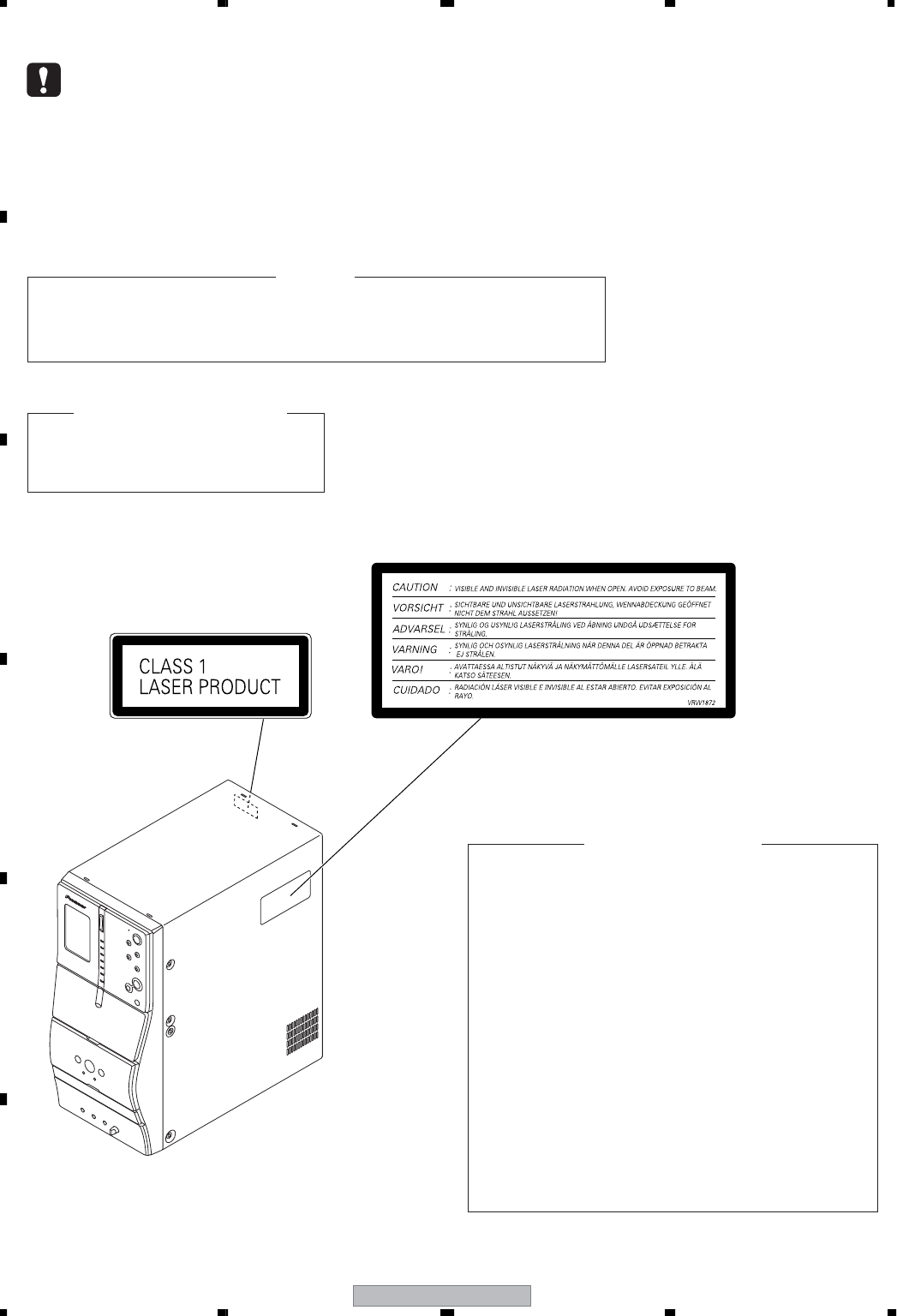
WARNING !
THE AEL (ACCESSIBLE EMISSION LEVEL) OF THE LASER POWER OUTPUT IS LESS THAN CLASS 1
BUT THE LASER COMPONENT IS CAPABLE OF EMITTING RADIATION EXCEEDING THE LIMIT FOR
CLASS 1.
A SPECIALLY INSTRUCTED PERSON SHOULD DO SERVICING OPERATION OF THE APPARATUS.
LASER DIODE CHARACTERISTICS
FOR DVD : MAXIMUM OUTPUT POWER : 5 mW
WAVELENGTH : 650 nm
FOR CD : MAXIMUM OUTPUT POWER : 7 mW
WAVELENGTH : 780 nm
Additional Laser Caution
Printing on Rear Panel
1. Laser Interlock Mechanism
• Loading switch (S101 on the LOAB Assy) is used for interlock
mechanism of the laser.
When this switch turned ON in SW2 (CLOSE) side (OPEN signal is
0V and CLOSE signal is 3.5V), a laser becomes the status which can
completely oscillation.
Furthermore, the laser completely oscillates in the disc judgment and
disc playback.
When player is power ON state and laser diode is not completely
oscillating, 780nm laser diode is always oscillating by half power.
• Laser diode is driving with Q307 (650nm LD) and Q308 (780nm LD)
on the DVDM Assy.
Therefore, when short-circuit between the emitter and collector of these
transistors or the base voltage is supplied for transistors turn on, the
laser oscillates. (failure mode)
• In the test mode ∗ , there is the mode that the laser oscillates except
for the disc judgment and playback. LD ON mode in the test mode
oscillates with the laser forcibly.
The interlock mechanism mentioned above becomes invalid in this
mode.
2. When the cover is open, close viewing through the objective lens with
the naked eye will cause exposure to the laser beam.
LABEL CHECK
∗ : Refer to page 96.
VRW1872
XV-EV1000 3
5678
5678
C
D
F
A
B
E
[Important Check Points for Good Servicing]
In this manual, procedures that must be performed during repairs are marked with the below symbol.
Please be sure to confirm and follow these procedures.
1. Product safety
Please conform to product regulations (such as safety and radiation regulations), and maintain a safe servicing environment by
following the safety instructions described in this manual.
1 Use specified parts for repair.
Use genuine parts. Be sure to use important parts for safety.
2 Do not perform modifications without proper instructions.
Please follow the specified safety methods when modification(addition/change of parts) is required due to interferences such as
radio/TV interference and foreign noise.
3 Make sure the soldering of repaired locations is properly performed.
When you solder while repairing, please be sure that there are no cold solder and other debris.
Soldering should be finished with the proper quantity. (Refer to the example)
4 Make sure the screws are tightly fastened.
Please be sure that all screws are fastened, and that there are no loose screws.
5 Make sure each connectors are correctly inserted.
Please be sure that all connectors are inserted, and that there are no imperfect insertion.
6 Make sure the wiring cables are set to their original state.
Please replace the wiring and cables to the original state after repairs.
In addition, be sure that there are no pinched wires, etc.
7 Make sure screws and soldering scraps do not remain inside the product.
Please check that neither solder debris nor screws remain inside the product.
8 There should be no semi-broken wires, scratches, melting, etc. on the coating of the power cord.
Damaged power cords may lead to fire accidents, so please be sure that there are no damages.
If you find a damaged power cord, please exchange it with a suitable one.
9 There should be no spark traces or similar marks on the power plug.
When spark traces or similar marks are found on the power supply plug, please check the connection and advise on secure
connections and suitable usage. Please exchange the power cord if necessary.
0 Safe environment should be secured during servicing.
When you perform repairs, please pay attention to static electricity, furniture, household articles, etc. in order to prevent injuries.
Please pay attention to your surroundings and repair safely.
2. Adjustments
To keep the original performance of the products, optimum adjustments and confirmation of characteristics within specification.
Adjustments should be performed in accordance with the procedures/instructions described in this manual.
4. Cleaning
For parts that require cleaning, such as optical pickups, tape deck heads, lenses and mirrors used in projection monitors, proper
cleaning should be performed to restore their performances.
3. Lubricants, Glues, and Replacement parts
Use grease and adhesives that are equal to the specified substance.
Make sure the proper amount is applied.
5. Shipping mode and Shipping screws
To protect products from damages or failures during transit, the shipping mode should be set or the shipping screws should be
installed before shipment. Please be sure to follow this method especially if it is specified in this manual.

XV-EV1000
4
1234
1234
C
D
F
A
B
E
CONTENTS
SAFETY INFORMATION..................................................................................................................................... 2
1. SPECIFICATIONS ............................................................................................................................................ 5
2. EXPLODED VIEWS AND PARTS LIST ............................................................................................................ 7
2.1 PACKING ................................................................................................................................................... 7
2.2 EXTERIOR SECTION................................................................................................................................ 8
2.3 AMP SECTION ........................................................................................................................................ 10
2.4 FRONT PANEL SECTION ....................................................................................................................... 12
2.5 05 LOADER ASSY................................................................................................................................... 14
2.6 Traverse Mechanism Assy-S.................................................................................................................... 16
2.7 DECK MECHANISM ASSY ..................................................................................................................... 17
3. BLOCK DIAGRAM AND SCHEMATIC DIAGRAM..........................................................................................18
3.1 BLOCK DIAGRAM ................................................................................................................................... 18
3.2 OVERALL WIRING CONNECTION DIAGRAM and LOAB ASSY ........................................................... 20
3.3 DVDM ASSY (1/2).................................................................................................................................... 22
3.4 DVDM ASSY (2/2).................................................................................................................................... 24
3.5 IFAF ASSY (1/4)....................................................................................................................................... 26
3.6 IFAF ASSY (2/4)....................................................................................................................................... 28
3.7 IFAF ASSY (3/4)....................................................................................................................................... 30
3.8 IFAF ASSY (4/4)....................................................................................................................................... 32
3.9 DSP ASSY ............................................................................................................................................... 34
3.10 KEY, LED and DISPLAY ASSYS............................................................................................................ 36
3.11 HP/MIC ASSY........................................................................................................................................ 38
3.12 AMP ASSY............................................................................................................................................. 40
3.13 POWER ASSY (1/4)............................................................................................................................... 42
3.14 POWER (2/4) and TRADE ASSYS ........................................................................................................ 44
3.15 POWER ASSY (3/4)............................................................................................................................... 46
3.16 POWER ASSY (4/4)............................................................................................................................... 48
3.17 WAVEFORMS ........................................................................................................................................ 50
4. PCB CONNECTION DIAGRAM ..................................................................................................................... 51
4.1 LOAB ASSY............................................................................................................................................. 51
4.2 DVDM ASSY ............................................................................................................................................ 52
4.3 IFAF ASSY ............................................................................................................................................... 54
4.4 KEY, LED and DISPLAY ASSYS.............................................................................................................. 58
4.5 AMP ASSY............................................................................................................................................... 60
4.6 POWER ASSY ......................................................................................................................................... 62
4.7 HP/MIC and TRADE ASSYS ................................................................................................................... 66
4.8 DSP ASSY ............................................................................................................................................... 68
5. PCB PARTS LIST ........................................................................................................................................... 69
6. ADJUSTMENT ............................................................................................................................................... 88
6.1 DECK SECTION ...................................................................................................................................... 88
6.1.1 ADJUSTMENT CONDITION ............................................................................................................. 88
6.1.2 PLAYBACK and RECORDING SECTION ......................................................................................... 89
6.2 DVD SECTION......................................................................................................................................... 91
6.2.1 ADJUSTMENT ITEMS AND LOCATION........................................................................................... 91
6.2.2 JIGS AND MEASURING INSTRUMENTS ........................................................................................ 91
6.2.3 NECESSARY ADJUSTMENT POINTS ............................................................................................. 92
6.2.4 TEST MODE...................................................................................................................................... 93
6.2.5 MECHANISM ADJUSTMENT............................................................................................................ 94
7. GENERAL INFORMATION ............................................................................................................................. 96
7.1 DIAGNOSIS ............................................................................................................................................. 96
7.1.1 TEST MODE...................................................................................................................................... 96
7.1.2 DISPLAY SPECIFICATION OF THE TEST MODE............................................................................ 97
7.1.3 FUNCTIONAL SPECIFICATION OF THE SHORTCUT KEY ............................................................ 98
7.1.4 SPECIFICATION OF MODEL INFORMATION DISPLAY .................................................................. 99
7.1.5 FUNCTIONAL SPECIFICATION OF THE SERVICE MODE ........................................................... 100
7.1.6 SERVICE TEST MODE ................................................................................................................... 101
7.1.7 METHOD FOR DIAGNOSING DEGRADATION OF THE LDs ON THE PICKUP ASSY................. 103
7.1.8 DVD TROUBLE SHOOTING............................................................................................................ 104
7.1.9 ID NUMBER AND ID DATA SETTING ............................................................................................. 107
7.1.10 DSP TROUBLE SHOOTING ......................................................................................................... 110
7.1.11 DISASSEMBLY.............................................................................................................................. 112
7.2 PARTS.................................................................................................................................................... 122
7.2.1 IC ..................................................................................................................................................... 122
7.3 EXPLANATION ...................................................................................................................................... 125
7.3.1 SEQUENCE AFTER POWER ON................................................................................................... 125
7.3.2 PROTECTION CIRCUIT.................................................................................................................. 126
8. PANEL FACILITIES ...................................................................................................................................... 131
XV-EV1000 5
5678
5678
C
D
F
A
B
E
1. SPECIFICATIONS
• Amplifier section
Continuous power output:
Front . . . . . . . . . . . . . . . . . . . . 100 W per channel
(1kHz, 10 % T.H.D., 6Ω)
Center . . . . . . . . . 100 W (1kHz, 10 % T.H.D., 6Ω)
Surround . . . . . . . . . . . . . . . . .100 W per channel
(1kHz, 10 % T.H.D., 6Ω)
Subwoofer . . . . . 100 W (100Hz, 10 % T.H.D., 6Ω)
• Disc section
Digital audio
characteristics . . . . . . . . . DVD fs: 96 kHz, 24-bit
Type. DVD system, Video CD/Super VCD system
and Compact Disc digital audio system
Frequency response . . . . . . . . . . .4 Hz to 44 kHz
S/N ratio . . . . . . . . . . . . . . . . . . . . . . . . . . . 95 dB
Dynamic range . . . . . . . . . . . . . . . . . . . . . . 95 dB
Total harmonic distortion . . . . . . . . . . . . 0.005 %
Wow and Flutter . . . . . . . . .Limit of measurement
(±0.001 % W.PEAK) or less (JEITA)
• Cassette deck section
Systems . . . . . . . . . . . . 4 track, 2-channel stereo
Heads . . . . . . . . . . . Recording/playback head x 1
Erasing head x 1
Motor . . . . . . . . . . . . . . . . . . . DC servo motor x 1
Tape types . . . . . . . . . . . . . . . . . Type I (Normal)
• FM tuner section
Frequency range . . . . . . . . 87.5 MHz to 108 MHz
Antenna . . . . . . . . . . . . . . . . . . . 75Ω, unbalanced
• AM tuner section
Frequency range
With 9kHz step . . . . . . . . 531 kHz to 1,602 kHz
With 10kHz step. . . . . . . 530 kHz to 1,700 kHz
Antenna . . . . . . . . . . . . . . . . . . . . . Loop antenna
• Miscellaneous
Power requirements
Multi voltage model . . . . AC 110-127/220-230/
240 V (switchable), 50/60 Hz
Power consumption
. . . . . . . . . . . . . . . . . 179 W
Power consumption in standby mode . . . . . 0.5 W
Dimensions:
DVD Tuner Deck Receiver . . . . 170(W) 352.5 (H)
340.1 (D) mm
Weight:
DVD Tuner Deck Receiver . . . . . . . . . . . . . 7.2 kg
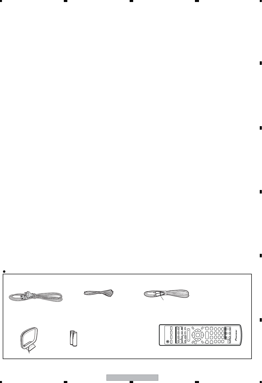
• Accessories (Stereo DVD Tuner Deck)
Remote control . . . . . . . . . . . . . . . . . . . . . . . . . . 1
Power cord
Central and South American, Taiwan,
Philippines, Argentina, Mexico models . . . . . . 2
All other models . . . . . . . . . . . . . . . . . . . . . . . .1
Power plug adapter (Central and South American,
US Military and Duty Free models only) . . . . . . . 1
Video cord . . . . . . . . . . . . . . . . . . . . . . . . . . . . . . 1
AM loop antenna . . . . . . . . . . . . . . . . . . . . . . . . . 1
FM antenna . . . . . . . . . . . . . . . . . . . . . . . . . . . . 1
Dry cell batteries (AA/R6) . . . . . . . . . . . . . . . . . . 2
Warranty Card (US Military and Duty
Free models only) . . . . . . . . . . . . . . . . . . . . . . . . 1
Operating instructions
Manufactured under license from Dolby
Laboratories.“Dolby”, “Pro Logic” and the double-D
symbol are trademarks of Dolby Laboratories.
“DTS” and “DTS Digital Surround” are registered
trademarks of Digital Theater Systems, Inc.
123
456
7890
CLEAR
ENTER
SYSTEM SETUP
HOME
MENU
TOP MENU
DVD MENU
SHIFT
CHANNEL VOLUME
INPUT
SUBTITLE
VOLUME
ANGLE ZOOM
SURROUND
ADVANCED
FRONT
SURROUND
ECHO
DSP
AUDIO
DVD/CD TAPE FM/AM LINE
X.BOOM
PROGRAM
ST.MEMORY
TEST TONE
REPEAT
MONO
CH LEVEL
RANDOM
TIMER
KARAOKE
I –
KEYCON
– i
DISPLAY MUTE
RETURN
SOUND
MODE
ENTER
STANDBY/ON
4
/eE/
1¡
¢
8
7
3
3
3
TUNE +
ST +ST
–
TUNE
–
DVD
TV CONTROL
Accessories
• Power cord
(ADG1154)
• FM Antenna (ADH7030)
• AM Loop Antenna
(ATB7013)
• Video Cord
(L = 1.5m) (XDE3046)
• Remote Control
(XXD3098)
• Dry Cell Batteries
Yellow
XV-EV1000
6
1234
1234
C
D
F
A
B
E
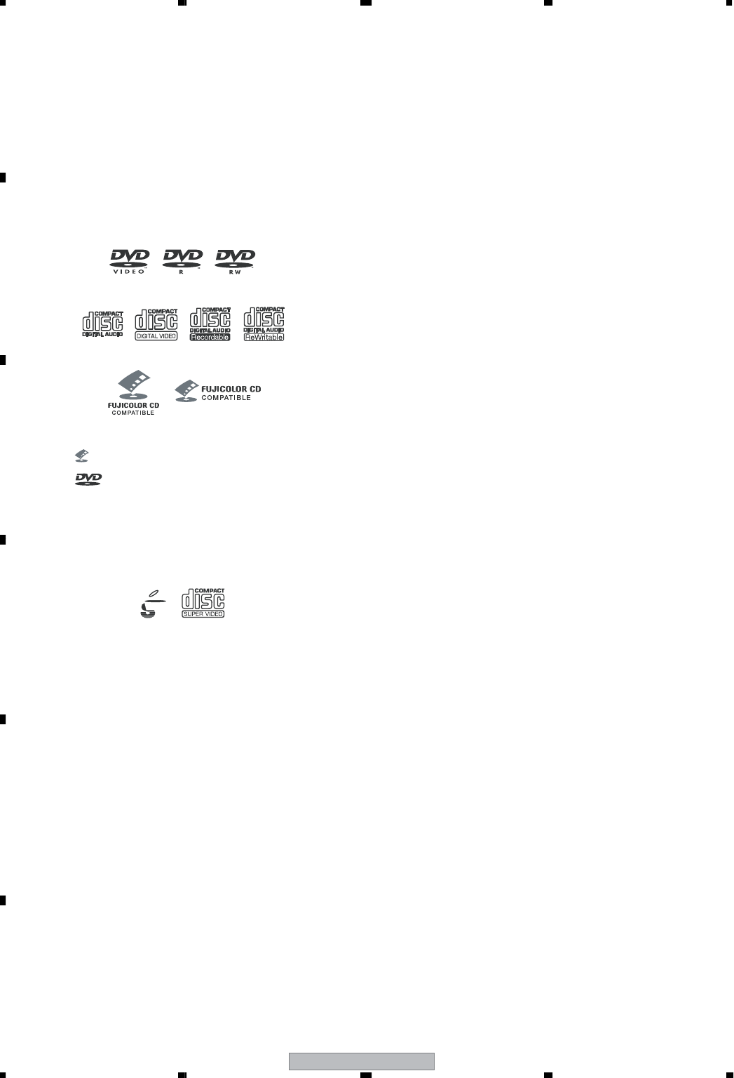
Disc / content format playback
compatibility
This player is compatible with a wide range of
disc types (media) and formats. Playable discs
will generally feature one of the following logos
on the disc and/or disc packaging. Note
however that some disc types, such as
recordable CD and DVD, may be in an
unplayable format.
See the Disc compatibility table below for more
information.
• is a trademark of Fuji Photo Film Co. Ltd.
• is a trademark of DVD Format/Logo
Licensing Corporation
• Also compatible with KODAK Picture CD
This player supports the IECís Super VCD stan-
dard for superior picture quality, dual
soundtracks, and widescreen support.
DVD-Video DVD-R DVD-RW
Video CD
Fujicolor CD
Audio CD CD-R CD-RW
VIDEO
CD
Super Video CD (Super VCD)
XV-EV1000 7
5678
5678
C
D
F
A
B
E
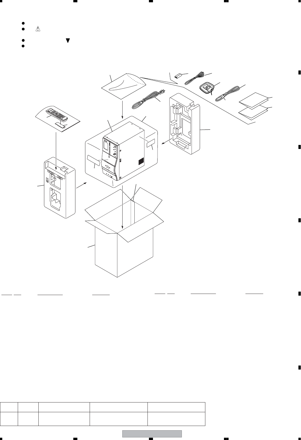
2. EXPLODED VIEWS AND PARTS LIST
2.1 PACKING
(1) PACKING SECTION PARTS LIST
(2) CONTRAST TABLE
XV-EV700/DLXJ/NC and XV-EV1000/DLXJ/NC are constracted the same except for the following :
Parts marked by "NSP" are generally unavailable because they are not in our Master Spare Parts List.
The mark found on some component parts indicates the importance of the safety factor of the part.
Therefore, when replacing, be sure to use parts of identical designation.
Screws adjacent to mark on product are used for disassembly.
For the applying amount of lubricants or glue, follow the instructions in this manual.
(In the case of no amount instructions, apply as you think it appropriate.)
NOTES:
Yellow
8
11
15
12
13
14
9
2
1
3
Junction
10
16
6 4
57
XV-EV1000 or
XV-EV700
Mark No. Description Part No.
1 Label VRW1872
NSP 2 Getter Label See Contrast table (2)
>
3AC Power Cord ADG1154
4 FM Antenna ADH7030
5 AM Loop Antenna ATB7013
NSP 6 Dry Cell Batteries (AA/R6) VEM1031
7 Video Cord XDE3046
8 Operating Instructions (English) XRB3053
9 Operating Instructions (Chinese)XRC3209
10 Remote Control XXD3098
NSP 11 Polyethylene Bag Z21-038
12 Front Pad XHA3156
13 Rear Pad XHA3157
14 Packing Case See Contrast table (2)
15 Packing Sheet XHG3010
16 Battery Cover AZN7933
Mark No. Description Part No.
Mark No. Description XV-EV1000/DLXJ/NC XV-EV700/DLXJ/NC
NSP 2 Getter Label XAX3539 XAX3526
14 Packing Case XHD3565 XHD3555
XV-EV1000
8
1234
1234
C
D
F
A
B
E
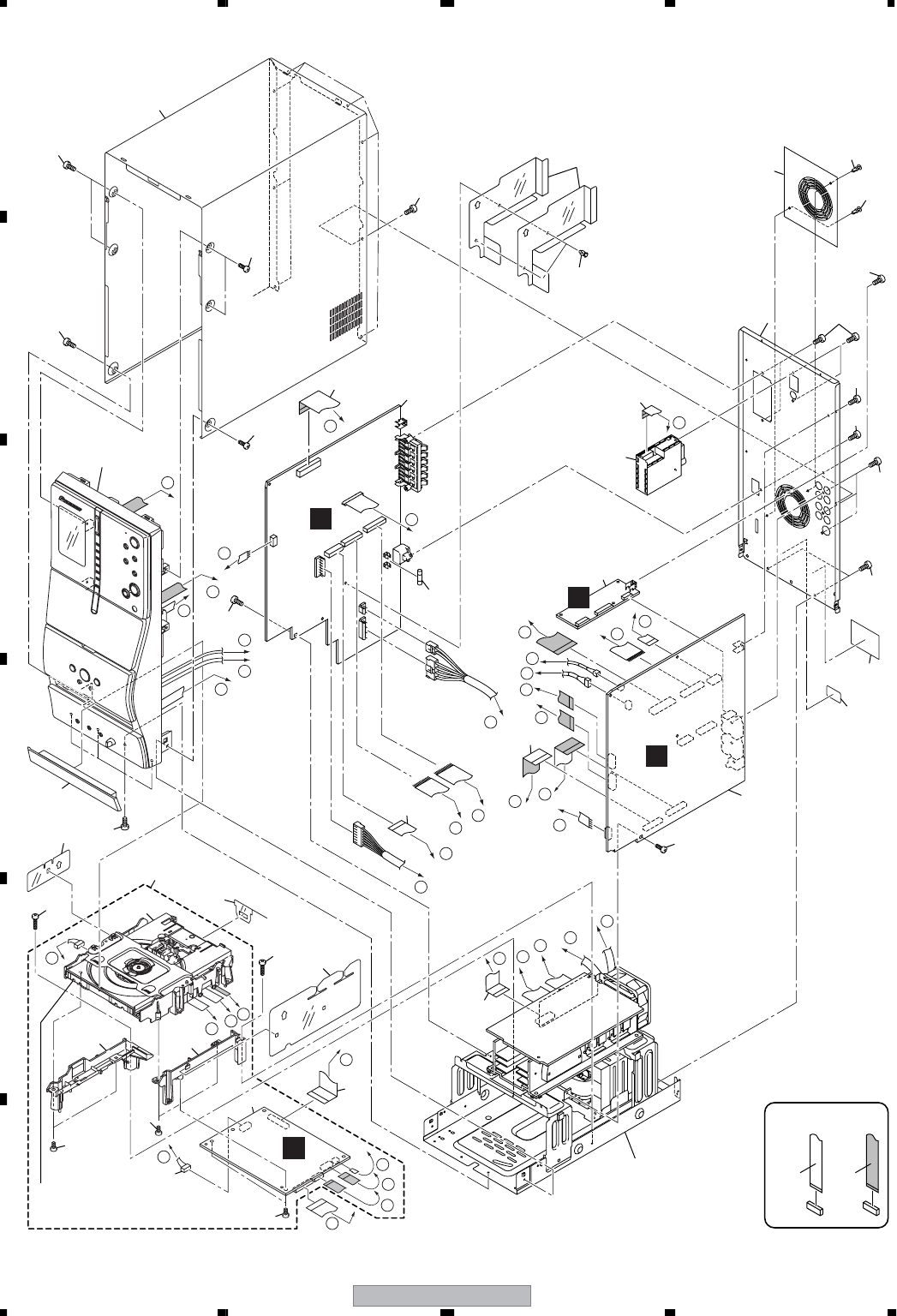
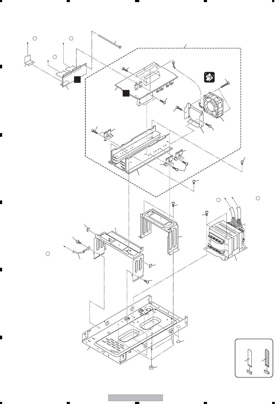
2.2 EXTERIOR SECTION
CONTACT SIDE
NON-CONTACT
SIDE
Refer to
"2.4 FRONT PANEL
SECTION".
Refer to
"2.5 05 LOADER ASSY".
Refer to
"2.3 AMP SECTION".
A
B
C
D
J
AB
C
B
C
E
F
E
D
D
G
FG
H
H
IJ
O
P
R
S
T
T
R
S
Q
Q
O
P
J
M
L
K
M
L
K
N
N
I
25
29
28
28
3
29
28
10
32
18
18
18
28
24
22
31
31
11
21
19
15
13
29
14
12
9
29
8
7
28
4
5
20
1
2
6
26
27
28
28
30
28
28
28
23
29
16
7
17
XV-EV1000 9
5678
5678
C
D
F
A
B
E
(1) EXTERIOR SECTION PARTS LIST
(2) CONTRAST TABLE
XV-EV700/DLXJ/NC and XV-EV1000/DLXJ/NC are constracted the same except for the following :
Mark No. Description Part No.
1 DSP Assy AWX8588
2FM/AM TUNER Unit AXX7173
3POWER Assy See Contrast table (2)
4IFAF Assy See Contrast table (2)
>
5 Fuse (FU1) (5.0A/250V) REK1029
6 11P F.F.C/60V XDD3179
7 17P F.F.C/60V XDD3180
8 25P F.F.C/60V XDD3182
9 27P F.F.C/60V XDD3183
10 27P F.F.C/60V XDD3186
NSP 11 DVD Assy XXA3037
NSP 12 05 LOADER Assy VWT1219
13 DVDM Assy AWM7964
14 Adaptor 05 L XNW3014
15 Adaptor 05 R XNW3015
16 Connector Assy PG05KK-E07
17 Rear Panel See Contrast table (2)
18 Push Rivet XEC3034
19 Mecha Barrier XEC3062
20 Primary Barrier XEC3063
21 FFC Barrier XEC3064
22 Cable Barrier XEC3065
23 Fan Barrier XEC3066
24 Tray Cap XAK3504
25 Bonnet Case XZN3179
NSP 26 Label VRW1629
NSP 27 ID Label Assy VXW1002
28 Screw BBZ30P080FNI
29 Screw BPZ30P080FNI
30 Screw PPZ30P080FNI
31 Screw XBA3015
32 Screw ABA7112
Mark No. Description Part No.
Mark No. Description XV-EV1000/DLXJ/NC XV-EV700/DLXJ/NC
3POWER Assy XWZ4016 XWZ4018
4IFAF Assy XWZ4003 XWZ4006
17 Rear Panel XNC3399 XNC3381
XV-EV1000
10
1234
1234
C
D
F
A
B
E
2.3 AMP SECTION
CONTACT SIDE
NON-CONTACT
SIDE
K
I
22
21
21
21
7
9
19
10
8
8
8
21
21
21
17
20
3
6
Refer to
"2.2 EXTERIOR
SECTION. "
D
Refer to
"2.2 EXTERIOR
SECTION. "
H
Refer to
"2.2 EXTERIOR
SECTION. "
G
Refer to
"2.4 FRONT PANEL
SECTION. "
U
Refer to
"2.2EXTERIOR
SECTION. "
F
Refer to
"2.2 EXTERIOR
SECTION. "
E
4
1
5
19
18
13
15
16
14
19
2
19
15 12
11
Cleaning paper
GED-008

XV-EV1000 11
5678
5678
C
D
F
A
B
E
AMP SECTION PARTS LIST
Mark No. Description Part No.
1 TRADE Assy XWZ4022
>
2Power Transformer (T1) XTS3099
NSP 3 Cord With Plug DE015VE0
4 17P F.F.C/60V XDD3180
NSP 5 AMP Unit XXQ3005
6 AMP Assy XWK3202
7 DC Fan Motor XXM3009
8 FET Bracket A ANG7418
9Fan Plate ANG7462
NSP 10 Heat Sink XNH3038
NSP 11 Chassis Hal XNA3025
12 AMP Support F XNG3141
13 AMP Support R XNG3142
NSP 14 Spacer AEB7092
15 Rubber Cushion XEB3047
16 LEG Cushion R XEB3050
17 Binder ZCA-SKB90BK
18 Screw BBZ30P060FTC
19 Screw BBZ30P080FNI
20 Screw BBZ40P060FTC
21 Screw BBZ30P140FTC
22 Screw BBZ30P300FTC
XV-EV1000
12
1234
1234
C
D
F
A
B
E
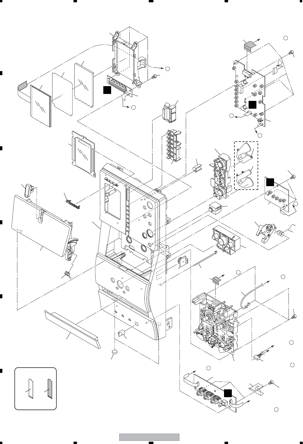
2.4 FRONT PANEL SECTION
Refer to
"2.2 EXTERIOR
SECTION. "
Refer to
"2.2 EXTERIOR
SECTION. "
Refer to
"2.3 AMP
SECTION. "
Refer to
"2.2 EXTERIOR
SECTION. "
Refer to
"2.2 EXTERIOR
SECTION. "
XV-EV1000
Only
Refer to
"2.2 EXTERIOR
SECTION. "
Refer to
"2.2 EXTERIOR
SECTION. "
CONTACT SIDE
NON-CONTACT
SIDE
G
F
E
H
1
5
6
7
8
9
10
11
12
3
13
14
15
16
17
18
19
20
21
22
23
34
35
36
36
36
36
36
24
25
26
27
28
29
30
31
32
33
V
W
V
X
O
X
P
U
S
R
T
Q
W
2
4
XV-EV1000 13
5678
5678
C
D
F
A
B
E
(1) FRONT PANEL SECTION PARTS LIST
(2) CONTRAST TABLE
XV-EV700/DLXJ/NC and XV-EV1000/DLXJ/NC are constracted the same except for the following :
Mark No. Description Part No.
1 HP/MIC Assy XWZ4014
2DISPLAY Assy See Contrast table (2)
3 KEY Assy XWZ4013
4 LED Assy XWZ4023
5Vertical LCD XAV3028
NSP 6 Cord With Plug DE015VE0
7 11P F.F.C/60V XDD3184
8 13P F.F.C/60V XDD3185
9 Cable Assy XDE3066
10 DECK Mechanism Unit XYM3019
11 GND Plate XNG3143
12 Ratch Spring R ABH7131
13 Damper Assy AXA7052
14 Door Spring R XBH3002
15 Leg Cushion F XEB3051
16 Ratch Mold R XMR3002
17 LCD Holder XMR3095
18 Binder ZCA-SKB90BK
19 MIC Knob XAA3029
20 LCD LT Cond XAK3502
21 LCD Window XAK3503
22 Tray Cap XAK3504
23 Timer Lens XAK3506
24 Diffusion Sheet XAK3510
25 FUNC. LT. Cond. See Contrast table (2)
26 VOL. LT. Cond. See Contrast table (2)
27 Front Panel Assy See Contrast table (2)
28 Pioneer Name Plate VAM1129
29 Operation Button XAD3225
30 Sub Button See Contrast table (2)
31 Sensor Cover XAK3505
32 DECK Panel See Contrast table (2)
33 DECK Door XAN3056
34 Main Button Assy See Contrast table (2)
35 X.Boon Button Assy XXG3230
36 Screw BPZ30P080FNI
Mark No. Description Part No.
Mark No. Description XV-EV1000/DLXJ/NC XV-EV700/DLXJ/NC
2 DISPLAY Assy XWZ4012 XWZ4010
25 FUNC. LT. Cond. XAK3514 Not used
26 VOL. LT. Cond. XAK3515 Not used
27 Front Panel Assy XZN3182 XZN3180
30 Sub Button XAD3227 XAD3224
32 DECK Panel XAK3512 XAK3508
34 Main Button Assy XXG3218 XXG3217
XV-EV1000
14
1234
1234
C
D
F
A
B
E
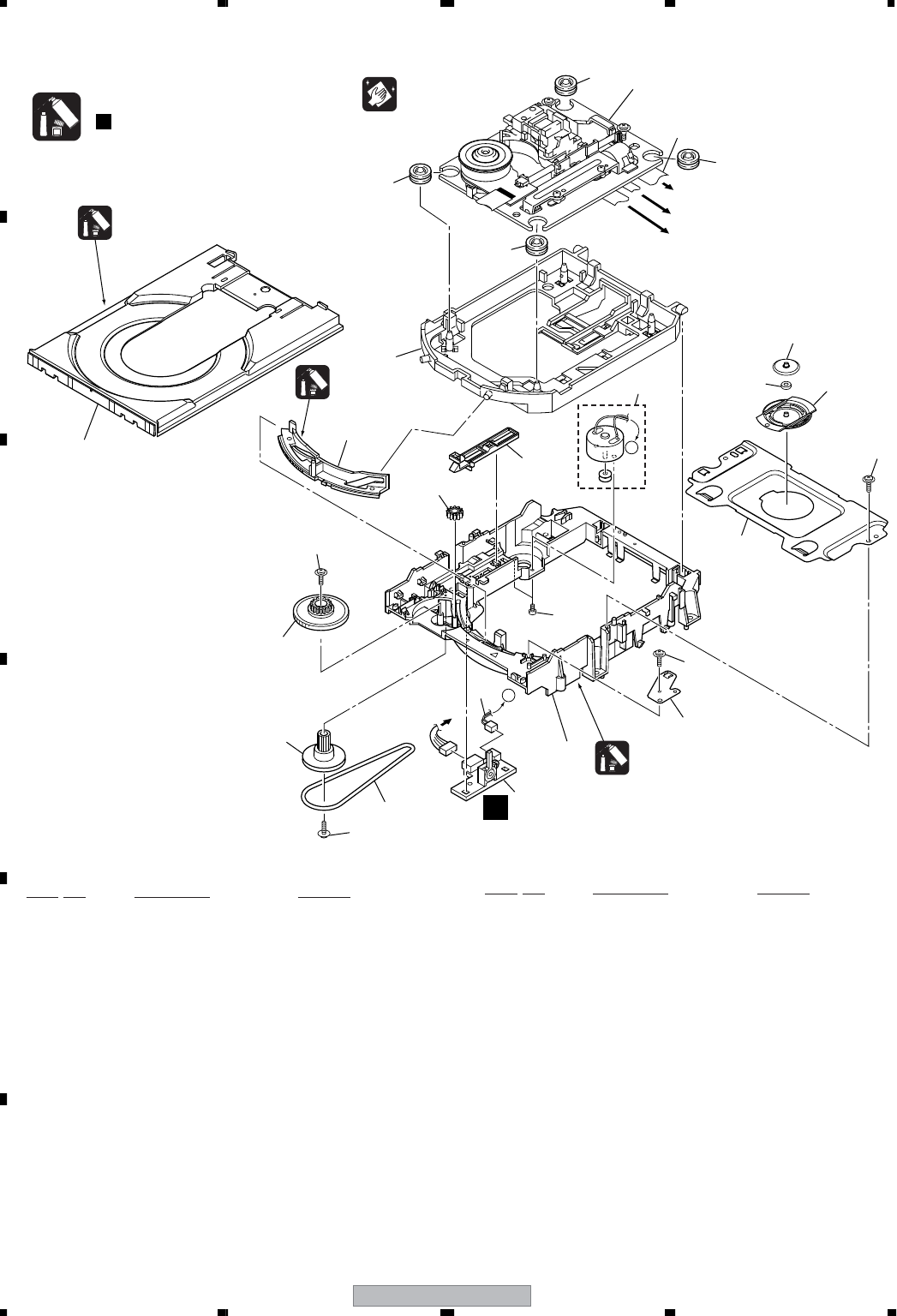
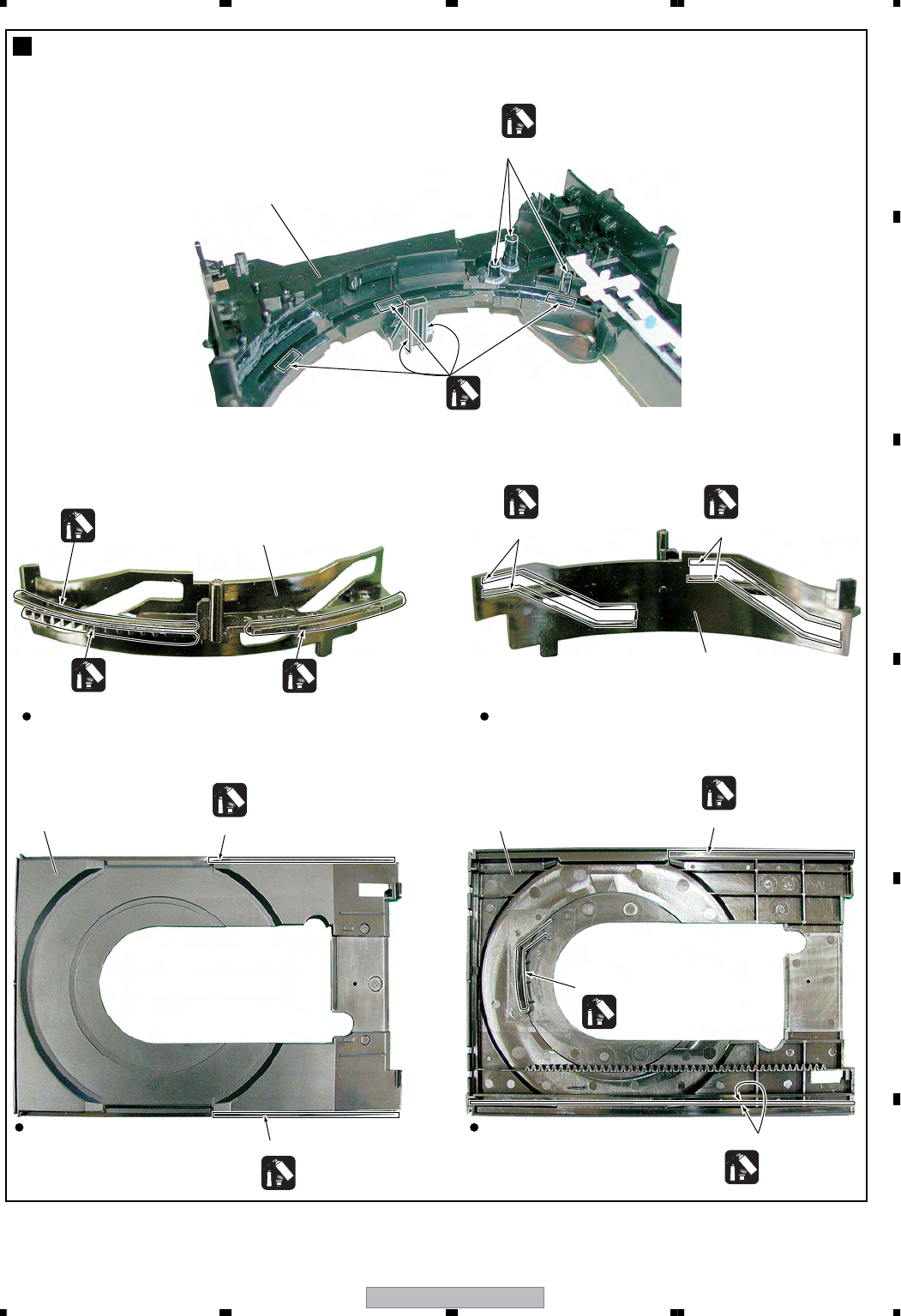
2.5 05 LOADER ASSY
05 LOADER ASSY PARTS LIST
A
A
To DVDM CN101 (Pickup)
To DVDM CN104 (Stepping Motor)
To DVDM CN102 (Spindle Motor)
To
DVDM CN103
2
12
23
13
17
21
16
22
15
14
22
22
22
20
19
91
7
10
11
6
8
8
8
8
18
24
3
A
Lubricating Oil
GYA1001
Daifree
GEM1036
Refer to
" Application of Lubricant".
Note :
Lubricating Oil
GYA1001
Refer to
"2.4 Traverse Mechanism Assy-S".
Pickup leneses
Cleaning liquid
GEM1004
Cleaning paper
GED-008
Mark No. Description Part No.
NSP 1 LOAB Assy VWG2346
2Traverse Mechanism Assy-S DXX2568
3 Loading Motor Assy VXX2912
4• • • • •
5• • • • •
6 Flexible Cable (24P) VDA2008
7 Connector Assy 2P VKP2253
8 Floating Rubber VEB1351
9 Belt VEB1358
10 Stabilizer VNE2253
11 Loading Base VNL1917
12 Float Base 04 VNL1968
13 Drive Cam VNL1919
14 Gear Pulley VNL1921
15 Loading Gear VNL1922
16 Drive Gear VNL1923
17 SW Lever VNL1925
18 Clamper Plate 04 VNE2342
19 Bridge 04 VNE2343
20 Clamper 04 VNL1969
21 Screw JGZ17P028FTC
22 Screw VBA1094
23 Tray VNL1920
24 Clamp Magnet VMG1029
Mark No. Description Part No.
XV-EV1000 15
5678
5678
C
D
F
A
B
E
Application of Lubricant
Lubricating Oil
GYA1001
Around the shaft
No. 11
Loading Base
No. 13
Drive Cam
No. 13
Drive Cam
No. 23
Tray No. 23
Tray
Front View Rear View
Daifree
GEM1036
Inner side of a ditch
Concave of unevenness
Top View Bottom View
Daifree
GEM1036
Daifree
GEM1036
Side of the rib
Concave of unevenness
Daifree
GEM1036 Concave of unevenness
Daifree
GEM1036
Inner side of a ditch
Lubricating Oil
GYA1001
Inner side of a ditch
Lubricating Oil
GYA1001
Lubricating Oil
GYA1001
Lubricating Oil
GYA1001
Lubricating Oil
GYA1001
Lubricating Oil
GYA1001
XV-EV1000
16
1234
1234
C
D
F
A
B
E
2.6 Traverse Mechanism Assy-S
Traverse Mechanism Assy-S PARTS LIST
To
DVDM CN101
(Pickup Assy)
To
DVDM CN104
(Stepping Motor)
To DVDM CN102
(Spindle Motor)
CONTACT SIDE
NON-CONTACT
SIDE
13
10
10
11
11
12
2
4
1
3
6
9
5
7
Silicone Adhesive
GEM1037
Refer to
" Application of Lubricant".
Note :
Note : When part #2 is replaced,
part #13 also need to be
replaced at the same time.
8
Note : Spindle screw (DBA1252) of No.13 is the screw which applied special bond.
Therefore the adhesion becomes ineffective when takes it off once. Spindle screw is the part which cannot recycle.
When part #2 is replaced, part #13 also need to be replaced at the same time.
Pickup leneses
Cleaning liquid
GEM1004
Cleaning paper
GED-008
Mark No. Description Part No.
>
1 05SD Pickup Assy-S OXX8014
2 Spindle Motor N200 DXM1197
3 Guide Shaft VK1 DLA1940
4 Sub Guide Shaft VK1 DLA1941
NSP 5 Joint VK1B DNK4272
6 Joint Spring VK1 DBK1235
7 Stepping Motor VK1 DXM1201
NSP 8 Mechanism Frame VK1 DNK4160
9 Precision Screw VK1 DBA1209
10 Skew Screw VK1 DBA1211
11 Skew Spring VK1 DBH1516
NSP 12 Stepping Screw DBA1205
13 Spindle Screw VK1(for Service) DBA1252
Mark No. Description Part No.
XV-EV1000 17
5678
5678
C
D
F
A
B
E
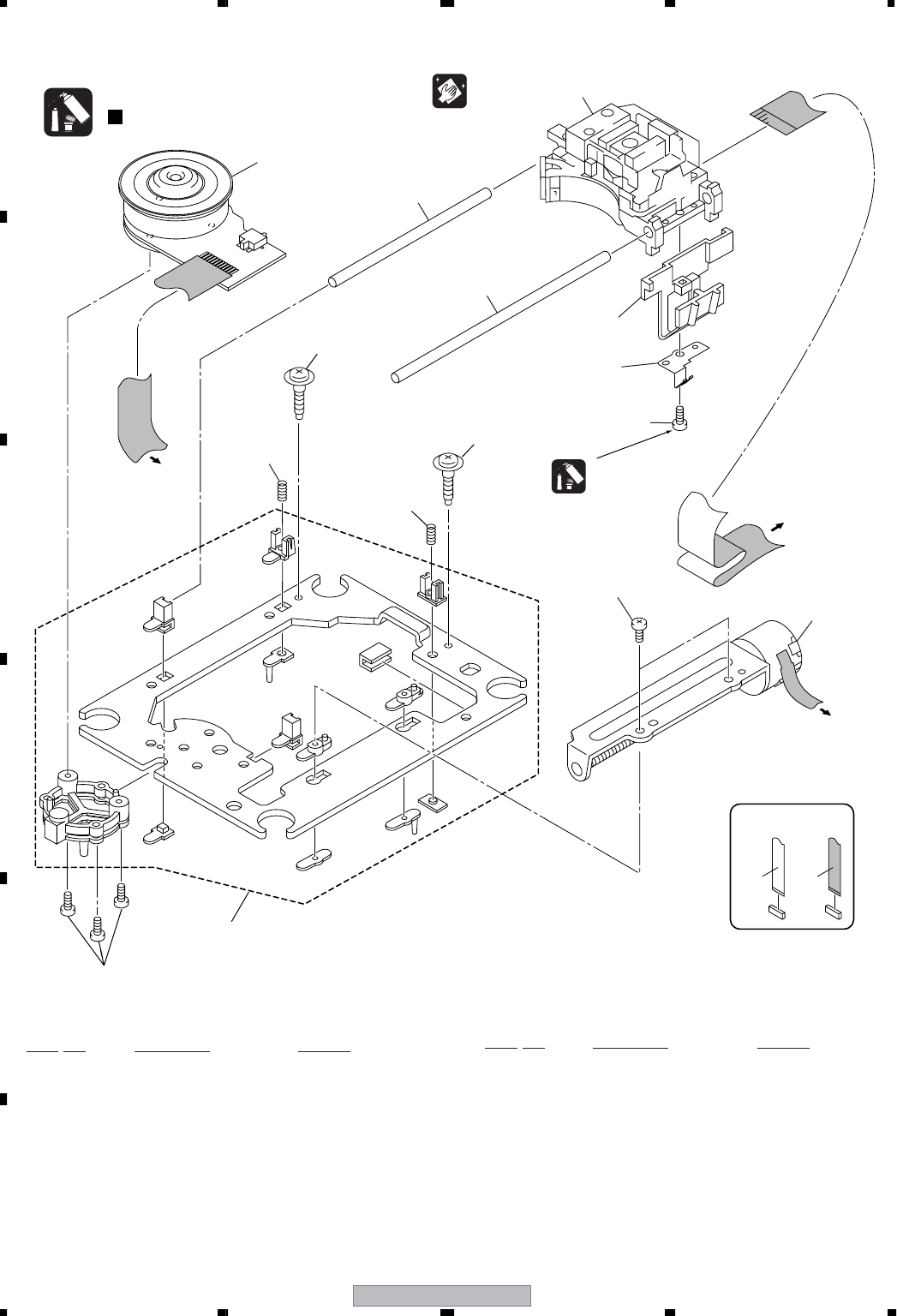
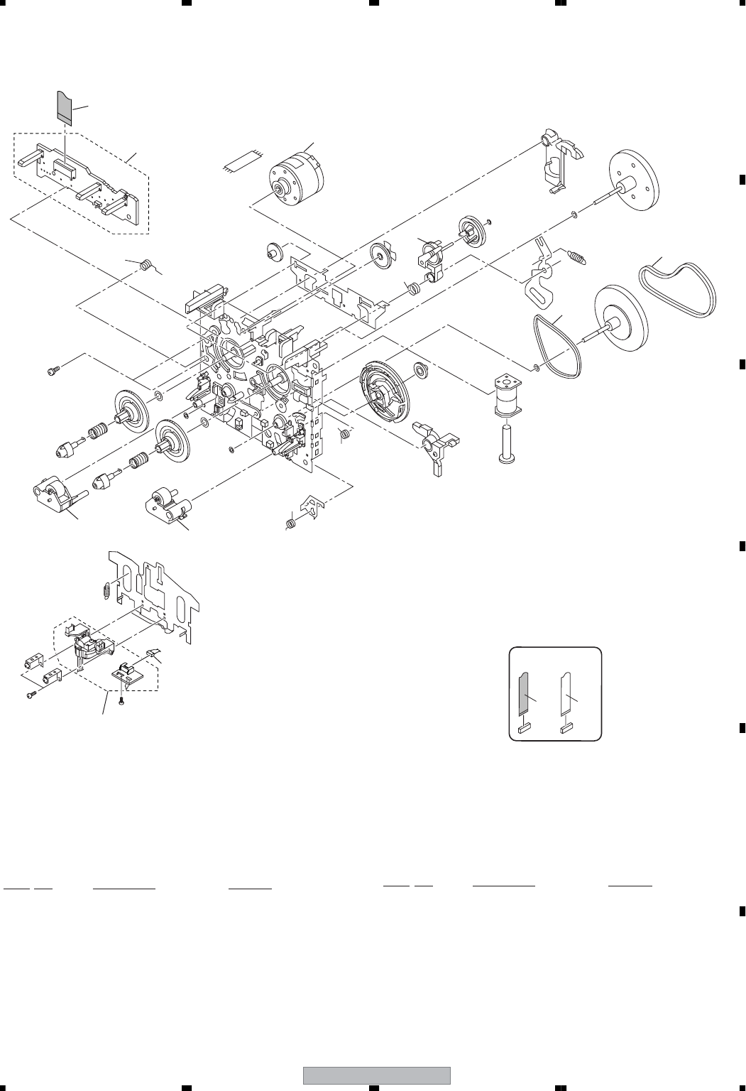
2.7 DECK MECHANISM ASSY
DECK MECHANISM ASSY PARTS LIST
CONTACT SIDE
NON-CONTACT
SIDE
2
7
1
8
10
6
4
5
9
3
Mark No. Description Part No.
1 Main Belt FF20B-13A
2 F/R Belt FF19S-31
3 Plate HD Blk F513-926
4 Roller Pinch Blk R F514-133
5 Roller Pinch Blk L F514-134
6 Clutch Assy Blk F522-063
7 Motor Main Blk F525-394
8 PCB Control Blk F567-747
9 Cable Assy XDE3066
10 11P F.F.C/60V XDD3184
Mark No. Description Part No.
XV-EV1000
18
1234
1234
C
D
F
A
B
E
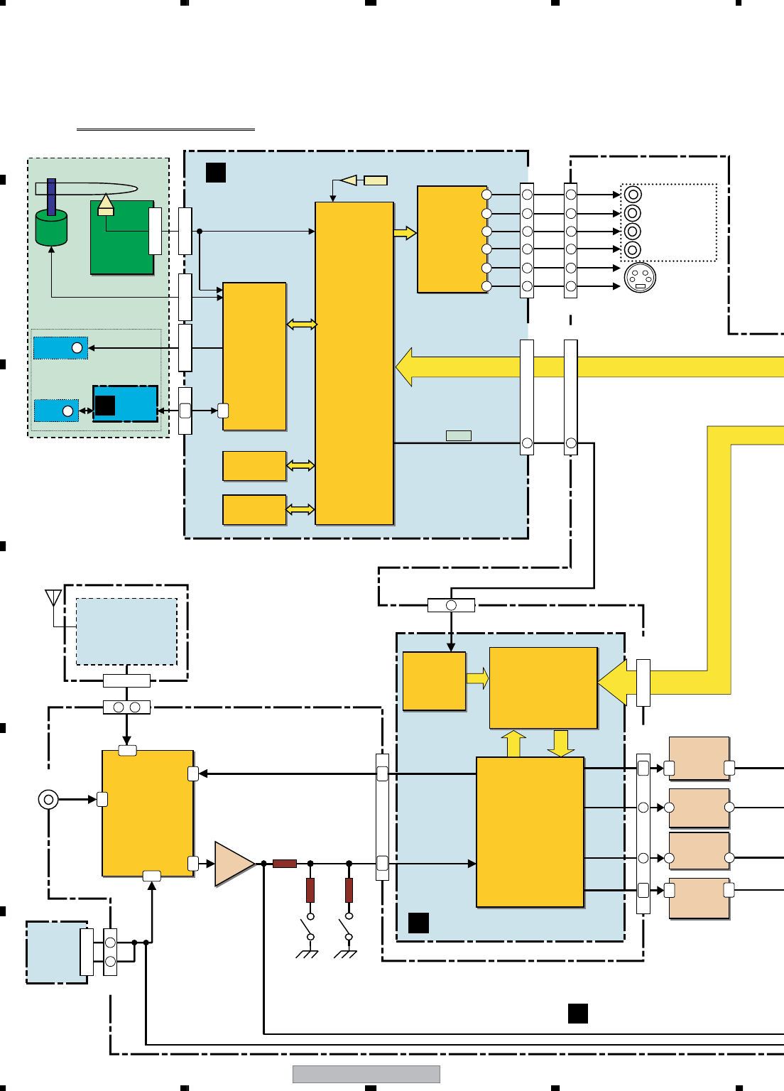
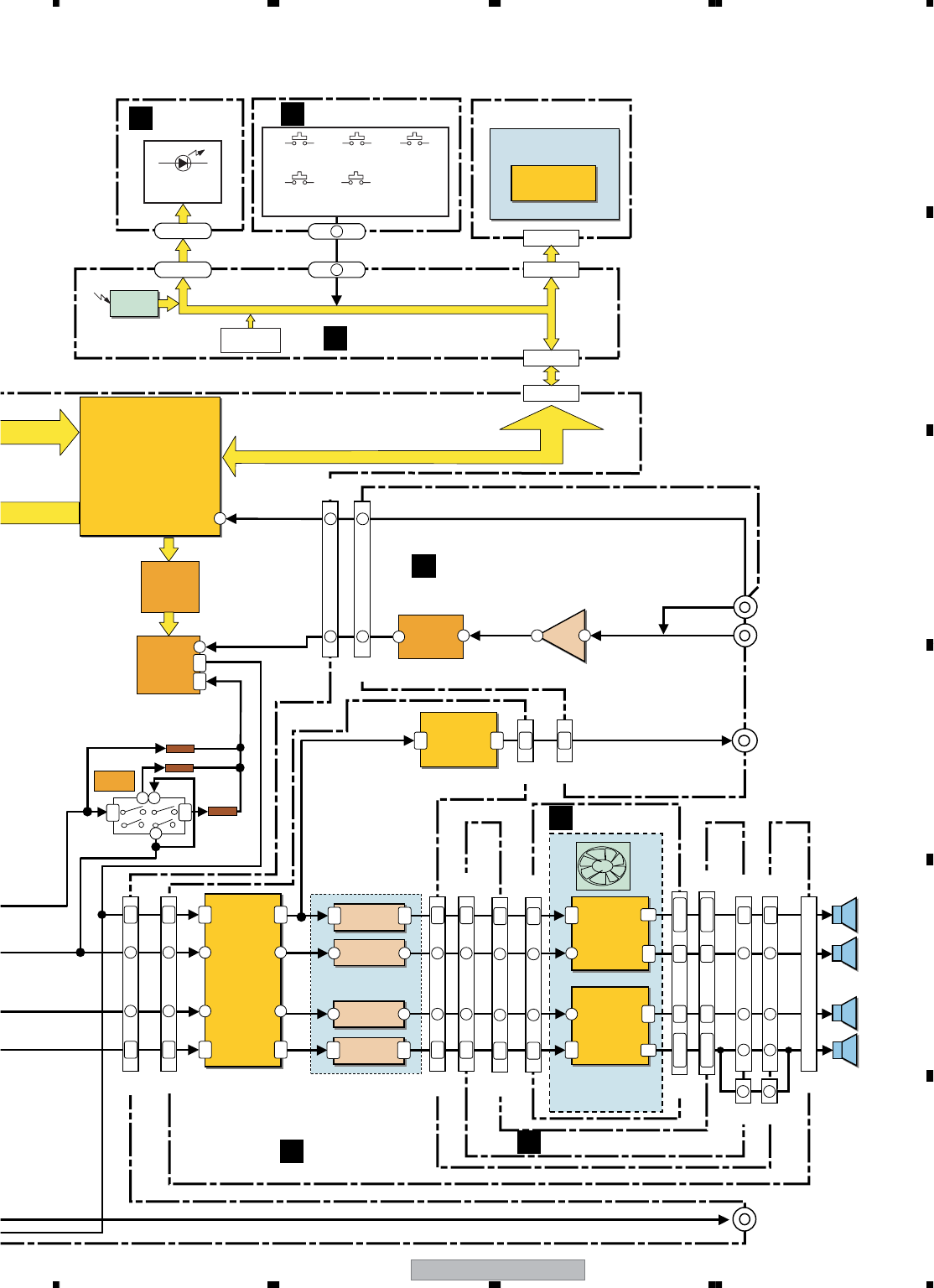
3. BLOCK DIAGRAM AND SCHEMATIC DIAGRAM
3.1 BLOCK DIAGRAM
- 6dB - 10dB
·MPEG Video Decoder
MPEG Video Decoder
·Video
Video
Encoder
Encoder
·Video
Video
DAC
DAC
(withPictureContorol)
(withPictureContorol)
(Progressive: 54MHz
rogressive: 54MHz
)
(VRmode with CPRM)
(VRmode with CPRM)
·Audio Decoder
Audio Decoder
-DD MPEG
-DD MPEG
·JPEG Viewer
JPEG Viewer
·WMA Playback
WMA Playback
·RW Playback
RW Playback
IC202
64M SDRAM
64M SDRAM
IC203
16M
16M
FLASH ROM
FLASH ROM
M
+ -
+ -
6IN-6OUT
6IN-6OUT
BACK END IC
VIDEO DRIVER
VIDEO DRIVER
system control
system control
M
+ -
+ -
DOUT
DOUT
C
V
Y
Cb
Cb
Cr
Cr
Y
·DolbyDigital Decoder
DolbyDigital Decoder
·DTS Decoder
DTS Decoder
·DolbyPrologicII
DolbyPrologicII
IC8101
HEF4052BT
HA17558AF
(BUH4052BCF)
FUNCTION
SELECTOR LPF
PASSIVE
FLO/FRO
FLO/FRO
SWO
SWO
CO
CO
8ch
CODEC
SLO/SRO
SLO/SRO
LPF
LPF
LPF
3ch
Power Amp
IC 8602
HFE4066BT
HEADPHONE
AMP
MIC ECHO
BU9255FS
IC5401
VOCAL
FADER
KEY
CONTROL
RECL/
RECR
DECKL/
DECKR
MICDET MIC DET
PBL/
PBL/
Lch
Lch
Rch
Rch
PBR
PBR
SBLO/
SBLO/
SBRO
SBRO
TUNER MODULE
TUNER MODULE
TAPE DECK
MECHA
MECHA
XYM3019
LINE IN
AUXL/
AUXL/
AUXR
AUXR
TXL/
TXL/
TXR
TXR
YO
YO
Y1
Y1
X1
X1
XO
XO
DSPINL/
DSPINL/
DSPINR
DSPINR
DOWNMIX
DOWNMIX
SBLO/SBRO
SBLO/SBRO
DECKL/
DECKL/
DECKR
DECKR
CN101
(24P)
CN102
(12P)
CN103
(4P)
CN104
(5P)
CN1013
(24P)
SPINDLE
SPINDLE
03SD PU
03SD PU
PlCK UP
ASSY
*SINGLE DISC MECHA
*SINGLE DISC MECHA
Stepping
Stepping
Motor
Motor
Load
Load
Motor
Motor
Motor
Motor
IC101
BD7995EFS
DIR
IC8201
AK4114
IC8401
AK4529
IC8501
DSPD56367PV150
IC201
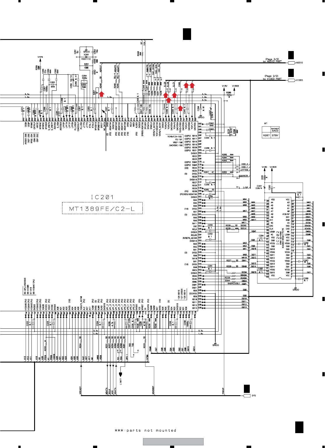
MT1389FE/C2-L
IC401
MN1623BF
FTS DRlVER
AMP
CN902
(27P)
16
20
18
23
26
21
16
12
14
8
6
10
CN8301
(27P)
16
12
14
8
64
3
10
CN901
(25P)
16
CN5102
(25P)
16
R
27MHz
27MHz
G
B
V
SC
SC
SY
SY
COMPONENT&
COMPONENT&
JA8850
CN8830
COMPOSITE
COMPOSITE
VIDEO OUT
OUT
S-VIDEO
IR
LCD DISPLAY
SENSOR
2
CN5505
(9P)
IC8111
BUFFER
ATTENUATOR
FL/FR
SW
C
SL/SR
FL/FR
FL/FR
OUT
MIC 2
MIC 1
HEADPHONE
JACK
SW
OUT
CENTRE
OUT
SL/SR
OUT
LINE
OUT
SW
C
SL/SR
MIC
AMP
E-VOL
ANDREW CIRCUIT
POWER AMP
MODULE
IC3401
STK433-270
IC3301
STK433-270
6 8
CN5701
CN8401
(11P)
Y2
Y2
X2
X2
2
15
Y3
Y3
X3
X3
Y(Lch)
Y(Lch)
X(Rch)
X(Rch)
3
13
14
5
CN2301
(4P)
1
3
5
3
7
1
CN5506
(1/2)
(19P)
CN5506
(2/2)
(19P)
5
7
9
11
13
15
2
6
3
5
6
3
1
7
1
7
7
1
IC8601
HA17558AF
IC8702(1/2)
HA17558AF
IC8702(2/2)
HA17558AF
IC8701
HA17558AF
IC8201
M65847AFP
IC8301
BA3838F
IC5402
JA5401
JA5402
JA5403
HA17558AF
IC3901
NJM4565M
IC3056
HA17558AF
IC3058(1/2)
HA17558AF
IC3058(2/2)
HA17558AF
IC3057
HA17558AF
CN8401
SL
SR
IC5201 S5101-S5108
D5207,5209
D5211-5213
S5201-S5207
GP1UM28XK0VF
1 12
4 11
3ch
Power Amp
DVDM ASSY
VERTICAL Block Diagram
B
IFAF ASSY
C
DSP ASSY
D
LOAB
ASSY
A
PASSIVE
17
19
1
3
CN5507
(13P)
1
2
1
2
XV-EV1000 19
5678
5678
C
D
F
A
B
E
- 6dB - 10dB
·MPEG Video Decoder
·Video Encoder
·Video DAC
(withPictureContorol)
(Progressive: 54MHz)
(VRmode with CPRM)
·Audio Decoder
-DD MPEG
·JPEG Viewer
·WMA Playback
·RW Playback
IC202
64M SDRAM
IC203
16M
FLASH ROM
M
+ -
6IN-6OUT
BACK END IC
VIDEO DRIVER
system control
M
+ -
DOUT
C
V
Y
Cb
Cr
Y
·DolbyDigital Decoder
·DTS Decoder
·DolbyPrologicII
IC8101
HEF4052BT
HA17558AF
(BUH4052BCF)
FUNCTION
SELECTOR LPF
PASSIVE
FLO/FRO
SWO
CO
8ch
CODEC
SLO/SRO
LPF
LPF
LPF
3ch
Power Amp
Power Amp
IC 8602
HFE4066BT
HFE4066BT
HEADPHONE
AMP
AMP
MIC ECHO
ECHO
BU9255FS
IC5401
VOCAL
FADER
KEY
CONTROL
RECL/
RECL/
RECR
RECR
DECKL/
DECKL/
DECKR
DECKR
MICDET
MICDET
MIC DET
MIC DET
PBL/
Lch
Rch
PBR
SBLO/
SBRO
TUNER MODULE
TAPE DECK
MECHA
XYM3019
LINE IN
AUXL/
AUXR
TXL/
TXR
YO
Y1
X1
XO
DSPINL/
DSPINR
DOWNMIX
SBLO/SBRO
DECKL/
DECKR
SPINDLE 03SD PU
*SINGLE DISC MECHA
Stepping
Motor
Load
Motor
Motor
DIR
AMP
R
27MHz
G
B
V
SC
SY
COMPONENT&
JA8850
CN8830
COMPOSITE
VIDEO OUT
OUT
S-VIDEO
IR
LCD DISPLAY
SENSOR
MICROPROCESSOR
LCD DRIVER
IC5501
PDC127
IC8111
BUFFER
ATTENUATOR
FL/FR
FL/FR
SW
SW
C
SL/SR
SL/SR
FL/FR
FL/FR
FL/FR
OUT
MIC 2
MIC 1
HEADPHONE
JACK
SW
OUT
CENTRE
OUT
SL/SR
OUT
LINE
OUT
SW
SW
C
SL/SR
SL/SR
MIC
MIC
AMP
E-VOL
ANDREW CIRCUIT
ANDREW CIRCUIT
IC3062
BD3814FV
POWER AMP
POWER AMP
MODULE
MODULE
IC3401
STK433-270
IC3301
STK433-270
Y2
X2
Y3
X3
Y(Lch)
X(Rch)
CN8303
(27P)
9
11
3
5
7
1
CN3051
(27P)
9
11
3
5
7
1
CN3011
(17P)
6
8
14
16
12
10
CN3031
(17P)
6
8
14
16
12
10
CN3021
(23P)
17
19
22
23
20
21
CN3002
(23P)
17
19
22
23
20
21
J3033
(14P)
J3032
(13P)
3
6
8
11
14
CN3001
(23P)
18
19
22
23
3
4
7
8
11
15
18
19
14
15
10
11
CN3022
(23P)
18
19
22
23
3
4
7
8
14
15
10
11
18
19
11
15
16
16
19
17
13
11
9
15
27
28
30
31
32
29
3
5
1
7
3
5
5
3
1
7
7
1
6
9
3
13
10 9
3
2
IC8601
HA17558AF
IC8702(1/2)
HA17558AF
IC8702(2/2)
HA17558AF
IC8701
HA17558AF
IC8201
M65847AFP
M65847AFP
IC8301
BA3838F
89
3 3
5 5
J5401
(5P)
CN5105
(5P)
3
72
IC5402
JA5401
JA5402
JA5403
HA17558AF
IC3901
NJM4565M
NJM4565M
2
4
2
4
1
7
3
5
J3902
(4P)
CN3008
(4P)
IC3056
HA17558AF
IC3058(1/2)
HA17558AF
IC3058(2/2)
HA17558AF
IC3057
HA17558AF 4-7
4-7
3
CN3013
(14P)
CN3012
(13P)
3
6
8
11
14
JA3301
CN8401
(12P)
3
SL
SL
SR
SR
CN5501
(13P)
CN5101
(13P)
CN5104
(10P)
IC5201 S5101-S5108
S5101-S5108
D5207,5209
D5207,5209
D5211-5213
D5211-5213
S5201-S5207
S5201-S5207
GP1UM28XK0VF
GP1UM28XK0VF
1
1
J1
(4P)
J1
(4P)
J2
(2P)
J2
(2P)
OPEN/CLOSE
S5301
PLAY
S5302
MS-/REW
S5304
MS+/FF
S5305
STOP
S5303
3ch
Power Amp
Power Amp
TRADE ASSY
K
AMP ASSY
I
HP/MIC ASSY
H
POWER ASSY
J
DISPLAY ASSY
LCD ASSY
G
KEY ASSY
E
LED ASSY
F
PASSIVE
1
11
4
8
XV-EV1000
20
1234
1234
C
D
F
A
B
E
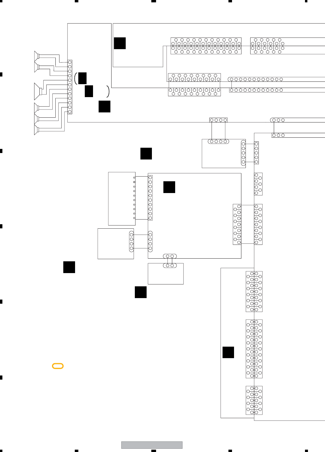
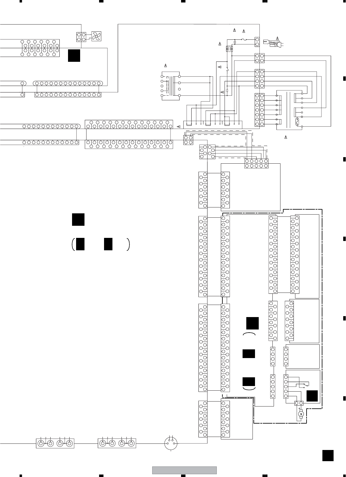
3.2 OVERALL WIRING CONNECTION DIAGRAM and LOAB ASSY
1
2
5
3
4
6
7
8
9
2
1
5
4
3
6
8
7
12
11
10
9
13
14
12
15
16
17
19
18
1
2
4
3
5
6
7
9
10
8
13
11
12
2
1
4
2
1
21
21
3
10
4
32
4
6
8
8
9
6
7
4
5
10
12
3
1
3
2
1
5
4
5
6
9
77
8
9
10
11
12
1313
11
7
6
1
2
3
2143
4132
1
4
2
1
3
5
1
2
33
2
5
44
5
15 1314
15 1314
6
8
10
11
9
7
5
4
3
2
1
11
12
17 15
16
9
10
13
8
14 4
7
6
53
2
11312
17 13
14
15
16 8
11
12
9
10 4
7
6
53
2
11213
23
21
22
20
19
15
16
17
18
20
23
21
22
19
17
18
15
16
14
13
12
11
10
9
8
7
3
4
6
5
2
14
11
13
12
8
7
10
9
4
3
6
5
2
10 7811 456932
610 5 479811 3 2
1
20
23
21
22
19
17
18
16
1
23
21
22
20
19
17
18
16
14
13
15
14
13
15
CN5505
CN5506
Speaker for SL/SR/C/SW
JA3301
CN5507
J1_ J1
CN5101
J2_ J2
CN5104
CN5501
FLASH MICRO_P
CN5502
J5401
J3902 CN3008
CN5105
CN8302 J3002
CN3011 CN3031
XKP3064-
XKP3069-
XKE3037
51048-0200
XKP3066-
51048-0400 51048-0400
52044-1345
51048-0200
NC NC
52492-1020
VDD
NC
LCDCLK
VLCD
VSS
NC
NC
LCDDAT
NC
LCDCLK
VDD
NC
52044-1345
NC
GNDU
HLEM7S
NC
LCDDAT
NC NC
VLCD
VSS
ECHOVOL
51048-0500
51048-0400
GNDHP
HP R
HP L
HP DET
VA+12V
MIC
GNDA
MICSW
D20PYY0430E
52044-1745
52151-0410
HP L
GNDHP
HP R
HP DET
52147-0510
ECHOVOL
VE+56
XRESET
FLASH DO
FLASH E/D
FLASH CLK
VA+12V
MIC
D20PYY0520E
MICSW
GNDA
52147-1510 51048-1500
GNDA
SRIN
GNDA
SLIN
GNDA
SWIN
GNDA
CIN
GNDA
FRIN
XDD318017P FFC
GNDA
FLIN
MUTE
MUTEC
RYFS
RYRC
XPROT
VPR+8
VPR+8
GNDA
SRIN
GNDA
SLIN
GNDA
SWIN
GNDA
CIN
GNDA
FRIN
FLOUT
FLOUT
VL-
VL-
FROUT
FROUT
VL+
VL+
SWOUT
VPR+8
52044-1745
VPR+8
GNDA
FLIN
MUTE
MUTEC
RYFS
RYRC
XPROT
SWOUT
VH+
VH+
COUT
COUT
GNDS
SLOUT
SLOUT
GNDP
GNDP
SROUT
SROUT
VH-
FLOUT
FLOUT
VL-
VL-
FROUT
FROUT
VL+
VL+
SWOUT
VH+
COUT
VH+
SWOUT
SLOUT
COUT
SLOUT
GNDS
GNDP
GNDP
SROUT
SROUT
VH-
UN+8V
GNDREG
VD+5
VA-12
VP+12
VFL+5
D20PYY1315E
GNDF
UN+8V
SLOUT
VL-
VP+12
VD+5
UN+8V
UN+8V
GNDF
VFL+5 VH-
SRIN
SLIN
CIN
SWIN
FRIN
GNDA
VA-12
GNDREG
VPR+8
FLIN
SLOUT
VL- MUTE
VPR+8
MUTEC
VH-
SWIN
CIN
SLIN
SRIN
VPR+8
FLIN
GNDA
FRIN
MUTEC
MUTE
VPR+8
XKP3076-
GNDU
AC3IN
GNDU
AC3IN
DIN
GNDD1
GNDD GNDD
DIN
GNDD1
GNDD
VD+5
NC
GNDD
VD+5
NC
V+5A V+5A
XKP3080-
GNDC(IN)
RIN RIN
GNDC(IN)
FRO
LIN
GNDC(IN)
FRO
GNDC(IN)
LIN
RECMUTE
VCOMG
FLO
RECMUTE
FLO
VCOMG
XDSPRST
GNDU
KEY3
GNDC
SLO
SRO
SLO
GNDC
SRO
SWO
GNDC
GNDC
GNDC
SWO
GNDC
CO
GNDC
SBRO
CO
GNDC
SBRO
GNDC
SBLO SBLO
GNDC
XKP3078-
DIRERR DIRERR
DIRCS
DIRDO
DIRRST DIRRST
DIRCS
DIRDO
BUSY
DSPMODE
DSPHREQ DSPHREQ
DSPMODE
BUSY
DSPSS
DSPCLK
DSPSS
XDSPRST
DSPCLK
DSPDO
DECMUTE
DSPDI
DSPDO
DSPDI
DECMUTE
GNDLED
LEDCN1
D20PYY0225
LEDCN1
GNDLED
KEY3
GNDU
LEDCN2
VP+12
10P FPC
VP+12
LEDCN2
D20PYY0410 TIMERLED
KEY3
KEY2
VE+5
VP+12
GNDU
GNDLED
KEY1
REMOCON
LCDCLK
MOVIELED
LCDDAT
MUSICLED
13P FFC REMOCON
GNDU
TIMERLED
KEY3
VE+5
VP+12
XDD3185
GNDLED
KEY1
KEY2
MOVIELED
MUSICLED
LCDCLK
LCDDAT
VD+5
VP+12
VA+5
VD+5
VP+12
VA+5
Speaker for FL/FR
DISPLAY ASSY
(XV-EV1000:XWZ4012)
(XV-EV700:XWZ4010)
G
KEY ASSY
(XWZ4013)
E
DSP ASSY
(AWX8588)
D
LED ASSY
(XWZ4023)
F
LCD ASSY
(XAV3028)
HP/MIC ASSY
(XWZ4014)
H
AMP ASSY
(XWK3202)
I
POWER ASSY
(XV-EV1000:XWZ4016)
(XV-EV700:XWZ4018)
J
CN3022 CN3001
XKP3082- XKP3071
NOTES: • When ordering service parts, be sure to refer to “EXPLODED
VIEWS and PARTS LIST” or “PCB PARTS LIST”.
• The > mark found on some component parts indicates the
importance of the safety factor of the part.
Therefore, when replacing, be sure to use parts of identical
designation.
• : The power supply is shown with the marked box.
J1/4-
J4/4
XV-EV1000 21
5678
5678
C
D
F
A
B
E
11
10
5
6
1
9
7
2
3
4
8
1
2
3
6
4
5
10
11
2
1
3
4
7
8
5
6
9
14
9
8
11
12
10
7
13
15
20
21
24
17
18
16
19
22
23
27
26
25
25
23
24
15
14
13
21
22
19
20
17
18
16
5
6
12
11
10
9
7
8
4
11
9
2
3
1
10
26
27
12 911 10 67854213
12 911 10 67854213
26
27
2
3
4
7
8
5
6
1
20
21
24
25
13
17
16
15
14
18
19
22
23
1
2
3
5
6
7
4
12
11
10
9
8
1
2
3
2
3
1
2
1
44
21
24
25
22
23
17
18
19
20
13
16
15
14
10
12
11
9
8
7
4
5
6
1
2
3
2
1
7
5
6
114
1
13 12
1213
10 7811 4569132
6
10 54798
11 321
14
12
11
9
8
7
10
4
6
5
3
12
11
10
8
7
9
3
4
6
5
1
2
1
2
2
1
3
4
1
2
1
3
2
4
2
1
1
2
CN8401
JA8850
CN5701
CN8830
CN8301
TUNER MODULE
CN902
CN5102
CN5503
CN8303 CN3051
CN2301
CN2302
CN901
XYM3019
MECHA
TAPE DECK
XDE5066
CN3012 J3032
CN3021 CN3002
CN3013 J3033
CN3651 FAN
CN4
CN2
CN1
C1 AN1
AKB7015
VKB1168-
52045-1145
AKP7179-
GND
RDS
VSM
TXR
+9V
TXL
GND
DO
CLK
DI
CE
VKN1258-
SQUEEZE
NC
VSEL2
VSEL1
ASPECT
SC
GND
RDS
VSM
TXR
DI
+9V
TXL
DO
CLK
CE
GNDD
V
GNDD
SY
GNDD
G
GNDD
B
GNDD
NC
GNDD
NC
GNDD
NC
GNDD
GNDA
R
GNDD
NC
GNDA
NC
SQUEEZE
NC
VSEL2
VSEL1
ASPECT
SC
GNDD
V
GNDD
SY
GNDD
G
GNDD
B
GNDD
NC
GNDD
NC
GNDD
NC
GNDD
GNDA
R
GNDD
NC
GNDA
NC
VKN1256
VDVD+12
VPR+8
VPR+8
GNDM
GNDM
DOUT(AC3)
GNDD
GNDD
GNDD
DVDPOWER
VPR+8M
VPR+8M
GNDD
XREADY
GNDD
GNDD
VDET
XDVDRST
SCLK
SDATA
MDATA
DVDACK
TRKUP
NC
MOTOR
RECF
RECR
52045-1145
DVDMUTE
TRKUP
DVDMUTE
52044-2745
D20PYY1515E
52044-2745
PULSE
NC
SOL
GNDM
VD+5V
GNDM(TC)
MODE
HALF
B4B-PH-K-S
B2B-PH-K-S
BIAS
VREF
R CH
VREF
L CH
GNDA
27P FFC
XDD3186
MOTOR
RECF
RECR
VD+5V
GNDM(TC)
MODE
PULSE
NC
HALF
SOL
GNDM
VREF
BIAS
R CH
VREF
L CH
SUBAC1
SUBAC1
BHAC2
SROUT
VL+
VL+
COUT
VL-
52147-1310
VH+
VH+
SWOUT
FLOUT
GNDS
GNDP
GNDP
FROUT
D20PYY1415E
VL-
51048-1300
SROUT
COUT
VL+
VL+
RYFS
VD+5
XPROT
VFL+5
VP+12
VA-12
GNDREG
GNDREG
UN+8V
UN+8V
SWOUT
VH+
VH+
GNDP
FLOUT
GNDS
FROUT
GNDP
RYRC
GNDF
VFL+5
RYFS
XPROT
VD+5
VA-12
VP+12
GNDREG
GNDREG
UN+8V
UN+8V
XKP3082- XKP3071
RYRC
GNDF
VH-
VH-
52147-1410
VH-
VH-
51048-1400
XTF3004
KM200SA2 XXM3009
GND
BLAC2
0.01
ACE7013
B7P-VH
BHAC1
BLAC1
C3
120v
0v
10v
XSR3008
RY81
B4P7-VH
0v
120v
0v
L1
B2P3-VH
ACE7013 H2
AEK1061
FU1
0.01 H1 XKP3084
LINE OUT
LINE IN
VIDEO/COMPONENT OUT
R
L
R
L
Y
Video
Cb
Cr
S-VIDEO OUT
11P FFC
XDD3179
27P FFC
25P FFC
11P FFC
GNDM(TC)
GNDM(DV)
VPR+8
GNDD
GNDD
VPR+8M
VPR+8M
VE+56
GNDU
VA+12
VA+12TX
GNDTX
VA-12
VPR+8
GNDM(DV)
GNDM(TC)
VPR+8M
VPR+8M
VPR+8
GNDD
GNDD
VA-12
VPR+8
GNDTX
VA+12
VA+12TX
GNDU
VE+56
XDD3184
NC
MUTEC
RYRC
MUTE
RYFS
HPAC1
SYSPOW
XHPMUTE
EVOLCLK
EVOLDATA
HPDET
SUBAC
XPROTECT
C
GNDA
FR
GNDA
FL
GNDA
SW
GNDA
SR
GNDA
SL
GNDA
RYFS
RYRC
MUTEC
NC
MUTE
EVOLDATA
EVOLCLK
SYSPOW
HPAC1
XPROTECT
HPDET
SUBAC
XHPMUTE
FR
GNDA
FL
GNDA
GNDA
SW
GNDA
SR
GNDA
SL
GNDA
C
S1
XKX3001
lkji
hgf
9
11
10
8
7
6
5
4
3
2
1
Deck Shield Wire 5P
edc ab
T1 *
SUBAC1
SUBAC1
BHAC2
0 0
0 0
5
7
6
0V
40V 0V0V
2
NC
3NC NC NC
8
9
T2
ATT7080
115V
230V
1230V
NC
100V
NC
120V
NC
BLAC2
GND
BLAC1
BHAC1
1
120120
0
10
120
2
1
4
3
2
NEUTRAL
LIVE
S5B-PH-SM3
AKN7035
VKN1482
VKN1258-
VKN1256-
CN104
CN103
CN101
2
1
3
4
5
4
1
3
2
1
3
4
2
4
1
3
2
5
8
9
7
12
10
11
16
18
21
22
23
24
17
20
19
13
12
15
14
11
7
10
8
9
4
5
6
3
2
3
4
5
6
8
12
10
2
4
6
1
9
7
11
3
5
1
1
2
3
5
6
7
4
1
2
12
9
8
13
19
11
10
17
16
15
14
18
20
25
23
21
26
24
22
27
8
2
10
4
6
18
14
22
20
12
16
24
7
1
9
3
5
21
23
17
15
13
19
11
25
V+3D
SW2
LOAD+
LOAD-
MOTOR
STEPPING
SW1
H2+
H1-
H1+
A1
A2
A3
SPINDLE
LOAD-
SW2
V+3D
LOAD+
SW1
ST2-
ST1-
ST1+
ST2+
H2+
H1-
H1+
A2
A3
A1
GNDS
H3-
H3+
H2-
MOTOR
INSIDE
V+5S
CN1013
FOCS RTN
FOCS DRV
TRKG RTN
TRKG DRV
PD
GND
LD(780)
LD(650)
VSHF
PICKUP ASSY
MD
GND
VREF(2.1V)
MPD(650)
MPD(780)
B1
B2
OEICG
B3
B4
780/650
A
C
24P FFC
ADD7418
H2-
H3+
H3-
INSIDE
V+5S
GNDS
DVD MODULE
GND
VCC
20
21
17
16
19
18
22
23
24
7
4
5
10
13
12
15
14
8
9
6
11
3
2
1
GND
PD
TRKG DRV
TRKG RTN
FOCS DRV
FOCS RTN
VSHF
LD(650)
LD(780)
OEICG
780/650
GND
MD
B2
B1
A
C
B4
B3
MPD(780)
MPD(650)
VREF(2.1V)
VCC
GND
XXA3037
XDD3176
SDATA
MDATA
SCLK
VDET
NC
GNDD
GNDD
ACK
XDVDRST
DVDPOWER
GNDD
GNDD
XREADY
GNDM
GNDM
GNDD
GNDD
DOUT
VPR+8
VPR+8M
VPR+8M
XDD3175
VDVD+12
VPR+8
S5B-PH-K-S
CN601
CN602
2
1
LOADING
MOTOR
ASSY
: VXX2912
A
LOAB ASSY
(VWG2346)
A
XTS3099-A
AKN7301
CN102
TRADE ASSY
(XWZ4022)
K
IFAF ASSY
(XV-EV1000:XWZ4003)
(XV-EV700:XWZ4006)
C
DVDM ASSY
(AWM7964)
B
B1/2- B2/2
C1/4- C4/4
XV-EV1000
22
1234
1234
C
D
F
A
B
E
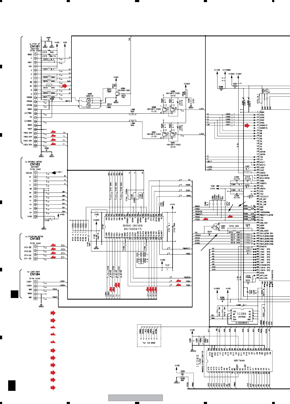
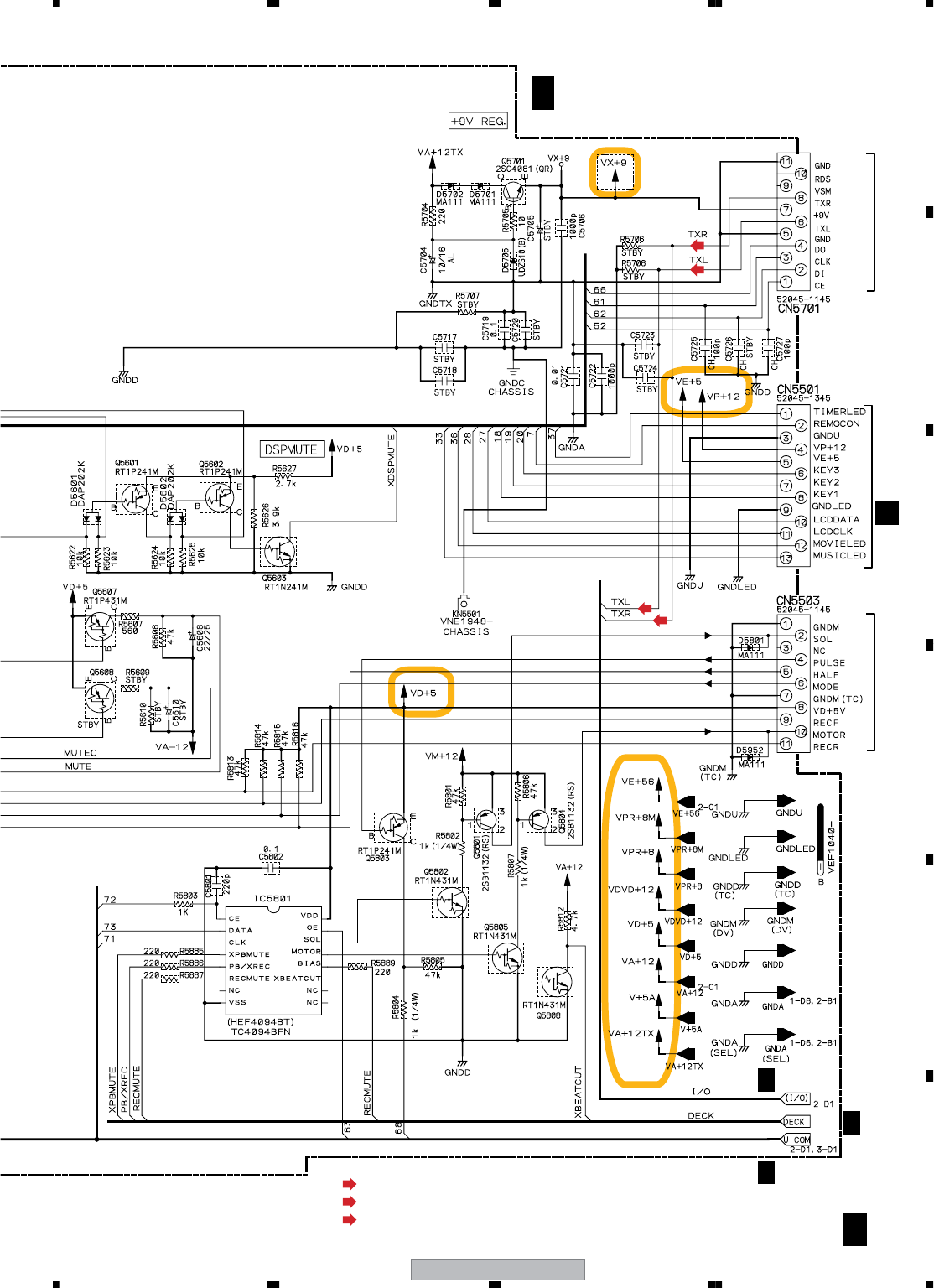
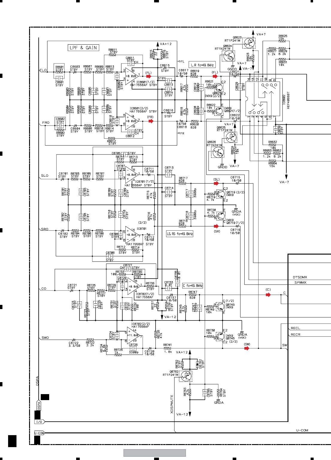
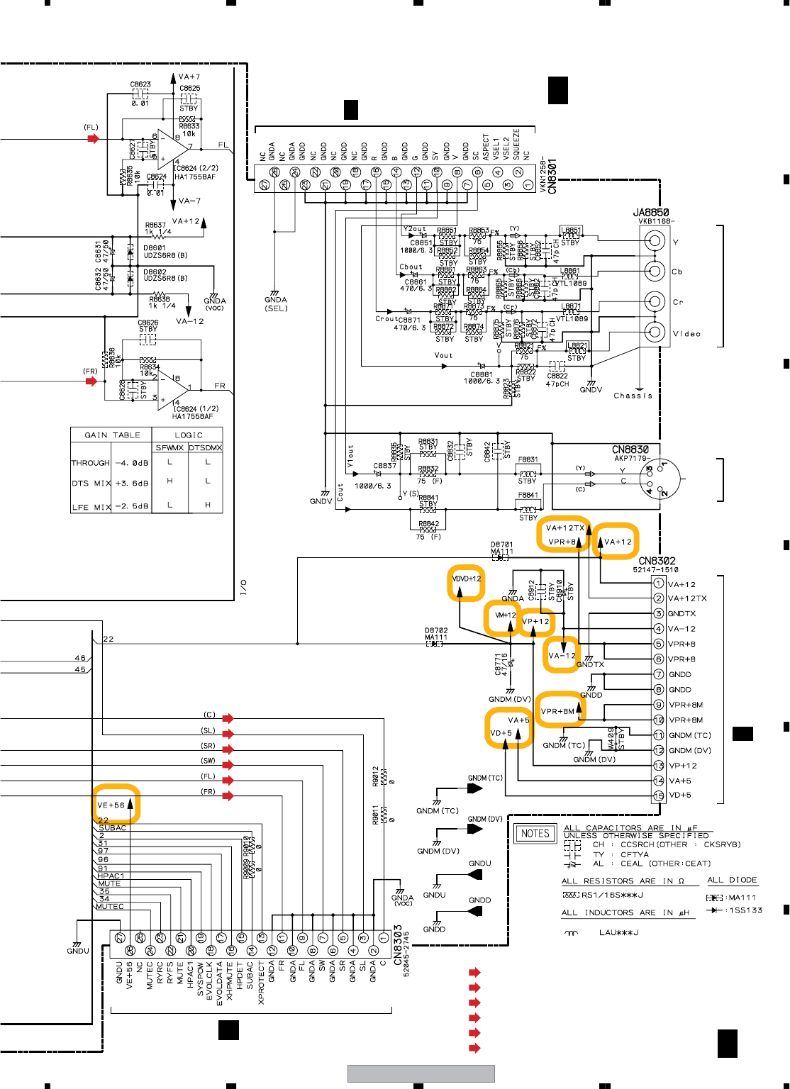
3.3 DVDM ASSY (1/2)
AKN7035
S5B-PH-SM3
A
B
: TRACKING SERVO LOOP LINE
(T)
: FOCUS SERVO LOOP LINE
(F)
: AUDIO SIGNAL ROUTE(DIGITAL)
: RF SIGNAL ROUTE
(T)
(T)
(F)
(F)
(S)
(S)
(S)
(S)
(F)
(F)
(S)
(S)
(S)
(S)
(F)
(F) (T)
(T)
(T)
(T)
: STEPPING SERVO LOOP LINE
(S)
(D)
(RF)
(RF)
(RF)
1/2
ACN601 PICKUP ASSY CN1013SPINDLE MOTOR
STEPPING
MOTOR
: VIDEO SIGNAL ROUTE(G/Y)
(G/Y)
: VIDEO SIGNAL ROUTE(R/Cr)
(R/Cr)
: VIDEO SIGNAL ROUTE
: S VIDEO SIGNAL ROUTE
(S_Y)
: VIDEO SIGNAL ROUTE(B/Cb)
(B/Cb)
: S VIDEO SIGNAL ROUTE
(S_C)
(C/V)
1
23
LD Driver for CD
LD Driver for DVD
FTS DRIVER
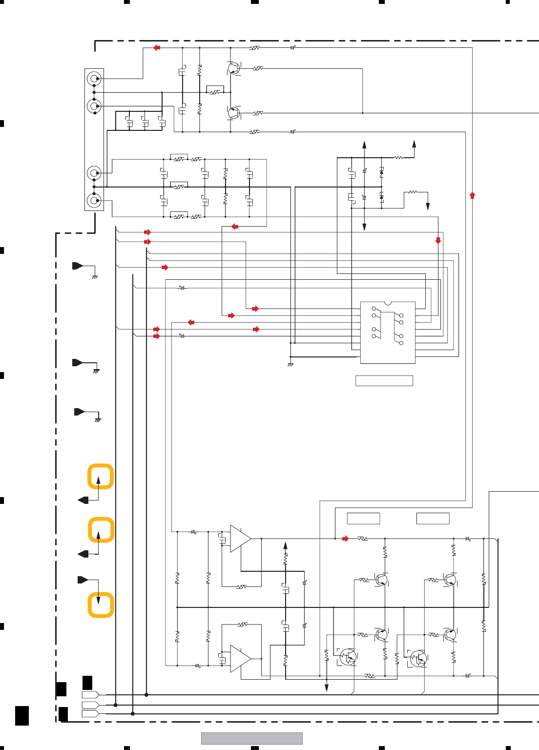
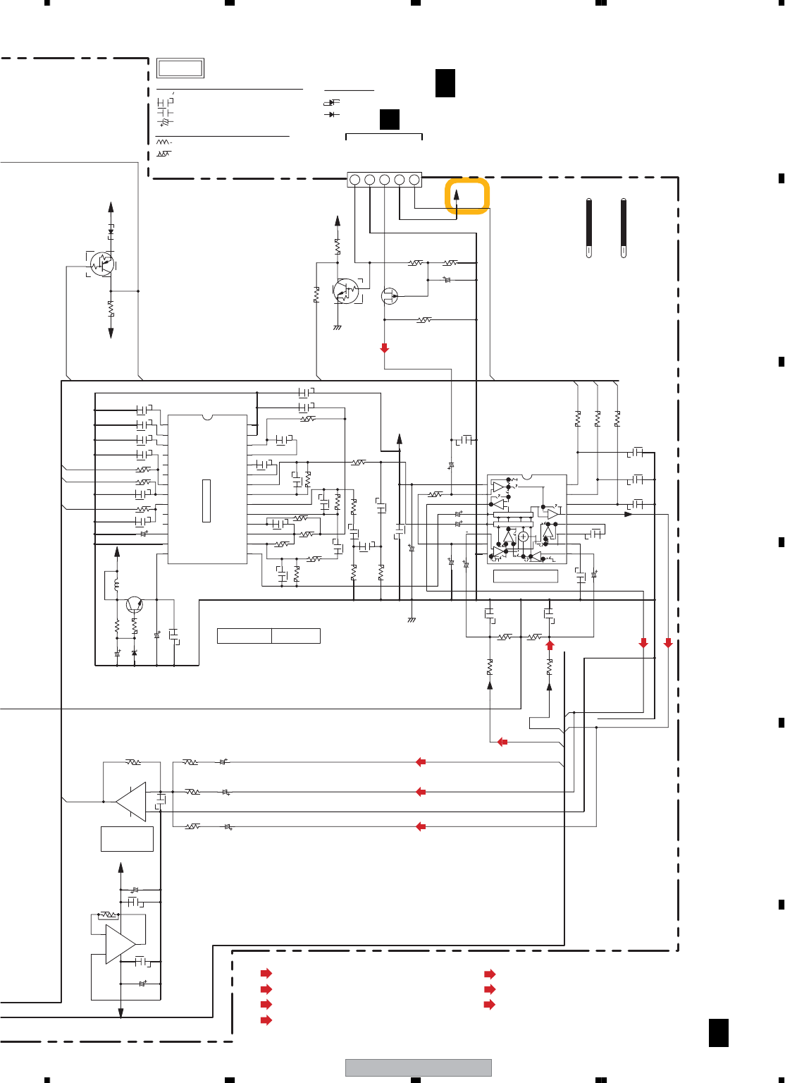
XV-EV1000 25
5678
5678
C
D
F
A
B
E
A
B
2/2
CN5102
: VIDEO SIGNAL ROUTE(G/Y)
(G/Y)
: VIDEO SIGNAL ROUTE(R/Cr)
(R/Cr)
: VIDEO SIGNAL ROUTE
: AUDIO SIGNAL ROUTE
: S VIDEO SIGNAL ROUTE
(S_Y)
: VIDEO SIGNAL ROUTE(B/Cb)
(B/Cb)
: S VIDEO SIGNAL ROUTE
(S_C)
(R/Cr)
(B/Cb)
(G/Y)
(S_Y)
(C/V)
(S_C) (S_C)
(C/V)
(S_Y)
NC
NC
NC
NC
NC
NC
G
B
R
(G/Y)
(B/Cb)
(R/Cr)
(C/V)
(D)
(D)
CN8301
Video Driver Amp
5V Regulator
3V Regulator
1.8V Regulator
6.5V Regulator
7.8V
6.4V
5.0V 7.8V
1/4C
3/4
C
XV-EV1000
28
1234
1234
C
D
F
A
B
E
3.6 IFAF ASSY (2/4)
42
41
DSPINR
DSPA
SBLO
SBRO
74
TXL
75
TXR
DSPINL
+
-
-
+
5
6
4
7
8
E
BC
B
E
C
2
3
1
8
4
8
7
9
10
5
6
12
11
4
314
13
2
116
15
C2
E2
E
C
B2
B
(2/2)
(1/2)
GNDA
(VOC)
(VOC)
GNDA
(SEL)
GNDA
GNDA
(SEL)
PBL
PBR
AUXL
LINE IN
R
ATT 6dB ATT 10dB
(SEL)
FUNCTION SELECTOR
(BUH4052BCF)
VSS
VEE
B
A
INH
Y1 X0
X3
Y3
Y(Lch)
X(Rch)
X1
VDD
X2Y2
Y0
1/4W
AUXR
L
LINE OUT
R
L
1/4W
10/50
-TS
STBY
47k
47k
VA-12
VA-5
100k
1.5k
22
HA17558AF
0.01
RT1P241M
STBY
1.5k
RT1P241M
100k
10k
100
100
0.01
2SC4081(QR)
STBY
2SC4081(QR)
10k
680
10/50
10k
STBY STBY
10k
47k
47k
10/50
-TS
STBY
VE+56
VA+12
10/50
GNDA
10/50
220p
STBY 330
STBY
STBY
22
VA+12
2SC4081(QR)
1.5k
2SC4081(QR)
HA17558AF 1.5k
680
10/50
HEF4052BT
GNDA
VA-5
STBY
STBY
0.01
47/16
MTZJ5R6(B)
VA-12
MTZJ5R6(B)
TS
1k
STBY
STBY
220p
STBY
STBY
STBY
330
470p
220k
(1/2)
IMX9
STBY
AKB7015-
470p
220k
(1/2)
IMX9
STBY
STBY
10/50
1.8k
0.01
47/16 TS
1k
VA+5
4.7k
VA+12
1.8k
4.7k
10/50
C8118
C8116
R8106
R8104
R8105
R8103
R8117
R8118
R8108
IC8111
C8108
C8120
Q8115
R8114
R8112
Q8116
R8125
C8107
R8116
C8119
Q8112
R8115
C8122
R8122
R8120
R8126 R8127
R8119
Q8114
C8117
C8115
C8751
C8752
C8402
R8402 R8404
C8404
R8406
R8411
R8124
R8107
Q8111
R8113
IC8111 R8111
Q8113
R8121
C8121
IC8101
C8406
C8101
C8908
D8902
R8904
C8513
C8518
C8514
C8401
C8403
R8405
R8401
R8403
C8516
R8516
Q8501
R8517
CN8401
C8517
R8515
Q8501
C8405
C8103
C8907
D8901
R8901
R8512 C8510
R8514
R8513
R8511 C8509
(I/O)
DSPA
U-COM
VA-12
VE+56
VA+12
GNDA
C
2/4
(AUX)
(TX)
(TC)
1/4C
3/4
C
1/4
C
(AUX)
(TX)
(TX)
(AUX)
(TC)
(TC)
1/4,
XV-EV1000 29
5678
5678
C
D
F
A
B
E
LEVELIN
90
95
92
32
HPAC1
3
C
RECR
RECL
48
38
47
ECHCNT
U-COM
+
-
+
-
54
68
7
1
3
4
2
8
12
11
14
13
15
16
18
17
9
10
7
8
5
6
19
20
21
22
24
23
BC
3
4
1
2
25
26
27
28
C
E
B
7
8
5
6
9
10
12
11
3
4
2
1
14
13
15
16
E
12534
(2/2)
INDICATOR
SPECTRUM
(1/2)
LCD
1/4W
IC8301 input
Gain for -12.7dB (VOC)
Vcc
GND
REF
KEY5
MIX OUT
MIX IN
LPF2OUT
LPF2IN
KEY4
STROBE
KEY CON
HPFOUT
HPFIN
SCK
SDATA
LPF1OUT
LPF1IN
CLKO
KEYUP ADINT OUT
ADINT IN
KEYDOWN
DACCONT2
DAINT IN
DAINT OUT
DACCONT1
ADCONT
MODE1
MODE2
(MICDET)
FR
FL DECKR
DECKL
VOCAL FADER
REF
LIN
SW1
RIN
LOUT
SW2
MIC IN
ROUT
A
STBY STBY
D
ALL RESISTORS ARE IN
RS1/16S***J
RD1/4PU***J
MIC SW
GNDA
ECHOVOL
MIC
VA+12
AL : CEAL
TY : CFTYA
CH : CCSRCH
ALL CAPACITORS ARE IN µF
NOTES
UNLESS OTHERWISE SPECIFIED
(OTHER : CEAT)
(OTHER : CKSR
:1SS133
:MA111
ALL DIODE
VEF1040-
52147-0510
VA-12
0.01
STBY
HA17558AF
STBY
0.01
STBY
VA+12
HA17558AF
56k
10/50
MTZJ5R6(B)
10k 10/50
10/50
10k
STBY
10K 10/50
1k
68
STBY
100p
47/16
VA+12
CH
STBY 1k
1k
STBY 1k
0.047
47/16
2SD1858X(QR)
1000p
GNDA
6.8k
4.7k
4.7k
15k
10k
10k
47/16
0.01
0.01
0.01
0.047
1200p 6.8k
4700p
470p
0.22
CH
10k
5.6k
10k
0.01
10k
0.068
0.068
0.068
VA-12
47k
M65847AFP
15k
0.22
8200p
STBY
VA+12
GNDD 22K
220
RT1N431M
2SJ103
(GR)
2.7k
2.7k
820
STBY
47/16
2.2/50
820
STBY 0.047
2.2/50
2.2/50
0.22
2.2/50
10k
4.7/50
BA3838F 0.1
0.1
0.01
1k
1k
1k
0.1
0.22/50
MA111
RT1P241M
VE+56
VD+5
10k
1M 1M
VA+12
C8829
IC8801
C8828
C8830
C8831
R8816
IC8801
C8803
R8805
D8201
C8221
R8802 C8834
R8801 C8833
R8803 C8835
R8216
R8215
C8222
L8201
Q8201
C8213
C8212
R8214
C8211
R8213
R8212
C8223
C8220
R8211
R8209
C8218
R8210
R8208
R8203
R8202
C8201
C8204
C8205
C8202
C8219 R8207
C8216
C8217
R8205
R8206
R8204
C8310
C8203
R8308
C8209
C8210
C8208
C8207
R8518
Q8503
IC8201
C8215
C8214 R8217
C8206
R8201
C8224
R5434
R5404
Q5403
Q5402
R8307
R8304
R8306
C8316
R8305
C8315 C8306
C8308
C8307
C8309
C8305
C8304
C8312
IC8301 C8302
C8303
C8313
R8302
R8301
R8303
C8301
C5433
D8501
R5403
R5431
CN5105
R5432
S
D
G
C
2/4
: AUDIO SIGNAL ROUTE (L ch) : AUDIO SIGNAL ROUTE
(AUX)
: AUDIO SIGNAL ROUTE (Front L ch)
(FL)
: AUDIO SIGNAL ROUTE (Front R ch)
(FR)
: AUDIO SIGNAL ROUTE
(TX)
: AUDIO SIGNAL ROUTE (Center ch)
(C)
(C)
(FR)
(FL)
(FR)
(FL)
(MIC)
J5401
H
C
2/4
IFAF ASSY(XV-EV1000:XWZ4003)
(XV-EV700:XWZ4006)
(FL)
(FR)
: AUDIO SIGNAL ROUTE
(TC)
XV-EV1000 31
5678
5678
C
D
F
A
B
E
: AUDIO SIGNAL ROUTE (Front R ch)
: AUDIO SIGNAL ROUTE (Surround Rch)
(SR)
: AUDIO SIGNAL ROUTE (Front L ch)
(FL)
(FR)
: AUDIO SIGNAL ROUTE(Surround Lch)
(SL)
: AUDIO SIGNAL ROUTE(Sub Woofer ch)
(SW)
: AUDIO SIGNAL ROUTE (Center ch)
(C)
C
3/4
C
3/4
IFAF ASSY
VIDEO/COMPONETS-VIDEO
1/4
CN3051
J
CN902
CN3002
(XV-EV1000:XWZ4003)
(XV-EV700:XWZ4006)
2/2B
1/4J
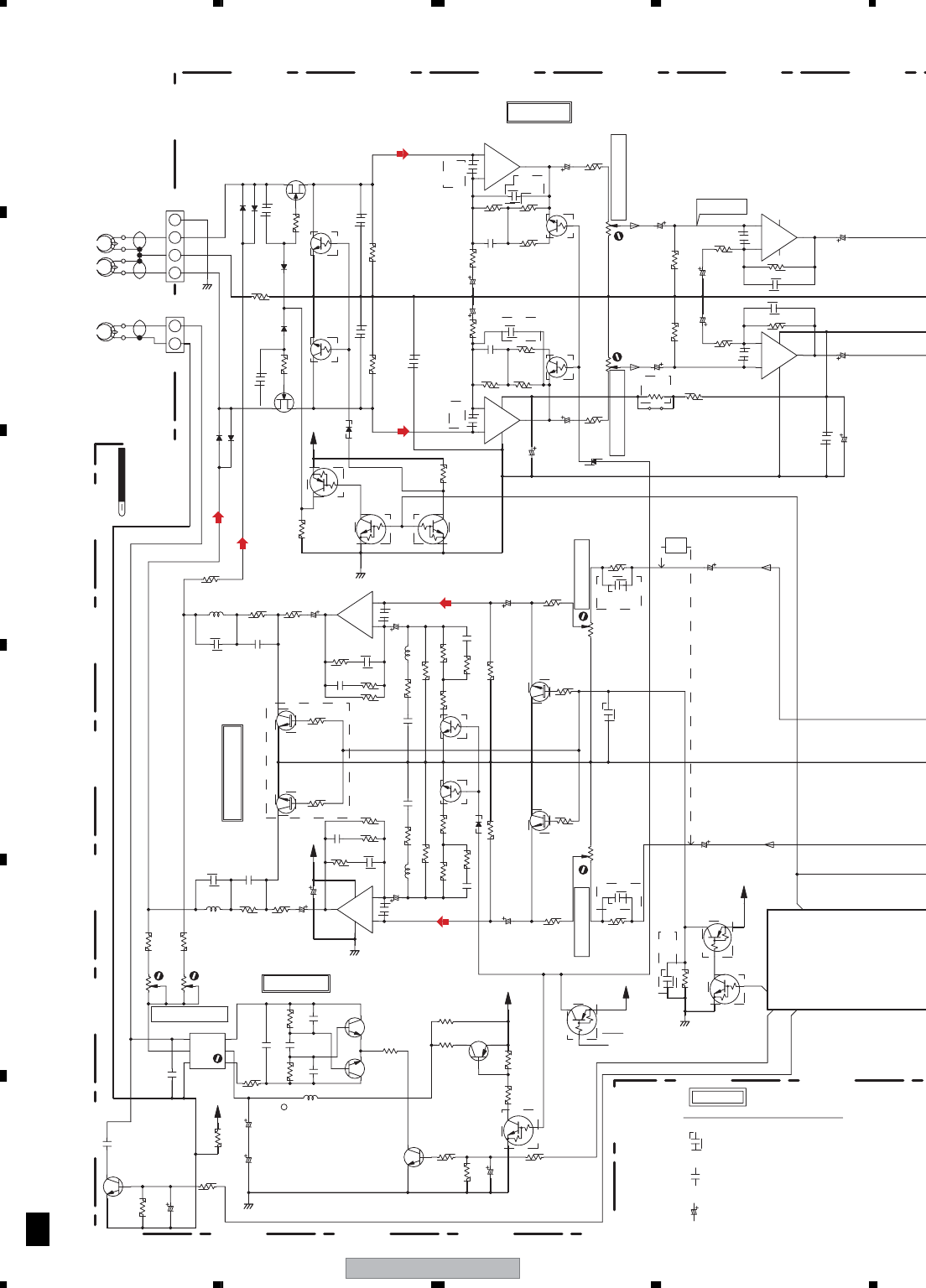
XV-EV1000
32
1234
1234
C
D
F
A
B
E
3.8 IFAF ASSY (4/4)
+
-
-
+
A1
STBY
CRO2
XBEATCUT
BIAS
RECMUTE
PB/XREC
AL:CEAL***M##-*
(OTHER : CEAT***M##)
M:CQMA***
OTHER:CKSRYB***
YF:CKSRYF***
TS:CE*****M##-TS
JQ:CEJQ***M##-*
UNLESS OTHERWISE SPECIFIED
ALL CAPACITORS ARE IN µF
NOTES
CH:CCSRCH***
105KHz
1
43
8
2
STBY
VEF1040-
C
STBY
STBY
STBY
STBY
(2/2)
YK56R-AA4N3
STBY
STBY
(1/2)
BIAS OFFSET
BIAS OSC.
HA:CQHA***
MB:CQMBA***
Not Connected
REC EQ AMP
REC LEVEL Adj. REC LEVEL Adj.
TP
PB LEVEL Adj.
TS
Rch
Lch
PB LEVEL Adj.
-32.2dBV
PB AMP
TS
4
6
52
3
1
7
6
5
2
1
54
68
7
5
7
4
68
1
2
3
4
2
3
1
2
8
3
1
4
L2801
R2803
R2806
R2805
Q2454
L2404 R2416 R2415 L2403
Q2351 Q2352
D2307
C2452
D2401
R2410
C2412
Q2460
Q2453
R2409
C2451
C2411
Q2353
D2308
W239
R2321
C2208
C2228
C2227
IC2201
C2207
IC2201
B
-
+
B
B
+
-
S
DG
B
B
B
B
B
-
+
B
B
S
D
G
B
-
+
33/10
C2810
R2816
JQ
4.7K
2SC2240
Q2806
(Y/GR)
150p/500
C2809
1K
GNDM(TC)
R2815
JQ
C2806
33/10
R9005
2SC1815(YGR)
Q2805
8200P/200
HA
C2808
0
JQ
33/10
C2805
VREF
0
LFA121J
0.12mH
RTD1082 R2898
10K
R2801
L2802
C2803
2SC1815(YGR)
4700P
Q2801
M
PCP1032
100K-B
VR2802
C2801
M
0.012
M
10K
R2802
PCP1032
100K-B
VR2801
6800P
C2802
(1/2W)VM
4.7
M
4700P
C2804
2SC1815(YGR)
Q2802
1K
47K
R2810
47/16
C2807
R2811 R2809
1K
STBY
Q2804
STBY STBY
R2808 R2807
STBY
STBY
160
Q2803
(1/2W)VM
VM+12
47k
R2453
GNDA
R2814
R2813
6.2K
6.2K
RTF1004
10mH
L2402
11k
R2424
1/50
C2420
1k
GNDA
HA17558AF
IC2401(2/2)
47p
C2401
CH M
R2426
C2424
220P 1500P
C2422
VA+12V
C2425
47/16
33/50
C2408
4.7mH
R2432
33K C2432
1200P
0.068 47k
MB
2SD2114K
Q2456
C2406 R2414
82k
R2412
C2410
6.8k
R2456
2SD2114K
Q2455
R2455
6.8k 82k
R2411
C2409
0.068
MB 47k
CH
220P
C2423 1500P M
C2421
10mH
L2401 11k R2425
C2405 R2413
4.7mH
1/50
33k
R2431 1200P
C2431
C2419
C2402
C2407
33/50
47K
R2351
0
R2899
R2423
RTF1004 1k 47p
GNDA HA17558AF
IC2401(1/2)
RT1P241M RT1N241M
D2304
D2302
2SK373(YGR)
Q2302
C2302
R2304
330K
VA+12V
CN2302
B2B-PH-K-S
10P
CH
1M
R2302 D2306
0
C2315
DTC114TK
Q2304
680p
C2304
C2404
1/50
VA+12V
R2404
022K
R2402
RT1N241M
STBY
RTF1021
M
STBY
C2418
1.2k
R2418
R2420
STBY
R2498
STBY
56
R2422
100K
680P
PCP1028
4.7k-B
VR2402
2SD2114K(VW)
Q2452 10K
1/50
C2218
CH
M
0.022
STBY
STBY
Q2402
STBY
R2452
RT1P241M
VA+12V
Q2401
STBY
M
0.022 56 R2417
R2421
STBY
100K
2SD2114K(VW)
Q2451
STBY
10K
R2451
R2419
1.2K
RTF1021
STBY
STBY
R2499
M
STBY
C2417
JQ
1/50 0
PCP1028
4.7k-B
VR2401
C2403 R2403 680P
22K
R2401
CH
C2217
1/50
RT1N241M
22K
R2352
STBY
47/16
C2314
HA17558AF
IC2301(2/2)
C2322
1000p
470K
R2306 R2308
10/50 470
C2312 R2320
22K
4.7K-B
PCP1028
VR2302
0
STBY R9008
6800P
M
C2308
240
R2312
33/50
C2310
C2324
STBY
R2310
STBY
Q2306
1/50
C2202
STBY
100k
R2223
2.2/50
C2223
2.2k
R2213
100P
47/16
0.01
HA17558AF
10/50
C2204
C2206
56k
R2212
GNDA R2399
D2305
D2301
D2303
R2301
CH
R2303
330K
1M
DTC114TK
Q2303
B4B-PH-K-S
CN2301
10P
C2301
Q2301
2SK373(YGR)
680p
C2303
33/50
C2309
240
R2311
6800P
C2307
MSTBY
R2309
PCP1028
VR2301
4.7K-B
STBY
C2222
2.2/50
R2222
100k
2.2k
R2210
1/50
STBY
R2305
470K
C2321
22K
R2307
Q2305
C2323 10/50 470
HA17558AF
IC2301(1/2)
C2311 R2319
C2201
100P
C2205
56k
R2209
10/50
C2203
HA17558AF
C
4/4
(TC)
(TC)
(FR)
(FL)
(FL)
(FR)
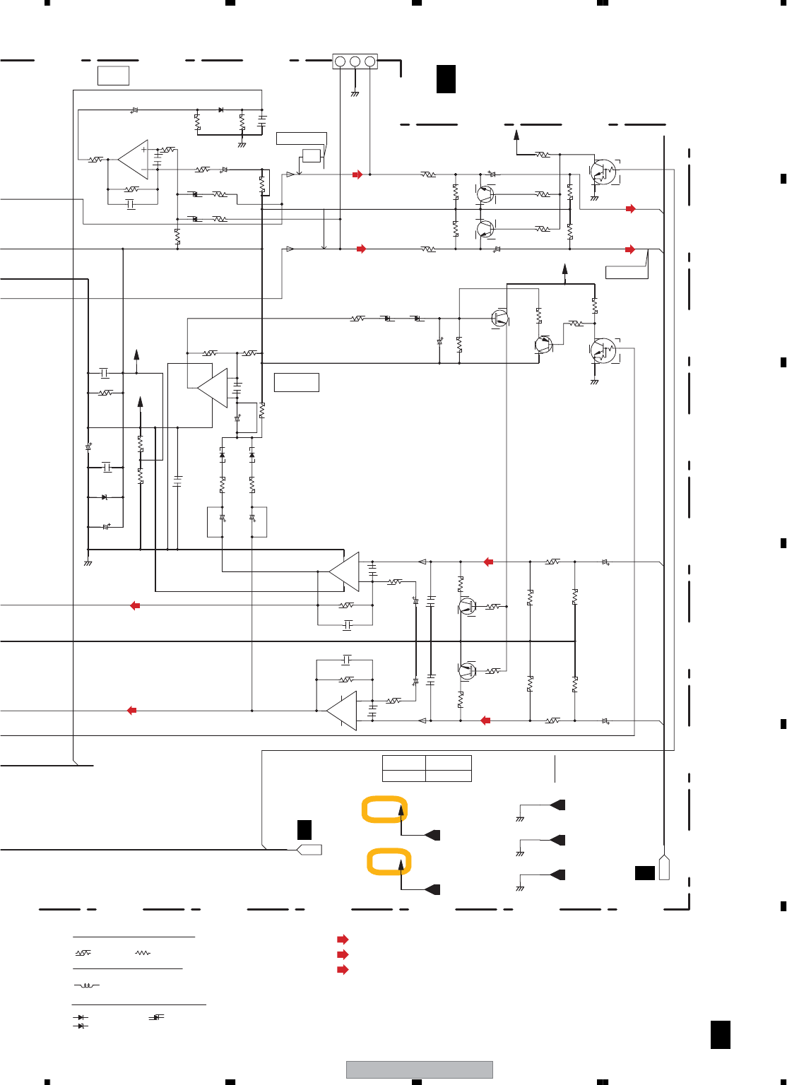
XV-EV1000 33
5678
5678
C
D
F
A
B
E
+
-
-
+
DECK
VA+12
VM+12
GNDA(SEL)
GNDM(TC)
I/O
GNDD
XPBMUTE
70
DECKR
DECKL
PBL
PBR
MTZJ***
ALL COILS ARE IN µH
UNLESS OTHERWISE SPECIFIED
ALL DIODES ARE 1SS133
UNLESS OTHERWISE SPECIFIED
1SS133 MA111
LAU***J
UNLESS OTHERWISE SPECIFIED
ALL RESISTORS ARE IN
1/16W 1/4WPU
-16.3dB
(2/2)
0.01
STBY STBY
(1/2)
STBY
-19.0dB
CH
C2255
PB TEST POINT
(VW)
(VW)
ALC
-6.0dBV
MS
TP
-3.7dBV
4
7
5
6
8
82
1
43
83
1
2
4
6
7
5
3
1
2
IC2203
C2219
R2216
C2214
R2217
C2212
C2225
C2216
D2201
R2275
C2231
C2215
R2274
C2213
R2214
C2224
C2211
R2215
C2260
C2259
IC2203
C2210
C2226
R2259
R2260
D2253
D2254
IC2202(1/2)
R2291
C2230
C2209
C2256
R2271
R2265
C2251
R2257
R2262
D2255 D2252
R2206 C2221
Q2252
R2252
R2208
R2254
R2204
Q2251
R2253
R2207
R2251
R2203
R2205 C2220
R2256
Q2253
R2255
Q2254
R2277
Q2255
C2262
R2276
C2257
IC2202(2/2)
D2258
D2257
R9006
R2272
R2261
CN2507
R2264
Q2262
R2263
Q2261
R2164
R2282
R2281
R2163
C2261 R2283
Q2263
-
+
B
B
B
VM+12
GNDA
GNDM(TC)
VA+12V
HA17558AF STBY
100P
56k
100P
2.2k
1500P
2.2/50
220/16
GNDA
MTZ6R2(B)
100/16
56k
2.2/50
1500P
STBY
2.2k
STBY
STBY
HA17558AF
0.01
10K MA111
HA17558AF
MA11110K
680
VA+12V
VREF
STBY
47p
100k
10K
12K
R2266
MA111 MA111
100
3.9K
GNDD
2.2k
2SC3052(EF)
15k 10/50
1K
STBY
2.7k
2SC3052(EF)
1K
2.2k
STBY
2.7k
15k 10/50
GNDD
2SA1235A(EF)
22/50
1M
2SC3052(EF)
1K
22K RT1N241M
4.7/50
4.7K
VA+12V
270P
C2253
1K
R2270
39K
R2269
HA17558AF 100
R2268
1/50
AL
MA111
100K
R2243
10K
R2242
MA111 10K
R2241
STBY
3.9K
100
R2267
2.2/50
AL
47p C2254
GNDD
R2273
10K
150K
0.33
1SS133-T
D2256
C2252
B3P-SHF-1AA
GNDA
15K
2SD2114K
15K
2.2K
STBY
2.2K GNDA
STBY
4.7/50
2SD2114K
VA+12V
4.7K
RT1N431M
ALC ON
ALC OFF
C
4/4
1/4C
2/4C
C
4/4
IFAF ASSY(XV-EV1000:XWZ4003)
(XV-EV700:XWZ4006)
: AUDIO SIGNAL ROUTE (Front L ch)
: AUDIO SIGNAL ROUTE (Front R ch)
(FR)
(FL)
: AUDIO SIGNAL ROUTE
(TC)
(TC)
(TC) (TC)
(TC)
(FR)
(FL)
(FR)
(FL)
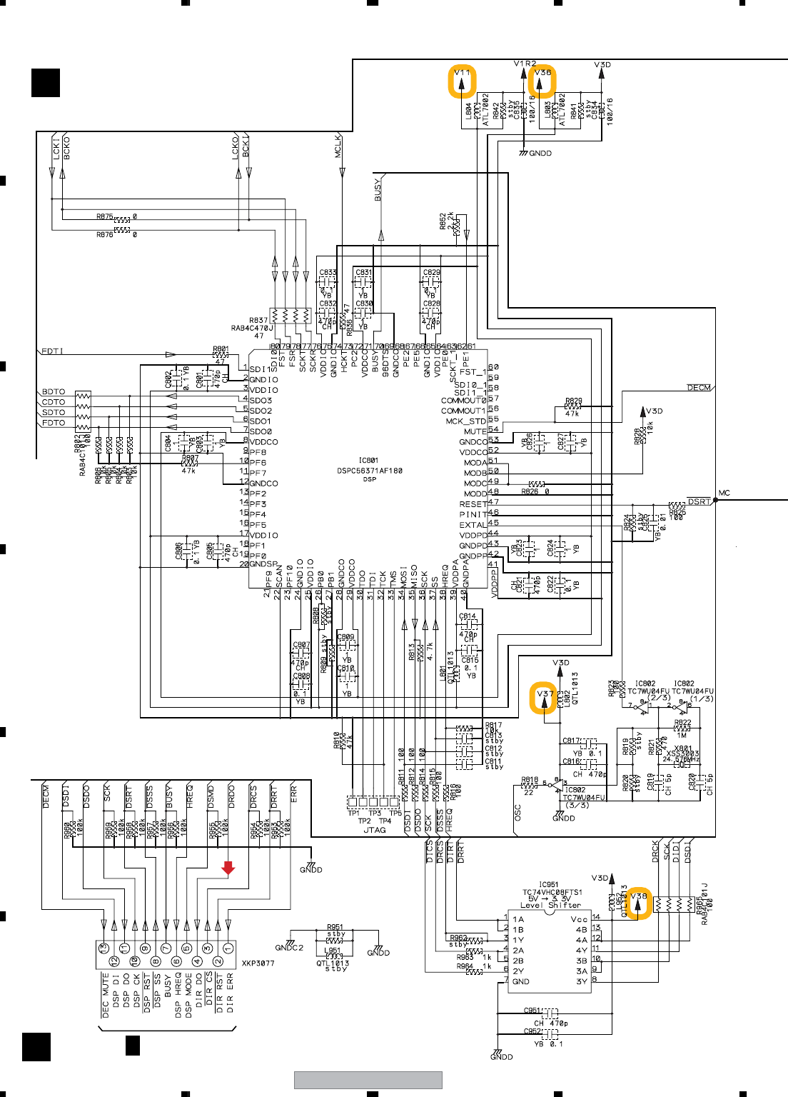
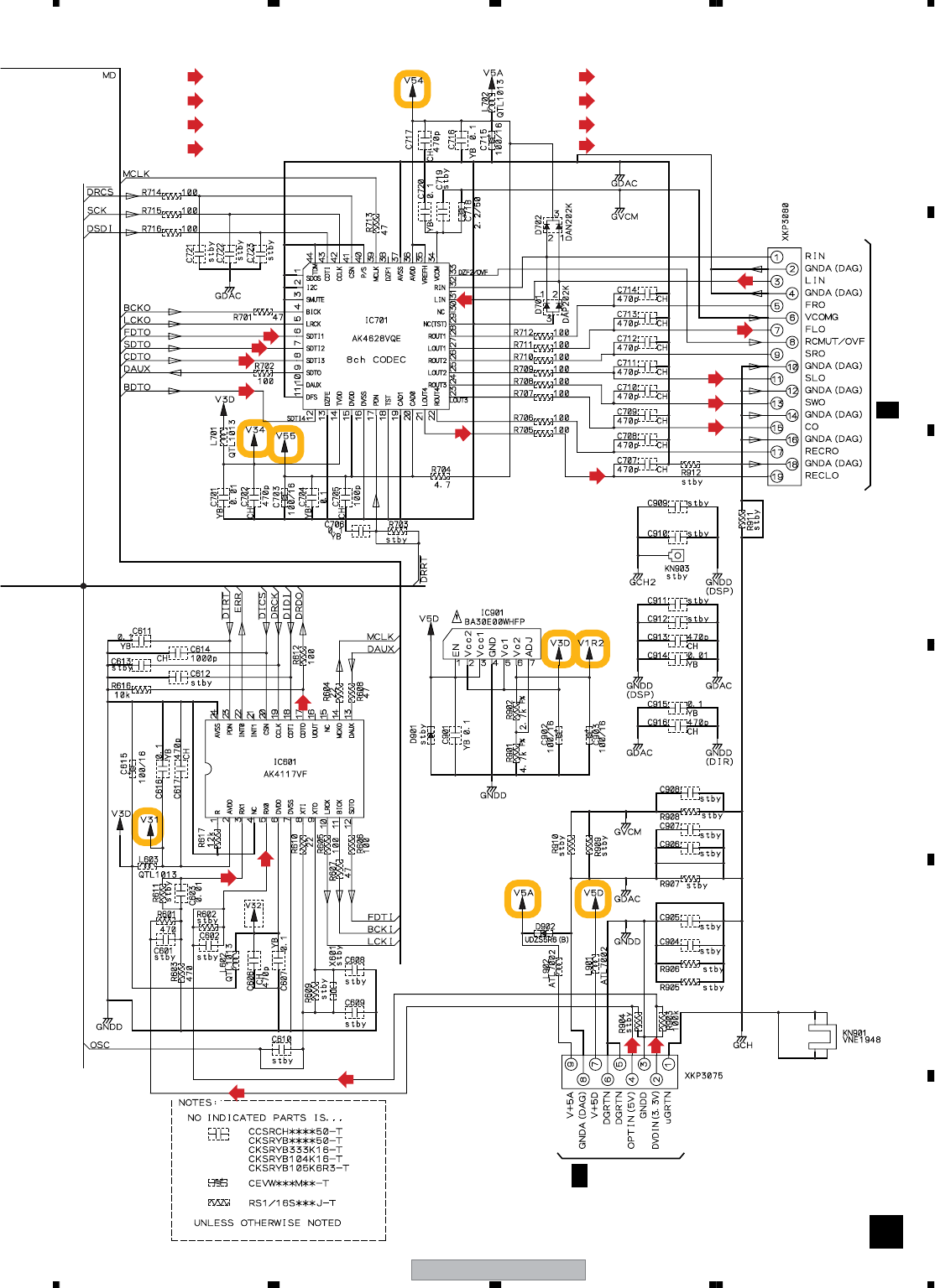
XV-EV1000 35
5678
5678
C
D
F
A
B
E
CN901
CN701
(D)
(D)
(D)
(D)
(FL)
(SL)
(AD)
(AD)
(AD)
(AD)
(sw)
(C)
(DVD)
(DVD)
(D)
(D)
(D)
C1/4
CN5505
C1/4
CN5506
: AUDIO DATA SIGNAL ROUTE
: AUDIO SIGNAL ROUTE(DIGITAL)
(AD)
(D)
: AUDIO SIGNAL ROUTE(DVD L ch)
: AUDIO SIGNAL ROUTE(L ch)
(DVD) : AUDIO SIGNAL ROUTE(Surround L ch)
: AUDIO SIGNAL ROUTE(Front L ch)
(FL)
(SL)
: AUDIO SIGNAL ROUTE(Sub Woofer ch)
: AUDIO SIGNAL ROUTE(Center ch)
(SW)
(C)
D
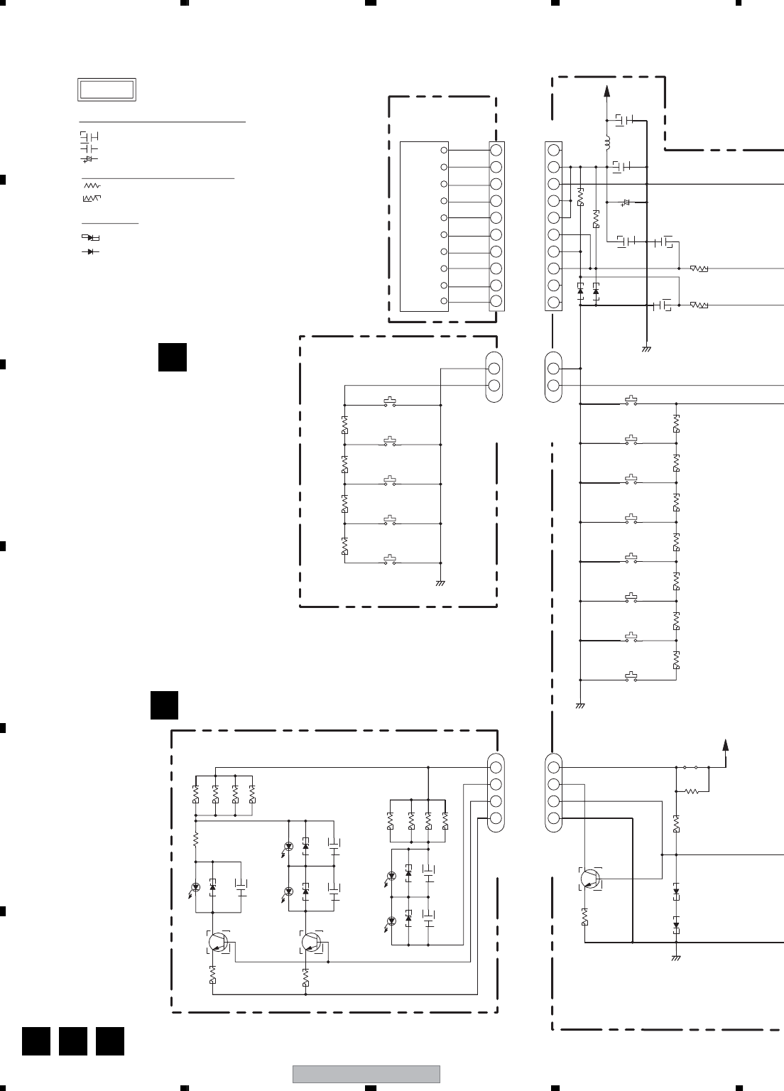
XV-EV1000
36
1234
1234
C
D
F
A
B
E
3.10 KEY, LED and DISPLAY ASSYS
2
11
2
4
3
4
3
2
1
2
1
51048-0400
51048-0400
51048-0200
51048-0200
XMR3099-
LED HOLDER
MS+/FF
MS-/REW
STOP
PLAY
OPEN/CLOSE
D20PYY0410E
LEDCN1
GNDLED
VP+12
LEDCN2
REC STOP
ASES
REVERSE MODE
KARAOKE
ENTER
D20PYY0225E
FRONT SURROUND
SOUND MODE
KEY3
GNDU
MUSIC/MOVIE
10
9
NC
NC
:MA111
:1SS133
ALL DIODE
RS1/16S***J
RD1/4PU***J
ALL RESISTORS ARE IN
AL : CEAL (OTHER : CEAT)
NOTES
UNLESS OTHERWISE SPECIFIED
ALL CAPACITORS ARE IN µF
TY : CFTYA
CH : CCSRCH (OTHER : CKSRYB)
LCD
8
LCDCLK
LCDDAT
VDD
NC
7
6
5
NC
VLCD
VSS
1
3
2
NC
4
10
9
8
7
6
5
1
3
2
4
R5219
R5220
D5207
Q5219
D5219
Q5220
C5207
D5209
D5221
D5212
D5224
C5212
C5209
D5213
D5225
C5213
R5223
R5224
R5225
R5226
D5223
D5211
R5227
C5211
R5228
R5229
R5230
R5303
R5304
S5305
S5304
R5301R5302
S5303
S5302
S5301
Q5204
R5216
R5231
J1_
J1
D5215D5216 R5217
R5214
W739
S5108
S5107
S5106
S5104
S5105
R5107 R5106 R5105 R5104 R5103
J2_
S5102
S5103
J2
S5101
D5112
D5113
R5102 R5101
C5106 R5109
R5122
C5104
R5123
C5103
L5101
C5102
C5101
CN5104
C5105
R5108
27
27
2SC3052(EF) 2SC3052(EF)
NSPBF50S-3026
(Blue)
GNDLED
UDZS6R8(B)
NSPWF50BS-9706
NSPWF50BS-9706
UDZS6R8(B)
STBY
UDZS6R8(B)
STBY
NSPBF50S-3026
(Blue)
UDZS6R8(B)
1/4W
150
STBY
180
NSPWF50BS-9706
UDZS6R8(B)
180
180
STBY
390
390
390
GNDU
1.8K 1.5K 1.2K 1K
STBY STBY
2SC3052(EF)
100
STBY
MA111 MA111 1.2K
STBY
VP+12
GNDU
5.6k 3.3k 2.7k 1.8k 1.5k
GNDU
STBY
STBY
1.2k 1k
220
CH22p
STBY
YB0.1
STBY
47/16 AL-TS
STBY
22
52492-1020
1000p
VE+5
220
CH10p
YB
LCD ASSY
(XAV3028)
KEY ASSY
(XWZ4013)
E
LED ASSY
(XWZ4023)
F
GE F
KEY ASSY
S5301 : 0 (OPEN/CLOSE)
S5302 : 6 (PLAY)
S5303 : 7 (STOP)
S5304 : 4 (MS–/REW, TUNING –)
S5305 : ¢ (MS+/FF, TUNING +)
Switches
DISPLAY ASSY
S5101 : X.BOOM
S5102 : FRONT SURROUND
S5103 : SOUND MODE
S5104 : KARAOKE
S5105 : ENTER
S5106 : REVERSE MODE
S5107 : REC STOP
S5108 : ASES
Switches
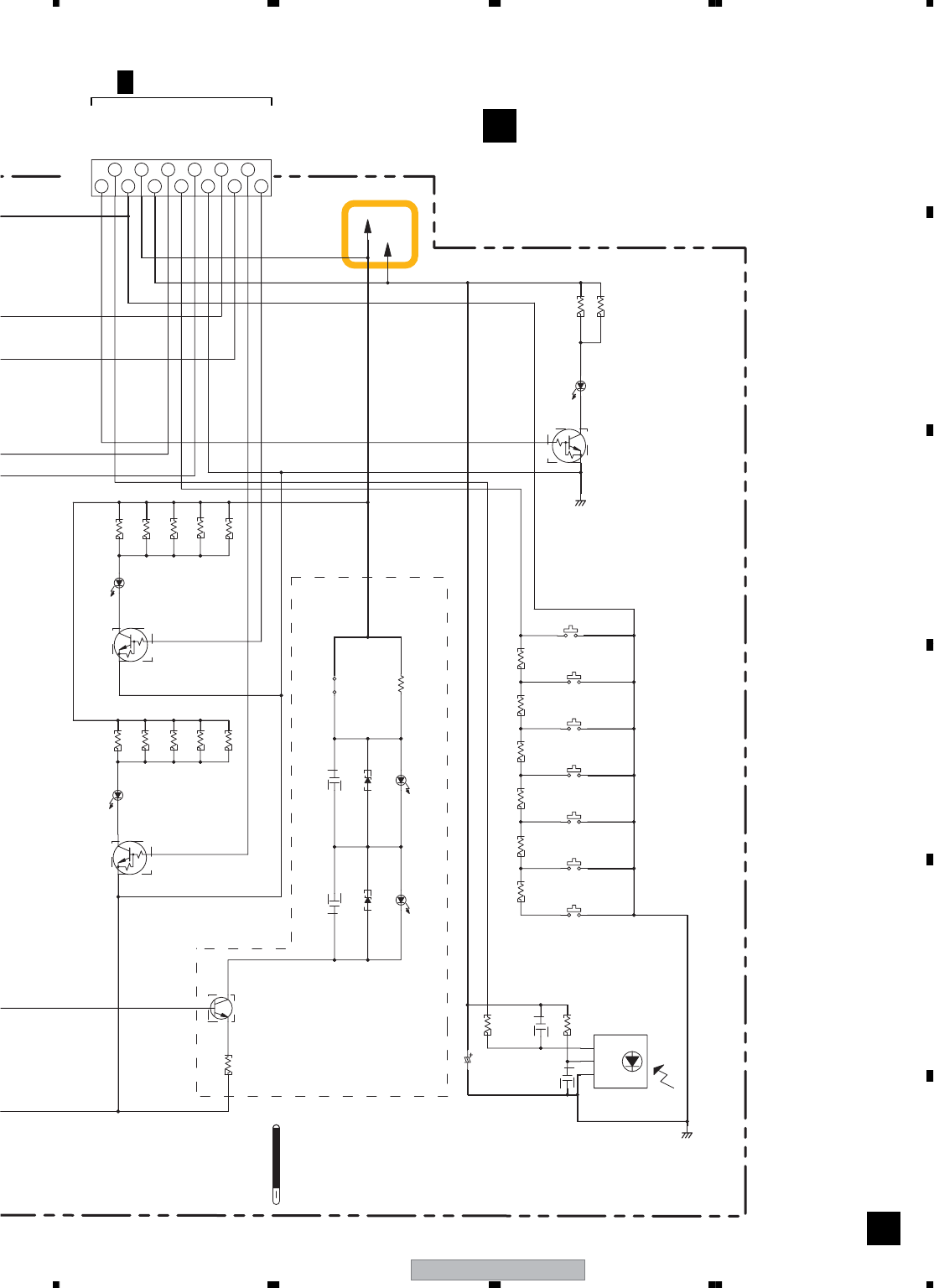
XV-EV1000 37
5678
5678
C
D
F
A
B
E
3
2
1
46
59
10
7
8
1311
12
STBY
LED COVER (2X):
XMR3053-
XEB3039-
LED CUSHION (2X):
(WHITE)
(ORANGE) (BLUE)
(WHITE)
STANDBY/ON
XV-EV1000 ONLY
VCC
GND
VOUT
VOL-
VOL+
TUNER
AUX
DVD/CD
TAPE
(GREEN)
REMOCON
TIMERLED
VP+12
GNDU
KEY3
VE+5
KEY2
LCDDAT
GNDLED
KEY1
LCDCLK
MOVIELED
MUSICLED
Q5102
R5211
C5201
C5204
R5208
Q5201
D5203
D5202
C5205
R5206 R5205
D5102 R5116
R5117
R5118
Q5101
D5101
D5302
C5301
D5301
R5204
R5119
R5120
W735
R5210
R5202
R5203 R5201
R5112
R5113
R5114
R5121
R5115
C5202
R5209
S5206
S5207
S5205
S5204
S5203
S5202
S5201
Q5110
D5110
CN5101
R5111
R5110
GNDU
RT1N431M
27
100/10
AL-TS
1k
2SC3052(EF)
NSPW500BS-2146
UDZS6R8(B)
STBY
3.3k 2.7k
SLI-343DCW(STU)
2.7k
2.7k
RT1N431M
SLR-343BBT(FGHJ)
UDZS6R8(B)
STBY
NSPW500BS-2146
1.8k
2.7k
2.7k
STBY
STBY
120
1.5k 1.2k
1/4W
1k
2.7k
2.7k
2.7k
2.7k
2.7k
0.01 STBY
47
GP1UM28XK0VF
IC5201
GNDLED
RT1N431M
SLR-343MC(NPQ)
52044-1345
VP+12
VE+5
330
330
DISPLAY ASSY
(XV-EV1000:XWZ4012)
(XV-EV700:XWZ4010)
G
G
CN5501
DISPLAY ASSY
S5201 : STANDBY/ON
S5202 : DVD/CD
S5203 : TAPE
S5204 : TUNER
S5205 : LINE
S5206 : VOLUME +
S5207 : VOLUME –
Switches
1/4C
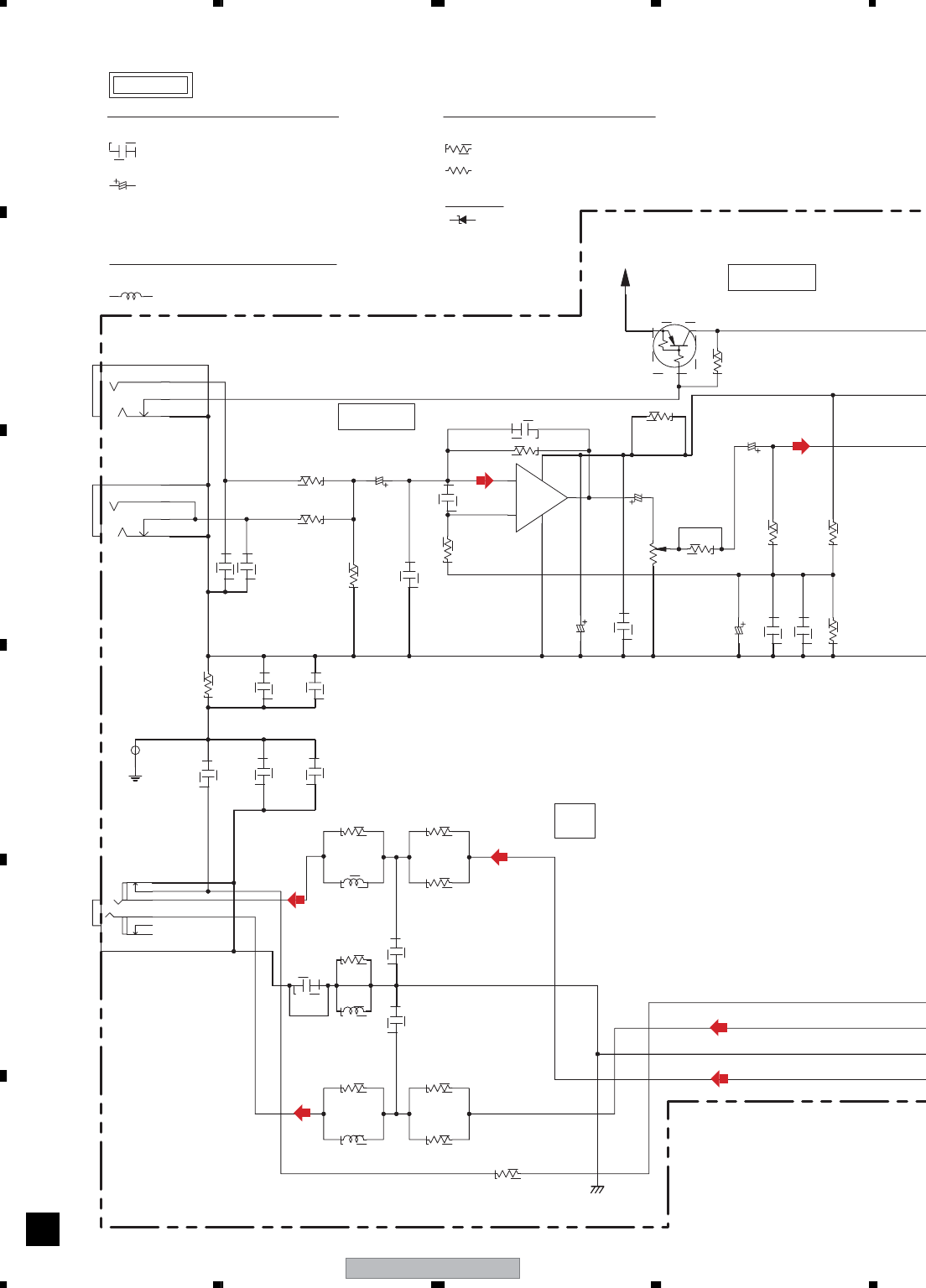
XV-EV1000
38
1234
1234
C
D
F
A
B
E
3.11 HP/MIC ASSY
RT1P431M
+
-
HA17558AF
IC5402
A592
DE007WE0
3
1
8
4
2
5
1
3
4
(SUB)
3
4
5MIC AMP
1
(MAIN)
LAU***J
HP
(1/2)
39k
1000pF
21.5dB
UNLESS OTHERWISE SPECIFIED.
OTHER : CEAT***M##
ALL INDUCTORS ARE IN µH
AL:CEAL***M##-TS
JQ:CEJQ***M##-TS
CH:CCSRCH*** (OTHER:CKSRYB***)
ALL CAPACITORS ARE IN µF
UNLESS OTHERWISE SPECIFIED
NOTES
MTZJ***
RS1/16S***J
RD1/4PU***J
DIODES
ALL RESISTORS ARE IN
UNLESS OTHERWISE SPECIFIED.
MIC DETECT
L3902
R3914
L3903
R3909
R3904
C3904
R3908
C3921
R3915
JA5403
L3901
C3905
C3920
C3919
R3913
J1
R5429
C5430
C5429
C5428
C5427
R5422
R5425
C5425
JA5402 C5426
R5423
JA5401
MIC1
MIC2
HEADPHONE
JACK
C3903
R3903
R3907
C5413
C5420
C5412
R5421
R5419
VR5401
C5436
C5419
R5417
R5418
R5416
C5424
C5422
R5420
C5423 R5412
Q5401
R5426
C5421
CTF1399
STBY
STBY
68
68 GNDHP
68
0.047
STBY
STBY
AKN7005-A
CTF1399
GNDC
0.01
STBY
STBY
STBY
STBY
0.01
0.1
100pF
CH
100pF
STBY
3.3k
STBY
CH
XKN3012-
2.2/50
JQ-TS
3.3k
XKN3012-
0.047
68
68
STBY
0.1
JQ-TS
47/16
10k
STBY
XCS3007
CH
0.1
100pF
3.3k
YB
47k
3.3k
STBY
2.2/50
JQ-TS
CH
STBY
STBY
2.2/50
JQ-TS
VA+12V
H
(FL)
(FL)
(MIC)
(MIC)
(FR)
(FL)
(FR)
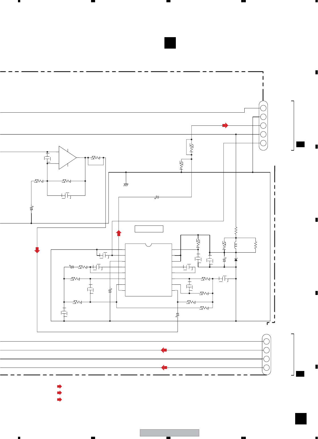
XV-EV1000 39
5678
5678
C
D
F
A
B
E
+
-
51048-0400
2
1
4
3
89
4
5
3
7
6
14
11
13
12
10
1
2
16
15
8
5
6
4
7
2
1
3
5
4
GNDHP
HP L
HP R
HPDET
MIC OUT MIC IN
BIAS
DAINT IN
DAINT OUT
DALPF IN
DALPF OUT
Vcc
ADINT IN
ADINT OUT
ADLPF OUT
ADLPF IN
GND
ECHO VR
CR
MUTE
MIC ECHO
(2/2)
D20PYY0430E
D20PYY0520E
VA+12V
MIC
ECHOVOL
GNDA
MIC SW
C5407
R5407
C5410
R5408
NoAssign7
C5409
C5408
R5405
C5406
R5409 C5411
C5416
C5414
C5434
IC5401
C5432
R5415 R5414
C5415
IC5402
R5430
R5413
J3902
R5406
R5404
R5403 C5405
C5404
C5403
C5401
D5401
R5411
C5402
R5402
R5410
L5401 R5401
J5401
R5427
0.01
4.7k
15k
0.47/50
JQ-TS
JQ-TS
2.2/50
22/16
3300
AL-TS
20k
0.01
10k
2.2/50 JQ-TS
2.2k
1200p
STBY
BU9255FS
2.2/50
JQ-TS
12k
GNDA
STBY
HA17558AF
STBY
22k
20k
8.2k
4700p
10k 0.012
0.01
100
MTZJ5.1 B
JQ-TS
100/16
STBY
39k
0.1
STBY
(1/4W)
10
680
51048-0500
STBY
HP/MIC ASSY
(XWZ4014)
H
H
: AUDIO SIGNAL ROUTE (Front L ch)
(FL)
: AUDIO SIGNAL ROUTE
(MIC)
(MIC)
(MIC)
CN5105CN3008
(MIC)
(FL)
(FR)
: AUDIO SIGNAL ROUTE (Front R ch)
(FR)
2/4C
1/4
J
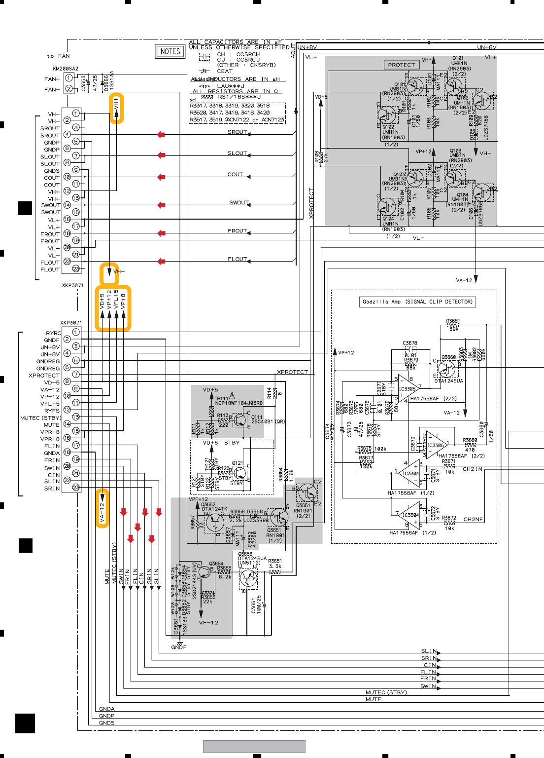
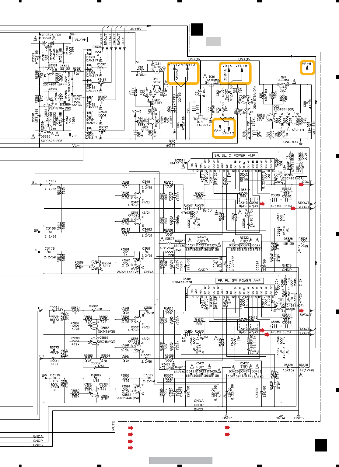
XV-EV1000 41
5678
5678
C
D
F
A
B
E
(C)
(SL)
(SW)
(FL)
: AUDIO SIGNAL ROUTE (Surround L ch)
(SL)
: AUDIO SIGNAL ROUTE (Surround R ch)
(SR)
: AUDIO SIGNAL ROUTE (Center ch)
(C)
: AUDIO SIGNAL ROUTE (Sub Woofer ch)
(SW)
: Refer to "7.3.2 PROTECTION CIRCUIT.
I
AMP ASSY (XWK3202)
I
Search : 2.3A
Normal : 950mA
(SR)
(FR)
: AUDIO SIGNAL ROUTE (Front L ch)
(FL)
: AUDIO SIGNAL ROUTE (Front R ch)
(FR)
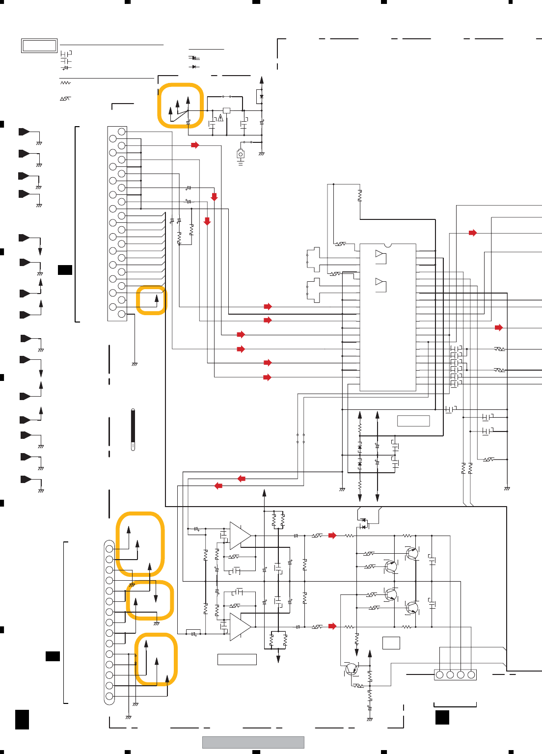
XV-EV1000
42
1234
1234
C
D
F
A
B
E
3.13 POWER ASSY (1/4)
51048-1500
STBY
GNDMDV
GNDMTC
UN8V
GNDD
GNDU
VL+
VL-
VH+
GNDREG
GNDP
VE+56
VH-
GNDTX
GNDF
GNDS
XHPMUTE
HPDET
13
RYRC
RYFS
HPAC1
14
SYSPOW
E_CLK
XHPMUTE
E_DATA
CONTROL
HPDET
SUBAC
XPROT
HPAC1
HPAC
E_CLK
E_DATA
+
-
-
+
W255
IC3901
C3907
R3921
C3909
R3923 C3911
R3944 R3943
C3906
R3933
R3927
Q3909
R3910
R3916
C3926
R3925
C3923
C3917
C3915
R3935
R3911
R3929
R3901
R3905
R3917 NoAssign4
NoAssign1
CN3008
C3901
C3912
R3922
R3924
J3002
C3908 C3910
IC3901
R3096
R3098
C3095
C3096
C3174
C3913
C3914
C3918
R3926
C3924
C3916
R3930
R3918
R3906
R3934
R3928
C3925
R3936 R3912
Q3902 Q3901
D3901 R3902
D3053
R3118
C3116
C3114
C3902
R3143
R3140
R3141
W225
W226
D3052
C3113
C3115
R3119
C3128
C3132
C3131
C3126
C3124
C3125
C3122
C3123
C3121
R3102
R3101
R3318
R3314 IC3062
R3313
C3173
KN3001
CN3051
C3954
C3953
IC3951
W290
C3952
C3951 D3591
GNDMTC
GNDMDV
VD+5
STBY
VA+5
STBY
NJM4565M
VPR+8M
VP+12
GNDD CH
47p
39k
1.2k
47/16
1k
10/50
GNDD
1k
15k
47
VA-12
NP
VA-12
2SA1576A(QR)
0
VD+5
47k
47
47/16
39k
CH
10/50
10/50
(1/4W)
33
100k
33(1/4W)
2.2k
2.2k
52151-0410
1000p
VPR+8
GNDTX VA-12
47/16
39k
1.2k
VA+12
VA+12TX
STBY
NJM4565M
47p
CH
GNDMDV
GNDMTC
GNDD
UN8V
VH+
VL- GNDU
GNDU
VE+56
VL+
VE+56
VH-
GNDP
0
GNDREG
10/50
10/50
STBY
10/50
100p
0.1
CH
100p
10/50
39k
0.1
100k
10/50
0
(1/4W)
2.2k
2.2k
IMX9-T
47/16
NP
47
47
33
VA-12
DAP202K
IMX9-T
33 (1/4W)
VA-7
VA+12
UDZS6R8B
GNDA
1/2W PM
150
220/10
0.1
1000p
10k
GNDD
0
UDZS6R8B
0
VA+12
0.1
1/2W PM
150
220/10
VA+7
1k
STBY
1k
CH
100p
CH
100p
4700p
0.1
0.1
4700p
0.1
0.1
4.7k
4.7k
W515 0 W514
0
0
0BD3814FV
0
GNDTX
GNDS
GNDF
10/50
52044-2745
VF+12
47/16
STBY
VA+12
VA+12TX
STBY
GNDREG
STBY
STBY
STBY STBY
VP+12
15
14
13
11
12
10
6
9
7
8
5
6
8
7
4
4132
2
1
4
5
3
2
3
26
27
24
25
22
23
20
21
18
19
17
16
15
13
14
12
11
10
9
1
8
4
18
19
20
23
22
21
15
17
14
16
13
12
25
24
27
26
29
28
10
11
7
9
8
5
6
31
30
34
32
33
35
36
3
4
1
2
37
38
39
40
4
5
3
6
8
7
1
2
VD+5
VA+5
GNDM(DV)
GNDM(TC)
VPR+8M
VP+12
HP AMP
GNDD
VPR+8
GNDD
VPR+8M
TS
(2/2)
TS
MUTE
HP
TS
IMX9-T
Q3901 (2/2)
HPDET
HP R
GNDHP
HP L
VA+12TX
VA+12
GNDTX
VPR+8
VA-12
TS TS
D20PYY1515E
A
STBY
GNDU
VE+56
NC
MUTEC
RYRC
RYFS
MUTE
HPAC1
SYSPOW
EVOLCLK
EVOLDATA
XHPMUTE
FL
HPDET
SUBAC
XPROTECT
GNDA
FR
GNDA
TS
TS
TS
TS
IMX9-T
Q3902
(2/2)
(1/2)
(1/2)
TS (1/2)
TS TS
E-VOL
VEE(-7V)
FLIN
GND BNF1R
TNFL
TNFR
FRIN
GND
BNF2R
BNF1L
CIN
GND FLOUT
BNF2L
SLIN
GND
FROUT
COUT
SRIN
GND
SWIN SWOUT
SROUT
SLOUT
OUT2
GND
DGND
GND
INN2
INP2 DATA
MUTE
GND
OUT1 GND
CLK
INN1
INP1
VCC(+7V)
GND
GNDA
SW
GNDA
SR
GNDA
SL
GNDA
C
RS1/16S***J
TS
OUT
1/2w RD1/2PU***J
1/4w RD1/4PU***J
ALL RESISTORS ARE IN
AL : CEAL
TY : CFTYA
CH : CCSRCH
(OTHER : CEAT)
(OTHER : CKSRYB) :MA111
:1SS133
NOTES UNLESS OTHERWISE SPECIFIED
ALL CAPACITORS ARE IN µFALL DIODE
IN
J
1/4
(C)
(SL)
(SW)
(FR)
(FL)
(HPL)
(HPR)
CN8303
CN8302
J3902
H
3/4C
3/4
C
(SL)
(SR)
(FR)
(FL)
(FR)
(FL)
(FR)
(C)
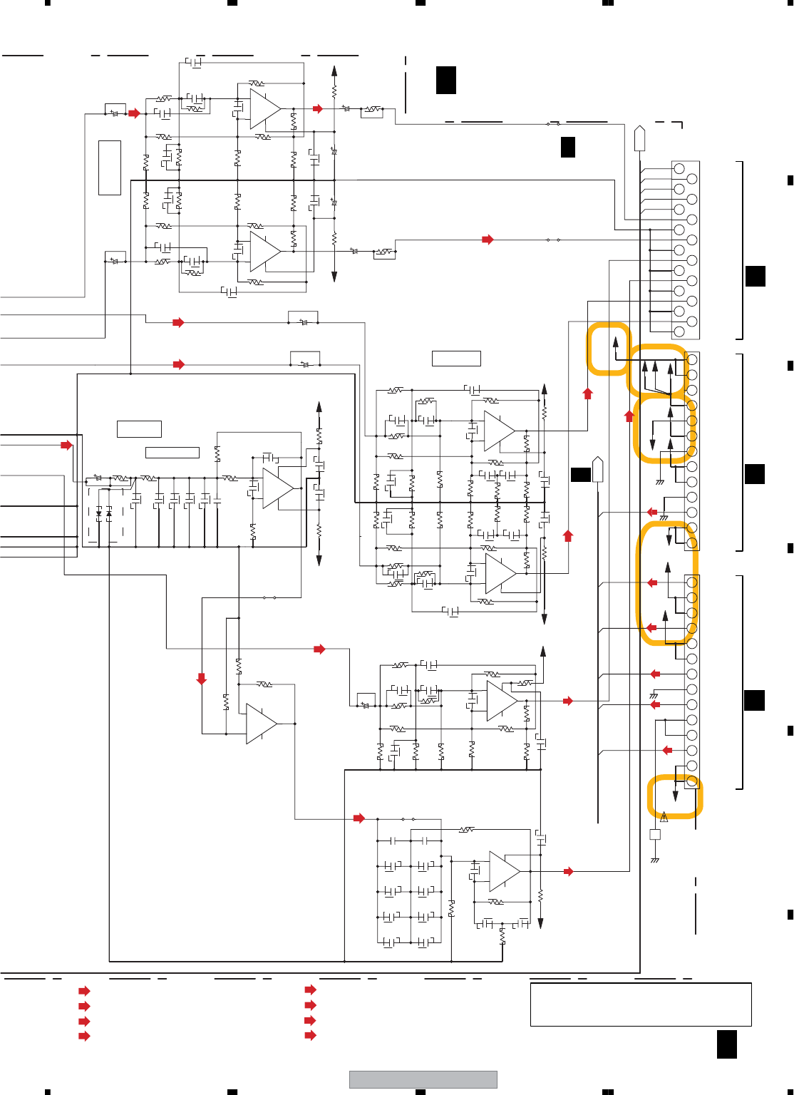
XV-EV1000 43
5678
5678
C
D
F
A
B
E
AFSIGNAL
CONTROL
FR
FL
SW
C
SR
SL
14
RYFS
XPROT
13
RYRC
-
+
+
-
+
-
-
+
+
-
-
+
+
-
-
+
C3186 C3187
C3178 C3181
R3182
C3177 C3180
C3168
C3338
R3341
C3339
R3340
R3206
C3176 C3179
C3164 C3166
W299
R3184
R3179
C3279
R3180
R3186
R3339
R3345
R3344
IC3055
C3196
R3185
R3265
C3195
IC3058
R3183
C3283 C3165
D3701
D3702
C3182
C3184
C3183
C3135
R3145
R3181 C3163
C3154
NoAssign2
C3136
R3354
0
R3208
C3268
R3170 C3156
C3194
R3168 R3256
R3166
C3342
C3185
IC3055
R3147
C3137
R3124
C3172
R3123
C3171
C3224
R3174 120k
R3172
R3176
C3223
R3171
R3175
R3173
C3340
C3134 R3144
R3158C3140
R3242
R3146
C3138 470p
R3207
R3169
R3167
C3267 C3155
C3152
C3153
R3255
R3165
C3144
R3104
C3151
IC3058
C3169
IC3101
R3187
R3139
R3137
C3170
R3138
R3205
R3130
R3112
IC3057
R3116
R3177
R3114 CN3013
R3343
C3343
R3122
C3160
R3342
R3117
C3341
C3159
R3113
R3115
IC3057
R3164
R3111
CN3012
C3256
C3142
R3136
C3236
R3154
R3150
C3235
R3135
R3149
R3153
C3255 R3241
C3139 R3157
C3146
IC3056
R3160
R3106
R3108
C3190
R3178
R3110
C3148
C3150
R3704
R3109
R3159
C3147
C3149
C3145
IC3056
C3141
R3103
R3107
C3189
R3163
R3703
C3143
W284
CN3011
W283
STBY STBY
STBY 0.082
47k
0.022 0.1
CH
8200p 0.22
47p
STBY
STBY
0STBY
VA-12
22
GNDP
TY
STBY TY
STBY 5.6k
STBY
3.3k
STBY
0.1
120k
STBY HA17558AF
STBY
10k
10k
HA17558AF
0.33 STBY 10k
STBY
6800p STBY
STBY
0.1
0.033
STBY
STBY 10k
820 STBY
STBY STBY
W267
STBY
22
VA-12 3300p
10k
STBY
STBY
22k
STBY STBY
STBY
0.027
TY
HA17558AF
220k
3.3k
0.01 0.01
3.3k
0.015
STBY
2.2k 2.2k
0.015
120k
STBY
STBY
4.7k
STBY
100k
STBY
22
STBY
STBY
STBY
STBY
10k
3300p 22k
VA+12
STBY
STBY
STBY
6.8k STBY
HA17558AF
VA-12
HA17558AF
0.1
(7A)
VH-
AEK7047
2.2k
STBY
0
0.1
4.7k
STBY
22
GNDS
VA-12
STBY
VA+12
VH+
0
6.8k
22
STBY
52147-1410
VL+
VL-
STBY
0.1
STBY
STBY
STBY
0.1
STBY
GNDREG
GNDF
0
6.8k
CH
HA17553AF
22
VA-12
UN8V VD+5
STBY
STBY
VA+12
VF+12
VA+12TX
VPR+8
VA+12
52147-1310
STBY
8200p
STBY
0.033
STBY
STBY
0.033
STBY
8200p
STBY
4.7k
STBY
100k
2.2k
8.2k
10/50
1.2k
22
STBY
0.01
47/16
STBY
100k
8.2k
STBY
0.01
47/16
6.8k
STBY
STBY
STBY
HA17558AF
1.2k
10/50
22
STBY
VA+12
STBY
0
0
52045-1745
68
5
7
54
6
7
8
3
2
4
1
8
4
4
2
3
1
24
3
1
8
8
7
6
5
12
13
9
10
11
54
6
7
8
1
14
3
2
4
5
6
28
3
1
4
7
8
9
10
11
13
12
14
11
12
17
15
16
13
54
68
7
28
34
1
9
10
8
7
6
5
4
3
2
1
(1/2)
STBY
+13.4dB
(2/2)
SW LPF
SW fc=200Hz
ANDREW
TS
(2/2)
VH-
VH-
FROUT
GNDP
(1/2) GNDP
FLOUT
SWOUT
GNDS
VH+
VH+
COUT
VL+
VL+
(2/2)
SR
SROUT
VL-
VL-
SLOUT
GNDF
UN+8V
UN+8V
(1/2)
SL
GNDREG
VD+5
VP+12
VA-12
VFL+5
VPR+8
VPR+8
GNDA
GNDA
SRIN
GNDA
SLIN
SWIN
GNDA
ANDREW
+14.4dB
(2/2) FR
+14.4dB
TS
(1/2)
GNDA
CIN
GNDA
FRIN
MUTE
FLIN
MUTEC
RYFS
XPROT
RYRC
: AUDIO SIGNAL ROUTE
(HPL)
: AUDIO SIGNAL ROUTE (Front L ch)
(FL)
: AUDIO SIGNAL ROUTE (Front R ch)
(FR)
: AUDIO SIGNAL ROUTE
(HPR)
: AUDIO SIGNAL ROUTE(Surround Lch)
(SL)
: AUDIO SIGNAL ROUTE(Sub Woofer ch)
(SW)
: AUDIO SIGNAL ROUTE (Center ch)
(C)
R3105
2.2k
HA17553AF
CN3031
K
(FR)
(C)
(SW)
C3193
: AUDIO SIGNAL ROUTE(Surround Rch)
(SR)
J
1/4
J
1/4
POWER ASSY
(C)
(FL)
(FL)
(SW)
(SW)
J3033
KJ3032
K
2/4J
2/4-4/4J
(XV-EV1000:XWZ4016)
(XV-EV700:XWZ4018)
(SR)
(SL)
(SL)
(SW)
(SR)
(SW)
(SL)
(SR)
(C)
(SW)
(FL)
(FR)
CAUTION : FOR CONTINUED PROTECTION AGAINST
RISK OF FIRE. REPLACE ONLY WITH
SAME TYPE NO. 491007 MFD, BY
LITTELFUSE INK. FOR IC3101 (AEK7047).
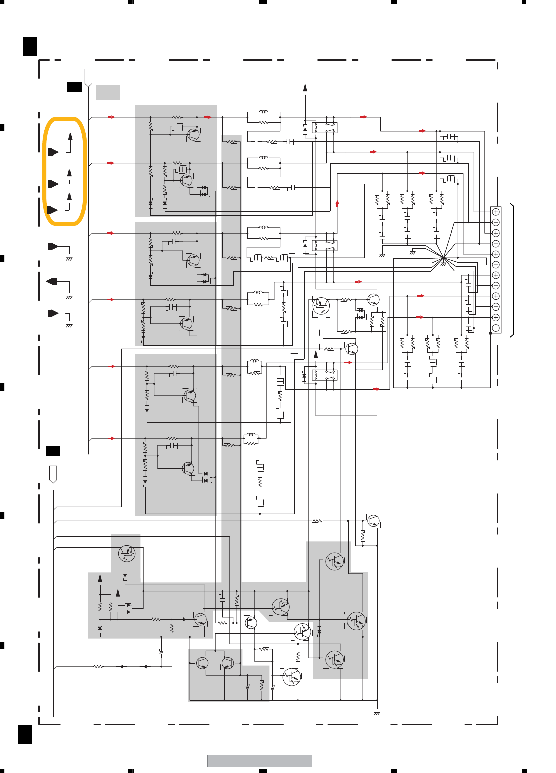
XV-EV1000
44
1234
1234
C
D
F
A
B
E
3.14 POWER (2/4) and TRADE ASSYS
CONTROL
GNDREG
RETGND
GNDB
VH+
VF+12
V+5D
AFSIGNAL
HPAC
RY-F
RY-R
XPROT
SL
SR
C
SW
FR
FL
EE
BCB
C
E
BC
E
B
C
B2
C2
E2
B2
C2
B
C
E
E2
E
B
C
BC
E
E
BC
BC
E
BC
E
BC
E
BC
C
E
B
BC
E
B
E
C
E
BC
E
AC1
TS
TS
UMB1N RN1901
(1/10W)
(1/10W)
(1/10W)
(1/10W)
(1/10W)
STBY
SP CHASSIS
(1/10W)
(1/10W)
(1/10W)
(1/10W)
C
SR
SL
FL
SW
(1/10W)
(1/10W)
FR
(FL)
(12 PINS)
R3635 D3632 D3633
C3631
Q3637
Q3639
R3631
D3631
R3634
D3635
R3632
R3633
R3668
D3634
Q3631
C3632
R3638
C3633
Q3640
Q3638
R3651
R3639
D3637
Q3633
Q3632
Q3632 Q3633
Q3635
D3636
R3669
C3668
R3613
D3611
D3613
Q3611
R3611
C3676
R3617
D3612
R3615
R3614 R3612
C3677
Q3612
R3616
R3618
D3622 R3624
Q3622
R3622
C3675
R3628
D3621
R3626
D3623
R3623
Q3621
R3621
R3625
C3627
R3627
D3601
D3602 R3604
Q3602
R3606
C3463
Q3636
R3644
R3642
Q3642
C3461
R3463
R3462
L3462
C3464 R3464
R3461
C3462
D3643
RY3643
C3468
C3467
C3466
L3461
C3564
Q3644
R3641
R3643
R3645
D3644
R3468
R3647
R3466
C3667
C3465
C3665
R3467
R3665
R3667
R3465
C3469
R3661
R3562
C3562
L3661
Q3645 R3646
Q3641
C3561 C3563
R3563
D3642
R3561
C3567
C3368
L3561
C3362 R3364 C3364
RY3642
C3565
C3366
R3565
R3566
R3366
R3368
C3470
C3669
C3367
C3365
R3365
R3367
JA3301
R3603
R3602
R3608
Q3601
D3603
C3673
R3605
C3672
R3601
R3607
R3362
L3362
C3361 R3363 C3363
D3641
R3361
L3361
RY3641
C3569
C3370
C3369
MTZJ5R1B
3.3k 1SS133 1SS133 2SC4081(QR)
2.2/100
2SC4081(QR)
2SA1576A(QR)
22k
DAN202K
1/4W
2.7k
22k
1/4W
6.8k
VD+5
1SS133
22k
2SC4081(QR)
470/6.3
10k
10/50
RT1N241M
GNDB
STBY
27k
STBY
STBY
RN1901
STBY RN1901
RT1P241M
VH+
MA111
22k
0.01
STBY
33k
MA111
2SC4081(QR)
DAP202K
1.8k
ACN7112(2W)
MA111
2SC4081(QR)
27k
0.1
33k 1.8k
STBY 27k
GNDREG
ACN7112(2W)
MA111
2SC4081(QR)
33k
STBY
0.1
RETGND
1.8k
ACN7112(2W)
MA111
27k
0.1
DAP202K
GNDB
33k
2SC4081(QR)
1.8k
ACN7112(2W)
27k
STBY
VF+12
MA111
MA111 33k
0.1
2SC4081(QR)
DAP202K
27k
STBY
0.022
STBY
STBY
STBY
4.7
0.022
(1/2W)PMF
100
ATH-059
0.022 4.7
(1/2W)PMF
100
0.022
STBY
STBY
0.047
0.047
ATH-059
100
0.022
VF+12 STBY
STBY
STBY
22
22
STBY
STBY
22
0.047
0.047
0.047
0.047
22
22
22
XCG3008
0.01
(1/2W)PMF
4.7
ATH-059
0.022
STBY
STBY
STBY
0.022 0.022
(1/2W)PMF
4.7
STBY
100 STBY
RETGND
0.047
GNDREG
0.047
0.047
ATH-059
0.022 4.7 0.022
0.047
22
22
22
22
XCG3008
0.01
XCG3008
0.01
GND
0.047
0.047
22
22
XKE3037
VH+
33k
1.8k
ACN7112(2W)
2SC4081(QR)
STBY
0.1
27k
V+5D STBY
ACN7112(2W)
1.8k
0.1
(1/2W)PMF
100
ATH-059
0.022 4.7 0.022
XCG3008
(1/2W)PMF
STBY
ATH-059
100
STBY
VL+
0.01
0.01
0.01
XCG3008
XCG3008
(FL)
(FR)
(SW)
(C)
(SR)
(SL)
J2/4
J2/4
POWER ASSY(XV-EV1000:XWZ4016)(XV-EV700:XWZ4018)
(SL)
(SL)
(SW)
(SW)
(FL)
(FL)
1/4J
1/4
J
SPEAKER for SL/SR/C/SW
(FR)
(C)
(SR)
(SR)
: Refer to "7.3.2 PROTECTION CIRCUIT"
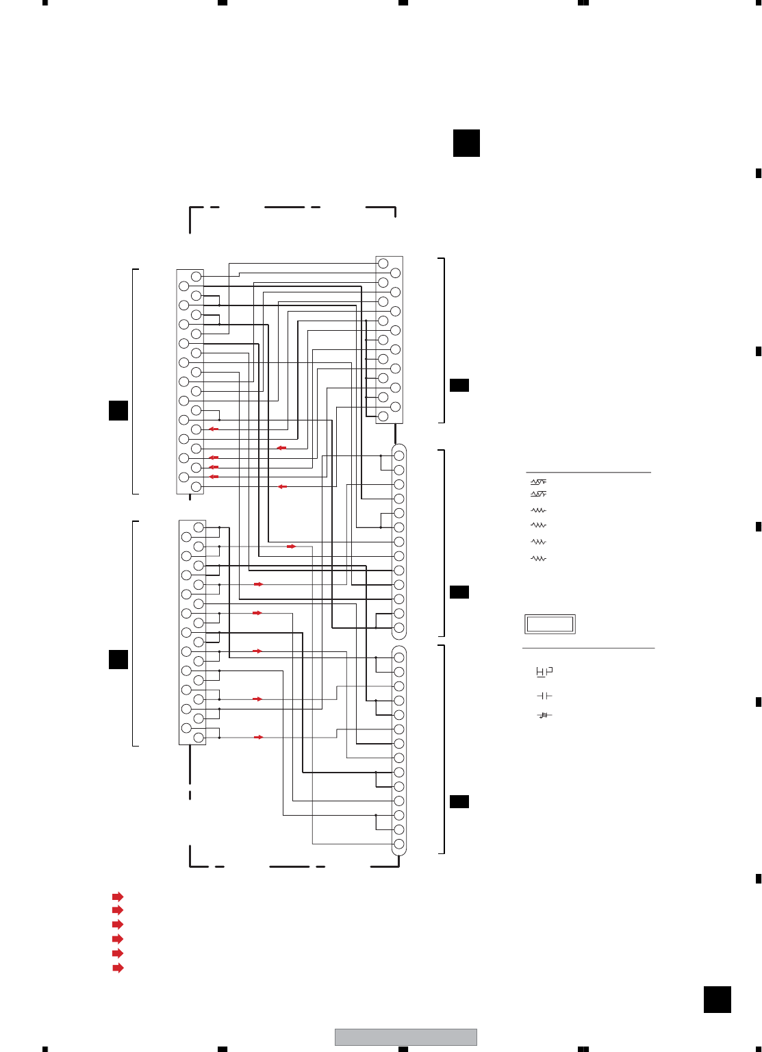
XV-EV1000 45
5678
5678
C
D
F
A
B
E
: AUDIO SIGNAL ROUTE (Front L ch)
(FL)
: AUDIO SIGNAL ROUTE (Surround Lch)
(SL)
: AUDIO SIGNAL ROUTE (Sub Woofer ch)
(SW)
: AUDIO SIGNAL ROUTE (Center ch)
(C)
12
14
13
11
9
10
7
8
22
19
18
23
20
17
21 5
3
4
6
12
13
14
11
15
16 2
13
1
8
9
4
10
6
5
710
9
12
11
8
1
2
3
5
6
7
4
19
18
23
22
20
21
1
2
3
13
11
14
12
17
15
16
13
14
15
17
16
10
8
7
9
6
5
11
12
10
8
9
7
6
1
2
3
4
3
2
5
1
4
D20PYY1415E
VL+
VL+
SROUT
GNDA
SRIN
GNDA
SLIN
GNDA
CIN
GNDA
SWIN
FRIN
GNDA
FLIN
GNDA
XPROT
MUTEC
MUTE
RYFS
RYRC
COUT
VH+
VH+
SWOUT
GNDS
FLOUT
GNDP
GNDP
FROUT (OTHER: CKSRYB)
M
CEAT
CQMA
VH-
VH-
VPR+8
ALL CAPACITORS ARE IN µF
NOTES
CH:CCSRCH
UNLESS OTHERWISE SPECIFIED
VFL+5
VD+5
VP+12
VA-12
VPR+8
RF1/4PS***J
FU(1/4W)
UN+8V
GNDF
GNDREG
UN+8V
PMF(1/2W)
RD1/2PMF***J
(1W)
RS1LMF***J
(1/10W)
RD1/4PU***J
RS1/10S***J
VL-
VL-
SLOUT
D20PYY1315E
RS1/16S***J
ALL RESISTORS ARE IN
J3033
CN3022
CN3021
J3032
CN3031
51048-1400
VL-
VL-
VL+
FLOUT
FROUT
FROUT
FLOUT
VH+
VL+
VH+
COUT
SWOUT
SWOUT
GNDS
COUT
SLOUT
GNDP
GNDP
SROUT
SLOUT
VH-
VH-
SROUT
XKP3082-
SLIN
CIN
SWIN
GNDA
FRIN
SRIN
RYFS
FLIN
MUTEC
VFL+5
MUTE
VPR+8
VPR+8
VP+12
VA-12
VD+5
XPROT
GNDREG
GNDREG
UN+8V
XKP3082-
UN+8V
GNDF
RYRC
51048-1300
52045-1745
CN3013 CN3012 CN3011
CN3002
I
CN3001
I
: AUDIO SIGNAL ROUTE (Front R ch)
(FR)
: AUDIO SIGNAL ROUTE (Surround Rch)
(SR)
TRADE ASSY(XWZ4022)
K
K
(SL)
(C)
(FL)
(SW)
(SL)
(C)
(SW)
(FL)
(FR)
(SR)
(SR)
(FR)
1/4J1/4J1/4J
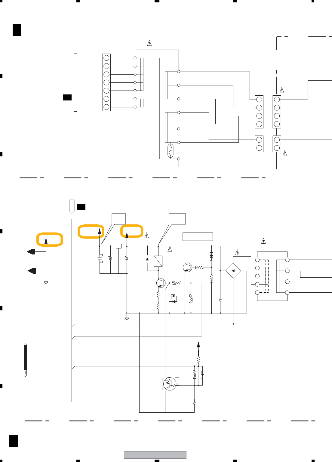
XV-EV1000
46
1234
1234
C
D
F
A
B
E
3.15 POWER ASSY (3/4)
1
2
4
1
3
2
SYSPOW
XPROT
SUBAC
GNDU
VE+56
CONTROL
C86
R91
Q83
D90
R90
R85 R83
D87
R87
C82
D88
C84
C85
C83
Q81
R81
R88
R89
D80
RY81 Q82
D89
CN1
CN2
STBY
STBY
RT1P241M
STBY
GNDU
VE+56
VE+56
VD+5
27k
GNDU
18
DAN217
18
10k
1000/25
2SD1858X(QR)
10/50
0.01
1/50
1k
22k
2.2k UDZS20(B)
S1NB60
NJM78M56FA
UN+56
XSR3008 2SC4081(QR)
B2P3-VH
B4P7-VH
+-
B
VEF1040-
BLAC2
BLAC1
GND
BHAC2
SUBAC1
SUBAC1
BHAC1
TS
6
54
7
3
9
8115V
1
2
NC
NC
0V0V
NC
IC5508
BAIDEN PROTECT
5.6V 13.5V
0 0
230V
ATT7080
T2
230V
0 0
BLU
BLU
GRY
10
120
0
120
BRN
BRN
BLK
GRY *3
120
1
4
2
3
2
1
T1
XTS3099-A
*
J3/4
J3/4
POWER ASSY
1/4J
(XV-EV1000:XWZ4016)
(XV-EV700:XWZ4018)
4/4J
CN4
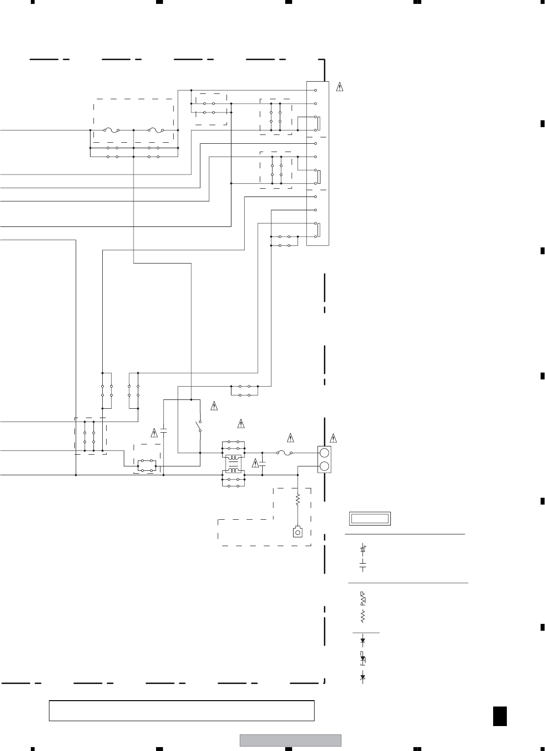
XV-EV1000 47
5678
5678
C
D
F
A
B
E
1
2
W104
W109
W107
W108
C3
W116
W117
KN2
R1
W115
W114
RY81
L1
C1
H2 H1
AN1
W125
W124
W105
W106
W110
W113
W133 W131
H6
W132
H5
W129
H4 H3
W122
W123
W137
W136
W130
W128
W135
W134
0.01
ACE7013
RCN1080
STBY
VNF1084
STBY
XSR3008
XTF3004
0.01
ACE7013
STBY
STBY XKP3084
0V
NC
NC
0V
NC
NC
STBY
STBY
CHASSIS GND
STBY
H1,H2:AKR7001
REK1029 (5.0A/250V)
FU1
NEUTRAL
LIVE
100V 120V
FU3 FU2
H3-H6:STBY
PRIMARY PART
lk ij
240V/220V-230V/110V-127V
STBY
hfge
STBY
STBY
cdba
XKX3001
S1
ALL VOLTAGE'S AT POWER ON CONDITION
MTZJ***
MA111
DIODE
RS1/4PU***J
RS1/16S***J
1SS133
ALL RESISTORS ARE IN
UNLESS OTHERWISE SPECIFIED
REPLACE WITH SAME TYPE AND RATINGS ONLY
FOR CONTINUED PROTECTION AGAINST RISK OF FIRE,
ALL CAPACITORS ARE IN µF
UNLESS OTHERWISE SPECIFIED
CKSRYB
CEAT***M##
NOTES
J3/4
• NOTE FOR FUSE REPLACEMENT
FOR CONTINUED PROTECTION AGAINST RISK OF FIRE.
REPLACE WITH SAME TYPE AND RATINGS OF FUSE.
CAUTION -
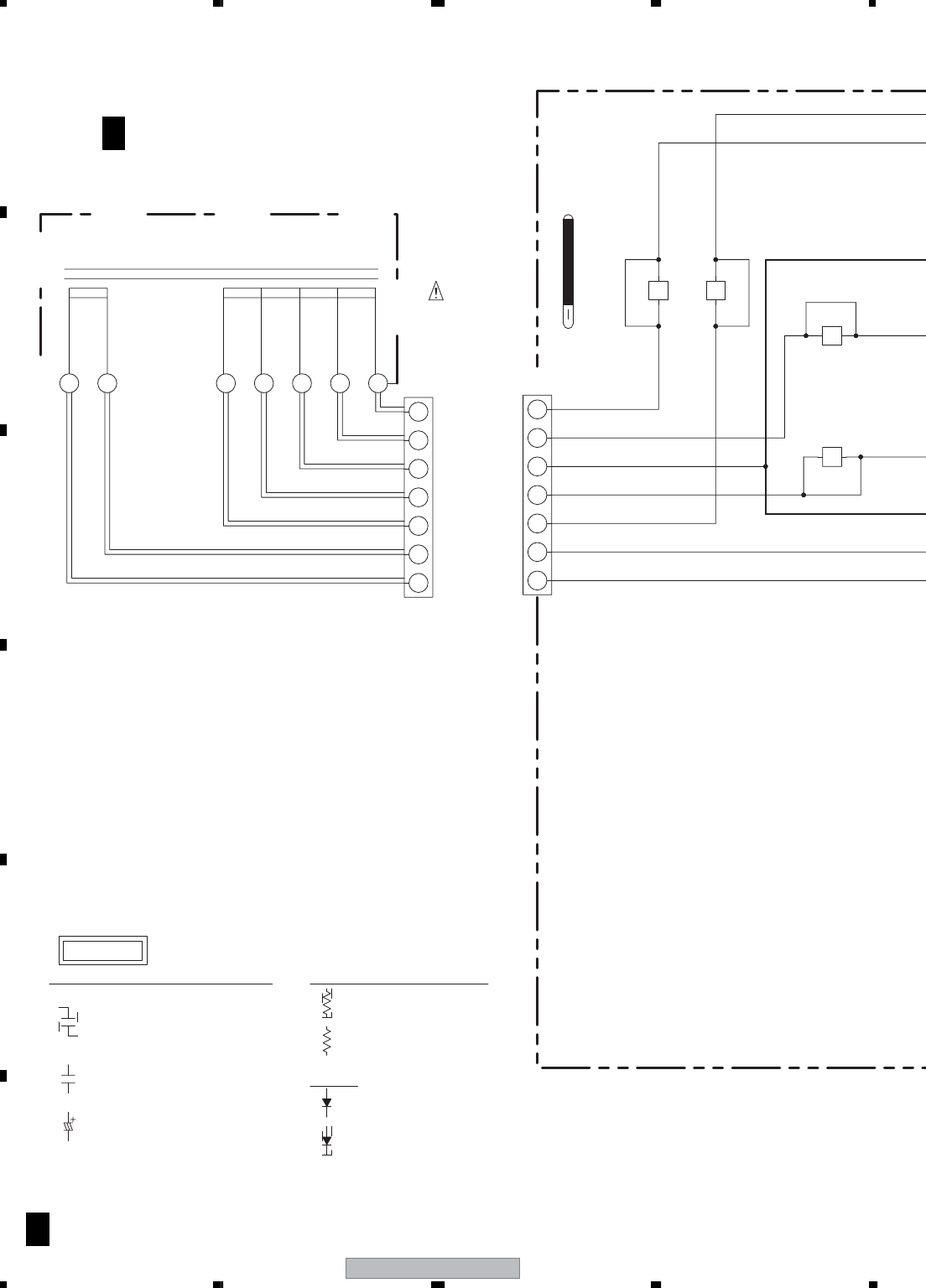
XV-EV1000
48
1234
1234
C
D
F
A
B
E
3.16 POWER ASSY (4/4)
7
6
3
4
5
1
2
STBY
B7P-VH
STBY
STBY
STBY
CN4
IC22
IC12
IC11
IC21
(OTHER : CEAT***M##)
M : CQMBA
AL : CEAL
UNLESS OTHERWISE SPECIFIED
YF : CKSRYF
(OTHER : CKSRYB)
ALL CAPACITORS ARE IN µF
NOTES
DIODE
1SS133
MA111
1/4WPU
1/16W
ALL RESISTORS ARE IN
SUBAC1
SUBAC1
BHAC2
GND
BLAC2
BLAC1
BHAC1
T1
XTS3099A
VEF1040-
C
J4/4
J4/4
POWER ASSY(XV-EV1000:XWZ4016)
(XV-EV700:XWZ4018)
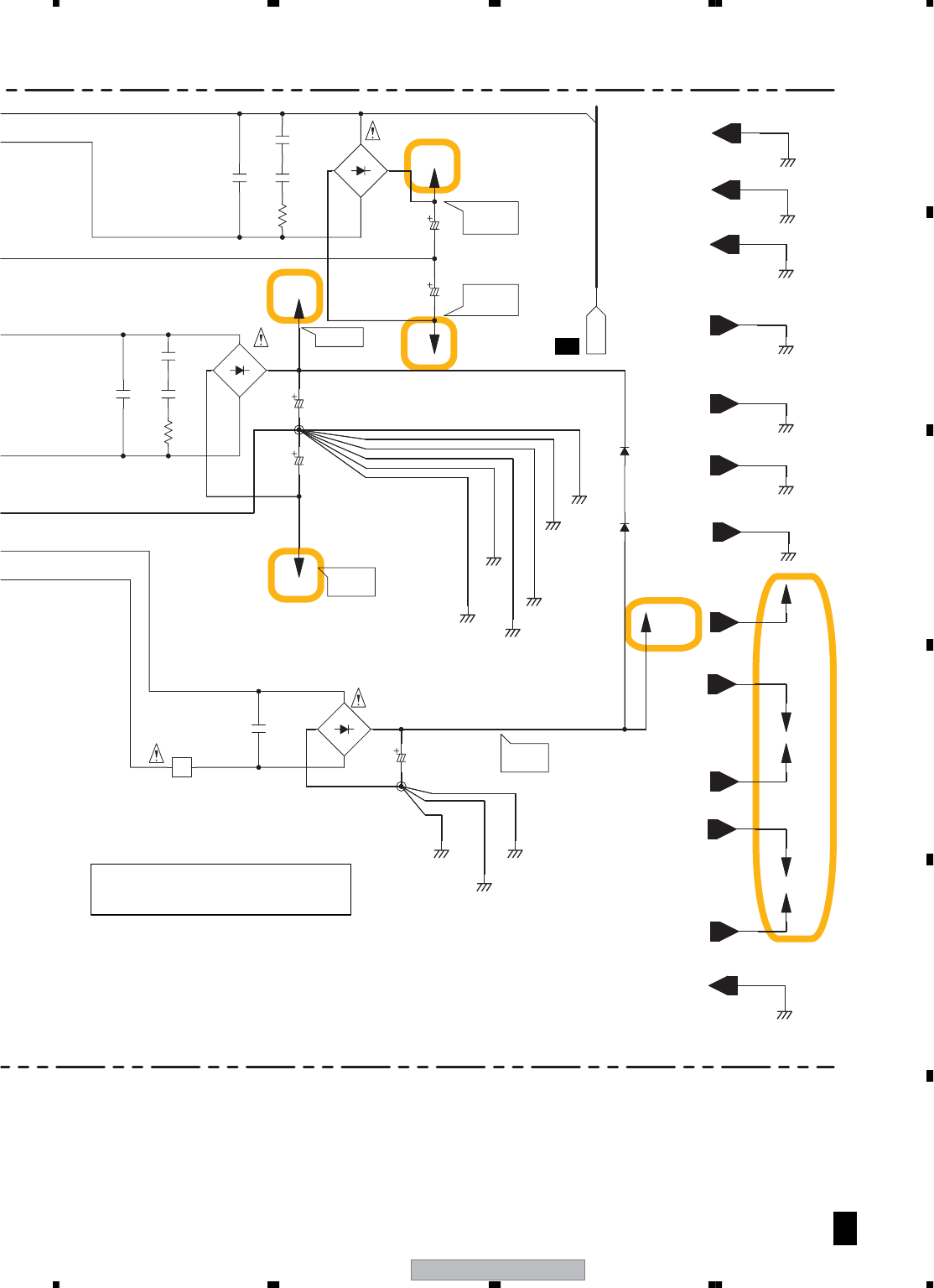
XV-EV1000 49
5678
5678
C
D
F
A
B
E
AC1
GNDTX
GNDD
(7A)
AEK7021-
*
6800/25
D5SBA20(B)
VL-
GNDTX
5600/35
XCH3023
STBY
STBY
CQMA473K2E
STBY
5600/35
XCH3023
D5SBA20(B)
VL+
VH-
2200/63
STBY
2200/63
GNDMTC UN8V
GNDMDV VH-
VH+
VL-
GNDS
GNDP
GNDF UN8V
VL+
GNDP
RETGND
GNDB
STBY STBY
GNDS
GNDF
RETGND
GNDB
GNDMDV
CQMA103K2E
STBY
STBY
VH+
D5SBA20(B)
GNDMTC
GNDTX
UN8V
VH-
VH+
VL+
VL-
GNDP
GNDS
GNDF
CONTROL
GNDB
RETGND
GNDMDV
GNDMTC
IC41
C9041
C41
D41
C22
R9021
C9021
C9023
C9022
C21
D21
R9011
C11
C12
D3061 D3060
C9011
C9013
C9012
D11
TUBE:ADN7004
-30V
HT SINK:XNH3030
30V
XCH3024
SCREW:BBZ30P080FTC
XCH3024
17V
50.4V
50.2V
HT SINK:STBY
SCREW:STBY
+
-
+-
+
-
J4/4
1/4J
CAUTION : FOR CONTINUED PROTECTION AGAINST
RISK OF FIRE. REPLACE ONLY WITH
SAME TYPE NO. 491007 MFD, BY
LITTELFUSE INK. FOR IC41 (AEK7021).
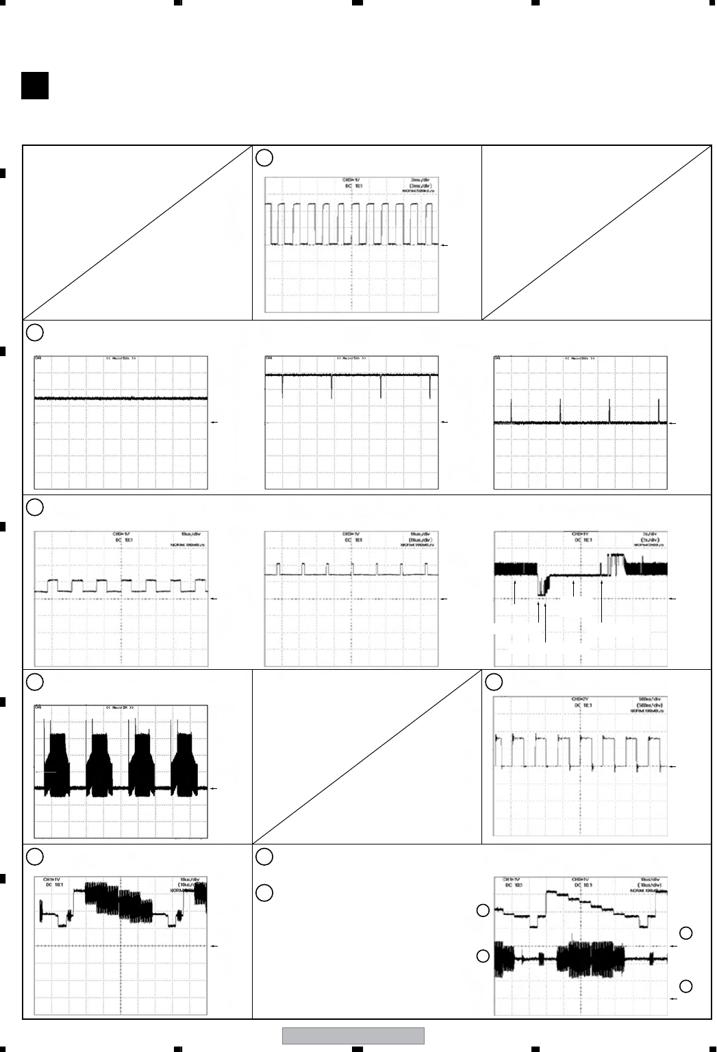
XV-EV1000
50
1234
1234
C
D
F
A
B
E
3.17 WAVEFORMS
Note : The encircled numbers denote measuring point in the schematic diagram.
Measurement condition ;
No. 1 to 10 : reference A1 (DVD), T2-chp 19, Color-bar
No. 11 to 14 : reference A1 (DVD), T1
DVDM ASSY
B
2IC201-pin 39 [TROPENPWM]
V: 1V/div. H: 5µsec/div.
3IC201-pin37 [DMSO]
V: 1V/div. H: 10µsec/div. V: 1V/div. H: 10µsec/div. V: 1V/div. H: 2sec/div.
1IC201-pin47 [FG]
V: 1V/div. H: 2msec/div.
8IC401-pin23 [CompositeVideo Out]
V: 1V/div. H: 10µsec/div.
4CN102-pin 11, 10, 9 (IC101-pin 14, 13, 12)
[SPINDLE (WVU)]
V: 2V/div. H: 2msec/div.
GND
GND GND GND
GND
GND
GND
GND
GND
PLAY
Tray :
opening
Pless OPEN key Pless PLAY key
Braking a turn of disc
[Tray stops]
[TRAY OPEN] [DVD PLAY] [DMSO]
[Tray is opening] [Tray is closing]
9
9
10
9
10
IC401-pin21 [S VIDEO OUT - Y]
V: 1V/div. H: 10µsec/div.
10 IC401-pin26 [S VIDEO OUT - C]
V: 1V/div. H: 10µsec/div.
GND
GND
11 IC201-pin225 [ASPDIF AUDIO DIGITAL SIGNAL]
V: 2V/div. H: 500nsec/div.
GND
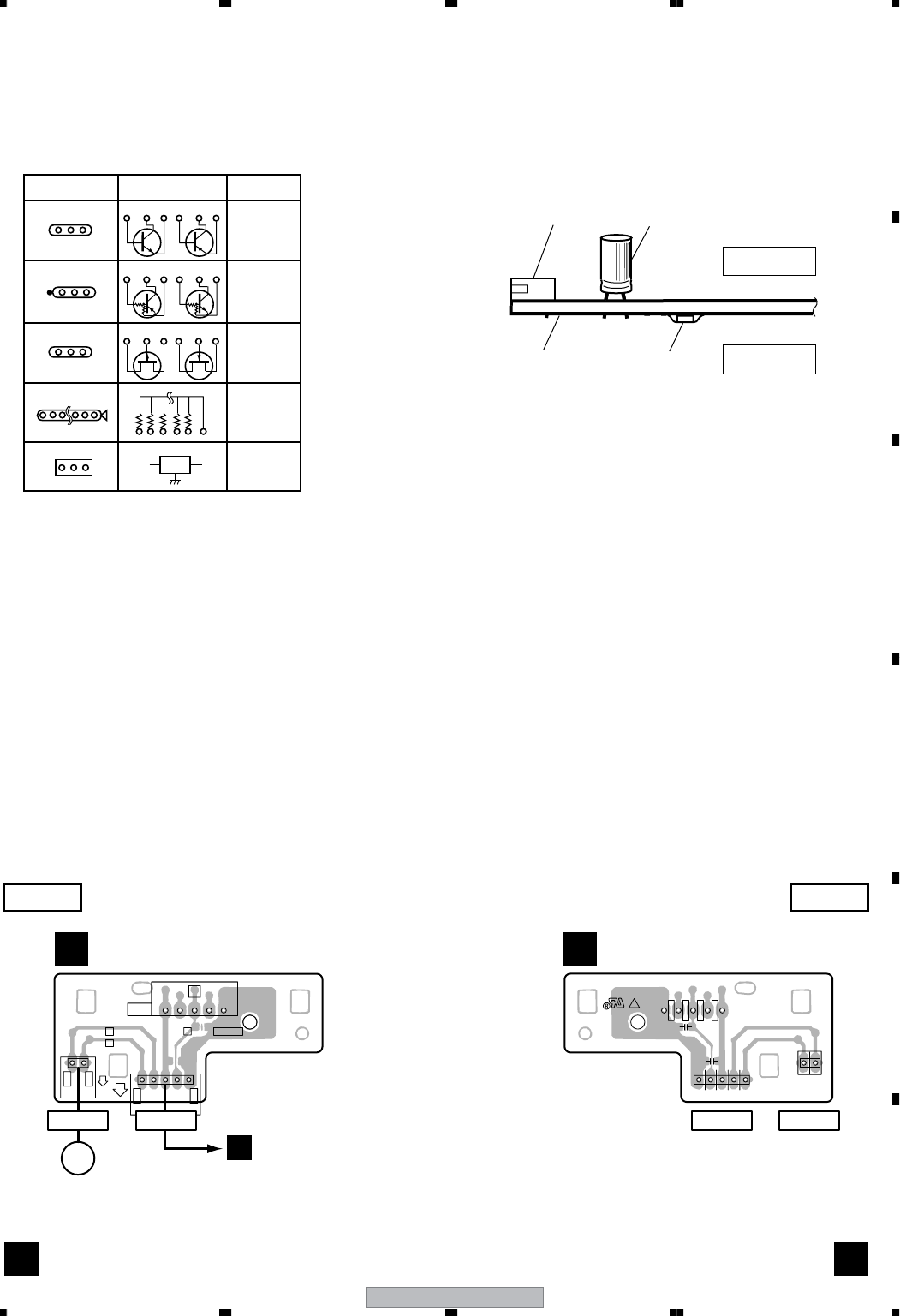
XV-EV1000 51
5678
5678
C
D
F
A
B
E
4. PCB CONNECTION DIAGRAM
4.1 LOAB ASSY
NOTE FOR PCB DIAGRAMS :
1. Part numbers in PCB diagrams match those in the schematic
diagrams.
2. A comparison between the main parts of PCB and schematic
diagrams is shown below.
3. The parts mounted on this PCB include all necessary parts for
several destinations.
For further information for respective destinations, be sure to
check with the schematic diagram.
4. View point of PCB diagrams.
Symbol In PCB
Diagrams
Symbol In Schematic
Diagrams Part Name
BCE
D
D
G
G
S
S
BCE
BCE
DGS
BCEBCE
BCE
Transistor
Transistor
with resistor
Field effect
transistor
Resistor array
3-terminal
regulator
Capacitor
Connector
P.C.Board Chip Part
SIDE A
SIDE B
15
51
SW2
(V+5D)
V+3D
LOAD-
LOAD+
GND
PNE-1B1
C102
C101
CN602
CN601
12
51
VWG2346-
VWG2279-
5
VWG
LOAB
5
1
VNP1836-C
CN602
S101
CN601
SIDE A SIDE B
LOAB ASSY
ALOAB ASSY
A
CN103
B
(VNP1836-C) (VNP1836-C)
LOADING MOTOR
ASSY
M
CN601CN602 CN601 CN602
A A
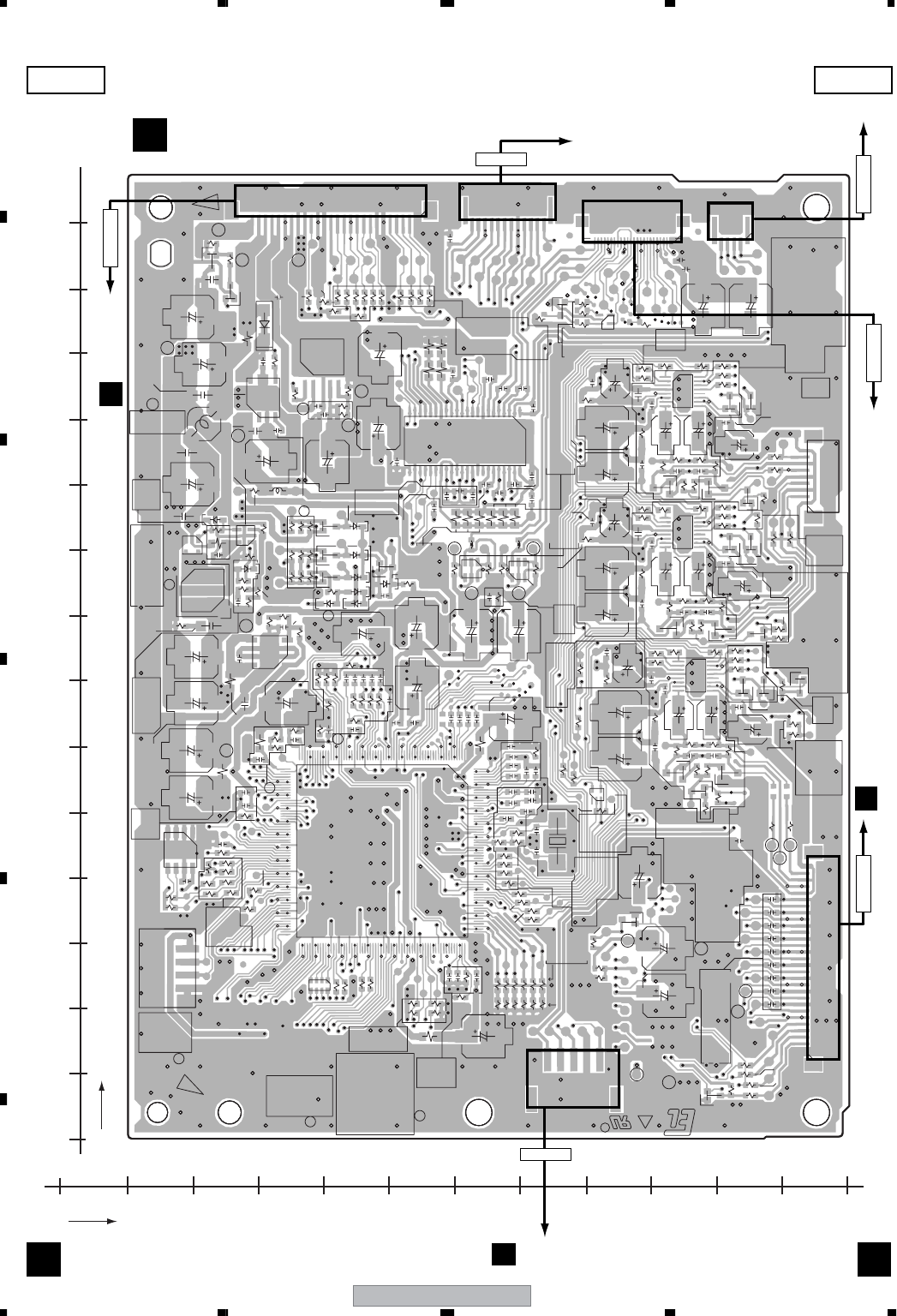
XV-EV1000
52
1234
1234
C
D
F
A
B
E
4.2 DVDM ASSY
24
1
1
9
UP SIDE
14
125
112
17
LF 122
45
13
13
45
1
4
57
9
1
1
9
129
12865
64
256 193
192
1
21
5
3
8
5
4
1
1
27
4
31
5
58
14
1
4
R
1
5
BOTTOM SIDE
BOTTOM SIDE UP SIDE
GNDD
12V
8V
UP SIDE
E
5V
GNDM
6.5V
E
GNDD
LD_CD
LD_DVD
3.3V
3.3V
C
D
3.3V
C
GNDD
UP SIDE
LR
GNDA
5V
A
B
1.8V
GNDD
V
GNDD 5V
AB
2/2 D
C376
CN101
C374
C564
IC561
R568
R569
C567
R567
Q563
C372
C373
CN103
C371
CN901
C140
Q304
CN102
Q701
C701
R702
R701
CN903
C569
R536 R535
R565
Q561
C571
C572
R537
C573
R566
R575
R564
R576
Q564
R573
R538
C561
R561
R572
R563
R574
R534
C568
R582
R581
R373
Q562
C574
R571
Q565
R579
R910
R911
R912
R913
R908
R152 R153
C152
R133
C146
R135
C144
C141
C142
C143
R154 C161
R136
C104
C133
R909
R914
R915
R905
R318
C103
C153
C151
C102
C535
C566
C563
C565
R151
C562
R562
R315
R314
C536
C145
IC101
R903
R313
Q305
R907
D733
C761
Q702
L751
R904
R906
C132
C131
C101
R764 C763
C762
R901
IC731
C734
C732
C731
IC751
C754
R732
D751
C736
C752
R733
C753
R763
R762
IC761
C733
C751
R731
R761
L731
C702
D881
R750
R751
C1002
R520
R541
C544
R578
C534
C512
R509
C542
C539
R548
C541
R533
R543
R539
R546
IC531
Q534
C531
R544
C538
Q531
R545
C543
C537
R601
R602
R531
C504
C503
R504
R501
R506
R505
Q532
R503
Q503
C508
Q504
R542
R552
R551
Q533
R508
C507
IC501
R507
C511
Q506
C509
Q535
R549
C320
R132
R134
C213
C215
C344
C343
R256
C202
C203
C346
Q307
R322
Q308
R321
R310
C310
R532
R131
R326
L308 L309
C532
C533
C505
R594
R595
IC201
R502
C506
C345
C309
R325
D801
R801
R210
R211
R217
R216
C216
C217
R284
R852
Q851
R214
D821
C712 R713
R714
R712
Q731
R215
R883 R853
R201
R202
R205
R206
C209
C208
C211
C212
C210 R204
C221
C204
C205
C206
C219
R212
R213
R881
IC711
Q821
C737
D861
D851
C740
C713
C714
C739
C735
R734
R735
D731
R738
R740
Q881
C711
C738
R737
L732
C801
R822R851
R823
D862
R824
R711
R736
R882
Q801
D852
R821
R739
C424
C425
C426
CN902
C454
C451
C476
C474
C475
R521
R522
C513
C502
C501
R512
R518
R514
R515
R513
Q502
Q501
C514
Q401
R511
R516 R519
Q505
C1001
R270
R269
R207
R592
C252
X201
C251
R251 R252
C258
R253
C259
C262 C263
C265 C267
C268
C269
C270
C271
C272
C273
R241
R242
R243
R244
R245
R246
IC591
R593
R591
R401
R416
R412
R431
R433
R414
R415
R411
R224
IC204
C224
C223
C222
R235
C220
R232
R221
R237
R220
CN204
C201
R223
R259
R260R261
R200
R258
R234
C290
R228
R219
R218
C421
C422
C423
R921
R923
R922
R924
C404
Q481
R481
R405
R209
C244
R404
R279
C237
R280
C243
C242
R262
R263
R264
R265
CN104
R432
R434
R436
R413
R435
R225
R229
R227
R226
10
0
10
0
20
30
40
50
60
70
80
90
100
110
120
130
140
20 30 40 50 60 70 80 90 100 110 120
X
Y
SIDE ASIDE A
DVDM ASSY
B
(ANP7527-A)
B B
To SPINDLE MOTOR
To PICKUP ASSY
To STEPPING MOTOR
CN104
CN8301
C
CN601
A
CN5503
C
CN102
CN902 CN101 CN103
CN901
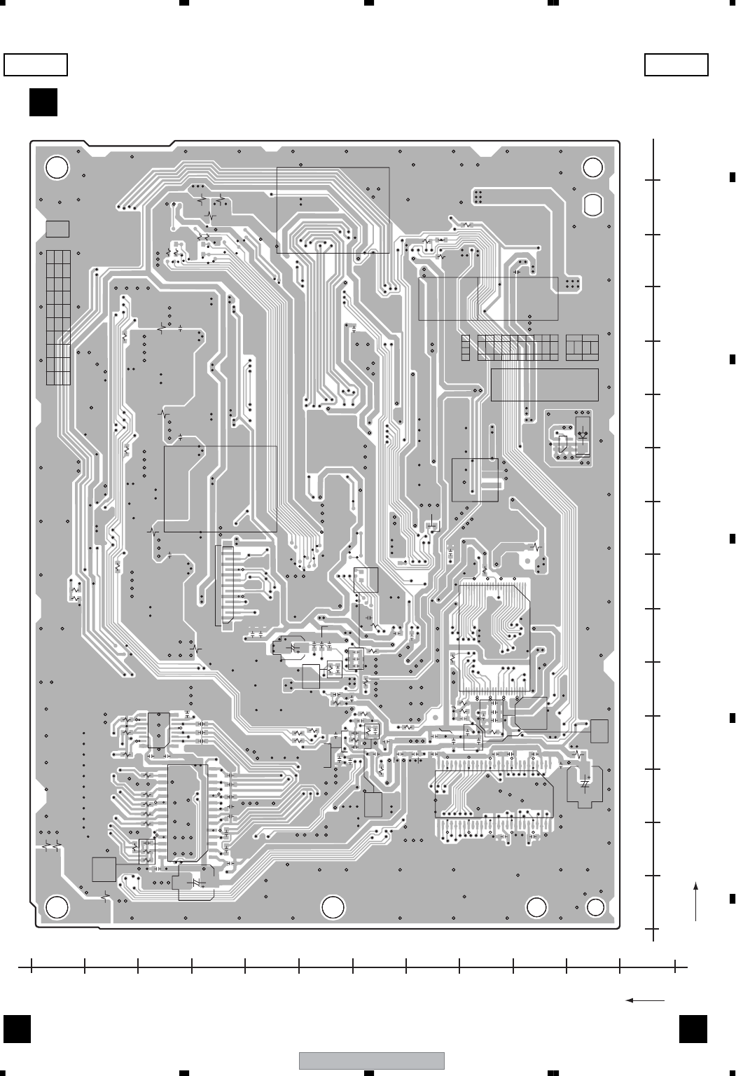
XV-EV1000 53
5678
5678
C
D
F
A
B
E
LF
A
B
C
1
0
0
321
0987654321
0
1
113
48
124
25
1
64
3
21
28
1
14 15
18
16 9
54
127
28
DVDM ASSY
AWM7
9 9 9
8 8 8
7 7 7
6 6 6
5 5 5
4 4 4
3 3 3
2 2 2
1 1 1
0 0 0
PRODUCTION CODE
ICT FC
R301
R371
R372
R374
R375
R303
R302
R902
R530
R560
C560
R577
C121
R917
L901 R916
C1003
R500
R603
C530
C500
R517
R547
R604
CN951
C257
C260
C266
IC203
R208
Q732
CN952
Q201
C218
R282
D732
C453
C465
C452
C464
C455
C466
R474
R475
R476
R426
IC401
R590
IC451
C347
R267
R238
C245
C246
R247
R249 R257
C250
R248
C248
C247
R240
C253
C241
C240
C239
R230
C254
R254
C256
C255 C261
C264
R255
R231
C591
C416
C415
C235
C236
C592
R268
R266
C289
C225
C226
C228
R233
R285
R236
C214
C207
R239
C296
C288
C227
C230
C233
IC202 C282
C231
C286
C232
C287
C234
C283
R281
C281
R1001
R1003
R1002
R403
R424
R425
C402
C401
R422
R421
R423
R402
C406
C411
C413
C414
C412
C405
C403
C284
C285
10
0
2030405060708090100110120
X
10
0
20
30
40
50
60
70
80
90
100
110
120
130
140
Y
SIDE BSIDE B
DVDM ASSY
B
(ANP7527-A)
B B
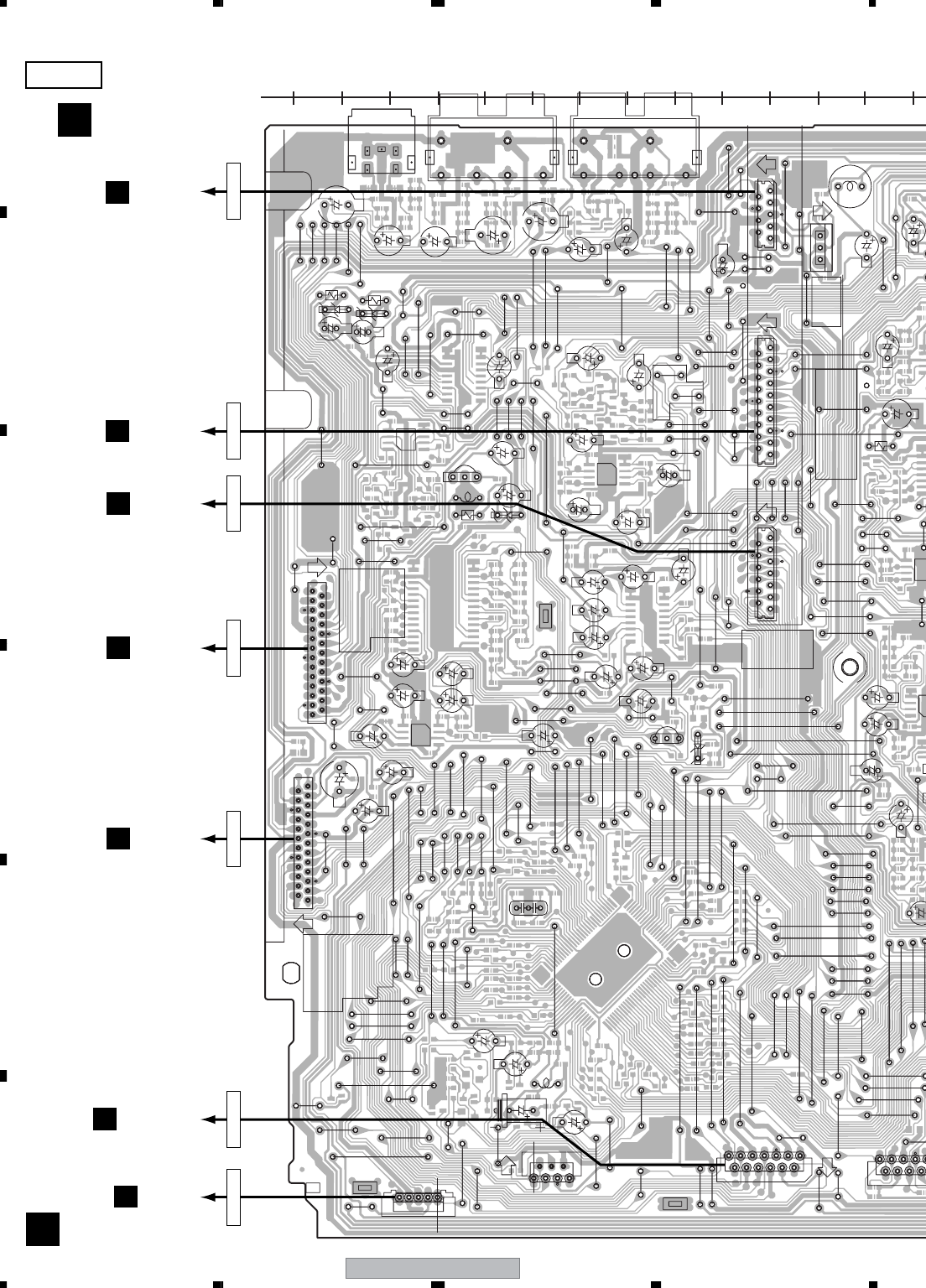
XV-EV1000
54
1234
1234
C
D
F
A
B
E
4.3 IFAF ASSY
17
11
1
19
1
9
125
15
127
13
1
113
X5501
C5511
C5501
L5501
C5502
C5506
CN5502 CN5503
D5955
CN5506
CN5505
C5963
C5966
C5968
CN5102
C5640
C5708
L5601
C5601
IC5601
W598
C8510
C8509
CN8401
R8216
C8221
D8201
C8222
C8305
C8308
L8201
C8307
C8213
C8310
C8309
C8201
C8312
C8831
C8829
C8833
C8834
R8904
C8908
C8907
R8901
C8122
C8116
C8120
C8119
C8121
C8115
C8835
CN5105
Q5402
C5433
C8721
C8701
C8616
C8603
C873
7
C8711
C8631
R8637
C8751
C8752
CN8830
C8837
C8881
C8871
C8851
C8861
CN8301
JA8850
W549
W465
W632
W655
W525
W563
W649
W617
W681
W669
W565
W674
W
W482
W589
W555
W675
W613
W540
W600
W671
W670
W688
W682
W683
W684
W685
W586
W557
W556 W537
W593
W531
W564
W533
W633
W543
W548
W522
W609
W610
W584
W662
W594
W619
W591
W558
W561
W572
W496
W680
W689
W676
CN5507
W451
CN5501
W587
W658
W483
W616
W623
W677
W581
W552
Q8201
W494
W665
W569
W601
W448
W657
W48
4
W644 W450
W560
W460
W524
W559
W553
W679
W585
W611 W588
W687
W673
W622
W481
W641
W527
W650
W668
W621
W664
W576
W618
W647
W493
W490
D8902
D8901
W519
W646
W629
W612
W648
W520
W653
W577
W740
W528
W614
W530
W630
W627
W642
W602
W634
W596
W635
W636
W539
W663
W567
W571
W661
W516
W551
W615
W643
W590
W690
W562
W512
W529
W579
W580
W592
W504
W514
W568
W672
W499
W536
W498
W686
W651
W566
W595
W625
W656
W501
W489
W541
W508
W583
W544
W608
W515
W535
W542
W605
W509
W574
W575
W578
W546
W547
W487
W517
W638
W532
W628
W521
W631
W604
W526
W603
W654
W510
W639
W597
W491
W620
W502
W545
W503
W505
W513
W626
W511
W659
W446
W500
W523
W570
W624
W550
W666
W645
W606
W492
W640
W637
W652
W667
W495
W497
W485
W599
W660
W486
W692
W506
W607
W538
W534
W507
W488
W554
W573
W582
W691
W518
STBY
CONTACT
3
.
N
.
C
.
6.KEY3
3.GNDU
4.PULSE
4.VP+12
A
3.MIC
2.VA+12
1.ECHOVOL
2.REMOCON
1.TIMERLED
7.KEY2
13.MUSICLED
6.MODE
5.HALF
9.LCDDATA
11.RECR
SIDE
5.VE+5
5.MIC SW
4.GNDA
12.MOVIELED
11.LCDCLK
10.SY
8.KEY1
9.RECF
21.VPR+8(M)
17.GNDD
18.GNDD
19.GNDM
15.GNDD
14.GNDD
16.DOUT
22.VPR+8(M)
20.GNDM
B
7.GNDM(TC)
8.VD+5V
1.GNDU
3.GNDD1
2.AC3IN
4.DIN
5.GNDD
6.GNDD
7.VD+5
8.NC
9.V+5A
3.LIN
4.GNDC(IN)
5.FRO
6.VCOMG
7.FLO
8.RECMUTE
9.SRO
10.GNDC
11.SLO
12.GNDC
13.SWO
14.GNDC
15.CO
16.GNDC
17.SBRO
18.GNDC
19.SBLO
1.RIN
2.GNDC(IN)
1.DIRERR
2.DIRRST
3.DIRCS
4.DIRDO
5.DSPMODE
6.DSPHREQ
7.BUSY
8.DSPSS
9.XDSPRST
10.DSPCLK
11.DSPDO
12.DSPDI
13.DECMUTE
10.MOTOR
24.GNDA
23.GNDD
22.R
21.GNDD
20.B
19.GNDD
18.G
17.GNDD
25.FL
9.SDATA
8.MDATA
7.DVDACK
6.GNDD
10.SCLK
12.XDVDRST
11.XREADY
13.DVDPOWER
16.Cr/R
5.GNDD
15.GNDD
14.Cb/B
13.GNDD
12.CY/G
11.GNDD
1.P/XI
2.SQUEEZE
3.VSEL2
27.FR
4.VSEL1
5.ASPECT
6.SC
7.GNDD
26.GNDA
8.V
9.GNDD
10.SY
4.VDET
1.NC
3.DVDMUTE
2.TRKUP
Printed Side
2CH ONLY
24.VPR+8
23.VPR+8
25.VDVD+12
CONTACT SIDE
SIDE A
IFAF ASSY
C
(XNP3096-C)
C
CN902
B
CN951
D
CN8301
CN901
B
CN5102
J5401
H
CN5105
CN5101
G
CN5501 CN5507
CN701
D
CN901
D
CN5506 CN5505
110
120
130
140
150
160
170
180
190
200
210
220
230
240
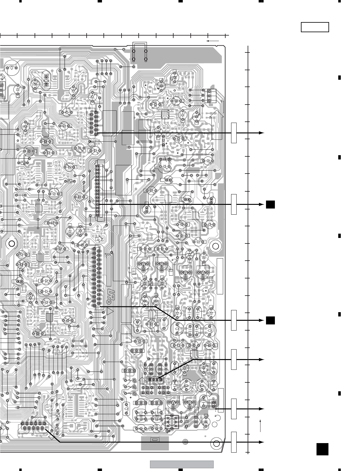
XV-EV1000 55
5678
5678
C
D
F
A
B
E
111
111
127
15 10 1
14
2
OPEN
1
DIP
31
FCDC
R5807
R5802
C5608
CN5503
W421
C5705
C5704
CN5701
X5702
C5709
C5708
L5601
C5601
KN5501
Q2806
C8722
C8721
C8702
C8701
C8604
C8616
C8615
C8603
C8771
C8618
C8617
C8737
C8728
C8711
C8712
C8631
C8632
R8637
R8638
W315
C2220
C8910
W465
W449
W439
W416
W400
W430
W434
W475
W410
W405
W482
W474
W427
W429
W424
W522
W428
W435
W437
W438
W496
W470
W426
W447
C2307
W451
CN8303
W329
W425
W318
W483
W319
C5610
W420
W409
W494
C8621
C8622
C8715
C8716
W407
W328
W415
W448
W442
W406
W327
W484
W408
W441
W431
W403
W450
W460
W476
W401
W412
W419
CN8302
W480
W479
CN2301
W433
C2808
W464
W325
W493
L2402
CN2302
W299
C2418
R2321
W490
VR2401
W250
W418
W473
R2803
W469
5
19
W303
C2406
W422
5
20
W306
D2301
W445
D2256
W528
W310
W220
W478
W317
W301
C2224
W314
W458
C2225
L2802
W252
C2260
C2425
C2801
C2802
C2803
C2203
C2201
W331
W516
W467
C2405
W472
W512
VR2402
C2419
C2404
W514
W498
W454
W457 W453
W471
W436
W461
C2209
W501
C2403
W489
W312
W508
W324
W
C2314
C2807
W515
W468
W455
W509
C2222
W240
L2401
VR2801
W414
W321
W323
W322
C2420
W487
C2308
W517
W251
W521
W404
C2409
C2216
C2408
W300
C2407
VR2301
W330
W456
W510
W459
CN2507 W302
W258
W491
W440
W513
W402
W511
W413
W466
W446
W500
W333
W432
W492
W411
W444
C2810
W423
W417
W477
W495
W463
W462
W443
W497
W332
C2809
W452
D2306
VR2802
D2305
D2304
C2221
W233
D2303
W485
D2302
C2417
C2410
D2201
W486
R2806
C2804
C2204
C2228
C2202
C2215
C2217
C2218
C2223
Q2301
C2251
C2254
C2255
C2261
C2262
Q2302
C2805
C2309
W232
W231
W313
W230
Q2801 Q2802
Q2803
Q2805
VR2302
W320
C2259
W305
W239
W244
W316
W261
W242
W259
W241
C2421
W260
R2805
W262
W222
W224
W243
L2801
L2403
5
06
C2422
W308
W238
W326
W309
W304
W311
C2310
C2806
C2311
C2312
W488
W307
W249
L2404
W518
C
SIDEPRINTED
3.N.C.
24.MUTEC
4.PULSE
2.SOL
26.VE+56
REC
4.DO
19.SYSPOW
20.HPAC1
23.RY_R
25.NC
1.GNDM
6.MODE
5.HALF
11.RECR
2.DI
27.GNDU
21.MUTE
22.RY_F
10.RDS
11.CND
L
9.VSM
PNE-1B1
IFAF ASSY
9.RECF
6.GNDDTXL
7.GNDM(TC)
3.CLK
8.VD+5V
12.GNDM(DV)
13.VP+12
11.GNDM(TC)
10.VPR+8M
9.VPR+8M
8.GNDD
7.GNDD
6.VPR+8
5.VPR+8
4.VA-12
3.GNDTX
2.VA+12TX
1.VA+12
16.XHPMUTE
15.HPDET
7.+9V
8.TXR
18.EVOLCLK
17.EVOLDATA
2.GNDA
1.C
3.SL
4.GNDA
5.SR
6.GNDA
7.SW
8.GNDA
9.FL
10.GNDA
11.FR
12.GNDA
13.XPROTECT
14.SUBAC
15.VD+5
14.V+5A
GNDC
GNDM (DV)
VPR+8M
GNDD
RECR
G
NDU
G
NDD1
A
C3IN
DIN
G
NDD
G
NDD
V
D+5
NC
V
+5A
3.LIN
4.GNDC(IN)
5.FRO
6.VCOMG
7.FLO
8.RECMUTE
9.SRO
10.GNDC
11.SLO
12.GNDC
13.SWO
14.GNDC
15.CO
16.GNDC
17.SBRO
18.GNDC
19.SBLO
1.RIN
2.GNDC(IN)
1.CE
5.GND
10.MOTOR
ICT FC
VA12
OPEN
BIG
DECK TP Adj.
Adj.PB
VA12
GNDA GNDA
VREF
VA12
DECK PART
Production Code
BIAS
GNDA
VREF
VREF
VA12
A
LEVEL
Adj.
GNDA
R
GNDA
Rch
LCH
GNDA
VA12
VA12
MS
Printed Side
BIG
Rch
Lch
DC
Lch
IC2401
Rch
VREF
VREF
GNDA
IC2301
FC
RCH
LEVEL
IC2202 Lch
SIDE A
C
FM/AM
TUNER UNIT
J3002
J
CN8302
CN3501
J
CN8303
TAPE DECK
MECHA
TAPE DECK
MECHA
CN2301
TAPE DECK
MECHA
CN5503 CN5701
10
0
10
0
20
30
40
50
60
70
80
90
100
110
120
130
20 30 40 50 60 70 80 90 100 110 120 130 140 150 160 170 180 190 200 210 220 230
X
Y
CN2302
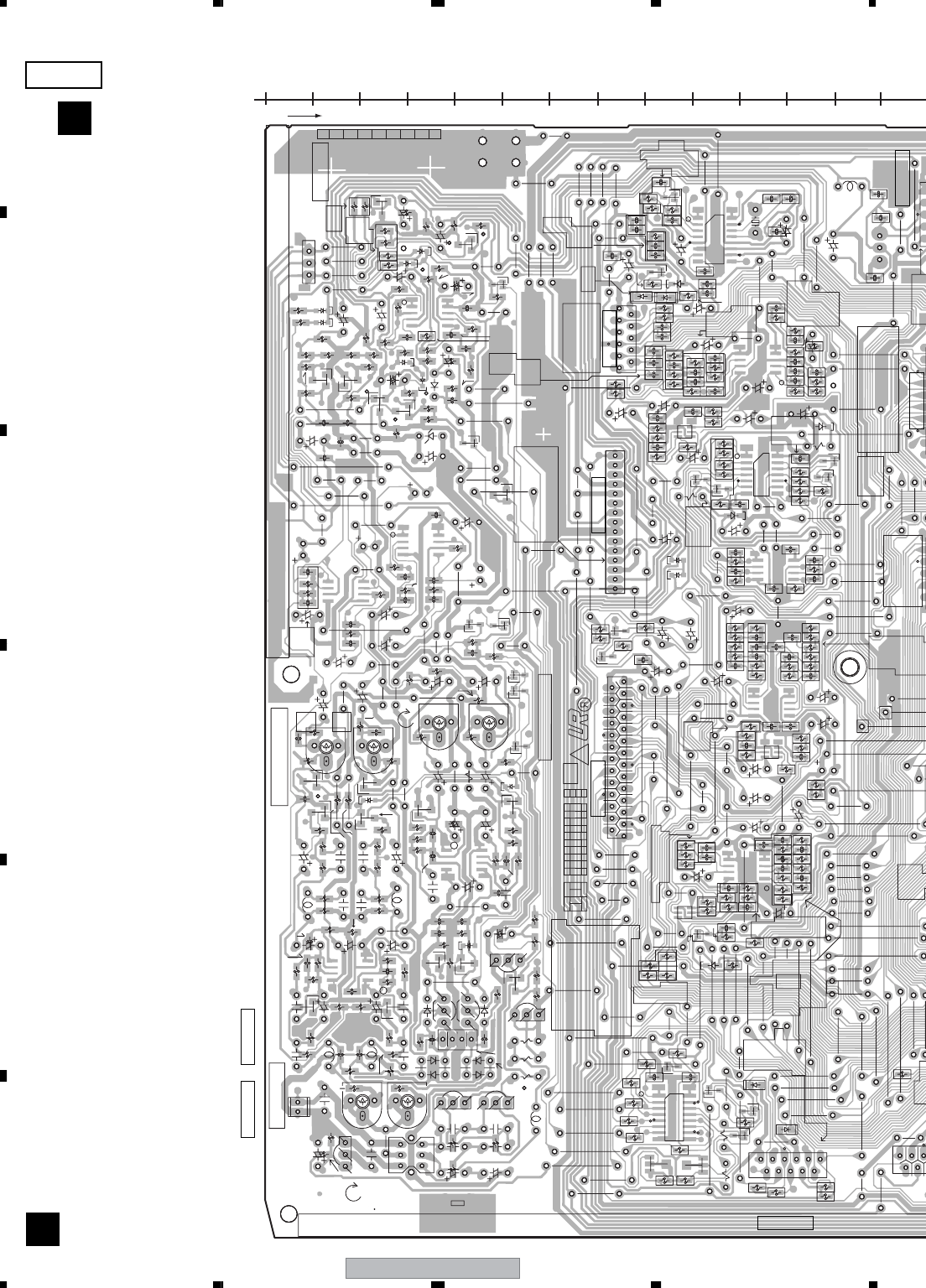
XV-EV1000
56
1234
1234
C
D
F
A
B
E
9
16
18
10
1
11
119 19
10
1
11
16
1
9
8
14
58
14
58
14
58
14
1
8
7
14
58
NP
NP
NP
113
1
27
1
LF
1
.
1510
14
1
14
58
14
58
14
58
14
58
1
0123456789
0123
0
01
C
B
A
85
4
1
R5597
R
5
R5556
R
R5545
R
R
R5803
C5801 C5802
IC5801
R5598
R5
5
D5801
R5801
R5805
D5952
R5806
R5812
R5813
R5814
R5815
R5816
R
R5588
R5608 R5607
R5885
R5886
R5887 R5889
R
R
R5706
R5708
C5723
C5724
C5706
C5721
C5722
R5705
D5705
R5707
C5719
C5720
R5704
D5702
D5701
C5717
C5718
C5725
C5726
C5727
C5710
R5712
IC5701
R5711
R5713
C5711
C5712
C5714 C5713
C5715
C5602
C5603
C5604
Q5608
Q5808
Q5805
Q5802
Q5803
Q5701
Q5712
Q5804
Q5801
D2254
R2816
R2210
R2815
R8726
C8726
R8722
C8724
R8724
IC8702
R8739
R8737
C8731
R8731
C8723
R8723
C8725
C8735
C8733
C8729
R8727
R8729
R8725
R8735
C8727
R8733
C8706 R8714
R8712
C8708
IC8701
C8710
R8710
R8706
R8708
R8702 C8704R8704
C
C8713
C8714
R8602
C8602
C8612
R8610
R8614
C8610
R8612
R8608
IC8601
C8608
R8606
C8606
R8604
C8614
C8607
R8605
C8605
R8603
R8601
R8616
R8615
C8613
C8611
R8611 R8609
R8613
C8609
R8607
C8601
R8624
Q8626
R8952
R8953
R8954
R8632
Q8625
IC8602 R8627
R8625
R8631
R8629
R8623
Q8623
Q8624
R8618
R8620
R8617
R8619
R8747
R8745
R8728
R8716
R8715
C8629
C8630
Q2460
R2209
IC8624
R8718
R8717
C8747
R8741
D8702
D8701
C8912
R8622
R8621
R8720
R8719
C8619
C8620
C8717
C8718
R8730
R8749
R8763
C8765
Q8762
Q8745
Q8719
Q8621
D8601
D8602
R2241
R2242 D2257
D2258
C8624
C8627
R8636
R8634
R8633
R8635
C8628
C8626
R2222
Q5607
R5609
R5610
C8623
Q2351
Q2353
C2256
R2243
R8764
R2223
D8762
R8762
C8625
D2253
R2452
R2453
C2432
R2260
R2259
R2801
R8732
R2309
R2899
R2310
R2455 R2456
C2227
C2205
Q2255
R2207
R2276
R2208
C2206
C2452
R2311
R2306
R2307
R2426
R2312
R2267
R2268
R2269
R9006
R2217
C2207
C2214
C2208
R2807
D2255
R2215
Q2352
C2210
Q2263
R2263
C2257
C2402
D2252
R2272
IC2401
IC2203
Q2455
R2274
Q2456
Q2804
Q2304
Q2303
Q2401 Q2451
Q2452
Q2402
Q2305
Q2306
Q2453
IC2301
Q2454
Q2254
Q2253
Q2252
Q2251
IC2201
Q2262
Q2261
R9011
R8736
R2319
D2307
D2401
D2308
C2401
R2320
R2351
R9009
R2352
C2226
R2399
R2401
R2402
R2403
R2275
R2265
R9012
C2451
C2423
C2424
R9010
R2264
C2431
R2802
R5804
C2321
R9005
R9008
R2498
R2164
C2322
C2302
C2231
R2412
R2413
R2499
R2282
R2283
R2404
R2423
R2424
C2211 C2212
C2230
C2323
R2420
R2414R2301
R2421 R2422
R2271
R2281
R2417
R2409
R2418
R2419
R2425
R2415
C2411
C2412
C2324
C2252
C2303
C2301
C2253
R2291
R2410
R2411
R2255
R2251
R2256
R2262
R2252
R2253
R2257
C2304
R2216
C2213
R2273
R2302
R2308
R2303
R2304
R2305
R2163
R2898
R2814
R2813
R2811
R2203
R2204
R2205
R2270
R2810
R5961
C2315
R2431 R2432
R2416
IC2202
R2213
R2277
R2206
C2219
R2451
R2214
R2809
R2808
R2266
R2212
R2261
R2254
CN2507
SR
GNDM(DV)
PNE-1B1
IFAF ASSY
XWZ4015
XWZ4011
XWZ4009
XWZ4003
XWZ4008
XWZ4006
XWZ4005
XWZ4004
C
11.GND
10.RDS
9.VSM
8.TXR
7.+9V
5.GND
6.TXL
4.DO
3.CLK
2.DI
1.CE
GNDU
GNDU
FLO
C
GNDA
GNDA
GNDA
FR
SW
SW
SL
GNDM (TC)
GNDTX
VA+12
VD+5
GNDM (TC)
VD+5
GNDD
GNDC
VPR+8
V+5A
VD+5
GNDC
11.RECR
8.VD+5V
10.MOTOR
9.RECF
7.GNDM(TC)
6.MODE
5.HALF
4.PULSE
3.N.C.
1.GNDM
2.SOL
27.GNDU
26.VE+56
25.NC
24.MUTEC
23.RY_R
22.RY_F
21.MUTE
19.SYSPOW
20.HPAC1
18.EVOLCLK
17.EVOLDATA
16.XHPMUTE
15.HPDET
14.SUBAC
13.XPROTECT
12.GNDA
11.FR
10.GNDA
9.FL
8.GNDA
6.GNDA
7.SW
5.SR
4.GNDA
3.SL
2.GNDA
1.C
15.VD+5
14.V+5A
12.GNDM(DV)
13.VP+12
11.GNDM(TC)
10.VPR+8M
9.VPR+8M
8.GNDD
7.GNDD
6.VPR+8
5.VPR+8
4.VA-12
3.GNDTX
2.VA+12TX
1.VA+12
9.V+
5
8.NC
6.GN
7.VD
+
5.GN
18.GNDC
19.SBLO
14.GNDC
15.CO
16.GNDC
17.SBRO
13.SWO
12.GNDC
11.SLO
10.GNDC
9.SRO
8.RECMUTE
7.FLO
6.VCOMG
5.FRO
4.GNDC(IN)
1.RIN
1.GN
D
3.GN
2.AC
3
13.DECMUTE
12.DSPDI
10.DSPCLK
11.DSPDO
9.XDSPRST
8.DSPSS
7.BUSY
6.DSPHREQ
5.DSPMODE
4.DIRDO
3.DIRCS
2.DIRRST
1.DIRERR
3.LIN
2.GNDC(IN)
D2306
GNDA
Q2805
RECR
VREF
Q2802
L
VREF
Q2803
VPR+8M
Q2801
SWO
CO
SWO
SLO
SRO
FRO
BIG
TP2
TP1
D2302
D2303
D2301
L2802
L2801
D2304
L2402
VR2801
D2201
D2256
VR2401
VR2402
L2401
L2404
CN2301
CN2302
VA12
GNDA
1
VREF
3
VA12
GNDA
GNDA
VA12
VREF
BIG
R
GNDD
1
Adj.
R
L
Adj.
LEVEL
LEVEL
R
L
PB
REC
Adj.
R
L
BIAS
MS
GNDA
VR2802
Q2301
Q2302
VA12
L2403
VREF
GNDA
VA12
VREF
R
E
VREF
L
D2305
Q2806
VR2302
VR2301
4.DI
N
SIDE B
IFAF ASSY
C
C(XNP3096-C)
10
0
20
30
40
50
60
70
80
90
100
110
120
130
140
Y
CN8302
CN8303
CN2301
CN5503
CN5701
CN5506
CN5505
CN2302
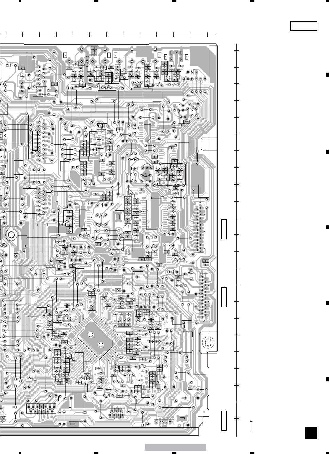
XV-EV1000 57
5678
5678
C
D
F
A
B
E
1
80
30
51
50
81
31
100
1
7
11
119 19
125
16
1
9
8
16
1
9
8
28 15
114
14
58
14
58
14
58
NP
1
27
113
113
R5502
R5579
R5582
C5514 C5513
R5586
R5540
R5577
R5506
R5576
R5571
R5568
R5544
R5530
R5535
R5538
R5543
R5597
R5567
R5536
R5539
R5562
R5563
R5558
R5559
R5560
R5561
R5554
R5553
R5552
R5551
R5555
R5557
R5546
R5545
R5548
R5547
R5549
R5550
R5510
R5511
R5516
R5520
R5519
R5518
R5517
R5523
R5522
R5521
R5526
R5525
C5515
C5520
C5519
R5578
R5529
R5601
R5605
IC5501
R5598
R5590
R5542
R5541
R5621
R5966
C5961
R5963
R5964
R5965
C5960
D5954
R5593
8
13
8
14
R5967
C5962
D5502
Q5501
C5509
R5501 C5508
R5504
C5507
R5503
C5505
Q5502
R5581
R5508
Q5503
R5580
C5504
R5505
R5595
R5594
R5632
R5633
R5592
R5588
C5535
R5634
R5615
R5639
R5512
R5515
R5603
R5604
R5569
C5964
C5965
C5967
C5639
R5624
R5625
R5622
R5623
Q5603
R5626
D5602
D5601
R5627
R5638
L5502
R5532
R5531
C5602
C5603
C5604
Q5602
Q5601
C8103
C8101
IC8101
R8802
R8801
C8513
C8514
R8512
R8517
R8516
R8514
R8515
R8513
R8402
R8511
C8402
R8404
R8406
C8404
C8406
C8401
R8411
R8405
C8403
C8405
R8403
R8401
R8215
C8223
C8306
R8203
R8202
R8211
C8304
R8208
C8218
R8209
C8204
C8205
R8210
C8220
C8302
C8303
C8203
R8308
R8204
R8205
C8217
R8207
C8219
R8213
R8212
C8211
R8214
C8212
R8303
C8301
R8301
R8302
IC8301
C8202
R8201
R8206
C8215
C8214
C8216
C8209
C8210
R8217
C8206
IC8201
C8207
C8208
R8304
R8307
R8306
R8305
IC8801
C8803
R8805
R8816
C8830
C8828
C8516 C8517
C8313
C8518
C8315
C8316
R8112
R8108
R8122
R8114
R8120
R8116
IC8111
Q8114
Q8112
C8108
R8106
R8104
Q8113
R8119
R8115
Q8111
C8107
R8105
R8103
R8121
R8113
R8111
R8107
R8518
R8803
C8117
C8118
R8124
R8125
R8118
R8117
R8127 R8126
R5434
R5431
R5432
D8501
R5403R5404
R8520 R8510
R8508
R8506
IC8501
R8504
R8502
R8509
R8505
R8507
R8503
R8519
R8501
R8521
C8521
C8522
R8522
Q8501
Q8116
Q8115
Q8503
Q5403
Q8505
Q8506
3
9
5
7
9
5
5
7
C8706 R8714
R8712
C8708
C8710
R8710
R8706
R8708
R8702 C8704R8704 R8709
C8709 R8701
C8703
C8707 R8705
R8707
R8703
R8713 C8705
R8711
C
8605
R
8609
R
8613
R
8607
R8629
Q8623
Q8624
7
5
7
15
7
17
7
F8841
R8842
F8831
R8841
R8832
C8842
R8831
C8832
R8835
R8823
R8822
L8871
C8822
L8821
R8875
R8876
C8872
R8821
R8872
R8874
L8861
R8865
R8866
C8862 R8861
R8863
R8871
R8862
R8873
R8864
L8851
R8856
R8855
C8852
R8851
R8853
R8852
R8854
7
17
D8601
7
3
C5518
C5517
R5584
C5516
R5583
R5585
C8224
R8523
R8524
R8525
R8526
R8527
Q8524
C8501
C8502
2
5
R5537
R5528
R5804
R5961
U-TEST
S-TEST
GNDD
GNDA
VA-12
VDVD+12
VPR+8
VD+5
VD+5
GNDD
GNDD
VA+12
VA+12
VA+12
GNDA
GNDA
VA+12
GNDA
GNDU
GNDU
VE+56
GNDU
VE+5
VU+5
FLO
C
GNDA
GNDA
FR
FL
51
5.MIC SW
4.GNDA
3.MIC
1.ECHOVOL
2.VA+12
13.MUSICLED
12.MOVIELED
11.LCDCLK
10.SY
8.KEY1
9.LCDDATA
7.KEY2
6.KEY3
5.VE+5
4.VP+12
3.GNDU
2.REMOCON
1.TIMERLED
9.V+5A
8.NC
6.GNDD
7.VD+5
5.GNDD
18.GNDC
19.SBLO
14.GNDC
15.CO
16.GNDC
17.SBRO
13.SWO
12.GNDC
11.SLO
10.GNDC
9.SRO
8.RECMUTE
7.FLO
6.VCOMG
5.FRO
4.GNDC(IN)
1.RIN
1.GNDU
3.GNDD1
2.AC3IN
13.DECMUTE
12.DSPDI
10.DSPCLK
11.DSPDO
9.XDSPRST
8.DSPSS
7.BUSY
6.DSPHREQ
5.DSPMODE
4.DIRDO
3.DIRCS
2.DIRRST
1.DIRERR
25.FL
26.GNDA
27.FR
24.GNDA
23.GNDD
22.R
21.GNDD
20.B
19.GNDD
18.G
17.GNDD
16.Cr/R
15.GNDD
14.Cb/B
13.GNDD
12.CY/G
11.GNDD
10.SY
9.GNDD
8.V
7.GNDD
6.SC
5.ASPECT
4.VSEL1
3.VSEL2
2.SQUEEZE
3.LIN
2.GNDC(IN)
1.P/XI
25.VDVD+12
24.VPR+8
23.VPR+8
22.VPR+8(M)
21.VPR+8(M)
20.GNDM
19.GNDM
18.GNDD
17.GNDD
16.DOUT
15.GNDD
14.GNDD
13.DVDPOWER
SWO
CO
VA+12
SWO
SLO
SRO
FRO
12.XDVDRST
11.XREADY
10.SCLK
9.SDATA
8.MDATA
7.DVDACK
6.GNDD
5.GNDD
4.VDET
3.DVDMUTE
2.TRKUP
1.NC
C
4.DIN
SIDE B
C
120
130
140
150
160
170
180
190
200
210
220
230
240
10
0
20 30 40 50 60 70 80 90 100 110 120 130 140 150 160 170 180 190 200 210 220 230
X
CN8301CN5102CN5105
CN5501
CN5507
CN5506
CN5505
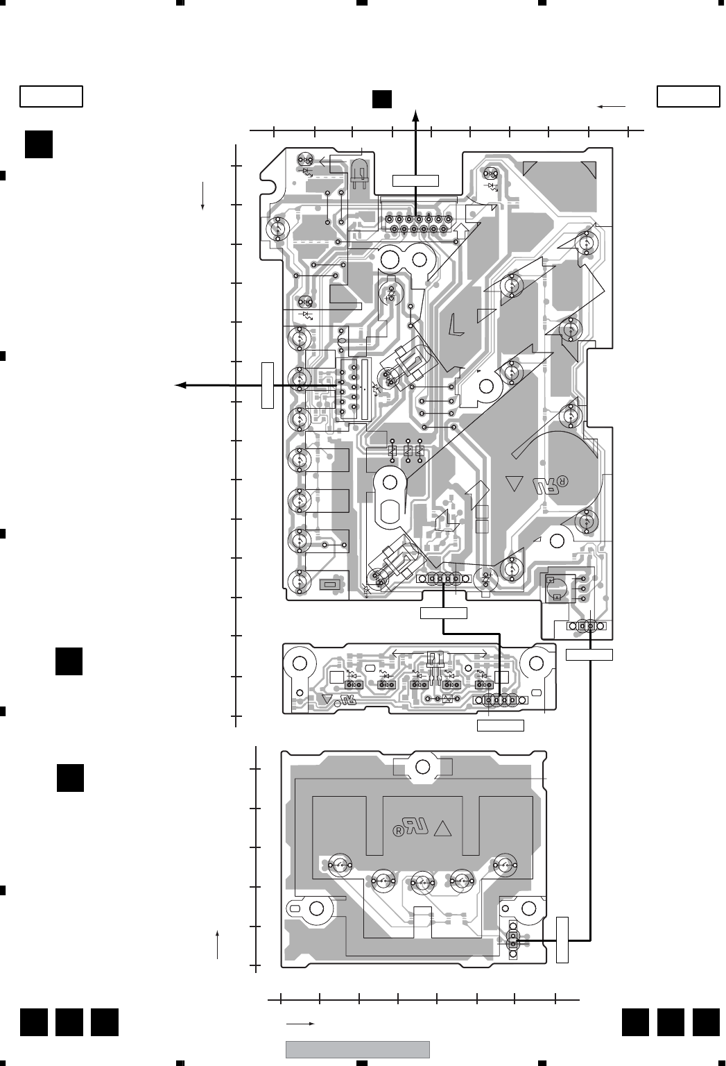
XV-EV1000
58
1234
1234
C
D
F
A
B
E
4.4 KEY, LED and DISPLAY ASSYS
J2_
S5301
S5302
S5303
S5304S5305
PNE-1B1
XWZ4013
KEY ASSY
PLAY
<<| >>|
STOP OPEN/CLOSE
D5102
W735
W736
R5214
W727
W733
W731
W729
W732
W728
W737
D5211
CN5101
W726
W730
W739
D5203
D5302
D5213D5212
W725
D5110
J2
D5209
CN5104
IC5201
C5204
R5210
W734
R5213
D5207
S5201
S5202
S5203
S5204
S5205
S5206
S5207
L5101
C5103
S5105 S5106 S5107 S5108
S5102 S5103
S5101
S5104
R5223
D5101
J1
W738
J1_
ONUPPER
PNE-1B1
PNE-1B1
BLUE
XWZ4010
XWZ4012
XWZ4023
DISPLAY ASSY
LED ASSY
ASES
VOL-
MUSIC/MOVIE
FRONT SURROUND
KARAOKE
ENTER
SOUND MODE
REVERSE MODE
REC STOP
DVD/CD
TAPE
TUNER
STANDBY/ON
LINE
VOL+
SIDE
CONTACT
STBY
1
R
113
1
1
10
14
14
(XNP3096-C)
(XNP3096-C)
(XNP3096-C)
SIDE A SIDE A
LED ASSY
F
F
KEY ASSY
E
E
DISPLAY ASSY
G
G FE G
CN5501
C
LCD ASSY
CN5101
CN5104
250 260 270 280 290 300 310 320
150
160
170
180
190
200
Y
X
230240250260270280290300310320
10
20
30
40
50
60
70
80
90
100
110
120
130
140
150
Y
X
J1
J1
J2
J2
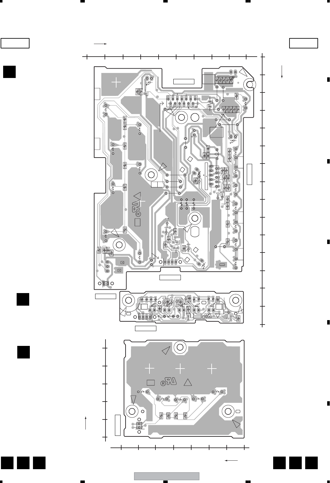
XV-EV1000 59
5678
5678
C
D
F
A
B
E
R5301
R5302
R5303
R5304
2
PNE-1B1
XWZ4013
KEY ASSY
1.KEY3
GNDU
STOP
<<|
PLAY
>>|
OPEN/CLOSE
1
3
R5225
R5226
R5224
R5229
R5231
R5230
R5228
Q5204
R5121
Q5220
R5118
R5115
D5224
C5212
R5116
C5213
R5227
R5216
D5225
R5117
R5114
Q5201
R5113
R5112
Q5102
R5119
R5120
D5219
D5221
D5223
Q5110
C5207
C5201
R5209
C5202
R5208
D5202
C5205
C5211 R5217
C5209
R5211
D5216
D5215
R5201
R5202
R5203
R5204
R5205
R5206
C5301
C5101
C5102
R5108
R5109 C5106
C5105
C5104
R5110
R5111
R5105
R5106
R5107
R5104
D5301
R5101
R5102R5103
R5220
R5219
D5112
D5113
R5123
R5122
Q5219
Q5101
4.VP+12
PNE-1B1
PNE-1B1
XWZ4010
XWZ4012
LED ASSY
DISPLAY ASSY
XWZ4023
1.GNDLED
LCDCLK
MUSIC
MOVIE
10.LCDDAT
GNDLED
KEY1
KEY2
KEY3
5.VE+5
VP+12
GNDU
REMOCON
1.TIMERLED
ASES
REC STOP
REVERSE MODE
ENTER KARAOKE SOUND MODE FRONT SURROUND
MUSIC/MOVIE
STANDBY/ON
TAPE
LINE
VOL+
VOL-
2.LEDCN1
3.LEDCN2
4.VP+12
1.GNDLED
2.LEDCN1
3.LEDCN2
9
10
8
4
6
5
7
LF
1
RLF
LF
1
13
1
1
10
41
41
SIDE B SIDE B
FE G FE G
(XNP3096-C)
(XNP3096-C)
(XNP3096-C)
150
160
170
180
190
200
Y
250260270280290300310320
X
10
0
20
30
40
50
60
70
80
90
100
110
120
130
140
150
Y
230 240 250 260 270 280 290 300 310 320
X
LED ASSY
F
KEY ASSY
E
DISPLAY ASSY
G
CN5101
CN5104
J1
J1
J2
J2
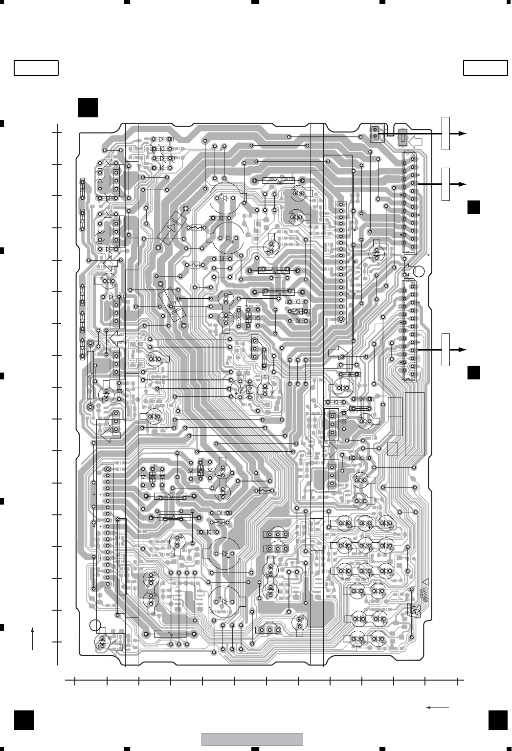
XV-EV1000
60
1234
1234
C
D
F
A
B
E
4.5 AMP ASSY
C3308
W115
W107
C102
W127
W146
W179
C3321
C3663
W192
C3323
C3424
C63
W223
D3321
C3680
W213
W176
W142
W147
W178
D3325
W150
W174
W180
C3402
W175
C3653
D63
C3507
W255
C3301
W177
W121
W224
R3328
D3327
C3322
W196
D3323
W225
D3322
D3424
D3391
R3322
IC3301
W129
W103
W118
C3661
C3401
D3422
W126
C3178
IC61
W111
CN3002
D3324
C3318
D98
Q3654
W195
W210
D3326
W112
IC3401
C91
W149
CN3001
W157
W156
R3318
W155
W106
W232
C3652
R3417
IC81
C3312
D82
W141
Q3657
W189
Q91
W133
CN3651
C3508
W188
W187
W167
W168
W114
W204
C3168
C3167
C3501
D3655
C3179
W218
R3518
W222
W219
R3428
R85
R3657
W169
W214
D3601
W122
C3421
W131
C3423
W170
W138
W200
W163
W201
W143
W211
W202
W203
W209
W221
W135
Q3384
D3421
C3673
W256
R3388
W140
W215
D3394
D3390
W124
W193
D3605
W123
D3603
W113
W216
R3427
C3422
C3317
D3428
W109
W234
W181
D3389
D3425
D3393
D3427
W130
Q3383
W173
C72
W208
W165
D3653
C3662
W199
D72
C82
W144
W108
W172
D3604
W190
R3387
C98
W198
W205
Q3655
C3407
D3602
W171
D3654
D3651
C3302
R3317
IC71
Q62
W251
W148
W197
C101
W110
W212
R3422
C3311
R3421
W117
W252
D3426
W151
W206
D3423
W207
D3386
R3321
W125
W153
W154
D3385
C3502
W183
W254
W184
W102
W116
C3674
C3307
R3418
R3517
W185
Q3656
W101
W194
C3324
C3408
W145
D3387
W152
C3651
D3388
D3652
W162
R3327
W226
D3392
W253
D3328
W220
VH+
VL-
VH-
VL+
SROUT
GNDP
+Vcc
VF-12
GNDP
GNDP
XPROTECT
-Vcc
VH+
VL-
19
AMP ASSY
Production Code
FC DC SLOUT
1
2SJ304
Word
VL+
TA79012S
UN+8
VA-12
VL-
TA7805S
TA7812S
VA-12
VPF+12
VP+12
GNDS
1
GNDP
word surface
Word Surface
FLOUT
GNDREG
FROUT
SWOUT
Surface 2SJ304
FROUT
word surface
+Vcc
VD+5
2SK2232
19
-Vcc
1
SWOUT
VL+
PNE-1B1
LF
231231
10
0
20
30
40
50
60
70
80
90
100
110
120
20 30 40 50 60 70 80 90 100 110 120 130 140 150 160 170 180
X
Y
(XNP3088-C)
SIDE A SIDE A
AMP ASSY
I
I I
CN3022
K
CN3001
To FAN
CN3651
CN3021
K
CN3002
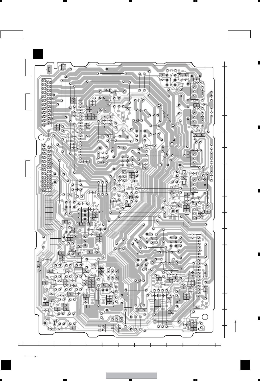
XV-EV1000 61
5678
5678
C
D
F
A
B
E
R3664
R122
IC3304
R91
C3309
C3506
R3687
R3310
D3481
D106
D3301
R104
R3371
D91
Q101
R95
R3396
R3402
D102
D3382 D3381
C61
R3303
R121
R3682
R111
R3500
R3403
R113
R64
C3505
R3591
R3683
R3678
R3410
D3401
R3409
R3491
R3301
R3677
D3658
C3678
R3503
R3405
R3656
R3655
C3403
Q3485
R3513
R3313
R3326
C3672
C3326
C3509
Q3502
R3407
R3674
R3663
Q103
D3581
R3372
R3675
Q43
C3406
R3511
R3508
R3506
R66
R3505
C92
C3510
R63
R3592
R46
R3493
R61
Q3660
C62
R3676
R123
R3314
R3679
R3414
R3673
D3657
R3665
Q63
C97
R3510
R3512
R3307
R3509
R3408
C3306
C3303
Q3301
R3304
R3651
R3654
Q3653
C3410
Q92
R96
R93
R92
R48
Q3382
Q3381
R3671
R3390
R45
R47
D105
R3669
R3384
R3386
R3385
R3309
R3383
R3389
R3411
Q3385
R3302
R3494
R3514
R3426
R3306
R102
R3661
C3677
R3451
C3426
R3413
R3680
D101
R3495
TH111
R3312
C3304
R3658
TH121
Q121
R3423
R97
R3667
R3668
C71
R106
R103
D42
R3672
Q3652
R105
R108
R3502
Q3501
R62
R3424
R101
R3324
R112
C3409
R94
R3323
R114
C3310
R68
R109
C3504
R3351
R3394
R3681
R3395
R3412
Q102
R67 Q104
R3311
C66
Q3651
C3305
R3406
R3305
R3373
C3679
IC3305
R3393
R65
R3401
D3582
R3666
R3501
C3676
R3507
R3504
Q3504
C3503
R3381
C3404
D3482
Q111
R3391
R3492
C3671
R3404
C3405
R3382
R3662
Q3401
C81
R3374
R3496
R3392 R3308
GNDP
VL-
GNDP
XPROTECT
GNDP
+Vcc
-Vcc
VL+
VF-12
VH+
VL-
SROUT
VL+
VL+
FROUT
FROUT
FLOUT
FLOUT
VL-
E1
VL-
B1
OUT
SLOUT
SLOUT
GNDP
GNDP
SROUT
-Vcc
SROUT
SWOUT
SWOUT
B2
VH+
VH+
VH-
VH-
SLOUT
COUT
GNDS
COUT
GNDP
GNDP
C2
E2
UN+8
S
VL-
FAN SIDE
VA-12
FROUT
GNDREG
C1
OUT
G
IN
VPF+12
VD+5
VL+
GNDP
IC3401
SWOUT
GNDS
FLOUT
D
OUT
1
VA-12
IN
VP+12
XWK3202
XWK3203
XWK3188
G
VPR+8
MUTEC
VFL+5
VPR+8
FLIN
RYFS
GNDA
FRIN
SWIN
MUTE
SLIN
CIN
SRIN
VA-12
VP+12
XPRCT
UN+8
UN+8
+Vcc
S
GNDR
IN
D
GNDF
RYRC
VD+5
GNDR
SWOUT
FROUT
IC3301
SGD
VH+
VH-
VL+
PNE-1B1
8
5
41
NP
119
23 1
LF
119
23
NP
1
0123456789
0123
0
01
C
B
A
8
5
41
10
0
20
30
40
50
60
70
80
90
100
110
120
Y
20 30 40 50 60 70 80 90 100 110 120 130 140 150 160 170 180
X
SIDE B SIDEB
I I
CN3001CN3002
(XNP3088-C)
AMP ASSY
I
CN3651
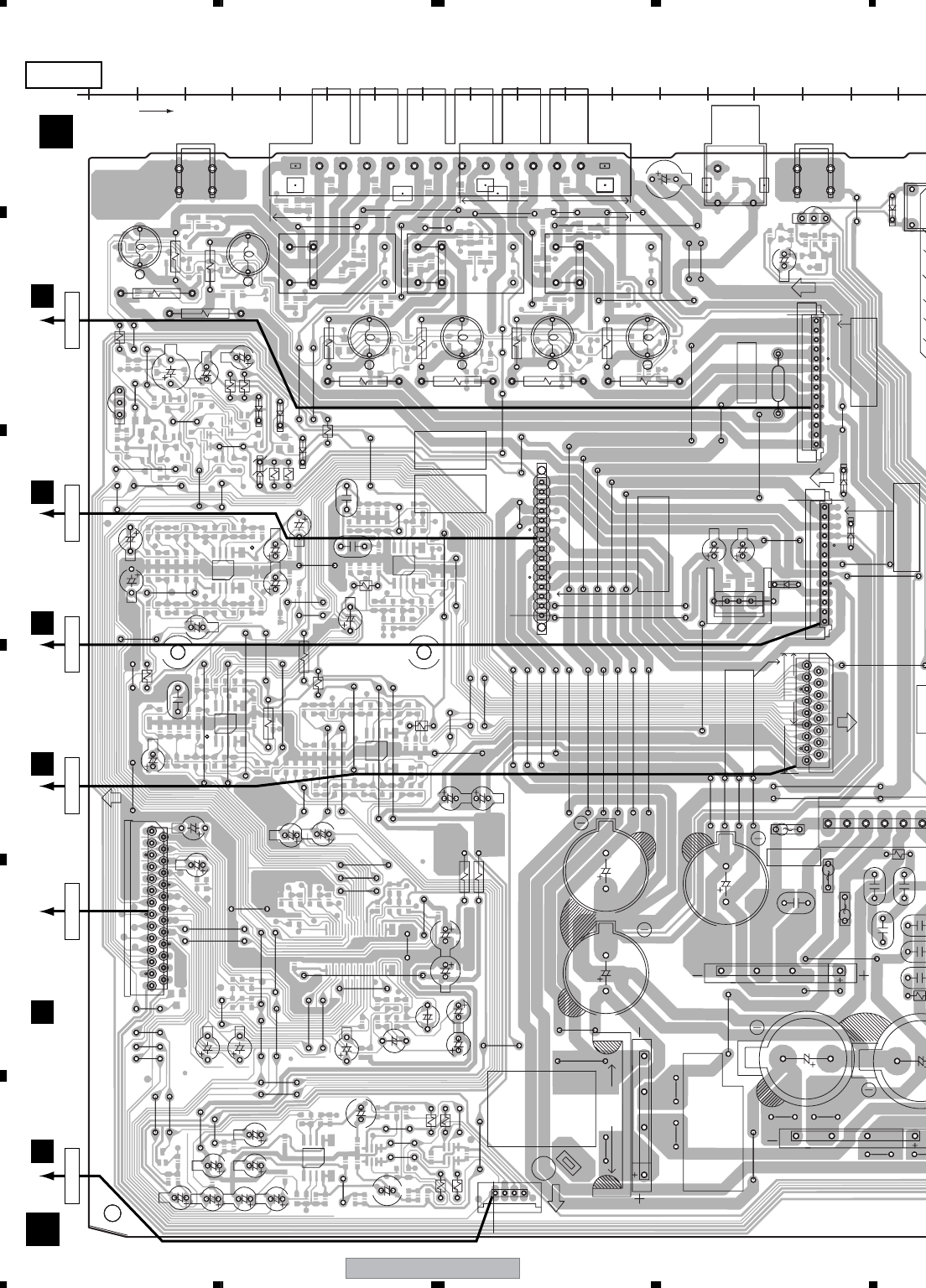
XV-EV1000
62
1234
1234
C
D
F
A
B
E
4.6 POWER ASSY
C3113
C3114
C3174 C3173
C3166
C3164
C3150
C3149
R3177
R3119
R3118
C3134
C3136
C3139
C3140
C3189 C3190
C3151 C3152
C3196
C3908 C3925
C3912
C3924
C3918
C3911
C3923
C3917
C3907
CN3012
C3906
C3096
C3095
W299
W268
C3926
R3911
R3912
R3902
R3901
CN3008
W252
R3206
W203
W204
C41
W224
RY3641
W316
R3635
C3632
C3315
C3954
C3319
W202
W242
W230
W265
W217
W290
R3164
W284
Q3641
Q81
W297
W
5
W243
W294
CN3013
W244
W253
W231
W320
W212
W211
W200
W205
W222
W210
D41
W506
C22
R3631
W322
C21
W508
IC21
W234
W235
IC11
C9022
C9023
C9021
R9021
C12
W229
W317
W515
D3631
W295
W514
W311
W310
W328
W327
W332
W329
W321
W330
W331
W296
W309
W307
W308
3603
W318
W334
W335
W337
W336 KN2
W324
W325
W338
W323
W333
W319
W206
R3462
L3462
R3461
L3461
R3661
L3661
R3617
R3618
R3628
R3668
C3671
C3633
RY3643 RY3642
R3627
L3561
R3561
R3608
R3362
L3362
D3633
C3631
D3632
D3634
R3634
R3633
R3632
L3361
R3607
R3361
C86
W513
C9041
W214
W216
D21
W505
W507
W509
W223
W228
W201
W280
W339
CN3051
W215
W236
W237
W239
C3951
C3311
W340
W240
W271
W270
W249
IC3951
D3591
W276
W227
W302
W305
W248
W312
W267
W251
IC41
D3060
D3061
W209
W241
W246
W233
J3002
W263
W255
W301
W269 W300
W291
W279
W254
W285
R3208
C3320
W283
W286
C3316
W272
W258
R3163
W213
W247
W266
CN3011
R3178
W303
W232
W226
W225
W313
W278
W277
W275
W273
W274
W256
W260
W261
W315
W287
W306
W288
W257
W259
W264
W292
W262
W314
W326
W289
W238
W282
W298
D88
W293
W304
W511
W510
W250
W281
C11
KN3001
IC3101
FC
ICT
INDIQUE.DE CHEZ
(6CH)
491007
BOND
(2CH)
A
LITTELFUSE INC.
CONTACT
SIDE
VD+5
GNDA
VPR+8
CONTACT
127
SIDE
CONTACT
SIDE
CONTACT
SIDE
6ch
2ch
SLIN
GNDA
SR
GNDA
GNDA
COUT
SW
GNDA
FL
GNDA
FR
GNDA
XPROT
SUBAC
SRIN
HPDET
XHPMUTE
EDATA
ECLK
S-POW
HPAC1
MUTE
RY-F
RY-R
MUTEC
NC
SROUT
VE+56
GNDU
VA+12
VA+12TX
GNDTX
VA-12
VPR+8
VPR+8
GNDD
GNDD
VPR+8M
VPR+8M
GNDMTC
GNDMDV
VP+12
VA+5
VD+5
FLOUT
CN3012
CN3011
VL-
SWIN
BOND
VL+
VL-
VH-
SLOUT
SWOUT
BOND
VH-
LINKS COMME
REPLACE IC LINKS AS
CAUTION
REMPLACER LE IC
ATTENTION
LITTELFUSE INC.
MARKED.MFD BY
GNDA
VH+
VL+
GNDS
VH+
GNDF
UN+8V
UN+8V
GNDREG
C
GNDA
SL
GNDA
GNDP
GNDP
491007
UPPER SIDE
CONTACT ON
VA-12
VPR+8
VP+12
XPROT
RY-R
RY-F
VFL+5
MUTEC
MUTE
FLIN
GNDA
FROUT
FRIN
GNDA
CIN
BOND
BOND
BOND
BOND
P
NP
13 1
10
NP
14
NP
NP
1
10
14
7
117
SIDE A
POWER ASSY
J
J
J3033
K
CN3031
KCN8302
C
CN3013
CN8303
C
CN3051
J3902
H
CN3008 J3002
J3032
K
CN3012CN3011
10
0
20 30 40 50 60 70 80 90 100 110 120 130 140 150 160 170
X
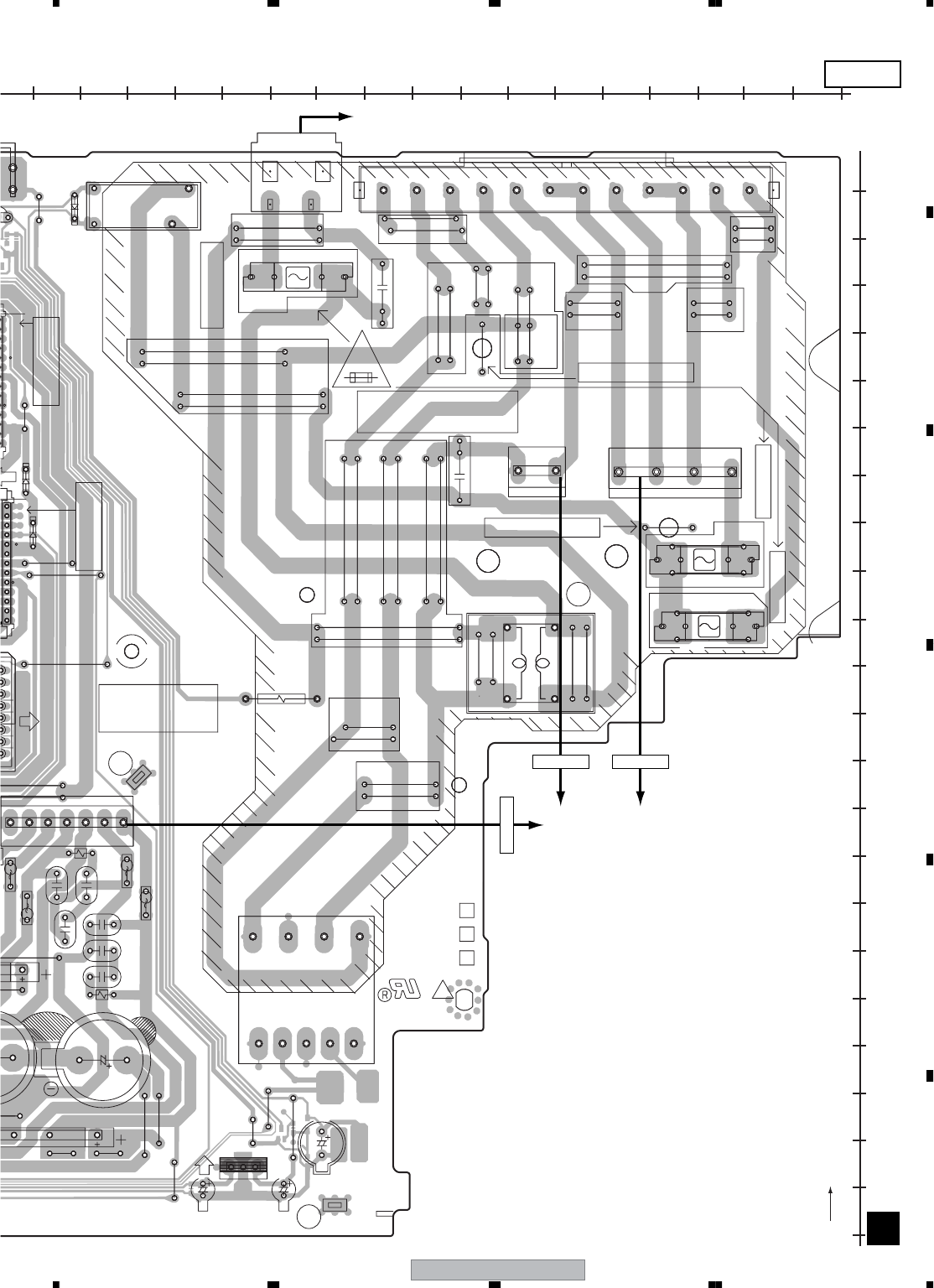
XV-EV1000 63
5678
5678
C
D
F
A
B
E
W124
IC5508
W152
W163
W316
1
H1
CN1
R1
H2
L1
W123
W109
W122
W512
W207
W108
D41
W137
C9013
IC12
R9011
CN4
C9011
C9012
IC21
W234
W
235
IC11
C9022
C9023
C9021
R9021
C12
W220
W105
C82
C83
W221
W167
W157
W513
W107
W104
C1
W116
W117
W159
W160
W166
W106
D11
C84
W120
W165
W155
W154
W218
W153
D3060
D3061
IC22
W208
W129
W219
W291
W279
W113
CN3011
W162
W292
W164
H6
H3
W133
W156
W121
D88
S1
W158
H4
W175
H5
CN2
W125
W131
T2
W114
W135
W511
W110
W
510
W130
AN1
W132
W161
C3
W128
RY81
W136
W115
W176
W134
C11
7
POWER
ASSY
XWZ4020
PRIMARY
TX WINDING CHECK
TX WINDING CHECK
CONTACT
SIDE
VD+5
VPR+8
CONTACT
SIDE
B
C
FU3
COUT
SROUT
FLOUT
VL-
ALL
XWZ4018
FU2
VL+
VL-
PRINTED
SIDE
VH-
SLOUT
SWOUT
VH-
REPLACE FUSE AS MARKED.
RISK OF FIRE
EXCEPT
VH+
VL+
GNDS
VH+
GNDF
UN+8V
UN+8V
GNDREG
GNDP
GNDP
ALL
ALL
ALL
GEN
EXCEPT
GEN
L
VA-12
VPR+8
VP+12
VFL+5
FROUT
BOND
SECONDARY
KUC
GEN
GEN
ALL
BOND
YPW
FU1
PRODUCTION CODE
XWZ4016
MY,NV
N
PNE-1B1
13 1
10
12
1
10
14
1
14
SIDE A
(XNP3097B) J
AC IN
CN2CN1
TRANSFORMER
CN4
160 170 180 190 200 210 220 230 240 250 260 270 280 290 300 310 320
330
10
0
20
30
40
50
60
70
80
90
100
110
120
130
140
150
160
170
180
190
200
210
220
Y
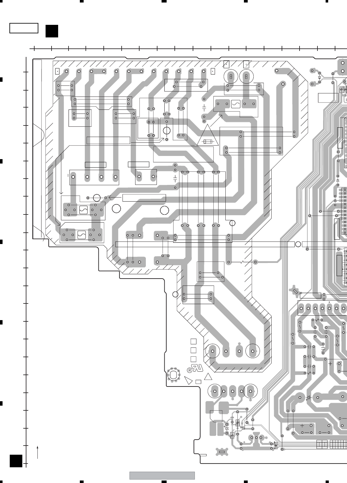
XV-EV1000
64
1234
1234
C
D
F
A
B
E
Q82
R88
D90
R89
D89
D
8
R87
R81
R91
C85
R83
R90
R85
D80
PNE-1B1
TX WINDING CHECK
FU3
SECONDARY
PRIMARY
ALL
GEN
EXCEPT
ALL
REPLACE FUSE AS MARKED.
C
CN
3
XWZ4016
POWER
ASSY
XWZ4018
XWZ4020
VL+
XPROT
VD+5
GNDREG
AC1
TX WINDING CHECK
RISK OF FIRE
ALL
GEN
GEN
YPW
MY,NV
SUBAC
GNDU
UN+56
VH+
VH+
ALL
FU2
N
abcdef h
GEN
FU1
gi
L
lkj
ALL
EXCEPT
KUC
1
012345
6
0123
0
01
LF
12
17
14
41
23
SIDE B POWER ASSY
J
J(XNP3097-B)
10
0
20
30
40
50
60
70
80
90
100
110
120
130
140
150
160
170
180
190
200
210
220
Y
160170180190200210220230240250260270280290300310320330
CN2 CN1
CN4
CN3013
CN3012
CN3011
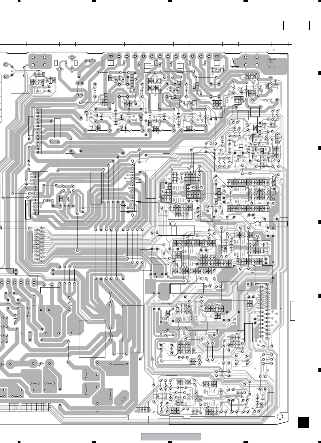
XV-EV1000 65
5678
5678
C
D
F
A
B
E
D3052 D3053
C3115
R3140
R3141
C3131
C3132
C3116
C3128
R3143
C3168
R3182
IC3058
C3170
R3184
C3159
C3160
C3146
IC3056
R3154
R3152
C3142
C3148
R3160
R3158
R3156
C3144
C3147
R3159
R3157
R3155
C3145
C3141
R3153
R3151
C3138
R3147
R3145
C3137
R3146
R3144
IC3055
C3135
R3149
R3150
C3171 C3172
R3205
R3207
C3176
C3177
C3178
C3179
C3180
C3181
C3186
C3187
C3182
C3183
C3184
C3185
R3702 R3701
IC3062
R3109
R3105
R3103
C3143
R3107
R3106
R3108
R3110
R3104
C3154
R3112
R3170
R3116
R3114
C3194
C3156
R3168
R3166
R3122
R3117
IC3057
R3176 R3175
R3174
R3172
R3173
R3171
R3115
R3113
C3193
R3169
R3167
R3111
C3155
C3153
R3165
R3137
R3139
R3186
R3187 R3185
R3180
R3138
C3195
R3181
C3165
R3183
R3130
C3163
R3934
R3928
C3910
R3938
R3922
R3924
C3914
R3926
C3916
R3930
R3936
R3921
R3923
C3913
R3925
C3915
R3929
C3909
R3933
R3927
R3937
R3935
R3357
R3943
R3916
R3944
Q3909
IC3901
C3335
R3335 R3334
C3334
C3336
R3302
R3303
C3337
R3098
R3096
R3340C3338
C3339
R3341
R3703
R3704
R3355
R3135
R3136
R3123
R3124
R3179
C3121
C3122
C3123
C3124
C3125
C3126
R3101
R3102
R3906 R3918
R3917
R3905
C3901
C3902
R3910
R3346
C3363
R3612
R3347
R3356
R3393
R3394
R3363
D3901
D3702
R3352
R3353
Q3633
R3345
C3318
C3314
R3317
R3602
C3369
R3601
R3344
C3312
R3313
R3339
R3241
C3255
C3235
C3236
C3256
R3242
R3255
C3267
C3223
C3224
R3256
C3268
C3279
R3265
C3283
D3643
Q3635
R3354
C3368
R3311
R3621
R3622
R3375
D3635
R3642
Q3639
R3615
R3616
R3626
R3625
R3606
R3605
D3644
R3643
R3651
C3673
R3613
D3611
Q3611
C3676
D3613
R3614
Q3612
C3677
D3612
D3623
R3624
C3675
Q3622
D3622
C3672
C3668
R3669
C3562
R3562
C3564
C3461
R3463
C3463
C3464
R3464
C3462
C3670
R3565
R3566
R3368
R3366
R3365
R3367
R3667
R3467
R3468
Q3638
Q3637
Q3632
R3639
Q3645
Q3636
Q3602
Q3601
Q3621
Q3644
Q3642
Q3631
C3627
R3647
D3636
R3665
R3465
R3466
C3665
C3466
C3465
C3667
C3467
C3468
C3669
C3469
C3470
D3621
R3623
C3563
R3563
C3561
D3642
C3569
C3370
D3601 R3603
C3364
R3364
C3362
D3637
R3645
D3603
D3641
R3646
C3565
C3567
C3365C3367
C3366
R3611
R3604
D3602
R3641
R3644
D90
Q3640
D87
D3701
R87
R81
R91
C3361
R83
C3953
C3952
C3340
C3341
R3342
R3343
C3342
C3343
R3349
C3169
R3312
R3348
R3316
R3314
R3318
Q3901
Q3902
R3320
R3321
R90
Q83
R3351
R85
R3638
10
VA+12TX
XPROT
RY-F
MUTEC
MUTE
FLIN
GNDA
FRIN
GNDA
CIN
GNDA
SWIN
GNDA
SLIN
GNDA
SRIN
GNDA
Q3633
RN1901
VH-
FROUT
VH-
GNDP
GNDP
FLOUT
GNDS
SWOUT
VH+
VH+
COUT
HP-L(2CH)
HP-R(2CH)
SL
SR
SW
2CH
C
2CH
VL+
LITTELFUSE INC.
INDIQUE.DE CHEZ
LINKS COMME
REMPLACER LE IC
ATTENTION
LITTELFUSE INC.
MARKED.MFD BY
REPLACE IC LINKS AS
CAUTION
VL+
SROUT
CN3013
CN3011
CN3051
CN3012
VL-
SLOUT
VL-
GNDF
UN+8V
UN+8V
GNDREG
VD+5
VA-12
E
B
RY-R
GNDA
HPDET
HP-R
GNDHP
HP-L
CN3008
GNDRET
GNDRET
GNDRET
GNDRET
GNDP
VL-
VL-
GNDP
GNDP
VL+
VL+
VL+
VH+
VH+
VH+
VH+
VH-
VH-
VH-
GNDTX
GNDD
GNDD
GNDD
UN8V
GNDMTC
GNDMDV
GNDMTC
GNDMDV
GNDB
GNDB
GNDB
GNDB
VA+12
VA+12
VA+12TX
XPROT
VD+5
GNDREG
GNDREG
VA+12
VA-12
VA+7
VA-7
GNDHP
VA+12
VA-12
UMB1N
Q3632
C
SL
GNDA
SR
GNDA
SW
GNDA
FL
GNDA
FR
GNDA
XPROT
SUBAC
HPDET
XHPMUTE
C
22k
EDATA
ECLK
S-POW
EBC
IC3101
HPAC1
MUTE
RY-F
GNDU
VE+56
NC
MUTEC
RY-R
VA+12
E
VH-
GNDA
GNDA
GNDA
GNDA
GNDA
FL
FR
EDATA
ECLK
HP-L(6CH)
HP-R(6CH)
C
SL
SR
GNDTX
VA-12
VPR+8
VPR+8
GNDD
GNDD
VPR+8M
VPR+8M
GNDMTC
GNDMDV
VP+12
VA+5
VD+5
491007
VP+12
VFL+5
VPR+8
VPR+8
CB
E
XPROT
VA-12
HPAC
4.7k
B C
491007
IC41
14
5
8
8
14
5
14
5
8
8
5
4
1
5
14
1
0123456789
0123
0
01
C
B
A
7
NP
27
1
NP
NP
1
15
17
1
SIDE B
J
10
0
2030405060708090100110120130140150160170
X
C
N4
CN3013
CN3051
CN3008
J3002
CN3012
CN3011
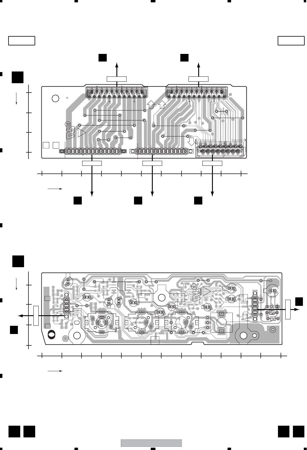
XV-EV1000
66
1234
1234
C
D
F
A
B
E
4.7 HP/MIC and TRADE ASSYS
W478
C5410
W479 W475
JA5401
JA5402
W482
C5401
W483
CN3031
W457
W458
CN3021
W461
W459
W456
W452
C5413
C5421
C5416
C5420
W455
W451
W454
W460
W453
W450
CN3022
J3032
J3033
W477
W480
C5432
VR5401
R5401
C5422
C5409
C5426
R5411
D5401
W476
JA5403
J5401
J3902
L5401
W481
C5431
TRADE
PNE-1B1
CN3032
3. SCTL2
2. SCTL1
1. XPROT
VL-
9. GNDS
8. SLOUT
7. SLOUT
6. GNDP
5. GNDP
4. SROUT
3. SROUT
2. VH-
1. VH-
6ch
2ch
SROUT
VL+
VL+
COUT
VH+
VH+
SWOUT
GNDS
CONTACT
SIDE
CN3031
CN3032
FLOUT
GNDP
GNDP
FROUT
VH-
VH-
23. FLOUT
22. FLOUT
21. VL-
20. VL-
19. FROUT
18. FROUT
17. VL+
ASSY
XWZ4022
XWZ4027
16. VL+
15. SWOUT
14. SWOUT
13. VH+
12. VH+
11. COUT
10. COUT
VPR+8
VPR+8
VFL+5
VP+12
VA-12
VD+5
GNDREG
UN+8V
UN+8V
ASSY
XWZ4026
XWZ4014
HP/MIC
GNDF
SLOUT
VL-
17. GNDA
16. SRIN
15. GNDA
14. SLIN
13. GNDA
12. SWIN
11. GNDA
10. CIN
9. GNDA
8. FRIN
7. GNDA
6. FLIN
5. MUTE
4. MUTEC
23. SRIN
22. SLIN
21. CIN
20. SWIN
19. FRIN
18. GNDA
17. FLIN
16. VPR+8
15. VPR+8
14. MUTE
13. MUTEC
12. SCTL2
11. VFL+5
10. VP+12
9. VA-12
8. VD+5
7. XPROT
6. GNDREG
5. GNDREG
4. UN+8V
3. UN+8V
2. GNDF
1. SCTL1
PNE-1B1
J5410
1
17
23 1 1
23
113
1
15
14
(XNP3097-B)
(XNP3097-B)
SIDE A SIDE A
TRADE ASSY
K
K
HP/MIC ASSY
H
H H K
CN5105
C
J5401
CN3008
J
J3902
CN3013
J
J3033
CN3012
J
J3032
CN3011
J
CN3031
CN3002
I
CN3021
CN3001
I
CN3022
260270280290
X
10
0
20
30
40
50
60
70
80
90
100
110
120
Y
X
10
0
20
30
40
50
60
70
80
90
100
Y
300310320330
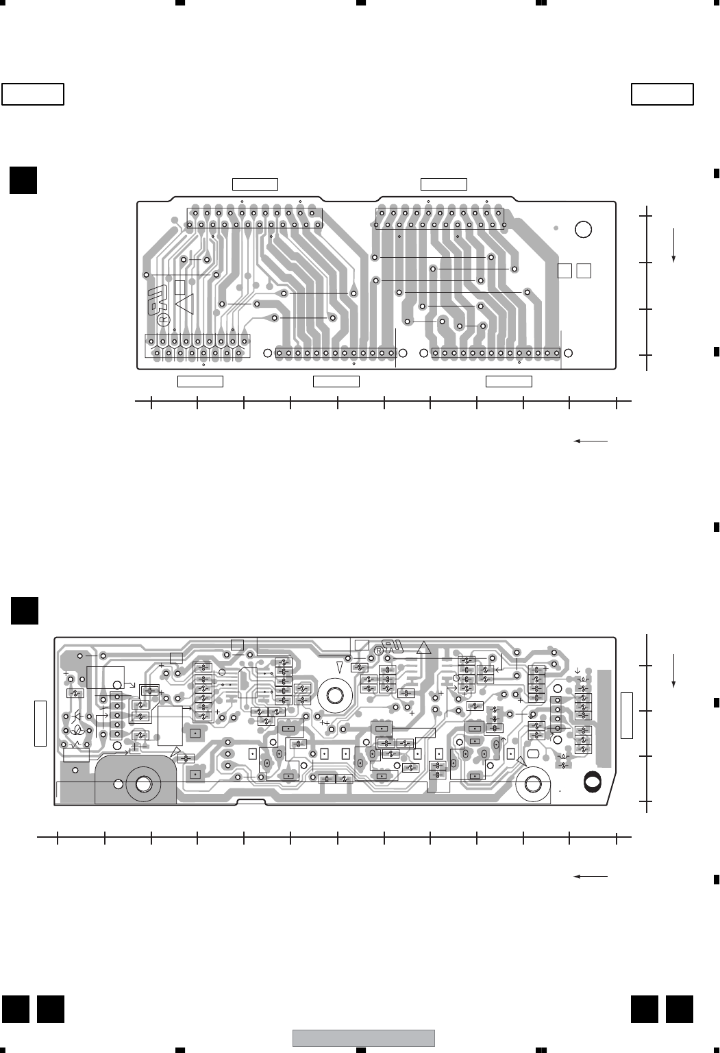
XV-EV1000 67
5678
5678
C
D
F
A
B
E
R5403
Q5401
R5405
R5406
C5408 R5404
C5407
R5407
R5410
C5412
C5402
R5413
R5402
IC5401
R5429
C5430
C5429
R5420
R5417
C5419
C5423
R5430
C5425
R5422C5427
C5428
C5414
R5414
R5415
C5415
C5434
C5436
C3905
R5418
R5416
R5419
IC5402
R5421
C5424
C5404
C5403
C5411
R5425
R5423
R5412
R5409
R5408
C5405
R5427
R5426
C3921
R3907
R3913
C3903
R3903
L3901
R3915 R3908
C3904
R3914
C3919
L3903
R3909
R3904
L3902
C3920
C5406
PNE-1B1
PNE-1B1
HPDET
HP-R
GNDHP
HP-L
1.EC VOL
VA+12V
3.MIC
4.GNDA
5.MICSW
XWZ4027
XWZ4022
2
3
1
HP/MIC ASSY XWZ4014
XWZ4026
TRADE ASSY
LF
LF
171
231
16
1
9
8
123
10 113 10 114
14
58
15
41
SIDE B SIDE B
KH H K
10
0
20
30
40
50
60
70
80
90
100
110
120
Y
260270280290300310320330
X X
10
0
20
30
40
50
60
70
80
90
100
Y
(XNP3097-B)
(XNP3097-B)
TRADE ASSY
K
HP/MIC ASSY
H
J5401
J3902
J3033J3032CN3031
CN3021 CN3022
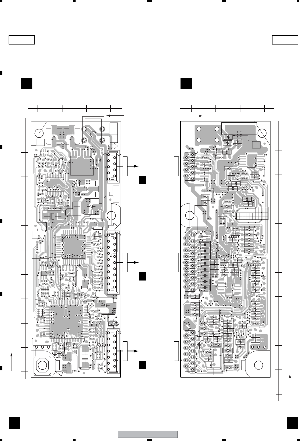
XV-EV1000
68
1234
1234
C
D
F
A
B
E
4.8 DSP ASSY
C615
R604
R617
C617
C616
L603
C609
C606
C607
X601
C611
C614
C608
R616
IC701
C715
C704
C705
C703
C701
C702
C717
C716
C718
C720
R713
C613
C612
R609
CN701 R907
R908
R703
C907
C906 C908
R712
D701
C719
R911
R711
R710
R709
R708
R707
R706
R705
KN903
901
R610
CN901
IC901
C902 C903
IC601
R818
IC802
C816
C819
X801
C820
R810
C817
R821
R822
C808
C810 C807
C809
C815
C814
C806
C805
C821
C822
R823
C823
C824
R824
C825
R825
C804
C803
R802
C826
C827
R829
C802 R801
C801
IC801
C872
C871
R836
C832
C830
R834
R833
R832
C828
IC871
C833
C831
C829
R855
R857
R835
R852
R851
L871
L851
C835
L803
R841
C834
R951
L951
R963
R962
R964
C610
R837
R965
R958
R960
R830
R611 C603
CN951
44
34
33
23
22
12
111
1199
1
1
24 13
121
4
5
1
8
8061
6041
4021
201
4
5
1
8
ICTFC
1
13
1
LF
A
20
1
13
B
B
A
5
3
2
4
KN
19 1 91
4
58
1
14 8
71
13 1
7
8
5
6
0
1
2
3
4
5
6
7
8
9 9
8
7
6
5
4
3
2
1
0
LF
AWX8
1
DSP ASS'Y
9
PRODUCTION CODE
E
R814
R605
R607
R606
L602
R612
C602
L702
R704
L701
C723
C722
C721
R714
R715
R716
R702
R701
L902
L901
R906
R903
R901
C904
C706
C912
C911
C905
C909
C910
C714
C713
C712
C711
C710
C709
C708
C707
D702
R602
R601
C601
R608
R904
R912
R910
R905
C913
C914
C916
C915
D902
R909
R815
D901
C901
R902
R820
R816
R811
C812
C811
R817
C813
R819
R813
L801
L802
R808
R809
R803
R804
R805
R806
R807
R826
R827
R828
R873
R872
R871
R874
R854
R856
R875
R876
R853
IC851
C852
C851
R842
L804
R953
R954
R955
IC951
C951
C952
L952
R956
R812
R957
R959
R603
Q801
10 20 30 40 50 60 70 80 90 100 110
X
30
40
50
60
Y
30
40
50
60
Y
10
0
20 30 40 50 60 70 80 90 100 110
X
(ANP7526-A)
SIDE A SIDE B
DSP ASSY
DDSP ASSY
D
D D
CN5507
C
CN951
CN5506
C
CN701
CN5505
C
CN901
CN951CN701CN901
XV-EV1000 69
5678
5678
C
D
F
A
B
E
5. PCB PARTS LIST
77
77 CONTRAST OF PCB ASSEMBLIES
XWZ4006 and XWZ4003 are constructed the same except for the following:
XWZ4010 and XWZ4012 are constructed the same except for the following:
Although XWZ4018 and XWZ4016 are different in part number, they consist of the same components.
This assembly has no service parts.
Parts marked by "NSP" are generally unavailable because they are not in our Master Spare Parts List.
The mark found on some component parts indicates the importance of the safety factor of the part.
Therefore, when replacing, be sure to use parts of identical designation.
When ordering resistors, first convert resistance values into code form as shown in the following examples.
Ex.1 When there are 2 effective digits (any digit apart from 0), such as 560 ohm and 47k ohm (tolerance is shown by J=5%,
and K=10%).
Ex.2 When there are 3 effective digits (such as in high precision metal film resistors).
561
473
R50
1R0
5621
NOTES:
560 Ω
47k Ω
0.5 Ω
1 Ω
RD1/4PU J
RD1/4PU J
RN2H K
RS1P K
56 x 10
1
47 x 10
3
R50
1R0
561
473
5.62k Ω
RN1/4PC F562 x 10
1
5621
Mark No. Description Part No.
LIST OF ASSEMBLIES
NSP 1..DVD ASSY XXA3037
2..DVDM ASSY AWM7964
NSP 2..05 LOADER ASSY VWT1219
3..LOAB ASSY VWG2346
NSP 1..MEDIA ASSY (XV-EV1000) XWM3294
NSP 1..MEDIA ASSY (XV-EV700) XWM3297
2..IFAF ASSY (XV-EV1000) XWZ4003
2..IFAF ASSY (XV-EV700) XWZ4006
2..DISPLAY ASSY (XV-EV1000) XWZ4012
2..DISPLAY ASSY (XV-EV700) XWZ4010
2..KEY ASSY XWZ4013
2..LED ASSY XWZ4023
NSP 1..COMPLEX ASSY (XV-EV1000) XWK3193
NSP 1..COMPLEX ASSY (XV-EV700) XWK3195
2..HP/MIC ASSY XWZ4014
2..POWER ASSY (XV-EV1000) XWZ4016
2..POWER ASSY (XV-EV700) XWZ4018
2..TRADE ASSY XWZ4022
1..DSP ASSY AWX8588
NSP 1..AMP UNIT 6CH XXQ3005
2..AMP ASSY XWK3202
1..FM/AM TUNER UNIT AXX7173
Mark No. Description Part No.
CIFAF ASSY
Mark Symbol and Description XWZ4003 XWZ4006
R5531 Not used RS1/16S473J
R5532 RS1/16S473J Not used
GDISPLAY ASSY
Mark Symbol and Description XWZ4012 XWZ4010
Q5201 2SC3052 Not used
D5202, D5301 UDZS6R8 Not used
D5203, D5302 NSPW500BS-2146 Not used
R5210 RD1/4PU121J Not used
R5211 RS1/16S270J Not used
PCB SPACER XEB3039 Not used
LED HOLDER XMR3053 Not used
JPOWER ASSY
• FM/AM TUNER UNIT

XV-EV1000
70
1234
1234
C
D
F
A
B
E
77
77 PCB PARTS LIST FOR XV-EV1000/DLXJ/NC UNLESS OTHER WISE NOTED
Mark No. Description Part No.
ALOAB ASSY
MISCELLANEOUS
S101 VSK1011
CN602 CONNECTOR S2B-PH-K
CN601 CONNECTOR S5B-PH-K
BDVDM ASSY
MISCELLANEOUS
IC 101 (A,62 ,106 ) 6CH DRIVER IC BD7995EFS
IC 201 (A,50 ,44 ) DVD IC MT1389FE/C2-L
IC 202 (B,34 ,25 ) IC K4S641632H-TC75
IC 203 (B,34 ,54 ) FLASH ROM AYW7069
IC 204 (A,19 ,44 ) EEPROM S-24CS04AFJ
IC 401 (B,92 ,22 ) DVD VIDEO AMP IC MM1623BF
>IC 711 (A,33 ,74 ) REGULATOR (1.8V) MM1661JH
>IC 731 (A,29 ,92 ) DC/DC CONTROLLER IC R1224N102H
>IC 751 (A,32 ,113 ) REGULATOR IC (5.0V) MM1565AF
>IC 761 (A,41 ,119 ) REGURATOR (ADJ.) BA3948FP
Q304 (A,77 ,127 ) TRANSISTOR 2SC4081
Q305 (A,84 ,125 )
NMOS FET TRANSISTOR
UM5K1N
Q307 (A,71 ,87 ) CHIP TRANSISTOR HN1A01F
Q308 (A,63 ,87 ) CHIP TRANSISTOR HN1A01F
Q481 (A,100 ,7 ) CHIP TRANSISTOR DTC114YUA
Q701 (A,24 ,134 ) TRANSISTOR 2SA1576A
Q702 (A,27 ,129 ) DIGITAL TRANSISTOR DTC124EUA
>Q732 (B,22 ,90 ) FET RSQ035P03
Q801 (A,50 ,87 ) DIGITAL TRANSISTOR DTC124EUA
Q821 (A,42 ,86 ) TRANSISTOR 2SA1576A
Q851 (A,42 ,89 ) TRANSISTOR 2SA1576A
Q881 (A,42 ,93 ) TRANSISTOR 2SA1576A
D731 (A,29 ,87 ) DIODE 1SS355
D732 (B,18 ,92 ) DIODE RSX201L-30
D733 (A,24 ,94 ) DIODE 1SS355
D801 (A,50 ,85 ) DIODE UDZS4R7(B)
D821 (A,46 ,86 ) DIODE 1SS355
D851 (A,46 ,89 ) DIODE 1SS355
D852 (A,42 ,82 ) DIODE 1SS355
D861 (A,46 ,82 ) DIODE 1SS355
D862 (A,46 ,83 ) DIODE 1SS355
D881 (A,46 ,93 ) DIODE 1SS355
L731 (A,23 ,109 )
POWER INDUCTOR(22U)
DTL1099
L732 (A,22 ,84 ) POWER INDUCTOR ATH7011
L751 (A,34 ,99 ) CHIP BEADS VTL1095
L901 (B,44 ,129 ) CHIP BEADS VTL1075
X201 (A,77 ,45 ) CRYSTAL RESONATOR VSS1172
X201 (A,77 ,45 ) CRYSTAL RESONATOR VSS1172
(27MHz)
CN102 (A,69 ,142 ) 12P CONNECTOR AKN7031
CN103 (A,103 ,139 ) 04P CONNECTOR RKN1045
CN104 (A,79 ,9 ) CONNECTOR AKM1291
CN901 (A,42 ,142 ) 25P CONNECTOR VKN1317
CN902 (A,116 ,28 ) 27P CONNECTOR VKN1319
RESISTORS
R131 (A,61 ,95 ) RS1/10S4R7J
R132 (A,63 ,95 ) RS1/10S4R7J
R133 (A,66 ,95 ) RS1/10S4R7J
R134 (A,65 ,95 ) RS1/10S4R7J
R135 (A,68 ,95 ) RS1/10S4R7J
R136 (A,70 ,95 ) RS1/10S4R7J
R151 (A,59 ,117 ) RS1/10S1R0J
R152 (A,59 ,121 ) RS1/10S1R8J
R153 (A,57 ,117 ) RS1/10S1R0J
R154 (A,57 ,121 ) RS1/10S1R8J
R200 (A,25 ,56 ) RS1/10S0R0J
R201 (A,49 ,67 ) RS1/16S152J
R202 (A,48 ,67 ) RS1/16S223J
R204 (A,47 ,67 ) RS1/16S223J
R205 (A,45 ,67 ) RS1/16S184J
R206 (A,46 ,64 ) RS1/16S224J
R207 (A,65 ,60 ) RS1/10S0R0J
R208 (B,27 ,71 ) RS1/10S0R0J
R209 (A,57 ,16 ) RS1/10S0R0J
R212 (A,40 ,70 ) RS1/16S103J
R213 (A,41 ,70 ) RS1/16S103J
R214 (A,45 ,72 ) RS1/16S0R0J
R216 (A,36 ,62 ) RS1/16S0R0J
R217 (A,31 ,61 ) RS1/10S0R0J
R218 (A,18 ,37 ) RS1/16S103J
R219 (A,18 ,35 ) RS1/16S103J
R221 (A,25 ,44 ) RS1/16S330J
R223 (A,29 ,35 ) RS1/16S330J
R224 (A,29 ,49 ) RS1/16S330J
R225 (A,40 ,23 ) CHIP RESISTOR ARRAY RAB4C330J
R226 (A,43 ,23 ) RS1/16S330J
R227 (A,44 ,23 ) RS1/16S330J
R229 (A,48 ,24 ) RS1/16S330J
R232 (A,34 ,60 ) RS1/16S0R0J
R233 (B,42 ,50 ) RS1/16S0R0J
R234 (A,26 ,42 ) RS1/16S330J
R235 (A,26 ,41 ) RS1/16S472J
R237 (A,23 ,41 ) RS1/16S330J
R238 (B,60 ,35 ) RS1/16S103J
R247 (B,58 ,37 ) RS1/16S103J
R248 (B,58 ,46 ) RS1/16S330J
R249 (B,59 ,40 ) RS1/16S103J
R251 (A,70 ,47 ) RS1/16S104J
R252 (A,68 ,45 ) RS1/16S0R0J
R253 (A,70 ,45 ) RS1/16S681J
R254 (B,65 ,48 ) RS1/16S754J
R255 (B,57 ,52 ) RS1/16S104J
R256 (A,73 ,59 ) RS1/16S153J
R257 (B,64 ,42 ) RS1/16S0R0J
R258 (A,23 ,39 ) RS1/16S330J
R259 (A,26 ,39 ) RS1/16S330J
R260 (A,24 ,37 ) RS1/16S330J
R261 (A,27 ,38 ) RS1/16S330J
R266 (B,51 ,38 ) RS1/16S330J
R279 (A,63 ,25 ) CHIP RESISTOR RS1/16S2201F
R281 (B,19 ,33 ) RS1/10S0R0J
R284 (A,34 ,61 ) RS1/16S103J
R301 (B,89 ,136 ) RS1/10S0R0J
R302 (B,86 ,136 ) RS1/10S0R0J
R303 (B,87 ,133 ) RS1/10S0R0J
R313 (A,80 ,125 ) RS1/16S104J
Mark No. Description Part No.

XV-EV1000 71
5678
5678
C
D
F
A
B
E
R314 (A,75 ,125 ) RS1/16S103J
R315 (A,80 ,128 ) RS1/16S103J
R318 (A,80 ,126 ) RS1/16S104J
R321 (A,61 ,87 ) RS1/16S4R7J
R322 (A,73 ,87 ) RS1/16S4R7J
R325 (A,68 ,87 ) RS1/16S4R7J
R326 (A,66 ,87 ) RS1/16S4R7J
R401 (A,82 ,30 ) RS1/16S103J
R402 (B,99 ,14 ) RS1/16S103J
R403 (B,99 ,13 ) RS1/16S0R0J
R404 (A,83 ,25 ) RS1/16S102J
R411 (A,69 ,23 ) RS1/16S1500F
R412 (A,70 ,23 ) RS1/16S1500F
R413 (A,67 ,23 ) RS1/16S1500F
R414 (A,71 ,23 ) RS1/16S1500F
R415 (A,73 ,23 ) RS1/16S1500F
R416 (A,74 ,23 ) RS1/16S1500F
R421 (B,102 ,15 ) RS1/16S0R0J
R422 (B,99 ,20 ) RS1/16S0R0J
R423 (B,99 ,21 ) RS1/16S0R0J
R424 (B,99 ,23 ) RS1/16S0R0J
R425 (B,99 ,25 ) RS1/16S0R0J
R426 (B,99 ,29 ) RS1/16S0R0J
R481 (A,103 ,7 ) RS1/16S102J
R500 (B,98 ,74 ) RS1/10S0R0J
R530 (B,96 ,96 ) RS1/10S0R0J
R560 (B,97 ,112 ) RS1/10S0R0J
R590 (B,90 ,52 ) RS1/10S0R0J
R701 (A,24 ,137 ) RS1/16S473J
R702 (A,27 ,134 ) RS1/16S103J
R732 (A,25 ,91 ) RS1/10S100J
R733 (A,25 ,93 ) RS1/16S220J
R734 (A,30 ,89 ) RS1/16S473J
R735 (A,29 ,84 ) RS1/16S272J
R736 (A,32 ,93 ) RS1/16S1802F
R737 (A,31 ,83 ) RS1/16S2702F
R738 (A,29 ,82 ) RS1/16S1502F
R739 (A,19 ,78 ) RS1/16S0R0J
R740 (A,29 ,85 ) RS1/16S0R0J
R750 (A,30 ,99 ) RS1/16S0R0J
R751 (A,33 ,119 ) RS1/16S0R0J
R761 (A,37 ,114 ) RS1/16S0R0J
R762 (A,45 ,114 ) RS1/16S3902F
R763 (A,44 ,112 ) RS1/16S334J
R764 (A,44 ,110 ) RS1/16S334J
R801 (A,54 ,85 ) RS1/16S471J
R821 (A,42 ,83 ) RS1/16S103J
R822 (A,39 ,86 ) RS1/16S473J
R823 (A,36 ,86 ) RS1/16S153J
R824 (A,37 ,86 ) RS1/16S103J
R851 (A,39 ,89 ) RS1/16S473J
R852 (A,36 ,89 ) RS1/16S103J
R853 (A,37 ,89 ) RS1/16S103J
R881 (A,39 ,93 ) RS1/16S473J
R882 (A,36 ,93 ) RS1/16S103J
R901 (A,39 ,128 ) RS1/16S0R0J
R902 (B,40 ,131 ) RS1/16S0R0J
R903 (A,43 ,128 ) RS1/16S332J
R904 (A,41 ,128 ) RS1/16S682J
R905 (A,44 ,128 ) RS1/16S332J
Mark No. Description Part No.
R906 (A,42 ,126 ) RS1/16S682J
R907 (A,46 ,128 ) RS1/16S471J
R908 (A,47 ,128 ) RS1/16S332J
R909 (A,46 ,125 ) RS1/16S682J
R910 (A,48 ,128 ) RS1/16S221J
R911 (A,50 ,128 ) RS1/16S221J
R912 (A,53 ,128 ) RS1/16S0R0J
R916 (B,47 ,128 ) RS1/16S223J
R917 (B,44 ,125 ) RS1/16S223J
R921 (A,106 ,7 ) RS1/16S0R0J
R922 (A,106 ,8 ) RS1/16S0R0J
R923 (A,105 ,10 ) RS1/16S0R0J
R924 (A,105 ,11 ) RS1/16S0R0J
R1001(B,107 ,6 ) RS1/10S0R0J
R1002(B,116 ,16 ) RS1/10S0R0J
R1003(B,118 ,16 ) RS1/10S0R0J
CAPACITORS
C101 (A,49 ,120 ) CEVW101M16
C102 (A,73 ,101 ) CKSRYB105K10
C103 (A,66 ,116 ) CKSRYB105K10
C104 (A,61 ,117 ) CKSRYB105K10
C121 (B,61 ,112 ) CKSRYB105K10
C131 (A,52 ,103 ) CKSRYB104K25
C140 (A,60 ,137 ) CKSRYB105K10
C144 (A,62 ,99 ) CKSRYB222K50
C145 (A,64 ,98 ) CKSRYB222K50
C146 (A,60 ,98 ) CKSRYB222K50
C151 (A,68 ,114 ) CKSRYB103K50
C152 (A,71 ,114 ) CKSRYB103K50
C153 (A,73 ,111 ) CKSRYB103K50
C161 (A,58 ,96 ) CKSRYB102K50
C201 (A,21 ,52 ) CHIP ELECT.CAPACITOR CEVW221M4
C202 (A,69 ,64 ) CHIP ELECT.CAPACITOR CEVW221M4
C203 (A,55 ,78 ) CHIP ELECT.CAPACITOR CEVW470M16
C204 (A,52 ,63 ) CKSRYB104K25
C205 (B,52 ,69 ) CKSRYB104K25
C206 (A,47 ,77 ) CHIP ELECT.CAPACITOR CEVW470M16
C207 (B,53 ,55 ) CKSRYB104K25
C208 (A,48 ,70 ) CKSRYB222K50
C209 (A,50 ,70 ) CKSRYB104K25
C210 (A,47 ,70 ) CKSRYB222K50
C211 (A,46 ,70 ) CCSRCH560J50
C212 (A,44 ,70 ) CCSRCH560J50
C213 (A,55 ,63 ) CKSRYB104K25
C214 (B,50 ,54 ) CKSRYB104K25
C215 (A,55 ,69 ) CHIP ELECT.CAPACITOR CEVW470M16
C216 (A,46 ,62 ) CKSRYB104K25
C217 (A,42 ,62 ) CKSRYB104K25
C219 (A,36 ,61 ) CKSRYB152K50
C220 (A,31 ,58 ) CKSRYB104K25
C222 (A,29 ,53 ) CKSRYB104K25
C223 (A,29 ,51 ) CKSRYB104K25
C224 (A,25 ,45 ) CKSRYB104K25
C225 (B,34 ,39 ) CKSRYB104K25
C226 (B,40 ,39 ) CKSRYB103K50
C227 (B,36 ,40 ) CCSRCH221J50
C228 (B,39 ,37 ) CKSRYB104K25
C230 (B,37 ,35 ) CKSRYB102K50
Mark No. Description Part No.

XV-EV1000
72
1234
1234
C
D
F
A
B
E
C231 (B,42 ,35 ) CKSRYB104K25
C232 (B,46 ,36 ) CKSRYB104K25
C233 (B,49 ,33 ) CKSRYB104K25
C234 (B,52 ,33 ) CKSRYB104K25
C235 (B,55 ,35 ) CKSRYB104K25
C236 (B,56 ,33 ) CKSRYB104K25
C237 (A,65 ,16 ) CHIP ELECT.CAPACITOR CEVW221M4
C239 (B,60 ,34 ) CKSRYB104K25
C240 (B,59 ,39 ) CKSRYB104K25
C241 (B,61 ,43 ) CKSRYB104K25
C243 (A,61 ,25 ) CKSRYB105K10
C244 (A,60 ,25 ) CKSRYB104K25
C245 (B,61 ,31 ) CKSRYB104K25
C246 (B,63 ,32 ) CKSRYB104K25
C250 (B,64 ,36 ) CKSRYB103K50
C251 (A,73 ,47 ) CCSRCH8R0D50
C252 (A,73 ,44 ) CCSRCH100D50
C253 (B,64 ,44 ) CKSRYB104K25
C254 (B,64 ,48 ) CCSRCH391J50
C255 (B,65 ,53 ) CKSRYB474K10
C256 (B,72 ,52 ) CEVW100M16
C257 (B,60 ,49 ) CKSRYB104K25
C258 (A,69 ,49 ) CKSRYB473K50
C259 (A,72 ,50 ) CKSRYB473K50
C260 (B,60 ,50 ) CKSRYB104K25
C265 (A,73 ,53 ) CCSRCH220J50
C266 (B,60 ,52 ) CKSRYB104K25
C267 (A,70 ,53 ) CKSRYB102K50
C268 (A,73 ,56 ) CKSRYB104K25
C269 (A,72 ,56 ) CKSRYB333K16
C271 (A,70 ,57 ) CKSRYB104K25
C272 (A,70 ,58 ) CKSRYB104K25
C273 (A,69 ,60 ) CKSRYB104K25
C281 (B,18 ,27 ) CHIP ELECT.CAPACITOR CEVW221M4
C282 (B,22 ,31 ) CKSRYB105K10
C283 (B,46 ,33 ) CKSRYB104K25
C284 (B,33 ,17 ) CKSRYB104K25
C285 (B,27 ,17 ) CKSRYB104K25
C286 (B,27 ,33 ) CKSRYB104K25
C287 (B,31 ,33 ) CKSRYB104K25
C288 (B,34 ,33 ) CKSRYB104K25
C289 (B,34 ,40 ) CKSRYB105K10
C290 (A,20 ,39 ) CKSRYB104K25
C296 (B,34 ,42 ) CKSRYB102K50
C309 (A,71 ,77 ) CHIP ELECT.CAPACITOR CEVW470M16
C310 (A,63 ,77 ) CHIP ELECT.CAPACITOR CEVW470M16
C343 (A,64 ,64 ) CKSRYB105K10
C344 (A,60 ,64 ) CKSRYB105K10
C345 (A,62 ,64 ) CKSRYB105K10
C346 (A,63 ,64 ) CKSRYB105K10
C347 (A,59 ,64 ) CKSRYB105K10
C371 (A,94 ,134 ) CKSRYB104K25
C372 (B,94 ,134 ) CKSRYB104K25
C373 (A,99 ,127 ) CEVW101M16
C401 (B,90 ,9 ) CEVW101M16
C402 (B,97 ,11 ) CKSRYB104K25
C404 (A,93 ,23 ) CEVW101M16
C405 (B,84 ,22 ) CKSRYB104K25
C406 (B,99 ,16 ) CKSRYB104K25
C411 (B,84 ,15 ) CKSRYB104K25
Mark No. Description Part No.
C412 (B,84 ,18 ) CKSRYB105K10
C413 (B,84 ,21 ) CKSRYB105K10
C414 (B,84 ,25 ) CKSRYB105K10
C415 (B,84 ,27 ) CKSRYB104K25
C416 (B,84 ,29 ) CKSRYB104K25
C701 (A,24 ,131 ) CKSQYB105K16
C711 (A,28 ,73 ) CKSRYB105K10
C712 (A,35 ,78 ) CCSRCH471J50
C713 (A,29 ,66 ) CKSQYB225K10
C732 (A,22 ,113 ) CHIP CERAMIC C. DCH1165
C733 (A,20 ,105 ) CHIP CERAMIC C. DCH1165
C734 (A,21 ,100 ) CEVW101M16
C735 (A,20 ,95 ) CHIP CERAMIC C. DCH1165
C736 (A,25 ,89 ) CKSRYB104K25
C737 (A,28 ,82 ) CCSRCH121J50
C738 (A,24 ,78 ) CHIP CERAMIC C. DCH1165
C739 (A,21 ,66 ) CEVW101M16
C751 (A,32 ,119 ) CKSRYB105K10
C752 (A,34 ,108 ) CCSRCH471J50
C753 (A,30 ,108 ) CKSQYB225K10
C761 (A,41 ,103 ) CEVW101M16
C762 (A,40 ,112 ) CKSRYB105K10
C801 (A,50 ,83 ) CKSRYB104K25
CIFAF ASSY
MISCELLANEOUS
IC 2201(B,146 ,33 ) OP-AMP IC HA17558AF
IC 2202(B,194 ,35 ) OP-AMP IC HA17558AF
IC 2203(B,136 ,17 ) OP-AMP IC HA17558AF
IC 2301(B,80 ,42 ) OP-AMP IC HA17558AF
IC 2401(B,56 ,18 ) OP-AMP IC HA17558AF
IC 5501(B,58 ,174 ) CPU PDC127A
>IC 5601(A,211 ,129 ) IC TA7805S
IC 5801(B,25 ,86 ) LOGIC IC TC4094BFN
IC 8101(B,181 ,204 ) LOGIC IC HEF4052BT
IC 8111(B,161 ,174 ) OP-AMP IC HA17558AF
IC 8201(B,132 ,209 ) DIGITAL KEYCONTROL M65847AFP
IC 8301(B,130 ,166 ) VOCAL FADER BA3838F
IC 8602(B,161 ,105 ) ANALOG SWITCH HEF4066BT
IC 8624(B,141 ,107 ) OP-AMP IC HA17558AF
IC 8702(B,78 ,101 ) OP-AMP IC HA17558AF
IC 8801(B,106 ,213 ) OP-AMP IC HA17558AF
Q2251(B,180 ,11 ) TRANSISTOR(SC-59) 2SC3052
Q2252(B,180 ,18 ) TRANSISTOR(SC-59) 2SC3052
Q2253(B,175 ,24 ) TRANSISTOR(SC-59) 2SC3052
Q2254(B,174 ,29 ) TRANSISTOR(SC-59) 2SA1235A
Q2255(B,167 ,43 ) TRANSISTOR RT1N241M
Q2261(B,209 ,42 ) TRANSISTOR 2SD2114K
Q2262(B,217 ,25 ) TRANSISTOR 2SD2114K
Q2263(B,201 ,49 ) DIGITAL TR(SC-70) RT1N431M
Q2301(A,45 ,38 ) N-FET 2SK373
Q2302(A,45 ,43 ) N-FET 2SK373
Q2303(B,58 ,35 ) TRANSISTOR DTC114TK
Q2304(B,58 ,43 ) TRANSISTOR DTC114TK
Q2351(B,103 ,54 ) DIGITAL TR(SC-70) RT1P241M
Q2352(B,118 ,54 ) TRANSISTOR RT1N241M
Q2353(B,115 ,54 ) TRANSISTOR RT1N241M
Q2451(B,96 ,9 ) TRANSISTOR 2SD2114K
Q2452(B,96 ,22 ) TRANSISTOR 2SD2114K
Mark No. Description Part No.

XV-EV1000 73
5678
5678
C
D
F
A
B
E
Q2453(B,129 ,49 ) TRANSISTOR RT1N241M
Q2460(B,129 ,44 ) DIGITAL TR(SC-70) RT1P241M
Q2801(A,28 ,51 ) TRANSISTOR 2SC1815
Q2802(A,28 ,42 ) TRANSISTOR 2SC1815
Q2805(A,58 ,49 ) TRANSISTOR 2SC1815
Q2806(A,20 ,17 ) TRANSISTOR 2SC2240
Q5402(A,105 ,164 ) P-FET 2SJ103
Q5403(B,29 ,231 ) DIGITAL TR(SC-70) RT1N431M
Q5501(B,32 ,194 ) DIGITAL TR(SC-70) RT1N431M
Q5502(B,28 ,181 ) TRANSISTOR 2SC4081
Q5503(B,24 ,192 ) TRANSISTOR 2SC4081
Q5601(B,29 ,203 ) DIGITAL TR(SC-70) RT1P241M
Q5602(B,38 ,203 ) DIGITAL TR(SC-70) RT1P241M
Q5603(B,27 ,210 ) TRANSISTOR RT1N241M
Q5607(B,122 ,72 ) DIGITAL TR(SC-70) RT1P431M
Q5701(B,203 ,82 ) TRANSISTOR 2SC4081
Q5801(B,15 ,90 ) TRANSISTOR 2SB1132
Q5802(B,27 ,102 ) DIGITAL TR(SC-70) RT1N431M
Q5803(B,31 ,95 ) DIGITAL TR(SC-70) RT1P241M
Q5804(B,16 ,83 ) TRANSISTOR 2SB1132
Q5805(B,22 ,100 ) DIGITAL TR(SC-70) RT1N431M
Q5808(B,36 ,86 ) DIGITAL TR(SC-70) RT1N431M
Q8111(B,174 ,172 ) TRANSISTOR 2SC4081
Q8112(B,172 ,177 ) TRANSISTOR 2SC4081
Q8113(B,177 ,172 ) TRANSISTOR 2SC4081
Q8114(B,179 ,177 ) TRANSISTOR 2SC4081
Q8115(B,168 ,172 ) DIGITAL TR(SC-70) RT1P241M
Q8116(B,175 ,177 ) DIGITAL TR(SC-70) RT1P241M
Q8201(A,160 ,207 ) TRANSISTOR 2SD1858X
Q8501(B,213 ,175 ) TRANSISTOR IMX9
Q8503(B,80 ,171 ) DIGITAL TR(SC-70) RT1P241M
Q8621(B,170 ,88 ) TRANSISTOR IMX9
Q8623(B,163 ,119 ) DIGITAL TR(SC-70) RT1P241M
Q8624(B,160 ,117 ) TRANSISTOR RT1N241M
Q8625(B,158 ,96 ) DIGITAL TR(SC-70) RT1P241M
Q8626(B,160 ,92 ) TRANSISTOR RT1N241M
Q8719(B,102 ,107 ) TRANSISTOR IMX9
Q8745(B,68 ,88 ) TRANSISTOR IMX9
Q8762(B,64 ,92 ) DIGITAL TR(SC-70) RT1P241M
D2201(A,169 ,32 ) DIODE MTZJ6R2(B)
D2252(B,180 ,33 ) DIODE MA111
D2253(B,195 ,12 ) DIODE MA111
D2254(B,193 ,12 ) DIODE MA111
D2255(B,184 ,29 ) DIODE MA111
D2256(A,177 ,36 ) DIODE 1SS133
D2257(B,208 ,33 ) DIODE MA111
D2258(B,205 ,30 ) DIODE MA111
D2301(A,37 ,38 ) DIODE 1SS133
D2302(A,37 ,42 ) DIODE 1SS133
D2303(A,34 ,33 ) DIODE 1SS133
D2304(A,34 ,47 ) DIODE 1SS133
D2305(A,50 ,34 ) DIODE 1SS133
D2306(A,50 ,46 ) DIODE 1SS133
D2307(B,61 ,43 ) DIODE MA111
D5502(B,58 ,151 ) DIODE MA111
D5601(B,25 ,203 ) DIODE DAP202K
D5602(B,33 ,202 ) DIODE DAP202K
D5701(B,198 ,79 ) DIODE MA111
D5702(B,198 ,84 ) DIODE MA111
D5705(B,201 ,87 ) DIODE UDZS10(B)
Mark No. Description Part No.
D5801(B,32 ,103 ) DIODE MA111
D5952(B,23 ,110 ) DIODE MA111
D5954(B,109 ,155 ) DIODE MA111
D5955(A,101 ,155 ) DIODE MTZJ5R6(B)
D8201(A,152 ,197 ) DIODE MTZJ5R6(B)
D8501(B,83 ,171 ) DIODE MA111
D8601(B,171 ,117 ) DIODE UDZS6R8(B)
D8602(B,152 ,99 ) DIODE UDZS6R8(B)
D8701(B,139 ,87 ) DIODE MA111
D8702(B,143 ,87 ) DIODE MA111
D8901(A,195 ,233 ) DIODE MTZJ5R6(B)
D8902(A,194 ,226 ) DIODE MTZJ5R6(B)
L2401(A,36 ,13 ) COIL RTF1004
L2402(A,36 ,22 ) COIL RTF1004
L2403(A,73 ,9 ) COIL(4.7MH) RTF1021
L2404(A,74 ,28 ) COIL(4.7MH) RTF1021
L2801(A,20 ,33 ) COIL RTD1082
L2802(A,28 ,57 ) RADIAL INDUCTOR LRCA121J
L5501(A,32 ,184 ) AXIAL INDUCTOR LAU220J
L5502(B,102 ,239 ) CHIP BEADS VTL1075
L5601(A,221 ,126 ) RADIAL INDUCTOR VTL1118
L8861(B,220 ,210 ) CHIP BEADS VTL1089
L8871(B,220 ,199 ) CHIP BEADS VTL1089
JA 8850(A,236 ,198 ) JACK VKB1168
KN5501(A,231 ,53 ) SCREW PLATE VNE1948
VR2301(A,109 ,34 ) VR PCP1028
VR2302(A,109 ,45 ) VR PCP1028
VR2401(A,104 ,10 ) VR PCP1028
VR2402(A,104 ,20 ) VR PCP1028
VR2801(A,29 ,18 ) VR PCP1032
VR2802(A,29 ,28 ) VR PCP1032
X5501(A,69 ,193 ) CERAMIC RESONATOR ASS7034
(10MHz)
CN2301(A,42 ,43 ) CONNECTOR B4B-PH
CN2302(A,29 ,7 ) CONNECTOR POST B2B-PH
CN2507(A,208 ,9 ) CONNECTOR B3P-SHF-1AA
CN5102(A,71 ,237 ) 25P CONNECTOR VKN1256
CN5105(A,9 ,210 )
5P JUMPER CONNECTOR
52147-0510
CN5501(A,17 ,134 ) CONNECTOR 52045-1345
CN5503(A,17 ,104 ) CONNECTOR 52045-1145
CN5505(A,220 ,140 ) 9P PLUG XKP3064
CN5506(A,187 ,140 ) 19P PLUG XKP3069
CN5507(A,147 ,140 ) 13P PLUG XKP3066
CN5701(A,183 ,75 ) CONNECTOR 52045-1145
CN8301(A,136 ,236 ) 27P CONNECTOR VKN1258
CN8302(A,165 ,74 )
15PJUMPER CONNECTOR
52147-1510
CN8303(A,117 ,75 ) 27P CONNECTOR 52045-2745
CN8401(A,236 ,168 ) PIN JACK(4P) AKB7015
CN8830(A,236 ,221 ) SOCKET AKP7179
2PCB BINDER VEF1040
3PCB BINDER VEF1040
RESISTORS
R2205(B,186 ,9 ) RS1/16S153J
R2206(B,186 ,23 ) RS1/16S153J
R2207(B,186 ,13 ) RS1/16S272J
R2208(B,186 ,18 ) RS1/16S272J
R2209(B,141 ,27 ) RS1/16S563J
R2210(B,136 ,30 ) RS1/16S222J
R2212(B,145 ,41 ) RS1/16S563J
Mark No. Description Part No.

XV-EV1000
74
1234
1234
C
D
F
A
B
E
R2213(B,136 ,36 ) RS1/16S222J
R2214(B,136 ,9 ) RS1/16S563J
R2215(B,138 ,9 ) RS1/16S222J
R2216(B,135 ,24 ) RS1/16S563J
R2217(B,127 ,18 ) RS1/16S222J
R2222(B,117 ,30 ) RS1/16S104J
R2223(B,119 ,36 ) RS1/16S104J
R2241(B,207 ,26 ) RS1/16S103J
R2242(B,205 ,26 ) RS1/16S103J
R2243(B,190 ,34 ) RS1/16S104J
R2251(B,183 ,9 ) RS1/16S222J
R2252(B,183 ,22 ) RS1/16S222J
R2253(B,178 ,9 ) RS1/16S102J
R2254(B,177 ,18 ) RS1/16S102J
R2255(B,178 ,30 ) RS1/16S102J
R2256(B,180 ,27 ) RS1/16S105J
R2257(B,186 ,29 ) RS1/16S101J
R2259(B,195 ,7 ) RS1/16S103J
R2260(B,193 ,8 ) RS1/16S103J
R2261(B,209 ,25 ) RS1/16S392J
R2262(B,217 ,19 ) RS1/16S392J
R2263(B,212 ,25 ) RS1/16S153J
R2264(B,216 ,30 ) RS1/16S153J
R2265(B,188 ,25 ) RS1/16S103J
R2266(B,196 ,28 ) RS1/16S123J
R2267(B,200 ,40 ) RS1/16S101J
R2268(B,187 ,34 ) RS1/16S101J
R2269(B,191 ,44 ) RS1/16S393J
R2270(B,183 ,43 ) RS1/16S102J
R2271(B,200 ,28 ) RS1/16S104J
R2272(B,179 ,39 ) RS1/16S154J
R2273(B,184 ,39 ) RS1/16S103J
R2276(B,172 ,34 ) RS1/16S472J
R2277(B,174 ,34 ) RS1/16S223J
R2281(B,213 ,45 ) RS1/16S222J
R2282(B,217 ,21 ) RS1/16S222J
R2283(B,198 ,49 ) RS1/16S472J
R2291(B,169 ,28 ) RS1/16S681J
R2301(B,41 ,33 ) RS1/16S105J
R2302(B,51 ,49 ) RS1/16S105J
R2303(B,62 ,38 ) RS1/16S334J
R2304(B,64 ,41 ) RS1/16S334J
R2305(B,82 ,32 ) RS1/16S474J
R2306(B,79 ,53 ) RS1/16S474J
R2307(B,84 ,32 ) RS1/16S223J
R2308(B,83 ,52 ) RS1/16S223J
R2311(B,87 ,40 ) RS1/16S241J
R2312(B,79 ,49 ) RS1/16S241J
R2319(B,105 ,33 ) RS1/16S471J
R2320(B,105 ,43 ) RS1/16S471J
R2351(B,122 ,48 ) RS1/16S473J
R2352(B,100 ,51 ) RS1/16S223J
R2399(B,58 ,39 ) RS1/16S0R0J
R2401(B,106 ,10 ) RS1/16S223J
R2402(B,108 ,20 ) RS1/16S223J
R2403(B,100 ,9 ) RS1/16S0R0J
R2404(B,100 ,27 ) RS1/16S0R0J
R2409(B,65 ,14 ) RS1/16S104J
R2410(B,64 ,18 ) RS1/16S104J
R2411(B,58 ,11 ) RS1/16S823J
Mark No. Description Part No.
R2412(B,58 ,26 ) RS1/16S823J
R2413(B,56 ,7 ) RS1/16S473J
R2414(B,56 ,29 ) RS1/16S473J
R2415(B,71 ,13 ) RS1/16S560J
R2416(B,71 ,24 ) RS1/16S560J
R2417(B,69 ,13 ) RS1/16S122J
R2418(B,69 ,24 ) RS1/16S122J
R2423(B,39 ,9 ) RS1/16S113J
R2424(B,39 ,27 ) RS1/16S113J
R2425(B,42 ,10 ) RS1/16S102J
R2426(B,42 ,26 ) RS1/16S102J
R2431(B,54 ,10 ) RS1/16S333J
R2432(B,54 ,26 ) RS1/16S333J
R2451(B,92 ,15 ) RS1/16S103J
R2452(B,92 ,18 ) RS1/16S103J
R2453(B,125 ,44 ) RS1/16S473J
R2801(B,20 ,49 ) RS1/16S103J
R2802(B,20 ,40 ) RS1/16S103J
R2803(A,34 ,53 ) CARBON FILM RESISTOR RD1/2VM4R7J
R2805(A,41 ,53 ) CARBON FILM RESISTOR RD1/2VM161J
R2809(B,67 ,57 ) RS1/16S102J
R2810(B,64 ,49 ) RS1/16S473J
R2811(B,62 ,57 ) RS1/16S102J
R2813(B,31 ,19 ) RS1/16S622J
R2814(B,31 ,28 ) RS1/16S622J
R2815(B,18 ,12 ) RS1/16S102J
R2816(B,21 ,14 ) RS1/16S472J
R2898(B,14 ,40 ) RS1/16S0R0J
R2899(B,35 ,18 ) RS1/16S0R0J
R5403(B,56 ,211 ) RS1/16S103J
R5404(B,56 ,207 ) RS1/16S221J
R5431(B,101 ,160 ) RS1/16S105J
R5432(B,109 ,161 ) RS1/16S105J
R5434(B,111 ,161 ) RS1/16S223J
R5501(B,41 ,189 ) RS1/16S222J
R5502(B,59 ,199 ) RS1/16S471J
R5503(B,39 ,189 ) RS1/16S473J
R5504(B,28 ,186 ) RS1/16S101J
R5505(B,24 ,188 ) RS1/16S103J
R5506(B,56 ,199 ) RS1/16S221J
R5508(B,29 ,198 ) RS1/16S103J
R5511(B,62 ,194 ) RS1/16S221J
R5512(B,63 ,199 ) RS1/16S221J
R5515(B,40 ,175 ) RS1/16S123J
R5516(B,77 ,188 ) RS1/16S221J
R5517(B,79 ,194 ) RS1/16S221J
R5518(B,79 ,188 ) RS1/16S221J
R5519(B,81 ,189 ) RS1/16S221J
R5520(B,85 ,171 ) RS1/16S221J
R5521(B,78 ,181 ) RS1/16S221J
R5522(B,80 ,180 ) RS1/16S221J
R5523(B,82 ,178 ) RS1/16S221J
R5525(B,83 ,189 ) RS1/16S221J
R5526(B,81 ,196 ) RS1/16S221J
R5528(B,87 ,187 ) RS1/16S221J
R5529(B,76 ,171 ) RS1/16S221J
R5530(B,78 ,171 ) RS1/16S221J
R5532(B,67 ,207 ) RS1/16S473J
R5535(B,79 ,156 ) RS1/16S221J
R5536(B,46 ,201 ) RS1/16S221J
Mark No. Description Part No.

XV-EV1000 75
5678
5678
C
D
F
A
B
E
R5537(B,75 ,156 ) RS1/16S221J
R5538(B,72 ,156 ) RS1/16S221J
R5539(B,34 ,170 ) RS1/16S221J
R5540(B,32 ,171 ) RS1/16S221J
R5541(B,37 ,177 ) RS1/16S472J
R5542(B,35 ,177 ) RS1/16S221J
R5543(B,50 ,198 ) RS1/16S221J
R5544(B,29 ,176 ) RS1/16S221J
R5545(B,67 ,146 ) RS1/16S221J
R5546(B,51 ,151 ) RS1/16S221J
R5547(B,41 ,151 ) RS1/16S221J
R5548(B,47 ,157 ) RS1/16S221J
R5549(B,44 ,151 ) RS1/16S221J
R5550(B,45 ,156 ) RS1/16S221J
R5553(B,39 ,156 ) RS1/16S221J
R5554(B,39 ,150 ) RS1/16S221J
R5555(B,37 ,155 ) RS1/16S221J
R5556(B,33 ,77 ) RS1/16S221J
R5557(B,34 ,151 ) RS1/16S221J
R5558(B,33 ,156 ) RS1/16S221J
R5559(B,32 ,152 ) RS1/16S221J
R5560(B,31 ,156 ) RS1/16S221J
R5561(B,32 ,163 ) RS1/16S822J
R5562(B,34 ,165 ) RS1/16S221J
R5563(B,36 ,168 ) RS1/16S221J
R5567(B,47 ,189 ) RS1/16S221J
R5568(B,33 ,177 ) RS1/16S221J
R5569(B,31 ,177 ) RS1/16S221J
R5571(B,47 ,196 ) RS1/16S101J
R5576(B,51 ,194 ) RS1/16S471J
R5577(B,53 ,194 ) RS1/16S221J
R5578(B,55 ,199 ) RS1/16S221J
R5579(B,55 ,194 ) RS1/16S221J
R5580(B,27 ,198 ) RS1/16S102J
R5581(B,42 ,212 ) RS1/16S102J
R5582(B,66 ,193 ) RS1/16S105J
R5583(B,71 ,206 ) RS1/16S103J
R5584(B,73 ,208 ) RS1/16S103J
R5585(B,65 ,211 ) RS1/16S103J
R5586(B,65 ,207 ) RS1/16S103J
R5588(B,65 ,146 ) RS1/16S221J
R5590(B,37 ,150 ) RS1/16S221J
R5592(B,62 ,155 ) RS1/16S221J
R5593(B,66 ,189 ) RS1/16S101J
R5594(B,77 ,194 ) RS1/16S221J
R5595(B,57 ,194 ) RS1/16S221J
R5597(B,69 ,146 ) RS1/16S221J
R5598(B,71 ,146 ) RS1/16S221J
R5601(B,62 ,149 ) RS1/16S221J
R5603(B,69 ,151 ) RS1/16S103J
R5604(B,71 ,151 ) RS1/16S103J
R5605(B,52 ,199 ) RS1/16S471J
R5607(B,124 ,75 ) RS1/16S561J
R5608(B,126 ,71 ) RS1/16S473J
R5615(B,14 ,193 ) RS1/16S153J
R5622(B,29 ,207 ) RS1/16S103J
R5623(B,32 ,207 ) RS1/16S103J
R5624(B,36 ,207 ) RS1/16S103J
R5625(B,34 ,207 ) RS1/16S103J
R5626(B,38 ,207 ) RS1/16S392J
Mark No. Description Part No.
R5627(B,40 ,212 ) RS1/16S272J
R5632(B,46 ,151 ) RS1/16S221J
R5633(B,49 ,156 ) RS1/16S221J
R5634(B,49 ,151 ) RS1/16S221J
R5638(B,104 ,239 ) RS1/16S221J
R5639(B,67 ,211 ) RS1/16S104J
R5704(B,198 ,89 ) RS1/16S221J
R5705(B,201 ,82 ) RS1/16S100J
R5801(B,12 ,88 ) RS1/16S473J
R5802(A,24 ,97 ) RD1/4PU102J
R5803(B,37 ,80 ) RS1/16S102J
R5804(B,34 ,134 ) RS1/16S102J
R5805(B,24 ,101 ) RS1/16S473J
R5806(B,12 ,84 ) RS1/16S473J
R5807(A,16 ,97 ) RD1/4PU102J
R5812(B,39 ,87 ) RS1/16S472J
R5813(B,9 ,118 ) RS1/16S473J
R5814(B,11 ,118 ) RS1/16S473J
R5815(B,10 ,108 ) RS1/16S473J
R5816(B,11 ,104 ) RS1/16S473J
R5885(B,28 ,78 ) RS1/16S221J
R5886(B,25 ,77 ) RS1/16S221J
R5887(B,21 ,78 ) RS1/16S221J
R5889(B,18 ,87 ) RS1/16S221J
R5961(B,73 ,146 ) RS1/16S473J
R5963(B,102 ,152 ) RS1/16S184J
R5964(B,104 ,152 ) RS1/16S392J
R5965(B,116 ,151 ) RS1/16S154J
R5966(B,112 ,155 ) RS1/16S103J
R5967(B,72 ,200 ) RS1/16S105J
R8103(B,157 ,166 ) RS1/16S473J
R8104(B,156 ,177 ) RS1/16S473J
R8105(B,159 ,166 ) RS1/16S473J
R8106(B,157 ,183 ) RS1/16S473J
R8107(B,163 ,183 ) RS1/16S220J
R8108(B,153 ,167 ) RS1/16S220J
R8111(B,172 ,166 ) RS1/16S152J
R8112(B,171 ,182 ) RS1/16S152J
R8113(B,174 ,166 ) RS1/16S152J
R8114(B,173 ,182 ) RS1/16S152J
R8115(B,168 ,166 ) RS1/16S103J
R8116(B,171 ,172 ) RS1/16S103J
R8117(B,170 ,166 ) RS1/16S104J
R8118(B,179 ,184 ) RS1/16S104J
R8119(B,181 ,182 ) RS1/16S103J
R8120(B,176 ,182 ) RS1/16S103J
R8121(B,176 ,166 ) RS1/16S681J
R8122(B,177 ,182 ) RS1/16S681J
R8124(B,163 ,166 ) RS1/16S101J
R8125(B,161 ,183 ) RS1/16S101J
R8201(B,124 ,198 ) RS1/16S103J
R8202(B,117 ,198 ) RS1/16S103J
R8203(B,119 ,193 ) RS1/16S103J
R8204(B,133 ,198 ) RS1/16S562J
R8205(B,142 ,193 ) RS1/16S103J
R8206(B,128 ,198 ) RS1/16S103J
R8207(B,132 ,193 ) RS1/16S682J
R8208(B,134 ,193 ) RS1/16S153J
R8209(B,136 ,193 ) RS1/16S472J
R8210(B,138 ,198 ) RS1/16S472J
Mark No. Description Part No.

XV-EV1000
76
1234
1234
C
D
F
A
B
E
R8211(B,142 ,198 ) RS1/16S682J
R8212(B,132 ,220 ) RS1/16S102J
R8213(B,134 ,220 ) RS1/16S102J
R8214(B,136 ,220 ) RS1/16S102J
R8215(B,160 ,197 ) RS1/16S680J
R8216(A,152 ,206 ) RD1/4PU102J
R8217(B,126 ,192 ) RS1/16S153J
R8301(B,126 ,154 ) RS1/16S102J
R8302(B,130 ,158 ) RS1/16S102J
R8303(B,128 ,156 ) RS1/16S102J
R8304(B,145 ,174 ) RS1/16S272J
R8305(B,143 ,178 ) RS1/16S821J
R8306(B,143 ,182 ) RS1/16S821J
R8307(B,145 ,182 ) RS1/16S272J
R8308(B,123 ,174 ) RS1/16S103J
R8403(B,216 ,165 ) RS1/16S331J
R8404(B,214 ,157 ) RS1/16S331J
R8511(B,216 ,181 ) RS1/16S182J
R8512(B,212 ,181 ) RS1/16S182J
R8513(B,216 ,171 ) RS1/16S472J
R8514(B,214 ,181 ) RS1/16S472J
R8515(B,216 ,177 ) RS1/16S224J
R8516(B,218 ,173 ) RS1/16S224J
R8518(B,183 ,188 ) RS1/16S473J
R8615(B,180 ,74 ) RS1/16S220J
R8617(B,174 ,94 ) RS1/16S473J
R8618(B,170 ,83 ) RS1/16S473J
R8619(B,172 ,94 ) RS1/16S821J
R8620(B,168 ,83 ) RS1/16S821J
R8621(B,164 ,82 ) RS1/16S103J
R8622(B,166 ,89 ) RS1/16S103J
R8623(B,161 ,113 ) RS1/16S103J
R8624(B,154 ,96 ) RS1/16S103J
R8625(B,159 ,113 ) RS1/16S153J
R8627(B,157 ,113 ) RS1/16S122J
R8629(B,157 ,117 ) RS1/16S822J
R8631(B,155 ,113 ) RS1/16S103J
R8632(B,161 ,97 ) RS1/16S103J
R8633(B,141 ,116 ) RS1/16S103J
R8634(B,142 ,99 ) RS1/16S103J
R8635(B,137 ,112 ) RS1/16S103J
R8636(B,138 ,99 ) RS1/16S103J
R8637(A,167 ,119 ) RD1/4PU102J
R8638(A,156 ,92 ) RD1/4PU102J
R8715(B,105 ,113 ) RS1/16S473J
R8716(B,108 ,102 ) RS1/16S473J
R8717(B,103 ,113 ) RS1/16S821J
R8718(B,106 ,101 ) RS1/16S821J
R8719(B,102 ,101 ) RS1/16S472J
R8720(B,99 ,110 ) RS1/16S472J
R8722(B,83 ,89 ) RS1/16S222J
R8724(B,81 ,89 ) RS1/16S682J
R8726(B,79 ,89 ) RS1/16S102J
R8728(B,70 ,98 ) RS1/16S473J
R8730(B,71 ,93 ) RS1/16S103J
R8732(B,80 ,109 ) RS1/16S101J
R8733(B,76 ,109 ) RS1/16S101J
R8737(B,95 ,116 ) RS1/16S220J
R8741(B,72 ,97 ) RS1/16S182J
R8745(B,74 ,102 ) RS1/16S473J
Mark No. Description Part No.
R8747(B,72 ,102 ) RS1/16S821J
R8749(B,69 ,93 ) RS1/16S103J
R8763(B,62 ,103 ) RS1/16S473J
R8801(B,108 ,205 ) RS1/16S103J
R8802(B,106 ,201 ) RS1/16S103J
R8803(B,110 ,205 ) RS1/16S103J
R8805(B,110 ,209 ) RS1/16S563J
R8821(B,216 ,187 ) CHIP RESISTOR RS1/16S75R0F
R8832(B,217 ,222 ) CHIP RESISTOR RS1/16S75R0F
R8842(B,215 ,217 ) CHIP RESISTOR RS1/16S75R0F
R8853(B,218 ,199 ) CHIP RESISTOR RS1/16S75R0F
R8863(B,223 ,215 ) CHIP RESISTOR RS1/16S75R0F
R8873(B,216 ,205 ) CHIP RESISTOR RS1/16S75R0F
R8901(A,198 ,230 ) RD1/4PU102J
R8904(A,197 ,221 ) RD1/4PU102J
R8952(B,165 ,97 ) RS1/16S822J
R8953(B,163 ,97 ) RS1/16S122J
R8954(B,167 ,97 ) RS1/16S153J
R9005(B,35 ,26 ) RS1/16S0R0J
R9008(B,113 ,45 ) RS1/16S0R0J
R9009(B,55 ,81 ) RS1/16S0R0J
R9010(B,55 ,85 ) RS1/16S0R0J
R9011(B,57 ,81 ) RS1/16S0R0J
R9012(B,59 ,85 ) RS1/16S0R0J
CAPACITORS
C2201(A,117 ,34 ) CEAT1R0M50
C2202(A,117 ,44 ) CEAT1R0M50
C2203(A,157 ,32 ) CEAT100M50
C2204(A,138 ,45 ) CEAT100M50
C2205(B,139 ,30 ) CCSRCH101J50
C2206(B,138 ,36 ) CCSRCH101J50
C2211(B,171 ,12 ) CKSRYB152K50
C2212(B,171 ,17 ) CKSRYB152K50
C2213(B,134 ,9 ) CCSRCH101J50
C2214(B,129 ,18 ) CCSRCH101J50
C2215(A,168 ,7 ) CEAT101M16
C2216(A,164 ,32 ) CEAT221M16
C2217(A,115 ,12 ) CEAT1R0M50
C2218(A,116 ,21 ) CEAT1R0M50
C2220(A,196 ,17 ) CEAT100M50
C2221(A,197 ,25 ) CEAT100M50
C2222(A,131 ,28 ) CEAT2R2M50
C2223(A,125 ,28 ) CEAT2R2M50
C2224(A,131 ,7 ) CEAT2R2M50
C2225(A,121 ,18 ) CEAT2R2M50
C2226(B,196 ,43 ) CKSRYB103K50
C2227(B,152 ,36 ) CKSRYB103K50
C2228(A,151 ,40 ) CEAT470M16
C2231(B,167 ,16 ) CKSRYB103K50
C2251(A,180 ,29 ) CEAT220M50
C2252(B,176 ,39 ) CKSRYB334K10
C2253(B,187 ,42 ) CCSRCH271J50
C2254(A,200 ,43 ) CEAT2R2M50
C2255(A,187 ,39 ) CEAT1R0M50
C2256(B,189 ,30 ) CCSRCH470J50
C2257(B,190 ,39 ) CCSRCH470J50
C2261(A,208 ,37 ) CEAT4R7M50
C2262(A,213 ,29 ) CEAT4R7M50
C2301(B,42 ,35 ) CCSRCH100D50
Mark No. Description Part No.

XV-EV1000 77
5678
5678
C
D
F
A
B
E
C2302(B,42 ,46 ) CCSRCH100D50
C2303(B,64 ,37 ) CCSRCH681J50
C2304(B,67 ,41 ) CCSRCH681J50
C2307(A,71 ,35 ) FILM CAPACITOR CQMBA682J50
C2308(A,70 ,51 ) FILM CAPACITOR CQMBA682J50
C2309(A,85 ,40 ) ELECT. CAPACITOR CEAT330M50
C2310(A,85 ,46 ) ELECT. CAPACITOR CEAT330M50
C2311(A,95 ,36 ) CEAT100M50
C2312(A,95 ,46 ) CEAT100M50
C2314(A,74 ,45 ) CEAT470M16
C2315(B,67 ,37 ) CKSRYB102K50
C2401(B,52 ,18 ) CCSRCH470J50
C2402(B,62 ,9 ) CCSRCH470J50
C2403(A,78 ,8 ) CEAT1R0M50
C2404(A,78 ,28 ) CEAT1R0M50
C2405(A,51 ,7 ) FILM CAPACITOR CQMBA683J50
C2406(A,51 ,29 ) FILM CAPACITOR CQMBA683J50
C2407(A,62 ,12 ) ELECT. CAPACITOR CEAT330M50
C2408(A,62 ,24 ) ELECT. CAPACITOR CEAT330M50
C2409(A,73 ,17 ) CQMA223J50
C2410(A,68 ,20 ) CQMA223J50
C2419(A,51 ,12 ) CEJQ1R0M50
C2420(A,51 ,23 ) CEJQ1R0M50
C2421(A,36 ,7 ) CQMA152J50
C2422(A,36 ,29 ) CQMA152J50
C2423(B,39 ,16 ) CCSRCH221J50
C2424(B,39 ,20 ) CCSRCH221J50
C2425(A,62 ,15 ) CEAT470M16
C2431(B,58 ,9 ) CKSRYB122K50
C2432(B,56 ,26 ) CKSRYB122K50
C2801(A,19 ,42 ) CQMA123J50
C2802(A,23 ,51 ) CQMA682J50
C2803(A,19 ,46 ) CQMA472J50
C2804(A,23 ,37 ) CQMA472J50
C2805(A,14 ,37 ) CEJQ330M10
C2806(A,14 ,46 ) CEJQ330M10
C2807(A,64 ,52 ) CEAT470M16
C2808(A,32 ,13 ) PPS CAPACITOR CQHA822J2A
C2809(A,15 ,22 ) CERAMIC CAPACITOR CCCSL151K2H
C2810(A,15 ,11 ) CEJQ330M10
C5433(A,113 ,165 ) ELECT. CAPACITOR CEJQR22M50
C5501(A,27 ,190 ) ACH1246
C5502(A,37 ,191 ) CEAT101M16
C5504(B,30 ,190 ) CCSRCH101J50
C5505(B,39 ,185 ) CKSRYB103K50
C5506(A,41 ,203 ) CEAT1R0M50
C5507(B,37 ,184 ) CKSRYB104K16
C5508(B,41 ,193 ) CKSRYB103K50
C5511(A,24 ,179 ) CEAT100M50
C5515(B,73 ,185 ) CKSRYB104K16
C5516(B,69 ,206 ) CKSRYB103K50
C5517(B,75 ,204 ) CKSRYB103K50
C5518(B,73 ,204 ) CKSRYB103K50
C5601(A,211 ,120 ) CEAT101M16
C5603(B,202 ,128 ) CKSRYB104K16
C5608(A,125 ,84 ) CEAT220M25
C5639(B,210 ,149 ) CKSRYB104K16
C5640(A,203 ,150 ) CEAT101M16
C5704(A,196 ,89 ) CEAL100M16
C5706(B,207 ,73 ) CKSRYB102K50
Mark No. Description Part No.
C5719(B,209 ,82 ) CKSRYB104K16
C5721(B,199 ,93 ) CKSRYB103K50
C5722(B,201 ,93 ) CKSRYB102K50
C5725(B,187 ,82 ) CCSRCH101J50
C5727(B,182 ,82 ) CCSRCH101J50
C5801(B,34 ,82 ) CCSRCH221J50
C5802(B,34 ,90 ) CKSRYB104K16
C5960(B,114 ,157 ) CKSRYB104K16
C5961(B,100 ,152 ) CKSRYB224K16
C5962(B,74 ,200 ) CKSRYB103K50
C5963(A,99 ,230 ) ELECT. CAPACITOR XCH3021
C5964(B,97 ,227 ) CKSRYB104K16
C5965(B,93 ,223 ) CKSRYB104K16
C5966(A,90 ,227 ) CEAT470M16
C5967(B,95 ,223 ) CKSRYB104K16
C5968(A,98 ,222 ) CEAT470M16
C8101(B,186 ,225 ) CKSRYB103K50
C8103(B,188 ,228 ) CKSRYB103K50
C8107(B,165 ,177 ) CKSRYB103K50
C8108(B,153 ,171 ) CKSRYB103K50
C8115(A,160 ,162 ) CEAT100M50
C8116(A,153 ,181 ) CEAT100M50
C8121(A,179 ,167 ) CEAT100M50
C8122(A,185 ,176 ) CEAT100M50
C8201(A,120 ,169 ) CEAT470M16
C8202(B,123 ,167 ) CKSRYB473K25
C8203(B,122 ,198 ) CKSRYB103K50
C8204(B,120 ,198 ) CKSRYB103K50
C8205(B,130 ,193 ) CKSRYB103K50
C8206(B,128 ,193 ) CKSRYB822K50
C8207(B,124 ,220 ) CKSRYB683K25
C8208(B,126 ,220 ) CKSRYB683K25
C8209(B,128 ,220 ) CKSRYB683K25
C8212(B,138 ,220 ) CCSRCH101J50
C8213(A,121 ,220 ) CEAT470M16
C8214(B,148 ,201 ) CKSRYB224K16
C8215(B,130 ,198 ) CKSRYB224K16
C8216(B,126 ,198 ) CKSRYB472K50
C8217(B,140 ,193 ) CKSRYB471K50
C8218(B,138 ,193 ) CKSRYB103K50
C8219(B,136 ,198 ) CKSRYB122K50
C8220(B,140 ,198 ) CKSRYB102K50
C8221(A,156 ,197 ) CEAT100M50
C8222(A,165 ,199 ) CEAT470M16
C8223(B,150 ,204 ) CKSRYB473K25
C8301(B,122 ,158 ) CKSRYB104K16
C8302(B,124 ,158 ) CKSRYB104K16
C8303(B,126 ,158 ) CKSRYB104K16
C8304(B,134 ,158 ) CKSRYB224K16
C8305(A,138 ,158 ) CEAT2R2M50
C8306(B,139 ,162 ) CKSRYB473K25
C8307(A,139 ,171 ) CEAT470M16
C8308(A,138 ,175 ) CEAT2R2M50
C8309(A,132 ,174 ) CEAT2R2M50
C8310(A,126 ,174 ) CEAT2R2M50
C8312(A,118 ,172 ) CEAT4R7M50
C8313(B,115 ,175 ) CKSRYB103K50
C8401(B,220 ,165 ) CCSRCH221J50
C8402(B,222 ,161 ) CCSRCH221J50
C8509(A,207 ,170 ) CEAT100M50
Mark No. Description Part No.

XV-EV1000
78
1234
1234
C
D
F
A
B
E
C8510(A,208 ,182 ) CEAT100M50
C8516(B,220 ,174 ) CKSRYB471K50
C8517(B,220 ,178 ) CKSRYB471K50
C8617(A,179 ,106 ) CEAT100M50
C8618(A,174 ,72 ) CEAT100M50
C8619(B,174 ,90 ) CKSRYB392K50
C8620(B,166 ,83 ) CKSRYB392K50
C8621(A,172 ,104 ) CEAT100M50
C8622(A,164 ,92 ) CEAT100M50
C8623(B,145 ,111 ) CKSRYB103K50
C8624(B,137 ,107 ) CKSRYB103K50
C8631(A,173 ,116 ) CEAT470M50
C8632(A,149 ,101 ) CEAT470M50
C8711(A,108 ,120 ) CEAT100M50
C8712(A,117 ,98 ) CEAT100M50
C8715(A,93 ,101 ) CEAT100M50
C8716(A,99 ,101 ) CEAT100M50
C8717(B,101 ,113 ) CKSRYB392K50
C8718(B,104 ,101 ) CKSRYB392K50
C8722(A,86 ,106 ) CEAT3R3M50
C8726(B,80 ,93 ) CKSRYB332K50
C8728(A,76 ,93 ) CEAT100M50
C8733(B,83 ,105 ) CKSRYB103K50
C8735(B,74 ,98 ) CKSRYB103K50
C8737(A,68 ,111 ) CEAT100M50
C8747(B,70 ,101 ) CKSRYB392K50
C8751(A,187 ,220 ) CEAT100M50
C8752(A,186 ,197 ) CEAT100M50
C8771(A,147 ,87 ) CEAT470M16
C8822(B,220 ,183 ) CCSRCH470J50
C8828(B,102 ,211 ) CKSRYB103K50
C8830(B,110 ,216 ) CKSRYB103K50
C8833(A,113 ,209 ) CEAT100M50
C8834(A,106 ,185 ) CEAT100M50
C8835(A,119 ,209 ) CEAT100M50
C8837(A,217 ,234 ) ELECT. CAPACITOR CEAT102M6R3
C8851(A,211 ,196 ) ELECT. CAPACITOR CEAT102M6R3
C8852(B,218 ,195 ) CCSRCH470J50
C8861(A,210 ,223 ) ELECT. CAPACITOR CEAT471M6R3
C8862(B,218 ,210 ) CCSRCH470J50
C8871(A,210 ,213 ) ELECT. CAPACITOR CEAT471M6R3
C8872(B,222 ,205 ) CCSRCH470J50
C8881(A,214 ,191 ) ELECT. CAPACITOR CEAT102M6R3
C8907(A,191 ,234 ) CEAT470M16
C8908(A,191 ,227 ) CEAT470M16
DDSP ASSY
MISCELLANEOUS
IC 601 (A,87,53) DIR IC AK4117VF
IC 701 (A,61,45) CODEC IC AK4628VQE
IC 801 (A,31,48) DSP IC DSPC56371AF180
IC 802 (A,21,34) IC TC7WU04FU
>IC 901 (A,95,42) REGULATOR IC BA30E00WHFP
IC 951 (B,96,55) IC TC74VHC08FTS1
D701 (A,65,35) DIODE DAP202K
D702 (B,65,36) DIODE DAN202K
D902 (B,86,35) DIODE UDZS5R6(B)
L602 (B,87,49) CHIP SOLID INDUCTOR QTL1013
Mark No. Description Part No.
L603 (A,84,58) CHIP SOLID INDUCTOR QTL1013
L701 (B,56,49) CHIP SOLID INDUCTOR QTL1013
L702 (B,84,38) CHIP SOLID INDUCTOR QTL1013
L801 (B,23,41) CHIP SOLID INDUCTOR QTL1013
L802 (B,23,37) CHIP SOLID INDUCTOR QTL1013
L803 (A,39,37) CHIP SOLID INDUCTOR ATL7002
L804 (B,20,50) CHIP SOLID INDUCTOR ATL7002
L901 (B,91,36) CHIP SOLID INDUCTOR ATL7002
L902 (B,89,36) CHIP SOLID INDUCTOR ATL7002
L952 (B,93,46) CHIP SOLID INDUCTOR QTL1013
X801 (A,16,40) CRYSTAL RESONATOR XSS3003
(24.576MHz)
CN701 (A,66,31) 19P SOCKET XKP3080
CN901 (A,99,31) 9P SOCKET XKP3075
CN951 (A,26,31) 13P SOCKET XKP3077
901 (A,115,37) SCREW PLATE VNE1948
RESISTORS
R601 (B,81,53) RS1/16S471J
R603 (B,79,54) RS1/16S471J
R604 (A,92,49) RS1/16S220J
R605 (B,76,45) RS1/16S101J
R606 (B,80,45) RS1/16S101J
R607 (B,78,45) RS1/16S470J
R608 (B,89,52) RS1/16S470J
R610 (A,79,51) RS1/16S220J
R612 (B,91,52) RS1/16S101J
R616 (A,95,51) RS1/16S103J
R617 (A,80,58) RS1/16S123J
R701 (B,62,54) RS1/16S470J
R702 (B,60,54) RS1/16S101J
R704 (B,56,44) RS1/16S4R7J
R705 (A,44,34) RS1/16S101J
R706 (A,47,34) RS1/16S101J
R707 (A,49,34) RS1/16S101J
R708 (A,52,34) RS1/16S101J
R709 (A,54,34) RS1/16S101J
R710 (A,57,34) RS1/16S101J
R711 (A,59,34) RS1/16S101J
R712 (A,62,36) RS1/16S101J
R713 (A,71,46) RS1/16S470J
R714 (B,68,54) RS1/16S101J
R715 (B,66,54) RS1/16S101J
R716 (B,64,54) RS1/16S101J
R801 (A,42,60) RS1/16S470J
R802 (A,34,59) RAB4C101J
R803 (B,38,57) RS1/16S103J
R804 (B,36,57) RS1/16S103J
R805 (B,34,57) RS1/16S103J
R806 (B,32,57) RS1/16S103J
R807 (B,30,57) RS1/16S473J
R810 (A,18,50) RS1/16S473J
R811 (B,17,45) RS1/16S101J
R812 (B,21,45) RS1/16S101J
R813 (B,19,45) RS1/16S472J
R814 (B,23,45) RS1/16S101J
R815 (B,27,45) RS1/16S101J
R816 (B,26,35) RS1/16S101J
R817 (B,25,39) RS1/16S103J
R818 (A,28,34) RS1/16S220J
Mark No. Description Part No.

XV-EV1000 79
5678
5678
C
D
F
A
B
E
R821 (A,15,37) RS1/16S471J
R822 (A,17,37) RS1/16S105J
R823 (A,25,35) RS1/16S101J
R825 (A,31,35) RS1/16S101J
R826 (B,31,45) RS1/16S0R0J
R828 (B,30,39) RS1/16S103J
R829 (A,35,37) RS1/16S473J
R836 (A,41,50) RS1/16S470J
R837 (A,43,57) RAB4C470J
R852 (A,40,37) RS1/16S222J
R875 (B,43,57) RS1/16S0R0J
R876 (B,50,57) RS1/16S0R0J
R901 (B,100,45) RS1/16S4701F
R902 (B,104,49) RS1/16S2701F
R903 (B,98,36) RS1/16S104J
R953 (B,37,32) RS1/16S104J
R954 (B,35,32) RS1/16S104J
R955 (B,28,35) RS1/16S104J
R956 (B,33,32) RS1/16S104J
R957 (B,21,41) RS1/16S104J
R958 (A,13,34) RS1/16S104J
R959 (B,12,46) RS1/16S104J
R960 (A,11,34) RS1/16S104J
R963 (A,95,59) RS1/16S102J
R964 (A,97,55) RS1/16S102J
R965 (A,100,57) RAB4C101J
CAPACITORS
C603 (A,80,57) CKSRYB103K50
C606 (A,81,54) CCSRCH471J50
C607 (A,79,54) CKSRYB104K16
C611 (A,90,59) CKSRYB104K16
C614 (A,94,55) CKSRYB102K50
C615 (A,85,39) CEVW101M16
C616 (A,87,59) CKSRYB104K16
C617 (A,87,58) CCSRCH471J50
C701 (A,51,49) CKSRYB103K50
C702 (A,53,49) CCSRCH471J50
C703 (A,48,40) CEVW101M16
C704 (A,51,46) CKSRYB104K16
C705 (A,53,46) CCSRCH101J50
C706 (B,54,47) CKSRYB104K16
C707 (B,44,36) CCSRCH471J50
C708 (B,47,36) CCSRCH471J50
C709 (B,49,36) CCSRCH471J50
C710 (B,52,36) CCSRCH471J50
C711 (B,54,36) CCSRCH471J50
C712 (B,57,36) CCSRCH471J50
C713 (B,59,36) CCSRCH471J50
C714 (B,62,36) CCSRCH471J50
C715 (A,78,38) CEVW101M16
C716 (A,71,43) CKSRYB104K16
C717 (A,70,43) CCSRCH471J50
C718 (A,70,35) CEVW2R2M50
C720 (A,70,40) CKSRYB104K16
C801 (A,38,58) CCSRCH471J50
C802 (A,38,59) CKSRYB104K16
C803 (A,31,57) CKSRYB105K6R3
C804 (A,31,58) CKSRYB105K6R3
C805 (A,25,57) CCSRCH471J50
Mark No. Description Part No.
C806 (A,25,58) CKSRYB104K16
C807 (A,21,53) CCSRCH471J50
C808 (A,19,53) CKSRYB104K16
C809 (A,21,50) CKSRYB105K6R3
C810 (A,19,50) CKSRYB105K6R3
C814 (A,20,44) CCSRCH471J50
C815 (A,20,45) CKSRYB104K16
C816 (A,17,35) CCSRCH471J50
C817 (A,16,35) CKSRYB104K16
C819 (A,12,37) CCSRCH5R0C50
C820 (A,20,37) CCSRCH5R0C50
C821 (A,24,38) CCSRCH471J50
C822 (A,24,37) CKSRYB104K16
C823 (A,27,38) CKSRYB105K6R3
C824 (A,27,37) CKSRYB105K6R3
C825 (A,29,37) CKSRYB103K50
C826 (A,32,38) CKSRYB105K6R3
C827 (A,33,37) CKSRYB105K6R3
C828 (A,40,44) CCSRCH471J50
C829 (A,41,44) CKSRYB104K16
C830 (A,41,47) CKSRYB105K6R3
C831 (A,42,47) CKSRYB105K6R3
C832 (A,41,52) CCSRCH471J50
C833 (A,42,52) CKSRYB104K16
C834 (A,37,32) CEVW101M16
C835 (A,14,47) CEVW101M16
C901 (B,100,41) CKSRYB104K16
C902 (A,106,46) CEVW101M16
C903 (A,106,53) CEVW101M16
C913 (B,51,40) CCSRCH471J50
C914 (B,49,40) CKSRYB103K50
C915 (B,71,43) CKSRYB104K16
C916 (B,73,43) CCSRCH471J50
C951 (B,92,56) CCSRCH471J50
C952 (B,90,56) CKSRYB104K16
EKEY ASSY
MISCELLANEOUS
J2 (A,240 ,127 ) JUMPER WIRE D20PYY0225E
S5301(A,305 ,175 ) SWITCH VSG1009
S5302(A,284 ,171 ) SWITCH VSG1009
S5303(A,263 ,175 ) SWITCH VSG1009
S5304(A,294 ,171 ) SWITCH VSG1009
S5305(A,274 ,171 ) SWITCH VSG1009
92P CABLE HOLDER 51048-0200
RESISTORS
R5301(B,297 ,162 ) RS1/16S102J
R5302(B,293 ,162 ) RS1/16S122J
R5303(B,289 ,162 ) RS1/16S152J
R5304(A,325 ,5 ) RS1/16S182J
R5304(A,283 ,204 ) RS1/16S182J
R5304(A,259 ,204 ) RS1/16S182J
R5304(A,250 ,159 ) RS1/16S182J
R5304(A,248 ,141 ) RS1/16S182J
R5304(A,312 ,121 ) RS1/16S182J
R5304(A,303 ,149 ) RS1/16S182J
R5304(A,309 ,132 ) RS1/16S182J
R5304(A,291 ,121 ) RS1/16S182J
Mark No. Description Part No.

XV-EV1000
80
1234
1234
C
D
F
A
B
E
R5304(A,324 ,25 ) RS1/16S182J
R5304(A,318 ,37 ) RS1/16S182J
R5304(A,318 ,67 ) RS1/16S182J
R5304(A,318 ,98 ) RS1/16S182J
R5304(A,261 ,121 ) RS1/16S182J
R5304(A,318 ,123 ) RS1/16S182J
R5304(A,318 ,196 ) RS1/16S182J
R5304(A,303 ,6 ) RS1/16S182J
R5304(A,248 ,6 ) RS1/16S182J
R5304(A,256 ,149 ) RS1/16S182J
R5304(A,261 ,132 ) RS1/16S182J
R5304(A,312 ,204 ) RS1/16S182J
R5304(A,318 ,156 ) RS1/16S182J
R5304(A,325 ,241 ) RS1/16S182J
R5304(A,240 ,67 ) RS1/16S182J
R5304(B,284 ,162 ) RS1/16S182J
FLED ASSY
MISCELLANEOUS
Q5219(B,309 ,147 ) TRANSISTOR(SC-59) 2SC3052
Q5220(B,285 ,146 ) TRANSISTOR(SC-59) 2SC3052
D5207(A,301 ,142 ) LED(WHITE) NSPWF50BS-9706
D5209(A,284 ,142 ) LED(WHITE) NSPWF50BS-9706
D5211(A,268 ,142 ) LED(WHITE) NSPWF50BS-9706
D5212(A,276 ,142 ) LED(BLUE) NSPBF50S-3026
D5213(A,293 ,142 ) LED(BLUE) NSPBF50S-3026
D5219(B,309 ,143 ) DIODE UDZS6R8(B)
D5221(B,281 ,138 ) DIODE UDZS6R8(B)
D5223(B,273 ,138 ) DIODE UDZS6R8(B)
D5224(B,278 ,138 ) DIODE UDZS6R8(B)
D5225(B,286 ,136 ) DIODE UDZS6R8(B)
J1 (A,274 ,115 ) JUMPER WIRE D20PYY0410E
LED COVER(PLS) XMR3099
10 4P CABLE HOLDER 51048-0400
RESISTORS
R5219(B,315 ,147 ) RS1/16S270J
R5220(B,287 ,142 ) RS1/16S270J
R5223(A,274 ,146 ) RD1/4PU151J
R5225(B,264 ,136 ) RS1/10S181J
R5226(B,266 ,136 ) RS1/10S181J
R5227(B,269 ,136 ) RS1/10S181J
R5228(B,290 ,136 ) RS1/10S391J
R5229(B,293 ,136 ) RS1/10S391J
R5230(B,298 ,136 ) RS1/10S391J
GDISPLAY ASSY
MISCELLANEOUS
Q5101(B,299 ,24 ) DIGITAL TR(SC-70) RT1N431M
Q5102(B,299 ,29 ) DIGITAL TR(SC-70) RT1N431M
Q5110(B,263 ,20 ) DIGITAL TR(SC-70) RT1N431M
Q5201(B,280 ,103 ) TRANSISTOR(SC-59) 2SC3052
Q5204(B,280 ,109 ) TRANSISTOR(SC-59) 2SC3052
D5101(A,311 ,9 ) LED(BLUE) SLR-343BBT(FGHJ)
D5102(A,311 ,45 ) LED(ORANGE) SLI-343DCW(STU)
D5110(A,264 ,12 ) LED(GREEN) SLR-343MC(NPQ)
D5202(B,287 ,108 ) DIODE UDZS6R8(B)
D5203(A,293 ,116 ) LED(WHITE) NSPW500BS-2146
D5215(B,275 ,98 ) DIODE MA111
Mark No. Description Part No.
D5216(B,275 ,93 ) DIODE MA111
D5301(B,293 ,70 ) DIODE UDZS6R8(B)
D5302(A,290 ,65 ) LED(WHITE) NSPW500BS-2146
L5101(A,303 ,57 ) AXIAL INDUCTOR LAU220J
S5101(A,319 ,24 ) SWITCH VSG1009
S5102(A,314 ,52 ) SWITCH VSG1009
S5103(A,314 ,62 ) SWITCH VSG1009
S5104(A,314 ,72 ) SWITCH VSG1009
S5105(A,314 ,82 ) SWITCH VSG1009
S5106(A,314 ,93 ) SWITCH VSG1009
S5107(A,314 ,103 ) SWITCH VSG1009
S5108(A,314 ,113 ) SWITCH VSG1009
S5201(A,241 ,27 ) SWITCH VSG1009
S5202(A,260 ,38 ) SWITCH VSG1009
S5203(A,245 ,49 ) SWITCH VSG1009
S5204(A,260 ,60 ) SWITCH VSG1009
S5205(A,245 ,71 ) SWITCH VSG1009
S5206(A,260 ,110 ) SWITCH VSG1009
S5207(A,241 ,98 ) SWITCH VSG1009
CN5101(A,276 ,24 ) 13P CONNECTOR 52044-1345
CN5104(A,300 ,61 ) CONNECTOR 10P 52492-1020
PCB SPACER (PLS) XEB3039
52P CABLE HOLDER 51048-0200
64P CABLE HOLDER 51048-0400
7LED HOLDER (PLS) XMR3053
8LED HOLDER (PLS) XMR3053
5201REMOTE RECEIVER UNIT GP1UM28XK0VF
RESISTORS
R5101(B,314 ,22 ) RS1/16S102J
R5102(B,310 ,53 ) RS1/16S122J
R5103(B,310 ,57 ) RS1/16S152J
R5104(B,309 ,80 ) RS1/16S182J
R5105(B,309 ,84 ) RS1/16S272J
R5106(B,309 ,94 ) RS1/16S332J
R5107(B,309 ,104 ) RS1/16S562J
R5108(B,310 ,74 ) RS1/16S221J
R5109(B,308 ,74 ) RS1/16S221J
R5110(B,260 ,20 ) RS1/16S331J
R5111(B,258 ,20 ) RS1/16S331J
R5112(B,311 ,13 ) RS1/16S272J
R5113(B,309 ,13 ) RS1/16S272J
R5114(B,307 ,13 ) RS1/16S272J
R5115(B,305 ,13 ) RS1/16S272J
R5116(B,309 ,30 ) RS1/16S272J
R5117(B,311 ,30 ) RS1/16S272J
R5118(B,313 ,30 ) RS1/16S272J
R5119(B,307 ,30 ) RS1/16S272J
R5121(B,303 ,13 ) RS1/16S272J
R5201(B,251 ,35 ) RS1/16S102J
R5202(B,251 ,39 ) RS1/16S122J
R5203(B,251 ,50 ) RS1/16S152J
R5204(B,251 ,61 ) RS1/16S182J
R5205(B,251 ,73 ) RS1/16S272J
R5206(B,251 ,97 ) RS1/16S332J
R5208(B,237 ,108 ) RS1/16S102J
R5209(B,244 ,110 ) RS1/16S470J
R5210(A,283 ,85 ) RD1/4PU121J
R5211(B,280 ,98 ) RS1/16S270J
R5216(B,276 ,102 ) RS1/16S101J
Mark No. Description Part No.

XV-EV1000 81
5678
5678
C
D
F
A
B
E
R5217(B,274 ,105 ) RS1/16S122J
CAPACITORS
C5101(B,298 ,52 ) CKSRYB102K50
C5103(A,290 ,44 ) CEAL470M16
C5104(B,296 ,56 ) CKSRYB104K16
C5105(B,309 ,68 ) CCSRCH100D50
C5106(B,307 ,68 ) CCSRCH220J50
C5202(B,240 ,109 ) CKSRYB103K50
C5204(A,266 ,114 ) CEAL101M10
HHP/MIC ASSY
MISCELLANEOUS
IC 5401(B,304 ,79 ) ECHO IC BU9255FS
IC 5402(B,301 ,40 ) OP-AMP IC HA17558AF
Q5401(B,318 ,102 ) DIGITAL TR(SC-70) RT1P431M
D5401(A,311 ,118 ) ZENER DIODE MTZJ5.1B
L3901(B,303 ,7 ) INDUCTOR CTF1399
L3902(B,320 ,11 ) INDUCTOR CTF1399
L5401(A,314 ,118 ) FERRI INDUCTOR LAU100J
J3902(A,314 ,13 ) JUMPER WIRE D20PYY0430E
J5401(A,307 ,107 ) JUMPER WIRE D20PYY0520E
JA 5401(A,319 ,70 ) MIC JACK XKN3012
JA 5402(A,319 ,50 ) MIC JACK XKN3012
JA 5403(A,319 ,30 ) MINITURE JACK AKN7005
VR5401(A,319 ,90 ) VARIABLE( 10K-X1) XCS3007
5P CABLE HOLDER 51048-0500
4P CABLE HOLDER 51048-0400
RESISTORS
R3903(B,307 ,7 ) RS1/16S680J
R3904(B,316 ,7 ) RS1/16S680J
R3907(B,309 ,7 ) RS1/16S680J
R3908(B,318 ,7 ) RS1/16S680J
R3909(B,313 ,17 ) RS1/16S680J
R5401(A,317 ,114 ) RD1/4PU681J
R5402(B,299 ,71 ) RS1/16S393J
R5403(B,312 ,75 ) RS1/16S103J
R5404(B,310 ,73 ) RS1/16S822J
R5405(B,305 ,67 ) RS1/16S203J
R5406(B,310 ,77 ) RS1/16S203J
R5407(B,311 ,89 ) RS1/16S153J
R5408(B,307 ,89 ) RS1/16S472J
R5409(B,305 ,89 ) RS1/16S103J
R5414(B,305 ,49 ) RS1/16S123J
R5415(B,303 ,53 ) RS1/16S222J
R5416(B,303 ,28 ) RS1/16S332J
R5417(B,303 ,17 ) RS1/16S332J
R5418(B,301 ,28 ) RS1/16S473J
R5420(B,305 ,32 ) RS1/16S393J
R5421(B,299 ,32 ) RS1/16S103J
R5423(B,322 ,44 ) RS1/16S332J
R5425(B,319 ,48 ) RS1/16S332J
R5430(B,309 ,102 ) RS1/16S223J
CAPACITORS
C3903(B,311 ,7 ) CKSRYB473K25
C3904(B,314 ,7 ) CKSRYB473K25
C3905(B,315 ,17 ) CKSRYB103K50
C5401(A,303 ,117 ) CEJQ101M16
C5402(B,304 ,71 ) CKSRYB104K25
Mark No. Description Part No.
C5403(B,301 ,71 ) CCSRCH101J50
C5404(B,306 ,71 ) CKSRYB103K50
C5405(B,308 ,67 ) CKSRYB123K50
C5406(B,308 ,71 ) CKSRYB472K50
C5407(B,306 ,100 ) CKSRYB103K50
C5408(B,309 ,89 ) CKSRYB332K50
C5409(A,302 ,97 ) CEAL220M16
C5410(A,307 ,97 ) CEJQR47M50
C5411(B,303 ,89 ) CKSRYB103K50
C5412(B,306 ,45 ) CKSRYB104K25
C5414(B,303 ,49 ) CKSRYB122K50
C5416(A,314 ,61 ) CEAL2R2M50
C5419(B,305 ,17 ) CCSRCH101J50
C5420(A,300 ,13 ) CEJQ470M16
C5421(A,306 ,22 ) CEJQ2R2M50
C5422(A,307 ,34 ) CEJQ2R2M50
C5423(B,303 ,32 ) CCSRCH102J50
C5426(A,307 ,39 ) CEJQ2R2M50
C5427(B,317 ,49 ) CCSRCH101J50
C5428(B,317 ,68 ) CCSRCH101J50
C5429(B,324 ,62 ) CKSRYB104K25
C5430(B,320 ,92 ) CKSRYB103K50
C5431(A,309 ,45 ) CEJQ2R2M50
C5432(A,311 ,85 ) CEJQ2R2M50
C5436(B,301 ,17 ) CKSRYB104K25
IAMP ASSY
MISCELLANEOUS
>IC 61 (A,110,107) REGULATOR IC TA7812S
>IC 71 (A,126,107) REGULATOR IC TA79012S
>IC 81 (A,86,39) IC TA7805S
>IC 3301(A,122,36) AUDIO IC STK433-270
IC 3304(B,34,84) OP-AMP IC HA17558AF
IC 3305(B,38,47) OP-AMP IC HA17558AF
>IC 3401(A,75,110) AUDIO IC STK433-270
Q43 (B,80,43) TRANSISTOR 2SA1576A
>Q91 (A,70,39) MOS FET 2SJ304
Q92 (B,67,36) TRANSISTOR 2SC4081
Q101 (B,109,101) CHIP TR (PNP X 2) UMB1N
Q102 (B,115,101) TRANSISTOR UMH1N
Q103 (B,97,95) CHIP TR (PNP X 2) UMB1N
Q104 (B,88,94) TRANSISTOR UMH1N
Q111 (B,83,47) TRANSISTOR 2SC4081
Q3301(B,54,23) DUAL CHIP TRANSISTOR XP4506
Q3381(B,170,99) TRANSISTOR 2SC4081
Q3382(B,178,99) TRANSISTOR 2SA1576A
>Q3383(A,152,107) MOS FET 2SJ304
>Q3384(A,168,107) MOS FET 2SK2232
Q3385(B,137,32) TRANSISTOR 2SC4081
Q3401(B,33,19) DUAL CHIP TRANSISTOR XP4506
Q3485(B,19,102) TRANSISTOR 2SC4081
Q3501(B,22,19) TRANSISTOR 2SD2114K
Q3502(B,46,20) TRANSISTOR 2SD2114K
Q3651(B,107,67) CHIP TRANSISTOR RN1901
Q3652(B,94,58) TRANSISTOR DTA124TK
Q3653(B,103,61) CHIP DIGITAL TRANS. DTA124EUA
Q3654(A,115,64) TRANSISTOR 2SD2144S
Q3655(A,54,59) N-FET 2SK246
Q3656(A,50,59) N-FET 2SK246
Mark No. Description Part No.

XV-EV1000
82
1234
1234
C
D
F
A
B
E
Q3657(A,24,61) N-FET 2SK246
Q3660(B,51,44) CHIP DIGITAL TRANS. DTA124EUA
D42 (B,94,46) DIODE MA111
>D63 (A,97,106) DIODE MTZJ18(B)
>D72 (A,129,106) DIODE MTZJ15(B)
>D82 (A,92,36) DIODE MTZJ7R5(B)
D91 (B,66,47) CHIP ZENER DIODE UDZS18B
>D98 (A,78,33) DIODE MTZJ11(B)
D101 (B,141,110) DIODE MA111
D102 (B,106,94) DIODE MA111
D105 (B,157,113) DIODE UDZS7R5(B)
D106 (B,95,91) DIODE UDZS7R5(B)
>D3301(B,134,30) DIODE MA111
>D3321(A,127,53) DIODE 1SR139-400
>D3322(A,125,63) DIODE 1SR139-400
>D3323(A,124,48) DIODE 1SR139-400
>D3324(A,120,66) DIODE 1SR139-400
>D3325(A,121,48) DIODE 1SR139-400
>D3326(A,124,69) DIODE 1SR139-400
D3327(A,141,71) DIODE 1SR139-400
D3328(A,153,77) DIODE 1SR139-400
>D3381(B,152,61) DIODE DAN217
>D3382(B,148,64) DIODE DAN217
D3385(A,172,90) DIODE MTZJ36(B)
D3386(A,175,95) DIODE MTZJ36(B)
D3387(A,169,95) DIODE 1SS133
D3388(A,178,90) DIODE 1SS133
D3389(A,147,112) DIODE MTZJ10(B)
D3390(A,168,112) DIODE MTZJ10(B)
>D3391(A,120,86) DIODE 30PDA20-FC6
>D3392(A,156,85) DIODE 30PDA20-FC6
D3393(A,144,107) DIODE MTZJ18(B)
D3394(A,160,112) DIODE MTZJ18(B)
>D3401(B,24,107) DIODE MA111
>D3421(A,70,93) DIODE 1SR139-400
>D3422(A,72,84) DIODE 1SR139-400
>D3423(A,75,96) DIODE 1SR139-400
>D3424(A,77,81) DIODE 1SR139-400
>D3425(A,70,99) DIODE 1SR139-400
>D3426(A,72,78) DIODE 1SR139-400
D3427(A,55,80) DIODE 1SR139-400
D3428(A,61,72) DIODE 1SR139-400
>D3481(B,46,88) DIODE DAN217
>D3482(B,47,83) DIODE DAN217
>D3581(B,33,113) DIODE DAN217
>D3582(B,164,57) DIODE DAN217
D3601(A,110,118) DIODE S5688G
D3602(A,119,118) DIODE S5688G
D3603(A,127,118) DIODE S5688G
D3604(A,155,118) DIODE S5688G
D3651(A,96,41) DIODE 1SS133
D3655(A,107,61) DIODE 1SS133
D3657(B,99,57) DIODE MA111
D3658(B,110,70) DIODE UDZS3R9(B)
>TH111 (B,92,43) THERMISTOR
NCP18WF104J03RB
CN3001(A,172,14) 23P PLUG XKP3071
CN3002(A,132,14) 23P PLUG XKP3071
CN3651(A,181,26) PLUG(2P) KM200SA2
RESISTORS
Mark No. Description Part No.
R45 (B,86,44) RS1/16S471J
R46 (B,83,42) RS1/16S103J
R47 (B,66,42) RS1/16S4701F
R48 (B,69,31) RS1/16S4701F
R85 (A,94,115) METAL OXIDE RESISTOR RS3LMF221J
R91 (B,68,47) RS1/16S104J
R92 (B,70,36) RS1/16S101J
R93 (B,65,35) RS1/16S221J
R94 (B,92,27) RS1/16S2701F
R95 (B,84,27) RS1/16S2701F
R96 (B,76,29) RS1/16S1002F
R97 (B,74,30) RS1/16S1002F
R101 (B,112,101) RS1/16S102J
R102 (B,138,112) RS1/16S103J
R103 (B,138,108) RS1/16S103J
R104 (B,94,97) RS1/16S102J
R105 (B,102,93) RS1/16S103J
R106 (B,104,93) RS1/16S103J
R108 (B,101,30) RS1/16S273J
R109 (B,114,107) RS1/16S821J
R111 (B,90,46) RS1/16S102J
R112 (B,88,46) RS1/16S102J
R113 (B,92,46) RS1/16S221J
R114 (B,103,44) RS1/16S0R0J
R3301(B,54,40) RS1/16S471J
R3302(B,48,32) RS1/16S471J
R3303(B,54,17) RS1/16S222J
R3304(B,54,29) RS1/16S222J
R3305(B,145,55) RS1/16S563J
R3306(B,157,54) RS1/16S563J
R3307(B,145,51) RS1/16S221J
R3308(B,149,45) RS1/16S221J
R3309(B,149,55) RS1/16S152J
R3310(B,151,45) RS1/16S152J
R3311(B,143,40) RS1/16S563J
R3312(B,150,33) RS1/16S563J
R3313(B,63,25) RS1/16S392J
R3314(B,48,28) RS1/16S392J
R3317(A,130,49) METAL OXIDE RESISTOR ACN7123
R3318(A,137,50) METAL OXIDE RESISTOR ACN7123
>R3323(B,137,40) RS1/16S1R0J
>R3324(B,122,40) RS1/16S1R0J
>R3327(A,139,80) CARBON FILM RESISTOR RD1/4MUF470J
>R3328(A,150,79) CARBON FILM RESISTOR RD1/4MUF470J
>R3351(B,130,32) RS1/16S1R0J
R3371(B,61,25) RS1/16S0R0J
R3372(B,65,25) RS1/16S0R0J
R3373(B,48,24) RS1/16S0R0J
R3381(B,172,87) RS1/16S103J
R3382(B,175,87) RS1/16S103J
R3383(B,172,102) RS1/16S104J
R3384(B,175,102) RS1/16S104J
R3385(B,172,98) RS1/16S153J
R3386(B,175,98) RS1/16S153J
R3387(A,155,112) RD1/4PU101J
R3388(A,171,112) RD1/4PU101J
R3389(B,157,108) RS1/16S104J
R3390(B,173,108) RS1/16S104J
R3391(B,149,51) RS1/16S0R0J
R3392(B,154,66) RS1/16S0R0J
Mark No. Description Part No.

XV-EV1000 83
5678
5678
C
D
F
A
B
E
R3393(B,144,22) RS1/16S222J
R3394(B,137,28) RS1/16S102J
R3395(B,142,22) RS1/16S333J
R3396(B,132,32) RS1/16S562J
R3401(B,33,28) RS1/16S102J
R3402(B,31,28) RS1/16S102J
R3403(B,34,15) RS1/16S222J
R3404(B,35,18) RS1/16S222J
R3405(B,52,91) RS1/16S563J
R3406(B,39,93) RS1/16S563J
R3407(B,52,95) RS1/16S221J
R3408(B,43,100) RS1/16S221J
R3409(B,48,92) RS1/16S152J
R3410(B,46,100) RS1/16S152J
R3411(B,53,106) RS1/16S563J
R3412(B,51,114) RS1/16S563J
R3413(B,39,25) RS1/16S104J
R3414(B,31,22) RS1/16S104J
R3417(A,66,98) METAL OXIDE RESISTOR ACN7123
R3418(A,59,96) METAL OXIDE RESISTOR ACN7123
>R3423(B,55,99) RS1/16S1R0J
>R3424(B,75,106) RS1/16S1R0J
>R3427(A,58,77) CARBON FILM RESISTOR RD1/4MUF470J
>R3428(A,68,58) CARBON FILM RESISTOR RD1/4MUF470J
>R3451(B,77,106) RS1/16S1R0J
R3491(B,48,96) RS1/16S0R0J
R3492(B,49,85) RS1/16S0R0J
R3493(B,18,107) RS1/16S222J
R3494(B,22,107) RS1/16S102J
R3495(B,20,107) RS1/16S333J
R3496(B,21,102) RS1/16S562J
R3501(B,19,32) RS1/16S102J
R3502(B,45,32) RS1/16S471J
R3503(B,18,18) RS1/16S222J
R3504(B,47,15) RS1/16S222J
R3505(B,29,93) RS1/16S563J
R3506(B,159,54) RS1/16S563J
R3507(B,39,102) RS1/16S221J
R3508(B,157,44) RS1/16S221J
R3509(B,37,102) RS1/16S152J
R3510(B,159,44) RS1/16S152J
R3511(B,43,114) RS1/16S563J
R3512(B,159,32) RS1/16S563J
R3513(B,18,24) RS1/16S104J
R3514(B,46,28) RS1/16S473J
R3517(A,23,83) METAL OXIDE RESISTOR ACN7123
R3518(A,165,49) METAL OXIDE RESISTOR ACN7123
R3591(B,32,109) RS1/16S0R0J
R3592(B,166,53) RS1/16S0R0J
R3651(B,95,66) RS1/16S332J
R3654(B,100,69) RS1/16S182J
R3655(B,112,68) RS1/16S822J
R3656(B,114,68) RS1/16S223J
R3657(A,102,65) RD1/4PU330J
R3658(B,97,57) RS1/16S222J
R3661(B,58,45) RS1/16S471J
R3662(B,56,45) RS1/16S471J
R3663(B,46,39) RS1/16S471J
R3664(B,48,39) RS1/16S471J
R3665(B,40,30) RS1/16S471J
Mark No. Description Part No.
R3666(B,40,35) RS1/16S471J
R3667(B,57,49) RS1/16S474J
R3668(B,55,49) RS1/16S474J
R3669(B,47,58) RS1/16S474J
R3671(B,39,88) RS1/16S103J
R3672(B,37,91) RS1/16S103J
R3673(B,45,43) RS1/16S681J
R3674(B,35,40) RS1/16S681J
R3675(B,36,54) RS1/16S104J
R3677(B,42,47) RS1/16S104J
R3678(B,49,43) RS1/16S683J
R3679(B,37,40) RS1/16S683J
R3680(B,34,54) RS1/16S471J
R3681(B,52,49) RS1/16S393J
R3682(B,45,55) RS1/16S684J
R3683(B,41,56) RS1/16S105J
R3687(B,76,33) RS1/16S273J
CAPACITORS
C63 (A,97,110) ELECT. CAPACITOR CEJQ220M35
C66 (B,111,113) CKSRYB473K50
C71 (B,126,103) CKSRYB473K50
C72 (A,134,108) CEAT100M50
C81 (B,83,38) CKSRYB473K50
C82 (A,90,30) ELECT. CAPACITOR CEAT470M25
C92 (B,67,31) CKSRYB104K16
C97 (B,80,33) CCSRCH221J50
C98 (A,71,32) ELECTR. CAPACITOR CEAL470M25
C101 (A,109,96) CEAT1R0M50
C102 (A,91,94) CEAT1R0M50
C3167(A,36,24) CEAL2R2M50
C3168(A,28,23) CEAL2R2M50
C3178(A,21,24) CEAL2R2M50
C3179(A,43,21) ELECTR. CAPACITOR CEAL100M50
C3301(A,58,28) CEAL2R2M50
C3302(A,51,28) CEAL2R2M50
C3303(B,147,55) CKSRYB102K50
C3304(B,151,41) CKSRYB102K50
C3305(B,147,51) CCSRCH470J50
C3306(B,149,41) CCSRCH470J50
C3307(A,143,58) CEAL100M16
C3308(A,154,52) CEAL100M16
C3309(B,145,40) CCSRCH8R0D50
C3310(B,152,33) CCSRCH8R0D50
C3311(A,141,25) ELECT. CAPACITOR CEAT470M25
C3312(A,19,111) ELECT. CAPACITOR CEAT470M25
C3321(A,129,73) ELECT. CAPACITOR CEATR22M2A
C3322(A,123,73) ELECT. CAPACITOR CEATR22M2A
C3323(A,147,69) CEAT221M50
C3324(A,160,75) CEAT221M50
C3401(A,36,30) CEAL2R2M50
C3402(A,28,30) CEAL2R2M50
C3403(B,50,91) CKSRYB102K50
C3404(B,46,105) CKSRYB102K50
C3405(B,50,95) CCSRCH470J50
C3406(B,48,105) CCSRCH470J50
C3407(A,53,88) CEAL100M16
C3408(A,41,96) CEAL100M16
C3409(B,51,106) CCSRCH8R0D50
C3410(B,53,114) CCSRCH8R0D50
Mark No. Description Part No.

XV-EV1000
84
1234
1234
C
D
F
A
B
E
C3421(A,66,74) ELECT. CAPACITOR CEATR22M2A
C3422(A,73,74) ELECT. CAPACITOR CEATR22M2A
C3423(A,33,76) CEAT221M50
C3424(A,48,71) CEAT221M50
C3501(A,21,30) CEAL2R2M50
C3502(A,43,28) CEAL2R2M50
C3503(B,43,104) CKSRYB102K50
C3504(B,153,42) CKSRYB102K50
C3505(B,41,104) CCSRCH470J50
C3506(B,155,42) CCSRCH470J50
C3507(A,35,96) CEAL470M6R3
C3508(A,161,51) CEAL100M16
C3509(B,41,114) CCSRCH8R0D50
C3510(B,161,32) CCSRCH8R0D50
C3651(A,97,68) CEAT101M25
C3652(A,98,60) ELECT. CAPACITOR CEAT470M25
C3653(A,100,35) ELECT. CAPACITOR CEAT470M35
C3661(A,58,34) CEAL1R0M50
C3662(A,51,34) CEAL1R0M50
C3663(A,43,34) CEAL3R3M50
C3673(A,35,59) ELECT. CAPACITOR CEAT470M25
C3674(A,28,49) ELECT. CAPACITOR CEAT470M25
C3676(B,47,43) CKSRYB103K50
C3678(B,39,40) CKSRYB103K50
C3680(A,42,59) CEAT1R0M50
JPOWER ASSY
MISCELLANEOUS
>IC 41 (A,150 ,86 ) PROTECTOR(7A) AEK7021
IC 3055(B,29 ,108 ) OP-AMP IC HA17558AF
IC 3056(B,28 ,140 ) OP-AMP IC HA17558AF
IC 3057(B,61 ,102 ) OP-AMP IC HA17558AF
IC 3058(B,66 ,141 ) OP-AMP IC HA17558AF
IC 3062(B,56 ,60 ) ELECTRIC VOL IC 6CH BD3814FV
>IC 3101(A,145 ,186 ) PROTECTOR(7A) AEK7047
IC 3901(B,47 ,17 ) DUAL OP-AMP NJM4565M
>IC 5508(A,207 ,15 ) REGULATOR IC NJM78M56FA
Q81 (A,150 ,214 ) TRANSISTOR 2SD1858X
Q82 (B,213 ,22 ) TRANSISTOR 2SC4081
Q83 (B,149 ,205 ) DIGITAL TR(SC-70) RT1P241M
Q3601(B,94 ,188 ) TRANSISTOR 2SC4081
Q3602(B,121 ,189 ) TRANSISTOR 2SC4081
Q3611(B,17 ,206 ) TRANSISTOR 2SC4081
Q3612(B,29 ,205 ) TRANSISTOR 2SC4081
Q3621(B,82 ,187 ) TRANSISTOR 2SC4081
Q3622(B,64 ,188 ) TRANSISTOR 2SC4081
Q3631(B,36 ,168 ) TRANSISTOR 2SC4081
Q3632(B,29 ,171 ) CHIP TR (PNP X 2) UMB1N
Q3633(B,24 ,168 ) CHIP TRANSISTOR RN1901
Q3635(B,20 ,163 ) DIGITAL TR(SC-70) RT1P241M
Q3637(B,20 ,175 ) TRANSISTOR 2SC4081
Q3638(B,17 ,175 ) TRANSISTOR 2SC4081
Q3639(B,14 ,183 ) TRANSISTOR 2SA1576A
Q3640(B,33 ,172 ) TRANSISTOR RT1N241M
Q3901(B,76 ,18 ) TRANSISTOR IMX9
Q3902(B,60 ,17 ) TRANSISTOR IMX9
Q3909(B,16 ,17 ) TRANSISTOR 2SA1576A
>D11 (A,174 ,21 ) DIODE D5SBA20(B)
Mark No. Description Part No.
>D21 (A,117 ,13 ) DIODE D5SBA20(B)
>D41 (A,158 ,56 ) DIODE D5SBA20(B)
>D80 (B,227 ,27 ) BRIDGE DIODE S1NB60
D87 (B,154 ,205 ) DIODE DAN217
D88 (A,169 ,214 ) DIODE 1SS133
D89 (B,218 ,24 ) DIODE UDZS20(B)
D3052(B,78 ,63 ) DIODE UDZS6R8(B)
D3053(B,78 ,56 ) DIODE UDZS6R8(B)
D3601(B,106 ,190 ) DIODE MA111
D3602(B,123 ,190 ) DIODE MA111
D3603(B,102 ,188 ) DIODE DAP202K
D3611(B,21 ,207 ) DIODE MA111
D3612(B,37 ,200 ) DIODE MA111
D3613(B,8 ,210 ) DIODE DAP202K
D3621(B,85 ,189 ) DIODE MA111
D3622(B,67 ,188 ) DIODE MA111
D3623(B,54 ,188 ) DIODE DAP202K
D3631(A,36 ,163 ) DIODE MTZJ5R1(B)
D3632(A,45 ,163 ) DIODE 1SS133
D3633(A,40 ,171 ) DIODE 1SS133
D3634(A,36 ,172 ) DIODE 1SS133
D3635(B,41 ,167 ) DIODE DAN202K
D3636(B,31 ,163 ) DIODE MA111
D3901(B,19 ,50 ) DIODE DAP202K
>L1 (A,260 ,128 ) LINE FILTER XTF3004
L3361(A,98 ,186 ) COIL ATH-059
L3362(A,118 ,186 ) COIL ATH-059
L3461(A,34 ,203 ) COIL ATH-059
L3462(A,11 ,205 ) COIL ATH-059
L3561(A,79 ,186 ) COIL ATH-059
L3661(A,59 ,186 ) COIL ATH-059
>AN1 (A,216 ,230 ) AC INLET 1P XKP3084
H1 (A,326 ,101 ) FUSE CLIP AKR7001
H1 (A,206 ,202 ) FUSE CLIP AKR7001
H2 (A,307 ,60 ) FUSE CLIP AKR7001
H2 (A,226 ,202 ) FUSE CLIP AKR7001
J3002(A,95 ,131 ) JUMPER WIRE 15P D20PYY1515E
JA 3301(A,76 ,230 )
SPEAKER TERMINAL 12P
XKE3037
>RY81 (A,173 ,213 ) POWER RELAY XSR3008
>S1 (A,311 ,220 ) VOLTAGE SELECTOR XKX3001
>T2 (A,207 ,63 )
STANDBY TRANSFORMER
ATT7080
>CN1 (A,270 ,161 ) CONNECTOR B2P3-VH
>CN2 (A,307 ,161 ) 4P-VH CONNECTOR B4P7-VH
CN4 (A,156 ,87 ) CONNECTOR B7P-VH
CN3008(A,86 ,9 ) 4PJUMPER CONNECTOR 52151-0410
CN3011(A,151 ,120 ) CONNECTOR 52045-1745
CN3012(A,155 ,130 )
13PJUMPER CONNECTOR
52147-1310
CN3013(A,153 ,167 )
14PJUMPER CONNECTOR
52147-1410
CN3051(A,13 ,85 ) 27P CONNECTOR 52044-2745
2PCB BINDER VEF1040
SCREW BBZ30P080FTC
1PCB BINDER VEF1040
RESISTORS
R81 (B,155 ,210 ) RS1/16S102J
R83 (B,151 ,210 ) RS1/16S180J
R85 (B,153 ,210 ) RS1/16S180J
R87 (B,157 ,210 ) RS1/16S103J
R88 (B,218 ,16 ) RS1/16S222J
R89 (B,215 ,23 ) RS1/16S223J
R90 (B,143 ,211 ) RS1/16S273J
Mark No. Description Part No.

XV-EV1000 85
5678
5678
C
D
F
A
B
E
R3096(B,23 ,74 ) RS1/16S0R0J
R3101(B,47 ,71 ) RS1/16S472J
R3102(B,41 ,71 ) RS1/16S472J
R3105(B,19 ,139 ) RS1/16S222J
R3106(B,23 ,143 ) RS1/16S222J
R3107(B,36 ,132 ) RS1/16S122J
R3108(B,37 ,148 ) RS1/16S122J
R3113(B,66 ,94 ) RS1/16S0R0J
R3114(B,63 ,111 ) RS1/16S0R0J
R3115(B,70 ,94 ) RS1/16S682J
R3116(B,65 ,111 ) RS1/16S682J
R3118(A,82 ,81 ) RD1/2PM151J
R3119(A,79 ,71 ) RD1/2PM151J
R3137(B,64 ,129 ) RS1/16S0R0J
R3138(B,72 ,133 ) RS1/16S472J
R3140(B,65 ,70 ) RS1/16S102J
R3141(B,63 ,70 ) RS1/16S102J
R3143(B,61 ,70 ) RS1/16S103J
R3145(B,19 ,100 ) RS1/16S103J
R3146(B,38 ,99 ) RS1/16S104J
R3147(B,36 ,99 ) RS1/16S224J
R3157(B,15 ,132 ) RS1/16S472J
R3158(B,15 ,148 ) RS1/16S472J
R3159(B,34 ,132 ) RS1/16S822J
R3160(B,35 ,148 ) RS1/16S822J
R3163(A,45 ,127 ) RD1/4PU220J
R3164(A,68 ,108 ) RD1/4PU220J
R3165(B,52 ,94 ) RS1/16S103J
R3170(B,45 ,111 ) RS1/16S103J
R3173(B,52 ,99 ) RS1/16S124J
R3174(B,54 ,103 ) RS1/16S124J
R3175(B,50 ,99 ) RS1/16S222J
R3176(B,52 ,103 ) RS1/16S222J
R3177(A,48 ,114 ) RD1/4PU220J
R3178(A,12 ,121 ) RD1/4PU220J
R3181(B,64 ,133 ) RS1/16S821J
R3182(B,61 ,145 ) RS1/16S473J
R3184(B,70 ,150 ) RS1/16S562J
R3186(B,75 ,138 ) RS1/16S124J
R3187(B,73 ,138 ) RS1/16S222J
R3205(B,72 ,146 ) RS1/16S220J
R3206(A,61 ,137 ) RD1/4PU220J
R3207(B,33 ,116 ) RS1/16S220J
R3208(A,38 ,103 ) RD1/4PU220J
R3241(B,17 ,132 ) RS1/16S682J
R3242(B,17 ,148 ) RS1/16S682J
R3255(B,48 ,94 ) RS1/16S223J
R3256(B,47 ,111 ) RS1/16S223J
R3265(B,68 ,133 ) RS1/16S103J
R3313(B,59 ,39 ) RS1/16S0R0J
R3314(B,65 ,49 ) RS1/16S0R0J
R3318(B,63 ,49 ) RS1/16S0R0J
R3340(B,68 ,150 ) RS1/16S0R0J
R3345(B,29 ,116 ) RS1/16S0R0J
R3354(B,23 ,106 ) RS1/16S0R0J
R3361(A,90 ,183 )
CARBON FILM RESISTOR
RD1/2PMF101J
R3362(A,109 ,183 )
CARBON FILM RESISTOR
RD1/2PMF101J
R3363(B,98 ,196 ) RS1/16S4R7J
R3364(B,114 ,197 ) RS1/16S4R7J
R3365(B,94 ,205 ) RS1/10S220J
Mark No. Description Part No.
R3366(B,101 ,211 ) RS1/10S220J
R3367(B,97 ,205 ) RS1/10S220J
R3368(B,103 ,212 ) RS1/10S220J
R3461(A,26 ,199 )
CARBON FILM RESISTOR
RD1/2PMF101J
R3462(A,18 ,201 )
CARBON FILM RESISTOR
RD1/2PMF101J
R3463(B,23 ,214 ) RS1/16S4R7J
R3464(B,44 ,197 ) RS1/16S4R7J
R3465(B,46 ,217 ) RS1/10S220J
R3466(B,53 ,202 ) RS1/10S220J
R3467(B,44 ,217 ) RS1/10S220J
R3468(B,56 ,204 ) RS1/10S220J
R3561(A,70 ,183 )
CARBON FILM RESISTOR
RD1/2PMF101J
R3562(B,62 ,197 ) RS1/16S4R7J
R3563(B,82 ,206 ) RS1/16S4R7J
R3565(B,78 ,210 ) RS1/10S220J
R3566(B,80 ,210 ) RS1/10S220J
R3601(B,102 ,182 ) RS1/16S182J
R3602(B,120 ,182 ) RS1/16S182J
R3603(B,106 ,186 ) RS1/16S333J
R3604(B,118 ,182 ) RS1/16S333J
R3605(B,90 ,188 ) RS1/16S273J
R3606(B,114 ,189 ) RS1/16S273J
R3607(A,89 ,180 ) RESISTOR (0.1OHM,2W) ACN7112
R3608(A,109 ,180 ) RESISTOR (0.1OHM,2W)ACN7112
R3611(B,10 ,198 ) RS1/16S182J
R3612(B,30 ,199 ) RS1/16S182J
R3613(B,21 ,203 ) RS1/16S333J
R3614(B,32 ,199 ) RS1/16S333J
R3615(B,13 ,207 ) RS1/16S273J
R3616(B,26 ,204 ) RS1/16S273J
R3617(A,7 ,199 ) RESISTOR (0.1OHM,2W) ACN7112
R3618(A,17 ,194 ) RESISTOR (0.1OHM,2W) ACN7112
R3621(B,82 ,181 ) RS1/16S182J
R3622(B,61 ,181 ) RS1/16S182J
R3623(B,85 ,185 ) RS1/16S333J
R3624(B,67 ,184 ) RS1/16S333J
R3625(B,76 ,189 ) RS1/16S273J
R3626(B,51 ,188 ) RS1/16S273J
R3627(A,70 ,180 ) RESISTOR (0.1OHM,2W) ACN7112
R3628(A,50 ,180 ) RESISTOR (0.1OHM,2W) ACN7112
R3631(A,42 ,163 ) RD1/4PU223J
R3632(A,39 ,163 ) RD1/4PU223J
R3633(A,30 ,182 ) RD1/4PU682J
R3634(A,33 ,182 ) RD1/4PU272J
R3635(A,50 ,172 ) RD1/4PU332J
R3638(B,14 ,176 ) RS1/16S103J
R3639(B,24 ,176 ) RS1/16S273J
R3661(A,51 ,183 )
CARBON FILM RESISTOR
RD1/2PMF101J
R3665(B,72 ,205 ) RS1/10S220J
R3667(B,70 ,205 ) RS1/10S220J
R3668(A,7 ,192 ) RD1/4PU223J
R3669(B,8 ,184 ) RS1/16S223J
R3901(A,75 ,27 ) RD1/4PU330J
R3902(A,78 ,8 ) RD1/4PU330J
R3905(B,67 ,26 ) RS1/16S222J
R3906(B,67 ,14 ) RS1/16S222J
R3910(B,71 ,9 ) RS1/16S473J
R3911(A,72 ,27 ) RD1/4PU330J
R3912(A,74 ,8 ) RD1/4PU330J
R3916(B,17 ,12 ) RS1/16S153J
Mark No. Description Part No.

XV-EV1000
86
1234
1234
C
D
F
A
B
E
R3917(B,65 ,26 ) RS1/16S222J
R3918(B,65 ,14 ) RS1/16S222J
R3921(B,26 ,12 ) RS1/16S393J
R3922(B,41 ,13 ) RS1/16S393J
R3923(B,45 ,25 ) RS1/16S122J
R3924(B,44 ,8 ) RS1/16S122J
R3925(B,51 ,25 ) RS1/16S393J
R3926(B,50 ,8 ) RS1/16S393J
R3927(B,56 ,8 ) RS1/16S470J
R3928(B,29 ,19 ) RS1/16S470J
R3929(B,57 ,20 ) RS1/16S104J
R3930(B,57 ,16 ) RS1/16S104J
R3933(B,58 ,8 ) RS1/16S470J
R3934(B,31 ,19 ) RS1/16S470J
R3935(B,63 ,26 ) RS1/16S0R0J
R3936(B,69 ,9 ) RS1/16S0R0J
R3943(B,19 ,12 ) RS1/16S102J
R3944(B,19 ,16 ) RS1/16S102J
CAPACITORS
>C1 (A,234 ,205 ) FILM CAPACITOR ACE7013
>C3 (A,250 ,155 ) FILM CAPACITOR ACE7013
C11 (A,180 ,37 ) ELECT. CAPACITOR XCH3024
C12 (A,156 ,38 ) ELECT. CAPACITOR XCH3024
C21 (A,109 ,52 ) ELECT. CAPACITOR XCH3023
C22 (A,109 ,73 ) ELECT. CAPACITOR XCH3023
C41 (A,134 ,71 ) ELECT. CAPACITOR CEAT682M25
C82 (A,221 ,22 ) ELECT. CAPACITOR CEAT102M25
C83 (A,196 ,11 ) CEAT1R0M50
C84 (A,213 ,11 ) CEAT100M50
C85 (B,194 ,10 ) CKSRYB103K50
C3095(A,25 ,86 ) CEAT100M50
C3096(A,24 ,78 ) CEAT100M50
C3113(A,75 ,65 ) CEAT221M10
C3114(A,75 ,57 ) CEAT221M10
C3115(B,74 ,68 ) CKSRYB104K16
C3116(B,43 ,58 ) CKSRYB104K16
C3121(B,51 ,71 ) CKSRYB104K16
C3122(B,49 ,71 ) CKSRYB104K16
C3123(B,45 ,71 ) CKSRYB104K16
C3124(B,43 ,71 ) CKSRYB104K16
C3125(B,42 ,67 ) CKSRYB472K50
C3126(B,44 ,67 ) CKSRYB472K50
C3131(B,65 ,73 ) CCSRCH101J50
C3132(B,63 ,73 ) CCSRCH101J50
C3138(B,29 ,100 ) CCSRCH471J50
C3147(B,35 ,142 ) CKSRYB103K50
C3148(B,23 ,139 ) CKSRYB103K50
C3149(A,44 ,152 ) CEAT470M16
C3150(A,9 ,141 ) CEAT470M16
C3159(B,67 ,104 ) CKSRYB104K16
C3160(B,54 ,99 ) CKSRYB104K16
C3168(B,55 ,150 ) CCSRCH470J50
C3169(B,61 ,141 ) CKSRYB104K16
C3170(B,73 ,142 ) CKSRYB104K16
C3171(B,35 ,112 ) CKSRYB103K50
C3172(B,35 ,109 ) CKSRYB103K50
C3173(A,32 ,37 ) CEAT100M50
C3174(A,25 ,37 ) CEAT100M50
C3176(B,57 ,153 ) CKSRYB822K50
Mark No. Description Part No.
C3177(B,59 ,153 ) CKSRYB223K25
C3179(B,63 ,150 ) CKSRYB224K16
C3180(B,59 ,150 ) CKSRYB104K16
C3181(B,57 ,150 ) CHIP CAPACITOR CKSRYB823K25
C3182(B,21 ,106 ) CKSRYB104K16
C3185(B,15 ,106 ) CKSRYB273K16
C3189(A,39 ,136 ) CEAT100M50
C3190(A,39 ,143 ) CEAT100M50
C3223(B,46 ,99 ) CKSRYB153K50
C3224(B,46 ,103 ) CKSRYB153K50
C3235(B,15 ,139 ) CKSRYB333K50
C3236(B,17 ,143 ) CKSRYB333K50
C3255(B,25 ,132 ) CKSRYB822K50
C3256(B,25 ,148 ) CKSRYB822K50
C3267(B,58 ,94 ) CKSRYB332K50
C3268(B,55 ,111 ) CKSRYB332K50
C3279(B,57 ,141 ) CKSRYB104K16
C3283(B,60 ,133 ) CKSRYB682K50
C3361(B,100 ,196 ) CKSRYB223K25
C3362(B,112 ,197 ) CKSRYB223K25
C3363(B,96 ,196 ) CKSRYB223K25
C3364(B,112 ,201 ) CKSRYB223K25
C3365(B,96 ,209 ) CKSRYB473K25
C3366(B,106 ,211 ) CKSRYB473K25
C3367(B,96 ,213 ) CKSRYB473K25
C3368(B,109 ,212 ) CKSRYB473K25
C3369(B,92 ,221 ) CHIP CAPACITOR XCG3008
C3370(B,101 ,221 ) CHIP CAPACITOR XCG3008
C3461(B,21 ,214 ) CKSRYB223K25
C3462(B,42 ,197 ) CKSRYB223K25
C3463(B,25 ,214 ) CKSRYB223K25
C3464(B,46 ,197 ) CKSRYB223K25
C3465(B,42 ,217 ) CKSRYB473K25
C3466(B,58 ,206 ) CKSRYB473K25
C3467(B,40 ,217 ) CKSRYB473K25
C3468(B,56 ,208 ) CKSRYB473K25
C3469(B,51 ,221 ) CHIP CAPACITOR XCG3008
C3470(B,60 ,221 ) CHIP CAPACITOR XCG3008
C3561(B,80 ,206 ) CKSRYB223K25
C3562(B,60 ,197 ) CKSRYB223K25
C3563(B,85 ,206 ) CKSRYB223K25
C3564(B,64 ,197 ) CKSRYB223K25
C3565(B,83 ,210 ) CKSRYB473K25
C3567(B,85 ,210 ) CKSRYB473K25
C3569(B,78 ,220 ) CHIP CAPACITOR XCG3008
C3631(A,34 ,185 ) ELECT. CAPACITOR CEAT2R2M2A
C3632(A,17 ,180 ) ELECT. CAPACITOR CEAT471M6R3
C3633(A,25 ,181 ) CEAT100M50
C3665(B,68 ,205 ) CKSRYB473K25
C3667(B,67 ,208 ) CKSRYB473K25
C3668(B,10 ,184 ) CKSRYB103K50
C3669(B,72 ,221 ) CHIP CAPACITOR XCG3008
C3901(B,72 ,17 ) CKSRYB102K50
C3902(B,80 ,18 ) CKSRYB102K50
C3906(A,21 ,8 ) CEAT100M50
C3909(B,47 ,25 ) CCSRCH470J50
C3910(B,46 ,8 ) CCSRCH470J50
C3911(A,36 ,22 ) CEAT470M16
C3912(A,34 ,8 ) CEAT470M16
C3913(B,49 ,25 ) CCSRCH101J50
Mark No. Description Part No.

XV-EV1000 87
5678
5678
C
D
F
A
B
E
C3914(B,48 ,8 ) CCSRCH101J50
C3915(B,54 ,16 ) CKSRYB104K16
C3916(B,41 ,20 ) CKSRYB104K16
C3917(A,36 ,15 ) CEAT100M50
C3918(A,28 ,15 ) CEAT100M50
C3923(A,82 ,92 ) CEAT100M50
C3924(A,75 ,92 ) CEAT100M50
C3925(A,64 ,10 ) ELECT. CAPACITOR CEANP470M16
C3926(A,57 ,25 ) ELECT. CAPACITOR CEANP470M16
C3954(A,132 ,143 ) CEAT470M16
C9011(A,177 ,66 )
MYLAR FILM CAPACITOR
CQMA103K2E
C9021(A,165 ,71 )
MYLAR FILM CAPACITOR
CQMA473K2E
C9041(A,146 ,70 )
MYLAR FILM CAPACITOR
CQMA103K2E
KTRADE ASSY
MISCELLANEOUS
J3032(A,290 ,48 ) JUMPER WIRE 13P D20PYY1315E
J3033(A,290 ,13 ) JUMPER WIRE D20PYY1415E
CN3021(A,262 ,91 ) 23P SOCKET XKP3082
CN3022(A,262 ,51 ) 23P SOCKET XKP3082
CN3031(A,287 ,100 ) CONNECTOR 52045-1745
13P CABLE HOLDER 51048-1300
Mark No. Description Part No.
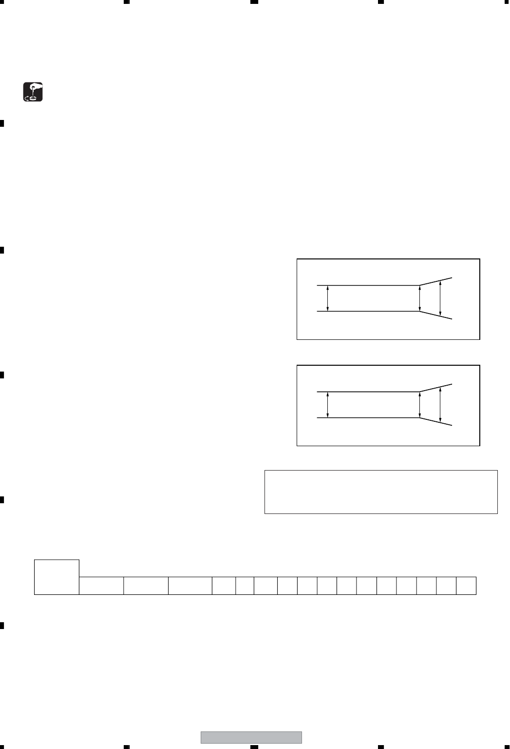
XV-EV1000
88
1234
1234
C
D
F
A
B
E
6. ADJUSTMENT
6.1 DECK SECTION
6.1.1 ADJUSTMENT CONDITION
7 Adjustment Condition
(1) The ground at the time of adjustment shall be W166.
(Refer to Fig. 6–3).
(2) Clean the heads and demagnetize them using a head eraser.
(3) Set the measurement level to 0 dBV = 1 Vrms.
(4) Use the specified tape for adjustment. Use the labeled (A) side
of the test tape.
NCT–111 : For Tape Speed adjustment
NCT-112 : For Playback adjustment
STD–633 : Normal blank tape
*As the reference recording level is 250 nwb/m for NCT–
112, the recording level will be higher than 4 dB for NCT–
112 (160nwb/m). When adjusting, pay carefully attention
to the type of tape used.
(5) Provide yourself with the following measuring devides:
÷ AC millivoltmeter
÷ Low-frequency oscillator
÷ Attenuator
÷ Oscilloscope
(6) Adjust both right and left channels unless other wise specified.
(7) Turn the DOLBY NR switch off unless otherwize specified.
(8) Warm up the unit for several minutes before adjustment. In
particular, be sure to warm up the unit in the REC/PLAY mode
for 3 to 5 minutes before starting recording/playback frequency
characteristics adjustment.
(9) Always follow the indicated adjustment order.
Otherwise, a complete adjustment may not be achieved.
7List of Adjustments
¶ Playback Section
(1) Tape Speed Confirmation
(2) Head Azimuth Adjustment
(3) Playback Level Adjustment
¶ Recording Section
(1) Recording Bias Adjustment
(2) Recording Level Adjustment
Dolby noise reduction manufactured under license from Dolby
Laboratories Licensing Corporation.
“DOLBY” and the double-D symbol are trademarks of Dolby
Laboratories Licensing Corporation.
Fig. 6-2 Test Tape NCT– 112
Fig. 6-1 Frequency Characteristics
0 dB
–20 dB
30s 0 dB: 315 Hz, 250 nwb/m
315 Hz
6.3 kHz 10 kHz 315 Hz 14 kHz 12.5
kHz 6.3
kHz 500
Hz 250
Hz 125
Hz
10 kHz 8 kHz 4 kHz 2 kHz 63 Hz 40 Hz
1 kHz
30 s 30 s 30 s 10s 10s .......................................................................................................... 10s
250
3dB
10k 12.5k
3dB 4dB
PLAY BACK
250
3dB
10k 12.5k
3dB 5dB
RECORDING
XV-EV1000 89
5678
5678
C
D
F
A
B
E
6.1.2 PLAYBACK and RECORDING SECTION
NCT-111 (3 kHz) ADJ. VR on
CASSETTE MECHA
(Refer to Fig. 6-3)
No. Mode Input Signal/Test Tape Adjustment Points Measurement Points Adjustment Value Remarks
PLAY1P1 R
(CN2507)
(IFAF ASSY) 3000 Hz Hz
(1) Tape Speed Confirmation
(1) Recording Bias Adjustment
¶ After the adjustment, caution should be exercised so as not to become under bias by checking the distortion rate.
NCT-110 test tape
(Playback: 10 kHz, –20 dB)
Head azimuth
adjustment Screw
(Refer to Fig. 6-3)
Remarks
PLAY
1
P3 L (CN2507)
P1 R (CN2507)
(IFAF ASSY)
Max. Playback
signal level
(2) Head Azimuth Adjustment
¶ This unit is equipped with auto tape selector.
¶ Do not switch between forward and reverse operation with the screwdriver inserted.
+10
–10
Playback Section
After adjustment, apply silicon
bond to the head azimuth
adjustment screw.
VR2301
PLAY
1
(3) Playback Level Adjustment
¶ Since this adjustment determines playback DolbyNR level, Perform it carefully.
L ch
R ch VR2302
P3 L (CN2507)
P1 R (CN2507)
(IFAF ASSY)
Recording Section
VR2801
REC/
PAUSE
1Input a 315Hz signal to the LINE -
IN terminal. ∗
L ch
R ch VR2802
P3 L (CN2507)
P1 R (CN2507)
(IFAF ASSY)
–3.7 dBV
Input signal level –23.7 dBV
REC =
PLAY
2
Load the STD–633 test tape and
record/playback the 315Hz and
10kHz signals. (see the Note below)
Repeat adjustment until playback level of
the 10kHz signal is within 0dBV ±0.5dB
from that of the 315Hz signal.
(2) Recording Level Adjustment
VR2401
REC/
PAUSE
1
L ch
R ch VR2402
P3 L (CN2507)
P1 R (CN2507)
(IFAF ASSY)
Input signal level –7.7 dBV
REC =
PLAY
2
STD–633 test tape and record/
playback the 315Hz signal.
Repeat recording, playback and
adjustment until playback level of the
315Hz signal becomes –
7.7dBV±0.5dB
.
Note: Set the 10kHz input signal level to the same value as the 315Hz input signal level of step 1.
Input a 315Hz signal to the LINE-
IN terminal.∗
No. Mode Input Signal/Test Tape Adjustment Points Measurement
Points
Adjustment
Value
RemarksNo. Mode Input Signal/Test Tape Adjustment Points Measurement
Points
Adjustment
Value
NCT-112 test tape
(Playback: 315 Hz, 4 dB)
Remarks
No. Mode Input Signal/Test Tape Adjustment Points Measurement
Points
Adjustment
Value
Remarks
No. Mode Input Signal/Test Tape Adjustment Points Measurement
Points
Adjustment
Value
FWD adjustment
REV Confirmation
( 3000 Hz Hz )
+40
–40
7
7
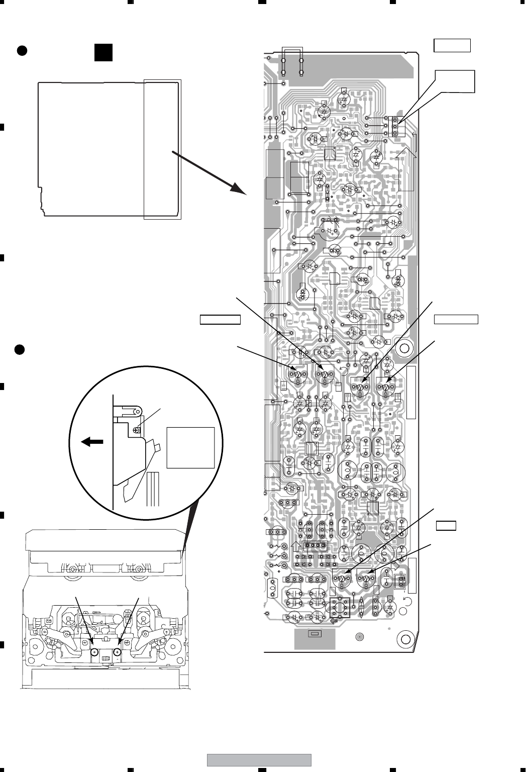
XV-EV1000
90
1234
1234
C
D
F
A
B
E
14
2
OPEN
1
DIP
31
FCDC
KN5501
Q2806
W315
C2220
C2307
2
0
W412
W419
CN2301
C2808
W325
L2402
CN2302
W299
C2418
R2321
VR2401
W250
R2803
W303
C2406
W306
D2301
D2256
W310
W220
W317
W301
C2224
W314
C2225
L2802
W252
C2260
C2425
C2801
C2802
C2803
C2203
C2201
C2405
VR2402
C2419
C2404
C2209
C2403
W312
W324
C2314
C2807
C2222
W240
L2401
VR2801
W414
W321
W323
W322
C2420
C2308
W251
C2409
C2216
C2408
W300
C2407
VR2301
CN2507 W302
W258
W413
W
333
W411
C2810
C2809
D2306
VR2802
D2305
D2304
C2221
W233
D2303
D2302
C2417
C2410
D2201
R2806
C2804
C2204
C2228
C2202
C2215
C2217
C2218
C2223
Q2301
C2251
C2254
C2255
C2261
C2262
Q2302
C2805
C2309
W232
W231
W313
W230
Q2801 Q2802
Q2803
Q2805
VR2302
C2259
W305
W239
W244
W316
W261
W242
W259
W241
C2421
W260
R2805
W262
W222
W224
W243
L2801
L2403
C2422
W308
W238
W326
W309
W304
W311
C2310
C2806
C2311
C2312
W307
W249
L2404
C
SIDEPRINTED
T
EC
5
6
REC
P
OW
C
1
R
D
U
T
E
F
L
IFAF ASSY
N
DM(DV)
P
+12
N
DM(TC)
P
R+8M
R
+8M
DD
N
DD
R
+8
R
+8
-
12
DTX
+
12TX
+
12
M
UTE
E
T
L
CLK
L
DATA
A
A
A
A
A
A
O
TECT
A
C
D
+5
+
5A
GNDC
GNDM (DV)
VPR+8M
GNDD
RECR
ICT FC
VA12
OPEN
BIG
DECK TP Adj.
VA12
GNDA GNDA
VREF
VA12
DECK PART BIAS
GNDA
VREF
VREF
VA12
A
Adj.
GNDA
R
GNDA
Rch
LCH
GNDA
VA12
VA12
MS
BIG
Rch
Lch
DC
Lch
IC2401
Rch
VREF
VREF
GNDA
IC2301
FC
RCH
LEVEL
IC2202 Lch
REV Azimuth
Adjustment Screw
FWD Azimuth
Adjustment Screw
MECHANISM UNIT
Front Side Cassette
Mechanism
Section
(Side View)
Tape Speed
ADJ. VR
IFAF ASSY C
REC LEVEL
PB LEVEL
BIAS
VR2301
(Lch)
VR2302
(Rch)
VR2402
(Rch)
VR2401
(Lch)
VR2801
(Lch)
VR2802
(Rch)
SIDE A
Fig. 6-3 Adjustment and Measurement Points
CN2507
(DECK TP)
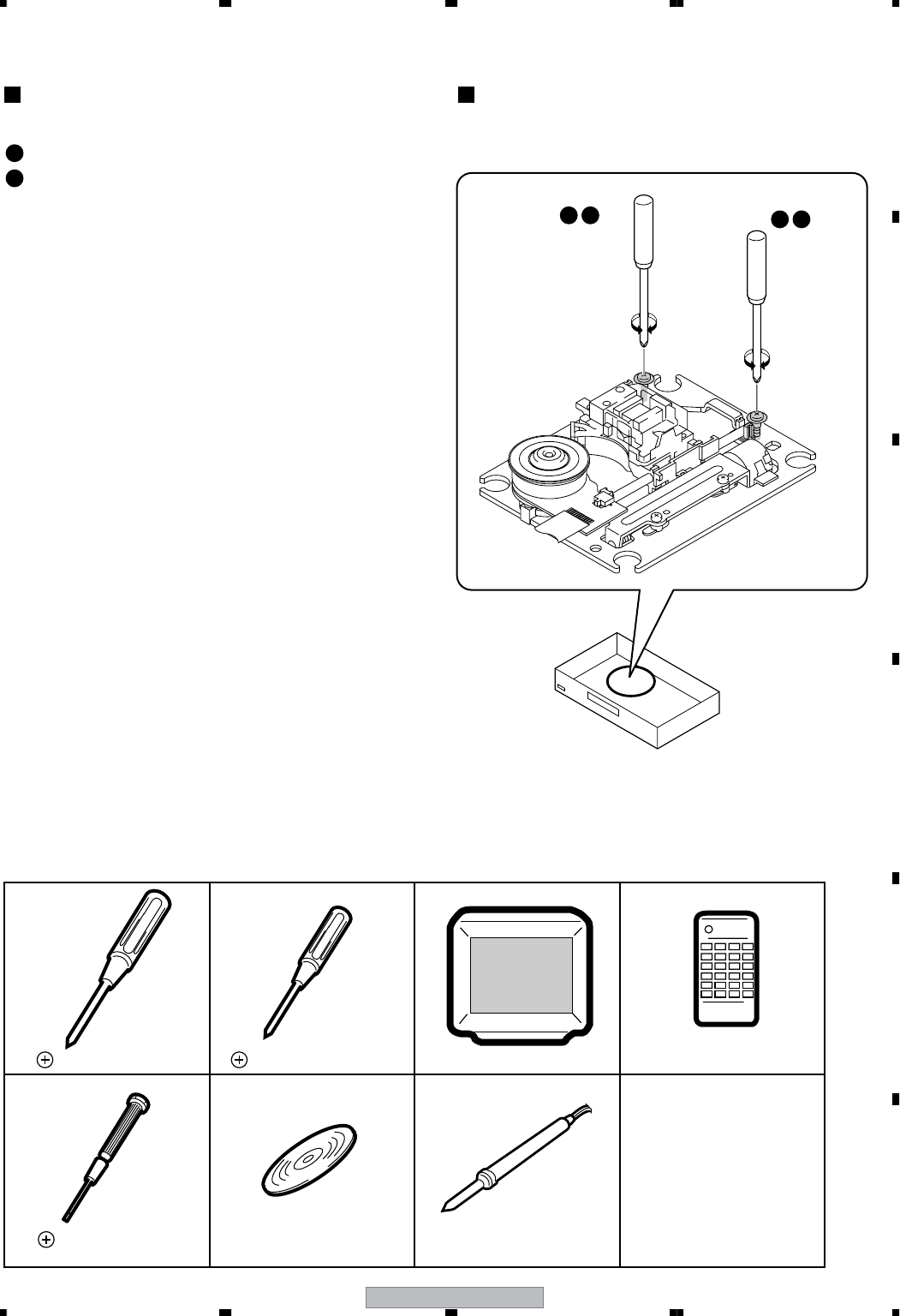
XV-EV1000 91
5678
5678
C
D
F
A
B
E
6.2 DVD SECTION
6.2.1 ADJUSTMENT ITEMS AND LOCATION
6.2.2 JIGS AND MEASURING INSTRUMENTS
1
2
Adjustment Items
[Mechanism Part]
[Electrical Part]
Tangential and Radial Height Coarse Adjustment
DVD Error Rate Adjustment
Electrical adjustments are not required.
Adjustment Points (Mechanism Part)
Cautions: After adjustment, adjustment screw locks with the
Screw tight.
1 2
Radial
adjustment
screw
1 2
Tangential
adjustment
screw
Screwdriver (large) TV monitor
Precise screwdriver DVD test disc
(GGV1025)
Test mode remote control
unit (GGF1381)
Screw tight
(GYL1001)
Screwdriver (medium)
Soldering iron
XV-EV1000
92
1234
1234
C
D
F
A
B
E
6.2.3 NECESSARY ADJUSTMENT POINTS
∗After adjustment, screw locks
with the Screw tight.
~, Ÿ
Mechanical
point
Electric
point
Mechanical
point
Electric
point
Mechanical
point
Electric
point
LOAB and DVDM ASSYS
Exchange Parts of Mechanism
Exchange PCB Assy
When Adjustment Points
Exchange the 05SD Pickup Assy
Exchange the Traverse Mechanism
Assy-S
Exchange PC Board
∗After adjustment, screw locks
with the Screw tight.
Ÿ
Mechanical
point
Electric
point
Exchange the Spindle Motor
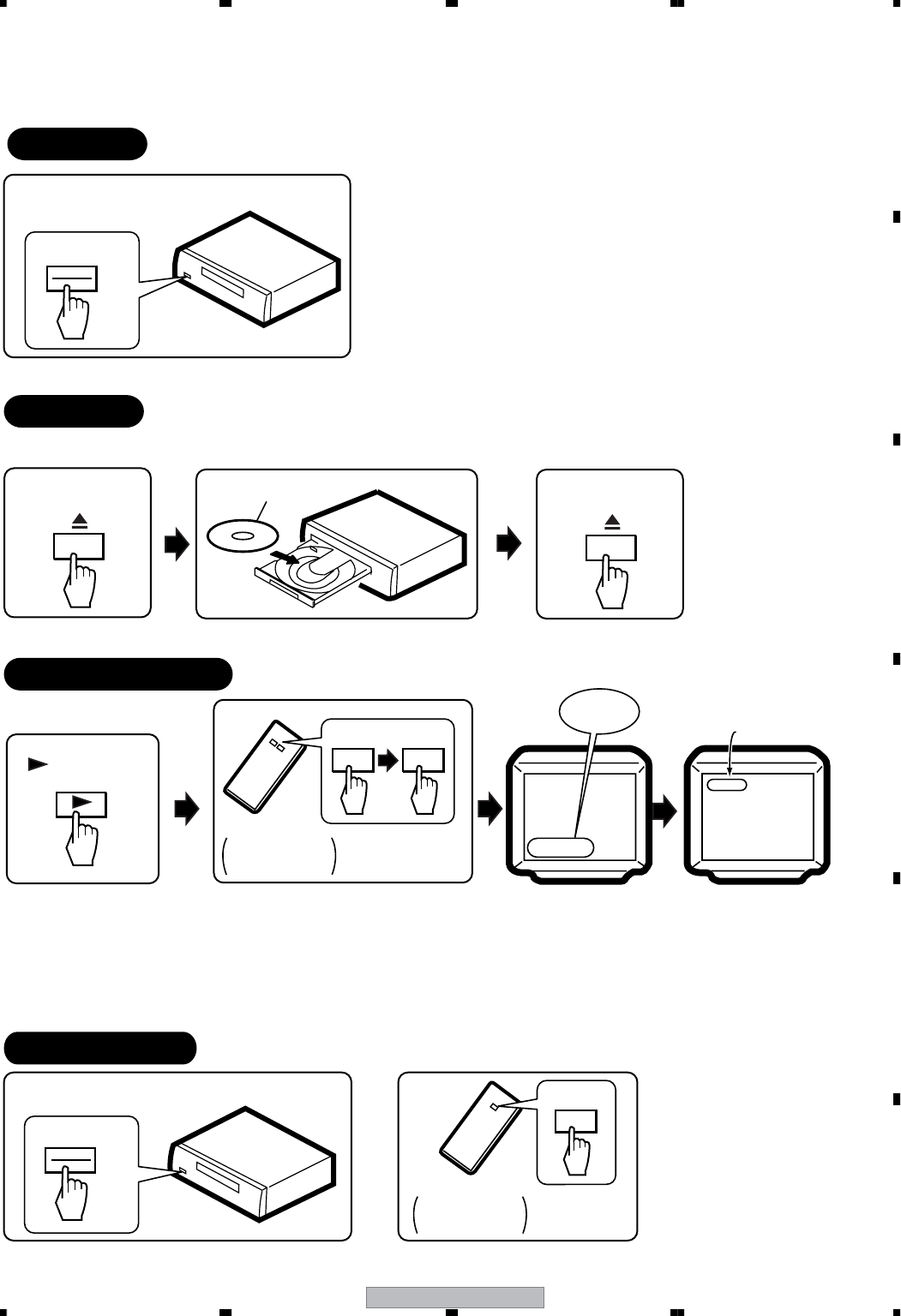
XV-EV1000 93
5678
5678
C
D
F
A
B
E
6.2.4 TEST MODE
POWER ON
DSC - &&&
GGF1381
Test mode
remote control
unit
GGF1381
Test mode
remote control
unit
<TRAY OPEN> <TRAY CLOSE>
OPEN/CLOSE
(Player)
OPEN/CLOSE
Press the play key
( ) of the normal
remote control unit.
(Player)
TEST MODE: PLAY
TEST MODE: OFF
An address is displayed
OR
ESC
<PLAY>
ESC TEST
CHECK
DVD, CD
DVD disc
POWER
ON
OFF
POWER
DISC SET
Notes:
• After going into test mode, if you play back the disc, "DISC-NON" is displayed.
• The video signal and the audio signal are outputted during the test mode.
• The SKIP key and the SCAN key are effective during the test mode.
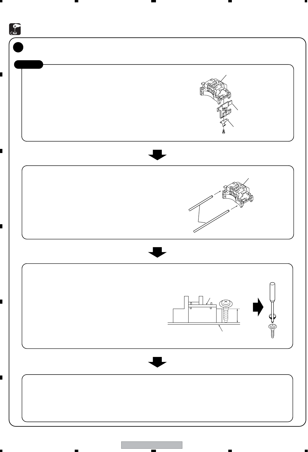
XV-EV1000
94
1234
1234
C
D
F
A
B
E
6.2.5 MECHANISM ADJUSTMENT
• Remove the 05SD Pickup Assy from the Traverse Mechanism Assy-S.
• Remove the joint and the joint spring of the 05SD Pickup Assy.
• Put the joint between the Tangential (or Radial) adjustment screw and the mechanism base
and turn each screw to adjust the height.
(Refer to "6.2.1 ADJUSTMENT ITEMS AND LOCATION".)
START
Tangential and Radial Height Coarse Adjustment
1
Note:
Before removing the flexible cable for the
pickup, soldering of the pickup circuit is
necessary.
For details, see "7.1.11 DISASSEMBLY".
• Pass through the guide shaft to a new 05SD Pickup Assy.
• Attach it to the Traverse Mechanism Assy-S.
• Attach the Traverse Mechanism Assy-S to the 05 LOADER Assy.
• Turn it over and attach the joint and the joint spring.
• Arrange the flexible cables.
(Refer to "7.1.11 DISASSEMBLY".)
7.5mm
Joint
Mechanism base
05SD Pickup Assy
05SD Pickup Assy
Joint
Joint Spring
Guide Shaft
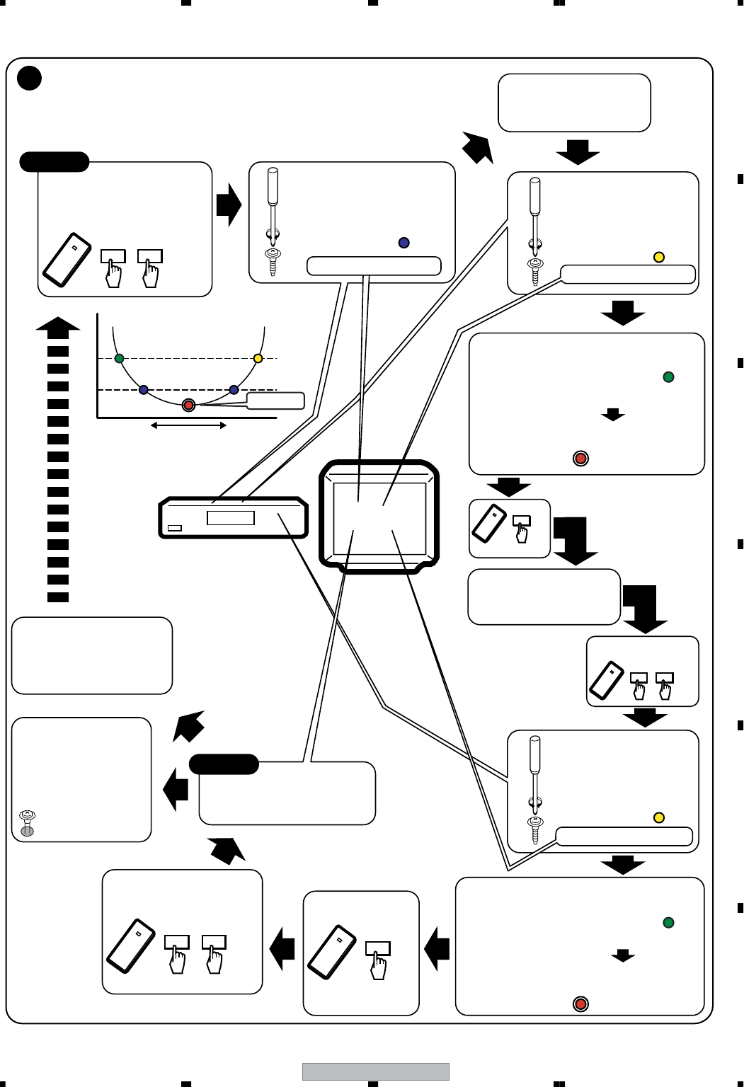
XV-EV1000 95
5678
5678
C
D
F
A
B
E
Player
Monitor
•Play the DVD test disc
at inner track
(around #30000)
•Play the DVD test disc
at outer track
(around #200000)
Traverse Mechanism
Assy-S
Adjust the radial adjustment
screw so that
ERROR RATE becomes
around "5E-4".
Traverse Mechanism
Assy-S
Fasten the radial
adjustment screw so that
ERROR RATE becomes
around "1E-3".
START
DVD Error Rate Adjustment
2
ERROR RATE: - - - -
ERROR RATE : "5E-4" ERROR RATE : "1E-3"
Service mode end
Disc playback normally.
• The measurement of
block error rate
If error rate is OK,
locks a root of
tangential and radial
adjustment screws with
the Screw tight.
Screw tight: GYL1001
Turn the POWER OFF in
case of NG once, and
perform the adjustment
once again.
CHP/TIMESC ESC
\ Service mode
Service mode end
ESC
NG
OK
•Play the DVD test disc
at inner track
• Display ERROR RATE
on the monitor
CHP/TIMESC
Notes:
•Use disc: GGV1025
•Unfasten the radial adjustment screw
by 90 degrees step till ERROR RATE
becomes around "1E-3" again .
• Record the number of rotation (N1).
(memorizing how much the screw was rotated.)
•Fasten the radial adjustment screw
till the number of rotation becomes
harf of N1.
Traverse Mechanism
Assy-S
Fasten the tangential
adjustment screw so that
ERROR RATE becomes
around "1E-3".
•Unfasten the tangential screw
by 90 degrees step till ERROR RATE
becomes around "1E-3" again .
• Record the number of rotation (N1).
•Fasten the tangential adjustment screw
till the number of rotation becomes
harf of N1.
ERROR RATE : "1E-3"
In this check, the error rate
that is less than "5E-5"is
better.
CHECK
CHP/TIMESC
A
B
B
C
Best Radial point
C
Best tangential point
1E-3
5E-4
Rotation of Radial screw
and Tangential screw
BER
Anticlock wise Clock wise
Best point
AA
BC

XV-EV1000
96
1234
1234
C
D
F
A
B
E
7. GENERAL INFORMATION
7.1 DIAGNOSIS
7.1.1 TEST MODE
Test Mode Functional Specification
1 Test mode entry
In the power ON state, press the [ESC] (A8-5F) key and [TEST] (A8-5E) key in order of the Test mode remote control unit.
• OSD displays test mode.
2 LD ON
Enter the test mode.
DVD : Press the [TEST] (A8-5E) and [1] (A8-01) keys in order, and turn on the laser diode (650n).
CD : Press the [TEST] (A8-5E) and [4] (A8-04) keys in order, and turn on the laser diode (780n).
3 Release the Test mode
• Turn off the power.
• Press the [ESC] (A8-5F) key of the remote control unit and reset it.
XV-EV1000 97
5678
5678
C
D
F
A
B
E
7.1.2 DISPLAY SPECIFICATION OF THE TEST MODE
Character in bold : Item name
: Information display
1
5
6
10
11
8
9
3
2
12
15
13
14
1 Address indication
The address being traced is displayed in number.
(as for the DVD, indication of decimal number is possible.)
DVD : ID indication (hexadecimal number, 8 digits)
[∗ ∗ ∗ ∗ ∗ ∗ ∗ ∗]
CD : ID indication [∗ ∗ ∗ ∗ ∗ ∗ ∗ ∗]
2 Code indication of remote control unit [R – ∗ ∗ ∗ ∗]
In case of double code, display a 2nd code.
3 Main unit keycode indication [K – ∗ ∗]
5 Tracking status [TRKG – ∗ ∗ ∗]
Tracking on : [ON]
Tracking off : [OFF]
6 Spindle status [SPDL – ∗ ∗ ∗]
CLV : [CLV]
Off : [OFF]
7 Mechanism (loading) position value [M – ∗ ∗]
Unknown : [01] or [41]
Open state : [04]
Close state : [08]
During opening : [12]
During closing : [22]
8 Slider position [S – ∗ ∗ ∗ ∗]
In Side Switch ON : [01]
In Side Switch OFF : [00]
9 Output video system [V – ∗ ∗ ∗ ∗]
NTSC system : [NTSC]
PAL system : [PAL]
Automatic setting : [AUTO]
Scart terminal output [SK – ∗ ∗]
(Display only the WY model which can do the output setting
of scart terminal.)
VIDEO : [00]
S-VIDEO : [01]
RGB : [02]
0 Disc sensing [DSC – ∗ ∗ ∗]
The type of discs loaded is displayed.
[DVD], [CD ]
- Jitter value [J – ∗ ∗ ∗ ∗]
Note: Don't use it.
= Version of the FL controller [FL: ∗ ∗ ∗ ∗]
Note: Don't use it.
~ Region setting of the player [REG: ∗]
Setting value : [1] to [6]
! Destination setting of the FL controller
[MDL: ∗ ∗ ∗ ∗ / ∗ ∗ ∗]
Four characters in the front represent code 01.
Three characters in the back represent the destination code.
J: /J, K: /KU, /KC, /KU/KC, R: /RL/RD, RAM : /RAM,
LB: /LB, WY: /WY
@ Version of the flash ROM [V: ∗ ∗. ∗ ∗]
Flash ROM size [FLASH = ∗ ∗]
7
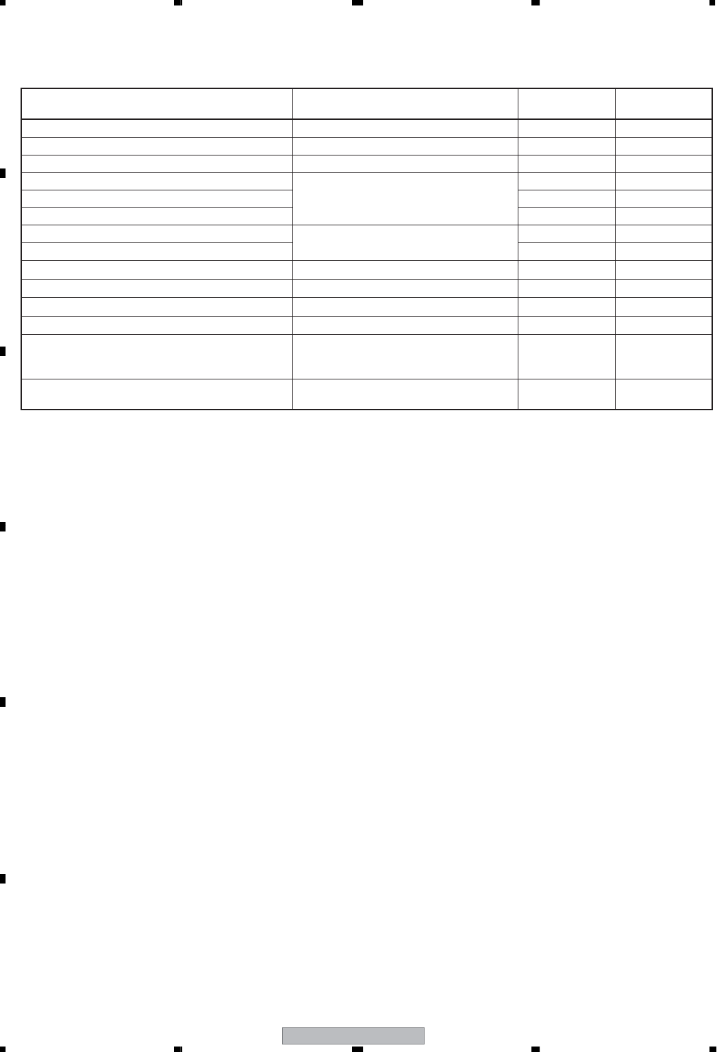
XV-EV1000
98
1234
1234
C
D
F
A
B
E
7.1.3 FUNCTIONAL SPECIFICATION OF THE SHORTCUT KEY
• Service mode indication (ESC + CHP/TIM keys)
ID Address
The error rate is always displayed in exponential notation, e.g., ∗.∗ ∗ e - ∗, for both DVDs and CDs.
EDC/ID/AV 1 error history (ID Address, EDC/ID Error, last eight errors)
• Calculation of the average error rate (ESC + "5" [Test mode remote control unit] keys)
The average of the last eight error rates is calculated and indicated in exponential notation. After the calculation is completed, "OK" or "NG" is
displayed. If "NG" is displayed, the disc tray will open (for both DVDs and CDs)
For DVDs: OK with 5.0e-4 or less, for CDs: OK with 7.6e-3 or less
• Indication of model information (ESC + CHAP keys)
The items from 12 to 15 of the TEST MODE Indications are displayed. However, in the indications, S in the standard test mode is changed to
CHIP VERSION, and M is changed to RF VERSION. For details, see 7.1.4.
• Region confirmation mode (ESC + A.MON [Test mode remote control unit] + "1"-"8" [Test mode remote control unit] keys)
After you press the AUDIO key while holding the ESC key pressed and then input the region number, if the number is different from that set in
the unit, an error message is displayed, and the tray opens.
Command Contents Conditions Remote Control
Key Name
Remote
Control Code
Memory clear and region / revision indication CLEAR (∗1) A8-45
Average value measurement of DVD error rate 5 (∗1) A8-05
CD error rate measurement 5 (∗1) A8-05
Scart terminal output : VIDEO
WY, models equipped with Scart terminal
AUDIO A3-BE
Scart terminal output : S-VIDEO SUBTITLE A3-36
Scart terminal output : RGB ANGLE A3-B5
Progressive OFF Only for progressive models R_SKIP A3-9D
Progressive ON F_SKIP A3-9C
FL indication of ID number STEREO (∗1) A8-4A
ZOOM ON (×4) ZOOM A3-37
Service mode indication (error rate indication, etc.) CHP/TIM (∗1) A8-13
Model information indication CHAP (∗1) A8-40
Title search Input mode IN
Title No. input
Search execution
SIDE A (∗1)
Numbers (∗1)
PLAY (∗1)
A8-4D
A8-00 to A8-09
A8-17
Region confimation mode A.MON (∗1)
Numbers (∗1)
A8-1E
A8-01 to A8-08
Only during normal playback, the following shortcut keys can be assigned by pressing a required key after pressing the ESC
key of the remote control unit. To quit, press the ESC key
∗1 : Test mode remote control unit
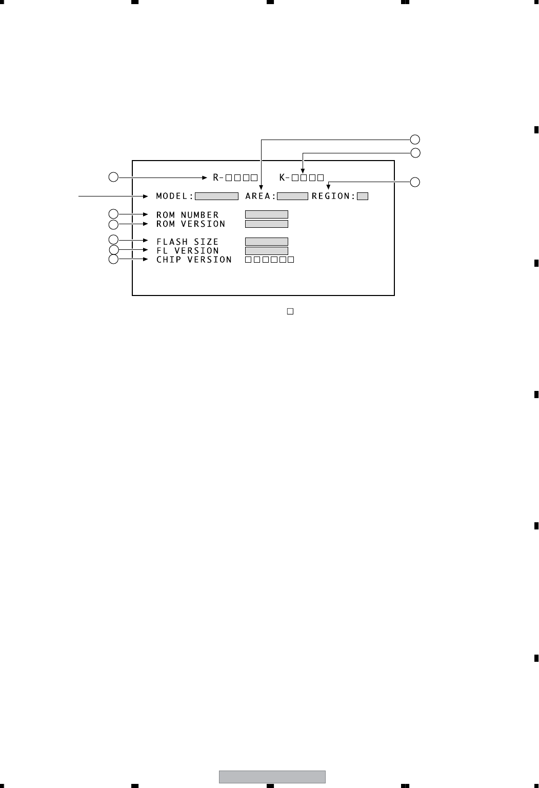
XV-EV1000 99
5678
5678
C
D
F
A
B
E
7.1.4 SPECIFICATION OF MODEL INFORMATION DISPLAY
• Display contents
Character in bold : Item name
: Information display
1
2
3
4
5
6
7
9
10
1 Destination indication
Display it according to model information set from the FL controller.
2 Region No.
3 Part number
4 ROM version
5 Flash size
6 FL controller version
7 CHIP VERSION
9 Remote control code
0 Key code of Main unit
To display model information : Press the ESC key then the CHAP key.
To close the model information display : Press the ESC key.
Don't care.
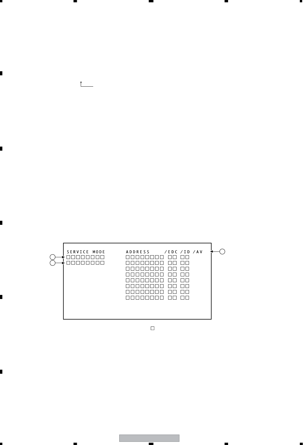
XV-EV1000
100
1234
1234
C
D
F
A
B
E
7.1.5 FUNCTIONAL SPECIFICATION OF THE SERVICE MODE
• Display during Service Mode
To enter Service Mode, press the CHP/TIM key while holding the ESC key pressed.
To quit, press the ESC key.
Service mode display
1 ID Address
2 Error rate (always displayed), in exponential notation
ERROR RATE : ∗ ∗ ∗ ∗ ∗ ∗ ∗
( ∗ ∗ ∗ ∗ )
• Calculation of the average error rate
For DVDs: OK with 5.0e-4 or less, for CDs: OK with 7.6e-3 or less
3 EDC/ID error history (ID Address, EDC/ID errors, last eight errors)
Note:
∗ Error of AV1 is not supported in this player.
Number of error
Indication plan contents
Character in bold : Item name
: Information display
1
2
3
ex) For DVDs
• Step 1
%%e -&
%%e -6 : OK
%%e -5 : OK
%%e -4 : Refer to Step 2
%%e -3 : NG
%%e -2 : NG
• Step 2
%%e -4
3.0e -4 : OK
4.0e -4 : OK
5.0e -4 : OK
6.0e -4 : NG
7.0e -4 : NG
XV-EV1000 101
5678
5678
C
D
F
A
B
E
7.1.6 SERVICE TEST MODE
W E L C O M E !
V O L 0
V O L 0
D V S V C
D V S V C
P R T E R R
V O L 0
D V S V C
V O L 0
D V S V C
P R T W N G
D V S V C
DVD/CD
TX S V C
TUNER
L1 S V C
LINE1
DV D P R T
T C S V C
TAPE
1. Specific conditions for Service Test mode
• VDET is neglected.
• XPROTECT is neglected.
• Even if the unit is urgently shut down in failure in Normal mode, you can turn it on without waiting for one minute.
2. How to enter Service Test mode
• While connecting STEST port (IC5501 Pin43) to "+5V", connect AC power cord. (See next page.)
3. How to quit Service Test mode, and the conditions for quitting
• To quit Service Test mode, turn the power off or disconnect the AC power cord.
• When quitting Service Test mode, only data on protection in RAM are cleared.
4. Indications when Service Test mode starts
• Indications on the FL display when Service Test mode starts differ depending on whether the unit was turned off normally or if the unit
was urgently shut down because the abnormality of the power, as described below.
5. Operations during Service Test mode
• Basically, operations in Service Test mode are the same as in Normal mode. However, to clarify that it is in Service Test mode, during
this mode, when functions are changed, the indications on the FL display become as follows:
[After the power is turned off normally] [After the power is shut down because of
a failure in the AMP system]
FL display
FL display
FL display
FL display
FL display
FL display
FL display
FL display
FL display
FL display
FL display
FL display
[After the power is shut down because of
an abnormality in the AMP system]
[After the power is shut down because of a failure
in the DVD system]
[Functions] [Indications on the FL display]
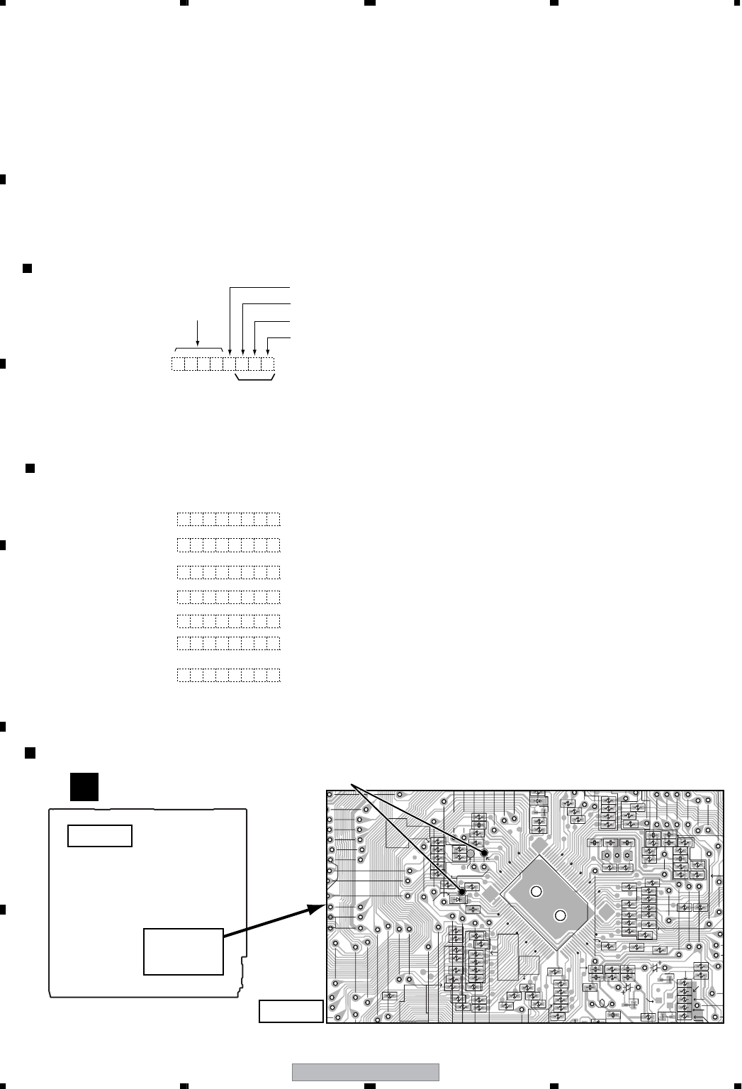
XV-EV1000
102
1234
1234
C
D
F
A
B
E
1
80
30
51
50
81
31
100
R5582
C5514 C5513
R5540
R5571
R5535
R5538
R5597
R5567
R5536
R5539
R5562
R5563
R5558
R5559 R5561
R5554
R5553
R5552
R5551
R5555
R5557
R5546
R5545
R5548
R5547
R5549
R5550
R5511
R5523
R5522
R5521
C5515
C5520
C5519
R5601
IC5501
R5598
R5590
R5542
R5541
R5593
D5502
Q5501
C5509
R5501 C5508
R5504
C5507
R5503
C5505
Q5502
R5581
R5508
C5504
R5632
R5633
R5592
R5588
C5535
R5634
R5512
R5515
R5603
R5604
R5624
R5625
R5623
R5626
D5602
R562
7
Q5602
R5403R5404
R5537
R5804
R5961
U-TEST
S-TEST
VE+5
VU+5
CO
ERR. 0
FL
ERR. 1
ERR. 2
ERR. 3
ERR. 4
NO ERR
(Source is 88.2/96kHz.)
(Source is not 88.2/96kHz.)
NO ERR
[Error]
6. DSP error message mode
[ How to enter DSP error message mode]
•Press "DISPLAY" button of the accessory remote control(*) in service test mode, to select the mode that DSP error message are displayed.
[ How to quit DSP error message mode]
• Press "DISPLAY" button of the accessory remote control(*) again to select normal service test mode.
For this reason, the usual function of "display" is not effective during Service Test mode.
• DVD total running time/remaining time display is inactive.
• OSD changing on TV is also inactive.
Space
DIR UNLOCK (This character is displayed while DIR is UNLOCK.)
DSP MUTE (This character is displayed while DSPMUTE is active.)
96k (This character is displayed while the source is 88.2 or 96kHz PCM.)
The name of the error is
displayed in four characters.
Refer to "7.1.10 DSP TROUBLE SHOOTING".
Specification of DSP error display
Example of DSP error display
SIDE B
SIDE B
IFAF ASSY
C
Service Test mode connecting point
*1 : The "U", "M" and "9" are not displayed synchronizing with the display "ERR_0" - "ERR_4" ("DIRERR",etc),
but it depends on the state each time.
The following example display of "ERR_0" - "ERR_4" is just a sample.
*1
(*) : The alternative control is "DISPLAY" button of the accessory remote control of
Pioneer Home Theater System or "SYSTEM DISPLAY" button of Pioneer
mini Component System.
- U M 9
‡‡‡‡
DIER - U M
12345678
DSER - U M
-UM
HREQ
D S N -G U M
DM TU - M
DS O K 9-
D S O K -
[Error] [Indications on the FL display]
Connecting point
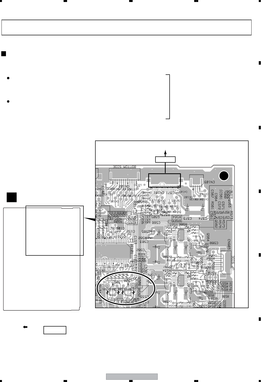
XV-EV1000 103
5678
5678
C
D
F
A
B
E
7.1.7 METHOD FOR DIAGNOSING DEGRADATION OF THE LDs ON THE PICKUP ASSY
05SD PICKUP ASSY
CN101
R321
R322
R325
R326
R325
R326
Case when this diagnosis is required :
When playback of any disc, including a test disc (DVD: GGV1025, CD: STD-905), won't play or doesn't play
How to diagnose
In the case mentioned above, degradation of the laser diodes (LDs) mounted on the 05SD Pickup Assy is suspected.
Measure the voltage between the two ends of one of the resistors mentioned below.
Measure the voltage between the both ends of R322 or R325 on the DVDM
Assy. If the voltage is 0.4 V or higher, the 650-nm LD is degraded.
No playback of a DVD :
Measure the voltage between the both ends of R321 or R326 on the DVDM
Assy. If the voltage is 0.4 V or higher, the 780-nm LD is degraded.
No playback of a CD :
If the measurements show degradation
of an LD, replace the 05SD Pickup
Assy.
DVDM ASSY
B
SIDE A
Front side

XV-EV1000
104
1234
1234
C
D
F
A
B
E
7.1.8 DVD TROUBLE SHOOTING
No. Symptoms Diagnosis Contents Possible Defective Points
1 The power is not turned on. Are wires of output connector (POWER SUPPLY Unit) and CN901
(DVDM Assy) disconnected or damaged ? Connector / cable
Check that the following voltage is output :
+ side of C739 : 3.3V
DVDM Assy
3.3V Regulator IC (IC341)
2An opening screen is not
displayed on the monitor
(The FL display lights. The
mechanism does not work.)
Are the signals output from IC201-pin 98 (MDATA) and pin 99 (SCLK)
on the DVDM Assy ? (in the range of 0-3V)
DVDM Assy
DVD IC (IC201)
Are the signals input into IC5501-pin 50 (MDATA) and pin 51 (SCLK)
on the IFAF Assy ? (in the range of 0-3V)
IFAF Assy
UCOM (IC5501)
Check that the following voltage are output :
IC751-pin 1 on the DVDM Assy : 5V
DVDM Assy
5V Regulator IC (IC751)
Is a resonator (X201: 27MHz) on the DVDM Assy oscillating ?
DVDM Assy
Crystal resonator (X201)
DVD IC (IC201)
• Is a signal input into IC203-pin26 (PCE#) on the DVDM Assy ?
(Is a signal "H" for 80 mS and then "L" after the power is turned
on ?)
→ Communication with flash ROM.
• Are the signals input into IC202-pin 16 (DWE#), pin 19 (DCS#)
and pin 38 (SDCLK) on the DVDM Assy ?
(Is a signal fluctuating ?)
→ Communication with SDRAM
DVDM Assy
DVD IC (IC201)
Flash ROM (IC203)
SDRAM (IC202)
Is a signal output from IC203-pin 28 (PRD#) on the DVDM Assy?
(Is a signal fluctuating for several hundred mS after the power is turned
on ?)
DVDM Assy
Flash ROM (IC203)
Is a signal input into IC5501-pin 67 (DVD ACK) on the CONTROL
Assy ? (Is a signal fluctuating ?)
→ Communication with FL Control IC
DVDM Assy
DVD IC (IC201)
IFAF Assy
UCOM (IC5501)
Is a signal output from IC5501-pin 30 (XREADY) on the CONTROL
Assy ? (Is a signal fluctuating in the range of 0-5V ?)
IFAF Assy
UCOM (IC5501)
Are the signals output from IC5501-pin 49 (SDATA) on the CONTROL
Assy ? (in the range of 0-5V)
DVDM Assy
DVD IC (IC201)
IFAF Assy
UCOM (IC5501)
Are the signals of IC204-pin 5(SDA) and pin 6(SCL) on the DVDM Assy
fluctuating for one or two seconds after the power is turned ?
DVDM Assy
EEPROM (IC204)
3An opening screen is not
displayed on the monitor
(The FL display lights. The
mechanism works.)
Check the video signal path between DVD IC (DVDM Assy IC201) and
video-out terminal (see the block diagram)
DVDM Assy
Video circuit after DVD IC
(IC201)

XV-EV1000 105
5678
5678
C
D
F
A
B
E
No. Symptoms Diagnosis Contents Possible Defective Points
4
A tray cannot be opened.
(An opening screen is
displayed on the monitor)
Does the voltage of CN104-pin 3 and pin 5 on the DVDM Assy change
normally ?
Pin 3 (SW2(TRIN)): Tray is fully closed: "L"
Pin 5 (SW1(TROUT)): Tray is fully opened: "L"
LOAB Assy
Tray SW (S101)
Is the signal input into IC101-pin 11 (TROPEN) on the DVDM Assy ?
At open: 3.3V, At close: 0V
DVDM Assy
DVD IC (IC201)
Are the signals output from IC101-pin 1 and pin 2 (CN103-pin 1 and
pin 2) on the DVDM Assy ?
Pin 2: Approx. 6V during opening tray approx. 0V during closing tray.
Pin 1: Approx. 0V during opening tray approx. 6V during closing tray.
DVDM Assy
FTS Driver IC (IC101)
Are wires of CN104 and CN103 on the DVDM Assy disconnected or
damaged ? Connector / cable
Does the voltage of CN102-pin 1 on the DVDM Assy change to 0V by
pressing the Inside switch. Inside switch
5Playback impossible
(no focusing)
Are the signals output from IC101-pin 3 (FOCS_DRV) and pin 4
(FOCS_RTN) on the DVDM Assy ?
DVDM Assy
FTS Driver IC (IC101)
Does 650-nm LD emit light ?
Does a pickup lens move up / down ?
Does an actuator spring bend ?
Pickup
Are plastic parts damaged ? Or is a shaft detached ?
Is the turntable detached or tilted ? Mechanism section (motor)
Is flexible cable of CN101 on the DVDM Assy disconnected or
damaged ? Flexible cable / connector
Is signal output from IC201-pin 42 (FOSO) on the DVDM Assy ?
(Device control of about 1.4 V is output usually. It is fluctuated by about
± 250 mV with focus up / down.)
DVDM Assy
DVD IC (IC201)
6Playback impossible
(Spindle does not turn)
Are the signals output from IC101-pin 30 (W), pin 33 (V) and pin 35 (U)
on the DVDM Assy ?
Is pin 26 (STBY) fixed LOW ? (pin 26 is High at playback: 3V)
DVDM Assy
FTS Driver IC (IC101)
Is there any part detached from the spindle motor ?
Or Is there any foreign object lodged in it ?
Mechanism section
(Spindle motor)
Are wires of CN102 on the DVDM Assy disconnected or damaged ? Flexible cable / connector
Is signal output from IC201-pin 37 (DMSO) on the DVDM Assy ? DVDM Assy
DVD IC (IC201)
7Playback impossible
(Playback stops)
Does 650-nm LD deteriorate ?
If the voltage at each both ends of R322 and R325 on the DVDM Assy
is 0.4 V or more, the 650-nm LD is definitely deteriorated.
650-nm LD deteriorated.
(When playback of a DVD is
impossible)
Does 780-nm LD deteriorate ?
If the voltage at each both ends of R321 and R326 on the DVDM Assy
is 0.4 V or more, the 780-nm LD is definitely deteriorated.
780-nm LD deteriorated.
(When playback of a CD is
impossible)
Is there abnormality in FG waveform ? (IC201-pin 47) DVDM Assy
FG output : FTS Driver IC (IC101)
Are there scratches or dirt on the disc ? Disc
8
Picture disturbance during
playback
(block noise, freeze, other)
Are there scratches or dirt on the disc ?
Is there a problem with the format of the disc ?
Check the video signals.
Composite video signal (IC401-pin 25)
S video signal (IC401-pin 21, pin 26)
RGB video signal (IC401-pin 16, pin 18, pin 20)
Disc
9No sound
(Picture is normal) Check the waveform (SPDIF: CN901-pin 16). DVDM Assy
DVD IC (IC201)
DVDM Assy
DVD IC (IC201)
Video IC (IC401, IC451)

XV-EV1000
106
1234
1234
C
D
F
A
B
E
Symptoms that may occur when any of the following ICs is in failure
IC Symptoms
EEP ROM
(DVDM Assy : IC204)
User's data cannot be stored in memory.
The ID number is lost.
Flash ROM
(DVDM Assy : IC203)
The power cannot be turned on.
Downloading of the firmware cannot be performed.
DVD IC
(DVDM Assy : IC201)
Any kind of symptoms (no power, a failure in any of the servo, video and audio systems, etc.) may be
generated, because the DVD processing is performed by a single chip.
64M SDRAM
(DVDM Assy : IC202)
No power.
Block noise is generated during playback.
XV-EV1000 107
5678
5678
C
D
F
A
B
E
7.1.9 ID NUMBER AND ID DATA SETTING
This display appears when the PLAY key is pressed in Step 4.
Enter a 9-digit number to compare. The number is also
displayed on the FL display.
6
By pressing the CLEAR key without having input a number, the
unit returns to Step 2 without doing anything else. Each press
of this key after a number has been input deletes one digit.
7
After entering all 9 digits, if you press the PLAY key, the unit
compares the numbers input in Steps 2 and 6, and only if the
numbers match, that number is set as the ID. Then the unit
automatically enters ID DATA Input Mode. If the numbers do not
match, the disc tray is opened, and the unit exits ID Number
Input Mode.
8
[Player's ID Number Setting]
ID Number ?
0 0 0 0 0 0 0 0 1
Compare
∗ ∗ ∗ ∗ ∗ ∗ ∗ ∗ ∗
Input ID Number !
6
[Player's ID Number Setting]
ID Number ?
0 0 0 0 0 0 0 0 1
Compare
0 0 0 0 0 0 0 0 1
<PLAY> Enter
Input ID Number !
8
Input ID Number !
After entering all 9 digits, if you press the SEARCH key, the
unit unconditionally sets the input number as the ID number.
Then the unit automatically enters Player's Data Input Mode.
(The SEARCH key is not accepted after all 9 digits have been
entered.)
5
[Player's ID Number Setting]
ID Number ?
0 0 0 0 0 0 0 0 1
<PLAY> Compare Mode
<SEARCH> Enter
4
5
Caution:
For the DVD players compatible with DVD-RW, for playback of a DVD-RW disc (CPRM), it is necessary that an individual ID
number and ID data are set for each player. If the ID number and ID data be not properly set in the manner described below,
future operations cannot be guaranteed. The ID number is written on the yellow label at the rear panel of the player.
If there is no yellow label, before downloading FLASH ROM, take note of the ID number set following the procedures
outlined in "ID Number Confirmation Mode" on the next page.
Note: Enter ID numbers while the unit is in Stop mode so that the values set will be immediately written to the flash ROM.
Note: If you press the PLAY button before inputting a 9-digit ID
number, the unit returns to Step 6 without doing anything
else.
To enter ID Number Input Mode, with no ID number set, such as
in a case of immediately after upgrading the firmware, press the
ESC key then the STEREO key.
Note: If a previous ID number and ID data, such as a factory-
preset ID number and ID data, are maintained, the unit
enters ID Number Confirmation Mode when the above keys
are pressed. However, if only an ID number is maintained,
the unit enters ID Data Input Mode.
ID Number Input Mode
[Player's ID Number Setting]
ID Number ?
- - - - - - - - -
<CLEAR> Exit
Input ID Number !
1
Enter a 9-digit ID number. The ID number is also displayed on
the FL display.
2
By pressing the CLEAR key without having input a number, you
can exit this mode. Each press of this key after a number has
been input deletes one digit.
3
After entering all 9 digits, if you press the PLAY key, the unit
enters Compare mode. Enter the same ID number again. Only
if your two input numbers match, the ID number is set. Compare
mode helps eliminate mistyping of the ID number.
4
2
3
Note: If you press the PLAY button before inputting a 9-digit ID
number, the unit returns to Step 2 without doing anything
else.
Setting an ID number or ID data is required in the
following case:
If NoIDNum! or NOIDDATA is displayed on the FL display
immediately after the power to the player is turned on or
during Stop mode.
JIGS AND MEASURING INSTRUMENTS
DVD Data Disc
[GGV1175]
Service Remote Control Unit
[GGF1381]
XV-EV1000
108
1234
1234
C
D
F
A
B
E
To enter ID Number Confirmation Mode after the ID number and
the ID data are set, press the ESC key then the STEREO key.
ID Number Confirmation Mode
1
The ID number already set is displayed.
(It is also displayed on the FL display.)
2
Enter a 9-digit number for comparison. This is not required
when you only wish to check the ID number visually.
(The number is also displayed on the FL display.)
3
By pressing the CLEAR key without having input a number, you
can exit this mode. Each press of this key after a number has
been input deletes one digit.
4
After entering all 9 digits, if you press the PLAY key, the unit
compares the number entered in Step 2 with the ID number
set, and only if the numbers match, the unit automatically exits
ID Number Confirmation Mode. If an ID data has not been
entered, the unit enters ID DATA Input Mode. If the numbers do
not match, the disc tray is opened, and the unit exits ID Number
Confirmation Mode.
5
After entering all 9 digits, if you press the STOP key, the unit
compares the number entered in Step 3 with the ID number
set, and only if the numbers match, the unit automatically
deletes the ID number and exits this mode. If the numbers do
not match, the disc tray is opened, and the unit exits this mode.
(The STOP key is not accepted after all 9 digits have been
entered.)
6
[Player's ID Number Setting]
ID Number ?
0 0 0 0 0 0 0 0 1
Compare
∗ ∗ ∗ ∗ ∗ ∗ ∗ ∗ ∗
<CLEAR> Exit
Input ID Number !
3
2
4
[Player's ID Number Setting]
ID Number ?
0 0 0 0 0 0 0 0 1
Compare
0 0 0 0 0 0 0 0 1
<PLAY> Enter
<STOP> Memory Clear
Input ID Number !
5
6
Note: If you press the PLAY button before inputting a 9-digit ID
number, the unit returns to Step 4 without doing anything
else.
• Indication of an ID number already set
An ID number already set is displayed in the following cases:
1) When the ESC key then the CLEAR key are pressed, user
settings are cleared, then the ID number set is displayed on
the screen. In this case, the ID number is not displayed on the
FL display.
2) When the unit enters ID Number Confirmation Mode by your
pressing the ESC key then the CLEAR key, the ID number set
is displayed. In this case, the ID number is also displayed on
the FL display.
If you only need to confirm the ID number, you can exit
this mode by pressing the CLEAR key or turning off the power.
• Indication when no ID number is set
If no ID number is set, the message "No ID Num!" flashes on
the screen and FL display for a few seconds after the power is
turned on or during Stop mode.
XV-EV1000 109
5678
5678
C
D
F
A
B
E
To enter ID DATA Input Mode, with the ID number set, press the
ESC key then the STEREO key.
ID DATA Input Mode
1When writing of the data read from the disc to flash ROM is
completed, "Rom Write OK!" is displayed. After seeing this
message, you can exit this mode by pressing the CLEAR key.
5
If the data cannot be read from the disc, "Disc Error!" is
displayed on the screen, and the disc is ejected.
6
When the STEREO key is pressed, the unit enters ID DATA
Input Mode.
2
If the DVD DATA DISC is loaded in this mode, the unit
automatically starts reading the data.
(If the DVD DATA DISC has already been loaded, the unit does
not start reading the data. In this case, open then close the
tray.)
3
To exit this mode, press the CLEAR key. While data are being
read from the DVD DATA DISC, you cannot exit this mode.
4
[Player's ID Number Setting]
ID Number ?
[ 0 0 0 0 0 0 0 0 1 ]
Compare
> ∗ ∗ ∗ ∗ ∗ ∗ ∗ ∗ ∗
<CLEAR> Exit
<STEREO> ID Data Setting Mode
Input ID Number !
2
[Player's Data Input Mode]
<CLEAR> Exit
Insert The ID Data Disc !
4
[Player's Data Input Mode]
Rom Write OK!
<CLEAR> Exit
5
[Player's Data Input Mode]
Disc Error!
<CLEAR> Exit
6
Note: Whether or not the data have been written to flash ROM can
be confirmed by watching for the message "Rom Write OK!"
being displayed after the disc is read.
• Indication when the data have not been set
If no ID data are set after the ID number is changed, the message
"NO ID DATA" displays on FL display after the power is turned on
or during Stop mode.
XV-EV1000
110
1234
1234
C
D
F
A
B
E
7.1.10 DSP TROUBLE SHOOTING
Detectable DSP Errors
The following conditions are assumed,
in order to eliminate causes other than "DSP-assy" and "between DSP-assy and microcomputers".
• Electric power is correctly supplied to DSP-assy.
• The SPDIF signal is coming to the input port of DIR ("COAX IN" RX0 & "OPT IN" RX3 & "DVD" RX7).
• There is no audio output from DSP-assy, or audio output is unusual.
Check the signal route by referring the connection diagram between U-com and DSP module IC (next page).
• ERR_0 : –Cannot receive data from DIR–
→Communication fault has occurred somewhere between DIR (PinNo.17 CDTO)– µ-com (PinNo.80 DIRDO).
→Communication fault has occurred somewhere between the µ- com-port (*1) which has sent the signal and each IC.
• ERR_1 : –Cannot receive data from DSP–
→
Communication fault has occurred somewhere between DSP (PinNo.35 MISO)–µ-com (PinNo.24 DSPDO).
→Communication fault has occurred somewhere between the µ-com-port (*1) which has sent the signal and each IC.
→Communication fault has occurred somewhere between the DIR and DSP.
• ERR_2 : –There is no return value of HREQ.–
→
Communication fault has occurred somewhere between DSP (PinNo.38 HREQ)–µ-com (PinNo.82 DSPHREQ).
→Communication fault has occurred somewhere between the µ-com-port (*1) which has sent the signal and each IC.
→Communication fault has occurred somewhere between the DIR and DSP.
• ERR_3 : –ERR information from DSP–
→Communication fault has occurred somewhere between the µ-com-port (*1) which has sent the signal and each IC.
(especially the fault inside DSP)
→Communication fault has occurred somewhere between the DIR and DSP.
• ERR_4 : –DECOMUTE continues being LOW(MUTE).–
→
Communication fault has occurred somewhere between DSP (PinNo.54 MUTE)–µ-com (PinNo.83 DECMUTE).
→Communication fault has occurred somewhere between the µ-com-port (*1) which has sent the signal and each IC.
→Communication fault has occurred somewhere between the DIR and DSP.
Although the following are not errors, they are displayed separately and are helpful in finding a solution.
• INFO_0 : –DIRERR is HIGH (UNLOCK) in digital function.–
If DIRERR continues being HIGH (UNLOCK) without the above-mentioned error display.
→Communication fault has occurred in somewhere between DIR (PinNo.22 INT0)–µ-com (PinNo.77 DIRERR).
→Check that the external set and this model is properly connected by the digital cable when selecting LINE2 (External Digital) function.
• INFO_1 : –DSPMUTE is LOW (MUTE).–
If DSPMUTE continues being LOW (MUTE) without the above-mentioned error display.
→Communication fault has occurred somewhere between µ-com (PinNo.87 XDSPMUTE)–E-VOL (IC3062) (PinNo.35 MUTE).
• INFO_2 : –Loading 88.2kHz/96kHz PCM–
DSP
function is limited when this information is displayed.
Notes :
Only the high priority error (near to ERR_0) is displayed when the multiple errors have occurred.
When the analog audio output of a DSP module is unusual but the above error information is not displayed, the fault is probably in the
CODEC IC (IC701) and the peripheral circuits.
As the µ-com has not received data from the CODEC IC, it cannot detect the fault and display the error information.
*
"U", "M" display below is a sample.
Those character display ON/OFF depends on the state.
DIER - U M
FL
FL
FL
FL
FL
DSER - U M
HREQ - U M
DS N -G U M
DM TU - M
FL DS O K - MU
FL DS O K - M
FL DS O K - 9
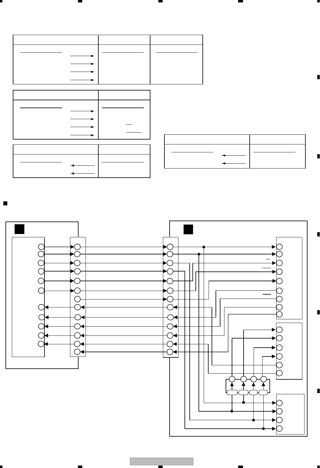
XV-EV1000 111
5678
5678
C
D
F
A
B
E
IC5501 µ-com port IC601 DIR port
Pin No. Pin Name
No.25 DSPCLK
No.23 DSPDI
No.79 DIRCS
No.78 DIRRST
Pin No. Pin Name
No.19 CCLK
No.18 CDTI
No.20 CSN
No.23 PDN
Pin No. Pin Name
No.42 CCLK
No.43 CDTI
No.41 CSN
No.17 PDN
IC701 CODEC port
IC5501 µ-com port IC801 DSP port
Pin No. Pin Name
No.25 DSPCLK
No.23 DSPDI
No.84 DSPSS
XDSPRST
Pin No. Pin Name
No.36 SCK
No.34 MOSI
No.37 SS
No.47 RESETNo.85
IC5501 µ-com port IC601 DIR port
Pin No. Pin Name
No.80 DIRDO
No.77 DIRERR
Pin No. Pin Name
No.17 CDTO
No.22 INT0
IC5501 µ-com port IC801 DSP port
Pin No. Pin Name
No.24 DSPDO
No.82 DSPHREQ
Pin No. Pin Name
No.35 MISO
No.38 HREQ
IC5501
CN5507 CN951
IC801
DSP
IC601
DIR
IC701
IC951
LEVEL
SHIFTER
CODEC
DSPCLK SCK
DSPDI MOSI
DIRCS SS
DIRRST RESET
DSPSS MODA
XDSPRST MISO
HREQ
DIRDO MUTE
DSPDO
DSPHREQ
CCLK
DECMUTE
CDTI
DIRERR
DSPCK
DSPDI
DIRCS
DIRRST
DSPSS
DSPRST
DSPMODE
DIRDO
DSPDO
DSPHREQ
DECMUTE
DIRRERR
BUSY
BUSY
CSN
PDN
CDTO
INT0
CCLK
CDTI
CSN
PDN
12
3
2
8
9
5
4
11
6
13
1
10 36
34
37
47
51
35
38
54
70
19
18
20
23
17
22
42
43
41
17
7
12
3
2
8
9
5
4
11
6
13
1
10
7
23
79
78
84
85
80
24
82
83
77
25
U-com
IFAF ASSY DSP ASSY
CD
11 8 6 3
12,13 9,10 4,5 1,2
*1 : µ-com-port which has sent the signal to IC
CONNECTION DIAGRAM
* This connection diagram displays the connection between
the U-com, DSP, DIR and CODEC.
The pin order is different from the true assignment.
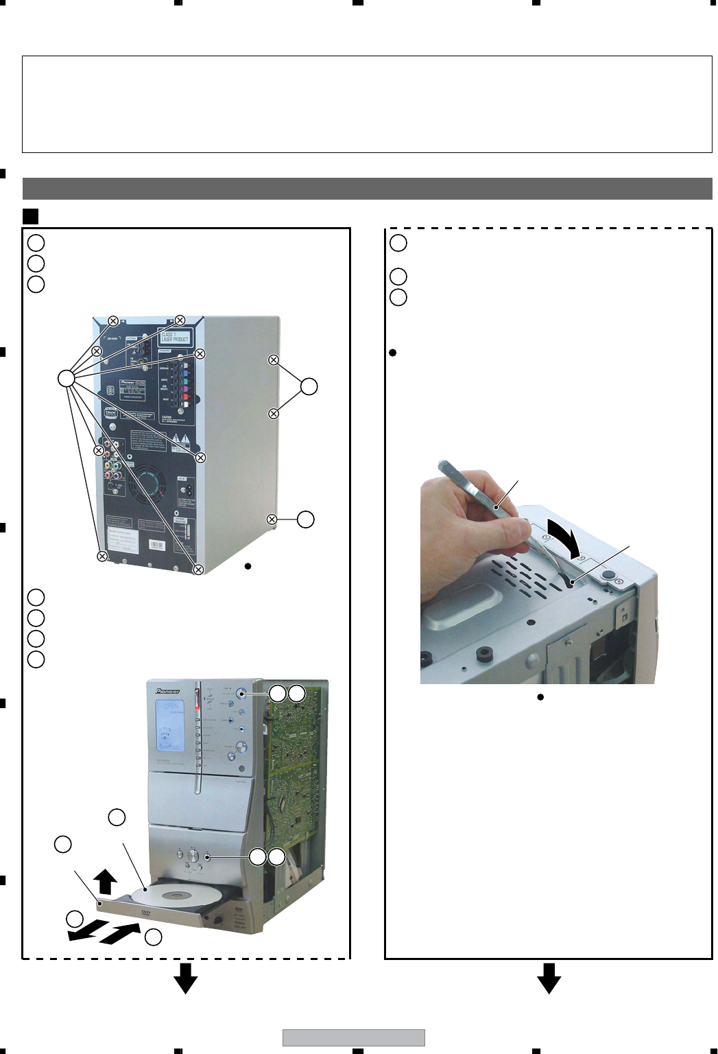
XV-EV1000
112
1234
1234
C
D
F
A
B
E
7.1.11 DISASSEMBLY
1Remove 4 screws from Bonnet L and R (BPZ30P080FNI).
Remove 2 screws from Bonnet L and R (BBZ30P080FNI).
Remove the Bonnet by removing the 8 screws
(BBZ30P080FNI).
4
4 9
Press the STANDBY/ON button to turn on the power.
5Press the 0 OPEN/CLOSE button to open the Tray.
6Remove the Tray Cap Assy.
7Set the Test Disc.
Bonnet and Tray panel
1
How to open the tray when the power cannot be on
Insert a Tweezer(as shown in the photo) into the slit located at
the bottom of the unit and slide the projection of the Drive Cam in
the Loader Assy in the direction of the arrow, as indicated in the
photo.
If the tray pops out a little, fully pull it out by hand.
Diagnosis of PCB's
Note 1: Do NOT look directly into the pickup lens. The laser beam may cause eye injury.
Note 2: Even if the unit shown in the photos and illustrations in this manual may differ from your product, the procedures
described here are common.
Note 3: For performing the diagnosis shown below, the following jigs for service is required:
• Flexible cable for service (GGD1309)
• Cable for service (GGD1425)
8Press the 0 OPEN/CLOSE button to close the Tray.
(Test disc is clamped.)
9Press the STANDBY/ON button to turn off the power.
10
Pull out the Power cord.
Tray Cap Assy
Test Disc
Tweezer
Rear View
Bottom View
2
3
1
2
3
5
5
6
7
8
8
Slit
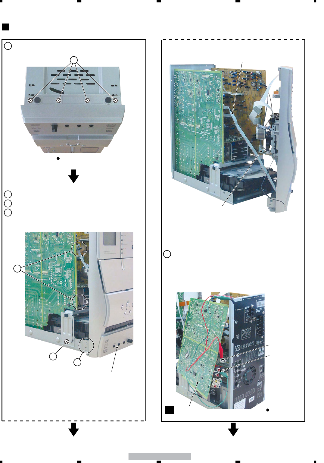
XV-EV1000 113
5678
5678
C
D
F
A
B
E
1Remove 4 screws at bottom side of the unit.
Front Panel, Amplifier Assy and
DSP Board diagnosis
2
5In the event that Power Amplifier Assy was removed and
repaired(IFAF Assy had been removed)
If you want to power on the set with IFAF Assy removed
from the Rear Panel, make sure both the DSP and RCA
grounds are connected to the Rear Panel as shown in
the attached photo.
Do not remove this cable, once removed,
the display will indicate "Mic in"
and you cannot select 5.1 channel output signal,
only 2 channel signals will be output.
Not affected for model with 2 channel output.
(But display will also indicate "Mic in")
Do not remove this cable, once removed,
there is no amplify output signal, you need
to use the headphone to hear the output signal.
2
2
Remove the grounding screw.
3
4
Unhook the 2 cable hooks.
4Released the hook at the right and left side of the Front
Panel Assy.
Bottom View
Rear View
1
DSP Ground
RCA Ground
Front Panel Assy
IFAF Assy
3
C
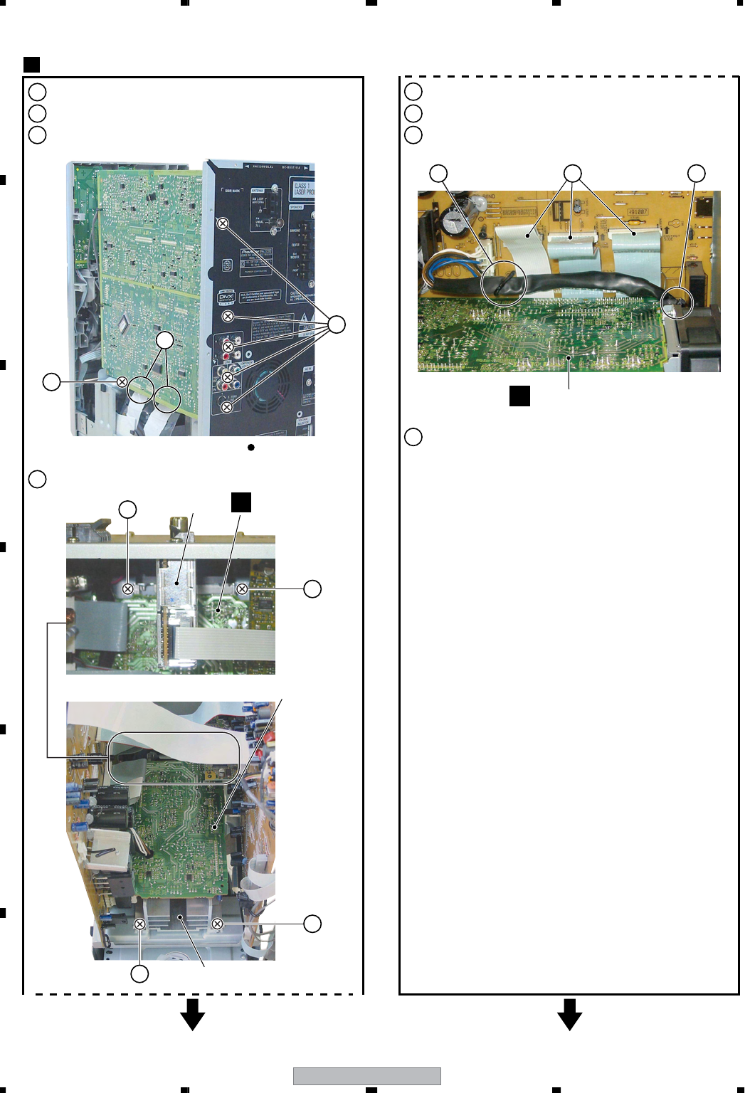
XV-EV1000
114
1234
1234
C
D
F
A
B
E
1Remove 5 screws at the Rear Panel of the unit.
4
4
Remove 4 screws on the Power Amplifier Module.
Disassembly of Power Amplifier Module
3
8Lift up the IFAF Assy as shown in the photo above to
remove the Power Amplifier Module.
2Remove 1 screw on the IFAF Assy Bracket. 6Remove the binder.
3Disconnect the FFC Cables at CN5102 and CN8301. 7Remove the cables on CN3011, CN3012 and CN3013
Rear View
1
2
3
Tuner Assy
Power Amplifier Assy
AMP Assy
4
4
4
Power Amplifier Module
5Remove the cable hook.
75 6
I
AMP Assy
I
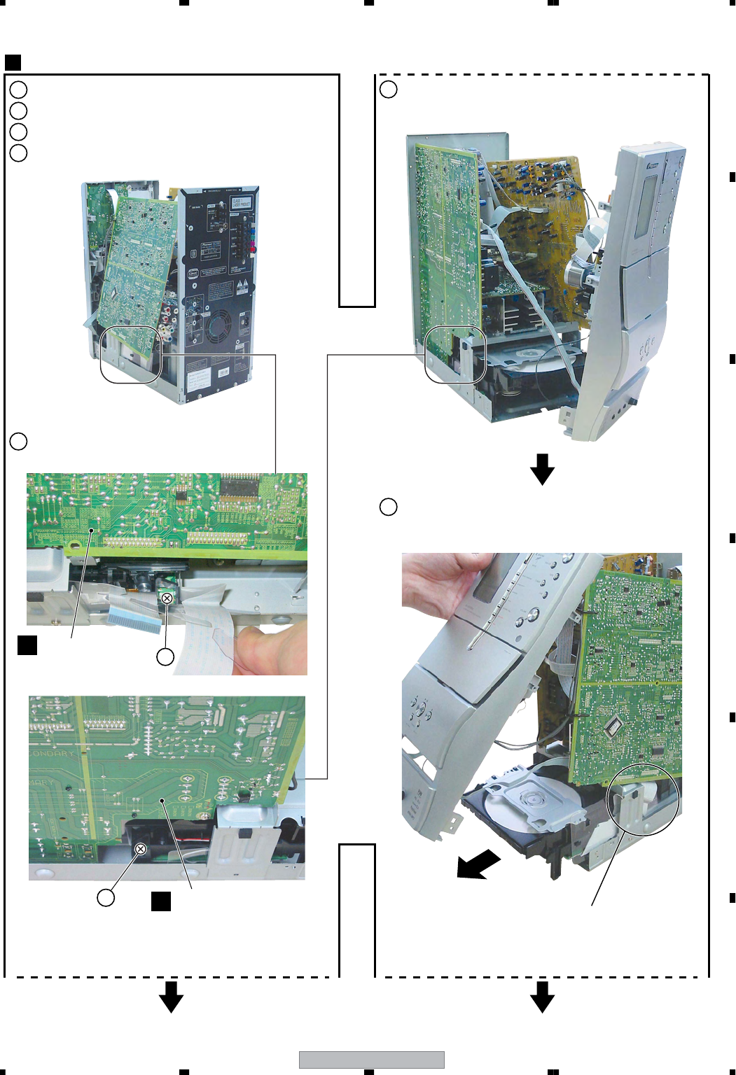
XV-EV1000 115
5678
5678
C
D
F
A
B
E
1Remove the Top Bonnet.
DVD Main Board diagnosis
4
7Carefully remove the DVD Module
by lifting the Front Panel Assy upward.
Caution : Be careful not to damaged
the 2 DVD FFC Cable
2Power on the unit, open the Tray and remove the Tray Cap.
3Load in a DVD test disc and power off the unit.
4Remove the IFAF Assy as in section 3 steps 1 to 3.
5
5
Remove 2 screws from the DVD Module.
IFAF Assy
POWER Assy
6Follow the procedure in section 2 (Steps 1 to 5)
and remove the Front Panel Assy as shown in the photo.
5
C
J
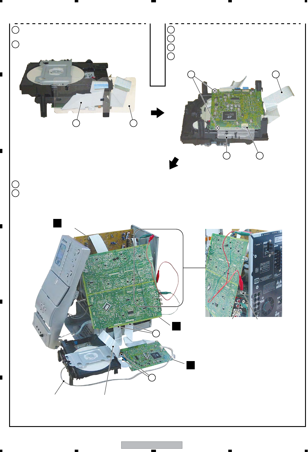
XV-EV1000
116
1234
1234
C
D
F
A
B
E
8Remove the DVD FFC Plastic Holder
as shown in the photo below.
9Remove the FFC Cable and replaced it with GGD1309.
10
Remove the FFC Cable from the hooks.
11
Remove 2 screws.
12
Remove Plastic Holder and unhook the cable.
13
Remove cables and replaced it with GGD1425.
14
Flip the DVD PCB and unhook the 2 flexible as shown in the photo.
15
Connect both FFC Cables onto IFAF Assy CN5102 (use GGD1309) and CN8301(use back original cable)
Flip the DVD Main Board as shown in the photo.
Also ensure that both the DSP and RCA ground are connected to the Rear Panel.
89
1011
12 13
GGD1309
14
15
GGD1425
RCA Ground DSP Ground
DVDM Assy
B
IFAF Assy
C
POWER Assy
J
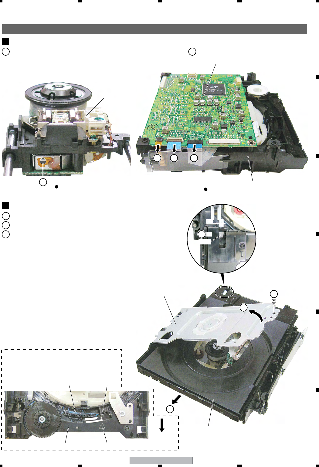
XV-EV1000 117
5678
5678
C
D
F
A
B
E
Removing the Traverse Mechanism Assy-S and 05SD Pickup Assy-S
1
05 LOADER Assy
1
Short-circuit point by soldering. 2Disconnect the three flexible cables.
Note: After replacement, connect the flexible
cable for pickup, then remove the
soldered joint (open).
1
222
Rear view Bottom view
DVDM Assy
05 LOADER Assy
05SD Pickup Assy-S
1Remove the one screw.
2Remove the bridge 04.
3Pull out the tray, then remove it by pressing the
hook.
1
2
3
Bridge 04
Front side
Hook
Tray
Loading base Triangle
Pin
Drive cam
-2
3-2
Note when reinserting the tray
When reinserting the tray, first align the triangle
printed on the loading base and the pin of the drive
cam, then insert the tray.
Bridge 04, Tray
2
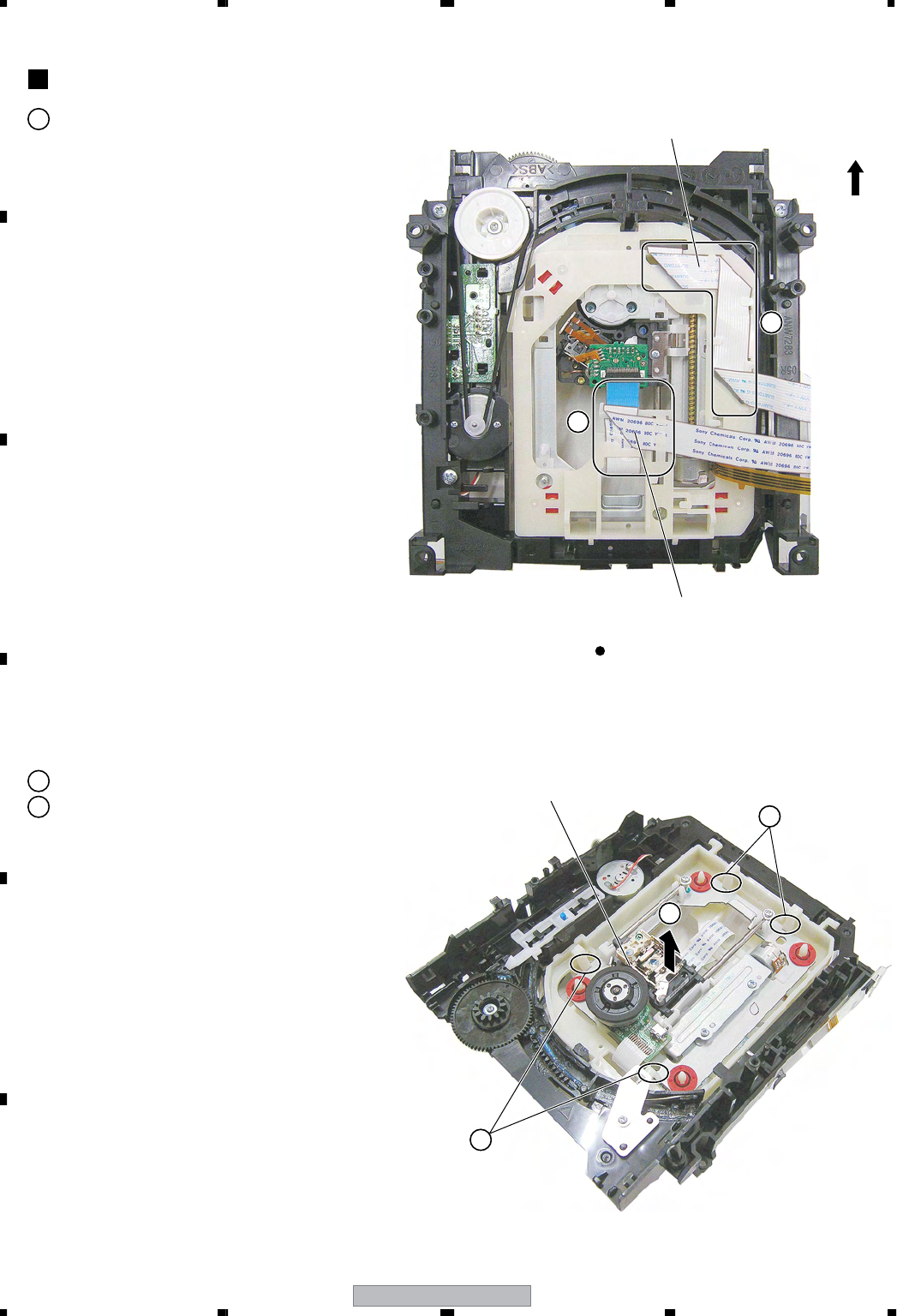
XV-EV1000
118
1234
1234
C
D
F
A
B
E
1
Traverse Mechanism Assy-S
3
Dislodge the two flexible cables from their factory
placement.
2Unhook the four hooks.
3Remove the Traverse Mechanism Assy-S
× 2
2
× 2
2
3
Traverse Mechanism Assy-S
1
1
Front Side
Flexible cable
for the spindle motor
Flexible cable for the pickup
Bottom view
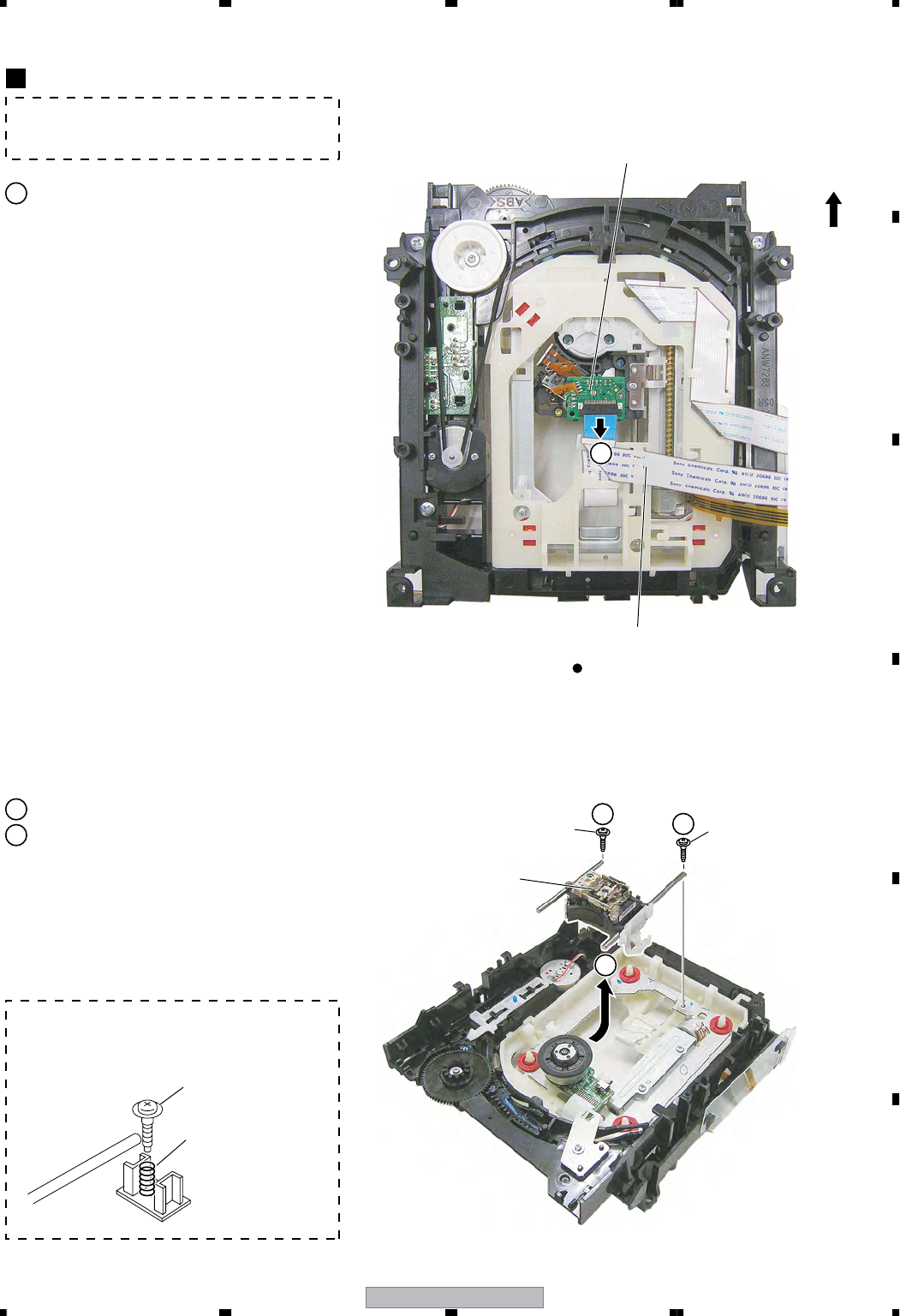
XV-EV1000 119
5678
5678
C
D
F
A
B
E
3
2
2Adjustment screw
(skew screw VK1)
Adjustment screw
(skew screw VK1)
Adjustment screw
(skew screw VK1)
Adjustment spring
(skew spring VK1)
05SD Pickup Assy-S
4
Note: The 05SD Pickup Assy can be removed
without removing the TTraverse Mechanism
Assy-S.(shown as Step π.)
Note: Be careful not to lose the adjustment spring
(skew spring VK1).
Flexible cable for the pickup
05SD Pickup Assy-S
1
Front Side
1Disconnect the flexible cable for the pickup.
2Remove the two adjustment screws.
3Remove the 05SD Pickup Assy.
Bottom view
05SD Pickup Assy-S
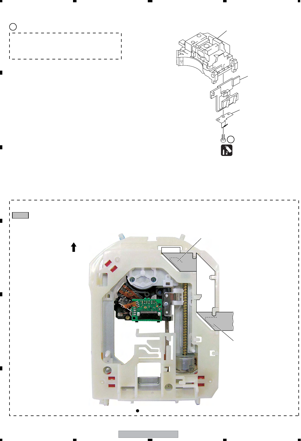
XV-EV1000
120
1234
1234
C
D
F
A
B
E
Note: The screw is secured with the silicone
adhesive.
Make sure to apply the silicone adhesive after
reattaching the screw.
4Remove the one screw.
4
Silicone Adhesive
GEM1037
05SD Pickup Assy
Joint VK1B
Joint spring VK1
: Conductive surface
Arrangement of the flexible cable for the spindle motor
Front Side
Hook
Hook
Bottom view
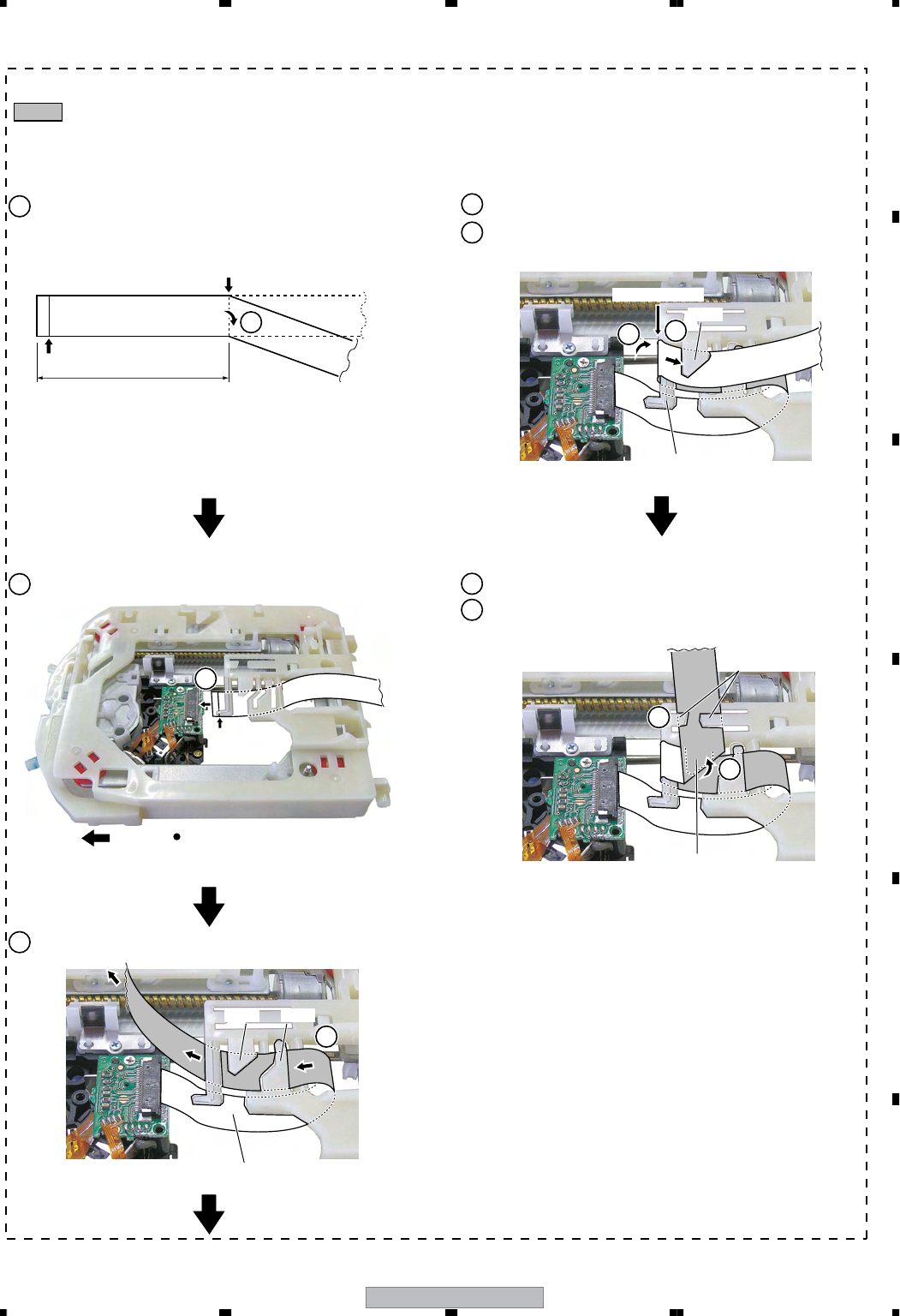
XV-EV1000 121
5678
5678
C
D
F
A
B
E
Front Side
Note:
Be sure to move the 05SD Pickup Assy to the innermost perimeter.
: Conductive surface
Arrangement of the flexible cable for the pickup
2
3
7
2Attach the flexible cable for the pickup to the connector. 6Fold the flexible cable along the hook.
7Pass the flexible cable through the hook.
3Pass the flexible cable through the hook.
Bottom View
Make sure that the cable is loose
Backing
Backing
Reference line
Hook
Hook
45
5Pass the flexible cable through the hook.
4Hook the part folded in Step 1 to the hook.
Hook
Reference line
6
Hook
1Fold the flexible cable for the pickup with the backing outward
in the illustration below.
76 mm
1
Hook
Hook

XV-EV1000
122
1234
1234
C
D
F
A
B
E
7.2 PARTS
7.2.1 IC
PDC127A (IFAF ASSY : IC5501)
• System Control Microcomputer
• The information shown in the list is basic information and may not correspond exactly to that shown in the schematic diagrams.
• List of IC
PDC127A
No. Pin Name I/O Pin Function
1 DVDON/OFF O Control power supply for DVD module
2 HPDET I Detect to insert headphone
Mic Detection
3 MICDET I
4 ACPULSE I AC PULSE input detection (Interruption 0)
Mute control for center speaker (Standby)
5 (XMUTEC) O
6 RDSCLK I Clock input from RDS decoder (Interruption 2, without RDS : Low output)
7 REMOCON I REMOCON signal input (Interruption 3)
8 XRESET I µ-com reset input
9 XT1 −Subclock (connect to VDD when no use)
10 XT2 −Subclock (leave open when no use, and set the bit 6 of OCR SFR)
11 VSS1 −
12 CF1 −Main Clock (connect to VDD when no use)
13 CF2 −
−
−
Main Clock (leave open when no use)
14 VDD1 −
15 SIMUKE I Destination distinction input
16 MODEL I Model distinction input
17 VDET I DVD3.3V detection input
18 KEY1 I Key1 input
Key2 input
Key3 input
Level meter signal input
19 KEY2 I
20 KEY3 I
21 LEVELIN I
22 XPROTECT I Protection and Fan Error detection input
23 DSPDI O Data output to DSP (MOTOROLA) and DIR
24 DSPDO I Data input from DSP (MOTOROLA)
25 DSPCLK O Clock output to DSP (MOTOROLA) and DIR
26 NC O
27 LCDDAT O Data for FL(LCD) driver
28 LCDCLK O Clock for FL(LCD) driver
29 DTS_ON/OFF O Control for DTS
30 XREADY O Chip select for system bus (to DVD module)
31 XHPMUTE O HP MUTE ON/OFF
REC OUTPUT MUTE ON/OFF
32 XRECMUTE O
33 B_MUSIC O Control for LED of BASS MUSIC
34 RYR O REAR RELAY ON/OFF
35 RYFSC O FRONT/SW/CENTER RELAY ON/OFF
Control for LED of BASS MOVIE
36 B_MOVIE O
37 TIMERLED O Control TIMER LED
Control for VOCALC
38 VOCALC O
39 VSS4
40 VDD4
Pin Functions

XV-EV1000 123
5678
5678
C
D
F
A
B
E
No. Pin Name I/O Pin Function
41 ATT10dB O Control for ATT 10dB
Control for ATT 6dB
42 ATT6dB O
43 STEST I Set TESTMODE for Service
44 UTEST I Set UNITCHECK for checker
45 DTSDMX O Control of gain-up for DTS down-mix
46 SWFMX O Control for subwoofer mix
47 VOCALA I Control for VOCALA
48 VOCALB I Control for VOCALB
49 SDATA O System bus data output (AMP side output)
50 MDATA I System bus data input (AMP side input)
51 SCLK I System bus clock input
Chip enable for Tuner LSI
52 TXCE O
53 NC
54 NC
55 VDD2
56 VSS2
57 TCHALF I Input switch of mecha half
58 TCMODE I
Input switch of mecha mode
59 TCRECF I Input switch of mecha during recording forward
60 TCRECR I Input switch of mecha during recording reverse
61 TXCLK O Clock for tuner LSI
62 TXODATA O Data for tuner LSI
63 TCEXPOE O Output enable to EXPAND IC for deck
64 (RDSPOW) O Control power supply of RDS (L : POWER ON)
65 (RDSDATA) O Input RDS data
66 TXIDATA I Input data from tuner LSI
67 DVDACK I Ackknowlegement from DVD MODULE(Interruption 4)
68 TCPULSE I Input pulse of TC reel
Request of MUTE from DVD MODULE(Interruption 5)
69 DVDMUTE I
70 TCMSIN I Input MS signa
71 TCEXPCLK O Clock to EXPAND IC for deck
72 TCEXPCE O Chip enable to EXPAND IC for deck
73 TCEXPDAT O Data to EXPAND IC for deck
74 INPUTSELB O AUDIO INPUT SELECT B
75 INPUTSELA O AUDIO INPUT SELECT A
76 ECHCNT1 O Control for ECHO1
77 DIRERR I LOCK/UNLOCK from DIR
78 DIRRST O Reset to DIR /CODEC
79 DIRCS O Chip select to DIR/CODEC
80 DIRDO I Data input from DIR/CODEC
−
−
−
−
XV-EV1000
124
1234
1234
C
D
F
A
B
E
No. Pin Name I/O Pin Function
81 ECHCNT2 O Control for ECHO2
82 DSPHREQ I Error detection from DSP(MOTOROLA)
83 DECMUTE I Detection of 1stDSP boot success from DSP MODULE
84 DSPSS O Slave selection to DSP(MOTOROLA)
85 XDSPRST O RESET to DSP(MOTOROLA) MODULE
86 ADMD I Control of DSPMUTE combining DIRERR, "H" at digital mode, "L" at analog mode.
MUTE request to DSP module
87 XDSPMUTE O
88 VSS3 −
89 VDD3 −
90 KCONSTB O Strobe for KEY CONTROL IC
91 SYSPOW O Control power supply of system
92 KCONDATA O Data for KEY CONTROL IC
93 XDVDRST O RESET to DVD MODULE
94 XSYSMUTE O Control mute of system
95 KCONCLK O Clock for KEY CONTROL IC
96 VOLCLK O Clock for E-vol IC
97 VOLDATA/CE O Data/CE for E-vol IC
98 FLASH E/D −for FLASH writing
99 FLASH DO −for FLASH writing
100 FLASH CLK −for FLASH writing
No.
1
2
3
4
5
6
7
8
Q1
Q2
Q3
Q4
Q5
Q6
Q7
Q8
XPBMUTE
PB/XREC
RMUTE
DOLBY
SOL
MOTOR
BIAS
XBEATCUT
Control PB mute
Switch DOLBY PB/REC
Control REC mute
Control DOLBY NR (Standby)
Output tape solenoid
Output tape motor
Control bias of deck
Control beat cut of deck
actual function
EXPAND IC (BU4094) Control for deck
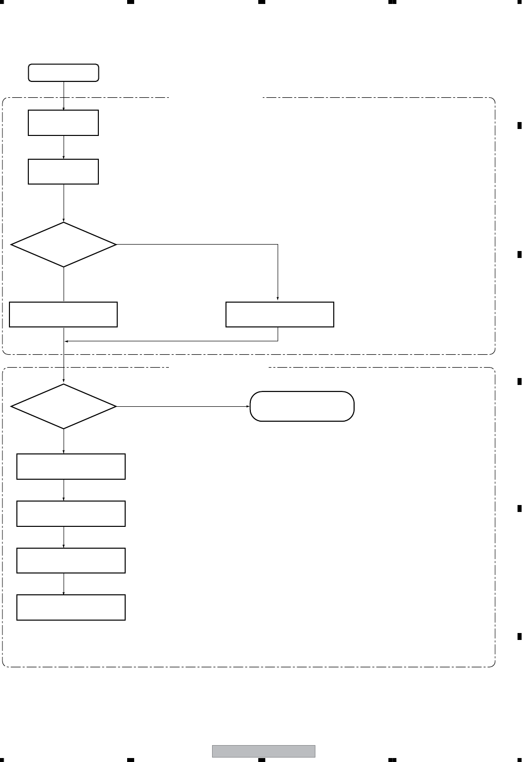
XV-EV1000 125
5678
5678
C
D
F
A
B
E
7.3 EXPLANATION
7.3.1 SEQUENCE AFTER POWER ON
Reset Start
Demonstration mode ?
Yes : Power ON
Yes
No
No
Microcomputer
initialization
Model
identification
Standby setting
• It starts when the XRESET terminal (Pin 8) is "H" level.
• The inputs to Pins 15 are inspected and the model identification is performed.
Demonstration mode
permission
Demonstration mode
System power supply on
DVD microcomputer start-up
Relay release
Demonstration mode
or Normal power ON mode
• The level of the SYSPOW terminal (Pin 91) is "H".
• Only in DVD function, the level of the XDVD RESET terminal (Pin 93) is "H".
• The speaker relay is turned on about four seconds after the power is turned on.
• The level at the RELAY ON/OFF terminal (Pins 34 and 35) are "H."
• The conditions are different depending on whether the headphones are connected
via the Headphones jack, or on the DSP mode.
• If no pulse is input to the AC terminal (Pin 4) for about 60 msec when the microcomputer is in Memory Backup mode,
it will not do any processing.
• The unit will recover from Memory Backup mode if a reset command is input to the XRESET terminal (Pin 8).
• The system mute is released about four seconds after the power is turned on.
The level of the XSYSMUTE terminal (Pin 94) is "L".
• Muting is not released in the following cases.
• When the main volume is 0.
• Whether Demonstration mode is entered or not can be
determined by inspecting the backup data.
• The default setting is "Demonstration mode OK."
Standby
Initialization routine
Main loop processing
Microcomputer IC (PDC127A) (IFAF Assy : IC5501)
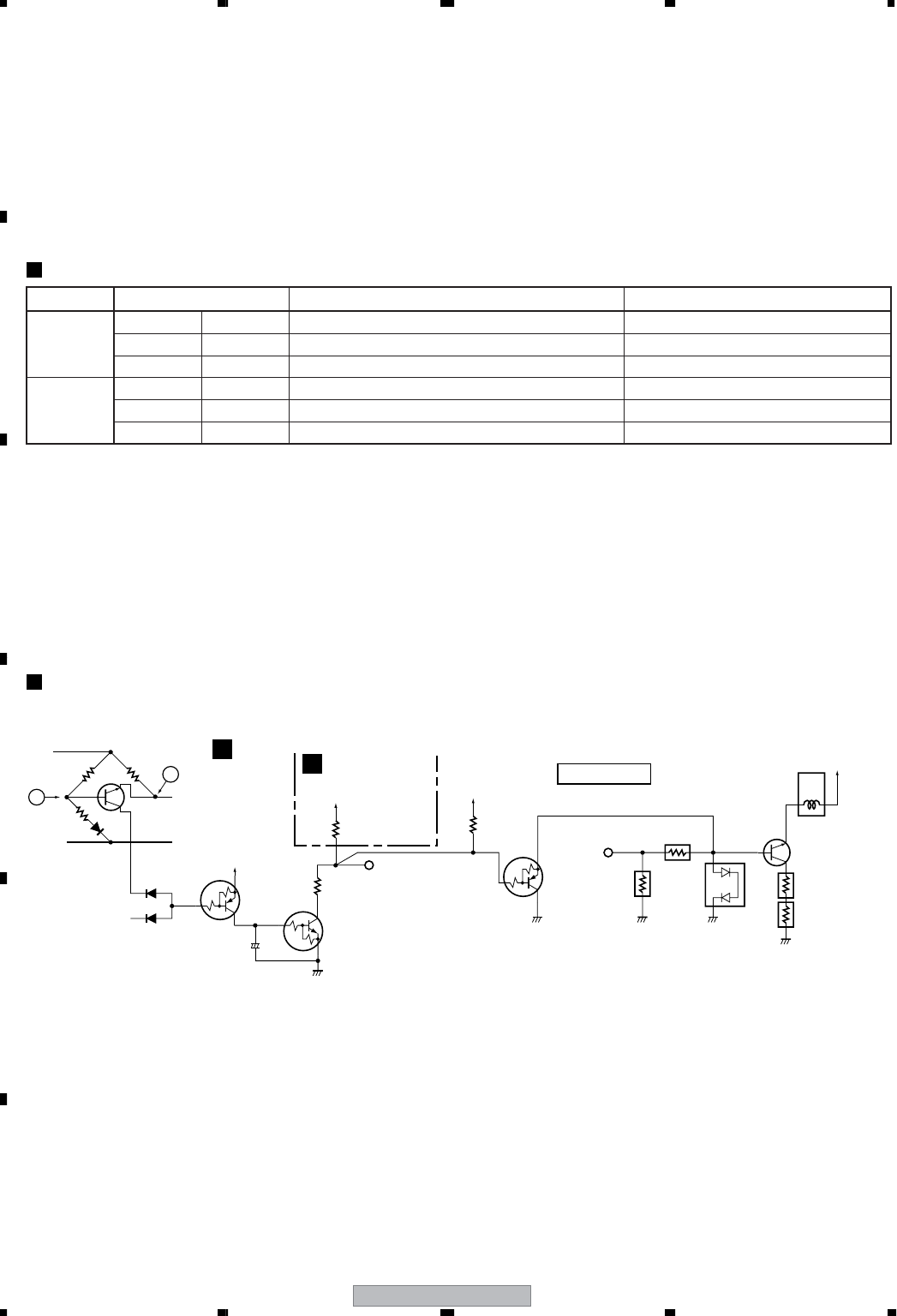
XV-EV1000
126
1234
1234
C
D
F
A
B
E
7.3.2 PROTECTION CIRCUIT
If the TIMER LED on the front panel flashes, check the protection circuit.
Note: If the protection circuit activates, the unit will not recover for 60 seconds even if the AC power cord is disconnected then reconnected.
If you activate Service Test mode, the protection circuit becomes invalid, which makes diagnosis easy. (To activate Service Test mode,
while connecting STEST port (IC5501 Pin43) to "+5V", connect AC power cord.) (Refer to "7.1.6 SERVICE TEST MODE")
There are three types of operations for the protection circuit, which are indicated on the FL display when Service Test mode is entered:
PRTCT WNG: The unit was shut down because of an abnormality in the AMP system. (The PROTECT line operates at the MID level.)
PRTCT ERR: The unit was shut down because of a failure in the AMP system. (The PROTECT line operates at the LO level.)
DVD PRTECT: The unit was shut down because of a failure in the DVD system. (The VDET line operates at the HI or LO level.)
Conditions for the protect circuit operations
Protection circuit that activates against a PRTCT WNG error
Voltage Conditions FL display in Service Test mode
PROTECT
HI level >3.55V Normal
MID level 1.8V - 3.5V The unit is shut down because of an abnormality. PRTCT WNG
LO level <1.8V The unit is shut down because of a failure. PRTCT ERR
VDET
HI level >4.25V The unit is shut down because of a failure. DVD PRTECT
MID level 3.3V Normal
LO level <2.5V The unit is shut down because of an abnormality. DVD PRTECT
The possible failures for each error message are as follows:
PRTCT WNG:
• The Speaker terminal became overloaded because of short-circuit. (See 1.)
PRTCT ERR:
• The main power supply became LO level because of short-circuit or disconnection of connectors. (See 2.)
• Disconnection of the FAN connector or interruption of rotation of the fan (See 3.)
• DC was generated at the output because of a failure in the AMP system, etc. (See 4.)
• Abnormal temperature was detected by the thermistor. (See 5.)
DVD PRTECT:
• An error was generated in the main power supply inside the DVDM. (See 6.)
1 When the Speaker terminal becomes overloaded
Q3601
Q3639
Q3640
B
E
C
+5V
D3603
DAP202K
C3633
10/50
D3601
R3607
0.1
R3639
27k
R108
27k
Front L ch
to
XPROTECT
GND FL
R3601
1.8k
R3603
33k
B
A
VD+5
+
to
SYSPOW
POWER Assy POWER Assy
JAMP Assy
I
In Normal mode, the speaker (6 ohms) is connected between the
FL and GND FL points. Because the voltage at Point A is higher
than that at Point B, Q3601 does not operate.
If the resistance between the FL and GND FL points becomes
1.83 ohms or less, Q3601 begins to operate, Q3639 is turned on,
Q3640 (E, C, and B)is turned on, and the level of XPROTECT
becomes MID.
→The microcomputer detects the XPROTECT level and
shuts the power to the unit off.
Q83
RT1P241M
Q81
2SD1858X(QR)
R83
18
RY81
XSR3008
R84
18
D87
DAN217
R90
27k
VD+5
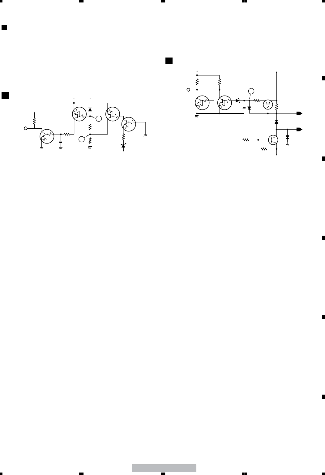
XV-EV1000 127
5678
5678
C
D
F
A
B
E
Protection circuit that activates against a PRTCT ERR error
B
A
C101
(C102)
1/50
+
to
XPROTECT
(µ-com)
AMP Assy
I
R108
27k R101
(R104)
1k
R102
(R105)
10k
R103
(R106)
10k
R109
820
D105
(D106)
Q102_1/2
(Q104_1/2)
Q102_2/2
(Q104_2/2)
Q101_1/2
(Q103_1/2)
Q101_2/2
(Q103_2/2)
D101
(D102)
VD+5
VD+5
VH+
(VP+15)
VH–
(VA–12)
2 -1 Short-circuit-detection circuit for the amplifier
power circuit (VH+[VP+15], VD+5, -12 V [VA-12])
Circuit for shutting the power off when VP+15, VD+5, or VA-12
is short-circuited to ground (GND)
• In Normal mode, as Q101 (Q103) (E2, B2, C2) and Q102
(Q104) (E2, B2, C2) are on, the voltage at Point A is about 5 V.
The voltage at Point B is therefore about the same. As Q101
(Q103) (E, C, B) is off, Q102 (Q104) (E, C, B) is also off.
(1) When VH+(VP+15) is short-circuited to GND
As the voltage at Point B becomes almost ground potential, and
Q101 (Q103) (E, C, B) then Q102 (Q104) (E, C, B) are turned on,
the level of XPROTECT becomes low.
→The microcomputer detects the XPROTECT level and shuts
the power to the unit off.
(2) When VH-(VA-12) is short-circuited
As the electric potential of VE at Q102 (Q104) (E2, C2, B2)
becomes the same as that at VB, Q102 (Q104) (E2, C2, B2) is
turned off. Following this, Q101 (Q103) (E2, B2, C2) is turned
off, which changes the voltage at Points A and B to a value other
than 5 V. Therefore, Q101 (Q103) (E, C, B) then Q102 (Q104) (E,
C, B) are turned on, the level of XPROTECT becomes low.
(3) When VD+5 is short-circuited
The level of the XPROTECT line becomes low. The
microcomputer detects the XPROTECT level and shuts the power
to the unit off.
C
C
E
E
B
B
B2
B2
E2
E2
C2
C2
2When the main power supply becomes LO level
because of short-circuit or disconnection of
connectors
* ( )means the wiring No. of VP+15 line.
A
+
to
XPROTECT
(µ-com)
R108
27k
Q3651_2/2
RN1901
Q3651_1/2
RN1901
C2 C
E
B
E2
B2
VD+5
FAN+
VPF+15
V-12F
R3654
1.8k
D3658
UDZS3.9B
D3657
1SS355 D3655
1SS133
D3651
1SS133
R3655
8.2k
R3656
22k
R3658
2.2k
R3657
33(1/4W)
Q3652
DTA124TK
Q3654
2SD2144S
C3652
47/50
AMP Assy
I
3When the FAN connector is disconnected or
when rotation of the fan is interrupted
FAN–
If no fan is connected between FAN+ and FAN-, or when the fan
cannot rotate because of a foreign object caught in the blades, the
BASE of Q3652 becomes OPEN, and Q3652 and Q3651-1/2 (E, C,
B) are turned off. Then Q3651-2/2 (E2, B2, C2) is turned on, and
the level of XPROTECT becomes low.
→ The microcomputer detects the XPROTECT level and shuts
the power to the unit off.
When FAN+ and FAN- are short-circuited, the electric potential at
Point A becomes higher than GND level by the addition of the
values at D3656 and D3657. As this value is lower than that at
D3658, Q3651 (E, C, B) is turned off, Q3651 (E2, B2, C2) is
turned on, and the level of XPROTECT becomes low.
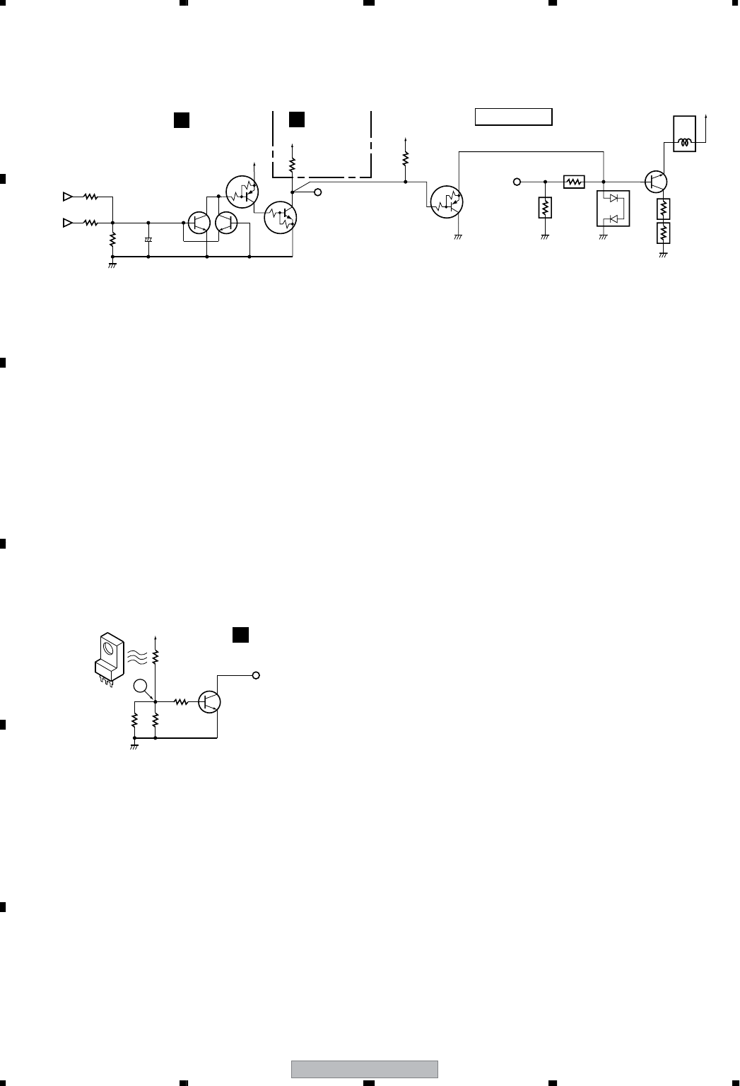
XV-EV1000
128
1234
1234
C
D
F
A
B
E
4
When DC is generated at the output because of
a failure in the AMP system, etc.
5
When abnormally high temperature is detected
by the thermistor
R3605
(R3625)
(R3615)
27k
R3606
(R3626)
(R3616)
27k
R3638
10k
Front L ch
(SW, SL)
+5V
C3632
470/6.3
Q3637
Q111
2SC4081
R113
220
IC81
TA7805S
R112
1k
TH111
NCP18WF104J03RB
R111
1k
Q3638
Q3632
Q3633
B
C
E
+
XPROTECT
to
XPROTECT
POWER Assy
J
R108
27k
VD+5
VD+5
AMP Assy
I
AMP Assy
I
Front R ch
(C, SR)
• In Normal mode, both Q3637 and Q3638 are off.
(1) When positive (+) DC voltage is generated at the SP
terminal
When positive (+) DC voltage is generated at the L or R channel,
and VB of Q3637 becomes higher than that at the operation point,
Q3632 (E, C, B) is turned on, and the level of XPROTECT
becomes low.
→The microcomputer detects the XPROTECT level and shuts
the power to the unit off.
(2) When negative (-) DC voltage was generated at the SP
terminal
Q3638 is turned on, and XPROTECT is activated.
5 -1 IC81 abnormal temperature detection circuit
A
The voltage at Point A becomes the divided voltage of TH111
and R111//R112 (combined resistance of parallel-connected
resistors R111 and R112.) In Normal mode, the resistance at
TH111 is much higher than R111//R112, and Q111 is off. (Note
that the resistance at TH111 becomes lower as the temperature
increases.) If the solder temperature at IC81 increases abnormally,
the temperature at TH111 (thermistor) mounted closest to the land
of IC81 increases accordingly, and the resistance at TH111
decreases.
When the temperature at TH111 reaches 90-110_C (varying
according to conditions,) the voltage at Point (A) becomes high
enough to turn Q111 on, and the level of the XPROTECT line
becomes low. The microcomputer detects the XPROTECT level
and shuts the power to the unit off.
to
SYSPOW
POWER Assy
Q83
RT1P241M
Q81
2SD1858X(QR)
R83
18
RY81
XSR3008
R84
18
D87
DAN217
R90
27k
VD+5
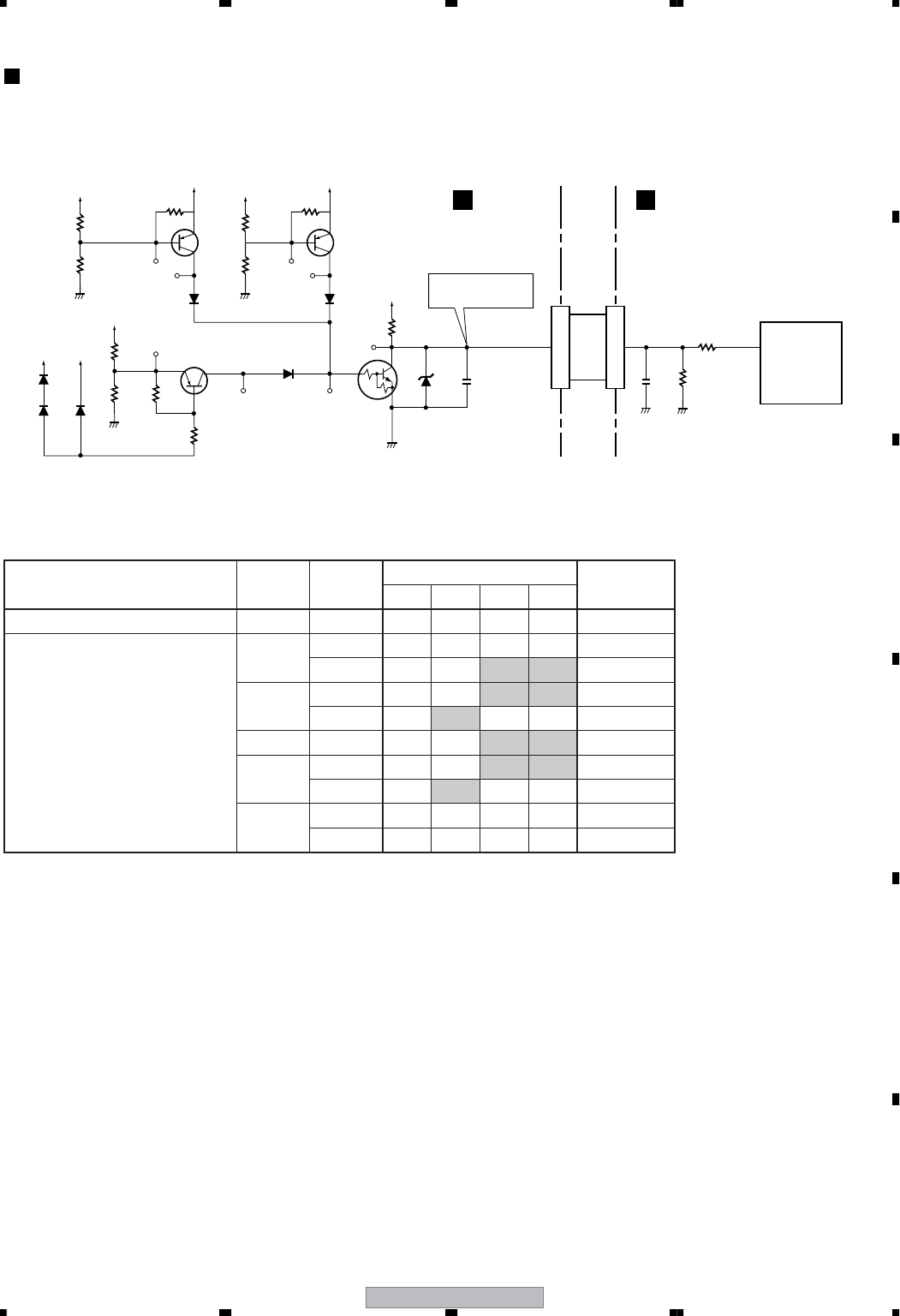
XV-EV1000 129
5678
5678
C
D
F
A
B
E
Protection circuit that activates against a DVD PRTECT error
6 The DVDM monitors the voltage of the main power supply by VDET signals.
In Normal mode, the VDET signal is at the MID level (3.3 V). In the following conditions, the VDET signal level becomes L or H, and
the microcomputer is notified of this abnormality.
Items to be detected by VDET
(1) When the power voltages inside the DVDM become abnormal, as shown in the table below
(2) When the VDET signal to the microcomputer is interrupted because of defective soldering of the 30-pin connector or incomplete
insertion of FFC
→ The VDET level is lowered by the pull-down resistor (1 Mohms) on the side of the microcomputer.
Status Power Voltage Operation VDET voltage
Q881 Q851 Q821 Q801
In Normal mode off off off off Mid 3.3V
When an abnormality is generat
VDVD+12 <8.8V on on off on L
>15.5V off off on on L
VPR+8 <5.2V −off on on L
>12.6V on −−on L
V+6R5 <3V −−on on L
V+5 <3.6V −off on on L
>6.6V −on off on L
V+3R3 <2.5V −−−− L
>4.25V −−−− H
DVDM Assy
BIFAF Assy
C
R5594
220
IC5501
PDC127A
R5967
1M
17
4VDET
CN5102
µcom
C5962
0.01
Q801
DTC124EUA
D852
D862
D861
D801
UDZS4.7B
C801 0.1
R801
470 VDET
NORMAL : 3.3V
ABNORMAL :
<
0.5VDD
>
0.85VDD
L
<
2.5VDD
H
>
4.25VDD
V+5VV+SR5
V+3R3
Q821
2SA1576A(RS)
D851
2SA1576A(RS)
D851
4
CN901
Q881
2SA1576A(RS)
D881
R882
10K
GNDD
GNDD
V+12
V+5V VPR+8
R801
470
R823
15K
GNDD
V+12
R824
10K R822
47K
R851
47K R881
47K
R821
10K
R821
R852
15K
GNDD
V+12
R853
10K
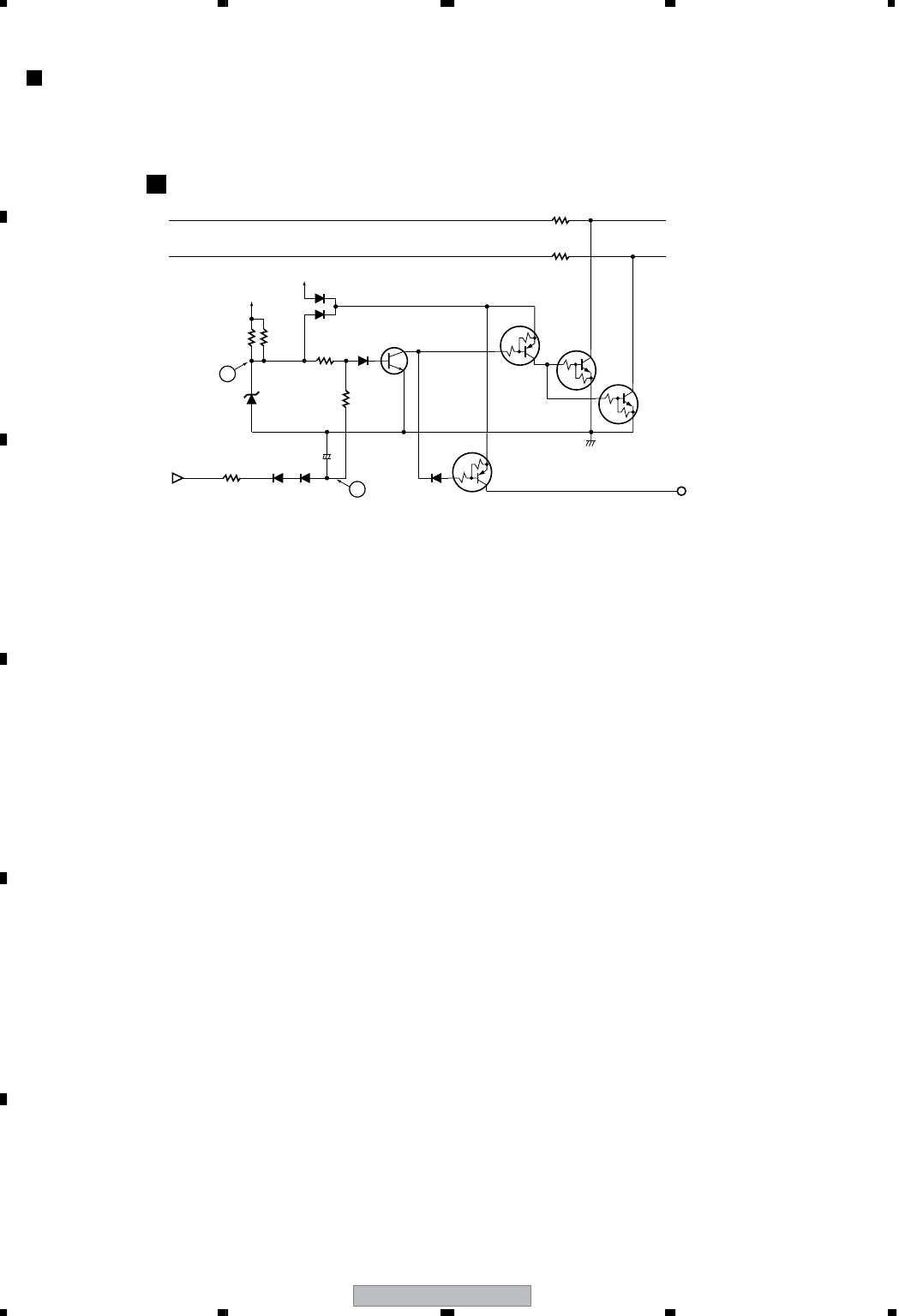
XV-EV1000
130
1234
1234
C
D
F
A
B
E
• The base voltage at Q3631 is a voltage between Points A and B divided by R3633 and R3634. As this voltage is negative (-) in Normal
mode, Q3631 is off.
When the AC power cord is disconnected and there is no AC power input, the base voltage at Q3631 becomes +0.6 V or more, and Q3631
is turned on. Then, the operations below follow.
(1) SP Relay
Q3632 (E2, C2, B2), Q3633, and Q3636 (E, C, B) are turned on, the line to activate the power amp mute becomes low level, and the power
amp mute is turned on.
(2) HP MUTE
Q3635 is turned on, and the MUTE circuit for HP is turned on.
Other protection circuit
AC detection circuit
7This is a protection circuit that prevents popping sounds in the Speaker and Headphones output when the AC power cord is connected or
disconnected.
POWER Assy
J
• The voltage at Point A is a DC voltage which has been generated by half-wave rectification on the minus side of the AC power.
• The voltage at Point B is approx. 5 V.
Q3633
Q3636
Q3632
Q3635
Q3631
D3636
D3634
R3634
2.7k
R3633
10k
D3635
DAN202K
R3641
STBY
B
C
C2
B2
E2
E
+
RYF to SP Relay Circuit
to SP Relay Circuit
to HP MUTE
VD+5
VH+
R3632
22k
R3631
22k
R3642
STBY
RYR
ACB
B
A
D3631
MTZJ5.1A
D3633D3632
C3631
2.2/100
R3635
3.3k
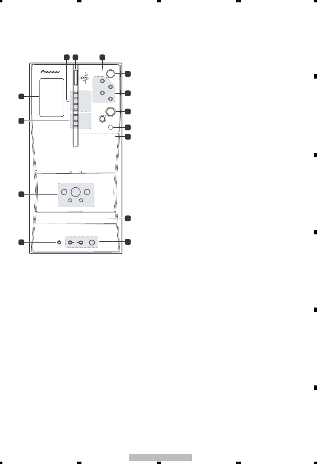
XV-EV1000 131
5678
5678
C
D
F
A
B
E
8. PANEL FACILITIES
Front panel
Illustration shows the EV700/1000 model
1 Display
See Display below.
2 Sound options
FRONT SURROUND (EV700/1000 only) –
Switches on the Front Surround mode.
SFC (EV500 only) – Selects sound modes or
custom settings from the Sound Field Control.
SOUND MODE
Accesses settings in the Sound menu,
such as the tone controls.
KARAOKE – Selects audio channels for
karaoke.
ENTER – Selects options or executes
commands.
3
X.BOOM
button
Press to switch on the bass boost.
4
TIMER
indicator
Lights when the timer has been set.
5
STANDBY/ON
Switches the player on or into standby.
6 Function select buttons
Selects the source you want to listen to.
7
VOLUME +/–
Adjusts the volume level.
8 Remote sensor
9
PUSH OPEN
Pressing down on this side on the cassette
door will open the tape deck.
10 Disc tray
11
MIC VOL
and MIC input jacks
Controls the volume of the karaoke mics
(MAIN and SUB).
12
PHONES
jack
Headphone jack.
PHONES SUB MAIN MIC VOL
MS+/FF
MUSIC TIMER
DVD/CD
TAPE
LINE
TUNER
VOLUME
STANDBY/ON
MOVIE
FRONT SURROUND
SOUND MODE
KARAOKE
ENTER
REVERSE MODE
REC/STOP
ASES
PUSH OPEN
+- TUNING
MS-/REW
MIC
MIN MAX
1
4
14
12
13
7
8
9
6
5
10
11
32
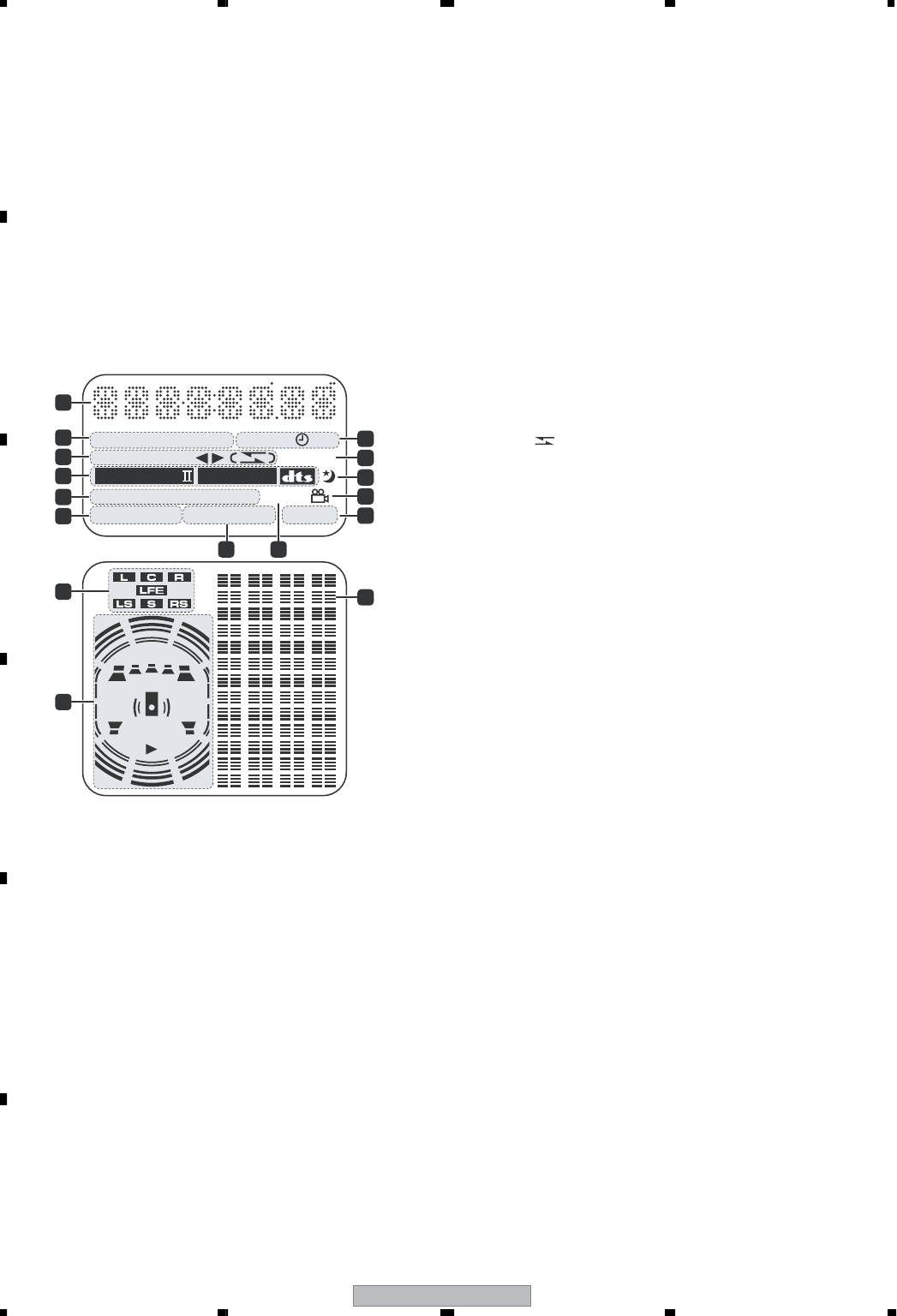
XV-EV1000
132
1234
1234
C
D
F
A
B
E
13
TUNING
and playback control buttons
The tuning/scan/skip buttons are used for
tuning into stations, skipping or scanning
tracks on discs or tapes. The playback control
buttons are used for playing, pausing and
stopping playback ( ejects the disc).
14 Tape cassette controls
REVERSE MODE – Selects the playback
mode for tapes.
REC/STOP – Starts/stops recording on the
tape deck.
ASES – Press for CD-to-tape synchro
recording.
Display
1 Character display
2Karaoke indicators
ECHO – Lights when the Karaoke ECHO
effect is selected.
KEY – Lights when the Karaoke pitch
control is selected.
KARAOKE (Vocal cancel) – Vocals in the
backing track are partially eliminated using
EQ.
L – Left channel only. Use for tracks that
have a vocal recorded in the right channel.
R – Right channel only. Use for tracks that
have a vocal recorded in the left channel.
L R – Use to put a single-channel vocal
track into the center of the mix.
3 Cassette deck indicators
B.CUT – Lights when the beat cut mode
has been switched toB.CUT 2.
ASES REC – Lights during ASES recording.
REC – Lights when recording to the tape
deck.
– Indicates the direction of tape
playback.
– Indicates the reverse mode.
4 Format indicators
2PRO LOGIC II (EV700/1000 only) – Lights
during Dolby Pro Logic II decoding.
2DIGITAL – Lights during playback of a
Dolby Digital signal.
DTS – Lights during playback of a DTS
source.
5
Tuner indicators
MONO – Lights when FM mono reception
is selected.
STEREO – Lights when a stereo FM
broadcast is being received in auto stereo.
mode
TUNED – Lights when a broadcast is being
received.
6 DSP indicators
ADV.SURR. (EV700/1000 only)
Lights when one of the Advanced or Front
Surround listening modes is selected.
SFC (EV500 only)
Lights when one of the Sound Field Control
listening modes is selected.
SUB
Wf
ECHO
B.CUT
MONO
ADV. SURR. SFC PGM RDM RPT
–
1LINE REC
STEREO TUNED 96kHz
2
PRO LOGIC
2
DIGITAL
ASES REC DIALOGUE
KEY KARAOKE L R WAKE
–
UP REC
2
1
3
4
5
6
7
8
11
12
13
14
15
910
16
( )
XV-EV1000 133
5678
5678
C
D
F
A
B
E
7 Channel indicators (EV700/1000 only)
These will light according to which channels
are encoded on the Dolby Digital or DTS
multichannel disc currently in the player. LFE
lights when the disc has an LFE channel.
8 Speaker and playback indicators
The playback indicator () lights during playback,
andthe speaker indicators (EV700/1000 only)
show which speakers are being used to output
the current source. The illustrations below
show some example displays.
(When headphones are connected, none of the
speaker indicators are lit.)
9
Playback mode indicators
PGM – Lights during program play
RDM – Lights during random playback
RPT-1 – RPT lights during repeat play (RPT-
1 lights during repeat one-track play)
10 96 kHz
Lights when a 96kHz source is detected (may
not light if the source is copy – protected).
11 Timer indicators
WAKE-UP – Lights when the wake-up
timer is set.
– Lights when the wake-up timer is set
and flashes when it activates.
REC – Lights when the record timer is set
and flashes when the timer starts
recording.
12 DIALOGUE
(EV700/1000 only)
Lights when Dialog Enhancement is on.
13
Lights when the sleep timer is active
14
Lights during multi-angle scenes on a DVD
15 LINE REC (EV700/1000 only)
Lights when the line recording mode is
switched on.
16 Level meter
5.1 channel surround sound
Stereo (2.1 channel) sound
2 channel sound
5.1 channel surround sound
with the Front Surround mode
active
SUB Wf
SUB Wf
SUB Wf
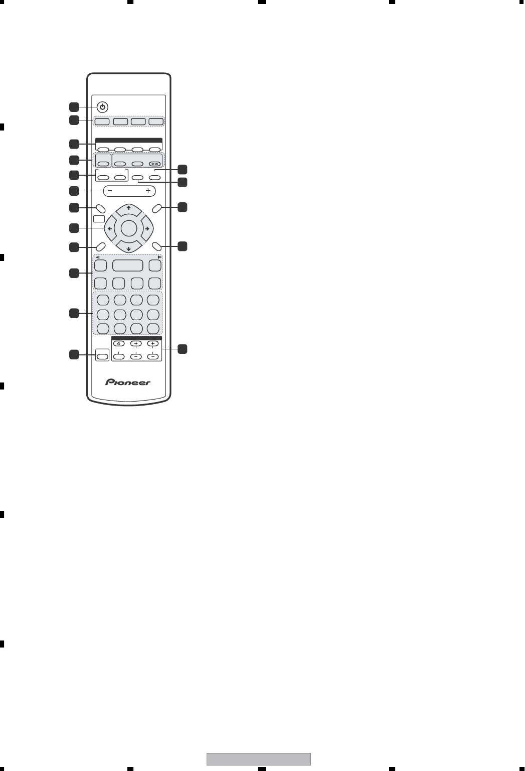
XV-EV1000
134
1234
1234
C
D
F
A
B
E
Remote control
Illustration shows the EV700/1000 model
1
STANDBY/ON
Switches the player on or into standby.
2 Input source function select
Selects the source you want to listen to.
3 DVD control buttons
AUDIO Selects the audio channel or
language.
SUBTITLE – Selects a subtitle display.
ANGLE – Changes the camera angle
during DVD multi-angle scene playback.
ZOOM – Changes the zoom level.
4 Sound Field / DSP buttons
X.BOOM – Switches the bass boost on or
off.
SFC / SOUND FIELD(EV500 only)
Selects sound modes or custom settings
from the Sound Field Control.
SURROUND (EV700/1000 only) – Selects a
surround listening mode
ADVANCED (EV700/1000 only) – Selects an
advanced listening mode
FRONT SURROUND (EV700/1000 only) –
Switches on the Front Surround mode.
5 KARAOKE controls
KARAOKE – Selects audio channels for
karaoke.
ECHO – Changes the echo level on the
karaoke mics.
KEY CONTROL – Lowers/raises the pitch
of the backing track.
6 VOLUME
Adjusts the volume level.
7
HOME MENU
Press to display (or exit) the on-screen
menu for Initial Settings, Play Mode
functions, etc.
SYSTEM SETUP (SHIFT+HOME MENU)
Use to make various system and surround
sound settings (EV700/1000 only).
Also used when
automatically saving station presets when
using the tuner.
8
ENTER
, TUNE & cursor control buttons
Navigates on-screen displays and menus.
ENTER selects an option or executes a
command.
123
456
7890
CLEAR
ENTER
SYSTEM SETUP
HOME
MENU
TOP MENU
DVD MENU
SHIFT
CHANNEL VOLUME
INPUT
SUBTITLE
VOLUME
ANGLE ZOOM
SURROUND
ADVANCED
FRONT
SURROUND
ECHO
DSP
AUDIO
DVD/CD TAPE FM/AM LINE
X.BOOM
PROGRAM
ST.MEMORY
TEST TONE
REPEAT
MONO
CH LEVEL
RANDOM
TIMER
KARAOKE
I –
KEYCON
– i
DISPLAY MUTE
RETURN
SOUND
MODE
ENTER
STANDBY/ON
4
/eE/
1¡
¢
8
7
3
3
3
TUNE +
ST +ST
–
TUNE
–
DVD
TV CONTROL
1
2
3
6
7
8
9
10
11
12
16
17
15
13
14
4
5

XV-EV1000 135
5678
5678
C
D
F
A
B
E
9 SOUND MODE
Accesses settings in the Sound menu, such as
the tone controls.
10 Playback controls
– Starts/resumes playback
and/ – Use for reverse slow
motion playback, frame reverse and
reverse scanning
and / – Use for forward slow
motion playback, frame advance and
forward scanning
– Jumps to the next chapter or track
– Jumps to the beginning of the
current chapter or track, then to previous
chapters/tracks
– Pauses playback; press again to restart
– Stops playback
11 Number buttons and SHIFT functions
The number buttons can be used for selecting
tracks directly, the functions above the buttons
are accessed by pressing SHIFT at the same
time as the button.
PROGRAM (SHIFT+1) – Use to program/
play a program list.
REPEAT (SHIFT+2) – Selects a repeat play
mode.
RANDOM (SHIFT+3) – Selects a random
play mode.
ST.MEMORY (SHIFT+4) – Use for saving
and listening to station presets.
MONO (SHIFT+5) – Press to listen to a
stereo FM broadcast in mono.
TIMER (SHIFT+6) – Use for setting and
checking the clock and the
timers.
TEST TONE (SHIFT+7) (EV700/1000 only) –
Press to output the test tone for speaker
setup.
CH LEVEL (SHIFT+8) (EV700/1000 only) –
Use to adjust the speaker level.
CLEAR – Clears an entry
ENTER – Selects menu options, etc. (works
exactly the same as theENTER button in 8
above)
12 SHIFT
Press to access the functions/commands
written in green on the remote
13
MUTE
Mutes the volume.
14
DISPLAY
Switches between information displays.
15
TOP MENU
Displays the top menu of a DVD disc.
DVD MENU
Displays the DVD menu (for Video CD/
Super VCDs, DivX video and WMA/MP3/
JPEG discs, the Disc Navigator screen
appears).
16
RETURN
Press to return to a previous menu screen.
17 TV CONTROL1
– Switches the TV on or into standby
INPUT – Switches the TV input
CHANNEL +/– – Selects channels
VOLUME +/– – Adjusts the TV volume
XV-EV1000
136
1234
1234
C
D
F
A
B
E
Service Remote Control Unit GGF1381
DVD Test Disc (DVD-Video) GGV1025
adjustment, diagnosis
Name Jig No. Remarks
Check of DVD-Video
CD Test Disc STD-905 Check of CD
Cable (5P) GGD1425
Flexible Cable (25P) GGD1309
diagnosis of DVDM ASSY
diagnosis of DVDM ASSY
Test Tape NCT-111 Tape Speed adjustment
Test Tape NCT-112 Tape Playback adjustment
Test Tape STD-633 Normal blank tape
DVD Data Disc GGV1175 diagnosis (ID data setting)
7 Jigs list
Lubricating Oil GYA1001
GEM1036
Daifree
Name Lubricants and Glues No. Remarks
refer to "2.5 05 LOADER ASSY"
refer to "2.5 05 LOADER ASSY"
GEM1037
Silicone Adhesive refer to "2.6 Traverse Mechanism Assy-S"
GYL1001
Screw tight refer to "6.2.5 MECHANISM ADJUSTMENT"
7 Lubricants and Glues list
Before shipping out the product, be sure to clean the following positions by using the prescribed cleaning tools:
Position to be cleaned Cleaning tools
Pickup leneses Cleaning liquid : GEM1004
Cleaning paper : GED-008
Position to be cleaned Cleaning tools
Cassette heads
Pinch rollers Cleaning paper : GED-008
Capstans
Position to be cleaned Cleaning tools
Fans Cleaning paper : GED-008
