Xlx_s9_lx9_fpga_microboard Ug110311x Xilinx Spartan 6 LX9 Micro Board Rev B2 Hardware User Guide
User Manual:
Open the PDF directly: View PDF ![]() .
.
Page Count: 19

Xilinx
®
Spartan
®
-6 FPGA LX9
MicroBoard
User Guide
Copyright © 2011 Avnet, Inc. AVNET and the AV logo are registered trademarks of Avnet, Inc. All other brands are property of their respective owners.
Avnet Electronics Marketing 2 of 19 Rev C 11/08/2011
Table of Contents
1.0
Introduction ............................................................................................................................................................................... 4
1.1
Description ............................................................................................................................................................................ 4
1.2
Board Features ..................................................................................................................................................................... 4
1.3
Reference Designs ............................................................................................................................................................... 5
1.4
Ordering Information ............................................................................................................................................................. 5
2.0
Functional Description .............................................................................................................................................................. 6
2.1
Xilinx Spartan-6 FPGA LX9 FPGA ....................................................................................................................................... 6
2.2
Clocks ................................................................................................................................................................................... 8
2.2.1
Triple Output User programmable Texas Instruments CDCE913 clock ........................................................................... 8
2.2.2
Optional 66.6 MHz Maxim low-cost, fixed-frequency oscillator ........................................................................................ 8
2.3
Memory................................................................................................................................................................................. 8
2.3.1
32 Mb x 16 (512 Mb) Micron LPDDR Mobile SDRAM component ................................................................................... 9
2.3.2
128 Mb Micron Multi-I/O SPI Flash ................................................................................................................................ 10
2.4
Communication ................................................................................................................................................................... 11
2.4.1
Universal Serial Bus (USB) 2.0, Full Speed USB-to-JTAG bridge via Atmel AT90USB162 / ATMEGA162U2 AVR
Microcontroller and Tyco USB-A connector ................................................................................................................................ 11
2.4.2
USB-UART ..................................................................................................................................................................... 11
2.4.3
10/100 Ethernet PHY via National Semiconductor DP83848J PHY and Tyco RJ45 connector ..................................... 12
2.5
User I/O and Expansion Connectors .................................................................................................................................. 13
2.5.1
Peripheral Module (PMOD) ............................................................................................................................................ 13
2.6
User Interfaces ................................................................................................................................................................... 14
2.6.1
User LEDs ...................................................................................................................................................................... 14
2.6.2
Four configurable FPGA user DIP switches (Tyco 1571983-4) ...................................................................................... 14
2.6.3
One configurable FPGA user push-button (Tyco 8-1437565-0) ..................................................................................... 14
2.7
Power ................................................................................................................................................................................. 14
2.7.1
Power Good LED ........................................................................................................................................................... 15
2.7.2
FPGA Decoupling .......................................................................................................................................................... 15
2.7.3
Power Results ................................................................................................................................................................ 16
2.8
Configuration ...................................................................................................................................................................... 16
2.8.1
Configuration Modes ...................................................................................................................................................... 17
2.8.2
Digilent On-board JTAG Boundary Scan Configuration ................................................................................................. 17
2.8.3
Multi-I/O SPI Flash Configuration ................................................................................................................................... 17
2.8.4
JTAG Chain .................................................................................................................................................................... 17
3.0
Test Design ............................................................................................................................................................................. 18
4.0
Acknowledgements ................................................................................................................................................................. 18
5.0
Getting Help and Support ....................................................................................................................................................... 18
6.0
Document Revision Table ....................................................................................................................................................... 19
Copyright © 2011 Avnet, Inc. AVNET and the AV logo are registered trademarks of Avnet, Inc. All other brands are property of their respective owners.
Avnet Electronics Marketing 3 of 19 Rev C 11/08/2011
Figures
Figure 1 – Spartan-6 FPGA LX9 MicroBoard Front .................................................................................................................................... 5
Figure 2 – Spartan-6 FPGA LX9 MicroBoard Back .................................................................................................................................... 5
Figure 3 – Spartan-6 FPGA LX9 MicroBoard Block Diagram ..................................................................................................................... 6
Figure 4 – XC6SLX9 CSG324 I/O Allocation .............................................................................................................................................. 7
Figure 5 – Spartan-6 FPGA LX9 MicroBoard Memory Interfaces ............................................................................................................... 9
Figure 6 – Spartan-6 FPGA LX9 LPDDR Mobile SDRAM Interface ........................................................................................................... 9
Figure 7 – 10/100 Ethernet Interface ........................................................................................................................................................ 12
Figure 8 – PMOD Connector Pinout ......................................................................................................................................................... 15
Figure 9 – TPS65708 Connections .......................................................................................................................................................... 15
Figure 10 – Xilinx Ribbon Cable JTAG Connector ................................................................................................................................... 17
Tables
Table 1 – CDCE913 Clocks ........................................................................................................................................................................ 8
Table 2 – CDCE913 I2C ............................................................................................................................................................................. 8
Table 3 – 66 MHz Clock ............................................................................................................................................................................. 8
Table 4 – LPDDR Timing Parameters ...................................................................................................................................................... 10
Table 5 – FPGA SPI Interface Pinout ....................................................................................................................................................... 10
Table 6 – USB-JTAG Signals ................................................................................................................................................................... 11
Table 7 – USB-to-UART Pin Locations..................................................................................................................................................... 12
Table 8 – 10/100 Pin Assignments ........................................................................................................................................................... 12
Table 9 – Peripheral Module Connections – J4 ........................................................................................................................................ 13
Table 10 – Peripheral Module Connections – J5 ...................................................................................................................................... 13
Table 11 – LED Pin Assignments ............................................................................................................................................................. 14
Table 12 – FPGA DIP Switches ............................................................................................................................................................... 14
Table 13 – FPGA Push-Button ................................................................................................................................................................. 14
Table 14 – S6LX9 MicroBoard Capacitors for XC6SLX9-CSG324 ........................................................................................................... 16
Table 15 – S6LX9 Board Capacitor Quantities for XC6SLX9-CSG324 .................................................................................................... 16

1.0 Introduction
The purpose of this manual is to describe the functionality and contents of the Avnet Spartan-6 FPGA LX9 MicroBoard from Avnet
Electronics Marketing. This document includes instructions for operating the board, descriptions of the hardware features, and
explanations of the test code programmed into the on-board programmable memory. For reference design documentation and
example projects, see the Avnet Design Resource Center (DRC).
DRC Home Page: www.em.avnet.com/drc
Spartan-6 FPGA LX9 MicroBoard Kit Home Page www.em.avnet.com/s6microboard
1.1 Description
The Spartan-6 FPGA LX9 MicroBoard provides a complete hardware environment for designers to accelerate their time to market.
The kit delivers a stable platform to develop and test designs targeted to the low-cost and low-power Xilinx Spartan-6 FPGA. The
installed Spartan-6 FPGA LX9 device offers a prototyping environment to effectively demonstrate the enhanced benefits of low-
cost Xilinx FPGA solutions. Reference designs are included with the kit to exercise standard peripherals on the evaluation board
for a quick start to device familiarization.
The Spartan-6 FPGA LX9 MicroBoard kit contains the following individual pieces:
• Avnet Spartan-6 FPGA LX9 MicroBoard
• Type A male to Type A female USB extension cable
• Type A to Micro-B USB cable
• Xilinx ISE® Design Suite (IDS) 12.4 DVD WebPACK edition
• ChipScope™ Pro and SDK license voucher (device-locked to XC6SLX9)
• Welcome Letter
• Getting Started Guide
Please note that this kit does NOT include a 10/100 Ethernet cable.
1.2 Board Features
• FPGA
o Xilinx Spartan-6 XC6SLX9-2CSG324C FPGA
• Clocks
o Triple output, user programmable, Texas Instruments CDCE913 clock
o Optional user installable Maxim DS1088LU-66+, low-cost, fixed-frequency oscillator
• Memory
o 32 Mb x 16 (512 Mb) Micron LPDDR Mobile SDRAM component.
o 128 Mb Micron Multi-I/O SPI Flash
• Communication
o One USB 2.0, Full Speed USB-to- JTAG bridge via Atmel AT90USB162 / ATMEGA162U2, Digilent JTAG firmware,
and Tyco USB-A connector
o One USB 2.0, Full Speed USB-to-UART bridge via Silicon Labs CP2102 and Tyco Micro-B connector.
o One 10/100 Ethernet port via National Semiconductor DP83848J PHY and Tyco RJ45 connector with Integrated
Magnetics.
• User I/O and Expansion Connectors
o Two Digilent 12-pin, 0.245mm pitch, Peripheral Module (PMOD) headers support 3rd party expansion modules.
• User Interfaces
o Four user LEDs
o Four configurable FPGA user DIP switches
o Two system push-button switches: one tied to user I/O and used for logical reset in the factory test image, one
hardwired for FPGA program initialization.
• Power
o Texas Instruments TPS65708 PMU multi-channel regulator, with 5V input supplied by either USB connection.
• Configuration
o 128Mb SPI Configuration Flash
o On-board USB Programming/Configuration based on the Digilent USB Full Speed JTAG design utilizing the Atmel
AT90USB162 / ATMEGA162U2.
o Xilinx Compatible JTAG Cable
• Test Files
o Files that are used to factory test the Spartan-6 FPGA LX9 MicroBoard are available and can be found on the Avnet
Electronics Marketing Design Resource Center (DRC) web site: www.em.avnet.com/s6microboard.
Copyright © 2011 Avnet, Inc. AVNET and the AV logo are registered trademarks of Avnet, Inc. All other brands are property of their respective owners.
Avnet Electronics Marketing 5 of 19 Rev C 11/08/2011
1.3 Reference Designs
Reference designs that demonstrate some of the potential applications of the Spartan-6 FPGA LX9 MicroBoard are available and
can be found on the Avnet Electronics Marketing Design Resource Center (DRC) web site: www.em.avnet.com/s6microboard.
See the PDF document included with each reference design for a complete description of the design and detailed instructions for
running a demonstration on the development board. Check the DRC periodically for updates and new designs. The Expanded
Getting Started Guide, available for download from the DRC, is the best place to start.
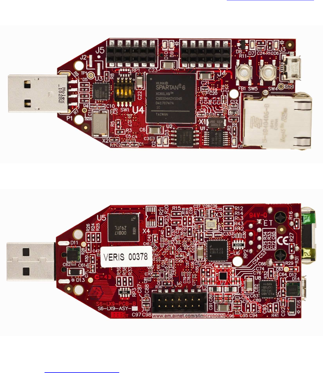
Figure 1 – Spartan-6 FPGA LX9 MicroBoard Front
Figure 2 – Spartan-6 FPGA LX9 MicroBoard Back
1.4 Ordering Information
The following table lists the evaluation kit part numbers and available software options.
Internet link at http://www.em.avnet.com/drc
Copyright © 2011 Avnet, Inc. AVNET and the AV logo are registered trademarks of Avnet, Inc. All other brands are property of their respective owners.
Avnet Electronics Marketing 6 of 19 Rev C 11/08/2011
Part Number Hardware
AES-S6MB-LX9-G Xilinx Spartan-6 FPGA LX9 MicroBoard
HW-USB-II-G Xilinx Platform Cable USB-II
JTAG HS1 HIGH SPEED CABLE Digilent HS1 JTAG Cable
EF-EDK-NL EDK Upgrade for ISE WebPack
EF-ISE-EMBD-NL ISE Embedded Edition
EF-ISE-SYSTEM-NL ISE System Edition
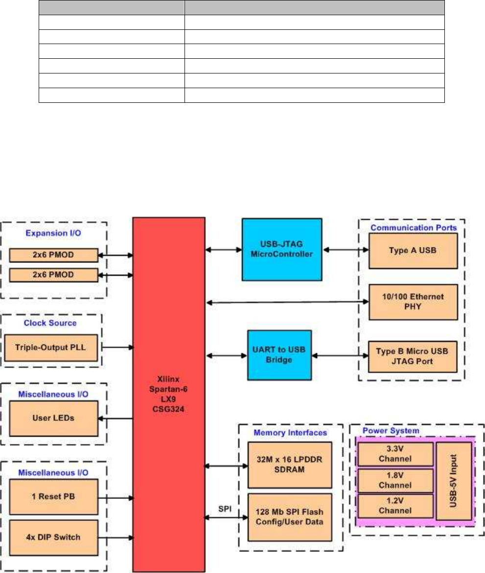
2.0 Functional Description
A Xilinx Spartan-6 FPGA LX9 (XC6SLX9-2CSG324) FPGA is the primary components of the Avnet Spartan-6 FPGA LX9 MicroBoard.
A 10/100 Ethernet port and 2 Full Speed USB interfaces provide means of off-board communication. On-board memory consists of a
256 Mbit x 16 LPDDR mobile SDRAM component and a 128 Mbit Multi-I/O SPI Flash that may be used by the FPGA for configuration.
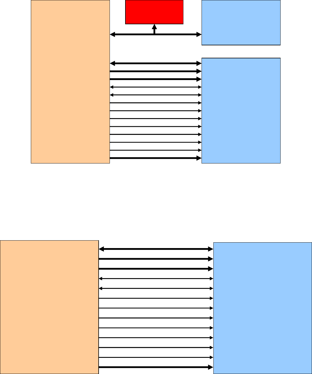
A high-level block diagram of the Spartan-6 FPGA LX9 MicroBoard is shown below followed by a brief description of each sub-section.
Figure 3 – Spartan-6 FPGA LX9 MicroBoard Block Diagram
2.1 Xilinx Spartan-6 FPGA LX9 FPGA
The Xilinx XC6SLX9-2CSG324C device designed onto the Spartan-6 FPGA LX9 MicroBoard is a member of the logic-optimized
Xilinx Spartan-6 LX FPGA family. This family is built on a mature 45 nm low-power copper process technology that delivers the
optimal balance of cost, power, and performance. The Spartan-6 LX family offers a new, more efficient, dual-register 6-input look-
up table (LUT) logic and a rich selection of built-in system-level blocks. These include 18 Kb (2 x 9 Kb) block RAMs, second
generation DSP48A1 slices, SDRAM memory controllers, enhanced mixed-mode clock management blocks, SelectIO™
technology, advanced system-level power management modes, auto-detect configuration options, and enhanced IP security with
Device DNA protection. These features provide a low-cost programmable alternative to custom ASIC products with unprecedented
Copyright © 2011 Avnet, Inc. AVNET and the AV logo are registered trademarks of Avnet, Inc. All other brands are property of their respective owners.
Avnet Electronics Marketing 7 of 19 Rev C 11/08/2011
ease-of-use. Spartan-6 FPGAs offer the best solution for high-volume logic designs, consumer-oriented DSP designs, and cost-
sensitive embedded applications.
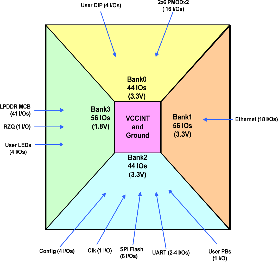
On the Avnet Spartan-6 FPGA LX9 MicroBoard, the FPGA provides four I/O banks. Banks 0, 1, and 2 Vcco as well as the Vccaux
power rail are tied to 3.3 V. This allows Bank 0 to interface to 3.3 V user I/O, Bank 1 to interface to 3.3 V Ethernet I/O, and Bank 2
to interface to 3.3 V configuration I/O. Bank 3 interfaces to the LPDDR memory and is connected to a 1.8 V power rail for low-
power consumption memory designs. The VCCINT power rail is connected to 1.2 V.
The four I/O banks are described in Figure 4 and detailed I/O pin usage is provided throughout this document.
Figure 4 – XC6SLX9 CSG324 I/O Allocation
Copyright © 2011 Avnet, Inc. AVNET and the AV logo are registered trademarks of Avnet, Inc. All other brands are property of their respective owners.
Avnet Electronics Marketing 8 of 19 Rev C 11/08/2011
2.2 Clocks
2.2.1 Triple Output User programmable Texas Instruments CDCE913 clock
The CDCE913 is a modular PLL-based low-cost, high-performance, programmable clock synthesizer, multiplier, and divider. It
can generate up to 3 output clocks from a single input frequency. Each output can be programmed via an SDA / SCL, SMBus /
I2C interface, for any clock frequency up to 230 MHz, using the integrated configurable PLL. The input crystal frequency on
the S6LX9 MicroBoard is 27 MHz. The following clock frequency outputs are pre-programmed into the CDCE913 during
factory configuration.
Clock CDCE913 Pin# Signal Name FPGA Pin#
40 MHz U1 pin 11 (Y1) USER_CLOCK V10 (GCLK0)
66.7 MHz U1 pin 9 (Y2) CLOCK_Y2 K15 (GCLK9)
100 MHz U1 pin 8 (Y3) CLOCK_Y3 C10 (GCLK13)
Table 1 – CDCE913 Clocks
The user is able to modify these frequencies using the FPGA’s connection to the CDCE913 I2C port. Internal FPGA pull-ups
are required for this interface to work properly.
Signal Name CDCE913 Pin# FPGA Pin#
SDA U1 pin 13 U13
SCL U1 pin 12 P12
Table 2 – CDCE913 I2C
2.2.2 Optional 66.6 MHz Maxim low-cost, fixed-frequency oscillator
This is an unpopulated Maxim 3.3 V low-cost oscillator, part number DS1088LU-66+.
Clock
Signal Nam
e
FPGA Pin#
66.7 MHz BACKUP_CLOCK R8 (GCLK31)
Table 3 – 66 MHz Clock
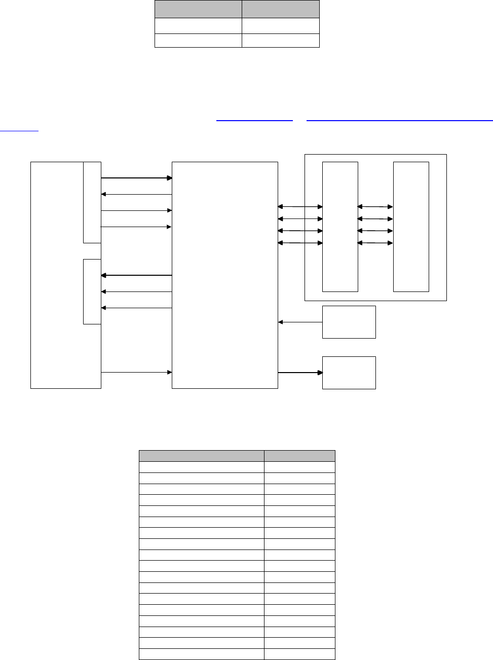
2.3 Memory
The Spartan-6 FPGA LX9 MicroBoard is populated with both LPDDR mobile SDRAM memory (256 Mbit x 16) and 128 Mbit SPI
Multi-I/O Flash to support various types of applications. The SPI Flash may be used for FPGA configuration.
Figure 5 shows a high-level block diagram of the memory interfaces on this board.
Copyright © 2011 Avnet, Inc. AVNET and the AV logo are registered trademarks of Avnet, Inc. All other brands are property of their respective owners.
Avnet Electronics Marketing 9 of 19 Rev C 11/08/2011
Figure 5 – Spartan-6 FPGA LX9 MicroBoard Memory Interfaces
2.3.1 32 Mb x 16 (512 Mb) Micron LPDDR Mobile SDRAM component
The Micron LPDDR mobile SDRAM device, part number MT46H32M16LFBF-5, provides a double data rate architecture to
achieve high-speed operation. The device provides 64 MB and it is internally configured as a quad-bank DRAM of memory on
a single IC. Each of the x16’s 134,217,728-bit banks is organized as 8,192 rows by 1,024 columns by 16 bits. The device has
an operating voltage of 1.8V and the interface is MOBILE_DDR. The Spartan-6 Memory Controller Block supports up to 400
Mb/s (200 MHz double data rate) performance. The following figure shows a high-level block diagram of the LPDDR Mobile
SDRAM interface on the MicroBoard.
Figure 6 – Spartan-6 FPGA LX9 LPDDR Mobile SDRAM Interface
S6LX9
CSG324
Bank 3
A[12:0]
BA[1:0]
LDQ
S
UDQ
S
LDM
UDM
CAS
RAS
WE#
CS#
CKE
CK_P/N
S6LX9
SPI Flash
Digilent 4-Pin Flash
Progrmming
Interface
LPDDR
Mobile SDRAM
DQ[15:0]
A[12:0]
BA[1:0]
LDQS
UDQS
LDM
UDM
CAS#
RAS#
WE#
CS#
CKE
CK_P/N
LPDDR
Mobile SDRAM
DQ[15:0]
Copyright © 2011 Avnet, Inc. AVNET and the AV logo are registered trademarks of Avnet, Inc. All other brands are property of their respective owners.
Avnet Electronics Marketing 10 of 19 Rev C 11/08/2011
The LPDDR signals are connected to I/O Bank 3 of the Spartan-6 FPGA LX9 FPGA. The voltage supply pins (VCCO) for the
LPDDR bank are connected to the 1.8V supply rail. This supply rail can be measured across the 100uF Capacitor C22.
It is highly recommended that anyone creating a Spartan-6 MCB design thoroughly read the two User Guides (UG388 and
UG416), the MIG Master Answer Record 33566, and the associated Answer Records linked from that Master Record.
The following table provides timing and other information about the Micron device necessary to implement a DDR2 memory
controller.
MT47H16M16BG
-
5E: Timing Parameters
Time (ps) or Number
Load Mode Register time (TMRD) 2 tCK
Write Recovery time (TWR) 15000
Write-to-Read Command Delay (TWTR) 10000
Delay between ACT and PRE Commands (TRAS) 40000
Delay after ACT before another ACT (TRC) 55000
Delay after AUTOREFRESH Command (TRFC) 75000
Delay after ACT before READ/WRITE (TRCD) 15000
Delay after ACT before another row ACT (TRRD) 10000
Delay after PRECHARGE Command (TRP) 15000
Refresh Command Interval (TREFC) 70000000
Avg. Refresh Period (TREFI) 7800000
Memory Data Width (DWIDTH) (2 devices) 32
Row Address Width (AWIDTH) 13
Column Address Width (COL_AWIDTH) 9
Bank Address Width (BANK_AWIDTH) 2
Memory Range (64 MB total) 0x3FFFFFF
Table 4 – LPDDR Timing Parameters
The layout guidelines for Spartan-6 MCB designs, as detailed in Spartan-6 FPGA Memory Controller, UG388, were followed in
the design of this board. The pinout specified in the Spartan-6 Packaging & Pinout Guide, UG385 for the XC6SLX9-CSG324
was followed.
2.3.2 128 Mb Micron Multi-I/O SPI Flash
The Spartan-6 FPGA LX9 Board includes a Micron Multi-I/O SPI Flash memory, part number N25Q128. The SPI Flash is
connected to the FPGA to support Quad-I/O (QIO), Dual-I/O (DIO), or Single-I/O (SIO) SPI configuration.
The SPI signals are also connected to the Atmel AT90USB162 / ATMEGA162U2 SPI interface pins. This interface can be
used to connect to the SPI flash via the AT90USB162 / ATMEGA162U2 USB and allows for direct Flash programming using a
Digilent provided utility
Signal N25Q128
Pin# FPGA
Pin#
AT90USB162
/
ATMEGA162U2
Pin#
FPGA_MOSI_MOSO0 (MOSI (DQ0)) U2 pin 5 (DQ0) T13 U3 pin 9
FPGA_D0_DIN_MISO_MISO1 (MISO (DQ1)) U2 pin 2 (DQ1) R13 U3 pin 8
FPGA_D1_MISO2 (W#/VPP (DQ2)) U2 pin 3 (DQ2) T14 NC
FPGA_D2_MISO3 (HOLD#(DQ3)) U2 pin 7 (DQ3) V14 NC
FPGA_CCLK (CLK) U2 pin 6 (C) R15 U3 pin 11
FPGA_SPI CS# (SEL) U2 pin 1 (S_N) V3 U3 pin 10
FPGA_PROG (PROGRAM_B) NC V2 U3 pin 19
Table 5 – FPGA SPI Interface Pinout
Copyright © 2011 Avnet, Inc. AVNET and the AV logo are registered trademarks of Avnet, Inc. All other brands are property of their respective owners.
Avnet Electronics Marketing 11 of 19 Rev C 11/08/2011
The SPI Flash is connected to Spartan-6 Bank 2, which has a Vcco of 3.3 V, which can be measured across the 100 uF
capacitor C23.
The SPI Flash can be programmed in the following ways:
• Use the Digilent sfutil.exe command line application to program the Flash directly through the AT90USB162 /
ATMEGA162U2. Please see the Spartan-6_LX9_MicroBoard_Configuration_Guide located at
http://www.em.avnet.com/s6microboard for an application note on this subject.
• Using Digilent USB via JTAG to program the Flash indirectly using iMPACT 12.1 or later with the Digilent Plug-in.
• Using Platform Cable USB via JTAG to program the Flash indirectly using iMPACT 12.1 or later.
Please note that the following patch may be required to build a MicroBlaze Hardware Platform that includes the XPS_SPI
peripheral: http://www.xilinx.com/support/answers/39017.htm
2.4 Communication
2.4.1 Universal Serial Bus (USB) 2.0, Full Speed USB-to-JTAG bridge via Atmel AT90USB162 / ATMEGA162U2 AVR
Microcontroller and Tyco USB-A connector
P1 is a Tyco USB-A board-mount connector. P1 connects to a full-speed (12 Mbps) USB peripheral port on the AT90USB162 /
ATMEGA162U2 device. Power supplied by the USB host via connector P1 (+5V_USB_A) is used in conjunction with power from
the other USB port, through diodes D13 and D16 to power the S6LX9 board.
The AT90USB162 / ATMEGA162U2 is used in the bridge configuration to allow FPGA configuration via the Digilent JTAG
interface, and in the SPI configuration to allow SPI Flash programming via the Digilent program controlled SPI interface. Operation
in the JTAG configuration is accomplished using iMPACT and the Digilent Plug-in. Please see the Spartan-
6_LX9_MicroBoard_Configuration_Guide located at http://www.em.avnet.com/s6microboard for an application note on this
subject.
Note that an additional Xilinx Platform Cable connector is provided (J6), for JTAG operation. Operation in the SPI configuration is
accomplished using the command line sfutil.exe. Both configurations make use of custom Digilent firmware loaded into the
AT90USB162 / ATMEGA162U2 device during manufacture. Note the SPI Flash Interface Pinout is shown in Table 5. The JTAG
Interface Pinout is shown in Table 6.
Signal Xilinx Parallel IV
Pin# FPGA
Pin# AT90USB162 /
ATMEGA162U2 Pin#
FPGA_TCK J6 pin 6 (TCK) A17 (TCK) U3 pin 15 (SCLK)
FPGA_TMS J6 pin 4 (TMS) B18 (TMS) U3 pin 14 (SS_N)
FPGA_TDO J6 pin 8 (TDO) D16 (TDO) U3 pin 17 (MISO)
FPGA_TDI J6 pin 10 (TDI) D15 (TDI) U3 pin 16 (MOSI)
FPGA_PROG NC V2 (PROGRAM_B) U3 pin 19 (PB5)
Table 6 – USB-JTAG Signals
2.4.2 USB-UART
The Spartan-6 FPGA LX9 MicroBoard implements a Silicon Labs CP2102 device that provides a USB-to-UART bridge. The
USB physical interface is brought out on a Tyco USB micro-B connector labeled “J3.” Power supplied by the USB host via
connector J3 (+5V_USB_B) is used in conjunction with power from the other USB port, through diodes D13 and D16 to power
the S6LX9 board.
Please see the Avnet DRC for an application note describing the driver installation and usage of this device.
The USB-to-UART bridge interface connects to the Spartan-6 FPGA through the following pins:
Copyright © 2011 Avnet, Inc. AVNET and the AV logo are registered trademarks of Avnet, Inc. All other brands are property of their respective owners.
Avnet Electronics Marketing 12 of 19 Rev C 11/08/2011
Net Name Spartan-6 Pin #
USB_RS232_RXD R7
USB_RS232_TXD T7
Table 7 – USB-to-UART Pin Locations
2.4.3 10/100 Ethernet PHY via National Semiconductor DP83848J PHY and Tyco RJ45 connector
The PHY device is a National Semiconductor DP83848J. The Tyco RJ45 connector includes integrated magnetics and LEDs.
A MAC must be placed inside the FPGA, such as the XPS Ethernet Lite or Tri-Mode Ethernet Media Access Controller
(TEMAC). These cores are accessible in ISE Embedded or EDK. The TEMAC requires the purchase and installation of a
license.
data
datadata
data_
__
_tx
txtx
tx[
[[
[3
33
3:
::
:0
00
0]
]]
]
clk
clkclk
clk_
__
_tx
txtx
tx
control
controlcontrol
control_
__
_tx
txtx
tx
data
datadata
data_
__
_rx
rxrx
rx[
[[
[3
33
3:
::
:0
00
0]
]]
]
clk
clkclk
clk _
__
_rx
rxrx
rx
control
controlcontrol
control_
__
_rx
rxrx
rx
Crystal
CrystalCrystal
Crystal
25
2525
25Mhz
MhzMhz
Mhz
10
1010
10/
//
/100
100 100
100 PHY
PHYPHY
PHY
S
SS
S6
66
6LX
LXLX
LX9
99
9
phy
phyphy
phy_
__
_reset
resetreset
reset
T
T
T
Tr
r
r
ra
a
a
an
n
n
ns
s
s
sm
m
m
mi
i
i
it
t
t
t
R
R
R
Re
e
e
ec
c
c
ce
e
e
ei
i
i
iv
v
v
ve
e
e
e
1
1
1
10
0
0
0/
/
/
/1
1
1
10
0
0
00
0
0
0
M
M
M
Ma
a
a
ag
g
g
gn
n
n
ne
e
e
et
t
t
ti
i
i
ic
c
c
cs
s
s
s
R
R
R
RJ
J
J
J4
4
4
45
5
5
5
C
C
C
Co
o
o
on
n
n
nn
n
n
ne
e
e
ec
c
c
ct
t
t
to
o
o
or
r
r
r
LEDs
LEDsLEDs
LEDs
TD
TDTD
TD _
__
_P
PP
P
TD
TDTD
TD _
__
_N
NN
N
RD
RDRD
RD_
__
_P
PP
P
RD
RDRD
RD _
__
_N
NN
N
gtxclk
gtxclkgtxclk
gtxclk
Figure 7 – 10/100 Ethernet Interface
Net Name
FPGA Pin#
FPGA_ETH_MDC M16
FPGA_ETH_MDIO L18
FPGA_ETH_RX_CLK L15
FPGA_ETH_RX_D0 T17
FPGA_ETH_RX_D1 N16
FPGA_ETH_RX_D2 N15
FPGA_ETH_RX_D3 P18
FPGA_ETH_RX_ER N18
FPGA_ETH_DV P17
FPGA_ETH_TX_CLK H17
FPGA_ETH_TX_D0 K18
FPGA_ETH_TX_D1 K17
FPGA_ETH_TX_D2 J18
FPGA_ETH_TX_D3 J16
FPGA_ETH_TX_EN L17
FPGA_ETH_COL M18
FPGA_ETH_CRS N17
FPGA_ETH_RESET# T18
Table 8 – 10/100 Pin Assignments
Please note that the PHY Address pins are not strapped on the board. The Avnet XBD for this board places pull-ups on the
AD[4:1] pins. The AD[0] pin is shared with COL, which gets stripped out of EDK 12.4 xps_ethernetlite full duplex designs. The
Copyright © 2011 Avnet, Inc. AVNET and the AV logo are registered trademarks of Avnet, Inc. All other brands are property of their respective owners.
Avnet Electronics Marketing 13 of 19 Rev C 11/08/2011
default bitgen options result in this now unused pin getting pulled-low, which results in a PHY Address of 11110b. If the bitgen
options are changed such that UnusedPins are PullNone, then the PHY Address will be 11111b due to the internal PHY pull-
up on AD[0]. The user must be aware that not controlling these PHY AD pins with internal pull-up and bitgen options will result
in a PHY Address of 00000b, which puts the PHY into Isolate Mode, and it will not operate correctly.
2.5 User I/O and Expansion Connectors
2.5.1 Peripheral Module (PMOD)
Two 12-pin (2 x 6 female) Peripheral Module (PMOD) headers (J4, J5) are interfaced to the FPGA, with each header providing
3.3 V power, ground, and eight I/O’s. These headers may be utilized as general-purpose I/Os or may be used to interface to
PMODs. J4 and J5 are placed in close proximity (0.9”-centers) on the PCB in order to support dual PMODs. Table 9 and Table
10 provide the connector and FPGA pinout. For Digilent PMODs see: http://www.digilentinc.com/pmods
FPGA
Pin # I/O Signal
Connector
Pin #
Connector
Pin # I/O Signal
FPGA
pin #
H12 FPGA_PMOD2_P1 1 7 FPGA_PMOD2_P7 K12
G13 FPGA_PMOD2_P2 2 8 FPGA_PMOD2_P8 K13
E16 FPGA_PMOD2_P3 3 9 FPGA_PMOD2_P9 F17
E18 FPGA_PMOD2_P4 4 10 FPGA_PMOD2_P10 F18
-
GND
5 11
GND
-
-
+3.3V_LS1
6 12
+3.3V_LS1
-
Table 9 – Peripheral Module Connections – J4
FPGA
Pin # I/O Signal
Connector
Pin #
Connector
Pin # I/O Signal
FPGA
pin #
F15 FPGA_PMOD1_P1 1 7 FPGA_PMOD1_P7 F14
F16 FPGA_PMOD1_P2 2 8 FPGA_PMOD1_P8 G14
C17 FPGA_PMOD1_P3 3 9 FPGA_PMOD1_P9 D17
C18 FPGA_PMOD1_P4 4 10 FPGA_PMOD1_P10 D18
-
GND
5 11
GND
-
-
+3.3V_LS1
6 12
+3.3V_LS1
-
Table 10 – Peripheral Module Connections – J5
Copyright © 2011 Avnet, Inc. AVNET and the AV logo are registered trademarks of Avnet, Inc. All other brands are property of their respective owners.
Avnet Electronics Marketing 14 of 19 Rev C 11/08/2011
Figure 8 – PMOD Connector Pinout
2.6 User Interfaces
2.6.1 User LEDs
Four discrete “high-brightness, low Vf” LEDs are installed on the board and can be used to display the status of the internal
logic. These LEDs are attached as shown below and are lit by forcing the associated FPGA I/O pin to a logic ‘1’ and are off
when the pin is either low (0) or not driven.
Net Name Reference FPGA Pin#
FPGA_GPIO_LED1 D2 P4
FPGA_GPIO_LED2 D3 L6
FPGA_GPIO_LED3 D9 F5
FPGA_GPIO_LED4 D10 C2
Table 11 – LED Pin Assignments
2.6.2 Four configurable FPGA user DIP switches (Tyco 1571983-4)
FPGA
DIP switch
FPGA Pin#
FPGA_DIP1 B3
FPGA_DIP2 A3
FPGA_DIP3 B4
FPGA_DIP4 A4
Table 12 – FPGA DIP Switches
Please note that internal pulldowns are required for these pins.
2.6.3 One configurable FPGA user push-button (Tyco 8-1437565-0)
FPGA Push
-
button
FPG
A Pin#
USER_RESET V4
Table 13 – FPGA Push-Button
Please note that an internal pulldown is required for this pin.
2.7 Power
The Texas Instruments TPS65708 provides two high-efficiency switching converters, two LDOs, and an LED driver. The output
voltages are tuned internally on the device. The default values are 3.3 V and 1.8 V for the switchers and 2.8 V and 1.2 V for the
LDOs. In this implementation, the 2.8 V LDO output is not utilized.
1 2 3 4 5 6
7 8 9
10 11 12
1 2 3
4 5 6
7 8 9
10 11 12
Copyright © 2011 Avnet, Inc. AVNET and the AV logo are registered trademarks of Avnet, Inc. All other brands are property of their respective owners.
Avnet Electronics Marketing 15 of 19 Rev C 11/08/2011
The Spartan-6 FPGA core voltage requires 1.2 V. Estimated max current is 160 mA. This is supplied by LDO2 on the TPS65708.
The input voltage is the 1.8 V generated by DCDC2.
The DCDC2 regulator generates 1.8 V. This voltage powers the Mobile DDR, FPGA Vcco, and the sources LDO2. Estimated max
current is 210 mA, plus the 160 mA that the 1.2 V LDO needs.
The DCDC1 regulator generates 3.3 V. This voltage powers the Flash, Ethernet, PMODs, Vcco_0, Vcco_1, and Vcco_2. Estimated
max current for the board circuits is 370 mA, which includes 50 mA for each PMOD.
The TPS65708 has built-in sequencing, resulting in a power-up sequence of 3.3 V 1.8 V 2.8 V 1.2 V.
Figure 9 – TPS65708 Connections
2.7.1 Power Good LED
A Green status LED is used to indicate when power is good on the board. This is tied to the ISINK of the TPS65708, while the
PWM input to the LED driver is connected to the 1.2 V supply. This ensures that the Power Good LED reflects the true
sequencing status of all supplies.
2.7.2 FPGA Decoupling
The decoupling requirements for the Spartan-6 device are specified in Xilinx UG393 Spartan-6 FPGA PCB Design Guide.
The S6LX9 MicroBoard follows the intent of these guidelines with a few variations:
• A 0.22 uF, 6.3 V, 0201 package capacitor is used for the smallest capacitor bin rather than 0.47 uF. The S6LX9
MicroBoard layout was constrained to using the 0201 package, and 0.22 uF was the largest available capacitance rated at
least 6.3 V. To compensate, twice the UG393-suggested number of caps are used.
• A 4.7 uF, 6.3 V, 0402 package capacitor is used for the medium capacitor bin rather than the 0805 package. As stated in
UG393, a smaller package is acceptable, and in fact provides better characteristics than the 0805 package.
• 100 uF, 6.3 V, 1206 package capacitor is used for the bulk capacitor bin. Again, a smaller package is used.
Please note that extensive testing during development has shown that 2.2 uF 0402 caps can be utilized instead of 4.7 uF 0402
caps in this application. To save on board space and costs this was extrapolated to a reduction in the number of 4.7 uF 0402
caps required for proper operation in this configuration.
Copyright © 2011 Avnet, Inc. AVNET and the AV logo are registered trademarks of Avnet, Inc. All other brands are property of their respective owners.
Avnet Electronics Marketing 16 of 19 Rev C 11/08/2011
Value Body
Size Type ESL
Max ESR
Min ESR
Max Voltage
Rating Part Number
100 uF 1206 2-Terminal
Ceramic X5R 5 nH
10
m
Ω
60
m
Ω
6.3 V Murata GRM31CR60J107ME39L
4.7 uF 0402 2-Terminal
Ceramic X5R 2 nH
10
m
Ω
60
m
Ω
6.3 V Panasonic ECJ-0EB0J475M
0.22 uF 0201 2-Terminal
Ceramic X5R
1.5 nH
10
mΩ
60
mΩ
6.3 V Panasonic ECJ-ZEB0J224M
Table 14 – Spartan-6 FPGA LX9 MicroBoard Capacitors for XC6SLX9-CSG324
Vccint Vccaux
Vcc
o
Bank 0
Vcc
o
Bank 1
Vcc
o
Bank 2
Vcc
o
Bank 3
100 uF 1 1 1 1 1 1
4.7 uF 2 1 2 2 2 2
0.22 uF 4 6 4 4 4 4
Table 15 – Spartan-6 FPGA LX9 Board Capacitor Quantities for XC6SLX9-CSG324
2.7.3 Power Results
The power circuitry was tested during the prototyping phase to verify compliance with the Xilinx Spartan-6, Micron LPDDR,
and Texas Instruments TPS65708 power requirements, such as:
• Power rail assignment
o Spartan-6 Vccint 1.2 V
o Spartan-6 Vccaux 3.3 V
o Spartan-6 Vcco_0,_1,_2 3.3 V
o Spartan-6 Vcco_3 1.8 V
o LPDDR V
DD
, V
DDQ
1.8 V
o TPS65708 V
CC
, V
IN1
, V
IN2
5 V
• Tolerance
o 1.2 V 1.14 to 1.26 V
o 1.8 V 1.71 to 1.89 V
o 3.3 V 3.15 to 3.45 V
o 5 V 3.6 to 6.0 V
• Ramp time
o 0.20 to 85 ms
o In-rush current does not overload the power circuitry at start-up
• Monotonicity
o No negative dips in 1.2 V, 1.8 V, or 3.3 V
• Sequencing
o Sequencing responds as expected based on design
2.8 Configuration
The Spartan-6 FPGA LX9 MicroBoard supports three methods of configuring the FPGA. The possible configuration sources
include Boundary-scan (On-board circuitry through P1), Boundary-scan (JTAG cable through J6), or Serial Peripheral Interface
(SPI Flash in x1, x2, or x4 modes).
The blue LED on the board illuminates to indicate when the FPGA has been successfully configured.
Copyright © 2011 Avnet, Inc. AVNET and the AV logo are registered trademarks of Avnet, Inc. All other brands are property of their respective owners.
Avnet Electronics Marketing 17 of 19 Rev C 11/08/2011
2.8.1 Configuration Modes
The S6LX9 MicroBoard is hardwired with a 4.87 K pullup resistor on HSWAPEN, M0 tied directly to 3.3 V and M1 tied directly
to GND. This puts the MicroBoard in Master Serial / SPI mode, always.
Spartan-6 devices have a dedicated four-wire JTAG port that is always available to the FPGA regardless of the mode pin
settings. The default configuration mode is “Master Serial / SPI” mode, which allows the FPGA to configure from the multi-I/O
SPI Flash device. The Flash is programmed at the factory with basic test application code to test the on-board peripherals.
The push button (SW4) is connected to the FPGA PROG pin and pulled up. Pushing the button connects PROG to ground.
Upon releasing the button, a re-configuration is initiated. This line can also be pulled low by the AT90USB162 /
ATMEGA162U2. In this case it holds off the FPGA configuration indefinitely, while programming flash memory.
After successful configuration, blue LED D1 lights when the FPGA DONE is asserted. Go to the Avnet DRC for the complete
Spartan-6LX9 MicroBoard Configuration User Guide.
2.8.2 Digilent On-board JTAG Boundary Scan Configuration
The Spartan-6 FPGA LX9 MicroBoard can be configured directly via full speed USB on-board circuitry featuring the Digilent
iMPACT plug-in. This method utilizes an AT90USB162 / ATMEGA162U2 as a USB / JTAG bridge to do a JTAG boundary
scan utilizing the Digilent Plug-in and the USB-A connection. Note that the AT90USB162 is now replaced with the fully
compatible ATMEGA162U2.
2.8.3 Multi-I/O SPI Flash Configuration
All three possible I/O modes for the SPI Flash – Quad, Double, and Single – are supported on the S6LX9 board through
iMPACT. Currently, the Digilent direct write SPI Flash programmer only works in Single mode.
2.8.4 JTAG Chain
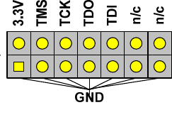
The Spartan-6 FPGA LX9 MicroBoard has one device in the JTAG chain, the Spartan-6 FPGA LX9 FPGA.
Configuring the Spartan-6 FPGA on the S6LX9 MicroBoard can be performed via Boundary Scan with a JTAG download
cable. The cable is attached to the 14-pin, 2 mm spaced keyed header J4 (Figure ) with a ribbon cable.
Figure 10 – Xilinx Ribbon Cable JTAG Connector

Copyright © 2011 Avnet, Inc. AVNET and the AV logo are registered trademarks of Avnet, Inc. All other brands are property of their respective owners.
Avnet Electronics Marketing 18 of 19 Rev C 11/08/2011
3.0 Test Design
The S6LX9 MicroBoard factory test is programmed into the Micron SPI Flash as part of the functional test when
the boards are built. The results of this test are described in the Xilinx® Spartan®-6 LX9 MicroBoard Getting
Started Guide, the full version of which is available on the DRC. Access to the factory test source archive,
including a document describing the factory test procedure, may be achieved by contacting your local
Avnet/Silica FAE or Avnet Centralized Technical Support.
4.0 Acknowledgements
Avnet would like to acknowledge the following key partners for their key contributions to this project.
Atmel
• USB 2.0 Full Speed USB-to- JTAG bridge via Atmel ATMEGA162U2
Micron
• Multi-I/O SPI Flash
• LPDDR Memory
National Semiconductor
• 10/100 Ethernet PHY
TE Connectivity
• RJ45 connector with Integrated Magnetics
• USB-A connector
• Micro-B USB connector
• DIP switch
• Push buttons
• USB Protection for electro-static discharge and over-voltage
Texas Instruments (www.ti.com/xilinxfpga)
• Clock PLL
• Power Management Unit for voltage regulation
Xilinx
• Spartan-6 FPGA
o www.xilinx.com/spartan6
• Xilinx ISE® Design Suite (IDS) DVD WebPACK edition
• ChipScope™ Pro and SDK license voucher (device-locked to XC6SLX9)
5.0 Getting Help and Support
The Spartan-6 FPGA LX9 MicroBoard home page with Documentation and Reference Designs is located at:
• www.em.avnet.com/s6microboard
Avnet Spartan-6 FPGA LX9 MicroBoard forum:
• http://community.em.avnet.com/t5/Spartan-6-LX9-MicroBoard/bd-p/Spartan-6LX9MicroBoard
For Xilinx technical support, you may contact Xilinx Online Technical Support at www.support.xilinx.com. On this site you will also find
the following resources for assistance:

Copyright © 2011 Avnet, Inc. AVNET and the AV logo are registered trademarks of Avnet, Inc. All other brands are property of their respective owners.
Avnet Electronics Marketing 19 of 19 Rev C 11/08/2011
• Software, IP, and Documentation Updates
• Access to Technical Support Web Tools
• Searchable Answer Database with Over 4,000 Solutions
• User Forums
• Training - Select instructor-led classes and recorded e-learning options
Contact Avnet Support for any questions regarding the Spartan-6 FPGA LX9 MicroBoard reference designs or kit hardware
• http://www.em.avnet.com/techsupport
You can also contact your local Avnet/Silica FAE.
6.0 Document Revision Table
Revision Date Change
A 2/28/2011 Initial Release
B 7/27/2011
Modified Tables 9 and 10 to reflect PMOD pin order; Changed
USER_RESET_N to USER_RESET to reflect actual polarity; Updated
page 10 TBD references. Changed reference to Factory Test availability
on DRC to Avnet/Silica FAE or Avnet Centralized Technical Support;
Removed version reference for DVD WebPACK.
C 11/6/2011
Added this revision table; Added PMOD pinout figure 8; Added Atmel
and National as board sponsors; Changed Atmel
AT90USB162references to Atmel AT90USB162 / ATMEGA162U2;
Moved LED’s to Bank 3 in Figure 4.
