Perip Zilog Z80 CPU Peripherals User Manual (UM0081)
User Manual:
Open the PDF directly: View PDF ![]() .
.
Page Count: 330 [warning: Documents this large are best viewed by clicking the View PDF Link!]
- Table of Contents
- List of Figures
- List of Tables
- Counter/Timer Channels
- Direct Memory Access
- DMA Overview
- DMA Functional Description
- Pin Description
- Internal Structure
- Programming
- Overview
- Write Registers
- Write Register 0 Group
- Write Register 1 Group
- Write Register 2 Group
- Write Register 3 Group
- Write Register 4 Group
- Write Register 5 Group
- Write Register 6 Group
- Read Registers
- Review of Programming Sequences
- Z80 DMA and CPU
- Z80 DMA and Z80 SIO Example
- Using The Z80 DMA With Other Processors
- Performance Limitations
- Timing
- Register Bit Functions
- Parallel Input/Output
- Serial Input/Output

ZiLOG Worldwide Headquarters • 910 E. Hamilton Avenue • Campbell, CA 95008
Telephone: 408.558.8500 • Fax: 408.558.8300 • www.ZiLOG.com
User Manual
UM008101-0601
Z80 Family
CPU Peripherals

Z80 CPU Peripherals
User Manual
UM008101-0601 Disclaimer
ii
This publication is subject to replacement by a later edition. To determine whether a later
edition exists, or to request copies of publications, contact:
ZiLOG Worldwide Headquarters
910 E. Hamilton Avenue
Campbell, CA 95008
Telephone: 408.558.8500
Fax: 408.558.8300
www.ZiLOG.com
Windows is a registered trademark of Microsoft Corporation.
Document Disclaimer
©2001 by ZiLOG, Inc. All rights reserved. Information in this publication concerning the devices,
applications, or technology described is intended to suggest possible uses and may be superseded.
ZiLOG, INC. DOES NOT ASSUME LIABILITY FOR OR PROVIDE A REPRESENTATION OF
ACCURACY OF THE INFORMATION, DEVICES, OR TECHNOLOGY DESCRIBED IN THIS
DOCUMENT. ZiLOG ALSO DOES NOT ASSUME LIABILITY FOR INTELLECTUAL PROPERTY
INFRINGEMENT RELATED IN ANY MANNER TO USE OF INFORMATION, DEVICES, OR
TECHNOLOGY DESCRIBED HEREIN OR OTHERWISE. Devices sold by ZiLOG, Inc. are covered
by warranty and limitation of liability provisions appearing in the ZiLOG, Inc. Terms and Conditions of
Sale. ZiLOG, Inc. makes no warranty of merchantability or fitness for any purpose Except with the
express written approval of ZiLOG, use of information, devices, or technology as critical components
of life support systems is not authorized. No licenses are conveyed, implicitly or otherwise, by this
document under any intellectual property rights.

Z80 CPU Peripherals
User Manual
UM008101-0601 Table of Contents
iii
Table of Contents
Counter/Timer Channels
CTCFeatures ............................................1
CTCGeneralDescription ................................1
CTCArchitecture .........................................2
Overview.............................................2
StructureofChannelLogic...............................3
InterruptControlLogic..................................7
CTCPinDescription.......................................9
PinFunctions .........................................9
CTCOperatingModes ....................................16
Overview............................................16
CTC Counter Mode ...................................16
CTCTimerMode .....................................17
CTC Programming .......................................18
Overview............................................18
LoadingTheChannelControlRegister ....................19
LoadingTheTimeConstantRegister ......................22
LoadingTheInterruptVectorRegister.....................22
CTC Timing ............................................24
Overview............................................24
CTCWriteCycle .....................................24
CTCReadCycle ......................................25
CTCCountingandTiming ..............................26
CTCInterruptServicing ...................................27
Overview............................................27
Interrupt Acknowledge Cycle ............................28
ReturnfromInterruptCycle .............................29
Daisy-ChainInterruptServicing ..........................30

Z80 CPU Peripherals
User Manual
UM008101-0601 Table of Contents
iv
Direct Memory Access
DMAOverview .........................................33
CPUDataTransfers ...................................33
DMADataTransfers ..................................35
DMACharacteristics ..................................37
DMAFunctionalDescription ...............................43
Features .............................................43
Overview............................................44
Programming ........................................45
ClassesofOperation ...................................46
ModesofOperation ...................................49
TransferSpeed .......................................56
AddressGeneration....................................57
ByteMatching(Searching)..............................58
Interrupts ............................................59
AutoRestart .........................................60
PulseGeneration ......................................60
VariableCycle .......................................60
EventsandActions ....................................61
PinDescription ..........................................62
InternalStructure ........................................71
GeneralOrganization ..................................71
ControlAndStatusRegisters ............................72
AddressandByteCounting .............................75
BusControl ..........................................77
Interrupts ............................................79
Programming ...........................................89
Overview............................................89
WriteRegisters .......................................91
WriteRegister0Group.................................92
WriteRegister1Group.................................95
WriteRegister2Group.................................97

Z80 CPU Peripherals
User Manual
Table of Contents UM008101-0601
v
Direct Memory Access (continued)
WriteRegister3Group.................................97
WriteRegister4Group.................................99
WriteRegister5Group................................102
WriteRegister6Group................................104
ReadRegisters ......................................113
ReviewofProgrammingSequences ......................117
Applications ...........................................128
Z80DMAandCPU ..................................128
Z80DMAandZ80SIOExample........................138
UsingTheZ80DMAWithOtherProcessors...............142
PerformanceLimitations..................................148
BusContention ......................................148
ControlOverhead ....................................149
Timing................................................150
TheCPUAsBusMaster...............................150
TheDMAAsBusMaster ..............................152
RegisterBitFunctions ...................................170
WriteRegisterBitFunctions ...........................170
ReadRegisterBitFunctions ............................174
Parallel Input/Output
Overview..............................................175
Features ...............................................175
PIOArchitecture ........................................176
Overview...........................................176
PinDescription .........................................180
ProgrammingthePIO ....................................187
Reset ..............................................187
LoadingTheInterruptVector ...........................188
SelectingAnOperatingMode ..........................189
Setting The Interrupt Control Word ......................191

Z80 CPU Peripherals
User Manual
UM008101-0601 Table of Contents
vi
Parallel Input/Output (continued)
Timing................................................192
OutputMode(Mode0) ................................192
Input Mode (Mode 1) .................................193
BidirectionalMode(Mode2) ...........................194
ControlMode(Mode3) ...............................195
InterruptServicing ......................................197
Applications ...........................................199
ExtendingTheInterruptDaisy-Chain.....................199
I/ODeviceInterface ..................................200
ControlInterface .....................................202
Programming Summary ..................................205
Overview...........................................205
LoadInterruptVector .................................205
SetMode ...........................................205
SetInterruptControl ..................................206
Serial Input/Output
Overview..............................................207
Features ...............................................207
PinDescription .........................................210
PinFunctions .......................................210
Bonding Options .....................................213
Architecture ...........................................222
Overview...........................................222
DataPath...........................................223
FunctionalDescription ................................226
Asynchronous Operation .................................230
Overview...........................................230
Asynchronous Transmit ...............................232
Asynchronous Receive ................................235
Synchronous Operation ...................................238
Overview...........................................238

Z80 CPU Peripherals
User Manual
Table of Contents UM008101-0601
vii
Synchronous Modes Of Operation .......................240
Serial Input/Output (continued)
Synchronous Transmit ................................244
Synchronous Receive .................................249
SDLC(HDLC)Operation.................................255
Overview...........................................255
SDLCTransmit......................................256
SDLC Receive ......................................265
Programming ..........................................272
Overview...........................................272
WriteRegisters ......................................272
ReadRegisters ......................................292
Applications ...........................................301
Overview...........................................301
Timing................................................305
ReadCycle .........................................305
WriteCycle .........................................305
Interrupt Acknowledge Cycle ...........................306
ReturnFromInterruptCycle............................307
DaisyChainInterruptNesting ..........................308

Z80 CPU Peripherals
User Manual
UM008101-0601 Table of Contents
viii

Z80 CPU Peripherals
User Manual
List of Figures UM008101-0601
ix
List of Figures
Counter/Timer Channels
Figure1. CTCBlockDiagram ...............................3
Figure2. ChannelBlockDiagram ............................4
Figure3. Z8016-BitPointer(InterruptStartingAddress) ..........8
Figure4. CTCPinConfiguration ............................10
Figure5. PackageConfiguration ............................10
Figure6. 44-PinChipCarrierPinAssignments .................11
Figure7. 44-PinQuadFlatPackPinAssignments ..............12
Figure8. Mode2InterruptOperation ........................23
Figure9. CTCWriteCycle ................................25
Figure10. CTCReadCycle .................................26
Figure 11. CTC Counting and Timing .........................27
Figure 12. Interrupt Acknowledge Cycle .......................29
Figure13. ReturnfromInterruptCycle ........................30
Figure14. Daisy-ChainInterruptServicing .....................31
Direct Memory Access
Figure15. TypicalCPUI/OSequence .........................34
Figure 16. Conceptual Comparison of Various I/O Transfer Methods 39
Figure17. ModesofOperation ..............................42
Figure18. ClassofOperation................................47
Figure19. BasicFunctionsoftheZ80DMA ....................49
Figure20. Transfer/SearchOneByte ..........................51
Figure21. ByteMode......................................52
Figure22. BurstMode .....................................53
Figure 23. Continuous Mode ................................55

Z80 CPU Peripherals
User Manual
UM008101-0601 List of Figures
x
Direct Memory Access (continued)
Figure24. VariableCycleLength............................ 61
Figure25. PinFunctions(CMOSPLCCPackageOnly) .......... 67
Figure26. 40-PinDIPPinAssignments ....................... 68
Figure 27. 44-Pin PLCC Pin Assignments (Z8410 NMOS) ........ 69
Figure 28. 44-Pin PLCC Pin Assignments (Z84C10 NMOS) . . . . . . 70
Figure29. Z80DMABlockDiagram ......................... 71
Figure 30. Write Register Organization (left) and Read Register Organi-
zation(right) ................................... 74
Figure31. Bus-RequestingDaisy-Chain ...................... 79
Figure32. Z80InterruptSequence ........................... 81
Figure33. InterruptServiceRoutine.......................... 83
Figure34. InterruptPending(IP)Latch ....................... 84
Figure35. InterruptUnderService(IUS)Latch ................. 84
Figure36. InterruptOnReady(IOR)Latch .................... 86
Figure37. InterruptDaisy-Chain ............................ 88
Figure38. PollingforaServiceRequestBit ................... 89
Figure 39. Write-Register Pointing Methods ................... 92
Figure40. WriteRegister0Group ........................... 94
Figure41. WriteRegister1Group ........................... 96
Figure42. WriteRegister2Group ........................... 97
Figure43. WriteRegister3Group ........................... 99
Figure44. WriteRegister4Group .......................... 102
Figure45. WriteRegister5Group .......................... 104
Figure46. WriteRegister6Group .......................... 107
Figure 47. Read Register 0 through Read Register 6 . ........... 116
Figure48. Z80/Z8000ClockDriver ......................... 129
Figure49. ChipEnableDecodingwithZ80CPU .............. 131

Z80 CPU Peripherals
User Manual
List of Figures UM008101-0601
xi
Direct Memory Access (continued)
Figure50. CE/WAITMultiplexer ...........................133
Figure51. SimultaneousTransferMultiplexer .................133
Figure52. SimultaneousTransfer ...........................134
Figure53. DelayingtheLeadingEdgeofMWR ................135
Figure54. DataBusBufferControlExample ..................138
Figure55. DMA-SIOEnvironment ..........................142
Figure 56. Connecting DMA to Demultiplexed Address/Data Buses 145
Figure 57. Z8000/Z80 Peripheral Interface ....................147
Figure58. DMABus-MasterGate(ByteorBurstModesOnly) ....149
Figure59. CPU-to-DMAWriteCycleRequirements ............151
Figure60. CPU-to-DMAReadCycleRequirements .............152
Figure 61. Sequential Memory-to-I/O Transfer, Standard Timing
(SearchingisOptional) ...........................154
Figure 62. Sequential I/O-to-Memory Transfer, Standard Timing
(SearchingisOptional) ...........................155
Figure 63. Simultaneous Memory-to-I/O Transfer (Burst and Continuous
Mode) ........................................156
Figure64. SimultaneousMemory-to-I/OTransfer(ByteMode)....157
Figure65. BusRequestandAcceptanceTiming ................159
Figure66. BusReleaseinByteMode ........................160
Figure 67. Bus Release on End-of-Block (Burst and
Continuous Modes) ..............................160
Figure 68. Bus Release on Match (Burst and Continuous Modes) . .161
Figure69. BusReleaseonNotReady(BurstMode) .............162
Figure70. RDYLineinByteMode ..........................163
Figure71. RDYLineinBurstMode .........................164
Figure 72. RDY Line in Continuous Mode ....................165
Figure73. Variable-CycleandEdgeTiming ...................166

Z80 CPU Peripherals
User Manual
UM008101-0601 List of Figures
xii
Direct Memory Access (continued)
Figure74. WAITLineSamplinginVariable-CycleTiming ...... 167
Figure 75. Interrupt Acknowledge .......................... 169
Figure76. WriteRegister0Group .......................... 170
Figure77. WriteRegister1Group .......................... 170
Figure78. WriteRegister2Group .......................... 171
Figure79. WriteRegister3Group .......................... 171
Figure80. WriteRegister4Group .......................... 172
Figure81. WriteRegister5Group .......................... 173
Figure82. WriteRegister6Group .......................... 173
Figure83. ReadRegister0through6BitFunctions............. 174
Parallel Input/Output
Figure84. PIOBlockDiagram ............................. 177
Figure85. PortI/OBlockDiagram.......................... 178
Figure86. PIOPinFunctions .............................. 184
Figure87. 44-PinPLCCPinAssignments .................... 185
Figure88. 44-PinQFPPinAssignments ..................... 186
Figure89. 40-PinDIPPinAssignments ...................... 187
Figure90. Mode0(Output)Timing ......................... 193
Figure 91. Mode 1 (Input) Timing .......................... 194
Figure92. PortA,Mode2(Bidirectional)Timing .............. 195
Figure93. ControlMode(Mode3)Timing ................... 196
Figure 94. Interrupt Acknowledge Timing .................... 198
Figure95. ReturnfromInterruptCycle ...................... 198
Figure96. Daisy-ChainInterruptServicing ................... 199
Figure 97. A Method of Extending the Interrupt Priority
Daisy-Chain ................................... 200

Z80 CPU Peripherals
User Manual
List of Figures UM008101-0601
xiii
Parallel Input/Output (continued)
Figure98. ExampleofI/OInterface..........................201
Figure99. ControlModeApplication ........................204
Serial Input/Output
Figure 100. Z80 SIO Block Diagram . . ........................209
Figure 101. Z80 SIO/0 Functions .............................214
Figure 102. Z80 ZIO/0 Pin Assignments .......................215
Figure 103. Z80 SIO/1 Pin Functions . . ........................216
Figure 104. Z80 ZIO/1 Pin Assignments .......................217
Figure 105. Z80 SIO/2 Pin Functions . . ........................218
Figure 106. Z80 ZIO/2 Pin Assignments .......................219
Figure 107. Z80 SIO/3 Pin Assignments .......................220
Figure 108. Z80 SIO/4 Pin Assignments .......................221
Figure 109. Transmit and Receive Data Path ....................226
Figure 110. Interrupt Structure ...............................230
Figure 111. Asynchronous Message Format ....................231
Figure 112. Synchronous Formats ............................239
Figure 113. Transmit/Receive SDLC/HDLC Message Format ......256
Figure 114. Write Register 0 ................................274
Figure 115. Write Register 1 ................................279
Figure 116. Write Register 2 ................................282
Figure 117. Write Register 3 ................................284
Figure 118. Write Register 4 ................................286
Figure 119. Write Register 5 ................................289
Figure 120. Write Register 6 ................................290
Figure 121. Write Register 7 ................................291
Figure 122. Read Register 0 .................................294
Figure 123. Read Register 1 .................................299

Z80 CPU Peripherals
User Manual
UM008101-0601 List of Figures
xiv
Serial Input/Output (continued)
Figure 124. Read Register 2 (Channel B Only) ................. 301
Figure 125. Synchronous/Asynchronous Processor-to-Processor Commu-
nication(DirectWiretoRemoteLocations) .......... 302
Figure 126. Synchronous/Asynchronous Processor-to-Processor
Communication (Using Telephone Line) . ........... 302
Figure 127. Data Concentrator . ............................. 304
Figure 128. Read Cycle Timing ............................. 305
Figure 129. Write Cycle Timing ............................. 306
Figure 130. Interrupt Acknowledge Cycle Timing ............... 307
Figure 131. Return from Interrupt Cycle Timing ................ 308
Figure 132. Typical Interrupt Service ......................... 309

Z80 CPU Peripherals
User Manual
List of Tables UM008101-0601
xv
List of Tables
Counter/Timer Channels
Table1. ChannelValues ...................................4
Table2. ChannelControlRegister ...........................5
Table3. InterruptVectorRegister ...........................7
Table4. ChannelSelectTruthTable.........................13
Table5. ChannelControlRegister ..........................19
Table6. TimeConstantRegister............................22
Table7. InterruptVectorRegister ..........................23
Direct Memory Access
Table 8. Maximum Transfer and Search Speeds (Burst and Continuous
Modes) ........................................57
Table 9. Reduction in Z80 CPU Throughput per Kbaud
(ByteModeTransfers) ............................57
Table10. EventsandActions ...............................62
Table 11. Contents of Counters After DMA Stops Because of End-of-
Block(TransferOperations) ........................76
Table 12. Contents of Counters After DMA Stops Due to Byte Match
(SearchorTransfer/SearchOperations) ...............76
Table13. DMAStatus.....................................90
Table14. ReinitializeStatusByte ...........................110
Table15. ControlByteOrder ..............................118
Table16. SampleDMAProgram ...........................126
Table17. ReceiveEventSequence ..........................139
Table18. TransmitEventSequence .........................139

Z80 CPU Peripherals
User Manual
UM008101-0601 List of Tables
xvi
Parallel Input/Output
Table19. PIOModeSelection............................. 189
Serial Input/Output
Table20. WriteRegisterFunctions ......................... 223
Table21. ReadRegisterFunctions ......................... 223
Table 22. Contents of Write Registers 3, 4, and 5 in Asynchronous
Modes ....................................... 232
Table 23. Asynchronous Mode ............................ 233
Table 24. Contents of Write Registers 3, 4, and 6 In
Synchronous Modes ............................ 241
Table25. BisyncTransmitMode .......................... 242
Table26. BisyncReceiveMode ........................... 252
Table 27. Contents of Write Registers 3, 4, and 5 in SDLC Modes 258
Table28. SDLCTransmitMode ........................... 262
Table29. SDLCReceiveMode............................ 268
Table30. ChannelSelectFunctions ........................ 272
Table31. WriteRegister0................................ 273
Table32. Z80SIOCommands ............................ 275
Table33. WriteRegister1................................ 277
Table34. ResetCommands ............................... 277
Table35. VectorResults ................................. 278
Table36. ReceiveInterruptModes ......................... 279
Table37. Wait/ReadyFunctions ........................... 280
Table38. WriteRegister2InterruptVector .................. 281
Table39. WriteRegister3LogicControl .................... 282
Table40. SerialBits/Character ............................ 284
Table41. WriteRegister4RxandTxControl ................ 285
Table42. StopBits ..................................... 285

Z80 CPU Peripherals
User Manual
List of Tables UM008101-0601
xvii
Serial Input/Output (continued)
Table43. SyncModes....................................286
Table44. ClockRate.....................................287
Table45. WriteRegister5TransmitterControl ................287
Table46. TransmitBits...................................289
Table47. DataCharacterFormat ...........................290
Table48. WriteRegister6TransmitSync ....................291
Table49. WriteRegister7ReceiveSync .....................291
Table50. ReadRegister0RxandTxBuffers .................292
Table 51. Read Register 1 Special Receive Condition Status ......297
Table52. ResidueCodes..................................297
Table53. ReceiveCharacterLength .........................298
Table54. InterruptVector.................................300

Z80 CPU Peripherals
User Manual
UM008101-0601 List of Tables
xviii

UM008101-0601 Counter/Timer Channels
Counter/Timer Channels
CTC FEATURES
•
Four independently programmable counter/timer channels (CTC),
each with a readable down-counter and a selectable 16 or 256
prescaler. Down-counters are reloaded automatically at zero count
•
Selectable positive or negative trigger initiates timer operation
•
Three channels have zero count/timeout outputs capable of driving
Darlington transistors
•
NMOS version for high-cost performance solutions
•
CMOS version for the designs requiring low power consumption
•
NMOS Z0843004 - 4 MHz, Z0843006 - 6.17 MHz
•
CMOS Z84C3006 - dc to 6.17 MHz, Z84C3008 dc to 8 MHz,
Z84C3010 - dc to 10 MHz
•
Interfaces directly to the Z80 CPU. Interfaces to the Z80 SIO for baud
rate generation
•
Standard Z80 Family daisy-chain interrupt structure provides fully
vectored, prioritized interrupts without external logic. The CTC may
also be used as an interrupt controller
•
A 6 MHz version supports 6.144 MHz CPU clock operation
CTC General Description
The Z80 CTC is a four-channel counter/timer that can be programmed by
system software for a broad range of counting and timing applications.
These four independently programmable channels satisfy common

UM008101-0601 Counter/Timer Channels
microcomputer system requirements for event counting, interrupt and
interval timing, and general clock rate generation.
System design is simplified by connecting the CTC directly to both the
Z80 CPU and the Z80 SIO with no additional logic. In larger systems,
address decoders and buffers may be required.
The CTC allows easy programming: each channel is programmed with
two bytes; a third is necessary when interrupts are enabled. When started,
the CTC counts down, automatically reloads its lime constant, and
resumes counting. Software timing loops are eliminated. Interrupt
processing is simplified because only one vector needs to be specified; the
CTC internally generates a unique vector for each channel.
The Z80 CTC requires a single +5V power supply and the standard Z80
single-phase system clock. It is packaged in 28-pin DIPs, a 44-pin plastic
chip carrier, and a 44-pin Quad Flat Pack. The QFP package is only
available for CMOS versions.
CTC ARCHITECTURE
Overview
The internal structure of the Z80 CTC consists of:
•
A Z80 CPU bus interface, internal control logic
•
Four sets of Counter/Timer Channel logic
•
Interrupt control logic
The four independent, counter/timer channels are identified by sequential
numbers from 0 to 3. The CTC can generate a unique interrupt vector for
each separate channel for automatic vectoring to an interrupt service
routine. The four channels can be connected in four contiguous slots in the
standard Z80 priority chain with channel number 0 having the highest
UM008101-0601 Counter/Timer Channels
priority. The CPU bus interface logic allows the CTC device to interface
directly to the CPU with no other external logic. However, port address
decoders and/or line buffers may be required for large systems. A block
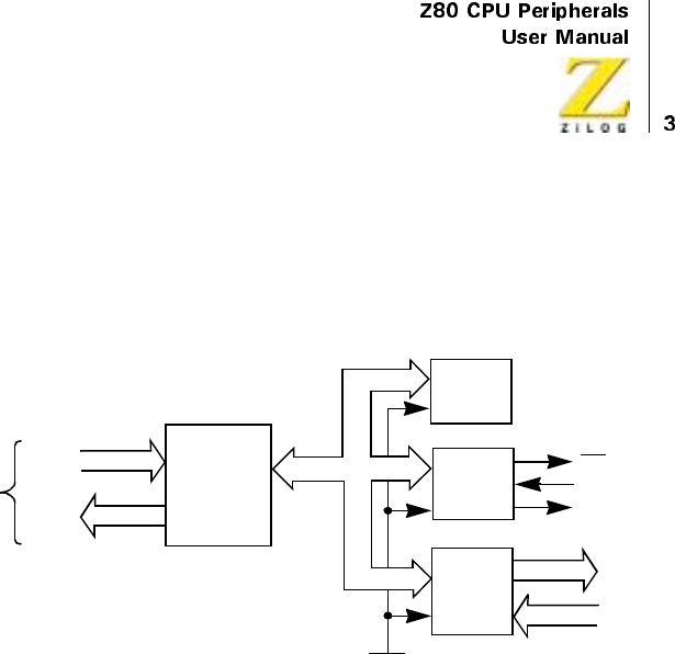
diagram of the Z80 CTC is depicted in Figure 1.
Figure 1. CTC Block Diagram
Structure of Channel Logic
The structure of one of the four sets of Counter/Timer channel logic is
illustrated in Figure 2. This logic is composed of:
•
Two registers
•
Two counters
•
Control logic
The registers consist of an 8-bit Time Constant register and an 8-bit
Channel Control register. The counters consist of an 8-bit CPU-readable
down-counter and an 8-bit prescaler.
From
Z80 CPU
Data
Control
8
6
CPU
BUS
I/O
Internal
Control
Logic
Interrupt
Logic
Counter/
Timer
Logic
RESET
ZC/TO
3
4
IEO
INT
IEI
Internal Bus
UM008101-0601 Counter/Timer Channels
In Channel Control Register and Logic
The Channel Control register (8-bit) and Logic is written to by the CPU to
select the modes and parameters of the channel. Within the CTC device,
four such registers correspond to the four Counter/Timer channels. The
register to be written to is determined by the encoding of two channel select
input pins: CS0 and CS1, which are usually attached to A0 and A1 of the
CPU address bus. The channel values are described in Table 1.
In the control word, which is written to program each Channel Control
register, bit 0 is always set; the other seven bits are programmed to select
alternatives on the channel’s operating modes and parameters. These values
are described in Table 2. For a more complete discussion, see “CTC
Operating Modes” on page 16 and “CTC Programming” on page 18).
Figure 2. Channel Block Diagram
Table 1. Channel Values
CS0 CS1
Channel 0 0 0
Channel 1 0 1
Channel 2 1 0
Channel 3 1 1
ZC/TO
Prescaler
CLK
CLK/TRG
Internal Bus
8-Bit
Down
Counter
Time
Constant
Register
Channel
Control
Logic
UM008101-0601 Counter/Timer Channels
The Prescaler
The prescaler is an 8-bit device that is used in the TIMER mode only. The
prescaler is programmed by the CPU through the Channel Control register
to divide its input, the System clock (0), by 16 or 256. The output of the
prescaler is then fed as an input to clock the down-counter. Each time that
Table 2. Channel Control Register
76543210
Interrupt Mode Prescaler
Val ue*
CLK/TRG
Section
Time
Trigger*
Time
Constant
Reset Control or
Vec tor
R/W R/W R/W R/W R/W R/W R/W R/W
Bit Number Field R/W Value Description
7 Interrupt R/W 1
0
Enable Interrupt
Disable Interrupt
6Mode R/W1
0
COUNTER Mode
TIMER Mode
5 Prescaler Value* R/W 1
0
256
16
4 CLK/TRG Edge
Section
R/W 1
0
Rising Edge
Falling Edge
3 Time Trigger* R/W 1
0
CLK/TRG Pulse Starts Timer
Automatic trigger when time constant is loaded
2 Time Constant R/W 1
0
Time Constant Follows
No Time Constant Follows
1 Reset R/W 1
0
Software Reset
Continue Operation
0 Control or Vector R/W 1
0
Control
Vec tor
*TIMER mode only

UM008101-0601 Counter/Timer Channels
the down-counter counts to zero, the down-counter is automatically
reloaded with the contents of the Time Constant register. This process
divides the System clock by an additional factor of the time constant. Each
time the down-counter counts to zero, its output, Zero Count/Timeout (ZC/
TO), is pulsed High.
The Time Constant Register
The 8-bit Time Constant register is used in both Counter and Timer modes.
It is programmed by the CPU just after the channel control word, with an
integer time constant value of 1 through 256. This register loads the
programmed value to the down-counter when the CTC is first initialized
and reloads the same value into the down-counter automatically whenever
it counts down thereafter to zero. If a new time constant is loaded into the
Time Constant register while a channel is counting or timing, the present
down count is completed before the new time constant is loaded into the
down counter. For details about writing a time constant to a CTC channel,
see “CTC Programming” on page 18
The Down-Counter
The down-counter is an 8-bit register that is used in both COUNTER and
TIMER modes. This register is loaded by the Time Constant register both
initially, and when it counts down to zero. In the COUNTER mode, the
down-counter is decremented by each external clock edge. In the TIMER
mode, it is decremented by the clock output of the prescaler. By performing
a simple I/O Read at the port address assigned to the selected CTC channel,
the CPU can access the contents of the down-counter and obtain the number
of counts-to-zero. Any of the four CTC channels may be programmed to
generate an interrupt request sequence each time the zero count is reached.
In Channels 0, 1, and 2, a signal pulse appears at the corresponding ZC/TO
pin when the zero count condition is reached. Because of package pin
limitations, however, Channel 3 does not have this pin and so may be used
only in applications where this output pulse is not required.
UM008101-0601 Counter/Timer Channels
Interrupt Control Logic
The Interrupt Control Logic insures that the CTC acts in accordance with
Z80 system interrupt protocol for Nested Priority Interrupting and Return
From Interrupt. The priority of any system device is determined by its
physical location in a daisy-chain configuration. Two signal lines, CIEI and
IEO, are provided in CTC devices to form this system daisy-chain. The
device closest to the CPU has the highest priority. Within the CTC,
interrupt priority is predetermined by channel number, with Channel 0
having highest and Channel 3 the lowest priority. See Table 3. The purpose
of a CTC-generated interrupt, as with any peripheral device, is to force the
CPU to execute an interrupt service routine. According to Z80 system
interrupt protocol, lower priority devices or channels may not interrupt
higher priority devices or channels that have not had their interrupt service
routines completed. However, high priority devices or channels may
interrupt the servicing of lower priority devices or channels.
Table 3. Interrupt Vector Register
76543210
Supplied by User Channel Identifier Word
R/W R/W R/W
Bit Number Field R/W Value Description
7–3 Reserved R/W Supplied by User
2–1 Channel Identifier
(Automatically
inserted by CTC)
R/W 11
10
01
00
Channel 3
Channel 2
Channel 1
Channel 0
0Word R/W1
0
Control
Interrupt Vector
UM008101-0601 Counter/Timer Channels
A CTC channel may be programmed to request an interrupt every time its
down-counter reaches a count of zero. However, using this feature requires
that the CPU be in INTERRUPT Mode 2. After the interrupt request, the
CPU sends out an interrupt acknowledge. The CTC’s interrupt control
logic determines the highest-priority channel requesting an interrupt. If
the CTC’s IEI input is active, indicating that it has priority within the
system daisy-chain, it places an 8-bit interrupt vector on the system data
bus as follows:
1. The high order five bits of this vector were written to the CTC earlier
as part of the CTC initial programming process.
2. The next two bits are provided by the CTC’s interrupt control logic as a
binary code corresponding to the highest-priority channel requesting an
interrupt.
3. The low-order bit of the vector is always zero according to a
convention (Figure 3).
This interrupt vector is used to form a pointer to a location in memory
where the address of the interrupt service routine is stored in a table. The
vector represents the least-significant eight bits. The CPU reads the
contents of the I register to provide the most-significant eight bits of the
16-bit pointer. The address pointed to in memory contains the low-order
byte and the next highest address contains the high-order byte of an
address, which in turn contains the first Op Code of the interrupt service
routine. Thus, in Mode 2, a single 8-bit vector stored in an interrupting
CTC can result in an indirect call to any memory location (Figure 3).
Figure 3. Z80 16-Bit Pointer (Interrupt Starting Address)
0
Vector
7Bitsfrom
Peripheral
1Reg
Contents
Z80 16-Bit Pointer (Interrupt Starting Address)

UM008101-0601 Counter/Timer Channels
According to Z80 system convention, all addresses in the interrupt service
routine table place their low-order byte in an even location in memory, and
their high-order byte in the next highest location in memory. This location is
always odd so that the least-significant bit of any interrupt vector is always
even. Therefore, the least-significant bit of any interrupt vector always zero.
The RETI instruction is used at the end of an Interrupt Service Routine to
initialize the Daisy Chain Enable line IEO for control of nested priority
interrupt handling. The CTC monitors the system data bus and decodes this
instruction when it occurs. Therefore, the CTC channel control logic knows
when the CPU has completed servicing an interrupt.
CTC PIN DESCRIPTION
Pin Functions
Diagrams of the Z80 CTC Pin Configuration and Z80 CTC Package
Configuration are illustrated in Figure 4 through Figure 7, respectively.
This section describes the function of each pin.
UM008101-0601 Counter/Timer Channels
Figure 4. CTC Pin Configuration
Figure 5. Package Configuration
Daisy-Chain
Interrupt
Control
CTC
Control
from CPU
CPU
Data Bus
Z80 CTC
Channel
Signals
CLK +5V GND
CLK/TRG0
ZC/TO0
CLK/TRG1
ZC/TO1
CLK/TRG2
ZC/TO2
CLK/TRG3
RESET
INT
IEO
IEI
RD
IORQ
M1
CS1
CS0
CE
D0
D0
D1
D2
D3
D4
D5
D6
D7
D4
D5
D6
D7
GND
RD
ZC/TO0
ZC/TO1
IZC/TO2
IORQ
IEO
INT
IEI
M1
1
2
3
4
6
7
8
9
10
5
11
12
13
14
D3
D2
D1
D0
+5V
CLK/TRG1
CLK/TRG2
CLK/TRG3
CS1
CS0
RESET
CE
CLK
Z80 CTC
28
27
26
25
23
22
21
20
19
24
18
17
16
15
CLK/TRG0
UM008101-0601 Counter/Timer Channels
Figure 6. 44-Pin Chip Carrier Pin Assignments
7
8
9
10
11
12
13
14
15
16
17
39
38
37
36
35
34
33
32
31
30
29
N/C
N/C
+5V
N/C
N/C
N/C
CS1
CLK/TRG3
CLK/TRG0
CLK/TRG1
CLK/TRG2
Z80 CTC
65432144 43 42 41 40
18 19 20 21 22 23 24 25 26 27 28
N/C
D7
D6
N/C
D5
D4
D3
D2
D1
D0
N/C
N/C
INT
N/C
IEI
M1
N/C
RESET
CS0
N/C
CE
CLK
GND
N/C
RD
ZC/TO0
N/C
ZC/TO1
ZC/TO2
IORQ
N/C
IEO
N/C
UM008101-0601 Counter/Timer Channels
Figure 7. 44-Pin Quad Flat Pack Pin Assignments
Bit 7–Bit 0
System Data Bus (bidirectional, tristate). Thisbusisusedtotransferall
date and command words between the Z80 CPU and the Z80 CTC. There
are eight bits on this bus, of which bit 0 is the least-significant. CSI CSO
Channel Select (input, active High). These pins form a 2-bit binary address
code for selecting one of the four independent CTC channels for an I/O
WriteorRead.(SeeTable4).
34
33
N/C
CS1
CLK/TRG3
CLK/TRG2
N/C
N/C
CLK/TRG1
CLK/TRG0
N/C
+5V
N/C
IEO
IORQ
N/C
ZC/TO2
ZC/TO1
N/C
ZC/TO0
N/C
RD
GND
D7
CS0
RESE
T
CE
N/C
CLK
N/C
M1
N/C
IEI
N/C
INT
D0
D1
D2
D3
N/C
N/C
N/C
D4
D5
D6
N/C
44
22
12
11
1
CMOS
Z80 CTC
UM008101-0601 Counter/Timer Channels
CE
Chip Enable (input, active Low). A Low level on this pin enables the
CTC to accept control words, interrupt vectors, or time constant data
words from the Z80 data bus during an I/O Write cycle; or to transmit the
contents or the down-counter to the CPU during an I/O Read cycle. In
most applications this signal is decoded from the eight least-significant
bits of the address bus for any of the four I/O port addresses that are
mapped to the four Counter/Timer channels.
Clock(Φ)
System Clock (input). This single-phase clock is used by the CTC to
internally synchronize certain signals.
M1
Machine Cycle One Signal from CPU (input, active low). When M1 is
activeandtheRDsignal is active, the CPU fetches an instruction from
memory. When M1 is active and the IORQ signal is active, the CPU
acknowledges an interrupt, alerting the CTC to place an interrupt vector on
the Z80 data bus if it has daisy-chain priority and one of its channels has
requested an interrupt.
Table 4. Channel Select Truth Table
CS1 CS0
Channel 0 0 0
Channel l 0 1
Channel 2 1 0
Channel 3 1 1

UM008101-0601 Counter/Timer Channels
IORQ
Input/Output Request from CPU (input, active Low). The IORQ signal
is used in conjunction with the CE and RD signals to transfer data and
channel control words between the Z80 CPU and the CTC. During a CTC
Write cycle, IORQ and CE must be true and RD false. The CTC does not
receive a specific write signal. Instead it generates one internally from the
inverse of a valid RD signal. In a CTC Read cycle, IORQ,CE,andRD
must be active to place the contents of the down-counter on the Z80 data
bus. If IORQ and M1 are both true, the CPU is acknowledging an interrupt
request, and the highest priority interrupting channel places its interrupt
vector on the Z80 data bus.
RD
Read Cycle Status from the CPU (input, active Low). The RD signal is
used in conjunction with the IORQ and CE signals to transfer data and
channel control words between the Z80 CPU and the CTC. During a CTC
Write Cycle, IORQ and CE must be true and RD false. The CTC does not
receive a specific write signal, instead it generates one internally from the
inverse of a valid RD signal. In a CTC Read cycle, IORQ CE,andRDmust
be active to place the contents of the down-counter on the Z80 data bus.
IEI
Interrupt Enable In (input, active High). This signal is used to form a
system-wide interrupt daisy-chain which establishes priorities when more
than one peripheral device in the system has interrupting capability. A High
level on this pin indicates that no other interrupting devices of higher
priority in the daisy chain are being serviced by the Z80 CPU.
IEO
Interrupt Enable Out (output, active High. The IEO signal, in
conjunction with IEI, is used to form a system-wide interrupt priority
daisy-chain. IEO is High only if IEI is High and the CPU is not servicing

UM008101-0601 Counter/Timer Channels
an interrupt from any CTC channel. Therefore, this signal blocks lower-
priority devices from interrupting while a higher-priority interrupting
device is being serviced by the CPU.
INT
Interrupt Request (output, open-drain, active Low). This signal goes
true when a CTC channel, which has been programmed to enable
interrupts, has a zero-count condition in its down-counter.
RESET
Reset (input, active Low). This signal stops all channels from counting
and resets interrupt enable bits in all control registers, thereby disabling
CTC-generated interrupts. The ZC/TO and INT outputs go inactive, IEO
reflects IEI, and the CTC’s data bus output drivers go to the high-
impedance state.
CLK/TRG3–CLK/TRG0
External Clock/Timer Trigger (input, user-selectable active High or
Low). Four CLK/TRG pins correspond to the four independent CTC
channels. In the Counter mode, every active edge on this pin decrements
the down-counter. In the TIMER mode, an active edge on this pin initiates
the timing function. The user may select the active edge to be either rising
or falling.
ZC/TO2-AC/TO0
Zero Count/Timeout (output, active High). Three ZC/TO pins
correspond to CTC Channels 2 through 0. (Because of package pin
limitations Channel 3 has no ZC/TO pin.) In either COUNTER mode or
TIMER mode, when the down-counter decrements to zero, an active High
pulse appears at this pin.

UM008101-0601 Counter/Timer Channels
CTC OPERATING MODES
Overview
At power-on, the Z80 CTC state is undefined. Asserting RESET puts the
CTC in a known state. Before a channel can begin counting or timing, a
channel control word and a time constant data word must be written to the
appropriate registers of that channel. Additionally, if a channel has been
programmed to enable interrupts, an interrupt vector word must be written
to the CTC’s interrupt control logic. (For further details, refer the “CTC
Programming” on page 18) When the CPU has written all of these words to
the CTC, all active channels are programmed for immediate operation in
either the COUNTER mode or the TIMER mode.
CTC COUNTER Mode
In CTC COUNTER mode, the CTC counts edges of the CLK/TRG input.
This mode is programmed for a channel when its Channel Control Word is
written with bit 6 set. The channel’s external clock (CLK/TRG) input is
monitored for a series of triggering edges. After each, in synchronization
with the next rising edge of Φ(the System clock), the down-counter (which
is initialized with the Time Constant Data word at the start of each sequence
of down-counting) is decremented. Although there is no setup time
requirement between the triggering edge of the External clock and the
rising edge of Φ(Clock), the down-counter is not decremented until the
following pulse. A channel’s External clock input is pre programmed by bit
4 of the channel control word to trigger the decrementing sequence with
either a high- or a low-going edge.
In Channels 0, 1, or 2, when the down-counter is successively decremented
from the original time constant (until it reaches zero), the Zero Count (ZC/
TO) output pin for that channel is pulsed active (High). Due to package pin
limitations, this pin does not exist on Channel 3 and so this pin may only be

UM008101-0601 Counter/Timer Channels
used in applications where this output pulse is not required. Additionally, if
the channel is pre-programmed by bit 7 of the channel control word, an
interrupt request sequence is generated. For more details, see the CTC
Interrupt Servicing section
The zero-count condition also results in the automatic reload of the down-
counter with the original time constant data word in the Time Constant
register. There is no interruption in the sequence of continued down-
counting. If the Time Constant register is written with a new Time Constant
Data Word while the down-counter is decrementing, the present count is
completed before the new time constant is loaded into the down-counter.
CTC TIMER Mode
In CTC TIMER mode, the CTC generates timing intervals that are an
integer value of the system clock period. This mode is programmed for a
channel when its Channel Control Word is written with bit 6 reset. The
channel then may be used to measure intervals of time based on the System
clock period. The System clock is fed through the prescaler and the down-
counter. Depending on the pre programmed bit 5 in the Channel Control
Word, the prescaler divides the System clock by a factor of 16 or 256.
The output of the prescaler is then used as a clock to decrement the down-
counter, which may be pre programmed with any time constant integer
between 1 and 256. The time constant is automatically reloaded into the
down-counter at each zero-counter condition. At zero count, the channel’s
Time Cut (ZC/TO) output (which is the output of the down-counter) is
pulsed, resulting in a uniform pulse train of the precise period given by the
product as shown below.
Where tcis the System clock, P is the prescaler factor of 16 or 256, and TC
is the pre-programmed time constant.

UM008101-0601 Counter/Timer Channels
Timing may be initialized automatically or with a triggering edge at the
channel’s Timer Trigger (CLK/TRG) input. This timing is determined by
programming bit 3 of the channel control word. If bit 3 is reset?, the timer
automatically begins operation at the start of the CPU cycle following the I/
O Write machine cycle that loads the time constant data word to the
channel.
If bit 3 is set, the timer begins operation on the second succeeding rising
edge of Φafter the Timer Trigger edge following the loading of the time
constant data word.
If no time constant word is to follow, the timer begins operation on the
second succeeding rising edge of Φafter the Timer Trigger edge and
following the control word write cycle. Bit 4 of the channel control word is
pre programmed to select whether the Timer Trigger is sensitive to a rising
or falling edge. There is no setup requirement between the active edge of
the Timer Trigger and the next rising edge of Φ.
If the Timer Trigger edge occurs closer than a specified minimum setup
time to the rising edge of Φ, the down-counter does not begin decrementing
until the following rising edge of Φ. If bit 7 in the channel control word is
set, the zero-count condition in the down-counter causes a pulse at the
channel’s Time Out pin, and initiates an interrupt request sequence. (For
more details, see “CTC Interrupt Servicing” on page 27).
CTC PROGRAMMING
Overview
To begin counting or timing operations, a Channel Control Word and Time
Constant Data Word are written to the appropriate channel by the CPU.
These words are stored in the Channel Control or Time Constant registers
of each channel. If a channel has been programmed to enable interrupts, an
interrupt vector is written to the appropriate register in the CTC. Because of

UM008101-0601 Counter/Timer Channels
automatic features in the interrupt control logic, one pre-programmed
interrupt vector suffices for all four channels.
Loading The Channel Control Register
To load a Channel Control Word, the CPU performs a normal I/O Write
sequence to the port address corresponding to the desired CTC channel. The
CTC input pins CS0 and CS1 are used to form a 2-bit binary address to select
one of four channels within the device. (See Table 2 on page 5.) In many
system architectures, these two input pins are connected to Address Bus lines
A0 and A1, respectively, so that the four channels in a CTC device occupy
contiguous I/O port addresses. A word written to a CTC channel is
interpreted as a channel control word, and loaded into the channel control
register (bit 0 is a logic 1). The other seven bits of this word select operating
modes and conditions as indicated in Table 2.
Table 5. Channel Control Register
76543210
Interrupt Mode Prescaler
Val ue*
CLK/TRG
Section
Time
Trigger*
Time
Constant
Reset Control or
Vec tor
R/W R/W R/W R/W R/W R/W R/W R/W
Bit
Number Field R/W Value Description
7 Interrupt R/W 1
0
Enable Interrupt
Disable Interrupt
6Mode R/W1
0
COUNTER Mode
TIMER Mode
5 Prescaler Value* R/W 1
0
256
16
*TIMER mode only

UM008101-0601 Counter/Timer Channels
Bit 7 = 1. Each channel is enabled to generate an interrupt request sequence
when the down-counter reaches a zero-count condition. To set the interrupt
bit to 1 in any of the four Channel Control registers an interrupt vector is
written to the CTC before operation begins. Channel interrupts may be
programmed in either Counter or Timer mode. If an updated channel
control word is written to a channel in operation, with bit 7 set, the interrupt
enable selection is not retroactive to a preceding zero-count condition.
Bit 7 = 0. Channel interrupts disabled.
Bit 6 = 1. Counter mode selected. The down-counter is decremented by
each triggering edge of the External clock (CLK/TRG) input. The prescaler
is not used.
Bit 6 = 0. Timer mode selected. The prescaler is clocked by the System
clock Φ, and the output of the prescaler in turn clocks the down-counter.
The output of the down-counter (the channel’s ZC/TO output) is a uniform
pulse train of period given by the product as shown below
4 CLK/TRG Edge
Section
R/W 1
0
Rising Edge
Falling Edge
3 Time Trigger* R/W 1
0
CLK/TRG Pulse Starts Timer
Automatic trigger when time constant is loaded
2 Time Constant R/W 1
0
Time Constant Follows
No Time Constant Follows
1Reset R/W1
0
Software Reset
Continue Operation
0 Control or Vector R/W 1
0
Control
Ve c t o r
Bit
Number Field R/W Value Description
*TIMER mode only

UM008101-0601 Counter/Timer Channels
where tcis the period of System clock, P is the prescaler factor of 16 or 256,
and TC is the time constant data word.
Bit 5 = 1. Defined for Timer mode only. Prescaler factor is 256.
Bit 5 = 0. Defined for Timer mode only. Prescaler factor is 16.
Bit 4 = 1. TIMER Mode: positive edge trigger starts timer operation.
COUNTER Mode: positive edge decrements the down-counter.
Bit 4 = 0. TIMER Mode: negative edge trigger starts timer operation.
COUNTER Mode: negative edge decrements the down-counter.
Bit 3 = 1. TIMER Mode only. External trigger is valid for starting timer
operation after rising edge of T2 of the machine cycle following the one
that loads the tune constant. The prescaler is decremented two clock cycles
later if the setup tune is met, otherwise three clock cycles.
Bit 3 = 0. TIMER Mode only. Timer begins operation on the rising edge of
T2 of the machine cycle following the one that loads the time constant.
Bit 2 = 1. The time constant data word for the Time Constant register is the
next word written to this channel. If an updated channel control word and
time constant data word are written to a channel while it, is already in
operation, the down-counter continues decrementing to zero before the new
time constant is loaded.
Bit 2 = 0. No time constant date word for the Time Constant register is to
follow. The channel control word updates the status of a channel already in
operation to channel will not operate without a correctly programmed data
word in the lime Constant register. Bit 2 in the channel control word must
be set in order to write to the Time Constant register.
Bit 1 = 1. Counting and/or timing operation is terminated and the channel is
reset. This is not a stored condition. The bits in the Channel Control register
are unchanged. If bits 1 and 2 are set to 1, the channel resumes operation
upon loading a time constant.
Bit 1 = 0. Channel continues current operation.

UM008101-0601 Counter/Timer Channels
Loading The Time Constant Register
A Time Constant Data Word is written to the Time Constant register by the
CPU. This event occurs on the I/O Write Cycle following that of the
channel control word. The Time Constant Data Word may be any integer
value in the range 1-256 (Table 6). If all eight bits in this word are zero, it is
interpreted as 256. If a Time Constant Date Word is loaded to a channel
already in operation, the down-counter continues decrementing to zero
before the new time constant is loaded.
Loading The Interrupt Vector Register
The Z80 CTC operates with the Z80 CPU programmed for mode 2
interrupt response. When a CTC interrupt request is acknowledged, a 16-bit
pointer is formed to obtain a corresponding interrupt service routine
starting address (Figure 8). The upper eight bits of this pointer are provided
by the CPU’s I register; the lower eight bits are provided by the CTC in the
form of an interrupt vector unique to the requesting channel (Figure 8). For
further details, see “CTC Interrupt Servicing” on page 27.
The five high-order bits of the interrupt vector are written to the CTC in
advance as part of the initial programming sequence. The CPU writes to the
I/O port address corresponding to the CTC Channel 0. A 0 in bit 0 signals
the CTC to load the incoming word into the interrupt vector register. When
the interrupt vector is placed on the Z80 data bus, the interrupt control logic
of the CTC automatically supplies a binary code in bits 1 and 2 identifying
which of the four CTC channels is to be serviced.
Table6.TimeConstantRegister
76543210
TC7 TC6 TC5 TC4 TC3 TC2 TC1 TC0
R/W R/W R/W R/W R/W R/W R/W R/W
UM008101-0601 Counter/Timer Channels
Figure 8. Mode 2 Interrupt Operation
Table 7. Interrupt Vector Register
76543210
Supplied by User Channel Identifier Word
R/W R/W R/W
Bit
Number Field R/W Value Description
7–3 Reserved R/W Supplied by User
2–1 Channel
Identifier
R/W 11
10
01
00
Channel 3
Channel 2
Channel 1
Channel 0
0Word R/W1
0
Control
Interrupt Vector
Service Interrupt Routine
Starting Address Low Order
High Order
Desired starting address pointed to by:
1Reg
Contents 7Bitsfrom
Peripheral 0

UM008101-0601 Counter/Timer Channels
CTC TIMING
Overview
This section describes the timing relationships of the relevant CTC pins for
the following types of operation:
•
Writing a word to the CTC
•
Reading a word from the CTC
•
Counting and timing
A timing diagram, Figure 12, relating to interrupt servicing is found in
“Interrupt Acknowledge Cycle” on page 28.
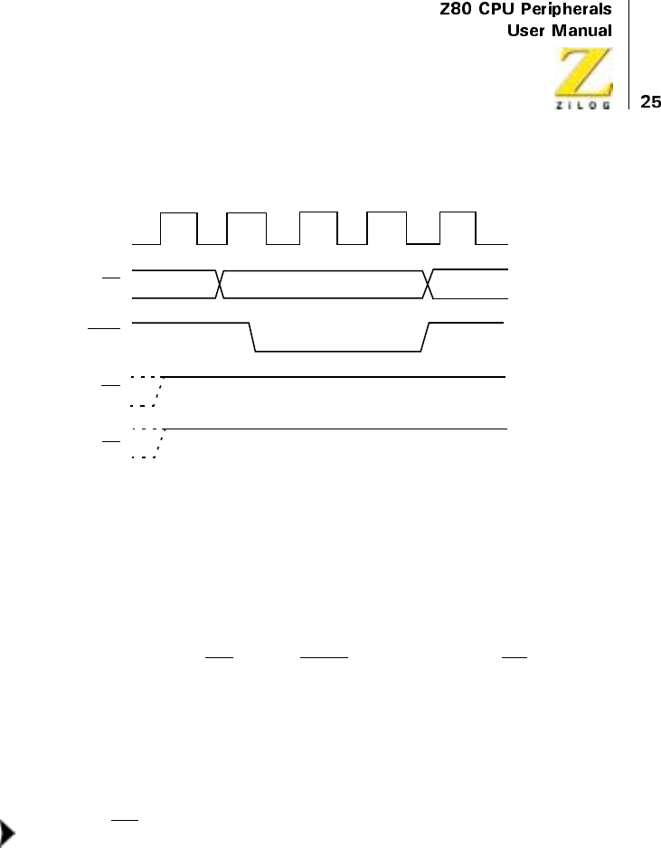
CTC Write Cycle
Figure 9 illustrates the timing associated with the CTC Write cycle. This
sequence is applicable to loading a channel control word, an interrupt
vector, or a time constant data word.
In the sequence shown, during clock cycle T1, the Z80 CPU prepares for
the Write cycle with a false (High) signal at CTC input pin RD (Read).
Because the CTC has no separate Write signal input, it generates its own
input internally from the false RD input. During clock cycle T2, the Z80
CPU initiates the Write cycle with true (Low) signals at CTC input pins
IORQ (I/O Request) and CE (Chip Enable). (See Note below.) A 2-bit
binary code appears at CTC inputs CS1 and CS0 (Channel Select 1 and 0),
specifying which of the four CTC channels is being written to. At this time,
a channel control, interrupt vector, or time constant data word may be
loaded to the appropriate CTC internal register in synchronization with the
rising edge beginning clock cycle T3.
M1 must be false to distinguish the cycle from an interrupt
acknowledge.
Note:
UM008101-0601 Counter/Timer Channels
Figure 9. CTC Write Cycle
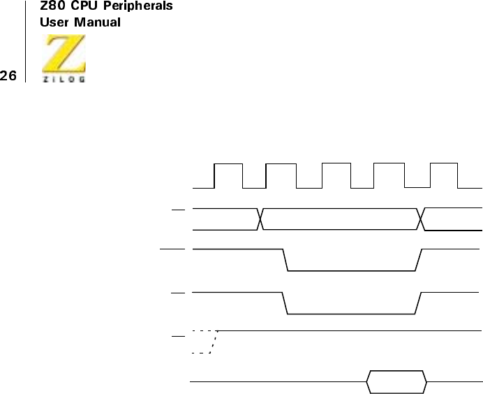
CTC Read Cycle
Figure 10 illustrates the timing associated with the CTC Read cycle. This
sequence is used when CPU reads the current contents of the down counter.
During clock cycle T2, the Z80 CPU initiates the Read cycle with true
signals at input pins RD (Read), IORQ (I/O Request), and CE (Chip
Enable). A 2-bit binary code appears at CTC inputs CS1 and CS0 (Channel
Select 1 and 0), specifying which of the four CTC channels is being read
from. (See Note below.) On the rising edge of the cycle T3, the valid
contents of the down-counter rising edge of cycle T2 is available on the
Z80 data bus. No additional wait states are allowed.
M1 must be false to distinguish the cycle from an interrupt
acknowledge.
CS0. CS1, CE
IORQ
RD
M1
Channel Address
T1T1
T2TWA T3
Note:
UM008101-0601 Counter/Timer Channels
Figure 10. CTC Read Cycle
CTC Counting and Timing
Figure 11 illustrates the timing diagram for the CTC Counting and Timing
modes.
In the Counter mode, the edge (rising edge is active in this example) from
the external hardware connected to pin CLK/TRG, decrements the down-
counter in synchronization with the System Clock Φ. This CLK/TRG pulse
must have a minimum width and the minimum period must not be less than
twice the System clock period. Although there is no setup time requirement
between the active edge of the CLK/TRG and the rising edge of Φ,ifthe
CLK/TRG edge occurs closer than a specified minimum time, the
decrement of the down-counter will be delayed one cycle of Φ.
Immediately after the 1 to 0 decrement of the down-counter, the ZC/TO
output is pulsed true.
In the Timer mode, a pulse trigger (user selectable as either active High or
active Low) at the CLK/TRG pin enables the timing function on the second
succeeding rising edge of Φ. As in the Counter mode, the triggering pulse is
CS0. CS1, CE
IORQ
RD
M1
DATA
Channel Address
T1T1
T2TWA T3
CLK
OUT
UM008101-0601 Counter/Timer Channels
detected asynchronously and must have a minimum width. The timing
function is initiated in synchronization with Φ. A minimum setup time is
required between the active edge of the CLK/TRG and the rising edge of Φ.
If the CLK/TRG edge occurs closer than this, the initiation of the timer
function will be delayed one cycle of Φ.
Figure 11. CTC Counting and Timing
CTC INTERRUPT SERVICING
Overview
Each CTC channel may be individually programmed to request an
interrupt every time its down-counter reaches zero. The purpose of a CTC-
generated interrupt is to force the CPU to execute an interrupt service
routine. To use this feature the Z80 CPU must be programmed for Mode 2
interrupt response. In this mode, when a CTC channel interrupt request is
acknowledged, a 16-bit pointer must be formed to obtain a corresponding
interrupt service routine. The lower eight bits of the pointer are provided
by the CTC in the form of an interrupt vector unique to the requesting
channel. For further details, refer to the Z80 CPU User’s Manual.
ZC/TO
CLK/TRG
Internal
Counter
Lead
Time
Zero
Count

UM008101-0601 Counter/Timer Channels
The CTC’s interrupt control logic ensures that it acts in accordance with
Z80 system interrupt protocol for nested priority interrupt and proper return
from interrupt. The priority of any system device is determined by its
physical location in a daisy-chain configuration. Two signal lines (IEI and
IEO) are provided in the CTC to form the system daisy chain. The device
closest to the CPU has the highest priority. Interrupt priority is
predetermined by channel number, with Channel 0 having highest priority.
According to Z80 system interrupt protocol, low priority devices or
channels may not interrupt higher priority devices or channels that have not
had their interrupt service routines completed. High priority devices or
channels may interrupt the servicing of lower priority devices or channels.
(For further details, see “CTC Architecture” on page 2.)
“Return from Interrupt Cycle” on page 29 and “Daisy-Chain Interrupt
Servicing” on page 30 describe the nominal timing relationships of the
relevant CTC pins for the Interrupt Acknowledge cycle and the Return
from Interrupt cycle. “Daisy-Chain Interrupt Servicing” on page 30
discusses a typical example of daisy-chain interrupt servicing.
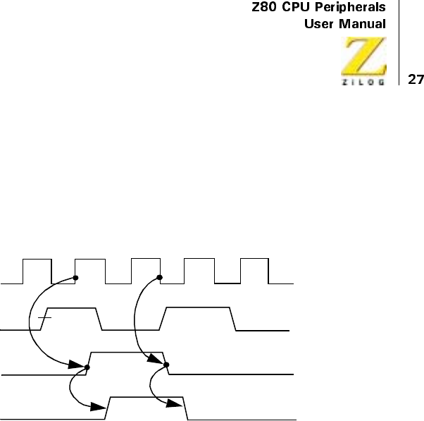
Interrupt Acknowledge Cycle
Figure 12 illustrates the timing associated with the Interrupt Acknowledge
cycle. After an interrupt is requested by the CTC, the CPU sends out an
interrupt acknowledge (M1 and IORQ). To insure that the daisy-chain
enable lines stabilize, channels are inhibited from changing their interrupt
request status when M1 is active. M1 is active two clock cycles earlier than
IORQ and RD is false to distinguish the cycle from an instruction fetch.
During this time, the interrupt logic of the CTC determines the highest
priority channel requesting an interrupt. If the CTC Interrupt Enable input
(IEI) is active, the highest priority interrupting channel within the CTC
places its interrupt vector onto the data bus when IORQ goes active. Two
Wait States (TW*) are automatically inserted at this time to allow the daisy-
chain to stabilize. Additional Wait States may be added.
UM008101-0601 Counter/Timer Channels
Figure 12. Interrupt Acknowledge Cycle
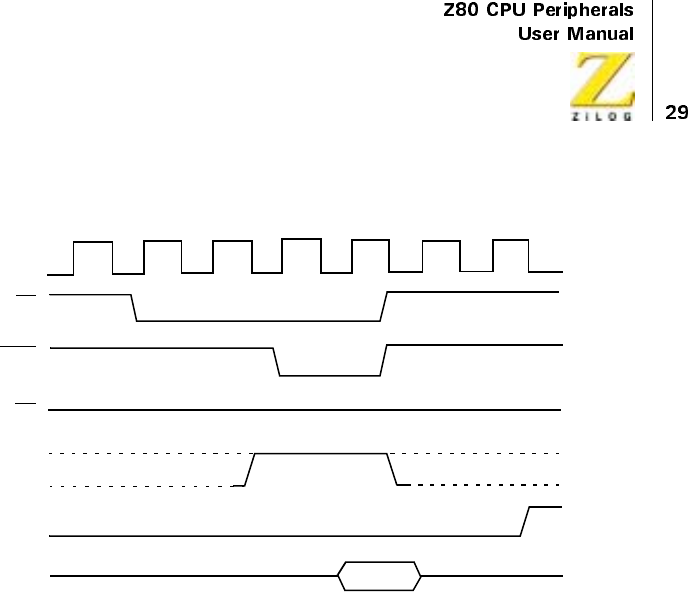
Return from Interrupt Cycle
Figure 13 illustrates the timing associated with the RETI Instruction. This
instruction is used at the end of an Interrupt Service Routine to initialize
the daisy-chain enable lines for control of nested priority interrupt
handling. The CTC decodes the two-byte RETI code internally and
determines whether it is intended for a channel being serviced.
When several Z80 peripheral chips are in the daisy-chain, IEI becomes
active on the chip currently under service when an EDH Op Code is
decoded. If the following Op Code is 4DH, the peripheral being serviced is
re-initialized and its IEO becomes active.
DATA
CLK
T1T1
T2TW*T
3
TW*T
4
Vector
INT
IEI
RD
IORQ
M1
UM008101-0601 Counter/Timer Channels
Figure 13. Return from Interrupt Cycle
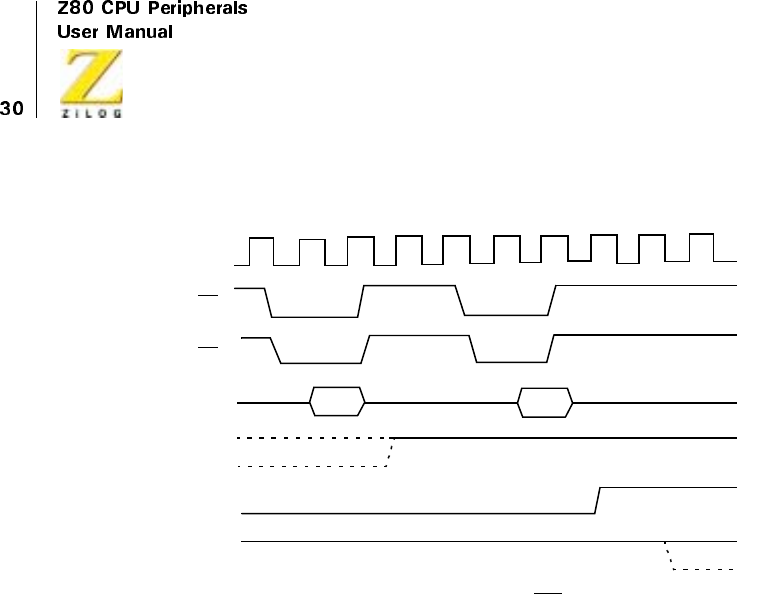
Daisy-Chain Interrupt Servicing
Figure 14 illustrates a typical nested interrupt sequence that may occur in
the CTC. In this example, Channel 2 interrupts and is granted service.
While this channel is being serviced, higher priority Channel 1 interrupts
and is granted service. The service routine for the higher priority channel is
completed, and a RETI instruction is executed to signal the channel that its
routine is complete (see “Return from Interrupt Cycle” on page 29 for
further details). At this time, the service routine of the lower priority
Channel 2 is resumed and completed.
IEO
CLK
INT
IEI
RD
M1
T1T2T3T4
D7–D0
*INT goes Low if more interrupts are pending on the RTC.
T1T2T3T4T1
ED 4D
UM008101-0601 Counter/Timer Channels
Figure 14. Daisy-Chain Interrupt Servicing
IEI IEO
HI
+
IEI IEO
HI
+
IEI IEO
HI
+
IEI IEO
HI
+
IEI IEO
HI
IEI IEO
HI
IEI IEO
HI
IEI IEO
HI
IEI IEO
HI
IEI IEO
HI
+
IEI IEO
HI
IEI IEO
HI
IEI IEO
LO
IEI IEO
HI
IEI IEO
HI
IEI IEO
HI
IEI IEO
LO
IEI IEO
LO
IEI IEO
LO
IEI IEO
HI
HI
LO
LO
LO
HI
Channel 3
Channel 2
Channel 1
Under Service
Service Suspended
Service Resumed
Service Complete
5. Second ‘RETI’ instruction issued on completion of Channel 2 Service Routine.
4. Channel 1 service routine complete, ‘RETI’ issued, Channel 2 serviced resumed.
3. Channel 1 interrupts, suspends servicing of Channel 2.
2. Channel 2 requests an interrupt and is acknowledged.
1. Priority interrupt daisy chain before any interrupt occurs.
Service Complete
Under Service
Channel 0
Highest Priority Channel

UM008101-0601 Counter/Timer Channels

UM008101-0601 Direct Memory Access
Direct Memory Access
DMA OVERVIEW
Direct Memory Access (DMA) and DMA Controllers are dedicated to
controlling high-speed block transfers of data independently of the CPU.
DMA data transfers are usually between memory and I/O, or vice versa.
A DMA controller (DMAC) also performs some transfers that have tradi-
tionally been done by the CPU. For example, the Z80 DMA can perform
memory-to-memory, memory-to-I/O, and I/O-to-memory transfers, as
well as search for particular patterns of bits in a byte either simulta-
neously with or independently of transfers.
The advantages of DMA transfers are:
•
Transfers bypass the CPU
•
Transfers are fast
CPU Data Transfers
In systems without DMA, data transfers must pass through the CPU and be
implemented in software. Data transfers through the CPU include
executing an instruction sequence for input and output, and tracking each
byte of data in the block to be transferred.
Figure 15 illustrates the minimum sequence of instructions that must be
fetched from memory and executed by conventional CPUs to transfer a
block of data one byte at a time. Most CPUs require many more instructions.
CPU transfers are relatively slow and tie up the CPU. In addition response
time (startup time for the first byte) is also usually slow because the I/O
device typically uses interrupts to signal its readiness, and the CPU interrupt
service routine causes a significant time lag in transferring the first byte.
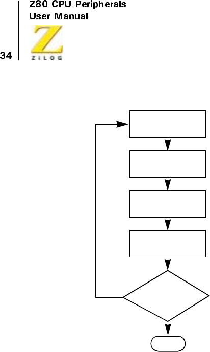
UM008101-0601 Direct Memory Access
Figure 15. Typical CPU I/O Sequence
The Z80 and Z8000 CPUs both have block-transfer and string-search
instructions that can operate on up to 64 Kbytes of data with a single
instruction.
A single block transfer instruction repetitively performs all of the functions
illustrated in Figure 15 on an entire sequence of bytes. Therefore, transfer
rates are significantly faster. The 4 MHz Z80A CPU can transfer at about
200 Kbytes/sec and the 4 MHz Z8000 CPU can reach 800 Kbytes/sec.
The problem with CPU block transfers in the Z80 and Z8000 devices is not
transfer speed but response time at startup. One of the following methods is
normally used to set up executing a block transfer instruction:
Read
Source Port
Write to
Destination Port
Increment
Address Counter
Increment
Byte Counter
NO
YES
END
Byte Count
Equal
Block Length
?

UM008101-0601 Direct Memory Access
•
The I/O device interrupts the CPU and the block transfer instruction
is executed in the CPU interrupt service routine. This method has a
response time of at least 5 to 10 µs, even in 4 MHz Z80A and
Z8000 devices.
•
The CPU begins executing the device service routine before the I/O
device is ready, and a flag bit is constantly polled by the CPU. When
the flag bit indicates that the device is ready, the CPU jumps to the
block transfer instruction. This method sometimes produces a response
time of less than 5 µs, but it uses the entire capability of the CPU.
•
The CPU begins executing the block transfer instruction in an interrupt
service routine before the I/O device is actually ready. The I/O device
idles the CPU with the Wait line just after the Read and Chip-Select
lines become active. When the I/O device is ready, it releases the wait
line and the transfer is completed. This method gives the best response
time (250 ns in a 4 MHz Z80A or Z8000 CPU) but ties up the bus.
Both transfer and response times on most CPUs are often too slow. While
transfer speed can be quite high with the Z80 and Z8000 CPUs, the
response time can be too long in interrupt-driven transfer situations.
DMA Data Transfers
A DMA controller (DMAC) performs direct data transfers between the
source and destination without going through the CPU, and without the
instruction fetches required by the CPU. It performs all of the steps illus-
trated in Figure 15 through hardware.
for example, in a memory-to-I/O transfer, the starting address in memory
and the length of the block to be transferred are written to the DMA by the
CPU before to the transfer. The DMAC begins transferring data when the
CPUenablestheDMACandtheReadylineI/Oofthedevicebecomes
active. In most cases, the CPU is idle during a DMA transfer. When the
transfer is complete, the DMAC signals the CPU and releases control.

UM008101-0601 Direct Memory Access
DMACs are used when one or more of the following situations or require-
ments are present:
•
CPU has too much I/O and cannot perform other tasks properly
•
Data transfer must be faster than the CPU can perform
•
Transfer response tune (startup) must be faster than the CPU can provide
Small and low-performance systems generally run without DMA.
Medium-performance systems can also be designed without DMA if the
CPU can handle transfers fast enough and still perform other operations.
When systems require fast transfers or fast response, DMACs are strong
candidates for performance enhancement. Not only do DMACs transfer
faster than most CPUs, but the response time is better. Response times can
even be improved using the techniques described above for CPU response.
The following examples are cases in which DMA is usually the best choice:
•
Disk and diskette controllers
•
Scanning operations, such as CRT I/O
•
Data acquisition
•
Memory-to-memory transfers
•
Memory searches
•
Backup storage (I/O-to-I/O)
•
Parallel bus systems such as the IEEE 488
•
Fiber optic links
•
Block transfers in networking, multiprocessing, or multiprogramming
The trade-off for speed is that the CPU typically remains idle and lacks full
or partial control of the system bus while the DMA is operating. This
condition can affect total system throughput, and can also affect such things
as memory refresh and other interrupts.

UM008101-0601 Direct Memory Access
DMA Characteristics
All DMACs are programmable because the CPU must at least write a
block length (byte count) and starting memory address to a DMAC before
they can begin managing a data transfer. The starting address is incre-
mented or decremented as the transfer proceeds, and the byte counter is
incremented from zero up to the specified block length.
In addition to being programmable, DMACs vary in characteristics and
capabilities.
Ports and Channels
Every data transfer has a source and a destination. For example, in
memory-to-I/O transfers, memory is the source and I/O is the destination
port. The means of controlling and tracking the data exchange between the
two ports is called a channel. A channel includes the hardware for address
and byte counting, bus control, and coordination of the entire transfer
process.
The location for each source and destination for a channel is specified
either by the DMA address-generation mechanism or by hardwiring. The
Z80 DMA generates addresses for both memory and I/O ports during each
byte transfer.
Some DMACs have multiple channels, which means that they can keep
track of multiple interleaved transfers, and that one DMA can be hardwired
to multiple I/O devices. However, because any DMA can execute only one
read and/or write cycle at a time, multiple channels do not mean higher
throughput than single channels in a given speed. The Z80 DMA is a
single-channel device that can generate addresses to perform memory-to-
memory data transfers. I/O port addresses on the address bus.
The Z80 DMA can also perform internal byte searches. When the Z80 DMA
loads bytes to an internal DMAC register during transfers, the result is that,
when a byte is loaded, it can be compared with a maskable control byte.

UM008101-0601 Direct Memory Access
Transfer Methods
Figure 16 compares conventional CPU instructions and the Z80 and Z8000
CPU block transfer instructions as well as two different methods of DMA
transfer. This figure compares the read and write cycles to the transfer of a
single byte of data.
Figure 16a illustrates conventional CPU I/O instruction activity. The
number of read and write cycles is approximate, some CPUs require more
cycles. The CPU instruction executes all the steps illustrated in Figure 15,
plus additional housekeeping tasks.
Figure 16b illustrates Z80 and Z8000 CPU block transfer instructions.
These instructions are approximate and require more activity than one read
cycle and one write cycle after initiation, especially with the Z80 CPU. A
single block transfer instruction is capable of transferring up to 64 Kbytes
of data.
Figure 16c illustrates sequential or flow-through DMA transfer where a
byte is read from the source port to the DMA and then written to the desti-
nation port. This method can be implemented on the Z80 DMA with no
external logic in a Z80 CPU environment. Sequential transfer provides
speeds that match or exceed the capability of most serial communication
processors and many other I/O or memory devices.
Figure 16d illustrates simultaneous or flyby DMA transfer where a byte is
both read and written in the same machine cycle. Read and Write control
lines are both active. Source and destination are determined by signals that
specify either a memory-read with an I/O-write or an I/O read/memory-
write. This is the fastest transfer method, but the external logic required
makes timing interfaces to memory and I/O somewhat more complicated.
Another method used for some DMACs is called a Transparent or Cycle-
stealing transfer. This technique is similar to the instruction in Figure 16c,
except that control of the bus causes the DMA data transfers to be inter-
leaved with CPU cycles (dynamic memory is not refreshed). This method
UM008101-0601 Direct Memory Access
also requires external logic and inhibits memory refresh. Additionally, it
reduces DMA throughput.
All DMA transfers interrupt dynamic memory refresh by the CPU and
most of them idle the CPU. It is, therefore, important to consider these
implications when making the trade-off for higher DMA transfer speed.
Figure 16. Conceptual Comparison of Various I/O Transfer Methods
CPU MEMORY I/O
CPU MEMORY I/O
Read/Write Cycle
DMA
DMA
D.
DMA
Simultaneous
Transfers
C.
DMA
Sequential
Instruction
Read Cycle
Write Cycle
BUS
BUS
BUS
CPU MEMORY I/O DMA
CPU MEMORY I/O DMA
Fetch and Read Cycles Write Cycle BUS
B.
Z80/Z8000
Block Transfer
Instruction
A.
Conventional
Programmed
Instruction
Sequence
Write Cycle
Read Cycle

UM008101-0601 Direct Memory Access
Modes of Operation
Within each of the methods illustrated in Figure 16c and Figure 16d there
are up to three modes of operation. These are termed Byte, Burst, and
Continuous modes in this manual, although they are also sometimes
referred to as Single, Demand, and Block modes. Figure 17 illustrates the
typical sequence of events for each mode, when the I/O device’s Ready
signal to the DMAC becomes active and before the DMA process reaches
an end-of-block or other terminating condition. (These figures are
expanded in Figure 20 through Figure 23.)
In Byte mode, the DMAC transfers only one byte at a time while the I/O
device Ready line is active. Control of the system bus is released back to
the CPU between each byte. The CPU can then interleave its other activ-
ities, until the DMA makes a new request to the CPU for system bus control
before transferring the next byte. Byte mode is related to the transparent
method of transfer in that both cause interleaving of CPU and DMA func-
tions. The Byte mode, however, includes the protocol of requesting and
releasing the bus for each byte transfer.
In Burst mode, which is the most common mode, the DMAC continues to
transfer bytes after gaining control of the system bus until the I/O device
Ready line goes inactive. During this time, the CPU typically remains idle.
When the Ready line goes inactive, the DMAC releases system bus control
back to the CPU.
In Continuous mode, the DMAC holds the system bus until the entire block
of data has been transferred. If the I/O device Ready line goes inactive
before the block is completely transferred, the DMAC waits until it
becomes active again, but the system bus is not released as in Burst mode.
The Continuous mode is the fastest mode because it has the least response-
time overhead when the Ready line momentarily goes inactive and returns
active again. However, this mode does not allow any CPU activity for the
duration of the transfer.

UM008101-0601 Direct Memory Access
Bus Control
Most DMACs do not control the system bus in the same way that a CPU
controls it. For example, many DMACs do not have a straightforward
interface to the system data bus but rather multiplex a portion of the
memory address onto the data bus, from which it must be latched by
external logic. Nor do most DMACs generate all of the bus control
signals that the CPU generates, and therefore they lack some degree of
bus control when they operate.
The Z80 DMA is unique among 8-bit DMACs because it generates
exactly the same bus control signals for read and write cycles that the Z80
CPU does, and also because it has exactly the same logical and electrical
interface to the data and address buses as the CPU. This means the other
system components cannot discern the difference between the Z80 DMA
and CPU; control by these devices is totally interchangeable. In the
sequential DMA transfer method (a read cycle followed by a write cycle),
it also means that the Z80 DMA pins can be tied directly to the corre-
sponding Z80 CPU pins without any of the external interfacing logic that
some DMACs require. This property considerably simplifies design and
lowers part counts.
Programmability
How a DMAC starts, transfers data, and stops is determined by control
information written to the DMAC by the CPU prior to the transfer. Status
registers, which can be read by the CPU to determine the transfer condition
after the DMAC stops transferring, are also typically provided.
The degree of programmability is directly related to the DMACs flexibility
in handling a variety of transfer tasks. Most DMACs are limited in their
programmability. The Z80 DMA, by contrast, has over 140 bits of control
information used to tailor the device (and retailor it between operations) for
a wide variety of tasks and environments.
UM008101-0601 Direct Memory Access
For example, the Z80 DMA can be programmed either to stop, interrupt the
CPU, continue, or repeat a transfer when a target event such as an end-of-
block, byte match, or Ready-line condition is reached. Alternatively, its
buffered address counters can be reloaded during one byte-mode transfer so
that the next transfer can begin quickly at a new location. Also, entire read
and write cycle timings can be modified independently for each port to fit
the requirements of other CPUs, memory, or I/O devices that are faster or
slower than the standard Z80 Family timing.
This topic, as well as the others described earlier, are expanded in following
chapters. They are introduced here to give a generalized framework from
whichtolaunchamoredetaileddiscussionoftheZ80DMA.
(See also Figure 20 through Figure 23).
Figure 17. Modes of Operation
BYTE
(Single) BURST
(Demand) CONTINUOUS
(Block)
YES
NO
YES
NO
Release
Control
RDY
Active
?
Release
Control
Transfer
Byte
Request
Control
YES
NO
Transfer
Byte
Request
Control
Transfer
Byte
Request
Control
RDY
Active
?
RDY
Active
?

UM008101-0601 Direct Memory Access
DMA FUNCTIONAL DESCRIPTION
Features
•
Single Highly Versatile Channel
•
Dual Port Address Generation with Incrementing, Decrementing, or
Fixed Address in Both Ports
•
Buffered Address and Block-Length Registers
•
64 Kbyte Maximum Block Length
•
2.4 or 4 MHz Clock Rates (Z80 or Z80A DMA)
•
1.25 or 2 MB/s Data Rate (Z80 or Z80A DMA)
•
Transfer, Search, or Transfer/Search Operations
•
Bit-Maskable Byte Searching
•
Sequential (Flow-Through) or Simultaneous (Flyby) Transfers
•
Compatible with Z80 and Many Other CPUs
•
Byte, Burst, and Continuous Modes
•
Auto Restart Capability
•
Variable Cycle Timing
•
Wait-Line Cycle Extension
•
Internally Modifiable Interrupt Vectors
•
Programmable Interrupts on Ready, End-of-Block, Byte Match
•
Hardware Priority Daisy-Chains for Bus Requests and Interrupts
•
Periodic Pulse Generation for External Device
•
21 Writeable Control Registers
•
Seven Readable Status Registers

UM008101-0601 Direct Memory Access
•
Programmable Force Ready Condition
•
Programmable Active State for Ready Line
•
Programmable DMA Enable
•
Complete System Bus Mastering
•
No External Logic Needed for Sequential Transfers in Z80
Environments
Overview
The Z80 DMA performs data transfers and searches in a wide variety of
8-bit CPU environments. This DMA is unique among DMACs because it
takes full control of the system address, data, and control buses, and is
therefore a special-purpose processor when enabled by the CPU to
function in this unique way. The DMA also provides complete interfacing
to the system bus. For example, in a Z80 CPU environment, the Z80
DMA generates the same signal levels and timings, including tristate
control, which the Z80 CPU generates to accomplish a transfer. It
normally does this without external TTL packages, which other DMAs
may require.
For this reason, and because of its extensive programmability for operating
on data and dataflow, the Z80 DMA can be called a special-purpose transfer
processor. It unburdens not only the CPU but also the system designer.
The Z80 DMA is also unique in other respects. First, it generates two port
addresses instead of one. Because both addresses can be either variable or
fixed, the memory-to-memory or I/O-to-I/O transfers can be done with a
single channel, whereas other DMACs may require more than one
channel or may not do such transfers at all.
The capability of the Z80 DMA’s channel surpasses the capability of any
other available monolithic DMAC channel to service either fast or slow
devices. In addition to having a Wait line for extending cycles, the basic

UM008101-0601 Direct Memory Access
read and write cycles can be programmed for different timing requirements.
If multiple channels are needed, multiple Z80 DMAs can be easily inte-
grated. The interrupt structure is fast and versatile. Interrupt signals and
vectors can be generated under several conditions. Finally, the Z80 DMA
passes data through itself and can therefore compare bytes against a bit-
maskable match byte. An overview of Z80 DMA features are listed below
and each point is described more thoroughly in this and other chapters.
Throughout the remainder of this manual the Z80 DMA is referred to as the
DMA. This DMA is available as either the 2.4 MHz Z80 DMA or the 4 MHz
Z80A DMA. Both parts have the same features and differ only in speed.
Programming
The Z80 DMA has 21 writeable 8-bit control registers and 7 readable 8-bit
status registers available to the CPU. Control bytes can be written to the
DMA or status bytes can be read from the DMA whenever the DMA is not
controlling the bus.
Control bytes writeable to the DMA include those that effect immediate
command actions such as enable, disable, reset, load starting addresses,
continue transferring or searching, clear byte and address counters, clear
status bits, and more. In addition, many mode-setting control bytes can be
written, including the class and mode of operation, port configuration,
starting addresses, block length, address-counting rule, match and match-
mask bytes, interrupt conditions, interrupt vector, end-of-block rule, Ready-
line and Wait-line rules, and others.
Readable status registers include a general status byte that reflects Ready-
line, end-of-block, byte-match, and interrupt conditions, as well as registers
for the current byte count and port addresses. There is a full chapter on
programming on page 90 that explains these functions in detail, and most of
them are described in general terms on the pages that follow.

UM008101-0601 Direct Memory Access
Classes of Operation
The Z80 DMA has three basic classes of operation, and two of the classes
are each broken into subclasses as follows:
•
Transfers of data between any two DMA ports:
– Sequential transfers (flow-through)
– Simultaneous transfers (flyby)
•
Searches for a particular bit pattern within a byte at a single DMA port
•
Combined transfers and searches between any two DMA ports:
– Sequential transfer/search
– Simultaneous transfer/search
Figure 18 illustrates these classes. The two subclasses of transfers are illus-
trated at the top; the search-only class is depicted in the middle, and the two
subclasses of transfer-while-searching are featured at the bottom. In all
cases, the DMA assumes full control of the system address, data, and
control buses while transferring or searching a given byte. The DMA ports
are the source and destination of data; a port is used here to mean either
memory or an I/O device.
In sequential transfers, which are sometimes called flow-through transfers,
each byte transfer includes a read cycle followed by a write cycle. The DMA
reads the byte via the data bus to an internal register and sustains the byte on
the data bus into the subsequent write cycle. In a Z80 CPU environment, as
well as in certain other CPU environments, sequential DMA transfers can be
implemented with no external logic between the DMA and the CPU.
In simultaneous transfers, which are sometimes called flyby transfers,
each byte is simultaneously read from the source into the DMA and
written from the source directly to the destination in a single machine
cycle. These transfers, therefore, occur at twice the rate of sequential
transfers, but they require at least one external logic package to cause the
proper signals to appear simultaneously on the control bus (see “The
actual number of bytes transferred is one more than specified by the block
<%272GTKRJGTCNU
7UGT/CPWCN
80 'LUHFW0HPRU\$FFHVV
OHQJWK 7KHVHHQWULHVDUHQHFHVVDU\RQO\LQWKHFDVHRIDIL[HG
GHVWLQDWLRQDGGUHVV´RQSDJH
,QWKHVHDUFKRQO\FODVVHDFKE\WHLVUHDGWKURXJKWKHGDWDEXVIURPWKH
VRXUFHSRUWLQWRWKH'0$ZKHUHLWLVFRPSDUHGZLWKDPDWFKE\WH7KH
PDWFKE\WHFDQRSWLRQDOO\EHPDVNHGZLWKDQRWKHUE\WHVRWKDWRQO\
FHUWDLQELWVLQWKHGDWDDQGPDWFKE\WHVDUHFRPSDUHG7KHVHDUFKRQO\
FODVVQHHGVQRH[WHUQDOORJLFEHWZHHQWKH'0$DQG&38LQ=V\VWHPV
DQGFHUWDLQRWKHU&38HQYLURQPHQWV
Figure 18. Class of Operation
CPU MEMORY DMA I/O
CPU MEMORY DMA I/O
CPU MEMORY DMA I/O
CPU MEMORY DMA I/O
CPU MEMORY DMA I/O
Sequential
Transfer
(Flow through)
Simultaneous
Transfer
(Flyby)
Search
Only
Sequential
ransfer/Search
Simultaneous
ransfer/Search
Read Write
Read Write
Read
Read/Write
Read Write

<%272GTKRJGTCNU
7UGT/CPWCN
80 'LUHFW0HPRU\$FFHVV
,QVHTXHQWLDOWUDQVIHUVHDUFKHVGDWDLVWUDQVIHUUHGLQWKHVDPHZD\DVLQ
WKHVHTXHQWLDOWUDQVIHUFODVVDQGVLPXOWDQHRXVO\VHDUFKHGDVLQWKHVHDUFK
RQO\FODVV7KLVFODVVDOVRUHTXLUHVQRH[WHUQDOORJLFLQ=DQGVRPH
RWKHUHQYLURQPHQWV
,QVLPXOWDQHRXVWUDQVIHUVHDUFKHVGDWDLVWUDQVIHUUHGMXVWDVLQWKHVLPXOWD
QHRXVWUDQVIHUFODVVDQGVLPXOWDQHRXVO\VHDUFKHGMXVWDVLQWKHVHDUFKRQO\
FODVV,QWKLVFDVHDWOHDVWRQHDGGLWLRQDOH[WHUQDOORJLFSDFNDJHLVQHHGHGWR
REWDLQWKHGRXEOLQJRIVSHHG
)LJXUH VXPPDUL]HVWKHIXQFWLRQVRIHDFKFODVVRI='0$RSHUDWLRQ
ZLWKUHVSHFWWRWKHWZRW\SHVRIDGGUHVVDEOHSRUWVWKDWFDQEHVHOHFWHGDVD
VRXUFHDQGGHVWLQDWLRQ7KHPRVWFRPPRQDSSOLFDWLRQVRI'0$DUH
WUDQVIHUVIURPPHPRU\WR,2RU,2WRPHPRU\ZLWKRXWVHDUFKDQGPRVW
'0$GHYLFHVDUHOLPLWHGWRWKHVHRSHUDWLRQV7KHVLPXOWDQHRXVVHDUFKLQJ
IXQFWLRQLVXQLTXHWRWKH='0$6LPXOWDQHRXVWUDQVIHUVIO\E\DUH
OLPLWHGWRWUDQVIHUVEHWZHHQPHPRU\DQG,2
7UDQVIHUVIURPPHPRU\WRPHPRU\DUHXVHIXOLQUHORFDWLQJPHPRU\
FRQWHQWV7KH\FDQDOVREHXVHGLQVXSSRUWLQJPHPRU\PDSSHG,2$
5HDG\FRQGLWLRQFDQEHSURJUDPPHGLQWRWKH'0$WRVLPXODWHDQDFWLYH
,25HDG\OLQHIRUPHPRU\WRPHPRU\WUDQVIHUV5HDGPRUHDERXWWKLVLQ
WKH³3URJUDPPLQJ´VHFWLRQ
7UDQVIHUVIURP,2WR,2FDQEHXVHGLQDSSOLFDWLRQVVXFKDVUHDOWLPH
GDWDDFTXLVLWLRQZKHUHEDFNXSVWRUDJHRIWKHLQFRPLQJGDWDLVUHTXLUHG
7KHRSWLRQDOVHDUFKFDSDELOLW\DOORZVEUDQFKLQJWRYDULRXVRWKHUDFWLRQV
ZKHQDE\WHPDWFKLVIRXQGDVLQPHPRU\WRPHPRU\WUDQVIHUV0HPRU\
VHDUFKHVDQG,2VHDUFKHVZLWKRXWWUDQVIHUDUHXQLTXHWRWKH='0$
DQGDUHXVHIXOLQORFDWLQJDQHQGRIEORFNFKHFNFKDUDFWHURURWKHU
VSHFLDOE\WHLQDEORFN
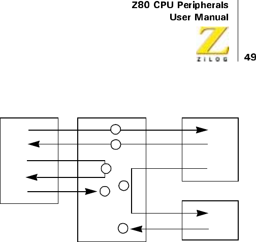
UM008101-0601 Direct Memory Access
Figure 19. Basic Functions of the Z80 DMA
Modes of Operation
Within any class of operation, the Z80 DMA can be programmed to operate
in one of three Transfer and/or, Search modes:
Byte Mode
Data operations are performed one byte at a time. Between each byte oper-
ation the system bus is released to the CPU. The bus is requested again for
each succeeding byte operation. This is also sometimes called Single mode
or byte-at-a-time mode.
Burst Mode
Data operations continue until a port’s Ready line to the DMA goes
inactive. The DMA then stops (releases the system bus) after completing its
current byte operation. This is also called demand mode.
Continuous Mode
Data operations continue until the end of the programmed block of data or a
stop-on-match condition is reached before the system bus is released. If a
DMA I
/O
I/O
1. Transfer Memory-to-I/O (optional search)
2. Transfer I/O-to-Memory (optional search)
3. Transfer Memory-to-Memory (optional search)
4. Transfer I/O-to-I/O (optional search)
5. Search Memory
6. Search I/O
Memory
1
2
3
54
6

UM008101-0601 Direct Memory Access
port’s Ready line goes inactive before this occurs, the DMA pauses until
the Ready line comes active again. This is also called Block mode.
In all modes, the operation on the byte is completed in an orderly fashion
when a byte of data is read into the DMA, regardless of the state of other
signals (including a port’s Ready line). Figure 20 illustrates the sequence of
events that occur in a sequential transfer/search of one byte, whatever of the
mode of operation. First, the source port address is incremented or decre-
mented, if it was programmed to be a variable-address port. Then, the byte
is read from that port to the DMA. Next, the destination port address is
incremented or decremented, if it was programmed to be a variable. The
byte is then written to the destination port. If a search capability is included,
the byte is compared to the match byte. When no byte match occurs, the
DMA increments the byte counter and continues. When a byte is found, a
status bit is set and the DMA either continues by incrementing the byte
counter, stops (releases the bus), or interrupts the CPU, depending on its
initial programming. The next three figures illustrate how the three modes
function before, during, and after the single-byte operation, which is shown
in Figure 20.
Operation in the Byte mode (Figure 21) begins with an enabling command
from the CPU and a test of the I/O device’s Ready line. When the Ready
line is active, the DMA requests the system bus (address, data, and control
buses) through the Bus Request line, and the CPU acknowledges and
releases control to the DMA. The transfer of and/or search of one byte takes
place as in Figure 20. Then, a test is made for end-of-block by checking to
see if the byte counter has reached the programmed block length. If the end
is not reached, the DMA releases the bus back to the CPU. If the end is
reached, a status bit is set and some terminating action occurs, according to
the initial programming. Releasing the bus between each byte allows the
CPU to execute at least one machine cycle before releasing the bus again to
the DMA for the next byte transfer. This means that while the DMA
operates more slowly than it could in other modes, CPU activities like
interrupt acknowledgement, polling, and memory refresh can be inter-
leaved with DMA transfers in the Byte mode.
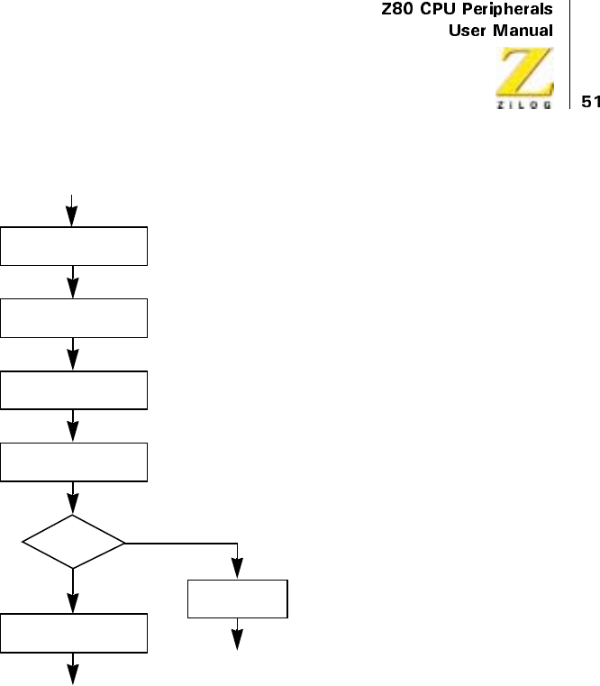
UM008101-0601 Direct Memory Access
Figure 20. Transfer/Search One Byte
Byte
Match
?
Write Data
to Destination Port
Increment/Decrement
Destination Port Address
Read
Source-Port Data
YES
Increment
Byte Counter
Set
Status Flag
• Continue
• Release Bus
• Interrupt
Increment/Decrement
Source-Port Address
NO
UM008101-0601 Direct Memory Access
Figure 21. Byte Mode
RDY
Active
?
Transfer/Search One Byte
(See Figure 20)
• Interrupt
• Release Bus
• Auto Restart
Request Bus
Enable
DMA
End
?
of Block
NO
NO
YES
Set Status Flag
YES
Release Bus
(CPU Executes
at least one
Machine Cycle)
UM008101-0601 Direct Memory Access
Figure 22. Burst Mode
In the Burst mode (Figure 22), the bus is requested in the same manner as
previously, but when the DMA has control of the bus it continues to transfer
bytes until it encounters either an inactive Ready signal from an I/O port, an
end-of-block, or a byte match as in Figure 20. If the Ready line goes
inactive before end-of-block is reached, the DMA releases the bus to the
CPU and repetitively tests the Ready signal until it comes active again.
Then it requests the bus again and continues its transfers. Because of this,
the Burst mode is often the most useful one for general-purpose applica-
tions. It does not request the bus until it actually can use it, but once it
RDY
Active
?
• Interrupt
•ReleaseBus
• Auto Restart
Request Bus
Enable
DMA
End
?
of Block
NO
NO
YES
Set Status Flag
NO
Request Bus
RDY
Active
?
YES
YES
Transfer/Search One Byte
(See Figure 20)

UM008101-0601 Direct Memory Access
attains the bus, the transfers are made at maximum speed. If the transfers
are long, however, this mode can interfere with other CPU activities, which
come to a halt for the entire duration of DMA transfers.
In the Continuous mode (Figure 23), the DMA requests the bus in the same
manner as other modes and repetitively transfers bytes in the same manner
as Burst mode. However, unlike the Burst mode the bus is retained by the
DMA whenever an inactive Ready signal is encountered prior to a stop on
end-of-block or byte match. The DMA simply idles, while holding onto the
bus, until Ready becomes active again. Then it completes the transfer
sequence. This is the fastest of the three modes because it eliminates the
necessity of releasing the bus and requesting it again between complete
block transfers. In this mode, however, the system bus is continuously
preempted by the DMA. This mode is usually used only when very fast
transfers are required and when the impact on CPU activities can be
tolerated. This might be the case, for instance, when an operating system is
beingloadedtomemoryfromdisk.
Due to the DMA’s high-speed buffered method of reading data, operations
on one byte are not completed until the next byte is read in. This means that
total transfer or search block lengths must be two or more bytes, even in the
Byte mode, and that block lengths programmed into the DMA must be one
less than the desired block length. This characteristic is described in detail
in Internal Structure under the section entitled, “Address and Byte
Counting” on page 75.”
UM008101-0601 Direct Memory Access
Figure 23. Continuous Mode
YES
RDY
Active
?
• Interrupt
• Release Bus
•AutoRestart
Request Bus
Enable
DMA
End
?
of Block
NO
NO
YES
Set Status Flag
NO
RDY
Active
?
YES Transfer/Search One Byte
(See Figure 20)

UM008101-0601 Direct Memory Access
Transfer Speed
The Z80 DMA has one of the fastest maximum transfer rates of any 8-bit
DMAC device. This rate is achieved in the simultaneous transfer class of
operation and, unlike the more common sequential transfer class, it requires
at least one external TTL package. But because some other 8-bit DMAs
require some external logic, this constitutes a legitimate speed comparison.
Table 8 describes the maximum rates that can be achieved in different
classes of DMA operation. Maximum CPU block-transfer rates are also
given for comparison. All DMA transfers assume the uninterrupted use of
Burst or Continuous mode, and they assume read and write cycles that last
two cycles (see “Variable Cycle” on page 60).
Transfer speed in Byte mode depends on how long the CPU keeps the bus
between each byte transfer of the DMA. Therefore, the speed is best
expressed from the CPU viewpoint.
Table 9 describes the reduction in Z80 throughput (per Kilobaud trans-
ferred) caused by byte-mode DMA transfers, and this rate is compared with
the reduction in throughput that would occur if the CPU did its own byte
transfers using an interrupt service routine of six instructions (a practical
lower limit). “Z80 DMA and Z80 SIO Example” on page 139 contains
more detail on this data. This data assumes sequential DMA transfers with
longer cycle timing than the minimum of two clock cycles per read or
write. Simultaneous transfers of two clock cycles would, therefore, result in
even lower impact on CPU throughput.
Table 8 describes that DMA transfer rates in Burst and Continuous modes
can be up to ten times faster than Z80 CPU rates. Table 9 describes that the
reduction of CPU throughput with Byte mode DMA transfers is about five
times less than the reduction that results when the CPU handles its own
byte-mode I/O in the normal interrupt mode.
UM008101-0601 Direct Memory Access
Address Generation
Two 26-bit addresses are generated by the DMA for every transfer oper-
ation: one address for the source port and another for the destination port.
The two addresses are multiplexed onto the address bus, according to
whether the DMA is reading the source or writing to the destination.
The two ports are arbitrarily named Port A and Port B. Both A and B can be
either source or destination, either memory or I/O, and have fixed or
variable addresses.
Table 8. Maximum Transfer and Search Speeds (Burst and Continuous
Modes)
Action
Z80
(2.4 MHz)
Z80Z
(4.0 MHz)
DMA Simultaneous Transfer 1.25
MB/s
2.0
MB/s
DMA Search Only
DMA Simultaneous Transfer/Search
DMA Sequential Transfer 0.625
MB/s
1.0
MB/s
DMA Sequential Transfer/Search
CPU Block Transfer Instruction 0.125
MB/s
0.200
MB/s
Table 9. Reduction in Z80 CPU Throughput per Kbaud
(Byte Mode Transfers)
Action
Z80
(2.4 MHz)
Z80Z
(4.0 MHz)
DMA Sequential Transfer 0.085% 0.041%
DMA Sequential Transfer/Search
CPU Interrupt Driven Transfer 0.340% 0.213%

UM008101-0601 Direct Memory Access
Variable addresses can either increment or decrement automatically from
the programmed starting address. Fixed addresses are useful for I/O devices
and the DMAs capability to generate fixed addresses eliminates the need
for transfer/search enabling wires to the I/O device (although Chip Enable
hardwiring is still required, as it is with all peripheral circuits).
Two readable address counters keep the current address of each port. These
counters are distinct from the starting address registers for each port, that is,
the counters are buffered by the registers. Therefore, new starting addresses
can be written to the DMA whenever the DMA is not holding the bus, for
example, between byte transfers in Byte mode. New starting addresses for a
new block of data can be loaded into the DMA before the transfer of the
current block is finished. Loading new starting addresses does not disturb
the contents of the associated port address counters.
DMA address generation capabilities can be used in the following ways:
•
Start at a base address and count up or down.
•
Automatically step back to the beginning at the completion of an
address sequence.
•
Load new starting addresses or reload previous ones for the next
sequence.
Byte Matching (Searching)
Searches for byte matches can be performed either as a sole function or
simultaneously with transfers. When a byte match is found, a status bit in
the readable status register is set and the DMA can be programmed to do
one of the following:
•
Stop (release the bus) immediately upon byte match.
•
Stop and interrupt the CPU immediately upon byte match.
•
Interrupt the CPU when the DMA stops at the end of a block.

UM008101-0601 Direct Memory Access
The match byte written into the DMA is masked with another byte so that
only certain bits within the match byte can be compared with the corre-
sponding bits in the data bytes being searched.
Interrupts
The DMA can be programmed to interrupt the CPU on three conditions:
•
Interrupt on Ready
•
Interrupt on Byte Match
•
Interrupt on End-of-Block
The first condition (I/O-port Ready line becoming active) causes an
interrupt before the DMA requests the bus. The other two conditions
cause the DMA to interrupt the CPU after the DMA stops (releases the
bus). Stopping the DMA on byte match or end-of-block is separately
programmed.
Any of these conditions (Ready line becoming active, byte match, or end-
of-block) causes a readable status bit to be set. In addition, when an
interrupt on any of these conditions is programmed, an interrupt-pending
status bit is also set, and each type of interrupt can optionally alter the
DMAs interrupt vector.
The DMA shares the Z80 Family’s versatile interrupt scheme, which
provides fast interrupt service in real-time applications. In a Z80 CPU
environment where the CPU is using its Mode 2 interrupts, the DMA
passes its internally modifiable 8-bit interrupt vector to the CPU, which
attaches an additional eight bits to form the memory address of the
interrupt routine table. This table contains the address of the beginning of
the interrupt routine. In this process, CPU control is transferred to the
interrupt routine, so that the next instruction executed after an interrupt
acknowledge is the first instruction of the interrupt routine.

UM008101-0601 Direct Memory Access
Auto Restart
Block transfers can be repeated automatically by the DMA. This function
causes the byte counter to be cleared and the address counters to be
reloaded with the contents of the starting-address registers.
The Auto Restart feature relieves the CPU of software overhead for repet-
itive operations such as CRT refresh and many others. Moreover, the CPU
can write different starting addresses into the buffer registers during
transfers in the Byte mode (or Burst mode when the Ready line is inactive
and the bus is released) causing the Auto Restart to begin at a new location.
Pulse Generation
External devices can keep track of how many bytes have been transferred
by using the DMA’s Pulse output, which provides a signal at 256-byte
intervals. The interval sequence may be offset at the beginning by 1 to
255 bytes.
The interrupt line carries the Pulse signal in a manner that prevents inter-
pretation by the Z80 CPU as an interrupt request, because the signal only
appears when the Bus Request and Bus Acknowledge lines are both
active. Under these conditions, the Z80 CPU does not monitor the
Interrupt (INT) line.
Variable Cycle
The Z80 DMA offers the unique feature of programmable operation-cycle
length. This is valuable in tailoring the DMA to the particular requirements
of various CPUs and other system components (fast or slow), and in maxi-
mizing the data-transfer rate. Also, it often eliminates external logic and
reduces CPU software overhead.
There are two aspects to the variable cycle feature. First, the entire read and
write cycles (periods) associated with the source and destination ports can
UM008101-0601 Direct Memory Access
be independently programmed as 2, 3, or 4 clock cycles long (more if Wait
cycles are used), thereby increasing or decreasing the speed at which all
DMA signals change.
Second, the four signals in each port (I/O Request, Memory Request, Read,
and Write) can each have its active trailing edge terminated one-half clock
cycle early. This adds a further flexibility by allowing functions such as
shorter-than-normal Read or Write signals to go inactive before data starts
to change. Figure 24 illustrates the general capability, which is described
laterin“Timing”onpage151”
Figure 24. Variable Cycle Length
Events and Actions
Table 10 gives an overview of the events that can cause specific actions by
the DMA, depending on how it is programmed. The events are conditions
in the DMA’s internal registers, signals from the I/O device, or instructions
onthedatabusforwhichtheDMAwatches.
CLK
T1T2T3T4
2-Cycle
3-Cycle
4-Cycle
Early Ending
for Control Signals

UM008101-0601 Direct Memory Access
PIN DESCRIPTION
The following pin descriptions detail the function of the Z80 DMA external
pins as illustrated in Figure 25 through Figure 28.
A15-A0
System Address Bus (output, tristate). Addresses generated by the DMA are
sent to both source and destination ports, either of which may be main
memory or I/O peripherals.
Table 10. Events and Actions
Event
Actions Possible When Event
Occurs
End-of-Block 1. Release Bus
2. Interrupt CPU
3. Auto Restart
Byte Match (Compare) 1. Release Bus
2. Interrupt CPU
3. Continue
Pulse-control byte matches lower part of
byte counter
1. Generate Pulse
READY Inactive 1. Release Bus
2. Suspend (continuous mode
only)
READY Active 1. Request Bus
2. Interrupt CPU
RETI Instruction (return from interrupt
instruction from the Z80 CPU)
1. Request Bus

UM008101-0601 Direct Memory Access
BAI
Bus Acknowledge In (input, active Low). Signals that the system buses
have been released for DMA control.
BAO
Bus Acknowledge Out (output, active Low). In multiple-DMA configura-
tions, this pin signals that the CPU has relinquished control of the bus. BAI
and BAO form a daisy-chain for multiple DMA priority resolution over bus
control. Unlike the interrupt daisy-chain formed with the IEI and IEO lines,
this chain does not allow preemption of control by a high-priority DMA
when a lower-priority DMA is already bus master. The DMA that has the
bus is always allowed to finish, regardless of its priority in the chain.
BUSREQ
Bus Request (bidirectional, active Low, open-drain). As an output, this pin
sends requests for control of the system address bus, data bus, and control
bus to the CPU. As an input when multiple DMAs are strung together in a
priority daisy-chain through BAI and BAO, this pin senses when another
DMA has requested the buses and causes this DMA to delay its bus request
until the first DMA is finished. Because this bidirectional pin allows simul-
taneous bidirectional signals with no means of control, no buffers come
between this DMA and other DMAs. There can, however, be buffers
between it and the CPU because it is unidirectional into the CPU. A 1.8
Kohms pull-up resistor is typically connected to this pin.
CE/WAIT
Chip Enable and Wait (input, active Low). Normally, this functions only as
aCEline, but it can also be programmed to serve as a WAIT function. As a
CE line from the CPU, this pin becomes active when IORQ is active and
the I/O port address (up to 16 bits) on the system address bus is the DMA’s
address, thereby allowing control bytes to be written from the CPU to the
DMA. As a WAIT line from memory or I/O devices, after the DMA has
received a bus acknowledge (BUSACK) from the CPU, this pin causes wait

UM008101-0601 Direct Memory Access
states to be inserted in the DMA’s operation cycles, thereby slowing the
DMA to a speed that matches the memory or I/O device. The Applications
chapter contains a description of how the CE and WAIT inputs can be
multiplexed by the CPU’s BUSACK line.
CLK
System Clock (input). This pin is standard Z80 single-phase clock at 2.8
MHz (Z80 DMA) or 4.0 MHz (Z80A DMA). For slower system clocks, a
TTL gate with a pull-up resistor may be adequate to meet the timing and
voltage level specifications. For higher speed systems, use a clock driver
with an active pull-up to meet the VIH specification and rise time require-
ments. There should always be a resistive pull-up to the power supply (10
Kohms maximum), ensuring correct power at DMA reset.
D7-D0
System Data Bus (bidirectional, tristate). These pins transfer control bytes
from the CPU, status byes from the DMA, and data from memory or I/O
peripherals. Data transfers or searches by the DMA occur only when the
DMA controls both this bus and the address bus. When the CPU controls
these buses, it can write or read DMA control or status bytes.
IEI
Interrupt Enable In (input, active High). This line, combined with the IEO,
form a priority daisy-chain when there is more than one interrupting device.
A High on this line indicates that no other device of higher priority is inter-
rupting, thereby allowing this DMA to interrupt.
IEO
Interrupt Enable Out (output, active High). IEO is High only when IEI is
High and this DMA is not requesting an interrupt. Therefore, this signal
blocks lower priority devices from interrupting while a higher priority
device is being serviced by its CPU interrupt service routine. Unlike
devices in a bus-request daisy-chain, devices in an interrupt daisy-chain can

UM008101-0601 Direct Memory Access
be preempted by higher priority devices before the lower priority device
has been fully serviced.
INT/PULSE
Interrupt Request (output, active Low, open-drain). This requests a CPU
interrupt when brought Low while the DMA is not the bus master. The
CPU acknowledges the interrupt by pulling its IORQ output Low during an
M1 cycle. The DMA INT pin is typically connected to the INT pin of the
CPU with a pull-up resistor and tied to all other INT pins in the system.
This pin can also be used to generate periodic pulses to an external device.
It can be used this way only when the DMA is bus master, for example, the
CPU’s BUSREQ and BUSACK lines are both Low and the CPU cannot
sense interrupts.
IORQ
Input/Output Request (bidirectional, active Low, tristate). Used as an input,
this pin indicates that the lower half of the address bus contains a valid I/O
port address for transfer of control or status bytes from or to the CPU. This
DMA is the addressed port if its CE pin, IORQ pin, and or RD pin are
simultaneously active. As an output, after the DMA has taken control of the
system buses, this pin indicates that the address bus contains a valid 8-bit or
16-bit port address for another I/O device involved in a DMA transfer of
data. When IORQ and M1 are both active inputs to the DMA, an interrupt
acknowledge by the CPU is indicated.
M1
Machine Cycle One (input, active Low). This pin indicates that the current
CPU machine cycle is an instruction fetch. This pin has two purposes in the
DMA’s interrupt structure. First, it is used by the DMA to detect return-
from-interrupt instructions (RETI, or ED4DH) fetched over the data bus by
the CPU at the end of interrupt service routines. Second, an interrupt
acknowledge is indicated when both M1 and IORQ are active inputs to the
DMA. During 2-byte instruction fetches, M1 is active as each Op Code
byte is fetched. In the CMOS DMA, the M1 signal has a different function:

UM008101-0601 Direct Memory Access
when M1 occurs without an active RD or IORQ for at least two clock
cycles, the internal reset is activated at the falling clock after M1 returns to
the inactive state. This internal reset lasts for three clock cycles.
MREQ
Memory Request (output, active Low, tristate). This line indicates that the
address bus contains a valid address for a memory read or write operation.
After the DMA has taken control of the system buses, it indicates a DMA
transfer request from or to memory.
RD
Read (bidirectional, active Low, tristate). As an input, this signal indicates
that the CPU is ready to read status bytes from the DMAs read registers. As
an output, after the DMA has taken control of the system buses, it indicates
a DMA-controlled read from memory or I/O port address.
RDY
Ready (input, programmable active Low or High). This pin is monitored by
the DMA to determine when a peripheral device associated with a DMA
port is ready for a read or write operation. When the DMA is enabled to
operate, the RDY line indirectly controls DMA activity; the manner in
which DMA activity is controlled by RDY depends on what operating
mode is selected (Byte, Burst, or Continuous). An active RDY line can be
simulated by programming a Force Ready condition. This is useful in
memory-to-memory operations. It is preferable to have the RDY signal
synchronized to the CLK signal, for example, RDY should become active
on the rising edge of CLK. This is particularly important in the Continuous
mode of operation.
WR
Write (bidirectional, active Low, tristate). As an input, this indicates that the
CPU is requesting to write control bytes to the DMA write registers when
the DMA is selected. As an output, after the DMA has taken control of the
UM008101-0601 Direct Memory Access
system buses, it indicates a DMA-controlled write to a memory or
I/O port address.
RESET
Reset (input, active Low) is available in the CMOS PLCC version only. A
Low in this signal resets the DMA.
Figure 25. Pin Functions (CMOS PLCC Package Only)
System
Control
BUS
System
Data
Bus
Z80 DMA
CLK+5V GND
BAO
BAI
BUSREQ
D0
D1
D2
D3
D4
D5
D6
D7
A0
A1
A2
A3
A4
A5
A6
A7
A8
A9
A10
A11
A12
A13
A14
A15
System
Address
Bus
RDY
C5/WAIT
INT/PULSE
IEI
IEO
DMA
Control
Interrupt
Control
M1
IORQ
MREQ
RD
WR
RESET
C-MOS DMA
PLCC Package Only
BUS
Control
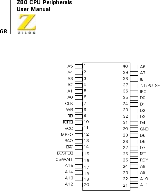
UM008101-0601 Direct Memory Access
Figure 26. 40-Pin DIP Pin Assignments
Z80 DMA
(DIP)
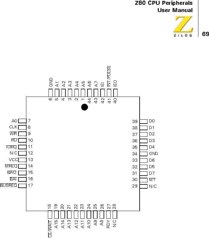
UM008101-0601 Direct Memory Access
Figure 27. 44-Pin PLCC Pin Assignments (Z8410 NMOS)
Z8410
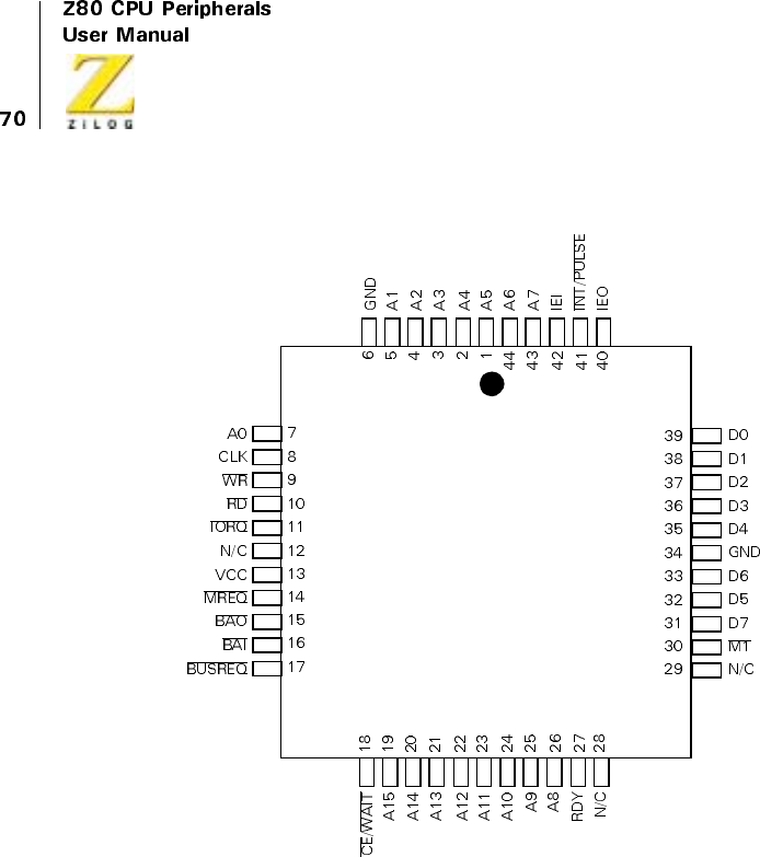
UM008101-0601 Direct Memory Access
Figure 28. 44-Pin PLCC Pin Assignments (Z84C10 NMOS)
Z84C10
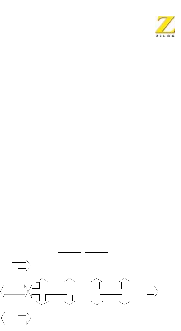
<%272GTKRJGTCNU
7UGT/CPWCN
80 'LUHFW0HPRU\$FFHVV
,17(51$/6758&785(
*HQHUDO2UJDQL]DWLRQ
7KHLQWHUQDOVWUXFWXUHRIWKH='0$LQFOXGHVGULYHUDQGUHFHLYHU
FLUFXLWU\XVHGWRLQWHUIDFHZLWKDQELWGDWDEXVDELWDGGUHVVEXVDQG
V\VWHPFRQWUROOLQHV,QD=&38HQYLURQPHQWWKH'0$FDQEH
FRQQHFWHGGLUHFWO\WRWKHFRUUHVSRQGLQJSLQVRQWKH&38ZLWKQRDGGLWLRQDO
EXIIHULQJH[FHSWIRUWKH&(:$,7OLQHZKHQRSHUDWLRQLVOLPLWHGWR
VHTXHQWLDOWUDQVIHUVDQGVHDUFKHV³7KHDFWXDOQXPEHURIE\WHVWUDQVIHUUHGLV
RQHPRUHWKDQVSHFLILHGE\WKHEORFNOHQJWK 7KHVHHQWULHVDUH
QHFHVVDU\RQO\LQWKHFDVHRIDIL[HGGHVWLQDWLRQDGGUHVV´RQSDJH
SURYLGHVDGHVFULSWLRQRIWKLV
)LJXUH LOOXVWUDWHVKRZWKH'0$¶VLQWHUQDOGDWDEXVLQWHUIDFHVZLWKWKH
V\VWHPGDWDEXVDQGKRZWKH'0$VHUYLFHVDOOLQWHUQDOORJLFDQGUHJLVWHUV
$GGUHVVHVJHQHUDWHGIRU3RUWV$DQG%RIWKH'0$¶VVLQJOHWUDQVIHU
FKDQQHODUHPXOWLSOH[HGRQWRWKHV\VWHPDGGUHVVEXV
6SHFLDOL]HGORJLFFLUFXLWVLQWKH'0$DUHGHGLFDWHGWRWKHYDULRXVIXQFWLRQV
RIWKHH[WHUQDOEXVLQWHUIDFLQJWKHLQWHUQDOEXVFRQWUROE\WHPDWFKLQJE\WH
FRXQWLQJSHULRGLFSXOVHJHQHUDWLRQ&38LQWHUUXSWVEXVUHTXHVWVDQG
DGGUHVVJHQHUDWLRQ
Figure 29. Z80 DMA Block Diagram
System
Data
Bus
(8-Bit)
System
Data
Bus
(16-Bit)
Control
Interrupt
and Bus
Priority
Logic
Pulse
Logic
Bus
Control
Logic
Control
and
Status
Registers
BYTE
Match
Logic
BYTE
Counter
Internal Bus MUX
Port A
Address
Port B
Address

<%272GTKRJGTCNU
7UGT/CPWCN
80 'LUHFW0HPRU\$FFHVV
&RQWURO$QG6WDWXV5HJLVWHUV
$VHWRIZULWDEOHFRQWUROUHJLVWHUVDQGUHDGDEOHVWDWXVUHJLVWHUVDOORZ
WKH&38WRJRYHUQDQGPRQLWRUWKHDFWLYLWLHVRIORJLFFLUFXLWV$OOUHJLVWHUV
DUHELWVZLGHWKHZLGWKRIWKHGDWDEXVDQGGRXEOHE\WHLQIRUPDWLRQLV
VWRUHGLQDGMDFHQWUHJLVWHUV
7KHFRQWUROUHJLVWHUVZULWDEOHWKURXJKWKHGDWDEXVDUHRUJDQL]HGLQWR
VHYHQEDVHUHJLVWHUJURXSV:5WKURXJK:5PRVWRIZKLFKKDYH
PXOWLSOHUHJLVWHUV7KHEDVHUHJLVWHUVLQHDFKJURXSFRQWDLQERWKFRQWURO
ELWVDQGSRLQWHUELWVWKDWFDQEHVHWWRDGGUHVVRWKHUUHJLVWHUVZLWKLQWKH
JURXS:ULWLQJWRDUHJLVWHUZLWKLQDJURXSLQYROYHVILUVWZULWLQJWRWKH
EDVHUHJLVWHUIRUWKDWJURXSZLWKWKHDSSURSULDWHSRLQWHUELWVVHWWKHQ
ZULWLQJWRRQHRUPRUHRIWKHRWKHUUHJLVWHUVWKDWKDYHEHHQSRLQWHGWR
ZLWKLQWKHJURXS7KHFKDSWHURQ³3URJUDPPLQJ´FRQWDLQVDIXOO
GLVFXVVLRQRIWKLVWHFKQLTXH7KHQDPHVRIWKHZULWHUHJLVWHUVVKRZQLQ
)LJXUH GRQRWLQGLFDWHWKHIXOOH[WHQWRIWKH'0$¶VSURJUDPPDELOLW\
EHFDXVHPDQ\PRGHVDQGIXQFWLRQVDUHVHWZLWKVLQJOHELWVLQWKHEDVH
UHJLVWHUE\WHVRIHDFKJURXS
)LJXUH OHIWLOOXVWUDWHVWKHZULWHUHJLVWHUV7KHVHDUHWKHUHJLVWHUVIRU
ZKLFKLQSXWVIURPWKHGDWDEXVDUHVKRZQLQWKHILJXUH&RPSDUHWKLVILJXUH
ZLWK)LJXUH ULJKWZKLFKLGHQWLILHVWKHUHDGUHJLVWHUV
7KHWZRELWVWDUWLQJDGGUHVVUHJLVWHUVLQJURXSV:5DQG:5DQGWKH
ELWEORFNOHQJWKUHJLVWHULQJURXS:5KDYHELWFRXQWHUVDVVRFLDWHG
ZLWKWKHP7KHFRXQWHUVXQOLNHWKHLUDVVRFLDWHGUHJLVWHUVFDQQRWEHZULWWHQ
WR7KHWZRDGGUHVVFRXQWHUVJHQHUDWHWKHDGGUHVVHVWKDWDUHSODFHGRQWRWKH
DGGUHVVEXV7KHDGGUHVVFRXQWHUVFDQDOVREHUHDGE\WKH&38WKURXJKWKH
GDWDEXVDVFDQWKHE\WHFRXQWHU$OOWKUHHZULWDEOHUHJLVWHUVVHUYHDV
EXIIHUVIRUWKHUHDGDEOHFRXQWHUV7KHFRQWHQWVRIWKHUHJLVWHUVFDQEH
FKDQJHGGXULQJDEORFNWUDQVIHUZLWKRXWGLVWXUELQJWKHFRQWHQWVRIWKH
FRXQWHUV7KLVIHDWXUHLVXVHIXOIRUH[DPSOHGXULQJ%\WHPRGHWUDQVIHUVLQ
ZKLFKFRQWUROE\WHVFDQEHZULWWHQWRWKH'0$ZKLOHWKH&38KDVWKHEXV
EHWZHHQE\WHWUDQVIHUV7KLVDOORZVWKHQH[WEORFNZKLFKFDQEHDQ$XWR
5HVWDUWEORFNWREHJLQTXLFNO\DWDQHZORFDWLRQ1RWLFHWKDWWKHEORFN

UM008101-0601 Direct Memory Access
which control bytes can be written to the DMA while the CPU has the bus
between byte transfers. This allows the next block, which can be an Auto
Restart block, to begin quickly at a new location. Notice that the block
length counter stops (or Auto Restarts) as a result of a comparison to the
block length register. In changing the register, the block length also changes
with what may be unpredictable results.
The pulse-control byte illustrated in Figure 30 (in the WR4 group) also has
a relationship to the byte counter in WR0. The pulse-control byte can be
loaded with an offset value between 0 and 255 and this value is continu-
ously compared with the lower byte of the byte counter. The NT line
generates a pulse each time a match occurs, which happens on every 256
bytes of transfer or search after the initial offset. Because the pulse signals
generated on the NT line only occur when the DMA has control of the
system bus, for example, when the BUSREQ and BUSACK lines are
simultaneously active, the CPU cannot detect theme and they can be
directed exclusively to an external gate, counter, or other device.
Figure 30 illustrates the seven status registers readable through the data bus.
Unlike the write registers, the status registers include no second-level
registers or groups. These registers are accessed sequentially according to
the read mask written to the WR6 group, except that the status byte can be
read separately from the other read registers.
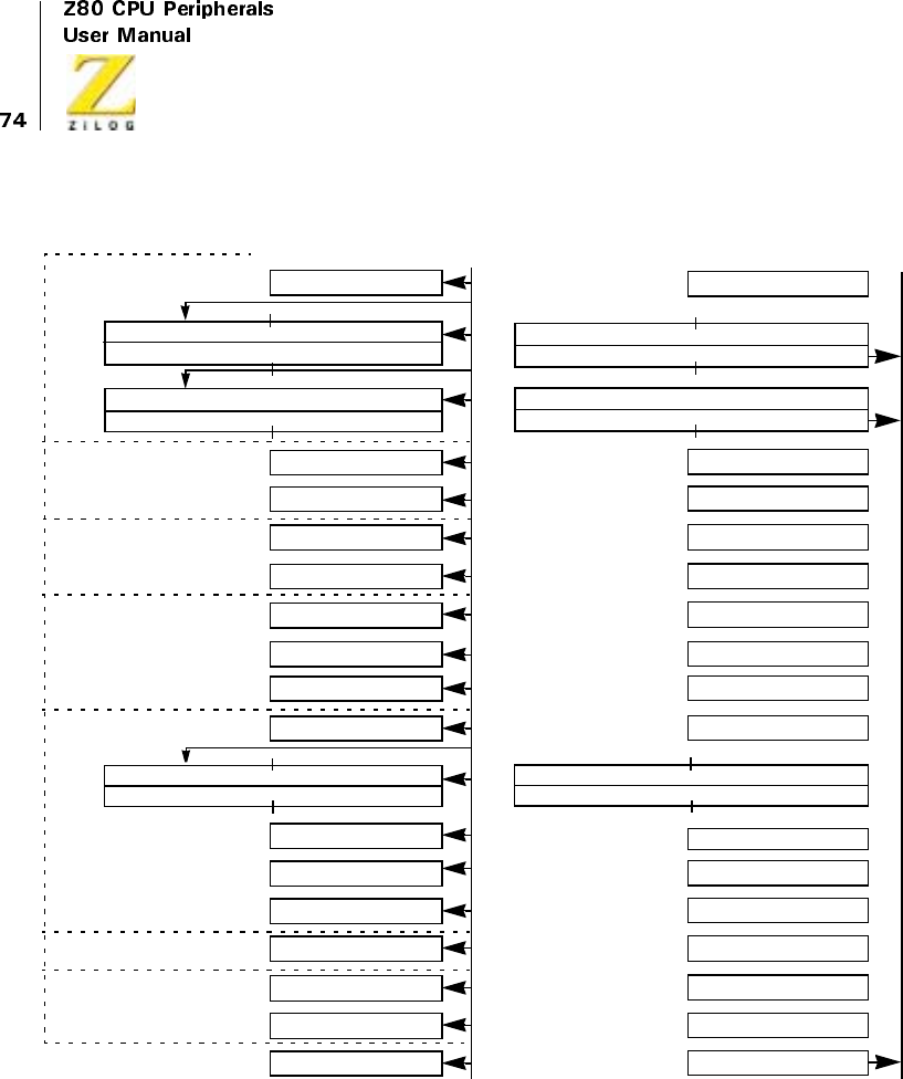
UM008101-0601 Direct Memory Access
Figure 30. Write Register Organization (left) and Read Register Organization (right)
WRQ
WR1
WR2
WR3
WR4
WR6
WR5
Data
BUS
70
Base Register Byte
Base Register Byte
Base Register Byte
Base Register Byte
Base Register Byte
Base Register Byte
Base Register Byte
Port A Starting Address Register
15 8 7 0
Block Length Register
Port A Variable Timing
Port B Variable Timing
Mask Byte
Match Byte
15 8 7 0
Port B Starting Address Register
Interrupt Control Byte
Pulse Control Byte
Interrupt Vector
Read Mask
Data
BUS
0
Port A Address Counter
Byte Counter
RR4 RR3
RR2 RR1
Port B Address Counter
RR6 RR5
Status Byte
RR0
Port A Address Counter (see right illustration)
Port B Address Counter (see right illustration)
Byte Counter (see right illustration)
Status Byte (see right)

UM008101-0601 Direct Memory Access
Address and Byte Counting
Addresses for either port may be fixed at their programmed starting
address, or they may be incremented or decremented from the programmed
starting address by the address counters. The block length programmed into
the DMA is compared with the byte counter, which starts at zero and incre-
ments at the completion of each byte operation (Figure 20).
The DMA uses a high-speed buffering or pipelining scheme for reading
data. When transferring data and stopping on an end-of-block, the effect of
this pipelining is that one more transfer is completed than is programmed
into the block-length register; the only exception to this rule occurs in
simultaneous transfers that use two-cycle variable timing, in which case
two extra bytes are transferred if the Ready line remains active.
Table 11 describes the contents of the counters in the various classes and
the modes of transfer involving stopping or interrupting at an end-of-block
(interrupts imply prior stopping).
Search and transfer/search operations that are programmed to stop on byte
match function somewhat differently, as described in Table 12. Matches are
discovered only after the next byte is read. In all classes of transfer/search
operations, the matched byte is transferred. In simultaneous transfer/search
operations, however, an additional byte is usually also transferred. The only
exception to this occurs in Burst and Continuous modes when the Ready
line goes inactive while the byte match is being located. During simulta-
neous transfer/searches in Burst or Continuous mode, these searches are
typically continuous processes performed in memory using a Force Ready
condition or a Ready line that will not go inactive. However, when this
exception is encountered, the CPU can be programmed to research two
bytes when such a match occurs.

UM008101-0601 Direct Memory Access
Notes:
* Address can increment (+) or decrement (-) from the programmed starting address (As), which is the first
address for transfer purposes.
** Occurs only in 2-cycle (variable timing) simultaneous transfers when the Ready line is still active at the end
of the N + 1 byte transfer.
*** Simultaneous transfers cannot have both ports variable. This class of operation is programmed as a DMA
search-only operation, with variable addresses ascribed to the programmed source port. What the DMA senses
is the source port may be either the real source or destination, as determined by external hardware. See “The
actual number of bytes transferred is one more than specified by the block length. * These entries are
necessary only in the case of a fixed destination address.” on page 129.
Table 11. Contents of Counters After DMA Stops Because of End-of-Block (Transfer
Operations)
Class Mode
Programmed
Block Length
Bytes Transferred
At Stop Byte Counter
Source Port
Address Counter*
Destination Port
Address Counter*
Sequential Byte N N+1 N As±(N+1) As±(N)
Transfer Burst N N+1 N As±(N+1) As±(N)
Continuous N N+1 N As±(N+1) As±(N)
Search Only or
Simultaneous
Transfer/Search
Byte N N+1 N As±(N+1) ***
Burst N N+1 N+1 As±(N+1) ***
Burst N N+2** N+1 ** As±(N+2)** ***
Continuous N+1 N+1 N+1 As±(N+1) ***
Continuous N+1 N+2** N+1 ** As±(N+2)** ***
Table 12. Contents of Counters After DMA Stops Due to Byte Match (Search or Transfer/
Search Operations)
Class Mode
Match Occurs
On This Byte
Bytes Transferred At Stop
If Transferring Byte Counter
Source Port
Address Counter*
Destination Port
Address Counter
Sequential
Transfer
Byte M M M-1 As±(M) As±(M-1)
Burst M M M-1 As±(M) As±(M-)
Continuous M M+ M-1 As±(M) As±(M -)
Search Only or
Simultaneous
Transfer Search
ByteMM MAs±(M) ***
Burst M M+1 M+1 As±(M+1) ***
Burst M M** M-1** As±(M** ***
Continuous M M+1 M+1 As±(M+1) ***

UM008101-0601 Direct Memory Access
Notes:
* Address can increment (+) or decrement (-) from the programmed starting address (As), which is the first
address for transfer or search.
** Occurs only when the Ready line is still inactive just prior to the beginning of the last possible cycle in the
operation. For example, Ready is sampled inactive on the rising edge of CLK in the last cycle of the last read
operation.
*** Search only has no destination. Simultaneous transfer/search cannot have both ports variable. This class of
operation is programmed as a DMA search only operation, with variable addresses assigned to the
programmed source port. What the DMA senses as the source port may be either the real source or destination,
as determined by external hardware. See the 'Applications' chapter.
Bus Control
The DMA transfers and searches data by controlling the system buses in the
same way that the Z80 CPU controls them to perform read and write cycles.
Specifically, the DMA controls the following lines:
•
Address Bus (16 bits)
•
Data Bus (8 bits)
•
IORQ
•
MREQ
•
RD
•
WR
In addition, the DMA can also be programmed to watch a WAIT line
through its dual-purpose CE/WAIT pin.
Continuous M M** M-1** As±(M** ***
Table 12. Contents of Counters After DMA Stops Due to Byte Match (Search or Transfer/
Search Operations)
Class Mode
Match Occurs
On This Byte
Bytes Transferred At Stop
If Transferring Byte Counter
Source Port
Address Counter*
Destination Port
Address Counter

UM008101-0601 Direct Memory Access
When the DMA has requested and received the bus from the CPU, other
devices on the system do not perceive the change. The CPU is idle during
this time because it cannot fetch instructions from memory.
Bus Requesting
Two conditions enable the DMA to request the bus from the CPU: an
enabling command from the CPU, and an active Ready condition, resulting
from either an active Ready line from an I/O device or a Force Ready
command by the CPU.
The DMA requests the bus by latching its BUSREQ line Low. The CPU
always responds to a bus request and it does so quickly, in no more than one
machine cycle (3 to 10 clock cycles) plus one additional clock cycle by
lowering its BUSACK line as an input to the DMA’s BAI line. Both the
DMA’s BUSREQ output and the CPU’s BUSACK output remain Low
whiletheDMAhasthebus.
The bus is released back to the CPU when the DMA’s BUSREQ line goes
High; the CPU’s BUSACK line goes High in the next clock cycle. The
DMA releases its BUSREQ line in a variety of conditions, including:
•
Completion of single-byte transfer (Byte mode
•
Ready line going inactive (Byte and Burst modes)
•
Byte match (Burst and Continuous modes) if stop-on-match is
programmed
•
End-of-block (all modes), if stop-on-end-of-block is programmed
These conditions are explained in the “Timing” chapter. Bus requests
cannot be made while the CPU services an interrupt from the DMA. This
is prevented by the Interrupt Under Service (IUS) latch, which is
discussed later.
UM008101-0601 Direct Memory Access
Bus Request Daisy-Chains
Multiple DMAs can be linked in a prioritized daisy-chain for the purpose of
requesting the bus. Figure 31 illustrates this procedure.
Each DMA’s BUSREQ pin is bidirectional. As an output, it requests the
bus. As an input, this pin senses when another DMA in the daisy-chain has
requested the bus (brought the BUSREQ line Low) and therefore prevents
this DMA from also requesting the bus until the other DMA has finished.
Any DMA that has the bus is always allowed to finish its operation; a
higher priority DMA cannot preempt it during this time.
Their proximity to the CPU determines the priority of DMAs in a daisy-
chain. The DMA electrically closest to the CPU (as measured along the
BUSACKI/BAI lines) has the highest priority. Priority matters only when
multiple DMAs request the bus on the same clock cycle. The higher
priority DMA can then prevent lower priority DMAs from receiving a bus-
acknowledge signal through the BAI/BAO chain. The lower priority DMAs
continue to hold their BUSREQ lines Low until the higher priority DMA
finishes and releases the bus, thereby allowing lower priority DMAs to
contend for the bus.
Figure 31. Bus-Requesting Daisy-Chain
1.8K
CPU
BUSREQ
BUSACK
DMA
BAI BAOBUSREQ
DMA
BAI BAOBUSREQ

UM008101-0601 Direct Memory Access
Interrupts
Conditions and Methods
The Z80 CPU prioritizes external events in the following order:
1. Bus Requests (BUSREQ)
2. Non-Maskable Interrupts (NMI)
3. Maskable Interrupts (INT)
In addition to bus requests, the DMA normally allows only maskable inter-
rupts (INT) and uses them in CPU Mode 2, which allows interrupt vectors.
Non-maskable interrupts are typically reserved for extreme priority events
such as power-failure signaling.
The DMA can be programmed to interrupt the CPU under the following
conditions:
•
After the DMA’s RDY line has gone active and before the DMA
requests the bus (interrupt on RDY).
•
On an end-of-block, when the contents of the byte counter match the
contents of the block-length register.
•
On a byte match, when the contents of the match-byte register (after
masking by the mask-byte register) corresponds to a data byte being
transferred or searched.
The DMA cannot have control of the bus when it interrupts the CPU.
SignalingontheINTline while the DMA is bus master generates periodic
pulses to an external device. These pulses are not perceived by the Z80
CPU. Therefore, at stop-on-end-of-block or byte match, the DMA first
releases the bus before interrupting the CPU, as shown in Figure 32.
If the DMA is programmed to interrupt on end-of-block and also to Auto
Restart on end-of-block, an interrupt occurs (and should be acknowledged
for continued operation) at each end-of-block. However, the end-of-block

UM008101-0601 Direct Memory Access
status bit is not set as it would be without the Auto Restart. Therefore, the
interrupt vector cannot indicate the specific interrupt cause, for example,
Status Affects Vector is not effective.
The Z80 CPU acknowledges the interrupt by pulling its M1 and IORQ lines
low for one machine cycle (see the “Timing” chapter). This causes the
DMA to put its 8-bit interrupt vector on the data bus, thereby identifying
itself and optionally identifying the origin of the interrupt. The CPU uses
the vector to access an interrupt service routine, which is then executed.
The interrupt service routine typically reenables the DMA to request the
bus and cause interrupts again.
For CPUs that have no interrupt acknowledge or a noncompatible one,
DMA control bytes can be written (usually in the interrupt service routine)
to simulate the same functions.
UM008101-0601 Direct Memory Access
Figure 32. Z80 Interrupt Sequence
Interrupt Vectors
The Z80 CPU interrupt acknowledge cycle causes the DMA to put its 8-bit
interrupt vector on the data bus (Figure 33a). This vector is read by the
DMA CPU
End-of-Block
or Byte Match
DMA Releases
Bus and
Interrupts CPU
CPU Acknowledges
Interrupt
DMA Passes
Interrupt Vector
to CPU
CPU Executes
Interrupt Service
Routine
DMA Requests
Bus Again
*
*Bus Master
*
*
*
BUSREQ
BAI
BUSREQ
BUSACK
INT INT
M1
IORQ
M1
IORQ
MEMORY
BUSREQ
BAI
BUSREQ
BUSACK

UM008101-0601 Direct Memory Access
CPU to a temporary register. It normally identifies the interrupting device
and it can also identify the cause of the interrupt (actually the current state
of certain status bits). The I Register of the Z80 CPU (when the CPU is
programmed to Mode 2 state) has the upper byte of a 16-bit address, which
is formed with the interrupt vector, and this address points to a jump table
entryinmemory.
The jump table location in memory contains an address that is read to the
CPU’s program counter (Figure 33b). This address points to the first
instruction of the interrupt service routine, which then begins executing. In
most DMA applications, the CPU’s interrupt service routine contains
instructions that write control bytes back into the DMA through a register
in the CPU (Figure 33c).
In CPU environments without interrupt vectors, the CPU must poll each
peripheral or an external register to determine tristate device interrupted
and why.
UM008101-0601 Direct Memory Access
Figure 33. Interrupt Service Routine
Interrupt Latches
Two primary latches are associated with the interrupt structure:
•
Interrupt Pending (IP). Set whenever the DMA requests an interrupt
but has not yet acknowledged. It holds the INT line Low (Figure 34).
•
Interrupt Under Service (IUS). Set when the CPU acknowledges the
DMA interrupt (Figure 35). This accomplishes three things:
– Prevents further interrupts by this DMA
MEMORY CPU DMA
Jump Table IRegister Interrupt
Vector
Jump Table
Service Routine
Program
Counter
Program
Counter
Service Routine Write
Registers
Register
A.
B.
C.
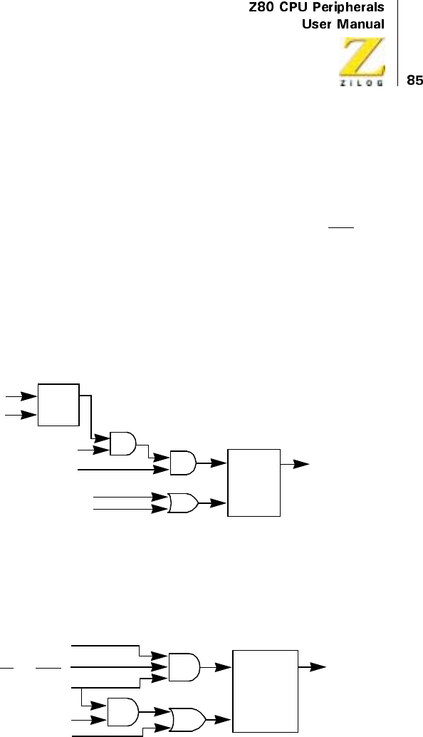
UM008101-0601 Direct Memory Access
– Prevents interrupts from lower priority devices in an interrupt
daisy-chain
– Prevents further bus requests by this DMA
If the Interrupt on RDY (interrupt before requesting bus) option is selected,
the IP latch is set when the Ready line becomes active, causing INT to go
Low.
The IP latch is reset whenever the IUS latch is se. If the interrupt causing
condition is not removed before IUS reset, IP becomes set again after IUS
reset, causing another interrupt. The US latch can be reset by the Z80
CPU’s Return from Interrupt (RETI) instruction or by control bytes written
to the DMA.
Figure 34. Interrupt Pending (IP) Latch
Figure 35. Interrupt Under Service (IUS) Latch
Reinitialize Status Byte
Reset and Disable Interrupts
*NOTE: Interrupt conditions can include end-of-block,
byte match, or active RDY line, depending on programming.
M1 Inactive
Interrupt Condition
Enable Interrupts
Disable Interrupts
S
R
Q
S
R
IP
OInterrupt Pending
(ToIUSLatchSet)
S
R
IUS
ODisable DMA
Reset and Disable Interrupts
RETI
IEI
Interrupt Acknowledge
(M1 and IORQ)
Interrupt Pending
(from IP Latch)

UM008101-0601 Direct Memory Access
Interrupt On Ready
Normally, when the DMA has been enabled by the CPU to request the bus
while the I/O device’s Ready line is inactive, the Ready line’s transition to
the active state causes the BUSREQ line to go Low (Figure 65). It does so
within two clock cycles if the setup time to the rising edge of CLK is met.
This does not take place, however, when the Interrupt on Ready option
(also called the Interrupt Before Requesting Bus option) is selected. When
this option is used, the DMA interrupts the CPU when the Ready line
comes active. The CPU’s interrupt service routine now writes control bytes
to the DMA, which enable the DMA to request the bus after the service
routine finishes.
As noted earlier, the CPU cannot respond to an interrupt when the DMA
is bus master. Thus, when enabled in Continuous mode, the DMA inter-
rupts the CPU when the Ready line first becomes active, but not on
succeeding transitions.
The Interrupt on Ready option is typically used to put new starting
addresses into the DMA, so that transfers go to a part of memory that is
dynamically determined.
Interrupt Service Routines
In addition to the DMA’s extensive programmability for mode-setting
(usually done at power-up initialization), numerous commands (control
bytes) are designed for use in various interrupt service routines.
The next chapter on “Programming,” fully explains the commands, but a
quick overview follows.
Some typical functions for which control bytes are available for use in
interrupt service routines include:
•
Reset the DMA
– Enable the DMA for bus requesting
– Disable the DMA for bus requesting
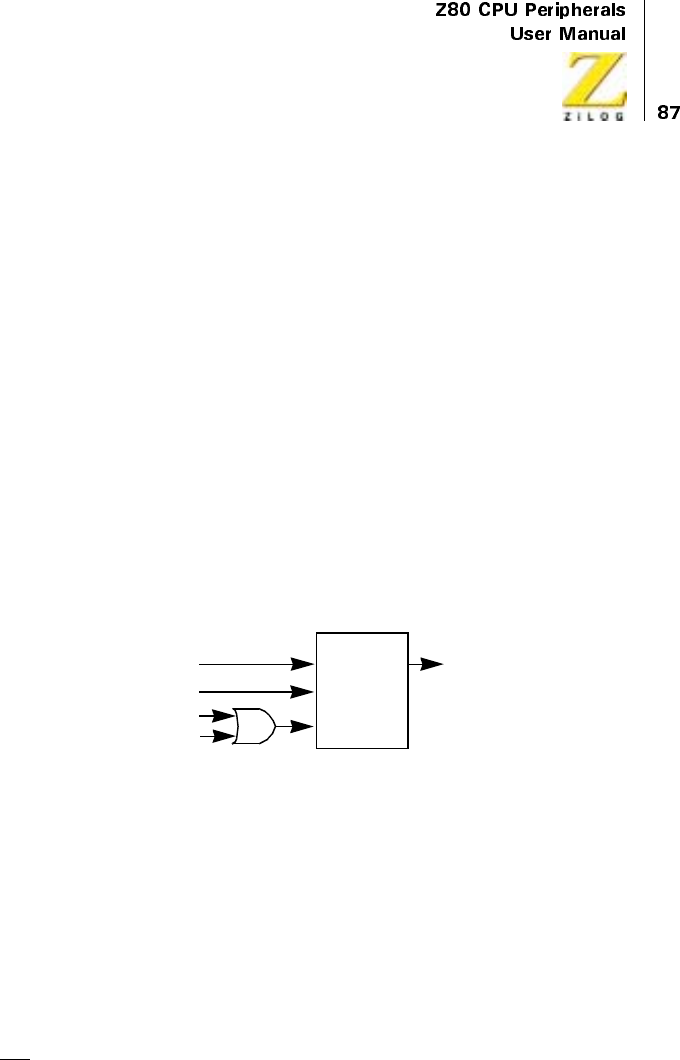
UM008101-0601 Direct Memory Access
•
Reset and disable DMA interrupts
– Enable DMA interrupts
– Disable DMA interrupts
•
Load new starting addresses and block length
– Continue prior address counting
– Clear block length counter
•
Force the Ready condition
•
Read the status byte
– Initiate a status-register read sequence
– Clear status
Interrupt service routines on a Z80 CPU always end with a Return From
Interrupt (RETI or hex ED4D) instruction, which is now explained.
Figure 36. Interrupt On Ready (IOR) Latch
Return From Interrupt
At the end of an interrupt service routine, the Z80 CPU executes a return-
from-interrupt (RETI or hex ED4D) instruction. This returns the CPU from
the interrupt service routine.
The DMA also simultaneously decodes the RETI instruction, which it
recognizes on the data bus as an instruction (occurring when the DMA’s
M1 input is Low). This causes at least one, and possibly two, events within
the DMA:
D
R
IOR
ODisable DMA
CY
D-FLIP-FLOP
+5V
Interrupt Condition (Active RDY)
Enable after RETI
Reset and Disable Interrupts
*NOTE: This latch is only set when the Interrupt-On-Ready option is selected.

UM008101-0601 Direct Memory Access
•
Resets the Interrupt Under Service (IUS) latch in the DMA, thereby
allowing its IEO pin to go High so that lower priority devices can
interrupt.
•
Enables the DMA to request the bus again. This occurs only in the
Interrupt on Ready option and only when the Enable DMA control
byte is also used.
For non-Z80 environments, control bytes are provided to simulate these
actions.
Interrupt Daisy-Chains
Multiple DMAs can be chained together by their IEI and IEO lines, as
depicted in Figure 37. In the Z80 Family, the DMA’s location in the IEI/
IEO chain sets priority.
When peripherals simultaneously interrupt the Z80 CPU, the highest
priority peripheral (nearest the +5V end of the daisy-chain) is serviced. The
CPU receives the winning peripheral’s interrupt vector. The IEI/IEO chain
allows only the highest priority interrupting peripheral to place its interrupt
vector on the data bus. In non-Z80 environments that have no interrupt
vectors, the winning peripheral is determined by successively reading the
status of all peripherals.
For a device to have priority, its IEI line must be High. When a device
needs service, it prevents downstream devices from interrupting by pulling
its IEO line Low. The next device in the chain then passes this Low
condition on to other downstream devices by pulling its IEO line Low, and
so on.
Whenever an interrupt is acknowledged (Figure 32), the CPU’s interrupt
structure is disabled. It must subsequently be reenabled by an enable inter-
rupts instruction before other devices can interrupt again. This normally
takes place within the interrupt service routine. When done early in the
service routine, this permits higher priority peripherals to interrupt the CPU
while the latter is still executing that service routine. Thus, nested interrupts
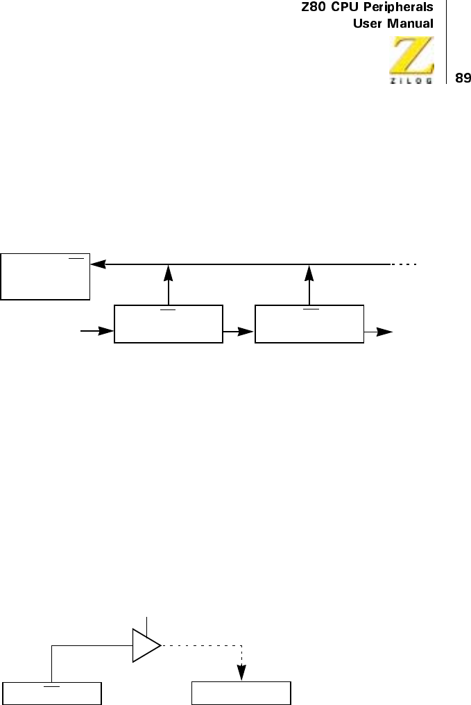
UM008101-0601 Direct Memory Access
are allowed in which the higher priority peripheral suspends the execution
of the lower priority peripheral’s service routine.
Bus-requesting daisy-chains do not have this preemption or nesting
ability. Instead, any peripheral that is able to get the bus keeps it until task
completion.
Figure 37. Interrupt Daisy-Chain
Polling for Service Requests
When the CPU cannot detect interrupts directly, it polls an external gate as
shown in Figure 38.
Polling is accomplished in the following way:
•
Enable the DMA’s interrupt structure with a control byte
•
Poll a status bit to see when an interrupt request occurs
+5V
Z80
CPU
INT
IEI
INT
IEO
INT
Highest Priority
Interrupting Device
IEI IEO
To
Lower
Priority
Interrupting
Device
DMA
tristate enable line, normally at tristate,
for example, connected to a chip select decoder.
Pending
Polling
CPU
INT

UM008101-0601 Direct Memory Access
Figure 38. Polling for a Service Request Bit
PROGRAMMING
Overview
The DMA must be programmed before use. Its control registers have no
useful default values at power-up. In addition, commands are frequently
written to the DMA after the initial power-up programming sets basic
DMA operating modes; this is most commonly done within service
routines for purposes such as reading status, changing starting addresses,
and reenabling both interrupt and bus-request logic after a block transfer
or search.
The DMA has two primary states that can be set: (1) an enabled state, in
which the DMA gains control of the system buses and directs data
transfers between ports or data searching from a single port; and (2) a
disabled state, in which the DMA initiates neither bus requests nor data
transfers. Table 13 describes these states and their substates in detail.
When the DMA is powered-up or reset by any means, it is automatically
placed into the disabled state. Program commands can be written to it by
the CPU in the enable/inactive state, but this automatically puts the DMA
into the disabled state, which is maintained until an ENABLE DMA
command is written by the CPU to the DMA’s Write Register 6 (WR6).
In the Z80 Family, the DMA normally exists as a peripheral device in
system I/O space. Its Chip Enable (CE) signal is decoded from the lower
byte of the address bus for this purpose and all control bytes and status
bytes are written to and read from the same I/O port address, using an
output instruction such as OTIR (in the Z80 CPU).
It is possible to use the DMA in memory mapped I/O structures, but this
involves some external logic, which is explained in the “Applications”

UM008101-0601 Direct Memory Access
chapter. It is not possible for the DMA to program itself by directing
transfers of control bytes from memory to its own internal registers.
When DMA interrupt vectors are used in a Z80 environment, the Z80 CPU
should be programmed for Mode-2 maskable interrupts.
Table 13. DMA Status
DISABLED ENABLED
ACTIVE
Inactive (Stopped) Suspended Operating
Description DMA cannot request the bus (cannot pull
its BUSREQ input to CPU low).
DMA can request the bus
and may have had the bus
immediately prior to this
state, but it is not
currently the bus master.
DMA is bus
master but no
operations are
taking place.
DMA is bus master
and is transferring and/
or searching in one of
three modes: Byte,
Burst, or Continuous
Can the CPU
write DMA
control bytes
or read DMA
status bytes?
Yes Yes, but first write a
DISABLE DMA
command
No No
External
actions that
cause the
state
Power-down End-of-block in any
mode, except with Auto
Restart. Byte Match in
any mode. Byte or Burst
mode BAI line inactive.
Loss of power.
RDY line
inactive in
Continuous
mode.
RDY line active in
Burst mode, if DMA is
enabled. RETI
instruction fetched by
CPU, if DMA is
enabled and RDY line
is active.
DMA
commands
(WR6 control
bytes)
causing the
state
Any command except the ENABLE DMA
command. (And the REINITIALIZE
STATUS BYTE command, if it is not
preceded by another command.) The
DISABLE DMA command is specifically
designed for this situation.
ENABLE DMA if RDY
line is inactive and the
FORCE READY
command is not used.
ENABLE
DMA, if RDY
line is inactive
in Continuous
mode.
ENABLE DMA, if
RDY is active or the
FORCE is used and
the command is
outside an interrupt
service routine.

UM008101-0601 Direct Memory Access
Write Registers
Control bytes must be written to all relevant registers in the DMA at power-
up initialization. This section describes and illustrates each of the write
registers, WR0 through WR6, to which control bytes can be written. The
convention of calling the control bytes written to WR6 “commands” is
often used, because they are commonly used within CPU interrupt service
routines and at other times during system operation in addition to their use
at power-up initialization of the DMA.
“Internal Structure” on page 71 gives an organizational overview of the
write registers (Figure 30) and describes the access method. Control bytes
are written to one or more of the write register groups (WR6-WR0) by first
writing a byte to the “base register” in that group. All groups have base
registers and most groups have additional associated registers. The asso-
ciated registers in a group are sequentially accessed by first writing a byte
to the base register. The base register byte contains both control bits for
DMA function control, and pointer bits (1s) to one or more of the asso-
ciated registers in the base register’s group.
Figure 39 for WR0 illustrates this. In this figure, the sequence in which
associated registers within a group can be written to is shown by the
vertical position of the associated registers. For example, if a byte written to
the DMA contains the bits that identify WR0 (bits D0, D1, and D7), and
also contains 1s in the bit positions that point to associated registers 2 and 4,
then the next two bytes written to the DMA after the base register byte is
stored in these two associated registers, in that order.
Figure 40 through Figure 46 illustrate and describe each of seven base
registers and their associated registers. These figures, unlike Figure 30, do
not include the 16-bit counters associated with the starting-address and
block-length registers.
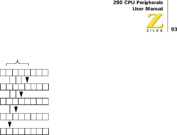
UM008101-0601 Direct Memory Access
Figure 39. Write-Register Pointing Methods
Write Register 0 Group
The WR0 base register byte is identified by a 0 in bit 7 and any combi-
nation except 0, 0 in bits 0 and 1 (Figure 40). It sets the following condi-
tions.
Class of Operation
Bits 1 and 0 used together set the class of operation as sequential transfer
(0,1), search only (1,0), or sequential/transfer/search (1,1). Simultaneous
transfers or transfer/searches are obtained by selecting the search-only
class (1,0) and by allowing the external hardware to generate the appro-
priate bus control signals for the complete transfer (see the chapter
“Applications”).
D7 D6 D5 D4 D3 D2 D1 D0
Base Register
Associated Register #1
Associated Register #2
Associated Register #3
Associated Register #4
Pointer Bits

UM008101-0601 Direct Memory Access
Source and Destination
Bit 2 indicates the source port and, by implication, the destination port, if
the operation is a sequential transfer. When bit 2 is 0, Port B is the source;
when bit 2 is 1, Port A is the source. Search-only operations have only a
source port. If the operation is a simultaneous transfer or transfer/search
(where the class is set to search-only), external hard wiring determines the
destination port.
The direction of transfer should only be changed from its current setting
after the DMA is disabled by writing some other control byte to it.
Therefore, the WR0 byte should not be the first byte written to the DMA if
changing the direction of transfer.
Port A Starting Address
If Port A is used for either source or destination, its starting address must be
programmed. Set bits 3 and 4 in the base register byte to 1 so that the next
two bytes written to the DMA are recognized as the low and high bytes,
respectively, of the Port A starting address. This address is interpreted in the
context of the entries in WR1 bits 3 through 5, which differentiate the
address as either memory or I/O, fixed or variable, and, if variable, incre-
menting or decrementing. If Port A is to be a fixed address destination port,
see the section following entitled “Fixed-Address Destination Ports.”
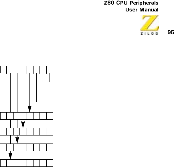
UM008101-0601 Direct Memory Access
Figure 40. Write Register 0 Group
Block Length
All operations must have a declared block length because the default values
at power-up are unpredictable for block length. These registers are written
to by setting pointer bits 5 and 6 in the WR0 base register byte. The block
length can be up to 64 Kbytes. Due to the pipelining method of reading in
data, the number of bytes actually searched or transferred may be one or
two more than the number entered here. “Address and Byte Counting” on
page 75 in “Internal Structure” on page 71 describes this (Table 11).
Programming a block length of zero results in the transfer or search of 216
+ 1 bytes. Therefore, the shortest block length that can be entered is 1,
which usually results in a transfer or search of two bytes (Table 12).
D7 D6 D5 D4 D3 D2 D1 D0
Base Register Byte
Port A starting address (Low Byte)
Port A starting address (High Byte)
Block length (Low Byte)
Block length (High Byte)
00
0
1
1
1
0
1
Do not use
=Transfer
=Search
= Search/Transfer
0=PortB→Port A
0=PortA→Port B

UM008101-0601 Direct Memory Access
Write Register 1 Group
Bits 7, 2, 1, and 0, as Figure 41 illustrates, select the base register byte for
this group. The group is used only when Port A is used, for example, do not
program it for a search only, simultaneous transfer, or simultaneous transfer/
search with Port B as the source. It specifies the following characteristics:
Device Type (Port A)
Bit 3 identifies Port A as either memory or I/O. This specification causes
the proper control line MREQ or IORQ to come active for cycles involving
that port.
Variable/Fixed Addressing (Port A)
Bits 4 and 5 specify whether the Port A address increments, decrements, or
remains fixed for each byte of data transferred or searched. The first byte of
data in an operation uses the starting address entered for Port A in WR0.
Incrementing or decrementing begins on the second byte of the operation.
Variable Cycle (Port A)
If bit 6 is set to 0, the DMA’s variable-cycle timing feature is not used;
instead, standard Z80 timing for read and write cycles is used, which is
described in the “Timing” chapter. If bit 6 is set to 1, the next byte written
to the DMA after the WR1 base register byte is the Port A variable-timing
byte. This allows the length of the port’s read and write cycles to be
shortened. The choices for overall cycle timing of the DMA, including
activation of the IORQ,MREQ,RD,andWRlines, are specified in bits 1
and 0 as follows:
4 clock cycles
3 clock cycles
2 clock cycles
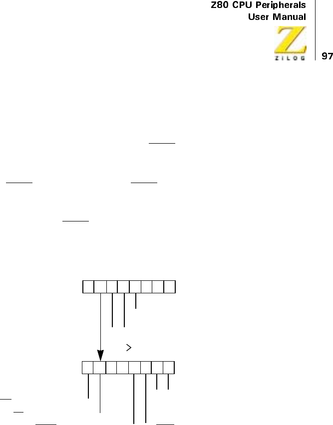
UM008101-0601 Direct Memory Access
In addition, bits 7, 6, 3, and 2 of the variable-timing byte allow termination
of various lines 1/2 cycle earlier than specified in bits 1 and 0. The chapter
on “Timing” illustrates and describes the effect of this in detail.
Particular note must be taken of the IORQ line when variable-cycle timing
is used in sequential transfers or transfer/searches. In I/O-to-memory or
memory-to-I/O operation, the memory port must be programmed to allow
its IORQ line to end early. (The IORQ line normally has nothing to do with
memory). However, this requirement does not apply to the CMOS DMA
counter controller. If an I/O-to-I/O operation is being performed, both ports
must have their IORQ lines end early. When the variable-timing feature is
employed the IORQ line changes logic levels off a different clock cycle
edge than the other control lines.
Figure 41. Write Register 1 Group
D7 D6 D5 D4 D3 D2 D1 D0
Base Register Byte
00
0
1
1
1
0
1
= Port A Address Decrements
0= Port A is Memory
0= Port A is I/O
Port A Variable
00
0
1
1
1
0
1
= Cycle Length = 3
= Cycle Length = 2
=DoNotUse
= Port A Address Increments
= Port A Address Fixed
Timing Byte
= Cycle Length = 4
WR Ends 1/2 Cycle Early = 0
RD Ends 1/2 Cycle Early = 0
MREQ Ends 1/2 Cycle Early = 0 0=IORQEnds 1/2 Cycle Early
00
0010
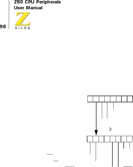
UM008101-0601 Direct Memory Access
Write Register 2 Group
Bits 7, 2, 1, and 0, depicted in Figure 42, specify the base register byte for
this group. The group is used only when Port B is used, for example, do not
program it for a search-only, simultaneous transfer, or simultaneous
transfer/search with Port A as the source. Its syntax is the same as WR1.
Figure 42. Write Register 2 Group
Write Register 3 Group
Bits 7, 1, and 0, depicted in Figure 43, specify the base register byte for this
group. The group is used primarily to specify the stop-on-match condition
as well as the specific match byte for a search operation. It can perform fast,
one-byte enabling of both bus requests and interrupts. A description of its
functions follows.
D7 D6 D5 D4 D3 D2 D1 D0
Base Register Byte
00
0
1
1
1
0
1
= Port B Address Decrements
0= Port B is Memory
0=PortBisI/O
Port B Variable
00
0
1
1
1
0
1
= Cycle Length = 3
= Cycle Length = 2
=DoNotUse
= Port B Address Increments
= Port B Address Fixed
Timing Byte
= Cycle Length = 4
WR Ends 1/2 Cycle Early = 0
RD Ends 1/2 Cycle Early = 0
MREQ Ends 1/2 Cycle Early = 0 0=IORQEnds 1/2 Cycle Early
0000

UM008101-0601 Direct Memory Access
Stop on Match
Setting bit 2 of the base register byte to 1 causes the DMA to stop and
release the bus when a data byte matches the match byte, which is
described later. A search or transfer/search operation must be specified in
WR0 to make this bit valid when set. If this bit is 0 (no stop on match), a
status flag is still set in the status byte when a match occurs and there still
remains the option of interrupting on match (see WR4). No stop or interrupt
on match in the search class is used to obtain simultaneous transfers
without searching actions.
Match Byte
When bit 4 of the base register is set to 1, the match byte that is compared
with every data byte searched must be specified. A search operation must
be specified in WR0 to make this bit valid, as shown in the following
function.
Mask Byte
When bit 3 is set to 1, the mask byte must be subsequently specified. Bit
positions that contain 1s in the mask byte cause comparisons at those same
bit positions in the match byte (see preceding paragraph) to be ignored. For
example, if the mask byte is 00001111, only the high four bits of the match
byte is compared to the data bytes being searched.
Interrupt Enable
A 1 in bit 5 of the base register enables the DMA to generate an interrupt.
This function duplicates the ENABLE INTERRUPTS command in WR6.
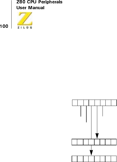
UM008101-0601 Direct Memory Access
DMA Enable
A1 in bit 6 of the base register enables the DMA to request the bus. This
function duplicates the ENABLE DMA command in WR6 and is used as
the last control byte written to the DMA prior to allowing the DMA to
usurp the bus from the CPU. The ENABLE DMA command is often better
for this purpose.
Figure 43. Write Register 3 Group
Write Register 4 Group
Bits 7, 1, and 0, which Figure 44 shows, select the base register byte for this
group. The group specifies the following characteristics:
Operating Mode
Bits 6 and 5 of the base register specify the operating mode as Byte, Burst,
or Continuous. For a review of these modes, see Figure 41 through
Figure 44, Table 13 and Table 15.
D7 D6 D5 D4 D3 D2 D1 D0
Base Register Byte
Mask Byte (0 = Compare)
000
DMA Enable = 1
Interrupt Enable = 1
1 = Stop on Match
Match Byte

UM008101-0601 Direct Memory Access
Starting Address (Port B)
The starting address for Port B in the next two bytes may be specified by
setting bits 2 and 3 of the base register to 1. This is only needed if Port B is
used, and then it specifies the first address at which a byte is read from or
written to, depending on whether the port is declared a source or destination
in WR0. If Port B is to be a fixed-address destination, see “Fixed-Address
Destination Ports” on page 121.
Interrupts
Bit 4 of the base register byte can point to the interrupt control byte, and
bits 4 and 3 of the interrupt control byte can point to the interrupt vector and
pulse control bytes, respectively. The interrupt control byte also specifies
one or more of the following three interrupt conditions:
•
Interruptonmatch(bit0),ifstoponmatchorstoponend-of-blockis
also programmed
•
Interrupt at end-of-block (bit 1), if stop on end-of-block is also
programmed
•
Interrupt on Ready (bit 6), for example, interrupt before requesting
the bus when the Ready line becomes active
Setting any of these bits to 1 enables the interrupt condition but not the
interrupt circuitry itself, which is enabled either through the ENABLE
INTERRUPTS command in WR6 or through bit 5 in WR3. Interrupts do
not occur on these conditions if their associated bits are 0 in the interrupt
control byte. Table 13 and Table 15 in the previous chapter apply to these
interrupt conditions because the DMA releases the bus (stops) before inter-
rupting the CPU.

UM008101-0601 Direct Memory Access
Interrupt Vector
Bit 4 of the interrupt control byte allows the interrupt vector to be entered.
In addition, when bit 5 of the interrupt control byte (Status Affects Vector)
issetto1,bits1and2oftheinterruptvectoraremodifiedtoreflectthe
cause of the interrupt (for example, the state of the Ready line or Status
latches) before the vector is placed on the data bus in response to the CPU’s
interrupt acknowledge.
The Status Affects Vector mode must not be used when both Auto Restart
and interrupt on end-of-block have been programmed. The interrupt vector
sent at the end of each block in this case cannot be modified to reflect the
end-of-block status.
Pulse Generation
Pulse generation is caused by (1) pointing to the interrupt control byte with
the base register byte, (2) setting bits 2 and 3 of the interrupt control byte,
and (3) entering an offset value in the pulse control byte. The pulse control
byte is compared with the lower byte of the byte counter and a pulse is
generatedontheINTline whenever a match occurs, which is every 256-
byte transfers or searches after the initial offset number of bytes.
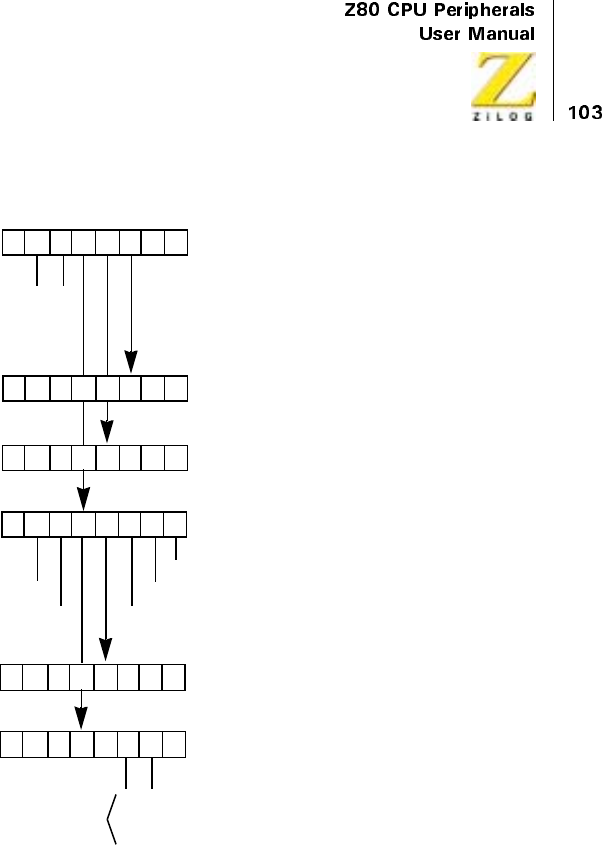
UM008101-0601 Direct Memory Access
Figure 44. Write Register 4 Group
Write Register 5 Group
Bits 7, 6, 2, 1, and 0, illustrated in Figure 45, specify the base register byte
for this one register group. The byte is used to specify these characteristics:
D7 D6 D5 D4 D3 D2 D1 D0
Base Register Byte
0
0
0
0= Interrupt on End-of-Block
= Interrupt on Match and End-of-Block
= Interrupt on RDY
011
Port B Starting Address
Pulse Control Byte
Interrupt on RDY = 1
Status Affects Vector = 1 1 = Pulse Generated
Interrupt Vector
0
0
0
0
Modified as shown only if
Status Affects Vector bit is set
Vector is automatically
1 = Interrupted at End-of-Block
1 = Interrupted on Match
0Interrupt Control Byte
(High Byte)
Port B Starting Address
(Low Byte)
0
1
0
1
0
0
1
1
Continuous =
Burst =
Do Not Program =
Byte =
= Interrupt on Match

UM008101-0601 Direct Memory Access
End-of-Block Action
Bit 5 specifies either a stop (bus release) or an auto repeat at the end of the
blocklengthprogrammedinWR0.Tointerruptattheendofablock
(WR4), bit 5 should be 0 because the DMA must reset the end-of-block
status bit to proceed with a new block. In Auto Restart, the end-of-block
status bit is also reset.
CE/WAIT Line Use
Bit 4 specifies that the DMA’s CE/WAIT line is to be used in one of two
ways:
CE Only
The CE/WAIT line functions only as a chip enable line, allowing CPU
writing and reading of control/status bytes when the DMA is not bus
master. See the “Applications” chapter for the method by which this time is
decoded from the address bus.
CE/WAIT Multiplex
This line functions as described in “CE only” above, when the DMA is not
bus master. When the DMA has the bus, however, the line allows external
Wait inputs from external logic to extend the DMA's cycle programmed in
WR1 and/or WR2. See the “Applications” chapter for hardware interfacing
of this option.
Ready-Line State
Bit 3 specifies that the DMA interprets the Ready (RDY) line as active
when High or active when Low. This allows flexibility in interfacing to a
variety of other devices.
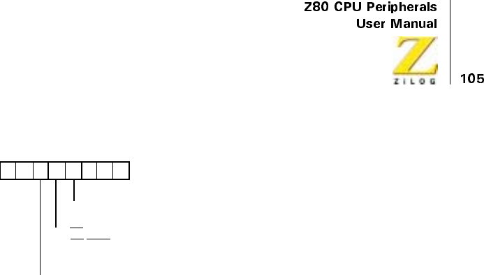
UM008101-0601 Direct Memory Access
Figure 45. Write Register 5 Group
Write Register 6 Group
The base register byte for this group has bits 7, 1, and 0 set to one, which
Figure 46 depicts. The remaining bits specify 16 commands that are
commonly used after DMA initialization (for example, within CPU
interrupt service routines), and to point to a read mask for the read registers.
Each of these commands, except the ENABLE DMA command, disables
the DMA. Therefore, the ENABLE DMA command must be the last
command written before DMA bus requests can begin.
Reset (C3)
This command is used at power-up and when aborting a program sequence
to do the following:
•
Disable interrupt and bus-request logic
•
Reset interrupt latches
•
Unforce a FORCE READY condition
•
Reset the Auto Repeat function (see WR5)
•
Reset the Wait function (See WR5)
D7 D6 D5 D4 D3 D2 D1 D0
Base Register Byte
0= Ready Active Low
1= Ready Active High
10010
0= Stop on End-of-Block
1= Auto Restart on End-of-Block
0=CEOnly
1=CE
/WAIT Only

UM008101-0601 Direct Memory Access
•
Reinitialize Ports A and B to standard Z80 cycle timing (see WR1
and WR2)
At power-up, one reset command is sent to the DMA prior to the initial-
ization program. When aborting an operation sequence, sending six reset
commands guarantees resetting (this is because WR4 has five associated
registers that can potentially be pointed to).
The RESET command does not perform a complete DMA reset. For
example, it does not reset the read sequence, which is set by the INITIATE
READ SEQUENCE command.
ResetPortATiming(C7)
Resets the Port A variable timing byte in WR1 to standard Z80 timing. The
RESET command also perform this function.
ResetPortBTiming(CB)
Resets the Port B variable timing byte in WR2 as described in Reset Port A
Timing (C7).
Load (CF)
This command must be used to write new addresses to the address registers
(WR0 and/or WR4) or to restart an operation (except Auto Restart) at the
same addresses. It loads the contents of both starting-address registers to
their associated address counters (Figure 30). It also clears the byte counter
associated with the block-length register, and it unforces an internal Force
Ready condition. The starting addresses must be written in WR0 and/or
WR4 before the LOAD command is written, if they are to differ from the
previous starting addresses.
Only the source-port address counter is immediately loaded. The desti-
nation-port address counter (if used) is loaded during the first count of the
destination-port address. If the destination-port address is fixed, this indi-

UM008101-0601 Direct Memory Access
cates that it is never loaded. This special situation is discussed in a later
section entitled “Fixed-Address Destination Ports.”
If the DMA is in an inactive state (Table 15) when the LOAD command is
written, another DMA control byte must precede the LOAD. Any other
command, such as DISABLE DMA, serves this purpose. Because LOAD
unforces a Forced-Ready condition, the LOAD must precede a FORCE
READY command when the latter is used.
Continue (D3)
This command clears the byte counter to zero but leaves the address
counters of both ports with their current contents. Transfers or searches
continue from where they left off after an ENABLE DMA command,
although the byte count starts over.
The CONTINUE command is typically used to transfer several blocks to
consecutive locations in memory when it is desirable to know when each
block has finished transferring. Specifically, an interrupt at the end of each
block may be needed. Use this command rather than a LOAD command to
transfer the next block after the interrupt. A new block length can be
entered in WR0 in conjunction with the CONTINUE command.
If the DMA is in an inactive state (Figure 15) when the CONTINUE
command is written, another DMA control byte must precede the
CONTINUE. Any other command, such as DISABLE DMA, serves this
purpose.
Disable Interrupts (AF)
The command is used in non-Z80 CPU environments to simulate the Z80
CPU’s automatic interrupt acknowledge to the DMA. When the DMA
interrupts a non-Z80 CPU, the CPU writes a DISABLE INTERRUPTS to
the DMA early in the service routine. This allows the INT line to go
inactive but prevents the DMA from sending subsequent interrupts while
UM008101-0601 Direct Memory Access
the routine is being executed. Near the end of the routine, the CPU writes
an ENABLE INTERRUPTS command to the DIVA, which enables it to
generate a new interrupt.
This command is less extensive than the RESET AND DISABLE INTER-
RUPTS command because it does not reset the Interrupt Pending (IP) and
Interrupt Under Service (IUS) latches.
Figure 46. Write Register 6 Group
D7 D6 D5 D4 D3 D2 D1 D0
Base Register Byte
01
111
=C3=Reset
000
Hex Command Name
01 =C7=ResetPortATiming
001
01 =C8=ResetPortBTiming
010
01 = CF = Load
011
01 = D3 = Continue
100
10 = AF = Disable Interrupts
011
10 = AB = Enable Interrupts
010
10 = A3 = Reset and Disable Interrupts
000
10 = B7 = Enable after RETI
101
10 = BF = Read Status Byte
111
00 = 8B = Reinitialize Status Byte
010
10 = A7 = Initialize Read Sequence
001
10 = B3 = Force Ready
100
00 =87=EnableDMA
001
00 = 83 = Disable DMA
000
10 = BB = Read Mask Follows
110
Read Mask (1=Enable)
Status Byte
Byte Counter (Low Byte)
Byte Counter (High Byte)
Port A Address (Low Byte)
Port B Address (High Byte)
0
Port B Address (Low Byte)
Port A Address (High Byte)

UM008101-0601 Direct Memory Access
Enable Interrupts (AB)
See the preceding description of DISABLE INTERRUPTS. A Z80 CPU
environment uses this command at power-up to enable the interrupt logic at
the beginning (the DMA comes up with this logic disabled). It is not
needed, however, to enable subsequent interrupts because this function is
provided for by the CPU’s fetching and the DMA’s decoding of the RETI
instruction. The only exception is when the DISABLE INTERRUPTS
command is used; the ENABLE INTERRUPTS command must also be
used to begin DMA operations again.
Any conditions selected to cause an interrupt are latched in the DMA even
when interrupts are disabled. They can then cause a later interrupt after
interrupts are reenabled.
The ENABLE INTERRUPTS command must not be written until after the
DMA has been configured and the REINITIALIZE STATUS BYTE
command has been written. This command has the same effect as writing a
1tobit5ofWR3.
Reset and Disable Interrupts (A3)
This command is useful in CPU environments such as the 8080 and 8085
where there is an interrupt acknowledge function but no RETI instruction,
as in the Z80 CPU. This command accomplishes four functions:
•
Resets the Interrupt Under Service (IUS) latch
•
Resets the Interrupt Pending (IP) latch
•
Unforces an internal FORCE READY condition
•
Disables further interrupts by the DMA (same as the DISABLE
INTERRUPTS command)
In the non-Z80 environment just described, it would be used as follows:
after the DMA interrupt is received and acknowledged, the interrupt
vector is sent to the CPU, which branches to the service routine. Near the

UM008101-0601 Direct Memory Access
end of the service routine, the CPU writes a RESET AND DISABLE
INTERRUPTS command, then an ENABLE INTERRUPTS command,
and then an ENABLE DMA command before executing its return-from-
interrupt instruction.
This command, when followed by an ENABLE INTERRUPTS command,
takes the place of the Z80 RETI instruction. It is not needed in a Z80 envi-
ronment. Because RESET AND DISABLE INTERRUPTS unforces a
FORCED-READY condition, the RESET AND DISABLE INTERRUPTS
must precede a FORCE READY command when the latter is used.
Enable After RETI (B7)
ThiscommandisusedonlywhentheDMAisoperatedintheInterruptOn
Ready mode (programmed in WR4). It enables the DMA to request the bus
again after returning from an interrupt. This command is always used in
Z80 CPU environments to get further bus requesting after an Interrupt on
Ready. It is sometimes used in other environments, such as the 8080.
An Interrupt on Ready (IOR) latch is set during such an interrupt. This latch
prevents the DMA from requesting the bus from the time the Ready line
goes active until the time the latch is reset by the ENABLE AFTER RETI
command (in Z80 and some other environments, there is an overlap in bus-
request prevention by the IOR and the IUS latches).
In a Z80 CPU interrupt service routine, the order of DMA commands and
CPU instructions MUST be:
1. •
2. •
3. •
4. ENABLE AFTER RETI command
5. ENABLE DMA command

UM008101-0601 Direct Memory Access
6. •
7. •
8. •
RETI instruction
Read Status Byte (BF)
This command causes the next CPU read of the DMA to access the status
byte, which is illustrated in “Read Registers” on page 114.
If other read registers are being read, the sequence of reading (as defined by
the read mask) must be completed before issuing this command.
Reinitialize Status Byte (8B)
This command reinitializes bits 4 and 5 of the status byte. After reinitial-
ization, the status byte looks like this:
The DISABLE DMA or any other command must be used before the
REINITIALIZE STATUS BYTE command after having stopped on end-of-
block or byte match. Due to a potential hardware race condition internal to
Table 14. Reinitialize Status Byte
Bit Value Meaning
0 I/O DMA operation has/has not occurred
1 I/O Ready line active/inactive
2 X Undefined bit
3 0/1 Interrupt pending/not pending
4 1 Match not found
5 1 Not end-of-block
6 X Undefined bit
7 X Undefined bit

UM008101-0601 Direct Memory Access
the DMA, reinitialization of the status bits may remove the condition that
stopped the DMA and the DMA might immediately request the bus again if
it is not disabled. (The REINITIALIZE STATUS BYTE command in WR6
is similar in this respect to the WR0 byte when transfer direction is being
changed: both of these control bytes must be preceded by some other
control bytes to ensure that the DMA is disabled.)
The interrupt pending status (bit 3) of the status bytes can be reinitialized by
acknowledging the interrupt, servicing it, and writing a RESET AND
DISABLE INTERRUPTS command. The DMA operation status (bit 0) can
be reinitialized with a LOAD command.
Read Mask Follows (BB)
This command points to the read mask (Figure 46). It allows the next control
bytewrittentotheDMAtogotothereadmaskregister.Thereadmaskis
used to set a new sequence, for reading the read registers, RR0 through RR6,
and it is normally part of the power-up initialization of the DMA.
The read registers are always read in a fixed sequence beginning with RR0
and ending with RR6. However, the registers read in this sequence can be
limited by programming the read mask. The read mask is programmed with
1s in the bit positions associated with the registers to be read. For example,
if the read mask contains 0001 1001, the following read registers are read
in the following order:
1. Status byte (RR0)
2. Port A address counter, low byte (RR3)
3. Port A address counter, high byte (RR4)
When the read mask has been programmed, it must be initialized to begin at
the lowest-order register selected. Do this with the INITIATE READ
SEQUENCE command.

UM008101-0601 Direct Memory Access
Initiate Read Sequence (A7)
This command initiates the read-sequence pointer command, allowing the
next CPU read instruction to the DMA access to the first (low-order) read
register designated as readable by the read mask. When started, the read
sequence specified by the read mask must be completed before, for
example, giving another INITIATE READ SEQUENCE or a READ
STATUS BYTE command.
Registers do not need to be read immediately after writing the INITIATE
READ SEQUENCE command. Other commands (except INITIATE READ
SEQUENCE and READ STATUS BYTE) can be written and can go through
bus-request/bus release cycles before executing the first read and subse-
quent reads.
Force ReadY (B3)
This command, in Burst or Continuous mode, forces an internal Ready
condition to take the place of an external active Ready signal. It is used for
memory-to-memory transfers and memory searches where no Ready line is
necessary. Ready active High/Low (bit 3 of WR5) need not be considered
when this command is used. The FORCE READY condition is unforced by
the following commands and conditions:
•
RESET command
•
LOAD command
•
RESET AND DISABLE INTERRUPTS command
•
End-of-block termination
•
Byte-match termination
•
Bus release by DMA
Because bus release by the DMA unforces the Ready condition, this
command allows the DMA to transfer only one byte in the byte mode.

UM008101-0601 Direct Memory Access
Enable DMA (87)
This command allows the DMA to request the system bus and proceed with
its operation if all other functional conditions are met, for example, if the
Ready line is active or the FORCE READY condition is present. This
command, and bit 6 of WR3, are the only control bytes that do not disable the
DMA. All other control bytes written to the DMA automatically disable the
DMA. Therefore, the ENABLE DMA command is always required as the last
command after writing or reading any other bytes to or from the DMA.
This command enables the DMA’s bus request logic. It does not affect
interrupt logic and it does not reset any functions or latches. This bus-
request-enabling function is duplicated in bit 6 of WR3.
In an interrupt service routine, the ENABLE DMA command must be the
last command to the DMA before the CPU executes its return-from-
interrupt instruction.
Disable DMA (83)
This command prevents the DMA from requesting the bus. It is used to stop
DMA action for external reasons, such as a pending power-out, and in the
special case of reinitializing the status byte after a stop on end-of-block or a
stop on byte match (see the REINITIALIZE STATUS BYTE command).
Read Registers
Process Read registers by first writing a command to the DMA, then by
reading either immediately or later. Accomplish CPU reads by addressing
the DMA as an I/O device using input instructions (such as INIR for the
Z80 CPU).
Commands written to the DMA can be either of the following:

UM008101-0601 Direct Memory Access
Read Status Byte
This command causes the next CPU read of the DMA to access the status
byte, which is the first read register.
Initiate Read Sequence
This command initializes access to a repeatable series of reads that follow
the sequence defined in the read mask.
These commands are described in the immediately preceding pages, and
Figure 46 illustrates the read mask. As mentioned in the description of
these commands, the reading of registers do not need to be contiguous in
time with these write commands or with other CPU read instructions
accessing registers in the same read sequence.
Two other commands are also related to the read registers:
Reinitialize Status Byte
This command reinitializes bits 4 and 5 of the status byte to 1s.
Read Mask Follows
This command allows the read mask to be programme. Figure 47 illustrates
more clearly the group of the seven read registers in relation to the write
registers. The read registers include:
Status Byte (RR0)
The status byte can be read independently from the other read registers and
two of its bits can be reinitialized to identify end-of-block and match bytes.
The bits in the status byte are defined as follows:

UM008101-0601 Direct Memory Access
Bit 0 Indicates whether the DMA has requested the bus after the fast
LOAD command. 1 indicates yes, 0 indicates no.
Bit 1 Indicates whether the DMA’s RDY pin currently has a signal input
that is defined as active by bit 3 of WR5. 1 indicates an active Ready line. 0
indicates an inactive Ready line.
Bit 2 Undefined.
Bit 3 Indicates the state of the Interrupt Pending (IP) latch. A 0 indicates
that an interrupt is pending (the DMA has its INT line active if the interrupt
has not been acknowledged). A 1 indicates no interrupt pending.
Bit 4 A 0 indicates that a match has been found after the last RESET or
REINITIALIZE STATUS BYTE command. A1 indicates no match was
found. See Table 11 to determine where the match occurred.
Bit 5 A 0 indicates that an end-of-block was reached after the last
RESET, LOAD, CONTINUE, or REINITIALIZE STATUS BYTE
command. A 1 indicates no end-of-block was reached. See Table 12 to
determine the contents of counters when the DMA stops.
Bit 6 Undefined.
Bit 7 Undefined.
UM008101-0601 Direct Memory Access
Figure 47. Read Register 0 through Read Register 6
Byte Counter (RR1, RR2)
This 16-bit counter is cleared to 0 by the LOAD, CONTINUE, and RESET
commands only. When the DMA begins transferring or searching, the byte
counter increments by one at the end of each read cycle and the byte counter
is compared with the programmed contents of the block length register,
determining end-of-block. The number of bytes read in a transfer always
equals the number of bytes written because the DMA completes any transfer
it starts, even when stopping on byte matches in transfer/search operations.
D7 D6 D5 D4 D3 D2 D1 D0
Status Byte
XX
1 = DMA Operation has Occurred
0 = Ready Active
0 = Interrupt Pending
0 = Match Found
0 = End-of-Block
Byte Counter (Low Byte)
Read Register 1
Byte Counter (High Byte)
Read Register 2
Port A Address Counter (Low Byte)
Read Register 3
Port A Address Counter (High Byte)
Read Register 4
Port B Address Counter (Low Byte)
Read Register 5
Port B Address Counter (High Byte)
Read Register 6

UM008101-0601 Direct Memory Access
Table 11 and Table 12 illustrate how the pipelining of data affects the
number of bytes transferred or searched in the various classes, modes, and
circumstances of operation. In most cases, the number of bytes transferred
in a transfer operation that stops at end-of-block is one more than the
programmed block length.
When the pulse-generation feature is used, the contents of the pulse control
byte in WR4 are compared with the lower byte of the byte counter after
each byte is transferred.
Port A Address Counter (RR3, RR4)
This 16-bit counter is loaded from the Port A starting address register in
WR0 by the LOAD command. It increments, decrements, or remains fixed
according to the specifications in WR1. Table 11 and Table 12 show how
this counter reads under various transfer or search conditions.
Port B Address Counter (RR5, RR6)
This counter is identical to the Port A address counter just described. If
either Port A or Port B is a fixed-address destination port, it must be
programmed as described in “Fixed-Address Destination Ports” on
page 121 to function properly.
Review of Programming Sequences
This section describes programming the DMA in both the general and in
application-specific cases. Also, see Table 16 on page 127 for a sample
DMA Program.
DMA Initialization
Program all registers to be used in the DMA at power-up. None of these
registers contain useful defaults. This procedure includes the enabling of

UM008101-0601 Direct Memory Access
interrupts and reinitialization of the status byte as well as many other func-
tions, including class and mode designation, port designation, address and
block-length designation.
Table 15 lists the order in which control bytes must be written for the
initialization or reinitialization because of program abort. Some of these
control bytes may not be relevant to a specific application. All commands
referred to are WR6 control bytes. Thirty-five control bytes occur when all
of the control bytes are written.
All control bytes written to the DMA disable the DMA, except the
ENABLE DMA command and possibly also the REINITIALIZE STATUS
BYTE command and the WR0 control byte (when changing transfer direc-
tions). The ENABLE DMA command must always be the last command
written after any communication between the CPU and DMA if the DMA
is to continue operating. Furthermore, communication with the DMA can
only occur when the CPU is bus master.
Table 15. Control Byte Order
Initialization/Reinitialization Sequence
Maximum Number of Z80 CPU
Bytes
DISABLE DMA Command 1
RESET Command (Multiple) 6
WR0 Control Bytes 5
WR1 Control Bytes 2
WR2 Control Bytes 2
WR3 Control Bytes 3
WR4 Control Bytes 5
WR5 Control Bytes 1
RESETPORTATIMINGCommand 1
RESETPORTBTIMINGCommand 1
LOAD Command 1
UM008101-0601 Direct Memory Access
Port Designation
Either Port A or Port B can be selected as the source or destination, (illus-
trated in Figure 19) because both ports feature the same degree of program-
mability. When the destination port is also a fixed-address port, see the
section “Fixed-Address Destination Ports.” Port characteristics are spec-
ified in the following control byte groups:
In a transfer, if the direction of transfer (bit 2 of WR0) changes, the WR0
control byte must be preceded by a different control byte, thereby insuring
that the DMA is disabled.
REINITIALIZE STATUS BYTE
Command
1
READ MASK FOLLOWS Command 1
Read Mask Control Byte 1
INITIATE READ SEQUENCE
Command
1
FORCE READY Command 1
ENABLE INTERRUPTS Command 1
ENABLE DMA Command 1
Total 35
Port A Port B
WR0 WR0
WR1 WR2
WR6 WR4
WR6
Table 15. Control Byte Order (Continued)
Initialization/Reinitialization Sequence
Maximum Number of Z80 CPU
Bytes

UM008101-0601 Direct Memory Access
Address Loading
Write starting addresses to the starting-address registers for each port using
WR0 (Port A) and WR4 (Port B). They are loaded to the address counters
by the LOAD command. The addresses must he written to the registers
before they are loaded to the counters.
New addresses may be written to the address registers at any time when the
CPU is bus master, even between transfers and even when the DMA is oper-
ating in the Auto Restart mode, for example, in Byte mode between byte
transfers. With the exception of the Auto Restart mode, the new addresses
must be reloaded before they are used. If a Forced-Ready condition is used,
the LOAD command must precede the FORCE READY command.
Fixed-Address Destination Ports
A special circumstance arises when programming a destination port to have
a fixed address. The load command in WR6 only loads a fixed address to a
port selected as the source, not to a port selected as the destination.
Therefore, a fixed-destination address must be loaded after temporarily
declaring its port as a source port. The true source port is subsequently
declared (making the other port a destination) and the true source address is
then loaded.
The following example describes the steps in this procedure, assuming that
transfers are to occur from a variable-address source (Port A) to a fixed-
address destination (Port B).
1. Write Port B (fixed destination) address to WR4.
2. Temporarily declare Port B as source in WR0 (bit 2 = 0).
3. Load Port B address with the LOAD command.
4. Write Port A (variable source) starting address to WR0.
5. Declare Port A as source in WR0 (bit 2 = 1).
6. Load Port A address with the LOAD command.

UM008101-0601 Direct Memory Access
•
•
•
7. Enable DMA with the ENABLE DMA command.
Interrupts
The interrupt vector (WR4) must be written before interrupts using it can
occur, and interrupts must be enabled with the ENABLE INTERRUPTS
command at initialization or reinitialization. In a Z80 CPU environment,
interrupt service routines after DMA initialization usually include the
following commands at the end of the routine:
1. Interrupt on End-of-Block or Byte Match
•
•
•
2. ENABLE DMA command
•
•
•
•
3. RETI instruction
4. Interrupt on Ready (before requesting the bus)
•
•
•

UM008101-0601 Direct Memory Access
5. ENABLE AFTER RETI command
6. ENABLE DMA command
•
•
•
7. RETI instruction
Interrupts at end-of-block, for example, might occur when reading a
floppy disk. If the disk transfers 128-byte records, the DMA can be made
to interrupt at the end of each record to notify the CPU of its completion.
Then the CPU can read the destination (memory) address counter to find
the last memory location filled. See Table 12 for address-counter
contents. A service routine for continuing inputs to contiguous locations
of memory typically contains the CONTINUE,REINITIALIZE STATUS
BYTE,andENABLE DMA commands before the CPU’s return from
interrupt. A service routine for shutting down the DMA after the record
arrives typically includes DISABLE DMA and REINITIALIZE STATUS
BYTE commands. If the DMA transfer is started by an interrupt from
another device, the service routine for that other device includes an
ENABLE DMA command written to the DMA’s port address.
Interrupts on byte match (a search or transfer/search operation) can be
implemented so that any ending byte, error indicator, or other character
causes the interrupt. This procedure frees the CPU from looking for these
characters in a stream of data, increases throughput, and reduces CPU
software complexity. For example, the DMA might search for end-of-text
(EXT) characters or carriage returns in a communications environment and
interrupt the CPU only when the complete message frame has arrived. The
service routines for this would be very much like those for interrupts on
end-of-block.
Interrupts on Ready are somewhat different. First, the DMA cannot be the
bus master before the interrupt because the CPU only senses interrupts
when the CPU is the bus master (the other types of interrupts are not

UM008101-0601 Direct Memory Access
processed until the bus is released). Second, to enable the DMA, the
ENABLE AFTER RETI command must be used in the service routine after
an Interrupt on Ready. The typical purpose of interrupting when the Ready
line comes active is to allow the CPU time to determine where a transfer
should go, which it does in the service routine. This often occurs in systems
with dynamic memory allocation and it improves the efficiency with which
memory can be allocated. For example, the CPU might write and load new
starting addresses for a memory destination to the DMA in the service
routine. Only at the end of the service routine is the DMA enabled to
request the bus. The ENABLE AFTER RETI command, which must precede
the ENABLE DMA command, resets a latch that is set when the Interrupt on
Ready first occurred.
For non-Z80 CPU environments, the DISABLE INTERRUPTS,ENABLE
INTERRUPTS,andRESET AND DISABLE INTERRUPTS commands are
available. They can simulate the Z80 CPU’s interrupt-acknowledge cycle
and return-from-interrupt instruction, both of which the DMA needs to
perform and return from interrupts.
Byte Matching (Searches)
In stopping, or stopping and interrupting on match (WR3, WR4), to
perform additional operations with the DMA, the following sequence of
commands are written:
1. LOAD or CONTINUE.
2. REINITIALIZE STATUS BYTE.
3. ENABLE DMA.
Another command (with the exception of ENABLE DMA) must precede the
REINITIALIZE STATUS BYTE command. Table 11 on page 76 describes
the contents of various counters when stopping on byte match.

UM008101-0601 Direct Memory Access
End-of-Block
After a stop or stop and interrupt on end-of-block (WR4 or WR5), where it
is necessary to perform additional operations with the DMA, write the same
sequence of commands listed immediately under “Byte Matching
(Searches)” on page 124. Table 12 on page 76 describes the contents of
various counters when stopping on end-of-block.
Auto Restart
To obtain a repetitive transfer or search using the same block length and
starting addresses originally entered, initialize the DMA including WR%
bit 5 = 1. Loading of addresses and clearing of the byte counter is auto-
matic.
When in Byte mode (or Burst mode where the Ready line is occasionally
released), it is possible to alter the starting addresses during a transfer (for
example, between bus requests) without disturbing that transfer. At the end
of this transfer, the DMA automatically loads the new addresses to the
counter and continues without interruption.
Force Ready Condition
The FORCE READY command is provided for operations such as memory-to-
memory transfer or memory search-only where no Ready line from an I/O
device is used. However, several DMA commands unforce the Ready
condition after the FORCE READY command is written. The sequence of
command entry is therefore important. This sequence is described in the
FORCE READY command in “Write Register 6 Group” on page 105.
Pulse Generation
To obtain pulses at 256-byte intervals, after a variable offset period,
consider only the WR4 group. The INT line is used for these pulses.

UM008101-0601 Direct Memory Access
Variable Timing
The timing on the RD,WR,MREQ,andIORQlines can be varied indepen-
dently for either port by programming the WR1 and/or WR2 register groups.
When programming memory-to-I/O, I/O-to-memory, or I/O-to-I/O
sequential transfers or transfer/searches, the IORQ line must be programmed
in a specific way. See “Variable Cycle (Port A)” on page 96.
Enabling the DMA
The last command written to the DMA before an operation occurs must be
the ENABLE DMA command, or WR3 bit 6 = 1, which is equivalent. Only
this command makes the DMA operate. If all other conditions for operation
are satisfied at the time of enabling (for example, the Ready line is active)
the DMA begins immediately. In an interrupt service routine, the ENABLE
DMA command must be the last DMA command written before the return
from-interrupt instruction. Other instructions usually follow the ENABLE
DMA command in the service routine before the RETI instruction is
executed, but none of these commands affect the DMA.
Reading Status
These two commands allow the CPU to read DMA status:
READ STATUS BYTE
Causes the next CPU read of the DMA to access the status byte. Every time
the status byte is to be read, the READ STATUS BYTE command must first be
written.
INITIATE READ SEQUENCE
Causes the next CPU read of the DMA to access the first status register
specified as readable by the read mask. Subsequent reads of the DMA,
which must complete the sequence of all designated readable registers, do
not require write commands. Reading of the sequence of registers must be

UM008101-0601 Direct Memory Access
completed before the next READ STATUS BYTE or INITIATE READ
SEQUENCE command.
Table 16 illustrates a program to transfer data from memory (Port A) to a
peripheral device (Port B). In this example, the Port A memory starting
address is 1050H and the Port B peripheral fixed address is 05H.The
number of data bytes to be transferred is 1001H bytes (one more than spec-
ified by the block length). The table of DMA commands may be stored in
consecutive memory locations and transferred to the DMA with an output
instruction such as the Z80 CPU’s OTIR instruction.
Table 16. Sample DMA Program
D7 D5 D4 D3 D2 D1 D0 HEX
WR0 sets DMA to
receive block length,
Port A starting
address, and
temporarily sets Port
B as source.
01
Block
Length
Upper
Follows
1
Block
Length
Upper
Follows
1
Port A
Upper
Address
Follows
1
Port A
Upper
Address
Follows
0
B→A
Tempor
ary for
Leading
B
Address
0
Transfer. No
Search
Port A address
(lower)
01 0 1 0 0 0 0 50
Port A address
(upper)
00 0 1 0 0 0 0 10
Block length (lower) 0 0 0 0 0 0 0 0 00
Block length (upper) 0 0 0 1 0 0 0 0 10
WR1 defines Port A
as memory with
fixed incrementing
address
00
No
Timing
Follows
0
Address
Change
s
1
Address
Change
s
0
Port is
Memor
y
10014
WR4 defines Port A
as memory with
fixed incrementing
address
00
No
Timing
Follows
1
Fixed
Address
01
Port is
I/O
01028

UM008101-0601 Direct Memory Access
WR4 sets mode to
Burst and sets DMA
to expect Port B
address
11 0 0
No
Interrup
t
Control
Byte
Follows
0
No
Upper
Address
1
Port B
Lower
Address
Follows
01C5
Port B address
(lower)
00 0 0 0 1 0 1 05
WR5 sets Ready
active High
10 0
No
Auto
Restart
0
No Wait
Status
1
RDY
Active
High
0108A
WR6 loads Port B
address and resets
block counter *
11 0 0 1 1 1 1 CF
WR0 sets Port A as
source *
00 0 0 0 1
B→A
0105
No Address or Block
Length Bytes
Transfer No
Search
WR6 loads Port A
address
and resets block
counter
11 0 0 1 1 1 1 CF
WR6 enables DMA
to start operation.
10 0 0 0 1 1 1 87
Table 16. Sample DMA Program (Continued)
D7 D5 D4 D3 D2 D1 D0 HEX

UM008101-0601 Direct Memory Access
Note: The actual number of bytes transferred is one more than specified by the block length.
* These entries are necessary only in the case of a fixed destination address.
Z80 DMA and CPU
As a member of the Z80 Family, the Z80 DMA’s signals and timing are
compatible with those of the Z80 CPU. As bus master, the DMA has read-
and write-cycle characteristics identical to those of the Z80 CPU, thereby
simplifying system design. In addition, variable timing features allow the
system designer to interface memories and I/O devices more easily with
non-standard capabilities or requirements. The DMA can shorten its read-
or write-cycle timings for higher performance or lengthen and tailor control
signals to accommodate slower devices. Because these features are under
programmed control, the hardware configuration is not affected by changes
in cycle and control signal timings.
Interconnection
In small systems, or where the Z80 DMA shares a board with the CPU,
most of the pins on the DMA may be connected directly to the corre-
sponding CPU pins. These pins include the address bus (A15-A0), the data
bus (D7-D0), and the control signals MREQ,IORQ,RD,andWR.The
interrupt request and bus request signals, INT and BUSREQ, may also be
connected directly to the CPU, in common with corresponding open-drain
outputs from other devices. The priority daisy-chains for these functions are
described in an earlier chapter and are illustrated in Figure 31 and
Figure 37.
Power, ground, and clock signals are also common to the CPU and DMA,
but extra care must be taken to provide low impedance paths and adequate
decoupling. A 300 Ohms pull-up from a TTL clock driver output may be
adequate for small systems operating at the 2.5 MHz rate, but the increased
loadings and speeds in larger high-performance systems require active pull-
UM008101-0601 Direct Memory Access
up. A complementary-transistor driver for Z80/Z8000 systems is depicted
in Figure 48.
Chip Selection and Enabling
Z80 peripherals are normally addressed in the 256 address I/O space.
Each peripheral Chip is enabled by an active-low Chip Enable (CE) input.
The CE input becomes active when an active IORQ signal coincides with
the peripheral’s address on the low order byte of the address bus. Small
systems may dedicate address lines to their few peripherals, making
decoder hardware unnecessary. A system using DMA, however, usually
has more peripherals, so that address decoding by means of PROM or
MSI TTL decoder is normally provided.
Figure 48. Z80/Z8000 Clock Driver
Figure 49 illustrates three chip enable arrangements in a small system. In it,
the DMA responds to half of the 256 possible I/O addresses. In
(Figure 49b), a 256 x 4 PROM is programmed to provide a Low output on
the 01 pin only when the DMA’s address is present. The PROM must
respond quickly to meet the DMA’s CE setup time requirement.
+5V
TTL
0.01 µF
10K (max)
Clock
2N5772 or
2N3646
120
470
470
240
22
22
2N5771 or
2N3546

UM008101-0601 Direct Memory Access
Figure 49c depicts a one-of-eight TTL decoder which provides chip enable
signals for eight different peripheral devices. Address bits A0 and A1 are
often used directly by peripherals such as the Z80 SIO, PIO, and CTC, and
so are not decoded here. Additional decoders can be added when more
peripheral devices are present.
IORQ and M1 are internally gated with CE in Z80 peripheral devices and
need not be terms in CE. However, gating chip-enable signals with these
control lines do no harm and may produce less-ambiguous logic sequences
for circuit-level debugging, as seen in Figure 49c.
UM008101-0601 Direct Memory Access
Figure 49. Chip Enable Decoding with Z80 CPU
Use of WAIT Input
When the DMA is bus master, the CE/WAIT pin functions as an input from
memory or I/O logic that may extend read or write cycles by requesting
Waits states. An active BUSACK output from the CPU signals that the
Z80
CPU
M1
IORQ
CPU
M1
IORQ
DMA
M1 IORQ CE
DMA
M1 IORQ CE
CE7
CE1
A2 A3 A4
CE3
CE2
CE1
A5 A0 A7
A7
A0
ADMA responds to
I/O addresses 00H
through 77H
BPROM determines
DMA response
CDMA responds to
I/O addresses E0H
through E3H
DMA
M1 IORQ CE
Address Bus A7
A7
A0
04
03
02
01
256X4
PROM
CPU
M1
IORQ 12345670
74LS138
S0 S1 S2
E
E
E
.
.
.
.

UM008101-0601 Direct Memory Access
CPU has relinquished the bus. Therefore, if this DMA is bus master, it
samples the WAIT signal for these requests. A simple 2-input multiplexer
steers the CE/WAIT signalsasdepictedinFigure50.UsingBUSACK
assumes that there is only one DMA. In systems with three or more
possible bus masters, BAl active and BAO inactive identify the master.
Simultaneous Transfers
The highest-speed DMA transfer method is the simultaneous transfer
method, or flyby method. This requires some external hardware to
generate simultaneous read- and write-control signals to the source and
destination ports.
Because the address bus is used for memory address, only transfers
between I/O and memory can be accomplished directly when the I/O port
selection is performed by hard wiring. The DMA is put into search mode,
and a circuit, such as that illustrated in Figure 51, generates separate simul-
taneous read- and write-control signals, which may be ORed into the read-
and write-control paths at memory and I/O. Figure 52 depicts such an
arrangement. This arrangement allows both the CPU and DMA access to
the I/O peripheral. (If the peripheral communicates only through DMA, it
only needs to use the IORD and IOWR signals.)
Pay careful attention to access, setup, and hold times in this mode. Because
the DMA is programmed to do searching, the MWR and IOWR signals are
derived from the DMA RD signal and mimic its timing. This does not cause
a problem for write operations, which are trailing edge activated. To make
MWR appear more like a CPU or DMA write cycle signal, the circuit of
Figure 50 may be used to delay the leading edge of MWR until after the
falling edge in T2. The programmable variable timing features of the DMA
may be useful, too.
UM008101-0601 Direct Memory Access
Figure 50. CE/WAIT Multiplexer
Figure 51. Simultaneous Transfer Multiplexer
I1 I0
SEL 1/4
74LS157
Y
DMA
CE/WAIT
BUSACK
CE (From Decoder)
WAIT (From Peripheral or Memory Logic)
+5V
IOWR IORD MWR MRD
BUSACK or BAI-BAO
RD (from DMA)
IORQ (from DMA)
Y4 Y3 Y1
SEL 74LS257 OE
Y2
01000111
UM008101-0601 Direct Memory Access
Figure 52. Simultaneous Transfer
DMA
IORQ RD WR BUSACK BAI RD IORQ
MRD
MWR
HIGH
RD WR
MEMORY I/O
DMA
I/O
DECODER
IOCE
IOWR
IORD
Address and Data Buses
RD WR CE
OE
Y1 Y2 Y3 Y4
SEL
10001101
UM008101-0601 Direct Memory Access
Figure 53. Delaying the Leading Edge of MWR
Bus Buffering
Microcomputer systems using DMA often include large memories, many
peripheral devices, or occupy several circuit cards. In these cases, the
system buses and control signals require buffering to increase drive capa-
bility and noise margin and to decrease delay times.
The need for buffering within a single circuit card can be estimated by
comparing drive capabilities of bus master devices (CPU and DMA) to
loadings presented by all inputs and outputs connected to the buses. Both
static (DC current) and dynamic (capacitive drive) requirements must be
considered. When driving a motherboard or other cards, buffering is a prac-
tical necessity.
If the bus master devices (CPU and DMAs) are on the same card, they can
share buffers for address, data, and control buses to other cards. Otherwise,
each card’s bus interfaces require buffering.
Address lines are unidirectional and can be buffered by many common
devices such as 74LS244 and 74LS367 (non-inverting tristate buffer/
drivers) or 74LS240 and 74LS366 (inverting tristate buffer/drivers). The
tristate enable inputs on buffers such as these allow the bus to be isolated
+5V
CLK
BUSACK
DMWR
MWR
CLK
PRE
DQ
1/2
74LS74

UM008101-0601 Direct Memory Access
(floated) in a manner similar to the CPU and DMA address pins. For
example, in a system with one CPU and one DMA, the BUSACK signal
can disable CPU buffers and enable DMA buffers when it is active. Where
there are three or more potential bus masters, only those buffers associated
with the actual bus master must be active at any time. Therefore, each
DMA, if its BAI signal is active (Low) and its BAO signal is inactive
(High), has control of the bus and can enable its drivers.
Data bus lines are bidirectional, making their buffer control more compli-
cated. Any device from which the CPU can read drives the data bus when it
is selected and the RD control signal is active. In this sense, the RD signal
is the principal directional control. Non-CPU devices also drive the data
bus during interrupt-acknowledge cycles in which the device puts its
vector on the bus and during DMA write cycles. Figure 54 illustrates a
bidirectional data bus buffer and its control. Here, Z80 SIC, PIO, CTC,
and DMA peripherals share a circuit card. Their common on-card data
bus is buffered to and from the system (motherboard or backplane) bus.
Each of the three conditions mentioned causes the buffers to drive data out
onto the system bus; otherwise, data is buffered into the card. Suitable
devices for bidirectional buffering include the 74LS241 (tristate bus
drivers) and 74LS245 (transceivers).
The control signals MREQ,IORQ,RD,andWRshould be unidirectionally
buffered in large- or multi-card systems. These signal buffers are, again,
enabled when their associated device or card has bus control and are forced
into high-impedance states when another master takes control of these bus
lines. Because there are short intervals during transfer of the bus (when the
bus is not driven by any master), MREQ,IORQ,RD,andWRshould be
pulled up to + 5V with 2.7 Kohms to 4.7 Kohms resistors so that they
remain inactive. Other control signals on CPU and DMA may be perma-
nently driven. This usually includes M1, RFSH,andHALTfrom the CPU,
and BAO from a DMA.
The BUSREQ line is bidirectional and cannot easily be externally buffered.
However, the DMA can sink 3.2 mA on BUSREQ,morethanonother

UM008101-0601 Direct Memory Access
signals. To maximize current, the system’s BUSREQ pull-up resistor can be
as low as 1.8 Kohms.
TTL buffers and drive capacitive loads
While the DC output ratings of standard buffers such as the 74LS367 are
usually ample, propagation times through these buffers are rated at capac-
itive loadings of only 30 pF, a value easily exceeded in practice. Capacitive
loading thus usually dominates bus driving requirements. Z80 Family parts
are specified over ranges of capacitive loading.
The load seen by a device driving a bus line has components due to wiring
and printed circuit land capacitance, connector capacitance, and capaci-
tances of inputs and outputs connected to the signal. A standard low-power
Schottky (LS) TTL input presents about 6 pF of capacitive load, an LS
output of about 8 pF. Most other input and output capacitances can be esti-
mated from device data sheets, but capacitance associated with intercon-
nection may vary markedly. Sometimes, propagation delays and allowable
capacitive loading for buffered lines must be determined by measurement
or by trial and error.
UM008101-0601 Direct Memory Access
Figure 54. Data Bus Buffer Control Example
Z80 DMA and Z80 SIO Example
A common DMA application is performing data transfers over a serial data
link. The Z80 SIO peripheral is used to interface to the link, providing
conversion between serial and parallel data formats, synchronization, and
other functions.
Comparing the efficiency of interrupt driven and DMA data transfers
requires examination of the event sequences during the brief time intervals
in which the SIO needs a character (byte) transfer. Most of the time the SIO
is busy transmitting or receiving message bits and requires no service.
The SIO must be programmed to drive its WAIT/RDY line as a RDY signal
to the DMA, which is programmed for active-Low RDY in Byte mode.
ON.CARD.INT ACK
RD DMA.WRITE
ON.CARD.READ
ON.CARD.ENABLE
DIR EN
DRIVE.DATA.OUT
On-Card Data Bus
System Data Bus 47LS
245
RD
CARD.IEO
CARD.IEI
M1
IORQ
DMA.CE
SIO.CE
PIO.CE
CTC.CE
DMA.HAS.BUS
UM008101-0601 Direct Memory Access
The event sequences for SIO-DMA transfers are described in Table 17 and
Table 18.
Table 17. Receive Event Sequence
Event
Inter-event delay
(clock periods)
SIO receives last bit of character 10-13 latency
SIO RDY becomes active 2 latency
DMA asserts BUSREQ 1-5 latency
Current CPU machine cycle ends 1 latency, bus occupancy
CPU asserts BUSACK 4 latency, bus occupancy
DMA I/O read cycle begins 4 latency, bus occupancy
DMA memory write cycle begins 2 bus occupancy
DMA terminates BUSREQ 1 bus occupancy
DMA memory write cycle ends 1 bus occupancy
CPU terminates BUSACK and
regains control of bus
1 bus occupancy
Note: Latency (delay from reception of final data bit to reading of received data) is 22 to
29 clock periods. The system bus is occupied by the DMA for 13 clock periods per byte
transferred.
Table 18. Transmit Event Sequence
Event
Inter-event delay
(clock periods)
SIO transmits last bit of character 5-6 latency
SIO RDY becomes true 2 latency
DMA asserts BUSREQ 1-5 latency
Current CPU machine cycle ends 1 latency, bus occupancy
CPU asserts BUSACK 4 latency, bus occupancy
DMA memory read cycle begins 3 latency, bus occupancy
UM008101-0601 Direct Memory Access
In an interrupt-driven CPU transfer scheme, the SIO must interrupt the CPU
whenever it has received a character or needs another character to transmit.
A very short benchmark service routine, which assumes the exclusive use of
the Z80 CPU’s alternate register set for SIO interrupt handling, is provided
below.The numbers in parentheses are clock periods per instruction.
Before the service routine can be executed, the CPU must have its inter-
rupts enabled, finish its current instruction, and execute an interrupt
acknowledge cycle (19 clock periods). This optimistic benchmark takes at
least 68 clock periods per byte transferred, and severely restricts CPU
activity by permanently occupying the alternate register set.
To compare these transfer methods, the ratios of clock cycles used per
Kbaud to clock cycles available per second can be calculated. These
DMA I/O write cycle begins 3 latency, bus occupancy
DMA terminates BUSREQ 1 latency, bus occupancy
DMA I/O write cycle ends 1 latency, bus occupancy
CPU terminates BUSACK and
regains control of bus
1 bus occupancy
SIOSVC:
EXX ; get transfer parameters (4)
OUTI ; transfer a byte,
; update parameters (16)
JRZ,BLKEND ; test for end-of-block (7)
EXX ; save parameters (4)
EI ; reenable interrupts (4)
RETI (14)
Table 18. Transmit Event Sequence (Continued)
Event
Inter-event delay
(clock periods)

UM008101-0601 Direct Memory Access
represent the fractional reductions in CPU throughput per Kbaud trans-
ferred.
The DMA has a shorter and more predictable latency period and decreases
system overhead by at least a factor of five in this conservative example.
A diagram of a typical Z80 system using a Z80 CPU, a Z80 CTC for asyn-
chronous baud rate generation, both channels of a Z80 SIO, and two Z80
DMAs (one for each serial channel) appears in Figure 55. The diagram
omits the system memory (ROM and RAM), bus buffers (as required), and
chip enable decoders, which are described above.
Z80
(2.5 MHz)
Z80A
(4 MHz)
DMA sequential transfer 0.065% 0.041%
DMA sequential transfer/search
Interrupt-driven transfer 0.340% 0.213%
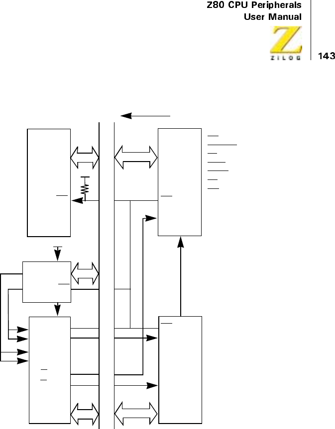
UM008101-0601 Direct Memory Access
Figure 55. DMA-SIO Environment
Using The Z80 DMA With Other Processors
The Z80 DMA offers great versatility and is a powerful alternative for
board designers. Because the DMA is designed as a member of the Z80
Family, it requires certain signals and bus characteristics, such as those of
+5V
+5V
SIO
RxCA
W/RDYA
W/RDYB
RxCB
TxCA
TxCB
CPU
DMA
DMA
INT
INT INT
IEI
RDY
IEO
IEI
RDY
S
ystem
Buses Common: A16–A0
D7–D0
CLK
INT
BUSREQ
M1
IORQ
MREQ
RD
WR
IEI
ZC/TO1
ZC/TO2
IEO
CTC INT

UM008101-0601 Direct Memory Access
the Z80 bus, to function. These functions are described in the following
sections, and design solutions are offered:
•
Bus request/release mechanisms
•
Bus characteristics
•
Interrupt request, acknowledge, and return
Bus Request/Release Mechanisms
The most fundamental characteristic that distinguishes the Z80 DMA from
other monolithic DMACs is its full control of the system bus during its
active state. Therefore, processors using the DMA must be able to give up
control of the system bus, including address, data, and the control lines
MREQ,IORQ,RD,andWR(or their equivalents). Some processors have
no mechanism for freeing the bus. Others, including the 6800, have rudi-
mentary bus control facilities, but because of their internal dynamic logic
implementations, cannot relinquish control for indefinite periods of time.
This makes them difficult to interface to the DMA.
Many popular microprocessor CPUs, however, do have adequate bus
control facilities, and some are very similar to the Z80 BUSREQ and
BUSACK signals. For instance, the 8080, 8085, and 8086 signals HOLD
and HLDA are very close approximations.
The active levels of HOLD and HLDA are positive rather than negative,
and variations exist in timing. But the use of HOLD and HLDA allows the
address and data bus drivers to be put into their high-impedance states. In
8080 systems using an 8238 to demultiplex commands, the MEMW,
MEMR,IOW,and IOR control lines can be floated using the BUSEN
input. With the 8085, a tristate decoder allows decode or disable corre-
sponding signals. The 8086 and its support chips also tristate their control
signals when HLDA is active.

UM008101-0601 Direct Memory Access
Bus Characteristics
Similar to the Z80, the 8080 and 8085 have 8-bit data paths and 16-bit
addresses. The DMA is matched well to these numbers; it can search whole
data words and directly address any byte in the memory.
The 8086 and the Z8000 CPUs have 16-bit data paths and larger address
spaces, thus making it somewhat harder to use the Z80 DMA. Searching
can be done for match bytes in either half of the data word, but not for a
whole unique word. Often this is not a problem because byte matches
suffice, for example, in detecting special ASCII characters in a data block.
The problem of larger address spaces can be resolved by using an external
segment or page register, latched to the appropriate high-order addresses
before the DMA becomes bus master, or by other schemes such as
indexing. This requires some external hardware.
To conserve pins, the 8085, 8086, Z8001, and Z8002 multiplex addresses
and data. Strobes allowing demultiplexing then become part of the bus
structure and must be accounted for in DMA interface. In such cases, the
DMA should be connected to the demultiplexed address and data lines
rather than closer to the processor. Figure 56 is a simplified diagram of
this concept.
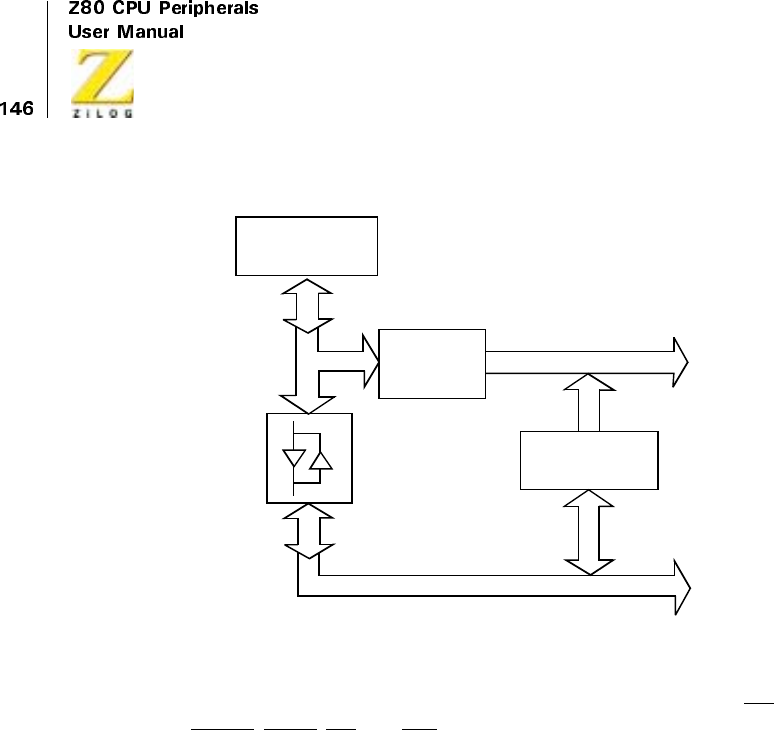
UM008101-0601 Direct Memory Access
Figure 56. Connecting DMA to Demultiplexed Address/Data Buses
Many processors encode their control signals, as does the Z80’s M1,
MREQ,IORQ,RD,andWR, into status words that are often demultiplexed
before they are distributed to memory, peripherals, and more. Link the
DMA to these demultiplexed signals and take advantage of tristate
decoders to float the outputs when the DMA is master.
The DMA’s Z80-like control signals must usually be retimed to meet the
requirements of the foreign buses. But the programmable timing feature of
the DMA may well reduce the hardware costs incurred.
Interrupt Request, Acknowledge, and Return
When using the DMA with other processors, this area is the most chal-
lenging because of the many methods of signaling, prioritizing, identifying,
responding to, and returning from interrupts.
Latched Address Bus
CPU
DMA
Buffered Bidirectional Data Bus
Multiplexed
Address
and
Data Bus
3-Stage
Latches

UM008101-0601 Direct Memory Access
Non-Z80 interrupt environments do not use the IEI and IEO signals, and
often they use separate interrupt controllers to generate vectors, and handle
acknowledgement and return in different ways, or not at all.
Interrupt request is usually easy: active levels typically are low voltage, and
there may be one or more separate interrupt request pins. Timing require-
ments for interrupt requests are varied and may including pulse widths,
latching, and more, and must be carefully examined.
Priority of simultaneous or overlapping requests is handled in several ways:
some processors (for example, the 8085) have multiple interrupt-request
pins, some use daisy-chained priority schemes (as in the Z80), and several
types of interrupt control ICs are available.
Acknowledgement and identification methods vary too. Sometimes, several
fixed memory locations correspond to different interrupt pins’ service
routines. In other cases, the interrupting device identifies itself by putting a
vector or instruction on the data bus for the CPU to read. Interrupt
controllers often provide appropriate vectors to the CPU and distinguish
between and prioritize multiple requests. The DMA has the built-in capa-
bility of supplying an arbitrary vector byte when it detects a Z80 interrupt
acknowledge (IORQ and M1 both active) and its IEI input is active (no
higher-priority device is interrupting). Often, then, gating the M1,IORQ,
and IEI pins appropriately can rule out using a separate interrupt controller.
IORQ serves another function, too, therefore it must appear during CPU-
DMA transfers and be available to signal I/O reads or writes in the active
state.
At the end of its service routine, the DMA anticipates the CPU fetching the
RETI instruction (ED, 4D present on the data bus accompanied by M1).
The DMA command RESET AND DISABLE INTERRUPTS is designed
for this purpose in non-Z80 CPU environments. Alternatively, the RETI
instructionmightbesimulatedbyre-gatingM1and programming the CPU
to write to a phantom peripheral the bytes ED, 4D. The chip select for this
nonexistent peripheral is used to simulate M1. SeeFigure57.
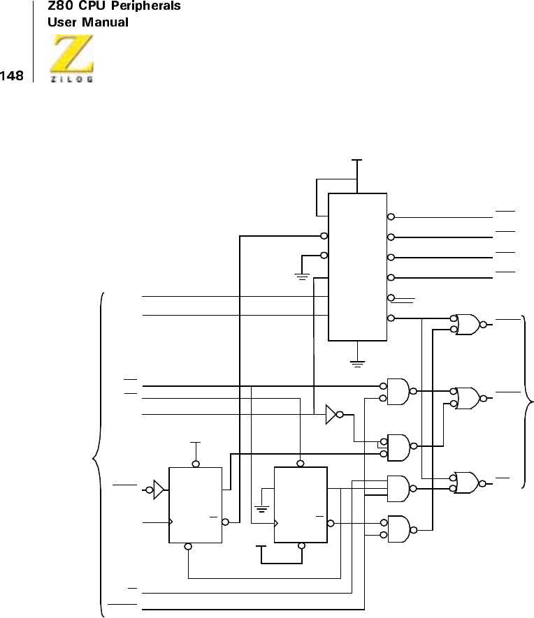
UM008101-0601 Direct Memory Access
Figure 57. Z8000/Z80 Peripheral Interface
+5V CLR
CLK
LS74
DQ
PRE
Q
LS32
LS10
LS10
LS32
LS04
Y0
Y1
Y2
Y3
Y4
Y5 RETI
G1
G2A
G2B
C
B
A
LS138
+5V
IORQ
LS06
To Z80
Peripherals
CE0
CE1
CE2
CE3
+5V
IORQ
CLOCK
R/W
VIACK (Vectored Interrupt Acknowledge from ST3-ST0)
DS
AS
LA5
LA4
LA3
From Z8000
Data Bus LS08
RD
LS06
IORQ
PRE
CLR
CLK
LS74
DQ
Q

UM008101-0601 Direct Memory Access
PERFORMANCE LIMITATIONS
Bus Contention
Using the Direct Memory Access (DMA) as bus master can negatively
effect CPU activity by preventing the CPU from fetching and executing
instructions. This method of bringing the CPU to a halt creates problems,
including:
•
No interrupt servicing (including nonmaskable CPU interrupts)
•
No refresh of dynamic memory (if performed by the CPU)
•
No polling
The CPU’s time-critical functions are affected by which operating mode
the DMA is using. These modes are Byte, Burst, and Continuous.
Byte Mode
When bus contention occurs, using Byte Mode allows interleaving of
CPU functions and DMA functions for each byte of data transferred. The
disadvantage to using this mode is slower transfer speed.
Burst Mode
Burst mode is useful when transferring data in short segments over a
longer period of time. This mode has the advantage of using the bus only
when needed. During those times, transfer speeds are maximized.
However, this mode may not be suitable for extended bursts of data (long
periods when the Ready line is active). Burst mode allows the DMA to
release the bus back to the CPU before other CPU-dependent functions
are compromised.
UM008101-0601 Direct Memory Access
Continuous Mode
Continuous Mode monopolizes the bus until the end-of-block or byte
match is reached, regardless of the state of the Ready line. While
achieving the fastest transfer speeds, this mode is employed when no
time-critical functions are dependent upon the CPU or when the data
blocks are relatively short.
Byte mode is used for most applications. When considering the use of
Burst or Continuous modes, the following must be known:
•
Maximum block length
•
Maximum DMA transfer rate (see Table 8)
•
Maximum time Ready line remains active
The DMA can be forced off the bus in either Byte or Burst mode.
Figure 58 illustrates how an external gate is used to remove the RDY-
input state from the DMA. Forcing the DMA to stop in the middle of a
transfer cannot be used when the DMA is operating in Continuous mode.
Only a power-down or normal termination with end-of-block or byte
match can make the DMA release the bus.
Figure 58. DMA Bus-Master Gate (Byte or Burst Modes Only)
Control Overhead
The CPU becomes less efficient when the DMA’s software must be
initialized or updated. As Table 15 illustrates, thirty-five control bytes are
required to initialize a fully functioning DMA. In addition, using the
Interrupt mode requires servicing by the CPU, which demands writing
additional control bytes to the DMA.
User Supplied
RDY To DMA
FORCE.OFF.BUS

UM008101-0601 Direct Memory Access
System throughput is decreased for applications requiring frequent DMA
reprogramming or extensive interrupt service of data-independent DMA
functions. It is more efficient to transfer large blocks of repetitive data.
TIMING
The CPU As Bus Master
When the CPU is the bus master, control bytes can program the Direct
Memory Access (DMA).
Writing Control Bytes
Table 13 illustrates the disabled, enabled/inactive, or enabled/stopped
states. The enabled/inactive and enabled/stopped states are equivalent. The
DMA is programmed by being addressed as an I/O peripheral in a CPU
output instruction. The DMA can be addressed in the full 64K I/O space. To
accomplish this, three lines must be simultaneously active-Low on the ris-
ing edge of the clock:
CE Chip Enable
IORQ Input/Output Request
WR Write
Figure 59 illustrates the timing required for this process. In a Z80 CPU
environment, this timing occurs automatically when the CPU and DMA are
on the same board and have no buffers, drivers, or other external gates in
series with the common CPU and DMA pins. This timing applies to the
sequential transfer, sequential transfer/search, and search-only classes of
operation. It may or may not apply to the simultaneous transfer or simulta-
neous transfer/search operations, depending on the speed of the external
devices used (see the Applications chapter).
UM008101-0601 Direct Memory Access
Figure 59. CPU-to-DMA Write Cycle Requirements
To write to the DMA control bites, the following conditions must be met:
•
The DMA’s CE line must be Low (normally done by decoding the
lower byte of the address bus).
•
The IORQ and WR lines must be Low at this time.
•
The control byte must be placed on the data bus so that it is stabilized
at a rising clock edge, which occurs one clock period after the CE,
IORQ,andWRlines have stabilized.
Reading Status Bytes
Figure 60 illustrates the timing needed for the CPU to read the DMA’s read
registers, RR6 through RR0, while the CPU is bus master. To read a regis-
ter, this condition must be met: The CE,IORQ,andRDlines must be
active and stabilized over two rising edges of the clock.
Status data becomes available on the data bus at the time of the second
clock rising edge, which remains on the bus for as long as both the CE,
IORQ,andRDlines remain active.
CLK
CE
IORQ
WR
D7–D0
UM008101-0601 Direct Memory Access
Figure 60. CPU-to-DMA Read Cycle Requirements
The DMA As Bus Master
Sequential Transfers
In sequential transfer and transfer/search operations, which both have the
same timing, data is latched onto the bus by the rising edge of the RD sig-
nal, with standard timing this is the falling edge of T3. Data is held on the
data bus across the boundary between read and write cycles, through the
end of the following write cycle. The DMA data bus drivers become active
when RD becomes inactive.
Figure 61 illustrates the timing for memory-to-I/O port transfers, and
Figure 62 illustrates I/O-to-memory transfers. Memory-to-memory and I/O
to-I/O transfer timings are simply permutations of these diagrams.
The default timing uses three clock cycles for memory transactions and
four clock cycles for I/O transactions, which include one automatically
inserted wait cycle between T2 and T3. If the CE/WAIT line is pro-
grammedtoserveasaWAITline during the DMA’s active state, it is sam-
pled on the falling edge of T2 for memory transactions and the falling edge
of TW for I/O transactions. If CE/WAIT is Low during this time, another T-
cycle is added, during which time the CE/WAIT line is again sampled. The
duration of transactions can thus be indefinitely extended.
CLK
CE
IORQ
WR
D7–D0

UM008101-0601 Direct Memory Access
Simultaneous Transfers
The timing for simultaneous transfers and simultaneous transfer/searches is
the same. The DMA is programmed in the Search-Only mode, and both
read and write cycles occur simultaneously in the time that a source-port
read would occur in search-only. Only one address is generated on the
address bus; the I/O port is hardwire-selected during this operation as
shown in the Applications chapter. The IORQ,MREQ,RD,and WR lines
are gated into two new signals by external logic. These signals are either:
MEMWR (Memory write)
IORD (I/O read)
or:
MEMRD (Memory read)
IOWR (I/O write)
UM008101-0601 Direct Memory Access
Figure 61.Sequential Memory-to-I/O Transfer, Standard Timing (Searching is Optional)
CE/WAIT
D7–D0 Memory
Drive DMA DMA Drives Data Bus
WR
IORQ
RD
MREQ
READ
WRITE
A15–A0
CLK
Memory Read I/O Write
T1T2T3T2TWT3
T1
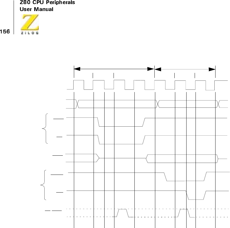
UM008101-0601 Direct Memory Access
Figure 62. Sequential I/O-to-Memory Transfer, Standard Timing
(Searching is Optional)
CE/WAIT
I/O Drives
Memory DMA Drives Data Bus
WR
IORQ
RD
MREQ
READ
WRITE
A15–A0
CLK
I/O Read Memory Write
T1T2TWT1T2T3
T3
IORQ
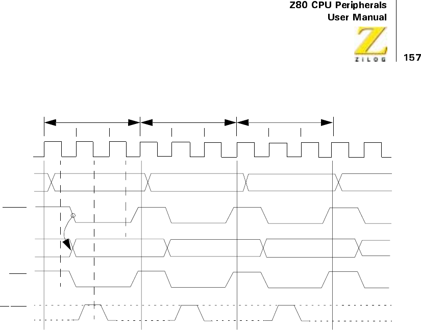
UM008101-0601 Direct Memory Access
Figure 63. Simultaneous Memory-to-I/O Transfer (Burst and Continuous
Mode)
CE/WAIT
A15–A0
CLK
T1T2T3
D7–D0
IOWR
MEMRD
C
ycle 1
C
ycle 2
C
ycle 3
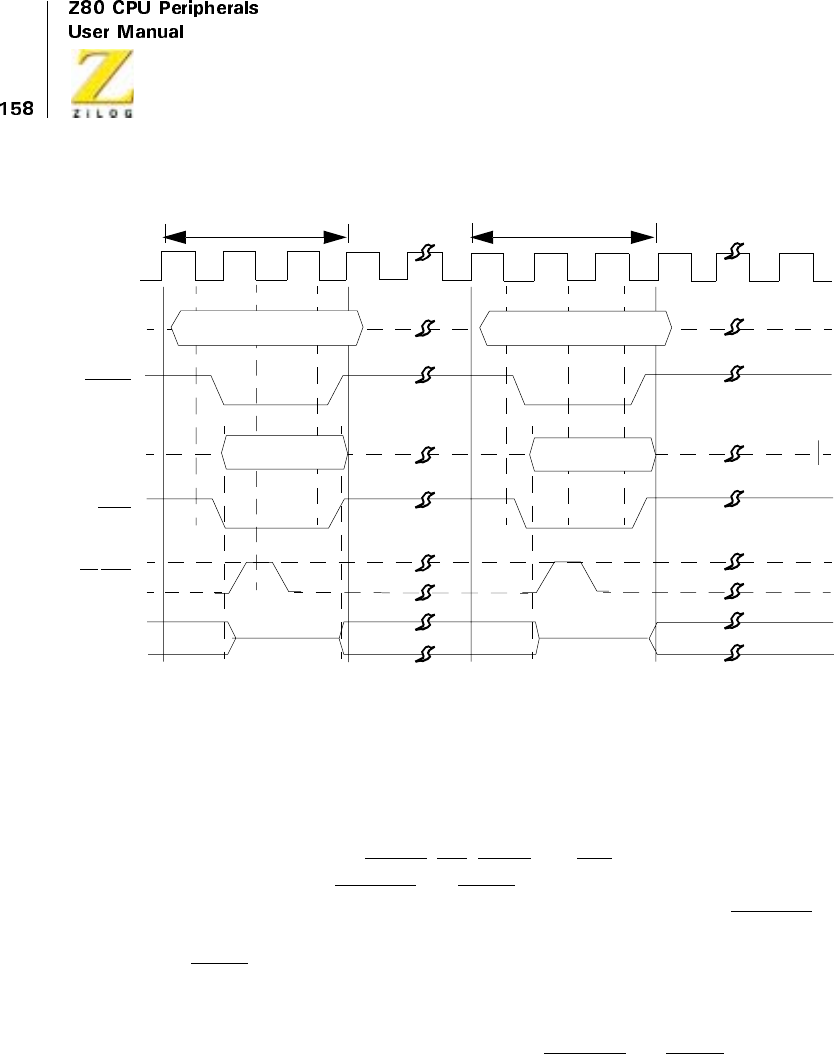
UM008101-0601 Direct Memory Access
Figure 64. Simultaneous Memory-to-I/O Transfer (Byte Mode)
Figure 63 illustrates the timing for simultaneous transfers in Burst and Con-
tinuous modes between memory and I/O, using standard Z80 timing. The
timing within each cycle is similar to the memory read cycle shown in
Figure 61. The address bus activity is the same, and the cycle length is the
same. However, the MREQ,RD,IORQ,andWRlines in Figure 61 have
been changed to MEMRD and IOWR lines in Figure 63. In addition, the
data bus becomes active earlier in Figure 63, in response to the MEMRD
line becoming active. Data is clocked to the l/O port on the rising edge of
IOWR
Figure 64 depicts the timing for Byte mode. Timing is identical to
Figure 63 within each cycle. The breaks between each cycle, where the
address and data bus are tristated and the MEMRD and IOWR lines remain
CE/WAIT
A15–A0
CLK
D7–D0
IOWR
MEMRD
C
ycle 2
DMA Drives
the Last Data
it Read During
this Time
Cycle 1

UM008101-0601 Direct Memory Access
inactive, are caused by the activity on the BUSREQ and BAI lines, which is
explained later.
Search-Only
The standard timing for search-only operations is identical to the read cycles
of Figure 61 and Figure 62. Search-only is equivalent to read-only. Data is
read to a DMA register for comparison with the match byte.
Bus Requests
Figure 65 illustrates the bus request and acceptance timing. The RDY line,
which may be programmed active High or Low, is sampled on every rising
edge of CLK.
If the RDY line is active, and if the bus is not in use by any other device, the
following rising edge of CLK drives BUSREQ Low. After receiving BUS-
REQ the CPU acknowledges on its BUSACK, which is connected to the
DMA’s BAI input either directly or through a multiple-DMA daisy-chain.
The CPU checks its BUSREQ input one clock cycle before the end of each
CPU machine cycle. If the CPU detects a request, it releases the bus at the
end of that same machine cycle. The maximum time delay between the
CPU receiving BUSREQ and the response on its BUSACK line is one
machine cycle plus slightly less than one clock cycle. The CPU tristates all
its bus control lines when it acknowledges on the BUSACK line. M1 is not
tristated.
The RDY line, which has a specified setup time with respect to a rising
edge of CLK, must remain active until after the DMA becomes bus master
in Byte or Burst modes.
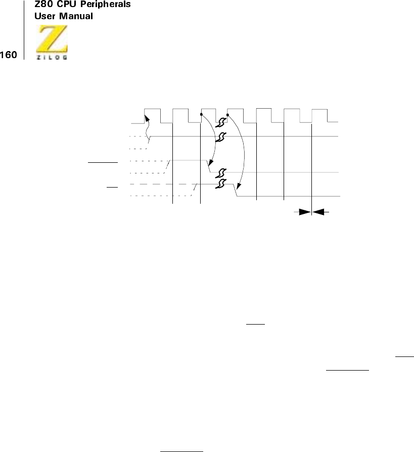
UM008101-0601 Direct Memory Access
Figure 65. Bus Request and Acceptance Timing
Continuous mode is the only instance when a pulse on RDY allows the
DMA to become bus master.In this event, the DMA becomes bus master
but does not begin operations.
When the DMA detects a Low on BAI for two consecutive rising edges of
CLK, the DMA begins transferring data on the next rising edge of CLK.
In Byte mode, after each byte is transferred, the DMA waits until its BAI
line goes inactive before requesting the bus again on BUSREQ for the next
byte transfer. This feature allows a minimum of one CPU machine cycle to
occur between each byte transferred.
Bus Release Byte-at-a-Time
In Byte mode, BUSREQ is brought High on the rising edge of CLK prior to
the end of each read cycle (search-only) or write cycle (transfer and trans-
fer/search) as illustrated in Figure 66. This action occurs regardless of the
state of RDY. There is no possibility of confusion when a Z80 CPU is used
because the CPU cannot begin an operation until the following clock cycle.
Nor does this condition affect most other CPUs. The result of timing is one-
clock-cycle less time needed for a byte transfer.
BUSREQ
RDY Active
Inactive
DMA
Inactive DMA
Active
BAI
CLK
Note: RDY is detected as a level, not an edge
UM008101-0601 Direct Memory Access
Figure 66. Bus Release in Byte Mode
The next bus request for the next byte comes after both BUSREQ and BAI
have returned High. In a Z80 environment, BAI returns High one clock
cycle after BUSREQ returns High.
Bus Release on End-of-Block.
When the DMA is programmed to stop on end-of-block in Burst or Contin-
uous modes, an end-of-block causes BUSREQ to go High (inactive) on the
same rising edge of CLK in which the DMA completes the data block
transfer (see Figure 67). The last byte in the block is transferred even if
RDY goes inactive before completion of the last byte operation.
Figure 67. Bus Release on End-of-Block (Burst and Continuous Modes)
BUSREQ
DMA Active
BAI
CLK
DMA Inactive
BUSREQ
RDY
Current Byte
Operation
DMA
Inactive
Active
Inactive
UM008101-0601 Direct Memory Access
Bus Release on Match
When the DMA is programmed to stop (release the bus) on match in Burst
or Continuous modes, a match causes BUSREQ to go inactive on the next
DMA operation, for example, at the end of the next read in search-only,
simultaneous transfer/searches, or at the end of the following write in
sequential transfer or transfer/searches (Figure 68).
Figure 68. Bus Release on Match (Burst and Continuous Modes)
Because of the pipelining scheme, matches are determined while the next
DMA read or write is being performed. Table 12 lists the number of bytes
transferred in any class or mode.
The RDY line can go inactive after the matching operation begins without
affecting this bus-release timing. However, the time at which RDY goes
inactive can affect the number of bytes transferred, as described in Table 11
and Figure 32.
Bus Release on Not Ready
Burst mode, when RDY goes inactive, causes BUSREQ to go High on the
next rising edge of CLK after the completion of its current byte operation,
for example, at the end of the current read in search-only, simultaneous
transfer/search, or at the end of the following write in sequential transfer/
BUSREQ
RDY
Byte n DMA
Inactive
Read in
Byte n+1
and
on Byte n
Read in
Match Found
Active
Inactive
CLK
UM008101-0601 Direct Memory Access
search (Figure 69). The action on BUSREQ is thus somewhat delayed from
action on the RDY line. The DMA always completes the current byte oper-
ation in an orderly fashion before releasing the bus.
Figure 69. Bus Release on Not Ready (Burst Mode)
By contrast, BUSREQ is not released in Continuous mode when RDY goes
inactive. Instead, the DMA idles after completing the current byte opera-
tion, awaiting an active RDY again.
Figure 70, Figure 71, and Figure 72 review the relationship between the
Ready line going inactive and the state of the other lines for each mode of
operation, assuming a search-only of memory using standard Z80 timing.
The timing for Ready coming active is discussed under Bus Request. RDY
is sampled on the rising edge of CLK in the last clock cycle of each read or
write cycle. It is a level-sample, not an edge-sample. RDY can go inactive
prior to the completion of the last byte operation without disturbing that
operation. At the end of that operation, the BUSREQ and BAI lines go
High in Byte or Burst mode according to Figure 68 and Figure 71. The bus
control lines MREQ,IORQ,RD,andWR,also remain High in Byte and
Burst mode during an inactive RDY, with both the address and data buses
tristated.
The Continuous mode (Figure 72) is different because the address bus
holds the pre incremented address for the next byte throughout the time
that RDY is inactive. This address is immediately available when RDY
comes active again.
BUSREQ
RDY
DMA
Inactive
Active
Inactive
CLK
Current Byte
Operation
UM008101-0601 Direct Memory Access
Figure 70. RDY Line in Byte Mode
A15–A0
D7–D0
RD
MREQ
BUSREQ
BAI
RDY
A
ct
i
ve
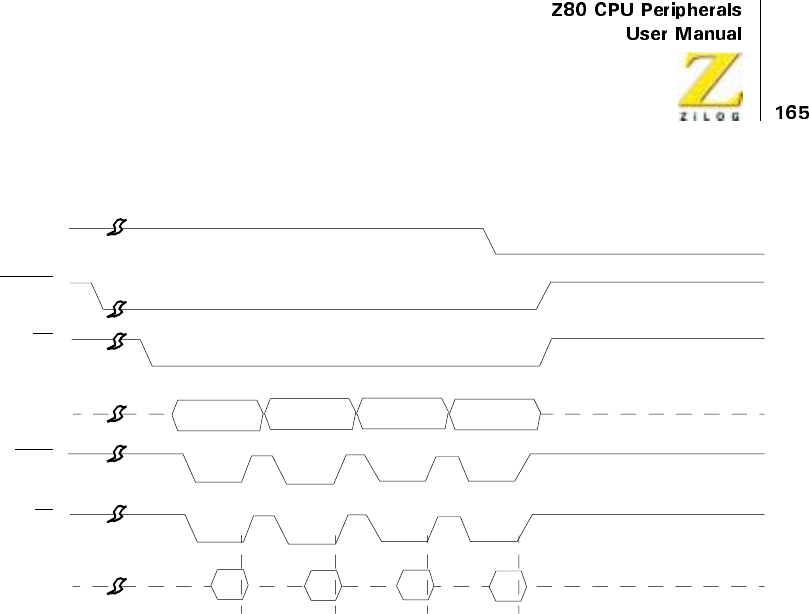
UM008101-0601 Direct Memory Access
Figure 71. RDY Line in Burst Mode
A15–A0
D7–D0
RD
MREQ
BUSREQ
BAI
RDY
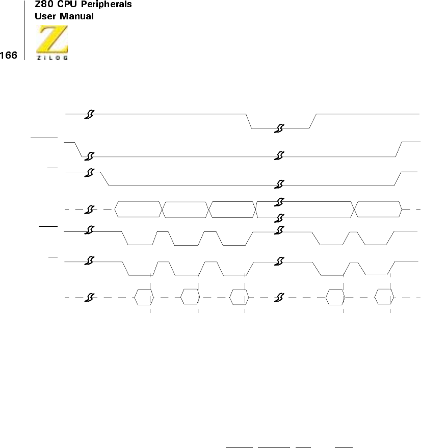
UM008101-0601 Direct Memory Access
Figure 72. RDY Line in Continuous Mode
Variable Cycle and Edge Timing
The Z80 DMA’s operation-cycle length, without Wait states for the source
(read) port and destination (write) port, can be independently programmed.
This variable-cycle feature allows read or write cycles consisting of two,
three, or four clock cycles, more if Wait cycles are inserted, increasing or
decreasing the pulse widths of all signals generated by the DMA. In addi-
tion, the trailing edges of the IORQ,MREQ,RD,andWRsignals can be
independently terminated one-half cycle early. See Figure 73 .
A15–A0
D7–D0
RD
MREQ
BUSREQ
BAI
RDY
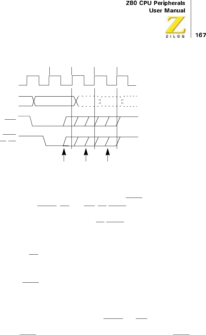
UM008101-0601 Direct Memory Access
Figure 73. Variable-Cycle and Edge Timing
In the Variable-Cycle mode, unlike default tuning, IORQ comes active one-
half cycle before MREQ,RD,andWR.CE/WAIT can be used to extend
only the 3 or 4 clock cycle variable memory cycles and only the 4-cycle
variable I/O cycle (see Figure 75). The CE/WAIT line is sampled at the
falling edge of T2 for 3- or 4-cycle memory operations, and at the falling
edge of T3 for 4-cycle I/O operations. The line is not sampled for 2-cycle
operations. During transfers, data is latched on the clock edge, causing the
rising edge of RD and held until the end of the write cycle.
Using variable timing on an I/O-search, a simultaneous transfer, or transfer/
search with I/O as the source port, creates a unique situation. In these appli-
cations, the IORQ line must be programmed to end early. See “Write Regis-
ter 1 Group” on page 96. The simultaneous transfers are programmed in the
DMA as searches and are only distinguished from searches by the way
external logic handles the bus control signals.
Figure 72 illustrates the bus control lines (MREQ and RD) remaining inac-
tive when the RDY line goes inactive in Continuous mode. The same is not
true of the IORQ line when variable timing is used. In this instance, IORQ
CLK
IORQ
A15–A0
T1T2T3T4
MREQ
RD,WR
2-Cycle
Early End 3-Cycle
Early End 4-Cycle
Early End
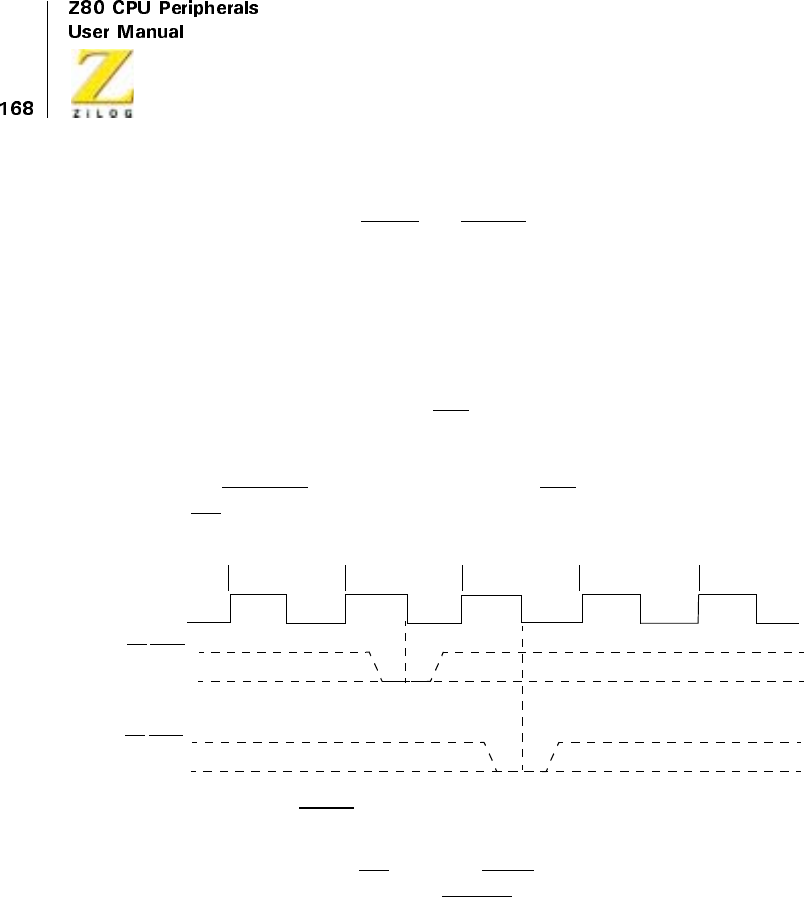
UM008101-0601 Direct Memory Access
and any functions created from it by external logic in simultaneous transfer
operations (such as IOWR and IORD), remain active during an inactive
RDY line before stopping on end-of-block or byte match.
Interrupts
Timings for interrupt acknowledge and return from interrupt are the same
as timings for these in other Z80 peripherals. Figure 74 illustrates this
timing. The interrupt signal INT issampledbytheCPUontherisingedge
of the final clock cycle of any instruction. The signal is not accepted if the
internal CPU software-controlled interrupt-enable flip-flop is not set or if
the BUSREQ signal is active. When the INT signal is accepted, a special
M1 cycle is generated.
Figure 74. WAIT Line Sampling in Variable-Cycle Timing
During this special M1 cycle, the IORQ signal becomes simultaneously
active (instead of the normal MREQ), indicating that the interrupting
device can place its 8-bit vector on the data bus. Two wait states are auto-
matically added to this cycle. These states are added so that a ripple-priority
interrupt scheme can be easily implemented. The two wait states allow time
for the ripple signals to stabilize and identify what I/O device must respond.
Refer to the Z80 CPU User’s Manual for more details.
CLK
T1T2T3T4
CE/WAIT
(4-Cycle I/O
Operations)
CE/WAIT
(3-Cycle and
4-Cycle Memory
Operations)
UM008101-0601 Direct Memory Access
Interrupt on RDY (interrupt before requesting the bus) does not directly
affect the BUSREQ line. Instead, the interrupt service routine may handle
this by issuing the following commands to WR6:
•
Enable after Return From Interrupt (RETI) Command — B7H
•
An RETI instruction that resets the Interrupt Under Service (IUS)
latch in the Z80 DMA — EDH, 4DH.
Pulse Generation
When the pulse generation option is selected, the INT line is driven Low
every 256 bytes after the offset value. The line goes Low during the DMA
cycle in which the pulse-control byte matches the lower byte of the byte
counter, and it remains Low for one complete transfer cycle. A transfer
cycle is defined as either a read cycle (search-only or simultaneous transfer
operations) or a read plus a write cycle, where read and write cycles can be
independently programmed for length through the variable-cycle option.
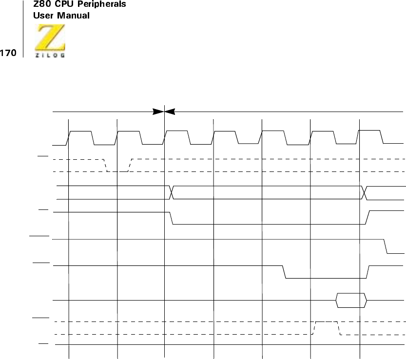
UM008101-0601 Direct Memory Access
Figure 75. Interrupt Acknowledge
A7–A0
RD
WAIT
CLOCK
IN
INT
DATA
BUS
M1
IORQ
MREQ
PC
Last M
C
ycle
of Instruction
T1
Last T State
M1
Refresh
T2TWT3
TW
UM008101-0601 Direct Memory Access
REGISTER BIT FUNCTIONS
Write Register Bit Functions
Figure 76. Write Register 0 Group
Figure 77. Write Register 1 Group
D7 D6 D5 D4 D3 D2 D1 D0
Base Register Byte
Port A Starting Address
00
0
1
1
1
0
1
Do not use
=Transfer
=Search
= Search/Transfer
0=PortB→Port A
0=PortA→Port B
(Low Byte)
Port A Starting Address
(High Byte)
Block Length
(Low Byte)
Block Length
(High Byte)
D7 D6 D5 D4 D3 D2 D1 D0
Base Register Byte
00
0
1
1
1
0
1
= Port A Address Decrements
0= Port A is Memory
0= Port A is I/O
Port A Variable
00
0
1
1
1
0
1
= Cycle Length = 3
= Cycle Length = 2
=DoNotUse
= Port A Address Increments
= Port A Address Fixed
Timing Byte
= Cycle Length = 4
WR Ends 1/2 Cycle Early = 0
RD Ends 1/2 Cycle Early = 0
MREQ Ends 1/2 Cycle Early = 0 0 = IORQ Ends 1/2 Cycle Early
00
0010
UM008101-0601 Direct Memory Access
Figure 78. Write Register 2 Group
Figure 79. Write Register 3 Group
D7 D6 D5 D4 D3 D2 D1 D0
Base Register Byte
00
0
1
1
1
0
1
= Port B Address Decrements
0= Port B is Memory
1= Port B is I/O
Port B Variable
00
0
1
1
1
0
1
= Cycle Length = 3
= Cycle Length = 2
=DoNotUse
= Port B Address Increments
= Port B Address Fixed
Timing Byte
= Cycle Length = 4
WR Ends 1/2 Cycle Early = 0
RD Ends 1/2 Cycle Early = 0
MREQ Ends 1/2 Cycle Early = 0 0=IORQEnds 1/2 Cycle Early
0000
D7 D6 D5 D4 D3 D2 D1 D0
Base Register Byte
Mask Byte (0 = Compare)
000
DMA Enable = 1
Interrupt Enable = 1
1=StoponMatch
Match Byte
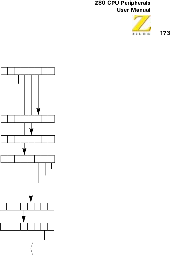
UM008101-0601 Direct Memory Access
Figure 80. Write Register 4 Group
D7 D6 D5 D4 D3 D2 D1 D0
Base Register Byte
0
0
0
0= Interrupt on End-of-Block
= Interrupt on Match and
= Interrupt on RDY
011
Port B Starting Address
Pulse Control Byte
Interrupt on RDY = 1
Status Affects Vector = 1 1=PulseGenerated
Interrupt Vector
End-of-Block
0
0
0
0
Modified as
Shown only if
‘Status Affects Vector’
Vector is Automatically
Bit is Set
1 = Interrupted at End-of-Block
1 = Interrupted on Match
0Interrupt Control Byte
(High Byte)
Port B Starting Address
(Low Byte)
0
1
0
1
0
0
1
1
Continuous =
Burst =
Do Not Program =
Byte =
= Interrupt on Match
UM008101-0601 Direct Memory Access
Figure 81. Write Register 5 Group
Figure 82. Write Register 6 Group
D7 D6 D5 D4 D3 D2 D1 D0
Base Register Byte
0= Ready Active Low
1= Ready Active High
10010
0=StoponEnd-of-Block
1= Auto Restart on End-of-Block
0=CEOnly
1=CE
/WAIT Multiplexed
D7 D6 D5 D4 D3 D2 D1 D0
Base Register Byte
01
111
=C3=Reset
000
Hex Command Name
01 =C7=ResetPortATiming
001
01 =C8=ResetPortBTiming
010
01 = CF = Load
011
01 = D3 = Continue
100
10 = AF = Disable Interrupts
011
10 = AB = Enable Interrupts
010
10 = A3 = Reset and Disable Interrupts
000
10 = B7 = Enable after RETI
101
10 = BF = Read Status Byte
111
00 = 8B = Reinitialize Status Byte
010
10 = A7 = Initialize Read Sequence
001
10 =B3=ForceReady
100
00 = 87 = Enable DMA
001
00 =83=DisableDMA
000
10 = BB = Read Mask Follows
110
Base Register Byte
Status Byte
Byte Counter (Low Byte)
Byte Counter (High Byte)
Port A Address (Low Byte)
Port B Address (High Byte)
0
Port B Address (Low Byte)
Port A Address (High Byte)
UM008101-0601 Direct Memory Access
Read Register Bit Functions
Figure 83. Read Register 0 through 6 Bit Functions
D7 D6 D5 D4 D3 D2 D1 D0
Status ByteXX
1 = DMA Operation has Occurred
0 = Ready Active
0 = Interrupt Pending
0 = Match Found
0 = End-of-Block
Byte Counter (Low Byte)
Read Register 1
Byte Counter (High Byte)
Read Register 2
Port A Address Counter (Low Byte)
Read Register 3
Port A Address Counter (High Byte)
Read Register 4
Port B Address Counter (Low Byte)
Read Register 5
Port B Address Counter (High Byte)
Read Register 6

UM008101-0601 Direct Memory Access

UM008101-0601 Parallel Input/Output
Parallel Input/Output
OVERVIEW
The Z80 Parallel Input/Output (PIO) Circuit is a programmable, two-port
device that provides a TTL-compatible interface between peripheral
devices and the Z80 CPU. The CPU configures the Z80 PIO to interface
with a wide range of peripheral devices with no other external logic
required. Typical peripheral devices that are fully compatible with the Z80
PIO include most keyboards, paper tape readers and punches, printers, and
PROM programmers. The Z80 PIO package is available in 40-pin DIP, 44-
pin PLCC, or 44-pin QFP. The CMOS version is available in all three pack-
age configurations. The NMOS version is available in 40-pin DIP and 44-
pin PLCC.
One unique feature that separates the Z80 PIO from other interface control-
lers is that all data transfers between the peripheral device and the CPU is
under total interrupt control. The PIO interrupt logic allows full use of the
efficient interrupt capabilities of the Z80 CPU during I/O transfers. All
logic necessary to implement a fully nested interrupt structure is included in
the PIO, requiring no additional circuits. Another unique feature is that the
PIO can be programmed to interrupt the CPU on the occurrence of speci-
fied status conditions in the peripheral device. For example, the PIO can be
programmed to interrupt when any specified peripheral alarm conditions
occur. This interrupt capability reduces the amount of time spent by the pro-
cessor polling peripheral status.
FEATURES
•
Two independent 8-Bit bidirectional peripheral interface ports with
handshake data transfer control
•
Interrupt-driven handshake for fast response

UM008101-0601 Parallel Input/Output
•
Four modes of port operation with interrupt-controlled handshake:
– Byte Output
– Byte Input
– Byte Bidirectional Bus (available on Port A only)
– Bit Control Mode
•
Daisy-chain priority interrupt logic, allowing automatic interrupt
vectoring without external logic
•
Eight outputs capable of driving darlington transistors
•
Fully TTL-compatible inputs and outputs
•
Single 5V supply and single-phase clock required
PIO ARCHITECTURE
Overview
Figure 1 illustrates ablock diagram of the Z80 PIO. The internal structure of
the Z80 PIO consists of a Z80 CPU bus interface, internal control logic,
Port A I/O logic, Port B I/O logic, and interrupt control logic. The CPU bus
interface logic allows the PIO to interface directly to the Z80 CPU with no
other external logic. However, address decoders and/or line buffers may be
required for large systems. The internal control logic synchronizes the CPU
data bus to the peripheral device interfaces (Port A and Port B). The two
I/O ports (A and B) are virtually identical and are used to interface directly
to peripheral devices.
Figure 2 depicts the Port I/O logic is composed of 6 registers with hand-
shake control logic. The registers include: an 8-bit data input register, an
8-bit data output register, a 2-bit mode control register, an 8-bit mask
register, an 8-bit input/output select register, and a 2-bit mask control
register.
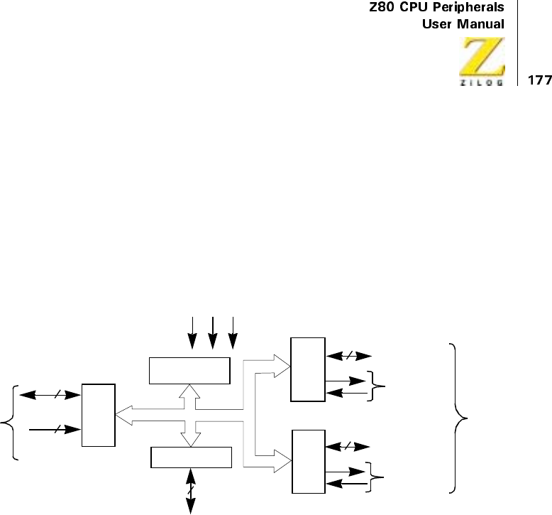
UM008101-0601 Parallel Input/Output
The 2-bit mode control register is loaded by the CPU to select the desired
operating mode (byte output, byte input, byte bidirectional bus, or bit
control mode). All data transfer between the peripheral device and the
CPU is achieved through the data input and data output registers. Data
may be written into the output register by the CPU or read back to the
CPU from the input register at any time. The handshake lines associated
with each port are used to control the data transfer between the PIO and
the peripheral device.
Figure 1. PIO Block Diagram
+5V GND Φ
CPU
Interface
8
6
Data Bus
PIO Control
Lines
Internal Bus
Interrupt Control Lines
Internal Control
Interrupt Control Data or Control
Handshake
8
8Data or Control
Handshake
Peripheral
Interface
Port
A
I/O
Port
B
I/O
3
Logic
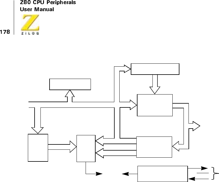
UM008101-0601 Parallel Input/Output
Figure 2. Port I/O Block Diagram
Use the 8-bit mask register and the 8-bit input/output select register only
in the Bit Control mode. In this mode, any of the eight peripheral data or
control bus pins can be programmed to be an input or an output as speci-
fied by the select register. The mask register is used in this mode in
conjunction with a special interrupt feature. This feature allows an inter-
rupt to be generated when any or all of the unmasked pins reach a speci-
fied state (either High or Low).
The 2-bit mask control register specifies the active state desired (High or
Low) and if the interrupt should be generated when all unmasked pins are
active (AND condition) or when any unmasked pin is active (OR condi-
tion). This feature reduces the requirement for CPU status checking of the
peripheral by allowing an interrupt to be automatically generated on
specific peripheral status conditions. For example, in a system with three
alarm conditions, an interrupt may be generated if any one occurs or if all
three occur.
Handshake
Lines
Ready
Strobe
Interrupt
Requests
Mask
Control
(2 Bits)
Reg
Data Output Reg
Mode Control Reg
(2 Bits) Output Enable
8-Bit Peripheral Data
Internal Bus
Input Data
Handshake Control Logic
(2 Bits)
Input/Output Select Reg
(8 Bits)
or Control Bus
(8 Bits)
Data Input
(8 Bits)
Mask
Reg
(8 Bits)

UM008101-0601 Parallel Input/Output
The interrupt control logic section handles all CPU interrupt protocol for
nested priority interrupt structures. The priority of any device is determined
by its physical location in a daisy-chain configuration. Two lines are
provided in each PIO to form this daisy-chain. The device closest to the
CPU has the highest priority. Within a PIO, Port A interrupts have higher
priority than those of Port B. In the byte input, byte output or bidirectional
modes, an interrupt can be generated whenever a new byte transfer is
requested by the peripheral. In the bit control mode an interrupt can be
generated when the peripheral status matches a programmed value. The
PIO provides for complete control of nested interrupts. That is, lower
priority devices may not interrupt higher priority devices that have not had
their interrupt service routine completed by the CPU. Higher priority
devices may interrupt the servicing of lower priority devices.
When an interrupt is accepted by the CPU in Mode 2, the interrupting
device must provide an 8-bit interrupt vector for the CPU. This vector is
used to form a pointer to a location in the computer memory where the
address of the interrupt service routine is located. The 8-bit vector from the
interrupting device forms the least-significant eight bits of the indirect
pointer while the I Register in the CPU provides the most-significant eight
bits of the pointer. Each port (A and B) has an independent interrupt vector.
The least-significant bit of the vector is automatically set to a 0 within the
PIO because the pointer must point to two adjacent memory locations for a
complete 16-bit address.
The PIO decodes the RETI (Return from interrupt) instruction directly from
the CPU data bus so that each PIO in the system knows at all times whether
it is being serviced by the CPU interrupt service routine without any other
communication with the CPU.

UM008101-0601 Parallel Input/Output
PIN DESCRIPTION
Figure 3 illustrates a diagram of the Z80 PIO pin configuration. This
section describes the function of each pin.
D7-D0
Z80 CPU Data Bus (bidirectional, tristate). This bus is used to transfer all
data and commands between the Z80 CPU and the Z80 PIO. D0 is the
least-significant bit of the bus.
B/A Sel
Port B or A Select (input, active High). This pin defines which port is
accessed during a data transfer between the Z80 CPU and the Z80 PIO. A
Low level on this pin selects Port A while a High level selects Port B.
Often, Address bit A0 from the CPU is used for this selection function.
C/D Sel
Control or Data Select (input, active High). This pin defines the type of
data transfer to be performed between the CPU and the PIO. A High level
on this pin during a CPU write to the PIO causes the Z80 data bus to be
interpreted as a command for the port selected by the B/A Select line. A
LowlevelonthispinmeansthattheZ80databusisbeingusedtotransfer
data between the CPU and the PIO. Often, Address bit Al from the CPU is
used for this function.
CE
Chip Enable (input, active Low). A Low level on this pin enables the PIO to
accept command or data inputs from the CPU during a write cycle or to
transmit data to the CPU during a read cycle. This signal is generally a decode
of four I/O port numbers that encompass Ports A and B, data, and control.

UM008101-0601 Parallel Input/Output
Φ
System Clock (input). The Z80 PIO uses the standard Z80 system clock to
synchronize certain signals internally. This is a single phase clock.
M1
Machine Cycle One Signal from CPU (input, active Low). This signal
from the CPU is used as a sync pulse to control several internal PIO opera-
tions. When M1 is active and the RD signal is active, the Z80 CPU is
fetching an instruction from memory. Conversely, when M1 is active and
IORQ is active, the CPU is acknowledging an interrupt. In addition, the M1
signal has two other functions within the Z80 PIO.
1. M1 synchronizes the PIO interrupt logic.
2. When M1 occurs without an active RD or IORQ signal, the PIO logic
enters a reset state.
IORQ
Input/Output Request from Z80 CPU (input,activeLow).TheIORQ
signal is used in conjunction with the B/ A Select, C/D Select, CE,and
RD signals to transfer commands and data between the Z80 CPU and the
Z80PIO.WhenCE,RD,andIORQare active, the port addressed by B/A
transfers data to the CPU (a read operation). Conversely, when CE and
IORQ areactivebutRDis not active, then the port addressed by B/A is
written to from the CPU with either data or control information as speci-
fied by the C/D Select signal. Also, if IORQ and M1 are active simulta-
neously, the CPU is acknowledging an interrupt and the interrupting port
automatically places its interrupt vector on the CPU data bus if it is the
highest priority device requesting an interrupt.
RD
Read Cycle Status from the Z80 CPU (input, active Low). If RD is active,
a MEMORY READ or I/O READ operation is in progress. The RD signal
is used with B/A Select, C/D Select, CE,andIORQsignals to transfer data
from the Z80 PIO to the Z80 CPU.

UM008101-0601 Parallel Input/Output
IEI
Interrupt Enable In (input, active High). This signal is used to form a
priority interrupt daisy-chain when more than one interrupt driven device is
being used. A high level on this pin indicates that no other devices of higher
priority are being serviced by a CPU interrupt service routine.
IEO
Interrupt Enable Out (output, active High). The IEO signal is the other
signal required to form a daisy-chain priority scheme. It is High only if IEI
is High and the CPU is not servicing an interrupt from this PIO. Thus, this
signal blocks lower priority devices from interrupting while a higher
priority device is being serviced by its CPU interrupt service routine.
INT
Interrupt Request (output, open-drain, active Low). When INT is active,
the Z80 PIO is requesting an interrupt from the Z80 CPU.
A7-A0
Port A Bus (bidirectional, tristate). This 8-bit bus is used to transfer data
and/or status or control information between Port A of the Z80 PIO and a
peripheral device. A0 is the least-significant bit of the Port A data bus.
ASTB
Port A Strobe Pulse from Peripheral Device (input, active Low). The
meaning of this signal depends on the mode of operation selected for Port A
as follows:
1. Output mode: The positive edge of this strobe is issued by the peripheral
to acknowledge the receipt of data made available by the PIO.
2. Input mode: The strobe is issued by the peripheral to load data from
the peripheral into the Port A input register. Data is loaded into the
PIO when this signal is active.

UM008101-0601 Parallel Input/Output
3. Bidirectional mode: When this signal is active, data from the Port A
output register is gated onto Port A bidirectional data bus. The
positive edge of the strobe acknowledges the receipt of the data.
4. Control mode: The strobe is inhibited internally.
ARDY
Register A Ready (output, active High). The meaning of this signal depends
on the mode of operation selected for Port A as follows:
1. Output mode: This signal goes active to indicate that the Port A
output register has been loaded and the peripheral data bus is stable
and ready for transfer to the peripheral device.
2. Input mode: This signal is active when the Port A input register is
empty and is ready to accept data from the peripheral device.
3. Bidirectional mode: This signal is active when data is available in the
Port A output register for transfer to the peripheral device. In this
mode, data is not placed on the Port A data bus unless ASTB is active.
4. Control mode: This signal is disabled and forced to a Low state.
B7-B0
Port B Bus (bidirectional, tristate). This 8-bit bus is used to transfer data
and/or status or control information between Port B of the PIO and a
peripheral device. The Port B data bus is capable of supplying 1.5 mA @
1.5V to drive Darlington transistors. B0 is the least significant bit of the bus.
BSTB
Port B Strobe Pulse from Peripheral Device (input, active Low). The
meaning of this signal is similar to that of ASTB with the following
exception: In the Port A bidirectional mode, this signal strobes data from
the peripheral device into the Port A input register.
UM008101-0601 Parallel Input/Output
BRDY
Register B Ready (output, active High). The meaning of this signal is
similartothatofAReadywiththefollowingexception:InthePortAbidi-
rectional mode, this signal is High when the Port A input register is empty
and ready to accept data from the peripheral device.
Figure 3. PIO Pin Functions
Z80–PIO
Port A
I/O
A0
A1
A2
A3
A4
A5
A6
A7
ARDY
ASTB
B0
B1
B2
B3
B4
B5
B7
BRDY
BSTB
B6
15
14
13
12
10
9
8
7
18
16
31
32
33
34
21
17
27
28
29
30 Port B
I/O
CPU
Data
D0
D1
A2
D3
D4
D5
D6
D7
Port B/A SEL
Control/Data SEL
Chip Enable
M1
IORQ
RD
+5V
Φ
INT
GND
19
20
1
40
39
38
3
2
6
5
26
11
25
23
4
37
36
35
INT Enable in 24
INT Enable out 22
BUS
PIO
Control
Interrupt
Control
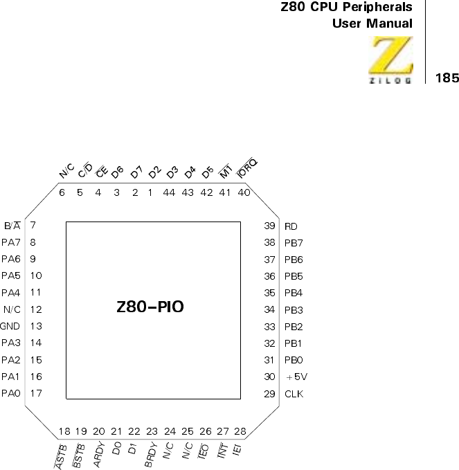
UM008101-0601 Parallel Input/Output
Figure 4. 44-Pin PLCC Pin Assignments
UM008101-0601 Parallel Input/Output
Figure 5. 44-Pin QFP Pin Assignments
34
33
N/C
CS1
CLK/TRG3
CLK/TRG2
N/C
N/C
CLK/TRG1
CLK/TRG0
N/C
+5V
N/C
IEO
IORQ
N/C
ZC/TO2
ZC/TO1
N/C
ZC/TO0
N/C
RD
GND
D7
CS0
RESET
CE
N/C
CLK
N/C
M1
N/C
IEI
N/C
INT
D0
D1
D2
D3
N/C
N/C
N/C
D4
D5
D6
N/C
44
22
12
11
1
CMOS
Z80 PIO
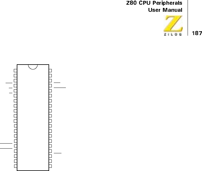
UM008101-0601 Parallel Input/Output
Figure 6. 40-Pin DIP Pin Assignments
PROGRAMMING THE PIO
Reset
The Z80 PIO automatically enters a reset state when power is applied. The
reset state performs the following functions:
1. Both port mask registers are reset to inhibit all port data bits.
2. Port data bus lines are set to a high-impedance state and the Ready
handshake signals are inactive (Low). Mode 1 is automatically selected.
3. The vector address registers are not reset.
4. Both port interrupt enable flip-flops are reset.
5. Both port output registers are reset.
1
2
3
4
5
6
7
8
9
10
11
12
13
14
15
16
17
18
19
20
40
39
38
37
36
35
34
33
32
31
30
29
28
27
26
25
24
23
22
21
Z80
PIO
D2
D7
D6
CE
C/D
B/A
PA7
PA6
PA5
PA4
GND
PA3
PA2
PA1
PA0
ASTB
BSTB
ARDY
D0
D1
D3
D4
D5
M1
IORQ
RD
PB7
PB6
PB5
PB4
PB3
PB2
PB1
PB0
+5V
CLK
IEI
INT
IEO
BRDY
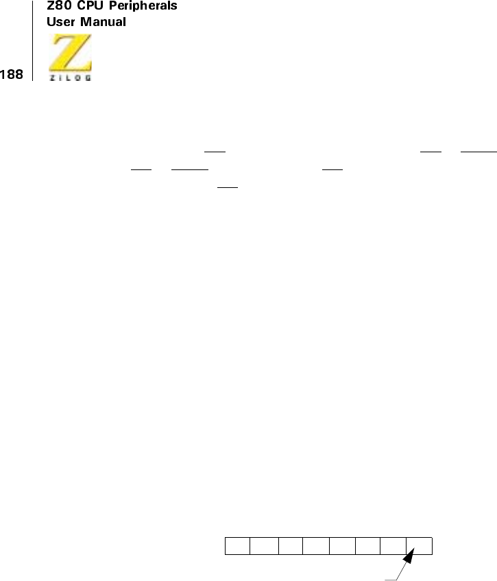
UM008101-0601 Parallel Input/Output
In addition to the automatic power-on reset, the PIO can be reset by
applying an M1 signal without the presence of a RD or IORQ signal. If no
RD or IORQ is detected during M1, the PIO enters the reset state immedi-
ately after the M1 signal goes inactive. This reset allows a single external
gate to generate a reset without a power-down sequence. The 40-pin pack-
aging requires this routine.
When the PIO enters the internal reset state, it is held there until the PIO
receives a control word from the CPU.
Loading The Interrupt Vector
The PIO is designed to operate with the Z80 CPU using the Mode 2 inter-
rupt response. This mode requires that an interrupt vector be supplied by
the interrupting device. This vector is used by the CPU to form the address
for the interrupt service routine of that port. This vector is placed on the
Z80 data bus during an interrupt acknowledge cycle by the highest priority
device requesting service at that time. (Refer to the Z80 CPU User’s
Manual Section for details on how an interrupt is serviced by the CPU).
The interrupt vector is loaded to the PIO by writing a control word to the
appropriate PIO port using the following format:
D0 functions as a flag bit, which when Low, loads V7 through V1 to the
vector register. At interrupt acknowledge, the vector of the interrupting port
appears on the Z80 data bus exactly as illustrated in the diagram above.
Signifies this Control Word
is an Interrupt Vector
V7 V6 V5 V4
D7 D6 D5 D4 D3 D0D2 D1
V3 V2 V1 0
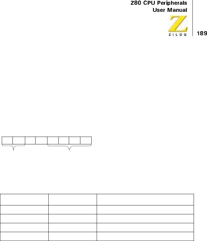
UM008101-0601 Parallel Input/Output
SelectingAnOperatingMode
PIO Port A allows operation in four modes: Mode 0 (output mode), Mode 1
(input mode), Mode 2 (bidirectional mode), and Mode 3 (control mode).
The mode numbers are assigned for mnemonic significance: 0 = Out,
1 = In, 2 = Bidirectional. Port B cannot operate in Mode 2.
The mode of operation must be established by writing a control word to the
PIO in the following format:
Listed in Table 1, Bits D7 and D6 form the binary code that designate mode
of operation:
Bits D5 and D4 are ignored. Bits D3-D0 must be set to 1111 to indicate
Set Mode.
Selecting Mode 0 enables any data written to the port output register by
the CPU to be enabled onto the port data bus. The output register contents
may be changed by writing a new data word to the port. Also, the current
contents of the output register may be read back to the Z80 CPU by
executing an input instruction.
When Mode 0 is active, a data write from the CPU causes the port’s
Ready handshake line to go High, thereby notifying the peripheral that
Table 1. PIO Mode Selection
D7 D6 Mode
0 0 0 (output)
0 1 1 (input)
1 0 2 (bidirectional)
113(control)
Mode Word
M1 M0 X X
Signifies Mode Word to be Set
D7 D6 D5 D4 D3 D0D2 D1
11 11

UM008101-0601 Parallel Input/Output
data is available. This signal remains High until a strobe is received from
the peripheral. The rising edge of the strobe generates an interrupt (if it
has been enabled) and causes the Ready line to go inactive. This hand-
shakeissimilartothoseusedbymanyperipheraldevices.
By selecting Mode 1, the port enters input mode. To initiate a handshake,
the CPU performs an input read from the port. This activates the Ready
line, which signals the peripheral that data can be loaded to the empty input
register. The peripheral device then strobes data to the port input register
through the strobe line. Again, the rising edge of the strobe causes an inter-
rupt request (if it has been enabled) and deactivates the Ready signal. Data
may be strobed to the input register regardless of the state of the Ready
signal if care is taken to prevent a data overrun condition.
Mode 2 is a bidirectional data transfer mode, utilizing all four handshake
lines. Therefore, only Port A is used for Mode 2 operation. Mode 2 opera-
tion uses the Port A handshake signals for output control, and uses the Port
B handshake signals for input control. Thus, both ARDY and BRDY may
be active simultaneously. The only operational difference between Mode 0
and the output portion of Mode 2 is: Data from the Port A output register is
allowed on the port data bus when ASTB is active. Bidirectional capability
is achieved only when ASTB is active.
Mode 3 operation is used for status and control applications and does not
utilize the handshake signals. When Mode 3 is selected, the next control
word sent to the PIO must define which port data bus lines are inputs and
which are outputs. The format of the control word is depicted below:
If any bit is set to a one, then the corresponding data bus line is used as an
input. Conversely, if the bit is reset, the line is used as an output.
During Mode 3 operation, the strobe signal is ignored and the Ready line is
held Low. Data may be written to a port or read from a port by the Z80 CPU
at any time during Mode 3 operation. The data returned from a port to the
I/O7 I/O6 I/O5 I/O4 I/O3 I/O2 I/O1 I/O0
D7 D6 D5 D4 D3 D0D2 D1
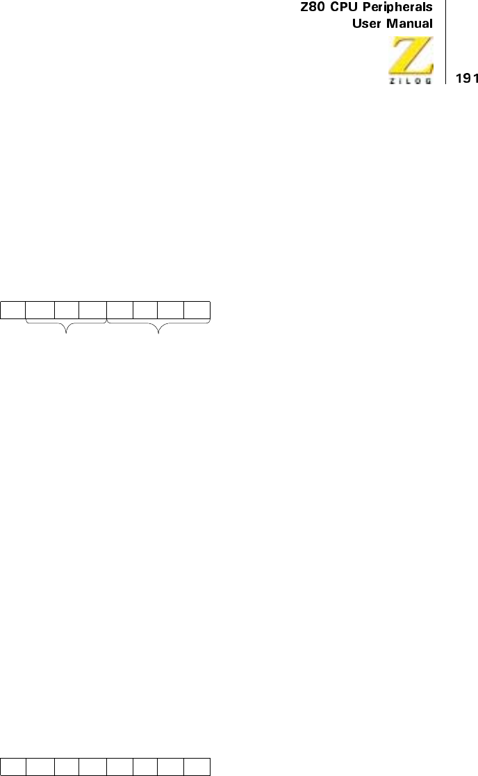
UM008101-0601 Parallel Input/Output
CPU is composed of input data, which comes from port data bus lines
assigned as inputs, and port output register data, which comes from lines
assigned as outputs.
Setting The Interrupt Control Word
The interrupt control word for each port has the following format:
If bit D7 = 1, the interrupt enable flip-flop of the port is set and the port
may generate an interrupt. If bit D7 = 0, the enable flag is reset and inter-
rupts may not be generated. If an interrupt is pending when the enable
flag is set, the interrupt is then enabled to the CPU interrupt request line.
Bits D6, D5, and D4 are used only with Mode 3 operation. However,
setting bit D4 of the interrupt control word in any mode of operation
causes a pending interrupt to be reset. These three bits allow interrupts in
Mode 3, but only when specific I/O lines go to defined states. Bit D6
(AND/OR) defines the logical operation to be performed in port moni-
toring. If bit D6 = 1, an AND function is specified and if D6 = 0, an OR
function is specified. For example, if the AND function is specified, all
bits must go to a specified state before an interrupt is generated.
Conversely, the OR function generates an interrupt if any specified bit
goes to the active state.
Bit D5 defines the active polarity of the port data bus line to be monitored.
If bit D5 = 1, the port data lines are monitored for a high state. When bit D5
= 0, the port data lines are monitored for a low state.
If bit D4 = 1, the next control word sent to the PIO must define a mask as
follows:
Used in Signifies Interrupt
D7 D6 D5 D4 D3 D0
Enable
Int. AND/
OR High
Low Masks
Follows
D2 D1
Mode 3 Only
01 11
Control Word
MB7 MB6 MB5 MB4 MB3 MB2 MB1 MB0
D7 D6 D5 D4 D3 D0D2 D1

UM008101-0601 Parallel Input/Output
Only port lines whose mask bit is zero are monitored for generating an
interrupt. When IORQ is high, the forced state of Ready prevents input
register data from changing while the CPU is reading the PIO. Ready goes
High again after the trailing edge of the IORQ, as previously described
TIMING
Output Mode (Mode 0)
Figure 7 illustrates the timing associated with Mode 0 operation. An output
cycle is always started by the execution of an output instruction by the
CPU. A WR*pulse is generated by the PIO during a CPU I/O write opera-
tion and is used to latch the data from the CPU data bus to the addressed
ports (A or B) output register. The rising edge of the WR*pulse then raises
the Ready flag after the next falling edge of Φ, indicating that data is avail-
able for the peripheral device. In most systems, the rising edge of the Ready
signal can be used as a latching signal in the peripheral device. The Ready
signal remains active until: (1) a positive edge is received from the strobe
line, indicating that the peripheral has taken the data, or (2) if already
active, Ready is forced low for one and one-half Φcycles after the leading
edge of IORQ, but only if the port’s output register is written to. Ready
returns High on the first falling edge of Φafter the trailing edge of IORQ.
This guarantees that Ready is low when port data is changing. The Ready
signal does not go inactive until a falling edge occurs on the clock (Φ) line.
The purpose of delaying the negative transition of the Ready signal until
after a negative clock transition is to allow a simple generation scheme for
the strobe pulse. By connecting the Ready line to the Strobe line, a strobe
with a duration of one clock period is generated with no other logic
required. The positive edge of the strobe pulse automatically generates an
INT request when the interrupt enable flip-flop has been set and this device
is the highest priority device requesting an interrupt.
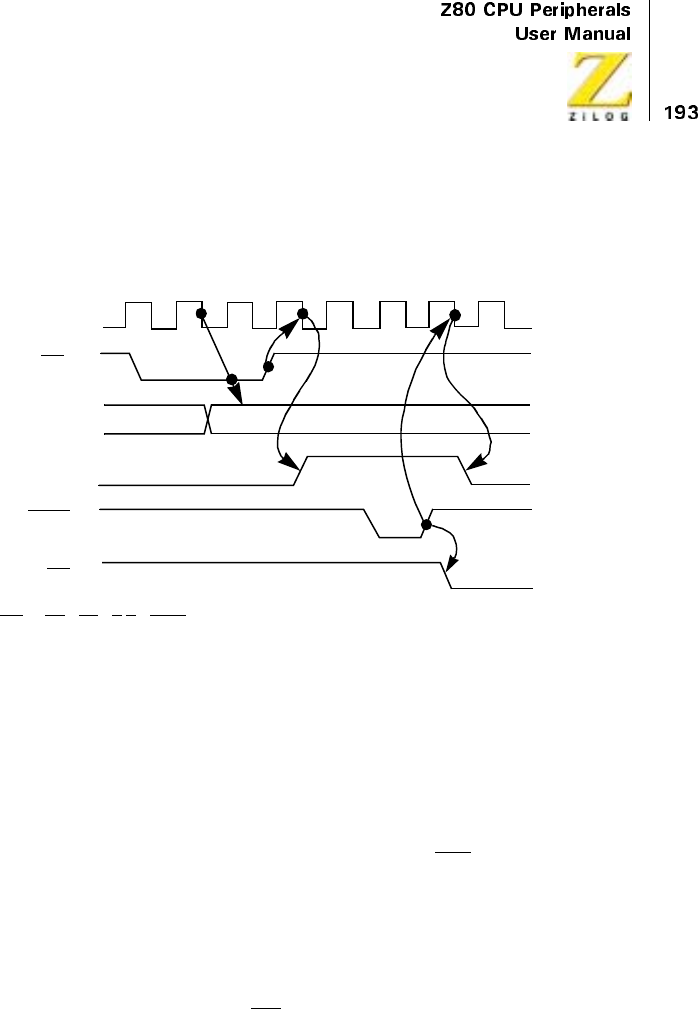
UM008101-0601 Parallel Input/Output
If the PIO is not in a reset state, the output register may be loaded before
Mode 0 is selected. This allows the port output lines to become active in a
user-defined state.
Figure 7. Mode 0 (Output) Timing
Input Mode (Mode 1)
Figure 8 illustrates the timing of an input cycle. The peripheral initiates this
cycleusingthestrobelineaftertheCPUhasperformedadataread.Alow
level on this line loads data to the port input register and the rising edge of
the strobe line activates the interrupt request line (INT)iftheinterrupt
enable is set and this is the highest priority requesting device. The next
falling edge of the clock line (Φ) resets the Ready line to an inactive state,
signifying that the input register is full and further loading must be inhibited
until the CPU reads the data. The CPU, in the course of its interrupt service
routine, reads the data from the interrupting port. When this occurs, the
positive edge from the CPU RD signal raises the Ready line with the next
low going transition of Φ, indicatingthatnewdatacanbeloadedtothe
Strobe
Ready
WR*
Port Output
(8 Bits)
INT
WR*=RD•CE •C/D •IORQ
Φ
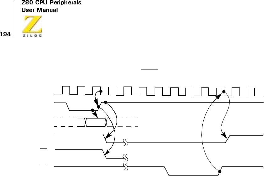
UM008101-0601 Parallel Input/Output
PIO. If already active, Ready is forced low for one and one-half Φperiods
following the leading edge of IORQ during a read of a PIO port.
Figure 8. Mode 1 (Input) Timing
Bidirectional Mode (Mode 2)
This mode is a combination of Mode 0 and Mode 1, using all four hand-
shake lines. Because this mode requires all four lines, it is available only on
Port A. When this mode is used on Port A, Port B must be set to the Bit
Control Mode. The same interrupt vector is returned for a Mode 3 interrupt
on Port B and an input transfer interrupt during Mode 2 operation of Port A.
Ambiguity is avoided if Port B is operated in a polled mode and the Port B
mask register is set to inhibit all bits.
Figure 9 illustrates the timing for this mode. It is almost identical to that
previously described for Mode 0 and Mode 1 with the Port A handshake
lines used for output control and the Port B lines used for input control. The
difference between the two modes is that, in Mode 2, data is allowed out
onto the bus only when the A strobe is Low. The rising edge of this strobe
can be used to latch the data to the peripheral because the data remains stable
Ready
Port Input
(8 Bits)
Strobe
INT
RD*
Φ
Sample
RD*=RD•CE •C/D •IORQ
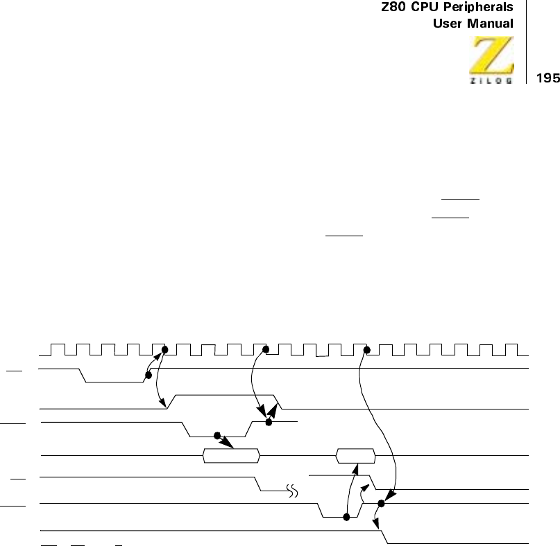
UM008101-0601 Parallel Input/Output
after this edge has risen. The input portion of Mode 2 operates identically to
Mode 1. Notice that both Port A and Port B must have their interrupts
enabled to achieve an interrupt-driven, bidirectional transfer.
The peripheral must not gate data onto a port data bus while ASTB is
active. Bus contention is avoided when the peripheral uses BSTB to gate
input data onto the bus. The PIO uses the BSTB low level to latch this data.
The data can be disabled from the bus immediately after the strobe rising
edge. This is because the PIO has been designed with a zero hold time
requirement for the data when latching in this mode. This gating structure
can be used by the peripheral.
Figure 9. Port A, Mode 2 (Bidirectional) Timing
Control Mode (Mode 3)
The control mode does not utilize the handshake signals, therefore a normal
port write or port read can be executed at any time. When writing, the data
is latched to output registers with the same timing as Mode 0. ARDY is
forced low whenever Port A is operated in Mode 3. BRDY is held Low
whenever Port B is operated in Mode 3 unless Port A is in Mode 2. In the
latter case, the state of BRDY is not affected.
WR*
Φ
Sample
WR*=RD•CE •C/D •IORQ
Data Out Data In
ARDY
ASTB
Port A
Data Bus
INT
BSTB
BRDY
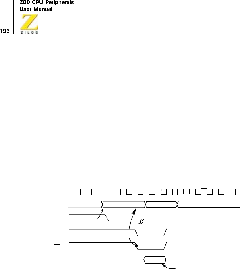
UM008101-0601 Parallel Input/Output
When reading the PIO, the data returned to the CPU is composed of output
register data from port data lines assigned as outputs and input register data
from port data lines assigned as inputs. The input register contains data that
was present immediately prior to the falling edge of RD. See Figure 10.
An interrupt is generated if interrupts from the port are enabled and the
data on the port data lines satisfies the logical equation defined is not
generated until a change occurs in the status of the logical equation. A
Mode 3 interrupt is generated only when the result of a Mode 3 logical
operation changes from false to true. For example, Mode 3 logical equa-
tion is an OR function. An unmasked port data line becomes active and an
interrupt is requested. If a second unmasked port data line becomes active
concurrently with the first, a new interrupt is not requested because a
change in the result of the Mode 3 logical operation has not occurred.
If the result of a logical operation becomes true immediately prior to or
during M1 an interrupt is requested after the trailing edge of M1
Figure 10. Control Mode (Mode 3) Timing
Φ
Data In
Data Word 1 Data Word 2
Data Match
Occurs Here
T1T2TW*T
3
*Timing Diagram Refers to Bit Mode Read
D7–D0
RD
IORQ
INT
Port
Data Bus
DataWord1PlacedonBus

UM008101-0601 Parallel Input/Output
INTERRUPT SERVICING
After an interrupt is requested by the PIO, the CPU sends out an interrupt
acknowledge (M1 and IORQ). During this time, the interrupt logic of the
PIO determines which port has the highest priority interrupt. (This is a
device which has an Interrupt Enable Input High and an Interrupt Enable
Output Low). To insure that the daisy-chain enable lines stabilize, devices
are inhibited from changing their interrupt request status when M1 is
active. The highest priority device places the contents of its interrupt
vector register onto the Z80 data bus during interrupt acknowledge.
Figure 11 illustrates the timing associated with interrupt requests. During
M1 time, no new interrupt requests can be generated. This allows time for
the lnt Enable signals to ripple through up to four PIO circuits. The PIO,
with IEI High and IEO Low during INTA, places the 8-bit interrupt
vector of the appropriate port on the data bus at this time.
If an interrupt requested by the PIO is acknowledged, the requesting port
is under service. The IEO of this port remains low until a return from
interrupt instruction (RETI) is executed, during which time the IEI of the
port is High. If an interrupt request is not acknowledged, IEO is forced
High for one M1 cycle after the PIO decodes the Op Code ED. This
action guarantees that the 2-byte RETI instruction is decoded by the
correct PIO port (Figure 12).
Figure 13 illustrates a typical nested interrupt sequence that could occur
with four ports connected in the daisy-chain. In this sequence, Port 2A
requests and is granted an interrupt. While this port is being serviced, a
higher priority port (1B) requests and is granted an interrupt. The service
routine for the higher priority port is completed and a RETI instruction is
executed, indicating to the port that its routine is complete. The service
routine of the lower priority port is then complete.
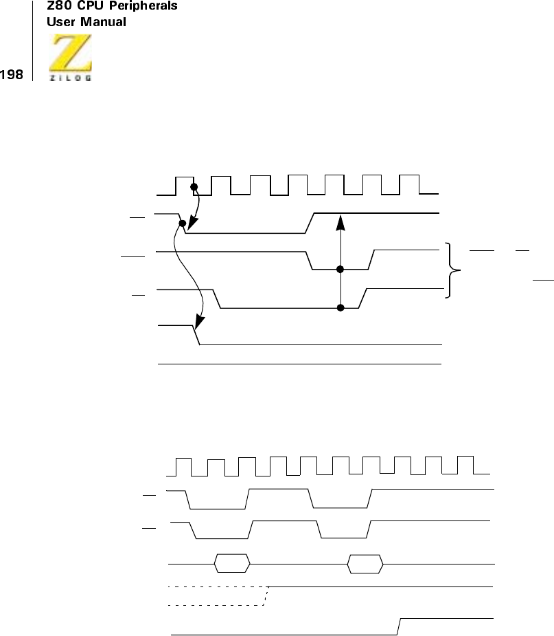
UM008101-0601 Parallel Input/Output
Figure 11. Interrupt Acknowledge Timing
Figure 12. Return from Interrupt Cycle
Φ
M1
IORQ
INT
IORQ and M1
indicate Interrupt
IEO
IEI
Last T
State T1T2TW*T3
TW*
Sample
INT
Acknowledge (INTA)
IEO
CLK
IEI
RD
M1
T1T2T3T4
D7–D0
T1T2T3T4T1
ED 4D
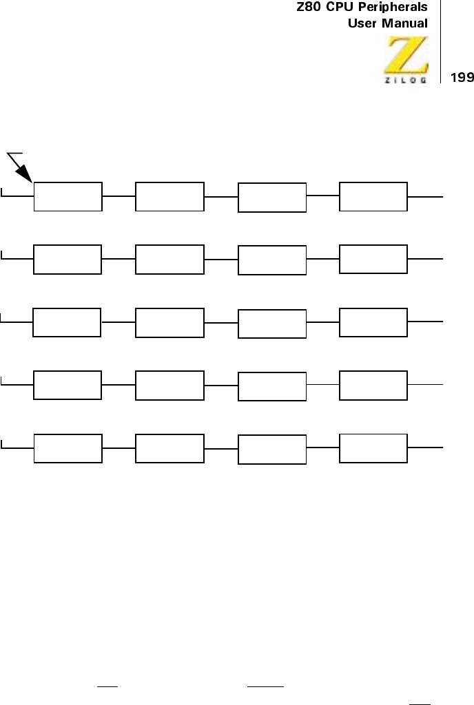
UM008101-0601 Parallel Input/Output
Figure 13. Daisy-Chain Interrupt Servicing
APPLICATIONS
Extending The Interrupt Daisy-chain
Without external logic, a maximum of four Z80 PIO devices may be daisy-
chained into a priority interrupt structure. This limitation allows the inter-
rupt enable status (IEO) to ripple through the entire daisy-chain between
the beginning of M1 and the beginning of IORQ during an interrupt
acknowledge cycle. The interrupt enable status cannot change during M1,
therefore, the vector address returned to the CPU is assured to be from the
highest priority device that requested an interrupt.
IEI IEO
HI
+
IEI IEO
HI
+
IEI IEO
HI
+
IEI IEO
HI
+
IEI IEO
HI
IEI IEO
HI
IEI IEO
HI
IEI IEO
HI
IEI IEO
HI
IEI IEO
HI
+
IEI IEO
HI
IEI IEO
HI
IEI IEO
LO
IEI IEO
HI
IEI IEO
HI
IEI IEO
HI
IEI IEO
LO
IEI IEO
LO
IEI IEO
LO
IEI IEO
HI
HI
LO
LO
LO
HI
Port 2B
Port 1B
Port 2A
Under Service
Service Suspended
Service Resumed
Service Complete
5. Second ‘RETI’instruction issued on completion of Port 2A service routine.
4. Port 1B service routine complete, ‘RETI’issued, Port 2A service resumed.
3. Port 1B1 interrupts, suspends servicing of Port 2A.
2. Port 2A requests an interrupt and is Acknowledged.
1. Priority interrupt daisy chain before any interrupt occurs.
Service Complete
Under Service
Port 1A
Hi
g
h
est
P
r
i
or
i
ty
Ch
anne
l
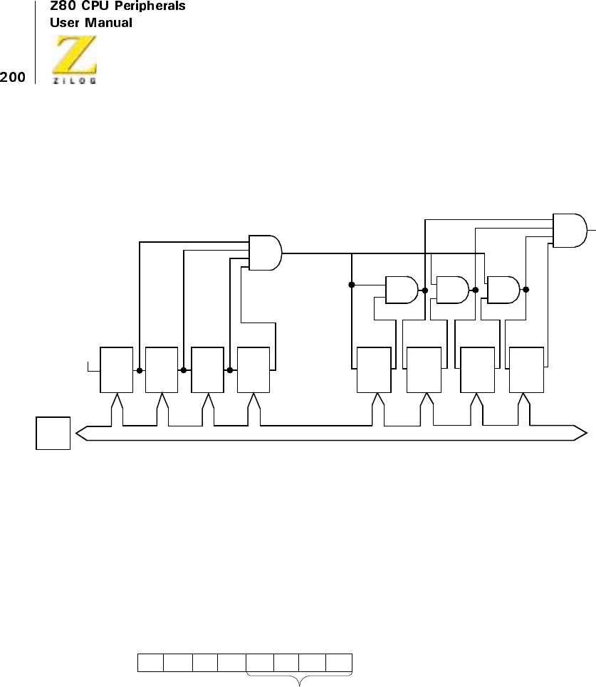
UM008101-0601 Parallel Input/Output
If more than four PIO devices must be accommodated, a look-ahead struc-
ture may be used as shown in Figure 14. With this technique, more than
thirty PIOs may be chained together using standard TTL logic.
Figure 14. A Method of Extending the Interrupt Priority Daisy-Chain
I/O Device Interface
In this example, the Z80 PIO is connected to an I/O terminal device, which
communicates over an 8-bit parallel bidirectional data bus as illustrated in
Figure 15. Mode 2 operation (bidirectional) is selected by sending the
following control word to Port A:
Next, the appropriate interrupt vector is loaded (refer to Z80 CPU User’s
Manual for details on the operation of the interrupt).
Z80
CPU
IEOIEI IEOIEI IEOIEI IEOIEI
Data Bus
+V PI0 PI0 PI0 PI0
IEOIEI IEOIEI IEOIEI IEOIEI
PI0 PI0 PI0 PI0
Mode Control
XX
D7 D6 D5 D4 D3 D0D2 D1
11 11
10
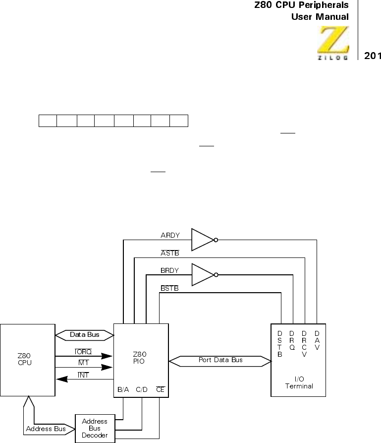
UM008101-0601 Parallel Input/Output
Interrupts are then enabled by the rising edge of the first M1 after the inter-
rupt mode word is set unless that first M1 defines an interrupt acknowledge
cycle. If a mask follows the interrupt mode word, interrupts are enabled by
the rising edge of the first M1 following the setting of the mask.
Data can now be transferred between the peripheral and the CPU. The
timing for this transfer is as described in “Timing”on page 192.
Figure 15. Example of I/O Interface
V5 V4
D7 D6 D5 D4 D3 D0D2 D1
V3 V2 V1 V0
V1 V6
UM008101-0601 Parallel Input/Output
Control Interface
A typical control mode application is illustrated in Figure 16. In this
example, an industrial process is to be monitored. The occurrence of any
abnormal operating condition is to be reported to a Z80 CPU-based control
system. The process control and status word has the following format:
The PIO may be used as follows. First, Port A is set for Mode 3 operation
by writing the following control word to Port A.
Whenever Mode 3 is selected, the next control word sent to the port must
be an I/O select word. In this example, port data lines A5, A3, and A0 are
selected as inputs, and the following control word is written:
Next, the appropriate interrupt vector must be loaded (refer to the Z80 CPU
User’s Manual for details):
An interrupt control word is next sent to the port:
The mask word following the interrupt mode word is:
D7 D6 D5 D4 D3 D0
Halt
Processing
D2 D1
Special
Test
Turn On
Power
Power
Failure Alarm
Te m p.
Alarm
Turn On
Heaters
Pressurize
System
Pressure
Alarm
11XX
D7 D6 D5 D4 D3 D0D2 D1
11 11
001 0
D7 D6 D5 D4 D3 D0D2 D1
10 01
V5 V4
D7 D6 D5 D4 D3 D0D2 D1
V3 V2 V1 0V1 V6
Interrupt Control
11
D7 D6 D5 D4 D3 D0D2 D1
01 11
10
Enable
Interrupts OR
Logic Active
High Mask
Follows
UM008101-0601 Parallel Input/Output
If a sensor puts a High level on lines A5, A3, or A0, an interrupt request is
generated. The mask word may select any combination of inputs or
outputs to cause an interrupt. For example, if the mask word above is:
then an interrupt request would also occur if bit A7 (Special Test) of the
output register was set.
Assume that the following port assignments are to be used:
E0H = Port A Data
E1H = Port B Data
E2H = Port A Control
E3H = Port B Control
All port numbers are in hexadecimal notation. This particular assignment of
port numbers is convenient because A0 of the address bus can be used as
the Port B/A Select and A1 of the address bus can be used as the Control/
Data Select. The Chip Enable is the decode of CPU address bits A7 through
A2 (111000).
Note: When only a few peripheral devices are being used, a Chip Enable
decode may not be required because a higher order address bit may be
used directly.
Selects A5, A3, and A0 to be Monitored
01
D7 D6 D5 D4 D3 D0D2 D1
01 10
11
01
D7 D6 D5 D4 D3 D0D2 D1
01 10
01
UM008101-0601 Parallel Input/Output
Figure 16. Control Mode Application
Z80 CPU Z80 PIO Industrial
Processing
System
B/A C/D CE
A15–A0
D7–D0
Spec. Test
Turn on Pwr.
Pwr. Fail Alm.
HALT
Temp. Alm.
HTRS. on
Press. Sys
Press. Alm.
A7
A5
A4
A3
A2
A1
A0
A6
Port A Bus
Address
Decoder
UM008101-0601 Parallel Input/Output
PROGRAMMING SUMMARY
Overview
This section discusses the Load Interrupt Vector, Set Mode, Set Interrupt
control registers.
Load Interrupt Vector
Set Mode
When selecting Mode 3, the next word must set the I/O Register:
M1 M0 Mode
00Output
0 1 Input
1 0 Bidirectional
1 1 Bit Control
V5 V4
D7 D6 D5 D4 D3 D0D2 D1
V3 V2 V1 0V1 V6
M1 M0 X X
D7 D6 D5 D4 D3 D0D2 D1
11 11
UM008101-0601 Parallel Input/Output
Set Interrupt Control
If the mask follows bit is high, the next control word written to the port
must be the mask:
In addition, the interrupt enable flip-flop of a port may be set or reset
without modifying the remainder of the interrupt control word. This is
accomplished by issuing the following command:
Used in
Enable
Int. AND/
OR High
Low Masks
Follows
Mode3Only
01 11
MB7 MB6 MB5 MB4 MB3 MB2 MB1 MB0
XX00 11
X
Enable
Int.

Z80 CPU Peripherals
User Manual
UM008101-0601 Serial Input/Output
207
Serial Input/Output
OVERVIEW
The Z80 Serial Input/Output (SIO) is a dual-channel multi-function
peripheral component designed to satisfy a wide variety of serial data
communications requirements in microcomputer systems. The Z80 SIO
functions as a serial-to-parallel, parallel-to-serial converter/controller, and
is systems-software configurable to allow optimization for a given serial
data communications application.
The Z80 SIO is capable of handling asynchronous and synchronous byte-
oriented protocols such as IBM Bisync and synchronous bit-oriented
protocols such as HDLC and IBM SDLC. This versatile device also
supports virtually any other serial protocol for applications other than data
communications, such as cassette or floppy disk interfaces.
The Z80 SIO can generate and check CRC codes in any synchronous mode
and can be programmed to check data integrity in various modes. The
device also has features for modem controls in both channels. In applica-
tions where these controls are not needed, the modem controls can be used
for general-purpose I/O.
FEATURES
•
CMOS and NMOS Version
•
40-Pin DIP, 44-Pin PLCC/QFP Packages
•
Single 5V Power Supply
•
Single-Phase 5V Clock

UM008101-0601 Serial Input/Output
208
•
TTL-Compatible Inputs and Outputs
•
Two Independent Full-Duplex Channels
•
Data Rates in Synchronous or Isosynchronous Modes:
–0-800K Bits/Second with 4 MHz System Clock Rate
–0-1.2M Bits/Second with 6 MHz System Clock Rate
–0-2.5M Bits/Second with 10 MHz System Clock Rate
•
Receiver Data Registers Quadruply Buffered; Transmitter Doubly
Buffered
•
Asynchronous Features:
–5, 6, 7, or 8 Bits per Character
–1, 1 1/2, or 2 Stop Bits
–Even, Odd, or No Parity
–x1, x16, x32, and x64 Clock Modes
–Break Generation and Detection
–Parity, Overrun, and Framing Error Detection
•
Binary Synchronous Features:
–Internal or External Character Synchronization
–One or Two Sync Characters in Separate Registers
–Automatic Sync Character Insertion
–CRC Generation and Checking
•
HDLC and IBM SDLC Features:
–Abort Sequence Generation and Detection
–Automatic Zero Insertion and Deletion
–Automatic Flag insertion Between Messages
–Address Field Recognition
–1-Field Residue Handling
–Valid Receive Messages Protected from Overrun
Z80 CPU Peripherals
User Manual
UM008101-0601 Serial Input/Output
209
•
CRC generation and checking
•
Separate Modem Control Inputs and Outputs for Both Channels
•
CRC-16 or CRC-CCITT Block Check
•
Daisy-Chain Priority Interrupt Logic Provides Automatic Interrupt
Vectoring Without External Logic
•
Modem Status can be Monitored
Figure 100. Z80 SIO Block Diagram
CPU
Bus I/O
+5V GND Φ
Data
Control
International
Control
Logic
Channel A
Read/Write
Registers
Channel B
Read/Write
Registers
International
Control
Logic
8
6
Interrupt
Control
Lines
Channel B
Discrete
Control and
Status
(Channel A)
Channel A
Modem
or other
Serial Data
Channel Clocks
Discrete
Control and
Status
(Channel B)
SYNC
Wait/Ready
Controls
Modem
or other
Controls
Serial Data
Channel Clocks
SYNC
Wait/Ready

UM008101-0601 Serial Input/Output
210
PIN DESCRIPTION
Pin Functions
D7-D0 System Data Bus (bidirectional, tristate). The system data bus
transfers data and commands between the CPU and the Z80 SIO. D0 is
the least-significant bit.
B/AChannel A or B Select (input, High selects Channel B). This input
defines which channel is accessed during a data transfer between the CPU
and the Z80 SIO. Address bit A0 from the CPU is often used for the selec-
tion function.
C/D Control Or Data Select (input, High selects Control). This input
defines the type of information transfer performed between the CPU and
the Z80 SIO. A High at this input during a CPU write to the Z80 SIO
causes the information on the data bus to be interpreted as a command for
the channel selected by B/A.ALowatC/Dindicates that the information
on the data bus is data. Address bit A1 is often used for this function.
CE Chip Enable (input, active Low). A Low level at this input enables the
Z80 SIO to accept command or data inputs from the CPU during a write
cycle, or to transmit data to the CPU during a read cycle.
ΦSystem Clock (input). The Z80 SIO uses the standard Z80A System
Clock to synchronize internal signals. This is a single-phase clock.
M1 Machine Cycle One (input from Z80 CPU, active Low). When M1 is
active and RD is also active, the Z80 CPU is fetching an instruction from
memory; when M1 is active while IORQ is active, the Z80 SIO accepts
M1 and IORQ as an interrupt acknowledge if the Z80 SIO is the highest
priority device that has interrupted the Z80 CPU.
IORQ input/Output Request (input from CPU, active Low). IORQ is used
in conjunction with B/A,C/D,CE,andRDto transfer commands and data
between the CPU and the Z80 SIO. When CE,RD,andIORQare all active,
the channel selected by B/A transfers data to the CPU (a read operation).

Z80 CPU Peripherals
User Manual
UM008101-0601 Serial Input/Output
211
When CE and IORQ are active, but RD is inactive, the channel selected by
B/A is written to by the CPU with either data or control information as
specified by C/D. As mentioned previously, if IORQ and M1 are active
simultaneously, the CPU is acknowledging an interrupt and the Z80 SIO
automatically places its interrupt vector on the CPU data bus if it is the
highest priority device requesting an interrupt.
RD Read Cycle Status (input from CPU, active Low). If RD is active, a
memory or I/O read operation is in progress. RD is used with B/A,CE,
and IORQ to transfer data from the Z80 SIO to the CPU.
RESET Reset (input, active Low). A Low /RESET disables both /RESET
and transmitters, forces TxDA and TxDB marking, forces the modem
controls High and disables all interrupts. The control registers must be
rewritten after the Z80 SIO is reset and before data is transmitted or received.
IEI Interrupt Enable In (input, active High). This signal is used with IEO
to form a priority daisy-chain when there is more than one interrupt-
driven device. A High on this line indicates that no other device of higher
priority is being serviced by a CPU interrupt service routine.
IEO Interrupt Enable Out (output, active High). IEO is High only if IEI is
High and the CPU is not servicing an interrupt from this Z80 SIO. There-
fore, this signal blocks lower priority devices from interrupting while a
higher priority device is being serviced by its CPU interrupt service routine.
INT Interrupt Request (output, open-drain, active Low). When the Z80
SIO is requesting an interrupt, it pulls INT Low.
W/RDYA,W/RDYBWait/Ready A, Wait/Ready B (outputs, open-drain
when programmed for Wait function, driven High and Low when
programmed for Ready function). These dual-purpose outputs may be
programmed as Ready lines for a DMA controller or as Wait lines that
synchronize the CPU to the Z80 SIO data rate. The reset state is open-drain.
CSTA,CSTBClear To Send (inputs, active Low). When programmed as
Auto Enables, a Low on these inputs enables the respective transmitter. If
not programmed as Auto Enables, these inputs may be programmed as

UM008101-0601 Serial Input/Output
212
general-purpose inputs. Both inputs are Schmitt-trigger buffered to
accommodate slow-risetime inputs. The Z80 SIO detects pulses on these
inputs and interrupts the CPU on both logic level transitions. The
Schmitt-trigger inputs do not guarantee a specified noise-level margin.
DCDA, DCDB Data Carrier Detect (inputs, active Low). These signals
are similar to the CTS inputs, except they can be used as receiver enables.
RxDA, RxDB Receive Data (inputs, active High).
TxDA, TxDB Transmit Data (outputs, active High).
RxCA, RxCB* Receiver Clocks (inputs). See the following section on
bonding options. The Receive Clocks may be 1, 16, 32, or 64 times the
data rate in asynchronous modes. Receive data is sampled on the rising
edge of RxC.
TxCA,TxCB*Transmitter Clocks (inputs). See section on bonding
options. In asynchronous modes, the Transmitter clocks may be 1, 16, 32,
or 64 times the data rate. The multiplier for the transmitter and the receiver
must be the same. Both the TxC and RxC inputs are Schmitt-trigger buff-
ered for relaxed rise- and fall-time requirements (no noise margin is speci-
fied). TxD Changes on the falling edge of TxC.
These clocks may be directly driven by the Z80 CTC (Counter Timer
Circuit) for fully programmable baud rate generation.
RTSA,RTSBRequest To Send (outputs, active Low). When the /RTS bit is
set, the RTS output goes Low. When the RTS bit is reset in the Asynchro-
nous mode, the output goes High after the transmitter is empty. In Synchro-
nous modes, the RTS pin strictly follows the state of the RTS bit. Both pins
can be used as general-purpose outputs.
DTRA,DTRBData Terminal, Ready (outputs, active Low). See note on
bonding options. These outputs follow the state programmed into the DTR
bit. They can also be programmed as general-purpose outputs.
SYNCA, SYNCB Synchronization (inputs/outputs, active Low). These
pins can act either as inputs or outputs. In the Asynchronous Receive mode,

Z80 CPU Peripherals
User Manual
UM008101-0601 Serial Input/Output
213
they are inputs similar to CTS and DCD. In this mode, the transitions on
these lines affect the state of the Sync/Hunt status bits in RR0. In the
External Sync mode, these lines also act as inputs. When external synchro-
nization is achieved, SYNC must be driven Low on the second rising edge
of RxC after that rising edge of RxC on which the last bit of the sync char-
acter was received. In other logic must wait for two full Receive Clock
cycles to activate the SYNC input. When SYNC is forced Low, keep it Low
until the CPU notifies the external sync logic that synchronization has been
lost or that a new message is about to start. Character assembly begins on
the rising edge of RxC that immediately precedes the falling edge of SYNC
in the External Sync mode.
In the Internal Synchronization mode (Monosync and Bisync), these pins
function as outputs that are active during the part of the receive clock (RxC)
cycle in which sync characters are recognized. The sync condition is not
latched, therefore, these outputs are active each time a sync pattern is recog-
nized, regardless of character boundaries.
Bonding Options
Theconstraintsofa40-pinpackagemakeitimpossibletobringoutthe
Receive Clock, Transmit Clock, Data Terminal Ready, and Sync signals for
both channels. Therefore, Channel B must sacrifice a signal or have two
signals bonded together. Because user requirements vary, three bonding
options are offered:
•
Z80 SIO/0 contains all four signals, but TxCB and RxCD are bonded
together (Figure 101).
•
Z80 SIO/1 sacrifices DTRB and keeps TxCB,RxCDand SYNCB
(Figure 103).
•
Z80 SIO/2 sacrifices SYNCB and keeps TxCB,RxCBand DTRB
(Figure 105).
•
The 44-pin package version SIO/3 (QFP) and SIO/4 (PLCC) have all
signals (Figure 107 and Figure 108).
UM008101-0601 Serial Input/Output
214
Figure 101. Z80 SIO/0 Functions
Z80 SIO/0
40
39
38
37
36
35
34
33
32
31
30
29
28
27
26
25
24
23
22
21
D0
D2
D6
D4
IORQ
CE
B/A
C/D
RD
GND
W/RDYB
SYNCB
RxDB
RxTxCB
TxDB
DTRB
RTSB
CTSB
DCDB
RESET
1
2
3
4
5
6
7
8
9
10
11
12
13
14
15
16
17
18
19
20
D1
D3
D7
D5
INT
IEI
IEO
M1
VDD
W/RDYA
SYNCA
RxDA
RxCA
TxCA
TxDA
DTRA
RTSA
CTSA
DCDA
Φ
Z80 CPU Peripherals
User Manual
UM008101-0601 Serial Input/Output
215
Figure 102. Z80 SIO/0 Pin Assignments
Z80 –SIO/0
CH-A
RxDA
RxCA
TxDA
TxCA
SYNCA
W/RDYA
RTSA
CTSA
DTRA
DCDA
RxDB
RxTxCB
TxDB
SYNCB
W/RDYB
CTSB
DTRB
DCDB
RTSB
12
13
15
14
11
10
17
18
16
19
30
24
23
25
22
28
27
26
29
CH-B
CPU
Data
BUS
SIO
Control
D0
D1
D2
D3
D4
D5
D6
D7
CE
RESET
M1
IORQ
RD
5V
GND
INT
IEI
IEO
Φ
40
1
39
2
38
3
37
4
35
21
31
20
5
6
7
8
36
32
9
from
CPU
Daisy
Chain
Interrupt
Control Modem
Control
Modem
Control
33 34
C/D B/A
UM008101-0601 Serial Input/Output
216
Figure 103. Z80 SIO/1 Pin Functions
Z80 SIO/1
40
39
38
37
36
35
34
33
32
31
30
29
28
27
26
25
24
23
22
21
D0
D2
D6
D4
IORQ
CE
B/A
C/D
RD
GND
W/RDYB
SYNCB
RxDB
RxCB
TxCB
TxDB
RTSB
CTSB
DCDB
RESET
1
2
3
4
5
6
7
8
9
10
11
12
13
14
15
16
17
18
19
20
D1
D3
D7
D5
INT
IEI
IEO
M1
VDD
W/RDYA
SYNCA
RxDA
RxCA
TxCA
TxDA
DTRA
RTSA
CTSA
DCDA
Φ
Z80 CPU Peripherals
User Manual
UM008101-0601 Serial Input/Output
217
Figure 104. Z80 SIO/1 Pin Assignments
Z80 –SIO/1
CH-A
RxDA
RxCA
TxDA
TxCA
SYNCA
W/RDYA
RTSA
CTSA
DTRA
DCDA
RxDB
RxTxCB
TxCB
SYNCB
W/RDYB
CTSB
DCDB
RTSB
12
13
15
14
11
10
17
18
16
19
30
24
23
22
28
27
26
29
CH-B
CPU
Data
BUS
SIO
Control
D0
D1
D2
D3
D4
D5
D6
D7
CE
RESET
M1
IORQ
RD
5V
GND
INT
IEI
IEO
F
40
1
39
2
38
3
37
4
35
21
31
20
5
6
7
8
36
32
9
from
CPU
Daisy
Chain
Interrupt
Control
Modem
Control
TxDB
25
Modem
Control
33 34
C/D B/A
UM008101-0601 Serial Input/Output
218
Figure 105. Z80 SIO/2 Pin Functions
Z80 SIO/2
40
39
38
37
36
35
34
33
32
31
30
29
28
27
26
25
24
23
22
21
D0
D2
D6
D4
IORQ
B/A
C/D
RD
GND
W/RDYB
RxDB
RxCB
TxCB
TxDB
DTRB
RTSB
CTSB
DCDB
RESET
1
2
3
4
5
6
7
8
9
10
11
12
13
14
15
16
17
18
19
20
D1
D3
D7
D5
INT
IEI
IEO
M1
VDD
W/RDYA
SYNCA
RxDA
RxCA
TxCA
TxDA
DTRA
RTSA
CTSA
DCDA
F
CE
Z80 CPU Peripherals
User Manual
UM008101-0601 Serial Input/Output
219
Figure 106. Z80 SIO/2 Pin Assignments
Z80 –SIO/2
CH-A
RxDA
RxCA
TxDA
TxCA
SYNCA
W/RDYA
RTSA
CTSA
DTRA
DCDA
RxDB
RxCB
TxCB
W/RDYB
CTSB
DCDB
RTSB
12
13
15
14
11
10
17
18
16
19
30
24
23
22
29
28
27
CH-B
CPU
Data
BUS
SIO
Control
D0
D1
D2
D3
D4
D5
D6
D7
CE
RESET
M1
IORQ
RD
5V
GND
INT
IEI
IEO
F
40
1
39
2
38
3
37
4
35
21
31
20
5
6
7
8
36
32
9
from
CPU
Daisy
Chain
Interrupt
Control
Modem
Control
TxDB
26
Modem
Control
33 34
C/D B/A
DTRB
25
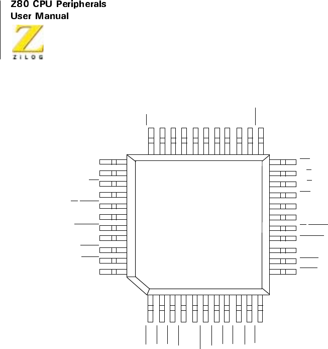
UM008101-0601 Serial Input/Output
220
Figure 107. Z80 SIO/3 Pin Assignments
34
33
IEI
IEO
M1
+5V
W/RDYA
N/C
SYNCA
RxDA
RxCA
TxCA
TxDA
CE
B/A
C/D
RD
GND
N/C
W/RDYB
SYNCB
RxDB
RxCB
TxCB
INT
D7
D5
D3
D1
N/C
D0
D2
D4
D6
IORQ
DTRA
RTSA
CTSA
DCDA
CLK
RESET
DCDB
CTSB
RTSB
DTRB
TxDB
44
22
12
11
1
CMOS Z80
Z804C43
SIO/3
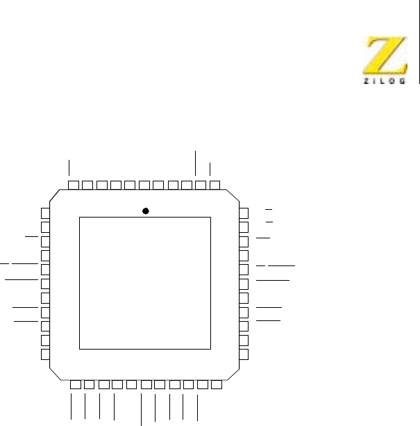
Z80 CPU Peripherals
User Manual
UM008101-0601 Serial Input/Output
221
Figure 108. Z80 SIO/4 Pin Assignments
IEI
IEO
M1
+5V
W/RDYA
SYNCA
RxDA
RxCA
TxCA
TxDA
B/A
C/D
RD
GND
W/RDYB
SYNCB
RxDB
RxCB
TxCB
TxDB
DTRA
RTSA
CTSA
DCDA
CLK
RESET
DCDB
CTSB
RTSB
DTRB
N/C
Z80
SIO/4
NC
7
8
9
10
11
12
13
14
15
16
17
39
38
37
36
35
34
33
32
31
30
29
INT
D7
D5
D3
D1
D0
D2
D4
D6
IORQ
CE
N/C
6 5 4 3 2 1 44 43 42 41 40
18 19 20 21 22 23 24 25 26 27 28

UM008101-0601 Serial Input/Output
222
ARCHITECTURE
Overview
The device internal structure includes a Z80 CPU interface, internal control
and interrupt logic, and two full-duplex channels. Associated with each
channel are read and write registers, and discrete control and status logic
that provides the interface to modems or other external devices.
The read and write register group includes five 8-bit control registers, two
sync-character registers, and two status registers. The interrupt vector is
written into an additional 8-bit register (Write Register 2) in Channel B that
may be read through Read Register 2 in Channel B. The registers for both
channels are designated as follows:
WR7–WR0 —Write Registers 0 through 7
RR2–RR0 —Read Registers 0 through 2
The bit assignment and functional grouping of each register is configured to
simplify and organize the programming process. Table 1 and Table 2 illus-
trate the functions assigned to each read or write register.
The logic for both channels provides formats, synchronization, and valida-
tion for data transferred to and from the channel interface. The modem
control inputs Clear to Send (CTS) and Data Carrier Detect (DCD)are
monitored by the discrete control logic under program control. All the
modem control signals are general purpose and can be used for functions
other than modem control.
For automatic interrupt vectoring, the interrupt control logic determines
which channel and which device within the channel has the highest priority.
Priority is fixed with Channel A assigned a higher priority than Channel B;
Receive, Transmit and External/Status interrupts are prioritized in that
order within each channel.

Z80 CPU Peripherals
User Manual
UM008101-0601 Serial Input/Output
223
Data Path
The transmit and receive data path for each channel is depicted in
Figure 109. The receiver contains three 8-bit buffer registers in a FIFO
arrangement (to provide a 3-byte delay) in addition to the 8-bit receive shift
register. This arrangement creates additional time for the CPU to service an
interrupt at the beginning of a block of high-speed data. The receive error
FIFO stores parity and framing errors and other types of status information
for each of the three bytes in the receive data FIFO.
Incoming data is routed through one of several paths depending on the
mode and character length. In the Asynchronous mode, serial data is
Table 1. Write Register Functions
Bit Function
WR0 Register pointers, CRC initialize, initialization commands for the
various modes and more
WR1 Transmit/Receive interrupt and data transfer mode definition
WR2 Interrupt vector (Channel B only)
WR3 Receive parameters and controls
WR4 Transmit/Receive miscellaneous parameters and modes
WR5 Transmit parameters and controls
WR6 Sync character or SDLC address field
WR7 Sync character or SDLC flag
Table 2. Read Register Functions
Bit Function
RR0 Transmit/Receive buffer status, interrupt status, and external status
RR1 Special Receive Condition status
RR2 Modified interrupt vector (Channel B only)

UM008101-0601 Serial Input/Output
224
entered in the 3-bit buffer if the data has a character length of seven or eight
bits, or is entered in the 8-bit receive shift register if the data has a length of
five or six bits.
In the Synchronous mode, the data path is determined by the phase of the
receive process currently in operation. A Synchronous Receive operation
begins with the receiver in the Hunt phase, during which the receiver
searches the incoming data stream for a bit pattern that matches the prepro-
grammed sync characters for flags in the SDLC mode. If the device is
programmed for Monosync Hunt, a match is made with a single sync char-
acter stored in WR7. In Bisync Hunt, a match is made with dual sync char-
acters stored in WR6 and WR7.
In either case, the incoming data passes through the receive sync register,
and is compared against the programmed sync character in WR6 or WR7.
In the Monosync mode, a match between the sync character programmed to
WR7 and the character assembled in the receive sync register establishes
synchronization.
In the Bisync mode, however, incoming data is shifted to the receive shift
register while the next eight bits of the message are assembled in the
receive sync register. The match between the assembled character in the
receive sync registers with the programmed sync character in WR6 and
WR7 establishes synchronization. When synchronization is established,
incoming data bypasses the receive sync register and directly enters the
3-bit buffer.
In the SDLC mode, incoming data first passes through the receive sync
register, which continuously monitors the receive data stream and
performs zero deletion when indicated. Upon receiving five contiguous
1s, the sixth bit is inspected. If the sixth bit is a 0, it is deleted from the
data stream. If the sixth bit is a 1, the seventh bit is inspected. If the
seventh bit is a 0, a Flag sequence has been received; if it is a 1, an Abort
sequence has been received.
The reformatted data enters the 3-bit buffer and is transferred to the receive
shift register. The SDLC receive operation also begins in the Hunt phase,

Z80 CPU Peripherals
User Manual
UM008101-0601 Serial Input/Output
225
during which the Z80 SIO tries to match the assembled character in the
receive shift register with the nag pattern in WR7. When the first flag char-
acter is recognized, all subsequent data is routed through the same path,
regardless of character length.
Although the same CRC checker is used for both SDLC and synchronous
data, the data path taken for each mode is different. In Bisync protocol, a
byte-oriented operation requires that the CPU decide to include the data
character in CRC. To allow the CPU ample time to make this decision, the
Z80 SIO provides an 8-bit delay for synchronous data. In the SDLC mode,
no delay is provided because the Z80 SIO contains logic that determines the
bytes on which CRC is calculated.
The transmitter has an 8-bit transmit data register that is loaded from the
internal data bus and a 20-bit transmit shift register that can be loaded from
WR6, WR7, and the transmit data register. WR6 and WR7 contain sync
characters in the Monosync or Bisync modes, or address field (one char-
acter long) and flag respectively in the SDLC mode. During Synchronous
modes, information contained in WR6 and WR7 is loaded to the transmit
shift register at the beginning of the message and, as a time filler, in the
middle of the message if a Transmit Underrun condition occurs. In the
SDLC mode, the flags are loaded to the transmit shift register at the begin-
ning and end of message.
Asynchronous data in the transmit shift register is formatted with start and
stop bits and is shifted out to the transmit multiplexer at the selected clock
rate. Synchronous (Monosync or Bisync) data is shifted out to the transmit
multiplexer and also to the CRC generator at the x1 clock rate.
SDLC/HDLC data is shifted out through the zero insertion logic, which is
disabled while the flags are sent. For all other fields (address, control, and
frame check) a 0 is inserted following five contiguous 1s in the data stream.
The CRC generator result for SDLC data is also routed through the zero
insertion logic.
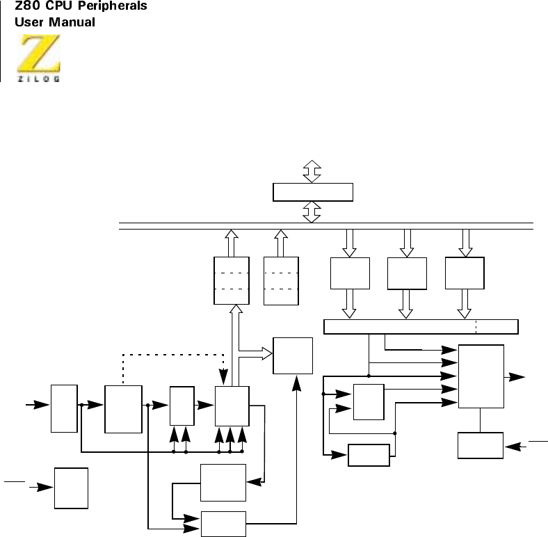
UM008101-0601 Serial Input/Output
226
Figure 109. Transmit and Receive Data Path
Functional Description
The functional capabilities of the Z80 SIO are described in two ways: as a
data communications device, and as a Z80 family peripheral.
As a data communications device, The S80 SIO transmits and receives
serial data, and meets the requirements of various data communications
protocols. As a Z80 family peripheral, it interacts with the Z80 CPU and
other Z80 peripheral, circuits, and shares their data, address and control
Receive
Error
Logic
I/O Data Buffer
CPU I/O
Internal Data Bus
Receive
Clock
Logic
ASYNC Data
CRC Delay
Register
(8 Bits)
SYNC-
CRC
RxDA
RxCA
Hunt Mode (BISYNC)
3Bits
1-Bit
Delay
CRC
Checker
SYNC
SDLC-CRC CRC Result
SYNC-CRC
Transmit
Clock Logic
SYNC Data
SDLC-CRC
ASYNC Data
Transmit
Multiplexer
and TxDA
TxCA
20-Bit Transmit Shift Register Start Bit
Transmit
WR7
SYNC
and Zero
Delay
Register
WR6
SYNC
Register Data
SDLC Data
CRC
Generator
2-Bit
Zero
(5 Bits)
Insert
Register
Delete
Receive
S.R.
(8 Bits)
Receive
Error
FIFO
Receive
Error
FIFO

Z80 CPU Peripherals
User Manual
UM008101-0601 Serial Input/Output
227
busses, as well as being a part of the Z80 interrupt structure. As a peripheral
to other microprocessors, the Z80 SIO offers valuable features such as non-
vectored interrupts, polling and simple handshake capabilities.
The first part of the following functional description describes the interac-
tion between the CPU and Z80 SIO. The second part introduces its data
communications capabilities.
I/O Capabilities
The Z80 SIO offers the choice of Polling, Interrupt (vectored or non-
vectored), and Block Transfer modes to transfer data, status, and control
information to and from the CPU. The Block Transfer mode can be imple-
mented under CPU or DMA control.
Polling
The Polled mode avoids interrupts. Status registers RR0 and RR1 are
updated at appropriate times for each function being performed, for example,
CRC Error status valid at the end of the message. All the Z80 SIO interrupt
modes must be disabled to operate the device in a polled environment.
While in Polling sequence, the CPU examines the status contained in RR0
for each channel. The RR0 status bits serve as an acknowledge to the Poll
inquiry. The two RR0 status bits D0 and D2 indicate that a receive or
transmit data transfer is needed. The status also indicates Error or other
special status conditions (see “Programming”on page 272). The Special
Receive Condition status contained in RR1 does not have to be read in a
Polling sequence because the status bits in RR1 are accompanied by a
Receive Character Available status in RR0
Interrupts
The Z80 SIO offers an elaborate interrupt scheme to provide fast interrupt
response in real-time applications. As covered earlier, Channel B registers
WR2 and RR2 contain the interrupt vector that points to an interrupt service

UM008101-0601 Serial Input/Output
228
routine in the memory. To service operations in both channels and to elimi-
nate the necessity of writing a status analysis routine, the Z80 SIO can
modify the interrupt vector in RR2 so that it points directly to one of eight
interrupt service routines. This is done under program control by setting a
program bit (WR1, D2) in Channel B called “Status Affects Vector.”when
this bit is set, the interrupt vector in WR2 is modified according to the
assigned priority of the various interrupting conditions. The table in “Write
Register 1”on page 279 lists the modification details.
Transmit interrupts, Receive interrupts, and External/ Status interrupts are
the main sources of interrupts (Figure 110). Each interrupt source is
enabled under program control with Channel A having a higher priority
than Channel B, and with Receiver, Transmit, and External/Status inter-
rupts prioritized in that order within each channel. When the Transmit
interrupt is enabled, the CPU is interrupted by the transmit buffer
becoming empty. This implies that the transmitter had a data character
written into it so it can become empty. When enabled, the receiver can
interrupt the CPU in one of three ways:
•
Interrupt on first receive character
•
Interrupt on all receive characters
•
Interrupt on a Special Receive condition
Interrupt On First Character is typically used with the Block Transfer mode.
Interrupt On All Receive Characters has the option of modifying the inter-
rupt vector in the event of a parity error. The Special Receive Condition
interrupt can occur on a character or message basis, for example, End-of-
Frame interrupt in SDLC. The Special Receive condition can cause an
interrupt only if the Interrupt On First Receive Character or Interrupt On
All Receive Characters mode is selected. In Interrupt On First Receive
Character, an interrupt can occur from Special Receive conditions (except
Parity Error) after the first receive character interrupt, for example, Receive
Overrun interrupt.
The main function of the External/Status interrupt is to monitor the signal
transitions of the CTS,DCD,andSYNCpins; however, an External/Status

Z80 CPU Peripherals
User Manual
UM008101-0601 Serial Input/Output
229
interrupt is also caused by a Transmit Underrun condition or by the detec-
tion of a Break (Asynchronous mode) or Abort (SDLC mode) sequence in
the data stream. The interrupt caused by the Break/Abort sequence has a
special feature that allows the Z80 SIO to interrupt when the Break/Abort
sequence is detected or terminated. This feature facilitates the proper termi-
nation of the current message, correct initialization of the next message,
and the accurate timing of the Break/Abort condition in external logic.
CPU/DMA Block Transfer
The Z80 SIO provides a Block Transfer mode to accommodate CPU block
transfer functions and DMA controllers (Z80-DMA or other designs). The
Block Transfer mode uses the WAIT/READY output in conjunction with
the Wait/Ready bits of Write Register 1. The WAIT/READY output can be
defined under software control as a WAIT line in the CPU Block Transfer
mode or as a READY line in the DMA Block Transfer mode.
To a DMA controller, the Z80 SIO READY output indicates that the Z80
SIO is ready to transfer data to or from memory. To the CPU, the WAIT
output indicates that the Z80 SIO is not ready to transfer data, thereby
requesting the CPU to extend the I/O cycle. The programming of bits 5, 6,
and 7 of Write Register 1 and the logic states of the WAIT/READY line are
defined in “Write Register 1”on page 279.
Data Communications Capabilities
In addition to the I/O capabilities previously discussed, the Z80 SIO
provides two independent full-duplex channels as well as Asynchronous,
Synchronous, and SDLC (HDLG) operational modes. These modes facili-
tate the implementation of commonly used data communications protocols.
The specific features of these modes are described in the following
sections. To preserve the independence and completeness of each section,
someinformationcommontoallmodesisrepeated.
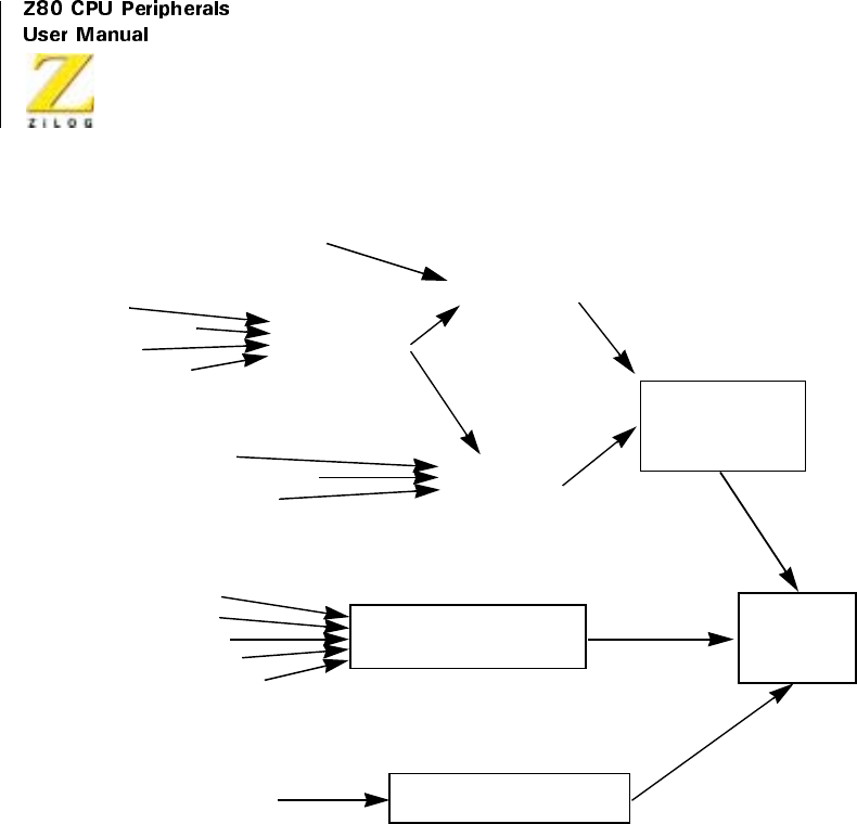
UM008101-0601 Serial Input/Output
230
Figure 110. Interrupt Structure
ASYNCHRONOUS OPERATION
Overview
To receive or transmit data in the Asynchronous mode, the Z80 SIO must
be initialized with the following parameters: character length, clock rate,
number of stop bits, even or odd parity, interrupt mode, and receiver or
transmitter enable. The parameters are loaded to the appropriate write
Buffer Becoming Empty Transmit Interrupt
External Status
Interrupt
Break/Abort Detection
Tx Underrun/EOM
SYNC Transition
CTS Transition
DCD Transition
Z80-SIO
Interrupt
Interrupt on
First Character
Valid Address Byte (SDLC)
First Non-Sync Character (SYNC)
First Data Character
End-of-Frame (SDLC)
Framing Error
Receive Overrun Error
Parity Error
Special Receive
Condition Interrupt
Receive Character
Interrupt on All
Receive Characters
Receive
Interrupt
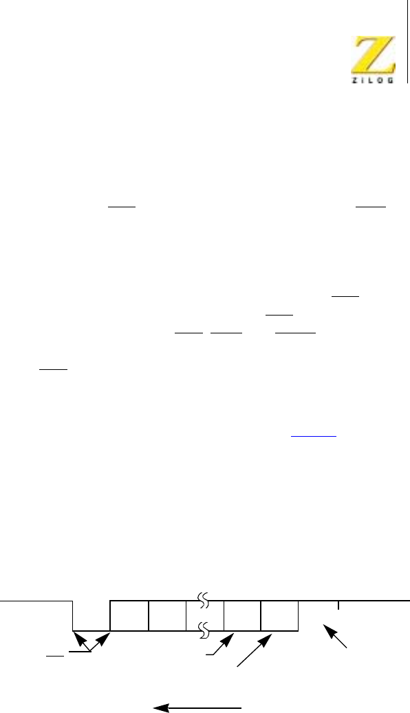
Z80 CPU Peripherals
User Manual
UM008101-0601 Serial Input/Output
231
registers by the system program. WR4 parameters must be issued before
WR1, WR3, and WR5 parameters or commands.
If the data is transmitted over a modem or RS232C interface, the
REQUEST TO SEND (RTS) and DATA TERMINAL READY (DTR)
outputs must be set along with the Transmit Enable bit. Transmission
cannot begin until the Transmit Enable bit is set.
The Auto Enables feature allows the programmer to send the first data
character of the message to the Z80 SIO without waiting for CTS.Ifthe
Auto Enables bit is set, the Z80 SIO waits for the CTS pintogoLow
before it begins data transmission. CTS,DCD, and SYNC are general-
purpose I/O lines that may be used for functions other than their labeled
purposes. If CTS is used for another purpose, the Auto Enables Bit must
be programmed to 0.
Figure 111 illustrates asynchronous message formats; Table 3 describes
WR3, WR4, and WR5 with bits set to indicate the applicable modes,
parameters and commands in asynchronous modes. WR2 (Channel B
only) stores the interrupt vector; WR1 defines the interrupt modes and
data transfer modes. WR6 and WR7 are not used in asynchronous modes.
Table 4 describes the typical program steps that implement a full-duplex
receive/transmit operation in either channel.
Figure 111. Asynchronous Message Format
Marking Line Start D0 D1 DN
N = 5, 6, 7, or 8
Message Flow
May be present or not
Even or Odd
Parity Stop Marking Line
1, 1 1/2, or 2 Bits
Asynchronous Format
All Transactions Occur
on a Falling Edge of TxC

UM008101-0601 Serial Input/Output
232
Asynchronous Transmit
The Transmit Data output (TxD) is held marking (High) when the trans-
mitter has no data to send. Under program control, the Send Break (WR5,
D4) command can be issued to hold TxD spacing (Low) until the
command is cleared.
The Z80 SIO automatically adds the start bit, the programmed parity bit
(odd, even, or no parity), and the programmed number of stop bits to the
data character to be transmitted. When the character length is six or seven
bits, the unused bits are automatically ignored by the Z80 SIO. If the char-
acter length is five bits or less, refer to the table in the Write Register 5
description (Z80 SIO Programming section) for the data format.
Serial data is shifted from TxD at a rate equal to 1, 1/16th, 1/32nd, or 1/64th
of the clock rate supplied to the Transmit Clock input TxC Serial data is
shifted out on the falling edge of TxC.
If set, the External/Status Interrupt mode monitors the status of DCD,CTS,
and SYNC throughout the transmission of the message. If these inputs
change for a period of time greater than the minimum specified pulse
width, the interrupt is generated. In a transmit operation, this feature is used
to monitor the modem control signal CTS.
Table 3. Contents of Write Registers 3, 4, and 5 in Asynchronous Modes
Bit 7 Bit 6 Bit 5 Bit 4 Bit 3 Bit 2 Bit 1 Bit 0
WR3 00=Rx5Bits/Char
10 = Rx 6 Bits/Char
01 = Rx 7 Bits/Char
11=Rx8Bits/Char
Auto
Enables
00 0 0 Rx
Enable
WR4 00 = x1 Clock Mode
01 = x16 Clock Mode
10 = x32 Clock Mode
11 = x64 Clock Mode
0000=NotUsed
01 = 1 Stop Bit/Char
10 = 1-1/2 Stop Bits/
Char
11 = 2 Stop Bits/Char
Even/
Odd
Parity
Parity
Enable

Z80 CPU Peripherals
User Manual
UM008101-0601 Serial Input/Output
233
WR5 DTR 00 = Tx 5 Bits (or less)/
Char
10 = Tx 6 Bits/Char
01 = Tx 7 Bits/Char
11=Tx8Bits/Char
Send
Break
Tx
Enable
0RTS0
Table 4. Asynchronous Mode
Function Typical Program Steps Comments
Register: Information loaded:
Initialize WR0 Channel Reset Reset SIO
WR0 Pointer 2
WR2 Interrupt Vector Channel B Only
WR0 Pointer 4, Reset External/Status Interrupt
WR4 Asynchronous mode, Parity information, Stop
Bits information, Clock Rate information
Issue Parameters
WR0 Pointer 3
WR3 Receive Enable, Auto Enables, Receive
Character Length
WR0 Pointer 5
Table 3. Contents of Write Registers 3, 4, and 5 in Asynchronous Modes (Continued)
Bit 7 Bit 6 Bit 5 Bit 4 Bit 3 Bit 2 Bit 1 Bit 0

UM008101-0601 Serial Input/Output
234
WR5 Request to send, transmit enable, transmit
character length, data terminal ready
Receive and Transmit both
fully initialized. Auto Enables
enables transmitter if CTS is
active and receiver if DCD is
active
WR0 Pointer 1, Reset External/Status Interrupt
WR1 Transmit Interrupt Enable, Status Affects
Ve c t o r,
Interrupt on all Receive characters. Disable
Wait/Ready function, External Interrupt Enable
Transmit/receive Interrupt
Mode Selected.
External Interrupt monitors the
status of the CTS,DCD,and
SYNC inputs and detects the
Break sequence. Status affects
Vector In Channel B only. This
data byte must be transferred or
no transmit interrupts occur.
Transfer first data byte to SIO
Idle Mode Execute Halt Instruction or other program Program is waiting for an
interrupt from the SIO
Data transfer and
error monitoring
Z80 Interrupt Acknowledge cycle transfers
RR2 to CPU
When the interrupt occurs, the
interrupt vector is modified by:
1) Receive character available;
2) Transmit buffer empty;
3) External/status change; and
4) Special receive condition.
If a character is received:
•Transfer data character to CPU
•Update pointers and parameters
•Return from Interrupt
If transmitter buffer is empty: Program control is transferred
to one of the eight Interrupt
Service routines.
•Transfer data character to SIO
•Update pointers and parameters
•Return from interrupt
Table 4. Asynchronous Mode (Continued)
Function Typical Program Steps Comments

Z80 CPU Peripherals
User Manual
UM008101-0601 Serial Input/Output
235
Asynchronous Receive
An Asynchronous Receive operation begins when the Receive Enable bit is
set. If the Auto Enables option is selected, DCD must be Low. A Low
(spacing) condition on the Receive Data input (RxD) indicates a start bit. If
this Low persists for at least one-half of a bit time, the start bit is assumed to
be valid and the data input is then sampled at mid-bit time until the entire
character is assembled. This method of detecting a start bit improves error
rejection when noise spikes exist on an otherwise marking line.
If the x1 clock mode is selected, bit synchronization must be accom-
plished externally. Receive data is sampled on the rising edge of RxC.
The receiver inserts 1s when a character length of other than eight bits is
If External Status changes: If used with processors other
than the Z80, the modified
interrupt vector (RR2) should
be returned to the CPU in the
interrupt acknowledge
sequence.
•Transfer RRD to CPU
•Perform Error routines (include Break
detection)
•Return from Interrupt
If special receive condition occurs:
•TransferRR1toCPU
•D6 Special Error (such as framing error)
routine
•Return from Interrupt
Termination Redefine Receive/Transmit Interrupt modes
Disable Transmit/Receive modes
When Transmit or Receive
Data transfer is complete.
Update modem control outputs (such as RTS
off)
In Transmit, the all sent status
bit indicates transmission is
complete.
Table 4. Asynchronous Mode (Continued)
Function Typical Program Steps Comments

UM008101-0601 Serial Input/Output
236
used. If parity is enabled, the parity bit is not stripped from the assembled
character for character lengths other than eight bits. For lengths other than
eight bits, the receiver assembles a character length of the required
number of data bits, plus a parity bit and Is for any unused bits. For
example, the receiver assembles a 5-bit character with the following
format: 11 P D4 D3 D2 D1 D0.
Because the receiver is buffered by three 8-bit registers in addition to the
receive shift register, the CPU has enough time to service an interrupt and
to accept the data character assembled by the Z80 SIO. The receiver also
has three buffers that store error flags for each data character in the receive
buffer. These error flags are loaded at the same time as the data characters.
After a character is received, it is checked for the following error conditions:
•
When parity is enabled, the Parity Error bit (RR1, D4) is set whenever
the parity bit of the character does not match with the programmed
parity. Once this bit is set, it remains set until the Error Reset Command
(WR0) is given.
•
The Framing Error bit (RR1, D6) is set if the character is assembled
without any stop bits (that is, a Low level detected for a stop bit).
Unlike the Parity Error bit, this bit is set (and not latched) only for the
character on which it occurred. Detection of framing error adds an
additional one-half of a bit time to the character time so the framing
error is not interpreted as a new start bit.
•
If the CPU fails to read a data character while more than three
characters have been received, the Receive Overrun bit RR1 D5) is set.
When this occurs, the fourth character assembled replaces the third
character in the receive buffers. With this arrangement, only the
character that has been written over is flagged with the Receive Overrun
Error bit. Like Parity Error, this bit can only be reset by the Error Reset
command from the CPU. Both the Framing Error and Receive Overrun
Error cause an interrupt with the interrupt vector indicating a Special
Receive condition (if Status Affects Vector is selected).

Z80 CPU Peripherals
User Manual
UM008101-0601 Serial Input/Output
237
After the Parity Error and Receive Overrun Error flags are latched, the error
status that is read indicates an error in the current word in the receive buffer
plus any Parity or Overrun Errors received after the last Error Reset
command. To keep correspondence between the state of the error buffers
and the contents of the receive data buffers, the error status register must be
read before the data. This is easily accomplished if vectored interrupts are
used, because a special interrupt vector is generated for these conditions.
While the External/Status interrupt is enabled, break detection causes an
interrupt and the Break Detected status bit (RR0, D7) is set. The Break
Detected interrupt should be responded to by issuing the Reset External/
Status Interrupt command to the Z80 SIO in response to the first Break
Detected interrupt that has a Break status of 1 (RR0, D7). The Z80 SIO
monitors the Receive Data input and waits for the Break sequence to
terminate, at which time the Z80 SIO interrupts the CPU with the Break
status set to 0. The CPU must again issue the Reset External/Status Inter-
rupt command in its interrupt service routine to reinitialize the break
detection logic.
The External/Status interrupt also monitors the status of DCD.IftheDCD
pin becomes inactive for a period greater than the minimum specified
pulse width, an interrupt is generated with the DCD status bit (RR0, D3)
set to 1. The DCD input is inverted in the RR0, status register.
If the status is read after the data, the error data for the next word is also
included if it has been stacked in the buffer. If operations are performed
rapidly enough so the next character is not yet received, the status register
remains valid. An exception occurs when the Interrupt On First Character
Only mode is selected. A special interrupt in this mode holds the error
data and the character itself (even if read from the buffer) until the Error
Reset command is issued. This interrupt prevents further data from
becoming available in the receiver until the Reset command is issued, and
allows CPU intervention on the character with the error even if DMA or
block transfer techniques are in use.
If Interrupt On Every Character is selected, the interrupt vector is different
an error status occurs in RR1. If a Receiver Overrun occurs, the most recent

UM008101-0601 Serial Input/Output
238
character received is loaded into the buffer; the character preceding it is
lost. When the character that has been written over the other characters is
read, the Receive Overrun bit is set and the Special Receive. Condition
vector is returned if Status Affects Vector is enabled.
In a polled environment, the Receive Character Available bit (RR0, D0)
must be monitored so that the Z80 CPU knows when to read a character.
This bit is automatically reset when the receive buffers are read. To prevent
overwriting data in polled operations, the transmit buffer status must be
cheeked before writing to the transmitter. The Transmit Buffer Empty bit is
set to 1 whenever the transmit buffer is empty.
SYNCHRONOUS OPERATION
Overview
Before describing synchronous transmission and reception, the three types
of character synchronization, Monosync, Bisync, and External Sync,
require explanation. These modes use the x1 clock for both Transmit and
Receive operations. Data is sampled on the rising edge of the Receive
Clock input (RxC). Transmitter data transitions occur on the falling edge of
the Transmit Clock input (TxC).
The differences between Monosync, Bisync, and External Sync are in the
form in which initial character synchronization is achieved. The mode of
operation must be selected before sync characters are loaded, because the
registers are used differently in the various modes. Figure 112 depicts the
formats for all three of these synchronous modes.
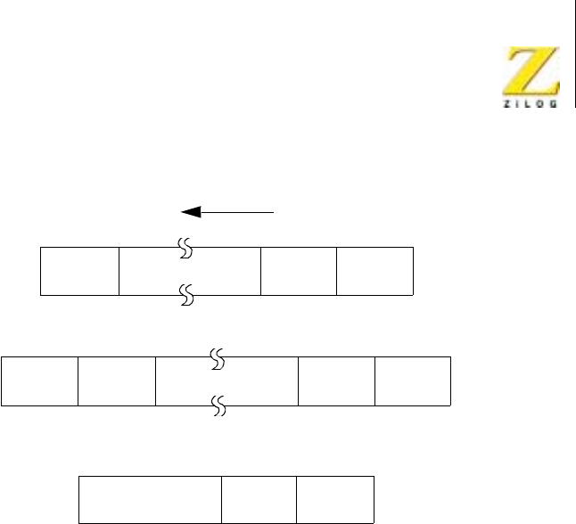
Z80 CPU Peripherals
User Manual
UM008101-0601 Serial Input/Output
239
Figure 112. Synchronous Formats
Message Flow
Beginning
Beginning
Beginning
(A) MONOSYNC Message Format (Internal SYNC Detected)
(B) BISYNC Message Format (Internal SYNC Detected)
(C) External SYNC Detect Format
07
07
07
70
70
70
15 8
15 8
15 8
Data Field CRC
Character CRC
Character
#1 #2
#1 #2
#1 #2
#1 #2
SYNC
Character SYNC
Character
SYNC
Character
CRC
Character
CRC
Character
CRC
Character
CRC
Character
Data Field
Data Field

UM008101-0601 Serial Input/Output
240
Synchronous Modes Of Operation
Monosync
In a Receive operation, matching a single sync character (8-bit sync
mode) with the programmed sync character stored in WR7 implies char-
acter synchronization and enables data transfer.
Bisync
Matching two contiguous sync characters (16-bit sync mode) with the
programmed sync characters stored in WR6 and WR7 implies character
synchronization. In both the Monosync and Bisync modes, SYNC is used
as an output, and is active for the part of the receive clock that detects the
sync character.
External Sync
In this mode, character synchronization is established externally. SYNC is
an input that indicates external character synchronization has been
achieved. After the sync pattern is detected, the external logic must wait
for two full Receive Clock cycles to activate the SYNC input. The SYNC
input must be held Low until character synchronization is lost. Character
assembly begins on the rising edge of RxC that precedes the falling edge
of SYNC.
In all cases after a reset, the receiver is in the Hunt phase, during which
the Z80 SIO looks for character synchronization. The hunt can begin only
when the receiver is enabled, and data transfer can begin only when char-
acter synchronization has been achieved. If character synchronization is
lost, the Hunt phase can be re-entered by writing a control word with the
Enter Hunt Phase bit set (WR3, D4). In the Transmit mode, the trans-
mitter always sends the programmed number of sync bits (8 or 16). In the

Z80 CPU Peripherals
User Manual
UM008101-0601 Serial Input/Output
241
Monosync mode, the transmitter transmits from WR6; the receiver
compares against WR7.
In the Monosync, Bisync, and External Sync modes, assembly of received
data continues until the Z80 SIO is reset, or until the receiver is disabled (by
command or by DCD in the Auto Enables mode), or until the CPU sets the
Enter Hunt Phase bit.
After initial synchronization has been achieved, the operation of the Mono-
sync, Bisync, and External Sync modes is similar. Any differences are spec-
ified in the following text.
Table 5 describes how WR3, WR4, and WR5 are used in synchronous
receive and transmit operations. WR0 points to other registers and issues
various commands, WR1 defines the interrupt modes, WR2 stores the
interrupt vector, and WR6 and WR7 store sync characters. Table 6 illus-
trates the typical program steps that implement a half-duplex Bisync
transmit operation.
Table 5. Contents of Write Registers 3, 4, and 6 In Synchronous Modes
Bit7 Bit6 Bit5 Bit4 Bit3 Bit2 Bit1 Bit0
WR
3
00 = Ax 5 Bits/char
10 = Rx 6 Bits/char
01 = Rx 7 Bits/char
11=Rx8Bits/char
Auto
Enables
Enter Hunt
Mode
Rx CRC
Enable
0 Sync char
load
inhibit
Rx
Enable
WR
4
0 0 00 = 8-bit Sync Char
01 = 16-bit Sync Char
10 = SDLC Mode
11 = Ext Sync Mode
0
Selects
Sync
Modes
0
Selects
Sync
Modes
Even/Odd
Parity
Parity
Enable
WR
5
DTR 00=Tx5Bits(orless)/
char
10 = Tx 6 Bits/char
01 = Tx 7 Bits/char
11 = Tx 8 Bits/char
Send
Break
Tx Enable 1
Selects
CRC-16
RTS Tx CRC
Enable

UM008101-0601 Serial Input/Output
242
Table6.BisyncTransmitMode
Function Typical Program Steps Comments
Register Information loaded
Initialize WR0 Channel Reset, Reset Transmit CRC
Generator
Reset SIO, Initialize CRC Generator
WR0 Pointer 2
WR2 Interrupt Vector Channel B only
WR0 Pointer 3
WR3 Auto Enables Transmission begins only after CTS
is detected
WR0 Pointer 4
WR4 Parity Information, Sync Modes
Information, X1Clock Mode
Issue transmit parameters
WR0 Pointer 6
WR6 Sync Character 1
WR0 Pointer 7, Reset External/Status Interrupts
WR7 Sync Character 2
WR0 Pointer 1, Reset External/Status Interrupts
WR1 Status Affects Vector, External Interrupt
Enable, Transmit Interrupt Enable or
WAIT/READY Mode Enable
External Interrupt Mode monitors
the status of CTS and DCD input
pins as well as the status of Tx
Underrun/EOM Latch. Transmit
Interrupt Enable interrupts when the
transmit buffer becomes empty; the
WAIT/READYModecanbeusedto
transfer data using DMA or CPU
block transfer.

Z80 CPU Peripherals
User Manual
UM008101-0601 Serial Input/Output
243
WR0 Pointer 5 Status affects vector (Channel B
only). Transmit CRC Enable should
be set when first non-sync data is
sent to Z80 SIO. Need several sync
characters in the beginning of
message. Transmitter is fully
initialized.
WR5 Request To Send, Transmit Enable, Bisync
CRC, transmit character length first Sync
Byte To SIO
Idle Mode Execute Halt Instruction or some other
program
Waiting for interrupt or WAIT/
READY output to transfer data.
Data Transfer and
Status Monitoring
When Interrupt (WAIT/READY) occurs: Interrupt Occurs (Wait/ready
Becomes Active) When first data
byte is being sent, Wait Mode allows
CPU block transfer from memory to
SIO; Ready Mode allows DMA
block transfer from memory to SIO.
The DMA chip can be programmed
to capture special control characters
(by examining only the bits that
specify ASCII or EBCDIC control
characters), and interrupt CPU.
•Include/Exclude data byte from CRC
Accumulation (in SIO)
•Transfer data byte from CPU (or
memory) to SIO
•Detect and set appropriate flags for
control characters (in CPU)
•Reset Tx Underrun/EOM Latch WR0 if
last character of message is detected
•Update pointers and parameters (CPU)
Return from Interrupt
If Error Condition Or Status Change
Occurs:
Tx Underrun/EOM indicates either
Transmit Underrun (sync character
being sent) or end of message (CRC-
16 being sent).
•Transfer RR0 to CPU
•Execute Error Routine
•Return From Interrupt
Termination Redefine Interrupt Modes, Update Modem
Control outputs (for example, turn off
RTS)
Program should gracefully terminate
message
Disable Transmit Mode
Table 6. Bisync Transmit Mode (Continued)
Function Typical Program Steps Comments

UM008101-0601 Serial Input/Output
244
Synchronous Transmit
Initialization
The system program must initialize the transmitter with the following
parameters: odd or even parity, x1 clock mode, 8-bit or 16-bit sync char-
acter(s), CRC polynomial, Transmitter Enables, Request To Send, Data
Terminal Ready, interrupt modes, and transmit character length. WR4
parameters must be issued before WR1, WR3, WR5, WR6, and WR7
parameters or commands.
One of two polynomials, CRC -16(X16 +X
15 +X
2+1)orSDLC(X
16 +
X12 +X
5+ 1), may be used with synchronous modes. In either case (SDLC
mode not selected), the CRC generator and checker are reset to all 0s. In the
transmit initialization process, the CRC generator is initialized by setting
the Reset Transmit CRC Generator command bits (WR0). Both the trans-
mitter and the receiver use the same polynomial.
Transmit Interrupt Enable or Wait/Ready Enable can be selected to transfer
the data. The External/Status interrupt mode is used to monitor the status of
the CLEAR TO SEND (CTS) input as well as the Transmit Underrun/EOM
latch. Optionally, the Auto Enables feature can be used to enable the trans-
mitter when CTS is active. The first data transfer to the Z80 SIO can begin
when the External/Status interrupt occurs (CTS status bit set) or immediately
following the Transmit Enable command (if the Auto Enables modes is set).
Transmit data is held marking after reset or if the transmitter is not
enabled. Break may be programmed to generate a spacing line that begins
as soon as the Send Break bit is set. With the transmitter fully initialized
and enabled, the default condition is continuous transmission of the 8-bit
or 16-bit sync character.
Data Transfer and Status Monitoring

Z80 CPU Peripherals
User Manual
UM008101-0601 Serial Input/Output
245
In this phase, there are several combinations of data transfers using inter-
rupts and Wait/Ready status.
Data Transfer Using Interrupts
If the Transmit Interrupt Enable bit (WR1, D1) is Set, an interrupt is gener-
ated each time the transmit buffer becomes empty. The interrupt can be
satisfied either by writing another character to the transmitter or by reset-
ting the Transmitter Interrupt Pending latch with a Reset Transmitter
Pending command (WR0, CMD5). If the interrupt is satisfied with this
command and nothing more is written to the transmitter, there can be no
further Transmit Buffer Empty interrupts, because it is the process of the
buffer becoming empty that causes the interrupts and the buffer cannot
become empty when it is already empty. This situation does cause a
Transmit Underrun condition, which is explained in the ““Bisync Transmit
Underrun”on page 245”section.
Data Transfer Using WAIT/READY
To the CPU, the activation of WAIT indicates that the Z80 SIO is not ready
to accept data and that the CPU must extend the output cycle. To a DMA
controller, READY indicates that the transmit buffer is empty and that the
Z80 SIO is ready to accept the next data character. If the data character is
not loaded to the Z80 SIO by the time the transmit shift register is empty,
the Z80 SIO enters the Transmit Underrun condition.
Bisync Transmit Underrun
In Bisync protocol, filler characters are inserted to maintain synchroniza-
tion when the transmitter has no data to send (Transmit Underrun condi-
tion). The Z80 SIO has two programmable options for resolving this
situation: it can insert sync characters, or it can send the CRC characters
generated so far, followed by sync characters.
These options are under the control of tile Reset Transmit Underrun/EOM
Command in WR0. Following a chip or channel reset, the Transmit
Underrun/EOM status bit (RR0, D6) is in a set condition and allows the

UM008101-0601 Serial Input/Output
246
insertion of sync characters when there is no data to send. CRC is not
calculated on the automatically inserted sync characters. When the CPU
detects the end of message, a Reset Transmit Underrun/EOM command
can be issued. This action allows CRC to be sent when the transmitter has
no data. In this case, the Z80 SIO sends CRC, followed by sync charac-
ters, to terminate the message.
There is no restriction as to when in the message the Transmit Underrun/
EOM bit can be reset. If Reset is issued after the first data character has
been loaded, the 16-bit CRC is Sent and followed by sync characters the
first time the transmitter has no data to send. Because of the Transmit
Underrun condition, an External/Status interrupt is generated whenever the
Transmit Underrun/EOM bit becomes set.
In the case of sync insertion, an interrupt is generated only after the first
automatically inserted sync character has been loaded. The status indicates
the Transmit Underrun/ EOM bit and the Transmit Buffer Empty bit are set.
In the case of CRC insertion, the Transmit Underrun/EOM bit is set and the
Transmit Buffer Empty bit is reset while CRC is being sent. When CRC has
been completely sent, the Transmit Buffer Empty status bit is set and an
interrupt is generated to indicate to the CPU that another message can begin
(this interrupt occurs because CRC has been sent and sync has been
loaded). If no more messages are to be sent, the program can terminate
transmission by resetting RTS, and disabling the transmitter (WR5, D3).
Pad characters may be sent by setting the Z80 SIO to eight bits/transmit
character and writing FF to the transmitter while sending CRC. Alterna-
tively, the sync characters can be redefined as pad characters during this
time. The following example clarifies this point.
1. The Z80 SIO interrupts with the Transmit Buffer Empty bit set.
2. The CPU recognizes that the last character (ETX) of the message has
already been sent to the Z80 SIO by examining the internal program
status.

Z80 CPU Peripherals
User Manual
UM008101-0601 Serial Input/Output
247
3. ToforcetheZ80SIOtosendCRC,theCPUissuestheReset
Transmit Underrun/EOM Latch command (WR0) and satisfies the
interrupt with the Reset Transmit Interrupt Pending command. (This
command prevents the Z80 SIO from requesting more data.) Because
of the transmit underrun caused by this command, the Z80 SIO starts
sending CRC. The Z80 SIO also causes an External/Status interrupt
with the Transmit Underrun/EOM latch set.
4. The CPU satisfies this interrupt by loading pad characters to the transmit
buffer and issuing the Reset External/Status Interrupt command.
5. With this sequence, CRC is followed by a pad character instead of a
sync character. The Z80 SIO interrupts with a Transmit Buffer Empty
interrupt when CRC is completely sent and that the pad character is
loaded to the transmit shift register.
6. From this point on the CPU can send more pad characters or sync
characters.
Bisync CRC Generation
Setting the Transmit CRC enable bit (WR5, D0) initiates CRC accumula-
tion when the program sends the first data character to the Z80 SIO.
Although the Z80 SIO automatically transmits up to two sync characters
(18-bit sync), it is recommended to send a few more sync characters ahead
of the message (before enabling Transmit CRC) to ensure synchronization
at the receiving end.
The transmit CRC Enable bit can be changed at any time in the message to
include or exclude a particular data character from CRC accumulation. The
Transmit CRC Enable bit should be in the suitable state when the data char-
acter is loaded from the transmit data buffer to the transmit shift register. To
ensure this bit is in a suitable state, the Transmit CRC Enable bit must be
issued before sending the data character to the Z80 SIO.

UM008101-0601 Serial Input/Output
248
Transmit Transparent Mode
Transparent mode (Bisync protocol) operation is made possible by the
ability to change Transmit CRC Enable on the fly and by the additional
capability of inserting 16-bit sync characters. Exclusion of IDLE characters
from CRC calculation can be achieved by disabling CRC calculation
immediately preceding the IDLE character transfer to the Z80 SIO.
In the case of a Transmit Underrun condition in the Transparent mode, a
pair of DLE-SYN characters are sent. The Z80 SIO can be programmed to
send the DLE-SYN sequence by loading a IDLE character to WR6 and a
sync character to WR7.
Transmit Termination
The Z80 SIO is equipped with a special termination feature that maintains
data integrity and validity. If the transmitter is disabled while a data or sync
character is being sent, that character is sent as usual, but is followed by a
marking line rather than CRC or sync characters. When the transmitter is
disabled, a character in the buffer remains in the buffer. If the transmitter is
disabled while CRC is being sent, the 16-bit transmission is completed, but
sync is sent instead of CRC.
A programmed break is effective as soon as it is written to the control
register; therefore, characters in the transmit buffer and shift register are lost.
In all modes, characters are sent with the least-significant bits first. This
requires right justification of transmitted data if the word length is less than
eight bits. If the word length is five bits or less, the special technique
described in the Write Register 5 discussion (Z80 SIO Programming
section) must be used for the data format. The states of any unused bits in a
data character are irrelevant except when in the Five Bits Or Less mode.
If the External/Status Interrupt Enable bit is set, transmitter conditions such
as “starting to send CRC characters,”“starting to send sync characters,”and
CTS changing state cause interrupts that have a unique vector if Status
Affects Vector is set. This interrupt mode may be used during block transfers.

Z80 CPU Peripherals
User Manual
UM008101-0601 Serial Input/Output
249
All interrupts may be disabled for operation in a Polled mode or to avoid
interrupts at inappropriate tunes during the execution of a program.
Synchronous Receive
Initialization
The system program initiates the Synchronous Receive operation with the
following parameters: odd or even parity, 8-bit or 16-bit sync characters, x1
clock mode, CRC polynomial, receive character length, and more. Sync
characters must be loaded to registers WR6 and WR7. The receivers can be
enabled only after all receive parameters are set. WR4 parameters must be
issued before WR1, WR3, WR5, WR6, and WR7 parameters or commands.
After these condititons are met, the receiver is in the Hunt phase. It remains in
this phase until character synchronization is achieved. Under program
control, all the leading sync characters of the message can be inhibited from
loading the receive buffers by setting the Sync Character Load Inhibit bit in
WR3.
Data Transfer and Status Monitoring
After character synchronization is achieved, the assembled characters are
transferred to the receive data FIFO. The following four interrupt modes are
available to transfer the data and its associated status to the CPU.
No Interrupts Enabled
This mode is used for a purely polled operation or for off-line conditions.
Interrupt On First Character Only
This mode is normally used to start a polling loop or a Block Transfer
instruction using WAIT/READY to synchronize the CPU or the DMA
device to the incoming data rate. In this mode, the Z80 SIO interrupts on
the first character and thereafter interrupts only if Special Receive condi-

UM008101-0601 Serial Input/Output
250
tions are detected. The mode is reinitialized with the Enable Interrupt On
Next Receive Character command to allow the next character received to
generate an interrupt. Parity errors do not cause interrupts in this mode, but
End-of-Frame (SDLC mode) and Receive Overrun do.
If External/Status interrupts are enabled, they may interrupt any time DCD
changes state.
Interrupt On Every Character
Whenever a character enters the receive buffer, an interrupt is generated.
Error and Special Receive conditions generate a special vector if Status
Affects Vector is selected. Optionally, a Parity Error may be directed not to
generate the special interrupt vector.
Special Receive Condition Interrupts
The Special Receive Condition interrupt can occur only if either the
Receive Interrupt On First Character Only or Interrupt On Every Receive
Character modes is also set. The Special Receive Condition interrupt is
caused by the Receive Overrun error condition. Since the Receive Overrun
and Parity error status bits are latched, the error status-when read-reflects
an error in the current word in the receive buffer in addition to any Parity or
Overrun errors received after the last Error Reset command. These status
bits can only be reset by the Error reset command.
CRC Error Checking and Termination
A CRC error check on the receive message can be performed on a per char-
acter basis under program control. The Receive CRC Enable bit (WR3, D3)
must be set/reset by the program before the next character is transferred
from the receive shift register to the receive buffer register. This ensures
proper inclusion or exclusion of data characters in the CRC check.
To allow the CPU ample time to enable or disable the CRC check on a
particular character, the Z80 SIO calculates CRC eight bit times after the
character has been transferred to the receive buffer. If CRC is enabled

Z80 CPU Peripherals
User Manual
UM008101-0601 Serial Input/Output
251
before the next character is transferred, CRC is calculated on the transferred
character. If CRC is disabled before the time of the next transfer, calcula-
tion proceeds on the word in progress, but the word just transferred to the
buffer is not included. When these requirements are satisfied, the 3-byte
receive data buffer is, in effect, unusable in Bisync operation. CRC may be
enabled and disabled as many times as necessary for a given calculation.
In the Monosync, Bisync, and External Sync modes, the CRC/Framing Error
bit (RR1, D6) contains the comparison result of the CRC checker 16-bit
times (eight bits delay and eight shifts for CRC) after the character has been
transferred from the receive shift register to the buffer. The result should be
zero, indicating an error-free transmission.
The result is valid only at the end of CRC calculation. If the result
is examined before this time, it usually indicates an error.
The comparison is made with each transfer and is valid only as long as the
character remains in the receive FIFO.
Following is an example of the CRC checking operation when four charac-
ters (A, B, C, and D) are received in that order.
•
Character A loaded to buffer
•
Character B loaded to buffer
If CRC is disabled before C is in the buffer, CRC is not calculated on B.
•
Character C loaded to buffer
After C is loaded, the CRC/Framing Error bit shows the result of the
comparison through character A.
•
Character D loaded to buffer
After D is in the buffer, the CRC Error bit shows the result of the comparison
through character B whether or not B was included in the CRC calculations.
Due to the serial nature of CRC calculation, the Receive Clock (RxC)
must cycle 16 times (8-bit delay plus 8-bit CRC shift) after the second
Note:

UM008101-0601 Serial Input/Output
252
CRC character has been loaded to the receive buffer, or 20 times (the
previous 16 plus 3-bit buffer delay and 1-bit input delay) after the last bit
is at the RxD input, before CRC calculation is complete. A faster external
clock can be gated to the Receive Clock input to supply the required 16
cycles. The Transmit and Receive Data Path diagram (Figure 109) illus-
trates the various points of delay in the CRC path.
The typical program steps that implement a half-duplex Bisync Receive
mode are illustrated in Table 7. The complete set of command and status
bit definitions are explained under “Programming”on page 272.
Table7.BisyncReceiveMode
Function Typical Program Steps Comments
Register Information Loaded
Initialize WR0 Channel Reset, Reset Receive CRC
Checker
Reset SIO; initialize receive CRC
checker
WR0 Pointer 2
WR2 Interrupt Vector Channel B only
WR0 Pointer 4
WR4 Parity Information, Sync Modes
Information, Clock Mode
Issue Receive Parameters
WR0 Pointer 5, Reset External Status
Interrupt
WR5 Bisync CRC-16, Data Terminal Ready
WR0 Pointer 3
WR3 Sync Character Load Inhibit, Receive
CRC Enable; Enter Hunt Mode, Auto
Enables, Receive Character Length
Sync Character Load Inhibit strips all
the leading sync characters at the
beginning of the message. Auto Enables
enables the receiver to accept data only
after the DCD input is active.
WR0 Pointer 6
WR6 Sync Character 1
WR0 Pointer 7
WR7 Sync Character 2

Z80 CPU Peripherals
User Manual
UM008101-0601 Serial Input/Output
253
WR0 Pointer 1, Reset External/Status
Interrupt
WR1 Status Affects Vector, External
Interrupt Enable, Receive Interrupt on
first character only
In this interrupt mode, only the first
non-sync data character is transferred to
the CPU. All subsequent data is
transferred on a DMA basis; however,
special receive condition interrupts
interrupt the CPU. status affects vector
used in Channel B only.
WR0 Pointer 3, Enable Interrupt on next
Receive character
Resetting this Interrupt Mode provides
simple program loopback entry for the
next transaction.
WR3 Receive Enable, sync character load
inhibit, enter Hunt Mode Auto Enable,
receive word length
WR3 is reissued to enable receiver;
receive CRC enable must be set after
receiving SOH or STX character.
Idle Mode Execute Halt Instruction or some other
program
Receive mode is fully initialized and the
system is waiting for interrupt on first
character.
Table 7. Bisync Receive Mode (Continued)
Function Typical Program Steps Comments

UM008101-0601 Serial Input/Output
254
Data Transfer And
Status Monitoring
When Interrupt on first character
occurs, the CPU performs the
following:
During the hunt mode, the SIO detects
two contiguous characters to establish
synchronization. The CPU establishes
the DMA Mode and all subsequent data
characters are transferred by the DMA
controller. The controller is also
programmed to capture special
characters (by examining only the bits
that specify ASCII or EBCDIC control
characters) and interrupt the CPU upon
detection. In response, the CPU
examines the status or control characters
and takes appropriate action, such as
CRC enable update.
•Transfers data byte to CPU
•Detects and sets appropriate flags for
control characters (in CPU)
•Includes/Excludes data byte in CRC
checker
•Updates pointers and other
parameters
•Enables Wait/Ready for DMA
operation
•Enables DMA controller
•Returns from Interrupt
When Wait/Ready becomes active, the
DMA controller performs the
following:
•Transfers Data Byte to memory
•Interrupts CPU if a special character
is captured by the DMA controller
•Interrupts the CPU if the last
character of the message is detected
For Message Termination, the CPU
performs the following:
The SIO interrupts the CPU for error
condition, and the error routine aborts
the present message, clears the error
condition, and repeats the operation.
•Transfers RR1 to the CPU
•Sets Ack/Nak Reply Flag based on
CRC result
•Updates pointers and parameters
•Returns from Interrupt
Table 7. Bisync Receive Mode (Continued)
Function Typical Program Steps Comments

Z80 CPU Peripherals
User Manual
UM008101-0601 Serial Input/Output
255
SDLC (HDLC) OPERATION
Overview
The Z80 SIO allows processing of both High-level Synchronous Data
Link Control (HDLC) and IBM Synchronous Data Link Control (SDLC)
protocols. In this chapter only Synchronous Data Link Control (SDLC) is
covered because of the similarity between SDLC and HDLC.
The SDLC mode is bit oriented which differs from Synchronous Bisync
protocol, which is character oriented. Therefore, SDLC mode allows trans-
parent operation and variable message length. The bit-orientation SDLC is
a flexible protocol because it can process longer message length and bit
patterns. IBM document GA27-3093 has more information about SDLC
protocol.
The SDLC message, called the frame (Figure 113), is opened and closed by
flags that are similar to the sync characters in Bisync protocol. The Z80 SIO
handles the transmission and recognition of the flag characters that mark
the beginning and end of the frame. Although the Z80 SIO can receive
shared-zero flags, it cannot transmit them. The 8-bit address field of an
SDLC frame contains the secondary station address. The Z80 SIO has an
Address Search mode that recognizes the secondary station address,
allowing it to accept or reject the frame.
Termination Redefine Interrupt Modes and Sync
Modes
Update Modem Controls
Disables Receive Mode
Table 7. Bisync Receive Mode (Continued)
Function Typical Program Steps Comments
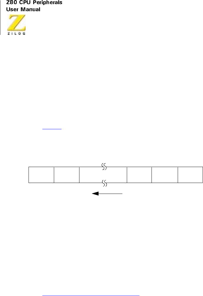
UM008101-0601 Serial Input/Output
256
The control field of the SDLC frame is transparent to the Z80 SIO, and it
is transferred to the CPU. The Z80 SIO handles the Frame Check
sequence in a way that simplifies the program by incorporating features,
such as initializing the CRC generator to all 1s, resetting the CRC checker
when the opening flag is detected in the Receive mode, and sending the
Frame Check/Flag sequence in the Transmit mode. Controller hardware is
simplified by automatic zero insertion and deletion logic contained in the
Z80 SIO.
Table 8 lists the contents of WR3, WR4, and WR5 during SDLC Receive
and Transmit modes. WR0 points to other registers and issues commands.
WR1 defines the interrupt modes. WR2 stores the interrupt vector. WR7
stores the flag character and WR6 the secondary address.
Figure 113. Transmit/Receive SDLC/HDLC Message Format
SDLC Transmit
Initialization
The SDLC Transmit mode must be initialized with the following parame-
ters: SDLC mode, SDLC polynomial, Request To Send, Data Terminal
Ready, transmit character length, transmit interrupt modes (or Wait/Ready
function), Transmit Enable, Auto Enables, and External/Status interrupt. Se
“SDLC Transmit Mode”on page 262)
Selecting the SDLC mode and the SDLC polynomial allows the Z80 SIO to
initialize the CRC Generator to all 1s. Initialization is accomplished by
issuing the Reset Transmit CRC Generator command WR0. Refer to the
Beginning
Opening
Flag
0111 1110
Address
8Bits
CRC
15 #1 87 0
CRC
#2
Closing
Flag
0111 1110
End
Message Flow
Data Field or
I-Field

Z80 CPU Peripherals
User Manual
UM008101-0601 Serial Input/Output
257
“Synchronous Operation”on page 238 section for more details on the
interrupt modes.
After reset, or when the transmitter is not enabled, the Transmit Data output
is held marking. Break may be programmed to generate a spacing line.
With the transmitter fully initialized and enabled, continuous flags are
transmitted on the Transmit Data output.
An abort sequence may be sent by issuing the Send Abort command WR0
CMD1). The Send Abort command causes at least 8, but less than 14, 1s to
be sent before the line reverts to continuous flags. It is possible that the
Abort sequence (eight 1s) could follow up to five continuous 1 bits
(allowed by the zero insertion logic) and thus cause up to thirteen 1s to be
sent. Any data being transmitted and any data in the transmit buffer is lost
when an abort is issued.
When required, an extra 0 is automatically inserted when five contiguous
1s occur in the data stream. Automatic insertion does not apply to flags or
aborts.
Data Transfer and Status Monitoring
SDLC mode allows several combinations of interrupts and Wait/Ready
functions.
Data Transfer Using Interrupts
If the Transmit Interrupt Enable bit is set, an interrupt is generated when the
buffer becomes empty. The interrupt may be satisfied either by writing
another character to the transmitter or by resetting the Transmit Interrupt
Pending latch with a Reset Transmitter Pending command (WR0, CMD5).
If the interrupt is satisfied with this command and no more is written to the
transmitter, then no more transmitter interrupts occur. The result is a
Transmit Underrun condition. When another character is written and sent,
the transmitter can again become empty and interrupt the CPU. Following
the flags in an SDLC operation, the 8-bit address field, control field and

UM008101-0601 Serial Input/Output
258
information field may be sent to the Z80 SIO using the Transmit Interrupt
mode. The Z80 SIO transmits the Frame Check sequence using the
Transmit Underrun feature.
When the transmitter is first enabled, it is already empty and cannot then
become empty. Therefore, no Transmit Buffer Empty interrupts can occur
until after the first data character is written.
Data Transfer Using WAIT/READY
When the Wait/Ready function is selected, WAIT communicates to the
CPU that the Z80 SIO is not ready to accept the data and that the CPU must
extend the I/O cycle. To a DMA controller, READY communicates that the
transmitter buffer is empty and that the Z80 SIO is ready to accept the next
character. If the data character is not loaded to the Z80 SIO by the time the
transmit shift register is empty, the Z80 SIO enters the Transmit Underrun
condition. Address, control, and information fields may be transferred to
Table 8. Contents of Write Registers 3, 4, and 5 in SDLC Modes
Bit7 Bit6 Bit5 Bit4 Bit3 Bit2 Bit1 Bit0
WR
3
00 = Rx 5 Bits Char
10 = Rx 6 Bits Char
01 = Rx 7 Bits Char
11 = Rx 8 Bits Char
Auto
Enables
Enter Hunt
Mode (if
incoming
data not
needed)
Rx CRC
Enable
Address
Search
Mode
0Rx
Enable
WR
4
00 1
Selects
SDLC
Mode
0
Selects
SDLC
Mode
0000
WR
5
DTR 00=Tx5Bits(orless)
Char
10=Tx6BitsChar
01=Tx7BitsChar
11 = Tx 8 Bits Char
0 Tx Enable 0
Selects
SDLC
CRC
RTS Tx CRC
Enable

Z80 CPU Peripherals
User Manual
UM008101-0601 Serial Input/Output
259
the Z80 SIO with this mode using the Wait/Ready function. The Z80 SIO
transmits the Frame Check sequence using the Transmit Underrun feature.
SDLC Transmit Underrun/End of Message
SDLC-like protocols do not have provisions for fill characters within a
message. The Z80 SIO therefore automatically terminates an SDLC frame
when the transmit data buffer and output shift register have no more bits to
send. It does this by first sending the two bytes of CRC followed by one or
more flags. This technique allows very high-speed transmissions under
DMA or CPU block I/O control without requiring the CPU to respond
quickly to the end of message condition.
The Z80 SIO response to the underrun condition depends on the state of the
Transmit Underrun/EOM command. Following a reset, the Transmit
Underrun/EOM status bit is in the set state and prevents the insertion of
CRC characters while there is no data to send. Consequently, flag charac-
ters are sent. The Z80 SIO starts sending the frame while data is written to
thetransmitbuffer.Betweenthetimethefirstdatabyteiswrittenandthe
end of the message, the Reset Transmit Underrun/EOM Command must be
issued. Thus the Transmit Underrun/EOM status bit is in the reset state at
the end of the message (when underrun occurs), which automatically sends
the CRC characters. The sending of CRC again sets the Transmit/Underrun/
EOM status bit.
Although there is no restriction about when the Transmit Underrun/EOM
bit can be reset within a message, the reset usually occurs after the first data
character (secondary address) is sent to the Z80 SIO. Resetting this bit
allows CRC and flags to be sent when there is no data to send, allowing
additional time for the CPU to recognize the fault and respond with an abort
command. By resetting this bit early in the message, the entire message is
allotted the maximum amount of CPU response time in an unintentional
transmit underrun situation.
When the External/Status interrupt is set and while CRC is sent, the
Transmit Underrun/EOM bit is set and the Transmit Buffer Empty bit is
reset to indicate that the transmit register is full of CRC data. When CRC

UM008101-0601 Serial Input/Output
260
has been completely sent, the Transmit Buffer Empty status bit is set and an
interrupt is generated to indicate to the CPU that another message can
begin. This interrupt occurs because CRC is sent and the flag is loaded. If
no more messages are to be sent, the program can terminate transmission
by resetting RTS, disabling the transmitter.
In the SDLC mode, reset the Transmit Underrun/EOM status bit immedi-
ately after the first character is sent to the Z80 SIO. When the Transmit
Underrun is detected, this ensures that the transmission time is filled by
CRC characters, giving the CPU enough time to issue the Send Abort
command. This procedure also stops the flags from going on the line
prematurely and eliminates the possibility of the receiver accepting the
frame as valid data. For example, the data pattern, immediately preceding
the automatic flag insertion, could match the CRC checker, thereby giving a
false CRC check result. The External/Status interrupt is generated when-
ever the Transmit Underrun/EOM bit is set as a result of the Transmit
Underrun condition.
The transmit underrun logic provides additional protection from premature
flag insertion if the proper response is given to the Z80 SIO by the CPU
interrupt service routine. The following example illustrates this point:
1. The Z80 SIO interrupts with the Transmit Buffer Empty status bit set.
2. The CPU does not respond in a timely manner, which causes a
Transmit Underrun condition.
3. The Z80 SIO starts sending CRC characters (two bytes).
4. The CPU eventually satisfies the Transmit Buffer Empty interrupt
with a data character that follows the CRC character being
transmitted.
5. The Z80 SIO sets the External/Status interrupt with the Transmit
Underrun/EOM status bit set
6. The CPU recognizes the Transmit Underrun/EOM status and
determines from its internal program status that the interrupt is not
“end of message”.

Z80 CPU Peripherals
User Manual
UM008101-0601 Serial Input/Output
261
7. The CPU immediately issues a Send Abort Command WR0 to the
Z80 SIO.
8. The Z80 SIO sends the Abort sequence by destroying whatever data
(CRC, data, or flag) is being sent.
As this sequence describes, the CPU has a protection of 22 minimum and
30 maximum transmit clock cycles.
SDLC CRC Generation
Reset the CRC generator to all 1s at the beginning of each frame before
CRC accumulation begins. Actual accumulation begins when the program
sends the address field (eight bits) to the Z80 SIO. Although the Z80 SIO
automatically transmits one flag character following the Transmit Enable,
send a few more flag characters ahead of the message to ensure that char-
acter synchronization occurs at the receiving end. Synchronization is
accomplished by externally timing out after enabling the transmitter, and
before loading the first character.
The Transmit CRC Enable (WR5, D0) must be enabled before sending the
address field. In the SDLC mode, all the characters between the opening
and closing flags are included in CRC accumulation, and the CRC gener-
ated in the Z80 SIO transmitter is inverted before it is sent on the line.
Transmit Termination
If the transmitter is disabled while a character is being sent, that Character
(data or flag) is sent, but is followed by a marking line rather than CRC or
flag characters.
A character in the buffer while the transmitter is disabled, remains in the
buffer; however, a programmed Abort sequence executes when it is written
to the control register. Characters being transmitted, if any, are lost. In the
case of CRC, the 16-bit transmission is completed if the transmitter is
disabled; however, flags are sent in place of CRC.

UM008101-0601 Serial Input/Output
262
In all modes, characters are sent with the least-significant bits first. This
requires right justification of data to be transmitted when the word length is
less than eight bits. If the word length is five bits or less, use the special
technique described in “Write Register 5”on page 289.
Because the number of bits/character can be changed on-the-fly, the data
field can be filled with any number of bits. When used in conjunction with
the Receiver Residue codes, the Z80 SIO can receive a message that has a
variable I-field and retransmit it exactly as received with no previous infor-
mation about the character structure of the I-field (if any). A change in the
number of bits does not affect the character being shifted out. Characters
are sent with the number of bits programmed at the time that the character
is loaded from the transmit buffer to the transmitter.
If the External/Status Interrupt Enable is set, transmitter conditions, such as
“startingtosendCRCcharacters,”“starting to send flag characters,”and CTS
changing state, cause interrupts, having a unique vector if Status Affects
Vector is set. All interrupts can be disabled for operation in a polled mode.
Table 9 describes the typical program steps that implement the half-duplex
SDLC Transmit mode.
Table 9. SDLC Transmit Mode
Function Typical Program Steps Comments
Register Information loaded:
Initialize WR0 Channel Reset Reset SIO
WR0 Pointer 2
WR2 Interrupt Vector Channel B only
WR0 Pointer 3
WR3 Auto Enables Transmitter sends data only after CTS is
detected
WR0 Pointer 4, Reset External/status
Interrupts

Z80 CPU Peripherals
User Manual
UM008101-0601 Serial Input/Output
263
WR4 Parity Information, SDLC
Mode, X1 Clock Mode
WR0 Pointer 1. Reset External/Status
Interrupts
WR1 External Interrupt Enable,
Status Affects Vector, Transmit
Interrupt Enable or Wait/Ready
Mode Enable
The External Interrupt Mode monitors the
status of the CTS and DCD inputs, as well as
the status of Tx Underrun/EOM Latch.
Transmit Interrupt interrupts when the transmit
butter becomes empty; the Wait/Ready mode
canbeusedtotransferdataonaDMAorblock
transfer basis. The first Interrupt occurs when
CTS becomes active, at which time flags are
transmitted by the Z80 SIO. The first data byte
(address field) can be loaded in the Z80 SIO
after this interrupt. Flags cannot be sent to the
Z80 SIO as data. Status Affects Vector used in
Channel B only.
WR0 Pointer 5
WR5 Transmit CRC Enable, Request
to Send, SDLC-CRC Transmit
Enable, Transmit Word Length,
Data Terminal Ready
SDLC-CRC Mode must be defined before
initializing Transmit CRC Generator
WR0 Reset Transmit CRC Generator Initialize CRC Generator to all 1s
Idle Mode Execute Halt Instruction or
some other program
Waiting for Interrupt or Wait/Ready output to
transfer data
Table 9. SDLC Transmit Mode (Continued)
Function Typical Program Steps Comments

UM008101-0601 Serial Input/Output
264
Data Transfer and
Status
Monitoring
When Interrupt (Wait Ready)
occurs, the CPU performs the
following:
Flags are transmitted by the SIO as soon as
Transmit Enable is set and CTS becomes active.
The CTS status change is the first interrupt that
occurs and is followed by transmit buffer empty
for subsequent transfers. Word length can be
changed on-the-fly for variable I-Field length.
The data byte can contain address, control, or I-
Field information, but not a flag. Reset Tx
Underrun/EOM Latch in the beginning of the
message to avoid a false end-of-frame detection
at the receiving end. This ensures that, when
underrun occurs, CRC is transmitted and
Underrun Interrupt (Tx Underrun/EOM Latch
active) occurs. Send Abort can be issued to the
SIO in response to any interrupting, continuing
to abort the transmission.
•Changes Transmit Word
Length (if necessary)
•Transfers Data Byte from
CPU (memory) to SIO
•Resets Tx Underrun/EOM
Latch WR0
If the last character of the I-
Field is sent, the SIO performs
the following:
•Sends CRC
•Sends Closing Flag
•Interrupts CPU with Buffer
Empty status
The CPU performs the
following:
•Issues Reset Tx Interrupt
Pending Command to the Z80
SIO
•Updates NS count
•Repeats the process for next
message, and more.
If the Vector Indicates an error,
the CPU performs the
following:
•Sends Abort
•Executes Error Routine
•Updates Parameters, Modes,
and more
Table 9. SDLC Transmit Mode (Continued)
Function Typical Program Steps Comments

Z80 CPU Peripherals
User Manual
UM008101-0601 Serial Input/Output
265
SDLC Receive
Initialization
The system initializes the SDLC Receive mode using polynomial, receive
word length, and more. The flag characters must also be loaded in WR7
and the secondary address field loaded in WR6. The receiver is enabled
only after all the receive parameters have been set. After all this is
completed, the receiver is in the Hunt phase and remains in this phase
until the first flag is received. While in the SDLC mode, the receiver
never re-enters the Hunt phase, unless specifically instructed to do so by
the program. The WR4 parameters must be issued prior to the WR1,
WR3, WR5, WR6, and WR7 parameters.
Under program control, the receiver can enter the Address Search mode. If
the Address Search bit (WR1, D2) is set, a character following the flag
(first non-flag character) is compared to the programmed address in WR6
and the hardwired global address (1111 1111). If the SDLC frame address
field matches either address, data transfer begins.
Because the Z80 SIO is capable of matching only one address character,
extended address field recognition must be done by the CPU. In this
instance, the Z80 SIO transfers the additional address bytes to the CPU as if
they were data characters. If the CPU determines that the frame does not
have the correct address field, it can set the Hunt bit, and the Z80 SIO
suspends reception and searches for a new message headed by a flag.
Termination Redefine Interrupt Modes Terminate gracefully
Update Modem Control
Outputs
Disable Transmit Mode
Table 9. SDLC Transmit Mode (Continued)
Function Typical Program Steps Comments

UM008101-0601 Serial Input/Output
266
Because the control field of the frame is transparent to the Z80 SIO, it is
transferred to the CPU as a data character. Extra zeros inserted in the data
stream are automatically deleted; flags are not transferred to the CPU.
Data Transfer and Status Monitoring
After receipt of a valid flag, the assembled characters are transferred to the
receive data FIFO. The following four interrupt modes are available to
transfer this data and its associated status.
No Interrupts Enabled
This mode is used for purely polled operations or for off-line conditions.
Interrupt On First Character Only
Use this mode to start a software polling loop or a Block Transfer instruc-
tion using WAIT/READY to synchronize the CPU or FNMA device to the
incoming data rate. In this mode, the Z80 SIO interrupts on the first char-
acter and thereafter only interrupts if Special Receive conditions are
detected. The mode is reinitialized by the Enable Interrupt On Next
Receive Character Command.
The first character received after this command is issued causes an inter-
rupt. If External/Status interrupts are enabled, they may interrupt any time
the DCD input changes state. Special Receive conditions such as End-of-
Frame and Receiver overrun also cause interrupts. The End-of-Frame inter-
rupt can be used to exit the Block Transfer mode.
Interrupt On Every Character
An interrupt is generated whenever the receive FIFO contains a character.
Error and Special Receive conditions generate a special vector if Status
Affects vector is selected.

Z80 CPU Peripherals
User Manual
UM008101-0601 Serial Input/Output
267
Special Receive Condition Interrupts
The Special Receive Condition interrupt is not, as such, a separate interrupt
mode. Before the Special Receive condition can cause an interrupt, either
Interrupt On First Receive Character only or Interrupt On Every Character
must be selected. The Special Receive Condition interrupt is caused by a
Receive Overrun or End-of-Frame detection. When the Receive Overrun
status bit is latched, the error status read indicates that an error occurred in
the current word in the receive buffer in addition to any errors received after
the last Error Reset command. The Receive overrun status bit can only be
reset by the Error Reset command. The End-of-Frame status bit indicates
that a valid ending flag has been received and that the CRC Error and
Residue codes are also valid.
Character length may be changed on-the-fly. If the address and control
bytes are processed as 8-bit characters, the receiver may be switched to a
shorter character length while the first information character is being
assembled. This change must be made fast enough so that it is effective
before the number of bits specified for the character length have been
assembled. For example, if the change is to be from the 8-bit control field to
a 7-bit information field, the change must be made before the first seven
bits of the I-Field are assembled.
SDLC Receive CRC Checking
Control of the receive CRC checker is automatic. It is reset by the leading
flag and CRC is calculated up to the final flag. The byte that has the End-of-
Frame bit set is the byte that contains the result of the CRC check. If the
CRC/Framing Error bit is not set, the CRC indicates a valid message. A
special check sequence is used for the SDLC check because the transmitted
CRC check is inverted. The final check must be 0001 1101 0000 1111.
The 2-byte CRC check characters must be read by the CPU and discarded
because the Z80 SIO, while using them for CRC checking, treats them as
ordinary data.

UM008101-0601 Serial Input/Output
268
SDLC Receive Termination
If enabled, a special vector is generated when the closing flag is received.
This signals that the byte with the End-of-Frame bit set has been received.
In addition to the results of the CRC check, RR1 has three bits of Residue
code valid at this time. When the number of bits in the I-Field is not an inte-
gral multiple of the character length used, these bits indicate the boundary
between the CRC check bits and the I-Field bits. For a detailed description
of the meaning of these bits, see the description of the residue codes in RR1
in “Z80 SIO Programming.”
Any frame can be prematurely aborted by an Abort sequence. Aborts are
detected if seven or more 1s occur, causing an External/Status interrupt (if
enabled) with the Break/Abort bit in RR0 set. After the Reset External/
Status interrupts command has been issued, a second interrupt occurs when
the continuous 1s condition has been cleared. This can be used to distin-
guish between the Abort and Idle line conditions.
Unlike the synchronous mode, CRC calculation in SDLC does not have an
8-bit delay because all the characters are included in CRC calculation.
When the second CRC character is loaded to the receive buffer, CRC calcu-
lation is complete.
Table 10 lists steps employed to implement a half-duplex SDLC receive
mode. The complete set of command and status bit definitions is provided
in the next section.
Table 10. SDLC Receive Mode
Function Typical Program Steps Comments
Register Information loaded:
Initialize WR0 Channel 2 Reset SIO
WR0 Pointer 2
WR2 Interrupt Vector Channel B only
WR0 Pointer 4

Z80 CPU Peripherals
User Manual
UM008101-0601 Serial Input/Output
269
WR4 Parity information, Sync Mode, SDLC
Mode, X1 Clock Mode
WR0 Pointer 5, Reset External/Status
Interrupts
WR5 SDLC-CRC, Data Terminal Ready
WR0 Pointer 3
WR3 Receive CRC Enable, enter Hunt Mode,
Auto Enables, Receive Character Length,
Address Search Mode
Auto Enables enables the receiver to
accept data only after MB becomes
active. Address Search Mode Enables
SIO to match the message address
with the programmed address or the
global address.
WR0 Pointer 6
WR6 Secondary Address Field This address is compared to the
message address in an SDLC Poll
operation.
WR0 Pointer 7
WR7 SDLCFlag01111110 Thisflagdetectsthestartandend-of-
frame in an SDLC Operation. In this
Interrupt Mode, only the address field
(1 character only) is transferred to the
CPU. All subsequent fields (control,
information, and more.) are
transferred on a DMA basis. Status
Affects Vector in Channel B only.
WR0 Pointer 1, Reset External/Status
Interrupts
WR1 Status Affects Vector, External Interrupt
Enable, Receive Interrupt on first
character only.
WR0 Pointer 3, Enable Interrupt on next
Receive Character
This flag provides simple loop-back
entry point for next transaction.
WR3 Receive Enable, Receive CRC Enable,
enter Hunt Mode, Auto Enables,
Receiver Character Length, Address
Search Mode
WR3 reissued to enable receiver.
Table 10. SDLC Receive Mode (Continued)
Function Typical Program Steps Comments

UM008101-0601 Serial Input/Output
270
Idle Mode Execute Halt Instruction or some other
program
SDLCReceiveModeisfully
initialized and SIO is waiting for the
opening flag followed by a matching
address field to interrupt the CPU.
Data Transfer and
Status
Monitoring
When Interrupt On First Character
occurs, the CPU
performs the following:
During the Hunt Phase, the SIO
interrupts when the programmed
address matches the message address.
The CPU establishes the DMA Mode
and all subsequent data characters are
transferred by the DMA controller to
memory.
•Transfers Data Byte (address byte) to
CPU
•Detects And Sets appropriate Flag for
Extended Address Field
•Updates pointers and parameters
•Enables DMA Controller
•EnablesWait/ReadyfunctioninSIO
•Returns from Interrupt
When the Ready Output becomes active,
the DMA Controller performs the
following:
During the DMA operation, the SIO
monitors the DCD Input and the Abort
sequence in the data stream to
interrupt the CPU with external status
error. The special receive condition
interrupt is caused by the Receive
Overrun Error.
•Transfers the Data Byte to memory
•Updates the pointers
Table 10. SDLC Receive Mode (Continued)
Function Typical Program Steps Comments

Z80 CPU Peripherals
User Manual
UM008101-0601 Serial Input/Output
271
When End Of Frame Interrupt occurs, the
CPU performs
the following:
Detection of End-of-frame (flag)
causes Interrupt and deactivates the
Wait/Ready function. Residue codes
indicate the bit structure of the last
two bytes of the message that were
transferred to memory under DMA.
'error Reset' is issued to clear the
special condition. Abort Sequence is
detected when seven or more 1s occur
in the data stream.
•Exits DMA Mode (disables Wait/
Ready)
•Transfers RR1 to the CPU
•Checks the CRC error bit status and
residue codes
•Updates NR count
•Issues Error Reset Command to SIO
When Abort Sequence Detected Interrupt
occurs, the CPU performs the following:
•Transfers RR0 to the CPU
•Exits DMA Mode
•Issues the Reset External Status
Interrupt Command to the SIO
•Enters the Idle Mode CPU is waiting for Abort Sequence to
terminate. Termination clears the
Break/Abort status bit and causes
interrupt. at this point, the program
proceeds to terminate this message.
When the second Abort Sequence
Interrupt occurs, the CPU performs the
following:
•Issues the Reset External Status
Interrupt Command to the SIO
Termination Redefine Interrupt Modes, Sync Mode
and SDLC Modes, Disable Receive
Mode
Table 10. SDLC Receive Mode (Continued)
Function Typical Program Steps Comments

UM008101-0601 Serial Input/Output
272
PROGRAMMING
Overview
To program the Z80 SIO, the system program first issues a series of
commands that initialize the basic mode of operation and then other
commands that qualify conditions within the selected mode. For example,
the Asynchronous mode, character length, clock rate, number of stop bits,
even or odd parity are first set, then the interrupt mode and, finally, receiver
or transmitter enable. The WR4 parameters must be issued before any other
parameters are issued in the initialization routine.
Both channels contain command registers that must be programmed via the
system program prior to operation.
The Channel Select input (B/A) and the Control/Data input (C/D)arethe
command structure addressing controls, and are normally controlled by the
CPU address bus (see Table 11). Figures 114 through 117 illustrate the
timing relationships for programming the write registers, and transferring
data and status.
Write Registers
The Z80 SIO contains eight registers (WR7-WR0) in each channel that are
programmed separately by the system program to configure the functional
Table 11. Channel Select Functions
C/DB/AFunction
00ChannelAData
01ChannelBData
1 0 Channel A Commands/Status
1 1 Channel B Commands/Status

Z80 CPU Peripherals
User Manual
UM008101-0601 Serial Input/Output
273
characteristics of the channels. With the exception of WR0, programming
the write registers requires two bytes. The first byte contains three bits (D2-
D0) that point to the selected register; the second byte is the actual control
word that is written into the register to configure the Z80 SIO.
After pointing to the selected register, a programmer can either read to test
the read register or write to initialize the write register. The Z80 SIO
software can be initialized in either a modular or structured mode, allowing
the programmer to use powerful block I/O instructions.
WR0 functions as a unique register because all the basic commands
(CM02-CMDO) can be accessed with a single byte. Reset (internal or
external) initializes the pointer bits D0-D2 to point to WR0.
The basic commands (CMD2-CMD0) and the CRC controls (CRC0,
CRC1) are contained in the first byte of any write register access. This
allows maximum flexibility and system control. Each channel contains
the following control registers. These registers are addressed as
commands, not data.
Write Register 0
WR0, (Figure 114) is the command register; however, it is also used for
CRC reset codes and points to the other registers.
Table12.WriteRegister0
D7 D6 D5 D4 D3 D2 D1 DO
CRC CRC CMD CMD CMD PTR PTR PTR
ResetReset210210
Code Code
10
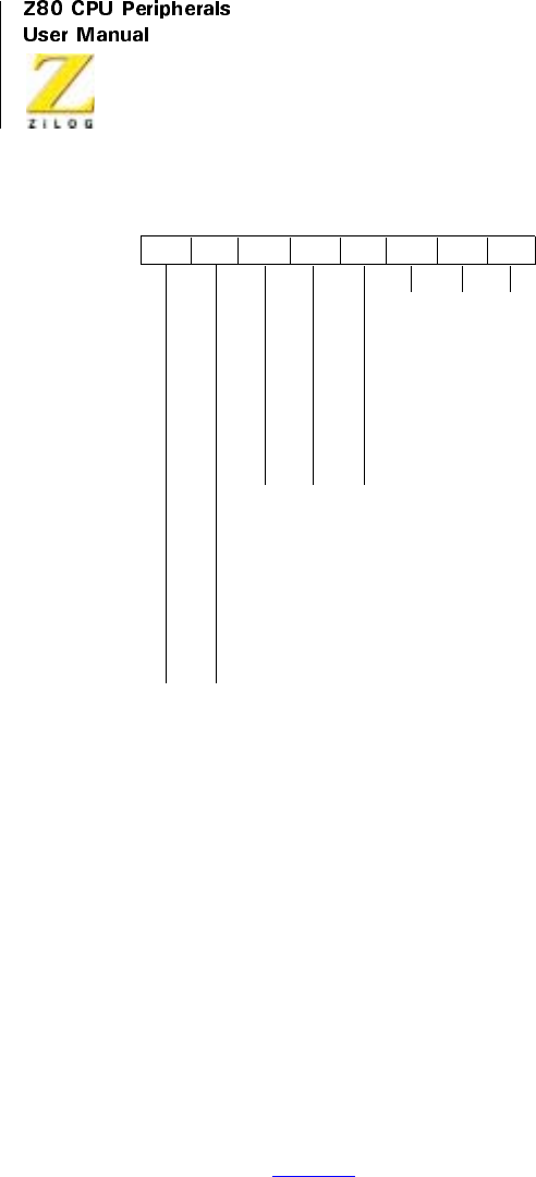
UM008101-0601 Serial Input/Output
274
Figure 114. Write Register 0
Pointer Bits (D2-D0)
Bits D2-D0 are pointer bits that determine which write register the next
byte writes to or which read register the next byte reads from. The first byte
written to each channel after a reset (either by a Reset command or by the
external reset input) goes to WR0. Following a read or write to any register
(except WR0), the pointer points to WR0
Command Bits (D5-D3)
Threebits,D5-D3,areencodedtoissuethesevenbasicZ80SIO
commands (Table 13).
00
01
10
11
000
001
010
011
100
101
110
111
000
001
010
011
100
101
110
111
Null Code
Reset Rx CRC Checker
Reset Tx CRC Generator
Reset Tx Underrun/EOM Latch
Register 0
Register 1
Register 2
Register 3
Register 4
Register 5
Register 6
Register 7
Null Code
Send Abort (SDLC)
Reset Ext/Status Interrupts
Channel Reset
Enable INT on Next Ax Character
Reset TxINT Pending
Error Reset
Return from INT (CH-A Only)
D7 D6 D5 D4 D3 D2 D1 D0

Z80 CPU Peripherals
User Manual
UM008101-0601 Serial Input/Output
275
Command 0 (Null). The Null command has no effect. Normally the null
command instructs the Z80 SIO to wait while the pointers are set for the
following byte.
Command 1 (Send Abort). This command is used only in SDLC mode to
generate a sequence of eight to thirteen 1s.
Command 2 (Reset External/Status Interrupts). After an External/Status
interrupt, such as a change on a modem line or a break condition, the status
bits of RR0 are latched. This command re-enables them, again allowing
Interrupts to occur. Latching the status bits captures short pulses until the
CPU has time to read the change.
Command 3 (Channel Reset). This command performs the same function
as an External Reset, but on a single channel. Channel A Reset also resets
the interrupt prioritization logic. All control registers for the channel must
be rewritten after a Channel Reset command.
After a Z80 SIO Channel Reset, add four system clock cycles before addi-
tional commands or controls write to that channel. This is normally the
same amount of time that is used by the CPU to fetch the next Op Code.
Table 13. Z80 SIO Commands
Command CMD2 CMD1 CMD0 Result
0 0 0 0 Null Command (no effect)
1 0 0 1 Send Abort (SDLC Mode)
2 0 1 0 Reset External/Status Interrupts
3 011ChannelReset
4 1 0 0 Enable Interrupt on next Rx Character
5 1 0 1 Reset Transmitter Interrupt Pending
6 1 1 0 Error Reset (latches
7 1 1 1 Return from Interrupt (Channel A)

UM008101-0601 Serial Input/Output
276
Command 4 (Enable Interrupt On Next Receive Character). If the Interrupt
On First Receive Character mode is selected, command 4 reactivates the
Enable Interrupt On Next Receive Character mode after receiving each
complete message. This sequence prepares the Z80 SIO for the next message.
Command 5 (Reset Transmitter Interrupt Pending). A transmitter interrupt
occurs when the transmit buffer becomes empty. This interrupt happens
only when the Transmit Interrupt Enable mode is selected. When there are
no more characters to be sent for example, at the end of message, issuing
this command prevents further transmitter interrupts until after the next
character is loaded to the transmit buffer or until CRC is completely sent.
Command 6 (Error Reset). This command resets the error latches. Parity
and Overrun errors are latched in RR1 until they are reset with this
command. Using this method, parity errors occurring in block transfers can
be examined at the end of the block.
Command 7 (Return From Interrupt). This command must be issued in
Channel A and is interpreted by the Z80 SIO in the same way it interprets
an RETI command on the data bus. This command resets the interrupt
under-service latch of the highest priority internal device under service.
This reset allows lower-priority devices to interrupt through the daisy-
chain. This command also allows use of the internal daisy-chain even in
systems with no external daisy-chain or RETI command.
CRC Reset Codes 0 and 1 (D6 and D7). Used together, these bits select one
of the three following reset commands, described in Table 14:

Z80 CPU Peripherals
User Manual
UM008101-0601 Serial Input/Output
277
The Reset Transmit CRC Generator command normally initializes the CRC
generator to 0s. If the SDLC mode is selected, this command initializes the
CRC generator to 1s. The Receive CRC checker is also initialized to 1s for
the SDLC mode.
Write Register 1
WR1 (Figure 115) contains the control bits for the various interrupt and
Wait/Ready modes.
External/Status Interrupt Enable (D0)
The External/Status Interrupt Enable allows interrupts to occur as a result of
transitions on the DCD,CTS,orSYNCinputs, as a result of a Break/Abort
Table 14. Reset Commands
CRC Reset
Code 1
CRC Reset
Code 0 Result
0 0 Null Code (no affect)
0 1 Reset Receive CRC Checker
1 0 Reset Transmit CRC Generator
1 1 Reset Tx Underrun/End of Message latch
Table15.WriteRegister1
D7 D6 D5 D4
Wait/Ready
Enable
Wait or Ready
Function
Wait/Ready on
Receive Transmit
Receive Interrupt
Mode 1
D3 D2 D1 D0
Receive Interrupt
Mode 0
Status Affects
Ve c t o r
Transmit Interrupt
Enable
External Interrupts
Enable

UM008101-0601 Serial Input/Output
278
detection and termination, or at the beginning of CRC or sync character
transmission when the Transmit Underrun/EOM latch sets.
Transmitter Interrupt Enable (D1)
If enabled, interrupts occur whenever the transmitter buffer becomes empty.
Status Affects Vector (D2)
This bit is active in Channel B only. If this bit is not set, the fixed vector
programmed in WR2 is returned from an interrupt acknowledge sequence.
If this bit is set, the vector returned from an interrupt acknowledge is
variable. Table 16 describes the vector results. Ta ble 17 describes the
Receive Interrupt modes.
Receive Interrupt Modes 0 and 1 (D3 and D4)
Used together, these two bits specify the various character-available condi-
tions. In Receive Interrupt modes 1, 2, and 3, a Special Receive Condition
can cause an interrupt that modifies the interrupt vector.
Table 16. Vector Results
V3 V2 V1 Result
Ch B 0 0 0 Ch B Transmit Buffer Empty
0 0 1 Ch B External/Status Change
0 1 0 Ch B Receive Character Available
0 1 1 Ch B Special Receive Condition*
Ch A 1 0 0 Ch A Transmit Buffer Empty
1 0 1 Ch A External/Status Change
1 1 0 Ch A Receive Character Available
1 1 1 Ch A Special Receive Condition*
Note: *Special Receive Conditions: Parity Error, Rx Overrun Error, Framing Error, End-
of-Frame (SDLC).
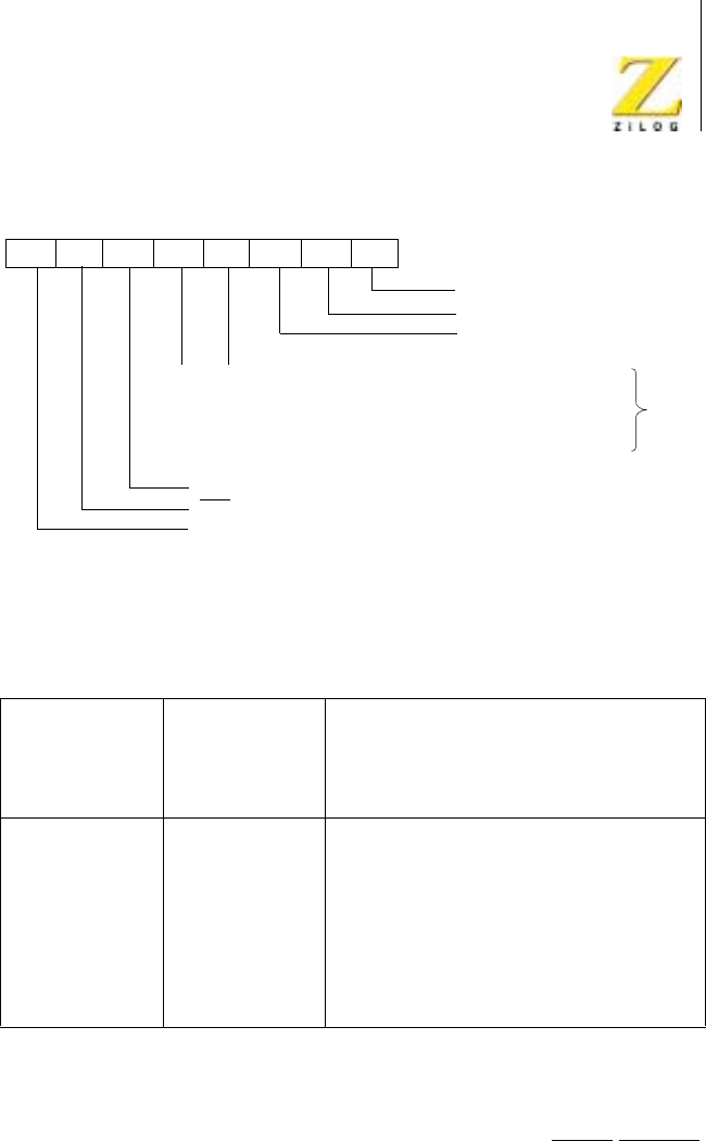
Z80 CPU Peripherals
User Manual
UM008101-0601 Serial Input/Output
279
Figure 115. Write Register 1
Wait/Ready Function Selection (D7-D5). The Wait and Ready functions are
selected by controlling D5, D6, and D7. Wait/Ready function is enabled by
setting Wait/Ready Enable (WR1, D7) to 1. The Ready function is selected
by setting D5 (Wait/Ready function) to 1. If this bit is 1, the WAIT/READY
output switches from High to Low when the Z80 SIO is ready to transfer
Table 17. Receive Interrupt Modes
D4
Receive
Interrupt Mode
1
D3
Receive
Interrupt Mode
0Result
0 0 Receive Interrupts Disabled
0 1 Receive Interrupt On First Character Only
1 0 Interrupt On All Receive Characters −
parity error is a Special Receive condition
1 1 Interrupt On All Receive Characters −
parity error is not a Special Receive
condition
00
01
10
11
Rx INT Disable
Rx INT on First Character
INT on All Rx Characters (Parity Affects Vector)
INT on All Rx Characters (Parity Does Not Affect Vector)
EXE INT Enable
Tx INT Enable
Status Affects Vector
(CH.B Only)
Wait/Ready on R/T
Wait/Ready Function
Wait/Ready Enable
D7 D6 D5 D4 D3 D2 D1 D0
*Or on special condition
*

UM008101-0601 Serial Input/Output
280
data. The Wait function is selected by setting D6 to 0. If this bit is 0, the
WAIT/READY output is in the open-drain state and goes Low when active.
Both the Wait and Ready functions can be used in either the Transmit or
Receive modes, but not both simultaneously. If D5 (Wait/Ready on Receive/
Transmit) is set to 1, the Wait/Ready function responds to the condition of
the receive buffer (empty or full). If D5 is set to 0, the Wait/Ready function
responds to the condition of the transmit buffer (empty or full).
The logic states of the WAIT/READY output, which are either active or
inactive, depend on the combination of modes selected. Table 18 summa-
rizes these combinations.
The WAIT output High-to-Low transition occurs at the delay time
tDIC(WR) after the I/O request. The Low-to-High transition occurs at the
delay tDHΦ(WR) at the falling edge of Φ. The READY output High-to-
Low transition occurs at the delay tDLΦ(WR) at the rising edge of Φ.The
READY output Low-to-High transition occurs at the delay tDIC(WR)
after IORQ falls.
The Ready function can occur when the Z80 SIO is not selected. When
the READY output becomes active Low, the DMA controller issues
Table 18. Wait/Ready Functions
If D7 = 0
and D6 = 1 and D6 = 0
READY is High WAIT is floating
If D7 = 0
and D5 = 0 and D5 = 1
READY is High when transmit buffer is full READY is High when receive buffer is empty
WAIT is low when transmit buffer is full and
S10dataportisanselected
WAIT is Low when receive buffer is empty
and SID data port is selected
READY is Low when transmit buffer is empty READY is Low when receive buffer is full
WAIT is floating when transmit buffer is empty WAIT is floating when receive buffer is full

Z80 CPU Peripherals
User Manual
UM008101-0601 Serial Input/Output
281
IORQ and the corresponding S/A and C/D inputs to the Z80 SIO to
transfer data. The READY output becomes inactive when IORQ and CS
become active. The Ready function can occur internally in the Z80 SIO,
whether it is addressed or not. Therefore, the READY output becomes
inactive when any CPU data or command transfer occurs. Because the
DMA controller is not enabled when the CPU transfer occurs, the system
continues to function normally.
The Wait function is active only when the CPU attempts to read Z80 SIO
data that has not yet been received, which occurs frequently when block
transfer instructions are used. The Wait function can also become active
(under program control) if the CPU tries to write data while the transmit
buffer is still full. The WAIT output for either channel becomes active
when the opposite channel is addressed. This active state occurs because
the Z80 SIO is addressed and does not affect software loops or block move
instructions.
Write Register 2
WR2 (Figure 116) is the interrupt vector register and occurs in Channel B
only. V7-V4 and V0 are always returned exactly as written; V3-V1 are
returned as written if the Status Affects Vector (WR1, D2) control bit is 0. If
this bit is 1, they are modified as explained in “Write Register 1”on
page 277.
Table19.WriteRegister2InterruptVector
D7 D6 D5 D4 D3 D2 D1 D0
V7 V6 V5 V4 V3 V2 V1 V0
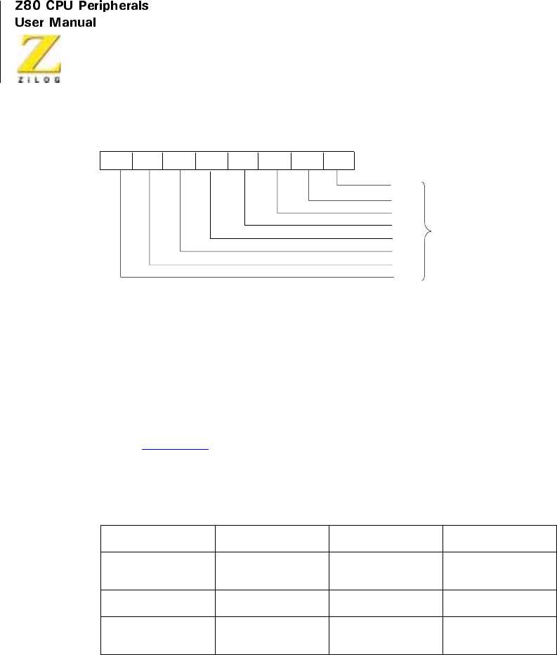
UM008101-0601 Serial Input/Output
282
Figure 116. Write Register 2
Write Register 3
WR3 (Figure 117) contains receiver logic control bits and parameters.
(Table 20)
Receiver Enable (D0)
A 1 programmed into this bit allows receive operations to begin. Set this bit
only after all other receive parameters are set and the receiver is completely
initialized.
Table 20. Write Register 3 Logic Control
D7 D6 D5 D4
Receiver Bits/
Chars
Receiver Bits/Char
0
Auto Enables Enter Hunt Phase
D3 D2 D1 D0
Receiver CRC
Enable
Address Search
Mode
Sync Char Load
Inhibit
Receiver Enable
V0
V1
V2
V3
D7 D6 D5 D4 D3 D2 D1 D0
Interrupt
V4
V5
V6
V7
Vector

Z80 CPU Peripherals
User Manual
UM008101-0601 Serial Input/Output
283
Sync Character Load Inhibit (D1)
Sync characters preceding the message (leading sync characters) are not
loaded into the receive buffers if this option is selected. Because CRC
calculations are not stopped by sync character stripping, this feature should
be enabled only at the beginning of the message.
Address Search Mode (D2)
If SDLC is selected, no receive interrupts can occur in the Address Search
mode without an address match. Therefore, messages containing addresses
that do not match the programmed address in WR6 or the global (1111
1111) are rejected.
Receiver CRC Enable (D3)
If this bit is set, CRC calculation starts or restarts at the beginning of the last
character transferred from the receive shift register to the buffer stack. This
start or restart occurs regardless of the number of characters in the stack.
For more information about setting this bit, see “SDLC Receive CRC
Checking”(SDLC Receive section) and “CRC Error Checking”
(Synchronous Receive section).
Enter Hunt Phase (D4)
The Z80 SIO automatically enters the Hunt phase after a reset. However, it
can be re-entered if character synchronization is lost (Synchronous mode)
or if the contents of an incoming message are not needed (SDLC mode).
The Hunt phase is reentered by writing a 1 to bit D4. This sets the Sync/
Hunt bit (D4) in RR0.
Auto Enables(D5)
If this mode is selected, DCD and CTS become the receiver and transmitter
enables, respectively. If this bit is not set, DCD and CTS are simply inputs
to their corresponding status bits in RR0.
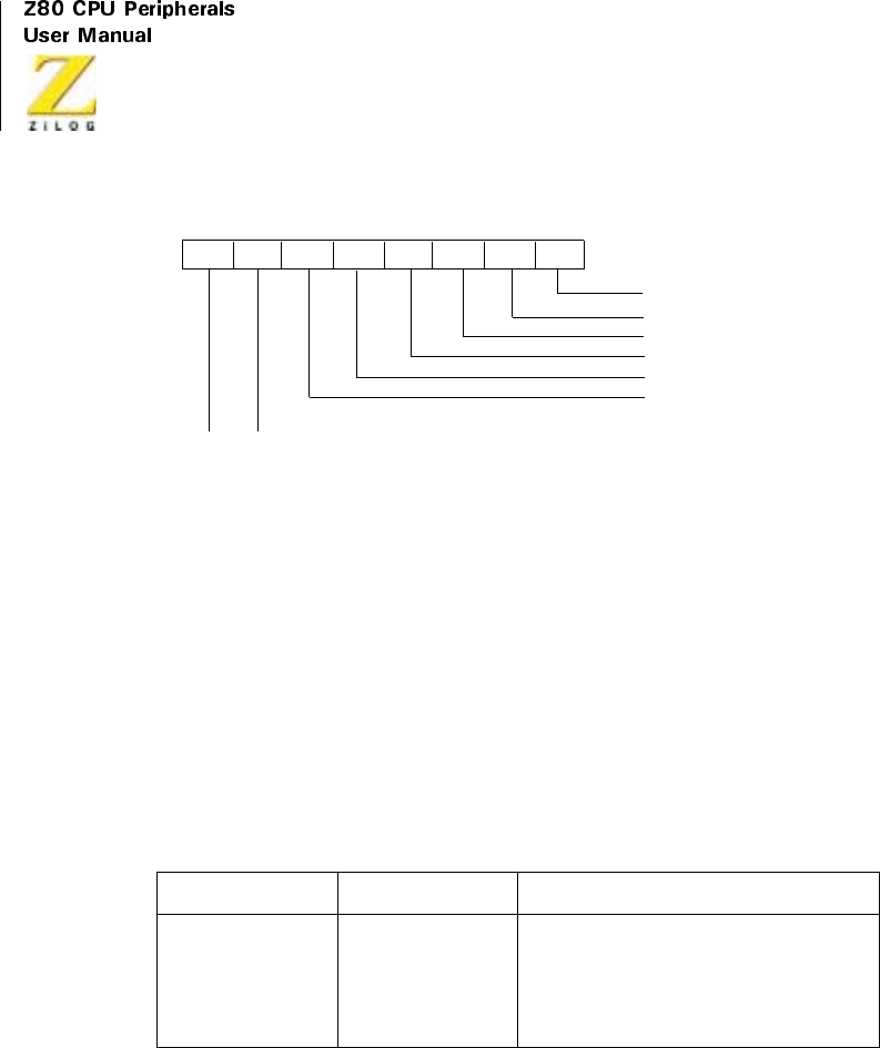
UM008101-0601 Serial Input/Output
284
Figure 117. Write Register 3
Receiver Bits/Characters 1 and 0 (D7 and D6)
Used together, these bits determine the number of serial receive bits
assembled to form a character. Both bits may be changed during the time
that a character is being assembled, but they must be changed before the
currently programmed number of bits is reached.
Write Register 4
WR4 contains the control bits that affect both the receiver and transmitter.
In the transmit and receive initialization routine, these bits should be set
beforeissuingWR1,WR3,WR5,WR6,andWR7.
Table 21. Serial Bits/Character
D7 D6 Bits/Character
00 5
01 7
10 6
11 8
Rx Enable
SYNC Character Load Inhibit
Address Search Mode (SDLC)
Rx CRC Enable
D7 D6 D5 D4 D3 D2 D1 D0
Enter Hunt Phase
Auto Enables
00
01
10
11
Rx 5 Bits/Character
Rx 7 Bits/Character
Rx 6 Bits/Character
Rx 8 Bits/Character

Z80 CPU Peripherals
User Manual
UM008101-0601 Serial Input/Output
285
Parity (D0)
If this bit is set, an additional bit position is added to transmitted data and is
expected in receive data. This added bit position is in addition to those bits
specified in the bits/character control. In the Receive mode, the parity bit
received is transferred to the CPU as part of the character, unless eight bits/
character is selected.
Parity Even/Odd (D1)
If parity is specified, this bit determines whether the bit is sent and checked
as even or odd (1 = even).
StopBits0and1(D2andD3)
These bits determine the number of stop bits added to each asynchronous
character sent. The receiver always checks for one stop bit. A special mode
(00) designates that a synchronous mode is to be selected.
Table 22. Write Register 4 Rx and Tx Control
D7 D6 D5 D4 D3 D2 D1 D0
Clock
Rate 1
Clock
Rate 0
Sync
Modes 1
Sync
Modes 0
Stop
Bits 1
Stop
Bits 0
Parity
Even/
Odd
Parity
Table 23. Stop Bits
D3
Stop Bits 1
D2
Stop Bits 0 Result
0 0 Sync modes
0 1 1 stop bit per character
1 0 1-1/2 stop bits per character
1 1 2 stop bits per character
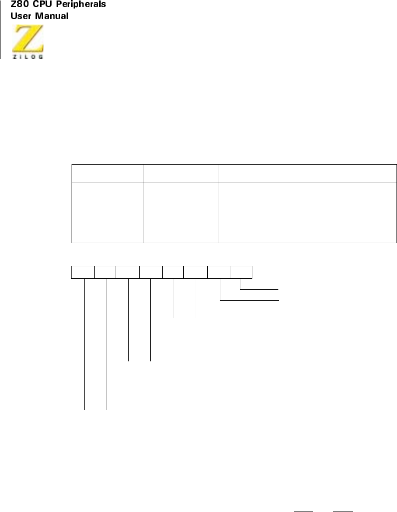
UM008101-0601 Serial Input/Output
286
Sync Modes 0 and 1 (D4 and D5)
These bits select various options for character synchronization.
Figure 118. Write Register 4
ClockRate0and1(D6andD7)
These bits specify the multiplier between the clock (TxC and RxC)anddata
rates. For synchronous modes, the x1 clock rate must be specified. Any rate
may be specified for asynchronous modes; however, the same rate must be
Table 24. Sync Modes
Sync Mode 1 Sync Mode 0 Result
0 0 8-bit programmed sync
0 1 16-bit programmed sync
1 0 SDLCmode(01111110flagpattern)
1 1 External Sync mode
Parity Enable
Parity Even/Odd
D7 D6 D5 D4 D3 D2 D1 D0
00
01
10
11
SYNC Modes Enable
1 Stop Bit/Character
1-1/2 Stop Bits/Character
2 Stop Bits/Character
00
01
10
11
8-Bit SYNC Character
16-Bit SYNC Character
SDLC Mode (0111 1110 Flag)
External SYNC Mode
00
01
10
11
X1 Clock Mode
X16 Clock Mode
X32 Clock Mode
X64 Clock Mode

Z80 CPU Peripherals
User Manual
UM008101-0601 Serial Input/Output
287
used for both the receiver and transmitter. The system clock in all modes
must be set to at least 4.5 times the data rate. If the x1 clock rate is selected,
bit synchronization must be performed externally.
Write Register 5
WR5 contains control bits that affect the operation of transmitter, with the
exception of D2, which affects the transmitter and receiver.
Transmit CRC Enable (D0)
This bit determines if CRC is calculated on a specific transmit character. If
it is set at the time the character is loaded from the transmit buffer into the
transmit shift register, CRC is calculated on the character. CRC is not auto-
matically sent unless this bit is set when the Transmit Underrun condition
occurs.
Table 25. Clock Rate
Clock Rate 1 Clock Rate 0 Result
0 0 Data Rate x1 = Clock Rate
0 1 Data Rate x16 = Clock Rate
1 0 Data Rate x32 = Clock Rate
1 1 Data Rate x64 = Clock Rate
Table26.WriteRegister5TransmitterControl
D7 D6 D5 D4 D3 D2 D1 DO
DTR Tx
Bits/
Char 1
Tx
Bits/
Char 0
Send
Break
Tx
Enable
CRC-16/
SDLC
RTS Tx
CRC
Enable

UM008101-0601 Serial Input/Output
288
Request To Send (D1)
This is the control bit for The RTS pin. When the RTS bit is set, the RTS
pin goes Low; when reset, RTS goes High. In the Asynchronous mode,
RTS goes High only after all the bits of the character are transmitted and
the transmitter buffer is empty. In Synchronous modes, the pin directly
follows the state of the bit.
CRC-16/SDLC (D2)
This bit selects the CRC polynomial used by both the transmitter and
receiver. When set, the CRC-16 polynomial (X16 +X15 +X
2+1)isused;
when reset, the SDLC polynomial (X16 +X
12 +X
5+1)isused.IftheSDLC
mode is selected, the CRC generator and checker are preset to 1s and a
special check sequence is used. The SDLC CRC polynomial must be
selected when the SDLC mode is selected. If the SDLC mode is not selected,
the CRC generator and checker are preset to 0s for both polynomials.
Transmit Enable (D3)
Data is not transmitted until this bit is set, and the Transmit Data output is
held marking. Data or sync characters in the process of being transmitted
are completely sent if this bit is reset after transmission is started. If the
transmitter is disabled during the transmission of a CRC character, sync, or
flag characters are sent instead of CRC.
Send Break (D4)
When set, this bit immediately forces the Transmit Data output to the
spacing condition, regardless of any data being transmitted. When reset,
TxD returns to marking.
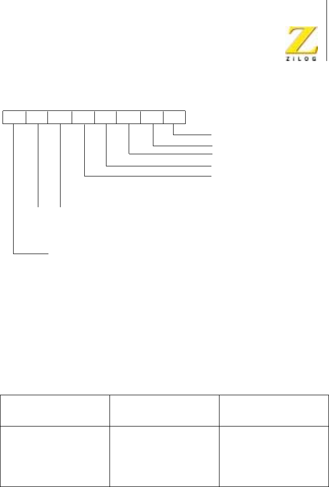
Z80 CPU Peripherals
User Manual
UM008101-0601 Serial Input/Output
289
Figure 119. Write Register 5
Transmit Bits/Characters 0 and 1 (D5 and D6)
Together, D6 and D5 control the number of bits in each byte transferred to
the transmit buffer.
Bits to be sent must be right justified, least-significant bits first. The Five-
Or-Less mode allows transmission of one to five bits per character;
however, the CPU should format the data character as depicted in the
following table.
Table 27. Transmit Bits
D6 Transmit Bits/
Character 1
D5 Transmit Bits/
Character 0 Bits/Character
0 0 Five or less
017
106
118
Tx CRC Enable
RTS
D7 D6 D5 D4 D3 D2 D1 D0
00
01
10
11
8-Bit SYNC Character
16-Bit SYNC Character
SDLC Mode (0111 1110 Flag)
External SYNC Mode
SDLC/CRC-16
Tx Enable
Send Break
DTR
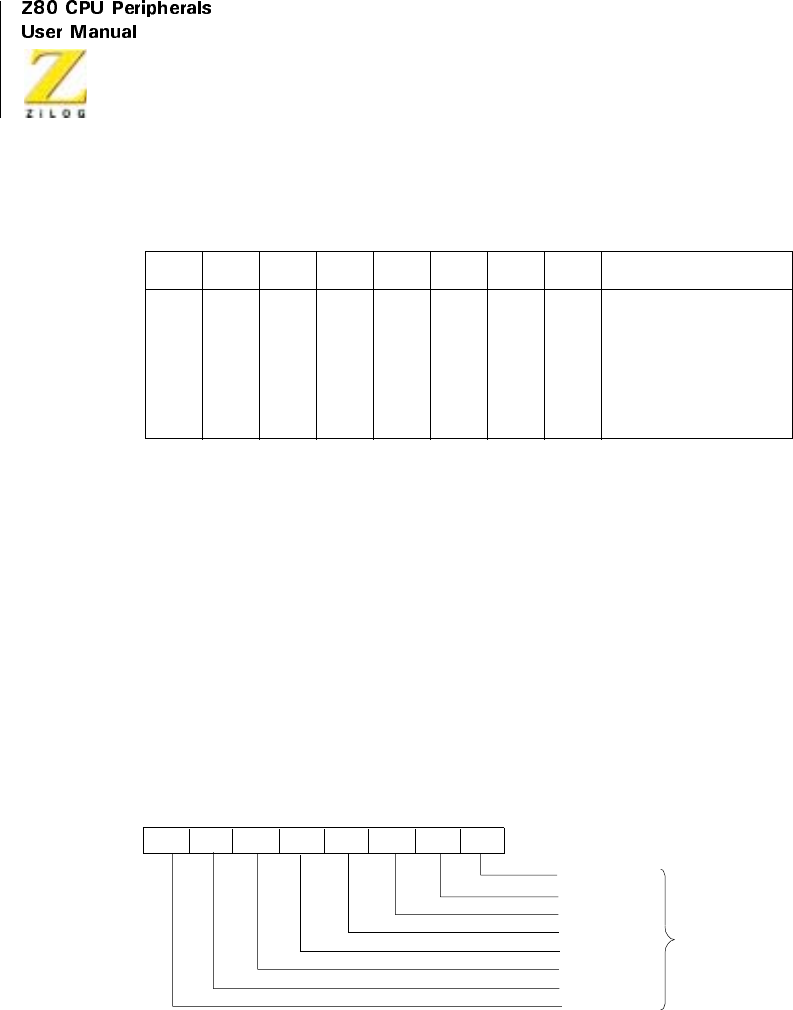
UM008101-0601 Serial Input/Output
290
Data Terminal Ready (D7)
This is the control bit for the DTR pin. When set, DTR is active (Low);
when reset, DTR is inactive (High).
Write Register 6
This register is programmed to contain the transmit sync character in the
Monosync mode, the first eight bits of a 16-bit sync character in the Bisync
mode, or a transmit sync character in the External Sync mode. In the SDLC
mode, it is programmed to contain the secondary address field, which is
used to compare against the address field of the SDLC frame.
Figure 120. Write Register 6
Table 28. Data Character Format
D7 D6 D5 D4 D3 D2 D1 D0 Result
1 1 1 1 0 0 0 D Sends one data bit
111000DDSendstwodatabits
1 1 0 0 0 D D D Sendsthreedatabits
1 0 0 0 D D D D Sends four data bits
0 0 0 D D D D D Sends five data bits
SYNC Bit 0
SYNC Bit 1
SYNC Bit 2
SYNC Bit 3
D7 D6 D5 D4 D3 D2 D1 D0
*
SYNC Bit 4
SYNC Bit 5
SYNC Bit 6
SYNC Bit 7
*Also SDLC Address Field
Z80 CPU Peripherals
User Manual
UM008101-0601 Serial Input/Output
291
Write Register 7
This register is programmed to contain the receive sync character in the
Monosync mode, a second byte (last eight bits) of a 16-bit sync character in
the Bisync mode, or a flag character (0111 1110) in the SDLC mode. WR7
is not used in the External Sync mode.
Figure 121. Write Register 7
Table29.WriteRegister6TransmitSync
D7 D6 D5 D4 D3 D2 D1 D0
Sync 7 Sync 6 Sync 5 Sync 4 Sync 3 Sync 2 Sync 1 Sync 0
Table30.WriteRegister7ReceiveSync
D7 D6 D5 D4 D3 D2 D1
Sync 15 Sync 14 Sync 13 Sync 12 Sync 11 Sync 10 Sync 9 Sync 8
SYNC Bit 8
SYNC Bit 9
SYNC Bit 10
SYNC Bit 11
D7 D6 D5 D4 D3 D2 D1 D0
*
SYNC Bit 12
SYNC Bit 13
SYNC Bit 14
SYNC Bit 15
*For SDLC it must be programmed to ‘0111 1110’for flag recognition

UM008101-0601 Serial Input/Output
292
Read Registers
The Z80 SIO contains three registers, RR2-RR0 (Figure 122 through
Figure 124), that are read to obtain the status information for each channel,
with the exception of RR2-Channel B. The status information includes error
conditions, interrupt vector, and standard communications-interface signals.
To read the contents of a selected read register other than RRD, the system
program must first write the pointer byte to WR0, in exactly the same way
as a write register operation. Then, by executing an input instruction, the
contents of the addressed read register can be read by the CPU.
The status bits of RR0 and RR1 are carefully grouped to simplify status
monitoring. For example, when the interrupt vector indicates that a Special
Receive Condition interrupt occurred, all the appropriate error bits can be
read from a single register (RR1).
Read Register 0
This register contains the status of the receive and transmit buffers; the
DCD,CTS, and SYNC inputs; the Transmit Underrun/EOM latch; and the
Break/Abort latch.
Receive Character Available (DO)
This bit is set when at least one character is available in the receive buffer;
it is reset when the receive FIFO is empty.
Table 31. Read Register 0 Rx and Tx Buffers
D7D6IDSD4D3D2D1D0
Break/
Abort
Transmit
Underrun
EOM
CTS Sync/
Hunt
Buffer
Empty
DCD Transmit
Pending
Interrupt
Pending
(Ch.A
only)
Receive
Character
available

Z80 CPU Peripherals
User Manual
UM008101-0601 Serial Input/Output
293
Interrupt Pending (D1)
AnyinterruptingconditionintheZ80SIOcausesthisbittoset;however,it
is readable only in Channel A. This bit is primarily used in applications not
having vectored interrupts available. During the interrupt service routine in
these applications, this bit indicates if any interrupt conditions are present
in the Z80 SIO. This eliminates the need for analyzing all the bits of RR0 in
both Channels A and B. Bit D1 is reset when all the interrupting conditions
are satisfied. This bit is always 0 in Channel B.
Transmit Buffer Empty (D2)
This bit is set whenever the transmit buffer becomes empty, except when a
CRC character is being sent in a synchronous or SDLC mode. The bit is
reset when a character is loaded into the transmit buffer. This bit is in the set
condition after a reset.
Data Carrier Detect (D3)
The DCD bit indicates the state of the DCD input at the time of the last
change of any of the five External/Status bits (DCD,CTS,Sync/Hunt,
Break/ Abort, or Transmit Underrun/EOM). Any transition of the DCD
input causes the DCD bit to latch and causes an External/Status interrupt.
To read the current state of the DCD bit, this bit must be read immediately
following a Reset External/Status Interrupt command.
Sync/Hunt (D4)
Because this bit is controlled differently in the Asynchronous,
Synchronous, and SDLC modes, its operation is somewhat more complex
than that of the other bits and therefore requires more explanation.
In asynchronous modes, the operation of this bit is similar to the DCD
status bit, except that Sync/Hunt shows the state of the SYNC input. Any
High-to-Low transition on the SYNC pin sets this bit and causes an
External/Status interrupt (if enabled). The Reset External/Status Interrupt
command is issued to clear the interrupt. A Low-to-High transition clears
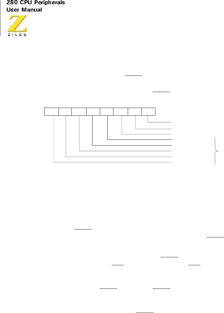
UM008101-0601 Serial Input/Output
294
this bit and sets the External/Status interrupt. When the External/Status
interrupt is set by the change in state of any other input or condition, this bit
shows the inverted state of the SYNC pin at the time of the change. This bit
must be read immediately following a Reset External/Status Interrupt
command to read the current state of tile SYNC input.
Figure 122. Read Register 0
In the External Sync mode, the Sync/Hunt bit operates similar to the Asyn-
chronous mode, except the Enter Hunt Mode control bit enables the
external sync detection logic. When the External Sync Mode and Enter
Hunt Mode bits are set for example, when the receiver is enabled following
a reset, the SYNC input must be held High by the external logic until
external character synchronization is achieved. A High at the SYNC input
holds the Sync/Hunt status bit in the reset condition.
When external synchronization is achieved, SYNC must be driven Low on
the second rising edge of RxC after that rising edge of RxC on which the
last bit of the sync character was received. In other words, after the sync
pattern is detected, the external logic must wait for two full Receive Clock
cycles to activate the SYNC input. When SYNC is forced Low, keep it Low
until the CPU informs the external sync logic that synchronization is lost or
that a new message is about to start. Refer to Figure 122 for timing details.
The High-to-Low transition of the SYNC input sets the Sync/Hunt bit,
which, in turn, sets the External/Status interrupt. The CPU must clear the
interrupt by issuing the Reset External/Status Interrupt command.
Rx Character Available
INT Pending (CH.A Only
Tx Buffer Empty
DCD
D7 D6 D5 D4 D3 D2 D1 D0
*
SYNC/Hunt
Tx Underrun/EOM
Break/Abort
*Used with ‘External/Status Interrupt Mode
CTS

Z80 CPU Peripherals
User Manual
UM008101-0601 Serial Input/Output
295
When the SYNC input goes High again, another External/ Status interrupt
is generated that must also be cleared. The Enter Hunt Mode control bit is
set whenever character synchronization is lost or the end of message is
detected. In this case, the Z80 SIO again looks for a High-to-Low transition
of the SYNC input and the operation repeats as explained previously. This
implies the CPU should also inform the external logic that character
synchronization has been lost and that the Z80 SIO is wailing for SYNC to
become active.
In the Monosync and Bisync Receive modes, the Sync/Hunt status bit is
initially set to 1 by the Enter Hunt Mode bit. The Sync/Hunt bit is reset
when the Z80 SIO establishes character synchronization. The High-to-Low
transition of the Sync/Hunt bit causes an External/Status interrupt that must
be cleared by the CPU issuing the Reset External/ Status Interrupt
command. This enables the Z80 SIO to detect the next transition of other
External/Status bits.
When the CPU detects the end of message or loss of character synchroniza-
tion, it sets the Enter Hunt Mode control bit, which-in turn-sets the Sync/
Hunt bit to 1. The Low-to-High transition of the Sync/Hunt fit sets the
External/Status interrupt, which must also be cleared by the Reset External/
Status Interrupt command.
The SYNC pin functions as an output in this mode and goes Low when a
sync pattern is detected in the data stream.
In the SDLC mode, the Sync/Hunt bit is initially set by the Enter Hunt
mode bit, or when the receiver is disabled. It is reset to 0 when the opening
flag of the first frame is detected by the Z80 SIO. The External/Status inter-
rupt is also generated, and should be handled as discussed previously.
Unlike the Monosync and Bisync modes, when the Sync/Hunt bit is reset in
the SDLC mode, it does not need to be set when the end of message is
detected. The Z80 SIO automatically maintains synchronization. The Sync/
Hunt bit can only be set again by the Enter Hunt Mode bit or by disabling
the receiver.

UM008101-0601 Serial Input/Output
296
Clear To Send, (D5). This bit is similar to the DCD bit, except that it shows
the inverted state of the CTS pin.
Transmit Underrun/End of Message (D6)
This bit is in a set condition following a reset, either internal or external.
The only the Reset Transmit Underrun/EOM Latch command (WR0, D6
and D7) can reset this bit. When the Transmit Underrun condition occurs,
this bit is set; causing the External/Status interrupt, which is reset by issuing
the Reset External/Status Interrupt command bits (WR0). This status bit,
along with other control bits, has an important function in controlling a
transmit operation. For more information, see “Bisync Transmit Underrun”
and “SDLC Transmit Underrun”.
Break/Abort (D7)
In the Asynchronous Receive mode, this bit is set when a Break sequence
(null character plus framing error) is detected in the data stream. The
External/Status interrupt, if enabled, is set when Break is detected. The
interrupt service routine must issue the Reset External/Status Interrupt
command (WR0, CMD2) to the break detection logic, enabling the Break
sequence termination to be recognized.
The Break/Abort bit is reset when the termination of the Break sequence is
detected in the incoming data stream. The termination of the Break
sequence also causes the External/Status interrupt to set. The Reset
External/Status Interrupt command must be issued to enable the break
detection logic to look for the next Break sequence. When a single extra-
neous null character is present in the receiver after the termination of a
break; it should be read and discarded.
In the SDLC Receive mode, this status bit is set by the detection of an
Abort sequence (seven or more 1s). The External/Status interrupt is handled
the same way as a Break. The Break/Abort bit is not used in the Synchro-
nous Receive mode.

Z80 CPU Peripherals
User Manual
UM008101-0601 Serial Input/Output
297
Read Register 1
This register contains the Special Receive condition status bits and Residue
codes for the I-Field in the SDLC Receive Mode.
All Sent (D0)
In asynchronous modes, this bit is set when all the characters have
completely cleared the transmitter. Transitions of this bit do not cause inter-
rupts and it is always set in synchronous modes.
Residue Codes 0, 1, and 2 (D3-D1)
In SDLC receive mode, these three bits indicate the length of the I-field,
when the I-field is not an integral multiple of the character length. These
codes are only meaningful for a transfer in which the End-of-Frame bit is
set (SDLC). For a receive character length of eight bits per character, the
codes signify the following:
Table 32. Read Register 1 Special Receive Condition Status
D7 D6 DS D4 D3 D2 D1 D0
End of
Frame
(SDLC)
CRC/
Framing
Error
Receiver
Overrun
Error
Parity
Error
Residue
Code 2
Residue
Code 1
Residue
Code 0
All sent
Table33.ResidueCodes
Residue Code
2
Residue Code
1
Residue Code
0
I-Field Bits in
Previous Byte
I-Field Bits in
Second
Previous Byte
10003
01004
11005
00106
10107

UM008101-0601 Serial Input/Output
298
I-Field bits are always right justified.
If a receive character length is different from eight bits is used for the I-
field, a table similar to the previous one may be constructed for each
different character length. For no residue, that is, when the last character
boundary coincides with the boundary of the I-field and CRC field, the
Residue codes are:
01108
11118
00028
Table34.ReceiveCharacterLength
Bits per Character Residue Code 2 Residue Code 1 Residue Code 0
8 Bits per Character 0 1 1
7 Bits per Character 0 0 0
6 Bits per Character 0 1 0
5 Bits per Character 0 0 1
Table33.ResidueCodes
Residue Code
2
Residue Code
1
Residue Code
0
I-Field Bits in
Previous Byte
I-Field Bits in
Second
Previous Byte
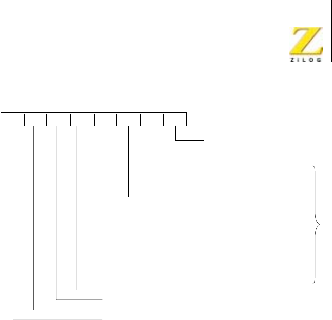
Z80 CPU Peripherals
User Manual
UM008101-0601 Serial Input/Output
299
Figure 123. Read Register 1
Parity Error (D4)
When parity is enabled, this bit is set for those characters whose parity does
not match the programmed sense (even/odd). The bit is latched, so when an
error occurs, the bit remains set until given the Error Reset command (WR0).
Receive Overrun Error (D5)
This bit indicates that more than three characters have been received
without a read from the CPU. Only the character that has been written over
is flagged with this error, but when this character is read, the error condition
is latched until reset by the Error Reset command. If Status Affects Vector
is enabled, the character that has been overrun interrupts with a Special
Receive Condition vector.
100
010
110
001
101
011
111
000
Parity Error
Rx Overrun Error
CRC/Framing Error
End-of-Frame (SDLC)
D7 D6 D5 D4 D3 D2 D1 D0
*Residue Data for Eight Rx
Bits/Character Programmed
All Sent
IFieldBits
in Previous
Byte
0
0
0
0
0
0
1
2
I Field Bits in
Second Previous
Byte
3
4
5
6
7
8
8
8
*

UM008101-0601 Serial Input/Output
300
CRC/Framing Error (D6)
If a Framing Error occurs (asynchronous modes), this bit is set (and not
latched) for the receive character in which the Framing Error occurred.
Detection of a Framing Error adds an additional one-half bit time to the
character time, so the Framing Error is not interpreted as a new start bit. In
synchronous and SDLC modes, this bit indicates the result of comparing
the CRC checker to the appropriate check value. This bit is reset by issuing
an Error Reset command. The bit is not latched, so it is always updated
when the next character is received. When used for CRC error and status in
synchronous modes, it is usually set because most bit combinations result
in a non-zero CRC except for a correctly completed message.
End-of-Frame (D7)
This bit is used only with the SDLC mode and indicates that a valid ending
flag has been received and that the CRC Error and Residue codes are also
valid. This bit can be reset by issuing the Error Reset command. It is also
updated by the first character of the following frame.
Read Register (Channel B Only)
This register contains the interrupt vector written into WR2 if the Status
Affects Vector control bit is not set. If the control bit is set, it contains the
modified vector listed in the Status Affects Vector paragraph of the Write
Register 1 section. When this register is read, the vector returned is modi-
fied by the highest priority interrupting condition at the time of the read. If
no interrupts are pending, the vector is modified with V3 = 0, V2 = 1, and
V1 = 1. This register is read only through Channel B.
Table 35. Interrupt Vector
D7 D6 D5 D4 D3 D2 D1 D0
V7 V6 V5 V4 V3* V2* V1* V0
*Variable if ‘Status Affects Vector’is programmed
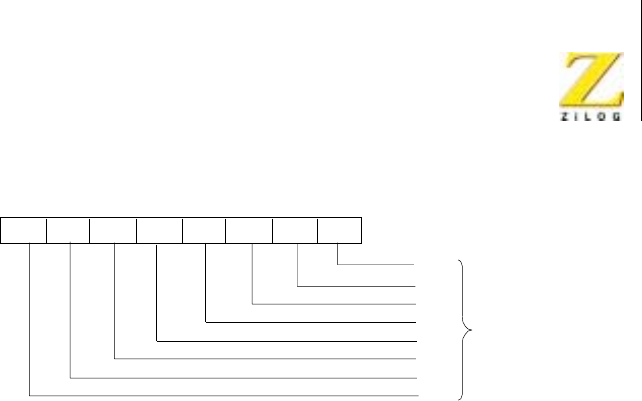
Z80 CPU Peripherals
User Manual
UM008101-0601 Serial Input/Output
301
Figure 124. Read Register 2 (Channel B Only)
APPLICATIONS
Overview
Flexibility and versatility make the Z80 SIO useful for numerous applica-
tions, a few of which are described here. These examples demonstrate
how several applications combine the Z80 SIO with other members of the
Z80 family.
Figure 125 depicts simple processor-to-processor communication over a
direct line. Both remote processors in this system communicate to the Z80
CPU with different protocols and data rates. Depending on the complexity
of the application, other Z80 peripheral circuits (Z80 CTC, for example)
may be required. The unused Z80 SIO channel is available to control other
peripherals or to connect with remote processors.
V0
V1*
V2*
V3*
D7 D6 D5 D4 D3 D2 D1 D0
Interrupt
V4
V5
V6
V7
Vector
*Variable if ‘Status Affects Vector’is programmed
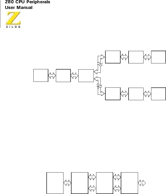
UM008101-0601 Serial Input/Output
302
Figure 125. Synchronous/Asynchronous Processor-to-Processor
Communication (Direct Wire to Remote Locations)
Figure 126 illustrates how both channels of a single Z80 SIO are used with
modems that have primary and secondary or reverse channel options.
Alternatively, two modems without these options can be connected to the
Z80 SIO. A correct baud-rate generator (Z80 CTC) must be used for asyn-
chronous modems.
Figure 126. Synchronous/Asynchronous Processor-to-Processor
Communication (Using Telephone Line)
Figure 127 depicts the Z80 SIO in a data concentrator, a relatively
complex application that uses two Z80 SIOs to perform a variety of func-
tions. The data concentrator can be used to collect data from many termi-
nals over low-speed lines and transmit it over a single high-speed line after
editing and reformatting.
Z80
CPU Z80
SIO
RSXYZ
Drivers/
Receivers
RSXYZ
Drivers/
Receivers
Z80
SIO Z80
CPU
RSXYZ
Drivers/
Receivers
Z80
SIO Z80
CPU
Z80
CPU
Z80
SIO
Ch.A
Ch.B
RS
Driver/
Receiver
Primary
Channel
Secondary
Channel
Modem
(SYNC or
ASYNC)
Data Link
to Remote
Processor

Z80 CPU Peripherals
User Manual
UM008101-0601 Serial Input/Output
303
The Z80 DMA controller circuit is used with Z80 SIO/2 to transmit the
reformatted data at high speed with the required protocol. The high-speed
modem provides the transmit clock for this channel. The Z80 CTC counter-
timer circuit supplies the transmit and receive clocks for the low-speed
lines and is also used as a time-out counter for various functions.
Z80 SIO/1 controls local or remote terminals. A single intelligent terminal
is placed within the dashed lines. The terminal employs a Z80 SIO to
communicate to the data concentrator on one channel while providing the
interface to a line printer over its second channel. The intelligent terminal
could be designed to operate interactively with the operator.
Depending on the software and hardware capabilities built into this system,
the data concentrator can employ store-and-forward or hold-and-forward
methods for regulating information traffic between slow terminals and the
high-speed remote processor. If the high-speed channel is provided with a
dial-out option, the channel can be connected to a number of remote
processors over a switched line.
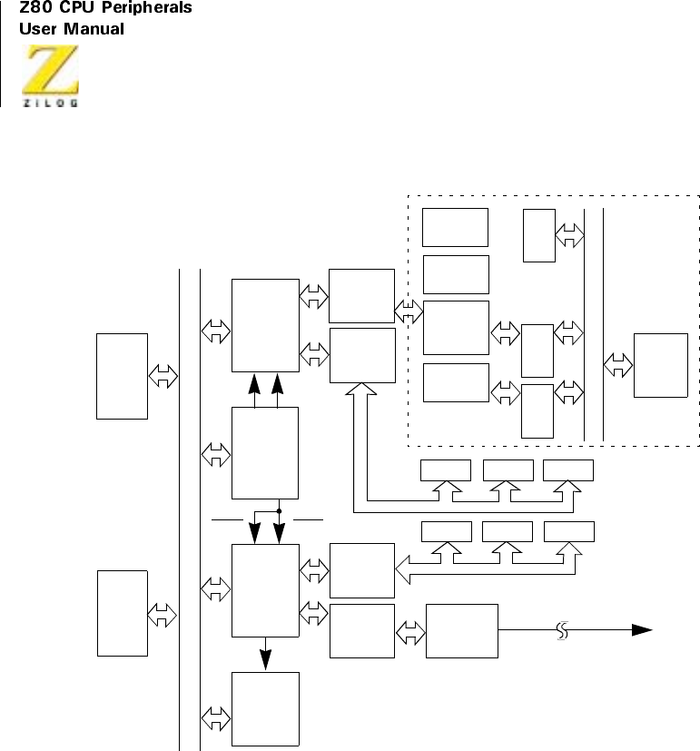
UM008101-0601 Serial Input/Output
304
Figure 127. Data Concentrator
Keyboard
Display/
Line
Printer
Z80
Te r mi na l
Bus
Terminal Interfaces
To Remot e
High-Speed
Modem
System
Z80
Z80
RDY
RDY
Ch.A
Z80
System Bus
(Data, Address, and Control)
RxCA TxCA
Z80
CPU
and
Memory
Intelligent
Terminal
SIO Clock
Generator
and
Time Out
Counters
Terminal Interfaces
Processor
Memory
CPU
Receivers
Drivers/
RS 232
Receivers
Drivers/
RS 232 Receivers
Drivers/
RS 232
Console
SIO
Z80
PIO
Z80
CTC
Receivers
Drivers/
RS 232
Receivers
Drivers/
RS 232
SIO #2
Ch.B
DMA
Ch.A
Z80
SIO #1
Ch.B
Communications Link
(SDLC Protocol)
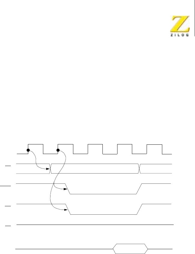
Z80 CPU Peripherals
User Manual
UM008101-0601 Serial Input/Output
305
TIMING
Read Cycle
The timing signals that are generated by a Z80 CPU input instruction,
which read a Data or Status byte from the Z80 SIO, are illustrated in
Figure 128.
Figure 128. Read Cycle Timing
Write Cycle
Figure 129 illustrates the timing and data signals generated by a
Z80 CPU output instruction, which write a Data or Control byte
to the Z80 SIO.
Out
Channel Address
T1
Φ
CE
IORQ
RD
M1
Data
T2TWT3T1
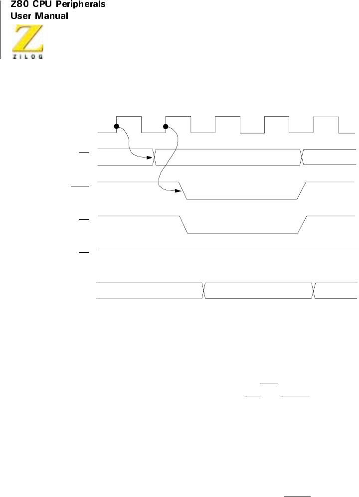
UM008101-0601 Serial Input/Output
306
Figure 129. Write Cycle Timing
Interrupt Acknowledge Cycle
After receiving an Interrupt Request signal, INT pulled Low, the Z80 CPU
sends an Interrupt Acknowledge signal, M1 and IORQ, both Low. The
daisy-chained interrupt circuits determine the highest priority interrupt
requestor. The IEI of the highest priority peripheral is terminated High.
Peripherals that have no interrupt pending or under service are terminated
IEO = IEI. Any peripheral that does have an interrupt pending or under
service, forces its IEO Low.
To insure stable conditions in the daisy-chain, all interrupt status signals are
prevented from changing while MI is Low. When IORQ is Low, the highest
priority interrupt requestor, which is the one with IEI High, places its
interrupt vector on the data bus and sets its internal interrupt-underservice
latch. See Figure 130.
Channel Address
T1
Φ
CE
IORQ
RD
M1
Data
T2TWT3T1
In
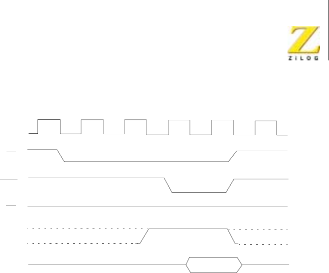
Z80 CPU Peripherals
User Manual
UM008101-0601 Serial Input/Output
307
Figure 130. Interrupt Acknowledge Cycle Timing
Return From Interrupt Cycle
Normally, the Z80 CPU issues a RETI, RETurn from Interrupt, instruction
at the end of an interrupt service routine. The RETI is a 2-byte Op Code,
ED-4D, which resets the interrupt-underservice latch that terminates the
interrupt just processed. This is accomplished by manipulating the daisy-
chaininthefollowingway.
The normal daisy-chain operation can detect a pending interrupt; however,
it cannot distinguish between an interrupt under service and a pending
unacknowledged interrupt of a higher priority. Whenever ED is decoded,
the daisy-chain is modified by forcing High the IEO of any interrupt not yet
acknowledged.
Thus the daisy-chain identifies the device presently under service as the
only one with an IEI High and an IEO Low. If the next Op Code byte is 4D,
the interrupt-underservice latch is reset. See Figure 131.
T1
Φ
IORQ
RD
M1
Data
T2TWT3T4
IEI
Vector
TW
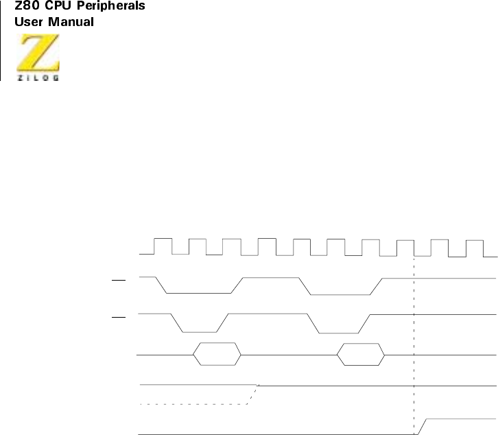
UM008101-0601 Serial Input/Output
308
The Tipple time of the interrupt daisy-chain, both the High-to-Low and
the Low-to-High transitions, limits the number of devices that can be
placed in the daisy-chain. Ripple time can be improved with carry-
lookahead, or by extending the interrupt acknowledge cycle.
Figure 131. Return from Interrupt Cycle Timing
Daisy Chain Interrupt Nesting
Figure 132 illustrates the daisy-chain configuration of interrupt circuits and
their interaction with nested interrupts, which is an interrupt that is inter-
rupted by another with a higher priority.
Each box in the illustration can be a separate external Z80 peripheral circuit
with a user-defined order of interrupt priorities. However, a similar daisy-
chain structure also exists inside the Z80 SIO, which has six interrupt levels
with a fixed order of priorities.
The situation illustrated in Figure 132 occurs when the transmitter of
Channel B interrupts and is granted service. While this interrupt is being
serviced, it is interrupted by a higher priority interrupt from Channel A. The
second interrupt is serviced and, upon completion, a RETI instruction is
T1
Φ
RD
M1
T2T3T4
IEI
IEO
D7–D0 ED 4D
T1T2T3T4T1

Z80 CPU Peripherals
User Manual
UM008101-0601 Serial Input/Output
309
executed or a RETI command is written to the Z80 SIO, resetting the
interrupt-under-service latch of the Channel A interrupt. At this time, the
service routine for Channel B is resumed. When the service routine is
completed, another RETI instruction is executed to complete the interrupt
service.
Figure 132. Typical Interrupt Service
IEI
High
+High
5. Channel B Transmitter Service Routine Complete, Second RETI Issued.
Channel A
Receiver
IEO IEI
High
IEO IEI
High
IEO IEI
High
IEO IEI
High
IEO IEI
High
IEO
Service Completed
IEI
High
+High
IEO IEI
High
IEO IEI
High
IEO IEI
High
IEO IEI
High
IEO IEI
High
IEO
IEI
High
+
Low
IEO IEI
High
IEO IEI
High
IEO IEI
High
IEO IEI
High
IEO IEI IEO
Service Resumed
Low
4. Channel A External/Status Routine Complete, RETI Issued, Channel B Transmitter Service Resumed.
IEI
High
+
Low
IEO IEI
High
IEO IEI
High
IEO IEI
High
IEO IEI
High
IEO IEI IEO
Service Suspended
Low
IEI
High
+
Low
IEO IEI
High
IEO IEI
High
IEO IEI
High
IEO IEI
High
IEO IEI IEO
Under Service
Low
Channel A
Transmitter Channel A
External Status Channel B
Receiver Channel B
Transmitter Channel B
External Status
3. External/Status Channel A Interrupts Suspending Service of Channel B Transmitter.
2. Channel B Transmitter Interrupts and is Acknowledged.
1. Priority Interrupt Daisy Chain before Any Interrupt Occurs.

UM008101-0601 Serial Input/Output
310
