AAT1217 Datasheet. Www.s Manuals.com. Analogic
User Manual: Marking of electronic components, SMD Codes WA, WA-***, WA1, WAB, WAF, WAM**, Wa***. Datasheets 2N7002, AAT1217ICA-3.3-T1, AX5505R42, BAW101, BZT52-C5V6, BZT52C6V2, BZX84-C75, BZX84C5V6, BZX84C5V6-AU, MIC3291-18YML, PDTA115ET, PZU10BA/DG, RP130K341D, RT9818A-22PB.
Open the PDF directly: View PDF ![]() .
.
Page Count: 14
General Description
The AAT1217 a high efficiency, synchronous, fixed
frequency, step-up converter designed for single-
cell or dual-cell alkaline, NiMH, or NiCd battery-
powered applications. The high 1.2MHz switching
frequency and completely integrated control cir-
cuitry minimize the total solution footprint area
while maintaining excellent regulation, ripple, and
transient response throughout the full load range.
Pulse skipping mode operation and low quiescent
current allow the AAT1217 to maintain high effi-
ciency performance for light load and sleep mode
conditions. With a 1.2A peak switch current limit,
the AAT1217 is capable of delivering 100mA to the
load from a single AA cell or up to 400mA from dual
AA cells. The AAT1217 has a 0.85V start-up volt-
age with operation down to 0.5V.
The AAT1217 is available in a Pb-free, space-sav-
ing low profile (1mm) 6-pin TSOT23 package and
is rated over the -40°C to +85°C ambient tempera-
ture range.
Features
•V
IN Operation Range: 0.5V to VOUT
•V
OUT Range: 2.5V to 5.5V
• 100mA Output from a Single AA Cell Input
• 400mA Output from a Dual AA Cell Input
• High Efficiency: Up to 93% Efficiency
• Low Start-Up Voltage: 0.85V Typical
• Internal Synchronous Rectifier
—V
OUT ≤ 4.5V: No External Schottky Diode
• Fixed Frequency Pulse Width Modulation
(PWM) Current-Mode Control Scheme with
Internal Compensation
• 1.2MHz Fixed Switching Frequency
• 1.2A Current Limit
• Light Load Pulse Skipping Mode Operation
• Low 80µA No Load Input Current
• Over-Current Protection
• EMI Reduction Anti-Ringing Control Circuitry
• Low Shutdown Current: <1.0µA
• -40°C to +85°C Ambient Temperature Range
• Low Profile (1mm) TSOT23-6 Package
Applications
• Cellular and Smart Phones
• Digital Still and Video Cameras
• Microprocessors and DSP Core Supplies
• MP3 Player
• Portable Instruments
• Wireless and DSL Modems
AAT1217
600mA, 1.2MHz, Micropower
Synchronous Step-Up Converter
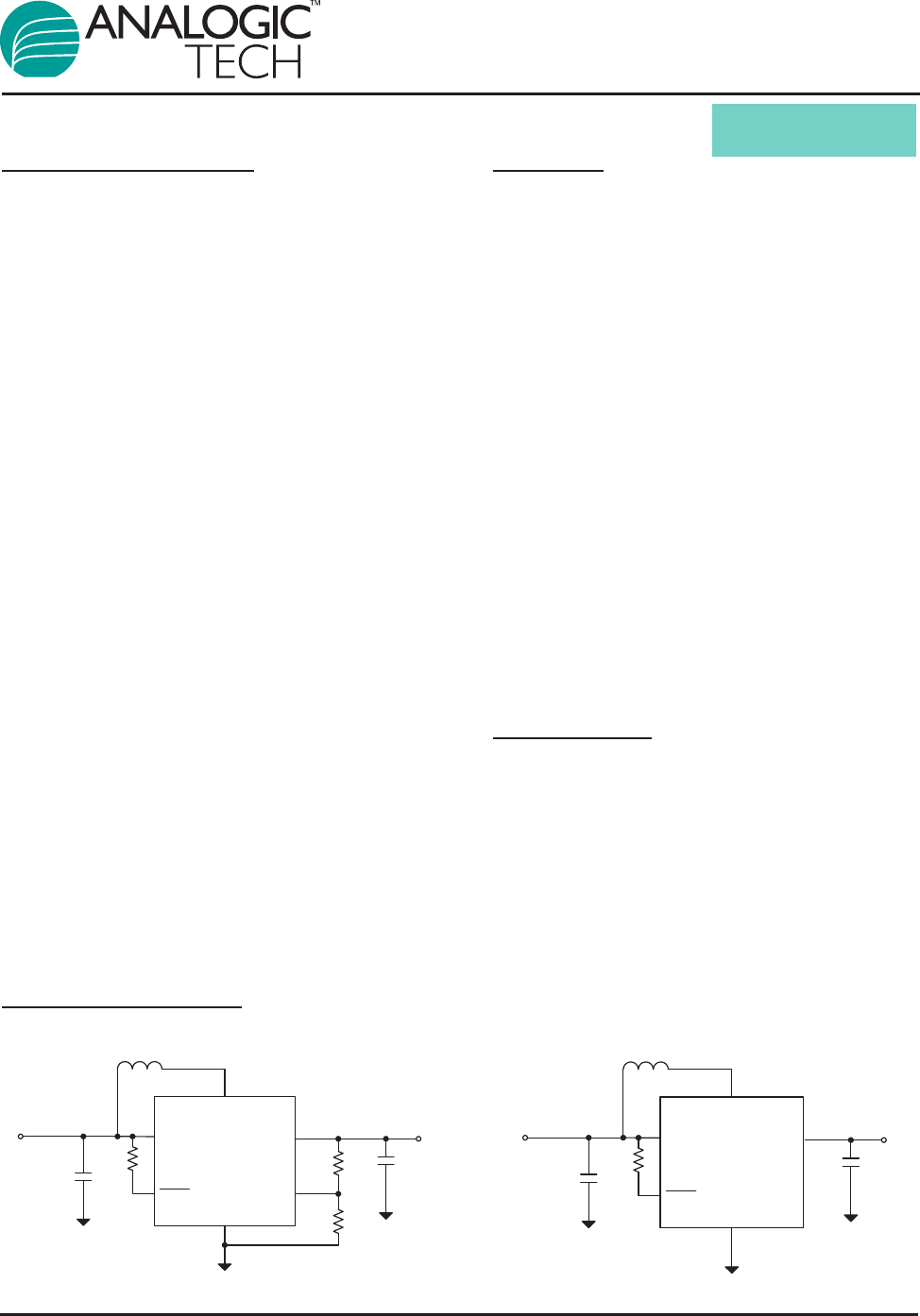
Typical Application
FB
VIN
SHDN
GND
VOUT
AAT1217-1.2
CIN
4.7µF
VIN:0.85V
L1
4.7µH
R1
1.02MΩ
R2
604kΩ
VOUT:
3.3V,100mA
SW
R3
1MΩCOUT
4.7µF
FB
VIN
SHDN
GND
VOUT
AAT1217-3.3
CIN
4.7µF
VIN:0.85V
L1
4.7µH
VOUT:
3.3V,100mA
SW
R3
1MΩCOUT
4.7µF
1217.2007.07.1.0 1
SwitchReg™
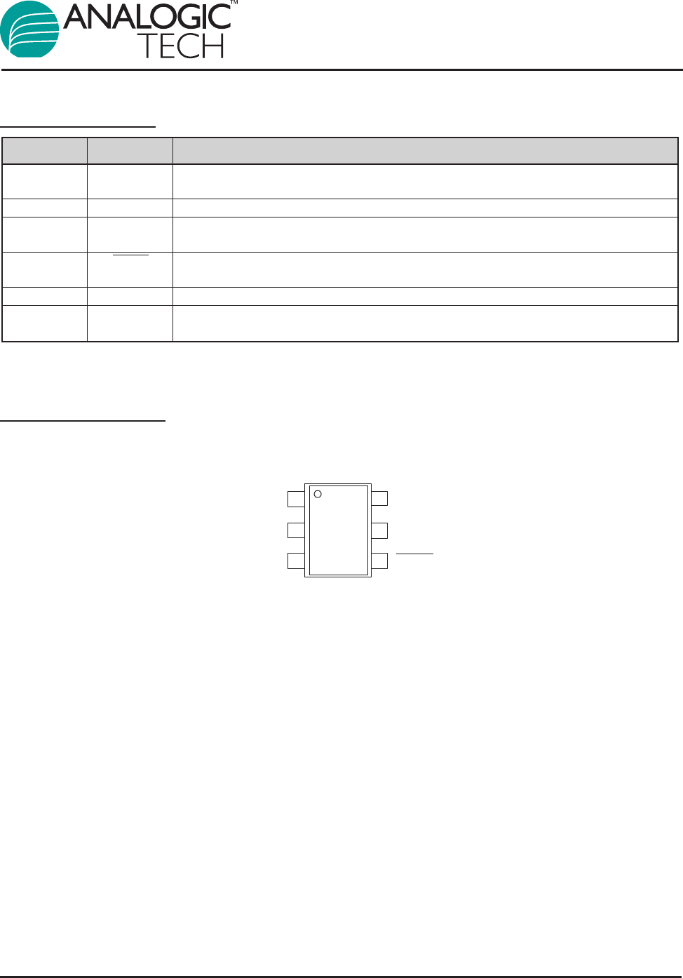
Pin Descriptions
Pin Configuration
TSOT23-6
(Top View)
GND
VIN
VOUT
SHDN
FB
SW
1
2
34
5
6
Pin # Symbol Function
1 SW Power Switch Pin. Ties to the drains of the PMOS synchronous rectifier and the
NMOS switch.
2 GND Ground Pin
3 FB Feedback Input Pin. Connect FB to the center point of the external resistor divider.
The feedback threshold voltage is 1.23V.
4 SHDN Shutdown Signal Input. Logic high enables the IC. Logic low disables the IC. Shutdown
current is <1µA.
5 VOUT Power Output Pin. Tied to the source of the PMOS synchronous rectifier.
6 VIN Power Supply Input. Must be closely decoupled to GND, Pin 2, with a 4.7µF or greater
ceramic capacitor.
AAT1217
600mA, 1.2MHz, Micropower
Synchronous Step-Up Converter
21217.2007.07.1.0
Absolute Maximum Ratings1
Thermal Information3
Symbol Description Value Units
θJA Maximum Thermal Resistance 190 °C/W
PDMaximum Power Dissipation 526 mW
Symbol Description Value Units
VIN Input Supply Voltage -0.3 to 6 V
VSW SW Voltage -0.3 to 6 V
VFB, VSHDN FB, SHDN Voltages -0.3 to 6 V
VOUT VOUT Voltage -0.3 to 6 V
TAOperating Ambient Temperature Range2-40 to 85 °C
TSTORAGE Storage Temperature Range -65 to 150 °C
TLEAD Lead Temperature (Soldering, 10s) 300 °C
TJOperating Junction Temperature Range2-40 to 150 °C
AAT1217
600mA, 1.2MHz, Micropower
Synchronous Step-Up Converter
1217.2007.07.1.0 3
1. Absolute Maximum Ratings are those values beyond which the life of a device may be impaired.
2. TJis calculated from the ambient temperature TAand power dissipation PDaccording to the following formula: TJ= TA+ PDxθJA.
3. Mounted on an FR4 board.
Electrical Characteristics1
VIN = 1.2V, VOUT = 3.3V, TA= 25°C, unless otherwise noted.
Symbol Description Conditions Min Typ Max Units
VIN
Minimum Start-Up Voltage IOUT = 1mA 0.85 1 V
Minimum Operating Voltage VSHDN = VIN 0.5 0.65
VOUT
Output Voltage Range 2.5 5.5 V
Output Voltage Accuracy3IOUT = 10mA; TA= -40°C to +85°C -4 +4 %
VFB Reference Voltage TA= -40°C to +85°C 1.192 1.230 1.268 V
VIN = 1.2V to 2.4V, IOUT = 10mA,
∆VOUT/VOUT/ Reference Voltage Line VOUT = 3.3V 0.2
%/V
∆VIN Regulation VIN = 2.4V to 4.2V, IOUT = 10mA,
VOUT = 5.0V 0.4
VIN = 1.2V, IOUT = 10mA to 100mA
∆VOUT/VOUT/ Reference Voltage Load VOUT = 3.3V 0.003
%/mA
∆IOUT Regulation VIN = 3.6V, IOUT = 10mA to 400mA
VOUT = 5.0V 0.004
IQ
Quiescent Current (Shutdown) VSHDN = 0 0.01 1
Quiescent Current (Active) VIN = 1.8V, Current from input voltage 115 µA
source. VSHDN = VIN
Quiescent Current (Active) Measured on VOUT, VSHDN = VIN 300 500
ILNMOS NMOS Switch Leakage VSW = 5V 0.1 5 µA
ILPMOS PMOS Switch Leakage VSW = 0V 0.1 5 µA
RDS(ON)L NMOS Switch ON Resistance VOUT = 3.3V 0.35 Ω
VOUT = 5V 0.30
RDS(ON)H PMOS Switch ON Resistance VOUT = 3.3V 0.60 Ω
VOUT = 5V 0.55
ICL NMOS Current Limit 750 1200 mA
∆t(ICL) Current Limit Delay to Output 40 ns
DMAX Maximum Duty Cycle VFB = 1.15V, TA= -40°C to +85°C 80 85 %
FOSC Switching Frequency TA= -40°C to +85°C 0.9 1.2 1.5 MHz
VSHDN
SHDN Input Low 0.35 V
SHDN Input High 1.00
ISHDN SHDN Input Current VSHDN = 5.5V 0.01 1 µA
TSD Thermal Shutdown 160 °C
Hysteresis 20
AAT1217
600mA, 1.2MHz, Micropower
Synchronous Step-Up Converter
41217.2007.07.1.0
1. Specifications over the temperature range are guaranteed by design, characterization, and correlation with statistical process con-
trols.
2. Not including the current into internal resistance divider.
3. For fixed 3.3V and 5.0V output voltage version. The adjustable output voltage is guaranteed by reference voltage accuracy.
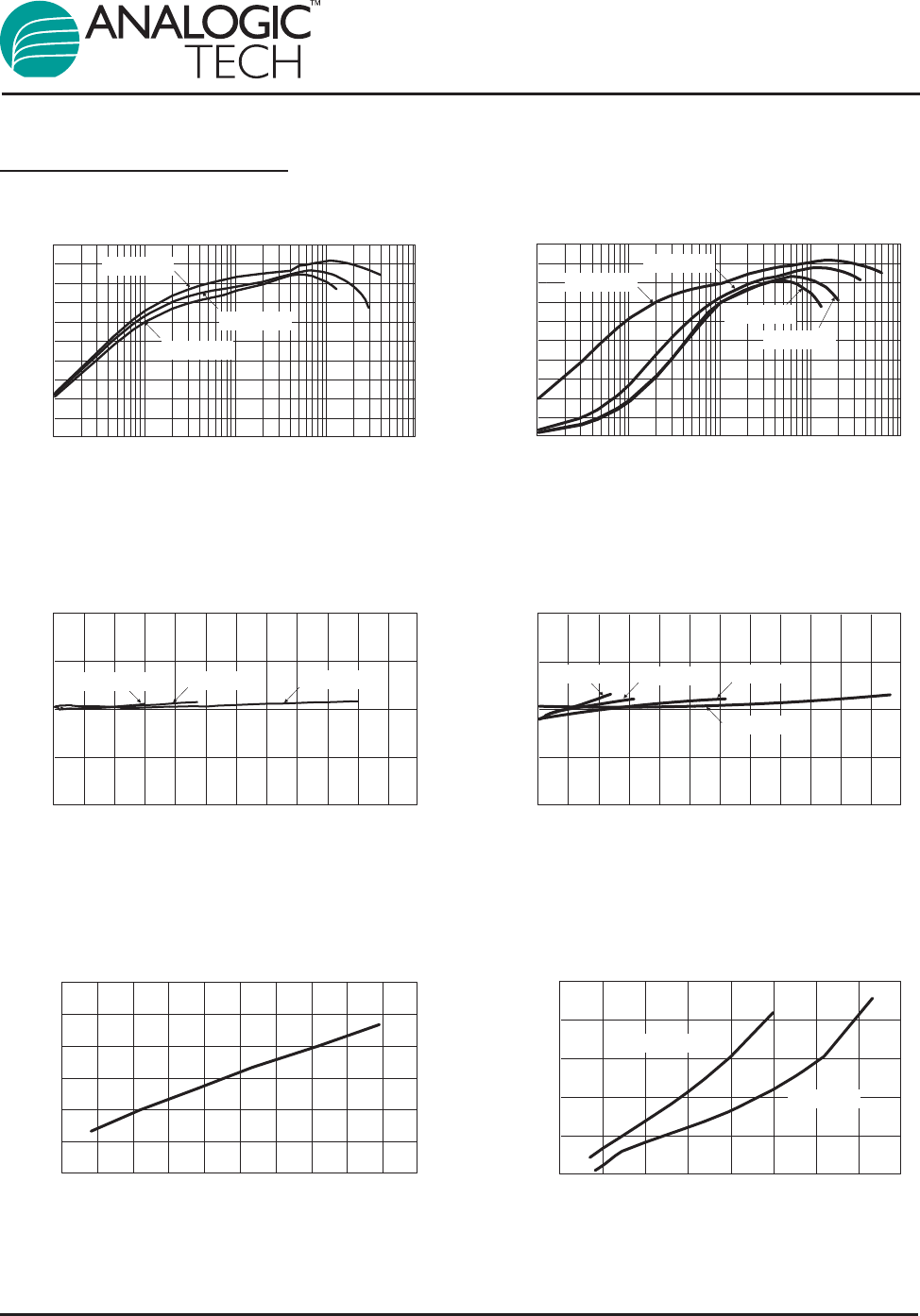
Typical Characteristics
Minimum Start-Up Voltage vs. Output Current
(VOUT = 3.3V; TA= 25°°C)
Output Current (mA)
Start-Up Voltage (V)
0 20 40 60 80 100 120 140 160 180 200
0.6
0.75
0.9
1.05
1.2
1.35
1.5
Maximum Output Current vs. Input Voltage
(L = 4.7µH; TA= 25°°C)
Input Voltage (V)
Maximum Output
Current (mA)
0.5 11.5 22.5 33.5 44.5
0
200
400
600
800
1000
VOUT = 5V
VOUT = 3.3V
Output Voltage vs. Output Current
(VOUT = 3.3V; TA= 25°°C)
Output Current (mA)
Output Voltage (V)
0100 200 300 400 500 600
3.1
3.2
3.3
3.4
3.5
VIN = 1.2V VIN = 1.5V VIN = 2.4V
Output Voltage vs. Output Current
(VOUT = 5V; TA= 25°°C)
Output Current (mA)
Output Voltage (V)
0100 200 300 400 500 600
4.8
4.9
5
5.1
5.2
VIN = 1.2V VIN = 1.5V VIN = 2.4V
VIN = 3.6V
Efficiency vs. Output Current
(VOUT = 3.3V; TA= 25°°C)
Output Current (mA)
Efficiency (%)
0.1 1 10 100 1000
0
10
20
30
40
50
60
70
80
90
100
VIN = 2.4V
VIN = 1.2V
VIN = 1.5V
Efficiency vs. Output Current
(VOUT = 5V; TA= 25°°C)
Output Current (mA)
Efficiency (%)
0.1 110 100 1000
0
10
20
30
40
50
60
70
80
90
100
VIN = 1.2V
VIN = 1.5V
VIN = 3.6V
VIN = 2.4V
AAT1217
600mA, 1.2MHz, Micropower
Synchronous Step-Up Converter
1217.2007.07.1.0 5
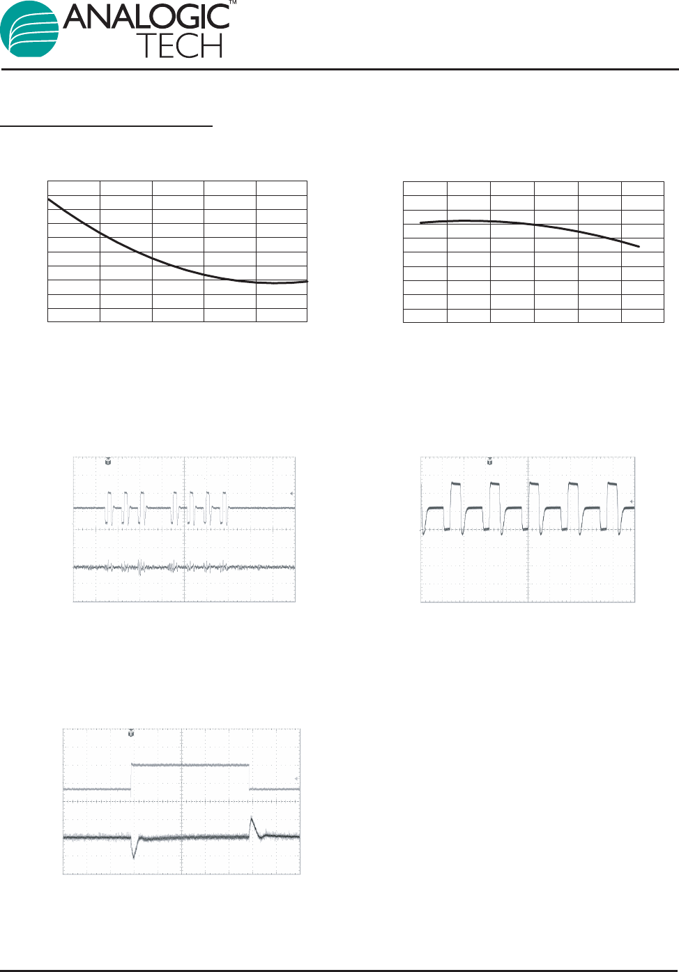
Typical Characteristics
Load Transient Response
(VIN = 1.5V; VOUT = 3.3V; CFF = 100pF)
IOUT
50mA/div
VOUT
100mV/div
(AC)
Time (100µs/div)
0A
40mA
100mA
Pulse Skipping Mode Operation
(VIN = 1.8V; VOUT = 3.3V; IOUT = 5mA)
VSW
2V/div
VOUT
50mV/div
(AC)
Time (1ms/div)
0V
Anti-Ringing Operation at SW
(VIN = 2.4V; VOUT = 5V; IOUT = 20mA)
VSW
2V/div
0V
Time (400ns/div)
No Load Input Current vs. Input Voltage
(VOUT = 3.3V; TA= 25°°C; No Load)
Input Voltage (V)
Input Current (µA)
1.5 1.8 2.1 2.4 2.7 3
50
60
70
80
90
100
110
120
130
140
150
Output Voltage vs. Temperature
Temperature (°°C)
Output Voltage (V)
-50 -25 0 25 50 75 100
3.25
3.26
3.27
3.28
3.29
3.3
3.31
3.32
3.33
3.34
3.35
AAT1217
600mA, 1.2MHz, Micropower
Synchronous Step-Up Converter
61217.2007.07.1.0
Functional Block Diagram
COUT R1
R2
PWM
Logic
Shutdown
Control
+
–
Comp
–
EA
+
VOUT
GND
SHDN
FB
VOUT
Oscillator
1.2MHz
Antiringing
Control
Bandgap
1.23V
Start-Up
Oscillator
+
–
VOUT
GOOD
MUX
Current
Sense
Slope
Compensation
To VIN
2.3V
L1
VIN VIN
SW
–
+
CIN
AAT1217
600mA, 1.2MHz, Micropower
Synchronous Step-Up Converter
1217.2007.07.1.0 7
Functional Description
The AAT1217 is a synchronous step-up DC-DC con-
verter. It utilizes internal MOSFET switches to
achieve high efficiency over the full load current
range. It operates at a fixed switching frequency of
1.2MHz, and uses the slope compensated current
mode pulse width modulation (PWM) architecture.
The device can operate with an input voltage below
1V; the typical start-up voltage is 0.85V.
Synchronous Rectification
The AAT1217 integrates a synchronous rectifier to
improve efficiency as well as to eliminate the need
for an external Schottky diode. The synchronous
rectifier is used to reduce the conduction loss con-
tributed by the forward voltage of an external
Schottky diode. The synchronous rectifier is real-
ized by a P-channel MOSFET (PMOS) with gate
control circuitry that incorporates relatively compli-
cated timing concerns. An external Schottky diode
is required when the output voltage is greater than
4.5V.
Low Voltage Start-Up
The AAT1217 can start-up with supply voltages
down to 0.85V. During start-up, the internal low
voltage start-up circuitry controls the internal
NMOS switch. The AAT1217 leaves the start-up
mode once VOUT exceeds 2.3V. An internal com-
parator (VOUT GOOD) monitors the output voltage
and places the chip into normal operation once
VOUT exceeds 2.3V. The AAT1217’s control circuit-
ry is biased by VIN during start-up and biased by
VOUT once VOUT exceeds VIN. When VOUT exceeds
VIN, the AAT1217’s operation will be independent
of VIN.
Current Mode Operation
The AAT1217 is based on a slope compensated
current mode PWM control topology. It operates at
a fixed frequency of 1.2MHz. At the beginning of
each clock cycle, the main switch (NMOS) is turned
on and the inductor current starts to ramp. After the
maximum duty cycle or the sense current signal
equals the error amplifier (EA) output, the main
switch is turned off and the synchronous switch
(PMOS) is turned on. This control topology fea-
tures cycle-by-cycle current limiting which can pre-
vent the main switch from overstress and the exter-
nal inductor from saturating.
Pulse Skipping Mode Operation
At very light load, the AAT1217 automatically
switches into pulse skipping mode operation to
improve efficiency. During this mode, the PWM
control will skip some pulses to maintain regulation.
If the load increases and the output voltage drops,
the device will automatically switch back to normal
PWM mode and maintain regulation.
Anti-Ringing Control
An anti-ringing circuitry is included to remove the
high frequency ringing that appears on the SW pin
when the inductor current goes to zero. In this
case, a ringing on the SW pin is induced due to
remaining energy stored in parasitic components of
switch and inductor. The anti-ringing circuitry
clamps the voltage internally to the battery voltage
and therefore dampens this ringing.
Device Shutdown
When SHDN is set logic high, the AAT1217 is put
into active mode operation. If SHDN is set logic
low, the device is put into shutdown mode and con-
sumes less than 1µA of current. After start-up, the
internal circuitry is supplied by VOUT, however, if
shutdown mode is enabled, the internal circuitry
will be supplied by the input source again.
Application Information
Adjustable Output Voltage
An external resistor divider is used to set the output
voltage. The output voltage of the switching regula-
tor (VOUT) is determined by the following equation:
Table 1 lists the recommended resistor values for
particular output voltage settings.
Table 1: Resistor Selection for Output Voltage
Setting.
Fixed Output Voltage
AAT1217 has two fixed output voltage options:
3.3V and 5V. An internal resistor divider is con-
nected to the FB pin inside the package which elim-
inates the need for external feedback resistors.
When designing with the fixed output voltage
option, remember to leave the FB pin open; other-
wise the output voltage will be affected. However, a
feed-forward capacitor can still be added between
the FB and VOUT pins to enhance the control loop
performance.
Inductor Selection
The high switching frequency of 1.2MHz allows for
small surface mount inductors. For most applica-
tions, the AAT1217 operates with inductors from
2.2µH to 10µH. Use the following equations to
select the proper inductor value for a particular
application condition:
VOUT R1(ΩΩ) R2(ΩΩ)
3.3V 1.02M 604k
5.0V 1.02M 332k
VOUT = 1.23V · 1 + R1
R2
AAT1217
600mA, 1.2MHz, Micropower
Synchronous Step-Up Converter
81217.2007.07.1.0

IPEAK Peak Inductor Current
IDC DC Component (Average) of the Inductor
Current
∆ILPeak-Peak Inductor Ripple Current
IOUT Output (Load) Current
VOUT Output Voltage
VIN Input Voltage
η AAT1217 Efficiency (consult the perform-
ance graphs in the “Typical Characteristics”
section of the data sheet)
D Steady-State Duty Cycle
FSW Switching Frequency
L Inductor Value
For a given chosen inductor value and application
conditions make sure the peak inductor current does
not exceed the maximum current rating of the select-
ed vendor’s inductor. For optimum load transient and
efficiency, low DCR inductors should be selected.
Table 2 lists some typical surface mount inductors
that are suitable for typical AAT1217 applications.
Input Capacitor
A surface mount 4.7µF or greater, X5R or X7R,
ceramic capacitor is suggested for the input capac-
itor. The input capacitor provides a low impedance
loop for the edges of pulsed current drawn by the
AAT1217. Low ESR/ESL X7R and X5R ceramic
capacitors are ideal for this function. To minimize
stray inductance, the capacitor should be placed
as close as possible to the IC. This keeps the high
frequency content of the input current localized,
minimizing EMI and input voltage ripple. Always
examine the ceramic capacitor DC voltage coeffi-
cient characteristics to get the proper value. For
example, the capacitance of a 10µF, 6.3V, X5R
ceramic capacitor with 5.0V DC applied is actually
about 6µF.
A laboratory test set-up typically consists of two long
wires running from the bench power supply to the
evaluation board input voltage pins. The inductance
of these wires, along with the low-ESR ceramic input
capacitor, can create a high Q network that may
affect converter performance. This problem often
becomes apparent in the form of excessive ringing
in the output voltage during load transients which
can produce errors in loop phase and gain meas-
urements. Since the inductance of a short printed
circuit board (PCB) trace feeding the input voltage is
significantly lower than the power leads from the
bench power supply, most actual applications do not
exhibit this problem. In applications where the input
power source lead inductance cannot be reduced to
a level that does not affect the converter perform-
ance, a high ESR tantalum or aluminum electrolytic
capacitor should be placed in parallel with the low
ESR, ESL bypass input ceramic capacitor. The intro-
duction of the high ESR capacitor dampens the high
Q network and stabilizes the AAT1217.
IPEAK = +
IOUT · VOUT
η · VIN
VIN · (VOUT - VIN)
2L · FSW · VOUT
∆IL = ; D =
=VIN · (VOUT - VIN)
L · FSW · VOUT
VIN · D
L · FSW
VOUT - VIN
VOUT
∆IL
IDC = IOUT · VOUT
η · VIN
IPEAK = IDC + ∆IL
2
AAT1217
600mA, 1.2MHz, Micropower
Synchronous Step-Up Converter
1217.2007.07.1.0 9
Table 2. Typical Surface Mount Inductors.
Part Number L (µH) Max DCR (mΩΩ) Rated DC Current (A) Size WxLxH (mm)
2.2 123 1.15
Sumida CDH28D11/S 4.7 238 0.75 3x3.3x1.2
10 431 0.53
2.2 140 (typ) 1.12
Coiltronics SD3112 4.7 246 (typ) 0.8 3.1x3.1x1.2
10 446 (typ) 0.55
2.2 100 1
TDK VLF3012A 4.7 190 0.74 2.8x2.6x1.2
10 410 0.49
2.2 71.2 1.75
Sumida CR43 4.7 108.7 1.15 4.3x4.8x3.5
10 182 1.04
2.2 31.3 2.04
Sumida CDRH4D28 4.7 72 1.32 5.0x5.0x3.0
10 128 1
Toko D53LC 4.7 45 1.87 5.0x5.0x3.0
10 90 1.33
AAT1217
600mA, 1.2MHz, Micropower
Synchronous Step-Up Converter
10 1217.2007.07.1.0
Output Capacitor
The output capacitor limits the output ripple and pro-
vides holdup during large load transitions. A 4.7µF to
10µF, X5R or X7R, ceramic capacitor is suggested
for the output capacitor. Typically the recommended
capacitor range provides sufficient bulk capacitance
to stabilize the output voltage during large load tran-
sitions and has the ESR and ESL characteristics
necessary for low output voltage ripple.
In addition, the output voltage droop during load
transient is dominated by the capacitance of the
ceramic output capacitor. During a step increase in
load current, the ceramic output capacitor alone
supplies the load current until the loop responds.
Within several switching cycles, the loop responds
and the inductor current increases to match the
load current demand. Larger output capacitor val-
ues help to reduce the voltage droop during large
load current transients.
External Diode Selection
An external Schottky diode is required when the
output voltage is above 4.5V. The Schottky diode is
optional for output voltages ≤4.5V, but can
improve efficiency by about 2% to 3%.
Load Disconnect in Shutdown
In conventional synchronous step-up converters, a
conduction path exists from input to output through
the backgate (body diode) of the P-channel MOS-
FET during shutdown. Special application circuitry
can disconnect the load from the battery during
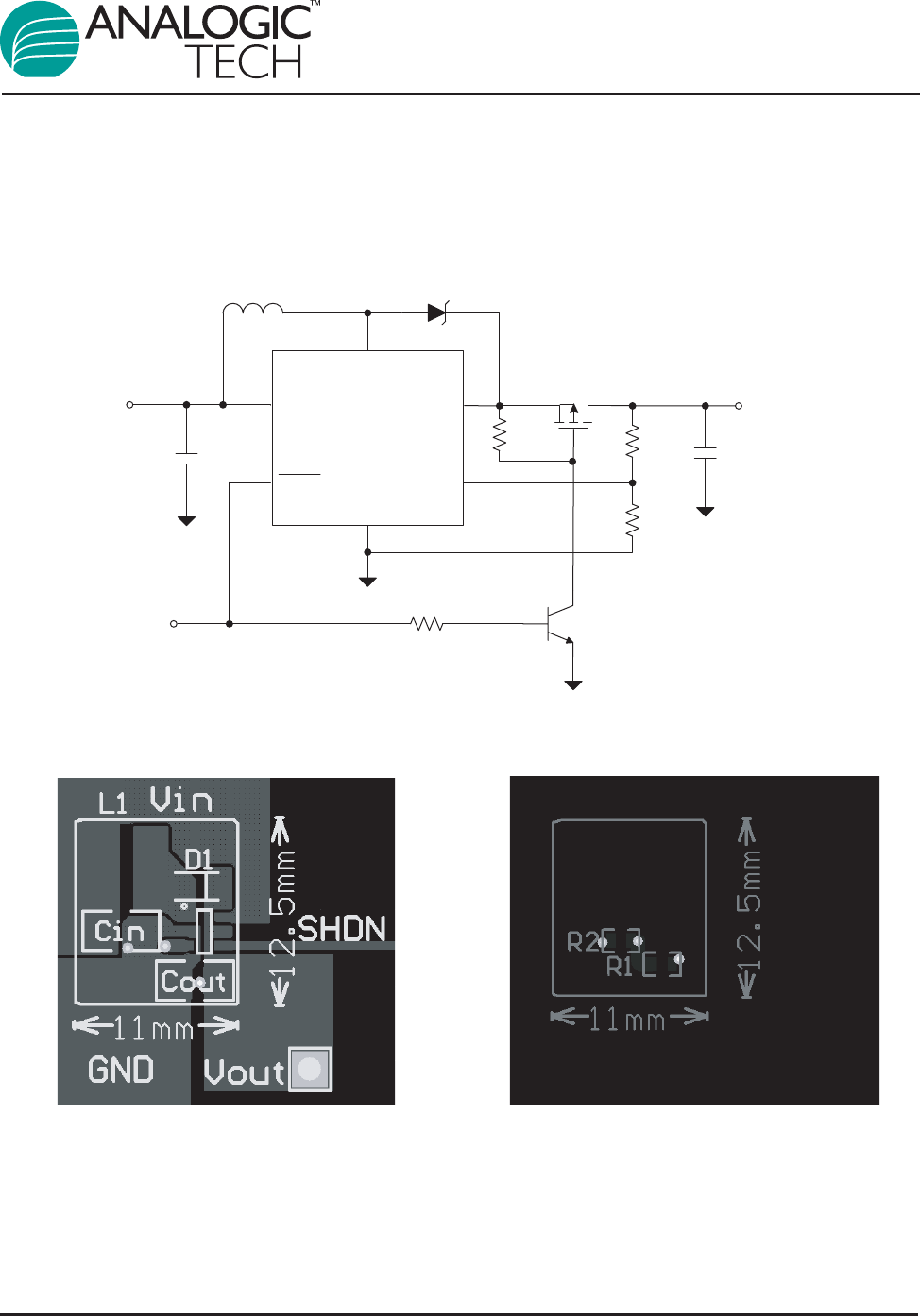
shutdown (see Figure 1).
PCB Layout Guidance
The AAT1217 typically operates at 1.2MHz. This is a
considerably high frequency for DC-DC converters.
PCB layout is important to guarantee satisfactory
performance. It is recommended to make traces of
the power loop, especially where the switching node
is involved, as short and wide as possible. First of
all, the inductor, input and output capacitor should
be as close as possible to the device. Feedback and
shutdown circuits should avoid the proximity of large
AC signals involving the power inductor and switch-
ing node. The optional rectifier diode (D1 in Figure
1) can improve efficiency and alleviate the stress on
the integrated MOSFETs. The diode should also be
close to the inductor and the chip to form the short-
est possible switching loop. While the two-layer PCB
shown in Figures 2 and 3 is enough for most appli-
cations, large and integral multi-layer ground planes
AAT1217
600mA, 1.2MHz, Micropower
Synchronous Step-Up Converter
1217.2007.07.1.0 11
Figure 1. AAT1217 High Efficiency Load Disconnect Application Circuit
Figure 2. AAT1217 Evaluation Board Layout Figure 3. AAT1217 Evaluation Board Layout
Example Top Layer Example Bottom Layer
FB
VIN
SHDN
GND
VOUT
AAT1217
CIN
4.7µF
VIN 0.85V
L1
4.7µH
COUT
4.7µF
R1
1.02MΩ
R2
604kΩ
VOUT
3.3V,100mA
1
2
34
5
SW
6
D1
MBR0520
R3
510kΩ
ON/OFF Control
Q1
Si2305 DS
Q2
2N3904
R4
510kΩ
are ideal for high power applications. Large areas of
copper have lower resistance and help to dissipate
heat. The converter's ground should join the system
ground to which it supplies power at one point only.
Figure 1 is the schematic for a highly efficient load
disconnect application circuit for the AAT1217. An
example PCB layout for the AAT1217 is shown in
Figures 2 and 3.
Ordering Information
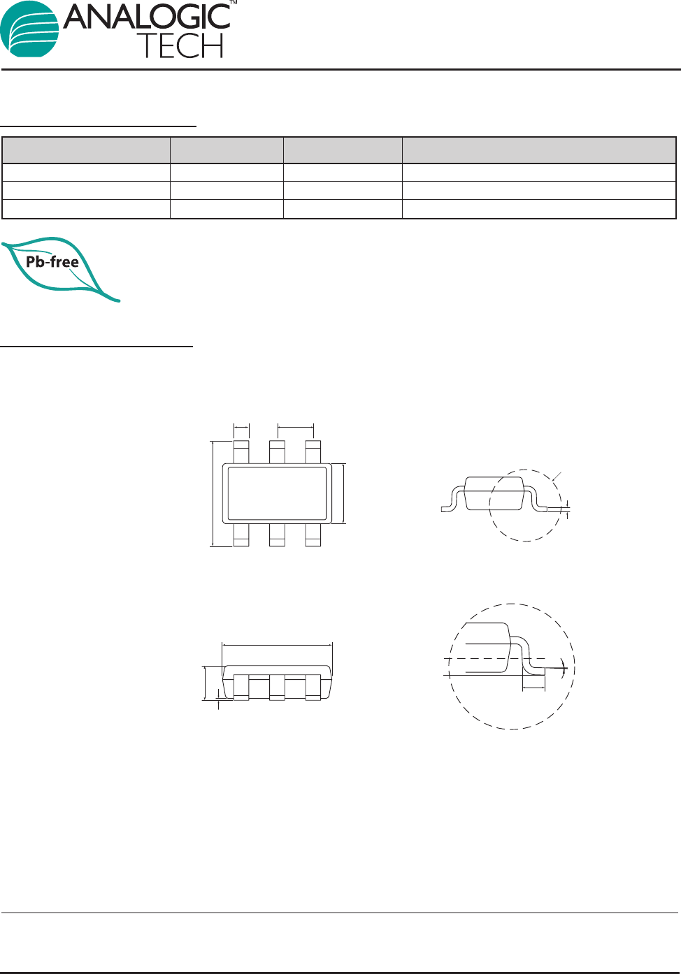
Package Information
TSOT23-6
All dimensions in millimeters.
Part Dimensions
0.40 ±± 0.10 0.95 BSC
1.60 BSC
0.45 ±± 0.15
0.25 BSC
0.127 BSC
Detail "A"
2.80 BSC
1.00 ±± 0.10
0.000 ++ 0.100
- 0.000
1.00 ++10°
-0°
2.90 BSC
Top View
End View
Detail "A"
Side View
All AnalogicTech products are offered in Pb-free packaging. The term “Pb-free” means
semiconductor products that are in compliance with current RoHS standards, including
the requirement that lead not exceed 0.1% by weight in homogeneous materials. For more
information, please visit our website at http://www.analogictech.com/pbfree.
Output Voltage1Package Marking2Part Number (Tape and Reel)3
Adj. TSOT23-6 VZMYY AAT1217ICA-1.2-T1
Fixed 3.3V TSOT23-6 WAMYY AAT1217ICA-3.3-T1
Fixed 5.0V TSOT23-6 WBMYY AAT1217ICA-5.0-T1
AAT1217
600mA, 1.2MHz, Micropower
Synchronous Step-Up Converter
12 1217.2007.07.1.0
1. Please contact sales for other voltage options.
2. YY = Manufacturing Date Code.
3. Sample stock is generally held on part numbers listed in BOLD.

AAT1217
600mA, 1.2MHz, Micropower
Synchronous Step-Up Converter
1217.2007.07.1.0 13
Advanced Analogic Technologies, Inc.
830 E. Arques Avenue, Sunnyvale, CA 94085
Phone (408) 737- 4600
Fax (408) 737- 4611
© Advanced Analogic Technologies, Inc.
AnalogicTech cannot assume responsibility for use of any circuitry other than circuitry entirely embodied in an AnalogicTech product. No circuit patent licenses, copyrights, mask work
rights, or other intellectual property rights are implied. AnalogicTech reserves the right to make changes to their products or specifications or to discontinue any product or service with-
out notice. Except as provided in AnalogicTech’s terms and conditions of sale, AnalogicTech assumes no liability whatsoever, and AnalogicTech disclaims any express or implied war-
ranty relating to the sale and/or use of AnalogicTech products including liability or warranties relating to fitness for a particular purpose, merchantability, or infringement of any patent,
copyright or other intellectual property right. In order to minimize risks associated with the customer’s applications, adequate design and operating safeguards must be provided by the
customer to minimize inherent or procedural hazards. Testing and other quality control techniques are utilized to the extent AnalogicTech deems necessary to support this warranty.
Specific testing of all parameters of each device is not necessarily performed. AnalogicTech and the AnalogicTech logo are trademarks of Advanced Analogic Technologies Incorporated.
All other brand and product names appearing in this document are registered trademarks or trademarks of their respective holders.