ADP3330 Datasheet. Www.s Manuals.com. Analog
User Manual: Marking of electronic components, SMD Codes L3, L3 *, L3***, L3-***, L30, L324, L324A, L324K, L324KA, L3533, L358, L358A, L37A, L37B, L3B. Datasheets ADP3330ART-2.85, APL3533QB, BAV23S, BZX384-B6V8, LM317DCY, LM324APW, LM324KAPW, LM324KPW, LM324PW, LM358APW, LM358PSR, LM358PW, LP2980AIM5-4.7, LP2980IM5-4.7, NZL7V5AXV3T1, RT9819E-25PV, SST503, Si2303BDS, mESD6.0DT5G.
Open the PDF directly: View PDF ![]() .
.
Page Count: 12
REV. A
a
ADP3330
One Technology Way, P.O. Box 9106, Norwood, MA 02062-9106, U.S.A.
Tel: 781/329-4700 World Wide Web Site: http://www.analog.com
Fax: 781/326-8703 © Analog Devices, Inc., 1999
Information furnished by Analog Devices is believed to be accurate and
reliable. However, no responsibility is assumed by Analog Devices for its
use, nor for any infringements of patents or other rights of third parties
which may result from its use. No license is granted by implication or
otherwise under any patent or patent rights of Analog Devices.
High Accuracy Ultralow I
Q
,
200 mA, SOT-23, anyCAP
™
Low Dropout Regulator
FUNCTIONAL BLOCK DIAGRAM
THERMAL
PROTECTION CC
IN
ADP3330
OUT
R1
R2
GND
Q1
SD BANDGAP
REF
DRIVER g
m
ERR
FEATURES
High Accuracy Over Line and Load: 60.7% @ +258C,
61.4% Over Temperature
Ultralow Dropout Voltage: 140 mV (Typ) @ 200 mA
Requires Only CO = 0.47 mF for Stability
anyCAP = Stable with Any Type of Capacitor
(Including MLCC)
Current and Thermal Limiting
Low Noise
Low Shutdown Current: <2 mA
2.9 V to 12 V Supply Range
–408C to +858C Ambient Temperature Range
Ultrasmall Thermally Enhanced Chip-on-Lead™
SOT-23-6 6-Lead Package
APPLICATIONS
Cellular Telephones
Notebook, Palmtop Computers
Battery Powered Systems
PCMCIA Regulator
Bar Code Scanners
Camcorders, Cameras
GENERAL DESCRIPTION
The ADP3330 is a member of the ADP330x family of precision
low dropout anyCAP voltage regulators. The ADP3330 operates
with an input voltage range of 2.9 V to 12 V and delivers a load
current up to 200 mA. The ADP3330 stands out from the con-
ventional LDOs with a novel architecture and an enhanced
process that enables it to offer performance advantages and
higher output current than its competition. Its patented design
requires only a 0.47 µF output capacitor for stability. This
device is insensitive to output capacitor Equivalent Series
Resistance (ESR), and is stable with any good quality capaci-
tor, including ceramic (MLCC) types for space-restricted
applications. The ADP3330 achieves exceptional accuracy of
±0.7% at room temperature and ±1.4% over temperature, line
and load variations. The dropout voltage of the ADP3330 is
only 140 mV (typical) at 200 mA. This device also includes a
safety current limit, thermal overload protection and a shutdown
feature. In shutdown mode, the ground current is reduced to
less than 2 µA. The ADP3330 has ultralow quiescent current
34 µA (typ) in light load situations.
anyCAP and Chip-on-Lead are trademarks of Analog Devices, Inc.
V
OUT
V
IN
+
–
ADP3330
NR
OUT
ERR
ON
OFF
SD GND
IN
C
OUT
0.47mF
C
IN
0.47mF
+
–
Figure 1. Typical Application Circuit
The SOT-23-6 package has been thermally enhanced using
Analog Devices’ proprietary Chip-on-Lead feature to maximize
power dissipation.

–2– REV. A
ADP3330-xx–SPECIFICATIONS
Parameter Symbol Conditions Min Typ Max Units
OUTPUT VOLTAGE ACCURACY V
OUT
V
IN
= V
OUTNOM
+0.25 V to +12 V
I
L
= 0.1 mA to 200 mA
T
A
= +25°C –0.7 +0.7 %
V
IN
= V
OUTNOM
+0.25 V to +12 V
I
L
= 0.1 mA to 150 mA
T
A
= –40°C to +85°C –1.4 +1.4 %
V
IN
= V
OUTNOM
+0.25 V to +12 V
I
L
= 0.1 mA to 200 mA
T
A
= –20°C to +85°C –1.4 +1.4 %
LINE REGULATION V
IN
= V
OUTNOM
+0.25 V to +12 V
T
A
= +25°C 0.04 mV/V
LOAD REGULATION I
L
= 0.1 mA to 200 mA
T
A
= +25°C 0.04 mV/mA
GROUND CURRENT I
GND
I
L
= 200 mA, T
A
= –20°C to +85°C 1.6 4.0 mA
I
L
= 150 mA 1.2 3.1 mA
I
L
= 50 mA 0.4 1.1 mA
I
L
= 0.1 mA 34 50 µA
GROUND CURRENT IN DROPOUT I
GND
V
IN
= V
OUTNOM
– 100 mV
I
L
= 0.1 mA 37 55 µA
DROPOUT VOLTAGE V
DROP
V
OUT
= 98% of V
OUTNOM
I
L
= 200 mA, T
A
= –20°C to +85°C 0.14 0.23 V
I
L
= 150 mA 0.11 0.17 V
I
L
= 10 mA 0.042 0.06 V
I
L
= 1 mA 0.025 0.05
2
V
PEAK LOAD CURRENT I
LDPK
V
IN
= V
OUTNOM
+ 1 V 300 mA
OUTPUT NOISE
3
V
NOISE
f = 10 Hz–100 kHz, C
L
= 10 µF
I
L
= 200 mA, C
NR
= 10 nF, V
OUT
= 3 V 47 µV rms
f = 10 Hz–100 kHz, C
L
= 10 µF
I
L
= 200 mA, C
NR
= 0 nF, V
OUT
= 3 V 95 µV rms
SHUTDOWN THRESHOLD V
THSD
ON 2.0 V
OFF 0.4 V
SHUTDOWN PIN INPUT CURRENT I
SD
V
IN
= 12 V, 0 < SD, ≤ 12 V 1.9 9 µA
0 < SD, ≤ 5 V 1.4 6 µA
GROUND CURRENT IN SHUTDOWN
MODE I
GNDSD
SD = 0 V, V
IN
= 12 V 0.01 2 µA
OUTPUT CURRENT IN SHUTDOWN I
OSD
T
A
= +25°C @ V
IN
= 12 V 1 µA
MODE T
A
= +85°C @ V
IN
= 12 V 2 µA
ERROR PIN OUTPUT LEAKAGE I
EL
V
EO
= 5 V 1 µA
ERROR PIN OUTPUT “LOW”
VOLTAGE V
EOL
I
SINK
= 400 µA 0.19 0.40 V
NOTES
1
Ambient temperature of +85°C corresponds to a junction temperature of +125°C under typical full load test conditions.
2
Application stable with no load.
3
See detail in Figure 19 and Application section of data sheet.
Specifications subject to change without notice.
(@ TA = –408C to +858C, VIN = +7 V, CIN = 0.47 mF, COUT = 0.47 mF,
unless otherwise noted).1, 2 The following specifications apply to all voltage options except –2.5.
∆V
O
∆V
IN
∆
∆
V
I
O
L

–3–REV. A
ADP3330
ADP3330-2.5–SPECIFICATIONS
Parameter Symbol Conditions Min Typ Max Units
OUTPUT VOLTAGE ACCURACY V
OUT
V
IN
= +2.9 V to +12 V
I
L
= 0.1 mA to 200 mA
T
A
= +25°C –0.7 +0.7 %
V
IN
= +2.9 V to +12 V
I
L
= 0.1 mA to 150 mA
T
A
= –40°C to +85°C –1.4 +1.4 %
V
IN
= +2.9 V to +12 V
I
L
= 0.1 mA to 200 mA
T
A
= –20°C to +85°C –1.4 +1.4 %
LINE REGULATION V
IN
= +2.9 V to +12 V
T
A
= +25°C 0.04 mV/V
LOAD REGULATION I
L
= 0.1 mA to 200 mA
T
A
= +25°C 0.04 mV/mA
GROUND CURRENT I
GND
I
L
= 200 mA, T
A
= –20°C to +85°C 1.6 4.0 mA
I
L
= 150 mA 1.2 3.1 mA
I
L
= 50 mA 0.4 1.1 mA
I
L
= 0.1 mA 34 50 µA
GROUND CURRENT IN DROPOUT I
GND
V
IN
= V
OUTNOM
– 100 mV
I
L
= 0.1 mA 37 55 µA
DROPOUT VOLTAGE V
DROP
V
OUT
= 98% of V
OUTNOM
I
L
= 200 mA, T
A
= –20°C to +85°C 0.14 0.4 V
I
L
= 150 mA 0.11 0.3 V
I
L
= 10 mA 0.042 0.06 V
I
L
= 1 mA 0.025 0.05
2
V
PEAK LOAD CURRENT I
LDPK
V
IN
= V
OUTNOM
+ 1 V 300 mA
OUTPUT NOISE
3
V
NOISE
f = 10 Hz–100 kHz, C
L
= 10 µF
I
L
= 200 mA, C
NR
= 10 nF, V
OUT
= 3 V 47 µV rms
f = 10 Hz–100 kHz, C
L
= 10 µF
I
L
= 200 mA, C
NR
= 0 nF, V
OUT
= 3 V 95 µV rms
SHUTDOWN THRESHOLD V
THSD
ON 2.0 V
OFF 0.4 V
SHUTDOWN PIN INPUT CURRENT I
SD
V
IN
= 12 V, 0 < SD, ≤ 12 V 1.9 9 µA
0 < SD, ≤ 5 V 1.4 6 µA
GROUND CURRENT IN SHUTDOWN
MODE I
GNDSD
SD = 0 V, V
IN
= 12 V 0.01 2 µA
OUTPUT CURRENT IN SHUTDOWN I
OSD
T
A
= +25°C @ V
IN
= 12 V 1 µA
MODE T
A
= +85°C @ V
IN
= 12 V 2 µA
ERROR PIN OUTPUT LEAKAGE I
EL
V
EO
= 5 V 1 µA
ERROR PIN OUTPUT “LOW”
VOLTAGE V
EOL
I
SINK
= 400 µA 0.19 0.40 V
NOTES
1
Ambient temperature of +85°C corresponds to a junction temperature of +125°C under typical full load test conditions.
2
Application stable with no load.
3
See detail in Figure 19 and Application section of data sheet.
Specifications subject to change without notice.
(@ TA = –408C to +858C, VIN = +7 V ,CIN = 0.47 mF, COUT = 0.47 mF,
unless otherwise noted).1, 2
∆V
O
∆V
IN
∆
∆
V
I
O
L
ADP3330
–4– REV. A
CAUTION
ESD (electrostatic discharge) sensitive device. Electrostatic charges as high as 4000 V readily
accumulate on the human body and test equipment and can discharge without detection.
Although the ADP3330 features proprietary ESD protection circuitry, permanent damage may
occur on devices subjected to high energy electrostatic discharges. Therefore, proper ESD
precautions are recommended to avoid performance degradation or loss of functionality.
ABSOLUTE MAXIMUM RATINGS*
Input Supply Voltage . . . . . . . . . . . . . . . . . . . . –0.3 V to +16 V
Shutdown Input Voltage . . . . . . . . . . . . . . . . . –0.3 V to +16 V
Power Dissipation . . . . . . . . . . . . . . . . . . . . Internally Limited
Operating Ambient Temperature Range . . . . . –40°C to +85°C
Operating Junction Temperature Range . . . . –40°C to +125°C
θ
JA
(4-Layer Board) . . . . . . . . . . . . . . . . . . . . . . . +165°C/W
θ
JA
(2-Layer Board) . . . . . . . . . . . . . . . . . . . . . . . +190°C/W
Storage Temperature Range . . . . . . . . . . . . . –65°C to +150°C
Lead Temperature Range (Soldering 10 sec) . . . . . . . . +300°C
Vapor Phase (60 sec) . . . . . . . . . . . . . . . . . . . . . . . . +215°C
Infrared (15 sec) . . . . . . . . . . . . . . . . . . . . . . . . . . . +220°C
*This is a stress rating only; operation beyond these limits can cause the device to
be permanently damaged.
ORDERING GUIDE
Voltage Package Marking
Model Output Option* Code
ADP3330ART-2.5 2.5 V RT-6 (SOT-23-6) L1B
ADP3330ART-2.75 2.75 V RT-6 (SOT-23-6) L2B
ADP3330ART-2.85 2.85 V RT-6 (SOT-23-6) L3B
ADP3330ART-3 3.0 V RT-6 (SOT-23-6) L4B
ADP3330ART-3.3 3.3 V RT-6 (SOT-23-6) L5B
ADP3330ART-3.6 3.6 V RT-6 (SOT-23-6) L6B
ADP3330ART-5 5.0 V RT-6 (SOT-23-6) L8B
*Contact the factory for the availability of other output voltage options.
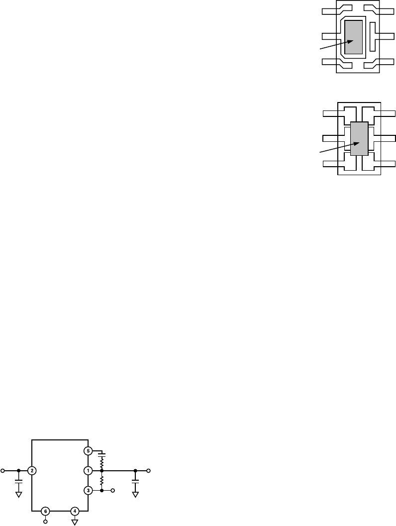
PIN FUNCTION DESCRIPTIONS
Pin Name Function
1 OUT Output of the Regulator. Bypass to ground
with a 0.47 µF or larger capacitor.
2 IN Regulator Input.
3ERR Open Collector Output that goes low to
indicate that the output is about to go out
of regulation.
4 GND Ground Pin.
5 NR Noise Reduction Pin. Used for further
reduction of output noise (see text for
detail). No connection if not used.
6SD Active Low Shutdown Pin. Connect to
ground to disable the regulator output.
When shutdown is not used, this pin
should be connected to the input pin.
PIN CONFIGURATION
TOP VIEW
(Not to Scale)
6
5
4
1
2
3
GND
NR
SD
ERR
IN
OUT
ADP3330
WARNING!
ESD SENSITIVE DEVICE
ADP3330
–5–REV. A
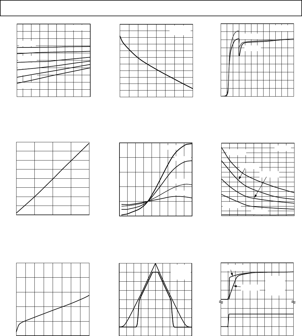
Typical Performance Characteristics–
INPUT VOLTAGE – Volts
OUTPUT VOLTAGE – Volts
3.010
3.002
2.996
3.25 456789101112
3.008
3.006
3.000
2.998
3.004
2.994
2.992
2.990
V
OUT
= 3.0V
I
L
= 0mA
I
L
= 10mA
I
L
= 100mA
I
L
= 50mA
I
L
= 150mA
I
L
= 200mA
Figure 2. Line Regulation Output
Voltage vs. Supply Voltage
OUTPUT LOAD – mA
GROUND CURRENT – mA
1.6
1.4
0.6
050 200
100 150
1.2
1.0
0.8
V
IN
= 7V
0.4
0.2
0
Figure 5. Ground Current vs. Load
Current
OUTPUT LOAD – mA
INPUT/OUTPUT VOLTAGE – mV
250
200
00 25 10050 75
150
100
50
125 150 175 200
Figure 8. Dropout Voltage vs.
Output Current
OUTPUT LOAD – mA
OUTPUT VOLTAGE – Volts
3.005
2.998
025 50 75 100 125 150 175 200
3.004
3.003
3.002
3.001
3.000
2.999
V
OUT
= 3.0V
V
IN
= 7V
2.997
2.996
2.995
2.994
Figure 3. Output Voltage vs. Load
Current
0.2
0.4
–45 –25 135–5 15 35 75 95 11555
0.1
0.0
–0.1
0.3
JUNCTION TEMPERATURE – 8C
OUTPUT VOLTAGE – %
I
L
= 50mA
I
L
= 0mA
I
L
= 150mA
I
L
= 200mA
Figure 6. Output Voltage Variation %
vs. Junction Temperature
3.5
3.0
2.5
2.0
1.5
1.0
0.5
0
0 1.0 2.0 3.0 4.0 5.0
INPUT/OUTPUT VOLTAGE – Volts
TIME – Sec
V
OUT
= 3V
SD = V
IN
R
L
= 15V
Figure 9. Power-Up/Power-Down
INPUT VOLTAGE – Volts
GROUND CURRENT – mA
45
40
20
02 4 6 8 10 12
35
30
25
V
OUT
= 3V
15
10
5
0
I
L
= 100mA
I
L
= 0mA
Figure 4. Ground Current vs. Supply
Voltage
JUNCTION TEMPERATURE – 8C
GROUND CURRENT – mA
3.0
2.8
0
–45 –25 115
–5 15 35 55 75 95
2.6
2.4
2.2
2.0
1.8
1.6
1.4
1.2
1.0
0.8
0.6
0.4
0.2
135
V
IN
= 7V
I
L
= 0mA
I
L
= 100mA
I
L
= 50mA
I
L
= 150mA
I
L
= 200mA
Figure 7. Ground Current vs. Junction
Temperature
3
2
1
0
10
5
0
0 100 200 300 400 500
VOUT – VoltsVIN – Volts
TIME – ms
VIN = 7V
VOUT = 3V
SD = VIN
RL = 15V
CL = 10mF
CL = 0.47mF
Figure 10. Power-Up Response
ADP3330
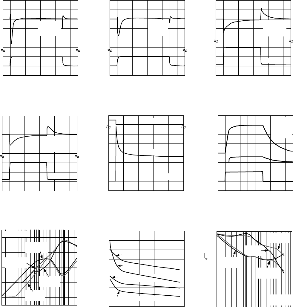
–6– REV. A
3.020
3.000
2.980
2.960
2.940
7.5
7.0
0 100 200 300 400 500
TIME – ms
V
OUT
– VoltsV
IN
– Volts
V
OUT
= 3V
R
L
= 15V
C
L
= 0.47mF
Figure 11. Line Transient Response
3.100
3.050
3.000
2.950
2.900
200
100
0
0 200 400 600 800 1000
VoltsmA
TIME –
m
s
V
IN
= 7V
V
OUT
= 3V
C
L
= 10mF
20mA
Figure 14. Load Transient Response
FREQUENCY – Hz
RIPPLE REJECTION – dB
0
10 100 1k 10k 100k 1M 10M
–10
–20
–30
–40
–50
–60
–70
–80
–90
–100
CL = 0.47mF
IL = 0.1mA
CL = 0.47mF
IL = 200mA
CL = 10mF
IL = 200mA
CL = 10mF
IL = 0.1mA
VOUT = 3.0V
Figure 17. Power Supply Ripple
Rejection
3.020
3.000
2.980
2.960
2.940
7.5
7.0
0 100 200 300 400 500
TIME – ms
V
OUT
– VoltsV
IN
– Volts
V
OUT
= 3V
R
L
= 15V
C
L
= 10mF
Figure 12. Line Transient Response
3
0
500
400
300
200
100
0
VoltsmA
0 0.5 1.0 1.5 2.0 2.5 3.0 3.5 4.0 4.5 5.0
TIME – Sec
V
OUT
I
OUT
V
IN
= 7V
Figure 15. Short Circuit Current
120
160
05010 20 30 40
100
80
60
140
C
L
– mF
RMS NOISE – mV
40
20
0
I
L
= 0mA WITH NOISE REDUCTION
I
L
= 200mA
I
L
= 200mA
WITH NOISE REDUCTION
I
L
= 0mA
Figure 18. RMS Noise vs. C
L
(10 Hz–100 kHz)
3.100
3.050
3.000
2.950
2.900
200
100
0
0 200 400 600 800 1000
VoltsmA
TIME – ms
V
IN
= 7V
V
OUT
= 3V
C
L
= 0.47mF
20mA
Figure 13. Load Transient Response
3
2
1
0
0
2
0
3
Volts
V
OUT
V
ERR
V
SD
0 200 400 600 800 1000
TIME – ms
V
IN
= 7V
V
OUT
= 3V
C
L
= 10mF
R
L
= 15V
Figure 16. Turn On–Turn Off Response
FREQUENCY – Hz
VOLTAGE NOISE SPECTRAL
DENSITY – mV/ Hz
1
0.0110 100 1M
0.1
1k 10k 100k
VOUT = 3.0V
IL = 200mA
CL = 0.47mF
CNR = 0
CL = 10mF
CNR = 0
CL = 0.47mF
CNR = 10nF
CL = 10mF
CNR = 10nF
Figure 19. Output Noise Density
ADP3330
–7–REV. A
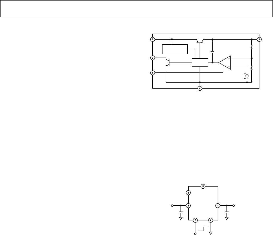
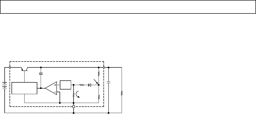
THEORY OF OPERATION
The new anyCAP
LDO ADP3330 uses a single control loop for
regulation and reference functions. The output voltage is sensed
by a resistive voltage divider consisting of R1 and R2 which is
varied to provide the available output voltage options. Feedback
is taken from this network by way of a series diode (D1) and a
second resistor divider (R3 and R4) to the input of an amplifier.
PTAT
V
OS
g
m
NONINVERTING
WIDEBAND
DRIVER
INPUT
Q1
ADP3330
COMPENSATION
CAPACITOR ATTENUATION
(V
BANDGAP
/V
OUT
)R1
D1
R2
R3
R4
OUTPUT
PTAT
CURRENT R
LOAD
C
LOAD
(a)
GND
Figure 20.␣ Functional Block Diagram
A very high gain error amplifier is used to control this loop.
The amplifier is constructed in such a way that at equilibrium it
produces a large, temperature-proportional input “offset voltage”
that is repeatable and very well controlled. The temperature-
proportional offset voltage is combined with the complementary
diode voltage to form a “virtual bandgap” voltage, implicit in
the network, although it never appears explicitly in the circuit.
Ultimately, this patented design makes it possible to control the
loop with only one amplifier. This technique also improves the
noise characteristics of the amplifier by providing more flexibil-
ity on the tradeoff of noise sources that leads to a low noise
design.
The R1, R2 divider is chosen in the same ratio as the bandgap
voltage to the output voltage. Although the R1, R2 resistor
divider is loaded by the diode D1, and a second divider consist-
ing of R3 and R4, the values are chosen to produce a tempera-
ture stable output. This unique arrangement specifically
corrects for the loading of the divider so that the error resulting
from base current loading in conventional circuits is avoided.
The patented amplifier controls a new and unique noninverting
driver that drives the pass transistor, Q1. The use of this special
noninverting driver enables the frequency compensation to
include the load capacitor in a pole splitting arrangement to
achieve reduced sensitivity to the value, type and ESR of the
load capacitance.
Most LDOs place strict requirements on the range of ESR
values for the output capacitor because they are difficult to
stabilize due to the uncertainty of load capacitance and resis-
tance. Moreover, the ESR value, required to keep conventional
LDOs stable, changes depending on load and temperature.
These ESR limitations make designing with LDOs more
difficult because of their unclear specifications and extreme
variations over temperature.
With the ADP3330 anyCAP LDO, this is no longer true. It
can be used with virtually any good quality capacitor, with no
constraint on the minimum ESR. The innovative design allows
the circuit to be stable with just a small 0.47 µF capacitor on the
output. Additional advantages of the pole splitting scheme
include superior line noise rejection and very high regulator gain
which leads to excellent line and load regulation. An impressive
±1.4% accuracy is guaranteed over line, load and temperature.
Additional features of the circuit include current limit, thermal
shutdown and noise reduction. Compared to standard solutions
that give warning after the output has lost regulation, the
ADP3330 provides improved system performance by enabling the
ERR pin to give warning just before the device loses regulation.
As the chip’s temperature rises above +165°C, the circuit
activates a soft thermal shutdown, indicated by a signal low on
the ERR pin, to reduce the current to a safe level.
ADP3330
–8– REV. A
APPLICATION INFORMATION
Capacitor Selection
Output Capacitors: as with any micropower device, output
transient response is a function of the output capacitance. The
ADP3330 is stable with a wide range of capacitor values, types
and ESR (anyCAP). A capacitor as low as 0.47 µF is all that is
needed for stability; larger capacitors can be used if high output
current surges are anticipated. The ADP3330 is stable with
extremely low ESR capacitors (ESR ≈ 0), such as Multilayer
Ceramic Capacitors (MLCC) or OSCON. Note that the
effective capacitance of some capacitor types may fall below the
minimum at cold temperature. Ensure that the capacitor
provides more than 0.47 µF at minimum temperature.
Input Bypass Capacitor: an input bypass capacitor is not strictly
required but it is advisable in any application involving long
input wires or high source impedance. Connecting a 0.47 µF
capacitor from IN to ground reduces the circuit’s sensitivity to
PC board layout. If a larger value output capacitor is used, then
a larger value input capacitor is also recommended.
Noise Reduction
A noise reduction capacitor (C
NR
) can be used to further reduce
the noise by 6 dB–10 dB (Figure 21). Low leakage capacitors in
10 pF–500 pF range provide the best performance. Since the
noise reduction pin (NR) is internally connected to a high imped-
ance node, any connection to this node should be carefully done
to avoid noise pickup from external sources. The pad connected
to this pin should be as small as possible and long PC board
traces are not recommended.
When adding a noise reduction capacitor, use the following
guidelines:
• Maintain a minimum load current of 1 mA when not in
shutdown.
• For CNR values greater than 500 pF, add a 100 kΩ series
resistor (RNR).
It is important to note that as CNR increases, the turn-on time
will be delayed. With CNR values greater than 1 nF, this delay
may be on the order of several milliseconds.
+
–
V
IN
+
C1
0.47mF
IN
–
ADP3330-3
SD GND
V
OUT
= +3.3V
OUT
330kVC2
0.47mF
R1
CNR
NR
ERR
RNR
Figure 21.␣ Noise Reduction Circuit
Chip-on-Lead Package
The ADP3330 uses a patented Chip-on-Lead package design to
ensure the best thermal performance in an SOT-23 footprint. In
a standard SOT-23, the majority of the heat flows out of the
ground pin. This new package uses an electrically isolated die
attach that allows all pins to contribute to heat conduction.
This technique reduces the thermal resistance to 190°C/W on a
2-layer board as compared to >230°C/W for a standard SOT-23
leadframe. Figure 22 shows the difference between the standard
SOT-23 and the Chip-on-Lead leadframes.
SILICON
DIE
a. Normal SOT-23-6 Package
SILICON DIE WITH
ELECTRICALLY
ISOLATED
DIE ATTACH
b. Thermally Enhanced Chip-on-Lead Package
Figure 22.
Thermal Overload Protection
The ADP3330 is protected against damage due to excessive
power dissipation by its thermal overload protection circuit
which limits the die temperature to a maximum of +165°C.
Under extreme conditions (i.e., high ambient temperature and
power dissipation) where die temperature starts to rise above
+165°C, the output current is reduced until the die temperature
has dropped to a safe level. The output current is restored when
the die temperature is reduced.
Current and thermal limit protections are intended to protect
the device against accidental overload conditions. For normal
operation, device power dissipation should be externally limited
so that junction temperatures will not exceed +125°C.
Calculating Junction Temperature
Device power dissipation is calculated as follows:
P
D
= (V
IN
– V
OUT
) I
LOAD
+(V
IN
) I
GND
Where I
LOAD
and I
GND
are load current and ground current, V
IN
and V
OUT
are input and output voltages respectively.
Assuming I
LOAD
= 200 mA, I
GND
= 4 mA, V
IN
= 4.2 V and
V
OUT
= 3.0 V, device power dissipation is:
P
D
= (4.2 – 3) 200 mA + 4.2 (4 mA) = 257 mW
The proprietary package used in the ADP3330 has a thermal
resistance of 165°C/W, significantly lower than a standard
6-lead SOT-23 package. Assuming a 4-layer board, the junction
temperature rise above ambient temperature will be approxi-
mately equal to:
∆T
JA
= 0.257 W × 165
°
C/W = 42.4
°
C
To limit the maximum junction temperature to +125°C,
maximum allowable ambient temperature will be:
T
A MAX
= 125
°
C – 42.4
°
C = 82.6
°
C
ADP3330
–9–REV. A
Printed Circuit Board Layout Considerations
All surface mount packages rely on the traces of the PC board
to conduct heat away from the package.
In standard packages the dominant component of the heat
resistance path is the plastic between the die attach pad and the
individual leads. In typical thermally enhanced packages one or
more of the leads are fused to the die attach pad, significantly
decreasing this component. To make the improvement mean-
ingful, however, a significant copper area on the PCB must be
attached to these fused pins.
The patented chip-on-lead frame design of the ADP3330
uniformly minimizes the value of the dominant portion of the
thermal resistance. It ensures that heat is conducted away by all
pins of the package. This yields a very low 165°C/W thermal
resistance for an SOT-23-6 package, without any special board
layout requirements, just relying on the normal traces con-
nected to the leads. This yields a 17% improvement in heat
dissipation capability as compared to a standard SOT-23-6
package. The thermal resistance can be decreased by, approxi-
mately, an additional 10% by attaching a few square cm of
copper area to the V
IN
pin of the ADP3303 package.
It is not recommended to use solder mask or silkscreen on the
PCB traces adjacent to the ADP3330’s pins since it will increase
the junction to ambient thermal resistance of the package.
Error Flag Dropout Detector
The ADP3330 will maintain its output voltage over a wide
range of load, input voltage and temperature conditions. If the
output is about to lose regulation by reducing the supply voltage
below the combined regulated output and dropout voltages,
the ERR flag will be activated. The ERR output is an open
collector, which will be driven low.
Once set, the ERR flag’s hysteresis will keep the output low
until a small margin of operating range is restored either by
raising the supply voltage or reducing the load.
Shutdown Mode
Applying a TTL high signal to the shutdown (SD) pin, or tying
it to the input pin, will turn the output ON. Pulling SD down to
0.4 V or below, or tying it to ground, will turn the output OFF.
In shutdown mode, quiescent current is reduced to much less
than 1 µA.
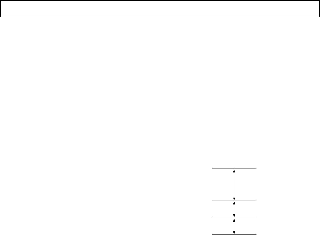
Low Power, Low Dropout Applications
ADP3330 is well suited for applications such as cellular phone
handsets that require low quiescent current and low dropout
voltage features. ADP3330 draws 34 µA typical under light load
situations (i.e., load current = 100 µA), which results in low
power consumption when the cell phone is in standby mode.
Figure 23 shows an application in which the ADP3330 is used
in a handset to provide 2.75 V nominal output voltage. The cell
phone is powered from 3 cell NiCd or 1 cell Li-Ion battery.
ADP3330 guarantees an accuracy of 1.4%, even when the input/
output differential is merely 250 mV (worst case). This implies
that the output is regulated and within specification even when
the battery voltage has reached its end-of-discharge voltage of
3 V. The output voltage never falls below 2.7 V, even under
worst case load and temperature conditions. The low dropout
feature coupled with the high accuracy of the ADP3330 ensures
that the system is reliably powered until the end of the life of the
battery, which results in increased system talk time.
MINIMUM BATTERY
VOLTAGE 3.0V
NOMINAL OUTPUT
VOLTAGE 2.75V
2.712V
ABSOLUTE MINIMUM
OUTPUT VOLTAGE
2.700V
END OF DISCHARGE VOLTAGE
OF 3 CELL NiCd OR 1 CELL
Li-Ion BATTERY
250mV MAXIMUM INPUT-OUTPUT
OVERHEAD FOR 200mA OUTPUT
CURRENT
–1.4% OUTPUT
VOLTAGE ACCURACY
12mV TRANSIENT, LINE AND
LOAD RESPECTIVE MARGIN
Figure 23.␣ LDO Budgeting for a 3 Cell NiCd/1 Cell
Li-Ion Supply
ADP3330
–10– REV. A
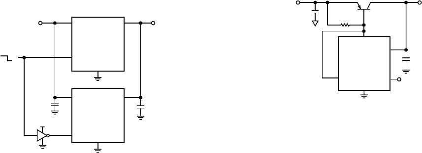
APPLICATION CIRCUITS
Crossover Switch
The circuit in Figure 24 shows how two ADP3330s can be used to
form a mixed supply voltage system. The output switches between
two different levels selected by an external digital input. Output
voltages can be any combination of voltages from the Ordering
Guide of the data sheet.
ADP3330-3.6
ADP3330-2.5
+
OUTIN
SD
GND
+
IN OUT
SD GND
C1
1.0mFC2
0.47mF
VOUT = 3.6V/2.5VVIN = 3.85V TO 12V
OUTPUT SELECT
3V
0V
LOGIC SUPPLY
Figure 24.␣ Crossover Switch
Higher Output Current
The ADP3330 can source up to 200 mA at room temperature
without any heatsink or pass transistor. If higher current is
needed, an appropriate pass transistor can be used, as in Figure
25, to increase the output current to 1 A.
ADP3330-3
OUT
IN
SD
GND
+
V
IN
= 4.5V TO 8V MJE253* V
OUT
= 3V@1A
C1
100mF
C2
100mF
*AAVID531002 HEAT SINK IS USED
ERR
R1
50V
Figure 25.␣ High Output Current Linear Regulator
ADP3330
–11–REV. A
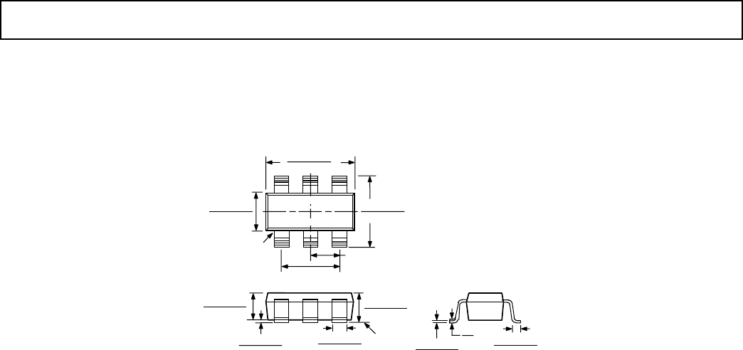
6-Lead Surface Mount
RT-6 (SOT-23-6)
0.122 (3.10)
0.106 (2.70)
PIN 1
0.071 (1.80)
0.059 (1.50) 0.118 (3.00)
0.098 (2.50)
0.075 (1.90)
BSC
0.037 (0.95) BSC
1 3
4 5 6
2
0.009 (0.23)
0.003 (0.08)
0.022 (0.55)
0.014 (0.35)
10°
0°
0.020 (0.50)
0.010 (0.25)
0.059 (0.15)
0.000 (0.00)
0.051 (1.30)
0.035 (0.90)
SEATING
PLANE
0.057 (1.45)
0.035 (0.90)
OUTLINE DIMENSIONS
Dimensions shown in inches and (mm).
C3455a–0–8/99
PRINTED IN U.S.A.