Name: An Smt Module Rf Reference Design Guide V1.01
User Manual:
Open the PDF directly: View PDF ![]() .
.
Page Count: 23

SMT Module RF Reference
Design Guide
AN_ SMT Module RF Reference Design Guide
_V1.01

SIM900 Design Application Notes
AN_SMT Module RF Reference Design Guide_V1.01 10.02.2010
2
Document Title: SMT Module RF Reference Design Guide
Version: 1.01
Date: 2010-2-10
Status: Release
Document Control ID: AN_SMT Module RF Reference Design Guide_V1.01
General Notes
SIMCOM offers this information as a service to its users, to support application and engineering
efforts that use the products designed by SIMCOM. The information provided is based upon
requirements specifically provided to SIMCOM by the users. SIMCOM has not undertaken any
independent search for additional relevant information, including any information that may be in the
user’s possession. Furthermore, system validation of this product designed by SIMCOM within a
larger electronic system remains the responsibility of the user or the user’s system integrator. All
specifications supplied herein are subject to change.
Copyright
This document contains proprietary technical information which is the property of SIMCOM
Limited., copying of this document and giving it to others and the using or communication of the
contents thereof, are forbidden without express authority. Offenders are liable to the payment of
damages. All rights reserved in the event of grant of a patent or the registration of a utility model or
design. All specification supplied herein are subject to change without notice at any time.
Copyright © Shanghai SIMCOM Wireless Solutions Ltd. 2010

SIM900 Design Application Notes
AN_SMT Module RF Reference Design Guide_V1.01 10.02.2010
3
Content
1 Introduction.......................................................................................................................................5
2 Circuit design....................................................................................................................................5
2.1 Power supply circuit design ...................................................................................................5
2.2 Antenna matching circuit design............................................................................................6
3 Consideration in components placement...........................................................................................7
4 Antenna Choosing.............................................................................................................................8
5 Stacking up of multi-layers PCB.......................................................................................................9
Stack-up of two-layers PCB.........................................................................................................9
Stack-up of four-layers PCB ......................................................................................................10
Stack-up of six-layers PCB........................................................................................................10
Stack-up of eight-layers PCB.....................................................................................................11
6 Impedance control of RF trace........................................................................................................11
7 Consideration in PCB layout...........................................................................................................14
Appendix............................................................................................................................................15
Two-layers PCB .........................................................................................................................15
Four-layers PCB.........................................................................................................................16
Six-layers PCB...........................................................................................................................17
Eight-layers PCB........................................................................................................................20

SIM900 Design Application Notes
AN_SMT Module RF Reference Design Guide_V1.01 10.02.2010
4
Version History
Data Version Description of change Author
2010-2-10 01.01 Origin Ye Haibing,
Wang Guoqiang

SIM900 Design Application Notes
AN_SMT Module RF Reference Design Guide_V1.01 10.02.2010
5
1 Introduction
This document describes the key points about RF design that should be taken into account in
customer’s application design. As SMT module can be integrated with a wide range of applications,
the application notes are described in detail.
SMT module is a well-known product which is provided by SIMCom. This type module become
very popular soon after it is released for its easy integration, good reliability. But in integrating
process, some bad RF design will lead to serious RF problems. In order to improve the RF
performance, this document is formed to give the customer some design guides in RF design of
SMT type module integration. Based on such considerations, at the later section, this document will
describe some key issues that should be paid more attention to.
NOTE: this document can apply for all SMT Modules, for example, SIM300D, SIM340D,
SIM300W, SIM340W, SIM500W, SIM540W, SIM700D, SIM900, SIM900A, SIM900D, and so on.
SIM900 is selected as a demonstration in the following sections.
2 Circuit design
When the customer begins to integrate the SMT type module into their product, the first thing to be
considered is the circuit design. This section will focus on the circuit design which is related to the
RF performance and is divided into two sub-parts, the first is the power supply circuit design; the
second is the antenna matching circuit design.
2.1 Power supply circuit design
Because the module is a high power consuming communication system, the maximum working
power will up to 2watt in worst case, this will cause a large voltage drop at the module’s power
supply port. To make the module have a stabilized working condition, a large tantalum capacitor
(100uF or more capacity) should be shunted to the module’s power supply port. To get better
noise decoupling performance, some additional small ceramic capacitors (for example 22pF, 100nF)
can be added together with the large capacitor.
If the SMT module is powered by a DC-DC in the customer’s design, to avoid the module’s RF
performance is affected by the switching frequency of the DC-DC, for example, modulation
SIM900 Design Application Notes
spectrum, switching spectrum maybe exceed 3GPP regulations, a series large current ferrite
bead(with rated current minimum 2A) should be added at the power supply port. The recommended
power supply circuit is shown as below:
R1
C3
55
SIM900
56
VBAT
VBAT C2 C1
VBAT
100uF 100nF 22pF
Figure1 Power Supply Circuit
VBAT 57
In this circuit, by default, the component R1 should be a 0ohm resistor with 0805 size. When the
module is powered by DC-DC, and the module’s RF performance is affected by the DC-DC’s
switching frequency, R1 can be changed to a large current ferrite bead to filter the noise.
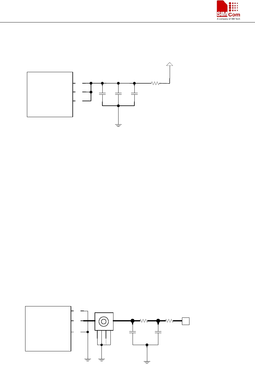
2.2 Antenna matching circuit design
Because the module is working under 50ohm system in RF part, to get the best RF performance, the
module’s load impedance should be tuned to 50ohm. But in fact, the most antenna’s port impedance
is not a purely 50ohm, so, to meet the 50ohm requirement, an additional antenna matching circuit
should be needed. Furthermore, to facilitate the antenna debugging and certification testing of RF
performance, we suggested the customer add a RF test connector in series between the module’s RF
port and the antenna matching circuit. The recommended antenna matching circuit is shown as
below:
RF Test Connector
J1
J2 R3
C6
59
SIM900
60
RF_IN
GND C5
61
GND
R4
Figure2 Antenna Matching Circuit
Antenna Feed Pad
Pi-Type
matching circuit
In the Figure2, the components, R4, C5 and C6 make up a pi-type matching circuit structure. The
component J2 is a RF test connector, which is used for conduct RF test. The traces in Bold type
should be 50 ohm impedance controlled.
For the RF test connector, the suggested part is MM8430-2610, vended by Murata, for details,
please visit http://www.murata.com.
AN_SMT Module RF Reference Design Guide_V1.01 10.02.2010
6
SIM900 Design Application Notes
3 Consideration in components placement
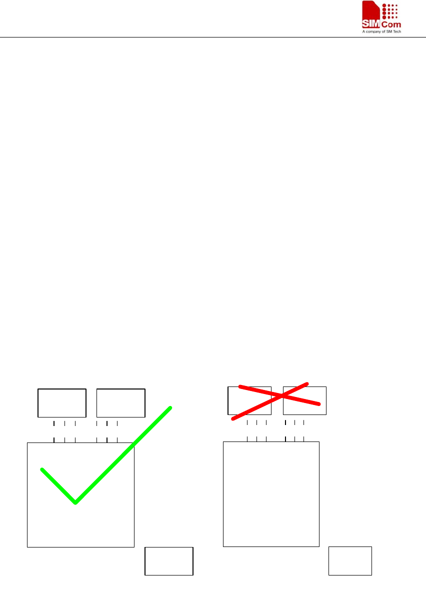
In PCB design, a good placement of components will help the improving of the product’s
performance. The following are some thumbs should be followed.
1)The module should be placed far away from the noise source circuit, such as high speed digital
circuit, etc. if this requirement cannot be met, the noise source circuit should be shielded perfectly.
This will help to reduce the interference between the module and the noise source circuit.
2)The placement of module should make the module’s RF_IN pad near to antenna’s feed pad
closely. This will make the length of RF trace between the module’s RF_IN pad and antenna as short
as possible.
3)The decoupling capacitor of module’s power supply should be placed close to the VBAT pads,
this will help the improvement of noise decoupling.
The best placement and some bad placements are shown as below:
SIM900
VBAT
Figure3 Good Placement
VBAT
VBAT
55
57
56
RF_IN
60 GND
GND
61
59
Antenna
Matching circuit
and Antenna area Power Supply
Noise Source
(high speed
digital circuit, or
others)
SIM900
VBAT
Figure4 Bad Placement
VBAT
VBAT
55
57
56
RF_IN
60 GND
GND
61
59
Antenna
Matching circuit
and Antenna area
Power Supply
Noise Source
(high speed
digital circuit, or
others)
ERROR:
power supply
and antenna part
are crossed
AN_SMT Module RF Reference Design Guide_V1.01 10.02.2010
7
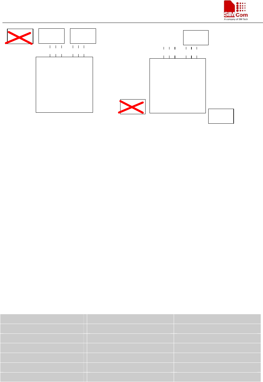
SIM900 Design Application Notes
AN_SMT Module RF Reference Design Guide_V1.01 10.02.2010
8
SIM900
VBAT
Figure5 Bad Placement
VBAT
VBAT
55
57
56
RF_IN
60 GND
GND
61
59
Antenna
Matching circuit
and Antenna area Power Supply
Noise Source
(high speed
digital circuit, or
others)
Power Supply
ERROR:
noise source
is too near to
RF_IN and
antenna
SIM900
VBAT
Figure6 Bad Placement
VBAT
VBAT
55
57
56
RF_IN
60 GND
GND
61
59
Antenna
Matching circuit
and Antenna area
ERROR:
antenna is
far away
from RF_IN
Noise Source
(high speed
digital circuit, or
others)
Figure3 is the best placement; antenna part is near to RF_IN pad, power supply is near to VBAT pad,
noise source is far away from the module.
Figure4, Figure5, Figure6 are bad placements. Figure4, power supply and antenna part are crossed;
Figure5, noise source is near to RF_IN pad and antenna; Figure6 antenna is far away from RF_IN
pad of the module.
4 Antenna Choosing
The antenna is a very important part in the terminal, which will affect the performance of the
terminal at most extent. The customer should select most suitable antenna depending on the
module’s working frequency band provided by network operator. The following table shows the
detailed working frequency range for each band.
Table 1 working frequency range for each band
BAND Transmit Frequency Receive Frequency
GSM850 824MHZ~849MHZ 869MHZ~894MHZ
GSM900 880MHZ~915MHZ 925MHZ~960MHZ
DCS1800 1710MHZ~1785MHZ 1805MHZ~1880MHZ
PCS1900 1850MHZ~1910MHZ 1930MHZ~1990MHZ
TD-SCDMA(A Band) 1880MHZ~1920MHZ 1880MHZ~1920MHZ
TD-SCDMA(A Band) 2010MHZ~2025MHZ 2010MHZ~2025MHZ
The customer should evaluate the antenna performance after antenna designer provide the antenna,
The antenna should fulfill the requirements as below:

SIM900 Design Application Notes
AN_SMT Module RF Reference Design Guide_V1.01 10.02.2010
9
Table2 antenna requirements
GAIN < 3dBi
IMPEDANCE 50 Ohm
INPUT POWER 2W peak power
VSWR < 2
TRP(GSM850/GSM900) > 29dBm
TRP(DCS1800/PCS1900) > 26dBm
TRP(TD-SCDMA) > 20dBm
TIS(GSM850/GSM900) < -104dBm
TIS(DCS1800/PCS1900) < -102dBm
TIS (TD-SCDMA) < -104dBm
5 Stacking up of multi-layers PCB
For EMC performance consideration, once the working frequency in the customer’s product is over
than 5MHz, or the rise-up/fall-down time of digital signal is less than 5ns, then multi-layers PCB
should be considered. Now, the more common multi-layer PCB structure is four-layers, six-layers
and eight-layers PCB, etc. If the customer’s product is designed in multi-layers PCB technology,
then the stack-up design of multi-layers PCB will become very important. The following will show
some typical stack-up design of multi-layers PCB, but each design has its own advantages and
disadvantages.
Note: In the following tables, S1 indicates the first signal layer, S2 indicates the second signal
layer, and so on.
Stack-up of two-layers PCB
Table3 Stack-up of two-layers PCB
Top layer Bottom layer
Case A S1+POWER+GND S2+POWER+GND
Two-layers PCB is the lowest cost solution, but this solution has the worst EMC performance, and it
is not appropriate in high speed design, because in this solution, the ground integrity, the crosstalk
between signal traces is very bad.
SIM900 Design Application Notes
AN_SMT Module RF Reference Design Guide_V1.01 10.02.2010
10
Stack-up of four-layers PCB
Table4 Stack-up of four-layers PCB
Top layer Second layer Third layer Bottom layer
Case A GND S1+POWER S2+POWER GND
Case B S1 GND POWER S2
Case A, should be the best case in four-layers PCB board design. In this case, the outer layer is
ground layer, which have some help in shielding the EMI signals; and also, the power supply layer
is very close to the ground layer, so the power supply resistance is smaller, and the EMC
performance will be very good. But if the density of devices on the PCB is very high, then this type
PCB stack-up should not be used to design, because the ground integrity can not be assured under
high density design, and the signal quality in second layer will be very bad. In this situation, Case B
is the most common way usually.
Stack-up of six-layers PCB
Top layer Second
layer
Third
layer
Fourth
layer
Fifth layer Bottom
layer
Case A S1 GND S2 S3 POWER S4
Case B S1 S2 GND POWER S3 S4
Case C S1 GND S2 POWER GND S3
Case D GND S1 POWER GND S2 GND
Table5 Stack-up of six-layers PCB
Six-layers PCB gives more design flexibility than a four-layers PCB, but it takes some work to
make it ideal in EMC terms.
Case A in the above table, is the usually common way. In this case, S1 is a better signal routing layer,
and S2 somewhat less. But this case has a disadvantage that this stack-up has very little distributed
capacitance between its ground and power planes.
Case B has good EMC characteristics, because this stack-up has good noise decoupling between the
power plane and ground for the big distributed capacitance.
Case C is the better stack-up, in this case, S1, S2 and S3 are good signal routing layer, the power
decoupling is good for the big distributed capacitance between the ground and power planes.
Case D is the best stack-up, the EMC performance will be good, but the disadvantage is that the
routing layer is less than other type stack-up.

SIM900 Design Application Notes
AN_SMT Module RF Reference Design Guide_V1.01 10.02.2010
11
Stack-up of eight-layers PCB
Top
layer
Second
layer
Third
layer
Forth
layer
Fifth
layer
Sixth
layer
Seventh
layer
Bottom
layer
A S1 S2 GND S3 S4 POWER S5 S6
B S1 S2 S3 GND POWER S4 S5 S6
C S1 GND S2 S3 S4 S5 POWER S6
D S1 GND S2 S3 GND POWER S4 S5
E S1 GND S2 GND S3 POWER S4 S5
F S1 GND S2 GND POWER S3 GND S4
Table6 Stack-up of eight-layers PCB
Eight-layers PCB gives more design flexibility than a six-layers PCB, but it takes some work to
make it ideal in EMC terms.
If the design needs 6 signal routing layers, then case A will be the best stack-up design, but this type
stack-up should not be used in high speed digital circuit design.
If the product design needs 5 signal routing layers, case E will be the best. In this case, S1, S2 and
S3 are good signal routing layer, and the power decoupling is good.
If the design needs 4 signal routing layers, case F will be the best. In this case, every signal routing
layers are good. In all the case, the signal trace routed in adjacent signal routing layers should be
orthogonal.
6 Impedance control of RF trace
Because the module’s RF part is working in a 50ohm system, so its output load impedance should
be 50ohm, to meet this requirement, the all RF signal traces should be impedance controlled, and its
characteristic impedance should be 50ohm.
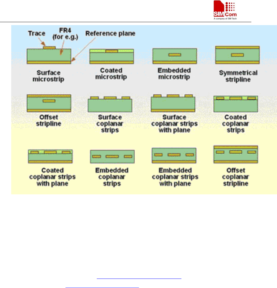
The RF trace impedance can be controlled through using different trace geometry. There are more
than thirty different types of transmission line which can easily be created on a PCB. Twelve of
them are shown in figure 7
SIM900 Design Application Notes
AN_SMT Module RF Reference Design Guide_V1.01 10.02.2010
12
Figure7 twelve typical PCB transmission line
Usually, Surface Mircostrip Transmission Line and offset Strip Transmission Line are the most
common structures. In 50ohm RF system, through adjusting the width of RF traces and the spacing
to the reference GND, the impedance of RF traces can be controlled to 50Ohm.The appendix will
show some illustration in impedance controlled RF trace designing.
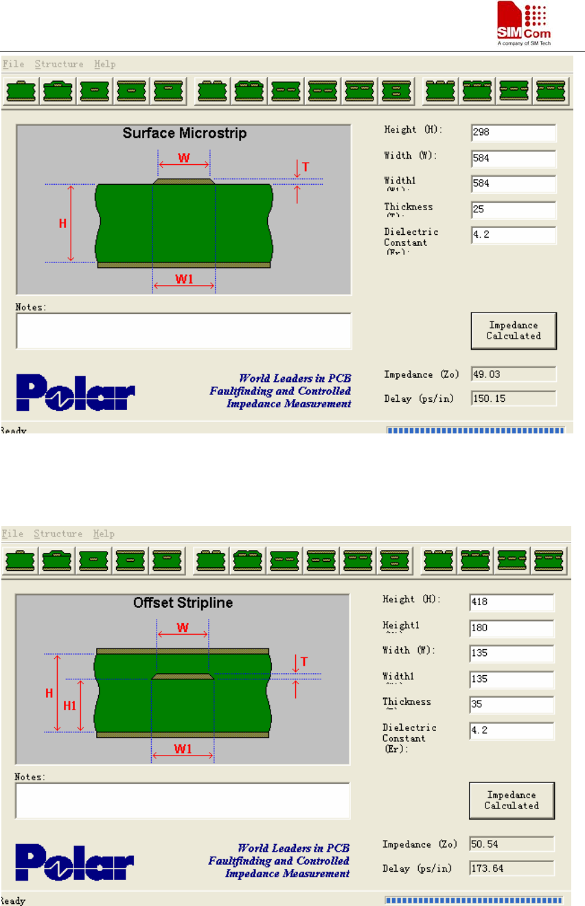
The customer may use software tool to calculate the impedance of RF trace, for example CITS25,
released by POLAR, the website is http://www.polarinstruments.com/, or APPCAD released by
AGILENT, the website is http://www.hp.woodshot.com.
Here are two examples about using CITS25 to calculate, Surface Mircostrip Transmission Line and
Offset strip Transmission Line correspondingly. Based on stack up of six-layers PCB (thickness
=1.0mm) shown in appendix.
Surface Mircostrip Transmission Line, the height is 298um (25+70+203=298um), the thickness is
25um, the result width (w) is 584um, as shown in figure8.
SIM900 Design Application Notes
AN_SMT Module RF Reference Design Guide_V1.01 10.02.2010
13
Figure8 Surface Mircostrip Calculate
Offset Strip Transmission Line,the height between two reference GND is 418um (203+35+180 =
418um), the height between RF trace and reference GND is 180um, the result width is 135um, as
shown in figure9.
Figure9 Offset Strip line Calculate

SIM900 Design Application Notes
AN_SMT Module RF Reference Design Guide_V1.01 10.02.2010
14
7 Consideration in PCB layout
In product’s PCB design, a good PCB layout will help the improvement of the whole product
performance, including reliability, EMC performance, etc. The following are some considerations
for referenced:
a) The Layer1.under the SMT module’s RF test port should be copper keep out , layer2 should be
GND;
b) The Layer2 under SMT module’s RF_IN pad should be copper keep out , layer3 should be
GND;
c) The Layer1, Layer2 under RF test connector should be copper keep out, layer3 should be GND;
the space from RF test connector to GND plane should more than 0.5mm.
d) If the antenna is directly connected to the antenna feed pad, All layers under the antenna feed
pad should be copper keep out. If the antenna is connected to the antenna pad with a RF coaxial
cable, the size of the antenna pad should no more than 2*2mm, and should be 50Ohm
impedance controlled.
e) RF traces from SMT module’s RF_IN pad to the antenna feed PAD all should be controlled to
50 Ohm
f) High speed signal should never be layout under the RF traces, or should be isolated by a ground
plane at least.
g) When layout surface Mircostrip Transmission Line or offset Strip Transmission Line , 3W rule
should be followed, that means the space between GND and RF trace on the same plane should
be three times more than the width of RF trace.
SIM900 Design Application Notes
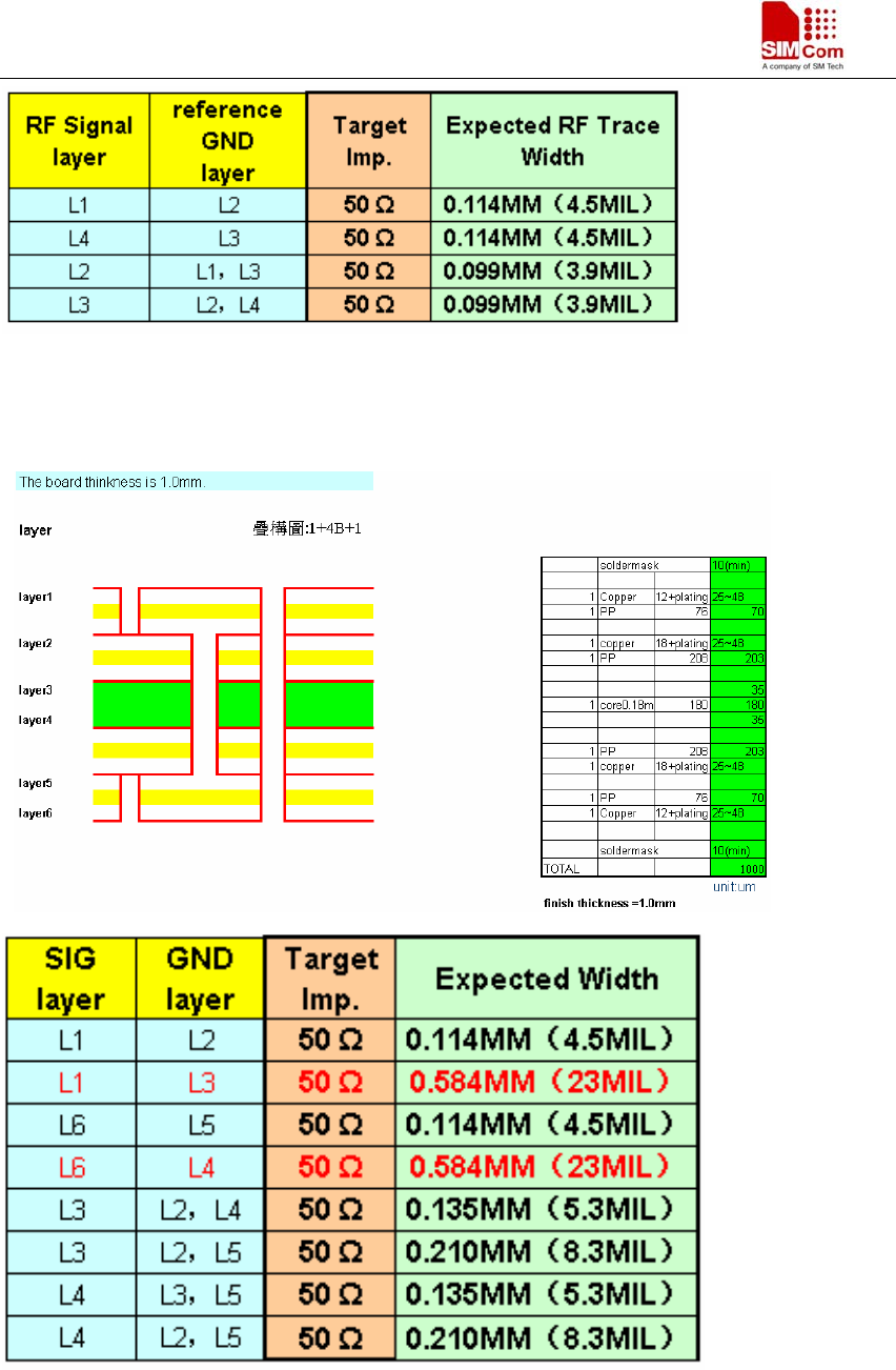
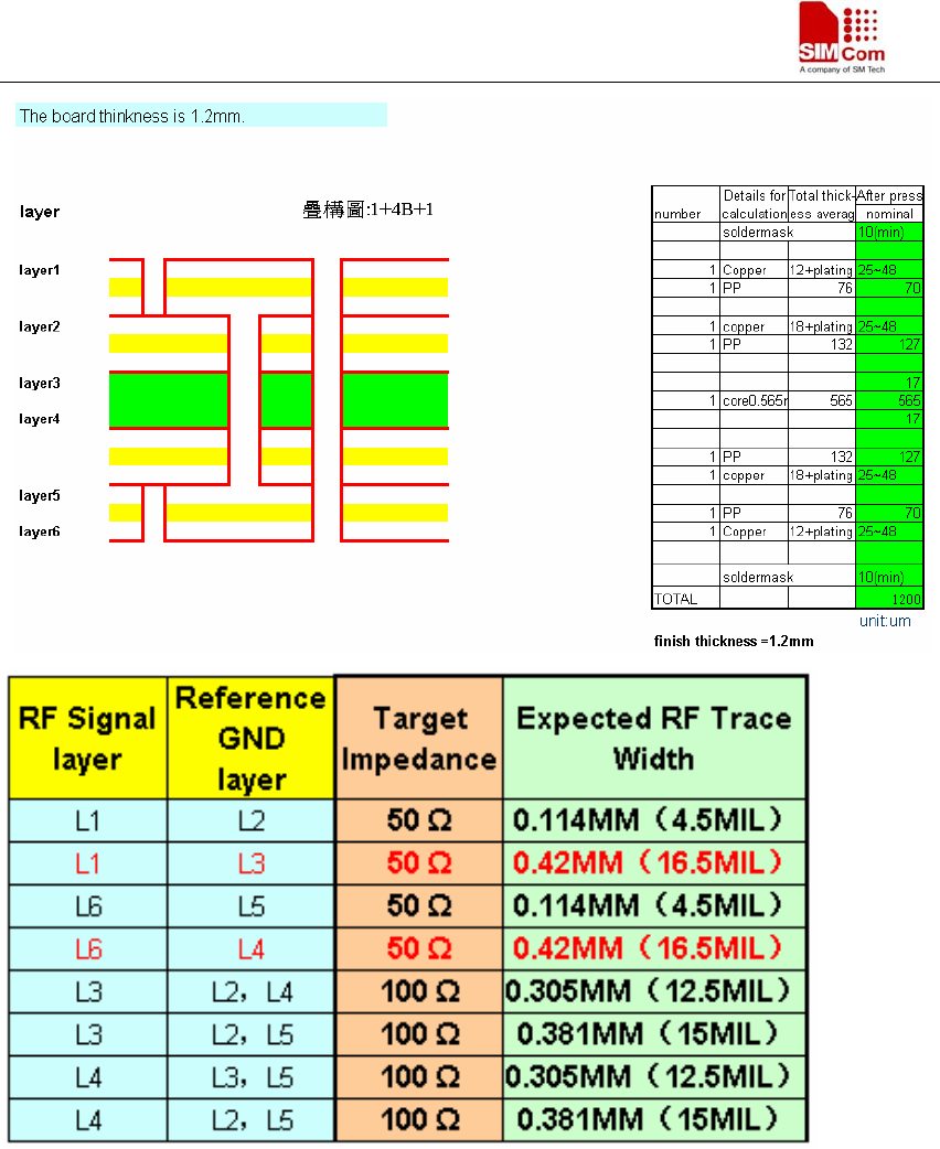
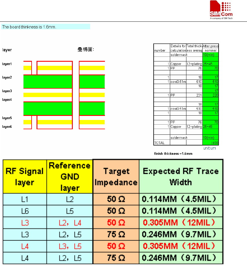
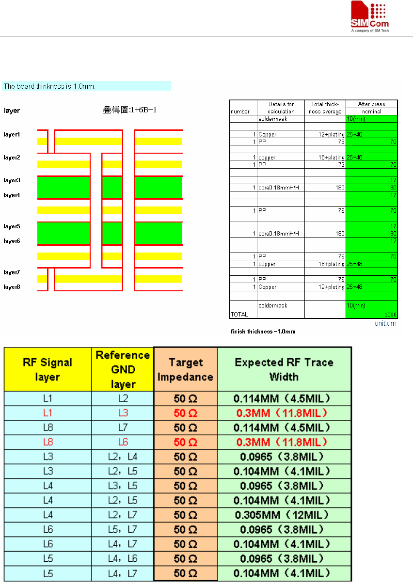
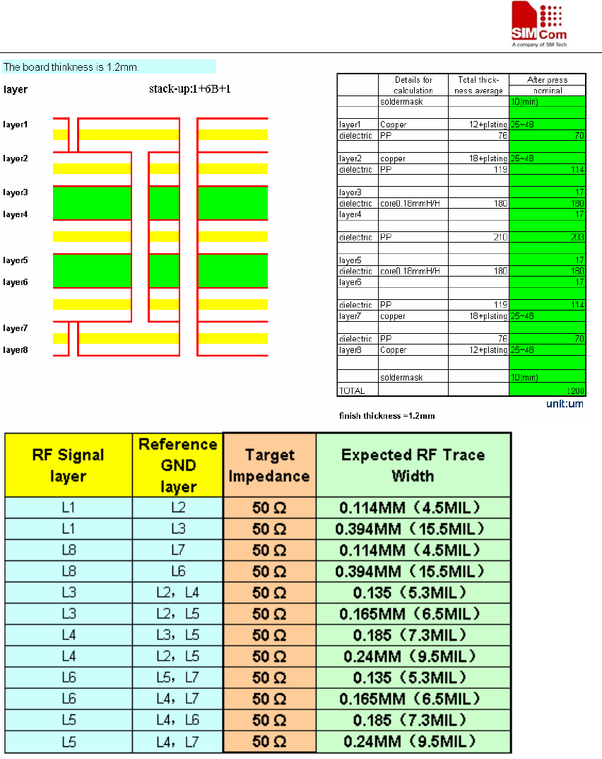
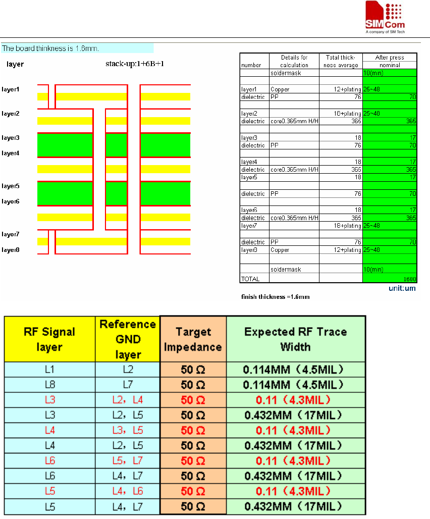
Appendix
The following are some illustration of impedance controlled RF trace designing. It is should be
noted that the RF trace’s width and spacing to the reference ground is combined to specific PCB
stack-up (the PCB’s thickness, clearance between every layer).
NOTE: In the following illustration, the RF impedance controlled traces on the outer layers (top
layer, bottom layer) are Surface Mircostrip Transmission Line, the RF impedance controlled
traces on the inner layers are Offset strip Transmission Line.
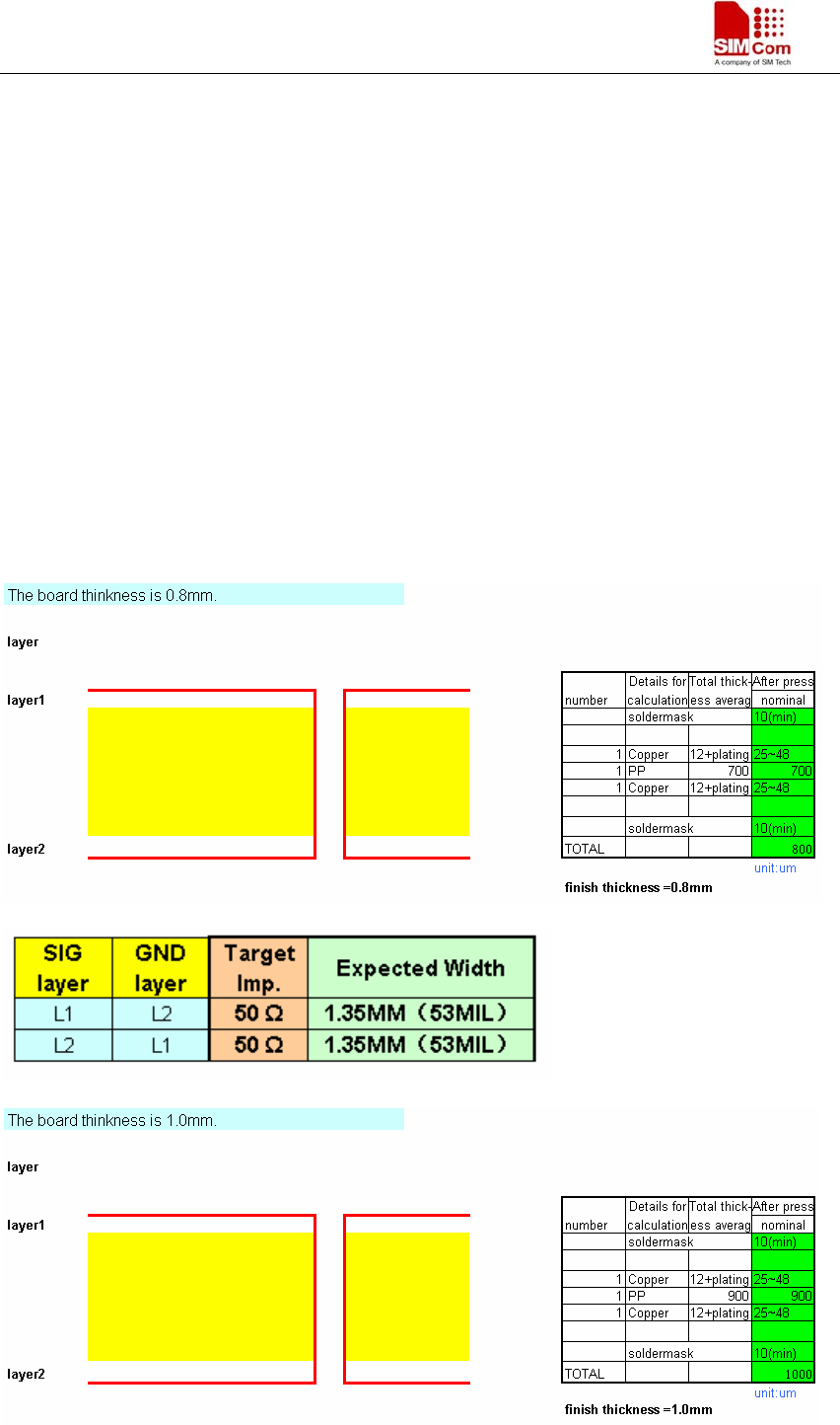
Two-layers PCB
AN_SMT Module RF Reference Design Guide_V1.01 10.02.2010
15
SIM900 Design Application Notes
AN_SMT Module RF Reference Design Guide_V1.01 10.02.2010
16
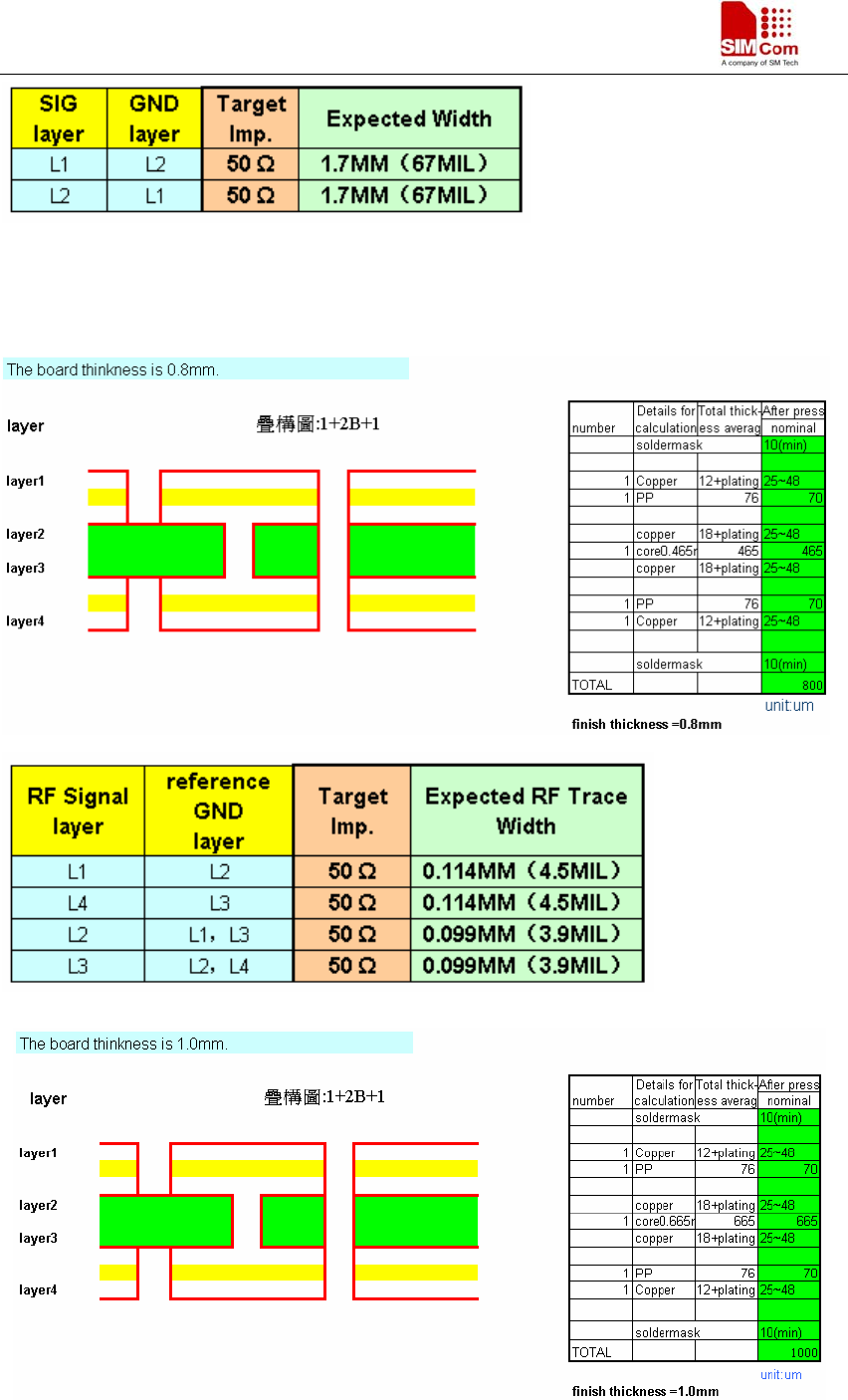
Four-layers PCB
SIM900 Design Application Notes
AN_SMT Module RF Reference Design Guide_V1.01 10.02.2010
17
Six-layers PCB
SIM900 Design Application Notes
AN_SMT Module RF Reference Design Guide_V1.01 10.02.2010
18
SIM900 Design Application Notes
AN_SMT Module RF Reference Design Guide_V1.01 10.02.2010
19
SIM900 Design Application Notes
Eight-layers PCB
AN_SMT Module RF Reference Design Guide_V1.01 10.02.2010
20
SIM900 Design Application Notes
AN_SMT Module RF Reference Design Guide_V1.01 10.02.2010
21
SIM900 Design Application Notes
AN_SMT Module RF Reference Design Guide_V1.01 10.02.2010
22

