AP2301GN HF 3 Datasheet. Www.s Manuals.com. Apec
User Manual: Marking of electronic components, SMD Codes N1, N1**, N1***, N1-, N10A, N10B, N10C, N10D, N10E, N10F, N10G, N10H, N10I, N10J, N10K, N10L, N10M, N10N, N10O, N10P, N10Q, N10R, N10S, N10T, N10U, N10V, N10W, N10X, N10Y, N10Z, N12, N16, N19, N1W, N1p, N1t. Datasheets 1KSMB10CA, 1KSMB11CA, 1KSMB12CA, 1KSMB13CA, 1KSMB15CA, 1KSMB16CA, 1KSMB18CA, 1KSMB20CA, 1KSMB22CA, 1KSMB24CA, 1KSMB27CA, 1KSMB30CA, 1KSMB33CA, 1KSMB36CA, 1KSMB39CA, 1KSMB43CA, 1KSMB47CA, 1KSMB51CA, 1KSMB56CA, 1KSMB6.8CA, 1KSMB62CA, 1KSMB68CA, 1KSMB7
Open the PDF directly: View PDF ![]() .
.
Page Count: 6
Advanced Power
Electronics Corp.
1/5
AP2301GN-HF-3
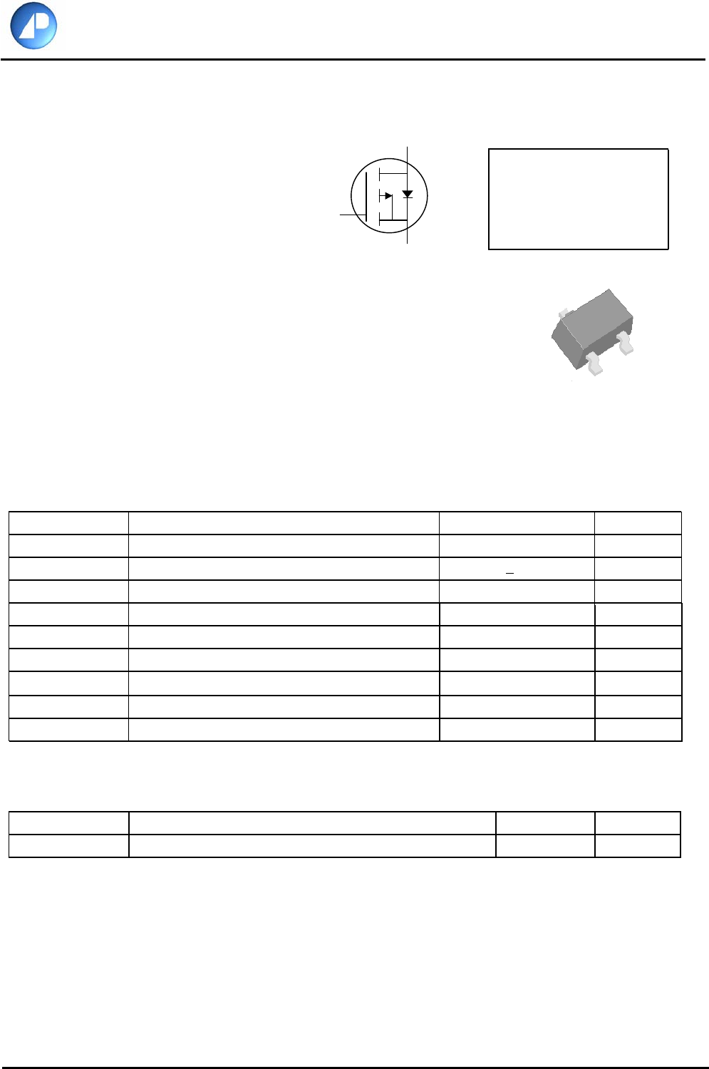
P-channel Enhancement-mode Power MOSFET
DSS
DS(ON)
D
Description
Absolute Maximum Ratings
Symbol Units
VDS
VGS
ID A
IDM
D at TA=25°C
TSTG
J
Symbol Value Unit
Parameter Rating
Gate-Source Voltage +
Continuous Drain Current3
Pulsed Drain Current1
Thermal Data
Parameter
Storage Temperature Range
A
dvanced Power MOSFETs from APEC provide the designer with the best
combination of fast switching, low on-resistance and cost-effectiveness.
The AP2301GN-HF-3 is in the popular SOT-23 small surface-mount package
BV -20V
Simple Drive Requirement
Lower On-resistance
Drain-Source Voltage -20 V
12 V
Rthj-a Maximum Thermal Resistance, Junction-ambient
which is widely used in commercial and industrial applications where a small
board footprint is required.
This device is well suited for use in medium current applications such as
load switches and DC-DC converters.
Ordering Information
D A
I Continuous Drain Current 3
www.a-powerusa.com
RoHS-compliant, halogen-free I -2.6A
at T =25°C -2.6 A
at T = 70°C -2.1 A
-10 A
P Total Power Dissipation 1.38 W
-55 to 150 °C
T Operating Junction Temperature Range -55 to 150 °C
90 °C/W
©2010 Advanced Power Electronics Corp. USA 200902046-3
Surface Mount Device R 130mΩ
D
G
S
SOT-23
AP2301GN-HF-3TR RoHS-compliant halogen-free SOT-23, shipped on tape and reel, 3000pcs/ reel
G
D
S
Linear Derating Factor 0.01 W/°C
Advanced Power
Electronics Corp.
2/5
AP2301GN-HF-3
©2010 Advanced Power Electronics Corp. USA
www.a-powerusa.com
Electrical Specifications
at Tj=25°C (unless otherwise specified)
Source-Drain Diode
Notes:
THIS PRODUCT IS SENSITIVE TO ELECTROSTATIC DISCHARGE, PLEASE HANDLE WITH CAUTION.
USE OF THIS PRODUCT AS A CRITICAL COMPONENT IN LIFE SUPPORT OR OTHER SIMILAR SYSTEMS IS NOT AUTHORIZED.
APEC DOES NOT ASSUME ANY LIABILITY ARISING OUT OF THE APPLICATION OR USE OF ANY PRODUCT OR CIRCUIT DESCRIBED
HEREIN; NEITHER DOES IT CONVEY ANY LICENSE UNDER ITS PATENT RIGHTS, NOR THE RIGHTS OF OTHERS.
APEC RESERVES THE RIGHT TO MAKE CHANGES WITHOUT FURTHER NOTICE TO ANY PRODUCTS HEREIN TO IMPROVE
1. Pulse width limited by maximum junction temperature.
RELIABILITY, FUNCTION OR DESIGN.
copper pad of FR4 board; 270°C/W when mounted on minimum copper pad.
2
2. Pulse test - pulse width < 300µs , duty cycle < 2%
3. Surface mounted on 1in
Symbol Parameter Test Conditions Min. Typ. Max. Units
BVDSS Drain-Source Breakdown Voltage VGS=0V, ID=-250uA -20 - - V
RDS(ON) Static Drain-Source On-Resistance2VGS=-5V, ID=-2.8A - - 130 mΩ
VGS=-2.8V, ID=-2.0A - - 190 mΩ
VGS(th) Gate Threshold Voltage VDS=VGS, ID=-250uA -0.5 - -1.25 V
gfs Forward Transconductance VDS=-5V, ID=-2A - 4 - S
IDSS Drain-Source Leakage Current VDS=-20V, VGS=0V - - -1 uA
Drain-Source Leakage Current (Tj=70oC) VDS=-16V, VGS=0V - - -10 uA
IGSS
Gate-Source Leakage VGS=±12V, VDS=0V - - ±100
nA
QgTotal Gate Charge2ID=-2A - 5 9 nC
Qgs Gate-Source Charge VDS=-16V - 1 - nC
Qgd Gate-Drain ("Miller") Charge VGS=-4.5V - 2 - nC
td(on) Turn-on Delay Time2VDS=-10V - 6 - ns
tr
Rise Time ID=-1A - 17 -
ns
td(off)
Turn-off Delay Time RG=3.3Ω, VGS=-10V - 16 -
ns
tf
Fall Time RD=10Ω -5-ns
Ciss
Input Capacitance VGS=0V - 270 -
pF
Coss Output Capacitance VDS=-20V - 70 - pF
Crss Reverse Transfer Capacitance f=1.0MHz - 55 - pF
Rg
Gate Resistance f=1.0MHz - 10 15
Ω
Symbol Parameter Test Conditions Min. Typ. Max. Units
ISContinuous Source Current ( Body Diode ) VD=VG=0V , VS=-1.2V - - -1 A
ISM Pulsed Source Current ( Body Diode )1- - -10 A
VSD
Forward On Voltage2
Tj=25°C, IS=-1.6A, VGS=0V - - -1.2 V
Advanced Power
Electronics Corp.
3/5
AP2301GN-HF-3
©2010 Advanced Power Electronics Corp. USA
www.a-powerusa.com
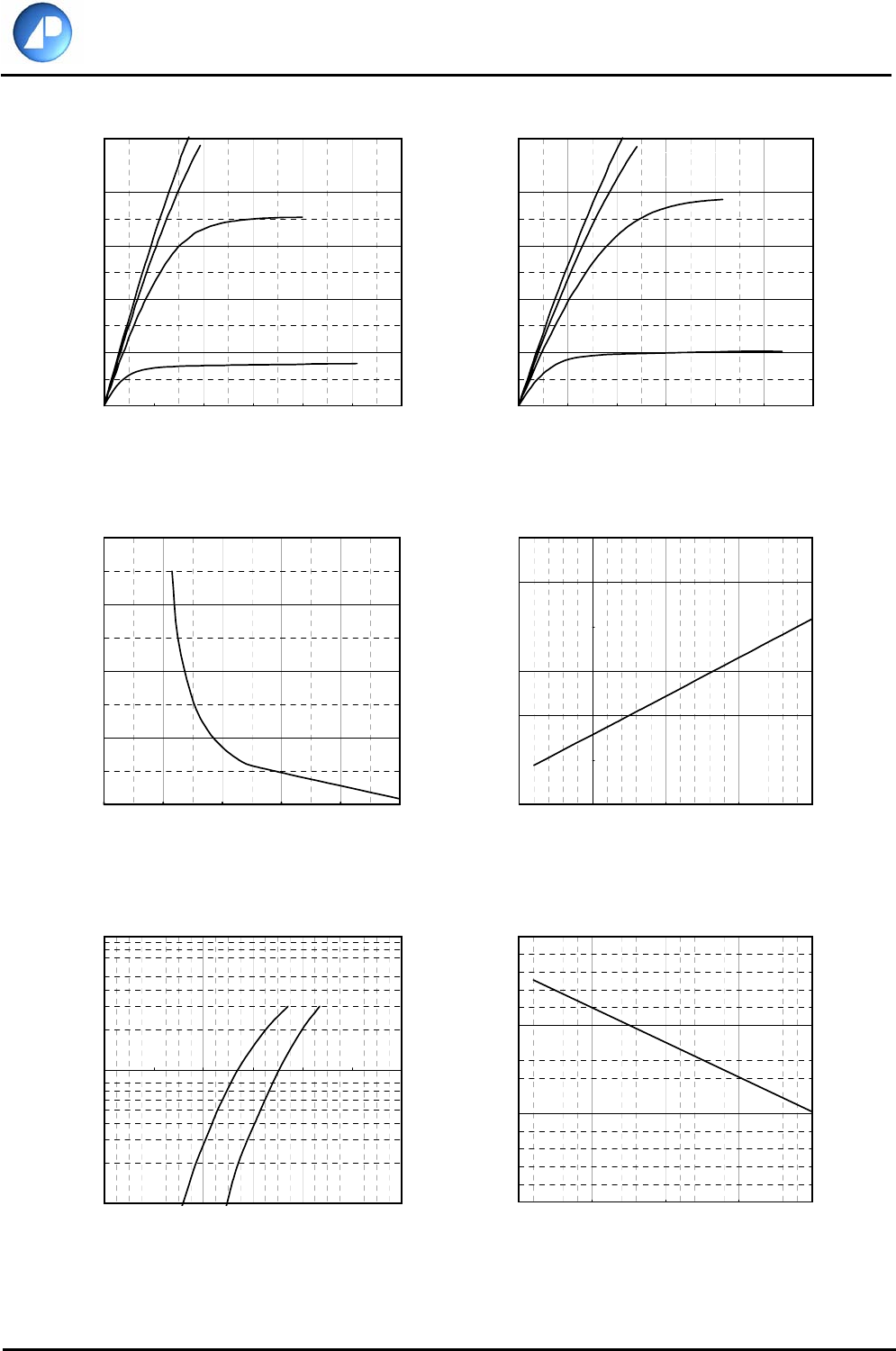
Fig 1. Typical Output Characteristics Fig 2. Typical Output Characteristics
vs. Junction Temperature
Fig 5. Forward Characteristic of Fig 6. Gate Threshold Voltage vs.
Reverse Diode Junction Temperature
Typical Electrical Characteristics
Gate Voltage
Fig 3. On-Resistance vs. Fig 4. Normalized On-Resistance
0
2
4
6
8
10
0123456
-VDS , Drain-to-Source Voltage (V)
-ID , Drain Current (A)
TA=25 oCVGS = -5V
VGS = -4V
VGS = -3V
VGS = -2V
0
2
4
6
8
10
0123456
-VDS , Drain-to-Source Voltage (V)
-ID , Drain Current (A)
TA=150 oCVGS = -5V
VGS = -4V
VGS = -3V
VGS = -2V
80
120
160
200
240
0246810
-VGS , Gate-to-Source Voltage (V)
RDS(ON) (Ω)
ID= -2A
TA
=25°C
0.6
0.8
1
1.2
1.4
1.6
1.8
-50 0 50 100 150
Tj , Junction Temperature ( oC)
Normalized RDS(ON)
ID= -2.8A
VGS = -5V
0
1
10
0.1 0.3 0.5 0.7 0.9 1.1 1.3
-VSD , Source-to-Drain Voltage (V)
-IS(A)
Tj=25 oCT j=150 oC
0.0
0.5
1.0
1.5
-50 0 50 100 150
Tj , Junction Temperature ( oC)
Normalized -VGS(th) (V)
Advanced Power
Electronics Corp.
4/5
AP2301GN-HF-3
©2010 Advanced Power Electronics Corp. USA
www.a-powerusa.com
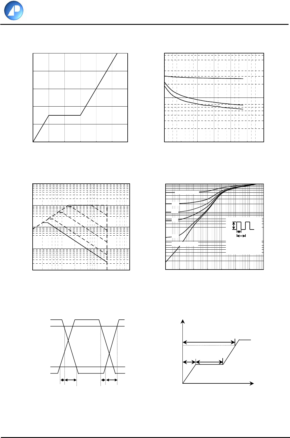
Fig 7. Gate Charge Characteristics Fig 8. Typical Capacitance Characteristics
Fig 9. Maximum Safe Operating Area Fig 10. Effective Transient Thermal Impedance
Fig 11. Switching Time Waveform Fig 12. Gate Charge Waveform
Typical Electrical Characteristics (cont.)
td(on) tr
td(off)
tf
VDS
VGS
10%
90%
Q
VG
-4.5V
QGS
QGD
QG
Charge
0.001
0.01
0.1
1
0.0001
0.001
0.01
0.1
1
10
100
1000
t , Pulse Width (s)
Normalized Thermal Response (Rthja)
0.01
0.05
0.1
0.2
Duty factor=0.5
PDM
Duty factor = t/T
Peak Tj = PDM x Rthja + Ta
Rthja = 270°C/W
t
T
Single Pulse
0
1
2
3
4
5
0123456
QG , Total Gate Charge (nC)
-VGS , Gate to Source Voltage (V)
ID
= -2A
VDS
= -16V
10
100
1000
1
5
9
13
17
21
25
-V DS , Drain-to-Source Voltage (V)
C (pF)
f
=1.0MH
z
Ciss
Coss
Crss
0.01
0.1
1
10
100
0.1 1 10 100
-V DS , Drain-to-Source Voltage (V)
-ID (A)
1ms
10ms
100ms
1s
DC
TA
=25 °C
Single Pulse
Advanced Power
Electronics Corp.
5/5
AP2301GN-HF-3
©2010 Advanced Power Electronics Corp. USA
www.a-powerusa.com
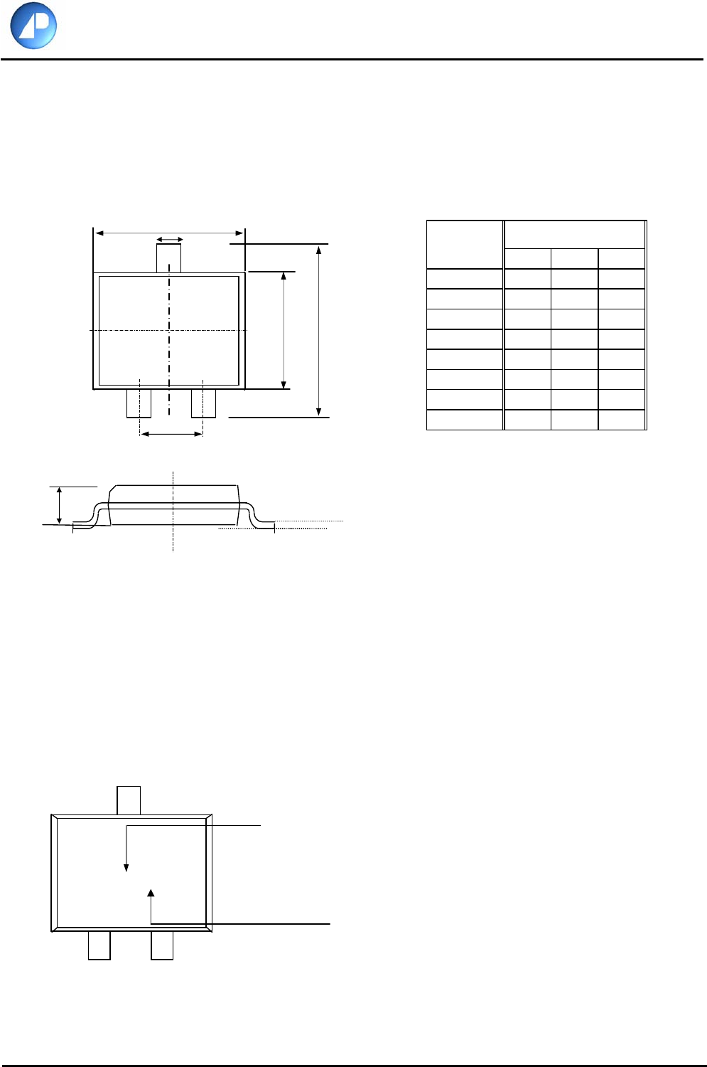
Package Dimensions: SOT-23
Marking Information: SOT-23
N1XX
Product: N1 = AP2301GN-HF-3
Date/lot code
For details of how to convert this
to standard YYWW date code format,
please contact us directly.
Millimeters
MIN NOM MAX
A 1.00 1.15 1.30
A1 0.00 -- 0.10
A2 0.10 0.15 0.25
D1 0.30 0.40 0.50
e 1.70 2.00 2.30
D 2.70 2.90 3.10
E 2.40 2.65 3.00
E1 1.40 1.50 1.60
1. All dimensions are in millimeters.
2. Dimensions do not include mold protrusions.
SYMBOLS
D
E1 E
e
D1
A
A1
A2
3
1 2