APL3533 Datasheet. Www.s Manuals.com. Ra.2 Anpec
User Manual: Marking of electronic components, SMD Codes L3, L3 *, L3***, L3-***, L30, L324, L324A, L324K, L324KA, L3533, L358, L358A, L37A, L37B, L3B. Datasheets ADP3330ART-2.85, APL3533QB, BAV23S, BZX384-B6V8, LM317DCY, LM324APW, LM324KAPW, LM324KPW, LM324PW, LM358APW, LM358PSR, LM358PW, LP2980AIM5-4.7, LP2980IM5-4.7, NZL7V5AXV3T1, RT9819E-25PV, SST503, Si2303BDS, mESD6.0DT5G.
Open the PDF directly: View PDF ![]() .
.
Page Count: 22
Copyright ANPEC Electronics Corp.
Rev. A.2 - Mar., 2013
APL3533
www.anpec.com.tw1
ANPEC reserves the right to make changes to improve reliability or manufacturability without notice, and
advise customers to obtain the latest version of relevant information to verify before placing orders.
Ultra-Low On-Resistance, 6A Dual Load Switch with Soft Start
•16mΩ(Typical) On-resistance per Channel
•6A Continuous Current
•Soft Start Time Programmable by External
Capacitor
•Wide Input Voltage Range (VIN): 0.8V to 5.5V
•Supply Voltage Range (VBIAS): 3V to 5.5V
•Output Discharge when Switch Disabled
•Reverse Current Blocking when Switch Disabled
•Over-Temperature Protection
The APL3533 is an ultra-low on-resistance, dual power-
distribution switch with external soft start control. It inte-
grates two N-channel MOSFETs that can deliver 6A con-
tinuous load current each.
The device integrates over-temperature protection. The
over temperature protection function shuts down the N-
channel MOSFET power switch when the junction tem-
perature rises beyond 160oC and will automatically turns
on the power switch when the temperature drops by 40oC.
The device is available in lead free TDFN2x3-14A
packages.
FeaturesGeneral Description
Applications
•Notebook
•AIO PC Simplified Application Circuit
•Enable Input
•Lead Free and Green Devices Available (RoHS
Compliant)
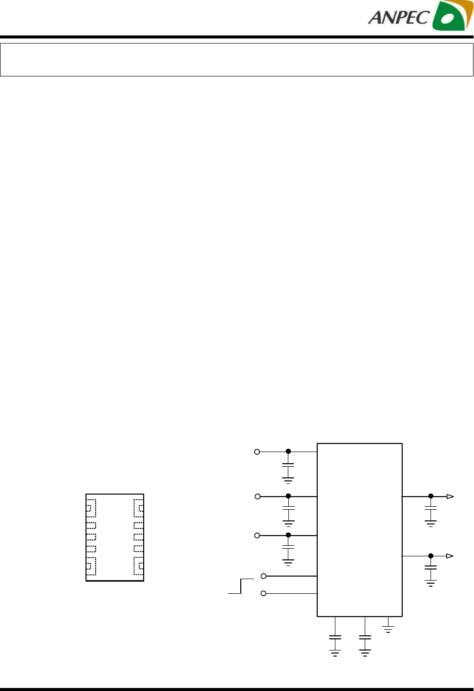
Pin Configurations
EN1 3
14 VOUT1VIN1 1
VIN1 2
BIAS 4
13 VOUT1
11 GND
12 SS1
TDFN2x3-14A
(Top View)
VIN2 7
EN2 5
VIN2 6
10 SS2
8 VOUT2
9 VOUT2
VIN1VOUT1
APL3533
SS2
EN1
VIN1
VOUT2
VIN2
SS1
EN2
BIAS
VBIAS
GND
On
Off
VIN2
VOUT1
VOUT2
Copyright ANPEC Electronics Corp.
Rev. A.2 - Mar., 2013
APL3533
www.anpec.com.tw2
Ordering and Marking Information
Note : ANPEC lead-free products contain molding compounds/die attach materials and 100% matte tin plate termination finish; which
are fully compliant with RoHS. ANPEC lead-free products meet or exceed the lead-free requirements of IPC/JEDEC J-STD-020D for
MSL classification at lead-free peak reflow temperature. ANPEC defines “Green” to mean lead-free (RoHS compliant)and halogen
free (Br or Cl does not exceed 900ppm by weight in homogeneous material and total of Br and Cl does not exceed 1500ppm by
weight).
Absolute Maximum Ratings (Note 1)
Symbol Parameter Rating Unit
VBIAS BAIS to GND Voltage -0.3 ~ 6 V
VIN1, VIN2 VIN1, VIN2 to GND Voltage -0.3 ~ 6 V
VOUT1, VOUT2
VOUT1, VOUT2 to GND Voltage -0.3 ~ 6 V
VEN1, VEN2 EN1, EN2 to GND Voltage -0.3 ~ 6 V
TJ Maximum Junction Temperature -40 ~ 150 oC
TSTG Storage Temperature -65 ~ 150 oC
TSDR Maximum Lead Soldering Temperature (10 Seconds) 260 oC
Note1: Stresses beyond those listed under "absolute maximum ratings" may cause permanent damage to the device. These are
stress ratings only and functional operation of the device at these or any other conditions beyond those indicated under "recom-
mended operating conditions" is not implied. Exposure to absolute maximum rating conditions for extended periods may affect device
reliability.
Thermal Characteristics
Symbol Parameter Typical Value
Unit
θJA Junction-to-Ambient Resistance in Free Air (Note 2) 80 oC/W
Note 2: θJA is measured with the component mounted on a high effective thermal conductivity test board in free air.
APL3533 Package Code
Operating Ambient Temperature Range
I : -40 to 85oC
Handling Code
TR : Tape & Reel
Assembly Material
Handling Code
TemperatureRange
Package Code G : Halogen and Lead Free Device
Assembly Material QB : TDFN2x3-14A
XXXXX-Date Code
APL3533 QB:L3533
XXXXX
Copyright ANPEC Electronics Corp.
Rev. A.2 - Mar., 2013
APL3533
www.anpec.com.tw3
Symbol
Parameter Range Unit
VBIAS BIAS Input Voltage 3.0 ~ 5.5 V
VIN1, VIN2
VIN1, VIN2 Input Voltage 0.8 ~ 5.5 V
IOUT VOUT1 or VOUT2 Output Current (single channel) 0 ~ 6 A
PD Maximum Power Dissipation, TA=50oC(Note4) 0.94 W
VIH EN1, EN2 Logic High Input Voltage 1.2 ~ 5.5 V
VIL EN1, EN2 Logic Low Input Voltage 0 ~ 0.4 V
TA Ambient Temperature -40 ~ 85 oC
TJ Junction Temperature -40 ~ 125 oC
Recommended Operating Conditions (Note 3)
Note 3 : Refer to the typical application circuit.
Electrical Characteristics
Unless otherwise specified, these specifications apply over VIN1= VIN2= 0.8V~5.5V, VEN1= VEN2=VBIAS =5V and TA= -40~85oC.
Typical values are at TA=25oC.
APL3533
Symbol
Parameter Test Conditions Min. Typ. Max.
Unit
SUPPLY CURRENT
BIAS Supply Current (both
channels) No load, VBIAS=5V =VEN1,2=5V - 60 90 µA
IBIAS BIAS Supply Current (single
channel) No load, VBIAS=5V, VEN1=5V, VEN2=0V - 50 - µA
ISD BIAS Supply Current at
Shutdown No load, VBIAS=5V, VEN1,2=0V - - 2 µA
No load, VBIAS=5V, VEN1,2=0V, VIN1,2=5V - 0.1 8 µA
No load, VBIAS=5V, VEN1,2=0V, VIN1,2=3.3V - 0.1 3 µA
No load, VBIAS=5V, VEN1,2=0V, VIN1,2=1.8V - 0.1 2 µA
IOFF VIN Off-State Supply Current
(per channel)
No load, VBIAS=5V, VEN1,2=0V, VIN1,2=0.8V - 0.1 1 µA
Reverse Leakage Current (per
channel) VEN1,2=0V, VIN1,2=0V - 0.1 16 µA
UNDER-VOLTAGE LOCKOUT (UVLO)
Rising BIAS UVLO Threshold VBIAS rising 1.9 2.4 2.9 V
BIAS UVLO Hysteresis - 0.1 - V
POWER SWITCH
IOUT=200mA, TJ= 25oC - 16 18 mΩ
IOUT=200mA, TJ= -40~125oC
Channel 1
- - 24 mΩ
IOUT=200mA, TJ= 25oC - 16 18 mΩ
RDS(ON) Power Switch On Resistance
IOUT=200mA, TJ= -40~125oC
Channel 2 - - 24 mΩ
VOUT Discharge Resistance VEN1,2=0V, VOUT1 or VOUT2 force 1V - 150 180 Ω
Note 4 : Refer to the thermal consideration on page 15.
Copyright ANPEC Electronics Corp.
Rev. A.2 - Mar., 2013
APL3533
www.anpec.com.tw4
Electrical Characteristics
APL3533
Symbol
Parameter Test Conditions Min. Typ. Max.
Unit
SOFT-START CONTROL PIN
SS Discharge Current VSS1,2=6V, VEN1,2=0V
, EN2=low, measured at
SS1 or SS2 - 560 - µA
EN INPUT PIN
Input Logic High 1.2 - - V
Input Logic Low - - 0.4 V
Input Current - - 1 µA
OVERT-TEMPERATURE PROTECTION (OTP)
Over-Temperature Threshold TJ rising - 160 - °C
Over-Temperature Hysteresis - 40 - °C
Unless otherwise specified, these specifications apply over VIN1= VIN2= 0.8V~5.5V, VEN1= VEN2=VBIAS =5V and TA= -40~85oC.
Typical values are at TA=25oC.
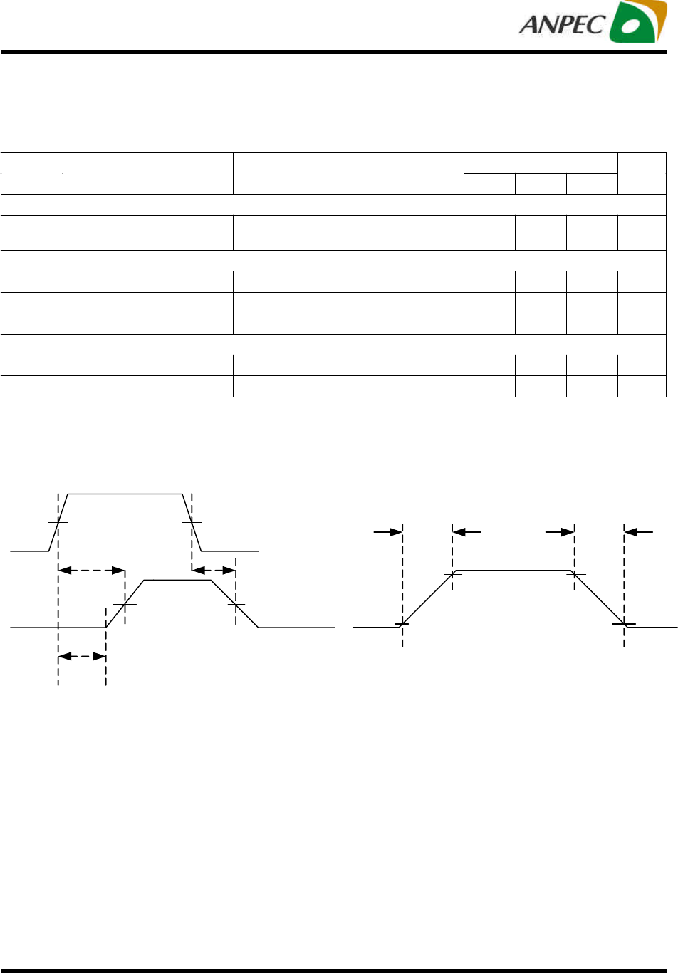
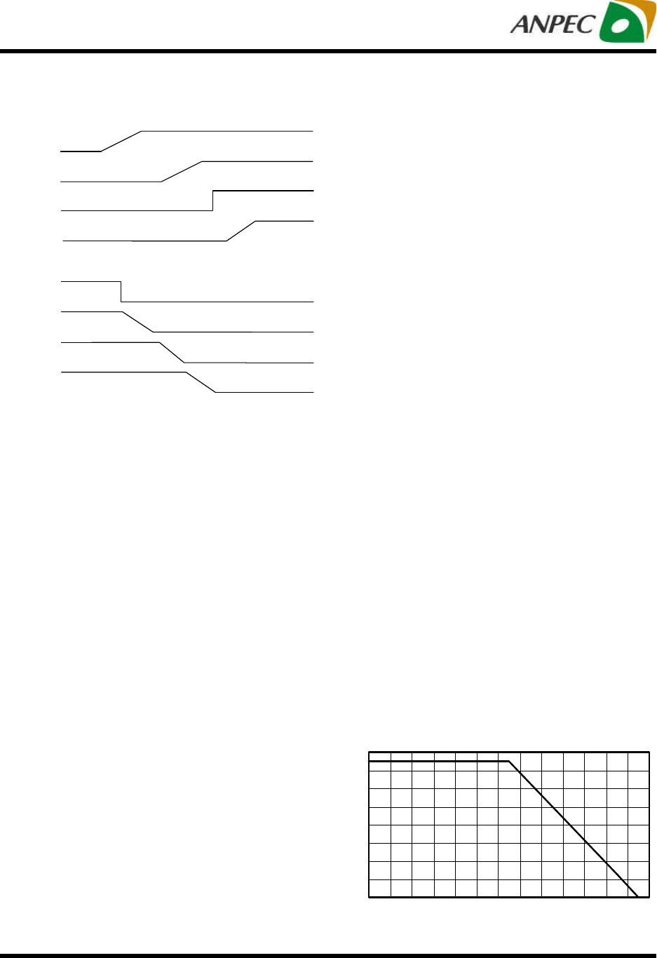
Timing Chart
Figure 1. tON/tOFF, tR/tF Waveforms
90%90%
tR
10%10%
tF
VOUT
50%50%
50%50%
tOFF
tD
tON
VOUT
VEN
Copyright ANPEC Electronics Corp.
Rev. A.2 - Mar., 2013
APL3533
www.anpec.com.tw5
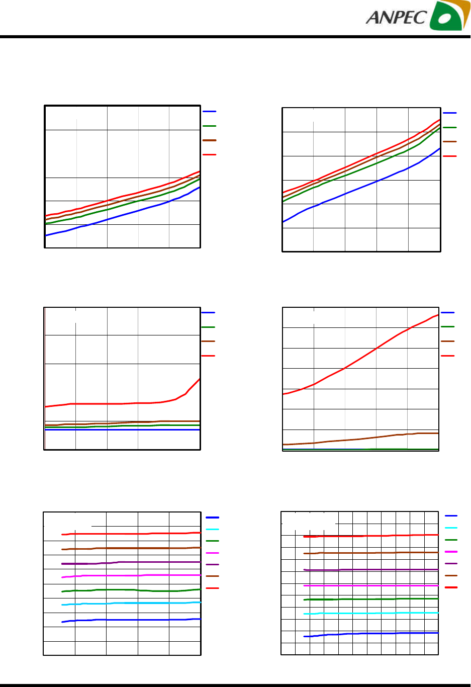
Typical Operating Characteristics
Quiescent Current vs. BIAS
Supply Voltage (Both Channels)
Quiescent Current, IBIAS (µA)
3 3.544.5 5 5.5
VBIAS = VIN
BIAS Supply Voltage, VBIAS
(V)
-40
25
85
125
40
50
60
70
80
90
100
Quiescent Current vs. BIAS Supply
Voltage (Single Channel)
BIAS Supply Voltage, VBIAS
(V)
Quiescent Current, IBIAS (µA)
3 3.5 4 4.5 5 5.5
VBIAS = VIN
30
35
40
45
50
55
60 -40
25
85
125
Shutdown Current vs. BIAS
Supply Voltage (Both Channels)
Quiescent Current, ISD(µA)
3 3.5 4 4.5 5 5.5
BIAS Supply Voltage, VBIAS
(V)
VBIAS = VIN
0
0.1
0.2
0.3
0.4
0.5-40
25
85
125
Off-Stage Supply Current vs. VIN
Supply Voltage (SINGLE CHANNEL)
VIN Supply Voltage, VIN (V)
Off-Stage Supply Current, IOFF (µA)
3 3.5 4 4.5 5 5.5
VBIAS = 5.5V-40
25
85
125
0
2
4
6
8
10
12
14
-40
0
25
50
75
100
125
Switch On Resistance vs. VIN
Supply Voltage
VIN Supply Voltage, VIN (V)
0.511.5 2 2.5 3
12
14
16
18
20
22
24
26
28
30
32 VBIAS = 3V
Switch On Resistance,RDS(ON) (mΩ)
-40
0
25
50
75
100
125
Switch On Resistance vs. VIN
Supply Voltage
VIN Supply Voltage, VIN (V)
Switch On Resistance,RDS(ON) (mΩ)
0 0.5 1 1.522.533.544.555.5
12
13
14
15
16
17
18
19
20
21
22
23
24
VBIAS = 5.5V
Copyright ANPEC Electronics Corp.
Rev. A.2 - Mar., 2013
APL3533
www.anpec.com.tw6
Typical Operating Characteristics
VBIAS=3.3V
VBIAS=5V
Switch On Resistance vs. VIN
Supply Voltage
TJ=25°C
14
15
16
17
18
19
20
21
22
23
24
0.5 1.5 2.5 3.5 4.5 5.5
VIN Supply Voltage, VIN (V)
Switch On Resistance,RDS(ON) (mΩ)
Output Current, IOUT (A)
Switch On Resistance vs. Output
Current
0 1 2 3 4 56
Switch On Resistance,RDS(ON) (mΩ)
14
15
16
17
18
VBIAS = 5V, VIN = 5V, TJ = 25°C
19
20
Turn On Delay Time vs. VIN
Supply Voltage
VIN Supply Voltage, VIN (V)
Turn On Delay Time, tD(µs)
50
100
150
200
250
300
350
400
450
500
0.8 1.0 1.2 1.4 1.6 1.8 2.0 2.2 2.4 2.6 2.8 3.0
-40
25
85
125
VBIAS = 3V, RL = 10 Ω
CSS = 1nF, COUT
= 0.1µF
VIN Supply Voltage, VIN (V)
Turn On Delay Time, tD(µs)
0.5 1.5 2.5 3.5 4.5 5.5
50
100
150
200
250
300
350
400
450
500
VBIAS = 5.5V, CSS = 1nF,
ROUT = 10Ω, COUT = 0.1µF
Turn On Delay Time vs. VIN Supply
Voltage
-40
25
85
125
Falling Time vs . VIN Supply Voltage
VIN Supply Voltage, VIN (V)
Falling Time, tF(µs)
0.8 1.0 1.2 1.4 1.6 1.8 2.0 2.2 2.4 2.6 2.8 3.0
0
1
2
3
4
5
VBIAS = 3V, RL = 10Ω
CSS = 1nF, COUT
= 0.1µF
-40
25
85
125
VIN Supply Voltage, VIN (V)
Falling Time, tF(µs)
0.5 1 1.5 2 2.5 3 3.5 4 4.555.5
1
2
3
4
5
Falling Time vs. VIN Supply Voltage
VBIAS = 5.5V, Css = 1nF,
ROUT = 10Ω, COUT = 0.1 µF
-40
25
85
125
Copyright ANPEC Electronics Corp.
Rev. A.2 - Mar., 2013
APL3533
www.anpec.com.tw7
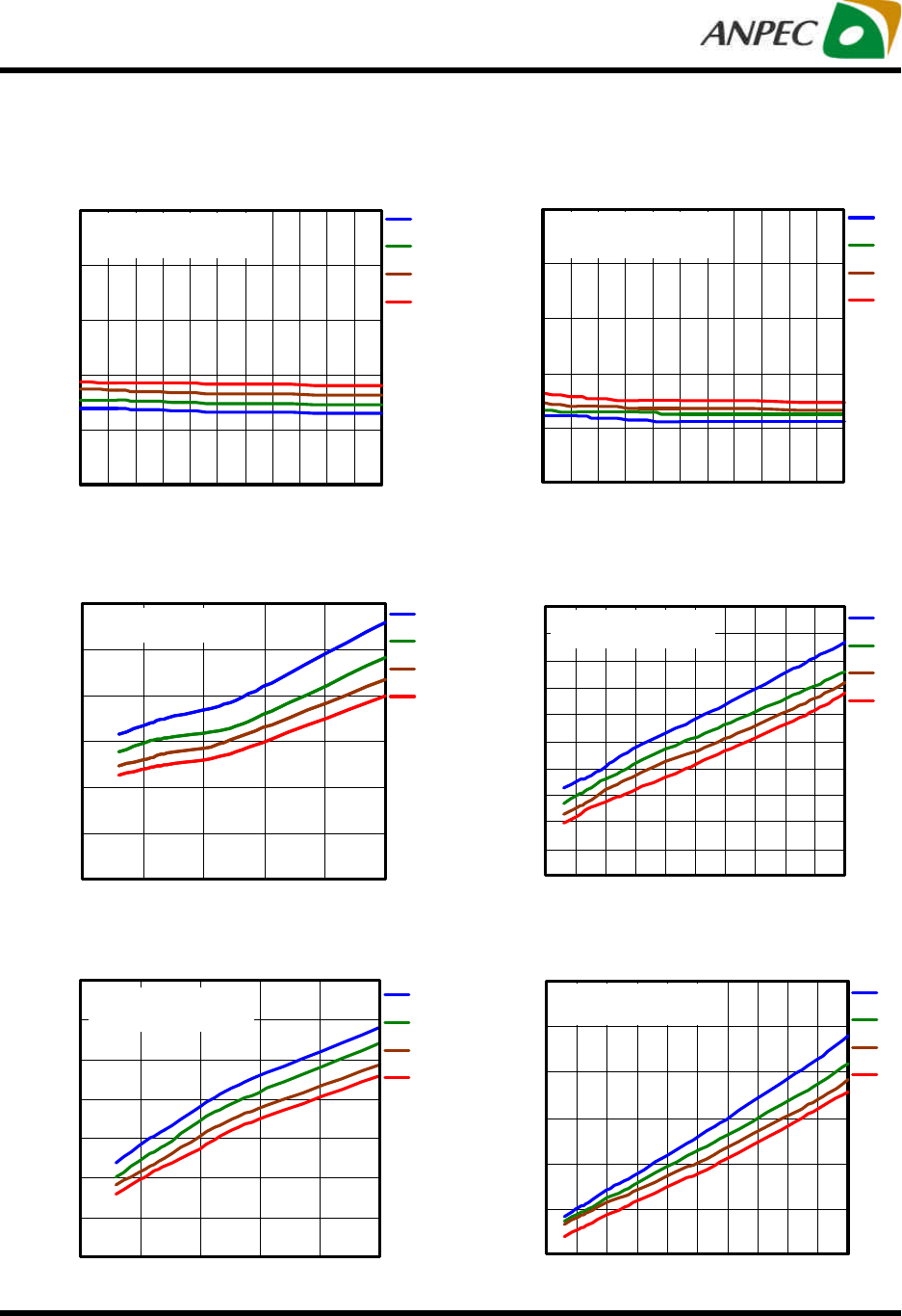
Typical Operating Characteristics
Turn Off Time vs. VIN Supply
Voltage
VIN Supply Voltage, VIN (V)
Turn Off Time, tOFF (µs)
0
1
2
3
4
5
VBIAS = 3V, RL = 10Ω
CSS = 1nF, COUT = 0.1µF
-40
25
85
125
0.8 1.0 1.2 1.4 1.6 1.8 2.0 2.2 2.4 2.6 2.8 3.0
Turn Off Time vs. VIN Supply
Voltage
VIN Supply Voltage, VIN (V)
Turn Off Time, tOFF (µs)
0.8 1.0 1.2 1.4 1 .6 1.8 2.0 2.2 2.4 2.6 2.8 3.0
0
1
2
3
4
5
VBIAS = 5.5V, RL = 10Ω
CSS = 1nF, COUT = 0.1µF
-40
25
85
125
Rising Time vs. VIN Supply Voltage
VIN Supply Voltage, VIN (V)
Rising Time, tR(µs)
0.5 1.0 1.5 2.0 2.5 3 .0
VBIAS = 3V, RL = 10Ω
CSS = 1nF, COUT = 0.1µF
0
200
400
600
800
1000
1200
1400 -40
25
85
125
Rising Time vs. VIN Supply Voltage
VIN Supply Voltage, VIN (V)
Rising Time, tR(µs)
VBIAS = 5.5V, RL = 10Ω
CSS = 1nF, COUT
= 0.1µF
0
500
1000
1500
2000
2500
3000
0.51.0 1 .5 2.0 2.53.0 3.5 4.04.5 5.0 5.5
-40
25
85
125
Turn On Time vs. VIN Supply
Voltage
VIN Supply Voltage, VIN (V)
Turn On Time, tON(µs)
0
200
400
600
800
1000
1200
0.5 1.0 1 .5 2.0 2.5 3.0
VBIAS = 3V, RL = 10Ω
CSS = 1nF, COUT = 0.1µF
-40
25
85
125
Turn On Time vs. VIN Supply
Voltage
VIN Supply Voltage, VIN (V)
Turn On Time, tON(µs)
VBIAS = 5.5V, RL = 10Ω
CSS = 1nF, COUT = 0.1µF
0.5 1.0 1.5 2.0 2.5 3.0 3.5 4.0 4.5 5.0 5.5
0
200
400
600
800
1000
1200
1400
1600
1800
2000 -40
25
85
125
Copyright ANPEC Electronics Corp.
Rev. A.2 - Mar., 2013
APL3533
www.anpec.com.tw8
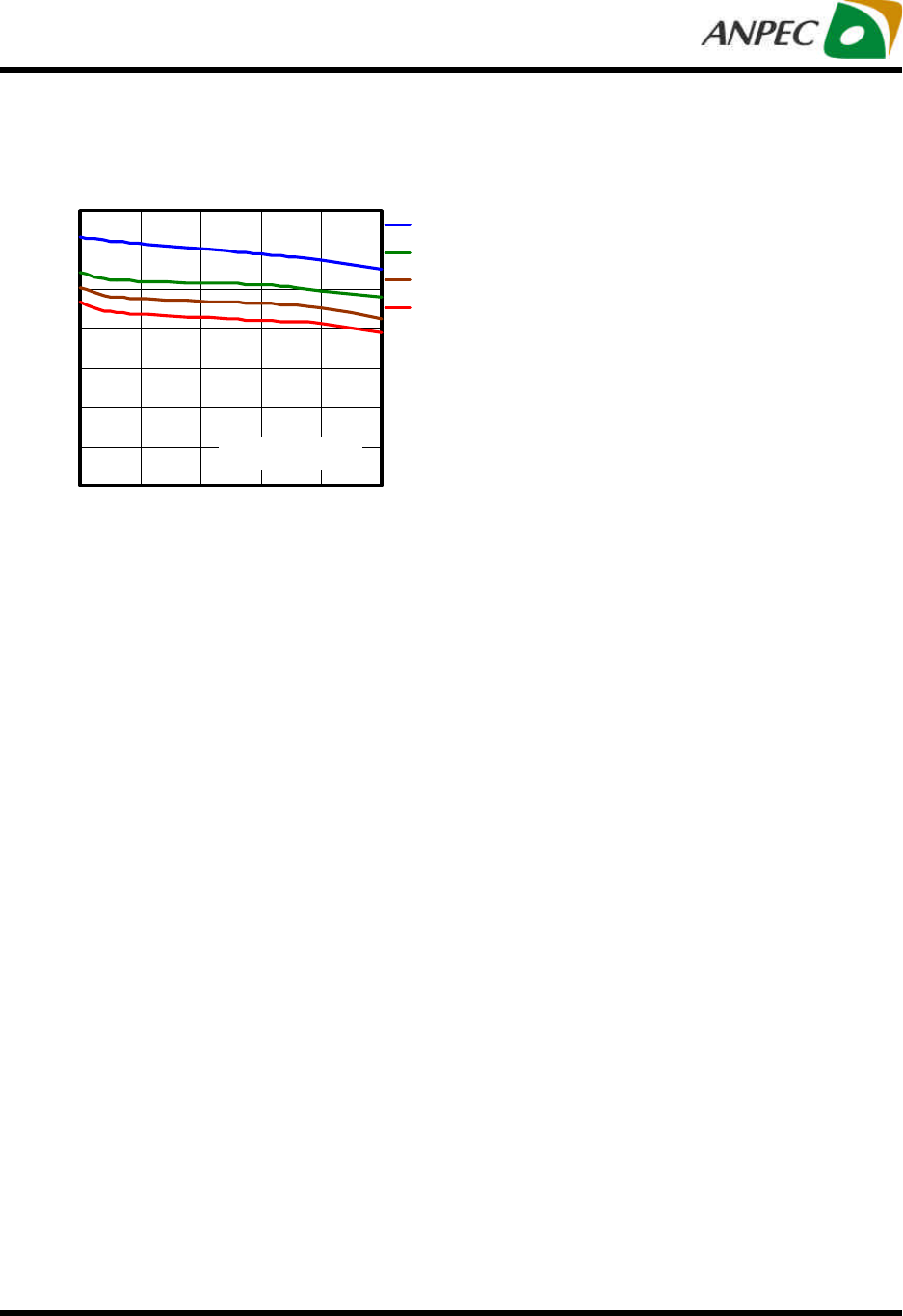
Typical Operating Characteristics
Rising Time vs. BIAS Supply
Voltage
BIAS Supply Voltage, VBIAS (V)
Rising Time, tR(µs)
200
400
600
800
1000
1200
1400
1600
3 3.54 4.5 5 5.5
-40
25
85
125
VIN = 3V, RL = 10Ω
CSS = 1nF, COUT = 0.1µF
Copyright ANPEC Electronics Corp.
Rev. A.2 - Mar., 2013
APL3533
www.anpec.com.tw9
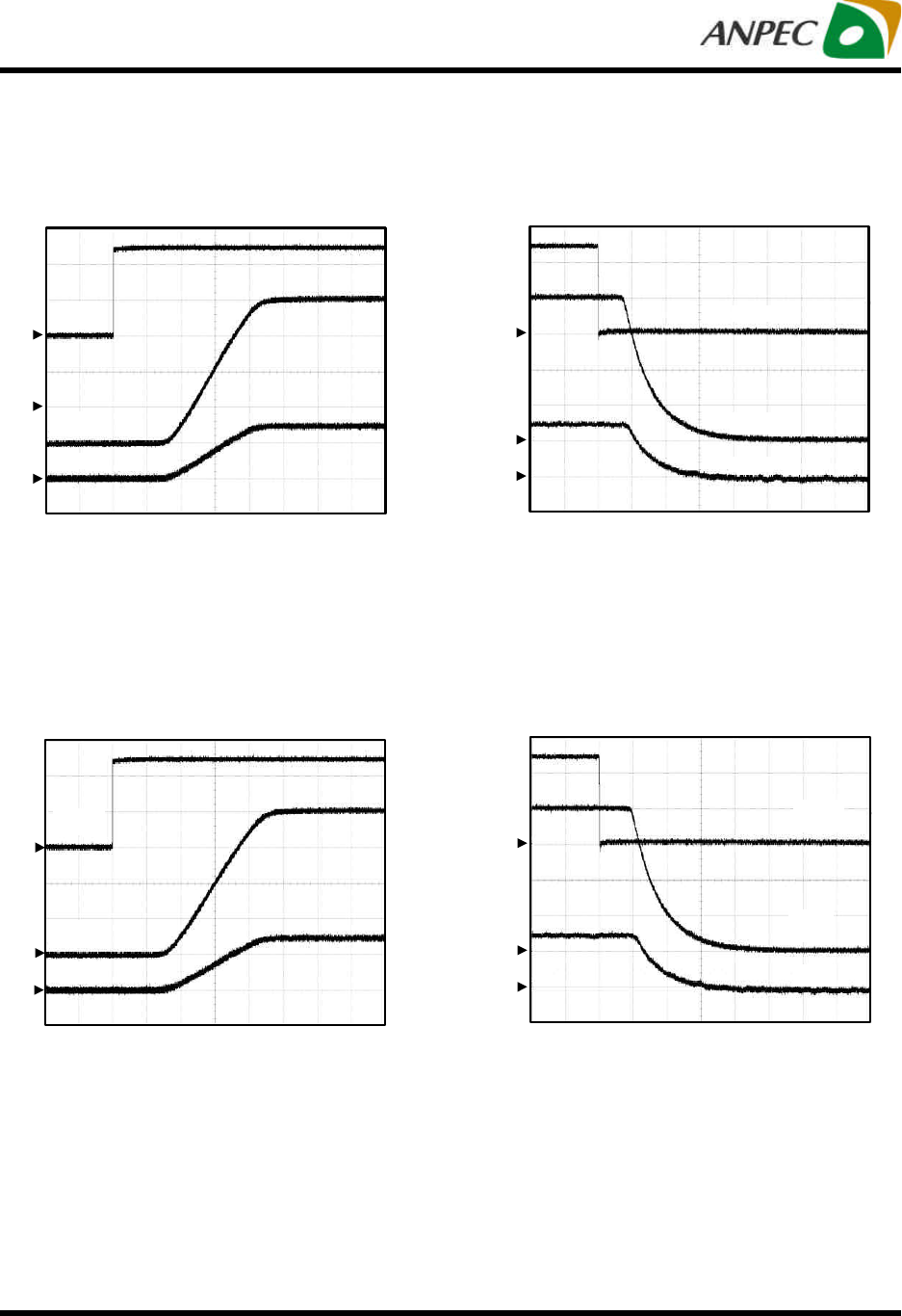
Operating Waveforms
Refer to the typical application circuit. TA= 25oC unless otherwise specified.
Shutdown
1
3
2
CH1: VEN
, 2V/Div, DC
CH2: VOUT, 200mV/Div, DC
CH3: IOUT, 50mA/Div, DC
TIME: 1µs/Div
VBIAS
=3V, VIN=0.8V
COUT =0.1µF, CSS=1nF, RL=10Ω
VEN
VOUT
IOUT
Enable
1
3
2
CH1: VEN
, 2V/Div, DC
CH2: VOUT, 200mV/Div, DC
CH3: IOUT, 50mA/Div, DC
TIME: 200µs/Div
VBIAS
=3V, VIN=0.8V
COUT=0.1µF, CSS=1nF, RL=10Ω
VEN
VOUT
IOUT
Shutdown
VEN
VOUT
IOUT
1
3
2
CH1: VEN, 2V/Div, DC
CH2: VOUT, 200mV/Div, DC
CH3: IOUT , 50mA/Div, DC
TIME: 1µs/Div
VBIAS
=3V, VIN=0.8V
COUT=0.1µF, CSS
=1nF, RL=10Ω
Enable
1
3
2
VEN
VOUT
IOUT
CH1: VEN, 2V/Div, DC
CH2: VOUT, 200mV/Div, DC
CH3: IOUT, 50mA/Div, DC
TIME: 200µs/Div
VBIAS=3V, VIN=0.8V
COUT =0.1µF, CSS=1nF, RL=10Ω
Copyright ANPEC Electronics Corp.
Rev. A.2 - Mar., 2013
APL3533
www.anpec.com.tw10
Operating Waveforms
Refer to the typical application circuit. TA= 25oC unless otherwise specified.
Shutdown
CH1: VEN, 2V/Div, DC
CH2: VOUT, 1V/Div, DC
CH3: IOUT, 200mA/Div, DC
1
3
2
VEN
VOUT
IOUT
VBIAS
=5V, VIN=5V
COUT=0.1µF, CSS=1nF, RL=10Ω
Enable
1
3
VEN
IOUT
VOUT
CH1: VEN, 2V/Div, DC
CH2: VOUT, 1V/Div, DC
CH3: IOUT, 200mA/Div, DC
TIME: 500µs/Div
VBIAS
=5V, VIN=5V
2
COUT =0.1µF, CSS
=1nF, RL=10Ω
Copyright ANPEC Electronics Corp.
Rev. A.2 - Mar., 2013
APL3533
www.anpec.com.tw11
Pin Description
PIN
NO. NAME FUNCTION
1 VIN1
2 VIN1 Power supply Input of switch 1. Connect this pin to an external DC supply.
3 EN1 Enable input of switch 1. Logic high turns on switch 1. The EN1 pin cannot be left floating.
4 BIAS Bias voltage input pin for internal control circuitry.
5 EN2 Enable input of switch 2. Logic high turns on switch 2. The EN2 pin cannot be left floating.
6 VIN2
7 VIN2 Power supply Input of switch 2. Connect this pin to an external DC supply.
8 VOUT2
9 VOUT2 Switch 2 output.
10 SS2 Soft start control of switch 2. A capacitor from this pin to ground sets the VOUT2’s rise slew
rate.
11 GND Ground pin of the circuitry. All voltage levels are measured with respect to this pin.
12 SS1 Soft start control of switch 1. A capacitor from this pin to ground sets the VOUT1’s rise slew
rate.
13 VOUT1
14 VOUT1 Switch 1 output.
Copyright ANPEC Electronics Corp.
Rev. A.2 - Mar., 2013
APL3533
www.anpec.com.tw12
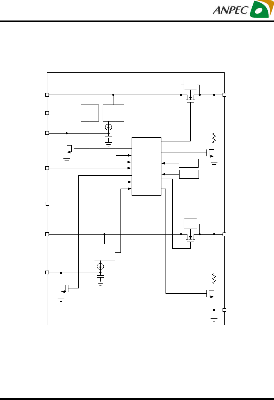
Block Diagram
UVLO
VIN1VOUT1
Charge
Pump
EN1
GND
SS1
BIAS
Bulk
Select
Control
Logic
OTP1
Bulk
Select
EN2
VIN2VOUT2
SS2
Charge
Pump
OTP2
Copyright ANPEC Electronics Corp.
Rev. A.2 - Mar., 2013
APL3533
www.anpec.com.tw13
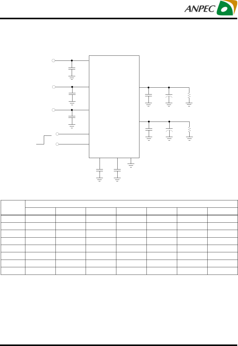
Typical Application Circuit
Soft-Start Time (µs) 10% to 90%, VBIAS=5V, CL=0.1µF, CIN=1µF, RL=10Ω, Typical values are at TA=25°C
CSS(pF) VIN=5V VIN=3.3V VIN=1.8V VIN=1.5V VIN=1.2V VIN=1.05V VIN=0.8V
0 112 73 53 49 45 42 38
220 492 322 197 170 146 132 128
330 685 450 270 230 198 180 145
470 911 598 355 307 263 233 188
1000 2030 1280 749 635 538 470 388
2200 4360 2740 1574 1336 1118 1014 797
4700 8780 5540 3218 2696 2289 2037 1624
10000 19060 12011 6862 5700 4806 4301 3410
Note: The table Contains soft-start time values measured on a typical device. The soft-start times shown are only valid for the power-
up sequence where VIN and VBIAS are already in steady state condition, and EN pin is asserted high.
VIN1VOUT1
APL3533
SS2
EN1
VOUT2
VIN2
SS1
EN2
BIAS
GND
CSS2
8, 9
13, 14
10 11
12
CSS1
RLOAD 1
CL1
150µF
COUT1
0.1µF
150
VIN1
CIN1
1µF
VBIAS
On
Off
CBIAS
0.1µF
VIN2
1,2
6,7
3
5
4
CIN2
1µF
0.1µF
COUT2CL2µFRLOAD2

Copyright ANPEC Electronics Corp.
Rev. A.2 - Mar., 2013
APL3533
www.anpec.com.tw14
Function Description
VIN Under-voltage Lockout (UVLO)
A under-voltage lockout (UVLO) circuit monitors the VBIAS
pins voltage to prevent wrong logic controls. The UVLO
function initiates a soft-start process after the BIAS sup-
ply voltages exceed rising UVLO voltage threshold dur-
ing powering on.
Power Switch
The power switch is an N-channel MOSFET with a ultra-
low RDS(ON). When IC is in shutdown state (VEN1,2=0V), the
MOSFET prevents a reverse current flowing from the VOUT
back to VIN. When IC is in UVLO state, the internal para-
sitic diodes connected from VOUT to VIN will be forward
biased.
Soft-start
The APL3533 Provides an adjustable soft-start circuitry
to control rise rate of the output voltage and limit the cur-
rent surge during start-up. The soft-start time is set with a
capacitor from the SS pin to the ground.
Enable Control
The APL3533 has a dedicated enable pin (EN). A logic
low signal applied to this pin shuts down the output. Fol-
lowing a shutdown, a logic high signal re-enables the
output through initiation of a new soft-start cycle.
Over-Temperature Protection (OTP)
When the junction temperature exceeds 160oC, the inter-
nal thermal sense circuit turns off the power FET and
allows the device to cool down. When the device’s junc-
tion temperature cools by 40oC, the internal thermal
sense circuit will enable the device, resulting in a pulsed
output during continuous thermal protection. Thermal
protection is designed to protect the IC in the event of
over temperature conditions. For normal operation, the
junction temperature cannot exceed TJ=+125oC.
Copyright ANPEC Electronics Corp.
Rev. A.2 - Mar., 2013
APL3533
www.anpec.com.tw15
Application Information
Power Sequencing
Capacitor Selection
The APL3533 requires proper input capacitors to supply
current surge during stepping load transients to prevent
the input voltage rail from dropping. Because the para-
sitic inductor from the voltage sources or other bulk ca-
pacitors to the VIN pin limit the slew rate of the surge
currents, more parasitic inductance needs more input
capacitance.
For normal applications (except OTP or output short cir-
cuit has occurred), the recommended input capacitance
of VIN is 1µF and output capacitance of VOUT is 0.1µF at
least. Please place the capacitors near the APL3533 as
close as possible.
A bulk output capacitor, placed close to the load, is rec-
ommended to support load transient current.
Soft-Start Capacitor
The soft-start capacitor on SS pin can reduce the inrush
current and overshoot of output voltage. The capacitor is
charge to VSS with a constant current source. This results
in a linear charge of the soft-start capacitor and thus the
output voltage.
The APL3533 has a built-in reverse current blocking cir-
cuit to prevent a reverse current flowing through the body
diode of power switch from the VOUT back VIN pin when
power switch disabled. The reverse current blocking cir-
cuit is not active before VBIAS is ready. When IC is in UVLO
state, the internal parasitic diodes of power switch con-
nected from VOUT to VIN will be forward biased.
Otherwise, VOUT should not be higher than VBIAS, and
VBIAS must be higher than the voltage of any other input
pin, the reason is that the internal parasitic diodes con-
nected from VOUT to VBIAS will be forward biased.
Figure 2. APL3533 Power Sequencing Diagram
Thermal Consideration
The APL3533 maximum power dissipation depends on
the differences of the thermal resistance and tempera-
ture between junction and ambient air. The power dissi-
pation PD across the device is:
PD = (TJ - TA) / θJA
where (TJ-TA) is the temperature difference between the
junction and ambient air. θJA is the thermal resistance
between junction and ambient air. Assuming the TA=25°C
and maximum TJ=160°C (typical thermal limit threshold),
the maximum power dissipation is calculated as:
PD(max)=(160-25)/80
= 1.68(W)
For normal operation, do not exceed the maximum oper-
ating junction temperature of TJ = 125°C. The calculated
power dissipation should be less than:
PD =(125-25)/80
= 1.25(W)....................................................TA=25oC
PD =(125-85)/80
= 0.5(W)......................................................TA=85oC
The power dissipation depends on operating ambient
temperature for fixed TJ=125oC and thermal resistance
θJA. For APL3533 packages, the Figure 3 of derating
curves allows the designer to see the effect of rising
ambient temperature on the maximum power allowed.
0.5
0.6
0.7
0.8
0.9
1.0
1.1
1.2
1.3
-40 -30 -20 -10 0 10 20 30 40 50 60 70 80 90
Ambient Temperature (oC)
Power Dissipation (W)
Figure 3. Derating Curves for APL3533 Package
VOUT1, VOUT2
VEN1, VEN2
VIN1, VIN2
VEN1, VEN2
VOUT1, VOUT2
VIN1, VIN2
VBIAS
VBIAS
Copyright ANPEC Electronics Corp.
Rev. A.2 - Mar., 2013
APL3533
www.anpec.com.tw16
Application Information
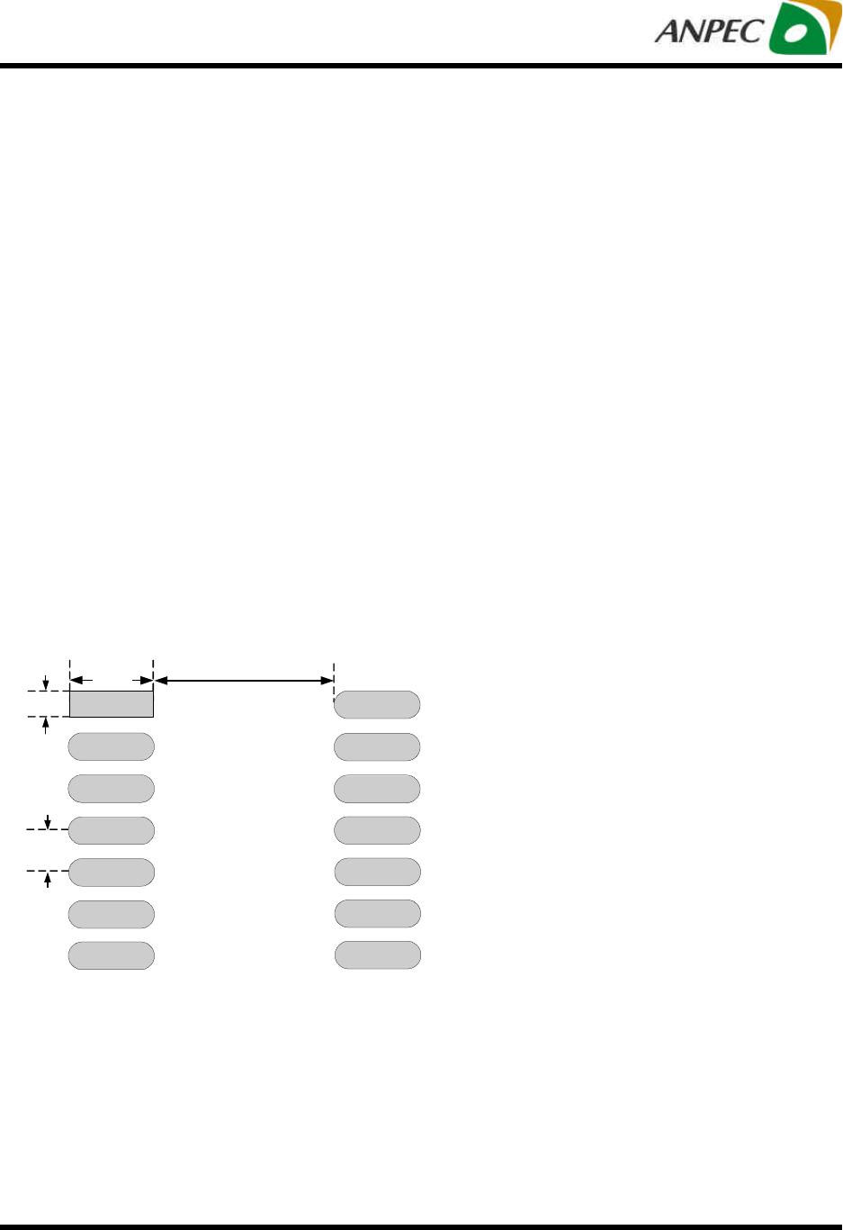
Recommended Minimum Footprint
Layout Consideration
The PCB layout should be carefully performed to maxi-
mize thermal dissipation and to minimize voltage drop,
droop and EMI. The following guidelines must be
considered:
1. Please place the input capacitors near the VIN pin as
close as possible.
2. Output decoupling capacitors for load must be placed
near the load as close as possible for decoupling high
frequency ripples.
3. Locate APL3533 and output capacitors near the load to
reduce parasitic resistance and inductance for excellent
load transient performance.
4. The negative pins of the input and output capacitors
and the GND pin must be connected to the ground plane
of the load.
5. Keep VIN and VOUT traces as wide and short as
possible.
0.25 (0.01)
0.48 (0.0192)
0.4 (0.016)
TDFN2x3-14AUnit: mm, (Inch)
1.3 (0.051)
Copyright ANPEC Electronics Corp.
Rev. A.2 - Mar., 2013
APL3533
www.anpec.com.tw17
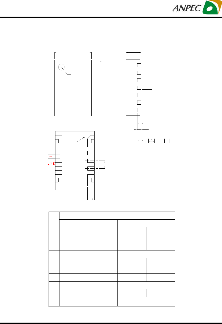
TDFN2x3-14A
Package Information
Pin 1
D
E
A
b
A1
A3
NX aaa c
SEATING PLANE
D2
e
Pin 1 Cornar
L
S
Y
M
B
O
LMIN.MAX.
0.80
0.00
0.15 0.25
2.90 3.10
0.05
0.30
A
A1
b
D
E
e
L
MILLIMETERS
A30.11 REF
TDFN2x3-14A
0.40
0.004 REF
MIN.MAX.
INCHES
0.031
0.000
0.006 0.010
0.114 0.122
0.012
0.70
0.016
0.028
0.002
0.40 BSC 0.016 BSC
1.90 2.10 0.075 0.083
aaa 0.08 0.003
Copyright ANPEC Electronics Corp.
Rev. A.2 - Mar., 2013
APL3533
www.anpec.com.tw18
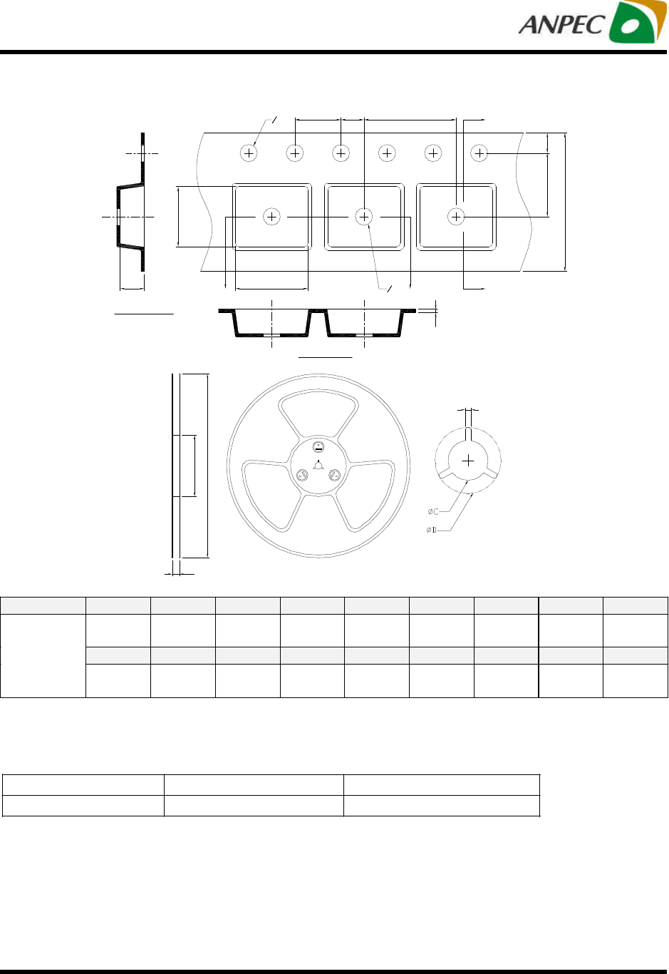
Carrier Tape & Reel Dimensions
A
E1
A
B
W
F
T
P0
OD0
BA0
P2
K0
B0
SECTION B-B
SECTION A-A
OD1
P1
H
T1
A
d
Application
A H T1 C d D W E1 F
178.0±2.00
50 MIN.
8.4+2.00
-0.00
13.0+0.50
-0.20
1.5 MIN.
20.2 MIN.
8.0±0.20
1.75±0.10
3.50±0.05
P0 P1 P2 D0 D1 T A0 B0 K0
TDFN2x3-14A
4.0±0.10
4.0±0.10
2.0±0.05
1.5+0.10
-0.00
1.5 MIN.
0.25±0.05
2.30±0.20
3.30±0.20
1.00±0.20
(mm)
Devices Per Unit
Package Type Unit Quantity
TDFN2x3-14A Tape & Reel 3000
Copyright ANPEC Electronics Corp.
Rev. A.2 - Mar., 2013
APL3533
www.anpec.com.tw19
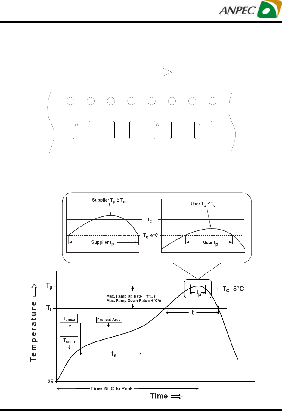
Taping Direction Information
TDFN2x3-14A
Classification Profile
USER DIRECTION OF FEED
Copyright ANPEC Electronics Corp.
Rev. A.2 - Mar., 2013
APL3533
www.anpec.com.tw20
Classification Reflow Profiles
Profile Feature Sn-Pb Eutectic Assembly Pb-Free Assembly
Preheat & Soak
Temperature min (Tsmin)
Temperature max (Tsmax)
Time (Tsmin to Tsmax) (ts)
100 °C
150 °C
60-120 seconds
150 °C
200 °C
60-120 seconds
Average ramp-up rate
(Tsmax to TP) 3 °C/second max. 3°C/second max.
Liquidous temperature (TL)
Time at liquidous (tL) 183 °C
60-150 seconds 217 °C
60-150 seconds
Peak package body Temperature
(Tp)* See Classification Temp in table 1 See Classification Temp in table 2
Time (tP)** within 5°C of the specified
classification temperature (Tc) 20** seconds 30** seconds
Average ramp-down rate (Tp to Tsmax)
6 °C/second max. 6 °C/second max.
Time 25°C to peak temperature 6 minutes max. 8 minutes max.
* Tolerance for peak profile Temperature (Tp) is defined as a supplier minimum and a user maximum.
** Tolerance for time at peak profile temperature (tp) is defined as a supplier minimum and a user maximum.
Table 2. Pb-free Process – Classification Temperatures (Tc)
Package
Thickness
Volume mm3
<350
Volume mm3
350-2000
Volume mm3
>2000
<1.6 mm 260 °C 260 °C 260 °C
1.6 mm – 2.5 mm 260 °C 250 °C 245 °C
≥2.5 mm 250 °C 245 °C 245 °C
Table 1. SnPb Eutectic Process – Classification Temperatures (Tc)
Package
Thickness
Volume mm3
<350
Volume mm3
≥350
<2.5 mm 235 °C 220 °C
≥2.5 mm 220 °C 220 °C
Test item Method Description
SOLDERABILITY JESD-22, B102 5 Sec, 245°C
HOLT JESD-22, A108 1000 Hrs, Bias @ Tj=125°C
PCT JESD-22, A102 168 Hrs, 100%RH, 2atm, 121°C
TCT JESD-22, A104 500 Cycles, -65°C~150°C
HBM MIL-STD-883-3015.7 VHBM≧2KV
MM JESD-22, A115 VMM≧200V
Latch-Up JESD 78 10ms, 1tr≧100mA
Reliability Test Program

Copyright ANPEC Electronics Corp.
Rev. A.2 - Mar., 2013
APL3533
www.anpec.com.tw21
Customer Service
Anpec Electronics Corp.
Head Office :
No.6, Dusing 1st Road, SBIP,
Hsin-Chu, Taiwan, R.O.C.
Tel : 886-3-5642000
Fax : 886-3-5642050
Taipei Branch :
2F, No. 11, Lane 218, Sec 2 Jhongsing Rd.,
Sindian City, Taipei County 23146, Taiwan
Tel : 886-2-2910-3838
Fax : 886-2-2917-3838