AT93C46D Datasheet. Www.s Manuals.com. Atmel
User Manual: Marking of electronic components, SMD Codes 46, 46**, 46-, 4604, 4634, 46D, 46N02KS, 46T, 46W, 46p, 46s, 46t. Datasheets AO4604, AT93C46D-PU, AT93C46D-TH, AT93C46DN-SH, AT93C46DU3-UU, AT93C46DY6-YH, BAS40-06, BAS40-06T, BAS40-06W, BSC046N02KS G, PDTC115EE, STN3446, Si4634DY, TK71546AS.
Open the PDF directly: View PDF ![]() .
.
Page Count: 22
Features
•Low-voltage and Standard-voltage Operation
– 1.8 (VCC = 1.8V to 5.5V)
•User-selectable Internal Organization
– 1K: 128 x 8 or 64 x 16
•Three-wire Serial Interface
•2 MHz Clock Rate (5V)
•Self-timed Write Cycle (5 ms max)
•High Reliability
– Endurance: 1 Million Write Cycles
– Data Retention: 100 Years
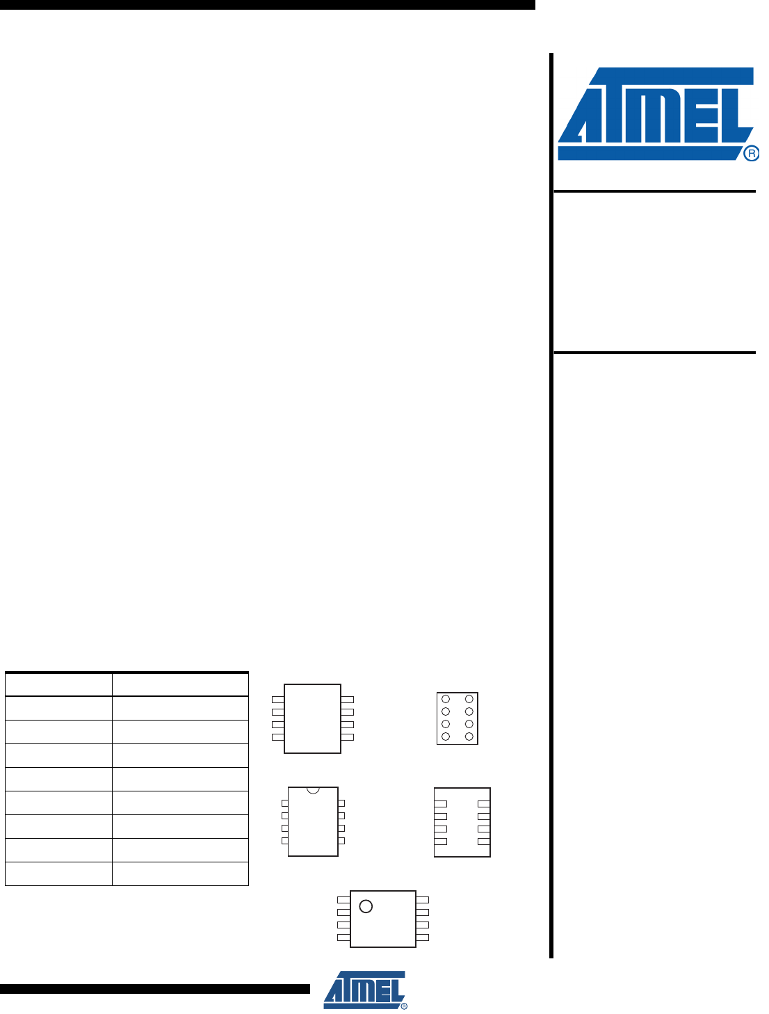
•8-lead JEDEC PDIP, 8-lead JEDEC SOIC, 8-lead Ultra Thin mini-MAP (MLP 2x3), 8-lead
TSSOP and 8-ball dBGA2 Packages
•Die Sales: Wafer Form, Tape and Reel, and Bumped Wafers
Description
The AT93C46D provides 1024 bits of serial electrically erasable programmable read-
only memory (EEPROM), organized as 64 words of 16 bits each (when the ORG pin is
connected to VCC), and 128 words of 8 bits each (when the ORG pin is tied to
ground). The device is optimized for use in many industrial and commercial applica-
tions where low-power and low-voltage operations are essential. The AT93C46D is
available in space-saving 8-lead PDIP, 8-lead JEDEC SOIC, 8-lead Ultra Thin mini-
MAP (MLP 2x3), 8-lead TSSOP, and 8-lead dBGA2 packages.
The AT93C46D is enabled through the Chip Select pin (CS) and accessed via a
three-wire serial interface consisting of Data Input (DI), Data Output (DO), and Shift
Clock (SK). Upon receiving a Read instruction at DI, the address is decoded and the
data is clocked out serially on the DO pin. The Write cycle is completely self-timed,
and no separate Erase cycle is required before Write. The Write cycle is only enabled
when the part is in the Erase/Write Enable state. When CS is brought high following
the initiation of a Write cycle, the DO pin outputs the Ready/Busy status of the part.
The AT93C46D is available in 1.8 (1.8V to 5.5V) version.
Table 0-1. Pin Configurations
Pin Name Function
CS Chip Select
SK Serial Data Clock
DI Serial Data Input
DO Serial Data Output
GND Ground
VCC Power Supply
ORG Internal Organization
NC No Connect
Three-wire
Serial
EEPROM
1K (128 x 8 or 64 x 16)
AT93C46D
5193F–SEEPR–1/08
1
2
3
4
8
7
6
5
CS
SK
DI
DO
VCC
NC
ORG
GND
VCC
NC
ORG
GND
CS
SK
D1
D0
1
2
3
4
8
7
6
5
1
2
3
4
8
7
6
5
CS
SK
DI
DO
VCC
NC
ORG
GND
1
2
3
4
8
7
6
5
VCC
NC
ORG
GND
CS
SK
DI
DO
1
2
3
4
8
7
6
5
CS
SK
DI
DO
VCC
NC
ORG
GND
8-lead SOIC 8-lead dBGA2
8-lead PDIP 8-lead Ultra Thin mini-MAP (MLP 2x3)
8-lead TSSOP
Bottom View
Bottom View
2
5193F–SEEPR–1/08
AT93C46D
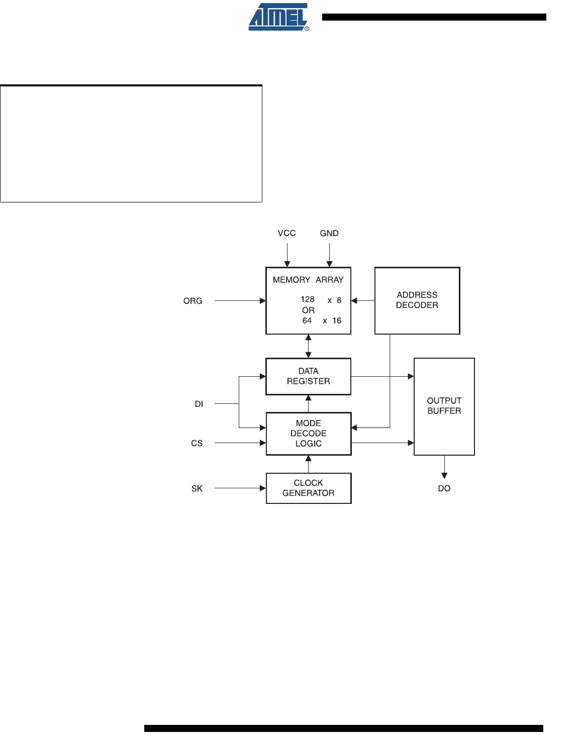
Figure 1-1. Block Diagram
Notes: 1. When the ORG pin is connected to VCC, the “x 16” organization is selected. When it is con-
nected to ground, the “x 8” organization is selected. If the ORG pin is left unconnected and the
application does not load the input beyond the capability of the internal 1 Meg ohm pullup, then
the “x 16” organization is selected.
2. For the AT93C46D, if the “x 16” organization is the mode of choice and pin 6 (ORG) is left
unconnected, Atmel® recommends using AT93C46E device. For more details, see the
AT93C46E datasheet.
1. Absolute Maximum Ratings*
Operating Temperature......................................−55°C to +125°C*NOTICE: Stresses beyond those listed under “Absolute
Maximum Ratings” may cause permanent dam-
age to the device. This is a stress rating only, and
functional operation of the device at these or any
other conditions beyond those indicated in the
operational sections of this specification is not
implied. Exposure to absolute maximum rating
conditions for extended periods may affect
device reliability
Storage Temperature .........................................−65°C to +150°C
Voltage on Any Pin
with Respect to Ground ........................................ −1.0V to +7.0V
Maximum Operating Voltage .......................................... 6.25V
DC Output Current........................................................ 5.0 mA
3
5193F–SEEPR–1/08
AT93C46D
Note: 1. This parameter is characterized and is not 100% tested.
Note: 1. VIL min and VIH max are reference only and are not tested.
Table 1-1. Pin Capacitance(1)
Applicable over recommended operating range from TA = 25°C, f = 1.0 MHz, VCC = +1.8V (unless otherwise noted)
Symbol Test Conditions Max Units Conditions
COUT Output Capacitance (DO) 5 pF VOUT = 0V
CIN Input Capacitance (CS, SK, DI) 5 pF VIN = 0V
Table 1-2. DC Characteristics
Applicable over recommended operating range from: TAI = −40°C to +85°C, VCC = +1.8V to +5.5V (unless otherwise noted)
Symbol Parameter Test Condition Min Typ Max Unit
VCC1 Supply Voltage 1.8 5.5 V
VCC2 Supply Voltage 2.7 5.5 V
VCC3 Supply Voltage 4.5 5.5 V
ICC Supply Current VCC = 5.0V READ at 1.0 MHz 0.5 2.0 mA
WRITE at 1.0 MHz 0.5 2.0 mA
ISB1 Standby Current VCC = 1.8V CS = 0V 0.4 1.0 µA
ISB2 Standby Current VCC = 2.7V CS = 0V 6.0 10.0 µA
ISB3 Standby Current VCC = 5.0V CS = 0V 10.0 15.0 µA
IIL Input Leakage VIN = 0V to VCC 0.1 1.0 µA
IOL Output Leakage VIN = 0V to VCC 0.1 1.0 µA
VIL1
(1) Input Low Voltage 2.7V ≤ VCC ≤ 5.5V
−0.6 0.8 V
VIH1
(1) Input High Voltage 2.0 VCC + 1
VIL2
(1) Input Low Voltage 1.8V ≤ VCC ≤ 2.7V
−0.6 VCC x 0.3 V
VIH2
(1) Input High Voltage VCC x 0.7 VCC + 1
VOL1 Output Low Voltage 2.7V ≤ VCC ≤ 5.5V IOL = 2.1 mA 0.4 V
VOH1 Output High Voltage IOH = −0.4 mA 2.4 V
VOL2 Output Low Voltage 1.8V ≤ VCC ≤ 2.7V IOL = 0.15 mA 0.2 V
VOH2 Output High Voltage IOH = −100 µA VCC – 0.2 V

4
5193F–SEEPR–1/08
AT93C46D
Note: 1. This parameter is ensured by characterization.
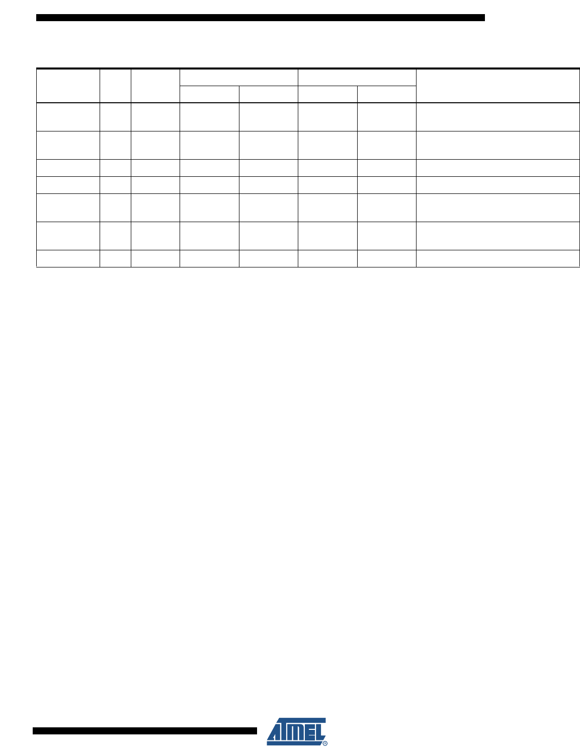
Table 1-3. AC Characteristics
Applicable over recommended operating range from TAI = −40°C to + 85°C, VCC = +2.7V to +5.5V,
CL = 1 TTL Gate and 100 pF (unless otherwise noted)
Symbol Parameter Test Condition Min Typ Max Units
fSK
SK Clock
Frequency
4.5V ≤ VCC ≤ 5.5V
2.7V ≤ VCC ≤ 5.5V
1.8V ≤ VCC ≤ 5.5V
0
0
0
2
1
0.25
MHz
tSKH SK High Time
4.5V ≤ VCC ≤ 5.5V
2.7V ≤ VCC ≤ 5.5V
1.8V ≤ VCC ≤ 5.5V
250
250
1000
ns
tSKL SK Low Time
4.5V ≤ VCC ≤ 5.5V
2.7V ≤ VCC ≤ 5.5V
1.8V ≤ VCC ≤ 5.5V
250
250
1000
ns
tCS
Minimum CS
Low Time
4.5V ≤ VCC ≤ 5.5V
2.7V ≤ VCC ≤ 5.5V
1.8V ≤ VCC ≤ 5.5V
250
250
1000
ns
tCSS CS Setup Time Relative to SK
4.5V ≤ VCC ≤ 5.5V
2.7V ≤ VCC ≤ 5.5V
1.8V ≤ VCC ≤ 5.5V
50
50
200
ns
tDIS DI Setup Time Relative to SK
4.5V ≤ VCC ≤ 5.5V
2.7V ≤ VCC ≤ 5.5V
1.8V ≤ VCC ≤ 5.5V
100
100
400
ns
tCSH CS Hold Time Relative to SK 0 ns
tDIH DI Hold Time Relative to SK
4.5V ≤ VCC ≤ 5.5V
2.7V ≤ VCC ≤ 5.5V
1.8V ≤ VCC ≤ 5.5V
100
100
400
ns
tPD1 Output Delay to “1” AC Test
4.5V ≤ VCC ≤ 5.5V
2.7V ≤ VCC ≤ 5.5V
1.8V ≤ VCC ≤ 5.5V
250
250
1000
ns
tPD0 Output Delay to “0” AC Test
4.5V ≤ VCC ≤ 5.5V
2.7V ≤ VCC ≤ 5.5V
1.8V ≤ VCC ≤ 5.5V
250
250
1000
ns
tSV CS to Status Valid AC Test
4.5V ≤ VCC ≤ 5.5V
2.7V ≤ VCC ≤ 5.5V
1.8V ≤ VCC ≤ 5.5V
250
250
1000
ns
tDF
CS to DO in High
Impedance
AC Test
CS = VIL
4.5V ≤ VCC ≤ 5.5V
2.7V ≤ VCC ≤ 5.5V
1.8V ≤ VCC ≤ 5.5V
100
150
400
ns
tWP Write Cycle Time 1.8V ≤ VCC ≤ 5.5V 0.1 3 5 ms
Endurance(1) 5.0V, 25°C 1M Write Cycles
5
5193F–SEEPR–1/08
AT93C46D
Note: The Xs in the address field represent DON’T CARE values and must be clocked.
2. Functional Description
The AT93C46D is accessed via a simple and versatile three-wire serial communication inter-
face. Device operation is controlled by seven instructions issued by the host processor. A valid
instruction starts with a rising edge of CS and consists of a start bit (logic “1”) followed by the
appropriate op code and the desired memory address location.
READ (READ): The Read (READ) instruction contains the address code for the memory loca-
tion to be read. After the instruction and address are decoded, data from the selected memory
location is available at the serial output pin DO. Output data changes are synchronized with the
rising edges of serial clock SK. It should be noted that a dummy bit (logic “0”) precedes the 8- or
16-bit data output string.
ERASE/WRITE ENABLE (EWEN): To assure data integrity, the part automatically goes into the
Erase/Write Disable (EWDS) state when power is first applied. An Erase/Write Enable (EWEN)
instruction must be executed first before any programming instructions can be carried out.
Please note that once in the EWEN state, programming remains enabled until an EWDS instruc-
tion is executed or VCC power is removed from the part.
ERASE (ERASE): The Erase (ERASE) instruction programs all bits in the specified memory
location to the logical “1” state. The self-timed erase cycle starts once the Erase instruction and
address are decoded. The DO pin outputs the Ready/Busy status of the part if CS is brought
high after being kept low for a minimum of 250 ns (tCS). A logic “1” at pin DO indicates that the
selected memory location has been erased and the part is ready for another instruction.
WRITE (WRITE): The Write (WRITE) instruction contains the 8 or 16 bits of data to be written
into the specified memory location. The self-timed programming cycle tWP starts after the last bit
of data is received at serial data input pin DI. The DO pin outputs the Read/Busy status of the
part if CS is brought high after being kept low for a minimum of 250 ns (tCS). A logic “0” at DO
indicates that programming is still in progress. A logic “1” indicates that the memory location at
the specified address has been written with the data pattern contained in the instruction and the
Table 1-4. Instruction Set for the AT93C46D
Instruction SB
Op
Code
Address Data
Commentsx 8 x 16 x 8 x 16
READ 1 10 A6 – A0A5 – A0
Reads data stored in memory, at
specified address
EWEN 1 00 11XXXXX 11XXXX Write enable must precede all
programming modes
ERASE 1 11 A6 – A0A5 – A0Erases memory location An – A0
WRITE 1 01 A6 – A0A5 – A0D7 – D0D15 – D0Writes memory location An – A0
ERAL 1 00 10XXXXX 10XXXX Erases all memory locations. Valid
only at VCC = 4.5V to 5.5V
WRAL 1 00 01XXXXX 01XXXX D7 – D0D15 – D0
Writes all memory locations. Valid
only at VCC = 4.5V to 5.5V
EWDS 1 00 00XXXXX 00XXXX Disables all programming instructions

6
5193F–SEEPR–1/08
AT93C46D
part is ready for further instructions. A Ready/Busy status cannot be obtained if the CS is
brought high after the end of the self-timed programming cycle tWP.
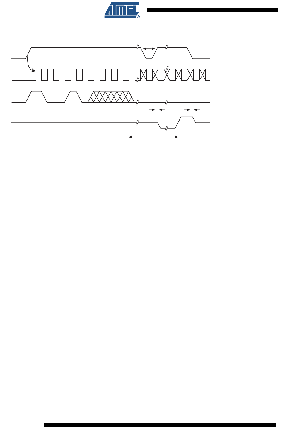
ERASE ALL (ERAL): The Erase All (ERAL) instruction programs every bit in the memory array
to the logic “1” state and is primarily used for testing purposes. The DO pin outputs the
Ready/Busy status of the part if CS is brought high after being kept low for a minimum of 250 ns
(tCS). The ERAL instruction is valid only at VCC = 5.0V ± 10%.
WRITE ALL (WRAL): The Write All (WRAL) instruction programs all memory locations with the
data patterns specified in the instruction. The DO pin outputs the Ready/Busy status of the part if
CS is brought high after being kept low for a minimum of 250 ns (tCS). The WRAL instruction is
valid only at VCC = 5.0V ± 10%.
ERASE/WRITE DISABLE (EWDS): To protect against accidental data disturb, the Erase/Write
Disable (EWDS) instruction disables all programming modes and should be executed after all
programming operations. The operation of the Read instruction is independent of both the
EWEN and EWDS instructions and can be executed at any time.
7
5193F–SEEPR–1/08
AT93C46D
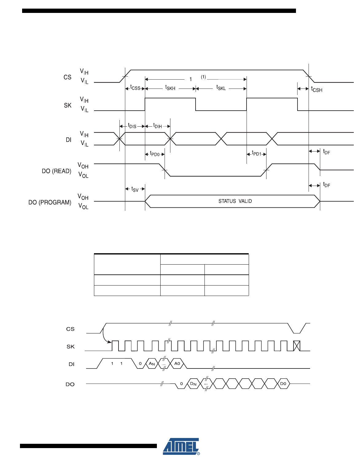
3. Timing Diagrams
Figure 3-1. Synchronous Data Timing
Note: 1. This is the minimum SK period.
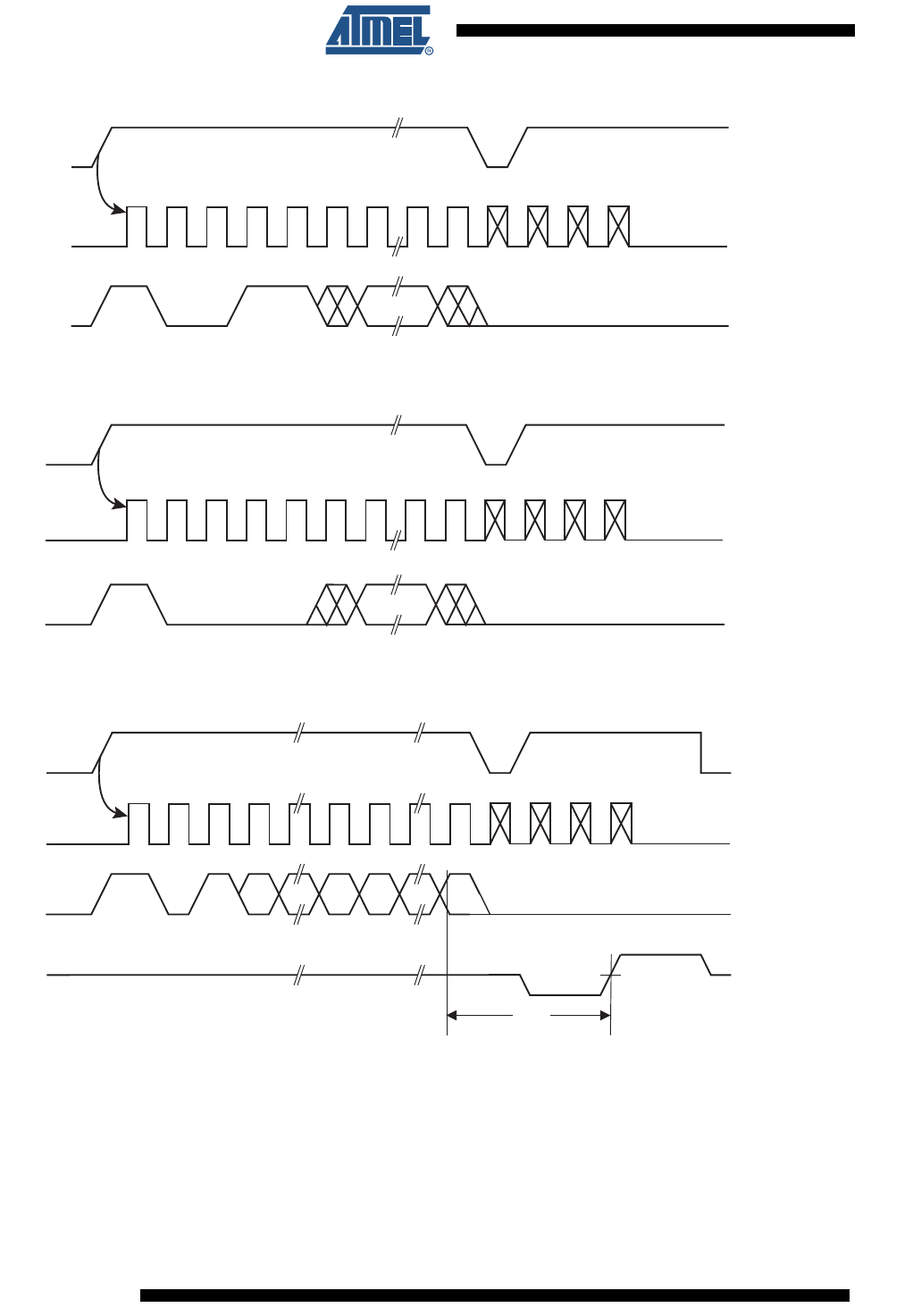
Figure 3-2. READ Timing
μs
Table 3-1. Organization Key for Timing Diagrams
I/O
AT93C46D (1K)
x 8 x 16
ANA6A5
DND7D15
High Impedance
tCS
8
5193F–SEEPR–1/08
AT93C46D
Figure 3-3. EWEN Timing
Figure 3-4. EWDS Timing
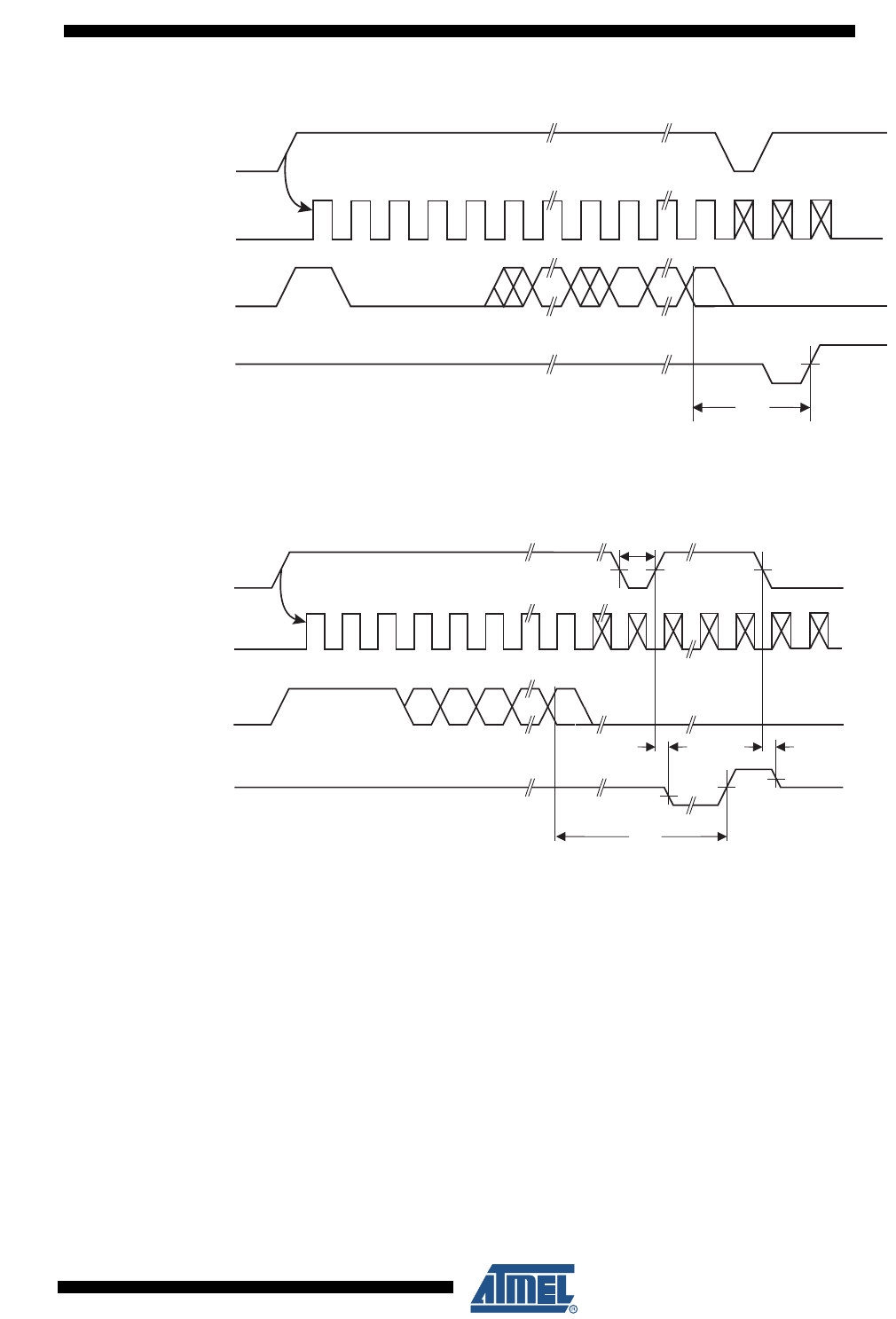
Figure 3-5. WRITE Timing
CS
11 ...
001
SK
DI
tCS
CS t
CS
SK
DI 1 0 000 ...
SK
CS tCS
tWP
11
ANDN
0A0D0
... ...
DI
DO HIGH IMPEDANCE BUSY READY
11
5193F–SEEPR–1/08
AT93C46D
Notes: 1. “-B” denotes bulk
2. “-T” denotes tape and reel. SOIC = 4K per reel. TSSOP, Ultra Thin Mini MAP, and dBGA2 = 5K per reel.
3. Available in tape and reel, and wafer form; order as SL788 for inkless wafer form. Bumped die available upon request.
Please contact Serial Interface Marketing.
4. AT93C46D Ordering Information
Ordering Code Voltage Package Operation Range
AT93C46D-PU (Bulk form only) 1.8 8P3
Lead-free/Halogen-free/
Industrial Temperature
(−40°C to 85°C)
AT93C46DN-SH-B(1) (NiPdAu Lead finish) 1.8 8S1
AT93C46DN-SH-T(2) (NiPdAu Lead finish) 1.8 8S1
AT93C46D-TH-B(1) (NiPdAu Lead finish) 1.8 8A2
AT93C46D-TH-T(2) (NiPdAu Lead finish) 1.8 8A2
AT93C46DY6-YH-T(2) (NiPdAu Lead finish) 1.8 8Y6
AT93C46DU3-UU-T(2) 1.8 8U3-1
AT93C46D-W-11(3) 1.8 Die Sale Industrial
(−40°C to 85°C)
Package Type
8P3 8-lead, 0.300" Wide, Plastic Dual Inline Package (PDIP)
8S1 8-lead, 0.150" Wide, Plastic Gull Wing Small Outline (JEDEC SOIC)
8A2 8-lead, 0.170" Wide, Thin Shrink Small Outline Package (TSSOP)
8U3-1 8-ball, Die Ball Grid Array Package (dBGA2)
8Y6 8-lead, 2.00 mm x 3.00 mm Body, 0.50mm Pitch, Ultra-Thin Mini-MAO, Dual No Lead Package. (DFN), (MLP 2x3mm)
Options
−1.8 Low Voltage (1.8V to 5.5V)

12
5193F–SEEPR–1/08
AT93C46D
5. Part Marking Scheme
5.1 AT93C46D 8-PDIP
5.2 AT93C46D 8-SOIC
TOP MARK Seal Year Y = SEAL YEAR WW = SEAL WEEK
| Seal Week 6: 2006 0: 2010 02 = Week 2
| | | 7: 2007 1: 2011 04 = Week 4
|---|---|---|---|---|---|---|---| 8: 2008 2: 2012 :: : :::: :
A T M L U Y W W 9: 2009 3: 2013 :: : :::: ::
|---|---|---|---|---|---|---|---| 50 = Week 50
4 6 D 1 52 = Week 52
|---|---|---|---|---|---|---|---|
* Lot Number Lot Number to Use ALL Characters in Marking
|---|---|---|---|---|---|---|---|
| BOTTOM MARK
Pin 1 Indicator (Dot) No Bottom Mark
TOP MARK Seal Year Y = SEAL YEAR WW = SEAL WEEK
| Seal Week 6: 2006 0: 2010 02 = Week 2
| | | 7: 2007 1: 2011 04 = Week 4
|---|---|---|---|---|---|---|---| 8: 2008 2: 2012 :: : :::: :
A T M L H Y W W 9: 2009 3: 2013 :: : :::: ::
|---|---|---|---|---|---|---|---| 50 = Week 50
4 6 D 1 52 = Week 52
|---|---|---|---|---|---|---|---|
* Lot Number Lot Number to Use ALL Characters in Marking
|---|---|---|---|---|---|---|---|
| BOTTOM MARK
Pin 1 Indicator (Dot) No Bottom Mark

13
5193F–SEEPR–1/08
AT93C46D
5.3 AT93C46D 8-TSSOP
5.4 AT93C46D 8-Ultra Thin Mini MAP
TOP MARK
Pin 1 Indicator (Dot) Y = SEAL YEAR WW = SEAL WEEK
| 6: 2006 0: 2010 02 = Week 2
|---|---|---|---| 7: 2007 1: 2011 04 = Week 4
* H Y W W 8: 2008 2: 2012 :: : :::: :
|---|---|---|---|---| 9: 2009 3: 2013 :: : :::: ::
4 6 D 1 * 50 = Week 50
|---|---|---|---|---| 52 = Week 52
BOTTOM MARK
|---|---|---|---|---|---|---|
C 0 0
|---|---|---|---|---|---|---|
A A A A A A A
|---|---|---|---|---|---|---|
<- Pin 1 Indicator
TOP MARK
Y = YEAR OF ASSEMBLY
|---|---|---|
4 6 D XX = ATMEL LOT NUMBER TO COORESPOND WITH
|---|---|---| NSEB TRACE CODE LOG BOOK.
H 1 (e.g. XX = AA, AB, AC,...AX, AY, AZ)
|---|---|---|
Y X X
|---|---|---| Y = SEAL YEAR
* 6: 2006 0: 2010
| 7: 2007 1: 2011
Pin 1 Indicator (Dot) 8: 2008 2: 2012
9: 2009 3: 2013

14
5193F–SEEPR–1/08
AT93C46D
5.5 AT93C46D dBGA2
TOP MARK
LINE 1-------> 46DU
LINE 2-------> YMTC
|<-- Pin 1 This Corner
Y = ONE DIGIT YEAR CODE
4: 2004 7: 2007
5: 2005 8: 2008
6: 2006 9: 2009
M = SEAL MONTH (USE ALPHA DESIGNATOR A-L)
A = JANUARY
B = FEBRUARY
" " """""""
J = OCTOBER
K = NOVEMBER
L = DECEMBER
TC = TRACE CODE (ATMEL LOT
NUMBERS TO CORRESPOND
WITH ATK TRACE CODE LOG BOOK)
15
5193F–SEEPR–1/08
AT93C46D
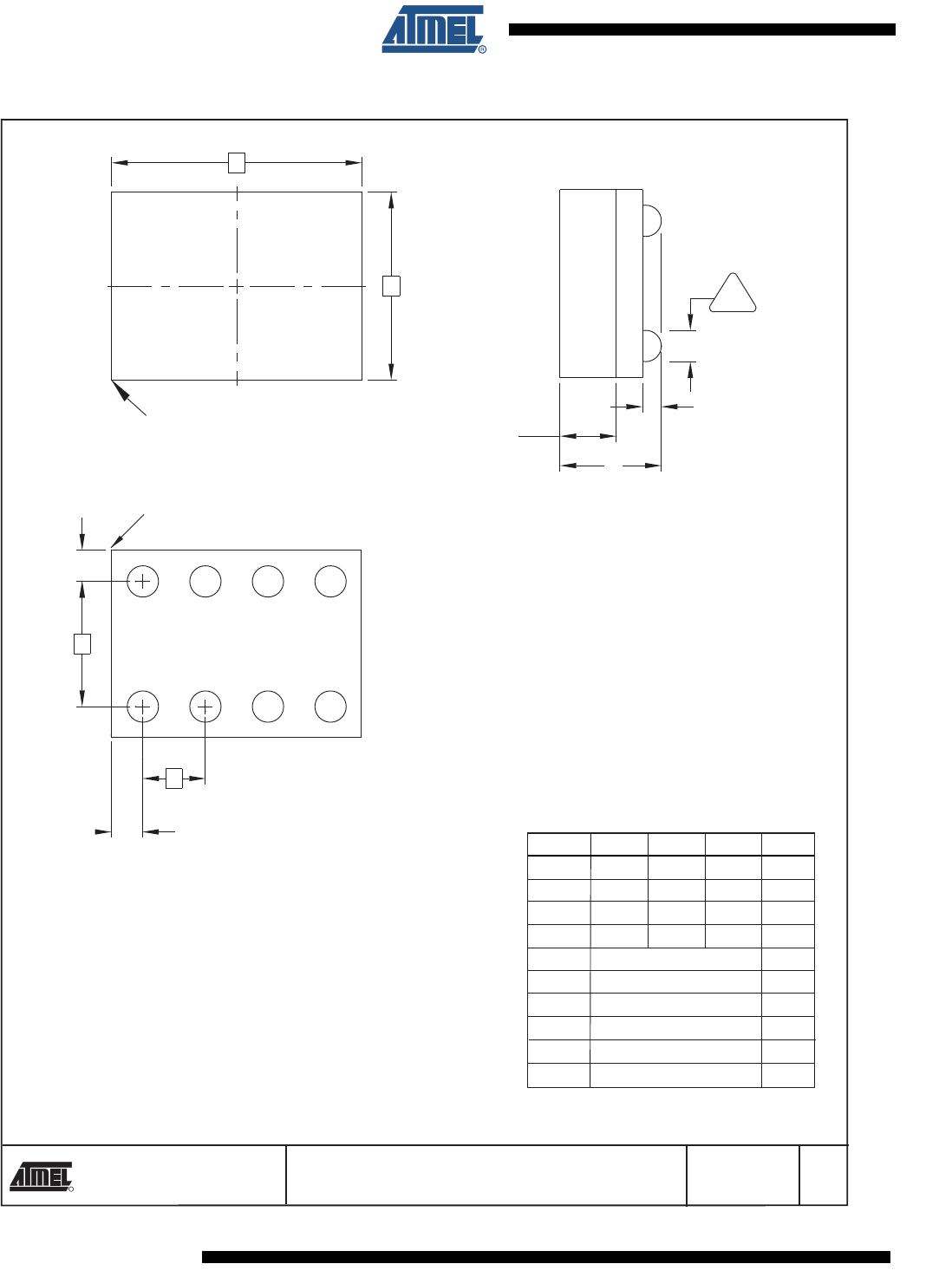
6. Package Information
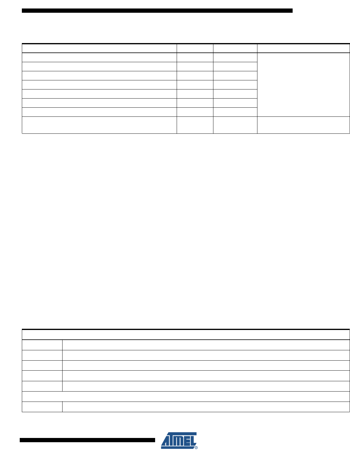
8P3 - PDIP
2325 Orchard Parkway
San Jose, CA 95131
TITLE DRAWING NO.
R
REV.
8P3, 8-lead, 0.300" Wide Body, Plastic Dual
In-line Package (PDIP)
01/09/02
8P3 B
Notes: 1. This drawing is for general information only; refer to JEDEC Drawing MS-001, Variation BA for additional information.
2. Dimensions A and L are measured with the package seated in JEDEC seating plane Gauge GS-3.
3. D, D1 and E1 dimensions do not include mold Flash or protrusions. Mold Flash or protrusions shall not exceed 0.010 inch.
4. E and eA measured with the leads constrained to be perpendicular to datum.
5. Pointed or rounded lead tips are preferred to ease insertion.
6. b2 and b3 maximum dimensions do not include Dambar protrusions. Dambar protrusions shall not exceed 0.010 (0.25 mm).
COMMON DIMENSIONS
(Unit of Measure = inches)
SYMBOL MIN NOM MAX NOTE
D
D1
E
E1
e
L
b2
b
A2 A
1
N
eA
c
b3
4 PLCS
A 0.210 2
A2 0.115 0.130 0.195
b 0.014 0.018 0.022 5
b2 0.045 0.060 0.070 6
b3 0.030 0.039 0.045 6
c 0.008 0.010 0.014
D 0.355 0.365 0.400 3
D1 0.005 3
E 0.300 0.310 0.325 4
E1 0.240 0.250 0.280 3
e 0.100 BSC
eA 0.300 BSC 4
L 0.115 0.130 0.150 2
Top View
Side View
End View
16
5193F–SEEPR–1/08
AT93C46D
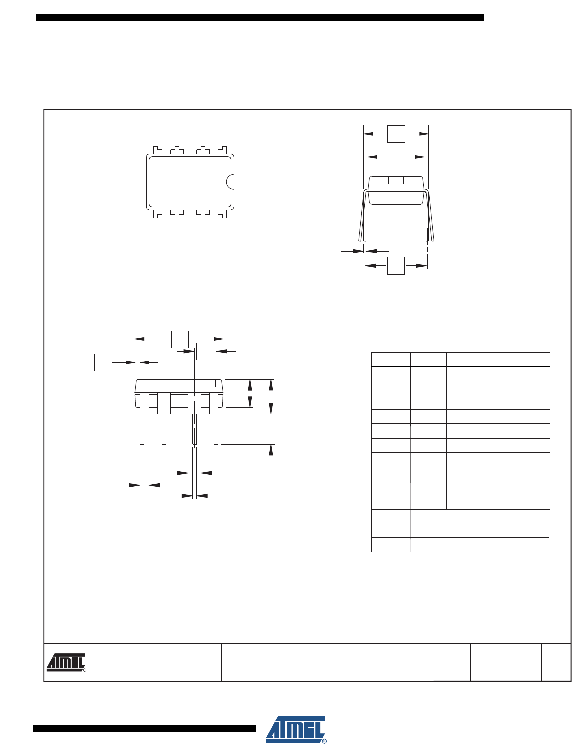
8S1 - JEDEC SOIC
1150 E. Cheyenne Mtn. Blvd.
Colorado Springs, CO 80906
TITLE DRAWING NO.
R
REV.
Note:
3/17/05
8S1, 8-lead (0.150" Wide Body), Plastic Gull Wing
Small Outline (JEDEC SOIC) 8S1 C
COMMON DIMENSIONS
(Unit of Measure = mm)
SYMBOL MIN NOM MAX NOTE
A1 0.10 – 0.25
These drawings are for general information only. Refer to JEDEC Drawing MS-012, Variation AA for proper dimensions, tolerances, datums, etc.
A 1.35 – 1.75
b 0.31 – 0.51
C 0.17 – 0.25
D 4.80 – 5.05
E1 3.81 – 3.99
E 5.79 – 6.20
e 1.27 BSC
L 0.40 – 1.27
θ 0° – 8°
ØØ
EE
11
NN
TOP VIEW
CC
E1E1
END VIEW
AA
bb
LL
A1A1
ee
DD
SIDE VIEW
17
5193F–SEEPR–1/08
AT93C46D
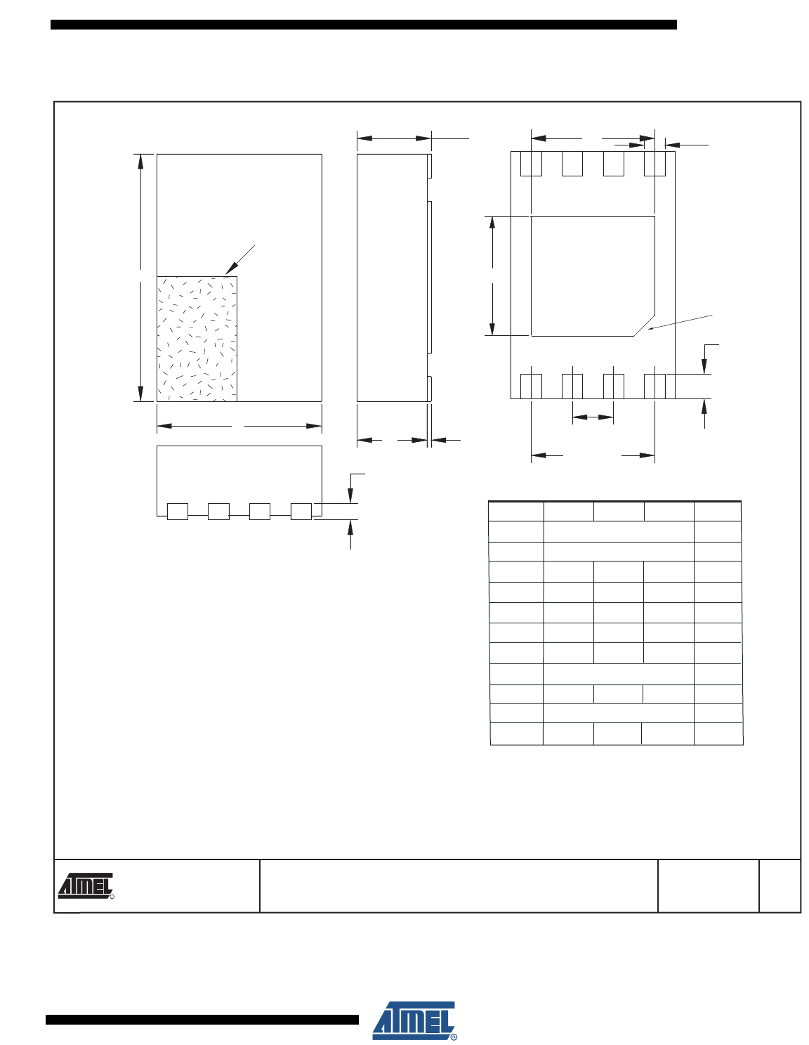
8A2 - TSSOP
2325 Orchard Parkway
San Jose, CA 95131
TITLE DRAWING NO.
R
REV.
5/30/02
COMMON DIMENSIONS
(Unit of Measure = mm)
SYMBOL MIN NOM MAX NOTE
D 2.90 3.00 3.10 2, 5
E 6.40 BSC
E1 4.30 4.40 4.50 3, 5
A – – 1.20
A2 0.80 1.00 1.05
b 0.19 – 0.30 4
e 0.65 BSC
L 0.45 0.60 0.75
L1 1.00 REF
8A2, 8-lead, 4.4 mm Body, Plastic
Thin Shrink Small Outline Package (TSSOP)
Notes: 1. This drawing is for general information only. Refer to JEDEC Drawing MO-153, Variation AA, for proper dimensions, tolerances,
datums, etc.
2. Dimension D does not include mold Flash, protrusions or gate burrs. Mold Flash, protrusions and gate burrs shall not exceed
0.15 mm (0.006 in) per side.
3. Dimension E1 does not include inter-lead Flash or protrusions. Inter-lead Flash and protrusions shall not exceed 0.25 mm
(0.010 in) per side.
4. Dimension b does not include Dambar protrusion. Allowable Dambar protrusion shall be 0.08 mm total in excess of the
b dimension at maximum material condition. Dambar cannot be located on the lower radius of the foot. Minimum space between
protrusion and adjacent lead is 0.07 mm.
5. Dimension D and E1 to be determined at Datum Plane H.
8A2 B
Side View
End View
Top View
A2
A
L
L1
D
123
E1
N
b
Pin 1 indicator
this corner
E
e
18
5193F–SEEPR–1/08
AT93C46D
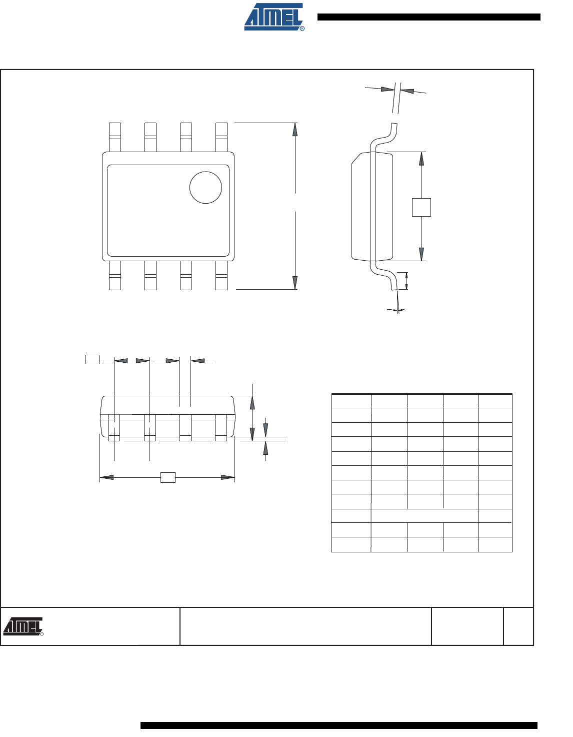
8U3-1 – dBGA2
R
1150 E. Cheyenne Mtn. Blvd.
Colorado Springs, CO 80906
TITLE
8U3-1, 8-ball, 1.50 x 2.00 mm Body, 0.50 mm pitch,
Small Die Ball Grid Array Package (dBGA2) PO8U3-1 B
DRAWING NO. REV.
COMMON DIMENSIONS
(Unit of Measure - mm)
SYMBOL MIN NOM MAX NOTE
A 0.73 0.79 0.85
A1 0.09 0.14 0.19
A2 0.40 0.45 0.50
b 0.20 0.25 0.30 2
D 1.50 BSC
E 2.0 BSC
e 0.50 BSC
e1 0.25 REF
d 1.00 BSC
d1 0.25 REF
5/3/05
b
D
E
A
A2
A1
8 SOLDER BALLS
1. This drawing is for general information only.
2. Dimension 'b' is measured at maximum solder ball diameter.
Bottem View
Side View
4
5
31
e
2
67
8
d
Top View
(e1)
(d1)
1.
PIN 1 BALL PAD CORNER
PIN 1 BALL PAD CORNER
19
5193F–SEEPR–1/08
AT93C46D
8Y6 – MLP 2x3
2325 Orchard Parkway
San Jose, CA 95131
TITLE DRAWING NO.
R
REV.
8Y6, 8-lead 2.0 x 3.0 mm Body, 0.50 mm Pitch, Utlra Thin Mini-Map,
Dual No Lead Package (DFN) ,(MLP 2x3)D
8Y6
10/16/07
Notes: 1. This drawing is for general information only. Refer to JEDEC Drawing MO-229, for proper dimensions,
tolerances, datums, etc.
2. Dimension b applies to metallized terminal and is measured between 0.15 mm and 0.30 mm from the terminal tip. If the
terminal has the optional radius on the other end of the terminal, the dimension should not be measured in that radius area.
3. Soldering the large thermal pad is optional, but not recommended. No electrical connection is accomplished to the
device through this pad, so if soldered it should be tied to ground
COMMON DIMENSIONS
(Unit of Measure = mm)
SYMBOL MIN NOM MAX NOTE
D 2.00 BSC
E 3.00 BSC
D2 1.40 1.50 1.60
E2 - - 1.40
A - - 0.60
A1 0.0 0.02 0.05
A2 - - 0.55
A3 0.20 REF
L 0.20 0.30 0.40
e 0.50 BSC
b 0.20 0.25 0.30 2
A2A2
b
(8X)
(8X)
Pin 1 IDPin 1 ID
Pin 1Pin 1
IndexIndex
AreaArea
A1A1
A3A3
D
E
A
L (8X)L (8X)
e (6X)e (6X)
1.50 REF.1.50 REF.
D2D2
E2E2
20
5193F–SEEPR–1/08
AT93C46D
7. Revision History
Doc. Rev. Date Comments
5193F 1/2008 Removed ‘preliminary’ status
5193E 11/2007 Modified ‘max’ value in AC Characteristics table
5193D 8/2007
Moved Pinout figure
Added new feature for Die Sales
Modified Ordering Information table layout
Modified Park Marking Schemes
5193C 6/2007
Updated to new template
Added Product Markup Scheme
Added Technical email contact
5193C 3/2007 Corrected Figures 4 and 5.
5193B 2/2007 Added ‘Ultra Thin’ description to 8-lead Mini-MAP package.
5193A 1/2007 Initial document release.
5193F–SEEPR–1/08
Headquarters International
Atmel Corporation
2325 Orchard Parkway
San Jose, CA 95131
USA
Tel: 1(408) 441-0311
Fax: 1(408) 487-2600
Atmel Asia
Room 1219
Chinachem Golden Plaza
77 Mody Road Tsimshatsui
East Kowloon
Hong Kong
Tel: (852) 2721-9778
Fax: (852) 2722-1369
Atmel Europe
Le Krebs
8, Rue Jean-Pierre Timbaud
BP 309
78054 Saint-Quentin-en-
Yvelines Cedex
France
Tel: (33) 1-30-60-70-00
Fax: (33) 1-30-60-71-11
Atmel Japan
9F, Tonetsu Shinkawa Bldg.
1-24-8 Shinkawa
Chuo-ku, Tokyo 104-0033
Japan
Tel: (81) 3-3523-3551
Fax: (81) 3-3523-7581
Product Contact
Web Site
www.atmel.com
Technical Support
s_eeprom@atmel.com
Sales Contact
www.atmel.com/contacts
Literature Requests
www.atmel.com/literature
Disclaimer: The information in this document is provided in connection with Atmel products. No license, express or implied, by estoppel or otherwise, to any
intellectual property right is granted by this document or in connection with the sale of Atmel products. EXCEPT AS SET FORTH IN ATMEL’S TERMS AND CONDI-
TIONS OF SALE LOCATED ON ATMEL’S WEB SITE, ATMEL ASSUMES NO LIABILITY WHATSOEVER AND DISCLAIMS ANY EXPRESS, IMPLIED OR STATUTORY
WARRANTY RELATING TO ITS PRODUCTS INCLUDING, BUT NOT LIMITED TO, THE IMPLIED WARRANTY OF MERCHANTABILITY, FITNESS FOR A PARTICULAR
PURPOSE, OR NON-INFRINGEMENT. IN NO EVENT SHALL ATMEL BE LIABLE FOR ANY DIRECT, INDIRECT, CONSEQUENTIAL, PUNITIVE, SPECIAL OR INCIDEN-
TAL DAMAGES (INCLUDING, WITHOUT LIMITATION, DAMAGES FOR LOSS OF PROFITS, BUSINESS INTERRUPTION, OR LOSS OF INFORMATION) ARISING OUT OF
THE USE OR INABILITY TO USE THIS DOCUMENT, EVEN IF ATMEL HAS BEEN ADVISED OF THE POSSIBILITY OF SUCH DAMAGES. Atmel makes no
representations or warranties with respect to the accuracy or completeness of the contents of this document and reserves the right to make changes to specifications
and product descriptions at any time without notice. Atmel does not make any commitment to update the information contained herein. Unless specifically provided
otherwise, Atmel products are not suitable for, and shall not be used in, automotive applications. Atmel’s products are not intended, authorized, or warranted for use
as components in applications intended to support or sustain life.
©2008 Atmel Corporation. All rights reserved. Atmel®, logo and combinations thereof, and others, are registered trademarks or trademarks
of Atmel Corporation or its subsidiaries. Other terms and product names may be trademarks of others.