ATX2005 Datasheet. Www.s Manuals.com. R1.0 Atx
User Manual: Datasheets ATX2005.
Open the PDF directly: View PDF ![]() .
.
Page Count: 7

ATX 2005
POWER SUPPLY PWM SUPERVISOR
Power Supply Pulse Width Modulation Integrated Circuit Controller
Specs
(English version)
version 1.0
April, 2012
Tra
nslated from
c
hin
e
s
e
by
:
Esquiloesperto
(Messias-BH.)
Original chinese document
down
loaded from
:
http://www.4shared.com/office/_E8A5czR/ATX_2005.html
ATX 2005
Specification: v-1.0
Page
02
General Description
The integrated circuit ATX-2005 is a pulse width modulation (PWM) controller, which can be used in the
power supplies' secondary side, ready to provide the total voltage and load switching control.
ATX-2005 has all inside functions for protection and control, undervoltage/overvoltage detection, output
voltage status monitor (PG), external remote control (REM)... and more.
The ATX-2005 is able to set the power supply's behavior in order to reduce the external devices usage to
get required control. The undervoltage (UVP) and overvoltage (OVP) modules assist the 3.3V, 5V, and
12V voltage levels. The PP function is set to monitor power and negative voltages, and a built-in shunt
regulator module (the 431 shunt regulator) is built to make the PWM's correct level control, providing a
stable output voltage through a group of amplifiers that monitor the feedback pattern. Besides, the anti-
noise filter prevents malfunction caused by outer interference.
Features
• 3.3V / 5V e 12V Overvoltage Protection
• 3.3V / 5V / 12V Undervoltage Protection
• 3.3V / 5V / 12V Undervoltage Detection
• PP: Overcharge and Negative voltage protection
• Pulse Width Modulation (PWM) control device
• "Soft-Start" improvement, using external capacitor to perform easy quick start
• RI – External resistor to settle down the internal reference current, noise immunity and delay time
protection
• PG-Shifter: monitor the normal voltage condition test
• Undervoltage Protection (UVP): noise reduction function added
• Overvoltage Protection (OVP): noise reduction function added
• Undervoltage Protection (UVP): 250ms delay time function
• Remote switching control (REM): noise reduction function added
• Built-in shunt regulator to provide stable output voltage (431 Shunt Regulator)
• Package type: 16-Pins Dual In-line Package (DIP-16)
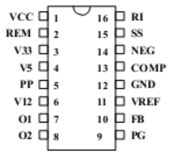
Pin Assignment
ATX 2005
Specification: v-1.0
Page
03
Pinning
Pin Symbol
Function Description
1 VCC Source Positive power source input
2 REM Input
Remote switch on/off signal (low: On / high: Off)
3 V3.3 Input
3,3V voltage monitor
4 V5 Input
5V voltage monitor
5 PP Input
Power/ Negative voltage protection input
6 V12 Input
12V voltage monitor
7 O1 Output
Open collector output driver #1
8 O2 Output
Open collector output driver #2
9 PG Output
"Power Good" status sensor input
10 FB Output
Shunt (shunt regulator) output
11 VREF Input Shunt (shunt regulator) input
12 GND Ground Negative power source input
13 COMP Output Compensation OpAmp output
– Duty Cycle Control
14 NEG Input Compensation OpAmp negative input
– Negative Feedback Sensor
15 SS Input Compensation OpAmp positive input
– Soft-start Capacitor pin
16 RI Input
External connection of a resistor to set the internal
reference current value, this feature can also adjust
the internal noise immunity and protection delay time
Limiting Values
Item Symbol Conditions
Min. Typ. Max. Unit
Supply
voltage
VCC 4,5 5 5,5 V
Power
dissaption
Pd -- 1000 -- mW
Operating
temperature
-10 -- +70 °C
Storage
temperature
-65 -- +150 °C
ATX 2005
Specification: v-1.0
Page
04
Electrical Characteristics
TA temperature = 25 °C, main voltage VCC = 5V
Voltage protection levels (V33, V5, V12, PP)
Item Symbol Conditions Min. Typ. Max. Unit
Overvoltage
• Protection
V33 PG low 3.9 4.1 4.4 V
V5 PG low 5.6 6.0 6.4 V
V12 PG low 13.4 14.0 14.4 V
PP PG low 2.3 2.6 2.8 V
Undervoltage
• Protection
V33 PG low 2.0 2.4 -- V
V5 PG low 3.0 3.6 -- V
V12 PG low 5.9 7.1 -- V
Undervoltage
• Detection
V33 PG low 2.6 2.9 3.1 V
V5 PG low 4.1 4.45 4.7 V
V12 PG low 9.6 10.3 10.7 V
Undervoltage
• Delay Time Td1 Remon On/Off 150 250 350 ms
Start Switch – On/Off (REM)
Item Symbol Conditions
Min. Typ. Max. Unit
High Level
Input Voltage
VIH --- 1.8 V
Low Level
Input Voltage
VIL --- 0.8 V
REMOTE
Delay Time
t
db-rem
--- 22 28 34 ms
REMOTE OFF
Delay Time
t
db-remoff
--- 4 ms
Pulse Width Modulation (PWM) Output 1, 2 (O1, O2)
Item Symbol Conditions
Min. Typ. Max. Unit
Leakage
Current
I
LEAKAGE
Output = 5v -- 5 -- uA
Duty Cycle
(máx.)
DC
max
Duty cycle
(max.) 84 -- 93
﹪
Power Good Sensor (PG)
Item Symbol Conditions
Min. Typ. Max. Unit
PG – Leakage
Current
I
PGL
PG=5V -- -- 2 uA
PG – Delay
Delay Time
Td -- 100 220 400 ms
Output Voltage
Low level
V
OL
I
PGO
=10mA -- 0.2 0.4 V
ATX 2005
Specification: v-1.0
Page
05
Shunt Regulator (VREF FB)
Item Symbol Conditions
Min. Typ. Max. Unit
Reference voltage
for Shunt Reg.
V
REF
I
FB
= 0.5mA 2.45 2.50 2.55 V
Output Sink
Current
I
OUT
V
FB
> 3V 10 -- -- mA
Op-amp OP (COMP NEG, e SS)
Item Symbol Conditions
Min. Typ. Max. Unit
Close Loop
Voltage gain
-- 0.5V~3.5V --
65 --
dB
Cross over
crossing point
-- 0 dB --
310 --
KHZ
Soft-start (SS,RI)
Item Symbol Conditions
Min. Typ. Max. Unit
Soft Start
charge current
I
CH
RI=75KΩ 8.0 9.5 11.0 µA
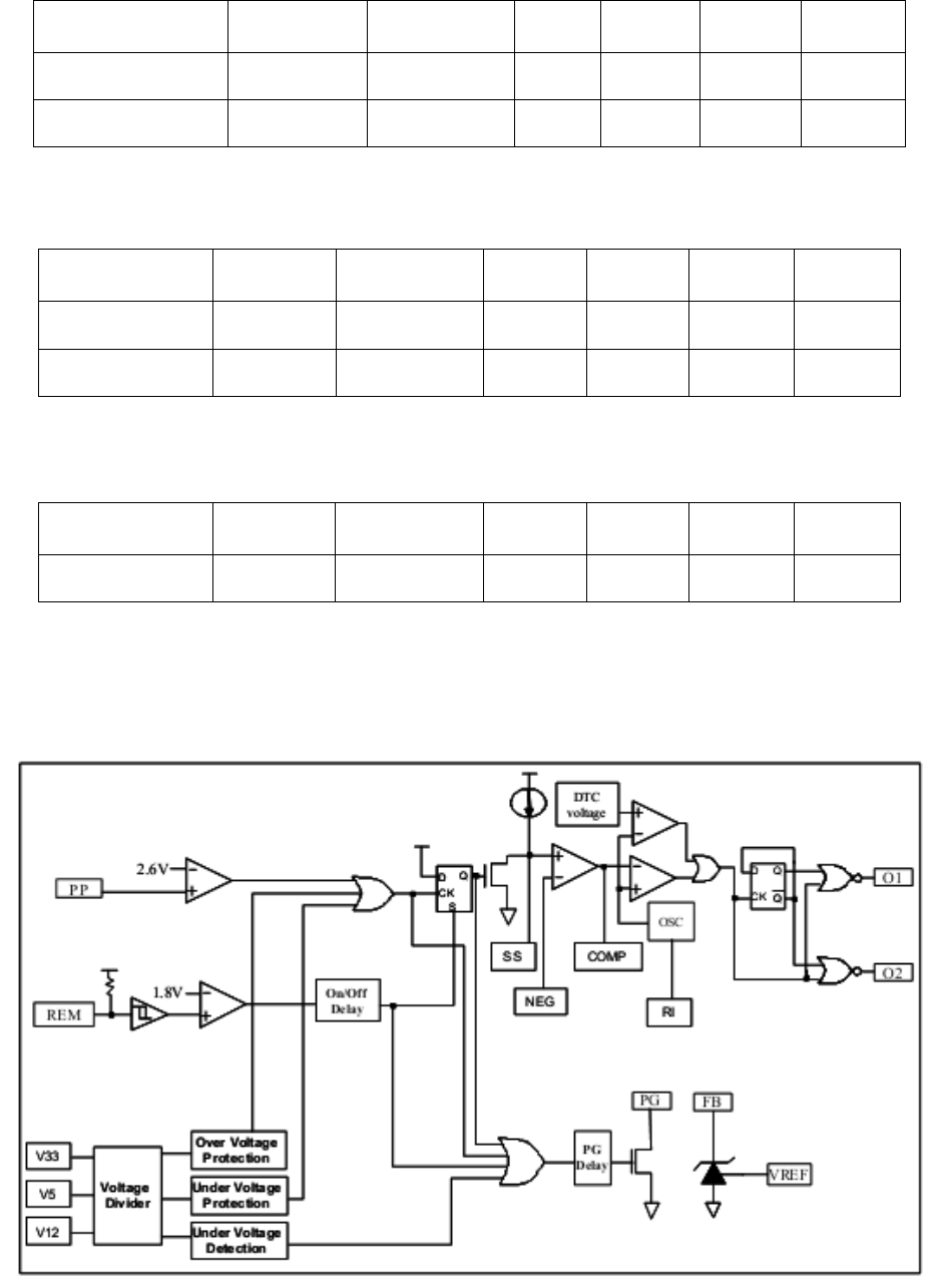
Reference:
Internal Control Circuit Diagram

ATX 2005
Specification: v-1.0
Page
06
Package Outline