B156XTN02.0 Datasheet. Www.s Manuals.com. R0.1 Auo
User Manual: Datasheets B156XTN02.0.
Open the PDF directly: View PDF ![]() .
.
Page Count: 29
1 of 28
AU OPTRONICS CORPORATION
Product Specification
B156XTN02.0 Document Version : 0.1
(
√
√√
√
) Preliminary Specifications
(
) Final Specifications
Module 15.6”HD 16:9 Color TFT-LCD with LED Backlight design
Model Name B156XTN02.0 (H/W:0A)
Note ( ) LED Backlight with driving circuit design
Customer Date
Checked &
Approved by
Date
Note: This Specification is subject to
change without notice.
Approved by Date
Buffy Chen
06/27/2011
Prepared by Date
Alonso JU Hsu
06/27/2011
NBBU Marketing Division
AU Optronics corporation

2 of 28
AU OPTRONICS CORPORATION
Product Specification
B156XTN02.0 Document Version : 0.1
Contents
1. Handling Precautions .......................................................................................4
2. General Description..........................................................................................5
2.1 General Specification .........................................................................................................5
2.2 Optical Characteristics .......................................................................................................6
3. Functional Block Diagram..............................................................................11
4. Absolute Maximum Ratings ...........................................................................12
4.1 Absolute Ratings of TFT LCD Module...............................................................................12
4.2 Absolute Ratings of Environment.....................................................................................12
5. Electrical Characteristics ...............................................................................13
5.1 TFT LCD Module ..................................................................................................................13
5.2 Backlight Unit ......................................................................................................................15
6. Signal Interface Characteristic......................................................................16
6.1 Pixel Format Image ............................................................................................................16
6.2 The Input Data Format ......................................................................................................17
6.3 Integration Interface Requirement .................................................................................18
6.4 Interface Timing..................................................................................................................20
7. Panel Reliability Test .......................................................................................22
7.1 Vibration Test.......................................................................................................................22
7.2 Shock Test............................................................................................................................22
7.3 Reliability Test......................................................................................................................22
8. Mechanical Characteristics...........................................................................23
8.1 LCM Outline Dimension.....................................................................................................23
8.2 Screw Hole Depth and Center Position..........................................................................25
9. Shipping and Package ..................................................................................26
9.1 Shipping Label Format ......................................................................................................26
9.2 Carton Package.................................................................................................................27
9.3 Shipping Package of Palletizing Sequence...................................................................28
10. Appendix: EDID Description.........................................................................28

3 of 28
AU OPTRONICS CORPORATION
Product Specification
B156XTN02.0 Document Version : 0.1
Record of Revision
Version and Date Page
Old description New Description Remark
0.1 2011/06/27 All First Edition for Customer

4 of 28
AU OPTRONICS CORPORATION
Product Specification
B156XTN02.0 Document Version : 0.1
1. Handling Precautions
1) Since front polarizer is easily damaged, pay attention not to scratch it.
2) Be sure to turn off power supply when inserting or disconnecting from input
connector.
3) Wipe off water drop immediately. Long contact with water may cause
discoloration or spots.
4) When the panel surface is soiled, wipe it with absorbent cotton or other soft
cloth.
5) Since the panel is made of glass, it may break or crack if dropped or bumped
on hard surface.
6) Since CMOS LSI is used in this module, take care of static electricity and insure
human earth when handling.
7) Do not open nor modify the Module Assembly.
8) Do not press the reflector sheet at the back of the module to any directions.
9) At the insertion or removal of the Signal Interface Connector, be sure not to
rotate nor tilt the Interface Connector of the TFT Module.
11) After installation of the TFT Module into an enclosure (Notebook PC Bezel, for
example), do not twist nor bend the TFT Module even momentary. At designing
the enclosure, it should be taken into consideration that no bending/twisting
forces are applied to the TFT Module from outside. Otherwise the TFT Module
may be damaged.
12) Small amount of materials having no flammability grade is used in the LCD module.
The LCD module should be supplied by power complied with requirements of Limited
Power Source (IEC60950 or UL1950), or be applied exemption.
13) Disconnecting power supply before handling LCD modules, it can prevent electric
shock, DO NOT TOUCH the electrode parts, cables, connectors and LED circuit part of
TFT module that a LED light bar build in as a light source of back light unit. It can
prevent electronic breakdown.
5 of 28
AU OPTRONICS CORPORATION
Product Specification
B156XTN02.0 Document Version : 0.1
2. General Description
B156XTN02.0 is a Color Active Matrix Liquid Crystal Display composed of a TFT LCD panel,
a driver circuit, and LED backlight system. The screen format is intended to support the
16:9 HD, 1366(H) x768(V) screen and 262k colors (RGB 6-bits data driver) with LED
backlight driving circuit. All input signals are LVDS interface compatible.
B156XTN02.0 is designed for a display unit of notebook style personal computer and
industrial machine.
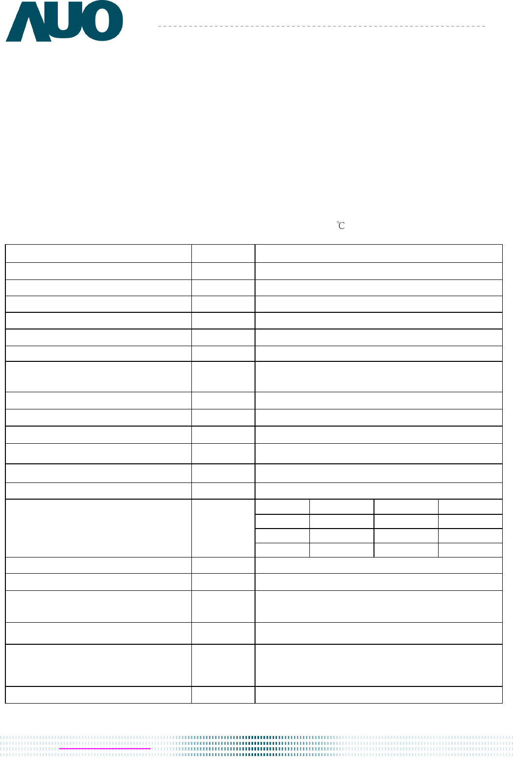
2.1 General Specification
The following items are characteristics summary on the table at 25 condition:
Items Unit Specifications
Screen Diagonal [mm] 394.91
Active Area [mm] 344.23 X193.54
Pixels H x V 1366x3(RGB) x 768
Pixel Pitch [mm] 0.252X0.252
Pixel Format R.G.B. Vertical Stripe
Display Mode Normally White
White Luminance (I
LED
=25mA)
(Note: ILED is LED current)
[cd/m
2
] 220 typ. (5 points average)
187 min. (5 points average)
Luminance Uniformity 1.25 max. (5 points)
Contrast Ratio 500 typ
Response Time [ms] 16 Max
Nominal Input Voltage VDD [Volt] +3.3 typ.
Power Consumption [Watt] 5.0 max. (Include Logic and Blu power)
Weight [Grams] 450 max.
Min. Typ. Max.
Length
-
359.3
359.8
Width
-
209.5
210
Physical Size
Include bracket
[mm]
Thickne -
-
5.5
Electrical Interface 1 channel LVDS
Glass Thickness [mm] 0.5
Surface Treatment Glare, Hardness 3H,
Reflection 4.3%
Support Color 262K colors ( RGB 6-bit )
Temperature Range
Operating
Storage (Non
-
Operating)
[
o
C]
[
o
C]
0 to +50
-20 to +60
RoHS Compliance
RoHS Compliance
6 of 28
AU OPTRONICS CORPORATION
Product Specification
B156XTN02.0 Document Version : 0.1
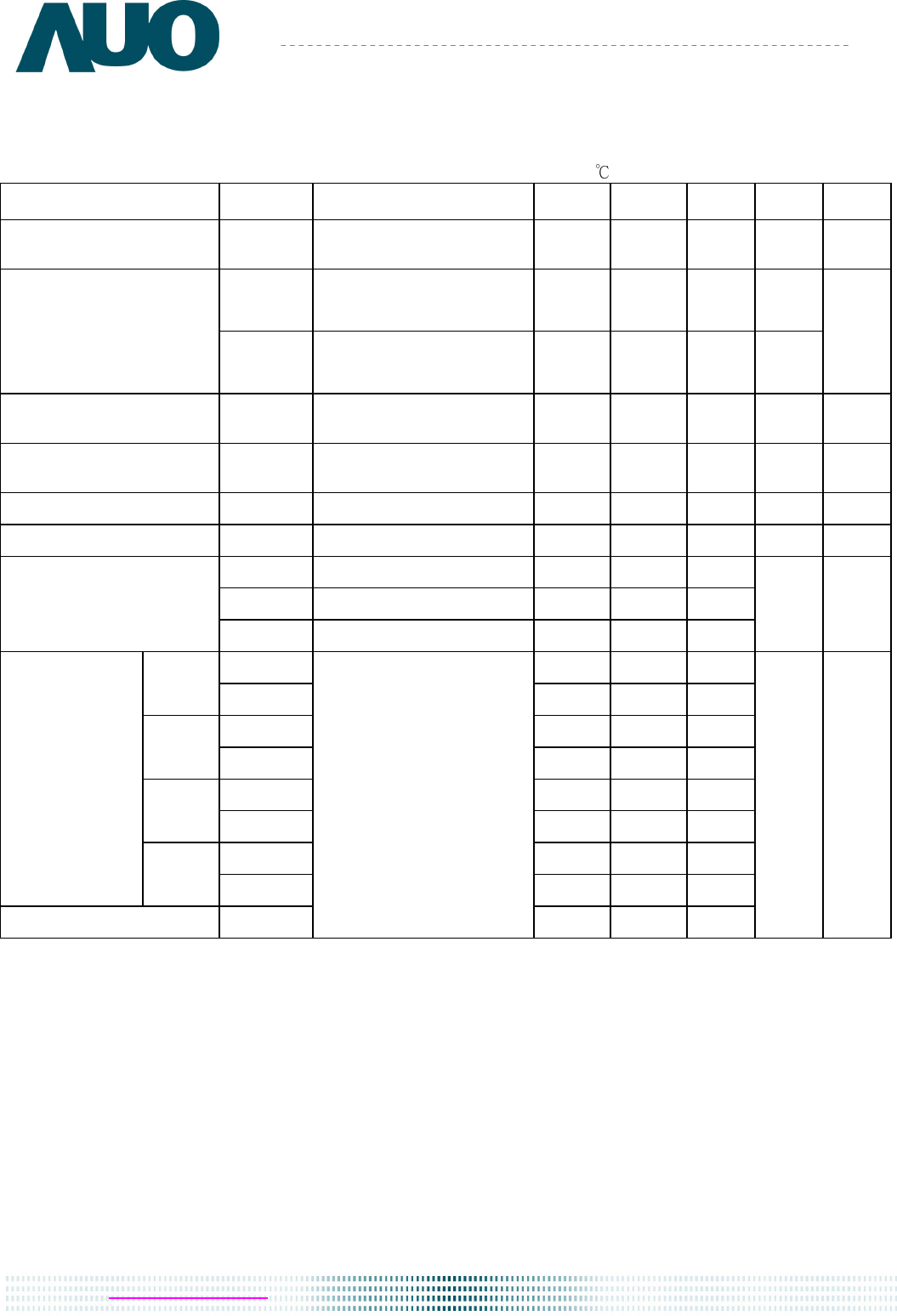
2.2 Optical Characteristics
The optical characteristics are measured under stable conditions at 25 (Room Temperature) :
Item Symbol
Conditions Min. Typ. Max.
Unit Note
White Luminance
I
LED
=25mA 5 points average 187 220 -
cd/m
2
1, 4, 5.
θ
R
θ
L
Horizontal (Right)
CR = 10 (Left)
40
40
45
45
-
-
degree
Viewing Angle
ψ
H
ψ
L
Vertical (Upper)
CR = 10 (Lower)
10
30
15
35
-
-
4, 9
Luminance
Uniformity δ
5P
5 Points - - 1.25
1, 3, 4
Luminance
Uniformity δ
13P
13 Points - - 1.50
2, 3, 4
Contrast Ratio CR - 500 -
4, 6
Cross talk % 4
4, 7
T
r
Rising - 6 -
T
f
Falling - 2 -
Response Time
T
RT
Rising + Falling - 8 16
msec
4, 8
Rx TBD TBD TBD
Red Ry TBD TBD TBD
Gx TBD TBD TBD
Green
Gy TBD TBD TBD
Bx TBD TBD TBD
Blue By TBD TBD TBD
Wx 0.283
0.313
0.343
Color /
Chromaticity
Coodinates
White
Wy 0.299
0.329
0.359
NTSC %
CIE 1931
- 60 -
4
7 of 28
AU OPTRONICS CORPORATION
Product Specification
B156XTN02.0 Document Version : 0.1
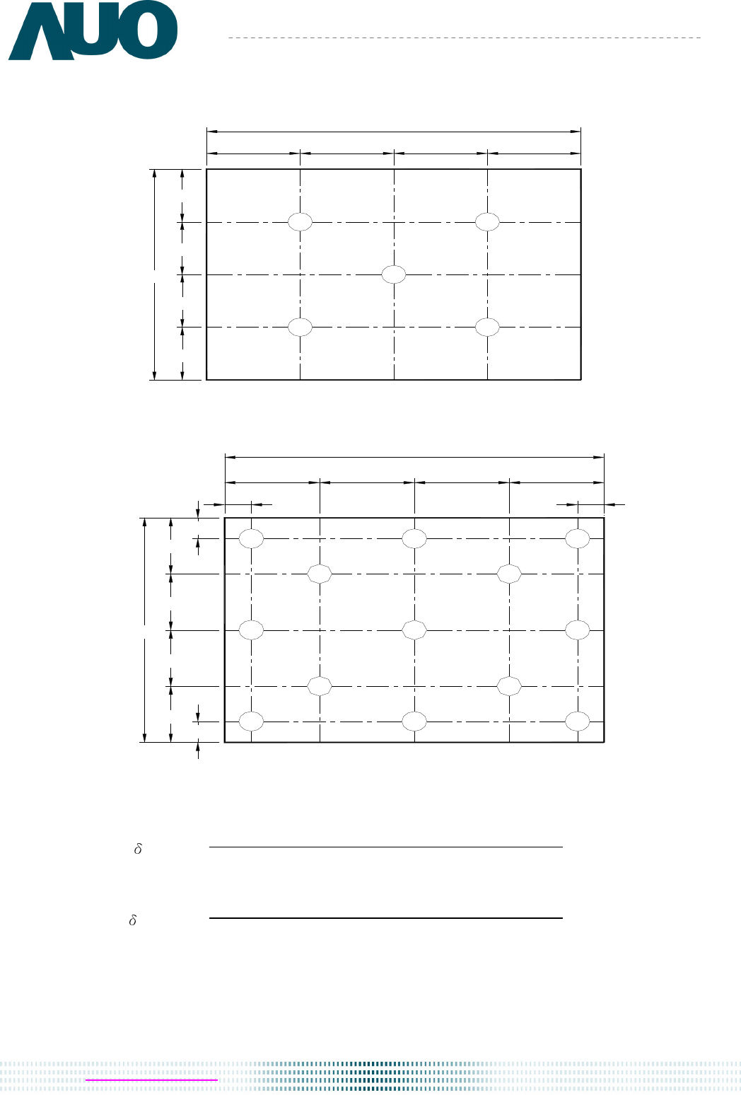
Note 1: 5 points position (Ref: Active area)
1 2
3
45
H /4
H /4
H /4
H /4
H
W
W /4 W /4 W /4 W /4
Note 2: 13 points position (Ref: Active area)
W /4
W
W /4
H
H /4
H /4
H /4
H /4
7
9
1 0
W /4
1
8
W /4
1 0
1 0
1 0
1 0
23
1 3
1 2
4 5
6
1 1
Note 3: The luminance uniformity of 5 or13 points is defined by dividing the maximum luminance values by
the minimum test point luminance
Note 4: Measurement method
The LCD module should be stabilized at given temperature for 30 minutes to avoid abrupt temperature
change during measuring. In order to stabilize the luminance, the measurement should be executed after
W13
=
Maximum Brightness of thirteen points
Minimum Brightness of thirteen points
Maximum Brightness of five points
W5
=
Minimum Brightness of five points
8 of 28
AU OPTRONICS CORPORATION
Product Specification
B156XTN02.0 Document Version : 0.1
lighting Backlight for 30 minutes in a stable, windless and dark room, and it should be measured in the
center of screen.
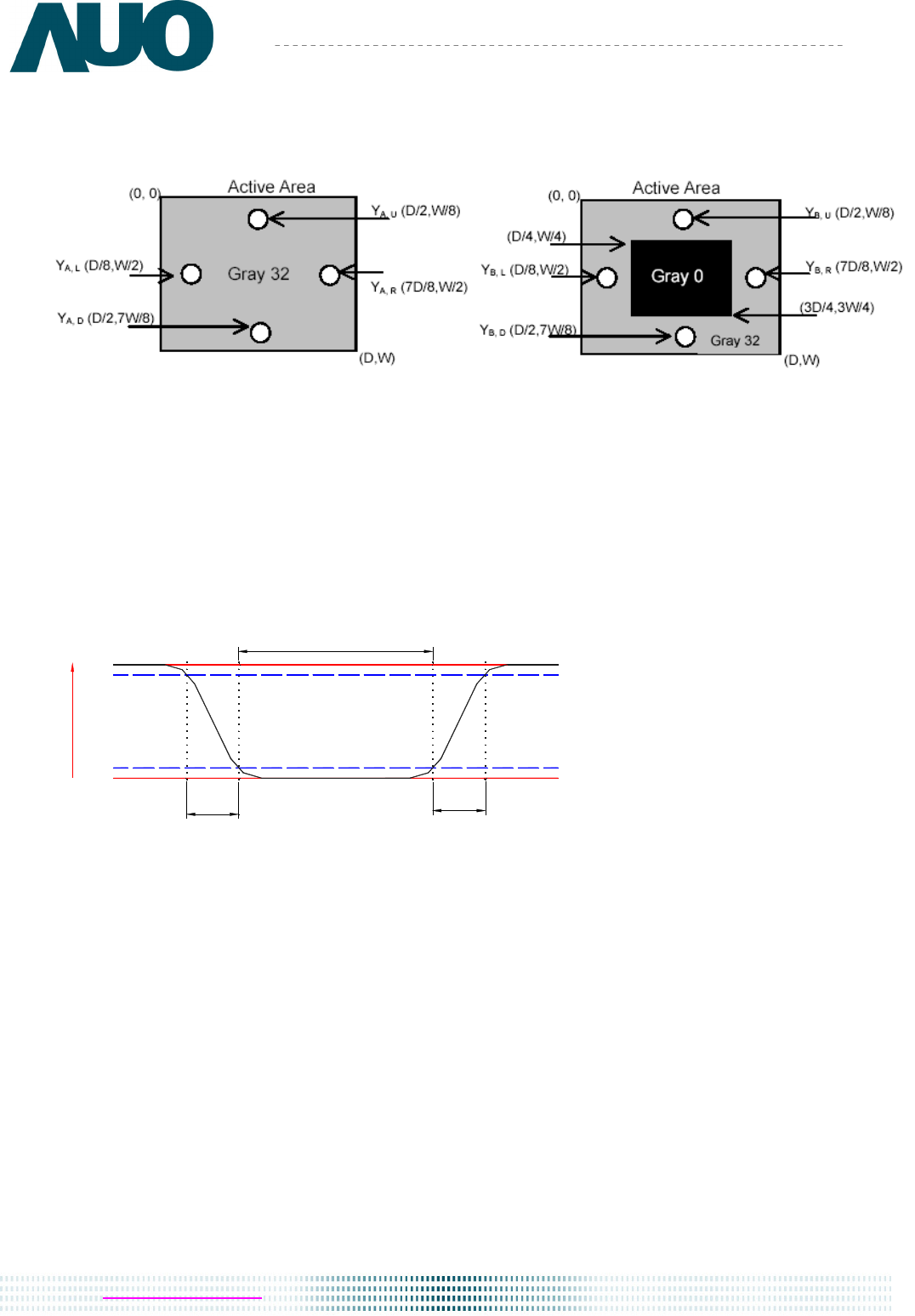
Note 5 Definition of Average Luminance of White (Y
L
):
Measure the luminance of gray level 63 at 5 points Y
L
= [L (1)+ L (2)+ L (3)+ L (4)+ L (5)] / 5
L (x) is corresponding to the luminance of the point X at Figure in Note (1).
Note 6 Definition of contrast ratio:
Contrast ratio is calculated with the following formula.
Note 7 Definition of Cross Talk (CT)
CT = | Y
B
– Y
A
| / Y
A
× 100 (%)
Where
Y
A
= Luminance of measured location without gray level 0 pattern (cd/m
2
)
Y
B
= Luminance of measured location with gray level 0 pattern (cd/m
2
)
Center of the screen
TFT
-
LCD Module
50 cm
Photo detector
LCD Panel
Field=2
Contrast ratio (CR)=
Brightness on the “White” state
Brightness on the “Black” state
9 of 28
AU OPTRONICS CORPORATION
Product Specification
B156XTN02.0 Document Version : 0.1
Note 8: Definition of response time:
The output signals of BM-7 or equivalent are measured when the input signals are changed from “Black”
to “White” (falling time) and from “White” to “Black” (rising time), respectively. The response time interval
between the 10% and 90% of amplitudes. Refer to figure as below.
Signal(Relative value)
"Black"
Tr Tf
"White""White"
0%
10%
90%
100%
10 of 28
AU OPTRONICS CORPORATION
Product Specification
B156XTN02.0 Document Version : 0.1
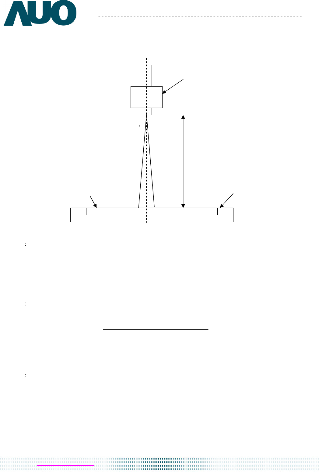
Note 9. Definition of viewing angle
Viewing angle is the measurement of contrast ratio 10, at the screen center, over a 180° horizontal
and 180° vertical range (off-normal viewing angles). The 180° viewing angle range is broken down as
follows; 90° (θ) horizontal left and right and 90° (Φ) vertical, high (up) and low (down). The measurement
direction is typically perpendicular to the display surface with the screen rotated about its center to
develop the desired
measurement viewing angle.
11 of 28
AU OPTRONICS CORPORATION
Product Specification
B156XTN02.0 Document Version : 0.1
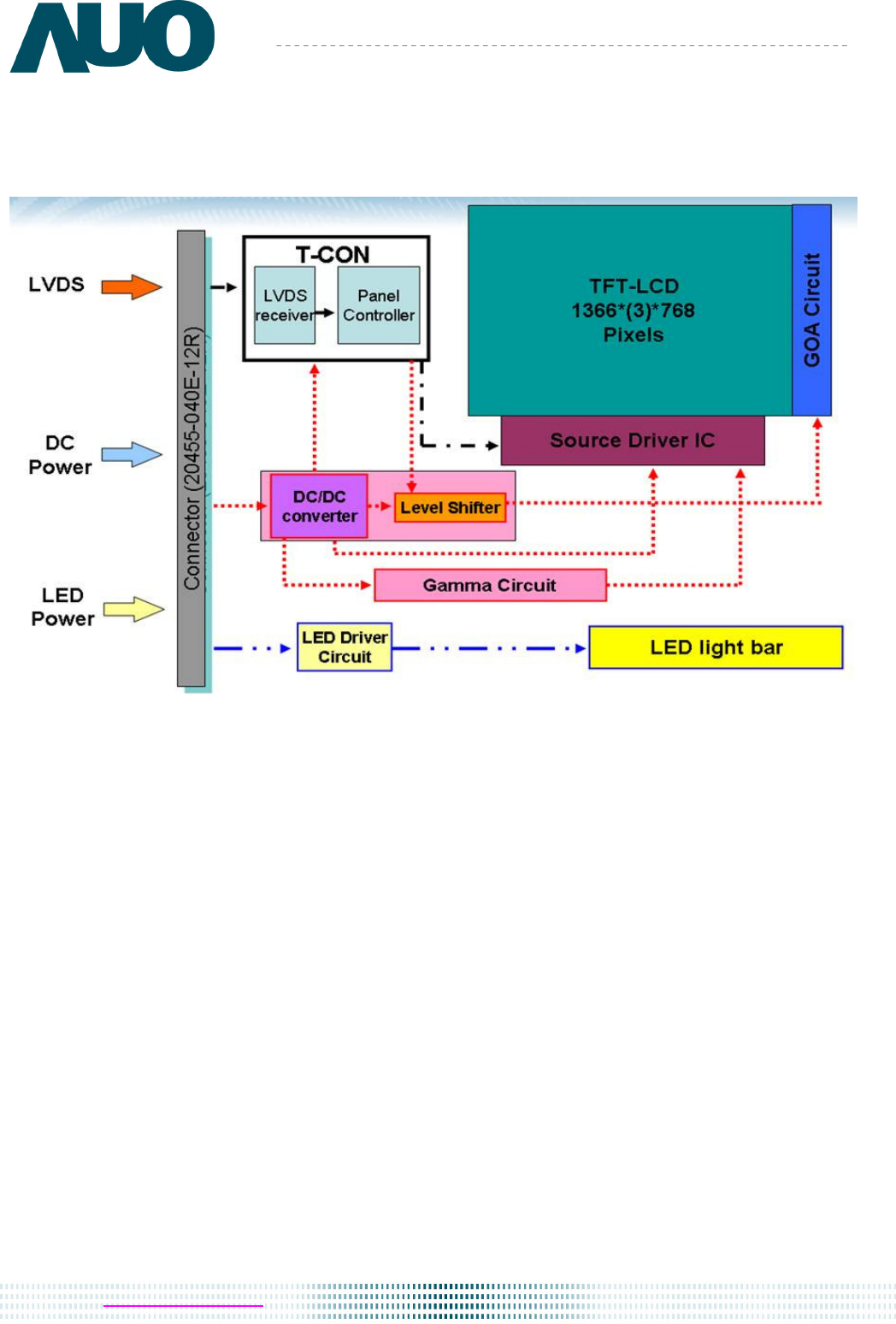
3. Functional Block Diagram
The following diagram shows the functional block of the 15.6 inches wide Color TFT/LCD 40 Pin one
channel Module
12 of 28
AU OPTRONICS CORPORATION
Product Specification
B156XTN02.0 Document Version : 0.1
4. Absolute Maximum Ratings
An absolute maximum rating of the module is as following:
4.1 Absolute Ratings of TFT LCD Module
Item Symbol Min Max Unit Conditions
Logic/LCD Drive Vin -0.3 +4.0 [Volt] Note 1,2
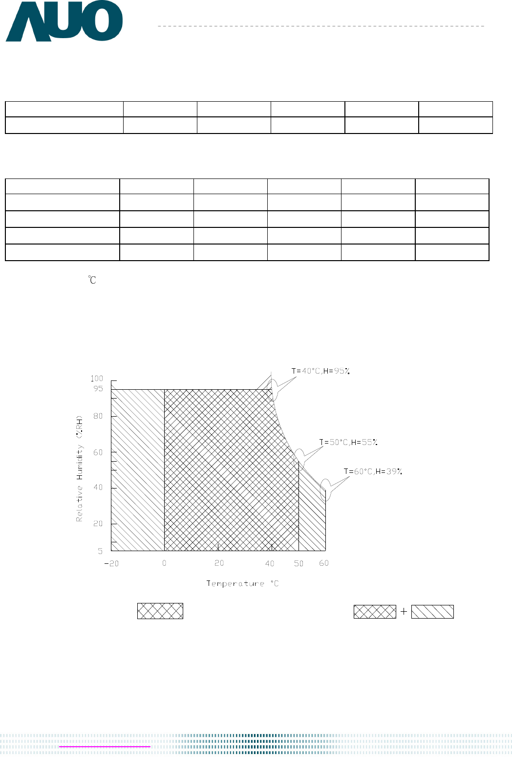
4.2 Absolute Ratings of Environment
Item Symbol Min Max Unit Conditions
Operating TOP 0 +50 [
o
C] Note 4
Operation Humidity HOP 5 95 [%RH] Note 4
Storage Temperature
TST -20 +60 [
o
C] Note 4
Storage Humidity HST 5 95 [%RH] Note 4
Note 1: At Ta (25 )
Note 2: Permanent damage to the device may occur if exceed maximum values
Note 3: LED specification refer to section 5.2
Note 4: For quality performance, please refer to AUO IIS (Incoming Inspection Standard).
Twb=39°C
Operating Range
Storage Range
13 of 28
AU OPTRONICS CORPORATION
Product Specification
B156XTN02.0 Document Version : 0.1
5. Electrical Characteristics
5.1 TFT LCD Module
5.1.1 Power Specification
Input power specifications are as follows;
The power specification are measured under 25 and frame frenquency under 60Hz
Symble Parameter Min
Typ Max Units Note
VDD Logic/LCD Drive
Voltage
3.0
3.3 3.6 [Volt]
PDD VDD Power -
- 1.3 [Watt] Note 1
IDD IDD Current - 250 400 [mA] Note 1
I
Rush
Inrush Current
- -
1500 [mA] Note 2
VDDrp Allowable
Logic/LCD Drive
Ripple Voltage
- -
100 [mV]
p-p
Note 1 : Maximum Measurement Condition Black Pattern at 3.3V driving voltage. (P
max
=V
3.3
x I
black
)
Note 2 Measure Condition
90%
10%
Vin rising time
0V
3.3V
0.5ms
14 of 28
AU OPTRONICS CORPORATION
Product Specification
B156XTN02.0 Document Version : 0.1
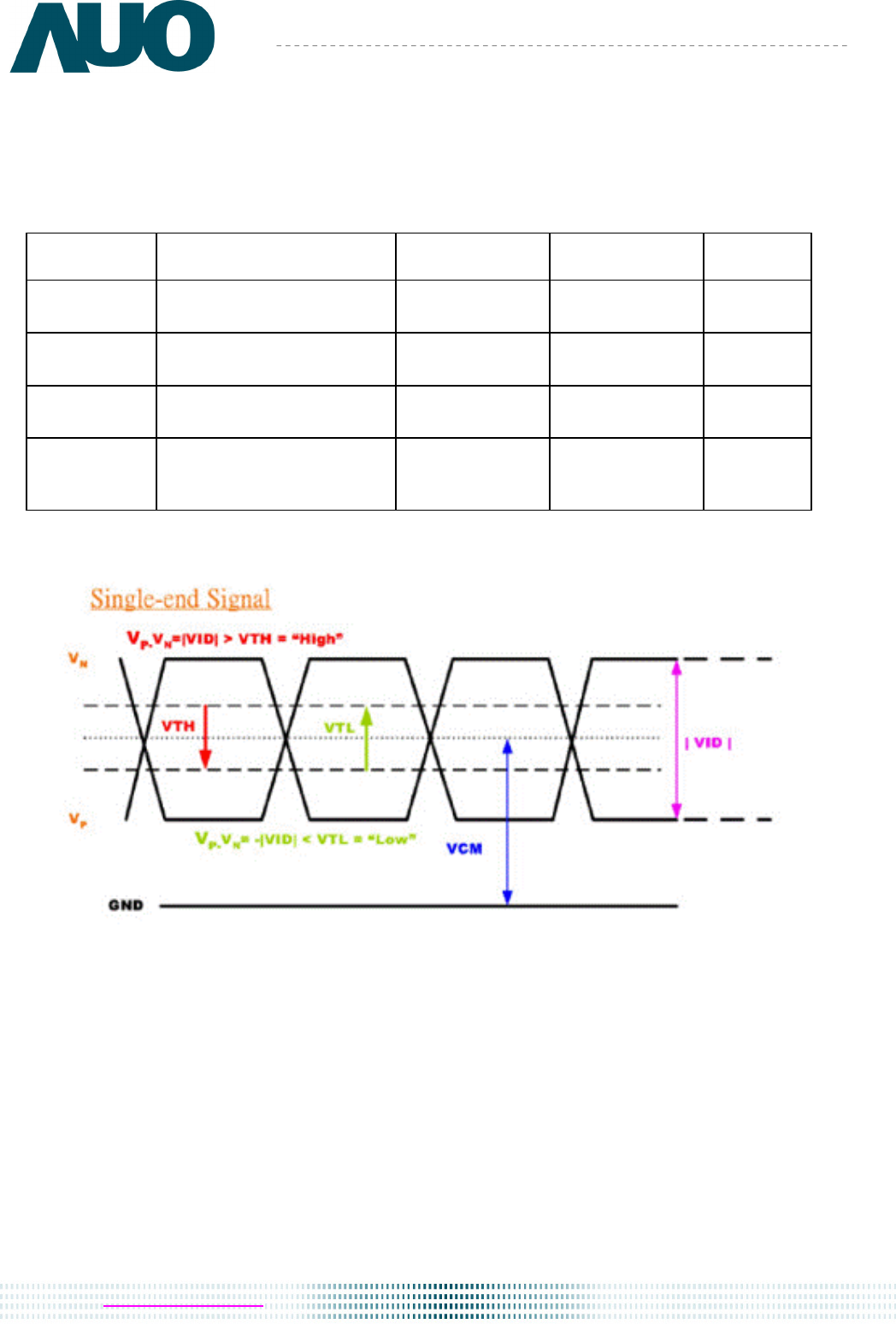
5.1.2 Signal Electrical Characteristics
Input signals shall be low or High-impedance state when VDD is off.
Signal electrical characteristics are as follows;
Parameter Condition Min Max Unit
V
TH
Differential Input High
Threshold (Vcm=+1.2V) 100
[mV]
V
TL
Differential Input Low
Threshold (Vcm=+1.2V)
-100 -
[mV]
|V
ID
| Differential Input
Voltage
100
600
[mV]
V
CM
Differential Input
Common Mode
Voltage
1.125 1.375 [V]
Note: LVDS Signal Waveform
15 of 28
AU OPTRONICS CORPORATION
Product Specification
B156XTN02.0 Document Version : 0.1
5.2 Backlight Unit
5.2.1 LED characteristics
Parameter Symbol Min Typ Max Units Condition
Backlight Power
Consumption PLED - 3.05 3.7 [Watt]
(Ta=25 ), Note 1
Vin =12V
LED Life-Time N/A 12,000 - - Hour (Ta=25 ), Note 2
I
F
=20 mA
Note 1: Calculator value for reference P
LED
= V
F
(Normal Distribution) * I
F
(Normal Distribution) / Efficiency
Note 2: The LED life-time define as the estimated time to 50% degradation of initial luminous.
5.2.2 Backlight input signal characteristics
Parameter Symbol Min Typ Max
Units Remark
LED Power Supply VLED 6.0 12.0 21.0 [Volt]
LED Enable Input
High Level 2.5 - 5.5 [Volt]
LED Enable Input
Low Level
VLED_EN - - 0.8 [Volt]
PWM Logic Input
High Level
2.5 - 5.5 [Volt]
PWM Logic Input
Low Level
VPWM_EN - - 0.8 [Volt]
PWM Input Frequency FPWM 100 - 20K Hz
PWM Duty Ratio Duty 5 -- 100 %
Define as
Connector
Interface
(Ta=25 )
16 of 28
AU OPTRONICS CORPORATION
Product Specification
B156XTN02.0 Document Version : 0.1
6. Signal Interface Characteristic
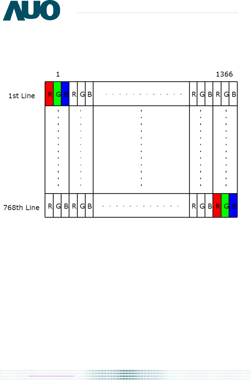
6.1 Pixel Format Image
Following figure shows the relationship of the input signals and LCD pixel format.
17 of 28
AU OPTRONICS CORPORATION
Product Specification
B156XTN02.0 Document Version : 0.1
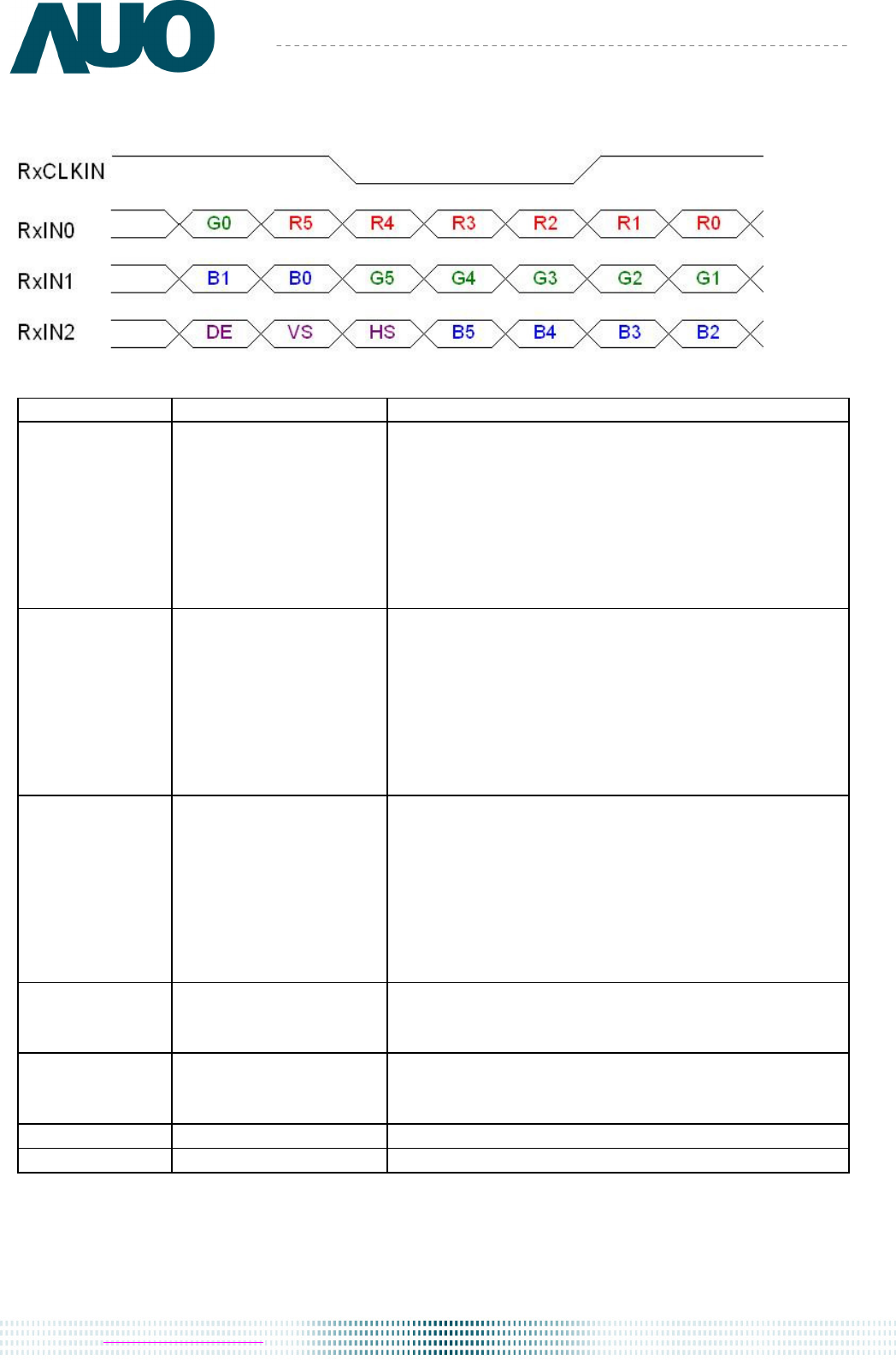
6.2 The Input Data Format
Signal Name Description
R5
R4
R3
R2
R1
R0
Red Data 5 (MSB)
Red Data 4
Red Data 3
Red Data 2
Red Data 1
Red Data 0 (LSB)
Red-pixel Data
Red-pixel Data
Each red pixel's brightness data consists of these
6 bits pixel data.
G5
G4
G3
G2
G1
G0
Green Data 5 (MSB)
Green Data 4
Green Data 3
Green Data 2
Green Data 1
Green Data 0 (LSB)
Green-pixel Data
Green-pixel Data
Each green pixel's brightness data consists of
these 6 bits pixel data.
B5
B4
B3
B2
B1
B0
Blue Data 5 (MSB)
Blue Data 4
Blue Data 3
Blue Data 2
Blue Data 1
Blue Data 0 (LSB)
Blue-pixel Data
Blue-pixel Data
Each blue pixel's brightness data consists of
these 6 bits pixel data.
RxCLKIN
Data Clock
The signal is used to strobe the pixel data and
DE signals. All pixel data shall be valid at the
falling edge when the DE signal is high.
DE Display Timing This signal is strobed at the falling edge of
RxCLKIN. When the signal is high, the pixel data
shall be valid to be displayed.
VS Vertical Sync The signal is synchronized to RxCLKIN .
HS Horizontal Sync The signal is synchronized to RxCLKIN .
Note: Output signals from any system shall be low or High-impedance state when VDD is off.
18 of 28
AU OPTRONICS CORPORATION
Product Specification
B156XTN02.0 Document Version : 0.1
6.3 Integration Interface Requirement
6.3.1 Connector Description
Physical interface is described as for the connector on module.
These connectors are capable of accommodating the following signals and will be
following components.
Connector Name / Designation For Signal Connector
Manufacturer IPEX or compatible
Type / Part Number IPEX 20455-040E-12R
Mating Housing/Part Number IPEX 20353-040T-11
6.3.2 Pin Assignment
LVDS is a differential signal technology for LCD interface and high speed data transfer device.
PIN# Signal Name Description
1
NC Connect to pin34
2
VDD Power Supply +3.3V ( typical )
3
VDD Power Supply +3.3V ( typical )
4
V_EDID DDC +3.3V Power
5
AGING Aging
6
EDID_ CLK EDID_Clock
7
EDID_DATA EDID_Data
8
RIN0- -LVDS Differential Data INPUT ( R0-R5,G0 )
9
RIN0+ +LVDS Differential Data INPUT ( R0-R5,G0 )
10
GND Ground
11
RIN1- -LVDS Differential Data INPUT ( G1-G5,B0-B1 )
12
RIN1+ +LVDS Differential Data INPUT ( G1-G5,B0-B1)
13
GND Ground
14
RIN2- -LVDS Differential Data INPUT ( B2-B5,HS,VS,DE )
15
RIN2+ +LVDS Differential Data INPUT ( B2-B5,HS,VS,DE )
16
GND Ground
17
ClKIN- -LVDS Differential Clock INPUT
18
ClKIN+ -LVDS Differential Clock INPUT
19
CM_EN CM_EN ( Color Matrix )
20
NC No connection
21
NC No connection
19 of 28
AU OPTRONICS CORPORATION
Product Specification
B156XTN02.0 Document Version : 0.1
22
GND Ground
23
NC No connection
24
NC No connection
25
GND Ground
26
NC No connection
27
NC No connection
28
GND Ground
29
NC No connection
30
NC No connection
31
VLED_GND LED Ground
32
VLED_GND LED Ground
33
VLED_GND LED Ground
34
NC Connect to pin1
35
BL_PWM System PWM Signal input ( +3.3V input )
36
BL_EN LED enable pin ( +3.3V input )
37
DCR_EN DCR_EN
38
VLED LED Power Supply 6-21V
39
VLED LED Power Supply 6-21V
40
VLED LED Power Supply 6-21V
Note1: Input signals shall be low or High-impedance state when VDD is off.
20 of 28
AU OPTRONICS CORPORATION
Product Specification
B156XTN02.0 Document Version : 0.1
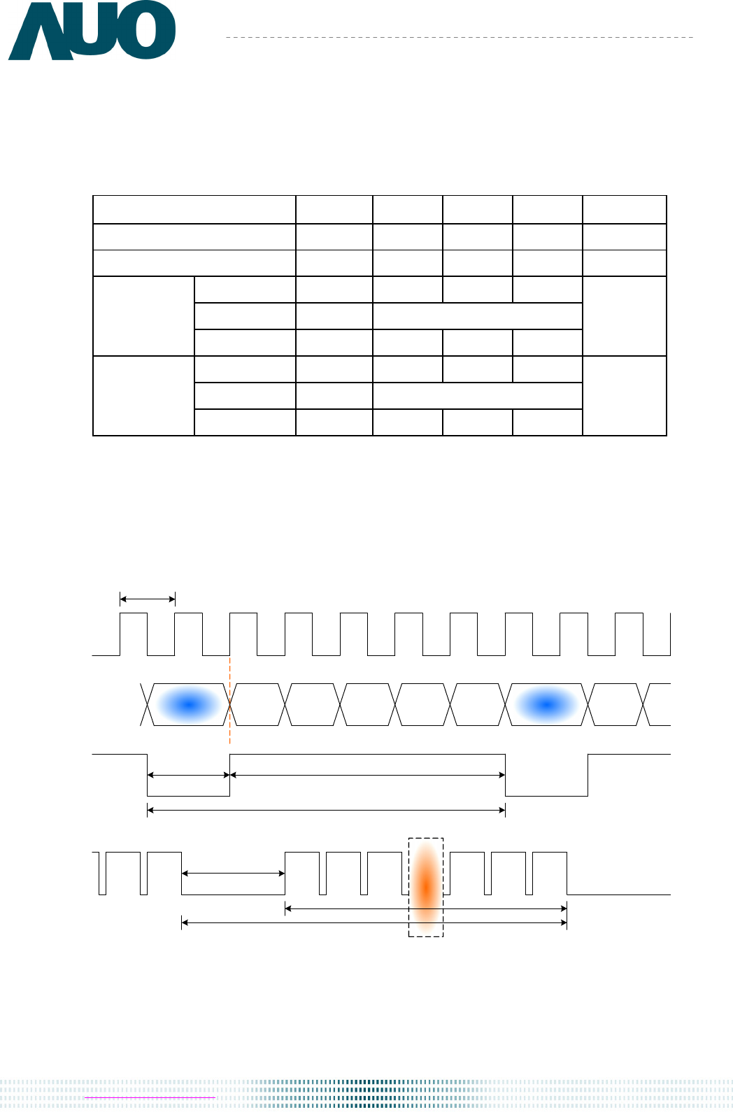
6.4 Interface Timing
6.4.1 Timing Characteristics
Basically, interface timings should match the 1366x768 /60Hz manufacturing guide line
timing.
Parameter Symbol Min. Typ. Max. Unit
Frame Rate - 50 60 TBD Hz
Clock frequency 1/ T
Clock
65 69.3 72 MHz
Period T
V
776 808 1023
Active T
VD
768
Vertical
Section
Blanking T
VB
8 40 255
T
Line
Period T
H
1396 1606 2047
Active T
HD
1366
Horizontal
Section
Blanking T
HB
30 240 681
T
Clock
Note : DE mode only
6.4.2 Timing diagram
DOTCLK
DE
T
H
T
HB
T
HD
DE
T
V
T
VB
T
VD
Input Timing Definition ( DE Mode)
T
CLOCK
Input
Data
Pixel
1
Pixel
2
Pixel
3
Pixel
N-1
Pixel
N
Invaild
Data
Invaild
Data
Pixel
1
21 of 28
AU OPTRONICS CORPORATION
Product Specification
B156XTN02.0 Document Version : 0.1
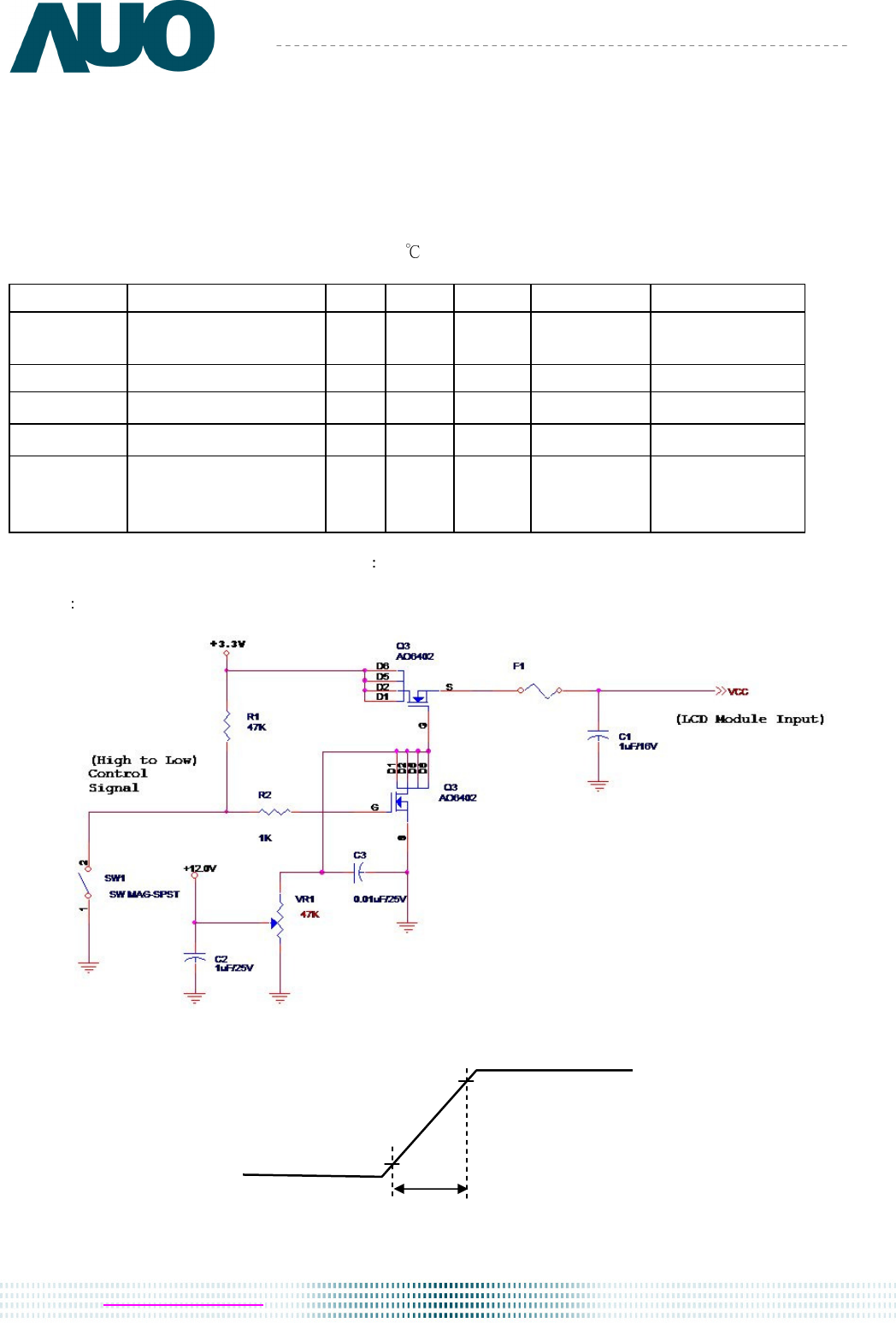
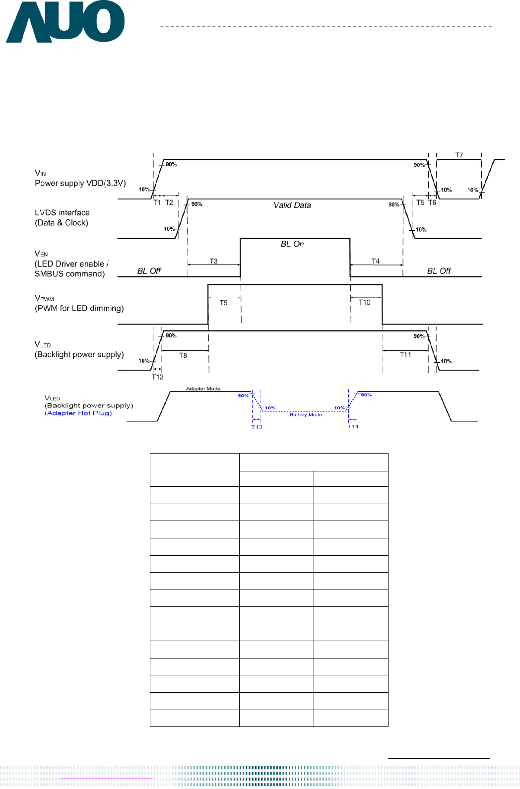
6.5 Power ON/OFF Sequence
Power on/off sequence is as follows. Interface signals and LED on/off sequence are also
shown in the chart. Signals from any system shall be Hi-Z state or low level when VDD is off
Note:If T3,T5,T6 couldn’t match above specifications, must request T3+T5+T6 > 200ms at least
Value
Parameter Min.(ms) Max.(ms)
T1 0.5 10
T2 0 50
T3 200 -
T4 200 -
T5 0 50
T6 0 10
T7 500 -
T8 10 -
T9 10 -
T10 10 -
T11 10 -
T12 0.5 10
T13 1 -
T14 1 -
22 of 28
AU OPTRONICS CORPORATION
Product Specification
B156XTN02.0 Document Version : 0.1
7. Panel Reliability Test
7.1 Vibration Test
Test Spec:
Test method: Non-Operation
Acceleration: 1.5 G
Frequency: 10 - 500Hz Random
Sweep: 30 Minutes each Axis (X, Y, Z)
7.2 Shock Test
Test Spec:
Test method: Non-Operation
Acceleration: 220 G , Half sine wave
Active time: 2 ms
Pulse: X,Y,Z .one time for each side
7.3 Reliability Test
Items Required Condition Note
Temperature
Humidity Bias Ta= 40℃
℃℃
℃, 90%RH, 300h
High Temperature
Operation Ta= 50℃
℃℃
℃, Dry, 300h
Low Temperature
Operation Ta= 0℃
℃℃
℃, 300h
High Temperature
Storage Ta= 60℃
℃℃
℃, 35%RH, 300h
Low Temperature
Storage Ta= -20℃
℃℃
℃, 50%RH, 250h
Thermal Shock
Test Ta=-20℃
℃℃
℃to 60℃
℃℃
℃, Duration at 30 min, 100 cycles
ESD Contact : ±8 KV
Air : ±15 KV
Note 1
Note1: According to EN 61000-4-2 , ESD class B: Some performance degradation allowed.
Self-recoverable.
No data lost, No hardware failures.
Remark: MTBF (Excluding the LED): 30,000 hours with a confidence level 90%
23 of 28
AU OPTRONICS CORPORATION
Product Specification
B156XTN02.0 Document Version : 0.1
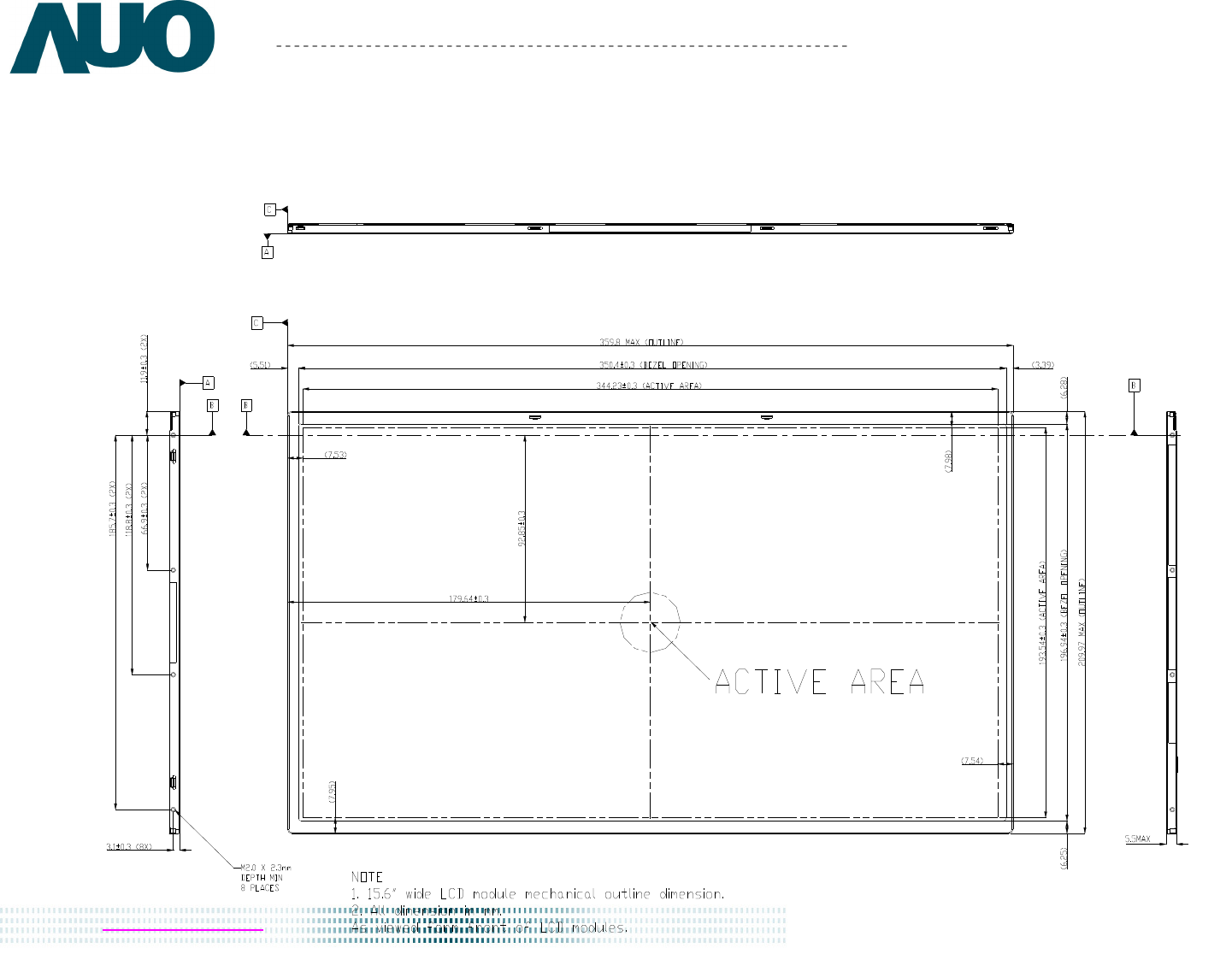
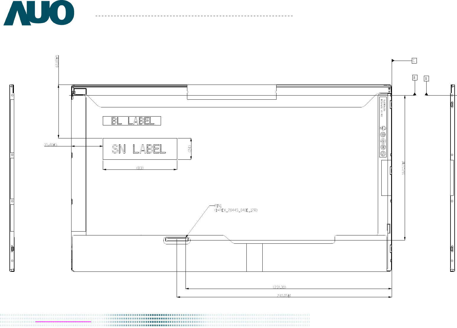
8. Mechanical Characteristics
8.1 LCM Outline Dimension
8.1.1 Standard Front View
The drawing following 2D standard drawing and remark.
24 of 28
AU OPTRONICS CORPORATION
Product Specification
B156XTN02.0 Document Version : 0.1
8.1.2 Standard Rear View
25 of 28
AU OPTRONICS CORPORATION
Product Specification
B156XTN02.0 Document Version : 0.1
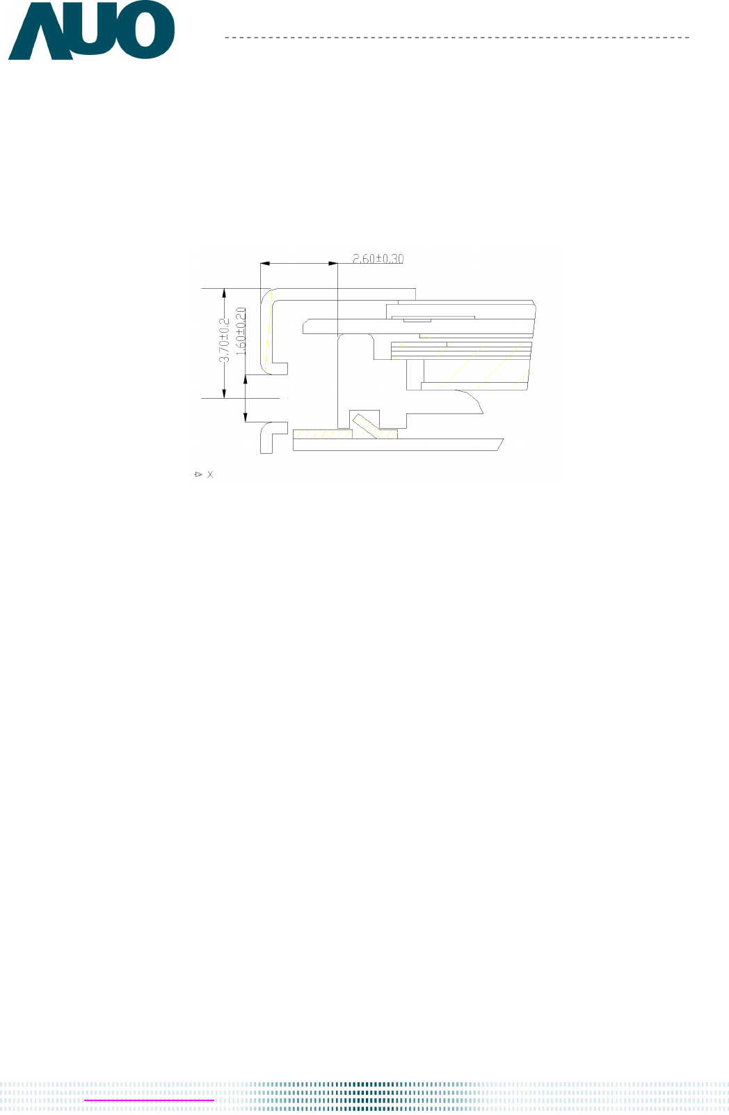
8.2 Screw Hole Depth and Center Position
Maximum Screw penetration from side surface is 2.3 mm
The center of screw hole center location is 3.7 ± 0.2mm from front surface
Screw Torque: Maximum 2.5 kgf-cm
26 of 28
AU OPTRONICS CORPORATION
Product Specification
B156XTN02.0 Document Version : 0.1
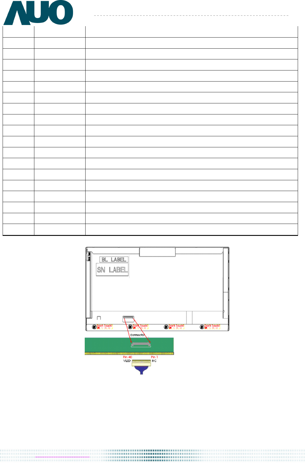
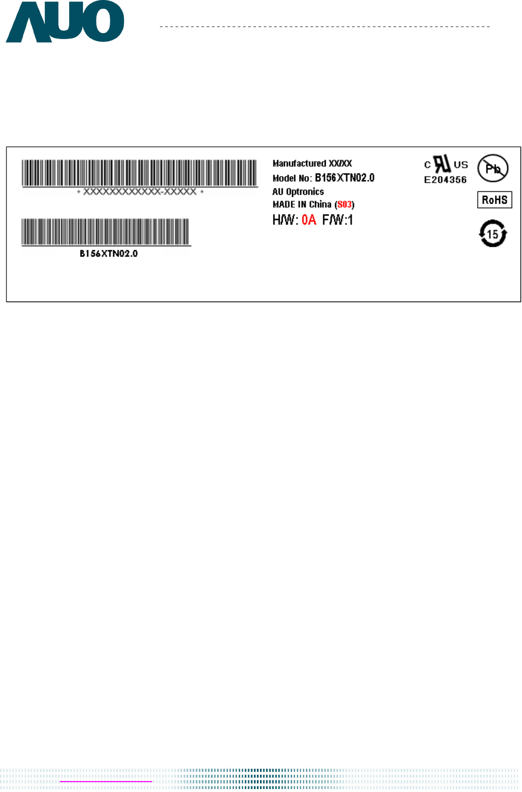
9. Shipping and Package
9.1 Shipping Label Format
27 of 28
AU OPTRONICS CORPORATION
Product Specification
B156XTN02.0 Document Version : 0.1
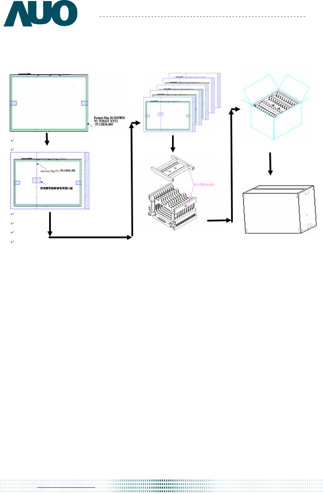
9.2 Carton Package
The outside dimension of carton is 437 (L)mm x 369 (W)mm x 313 (H)mm
28 of 28
AU OPTRONICS CORPORATION
Product Specification
B156XTN02.0 Document Version : 0.1
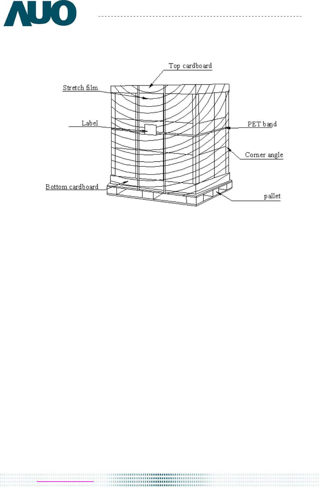
9.3 Shipping Package of Palletizing Sequence
10. Appendix: EDID Description
TBD

