BF517 Datasheet. Www.s Manuals.com. Infineon
User Manual: Marking of electronic components, SMD Codes LR, LR-, LR-***, LR1G, LR1L, LRAG, LRAL, LRCG, LRDG, LRJ, LRP, LRs, Lr. Datasheets 1SMB17AT3, BD52E23G, BF517, LP2985-10DBVR, LP2985A-10DBVR, LP2985A-30DBVR, LP2985A-50DBVR, NL17SZ16DFT2, NL17SZ16XV5T2, P6SMB30A, PZU6.8BA , RT9818C-13PV, RT9818C-27PX, SMBJ17A, TPSMB30A.
Open the PDF directly: View PDF ![]() .
.
Page Count: 5
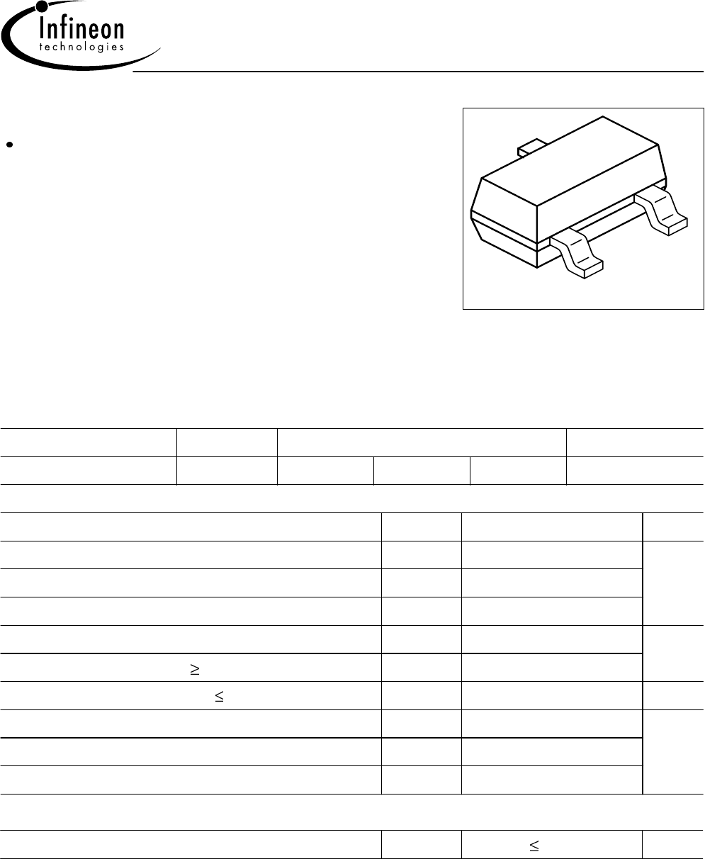
BF 517
Oct-26-19991
NPN Silicon RF Transistor
For amplifier and oscillator
applications in TV-tuners
1
2
3
VPS05161
Type Marking Pin Configuration Package
BF 517 LRs 1 = B 2 = E 3 = C SOT-23
Maximum Ratings
Parameter Symbol UnitValue
Collector-emitter voltage 15VCEO V
Collector-base voltage VCBO 20
Emitter-base voltage 2.5VEBO
25IC
Collector current mA
Peak collector current, f 10 MHz ICM 50
Total power dissipation, TS 55 °C F) Ptot 280 mW
Junction temperature Tj150 °C
Ambient temperature TA-65 ... 150
Storage temperature Tstg -65 ... 150
Thermal Resistance
Junction - soldering point RthJS 340 K/W
1TS is measured on the collector lead at the soldering point to the pcb
BF 517
Oct-26-19992
Electrical Characteristics at TA = 25 °C, unless otherwise specified.
Parameter ValuesSymbol Unit
max.typ.min.
DC characteristics
V(BR)CEO 15 -Collector-emitter breakdown voltage
IC = 1 mA, IB = 0
- V
Collector-base cutoff current
VCB = 15 V, IE = 0
ICBO - - nA50
-DC current gain
IC = 5 mA, VCE = 10 V
-25hFE 250
VCollector-emitter saturation voltage
IC = 10 mA, IB = 1 mA
VCEsat - 0.1 0.5
AC characteristics
-GHzTransition frequency
IC = 5 mA, VCE = 10 V, f = 200 MHz
21fT
Collector-base capacitance
VCB = 5 V, f = 1 MHz
0.750.3 pFCcb 0.55
0.4Cce 0.25-Collector-emitter capacitance
VCE = 5 V, f = 1 MHz
-Input capacitance
VEB = 0.5 V, IC = 0 , f = 1 MHz
Cibo 1.45-
-Cobs -Output capacitance
VCE = 5 V, VBE = 0 , f = 1 MHz
0.8
-F2.5-Noise figure
IC = 5 mA, VCE = 10 V, f = 100 MHz,
ZS = 75
dB
BF 517
Oct-26-19993
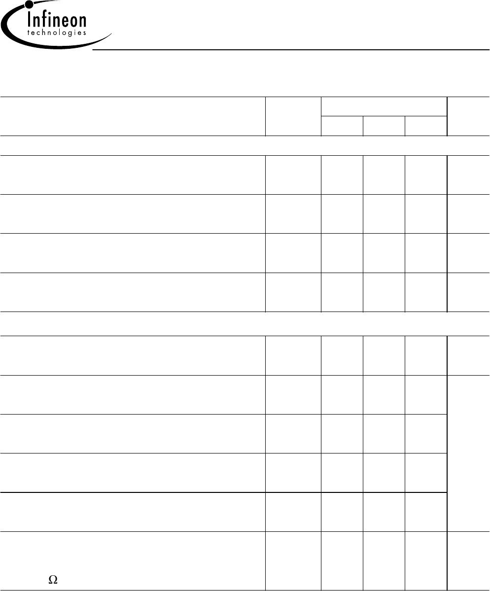
Total power dissipation Ptot = f (TA*, TS)
* Package mounted on epoxy
0 20 40 60 80 100 120 °C 150
TA,TS
0
50
100
150
200
mW
300
P
tot
TS
TA
Permissible Pulse Load RthJS = f (tp)
10 -6 10 -5 10 -4 10 -3 10 -2 10 0
s
tp
-1
10
0
10
1
10
2
10
3
10
K/W
R
thJS
0.5
0.2
0.1
0.05
0.02
0.01
0.005
D = 0
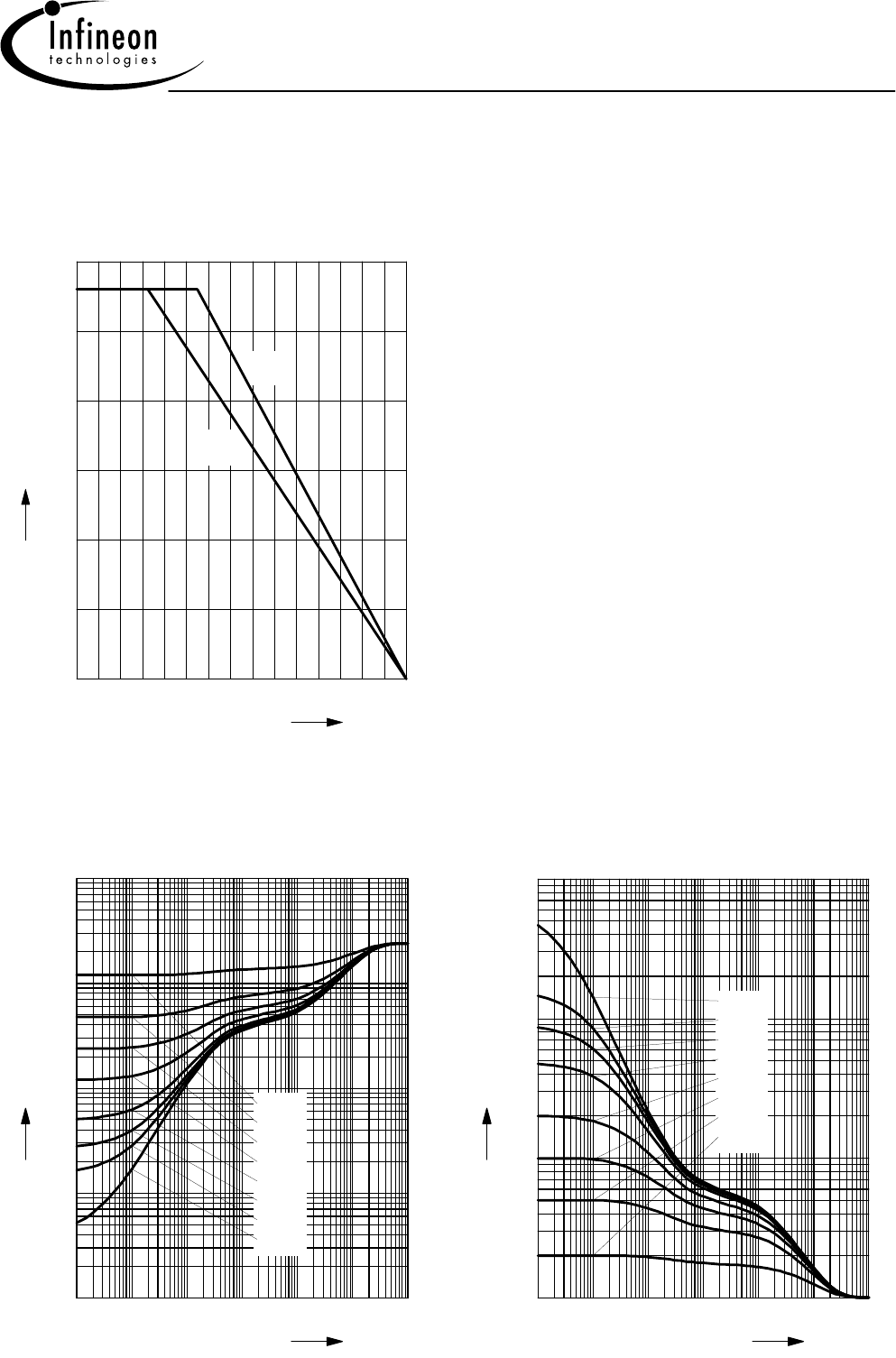
Permissible Pulse Load
Ptotmax/PtotDC = f (tp)
10 -6 10 -5 10 -4 10 -3 10 -2 10 0
s
tp
0
10
1
10
2
10
3
10
-
P
totmax
/ P
totDC
D = 0
0.005
0.01
0.02
0.05
0.1
0.2
0.5
BF 517
Oct-26-19994
Collector-base capacitance Ccb = f (VCB)
f = 1MHz
0 4 8 12 16 20 V26
VCB
0.0
0.1
0.2
0.3
0.4
0.5
0.6
0.7
0.8
0.9
1.0
1.1
pF
1.3
C
cb
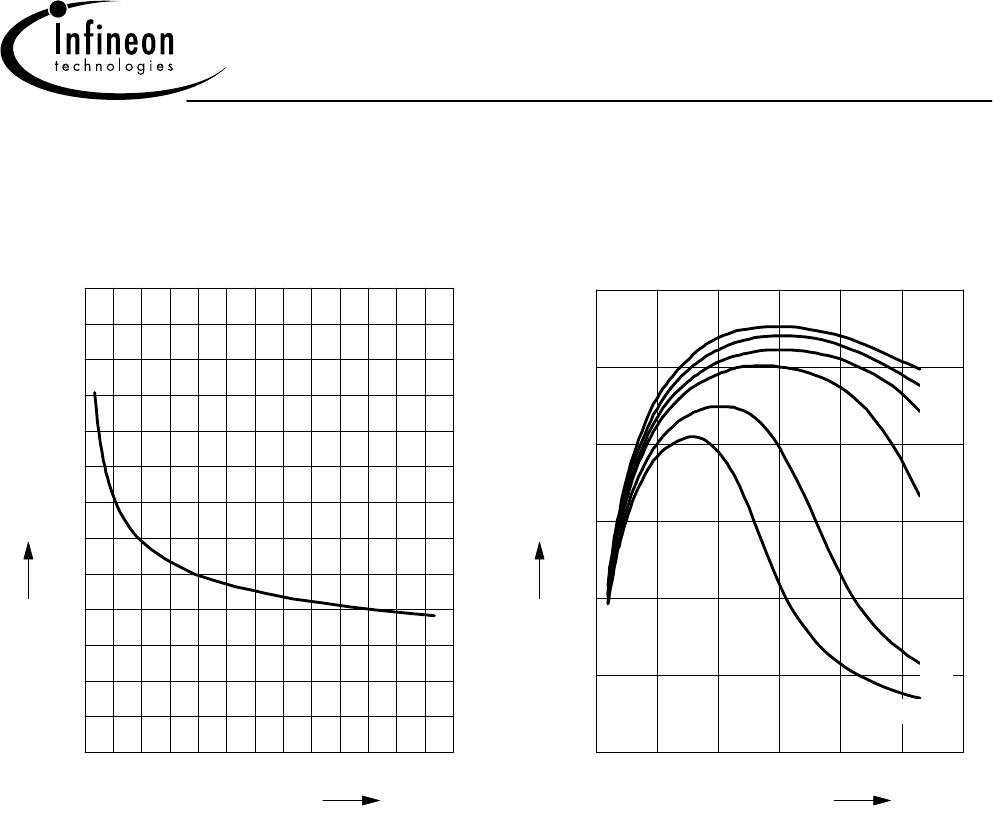
Transition frequency fT = f (IC)
VCE = Parameter
0 5 10 15 20 mA 30
IC
0.0
0.5
1.0
1.5
2.0
GHz
3.0
f
T
10V
5V
3V
2V
1V
0.7V