Xilinx UG130 Spartan 3 FPGA Starter Kit Board User Guide
User Manual:
Open the PDF directly: View PDF ![]() .
.
Page Count: 64
- Table of Contents
- About This Guide
- Introduction
- Fast, Asynchronous SRAM
- Four-Digit, Seven-Segment LED Display
- Switches and LEDs
- VGA Port
- PS/2 Mouse/Keyboard Port
- RS-232 Serial Port
- Clock Sources
- FPGA Configuration Modes and Functions
- Platform Flash Configuration Storage
- JTAG Programming/Debugging Ports
- Power Distribution
- Expansion Connectors and Boards
- Board Schematics
- Reference Material for Major Components

R
Spartan-3 FPGA
Starter Kit Board
User Guide
UG130 (v1.2) June 20, 2008
Spartan-3 FPGA Starter Kit Board User Guide www.xilinx.com UG130 (v1.2) June 20, 2008
Xilinx is disclosing this Document and Intellectual Property (hereinafter “the Design”) to you for use in the development of designs to operate
on, or interface with Xilinx FPGAs. Except as stated herein, none of the Design may be copied, reproduced, distributed, republished,
downloaded, displayed, posted, or transmitted in any form or by any means including, but not limited to, electronic, mechanical,
photocopying, recording, or otherwise, without the prior written consent of Xilinx. Any unauthorized use of the Design may violate copyright
laws, trademark laws, the laws of privacy and publicity, and communications regulations and statutes.
Xilinx does not assume any liability arising out of the application or use of the Design; nor does Xilinx convey any license under its patents,
copyrights, or any rights of others. You are responsible for obtaining any rights you may require for your use or implementation of the
Design. Xilinx reserves the right to make changes, at any time, to the Design as deemed desirable in the sole discretion of Xilinx. Xilinx
assumes no obligation to correct any errors contained herein or to advise you of any correction if such be made. Xilinx will not assume any
liability for the accuracy or correctness of any engineering or technical support or assistance provided to you in connection with the Design.
THE DESIGN IS PROVIDED “AS IS” WITH ALL FAULTS, AND THE ENTIRE RISK AS TO ITS FUNCTION AND IMPLEMENTATION IS
WITH YOU. YOU ACKNOWLEDGE AND AGREE THAT YOU HAVE NOT RELIED ON ANY ORAL OR WRITTEN INFORMATION OR
ADVICE, WHETHER GIVEN BY XILINX, OR ITS AGENTS OR EMPLOYEES. XILINX MAKES NO OTHER WARRANTIES, WHETHER
EXPRESS, IMPLIED, OR STATUTORY, REGARDING THE DESIGN, INCLUDING ANY WARRANTIES OF MERCHANTABILITY,
FITNESS FOR A PARTICULAR PURPOSE, TITLE, AND NONINFRINGEMENT OF THIRD-PARTY RIGHTS.
IN NO EVENT WILL XILINX BE LIABLE FOR ANY CONSEQUENTIAL, INDIRECT, EXEMPLARY, SPECIAL, OR INCIDENTAL
DAMAGES, INCLUDING ANY LOST DATA AND LOST PROFITS, ARISING FROM OR RELATING TO YOUR USE OF THE DESIGN,
EVEN IF YOU HAVE BEEN ADVISED OF THE POSSIBILITY OF SUCH DAMAGES. THE TOTAL CUMULATIVE LIABILITY OF XILINX IN
CONNECTION WITH YOUR USE OF THE DESIGN, WHETHER IN CONTRACT OR TORT OR OTHERWISE, WILL IN NO EVENT
EXCEED THE AMOUNT OF FEES PAID BY YOU TO XILINX HEREUNDER FOR USE OF THE DESIGN. YOU ACKNOWLEDGE THAT
THE FEES, IF ANY, REFLECT THE ALLOCATION OF RISK SET FORTH IN THIS AGREEMENT cc THAT XILINX WOULD NOT MAKE
AVAILABLE THE DESIGN TO YOU WITHOUT THESE LIMITATIONS OF LIABILITY.
The Design is not designed or intended for use in the development of on-line control equipment in hazardous environments requiring fail-
safe controls, such as in the operation of nuclear facilities, aircraft navigation or communications systems, air traffic control, life support, or
weapons systems (“High-Risk Applications”). Xilinx specifically disclaims any express or implied warranties of fitness for such High-Risk
Applications. You represent that use of the Design in such High-Risk Applications is fully at your risk.
© 2004-2008 Xilinx, Inc. All rights reserved. XILINX, the Xilinx logo, and other designated brands included herein are trademarks of Xilinx,
Inc. PowerPC is a trademark of IBM Corp. and used under license. PCI, PCI-X, and PCI EXPRESS are registered trademarks of PCI-SIG.
All other trademarks are the property of their respective owners.Some portions reproduced by permission from Digilent, Inc.
Spartan-3 FPGA Starter Kit Board User Guide
UG130 (v1.2) June 20, 2008
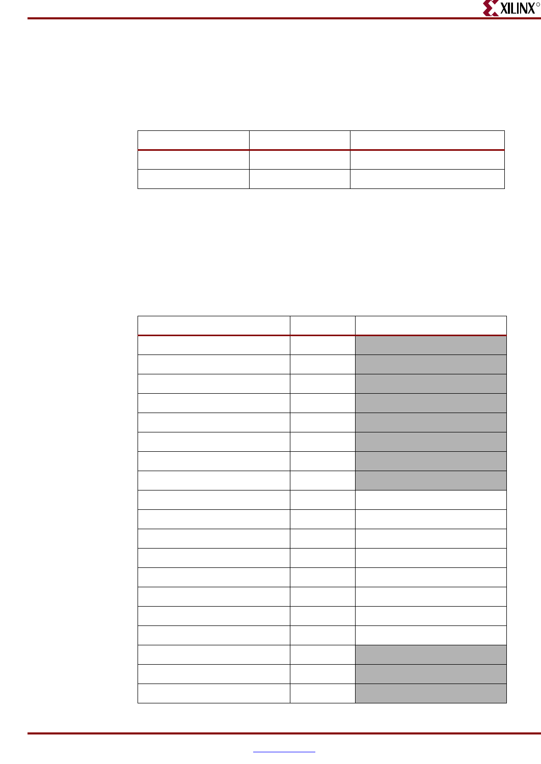
The following table shows the revision history for this document.
R
Version Revision
04/26/04 1.0 Initial Xilinx release.
06/07/04 1.0.1 Minor modifications for printed release.
07/21/04 1.0.2 Added information on auxiliary serial port connections to Chapter 7.
05/13/05 1.1 Clarified that SRAM IC10 shares eight lower data lines with A1 connector.
06/20/08 1.2 Corrected A1 pins in Table 2-2. Updated links.

Spartan-3 FPGA Starter Kit Board User Guide www.xilinx.com 3
UG130 (v1.2) June 20, 2008
Preface: About This Guide
Guide Contents . . . . . . . . . . . . . . . . . . . . . . . . . . . . . . . . . . . . . . . . . . . . . . . . . . . . . . . . . . . . . . 5
Chapter 1: Introduction
Key Components and Features . . . . . . . . . . . . . . . . . . . . . . . . . . . . . . . . . . . . . . . . . . . . . . . 7
Component Locations . . . . . . . . . . . . . . . . . . . . . . . . . . . . . . . . . . . . . . . . . . . . . . . . . . . . . . . . 9
Chapter 2: Fast, Asynchronous SRAM
Address Bus Connections . . . . . . . . . . . . . . . . . . . . . . . . . . . . . . . . . . . . . . . . . . . . . . . . . . . 12
Write Enable and Output Enable Control Signals . . . . . . . . . . . . . . . . . . . . . . . . . . . . 13
SRAM Data Signals, Chip Enables, and Byte Enables . . . . . . . . . . . . . . . . . . . . . . . . 13
Chapter 3: Four-Digit, Seven-Segment LED Display
Chapter 4: Switches and LEDs
Slide Switches . . . . . . . . . . . . . . . . . . . . . . . . . . . . . . . . . . . . . . . . . . . . . . . . . . . . . . . . . . . . . . 19
Push Button Switches . . . . . . . . . . . . . . . . . . . . . . . . . . . . . . . . . . . . . . . . . . . . . . . . . . . . . . . 19
LEDs. . . . . . . . . . . . . . . . . . . . . . . . . . . . . . . . . . . . . . . . . . . . . . . . . . . . . . . . . . . . . . . . . . . . . . . . 20
Chapter 5: VGA Port
Signal Timing for a 60Hz, 640x480 VGA Display. . . . . . . . . . . . . . . . . . . . . . . . . . . . . 22
VGA Signal Timing . . . . . . . . . . . . . . . . . . . . . . . . . . . . . . . . . . . . . . . . . . . . . . . . . . . . . . . . . 24
Chapter 6: PS/2 Mouse/Keyboard Port
Keyboard . . . . . . . . . . . . . . . . . . . . . . . . . . . . . . . . . . . . . . . . . . . . . . . . . . . . . . . . . . . . . . . . . . . 28
Mouse . . . . . . . . . . . . . . . . . . . . . . . . . . . . . . . . . . . . . . . . . . . . . . . . . . . . . . . . . . . . . . . . . . . . . . 30
Voltage Supply . . . . . . . . . . . . . . . . . . . . . . . . . . . . . . . . . . . . . . . . . . . . . . . . . . . . . . . . . . . . . 31
Chapter 7: RS-232 Serial Port
Chapter 8: Clock Sources
Chapter 9: FPGA Configuration Modes and Functions
FPGA Configuration Mode Settings . . . . . . . . . . . . . . . . . . . . . . . . . . . . . . . . . . . . . . . . . 36
Program Push Button/DONE Indicator LED . . . . . . . . . . . . . . . . . . . . . . . . . . . . . . . . . 37
Table of Contents

4www.xilinx.com Spartan-3 FPGA Starter Kit Board User Guide
UG130 (v1.2) June 20, 2008
R
Chapter 10: Platform Flash Configuration Storage
Platform Flash Jumper Options (JP1) . . . . . . . . . . . . . . . . . . . . . . . . . . . . . . . . . . . . . . . . 38
“Default” Option . . . . . . . . . . . . . . . . . . . . . . . . . . . . . . . . . . . . . . . . . . . . . . . . . . . . . . . . . . . 38
“Flash Read” Option . . . . . . . . . . . . . . . . . . . . . . . . . . . . . . . . . . . . . . . . . . . . . . . . . . . . . . . . 39
“Disable” Option . . . . . . . . . . . . . . . . . . . . . . . . . . . . . . . . . . . . . . . . . . . . . . . . . . . . . . . . . . . 40
Chapter 11: JTAG Programming/Debugging Ports
JTAG Header (J7) . . . . . . . . . . . . . . . . . . . . . . . . . . . . . . . . . . . . . . . . . . . . . . . . . . . . . . . . . . . 41
Parallel Cable IV/MultiPro Desktop Tool JTAG Header (J5). . . . . . . . . . . . . . . . . . 42
Chapter 12: Power Distribution
AC Wall Adapter. . . . . . . . . . . . . . . . . . . . . . . . . . . . . . . . . . . . . . . . . . . . . . . . . . . . . . . . . . . . 45
Voltage Regulators . . . . . . . . . . . . . . . . . . . . . . . . . . . . . . . . . . . . . . . . . . . . . . . . . . . . . . . . . . 45
Chapter 13: Expansion Connectors and Boards
Expansion Connectors. . . . . . . . . . . . . . . . . . . . . . . . . . . . . . . . . . . . . . . . . . . . . . . . . . . . . . . 47
A1 Connector Pinout . . . . . . . . . . . . . . . . . . . . . . . . . . . . . . . . . . . . . . . . . . . . . . . . . . . . . . 49
A2 Connector Pinout . . . . . . . . . . . . . . . . . . . . . . . . . . . . . . . . . . . . . . . . . . . . . . . . . . . . . . 50
B1 Connector Pinout . . . . . . . . . . . . . . . . . . . . . . . . . . . . . . . . . . . . . . . . . . . . . . . . . . . . . . 51
Expansion Boards . . . . . . . . . . . . . . . . . . . . . . . . . . . . . . . . . . . . . . . . . . . . . . . . . . . . . . . . . . . 52
Appendix A: Board Schematics
Appendix B: Reference Material for Major Components

Spartan-3 FPGA Starter Kit Board User Guide www.xilinx.com 5
UG130 (v1.2) June 20, 2008
R
Preface
About This Guide
This user guide describes the components and operation of the Spartan®-3 FPGA Starter
Kit Board.
Guide Contents
This manual contains the following chapters:
•Chapter 1, “Introduction”
•Chapter 2, “Fast, Asynchronous SRAM”
•Chapter 3, “Four-Digit, Seven-Segment LED Display”
•Chapter 4, “Switches and LEDs”
•Chapter 5, “VGA Port”
•Chapter 6, “PS/2 Mouse/Keyboard Port”
•Chapter 7, “RS-232 Serial Port”
•Chapter 8, “Clock Sources”
•Chapter 9, “FPGA Configuration Modes and Functions”
•Chapter 10, “Platform Flash Configuration Storage”
•Chapter 11, “JTAG Programming/Debugging Ports”
•Chapter 12, “Power Distribution”
•Chapter 13, “Expansion Connectors and Boards”
•Appendix A, “Board Schematics”
•Appendix B, “Reference Material for Major Components”

Spartan-3 FPGA Starter Kit Board User Guide www.xilinx.com 7
UG130 (v1.2) June 20, 2008
R
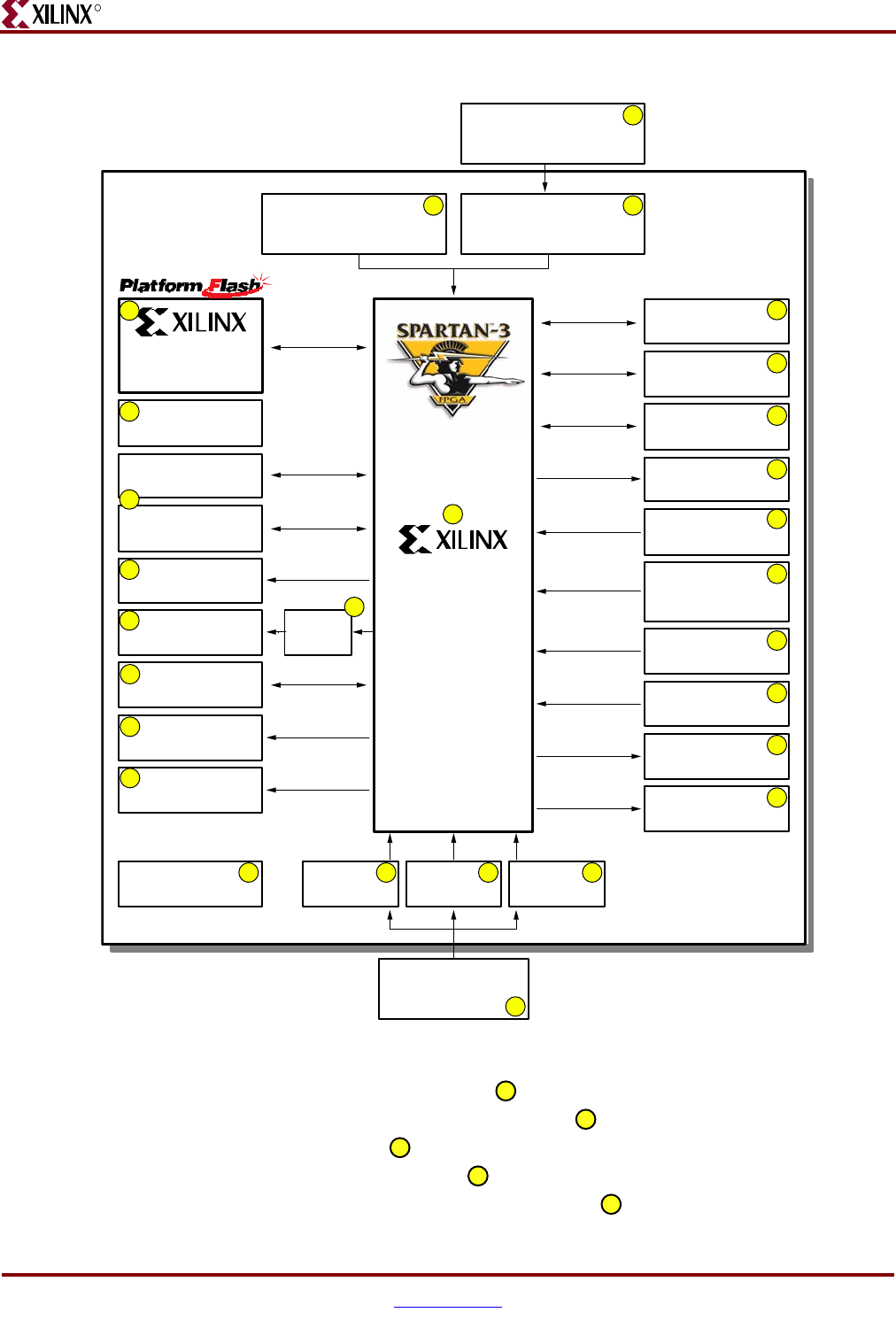
Chapter 1
Introduction
The Xilinx Spartan®-3 FPGA Starter Kit provides a low-cost, easy-to-use development and
evaluation platform for Spartan-3 FPGA designs.
Key Components and Features
Figure 1-1 shows the Spartan-3 Starter Kit board, which includes the following
components and features:
•200,000-gate Xilinx Spartan-3 XC3S200 FPGA in a 256-ball thin Ball Grid Array
package (XC3S200FT256)
♦4,320 logic cell equivalents
♦Twelve 18K-bit block RAMs (216K bits)
♦Twelve 18x18 hardware multipliers
♦Four Digital Clock Managers (DCMs)
♦Up to 173 user-defined I/O signals
•2Mbit Xilinx XCF02S Platform Flash, in-system programmable configuration
PROM
♦1Mbit non-volatile data or application code storage available after FPGA
configuration
♦Jumper options allow FPGA application to read PROM data or FPGA
configuration from other sources
•1M-byte of Fast Asynchronous SRAM (bottom side of board, see Figure 1-3)
♦Two 256Kx16 ISSI IS61LV25616AL-10T 10 ns SRAMs
♦Configurable memory architecture
-Single 256Kx32 SRAM array, ideal for MicroBlaze code images
-Two independent 256Kx16 SRAM arrays
♦Individual chip select per device
♦Individual byte enables
•3-bit, 8-color VGA display port
•9-pin RS-232 Serial Port
♦DB9 9-pin female connector (DCE connector)
♦RS-232 transceiver/level translator
♦Uses straight-through serial cable to connect to computer or workstation serial
port
♦Second RS-232 transmit and receive channel available on board test points
1
2
3
4
5
6
7
8
8www.xilinx.com Spartan-3 FPGA Starter Kit Board User Guide
UG130 (v1.2) June 20, 2008
Chapter 1: Introduction
R
•PS/2-style mouse/keyboard port
•Four-character, seven-segment LED display
•Eight slide switches
•Eight individual LED outputs
•Four momentary-contact push button switches
Figure 1-1: Xilinx Spartan-3 Starter Kit Board Block Diagram
4 Push Buttons
8 Slide Switches
4 Character
7-Segment LED
8 LEDs
PS/2 Port
RS-232 Port
Serial Port
8-color
VGA Port
XCF02S 2Mbit
Configuration
PROM
Parallel Cable IV
MutliPro Desktop Tool
JTAG Connector
PROGRAM
Push Button
50 MHz
Oscillator
Auxiliary
Oscillator Socket
XC3S200
Spartan-3
FPGA
256Kx16
10ns SRAM
256Kx16
10ns SRAM Configuration
DONE LED
Power On
LED
Configuration
Mode Select
Jumpers
Platform Flash
Option Jumpers
Low-Cost JTAG
Download Cable
Connector
5 VDC, 2A Supply
100-240V AC Input
50-60 Hz
Digilent Low-Cost
Parallel Port to JTAG
Cable
3.3V
Regulator 2.5V
Regulator 1.2V
Regulator
RS-232
Driver
A1 Expansion
Header
A2 Expansion
Header
B1 Expansion
Header
VCCO
AC Wall Adapter
Included
Included
UG130_c1_01_042504
26
11
10
9
7
6
5
3
1
2
4
25
27 28 29
12
18
19
20
21
2224
23
17
16
15
14
13
9
10
11
12
13
Spartan-3 FPGA Starter Kit Board User Guide www.xilinx.com 9
UG130 (v1.2) June 20, 2008
Component Locations
R
•50 MHz crystal oscillator clock source (bottom side of board, see Figure 1-3)
•Socket for an auxiliary crystal oscillator clock source
•FPGA configuration mode selected via jumper settings
•Push button switch to force FPGA reconfiguration (FPGA configuration happens
automatically at power-on)
•LED indicates when FPGA is successfully configured
•Three 40-pin expansion connection ports to extend and enhance the Spartan-3 Starter
Kit Board
♦See compatible expansion cards at
www.xilinx.com/products/boards/DO-SPAR3-DK/boards/daughtercards.htm
♦Compatible with Digilent, Inc. peripheral boards
www.digilentinc.com/Products/Catalog.cfm?Nav1=Products&Nav2=Peripheral&Cat=Peripheral
♦FPGA serial configuration interface signals available on the A2 and B1 connectors
-PROG_B, DONE, INIT_B, CCLK, DONE
•JTAG port for low-cost download cable
•Digilent JTAG download/debugging cable connects to PC parallel port
•JTAG download/debug port compatible with the Xilinx Parallel Cable IV and
MultiPRO Desktop Tool
•AC power adapter input for included international unregulated +5V power
supply
•Power-on indicator LED
•On-board 3.3V , 2.5V , and 1.2V regulators
Component Locations
Figure 1-2 and Figure 1-3 indicate the component locations on the top side and bottom side
of the board, respectively.
14
15
16
17
18
19
20
21
22
23
23
24
25
26
27
28
29
10 www.xilinx.com Spartan-3 FPGA Starter Kit Board User Guide
UG130 (v1.2) June 20, 2008
Chapter 1: Introduction
R
Figure 1-2: Xilinx Spartan-3 Starter Kit Board (Top Side)
POWER
2Mbit
PlatformFlash
A1 Expansion Connector A2 Expansion Connector
POWER
PROG
DONE
PS/2
XILINX
XC3S200
FPGA
VGA
3.3V
RS-232
RS-232
B1 Expansion Connector
ug130_c1_02_042704
7
8
1
23
6
5
9
17 18
24
22
20
21
31
16
19
27
26
25
12
13
11
10
15 30
Figure 1-3: Xilinx Spartan-3 Starter Kit Board (Bottom Side)
50
MHz
256Kx16
SRAM
2.5V
1.2V
256Kx16
SRAM
ug130_c1_03_042704
4
5
6
28
29
14
Spartan-3 FPGA Starter Kit Board User Guide www.xilinx.com 11
UG130 (v1.2) June 20, 2008
R
Chapter 2
Fast, Asynchronous SRAM
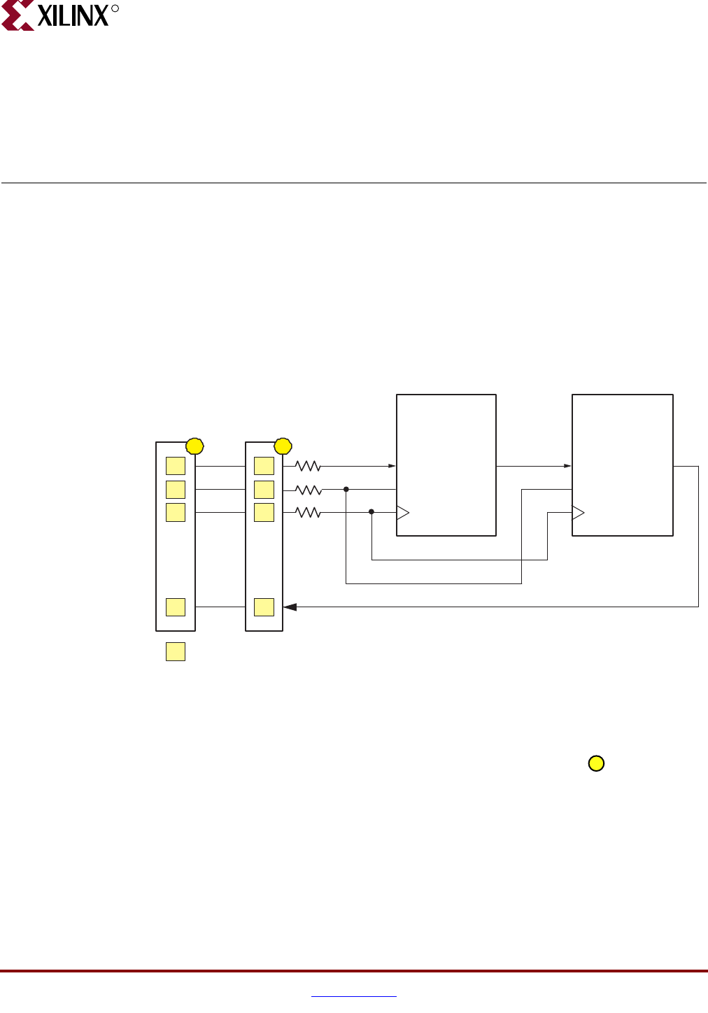
The Spartan®-3 FPGA Starter Kit board has a megabyte of fast asynchronous SRAM,
surface-mounted to the backside of the board. The memory array includes two 256Kx16
ISSI IS61LV25616AL-10T 10 ns SRAM devices, as shown in Figure 2-1. A detailed
schematic appears in Figure A-8.
Figure 2-1: FPGA to SRAM Connections
Spartan-3
FPGA
ISSI
256Kx16 SRAM
(10 ns)
I/O[15:0]
A[17:0]
CE
UB
LB
WE
OE
ISSI
256Kx16 SRAM
(10 ns)
I/O[15:0]
A[17:0]
CE
UB
LB
WE
OE
IC10
IC11
(K4)
(G3)
(P5)
(R4)
(N5)
(P7)
(T4)
(P6)
OE
WE
(see Table 2-1)
LB2
UB2
CE2
LB1
UB1
CE1
(see Table 2-3)
(see Table 2-4)
(xx) = FPGA pin number
UG130_c2_01_042604
(see Table 2-4)
(see Table 2-1)
(see Table 2-3)
12 www.xilinx.com Spartan-3 FPGA Starter Kit Board User Guide
UG130 (v1.2) June 20, 2008
Chapter 2: Fast, Asynchronous SRAM
R
The SRAM array forms either a single 256Kx32 SRAM memory or two independent
256Kx16 arrays. Both SRAM devices share common write-enable (WE#), output-enable
(OE#), and address (A[17:0]) signals. However, each device has a separate chip select
enable (CE#) control and individual byte-enable controls to select the high or low byte in
the 16-bit data word, UB and LB, respectively.
The 256Kx32 configuration is ideally suited to hold MicroBlaze instructions. However, it
alternately provides high-density data storage for a variety of applications, such as digital
signal processing (DSP), large data FIFOs, and graphics buffers.
Address Bus Connections
Both 256Kx16 SRAMs share 18-bit address control lines, as shown in Table 2-1. These
address signals also connect to the A1 Expansion Connector (see “Expansion Connectors,”
page 47).
Table 2-1: External SRAM Address Bus Connections to Spartan-3 FPGA
Address Bit FPGA Pin A1 Expansion Connector Pin
A17 L3 35
A16 K5 33
A15 K3 34
A14 J3 31
A13 J4 32
A12 H4 29
A11 H3 30
A10 G5 27
A9 E4 28
A8 E3 25
A7 F4 26
A6 F3 23
A5 G4 24
A4 L4 14
A3 M3 12
A2 M4 10
A1 N3 8
A0 L5 6
Spartan-3 FPGA Starter Kit Board User Guide www.xilinx.com 13
UG130 (v1.2) June 20, 2008
Write Enable and Output Enable Control Signals
R
Write Enable and Output Enable Control Signals
Both 256Kx16 SRAMs share common output enable (OE#) and write enable (WE#) control
lines, as shown in Table 2-2. These control signals also connect to the A1 Expansion
Connector (refer to “Expansion Connectors,” page 47).
SRAM Data Signals, Chip Enables, and Byte Enables
The data signals, chip enables, and byte enables are dedicated connections between the
FPGA and SRAM. Table 2-3 shows the FPGA pin connections to the SRAM designated
IC10 in Figure A-8. Table 2-4 shows the FPGA pin connections to SRAM IC11. To disable an
SRAM, drive the associated chip enable pin High.
Table 2-2: External SRAM Control Signal Connections to Spartan-3 FPGA
Signal FPGA Pin A1 Expansion Connector Pin
OE# K4 18
WE# G3 16
Table 2-3: SRAM IC10 Connections
Signal FPGA Pin A1 Expansion Connector Pin
IO15 R1
IO14 P1
IO13 L2
IO12 J2
IO11 H1
IO10 F2
IO9 P8
IO8 D3
IO7 B1 19
IO6 C1 17
IO5 C2 15
IO4 R5 13
IO3 T5 11
IO2 R6 9
IO1 T8 7
IO0 N7 5
CE1 (chip enable IC10) P7
UB1 (upper byte enable IC10) T4
LB1 (lower byte enable IC10) P6
14 www.xilinx.com Spartan-3 FPGA Starter Kit Board User Guide
UG130 (v1.2) June 20, 2008
Chapter 2: Fast, Asynchronous SRAM
R
Table 2-4: SRAM IC11 Connections
Signal FPGA Pin
IO15 N1
IO14 M1
IO13 K2
IO12 C3
IO11 F5
IO10 G1
IO9 E2
IO8 D2
IO7 D1
IO6 E1
IO5 G2
IO4 J1
IO3 K1
IO2 M2
IO1 N2
IO0 P2
CE2 (chip enable IC11) N5
UB2 (upper byte enable IC11) R4
LB2 (lower byte enable IC11) P5
Spartan-3 FPGA Starter Kit Board User Guide www.xilinx.com 15
UG130 (v1.2) June 20, 2008
R
Chapter 3
Four-Digit, Seven-Segment LED Display
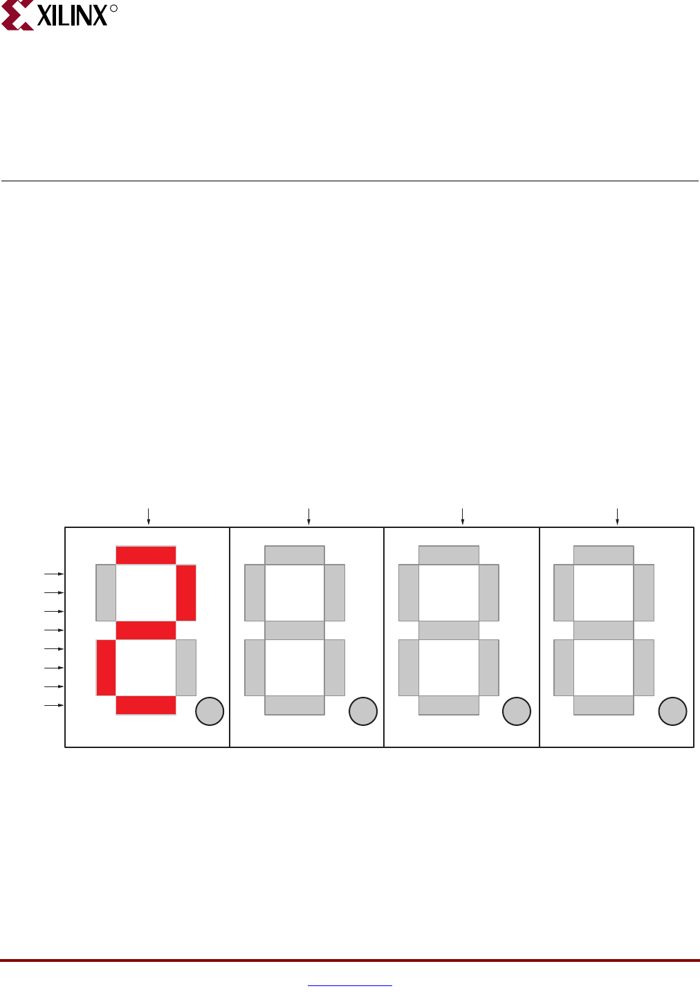
The Spartan®-3 FPGA Starter Kit board has a four-character, seven segment LED display
controlled by FPGA user-I/O pins, as shown in Figure 3-1. Each digit shares eight common
control signals to light individual LED segments. Each individual character has a separate
anode control input. A detailed schematic for the display appears in Figure A-2.
The pin number for each FPGA pin connected to the LED display appears in parentheses.
To light an individual signal, drive the individual segment control signal Low along with
the associated anode control signal for the individual character. In Figure 3-1, for example,
the left-most character displays the value ‘2’. The digital values driving the display in this
example are shown in blue. The AN3 anode control signal is Low, enabling the control
inputs for the left-most character. The segment control inputs, A through G and DP, drive
the individual segments that comprise the character. A Low value lights the individual
segment, a High turns off the segment. A Low on the A input signal, lights segment ‘a’ of
the display. The anode controls for the remaining characters, AN[2:0] are all High, and
these characters ignore the values presented on A through G and DP.
Table 3-1 lists the FPGA connections that drive the individual LEDs comprising a seven-
segment character. Table 3-2 lists the connections to enable a specific character. Table 3-3
shows the patterns required to display hexadecimal characters.
Figure 3-1: Seven-Segment LED Digit Control
A
B
C
D
E
F
G
DP
f
a
b
ec
g
d
(E14)
(G13)
(N15)
(P15)
(R16)
(F13)
(N16)
(P16)
f
a
b
e c
g
d
f
a
b
e c
g
d
f
a
b
e c
g
d
AN3 (E13) AN2 (F14) AN1 (G14) AN0 (D14)
0
0
0
1
0
0
1
0
1
111
UG130_c3_01_042704
dp dp dp dp
16 www.xilinx.com Spartan-3 FPGA Starter Kit Board User Guide
UG130 (v1.2) June 20, 2008
Chapter 3: Four-Digit, Seven-Segment LED Display
R
Table 3-1: FPGA Connections to Seven-Segment Display (Active Low)
Segment FPGA Pin
AE14
BG13
CN15
DP15
ER16
FF13
GN16
DP P16
Table 3-2: Digit Enable (Anode Control) Signals (Active Low)
Anode Control AN3 AN2 AN1 AN0
FPGA Pin E13 F14 G14 D14
Table 3-3: Display Characters and Resulting LED Segment Control Values
Character a b c d e f g
0 0000001
1 1001111
2 0010010
3 0000110
4 1001100
5 0100100
6 0100000
7 0001111
8 0000000
9 0000100
A 0001000
b 1100000
C 0110001
d 1000010
E 0110000
F 0111000
Spartan-3 FPGA Starter Kit Board User Guide www.xilinx.com 17
UG130 (v1.2) June 20, 2008
R
The LED control signals are time-multiplexed to display data on all four characters, as
shown in Figure 3-2. Present the value to be displayed on the segment control inputs and
select the specified character by driving the associated anode control signal Low. Through
persistence of vision, the human brain perceives that all four characters appear
simultaneously, similar to the way the brain perceives a TV display.
This “scanning” technique reduces the number of I/O pins required for the four
characters. If an FPGA pin were dedicated for each individual segment, then 32 pins are
required to drive four 7-segment LED characters. The scanning technique reduces the
required I/O down to 12 pins. The drawback to this approach is that the FPGA logic must
continuously scan data out to the displays—a small price to save 20 additional I/O pins.
Figure 3-2: Drive Anode Input Low to Light an Individual Character
AN3
AN2
AN1
AN0
DISP3 DISP2 DISP1 DISP0
{A,B,C,D,E,F,G,DP}
UG130_c3_02_042404

Spartan-3 FPGA Starter Kit Board User Guide www.xilinx.com 19
UG130 (v1.2) June 20, 2008
R
Chapter 4
Switches and LEDs
Slide Switches
The Spartan®-3 FPGA Starter Kit board has eight slide switches, indicated as in
Figure 1-2. The switches are located along the lower edge of the board, toward the right
edge. The switches are labeled SW7 through SW0. Switch SW7 is the left-most switch, and
SW0 is the right-most switch. The switches connect to an associated FPGA pin, as shown in
Table 4-1. A detailed schematic appears in Figure A-2.
When in the UP or ON position, a switch connects the FPGA pin to VCCO, a logic High.
When DOWN or in the OFF position, the switch connects the FPGA pin to ground, a logic
Low. The switches typically exhibit about 2 ms of mechanical bounce and there is no active
debouncing circuitry, although such circuitry could easily be added to the FPGA design
programmed on the board. A 4.7KΩ series resistor provides nominal input protection.
Push Button Switches
The Spartan-3 Starter Kit board has four momentary-contact push button switches,
indicated as in Figure 1-2. These push buttons are located along the lower edge of the
board, toward the right edge. The switches are labeled BTN3 through BTN0. Push button
switch BTN3 is the left-most switch, BTN0 the right-most switch. The push button
switches connect to an associated FPGA pin, as shown in Table 4-2. A detailed schematic
appears in Figure A-2.
Pressing a push button generates a logic High on the associated FPGA pin. Again, there is
no active debouncing circuitry on the push button.
The left-most button, BTN3, is also the default User Reset pin. BTN3 electrically behaves
identically to the other push buttons. However, when applicable, BTN3 resets the
provided reference designs.
Table 4-1: Slider Switch Connections
Switch SW7 SW6 SW5 SW4 SW3 SW2 SW1 SW0
FPGA Pin K13 K14 J13 J14 H13 H14 G12 F12
11
Table 4-2: Push Button Switch Connections
Push Button BTN3 (User Reset) BTN2 BTN1 BTN0
FPGA Pin L14 L13 M14 M13
13
20 www.xilinx.com Spartan-3 FPGA Starter Kit Board User Guide
UG130 (v1.2) June 20, 2008
Chapter 4: Switches and LEDs
R
LEDs
The Spartan-3 Starter Kit board has eight individual surface-mount LEDs located above
the push button switches, indicated by in Figure 1-2. The LEDs are labeled LED7
through LED0. LED7 is the left-most LED, LED0 the right-most LED. Table 4-3 shows the
FPGA connections to the LEDs.
The cathode of each LED connects to ground via a 270Ω resistor. To light an individual
LED, drive the associated FPGA control signal High, which is the opposite polarity from
lighting one of the 7-segment LEDs.
Table 4-3: LED Connections to the Spartan-3 FPGA
LED LD7 LD6 LD5 LD4 LD3 LD2 LD1 LD0
FPGA Pin P11 P12 N12 P13 N14 L12 P14 K12
12
Spartan-3 FPGA Starter Kit Board User Guide www.xilinx.com 21
UG130 (v1.2) June 20, 2008
R
Chapter 5
VGA Port
The Spartan®-3 FPGA Starter Kit board includes a VGA display port and DB15 connector,
indicated as in Figure 1-2. Connect this port directly to most PC monitors or flat-panel
LCD displays using a standard monitor cable.
As shown in Figure 5-1, the Spartan-3 FPGA controls five VGA signals: Red (R), Green (G),
Blue (B), Horizontal Sync (HS), and Vertical Sync (VS), all available on the VGA connector.
The FPGA pins that drive the VGA port appear in Table 5-1. A detailed schematic is in
Figure A-7.
5
Figure 5-1: VGA Connections from Spartan-3 Starter Kit Board
Pin 1
Pin 6
Pin 11
Pin 5
Pin 10
Pin 15
1
6
11
2
7
12
3
8
13
4
9
14
5
10
15
GND
DB15
Connector
Red
Green
Blue
Horizontal Sync
Vertical Sync
270Ω
270Ω
270Ω
R
G
B
HS
VS
(R12)
(T12)
(R11)
(R9)
(T10)
DB15 VGA Connector
(front view)
(xx) = FPGA pin number
UG130_c5_01_042604
22 www.xilinx.com Spartan-3 FPGA Starter Kit Board User Guide
UG130 (v1.2) June 20, 2008
Chapter 5: VGA Port
R
Each color line has a series resistor to provide 3-bit color, with one bit each for Red, Green,
and Blue. The series resistor uses the 75Ω VGA cable termination to ensure that the color
signals remain in the VGA-specified 0V to 0.7V range. The HS and VS signals are TTL level.
Drive the R, G, and B signals High or Low to generate the eight possible colors shown in
Table 5-2.
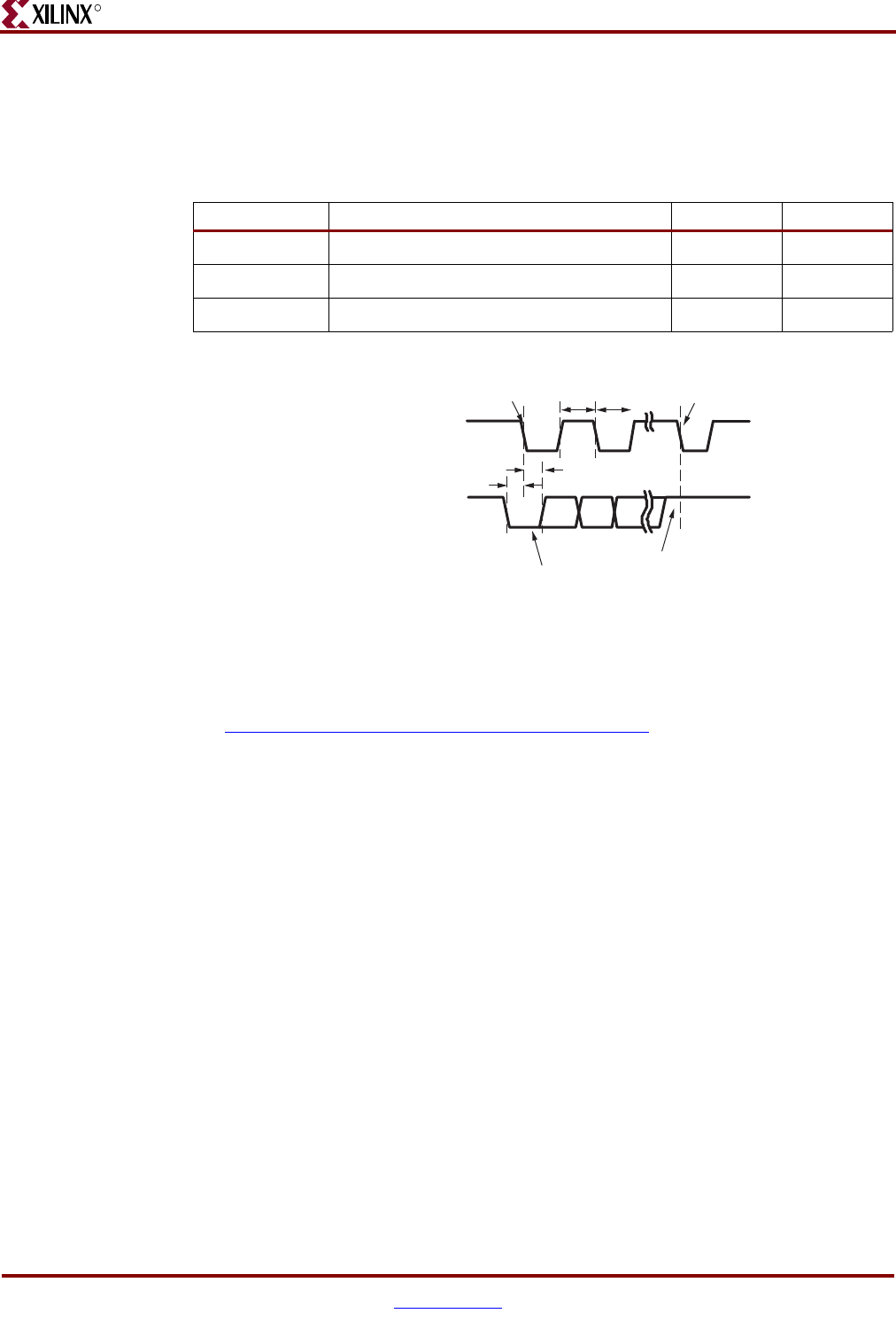
VGA signal timing is specified, published, copyrighted, and sold by the Video Electronics
Standards Association (VESA). The following VGA system and timing information is
provided as an example of how the FPGA might drive VGA monitor in 640 by 480 mode.
For more precise information or for information on higher VGA frequencies, refer to
documents available on the VESA website or other electronics websites:
•Video Electronics Standards Association
http://www.vesa.org
•VGA Timing Information
http://www.epanorama.net/documents/pc/vga_timing.html
Signal Timing for a 60Hz, 640x480 VGA Display
CRT-based VGA displays use amplitude-modulated, moving electron beams (or cathode
rays) to display information on a phosphor-coated screen. LCD displays use an array of
switches that can impose a voltage across a small amount of liquid crystal, thereby
changing light permitivity through the crystal on a pixel-by-pixel basis. Although the
following description is limited to CRT displays, LCD displays have evolved to use the
Table 5-1: VGA Port Connections to the Spartan-3 FPGA
Signal FPGA Pin
Red (R) R12
Green (G) T12
Blue (B) R11
Horizontal Sync (HS) R9
Vertical Sync (VS) T10
Table 5-2: 3-Bit Display Color Codes
Red (R) Green (G) Blue (B) Resulting Color
0 0 0 Black
0 0 1 Blue
0 1 0 Green
0 1 1 Cyan
1 0 0 Red
1 0 1 Magenta
1 1 0 Yellow
1 1 1 White
Spartan-3 FPGA Starter Kit Board User Guide www.xilinx.com 23
UG130 (v1.2) June 20, 2008
Signal Timing for a 60Hz, 640x480 VGA Display
R
same signal timings as CRT displays. Consequently, the following discussion pertains to
both CRTs and LCD displays.
Within a CRT display, current waveforms pass through the coils to produce magnetic
fields that deflect electron beams to transverse the display surface in a “raster” pattern,
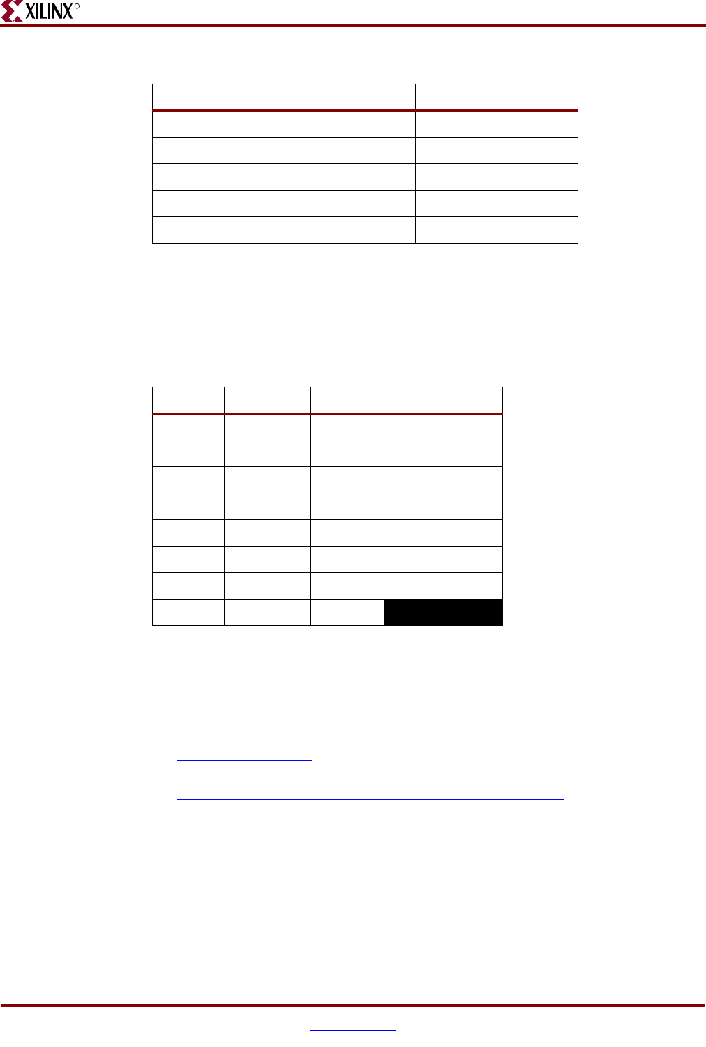
horizontally from left to right and vertically from top to bottom. As shown in Figure 5-2,
information is only displayed when the beam is moving in the “forward” direction—left to
right and top to bottom—and not during the time the beam returns back to the left or top
edge of the display. Much of the potential display time is therefore lost in “blanking”
periods when the beam is reset and stabilized to begin a new horizontal or vertical display
pass.
The size of the beams, the frequency at which the beam traces across the display, and the
frequency at which the electron beam is modulated determine the display resolution.
Figure 5-2: CRT Display Timing Example
Current
through the
horizontal
deflection
coil
Stable current ramp: Information is
displayed during this time
Retrace: No
information
is displayed
during
this time
Total horizontal time
Horizontal display time
Horizontal sync signal
sets the retrace frequency
retrace time
time
HS
"front porch"
"back porch"
VGA Display
640 pixels are displayed each
time the beam traverses the screen
pixel 0,639
pixel 0,0
pixel 479,0 pixel 479,639
"back porch"
UG130_c5_02_051305
24 www.xilinx.com Spartan-3 FPGA Starter Kit Board User Guide
UG130 (v1.2) June 20, 2008
Chapter 5: VGA Port
R
Modern VGA displays support multiple display resolutions, and the VGA controller
dictates the resolution by producing timing signals to control the raster patterns. The
controller produces TTL-level synchronizing pulses that set the frequency at which current
flows through the deflection coils, and it ensures that pixel or video data is applied to the
electron guns at the correct time.
Video data typically comes from a video refresh memory with one or more bytes assigned
to each pixel location. The Spartan-3 Starter Kit board uses three bits per pixel, producing
one of the eight possible colors shown in Table 5-2. The controller indexes into the video
data buffer as the beams move across the display. The controller then retrieves and applies
video data to the display at precisely the time the electron beam is moving across a given
pixel.
As shown in Figure 5-2, the VGA controller generates the HS (horizontal sync) and VS
(vertical sync) timings signals and coordinates the delivery of video data on each pixel
clock. The pixel clock defines the time available to display one pixel of information. The VS
signal defines the “refresh” frequency of the display, or the frequency at which all
information on the display is redrawn. The minimum refresh frequency is a function of the
display’s phosphor and electron beam intensity, with practical refresh frequencies in the
60 Hz to 120 Hz range. The number of horizontal lines displayed at a given refresh
frequency defines the horizontal “retrace” frequency.
VGA Signal Timing
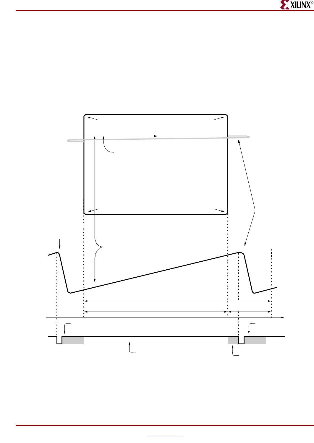
The signal timings in Table 5-3 are derived for a 640-pixel by 480-row display using a
25 MHz pixel clock and 60 Hz ±1 refresh. Figure 5-3 shows the relation between each of the
timing symbols. The timing for the sync pulse width (TPW) and front and back porch
intervals (TFP and TBP) are based on observations from various VGA displays. The front
and back porch intervals are the pre- and post-sync pulse times. Information cannot be
displayed during these times.
Table 5-3: 640x480 Mode VGA Timing
Symbol Parameter Vertical Sync Horizontal Sync
Time Clocks Lines Time Clocks
TSSync pulse time 16.7 ms 416,800 521 32 μs800
TDISP Display time 15.36 ms 384,000 480 25.6 μs640
TPW Pulse width 64 μs 1,600 2 3.84 μs96
TFP Front porch 320 μs 8,000 10 640 ns 16
TBP Back porch 928 μs 23,200 29 1.92 μs48
Figure 5-3: VGA Control Timing
TFP
TDISP
TS
TPW TBP
UG130_c5_03_051305

Spartan-3 FPGA Starter Kit Board User Guide www.xilinx.com 25
UG130 (v1.2) June 20, 2008
VGA Signal Timing
R
Generally, a counter clocked by the pixel clock controls the horizontal timing. Decoded
counter values generate the HS signal. This counter tracks the current pixel display
location on a given row.
A separate counter tracks the vertical timing. The vertical-sync counter increments with
each HS pulse and decoded values generate the VS signal. This counter tracks the current
display row. These two continuously running counters form the address into a video
display buffer. For example, the on-board fast SRAM is an ideal display buffer.
No time relationship is specified between the onset of the HS pulse and the onset of the VS
pulse. Consequently the counters can be arranged to easily form video RAM addresses, or
to minimize decoding logic for sync pulse generation.

Spartan-3 FPGA Starter Kit Board User Guide www.xilinx.com 27
UG130 (v1.2) June 20, 2008
R
Chapter 6
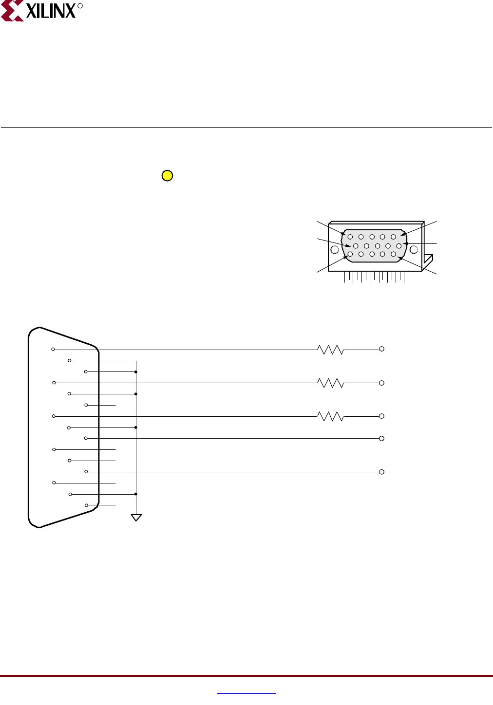
PS/2 Mouse/Keyboard Port
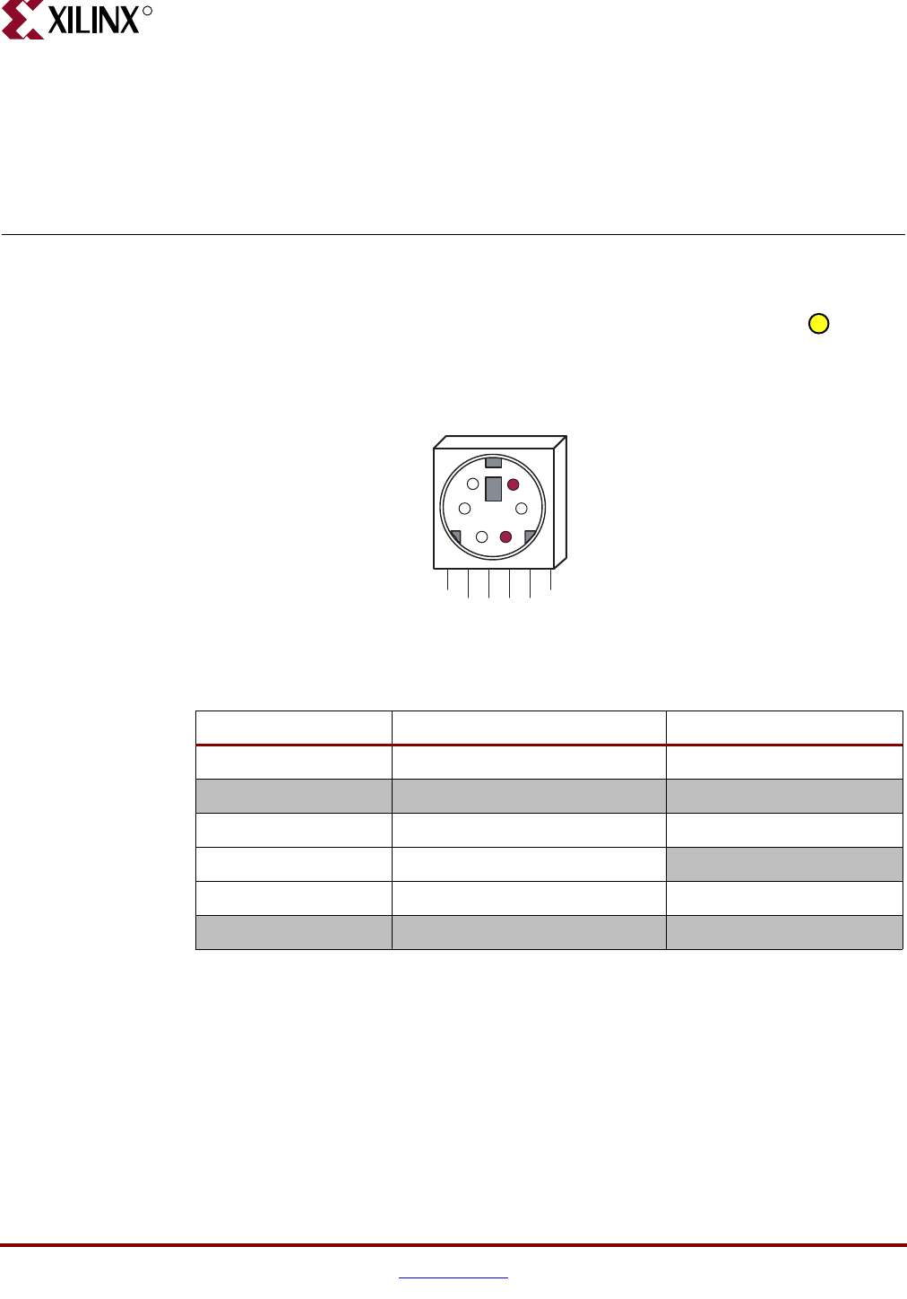
The Spartan®-3 FPGA Starter Kit board includes a PS/2 mouse/keyboard port and the
standard 6-pin mini-DIN connector, labeled J3 on the board and indicated as in
Figure 1-2. Figure 6-1 shows the PS/2 connector, and Table 6-1 shows the signals on the
connector. Only pins 1 and 5 of the connector attach to the FPGA. A detailed schematic
appears in Figure A-7.
Both a PC mouse and keyboard use the two-wire PS/2 serial bus to communicate with a
host device, the Spartan-3 FPGA in this case. The PS/2 bus includes both clock and data.
Both a mouse and keyboard drive the bus with identical signal timings and both use 11-bit
words that include a start, stop and odd parity bit. However, the data packets are
organized differently for a mouse and keyboard. Furthermore, the keyboard interface
allows bidirectional data transfers so the host device can illuminate state LEDs on the
keyboard.
The PS/2 bus timing appears Table 6-2 and Figure 6-2. The clock and data signals are only
driven when data transfers occur, and otherwise they are held in the idle state at logic
High. The timings define signal requirements for mouse-to-host communications and
Figure 6-1: PS/2 DIN Connector
Table 6-1: PS/2 Connections to the Spartan-3 FPGA
PS/2 DIN Pin Signal FPGA Pin
1DATA (PS2D) M15
2Reserved —
3GND GND
4Voltage Supply —
5CLK (PS2C) M16
6Reserved —
9
1
53
2
46
UG130_c6_01_042404
28 www.xilinx.com Spartan-3 FPGA Starter Kit Board User Guide
UG130 (v1.2) June 20, 2008
Chapter 6: PS/2 Mouse/Keyboard Port
R
bidirectional keyboard communications. As shown in Figure 6-2, the attached keyboard or
mouse writes a bit on the data line when the clock signal is High, and the host reads the
data line when the clock signal is Low.
The following site contains additional information on the PS/2 bus protocol:
•PS/2 Mouse/Keyboard Protocol
http://www.computer-engineering.org/ps2protocol/
Keyboard
The keyboard uses open-collector drivers so that either the keyboard or the host can drive
the two-wire bus. If the host never sends data to the keyboard, then the host can use simple
input pins.
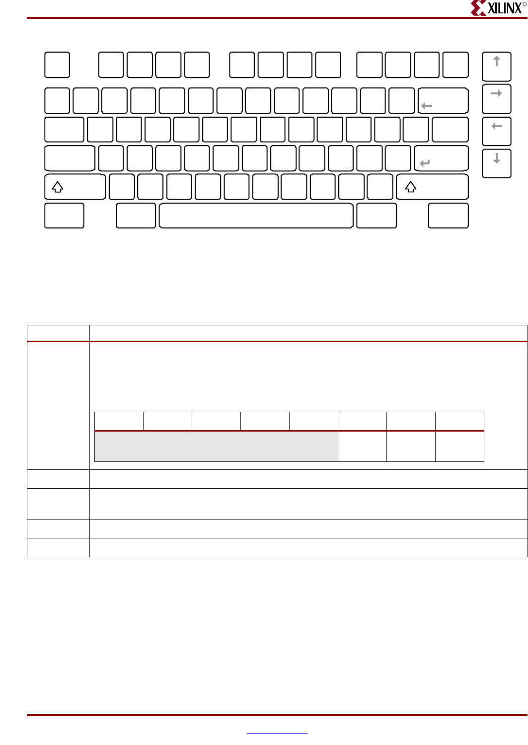
A PS/2-style keyboard uses scan codes to communicate key press data. Nearly all
keyboards in use today are PS/2 style. Each key has a single, unique scan code that is sent
whenever the corresponding key is pressed. The scan codes for most keys appear in
Figure 6-3.
If the key is pressed and held, the keyboard repeatedly sends the scan code every 100 ms or
so. When a key is released, the keyboard sends a “F0” key-up code, followed by the scan
code of the released key. The keyboard sends the same scan code, regardless if a key has
different “shift” and “non-shift” characters and regardless whether the Shift key is pressed
or not. The host determines which character is intended.
Some keys, called extended keys, send an “E0” ahead of the scan code and furthermore,
they may send more than one scan code. When an extended key is released, a “E0 F0” key-
up code is sent, followed by the scan code.
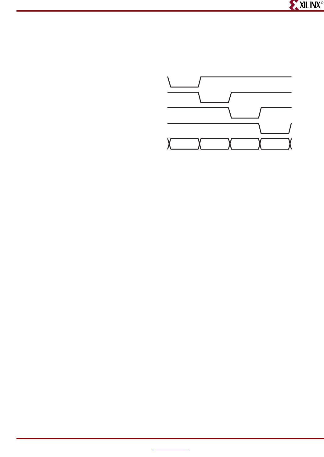
Table 6-2: PS/2 Bus Timing
Symbol Parameter Min Max
TCK Clock High or Low time 30 μs50 μs
TSU Data-to-clock setup time 5 μs25 μs
THLD Clock-to-data hold time 5 μs25 μs
Figure 6-2: PS/2 Bus Timing Waveforms
TCK
TSU THLD
TCK
Edge 0 Edge 10
CLK (PS2C)
DATA (PS2D)
'0' start bit '1' stop bit
UG130_c6_02_042404
Spartan-3 FPGA Starter Kit Board User Guide www.xilinx.com 29
UG130 (v1.2) June 20, 2008
Keyboard
R
The host can also send data to the keyboard. Table 6-3 provides a short list of some often-
used commands.
The keyboard sends data to the host only when both the data and clock lines are High, the
Idle state.
Because the host is the “bus master”, the keyboard checks whether the host is sending data
before driving the bus. The clock line can be used as a “clear to send” signal. If the host
pulls the clock line Low, the keyboard must not send any data until the clock is released.
The keyboard sends data to the host in 11-bit words that contain a ‘0’ start bit, followed by
eight bits of scan code (LSB first), followed by an odd parity bit and terminated with a ‘1’
stop bit. When the keyboard sends data, it generates 11 clock transitions at around 20 to
30 kHz, and data is valid on the falling edge of the clock as shown in Figure 6-2.
Figure 6-3: PS/2 Keyboard Scan Codes
ESC
76
` ~
0E
TAB
0D
Caps Lock
58
Shift
12
Ctrl
14
1 !
16
2 @
1E
3 #
26
4 $
25
5 %
2E
Q
15
W
1D
E
24
R
2D
T
2C
A
1C
S
1B
D
23
F
2B
G
34
Z
1Z
X
22
C
21
V
2A
B
32
6 ^
36
7 &
3D
8 *
3E
9 (
46
0 )
45
- _
4E
= +
55
Back Space
66
Y
35
U
3C
I
43
O
44
P
4D
[ {
54
] }
5B
\ |
5D
H
33
J
3B
K
42
L
4B
; :
4C
' "
52
Enter
5A
N
31
M
3A
, <
41
> .
49
/ ?
4A
Shift
59
Alt
11
Space
29
Alt
E0 11
Ctrl
E0 14
F1
05
F2
06
F3
04
F4
0C
F5
03
F6
0B
F7
83
F8
0A
F9
01
F10
09
F11
78
F12
07 E0 75
E0 74
E0 6B
E0 72
UG130_c6_03_042404
Table 6-3: Common PS/2 Keyboard Commands
Command Description
ED Turn on/off Num Lock, Caps Lock, and Scroll Lock LEDs. The keyboard acknowledges receipt of
an “ED” command by replying with an “FA”, after which the host sends another byte to set LED
status. The bit positions for the keyboard LEDs appear in Table 6-4. Write a ‘1’ to the specific bit to
illuminate the associated keyboard LED.
EE Echo. Upon receiving an echo command, the keyboard replies with the same scan code “EE”.
F3 Set scan code repeat rate. The keyboard acknowledges receipt of an “F3” by returning an “FA”,
after which the host sends a second byte to set the repeat rate.
FE Resend. Upon receiving a resend command, the keyboard resends the last scan code sent.
FF Reset. Resets the keyboard.
Table 6-4: Keyboard LED Control
76543210
Ignored Caps
Lock
Num
Lock
Scroll
Lock
30 www.xilinx.com Spartan-3 FPGA Starter Kit Board User Guide
UG130 (v1.2) June 20, 2008
Chapter 6: PS/2 Mouse/Keyboard Port
R
The following site contains more information on PS/2 keyboard interfaces:
•The PS/2 Keyboard Interface
http://www.computer-engineering.org/index.php?title=PS/2_Keyboard_Interface
Mouse
A mouse generates a clock and data signal when moved; otherwise, these signals remain
High indicating the Idle state. Each time the mouse is moved, the mouse sends three 11-bit
words to the host. Each of the 11-bit words contains a ‘0’ start bit, followed by 8 data bits
(LSB first), followed by an odd parity bit, and terminated with a ‘1’ stop bit. Each data
transmission contains 33 total bits, where bits 0, 11, and 22 are ‘0’ start bits, and bits 10, 21,
and 32 are ‘1’ stop bits. The three 8-bit data fields contain movement data as shown in
Figure 6-4. Data is valid at the falling edge of the clock, and the clock period is 20 to 30 kHz.
As shown in Figure 6-5, a PS/2 mouse employs a relative coordinate system wherein
moving the mouse to the right generates a positive value in the X field, and moving to the
left generates a negative value. Likewise, moving the mouse up generates a positive value
in the Y field, and moving down represents a negative value. The XS and YS bits in the
status byte define the sign of each value, where a ‘1’ indicates a negative value.
The magnitude of the X and Y values represent the rate of mouse movement. The larger the
value, the faster the mouse is moving. The XV and YV bits in the status byte indicate when
the X or Y values exceed their maximum value, an overflow condition. A ‘1’ indicates when
Figure 6-4: PS/2 Mouse Transaction
L R 0 1 XS YS XV YV P X0 X1 X2 X3 X4 X5 X6 X7 P Y0 Y1 Y2 Y3 Y4 Y5 Y6 Y7 P
10 10
0 11
Idle state Idle state
Start bit Start bit
Stop bit Stop bit Stop bit
Start bit
Mouse status byte X direction byte Y direction byte
UG130_c6_04_042404
Figure 6-5: The Mouse Uses a Relative Coordinate System to Track Movement
(YS=0)
-Y values
+Y values
(YS=1)
+X values-X values
(XS=1) (XS=0)
UG130_c6_05_042404
Spartan-3 FPGA Starter Kit Board User Guide www.xilinx.com 31
UG130 (v1.2) June 20, 2008
Voltage Supply
R
an overflow occurs. If the mouse moves continuously, the 33-bit transmissions repeat
every 50 ms or so.
The L and R fields in the status byte indicate Left and Right button presses. A ‘1’ indicates
that the associated mouse button is being pressed.
The following site contains additional information on interfacing to a PS/2-style mouse:
•The PS/2 Mouse Interface
http://www.computer-engineering.org/index.php?title=PS/2_Mouse_Interface
Voltage Supply
Most modern keyboards and mice work equally well from a 3.3V or 5V supply. The voltage
supply for the PS/2 port is selectable via the JP2 jumper, indicated as in Figure 1-2,
located immediately above the PS/2 connector along the right edge. The 3.3V setting is
preferred as the FPGA’s output signals operate from the 3.3V supply. The JP2 jumper
should be positioned as shown in Table 6-5 by default.
Some older keyboards and mice are 5V only. Consequently, the JP2 jumper should be set
for 5V operation as shown in Table 6-5. The Spartan-3 FPGA can tolerate 5V signals due to
the 270Ω series resistors on the PS/2 data and clock signals connected to the FPGA. See the
schematic in Figure A-7 for more details.
Table 6-5: PS/2 Port Supply Voltage Options
PS/2 Port
Supply Voltage Jumper JP2
Setting
3.3V
(DEFAULT)
5V
30
JP2
3.3V
VU
3.3V
VU
JP2

Spartan-3 FPGA Starter Kit Board User Guide www.xilinx.com 33
UG130 (v1.2) June 20, 2008
R
Chapter 7
RS-232 Serial Port
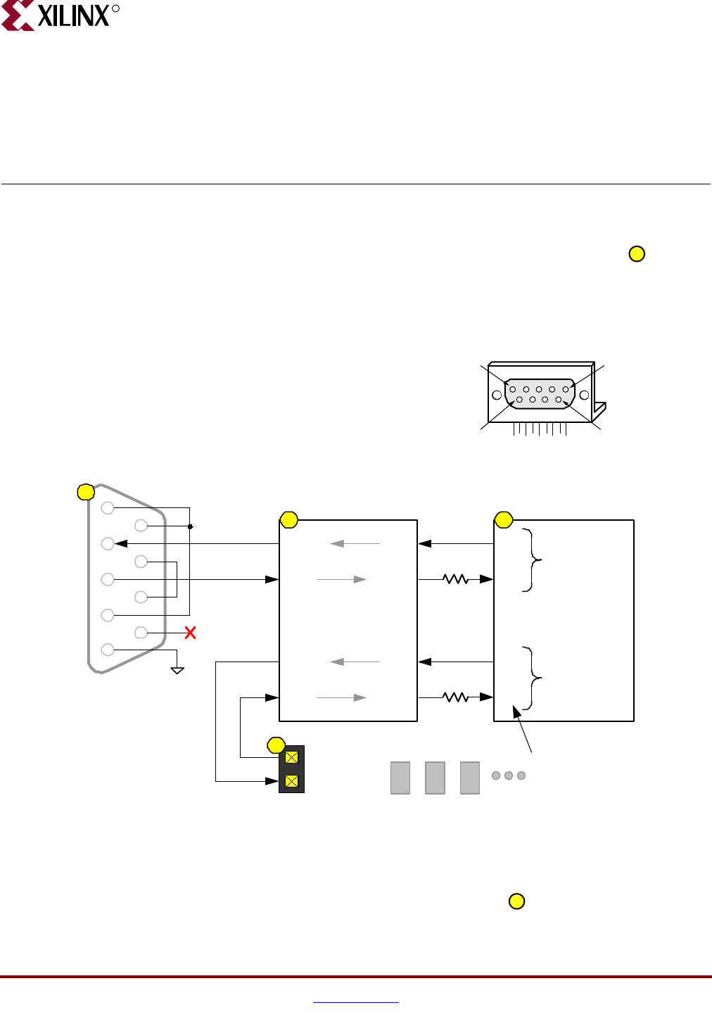
The Spartan®-3 FPGA Starter Kit board has an RS-232 serial port. The RS-232 transmit and
receive signals appear on the female DB9 connector, labeled J2, indicated as in
Figure 1-2. The connector is a DCE-style port and connects to the DB9 DTE-style serial port
connector available on most personal computers and workstations. Use a standard
straight-through serial cable to connect the Spartan-3 Starter Kit board to the PC’s serial
port.
Figure 7-1 shows the connection between the FPGA and the DB9 connector, including the
Maxim MAX3232 RS-232 voltage converter, indicated as in Figure 1-2. The FPGA
supplies serial output data as LVTTL or LVCMOS levels to the Maxim device, which in
6
Figure 7-1: RS-232 Serial Port
Pin 1
Pin 6
Pin 9
Pin 5
DB9 Serial Port Connector
(front view)
UG130_c7_01_072104
R13
T13
TXD
RXD
T14
N10
TXD-A
RXD-A
Spartan-3 FPGA1
2
3
4
5
6
7
8
9
Maxim MAX3232
RS232 Voltage
Translator
DIN1
ROUT1
DB9
Connector
DOUT1
RIN1
J1 Header
Auxiliary Serial Port
DIN2
ROUT2
DOUT2
RIN2
7
6
1
8Receiver
Transmitter
FPGA pin number
GND
LD7 LD6 LD5
7
34 www.xilinx.com Spartan-3 FPGA Starter Kit Board User Guide
UG130 (v1.2) June 20, 2008
Chapter 7: RS-232 Serial Port
R
turn, converts the logic value to the appropriate RS-232 voltage level. Likewise, the Maxim
device converts the RS-232 serial input data to LVTTL levels for the FPGA. A series resistor
between the Maxim output pin and the FPGA’s RXD pin protects against accidental logic
conflicts. A detailed schematic appears in Figure A-7.
Hardware flow control is not supported on the connector. The port’s DCD, DTR, and DSR
signals connect together, as shown in Figure 7-1. Similarly, the port’s RTS and CTS signals
connect together.
The FPGA connections to the Maxim RS-232 translator appear in Table 7-1.
An auxiliary RS-232 serial channel from the Maxim device is available on two 0.1-inch
stake pins, indicated as J1 in the schematic and in Figure 1-2. The J1 stake pins are in
the lower left corner of the board, to the right of the DB9 serial connector, below the Maxim
RS-232 voltage translator, and to the left of the individual LEDs. The transmitter output
from the Maxim device drives the bottom stake pin while the receiver input connects to the
top stake pin.
The FPGA auxiliary RS-232 connections to the Maxim device appear in Table 7-1 with
signals RXD-A and TXD-A. Ignore the pin numbers listed on the silkscreen markings next
to the stake pins as these apply to the connections to the DB9 connector.
Place a jumper across the stake pins for an easy loop-back test. Alternately, create custom
serial ports by attaching the stake pins to other types of serial connectors such as male or
female DB9 or DB25 cable connectors or even create null modem connections.
Table 7-1: Accessory Port Connections to the Spartan-3 FPGA
Signal FPGA Pin
RXD T13
TXD R13
RXD-A N10
TXD-A T14
8
Spartan-3 FPGA Starter Kit Board User Guide www.xilinx.com 35
UG130 (v1.2) June 20, 2008
R
Chapter 8
Clock Sources
The Spartan®-3 FPGA Starter Kit board has a dedicated 50 MHz Epson SG-8002JF series
clock oscillator source and an optional socket for another clock oscillator source.
Figure A-5 provides a detailed schematic for the clock sources.
The 50 MHz clock oscillator is mounted on the bottom side of the board, indicated as
in Figure A-5. Use the 50 MHz clock frequency as is or derive other frequencies using the
FPGAs Digital Clock Managers (DCMs).
•Chapter 3: Using Digital Clock Managers (DCMs) in Spartan-3 FPGAs
www.xilinx.com/support/documentation/user_guides/ug331.pdf
The oscillator socket, indicated as in Figure 1-2, accepts oscillators in an 8-pin DIP
footprint.
Table 8-1: Clock Oscillator Sources
Oscillator Source FPGA Pin
50 MHz (IC4) T9
Socket (IC8) D9
14
15
Spartan-3 FPGA Starter Kit Board User Guide www.xilinx.com 36
UG130 (v1.2) June 20, 2008
R
Chapter 9
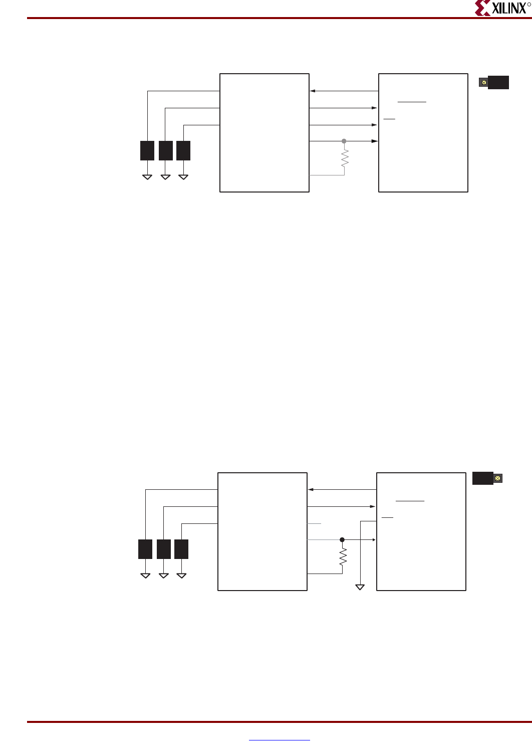
FPGA Configuration Modes and
Functions
FPGA Configuration Mode Settings
In most applications for the Spartan®-3 FPGA Starter Kit Board, the FPGA automatically
boots from the on-board Platform Flash memory whenever power is applied or the PROG
push button is pressed. However, the board supports all the available configuration modes
via the J8 header, indicated as in Figure 1-2. Table 9-1 provides the available option
settings for the J8 header. Additionally, the JP1 jumper setting is required when using
Master Serial configuration mode, as further described in “Platform Flash Jumper Options
(JP1).”
The default jumper settings for the board are:
•All jumpers in the J8 header are installed
•The JP1 jumper is in the “Default” position
16
Table 9-1: Header J8 Controls the FPGA Configuration Mode
Configuration
Mode
<M0:M1:M2>
Header J8
Settings Jumper JP1
Setting Description
Master Serial
<0:0:0> or
DEFAULT. The FPGA automatically boots from the Platform
Flash.
The FPGA attempts to boot from a serial configuration source
attached to either expansion connector A2 or B1.
Slave Serial
<1:1:1>
Another device connected to either the A2 or B1 expansion
connector provides serial data and clock to load the FPGA.
Master Parallel
<1:1:0>
The FPGA attempts to boot from a parallel configuration source
attached to the B1 expansion connector.
M0 M1 M2
J8
GND
MODE
JP1
JP1
JP1
M0 M1 M2
MODE
J8
GND
JP1
MODE
M0 M1 M2
J8
GND
JP1
Spartan-3 FPGA Starter Kit Board User Guide www.xilinx.com 37
UG130 (v1.2) June 20, 2008
Program Push Button/DONE Indicator LED
R
Program Push Button/DONE Indicator LED
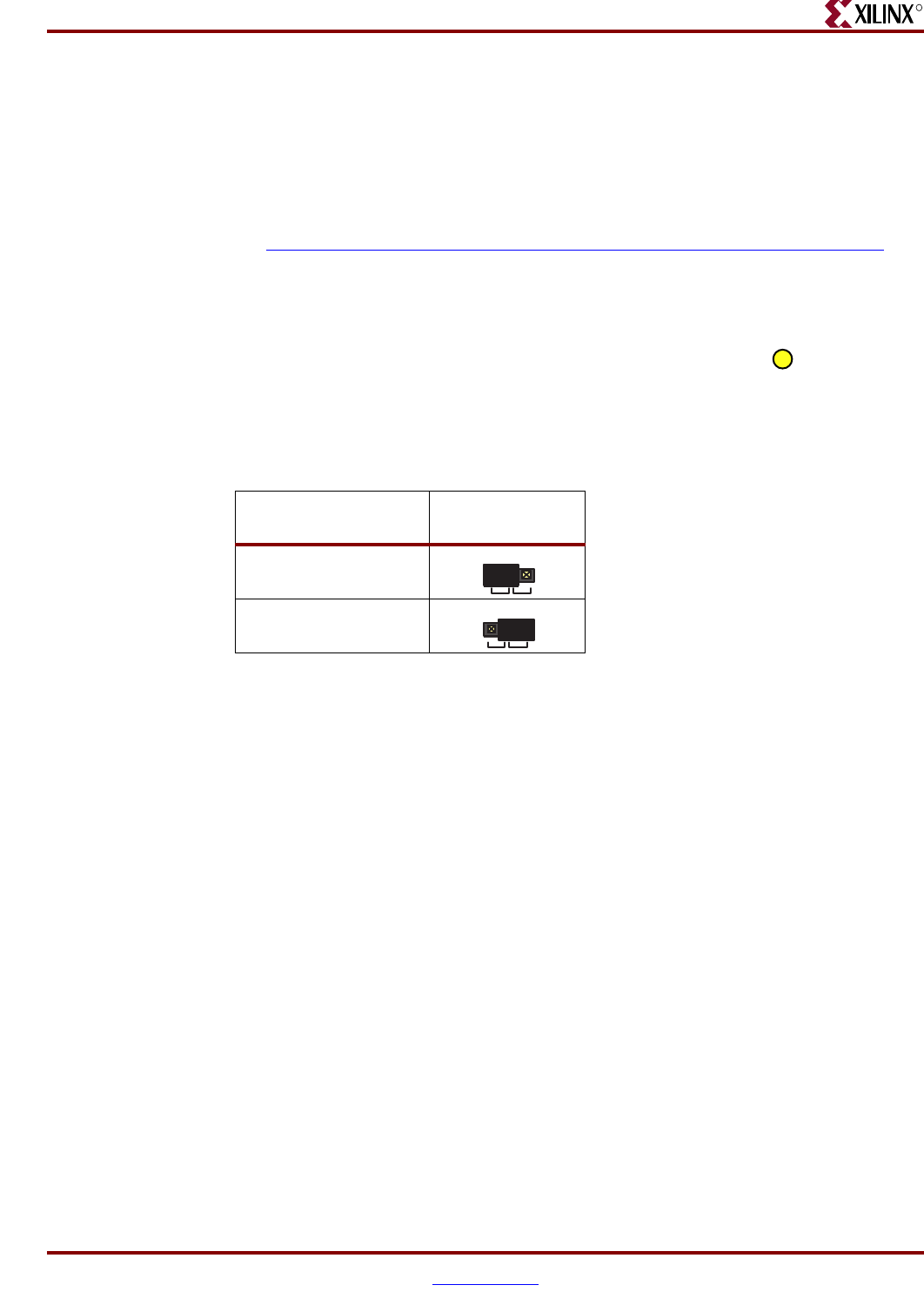
The Spartan-3 Starter Kit Board includes two FPGA configuration functions, located near
the VGA connector and the AC power input connector, as shown in Figure 9-1. The PROG
push button, shown as in Figure 9-1, drives the FPGA’s PROG_B programming pin.
When pressed, the PROG push button forces the FPGA to reconfigure and reload it
configuration data.
The DONE LED, shown as in Figure 9-1, connects to the FPGA’s DONE pin and lights
up when the FPGA is successfully configured.
Slave Parallel
<0:1:1>
Another device connected to the B1 expansion connector
provides parallel data and clock to load the FPGA.
JTAG
<1:0:1>
The FPGA waits for configuration via the four-wire JTAG
interface.
Table 9-1: Header J8 Controls the FPGA Configuration Mode (Continued)
Configuration
Mode
<M0:M1:M2>
Header J8
Settings Jumper JP1
Setting Description
MODE
M0 M1 M2
J8
GND
JP1
MODE
M0 M1 M2
J8
GND
JP1
Figure 9-1: The PROG Button and the DONE LED
17
18
PROG
DONE
VGA
VGA
UG130_c9_03_042704
17
18
Spartan-3 FPGA Starter Kit Board User Guide www.xilinx.com 38
UG130 (v1.2) June 20, 2008
R
Chapter 10
Platform Flash Configuration Storage
The Spartan®-3 FPGA Starter Kit board has an XCF02S serial configuration Flash PROM to
store FPGA configuration data and potentially additional non-volatile data, including
MicroBlaze application code. To configure the FPGA from Platform Flash memory, all
three jumpers must be installed on the J8 header, indicated as in Figure 1-2.
Platform Flash Jumper Options (JP1)
The Platform Flash has three optional settings controlled by the JP1 jumper, which is
located in the upper right-hand corner of the board, adjacent to the Platform Flash
configuration PROM. The JP1 jumper is indicated as in Figure 1-2. A detailed
schematic is provided in Figure A-4. Table 10-1 summarizes the available options, which
are described in more detail below.
“Default” Option
For most applications, this is the default jumper setting. As shown in Figure 10-1, the
Platform Flash is enabled only during configuration when the FPGA’s DONE pin is Low.
When the DONE pin goes High at the end of configuration, the Platform Flash is disabled
and placed in low-power mode.
16
3
Table 10-1: Jumper JP1 Controls the Platform Flash Options
Option Jumper JP1
Setting Description
Default The FPGA boots from Platform Flash. No additional data storage is available.
Flash Read The FPGA boots from Platform Flash, which is permanently enabled. The FPGA
can read additional data from Platform Flash.
Disable Jumper removed. Platform Flash is disabled. Other configuration data source
provides FPGA boot data.
JP1
JP1
JP1
Spartan-3 FPGA Starter Kit Board User Guide www.xilinx.com 39
UG130 (v1.2) June 20, 2008
“Flash Read” Option
R
“Flash Read” Option
The Spartan-3 Starter Kit Board includes a 2Mbit Platform Flash configuration PROM. The
XC3S200 FPGA on the board only requires slightly less than 1Mbit for configuration data.
The remainder of the Platform Flash is available to store other non-volatile data, such as
revision codes, serial numbers, coefficients, an Ethernet MAC ID, or code for an embedded
processor, such as MicroBlaze, within the FPGA.
To allow the FPGA to read from Platform Flash after configuration, the JP1 jumper must be
properly positioned, as shown in Figure 10-2. When the jumper is in this position, the
Platform Flash is always enabled. After FPGA configuration completes, the FPGA
application drives the INIT_B pin High, FPGA pin N9. Consequently, the Platform Flash
data pointer is not reset and points to the additional data following the FPGA
configuration data. To read any subsequent data, the FPGA application generates
additional clock pulses on the RCLK signal from FPGA pin A14. After configuration, the
FPGA’s CCLK output is three-stated with a pull-up resistor to VCCAUX (2.5V). The
Platform Flash presents serial data on the FPGA’s DIN pin, pin M11.
The resistor between the CCLK output and FPGA pin A14 prevents any accidental
conflicts between the two signals.
Figure 10-1: Default Platform Flash Option
CCLK
INIT_B
USER I/O
DONE
CLK
D0
OE/RESET
CE
DIN/D0M0
M1
M2
Spartan-3 FPGA Platform Flash
J8
MODE
JP1
Default
RCLK
UG130_c10_01_060704
Figure 10-2: Read Additional Data from Platform Flash by Setting the JP1 Jumper
CCLK
INIT_B
USER I/O
DONE
CLK
D0
OE/RESET
CE
DIN/D0M0
M1
M2
Spartan-3 FPGA Platform Flash
J8
MODE
RCLK
UG130_c10_02_060404
Flash Read
JP1
(M11)
(N9)
(A14)
(xx) = FPGA pin number
40 www.xilinx.com Spartan-3 FPGA Starter Kit Board User Guide
UG130 (v1.2) June 20, 2008
Chapter 10: Platform Flash Configuration Storage
R
Additional FPGA logic is required to read the Platform Flash data, as described in the
following application note.
•XAPP694: Reading User Data from Configuration PROMs
www.xilinx.com/support/documentation/application_notes/xapp694.pdf
“Disable” Option
If the JP1 jumper is removed, then the Platform Flash is disabled, potentially allowing
configuration via an expansion board connected to one of the expansion connectors.
Spartan-3 FPGA Starter Kit Board User Guide www.xilinx.com 41
UG130 (v1.2) June 20, 2008
R
Chapter 11
JTAG Programming/Debugging Ports
The Spartan®-3 FPGA Starter Kit board includes a JTAG programming and debugging
chain. Both the Spartan-3 FPGA and the Platform Flash devices are part of the JTAG chain,
as shown in Figure 11-1. Additionally, there are two JTAG headers for driving the JTAG
signals from various supported JTAG download and debugging cables. A Digilent JTAG3
low-cost parallel to JTAG cable is included as part of the kit and connects to the J7 header.
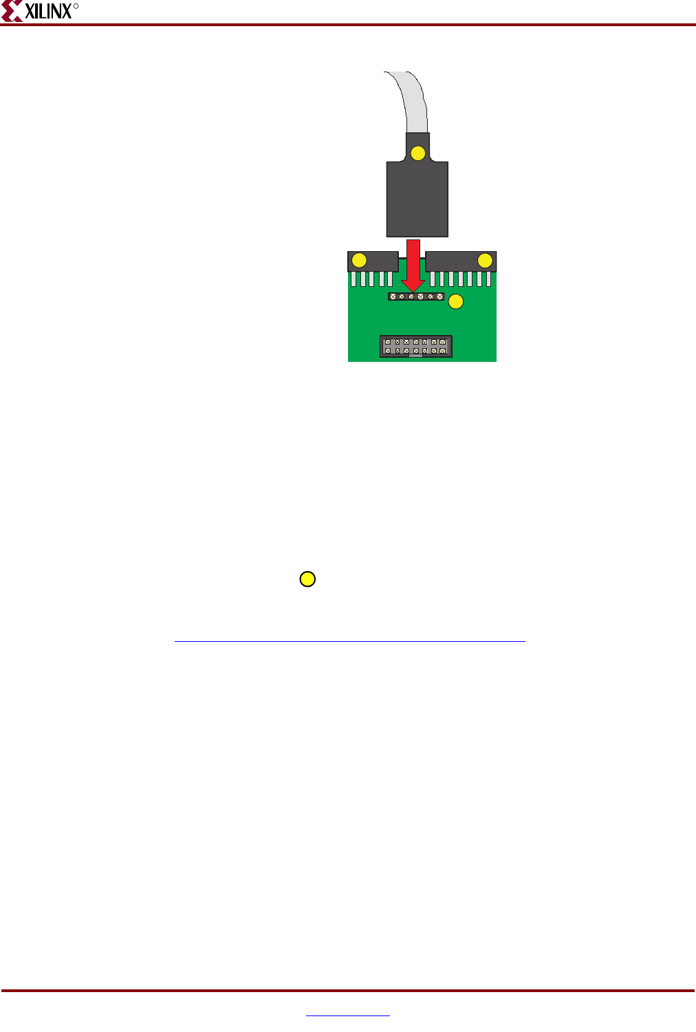
JTAG Header (J7)
This J7 JTAG header consists of 0.1-inch stake pins and is indicated as in Figure 1-2,
located toward the top edge of the board, directly below the two expansion connectors.
The Digilent low-cost parallel port to JTAG cable fits directly over the J7 header stake pins,
as shown in Figure 11-2. When properly fitted, the cable is perpendicular to the board.
Make sure that the signals at the end of the JTAG cable align with the labels listed on the
board. The other end of the Digilent cable connects to the PC’s parallel port. The Digilent
cable is directly compatible with the Xilinx iMPACT software. The schematic for the
Digilent cable appears in Figure A-9.
Figure 11-1: Spartan-3 Starter Kit Board JTAG Chain
TDI
TMS
TCK
TDO
Spartan-3 FPGA
(XC3S400FT256C)
TDI
TMS
TCK
TDO
PlatformFlash
(XCF02S)
4
6
8
Header
J5
2
1
4
5
Header
J7
10
Digilent
JTAG3 Parallel
Cable IV
Parallel
Cable 3 MultiPro
Desktop
Tool
xHeader pin number
22 24
UG130_c11_01_042504
22
42 www.xilinx.com Spartan-3 FPGA Starter Kit Board User Guide
UG130 (v1.2) June 20, 2008
Chapter 11: JTAG Programming/Debugging Ports
R
The J7 header also supports the Xilinx Parallel Cable 3 (PC3) download/debugging cable
when using the flying leaders. Again, make sure that the signals at the end of the JTAG
cable align with the labels listed on the board.
Figure A-4 provides a detailed schematic of the J7 header and the JTAG programming
chain.
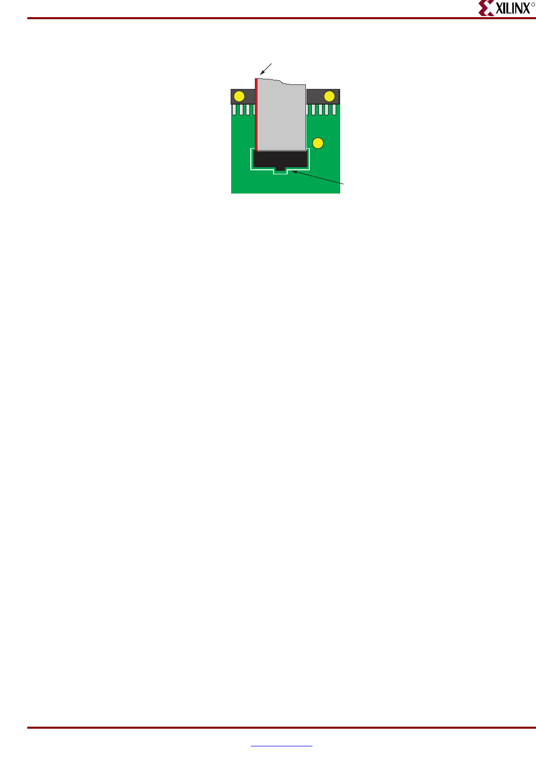
Parallel Cable IV/MultiPro Desktop Tool JTAG Header (J5)
The J5 header, shown as in Figure 1-2, supports the Xilinx download/debugging cable
listed below:
•Parallel Cable IV (PC IV)
http://www.xilinx.com/products/devkits/HW-PC4.htm
Use the 14-pin ribbon cable supplied with both cables to connect to the J5 header. DO NOT
use the flying leads that are also provided with some cables. Although the MultiPro
Desktop Tool and the Parallel Cable IV support multiple FPGA configuration modes, the
Spartan-3 Starter Kit board only supports the JTAG configuration method. The header is
designed for a keyed socket. However, the Spartan-3 Starter Kit uses only stake pins. The
outline of the keyed connector appears around the J5 header, as shown in Figure 11-3.
When properly inserted, the keyed header matches the outline on the board and the ribbon
cable crosses over the top edge of the board. The red-colored lead indicates pin 1 on the
cable and should be on the left side.
Figure 11-2: Digilent JTAG Cable Provided with Kit Connects to the J7 Header
TMS
TDI
TDO
TCK
GND
VDD
2.8V
UP TO 5V
J7
UG130_c11_02_042704
23
21 20
22
TMS
TDI
TDO
TCK
GND
VCC
24
Spartan-3 FPGA Starter Kit Board User Guide www.xilinx.com 43
UG130 (v1.2) June 20, 2008
Parallel Cable IV/MultiPro Desktop Tool JTAG Header (J5)
R
Figure 11-3: Use 14-Pin Ribbon Cable to Connect Parallel Cable IV or the MultiPro
Desktop Tool to the J5 Header
J5
Parallel Cable IV
JTAG
Red trace
indicates pin 1
Notch on outline
matches key on header
24
2021
UG130_c11_03_042704

Spartan-3 FPGA Starter Kit Board User Guide www.xilinx.com 45
UG130 (v1.2) June 20, 2008
R
Chapter 12
Power Distribution
AC Wall Adapter
The Spartan®-3 FPGA Starter Kit includes an international-ready AC wall adapter that
produces a +5V DC output. Connect the AC wall adapter to the barrel connector along the
left edge of the board, indicated as in Figure 1-2. There is no power switch to the board.
To disconnect power, remove the AC adapter from the wall or disconnect the barrel
connector.
The POWER indicator LED, shown as in Figure 1-2, lights up when power is properly
applied to the board. If the jumpers in the J8 header and JP1 header are properly set and
there is a valid configuration data file in the Platform Flash memory, then the DONE
indicator LED, shown as in Figure 1-2, also lights up.
The AC wall adapter is directly compatible for North America, Japan, and Taiwan locales.
Other locations might require a socket adapter to convert from the North American
standard to the local power socket standard. The AC wall adapter operates from 100V to
240V AC input, at 50 or 60 Hz.
Voltage Regulators
There are multiple voltages supplied on the Spartan-3 Starter Kit Board, as summarized in
Table 12-1.
25
26
18
Table 12-1: Voltage Supplies and Sources
Voltage Source Supplies
+5V DC AC Wall Adapter, 5V switching power supply
( in Figure 1-2)
3.3V regulator
Optionally, PS/2 port via jumper JP2 setting
Pin 1 (VU) on A1, A2, B1 expansion connectors
+3.3V DC National Semiconductor LM1086CS-ADJ 3.3V
regulator ( in Figure 1-2)
2.5V and 1.2V regulators
VCCO supply input for all FPGA I/O banks
Most components on the board
Pin 3 on A1, A2, B1 expansion connectors
+2.5V DC STMicroelectronics LF25CDT 2.5V regulator
( in Figure 1-2)
VCCAUX supply input to FPGA
+1.2V DC Fairchild Semiconductor FAN1112 1.2V
regulator ( in Figure 1-2)
VCCINT supply input to FPGA
25
27
28
29

46 www.xilinx.com Spartan-3 FPGA Starter Kit Board User Guide
UG130 (v1.2) June 20, 2008
Chapter 12: Power Distribution
R
Overall, the 5V DC switching power adapter that connects to AC wall power powers the
board. A 3.3V regulator, powered by the 5V DC supply, provides power to the inputs of
the 2.5V and 1.2V regulators. Similarly, the 3.3V regulator feeds all the VCCO voltage
supply inputs to the FPGA’s I/O banks and powers most of the components on the board.
The 2.5V regulator supplies power to the FPGA’s VCCAUX supply inputs. The VCCAUX
voltage input supplies power to Digital Clock Managers (DCMs) within the FPGA and
supplies some of the I/O structures. In specific, all of the FPGA’s dedicated configuration
pins, such as DONE, PROG_B, CCLK, and the FPGA’s JTAG pins, are powered by
VCCAUX. The FPGA configuration interface on the board is powered by 3.3V.
Consequently, the 2.5V supply has a current shunt resistor to prevent reverse current.
Finally, a 1.2V regulator supplies power to the FPGA’s VCCINT voltage inputs, which
power the FPGA’s core logic.
The board uses three discrete regulators to generate the necessary voltages. However,
various power supply vendors are developing integrated solutions specifically for
Spartan-3 FPGAs.
Figure A-3 provides a detailed schematic of the various voltage regulators. Similarly,
Figure A-6 shows the power decoupling capacitors.
Spartan-3 FPGA Starter Kit Board User Guide www.xilinx.com 47
UG130 (v1.2) June 20, 2008
R
Chapter 13
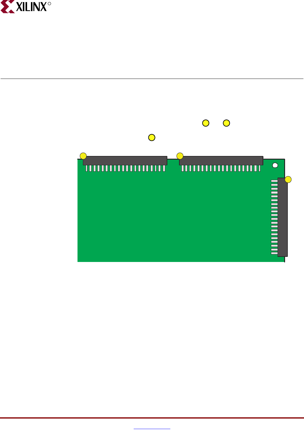
Expansion Connectors and Boards
Expansion Connectors
The Spartan®-3 FPGA Starter Kit board has three 40-pin expansion connectors labeled A1,
A2, and B1. The A1 and A2 connectors, indicated as and , respectively, in Figure 1-2,
are on the top edge of the board. Connector A1 is on the top left, and A2 is on the top right.
The B1 connector, indicated as in Figure 1-2, is along the right edge of the board.
Table 13-1 summarizes the capabilities of each expansion port. Port A1 supports a
maximum of 32 user I/O pins, while the other ports provide up to 34 user I/O pins. Some
pins are shared with other functions on the board, which may reduce the effective I/O
count for specific applications. For example, pins on the A1 port are shared with the SRAM
address signals, with the SRAM OE# and WE# control signals, and with the eight least-
significant data signals to SRAM IC10 only.
Figure 13-1: Spartan-3 Starter Kit Board Expansion Connectors
21
20
19
A2 Expansion ConnectorA1 Expansion Connector
B1 Expansion Connector
21 20
19
UG130_c12_01_042704
48 www.xilinx.com Spartan-3 FPGA Starter Kit Board User Guide
UG130 (v1.2) June 20, 2008
Chapter 13: Expansion Connectors and Boards
R
Each port offers some ability to program the FPGA on the Spartan-3 Starter Kit Board. For
example, port A1 provides additional logic to drive the FPGA and Platform Flash JTAG
chain. Similarly, ports A2 and B1 provide connections for Master or Slave Serial mode
configuration. Finally, port B1 also offers Master or Slave Parallel configuration mode.
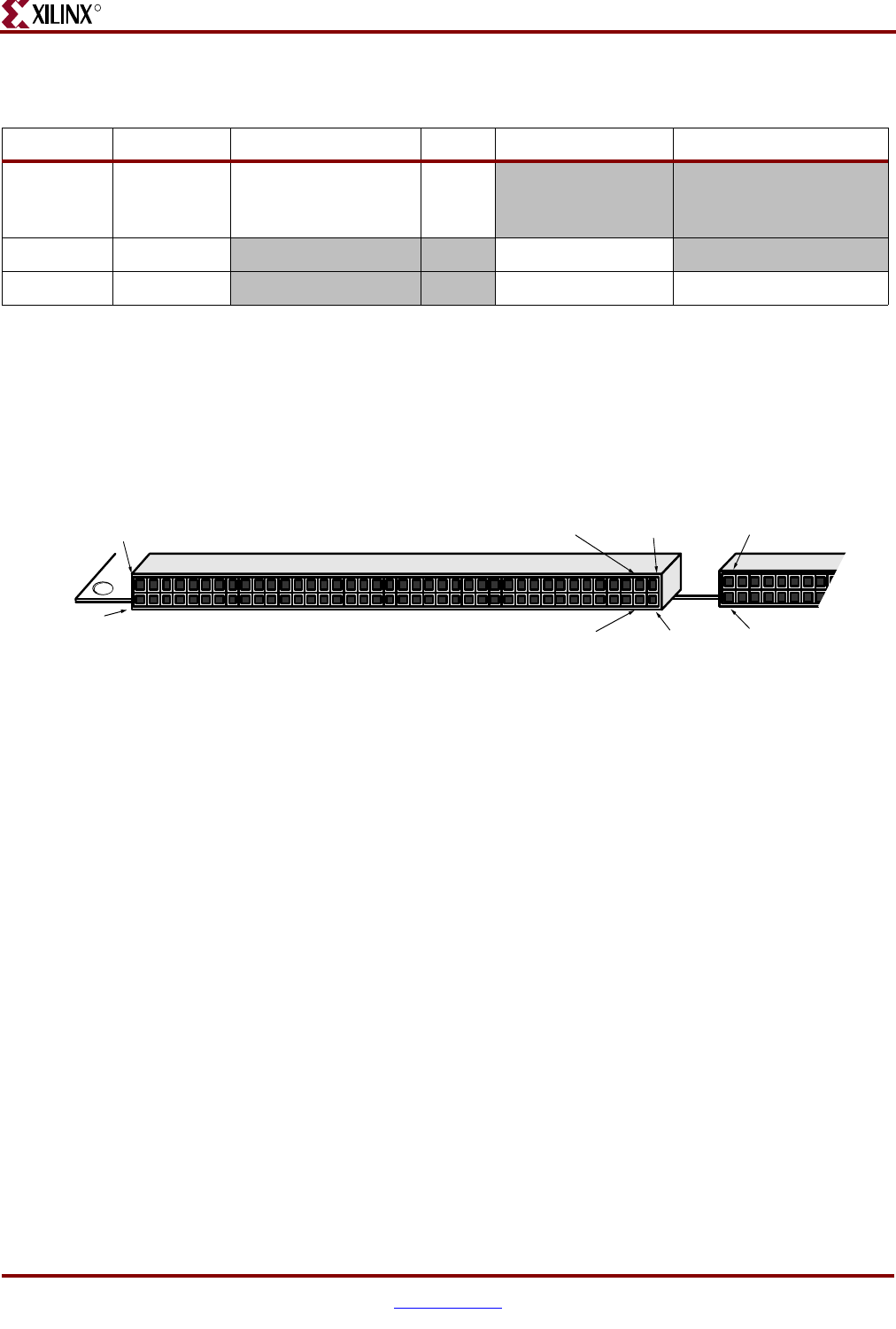
Each 40-pin expansion header, shown in Figure 13-2, uses 0.1-inch (100 mil) DIP spacing.
Pin 1 on each connector is always GND. Similarly, pin 2 is always the +5V DC output from
the switching power supply. Pin 3 is always the output from the +3.3V DC regulator.
The pinout information for each connector appears below. The tables include the
connections between the FPGA and the expansion connectors plus the signal names used
in the detailed schematic in Figure A-1.
Table 13-1: Expansion Connector Features
Connector User I/O SRAM JTAG Serial Configuration Parallel Configuration
A1 32 Address
OE#, WE#
Data[7:0] to IC10 only
√
A2 34 √
B1 34 √ √
Figure 13-2: 40-pin Expansion Connector
Pin 2: VU
Pin 3: +3.3V Pin 1: GND
Pin 39
Pin 40 Pin 4
Pin 39
Pin 40
+5V
UG130_c12_02_042504
Spartan-3 FPGA Starter Kit Board User Guide www.xilinx.com 49
UG130 (v1.2) June 20, 2008
Expansion Connectors
R
A1 Connector Pinout
The A1 expansion connector is located along the top edge of the board, on the left, as
indicated by in Figure 1-2. Table 13-2 provides the pinout for the A1 connector. The
FPGA connections are specified in parentheses.
21
Table 13-2: Pinout for A1 Expansion Connector
Schematic Name FPGA Pin Connector FPGA Pin Schematic Name
GND 1 2 VU (+5V)
VCCO (+3.3V) VCCO (all banks) 3 4 (N8) ADR0
DB0 (N7)
SRAM IC10 IO0 5 6 (L5)
SRAM A0
ADR1
DB1 (T8)
SRAM IC10 IO1 7 8 (N3)
SRAM A1
ADR2
DB2 (R6)
SRAM IC10 IO2 910 (M4)
SRAM A2
ADR3
DB3 (T5)
SRAM IC10 IO3 11 12 (M3)
SRAM A3
ADR4
DB4 (R5)
SRAM IC10 IO4 13 14 (L4)
SRAM A4
ADR5
DB5 (C2)
SRAM IC10 IO5 15 16 (G3)
SRAM WE#
WE
DB6 (C1)
SRAM IC10 IO6 17 18 (K4)
SRAM OE#
OE
DB7 (B1)
SRAM IC10 IO7 19 20 (P9)
FPGA DOUT/BUSY
CSA
LSBCLK (M7) 21 22 (M10) MA1-DB0
MA1-DB1 (F3)
SRAM A6 23 24 (G4)
SRAM A5
MA1-DB2
MA1-DB3 (E3)
SRAM A8 25 26 (F4)
SRAM A7
MA1-DB4
MA1-DB5 (G5)
SRAM A10 27 28 (E4)
SRAM A9
MA1-DB6
MA1-DB7 (H4)
SRAM A12 29 30 (H3)
SRAM A11
MA1-ASTB
MA1-DSTB (J3)
SRAM A14 31 32 (J4)
SRAM A13
MA1-WRITE
MA1-WAIT (K5)
SRAM A16 33 34 (K3)
SRAM A15
MA1-RESET
MA1-INT (L3)
SRAM A17 35 36 JTAG Isolation JTAG Isolation
TMS (C13)
FPGA JTAG TMS 37 38 (C14)
FPGA JTAG TCK
TCK
TDO-ROM Platform Flash
JTAG TDO 39 40 Header J7, pin 3 TDO-A
50 www.xilinx.com Spartan-3 FPGA Starter Kit Board User Guide
UG130 (v1.2) June 20, 2008
Chapter 13: Expansion Connectors and Boards
R
The A1 expansion connector shares connections with the 256Kx16 SRAM devices,
specifically the SRAM address lines, the OE# and WE# control signals, and the eight least-
significant data lines to SRAM IC10 only. Similarly, the JTAG chain is available on pins 36
through 40. Pin 20 is the FPGA DOUT/BUSY configuration signal and toggles during the
FPGA configuration process.
A2 Connector Pinout
The A2 expansion connector is located along the top edge of the board, on the right, as
indicated by in Figure 1-2. Table 13-3 provides the pinout for the A2 connector. The
FPGA connections are specified in parentheses.
Most of the A2 expansion connector pins connect only with the FPGA and are not shared.
Pin 35 connects to the auxiliary clock socket, if an oscillator is installed in the socket. Pins
36 through 40 include the signals required to configure the FPGA in Master or Slave Serial
mode.
20
Table 13-3: Pinout for A2 Expansion Connector
Schematic Name FPGA Pin Connector FPGA Pin Schematic Name
GND 1 2 VU (+5V)
VCCO (+3.3V) VCCO (all banks) 3 4 (E6) PA-IO1
PA-IO2 (D5) 5 6 (C5) PA-IO3
PA-IO4 (D6) 7 8 (C6) PA-IO5
PA-IO6 (E7) 910 (C7) PA-IO7
PA-IO8 (D7) 11 12 (C8) PA-IO9
PA-IO10 (D8) 13 14 (C9) PA-IO11
PA-IO12 (D10) 15 16 (A3) PA-IO13
PA-IO14 (B4) 17 18 (A4) PA-IO15
PA-IO16 (B5) 19 20 (A5) PA-IO17
PA-IO18 (B6) 21 22 (B7) MA2-DB0
MA2-DB1 (A7) 23 24 (B8) MA2-DB2
MA2-DB3 (A8) 25 26 (A9) MA2-DB4
MA2-DB5 (B10) 27 28 (A10) MA2-DB6
MA2-DB7 (B11) 29 30 (B12) MA2-ASTB
MA2-DSTB (A12) 31 32 (B13) MA2-WRITE
MA2-WAIT (A13) 33 34 (B14) MA2-RESET
MA2-INT/GCK4 (D9)
Oscillator socket 35 36 (B3)
FPGA PROG_B
PROG-B
DONE (R14)
FPGA DONE 37 38 (N9)
FPGA INIT_B
INIT
CCLK (T15)
FPGA CCLK
Connects to (A14) via
390Ω resistor
39 40
(M11) DIN
Spartan-3 FPGA Starter Kit Board User Guide www.xilinx.com 51
UG130 (v1.2) June 20, 2008
Expansion Connectors
R
B1 Connector Pinout
The B1 expansion connector is located on the right edge of the board, as indicated by in
Figure 1-2. Table 13-4 provides the pinout for the B1 connector. The FPGA connections are
specified in parentheses.
Most of the B1 expansion connector pins connect only with the FPGA and are not shared.
Pins 36 through 40 include the signals required to configure the FPGA in Master or Slave
Serial mode. These same pins plus pins 5, 7, 9, 11, 13, 15, 17, 19, and 20 provide the signals
required to configure the FPGA in Master or Slave Parallel mode.
19
Table 13-4: Pinout for B1 Expansion Connector
Schematic Name FPGA Pin Connector FPGA Pin Schematic Name
GND 1 2 VU (+5V)
VCCO (+3.3V) VCCO (all banks) 3 4 (C10) PB-ADR0
PB-DB0 (T3)
FPGA RD_WR_B config 5 6 (E10) PB-ADR1
PB-DB1 (N11)
FPGA D1 config 7 8 (C11) PB-ADR2
PB-DB2 (P10)
FPGA D2 config 910 (D11) PB-ADR3
PB-DB3 (R10)
FPGA D3 config 11 12 (C12) PB-ADR4
PB-DB4 (T7)
FPGA D4 config 13 14 (D12) PB-ADR5
PB-DB5 (R7)
FPGA D5 config 15 16 (E11) PB-WE
PB-DB6 (N6)
FPGA D6 config 17 18 (B16) PB-OE
PB-DB7 (M6)
FPGA D7 config 19 20 (R3)
FPGA CS_B config
PB-CS
PB-CLK (C15) 21 22 (C16) MB1-DB0
MB1-DB1 (D15) 23 24 (D16) MB1-DB2
MB1-DB3 (E15) 25 26 (E16) MB1-DB4
MB1-DB5 (F15) 27 28 (G15) MB1-DB6
MB1-DB7 (G16) 29 30 (H15) MB1-ASTB
MB1-DSTB (H16) 31 32 (J16) MB1-WRITE
MB1-WAIT (K16) 33 34 (K15) MB1-RESET
MB1-INT (L15) 35 36 (B3)
FPGA PROG_B
PROG-B
DONE (R14)
FPGA DONE 37 38 (N9)
FPGA INIT_B
INIT
CCLK (T15)
FPGA CCLK
Connects to (A14) via
390Ω resistor
39 40
(M11) DIN
52 www.xilinx.com Spartan-3 FPGA Starter Kit Board User Guide
UG130 (v1.2) June 20, 2008
Chapter 13: Expansion Connectors and Boards
R
Expansion Boards
Various expansion boards plug into the A1, A2, or B1 connectors as listed below:
•Spartan-3 Starter Kit Expansion Boards
www.xilinx.com/products/boards/DO-SPAR3-DK/boards/daughtercards.htm
•Digilent Expansion Boards
www.digilentinc.com/Products/Catalog.cfm?Nav1=Products&Nav2=Peripheral&Cat=Peripheral
•Digilent Breakout Probe Header (TPH1)
http://www.digilentinc.com/Products/Catalog.cfm?Cat=Accessory
•Digilent Breadboard (DBB1)
http://www.digilentinc.com/Products/Catalog.cfm?Cat=Accessory
•Digilent Wire-wrap Board (DWR1)
http://www.digilentinc.com/Products/Catalog.cfm?Cat=Accessory
•Digilent SPP, EPP, ECP Parallel Port (PIO1)
http://www.digilentinc.com/Products/Catalog.cfm?Nav1=Products&Cat=Older

Spartan-3 FPGA Starter Kit Board User Guide www.xilinx.com 53
UG130 (v1.2) June 20, 2008
R
Appendix A
Board Schematics
This appendix provides the schematics for the Spartan®-3 FPGA Starter Kit Board:
•Figure A-1, “A1, A2, and B1 Expansion Connectors”
•Figure A-2, “Slide Switches, Push Buttons, LEDs, and Four-Character 7-Segment
Display”
•Figure A-3, “Voltage Regulators, JP2 Jumper Setting for PS/2 Port Voltage”
•Figure A-4, “FPGA Configuration Interface, Platform Flash, JTAG Connections,
Jumper JP1”
•Figure A-5, “FPGA I/O Connections, Clock Sources”
•Figure A-6, “Power Decoupling Capacitors”
•Figure A-7, “RS-232 Serial Port, VGA Port, PS/2 Port, Parallel Cable IV JTAG
Interface”
•Figure A-8, “2x256Kx16 Fast Asynchronous SRAM Interface”
•Figure A-9, “Digilent JTAG3 Low-Cost JTAG Download/Debug Cable”
54 www.xilinx.com Spartan-3 FPGA Starter Kit Board User Guide
UG130 (v1.2) June 20, 2008
Appendix A: Board Schematics
R
Figure A-1: A1, A2, and B1 Expansion Connectors
UG130_ApA_01_051305
NOTE:
SRAM address lines and OE#, WE# controls have shared connections with A1 connector.
Likewise, lower eight data bits to SRAM IC10 are also shared with A1 connector.
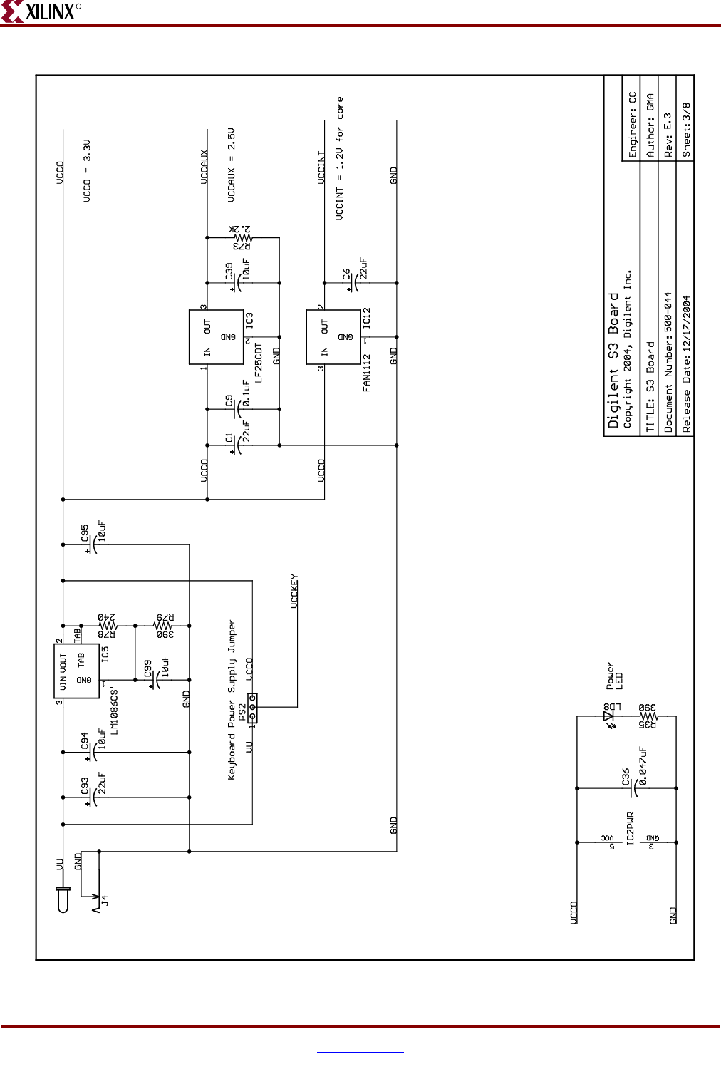
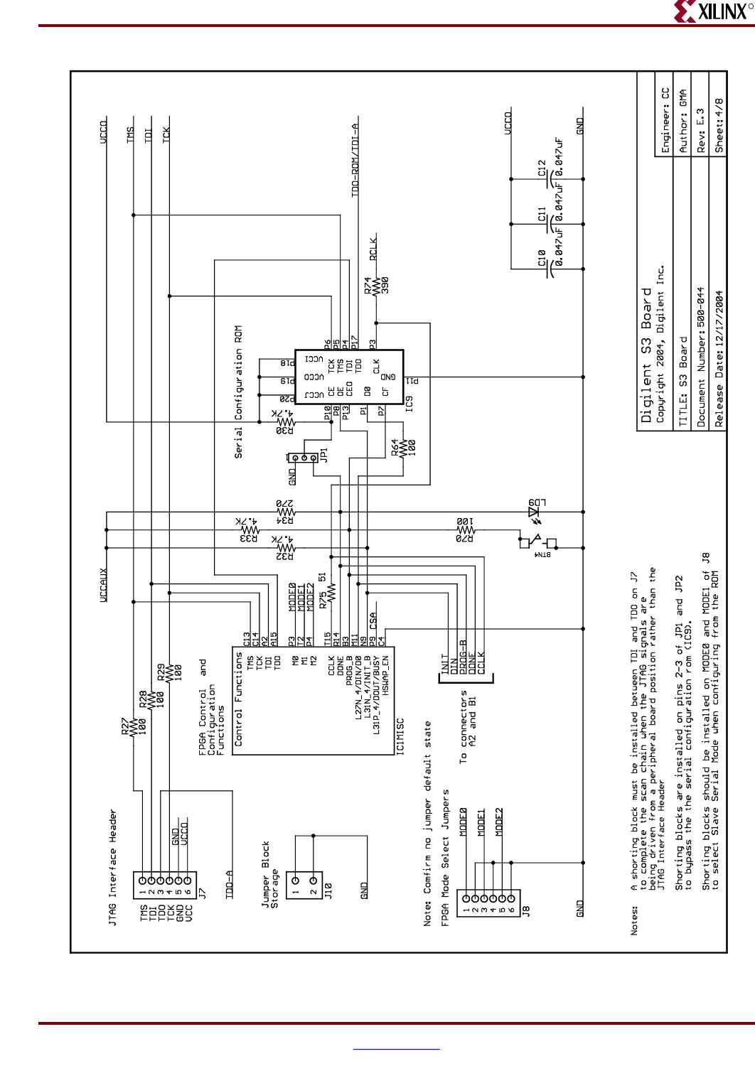
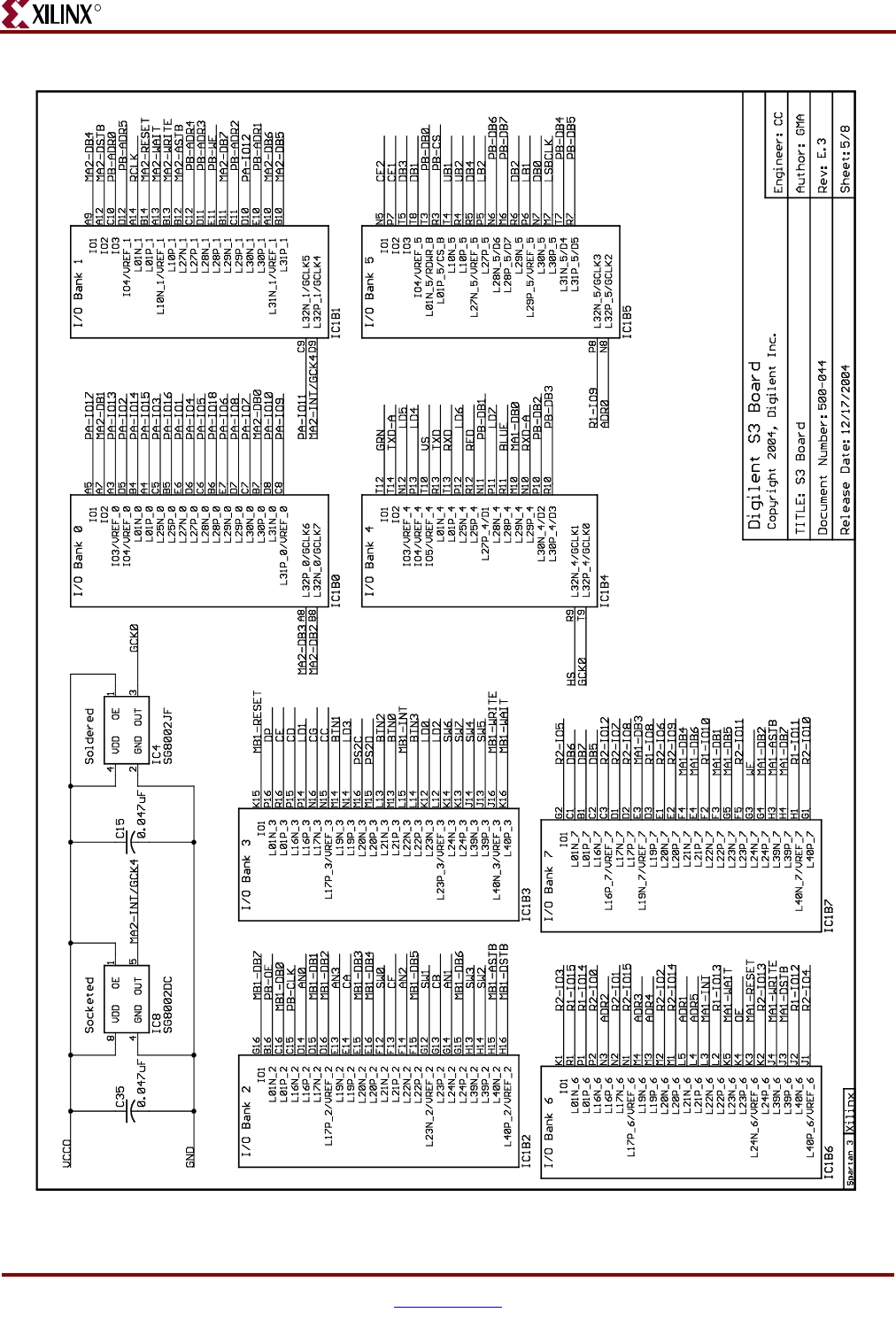
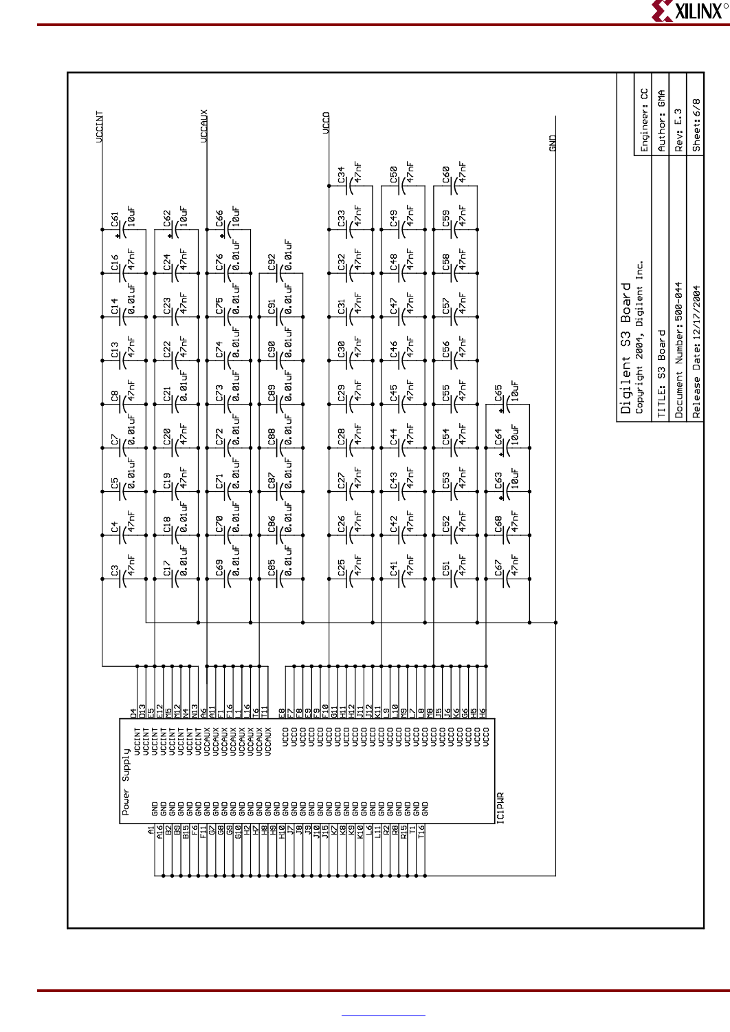
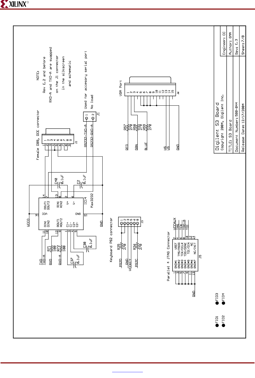
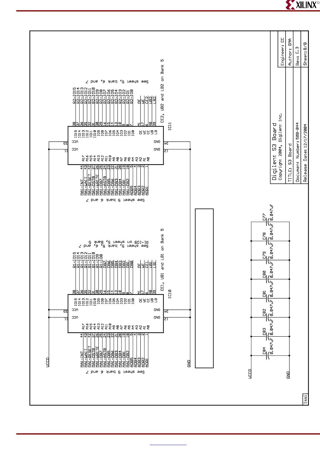
Spartan-3 FPGA Starter Kit Board User Guide www.xilinx.com 61
UG130 (v1.2) June 20, 2008
R
Figure A-8: 2x256Kx16 Fast Asynchronous SRAM Interface
UG130_ApA_08_051305
NOTE:
SRAM address lines and OE#, WE# controls have shared connections with A1 connector.
Likewise, lower eight data bits to SRAM IC10 are also shared with A1 connector.
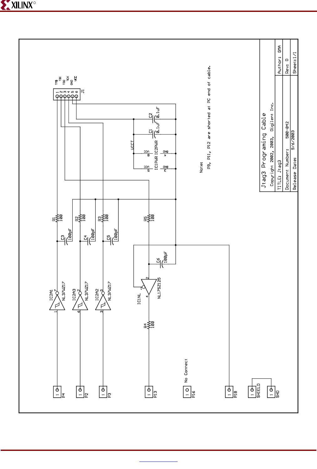
Spartan-3 FPGA Starter Kit Board User Guide www.xilinx.com 63
UG130 (v1.2) June 20, 2008
R
Appendix B
Reference Material for Major
Components
Table B-1 lists the major components on the Spartan®-3 FPGA Starter Kit Board, including
full part numbers and links to complete device data sheets.
Table B-1: Major Components and Data Sheet Links
Device Vendor Part Number Description/Data Sheet Link
(IC1)
Xilinx, Inc. XC3S200-4FT256C Spartan-3 FPGA
http://www.xilinx.com/support/documentation/data_sheets
/ds099.pdf
(IC9)
Xilinx, Inc. XCF02SVO20C Platform Flash Configuration Flash PROM
http://www.xilinx.com/support/documentation/data_sheets
/ds123.pdf
(IC10, IC11)
Integrated Silicon
Solutions, Inc. (ISSI)
IS61LV25616AL-10T 256Kx16 Fast Asynchronous SRAM
http://www.issi.com/pdf/61LV25616AL.pdf
(IC14)
Maxim, Intersil MAX3232, ICL3232 Dual-Channel RS-232 Voltage Translator
http://pdfserv.maxim-ic.com/en/ds/MAX3222-MAX3241.pdf
http://www.intersil.com/data/fn/fn4805.pdf
(IC4)
Epson SG-8002JF 50 MHz Crystal Oscillator
http://www.eea.epson.com/portal/pls/portal/docs/1/
793426.PDF
Interex APA-101M-05 5V Switching Regulator
(IC5)
National
Semiconductor
LM1086CS-ADJ 3.3V Regulator
http://www.national.com/mpf/LM/LM1086.html
(IC3)
STMicroelectronics LF25CDT 2.5V Regulator
http://www.st.com/stonline/books/pdf/docs/2574.pdf
(IC12)
Fairchild
Semiconductor
FAN1112 1.2V Regulator
http://www.fairchildsemi.com/ds/FA/FAN1112.pdf
1
2
4
7
14
25
27
28
29