BZX84 Series Voltage Regulator Diodes Nxp
User Manual: Marking of electronic components, SMD Codes Y6, Y6-, Y60, Y61, Y62, Y63, Y64, Y65, Y66, Y67, Y68, Y69, Y6W, Y6Y, Y6p, Y6t. Datasheets BZX84-A10, BZX84-A11, BZX84-A12, BZX84-A13, BZX84-A15, BZX84-A6V2, BZX84-A6V8, BZX84-A7V5, BZX84-A8V2, BZX84-A9V1, BZX84-C18, BZX84C18, BZX84C18-V, BZX84C18LT1G, CMSZDA18V, FMY6, PZU18B2A/DG, S9016, SZBZX84C18LT1G.
Open the PDF directly: View PDF ![]() .
.
Page Count: 11
DATA SHEET
Product data sheet
Supersedes data of 1999 May 18
2003 Apr 10
DISCRETE SEMICONDUCTORS
BZX84 series
Voltage regulator diodes
db
ook, halfpage
M3D088
2003 Apr 10 2
NXP Semiconductors Product data sheet
Voltage regulator diodes BZX84 series
FEATURES
•Total power dissipation: max. 250 mW
•Three tolerance series: ±1%, ±2% and approx. ±5%
•Working voltage range: nom. 2.4 to 75 V (E24 range)
•Non-repetitive peak reverse power dissipation:
max. 40 W.
APPLICATIONS
•General regulation functions.
DESCRIPTION
Low-power voltage regulator diodes in small SOT23
plastic SMD packages.
The diodes are available in the normalized E24 ±1%
(BZX84-A), ±2% (BZX84-B) and approx. ±5% (BZX84-C)
tolerance range. The series consists of 37 types with
nominal working voltages from 2.4 to 75 V.
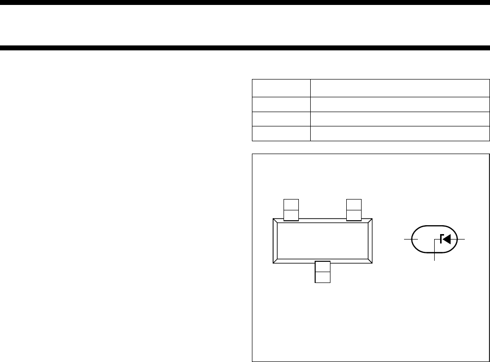
PINNING
PIN DESCRIPTION
1anode
2not connected
3cathode
Fig.1 Simplified outline (SOT23) and symbol.
handbook, halfpage
MAM243
2
n.c. 1
3
21
3
Top view
2003 Apr 10 3
NXP Semiconductors Product data sheet
Voltage regulator diodes BZX84 series
MARKING
Note
1. ∗ = p : Made in Hong Kong.
∗ = t : Made in Malaysia.
∗ = W : Made in China.
TYPE
NUMBER MARKING
CODE(1) TYPE
NUMBER MARKING
CODE(1) TYPE
NUMBER MARKING
CODE(1) TYPE
NUMBER MARKING
CODE(1)
Marking codes for BZX84-A2V4 to BZX84-A75
BZX84-A2V4 Y50 or ∗50 BZX84-A6V2 Y60 or ∗60 BZX84-A16 Y70 BZX84-A43 Y80 or ∗C5
BZX84-A2V7 Y51 or ∗51 BZX84-A6V8 Y61 or ∗61 BZX84-A18 Y71 BZX84-A47 Y81
BZX84-A3V0 Y52 or ∗52 BZX84-A7V5 Y62 or ∗62 BZX84-A20 Y72 or ∗C2 BZX84-A51 Y82 or ∗C6
BZX84-A3V3 Y53 BZX84-A8V2 Y63 or ∗63 BZX84-A22 Y73 BZX84-A56 Y83
BZX84-A3V6 Y54 or ∗C1 BZX84-A9V1 Y64 or ∗64 BZX84-A24 Y74 BZX84-A62 Y84
BZX84-A3V9 Y55 or ∗55 BZX84-A10 Y65 or ∗65 BZX84-A27 Y75 or ∗75 BZX84-A68 Y85
BZX84-A4V3 Y56 or ∗56 BZX84-A11 Y66 or ∗04 BZX84-A30 Y76 BZX84-A75 Y86 or ∗86
BZX84-A4V7 Y57 or ∗57 BZX84-A12 Y67 or ∗67 BZX84-A33 Y77 − −
BZX84-A5V1 Y58 or ∗58 BZX84-A13 Y68 or ∗C0 BZX84-A36 Y78 or ∗C3 − −
BZX84-A5V6 Y59 or ∗59 BZX84-A15 Y69 or ∗69 BZX84-A39 Y79 or ∗C4 − −
Marking codes for BZX84-B2V4 to BZX84-B75
BZX84-B2V4 Z50 or ∗Z0 BZX84-B6V2 Z60 or ∗R5 BZX84-B16 Z70 or ∗70 BZX84-B43 Z80 or ∗S5
BZX84-B2V7 Z51 or ∗Z1 BZX84-B6V8 Z61 or ∗R6 BZX84-B18 Z71 or ∗71 BZX84-B47 Z81 or ∗S6
BZX84-B3V0 Z52 or ∗S1 BZX84-B7V5 Z62 or ∗R8 BZX84-B20 Z72 or ∗72 BZX84-B51 Z82 or ∗S9
BZX84-B3V3 Z53 or ∗S2 BZX84-B8V2 Z63 or ∗R9 BZX84-B22 Z73 or ∗73 BZX84-B56 Z83 or ∗R0
BZX84-B3V6 Z54 or ∗S3 BZX84-B9V1 Z64 or ∗T1 BZX84-B24 Z74 or ∗74 BZX84-B62 Z84 or ∗R3
BZX84-B3V9 Z55 or ∗S4 BZX84-B10 Z65 or ∗66 BZX84-B27 Z75 or ∗Z5 BZX84-B68 Z85 or ∗R4
BZX84-B4V3 Z56 or ∗S7 BZX84-B11 Z66 or ∗Z6 BZX84-B30 Z76 or ∗Z4 BZX84-B75 Z86 or ∗R7
BZX84-B4V7 Z57 or ∗S8 BZX84-B12 Z67 or ∗Z7 BZX84-B33 Z77 or ∗Y1 − −
BZX84-B5V1 Z58 or ∗R1 BZX84-B13 Z68 or ∗Z8 BZX84-B36 Z78 or ∗Y2 − −
BZX84-B5V6 Z59 or ∗R2 BZX84-B15 Z69 or ∗Z9 BZX84-B39 Z79 or ∗S0 − −
Marking codes for BZX84-C2V4 to BZX84-C75
BZX84-C2V4 Z11 or ∗T3 BZX84-C6V2 Z4∗BZX84-C16 Y5∗BZX84-C43 Y15 or ∗B4
BZX84-C2V7 Z12 or ∗T4 BZX84-C6V8 Z5∗BZX84-C18 Y6∗BZX84-C47 Y16 or ∗B5
BZX84-C3V0 Z13 or ∗T9 BZX84-C7V5 Z6∗BZX84-C20 Y7∗BZX84-C51 Y17 or ∗B7
BZX84-C3V3 Z14 or ∗B1 BZX84-C8V2 Z7∗BZX84-C22 Y8∗BZX84-C56 Y18 or ∗B8
BZX84-C3V6 Z15 or ∗B2 BZX84-C9V1 Z8∗BZX84-C24 Y9∗BZX84-C62 Y19 or ∗B9
BZX84-C3V9 Z16 or ∗B3 BZX84-C10 Z9∗BZX84-C27 Y10 or ∗T2 BZX84-C68 Y20 or ∗B0
BZX84-C4V3 Z17 or ∗B6 BZX84-C11 Y1∗BZX84-C30 Y11 or ∗T5 BZX84-C75 Y21 or ∗A1
BZX84-C4V7 Z1∗BZX84-C12 Y2∗BZX84-C33 Y12 or ∗T6 − −
BZX84-C5V1 Z2∗BZX84-C13 Y3∗BZX84-C36 Y13 or ∗T7 − −
BZX84-C5V6 Z3∗BZX84-C15 Y4∗BZX84-C39 Y14 or ∗T8 − −
2003 Apr 10 4
NXP Semiconductors Product data sheet
Voltage regulator diodes BZX84 series
LIMITING VALUES
In accordance with the Absolute Maximum Rating System (IEC 60134).
Note
1. Device mounted on an FR4 printed circuit-board.
ELECTRICAL CHARACTERISTICS
Total BZX84-A and B and C series
Tj = 25 °C unless otherwise specified.
SYMBOL PARAMETER CONDITIONS MIN. MAX. UNIT
IFcontinuous forward current −200 mA
IZSM non-repetitive peak reverse current tp = 100 μs; square wave;
Tj = 25 °C prior to surge
see Tables
1 and 2
Ptot total power dissipation Tamb = 25 °C; note 1 −250 mW
PZSM non-repetitive peak reverse power
dissipation
tp = 100 μs; square wave;
Tj = 25 °C prior to surge; see Fig.2
−40 W
Tstg storage temperature −65 +150 °C
Tjjunction temperature −65 +150 °C
SYMBOL PARAMETER CONDITIONS MAX. UNIT
VFforward voltage IF = 10 mA; see Fig.3 0.9 V
IRreverse current
BZX84-A/B/C2V4 VR = 1 V 50 μA
BZX84-A/B/C2V7 VR = 1 V 20 μA
BZX84-A/B/C3V0 VR = 1 V 10 μA
BZX84-A/B/C3V3 VR = 1 V 5 μA
BZX84-A/B/C3V6 VR = 1 V 5 μA
BZX84-A/B/C3V9 VR = 1 V 3 μA
BZX84-A/B/C4V3 VR = 1 V 3 μA
BZX84-A/B/C4V7 VR = 2 V 3 μA
BZX84-A/B/C5V1 VR = 2 V 2 μA
BZX84-A/B/C5V6 VR = 2 V 1 μA
BZX84-A/B/C6V2 VR = 4 V 3 μA
BZX84-A/B/C6V8 VR = 4 V 2 μA
BZX84-A/B/C7V5 VR = 5 V 1 μA
BZX84-A/B/C8V2 VR = 5 V 700 nA
BZX84-A/B/C9V1 VR = 6 V 500 nA
BZX84-A/B/C10 VR = 7 V 200 nA
BZX84-A/B/C11 VR = 8 V 100 nA
BZX84-A/B/C12 VR = 8 V 100 nA
BZX84-A/B/C13 VR = 8 V 100 nA
BZX84-A/B/C15 to 75 VR = 0.7VZnom 50 nA
2003 Apr 10 5
NXP Semiconductors Product data sheet
Voltage regulator diodes BZX84 series
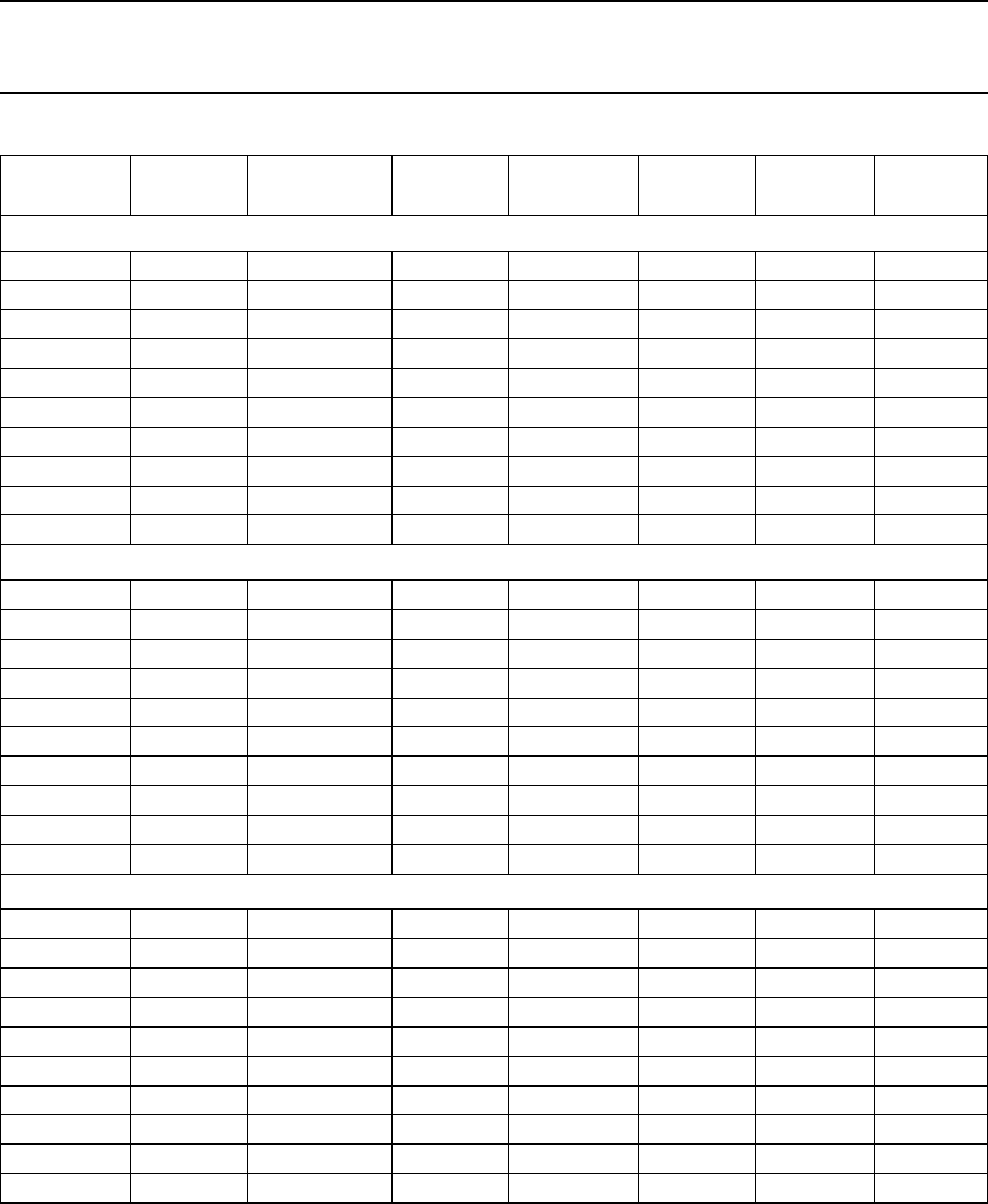
Table 1 Per type BZX84-A/B/C2V4 to A/B/C24
Tj = 25 °C unless otherwise specified.
BZX84-
Axxx
Bxxx
Cxxx
WORKING VOLTAGE
VZ (V)
at IZtest = 5 mA
DIFFERENTIAL
RESISTANCE
rdif (Ω)
TEMP. COEFF.
SZ (mV/K)
at IZtest = 5 mA
(see Figs 4 and 5)
DIODE CAP.
Cd (pF)
at f = 1 MHz;
VR = 0 V
NON-REPETITIVE
PEAK REVERSE
CURRENT
IZSM (A)
at tp = 100 μs;
Tamb = 25 °C
Tol. ±1% (A) Tol. ±2% (B) Tol. approx.
±5% (C) at
IZtest = 1 mA at
IZtest = 5 mA
MIN. MAX. MIN. MAX. MIN. MAX. TYP. MAX. TYP. MAX. MIN. TYP. MAX. MAX. MAX.
2V4 2.37 2.43 2.35 2.45 2.2 2.6 275 600 70 100 −3.5 −1.6 0450 6.0
2V7 2.67 2.73 2.65 2.75 2.5 2.9 300 600 75 100 −3.5 −2.0 0450 6.0
3V0 2.97 3.03 2.94 3.06 2.8 3.2 325 600 80 95 −3.5 −2.1 0450 6.0
3V3 3.26 3.34 3.23 3.37 3.1 3.5 350 600 85 95 −3.5 −2.4 0450 6.0
3V6 3.56 3.64 3.53 3.67 3.4 3.8 375 600 85 90 −3.5 −2.4 0450 6.0
3V9 3.86 3.94 3.82 3.98 3.7 4.1 400 600 85 90 −3.5 −2.5 0450 6.0
4V3 4.25 4.35 4.21 4.39 4.0 4.6 410 600 80 90 −3.5 −2.5 0450 6.0
4V7 4.65 4.75 4.61 4.79 4.4 5.0 425 500 50 80 −3.5 −1.4 0.2 300 6.0
5V1 5.04 5.16 5.00 5.20 4.8 5.4 400 480 40 60 −2.7 −0.8 1.2 300 6.0
5V6 5.54 5.66 5.49 5.71 5.2 6.0 80 400 15 40 −2.0 1.2 2.5 300 6.0
6V2 6.13 6.27 6.08 6.32 5.8 6.6 40 150 610 0.4 2.3 3.7 200 6.0
6V8 6.73 6.87 6.66 6.94 6.4 7.2 30 80 615 1.2 3.0 4.5 200 6.0
7V5 7.42 7.58 7.35 7.65 7.0 7.9 30 80 615 2.5 4.0 5.3 150 4.0
8V2 8.11 8.29 8.04 8.36 7.7 8.7 40 80 615 3.2 4.6 6.2 150 4.0
9V1 9.00 9.20 8.92 9.28 8.5 9.6 40 100 615 3.8 5.5 7.0 150 3.0
10 9.90 10.10 9.80 10.20 9.4 10.6 50 150 820 4.5 6.4 8.0 90 3.0
11 10.80 11.11 10.80 11.20 10.4 11.6 50 150 10 20 5.4 7.4 9.0 85 2.5
12 11.88 12.12 11.80 12.20 11.4 12.7 50 150 10 25 6.0 8.4 10.0 85 2.5
13 12.87 13.13 12.70 13.30 12.4 14.1 50 170 10 30 7.0 9.4 11.0 80 2.5
15 14.85 15.15 14.70 15.30 13.8 15.6 50 200 10 30 9.2 11.4 13.0 75 2.0
16 15.84 16.16 15.70 16.30 15.3 17.1 50 200 10 40 10.4 12.4 14.0 75 1.5
18 17.82 18.18 17.60 18.40 16.8 19.1 50 225 10 45 12.4 14.4 16.0 70 1.5
20 19.80 20.20 19.60 20.40 18.8 21.2 60 225 15 55 14.4 16.4 18.0 60 1.5
22 21.78 22.22 21.60 22.40 20.8 23.3 60 250 20 55 16.4 18.4 20.0 60 1.25
24 23.76 24.24 23.50 24.50 22.8 25.6 60 250 25 70 18.4 20.4 22.0 55 1.25
2003 Apr 10 6
NXP Semiconductors Product data sheet
Voltage regulator diodes BZX84 series
Table 2 Per type BZX84-A/B/C27 to A/B/C75
Tj = 25 °C unless otherwise specified.
BZX84-
Axxx
Bxxx
Cxxx
WORKING VOLTAGE
VZ (V)
at IZtest = 2 mA
DIFFERENTIAL
RESISTANCE
rdif (Ω)
TEMP. COEFF.
SZ (mV/K)
at IZtest = 2 mA
(see Figs 4 and 5)
DIODE CAP.
Cd (pF)
at f = 1 MHz;
VR = 0 V
NON-REPETITIVE
PEAK REVERSE
CURRENT
IZSM (A)
at tp = 100 μs;
Tamb = 25 °C
Tol. ±1% (A) Tol. ±2% (B) Tol. approx.
±5% (C) at
IZtest = 0.5 mA at
IZtest = 2 mA
MIN. MAX. MIN. MAX. MIN. MAX. TYP. MAX. TYP. MAX. MIN. TYP. MAX. MAX. MAX.
27 26.73 27.27 26.50 27.50 25.1 28.9 65 300 25 80 21.4 23.4 25.3 50 1.0
30 29.70 30.30 29.40 30.60 28.0 32.0 70 300 30 80 24.4 26.6 29.4 50 1.0
33 32.67 33.33 32.30 33.70 31.0 35.0 75 325 35 80 27.4 29.7 33.4 45 0.9
36 35.64 36.36 35.30 36.70 34.0 38.0 80 350 35 90 30.4 33.0 37.4 45 0.8
39 38.61 39.39 38.20 39.80 37.0 41.0 80 350 40 130 33.4 36.4 41.2 45 0.7
43 42.57 43.43 42.10 43.90 40.0 46.0 85 375 45 150 37.6 41.2 46.6 40 0.6
47 46.53 47.47 46.10 47.90 44.0 50.0 85 375 50 170 42.0 46.1 51.8 40 0.5
51 50.49 51.51 50.00 52.00 48.0 54.0 90 400 60 180 46.6 51.0 57.2 40 0.4
56 55.44 56.56 54.90 57.10 52.0 60.0 100 425 70 200 52.2 57.0 63.8 40 0.3
62 61.38 62.62 60.80 63.20 58.0 66.0 120 450 80 215 58.8 64.4 71.6 35 0.3
68 67.32 68.68 66.60 69.40 64.0 72.0 150 475 90 240 65.6 71.7 79.8 35 0.25
75 74.25 75.75 73.50 76.50 70.0 79.0 170 500 95 255 73.4 80.2 88.6 35 0.2
2003 Apr 10 7
NXP Semiconductors Product data sheet
Voltage regulator diodes BZX84 series
THERMAL CHARACTERISTICS
Note
1. Device mounted on an FR4 printed circuit-board.
SYMBOL PARAMETER CONDITIONS VALUE UNIT
Rth j-tp thermal resistance from junction to tie-point 330 K/W
Rth j-a thermal resistance from junction to ambient note 1 500 K/W
2003 Apr 10 8
NXP Semiconductors Product data sheet
Voltage regulator diodes BZX84 series
GRAPHICAL DATA
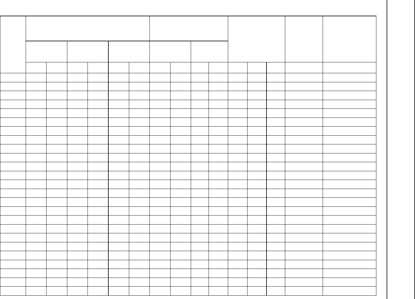
Fig.2 Maximum permissible non-repetitive peak
reverse power dissipation versus duration.
handbook, halfpage
MBG801
103
1 duration (ms)
PZSM
(W)
10
102
10−1
10
1
(1)
(2)
(1) Tj = 25 °C (prior to surge).
(2) Tj = 150 °C (prior to surge).
Fig.3 Forward current as a function of forward
voltage; typical values.
handbook, halfpage
0.6 1
300
100
0
200
MBG781
0.8 VF (V)
IF
(mA)
Tj = 25 °C.
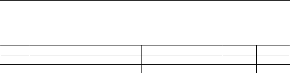
Fig.4 Temperature coefficient as a function of
working current; typical values.
handbook, halfpage
060
0
−2
−3
−1
MBG783
20 40 IZ (mA)
SZ
(mV/K) 4V3
3V9
3V6
3V0
2V4
2V7
3V3
BZX84-A/B/C2V4 to A/B/C4V3.
Tj = 25 to 150 °C.
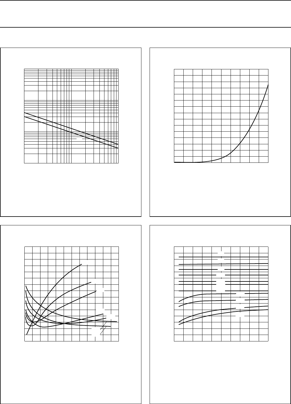
Fig.5 Temperature coefficient as a function of
working current; typical values.
handbook, halfpage
02016
10
0
−5
5
MBG782
4812 IZ (mA)
SZ
(mV/K)
4V7
12
11
10
9V1
8V2
7V5
6V8 6V2
5V6
5V1
BZX84-A/B/C4V7 to A/B/C12.
Tj = 25 to 150 °C.
2003 Apr 10 9
NXP Semiconductors Product data sheet
Voltage regulator diodes BZX84 series
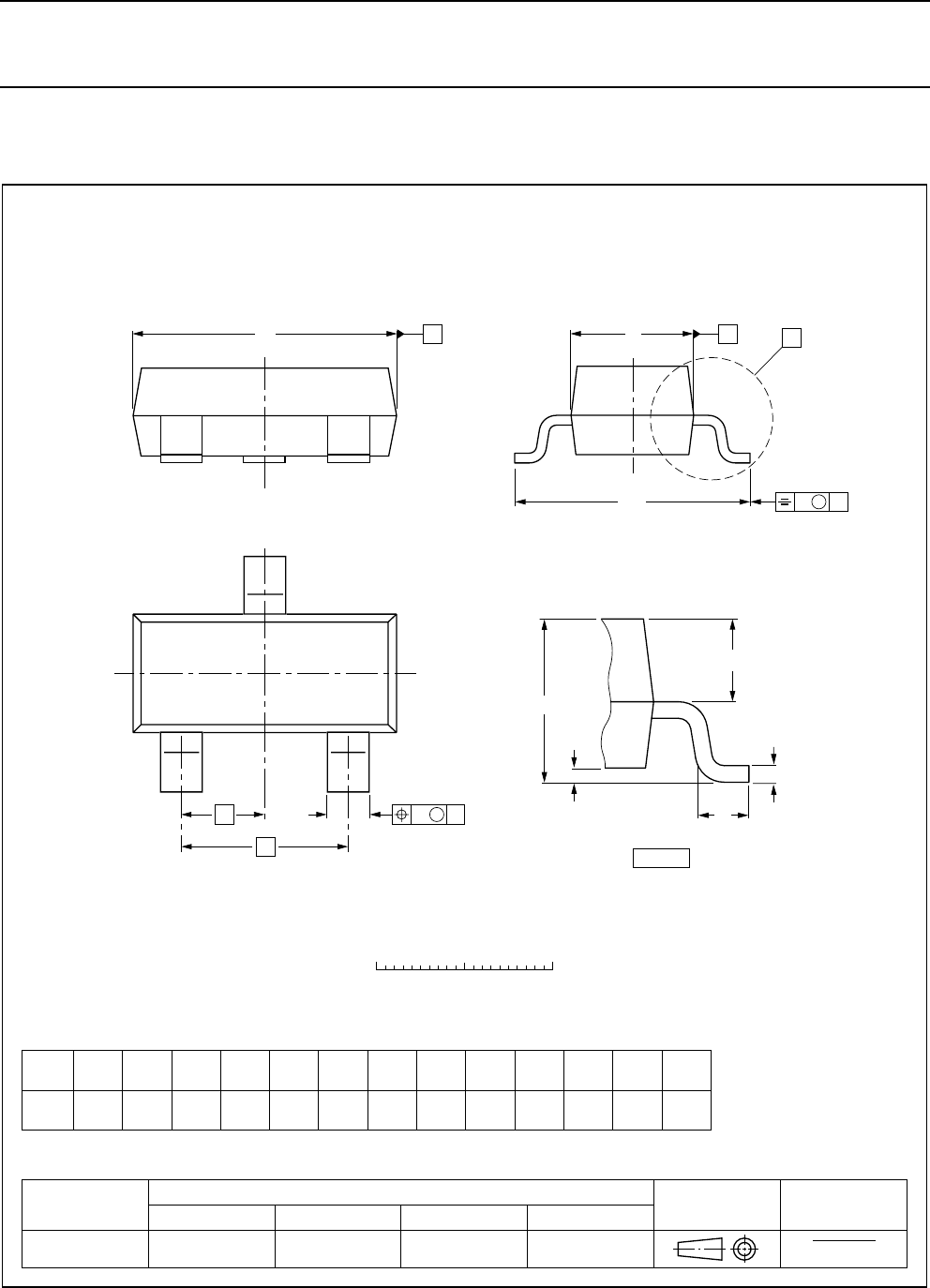
PACKAGE OUTLINE
UNIT A1
max. bpcDE e1HELpQwv
REFERENCES
OUTLINE
VERSION EUROPEAN
PROJECTION ISSUE DATE
97-02-28
99-09-13
IEC JEDEC EIAJ
mm 0.1 0.48
0.38 0.15
0.09 3.0
2.8 1.4
1.2 0.95
e
1.9 2.5
2.1 0.55
0.45 0.1
0.2
DIMENSIONS (mm are the original dimensions)
0.45
0.15
SOT23 TO-236AB
bp
D
e1
e
A
A1
Lp
Q
detail X
HE
E
wM
vMA
B
AB
0 1 2 mm
scale
A
1.1
0.9
c
X
12
3
Plastic surface mounted package; 3 leads SOT2
3
2003 Apr 10 10
NXP Semiconductors Product data sheet
Voltage regulator diodes BZX84 series
DATA SHEET STATUS
Notes
1. Please consult the most recently issued document before initiating or completing a design.
2. The product status of device(s) described in this document may have changed since this document was published
and may differ in case of multiple devices. The latest product status information is available on the Internet at
URL http://www.nxp.com.
DOCUMENT
STATUS(1) PRODUCT
STATUS(2) DEFINITION
Objective data sheet Development This document contains data from the objective specification for product
development.
Preliminary data sheet Qualification This document contains data from the preliminary specification.
Product data sheet Production This document contains the product specification.
DISCLAIMERS
General ⎯ Information in this document is believed to be
accurate and reliable. However, NXP Semiconductors
does not give any representations or warranties,
expressed or implied, as to the accuracy or completeness
of such information and shall have no liability for the
consequences of use of such information.
Right to make changes ⎯ NXP Semiconductors
reserves the right to make changes to information
published in this document, including without limitation
specifications and product descriptions, at any time and
without notice. This document supersedes and replaces all
information supplied prior to the publication hereof.
Suitability for use ⎯ NXP Semiconductors products are
not designed, authorized or warranted to be suitable for
use in medical, military, aircraft, space or life support
equipment, nor in applications where failure or malfunction
of an NXP Semiconductors product can reasonably be
expected to result in personal injury, death or severe
property or environmental damage. NXP Semiconductors
accepts no liability for inclusion and/or use of NXP
Semiconductors products in such equipment or
applications and therefore such inclusion and/or use is at
the customer’s own risk.
Applications ⎯ Applications that are described herein for
any of these products are for illustrative purposes only.
NXP Semiconductors makes no representation or
warranty that such applications will be suitable for the
specified use without further testing or modification.
Limiting values ⎯ Stress above one or more limiting
values (as defined in the Absolute Maximum Ratings
System of IEC 60134) may cause permanent damage to
the device. Limiting values are stress ratings only and
operation of the device at these or any other conditions
above those given in the Characteristics sections of this
document is not implied. Exposure to limiting values for
extended periods may affect device reliability.
Terms and conditions of sale ⎯ NXP Semiconductors
products are sold subject to the general terms and
conditions of commercial sale, as published at
http://www.nxp.com/profile/terms, including those
pertaining to warranty, intellectual property rights
infringement and limitation of liability, unless explicitly
otherwise agreed to in writing by NXP Semiconductors. In
case of any inconsistency or conflict between information
in this document and such terms and conditions, the latter
will prevail.
No offer to sell or license ⎯ Nothing in this document
may be interpreted or construed as an offer to sell products
that is open for acceptance or the grant, conveyance or
implication of any license under any copyrights, patents or
other industrial or intellectual property rights.
Export control ⎯ This document as well as the item(s)
described herein may be subject to export control
regulations. Export might require a prior authorization from
national authorities.
Quick reference data ⎯ The Quick reference data is an
extract of the product data given in the Limiting values and
Characteristics sections of this document, and as such is
not complete, exhaustive or legally binding.

NXP Semiconductors
Contact information
For additional information please visit: http://www.nxp.com
For sales offices addresses send e-mail to: salesaddresses@nxp.com
© NXP B.V. 2009
All rights are reserved. Reproduction in whole or in part is prohibited without the prior written consent of the copyright owner.
The information presented in this document does not form part of any quotation or contract, is believed to be accurate and reliable and may be changed
without notice. No liability will be accepted by the publisher for any consequence of its use. Publication thereof does not convey nor imply any license
under patent- or other industrial or intellectual property rights.
Customer notification
This data sheet was changed to reflect the new company name NXP Semiconductors. No changes were
made to the content, except for the legal definitions and disclaimers.
Printed in The Netherlands 613514/03/pp11 Date of release: 2003 Apr 10 Document order number: 9397 750 10959
