_new Chapter 3 Ch3
User Manual: Chapter 3 DL405 User Manual
Open the PDF directly: View PDF  .
.
Page Count: 56
- CPU Specificationsand Operation
- Overview
- CPU General Specifications
- CPU Electrical Specifications
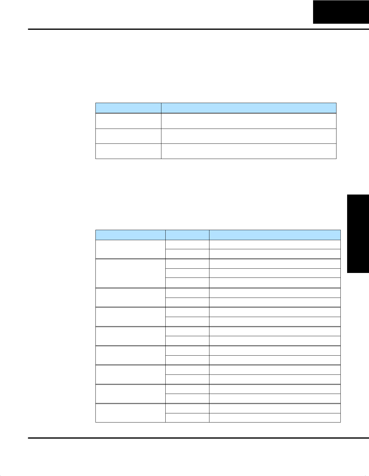
- CPU Hardware Features
- Using Battery Backup
- Selecting the Program Storage Media
- CPU Setup
- CPU Operation
- I/O Response Time
- CPU Scan Time Considerations
- PLC Numbering Systems
- Memory Map
- DL405 Aliases
- X Input/Y Output Bit Map
- Control Relay Bit Map
- Timer and Counter Status Bit Maps
- Remote I/O Bit Map
- Stage Control / Status Bit Map

13
CPU Specifications
and Operation
InThisChapter....
— Overview
— CPU General Specifications
— CPU Electrical Specifications
— CPU Hardware Features
— Using Battery Backup
— Selecting the Program Storage Media
— CPU Setup
— CPU Operation
— I/O Response Time
— CPU Scan Time Considerations
— PLC Numbering Systems
— Memory Map
— DL405 Aliases
— X Input/Y Output Bit Map
— Control Relay Bit Map
— Timer and Counter Status Bit Maps
— Remote I/O Bit Map
—Stage
tControl / Status Bit Map

CPU Specifications
and Operation
3--2 CPU Specifications and Operation
DL405 User Manual, 4th Edition, Rev. A
Overview
The CPU is the heart of the control system. Almost all system operations are
controlled by the CPU, so it is very important to set up and install it correctly. This
chapter provides the information needed to understand:
Sthe differences between the various models of CPUs
Sthe steps required to setup and install the CPU
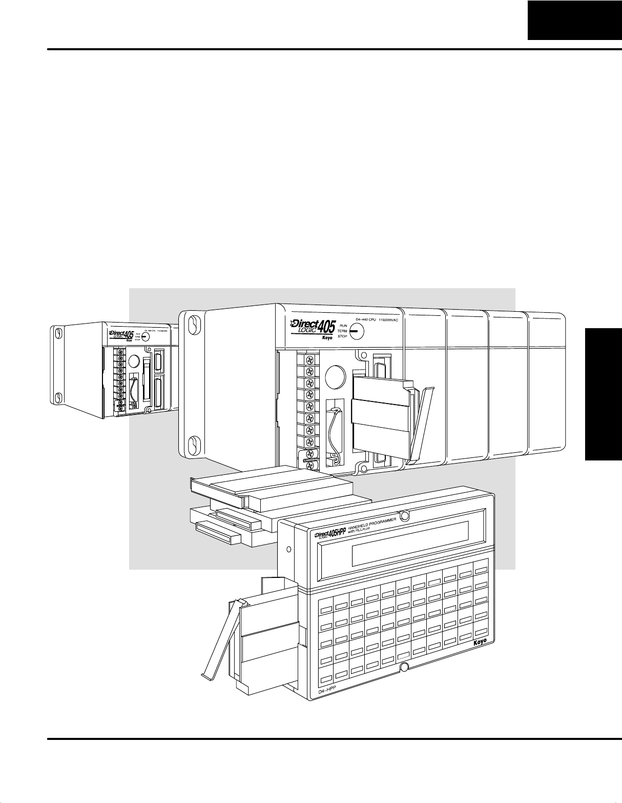
The DL430, DL440, and DL450 are all modular CPUs which are installed in either 4,
6, or 8 slot bases. All I/O modules in the DL405 family will work with either CPU. The
DL405 CPUs offer a wide range of processing power and program instructions. All
offer RLL and Stage program instructions (See Chapter 5 for instruction definitions).
All DL405 CPUs have extensive internal diagnostics that can be monitored from the
application program or from an operator interface.
The three standard CPU types accept either 110VAC or 220 VAC for power input.
The DL440 CPU is available in two additional DC versions: the DL440DC--1 uses 24
VDC, and the DL440DC--2 uses 125 VDC.
The DL430 has 6.5K of program memory comprised of 3.5K of ladder memory and
3K of V-memory (data registers). It has 113 instructions available for program
development, and supports a maximum of 640 points of local and local expansion
I/O and 512 points of remote I/O.
Program storage is in the EEPROM which is built into the CPU. In addition to the
EEPROM there is also RAM on the CPU which will store system parameters,
V-memory and other data which is not in the application program.
The DL430 provides two built-in communications ports. The first has a RS232C
interface and the other has a RS232C/RS422 interface. This allows for a
point-to-point connection on the first port and the option of either a multidrop network
connection (such as DirectNET) or a point-to-point connection on the other port.
The DL440 includes all the DL430 features, plus more I/O points, more program
instructions, and greater memory space with plug-in memory cartridges. It has a
maximum of 22.5K of program memory comprised of 15.5K of ladder memory and
7K of V-memory (data registers). It supports a maximum of 640 points of local and
local expansion I/O and 1024 points of remote I/O. Its two communications ports
operate identically to the DL430’s ports.
The DL440 has 170 instructions. The additional 57 instructions to the DL430
instruction set allow for more sophisticated program development through the use of
subroutines, additional instructions that support double word manipulation,
enhanced stack operations, diagnostic messaging, and ASCII/Hex data formatting.
General CPU
Features
DL430 CPU
Features
DL440 CPU
Features
CPU Specifications
and Operation
3--3
CPU Specifications and Operation
DL405 User Manual, 4th Edition, Rev. A
The new DL450 offers all the DL440 features, plus more I/O points, program
instructions, and two additional (4 total) communications ports. It has a maximum of
30.8K of program memory comprised of 15.5K of ladder memory and 15.3K of
V-memory (data registers). It supports a maximum of 2048 points of local and local
expansion I/O, and 1536 points of remote I/O. It includes an additional internal
RISC--based microprocessor for greater processing power. The DL450 has 210
instructions. The additional 40 instructions to the DL440 instruction set include drum
timers, a print function, floating point math, trigonometric functions, and PID loop
control for 16 loops.
The DL450 has a total of four communications ports. The first two ports are identical
to those on the DL430 and DL440. The third port has a RS-232C interface and can
be configured for either N sequence or K sequence protocol. It uses a modular
connector for point-to-point communications to devices such as the DV-1000 Data
Access Unit. The fourth port has a RS-422 interface using either MODBUS
master/slave, N sequence, or K sequence protocol. These four ports utilize three
physical connectors (the bottom connector has two ports on the DL450).
DL450 CPU
Features
CPU Specifications
and Operation
3--4 CPU Specifications and Operation
DL405 User Manual, 4th Edition, Rev. A
CPU General Specifications
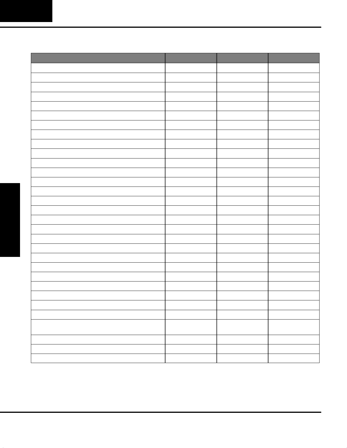
Features DL430 DL440 DL450
Total Program memory (words) 6.5K 14.5K / 22.5K* 22.8K / 30.8K*
Ladder memory (words), built-in 3.5K 7.5K / 15.5K* 7.5K / 15.5K*
V--memory (words) 3.0K 7.0K 15.3K
Scan Time, typical (1 K boolean) 8--10mS 2--3mS 4--5mS
Runtimeedit No Yes Yes
Supports Override No No Yes
RLL and RLLPLUS Programming Yes Yes Yes
Handheld programmer with cassette tape interface Yes Yes Yes
DirectSOFT programming for Windows™Yes Yes Yes
Built-in communication ports 2 ports 2 ports 4 ports
CMOS RAM No w/mem. cartridge w/mem. cartridge
UVPROM No w/mem. cartridge w/mem. cartridge
EEPROM Standard on CPU w/mem. cartridge w/mem. cartridge
FLASH RAM No No Standard on CPU
Compatible with:
CoProcessor™modules Yes Yes Yes
Networking modules Yes Yes Yes
RS232C/RS422 Data Comm. Module Yes Yes Yes
Total I/O 1152 1664 3584
Total I/O available as:
Local I/O / Local expansion I/O / Remote I/O 640 640 4096
Remote I/O 512 max. 1024 max. 2048 max.
Remote I/O Channels 223
Local discrete input points maximum 320 320 1024
Local discrete output points maximum 320 320 1024
Local analog input channels maximum 320** 320** 512**
Local analog output channels maximum 320** 320** 512**
Maximum number of channels / masters (remote
or slice) per local CPU base 222
Remote I/O Distance 3300 ft. (1000m) 3300 ft. (1000m) 3300 ft. (1000m)
Discrete I/O Module Point Density 8/16/32/64 8/16/32/64 8/16/32/64
Slots per Base 4/6/8 4/6/8 4/6/8
* The first values represent CPUs using the 7.5K memory cartridge and the second value is for using 15.5K
memory cartridges.
** Additional Discrete and Analog I/O can be supported (within the power budget) through the use of remote I/O.
CPU Specifications
and Operation
3--5
CPU Specifications and Operation
DL405 User Manual, 4th Edition, Rev. A
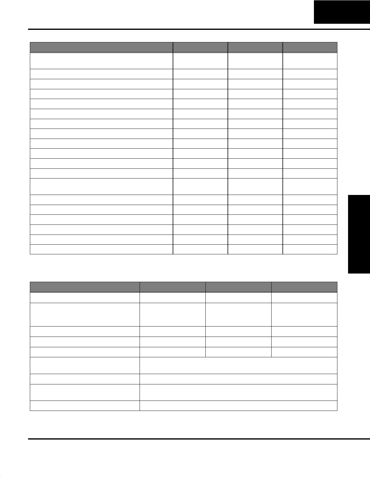
Feature DL430 DL440 DL450
Number of instructions available (see Chapter 5 for
a description of the available instructions) 113 170 210
Control relays 480 1024 2048
Special relays (system defined) 288 352 512
Stages in RLLPLUS 384 1024 1024
V-memory 3072 words 7168 words 15360 words
Timers 128 256 256
Counters 128 128 256
Immediate I/O Yes Yes Yes
Interrupt input 8 points 16 points 16 points
Subroutines No Yes Yes
For/Next Loops No Yes Yes
Drum Timers No No Yes
Math Integer Integer Integer and
Floating Point
PID Loop Control, built-in No No 16 loops
Time of Day Clock/Calendar No Yes Yes
Internal diagnostics Yes Yes Yes
Password security No Yes Yes, multi-level
System and user error log No Yes Yes
Battery backup Yes Yes Yes
CPU Electrical Specifications
Parameter DL430/DL440/DL450 DL440/450DC--1 DL440/450DC--2
Input Voltage, Nominal 120 VAC 24 VDC 125 VDC
Input Voltage Range 100--120 VAC and
196--240 VAC
+10% --15%
20--29 VDC 100--132 VDC
+10% --15%
Input Voltage Ripple N/A less than 10% less than 10%
Inrush Current, maximum 20 A 10 A 20 A
Power Consumption, maximum 50 VA 38W 30 W
Voltage withstand (dielectric strength) 1 min. at 1500 VAC between primary, secondary, field ground and run
relay
Insulation resistance > 10MΩat 500 VDC
Output Voltage, auxiliary power supply 20--28 VDC (24 nominal), ripple more than 1V P-P
(N/A on DL440--DC--1 and DL440--2)
Output Current, auxiliary power supply 24 VDC @ 400 mA maximum
CPU Specifications
and Operation
3--6 CPU Specifications and Operation
DL405 User Manual, 4th Edition, Rev. A
CPU Hardware Features
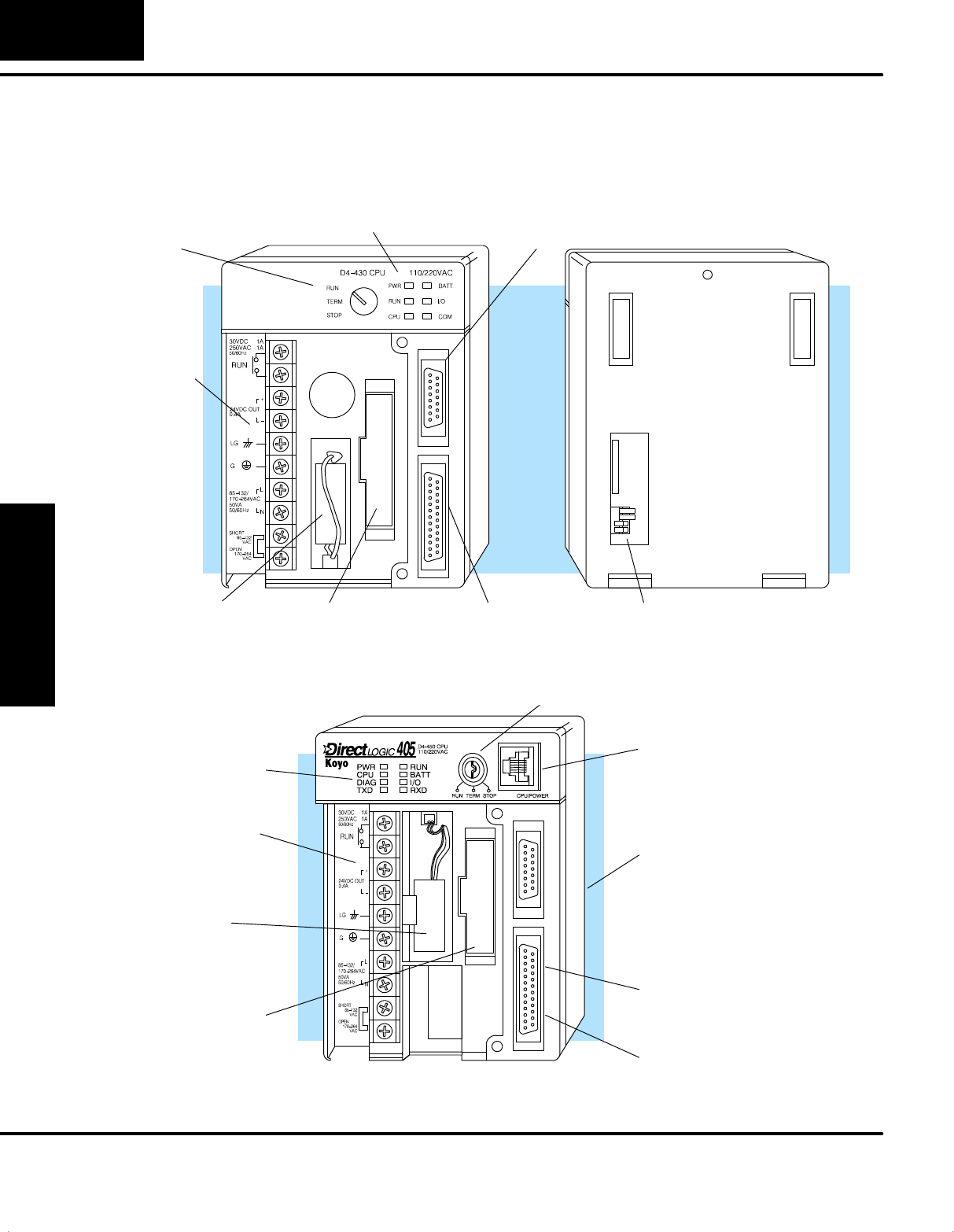
The following diagram shows the main external features of the DL405 CPUs.
CPU Battery Slot for DL440
Memory Cartridge
(optional on DL450)
Wiring Terminals
Port 0
(programming, MMI)
Port 1
(programming, MMI) DIP Switch Config.
(battery, station address, baud rate)
Keyswitch
(mode select)
Status indicators
DL430
/
DL440 CPUs
CPU Battery
Slot for optional
Memory Cartridge
Wiring Terminals
Keyswitch (mode select)
Port 0
(programming, MMI)
Port 2
(programming, MMI)
Port 1
(programming, MMI)
Port 3
(remote I
/
O, network)
Status indicators
DL450 CPU
CPU Specifications
and Operation
3--7
CPU Specifications and Operation
DL405 User Manual, 4th Edition, Rev. A
The keyswitch on the DL405 CPUs provides positions for enabling and disabling
program changes in the CPU. Unless the keyswitch is in the TERM position, RUN
and STOP mode changes will not be allowed by any interface device, (handheld
programmer, DirectSOFT programing package or operator interface). Programs
may be viewed or monitored but no changes may be made. If the switch is in the
TERM position and no program password is in effect, all operating modes as well as
program access will be allowed through the connected programming or monitoring
device.
Keyswitch Position CPU Action
RUN (Run Program) CPU is forced into the RUN mode if no errors are encountered. No
changes are allowed by the attached programming/monitoring device.
TERM (Terminal) RUN, PROGRAM and the TEST modes are available. Mode and
program changes are allowed by the programming/monitoring device.
STOP (Stop Program) CPU is forced into the STOP mode. No changes are allowed by the
programming/monitoring device.
There are two ways to change the CPU mode.
1. Use the CPU key switch to select the operating mode.
2. Place the CPU key switch in the TERM position and use a programming
device to change operating modes. In this position, you can change
between Run and Program modes.
The status indicator LEDs on the CPU front panels have specific functions which can
help in programming and troubleshooting.
Indicator Status Meaning
PWR ON Power good
OFF Power failure
RUN ON CPU is in Run Mode
OFF CPUisinStopMode
FLASHING CPU is in firmware upgrade mode
CPU ON CPU self diagnostics error
OFF CPU self diagnostics good
BATT
N
o
t
e
:
R
e
f
e
r
t
o
p
a
g
e
3
1
2
ON CPU battery voltage is low
Note:.Re
f
er to page 3--12 OFF CPU battery voltage is good or disabled
DIAG (DL450) ON CPU self diagnostics or local bus error
OFF CPU self diagnostics and local bus good
I/O ON I/O self diagnostics error
OFF I/O self diagnostics good
COM (DL430/DL440) ON Commuications error has occurred
OFF Communications OK
TXD (DL450) ON Data is being transmitted by the CPU
OFF No data is being transmitted by the CPU
RXD (DL450) ON Data is being received by the CPU
OFF No data is being received by the CPU
Keyswitch
Functions
Status Indicators
CPU Specifications
and Operation
3--8 CPU Specifications and Operation
DL405 User Manual, 4th Edition, Rev. A
Logic
Ground
Chassis
Ground
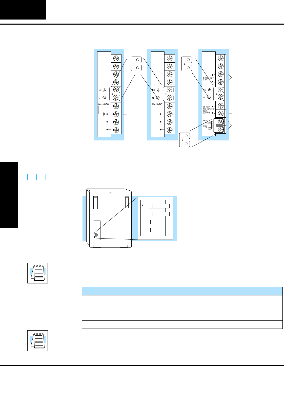
AC Terminal Strip
24V Auxiliary
Power
Logic Ground
Chassis
Ground
110/220
Voltage Select
Logic
Ground
Chassis
Ground
24VDC
Terminal Strip
125VDC
Terminal Strip
+DC
-- D C
+DC
-- D C
AC Line
AC Neutral
Install shunt for 110 VAC range,
leave off for 220 VAC range.
Install shunt between LG and G
Recommended screw torque: 10.6 lb--in (1.2Nm)
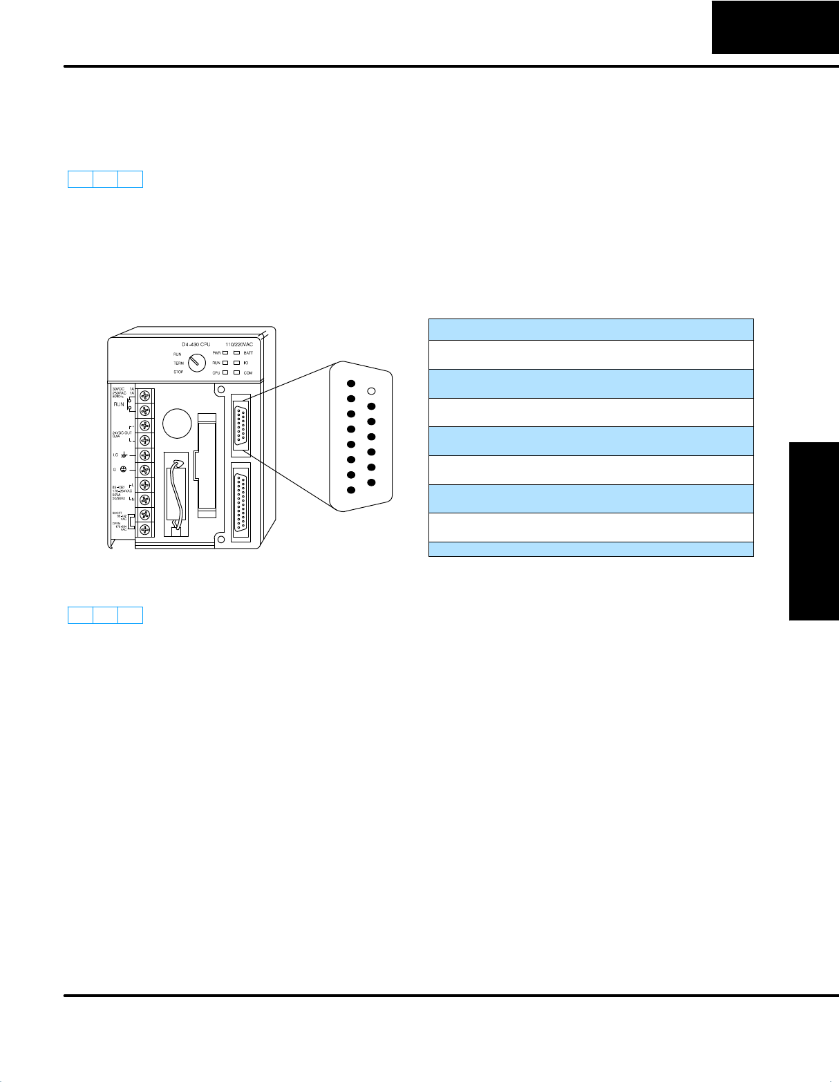
Locate the bank of four configuration switches located on the back of DL430 and
DL440 CPUs as shown in the figure below. These switches affect battery low
detection, station address override and baud rate of port 1 (25 pin D connector). Use
Aux Functions on the DL450 for these selections, via a programming device.
Switch 1
SON= Battery low indicator disabled
SOFF= Battery low indicator enabled
Switch 2
SON= Station address override is
enabled (address 1)
SOFF = Station address is set by
AUX function with programming
device
ON
1234
NOTE: Setting Switch 2 on forces the station address to 1. It does not change the
address set by the programming device. When Switch 2 is turned off again the
address will revert back to the address stored in memory via the AUX function.
Port 1 Baud Rate Switch 3 Switch 4
300 Off Off
1200 Off On
9600 On Off
19200 On On
NOTE: Parity, Mode and Station address for port 1 is selected by AUX functions
using a programming device.
430
440
450
Setting the CPU
DIP Switches
CPU Specifications
and Operation
3--9
CPU Specifications and Operation
DL405 User Manual, 4th Edition, Rev. A
DL405 CPUs provides up to four communication ports. The DL430/DL440 CPUs
have two ports, while the DL450 CPU has a total of four ports.
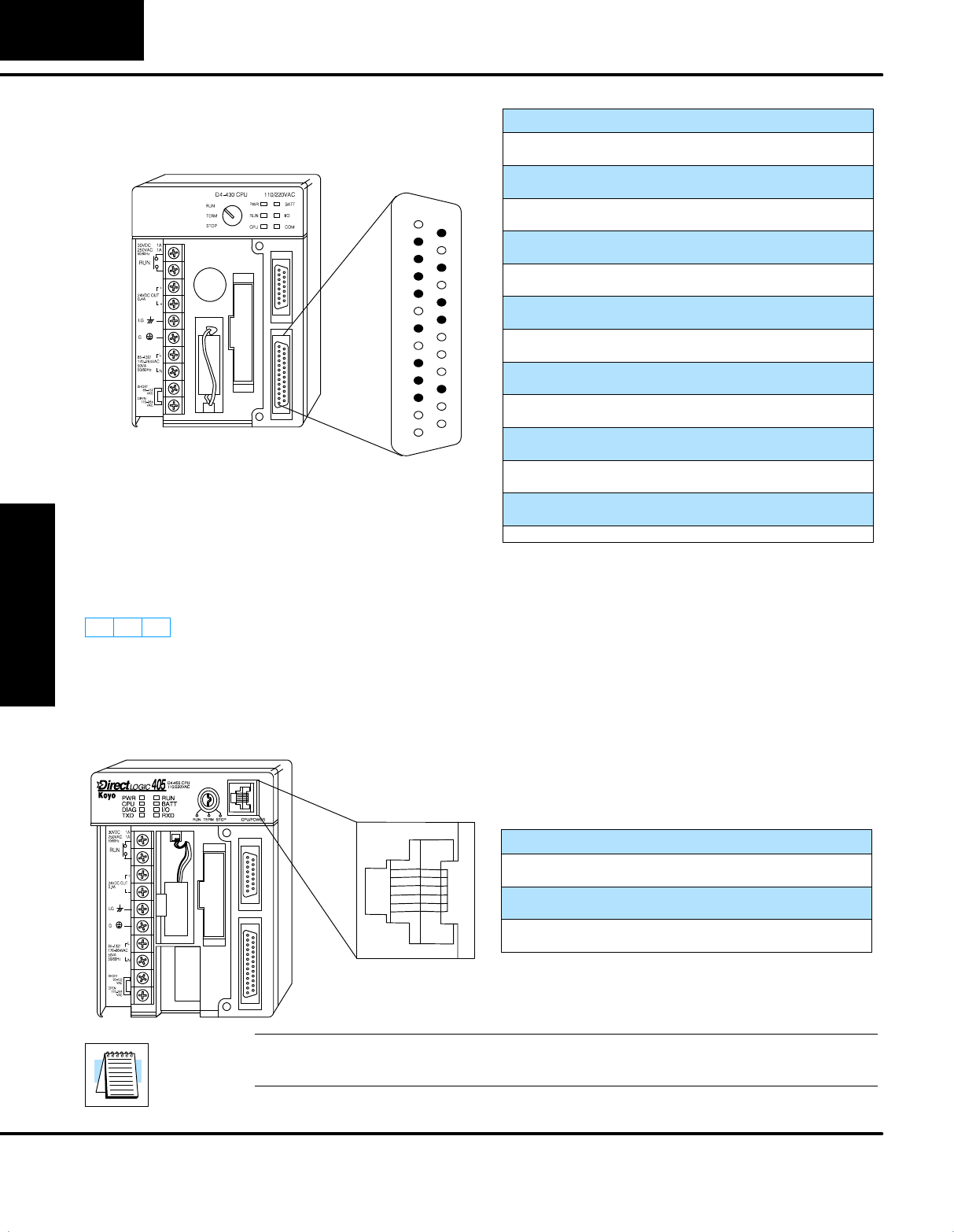
The first port (all CPUs) is located on the 15 pin D-shell conector. It is for general
programming such as DirectSOFT, or operator interface connections. The D4--HPP
handheld programmer can only be used on this port on the CPU. The operating
parameters for Port 0 are permanently set to the values shown.
S15 Pin female D type connector
SProtocol: K sequence
SRS232C, non-isolated, distance within 15 m (approx. 50 feet)
S9600 baud, 8 data bits, 1 start, 1 stop bit, odd parity
SAsynchronous, Half duplex, DTE
Port 0 Pin Descriptions (All CPUs)
1 YOP Sense connection between HPP and CPU
2 TXD Transmit Data (RS232C)
3 RXD Receive Data (RS232C)
4 ONLINE Request Communication (TTL)
5 ABNO CPU Error (TTL)
6 PRDY CPU ready to communicate (TTL)
7 CTS Clear to Send (RS232C)
8 YOM Sense connection between HPP and CPU
9 -- Not Used
10 LCBL Sense cable connection (TTL)
11 5V2 5 VDC for HPP logic
12 5V2 5 VDC for LCD backlight
13 0V Logic ground
14 0V Logic ground
15 0V Logic ground
15-pin Female
D Connector
1
8
9
15
Port 0
Port 1 (all CPUs) is located on the 25-pin connector, and is called the “secondary
comm port” for the DL430/DL440 CPUs. The secondary comm port address is
stored in the memory cartridge along with the I/O configuration. It is for general
programming such as DirectSOFT, operator interfaces, and networking, but it
cannot connect to the handheld programmer. Port 1 provides additional features
such as programmable baud rate, parity, ASCII/Hex mode and network address. Its
RS422 signals support multidrop networking and programming applications.
The baud rate and station address override is selected by dip switches on the rear of
the DL430/DL440 CPUs. The DL450 uses Aux functions to set the same parameters
(it has no DIP switches). RS232C or RS422 is selected by cabling to the proper
signal pin sets on the connector. Parity, ASCII/Hex mode and station address are
selected by AUX (auxiliary) functions with a programming device.
S25 Pin female D type connector
SProtocols: K-sequence, DirectNet. The DL450 additionally supports
Non-Sequence and MODBUS protocols. (Note: The DL430 cannot
support K--sequence on ports 0 and 1 simultaneously. Use DirectNet on
port 1 if port 0 is used for communications).
SRS232C / RS422, Selectable address 1--90 (use Aux function)
S300/ 600/ 1200/2400/4800/9600/19200/(38400 DL450 only) baud
SHex / ASCII modes (use Aux function to configure)
S8 data bits, 1 start, 1 stop bit, Odd, Even or No parity
SAsynchronous, Half duplex (use Aux function to configure), DTE
Communication
Ports
430
440
450
Port 0
Specifications
Port 1
Specifications
430
440
450
CPU Specifications
and Operation
3--10 CPU Specifications and Operation
DL405 User Manual, 4th Edition, Rev. A
114
13 25
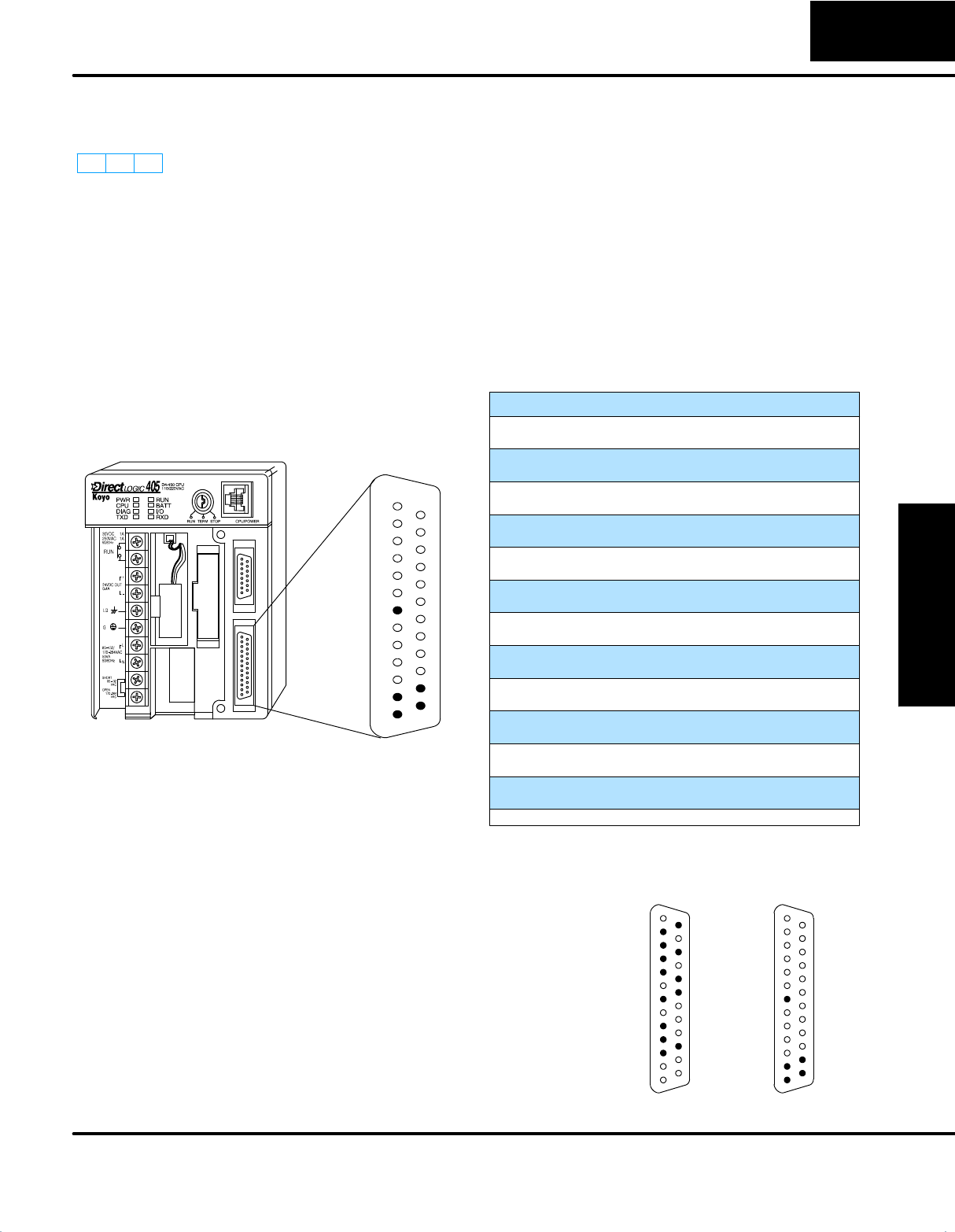
Port 1 Pin Descriptions (All CPUs)
1 -- Not used
2 TXD Transmit Data (RS232C)
3 RXD Receive Data (RS232C)
4 RTS Request to Send (RS232C)
5 CTS Clear to Send (RS2332C)
6 -- Not used
7 SG Signal ground (RS232C/RS422)
8 -- (port 3 on DL450)
9 RXD+ Receive Data + (RS422)
10 RXD-- Receive Data -- (RS422)
11 CTS+ Clear to Send + (RS422)
12 -- (port 3 on DL450)
13 -- (port 3 on DL450)
14 TXD+ Transmit Data + (RS422)
15 -- Not used
16 TXD-- Transmit Data -- (RS422)
17 -- Not used
18 RTS-- Request to Send -- (RS422)
19 RTS+ Request to Send + (RS422)
20 -- Not used
21 -- Not used
22 -- Not used
23 CTS-- Clear to Send -- (RS422)
24 -- (port 3 on DL450)
25 -- (port 3 on DL450)
25-pin Female
D Connector
Port 1
The operating parameters for Port 2 on the DL450 CPU are configurable using Aux
functions on a programming device.
S6 Pin female modular (RJ12 phone jack) type connector
SProtocols: DirectNet (slave only), K sequence, Non-procedure
SRS232C, 300 / 600 / 1200 / 2400 / 4800 / 9600 / 19200 / 38400 baud
S8 data bits, 1 start, 1 stop bit; odd, even, or no parity
SNodes -- from 1 to 90
Port 2 Pin Descriptions (DL450)
1 0V Power (--) connection (GND)
2 5V Power (+) conection
3 RXD Receive Data (RS232C)
4 TXD Transmit Data (RS232C
5 5V Power (+) conection
6 0V Power (--) connection (GND)
6-pin Female
Modular Connector
6
1
Port 2
NOTE: The 5V pins are rated at 200mA maximum, primarilly for use with some
operator interfaces.
Port 2
Specifications
430
440
450
CPU Specifications
and Operation
3--11
CPU Specifications and Operation
DL405 User Manual, 4th Edition, Rev. A
The operating parameters for Port 3 on the DL450 CPU are configurable using Aux
functions on a programming device.
S25 Pin female D type connector
SProtocols: DirectNet, K-sequence, Remote I/O, MODBUS master or
slave
SRS422, non-isolated, distance within 1000m (3280 ft.)
S300 / 600 / 1200 /2400 / 4800 / 9600 / 19200 / 38400 baud (DirectNet,
K-sequence, MODBUS protocols),19200 / 38400 (Remote I/0 protocol)
S8 data bits, 1 start, 1 stop bit, odd/none/even parity
SHex / ASCII modes (use Aux function to configure)
SSelectable address 1--90 (use Aux function to configure)
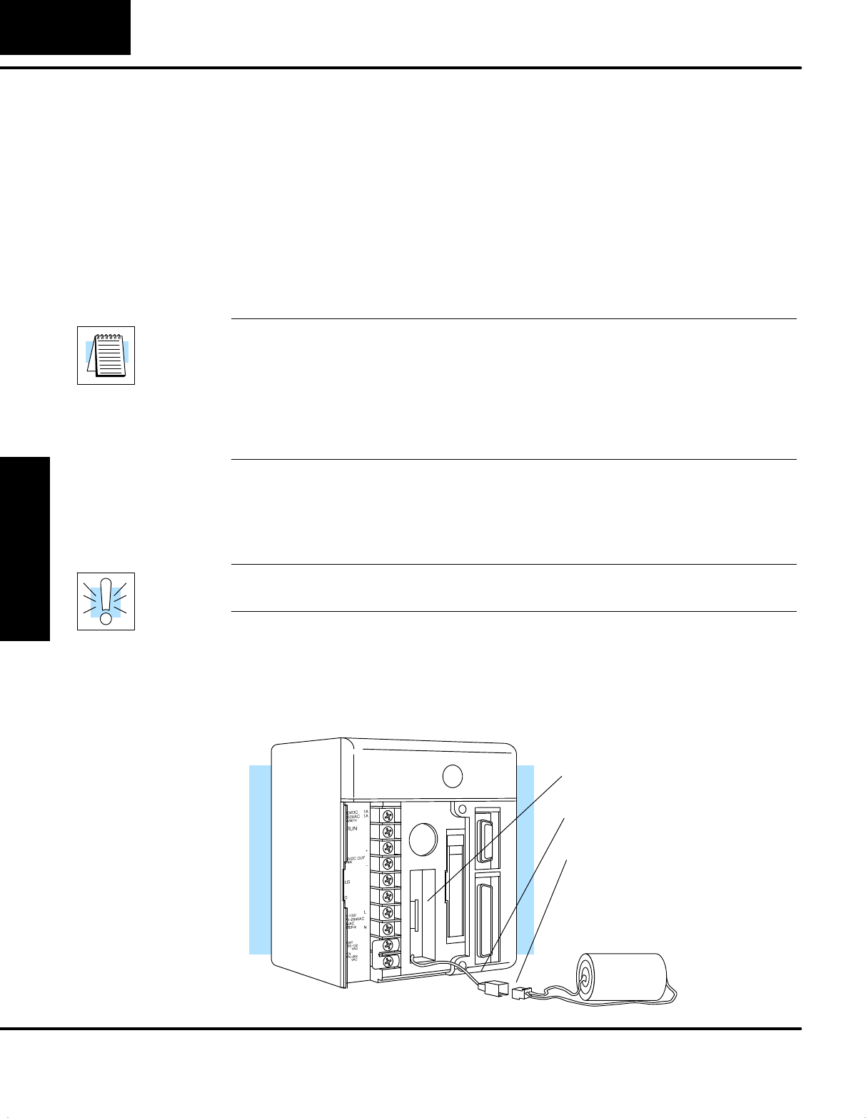
Port 3 Pin Descriptions (DL450)
1 -- Not used
2 (port 1)
3 (port 1)
4 (port 1)
5 (port 1)
6 -- Not used
7 SG Signal ground
8 Not used
9 (port 1)
10 (port 1)
11 (port 1)
12 TXD+ Transmit Data (+), (RS422)
13 TXD-- Transmit Data (--), (RS422)
14 (port 1)
15 -- Not used
16 (port 1)
17 -- Not used
18 (port 1)
19 (port 1)
20 -- Not used
21 -- Not used
22 -- Not used
23 (port 1)
24 RXD+ Receive Data (+), (RS422)
25 RXD-- Receive Data (--), (RS422)
25-pin Female
D Connector
114
13 25
Port 3
A drawing summarizing the pin locations
and functions of ports 1 and 3 on the
25-pin connector is to the right. The two
logical ports share two ground pins, but
have separate communications data pins.
When using both logical ports, you will
probably have to make a custom
connector which divides the signals in two
for two separate cables.
Two Logical Ports on
the 25 Pin Connector
Port 1
TXD
RXD
RTS
CTS
0V
RXD--
CTS+
TXD+
TXD--
RTS--
RTS+
CTS--
Port 3
0V
TXD+
TXD--
RXD+
RXD--
RXD+
Port 3
Specifications
430
440
450
CPU Specifications
and Operation
3--12 CPU Specifications and Operation
DL405 User Manual, 4th Edition, Rev. A
Using Battery Backup
The DL405 CPUs have a lithium battery to maintain system RAM retentive memory
when the system is without external power. Typical CPU battery life is five years,
which includes PLC runtime and normal shutdown periods. However, consider
installing a fresh battery if your battery has not been changed recently and the
system will be shutdown for a period of more than ten days.
Battery indicators will flash on and off when a battery needs changing.
SFlashing at 2 Hz means the CPU battery needs changing.
SFashing at 0.5 Hz means the RAM cartridge battery needs changing.
NOTE: Be sure to back up your V-memory and system parameters before replacing
your CPU battery. Just save the V-memory and system parameters to either a
Memory Cartridge, cassette tape, or to a personal computer (use DirectSOFT).
To prevent memory loss the CPU battery can be changed while the system is
powered up. If the CPU has been powered off you should power-up the CPU for at
least 5 seconds prior to changing the battery. This ensures the capacitor used to
maintain the proper voltage levels necessary to retain memory is fully charged.
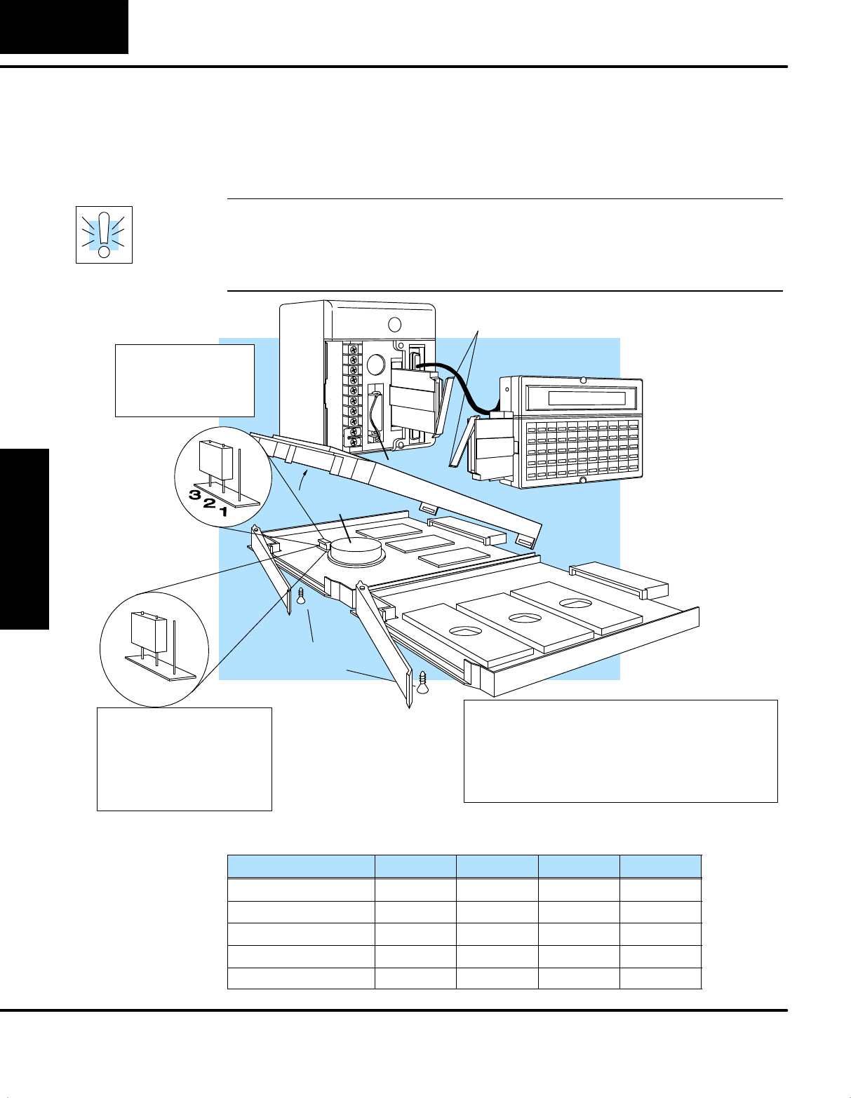
To remove the CPU battery:
1. Pull the battery out from the battery retaining clip.
2. Lift the clip on the two wire battery connector.
3. Slide the battery connector apart.
WARNING: Do not attempt to recharge the battery or dispose of it by fire. The
battery may explode or release hazardous materials.
To install the CPU battery:
1. Join the (keyed) battery connector so that the red wires match.
2. Push gently till the connector snaps closed
3. Slide the battery all the way into the retaining clip (flush with the opening).
4. Note the date the battery was changed.
1) Pull battery from
retaining clip
2) Extend battery
cable connector
3) Slide Battery
connector apart
Replace battery with
part # D3--D4--BAT

CPU Specifications
and Operation
3--13
CPU Specifications and Operation
DL405 User Manual, 4th Edition, Rev. A
Selecting the Program Storage Media
The DL430 CPU provides built-in EEPROM storage as a standard feature, so it
cannot use other types of program storage. The DL440 CPU requires a removable
memory cartridge for operation. The DL450 provides built-in FLASH memory as a
standard feature. It will still accept a memory cartridge for program storage. The
following paragraphs will help you choose the correct memory storage for your CPU
type and application.
NOTE: The source memory (either cartridge or internal) must be specified by using
either DirectSOFT or the handheld programmer (D4--HPP).
The two types of memory storage available are volatile and non--volatile. Volatile
memory retains your data only as long as proper voltage is maintainedto thestorage
media. Non-volatile memory does not require power to retain data. The DL405
CPUs maintain the proper voltage either through the power supply or the use of a
memory backup battery.
Memory cartridges are applicable to only the DL440 and DL450 CPUs. One
cartridge is required on the DL440, but is optional on the DL450.The removable
memory cartridge is available as either CMOS RAM, UVPROM or EEPROM. The
RAM and EEPROM types offer a write protect jumper selection internal to the
cartridge. When the cartridge is opened the jumper may be moved to the protect
position to prevent accidental erasure or alterations to the program.
SCMOS RAM (Complementary Metal Oxide Semiconductor / Random
Access Memory) requires a battery for memory retention, which is
located inside the cartridge. The memory can be modified or changed
easily with a handheld programmer or PC programming software.
Battery life is typically 3 years. Refer to Chapter 9, Maintenance and
Troubleshooting for battery replacement.
SUVPROM (Ultraviolet Programmable Read Only Memory) does not
require a battery for memory retention, so it is classified as
“non-volatile”. However, erasure (clearing memory) requires exposing
the memory ICs to an ultraviolet light source. The CPU can reprogram
the UVPROM cartridge after erasure, but this requires a handheld
programmer.
NOTE: When you purchase the UVPROM memory cartridge it is recommended you have
either a RAM or an EEPROM memory cartridge for program development. Once
development is completed you should then use the handheld programmer(D4--HPP) to copy
your application program to the UVPROM. We recommend the UVPROM memory cartridge
option for applications which are mass produced and do not require frequent alterations.
SEEPROM (Electrically Erasable Programmable Read Only Memory)
does not require a battery for memory retention, so it is classified as
“non-volatile”. Both erasure and programming are accomplished
electrically, eliminating ultraviolet light source requirement. So, the
EEPROM memory cartridge can be electrically reprogrammed (if not
write protected) without being removed from the CPU. This is the
memory type built into the DL430 CPU.
Volatile and
Non-volatile
Memory
Memory Storage
Types
CPU Specifications
and Operation
3--14 CPU Specifications and Operation
DL405 User Manual, 4th Edition, Rev. A
The diagram below displays a Memory Cartridge for the DL440 or DL450. It shows
how the memory cartridge fits in the CPU and in the handheld programmer. It also
shows how to open the memory cartridge for selecting write protect (for CMOS
RAM) or for erasing the UVPROM. Details about connecting the handheld
programmer to the CPU is covered in DL405 Handheld Programmer Manual.
WARNING: Do not insert or remove a CPU memory cartridge while the power
is connected. Your program or password may be corrupted if this occurs. A
corrupted program can cause unpredictable operation which may result in a
risk of injury to personnel or damage to equipment. If the password becomes
corrupted, you cannot access the CPU.
UVPROM Erasing Instructions
1) Remove cartridge from CPU or HPP
2) Remove cartridge retaining screw
3) Remove cover
4) Place cartridge in UV erasing lamp typical
12,000μw/cm2lamp @ 2.5cm for 15--20 minutes
5) Replace cover
Pull lever to
extract cartridge
Jumper pins 2 & 3
to Write Protect.
Jumper pins 1 & 2
to Write Enable.
CMOS Memory
Cartridge
Retaining
Screws
UVPROM Memory
Cartridge
(with cover removed)
CPU Battery
Memory
Cartridge
Battery
V
PROT
Jumper pin V to the
center pin
to Write Protect.
Jumper the center pin
to the unmarked pin
to Write Enable.
D4-EE-2
D4- RAM- 1 D4- RAM- 2 D4- UV- 2 D4- EE- 2
Program Storage Capacity 7.5K 15.5K 15.5K 15.5K
Cartridge Battery Type Lithium Lithium None None
Writing Cycle Life N/A N/A 1000 >10,000
Write Inhibit Internal jumper Internal jumper No Internal jumper
Memory Clear Method Electrical Electrical Ultraviolet light Electrical
Memory Cartridge
Memory Cartridge
Capacity Table

CPU Specifications
and Operation
3--15
CPU Specifications and Operation
DL405 User Manual, 4th Edition, Rev. A
CPU Setup
The DL440 and DL450 CPUs also have a Clock / Calendar that can be used for many
purposes. If you need to use this feature there are also AUX functions available that
allow you set the date and time. For example, you would use AUX 52,
Display/Change Calendar to set the time and date with the Handheld Programmer.
With DirectSOFT you would use the PLC Setup menu options.
There are also two instructions that allow you to change or modify the time and date
from within the application program. Chapter 5 provides information on the DATE
and TIME instructions that are used to establish the clock and calendar information.
The CPU uses the following format to
display the date and time.
SDate — Year, Month, Date, Day of
week (0 -- 6, Sunday thru Saturday)
STime — 24 hour format, Hours,
Minutes, Seconds
94/01/02 23:08:17
Handheld Programmer Display
You can use the AUX function to change any component of the date or time.
However, the CPU will not automatically correct any discrepancy between the date
and the day of the week. For example, if you change the date to the 15thof the month
and the 15th is on a Thursday, you will also have to change the day of the week
(unless the CPU already shows the date as Thursday).
The DL450 CPU offers three type of scan time configurations:
SVariable -- this is the standard scan time setting, in which the PLC scan
is running as fast as the ladder program execution allows.
SFixed --thescantimemaybesettobeconstant,from10mSto
9999 mS. The operating system inserts a delay after each ladder scan
to accomplish the requested fixed scan.
SLimit -- the PLC operates with a variable scan, but generates a
watchdog timeout error if the scan time exceeds the specified amount.
You can use this to trap program execution errors, for example.
To select the desired DL450 scan time option, use DirectSOFT and go online with
the DL450. Then select the PLC Menu, then Diagnostics, then Scantime, then
Setup. The three choices of Variable, Fixed, or Limit then appear.
The DL405 CPUs have a password protection feature which prevents unauthorized
access to CPU programs or data. Use AUX 81, 82, and 83 to either modify the
password, and unlock or lock the CPU respectively. The password must be an
eight-character numeric (0--9) code. Once you’ve entered a password, you can
remove it by entering all zeros (00000000). (This is the default from the factory.)
Multilevel Password (DL440/450 only) -- The DL440 and DL450 feature an
intermediate level of protection that you can choose by making the first character of
the password the character “A”. The remaining 7 characters must be numeric (0--9).
The intermediate password protection differs from the standard password in that it
does allow an operator interface device to access and change V-memory data such
as presets. It still does not allow a ladder program edit, however.
For more information on passwords, see Appendix A, Auxiliary Functions.
Setting the Clock
and Calendar
430
440
450
Variable/Fixed
Scan Time Feature
430
440
450
Password
Protection
CPU Specifications
and Operation
3--16 CPU Specifications and Operation
DL405 User Manual, 4th Edition, Rev. A
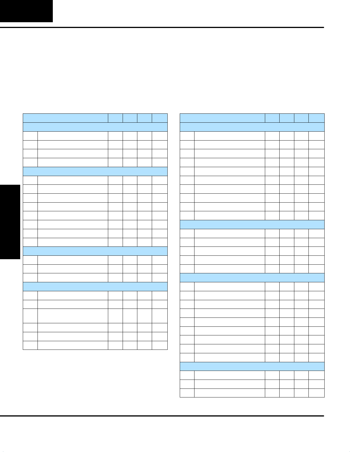
Many CPU setup tasks involve the use of Auxiliary (AUX) Functions. The AUX
Functions perform many different operations, ranging from simple operating mode
changes to copying programs to memory cartridges. They are divided into
categories that affect different system parameters. See Appendix A for detailed
descriptions of the AUX functions.
You can access the AUX Functions with the DL405 Handheld Programmer, or with
DirectSOFT’s pull-down menus. Manuals for those products provide step-by-step
instructions. Some AUX Functions are designed specifically for Handheld
Programmer setup, so they are not supported by DirectSOFT. The following table
lists the Auxiliary functions for the different CPUs and the Handheld Programmer.
AUX Function and Description 430 440 450 HPP
AUX 1* — Operating Mode
11 Go to Run Mode --
12 Go to Test Mode --
13 Go to Program Mode --
14 Run Time Edit --
AUX 2* — RLL Operations
21 Check Program --
22 Change Reference --
23 Clear Ladder Range --
24 Clear Ladders --
25 Select MC or Flash Memory --
26 Copy MC Contents to Flash --
27 Copy Flash contents to MC --
28 Verify Flash contents = MC --
AUX 3* — V-Memory Operations
31 Clear V Memory --
32 Clear V Range --
33 Find V-memory Value --
AUX 4* — I/O Configuration
41 Show I/O Configuration --
42 I/O Diagnostics --
44 Power up I/O Configuration
Check
--
45 Select Configuration --
46 Configure I/O --
47 Intelligent I/O --
supported
not supported
-- not applicable
AUX Function and Description 430 440 450 HPP
AUX 5* — CPU Configuration
51 Modify Program Name --
52 Display / Change Calendar --
53 Display Scan Time --
54 Initialize Scratchpad --
55 Set Watchdog Timer --
56 Configure Comm. Ports --
57 Set Retentive Ranges --
58 Test Operations --
5C Display Error History --
5D Select PLC Scan Mode --
AUX 6* — Handheld Programmer Configuration
61 Show Revision Numbers
62 Beeper On / Off
63 Backlight On / Off
64 Select Online / Offline
65 Run Self Diagnostics
AUX 7* — Memory Cartridge Operations
71 CPU to Memory Cartridge
72 Memory Cartridge to CPU
73 Compare MC with CPU
74 Memory Cart. Blank Check
75 Clear Memory Cartridge
76 Display Memory Cart. Type
77 Tape to Memory Cartridge
78 Memory Cartridge to Tape
79 Compare MC with Tape
AUX 8* — Password Operations
81 Modify Password --
82 Unlock CPU --
83 Lock CPU --
Auxiliary Functions
CPU Specifications
and Operation
3--17
CPU Specifications and Operation
DL405 User Manual, 4th Edition, Rev. A
Before entering a new program, it’s a good idea to always clear ladder memory. AUX
Function 24 clears the complete user program.
You can also use other AUX functions to clear other memory areas.
SAUX 23 — Clear Ladder Range
SAUX 31 — Clear V Memory
SAUX 32 — Clear V Range
The DL405 CPUs maintain system parameters in a memory area often referred to as
the “scratchpad”. In some cases, you may make changes to the system setup that
will be stored in system memory. For example, if you specify a range of Control
Relays (CRs) as retentive, these changes are stored.
AUX 54 resets the system memory to the default values.
WARNING:You may never have to use this feature unless you want to clear
any setup information that is stored in system memory. Usually, you’ll only
need to initialize the system memory if you are changing programs and the old
program required a special system setup. You can usually change from
program to program without ever initializing system memory.
Remember, this AUX function will reset all system memory. If you have set
special parameters such as retentive ranges, you will need to re-enter the
data.
Since the DL405 CPUs have built-in DirectNET ports, you can use the Handheld
Programmer to set the network address for the port and the port communication
parameters. The default settings are:
SStation address 1
SHex mode
SOdd parity
The DirectNET Manual provides additional information about choosing the
communication settings for network operation. If you’re using the bottom port for
programming, you can just use the default settings. For the extra two ports on the
DL450, see Chapter 4, System Design and Configuration.
Use AUX 56 to set the network address and communication parameters for the
secondary port(s).
The DL405 CPUs provide certain ranges of retentive memory by default. The default
ranges are suitable for many applications, but you can change them if your
application requires additional retentive ranges or no retentive ranges at all. The
default settings are:
M
e
m
o
r
y
A
r
e
a
DL430 DL440 DL450
M
emory
A
rea Default Range Avail. Range Default Range Avail. Range Default Range Avail. Range
Control Relays C600 -- C737 C0 -- C737 C600 -- C737 C0 -- C1777 C1000 -- C3777 C0 -- C3777
V--Memory V2000 -- V7377 V0 -- V7377 V2000 -- V7777 V0 -- V17777 V1400 -- V37777 V0 -- V37777
Timers None by default T0 -- T177 None by default T0 -- T377 None by default T0 -- T377
Counters CT0 -- CT177 CT0 -- CT177 CT0 -- CT177 CT0 -- CT177 CT0 -- CT377 CT0 -- CT377
Stages None by default S0 -- S577 None by default S0 -- S1777 None by default S0 -- S1777
Use AUX 57 to set the retentive ranges.
Clearing an
Existing Program
Initializing System
Memory
Setting the CPU
Network Address
Setting Retentive
Memory Ranges
CPU Specifications
and Operation
3--18 CPU Specifications and Operation
DL405 User Manual, 4th Edition, Rev. A
CPU Operation
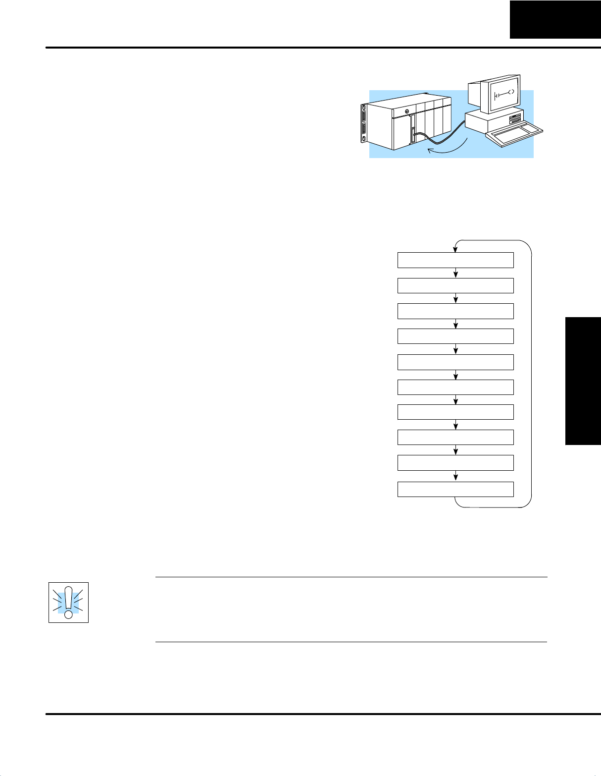
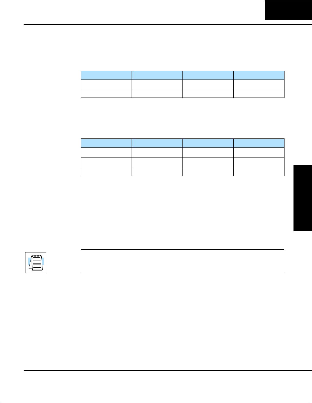
Achieving the proper control for your equipment or process requires a good
understanding of how DL405 CPUs control all aspects of system operation. The flow
chart below shows the main tasks of the CPU operating system. In this section, we
will investigate four aspects of CPU operation:
SCPU Operating System — the CPU manages
all aspects of system control.
SCPU Operating Modes — The three primary
modes of operation are Program Mode, Run
Mode, and Test Mode.
SCPU Timing — The two important areas we
discuss are the I/O response time and the
CPU scan time.
SCPU Memory Map — The CPU’s memory
map shows the CPU addresses of various
system resources, such as timers, counters,
inputs, and outputs.
At powerup, the CPU initializes the internal
electronic hardware. Memory initialization starts
with examining the retentive memory settings. In
general, the contents of retentive memory is
preserved, and non-retentive memory is initialized
to zero (unless otherwise specified).
After the one-time powerup tasks, the CPU begins
the cyclical scan activity. The flowchart to the right
shows how the tasks differ, based on the CPU mode
and the existence of any errors. The “scan time” is
defined as the average time around the task loop.
Note that the CPU is always reading the inputs,
even during program mode. This allows
programming tools to monitor input status at any
time.
The outputs are only updated in Run mode. In
program mode, they are in the off state.
In Run Mode, the CPU executes the user ladder
program. Immediately afterwards, any PID loops
which are configured are executed (DL450 only).
Then the CPU writes the output results of these two
tasks to the appropriate output points.
Error detection has two levels. Non-fatal errors are
reported, but the CPU remains in its current mode. If
a fatal error occurs, the CPU is forced into program
mode and the outputs go off.
YES
Power up
Initialize hardware
Check I/O module
config. and verify
Initialize various memory
based on retentive
configuration
Update input
Read input data from
Specialty and Remote I/O
Service peripheral
PGM Mode?
RUN
Execute ladder program
Update output
Write output data to
Specialty and Remote I/O
Do diagnostics
OK
NO
NO
Fatal error
Force CPU into
PGM mode
OK?
Report the error, set flag,
register,turnonLED
YES
CPU Bus Communication
Update Clock / Calendar
PID Operations (DL450)
CPU Operating
System
CPU Specifications
and Operation
3--19
CPU Specifications and Operation
DL405 User Manual, 4th Edition, Rev. A
In Program Mode the CPU does not
execute the application program or update
the output modules. The primary use for
Program Mode is to enter or change an
application program. You also use the
program mode to set up CPU parameters,
such as the network address, retentive
memory areas, etc. Download Program
You can use the key switch on the CPU to select Program Mode operation. Or, with
the keyswitch in TERM position, you can use a programming device such as the
Handheld Programmer to place the CPU in Program Mode.
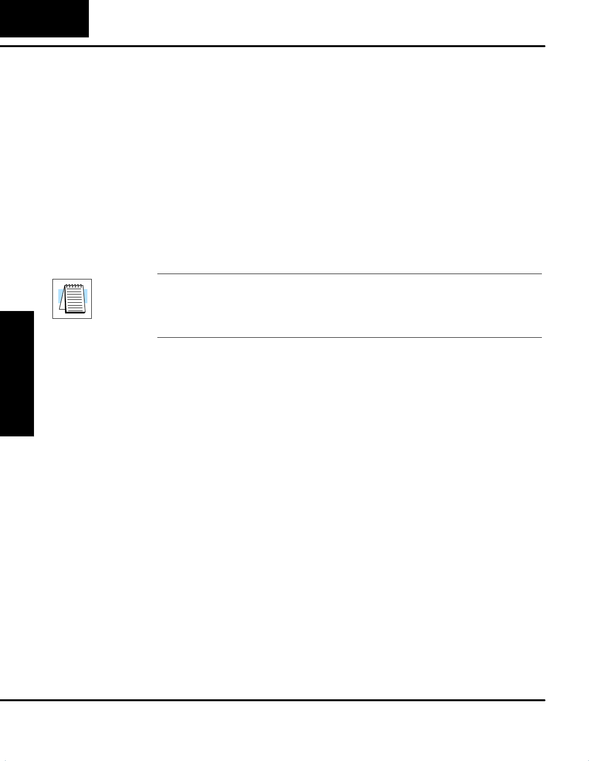
In Run Mode, the CPU executes the
application program, does PID
calculations for configured PID loops
(DL450) only, and updates the I/O system.
You can perform many operations during
Run Mode. Some of these include:
SMonitor and change I/O point status
SUpdate timer/counter preset values
SUpdate Variable memory locations
Run Mode operation can be divided into
several key areas. It is very important you
understand how each of these areas of
execution can affect the results of your
application program solutions.
You can use the key switch to select Run
Mode operation. Or, with the keyswitch in
TERM position, you can use a
programming device, such as the
Handheld Programmer to place the CPU
in Run Mode.
Read Inputs
Read Inputs from Specialty I/O
Solve the Application Program
Write Outputs
Diagnostics
Service Peripherals, Force I/O
Write Outputs to Specialty I/O
CPU Bus Communication
Update Clock, Special Relays
Solve PID Equatinos (DL450)
With the DL440 or DL450, you can also edit the program during Run Mode. The Run
Mode Edits are not “bumpless.” Instead, the CPU maintains the outputs in their last
state while it accepts the new program information. If an error is found in the new
program, then the CPU will turn all the outputs off and enter the Program Mode.
WARNING: Only authorized personnel fully familiar with all aspects of the
application should make changes to the program. Changes during Run Mode
become effective immediately. Make sure you thoroughly consider the impact
of any changes to minimize the risk of personal injury or damage to
equipment.
Program Mode
Operation
Run Mode
Operation
CPU Specifications
and Operation
3--20 CPU Specifications and Operation
DL405 User Manual, 4th Edition, Rev. A
The CPU reads the status of all inputs, then stores it in the image register. Input
image register locations are designated with an X followed by a memory location.
Image register data is used by the CPU when it solves the application program.
Of course, an input may change after the CPU has just read the inputs. Generally,
the CPU scan time is measured in milliseconds. If you have an application that
cannot wait until the next I/O update, you can use Immediate Instructions. These do
not use the status of the input image register to solve the application program. The
Immediate instructions immediately read the input status directly from I/O modules.
However, this lengthens the program scan since the CPU has to read the I/O point
status again. A complete list of the Immediate instructions is included in Chapter 5.
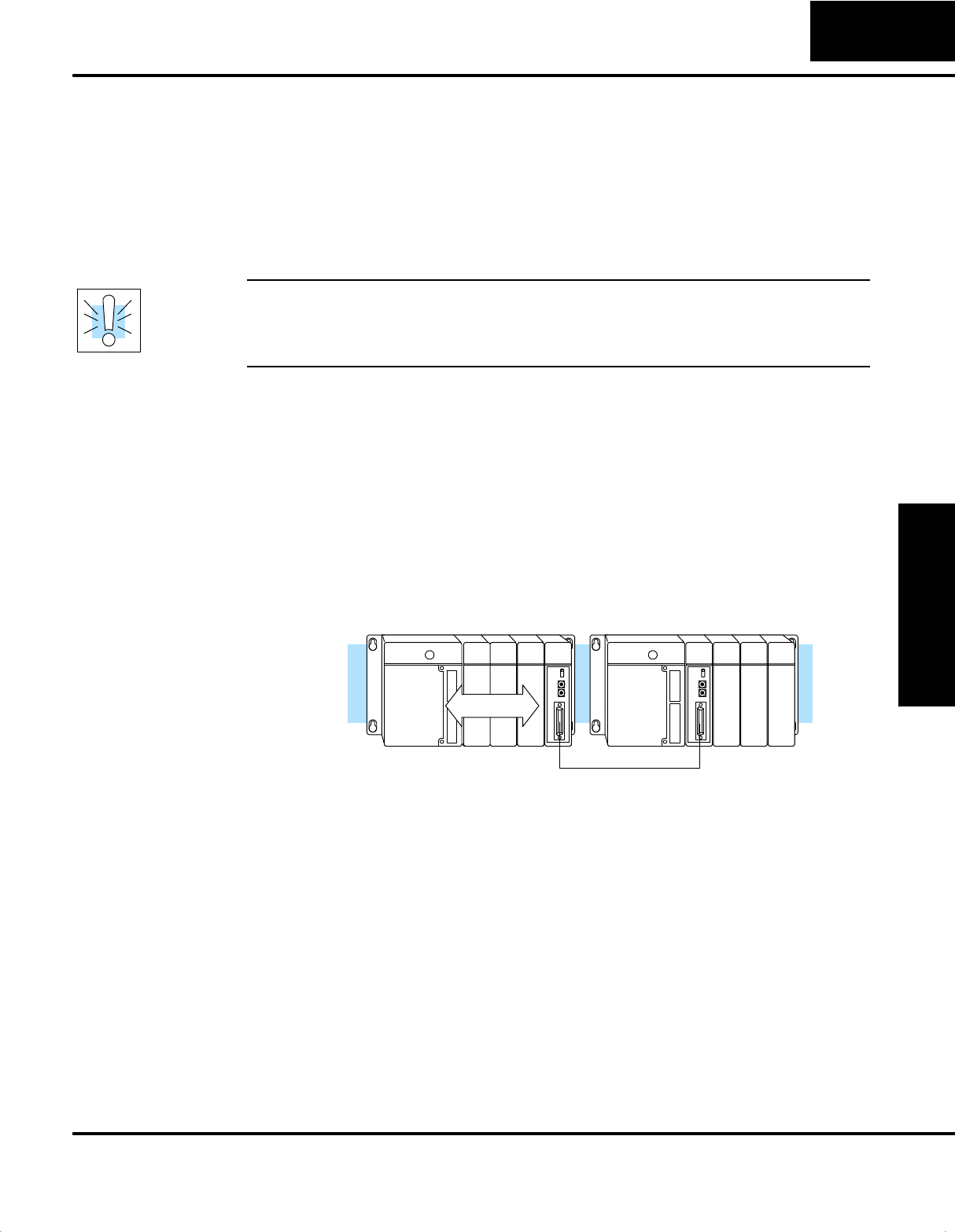
After the CPU reads the inputs from the input modules, it reads any input point data
from any Specialty modules that are installed, such as High Speed Counter
modules, etc.This is also the portion of the scan that reads the input status from
Remote I/O racks. The GX data type is usedfor both remote inputs and outputs. (The
DL405 Remote I/O Manual provides additional information on how to set up the
remote I/O link.)
NOTE: It may appear the Remote I/O point status is updated every scan. This is not
quite true. The CPU will receive information from the Remote I/O Master module
every scan, but the Remote Master may not have received an update from all the
Remote slaves. Remember, the Remote I/O link is managed by the Remote Master,
not the CPU.
After the CPU reads the inputs from the input modules, it reads any attached
peripheral devices. This is primarily a communications service for any attached
devices. For example, it would read a programming device to see if any input, output,
or other memory type status needs to be modified.
Forced I/O— temporarily changes the status of a discrete bit. For example, you may
want to force an input on, even though it is really off. This allows you to change the
point status that was stored in the image register. This value will be valid until the
image register location is written to during the next scan. This is primarily useful
during testing situations when you just need to force a bit on to trigger another event.
Forced Inputs — The CPU reads the status of X inputs during the Read Inputs
portion of the scan. When the CPU services the programming device, it logs any
request to force an X input on. If the input is used in the application program, the
ladder X contact is considered closed (on). Since an X input is a real-world input
point, the CPU will change the status when it reads the inputs on the next scan.
Read Inputs
Read Inputs from
Specialty and
Remote I/O
Service Peripherals
and Force I/O
CPU Specifications
and Operation
3--21
CPU Specifications and Operation
DL405 User Manual, 4th Edition, Rev. A
Forced Outputs— Outputs which are not used in the program can be forced on and
off for troubleshooting and maintenance purposes. You can temporarily allow the
forcing of any output by inserting an END coil instruction at the beginning of the
ladder program. Then you can use DirectSOFT or a HPP to force outputs on and off.
The DL405 CPUs only retain the forced value for one scan, if the I/O point
corresponds to an actual point on a module in the system. However, if the point
address is greater than any actual I/O point address in the system or it is not used in
the ladder program, then the point will maintain the forced status.
WARNING: Only authorized personnel fully familiar with all aspects of the
application should make changes to the program. Make sure you thoroughly
consider the impact of any changes to minimize the risk of personal injury or
damage to equipment.
There are certain V-memory locations that contain register information. This portion
of the execution cycle makes sure these locations get updated on every scan. Also,
there are several different Special Relays, such as diagnostic relays, etc., that are
also updated during this segment.
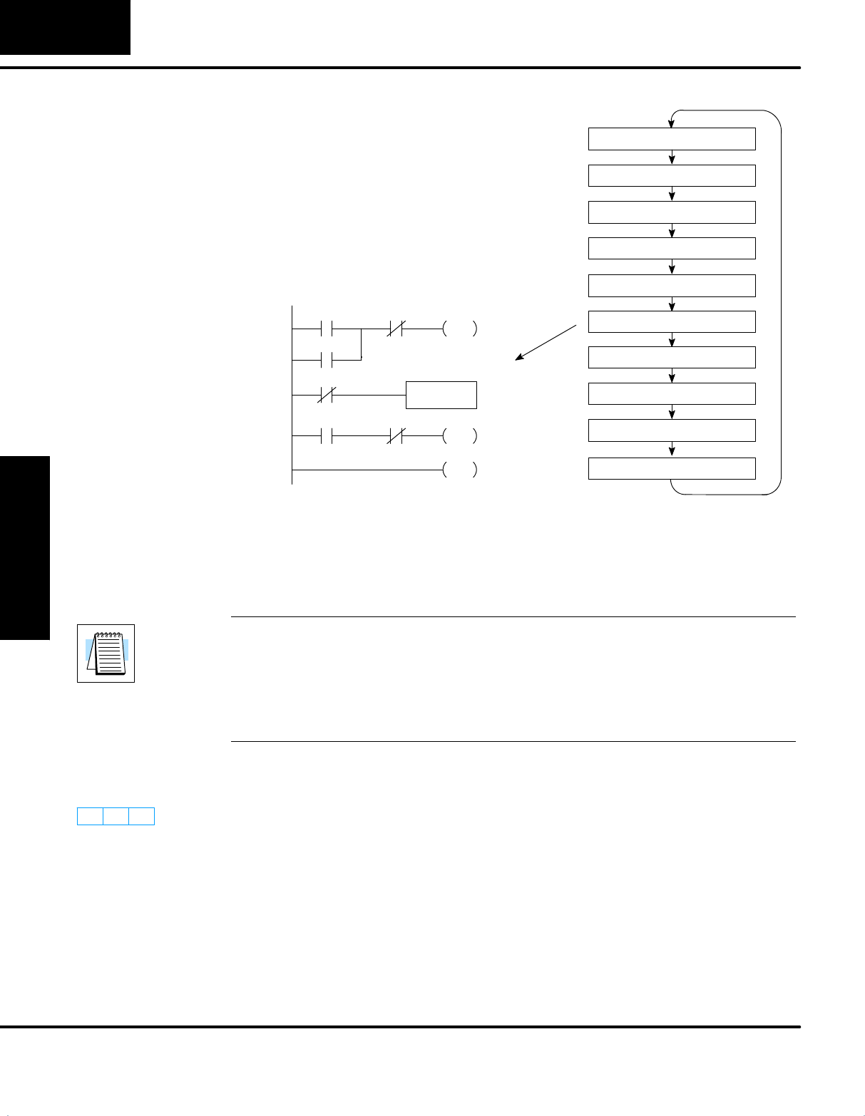
Many of the Specialty Modules, such as the Data Communications Module and the
FACTS CoProcessor modules, can transfer data to and from the CPU over the CPU
bus on the backplane. This data is more than just standard I/O point status. This type
of communications can only occur on the CPU (local) base. There is a portion of the
execution cycle used to communicate with these modules. The CPU performs both
read and write requests during this segment.
DCM DCM
Data
The DL440 and DL450 CPUs have an internal real-time clock and calendar timer
which is accessible to the application program. Special V-memory locations hold this
information. This portion of the execution cycle makes sure these locations get
updated on every scan. Also, there are several different Special Relays, such as
diagnostic relays, etc., that are also updated during this segment.
Update Special
Relays and Special
Registers
CPU Bus
Communication
Update Clock,
Special Relays,
and Special
Registers
CPU Specifications
and Operation
3--22 CPU Specifications and Operation
DL405 User Manual, 4th Edition, Rev. A
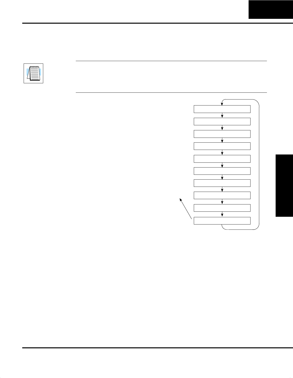
The CPU evaluates each instruction in the
application program during this segment
of the scan cycle. The instructions define
the relationship between input conditions
and the system outputs.
The CPU begins with the first rung of the
ladder program, evaluating it from left to
right and from top to bottom. It continues,
rung by rung, until it encounters the END
coil instruction. At that point, a new image
for the outputs is complete.
Read Inputs
Read Inputs from Specialty I/O
Solve the Application Program
Write Outputs
Diagnostics
Service Peripherals, Force I/O
Write Outputs to Specialty I/O
CPU Bus Communication
Update Clock, Special Relays
Solve PID equations (DL450)
X0 X1 Y0
OUT
C0
C100 LD K10
X5 X10 Y3
OUT
END
The internal control relays (C), the stages (S), the global relays (GX), and the
variable memory (V) are also updated in this segment.
You may recall the CPU may have obtained and stored forcing information when it
serviced the peripheral devices. If any I/O points or memory data have been forced,
the output image register also contains this information.
NOTE: If an output point was used in the application program, the results of the
program solution will overwrite any forcing information that was stored. For example,
if Y0 was forced on by the programming device, and a rung containing Y0 was
evaluated such that Y0 should be turned off, then the output image register will show
that Y0 should be off. Of course, you can force output points that are not used in the
application program. In this case, the point remains forced because there is no
solution that results from the application program execution.
The DL450 CPU can process up to 16 PID loops. The loop calculations are run as a
separate task from the ladder program execution, immediately following it. Only
loops which have been configured are calculated, and then only according to a
built-in loop scheduler. The sample time (calculation interval) of each loop is
programmable. Please refer to Chapter 8, PID Loop Operation, for more on the
effects of PID loop calculation on the overall CPU scan time.
Once the application program has solved the instruction logic and constructed the
output image register, the CPU writes the contents of the output image register to the
corresponding output points located in the local CPU base or the local expansion
bases. Remember, the CPU also made sure any forcing operation changes were
stored in the output image register, so the forced points get updated with the status
specified earlier.
Solve Application
Program
Solve PID
Loop Equations
430
440
450
Write Outputs
CPU Specifications
and Operation
3--23
CPU Specifications and Operation
DL405 User Manual, 4th Edition, Rev. A
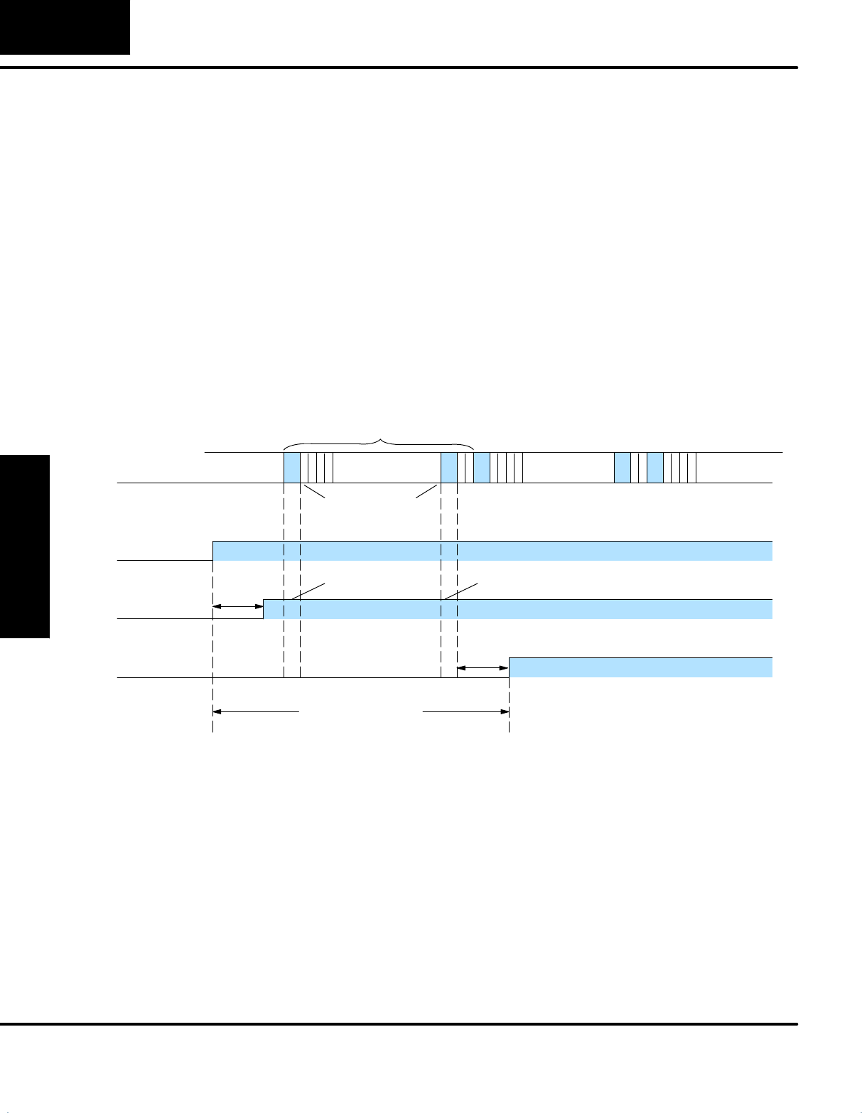
After the CPU updates the outputs in the local and expansion bases, it sends the
output point information that is required by any Specialty modules which are
installed. For example, this is the portion of the scan that writes the output status
from the image register to the Remote I/O racks.
NOTE: It may appear the Remote I/O point status is updated every scan. This is not
quite true. The CPU will send the information to the Remote I/OMaster module every
scan, but the Remote Master will update the actual remote modules during the next
communication sequence between the master and slave modules. Remember, the
Remote I/O link communication is managed by the Remote Master, not the CPU.
During this part o
f
the scan, the CPU
performs all system diagnostics and other
tasks, such as:
Scalculating the scan time
Supdating special relays
Sresetting the watchdog timer
DL405 CPUs automatically detect and
report many different error conditions.
Appendix B contains a listing of the
various error codes available with the
DL405 system.
One of the more important diagnostic
tasks is the scan time calculation and
watchdog timer control. DL405 CPUs
have a “watchdog” timer that stores the
maximum time allowed for the CPU to
complete the solve application segment of
the scan cycle. The default value set from
the factory is 200 mS. If this time is
exceeded the CPU will enter the Program
Mode, turn off all outputs, and report the
error. For example, the Handheld
Programmer displays “E003 S/W
TIMEOUT” when the scan overrun occurs.
Read Inputs
Read Inputs from Specialty I/O
Solve the Application Program
Write Outputs
Diagnostics
Service Peripherals, Force I/O
Write Outputs to Specialty I/O
CPU Bus Communication
Update Clock, Special Relays
Solve PID Loop Equations
You can use AUX 53 to view the minimum, maximum, and current scan time. Use
AUX 55 to increase or decrease the watchdog timer value. There is also an RSTWT
instruction that can be used in the application program to reset the watch dog timer
during the CPU scan.
Write Outputs to
Specialty and
Remote I/O
Diagnostics
CPU Specifications
and Operation
3--24 CPU Specifications and Operation
DL405 User Manual, 4th Edition, Rev. A
I/O Response Time
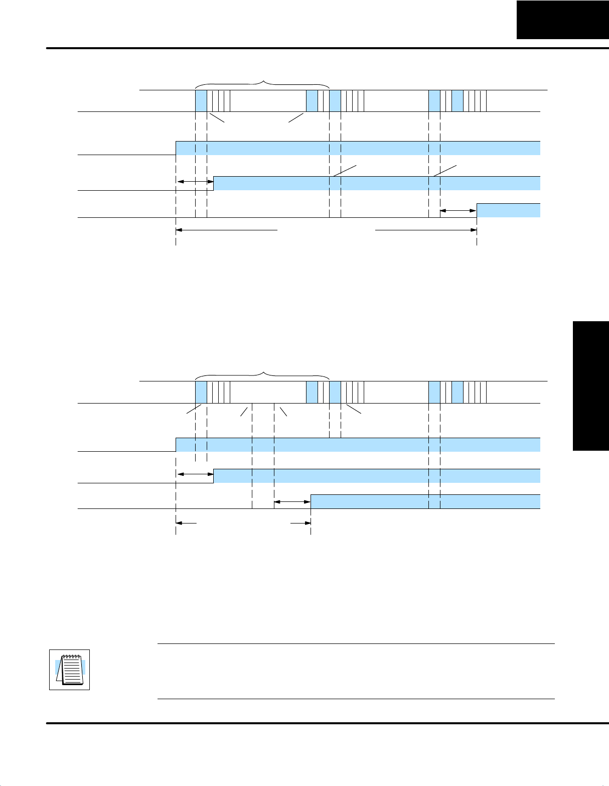
I/O response time is the amount of time required for the control system to sense a
change in an input point and update a corresponding output point. In the majority of
applications, the CPU performs this task practically instantaneously. However,
some applications do require extremely fast update times. There are four things that
can affect the I/O response time:
SThe point in the scan period when the field input changes states
SInput module Off to On delay time
SCPU scan time
SOutput module Off to On delay time
The I/O response time is shortest when the module senses the input change just
before the Read Inputs portion of the execution cycle. In this case the input status is
read, the application program is solved, and the output point gets updated. The
following diagram shows an example of the timing for this situation.
Solve
Program
Read
Inputs
Write
Outputs
Solve
Program
Scan
Solve
Program
Field Input
Input Module
Off/On Delay
CPU Reads
Inputs
Output Module
Off/On Delay
I/O Response Time
Scan
Solve
Program
CPU Writes
Outputs
In this case, you can calculate the response time by simply adding the following
items.
Input Delay + Scan Time + Output Delay = Response Time
The I/O response time is longest when the module senses the input change justafter
the Read Inputs portion of the execution cycle. In this case the new input status does
not get read until the following scan. The following diagram shows an example of the
timing for this situation.
In this case, you can calculate the response time by simply adding the following
items.
Input Delay +(2 x Scan Time) + Output Delay = Response Time
Is Timing Important
for Your
Application?
Normal Minimum
I/O Response
Normal Maximum
I/O Response
CPU Specifications
and Operation
3--25
CPU Specifications and Operation
DL405 User Manual, 4th Edition, Rev. A
Solve
Program
Read
Inputs
Write
Outputs
Solve
Program
Scan
Solve
Program
Field Input
Input Module
Off/On Delay
CPU Reads
Inputs
Output Module
Off/On Delay
I/O Response Time
Scan
Solve
Program
CPU Writes
Outputs
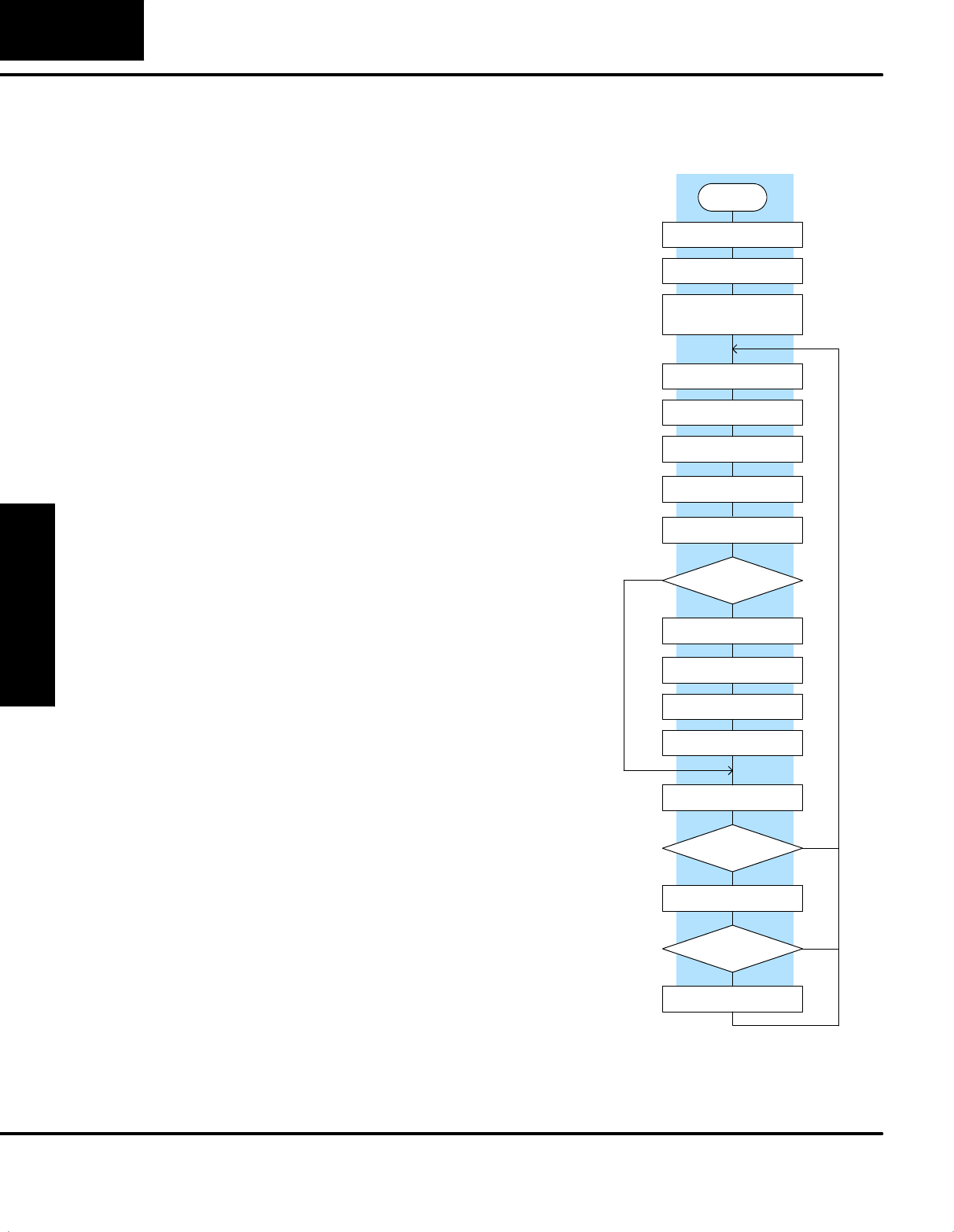
There are a few things you can do the help improve throughput.
SChoose instructions with faster execution times
SUse immediate I/O instructions (which update the I/O points during the
ladder program execution segment)
SChoose modules that have faster response times
Immediate I/O instructions are probably the most useful technique. The following
example shows immediate input and output instructions, and their effect.
Solve
Program
Read
Input
Immediate
Normal Write
Outputs
Solve
Program
Scan
Solve
Program
Field Input
Input Module
Off/On Delay
Output Module
Off/On Delay
I/O Response Time
Scan
Solve
Program
Normal Read
Input
Write
Output
Immediate
In this case, you can calculate the response time by simply adding the following
items.
Input Delay + Instruction Execution Time + Output Delay = Response Time
The instruction execution time is calculated by adding the time for the immediate
input instruction, the immediate output instruction, and all instructions inbetween.
NOTE: When the immediate instruction reads the current status from a module, it
uses the results to solve that one instruction without updating the image register.
Therefore, any regular instructions that follow will still use image register values. Any
immediate instructions that follow will access the module again to update the status.
Improving
Response Time
CPU Specifications
and Operation
3--26 CPU Specifications and Operation
DL405 User Manual, 4th Edition, Rev. A
CPU Scan Time Considerations
The scan time covers all the cyclical
tasks that are performed by the operating
system. You can use DirectSOFT or the
Handheld Programmer to display the
minimum, maximum, and current scan
times that have occurred since the
previous Program Mode to Run Mode
transition. This information can be very
important when evaluating the
performance of a system.
As we’ve shown previously there are
several segments that make up the scan
cycle. Each of these segments requires a
certain amount of time to complete. Of all
the segments, the only one you really
have the most control over is the amount
of time it takes to execute the application
program. This is because different
instructions take different amounts of
time to execute. So, if you think you need
a faster scan, then you can try to choose
faster instructions.
Your choice of I/O modules and system
configuration, such as expansion or
remote I/O, can also affect the scan time.
However, these things are usually
dictated by the application.
For example, if you have a need to count
pulses at high rates of speed, then you’ll
probably have to use a High-Speed
Counter module. Also, if you have I/O
points that need to be located several
hundred feet from the CPU, then you
need remote I/O because it’s much faster
and cheaper to install a single remote I/O
cable than it is to run all those signal
wires for each individual I/O point.
The following paragraphs provide some
general information on how much time
some of the segments can require.
YES
Power up
Initialize hardware
Check I/O module
config. and verify
Initialize various memory
based on retentive
configuration
Update input
Read input data from
Specialty and Remote I/O
Service peripheral
PGM Mode?
RUN
Execute ladder program
Update output
Write output data to
Specialty and Remote I/O
Do diagnostics
OK
NO
NO
Fatal error
Force CPU into
PGM mode
OK?
Report the error, set flag,
register, turn on LED
YES
CPU Bus Communication
Update Clock / Calendar
PID Equations (DL450)
CPU Specifications
and Operation
3--27
CPU Specifications and Operation
DL405 User Manual, 4th Edition, Rev. A
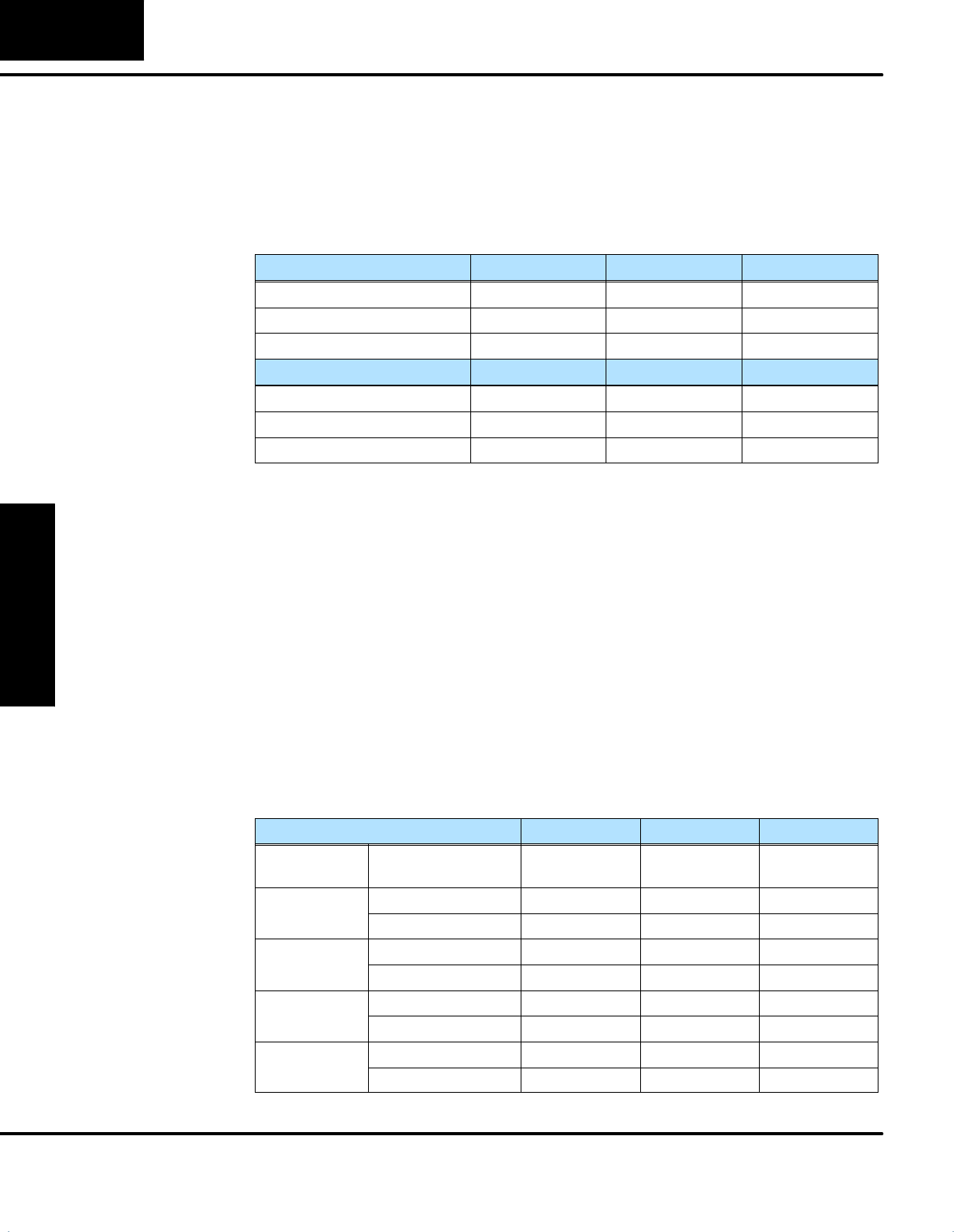
The CPU performs an initialization task once the system power is on. The required
time depends on system loading, such as the number of I/O modules installed, type
of memory cartridge being used etc. The initialization task is performed once at
power-up, so it does not affect the scan time for the application program.
Initialization DL430 DL440 DL450
Minimum Time 1.2 Seconds 1.0 Seconds 1.9 Seconds
Maximum Time 3.2 Seconds 2.5 Seconds 3.3 Seconds
The time required to read the input status for the local and expansion input modules
depends on which CPU you are using, the number of input points in these bases,
and the number of input modules being used. The following table shows typical
update times required by the CPU.
Timing Factors DL430 DL440 DL450
Overhead 20.0 μs14.5 μs20.0 μs
Per input module 48.0 μs22.6 μs13.0 μs
Per input point 4.0 μs2.5 μs6.3 μs
For example, the time required for a DL430to read two 16-point input modules would
be calculated as follows. (Where NM is the number of modules and NI is the total
number of input points.)
Time =20μs+(48μsxNM)+(4μsxNI)
Time =20μs+(48μsx2)+(4μs x 16)
Time =180 μs
Formula
Example
NOTE: This information provides the amount of time the CPU spends reading the
input status from the modules. Don’t confuse this with the I/O response time thatwas
discussed earlier.
Initialization
Process
Reading Inputs
CPU Specifications
and Operation
3--28 CPU Specifications and Operation
DL405 User Manual, 4th Edition, Rev. A
During this portion of the cycle the CPU reads any input points associated with the
following.
SRemote I/O
SSpecialty Modules (such as High-Speed Counter, etc.)
The time required to read any input status from these modules depends on which
CPU you are using, the number of modules, and the number of input points.
Specialty Module DL430 DL440 DL450
Overhead 32.0 μs20.0 μs20.0 μs
Per module (with inputs) 100.0 μs67.0 μs13.0 μs
Per input point 80.0 μs54.0 μs13.8 μs
Remote Module DL430 DL440 DL450
Overhead 32.0 μs22.0 μs19.0 μs
Per module (with inputs) 150.0 μs100.0 μs62.0 μs
Per input point 25.0 μs17.0 μs11.2 μs
For example, the time required for a DL430 to read two 32-point input modules
(located in a Remote base) and the input points associated with a single High-Speed
Counter module would be calculated as follows. (Where NM is the number of
modules and NI is the total number of input points.)
Time =32μs+(150μsxNM)+(25μsxNI)
Time =32μs+(150μsx2)+(25μsx32)
Time =1832 μs
Remote I
/
O
Time =32μs+(100μsxNM)+(80μsxNI)
Time =32μs+(100μsx1)+(80μsx16)
Time =1412 μs
High-Speed Counter
Total Time Time =3244 μs
Formula
Example
Formula
Example
Communication requests can occur at any time during the scan, but the CPU only
“logs” the requests for service until the Service Peripherals portion of the scan. (The
CPU does not spend any time on this if there are no peripherals connected.)
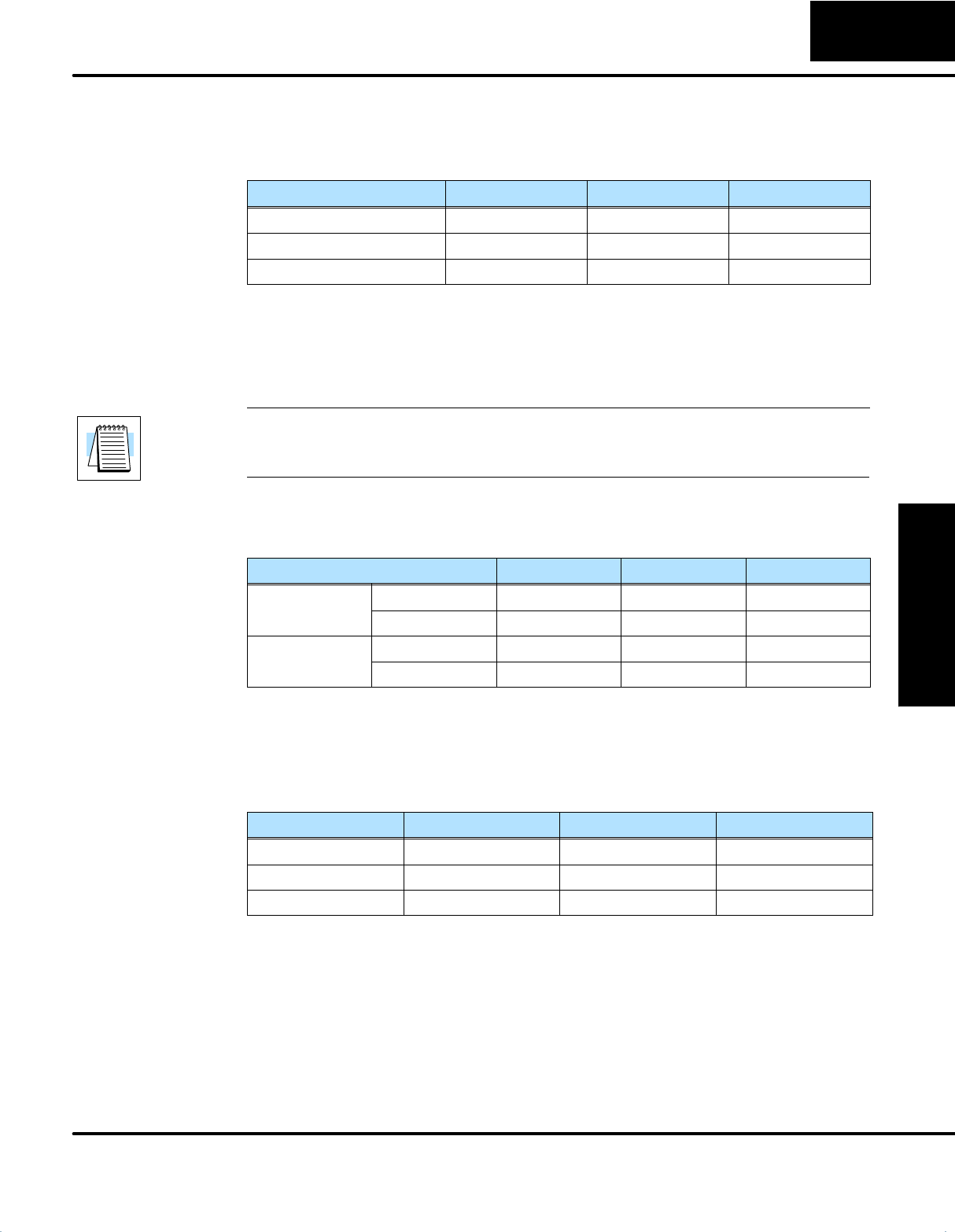
To Log Request (anytime) DL430 DL440 DL450
Nothing
Connected Min.&Max. 0μs 0 μs 0 μs
Port 0 Send Min. / Max. 52 / 62 μs40 / 48 μs38 / 38 μs
Rec.Min./Max. 60 / 78 μs52 / 63 μs45 /45 μs
Port 1 Send Min. / Max. 60 / 78 μs46 / 50 μs41 / 48 μs
Rec.Min./Max. 68 / 86 μs66 / 70 μs47 / 59 μs
Port 2 Send Min. / Max. N/A N/A 41 / 48 μs
Rec.Min./Max. N/A N/A 47 / 59 μs
Port 3 Send Min. / Max. N/A N/A 38 / 38 μs
Rec.Min./Max. N/A N/A 45 / 45 μs
Reading Inputs
from Specialty I/O
Service Peripherals
CPU Specifications
and Operation
3--29
CPU Specifications and Operation
DL405 User Manual, 4th Edition, Rev. A
During the Service Peripherals portion of the scan, the CPU analyzes the
communications request and responds as appropriate. The amount of time required
to service the peripherals depends on the content of the request.
To Service Request DL430 DL440 DL450
Minimum 170 μs120 μs96 μs
Run Mode Max. 18 ms 26 ms 160 ms
Program Mode Max. 3 Seconds 15 Seconds 11.2 Seconds
Some specialty modules can also communicate directly with the CPU via the CPU
bus. During this portion of the cycle the CPU completes any CPU bus
communications. The actual time required depends on the type of modules installed
and the type of request being processed.
NOTE: Some specialty modules can have a considerable impact on the CPU scan
time. If timing is critical in your application, consult the module documentation for any
information concerning the impact on the scan time.
The clock, calendar, and special relays are updated and loaded into special
V-memory locations during this time. This update is performed during both Run and
Program Modes.
Modes DL430 DL440 DL450
Program Mode Minimum 8.0 μsfixed 35.0 μs12.0 μs
Maximum 8.0 μsfixed 48.0 μs12.0 μs
Run Mode Minimum 20.0 μs60.0 μs22.0 μs
Maximum 26.0 μs85.0 μs29.0 μs
The time required to write the output status for the local and expansion I/O modules
depends on which CPU you are using, the number of output points in these bases,
and the number of output modules being used. The following table shows typical
update times required by the CPU.
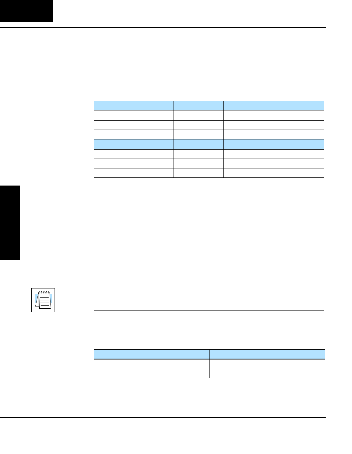
Timing Factors DL430 DL440 DL450
Overhead 20.0 μs12.6 μs15.0 μs
Per output module 45.0 μs21.0 μs13.0 μs
Per output point 4.0 μs2.5 μs14.1 μs
For example, the time required for a DL430 to write data for two 32-point output
modules would be calculated as follows (where NM is the number of modules and
NO is the total number of output points).
Time =20μs+(45μsxNM)+(4μsxNO)
Time =20μs+(45μsx2)+(4μs x 32)
Time =238 μs
Formula
Example
CPU Bus
Communication
Update
Clock/Calendar,
Special Relays,
Special Registers
Writing Outputs
CPU Specifications
and Operation
3--30 CPU Specifications and Operation
DL405 User Manual, 4th Edition, Rev. A
During this portion of the cycle the CPU writes any output points associated with the
following.
SRemote I/O
SSpecialty Modules (such as High-Speed Counter, etc.)
The time required to write any output image register data to these modules depends
on which CPU you are using, the number of modules, and the number of output
points.
Specialty Module DL430 DL440 DL450
Overhead 32.0 μs20.0 μs18.0 μs
Per module (with outputs) 100.0 μs67.0 μs13.0 μs
Per output point 80.0 μs54.0 μs14.1 μs
Remote Module DL430 DL440 DL450
Overhead 32.0 μs22.0 μs15.0 μs
Per module (with outputs) 150.0 μs100.0 μs54.0 μs
Per output point 25.0 μs17.0 μs13.9 μs
For example, the time required for a DL430 to write two 32-point output modules
(located in a Remote base) and the output points associated with a single
High-Speed Counter module would be calculated as follows. (Where NM is the
number of modules and NO is the total number of output points.)
Time =32μs+(150μsxNM)+(25μsxNO)
Time =32μs+(150μsx2)+(25μs x 32)
Time =1832 μs
Remote I
/
O
Time =32μs+(100μsxNM)+(80μsxNO)
Time =32μs+(100μsx1)+(80μsx4)
Time =452 μs
High-Speed Counter
Total Time
Time =2284 μs
Formula
Example
Formula
Example
NOTE: This total time is the actual time required for the CPU to update these
outputs. This does not include any additional time that is required for the CPU to
actually service the particular specialty modules.
The DL405 CPUs perform many types of system diagnostics. The amount of time
required depends on many things, such as the number of I/O modules installed, etc.
The following table shows the minimum and maximum times that can be expected.
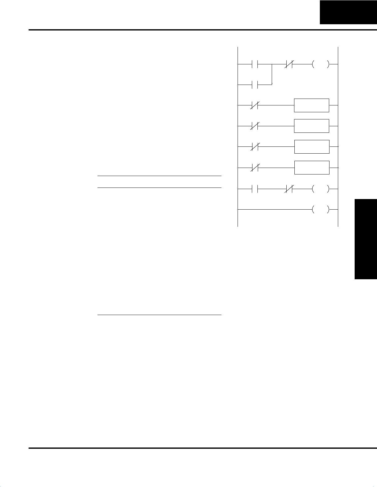
Diagnostic Time DL430 DL440 DL450
Minimum 680.0 μs540.0 μs282.0 μs
Maximum 880.0 μs920.0 μs398.0 μs
Writing Outputs to
Specialty I/O
Diagnostics
CPU Specifications
and Operation
3--31
CPU Specifications and Operation
DL405 User Manual, 4th Edition, Rev. A
V2002
The CPU processes the program from the
top (address 0) to the END instruction.
The CPU executes the program left to
right and top to bottom. As each rung is
evaluated the appropriate image register
or memory location is updated.
The time required to solve the application
program depends on the type and number
of instructions used, and the amount of
execution overhead.
You can add the execution times for all the
instructions in your program to find the
total program execution time.
For example, the execution time for a
DL430 running the program shown would
be calculated as follows.
Instruction Time
STR X0 4.7μs
OR C0 3.1μs
ANDN X1 3.4μs
OUT Y0 8.3μs
STRN C100 5.7μs
LD K10 112.0μs
STRN C101 8.3μs
OUT V2002 26.0μs
STRN C102 8.3μs
LD K50 112.0μs
STRN C103 8.3μs
OUT V0006 26.0μs
STR X5 4.7μs
ANDN X10 3.4μs
OUT Y3 8.3μs
END 15.5μs
TOTAL 358μs
X0 X1 Y0
OUT
C0
C100 LD K10
C101 OUT
C102 LD K50
C103 OUT
V006
X5 X10 Y3
OUT
END
Appendix C provides a complete list of instruction execution times for DL405 CPUs.
Program Control Instructions — the DL440 and DL450 CPUs offer additional
instructions that can change the way the program executes. These instructions
include FOR/NEXT loops, Subroutines, and Interrupt Routines. These instructions
can interrupt the normal program flow and effect the program execution time.
Chapter 5 provides detailed information on how these different types of instructions
operate.
Application
Program Execution

CPU Specifications
and Operation
3--32 CPU Specifications and Operation
DL405 User Manual, 4th Edition, Rev. A
PLC Numbering Systems
If you are a new PLC user or are using
AutomationDirect PLCs for the first time,
please take a moment to study how our
PLCs use numbers. You’ll find that each
PLC manufacturer has their own
conventions on the use of numbers in their
PLCs. We want to take just a moment to
familiarize you with how numbers are
used in AutomationDirect PLCs. The
information you learn here applies to all
our PLCs.
1482
0402
1001011011
7
3
3A9
??
?
?
BCD
binary
decimal
octal
hexadecimal
ASCII
1011
--961428
177 ?
--300124 A72B ?
49.832
As any good computer does, PLCs store and manipulate numbers in binary form:
just ones and zeros. So why do we have to deal with numbers in so many different
forms? Numbers have meaning, and some representations are more convenient
than others for particular purposes. Sometimes we use numbers to represent a size
or amount of something. Other numbers refer to locations or addresses, or to time. In
science we attach engineering units to numbers to give a particular meaning. (see
Appendix H for numbering system details).
PLCs offer a fixed amount of resources, depending on the model and configuration.
We use the word “resources” to include variable memory (V-memory), I/O points,
timers, counters, etc. Most modular PLCs allow you to add I/O points in groups of
eight. In fact, all the resources of our PLCs are counted in octal. It’s easier for
computers to count in groups of eight than ten, because eight is an even power of 2.
Octal means simply counting in groups o
f
eight things at a time. In the figure to the
right, there are eight circles. The quantity
in decimal is “8”, but in octal it is “10” (8 and
9 are not valid in octal). In octal, “10”
means 1 group of 8 plus 0 (no individuals).
Decimal12345678
Octal 1234 56710
In the figure below, we have two groups of eight circles. Counting in octal we have
“20” items, meaning 2 groups of eight, plus 0 individuals Don’t say “twenty”, say
“two--zero octal”. This makes a clear distinction between number systems.
Decimal 1 234 56 78
Octal 1 234 56 710
9 10111213141516
11 12 13 14 15 16 17 20
After counting PLC resources, it’s time to access PLC resources (there’s a
difference). The CPU instruction set accesses resources of the PLC using octal
addresses. Octal addresses are the same as octal quantities, except they start
counting at zero. The number zero is significant to a computer, so we don’t skip it.
Our circles are in an array of square
containers to the right. To access a
resource, our PLC instruction will address
its location using the octal references
shown. If these were counters, “CT14”
would access the black circle location.
01234567
2X
1X
X
X=
PLC Resources
CPU Specifications
and Operation
3--33
CPU Specifications and Operation
DL405 User Manual, 4th Edition, Rev. A
Variable memory (V-memory) stores data for the ladder program and for
configuration settings. V-memory locations and V-memory addresses are the same
thing, and are numbered in octal. For example, V2073 is a valid location, while
V1983 is not valid (“9” and “8” are not valid octal digits).
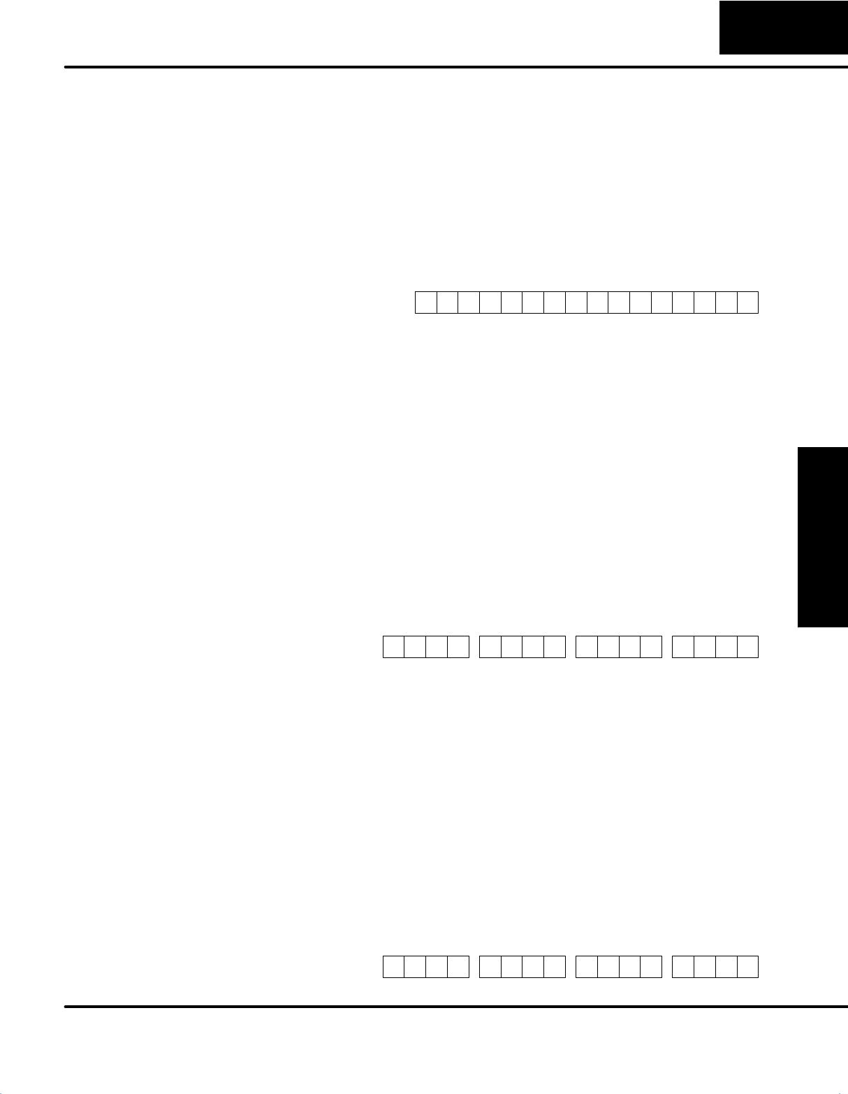
Each V-memory location is one data word wide, meaning 16 bits. For configuration
registers, our manuals will show each bit of a V-memory word. The least significant
bit (LSB) will be on the right, and the most significant bit (MSB) on the left. We use the
word “significant”, referring to the relative binary weighting of the bits.
0100111000101001
MSB LSB
V-memory data
(binary)
V-memory address
(octal)
V2017
V-memory data is 16-bit binary, but we rarely program the data registers one bit at a
time. We use instructions or viewing tools that let us work with binary, decimal, octal,
and hexadecimal numbers. All these are converted and stored as binary for us.
A frequently-asked question is “How do I tell if a number is binary, octal, BCD, or
hex”? The answer is that we usually cannot tell just by looking at the data... but it
does not really matter. What matters is: the source or mechanism which writes data
into a V-memory location and the thing which later reads it must both use the same
data type (i.e., octal, hex, binary, or whatever). The V-memory location is just a
storage box... that’s all. It does not convert or move the data on its own.
Since humans naturally count in decimal (10 fingers, 10 toes), we prefer to enter and
view PLC data in decimal as well (via operator interfaces). However, computers are
more efficient in usingpure binary numbers. A compromise solution between the two
is Binary-Coded Decimal (BCD) representation. A BCD digit ranges from 0 to 9, and
is stored as four binary bits (a nibble). This permits each V-memory location to store
four BCD digits, with a range of decimal numbers from 0000 to 9999.
0100 1001 0011 0110
49 36
V--memory storage
BCD number
8421 8421 8421 8421
In a pure binary sense, a 16-bit word represents numbers from 0 to 65535. In storing
BCD numbers, the range is reduced to 0 to 9999. Many math instructions use BCD
data, and DirectSOFT and the handheld programmer allow us to enter and view
data in BCD. Special RLL instructions convert from BCD to binary, or visa--versa.
Hexadecimal numbers are similar to BCD numbers, except they utilize all possible
binary values in each 4-bit digit. They are base-16 numbers so we need 16 different
digits. To extend our decimal digits 0 through 9, we use A through F as shown.
8 9 10 11 12 13 14 1501234567
89ABCDEF01234567
Decimal
Hexadecimal
A 4-digit hexadecimal number can represent all 65536 values in a V-memory word.
The range is from 0000 to FFFF (hex). PLCs often need this full range for sensor
data, etc. Hexadecimal is just a convenient way for humans to view full binary data.
1010 0111 1111 0100
A7 F4
V--memory storage
Hexadecimal number
V--Memory
Binary-Coded
Decimal Numbers
Hexadecimal
Numbers
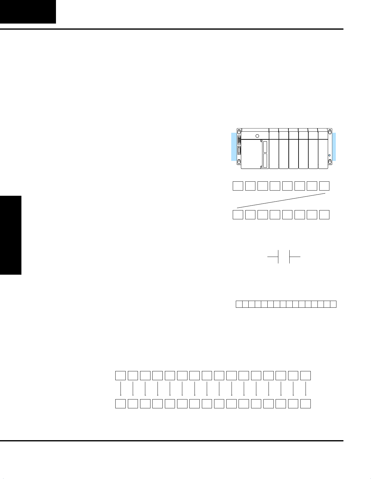
CPU Specifications
and Operation
3--34 CPU Specifications and Operation
DL405 User Manual, 4th Edition, Rev. A
Memory Map
With any PLC system, you generally have many different types of information to
process. This includes input device status, output device status, various timing
elements, parts counts, etc. It is important to understand how the system represents
and stores the various types of data. For example, you need to know how the system
identifies input points, output points, data words, etc. The following paragraphs
discuss the various memory types used in the DL405 CPUs. Memory maps for all
DL405 CPUs follow the memory descriptions.
All memory locations or areas are
numbered in Octal (base 8). The diagram
shows how the octal numbering system
works for the discrete input points. Notice
the octal system does not contain any
numbers with the digits 8 or 9.
Refer to the previous section on PLC
Numbering Systems for more on octal
numbering.
16pt
Input
8pt
Input
8pt
Input
8pt
Output
8pt
Output
16pt
Output
X0
--
X07
X10
--
X27
X30
--
X37
Y0
--
Y07
Y10
--
Y17
Y20
--
Y37
X0 X1 X2 X3 X4 X5 X6 X7
X10 X11 X12 X13 X14 X15 X16 X17
As you examine the different memory
types, you’ll notice two types of memory
in the DL405, discrete and word memory.
Discrete memory is one bit that can be
either a 1 or a 0. Word memory is referred
to as V--memory (variable) and is a 16-bit
location normally used to manipulate
data/numbers, store data/numbers, etc.
Some information is automatically stored
in V--memory. For example, the timer
current values are stored in V--memory. 0 110100000010010
X0
Discrete -- On or Off, 1 bit
Word Locations -- 16 bits
The discrete memory area is for inputs, outputs, control relays, special relays,
stages, global relays, timer status bits and counter status bits. However, you can
also access the bit data types as a V-memory word. Each V-memory location
contains 16 consecutive discrete locations. For example, the following diagram
shows how the X input points are mapped into V-memory locations.
X0X1X2X3X4X5X6X7X10X11X12X13X14X15X16X17
0123456789101112131415 V40400
Bit #
16 Discrete (X) Input Points
These discrete memory areas and the corresponding V--memory locations are listed
in the Memory Map tables for the DL430, DL440, and DL450 CPUs in this chapter.
Octal Numbering
System
Discrete and Word
Locations
V--Memory
Locations for
Discrete Memory
Areas
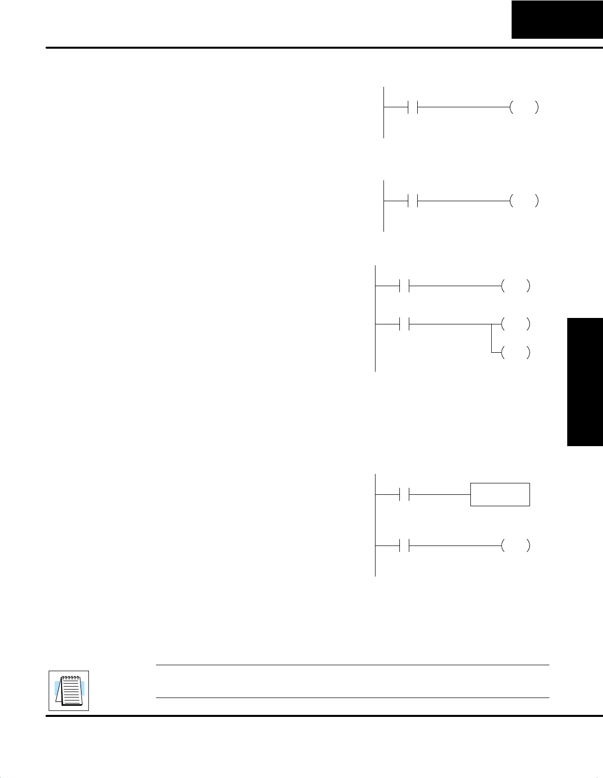
CPU Specifications
and Operation
3--35
CPU Specifications and Operation
DL405 User Manual, 4th Edition, Rev. A
The discrete input points are noted by an
X data type. Refer to the memory maps
for the number of discrete input points for
your CPU type. In this example, the
output point Y0 will energize when input
X0 turns on.
Y0
OUT
X0
The discrete output points are noted by a
Y data type. Refer to the memory maps
for the number of discrete input points for
your CPU type. In this example, output
point Y1 will energize when input X1
turns on.
Y1
OUT
X1
Control relays are discrete bits normally
used to control the user program. The
control relays do not represent a real world
device, that is, they cannot be physically
tied to switches, output coils, etc. They are
internal to the CPU. Because of this,
control relays can be programmed as
discrete inputs or discrete outputs. These
locations are used in programming the
discrete memory locations (C) or the
corresponding word location which
contains 16 consecutive discrete
locations.
C5
OUT
X10
Y10
OUT
C5
Y20
OUT
In this example, memory location C5 will energize when input X10 turns on. The
second rung shows a simple example of how to use a control relay as an input.
The amount of timers available depends
on the model of CPU you are using. The
tables at the end of this section provide the
amount of timers in each DL405 CPU
type. Regardless of the number of timers,
you have access to timer status bits that
reflect the relationship between the
current value and the preset value of a
specified timer. The timer status bit will be
on when the current value is equal or
greater than the preset value of a
corresponding timer.
Y12
OUT
T1
TMR T1
K30
X0
When input X0 turns on, timer T1 will start. When the timer reaches the preset of 3
seconds (K of 30) timer status contact T1 turns on. When T1 turns on, output Y12
energizes.
NOTE: Some timers and counters use one V-memory register, and other types
require two V-memory registers. See the instruction descriptions in Chapter 5.
Input Points
(X Data Type)
Output Points
(Y Data Type)
Control Relays
(C Data Type)
Timers and
Timer Status Bits
(T Data type)
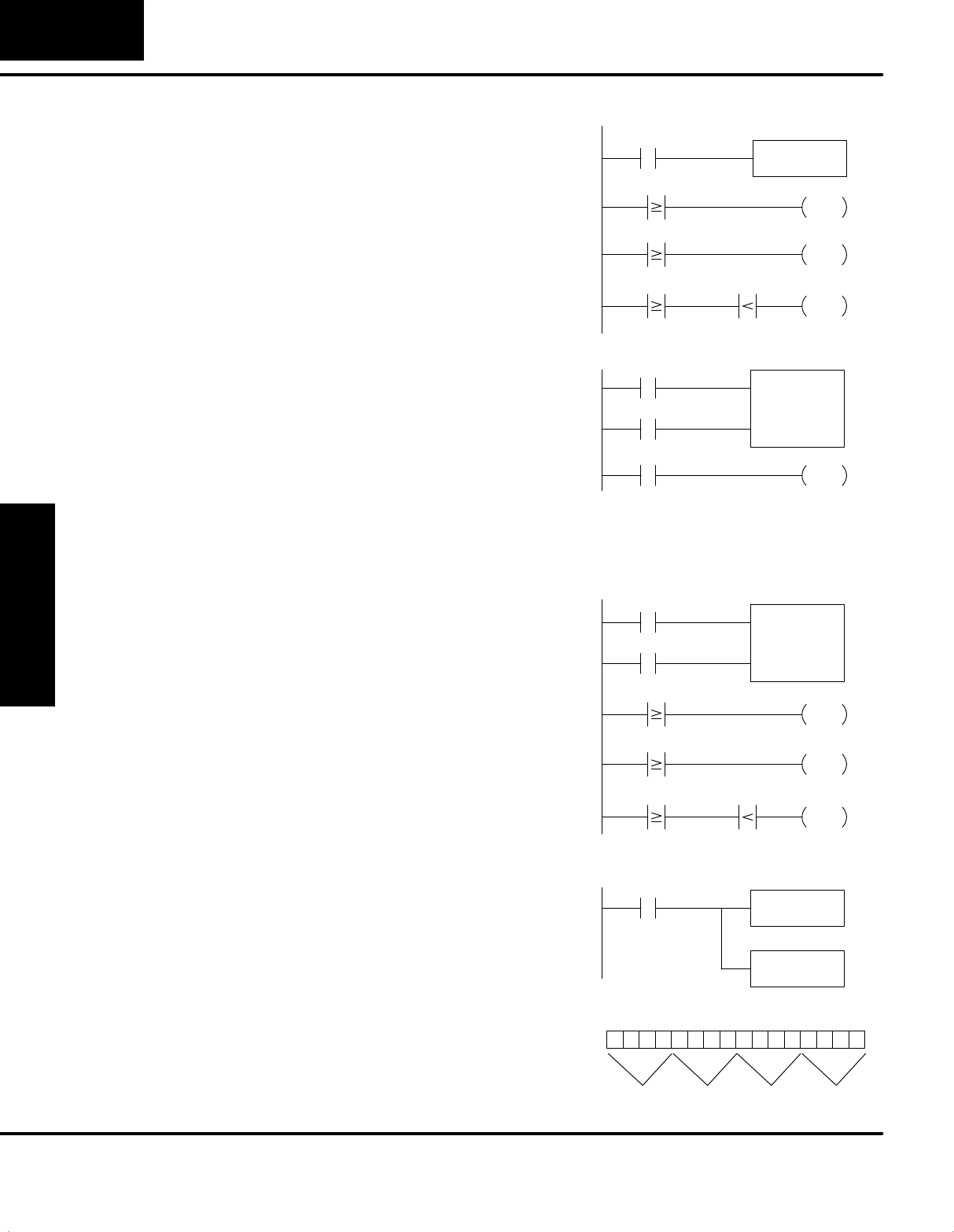
CPU Specifications
and Operation
3--36 CPU Specifications and Operation
DL405 User Manual, 4th Edition, Rev. A
V1 K100
Some information is automatically stored
in V--memory, such as the current values
associated with timers. For example, V0
holds the current value for Timer 0, V1
holds the current value for Timer 1, etc.
These are 4-digit BCD values.
The primary reason for this is
programming flexibility. The example
shows how you can use relational
contacts to monitor several time intervals
from a single timer.
TMR T1
K1000
X0
V1 K30 Y12
OUT
V1 K50 Y13
OUT
V1 K75 Y14
OUT
You have access to counter status bits that
reflect the relationship between the
current value and the preset value of a
specified counter. The counter status bit
will be on when the current value is equal
or greater than the preset value of a
corresponding counter.
Y12
OUT
CT3
X0 CNT CT3
K10
X1
Each time contact X0 transitions from off to on, the counter increments by one. (If X1
comes on, the counter is reset to zero.) When the counter reaches the preset of 10
counts (K of 10) counter status contact CT3 turns on. When CT3 turns on, output
Y12 turns on.
V1003 K8
Just like the timers, the counter current
values are also automatically stored in V--
memory. For example, V1000 holds the
current value for Counter CT0, V1001
holds the current value for Counter CT1,
etc. These are 4-digit BCD values.
The primary reason for this is
programming flexibility. The example
shows how you can use relational
contacts to monitor the counter values.
V1003 K1 Y12
OUT
V1003 K3 Y13
OUT
V1003 K5 Y14
OUT
X0 CNT CT3
K10
X1
V1400
Word memory is referred to as
V--memory (variable) and is a 16-bit
location normally used to manipulate
data/numbers, store data/numbers, etc.
Some information is automatically stored
in V--memory. For example, the timer
current values are stored in V--memory.
The example shows how a four-digit
BCD constant is loaded into the
accumulator and then stored in a
V-memory location.
0 100100110100010
Word Locations -- 16 bits
X0 LD K1345
OUT
1 3 4 5
Timer Current
Values
(V Data Type)
Counters and
Counter Status
Bits
(CT Data type)
Counter Current
Values
(V Data Type)
Word Memory
(V Data Type)
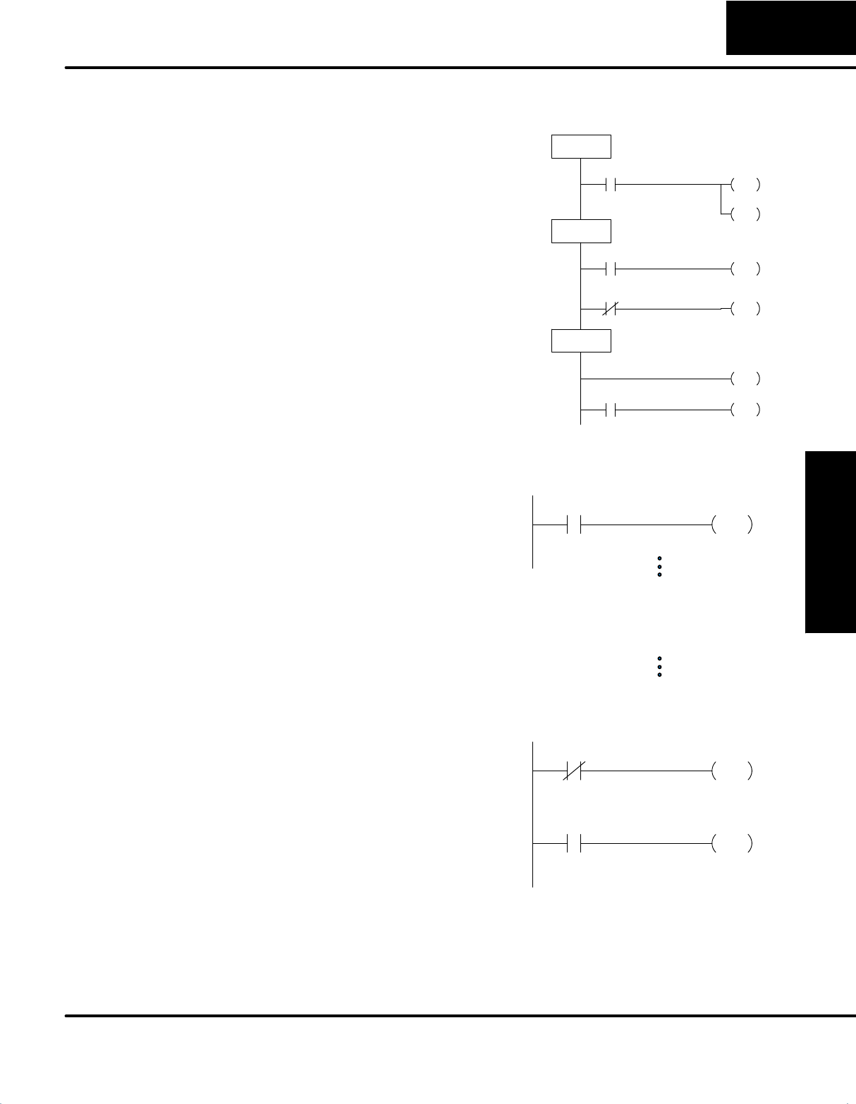
CPU Specifications
and Operation
3--37
CPU Specifications and Operation
DL405 User Manual, 4th Edition, Rev. A
Stages are used in RLL
P
L
U
S
programs to
create a structured program, similar to a
flowchart. Each program stage denotes a
program segment. When the program
segment, or stage, is active, the logic
within that segment is executed. If the
stage is off, or inactive, the logic is not
executed and the CPU skips to the next
active stage. (See Chapter 7 for a more
detailed description of RLLPLUS
programming.)
Each stage also has a discrete status bit
that can be used as an input to indicate
whether the stage is active or inactive. If
the stage is active, then the status bit is on.
If the stage is inactive, then the status bit is
off. This status bit can also be turned on or
off by other instructions, such as the SET
or RESET instructions. This allows you to
easily control stages throughout the
pro
g
ram.
Ladder Representation
ISGS0000
Start S1
JMP
SG S0001
Present S2
JMP
Part
X1
X0
S6
JMP
Present
Part
X1
SG S0002
Clamp
SET
S3
JMP
Locked
Part
X2
S400
Wait forStart
Check for a Part
Clamp the part
S500
JMP
Special relays are discrete memory
locations with pre-defined functionality.
There are many different types of special
relays. For example, some aid in program
development, others provide system
operating status information, etc.
Appendix D provides a complete listing of
the special relays.
In this example, control relay C10 will
energize for 50 ms and de--energize for 50
ms because SP5 is a pre--defined relay
that will be on for 50 ms and off for 50 ms.
C10
OUT
SP5
SP4: 1 second clock
SP5: 100 ms clock
SP6: 50 ms clock
Remote I/O points are represented by
global relays. They are generally used
only to control remote I/O, but they can be
used as normal control relays when
remote I/O is not used in the system. You
should notice the same data type, GX, is
used for both the remote input and remote
output points. There are setup routines
that must be placed in your application
program to designate which locations are
inputs and which are outputs. (The DL405
Remote and Slice I/O Modules manual
provides the details.)
In this example, memory location GX0
represents an output point and memory
location GX10 represents an input point.
Y12
OUT
X3 GX0
OUT
GX10
Stages
(S Data type)
Special Relays
(SP Data Type)
Remote I/O Points
(GX Data Type)
CPU Specifications
and Operation
3--38 CPU Specifications and Operation
DL405 User Manual, 4th Edition, Rev. A
Many system parameters, such as error codes, are automatically stored in
pre--defined V-memory locations. These memory locations store clock / calendar
information, error codes and other types of system setup information.
System
V-memory Description of Contents
V700, V701 Contains a copy of the contents of the accumulator. V700 is the lower
16 bit word, V701 is the upper 16 bit word.
V702, V703 Contains a copy of the contents of the 1st data stack location. V702 is
the lower 16 bit word, V703 is the upper 16 bit word.
V704, V705 Contains a copy of the contents of the 2nd data stack location. V704 is
the lower 16 bit word, V705 is the upper 16 bit word.
V706, V707 Contains a copy of the contents of the 3rd data stack location. V705 is
the lower 16 bit word, V706 is the upper 16 bit word.
V710, V711 Contains a copy of the contents of the 4th data stack location. V710 is
the lower 16 bit word, V711 is the upper 16 bit word.
V712, V713 Contains a copy of the contents of the 5th data stack location. V712 is
the lower 16 bit word, V713 is the upper 16 bit word.
V714, V715 Contains a copy of the contents of the 6th data stack location. V714 is
the lower 16 bit word, V715 is the upper 16 bit word.
V716, V717 Contains a copy of the contents of the 7th data stack location. V716 is
the lower 16 bit word, V717 is the upper 16 bit word.
V720, V721 Contains a copy of the contents of the 8th data stack location. V720 is
the lower 16 bit word, V721 is the upper 16 bit word.
System
V-memory Description of Contents
V737 Contains a BCD value (from 3 to 999) for Timed-interrupt 17 feature.
V7633 Bit 12 enables the low battery warning indicator.
V7747 Contains a 10 mS calendar timer used with the Clock / Calendar.
V7766 Contains the number of seconds on the clock. (00 to 59)
V7767 Contains the number of minutes on the clock. (00 to 59)
V7770 Contains the number of hours on the clock. (00 to 23)
V7771 Contains the day of the week. (0=Sun., 1=Mon, etc.)
V7772 Contains the day of the month (1st, 2nd, etc.)
V7773 Contains the month. (01 to 12)
V7774 Contains the year. (00 to 99)
System
V-memory Description of Contents
V736 Contains a BCD value (from 3 to 999) for Timed-interrupt 16 feature.
V7746 450: Battery voltage in tenths of a volt, (e.g., V7746 = 0031 is 3.1 Volts).
System Parameters
(V Data Type)
430
440 450
430
440
450
X
430
X
440
450
CPU Specifications
and Operation
3--39
CPU Specifications and Operation
DL405 User Manual, 4th Edition, Rev. A
System
V-memory
(continued)
Description of Contents
V7751 Fault Message Error Code — stores the 4-digit BCD code used with
the FAULT instruction when the instruction is executed. If you’ve used
ASCII messages (DL440/DL450 only) then the data label (DLBL)
reference number for that message is stored here.
V7752 I/O configuration Error — stores the module ID code for the module
that does not match the current configuration.
V7753 I/O Configuration Error — stores the correct module ID code.
V7754 I/O Configuration Error — identifies the base and slot number.
V7755 Error code — stores the fatal error code.
V7756 Error code — stores the major error code.
V7757 Communications Error Code -- stores the minor error code.
V7760 Module Error — identifies the base and slot number.
V7762 Module Error — identifies the type of error.
V7763 Program Grammatical Error — identifies the location of a syntax error
in a program.
V7764 Program Grammatical Error — identifies the type of error.
V7765 Scan — stores the total number of scan cycles that have occurred
since the last Program Mode to Run Mode transition.
V7775 Scan — stores the current scan time.
V7776 Scan — stores the minimum scan time that has occurred since the last
Program-to-Run Mode transition.
V7777 Scan — stores the maximum scan time that has occurred since the last
Program-to-Run Mode transition.
The following system control relays are valid only for DL450 CPU remote I/O setup
on Communications Port 3.
System CRs Description of Contents
C740 Completion of setups -- ladder logic must turn this relay on when it has
finished writing to the Remote I/O setup table
C741 ON -- the last state of inputs will be maintained.
OFF -- inputs will turn off when communication is lost.
C743 Re-start -- Turning on this relay will resume after a communications
hang-up on an error.
C750 to C757 Setup Error -- The corresponding relay will be ON if the setup table
contains an error (C750 = master, C751 = slave 1... C757=slave 7
C760 to C767 Communications Ready -- The corresponding relay will be ON if the
setup table data is valid (C760 = master, C761 = slave 1...
C767=slave 7
430
440
450
430
440
450
CPU Specifications
and Operation
3--40 CPU Specifications and Operation
DL405 User Manual, 4th Edition, Rev. A
Memory Type
Discrete Memory
Reference
(octal)
Word Memory
Reference
(octal)
Qty.
Decimal Symbol
Input Points X0 -- X477 V40400 -- V40423 320
Output Points Y0 -- Y477 V40500 -- V40523 320
Control Relays C0 -- C737 V40600 -- V40635 512
Special Relays SP0 -- SP137
SP320 -- SP617 V41200 -- V41205
V41215 -- V41230 288
Timers T0 -- T177 None 128
Timer Current
Values None V00000 -- V00177 128
Timer Status Bits T0 -- T177 V41100 -- V41107 128
Counters CT0 -- CT177 None 128
Counter
Current Values None V01000 -- V01177 128
Counter Status
Bits CT0 -- CT177 V41140 -- V41147 128
User Data Words None V1400 -- V7377 3072 None specific, used with many
instructions
Stages S0 -- S577 V41000 -- V41027 384
Remote In / Out GX0 -- GX777 V40000 -- V40037 512
System
parameters None V7400 -- V7777 256 None specific, used with many
instructions
DL430 Memory
Map
X0
Y0
C0C0
SP0
TMR T0
K100
V0 K100
T0
CNT CT0
K10
V1000 K100
CT0
SG S 001
S0
GX0GX0
CPU Specifications
and Operation
3--41
CPU Specifications and Operation
DL405 User Manual, 4th Edition, Rev. A
Memory Type
Discrete Memory
Reference
(octal)
Word Memory
Reference
(octal)
Qty.
Decimal Symbol
Input Points X0 -- X477 V40400 -- V40423 320
Output Points Y0 -- Y477 V40500--V40523 320
Control Relays C0 -- C1777 V40600--V40677 1024
Special Relays SP0 -- SP137
SP320 -- SP717 V41200--V41205
V41215--V41234 352
Timers T0 -- T377 None 256
Timer Current
Values None V00000 -- V00377 256
Timer Status Bits T0 -- T377 V41100 -- V41117 256
Counters CT0 -- CT177 None 128
Counter
Current Values None V01000 -- V01177 128
Counter Status
Bits CT0 -- CT177 V41140 -- V41147 128
User Data Words None V1400 -- V7377
V10000 -- V17777 3072
4096 None specific, used with many
instructions
Stages S0 -- S1777 V41000 -- V41077 1024
Remote In / Out GX0 -- GX1777 V40000 -- V40077 1024
System
parameters None V700 -- V737
V7400 -- V7777 288 None specific, used with many
instructions
DL440 Memory
Map
X0
Y0
C0C0
SP0
TMR T0
K100
V0 K100
T0
CNT CT0
K10
V1000 K100
CT0
SG S 001
S0
GX0GX0
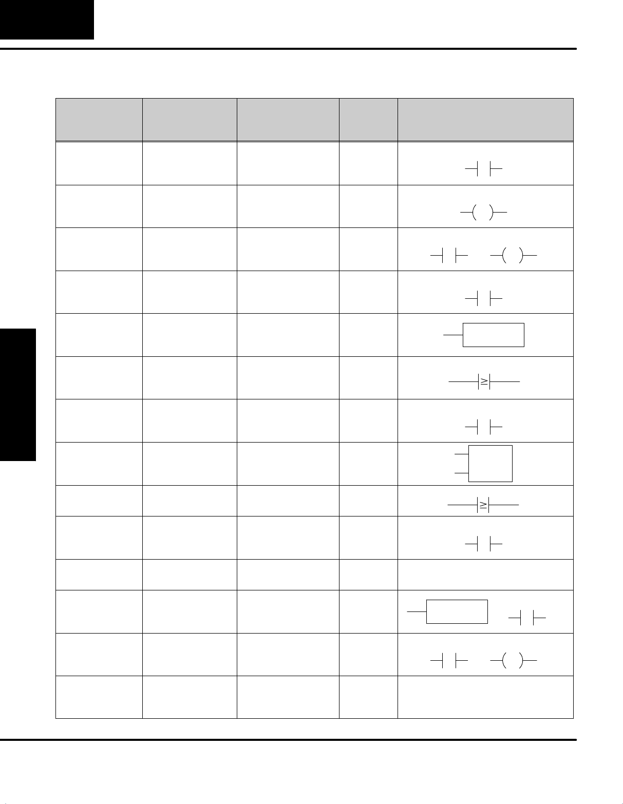
CPU Specifications
and Operation
3--42 CPU Specifications and Operation
DL405 User Manual, 4th Edition, Rev. A
Memory Type
Discrete Memory
Reference
(octal)
Word Memory
Reference
(octal)
Qty.
Decimal Symbol
Input Points X0 -- X1777 V40400 -- V40477 1024
Output Points Y0 -- Y1777 V40500 -- V40577 1024
Control Relays C0 -- C3777 V40600 -- V40777 2048
Special Relays SP0 -- SP777 V41200 -- V41237 512
Timers T0 -- T377 V41100 -- V41117 256
Timer Current
Values None V00000 -- V00377 256
Timer Status Bits T0 -- T377 V41100 -- V41117 256
Counters CT0 -- CT377 V41140 -- V41157 256
Counter
Current Values None V01000 -- V01377 256
Counter Status
Bits CT0 -- CT377 V41140 -- V41157 256
User Data Words None V1400 -- V7377
V10000 -- V36777 3072
11776 None specific, used with many
instructions
Stages S0 -- S1777 V41000 -- V41077 1024
Remote In / Out GX0 -- GX3777
GY0 -- GY3777
V40000 -- V40177
V40200 -- V40377
2048
2048
System
parameters None V700 -- V777
V7400 -- V7777
V37000 -- V37777
832 None specific, used with many
instructions
DL450 Memory
Map
X0
Y0
C0C0
SP0
TMR T0
K100
V0 K100
T0
CNT CT0
K10
V1000 K100
CT0
SG S 001
S0
GY0GX0
CPU Specifications
and Operation
3--43
CPU Specifications and Operation
DL405 User Manual, 4th Edition, Rev. A
DL405 Aliases
An alias is an alternate way of referring to certain memory types, such as
timer/counter current values, V--memory locations for I/O points, etc., which
simplifies understanding the memory address. The use of the alias is optional, but
some users may find the alias to be helpful when developing a program. The table
below shows how the aliases can be used to reference memory locations.
NOTE: Ranges depend on CPU type.
Address Start Alias Start Example
V0 TA0 V0 is the timer accumulator value for timer 0, therefore, it’s
alias is TA0. TA1 is the alias for V1, etc..
V1000 CTA0 V1000 is the counter accumulator value for counter 0,
therefore, it’s alias is CTA0. CTA1 is the alias for V1001, etc.
V40000 VGX
V40000 is the word memory reference for discrete bits GX0
through GX17, therefore, it’s alias is VGX0. V40001 is the word
memory reference for discrete bits GX20 through GX 37,
therefore, it’s alias is VGX20.
V40200
(DL450 only) VGY
V40200 is the word memory reference for discrete bits GY0
through GY17, therefore, it’s alias is VGY0. V40201 is the word
memory reference for discrete bits GY20 through GY 37,
therefore, it’s alias is VGY20.
V40400 VX0
V40400 is the word memory reference for discrete bits X0
through X17, therefore, it’s alias is VX0. V40401 is the word
memory reference for discrete bits X20 through X37, therefore,
it’s alias is VX20.
V40500 VY0
V40500 is the word memory reference for discrete bits Y0
through Y17, therefore, it’s alias is VY0. V40501 is the word
memory reference for discrete bits Y20 through Y37, therefore,
it’s alias is VY20.
V40600 VC0
V40600 is the word memory reference for discrete bits C0
through C17, therefore, it’s alias is VC0. V40601 is the word
memory reference for discrete bits C20 through C37, therefore,
it’s alias is VC20.
V41000 VS0
V41000 is the word memory reference for discrete bits S0
through S17, therefore, it’s alias is VS0. V41001 is the word
memory reference for discrete bits S20 through S37, therefore,
it’s alias is VS20.
V41100 VT0
V41100 is the word memory reference for discrete bits T0
through T17, therefore, it’s alias is VT0. V41101 is the word
memory reference for discrete bits T20 through T37, therefore,
it’s alias is VT20.
V41140 VCT0
V41140 is the word memory reference for discrete bits CT0
through CT17, therefore, it’s alias is VCT0. V41141 is the word
memory reference for discrete bits CT20 through CT37,
therefore, it’s alias is VCT20.
V41200 VSP0
V41200 is the word memory reference for discrete bits SP0
through SP17, therefore, it’s alias is VSP0. V41201 is the word
memory reference for discrete bits SP20 through SP37,
therefore, it’s alias is VSP20.
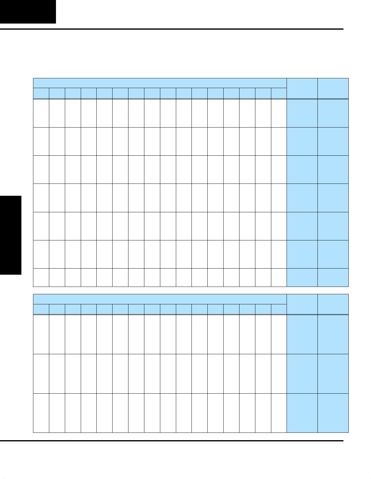
CPU Specifications
and Operation
3--44 CPU Specifications and Operation
DL405 User Manual, 4th Edition, Rev. A
X Input/Y Output Bit Map
This table provides a listing of individual Input and Output points associated with each V-memory address
bit for the DL430, DL440, and DL450 CPUs.
MSB DL430/DL440/DL450 Input (X) and Output (Y) Points LSB
X
In
p
ut
Y
Out
p
ut
15 14 13 12 11 10 9876543210
X
I
n
p
u
t
Address
Y
O
u
t
p
u
t
Address
017 016 015 014 013 012 011 010 007 006 005 004 003 002 001 000 V40400 V40500
037 036 035 034 033 032 031 030 027 026 025 024 023 022 021 020 V40401 V40501
057 056 055 054 053 052 051 050 047 046 045 044 043 042 041 040 V40402 V40502
077 076 075 074 073 072 071 070 067 066 065 064 063 062 061 060 V40403 V40503
117 116 115 114 113 112 111 110 107 106 105 104 103 102 101 100 V40404 V40504
137 136 135 134 133 132 131 130 127 126 125 124 123 122 121 120 V40405 V40505
157 156 155 154 153 152 151 150 147 146 145 144 143 142 141 140 V40406 V40506
177 176 175 174 173 172 171 170 167 166 165 164 163 162 161 160 V40407 V40507
217 216 215 214 213 212 211 210 207 206 205 204 203 202 201 200 V40410 V40510
237 236 235 234 233 232 231 230 227 226 225 224 223 222 221 220 V40411 V40511
257 256 255 254 253 252 251 250 247 246 245 244 243 242 241 240 V40412 V40512
277 276 275 274 273 272 271 270 267 266 265 264 263 262 261 260 V40413 V40513
317 316 315 314 313 312 311 310 307 306 305 304 303 302 301 300 V40414 V40514
337 336 335 334 333 332 331 330 327 326 325 324 323 322 321 320 V40415 V40515
357 356 355 354 353 352 351 350 347 346 345 344 343 342 341 340 V40416 V40516
377 376 375 374 373 372 371 370 367 366 365 364 363 362 361 360 V40417 V40517
417 416 415 414 413 412 411 410 407 406 405 404 403 402 401 400 V40420 V40520
437 436 435 434 433 432 431 430 427 426 425 424 423 422 421 420 V40421 V40521
457 456 455 454 453 452 451 450 447 446 445 444 443 442 441 440 V40422 V40522
477 476 475 474 473 472 471 470 467 466 465 464 463 462 461 460 V40423 V40523
MSB DL450 Additional Input (X) and Output (Y) Points LSB
X
In
p
ut
Y
Out
p
ut
15 14 13 12 11 10 9876543210
X
I
n
p
u
t
Address
Y
O
u
t
p
u
t
Address
517 516 515 514 513 512 511 510 507 506 505 504 503 502 501 500 V40424 V40524
537 536 535 534 533 532 531 530 527 526 525 524 523 522 521 520 V40425 V40525
557 556 555 554 553 552 551 550 547 546 545 544 543 542 541 540 V40426 V40526
577 576 575 574 573 572 571 570 567 566 565 564 563 562 561 560 V40427 V40527
617 616 615 614 613 612 611 610 607 606 605 604 603 602 601 600 V40430 V40530
637 636 635 634 633 632 631 630 627 626 625 624 623 622 621 620 V40431 V40531
657 656 655 654 653 652 651 650 647 646 645 644 643 642 641 640 V40432 V40532
677 676 675 674 673 672 671 670 667 666 665 664 663 662 661 660 V40433 V40533
717 716 715 714 713 712 711 710 707 706 705 704 703 702 701 700 V40434 V40534
737 736 735 734 733 732 731 730 727 726 725 724 723 722 721 720 V40435 V40535
757 756 755 754 753 752 751 750 747 746 745 744 743 742 741 740 V40436 V40536
777 776 775 774 773 772 771 770 767 766 765 764 763 762 761 760 V40437 V40537

CPU Specifications
and Operation
3--45
CPU Specifications and Operation
DL405 User Manual, 4th Edition, Rev. A
MSB DL450 Additional Input (X) and Output (Y) Points (cont’d) LSB
X
In
p
ut
Y
Out
p
ut
15 14 13 12 11 10 9876543210
X
I
n
p
u
t
Address
Y
O
u
t
p
u
t
Address
1017 1016 1015 1014 1013 1012 1011 1010 1007 1006 1005 1004 1003 1002 1001 1000 V40440 V40540
1037 1036 1035 1034 1033 1032 1031 1030 1027 1026 1025 1024 1023 1022 1021 1020 V40441 V40541
1057 1056 1055 1054 1053 1052 1051 1050 1047 1046 1045 1044 1043 1042 1041 1040 V40442 V40542
1077 1076 1075 1074 1073 1072 1071 1070 1067 1066 1065 1064 1063 1062 1061 1060 V40443 V40543
1117 1116 1115 1114 1113 1112 1111 1110 1107 1106 1105 1104 1103 1102 1101 1100 V40444 V40544
1137 1136 1135 1134 1133 1132 1131 1130 1127 1126 1125 1124 1123 1122 1121 1120 V40445 V40545
1157 1156 1155 1154 1153 1152 1151 1150 1147 1146 1145 1144 1143 1142 1141 1140 V40446 V40546
1177 1176 1175 1174 1173 1172 1171 1170 1167 1166 1165 1164 1163 1162 1161 1160 V40447 V40547
1217 1216 1215 1214 1213 1212 1211 1210 1207 1206 1205 1204 1203 1202 1201 1200 V40450 V40550
1237 1236 1235 1234 1233 1232 1231 1230 1227 1226 1225 1224 1223 1222 1221 1220 V40451 V40551
1257 1256 1255 1254 1253 1252 1251 1250 1247 1246 1245 1244 1243 1242 1241 1240 V40452 V40552
1277 1276 1275 1274 1273 1272 1271 1270 1267 1266 1265 1264 1263 1262 1261 1260 V40453 V40553
1317 1316 1315 1314 1313 1312 1311 1310 1307 1306 1305 1304 1303 1302 1301 1300 V40454 V40554
1337 1336 1335 1334 1333 1332 1331 1330 1327 1326 1325 1324 1323 1322 1321 1320 V40455 V40555
1357 1356 1355 1354 1353 1352 1351 1350 1347 1346 1345 1344 1343 1342 1341 1340 V40456 V40556
1377 1376 1375 1374 1373 1372 1371 1370 1367 1366 1365 1364 1363 1362 1361 1360 V40457 V40557
1417 1416 1415 1414 1413 1412 1411 1410 1407 1406 1405 1404 1403 1402 1401 1400 V40460 V40560
1437 1436 1435 1434 1433 1432 1431 1430 1427 1426 1425 1424 1423 1422 1421 1420 V40461 V40561
1457 1456 1455 1454 1453 1452 1451 1450 1447 1446 1445 1444 1443 1442 1441 1440 V40462 V40562
1477 1476 1475 1474 1473 1472 1471 1470 1467 1466 1465 1464 1463 1462 1461 1460 V40463 V40563
1517 1516 1515 1514 1513 1512 1511 1510 1507 1506 1505 1504 1503 1502 1501 1500 V40464 V40564
1537 1536 1535 1534 1533 1532 1531 1530 1527 1526 1525 1524 1523 1522 1521 1520 V40465 V40565
1557 1556 1555 1554 1553 1552 1551 1550 1547 1546 1545 1544 1543 1542 1541 1540 V40466 V40566
1577 1576 1575 1574 1573 1572 1571 1570 1567 1566 1565 1564 1563 1562 1561 1560 V40467 V40567
1617 1616 1615 1614 1613 1612 1611 1610 1607 1606 1605 1604 1603 1602 1601 1600 V40470 V40570
1637 1636 1635 1634 1633 1632 1631 1630 1627 1626 1625 1624 1623 1622 1621 1620 V40471 V40571
1657 1656 1655 1654 1653 1652 1651 1650 1647 1646 1645 1644 1643 1642 1641 1640 V40472 V40572
1677 1676 1675 1674 1673 1672 1671 1670 1667 1666 1665 1664 1663 1662 1661 1660 V40473 V40573
1717 1716 1715 1714 1713 1712 1711 1710 1707 1706 1705 1704 1703 1702 1701 1700 V40474 V40574
1737 1736 1735 1734 1733 1732 1731 1730 1727 1726 1725 1724 1723 1722 1721 1720 V40475 V40575
1757 1756 1755 1754 1753 1752 1751 1750 1747 1746 1745 1744 1743 1742 1741 1740 V40476 V40576
1777 1776 1775 1774 1773 1772 1771 1770 1767 1766 1765 1764 1763 1762 1761 1760 V40477 V40577

CPU Specifications
and Operation
3--46 CPU Specifications and Operation
DL405 User Manual, 4th Edition, Rev. A
Control Relay Bit Map
This table provides a listing of the individual control relays associated with each V-memory address bit.
MSB DL430 / DL440 / DL450 Control Relays (C) LSB
A
d
d
r
e
s
s
15 14 13 12 11 10 9 8 7 6 5 4 3 2 1 0
A
d
d
ress
017 016 015 014 013 012 011 010 007 006 005 004 003 002 001 000 V40600
037 036 035 034 033 032 031 030 027 026 025 024 023 022 021 020 V40601
057 056 055 054 053 052 051 050 047 046 045 044 043 042 041 040 V40602
077 076 075 074 073 072 071 070 067 066 065 064 063 062 061 060 V40603
117 116 115 114 113 112 111 110 107 106 105 104 103 102 101 100 V40604
137 136 135 134 133 132 131 130 127 126 125 124 123 122 121 120 V40605
157 156 155 154 153 152 151 150 147 146 145 144 143 142 141 140 V40606
177 176 175 174 173 172 171 170 167 166 165 164 163 162 161 160 V40607
217 216 215 214 213 212 211 210 207 206 205 204 203 202 201 200 V40610
237 236 235 234 233 232 231 230 227 226 225 224 223 222 221 220 V40611
257 256 255 254 253 252 251 250 247 246 245 244 243 242 241 240 V40612
277 276 275 274 273 272 271 270 267 266 265 264 263 262 261 260 V40613
317 316 315 314 313 312 311 310 307 306 305 304 303 302 301 300 V40614
337 336 335 334 333 332 331 330 327 326 325 324 323 322 321 320 V40615
357 356 355 354 353 352 351 350 347 346 345 344 343 342 341 340 V40616
377 376 375 374 373 372 371 370 367 366 365 364 363 362 361 360 V40617
417 416 415 414 413 412 411 410 407 406 405 404 403 402 401 400 V40620
437 436 435 434 433 432 431 430 427 426 425 424 423 422 421 420 V40621
457 456 455 454 453 452 451 450 447 446 445 444 443 442 441 440 V40622
477 476 475 474 473 472 471 470 467 466 465 464 463 462 461 460 V40623
517 516 515 514 513 512 511 510 507 506 505 504 503 502 501 500 V40624
537 536 535 534 533 532 531 530 527 526 525 524 523 522 521 520 V40625
557 556 555 554 553 552 551 550 547 546 545 544 543 542 541 540 V40626
577 576 575 574 573 572 571 570 567 566 565 564 563 562 561 560 V40627
617 616 615 614 613 612 611 610 607 606 605 604 603 602 601 600 V40630
637 636 635 634 633 632 631 630 627 626 625 624 623 622 621 620 V40631
657 656 655 654 653 652 651 650 647 646 645 644 643 642 641 640 V40632
677 676 675 674 673 672 671 670 667 666 665 664 663 662 661 660 V40633
717 716 715 714 713 712 711 710 707 706 705 704 703 702 701 700 V40634
737 736 735 734 733 732 731 730 727 726 725 724 723 722 721 720 V40635

CPU Specifications
and Operation
3--47
CPU Specifications and Operation
DL405 User Manual, 4th Edition, Rev. A
This portion of the table shows additional Control Relays points available with the DL440 and DL450.
MSB DL440 / DL450 Additional Control Relays (C) LSB
A
d
d
r
e
s
s
15 14 13 12 11 10 9 8 7 6 5 4 3 2 1 0
A
d
d
ress
757 756 755 754 753 752 751 750 747 746 745 744 743 742 741 740 V40636
777 776 775 774 773 772 771 770 767 766 765 764 763 762 761 760 V40637
1017 1016 1015 1014 1013 1012 1011 1010 1007 1006 1005 1004 1003 1002 1001 1000 V40640
1037 1036 1035 1034 1033 1032 1031 1030 1027 1026 1025 1024 1023 1022 1021 1020 V40641
1057 1056 1055 1054 1053 1052 1051 1050 1047 1046 1045 1044 1043 1042 1041 1040 V40642
1077 1076 1075 1074 1073 1072 1071 1070 1067 1066 1065 1064 1063 1062 1061 1060 V40643
1117 1116 1115 1114 1113 1112 1111 1110 1107 1106 1105 1104 1103 1102 1101 1100 V40644
1137 1136 1135 1134 1133 1132 1131 1130 1127 1126 1125 1124 1123 1122 1121 1120 V40645
1157 1156 1155 1154 1153 1152 1151 1150 1147 1146 1145 1144 1143 1142 1141 1140 V40646
1177 1176 1175 1174 1173 1172 1171 1170 1167 1166 1165 1164 1163 1162 1161 1160 V40647
1217 1216 1215 1214 1213 1212 1211 1210 1207 1206 1205 1204 1203 1202 1201 1200 V40650
1237 1236 1235 1234 1233 1232 1231 1230 1227 1226 1225 1224 1223 1222 1221 1220 V40651
1257 1256 1255 1254 1253 1252 1251 1250 1247 1246 1245 1244 1243 1242 1241 1240 V40652
1277 1276 1275 1274 1273 1272 1271 1270 1267 1266 1265 1264 1263 1262 1261 1260 V40653
1317 1316 1315 1314 1313 1312 1311 1310 1307 1306 1305 1304 1303 1302 1301 1300 V40654
1337 1336 1335 1334 1333 1332 1331 1330 1327 1326 1325 1324 1323 1322 1321 1320 V40655
1357 1356 1355 1354 1353 1352 1351 1350 1347 1346 1345 1344 1343 1342 1341 1340 V40656
1377 1376 1375 1374 1373 1372 1371 1370 1367 1366 1365 1364 1363 1362 1361 1360 V40657
1417 1416 1415 1414 1413 1412 1411 1410 1407 1406 1405 1404 1403 1402 1401 1400 V40660
1437 1436 1435 1434 1433 1432 1431 1430 1427 1426 1425 1424 1423 1422 1421 1420 V40661
1457 1456 1455 1454 1453 1452 1451 1450 1447 1446 1445 1444 1443 1442 1441 1440 V40662
1477 1476 1475 1474 1473 1472 1471 1470 1467 1466 1465 1464 1463 1462 1461 1460 V40663
1517 1516 1515 1514 1513 1512 1511 1510 1507 1506 1505 1504 1503 1502 1501 1500 V40664
1537 1536 1535 1534 1533 1532 1531 1530 1527 1526 1525 1524 1523 1522 1521 1520 V40665
1557 1556 1555 1554 1553 1552 1551 1550 1547 1546 1545 1544 1543 1542 1541 1540 V40666
1577 1576 1575 1574 1573 1572 1571 1570 1567 1566 1565 1564 1563 1562 1561 1560 V40667
1617 1616 1615 1614 1613 1612 1611 1610 1607 1606 1605 1604 1603 1602 1601 1600 V40670
1637 1636 1635 1634 1633 1632 1631 1630 1627 1626 1625 1624 1623 1622 1621 1620 V40671
1657 1656 1655 1654 1653 1652 1651 1650 1647 1646 1645 1644 1643 1642 1641 1640 V40672
1677 1676 1675 1674 1673 1672 1671 1670 1667 1666 1665 1664 1663 1662 1661 1660 V40673
1717 1716 1715 1714 1713 1712 1711 1710 1707 1706 1705 1704 1703 1702 1701 1700 V40674
1737 1736 1735 1734 1733 1732 1731 1730 1727 1726 1725 1724 1723 1722 1721 1720 V40675
1757 1756 1755 1754 1753 1752 1751 1750 1747 1746 1745 1744 1743 1742 1741 1740 V40676
1777 1776 1775 1774 1773 1772 1771 1770 1767 1766 1765 1764 1763 1762 1761 1760 V40677

CPU Specifications
and Operation
3--48 CPU Specifications and Operation
DL405 User Manual, 4th Edition, Rev. A
This portion of the table shows additional Control Relays points available with the DL450.
MSB DL450 Additional Control Relays (C) LSB
A
d
d
r
e
s
s
15 14 13 12 11 10 9 8 7 6 5 4 3 2 1 0
A
d
d
ress
2017 2016 2015 2014 2013 2012 2011 2010 2007 2006 2005 2004 2003 2002 2001 2000 V40700
2037 2036 2035 2034 2033 2032 2031 2030 2027 2026 2025 2024 2023 2022 2021 2020 V40701
2057 2056 2055 2054 2053 2052 2051 2050 2047 2046 2045 2044 2043 2042 2041 2040 V40702
2077 2076 2075 2074 2073 2072 2071 2070 2067 2066 2065 2064 2063 2062 2061 2060 V40703
2117 2116 2115 2114 2113 2112 2111 2110 2107 2106 2105 2104 2103 2102 2101 2100 V40704
2137 2136 2135 2134 2133 2132 2131 2130 2127 2126 2125 2124 2123 2122 2121 2120 V40705
2157 2156 2155 2154 2153 2152 2151 2150 2147 2146 2145 2144 2143 2142 2141 2140 V40706
2177 2176 2175 2174 2173 2172 2171 2170 2167 2166 2165 2164 2163 2162 2161 2160 V40707
2217 2216 2215 2214 2213 2212 2211 2210 2207 2206 2205 2204 2203 2202 2201 2200 V40710
2237 2236 2235 2234 2233 2232 2231 2230 2227 2226 2225 2224 2223 2222 2221 2220 V40711
2257 2256 2255 2254 2253 2252 2251 2250 2247 2246 2245 2244 2243 2242 2241 2240 V40712
2277 2276 2275 2274 2273 2272 2271 2270 2267 2266 2265 2264 2263 2262 2261 2260 V40713
2317 2316 2315 2314 2313 2312 2311 2310 2307 2306 2305 2304 2303 2302 2301 2300 V40714
2337 2336 2335 2334 2333 2332 2331 2330 2327 2326 2325 2324 2323 2322 2321 2320 V40715
2357 2356 2355 2354 2353 2352 2351 2350 2347 2346 2345 2344 2343 2342 2341 2340 V40716
2377 2376 2375 2374 2373 2372 2371 2370 2367 2366 2365 2364 2363 2362 2361 2360 V40717
2417 2416 2415 2414 2413 2412 2411 2410 2407 2406 2405 2404 2403 2402 2401 2400 V40720
2437 2436 2435 2434 2433 2432 2431 2430 2427 2426 2425 2424 2423 2422 2421 2420 V40721
2457 2456 2455 2454 2453 2452 2451 2450 2447 2446 2445 2444 2443 2442 2441 2440 V40722
2477 2476 2475 2474 2473 2472 2471 2470 2467 2466 2465 2464 2463 2462 2461 2460 V40723
2517 2516 2515 2514 2513 2512 2511 2510 2507 2506 2505 2504 2503 2502 2501 2500 V40724
2537 2536 2535 2534 2533 2532 2531 2530 2527 2526 2525 2524 2523 2522 2521 2520 V40725
2557 2556 2555 2554 2553 2552 2551 2550 2547 2546 2545 2544 2543 2542 2541 2540 V40726
2577 2576 2575 2574 2573 2572 2571 2570 2567 2566 2565 2564 2563 2562 2561 2560 V40727
2617 2616 2615 2614 2613 2612 2611 2610 2607 2606 2605 2604 2603 2602 2601 2600 V40730
2637 2636 2635 2634 2633 2632 2631 2630 2627 2626 2625 2624 2623 2622 2621 2620 V40731
2657 2656 2655 2654 2653 2652 2651 2650 2647 2646 2645 2644 2643 2642 2641 2640 V40732
2677 2676 2675 2674 2673 2672 2671 2670 2667 2666 2665 2664 2663 2662 2661 2660 V40733
2717 2716 2715 2714 2713 2712 2711 2710 2707 2706 2705 2704 2703 2702 2701 2700 V40734
2737 2736 2735 2734 2733 2732 2731 2730 2727 2726 2725 2724 2723 2722 2721 2720 V40735
2757 2756 2755 2754 2753 2752 2751 2750 2747 2746 2745 2744 2743 2742 2741 2740 V40736
2777 2776 2775 2774 2773 2772 2771 2770 2767 2766 2765 2764 2763 2762 2761 2760 V40737

CPU Specifications
and Operation
3--49
CPU Specifications and Operation
DL405 User Manual, 4th Edition, Rev. A
MSB DL450 Additional Control Relays (C) (cont’d) LSB
A
d
d
r
e
s
s
15 14 13 12 11 10 9 8 7 6 5 4 3 2 1 0
A
d
d
ress
3017 3016 3015 3014 3013 3012 3011 3010 3007 3006 3005 3004 3003 3002 3001 3000 V40740
3037 3036 3035 3034 3033 3032 3031 3030 3027 3026 3025 3024 3023 3022 3021 3020 V40741
3057 3056 3055 3054 3053 3052 3051 3050 3047 3046 3045 3044 3043 3042 3041 3040 V40742
3077 3076 3075 3074 3073 3072 3071 3070 3067 3066 3065 3064 3063 3062 3061 3060 V40743
3117 3116 3115 3114 3113 3112 3111 3110 3107 3106 3105 3104 3103 3102 3101 3100 V40744
3137 3136 3135 3134 3133 3132 3131 3130 3127 3126 3125 3124 3123 3122 3121 3120 V40745
3157 3156 3155 3154 3153 3152 3151 3150 3147 3146 3145 3144 3143 3142 3141 3140 V40746
3177 3176 3175 3174 3173 3172 3171 3170 3167 3166 3165 3164 3163 3162 3161 3160 V40747
3217 3216 3215 3214 3213 3212 3211 3210 3207 3206 3205 3204 3203 3202 3201 3200 V40750
3237 3236 3235 3234 3233 3232 3231 3230 3227 3226 3225 3224 3223 3222 3221 3220 V40751
3257 3256 3255 3254 3253 3252 3251 3250 3247 3246 3245 3244 3243 3242 3241 3240 V40752
3277 3276 3275 3274 3273 3272 3271 3270 3267 3266 3265 3264 3263 3262 3261 3260 V40753
3317 3316 3315 3314 3313 3312 3311 3310 3307 3306 3305 3304 3303 3302 3301 3300 V40754
3337 3336 3335 3334 3333 3332 3331 3330 3327 3326 3325 3324 3323 3322 3321 3320 V40755
3357 3356 3355 3354 3353 3352 3351 3350 3347 3346 3345 3344 3343 3342 3341 3340 V40756
3377 3376 3375 3374 3373 3372 3371 3370 3367 3366 3365 3364 3363 3362 3361 3360 V40757
3417 3416 3415 3414 3413 3412 3411 3410 3407 3406 3405 3404 3403 3402 3401 3400 V40760
3437 3436 3435 3434 3433 3432 3431 3430 3427 3426 3425 3424 3423 3422 3421 3420 V40761
3457 3456 3455 3454 3453 3452 3451 3450 3447 3446 3445 3444 3443 3442 3441 3440 V40762
3477 3476 3475 3474 3473 3472 3471 3470 3467 3466 3465 3464 3463 3462 3461 3460 V40763
3517 3516 3515 3514 3513 3512 3511 3510 3507 3506 3505 3504 3503 3502 3501 3500 V40764
3537 3536 3535 3534 3533 3532 3531 3530 3527 3526 3525 3524 3523 3522 3521 3520 V40765
3557 3556 3555 3554 3553 3552 3551 3550 3547 3546 3545 3544 3543 3542 3541 3540 V40766
3577 3576 3575 3574 3573 3572 3571 3570 3567 3566 3565 3564 3563 3562 3561 3560 V40767
3617 3616 3615 3614 3613 3612 3611 3610 3607 3606 3605 3604 3603 3602 3601 3600 V40770
3637 3636 3635 3634 3633 3632 3631 3630 3627 3626 3625 3624 3623 3622 3621 3620 V40771
3657 3656 3655 3654 3653 3652 3651 3650 3647 3646 3645 3644 3643 3642 3641 3640 V40772
3677 3676 3675 3674 3673 3672 3671 3670 3667 3666 3665 3664 3663 3662 3661 3660 V40773
3717 3716 3715 3714 3713 3712 3711 3710 3707 3706 3705 3704 3703 3702 3701 3700 V40774
3737 3736 3735 3734 3733 3732 3731 3730 3727 3726 3725 3724 3723 3722 3721 3720 V40775
3757 3756 3755 3754 3753 3752 3751 3750 3747 3746 3745 3744 3743 3742 3741 3740 V40776
3777 3776 3775 3774 3773 3772 3771 3770 3767 3766 3765 3764 3763 3762 3761 3760 V40777
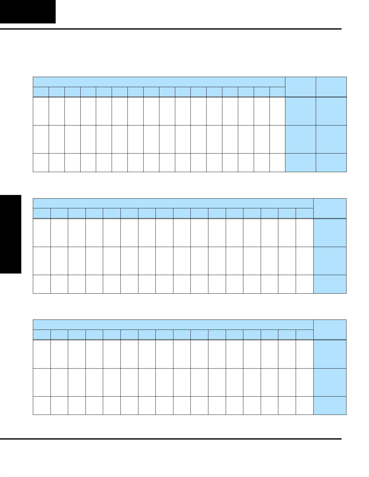
CPU Specifications
and Operation
3--50 CPU Specifications and Operation
DL405 User Manual, 4th Edition, Rev. A
Timer and Counter Status Bit Maps
This table provides a listing of the individual timer and counter contacts associated with each V-memory
address bit.
MSB DL430 / DL440 / DL450 Timer (T) and Counter (CT) Contacts LSB Timer Counter
15 14 13 12 11 10 9876543210
T
i
m
e
r
Address
C
o
u
n
t
e
r
Address
017 016 015 014 013 012 011 010 007 006 005 004 003 002 001 000 V41100 V41140
037 036 035 034 033 032 031 030 027 026 025 024 023 022 021 020 V41101 V41141
057 056 055 054 053 052 051 050 047 046 045 044 043 042 041 040 V41102 V41142
077 076 075 074 073 072 071 070 067 066 065 064 063 062 061 060 V41103 V41143
117 116 115 114 113 112 111 110 107 106 105 104 103 102 101 100 V41104 V41144
137 136 135 134 133 132 131 130 127 126 125 124 123 122 121 120 V41105 V41145
157 156 155 154 153 152 151 150 147 146 145 144 143 142 141 140 V41106 V41146
177 176 175 174 173 172 171 170 167 166 165 164 163 162 161 160 V41107 V41147
This portion of the table shows additional Timer contacts available with the DL440 and DL450.
MSB DL440 / DL450 Additional Timer (T) Contacts LSB Timer
15 14 13 12 11 10 9 8 7 6 5 4 3 2 1 0
T
i
m
e
r
Address
217 216 215 214 213 212 211 210 207 206 205 204 203 202 201 200 V41110
237 236 235 234 233 232 231 230 227 226 225 224 223 222 221 220 V41111
257 256 255 254 253 252 251 250 247 246 245 244 243 242 241 240 V41112
277 276 275 274 273 272 271 270 267 266 265 264 263 262 261 260 V41113
317 316 315 314 313 312 311 310 307 306 305 304 303 302 301 300 V41114
337 336 335 334 333 332 331 330 327 326 325 324 323 322 321 320 V41115
357 356 355 354 353 352 351 350 347 346 345 344 343 342 341 340 V41116
377 376 375 374 373 372 371 370 367 366 365 364 363 362 361 360 V41117
This portion of the table shows additional Counter contacts available with the DL450.
MSB DL450 Additional Counter (CT) Contacts LSB Counter
15 14 13 12 11 10 9 8 7 6 5 4 3 2 1 0
C
o
u
n
t
e
r
Address
217 216 215 214 213 212 211 210 207 206 205 204 203 202 201 200 V41150
237 236 235 234 233 232 231 230 227 226 225 224 223 222 221 220 V41151
257 256 255 254 253 252 251 250 247 246 245 244 243 242 241 240 V41152
277 276 275 274 273 272 271 270 267 266 265 264 263 262 261 260 V41153
317 316 315 314 313 312 311 310 307 306 305 304 303 302 301 300 V41154
337 336 335 334 333 332 331 330 327 326 325 324 323 322 321 320 V41155
357 356 355 354 353 352 351 350 347 346 345 344 343 342 341 340 V41156
377 376 375 374 373 372 371 370 367 366 365 364 363 362 361 360 V41157

CPU Specifications
and Operation
3--51
CPU Specifications and Operation
DL405 User Manual, 4th Edition, Rev. A
Remote I/O Bit Map
This table provides a listing of the individual remote I/O points associated with each V-memory address bit.
The DL430 and DL440 CPUs use the GX point type forboth remote input and output point types. TheDL450
CPU has the additional GY point type for use as remote output point references.
MSBDL430 / DL440 / DL450 Remote I/O (GX) and (GY) Point LSB GX
A
d
d
r
e
s
s
GY
A
d
d
r
e
s
s
15 14 13 12 11 10 9876543210
A
d
d
ress
A
d
d
ress
(DL450)
017 016 015 014 013 012 011 010 007 006 005 004 003 002 001 000 V40000 V40200
037 036 035 034 033 032 031 030 027 026 025 024 023 022 021 020 V40001 V40201
057 056 055 054 053 052 051 050 047 046 045 044 043 042 041 040 V40002 V40202
077 076 075 074 073 072 071 070 067 066 065 064 063 062 061 060 V40003 V40203
117 116 115 114 113 112 111 110 107 106 105 104 103 102 101 100 V40004 V40204
137 136 135 134 133 132 131 130 127 126 125 124 123 122 121 120 V40005 V40205
157 156 155 154 153 152 151 150 147 146 145 144 143 142 141 140 V40006 V40206
177 176 175 174 173 172 171 170 167 166 165 164 163 162 161 160 V40007 V40207
217 216 215 214 213 212 211 210 207 206 205 204 203 202 201 200 V40010 V40210
237 236 235 234 233 232 231 230 227 226 225 224 223 222 221 220 V40011 V40211
257 256 255 254 253 252 251 250 247 246 245 244 243 242 241 240 V40012 V40212
277 276 275 274 273 272 271 270 267 266 265 264 263 262 261 260 V40013 V40213
317 316 315 314 313 312 311 310 307 306 305 304 303 302 301 300 V40014 V40214
337 336 335 334 333 332 331 330 327 326 325 324 323 322 321 320 V40015 V40215
357 356 355 354 353 352 351 350 347 346 345 344 343 342 341 340 V40016 V40216
377 376 375 374 373 372 371 370 367 366 365 364 363 362 361 360 V40017 V40217
417 416 415 414 413 412 411 410 407 406 405 404 403 402 401 400 V40020 V40220
437 436 435 434 433 432 431 430 427 426 425 424 423 422 421 420 V40021 V40221
457 456 455 454 453 452 451 450 447 446 445 444 443 442 441 440 V40022 V40222
477 476 475 474 473 472 471 470 467 466 465 464 463 462 461 460 V40023 V40223
517 516 515 514 513 512 511 510 507 506 505 504 503 502 501 500 V40024 V40224
537 536 535 534 533 532 531 530 527 526 525 524 523 522 521 520 V40025 V40225
557 556 555 554 553 552 551 550 547 546 545 544 543 542 541 540 V40026 V40226
577 576 575 574 573 572 571 570 567 566 565 564 563 562 561 560 V40027 V40227
617 616 615 614 613 612 611 610 607 606 605 604 603 602 601 600 V40030 V40230
637 636 635 634 633 632 631 630 627 626 625 624 623 622 621 620 V40031 V40231
657 656 655 654 653 652 651 650 647 646 645 644 643 642 641 640 V40032 V40232
677 676 675 674 673 672 671 670 667 666 665 664 663 662 661 660 V40033 V40233
717 716 715 714 713 712 711 710 707 706 705 704 703 702 701 700 V40034 V40234
737 736 735 734 733 732 731 730 727 726 725 724 723 722 721 720 V40035 V40235
757 756 755 754 753 752 751 750 747 746 745 744 743 742 741 740 V40036 V40236
777 776 775 774 773 772 771 770 767 766 765 764 763 762 761 760 V40037 V40237

CPU Specifications
and Operation
3--52 CPU Specifications and Operation
DL405 User Manual, 4th Edition, Rev. A
This portion of the table shows additional Remote I/O (GX) points available with the DL440 and DL450. The
(GY) remote output point type is available only with the DL450 (the GX type points works as both input and
output point types for the DL440).
MSB DL440 / DL450 Additional Remote I/O (GX) Points LSB GX
A
d
d
r
e
s
s
GY
A
d
d
r
e
s
s
15 14 13 12 11 10 9876543210
A
d
d
ress
A
d
d
ress
(DL450)
1017 1016 1015 1014 1013 1012 1011 1010 1007 1006 1005 1004 1003 1002 1001 1000 V40040 V40240
1037 1036 1035 1034 1033 1032 1031 1030 1027 1026 1025 1024 1023 1022 1021 1020 V40041 V40241
1057 1056 1055 1054 1053 1052 1051 1050 1047 1046 1045 1044 1043 1042 1041 1040 V40042 V40242
1077 1076 1075 1074 1073 1072 1071 1070 1067 1066 1065 1064 1063 1062 1061 1060 V40043 V40243
1117 1116 1115 1114 1113 1112 1111 1110 1107 1106 1105 1104 1103 1102 1101 1100 V40044 V40244
1137 1136 1135 1134 1133 1132 1131 1130 1127 1126 1125 1124 1123 1122 1121 1120 V40045 V40245
1157 1156 1155 1154 1153 1152 1151 1150 1147 1146 1145 1144 1143 1142 1141 1140 V40046 V40246
1177 1176 1175 1174 1173 1172 1171 1170 1167 1166 1165 1164 1163 1162 1161 1160 V40047 V40247
1217 1216 1215 1214 1213 1212 1211 1210 1207 1206 1205 1204 1203 1202 1201 1200 V40050 V40250
1237 1236 1235 1234 1233 1232 1231 1230 1227 1226 1225 1224 1223 1222 1221 1220 V40051 V40251
1257 1256 1255 1254 1253 1252 1251 1250 1247 1246 1245 1244 1243 1242 1241 1240 V40052 V40252
1277 1276 1275 1274 1273 1272 1271 1270 1267 1266 1265 1264 1263 1262 1261 1260 V40053 V40253
1317 1316 1315 1314 1313 1312 1311 1310 1307 1306 1305 1304 1303 1302 1301 1300 V40054 V40254
1337 1336 1335 1334 1333 1332 1331 1330 1327 1326 1325 1324 1323 1322 1321 1320 V40055 V40255
1357 1356 1355 1354 1353 1352 1351 1350 1347 1346 1345 1344 1343 1342 1341 1340 V40056 V40256
1377 1376 1375 1374 1373 1372 1371 1370 1367 1366 1365 1364 1363 1362 1361 1360 V40057 V40257
1417 1416 1415 1414 1413 1412 1411 1410 1407 1406 1405 1404 1403 1402 1401 1400 V40060 V40260
1437 1436 1435 1434 1433 1432 1431 1430 1427 1426 1425 1424 1423 1422 1421 1420 V40061 V40261
1457 1456 1455 1454 1453 1452 1451 1450 1447 1446 1445 1444 1443 1442 1441 1440 V40062 V40262
1477 1476 1475 1474 1473 1472 1471 1470 1467 1466 1465 1464 1463 1462 1461 1460 V40063 V40263
1517 1516 1515 1514 1513 1512 1511 1510 1507 1506 1505 1504 1503 1502 1501 1500 V40064 V40264
1537 1536 1535 1534 1533 1532 1531 1530 1527 1526 1525 1524 1523 1522 1521 1520 V40065 V40265
1557 1556 1555 1554 1553 1552 1551 1550 1547 1546 1545 1544 1543 1542 1541 1540 V40066 V40266
1577 1576 1575 1574 1573 1572 1571 1570 1567 1566 1565 1564 1563 1562 1561 1560 V40067 V40267
1617 1616 1615 1614 1613 1612 1611 1610 1607 1606 1605 1604 1603 1602 1601 1600 V40070 V40270
1637 1636 1635 1634 1633 1632 1631 1630 1627 1626 1625 1624 1623 1622 1621 1620 V40071 V40271
1657 1656 1655 1654 1653 1652 1651 1650 1647 1646 1645 1644 1643 1642 1641 1640 V40072 V40272
1677 1676 1675 1674 1673 1672 1671 1670 1667 1666 1665 1664 1663 1662 1661 1660 V40073 V40273
1717 1716 1715 1714 1713 1712 1711 1710 1707 1706 1705 1704 1703 1702 1701 1700 V40074 V40274
1737 1736 1735 1734 1733 1732 1731 1730 1727 1726 1725 1724 1723 1722 1721 1720 V40075 V40275
1757 1756 1755 1754 1753 1752 1751 1750 1747 1746 1745 1744 1743 1742 1741 1740 V40076 V40276
1777 1776 1775 1774 1773 1772 1771 1770 1767 1766 1765 1764 1763 1762 1761 1760 V40077 V40277

CPU Specifications
and Operation
3--53
CPU Specifications and Operation
DL405 User Manual, 4th Edition, Rev. A
This portion of the table shows additional Remote I/O (GX and GY) points available with the DL450.
MSB DL450 Additional Remote I/O (GX) and (GY) Points LSB G
X
G
Y
15 14 13 12 11 10 9876543210
G
X
Address
G
Y
Address
2017 2016 2015 2014 2013 2012 2011 2010 2007 2006 2005 2004 2003 2002 2001 2000 V40100 V40300
2037 2036 2035 2034 2033 2032 2031 2030 2027 2026 2025 2024 2023 2022 2021 2020 V40101 V40301
2057 2056 2055 2054 2053 2052 2051 2050 2047 2046 2045 2044 2043 2042 2041 2040 V40102 V40302
2077 2076 2075 2074 2073 2072 2071 2070 2067 2066 2065 2064 2063 2062 2061 2060 V40103 V40303
2117 2116 2115 2114 2113 2112 2111 2110 2107 2106 2105 2104 2103 2102 2101 2100 V40104 V40304
2137 2136 2135 2134 2133 2132 2131 2130 2127 2126 2125 2124 2123 2122 2121 2120 V40105 V40305
2157 2156 2155 2154 2153 2152 2151 2150 2147 2146 2145 2144 2143 2142 2141 2140 V40106 V40306
2177 2176 2175 2174 2173 2172 2171 2170 2167 2166 2165 2164 2163 2162 2161 2160 V40107 V40307
2217 2216 2215 2214 2213 2212 2211 2210 2207 2206 2205 2204 2203 2202 2201 2200 V40110 V40310
2237 2236 2235 2234 2233 2232 2231 2230 2227 2226 2225 2224 2223 2222 2221 2220 V40111 V40311
2257 2256 2255 2254 2253 2252 2251 2250 2247 2246 2245 2244 2243 2242 2241 2240 V40112 V40312
2277 2276 2275 2274 2273 2272 2271 2270 2267 2266 2265 2264 2263 2262 2261 2260 V40113 V40313
2317 2316 2315 2314 2313 2312 2311 2310 2307 2306 2305 2304 2303 2302 2301 2300 V40114 V40314
2337 2336 2335 2334 2333 2332 2331 2330 2327 2326 2325 2324 2323 2322 2321 2320 V40115 V40315
2357 2356 2355 2354 2353 2352 2351 2350 2347 2346 2345 2344 2343 2342 2341 2340 V40116 V40316
2377 2376 2375 2374 2373 2372 2371 2370 2367 2366 2365 2364 2363 2362 2361 2360 V40117 V40317
2417 2416 2415 2414 2413 2412 2411 2410 2407 2406 2405 2404 2403 2402 2401 2400 V40120 V40320
2437 2436 2435 2434 2433 2432 2431 2430 2427 2426 2425 2424 2423 2422 2421 2420 V40121 V40321
2457 2456 2455 2454 2453 2452 2451 2450 2447 2446 2445 2444 2443 2442 2441 2440 V40122 V40322
2477 2476 2475 2474 2473 2472 2471 2470 2467 2466 2465 2464 2463 2462 2461 2460 V40123 V40323
2517 2516 2515 2514 2513 2512 2511 2510 2507 2506 2505 2504 2503 2502 2501 2500 V40124 V40324
2537 2536 2535 2534 2533 2532 2531 2530 2527 2526 2525 2524 2523 2522 2521 2520 V40125 V40325
2557 2556 2555 2554 2553 2552 2551 2550 2547 2546 2545 2544 2543 2542 2541 2540 V40126 V40326
2577 2576 2575 2574 2573 2572 2571 2570 2567 2566 2565 2564 2563 2562 2561 2560 V40127 V40327
2617 2616 2615 2614 2613 2612 2611 2610 2607 2606 2605 2604 2603 2602 2601 2600 V40130 V40330
2637 2636 2635 2634 2633 2632 2631 2630 2627 2626 2625 2624 2623 2622 2621 2620 V40131 V40331
2657 2656 2655 2654 2653 2652 2651 2650 2647 2646 2645 2644 2643 2642 2641 2640 V40132 V40332
2677 2676 2675 2674 2673 2672 2671 2670 2667 2666 2665 2664 2663 2662 2661 2660 V40133 V40333
2717 2716 2715 2714 2713 2712 2711 2710 2707 2706 2705 2704 2703 2702 2701 2700 V40134 V40334
2737 2736 2735 2734 2733 2732 2731 2730 2727 2726 2725 2724 2723 2722 2721 2720 V40135 V40335
2757 2756 2755 2754 2753 2752 2751 2750 2747 2746 2745 2744 2743 2742 2741 2740 V40136 V40336
2777 2776 2775 2774 2773 2772 2771 2770 2767 2766 2765 2764 2763 2762 2761 2760 V40137 V40337

CPU Specifications
and Operation
3--54 CPU Specifications and Operation
DL405 User Manual, 4th Edition, Rev. A
This table is continued from the previous page.
MSB DL450 Additional Remote I/O (GX) and (GY) Points LSB G
X
G
Y
15 14 13 12 11 10 9876543210
G
X
Address
G
Y
Address
3017 3016 3015 3014 3013 3012 3011 3010 3007 3006 3005 3004 3003 3002 3001 3000 V40140 V40340
3037 3036 3035 3034 3033 3032 3031 3030 3027 3026 3025 3024 3023 3022 3021 3020 V40141 V40341
3057 3056 3055 3054 3053 3052 3051 3050 3047 3046 3045 3044 3043 3042 3041 3040 V40142 V40342
3077 3076 3075 3074 3073 3072 3071 3070 3067 3066 3065 3064 3063 3062 3061 3060 V40143 V40343
3117 3116 3115 3114 3113 3112 3111 3110 3107 3106 3105 3104 3103 3102 3101 3100 V40144 V40344
3137 3136 3135 3134 3133 3132 3131 3130 3127 3126 3125 3124 3123 3122 3121 3120 V40145 V40345
3157 3156 3155 3154 3153 3152 3151 3150 3147 3146 3145 3144 3143 3142 3141 3140 V40146 V40346
3177 3176 3175 3174 3173 3172 3171 3170 3167 3166 3165 3164 3163 3162 3161 3160 V40147 V40347
3217 3216 3215 3214 3213 3212 3211 3210 3207 3206 3205 3204 3203 3202 3201 3200 V40150 V40350
3237 3236 3235 3234 3233 3232 3231 3230 3227 3226 3225 3224 3223 3222 3221 3220 V40151 V40351
3257 3256 3255 3254 3253 3252 3251 3250 3247 3246 3245 3244 3243 3242 3241 3240 V40152 V40352
3277 3276 3275 3274 3273 3272 3271 3270 3267 3266 3265 3264 3263 3262 3261 3260 V40153 V40353
3317 3316 3315 3314 3313 3312 3311 3310 3307 3306 3305 3304 3303 3302 3301 3300 V40154 V40354
3337 3336 3335 3334 3333 3332 3331 3330 3327 3326 3325 3324 3323 3322 3321 3320 V40155 V40355
3357 3356 3355 3354 3353 3352 3351 3350 3347 3346 3345 3344 3343 3342 3341 3340 V40156 V40356
3377 3376 3375 3374 3373 3372 3371 3370 3367 3366 3365 3364 3363 3362 3361 3360 V40157 V40357
3417 3416 3415 3414 3413 3412 3411 3410 3407 3406 3405 3404 3403 3402 3401 3400 V40160 V40360
3437 3436 3435 3434 3433 3432 3431 3430 3427 3426 3425 3424 3423 3422 3421 3420 V40161 V40361
3457 3456 3455 3454 3453 3452 3451 3450 3447 3446 3445 3444 3443 3442 3441 3440 V40162 V40362
3477 3476 3475 3474 3473 3472 3471 3470 3467 3466 3465 3464 3463 3462 3461 3460 V40163 V40363
3517 3516 3515 3514 3513 3512 3511 3510 3507 3506 3505 3504 3503 3502 3501 3500 V40164 V40364
3537 3536 3535 3534 3533 3532 3531 3530 3527 3526 3525 3524 3523 3522 3521 3520 V40165 V40365
3557 3556 3555 3554 3553 3552 3551 3550 3547 3546 3545 3544 3543 3542 3541 3540 V40166 V40366
3577 3576 3575 3574 3573 3572 3571 3570 3567 3566 3565 3564 3563 3562 3561 3560 V40167 V40367
3617 3616 3615 3614 3613 3612 3611 3610 3607 3606 3605 3604 3603 3602 3601 3600 V40170 V40370
3637 3636 3635 3634 3633 3632 3631 3630 3627 3626 3625 3624 3623 3622 3621 3620 V40171 V40371
3657 3656 3655 3654 3653 3652 3651 3650 3647 3646 3645 3644 3643 3642 3641 3640 V40172 V40372
3677 3676 3675 3674 3673 3672 3671 3670 3667 3666 3665 3664 3663 3662 3661 3660 V40173 V40373
3717 3716 3715 3714 3713 3712 3711 3710 3707 3706 3705 3704 3703 3702 3701 3700 V40174 V40374
3737 3736 3735 3734 3733 3732 3731 3730 3727 3726 3725 3724 3723 3722 3721 3720 V40175 V40375
3757 3756 3755 3754 3753 3752 3751 3750 3747 3746 3745 3744 3743 3742 3741 3740 V40176 V40376
3777 3776 3775 3774 3773 3772 3771 3770 3767 3766 3765 3764 3763 3762 3761 3760 V40177 V40377
CPU Specifications
and Operation
3--55
CPU Specifications and Operation
DL405 User Manual, 4th Edition, Rev. A
Stage Control / Status Bit Map
This table provides a listing of the individual stage control bits associated with each V-memory address bit.
MSB DL430 / DL440 / DL450 Stage (S) Control Bits LSB
A
d
d
r
e
s
s
15 14 13 12 11 10 9 8 7 6 5 4 3 2 1 0
A
d
d
ress
017 016 015 014 013 012 011 010 007 006 005 004 003 002 001 000 V41000
037 036 035 034 033 032 031 030 027 026 025 024 023 022 021 020 V41001
057 056 055 054 053 052 051 050 047 046 045 044 043 042 041 040 V41002
077 076 075 074 073 072 071 070 067 066 065 064 063 062 061 060 V41003
117 116 115 114 113 112 111 110 107 106 105 104 103 102 101 100 V41004
137 136 135 134 133 132 131 130 127 126 125 124 123 122 121 120 V41005
157 156 155 154 153 152 151 150 147 146 145 144 143 142 141 140 V41006
177 176 175 174 173 172 171 170 167 166 165 164 163 162 161 160 V41007
217 216 215 214 213 212 211 210 207 206 205 204 203 202 201 200 V41010
237 236 235 234 233 232 231 230 227 226 225 224 223 222 221 220 V41011
257 256 255 254 253 252 251 250 247 246 245 244 243 242 241 240 V41012
277 276 275 274 273 272 271 270 267 266 265 264 263 262 261 260 V41013
317 316 315 314 313 312 311 310 307 306 305 304 303 302 301 300 V41014
337 336 335 334 333 332 331 330 327 326 325 324 323 322 321 320 V41015
357 356 355 354 353 352 351 350 347 346 345 344 343 342 341 340 V41016
377 376 375 374 373 372 371 370 367 366 365 364 363 362 361 360 V41017
417 416 415 414 413 412 411 410 407 406 405 404 403 402 401 400 V41020
437 436 435 434 433 432 431 430 427 426 425 424 423 422 421 420 V41021
457 456 455 454 453 452 451 450 447 446 445 444 443 442 441 440 V41022
477 476 475 474 473 472 471 470 467 466 465 464 463 462 461 460 V41023
517 516 515 514 513 512 511 510 507 506 505 504 503 502 501 500 V41024
537 536 535 534 533 532 531 530 527 526 525 524 523 522 521 520 V41025
557 556 555 554 553 552 551 550 547 546 545 544 543 542 541 540 V41026
577 576 575 574 573 572 571 570 567 566 565 564 563 562 561 560 V41027
MSB DL440 / DL450 Additional Stage (S) Control Bits LSB
A
d
d
r
e
s
s
15 14 13 12 11 10 9 8 7 6 5 4 3 2 1 0
A
d
d
ress
617 616 615 614 613 612 611 610 607 606 605 604 603 602 601 600 V41030
637 636 635 634 633 632 631 630 627 626 625 624 623 622 621 620 V41031
657 656 655 654 653 652 651 650 647 646 645 644 643 642 641 640 V41032
677 676 675 674 673 672 671 670 667 666 665 664 663 662 661 660 V41033
717 716 715 714 713 712 711 710 707 706 705 704 703 702 701 700 V41034
737 736 735 734 733 732 731 730 727 726 725 724 723 722 721 720 V41035
757 756 755 754 753 752 751 750 747 746 745 744 743 742 741 740 V41036
777 776 775 774 773 772 771 770 767 766 765 764 763 762 761 760 V41037

CPU Specifications
and Operation
3--56 CPU Specifications and Operation
DL405 User Manual, 4th Edition, Rev. A
MSB DL440 / DL450 Additional Stage (S) Control Bits (continued) LSB
A
d
d
r
e
s
s
15 14 13 12 11 10 9 8 7 6 5 4 3 2 1 0
A
d
d
ress
1017 1016 1015 1014 1013 1012 1011 1010 1007 1006 1005 1004 1003 1002 1001 1000 V41040
1037 1036 1035 1034 1033 1032 1031 1030 1027 1026 1025 1024 1023 1022 1021 1020 V41041
1057 1056 1055 1054 1053 1052 1051 1050 1047 1046 1045 1044 1043 1042 1041 1040 V41042
1077 1076 1075 1074 1073 1072 1071 1070 1067 1066 1065 1064 1063 1062 1061 1060 V41043
1117 1116 1115 1114 1113 1112 1111 1110 1107 1106 1105 1104 1103 1102 1101 1100 V41044
1137 1136 1135 1134 1133 1132 1131 1130 1127 1126 1125 1124 1123 1122 1121 1120 V41045
1157 1156 1155 1154 1153 1152 1151 1150 1147 1146 1145 1144 1143 1142 1141 1140 V41046
1177 1176 1175 1174 1173 1172 1171 1170 1167 1166 1165 1164 1163 1162 1161 1160 V41047
1217 1216 1215 1214 1213 1212 1211 1210 1207 1206 1205 1204 1203 1202 1201 1200 V41050
1237 1236 1235 1234 1233 1232 1231 1230 1227 1226 1225 1224 1223 1222 1221 1220 V41051
1257 1256 1255 1254 1253 1252 1251 1250 1247 1246 1245 1244 1243 1242 1241 1240 V41052
1277 1276 1275 1274 1273 1272 1271 1270 1267 1266 1265 1264 1263 1262 1261 1260 V41053
1317 1316 1315 1314 1313 1312 1311 1310 1307 1306 1305 1304 1303 1302 1301 1300 V41054
1337 1336 1335 1334 1333 1332 1331 1330 1327 1326 1325 1324 1323 1322 1321 1320 V41055
1357 1356 1355 1354 1353 1352 1351 1350 1347 1346 1345 1344 1343 1342 1341 1340 V41056
1377 1376 1375 1374 1373 1372 1371 1370 1367 1366 1365 1364 1363 1362 1361 1360 V41057
1417 1416 1415 1414 1413 1412 1411 1410 1407 1406 1405 1404 1403 1402 1401 1400 V41060
1437 1436 1435 1434 1433 1432 1431 1430 1427 1426 1425 1424 1423 1422 1421 1420 V41061
1457 1456 1455 1454 1453 1452 1451 1450 1447 1446 1445 1444 1443 1442 1441 1440 V41062
1477 1476 1475 1474 1473 1472 1471 1470 1467 1466 1465 1464 1463 1462 1461 1460 V41063
1517 1516 1515 1514 1513 1512 1511 1510 1507 1506 1505 1504 1503 1502 1501 1500 V41064
1537 1536 1535 1534 1533 1532 1531 1530 1527 1526 1525 1524 1523 1522 1521 1520 V41065
1557 1556 1555 1554 1553 1552 1551 1550 1547 1546 1545 1544 1543 1542 1541 1540 V41066
1577 1576 1575 1574 1573 1572 1571 1570 1567 1566 1565 1564 1563 1562 1561 1560 V41067
1617 1616 1615 1614 1613 1612 1611 1610 1607 1606 1605 1604 1603 1602 1601 1600 V41070
1637 1636 1635 1634 1633 1632 1631 1630 1627 1626 1625 1624 1623 1622 1621 1620 V41071
1657 1656 1655 1654 1653 1652 1651 1650 1647 1646 1645 1644 1643 1642 1641 1640 V41072
1677 1676 1675 1674 1673 1672 1671 1670 1667 1666 1665 1664 1663 1662 1661 1660 V41073
1717 1716 1715 1714 1713 1712 1711 1710 1707 1706 1705 1704 1703 1702 1701 1700 V41074
1737 1736 1735 1734 1733 1732 1731 1730 1727 1726 1725 1724 1723 1722 1721 1720 V41075
1757 1756 1755 1754 1753 1752 1751 1750 1747 1746 1745 1744 1743 1742 1741 1740 V41076
1777 1776 1775 1774 1773 1772 1771 1770 1767 1766 1765 1764 1763 1762 1761 1760 V41077
