Chapter 4 Ch4
User Manual: Chapter 4 DL06 User Manual
Open the PDF directly: View PDF ![]() .
.
Page Count: 28

SyStem deSign and
configuration 4
4
4
Chapter
Chapter
Chapter
In This Chapter
DL06 System Design Strategies ........................................................ 4–2
Module Placement ........................................................................... 4–3
Power Budgeting ............................................................................. 4–5
Configuring the DL06’s Comm Ports ............................................... 4–7
Connecting to MODBUS and DirectNET Networks ........................... 4–9
Non–Sequence Protocol (ASCII In/Out and PRINT) ........................ 4–11
Network Slave Operation ............................................................... 4–12
Network Master Operation ............................................................ 4–18
Network Master Operation (using MRX and MWX Instructions) .... 4–22

DL06 Micro PLC User Manual; 3rd Edition Rev. D
4–2
Chapter 4: System Design and Configuration
1
2
3
4
5
6
7
8
9
10
11
12
13
14
A
B
C
D
DL06 System Design Strategies
I/O System Configurations
The DL06 PLCs offer a number of different I/O configurations. Choose the configuration
that is right for your application, and keep in mind that the DL06 PLCs offer the ability to
add I/O with the use of option cards. Although remote I/O isn’t available, there are many
option cards available. For instance:
• Various A/C and D/C I/O modules
• Combination I/O modules
• Analog I/O modules
• Combination Analog I/O modules
A DL06 system can be developed using several different arrangements using the option
modules. See our DL05/06 Options Modules User Manual (D0-OPTIONS-M) on the
website, www.automationdirect.com for detailed selection information.
Networking Configurations
The DL06 PLCs offers the following ways to add networking:
• Ethernet Communications Module s connects a DL06 to high-speed peer-to-peer networks. Any
PLC can initiate communications with any other PLC or operator interfaces, such as C-more, when
using the ECOM modules.
• Data Communications Modules s connects a DL06 to devices using either DeviceNet or Profibus
to link to master controllers, as well as a D0-DCM.
• Communications Port 1 s The DL06 has a 6-pin RJ12 connector on Port 1 that supports (as
slave) K-sequence, MODBUS RTU or DirectNET protocols.
• Communications Port 2 s The DL06 has a 15-pin connector on Port 2 that supports either
master/slave MODBUS RTU or DirectNET protocols, or K-sequence protocol as slave. (MRX
and MWX instructions allow you to enter native MODBUS addressing in your ladder program
with no need to perform octal to decimal conversions). Port 2 can also be used for ASCII IN/OUT
communictions.
1
2
3
4
5
6
7
8
9
10
11
12
13
14
A
B
C
D
DL06 Micro PLC User Manual; 3rd Edition Rev. D 4–3
Chapter 4: System Design and Configuration
1
2
3
4
5
6
7
8
9
10
11
12
13
14
A
B
C
D
Module Placement
Slot Numbering
The DL06 has four slots, which are numbered as follows:
1
2
3
4
5
6
7
8
9
10
11
12
13
14
A
B
C
D
Slot 1
Slot 2
Slot 3
Slot 4
DL06 Micro PLC User Manual; 3rd Edition Rev. D
4–4
Chapter 4: System Design and Configuration
1
2
3
4
5
6
7
8
9
10
11
12
13
14
A
B
C
D
Chapter 4: System Design and Configuration
1
2
3
4
5
6
7
8
9
10
11
12
13
14
A
B
C
D
Automatic I/O Configuration
The DL06 CPUs automatically detect any installed I/O modules (including specialty
modules) at powerup, and establish the correct I/O configuration and addresses. This applies
to modules located in the local base. For most applications, you will never have to change the
configuration.
I/O addresses use octal numbering, starting at X100 and Y100 in the slot next to the CPU.
The addresses are assigned in groups of 8, or 16 depending on the number of points for
the I/O module. The discrete input and output modules can be mixed in any order. The
following diagram shows the I/O numbering convention for an example system. Both
the Handheld Programmer and DirectSOFT 5 provide AUX functions that allow you
to automatically configure the I/O. For example, with the Handheld Programmer AUX
46 executes an automatic configuration, which allows the CPU to examine the installed
modules and determine the I/O configuration and addressing.With DirectSOFT 5, the PLC
Configure I/O menu option would be used.
Automatic
Manual
Manual I/O Configuration
It may never become necessary, but DL06 CPUs allow manual I/O address assignments
for any I/O slot(s) . You can manually modify an auto configuration to match arbitrary
I/O numbering. For example, two adjacent input modules can have starting addresses at
X100 and X200.Use DirectSOFT 5 PLC Configure I/O menu option to assign manual
I/O address. In automatic configuration, the addresses are assigned on 8-point boundaries.
Manual configuration, however, assumes that all modules are at least 16 points, so you can
only assign addresses that are a multiple of 20 (octal). You can still use 8 point modules, but
16 addresses will be assigned and the upper eight addresses will be unused.
WARNING: If you manually configure an I/O slot, the I/O addressing for the other modules
may change. This is because the DL06 CPUs do not allow you to assign duplicate I/O addresses.
You must always correct any I/O configuration errors before you place the CPU in RUN mode.
Uncorrected errors can cause unpredictable machine operation that can result in a risk of personal
injury or damage to equipment.
Slot 1
8pt. Input
X100–X107
Slot 2
16pt. Output
Y100–Y117
Slot 3
16pt. Input
X110–X127
Slot 4
8pt. Input
X130–X137
Slot 1
8pt. Input
X100–X107
Slot 2
16pt. Output
Y100–Y117
Slot 3
16pt. Input
X200–X217
Slot 4
8pt. Input
X120–X127

DL06 Micro PLC User Manual; 3rd Edition Rev. D 4–5
Chapter 4: System Design and Configuration
1
2
3
4
5
6
7
8
9
10
11
12
13
14
A
B
C
D
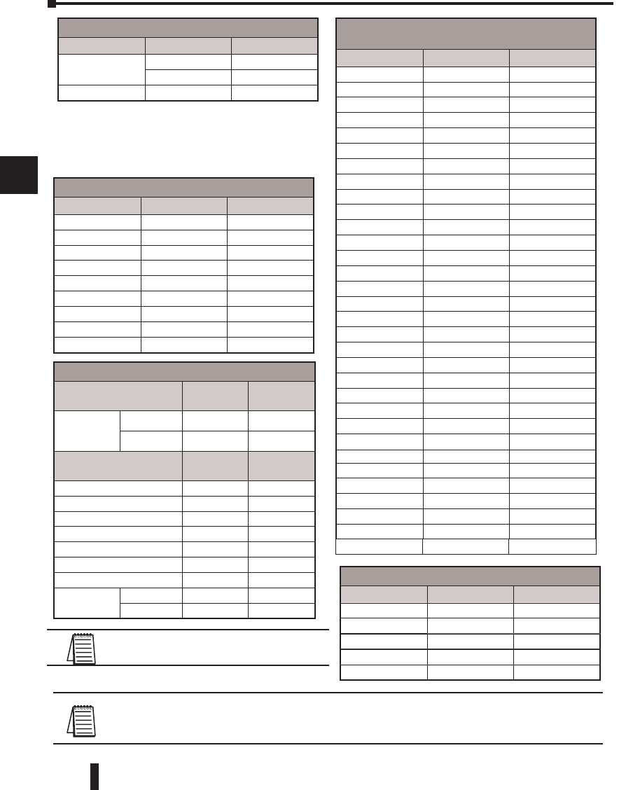
Power Budgeting
The DL06 has four option card slots. To determine whether the combination of cards you
select will have sufficient power, you will need to perform a power budget calculation.
Power supplied
Power is supplied from two sources, the internal base unit power supply and, if required, an
external supply (customer furnished). The D0-06xx (AC powered) PLCs supply a limited
amount of 24VDC power. The 24VDC output can be used to power external devices.
For power budgeting, start by considering the power supplied by the base unit. All DL06
PLCs supply the same amount of 5VDC power. Only the AC units offer 24VDC auxiliary
power. Be aware of the trade-off between 5VDC power and 24VDC power. The amount
of 5VDC power available depends on the amount of 24VDC power being used, and the
amount of 24VDC power available depends on the amount of 5VDC power consumed.
Determine the amount of internally supplied power from the table on the following page.
Power required by base unit
Because of the different I/O configurations available in the DL06 family, the power
consumed by the base unit itself varies from model to model. Subtract the amount of power
required by the base unit from the amount of power supplied by the base unit. Be sure to
subtract 5VDC and 24VDC amounts.
Power required by option cards
Next, subtract the amount of power required by the option cards you are planning to use.
Again, remember to subtract both 5VDC and 24VDC. If your power budget analysis shows
surplus power available, you should have a workable configuration.
Chapter 4: System Design and Configuration
1
2
3
4
5
6
7
8
9
10
11
12
13
14
A
B
C
D
DL06 Micro PLC User Manual; 3rd Edition Rev. D
4–6
Chapter 4: System Design and Configuration
1
2
3
4
5
6
7
8
9
10
11
12
13
14
A
B
C
D
Chapter 4: System Design and Configuration
1
2
3
4
5
6
7
8
9
10
11
12
13
14
A
B
C
DNOTE 1: Auxiliary 24VDC used to power V+ terminal of D0-06DD1/-D sinking outputs.
NOTE 2: If the PLC’s auxiliary 24VDC power source is used to power the sinking outputs, use power
choice A, above.
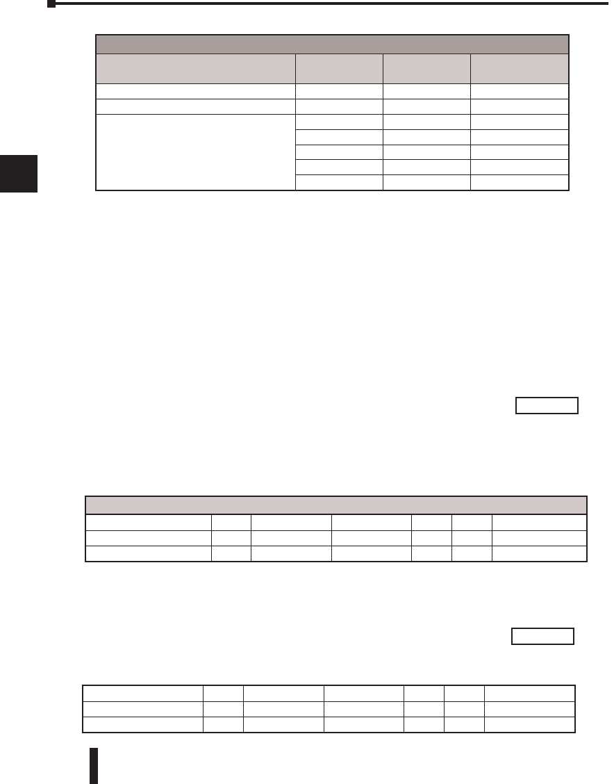
Power Budgeting Example
Power Source 5VDC
power (mA)
24VDC
power (mA)
D0-06DD1
(select row
A or row B)
A1500mA 300mA
B2000mA 200mA
Current Required 5VDC
power (mA)
24VDC
power (mA)
D0-06DD1 600mA 280mA, note 1
D0-16ND3 35mA 0
D0-10TD1 150mA 0
D0-08TR 280mA 0
F0-4AD2DA-2 100mA 0
D0-06LCD 50mA 0
Total Used 1215mA 280mA
Remaining A285mA 20mA
B 785mA note 2
DL06 Power Supplied by Base Units
Part Number 5 VDC (mA) 24 VDC (mA)
D0-06xx <1500mA 300mA
<2000mA 200mA
D0-06xx-D 1500mA none
DL06 Power Consumed by Other Devices
Part Number 5 VDC (mA) 24 VDC (mA)
D0-06LCD 50mA none
D2-HPP 200mA none
DV-1000 150mA none
EA1-S3ML 210mA none
EA1-S3MLW 210mA none
DL06 Base Unit Power Required
Part Number 5 VDC (mA) 24 VDC (mA)
D0-06AA 800mA none
D0-06AR 900mA none
D0-06DA 800mA none
D0-06DD1 600mA 280mA, note 1
D0-06DD2 600mA none
D0-06DR 950mA none
D0-06DD1-D 600mA 280mA, note 1
D0-06DD2-D 600mA none
D0-06DR-D 950mA none
If the 5VDC loading is less than 2000mA, but more than
1500mA, then available 24VDC supply current is 200mA.
If the 5VDC loading is less than 1500mA, then the
available 24VDC current is 300mA.
NOTE: See the DL05/DL06 OPTIONS
manual for the module data for your project.
DL06 Power Consumed
by Option Cards
Part Number 5 VDC (mA) 24 VDC (mA)
D0-07CDR 130mA none
D0-08CDD1 100mA none
D0-08TR 280mA none
D0-10ND3 35mA none
D0-10ND3F 35mA none
D0-10TD1 150mA none
D0-10TD2 150mA none
D0-16ND3 35mA none
D0-16TD1 200mA none
D0-16TD2 200mA none
D0-DCM 250mA none
D0-DEVNETS 45mA none
F0-04TRS 250mA none
F0-08NA-1 5mA none
F0-04AD-1 50mA none
F0-04AD-2 75mA none
F0-04DAH-1 25mA 150mA
F0-04DAH-2 25mA 30mA
F0-08ADH-1 25mA 25mA
F0-08ADH-2 25mA 25mA
F0-08DAH-1 25mA 220mA
F0-08DAH-2 25mA 30mA
F0-2AD2DA-2 50mA 30mA
F0-4AD2DA-1 100mA 40mA
F0-4AD2DA-2 100mA none
F0-04RTD 70mA none
F0-04THM 30mA none
F0-CP128 150mA none
H0-CTRIO(2) 250mA none
H0-ECOM 250mA none
H0-ECOM100 300mA none
H0-PSCM 530mA none
DL06 Micro PLC User Manual; 3rd Edition Rev. D 4–7
Chapter 4: System Design and Configuration
1
2
3
4
5
6
7
8
9
10
11
12
13
14
A
B
C
D
Chapter 4: System Design and Configuration
1
2
3
4
5
6
7
8
9
10
11
12
13
14
A
B
C
D
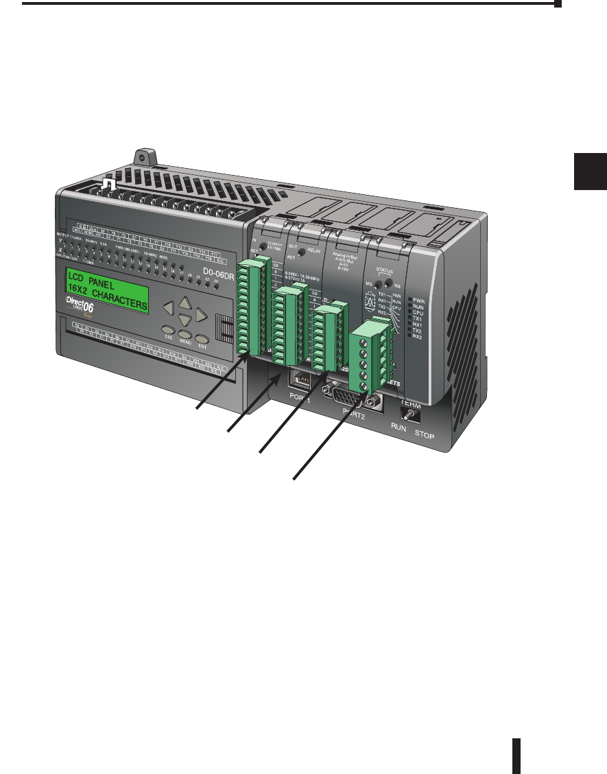
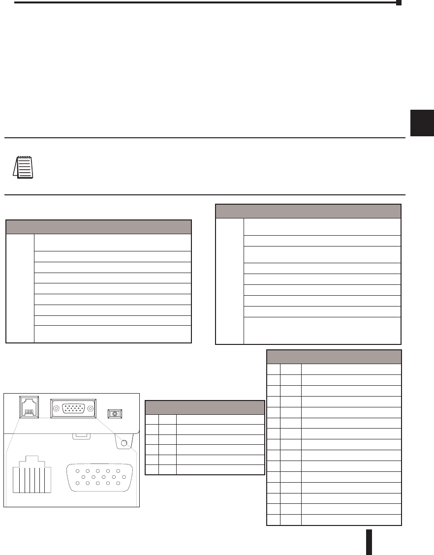
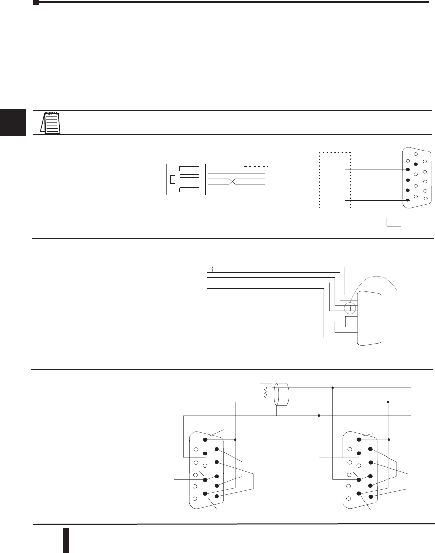
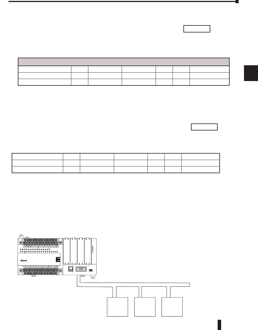
DL06 Port Pinouts
Configuring the DL06’s Comm Ports
This section describes how to configure the CPU’s built-in networking ports for either
MODBUS or DirectNET. This will allow you to connect the DL06 PLC system directly to
MODBUS networks using the RTU protocol, or to other devices on a DirectNET network.
MODBUS masters on the network must be capable of issuing the MODBUS commands
to read or write the appropriate data. For details on the MODBUS protocol, please refer
to the Gould MODBUS Protocol reference Guide (P1–MBUS–300 Rev. B). In the event
a more recent version is available, check with your MODBUS supplier before ordering the
documentation. For more details on DirectNET, order our DirectNET manual, part number
DA–DNET–M.
NOTE: For information about the MODBUS protocol see the Group Schneider Web site at: www.
schneiderautomation.com. At the main menu, select Support/Services, Modbus, Modbus Technical Manuals,
PI-MBUS-300 Modbus Protocol Reference Guide or search for PIMBUS300. For more information about
the DirectNET protocol, order our DirectNET user manual, part number DA–DNET–M, or download it
free from our Web site: www.automationdirect.com. Select Documentation/Misc./DA-DNET-M.
Communications Port 2
Port 2
Connects to HPP, DirectSOFT 5, operator
interfaces, etc.
15-pin, multifunction port, RS232C, RS422, RS485
Communication speed (baud): 300, 600, 1200,
2400, 4800, 9600, 19200, 38400
Parity: odd (default), even, none
Station Address: 1 (default)
8 data bits
1 start, 1 stop bit
Asynchronous, half-duplex, DTE
Protocol (auto-select): K-sequence (slave only),
DirectNET (master/slave), MODBUS (master/slave),
non-sequence/print/ASCII in/out
Port 1 Pin Descriptions
10V Power (-) connection (GND)
25V Power (+) connection
3RXD Receive data (RS-232C)
4TXD Transmit data (RS-232C)
55V Power (+) connection
60V Power (-) connection (GND)
Port 2 Pin Descriptions
15V Power (+) connection
2TXD Transmit data (RS-232C)
3RXD Receive data (RS-232C)
4RTS Ready to send (RS-232C)
5CTS Clear to send (RS232C)
6RXD- Receive data (-) (RS-422/485)
70V Power (-) connection (GND)
80V Power (-) connection (GND)
9TXD+ Transmit data (+) (RS-422/485)
10 TXD- Transmit data (-) (RS-422/485)
11 RTS+ Ready to send (+) (RS-422/485)
12 RTS- Ready to send (-) (RS-422/485)
13 RXD+ Receive data (+) (RS-422/485)
14 CTS+ Clear to send (+) (RS-422/485)
15 CTS- Clear to send (-) (RS-422/485)
Communications Port 1
Port 1
Connects to HPP, DirectSOFT 5, operator
interfaces, etc.
6-pin, RS232C
Communication speed (baud): 9600 (fixed)
Parity: odd (fixed)
Station Address: 1 (fixed)
8 data bits
1 start, 1 stop bit
Asynchronous, half-duplex, DTE
Protocol (auto-select): K-sequence (slave only),
DirectNET (slave only), MODBUS (slave only)
DL06 Port Specifications
PORT1 PORT2
TERM
RUN STOP
P
ORT
1
PORT
2
R
R
PORT1 PORT2
16
3425
15
610
1115
DL06 Micro PLC User Manual; 3rd Edition Rev. D
4–8
Chapter 4: System Design and Configuration
1
2
3
4
5
6
7
8
9
10
11
12
13
14
A
B
C
D
1
2
3
4
5
6
7
8
9
10
11
12
13
14
A
B
C
D
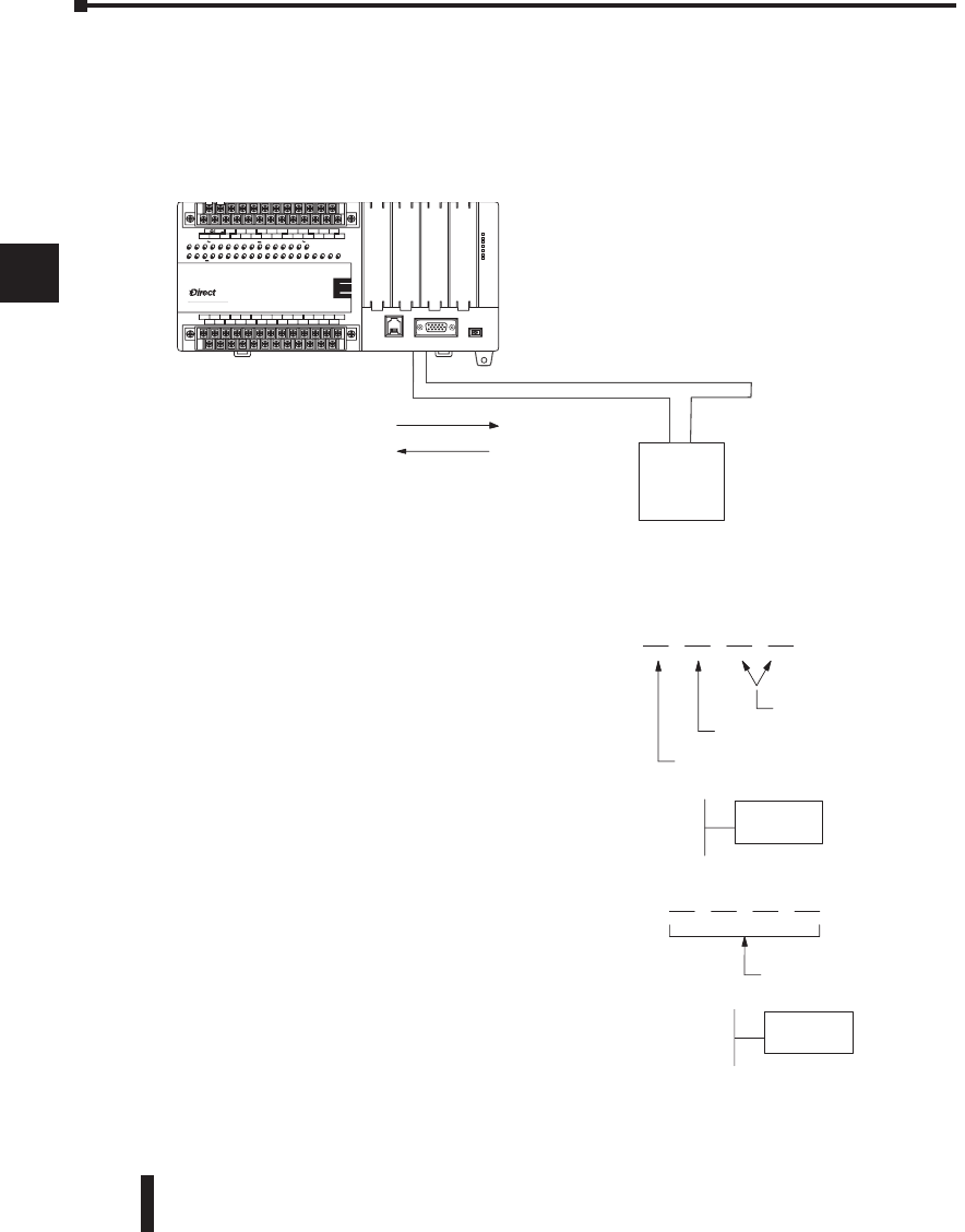
RS-232 Network
Normally, the RS-232
signals are used for
shorter distances (15
meters maximum),
for communications
between two devices.
Choosing a Network Specification
The DL06 PLC’s multi-function port gives you the option of using RS-232C, RS-422, or
RS-485 specifications. First, determine whether the network will be a 2-wire RS–232C type,
a 4-wire RS–422 type, or a 2-wire/4-wire RS-485 type.
The RS–232C specification is simple to implement for networks of shorter distances (15
meters max) and where communication is only required between two devices. The RS–422
and RS-485 signals are for networks that cover longer distances (1000 meters max.) and for
multi-drop networks (from 2 to 247 devices).
NOTE: Termination resistors are required at both ends of RS–422 and RS-485 networks. It is necessary to
select resistors that match the impedance rating of the cable (between 100 and 500 ohms).
DL06 CPU Port 2
TXD+ / RXD+
TXD– / RXD–
Termination
Resistor
Signal GND
Connect shield
to signal ground
TXD+
TXD–
RXD–
RXD+
0V
TXD+
TXD–
RXD–
RXD+
0V
TXD+ / RXD+
TXD– / RXD–
Signal GND
TXD+ / RXD+
TXD– / RXD–
Signal GND
RTS+
RTS–
CTS+
CTS–
RTS+
RTS–
CTS+
CTS–
DL06 CPU Port 2
1
6
11
1
6
11
5
10
15
5
10
15
The recommended cable for
RS422 is AutomationDirect L19954
(Belden 9842) or equivalent.
RXD+
RXD–
TXD+
TXD–
Signal GND
PORT 2
Master
9 TXD+
10 TXD–
13 RXD+
6 RXD–
1 1 R TS+
12 R TS–
14 CTS+
15 CTS–
70 V
T ermination
Resistor at
both ends of
network
The recommended cable for RS422 is
AutomationDirect L19772 (Belden 8102)
or equivalent.
Signal GND
RXD
TXD
TXD
RXD
GND
RTS
CTS
RTS
CTS
RTS
CTS
OR
Loop
Back
PORT1
6P6C
Phone Jack
Point-to-point
DTE Device
Signal GND
RXD RXD
TXD TXD
0V
1
4
3
1
6
11
5
10
15
Connections on Port 2
Connections on Port 1
RS-422 Network
RS-422 signals are for
long distances ( 1000
meters maximum). Use
terminator resistors at both
ends of RS-422 network
wiring, matching the
impedence rating of the
cable (between 100 and
500 ohms).
RS-485 Network
RS-485 signals are for
longer distances (1000
meters max) and for
multi-drop networks.
Use termination resistors
at both ends of RS-485
network wiring, matching
the impedance rating of
the cable (between 100
and 500 ohms).
DL06 Micro PLC User Manual; 3rd Edition Rev. D 4–9
Chapter 4: System Design and Configuration
1
2
3
4
5
6
7
8
9
10
11
12
13
14
A
B
C
D
1
2
3
4
5
6
7
8
9
10
11
12
13
14
A
B
C
D
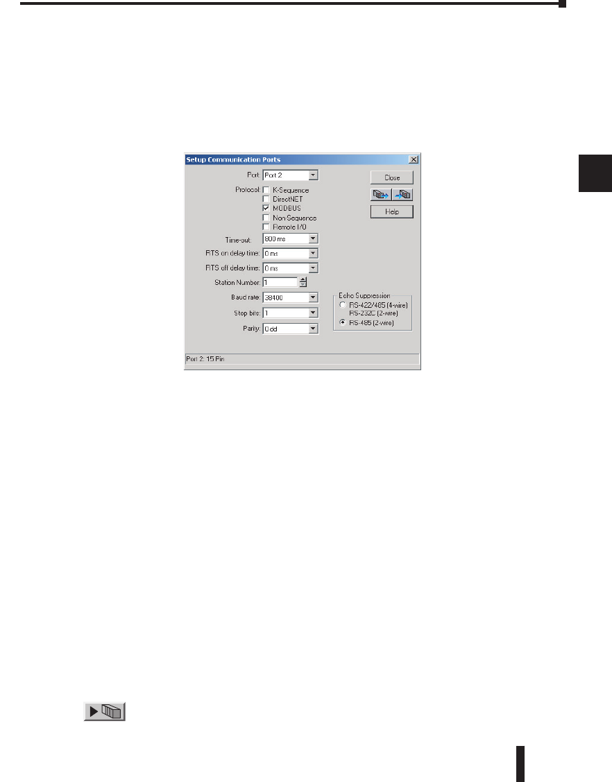
Connecting to MODBUS and DirectNET Networks
MODBUS Port Configuration
In DirectSOFT 5, choose the PLC menu, then Setup, then “Secondary Comm Port”.
• Port: From the port number list box at the top, choose “Port 2”.
• Protocol: Check the box to the left of “MODBUS” (use AUX 56 on the HPP, and select
“MBUS”), and then you’ll see the box below.
• Timeout: amount of time the port will wait after it sends a message to get a response before logging
an error.
• RTS ON / OFF Delay Time: The RTS ON Delay Time specifies the time the DL06 waits to send
the data after it has raised the RTS signal line. The RTS OFF Delay Time specifies the time the
DL06 waits to release the RTS signal line after the data has been sent. When using the DL06 on a
multi-drop network, the RTS ON Delay time must be set to 5ms or more and the RTS OFF Delay time
must be set to 2ms or more. If you encounter problems, the time can be increased.
• Station Number: For making the CPU port a MODBUS master, choose “1”. The possible range
for MODBUS slave numbers is from 1 to 247, but the DL06 network instructions used in Master
mode will access only slaves 1 to 99. Each slave must have a unique number. At powerup, the port
is automatically a slave, unless and until the DL06 executes ladder logic network instructions which
use the port as a master. Thereafter, the port reverts back to slave mode until ladder logic uses the
port again.
• Baud Rate: The available baud rates include 300, 600, 1200, 2400, 4800, 9600, 19200, and 38400
baud. Choose a higher baud rate initially, reverting to lower baud rates if you experience data errors
or noise problems on the network. Important: You must configure the baud rates of all devices on
the network to the same value. Refer to the appropriate product manual for details.
• Stop Bits: Choose 1 or 2 stop bits for use in the protocol.
• Parity: Choose none, even, or odd parity for error checking.
•Echo Suppression: Select the appropriate wiring configuration used on Port 2.
Then click the button indicated to send the Port configuration to the CPU, and click
Close.
DL06 Micro PLC User Manual; 3rd Edition Rev. D
4–10
Chapter 4: System Design and Configuration
1
2
3
4
5
6
7
8
9
10
11
12
13
14
A
B
C
D
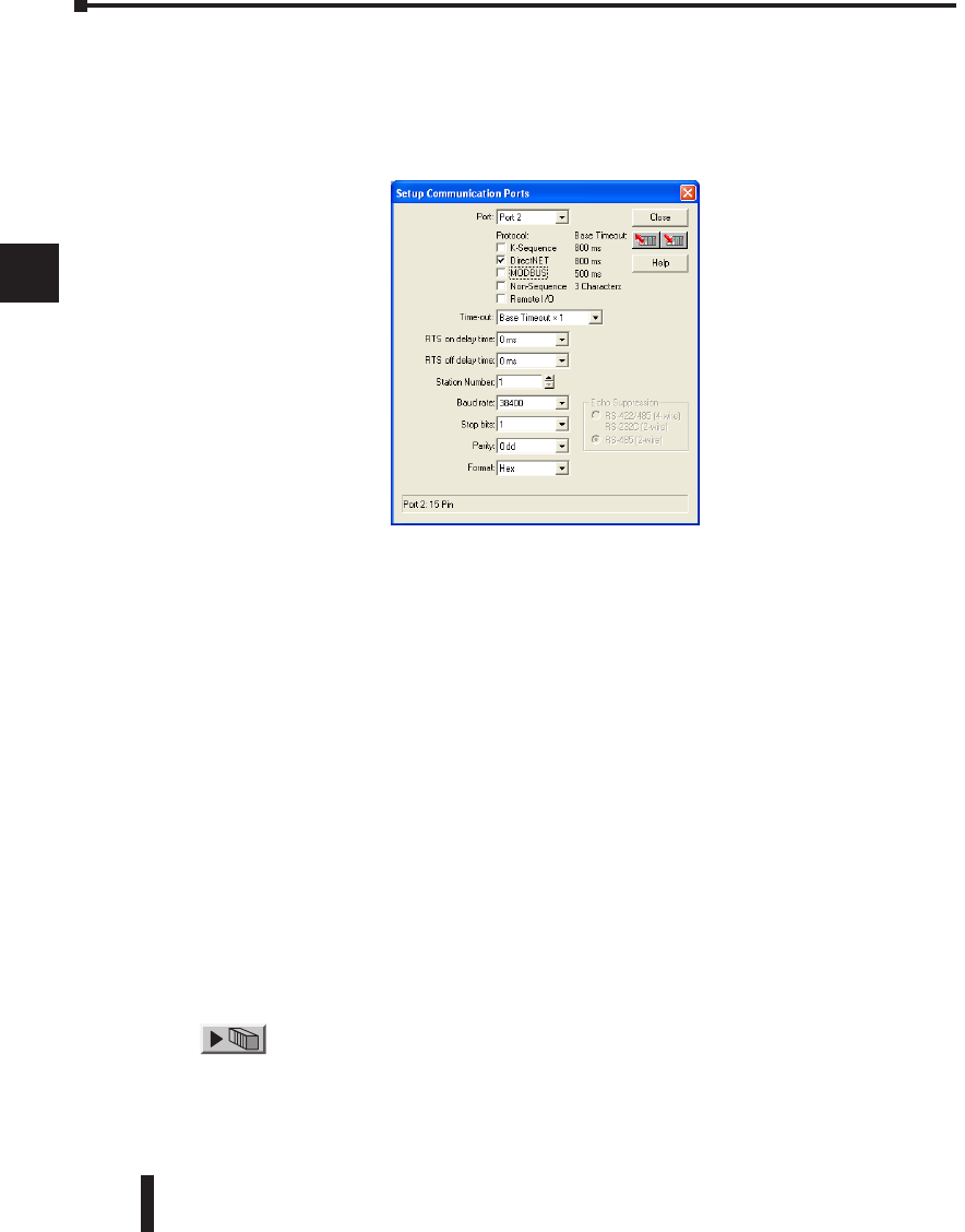
DirectNET Port Configuration
In DirectSOFT 5, choose the PLC menu, then Setup, then “Secondary Comm Port”.
• Port: From the port number list box, choose “Port 2 ”.
• Protocol: Check the box to the left of “DirectNET” (use AUX 56 on the HPP, then select
“DNET”), and then you’ll see the dialog below.
• Timeout: Amount of time the port will wait after it sends a message to get a response before logging
an error.
• RTS ON / OFF Delay Time: The RTS ON Delay Time specifies the time the DL06 waits to send
the data after it has raised the RTS signal line. The RTS OFF Delay Time specifies the time the
DL06 waits to release the RTS signal line after the data has been sent. When using the DL06 on a
multi-drop network, the RTS ON Delay time must be set to 5ms or more and the RTS OFF Delay time
must be set to 2ms or more. If you encounter problems, the time can be increased.
• Station Number: For making the CPU port a DirectNET master, choose “1”. The allowable range
for DirectNET slaves is from 1 to 90 (each slave must have a unique number). At powerup, the port
is automatically a slave, unless and until the DL06 executes ladder logic instructions which attempt
to use the port as a master. Thereafter, the port reverts back to slave mode until ladder logic uses the
port again.
• Baud Rate: The available baud rates include 300, 600, 1200, 2400, 4800, 9600, 19200, and 38400
baud. Choose a higher baud rate initially, reverting to lower baud rates if you experience data errors
or noise problems on the network. Important: You must configure the baud rates of all devices on
the network to the same value.
• Stop Bits: Choose 1 or 2 stop bits for use in the protocol.
• Parity: Choose none, even, or odd parity for error checking.
• Format: Choose between hex or ASCII formats.
Then click the button indicated to send the Port configuration to the CPU, and click
Close.
1
2
3
4
5
6
7
8
9
10
11
12
13
14
A
B
C
D
DL06 Micro PLC User Manual; 3rd Edition Rev. D 4–11
Chapter 4: System Design and Configuration
1
2
3
4
5
6
7
8
9
10
11
12
13
14
A
B
C
D
1
2
3
4
5
6
7
8
9
10
11
12
13
14
A
B
C
D
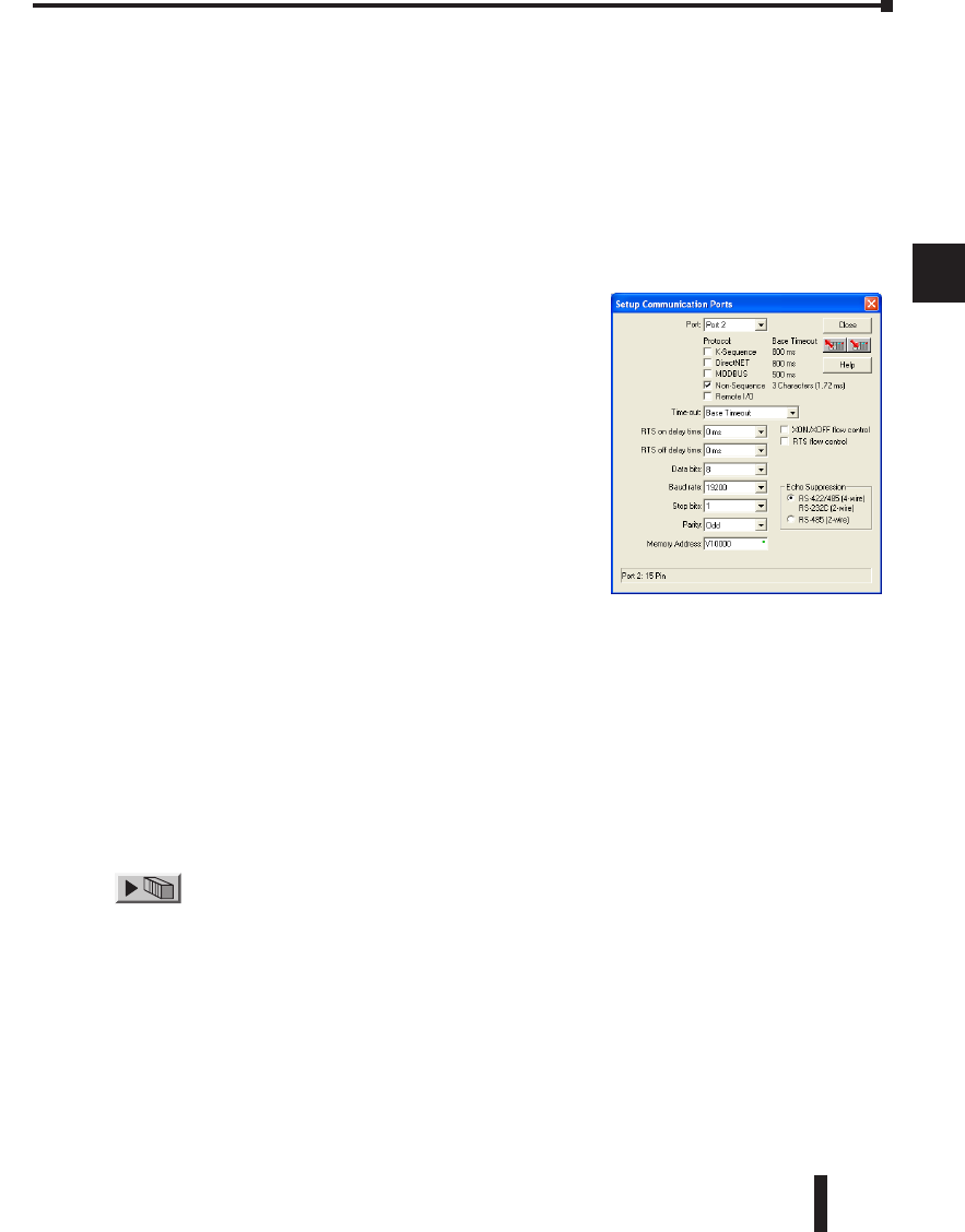
Non–Sequence Protocol (ASCII In/Out and PRINT)
Non-Sequence Port Configuration
Configuring port 2 on the DL06 for Non–Sequence allows the CPU to use port 2 to
either read or write raw ASCII strings using the ASCII instructions. See the ASCII In/Out
instructions and the PRINT instruction in chapter 5.
In DirectSOFT 5, choose the PLC menu, then Setup, then “Secondary Comm Port”.
• Port: From the port number list box at the top, choose “Port 2”.
• Protocol: Check the box to the left of “Non–Sequence”.
• Timeout: Amount of time the port will wait after it sends a
message to get a response before logging an error.
• RTS On Delay Time: The amount of time between raising
the RTS line and sending the data.
• RTS Off Delay Time: The amount of time between resetting
the RTS line after sending the data.
• Data Bits: Select either 7–bits or 8–bits to match the number
of data bits specified for the connected devices.
• Baud Rate: The available baud rates include 300,
600, 900, 2400, 4800, 9600, 19200, and 38400
baud. Choose a higher baud rate initially, reverting to
lower baud rates if you experience data errors or noise
problems on the network. Important: You must configure the
baud rates of all devices on the network to the same value.
Refer to the appropriate product manual for details.
• Stop Bits: Choose 1 or 2 stop bits to match the number of stop bits specified for the connected
devices.
• Parity: Choose none, even, or odd parity for error checking. Be sure to match the parity specified
for the connected devices.
• Echo Suppression: Select the appropriate radio button based on the wiring configuration used on
port 2.
• Xon/Xoff Flow Control: Choose this selection if you have Port 2 wired for Hardware Flow Control
(Xon/Xoff) with RTS and CTS signal connected between all devices.
• RTS Flow Control: Choose this selection if you have Port 2 RTS signal wired between all devices.
Click the button indicated to send the port configuration to the CPU, and click Close.
• Memory Address: Please choose a memory address with 64 words of contiguous free memory for
use by Non-Sequence Protocol.
DL06 Micro PLC User Manual; 3rd Edition Rev. D
4–12
Chapter 4: System Design and Configuration
1
2
3
4
5
6
7
8
9
10
11
12
13
14
A
B
C
D
Network Slave Operation
This section describes how other devices on a network can communicate with a CPU port
that you have configured as a DirectNET slave or MODBUS slave (DL06). A MODBUS
host must use the MODBUS RTU protocol to communicate with the DL06 as a slave. The
host software must send a MODBUS function code and MODBUS address to specify a PLC
memory location the DL06 comprehends. The DirectNET host uses normal I/O addresses to
access applicable DL06 CPU and system. No CPU ladder logic is required to support either
MODBUS slave or DirectNET slave operation.
NOTE: For more intformation on DirectNET proprietary protocol, see the DirectNET reference
manual, DA-DNET-M, available on our website.
MODBUS Function Codes Supported
The MODBUS function code determines whether the access is a read or a write, and whether
to access a single data point or a group of them. The DL06 supports the MODBUS function
codes described below.
Determining the MODBUS Address
There are typically two ways that most host software conventions allow you to specify a PLC
memory location. These are:
• By specifying the MODBUS data type and address
• By specifying a MODBUS address only
1
2
3
4
5
6
7
8
9
10
11
12
13
14
A
B
C
D
MODBUS Function Code Function DL06 Data Types Available
01 Read a group of coils Y, CR, T, CT
02 Read a group of inputs X, SP
05 Set / Reset a single coil Y, CR, T, CT
15 Set / Reset a group of coils Y, CR, T, CT
03, 04 Read a value from one or more registers V
06 Write a value into a single register V
16 Write a value into a group of registers V
DL06 Micro PLC User Manual; 3rd Edition Rev. D 4–13
Chapter 4: System Design and Configuration
1
2
3
4
5
6
7
8
9
10
11
12
13
14
A
B
C
D
If Your Host Software Requires the Data Type and Address
Many host software packages allow you to specify the MODBUS data type and the
MODBUS address that corresponds to the PLC memory location. This is the easiest method,
but not all packages allow you to do it this way.
The actual equation used to calculate the address depends on the type of PLC data you are
using. The PLC memory types are split into two categories for this purpose.
• Discrete – X, SP, Y, CR, S, T, C (contacts)
• Word – V, Timer current value, Counter current value
In either case, you basically convert the PLC octal address to decimal and add the appropriate
MODBUS address (if required). The table below shows the exact equation used for each
group of data.
1
2
3
4
5
6
7
8
9
10
11
12
13
14
A
B
C
D
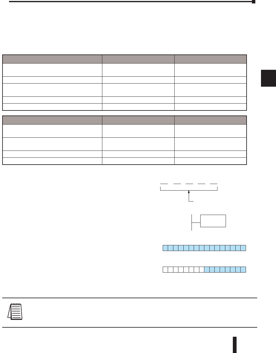
DL06 Memory Type QTY
(Decimal)
PLC Range
(Octal)
MODBUS Address
Range
(Decimal)
MODBUS Data Type
For Discrete Data Types .... Convert PLC Addr. to Dec. + Start of Range + Data Type
Inputs (X) 512 X0 – X777 2048 – 2559 Input
Special Relays(SP) 512 SP0 – SP777 3072 – 3583 Input
Outputs (Y) 512 Y0 – Y777 2048 – 2559 Coil
Control Relays (CR) 1024 C0 – C1777 3072 – 4095 Coil
Timer Contacts (T) 256 T0 – T377 6144 – 6399 Coil
Counter Contacts (CT) 128 CT0 – CT177 6400 – 6527 Coil
Stage Status Bits(S) 1024 S0 – S1777 5120 – 6143 Coil
For Word Data Types .... Convert PLC Addr. to Dec. + Data Type
Timer Current Values (V) 256 V0 – V377 0 – 255 Input Register
Counter Current Values (V) 128 V1000 – V1177 512 – 639 Input Register
V-Memory, user data (V) 3200 V1200 – V7377 640 – 3839 Holding Register
4096 V10000 - V17777 4096 - 8191 Holding Register
V-Memory, non-volatile (V) 128 V7400 – V7577 3840 – 3967 Holding Register
DL06 Micro PLC User Manual; 3rd Edition Rev. D
4–14
Chapter 4: System Design and Configuration
1
2
3
4
5
6
7
8
9
10
11
12
13
14
A
B
C
D
1
2
3
4
5
6
7
8
9
10
11
12
13
14
A
B
C
D
The following examples show how to generate the MODBUS address and data type for hosts
which require this format.
Example 1: V2100
Find the MODBUS address for User V location V2100.
1. Find V-memory in the table.
2. Convert V2100 into decimal (1088).
3. Use the MODBUS data type from the table.
Example 2: Y20
Find the MODBUS address for output Y20.
1. Find Y outputs in the table.
2. Convert Y20 into decimal (16).
3. Add the starting address for the range (2048).
4. Use the MODBUS data type from the table.
Example 3: T10 Current Value
Find the MODBUS address to obtain the current value from Timer T10.
1. Find Timer Current Values in the table.
2. Convert T10 into decimal (8).
3. Use the MODBUS data type from the table.
Example 4: C54
Find the MODBUS address for Control Relay C54.
1. Find Control Relays in the table.
2. Convert C54 into decimal (44).
3. Add the starting address for the range (3072).
4. Use the MODBUS data type from the table.
V-memory, user data (V) 3200 V1200 – V7377 640 – 3839 Holding Register
Control Relays (CR) 512 C0 – C77 3072 – 3583 Coil
Outputs (V) 256 Y0 – Y377 2048 - 2303 Coil
Timer Current Values (V) 128 V0 – V177 0 - 127 Input Register
Coil 2064
Coil 3116
Holding Reg 1088
Input Reg. 8
DL06 Micro PLC User Manual; 3rd Edition Rev. D 4–15
Chapter 4: System Design and Configuration
1
2
3
4
5
6
7
8
9
10
11
12
13
14
A
B
C
D
1
2
3
4
5
6
7
8
9
10
11
12
13
14
A
B
C
D
If Your MODBUS Host Software Requires an Address ONLY
Some host software does not allow you to specify the MODBUS data type and address.
Instead, you specify an address only. This method requires another step to determine the
address, but it’s still fairly simple. Basically, MODBUS also separates the data types by
address ranges as well. So this means an address alone can actually describe the type of
data and location. This is often referred to as “adding the offset”. One important thing to
remember here is that two different addressing modes may be available in your host software
package. These are:
• 484 Mode
• 584/984 Mode
We recommend that you use the 584/984 addressing mode if your host software allows
you to choose. This is because the 584/984 mode allows access to a higher number of
memory locations within each data type. If your software only supports 484 mode, then there
may be some PLC memory locations that will be unavailable. The actual equation used to
calculate the address depends on the type of PLC data you are using. The PLC memory types
are split into two categories for this purpose.
• Discrete – X, SP, Y, CR, S, T (contacts), C (contacts)
• Word – V, Timer current value, Counter current value
In either case, you basically convert the PLC octal address to decimal and add the appropriate
MODBUS addresses (as required). The table below shows the exact equation used for each
group of data.
Discrete Data Types
DL06 Memory Type PLC Range
(Octal)
Address (484
Mode)
Address (584/984
Mode)
MODBUS Data
Type
Global Inputs (GX) GX0-GX1746 1001 - 1999 10001 - 10999 Input
GX1747-GX3777 --- 11000 - 12048 Input
Inputs (X) X0 – X1777 --- 12049 - 13072 Input
Special Relays (SP) SP0 – SP777 --- 13073 - 13584 Input
Global Outputs (GY) GY0 - GY3777 1 - 2048 1 - 2048 Output
Outputs (Y) Y0 – Y1777 2049 - 3072 2049 - 3072 Output
Control Relays (CR) C0 – C3777 3073 - 5120 3073 - 5120 Output
Timer Contacts (T) T0 – T377 6145 - 6400 6145 - 6400 Output
Counter Contacts (CT) CT0 – CT377 6401 - 6656 6401 - 6656 Output
Stage Status Bits (S) S0 – S1777 5121 - 6144 5121 - 6144 Output
DL06 Micro PLC User Manual; 3rd Edition Rev. D
4–16
Chapter 4: System Design and Configuration
1
2
3
4
5
6
7
8
9
10
11
12
13
14
A
B
C
D
1
2
3
4
5
6
7
8
9
10
11
12
13
14
A
B
C
D
Example 1: V2100 584/984 Mode
Example 1: V2100 584/984 Mode
Find the MODBUS address for User V location V2100. PLC Address (Dec.) + Mode Address
1. Find V-memory in the table. V2100 = 1088 decimal
2. Convert V2100 into decimal (1088). 1088 + 40001 =
3. Add the MODBUS starting address for the
mode (40001).
Example 2: Y20 584/984 Mode
Find the MODBUS address for output Y20. PLC Addr. (Dec.) + Start Address + Mode
1. Find Y outputs in the table. Y20 = 16 decimal
2. Convert Y20 into decimal (16). 16 + 2048 + 1 =
3. Add the starting address for the range (2048).
4. Add the MODBUS address for the mode (1).
Word Data Types
Registers PLC Range
(Octal)
Input/Holding
(484 Mode)*
Input/Holding
(584/984 Mode)*
V-memory (Timers) V0 - V377 3001/4001 30001/40001
V-memory (Counters) V1000 - V1177 3513/4513 30513/40513
V-memory (Data Words)
V1200 - V1377 3641/4641 30641/40641
V1400 - V1746 3769/4769 30769/40769
V1747 - V1777 --- 31000/41000
V2000 - V7377 --- 41025
V10000 - V17777 --- 44097
1. Refer to your PLC user manual for the correct memory mapping size of your PLC. Some of
the addresses shown above might not pertain to your particular CPU.
2. For an automated MODBUS/Koyo address conversion utility, go to our
website, www.automationdirect.com, and down load download the EXCEL file
modbus_conversion.xls located at: Tech Support > Technical Support Home page.
41089
For Word Data Types.... PLC Address (Dec.) + Appropriate Mode Address
Timer Current Values (V) 128 V0 – V177 0 – 127 3001 30001 Input Register
Counter Current Values (V) 128 V1200 – V7377 640 – 3839 3001 30001 Input Register
V-memory, user data (V) 1024 V2000 – V3777 1024 – 2047 4001 40001 Holding Register
2065
Outputs (Y) 320 Y0 - Y477 2048 – 2367 1 1 Coil
Control Relays (CR) 256 C0 - C377 3072 – 3551 1 1 Coil
Timer Contacts (T) 128 T0 - T177 6144 – 6271 1 1 Coil
*MODBUS: Function 04
DL06 Micro PLC User Manual; 3rd Edition Rev. D 4–17
Chapter 4: System Design and Configuration
1
2
3
4
5
6
7
8
9
10
11
12
13
14
A
B
C
D
1
2
3
4
5
6
7
8
9
10
11
12
13
14
A
B
C
D
Example 3: T10 Current Value 484 Mode
Find the MODBUS address to obtain the PLC Address (Dec.) + Mode Address
current value from Timer T10. TA10 = 8 decimal
1. Find Timer Current Values in the table. 8 + 3001
=
2. Convert T10 into decimal (8).
3. Add the MODBUS starting address for the mode (3001).
Example 4: C54 584/984 Mode
Find the MODBUS address for Control Relay C54. PLC Addr. (Dec.) + Start Address + Mode
1. Find Control Relays in the table. C54 = 44 decimal
2. Convert C54 into decimal (44). 44 + 3072 + 1
=
3. Add the starting address for the range (3072).
4. Add the MODBUS address for the mode (1).
Network Master Operation
This section describes how the DL06 can communicate on a MODBUS or DirectNET
network as a master. For MODBUS networks, it uses the MODBUS RTU protocol, which
must be interpreted by all the slaves on the network. Both MODBUS and DirectNet are
single master/multiple slave networks. The master is the only member of the network that can
initiate requests on the network. This section teaches you how to design the required ladder
logic for network master operation.
For Word Data Types.... PLC Address (Dec.) + Appropriate Mode Address
Timer Current Values (V) 128 V0 – V177 0 – 127 3001 30001 Input Register
Counter Current Values (V) 128 V1200 – V7377 512 – 639 3001 30001 Input Register
V-memory, user data (V) 1024 V2000 – V3777 1024 – 2047 4001 40001 Holding Register
Outputs (Y) 320 Y0 – Y477 2048 – 2367 1 1 Coil
Control Relays (CR) 256 C0 – C377 3072 – 3551 1 1 Coil
Timer Contacts (T) 128 T0– T177 6144 – 6271 1 1 Coil
3009
3117
Slave #1 Slave #3
Master M
O
DB
US
,
RTU Protocol, or DirectNET
,
Slave #2
LOGIC
Koyo
06
C0 C4C2X1 X3 X4 X6 X11X13 X14X16 X21X23 N.C.
C1 C3X2 X5 X7 X10X12 X15 X17X20 X22X0 N.C.
AC(N)24V
0V
N.C.
C1 C3Y0 Y15Y12Y10Y17Y7Y5Y2
C0 C2 Y16Y14Y13Y11Y6Y4Y3Y1
LGG
AC(L)
D0-06DR
2.0AOUTPUT: 6-240V 50 - 60Hz 2.0A,6 - 27V
INPUT: 12 - 24V 3 - 15mA
Y
X
40VA50-60HzPWR: 100-240V
01 2345 6710 11 12 13 14 15 16 17 20 21 22 23
PORT1PORT2
TERM
RUNSTOP
PWR
RUN
CPU
TX1
RX1
TX2
RX2
DL06 Micro PLC User Manual; 3rd Edition Rev. D
4–18
Chapter 4: System Design and Configuration
1
2
3
4
5
6
7
8
9
10
11
12
13
14
A
B
C
D
1
2
3
4
5
6
7
8
9
10
11
12
13
14
A
B
C
D
When using the DL06 PLC as the master station, simple RLL instructions are used to initiate
the requests. The WX instruction initiates network write operations, and the RX instruction
initiates network read operations. Before executing either the WX or RX commands, we will
need to load data related to the read or write operation onto the CPU’s accumulator stack.
When the WX or RX instruction executes, it uses the information on the stack combined with
data in the instruction box to completely define the task, which goes to the port.
The following step-by-step procedure will provide you the information necessary to set up
your ladder program to receive data from a network slave.
Slave
Master
WX
(write)
RX (read)
Network
LOGIC
Koyo
06
C0 C4C2X1 X3 X4 X6 X11X13 X14X16 X21X23 N.C.
C1 C3X2 X5 X7 X10X12 X15 X17X20 X22X0 N.C.
AC(N)24V
0V
N.C.
C1 C3Y0 Y15Y12Y10Y17Y7Y5Y2
C0 C2 Y16Y14Y13Y11Y6Y4Y3Y1
LG
G
AC(L)
D0-06DR
2.0AOUTPUT: 6-240V 50 - 60Hz 2.0A, 6 - 27V
INPUT: 12 - 24V3 - 15mA
Y
X
40VA50-60HzPWR: 100-240V
01 2345 6710 11 12 13 14 15 16 17 20 21 22 23
PORT1 PORT2
TERM
RUN STOP
PWR
RUN
CPU
TX1
RX1
TX2
RX2
2 0 1F
Internal port (hex)
Port number (BCD)
Slave address (BCD)
LD
KF201
6 4 (BCD)
# of bytes to transfer
LD
K64
Step 2: Load Number of Bytes to Transfer
The second Load (LD) instruction determines
the number of bytes which will be transferred
between the master and slave in the subsequent
WX or RX instruction. The value to be loaded
is in BCD format (decimal), from 1 to 128
bytes.
Step 1: Identify Master Port # and Slave #
The first Load (LD) instruction identifies the
communications port number on the network
master (DL06) and the address of the slave
station. This instruction can address up to 99
MODBUS slaves, or 90 DirectNET slaves.
The format of the word is shown to the right.
The “F2” in the upper byte indicates the use of
the right port of the DL06 PLC, port number
2. The lower byte contains the slave address
number in BCD (01 to 99).
DL06 Micro PLC User Manual; 3rd Edition Rev. D 4–19
Chapter 4: System Design and Configuration
1
2
3
4
5
6
7
8
9
10
11
12
13
14
A
B
C
D
1
2
3
4
5
6
7
8
9
10
11
12
13
14
A
B
C
D
DL05 / 06 / 205 / 350 / 405 Memory Bits per unit Bytes
V-memory
T / C current value
16
16
2
2
Inputs (X, SP) 8 1
Outputs
(Y, C, Stage, T/C bits) 8 1
Scratch Pad Memory 8 1
Diagnostic Status 8 1
DL330 / 340 Memory Bits per unit Bytes
Data registers
T / C accumulator
8
16
1
2
I/O, internal relays, shift register bits, T/C
bits, stage bits 1 1
Scratch Pad Memory 8 1
Diagnostic Status(5 word R/W) 16 10
The number of bytes specified also depends on the type of data you want to obtain. For
example, the DL06 Input points can be accessed by V-memory locations or as X input
locations. However, if you only want X0 – X27, you’ll have to use the X input data type
because the V-memory locations can only be accessed in 2-byte increments. The following
table shows the byte ranges for the various types of DirectLOGIC products.
NOTE: Since V-memory words are always 16 bits, you may not always use the whole word. For example,
if you only specify 3 bytes and you are reading Y outputs from the slave, you will only get 24 bits of data. In
this case, only the 8 least significant bits of the last word location will be modified. The remaining 8 bits are
not affected.
6 0 00
(octal)
LDA
O40600
4
Starting address of
master transfer area
V40600
MSB LSB
0
15
V40601
MSB LSB
015
Step 3: Specify Master Memory Area
The third instruction in the RX or WX sequence
is a Load Address (LDA) instruction. Its purpose
is to load the starting address of the memory area
to be transferred. Entered as an octal number, the
LDA instruction converts it to hex and places the
result in the accumulator.
For a WX instruction, the DL06 CPU sends
the number of bytes previously specified from
its memory area beginning at the LDA address
specified.
For an RX instruction, the DL06 CPU reads the
number of bytes previously specified from the
slave, placing the received data into its memory
area beginning at the LDA address specified.
DL06 Micro PLC User Manual; 3rd Edition Rev. D
4–20
Chapter 4: System Design and Configuration
1
2
3
4
5
6
7
8
9
10
11
12
13
14
A
B
C
D
1
2
3
4
5
6
7
8
9
10
11
12
13
14
A
B
C
D
DL305 Series CPU Memory Type–to–MODBUS Cross Reference (excluding 350 CPU)
PLC Memory Type PLC Base
Address
MODBUS
Base Address
PLC Memory
Type
PLC Base
Address
MODBUS
Base Address
TMR/CNT Current Values R600 V0 TMR/CNT Status
Bits CT600 GY600
I/O Points IO 000 GY0 Control Relays CR160 GY160
Data Registers R401,R400 V100 Shift Registers SR400 GY400
Stage Status Bits (D3-330P only) S0 GY200
LD
KF201
LD
K64
LDA
O40600
RX
SP116
Y0
Step 4: Specify Slave Memory Area
The last instruction in our sequence is the WX or RX
instruction itself. Use WX to write to the slave, and
RX to read from the slave. All four of our instructions
are shown to the right. In the last instruction, you
must specify the starting address and a valid data type
for the slave.
• DirectNET slaves – specify the same address in the WX
and RX instruction as the slave’s native I/O address
• MODBUS DL405, DL205, or DL06 slaves – specify
the same address in the WX and RX instruction as the
slave’s native I/O address
• MODBUS 305 slaves – use the following table to
convert DL305 addresses to MODBUS addresses
LD
K101
LD
K4128
LDA
O4000
RX
V0
The Maximum constant possible is 4128. This
is due to the 128 maximum number of Bytes
that the RX/WX instruction can allow. The
value of 4 in the most significant position of
the word will cause the RX to use function 04
(30001 range).
The DL05/06, DL250-1/260, DL350 and DL450 will support function 04, read input
register (Address 30001). To use function 04, put the number ‘4’ into the most significant
position (4xxx). Four digits must be entered for the intruction to work properly with this
mode.
DL06 Micro PLC User Manual; 3rd Edition Rev. D 4–21
Chapter 4: System Design and Configuration
1
2
3
4
5
6
7
8
9
10
11
12
13
14
A
B
C
D
1
2
3
4
5
6
7
8
9
10
11
12
13
14
A
B
C
D
Port Communication Error
LD
KF201
LD
K0003
LDA
O40600
RX
Y0
SP116
Port Busy
SP117
SET
Y1
Interlocking Relay
LD
KF201
LD
K0003
LDA
O40600
RX
VY0
SP116
SET
C100
C100
LD
KF201
LD
K0003
LDA
O40400
WX
VY0
SP116
RST
C100
C100
Interlocking
Relay
Multiple Read and Write Interlocks
If you are using multiple reads and writes
in the RLL program, you have to interlock
the routines to make sure all the routines are
executed. If you don’t use the interlocks, then
the CPU will only execute the first routine.
This is because each port can only handle one
transaction at a time.
In the example to the right, after the RX
instruction is executed, C100 is set. When the
port has finished the communication task, the
second routine is executed and C100 is reset.
If you’re using RLLPLUS Stage Programming,
you can put each routine in a separate program
stage to ensure proper execution and switch
from stage to stage allowing only one of them
to be active at a time.
Communications from a Ladder Program
Typically network communications will last
longer than 1 scan. The program must wait
for the communications to finish before
starting the next transaction.
Port 2, which can be a master, has two
Special Relay contacts associated with it (see
Appendix D for comm port special relays).
One indicates “Port busy”(SP116), and
the other indicates ”Port Communication
Error”(SP117). The example above shows the
use of these contacts for a network master that
only reads a device (RX). The “Port Busy”
bit is on while the PLC communicates with
the slave. When the bit is off the program can
initiate the next network request.
The “Port Communication Error” bit turns
on when the PLC has detected an error. Use
of this bit is optional. When used, it should
be ahead of any network instruction boxes
since the error bit is reset when an RX or WX
instruction is executed
DL06 Micro PLC User Manual; 3rd Edition Rev. D
4–22
Chapter 4: System Design and Configuration
1
2
3
4
5
6
7
8
9
10
11
12
13
14
A
B
C
D
Network Master Operation (using MRX and MWX
Instructions)
This section describes how the DL06 can communicate on a MODBUS RTU network as a
master using the MRX and MWX read/write instructions. These instructions allow you to
enter native MODBUS addressing in your ladder logic program with no need to perform
octal to decimal conversions. MODBUS is a single master/multiple slave network. The
master is the only member of the network that can initiate requests on the network. This
section teaches you how to design the required ladder logic for network master operation.
MODBUS Function Codes Supported
The MODBUS function code determines whether the access is a read or a write, and whether
to access a single data point or a group of them. The DL06 supports the MODBUS function
codes described below.
1
2
3
4
5
6
7
8
9
10
11
12
13
14
A
B
C
D
MODBUS Function Code Function DL06 Data Types Available
01 Read a group of coils Y, CR, T, CT
02 Read a group of inputs X, SP
05 Set / Reset a single coil (slave only) Y, CR, T, CT
15 Set / Reset a group of coils Y, CR, T, CT
03, 04 Read a value from one or more registers V
06 Write a value into a single register (slave only) V
07 Read Exception Status V
08 Diagnostics V
16 Write a value into a group of registers V
Slave #1 Slave #3
Master M
O
DB
US
,
RTU Protocol, or DirectNET
,
Slave #2
LOGIC
Koyo
06
C0 C4C2X1 X3 X4 X6 X11X13 X14X16 X21X23 N.C.
C1 C3X2 X5 X7 X10X12 X15 X17X20 X22X0 N.C.
AC(N)24V
0V
N.C.
C1 C3Y0 Y15Y12Y10Y17Y7Y5Y2
C0 C2 Y16Y14Y13Y11Y6Y4Y3Y1
LGG
AC(L)
D0-06DR
2.0AOUTPUT: 6-240V 50 - 60Hz 2.0A,6 - 27V
INPUT: 12 - 24V 3 - 15mA
Y
X
40VA50-60HzPWR: 100-240V
01 2345 6710 11 12 13 14 15 16 17 20 21 22 23
PORT1PORT2
TERM
RUNSTOP
PWR
RUN
CPU
TX1
RX1
TX2
RX2
DL06 Micro PLC User Manual; 3rd Edition Rev. D 4–23
Chapter 4: System Design and Configuration
1
2
3
4
5
6
7
8
9
10
11
12
13
14
A
B
C
D
MODBUS Read from Network(MRX)
The MODBUS Read from Network (MRX) instruction is used by the DL06 network master
to read a block of data from a connected slave device and to write the data into V–memory
addresses within the master. The instruction allows the user the to specify the MODBUS
Function Code, slave station address, starting master and slave memory addresses, number of
elements to transfer, MODBUS data format and the Exception Response Buffer.
• Port Number: must be DL06 Port 2 (K2)
• Slave Address: specify a slave station address (0–247)
• Function Code: The following MODBUS function codes are supported by the MRX
instruction:
01 – Read a group of coils
02 – Read a group of inputs
03 – Read holding registers
04 – Read input registers
07 – Read Exception status
08 – Diagnostics
• Start Slave Memory Address: specifies the starting slave memory address of the data to be
read. See the table on the following page.
• Start Master Memory Address: specifies the starting memory address in the master where
the data will be placed. See the table on the following page.
• Number of Elements: specifies how many coils, input, holding registers or input register
will be read. See the table on the following page.
• MODBUS Data Format: specifies MODBUS 584/984 or 484 data format to be used
• Exception Response Buffer: specifies the master memory address where the Exception
Response will be placed. See the table on the following page.
1
2
3
4
5
6
7
8
9
10
11
12
13
14
A
B
C
D
DL06 Micro PLC User Manual; 3rd Edition Rev. D
4–24
Chapter 4: System Design and Configuration
1
2
3
4
5
6
7
8
9
10
11
12
13
14
A
B
C
D
MRX Slave Memory Address
MRX Master Memory Addresses
MRX Number of Elements
MRX Exception Response Buffer
1
2
3
4
5
6
7
8
9
10
11
12
13
14
A
B
C
D
MRX Slave Address Ranges
Function Code MODBUS Data Format Slave Address Range(s)
01 – Read Coil 484 Mode 1–999
01 – Read Coil 584/984 Mode 1–65535
02 – Read Input Status 484 Mode 1001–1999
02 – Read Input Status 584/984 Mode 10001–19999 (5 digit) or 100001–165535
(6 digit)
03 – Read Holding Register 484 Mode 4001–4999
03 – Read Holding Register 584/984 40001–49999 (5 digit) or 4000001–465535
(6 digit)
04 – Read Input Register 484 Mode 3001–3999
04 – Read Input Register 584/984 Mode 30001–39999 (5 digit) or 3000001–365535
(6 digit)
07 – Read Exception Status 484 and 584/984 Mode n/a
08 – Diagnostics 484 and 584/984 Mode 0–65535
MRX Master Memory Address Ranges
Operand Data Type DL06 Range
Inputs X 0–1777
Outputs Y 0–1777
Control Relays C 0–3777
Stage Bits S 0–1777
Timer Bits T 0–377
Counter Bits CT 0–377
Special Relays SP 0–777
V–memory V All
Global Inputs GX 0–3777
Global Outputs GY 0–3777
MRX Number of Elements
Operand Data Type DL06 Range
V–memory V All
Constant K 1–2000
MRX Exception Response Buffer
Operand Data Type DL06 Range
V–memory V All
DL06 Micro PLC User Manual; 3rd Edition Rev. D 4–25
Chapter 4: System Design and Configuration
1
2
3
4
5
6
7
8
9
10
11
12
13
14
A
B
C
D
MODBUS Write to Network (MWX)
The MODBUS Write to Network (MWX) instruction is used to write a block of data from
the network masters’s (DL06) memory to MODBUS memory addresses within a slave device
on the network. The instruction allows the user to specify the MODBUS Function Code,
slave station address, starting master and slave memory addresses, number of elements to
transfer, MODBUS data format and the Exception Response Buffer.
• Port Number: must be DL06 Port 2 (K2)
• Slave Address: specify a slave station address (0–247)
• Function Code: The following MODBUS function codes are supported by the MWX
instruction:
05 – Force Single coil
06 – Preset Single Register
08 – Diagnostics
15 – Force Multiple Coils
16 – Preset Multiple Registers
• Start Slave Memory Address: specifies the starting slave memory address where the data
will be written.
• Start Master Memory Address: specifies the starting address of the data in the master that is
to written to the slave.
• Number of Elements: specifies how many consecutive coils or registers will be written to.
This field is only active when either function code 15 or 16 is selected.
• MODBUS Data Format: specifies MODBUS 584/984 or 484 data format to be used.
• Exception Response Buffer: specifies the master memory address where the Exception
Response will be placed.
1
2
3
4
5
6
7
8
9
10
11
12
13
14
A
B
C
D
DL06 Micro PLC User Manual; 3rd Edition Rev. D
4–26
Chapter 4: System Design and Configuration
1
2
3
4
5
6
7
8
9
10
11
12
13
14
A
B
C
D
MWX Slave Memory Address
MWX Master Memory Addresses
MWX Number of Elements
MWX Exception Response Buffer
Chapter 4: System Design and Configuration
1
2
3
4
5
6
7
8
9
10
11
12
13
14
A
B
C
D
MWX Slave Address Ranges
Function Code MODBUS Data Format Slave Address Range(s)
05 – Force Single Coil 484 Mode 1–999
05 – Force Single Coil 584/984 Mode 1–65535
06 – Preset Single Register 484 Mode 4001–4999
06 – Preset Single Register 84/984 Mode 40001–49999 (5 digit) or 400001–
465535 (6 digit)
08 – Diagnostics 484 and 584/984 Mode 0–65535
15 – Force Multiple Coils 484 1–999
15 – Force Multiple Coils 585/984 Mode 1–65535
16 – Preset Multiple Registers 484 Mode 4001–4999
16 – Preset Multiple Registers 584/984 Mode 40001–49999 (5 digit) or 4000001–
465535 (6 digit)
MWX Number of Elements
Operand Data Type DL06 Range
V–memory V All
Constant K 1–2000
MWX Exception Response Buffer
Operand Data Type DL06 Range
V–memory V All
MWX Master Memory Address Ranges
Operand Data Type DL06 Range
Inputs X 0–777
Outputs Y 0–777
Control Relays C 0–1777
Stage Bits S 0–1777
Timer Bits T 0–377
Counter Bits CT 0–177
Special Relays SP 0–777
V–memory V All
Global Inputs GX 0–3777
Global Outputs GY 0–3777

DL06 Micro PLC User Manual; 3rd Edition Rev. D 4–27
Chapter 4: System Design and Configuration
1
2
3
4
5
6
7
8
9
10
11
12
13
14
A
B
C
D
Chapter 4: System Design and Configuration
1
2
3
4
5
6
7
8
9
10
11
12
13
14
A
B
C
D
MRX/MWX Example in DirectSOFT 5
DL06 port 2 has two Special Relay contacts associated with it (see Appendix D for comm
port special relays). One indicates “Port busy”(SP116), and the other indicates ”Port
Communication Error”(SP117). The “Port Busy” bit is on while the PLC communicates
with the slave. When the bit is off the program can initiate the next network request. The
“Port Communication Error” bit turns on when the PLC has detected an error and use
of this bit is optional. When used, it should be ahead of any network instruction boxes
since the error bit is reset when an MRX or MWX instruction is executed. Typically
network communications will last longer than 1 CPU scan. The program must wait for the
communications to finish before starting the next transaction.
The “Port Communication Error” bit turns on when the PLC has detected an error. Use of
this bit is optional. When used, it should be ahead of any network instruction boxes since the
error bit is reset when an RX or WX instruction is executed.
Multiple Read and Write Interlocks
If you are using multiple reads and writes in the RLL program, you have to interlock the
routines to make sure all the routines are executed. If you don’t use the interlocks, then
the CPU will only execute the first routine. This is because each port can only handle one
transaction at a time. In the example below, after the MRX instruction is executed, C100
is set. When the port has finished the communication task, the second routine is executed
and C100 is reset. If you’re using RLLplus Stage Programming, you can put each routine in
a separate program stage to ensure proper execution and switch from stage to stage allowing
only one of them to be active at a time.
See example on the next page.
DL06 Micro PLC User Manual; 3rd Edition Rev. D
4–28
Chapter 4: System Design and Configuration
1
2
3
4
5
6
7
8
9
10
11
12
13
14
A
B
C
D
1
2
3
4
5
6
7
8
9
10
11
12
13
14
A
B
C
D
SP116 C100
SP116 C100
Port Number: K2
Slave Address: K1
Function Code: 06 - Preset Single Register
Start Slave Memory Address: 40001
Number of Elements: n/a
Modbus Data Type: 584/984 Mode
Exception Response Buffer: V400
Instruction interlock bit
C100
( SET )
( RST )
C100
Instruction interlock bit
MRX
Port Number: K2
Slave Address: K1
Function Code: 01 - Read Coil Status
Start Slave Memory Address: 1
Start Master Memory Address: C0
Number of Elements: 32
Modbus Data Type: 584/984 Mode
Exception Response Buffer: V400
This rung does a MODBUS write to the first holding register 40001 of slave address number one.
It writes the values over that reside in V2000. This particular function code only writes to one
register. Use function code 16 to write to multiple registers. Only one Network Instruction
(WX, RX, MWX, MRX) can be enabled in one scan. That is the reason for the interlock bits. For using
many network instructions on the same port, use the Shift Register instruction.
This rung does a MODBUS read from the first 32 coils of slave address number one.
It will place the values into 32 bits of the master starting at C0.
3
4
MWX
Port 2 busy bit
Port 2 busy bit
Port 2 busy bit
SP116
Port 2 error bit
SP117
Pulse/Minute
C20
CT1
K9999
CNT
Number of errors
per minute
CT2
K9999
SP116 pulses on every transaction - CT1 counts the transactions per minute.
The counter is reset every minute.
SP117 pulses on every transaction - CT2 counts the errors per minute.
The counter is reset every minute.
3
4
CNT
Number of
transactions per
minute
_1Minute
SP3 C20
( PD )
C20
Calculation of communication transfer quantity per minute between PLC and device.
CTA1
LD
V3600
OUT
CTA2
LD
V3601
OUT
Transactions/Min
Errors/Minute
Pulse/Minute
C20
1
2
Pulse/Minute
Pulse/Minute
