Clevo M660SE, M665SE Service Manual. Www.s Manuals.com. Manual
User Manual: Notebook Clevo M660SE - Service manuals and Schematics, Disassembly / Assembly. Free.
Open the PDF directly: View PDF ![]() .
.
Page Count: 95
- Manual
- Preface
- Chapter 1: Introduction
- Overview
- System Specifications
- Model Differences
- External Locator - Top View with LCD Panel Open
- External Locator - Front & Rear Views
- External Locator - Left & Right Side Views
- External Locator - Bottom View
- M660SE Mainboard Overview - Top (Key Parts)
- M660SE Mainboard Overview - Bottom (Key Parts)
- M660SE Mainboard Overview - Top (Connectors)
- M660SE Mainboard Overview - Bottom (Connectors)
- Chapter 2: Disassembly
- Overview
- Maintenance Tools
- Connections
- Maintenance Precautions
- Removing the Battery
- Removing the Hard Disk Drive
- Removing the System Memory (RAM)
- Removing the Processor
- Removing the Wireless LAN Module
- Removing the Modem
- Removing the Bluetooth Module
- Removing the Optical (CD/DVD) Device
- Removing the Keyboard
- Appendix A: Part Lists
- Appendix B: Schematic Diagrams
- SYSTEM BLOCK DIAGRAM
- CLOCK GENERATOR
- CPU-1
- CPU-2
- VN896-1
- VN896-2
- VN896-3
- VN896-4
- DDR2-1
- DDR2-2
- VGA G72M-1
- VGA G72M-2
- VGA G72M-3
- VGA G72M-4
- VT8237A-1
- VT8237A-2
- VT8237A-3
- HDD & CDROM
- CARD READER
- NEW CARD SOCKET
- LAN
- USB & CCD
- HITACHI H8
- CRT & LVDS
- CPU FAN, LPC ROM
- MINI-PCI & BLUETOOTH
- AUDIO VT1708A/ALC883
- LED
- CHARGER, DC IN
- 1.05VS, 1.5V, 2.5VS
- VCORE
- 1.8V, 0.9VS
- VDD3, VDD5
- EXT GPU 1.0VS/1.2VS
- HOTKEY LT BOARD
- PWR HOT BOARD
- AUDIO & MODEM BOARD
- CLICK BOARD
- USB BOARD
- FINGERPRINT BOARD


Preface
I
Preface
Notebook Computer
M660SE/M665SE
Service Manual

Preface
II
Preface
Notice
The company reserves the right to revise this publication or to change its contents without notice. Information contained
herein is for reference only and does not constitute a commitment on the part of the manufacturer or any subsequent ven-
dor. They assume no responsibility or liability for any errors or inaccuracies that may appear in this publication nor are
they in anyway responsible for any loss or damage resulting from the use (or misuse) of this publication.
This publication and any accompanying software may not, in whole or in part, be reproduced, translated, transmitted or
reduced to any machine readable form without prior consent from the vendor, manufacturer or creators of this publica-
tion, except for copies kept by the user for backup purposes.
Brand and product names mentioned in this publication may or may not be copyrights and/or registered trademarks of
their respective companies. They are mentioned for identification purposes only and are not intended as an endorsement
of that product or its manufacturer.
Version 1.0
February 2007
Trademarks
Intel, Celeron, and Intel Core are trademarks/registered trademarks of Intel Corporation.
Windows® is a registered trademark of Microsoft Corporation.
Other brand and product names are trademarks and./or registered trademarks of their respective companies.

Preface
III
Preface
About this Manual
This manual is intended for service personnel who have completed sufficient training to undertake the maintenance and
inspection of personal computers.
It is organized to allow you to look up basic information for servicing and/or upgrading components of the M660SE/
M665SE series notebook PC.
The following information is included:
Chapter 1, Introduction, provides general information about the location of system elements and their specifications.
Chapter 2, Disassembly, provides step-by-step instructions for disassembling parts and subsystems and how to upgrade
elements of the system.
Appendix A, Part Lists
Appendix B, Schematic Diagrams

Preface
IV
Preface
IMPORTANT SAFETY INSTRUCTIONS
Follow basic safety precautions, including those listed below, to reduce the risk of fire, electric shock and injury to per-
sons when using any electrical equipment:
1. Do not use this product near water, for example near a bath tub, wash bowl, kitchen sink or laundry tub, in a wet
basement or near a swimming pool.
2. Avoid using a telephone (other than a cordless type) during an electrical storm. There may be a remote risk of elec-
trical shock from lightning.
3. Do not use the telephone to report a gas leak in the vicinity of the leak.
4. Use only the power cord and batteries indicated in this manual. Do not dispose of batteries in a fire. They may
explode. Check with local codes for possible special disposal instructions.
5. This product is intended to be supplied by a Listed Power Unit (DC Output 19V, 3.42A or 18.5, 3.5A AC/DC Adapter).
CAUTION
Always disconnect all telephone lines from the wall outlet before servicing or disassembling this equipment.
TO REDUCE THE RISK OF FIRE, USE ONLY NO. 26 AWG OR LARGER,
TELECOMMUNICATION LINE CORD
This Computer’s Optical Device is a Laser Class 1 Product
Preface
V
Preface
Instructions for Care and Operation
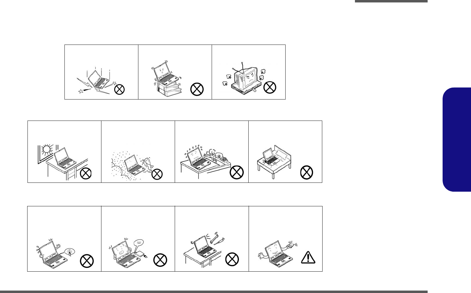
The notebook computer is quite rugged, but it can be damaged. To prevent this, follow these suggestions:
1. Don’t drop it, or expose it to shock. If the computer falls, the case and the components could be damaged.
2. Keep it dry, and don’t overheat it. Keep the computer and power supply away from any kind of heating element. This
is an electrical appliance. If water or any other liquid gets into it, the computer could be badly damaged.
3. Follow the proper working procedures for the computer. Shut the computer down properly and don’t forget to save
your work. Remember to periodically save your data as data may be lost if the battery is depleted.
Do not expose the computer
to any shock or vibration. Do not place it on an unstable
surface. Do not place anything heavy
on the computer.
Do not expose it to excessive
heat or direct sunlight. Do not leave it in a place
where foreign matter or mois-
ture may affect the system.
Don’t use or store the com-
puter in a humid environment. Do not place the computer on
any surface which will block
the vents.
Do not turn off the power
until you properly shut down
all programs.
Do not turn off any peripheral
devices when the computer is
on.
Do not disassemble the com-
puter by yourself. Perform routine maintenance
on your computer.
Preface
VI
Preface
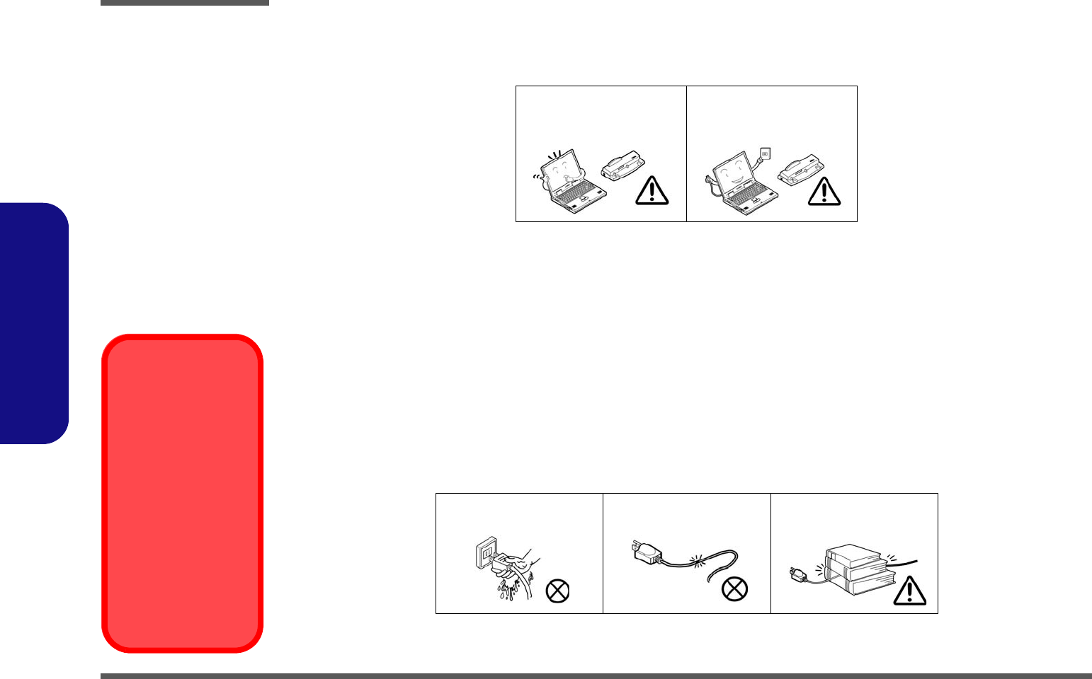
4. Avoid interference. Keep the computer away from high capacity transformers, electric motors, and other strong mag-
netic fields. These can hinder proper performance and damage your data.
5. Take care when using peripheral devices.
Power Safety
The computer has specific power requirements:
• Only use a power adapter approved for use with this computer.
• Your AC adapter may be designed for international travel but it still requires a steady, uninterrupted power supply. If you are
unsure of your local power specifications, consult your service representative or local power company.
• The power adapter may have either a 2-prong or a 3-prong grounded plug. The third prong is an important safety feature; do
not defeat its purpose. If you do not have access to a compatible outlet, have a qualified electrician install one.
• When you want to unplug the power cord, be sure to disconnect it by the plug head, not by its wire.
• Make sure the socket and any extension cord(s) you use can support the total current load of all the connected devices.
• Before cleaning the computer, make sure it is disconnected from any external power supplies.
Use only approved brands of
peripherals. Unplug the power cord before
attaching peripheral devices.
Do not plug in the power
cord if you are wet. Do not use the power cord if
it is broken. Do not place heavy objects
on the power cord.
Power Safety
Warning
Before you undertake
any upgrade proce-
dures, make sure that
you have turned off the
power, and discon-
nected all peripherals
and cables (including
telephone lines). It is
advisable to also re-
move your battery in
order to prevent acci-
dentally turning the
machine on.

Preface
VII
Preface
Battery Precautions
• Only use batteries designed for this computer. The wrong battery type may explode, leak or damage the computer.
• Do not continue to use a battery that has been dropped, or that appears damaged (e.g. bent or twisted) in any way. Even if the
computer continues to work with a damaged battery in place, it may cause circuit damage, which may possibly result in fire.
• Recharge the batteries using the notebook’s system. Incorrect recharging may make the battery explode.
• Do not try to repair a battery pack. Refer any battery pack repair or replacement to your service representative or qualified service
personnel.
• Keep children away from, and promptly dispose of a damaged battery. Always dispose of batteries carefully. Batteries may explode
or leak if exposed to fire, or improperly handled or discarded.
• Keep the battery away from metal appliances.
• Affix tape to the battery contacts before disposing of the battery.
• Do not touch the battery contacts with your hands or metal objects.
Battery Disposal
The product that you have purchased contains a rechargeable battery. The battery is recyclable. At the end of
its useful life, under various state and local laws, it may be illegal to dispose of this battery into the municipal
waste stream. Check with your local solid waste officials for details in your area for recycling options or proper
disposal.
Caution
Danger of explosion if battery is incorrectly replaced. Replace only with the same or equivalent type recommend-
ed by the manufacturer. Discard used battery according to the manufacturer’s instructions.

Preface
VIII
Preface
Related Documents
You may also need to consult the following manual for additional information:
User’s Manual on CD
This describes the notebook PC’s features and the procedures for operating the computer and its ROM-based setup pro-
gram. It also describes the installation and operation of the utility programs provided with the notebook PC.

Preface
IX
Preface
Contents
Introduction ..............................................1-1
Overview .........................................................................................1-1
System Specifications .....................................................................1-2
Model Differences ...........................................................................1-5
External Locator - Top View with LCD Panel Open ......................1-6
External Locator - Front & Rear Views ..........................................1-7
External Locator - Left & Right Side Views ...................................1-8
External Locator - Bottom View .....................................................1-9
M660SE Mainboard Overview - Top (Key Parts) ........................1-10
M660SE Mainboard Overview - Bottom (Key Parts) ...................1-11
M660SE Mainboard Overview - Top (Connectors) ......................1-12
M660SE Mainboard Overview - Bottom (Connectors) ................1-13
Disassembly ...............................................2-1
Overview .........................................................................................2-1
Maintenance Tools ..........................................................................2-2
Connections .....................................................................................2-2
Maintenance Precautions .................................................................2-3
Removing the Battery ......................................................................2-5
Removing the Hard Disk Drive .......................................................2-6
Removing the System Memory (RAM) ..........................................2-8
Removing the Processor ................................................................2-10
Removing the Wireless LAN Module ...........................................2-12
Removing the Modem ...................................................................2-13
Removing the Bluetooth Module ..................................................2-14
Removing the Optical (CD/DVD) Device ....................................2-15
Removing the Keyboard ................................................................2-16
Part Lists ..................................................A-1
Part List Illustration Location ........................................................A-2
Top (M660SE) ................................................................................A-3
Top (M665SE) ............................................................................... A-4
Bottom (M660SE/M665SE) .......................................................... A-5
LCD (M660SE/M665SE) .............................................................. A-6
CDRW (M660SE/M665SE) .......................................................... A-7
Combo (M660SE/M665SE) .......................................................... A-8
DVDRW (M660SE/M665SE) ....................................................... A-9
Schematic Diagrams.................................B-1
SYSTEM BLOCK DIAGRAM ......................................................B-2
CLOCK GENERATOR ..................................................................B-3
CPU-1 .............................................................................................B-4
CPU-2 .............................................................................................B-5
VN896-1 .........................................................................................B-6
VN896-2 .........................................................................................B-7
VN896-3 .........................................................................................B-8
VN896-4 .........................................................................................B-9
DDR2-1 .........................................................................................B-10
DDR2-2 .........................................................................................B-11
VGA G72M-1 ...............................................................................B-12
VGA G72M-2 ...............................................................................B-13
VGA G72M-3 ...............................................................................B-14
VGA G72M-4 ...............................................................................B-15
VT8237A-1 ...................................................................................B-16
VT8237A-2 ...................................................................................B-17
VT8237A-3 ...................................................................................B-18
HDD & CDROM ..........................................................................B-19
CARD READER ..........................................................................B-20
NEW CARD SOCKET .................................................................B-21
LAN ..............................................................................................B-22
USB & CCD .................................................................................B-23
HITACHI H8 ................................................................................B-24

Preface
X
Preface
CRT & LVDS ............................................................................... B-25
CPU FAN, LPC ROM .................................................................. B-26
MINI-PCI & BLUETOOTH ........................................................ B-27
AUDIO VT1708A/ALC883 ........................................................ B-28
LED .............................................................................................. B-29
CHARGER, DC IN ......................................................................B-30
1.05VS, 1.5V, 2.5VS .................................................................... B-31
VCORE ........................................................................................ B-32
1.8V, 0.9VS .................................................................................. B-33
VDD3, VDD5 ............................................................................... B-34
EXT GPU 1.0VS/1.2VS ............................................................... B-35
HOTKEY LT BOARD ................................................................. B-36
PWR HOT BOARD .....................................................................B-37
AUDIO & MODEM BOARD ...................................................... B-38
CLICK BOARD ........................................................................... B-39
USB BOARD ............................................................................... B-40
FINGERPRINT BOARD ............................................................. B-41

Introduction
Overview 1 - 1
1.Introduction
Chapter 1: Introduction
Overview
This manual covers the information you need to service or upgrade the M660SE/M665SE series notebook computer.
Information about operating the computer (e.g. getting started, and the Setup utility) is in the User’s Manual. Information
about drivers (e.g. VGA & audio) is also found in User’s Manual. That manual is shipped with the computer.
Operating systems (e.g. Windows XP, Windows Vista, etc.) have their own manuals as do application software (e.g. word
processing and database programs). If you have questions about those programs, you should consult those manuals.
The M660SE/M665SE series notebook is designed to be upgradeable. See “Disassembly” on page 2 - 1 for a detailed
description of the upgrade procedures for each specific component. Please note the warning and safety information indi-
cated by the “” symbol.
The balance of this chapter reviews the computer’s technical specifications and features.

Introduction
1 - 2 System Specifications
1.Introduction
System Specifications
Feature Specification
Processor Intel® Core™2 Duo Processor
(478-pin) Micro-FC-PGA Package
T7200/ T7400/ T7600
65nm (65 Nanometer) Process Technology
4MB On-die L2 Cache & 667MHz FSB
2.0/ 2.16/ 2.33 GHz
Intel® Core™2 Duo Processor
(478-pin) Micro-FC-PGA Package
T5500/ T5600
65nm (65 Nanometer) Process Technology
2MB On-die L2 Cache & 667MHz FSB
1.66/ 1.83 GHz
Intel® Core™ Duo Processor
(478-pin) Micro-FC-PGA Package
T2300/ T2400/ T2500/ T2600/ T2700
65nm (65 Nanometer) Process Technology
2MB On-die L2 Cache & 667MHz FSB
1.66/ 1.83/ 2.0/ 2.16/ 2.33 GHz
Intel® Core™ Solo Processor
(478-pin) Micro-FC-PGA Package
T1300/ T1400
65nm (65 Nanometer) Process Technology
2MB On-die L2 Cache & 667MHz FSB
1.66/ 1.83 GHz
Intel® Celeron® M Processor
(478-pin) Micro-FCPGA Package
410/ 420/ 430/ 440/ 450
65nm (65 Nanometer) Process Technology
1MB On-die L2 Cache & 533MHz FSB
1.46/ 1.60/ 1.73/ 1.86/ 2.0 GHz
Core Logic VIA VN896 + VT8237A Chipset
Memory Two 200 Pin SO-DIMM Sockets Supporting DDRII (DDR2) 533/667 MHz
64-bit Wide DDRII (DDR2) Data Per Channel
Memory Expandable up to 2GB (256/ 512/ 1024 MB DDRII Modules)
Latest Specification Information
The specifications listed in this Appendix are correct at the time of going to press. Certain items (particularly processor types/speeds and
CD/DVD device types) may be changed, delayed or updated due to the manufacturer's release schedule. Check with your service center
for details.
Introduction
System Specifications 1 - 3
1.Introduction
Security Security (Kensington® Type) Lock Slot BIOS Password
BIOS One 4Mb Flash ROM Phoenix™ BIOS
LCD 15.4" WXGA (1280 * 800) TFT LCD
Video Adapter VIA VN896 Integrated Video System
(Internal On Chip)
Chrome 9HC™
Integrated 128bit 2D/3D Graphic Engine and Clock up to 250MHz
Supports CRT Resolutions up to 2048 * 1536 at 75Hz
Supports Microsoft DirectX 9.0
Storage One Changeable 12.7mm(h) Optical Device (CD/DVD) Type Drive
One Easy Changeable 2.5" 9.5 mm (h) SATA (Serial) HDD
Audio Integrated AZALIA Compliant Interface (HDA)
3D Stereo Enhanced Sound System
Sound-Blaster PRO™ Compatible
2 * Built-In Speakers
Built-In Microphone
Keyboard &
Pointing Device Winkey Keyboard Built-In TouchPad with Scrolling Function
Interface Three USB 2.0 Ports
One External Monitor Port
One Headphone-Out Jack
One Microphone-In Jack
One Line-In Jack
One S/PDIF Out Jack
One RJ-11 Modem Jack
One RJ-45 LAN Jack
One DC-in Jack
Card Reader Embedded 7-in-1 Card Reader (MS/ MS Pro/ SD/ Mini SD/ MMC/ RS MMC/ MS Duo)
Note: MS Duo/ Mini SD/ RS MMC Cards require a PC adapter
ExpressCard Slot One ExpressCard/34(54) Slot
Communication AZALIA 56K Plug & Play Fax/Modem V.90/92 Compliant
10M/100Mb Base-T Ethernet LAN
802.11 b/g USB Wireless LAN Module (Option)
USB (2.0) Bluetooth Module - Version 2.0 (Factory Option)
300K or 1.3M Pixel USB PC Camera Module (Factory Option)
Feature Specification
Introduction
1 - 4 System Specifications
1.Introduction
Power
Management Supports ACPI 2.0 and PCI Bus Power Management 1.1
Compliant
Battery Low Suspend
Supports Wake on LAN
Power Full Range AC/DC Adapter 19V, 3.42A or 18.5V, 3.5A (65W), 100~240V, 50~60Hz
Battery 6 Cell Smart Lithium-Ion Battery Pack, 4000mAH
Environmental
Spec Temperature
Operating: 5°C ~ 35°C
Non-Operating: -20°C ~ 60°C
Relative Humidity
Operating: 20% ~ 80%
Non-Operating: 10% ~ 90%
Dimensions
& Weight 360mm (w) * 267mm (d) * 25.4-34mm (h) 2.6 kg With 6 Cell Battery
Optional Optical Drive Module Options:
DVD/CD-RW Combo Drive Module
DVD-Dual Drive Module
802.11 b/g USB Wireless LAN Module
300K or 1.3M Pixel USB PC Camera Module (Factory
Option)
USB (2.0) Bluetooth Module - Version 2.0 (Factory
Option)
Feature Specification
Introduction
System Specifications 1 - 5
1.Introduction
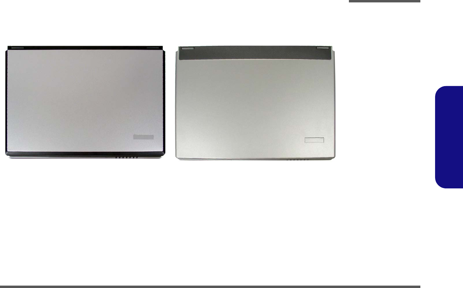
Model Differences
The models vary slightly in external cover design and color.
M660SE
M665SE
Figure 1
Model Differences
Introduction
1 - 6 External Locator - Top View with LCD Panel Open
1.Introduction
External Locator - Top View with LCD Panel Open
Figure 2
Top View
1. Optional Built-In
PC Camera
2. LCD
3. Speakers
4. Power Button
5. Hot Key Buttons
6. Keyboard
7. TouchPad and
Buttons
8. Built-In
Microphone
9. LED Indicators
2
5
1
7
8
4
6
9
33
5
9

Introduction
External Locator - Front & Rear Views 1 - 7
1.Introduction
External Locator - Front & Rear Views Figure 3
Front Views
1. LED Indicators
Figure 4
Rear Views
1. 1 * USB Port
2. DC-In Jack
3. Battery
1
1
3
2
1
Introduction
1 - 8 External Locator - Left & Right Side Views
1.Introduction
External Locator - Left & Right Side Views
4
1235 6 7
Figure 5
Left Side View
1. Security Lock Slot
2. Optical Device
Drive Bay
3. RJ-11 Modem
Jack
4. S/PDIF-Out Jack
5. Microphone-In
Jack
6. Headphone-Out
Jack
7. Line-In Jack
Figure 6
Right Side View
1. ExpressCard Slot
2. 7-in-1 Card
Reader
3. 2 * USB 2.0 Ports
4. RJ-45 LAN Jack
5. External Monitor
Port
123
345
Introduction
External Locator - Bottom View 1 - 9
1.Introduction
External Locator - Bottom View
Figure 7
Bottom View
1. Vent/Fan Intake
2. Battery
3. Hard Disk Bay
Cover
4. CPU/RAM Bay
Cover
Overheating
To prevent your com-
puter from overheating
make sure nothing
blocks the vent/fan in-
takes while the com-
puter is in use.
2
4
1
3
1
Introduction
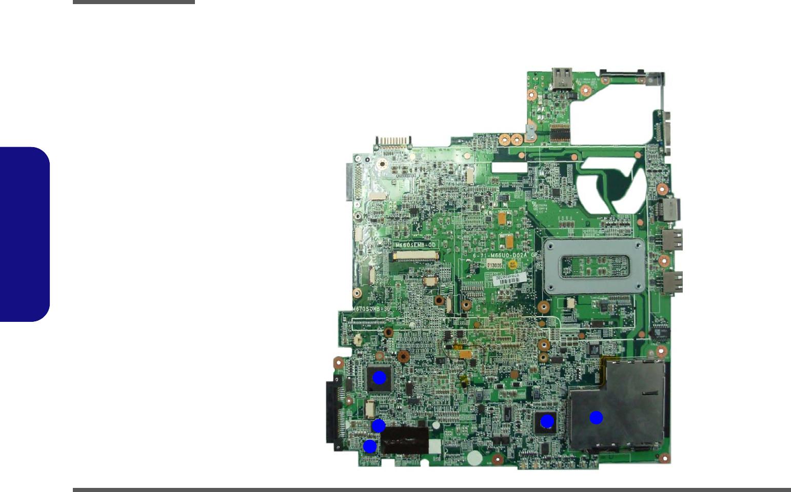
1 - 10 M660SE Mainboard Overview - Top (Key Parts)
1.Introduction
M660SE Mainboard Overview - Top (Key Parts)
Figure 8
Mainboard Top
Key Parts
1. Audio Codec
VT1613
2. Audio Amp
3. Hitachi H8
4. Card Reader
Control
5. PC Card
Assembly
2
3
1
45
Introduction
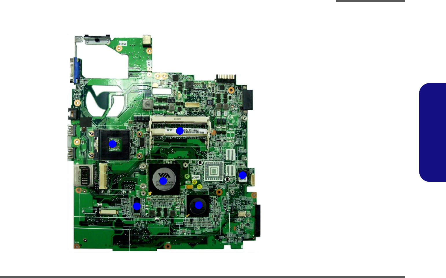
M660SE Mainboard Overview - Bottom (Key Parts) 1 - 11
1.Introduction
M660SE Mainboard Overview - Bottom (Key Parts) Figure 9
Mainboard Bottom
Key Parts
1. CPU Socket (no
CPU installed)
2. Memory Slots
DDRII So-DIMM
3. Northbridge-
VN896
4. ICS Clock
Generator
5. Southbridge-
VT8237A
6. Flash BIOS ROM
2
3
1
45
6
Introduction
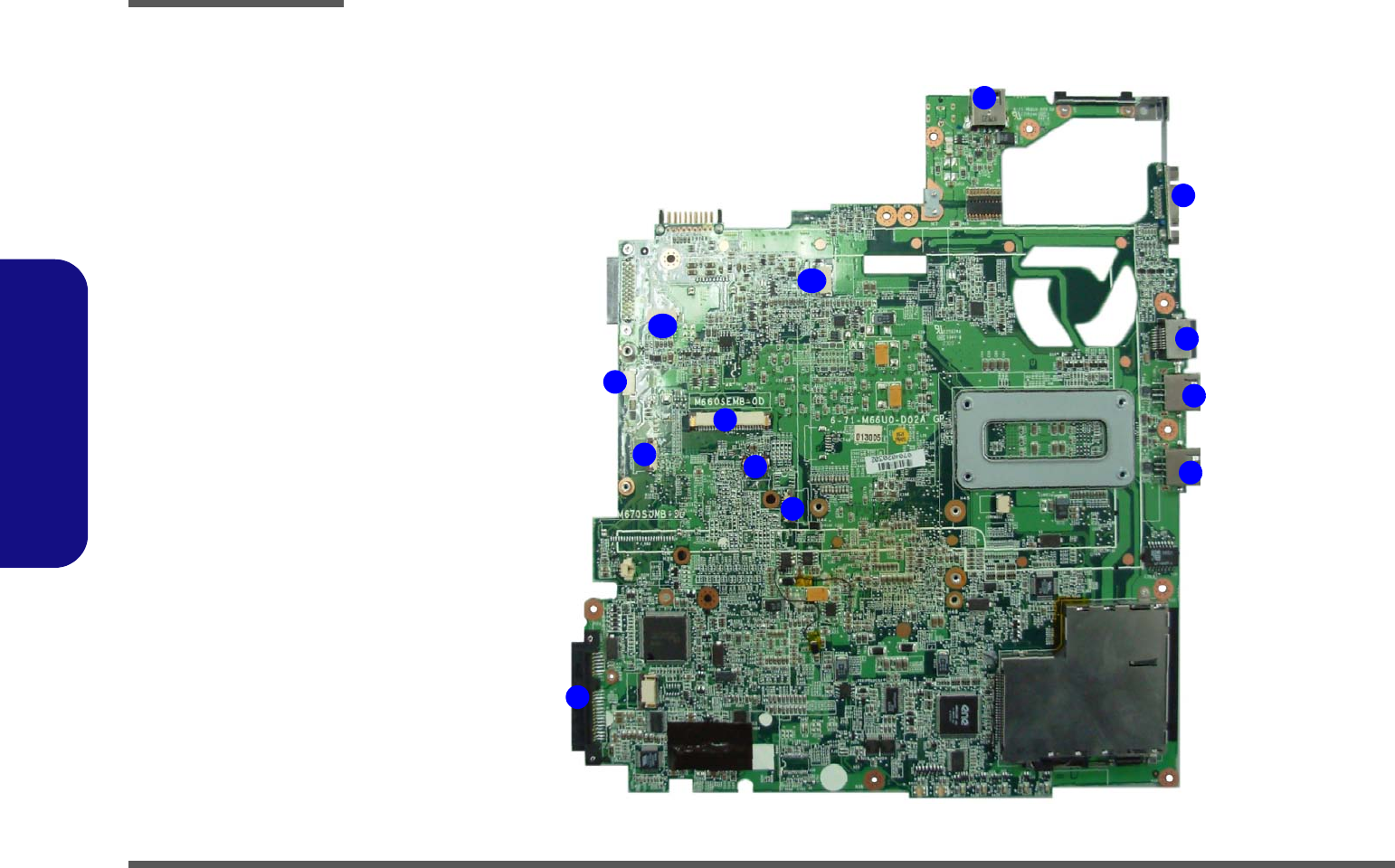
1 - 12 M660SE Mainboard Overview - Top (Connectors)
1.Introduction
M660SE Mainboard Overview - Top (Connectors)
Figure 10
Mainboard Top
Connectors
1. External Monitor
Port
2. RJ-45 LAN Jack
3. USB Port
4. HDD Connector
5. Hotkey Cable
Connector
6. Power Hotkey
Cable Connector
7. Touch Pad Cable
Connector
8. Keyboard Cable
Connector
9. Speaker Cable
Connector
10. Inverter Cable
Connector
11. CCD Cable
Connector
3
8
11
10
93
3
1
2
4
5
6
7
Introduction
M660SE Mainboard Overview - Bottom (Connectors) 1 - 13
1.Introduction
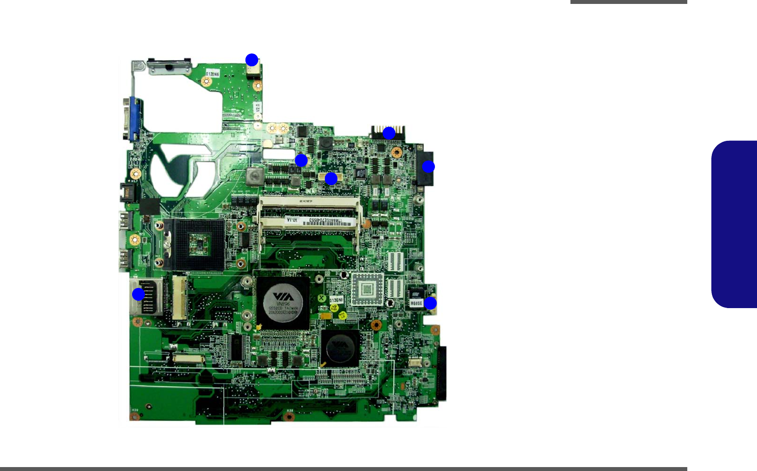
M660SE Mainboard Overview - Bottom (Connectors) Figure 11
Mainboard Bottom
Connectors
1. DC-In Jack
2. Fan Cable
Connector
3. LCD Cable
Connector
4. Batterry
Connector
5. Optical Device
Drive Connector
6. Bluetooth Cable
Connector
7. Card Reader
2
6
3
1
5
4
7

Introduction
1-14
1.Introduction

Disassembly
Overview 2 - 1
2.Disassembly
Chapter 2: Disassembly
Overview
This chapter provides step-by-step instructions for disassembling the M660SE/M665SE series notebook’s parts and sub-
systems. When it comes to reassembly, reverse the procedures (unless otherwise indicated).
We suggest you completely review any procedure before you take the computer apart.
Procedures such as upgrading/replacing the RAM, CD device and hard disk are included in the User’s Manual but are
repeated here for your convenience.
To make the disassembly process easier each section may have a box in the page margin. Information contained under
the figure # will give a synopsis of the sequence of procedures involved in the disassembly procedure. A box with a
lists the relevant parts you will have after the disassembly process is complete. Note: The parts listed will be for the dis-
assembly procedure listed ONLY, and not any previous disassembly step(s) required. Refer to the part list for the previ-
ous disassembly procedure. The amount of screws you should be left with will be listed here also.
A box with a will also provide any possible helpful information. A box with a contains warnings.
An example of these types of boxes are shown in the sidebar.
Information
Warning

Disassembly
2 - 2 Overview
2.Disassembly
NOTE: All disassembly procedures assume that the system is turned OFF, and disconnected from any power supply (the
battery is removed too).
Maintenance Tools
The following tools are recommended when working on the notebook PC:
• M3 Philips-head screwdriver
• M2.5 Philips-head screwdriver (magnetized)
• M2 Philips-head screwdriver
• Small flat-head screwdriver
• Pair of needle-nose pliers
• Anti-static wrist-strap
Connections
Connections within the computer are one of four types:
Locking collar sockets for ribbon connectors To release these connectors, use a small flat-head screwdriver to
gently pry the locking collar away from its base. When replac-
ing the connection, make sure the connector is oriented in the
same way. The pin1 side is usually not indicated.
Pressure sockets for multi-wire connectors To release this connector type, grasp it at its head and gently
rock it from side to side as you pull it out. Do not pull on the
wires themselves. When replacing the connection, do not try to
force it. The socket only fits one way.
Pressure sockets for ribbon connectors To release these connectors, use a small pair of needle-nose pli-
ers to gently lift the connector away from its socket. When re-
placing the connection, make sure the connector is oriented in
the same way. The pin1 side is usually not indicated.
Board-to-board or multi-pin sockets To separate the boards, gently rock them from side to side as
you pull them apart. If the connection is very tight, use a small
flat-head screwdriver - use just enough force to start.

Disassembly
Overview 2 - 3
2.Disassembly
Maintenance Precautions
The following precautions are a reminder. To avoid personal injury or damage to the computer while performing a re-
moval and/or replacement job, take the following precautions:
1. Don't drop it. Perform your repairs and/or upgrades on a stable surface. If the computer falls, the case and other
components could be damaged.
2. Don't overheat it. Note the proximity of any heating elements. Keep the computer out of direct sunlight.
3. Avoid interference. Note the proximity of any high capacity transformers, electric motors, and other strong mag-
netic fields. These can hinder proper performance and damage components and/or data. You should also monitor
the position of magnetized tools (i.e. screwdrivers).
4. Keep it dry. This is an electrical appliance. If water or any other liquid gets into it, the computer could be badly
damaged.
5. Be careful with power. Avoid accidental shocks, discharges or explosions.
•Before removing or servicing any part from the computer, turn the computer off and detach any power supplies.
•When you want to unplug the power cord or any cable/wire, be sure to disconnect it by the plug head. Do not pull on the wire.
6. Peripherals – Turn off and detach any peripherals.
7. Beware of static discharge. ICs, such as the CPU and main support chips, are vulnerable to static electricity.
Before handling any part in the computer, discharge any static electricity inside the computer. When handling a
printed circuit board, do not use gloves or other materials which allow static electricity buildup. We suggest that
you use an anti-static wrist strap instead.
8. Beware of corrosion. As you perform your job, avoid touching any connector leads. Even the cleanest hands pro-
duce oils which can attract corrosive elements.
9. Keep your work environment clean. Tobacco smoke, dust or other air-born particulate matter is often attracted
to charged surfaces, reducing performance.
10. Keep track of the components. When removing or replacing any part, be careful not to leave small parts, such as
screws, loose inside the computer.
Cleaning
Do not apply cleaner directly to the computer, use a soft clean cloth.
Do not use volatile (petroleum distillates) or abrasive cleaners on any part of the computer.
Power Safety
Warning
Before you undertake
any upgrade proce-
dures, make sure that
you have turned off the
power, and discon-
nected all peripherals
and cables (including
telephone lines). It is
advisable to also re-
move your battery in
order to prevent acci-
dentally turning the
machine on.

Disassembly
2 - 4 Overview
2.Disassembly
Disassembly Steps
The following table lists the disassembly steps, and on which page to find the related information. PLEASE PERFORM
THE DISASSEMBLY STEPS IN THE ORDER INDICATED.
To remove the Battery:
1. Remove the battery page 2 - 5
To remove the HDD:
1. Remove the battery page 2 - 5
2. Remove the HDD page 2 - 6
To remove the System Memory:
1. Remove the battery page 2 - 5
2. Remove the system memory page 2 - 8
To remove the Processor:
1. Remove the battery page 2 - 5
2. Remove the processor page 2 - 10
To remove the Wireless LAN Module:
1. Remove the battery page 2 - 5
2. Remove the wireless LAN page 2 - 12
To remove the Modem :
1. Remove the battery page 2 - 5
2. Remove the modem page 2 - 13
To remove the Bluetooth:
1. Remove the battery page 2 - 5
2. Remove the bluetooth page 2 - 14
To remove the Optical Device:
1. Remove the battery page 2 - 5
2. Remove the Optical device page 2 - 15
To remove the Keyboard:
1. Remove the battery page 2 - 5
2. Remove the keyboard page 2 - 16
Disassembly
Removing the Battery 2 - 5
2.Disassembly
Removing the Battery
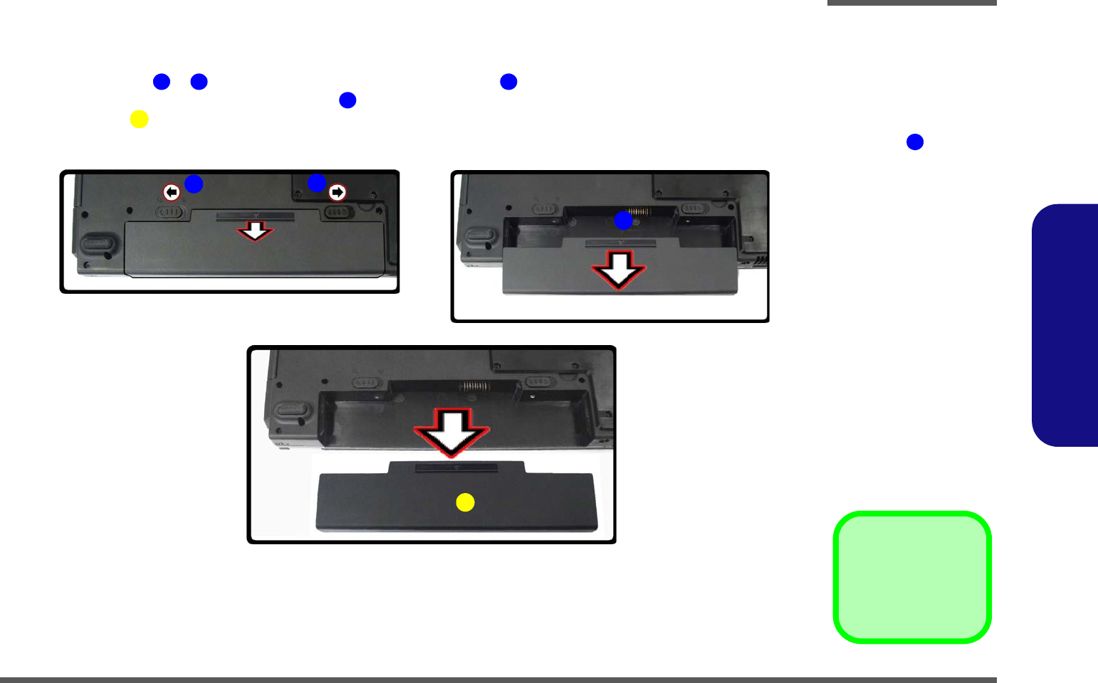
1. Turn the computer off, and turn it over.
2. Slide the latches ( & ) the direction of the arrow, and hold latch in place.
3. Slide the battery in the direction of the arrow .
4. Lift the battery out.
4. Battery
1 2 2
3
6
4
1
a. b.
c.
2
3
4
Figure 1
Battery Removal
a. Slide the 2 latches and
hold latch in place.
b. Slide the battery in the di-
rection of the arrow.
c. Lift the battery out.
2
Disassembly
2 - 6 Removing the Hard Disk Drive
2.Disassembly
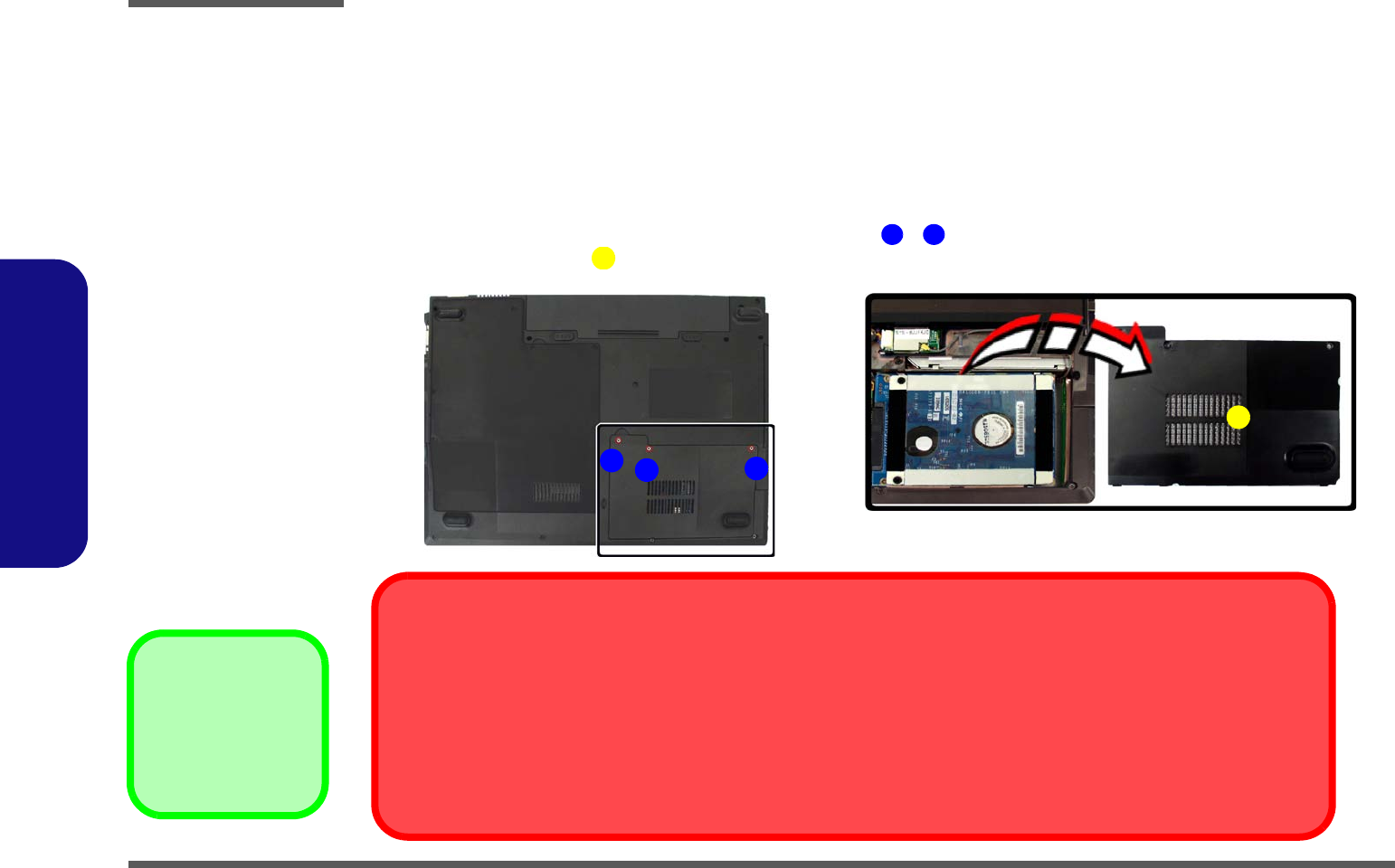
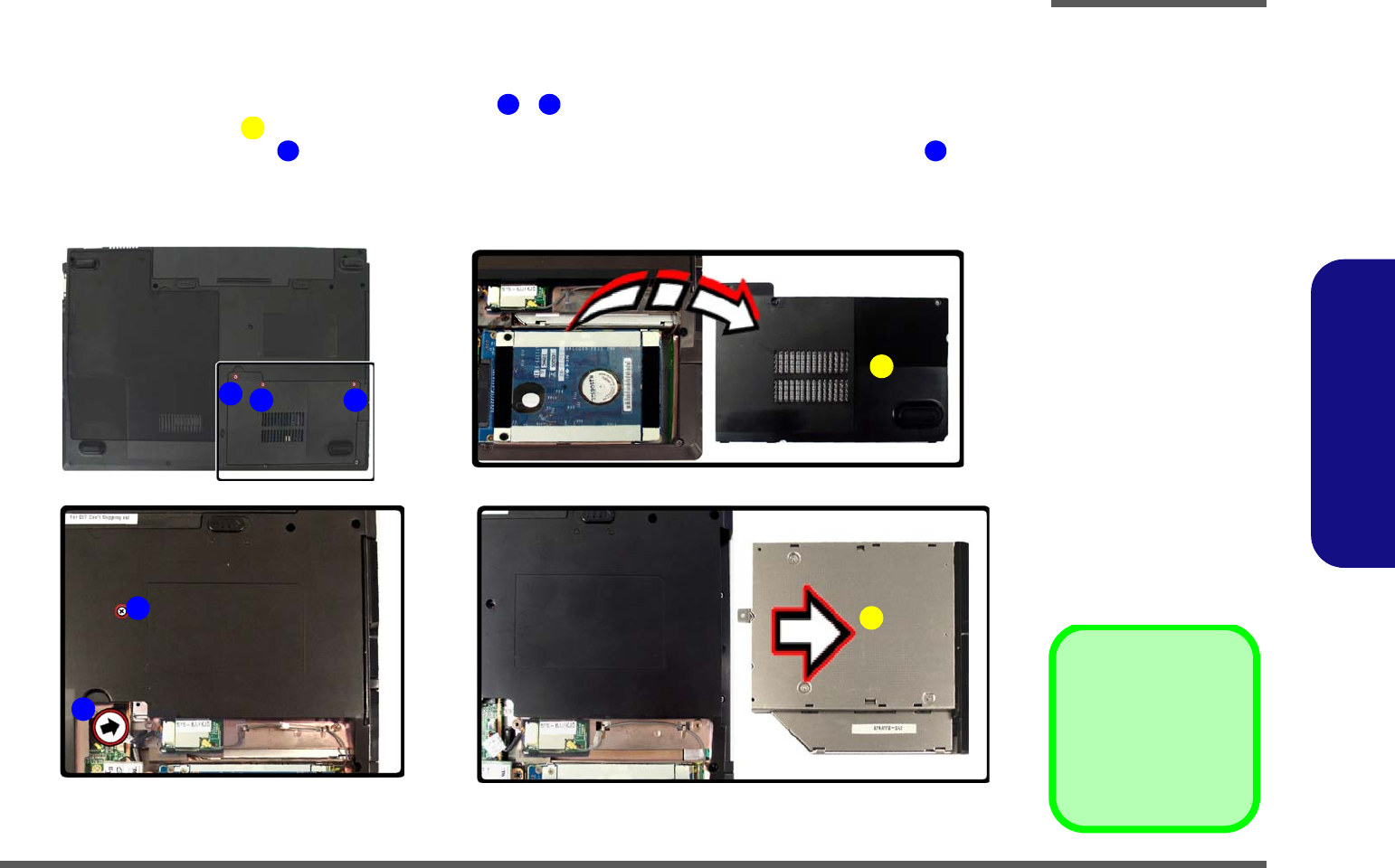
Removing the Hard Disk Drive
The hard disk drive can be taken out to accommodate other 2.5" serial (SATA) hard disk drives with a height of 9.5mm
(h). Follow your operating system’s installation instructions, and install all necessary drivers and utilities (as outlined in
Chapter 4 of the User’s Manual) when setting up a new hard disk.
Hard Disk Upgrade Processl
1. Turn off the computer, and remove the battery (page 2 - 5).
2. Locate the hard disk bay cover and remove the screws ( - ).
3. Remove the bay cover .
Figure 2
HDD Assembly
Removal
a. Locate the HDD bay cov-
er and remove the
screws.
b. Remove the bay cover.
4. HDD Bay Cover
•3 Screw
1 3
6
4
a.
13
2
HDD System Warning
New HDD’s are blank. Before you begin make sure:
You have backed up any data you want to keep from your old HDD.
You have all the CD-ROMs and FDDs required to install your operating system and programs.
If you have access to the internet, download the latest application and hardware driver updates for the operating system you plan
to install. Copy these to a removable medium.
4
b.
Disassembly
Removing the Hard Disk Drive 2 - 7
2.Disassembly
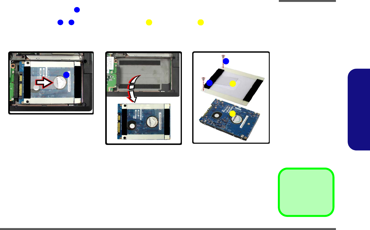
4. Carefully grip the mylar tab and slide the hard disk in the direction of arrow.
5. Lift the hard disk up (Figure d) in the direction of arrow.
6. Remove the screws - and separate the mylar cover from the hard disk .
7. Reverse the process to install any new hard disk.
5Figure 3
HDD Assembly
Removal Sequence
c. Slide the HDD in the di-
rection of the arrow.
d. Lift the HDD out of the
bay.
e. Remove the screws and
separate the mylar cover
from the HDD.
6 7 6
86
9
8. Mylar Cover
9. HDD
c. d.
5
e.
7
6
9
8
Disassembly
2 - 8 Removing the System Memory (RAM)
2.Disassembly
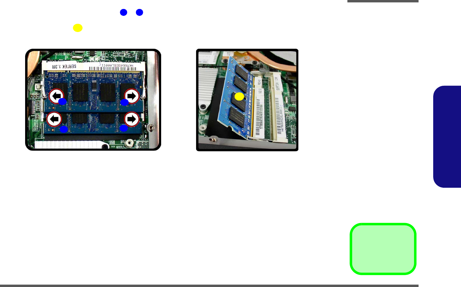
Removing the System Memory (RAM)
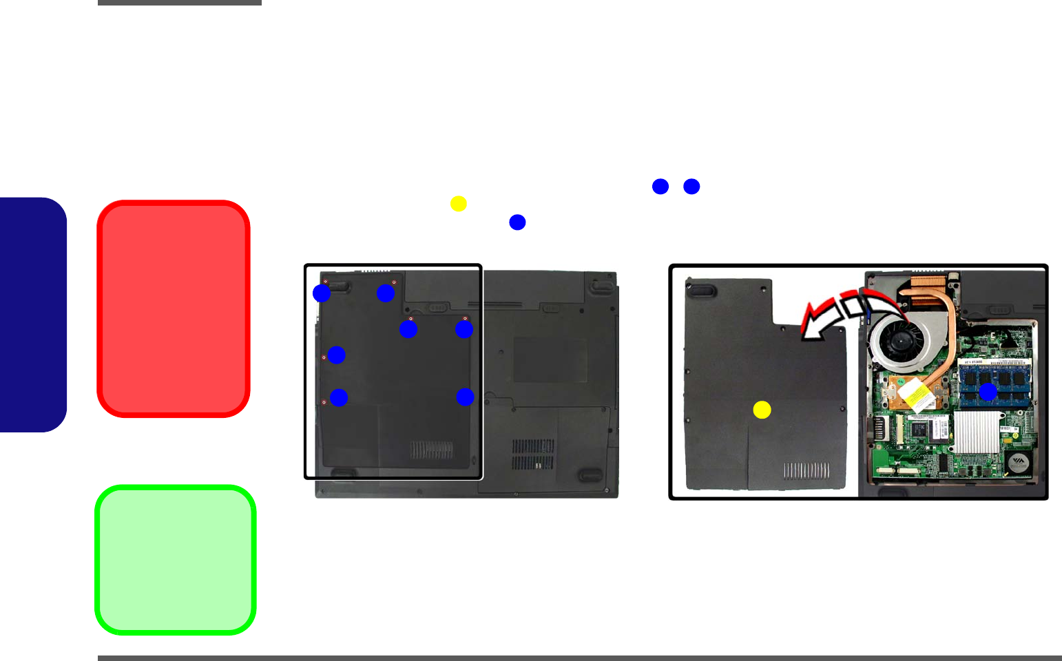
The computer has two memory sockets for 200 pin Small Outline Dual In-line Memory Modules (SO-DIMM) supporting
DDRII 533/667MHz. The main memory can be expanded up to 2GB. The SO-DIMM modules supported are 256MB,
512MB and 1024MB DDRII Modules. The total memory size is automatically detected by the POST routine once you
turn on your computer.
Memory Upgrade Process
1. Turn off the computer, remove the battery (page 2 - 5).
2. Locate the CPU/RAM bay cover, and remove screws - .
3. Remove the bay cover .
4. The RAM will be visible at point on the mainboard.
Figure 4
RAM Module
Removal
a. Remove the screws.
b. Remove the cover.
Contact Warning
Be careful not to touch
the metal pins on the
module’s connecting
edge. Even the clean-
est hands have oils
which can attract parti-
cles, and degrade the
module’s perfor-
mance.
1 7
8
8. CPU/RAM Bay Cover
•7 Screws
9
a.
3 4
1
56
78
b.
2
9
Disassembly
Removing the System Memory (RAM) 2 - 9
2.Disassembly
5. Gently push the two release latches ( & ) on the sides of the memory socket in the direction indicated by the
arrows (Figure c).
6. The RAM module(s) will pop-up (Figure d), and you can then remove it.
7. Push the latches to release the second module if necessary.
8. Insert a new module holding it at about a 30° angle and fit the connectors firmly into the memory slot.
9. The module will only fit one way as defined by its pin alignment. Make sure the module is seated as far into the slot
as it will go. DO NOT FORCE IT; it should fit without much pressure.
10. Press the module down towards the mainboard until the slot levers click into place to secure the module.
11. Replace the bay cover and the screws (see page 2 - 8).
12. Restart the computer to allow the BIOS to register the new memory configuration as it starts up.
10 11
12
Figure 5
Memory Removal
Sequence
c. Push the release
latch(es).
d. Remove the module(s).
10
c. d.
12
11
10 11
12 RAM Module(s)
Disassembly
2 - 10 Removing the Processor
2.Disassembly
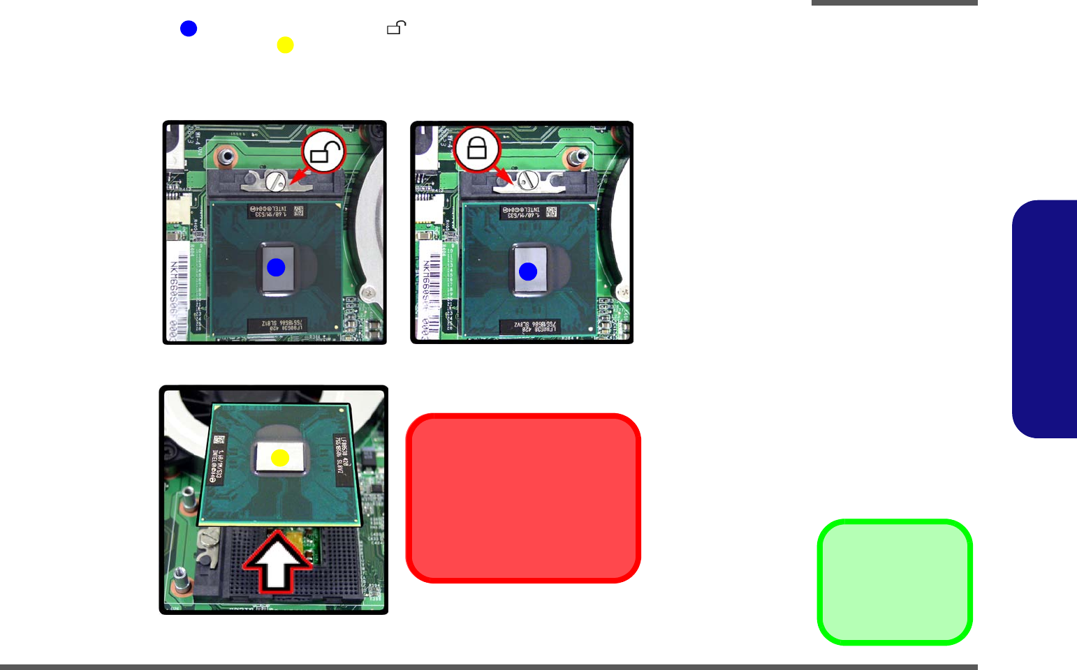
Removing the Processor
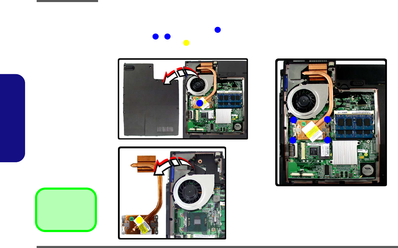
1. Turn off the computer, and remove the battery (page 2 - 5) and the CPU/RAM bay cover (page 2 - 8).
2. The CPU heat sink will be visible at point on the mainboard.
3. Remove screws - from the heat sink in the order indicated.
4. Carefully lift up the heat sink (Figure c) off the computer.
1
2 5
6
Figure 6
Processor Removal
a. Remove the cover and
Iocate the heat sink.
b. Remove the 4 screws in
the order indicated.
c. Remove the heat sink.
6. Heat Sink
•4 Screws
b.
6
1
5
4
a.
c. 3
2
Disassembly
Removing the Processor 2 - 11
2.Disassembly
5. Turn the release latch towards the unlock symbol , to release the CPU (Figure d).
6. Carefully (it may be hot) lift the CPU up out of the socket (Figure e).
7. Reverse the process to install a new CPU.
8. When re-inserting the CPU, pay careful attention to the pin alignment, it will fit only one way (DO NOT FORCE IT!).
78
Figure 7
Processor Removal
(cont’d)
d. Turn the release latch to
unlock the CPU.
e. Lift the CPU out of the
socket.
d.
8
e.
Caution
The heat sink, and CPU area in
general, contains parts which are
subject to high temperatures. Allow
the area time to cool before remov-
ing these parts.
Unlock Lock
7
7
8. CPU
Disassembly
2 - 12 Removing the Wireless LAN Module
2.Disassembly
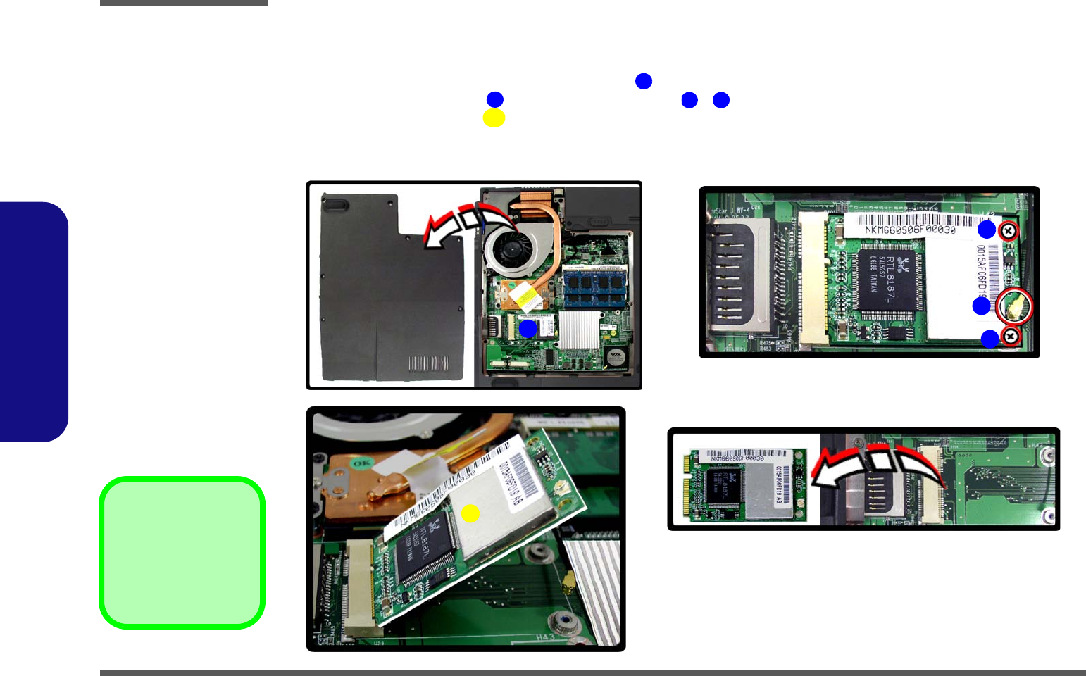
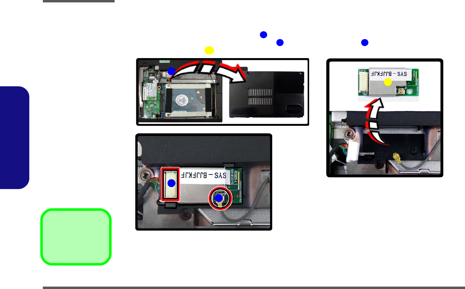
Removing the Wireless LAN Module
1. Turn off the computer, remove the battery (page 2 - 5) and the module bay cover (page 2 - 8).
1. The Wireless LAN module will be visible at point on the mainboard.
2. Carefully disconnect cable , then remove the screws - from the module socket.
3. The wireless LAN module will pop-up.
4. Lift the wireless LAN module (Figure d) up and off the computer.
Figure 8
Wireless LAN
Module Removal
a. Remove the cover and
Iocate the heat sink.
b. Disconnect the cable
and remove the 2
screws.
c. The WLAN module will
pop up.
d. Remove the WLAN
module.
Note: Make sure you
reconnect the antenna
cable to the “Main”
socket (Figure b).
1
23 4
5
1
2
4
c.
a.
5
3
b.
d.
5. WLAN Module
•2 Screws
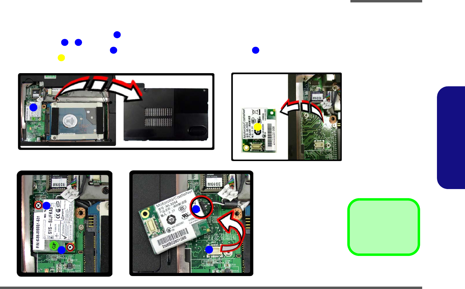
Disassembly
Removing the Modem 2 - 13
2.Disassembly
Removing the Modem
1. Turn off the computer, remove the battery (page 2 - 5), and remove the hard disk bay cover (page 2 - 6).
2. The modem will be visible at point on the mainboard.
3. Remove screws - from the modem module.
4. Lift the modem up off the socket and separate the modem from the connector .
5. Lift the modem up and off the computer.
1
2 3
4 5
6
Figure 9
Modem Removal
a. Remove the cover and
locate the modem.
b. Remove the screws.
c. Lift the modem up off the
socket and disconnect
the connector.
d. Lift the modem out.
a.
c.
b.
34
1
2
d.
6
5
6. Modem
•2 Screws
Disassembly
2 - 14 Removing the Bluetooth Module
2.Disassembly
Removing the Bluetooth Module
1. Turn off the computer, remove the battery (page 2 - 5) and remove the hard disk bay cover (page 2 - 6).
2. The Bluetooth module will be visible at point on the mainboard.
3. Carefully separate the module from the connector and disconnect the cable .
4. Lift the Bluetooth module (Figure c) up and off the computer.
Figure 10
Bluetooth Removal
a. Remove the cover and
locate the Bluetooth
module.
b. Separate the the mod-
ule from connector and
disconnect the cable.
c. Remove Bluetooth mod-
ule.
1
2 3
4
a. c.
b.
3
1
2
4
4. Bluetooth Module
Disassembly
Removing the Optical (CD/DVD) Device 2 - 15
2.Disassembly
Removing the Optical (CD/DVD) Device
1. Turn off the computer, remove the battery (page 2 - 5).
2. Locate the hard disk bay cover and remove screws ( - ).
3. Remove the bay cover .
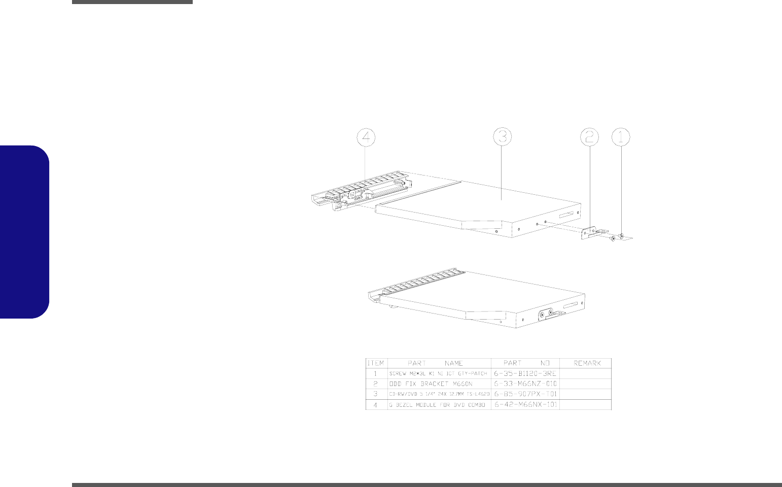
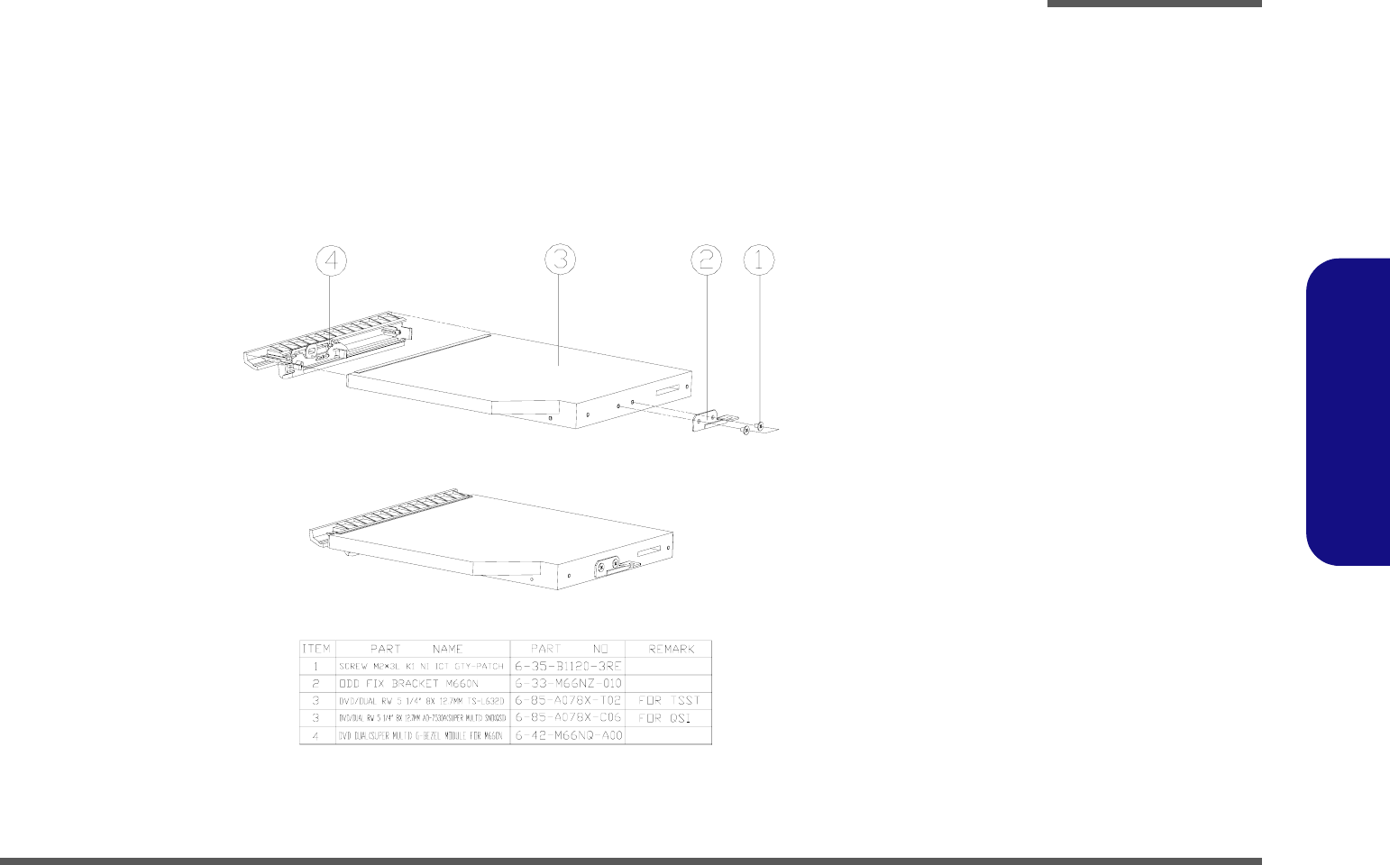
4. Remove the screw at point , and use a screwdriver to carefully push out the optical device at point .
5. Insert the new device and carefully slide it into the computer (the device only fits one way. DO NOT FORCE IT; The
screw holes should line up.
6. Restart the computer to allow it to automatically detect the new device.
Figure 11
Optical Device
Removal
a. Remove the screws.
b. Remove the cover.
c. Remove the screw and
push the optical device
out off the computer at
point 6.
d. Remove the optical de-
vice.
1 3
6
45 6
4 HDD Bay Cover
7 Optical Device
•4 Screws
32
1
a.
4
b.
c. d.
5
6
7
Disassembly
2 - 16 Removing the Keyboard
2.Disassembly
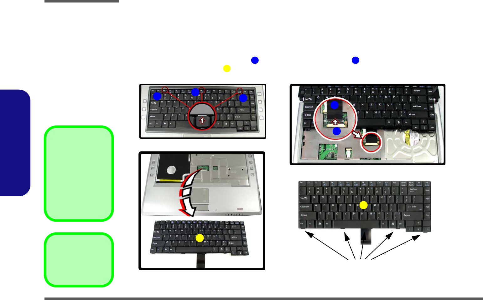
Removing the Keyboard
1. Turn off the computer, and remove the battery (page 2 - 5).
2. Press the three keyboard latches at the top of the keyboard to elevate the keyboard from its normal position (you
may need to use a small screwdriver to do this).
3. Carefully lift the keyboard up, being careful not to bend the keyboard ribbon cable (Figure b).
4. Disconnect the keyboard ribbon cable from the locking collar socket .
5. Carefully lift up the keyboard (Figure c) off the computer.
4 5
Figure 12
Keyboard Removal
a. Press the three latches
to release the keyboard.
b. Lift the keyboard up and
disconnect the cable
from the locking collar.
c. Remove the keyboard.
Re-Inserting the Key-
board
When re-inserting the
keyboard firstly align
the five keyboard tabs
at the bottom of the
keyboard with the slots
in the case.
6
a. b.
1234
5
Keyboard Tabs
6
c.
6
6. Keyboard

Part Lists
A-1
A.Part Lists
Appendix A:Part Lists
This appendix breaks down the M660SE/M665SE series notebook’s construction into a series of illustrations. The com-
ponent part numbers are indicated in the tables opposite the drawings.
Note: This section indicates the manufacturer’s part numbers. Your organization may use a different system, so be sure
to cross-check any relevant documentation.
Note: Some assemblies may have parts in common (especially screws). However, the part lists DO NOT indicate the
total number of duplicated parts used.
Note: Be sure to check any update notices. The parts shown in these illustrations are appropriate for the system at the
time of publication. Over the product life, some parts may be improved or re-configured, resulting in new part numbers.
Part Lists
A - 2 Part List Illustration Location
A.Part Lists
Part List Illustration Location
The following table indicates where to find the appropriate part list illustration.
Table A - 1
Part List Illustration
Location Part Pages#
Top - (M660SE) page A - 3
Top - (M665SE) page A - 4
Bottom - (M660SE/M665SE) page A - 5
LCD - (M660SE/M665SE) page A - 6
CDRW - (M660SE/M665SE) page A - 7
Combo - (M660SE/M665SE) page A - 8
DVDRW - (M660SE/M665SE) page A - 9
Part Lists
Top (M660SE) A - 3
A.Part Lists
Top (M660SE)
Figure A - 1
Top (M660SE)
無鉛
無鉛
無鉛
無鉛
無鉛
無鉛
無鉛
無鉛
鴻富
無鉛
無鉛
(銅釘設計變更)(無鉛)
無鉛
無鉛
無鉛
無鉛
(太乙加邊框) 無鉛
Part Lists
A - 4 Top (M665SE)
A.Part Lists
Top (M665SE)
無鉛
(銅釘設變) 無鉛
無鉛
無鉛
(太乙加邊框) 無鉛
無鉛
(折角96度)(無鉛)
鴻富
無鉛
無鉛
無鉛
無鉛
無鉛
無鉛
被 無鉛
無鉛
無鉛
Figure A - 2
Top (M665SE)

Part Lists
Bottom (M660SE/M665SE) A - 5
A.Part Lists
Bottom (M660SE/M665SE)
Figure A - 3
Bottom (M660SE/
M665SE)
無鉛
無鉛
(中間加肉 0.8MM)(無鉛)
無鉛
螺絲孔位置加厚度補強) 無鉛
無鉛
無鉛
無鉛
華力
(無散熱片)無鉛
無鉛
無鉛
無鉛
無鉛
無鉛
無鉛
無鉛
無鉛
華力
無鉛
無鉛
無鉛
無鉛
(高度8.0MM)無鉛
無鉛
黑色(高度8.0MM)無鉛
無鉛
無鉛
無鉛
無鉛
無鉛
無鉛
(底部RIB加高、鎖HINGE處肉厚加厚)黑色 無鉛
無鉛
無鉛
Part Lists
A - 6 LCD (M660SE/M665SE)
A.Part Lists
LCD (M660SE/M665SE)
Figure A - 4
LCD (M660SE/
M665SE)
無鉛
無鉛
無鉛
華力 無鉛
無鉛(公模面增加兩個理線BOSS)
無鉛
中性
華力 無鉛
無鉛
無鉛
無鉛
無鉛
無鉛
無鉛
無鉛
無鉛
無鉛
含背膠)(無鉛)
含背膠)(無鉛)
華力 端 改為 無鉛
無鉛
無鉛
無鉛
無鉛
無鉛

Part Lists
CDRW (M660SE/M665SE) A - 7
A.Part Lists
CDRW (M660SE/M665SE)
Figure A - 5
CDRW (M660SE/
M665SE)
Part Lists
A - 8 Combo (M660SE/M665SE)
A.Part Lists
Combo (M660SE/M665SE)
Figure A - 6
Combo (M660SE/
M665SE)
Part Lists
DVDRW (M660SE/M665SE) A - 9
A.Part Lists
DVDRW (M660SE/M665SE)
Figure A - 7
DVDRW (M660SE/
M665SE)

Part Lists
A - 10
A.Part Lists
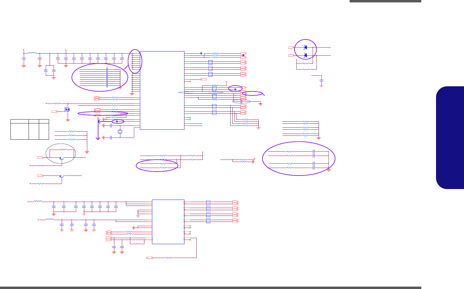
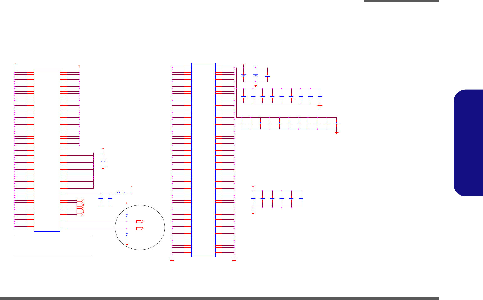
Schematic Diagrams
B-1
B.Schematic Diagrams
Appendix B:Schematic Diagrams
This appendix has circuit diagrams of the M660SE/M665SE notebook’s PCB’s. The following table indicates where to
find the appropriate schematic diagram.
Diagram - Page Diagram - Page Diagram - Page
SYSTEM BLOCK DIAGRAM - Page B - 2 VT8237A-1 - Page B - 16 CHARGER, DC IN - Page B - 30
CLOCK GENERATOR - Page B - 3 VT8237A-2 - Page B - 17 1.05VS, 1.5V, 2.5VS - Page B - 31
CPU-1 - Page B - 4 VT8237A-3 - Page B - 18 VCORE - Page B - 32
CPU-2 - Page B - 5 HDD & CDROM - Page B - 19 1.8V, 0.9VS - Page B - 33
VN896-1 - Page B - 6 CARD READER - Page B - 20 VDD3, VDD5 - Page B - 34
VN896-2 - Page B - 7 NEW CARD SOCKET - Page B - 21 EXT GPU 1.0VS/1.2VS - Page B - 35
VN896-3 - Page B - 8 LAN - Page B - 22 HOTKEY LT BOARD - Page B - 36
VN896-4 - Page B - 9 USB & CCD - Page B - 23 PWR HOT BOARD - Page B - 37
DDR2-1 - Page B - 10 HITACHI H8 - Page B - 24 AUDIO & MODEM BOARD - Page B - 38
DDR2-2 - Page B - 11 CRT & LVDS - Page B - 25 CLICK BOARD - Page B - 39
VGA G72M-1 - Page B - 12 CPU FAN, LPC ROM - Page B - 26 USB BOARD - Page B - 40
VGA G72M-2 - Page B - 13 MINI-PCI & BLUETOOTH - Page B - 27 FINGERPRINT BOARD - Page B - 41
VGA G72M-3 - Page B - 14 AUDIO VT1708A/ALC883 - Page B - 28
VGA G72M-4 - Page B - 15 LED - Page B - 29
Table B - 1
Schematic
Diagrams
Version Note
The schematic dia-
grams in this chapter
are based upon ver-
sion 6-7P-M66U7-001.
If your mainboard (or
other boards) are a lat-
er version, please
check with the Service
Center for updated di-
agrams (if required).
Schematic Diagrams
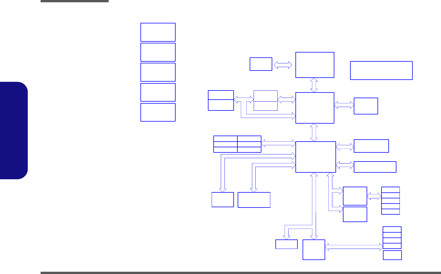
B - 2 SYSTEM BLOCK DIAGRAM
B.Schematic Diagrams
SYSTEM BLOCK DIAGRAM
Sheet 1 of 40
SYSTEM BLOCK
DIAGRAM
AC97
LAN
DEBUGB
PORT
DDR2
SO-DIMM
x2
MDC or
MBC
CCD Camera
LCD
H8 KBC
LPC
X4 DMI
Interface
Yonah 478
AUDIO&MODEM
BOARD
CLICK BOARD
PORT PRT
HOTKEY LT
BOARD
Keyboard
SATA
HDD
LPC
MIC. IN
VT8237A
USB Port 3
CRT
FAN X 1
CD-ROM
(IDE)
VN896
PWR_HOT BOARD
VGA G27M
uFCPGA
ICS953009AF+ICS9P936AF
IMVP-6 VR
CLOCK GEN
Audio
Codec
VT1708
USB 2.0
SOUTH BRIDGE
LINE IN
USB Port 2
SPK. OUT
SPEAKER x2
ULTRA-DMA33/66/100
USB Port 1
FSB667
BATT.X1
FWH
USB BOARD
Touch PAD
PCI
Blue Tooth
SATA
SPDIF
CARD READER
ENE CB714F
M660SU BLOCK DIAGRAM
NORTH BRIDGE
MASTER
LAN
VT6103L
VRAM
Schematic Diagrams
CLOCK GENERATOR B - 3
B.Schematic Diagrams
CLOCK GENERATOR
Sheet 2 of 40
CLOCK
GENERATOR
Q17
*2N3904
B
E C
C437
.01U_16V_04
R540 22_04
C611
.01U _16V_04
C753 .1U_16V_04
Z0201
C758 .1U_16V_04 NC_CLKREQ# 20
PCICLKX4
R304 51.1_1%_04
R556 1K_04
CPU_BSEL03
Z0215
NB_PEXCLK#
C401
.01U_16V_04
R539 0_04
R579 10K_04
M_CLK_DDR#2 9
PCLKPC M 19
3.3VCLK
0
R660 0_06
R284 1K_04
R *4.7K->0 OHM C 33P->*33P
C960125
DK1+
3.3VCLK
C757 .1U_16V_04
C482
1U_10V_06
Z0222
Z0219
1.8VBFR
Z0211
C762 22P_50V_04
C458
.01U_16V_04
R576 22_04
3.3VS
C617
.1U_50V_06
M_CLK_DDR#0 10
R314 1K_04
0
VGA_PEXCLK 11
DK0+
3.3VS
D20 *RB751V
AC
133
HCLK-_
PCLK_FWH
FS1
APICCLK1 DEL
R659 C745 DEL
C960125
M_CLK_DDR#3 9
C700
10U_10V_08
C478
1U_10V_06
MCLKOC6
PM_STPCPU#16
Z0206 R315 51.1_1%_04
FS0
-PCI_STOP
KBCPCLK
C754 .1U_16V_04
33
DK3+
VGA_PEXCLK
NB_PEXCLK
3.3VS
Z0226
R321 10K_04
R307 51.1_1%_04
KBC_PCLK ADD 22OHM 22PF
FOR EMI 951124
3.3VS
Z0202
PCI
Z0203
-PCI_STOP
C397 27P_50V_06
C398 27P_50V_06
Z0218
R561 *1K_04
M_CLK_DDR0 10
Z0210
PCLKMPCI
GCLK_NB 7
FS1
R298 10K_04
R113 0_04
R294 51.1_1%_04
1
Z0208
R571 22_04
RN23 22_4P2R_041
23
4
NB_PEXCLK#
R283 10K_04
R274 475_1%_06
166
HCPUCLK-
3.3VCLK
CLK_USB4815
Z0209
R681 22_04
R658 0_06
M_CLK_DDR3 9
C589
10U_10V_08
R653 10K_04
KBC_PCLK 23
33
RN22 33_4P2R_041
2 3
4
GCLK_NB
1.5VS
GUICK8
3V66_0
U33 PIN1,3,10,16,22,26,39,45,49
ADD .1UF FOR EMI 951124
CLK_PCIE_NC#
FB18
HCB2012KF-121T30_08
C410
.01U_16V_04
200
SPC LK 17
RN18 22_4P2R_04
1
2 3
4
C599
.01U_16V_04
C756 .1U_16V_04
R657 0_06
SEL24_48
-CPU_STOP
DK1-
PCICLKX2
VGA_PEXCLK#
C746 *33P_50V_06
C699
*22P_50V_06
R289 10K_04
MCLKIT6
NB_PEXCLK# 7
DK2+
FS0
M_CLK_DDR2 9
C761 .1U_16V_04
CPU
Z0212
FB17
HCB2012KF-121T30_08
C116
*5P_50V_06
PM_STPPCI#16
MCLKITP
NB_PEXCLK
RN19 22_4P2R_04
1
2 3
4
R566 10K_04
APICCLK1 DEL
R562 DEL
C960125
SMB_SBDATA9,10,11,16
3.3VCLK
3.3VCLK
R577 22_04
R542 22_04
1
3.3VCLK
Z0207
3.3VCLK
MOD E
Z0227
33
R290 1K_04
FS3
C605
.01U _16V_04
NEW CARD hot plug NG
C960124
CLK_PCIE_NC# 20
VCLK_SB
U29
ICS9P956FLF-T
10
21
27
1
9
28
2
16
15
312
5
7
13
18
20
24
6
8
14
17
19
23
11
26
25
4
22
VDD2.5/1.8-0
VDD2.5/1.8-1
VDD2.5/1.8-2
AVD D 2.5-0
GND
GND
AGN D
SDATA
SCLK
BUF_IN T FB_OUTC
DDRT0
DDRT1
DDRT2
DDRT3
DDRT4
DDRT5
DDRC0
DDRC1
DDRC2
DDRC3
DDRC4
DDRC5
FB_OUTT
AVD D 2.5-1
AGN D
BUF_IN C
GND
CPU_BSEL13
PCLKMPC I 26
C743 *33P_50V_06
3.3VCLK
Z0221
SMB_SBDATA9,10,11,16
FS2
RN16 22_4P2R_04
1
2 3
4
R568 10K_04
1
C755 .1U_16V_04
C612
.01U_16V_04
DK2-
CLK_PCIE_NC#
R572 0_04
1
C759 .1U_16V_04
R703 22_04
FS1
Z0213
FS4
VGA_PEXCLK#
RN24 22_4P2R_041
2 3
4
PCLK_F W H 25
VCLK_SB 17
CLK_PWRGD
R475 0_04
C747 *33P_50V_06
R291 1K_06
BSEL0
Z0217
RN21 33_4P2R_041
2 3
4
Z0214
CLK_PCIE_NC
F0122-03
CLK_MCH_BCLK 5
3.3VCLK
FB22
HCB2012KF-121T30_08
RN25 22_4P2R_041
2 3
4
R310 51.1_1%_04
R280 51.1_1%_04
SIO_OSC16
PCICLK6->TP
951107
1.5VS
GCLK_NB
C590
10U_10V_08
R661 0_06
1.8V
MCLKOT6
SMB_SBCLK9,10,11,16
Y1
14.318MHZ
12
BSEL0,1 CHANGE 951101
FS0
Z0204
3.3VS
R547 10K_04
DK0-
C115
*5P_50V_06
R549 22_04
CLKEN#31
R541 0_04
Z0223
C610
.01U_16V_04
R268 1K_06
RN26 22_4P2R_041
23
4
NB_PEXCLK 7
FS3
Z0224
U33
ICS953009AFLF-T
48
10
17
6
11
18
28
32
30
2
21
22
29
26
25
7
9
27
40
3
39
12
13
14
15
16
19
20
1
45
56
55
52
49
23
24
4
5
8
44
43
42
41
38
37
36
35
34
33
31
54
53
51
50
47
46
SDATA
VDDPCI_1
PCICLK4
X1
**FSL2/PCICLK_F0
PCICLK5
**F S4/3V66_1
GNDPCIEX
GND3V66
GND
Reset#
VDD48
3V66_0
VDD3V66
GND48
X2
VttPWR_GD/PD#
**ITP_EN/3V66_2F_2X
GNDPCIEX
VDDREF
VDDPCIEX_1
**FS3/PCICLK1_2X
**TB_EN/PCICLK2
PCICLK3
GNDPCI
VDDPCI_2
GNDPCI
PCICLK6/*Turbo#
VDDA
VDDPCIEX_2
GND
IREF
GNDCPU
VDDCPU
**Mode0/48MHz
*Sel24_48#/24_48MHZ
**FSL0/REF0
FSL1/REF1
GNDREF
PCIEXT1
PCIEXC1
PCIEXT2
PCIEXC2
PCIEXT3
PCIEXC3
PCIEXT4/PEREQ1#*
PCIEXC4/PEREQ2#*
PCIEXT5/CPU_STOP#*
PCIEXC5/PCI_PCIEX_STOP#*
SCLK
CPUCLKT0_F
CPUCLKC0_F
CPUCLKT1
CPUCLKC1
CPUCLKT2_ITP/PCIEXT0
CPUCLKC2_ITP/PCIEXC0
266
DK3-
FS2
R319 22_04
M_CLK_DDR1 10
R473 0_04
R292 51.1_1%_04
C431
.01U_16V_04
PCICLK3 -> KBC_PCLK
951107
Z0216
CLK_RESET
R299 51.1_1%_04
C444
.01U_16V_04
R302 51.1_1%_04
HCLK+_
VGA_PEXCLK
C614
4.7U_6.3V_06
C703
22U _10V_12
R301 10K_04
BSEL1
MOD E
R711 0_04
3.3VCLK
CLK_MCH_BCLK# 5
CPU_CLK- 3
Z0220
3.3VCLK
VGA_PEXCLK# 11
PCLK_TPM 20
-CPU_STOP
CLK_PCIE_NC
D21 *RB751V
AC
3.3VS
Z0205
C595
4.7U_6.3V_06
0
BSEL0
BSEL1
R287 51.1_1%_04
Q19
2N7002W
G
DS
C744 *33P_50V_06
RN27 22_4P2R_041
2 3
4
33
1.8V
RN17 22_4P2R_04
1
23
4
CLK_PCIE_NC 20
C107
.01U_16V_04
SMB_SBCLK9,10,11,16
FS4
Q18
2N 3904
B
E C
R118 *100_04
PCLKMPCI
C760 .1U_16V_04
R546 0_04
C701
10U_10V_08
0
CPU_CLK+ 3
M_CLK_DDR#1 10
HCPUCLK+
C472
.01U_16V_04
C603
1U_10V_06
C422
.01U_16V_04
3.3VC LK
ADD *D20,*D21
951124
F122095
Schematic Diagrams
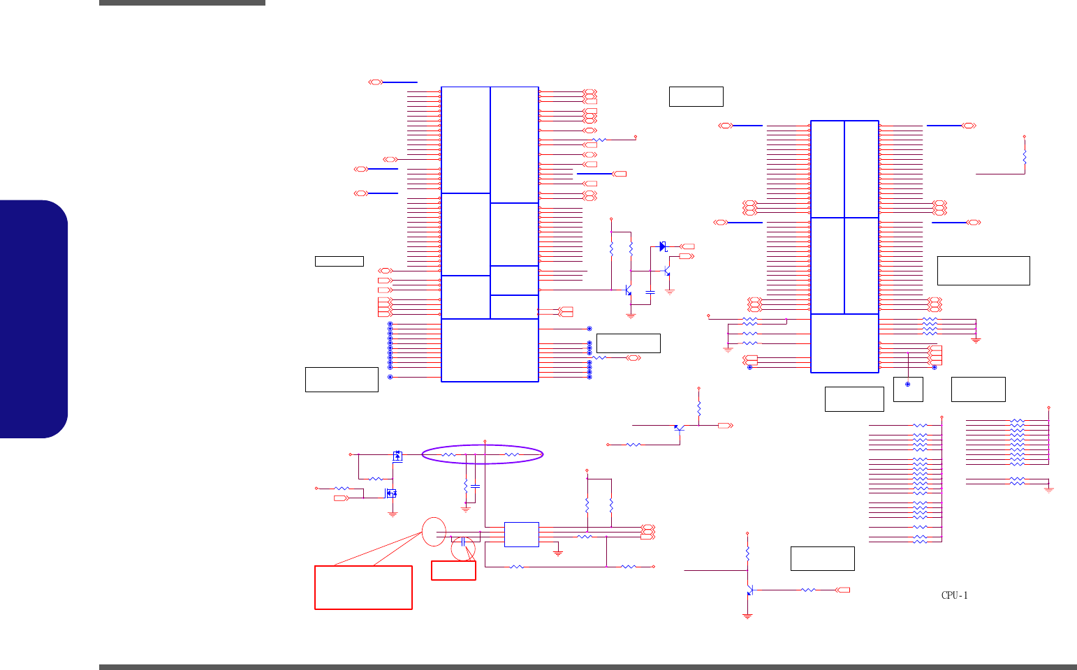
B - 4 CPU-1
B.Schematic Diagrams
CPU-1
VDD3
TP_A34#
H_D#51
H_D#49
H_D#31
R83 150_1%_04
Layout note: no stub
on H_STPCLK TP
H_REQ#1
H_REQ#2
XDP_DBRESET#
H_A#29
H_STPCLK#
H_A#5
TP_SPARE0
H_D#[63:0]
H_DINV#15
TP_EXTBREF R483 2K_1%_06
CPU_DPRSTP#
H_D#15
H_D#2
D10 SCS751V-40
A C
H_REQ#1
H_A#4
H_RS#[2:0] 5 XDP_DBRESET#
H_D#58
3.3V
H_D#47
H_D#18
Comp1,3 connect with Zo=55ohm,make
trace length shorter than 0.5"
A#[32-39], APM#[0-1]:
H_DSTBP#3 5
H_INIT#
H_D#40
H_A#27
H_CPURST#
H_TRDY#
TP_APM0#
TP_A32#
H_D#44
H_D#[63:0]
H_RS#2
R470 *0_04
H_DPSLP# 17
CPU_BSEL0
H_CPURST#
CPU_FERR#
H_REQ#0
R86
10K_06
Near to
ADM1032
VDD3
H_A#3
TP3F1
R89 150_1%_04
H_ADSTB#15
H_A#23
TP_A35#
XDP _ BPM# 0
H_A#14
R460
100K_04
Q38
NDS352
G
DS
R115 100_04
PM_THRMTRIP#
H_A#26 XDP _TD O
R79
10K_06
CPU_DPRSTP#
XDP _ BPM#4
H_DPWR# 5
H_D#[63:0]
TP_APM1#
XDP _ TCK
R467 56_04
R148 54.9_1%_06
H_DINV#2 5
TP_SPARE4
H_D#42
H_A#9
H_D#48
H_RS#1
THERMTRIP# 33
XDP _ TDI
H_A#18
PSI#
H_D#23
R472 *1K_06
H_DSTBN#2 5
H_A#7
H_DPSLP#
H_D#24
H_D#45
H_RS#[2:0]
F070395
H_ADSTB#05
TP_A37#
H_D#4
R95 150_1%_04
1.05VS
H_DSTBP#15
H_D#11
XDP_TRST#
H_BNR# 5
Z0302
H_A#6
CPU_BSEL12
XDP _ TMS
Z0306
CPU_BSEL02
H_A#20
H_D#36
COMP0
TP_SPARE3
CPU_FERR#
XDP_TRST#
R82
680_1%_04
R484 1K_1%_06
Place Series
Resistor on
H_PWRGD_XDP Without
stub
1.05VS
H_D#34
H_D#59
H_D#12
H_A#13
H_DBSY# 5
ASTB0 5
H_D#14
H_SMI#17
H_CPUSLP#
XDP _ BPM#0
H_SMI#
H_D#46
H_D#50
R155 51_1%_06
CPU_CLK- 2
H_D#39
H_D#25
H_NMI17
H_D#1
H_INTR
CPU_DPRSTP#
Layout:Connect test
point TP3F1 with no
atub
SMD_THERM 23
H_REQ#3
H_D#54
XDP _ BPM#3
H_D#53
H_D#63
R154 75_06
H_IGNNE#
H_NMI
H_A#17
H_D#55
XDP _ BPM#1
H_A#[31:3]5
H_THERMDA
R98 150_1%_04
Q11
2N3904
B
E C
XDP _ TCK
Z0310
PM_THRMTRIP# should
connect to ICH7 and GMCH
without T-ing(No STUB)
H_A#[31:3]5
H_NMI
H_DPSLP#
H_A20M#
MISC
DATA GRP3 DATA GRP2
DATA GRP0 DATA GRP1
BGA1B
Yonah Ball-out
E22
F24
E26
H22
F23
G25
E25
E23
K24
G24
J24
J23
H26
F26
K22
H25
H23
G22
J26
N22
K25
P26
R23
L25
L22
L23
P25
M23
P22
P23
T24
R24
L26
T25
N24
M24
N25
AD26
C26
B22
D25
B23
AA23
C21
AB24
V24
V26
W25
U23
U25
U22
AB25
W22
Y23
AA26
Y22
Y26
AC26
AA24
W24
V23
Y25
AC22
AC23
AB22
AA21
AB21
AC25
AD20
AE22
AF23
AD24
AE21
AD21
AE25
AF25
AF22
AF26
AD23
AE24
AC20M26
U26
U1
V1
E5
B5
D24
R26
D6
D7
AE6
D[0]#
D[1]#
D[2]#
D[3]#
D[4]#
D[5]#
D[6]#
D[7]#
D[8]#
D[9]#
D[10]#
D[11]#
D[12]#
D[13]#
D[14]#
D[15]#
DSTBN[0]#
DSTBP[0]#
DINV[0]#
D[16]#
D[17]#
D[18]#
D[19]#
D[20]#
D[21]#
D[22]#
D[24]#
D[23]#
D[25]#
D[26]#
D[27]#
D[28]#
D[29]#
D[30]#
D[31]#
DSTBN[1]#
DSTBP[1]#
GTLREF
TEST1
BSEL[0]
TEST2
BSEL[1]
D[32]#
BSEL[2]
D[33]#
D[34]#
D[35]#
D[36]#
D[37]#
D[38]#
D[39]#
D[40]#
D[41]#
D[42]#
D[43]#
D[45]#
D[44]#
D[46]#
D[47]#
DSTBN[2]#
DINV[2]#
DSTBP[2]#
D[48]#
D[49]#
D[50]#
D[51]#
D[52]#
D[53]#
D[54]#
D[55]#
D[56]#
D[57]#
D[58]#
D[59]#
D[60]#
D[61]#
D[62]#
D[63]#
DSTBN[3]#
DSTBP[3]#
DINV[3]#DINV[1]#
COMP[1]
COMP[2]
COMP[3]
DPRSTP#
DPSLP#
DPWR#
COMP[0]
PWRGOOD
SLP#
PSI#
R91 150_1%_04
H_D#[63:0]5
XDP _ TMS
TP_SPARE2
H_DRDY# 5
H_D#29
R75 10K_06
H_FERR# 17
XDP _ TDO
R94 150_1%_04
R120 220_06
H_D#56
PM_THRMTRIP#
Z0313
R131 27.4_1%_06
R87 *51_1%_06
NO_STUFF
1.05VS
H_DSTBN#3 5
H_RS#0
H_PROCHOT#
Please testpoint on
H_IERR# with a GND
0.1" away
H_A#[31:3] H_HIT# 5
TP_A33#
H_A#28
H_A#15
THERM_ALERT# 23
H_TRDY# 5
R465
4.7K_04
H_REQ#3
TP_SPARE6
Z0303
Q39
2N7002W
G
DS
1.05VS
H_CPUSLP# 5,17
R462
100K_04
H_PWRGD 17
R116 100_04
IN-Target Probe
SMC_THERM 23
H_D#19
H_CPURST#
Q10
2N3904
B
E C
H_D#38
H_D#9
H_INTR
C587
10U_10V_08
R92 150_1%_04
H_D#32
H_A#22
H_A#21
H_PROCHOT#
R93 150_1%_04
THER M_RST#23
ALL_PWROK 15,17,24
H_THERMDC
Z0308
R464
4.7K_04
H_A#8
H_A#12
H_A#19
R74 51_1%_06
Q12
2N3904
B
E C
1.05VS
XDP _ BPM#2
H_D#21
H_A20M#
R652 *0_06
10 MILE
Leave ascape routing on for
future functionality
H_STPCLK#17
H_D#17
H_A#24
H_A#16
H_D#8
C62
10U_10V_08
H_REQ#[4:0]5H_CPURST# 5
H_DSTBP#05
TP_SPARE7
COMP1
Z0305
R73 1K_06
10 MILE
H_A#10
H_REQ#4
RESERVED
HCLK THERM XDP/ITP SIGNALS CONTROL
ADDR GROUP1
ADDR GROUP0
BGA1A
Yonah Ball-out
J4
L4
M3
K5
M1
N2
J1
N3
P5
P2
L1
P4
R1
P1
L2
K3
H2
K2
J3
L5
Y2
U5
R3
W6
U4
Y5
U2
R4
T5
T3
W3
W5
Y4
W2
Y1
V4
A6
A5
C4
D5
C6
B4
A3
AA1
AA4
AB2
AA3
M4
N5
T2
V3
B2
B25
C3
H1
E2
G5
H5
F21
E1
F1
D20
B3
H4
B1
F3
F4
G3
G2
G6
E4
AD4
AD3
AD1
AC4
AC2
AC1
AC5
AA6
AB3
AB5
AB6
C20
D21
A24
A25
C7
A22
A21
T22
D2
F6
D3
C1
AF1
D22
C23
C24
A[3]#
A[4]#
A[5]#
A[6]#
A[7]#
A[8]#
A[9]#
A[10]#
A[11]#
A[12]#
A[13]#
A[14]#
A[16]#
A[15]#
ADSTB[0]#
REQ[0]#
REQ[1]#
REQ[2]#
REQ[3]#
REQ[4]#
A[17]#
A[18]#
A[19]#
A[20]#
A[21]#
A[22]#
A[23]#
A[24]#
A[25]#
A[26]#
A[27]#
A[28]#
A[29]#
A[30]#
A[31]#
ADSTB[1]#
A20M#
FERR#
IGNNE#
STPCLK#
LINT0
LINT1
SMI#
RSVD[01]
RSVD[02]
RSVD[03]
RSVD[04]
RSVD[05]
RSVD[06]
RSVD[07]
RSVD[08]
RSVD[09]
RSVD[11]
RSVD[10]
ADS#
BNR#
BPRI#
DEFER#
DRDY#
DBSY#
BR0#
IERR#
INIT#
LOCK#
RESET#
RS[0]#
RS[1]#
RS[2]#
TRDY#
HIT#
HITM#
BPM[0]#
BPM[1]#
BPM[2]#
BPM[3]#
PRDY#
PREQ#
TCK
TDI
TDO
TMS
TRST#
DBR#
PROCH OT#
THERMDA
THERMDC
THERMTRIP#
BCLK[0]
BCLK[1]
RSVD[12]
RSVD[13]
RSVD[14]
RSVD[15]
RSVD[16]
RSVD[17]
RSVD[18]
RSVD[19]
RSVD[20]
H_INTR17 CPU_CLK+ 2
H_A#31
H_THERMDA
Z0301
20 MILE
H_ADS# 5
TP_SPARE5
H_D#30
H_REQ#[4:0]
H_INIT# 17
R158 51_1%_06
U28
ADM1032ARM
8
7
6
54
3
2
1SCLK
SDATA
ALERT#
GNDTHER M#
D-
D+
VDD
R117 100_04
R474 51_1%_06
3.3V
H_D#[63:0]5
H_BPRI# 5
H_D#33
THM_VDD
H_A20M#17
H_DEFER# 5
H_D#5
Layout Note:
Route H_THERMDA and
H_THERMDC on same layer.
10 mil trace on 10 mil
spacing.
PM_DPRSLPVR 17,31
H_D#3
H_STPCLK#
R80 *51_1%_06 R151 54.9_1%_06
R84 150_1%_04
3.3VS
H_D#27
R133 27.4_1%_06
R96 150_1%_04
C586 1000P_50V_06
TP_A36#
H_D#7
R135 54.9_1%_06
H_PWRGD
CPU_BSEL1
CPU_FERR#
H_D#[63:0]
H_DINV#05
XDP _ BPM#5
COMP2
H_D#43
R471 0_06 XDP _ BPM# 5
R114 51.1_1%_04
R150 51_1%_06
R81
680_1%_04
Q13
2N3904
B
E C
R461 10K_04
H_D#35
H_SMI#
TP_SPARE1
R157 54.9_1%_06
R90 200_1%_04
H_CPUSLP#
Layout note:
H_IGNNE#17
H_REQ#0
XDP _ TDI
R152 54.9_1%_06
H_D#57
Z0307
TP_HEPLL
R463 0 ->*0 R471 *0 -> 0
C960125
1.05VS
H_D#16
R149 54.9_1%_06
R130 54.9_1%_06
H_D#[63:0] 5
H_D#62
R85 51_1%_06
H_A#30
Z0304
TP_A38#
R463 *0_04
Layout note:Zo=55ohm,0.5"
max for GTLREF
VCORE
Z0312
H_A#25
H_A#[31:3]
R466
150_1%_04
R156 51_1%_06
H_D#0
H_DSTBN#15
H_D#60
H_D#22
COMP3
TP_A39#
H_BREQ#0 5
XDP _ BPM# 4
H_D#10
R468 0_04
THM_VDD
H_D#28
H_D#6
H_D#13
H_A#11
H_D#41
1.05VS
H_DINV#3 5
H_LOCK# 5
XDP _ BPM# 1
H_D#52
Comp0,2 connect with Zo=27.4ohm,make
trace length shorter than 0.5"
H_IGNNE#
H_INIT#
H_REQ#2
R153 51_1%_06
C36 ->1000P
H_HITM# 5
H_DSTBP#2 5
H_THERMDC
XDP _ BPM# 2
H_D#37
H_D#26
H_D#[63:0] 5
H_DPWR#
H_D#61
XDP _ BPM# 3
R469 10K_04
H_DSTBN#05
Z0311
H_D#20
R88 150_1%_04
Sheet 3 of 40
CPU-1
Schematic Diagrams
CPU-2 B - 5
B.Schematic Diagrams
CPU-2
Sheet 4 of 40
CPU-2
Route VCCSENSE and VSSSENSE trace
at 27.4 ohms with 50mil spacing.
+
C624
*10U_10V_08
C600
22U_10V_12
C117
.1U_50V_06
C110
22U_10V_12
PLEASE NEAR CPU
C109
22U_10V_12
H_VID0 31
C585
22U_10V_12
C588
10U_10V_08
VSSSENSE 31
C112
.1U_50V_06
BGA1D
Yonah Ball-out
A4
A8
A11
A14
A16
A19
A23
A26
B6
B8
B11
B13
B16
B19
B21
B24
C5
C8
C11
C14
C16
C19
C2
C22
C25
D1
D4
D8
D11
D13
D16
D19
D23
D26
E3
E6
E8
E11
E14
E16
E19
E21
E24
F5
F8
F11
F13
F16
F19
F2
F22
F25
G4
G1
G23
G26
H3
H6
H21
H24
J2
J5
J22
J25
K1
K4
K23
K26
L3
L6
L21
L24
M2
M5
M22
M25
N1
N4
N23
N26
P3
P6
P21
P24
R2
R5
R22
R25
T1
T4
T23
T26
U3
U6
U21
U24
V2
V5
V22
V25
W1
W4
W23
W26
Y3
Y6
Y21
Y24
AA2
AA5
AA8
AA11
AA14
AA16
AA19
AA22
AA25
AB1
AB4
AB8
AB11
AB13
AB16
AB19
AB23
AB26
AC3
AC6
AC8
AC11
AC14
AC16
AC19
AC21
AC24
AD2
AD5
AD8
AD11
AD13
AD16
AD19
AD22
AD25
AE1
AE4
AE8
AE11
AE14
AE16
AE19
AE23
AE26
AF3
AF6
AF8
AF11
AF13
AF16
AF19
AF21
AF24
VSS[001]
VSS[002]
VSS[003]
VSS[004]
VSS[005]
VSS[006]
VSS[007]
VSS[008]
VSS[009]
VSS[010]
VSS[011]
VSS[012]
VSS[013]
VSS[014]
VSS[015]
VSS[016]
VSS[017]
VSS[018]
VSS[019]
VSS[020]
VSS[021]
VSS[022]
VSS[023]
VSS[024]
VSS[025]
VSS[026]
VSS[027]
VSS[028]
VSS[029]
VSS[030]
VSS[031]
VSS[032]
VSS[033]
VSS[034]
VSS[035]
VSS[036]
VSS[037]
VSS[038]
VSS[039]
VSS[040]
VSS[041]
VSS[042]
VSS[043]
VSS[044]
VSS[045]
VSS[046]
VSS[047]
VSS[048]
VSS[049]
VSS[050]
VSS[051]
VSS[052]
VSS[053]
VSS[054]
VSS[055]
VSS[056]
VSS[057]
VSS[058]
VSS[059]
VSS[060]
VSS[061]
VSS[062]
VSS[063]
VSS[064]
VSS[065]
VSS[066]
VSS[067]
VSS[068]
VSS[069]
VSS[070]
VSS[071]
VSS[072]
VSS[073]
VSS[074]
VSS[075]
VSS[076]
VSS[077]
VSS[078]
VSS[079]
VSS[080]
VSS[081]
VSS[082]
VSS[083]
VSS[084]
VSS[085]
VSS[086]
VSS[087]
VSS[088]
VSS[089]
VSS[090]
VSS[091]
VSS[092]
VSS[093]
VSS[094]
VSS[095]
VSS[096]
VSS[097]
VSS[098]
VSS[099]
VSS[100]
VSS[101]
VSS[102]
VSS[103]
VSS[104]
VSS[105]
VSS[106]
VSS[107]
VSS[108]
VSS[109]
VSS[110]
VSS[111]
VSS[112]
VSS[113]
VSS[114]
VSS[115]
VSS[116]
VSS[117]
VSS[118]
VSS[119]
VSS[120]
VSS[121]
VSS[122]
VSS[123]
VSS[124]
VSS[125]
VSS[126]
VSS[127]
VSS[128]
VSS[129]
VSS[130]
VSS[131]
VSS[132]
VSS[133]
VSS[134]
VSS[135]
VSS[136]
VSS[137]
VSS[138]
VSS[139]
VSS[140]
VSS[141]
VSS[142]
VSS[143]
VSS[144]
VSS[145]
VSS[146]
VSS[147]
VSS[148]
VSS[149]
VSS[150]
VSS[151]
VSS[152]
VSS[153]
VSS[154]
VSS[155]
VSS[156]
VSS[157]
VSS[158]
VSS[159]
VSS[160]
VSS[161]
VSS[162]
C113
.1U_50V_06
C619
22U_10V_12
C60
22U_10V_12
C620
22U_10V_12
BGA1C
Yonah Ball-out
A7
A9
A10
A12
A13
A15
A17
A18
A20
B7
B9
B10
B12
B14
B15
B17
B18
B20
C9
C10
C12
C13
C15
C17
C18
D9
D10
D12
D14
D15
D17
D18
E7
E9
E10
E12
E13
E15
E17
E18
E20
F7
F9
F10
F12
F14
F15
F17
F18
F20
AA7
AA9
AA10
AA12
AA13
AA15
AA17
AA18
AA20
AB9
AC10
AB10
AB12
AB14
AB15
AB17
AB18
AF18
AF17
AF15
AF14
AF12
AF10
AF9
AE20
AE18
AE17
AE15
AE13
AE12
AE10
AD18
AE9
AD17
AD15
AD14
AD12
AD10
AD9
AD7
AC18
AC17
AC15
AC13
AC12
AC9
AC7
AB7
AB20
AF20
V6
G21
J6
K6
M6
J21
K21
M21
N21
N6
R21
R6
T21
T6
V21
W21
B26
AD6
AF5
AE5
AF4
AE3
AF2
AE2
AF7
AE7
VCC[001]
VCC[002]
VCC[003]
VCC[004]
VCC[005]
VCC[006]
VCC[007]
VCC[008]
VCC[009]
VCC[010]
VCC[011]
VCC[012]
VCC[013]
VCC[014]
VCC[015]
VCC[016]
VCC[017]
VCC[018]
VCC[019]
VCC[020]
VCC[021]
VCC[022]
VCC[023]
VCC[024]
VCC[025]
VCC[026]
VCC[027]
VCC[028]
VCC[029]
VCC[030]
VCC[031]
VCC[032]
VCC[033]
VCC[034]
VCC[035]
VCC[036]
VCC[037]
VCC[038]
VCC[039]
VCC[040]
VCC[041]
VCC[042]
VCC[043]
VCC[044]
VCC[045]
VCC[046]
VCC[047]
VCC[048]
VCC[049]
VCC[050]
VCC[051]
VCC[052]
VCC[053]
VCC[054]
VCC[055]
VCC[056]
VCC[057]
VCC[058]
VCC[059]
VCC[060]
VCC[061]
VCC[062]
VCC[063]
VCC[064]
VCC[065]
VCC[066]
VCC[067]
VCC[099]
VCC[098]
VCC[097]
VCC[096]
VCC[095]
VCC[094]
VCC[093]
VCC[092]
VCC[091]
VCC[090]
VCC[089]
VCC[088]
VCC[087]
VCC[086]
VCC[084]
VCC[085]
VCC[083]
VCC[082]
VCC[081]
VCC[080]
VCC[079]
VCC[078]
VCC[077]
VCC[076]
VCC[075]
VCC[074]
VCC[073]
VCC[072]
VCC[071]
VCC[070]
VCC[069]
VCC[068]
VCC[100]
VCCP[01]
VCCP[02]
VCCP[03]
VCCP[04]
VCCP[05]
VCCP[06]
VCCP[07]
VCCP[08]
VCCP[09]
VCCP[10]
VCCP[11]
VCCP[12]
VCCP[13]
VCCP[14]
VCCP[15]
VCCP[16]
VCCA
VID[0]
VID[1]
VID[2]
VID[3]
VID[4]
VID[5]
VID[6]
VCCSENSE
VSSSENSE
C132
.1U_50V_06
C584
22U_10V_12
S17
S1
2 1
S16
S1
2 1
H_VID3 31
C131
22U_10V_12
H_VID5 31
H_VID6 31
C594
*10U_10V_08
H_VID1 31
C59
22U_10V_12
+
C608
330U_3V_D
C602
22U_10V_12
C58
22U_10V_12
Z0401
VCCSENSE 31
1.5VS
C621
22U_10V_12
H_VID4 31
VCORE
C130
22U_10V_12
C129
22U_10V_12
951128
VCORE VCORE
H_VID2 31
C108
22U_10V_12
C601
22U_10V_12
C181
22U_10V_12
C61
22U_10V_12
Layout Note:
PLEASE NEAR CPU
1.05VS
C118
.1U_50V_06
VCORE
1.05VS
C592
.01U_50V_06
+
C180
*10U_10V_12
C133
.1U_50V_06
place PU and PD winthin 1 inch of CPU
C583
22U_10V_12
L50
HCB1608KF-121T25_06
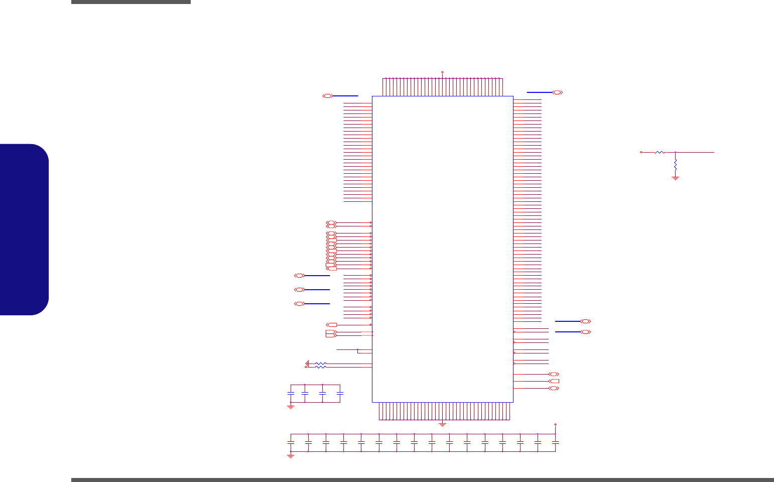
Schematic Diagrams
B - 6 VN896-1
B.Schematic Diagrams
VN896-1
Sheet 5 of 40
VN896-1
H_BREQ#03
H_D#55
H_D#52
H_DSTBP#1
H_A#30
H_D#6
H_D#15
CLK_MCH_BCLK#2
H_A#24
H_D#41
GTLVREF_NB
H_D#11
H_DPWR# 3
H_RS#[2:0]3
H_CPURST#3
1.05VS
H_D#2
H_DSTBP#[3:0]
H_A#11
H_A#17
H_REQ#2
H_A#21
C250
.1U_50V_06
H_ADS#3
H_D#34
H_D#20
H_RS#1
H_D#35
C249
1000P_50V_06
H_BPRI#3
H_DINV#1
H_REQ#[4:0]
C646
.1U_50V_06
H_REQ#[4:0]3
H_CPUSLP# 3,17
H_D#14
H_A#23
H_A#[31:3]
1.05VS
H_D#51
H_REQ#0
H_TRDY#3
C248
.1U_50V_06
R184 180_1%_06
H_D#1
H_A#18
H_D#3
H_D#58
H_DBSY#3
H_LOCK#3
H_A#14
H_D#54
H_A#4
H_A#6
H_A#3
H_D#63
H_D#9
H_D#27
H_A#26
H_D#12
H_RS#2
H_DEFER#3
H_D#23
H_A#12
H_D#59
H_D#19
H_D#33
H_DSTBP#3
H_A#10
H_D#18
H_REQ#1
H_D#16
H_DSTBN#2
H_A#20
H_REQ#3
H_DINV#[3:0]
H_D#38
CLK_MCH_BCLK2
H_D#62
H_REQ#4
H_A#8
H_A#[31:3]3
H_D#47
H_D#4
H_D#46
H_HITM#3
H_DSTBN#[3:0]
H_A#25
H_D#31
H_D#56
H_HIT#3
H_DSTBN#[3:0] 3
H_D#60
H_D#57
ASTB0
H_A#29
H_A#5
H_D#21
H_D#45
H_ADSTB#03
H_D#28
H_D#13
H_D#37
H_D#24
H_D#53
H_D#39
H_A#31
H_BNR#3
H_D#7
H_DINV#3
C219
.01U_50V_06
H_D#30
H_DINV#2
H_D#49
H_A#7
C643
.1U_50V_06
C210
.1U_50V_06
H_RS#0
H_D#5
C263
.1U_50V_06
1.05VS
H_ADSTB#13
H_DSTBN#1
H_D#[63:0] 3
C674
10U_10V_12
C406
10U_10V_12
H_D#32
GTLVREF_NB
C281
.1U_50V_06
H_DSTBP#[3:0] 3
H_A#13
H_D#17
H_A#15
H_D#10
GTLVREF_NB
C273
.1U_50V_06
H_DINV#[3:0]3
H_D#50
H_DSTBP#2
H_DSTBN#3
C645
1000P_50V_06
C229
.01U_50V_06
P4M890_Rev1.9->remove ha32,ha33
P4M900_Rev0.2
P4M900 only -->
P4M890 =>HA32,HA33
BGA5A
VN896
B35
A36
C33
C32
E31
B34
B33
A34
D30
A30
B31
B30
E30
C29
B29
C30
D36
F36
G36
H34
H35
F35
G35
C36
D35
F34
F33
G34
G33
E33
H32
G32
E28
E29
D28
D27
C28
H28
G28
F28
E27
D26
D25
E25
F25
G25
H26
H25
B23
B25
E23
B27
B28
A28
B24
B26
A26
C23
C22
A23
G23
A24
B22
E22
AC29 A32
C35
G26
C24
B32
C34
E26
C25
M33
N34
R33
T33
R34
P36
P34
N35
R36
U36
U34
U35
T30
U32
W35
V32
V36
V34
W36
W34
AA36
V33
AA34
Y35
Y33
AA32
W32
V31
W31
R35
W33
L35
K35
J32
M34
K32
J33
K33
L36
L34
J34
M35
T32
T31
R32
M32
M31
J35
N36
J36
C31
E35
G27
D22
F22
AC30
A17
A18
A19
A20
A21
B17
B18
B19
B20
B21
C17
C18
C19
C20
C21
D17
D18
D19
D20
D21
E17
E18
E19
E20
E21
U30
J25
F17
F18
F19
F20
F21
G17
G18
G19
G20
G21
T35
A1
A2
A8
A10
A22
A25
A27
A29
A31
A33
A35
B2
B3
B4
B36
C2
C3
C4
C5
E6
C26
C27
D3
L31
D4
D5
D6
D8
D11
D23
D24
D29
D31
D32
D34
E2
E4
E5
G22
H22
A3
AB32
HD00#
HD01#
HD02#
HD03#
HD04#
HD05#
HD06#
HD07#
HD08#
HD09#
HD10#
HD11#
HD12#
HD13#
HD14#
HD15#
HD16#
HD17#
HD18#
HD19#
HD20#
HD21#
HD22#
HD23#
HD24#
HD25#
HD26#
HD27#
HD28#
HD29#
HD30#
HD31#
HD32#
HD33#
HD34#
HD35#
HD36#
HD37#
HD38#
HD39#
HD40#
HD41#
HD42#
HD43#
HD44#
HD45#
HD46#
HD47#
HD48#
HD49#
HD50#
HD51#
HD52#
HD53#
HD54#
HD55#
HD56#
HD57#
HD58#
HD59#
HD60#
HD61#
HD62#
HD63#
HCLK+ H DSTB0P#
HDSTB1P#
HDSTB2P#
HDSTB3P#
HDSTB0N#
HDSTB1N#
HDSTB2N#
HDSTB3N#
HA03#
HA04#
HA05#
HA06#
HA07#
HA08#
HA09#
HA10#
HA11#
HA12#
HA13#
HA14#
HA15#
HA16#
HA17#
HA18#
HA19#
HA20#
HA21#
HA22#
HA23#
HA24#
HA25#
HA26#
HA27#
HA28#
HA29#
HA30#
HA31#
HADSTB0P#
HADSTB1#
ADS#
BNR#
BPRI#
BREQ0#
DBSY#
DEFER#
DRDY#
HIT#
HITM#
HLOCK#
HTRDY#
HREQ0#
HREQ1#
HREQ2#
HREQ3#
HREQ4#
RS0#
RS1#
RS2#
HDBI0#
HDBI1#
HDBI2#
HDBI3#
CPURST#
HCLK-
VTT
VTT
VTT
VTT
VTT
VTT
VTT
VTT
VTT
VTT
VTT
VTT
VTT
VTT
VTT
VTT
VTT
VTT
VTT
VTT
VTT
VTT
VTT
VTT
VTT
GTLVREF0
GTLVREF1
VTT
VTT
VTT
VTT
VTT
VTT
VTT
VTT
VTT
VTT
HADSTB0N#
GND
GND
GND
GND
GND
GND
GND
GND
GND
GND
GND
GND
GND
GND
GND
GND
GND
GND
GND
GND
GND
GND
GND
DPWR#
GND
GND
GND
GND
GND
GND
GND
GND
GND
GND
GND
GND
GND
GND
GTLCOMPP
GTLCOMPN
GND
CPUSLPIN#
H_D#40
H_D#22
H_DSTBN#0
C673
10U_10V_12
H_A#19
H_D#61
H_RS#[2:0]
GTLCOMPN
H_D#42
H_D#43
H_D#26
H_DINV#0
C220
.01U_50V_06
H_DSTBP#0
H_A#22
C407
10U_10V_12
ASTB0 3
H_D#[63:0]
R167
100_1%_06
C247
.01U_50V_06
1.05VS
R166 49.9_1%_06
H_D#36
H_A#9
C256
.1U_50V_06
H_D#48
H_A#27
GTLCOMPP
R183 360_1%_06
H_D#8
H_D#44
C697
1U_10V_06
H_D#29
H_A#16
H_DRDY#3
H_D#25
H_D#0
H_A#28
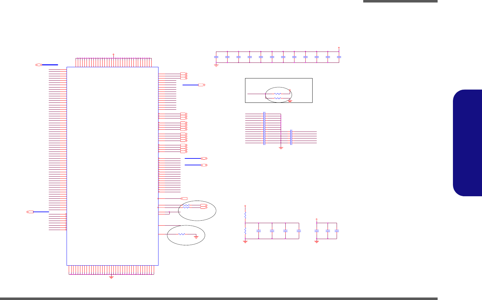
Schematic Diagrams
VN896-2 B - 7
B.Schematic Diagrams
VN896-2
Sheet 6 of 40
VN896-2
M_CKE3 9,10
MD_33
MD_6
C255
.1U_50V_06
C234
.1U_50V_06
MAA7
*
MD_30
R493 *4. 7K_04
951129
M_BA 0
MD_49
MCL KOT 2
M_R AS#
MD_42
MD_53
MD_ [63:0]
MAA1 2
MD_41
R492 4.7K_04
M_W E#
MEMDET SEL:
M_D QS +3
MAA1 1
0603-->0402
MD_38
C282
.1U_50V_06
MD_22
MD_51
M_D QS -3
C266
.1U_50V_06
1.8V
MAA[0:13]
MAA5
951129
M_R AS#
MAA12
M_W E# 9,10
M_ D QS +0 M _D Q S+ [ 0 .. 7 ]
C175
.1U _50V_06
MD_36
MD_37
M_C S0 #
M_W E#
MAA10
C227
1000P_50V_06
MD_1
C145 5P_50V_06
C287
1U_10V_06
M_RAS# 9,10
MD_61
M_C S1 #
BGA5B
VN896
AF35
AG34
AJ36
AK35
AF34
AG35
AJ34
AK34
AG32
AF32
AH30
AJ31
AF31
AH32
AH31
AJ32
AK33
AL36
AP35
AL34
AL35
AM35
AT36
AM34
AK24
AL23
AM24
AJ22
AK23
AN24
AM23
AM22
AK20
AK19
AM19
AR18
AL20
AM20
AL18
AM18
AR17
AT16
AN16
AN15
AM17
AP17
AM16
AM15
AN22
AN21
AP19
AT18
AT21
AR21
AT19
AR19
AR14
AM14
AP13
AR11
AP14
AN14
AT12
AP12
AB34
AB36
AH36
AF30
AN36
AN23
AN20
AT15
AP21
AT13
AT27
AP27
AT24
AP26
AH35
AH34
AP36
AP23
AC24
AD17
AD19
AD21
AT35
AJ28
AK25
AK27
AK29
AL26
AL28
AL30
AM25
AM29
AM31
AN26
AN27
AN31
AN33
AG29
AJ18
AP30
AR26
AA24
AB24
AR33
AN18
AR15
AR20
AR13
AM27
AT25
AT28
AT31
AR30
AR29
AT30
AN30
AP31
AR31
AT32
AP32
AN32
AN29
AR32
AT33
AR25
AR28
AN28
AR27
AP28
AT34
AP34
AR34
AN34
AP29
AT29
AM33
AF36
AB35
AT26
AP25
AR24
AN25
E7
E34
E36
F1
F2
F4
F5
F6
F7
F10
F14
F23
F26
F27
F29
F30
F32
G1
G2
G4
G7
G11
G29
H2
H4
H7
H23
H24
H27
H31
H36
J2
J4
J5
J6
J7
E9
F24
H33
AJ35
AH33
AR36
AR22
AP18
AP15
AP20
AR12
AD23
AD24
AJ26
AP33
AD22
AD20
AD16
AD18
MD00
MD01
MD02
MD03
MD04
MD05
MD06
MD07
MD08
MD09
MD10
MD11
MD12
MD13
MD14
MD15
MD16
MD17
MD18
MD19
MD20
MD21
MD22
MD23
MD24
MD25
MD26
MD27
MD28
MD29
MD30
MD31
MD32
MD33
MD34
MD35
MD36
MD37
MD38
MD39
MD40
MD41
MD42
MD43
MD44
MD45
MD46
MD47
MD48
MD49
MD50
MD51
MD52
MD53
MD54
MD55
MD56
MD57
MD58
MD59
MD60
MD61
MD62
MD63
MCLKI
MCLKO -
DQM0#
DQM1#
DQM2#
DQM3#
DQM4#
DQM5#
DQM6#
DQM7#
CS0#
CS1#
CS2#
CS3#
DQS0-
DQS1-
DQS2-
DQS3-
VCCMEM
VCCMEM
VCCMEM
VCCMEM
VCCMEM
VCCMEM
VCCMEM
VCCMEM
VCCMEM
VCCMEM
VCCMEM
VCCMEM
VCCMEM
VCCMEM
VCCMEM
VCCMEM
VCCMEM
VCCMEM
VCCMEM
MEMVREF0
MEMVREF1
VCCMEM
VCCMEM
VCCMEM
VCCMEM
VCCMEM
DQS4-
DQS5-
DQS6-
DQS7-
VCCMEM
VCCMEM
VCCMEM
VCCMEM
MA01
MA02
MA03
MA04
MA05
MA06
MA07
MA08
MA09
MA10
MA11
MA12
MA13
BA0
SRAS#
SCAS#
SWE#
CKE0
CKE1
CKE2
CKE3
BA1
MA00
DMCOMP
MEMDET
MCLKO+
ODT0
ODT1
ODT2
ODT3
GND
GND
GND
GND
GND
GND
GND
GND
GND
GND
GND
GND
GND
GND
GND
GND
GND
GND
GND
GND
GND
GND
GND
GND
GND
GND
GND
GND
GND
GND
GND
GND
GND
GND
GND
GND
GND
GND
GND
DQS0+
DQS1+
DQS2+
DQS3+
DQS4+
DQS5+
DQS6+
DQS7+
VCCMEM
VCCMEM
VCCMEM
BA2
VCCMEM
VCCMEM
VCCMEM
VCCMEM
C200
.1U_50V_06
M_CKE2 9,10
MD_46
C161 5P_50V_06
MD_54
M_D QS -1
MAA1
M_DM2
M_DM3
C295
.1U_50V_06
M_ODT0 10
MAA1
M_C S2 #
MAA1 0
MAA3
C146 5P_50V_06
C150 5P_50V_06
R173
150_1%_06
M_D QS +2
M_CS0# 10
M_D QS+[0. .7] 9,10
M_C KE0 10
MD_7
C157 5P_50V_06
1.8V
M_D QS -7
MD_[63:0]9,10
MD_58
MD_23
C267
.1U _50V_06
M_D QS -0
M_D QS -2
MAA6
M_DM1
C144 5P_50V_06
MD_26
C142 5P_50V_06
C262
.1U_50V_06
C151 5P_50V_06
C279
1000P_50V_06
MCL KOC 2
MAA4
MAA9
MD_21
MD_32
M_D QS +6
M_D QS +5
0603-->0402
M_BA 0
MD_20
C280
1000P_50V_06
MAA2
MC L KI T
MD_29
M_CS3# 9,10
MD_10 MA A5
C147 5P_50V_06
M_DM4
MD_17
MD_0
951129
M_CS2# 9,10
MD_35
MAA0
MD_59
MD_9
MD_48
MD_45
MD_16
MD_40
MVREF _NB
C630 5P_50V_06
C158 5P_50V_06
MAA2
MD_3
MD_62
M_BA2 9,10
MAA9
MD_47
C152 5P_50V_06
1: DDR2
M_DM7
MD_11
MD_28
MD_50
MD_15
MD_12
MEMDET
1.8V
M_DM[0..7]9,10
MD_13
MD_34
M_ODT2 9,10
M_D QS -4
M_D QS +1 M_DQS-[0..7]
M_BA 2
M_C LKO + R490 22_04
MCLKIT 2
M_DQS-[0..7] 9,10
MAA4
C163 5P_50V_06
M_ODT1 10
M_C KE1 10
C259
.1U_50V_06
MAA3
MAA8
M_DM6 C277
1U_10V_06
MD_4
M_BA0 9,10
MD_52
C162 5P_50V_06
MD_14
MAA13
MD_25
MAA8
C205
.1U _50V_06
C174
.1U_50V_06
R176
150_1%_06
MD_63
M_ODT3 9,10
M_D QS +7
C233
.1U_50V_06
MD_43
1.8V
M_C AS#
MAA[0:13] 9,10
MD_55
MCLKIT = DCLKx + 2 "
M_BA1 9,10
1.8V
M_CAS# 9,10
M_DM0
M_D QS +4
Z0601
M_D QS -6
C221
1000P_50V_06
MD_31
MD_18
MD_60
M_CS1# 10
MD_39
M_D M[0..7]
M_BA 2
MVREF_NB
MAA1 3
MCLKO+/- as short as passable
M_D QS -5
MAA6
MD_5
MD_27
C164 5P_50V_06
M_C AS#
MD_24
MD_44
MAA7
M_C LKO -
MAA0
M_BA 1
MEMDET
MD_2
R491 22_04
C149 5P_50V_06
C160 5P_50V_06 M_BA 1
MD_19
C143 5P_50V_06
0: DDR1
C148 5P_50V_06
0603-->0402
M_DM5
C159 5P_50V_06
M_C S3 #
MD_56
MD_8
R494 301_1%_04
MD_57
MAA11
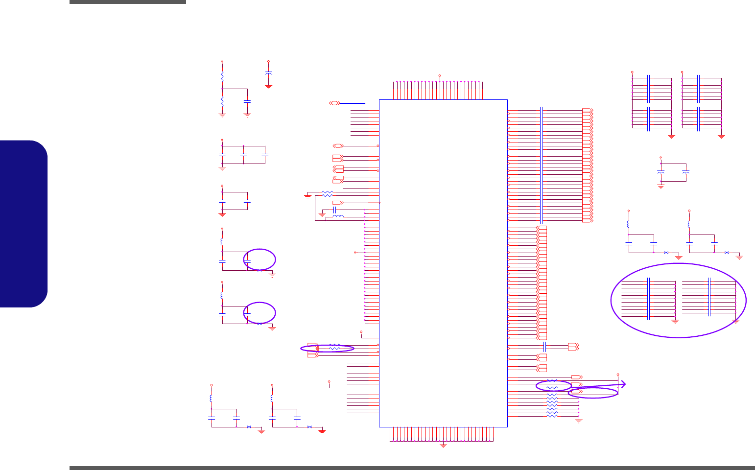
Schematic Diagrams
B - 8 VN896-3
B.Schematic Diagrams
VN896-3
Sheet 7 of 40
VN896-3
TX02-
TX12-
C408
1U_10V_06
1.5V
PE0TX4 11
PE0TX14
PE0R X8
C685 .1U_10V_04
BGA5C
VN896
D1
H1
E1
J1
AL4
B1
C1
AP1
AN3
AT3
AR4
AN2
AN1
AP5
AN4
AT2
AR3
AR1
AT1
AR5
AP4
AL6
AL5
W13
Y13
AA13
AB13
AC13
AJ1
AJ2
AJ3
AJ4
AJ5
AJ6
AN5
T13
U13
V13
AC32
AD29
AD31
AD14
AD13
AD35
AE36
AD36
AD34
R13
M23
M24
N12
N25
P12
P25
R12
T12
T25
U12
U25
V12
W12
W25
Y12
Y25
AA12
AB12
AC31
AD30
AB25
AC12
AC25
AD12
AJ7
N13
N14
P13
AK3
AK4
AK1
AK2
K1
L1
L4
M4
M1
N1
N4
P4
P1
R1
T1
U1
U4
V4
V1
W1
W4
AA1
AB1
AC1
AC4
AD4
AD1
AE1
Y4
E3
D2
F3
G3
H3
J3
K3
L3
K6
L6
M3
N3
M6
N6
P3
R3
T3
U3
T6
U6
V3
W3
W6
V6
Y3
AA3
AA6
AB6
AB3
AC3
AD3
AE3
Y1
AG1
AF1
AF4
AE4
B5
AC34
AG6
AF6
G6
AE6
AH5
H6
AE7
AH6
AH3
AH4
B6
K5
K7
K31
K34
K36
L2
L7
L32
L33
M5
M7
M36
N2
N5
N7
P2
P7
P14
P15
P16
P17
P18
P19
M13
M14
M15
M16
M20
M21
M22
K4
L5
M2
P5
P6
AK5
M12
AM5
P20
AF7
H5
AD7
G5
AD6
AH1
AH2
AC36
AC33
D7
K2
AD15
AK6
AK7
PEXTX01+
PEXTX02+
P E XTX0 1 -
P E XTX0 2 -
VCLK
PEXTX00+
P E XTX0 0 -
VD00
VD01
VD02
VD03
VD04
VD05
VD06
VBE#
UPSTB+
UPSTB-
DNSTB+
DNSTB-
UPCMD
DNCMD
VLVREF
VLCOMPN
VCC33PEX
VCC33PEX
VCC33PEX
VCC33PEX
VCC33PEX
VCC33PEX
VCC33PEX
VCC33PEX
VCC33PEX
VCC33PEX
VCC33PEX
VD07
VCC33PEX
VCC33PEX
VCC33PEX
GNDAHCK
GNDAMCK
VSUS15
VCC15VL
VCC15VL
SUSST#
TESTIN #
RESET#
PWROK
VCC33PEX
VCC15
VCC15
VCC15
VCC15
VCC15
VCC15
VCC15
VCC15
VCC15
VCC15
VCC15
VCC15
VCC15
VCC15
VCC15
VCC15
VCC15
VCC15
VCCA33HCK
VCCA33MCK
VCC15
VCC15
VCC15
VCC15
VCC33PEX
VCC33PEX
VCC33PEX
VCC33PEX
VCC33PEX
VCC33PEX
VCC33PEX
VCC33PEX
PEXTX03+
P E XTX0 3 -
PEXTX04+
P E XTX0 4 -
PEXTX05+
P E XTX0 5 -
PEXTX06+
P E XTX0 6 -
PEXTX07+
P E XTX0 7 -
PEXTX08+
P E XTX0 8 -
PEXTX09+
P E XTX0 9 -
PEXTX10+
P E XTX1 0 -
PEXTX11+
P E XTX1 2 -
PEXTX13+
P E XTX1 3 -
PEXTX14+
P E XTX1 4 -
PEXTX15+
P E XTX1 5 -
P E XTX1 1 -
PEXRX00+/DVP0D11
PEXRX00-/DVP0D10
PEXRX01+/DVP0D09
PEXRX01-/DVP0D08
PEXRX02+/DVP0D07
PEXRX02-/DVP0D06
PEXRX03+/DVP0CLK
PEXRX03-/DVPTVC LKR
PEXRX04+/DVP0D05
PEXRX04-/DVP0D04
PEXRX05+/DVP0D03
PEXRX05-/DVP0D02
PEXRX06+/DVP0D01
PEXRX06-/DVP0D00
P EXR X0 7 +/ D V P 0D E
P EXR X07 -/ D V P0 H S
PEXRX08+/DVP1D11
PEXRX08-/DVP1D10
PEXRX09+/DVP1D09
PEXRX09-/DVP1D08
PEXRX10+/DVP1D07
PEXRX10-/DVP1D06
PEXRX11+/DVP1CLK
PEXRX11-/DVP1D05
PEXRX12+/DVP1D04
PEXRX12-/DVP1D03
PEXRX13+/DVP1D02
PEXRX13-/DVP1D01
PEXRX14+/DVP1D00
P EXR X14 -/ D V P1 D E
P EXR X1 5 +/ D V P 1H S
PEXRX15-/DVP1VS
PEXTX12+
PEXTX16+
P E XTX1 6 -
PEXRX16+
PEXRX16-
PEXDET
PEXWAKE#
PEXCLK+
PEXCLK-
VCCA33PEX0
VCCA33PEX1
VCCA33PEXCK
GNDAPEX0
GNDAPEX1
GNDAPEXCK
VCCA33PEX2
GNDAPEX2
INTR#
GND
GND
GND
GND
GND
GND
GND
GND
GND
GND
GND
GND
GND
GND
GND
GND
GND
GND
GND
GND
GND
GND
GND
VCC15
VCC15
VCC15
VCC15
VCC15
VCC15
VCC15
GND
GND
GND
GND
GND
VCC33PEX
VCC15
VLCOMPP
GND
VSUS15PEX
PEXCOMP0
PEXCOMP1
PEXREXT0
PEXREXT1
PEXCOMP2
PEXREXT2
PEXHPSCI#
PEXPMESCI #
TCSEN #
GND
VCC15VL
VCC33PEX
VCC33PEX
PE0R X1# 11
PE0R X6 11
PE0TX9 11
Z0704
FB2
HCB2012KF-121T30_08
PE0R X4# 11
PE0R X5 11
NB_PEXCLK# 2
PE0TX8# 11
PE0RX1#
L38
HCB1608KF-121T25_06
PEXMESCI# 16
PE0TX10#
PE0TX6#
C358 4.7U_10V_08
NEAR NB(VN800)
TX10+
PE0RX1#
PE0R X12
3.3VS
PEXCOMP2
C318 2.2U_6.3V_06
C413 4.7U_10V_08
PE0TX7# 11
PE0RX3#
PE0RX11#
VLAD5
C657 .1U_10V_04
PE0R X7 11
PE0R X3# 11
PE0TX8 11
PE0RX0#
UPSTB#
PE0TX5#
+
CA1
*330U_6.3V_D
S8 S1
21
C272
.1U_50V_06
PE0TX0# 11
PE0TX4# 11
VCCA33PEX2
C768 *47P_50V_04
C664 .1U_10V_04
C677 .1U_10V_04
1.8V->GND 951101
PEXHPSCI# ADD
PULL 3.3VS
951102
3.3VS
PE0R X12# 11
WAKE 16
PE0TX0 11
PE0TX15 11
PE0TX0
PE0TX2
TX01+ C320 2.2U_6.3V_06
C246
.1U_50V_06
GNDAPEXCK
PE0RX5
C654 .1U_10V_04
PE0TX6 11
Z0702
C393
1U_10V_06
C764 *47P_50V_04
PEXREXT2
TX05-
C676 4.7U_10V_08
R225 340_1%_06
C171
1000P_50V_06
PE0RX3
PE0RX11
TX07+
TX15+
DNSTB#
C317 2.2U_6.3V_06
PE0R X0# 11
PE0R X10# 11
FB15
HCB2012KF-121T30_08
PE0TX7
C656 .1U_10V_04
PE0R X10 11
PE0R X6# 11
UPSTB#17
DNCMD17
PE0TX11# 11
VCCA33PEXCK
C652 .1U_10V_04
TX02+
C167
1000P_50V_06
PE0TX5# 11
PE0TX9# 11
TX12+
C290
.1U_50V_06
C669 4.7U_10V_08
PE0TX1
+
CA2
330U_6.3V_D
1.5VS
PE0TX3 11
VLAD0
PE0TX13 11
PE0TX2 11
LVREF_NB
PE0TX13#
GNDAPEXCK
R220 10.7K_1%_06
PE0R X13 11
TX09-
PE0RX2#
C683 .1U_10V_04
S3 S1
21
SB_PWROK16
VCCA33PEX1
FB16
HCB2012KF-121T30_08
1.5VS
PE0TX11
PM_SUS_STAT#16
PE0R X2# 11
C241 2.2U_6.3V_06
C688 .1U_10V_04
PE0RX1
PE0TX8#
C655 .1U_10V_04
S10 S1
21
C686 .1U_10V_04
C352
1000P_50V_06
PE0TX6# 11
DNSTB
PE0TX4
TX00-
PE0RX1 C767 *47P_50V_04
C414
1000P_50V_06
C690 .1U_10V_04
PE0R X7
PE0R X15# 11
PE0R X8# 11
TX05+
PE0TX10 11
TX14-
PE0R X11#
C775 *47P_50V_04
C672 4.7U_10V_08
C660 .1U_10V_04
C409
1U_10V_06
PE0R X14 11
PE0TX5 11
VLAD6
C261 2.2U_6.3V_06
C691 .1U_10V_04
C666 .1U_10V_04
C776 *47P_50V_04
R671 4.7K_06
VCCA33PEX2
C316 2.2U_6.3V_06
PE0R X9 11
C773 *47P_50V_04
1.5VS
PE0TX1 11
PE0TX13# 11
VLAD[0..7]
C357 4.7U_10V_08
C771 *47P_50V_04
3.3VS
VLAD1
R651 4.7K_06
C689 .1U_10V_04
1.5V
PE0TX2# 11
LCOMPP
PE0TX10
C327 2.2U_6.3V_06
C415
1000P_50V_06
C769 *47P_50V_04
C396 4.7U_10V_08
UPSTB17
PE0R X14# 11
GNDAMCK
TX09+
PE0RX0
NB_PEXCLK 2
PE0RX2#
PE0RX12
AVDD2
GNDAPEX0
R536 10.7K_1%_06
C779 *47P_50V_04
PE0TX2#
PE0TX14#
C681 .1U_10V_04
C662 .1U_10V_04
S12 S1
21
PE0R X0 11
PE0RX4#
TX14+
C663 .1U_10V_04
R543 249_1%_06
PCIE_TXN2_NC 20
PE0RX14
PE0RX2
PE0RX13
PE0RX6#
PE0R X1 11
PE0TX1# 11
C781 *47P_50V_04
C371
.1U_50V_06
1.5VS
UPCMD17
PE0RX6
PE0TX7#
PE0TX4#
TX00+
TX11-
C679 .1U_10V_04
C682 .1U_10V_04
C275
1000P_50V_06
PCIE_TXP2_NC 20
PE0RX0#
C168
22U_10V_12
R495 0_04
PEXCOMP0
C370 4.7U_10V_08
3.3VS
PE0TX7 11
PE0RX8#
PE0RX9#
TX04-
PE0RX6#
C766 *47P_50V_04
R229 270_1%_06
PE0R X9# 11
C778 *47P_50V_04
3.3VS
TX13-
PE0R X12#
C659 .1U_10V_04
C770 *47P_50V_04
C763 *47P_50V_04
VBE#17
PE0TX15#
PE0R X7# 11
PE0TX12#
FB9
HCB2012KF-121T30_08
PE0RX8
GNDAPEX2
UPCMD
PE0RX5
C390
1000P_50V_06
C653 .1U_10V_04
10U->22U 951101
GNDAPEX2
C170
22U_10V_12
VLAD2
C402 4.7U_10V_08
UPSTB
GNDAH CK
R230 10K_06
C354 4.7U_10V_08
R496 0603-->0402
AVDD1
PE0TX8
TES TIN _N B
R214
1K_1%_06
TX08-
C668 .1U_10V_04
PE0R X12 11
PEXCOMP1
PE0RX6
PCI_INTH# 15
C225 2.2U_6.3V_06
PE0RX4
VLAD3
LCOMPN
GNDAPEX1
PE0RX14#
PE0RX12#
Z0701
Z0703
R213
1.4K_1%_06
C782 *47P_50V_04
PE0RX0
PE0R X13
C355 4.7U_10V_08
Decoupling capacitors
951129
3.3VS
DNSTB17
PE0TX12 11
PE0TX3#
PE0TX9
PE0TX0#
R242 10.7K_1%_06
1.5VS
PE0RX9
TX11+
PE0RX2
C294 .1U_50V_06
PE0RX10#
PE0RX7
TX08+
VLAD7 TX04+
PEXREXT1
LVREF_NB
VLAD4
10U->22U 951101
PE0R X4 11
TX13+
PE0RX5#
C366
1U_10V_06
PE0TX15# 11
GNDAMC K
PE0RX15#
PE0RX10
PE0TX15
PE0TX1#
TX03+
3.3VS
AVDD1
TX06-
GNDAPEX0
PE0R X10#
PE0R X5# 11
FB11
HCB2012KF-121T30_08
C678 .1U_10V_04
C651 .1U_10V_04
C780 *47P_50V_04
C319 2.2U_6.3V_06
C359 4.7U_10V_08
PE0RX7#
+
C379
330U_6.3V_D
->GPI18 951101
ADD*47P? ? NB
FOR EMI 951124
PE0TX9#
PE0TX5
R215 249_1%_06
Decoupling capacitors
R496 1K_04
1.5VS
PCIE_RXN2_NC 20
PE0R X8#
PE0R X11# 11
TCSEN #
PE0RX5#
C322 2.2U_6.3V_06
C687 .1U_10V_04
C264 2.2U_6.3V_06
PEXREXT0
C658 .1U_10V_04
S13 S1
21
PE0R X15 11
PE0RX13#
C772 *47P_50V_04
PE0TX13
PE0TX11#
PE0TX3
PE0TX12
PE0R X10
LVREF_NB => VT8237R plus =0.625
LVREF_NB => VT8237A =0.45
PE0R X13# 11
PE0TX14 11
TX10-
PE0RX3
GCLK_N B2
C774 *47P_50V_04
1.5VS
PE0TX3# 11
DNCMD
GNDAHCK
TX03-
C765 *47P_50V_04
BUF_PLT_RST#15,20,23,26
PE0TX11 11
PE0RX15
FB3
HCB2012KF-121T30_08
C692 .1U_10V_04
PE0TX12# 11
S2 S1
21
PE0R X2 11
PE0R X11 11
PE0R X8 11
VCCA33PEX1
PE0TX6
TX01-
PE0R X7#
C284
.1U_50V_06
R241 249_1%_06
under NB( solder side)
GNDAPEX1
C216 4.7U_10V_08
C783 *47P_50V_04
TX06+
VCCA33PEXCK
C684 .1U_10V_04
C321 2.2U_6.3V_06
3.3VS
PE0TX10# 11
PCIE_RXP2_NC 20
TX07-
TX15-
C667 .1U_10V_04
C356 4.7U_10V_08
C680 .1U_10V_04
3.3VS
DNSTB#17
PE0TX14# 11
PEXDET
PEXMESCI#
C777 *47P_50V_04
C661 .1U_10V_04
AVDD2
PE0R X3 11
PEXHPSCI#
VCCA33PEX0
C665 .1U_10V_04
VLAD[0..7]17
VCCA33PEX0
Schematic Diagrams
VN896-4 B - 9
B.Schematic Diagrams
VN896-4
Sheet 8 of 40
VN896-4
Z0813
NB_DDC_DATA 24
3.3VS
NB_ENAVDD 24
DVP0VS 24
AR
VCCDAC1 PDVP1D E
Z0801
SW1_4 FD7 =>GFX Clock Select(VCK/LCDCK/ECK)
NB_LVDSDATA 24
R206
80.6_1%_06
3.3VS
GUICK2
R193 0_04
ADD*47P? ? NB
FOR EMI 951124
DVP2D09
L_BKLTEN 24
DVP2D00
SW1_2 FD5 =>Dedicated DVI Port Configuration
RN3
1K_8P4R_06
1
2
3
4 5
6
7
8
DVP2D04
RN4
1K_8P4R_06
1
2
3
4 5
6
7
8
AGP_BUSY # 17
VSY NC
Z0817
C285
1000P_50V_06
R196 0_04Z0807
DVP2D03
C291
1000P_50V_06
AG
R210 SE DEL
Enable spread
spectrum
C960124
AB
R198 *0_04
NB_VSY NC 24
VD15
0: Ref er Internal PLL(Default)
1: From External
Z0811
1.5VS
DVPDET
S9 S?
2 1
VCCPLL2
DACGND
DVP2D06
PDVP1H S
RN7
10K_8P4R_06
1
2
3
4 5
6
7
8
3.3VS
Z0805
DVP2D01
Z0806
C332
1U_10V_06
3.3VS
3.3VS
DVP2D07
VPAR17
Z0802
R209 22_04
SW1_5 FD10 =>CPUCK/M CK Clock Sele ct
ENAVEE24
Z0812
R199 *0_04
R235 0_06
3.3VS
Z0814
NB_DDC_CLK 24
VD10
DVP2D08
VCCDAC2
DVP0VS
NB_GREEN 24
DISPCLKO
DACGND
FB6
HCB2012KF-121T30_08
R218 10K_04
3.3VS
VD14
GND PLL
DVP2D02
DVP2D02
GND
R221 0_04
DVP2D09
R200 0_04
HSYNC
VD08
Z0816
HSYNC
R190 0_04
NB_BLUE 24
DVP2D01
GNDPLL
RN6
10K_8P4R_06
1
2
3
4 5
6
7
8
DVP2D11
0: From NB(Default)
1: From External
DACGND
L35 HCB1608KF-121T25_06
PDVP1C LK
C289
1000P_50V_06
DISPCLKO 24
DACGND
C276
1000P_50V_06
VD11
Z0809
SW1_3 FD6 =>Dedicated DVI Port Selection
DVP2D05
VCCPLL1
L36 HCB1608KF-121T25_06
0: TMDS
1: TV
Encoder
3.3VS
VD09
Z0804
NB_LVDSCLK 24
VCCPLL1
C325
1U_10V_06
FB5
HCB2012KF-121T30_08
C271
22P_50V_06
S7 S?
2 1
C288
22P_50V_06
FD[0:1:2:3:8:9:11] Reserved
DISPCLKI 24
R191 0_04
AR
DVP2DET
DVP2D04
R194 0_04
VCCPLL2
RN2
*1K_8P4R _06
1
2
3
4 5
6
7
8
R197 0_04
L34 HCB1608KF-121T25_06
NB_RED 24
BGA5E
P4M900
T24
R24
AE14
AJ10
AJ12
AK10
AK11
AJ11
AJ23
AJ20
AJ19
AG36
AG33
AG31
AG30
AG5
AG4
AG2
Y5
Y6
Y7
Y14
Y15
Y16
Y17
Y18
Y19
Y20
Y21
Y22
Y23
Y30
Y32
Y34
AA2
AA4
AA5
AA7
AA14
AA15
AA16
AA17
AA18
AA19
AA20
AA21
AA22
AA23
AA31
AA33
AA35
AB2
AB4
AB5
AB7
AB14
AB15
AB16
AB17
AB18
AB19
AB20
AB22
AB21
AC2
AC5
AC6
AC7
AC14
AC15
AC16
AC17
AC18
AC19
AC20
AC21
AC22
AC23
AD2
AD5
AD32
AE2
AE5
AE32
AE34
AF2
AF3
AF5
AB23
AJ13
AJ14
AK9
AK12
AK13
AK15
AL8
AL9
AL10
AL11
AL12
AL14
AM7
AM8
AM9
AM10
AM11
AG3
Y36
N22
N23
N24
P24
M17
M18
M19
N18
N19
N20
N21
AJ33
AK17
AK18
AK22
AK32
U24
V24
W24
Y24
AM12
AM13
AN19
AN17
AN13
AN12
AM36
AL33
AL24
AL22
AL19
AL17
AL16
AL15
AK36
AN35
AP2
AP16
AP22
AP24
AR16
AR23
AR35
AT4
AT17
AT20
AT22
AT23
AT11
AT14
AN8
AN9
AN10
AN11
AP8
AP9
AP10
AP11
AR7
AR8
AR9
AR10
AT7
AT8
AT9
AT10
AL3
AL7
AM2
AP3
AP6
AR2
AR6
AN7
AP7
AE16
AE18
AE20
AE21
AE22
VTT
VTT
VCC15
VCC15
VCC15
VCC15
VCC15
VCC15
GND
GND
GND
GND
GND
GND
GND
GND
GND
GND
GND
GND
GND
GND
GND
GND
GND
GND
GND
GND
GND
GND
GND
GND
GND
GND
GND
GND
GND
GND
GND
GND
GND
GND
GND
GND
GND
GND
GND
GND
GND
GND
GND
GND
GND
GND
GND
GND
GND
GND
GND
GND
GND
GND
GND
GND
GND
GND
GND
GND
GND
GND
GND
GND
GND
GND
GND
GND
GND
GND
GND
GND
GND
GND
GND
GND
GND
GND
GND
GND
GND
VCC15
VCC15
VCC15
VCC15
VCC15
VCC15
VCC15
VCC15
VCC15
VCC15
VCC15
VCC15
VCC15
VCC15
VCC15
VCC15
VCC15
GND
GND
VTT
VTT
VTT
VTT
VTT
VTT
VTT
VTT
VTT
VTT
VTT
GND
GND
GND
GND
GND
VTT
VTT
VTT
VTT
VCC15
VCC15
GND
GND
GND
GND
GND
GND
GND
GND
GND
GND
GND
GND
GND
GND
GND
GND
GND
GND
GND
GND
GND
GND
GND
GND
GND
GND
GND
GND
VCC15
VCC15
VCC15
VCC15
VCC15
VCC15
VCC15
VCC15
VCC15
VCC15
VCC15
VCC15
VCC15
VCC15
VCC15
VCC15
GND
GND
GND
GND
GND
GND
GND
VCC15
VCC15
VCC15
VCC15
VCC15
VCC15
VCC15
R217 *1K_04
NB_HSYNC 24
VN896
H11
D10
C11
C10
E10
G10
F11
C9
E8
B7
F9
C7
C6
A5
B9
D9
A9
E11
B10
C8
G13
A7
E13
A13
A12
A16
A15
A14
B16
B15
B14
B13
B12
C14
D14
E14
E12
F12
H12
G12
A11
B11
AC35
C13
H13
B8
A6
D12
N15
N16
N17
P21
P22
P35
U18
U19
U20
U21
U22
U23
U31
U33
V2
V5
V7
V14
V15
V16
V17
V18
V19
V20
V22
V21
V23
V30
V35
W2
W5
W7
W14
W15
W16
W17
W18
W19
W20
W21
W22
W23
Y2
R5
R6
R7
R14
R15
R16
R17
R18
R19
R20
R21
R23
R30
R31
T2
T4
T5
T7
T14
T15
T16
T17
T18
T19
T20
T21
T22
T23
T34
T36
U2
U5
U7
U14
U15
U16
U17
R2
R4
P23
R22
P33
AM1
AM3
AT5
AM6
AL2
AL1
AN6
AT6
AM4
D13
F13
C12
DVP2D00
DVP2D01
DVP2D02
DVP2D03
DVP2D04
DVP2D05
DVP2D06
DVP2D07
DVP2D08
DVP2D09
DVP2D10
DVP2D11
DVPDET
DVP0VS
DVP2CLK
DVP2DE
DVP2DET
DVP2HS
DVP2VS
SPCLK1
SPCLK2
SPD1
SPD2
VCCA33DAC1
VCCA33DAC2
VCCA33PLL1
VCCA33PLL2
VCCA33PLL3
GNDAPLL
GNDAPLL
GNDAPLL
GNDADAC
GNDADAC
AR
AG
AB
HSYNC
VSY NC
DISPCLKO
DISPCLKI
ENBLT
ENVDD
BUSY#
RSET
INTA#
GPO0
GPOUT
XI N
VCC33GFX
VCC33GFX
VCC33GFX
GND
GND
GND
GND
GND
GND
GND
GND
GND
GND
GND
GND
GND
GND
GND
GND
GND
GND
GND
GND
GND
GND
GND
GND
GND
GND
GND
GND
GND
GND
GND
GND
GND
GND
GND
GND
GND
GND
GND
GND
GND
GND
GND
GND
GND
GND
GND
GND
GND
GND
GND
GND
GND
GND
GND
GND
GND
GND
GND
GND
GND
GND
GND
GND
GND
GND
GND
GND
GND
GND
GND
GND
GND
GND
GND
GND
GND
GND
GND
GND
GND
GND
VD08
VD09
VD10
VD11
VD12
VD13
VD14
VD15
VPAR
GND
GND
GND
R195 0_04
L37 HCB1608KF-121T25_06
PCI_INTA#15,19
AB
C326
22P_50V_06
C278
22P_50V_06
VCCDAC1
R201 0_04
VSYNC
Z0815
DVP2D10
0: Disable
1: Enable
FB7
HCB2012KF-121T30_08
GND
DVP2D06
GNDPLL
DVP2D08
AG
GNDPLL
FB10
HCB2012KF-121T30_08
DVP2D07
SW1_1 FD4 =>Port Muxing
GFX power up strapping setting:
R210 4.7K_04
0: Two 12-bit DVI interf ace
1: One 24-bit Panel
interface
Z0803
DVP2D03
C283
1U_10V_06
1.05VS
GND PLL
VCCDAC2
VD12
DVP2D10
PDVP1VS
DISPCLKI
3.3VS
GND PLL
Z0810
DVP2D11
FB8
HCB2012KF-121T30_08 C293
22P_50V_06
C265
1U_10V_06
R192 0_04
C784
*47P_50V_04
VCCPLL3
3.3VS
C286
1U_10V_06
DVP2D05
VCCPLL3
DVP2D00
VD13
RN5
10K_8P4R_06
1
2
3
4 5
6
7
8
L39 HCB1608KF-121T25_06
C329
1000P_50V_06
Z0808
Schematic Diagrams
B - 10 DDR2-1
B.Schematic Diagrams
DDR2-1
Sheet 9 of 40
DDR2-1
MD_60
MD_55
MD_19
MD_37
M_DQS+1
MD_29
MD_30
MD_7
MAA3
1.8V
SMB_SBDATA2,10,11,16
M_CS3#
M_C K E36,10
MD_16
C48 10U_10V_08
MD_41
M_DM[0..7]
M_DM2
JDIMM1A
CA0145-200N02
102
101
100
99
98
97
94
92
93
91
105
90
89
116
86
84
85
5
7
17
19
4
6
14
16
23
25
35
37
20
22
36
38
43
45
55
57
44
46
56
58
61
63
73
75
62
64
74
76
123
125
135
137
124
126
134
136
141
143
151
153
140
142
152
154
157
159
173
175
158
160
174
176
179
181
189
191
180
182
192
194
107
106
108
109
113
110
115
79
80
30
32
164
166
195
197
200
198
10
26
52
67
130
147
170
185
13
31
51
70
131
148
169
188
11
29
49
68
129
146
167
186
114
119
A0
A1
A2
A3
A4
A5
A6
A7
A8
A9
A10/AP
A11
A12
A13
A14
A15
A16_BA2
DQ0
DQ1
DQ2
DQ3
DQ4
DQ5
DQ6
DQ7
DQ8
DQ9
DQ10
DQ11
DQ12
DQ13
DQ14
DQ15
DQ16
DQ17
DQ18
DQ19
DQ20
DQ21
DQ22
DQ23
DQ24
DQ25
DQ26
DQ27
DQ28
DQ29
DQ30
DQ31
DQ32
DQ33
DQ34
DQ35
DQ36
DQ37
DQ38
DQ39
DQ40
DQ41
DQ42
DQ43
DQ44
DQ45
DQ46
DQ47
DQ48
DQ49
DQ50
DQ51
DQ52
DQ53
DQ54
DQ55
DQ56
DQ57
DQ58
DQ59
DQ60
DQ61
DQ62
DQ63
BA0
BA1
RAS#
WE#
CAS#
S0#
S1#
CKE0
CKE1
CK0
CK0#
CK1
CK1#
SDA
SCL
SA1
SA0
DM0
DM1
DM2
DM3
DM4
DM5
DM6
DM7
DQS0
DQS1
DQS2
DQS3
DQS4
DQS5
DQS6
DQS7
DQS0#
DQS1#
DQS2#
DQS3#
DQS4#
DQS5#
DQS6#
DQS7#
ODT0
ODT1
M_DQS-6
M_C S 3#6, 10
MD_17
3.3VS
MD_2
M_WE#
M_BA 26, 10
M_DQS+6
R72 10K_06
M_DQS-1
C30 .1U_16V_06
C77 .1U_16V_06
M_DM1
MD_6
M_C L K_ DD R #22
MD_62
M_DM3
MD_13
M_ODT3
Z0901
MD_48
MD_0
C81 10U_10V_08
C65 .1U_16V_04
1.8V
MD_15
MD_56
M_C L K_ DD R 32
MD_44
MD_33
MD_20
MD_32
MD_34
MD_46
MD_12
MD_24
MD_3
MD_54
C63 .1U_16V_06
M_W E#6,10
M_DQS-5
M_C A S#6,10
MD_27
MAA7
MAA11
M_DQS+4
MD_40
MD_59
C69
.1U_50V_06
SMB_SBCLK2,10,11,16
M_CS2#
M_CKE2
M_DQS-0
1.8V
M_DQS+3
MD_4
+
C44 *330U_6.3V_D
1 2
MD_21
MAA12
M_C L K_ DD R #32
M_ D QS -[ 0 . . 7]6,10
MD_51
M_DQS-7
Trace Width 12 Mil
Space 20 Mil
MD_31
C75 .1U_16V_06
M_B A16,10
M_DM0
MD_26
MAA13
M_DQS+5
MD_14
M_O DT26,10
MAA2
M_BA0
MD_47
JDIMM1B
CA0145-200N02
112
111
117
96
95
118
81
82
87
103
88
104
199
83
120
50
69
163
1
201
202
47
133
183
77
12
48
184
78
71
72
121
122
196
193
8
18
24
41
53
42
54
59
65
60
66
127
139
128
145
165
171
172
177
187
178
190
9
21
33
155
34
132
144
156
168
2
3
15
27
39
149
161
28
40
138
150
162
VDD1
VDD2
VDD3
VDD4
VDD5
VDD6
VDD7
VDD8
VDD9
VDD10
VDD11
VDD12
VDDSPD
NC1
NC2
NC3
NC4
NCTEST
VREF
GND0
GND1
VSS1
VSS2
VSS3
VSS4
VSS5
VSS6
VSS7
VSS8
VSS9
VSS10
VSS11
VSS12
VSS13
VSS14
VSS15
VSS16
VSS17
VSS18
VSS19
VSS20
VSS21
VSS22
VSS23
VSS24
VSS25
VSS26
VSS27
VSS28
VSS29
VSS30
VSS31
VSS32
VSS33
VSS34
VSS35
VSS36
VSS37
VSS38
VSS39
VSS40
VSS41
VSS42
VSS43
VSS44
VSS45
VSS46
VSS47
VSS48
VSS49
VSS50
VSS51
VSS52
VSS53
VSS54
VSS55
VSS56
VSS57
MAA4
M_C S 2#6, 10
M_C L K_ DD R 22
MD_9
MAA10
C70
2.2U_6.3V_06
M_CAS#
M_DM4
M_DQS+0
MD_39
MD_1
M_D Q S+[ 0. . 7]
SDREFD
MD_61
MD_52
MD_22
MAA9
SDREFD
MD_18
+
C43 330U_6.3V_D
1 2
C32 .1U_16V_04
M_DQS-4
C78 .1U_16V_06
M_BA1
MD_49
MD_38
MAA6
C67 .1U_16V_04
M_DQS+[0..7]6,10
MAA[0:13]6,10
C76 .1U_16V_06
C71
2.2U_6.3V_06
M_DQS+7
MD_10
Z0902
MD_[0:63] 6, 10
C36 .1U_16V_04
DDRVREF GEN. & DECOUPLING
MAA[0:13]
MD_28
C68
.1U_16V_04
1.8V
M_D Q S-[ 0 . .7 ]
M_B A06,10
MD_11
MD_43
MD_57
M_DQS+2
MAA0
3.3VS
M_DM6
MD_50
M_R A S#6,10
MD_53
MD_25
M_ODT2
R70
75_1%_06
M_DM5
M_DQS-3
C35 .1U_16V_04
MD_35
MAA1
M_C K E26,10
C33
.1U_16V_04
MD_58
M_CKE3
MD_23
C66
.1U_16V_04
M_O DT36,10
C64 .1U_16V_06
MAA5
C83 .1U_16V_04
MD_36
M_DM7 MD_45
R71
75_1%_06
MD_63
C72 10U_10V_08
R65 10K_06
MD_42
C29 10U_10V_08
MAA8
M_DM[0..7]6,10
MD_[0:63]
MD_8
C49 10U_10V_08
MD_5
M_RAS#
M_DQS-2
C34
.1U_16V_04
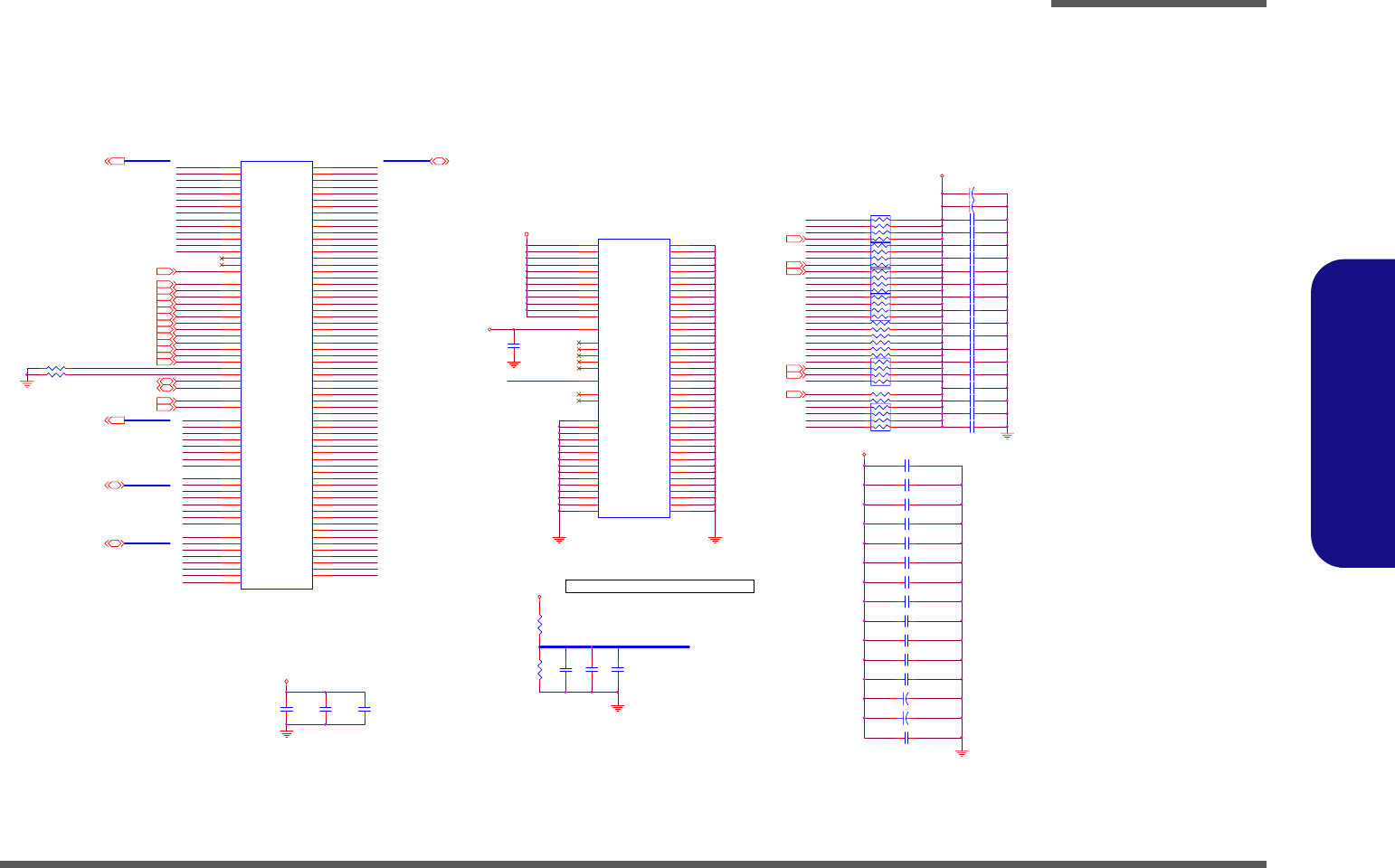
Schematic Diagrams
DDR2-2 B - 11
B.Schematic Diagrams
DDR2-2
1.8V
C96
.1U_16V_06
M_DM3
M_DQS+5
RP4 47_8P4R_0481 72 6
5
3
4
R105
75_1%_06
M_CKE0
M_DQS-2
SMB_SBDATA
R99 10K_06
MAA9
M_B A0
MD_1
MD_44
MD_8
M_CS0#
M_DQS+0
MD_10
MD_57
M_DQS+1
C55 .1U_16V_04
C73 10U_10V_08
M_W E#
M_BA1
MD_31
M_DQS-4
MD_0
+
C89 330U_6.3V_D
1 2
MAA7
C51 .1U_16V_04
C93 10U_10V_08
C100 .1U_16V_06
MD_[0:63] 6,9
M_DQS-0
MD_14
C84 .1U_16V_04
MAA1
MAA13
1.8V
MD_63
MD_47
C41 .1U_16V_04
C98
2.2U_6.3V_06
Layout Note:Place these Caps near So-Dimm0
MD_24
MD_32
MD_9
MD_12
C38 .1U_16V_04
MD_28
MAA10
3.3VS
M_CLK_DDR#12
M_CAS#6,9
M_CLK_DDR12
MAA0
C91 .1U_16V_04
M_BA26,9
MD_36
M_DQS+3
M_DQS+7
R100 47_04
MD_52
MD_33
MD_51
R102 47_04
R78 47_04
C54 .1U_16V_04
C101 .1U_16V_06
M_CS2#6,9
MAA0
M_CKE16
M_B A1
M_C A S #
M_CKE36,9
M_DM6
M_OD T36, 9
MD_48
M_DQS+2
MAA3
C50 .1U_16V_04
1.8V
MD_4
MD_59
JDIMM2B
CA0115-200N02
112
111
117
96
95
118
81
82
87
103
88
104
199
83
120
50
69
163
1
201
202
47
133
183
77
12
48
184
78
71
72
121
122
196
193
8
18
24
41
53
42
54
59
65
60
66
127
139
128
145
165
171
172
177
187
178
190
9
21
33
155
34
132
144
156
168
2
3
15
27
39
149
161
28
40
138
150
162
VDD1
VDD2
VDD3
VDD4
VDD5
VDD6
VDD7
VDD8
VDD9
VDD10
VDD11
VDD12
VDDSPD
NC1
NC2
NC3
NC4
NCTEST
VREF
GND0
GND1
VSS1
VSS2
VSS3
VSS4
VSS5
VSS6
VSS7
VSS8
VSS9
VSS10
VSS11
VSS12
VSS13
VSS14
VSS15
VSS16
VSS17
VSS18
VSS19
VSS20
VSS21
VSS22
VSS23
VSS24
VSS25
VSS26
VSS27
VSS28
VSS29
VSS30
VSS31
VSS32
VSS33
VSS34
VSS35
VSS36
VSS37
VSS38
VSS39
VSS40
VSS41
VSS42
VSS43
VSS44
VSS45
VSS46
VSS47
VSS48
VSS49
VSS50
VSS51
VSS52
VSS53
VSS54
VSS55
VSS56
VSS57
M_C K E 2
MD_27
M_DQS-3
M_CKE26,9
MAA11
Z1001
MD_15
MD_22
C53 .1U_16V_04
MD_60
M_DM[0..7]
M_C S 1 #
R103 47_04
M_DM4
MD_3
MD_17
M_DM5
MD_29
MD_39
M_B A2
MAA4
Trace Width 12 Mil
Space 20 Mil
MD_6
R101 47_04
M_C K E 0
MD_56
MD_30
+
C31 *150U_4V_B
MD_11
MAA8
MD_16
MAA[0: 13]
MD_2
MAA5
M_CAS#
MD_35
M_O D T3
M_W E #
MAA8
M_WE#6,9
MAA5
R104
75_1%_06
M_BA0
0.9VS
MD_62
RP1 47_8P4R_048 1
7 2
6
53
4C40 .1U_16V_04
MAA4
MAA12
C80 10U_10V_08
C92 .1U_16V_04
RP2 47_8P4R_048 1
7 2
6
53
4
M_BA06,9
MAA2
MAA9
MD_37
MAA7
MAA1
M_OD T0
MD_23
C85 .1U_16V_04
MAA[0: 13]6,9
M_CLK_DDR02
M_DQS+[0..7]
M_BA2
C82
.1U_16V_04
C39 .1U_16V_04
C52 .1U_16V_04
MD_42
MD_49
MAA11
M_RAS#
M_RAS#6,9
MD_34
C90 10U_10V_08
M_CS0#6MD_21
R107 47_04
SMB_SBCLK2,9,11,16
MD_19
MD_18
M_DQS+[0..7]6,9
MAA6
MD_53
MD_55
SDREFC
MD_25
M_DM7
MD_38
+
C47 150U_4V_B
MD_[0:63]
M_DM1
M_DQS-7
C591
.1U_16V_06
M_DQS-[0..7]6,9 M_DQS-[0..7]
M_O D T2
Z1002
MAA2
MD_5
C87 .1U_16V_06
M_CKE06
C56 .1U_16V_04
C79 10U_10V_08
M_O D T1
M_C S 3 #
M_DQS+6
M_DQS-6
MD_13 MA A12
MD_46
MD_61
M_DM2
C74 .1U_16V_06
JD IMM2A
CA0115-200N02
102
101
100
99
98
97
94
92
93
91
105
90
89
116
86
84
85
5
7
17
19
4
6
14
16
23
25
35
37
20
22
36
38
43
45
55
57
44
46
56
58
61
63
73
75
62
64
74
76
123
125
135
137
124
126
134
136
141
143
151
153
140
142
152
154
157
159
173
175
158
160
174
176
179
181
189
191
180
182
192
194
107
106
108
109
113
110
115
79
80
30
32
164
166
195
197
200
198
10
26
52
67
130
147
170
185
13
31
51
70
131
148
169
188
11
29
49
68
129
146
167
186
114
119
A0
A1
A2
A3
A4
A5
A6
A7
A8
A9
A10/AP
A11
A12
A13
A14
A15
A16_BA2
DQ0
DQ1
DQ2
DQ3
DQ4
DQ5
DQ6
DQ7
DQ8
DQ9
DQ10
DQ11
DQ12
DQ13
DQ14
DQ15
DQ16
DQ17
DQ18
DQ19
DQ20
DQ21
DQ22
DQ23
DQ24
DQ25
DQ26
DQ27
DQ28
DQ29
DQ30
DQ31
DQ32
DQ33
DQ34
DQ35
DQ36
DQ37
DQ38
DQ39
DQ40
DQ41
DQ42
DQ43
DQ44
DQ45
DQ46
DQ47
DQ48
DQ49
DQ50
DQ51
DQ52
DQ53
DQ54
DQ55
DQ56
DQ57
DQ58
DQ59
DQ60
DQ61
DQ62
DQ63
BA0
BA1
RAS#
WE#
CAS#
S0#
S1#
CKE0
CKE1
CK0
CK0#
CK1
CK1#
SDA
SCL
SA1
SA0
DM0
DM1
DM2
DM3
DM4
DM5
DM6
DM7
DQS0
DQS1
DQS2
DQS3
DQS4
DQS5
DQS6
DQS7
DQS0#
DQS1#
DQS2#
DQS3#
DQS4#
DQS5#
DQS6#
DQS7#
ODT0
ODT1
M_C K E 1
MAA3
R97 10K_06
MD_45
RP3 47_8P4R_048 1
7 2
6
53
4
C104 .1U_16V_06
M_BA16,9
M_O D T0
M_CLK_DDR#02
SMB_SBDATA2,9,11,16
MD_50
SMB_SBCLK
M_DQS-5
C102
.1U_16V_04
MD_43
MD_20
RP6 47_8P4R_0481 72 6
5
3
4
MD_26
C105 .1U_16V_06
M_CS1#6
M_CKE1
M_OD T1
MAA6
M_DQS-1
R670 47_04
MAA13
MD_7
C42 .1U_16V_04
SDREFC
MD_40 C37 .1U_16V_04
C103
.1U_16V_04
M_C S 2 #
M_DM0
C97
2.2U_6.3V_06
C99 .1U_16V_06
M_DM[0..7]6,9
R106 47_04
MAA10 M_ C KE 3
M_O D T06
MD_41
1.8V
MD_54
C95 .1U_16V_06
M_OD T26, 9
RP5 47_8P4R_0481 72 6
5
3
4
+
C88 *330U_6.3V_D
1 2
DDRVREF GEN. & DECOUPLING
M_O D T16
M_R A S #
M_DQS+4
M_CS1#
MD_58
M_CS3#6,9
M_C S 0 #
Sheet 10 of 40
DDR2-2
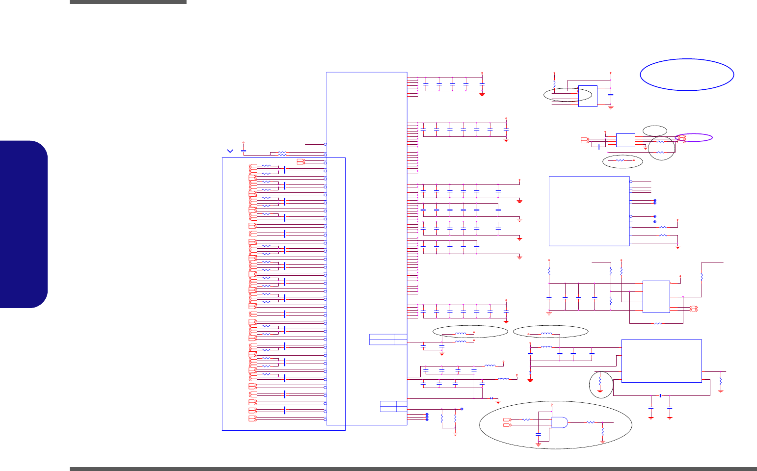
Schematic Diagrams
B - 12 VGA G72M-1
B.Schematic Diagrams
VGA G72M-1
Sheet 11 of 40
VGA G72M-1
C337 .1U_10V_04
U30
*ICS91730
2
4
5
3 6
7
1
8
VDD
CLKOUT/FS_IN0
REFOUT/FS_IN1
GND SDATA
SCLK
CLKIN
PD
S15
S1
2 1
R121 *47_04
VGA_THERMDA12
C598
470P_50V_04
R137
10K_06
PE0TX4#7
PE0R X127
Z1146
GPO016
C308 .1U_10V_04
C593
.1U_50V_06
PE0TX07
ROM_SI
Z1109
C618
.1U_50V_06
C185
.1U_50V_06
BUF RST
ROM_SO
C609
.1U_50V_06
1.2VS
SS_OUT
VGA_ALERT# 12
VGA_PEXCLK#2
C237
1U_10V_06
PEX_RX10#
C625
.1U _50V_06
R531 *22_04
C252
1U_10V_06
PEX_RX8
PE0TX6#7
PE0TX13#7
PE0R X5#7
DVP0D0724
U6
74AHC1G08GW
2
14
3
5
Z1113
C193
.47U_10V_04
7/1 2 M ISC2
BGA4D
PB GA 533- 08MM
COMM O N
GND
TESTMODE
SWAPRDY
STER EO
BUF RST
I2CH_SDA
I2CH_SCL
ROM_SCLK
ROM_SO
ROM_SI
ROM_CS
AC8
D7
A7
F7
A6
B7
C7
D2
D3
F3
D1
R208
10K_06
PE0TX157
VGA_PEXCLK2
DVP0D0924
VGA_THERMDC12
Z1112
BXTALOUT
PEX_RX1#
C344 .1U_10V_04
C182
.47U_10V_04
1.0VS
SSOUT
DVP1D0524
L405 *HCB1608K-121T25_06
1 2
PE0R X3#7
Z1104
C340 .1U_10V_04
C606
.1U_50V_06
3.3VS
3.3VS
PE0RX14#7
DVP0D0824
C339 .1U_10V_04
PEX_RX9
U4
AT25F512
4
87
1
3
5
2
6GND
VCCHOLD
CS
WP
SI
SO
SCK
C298 .1U_10V_04
3.3VS
PE0TX57
PE0TX15#7
PE0RX15#7
DVP0D1124
STER EO
NV46
G72/73 N V4x
NV44
NV_PLLAVDD
1/12 PCI _EXPRESS
BGA4A
COMMON
PB GA 533- 08M M
PEX_RX15
PEX_RX15
PEX_TX15
PEX_TX15
PEX_RX14
PEX_RX14
PEX_TX14
PEX_TX14
PEX_RX13
PEX_RX13
PEX_TX13
PEX_TX13
PEX_RX12
PEX_RX12
PEX_TX12
PEX_TX12
PEX_RX11
PEX_RX11
PEX_TX11
PEX_TX11
PEX_RX10
PEX_RX10
PEX_TX10
PEX_TX10
PEX_RX9
PEX_RX9
PEX_TX9
PEX_TX9
PEX_RX8
PEX_RX8
PEX_TX8
PEX_TX8
PEX_RX7
PEX_RX7
PEX_TX7
PEX_TX7
PEX_RX6
PEX_RX6
PEX_TX6
PEX_TX6
PEX_RX5
PEX_RX5
PEX_TX5
PEX_TX5
PEX_RX4
PEX_RX4
PEX_TX4
PEX_TX4
PEX_RX3
PEX_RX3
PEX_TX3
PEX_TX3
PEX_RX2
PEX_RX2
PEX_TX2
PEX_TX2
PEX_RX1
PEX_RX1
PEX_TX1
PEX_TX1
PEX_RX0
PEX_RX0
PEX_TX0
PEX_TX0
PEX_REFCLK
PEX_REFCLK
PEX_TSTCLK_OUT
PEX_TSTCLK_OUT
PEX_RST
NC
NC
NC
SPDIF NC
PEX_PLLGND
PEX_PLLDVDD
PEX_PLLAVDD
VDD
VDD3 3
VDD3 3
VDD3 3
VDD3 3
VDD3 3
VDD3 3
VDD_LP
VDD_LP
VDD_LP
VDD_LP
VDD
VDD
VDD
VDD
VDD
VDD
VDD
VDD
VDD
VDD
VDD
VDD
VDD
VDD
VDD
VDD
VDD
VDD
VDD
VDD
VDD
VDD
VDD
VDD
VDD
VDD
VDD
VDD
VDD
VDD
VDD
VDD
VDD
VDD
VDD
PEX_IOVDDQ
PEX_IOVDDQ
PEX_IOVDDQ
PEX_IOVDDQ
PEX_IOVDDQ
PEX_IOVDDQ
PEX_IOVDDQ
PEX_IOVDDQ
PEX_IOVDDQ
PEX_IOVDDQ
PEX_IOVDDQ
PEX_IOVDDQ
PEX_IOVDDQ
PEX_IOVDDQ
PEX_IOVDDQ
PEX_IOVDDQ
PEX_IOVDDQ
PEX_IOVDDQ
PEX_IOVDDQ
PEX_IOVDD
PEX_IOVDD
PEX_IOVDD
PEX_IOVDD
PEX_IOVDD
PEX_IOVDD
PEX_IOVDD
PEX_IOVDD
AF27
AG26
AD24
AE24
AG25
AG24
AE25
AF25
AF23
AF22
AD23
AD22
AG22
AG21
AE22
AE21
AF20
AF19
AD21
AC21
AG19
AG18
AE19
AE18
AF17
AF16
AD18
AC18
AG16
AG15
AE16
AE15
AG13
AG12
AD15
AC15
AF11
AF10
AC13
AD13
AG10
AG9
AE13
AE12
AF8
AF7
AC10
AD10
AG7
AG6
AE10
AE9
AF5
AF4
AC7
AD7
AG4
AG3
AE7
AE6
AG2
AF1
AD6
AD5
AE4
AE3
AF14
AF13
AC6
C13
F12
E12
D12
AA6
AA5
Y6
N9
J16
J15
F14
J13
F13
J12
W12
W11
W10
W9
T17
R17
N17
M17
W16
U16
T16
M16
L16
W15
U15
T15
M15
L15
T14
M14
W13
U13
T13
M13
L13
U12
T12
M12
L12
T11
R11
N11
M11
J11
J10
T9
R9
M9
J9
AC20
AC19
AB19
AB18
AC17
AB17
AC16
AB16
AB13
AC12
AB12
AC11
AC9
AB9
AB8
AB7
AB6
AB5
AA4
AB21
AB20
W18
W17
AB15
AB14
AB11
AB10
3.3VS
PEX_RX15#
I2CC_SCL/SDA ->
SMC/D_BAT1
CHANGE 951113
DVP0HS24
I2CH_SDA
R212
100_06
R527 *22_04
R159
*10K_06
C119
2200P_50V_06
PE0TX87
ROMCS#
C309 .1U_10V_04
C242
1U_10V_06
R119 2.2K_04
C348 .1U_10V_04
R512 *22_04
C345 .1U_10V_04
C629
18P_50V_04
PE0TX127
PEX_RX14
PE0RX12#7
PEX_PLLGN D
PEX_RX9#
PE0R X47
DVP1D0424
C303 .1U_10V_04
PE0R X107
C607
.1U_50V_06
C251
.01U_50V_06
C184
1U_10V_06
PE0TX77
PE0TX8#7
DVP1D0724
R515 *22_04
C299 .1U_10V_04
GND
R476
4.7_06
1.0VS
C244
.47U_10V_04
C615
.1U _50V_06
C253
.1U _50V_06
C347 .1U_10V_04
R528 *22_04
G72M-V
PEX_RX6
PE0TX27
PE0TX7#7
C336 .1U_10V_04
L30
HCB1608K-121T25_06
1 2
PE0R X37
SMD_BAT1 23,29
SW APRD Y _A
R533 *22_04 PEX_RX3
C301 .1U_10V_04
C304 .1U_10V_04
PULL HIGH
? ? PAGE
12
DVP1D0324
R182 100_1%_06
C196
.47U_10V_04
R521 *22_04
PE0TX67
C628
18P_50V_04
C213
.1U_50V_06
C297 .1U_10V_04
C596
.1U_50V_06
DVP0DE24
Z1105
R524 *22_04
C206
.1U_50V_06
C197
.47U_10V_04
C597
4.7U_6. 3V_06
C328
.1U_50V_06
G72M-V
PE0TX1#7
PE0TX11#7
PEX_RX11
PEX_RX13
3.3V
SMB_ SBC LK 2 ,9 , 10, 16
C254
4.7U_6.3V_06
C189
4700P_50V_04
R530 *22_04
C521
4.7U_6.3V_06
R517 *22_04
PEX_RX3#
SS_R EF
C306 .1U_10V_04
R514 *22_04
DVP1D0224
Z1149
C346 .1U_10V_04
I2CH_SCL
PEX_RX5#
R672 0_04
R482
75_1%_04
C311 .1U_10V_04
R478
10K_04
G72M-V
3.3VS
PE0TX12#7
Z1111
PEX_RX7#
PEX_RX12#
ROM_SCK
C186
.1U_50V_06
1.2VS
PE0TX0#7
PE0TX107
C350 .1U_10V_04
R522 *22_04
M660SE ALL DEL
2.5VS
VGAPLLGND
C245
.47U_10V_04
SMB_SBD ATA 2,9,10,16
PE0R X07
DVP0D0024
DVP1D1124
ROM_SO
C335 .1U_10V_04
C240
4.7U_6.3V_06
PE0R X77
PEX_RX4
C368
.1U _50V_06
C338 .1U_10V_04
C239
.1U_50V_06
PEX_RX11#
Y3
27MHZ
1 2
PEX_RX2
PEX_RX5
C341 .1U_10V_04
C296 .1U_10V_04
PE0R X137
C307 .1U_10V_04
R485
*0_06
R146
22_04
C140
.1U_50V_06
C236
.47U_10V_04
951117
1.2VS
PE0R X27
PE0R X57
R529 *22_04
3.3VS
PE0RX13#7
S6 S1
21
R649 0_04
C613
1U_10V_06
3.3VS
PEX_RST
PEX_RX13# R650
*60_06
C209
4.7U_6.3V_06
C224
.47U_10V_04
Z1101
R147
22_04
C519
.1U_50V_06
C300 .1U_10V_04
FOR NB8M,NB7M
DVP0D0124
PEX_RX6#
C215
.47U_10V_04
PE0R X87
R162 10K_04
L31
HCB1608K-121T25_06
1 2
PE0TX37
SS_VD D
PEX_RX4#
C623
.1U_50V_06
R489 10K_04
PE0R X2#7
PE0R X7#7
Z1147
ROMCS#
10/12 XTAL_PLL
BGA4E
PBGA533-08MM
COM MO N
XTAL_SS_IN
PLLGND
PLLVDD
XTAL_OUT
XTAL_OU T_BU F
XTAL_IN
C1
H5
H4
C2
C3
B1
SMC_BAT1 23,29
PE0TX117
DVP0D1024
C604
.1U _50V_06
C380
1U_10V_06
951129
DVP1D0624
DVP0CLK24
C360
.1U_50V_06
L407
*HCB1608K-121T25_06
1 2
75O HM
PE0TX10#7
PE0R X117
C258
.01U_50V_06
C228
.01U_50V_06
PE0R X1#7
PEX_RST
PEX_RX10
C343 .1U_10V_04
U3
ADM1032ARM
8
7
6
54
3
2
1SCLK
SDATA
ALERT#
GNDTHERM#
D-
D+
VDD
PEX_RX0#
PE0TX5#7
L32
HCB1608K-121T25_06
1 2
R513 *22_04
951117
NOTE:1.2VS93/61.1VS NB7M
PE0RX11#7
C235
.47U_10V_04
L26 HCB1608K-121T25_06
1 2
R525 *22_04
1.2VS
PE0TX14#7
PE0R X4#7
PEX_RX2#
PEX_RX1
PE0R X9#7
ROM_SI
R477
10K_04
DVP1D1024
C232
.1U_50V_06
PE0TX3#7
PE0R X147
PE0TX2#7
Z1114
Z1148
R408 0_06
C349 .1U_10V_04
PE0RX10#7
DVP0D0324
PEX_RX7
C188
4.7U_6.3V_06
951201
PE0R X6#7
DVP0D0624
C231
1U_10V_06
PEX_RX15
PE0TX147
Z1107
1.2VS
R532 *22_04
PE0TX97
PE0R X8#7
PE0TX47
BXTALOUT
R523 *22_04
C520
.1U_50V_06
951117
PE0R X0#7
PE0R X17
SSOUT
Z1115
C616
.1U_50V_06
C342 .1U_10V_04
C331
1U_10V_06
DVP0D0224
ROM_SCK
C192
.47U_10V_04
R519 *22_04
1.2VS
PE0TX137
PEX_RX12
C238
.01U_50V_06
R526 *22_04
PE0TX17
PLT_R S T#15,20,25, 26
Z1108
PEX_RX8#
C212
1U_10V_06
951117
3.3VS
PE0TX9#7
R520 *22_04
C178
.1U _50V_06
SU DEL->R ADD->C
SE DEL->C ADD->R
PE0R X157
C201
.47U_10V_04
C310 .1U_10V_04
951117
FOR NB8M,NB7M
1.2VS
PE0R X97
PE0R X67
Z1106
R179 100_1%_06
C214
.47U_10V_04
PEX_RX0
Z1114
C243
4.7U_6.3V_06
C323
.1U_50V_06
C305 .1U_10V_04
3.3VS
C622
.1U _50V_06
C631
4.7U_6. 3V_06
XTA LO U TB UF F
PEX_RX14#
Z1103
C302 .1U_10V_04
951117
R516 *22_04
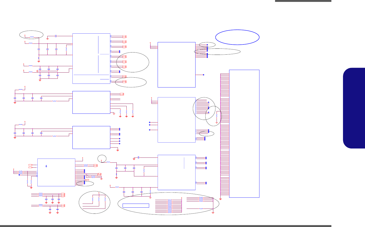
Schematic Diagrams
VGA G72M-2 B - 13
B.Schematic Diagrams
VGA G72M-2
Sheet 12 of 40
VGA G72M-2
R668 10K_04
3.3VS
C120
22P_50V_06
Z1296
R518
10K_04
951117
Z1259
C223 . 01U_16V_04
951117
LVDS-U2N
LVDS-U0N
Z1231
Z1220
3.3VS
VGA_BKLTEN 24
RAM_CFG2
RAM_CFG1
VGA_ALER T#
C179
.01U_16V_04
R6 90 * 2K_04
FOR
NB8M,NB7M
LVDS-UCLKN 24
Z1204
Z1202
L21 HCB1608KF-121T25_06
951129
LVDS-LCLKN 24
PCI _D EVID 4
AC_DET
C204
470P_50V_04
Z1225
12/12 IFPC
DATA
CLOCK
BGA4I
COM MO N
PBGA 533-08MM
IFPC_IO_VDD
IFPC_PLL_GND
IFPC_RSET
IFPC_PLL_VDD
IFPC_VPROBE
IFPC_TXC
IFPC_TXC
IFPC_TXD2
IFPC_TXD2
IFPC_TXD1
IFPC_TXD1
IFPC_TXD0
IFPC_TXD0
L4
M6
J3
M4
M5
V1
W1
V2
V3
T3
T2
T1
R1
S4
S1
2 1
VGA_THER MDA11
PCI _D EVID 2
Z1254
R647
270_04
Z1210
Z1291
R145 124_1%_04
Z1209
Z1282
Z1227
Z1264
L24 HCB1608KF-121T25_06
VGA_B 24
Z1292
Z1297
C124
22P_50V_06
951201
Z1278
Z1206
R6 62 * 10K_04
R6 63 10K_ 04
C173
4700P_50V_04
VGREEN
RAM_CFG2
C637
4.7U_6.3V_06
4/12 D AC_B
BGA4G
PBGA533-08MM
COMMO N
DAC_B_RSET
DAC_B_VREF
DAC_B_VDD
DAC_B_IDUMP
DAC_B_BLUE
DAC_B_GREEN
DAC_B_RED
DAC_B_VSYNC
DAC_B_HSYNC
I2CB_SDA
I2CB_SCL
D6
E7
F8
L9
D5
E4
F4
F5
E6
F10
F9
Z1208
C208 .01U_16V_04
3.3VS
VGA_G 24
R677 2K_04
R141
*150_04
Z1260
L20 HCB1608KF-121T25_06
C194
4.7U_6.3V_06
LOW from SYSTEM BIOS
VGA_R 24
V_VSY
SUB_VE NDOR
L52
HCB1608KF-121T25_06
LVDS-L0N 24
LVDS-UCLKP 24
LVDS-U1N
Z1293
G72M-V
2.5VS
Z1201
RAM_CFG1
R666 10K_04
R128
10K_04
951127
Z1215
C634
4700P_50V_04
Z1218
R674 2K_04
R174
1K_1%_04
PCI_DEVI D2
R667 *10K_04
R646 2K_04
RAM_CFG1
C269
4700P_50V_04
VGA_HSY 24
Z1217
LVDS-LCLKN
Z1213
C639
4700P_50V_04
R673 2K_04
Z1275
Z1262
PXE_MOD E
Z1279
G72M-V
Z1226
1.8VS
Z1207
Z1265
OPEN -->DESKTOP
HIGH -->MOBILE
Z1255
Z1276
R134 124_1%_04
VGA_VSY 24
3.3VS
L22 HCB1608KF-121T25_06
G72M-V
Z1222
LVDS-U1P 24
Z1219
V_HSY
R643 10K_04
C123
22P_50V_06
G72M-V
951129
3.3VS
LVDS-U0P 24
Z1295
AC_DET
Z1229
C122
22P_50V_06
Z1287
C641
4700P_50V_04
3/12 D AC_A
BGA4F
COMMO N
PBGA533-08MM
DAC_A_RSET
DAC_A_VREF
DAC_A_VDD
DAC_A_IDUMP
DAC_A_BLUE
DAC_A_GREEN
DAC_A_RED
DAC_A_VSYNC
DAC_A_HSYNC
I2CA_SDA
I2CA_SCL
AD3
AB4
AE2
U9
AD2
AD1
AE1
AC4
AD4
E10
D10
Z1257
Z1223
3.3VS
Z1285
R144 33_1%_04
951201
LVDS-UCLKP
Z1288
L25
HCB1608KF-121T25_06
FOR NB8M,NB7M L51? ? ?
VGA_THER MDC11 I2CC_SCL 24
RAM_CFG0
I2CC_SDA 24
I2CC_SDA
1.8VS
LVDS-L0N
PXE_MODE
LVDS-L2N 24
PCI _D EVID 3
C268
4.7U_6.3V_06
R648
1K_1%_04
SUB_VENDOR
I2CC_SCL
Z1280
Z1256
VGA_ALERT# 11
LVDS-L1P
Z1230
RAM_CFG2
951129
LVDS-U0P
PCI_DEVI D0
R642 180_04
VGA_DD CDATA 24
PCI _D EVID 0
Z1289
LVDS-UCLKN
V_HSY
C222
4.7U_6.3V_06
G72M-V
Z1242
L51 *HCB1608KF-121_06
R6 64 * 10K_04
C121
22P_50V_06
R143 33_1%_04
R6 91 * 2K_04
Z1298
R669 *10K_04
5/12 I FP_AB
B
B
A
A
CLOCK
DATA
BGA4H
COMMO N
PBGA533-08MM
IFP_B_IO_VDD
IFP_A_IO_VDD
IFP_AB_PLL_GND
IFP_AB_RSET
IFP_AB_PLL_VDD
IFP_AB_VPROBE
IFP_B_TXC
IFP_B_TXC
IFP_A_TXC
IFP_A_TXC
IFP_B_TXD7
IFP_B_TXD7
IFP_B_TXD6
IFP_B_TXD6
IFP_B_TXD5
IFP_B_TXD5
IFP_B_TXD4
IFP_B_TXD4
IFP_A_TXD3
IFP_A_TXD3
IFP_A_TXD2
IFP_A_TXD2
IFP_A_TXD1
IFP_A_TXD1
IFP_A_TXD0
IFP_A_TXD0
Y4
W4
V6
U6
V5
N6
W5
W6
T4
U4
AB3
AB2
AB1
AA1
AA2
AA3
W3
W2
R6
P6
T5
T6
R5
R4
N4
N5
C218
4700P_50V_04
R6 76 * 2K_04
951127
3.3VS
C203
4700P_50V_04
Z1283
R129
2.2K_1%_04
LVDS-U0N 24
LVDS-LCLKP
Z1299
L27
*HCB1608KF-121_06
Z1274
Z1263
G72M-V
Z1205
R139
*150_04
R6 65 10K_ 04
C257
.01U_16V_04
RAM_CFG3
L29
HCB1608KF-121T25_06
951127
1.8VS
Z1270
Z1224
Z1249
S5
S1
2 1
LVDS-U2N 24
R675 2K_04
C636
4.7U_6.3V_06
G72M-V
Z1272
L28
HCB1608KF-121T25_06 LVDS-L2N
PCI _D EVID 1
RAM_CFG0
Z1239
0 -->G72M
*0-->NB38X
Z1290
LVDS-L2P
Z1248
LVDS-U1P
L33
HCB1608KF-121T25_06
LVDS-U1N 24
C640
4.7U_6.3V_06
3.3VS
LVDS-L2P 24
VGA_DD CCLK 24
Z1294
Z1212
G72M-V
11/12 _GND_
BGA4C
COM MON
PBG A533- 08MM
GND
GND
GND
GND
GND
GND
GND
GND
GND
GND
GND
GND
GND
GND
GND
GND
GND
GND
GND
GND
GND
GND
GND
GND
GND
GND
GND
GND
GND
GND
GND
GND
GND
GND
GND
GND
GND
GND
GND
GND
GND
GND
GND
GND
GND
GND
GND
GND
GND
GND
GND
GND
GND
GND
GND
GND
GND
GND
GND
GND
GND
GND
GND
GND
GND
GND
GND
GND
GND
GND
GND
GND
GND
GND
GND
GND
GND
GND
GND
GND
GND
GND
GND
GND
GND
GND
GND
GND
GND
GND
GND
GND
GND
GND
AF26
AC26
Y26
U26
P26
L26
H26
E26
B26
AF24
AC23
Y23
U23
P23
L23
H23
E23
B23
AF21
AD20
E20
B20
AD19
V19
P19
K19
AF18
AD17
U17
P17
L17
E17
B17
AD16
R16
P16
N16
AF15
R15
P15
N15
AD14
AC14
W14
U14
R14
P14
N14
L14
J14
E14
B14
R13
P13
N13
AF12
AD12
R12
P12
N12
AD11
U11
P11
L11
F11
E11
B11
AF9
AD9
V9
P9
K9
AD8
E8
B8
AF6
H6
AC5
Y5
U5
P5
L5
E5
B5
AF3
AF2
AC2
Y2
U2
P2
L2
H2
E2
B2
LVDS-L0P
LVDS-LCLKP 24
R505
1K_1%_04
951129
VGA_EN AV DD 24
RAM_CFG3
Z1284
VBLUE
LVDS-U2P
LVDS-L1N 24
Z1250
Z1244
R644 10K_04
C166
4.7U_6.3V_06
Z1258
VBLU E
PCI_DEVI D3
C635
470P_50V_04
6/ 12 M I SC 1
BGA4K
PBG A533- 08MM
COMMO N
JTAG_TRST
JTAG_TDO
JTAG_TDI
JTAG_TMS
JTAG_TCK
THERMDP
THERMDN
GPI O12
GPI O11
GPI O10
GPI O9
GPI O8
GPI O7
GPI O6
GPI O5
GPI O4
GPI O3
GPI O2
GPI O1
GPI O0
I2CC_SDA
I2CC_SCL
5V_CLAMP
AD25
AE26
AD27
AD26
AE27
B9
C9
B16
A15
B15
B13
A13
A12
B12
C12
C10
B10
A10
D9
A9
D8
E9
D11
RAM_CFG0
L23 HCB1608KF-121T25_06
VRE D
MIO_ B_D E
PCI_DEVI D4
C642
470P_50V_04
RAM_CFG3
R689
0_04
L406
*HCB1608KF-121T25_06
DEVICE ID:G72MV -->0111
NB8M -->00111
LVDS-L1P 24
Z1271
Z1238
Z1211
VRED
8/12 MIO_A
BGA4J
PBGA 533-08MM
COM MO N
MIO_A_VDDQ
MIO_A_VDDQ
MIO_A_VDDQ
MIO_A_HSYNC
MIO_A_D10
MIO_A_D9
MIO_A_D8
MIO_A_D7
MIO_A_D6
MIO_A_D5
MIO_A_D4
MIO_A_D3
MIO_A_D2
MIO_A_D1
MIO_A_D0
J6
G6
F6
C4
V4
G5
C6
P4
B6
B4
A4
D4
A3
B3
A2
LVDS-L1N
V_VSY
Z1261
1.8VS
VGREEN
PCI_DEVI D1
R645 2K_04
Z1234
R138
*150_04
Z1203
C217
470P_50V_04
C638
470P_50V_04
SAMSUNG 16M X 16-->1010
SAMSUNG 32M X 16-->
M660SE ALL DEL
LVDS-L0P 24
R6 94 * 10K_04
9/12 MIO_B
BGA4L
PBGA 533-08MM
COM MO N
MIO_B_VREF
MIO_B_CAL_PU_GND
MIO_B_CAL_PD_VDDQ
MIO_B_VDDQ
MIO_B_VDDQ
MIO_B_VDDQ
MIO_B_CLKIN
MIO_B_CLKOUT
MIO_B_CLKOUT
MIO_B_CTL3
MIO_B_DE
MIO_B_HSYNC
MIO_B_VSYNC
MIO_B_D11
MIO_B_D10
MIO_B_D9
MIO_B_D8
MIO_B_D7
MIO_B_D6
MIO_B_D5
MIO_B_D4
MIO_B_D3
MIO_B_D2
MIO_B_D1
MIO_B_D0
J4
M3
J5
L6
K6
K5
R2
K3
K2
F2
G1
G4
F1
R3
N3
N2
N1
M1
M2
K1
K4
J1
J2
G3
G2
3. 3VS
R123
2. 2K _1%_ 04
LVDS-U2P 24
Z1245
C270
470P_50V_04
C177
470P_50V_04
951129
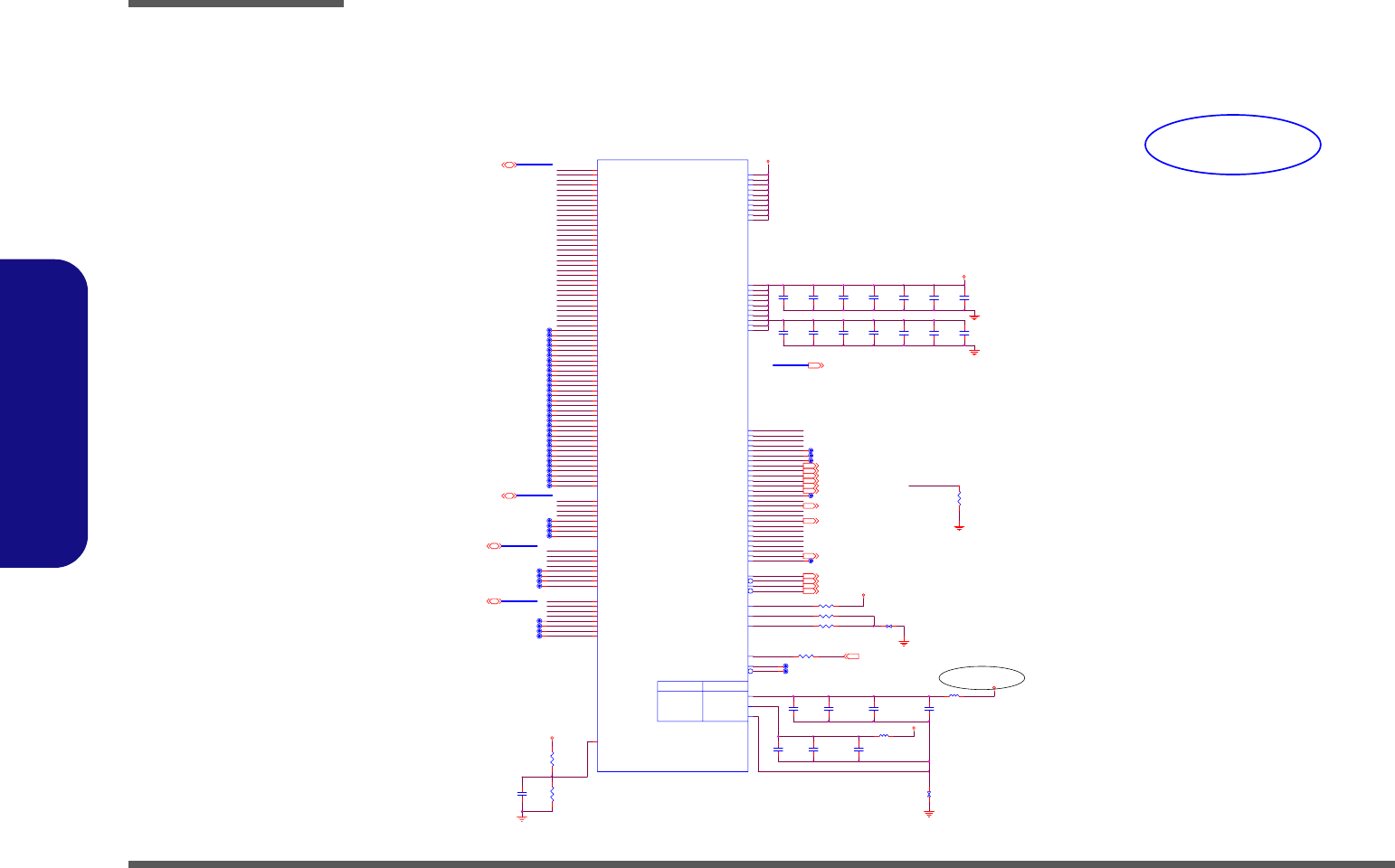
Schematic Diagrams
B - 14 VGA G72M-3
B.Schematic Diagrams
VGA G72M-3
Sheet 13 of 40
VGA G72M-3
1.8VS
FBAD[0..31]14
FBAD30
FBAD29
1.8VS
FBADQS_RN[0..3]14
FBAD8
FBA_CLK1#
FBADQS_RN[0..3]
FBA_CLK0
1.8VS
FBAD60
FBAD31
R480 30_1%_04
FBCAL_PD
FBAD56
FBADQS_RN7
FBAD59
951129
C190
.1U_16V_04
FBA_BA0 14
FBAD37
C135
.1U_16V_04
FBADQS_WP0
FBADQS_RN4
Z1314
FBA_CLK0 14
FBA_A6
1.2VS
FBADQM[0..3]14
FBAD23
Z1308
FBADQS_RN2
FBAD22
FBAD36
FBADQS_WP4
Z1307
C134
.1U_16V_04
C191
.47U_10V_04
Z1315
FBAD51
FBAD5
FBA_CLK1
Z1306
FBAD25
FBADQM7
FBAD26
FBADQS_RN3
FBADQS_WP6
C627
.1U _16V_04
FBADQS_RN0
1.2VS
FBADQS_WP5
FBA_A12
FBA_WE# 14
FBADQM1
FBAD27
FBAD12
C138
.1U_16V_04
FBADQS_WP7
FBAD6
FOR NB38X FB1? ? ?
FBA_BA2_SC1# 14
FBAD42
FBA_A5
FBA_CKE 14
FBA_RAS# 14
FBAD3
FBAD44
FBAD14
C155
470P_50V_04
FBA_CS0# 14
FBAD53
FBAD52
FBADQM5
FBADQM2
FBA_A9
FBA_CLK1 14
FBADQS_RN1
FBAD62
FBA_A2
C195
.1U _16V_04
FBADQM6
FBAD43
FBAD63
1.8VS
FBAD0
FBA_A[0..12] 14
FBA_A1
R168
10K_04
FBA_RST 14
FBCAL_TERM
FBAD4
C154
4700P_50V_04
FBAD24
R136 *0_04
FBA_CAS# 14
Z1305
FBAD13
FBAD21
FBAD39
FBA_A13
Z1311
FBA_A0
C211
4.7U _6.3V_06
FBAD[0..31]
FB4
HCB2012KF-121T30_08
Z1309
C183
.47U_10V_04
C137
.1U_16V_04
FBAD48
NC
NV46
2/12 FRAM E_BUFFER
NV44
FB_PLLGND
FB_PLLAVDD
BGA4B
COMMON
PBGA53 3-08MM
FB_VREF
FB_DQS_RN7
FB_DQS_RN6
FB_DQS_RN5
FB_DQS_RN4
FB_DQS_RN3
FB_DQS_RN2
FB_DQS_RN1
FB_DQS_RN0
FB_DQS_WP7
FB_DQS_WP6
FB_DQS_WP5
FB_DQS_WP4
FB_DQS_WP3
FB_DQS_WP2
FB_DQS_WP1
FB_DQS_WP0
FB_DQM7
FB_DQM6
FB_DQM5
FB_DQM4
FB_DQM3
FB_DQM2
FB_DQM1
FB_DQM0
FB_DQ63
FB_DQ62
FB_DQ61
FB_DQ60
FB_DQ59
FB_DQ58
FB_DQ57
FB_DQ56
FB_DQ55
FB_DQ54
FB_DQ53
FB_DQ52
FB_DQ51
FB_DQ50
FB_DQ49
FB_DQ48
FB_DQ47
FB_DQ46
FB_DQ45
FB_DQ44
FB_DQ43
FB_DQ42
FB_DQ41
FB_DQ40
FB_DQ39
FB_DQ38
FB_DQ37
FB_DQ36
FB_DQ35
FB_DQ34
FB_DQ33
FB_DQ32
FB_DQ31
FB_DQ30
FB_DQ29
FB_DQ28
FB_DQ27
FB_DQ26
FB_DQ25
FB_DQ24
FB_DQ23
FB_DQ22
FB_DQ21
FB_DQ20
FB_DQ19
FB_DQ18
FB_DQ17
FB_DQ16
FB_DQ15
FB_DQ14
FB_DQ13
FB_DQ12
FB_DQ11
FB_DQ10
FB_DQ9
FB_DQ8
FB_DQ7
FB_DQ6
FB_DQ5
FB_DQ4
FB_DQ3
FB_DQ2
FB_DQ1
FB_DQ0
FB_PLLGND
FB_PLLAVDD
FB_PLLVDD
FB_REFC LK
FB_REFC LK
FB_DEBUG
FB_CAL_TERM_GND
FB_CAL_PU_GND
FB_CAL_PD_VDDQ
FB_CLK1
FB_CLK1
FB_CLK0
FB_CLK0
FB_CMD 26
FB_CMD 25
FB_CMD 24
FB_CMD 23
FB_CMD 22
FB_CMD 21
FB_CMD 20
FB_CMD 19
FB_CMD 18
FB_CMD 17
FB_CMD 16
FB_CMD 15
FB_CMD 14
FB_CMD 13
FB_CMD 12
FB_CMD 11
FB_CMD 10
FB_CMD9
FB_CMD8
FB_CMD7
FB_CMD6
FB_CMD5
FB_CMD4
FB_CMD3
FB_CMD2
FB_CMD1
FB_CMD0
FB_VDDQ
FB_VDDQ
FB_VDDQ
FB_VDDQ
FB_VDDQ
FB_VDDQ
FB_VDDQ
FB_VDDQ
FB_VDDQ
FB_VDDQ
FB_VTT
FB_VTT
FB_VTT
FB_VTT
FB_VTT
FB_VTT
FB_VTT
FB_VTT
FB_VTT
FB_VTT
A16
W27
V23
W23
V26
B21
F21
E22
A22
W26
U24
W24
V25
C21
E21
D22
B22
V24
V22
W22
V27
A21
F20
F22
D21
W25
AA25
AB27
AB26
AB25
AA26
AA27
AA24
P24
N23
T22
R22
R23
R24
T23
T24
AA22
AA23
AC22
AC24
AB22
AB24
Y24
AB23
T26
T27
T25
R27
R26
R25
N25
N26
C18
C16
C19
D18
B19
A19
B18
A18
D19
D20
E18
E19
F18
D17
E16
D16
H24
G23
F24
J24
F23
E24
J23
G22
D23
B25
A25
C22
A24
B24
C24
A26
C15
D13
D14
M24
M23
K22
H22
E13
D15
N22
M22
K23
L24
N24
B27
G26
K27
F27
K24
K25
K26
D27
D26
M25
C26
M27
J26
G24
N27
D24
C25
C27
M26
J27
J25
G25
F25
F26
D25
G27
Y22
U22
P22
L22
J22
T19
M19
J19
F19
F17
W19
U19
R19
N19
L19
J18
J17
F16
F15
E15
FBAD QS_W P[ 0..3]14
FBAD11
FBAD54
FBAD9
R487
1K_1%_04
FBAD20
Z1312
FBAD41
FBADQM3
C199
.47U_10V_04
FOR NB83X
FBAD7
FBADQS_WP3
FBAD33
C172
4700P_50V_04
FBAD50
FBAD57
FBAD1
FBADQS_RN5
FBAD49
FBAD16
FBAD61
FBADQS_WP2
R488
1K_1%_04
M660SE ALL DEL
FBAD38
GND
FBADQS_WP[0..3]
S1
S1
2 1
FBA_RAS# 14
FBA_A3
C230
4.7U _6.3V_06
FBAD28
FBAD58
R486 40_1%_04
C156
4.7U_6.3V_06
FBAD15
FBADQS_RN6
FBAD17
FBA_CLK0#
FBAD18
FBA_CKE
C136
.1U_16V_04
C176
470P_50V_04
FBA_A10
FBA_CLK0# 14
FBCAL_PU
FBADQM0
FBADQM4
FBAD34
GND
FBAD2
FB1
*HCB2012KF-221T30_08
FBA_BA1 14
FBAD47
FBADQM[0..3]
C165
4.7U_6.3V_06
C169
4.7U_6.3V_06
FBAD46
C207
.47U_10V_04
FBA_A[0..12]
FBAD55
Z1301
FBADQS_WP1
FBAD40
Z1310
FBA_CLK1# 14
FBAD35
FBA_CKE
S14 S1
2 1
R142 *0_04
FBA_A11
FBA_A7
C139
.1U _16V_04
G72M-V
FBA_A8
FBAD32
FBAD45
FBAD10
FBAD19
Z1313
FBA_A4
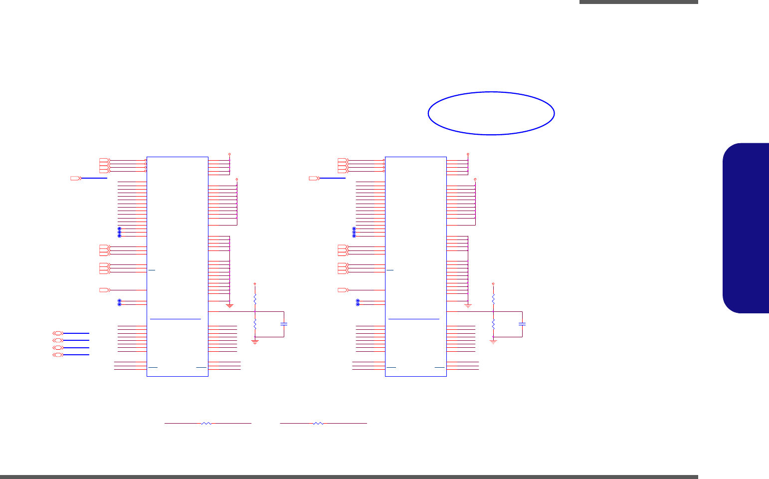
Schematic Diagrams
VGA G72M-4 B - 15
B.Schematic Diagrams
VGA G72M-4
Sheet 14 of 40
VGA G72M-4
FBAD4
FBA_A1
FBA_CLK0
FBA_CS0#13
FBA_CLK0#13
FBA_A[0..12]
FBAD28
FBA_RAS#
FBA_CKE13
FBAD11
FBADQS_RN1
Z1404
Z1409
FBAD7
FBA_CLK1#13
Z1411
Z1406
FBA_BA113
Z1410
FBAD14
FBA_RST13
FBAD29
Z1413
FBADQS_RN2
FBA_A[0..12]13
FBA_A8
1.8VS
FBAD20
FBA_CLK1#
FBAD2
FBA_A3
FBAD19
1.8VS
FBA_A0
FBA_A11
FBADQS_WP1
FBA_A6
FBAD15
FBA_A2
FBA_RAS#
FBA_A5
FBAD6
FBA_CAS#13
FBA_A2
FBA_CAS#13
FBADQM1
FBA_CLK0#
FBA_A7
FBAD26
Z1414
FBA_A11
1.8VS
FBAD[0..31]13
FBA_A7
FBA_CAS#
FBAD0
FBA_CLK113
FBADQM2
FBAD25
FBA_RST
FBAD17
BGA3
16M*16DDR2
K7
L7
K3
L8
M8
M3
M7
N2
N8
N3
N7
P2
P8
P3
M2
P7
L2
L3
L1
K2
J8
K8
A2
E2
K9
A1
E1
J9
M9
R1
A9
C1
C3
C7
C9
E9
G1
G3
G7
G9
J1
A7
B2
B8
D2
D8
E7
F2
F8
H2
H8
J7
A3
E3
J3
N1
P9
J2
R2
R8
R3
R7
G8
G2
H7
H3
H1
H9
F1
F9
B3
B7
A8
C8
C2
D7
D3
D1
D9
B1
B9
F3
F7
E8
RAS
CAS
WE
CS
A0
A1
A2
A3
A4
A5
A6
A7
A8
A9
A10
A11
BA0
BA1
NC/BA2
CKE
CLK
CLK
NC1
NC2
ODT
VD D
VD D
VD D
VD D
VD D
VDDQ
VDDQ
VDDQ
VDDQ
VDDQ
VDDQ
VDDQ
VDDQ
VDDQ
VDDQ
VDDL
VSSQ
VSSQ
VSSQ
VSSQ
VSSQ
VSSQ
VSSQ
VSSQ
VSSQ
VSSQ
VSSL
VSS
VSS
VSS
VSS
VSS
VREF
A12
NC/A13
NC/A14
NC/A15
LDQ0
LDQ1
LDQ2
LDQ3
LDQ4
LDQ5
LDQ6
LDQ7
UDM
UDQS
UDQS
UDQ0
UDQ1
UDQ2
UDQ3
UDQ4
UDQ5
UDQ6
UDQ7
LDM
LDQS
LDQS
FBA_BA013
FBAD30
FBAD27
FBA_A4
FBAD16
FBA_A12
FBAD3
FBADQS_RN0
FBA_BA2_SC1#13
FBAD5
FBA_A[0..12]
R140 120_1%_06
FBA_WE#
Z1402
FBA_A10
FBAD18
M660SE ALL DEL
C626
.1U_16V_04
1.8VS
FBA_CKE13
Z1412
FBAD1
FBADQS_RN[0..3]
FBADQS_RN3
FBA_A[0..12]13
FBADQM[0..3]13
FBA_RAS#13
FBA_BA013
1.8VS
FBADQS_WP0
FBAD10
FBAD[0..31] FBAD22
Z1407
FBA_A4
FBA_WE#13FBA_WE#13
FBA_CLK013
FBAD13
FBADQM[0..3]
FBA_A5
FBADQM3
FBAD23
FBA_A3
1.8VS
FBADQS_RN[0..3]13
FBADQS_WP[0..3]13
FBA_RST13
FBAD21
FBA_RAS#13
FBA_A8
Z1403
BGA2
16M*16DDR2
K7
L7
K3
L8
M8
M3
M7
N2
N8
N3
N7
P2
P8
P3
M2
P7
L2
L3
L1
K2
J8
K8
A2
E2
K9
A1
E1
J9
M9
R1
A9
C1
C3
C7
C9
E9
G1
G3
G7
G9
J1
A7
B2
B8
D2
D8
E7
F2
F8
H2
H8
J7
A3
E3
J3
N1
P9
J2
R2
R8
R3
R7
G8
G2
H7
H3
H1
H9
F1
F9
B3
B7
A8
C8
C2
D7
D3
D1
D9
B1
B9
F3
F7
E8
RAS
CAS
WE
CS
A0
A1
A2
A3
A4
A5
A6
A7
A8
A9
A10
A11
BA0
BA1
NC/BA2
CKE
CLK
CLK
NC1
NC2
ODT
VDD
VDD
VDD
VDD
VDD
VDDQ
VDDQ
VDDQ
VDDQ
VDDQ
VDDQ
VDDQ
VDDQ
VDDQ
VDDQ
VDDL
VSSQ
VSSQ
VSSQ
VSSQ
VSSQ
VSSQ
VSSQ
VSSQ
VSSQ
VSSQ
VSSL
VSS
VSS
VSS
VSS
VSS
VREF
A12
NC/A13
NC/A14
NC/A15
LDQ0
LDQ1
LDQ2
LDQ3
LDQ4
LDQ5
LDQ6
LDQ7
UDM
UDQS
UDQS
UDQ0
UDQ1
UDQ2
UDQ3
UDQ4
UDQ5
UDQ6
UDQ7
LDM
LDQS
LDQS
FBADQS_WP3
C644
.1U_16V_04
FBA_CS0#
R510
1K_1%_04
R481
1K_1%_04
FBA_BA113
Z1405
R479
1K_1%_04
FBA_RST
FBA_CLK1
FBA_A0
FBA_A9
FBA_A10
FBA_WE#
FBAD8
FBAD24
FBA_BA2_SC1#13
FBADQM0
R508
1K_1%_04
FBA_A12
FBA_CAS#
FBA_A1
FBAD31
FBAD12
FBAD9
R170 120_1%_06
FBA_A6
FBA_CS0#13
FBADQS_WP2
FBADQS_WP[0..3]
FBA_A9
FBA_CS0#
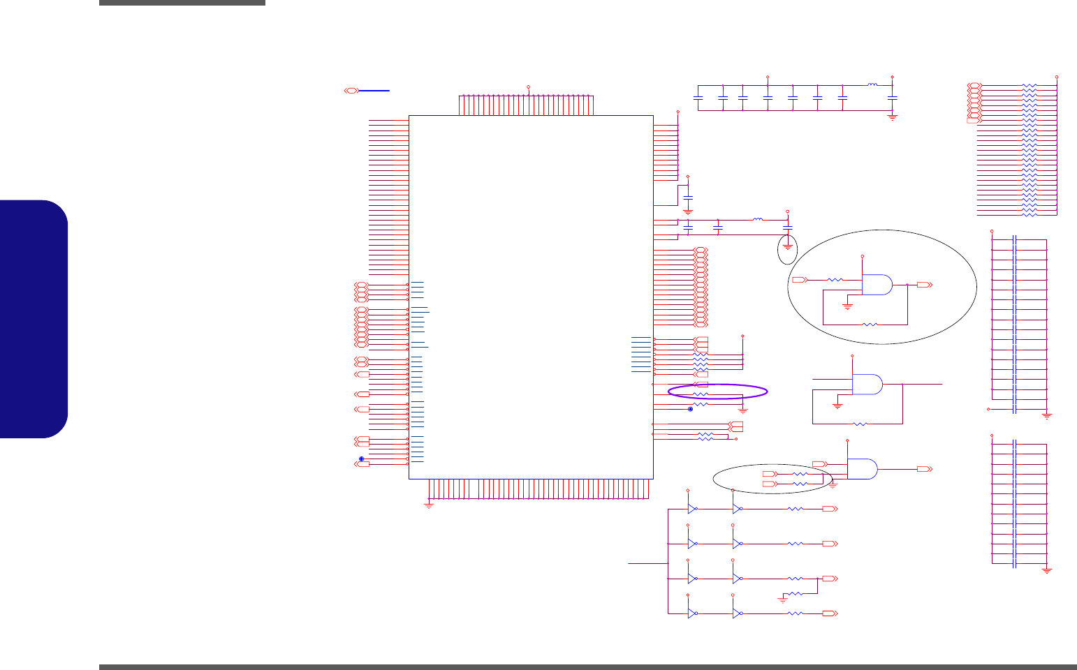
Schematic Diagrams
B - 16 VT8237A-1
B.Schematic Diagrams
VT8237A-1
PCI_INTA#8,19
PCI _AD2
-PC IRST_GATE
C464 .1U_50V_06
FB19
HCB2012KF-121T30_08
PCI _AD14
C467 .01U_50V_06
USB2+
C463 .1U_50V_06
F951202
PCI_PERR#19,26
H_A20GATE 23
PCI_STOP#
IDE_SATDET#
C451 .1U_50V_06
C425 .1U_50V_06
USB5+
R616 8.2K_06
C429 .01U_50V_06
PCI RST#
U23
74AHC1G08GW
2
14
3
5
U20A
74AHC04
1 2
14
PCI_REQ#3
Z1511
R370 8.2K_06
PCI_GNT#019
PCI_REQ#4
R613 8.2K_06
PWRGD_VCORE31
R250 10K_06
Z1506
C694
10U_10V_08
C399 1U_10V_06
PCI_IRDY#19,26
R534 6.2K_1%_06
3VUSB
U19B
74AHC 04
3 4
14
PCI_DEVSEL#19,26
PCI_INTC#
C430
.1U_50V_06
C383 1U_10V_06
R698 *0_04
2.5VS
USB5- 22
USB4-
Z1503
R678 *0_06
951202
SUSB#16,20,23,27,33,34
3.3V
USB3+ 22
PCI _AD4
R611 8.2K_06
3.3V
PLT_RST# 11,20,25,26
PCI_INTD#26
R380 8.2K_06
PCI _AD17
USB2+ 22
3.3V
3.3V
USB5-
C459
.1U_50V_06
PCI_C/BE0#19, 26
ALL_PWROK
NEW_CARD_RST# 20
PCI_IRDY #
R697 0_04
R385 8.2K_06
2.5VS
PCI _FRAME#
Z1513
PCI_C/BE1#19, 26
PCIRST#
USB1-
PCI _AD12
PCI _AD8
C420
.1U_50V_06
R379 2.2K_04
R369 8.2K_06
PCI _AD24
USB0+
PCI _AD15
U20B
74AHC 04
3 4
14
U10
74AHC1G08GW
2
14
3
5
IDE_PATDET#
IDE_SATDET#
PCIRSTC# 19
PCI_GNT#1
FWH_TBL#
C436 1U_10V_06
USB6+ 26
PCI_REQ#4
USB7+
PCI _AD7
R421 22_06
USB2- 22
USB6-
PCI_DEVSEL#
951129
3.3VS
OC2# 29
PCI _AD22
FWH_TBL#
PCI_REQ#1
PCI _INTD#
R406 22_06
-PCIRST_GATE
USB6+
USB6- 26
PCI _AD20
R253 10K_06
R384 8.2K_06
PCI _AD29
H_A20GATE
C441 .1U_50V_06
PC I_TR DY #19,26
PCI_TRDY#19,26
PCI_SERR#
USB0-
C333 .1U_50V_06
R593 8.2K_06
FOR NEW CARD RESET
3.3V
R382 8.2K_06
USB7- 20
FLASH#25
GPI O12
C421 1U_10V_06
PCI _AD10
PCI_TRDY #
R594 8.2K_06
PCI_GNT#126
C416 1U_10V_06
R609 2.2K_04
3.3V
ALL_PWROK 3,17,24
PCI _AD23
C367 1U_10V_06
951117
Z1518Z1514
PCI _AD9
KBC_RST#
FB20
HCB3216KF-800T30_12
KBC_RST# 23
FLASH#
Z1515
PCI_GNT#2
PCI_REQ#5
FLASH#
R383 8.2K_06
PCI_SER R #19,26
KBC_PWRGD23
USB7-
PCI_INTH#
USB4+ C428 1U_10V_06
PCI_REQ#019
OC7# 20
PCI _AD5
3.3V
PCI _AD31
R511 8.2K_06
ALL_PW ROK
R386 8.2K_06
R590 8.2K_06
C671
10U_25V_12
R615 8.2K_06
R591 8.2K_06
BUF_PLT_RST# 7,20,23,26
U37
74AHC1G08GW
2
14
3
5
C426 1U_10V_06
PCI_STOP#19,26
PCI_INTA#
PCI _AD30
PCI _AD0
PCI_INTB#19
USB1- 29
Z1501
R612 8.2K_06
3.3V
PCI_INTD#
PCI _INTH#
IDE_PATDET#
PCI_GNT#3
BGA6A
VT8237A-BGA541
G2
J4
J3
H3
F1
G1
H4
F2
E1
G3
E3
D1
G4
D2
D3
F3
K3
L3
K2
K1
M4
L2
N4
L1
M2
M1
P4
N3
N2
N1
P1
P2
E2
C1
L4
M3
J1
H2
J2
H1
K4
C2
F4
E20
D20
A20
B20
E8
F25
H23
A4
B4
B5
C4
A5
B6
C5
D5
P3
A6
D6
C6
E5
R4
E18
D18
A18
B18
D16
E16
A16
B16
C25
A24
C26
D24
B26
W3
V1
W1
W2
H9
H10
H12
J8
K8
L8
M8
N8
P8
R8
R19
J21
C3
R3
R2
R1
T8
T19
U19
V8
V19
D22
E22
F22
J13
J14
J15
J16
E23
B25
J25
B2
A17
A19
A21
B13
B15
B17
B19
B21
C13
C14
C15
C16
C17
C18
C19
C20
C21
D13
D15
D17
D19
D21
E13
E15
B24
C24
A23
B23
D23
C23
A22
B22
C22
J17
E17
E19
E21
A15
A13
D4
E4
A3
B3
D14
E14
A14
B14
A26
A25
D26
D25
U8
J18
H11
V21
W9
W10
W11
W17
W18
W19
W21
Y21
H13
H15
H16
H18
H14
H17
A1
A2
B1
W8
AD00
AD01
AD02
AD03
AD04
AD05
AD06
AD07
AD08
AD09
AD10
AD11
AD12
AD13
AD14
AD15
AD16
AD17
AD18
AD19
AD20
AD21
AD22
AD23
AD24
AD25
AD26
AD27
AD28
AD29
AD30
AD31
CBE0
CBE1
CBE2
CBE3
FRAME
DEVSEL
IRDY
TRDY
STOP
SERR
PAR
USBP0+
USBP0-
USBP1+
USBP1-
GND
GND
GND
INTA
INTB
INTC
INTD
REQ0
REQ1
REQ2
REQ3
REQ4
GNT0
GNT1
GNT2
GNT3
GNT4
USBP2+
USBP2-
USBP3+
USBP3-
USBP4+
USBP4-
USBP5+
USBP5-
USBOC3
USBOC5
USBOC0
USBOC1
USBOC2
KBCK/KA20G,KBCK
KBDT/KBRC, KBDT
MSCK
MSDT
VCC 33-1
VCC 33-2
VCC 33-4
VCC 33-5
VCC33-6
VCC 33-7
VCC 33-8
VCC33-9
VCC33-10
VCC33-11
VCC33-12
GND
PERR
REQ5/GPI7
GNT5/GPO7
PCIRST
VCC33-13
VCC33-14
VCC33-16
VCC33-17
VCC33-18
USBVCC4
USBVCC5
USBVCC6
USBVCC7
USBVCC8
USBVCC9
USBVCC10
USBCLK
USBR EXT
GND
GND
USBGND3
USBGND4
USBGND5
USBGND6
USBGND7
USBGND8
USBGND9
USBGND10
USBGND11
USBGND12
USBGND13
USBGND14
USBGND15
USBGND16
USBGND17
USBGND18
USBGND19
USBGND20
USBGND21
USBGND22
USBGND23
USBGND24
USBGND25
USBGND26
USBOC4
VSUSUSB
VCC UPLL1
VCC UPLL2
GNDUPLL1
GNDUPLL2
USBVCC1
USBVCC2
USBVCC3
USBVCC11
USBGND27
USBGND28
USBGND29
USBGND2
USBGND1
INTE/GPI12/GPO12
INTF/GPI13/GPO13
INTG/GPI14/GPO14
INTH/GPI15/GPO15
USBP6+
USBP6-
USBP7+
USBP7-
USBOC6
USBOC7
GPI9/UDPWR,GPI9
GPO9/UDPWREN ,GPO9
VCC33-15
USBVCC12
VCC33-3
VCC33-19
VCC33-20
VCC33-21
VCC33-22
VCC33-23
VCC33-24
VCC33-25
VCC33-26
VCC33-27
USBGND30
USBGND32
USBGND33
USBGND35
USBGND31
USBGND34
GND
GND
GND
VCC33-28
C454 .1U_50V_06
U20D
74AHC 04
9 8
14
3.3V
PCI_REQ#2
C470 .1U_50V_06
2.5V
PCI_AD[31:0]
R573 8.2K_06
R407 *51_1%_06
USB1+ 29
Z1508
PCI _AD27
PCI _AD3
PCI _AD16
R373 8.2K_06
IDERST# 18
3.3VS
PCI_REQ#3
C466 .01U_50V_06
PCI_REQ#2
PCI_GNT#0
PCI_GNT#3
PCI_GNT#0
R589 8.2K_06
C465 1U_10V_06
R252 10K_06
USB0+ 22
OC0# 22
C693
1U_10V_06
R254 10K_06
C423
4.7U_10V_08
PCI _AD25
3.3V
3.3V
PCI_REQ#0
USB3-
PCI _AD18
R371 8.2K_06
C461 1U_10V_06
GPO0416
PCI _INTC#
GPI O12
R372 8.2K_06
USB1+
USB2-
PCI _AD1
PCI_REQ#5
PCI_FRAME#19,26
PCI_DEVSEL#19,26
PCI_C/BE3#19, 26
PCI_REQ#126
Z1507
C417
1U_10V_06
C675
.1U_50V_06
USB4- 26
OC1# 22
Z1504
R614 8.2K_06
C670
.1U_50V_06
PCI_PERR#
3VUSB R617 8.2K_06
C361 .01U_50V_06
C438
1U_10V_06
USB0- 22
PCI _AD11
PCI _AD6
PCI_SERR#19,26
PCI_REQ#1
Z1505
Z1512
Z1510
PCI_INTH#7
C455 .01U_50V_06
R427 22_06
2.5VS
USB4+ 26
C460 1U_10V_06
3.3V
U20E
74AHC04
11 10
14
3VUSB
C411 1U_10V_06
PCI_PAR19,26
PCI _AD13
U20F
74AHC 04
13 12
14
USB3- 22
PCI _AD26
PCI_INTB#
3.3V
Z1509
PCI _AD19
C476
.1U_50V_06
PCI_FRAME#19,26
USB7+ 20
PCI _AD28
USB3+
R592 8.2K_06
PCI_IRDY#19,26
PCI _AD21
R699 0_04
C960124
R423 *0_06
C450 .1U_50V_06
PCI_STOP#19,26
3.3VS
3.3V
USB5+ 22
C442 .1U_50V_06
U20C
74AHC04
5 6
14
Z1519
C424 .01U_50V_06
PCI_GNT#1
U19A
74AHC04
1 2
14
R251 10K_06
C427 .01U_50V_06
C435 .1U_50V_06
R374 8.2K_06
CLK_USB48 2
R405 22_06
Z1517
C462 .1U_50V_06
PCI_PER R #19,26
PCI_C/BE2#19, 26
PCI _AD[31: 0]19,26
PCI RST#
Z1516
PCI_GNT#2
PCI_REQ#0
Sheet 15 of 40
VT8237A-1
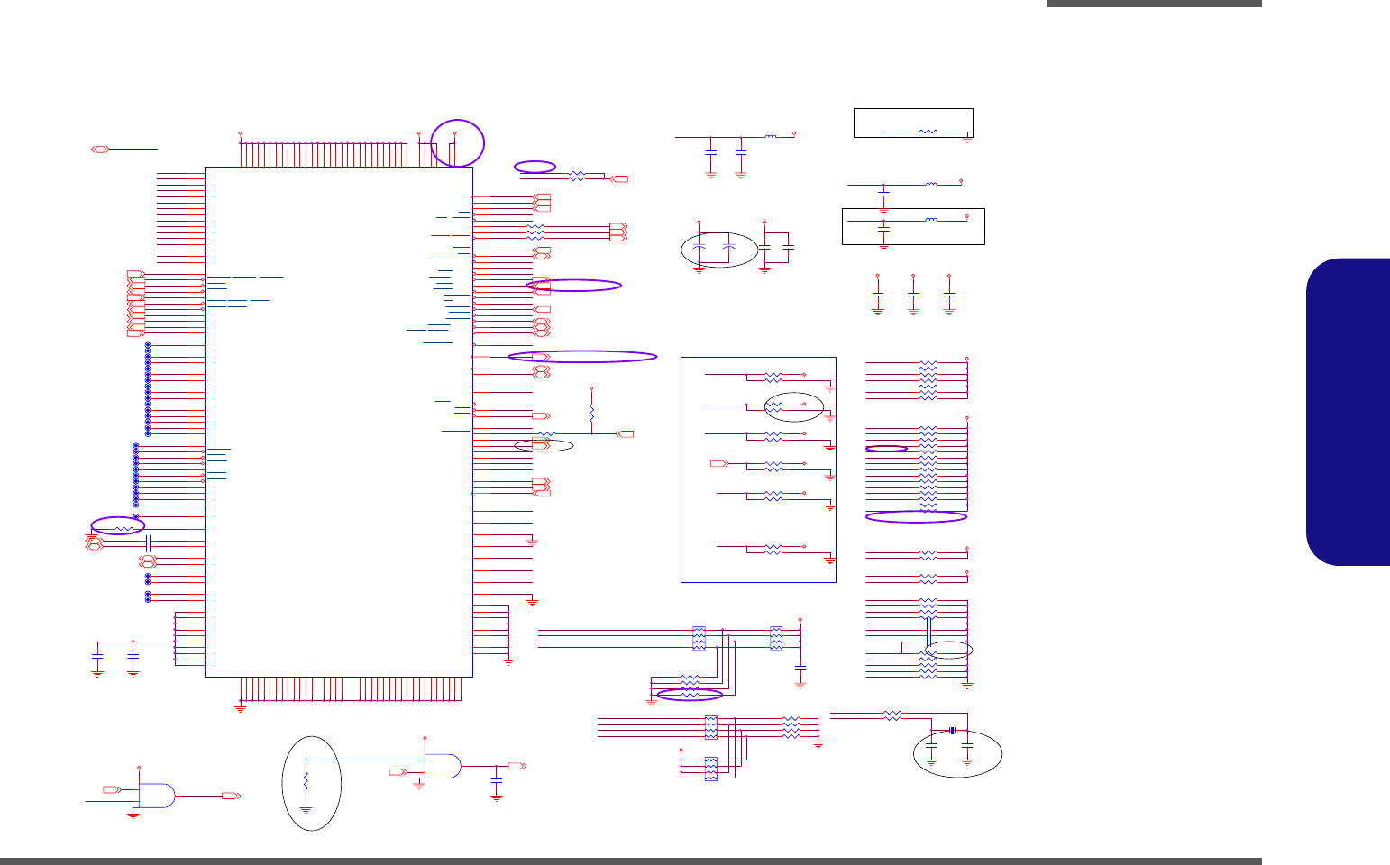
Schematic Diagrams
VT8237A-2 B - 17
B.Schematic Diagrams
VT8237A-2
Sheet 16 of 40
VT8237A-2
R600 4.7K_06
R348 10K_06
R357 *1K_06
3.3V
IDE_SDCS3#
R632 1K_06
951129
GPIOA
C698
.1U_50V_06
Power Up Strapping for VT8237A
F0123-03
IDE_PDD0
IDE_PD D 7
R603 0_06
PEXMESCI# ->GPI18 951101
2.5VSATA
PM_C LKRUN#
IDE_SD D 7
SATATXP0
IDE_SDD5
IDE_SIORDY
C456
6.8P_50V_06
C434
1U_10V_06
0/1:Enable/disable100Mhz VLink clock(Reserved)
ADD R286 951101
IDE_PDD11
C487 22P_50V_06
3.3VS
SIO_OSC 2
GPIOB
GPIOD
R598 4.7K_06
R575 4.7K_06
RN29
1K_8P4R_06
1
2
3
4 5
6
7
8
IDE_PDD8
IDE_SDDREQ
AZ_SDOUT
PM_STPCPU#
R347 0_06
951122
SATARXP0
Z1611
AZ_SDIN0
C695 .1U_50V_06
3.3V
IDE_PD C S1#18
25MHZXI_S
GPI0
IDE_SDD6
SMI#
2.5VS
C446
1U_10V_06
R565 4.7K_06
0/1:Enable/disable CPU FREQ strapping
3.3VS
WAKE 7
SATARXN0
IDE_PDD4
SDIN3
GPIOD
R276 0_06
SER I RQ 19,20, 23
IDE_PDD[0..15]18
GPO1 27
SMBDT2
Z1618 R629 1M_06
3.3V
3.3VS
INT_IRQ
GPIOA
+
C362
*330U_6.3V_D
AZ_RST# 27
8237_SUSB#
Z1603
GPIOB
RN28
2.2K_8P4R_06
1
2
3
45
6
7
8
VCCRTC
SEEDI17
IDE_PDD9
AZ_BITCLK
GPO1
R351 0_06
3.3VS
SUSB#
R262 10K_06
SB_PWROK
AZ_SDOUT
R625 10K_06
AZ_SDIN0 27
AZ_SDOUT
IDE_PD A118
IDE_SDD1
GPO1
8237TEST
Z1617
R264 4.7K_06
951117
IDE_PD A218
PWR _BTN#
IDE_SDD8
SMB_SBCLK
LAN PHY RESET:
RING
GPIOC
R596 22_06
R363 *2.2K_06
IDE_PDDACK#
C447
.1U_50V_06
R311 0_06
IDE_SDCS1#
GPIO D 0:AGTL+ pullup Enable
2.5VS
R627 4.7K_06
2.5VS->2.5V 951101
CPUMISS
GPI04
PME#
Z1604
C381
4.7U_10V_08
IDE_PD C S3#18
Z1615
AZ_SYNC
BGA6B
VT8237A-BGA541
AA22
Y24
AA26
AA25
AB26
AC26
AC23
AD25
AD26
AC24
AC25
AB24
AB23
AA24
Y26
AA23
W23
V25
W24
Y23
V24
W26
Y25
Y22
V22
V23
T1
U3
V2
U1
V3
T2
U2
T3
AD24
AE26
AC20
AB20
AC21
AE18
AF18
AD18
AD19
AF19
AE20
AF20
AD20
AE21
AF21
AD21
AD22
AF22
AD17
AD23
AF23
AE23
AF17
AF25
AF26
AF24
AC22
AE24
AD2
Y2
AA1
W4
AC1
V4
Y3
AB3
AA2
AD3
AF2
AB1
AC4
AB2
AC2
AA3
AE2
AE5
AF5
AC6
AD5
AB7
AC7
AD6
AA4
AB4
AB5
AB6
J9
J10
J11
AF14
L13
L14
AE9
AF1
L15
K9
L9
J12
L18
M9
AB14
AC14
AD12
AD13
AD14
AD15
AD16
AE12
AE14
AE16
AF12
L16
M11
AC11
AC17
AB13
AC13
AE15
AF15
AB15
AC15
AF16
L11
L12
T4
U4
AD9
AF8
AB8
AC3
AD1
AE1
Y4
AF9
Y1
AE3
AE13
AF13
AC10
AB10
AE11
AF11
AD11
AE10
AF10
AC19
AB21
AB11
AB17
W12
W13
W14
W15
W16
M18
N9
N18
P9
P18
R9
R18
T9
T18
U9
U18
V9
V10
V11
V12
V13
V14
V15
V16
V17
V18
AC16
AC12
AB16
AB12
M12
M13
M14
M15
M16
N11
N12
N13
N14
N15
N16
F6
F7
J5
K5
P5
R5
W5
V5
K18
Y5
PDD00
PDD01
PDD02
PDD03
PDD04
PDD05
PDD06
PDD07
PDD08
PDD09
PDD10
PDD11
PDD12
PDD13
PDD14
PDD15
PDA0/PDA0*
PDA1/PDA1*
PDA2/PDA2*
PDDRQ
PDDACK/PDDACK*,PDDACK
PDIOR/PHDMARDY/PHSTROBE
PDIOW/PSTOP
PDRDY/PDDMARDY/PDSTROBE
PDCS1/PDCS1*,PDCS1
PDCS3/PDCS3*
ACBITCLK,AZBITCLK
ACSDIN0,AZSDIN0
ACSDIN1,AZSDIN1
ACSDIN2,AZSDIN2/GPI20/GPO20/PCS0
ACSDIN3,AZSDIN3/GPI21/GPO21/PCS1/SLPBTN
ACSYNC,AZSYNC/ACSYNC*
ACSDOUT,AZSDOUT/ACSDOUT*
ACRST,AZRST
IRQ14
IRQ15
SDD00
SDD01
SDD02
SDD03
SDD04
SDD05
SDD06
SDD07
SDD08
SDD09
SDD10
SDD11
SDD12
SDD13
SDD14
SDD15
SDDRQ
SDDACK
SDIOR/SHDMARDY/SHSTROBE
SDIOW/SSTOP
SDRDY/SDDMARDY/SDSTROBE
SDCS1
SDCS3
SDA0
SDA1
SDA2
PWRBTN
RING/GPI03
EXTSMI/GPI02
PME
LID /GPI04
BATLOW/GPI05
SUSST1/GPO03
SUSCLK/GPO04
SUSA/GPO02
SUSB
SUSC
SMBALRT
SMBCK1
SMBDT1
GPI01,GPI01/THRMTRIP
GPO00
GPI00
Strap_VD1*,GPIOA*/PCREQA*
Strap_VD0*,GPIOC*/PCGNTA*
Strap_VD3*,GPIOD*/PCGNTB*
Strap_VD2*,GPIOB*/PCREQB*
PCKRUN
CPUSTP/GPO05
PCISTP/ PCISTP* / GPO06
VSU S33-1
VSU S33-2
VSU S33-3
VSUS33-4
VCC25-1
VCC25-2
VCC25-3
GNDATS11
GND
GND
TEST
PWROK
GND
VCC25-5
VCC25-6
VCC25-4
VCC25-7
VCC25-8
GNDATS0
GNDATS1
GNDATS2
GNDATS3
GNDATS4
GNDATS5
GNDATS6
GNDATS7
GNDATS8
GNDATS9
GNDATS10
GND
GND
VCCAS2
VCCAS1
STXP1
STXN 1
SRXP2
SRXN2
STXP2
STXN 2
GNDATS12
GND
GND
VSUS25-1
VSUS25-2
SERIRQ
SPKR/SPKR*
OSC
SMBCK2/GPI27/GPO27
SMBDT2/G PI 26/GPO26
INTRUDER/GPI16
AOLGPI/THRM/GPI18
TPO
CPUMISS/GPI17
GPO01
SRXP1
SRXN1
VCCAO
GND AO
VCCA33,NC
GNDA33,NC
SREXT
SXO
SXI
SVREF,NC
SCOMPP,NC
VCCAS4
VCCAS3
VDDATS-1
VDDATS-2
VDDATS-3
VDDATS-4
VDDATS-5
VCC25-9
VCC25-10
VCC25-11
VCC25-12
VC C25-13
VC C25-14
VCC25-15
VCC25-16
VCC25-17
VCC25-18
VCC25-19
VCC25-20
VCC25-21
VCC25-22
VCC25-23
VCC25-24
VC C25-25
VC C25-26
VCC25-27
VCC25-28
VCC25-29
GNDAS1
GNDAS2
GNDAS3
GNDAS4
GND
GND
GND
GND
GND
GND
GND
GND
GND
GND
GND
GND
GND
GND
GND
GND
GND
GND
GND
GND
NC, WAKE
1:Vlink Compensation(Manual setting)
3.3V
R604 4.7K_06
R633 *2.2K_06
AZ_SDIN0
R316 0_06
INT_IRQ15
IDE_PDIOW#
RN9
1K_8P4R_06
1
2
3
45
6
7
8
R355 *0_06
FB14
HCB3216KF-800T30_12
R361 *0_04
R552 4.7K_06
FB13
HCB2012KF-121T30_08
PEXMESCI#
Z1610
SMB_SBDATA
C488 22P_50V_06
R544 10K_06
SATARXN018
GPI0
IDE_PDD1
IDE_SDD9
CPUMISS
IDE_SDD14
R293 *0_06
R362 1K_06
0\1:P4/V4 Bus \ C3 Bus
3.3V
PM_SUS_STAT#
VDDA0
SIO_OSC
GPO0
R354 *1K_06
IDE_SDA0
GPO04
SDIN2
IDE_SDD13
ADD 360OHM 951101
PM_CLKRUN# 20,23
SATATXN 0
Z1609
R595 22_06
R296 5.6K_06
Z1616
R535 4.7K_06
C457
4.7U_10V_08
R631 4.7K_06
0:V4 support(Disable)
2.5VS
PM_STPPCI# 2
SMI# 23
WAKE
C452
6.8P_50V_06
PM_STPCPU# 2
GPIOC
Z1614
R358 4.7K_06
U35
74AHC1G08GW
2
14
3
5
2.5VS
IDE_SDD4
GPI04
PWR_BTN# 23
AZ_SDIN1 27
PM_BATLOW#
SIDEVREF
C449
.1U_50V_06
3.3V
VDDA33
IDE_SDD12
IDE_PDCS1#
R350 2.2K_06
IDE_PDA1
WAKE
R324 *2.2K_06
IDE_PD A018
IDE_PDD13
Z1612
+
C389
470U_4V_D
R586 2.2K_06
3.3VS
AZ_SYNC 27
R285
360_1%_06
5VS
3.3V
3.3VS
SUSB# 15,20,23,27,33,34
INT_IRQ
R628 1M_06
0/1:Enable/disable LPC FWH command
IDE_PDD2
TPO
IDE_PDD[0..15]
R308 6.19K_1%_06
R353 *0_06
R601 4.7K_06
R323 1K_06
IDE_PDDREQ18
AC_SPKR 27
25MHZXO_S
3.3VS
R623 *1K_06
IDE_PD D ACK#18
PM_STPCPU#
SREXT
C432
4.7U_10V_08
IDE_PDA1
SMB_SBCLK
IDE_PDA2
R619 4.7K_06
AZ_SDIN1
Z1605
8237_SU SB#
R366 4.7K_06
FB21
HCB2012KF-121T30_08
R626
10K_06
IDE_PD I OW#18
IDE_PDD7
RING
IDE_PDD10
Z1602
IDE_PIORDY
X3
25MHz
1 2
IDE_SDD3
IDE_PDD15
F0123-03
25MHZXO_S
R583
100_08
U34
74AH C1G08GW
2
14
3
5
PM_STPPCI#
AZ_RST#
GPO0 SMB_ALERT#
IDE_SDDACK#
SB_PW R OK 7
IDE_PDD12
R360 0_04
R656 10K_06
RSMRST#17,23
IDE_SDD2
IDE_SIORDY
1:DESKTOP MODE
IDE_SDD11
R624 4.7K_06
GPIO B 0:IOQ Depth 8 Level
GPO0 11
8237_PWROK
AZ_RST#
AZ_BITCLK 27
Z1607
C708
*10U_10V_08
SREXT
SMI#
IDE_SDIOW#
IDE_PDDREQ
SM_INTRUDER#
R368 *2.2K_06
3.3VS
AZ_SDOUT 27
SERIR Q
AC_SPKR
SMB_SBDATA
SATATXN018
IDE_PDA2
SMBDT2
VDDA33
C373
1U_10V_06
AZ_SY N C
Z1601
SERIRQ R 597 4.7K_06
F010496
PM _S U S_ STA T#
IDE_PDD14
PM_STPPCI#
R269 0_06
VT8237R plus => 4.7K
VT8237A => 6.12K
AP339A
0:MOBILE MODE
R365 10K_06
GPO04 15
VDDA0
R381 4.7K_06
R618 22_06
SATA50COMP
25MHZXI_S
SATATXP018
SMB_ALERT#
SUSC# 23
SMB_SBDATA 2,9,10,11
8237TEST
ACSDO
C490
4.7U_10V_08
2.5VS
SATARXP018
SMBCK2
RN20
2.2K_8P4R_06
1
2
3
45
6
7
8
C443
.1U_50V_06
IDE_PD I OR#18
R554 4.7K_06
GPI04
PEXMESCI#
VKCOMP for Vlink at 4X mode
GPIO C,A 1,1:Auto Mode
DEL SUSCLK
R602 C960125
IDE_PDD3
R286 0_06
R574 4.7K_06
2.5VS
PM_SUS_STAT# 7
PEXMESCI# 7
SUSC#
SB_PW R OK
Z1606
ACSYNC
2.5VS
3.3VS
TPO
IDE_SDDREQ
C440
.1U_50V_06
IDE_PDA0
IDE_SDD15
SM_INTRUDER#
R622 4.7K_06
IDE_PDA0
PM_BATLOW#
0/1:Enable/disable Auto Reboot
IDE_IRQ18
SWI# 23
IDE_SDA1
AZ_SDIN1
R364 4.7K_06
1:V4 support
PME# 19,23,26
IDE_SDD7
2.5VSATA
R621 10K_06
0/1:Disable/Enable LAN shadow EEPROM
F0123-03
2.5V
AC_SPKR
IDE_SDD0
SUSA#
IDE_SDD10
1:VKCOMP for Vlink at 4X mode 0.9V
IDE_SDIOR#
IDE_PDIOR#
IDE_PDCS3#
IDE_SDA2
Z1613
SCI# 23
IDE_PDD5
8237_PWROK
INT_IRQ15
IDE_PDD6
IDE_PDCS3#
Z1608
R581 10K_06
C696 .1U_50V_06
C362?C389???,???C362??
SMB_SBCLK 2,9,10,11
R545 4.7K_06
R599 10K_06
SDIN3
AZ_SDIN0
C493 22P_50V_06
R620 4.7K_06
1:V4-lite support
RSMRST#17,23
SMBCK2
PM_CLKRUN#
951117
IDE_PI ORDY18
AZ_SYNC
SUSA#
SDIN2
C492 22P_50V_06
0:V4-lite support(Disable)
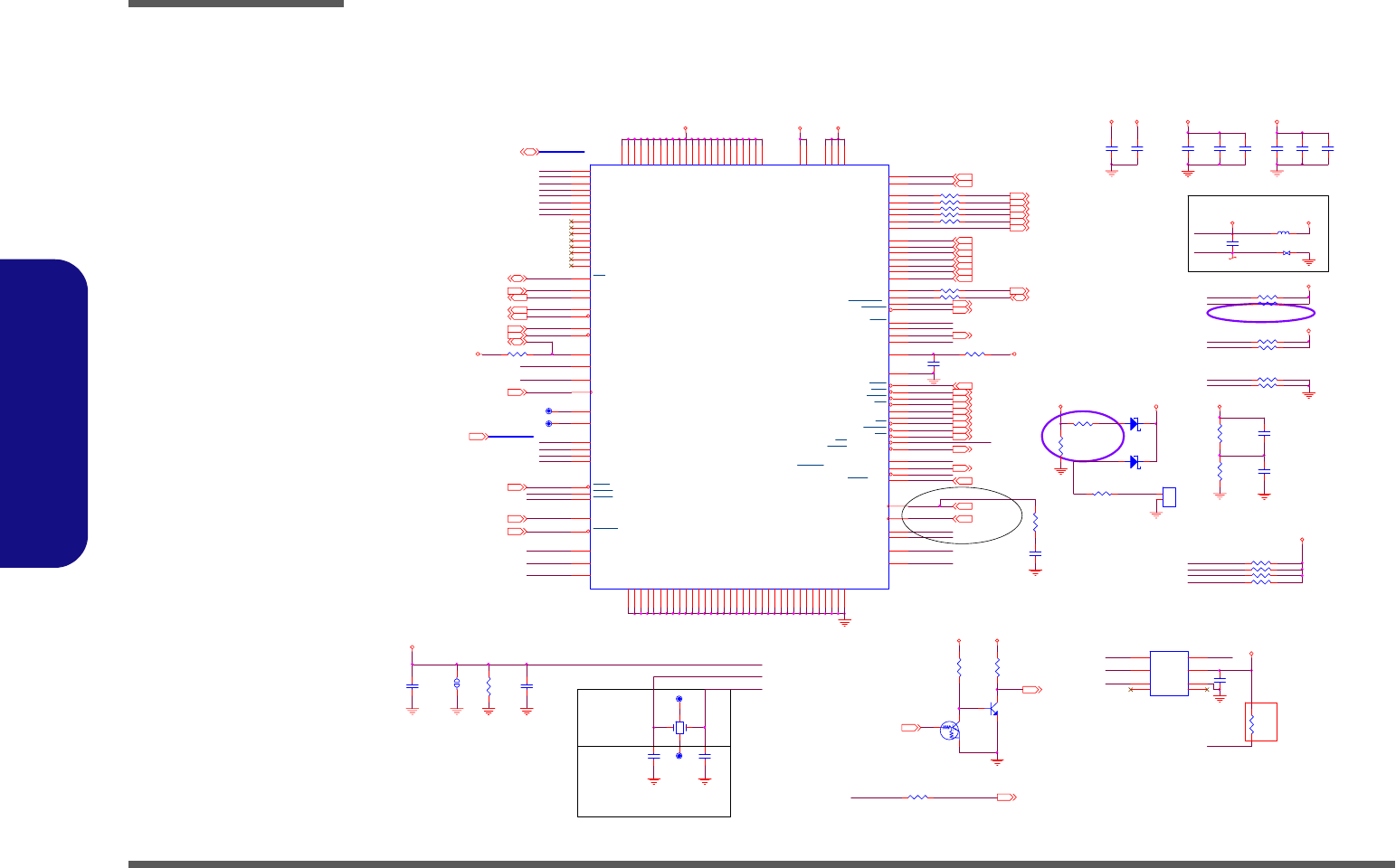
Schematic Diagrams
B - 18 VT8237A-3
B.Schematic Diagrams
VT8237A-3
Sheet 17 of 40
VT8237A-3
UPSTB#7
GHI
R318 10K_06
JBAT1
CON2_BAT
1
21
2
H_IGNNE# 3
MD I O
SEECLK
VPAR
C481
.1U_50V_06
32KHZX2
TXEN
R580
*100K_04
H_A20M# 3
VCCRTC
Z1702
C469
1U_10V_06
3.3VS
R555 33_1%_06
ALL_PWROK
2.5VSBPLL
VLAD3
2.5V
H_SMI# 3 C404
.1U_50V_06
LPC_DRQ#1
NC_CPPE#
SEEDO
VCCRTC
RXD3 21
C468
.1U_50V_06
R630 1K_06
VBE#7
Z1703
R267 360_1%_06
RXCLK 21
SEECS
DPRSLPVR
D39
RB751V
A C
VLAD[0..7]7
Z1716
PM_DPRSLPVR 3,31
DPRSLPVR
H_INIT# 3
VCLK_SB2
C484
12P_50V_06
SATA_LED# 28
LPC_FRAME#20,23,25
VCCRTC
R587 33_1%_06
3.3V
Z1706
R279
1.05K_1%_06
2.5VS
Z1711
Z1705
C374
4.7U_10V_08
AGP_BUSY# 8
H_INTR 3
2.5VSBPLL
C489
.1U_16V_04
APICCLK1 DEL
R248 DEL
C960125
MDC 21
COL 21
TXD2 21
C706
10U_10V_08
VLAD0
Z1713
MDIO
C403
.1U_50V_06
R359
10K_06
GHI
VLAD5
R716 1K_06
RSMRST#16,23
C439
4.7U_10V_08
VT8237R plus=> 10PF
VT8237A => 12PF
AP339A
Z1704
2.5VS
DNSTB7
Z1707
R325 2.2_08
H_FERR# 3
RXD0 21
LVREF_SB
3.3V
LPC_AD[3:0]
Z1708
RXDV 21
RXD2 21
32KHZX1
API CD1
LPC_AD3
EEPROM
2.5VS
H_NMI 3
J1
JOPEN
21
32KHZX1
D37
RB751V
A C
SPCLK
LPC_AD2
BGA6C
VT8237A-BGA541
H25
G26
K26
J23
F26
G25
K22
K24
A11
B11
B9
B10
A10
C11
C10
A9
A7
B7
C7
B8
D8
C9
D10
A8
D11
B12
A12
C12
E7
T22
U22
E24
G23
L26
L25
E26
E25
L24
M26
H22
K23
K25
J26
J24
H26
H24
J22 E6
E11
E9
E10
AF4
L22
D9
P11
P12
P13
P14
P15
P16
R11
R15
R14
R13
R12
R16
R21
T11
T12
T16
T15
T14
T13 M24
N21
N22
N23
N24
N25
N26
P22
P23
P24
P25
P26
M21
M22
M23
AE4
AF3
AE6
AF6
C8
D12
E12
L21
K21
AD8
AF7
AE7
AD7
G24
F24
AE8
D7
AC5
AD4
U24
U26
T24
R26
T25
T26
U25
R24
V26
R22
P21
R23
U23
R25
T23
AC9
AC8
AB9
AD10
M25
L23
L19
M19
N19
P19AA21
AB19
AB22
AB25
AC18
AE17
W22
W25
AE19
AE22
AE25
AA9
T21
AA10
AB18
K19
F23
G22
F8
VAD00
VAD01
VAD02
VAD03
VAD04
VAD05
VAD06
VAD07
MCRS
MCOL
MTXD2
MTXD1
MTXD0
MTXENA
MTXCLK
MTXD3
MDCK
MDI O
MRXD3
MRXD1
MRXDV
MRXCLK
MRXER R
MRXD2
EECS
EED O
EEDI/EEDI*
EECK
LANVCC
PLLVCC
PLLGN D
VAD08
VAD09
VAD10
VAD11
VAD12
VAD13
VAD14
VAD15
VLVREF
UPCMD
DNCMD
UPSTB+
UPSTB-
DNSTB+
DNSTB-
VLCOMP LANGND
MIIVCC4
MIIVCC2
MIIVCC3
VBAT
VCLK
MIIVCC1
GND
GND
GND
GND
GND
GND
GND
GND
GND
GND
GND
GND
GND
GND
GND
GND
GND
GND
GND VCCVK18
VCCVK4
VCCVK5
VCCVK6
VCCVK7
VCCVK8
VCCVK9
VCCVK10
VCCVK11
VCCVK12
VCCVK13
VCCVK14
VCCVK15
VCCVK16
VCCVK17
RTCX1
RTCX2
LREQ0
LFRM
MRXD0
MIIVCC25-1
MIIVCC25-2
VCCVK3
VCCVK2
LAD0
LAD1
LAD2
LAD3
VBE
VPAR
LREQ1
PHYRST
PWRGD
RSMRST
FERR
A20M
IGNNE
INIT
INTR
NMI
SMI
STPCLK
SLP
GHI/GPI22/GPO22
DPSLP/GPI23/GPO23
PCI CLK
APICCLK,GPI19
APICD0/GPIO10
APICD1/GPIO11
VGATE/GPIO8
GPI28/GPO28/VIDSEL/SATALED,GPI28/GPO28/VIDSEL
VRDPSLP/GPI29/GPO29
AGPBZ /GPI 06
VCCVK19
VCCVK1
VCCVK20
VCCVK21
VCCVK22
VCCVK23GND
GND
GND
GND
GND
GND
GND
GND
GND
GND
GND
GND
GND
GND
GND
GND
NC1
NC2
NC,PHYPWRDN
CRS 21
UPSTB7
VCOMPP
RXD1 21
DNSTB#7
H_STPCLK# 3
TXEN 21
LVREF_SB
VDD3
2.5V
AGP_BUSY #
C479
12P_50V_06
SEEC LK
3.3VS
C475
1U_10V_06
C445
.1U_50V_06
R277
*33_06
RXER 21
VLAD1
R559 0_04
LPC_FRAME#
R578 4.7K_04
SEEDO
SEEDI
VLAD4
API CD0
DNCMD7VGATE
R569 33_1%_06
Q21
2N 3904
B
E C
APICD0
ALL_PWROK3,15,24
GND_SBPLL
SEED I
R282 360_1%_06
SATA_LED#
VCOMPP
3.3VS
VLAD7
3.3V
ALL_PWROK3,15,24
S11 S121
C405
.1U_50V_06
FB12
HCB2012KF-121T30_08
C702
10U_10V_08
Near to
South
Bridge
2.5VS
C419
*10P_50V_06
R563 33_1%_06
R340
10K_06
TXD1 21
NC _CPPE# 20
2.5VS
APICD1
R567 4.7K_04
Y2
32.768KHZ
1
3
2
4
GND_SBPLL
VPAR8
VLAD[0..7]
LPC_DRQ#0
LPC_DRQ#1
C377
1U_10V_06
Q20
DTC114EUA
CE
B
LVREF_SB= 0.3V FOR VT8237R plus
LVREF_SB=0.45V FOR VT8237A
R588 33_1%_06 R275 1K_06
2.5VS
TXCLK 21
Z1709
40mil
VCCRTC
R261 360_1%_06
VGATE
R610
1.5K_04
SPC LK 2
Z1710
R551 33_1%_06
U11
CAT93C46S-26490T
3
2
1
4
8
5
6 7
DI
SK
CS
DO
VCC
GND
NC1 NC2
SEED I 16
-PH Y R ST 2 1
R263 4. 7K_06
R570 *4.7K_04
C448
.1U_50V_06
Must use +3.3VSUS if it want to wake
on LAN from resume function well.
Z1701
Z1714
32KHZX2
R558 4.7K_04
2.5VS
VLAD6
R313 33_1%_06
DEL GHL PULL UP RESISTER
H_PWRGD 3
TXD3 21
LPC_AD0
GND_SBPLL
R564 4.7K_06
MDIO 21
F0123-03
-PHYPWRDN 21
SEEC S
2.5VS
H_DPSLP# 3
R281
4.7K_06
TXD0 21
UPCMD7
LPC_DRQ#0
VLAD2
40mil
2.5VSBPLL
SPCLK
AGP_BUSY#
R717
1K_06
PM_DPRSLPVR
LPC_AD[3:0]20,23, 25
DPRSLPVR
Z1715
ADD 1K*2 FOR CMOS LOST
C960130
LPC_AD1
1.05VS
H_CPUSLP# 3,5
ADD GND SHIELD
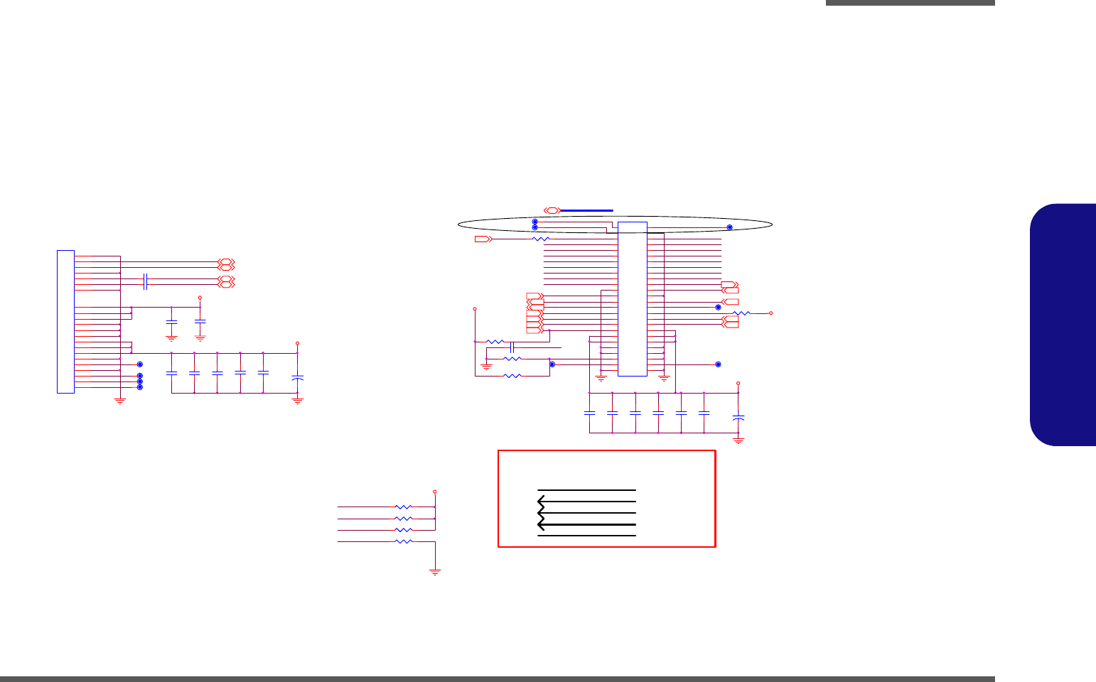
Schematic Diagrams
HDD & CDROM B - 19
B.Schematic Diagrams
HDD & CDROM
Sheet 18 of 40
HDD & CDROM
IDE_PDD12
5VS IDE_PIORDY16
IDE_PDIOW#
IDE_PDIOR#
R459 0_04
C570
.1U_10V_04
IDERST#15
C571
.1U_10V_04
Signal:Space = 1:1
SATARXP0
IDE_PDD2
C574
1U_16V_06
IDE_PDD3
Z1808
SATARXP0 16 IDE_PDD0
Z1801
C709
3900P_50V_04
C715
10U_10V_08
Z1803
CD_G
C471 .01U_50V_04
C12
10U_10V_08
IDE_IRQ
SATARXN0
Layout note:
5VS
IDERST#
R448 4.7K_06
Z1806
C710
10U_10V_08
CD_RESET#
IDE_PDDREQ
3.3VS
R451 4.7K_06
C175: .01U_50V_04 for Nvidia platform
R450 4.7K_06
J_HDD1
SAT-22RE1GA
S1
S2
S3
S4
S5
S6
S7
P1
P2
P3
P4
P5
P6
P7
P8
P9
P10
P11
P12
P13
P14
P15
3.3VS
IDE_PDD9
IDE_PIORDY
CD_L
3.3VS
Z1802 C474 .01U_50V_04
PIN GND1~2=GND
IDE_PDD7
C721
.1U_10V_04
IDE_PDIOR#
To
AUDIO
CODEC
CD_L
CD_DASP#
C714
1U_16V_06
IDE_PDA2
IDE_PDD[15:0]
Z1807
IDE_PDD15
IDE_PDD4
R452 10K_04
C569
.1U_10V_04
Z1809
C572
.1U_10V_04
SATARXN0 16
IDE_PDCS3# 16
IDE_PDA1
IDE_PDD[15:0]16
IDE_PDD11
R445 33_04
Other Signal
Other Signal
SATATXP0 16
Z1805
IDE_PD A016
IDE_PDD14
IDE_PDA0
CD-ROM
Signal:Space = 1:1
5VS
CD_DASP#28
IDE_PDIOW#
IDE_PDDIAG#
IDE_PDDREQ
Signal:Space = 1:2
IDE_PDA2 16
CD_DASP#
J_ODD1
CDR-50DD2
12
34
56
78
910
11 12
13 14
15 16
17 18
19 20
21 22
23 24
25 26
27 28
29 30
31 32
33 34
35 36
37 38
39 40
41 42
43 44
45 46
47 48
49 50
5251
951128
IDE_PDD10
C564 *.01U_50V_04
IDE_PIORDY
CD_RESET#
CD_G
Signal:Space = 1:2
C719
.1U_10V_04
IDE_PDD13SATATXN0
SATATXP0
CD_R & CD_G & CD_L must parallel
routing to Audio Codec. The wide is
12mils and space must be equal.
IDE_PDD1
IDE_PDD6
IDE_PDDACK#
IDE_PDD5
SATATXN0 16
SATA HDD
IDE_PDD8
+
C713
100U_6.3V_B
12
From
CD-ROM
IDE_PD A116
IDE_PDDACK# 16
R458 *4.7K_04
IDE_IRQ16
C720
.1U_10V_04
CD_R
CD_CABSEL
R457 10K_04
IDE_PDIOW#16
IDE_PDCS1#
IDE_PDIOR# 16
R449 4.7K_06
IDE_PDDREQ 16
IDE_PDCS1#16
Z1804
+
C17
100U_6.3V_B
12
CD_R
IDE_PDCS3#
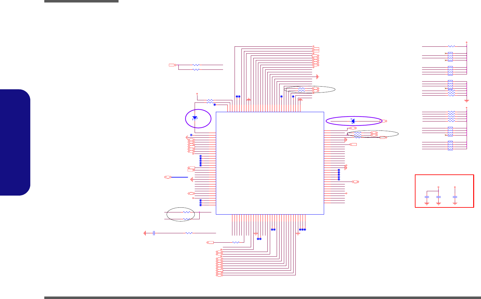
Schematic Diagrams
B - 20 CARD READER
B.Schematic Diagrams
CARD READER
PCI_PAR15,26
RN10 47K_8P4R_061
2
3
4 5
6
7
8
PCI_C/BE0# 15,26
Z1925
PCLKPCM
R378 47K_04
R343 47K_04
PCI_IRDY#15,26
PCM_MF5
PCI_AD11
C496
.1U_16V_04
MS _D 2 20
R387 47K_04
VCC_CARD
SD_D020 SD_D0
3.3VS
MS_D1
Z1926
SD_CLK
PCLKPCM2
PCI_AD24
MS _C LK
PCI_AD16
VCC_CARD
PCM_MF7
PCI_AD6
Z1920
R705 *0_04
Z1910
F951202
SD_CMD20
RN13 47K_8P4R_061
2
3
4 5
6
7
8
xDSMCE#
SD_D2
PCI_AD15
MS_D0
PCI_AD3
R608 0_06
PCI_INTB# 15
PCI_AD[31:0]
CARD_PWREN# 20
PCI_AD18
PCI_AD7
R344 47K_04
SD_WP
VCC_CARD
MS _D 1 20
SD_D3
3.3VS
PCI_REQ#015
PCM_RST#
MS_D3
PCI_AD9
R417 *0_06
PCI_AD8
R397 *100_04
xDWP#
R605 47K_04
MS_INS# 20
SD_D220
PCM_MF6
PCI_GNT#015
PCI_AD13
Z1901
PCIRSTC#15
PCI_PERR#15,26
PCM_MF5
PCI_AD25
SD_D2
PCI_TRDY #15,26
PCI_AD17
C518
.1U_16V_04
R707 100_04
SD_CMD
PCB FP M-SOD323A change
F01J2E C960131
PCI_AD0
PWREN#
G_RST#
XMD A T4B
MS_I N S#
PCI_AD20
U13
MR510
1
2
3
4
5
6
7
8
9
10
11
12
13
14
15
16
17
18
19
20
21
22
23
24
25
26
27
28
29
30
31
32
33
34
35
36
37
38
39
40
41
42
43
44
45
46
47
48
49
50
51
52
53
54
55
56
57
58
59
60
61
62
63
64
65
66
67
68
69
70
71
72
73
74
75
76
77
78
79
80
81
82
83
84
85
86
87
88
89
90
91
92
93
94
95
96
97
98
99
100
101
102
103
104
105
106
107
108
109
110
111
112
113
114
115
116
117
118
119
120
121
122
123
124
125
126
127
128
XSDPWR33OZ
NC
GND_SD
SDDAT2SMCLE
SDDAT3SMDAT4
SDCMDSMALE
SDCLKSMWEOZ
SDDAT0SMDAT7
SDDAT1SMDAT0
VCC_SD
NC
NC
NC
NC
NC
PCIREQOZ
PCIGNTIZ
PCIAD31
PCIAD30
PCIAD29
VSS
PCIAD28
PCIAD27
PCIAD26
PCIAD25
PCIAD24
PCICBE3Z
PCIIDSELI
VCC
NC
NC
NC
PCIAD23
PCIAD22
PCIAD21
PCIAD20
PCIRSTIZ
PCICLKI
PCIAD19
PCIAD18
SDCLKI
VCC
VSS
NC
NC
PCIAD17
PCIAD16
PCICBE2Z
PCIFRAMEZ
NC
NC
VCC
PCIIRDYZ
PCITRDYZ
PCID EVSELZ
PCISTOPZ
PCIPERRZ
PCISERROZ
PCIPAR
PCICBE1Z
VSS
NC
NC
NC
PCIAD15
PCIAD14
PCIAD13
PCIAD12
VCC
PCIAD11
PCIAD10
PCIAD9
PCIAD8
PCICBE0Z
NC
NC
NC
NC
NC
VSS
VCC
PCIAD7
PCIAD6
PCIAD5
PCIAD4
PCIAD3
PCIAD2
PCIAD1
SMCDIZ
MSI NSI Z
PCIAD0
VSS
RIOUTZ_PMEOZ
MFUN C0
MS_SMPW ROZ
MSBSOSMDAT1
VSS
XMDAT7BSMCEOZ
XMDAT4B
XMFUNC 1B
VCC
XMFUNC2B
XMFUNC3B
XGRSTIZ
XMFUNC4B
XMFU NC5B
XMFUNC6B
XSUSPENDIZ
GND_SD
XMFU NC7B
XMDAT6BSMBSYIZ
XMDAT5BSMWPOZ
VCC_SD
XMSDAT1BSMDAT6B
XMSDAT0BSMDAT2B
XMSDAT2BSMDAT5B
XMSDAT3BSMDAT3B
XMSCLKOSMREOZ
VSS
VCC
XSDWPISMWPDIZ
XSDCDIZ
NC
NC
XPMPWR_VCC
XPMPWR_O
XPMPWR_ENIZ
NC
3.3VS
PCI_AD30
xD_CD#
PCI_SERR#15,26
PCI_AD4
Z1906
SD_CLKIN
PCB FP M-SOD323A change
F01J2E C960131
Z1922
Z1931
R706 *0_04
xD_BSY#
PCI_INTB# 15
Z1911
CLOSE TO CHIP
Z1902
3.3VS
SD_D120
D23 SCS751V-40
AC
Z1904
PCI_AD12
G_RST#
R352 47K_04
C711
.1U_16V_04
RN11 47K_8P4R_061
2
3
4 5
6
7
8
SD_D0
CLOSE TO CARD SOCKET
Z1914
R341 *0_04
xDSMCE#
F0104-03
SD_WP 20
PME# 16,23,26
MS_BS
xD_BSY#
PCI_AD31
Z1928
3.3VS
PCI_FRAME#15,26
SD_D3
SD_CLK
R415 0_04
MS_CLK
R345 47K_04
PCI_AD1
Z1923
3.3VS
PCI_AD27
F0104-03
PCLKPCM
Z1913
VCC_CARD
MS_BS
3.3VS
xD_CD#
PCI_AD19
SD_CMD
PCI_AD21
MS _D 3 20
Z1909
MS_INS#
PCM_SUSPEND#
SD_CD#
SERIRQ 16,20,23
3.3VS
VCC_CARD
R356 *0_06
PCI_AD22
SD_WP
Z1912
PCI_AD25
PCI_INTA# 8,15
SD_CLKIN
R416 47K_04
PCI_AD29
PCI_AD28
Z1921
PCI_AD14
3. 3VS SD_CD# 20
PCM_IDSEL
SD_CLK20
Z1932
RN12 47K_8P4R_061
2
3
4 5
6
7
8
R342 47K_04
Z1919
Z1916
PCI_AD20
PCI_DEVSEL#15,26
951206
SD_CD#
PWR EN#
R700 *0_04
PCI_C/BE1#15, 26
MS_BS 20
CARD_PWREN#
Z1929
PCI_AD[31:0]15,26
PCI_AD26
RN14 47K_8P4R_061
2
3
4 5
6
7
8
R376 0_06
SD_D1
PCI_AD23
Z1903
3.3VS
Z1915
C532 *10P_50V_06
Z1930
Z1907
MS_C LK 20
XMD A T4 B
R606 *0_04
MS_D2
Z1917
Z1924
xDWP#
Z1908
PCM_RST#
PCI_AD5
PCI_AD10
SD_D1
PCI_C/BE3#15,26
Z1927
PCI_C/BE2#15,26
PCM_MF6
PCI_STOP#15,26
MS _D 0 20
Z1918
PCM_MF7
Z1905
PCM_SUSPEND#
PCM_IDSEL
D22
SCS751V-40
AC
CARD_PWREN#
R607 0_06
SD_D320
PCI_AD2
Sheet 19 of 40
CARD READER
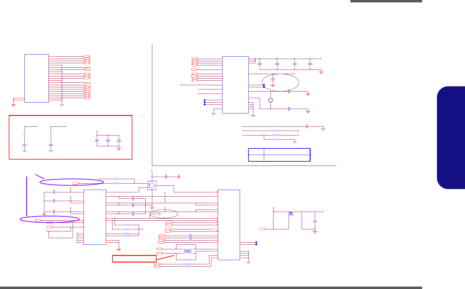
Schematic Diagrams
NEW CARD SOCKET B - 21
B.Schematic Diagrams
NEW CARD SOCKET
Sheet 20 of 40
NEW CARD
SOCKET
3.3VS
R403 0_04
48 mil
USB7+15 Z2007
SD_CMD 19
SD_D1
C544 .1U_10V_04
10mil
F0122-03
PCIE_TXP2_NC7
MS_D 1
48 mil
LPC_AD317,23,25
R169
*0_04
R686 *10K_04
MS_D 2
Z2002
LPC_AD217,23,25
TPM 1.2
R684 10K_04
C543 .1U_10V_04
R685 *33_04
C146, C147:
C540 .1U_10V_04
C788
1U_10V_06
ENE P2231 pin3,4,15,22
has internally
pulled high (170Kohm)
OC7#
Z2014
CLK_PCIE_NC2
MS_ BS 19
PCLK_TPM
C516
10U_10V_08
SD_CLK 19
SMB_ICHCLK
R426 *10K_04
NC_CPPE# 17
U21
74AHC1G08GW
1
2
5
4
3
C787
.1U_16V_04
VCC_CARD
LPC_AD017,23,25
PM_WAKE#
R428 * 100K_04
R188
*0_04
C789
0.1u_16V_04
3.3V
MS_ I NS# 19
TPM_BADD
TPM4105
3.3V
SD_WP 19
NC_CPUSB#
BUF_PLT_RST#
C531 .1U_10V_04
C485 .1U_10V_04
SD_D3 19
MS_CLK 19
MS_INS#
R687 10K_04
SD_CD#
3.3VS
PCIE_R XP2_NC7
SERIRQ16, 19,23
C511
.1U_16V_04
VCC_CARD
PCIE_RXN2_NC
PCIE_TXP2_NC
CLK_PCIE_NC#2
BUF_PLT_RST#7,15,23,26
SD_D2
Close to socket
NC_CLKREQ#2
SD_CMD
TPM
U38
SLB9635TT
17
26
23
20
10
13
24
19
22
21
16
27
15
4
11
18
25
6
2
14
8
9
7
1
3
12
28
5
LAD3
LAD0
LAD1
LAD2
VDD1
XTALI
VDD3
VDD2
LFRAME#
LCLK
LRESET#
SERIRQ
CLKRUN#
GND_1
GND_2
GND_3
GND_4
GPIO
GPIO2
XTAL O
TESTI
TESTBI/BADD
PP
NC_1
NC_2
NC_3
LPCPD#
VSB
R680 0_04
SUSB#15,16,23,27, 33,34
SD_CLK
Z2008
Q23
AO3409
G
DS
36 mil
NC_3.3V
PCLK_TPM2
R429 * 100K_04
SD_D1 19
PCIE_TXN2_NC7
NC_CLKREQ#
Z2013
TPM4103
C547 .1U_10V_04
C226
*10PF_04
3 IN 1 SOCKET SD/MMC/MS(Pro)
MS_ D 1 19
R412 0_06
C274
*10PF_04
NEW CARD
TPM_PP
3.3V
R424 * 10K_04
C486 .1U_10V_04
NEW_CARD_RST#
MS_ D 0 19
TPM4101
C549 .1U_10V_04
R409 0_06
USB7+
3.3V
Z2012
PCIE_TXN2_NC
MS_D 0
asserted before entering S3
VCC_CARD
USB7-15
CLK_PCIE_NC
TPM_BADD
SUSB#
C501
.1U_16V_04
Card Reader Power
>>>Near to S.B. for Intel platform
VCC_CARD
Z2009
R719 0_04
C546 .1U_10V_04
Z2010
NC_PERST#
C792 *10p_NPO_04
R679 *10K_04
SD_D2 19 LPC_AD117,23,25
J_NEW1
130801-1
17
1
10
26
20
23
4
19
18
22
21
25
24
14
15
12
9
13
11
8
7
16
5
6
3
2
CPPE#
GND
+1.5V
GND
GND
GND
CPUSB#
REFCLK+
REFCLK-
PERp0
PERn0
PETp0
PETn0
+3.3V
+3.3V
+3.3VAUX
+1.5V
PERST#
WAKE#
SMB_DATA
SMB_CLK
CLKREQ#
RESERVED
RESERVED
USB_D+
USB_D-
NEW_CARD_RST#<->BUF_PLT_RST#
C960130
MS_ C LK
R396 0_04
3.3VS
10/3/2006
SD_D0
CLK_PCIE_NC#
R389
100K_04
TPM4104
J_CR1
MDR019-X0-0X10(Rev erse)
2
21
3
4
5
6
7
8
9
10
11
12
13
14
15
16
17
18
19
20
1
23
22
DAT2_SD
VSS_MS
CD/DAT3_SD
CMD_SD
VSS_SD
VDD_SD
CLK_SD
VSS_SD
DAT0_SD
DAT1_SD
WP_SD
VSS_MS
VCC_MS
SCLK_MS
DAT3_MS
INS_MS
DAT2_MS
SDIO/D AT0_MS
DAT1_MS
BS_MS
CD_SD
GND
GND
NEW_CARD_RST#15
SD_CD# 19
Z2004
X4
DST410S_32.768KHZ
1 2
NC_CPPE# C506
.1U_16V_04
1.5VS
SMB_ICHCLK26
L42
*PLW3216S161SQ2
1
4
2
3
LPC_FRAME#17,23,25
R420 10K_04
PLT_RST#11,15,25,26
C790 12p_NPO_04
NC_3.3VAUX
3.3V
R388
1K_04
CARD_PWREN#19
3.3V
SD_CLK
R688 *10K_04
3.3VS
3.3VS
C786
.1U_16V_04
Co-lay Common Choke? 0O
??,??Cost
_Down? ?
TPM4102
HI : 4E/4F h
LOW : 2E /
2F h
F010496
MS_BS
Z2003
3.3V
NC_1.5V
OC7#15
TPM_PP
SD_WP
USB7-
C785
.1U_16V_04
LPCPD# inactive to LRST# inactive 32~96us
TPM_PP
>>>Near to J_NEW1 for Nvidia platform
Z2001
NC_RST#
MS_ D 3 19
PM_CLKRUN#16,23
MS_CLK
SD_D3
MS_D 3 TPM_BADD
SMB_ICHDATA26 SMB_ICHDATA
PCIE_RXP2_NC
HI : ACCESS
LOW :
NORM AL (
Internal PD )
PM_WAKE#26
PCIE_RXN2_NC7
U25
P2231THLFC1
2
3
4
6
5 8
7
9
1
11
14
15
16
17
18
19
20
21
22
23
10
12
13
24 25
SYSRST#
SHDN#
STBY#
3.3VIN
3.3VIN 3.3VOUT
3.3VOUT
PERST#
NC
GND
CPUSB#
CPPE#
1.5VOUT
1.5VOUT
1.5VIN
1.5VIN
AUXOUT
AUXIN
RCLKEN
OC#
NC
NC
NC
NC GND
C791 12p_NPO_04
MS_ D 2 19
Z2011
SD_D0 19
R425 * 10K_04
LPC reset timing:
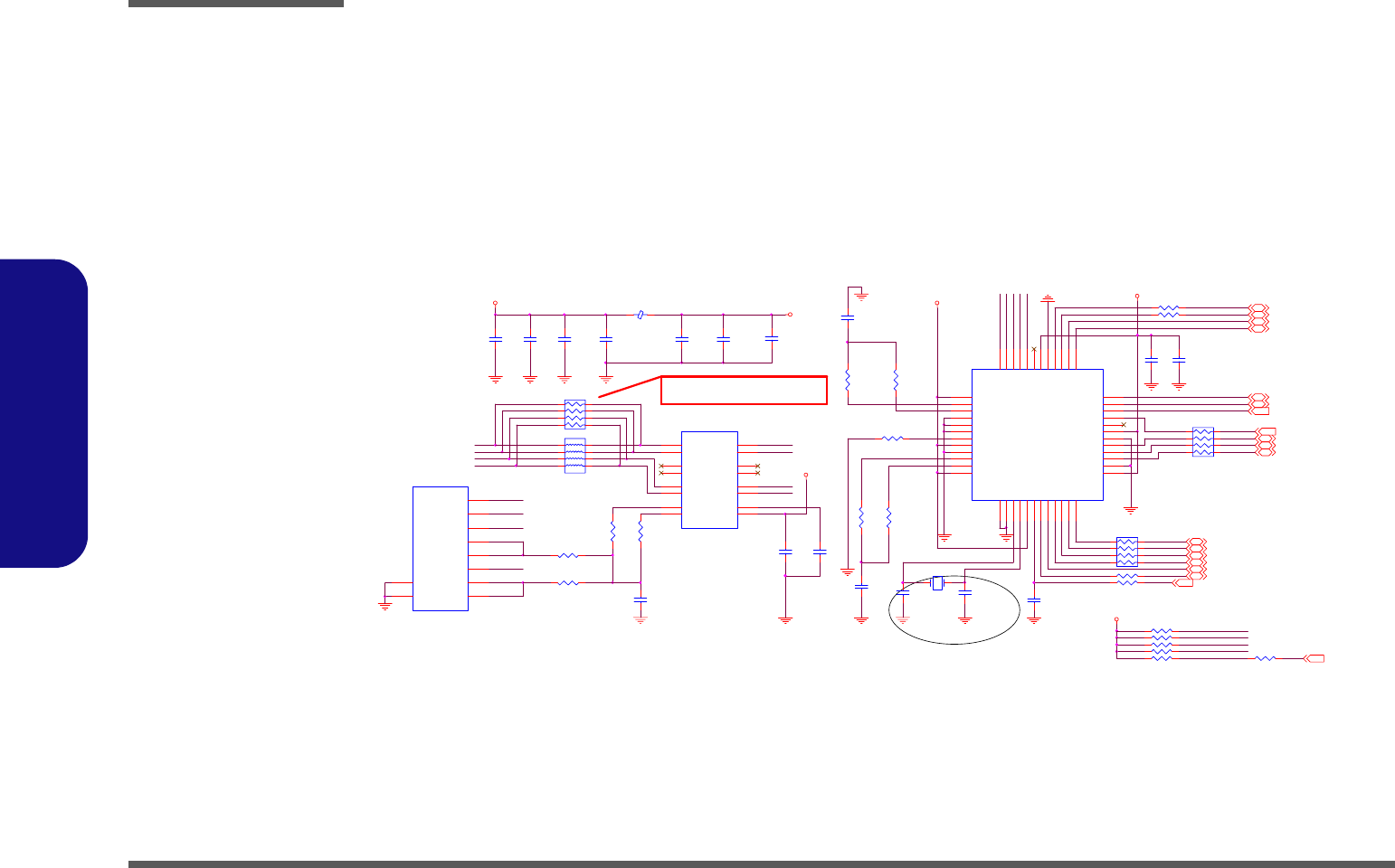
Schematic Diagrams
B - 22 LAN
B.Schematic Diagrams
LAN
Sheet 21 of 40
LAN
NWAY
R259 10K_04
PHYPWRDN
CRS 17
TXD2
PHY PWRDN
C394
.1U_10V_04
C372
.01U_50V_04
CMX4+
R219
49.9_1%_04
C351
.1U_16V_04
R272 10K_04
C382
.1U_10V_04
RXER 17
CMX4-
R257 33_04
DUPLEX
Z2107
3.3V
-PHYRST 17
RXD3#
C365
.1U_10V_04
R232
49.9_1%_04
C57
1000P_2KV_12
RD-
MDI O
C384
.1U_10V_04
3.3VLANPH
COL
CMX3+
LN1 B4W
1
2
3
4 5
6
7
8
R273 33_04
R256 33_04
RN15
*0_08_8P4R
81 72 6
5
3
4
Z2106
C364
.01U_16V_04
RD+
R260 10K_04
RXDV#
RXD2#
R207 33_04
RXD1 17
CRS#
RN1 33_8P4R_04
81 72 6
5
3
4
TXCLK#
TX-
R178
75_1%_04
Z2103
R237
49.9_1%_04
C315
.1U_10V_04
3.3VLANPH
CMX4-
Z2105
R222
49.9_1%_04
VT6103L
U7
VT6103L_LQFP
25
26
27
28
29
30
31
32
33
34
35
36
37
38
39
40
41
42
43
44
45
46
47
48
1
2
3
4
5
6
7
8
9
10
11
12
13
14
15
16
17
18
19
20
21
22
23
24
VDDRX
RX-
RX+
FXSD
GNDRX
GNDPLL
REXT
VDDPLL
GNDTXC
TX-
TX+
VDDTX
GNDTX
GNDOSC
XO
XI
VDDOSC
RST
MDIO
MDC
RXD3
RXD2
RXD1
RXD0
VDD1
GND1
RXDV
RXC
RXER
GNDC
VDDC
TXER
TXC
TXEN
TXD0
TXD1
TXD2
TXD3
COL
CRS
GND2
VDD2
INT
LED0
LED1
LED2
LED3
PD
Z2104
TXEN TXEN 17
R258 10K_04
C312
.1U_10V_04 RXD2 17
RXD0
LAN_CLKO
Z2102
TXD3 17
RXD0 17
SPEED
LINK
-PHYPWRDN 17
RXD2
R62 75_1%_04 Z2109
RXER#
TXD1 17
REXT
RXD3
TD-
T10
LF-H80P-1
1
2
16
15
314
412 5
6
7
13
9 8
11
10
RD+
RD-
RX+
RX-
RD_CTRX_CT
NCNC NC
TD_CT
TD+
NC
TX- TD -
TX_CT
TX+
LAN_CLKI
C314
10P_50V_04
For VIA platform
3.3V
C313
10P_50V_04
RX- TD +
TXCLK 17
3.3V
R180 *0_04
COL 17
SPEED
LAN_CLKO
MD C 1 7
RXCLK#
RXD0#
3.3VLANPH
RXD1#
R228
6.49K_1%_04
L41 HCB2012KF-121T30_08
1 2
CMX3-
Co-lay Common Choke? 0O
??,??Cost_Down??
C378
.01U_50V_04
CMX3+ RXDV 17
TXD3
TXD0 17
RXCLK 17
TX+
C395
10U_10V_08
TD-
RD-
RXD1
C363
.1U_10V_04
TXD 1
TXCLK
CMX3-
NWAY
Z2108
Z2101
RXDV
CMX4+
X1
25MHz
12
RX+
R177
75_1%_04
C369
.1U_10V_04
951122
MDC
CRS
RN8
33_8P4R_04
81 72 6
5
3
4
MDI O# MD I O 1 7
R271 10K_04
RXCLK
COL#
R66 75_1%_04
TXD 0
LINK
RD+
TXD2 17
RXD3 17
C260
2.2U_16V_08
JLAN1
PJS-28VL3
1
2
3
4
5
6
7
8
GND1
GND2
DA+
DA-
DB+
DC+
DC-
DB-
DD+
DD-
GND
GND
DUPLEX
TD+ RXER
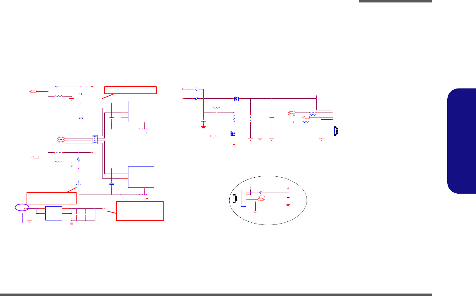
Schematic Diagrams
USB & CCD B - 23
B.Schematic Diagrams
USB & CCD
Sheet 22 of 40
USB & CCD
5
USB0+15
5VS_CCD
CCD_EN23
OC1#
R110 560K_04
6-19-91001-001
J_FP1
CON6_FP
1
2
3
4
5
6
Z2208
USBVCC
Z2209
C11 1U_16V_06
EMI solution,when placement
near to USB Port?
CCD
USB3- 15
Z2210
Q4
AO3409
G
DS
USBVCC
J_FP?
R112 470K_04
R13 0_06
??USB_Port????100U
??,?????Device??
?Restart??
Z2201
C9
10U_10V_08
48 mil
Z2207
R31
100K_04
R18 0_06
USB PORT
6
Z2204
C114
.1U_10V_04
5V
USBVCC
CCD_DET#23
Z2211
VDD3
C94
.1U_10V_04
+
C141
100U_6.3V_B
12
J_USB2
USB_4P
1
2
3
4
GND1
GND2
GND3
GND4
V+
DATA_L
DATA_H
GND
GND1
GND2
GND3
GND4
Z2205
C153
.1U_10V_04
60 mil
J_CCD1
88266-05001
1
2
3
4
5
J_USB1
USB_4P
1
2
3
4
GND1
GND2
GND3
GND4
V+
DATA_L
DATA_H
GND
GND1
GND2
GND3
GND4
OC1#15
Z2202 R6 330K_1%_04
L6
*HCB2012K-500T40_08
1 2
60 mil
USB2+
1
5VS
USBVCC?????5V
~ 5.25V? ? ,? ? ? ?
4.9V,???????
Device? Eye Pattern Test
fail? ? ? ? ? ?
3.3V_FP
1
3.3VS
USB2+15
R132 560K_04
C111
.1U_10V_04
C128
10U_10V_08
USB5-15
OC0#
951118
L7
HCB2012K-500T40_08
1 2
60 mil
From H8 default HI
+
C86
100U_6.3V_B
12
USB2- Q36
2N7002W
G
DS
5V
LP1
CM-4M3216-181JT
1
2
3
46
5
7
8
USB3+ 15
C106
10U_10V_08
USB0-
USB5+
OC0#15
C567
10U_10V_08
FP CONN
USB5+15
L404 HCB1608KF-121T25
USB0-15
R10
68K_1%_04
R122 470K_04
Z2203
U2
RT9701-CPL
1
2
3
4
5
VOUT
GND
VIN
VIN
VOUT
60 mil
J_CCD1
USB2-15
USB0+
L18
HCB3216K-800T30_12
1 2
Z2206
C748
.1U_16V_04
5VS->5V FOR VISTA
C960130
C568
.1U_10V_04
USB5-
L19
HCB3216K-800T30_12
1 2
R11 10K_04
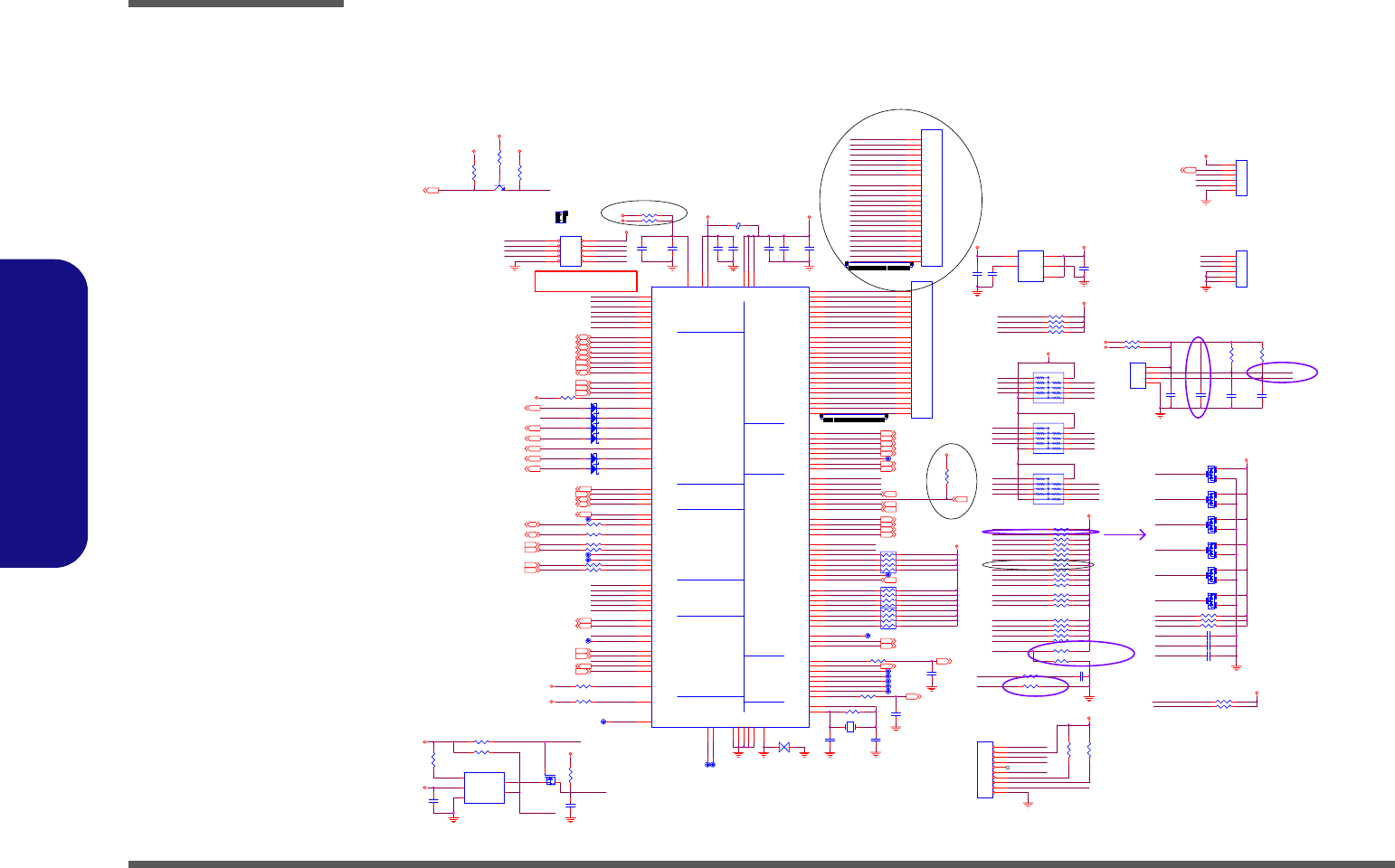
Schematic Diagrams
B - 24 HITACHI H8
B.Schematic Diagrams
HITACHI H8
Sheet 23 of 40
HITACHI H8
LED_BAT_CHG 28
DD_ON29, 3 3
H8_107
H8_RCIN#
JHOTKEY 1
CON6_HOTKEY
1
2
3
4
5
6
U12
AAT3510IGV
3
5
2
1
4
MR#
VCC
GND
RESET#
WDI
LED_BAT_FULL
WEB2#
R336 *10K_04
VDD3
80PORT_DET#
KB-S O2
KB-S I2
80POR T_DET#
80POR T_DET#
Z2313
KB-SI1
KB-S O7
D13 SCS751V-40
A C
R337 10K_04
C433
22P_50V_04
9
KBC_PWRGD15
SMD_BAT1
3IN1
R295 10_04
JA1
SH OR T-A
1 2
R240 120K_04
KBC_VDD
VDD3
CCD_DET# 22
H8_PB#
PM_CLKRUN#
H8_58
KB-S O15
D36
BAV99
A
C
AC
D18 SCS751V-40
A C
Z2303
H8_SMI#
KBC _V DD
SCI#16
LPC _AD2
SUSC #
R538 100_04
R708 10K_04
KB-SO6
SMC_BAT1
C392 1U_10V_06
3I N1
LED_AC IN
RP8 10K_8P4R_04
81 72 6
5
3
4
KBC_TXD1
KB-S O13
U5
CM2838GSIM25
1
2
3
4
5VIN
GND
SD
BP
VO
R243 120K_04
C480
.1U_10V_04
24
BAT1_DET
BRIGHTNESS
MD0_BOOT_FLASH
KB-S I4
KB-S O3
1
CCD_EN 22
CHG_CURSEN29
KBC_MD1
KBC _TXD 1
RP9 10K_8P4R_04
81 72 6
5
3
4
R537 10K_04
5VS
H8_P71
WEB2#
KB-S I3
J_KB1
85201-24051
24
23
22
14
12
11
21
8
20
19
6
5
18
4
17
10
9
7
3
2
1
16
15
13
RP12
10K_10P8R_04
10
9
8
7
6
1
2
3
4
5
RSMRST#
KB-S O14
KBD_CLK
SMD_THER M
CHG_CURSEN
D16 SCS751V-40
A C
R300 10K_04
SMI#16
R312 10K_04
D14
BAV99
A
C
AC
3.3VS
SRS_E N
H8_53
Q22
2N7002W
G
DS
H_A20G ATE
R297 10K_04
R49
10K_06
KB-S O0
R715 10K_06
SUSC #16
3IN1 WEB0#
GA20
H8_52
R709 10K_04
R266 10K_04
TOTAL_CUR
R255
10K_06
PM_CLKRUN#16,20
BUF_PLT_RST#7,15,20,26
BAT1_D ET
RSMRST#
KB-S I5
KB-S I4
C418 10P_50V_04
X2
10MHz
1 2
CPUFAN
TP_DATA
VCORE_ON31
KB-SO7
J_H8DBG1
SPUFZ-10S3-B-0-B
12 34 56 78 910
VDD3
KBC_PCLK
PWR_BTN#
KB-S O11
R330 10K_04
C387
10U_10V_08
VDD3
KB-S O5
D12 SCS751V-40
A C
KBC _P CLK
TOTAL_CUR
C334
.01U_50V_04
TH ERM_ALERT# CCD_DET#
KBC_RXD1
KB-SI0
KB-SI7
R125 *0_04
R247
1K_06
LOW(SU)
BLK_EN
Z2312
Z2310
CLK <-> DATA
CHANGE 951107
PME# 16,19,26
SUSB#15,16,20,27,33,34
LED_BAT_CHG
MD0_BOOT_FLASH
KB-S I0
WLAN _EN 26, 28
R329 10K_04
KBC_RST#15
KB-S O10
C125
1U_10V_06
24 mil
LPC_AD017,20,25
CPU_FAN 25
LPC _AD1
H8_SCI#
LPC _AD0
R124 0_04
LED_ACIN 28
AUX_DATA
BT_DET# 26
H8_GA20
LPC _F R AME#
H8_P74
5V
KB-SO8
LPC _AD3
WEB3#
KB-S O5
KB-S I2
R160 10K_04
BAT1_VOLT
R701
1K_04
RP10
10K_10P8R_04
10
9
8
7
6
1
2
3
4
5
1
Z2305
CHG_CURSEN
BUF_PL T_R ST#
WEB4#
SMC_THERM3
80C LK
MODEL_ID
KB-S O15
2
H8_109
KBC_RST#
KBC_RESET#
C126
47P_50V_04
VDD3
5VS
AUX_CLK
WLAN_DET#
H8_SMI#
SY S_F AN SEN
H8_108
WEB4#
KB-S O6
KB-S I0
R338 10K_04
R306 10M_06
R249
10K_06
C477
.1U_10V_04
VDD3
KBC_AGND
VDD5
LED_SCROLL 28
BT_EN
Z2308
SMC_BAT1
R127
10K_04
R278 10K_04
WEB0#
GA20
KB-SO5
R246 100_04
H8_P70
KB-S O12
J_KB
KB-SO11
R334 10K_04
JDEBUG1
HEADER 10_R
1
2
3
4
5
6
7
8
9
10
R317 10K_04
VOL_MUTE 27
KBC _MD1
H8_51
KB-S O4
TH ERM_ALERT#3
SMC_BAT1
H8_P75
WEB1#
H8_56
R231 100_04
H8 DEBUG PORT
3.3V
KB-SI4
KB-SI6
R553 4.7K_04
R339 0_04
LED_BAT_FULL 28
KBC_PWRGD
R303 100K_04
SMD_THERM3
BAT1_VOLT29
AUX_CLK
KBC_TXD1
H8_57
KB-S O8
KB-S I5
KB-S O14
R265 100_04
F0104-03
KBC_BEEP
3IN 1
THERM_RS T#3
CHG_CUR
TH E RM _R S T#
R327 10K_04
C473
.1U _10V_04
R245 10K_06
5V
KBC_PCLK2
R126
10K_04
R163 10K_04
SMD_BAT111, 2 9
H8_P74
H8_P71
KB-SO1
KB-SO2
VOL_MU TE
MD0_BOOT_FLASH
KB-S O7
BT_EN 26,28
SERI RQ16,19,20
SMI#
SWI#
KB-S I1
WEB5#
KBC_TXD1
KB-S O11
R582 DEL
FOR PWR IN-OUT FAIL
C960124
BT_D ET#
SUSB#
Z2307
D17 SCS751V-40
A C
CPU_FANSEN 25
CCD_DET#
AC_I N#
WEB5#
KB-S I6
KB-S I7
KB-S O9
C376
.1U_10V_04
L53 *FCM2012V-121_08
1 2
HI (SE)
KB-SO10
SCI#
LPC_AD217,20,25
KBC_LPCPD#
SMD_BAT1
PWR_BTN #16
MD0_BOOT_FLASH
H8_55
KB-S O8
R550 100_04
KB-SO9
WEB3#
C649
.1U_10V_04
SERIRQ
WEB2#
Z2301
D15 SCS751V-40
A C
C749 -> 10K
FOR PWR IN-OUT FAIL
C960124
LI D_ SW #24,29
H8_15
MOD E L _I D
AUX_DATA
LED_NUM
PME#
WEB3#
KBC_RXD 1
KBD_DATA
KBC_RXD1
KB-S O0
KB-S O3
R377 10K_04
PWR_SW#29
KB-SO3
WEB4#
VDD3
KBC_AGND
80PORT_DET#
KB-S O6
J_KB2
85201-24051
24
23
22
14
12
11
21
8
20
19
6
5
18
4
17
10
9
7
3
2
1
16
15
13
R349
10K _04
R244 10K_06
951121
Z2302
KB-S O1
24
951118
3.3VS
R333 10K_04
D11
BAV99
A
C
AC
5VS
H8_GA20
KBC_VDD
LPC_FRAME#17,20,25
KBC_BEEP 27
SMD_BAT1
H8_106
LED_PWR
KB-S O9
R560 100_04
R332 10K_04
LED_NUM 28
TP_CLK
WEB1#
C400 1U_10V_06
R375
100K_04
J_KB
BAT1_VOLT
KB-SO0
H8_54
KB-S O13
H8_VCCB(5VS) require
5ms rise time
LPC_AD117,20,25
SMC_THER M
R548 4.7K_04
Q16
2N3904
B
EC
R331 10K_04
VDD3
BAT2_DET
SUSC#
LED_CAP 28
SY S_F AN
R305 10K_04
C375
1U_10V_06
LED_CAP
BAT2_VOLT
VCOR E_ON
R270 10K_04
LI D_ SW #
WEB1#
VDD3
VDD3
R320 10K_04
AC_IN#29
KB-SO12
J_TP1
85201-04051
1
2
3
4
1
2
3
4
C412
10U_10V_08
M_BTN #29
WEB0#
H8_SWI#
H8_SWI#
Z2309
SWI#16
NMI
KBC _MD1
VDD3
KB-SO14
Z2306
KB-SO4
KBC_RESET#
R309 10K_04
RSMRST#16,17
KB-SO13
KB-SO15
KB-SI5
KBD _D ATA
PWR_SW#
KB-S I1
KB-S O4
KB-S I3
R328 100K_04
H_A20GATE15
D34
BAV99
A
C
AC
951122
SMC_BAT111, 2 9
KB-SI2
80CLK
H8_47
KB-S O1
LED_SC ROLL
C391
.1U_10V_04
VDD3
TP_CLK
MD0_BOOT_FLASH
80C LK
KB-S I7
KB-S I6
R326 10K_04
R161 10K_04
CCD_EN
R582 *10K_04
BAT1_D ET29
LED_EMAIL
RP7 10K_8P4R_04
81 72 6
5
3
4
VDD3
BAT1_DET
KBC _S TBY #
KB-SI3
INT. K/B
Debug Port
South
Bridge
Theraml
Battery
PS2
Power
Management
Consumer IR
LED
Ind icator
PWM
output
Clock
GPIO
U9
HD64F2111BVTE10BV
9
10
16
15
66
68
69
70
71
72
73
74
75
2
3
4
129
130
131
133
134
135
121
122
123
124
125
126
127
128
8
142
11
12
120
119
118
117
116
115
114
113
67
111
95
42
7
76
77
36
1
13
58
57
56
55
54
53
52
51
78
79
80
81
82
83
84
85
43
44
45
46
47
48
49
50
24
23
22
21
20
19
18
17
136
137
138
5
6
143
41
40
39
38
37
35
34
33
14
25
26
27
28
29
30
31
32
139 86
65
64
63
62
61
60
59
87
88
89
90
91
92
93
94
96
97
98
99
100
101
102
103
144
104
105
106
107
108
109
110
112
140
141
132
MD1
MD0
P50/ExTxD1*
P51/ExRxD1*
PD0
P70/AN0
P71/AN1
P72/AN2
P73/AN3
P74/AN4
P75/AN5
P76
P77
P43/TMC11
P44/TMO1
P45/TMR11
P80/PME#
P81//CS2#/GA20
P82/CLKRUN#/HI FSD
P84/IRQ3#/TxD1
P85/IRQ4#/RxD1
P86/IRQ5#/SCK1/SCL1
P30/D8/HDB0/LAD0
P31/D9/HDB1/LAD1
P32/ D 10/HD B2/LAD 2
P33/ D 11/HD B3/LAD 3
P34/ D 12/HD B4/LFR AME#
P35/ D 13/HD B5/LR ESET#
P36/D14/HDB6/LCLK
P37/D15/HDB7/SERIRQ
RESET#
RESET_OUT#
NMI
STBY#
PB0/D0/WUE0#/LSMI#
PB1/D1/WUE1#/LSCI
PB2/WUE2#
PB3/WUE3#
PB4/WUE4#
PB5/WUE5#
PB6/WUE6#
PB7/WUE7#
AVSS
VSS
VSS
VSS
VSS
AVCC
AVref
VCCB
VC C
VCL
PG0
PG1
PG2
PG3
PG4/ExSDAA*
PG5/Ex SC LA*
PG6/ExSDAB*
PG7/Ex SC LB*
P60/FTCI/KIN 0#/TMIX
P61/FTOA/KIN1#
P62/FTIA/KIN2#/TMIY
P63/FTIB/KIN3#
P64/FTIC/KIN4#
P65/FTID/KIN5#
P66/FTOB/KIN6#/IRQ6#
P67/TMOX/KIN7#/IRQ7#
PF7/TMOY*
PF6/ExTMOX*
PF5/ExTMIY*
PF4/ExTMIX*
PF3/TMOB
PF2/TMOA
PF1/TMIB
PF0/TMIA
P90/IRQ2#/ADTRG#
P91/IRQ1#
P92/IRQ0#
P93
P94
P95
P96/EXCL
P97SDA0
P40/TMC I 0
P41/TMO0
P42/TMRI0/SDA1
P46
P47
XTA L
PA0/KIN8#
PA1/KIN9#
PA2/KIN10#/PS2AC
PA3/KIN11#/PS2AD
PA4/KIN12#/PS2BC
PA5/KIN13#/PS2BD
PA6/KIN14#/PS2CC
PA7/KIN15#/PS2CD
P52/ExSCK1*/SCL0
PE7
PE6
PE5
PE4
PE3
PE2
PE1
PE0
VSS VCC
PD1
PD2
PD3
PD4
PD5
PD6
PD7
PC7
PC6
PC5
PC4
PC3
PC2
PC1
PC0
P27
P26
P25
P24
P23
P22
P21
P20
EXTAL
P17/PW7
P16/PW6
P15/PW5
P14/PW4
P13/PW3
P12/PW2
P11/PW1
P10/PW0
X1
X2
P83/LPCPD#
CHG_EN29
RE SE T_OU T#
KB-S O2
F951202
DD_ON
JHOTKEY 2
CON6_HOTKEY
1
2
3
4
5
6
J_H8DBG
5V
WLAN_DET# 26
PWR_BTN#
PWR_SW #
KBC_RXD1
KB-S O12
C388 1U_10V_06
TOTAL_CUR29
WLAN_EN
H8_48
D35
BAV99
A
C
AC
D19
BAV99
A
C
AC
CPU_FANSEN
KB-S O10
C386
.1U_16V_04
C752
10U_10V_08
LCD_BRIGHTNESS 24
BT_DET#
H8_SCI#
Z2304
TP_DATA
Z2311
R346 *0_04
R288 10K_04
1
H8_PB#
WLAN_DET#
M_BTN#
C650
.1U _10V_04
10
KBD _C LK
H8_P75
H8_46
C483
10U_10V_08
LPC_AD317,20,25
LED_PWR 28
3. 3V
CHG_CUR 29
H8_RCI N#
80CLK
CIR_EN
RSMRST#
RP11
10K_10P8R_04
10
9
8
7
6
1
2
3
4
5
C127
47P_50V_04
BLK_EN 24
CHG_EN
R48
10K_06
C453
22P_50V_04
C491
1U_10V_06
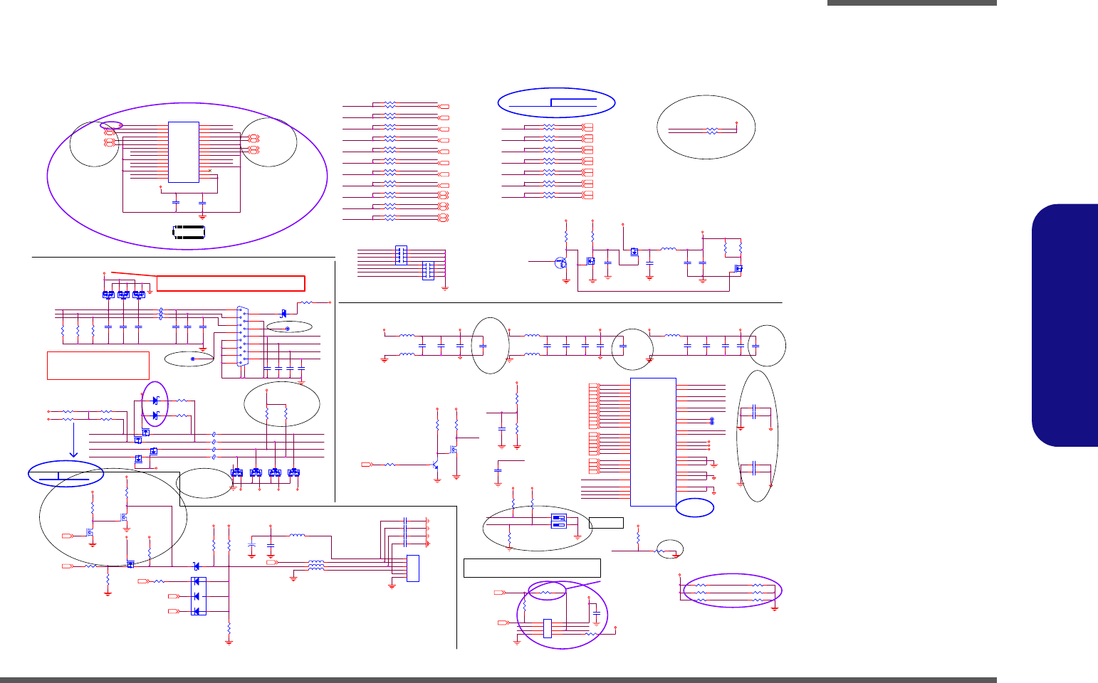
Schematic Diagrams
CRT & LVDS B - 25
B.Schematic Diagrams
CRT & LVDS
Sheet 24 of 40
CRT & LVDS
VGADDCDATA
FGRN
Z2410
C797
*.1U_16V_04
C6
22P_50V_04
C46
.1U_50V_06
L15 HCB2012KF-121T30_08
1 2
R54 0_06
29
1.5VS
Z2405
Z2428
C14
*. 1U _50V _06
R38 *0_06
R25
*1K_ 1%_06
R108
100K_06
NB_ RED 8
LVDSLP0
PLLVCC
LID_SW#23,29
DVP0HS11
R59
10K_06
Q8
2N7002W
G
DS
F010496
LCD_BRIGHTNESS23
LVDS-U2P 12
L49
*HCB2012KF-121T30_08
1 2
C19
*.1U_50V_06
951127
VSY
HSY
R227 *0_04
5VS
3. 3V S
NB_ V SY NC 8
L12
*HCB2012KF-121T30_08
1 2
R447 0_06
2
VGA_HSY 12
EDGE
R236 *0_04
R40
*2.2K_04
C7 99 * . 1U_16V _04
3.3VS
LVDS-LCLKP
EDGE
LVDSLN2
R47 0_06
3.3 VS
ALL_PWROK3, 15,17
LVDS-U0P
C5
1000P_50V_04
D5
*BAV99
A
CAC
Ra
INVERTER
C28 .1U_50V_06
F951202
Z2401
LVDS-L1N
PLLGND
I2CC_SCL 12
R35
*1K_ 1%_06
3.3VS
2.5VS
DVP1D0511
LA_DATAN1
LA_CLKN
DVP0CLK
30
3.3VS
Z2441
Z2431
G
LVDSLP1
Q1 2N7002W
G
DS
R7
75_1%_04
R3 4.7K_04
LVDS-L0N
R704
10K_06
C21
.1U_50V_06
R226 *0_04
24 mil
951124
LVDSLCLKP
LVDS-U1N
C580
*.01U_50V_06
CP2
*10P _8P4C_ 06
1
2
3
4 5
6
7
8
C563
10 00P_50V_04
If Ext VGA
USE 3.3VS
VGA(*SU)
R238,C385,U8 ->DEL*
FOR EMI 951124
Z2403
LVDSCLK
LVDSLCLKN
L10
*HCB2012KF-121T30_08
1 2
C578
*. 1U _50V _06
Q35
2N7002W
G
DS
VIN
3.3VS
J_CRT1
DZ 11A91- ND 208- 4F
8
7
6
5
4
3
2
19
10
11
12
13
14
15
GND2
GND1
PLLVCC
NB_ BLUE 8
CRT_HSYNC
R26
*4.7K_06
L9
*HCB2012KF-121T30_08
1 2
2.5VS
LVDSGND
R16 *0_06
Q34
2N7002W
G
DS
5V
LVDS-L1P 12
LVDSLP2
Z2404
C1
1000P_50V_04
PLEASE CLOSE TO CONNECTOR
LA_DATAP1
LVDS-UCLKP
R171 *2.2K_06
NB (SE)
R9
75_1%_04
OUT
F951202
LA_DATAN0
LVDSLCLKN
D8 RB751V
AC
J_LCD1
CON30A
1 2
3 4
5 6
7 8
910
11 12
13 14
15 16
17 18
19 20
21 22
23 24
25 26
27 28
29 30
12
34
56
78
910
11 12
13 14
15 16
17 18
19 20
21 22
23 24
25 26
27 28
29 30 R30 *0_06
VGA_G 12
VGA_DDCCLK 12
LVDS-U0N
5VS
R46 0_06
? 5VS? ? 951124
LVDS-U1P12
LVDS-LCLKN
R111
10K_06
L4 FCM1608K-121T06_061 2
R17 *0_06
F0122-03
2.5VS
NB_ DDC_CLK 8
LVDS-U2N
C8 00 * . 1U_16V _04
D31
*SCS751
AC
DVDD
LVDS-U0P 12
LA_DATAP2
R39 0_06
R42 0_06
R23 0_06
R239
*0_04
R216 4.7K_06
VGA (SU)
R24 *0_06
R56 0_06
DVP0VS8
LVDS-UCLKP12
LVDS-L0P
LVDSLP1
Q7
AO340
G
D S
C22
*. 01U_50V_06
R446 *0_06
INVERTER CONNECTOR
C13
*.01 U_50V_ 06
R58
100K_06
1-4 OFF;
2-3 ON
2.5VS
VGA_DDCDA TA 1 2
LVDSLP0
D40 RB751V
A C
B
LVDSLP2
R211 4.7K_06
R44 0_06
R21 *0_06
R19 *0_06
R4 44 4. 7K_ 04
LA_DATAN0
C25 *.1U_50V_06
Q5
*2N3904
B
E C
NB (SE)
DVP0D0211
ENAVDD
LVREF
L16
HCB2012KF-121T30_08
1 2
L3 FCM1608K-121T06_061 2
18bit FPD Mode: (recommended setting for notebook)
LVDSLN0
C581
*.1U_50V_06
Rb
PANEL INTERFACE
DVP1D0211
Z2437
CRT_VSYNC
D41 RB751V
A C
R28 *0_06
DVP0D1111
LA_CLKP
C15
*1U_10V_06
D3
BAV99
A
C
AC
R60 0_06
3.3VS
DVP0D0911
LVDS-L2P
Z2435
C27 *.1U_50V_06
LA_DATAP1
C582
*. 01U_50V_06
Z2436
SR0
R64
*10K_06
DVP0D0111
LVDSLCLKP
VSY
LVDSCLK
LVDS-L0P 12
Q37
2N7002W
G
DS
R713
4.7K_04
L46 F CM1608K-121T06_061 2
951118
+
C45
10U_25V_12
L_BKLTEN8
R8
75_1%_04
R43 0_06
R226,234,236 ->DEL *
FOR EMI 951124
For M660SE USE
LA_DATAN2
LA_DATAN2
LVDSLN1
Z2439
SR0
U27
*VT1634AL
3
2
1
48
47
46
44
43
42
41
40
39
36
35
34
33
32
31
24
23
21
20
19
18
14
13
16
15
45
28
27
29
8
9
10
11
30
37
22
6
4
26
38
12
17
25
5
7
D0
D1
D2
D3
D4
D5
D6
D7
D8
D9
D10
D11
D12
D13
D14
D15
D16
D17
A0M
A0P
A1M
A1P
A2M
A2P
A3M
A3P
CLK1M
CLK1P
CLKINP
HSYNC
VSYNC
DE
R_FB
TY P E
MOD SEL
PDB
VREF
DVDD
LVDSVCC
PLLVCC
DGND
DGND
DGND
LVDSGND
LVDSGND
LVDSGND
PLLGND
PLLGND
DDCDATA
Z2434
MOD SEL
LVDSLN1
D3P
D9 R B731U
1
2
3 4
5
6
+
+
+-
-
-
D2
BAV99
A
C
AC
Ra, Rb, Rc(?????75O)??
Intel Solution?, ???NB??
Connector?????150O??
1
5V
R29 *0_06
R69
4.7K_04
R233 *0_04
PLVDD
LVR EF
DEL
U26
951201
5VS
5VS
FRED
LVDSLN2
R37 0_06
R63
82K_06
R4 4. 7K_ 04
PWR
LVDS-U0N 12
R
R33 0_06
R22 0_06
R45 0_06
L2 FCM1608K-121T06_061 2
R36 *1K_1%_06
J_LCD1
LVDS-L2N 12
NB_ G REEN 8
Z2440
Z2412
LVDSLN1
R453
*1K_04
DVDD
NB_ENAVDD 8
DVP0D0011
LVDS-UCLKN12
VGA_BKLTEN12
LVDS-U2P
R712
4.7K_04
5VS
3.3VS
DVP0D0811
MOD SEL
LVDSLN2
R34 *0_06
Q40
2N7002W
G
S D
R109 *0_06
3.3VS
DVP1D0711
Q41
2N7002W
G
S D
U8
*P 2040C
1
2
3
4 5
6
7
8
951118
951201
L47 F CM1608K-121T06_061 2
5VS
DVP0CLK11
R223 *10K_04
5VS
DDCLK
LVDSDATA
R454 *1K_04
R53 0_06
MRA
LVDSVC C
VGA_R 12
NB_ HSY NC 8
NB_ DDC_DA TA 8
Z2408
Z2406
Z2442
LVDS-L1P
LVDSDATA
C26 *.1UF_50V_06
R455 *0_06
L48
HC B3216KF -800T30_1 2
1 2
DVP1D1111
TYPE
R52
100_08
DVP0D0611
Z2413
L14 FCM1608K-121T25_06
1 2
R702
0_04
951118
951201
951202
Q14
BSS138_NL
G
DS
WAITTING FOR EMI
SOLUTION
LVDS-LC LKN 12
R15 *0_06
JINV1
CON6_INV
1
2
3
4
5
6
R27 *0_06
C20
*.01U_50V_06
3.3VS
PLLGND
5VS
DVP0D1011
TY P E
CP3
*10P_8P4C_06
1
2
3
4 5
6
7
8
R234 *0_04
LVDSGND
CRT_VSYNC
Z2430
LA_DATAN1
? : D14,D15,D16? ? ? ? ? ? ? ? CHIP_SET
? ? ? ? ? ,? :Intel? 945GM? 2.5VS
VGA_B 12
DVP0D0711
VGADDCCLK LVD S_PD#
LVDS-UCLKN
SW1
*SW -4X2_4
1
2
4
3
R67
10K_06
R224 *0_04
Place D17, R349 for PR100
DVP1D1011
LA_DATAP2
ENAVDD
R443 4.7K_04
951201
2.5VS
PLLGND
DVP0D0311
L11
*HCB2012KF-121T30_08
1 2
C3
10P_50 V_04
R32 *0_06
C385
*.1U_16V_04
EDGE = L ow , TY PE = Do n' t c ar e, MODSEL = Hig h
Z2409
R238 SE UP 0 OHM
Enable spread
spectrum
C960124
DVP1D0611
C4
10P_50V_04
C7 98 * . 1U_16V _04
MRA
LA_CLKN
LVDS-LC LKP 12
HSY
R20 0_06
L13 FCM1608K-121T25_06
1 2
VGADDCCLK
G
CRT_HSYNC
D32
*BAV99
A
C
AC
C2
10P_50V_04
CRT PORT
NB (SE)
LVDSV C C
LVD S_P D#
LVDS-L2P 12
VGA_ENA VDD 12
C579
*1U_10V_06
2.5VS
NB_LVDSCLK 8
Z2429
LVDSCLK
R77 0_06
R68
4. 7K _04
L1 FCM1608K-121T06_061 2
Q6
*2N7002W
G
S D
2.5VS
NB_LVDSDATA 8
Z2411
R172 2.2K_06
R238 *22_04
DISPCLKI8
LVDS-U2N 12
CLKINP
LVDSLP1
LVDSLN0
LVDSLN0
C575
.1U_50V_06
5VS
NB (SE)
R36 1K_1%_06
LVDS-U1N12
SR1
LVDS-L2N
R
VGADDCDATA
LVDSLP2
I2CC_SDA 12
Z2438
LVDSDATA
L5 FCM1608K-121T06_061 2
C577
.1U_50V_06
R41
100_08
R456 *0_06
951123
3.3VS
LVDS-L0N 12
R442 *1K_04
C7
22P_50V_04
C18
.1U_50V_06
D33
*BAV99
A
C
AC
ENA VEE8
Z2407
SR1
DVP0CLK
R61 *0_06
2.5 VS
LVDS-L1N 12
DVP1D0411
LA_DATAP0
LVDSLCLKN
Z2443
LVDSLCLKP
Q9
DTC114EUA
CE
B
C795
*.1U_16V_04
R76
2.2K_06
VGA (SU)
5VS->3.3VS
951107
PLVDD
DDCLK
C576
4.7U_10V_08
5VS
3.3VS
LVDSGND
DISPCLKO8
D7
*BAV99
A
CAC
C16
4.7U_10V_08
Z2402
LA_CLKP
C566
*1U_10V_06
R55 0_06
R14 *0_06
C562
1000P_50V_04
2.5VS
DVP0DE11
DDCDATA
BLK_EN23
FBLU
LVDSLP0
C8
22P_50V_04
C8 01 * . 1U_16V _04
Q2
2N7002W
G
DS
DVP1D0311
B
LA_DATAP0
D4
BAV99
A
C
AC
951127
VGA_VSY 12
LVDS-U1P
C573
*.1U_50V_06
C796
*.1U_16V_04
Rc
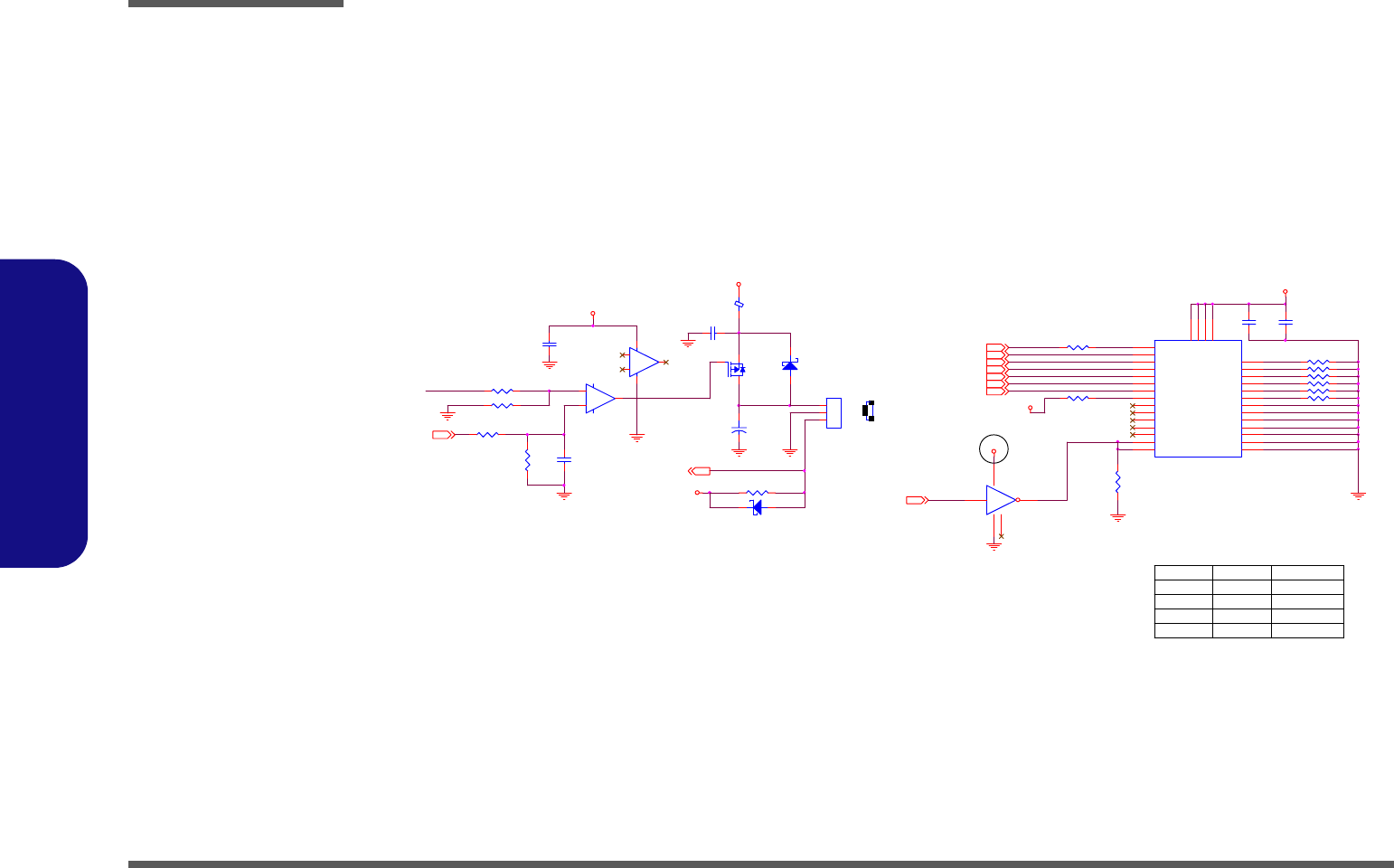
Schematic Diagrams
B - 26 CPU FAN, LPC ROM
B.Schematic Diagrams
CPU FAN, LPC ROM
Sheet 25 of 40
CPU FAN,
LPC ROM
+
C565
100U_6. 3V_B
12
U31
SST49LF008A
1
2
3
4
5
6
7
8
9
10
11
12
13
14
15
16
17
18
19
20
21
22
23
24
25
26
27
28
29
30
31
32
VPP
RST#
FGPI3
FGPI2
FGPI1
FGPI0
WP#
TBL#
ID3
ID2
ID1
ID0
FWH0
FWH1
FWH2
GND
FWH3
RFU
RFU
RFU
RFU
RFU
FWH4
INIT#
VCC
GND
VCCA
GNDA
IC
FGPI4
CLK
VCC
R509
2.2K_04
LPC_AD017,23
High
1
Z2512J_FAN1
85205-0300
1
2
3
Z2504
Z2509
High
40MIL
Z2511 R504 8.2K_04
3.3VS
R507 10K_06
FLASH#15
Z2508
Z2502
+
-
U1A
LM358
3
21
84
Z2507
Block 0
L8
HCB2012K-500T40_08
1 2
LPC_AD317,23
LPC_AD117,23
R12 4.99K_1%_06
Flash Mode
Normal Low
LPC_AD2
LPC_AD0
Z2506
R500 8.2K_04
LPC_FRAME#17,23
CPU_FAN23
C632
.1U_50V_04
CPU_FANSEN23
R499 8.2K_04
PCLK_FWH2
3.3VS
C633
.1U_50V_04
JFAN
Low
20mil
Low
PLT_RST#
PLT_RST#11,15,26
Z2513
FWH_TBL#
Z2503
+
-
U1B
LM358
5
67
Block 1~7
C23
.1U_16V_04
VDD3
R506 8.2K_04
Z2510
U32
MC74VH C1G14
2 4
53
1
3
HighLow
3.3VS
R503 100_04
LPC_AD217,23
D1 SCS551V
AC
SOCKET PLCC32
LPC_AD1
951011
R502 8.2K_04
FAN CONTROL
High
R57 10K_04
Block 0~7
Z2505
VDD5
LPC_AD3 R501 8.2K_04
Low
FWH_WP#
Z2501
FW ROM
R5 4.7K_04
VDD5
R51
*2.2M_04
R50 120K_04
D6
SCS551V
A C
LPC_FRAME#
C10
10U_10V_08
Q3
NDS352
G
D S
FAN_DC_VOL
FAN_DC_VOL
Protected
PCLK_FW H
C24
.1U_50V_04
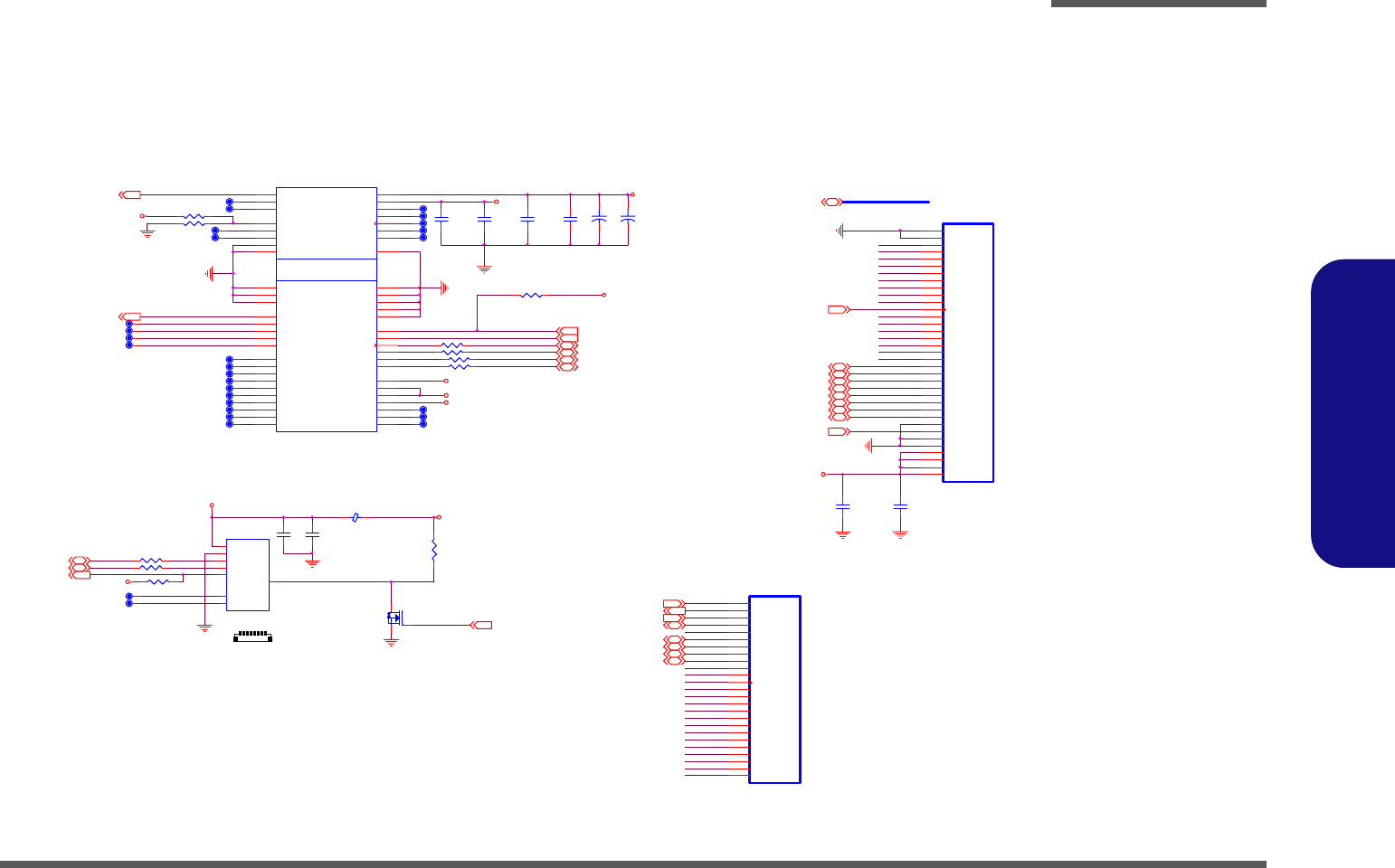
Schematic Diagrams
MINI-PCI & BLUETOOTH B - 27
B.Schematic Diagrams
MINI-PCI & BLUETOOTH
Sheet 26 of 40
MINI-PCI &
BLUETOOTH
USB4+15
SMB_ICHCLK
R189 0_06
3.3V
Z2613
PCI_AD7
R203 0_06
PCI_PERR#15,19
PCI_AD18
C292
.1U_10V_04
Z2601
+
C648
*220U_6.3V_D2
12
3VS_BT
PCI_AD20
PCI_AD24
R185
10K_04
PCI_AD17
Z2625
Z2607
Z2603
R164 10K_04
5VS
USB6+
WLAN_DET#
+
C647
*220U_6.3V_D2
12
PCI_INTD#15
R205 0_04
PCI_AD28
Bluetooth
Z2609
Z2629
R202 *0_04
Z2602
Z2620
R204 0_04
>>>WLAN_EN: Connect to H8
PCI_AD30
PCI_AD19
PCI_AD10
PLT_RST#11,15,20,25
Z2617
PCI_AD5
8
1.5VS
3.3VS
C330
.1U_10V_04
MINI-PCIE CARD
PM_WAKE#20
PCI_PAR15,19
Z2608 USB6+ 15
Z2604
SMB_ICHCLK 20
Z2628
PCI_AD2
BT_DAT
PCI_AD3
C324
10U_10V_08
3.3VS
PCI_AD1
PCI_AD29
Z2626
Z2622
BT_EN 23,28
Z2610
3.3VS
USB4-
PLT_RST#
R181 10K_04
BUF_PLT_RST# 7,15,20,23
PCI_AD23
PCI_AD22
48 mil
JBT
PCI_C/BE3#15,19
PCI_STOP#15,19
Z2611
SMB_ICHDATA
PCLKMPCI2
PCI_AD9
>>>High level ( ON ); Low level ( OFF )
3.3VS
BT_DET#23
PCIE_TXP1_WLAN
Z2605
Z2624 USB6- 15
PCI_AD[31:0]15,19
PCI_GNT#115
PCIE_RXP1_WLAN
BT_EN
PCI_AD4
C148, C155:
PCI_IRDY#15,19
PCIE_TXN1_WLAN
Z2612
C202
10U_10V_08
SMB_ICHDATA 20
Z2621
R186 100K_04
C704
.1U_16V_04
PCI_AD24
C353
.1U_10V_04
MINI FFC CONN
PCI_AD12
L40
HC B2012K-500T40_08
1 2
1
Z2614
R165 *0_04
Z2615
PCI_AD15
BUF_PLT_RST#
R187 *0_04
50mil
3.3VS
PME#16,19,23
Q15
2N7002W G
DS
J_BT1
85205-08001
1
2
3
4
5
6
7
8
+3.3v
GND
USB-
USB+
DETECT#
CH_DATA
CH _CLK
BT_ON#
WLAN_EN
PCI_TRDY#15,19
C705
.1U_16V_04
BT_CLK
PCI_DEVSEL#15,19
PCI_AD8
BT_EN#
PCI_AD27
1.5VS
Z2619
PCI_AD14
KEY
JMINI1
88911-5204
3
5
7
9
11
13
1
15
23
25
21
27
31
33
29
17
19
20
37
39
41
43
45
47
49
51 44
42
18
16
14
2
12
10
8
6
4
22
24
26
28
30
32
34
36
38
40
46
48
50
52
35
BT_DATA
BT_CHCLK
CLKREQ#
GND0
REFCLK-
REFCLK+
WAKE#
GND1
PETn0
PETp0
GND2
GND3
PERn0
PERp0
GND4
NC3
NC4
W_DISABLE#
NC6
NC7
NC8
NC9
NC10
NC11
NC12
NC13 LED_WLAN#
NC(LED_WWAN#)
GND6
UIM_VPP
UIM_RESET
3.3V_0
UIM_CLK
UIM_DATA
UIM_PWR
1.5V_0
GND5
PERSET#
3.3VAUX
GND7
1.5V_1
NC(SMB_CLK)
NC(SMB_DATA)
GND8
NC(USB_D-)
NC(USB_D+)
GND9
NC(LED_WPAN#)
1.5V_2
GND10
3.3V_1
GND11
PCI_AD21
Z2627
VDD3
PCI_C/BE2#15,19
PCI_REQ#115
BT_DET#
>>>Near to JMINI1 for Nvidia platform
USB6-Z2606
USB4+
Z2623
WLAN_EN 23,28
Z2616
PCI_AD26
PCI_AD25
PCI_AD13
USB4-15
PCIE_RXN1_WLAN
PCI_AD16
WLAN_DET#23
PM_WAKE#
JDFFC1
87151-25
3
5
7
9
11
13
1
15
23
25
21
17
19
20
18
16
14
2
12
10
8
6
4
22
24
GNT2#
IDSEL
SERR#
DEVSEL#
PCI_AD17
PCI_AD19
PIRQB#
PCI_AD21
PCI_AD29
PCI_AD31
PCI_AD27
PCI_AD23
PCI_AD25
PCI_AD26
PCI_AD24
PCI_AD22
PCI_AD20
REQ2#
PCI_AD18
PCI_AD16
PERR#
PAR
PME#
PCI_AD28
PCI_AD30
PCI_AD6
PCI_AD0
JDFFC2
87151-35
3
5
7
9
11
13
1
15
23
25
21
27
31
29
17
19
20
18
16
14
2
12
10
8
6
4
22
24
26
28
30
32
33
35
34
PCI_AD0
PCI_AD2
PCI_AD4
PCI_AD6
PCI_AD8
PCI_AD9
GND1
PCI_AD11
PCI_CBE#3
PCI_IRDY#
PCI_CBE#1
PCI_TRDY#
GND5
PCICLK
PCI_AD13
PCI_AD15
PCI_CBE#0
PCI_AD14
PCI_AD12
PCI_AD10
GND2
PCI_RST#
PCI_AD7
PCI_AD5
PCI_AD3
PCI_AD1
PCI_CBE#2
PCI_FRAME#
PCI_STOP#
GND3
GND4
VDD5-1
VDD5-2
VDD5-4
VDD5-3
3G card used: Place the C908, C909
PCI_AD31
PCI_FRAME#15,19
>>>Near to S.B. for Intel platform
PCI_C/BE1#15,19
PCI_AD[31:0]
PCI_SERR#15,19
PCI_AD11
C187
10U_10V_08
Z2618
PCI_C/BE0#15,19
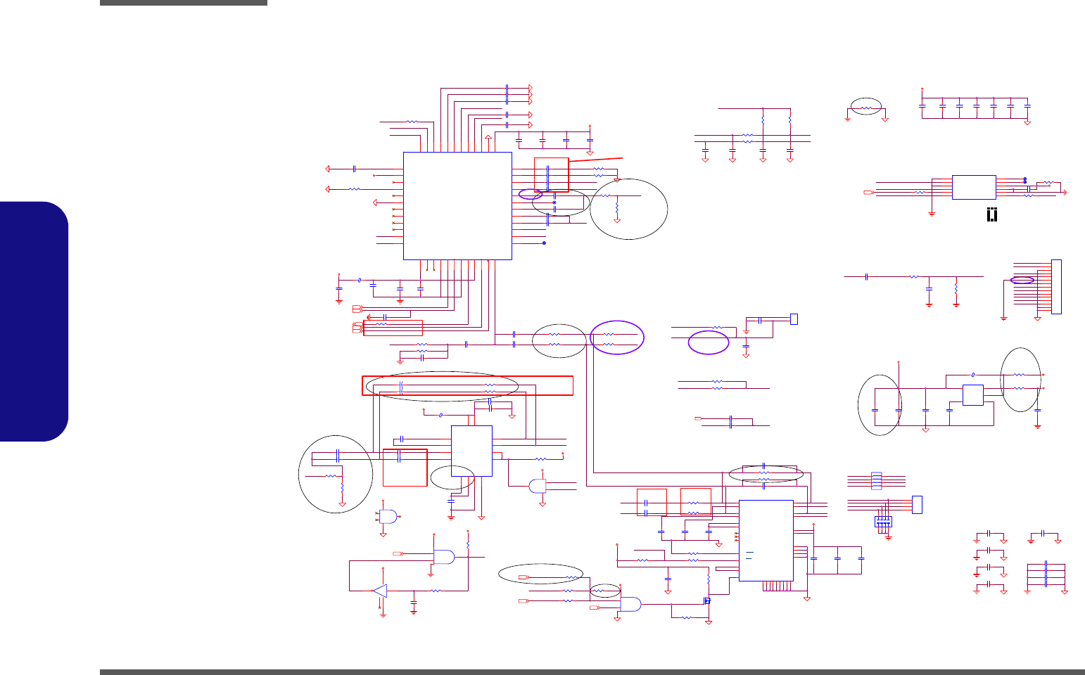
Schematic Diagrams
B - 28 AUDIO VT1708A/ALC883
B.Schematic Diagrams
AUDIO VT1708A/ALC883
EXT-MICL
LIN E-R
C500
.1U_16V_04
+
C537 22U_10V_121 2
MDC
951202
F0122-03
Z2737
JD_SENSE
R3 91 100K_04
AUDG
EXT-MIC -VREFO
C742 .1U_16 V_04
Z2725
Z2724
R413
4.7 K_04
SUSB#15,16,20,23,33,34
C536 270P_10V_06
VT1708
U22
1
13
2
4
5
6
7
8
9
10
11
12
34
14
15
16
17
18
19
20
21
22
23
24
25
26
37
31
33
3
29
30
28
32
35
36
27
38
39
41
40
42
43
44
46
45
47
48
DVDD_CORE
SENSE_A
NC
DVSS
SDO
BITCLK
DVSS
SDI
DVDD_CORE
SYNC
RESETN
PCBEEP
SENSE_B
PORT-E_L
PORT-E_R
PORT-F_L
PORT-F_R
CD-L
AFILT4
CD-R
PORT-B_L
PORT-B_R
PORT-C_L
PORT-C_R
AVDD1
AVSS1
AFILT3
CAP1
AFILT2
NC
VREFOU T-C_L
VREFOUT-F_L
VREFOUT-B_L
AFILT 1
PORT-D_L
PORT-D_R
VREF FILT
AVDD2
PORT-A_L
PORT-A_R
JDREF
AVSS2
PORT-G_L
PORT-G_R
PORT-H_R
PORT-H_L
S/PD IF RX / EAPD
S/PDIF TX
C507
*.1U_16V_04
C534
.1U_16V_04
R437
100_04
C716
10U _10V_08
1
AZ_R ST#16
AUDG
AUDG
KBC_BEEP23
Z2748
Z2747
Z2744
Z2719
PREHP_L
C541 .1U_16V_04
HP_L
HPSEL
FRONT-R
C727
.1U_16V_04
MIC R
SPKR-
R400 13K_04
Z2714
R654 *10K_04
R399 100K_04
951202
5VS_AUD
Z2736
Z2727
R64 0 1K_04
C554 .1U_16V_04
L45
FCM2012V-121_08
12
C558 .1U_16V_04
TJMDC3
951201
FRONT-R
C741 .1U_16 V_04
C498
470P_50V_06
??6 ,??DE POP???
????,??????
AUDG
AZ_ BITC LK16
LINE_SENSE
SPKR+
5VS_AUD
C508
.1U_16V_04
C545 2.2U_6.3V_06
4.7uf
? REALTEK
FAE? ?
???1uf
3.3VS
HP_SENSE
INTMIC
F0121-03
C522 1U_10V_06
C526 4.7U_10V_08
AZ_SY NC16
Z2741
MIC_SENSE
C499
10U_10V_08
HPSEL
Z2729
C729 .1U_16V_04
MDC MODEM
SPD_IFO->SPDIF
C960130
AFILT4
C504
*.1U_16V_04
H8_BEEP
AZ_BITC LK
SPKR+
R40 4 10K_04
Ra
AUDG
C533
1U_10V_06
Z2710
951122
5VS
AUDG
AUD G
R637 20K_1% _0 4
C548 4.7U_10V_08
R431 200_04
????
SPKL-
Q24
2N7002W
G
DS
R638 10K_1% _0 4
951202
R641 33_04
3.3V
AUDG
LIN E-L
PREHP_R
C717
*.1U_16V_04
3.3VS
H8_BEEP
C512
10U_10V_12
951201
AUDG
C750
10U_10V_08
AC_SPKR16
SPKOUTL-
Z2702
C539 .1U_16V_04
R422 100_1%_06
GPO116
Z2728
Z2738
BEEP
R682 *0_04
PLEASE PLACE CLOSE CODEC &
AMP THE POWER INPUT PINS
HP_R
C515 1000P_50V_04
C739 270P_10V_06
Z2739
INT-MIC-VREF O
EAPD
F010496
SPKOUTL-
R410 1M_04
5V
AZ_ SD OUT16
SPKL+
Z2720
R392 1K_04
AUDG
AUDG
MUTE IN#
JD_SENSE
+
C551 22U_10V_121 2
C514 1000P_50V_04
AUDG
LIN E_SEN SE
R367 *0_04
C740
.1U_16V_04
L54
HCB2012K-500T40_08
12
951128
AUDG
C494
.1u_16V_04
Z2740
???
Ca
951122
R2 0_ 06
C505
.1U_16V_04
3.3VS
Z2726
CP1
8P4CX180PF
1
2
3
45
6
7
8
Z2703
R683 *0_04
R402 0_04
MIC L
PREHP_R
U14
APA2020ARL
18
21
7
22
20 15
19
3
10
11
14 1
16
9
8
6
5
4
2
17
23
12
13
24
25
26
27
28
29
30
31
32
33
RVdd
RLINEIN
LVdd
ROUT+
RHPIN ROUT-
RBY PASS
LOUT+
LOU T-
MUTE IN
SE/BTL GN D/ HS
HP/LINE
MUTE OU T
SHUTDOWN
LBY PASS
LHPIN
LLINEIN
TJ
NC
NC
GND/HS
GND/HS
GND/HS
THREM/GND
THREM/GND
THREM/GND
THREM/GND
THREM/GND
THREM/GND
THREM/GND
THREM/GND
THREM/GND
AUDG
SPD_IFO
U24
*TPA4411
1
3
15
13
9
11
14
18
17
2
7
5
19
10
C1P
C1N
INR
INL
OUTL
OUTR
SHDN R#
SHDNL#
SGND
PGND
SVSS
PVSS
PVDD
SVDD
C528
.1U_16V_04
AUD G
Z2709
24 mil
SDATA-IN Max: 0.5inch
AZ_SDI N1
JINTMIC1
ACES/C ON2
1
2
1
2
VREFO-C_L
R584 *220_04
C735 .1U_16V_04
R395 100K_04
SPKOUTL+
Z2751
C553 10U _10 V_08
U18
MC 74V HC 1 G14D F T2G
24
53
1
R636 39.2K_1%_04
C529
2200P_50V_04
3.3VS
AUDG
FRONT-L
C738 22P_50V_04
SPKOUTL+
C523 1U_10V_06
C712
1U_10V_06
Z2711
C555 .1U_16V_04
11
DEL C 951124
C731
.1U_16V_04
C560 270P _10V_06
Cb
R418 100_1%_06
AUDG
Z2730
BEEP
LINE-L
SUSB#
R401 0_04
C734
.1U_16V_04
C730 1U _10V_06
5VS_AU D
Z2713
C19 8 330P_50V_ 04
3.3VS
SPKOUTR-
SDATA-IN
C517 10U_10V_08
4.7uf
? REALTEK
FAE? ?
???1uf
AUDG
AZ_SDIN116
AZ_SD IN 016
AZ_SY NC
Z2707
Z2752
Z2753
SPKOUTR+
C535
.1U_16V_04
U15D
74LVC08PW
12
13 11
147
AUDG
SPKOUTR+
C793 *4.7U_10V_08
JAUDIO1
CON15
1
2
3
4
5
6
7
8
9
10
11
12
13
14
15
Power Plane
AUD G
AUDG
SPDI F
Z2732
Z2750
L44
HCB1608KF- 121T25_06
12
3. 3V S
5VS_AUD
SPD_IFO
JSPK1
CON4_SPK
1
2
3
4
1
2
3
4
C542 4.7U_10V_08
3. 3VS
Z2742
EXT-MICR
Z2704
AUDG
AUD G
AZ_SDOUT
MIC L
Z2701
PREHP_R
GPO1
R714 0_06
C497
470P_50V_06
MU TE I N #
C718
10U_10V_08
2
5VS_AUD
C733 .1U_16V_04
AUDG
AUD G
C550
10U _10V_08
R419 2.2K_04
R1 *0_06
C557 .1U_16V_04
PLEASE PLACE CLOSE CODEC &
AMP THE POWER INPUT PINS
951122
AUDG
U36
*G924
1
23
4 5
SHDN #
GNDBYP
OUT VIN
C524 4.7U_10V_08
BEEP
951128
Z2749
R322 0_06
C538
.1U_16V_04
AUDG
1108
C736 10U_10V_08
C527 4.7U_10V_08
SPKOUTR-
R63 9 10K_04
C707 .1U_16V_04
U15C
74LVC08PW
9
10
8
147
C510
*.01U_X7R_04
AUD G
Z2735
MIC_ SE NSE
EXT-MICL
3.3VS
R414
4.7K_04
R585 0_06
AUDG
VOL_MUTE23
MU TE _O UT
Z2706
C502
10U_10V_12
EXT-MICR
BEEP
R390
10K_04
AUDG
EXT-MIC-VREFO
C509
*.01U_X7R_04
R3 94 10K_04
R710 *0_04
R693
*1K_04
Z2743
5VS_AUD
HPSEL
C503
10U _1 0V_ 08
C725 1U_10V_06
EAPD
R692
1K_04
AUDG
Z2708
C728 1U_10V_06
PREHP_L
INT-MIC-VR EFO
U16
74AHC1G08GW
2
14
3
5
C723 4.7U_10V_08
R393 100K_04
12
951122
3.3VS
AUDG
Z2715
Rb
Z2734
SPKL-
JMDC1
CON12_AMP
1
3
5
7
9
11 12
10
8
6
4
2
GND
Azalia_SDO
GND
Azalia_SYNC
Azalia_SDI
Azalia_RST# Azalia_BCLK
GND
GND
3.3V Main/aux
RESERVED
RESERVED
BEEP->Z?
C960130
AUDG
C724 .1U_16V_04
R557 0_04
C556
.1U_16V_04
R430 5.1K_1%_04
FRONT-L
U17
74AHC1G08GW
2
14
3
5
HP_R
C561
100P_50V_04
C530
330P _50V _04
C737 10U_10V_08
Cb
LP2
FCA3216KF4-121
1
2
3
45
6
7
8
Power Plane
AUDG
AUD G
KBC_BEEP
LINE-R
C552 . 1U_ 16V_04
PIN GND1~9=AUDG
AZ_RST#
SPDI F
C726 .1U_16V_04
C495
10U_10V_08
R655 *10K_04
Z2745
HP_SENSE
F0121-03
AUDG
SPKR-
INTMIC
C513
.1U_16V_04
C794 *4.7U_10V_08 PR EH P_L
Z2746
MIC R
Z2712
R695
*1K_04
R6 34 10K_04
C732 100P _5 0V_04
R175 10K_04
R398 100K_04
AUDG
SPKL+
C722 4.7U_10V_08
Z2731
MU TE I N
C5 59 . 01 U_ 50V_04
C525 4.7U_10V_08
HP_L
Z2718
R635 13K_04
R411
10K_04
R696
*1K_04
Sheet 27 of 40
AUDIO VT1708A/
alc883
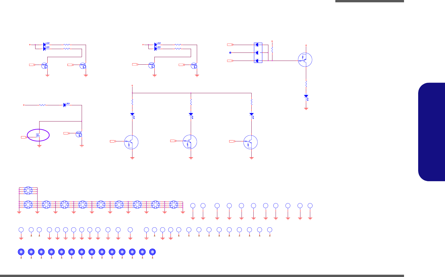
Schematic Diagrams
LED B - 29
B.Schematic Diagrams
LED
Sheet 28 of 40
LED
M14
M-MARK1
H26
C158
PD_LED#
47K
47K
MQ1
DTA114EUA
C
B
E
VDD5
R439
100_06
H49
H5_5D2_7
M11
M- MAR K 1
H14
C158
R438 100_06
R441
100_06
H2
C158D158
LED_BAT_FULL23
Z2806
R433 200_1%_06
LED_PWR23
M9
M-MAR K1
H15
C158
3906 -> 2N7002
CHANGE 951124
H43
H6_0D3_7
M6
M-MARK1
1
H38
MTH8_0D2_8
2
3
4
5 6
7
8
9
GREEN LED
H29
C158
SATA_LED#17
Q28
DTC114EUA
CE
B
H22
H6_5D4_2
H42
H7_7D4_5
H37
C158D158
Z2804
H3
C158D158
1
H16
MTH8_0D2_8
2
3
4
5 6
7
8
9
10K
10K
Q30
DTC114EUA
C
B
E
H44
C256D146
Q33
2N7002W
G
S D
D30
LED
AC
CD_DASP#18
Z2815
H40
C158D158
H47
H5_5D2_7
GREEN LED
M12
M-MARK1
Z2803
H6
C158D158
M4
M-MARK1 M8
M-MAR K1
1
H32
MTH8_0D2_8
2
3
4
5 6
7
8
9
VDD5 3.3VS
M10
M-MARK1
R432
4.7K_06
Z2808
H36
C158D158
H34
C79D79
1
H39
MTH8_0D2_8
2
3
4
5 6
7
8
9
MD1
LED
AC
SCR LOCK
H18
C158
10K
10K
Q31
DTC114EUA
C
B
E
H27
C158
Q27
DTC114EUA
CE
B
H12
C158
GREEN LED
Z2819
M2
M- MAR K1
H30
C158
H35
C217
H48
C256D146
H4
C158D158
H8
C79D79
R434 200_1%_06
1
H31
MTH8_0D2_8
2
3
4
5 6
7
8
9
H41
C158D158
Z2810
Z2805
R435 200_1%_06
Z2812
H23
H6_5D4_2
Q26
DTC114EUA
CE
B
Z2817
M5
M- MAR K1
CD_DASP#
NUM LOCK LED
H28
C256D146
H1
C158D158
M3
M-MAR K1
D28
LED
AC
H19
H6_5D4_2
LED_NUM23
5VS
MR1
100_06
LED_ACIN23
Z2814
M7
M- MAR K1
H5
C158D158
10K
10K
Q32
DTC114EUA
C
B
E
GREEN
ORANGE
D27
DLED
34
12
LED_BAT_CHG23
HDD/PD LED
WLAN_EN23,26
3.3VS
Z2818
D3P
D24
IMN10
1
2
3 4
5
6
+
+
+-
-
-
H46
C315D146
Z2809
SATA_LED#
R440
100_06
D25
LED
A C
M13
M-MAR K1
Q29
DTC114EUA
CE
B
Z2801
WIRELESS LAN /BT
LED
CAPS LOCK LED
H11
C158
H24
C256D146
H13
C158
Z2816
H20
H6_5D4_2
ACIN
PWR/SUS
M1
M-MARK1
GREEN
ORANGE
D26
DLED
34
12
1
H33
MTH8_0D2_8
2
3
4
5 6
7
8
9
LED_CAP23
H45
C315D146
H7
H6_0D2_3
Z2813
Z2807
GREEN LED
3.3VS
Q25
DTC114EUA
CE
B
D29
LED
AC
Z2802
1
H17
MTH8_0D2_8
2
3
4
5 6
7
8
9
1
H10
MTH8_0D2_8
2
3
4
5 6
7
8
9
LED_SCROLL23
1
H9
MTH8_0D2_8
2
3
4
5 6
7
8
9
Z2811
1
H21
MTH8_0D2_8
2
3
4
5 6
7
8
9
R436 200_1%_06
BT_EN23,26
BATT/E mail
CHARGE FULL
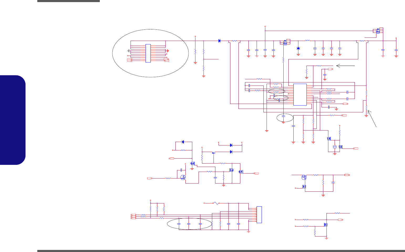
Schematic Diagrams
B - 30 CHARGER, DC IN
B.Schematic Diagrams
CHARGER, DC IN
Z2903
Z2915
PR117 100_06
Z2934
PQ24
DTA114EUA
CE
B
PR9
30K_1%_06
PR130
100K_04
PQ30
2N7002W
G
DS
PD17 FM0540-N
A C
PR110 *100K_04
PC119
30P_50V_06
VDD3
PR109
0_04
CHG_CURSEN 23
PC7 6800P_50V_06
PR43 0_06
PC124 10U_25V_12
Z2905
Z2913
PC125
10U_25V_12
PQ6
2N7002W
G
DS
DD_ON 23,33
PR108
*2.2M_04
PR131
6.8K_1%_06
# MAX CHARGE CURRENT = 2.5A
PQ5
2N7002W G
DS
VA
4A 160mil
ACOK
PQ21
SI4835
4
62 5
73
1
8
Z2902
Z2912
M_BTN#
Z2933
Z2906
Z2927
ACIN
PR31
100K_04
PC111 22P_50V_04
Z2908
3A 120mil
VB
Z2924
USB1-
ACOK
PC118 10U_25V_12
PC1 .01U_50V_06
Z2917
PC112 10U_25V_12
DD_ON
VA
PF1
7A
Hi:16.8V
Z2929
951201
Z2922
PR128
30K_1%_06
PR40 10K_04
MB39A126
PU5
MB39A126
1
2
3
4
5
6
7
8
9
10
11
12
24
13
14
15
16
17
18
19
20
21
22
23
-INC2
OUTC 2
+INE2
-INE2
ACOK
VREF
ACIN
-INE1
+INE1
OUTC1
OUTD/SEL
-INC1
+INC2
+INC1
CTL
FB123
-INE3
RT
XAC O K
VH
OUT
VCC
CS
GND
VIN
Z2931
VA
PR4
30K_1%_06
PR39 *1M_04
Low:12.6V
# TOTAL POWER = 60W
JBATTA1
CON_BAT
1
2
3
4
5
6
7
8
9
PR111
220K_1%_06
VIN1
PR12 *0_04
PC123 10U_25V_12
VIN
SMD_BAT111,23
Z2923
PR11
*10K_04
PC108
10U_25V_12
SYS5V
Z2909
Z2918
PR30
200K_06
From H8
CTL
PR21 100_06
ADJ C.V POINT
VIN
Z2904
PD15
FM0540-N
AC
PR119
.02_1%_25
PC4 .1U_25V_06
PR118
10K_06
PC2
1000P_50V_06
PR13 10K_06
VDD3
VREF
PR1 *0_04
PR6
33K_06
# BAT_SEL H:16.8V ; L: 12.6V
PQ1
DTA114EUA
C E
B
PD7
FM1040-T1
A C
5V
USB1-15
Z2921
BAT1_VOLT
ACIN
PQ23
SI4835
4
62 5
73
1
8
PC12
.1U_25V_06
PC128 10U_25V_12
PC5
2200P_50V_04 PR107 0_06
AC_IN# 23
PR106
0_06
PR22
10K_06
PR5
10K_1%_06
4A 160mil
SYS5V
BAT1_VOLT 23
PC3 .22U_16V_06
LID_SW# 23,24
PR112
20K_1%_06
CHG_EN
AC_IN#
Z2920
Z2914
PR116
10K_06
PR42
*200K_04
VB
# TOTAL_CUR : Vtotal_cur=0.020 X 20 X Ichg
VA
CHG_EN 23
PR23
0_06
PR122
.025_1%_25
PC142
.1U_25V_06
PR3 30K_06
PR7 10K_06
PC178
.1U_50V_06
PR34 10K_06
To H8
PQ27
2N7002W
G
DS
PQ26
2N7002W
G
DS
PC10
.1U_25V_06
PC126
10U_25V_12
PC109
.1U_25V_06
PR14 100K_04
PR8 100K_04
OC2#
Z2910
JUSB1
CON20AF
1 2
3 4
5 6
7 8
910
11 12
13 14
15 16
17 18
19 20
PD16 FM0540-N
A C
PR15 0_06
PR24
0_06
PR161 10_06
PWR_SW#
PC133 .1U_50V_06
PL2
15U_10*10*4
Z2928
PR32
100K_04
VDD3
PC180
30P_50V_06
PR2
10K_1%_06
5V
VREF
PQ3
*2N7002W
G
DS
VB
Z2901
USB1+
T_CUR_CONT
Z2935
PD14
FM5822
A C
BAT1_DET23
PC122 10U_25V_12
PC110
.01U_50V_06
PQ28
2SB1198KR
B
E C
# CURSEN : Vcursen=0.025 X 20 X Ichg
PWR_SW#23
PR10
10K_08
VA
Z2930
LID_SW#
Z2916
Z2936
PJ2
3mm
12
Z2932
PC120
30P_50V_06
SMC_BAT111,23
951118
M_BTN#23
OC2#15
Z2911
PR115 100_06
VIN
Z2907
TOTAL_ C U R 23
Z2919
USB1+ 15
PQ25
2N7002W
G
DS
PR16 0_06
PR29 10K_06
VDD3
CHG_CUR 23
CUR_CONT
PC6 6800P_50V_06
PR133 10K_06
PC138 10U_25V_12
Sheet 29 of 40
CHARGER, DC IN
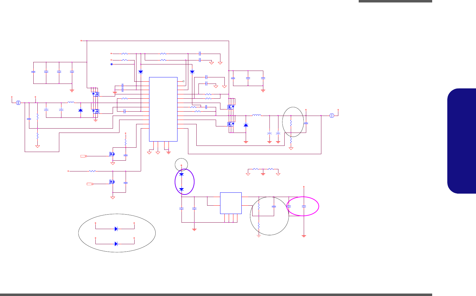
Schematic Diagrams
1.05VS, 1.5V, 2.5VS B - 31
B.Schematic Diagrams
1.05VS, 1.5V, 2.5VS
Sheet 30 of 40
1.05VS, 1.5V, 2.5VX
PC98 1000P_50V_04
SC413
PU4
1
2
3
4
5
6
7
8
9
10
11
12
13
14
15
16
17
18
19
20
21
22
23
24
25
26
27
28
PGND1
DL1
VDDP1
ILIM1
LX1
DH1
BST1
EN/ PSV2
TON2
VOUT2
VCCA2
FBK2
PGOOD2
AGND2
PGND2
DL2
VDDP2
ILIM2
LX2
DH2
BST2
EN/ PSV1
TON1
VOUT1
VCCA1
FBK1
PGOOD1
AGND1
PC81
10U_10V_08
Z3012
SUSB+32,34
PR95
10K_1%_06
V1.05
PR102
0_06
PQ56
SI4800BDY
4
62 5
73
1
8
1A
PR93
0_06
Rb
3.3VS
Z3017
PD24
FM5822
A C
SGND1
Z3015
PD5
FM0540-N
AC
+
PC90 220U_4V_D
12
PL9
2.5U_7*7*3.5
1 2
PC97
.1U_25V_06
Power Plane
PQ55
SI4800BDY
4
62 5
73
1
8
SGND2
Z3010
PD3
FM5822
A C
1.05VS
Z3020 PQ54
SI4800BDY
4
62 5
73
1
8
PC79
10U_10V_08
Ra
SGND2
Max output current is 1A
Rb
Z3018
FOR PWR
C960130
PC101 1U_10V_06
SGND1
PC84
*10U_25V_12
PC80
10U_10V_08
PR91 0_06
951129
F0123-03
PC91
.1U_50V_06
+
PC167 *220U_4V_D
12
SGND2
SGND1
SGND2
2.5V
PL8 2.5U_7*7*3.5
Power Plane
VDD5
Z3002
+
PC166
*220U_4V_D
12
Rb
2.5VS
3.3V
Z3001
PD4
FM5822
A C
2A
PD25
FM5822
A C
PR92 10_06
PR96 10K_1%_06
Z3009
1A
SGND1
PR101 10K_04
Z3014
PD27
FM4002
AC
PR89
1K_1%_06
PR99
10K_1%_06
3A
3.3V
SGND2
PC96
.1U_25V_06
PR97 0_04
SGND1
SGND1
DD_ON#
Z3007
PJ12
OPEN-3m m
1 2
PC78
*10U_10V_08
Ra
Ra
Z3008
5V
Z3003
PC99 100P_50V_04
5V
Z3004
PC88
10U_25V_12
PR100
11K_1%_06
2.5A
Z3006
PR153
47K_04
PJ13
OPEN-5mm
1 2
PC87
10U_25V_12
SGND2
Z3005
PR90
976_1%_06
PR94
22K_1%_06
PC95
22P_50V_04
PQ53
SI4800BDY
4
62 5
73
1
8
PC168 1000P_50V_04
PR152 750K_04
40mil
2.5V
DD_ON#32,33
PR155 1M_04
Z3019
1.5V
PR98
10K_1%_06
PC169
.1U_16V_04
5V
PQ17
2N7002W
G
DS
PC179
0.01U_16V_06
PC170
.1U_16V_04
40mil
PCB FP M-D4526 change M-DO214AC
C960131
Vout = 1.24V ( 1 + Ra / Rb )
PC85
10U_25V_12
Z3013
Z3016
Z3011
PC86
*10U_25V_12
+
PC89
220U_4V_D
12
PC94 1U_10V_06
F0122-03
PC80 -> 10U
PC81 -> 10U
PWR 960130
V1.5
Z3021
PQ18
2N7002W
G
DS
PC100 1U_10V_06
VIN
PC92
.1U_50V_06
PU3 GL39102
1
6
3
5
4
2
7
8
EN
GND
VOUT
GND
ADJ
VIN
GND
GND
PD26
FM4002
AC
PD6
FM0540-N
AC
PC93 1U_10V_06
PR154
47K_04
2A
VCCP_PWRGD
PR103 10_06
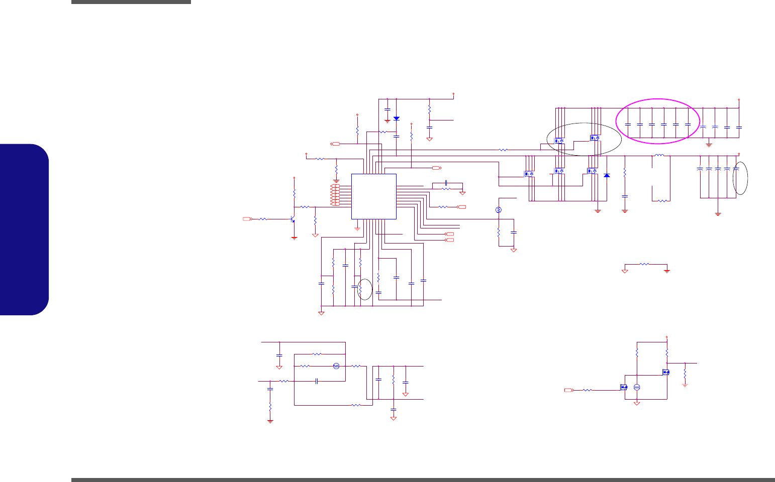
Schematic Diagrams
B - 32 VCORE
B.Schematic Diagrams
VCORE
PC24
*100P_50V_04
PC22 10U_25V_12
GND _SIGNAL PR51
*10K_04
PR77
130K_1%_06
VCORE FOR YUNA AND NAPA CPU
PR73
130K_1%_06
PR56
680_1%_06
VIN
PQ40
IRF7832
4
62 73 8
5
1
GND _SIGNAL
Z3112
GND_SIGNAL
PM_DPR SLPVR 3, 17
PR79
0_04
Z3104
Z3105
PQ36
IR F7413Z PBF
4
62 73 8
5
1
H_VID44
Z3102
PC183 .1U_50V_06
H_VID64
DRP_L1
PR159
*10_08
PC185 .1U_50V_06
DRN
3.3VS
PC41 1U_10V_06
40A
1.05VS
CLKEN#2
HYS
PR54
1K_04
GND_SIGNAL
EN_VCORE
PQ37
IRF7413ZPBF
4
62 73 8
5
1
PQ41
IRF7832
4
62 73 8
5
1
VCORE
GND_SIGNAL
Z3107
CS+
PR55
887_1%_06
H_VID24
PC42
1U_10V_06
PM_DPRSLPVR3,17
GND_SIGNAL
960131
PC43
1000P_50V_ 04
Z3109
PC27 1000P_50V_04
PC23 10U_25 V_ 12
PR63 0_06
PR72
*0_06
PC26
*10P_50V_06
PR36
27.4K_1%_06
CS-
CS+
PC25
*100P_50V_04
ERROUT
PR38
*0_04
PC28 .01U_X7R_50V_06
PR50
10K_04
PR37
28K_1%_06
PQ42
IRF7832
4
62 73 8
5
1
+
PC69
470U_2.5V_D
12
VREFVC
Z3106
PR44
10K_04
H_VID54
TG
PC181 .1U_50V_06
PR80
10K_04
BG
Z3114
DRN
H_VID04
PC182 .1U_50V_06
PTH1
100K_06
12
GND_SIGNAL
GND_SIGNAL
+
PC76
470U_2.5V_D
12
PR33 0_04
H_VID14
DRN
+
PC77
470U_2.5V_D
12
PR82
1K_04
PL3 .6U_13*13*4
+
PC146 15U_25V_D
12
DRN
PR52 10K_04
PC30 1000P_50V_04
PC174
*.001U_50V_08
H_VID34
PTH2
*100K
12
PR76
*0_04
PR53 0_06
PC186 .1U_50V_06
PC14
*3300P_50V_04
Z3101 Z3103
3.3VS
5V
PWRGD_VCORE 15
PJ1
3mm
1 2
VCCSENSE 4
PR48 12. 4K_1%_06 PC31 *100P_50V_04
3.3VS
PD1
FM0540-N
AC
PC20
*100P_50V_04
VCCA
F0122-03
PR69
100K_04
PR45
100_04
PR47
0_06
PU1
SC454
1
2
3
4
5
6
7
8
9
10
11
15
16
17
18
19
20
21
22
23
24
25
26
27
28
29
30
31
32
14
13
12
33
VID6
VID5
VID4
VID3
VID2
VID1
VID0
DPRSTP#
HYS
CLSET
VREF
DAC
SS
FB-
FB+
CS-
CS+
TTR I P
DPRSL
RAMP
EN
PWRGD
CLKEN#
V5
BG
DRN
TG
BST
VRTT#
ERROUT
VCCA
AGND
GND
CS-
VCCA
PC184 .1U_50V_06
PC44
180P_50V_04
Z3113
PC47
100P_50V_04
CLSET
BST
Z3115
CS1N
PD20
FM5822
A C
PR41
*0_04
PC46
1U_10V_06
PR49 0_06
F0122-03
SS
VCCA
CS1N
PR74
130K_1%_06
5V
+
PC75
330U_2.5V_D
12
PR67
0_06
PR35
0_04
Z3108
PR46
100_04
PC21 .033U_50V_06
PQ8
2N3904
B
E C
PQ2
2N7002W
G
DS
VCORE_ON23
EN_VCORE
PC51 *100P_50V_04
DACVREFVC
PQ4
2N7002W
G
DS
TTR I P
VSSSENSE 4
PR62
10_06
FOR EMI
PC29
*68P_50V_04
PR71
*10K_04
GND_SIGNAL
+
PC68
470U_2.5V_D
12
VR_ON
+
PC147 15U_25V_D
12
Sheet 31 of 40
VCORE
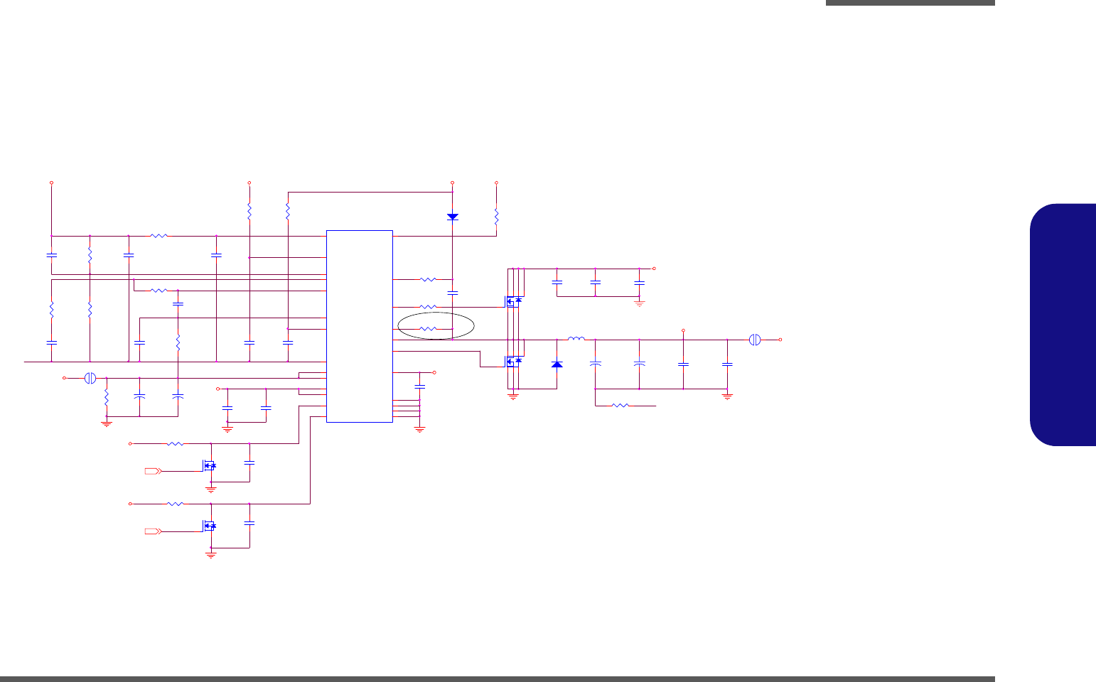
Schematic Diagrams
1.8V, 0.9VS B - 33
B.Schematic Diagrams
1.8V, 0.9VS
Sheet 32 of 40
1.8V, 0.9VS
PR61
10_06
3A
PQ38
SI4800BDY
4
62 5
73
1
8
V1.8
Z3204
Z3217
SUSB+30,34
Z3203
1.8V
PR83
0_06
7A
951205
+
PC57
*220U_4V_D
12
Ra
VSSA PQ43
SI4800BDY
4
62 5
73
1
8
+
PC154
*150U_4V_B2
12
PR68
10_06
Z3212
Z3202
Z3205
PD2
FM0540-N
AC
Z3207
PC40
*10U_10V_08
PR81 47K_04
Z3208
5V
PR59
1.5M_04
1.8VENPR64 47K_04
PR78
18K_1%_06
PL6
2.5U_7*7*3.5
5V
0.9VS
PR75
0_06
PC39
.01U_50V_06
PC143
10U_25V_12
PR58 10_06
Z3206
PC33
1000P_50V_04 Z3215
VSSA
Z3211
Z3201
PC50
.068U_50V_06
PC45
.1U_16V_04
PC36
1U_10V_06
+
PC48
220U_4V_D
12
VIN
+
PC59
150U_4V_B
12
PJ7
OPEN-8mm
1 2
PQ9
2N7002W
G
DS
PC52
*.1U_25V_06
PC55
1U_10V_06
PR57
10K_1%_06
DD_ON#
VTTEN
PR66
10_06
PC32
100P_50V_04
V1.8
PR145
20K_1%_06
PD21
FM5822
A C
Z3213
Z3216
PR60
2.2K_1%_06
PR142
10_06
3.3V
5V
Z3209
PC35
1U_10V_06
V1.8
PC49
.1U_25V_06
5V
PC34
.1U_16V_04
PR70
0_06
PR65
*100K_04
VIN
PC53
.1U_16V_04
Z3214
PC37
1U_10V_06
Rb
PC38
1U_10V_06
Z3210 PC145
.1U_50V_06
PC56
1U_10V_06
DD_ON#30,33
PC144
10U_25V_12
PU2
SC486
11
2
3
4
5
6
7
8
9
10
1
12
13
14
15
16
17
18
19
20
21
22
23
24
25
VTTEN
TON
VDDQS
VSSA
VCCA
FB
PGD
REF
COMP
VTTS
EN/PSV
VDDP2
VDDP2
VTT
VTT
PGND1
PGND2
PGND1
DL
VDDP1
ILIM
LX
DH
BST
GND
PQ7
2N7002W
G
DS
PJ3
OPEN-3mm
12
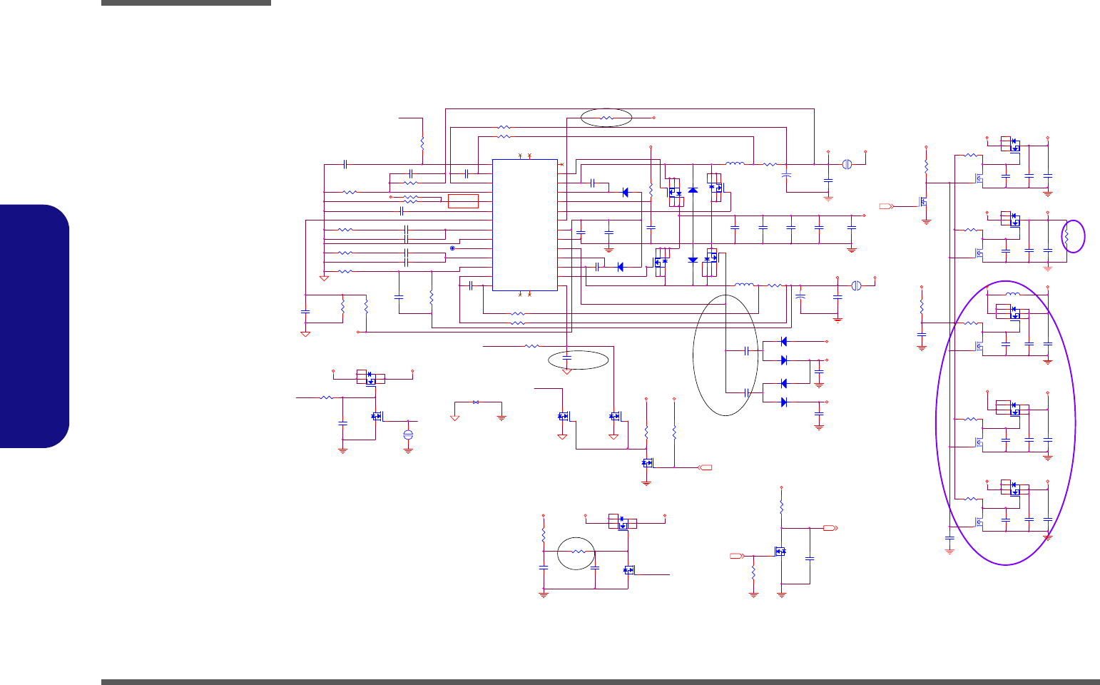
Schematic Diagrams
B - 34 VDD3, VDD5
B.Schematic Diagrams
VDD3, VDD5
Sheet 33 of 40
VDD3, VDD5
Z3307
PQ11
2N7002W
G
S D
PC16
10U_25V_12
PC134
.01U_50V_X7R_06
PC66
.1U_16V_04
RUN_SS1 2.5V
PC13
.1U_50V_06
PC19
10U_25V_12
Z3334
PC164
.1U _16V_04
Z3324
PJ9
OPEN-5mm
1 2
PC65
.1U_16V_04
PC11
2200P_50V_06
SYS3V
Z3327
PC132
0.01U_50V_06
3.3VS
THERMTRIP# 3
PQ51
SI4800BDY
4
6 2
5
7 3
1
8
PC64
.1U_16V_04
Z3323
Z3310
VDD5
Z3317
Z3311
PQ46
SI4800BDY
4
6 2
5
7 3
1
8
RUN_SS1
PC157
.1U_16V_04
VIN2
PC163
*.01U_25V_04
PR84
10K_04
SYS5V
5V
DD_ON23,29
Z3321
PR26 20K_1%_06
PQ10
2N7002W
G
S D
PR146
270K_04
EN_15V
PC141
.1U_25V_06
PD12 FM0540-N
AC
VDD3
PQ32
SI4800BDY
4
62 5
73
1
8
PC73
10U_10V_08
PC121 *30P_50V_04
PC63
.1U_16V_04
Power Plane
Z3313
PC135
.1U_25V_06
DD_ON
Z3330
Z3304
SGND4
Z3305
+
PC155
150U_6. 3V_D
12
PR114 0_04
PQ22
2N7002W
G
DS
SGND4
PC127
*1000P_50V_04
PR151
0_04
PR87
100K_04
1.8V
SYS15V
SYS10V
Z3301
PD19
FM5822
A C
SUSB#15,16,20,23,27,34
+
PC156
150U_6.3V_D
12
PR86
100K_04
PR17 *0_04
PC67
.1U_16V_04
INTVCC2
5V
PR25 20K_1%_06
PC131 .022U_25V_06
PR126 1M_04
PQ12
2N7002W
G
S D
PR121 10_04
PR120 10_04
Z3329
PQ13
2N7002W
G
S D
PL4
4.7U_7*7*3.5
1 2
PC129
1000P_50V_04
PC176
.1U_16V_04
DD_ON#
PC15
10U_25V_12
PQ47
SI4800BDY
4
6 2
5
7 3
1
8
PC83
10U_10V_08
3.3VREF
RUN_SS2
2.5VS
Z3326
INTVCC2
PC17
4.7U_10V_08
PQ16
SI4800BDY
4
6 2
5
7 3
1
8
PC117 *180P_50V_04
PJ10
OPEN-3mm
12
PC162
2200P_50V_04
PQ14
NTGS4141NT1G
3
2 4
1
5
6
PQ33
SI4800BDY
4
6 2
5
7 3
1
8
SY S15V
INTVCC2
PC137
.1U_16V_04
PQ49
2N7002W
G
DS
PR147
1M_04
PD9 FM0540-N
AC
DD_ON#
PR88
200K_04
PQ35
SI4800BDY
4
62 5
73
1
8
PR123 10_04
PQ29
2N7002W
G
DS
3.3V
PR148
0_04
PJ8
OPEN-5m m
1 2
SGND4
VDD3
PC139
.1U _25V_06
PR18
0_04 PR124 10_04
PQ15
NTGS4141NT1G
3
2 4
1
5
6
0V:220KHz
5V:640KHz
1.5VS
EN_15VS
SUSB#
5V
Z3315
PC70
10U_10V_08
Z3325
Z3316
PQ57
SI4800BDY
4
6 2
5
7 3
1
8
VIN2
Z3318
PC165
.1U_16V_04
PC62
2200P_50V_04
VIN
PR113 15K_04
PQ31
2N7002W
G
DS
PR150
10K_04
Power Plane
SGND4
PR85
1M_04
Z3331
PR28 105K_1%_06
Ra
PD8 FM0540-N
A C
5A
PR134
10K_04
PQ50
2N7002W
G
DS
PR132 10_06
PC140
1U_10V_06
PQ58
2N7002W
G
S D
PC130
1000P_50V_04
PC9
2200P_50V_06
5A
VDD5
PC61
*.1U_50V_06
PC116 .01U_16V_04
PC18
10U_25V_12
Z3314
PR160
0_04
PC161
.1U_25V_06
PC175
.1U_16V_04
VDD 5
1.8VS
5V
VDD3
PR19
*0_04
PC74
.1U_16V_04
Rb
Z3312
PQ48
2N7002W
G
DS
PU6
LTC3728LXCUH
28
30
31
1
2
3
4
5
6
15
17
14
19
20
21
22
23
24
27
187
8
9
11
12 13
25
26
32
29
10
16
RUN/SS1
SENSE1+
SENSE1-
VOSENSE1
PLLFLTR
PLLIN
FCB
ITH1
SGND
SW2
BOOST2
TG2
PGND
INTVCC
EXTVCC
BG1
VIN
BOOST1
PGOOD
BG23.3VOUT
ITH2
VOSENSE2
SENSE2-
SENSE2+ RU N /SS2
SW1
TG1
NC
NC
NC
NC
PC114 *30P_50V_04
Z3322
PC113 220P_50V_04
PD13
FM0540-N
AC
Z3335
5A
Z3302
EN_15V
PR143
.010_1%_25
PQ34
SI4800BDY
4
6 2
5
7 3
1
8
SGND4
INTVCC2
Z3319
PD11 FM0540-N
AC
PQ16,57,51
90N03 -> SI4800
SE PQ10,PQ51 DEL
Z3333 ? ?
C960124
Z3333
Z3308
VDD5
1.5V
Z3303
PL1
*HCB3216K-800T30
PR127
10K_04
Z3320
PC177
10U_10V_08
F0121-03
SGND4
PR20 15K_04
PR125
1M_04
5A
SYS15V
DD_ON#
PR129 0_06
PD10 FM0540-N
A C
Z3332
PQ52
2N7002W
G
S D
Ra
PC82
.1U_16V_04
PR144
.010_1%_25
PC136
.01U_50V_X7R_06
5A
PC115
.01U_16V_04
PR149
100K_04
PD18
FM5822
AC
Z3306
Z3328
PC71
10U_10V_08
SYS5V
VIN2
PJ6 SHORT-3mm
21
Z3309
PC8 220P_50V_04 R718
150_08
PR27
63.4K_1%_06
DD_ON# 30,32
5A
SYS5V
5VS
? ? 3VS PWR OFF TIME
ADD R 15ohm C960201
VIN1
PL5
4.7U_7*7*3.5
1 2
Rb
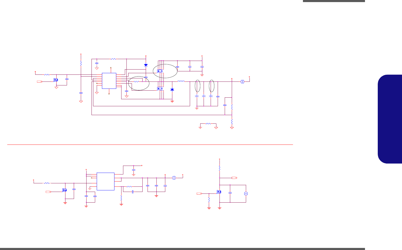
Schematic Diagrams
EXT GPU 1.0VS/1.2VS B - 35
B.Schematic Diagrams
EXT GPU 1.0VS/1.2VS
1.0V_EN
SUSB#
SUSB+ 30,32
+
PC159 *220U_4V_D
12
PQ39
2N7002W
G
DS
Z3403
+
PC72 *220U_4V_D
12
PR156 15K_1%_06
Z3405
PC103
.1U_16V_04
PC173
.1U_16V_04
PR138
10K_1%_06
PU8
APL5913
1
6
3
5
4
2
7
8
9
GND
VCNTL
VOUT
VIN
VOUT
VFB
POK
EN
VIN
PR104
100K_04
VIN
Z3410
SGND3
SUSB#15,16,20,23,27,33
PC102
.1U_16V_04
Z3407
Z3409
PC148
1U_10V_06
SGND3
SGND3
Z3404
5V
PC104
10U_10V_08
PJ4
OPEN-3mm
1 2
PU7
SC411
15
16
1
2
3
4
17
7
8
9
10
11
12
13
514
6
EN/PSV
TON
VOUT
VCCA
FBK
PGOOD
M1
PGND
DL
VDDP
ILIM
LX
DH
BST
NC NC
VSSA
PC149 30P_50V_04
PC105
10U_10V_08
PL7 2.5U _7*7*3.51 2
PR141
3K_0 6
V1.2VS
PQ19
2N7002W
G
DS
PJ11
OPEN-8mm
1 2
SGND3
SUSB+30,32
PC106
10U_10V_08
PC58
10U_25V_12
PC54
10U_25V_12
PR136
10_06
PR139
1.5M_04
PD23
FM5822
A C
VIN
PD22
FM0540-N
AC
PR105
10K_04
Z3408
SUSB+
PQ44
IRF7413ZPBF
4
62 73 8
5
1
+
PC160 220U_4V_D
12
PC153
1U_10V_06
951205
SYS5V
PC151
.1U_16V_04
1.5A
PC107
30P_50V_04
Z3402
PJ5
OPEN-3mm
12
PR 158 220K _04
5V
1.0VS
PQ45
IRF7832
4
62 73 8
5
1
5V
PC 150 1000P_50V_04
PR157
30K_1%_06
5V
V1.0
8A
SGND3
Z3401
Z3406
PC171
1U_10V_06
PR135
10K_1%_06
PR137
0_06
2A
PC172 82P_50V_04 PQ20
2N7002W
G
DS
SGND3
PC60
.1U_25V_06
SUSB+30,32
PC158 .1U_16V_04
SGND3
PC152
.1U_25V_06
V1.5
1.2VS
PR140
150K_04
Sheet 34 of 40
EXT GPU 1.0VS/
1.2VS
Schematic Diagrams
B - 36 HOTKEY LT BOARD
B.Schematic Diagrams
HOTKEY LT BOARD
HH2
C67D67
PIN5,6=HGND
HWEB2#-->WEB1-->E-MAIL
HGND
HWEB1#-->WEB2-->APPLICATION
WWW
HGND
PIN5,6=HGND
HGND
PIN5,6=HGND
HJHOTKEY1
CON6A
1
2
3
4
5
6
AP
HWEB2#
HWEB0#-->WEB0-->WWW
HH1
C67D67
HSW1
HCH STS-05
314 2
E-MAIL
HH5
C237D91
HGND
HWEB2# HWEB1#
HGND
HSW2
HCH STS-05
314 2
HH4
C237D91
HWEB0#
HSW3
HCH STS-05
314 2
HGND
HWEB0#
HWEB1#
HH3
C237D91
HGND
Sheet 35 of 40
HOTKEY LT
BOARD
Schematic Diagrams
PWR HOT BOARD B - 37
B.Schematic Diagrams
PWR HOT BOARD
PPSW4
HCH STS-05
314 2
PPGND
PPM_BTN#
PPGND
PPGND
PPGND
PP+5VS
PIN5,6=PPGND
PPJHOTKEY1
CON6A_HOTKEY
1
2
3
4
5
6
PPWEB4#
PPWEB3#
PPR1
221_06
PPSW1
HCH STS-05
314 2
PPH3
C237D91
PPH5
C67D67
PPGND
PPSW3
HCH STS-05
314 2PPWEB3#
PPH1
C67D67
PWR LED
Z3601
PPGND
PIN5,6=PPGND
PPWEB4#
PPH2
C237D91
PPGND
PIN5,6=PPGND
PPWEB5#
PPWEB5#
PIN5,6=PPGND
PP+5VS
PPM_BTN#
PPSW2
HCH STS-05
314 2
PPGND
PPH6
C237D91 PPH4
C237D91
PPD1
LED_12
AC
PPGND
PPGND
Sheet 36 of 40
PWR HOT BOARD
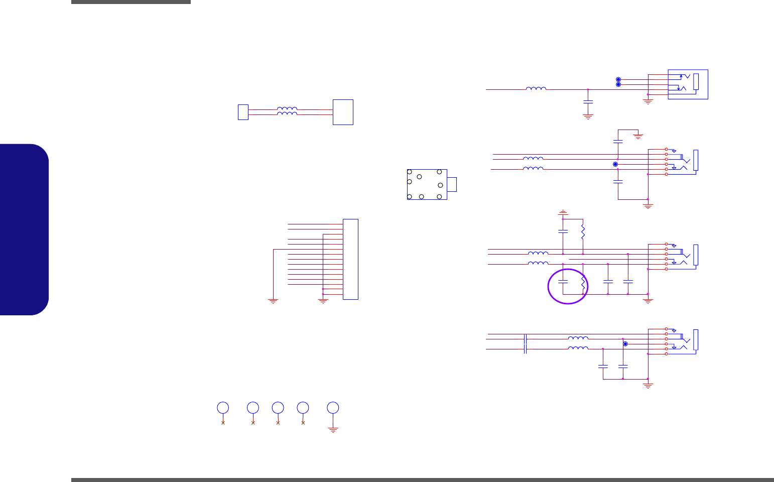
Schematic Diagrams
B - 38 AUDIO & MODEM BOARD
B.Schematic Diagrams
AUDIO & MODEM BOARD
Z3714
AHP_L
AHMDCC1
PJS
1
2TIP
RING
AHP_R
Z3709
AJLINEIN1
2SJ -S351-S05
2
6
5
3
1
4
AGND
AHPSEL
ALINE_SENSE
AGND
Line In
/REAL
Surround Out
AC9 680P -> 1U
Improve head phone quality
C960124
AMICSENSE
AC11 1U_10V_06
Z3706
AJMODEM1
85204-2
1
2
1
2
AL4 HCB1608KF-121T25_06
1 2
AH4
C315D110
Z3707
AJSPDIF1
AUDIO JACK
3
5
4
2
1
3
5
4
2
1
6
Z3703Z3701
AMICL
AJMIC1
2SJ -S351-S01
2
6
5
3
1
4
AR2
1K_06
Z3713
ALINE1-L
AH2
C111D111
ASPD_IFO
AC7
.1U_50V_06
3
AH3
C256D256
ASPDIF
AMICSENSE
AC5
1000P_50V_06
AHPSEL
AC3
680P_50V_06
AJAUDIO1
CON15_R
1
2
3
4
5
6
7
8
9
10
11
12
13
14
15
SOLDER SIDE VIEW
Z3708
AL7 HCB1608KF-121T25_06
AGND
ALINE1-R
AL3 HCB1608KF-121T25_06
1 2
ALINE1-L
AL9
HK2125 R10J-T_08
AGND
AMICR
Mic In
/Cen/LEF Out
AHP_L
AGND
AC12
2200P_50V_06
Z3711
SPDIF OUT
/Side Surronnd
OUT
Z3704
CONN.?????
AGND
AL6 HCB1608KF-121T25_06
1 2
AHP_SENSE
AC2
1000P_50V_06
1
AC9
1U_50V_06
AMICL
AHP_SENSE
ALINE_SENSE
AL10
HK2125 R10J-T_08
AR1
1K_06
AGND
Z3710
Z3715
5
Z3712
HEADPHONE
ASPD_IFO
AH1
C79D79
AGND
AL5 HCB1608KF-121T25_06
1 2
2
AGND
AGND
AJHP1
2SJ -S351-S03
2
6
5
3
1
4
ALINE1-R
AC13 1U_10V_06
AC10
2200P_50V_06
AHP_R
JLINEIN
Z3702
Z3705
AC8
2200P_50V_06
AMICR
AL8 HCB1608KF-121T25_06
AC6
2200P_50V_06
4
Z3716
AH5
C79D79
AL2 FCM1608K-121T06_06
1 2
PIN GND1=AGND
Sheet 37 of 40
AUDIO & MODEM
BOARD
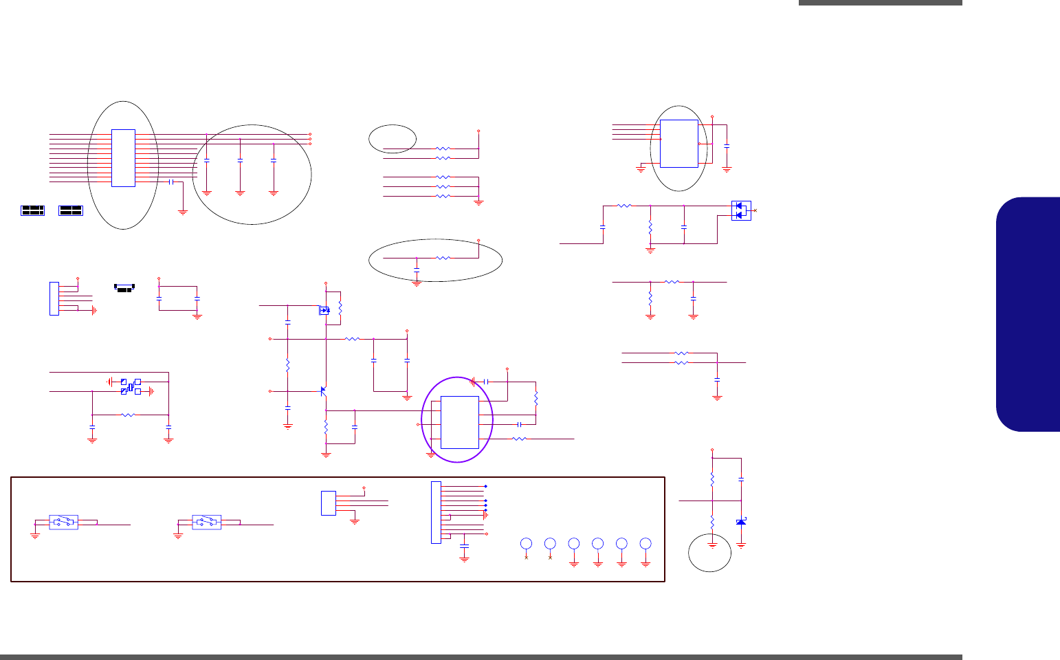
Schematic Diagrams
CLICK BOARD B - 39
B.Schematic Diagrams
CLICK BOARD
TX1
HSX531S_12MHz
12
34
TGND
TPBUTTON_L
TR12
100K_04
21
TMOSI
TC12
.022U_16V_04
TGND
TUSB_PN3
TR16
330K_04
TR5 47K_04
TGND
TTC_VDD
T3. 3V
TGND
TXOUT
T+5V
TXI N
TUSB_PP3_R
TR17 27.4_1%_04
TR24 47K_04
TSW 2
HCH STS-05
314 2
TJ_FP1
TGND
TGPIO1
TDATA1
21
TGND
TC26
1U_10V_06
TGND
TR21
*47K_04
TR11
330K_04
TTP_D A TA
TGND
TQ1
NDS352AP
G
D S
TC4
1U_10V_06
TDATA0
2
TXI N
TC22
1U_10V_06
TTC_VDD
TGND
TGPIO1
TH4
C237D91
TOP VIEW
? ? PCB FP SSOP8-050 ->M-SSOP8-P
C960130
TGND
TJ_ F P2
CON22A
1 2
3 4
5 6
7 8
910
11 12
13 14
15 16
17 18
19 20
2221
TG_F ET
BOTTON VIEW
TGND
TMCS
TMCS
T3. 3V
TDVDD 1
TGND
TG N D
TMISO/MODE3
T3.3V
TGPI O0/ I NT
TR4 330K_0 4
TC15
.1U_16V_04
TTC_VDD
TDATA1
TGND
TUSB_PP3
TH2
C67D67
TGND
TH6
C237D91
1
TNRESET
TMISO/MODE3
TC3 47P_50V_04
TC19
47P_50V_04
TC21 2.2U_6.3V_06
TC14
1U_10V_06
TGND
TESD _RI NG
TGND
TGND
TR2 330K_0 4
TUSB_PP3
TU2
M95128WMN6TP
1
2
3
4
5
6
7
8
CS#
Q
WP#
VSS
S
SCK
HOLD#
VDD
TR13 10K_04
T+5 V
TGND
951206
951121
TGRID0/SENSE
TR19 1.5K_04
TAVDD
TMCLK
TUSB_PN3_R
TH5
C67D67
J_FP1
TGND
TGND
TC23
*.1U_16V_04
TD 1
*SCS551V
A C
26PIN
-->22PIN
TJTP2
CON4
1
2
3
4
1
2
3
4
TPBUTTON_R
TGRID0/SENSE
TESD_RI NG
TESD_RI NG
TR22
*0_06
TR23
0_04
TMI SO/ MO DE3
TDATA2
TC18
.1U_16V_04
951127
Z3801
Z3804
TXOUT
TJ TP 1
87151-1207G
1
2
3
4
5
6
7
8
9
10
11
12
TR3 47K_04
TC24
1U_10V_06
TPBUTTON_R
TC8
18P_50V_06
PIN5,6=TGND
6
TR20 27.4_1%_04
TGND
TR9
33_06
TGN D
T3. 3V
TGPIO0/INT
TGN D
TC16
18P_50V_06
T3. 3V
TUSB_PN3_R
TGND
1
TGND
TPBUTTON_L
TC17
18P_50V_06
TDVD D 1
TPD_REG
PIN5,6=TGND
TGND
TGND
TC20
1U_10V_06
TC13
47P_50V_04
TC25
1U_10V_06
TMCL K
TG_FET
TC1
0.1UF_04
TMOSI
TC27
.1U_25V_06
Z3802
TC7
.1U_25V_06
951127
TC2
.1U_16V_04
TGN D
TQ2
2SB1198K
B
EC
2
TGN D
TNR ESET
TSW1
HCH STS-05
314 2
TGND
TUSB_PP3_R
22
1
TGND
TTP_C LK
TDATA2 TR1 47K_04
TAVD D
TH1
C237D91
TTP_CLK
TUSB_PN3
TDATA0
TTP_DATA
TR6 15_06
F112506
TU4
RClamp0502B
1
23
TR14 *47K_04
TH3
C237D91
22
F112506
TGN D
TGND
TTC_VDD
TPD_REG
TU3
74LVC1G123
8
7
6
54
3
2
1VCC
Rx/Cx
Cx
QGND
CLR#
B
A#
TTC _VD D
TJ _ F P 1
CON6_CLICK
1
2
3
4
5
6
T3. 3V
Z3803
TR15 100_04
TC5
.1U_16V_04
TR18
100K_04
Sheet 38 of 40
CLICK BOARD
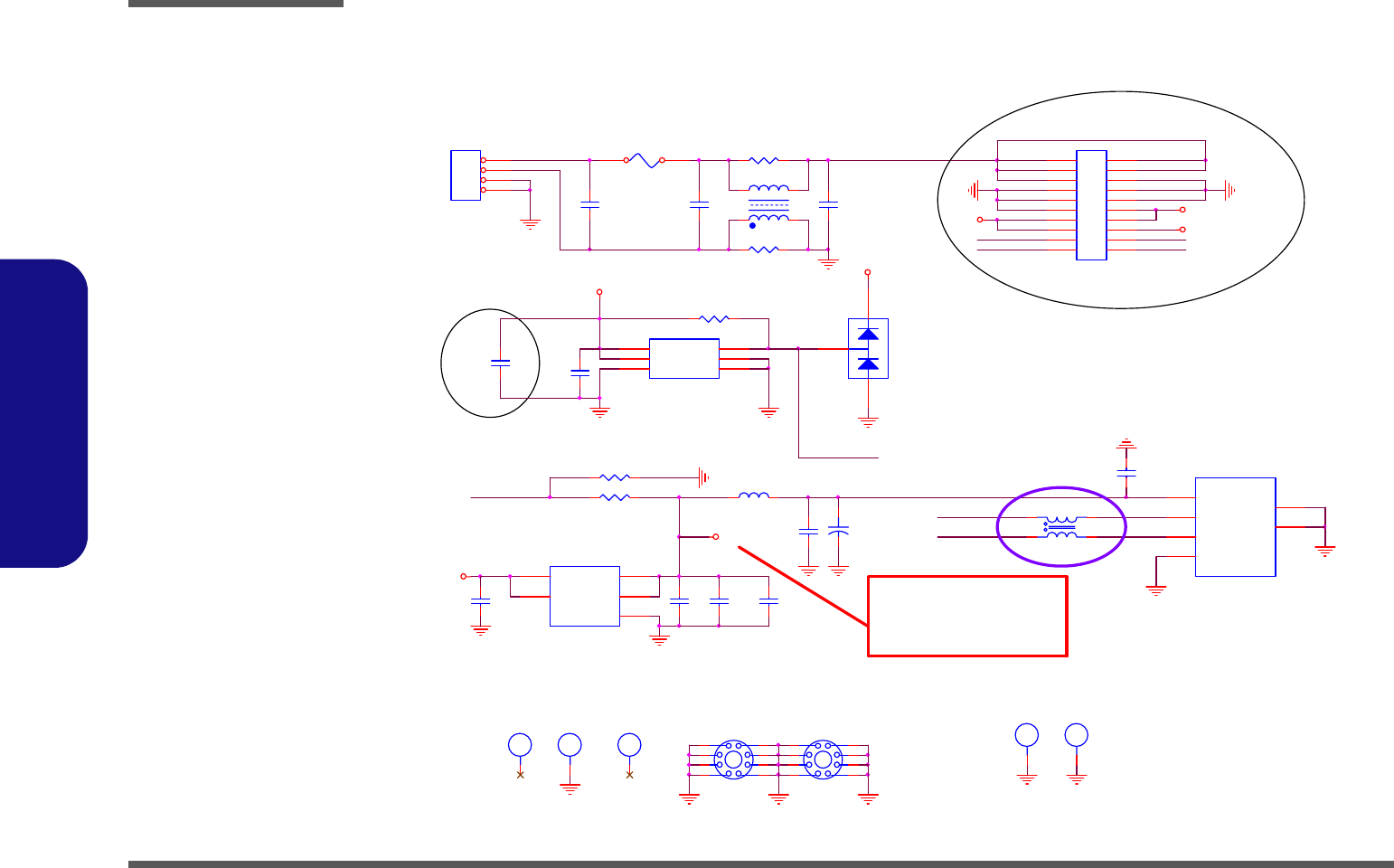
Schematic Diagrams
B - 40 USB BOARD
B.Schematic Diagrams
USB BOARD
951122
U+VDD3
UGND
Z3905
Z3904
U+5V
UGND
UJUSB1
USB_1
1
2
3
4
GND1
GND2
VCC
DATA-
DATA+
GND
S
S
UGND
UGND
UUSB_PN1
951118
UGND
1
UH4
MTH8_0D2_8
2
3
4
5 6
7
8
9
UPC3
.1U_50V_08
PIN GND3~4 =UGND
UGND
UGND
UC5
10U_10V_08
UUSBVCC
UC8
10U_10V_08
+
UC1
100U_10V_D
UC7
.1U_10V_04
UGND
UUSB_PP1
UGND
UVA++
UD1
*BAV99
C
AC
A
UGND
UC4
.01U_50V_06
Z3902
Z3901
UR1 470K_06
UGND
UGND
UUSB_PP1
1
UH5
MTH8_0D2_8
2
3
4
5 6
7
8
9
UUSB_OC2#
UH7
H6_0D2_3
UPR1 0_12
UPR2 0_12
UC2
.1U_50V_06
U+VDD3
UJUSB2
CON20A
1 2
3 4
5 6
7 8
910
11 12
13 14
15 16
17 18
19 20
Z3903
UGND
UPC2
.1U_50V_08
UGND
UVA+
UL3
WCM3216F2S-161T03
1
4
2
3
UU1
TLE4917DS
1
2
3
46 5
VS
GND
Q
GNDPRG GND
UL2
HCB3216KF-800T30_12
ULID_RSUM#UUSB_OC2#
UGND
UGND
U+5V
UUSB_PN1
UH3
C79D79
U+VDD3
UPF1
5A
UH1
C79D79
UU2
RT9701-CPL
1
2
3
4
5
VOUT
GND
VIN
VIN
VOUT
BOM CK
C960130
UC9
1U_10V_06
UUSBVCC? ? ? ? ? 5V
~5.25V??,????
4.9V, ? ? ? ? ? ? ?
Device? Eye Pattern Test
fail? ? ? ? ? ?
UR3 2.7K_06
UPC1
.1U_50V_08
UC3
.1U_50V_06
U+5V
UC6
.1U_10V_04
UH6
H6_0D2_3
UGND
UGND
UPL1
*EMI_CHOKE
32
1 4
UJAC1
ACIN_CON
1
2
GND1
GND2
1
2
3
4
UGND
ULID_RSUM#
UR2 560K_06
UGND
LID SWITCH
UH2
C237D91
Sheet 39 of 40
USB BOARD
Schematic Diagrams
FINGERPRINT BOARD B - 41
B.Schematic Diagrams
FINGERPRINT BOARD
FMOSI
26PIN
-->22PIN
TOP VIEW
FAVDD
FXIN
951121
FNRESET
FGND
FMISO/MODE3
22
FGND
FPD_REG
22
FGND
FMCS
FESD_GND -->FGND
FMISO/MODE3
BOTTON VIEW
FUSB_PP7_R
FXIN
951127
FMCS
FU1
TCS4B
A1
B1
C1
D1
E1
F1
G1
H1
J1
A2
B2
C2
D2
E2
F2
G2
H2
J2
A3
B3
C3
D3
E3
F3
G3
H3
J3
EXT_RING2
CRIDO
RING
MUXOUT
AVDD
MCS
PAD_VDD1B
MISO
DVDD
GPIO1
AGND
DATA0
DATA1
GPIO0
MCLK
USB_DN
USB_DP
MOSI
PD_REG
NRESET
DGND
DATA2
EXT_RING1
PVDD
XTA LI N
PGND
XTALOU T
FGPIO0/INT
FMCLK
1
FXOUT
FTC_VDD
FDATA1
FNRESET
FUSB_PN7_R
FGND
FTC_VDD
FESD_RING
FUSB_PN7_R
951118
21
FDATA1
FJ1
CON22
1 2
3 4
5 6
7 8
910
11 12
13 14
15 16
17 18
19 20
2221
FJ1
FUSB_PP7_R
1
FDATA0
FPD_REG
FDATA2
FMOSI
FESD_RING
FDATA0
FMCLK
FGPIO1
FAVDD
FDVDD1
FGRID0/SENSE
FESD_RING
FESD_RING
FGND
22
951121
FGND
21
FDVDD1
FGPIO0/INT
FXOUT
FGPIO1
FGRID0/SENSE
FTC_VDD
FDATA2
Sheet 40 of 40
FINGERPRINT
BOARD

Schematic Diagrams
B - 42
B.Schematic Diagrams