Clevo M660S, M665S Service Manual. Www.s Manuals.com. Manual
User Manual: Notebook Clevo M660S - Service manuals and Schematics, Disassembly / Assembly. Free.
Open the PDF directly: View PDF ![]() .
.
Page Count: 89
- Manual
- Preface
- Introduction 1-1
- Chapter 1: Introduction
- Overview
- System Specifications
- Model Differences
- External Locator - Top View with LCD Panel Open
- External Locator - Front & Rear Views
- External Locator - Left & Right Side Views
- External Locator - Bottom View
- M660S Mainboard Overview - Top (Key Parts)
- M660S Mainboard Overview - Bottom (Key Parts)
- M660S Mainboard Overview - Top (Connectors)
- M660S Mainboard Overview - Bottom (Connectors)
- Chapter 2: Disassembly
- Overview
- Maintenance Tools
- Connections
- Maintenance Precautions
- Removing the Battery
- Removing the Hard Disk Drive
- Removing the System Memory (RAM)
- Removing the Processor
- Removing the Wireless LAN Module
- Removing the Modem
- Removing the Bluetooth Module
- Removing the Optical (CD/DVD) Device
- Removing the Keyboard
- Appendix A: Part Lists
- Appendix B: Schematic Diagrams
- SYSTEM BLOCK DIAGRAM
- CLOCK GENERATOR
- CPU-1
- CPU-2
- VN800-1
- VN800-2
- VN800-3
- VN800-4
- DDR2-1
- DDR2-2
- VT8237-1
- VT8237-2
- VT8237-3
- HDD & CDROM
- CARDBUS / CARD READER
- CARD SOCKET
- LAN
- USB & CCD
- HITACHI H8
- CRT & LVDS
- CPU FAN, ROM
- LED
- MINI-PCI & BLUETOOTH
- 1.8V, 0.9VS, 2.5VS
- VDD3, VDD5
- CHARGER, DC IN
- VCORE
- 1.05VS, 1.5V
- AUDIO VT1613
- PWR HOT BOARD
- HOTKEY LT BOARD
- USB BOARD
- AUDIO & MODEM BOARD
- CLICK BOARD


Preface
I
Preface
Notebook Computer
M660S/M665S
Service Manual

Preface
II
Preface
Notice
The company reserves the right to revise this publication or to change its contents without notice. Information contained
herein is for reference only and does not constitute a commitment on the part of the manufacturer or any subsequent ven-
dor. They assume no responsibility or liability for any errors or inaccuracies that may appear in this publication nor are
they in anyway responsible for any loss or damage resulting from the use (or misuse) of this publication.
This publication and any accompanying software may not, in whole or in part, be reproduced, translated, transmitted or
reduced to any machine readable form without prior consent from the vendor, manufacturer or creators of this publica-
tion, except for copies kept by the user for backup purposes.
Brand and product names mentioned in this publication may or may not be copyrights and/or registered trademarks of
their respective companies. They are mentioned for identification purposes only and are not intended as an endorsement
of that product or its manufacturer.
Version 1.0
August 2006
Trademarks
Intel, Celeron, and Intel Core are trademarks/registered trademarks of Intel Corporation.
Windows® is a registered trademark of Microsoft Corporation.
Other brand and product names are trademarks and./or registered trademarks of their respective companies.

Preface
III
Preface
About this Manual
This manual is intended for service personnel who have completed sufficient training to undertake the maintenance and
inspection of personal computers.
It is organized to allow you to look up basic information for servicing and/or upgrading components of the M660S/
M665S series notebook PC.
The following information is included:
Chapter 1, Introduction, provides general information about the location of system elements and their specifications.
Chapter 2, Disassembly, provides step-by-step instructions for disassembling parts and subsystems and how to upgrade
elements of the system.
Appendix A, Part Lists
Appendix B, Schematic Diagrams

Preface
IV
Preface
IMPORTANT SAFETY INSTRUCTIONS
Follow basic safety precautions, including those listed below, to reduce the risk of fire, electric shock and injury to per-
sons when using any electrical equipment:
1. Do not use this product near water, for example near a bath tub, wash bowl, kitchen sink or laundry tub, in a wet
basement or near a swimming pool.
2. Avoid using a telephone (other than a cordless type) during an electrical storm. There may be a remote risk of elec-
trical shock from lightning.
3. Do not use the telephone to report a gas leak in the vicinity of the leak.
4. Use only the power cord and batteries indicated in this manual. Do not dispose of batteries in a fire. They may
explode. Check with local codes for possible special disposal instructions.
5. This product is intended to be supplied by a Listed Power Unit (DC Output 19V, 3.42A or 18.5, 3.5A AC/DC Adapter, OR by a
DC Output 20V, 4.5A minimum AC/DC Adapter if you are using the optional port replicator.
CAUTION
Always disconnect all telephone lines from the wall outlet before servicing or disassembling this equipment.
TO REDUCE THE RISK OF FIRE, USE ONLY NO. 26 AWG OR LARGER,
TELECOMMUNICATION LINE CORD
This Computer’s Optical Device is a Laser Class I Product
Preface
V
Preface
Instructions for Care and Operation
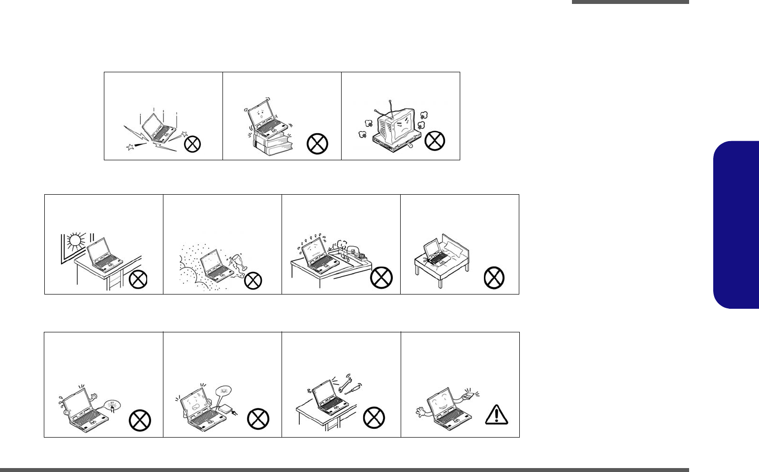
The notebook computer is quite rugged, but it can be damaged. To prevent this, follow these suggestions:
1. Don’t drop it, or expose it to shock. If the computer falls, the case and the components could be damaged.
2. Keep it dry, and don’t overheat it. Keep the computer and power supply away from any kind of heating element. This
is an electrical appliance. If water or any other liquid gets into it, the computer could be badly damaged.
3. Follow the proper working procedures for the computer. Shut the computer down properly and don’t forget to save
your work. Remember to periodically save your data as data may be lost if the battery is depleted.
Do not expose the computer
to any shock or vibration. Do not place it on an unstable
surface. Do not place anything heavy
on the computer.
Do not expose it to excessive
heat or direct sunlight. Do not leave it in a place
where foreign matter or mois-
ture may affect the system.
Don’t use or store the com-
puter in a humid environment. Do not place the computer on
any surface which will block
the vents.
Do not turn off the power
until you properly shut down
all programs.
Do not turn off any peripheral
devices when the computer is
on.
Do not disassemble the com-
puter by yourself. Perform routine maintenance
on your computer.
Preface
VI
Preface
4. Avoid interference. Keep the computer away from high capacity transformers, electric motors, and other strong mag-
netic fields. These can hinder proper performance and damage your data.
5. Take care when using peripheral devices.
Power Safety
The computer has specific power requirements:
• Only use a power adapter approved for use with this computer.
• Your AC adapter may be designed for international travel but it still requires a steady, uninterrupted power supply. If you are
unsure of your local power specifications, consult your service representative or local power company.
• The power adapter may have either a 2-prong or a 3-prong grounded plug. The third prong is an important safety feature; do
not defeat its purpose. If you do not have access to a compatible outlet, have a qualified electrician install one.
• When you want to unplug the power cord, be sure to disconnect it by the plug head, not by its wire.
• Make sure the socket and any extension cord(s) you use can support the total current load of all the connected devices.
• Before cleaning the computer, make sure it is disconnected from any external power supplies.
Use only approved brands of
peripherals. Unplug the power cord before
attaching peripheral devices.
Do not plug in the power
cord if you are wet. Do not use the power cord if
it is broken. Do not place heavy objects
on the power cord.
Power Safety
Warning
Before you undertake
any upgrade proce-
dures, make sure that
you have turned off the
power, and discon-
nected all peripherals
and cables (including
telephone lines). It is
advisable to also re-
move your battery in
order to prevent acci-
dentally turning the
machine on.

Preface
VII
Preface
Battery Precautions
• Only use batteries designed for this computer. The wrong battery type may explode, leak or damage the computer.
• Do not continue to use a battery that has been dropped, or that appears damaged (e.g. bent or twisted) in any way. Even if the
computer continues to work with a damaged battery in place, it may cause circuit damage, which may possibly result in fire.
• Recharge the batteries using the notebook’s system. Incorrect recharging may make the battery explode.
• Do not try to repair a battery pack. Refer any battery pack repair or replacement to your service representative or qualified service
personnel.
• Keep children away from, and promptly dispose of a damaged battery. Always dispose of batteries carefully. Batteries may explode
or leak if exposed to fire, or improperly handled or discarded.
• Keep the battery away from metal appliances.
• Affix tape to the battery contacts before disposing of the battery.
• Do not touch the battery contacts with your hands or metal objects.
Battery Disposal
The product that you have purchased contains a rechargeable battery. The battery is recyclable. At the end of
its useful life, under various state and local laws, it may be illegal to dispose of this battery into the municipal
waste stream. Check with your local solid waste officials for details in your area for recycling options or proper
disposal.
Caution
Danger of explosion if battery is incorrectly replaced. Replace only with the same or equivalent type recommend-
ed by the manufacturer. Discard used battery according to the manufacturer’s instructions.

Preface
VIII
Preface
Related Documents
You may also need to consult the following manual for additional information:
User’s Manual on CD
This describes the notebook PC’s features and the procedures for operating the computer and its ROM-based setup pro-
gram. It also describes the installation and operation of the utility programs provided with the notebook PC.

Preface
IX
Preface
Contents
Introduction ..............................................1-1
Overview .........................................................................................1-1
System Specifications .....................................................................1-2
Model Differences ...........................................................................1-5
External Locator - Top View with LCD Panel Open ......................1-6
External Locator - Front & Rear Views ..........................................1-7
External Locator - Left & Right Side Views ...................................1-8
External Locator - Bottom View .....................................................1-9
M660S Mainboard Overview - Top (Key Parts) ...........................1-10
M660S Mainboard Overview - Bottom (Key Parts) .....................1-11
M660S Mainboard Overview - Top (Connectors) ........................1-12
M660S Mainboard Overview - Bottom (Connectors) ...................1-13
Disassembly ...............................................2-1
Overview .........................................................................................2-1
Maintenance Tools ..........................................................................2-2
Connections .....................................................................................2-2
Maintenance Precautions .................................................................2-3
Removing the Battery ......................................................................2-5
Removing the Hard Disk Drive .......................................................2-6
Removing the System Memory (RAM) ..........................................2-8
Removing the Processor ................................................................2-10
Removing the Wireless LAN Module ...........................................2-12
Removing the Modem ...................................................................2-13
Removing the Bluetooth Module ..................................................2-14
Removing the Optical (CD/DVD) Device ....................................2-15
Removing the Keyboard ................................................................2-16
Part Lists ..................................................A-1
Part List Illustration Location ........................................................A-2
Top (M660S) ..................................................................................A-3
Top (M665S) ................................................................................. A-4
Bottom (M660S/M665S) ............................................................... A-5
LCD (M660S) ................................................................................ A-6
LCD (M665S) ................................................................................ A-7
Combo (M660S/M665S) ............................................................... A-8
DVDRW (M660S/M665S) ............................................................ A-9
Schematic Diagrams.................................B-1
SYSTEM BLOCK DIAGRAM ......................................................B-2
CLOCK GENERATOR ..................................................................B-3
CPU-1 .............................................................................................B-4
CPU-2 .............................................................................................B-5
VN800-1 .........................................................................................B-6
VN800-2 .........................................................................................B-7
VN800-3 .........................................................................................B-8
VN800-4 .........................................................................................B-9
DDR2-1 ........................................................................................B-10
DDR2-2 .........................................................................................B-11
VT8237-1 ......................................................................................B-12
VT8237-2 ......................................................................................B-13
VT8237-3 ......................................................................................B-14
HDD & CDROM ..........................................................................B-15
CARDBUS / CARD READER ....................................................B-16
CARD SOCKET ...........................................................................B-17
LAN ..............................................................................................B-18
USB & CCD .................................................................................B-19
HITACHI H8 ................................................................................B-20
CRT & LVDS ...............................................................................B-21
CPU FAN, ROM ..........................................................................B-22
LED ...............................................................................................B-23
MINI-PCI & BLUETOOTH .........................................................B-24

Preface
X
Preface
1.8V, 0.9VS, 2.5VS ...................................................................... B-25
VDD3, VDD5 ............................................................................... B-26
CHARGER, DC IN ......................................................................B-27
VCORE ........................................................................................ B-28
1.05VS, 1.5V ................................................................................ B-29
AUDIO VT1613 ........................................................................... B-30
PWR HOT BOARD .....................................................................B-31
HOTKEY LT BOARD ................................................................. B-32
USB BOARD ............................................................................... B-33
AUDIO & MODEM BOARD ...................................................... B-34
CLICK BOARD ........................................................................... B-35
...................................................................................................... B-36

Introduction
Overview 1 - 1
1.Introduction
Chapter 1: Introduction
Overview
This manual covers the information you need to service or upgrade the M660S/M665S series notebook computer. Infor-
mation about operating the computer (e.g. getting started, and the Setup utility) is in the User’s Manual. Information
about drivers (e.g. VGA & audio) is also found in User’s Manual. That manual is shipped with the computer.
Operating systems (e.g. DOS, Windows 9x, Windows NT 4.0, Windows 2000, Windows XP, OS/2 Warp, UNIX, etc.) have
their own manuals as do application software (e.g. word processing and database programs). If you have questions about
those programs, you should consult those manuals.
The M660S/M665S series notebook is designed to be upgradeable. See “Disassembly” on page 2 - 1 for a detailed de-
scription of the upgrade procedures for each specific component. Please note the warning and safety information indi-
cated by the “” symbol.
The balance of this chapter reviews the computer’s technical specifications and features.

Introduction
1 - 2 System Specifications
1.Introduction
System Specifications
Feature Specification
Processor Intel® Core™ Duo Processor
(478-pin) Micro-FC-PGA Package
T2300/ T2400/ T2500/ T2600/ T2700
65nm (65 Nanometer) Process Technology
2MB On-die L2 Cache & 667MHz FSB
1.66/ 1.83/ 2.0/ 2.16/ 2.33 GHz
Intel® Core™ Solo Processor
(478-pin) Micro-FC-PGA Package
T1300/ T1400
65nm (65 Nanometer) Process Technology
2MB On-die L2 Cache & 667MHz FSB
1.66/ 1.83 GHz
Intel® Celeron® M Processor
(478-pin) Micro-FCPGA Package
410/ 420/ 430
65nm (65 Nanometer) Process Technology
1MB On-die L2 Cache & 533MHz FSB
1.46/ 1.60/ 1.73 GHz
Core Logic VIA VN800 + VT8237R-Plus Chipset
Memory One 200 Pin SO-DIMM Sockets Supporting DDRII (DDR2) 533 MHz
2nd 200 Pin SO-DIMM Socket (Factory Option)
64-bit Wide DDRII (DDR2) Data Channel
Memory Expandable up to 1GB (256/ 512/ 1024 MB DDRII Module)
Memory Expandable up to 2GB if 2nd 200 Pin SO-DIMM Socket (Factory Option) is Used
(Note: Do Not Use Other Module Types)
Security Security (Kensington® Type) Lock Slot
BIOS One 4Mb Flash ROM Phoenix™ BIOS
LCD 15.4" WXGA TFT LCD
Latest Specification Information
The specifications listed in this Appendix are correct at the time of going to press. Certain items (particularly processor types/speeds and
CD/DVD device types) may be changed, delayed or updated due to the manufacturer's release schedule. Check with your service center
for details.

Introduction
System Specifications 1 - 3
1.Introduction
Video Adapter Video Controller: built-in VIA VN800 Chipset
Video Memory: Supports up to 64MB of Video Memory (dynamically allocated from system memory where needed)
Supports Analog Monitor Pixel Resolution up to 1600 * 1200
Integrated 128-bit 3D Graphics Engine Accelerator
Storage One Changeable 12.7mm(h) Optical Device (CD/DVD) Type Drive
One Easy Changeable 2.5" 9.5 mm (h) PATA (Parallel) HDD
Audio Integrated AC97 Compliant Interface
3D Stereo Enhanced Sound System
Sound-Blaster PRO™ Compatible
2 * Built-In Speakers
Built-In Microphone
Keyboard &
Pointing Device Winkey Keyboard Built-In TouchPad with Scrolling Function
Interface Three USB 2.0 Ports
One External Monitor Port
One Headphone-Out Jack
One Microphone-In Jack
One Line-In Jack
One S/PDIF Out Jack
One RJ-11 Modem Jack
One RJ-45 LAN Jack
One DC-in Jack
Card Reader Embedded 7-in-1 Card Reader (MS/ MS Pro/ SD/ Mini SD/ MMC/ RS MMC/ MS Duo)
Note: MS Duo/ Mini SD/ RS MMC Cards require a PC adapter
PCMCIA One Type-II PCMCIA CardBus PC Card Slot
Communication 56K Plug & Play Fax/Modem, V.90/92 Compliant
10Mb/100Mb Ethernet LAN
802.11b/g USB Wireless LAN Module (Option)
Bluetooth Module v2.0 (Factory Option)
300K or 1.3M Pixel USB PC Camera Module (Factory Option)
Power
Management Supports ACPI 2.0 Supports Wake on LAN
Power Full Range AC/DC Adapter 19V, 3.42A or 18.5V, 3.5A (65W), 100~240V, 50~60Hz
Full Range AC/DC Adapter 20V, 4.5A (90W), 100~240V, 50~60Hz (Supplied for the Optional Port Replicator Only)
Battery 6 Cell Smart Lithium-Ion Battery Pack, 4000mAH
Feature Specification
Introduction
1 - 4 System Specifications
1.Introduction
Environmental
Spec Temperature
Operating: 5°C ~ 35°C
Non-Operating: -20°C ~ 60°C
Relative Humidity
Operating: 20% ~ 80%
Non-Operating: 10% ~ 90%
Dimensions
& Weight 360mm (w) * 267mm (d) * 25.4mm (h) 2.6 kg With 6 Cell Battery
Optional Optical Drive Module Options:
DVD/CD-RW Combo Drive Module
DVD-Dual Drive Module
Port Replicator (10/100 Base-T Ethernet Port, 4 * USB 2.0
Ports, Serial Port, Parallel Port, External Monitor Port,
DC-In Jack)
(Note: Port Replicator requires the supplied 90W
power adapter)
802.11b/g USB Wireless LAN Module
USB PC Camera Module (Factory Option)
Bluetooth Module v2.0 (Factory Option)
Feature Specification
Introduction
System Specifications 1 - 5
1.Introduction
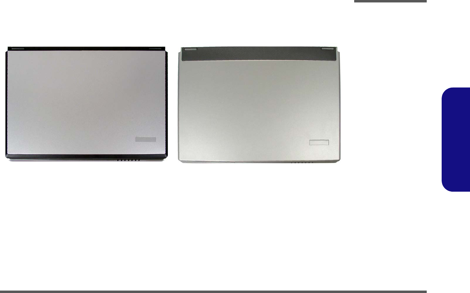
Model Differences
The models vary slightly in external cover design and color.
M660S
M665S
Figure 1
Model Differences
Introduction
1 - 6 External Locator - Top View with LCD Panel Open
1.Introduction
External Locator - Top View with LCD Panel Open
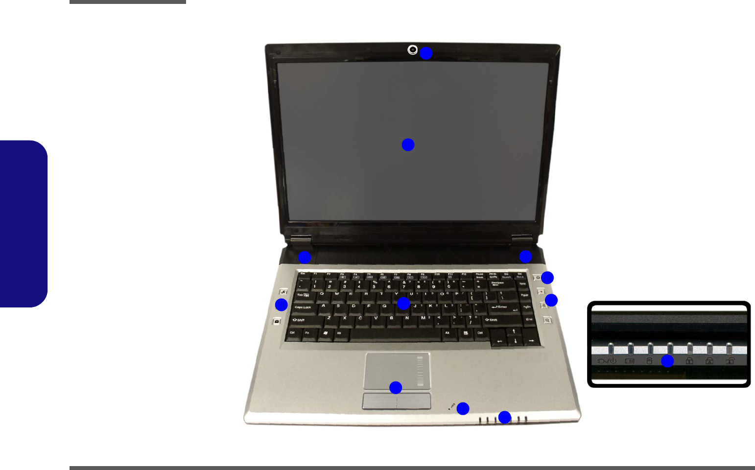
Figure 2
Top View
1. Optional Built-In
PC Camera
2. LCD
3. Speakers
4. Power Button
5. Hot Key Buttons
6. Keyboard
7. TouchPad and
Buttons
8. Built-In
Microphone
9. LED Indicators
2
5
1
7
8
4
6
9
33
5
9
Introduction
External Locator - Front & Rear Views 1 - 7
1.Introduction
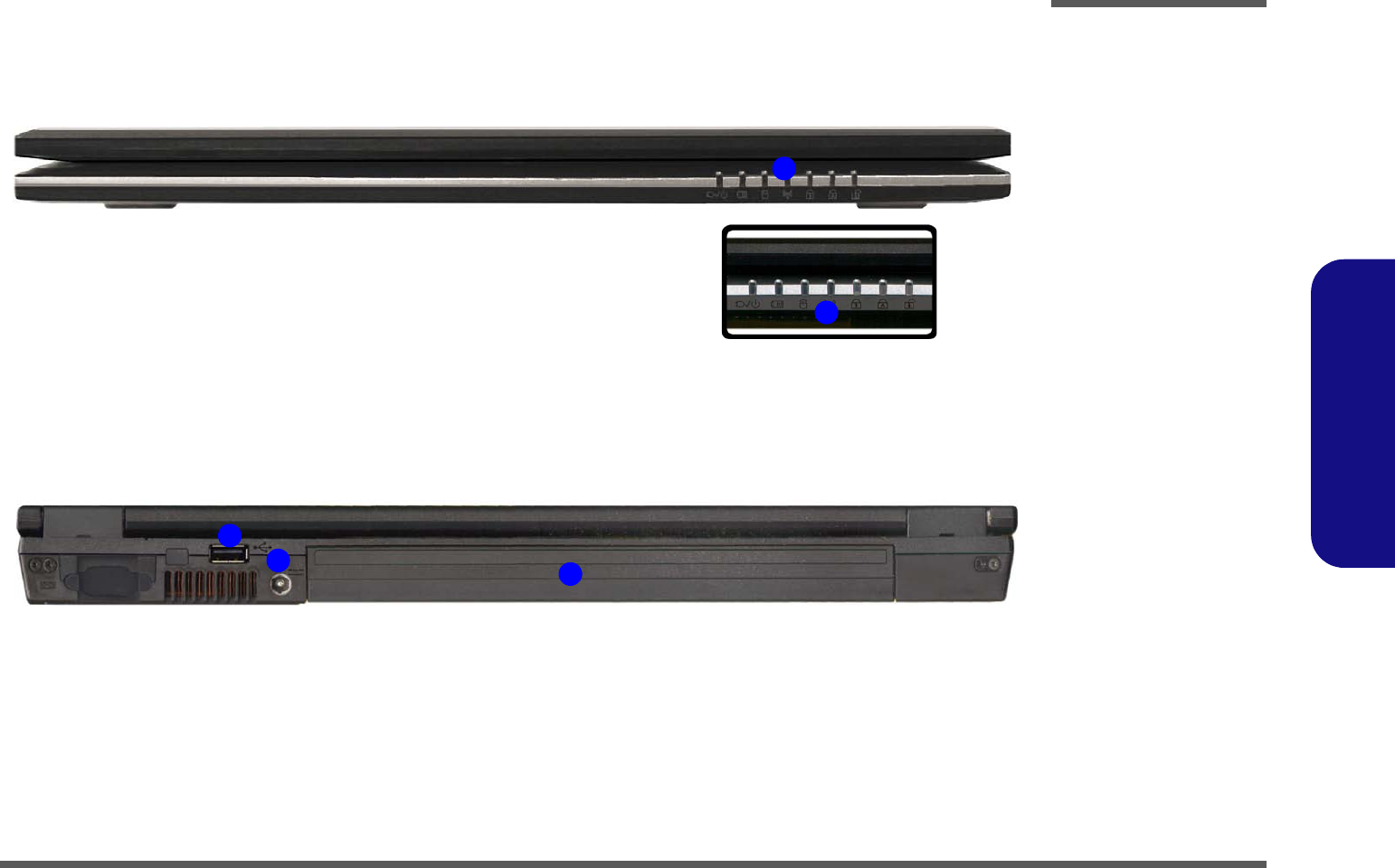
External Locator - Front & Rear Views Figure 3
Front Views
1. LED Indicators
Figure 4
Rear Views
1. 1 * USB Port
2. DC-In Jack
3. Battery
1
1
3
2
1
Introduction
1 - 8 External Locator - Left & Right Side Views
1.Introduction
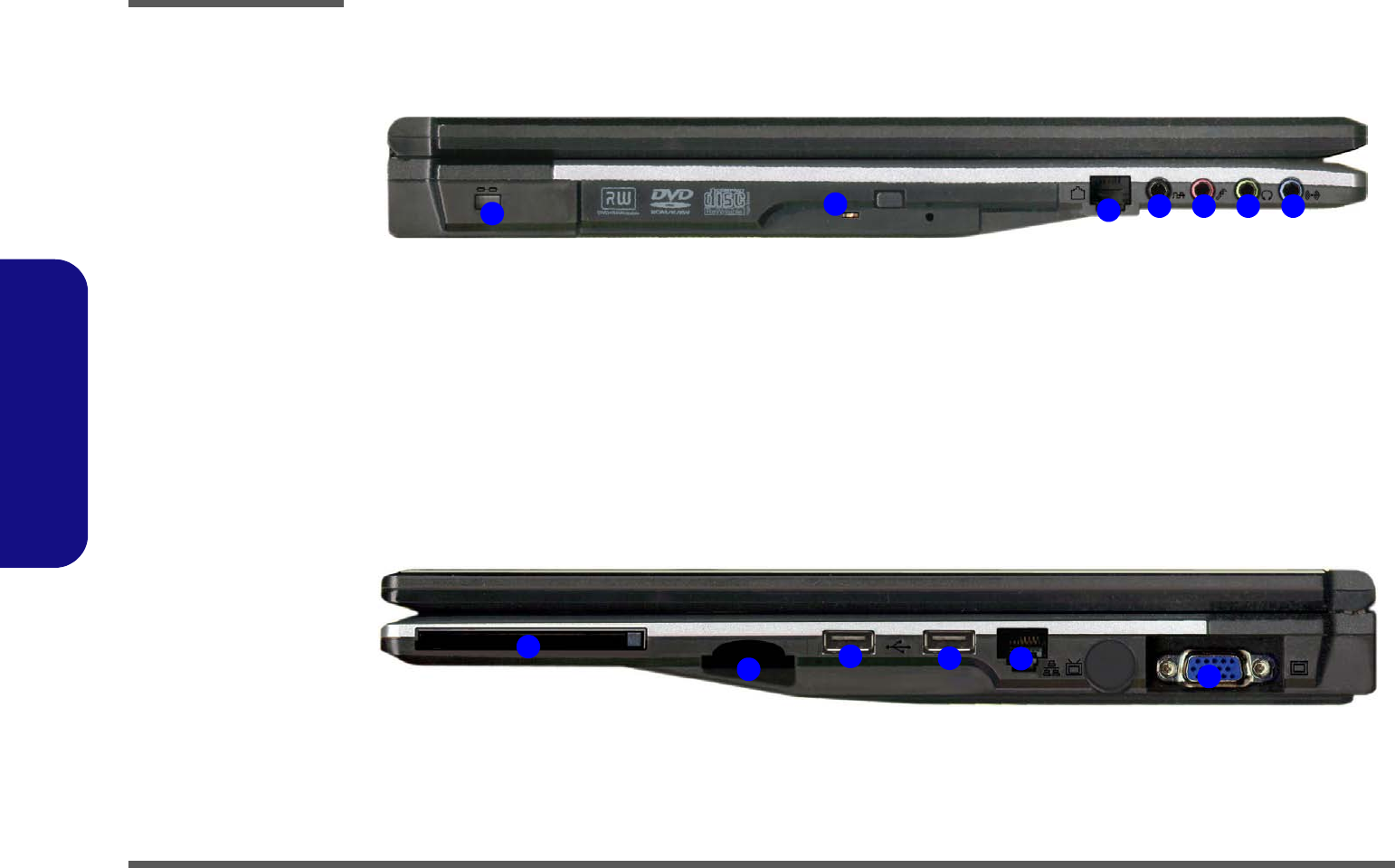
External Locator - Left & Right Side Views
4
1235 6 7
Figure 5
Left Side View
1. Security Lock Slot
2. Optical Device
Drive Bay
3. RJ-11 Modem
Jack
4. S/PDIF-Out Jack
5. Microphone-In
Jack
6. Headphone-Out
Jack
7. Line-In Jack
Figure 6
Right Side View
1. PC Card Slot
2. 7-in-1 Card
Reader
3. 2 * USB 2.0 Ports
4. RJ-45 LAN Jack
5. External Monitor
Port
123
345
Introduction
External Locator - Bottom View 1 - 9
1.Introduction
External Locator - Bottom View
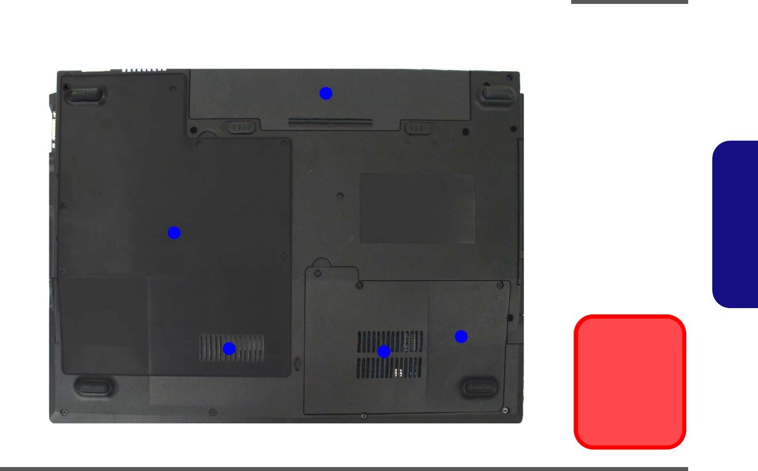
Figure 7
Bottom View
1. Vent/Fan Intake
2. Battery
3. Hard Disk Bay
Cover
4. CPU/RAM Bay
Cover
Overheating
To prevent your com-
puter from overheating
make sure nothing
blocks the vent/fan in-
takes while the com-
puter is in use.
2
4
1
3
1
Introduction
1 - 10 M660S Mainboard Overview - Top (Key Parts)
1.Introduction
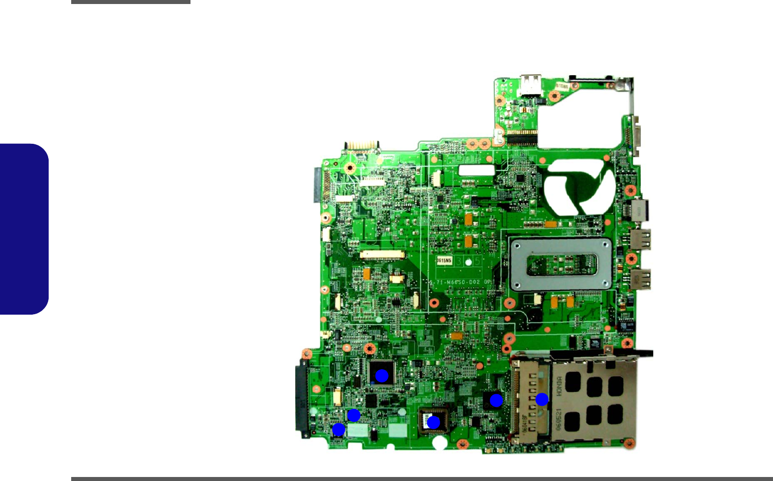
M660S Mainboard Overview - Top (Key Parts)
Figure 8
Mainboard Top
Key Parts
1. Audio Codec
VT1613
2. Audio Amp.
3. Hitachi H8
4. Flash BIOS ROM
5. ENE PCMCIA &
Card Control
6. PC Card
Assembly
2
3
14
56
Introduction
M660S Mainboard Overview - Bottom (Key Parts) 1 - 11
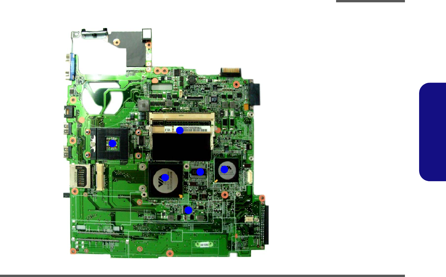
1.Introduction
M660S Mainboard Overview - Bottom (Key Parts) Figure 9
Mainboard Bottom
Key Parts
1. CPU Socket (no
CPU installed)
2. Memory Slots
DDRII So-DIMM
3. Southbridge-
VT8237R plus
4. ICS Clock
Generator
5. Northbridge-
VN800
6. SC1485ITS
2
6
3
1
54
Introduction
1 - 12 M660S Mainboard Overview - Top (Connectors)
1.Introduction
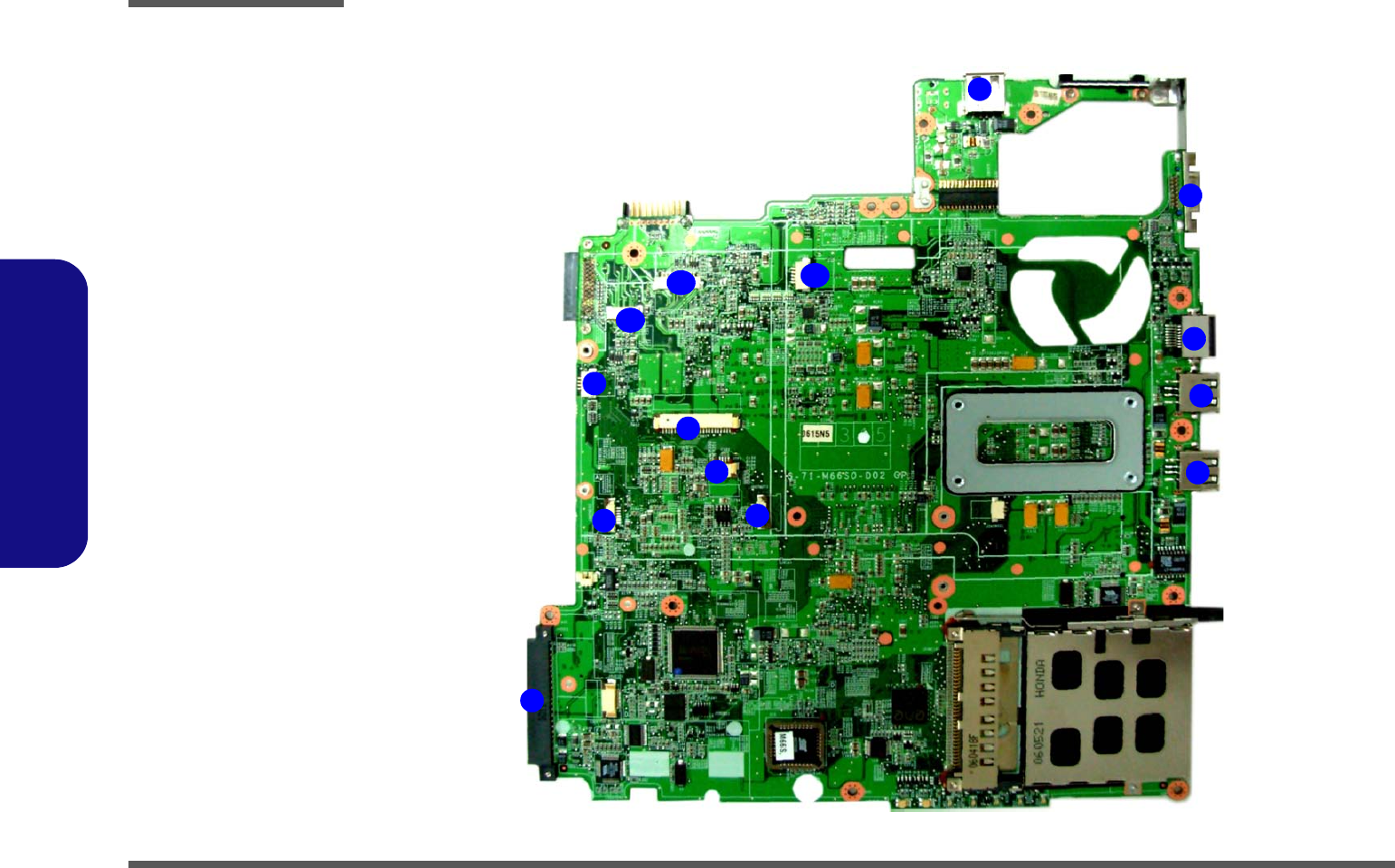
M660S Mainboard Overview - Top (Connectors)
Figure 10
Mainboard Top
Connectors
1. External Monitor
Port
2. RJ-45 LAN Jack
3. USB Port
4. HDD Connector
5. Hotkey Cable
Connector
6. Power Hotkey
Cable Connector
7. Touch Pad Cable
Connector
8. Keyboard Cable
Connector
9. Speaker Cable
Connector
10. Inverter Cable
Connector
11. Debug Cable
Connector
12. CCD Cable
Connector
3
8
11
10
93
3
1
2
4
56
7
12
Introduction
M660S Mainboard Overview - Bottom (Connectors) 1 - 13
1.Introduction
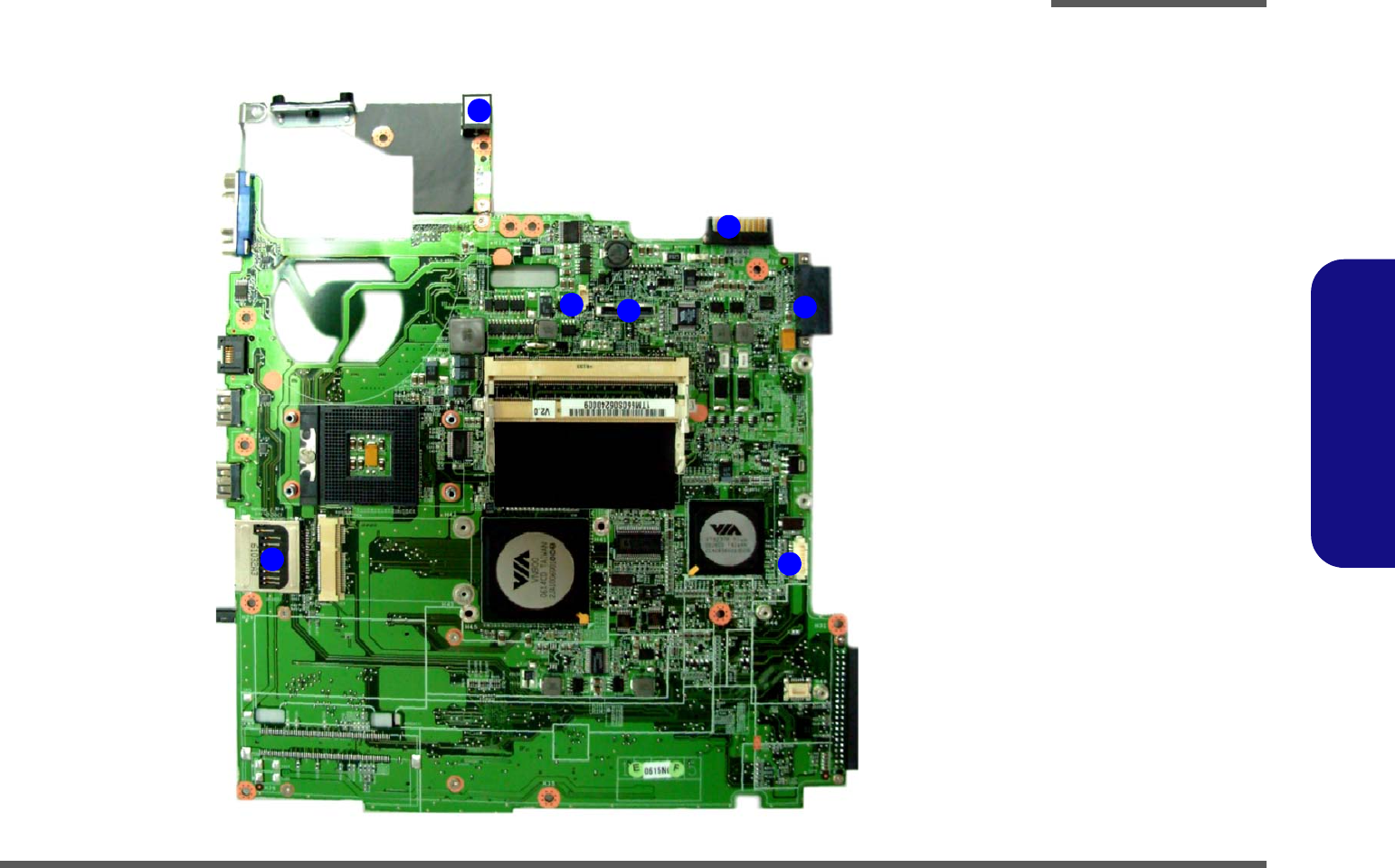
M660S Mainboard Overview - Bottom (Connectors) Figure 11
Mainboard Bottom
Connectors
1. DC-In Jack
2. Fan Cable
Connector
3. LCD Cable
Connector
4. Batterry
Connector
5. Optical Device
Drive Connector
6. Bluetooth Cable
Connector
7. Card Reader
2
6
3
1
5
4
7

Introduction
1-14
1.Introduction

Disassembly
Overview 2 - 1
2.Disassembly
Chapter 2: Disassembly
Overview
This chapter provides step-by-step instructions for disassembling the M660S/M665S series notebook’s parts and sub-
systems. When it comes to reassembly, reverse the procedures (unless otherwise indicated).
We suggest you completely review any procedure before you take the computer apart.
Procedures such as upgrading/replacing the RAM, CD device and hard disk are included in the User’s Manual but are
repeated here for your convenience.
To make the disassembly process easier each section may have a box in the page margin. Information contained under
the figure # will give a synopsis of the sequence of procedures involved in the disassembly procedure. A box with a
lists the relevant parts you will have after the disassembly process is complete. Note: The parts listed will be for the dis-
assembly procedure listed ONLY, and not any previous disassembly step(s) required. Refer to the part list for the previ-
ous disassembly procedure. The amount of screws you should be left with will be listed here also.
A box with a will also provide any possible helpful information. A box with a contains warnings.
An example of these types of boxes are shown in the sidebar.
Information
Warning

Disassembly
2 - 2 Overview
2.Disassembly
NOTE: All disassembly procedures assume that the system is turned OFF, and disconnected from any power supply (the
battery is removed too).
Maintenance Tools
The following tools are recommended when working on the notebook PC:
• M3 Philips-head screwdriver
• M2.5 Philips-head screwdriver (magnetized)
• M2 Philips-head screwdriver
• Small flat-head screwdriver
• Pair of needle-nose pliers
• Anti-static wrist-strap
Connections
Connections within the computer are one of four types:
Locking collar sockets for ribbon connectors To release these connectors, use a small flat-head screwdriver to
gently pry the locking collar away from its base. When replac-
ing the connection, make sure the connector is oriented in the
same way. The pin1 side is usually not indicated.
Pressure sockets for multi-wire connectors To release this connector type, grasp it at its head and gently
rock it from side to side as you pull it out. Do not pull on the
wires themselves. When replacing the connection, do not try to
force it. The socket only fits one way.
Pressure sockets for ribbon connectors To release these connectors, use a small pair of needle-nose pli-
ers to gently lift the connector away from its socket. When re-
placing the connection, make sure the connector is oriented in
the same way. The pin1 side is usually not indicated.
Board-to-board or multi-pin sockets To separate the boards, gently rock them from side to side as
you pull them apart. If the connection is very tight, use a small
flat-head screwdriver - use just enough force to start.

Disassembly
Overview 2 - 3
2.Disassembly
Maintenance Precautions
The following precautions are a reminder. To avoid personal injury or damage to the computer while performing a re-
moval and/or replacement job, take the following precautions:
1. Don't drop it. Perform your repairs and/or upgrades on a stable surface. If the computer falls, the case and other
components could be damaged.
2. Don't overheat it. Note the proximity of any heating elements. Keep the computer out of direct sunlight.
3. Avoid interference. Note the proximity of any high capacity transformers, electric motors, and other strong mag-
netic fields. These can hinder proper performance and damage components and/or data. You should also monitor
the position of magnetized tools (i.e. screwdrivers).
4. Keep it dry. This is an electrical appliance. If water or any other liquid gets into it, the computer could be badly
damaged.
5. Be careful with power. Avoid accidental shocks, discharges or explosions.
•Before removing or servicing any part from the computer, turn the computer off and detach any power supplies.
•When you want to unplug the power cord or any cable/wire, be sure to disconnect it by the plug head. Do not pull on the wire.
6. Peripherals – Turn off and detach any peripherals.
7. Beware of static discharge. ICs, such as the CPU and main support chips, are vulnerable to static electricity.
Before handling any part in the computer, discharge any static electricity inside the computer. When handling a
printed circuit board, do not use gloves or other materials which allow static electricity buildup. We suggest that
you use an anti-static wrist strap instead.
8. Beware of corrosion. As you perform your job, avoid touching any connector leads. Even the cleanest hands pro-
duce oils which can attract corrosive elements.
9. Keep your work environment clean. Tobacco smoke, dust or other air-born particulate matter is often attracted
to charged surfaces, reducing performance.
10. Keep track of the components. When removing or replacing any part, be careful not to leave small parts, such as
screws, loose inside the computer.
Cleaning
Do not apply cleaner directly to the computer, use a soft clean cloth.
Do not use volatile (petroleum distillates) or abrasive cleaners on any part of the computer.
Power Safety
Warning
Before you undertake
any upgrade proce-
dures, make sure that
you have turned off the
power, and discon-
nected all peripherals
and cables (including
telephone lines). It is
advisable to also re-
move your battery in
order to prevent acci-
dentally turning the
machine on.

Disassembly
2 - 4 Overview
2.Disassembly
Disassembly Steps
The following table lists the disassembly steps, and on which page to find the related information. PLEASE PERFORM
THE DISASSEMBLY STEPS IN THE ORDER INDICATED.
To remove the Battery:
1. Remove the battery page 2 - 5
To remove the HDD:
1. Remove the battery page 2 - 5
2. Remove the HDD page 2 - 6
To remove the System Memory:
1. Remove the battery page 2 - 5
2. Remove the system memory page 2 - 8
To remove the Processor:
1. Remove the battery page 2 - 5
2. Remove the processor page 2 - 10
To remove the Wireless LAN Module:
1. Remove the battery page 2 - 5
2. Remove the wireless LAN page 2 - 12
To remove the Modem :
1. Remove the battery page 2 - 5
2. Remove the modem page 2 - 13
To remove the Bluetooth:
1. Remove the battery page 2 - 5
2. Remove the bluetooth page 2 - 14
To remove the Optical Device:
1. Remove the battery page 2 - 5
2. Remove the Optical device page 2 - 15
To remove the Keyboard:
1. Remove the battery page 2 - 5
2. Remove the keyboard page 2 - 16
Disassembly
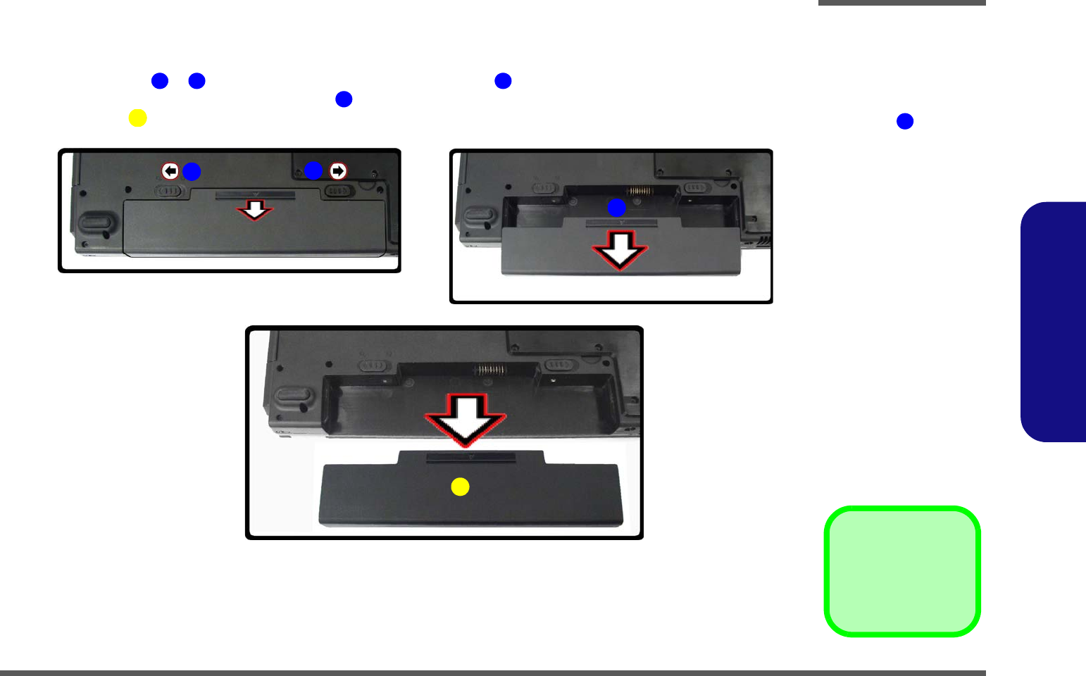
Removing the Battery 2 - 5
2.Disassembly
Removing the Battery
1. Turn the computer off, and turn it over.
2. Slide the latches ( & ) the direction of the arrow, and hold latch in place.
3. Slide the battery in the direction of the arrow .
4. Lift the battery out.
4. Battery
1 2 2
3
6
4
1
a. b.
c.
2
3
4
Figure 1
Battery Removal
a. Slide the 2 latches and
hold latch in place.
b. Slide the battery in the di-
rection of the arrow.
c. Lift the battery out.
2
Disassembly
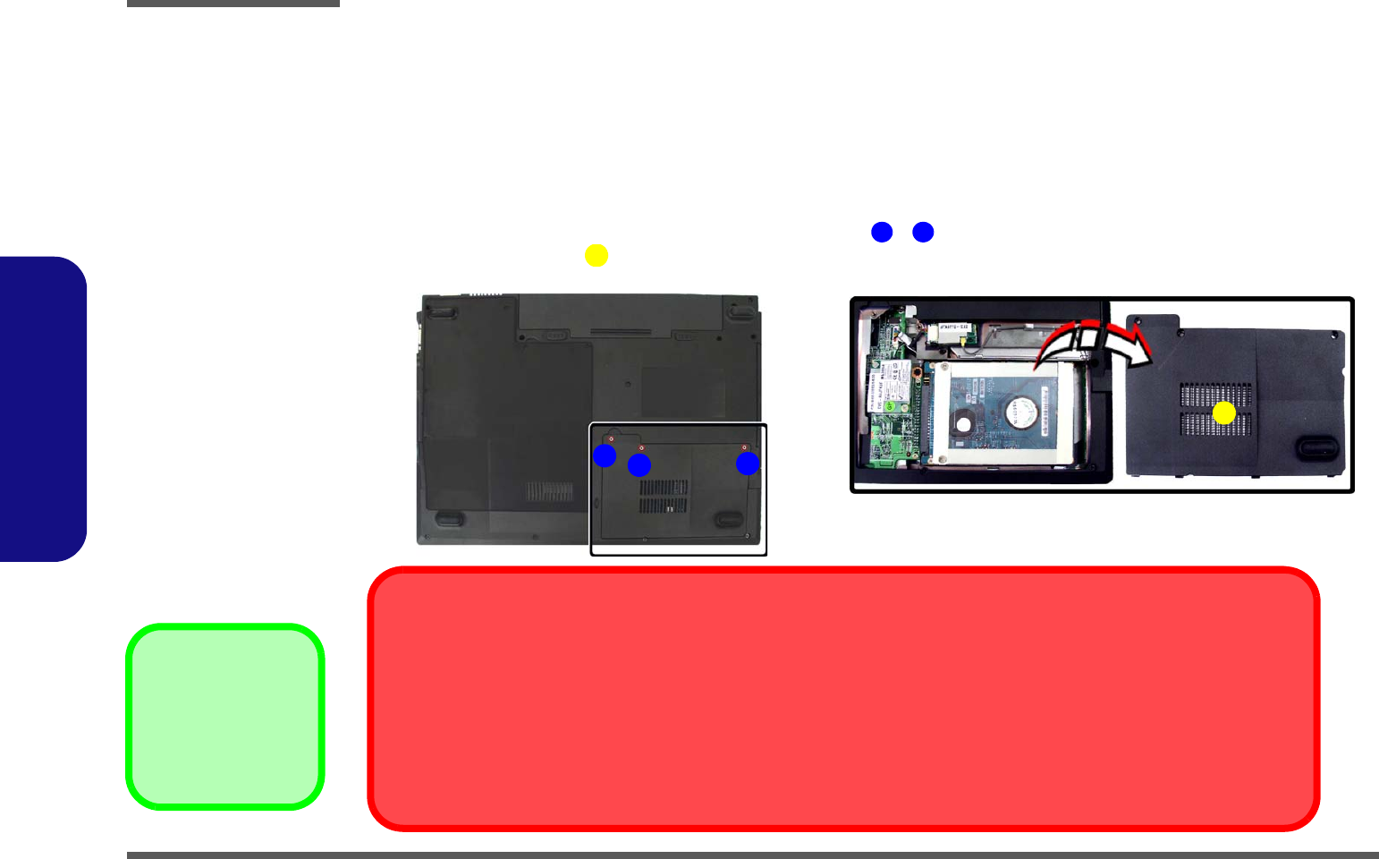
2 - 6 Removing the Hard Disk Drive
2.Disassembly
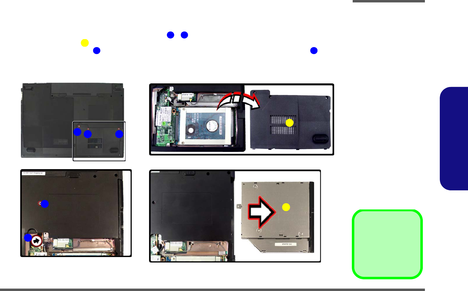
Removing the Hard Disk Drive
The hard disk drive can be taken out to accommodate other 2.5" serial (PATA) hard disk drives with a height of 9.5mm
(h). Follow your operating system’s installation instructions, and install all necessary drivers and utilities (as outlined in
Chapter 4 of the User’s Manual) when setting up a new hard disk.
Hard Disk Upgrade Processl
1. Turn off the computer, and remove the battery (page 2 - 5).
2. Locate the hard disk bay cover and remove the screws ( - ).
3. Remove the bay cover .
Figure 2
HDD Assembly
Removal
a. Locate the HDD bay cov-
er and remove the
screws.
b. Remove the bay cover.
4. HDD Bay Cover
•3 Screw
1 3
6
4
a.
13
2
HDD System Warning
New HDD’s are blank. Before you begin make sure:
You have backed up any data you want to keep from your old HDD.
You have all the CD-ROMs and FDDs required to install your operating system and programs.
If you have access to the internet, download the latest application and hardware driver updates for the operating system you plan
to install. Copy these to a removable medium.
4
b.
Disassembly
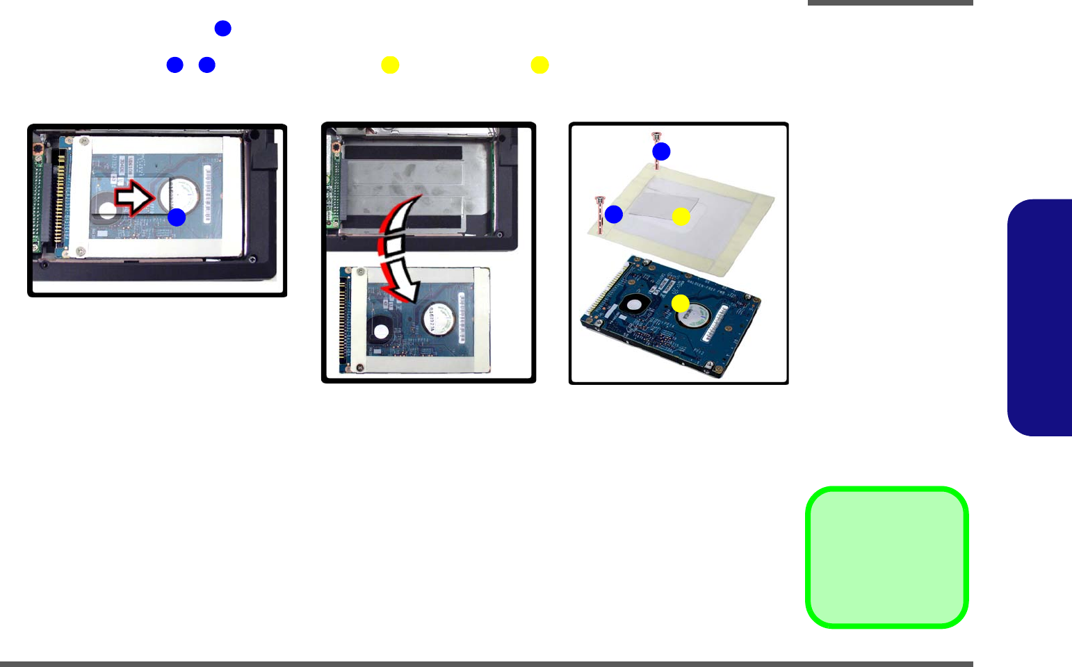
Removing the Hard Disk Drive 2 - 7
2.Disassembly
4. Carefully grip the mylar tab and slide the hard disk in the direction of arrow .
5. Lift the hard disk up (Figure d) in the direction of arrow.
6. Remove the screws - and separate the mylar from the hard disk .
7. Reverse the process to install any new hard disk.
5Figure 3
HDD Assembly
Removal Sequence
c. Slide the HDD in the di-
rection of the arrow.
d. Lift the HDD out of the
bay.
e. Remove the screws and
separate the mylar cover
from the HDD.
6 7 6
86
9
8. Mylar Cover
9. HDD
c. d.
5
e.
7
6
9
8
Disassembly
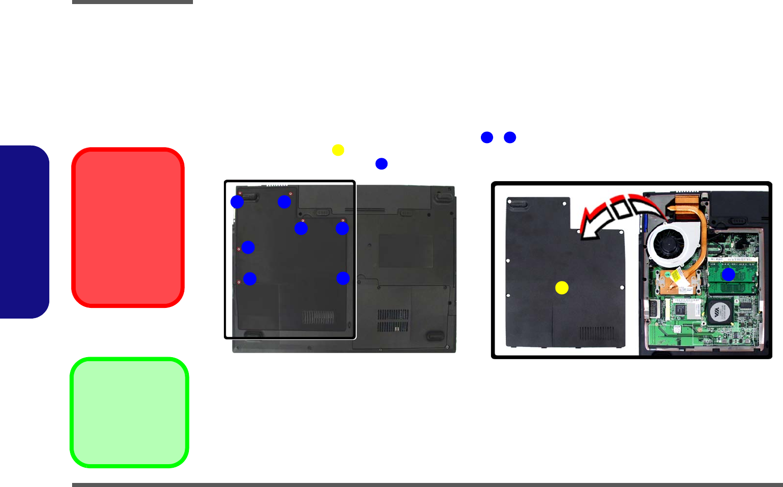
2 - 8 Removing the System Memory (RAM)
2.Disassembly
Removing the System Memory (RAM)
The computer has two memory sockets for 200 pin Small Outline Dual In-line Memory Modules (SO-DIMM) supporting
DDRII 533MHz. The main memory can be expanded up to 2GB. The SO-DIMM modules supported are 256MB,
512MB and 1024MB DDRII Modules. The total memory size is automatically detected by the POST routine once you
turn on your computer.
Memory Upgrade Process
1. Turn off the computer, remove the battery (page 2 - 5).
2. Locate the CPU/RAM bay cover, and remove screws - .
3. Remove the bay cover .
4. The RAM will be visible at point on the mainboard.
Figure 4
RAM Module
Removal
a. Remove the screws.
b. Remove the cover.
Contact Warning
Be careful not to touch
the metal pins on the
module’s connecting
edge. Even the clean-
est hands have oils
which can attract parti-
cles, and degrade the
module’s perfor-
mance.
1 7
8
8. CPU/RAM Bay Cover
•7 Screws
9
a.
3 4
1
56
78
b.
2
9
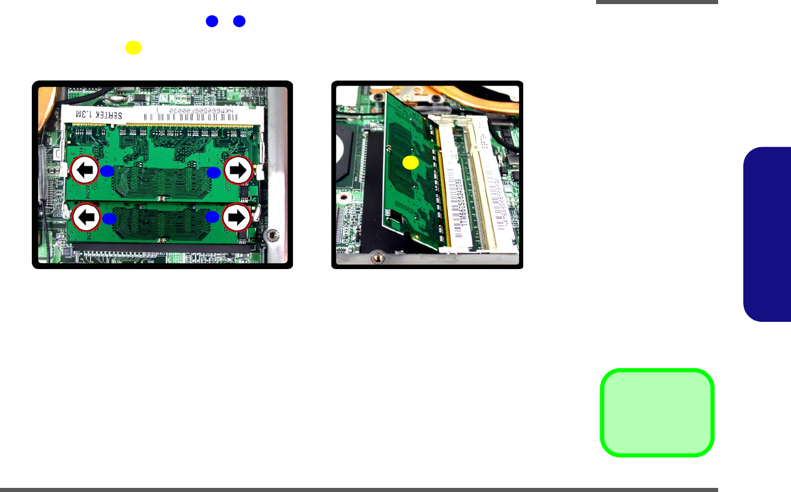
Disassembly
Removing the System Memory (RAM) 2 - 9
2.Disassembly
5. Gently push the two release latches ( & ) on the sides of the memory socket in the direction indicated by the
arrows (Figure c).
6. The RAM module(s) will pop-up (Figure d), and you can then remove it.
7. Push the latches to release the second module if necessary.
8. Insert a new module holding it at about a 30° angle and fit the connectors firmly into the memory slot.
9. The module will only fit one way as defined by its pin alignment. Make sure the module is seated as far into the slot
as it will go. DO NOT FORCE IT; it should fit without much pressure.
10. Press the module down towards the mainboard until the slot levers click into place to secure the module.
11. Replace the bay cover and the screws (see page 2 - 8).
12. Restart the computer to allow the BIOS to register the new memory configuration as it starts up.
10 11
12
Figure 5
Memory Removal
Sequence
c. Push the release
latch(es).
d. Remove the module(s).
10
c. d.
12
11
10 11
12 Ram Module(s)
Disassembly
2 - 10 Removing the Processor
2.Disassembly
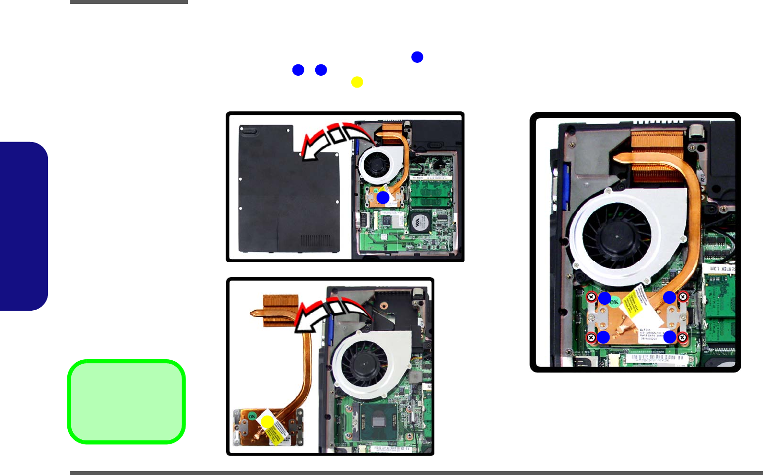
Removing the Processor
1. Turn off the computer, and remove the battery (page 2 - 5) and the CPU/RAM bay cover (page 2 - 8).
2. The CPU heat sink will be visible at point on the mainboard.
3. Remove screws - from the heat sink in the order indicated.
4. Carefully lift up the heat sink (Figure c) off the computer.
1
2 5
6
Figure 6
Processor Removal
a. Remove the cover and
Iocate the heat sink.
b. Remove the 4 screws in
the order indicated.
c. Remove the heat sink.
6. Heat Sink
•4 Screws
b.
6
1
5
4
a.
c.
3
2
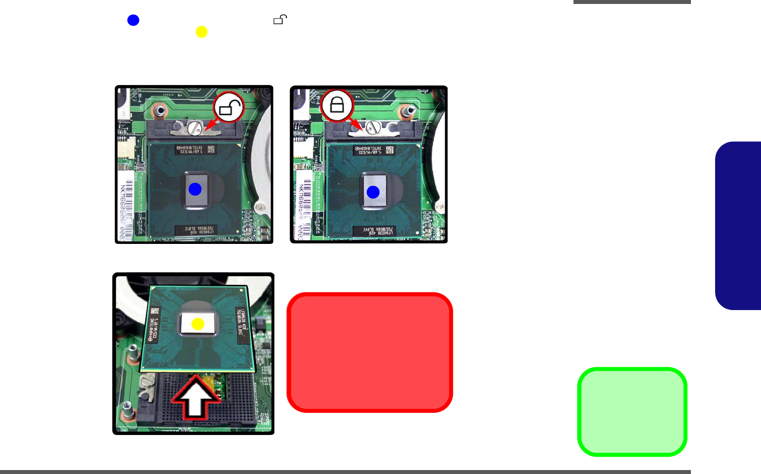
Disassembly
Removing the Processor 2 - 11
2.Disassembly
5. Turn the release latch towards the unlock symbol , to release the CPU (Figure d).
6. Carefully (it may be hot) lift the CPU up out of the socket (Figure e).
7. Reverse the process to install a new CPU.
8. When re-inserting the CPU, pay careful attention to the pin alignment, it will fit only one way (DO NOT FORCE IT!).
78
Figure 7
Processor Removal
(cont’d)
d. Turn the release latch to
unlock the CPU.
e. Lift the CPU out of the
socket.
d.
8
e.
Caution
The heat sink, and CPU area in
general, contains parts which are
subject to high temperatures. Allow
the area time to cool before remov-
ing these parts.
Unlock Lock
7
7
8. CPU
Disassembly
2 - 12 Removing the Wireless LAN Module
2.Disassembly
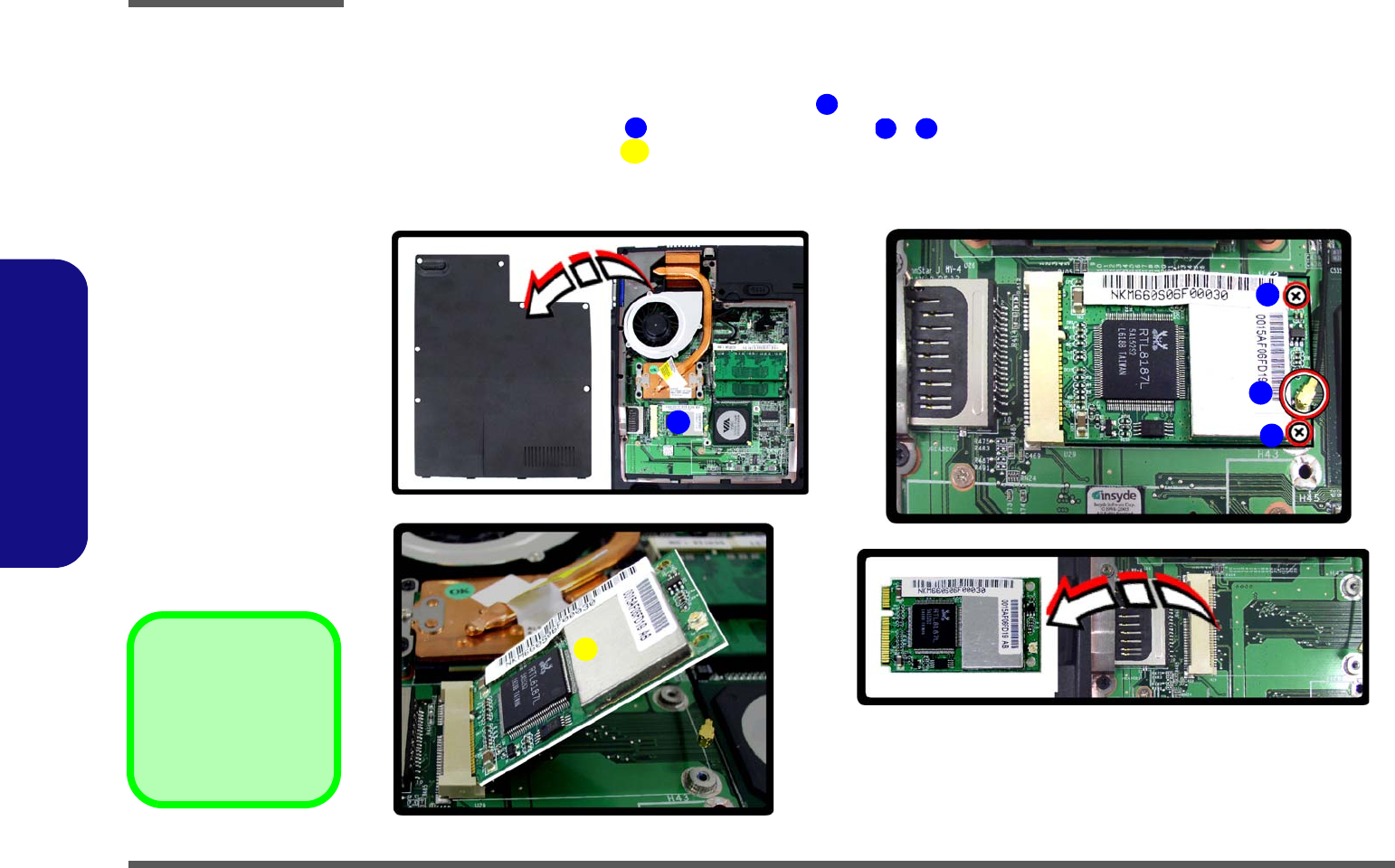
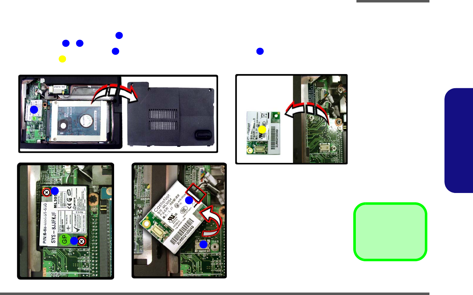
Removing the Wireless LAN Module
1. Turn off the computer, remove the battery (page 2 - 5) and the module bay cover (page 2 - 8).
1. The Wireless LAN module will be visible at point on the mainboard.
2. Carefully disconnect cable , then remove the screws - from the module socket.
3. The wireless LAN module will pop-up.
4. Lift the wireless LAN module (Figure d) up and off the computer.
Figure 8
Wireless LAN
Module Removal
a. Remove the cover and
Iocate the heat sink.
b. Disconnect the cable
and remove the 2
screws.
c. The WLAN module will
pop up.
d. Remove the WLAN
module.
Note: Make sure you
reconnect the antenna
cable to the “Main”
socket (Figure b).
1
23 4
5
1
2
4
c.
a.
5
3
b.
d.
5. WLAN Module
•2 Screws
Disassembly
Removing the Modem 2 - 13
2.Disassembly
Removing the Modem
1. Turn off the computer, remove the battery (page 2 - 5), and remove the hard disk bay cover (page 2 - 6).
2. The modem will be visible at point on the mainboard.
3. Remove screws - from the modem module.
4. Lift the modem up off the socket and separate the modem from the connector .
5. Lift the modem up and off the computer.
1
2 3
4 5
6
Figure 9
Modem Removal
a. Remove the cover and
locate the modem.
b. Remove the screws.
c. Lift the modem up off the
socket and disconnect
the connector.
d. Lift the modem out.
a.
c.
b.
34
1
2
d.
6
5
6. Modem
•2 Screws
Disassembly
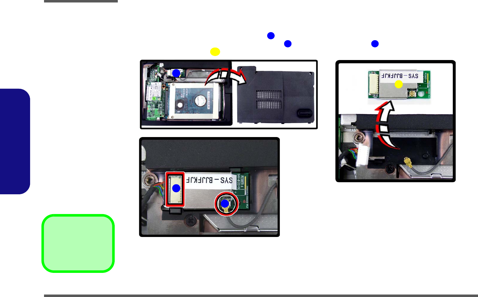
2 - 14 Removing the Bluetooth Module
2.Disassembly
Removing the Bluetooth Module
1. Turn off the computer, remove the battery (page 2 - 5) and remove the hard disk bay cover (page 2 - 6).
2. The Bluetooth module will be visible at point on the mainboard.
3. Carefully separate the module from the connector and disconnect the cable .
4. Lift the Bluetooth module (Figure c) up and off the computer.
Figure 10
Bluetooth Removal
a. Remove the cover and
locate the Bluetooth
module.
b. Seperate the the mod-
ule from connector and
disconnect the cable.
c. Remove Bluetooth mod-
ule.
1
2 3
4
a. c.
b.
3
1
2
4
4. Bluetooth Module
Disassembly
Removing the Optical (CD/DVD) Device 2 - 15
2.Disassembly
Removing the Optical (CD/DVD) Device
1. Turn off the computer, remove the battery (page 2 - 5).
2. Locate the hard disk bay cover and remove screws ( - ).
3. Remove the bay cover .
4. Remove the screw at point , and use a screwdriver to carefully push out the optical device at point .
5. Insert the new device and carefully slide it into the computer (the device only fits one way. DO NOT FORCE IT; The
screw holes should line up.
6. Restart the computer to allow it to automatically detect the new device.
Figure 11
Optical Device
Removal
a. Remove the screws.
b. Remove the cover.
c. Remove the screw and
push the optical device
out off the computer at
point 6.
d. Remove the optical de-
vice.
1 3
6
45 6
4 HDD Bay Cover
7 Optical Device
•4 Screws
32
1
a.
4
b.
c. d.
5
6
7
Disassembly
2 - 16 Removing the Keyboard
2.Disassembly
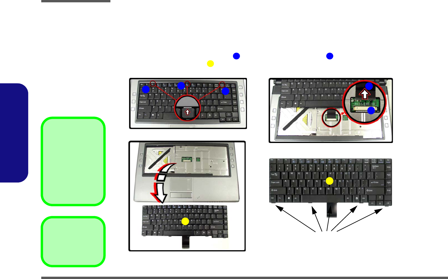
Removing the Keyboard
1. Turn off the computer, and remove the battery (page 2 - 5).
2. Press the three keyboard latches at the top of the keyboard to elevate the keyboard from its normal position (you
may need to use a small screwdriver to do this).
3. Carefully lift the keyboard up, being careful not to bend the keyboard ribbon cable (Figure b).
4. Disconnect the keyboard ribbon cable from the locking collar socket .
5. Carefully lift up the keyboard (Figure c) off the computer.
4 5
Figure 12
Keyboard Removal
a. Press the three latches
to release the keyboard.
b. Lift the keyboard up and
disconnect the cable
from the locking collar.
c. Remove the keyboard.
Re-Inserting the Key-
board
When re-inserting the
keyboard firstly align
the five keyboard tabs
at the bottom of the
keyboard with the slots
in the case.
6
a. b.
1234
5
Keyboard Tabs
6
c.
6
6. Keyboard

Part Lists
A-1
A.Part Lists
Appendix A:Part Lists
This appendix breaks down the M660S/M665S series notebook’s construction into a series of illustrations. The compo-
nent part numbers are indicated in the tables opposite the drawings.
Note: This section indicates the manufacturer’s part numbers. Your organization may use a different system, so be sure
to cross-check any relevant documentation.
Note: Some assemblies may have parts in common (especially screws). However, the part lists DO NOT indicate the
total number of duplicated parts used.
Note: Be sure to check any update notices. The parts shown in these illustrations are appropriate for the system at the
time of publication. Over the product life, some parts may be improved or re-configured, resulting in new part numbers.
Part Lists
A - 2 Part List Illustration Location
A.Part Lists
Part List Illustration Location
The following table indicates where to find the appropriate part list illustration.
Table A - 1
Part List Illustration
Location Part Pages#
Top - (M660S) page A - 3
Top - (M665S) page A - 4
Bottom - (M660S/M665S) page A - 5
LCD - (M660S) page A - 6
LCD - (M665S) page A - 7
Combo - (M660S/M665S) page A - 8
DVDRW - (M660S/M665S) page A - 9
Part Lists
Top (M660S) A - 3
A.Part Lists
Top (M660S)
Figure A - 1
Top (M660S)
無鉛
(加邊框)
無鉛
無鉛
無鉛
無鉛
無鉛
無鉛
無鉛
無鉛
無鉛
鴻富
無鉛
(PVT後設變)無鉛
無鉛
無鉛
Part Lists
A - 4 Top (M665S)
A.Part Lists
Top (M665S)
無鉛
無鉛 (加入ESD對策)
無鉛
無鉛
無鉛
無鉛
無鉛
無鉛
鴻富
無鉛
(加邊框)
無鉛
無鉛
無鉛
無鉛
無鉛
Figure A - 2
Top (M665S)
Part Lists
Bottom (M660S/M665S) A - 5
A.Part Lists
Bottom (M660S/M665S)
Figure A - 3
Bottom (M660S/
M665S)
昆山 無鉛
無鉛
無鉛
無鉛
無鉛
螺絲孔位置加厚度補強) 無鉛
昆山 無鉛
無鉛
無鉛
無鉛
華力
無鉛
無鉛
無鉛
無鉛
無鉛
無鉛
無鉛
無鉛
無鉛
無鉛
華力
無鉛
無鉛
無鉛
無鉛
無鉛
無鉛
黑色(恢復全面濺鍍)(無鉛)
無鉛
無鉛
無鉛
改為無破孔,設變改硬)黑色(無鉛)
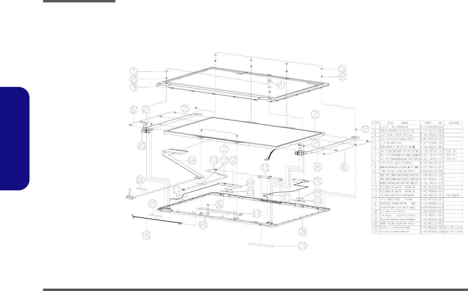
Part Lists
A - 6 LCD (M660S)
A.Part Lists
LCD (M660S)
Figure A - 4
LCD (M660S)
華力
無鉛(CCD處增加卡勾)
華力
無鉛
無鉛
無鉛
無鉛
無鉛
無鉛
含背膠)(無鉛)
含背膠)(無鉛)
華力 無鉛
無鉛
無鉛
無鉛
華力 無鉛
無鉛
中性 無鉛
無鉛
無鉛
無鉛
Part Lists
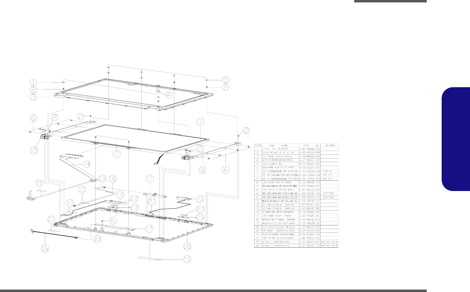
LCD (M665S) A - 7
A.Part Lists
LCD (M665S)
Figure A - 5
LCD (M665S)
無鉛
無鉛
無鉛
含背膠)(無鉛)
含背膠)(無鉛)
華力
中性
華力
無鉛
無鉛
無鉛
無鉛
無鉛
無鉛
無鉛
無鉛
無鉛
華力 無鉛
無鉛
無鉛
無鉛
Part Lists
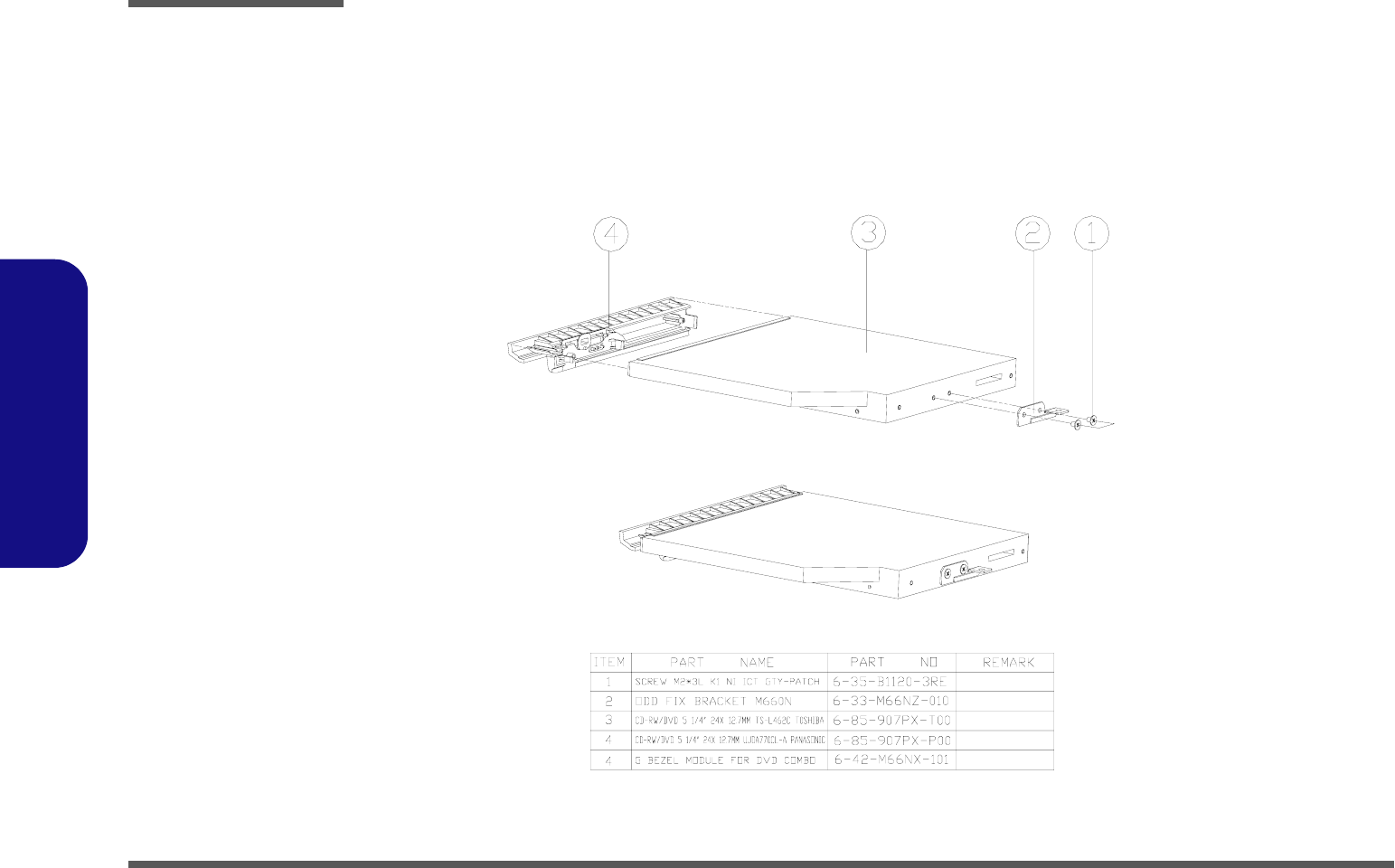
A - 8 Combo (M660S/M665S)
A.Part Lists
Combo (M660S/M665S)
Figure A - 6
Combo(M660S/
M665S)
Part Lists
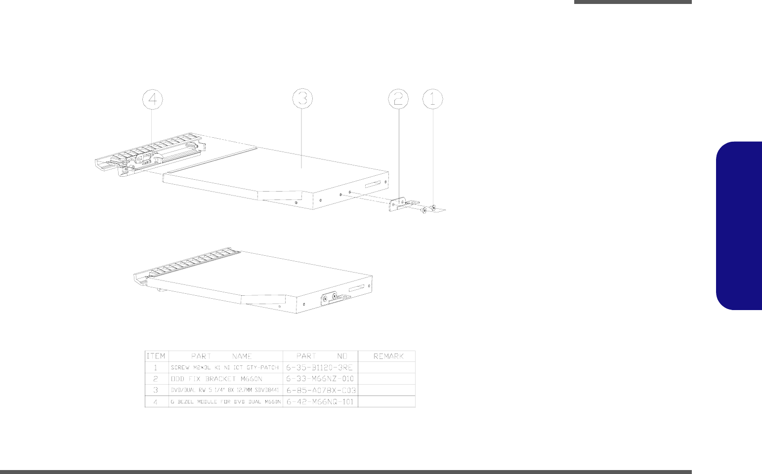
DVDRW (M660S/M665S) A - 9
A.Part Lists
DVDRW (M660S/M665S)
Figure A - 7
DVDRW(M660S/
M665S)

Part Lists
A - 10
A.Part Lists
Schematic Diagrams
B-1
B.Schematic Diagrams
Appendix B:Schematic Diagrams
This appendix has circuit diagrams of the M660S/M665S notebook’s PCB’s. The following table indicates where to find
the appropriate schematic diagram.
Diagram - Page Diagram - Page Diagram - Page
SYSTEM BLOCK DIAGRAM - Page B - 2 VT8237-3 - Page B - 14 VDD3, VDD5 - Page B - 26
CLOCK GENERATOR - Page B - 3 HDD & CDROM - Page B - 15 CHARGER, DC IN - Page B - 27
CPU-1 - Page B - 4 CARDBUS / CARD READER - Page B - 16 VCORE - Page B - 28
CPU-2 - Page B - 5 CARD SOCKET - Page B - 17 1.05VS, 1.5V - Page B - 29
VN800-1 - Page B - 6 LAN - Page B - 18 AUDIO VT1613 - Page B - 30
VN800-2 - Page B - 7 USB & CCD - Page B - 19 PWR HOT BOARD - Page B - 31
VN800-3 - Page B - 8 HITACHI H8 - Page B - 20 HOTKEY LT BOARD - Page B - 32
VN800-4 - Page B - 9 CRT & LVDS - Page B - 21 USB BOARD - Page B - 33
DDR2-1 - Page B - 10 CPU FAN, ROM - Page B - 22 AUDIO & MODEM BOARD - Page B - 34
DDR2-2 - Page B - 11 LED - Page B - 23 CLICK BOARD - Page B - 35
VT8237-1 - Page B - 12 MINI-PCI & BLUETOOTH - Page B - 24
VT8237-2 - Page B - 13 1.8V, 0.9VS, 2.5VS - Page B - 25
Table B - 1
Schematic
Diagrams
Version Note
The schematic dia-
grams in this chapter
are based upon ver-
sion 6-71-M66S-003. If
your mainboard (or
other boards) are a lat-
er version, please
check with the Service
Center for updated di-
agrams (if required).
Schematic Diagrams
B - 2 SYSTEM BLOCK DIAGRAM
B.Schematic Diagrams
SYSTEM BLOCK DIAGRAM
Sheet 1 of 34
SYSTEM BLOCK
DIAGRAM
NORTH BRIDGE
VN800
VT8237A/R plus
SOUTH BRIDGE
CLOCK GEN
MASTER
MINIPCI
HOTKEY LT
BOARD
AUDIO&MODEM
BOARD
USB BOARD
CLICK BOARD
PWR_HOT BOARD
CARD READER
CARD BUS
ENE CB714F
CD-ROM
(IDE)
FSB667
H8 KBC
USB Port 3
Keyboard
SPEAKER x2
Blue Tooth
SPK. OUT
USB Port 2
ICS952906FT+ICS9P936AF
DEBUGB
PORT
SPDIF
AC97
LPC
PCI
MIC. IN
DDR2
SO-DIMM
x2
LAN
VT6103L
uFCPGA
BATT.X1
CRT
LCD
Touch PAD
MDC or
MBC
ULTRA-DMA33/66/100
FAN X 1
USB Port 1
IMVP-6 VR
M660S BLOCK DIAGRAM
LPC
CCD Camera
Yonah 478
PORT PRT
FWH
IDE HDD
USB 2.0
Audio
Codec
VT1613
X4 DMI
Interface
LINE IN
Schematic Diagrams
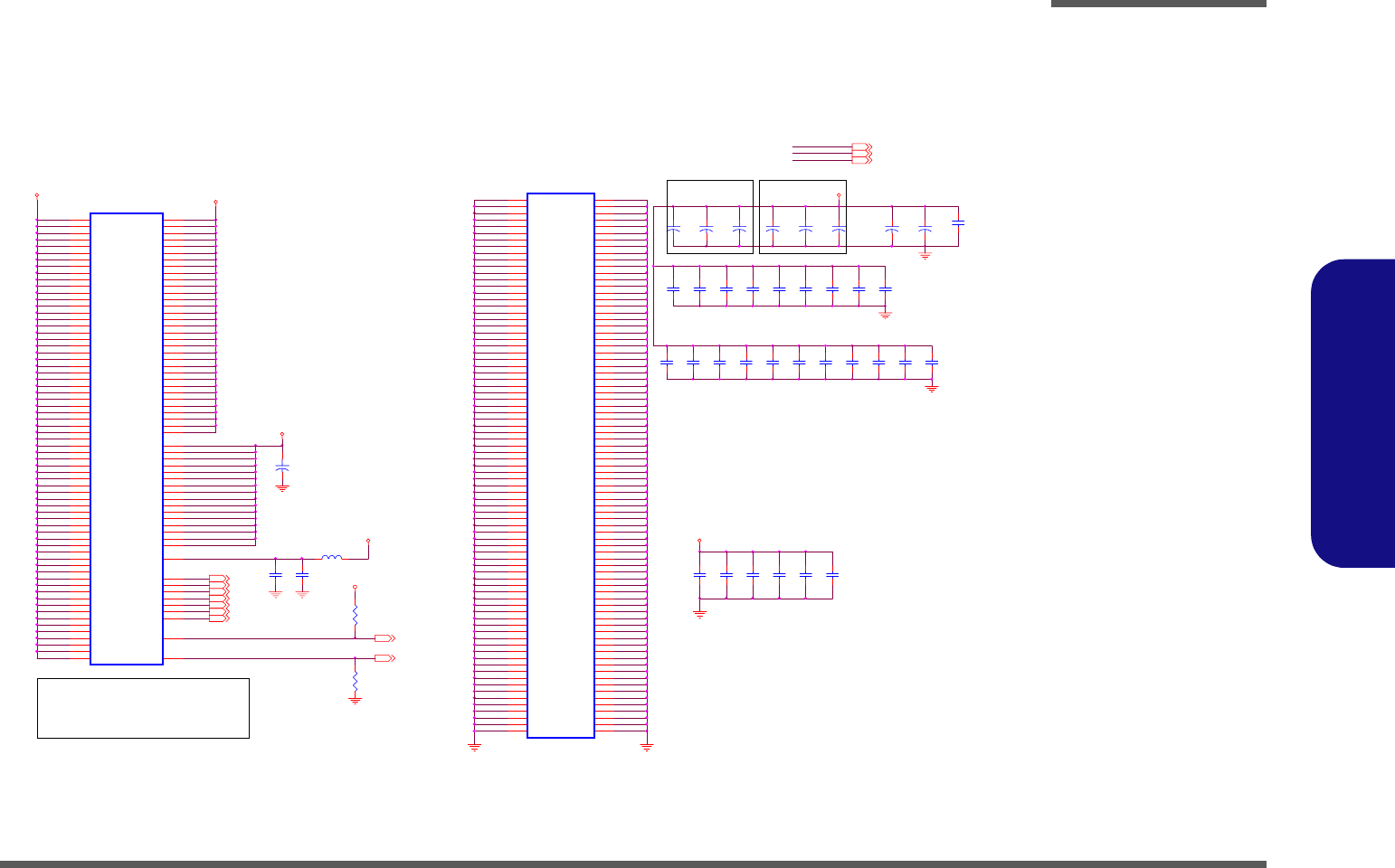
CLOCK GENERATOR B - 3
B.Schematic Diagrams
CLOCK GENERATOR
Sheet 2 of 34
CLOCK
GENERATOR
PCLKMPCI 24
12
Y2
14.318MHZ
C950719
FOR EMI
C464 27PF
C465 27PF
M_CLK_DDR3 9
M_CLK_DDR#3 9
M_CLK_DDR2 9
M_CLK_DDR#2 9
C417
10UF/10V_08
C95
4.7U
C96
1UF
C416
10UF/10V_08
C420
0.01U/16V_04
C426
0.01U/16V_04
C109
0. 01U/16V_04
C428
4.7U
C427
0.01U/16V_04
C433
0.1UF
C424
0.01U/16V_04
C120
0.01U/16V_04
C116
*5P
FS1
SEL24_48
MOD E
C115
*5P
FS0
FS3
3V66_0
3V66_1
PCICLKX4
Z0210
PCICLKX1
PCICLKX2
Z0209
PCICLKX3
FB8
HCB2012KF -121T30
FB11
HCB2012KF-121T30
C950719
2
OFF
OFF
1
OFF
FS1
3VS
CPU
33
ON
ON
PCI
ON ON
FS0
100
33
FS0
33166
OFF
33133
FS1
200
Z0211
R453 10K_04
R446 10K_04 Z0208 R447 1K_04
Z0207 R454 1K_04
VDD2.5/1.8-0
10
VDD2.5/1.8-1
21
VDD2.5/1.8-2
27
AVDD2. 5-0
1
GND
9
GND
28
AGND
2
SDATA
16
SCLK
15
BUF _INT
3
FB_OUTC 12
DDRT0 5
DDRT1 7
DDRT2 13
DDRT3 18
DDRT4 20
DDRT5 24
DDRC0 6
DDRC1 8
DDRC2 14
DDRC3 17
DDRC4 19
DDRC5 23
FB_OUTT 11
AVDD2. 5-1
26
AGND
25
BUF _INC
4
GND
22
U25
ICS9P936AF
MCLKOT6MCLKOC6
MCLKIT6
R83
0_04
MCLKITP__
R386 0_04
C950719
R385 0_04
FS2 R430 10K_04
FS3 R433 10K_04
Z0212
Z0213
2.5VS
FS4 R431 10K_04
1.8VBF R
C268
10UF/ 10V_08
C218
0.01U/16V_04
C232
0.01U/16V_04
C265
22UF/10V_12
C234
1UF
C177
0.01U/16V_04
C221
0.01U/16V_04
C459
0.01U/16V_04
C233
1UF
C220
0.01U/16V_04
C460
0.01U/16V_04
C219
0.01U/16V_04
C457
0.1UF
FB14
HCB2012KF-121T30
C461
0.01U/16V_04
3.3VCLK
3VS 7,8,9,10, 11,12,13,14,15,16,19,20, 22,23,24,26,28, 30
0/1: mobile mode / Desktop
-CPU_STOP
-PCI_STOP
2.5VCLK
B
E C
Q31
3904
Z0215
1.5VS R478
1K
1.5VS 4,7,20,24,26
M_CLK_DDR1 10
M_CLK_DDR#1 10
M_CLK_DDR0 10
M_CLK_DDR#0 10
CLK_RESET
3.3VCLK
2.5VS
R410 0_04
R135 0_04
R455 0_04
Z0201
R448 0_04
R409 10K_043VS
Z0202
950310
C950720
R134 1K_04
R408 22_04
R403
475_1%
Z0203 HCPUCLK+
HCPUCLK-
HCLK+_
HCLK-_
3.3VCLK
CLK_PWRGD
GCLK_NB
DK3-
DK1+
DK1-
DK3+
DK0+
DK0-
Z0204
FS2
FS4
25MHZXI_S112
CPU_CLK+ 3
CPU_CLK- 3
CLK_MCH_BCLK# 5
CLK_MCH_BCLK 5
-CPU_STOP
-PCI_STOP
MODE
DK2-
DK2+
1.8V 6,7,9,10,25
R441 1K_04
R407 10K_04
1
23
4RN214P2RX22
AC
D33
*RB751V
C950718
DEL SW1 C950719
R406 10K_04
CPU_BSEL13
R440 *1K_04
1
2 3
4RN12
4P2RX22
BSEL1
VDDA
48 VDD48
24
VDDPCI1
10
VDDPCI2
17
VDD
34
GND
6
GND
11
GND
18
GND
23
GND
28
GND
37
GND
43
GND
47
X1
4
X2
5
SDATA
32
SCLK
31
RESET
30
REF1/FS0 2
48MHZ/ FS3 21
24_48MHZ/SEL24_48 22
3V66_0 29
3V66_1 26
3V66_2 25
PCI_F0/FS2 7
PCI_F1/FS4 8
CPUCLKT1 42
VDD3V66
27
VDDCPU
40
VDDREF
3
CPUCLKT0 39
VTT_PW R GD/ PD
33
CPUCLKC0 38
IREF
46
CPUCLKC1 41
PCI_F2 9
MODE/PCICLK0 12
PCICLK1 13
PCICLK2 14
PCICLK3 15
PCICLK4 16
PCICLK5 19
PCICLK6 20
REF0/FS1 1
CPUCLKT_ITP/PCI_STOP 45
CPUCLKC_ITP/CPU_STOP 44
25Mhz_0
36
25Mhz_1
35
U28
ICS952906FT
2.5VS 3,11,12,13,20, 26
SIO_OSC 12
GUICK 8
BSEL0
CLK_USB48 11
GCLK_NB 7
1.5VS
VCLK_SB 13
SPCLK 13
APICCLK1 13
R474
1K
CPU_BSEL03
B
E C
Q30
3904
Z0216
PCLK_FWH 22
KBC_PCLK 19
1
2 3
4RN14
4P2RX22
1
2 3
4RN15
4P2RX22
BSEL1
C204
*22PF
BSEL0
R161 22_04
R429 22_04
R413 22_04
R434 10K_04
R133 22_04
AC
D34
*RB751V
R411 22_04
1
23
4
RN13
4P2RX22
1
23
4RN234P2RX22
1
2 3
4RN17
4P2RX33
1
2 3
4RN18
4P2RX33
3VS
1.8V
3VS
3VS
PM_STPCPU#12
PM_STPPCI#12
R432 0_04
SMB_SBDATA9,10,12,24 SMB_SBCLK9,10,12,24
SMB_SBCLK9,10,12,24 SMB_SBDATA9,10,12,24
R399 51.1_1%_04
R398 51.1_1%_04
R401 51.1_1%_04
R400 51.1_1%_04
CLKEN#28 G
DS
Q29
2N7002 Z0205
PCLK_SI/O
CLK_RESET
3V 11, 12,13,17,19,24, 25, 26,29,30
FB7
HCB2012KF-121T30
Z0206
R572 22_04
M950627
C260
10UF/10V_08
PCLKPCM 15
Schematic Diagrams
B - 4 CPU-1
B.Schematic Diagrams
CPU-1
H_DSTBN#15H_DSTBP#15
XD P _B P M #5
XD P _T DO
XD P _T DI
H_DINV#15
H_DSTBN#3 5
XD P _T MS
XD P _T CK
H_DINV#3 5
H_DSTBP#3 5
H_DSTBN#2 5
TP_APM1#
H_DINV#2 5
H_DSTBP#2 5
R55 150
R54 150
R63 150
R61 51_1%
R72 150
R52 150
R64 51_1%
R87 220
R56 150
R84 100_04
XD P _ T RS T #
XDP_DBRESET#
R85 100_04
TP_H EPLL
R62 150
R57 150
R68 51_1%
R70 *51_1%
R377 200
PM_THRMTRIP#
R53 150 R122 54.9_1%
R86 100_04
R120 54.9_1%
R123 54.9_1%
R121 54.9_1%
XD P _ TC K
1.05VS 4,5,13,28,29
TER M_R EST#19
IN-Target Probe
H_PROCHOT#
A[3]#
J4
A[4]#
L4
A[5]#
M3
A[6]#
K5
A[7]#
M1
A[8]#
N2
A[9]#
J1
A[10]#
N3
A[11]#
P5
A[12]#
P2
A[13]#
L1
A[14]#
P4
A[16]#
R1 A[15]#
P1
ADSTB[0] #
L2
REQ[0]#
K3
REQ[1]#
H2
REQ[2]#
K2
REQ[3]#
J3
REQ[4]#
L5
A[17]#
Y2
A[18]#
U5
A[19]#
R3
A[20]#
W6
A[21]#
U4
A[22]#
Y5
A[23]#
U2
A[24]#
R4
A[25]#
T5
A[26]#
T3
A[27]#
W3
A[28]#
W5
A[29]#
Y4
A[30]#
W2
A[31]#
Y1
ADSTB[1] #
V4
A20M#
A6
FERR#
A5
IGNNE#
C4
STPCLK#
D5
LINT0
C6
LINT1
B4
SMI#
A3
RSVD[01]
AA1
RSVD[02]
AA4
RSVD[03]
AB2
RSVD[04]
AA3
RSVD[05]
M4
RSVD[06]
N5
RSVD[07]
T2
RSVD[08]
V3
RSVD[09]
B2
RSVD[11]
B25
RSVD[10]
C3
ADS# H1
BNR # E2
BPRI# G5
DEFER# H5
DRDY# F21
DBSY# E1
BR0# F1
IERR# D20
INIT# B3
LOCK# H4
RESET# B1
RS[0]# F3
RS[1]# F4
RS[2]# G3
TRDY# G2
HIT# G6
HITM# E4
BPM[0]# AD4
BPM[1]# AD3
BPM[2]# AD1
BPM[3]# AC4
PRDY# AC2
PREQ# AC1
TCK AC5
TDI AA6
TD O AB3
TMS AB5
TRST# AB6
DBR# C20
PROCHOT# D21
TH ER MD A A24
TH ER MD C A25
TH ER MT RI P # C7
BCLK[0] A22
BCLK[1] A21
RSVD[12] T22
RSVD[13] D2
RSVD[14] F6
RSVD[15] D3
RSVD[16] C1
RSVD[17] AF1
RSVD[18] D22
RSVD[19] C23
RSVD[20] C24
RESERVED
HCLK THERM
XDP/ITP SIGNALS CONTROL
ADDR GROUP1
ADDR GROUP0
U26A
Yonah Ball-out
B
E C
Q11
3904
B
E C
Q13
3904
R49
10K
R66
10K
R51
10K
Z0307
1.05VS
Z0311
R375
150_04
CPU_FERR#
H_THERMDA
H_THERMDC
1.05VS
C538
2.2U_12_X7R
1.05VS
2.5VS
1.05VS
1.05VS
R67 *51_1%
H_FERR# 13
H_A#[31:3]5
H_A20M#13
H_CPURST#
PM_THRMTRIP#
XD P _ B PM # 5
XD P _ TD I
XD P _ B PM # 0
XD P _ B PM # 1
XD P _ B PM # 2
XD P _ B PM # 3
XD P _ B PM # 4
XD P _ TM S
R128 51_1%
CPU_CLK+ 2
CPU_CLK- 2
R125 51_1%
R379
4.7K_04
R129 51_1%
R14
680_04
H_REQ#1
TP_ SPARE0
TP_ SPARE1
R127 51_1%
TP_ SPARE2
TP_ SPARE3
R124 51_1%
TP_ SPARE5
TP_ SPARE4
3VH8 19,24,27, 30
F070395
R567
1K
TP_ SPARE6
TP_ SPARE7
Z0306
H_A#3
10 MILE
20 MILE
TP_ EXTB R EF
Near to
ADM1032
10 MILE
H_A#4
Layout Note:
Route H_THERMDA and
H_THERMDC on same layer.
10 mil trace on 10 mil
spacing.
R126 75
XD P _ TD O
VDD3 13,19,22,25,26,27
H_A#5
H_A#7
R119 54.9_1%
H_A#8
H_A#6
H_THERMDA
Z0308
H_THERMDC
XD P _ TR S T#
VCORE 4,28
H_A#11
H_A#10
H_A#9
B
E C
Q35
2N3904
H_D#0
H_A#12
H_A#14
H_A#13
R65
680_04
H_D#1
VCORE
H_A#16
R378 10K_04
H_A#15
R373
4.7K_04
R382
20K_1%_04
CPU_DPRSTP#
C412
0.1UF/10V_04
H_REQ#1
H_REQ#2
H_REQ#0
SCLK 8
SDATA 7
ALERT# 6
GND 5
THERM#
4D-
3D+
2VDD
1
U24
ADT1032ARM
R371
100K_04
C415 2200P
H_D#2
H_D#3
THERMTRIP# 26
Leave ascape routing on for
future functionality
A#[32-39], APM#[0-1]:
H_A#17
H_REQ#4
H_REQ#3
Layout note:Zo=55ohm,0.5"
max for GTLREF
H_D#4
H_CPURST#
H_D#5
CPU_FERR#
H_STPCLK#
H_SMI#
H_CPUSLP#
H_INIT#
H_PROCHOT#
R396
1K_1%
R394
2K_1%
H_D#9
H_D#6
H_D#8
H_D#7
H_D#10
H_D#11
H_A20M#
H_IGNNE#
H_INTR
H_REQ#0
H_NMI
D[0]#
E22
D[1]#
F24
D[2]#
E26
D[3]#
H22
D[4]#
F23
D[5]#
G25
D[6]#
E25
D[7]#
E23
D[8]#
K24
D[9]#
G24
D[10]#
J24
D[11]#
J23
D[12]#
H26
D[13]#
F26
D[14]#
K22
D[15]#
H25
DSTBN[0]#
H23
DSTBP[0]#
G22
DINV[0]#
J26
D[16]#
N22
D[17]#
K25
D[18]#
P26
D[19]#
R23
D[20]#
L25
D[21]#
L22
D[22]#
L23
D[24]#
P25 D[23]#
M2 3
D[25]#
P22
D[26]#
P23
D[27]#
T24
D[28]#
R24
D[29]#
L26
D[30]#
T25
D[31]#
N24
DSTBN[1]#
M2 4
DSTBP[1]#
N25
GTLREF
AD26
TES T1
C26
BSEL[0]
B22
TES T2
D25
BSEL[1]
B23
D[32]# AA23
BSEL[2]
C21
D[33]# AB24
D[34]# V24
D[35]# V26
D[36]# W25
D[37]# U23
D[38]# U25
D[39]# U22
D[40]# AB25
D[41]# W22
D[42]# Y23
D[43]# AA26
D[45]# Y22
D[44]# Y26
D[46]# AC26
D[47]# AA24
DSTBN[2]# W24
DINV[2]# V23
DSTBP[2]# Y25
D[48]# AC22
D[49]# AC23
D[50]# AB22
D[51]# AA21
D[52]# AB21
D[53]# AC25
D[54]# AD20
D[55]# AE22
D[56]# AF23
D[57]# AD24
D[58]# AE21
D[59]# AD21
D[60]# AE25
D[61]# AF25
D[62]# AF22
D[63]# AF26
DSTBN[3]# AD23
DSTBP[3]# AE24
DINV[3]# AC20
DINV[1]#
M2 6
COMP[1] U26
COMP[2] U1
COMP[3] V1
DPRSTP# E5
DPSLP# B5
DPWR# D24
COMP[0] R26
PWRGOOD D6
SLP# D7
PSI# AE6
MISC
DATA GRP3 DATA GRP2
DATA GRP0 DATA GRP1
U26B
Yonah Ball-out
H_A#19
H_A#18
H_A#20
H_DPSLP#
Layout note: no stub
on H_STPCLK TP
PM_THRMTRIP# should
connect to ICH7 and GMCH
without T-ing(No STUB)
H_D#14
H_D#15
H_D#12
CPU_PSI#
H_D#13
THERM_ALERT# 19
1.05VS
H_A#21
H_A#23
H_A#22
R383 *1K
H_D#18
H_D#19
H_D#16
H_D#17
R384 51_1%
H_D#21
H_D#20
Z0303
Please testpoint on
H_IERR# with a GND
0.1" away
H_A#26
H_A#24
H_A#25
Z0301
H_INIT#
H_D#23
H_D#22
Z0304
H_D#24
H_D#25
H_D#27
H_D#26
H_A#28
H_A#29
H_A#27
H_REQ#2
H_D#28
H_D#31
H_D#30
H_D#29
SMC_THERM 19
H_ADS# 5
H_BNR# 5
SMD_THERM 19
H_DRDY# 5
H_DBSY# 5
H_BREQ#0 5
H_BPRI# 5
H_A#31
H_DEFER# 5
H_A#30
H_D#48
H_D#52
H_D#50
H_D#51
H_D#49
H_D#53
TP_A34#
TP_A32#
TP_A33#
R376
56_04
1.05VS
H_D#56
H_D#54
H_D#57
H_D#59
H_D#58
H_D#55
TP_A36#
TP_A35#
TP_A37#
H_INIT# 13
H_LOCK# 5
H_HIT# 5
Z0305
CPU_BSEL02CPU_BSEL12
H_HITM# 5
H_D#60
H_D#62
H_D#61
H_D#63
TP_A39#
TP_APM0#
TP_A38#
COMP0
H_D#35
H_D#34
H_D#32
H_D#36
H_D#33
H_D#37
H_D#38
H_D#40
H_D#41
H_D#43
H_D#39
H_D#42
H_ADSTB#05
H_D#45
H_D#46
H_D#44
H_D#47
H_CPURST#
H_REQ#[4:0]5
H_A#[31:3]5
H_CPURST# 5
H_RS#0
CPU_DPRSTP#
H_AD STB#15
H_RS#1
H_DPSLP#
H_A20M#
R372
100K_04
H_RS#2
H_CPUSLP#
G
DS
Q27
NDS352
CPU_FERR#
R374 0_04
R571
6.8K_04
G
DS
Q28
2N7002W
B
E C
Q36
2N3904
CPU_PSI#
R90 27.4_1%
H_IGNNE#
R89 54.9_1%
C541
0.1UF _04_X7R
R92 27.4_1%
H_D#[63:0]5
H_D#[63:0]5
R98 54.9_1%
H_D#[63:0] 5
H_D#[63:0] 5
PM_DPRSLPVR 13,28
H_IGNNE#13
H_CPUSLP# 13
H_DPSLP# 13
H_DPWR#
H_STPC LK#13
CPU_BSEL1
CPU_BSEL0 R477 150
R472 150
H_PWRGD
THM_V D D
VDD3
Layout:Connect test
point TP3F1 with no
atub
VDD3
H_INTR13
VDD 3
THM_VDD
Z0302 COMP1
Comp1,3 connect with Zo=55ohm,make
trace length shorter than 0.5"
H_DPWR# 5
Comp0,2 connect with Zo=27.4ohm,make
trace length shorter than 0.5"
H_PWRGD 13
M950704
H_NMI13
H_INTR
C950718 C950718
C950718
Layout note:
H_SMI#13
H_NMI
H_RS#[2:0] 5
H_TRDY # 5
H_TRDY #
COMP3
Place Series
Resistor on
H_PWRGD_XDP Without
stub
R550 10K_04
NO_STUFF
H_SMI#
TP3F1
VDD3
COMP2
H_REQ#3
2.5VS 2,11,12,13,20,26
R549 51.1_04
CPU_DPRSTP#
XD P _B P M #0
1.5VS 2,4,7,20,24,26
H_DSTBN#05
XD P _B P M #1 H_DSTBP#05H_DINV#05
XD P _B P M #2
H_STPCLK#
XD P _B P M #3
XD P _ D B R E S E T#
XD P _B P M #4
Sheet 3 of 34
CPU-1
Schematic Diagrams
CPU-2 B - 5
B.Schematic Diagrams
CPU-2
Sheet 4 of 34
CPU-2
1.05VS 3,5,13,28,29
VSS[001]
A4
VSS[002]
A8
VSS[003]
A11
VSS[004]
A14
VSS[005]
A16
VSS[006]
A19
VSS[007]
A23
VSS[008]
A26
VSS[009]
B6
VSS[010]
B8
VSS[011]
B11
VSS[012]
B13
VSS[013]
B16
VSS[014]
B19
VSS[015]
B21
VSS[016]
B24
VSS[017]
C5
VSS[018]
C8
VSS[019]
C11
VSS[020]
C14
VSS[021]
C16
VSS[022]
C19
VSS[023]
C2
VSS[024]
C22
VSS[025]
C25
VSS[026]
D1
VSS[027]
D4
VSS[028]
D8
VSS[029]
D11
VSS[030]
D13
VSS[031]
D16
VSS[032]
D19
VSS[033]
D23
VSS[034]
D26
VSS[035]
E3
VSS[036]
E6
VSS[037]
E8
VSS[038]
E11
VSS[039]
E14
VSS[040]
E16
VSS[041]
E19
VSS[042]
E21
VSS[043]
E24
VSS[044]
F5
VSS[045]
F8
VSS[046]
F11
VSS[047]
F13
VSS[048]
F16
VSS[049]
F19
VSS[050]
F2
VSS[051]
F22
VSS[052]
F25
VSS[053]
G4
VSS[054]
G1
VSS[055]
G23
VSS[056]
G26
VSS[057]
H3
VSS[058]
H6
VSS[059]
H21
VSS[060]
H24
VSS[061]
J2
VSS[062]
J5
VSS[063]
J22
VSS[064]
J25
VSS[065]
K1
VSS[066]
K4
VSS[067]
K23
VSS[068]
K26
VSS[069]
L3
VSS[070]
L6
VSS[071]
L21
VSS[072]
L24
VSS[073]
M2
VSS[074]
M5
VSS[075]
M22
VSS[076]
M25
VSS[077]
N1
VSS[078]
N4
VSS[079]
N23
VSS[080]
N26
VSS[081]
P3
VSS[082] P6
VSS[083] P21
VSS[084] P24
VSS[085] R2
VSS[086] R5
VSS[087] R22
VSS[088] R25
VSS[089] T1
VSS[090] T4
VSS[091] T23
VSS[092] T26
VSS[093] U3
VSS[094] U6
VSS[095] U21
VSS[096] U24
VSS[097] V2
VSS[098] V5
VSS[099] V22
VSS[100] V25
VSS[101] W1
VSS[102] W4
VSS[103] W23
VSS[104] W26
VSS[105] Y3
VSS[106] Y6
VSS[107] Y21
VSS[108] Y24
VSS[109] AA2
VSS[110] AA5
VSS[111] AA8
VSS[112] AA11
VSS[113] AA14
VSS[114] AA16
VSS[115] AA19
VSS[116] AA22
VSS[117] AA25
VSS[118] AB1
VSS[119] AB4
VSS[120] AB8
VSS[121] AB11
VSS[122] AB13
VSS[123] AB16
VSS[124] AB19
VSS[125] AB23
VSS[126] AB26
VSS[127] AC3
VSS[128] AC6
VSS[129] AC8
VSS[130] AC11
VSS[131] AC14
VSS[132] AC16
VSS[133] AC19
VSS[134] AC21
VSS[135] AC24
VSS[136] AD2
VSS[137] AD5
VSS[138] AD8
VSS[139] AD11
VSS[140] AD13
VSS[141] AD16
VSS[142] AD19
VSS[143] AD22
VSS[144] AD25
VSS[145] AE1
VSS[146] AE4
VSS[147] AE8
VSS[148] AE11
VSS[149] AE14
VSS[150] AE16
VSS[151] AE19
VSS[152] AE23
VSS[153] AE26
VSS[154] AF3
VSS[155] AF6
VSS[156] AF8
VSS[157] AF11
VSS[158] AF13
VSS[159] AF16
VSS[160] AF19
VSS[161] AF21
VSS[162] AF24
U26D
Yonah Ball-out
1.5VS 2,7, 20,24,26
+
C62
*330UF/3V_D
+
C34
*330UF/3V_D
+
C172
330UF/3V_D
+
C171
330UF/3V_D
+
C117
*330UF/3V_D
+
C61
330UF/3V_D
+
C419
*10UF/10V_08
+
C162
*10UF/10V_12
+
C425
330UF/3V_D
C127
0.1UF
C429
22UF/10V_12
C118
0.1UF
C422
22UF/10V_12
C128
0.1UF
C434
*10UF/10V_08
C113
0.1UF
C123
22UF/10V_12
C119
0.1UF
C58
22UF/10V_12
C114
0.1UF
C409
22UF/10V_12
C161
22UF/10V_12
C410
22UF/10V_12
C431
22UF/10V_12
C423
22UF/10V_12
C125
22UF/10V_12
C112
22UF/10V_12
C411
22UF/10V_12
C57
22UF/10V_12
C110
22UF/10V_12
C421
22UF/10V_12
C111
22UF/10V_12
C59
22UF/10V_12
C430
22UF/10V_12
C124
22UF/10V_12
C60
22UF/10V_12
1.05VS
VCORE
C413
0.01UF
C414
10UF/10V_08
L23
FCB1608KF-121T25
VCORE
North sideSouth side
H_VID0 28
VCORE
H_VID1 28
PLEASE NEAR CPU
H_VID3 28
H_VID2 28
H_VID5 28
H_VID4 28
H_VID6 28
PLEASE NEAR CPU
VCCSENSE 28
VSSSENSE 28
R404
100_1%
Z0401
R405
100_1%
VCORE
1.05VS
1.5VS
Layout Note:
Route VCCSENSE and VSSSENSE trace
at 27.4 ohms with 50mil spacing.
place PU and PD winthin 1 inch of CPU
VCORE 3,28
VCC[001]
A7
VCC[002]
A9
VCC[003]
A10
VCC[004]
A12
VCC[005]
A13
VCC[006]
A15
VCC[007]
A17
VCC[008]
A18
VCC[009]
A20
VCC[010]
B7
VCC[011]
B9
VCC[012]
B10
VCC[013]
B12
VCC[014]
B14
VCC[015]
B15
VCC[016]
B17
VCC[017]
B18
VCC[018]
B20
VCC[019]
C9
VCC[020]
C10
VCC[021]
C12
VCC[022]
C13
VCC[023]
C15
VCC[024]
C17
VCC[025]
C18
VCC[026]
D9
VCC[027]
D10
VCC[028]
D12
VCC[029]
D14
VCC[030]
D15
VCC[031]
D17
VCC[032]
D18
VCC[033]
E7
VCC[034]
E9
VCC[035]
E10
VCC[036]
E12
VCC[037]
E13
VCC[038]
E15
VCC[039]
E17
VCC[040]
E18
VCC[041]
E20
VCC[042]
F7
VCC[043]
F9
VCC[044]
F10
VCC[045]
F12
VCC[046]
F14
VCC[047]
F15
VCC[048]
F17
VCC[049]
F18
VCC[050]
F20
VCC[051]
AA7
VCC[052]
AA9
VCC[053]
AA10
VCC[054]
AA12
VCC[055]
AA13
VCC[056]
AA15
VCC[057]
AA17
VCC[058]
AA18
VCC[059]
AA20
VCC[060]
AB9
VCC[061]
AC10
VCC[062]
AB10
VCC[063]
AB12
VCC[064]
AB14
VCC[065]
AB15
VCC[066]
AB17
VCC[067]
AB18
VCC[099] AF18
VCC[098] AF17
VCC[097] AF15
VCC[096] AF14
VCC[095] AF12
VCC[094] AF10
VCC[093] AF9
VCC[092] AE20
VCC[091] AE18
VCC[090] AE17
VCC[089] AE15
VCC[088] AE13
VCC[087] AE12
VCC[086] AE10
VCC[084] AD18
VCC[085] AE9
VCC[083] AD17
VCC[082] AD15
VCC[081] AD14
VCC[080] AD12
VCC[079] AD10
VCC[078] AD9
VCC[077] AD7
VCC[076] AC18
VCC[075] AC17
VCC[074] AC15
VCC[073] AC13
VCC[072] AC12
VCC[071] AC9
VCC[070] AC7
VCC[069] AB7
VCC[068] AB20
VCC[100] AF20
VCCP[01] V6
VCCP[02] G21
VCCP[03] J6
VCCP[04] K6
VCCP[05] M6
VCCP[06] J21
VCCP[07] K21
VCCP[08] M21
VCCP[09] N21
VCCP[10] N6
VCCP[11] R21
VCCP[12] R6
VCCP[13] T21
VCCP[14] T6
VCCP[15] V21
VCCP[16] W21
VCCA B26
VID[0] AD6
VID[1] AF5
VID[2] AE5
VID[3] AF4
VID[4] AE3
VID[5] AF2
VID[6] AE2
VCCSENSE AF7
VSSSENSE AE7
U26C
Yonah Ball-out
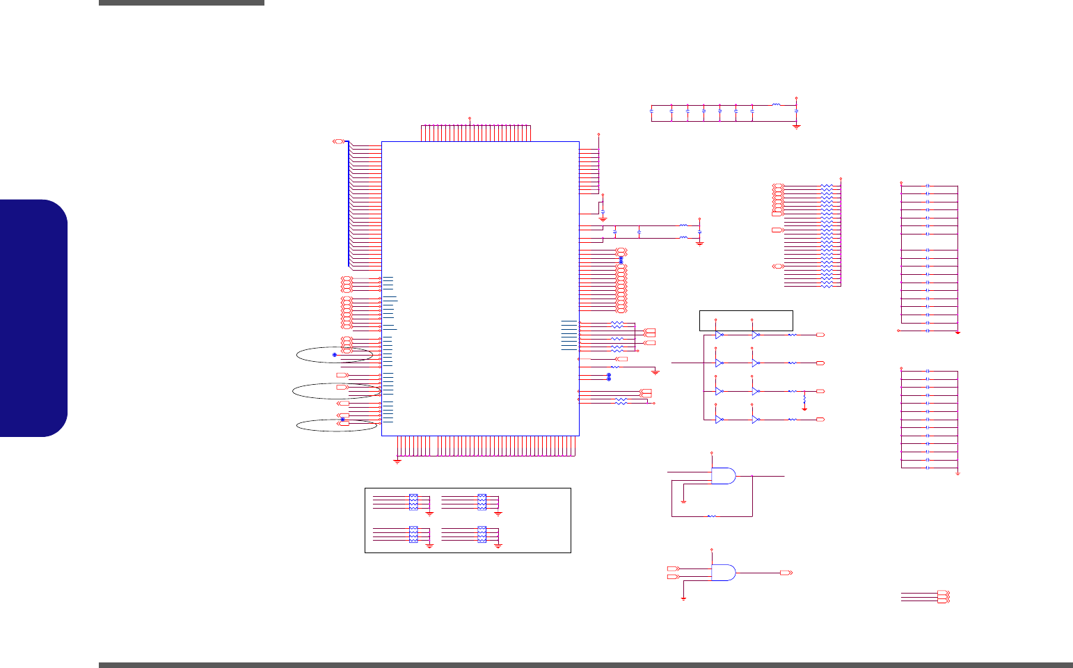
Schematic Diagrams
B - 6 VN800-1
B.Schematic Diagrams
VN800-1
Sheet 5 of 34
VN800-1
FLASH#22
PCI _DEVSEL#
PCI_DEVSEL#15,24
PCI_FRAME#15, 24
3V
Z1112
PCI _REQ#2
R459 8.2K
PCI_PERR#15,24
R465 8.2K
PCI _REQ#1
IDE_SATDET#
PCI _TRD Y #
PCI _IRDY#
R461 8.2K
PCI_SERR#15,24
PCI _FRAME#
R460 8.2K
PCI _INTA#
PCI _STOP#
PCI _INTD#
PCI_STOP#15,24
PCI_IRDY#15, 24
PCI _REQ#3
R457 8.2K
PCI _REQ#1
R154 8.2K
PM_CLKRUN#12,19
PCI _INTC#
R190 8.2K
Z1113
3VS
R462 8.2K
PCI_TRDY#15, 24
PCI _REQ#2
R188 8.2K
R463 8.2K
R168 8.2K
PM_CLKRUN#
R464 8.2K
Z1117
PCI _REQ#0
R445 8.2K
H_A20GATE 19
IDE_PATDET#
R165 8.2K
H_A20GATE
PCI _INTB#
R189 8.2K
R191 8.2K
R458 8.2K
PCI _REQ#3
3V
PCI _REQ#4
PCI _REQ#5
USB_PN6 2 4
USB_PP6 2 4
950524
950511
PCI_REQ#015
PCI _GNT#0
USB_PN7 2 4
USB_PP7 2 4
PCI _GNT#1
PCI _GNT#2
2.5VS 2,3,12,13,20,26
Only for VT8237R plus
AP339A
PCI _GNT#3
FWH_TBL#
3V 12,13,17,19,24,25,26,29,30
-PCIRST_GATE
2
14
3
5
U7
74AHC 1G08GW
3V
ALL_PWROK
USB_PP6
USB_PN4
USB_PP4
USB_PN6
PWRGD_VCORE28
KBC_PWRGD19
USB_PN0
USB_PN2
USB_PP0
USB_PP2
F042795
FLASH#22
PCI_GNT#015
Z1119
R187 8.2K
PCI _REQ#5
3VS 2,7,8, 9,10,12,13,14,15,16,19,20,22,23,24,2 6,28,30
ALL_PWROK 13,20
3V
PCI _C/BE0#
3V
PCI _C/BE1#
USB_PN5
PCI _AD0
PCI _C/BE2#
PCI _AD1
PCI _C/BE3#
3VU SB
Z1102
PCI_C/BE1#15,24 PCI_C/BE0#15,24
PCI_C/BE2#15,24 PCI_C/BE3#15,24
PCI_DEVSEL#15,24 PCI_IRDY#15,24
Z1121
PCI _REQ#4
PCI _GNT#3
PCI _GNT#2
2.5V
PCI _GNT#1
PCI _GNT#0
R146 8.2K
R443 8.2K
R153 8.2K
R466 8.2K
R155 8.2K
PCI _AD2
PCI _AD3
PCI _TRD Y #
PCI_TRDY#15,24
PCI_FRAME#15,24 PCI_FRAME#
PCI _DEVSEL#
PCI _IRDY#
PCI_PAR15,24 PCI_SERR#15,24
PCI _AD5
PCI _AD4
Z1120
Z1115
Z1103
PCI_INTD#24
PCI_REQ#324
PCI _PER R#
PCI _SER R#
PCI_GNT#324
PCI_STOP#15,24
PCI_PERR#15,24
PCI _PAR
PCI _STOP#
PCI _AD6
PCI _AD7
PCI RST#
-PCIRST_GATE
PCI _AD8
PCI _AD15
PCI _AD14
PCI _AD12
PCI _AD11
PCI _AD10
PCI _AD13
PCI _AD9
KBC_RST# 1 9
USB_PP0
PCI _AD20
PCI _AD16
PCI _AD21
PCI _AD23
PCI _AD18
PCI _AD19
PCI _AD22
PCI _AD17
USB_PN0
PCI _AD26
PCI _AD28
PCI _AD24
PCI _AD31
PCI _AD30
PCI _AD25
PCI _AD29
PCI _AD27 USB_PP1
PCI_INTB#15,24 PCI_INTA#8,15,24
PCI_INTC#15,24
USB_PN1
1 2
14
U31A
74AHC04
USB_PP2
CLK_USB48 2
USB_PN2
USB_PP3
3 4
14
U31B
74AHC04
USB_PN3
USB_PP4
ALL_PWROK
USB_PN4
USB_PP5
PCIRSTC# 15,24
USB_PN5
USB_PP6
USB_PN6
R486 22
USB_PP7
USB_PN7
Z1109
USB_PN0 1 8
USB_PN5 1 8
USB_PN2 2 7
USB_PP3 1 8
PCI RST#
USB_PP0 1 8
USB_PN3 1 8
USB_PP2 2 7
USB_PP4 2 0
USB_PP5 1 8
USB_PN4 2 0
1
2
3
45
6
7
8RN198P4RX15K
R484 22 C158 0. 01UF
C129
0.1UF
2
14
3
5
U5
74AHC 1G08GW
R391 5.11K_1%
PCI _INTD#
PCI _INTC#
PCI _INTA#
C136 1UF
C437 0. 1U F
PCI _INTB#
1
2
3
4 5
6
7
8
RN2 8P4RX15K
C173
0.1UF
C166
1UF
Z1116
C229 0. 01UF
C191 0. 1U F
R509
*51_1%
C142 0. 1U F
C183 0. 1U F
R392 10K
C230 1UF
5 6
14
U32C
74AHC04
C195 0. 01UF
C138 1UF
C209
0.1UF
C135 1UF
R482 22
C436 0. 01UF
1
2
3
4 5
6
7
8
RN3 8P4RX15K
C266 0. 01UF
C169 1UF
C207 1UF
C147
0.1UF
C139 0. 1U F
C170 1UF
C472
0.1UF
PCI_AD[31:0]15,24
Z1110
1
2
3
45
6
7
8RN208P4RX15K
C224 0. 1U F
C228 1UF
C167 0. 1U F
R492 22
C225 0. 1U F
C179 0. 01UF
C458
4.7uF C184
0.1UF
3 4
14
U32B
74AHC04
C238 1UF
C156
10UF /10V_08
1 2
14
U32A
74AHC04
C143 0. 01UF
R186 *0
C205 0. 1U F
FB1
HCB2012KF-121T30
C201 0. 1U F
FB13
HCB3216KF-800T30
Z1111
C178
1UF
C432 0. 1U F
C199 1UF
C144
10UF/25V_12
C160
1UF
11 10
14
U32E
74AHC04
13 12
14
U32F
74AHC04
C211 1UF
C227 0. 1U F
FB2
HCB2012KF-121T30
C206 1UF
9 8
14
U32D
74AHC04 3VS
3V
3VUSB
3VS
3V
2.5VS
3V
3V
3V
3V
2.5V
3V
2.5VS
3V
Z1104
IDERST# 14
PCIRSTX# 22
BUF_PLT_R ST# 7,19
Z1105
AD00
G2
AD01
J4
AD02
J3
AD03
H3
AD04
F1
AD05
G1
AD06
H4
AD07
F2
AD08
E1
AD09
G3
AD10
E3
AD11
D1
AD12
G4
AD13
D2
AD14
D3
AD15
F3
AD16
K3
AD17
L3
AD18
K2
AD19
K1
AD20
M4
AD21
L2
AD22
N4
AD23
L1
AD24
M2
AD25
M1
AD26
P4
AD27
N3
AD28
N2
AD29
N1
AD30
P1
AD31
P2
CBE0
E2
CBE1
C1
CBE2
L4
CBE3
M3
FRAME
J1
DEVSEL
H2
IRDY
J2
TRDY
H1
STOP
K4
SERR
C2
PAR
F4
USBP0+ E20
USBP 0- D20
USBP1+ A20
USBP 1- B20
GND
E8
GND
F25
GND
H23
INTA
A4
INTB
B4
INTC
B5
INTD
C4
REQ0
A5
REQ1
B6
REQ2
C5
REQ3
D5
REQ4
P3
GNT0
A6
GNT1
D6
GNT2
C6
GNT3
E5
GNT4
R4
USBP2+ E18
USBP 2- D18
USBP3+ A18
USBP 3- B18
USBP4+ D16
USBP 4- E16
USBP5+ A16
USBP 5- B16
USBOC3 C25
USBOC5 A24
USBOC0 C26
USBOC1 D24
USBOC2 B26
KBCK/KA20G, KBCK W3
KBDT/KBRC,KBDT V1
MSC K W1
MSDT W2
VCC33-1 H9
VCC33-2 H10
VCC33-4 H12
VCC33-5 J8
VCC33-6 K8
VCC33-7 L8
VCC33-8 M8
VCC 33-9 N8
VCC 33-1 0 P8
VCC 33-1 1 R8
VCC 33-12 R19
GND
J21
PERR
C3
REQ5/GPI7
R3
GNT5/GPO7
R2
PCIRST
R1
VCC33-13 T8
VCC33-14 T19
VCC33-16 U19
VCC33-17 V8
VCC33-18 V19
USBVCC4 D22
USBVCC5 E22
USBVCC6 F22
USBVCC7 J13
USBVCC8 J14
USBVCC9 J15
USBVCC10 J16
USBCLK E23
USBREXT B25
GND
J25
GND
B2
USBGND3
A17
USBGND4
A19
USBGND5
A21
USBGND6
B13
USBGND7
B15
USBGND8
B17
USBGND9
B19
USBGND10
B21
USBGND11
C13
USBGND12
C14
USBGND13
C15
USBGND14
C16
USBGND15
C17
USBGND16
C18
USBGND17
C19
USBGND18
C20
USBGND19
C21
USBGND20
D13
USBGND21
D15
USBGND22
D17
USBGND23
D19
USBGND24
D21
USBGND25
E13
USBGND26
E15
USBOC4 B24
VSUSUSB C24
VCCUPLL1 A23
VCCUPLL2 B23
GNDUPLL1 D23
GNDUPLL2 C23
USBVCC1 A22
USBVCC2 B22
USBVCC3 C22
USBVCC11 J17
USBGND27
E17
USBGND28
E19
USBG ND29
E21
USBGND2
A15 USBGND1
A13
INTE/GPI12/GPO12
D4
INTF/GPI13/GPO13
E4
INTG/GPI14/GPO14
A3
INTH/GPI15/GPO15
B3
USBP6+ D14
USBP 6- E14
USBP7+ A14
USBP 7- B14
USBOC6 A26
USBOC7 A25
GPI9/UDPWR,GPI9 D26
GPO9/UDPWREN,GPO9 D25
VCC33-15 U8
USBVCC12 J18
VCC33-3 H11
VCC33-19 V21
VCC33-20 W9
VCC33-21 W10
VCC33-2 2 W11
VCC33-2 3 W17
VCC 33-2 4 W18
VCC 33-2 5 W19
VCC 33-2 6 W21
VCC 33-27 Y21
USBGND30
H13
USBGND32
H15
USBGND33
H16
USBGND35
H18
USBGND31
H14
USBGND34
H17
GND
A1
GND
A2
GND
B1
VCC33-28 W8
U27A
VT8237R plus/VT8237A-BGA541
Z1106
GPIO12
950310
Z1107
IDE_PATDET#
Z1108
IDE_SATDET#
Modufy A1 rev
Z1118Z1114
USB_PP7
USB_OC3# 18
USB_OC5# 18
USB_OC2# 27
PCI_INTH#
USB_PP3
USB_PP1USB_PP5 USB_PN1
USB_PN3USB_PN7
R388 10K
R387 10K
R390 10K
R389 10K
R456 2.2K_04
R476 2.2K_04
KBC_RST#
PCI _REQ#0
R439 8.2K
R449 8.2K
PCI _INTH#
PCI_REQ#015
R160 8.2K
PCI _SER R#
PCI _PER R#
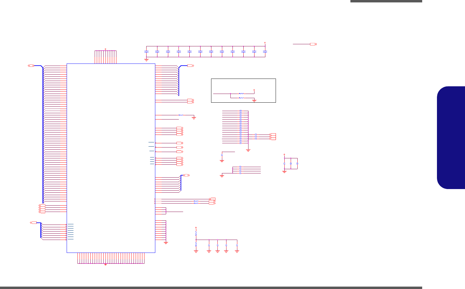
Schematic Diagrams
VN800-2 B - 7
B.Schematic Diagrams
VN800-2
Sheet 6 of 34
VN800-2
C212
0.1UF
C223
0.1UF
MD _4 3
C163
0.1UF
MD _4 4
R115 22
R116 22
MD _4 5
MD _4 6
MD _4 7
MD _4 8
MD _4 9
M_DQS4
MD _5 0
M_DQS7
M_DQS2
M_DQS1
MD _5 1
M_DQS3
M_DQS6
M_DQS5
M_DQS0MD _5 2
M_CLKO+
MD _5 3
MCLKIT
M_C LKO -
MD _5 4
M_CKE 1
MAA2
MAA3
MAA13
MAA7
MD _5 5
C196 33pF
MVREF_NB
C454 33pF
MD _5 6
C455 33pF
C456 33pF
MD _5 7
MD _5 8
MD _5 9
MEMDET
Z0601
M_CS0#
M_CS3#
M_CS1#
M_CS2#
MD _6 0
MD _6 1
MD _6 2
C185
*5pF
C214
1UF
R132 301_1%
C215
1UF
R112
150_1%
R117
150_1%
MD _6 3
1.8V
1.8V
MVREF_NB
1.8V
1.8V
MD _0
M_CKE 0
M_CKE 3
M_CKE 2
MAA8
MCLKIT
MAA1
MAA5
MAA12
MAA4
MAA11
MAA10
MAA6
MAA9
MAA0
MD _1
MD _2
MD _3
C447 *33PF
C445 *33PF
MD 0
AD28
MD 1
AE27
MD 2
AF27
MD 3
AG28
MD 4
AD27
MD 5
AE29
MD 6
AG27
MD 7
AG29
MD 8
AH29
MD 9
AJ29
MD 10
AG25
MD 11
AJ25
MD 12
AJ28
MD 13
AH27
MD 14
AH26
MD 15
AJ26
MD 16
AJ24
MD 17
AG24
MD 18
AJ22
MD 19
AG21
MD 20
AH24
MD 21
AG23
MD 22
AG22
MD 23
AJ21
MD 24
AH21
MD 25
AJ20
MD 26
AG18
MD 27
AH18
MD 28
AG20
MD 29
AH19
MD 30
AJ18
MD 31
AG17
MD 32
AJ12
MD 33
AG12
MD 34
AJ10
MD 35
AJ9
MD 36
AH12
MD 37
AJ11
MD 38
AG10
MD 39
AH9
MD 40
AG8
MD 41
AJ7
MD 42
AJ6
MD 43
AH6
MD 44
AG9
MD 45
AJ8
MD 46
AG5
MD 47
AJ5
MD 48
AH4
MD 49
AJ4
MD 50
AJ2
MD 51
AH1
MD 52
AG4
MD 53
AF4
MD 54
AG3
MD 55
AJ1
MD 56
AG1
MD 57
AF2
MD 58
AD3
MD 59
AD1
MD 60
AG2
MD 61
AF3
MD 62
AE1
MD 63
AD2
MA0 AF13
MA1 AD15
MA2 AJ15
MA3 AJ16
MA4 AJ17
MA5 AF16
MA6 AG15
MA7 AE18
MA8 AF17
MA9 AE19
MA10 AJ14
BA0 AF12
BA1 AJ13
MA11 AF20
MA12 AE21
GND
AH8
MCLKIA AD26
MCLK O- AE26
CKE0
AF21
CKE1
AF23
CKE2
AE22
CKE3
AF24
DQM0
AF28
DQM1
AJ27
DQM2
AJ23
DQM3
AJ19
DQM4
AG11
DQM5
AH7
DQM6
AJ3
DQM7
AF1
SCAS AF9
SWE AF11
SRAS AE12
CS0 AD9
CS1 AF8
CS2 AG7
CS3 AF7
DQS0 AF29
DQS1 AG26
DQS2 AH22
DQS3 AG19
DQS4 AH10
DQS5 AG6
DQS6 AH3
DQS7 AE3
VCC18MEM W12
VCC 18MEM W13
VCC18MEM W14
VCC 18MEM W15
VCC18MEM W16
VCC 18MEM W17
VCC18MEM W18
VCC 18MEM W19
VCC18MEM V19
GND M16
GND N16
GND P16
GND R16
GND T16
GND V16
MEMVREF 1 AD23
MEMVREF 2 AD17
MEMVREF 3 AD11
MEMVREF 4 AD8
VCC18MEM V11
VCC 18MEM W11
GND
M17
GND
N17
GND
P17
GND
R17
GND
T17
GND
U17
GND
V17
GND M15
GND N15
GND P15
GND U16
MCLKO+ AF26
GND
AH11
GND
AH14
GND
AH17
GND
AH20
GND
AH23
GND
AH25
GND
AH28
GND
AF5
GND
AH5 GND
AH2 GND
AE28 GND
AE25 GND
AE23 GND
AE20 GND
AE17 GND
AE16 GND
AE14 GND
AE11 GND
AE8 GND
AE2
MA13 AD7
GND
V15
GND
U15
GND
T15
GND
R15
DMCOMP AE5
MEMDET AE24
ODT0 AE9
ODT1 AE10
ODT2 AF6
ODT3 AD 6
U30B
VN800
C446 *33PF
C449 *33PF
C188 *33PF
C452 *33PF
MD _4
C186 *33PF
C441 *33PF
C453 *33PF
C448 *33PF
C443 *33PF
C451 *33PF
C198 *33PF
C189 *33PF
C442 *33PF
C444 *33PF
C450 *33PF
C190 *33PF
C440 *33PF
M_BA1
MAA1
MAA7
MAA12
MAA4
MAA13
MAA3
MAA9
MAA11
MAA6
MAA5
MD _5
MAA0
MAA8
M_BA0
MAA10
MAA2
MD _6
MD _7
MD _8
MD _9
MD_[0:63]9,10
MD _1 0
MD _1 1
MD _1 2
MD _1 3
MD _1 4
MAA[0:13] 9,10
M_BA1 9,10
M_ODT0 10
M_BA0 9,10
M_ODT1 10
M_ODT3 9,10
M_ODT2 9,10
M_CAS# 9,10
M_WE# 9,10
M_RAS# 9,10
M_CS0# 10
M_CS1# 10
M_CS2# 9,10
MCLKOC 2
M_CS3# 9,10
MCLKOT 2
M_C AS# 9,10
M_R AS# 9,10
MCLKIT 2
M_W E# 9,10
MD _1 5
MD _1 6
MD _1 7
M_CKE110 M_CKE010
M_CKE39,10 M_CKE29,10
MD _1 8
MD _1 9
MD _2 0
MD _2 1
MD _2 2
MD _2 3
MD _2 4
M_DM[0..7]9,10
MD _2 5
M_DM6
M_DM4
M_DM2
M_DM3
M_DM5
M_DM1
M_DM0
M_DM7
MD _2 6
0: DDR1
R113 4.7K
R114 *4.7K
MEMDET SEL:
MD _2 7
*
MD _2 8
MD _2 9
MD _3 0
MEMDET
1: DDR2
MD _3 1
MD _3 2
MD _3 3
MCLKO+/- as short as passable
MCLKIT = DCLKx + 2 "
MD _3 4
Near to NB chip
C151
1000PF
MD _3 5
C192
1000PF
C187
1000PF
C181
1000PF
M_DQS[ 0 . . 7 ] 9,10
MD _3 6
1.8V 2,7,9,10,25
MD _3 7
MD _3 8
C213
0. 1U F
MD _3 9
MD _4 0
C152
0.1UF
MD _4 1
C197
0.1UF
C148
0.1UF
C149
0.1UF
C145
0.1UF
C153
0.1UF
C217
0.1UF
MD _4 2
C150
0.1UF
C159
0.1UF
1.8V
Schematic Diagrams
B - 8 VN800-3
B.Schematic Diagrams
VN800-3
Sheet 7 of 34
VN800-3
M950626
LVREF_NB
TESTIN_NB
LVREF_NB => VT8237R plus =0.625
LVREF_NB => VT8237A =0.45
Decoupling capacitors
AGP8xdet 0=enable
Decoupling capacitors
1.5VS
12
CE2
330UF/6.3V
Z0750
Z0751
3VS 2,8,9,10,11,12,13,14,15,16,19,20,22,23,24,26,28,30
R159 402_1%
Z0761
Z0754
Z0758
Z0757
Z0756
Z0764
Z0763
Z0755
Z0759
Z0760
Z0762
3V 11,12,13,17,19,24,25,26,29,30
C950718
C950718
Z0713
Z0710
PDVP1HS
Z0748
C295
0.1UF
C257
0.1UF C253
1000PF
1.5VS
PDVP1CLK
Z0746
Z0747
Z0743
Z0715
Z0717
Z0738
Z0720
Z0733
Z0745
Z0729
Z0725
Z0721
Z0735
Z0722
Z0739
Z0724
Z0737
Z0732
Z0730
Z0736
Z0728
Z0719
Z0727
Z0731
Z0726
Z0718
Z0716
Z0723
PDVP1VS
Z0740
Z0741
Z0744
Z0742
R436
1.4K_1%
VLAD0
VLAD[ 0..7]13
VLAD1 PDVP1CLK 20
PDVP1HS 20
VLAD3
VLAD2
under NB( solder side)
VLAD4
VLAD5
R402
1K
VLAD6
VLAD7
R152
1K_1%
DNCMD 13
UPSTB 13
UPSTB# 13
DNSTB 13
UPCMD 13
DNSTB# 13
1.8V 2,6,9,10,25
AVDD1
GNDAHCK
GNDAMCK
AVDD2
C154
1UF
FB3 HCB2012KF-121T30
FB12 HCB2012KF-121T30
Z0749
R16 0_04
C439
1UF
3VS
3VS
1.5VS
1.5VS
1.5VS
1.8V
VBE#13
1.5VS 2,4,20,24,26
UPSTB
UPSTB#
PDVP1DE 20
PDVP1VS 20
DNSTB
C493 4.7uF
C256 4.7uF
C275 2.2UF
C235 2.2UF
C491 4.7uF
C248 4.7uF
C484 4.7uF
C485 4.7uF
C222 2.2UF
C267 2.2UF
C273 2.2UF
C490 4.7uF
1.5VS
+
C534
150UF/4V_B
DNSTB#
+
C535
150UF/4V_B
UPCMD
BUF_PLT_RST#11,19 SB_PWROK12
DNCMD
FPD10
R205 *4.7K_04
GD0/FPD10 P3
GD1/FPD11 P4
GD2/FP1CLK R3
GD3/FPD09 R4
GD4/FPD08 R1
GD5/FPD07 N2
GD6/FPD06 P1
GD7FPD05 R2
GD8/FP1DET M3
GD9/FP1HS M1
GD10/FPD01 N4
GD11/FPD23 L3
GD12/FPD00 L1
GD13/FPD22 N5
GD14/FPD21 K2
GD15/FPD20 R6
GD16/FPD18 J2
GD17/FPD17 H3
GD18/FPD16 H1
GD19/FPDE K4
GD20/FPD14 G1
GD21/FPCLK G2
GD22/FPD13 K5
GD23/FPD15 G3
GD24/GDVP1D09 J6
GD25 K6
GD26/GDVP1D10 J4
GD27/GDVP1D04 F2
GD28/GDVP1D07 J5
GD29/GDVP1D06 F3
GD30/GDVP1D08 H4
GD31/GDVP1DET E1
GC#BE0/FPD03 M2
GC#BE1/SBPLDAT K1
GC#BE2/FPD19 J1
GC#BE3/GDVP1D11 L6
GFRAME/FPHS L4
GIRDY/SBPLCLK M5
GTRDY K3
GDEVSEL/FPVS J3
GSTOP/FP1CLK M4
GPAR/FP1VS P6
GDBIH G5
GRBF F4
GWBF/FPCLK B3
GADSTBF0/FPD04 N1
GADSTBF1/FPD12 G4
GADSTBS0/FPD02 N3
GADSTBS1/FPDET F1
GSBA0/GDVP1VS A1
GSBA1/GDVP1DE A2
GSBA2/GDVP1D00 B1
GSBA3/GDVP1HS C3
GSBA4/GDVP1D05 D1
GSBA5/GDVP1D03 D4
GSBA6/GDVP1CLK D2
GSBA7/GDVP1CLK D3
AGPVREF1 N6
GCLK R5
GND
P13
GND
P14
GND
M12
GND
M13
GND
M14
GND
N12
GND
N13
GND
N14
GREQ/SBDDCCLK D5
GGNT/SBDDCDAT C4
GSBSTBF/GDVP1D01 C1
GSBSTBS/GDVP1D02 C2
GST0/ENAVEE E4
GST1/ENAVD D E3
GST2/ENABLT F5
VD0
V1
VD1
U2
VD2
Y2
VD3
Y3
VD4
T2
VD5
T3
VD6
AA2
VBE
U3
UPSTB+
W2
UPSTB-
W1
DNSTB+
V2
DNSTB-
V3
UPCMD
AA3
DNCMD
W3
VLVREF
V4
VLCOMPP
T4
VCC15AGP M11
VCC15AGP N11
VCC15AGP P11
VCC15AGP R11
VCC15AGP T11
VD7
AA1
GNDAHCK
AA26
GNDAMCK
AD24
VSUS15
AB1
GND
R12
GND
P12
SUSST
AB3
TES TI N
AF25
RESET
AC1
PWROK
AB2
VCC15
Y14
VCC15
Y16
VCC15
Y18
VCC15
Y20
VCC15
L10
VCC15
N10
VCC15
R10
VCC15
W10
VCCA33HCK
AA25
VCCA33MCK
AD25
GDBIL H6
AGP8XDET C5
AGPVREF2 G6
AGPCOMPP A3
GND
T14
GND
U12
GND
T13
GND
R13
GND
R14
GND
T12
VCC15
Y10
VCC15
Y12
VCC15
M20
VCC15
P20
VCC15
T20
VCC15
V20
VCC15
K19 VCC 15
K17 VCC 15
K15 VCC 15
K13 VCC 15
K12
VCC15
K20
VCC15VL
U11
VCC15VL
U10
VCC15VL
V10
GND
U13
GND
U14
GND
V12
GND
V13
GND
V14
GSERR/FP1DE M6
AGPBUSY T1
VCC15
K11 VCC 15
K10
VSUS15
AC25
AGPCOMPN A4
U30C
VN800
R203 4.7K_04
1.5VS
FPD11
NEAR NB(VN800)
FPD09
C243
0.1UF C249
0.1UF
FPD08
ENAVDD 20
FPD07
C438
1000PF
C155
1000PF
C240 0.1UF
FPD06
M950626
FPD05
LVREF_NB
FPD01
FPD00
FPD03
FPD04
FPD02
C281 2.2UF
21
S3
S1
21
S4 S1
FPD00 20
FPD03 20
FPD02 20
FPD01 20
FPD06 20
FPD05 20
FPD04 20
1.5V 26,29
FPD08 20
FPD07 20
FPD11 20
FPD10 20
FPD09 20
PDVP1DE
R193
10K_1%_04
R197
10K_1%_04
GNDAMCK
Z0701
GCLK_NB 2
1.5VS
C279
.1UF_04
1.5VS
L_BKLTEN 20
1.5V
ENAVEE 20
R228 60.4_1%
R227 60.4_1%
1.5VS
AGPCOMPP
AGPCOMPN
DNCMD
UPSTB
UPCMD
UPSTB#
DNSTB
DNSTB#
C466
0.1UF
R156
0
GNDAHCK
PM_SUS_STAT#12
AGP_BUSY # 13
+
CA2
*330UF/6.3V
+
CA1
330UF/6.3V
1.5VS
AVDD2
AVDD1AVDD1
LCOMPP
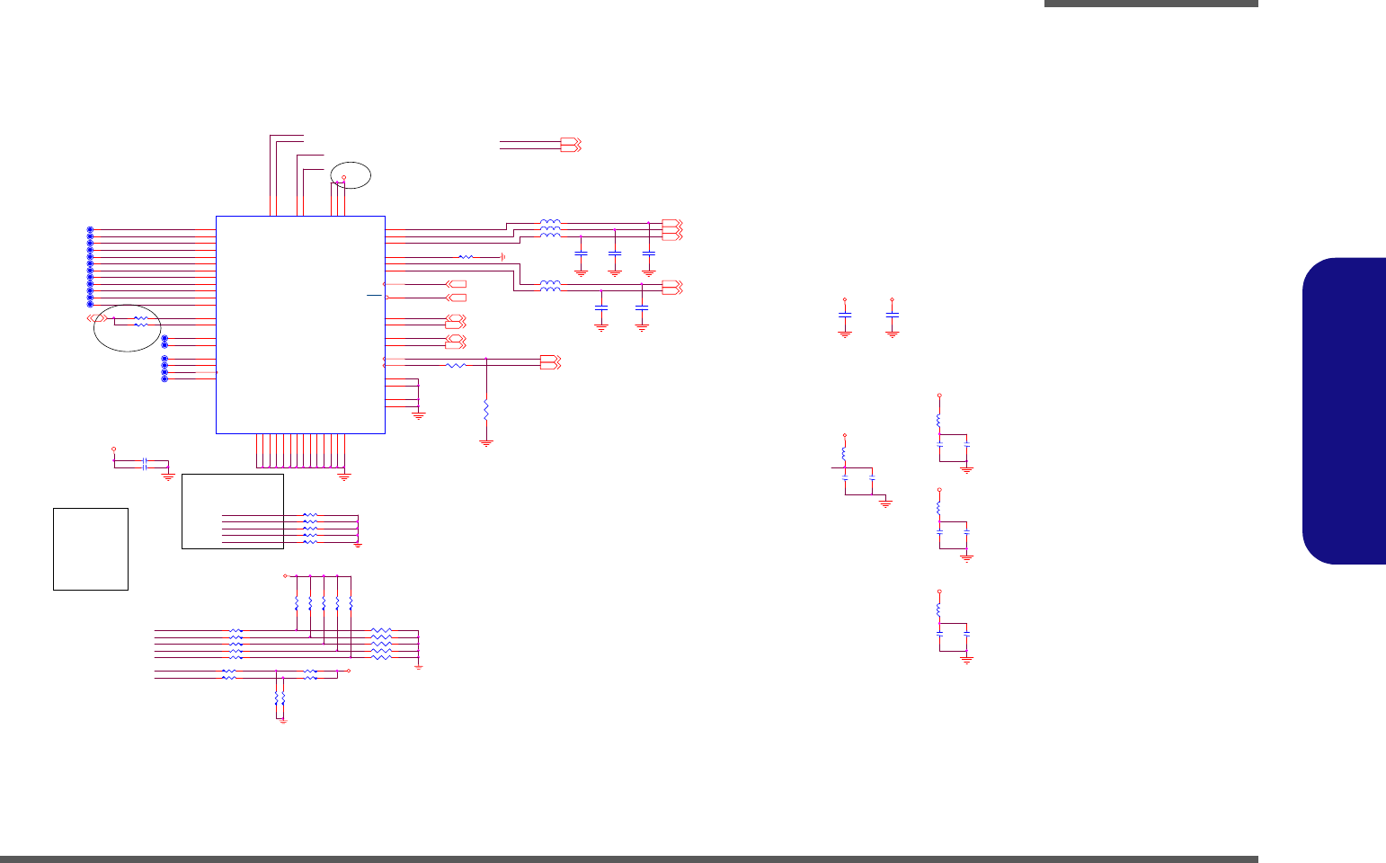
Schematic Diagrams
VN800-4 B - 9
B.Schematic Diagrams
VN800-4
Sheet 8 of 34
VN800-4
VCCDAC2
L25 HCB1608KF-121
L27 HCB1608KF-121
L26 HCB1608KF-121
L28 HCB1608KF-121
L29 HCB1608KF-121
0: TMDS
1: TV
Encoder
C14
22P
0: Ref er Internal PLL
1: From External
C16
22P C15
22P
C9
22P C18
22P
TVD7/DVP0D7 =>GFX Clock Select(VCK/LCDCK/ECK)
GFX power up strapping setting:
0: From NB
1: From
External
Modufy A1 rev
0: Disable
1: Enable
TVD10/DVP0D10 =>CPUCK/MCK Clock Select
0: External
1: Internal
TVD5/DVP0D5 =>Dedicated DVI Port Configuration
TVD8/DVP0D8 =>External AGP Function Enable
0: Disable
1: Enable
R551
4.7K_04
TVD4/DVP0D4 =>AGP Port Muxing
TVD6/DVP0D6 =>De dicated DVI Port Selection
TVD9/DVP0D9 =>PCI Signal Test Output Enable
0: Two 12-bit DVI interf ace
1: One 24-bit Panel
interf ace
3VS 2,7,9,10,11,12,13,14,15,16, 19,20,22,23,24,26,28,30
R246 0_04
R247 0_04
DVP0D9/TVD09
Z0812
Z0813
DVP0D7/TVD07
GUICK 2
DVP0D4/TVD04
DVP0D4/TVD04
DVP0D6/TVD06
DVP0D11/TVD11
DVP0D2/TVD02
DVP0D0/TVD00
DVP0D5/TVD05
DVP0D1/TVD01
DVP0D9/TVD09
DVP0D7/TVD07
DVP0D10/TVD10
DVP0D3/TVD03
DVP0D8/TVD08
DVP0D6/TVD06
DVP0D8/TVD08
C270 0.1UF
C271 0.1UF
L_DDC_DATA 20
L_DDC_CLK 20
Z0811
Z0809
M950626
DUAL20
950310
R259
1K_04
C298
1UF
FB16 HCB2012KF-121T30
C482
1000PF
C483
1UF
FB15 HCB2012KF-121T30
C481
1000PF
C297
1UF
C480
1000PF
R254
1K_04
R495 22_04
Z0807
FB17 HCB2012KF-121T30
C296
1000PF
DISPCLKO 20
R249
0_04
FB18 HCB2012KF-121T30
DISPCLKI 20
PCI_INTA# 11,15,24
Z0808
C299
1UF
3VS
3VS
3VS
3VS
3VS
3VS
3VS
Z0810
R257
1K_04
R256
1K_04
R255
*1K_04
GNDADAC2 D6
GNDADAC1 E6
GNDAPLL1 B7
GNDAPLL2 C6
INTA A9
AR B6
AG A5
AB B5
RSET A6
HSYNC B8
VSYNC A8
GPO0
E11
GPOUT
C11
DVP0VS/TVVS
C10 DVP0HS/TVHS
E10
DVP0CLK/TVCLK
D11
DVP0DE/TVDE
B10 TVCLKR
A10
XIN A7
SPCLK1 D9
SPCLK2 E9
SPD1 D10
SPD2 E8
VCCA33DAC1 E7
VCCA33DAC2 D7
VCC A33PLL1 D8
VCCA33PLL2 C7
VCC33GFX L13
VCC33GFX L12
DVP0D00/TVD00
C13
DVP0D01/TVD01
B13
DVP0D02/TVD02
A13
DVP0D03/TVD03
D13
DVP0D04/TVD04
E13
DVP0D05/TVD05
D12
DVP0D06/TVD06
C12
DVP0D07/TVD07
A12
DVP0D08/TVD08
B12
DVP0D09/TVD09
E12
DVP0D10/TVD10
B11
DVP0D11/TVD11
A11
GND
B4
GND
E2
GND
E5
GND
H2
GND
H5
GND
L2
GND
L5
GND
P2
GND
P5
GND
U1
GND
U4
GND
Y1
GND
B2 GND
A14
DISPCLKI C8
DISPCLKO C9
VCC33GFX L14
DVP0DET
B9
U30D
VN800
Modufy A1 rev
DVP0D11/TVD11
R223 4.7K_04
R229 4.7K_04
R222 4.7K_04
R494 4.7K_04
R231 4.7K_04
DVP0D2/TVD02
DVP0D3/TVD03
DVP0D1/TVD01
DVP0D0/TVD00
R497 80.6_1%
3VS
Z0801
Z0805
Z0804
Z0802
Z0803
R234 1K_04
R235 1K_04
R236 1K_04
R238 1K_04
R233 1K_04
R237 4.7K_04
GND
R232 4.7K_04
Z0806
GND
R258 1K_04
R253 1K_04
Z0815
DVP0D 10/TVD10
Z0816
R250 *0_04
DISPCLKO
RSET
R366 *0
R367 0
DVP0D5/TVD05
R248 0_04
R245 0_04
3V 11, 12, 13,17,19,24,25,26,29,30
CRT_DDC_CLK 20
CRT_DDC_DATA 20
DISPCLKI
R244
0_04
VCCPLL1
VCCDAC1
VCCPLL2
VCCDAC2
C521
47PF_04
3VS
GND
C522
47PF_04
GND
3VS
VCCPLL1
VCCPLL2
Z0814
CRT_BLUE 20
CRT_GREEN 20
CRT_RED 20
Trace w idth = 10 mils
CRT_HSYNC 20
VCCDAC1
CRT_VSYNC 20
GND
GND
GND
GND
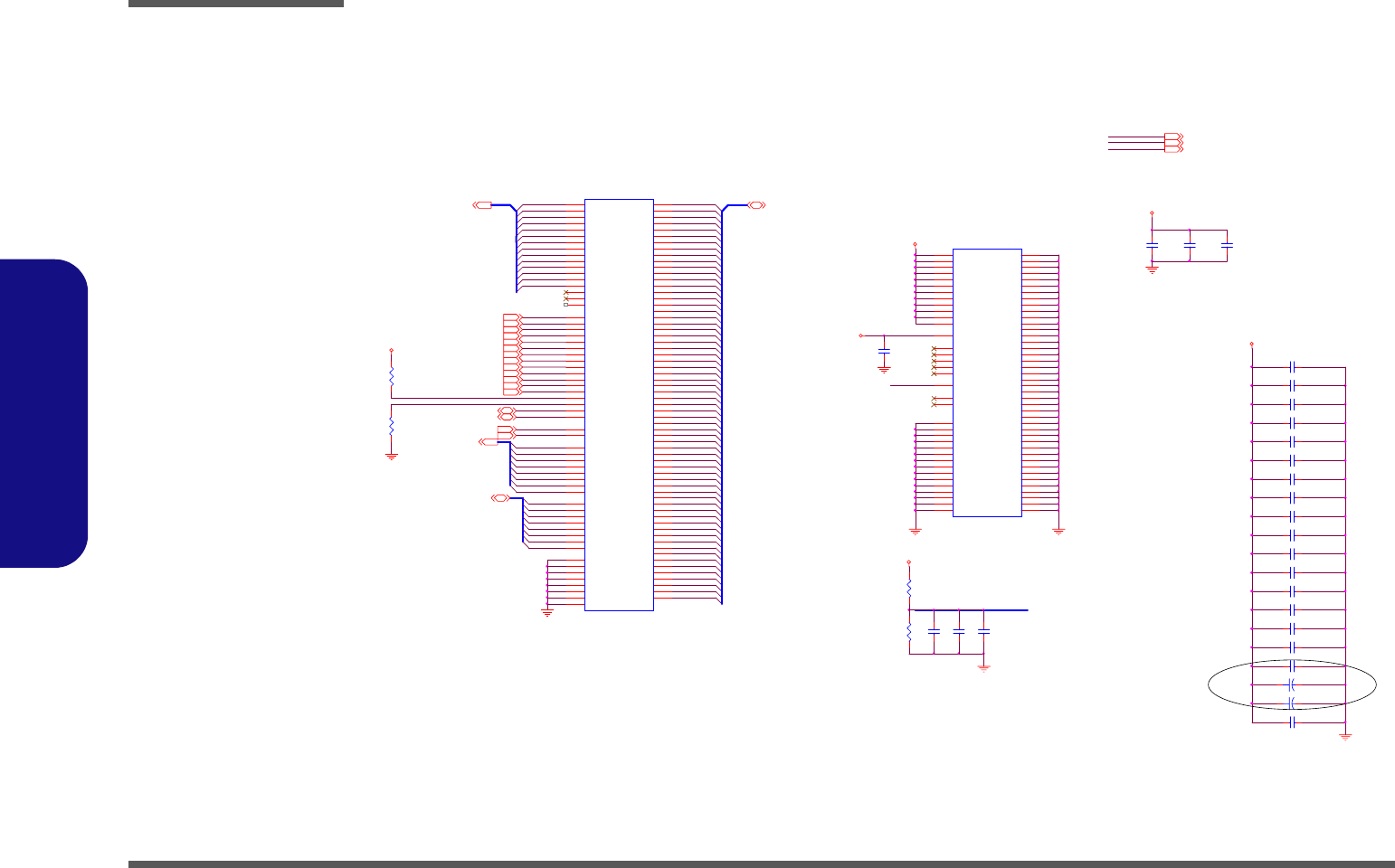
Schematic Diagrams
B - 10 DDR2-1
B.Schematic Diagrams
DDR2-1
Sheet 9 of 34
DDR2-1
M_CS2#
C88 10UF/10V_08
M_CS3#
M_OD T3
M_OD T2
C47 10UF/10V_08
C104 0.1UF
C74 0.1UF
C70 10UF/10V_08
C35 10UF/10V_08
C103 0.1UF
C81 0.1UF
C64 0.1UF
C93 10UF/10V_08
C63 0.1UF
C97 0.1UF
1 2
+
C43 330U F/ 6.3V
1 2
+
C44 *330UF/6.3V
1.8V
SMB_SBDATA2,10,12,24 SMB_SBCLK2,10,12,24
M_D QS6
M_D QS7
M_D QS3
M_D QS4
M_D QS1
M_D QS2
M_D QS5
M_DQS[0..7]6,10 M_DQS0
M_BA0
M_CAS#
M_WE#
M_WE#6,10
M_BA06,10
M_RAS#
M_RAS#6,10 M_CA S#6,10
M_BA16,10 M_BA 1
VDD1
112
VDD2
111
VDD3
117
VDD4
96
VDD5
95
VDD6
118
VDD7
81
VDD8
82
VDD9
87
VDD10
103
VDD11
88
VDD12
104
VDDSPD
199
NC1
83
NC2
120
NC3
50
NC4
69
NCTEST
163
VREF
1
GND0
201
GND1
202
VSS1
47
VSS2
133
VSS3
183
VSS4
77
VSS5
12
VSS6
48
VSS7
184
VSS8
78
VSS9
71
VSS10
72
VSS11
121
VSS12
122
VSS13
196
VSS14
193
VSS15
8
VSS16 18
VSS17 24
VSS18 41
VSS19 53
VSS20 42
VSS21 54
VSS22 59
VSS23 65
VSS24 60
VSS25 66
VSS26 127
VSS27 139
VSS28 128
VSS29 145
VSS30 165
VSS31 171
VSS32 172
VSS33 177
VSS34 187
VSS35 178
VSS36 190
VSS37 9
VSS38 21
VSS39 33
VSS40 155
VSS41 34
VSS42 132
VSS43 144
VSS44 156
VSS45 168
VSS46 2
VSS47 3
VSS48 15
VSS49 27
VSS50 39
VSS51 149
VSS52 161
VSS53 28
VSS54 40
VSS55 138
VSS56 150
VSS57 162
JDIMM1B
CA0145-200N02
R47
10K
3VS
SDREFD
M_CKE36,10
Z0902
MAA11
MAA4
MAA10
MAA12
MAA1
MAA13
MAA9
MAA2
MAA5
MAA0
MAA7
MAA3
MAA6
MAA8
M950626
M_CKE26,10
Trace Width 12 Mil
Space 20 Mil
MAA[0:13]6, 10
DDRVREF GEN. & DECOUPLING
Z0901
MD_[0:63] 6,10
M_CLK_DDR#22M_CLK_DDR22
M_CLK_DDR#32M_CLK_DDR32
M_DM[0..7]6,10
M_D M4
M_D M2
M_D M6
M_D M5
M_D M1
M_D M3
M_D M0
M_D M7
SDREFD
M_ODT36,10 M_ODT26,10
M_CKE2
M_CKE3
C106 0.1UF_04
C67
2.2UF
R46
75_1%
R44
10K
C65
0.1UF
R45
75_1%
C66
2.2UF
C68
0.1UF
3VS
1.8V
1.8V
M_CS3#6,10 M_ CS2#6,10
C278
0.1UF_04 C475
0.1UF_04 C527
0.1UF_04
1.8V
0.9VS 10,25
1.8V 2,6,7,10,25
3VS 2,7,8,10,11,12,13,14,15,16,19,20,22,23,24,26,28,30
MD_30
MD_63
MD_29
MD_44
MD_52
MD_34
MD_62
MD_0
MD_23
MD_35
MD_47
MD_13
MD_10
MD_61
MD_12
MD_20
MD_54
MD_11
MD_4
MD_16
MD_40
MD_57
MD_45
MD_48
MD_25
MD_6
MD_8
MD_9
MD_19
MD_2
MD_33
MD_28
MD_3
MD_55
MD_7
MD_22
MD_32
MD_36
MD_18
MD_60
MD_53
MD_49
MD_59
MD_31
MD_46
MD_27
MD_38
MD_15
MD_39
MD_1
MD_41
MD_56
MD_37
MD_43
MD_21
MD_17
MD_26
MD_51
MD_24
MD_58
MD_50
MD_42
MD_14
MD_5
C107 0.1UF_04
C140 0.1UF_04
C91 0.1UF_04
C121 0.1UF_04
C134 0.1UF_04
A0
102
A1
101
A2
100
A3
99
A4
98
A5
97
A6
94
A7
92
A8
93
A9
91
A10/AP
105
A11
90
A12
89
A13
116
A14
86
A15
84
A16_BA2
85
DQ0 5
DQ1 7
DQ2 17
DQ3 19
DQ4 4
DQ5 6
DQ6 14
DQ7 16
DQ8 23
DQ9 25
DQ10 35
DQ11 37
DQ12 20
DQ13 22
DQ14 36
DQ15 38
DQ16 43
DQ17 45
DQ18 55
DQ19 57
DQ20 44
DQ21 46
DQ22 56
DQ23 58
DQ24 61
DQ25 63
DQ26 73
DQ27 75
DQ28 62
DQ29 64
DQ30 74
DQ31 76
DQ32 123
DQ33 125
DQ34 135
DQ35 137
DQ36 124
DQ37 126
DQ38 134
DQ39 136
DQ40 141
DQ41 143
DQ42 151
DQ43 153
DQ44 140
DQ45 142
DQ46 152
DQ47 154
DQ48 157
DQ49 159
DQ50 173
DQ51 175
DQ52 158
DQ53 160
DQ54 174
DQ55 176
DQ56 179
DQ57 181
DQ58 189
DQ59 191
DQ60 180
DQ61 182
DQ62 192
DQ63 194
BA0
107
BA1
106
RAS#
108
WE#
109
CAS#
113
S0#
110
S1#
115
CKE0
79
CKE1
80
CK0
30
CK0#
32
CK1
164
CK1#
166
SDA
195 SC L
197 SA1
200 SA0
198
DM0
10
DM1
26
DM2
52
DM3
67
DM4
130
DM5
147
DM6
170
DM7
185
DQS0
13
DQS1
31
DQS2
51
DQS3
70
DQS4
131
DQS5
148
DQS6
169
DQS7
188
DQS0#
11
DQS1#
29
DQS2#
49
DQS3#
68
DQS4#
129
DQS5#
146
DQS6#
167
DQS7#
186
ODT0
114
ODT1
119
JDIMM1A
CA0145-200N02
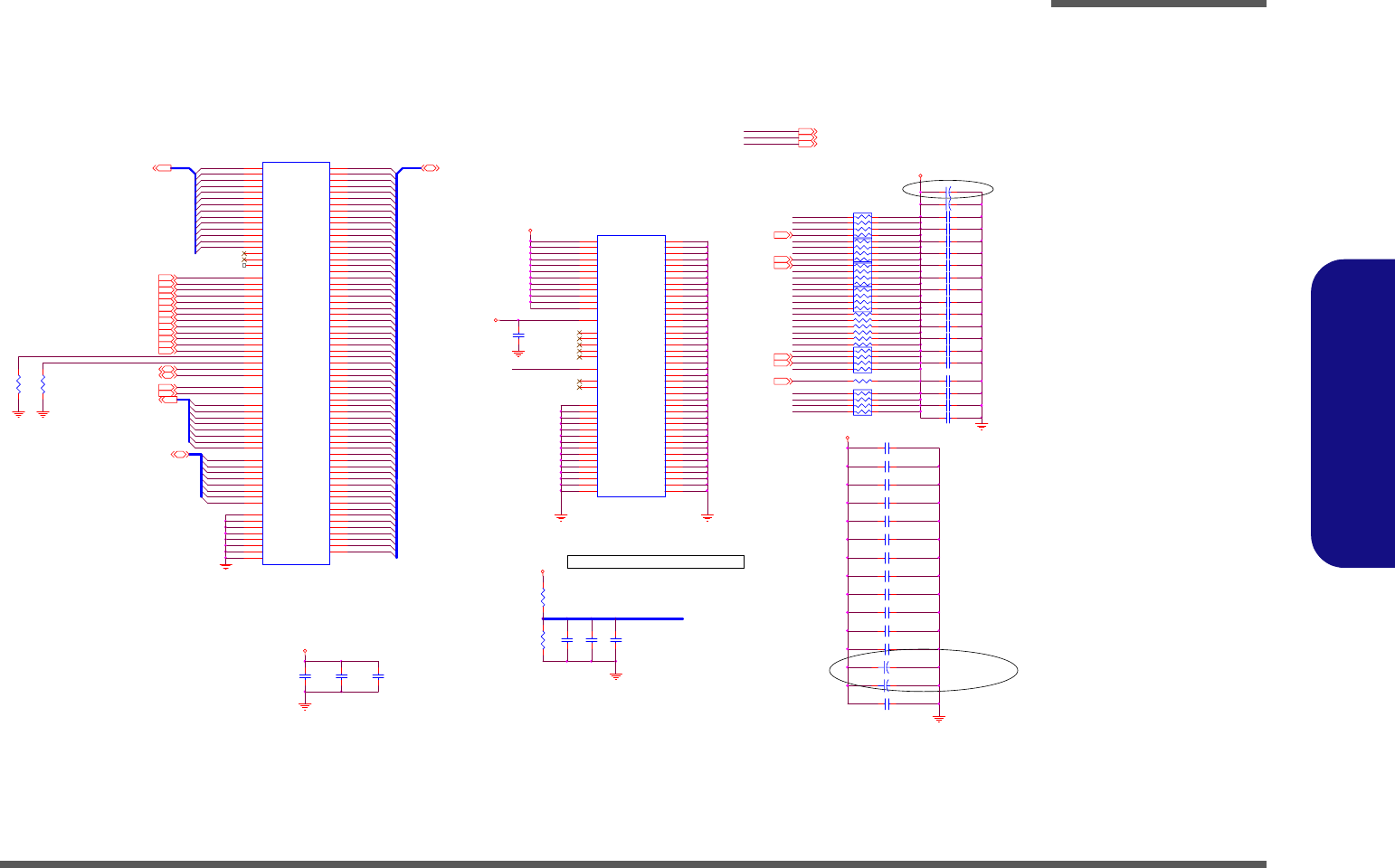
Schematic Diagrams
DDR2-2 B - 11
B.Schematic Diagrams
DDR2-2
MD_37
MD_43
MD_21
MD_17
MD_26
MD_51
MD_24
MD_58
MD_50
MD_42
MD_14
MD_5
C89 0.1UF_04
0. 9V S 25
1.8V 2,6,7,9,25
3VS 2,7,8,9,11,12,13,14,15,16,19,20,22,23,24,26,28,30
C528
0.1UF_04 C529
0.1UF_04 C530
0.1UF_04
1.8V
C79 0.1UF_04
81 72 6
5
3
4
RP5 8P4RX47_04
C98
2.2UF
C99
0.1UF
R71
10K
R78
75_1%
C100
2.2UF
C418
0.1UF
R79
75_1%
3VS
1.8V
1.8V
C80 0.1UF_04
M_CLK_DDR#02
M_WE #6,9
M_CLK_DDR#12
M_CKE16
M_CLK_DDR02
M_CLK_DDR12
M_CAS#6, 9 M_ R AS#6,9
M_CKE06
M_OD T0
M_OD T1
M_ODT16M_ODT06
M_CKE3
MAA5
MAA13
MAA7
MAA12
M_ODT0
MAA1
M_BA0
M_CAS#
M_ODT3
M_CKE2
M_ODT2
MAA10
MAA11
SDREFC
M_RAS#
M_CS3# R59 47_04
Z1001
Z1002
+
C536 *150U_4V_B
+
C537 150U_4V_B
C77 10UF/10V_08
C49 0.1UF_04
M_CS1#
M_WE#
M_CS2#
MAA6
MAA8
M_ODT1
MAA9
M_CS0#
M_CKE1
MAA3
M_CKE0
MAA11
MAA12
MAA1
MAA13
MAA4
MAA9
MAA2
MAA10
MAA0
MAA7
0.9VS
MAA6
MAA8
MAA5
MAA3
SMB_SBCLK2,9,12,24 SMB_SBDATA2,9,12,24 SMB_SBDATA
SMB_SBCLK
A0
102
A1
101
A2
100
A3
99
A4
98
A5
97
A6
94
A7
92
A8
93
A9
91
A10/AP
105
A11
90
A12
89
A13
116
A14
86
A15
84
A16_BA2
85
DQ0 5
DQ1 7
DQ2 17
DQ3 19
DQ4 4
DQ5 6
DQ6 14
DQ7 16
DQ8 23
DQ9 25
DQ10 35
DQ11 37
DQ12 20
DQ13 22
DQ14 36
DQ15 38
DQ16 43
DQ17 45
DQ18 55
DQ19 57
DQ20 44
DQ21 46
DQ22 56
DQ23 58
DQ24 61
DQ25 63
DQ26 73
DQ27 75
DQ28 62
DQ29 64
DQ30 74
DQ31 76
DQ32 123
DQ33 125
DQ34 135
DQ35 137
DQ36 124
DQ37 126
DQ38 134
DQ39 136
DQ40 141
DQ41 143
DQ42 151
DQ43 153
DQ44 140
DQ45 142
DQ46 152
DQ47 154
DQ48 157
DQ49 159
DQ50 173
DQ51 175
DQ52 158
DQ53 160
DQ54 174
DQ55 176
DQ56 179
DQ57 181
DQ58 189
DQ59 191
DQ60 180
DQ61 182
DQ62 192
DQ63 194
BA0
107
BA1
106
RAS#
108
WE#
109
CAS#
113
S0#
110
S1#
115
CKE0
79
CKE1
80
CK0
30
CK0#
32
CK1
164
CK1#
166
SDA
195 SCL
197 SA1
200 SA0
198
DM0
10
DM1
26
DM2
52
DM3
67
DM4
130
DM5
147
DM6
170
DM7
185
DQS0
13
DQS1
31
DQS2
51
DQS3
70
DQS4
131
DQS5
148
DQS6
169
DQS7
188
DQS0#
11
DQS1#
29
DQS2#
49
DQS3#
68
DQS4#
129
DQS5#
146
DQS6#
167
DQS7#
186
ODT0
114
ODT1
119
JDIMM2A
CA0115-200N02
MAA[0:13]6,9 MD_[0:63] 6,9
M950626
VDD1
112
VDD2
111
VDD3
117
VDD4
96
VDD5
95
VDD6
118
VDD7
81
VDD8
82
VDD9
87
VDD10
103
VDD11
88
VDD12
104
VDDSPD
199
NC1
83
NC2
120
NC3
50
NC4
69
NCTEST
163
VREF
1
GND0
201
GND1
202
VSS1
47
VSS2
133
VSS3
183
VSS4
77
VSS5
12
VSS6
48
VSS7
184
VSS8
78
VSS9
71
VSS10
72
VSS11
121
VSS12
122
VSS13
196
VSS14
193
VSS15
8
VSS16 18
VSS17 24
VSS18 41
VSS19 53
VSS20 42
VSS21 54
VSS22 59
VSS23 65
VSS24 60
VSS25 66
VSS26 127
VSS27 139
VSS28 128
VSS29 145
VSS30 165
VSS31 171
VSS32 172
VSS33 177
VSS34 187
VSS35 178
VSS36 190
VSS37 9
VSS38 21
VSS39 33
VSS40 155
VSS41 34
VSS42 132
VSS43 144
VSS44 156
VSS45 168
VSS46 2
VSS47 3
VSS48 15
VSS49 27
VSS50 39
VSS51 149
VSS52 161
VSS53 28
VSS54 40
VSS55 138
VSS56 150
VSS57 162
JDIMM2B
CA0115-200N02
R73
10K
M_ODT26,9
C105 0.1UF
M_C S2#6,9
1 2
+
C82 330UF/6.3V
DDRVREF GEN. & DECOUPLING
C76 10UF/10V_08
C101 0.1UF
C75 0.1UF
C73 0.1UF
C48 10UF/10V_08
1 2
+
C83 *330UF/6.3V
Layout Note:Place these Caps near So-Dimm0
C72 0.1UF
C102 0.1UF
C36 0.1UF
Trace Width 12 Mil
Space 20 Mil
C78 10UF/10V_08
C71 0.1UF
C69 10UF/10V_08
M_D M5
M_D M1
M_D M6
M_D M7
M_D M2
M_BA0
1.8V
M_D M3
M_BA1
M_ODT36,9
M_DM[0..7]6,9
M_D M4
M_D M0
C90 0.1UF_04
M_C KE26,9
M_BA06,9 M_BA16,9
C54 0.1UF_04
M_C KE36,9
M_CS0 #6M_CS1 #6
C53 0.1UF_04
SDREFC
M_C S3#6,9
C42 0.1UF_04
C39 0.1UF_04
C37 0.1UF_04
C38 0.1UF_04
M_BA1
MAA4
MAA0
MAA2
8 1
7 2
6
53
4
RP2 8P4RX47_04 C40 0.1UF_04
C41 0.1UF_04
R82 47_04
R77 47_04
R76 47_04
R80 47_04
C55 0.1UF_04
R75 47_04
81 72 6
5
3
4
RP4 8P4RX47_04
R81 47_04
M_RAS#
M_C KE1
M_WE #
M_CAS#
M_C KE0
C52 0.1UF_04
8 1
7 2
6
53
4
RP1 8P4RX47_04
F070395
C51 0.1UF_04
M_CS0 #
81 72 6
5
3
4
RP6 8P4RX47_04
M_D Q S6
M_CS1 #
M_D Q S1
M_D Q S4
M_D Q S5
M_D Q S2
M_D Q S7
M_D Q S3
M_DQS[0..7]6,9 M_DQS0
C50 0.1UF_04
8 1
7 2
6
53
4
RP3 8P4RX47_04
MD_30
MD_34
MD_63
MD_29
MD_23
MD_44
MD_52
MD_62
MD_0
MD_35
MD_47
MD_13
MD_54
MD_10
MD_57
MD_61
MD_12
MD_20
MD_11
MD_4
MD_16
MD_40
MD_45
MD_48
MD_25
MD_6
MD_8
MD_9
MD_19
MD_2
MD_55
MD_33
MD_28
MD_3
MD_7
MD_22
MD_32
MD_36
MD_18
MD_60
MD_53
MD_49
MD_59
MD_31
MD_46
MD_27
MD_38
MD_15
MD_39
MD_1
MD_41
MD_56
Sheet 10 of 34
DDR2-2

Schematic Diagrams
B - 12 VT8237-1
B.Schematic Diagrams
VT8237-1
FLASH#22
PCI _DEVSEL#
PCI_DEVSEL#15, 24
PCI_FRAME#15, 24
3V
Z1112
PCI _REQ#2
R459 8.2K
PCI_PERR#15, 24
R465 8.2K
PCI _REQ#1
IDE_SATDET#
PCI _TRDY#
PCI _IR DY #
R461 8.2K
PCI_SERR#15, 24
PCI _FRAME#
R460 8.2K
PCI _IN TA#
PCI _STOP#
PCI _IN TD#
PCI_STOP#15, 24
PCI_IRDY#15,24
PCI _REQ#3
R457 8.2K
PCI _REQ#1
R154 8.2K
PM_CLKRUN#12, 19
PCI _IN TC#
R190 8.2K
Z1113
3VS
R462 8.2K
PCI_TRDY#15,24
PCI _REQ#2
R188 8.2K
R463 8.2K
R168 8.2K
PM_CLKRUN#
R464 8.2K
Z1117
PCI _REQ#0
R445 8.2K
H_A20GATE 19
IDE_PATDET#
R165 8.2K
H_A20GATE
PCI _IN TB#
R189 8.2K
R191 8.2K
R458 8.2K
PCI _REQ#3
3V
PCI _REQ#4
PCI _REQ#5
USB_PN6 24
USB_PP6 24
950524
950511
PCI_REQ#015
PCI _GNT#0
USB_PN7 24
USB_PP7 24
PCI _GNT#1
PCI _GNT#2
2.5VS 2,3,12,13,20,26
Only for VT8237R plus
AP339A
PCI _GNT#3
FWH_TBL#
3V 12,13,17,19, 24,25, 26,29, 30
-PCIRST_GATE
2
14
3
5
U7
74AHC1G0 8GW
3V
ALL_PWROK
USB_PP6
USB_PN4
USB_PP4
USB_PN6
PWRGD_VCORE28
KBC_PWRGD19
USB_PN0
USB_PN2
USB_PP0
USB_PP2
F042795
FLASH#22
PCI_GNT#015
Z1119
R187 8.2K
PCI _REQ#5
3VS 2,7,8,9,10,12,13,14,15,16,19,20,22,23,24,26,28,30
ALL_PWROK 13, 20
3V
PCI _C/ BE0#
3V
PCI _C/ BE1#
USB_PN5
PCI _AD0
PCI _C/ BE2#
PCI _AD1
PCI _C/ BE3#
3VUSB
Z1102
PCI_C/BE1#15,24 PCI_C/BE0#15,24
PCI_C/BE2#15,24 PCI_C/BE3#15,24
PCI_DEVSEL#15,24 PCI_IRDY#15,24
Z1121
PCI _REQ#4
PCI _GNT#3
PCI _GNT#2
2.5V
PCI _GNT#1
PCI _GNT#0
R146 8.2K
R443 8.2K
R153 8.2K
R466 8.2K
R155 8.2K
PCI _AD2
PCI _AD3
PCI _TRDY#
PCI_TRDY#15,24
PCI_FRAME#15,24 PCI_FR AME#
PCI _DEVSEL#
PCI _IR DY #
PCI_PAR15,24 PCI_SERR#15,24
PCI _AD5
PCI _AD4
Z1120
Z1115
Z1103
PCI_INTD#24
PCI_REQ#324
PCI _PERR#
PCI _SERR#
PCI_GNT#324
PCI_STOP#15,24
PCI_PERR#15,24
PCI _PAR
PCI _STOP#
PCI _AD6
PCI _AD7
PCIRST#
-PCIRST_GATE
PCI _AD8
PCI _AD15
PCI _AD14
PCI _AD12
PCI _AD11
PCI _AD10
PCI _AD13
PCI _AD9
KBC_RST# 19
USB_PP0
PCI _AD20
PCI _AD16
PCI _AD21
PCI _AD23
PCI _AD18
PCI _AD19
PCI _AD22
PCI _AD17
USB_PN0
PCI _AD26
PCI _AD28
PCI _AD24
PCI _AD31
PCI _AD30
PCI _AD25
PCI _AD29
PCI _AD27 USB_PP1
PCI_INTB#15,24 PCI_INTA#8,15,24
PCI_INTC#15,24
USB_PN1
1 2
14
U31A
74AHC04
USB_PP2
CLK_USB48 2
USB_PN2
USB_PP3
3 4
14
U31B
74AHC04
USB_PN3
USB_PP4
ALL_PWROK
USB_PN4
USB_PP5
PCIR STC# 15,24
USB_PN5
USB_PP6
USB_PN6
R486 22
USB_PP7
USB_PN7
Z1109
USB_PN0 18
USB_PN5 18
USB_PN2 27
USB_PP3 18
PCI RST#
USB_PP0 18
USB_PN3 18
USB_PP2 27
USB_PP4 20
USB_PP5 18
USB_PN4 20
1
2
3
45
6
7
8RN198P4RX15K
R484 22 C158 0.01UF
C129
0.1UF
2
14
3
5
U5
74AHC1G0 8GW
R391 5.11K_1%
PCI _IN TD#
PCI _IN TC#
PCI _IN TA#
C136 1UF
C437 0.1UF
PCI _IN TB#
1
2
3
4 5
6
7
8
RN2 8P4RX15K
C173
0.1UF
C166
1UF
Z1116
C229 0.01UF
C191 0.1UF
R509
*51_1%
C142 0.1UF
C183 0.1UF
R392 10K
C230 1UF
5 6
14
U32C
74AHC04
C195 0.01UF
C138 1UF
C209
0.1UF
C135 1UF
R482 22
C436 0.01UF
1
2
3
4 5
6
7
8
RN3 8P4RX15K
C266 0.01UF
C169 1UF
C207 1UF
C147
0.1UF
C139 0.1UF
C170 1UF
C472
0.1U F
PCI_AD[31:0]15,24
Z1110
1
2
3
45
6
7
8RN208P4RX15K
C224 0.1UF
C228 1UF
C167 0.1UF
R492 22
C225 0.1UF
C179 0.01UF
C458
4.7uF C184
0.1UF
3 4
14
U32B
74AHC04
C238 1UF
C156
10UF/10V_08
1 2
14
U32A
74AHC04
C143 0.01UF
R186 *0
C205 0.1UF
FB1
HCB2012KF-121T30
C201 0.1UF
FB13
HCB3216KF-800T30
Z1111
C178
1UF
C432 0.1UF
C199 1UF
C144
10UF/25V_12
C160
1UF
11 10
14
U32E
74AHC04
13 12
14
U32F
74AHC04
C211 1UF
C227 0.1UF
FB2
HCB2012KF-121T30
C206 1UF
9 8
14
U32D
74AHC04 3VS
3V
3VUSB
3VS
3V
2.5VS
3V
3V
3V
3V
2.5V
3V
2.5VS
3V
Z1104
IDER ST# 14
PCIR STX# 22
BUF_PLT_RST# 7,19
Z1105
AD00
G2
AD01
J4
AD02
J3
AD03
H3
AD04
F1
AD05
G1
AD06
H4
AD07
F2
AD08
E1
AD09
G3
AD10
E3
AD11
D1
AD12
G4
AD13
D2
AD14
D3
AD15
F3
AD16
K3
AD17
L3
AD18
K2
AD19
K1
AD20
M4
AD21
L2
AD22
N4
AD23
L1
AD24
M2
AD25
M1
AD26
P4
AD27
N3
AD28
N2
AD29
N1
AD30
P1
AD31
P2
CBE0
E2
CBE1
C1
CBE2
L4
CBE3
M3
FRAME
J1
DEVSEL
H2
IRDY
J2
TRDY
H1
STOP
K4
SERR
C2
PAR
F4
USBP0+ E20
USBP0- D20
USBP1+ A20
USBP1- B20
GND
E8
GND
F25
GND
H23
INTA
A4
INTB
B4
INTC
B5
INTD
C4
REQ0
A5
REQ1
B6
REQ2
C5
REQ3
D5
REQ4
P3
GNT0
A6
GNT1
D6
GNT2
C6
GNT3
E5
GNT4
R4
USBP2+ E18
USBP2- D18
USBP3+ A18
USBP3- B18
USBP4+ D16
USBP4- E16
USBP5+ A16
USBP5- B16
USBOC3 C25
USBOC5 A24
USBOC0 C26
USBOC1 D24
USBOC2 B26
KBCK/KA20G,KBCK W3
KBDT/KBRC,KBDT V1
MSC K W1
MSD T W2
VCC33-1 H9
VCC33-2 H10
VCC33-4 H12
VCC33-5 J8
VCC33-6 K8
VCC33-7 L8
VCC33-8 M8
VCC 33-9 N8
VCC33-10 P8
VCC33-11 R8
VCC 33-12 R19
GND
J21
PERR
C3
REQ5/GPI7
R3
GNT5/GPO7
R2
PCIRST
R1
VCC33-13 T8
VCC33-14 T19
VCC33-16 U19
VCC33-17 V8
VCC33-18 V19
USBVCC4 D22
USBVCC5 E22
USBVCC6 F22
USBVCC7 J13
USBVCC8 J14
USBVCC9 J15
USBVCC10 J16
USBCLK E23
USBREXT B25
GND
J25
GND
B2
USBGND3
A17
USBGND4
A19
USBGND5
A21
USBGND6
B13
USBGND7
B15
USBGND8
B17
USBGND9
B19
USBGND10
B21
USBGND11
C13
USBGND12
C14
USBGND13
C15
USBGND14
C16
USBGND15
C17
USBGND16
C18
USBGND17
C19
USBGND18
C20
USBGND19
C21
USBGND20
D13
USBGND21
D15
USBGND22
D17
USBGND23
D19
USBGND24
D21
USBGND25
E13
USBGND26
E15
USBOC4 B24
VSUSUSB C24
VCCUPLL1 A23
VCCUPLL2 B23
GNDUPLL1 D23
GNDUPLL2 C23
USBVCC1 A22
USBVCC2 B22
USBVCC3 C22
USBVCC11 J17
USBGND27
E17
USBGND28
E19
USBGND29
E21
USBGND2
A15 USBGND1
A13
INTE/GPI12/GPO12
D4
INTF/GPI13/GPO13
E4
INTG/GPI14/GPO14
A3
INTH/GPI15/GPO15
B3
USBP6+ D14
USBP6- E14
USBP7+ A14
USBP7- B14
USBOC6 A26
USBOC7 A25
GPI9/UDPWR,GPI9 D26
GPO9/UDPWREN,GPO9 D25
VCC33-15 U8
USBVCC12 J18
VCC33-3 H11
VCC33-19 V21
VCC33-20 W9
VCC33-21 W10
VCC33-22 W11
VCC33-23 W17
VCC33-24 W18
VCC33-25 W19
VCC33-26 W21
VCC 33-27 Y21
USBGND30
H13
USBGND32
H15
USBGND33
H16
USBGND35
H18
USBGND31
H14
USBGND34
H17
GND
A1
GND
A2
GND
B1
VCC33-28 W8
U27A
VT8237R plus/VT8237A-BGA541
Z1106
GPIO12
950310
Z1107
IDE_PATDET#
Z1108
IDE_SATDET#
Modufy A1 rev
Z1118Z1114
USB_PP7
USB_OC3# 18
USB_OC5# 18
USB_OC2# 27
PCI_IN TH#
USB_PP3
USB_PP1USB_PP5 USB_PN1
USB_PN3USB_PN7
R388 10K
R387 10K
R390 10K
R389 10K
R456 2.2K_04
R476 2.2K_04
KBC_RST#
PCI _REQ#0
R439 8.2K
R449 8.2K
PCI _IN TH#
PCI_REQ#015
R160 8.2K
PCI _SERR#
PCI _PERR#
Sheet 11 of 34
VT8237-1
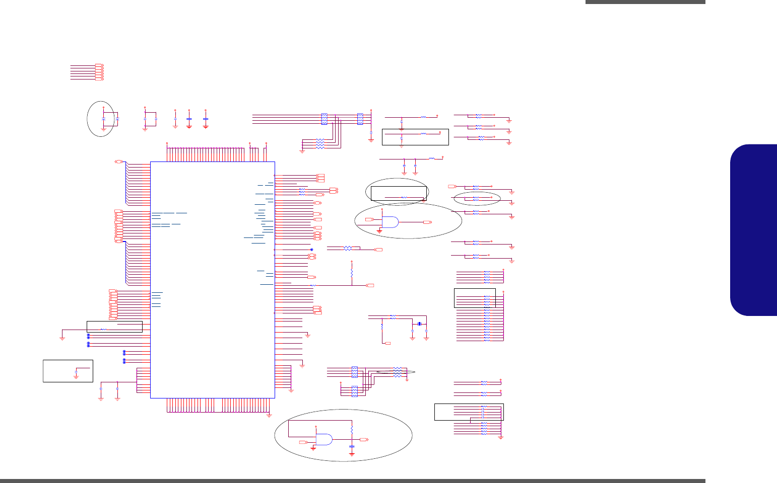
Schematic Diagrams
VT8237-2 B - 13
B.Schematic Diagrams
VT8237-2
Sheet 12 of 34
VT8237-2
IDE_PDI OW#
GPIOB
SERIRQ
WAKE
RING
IDE_PDD9
IDE_PDD12
IDE_PDD ACK#
ACZ_BITCLK
GPO0
Z1231
Z1230
Z1229
Z1228
ACZ_SYNC
PME#
SUSA#
SUSA#
R563 0_04
GPI18
IDE_PDCS1#
AC_SPKR
IDE_SDD4
IDE_SDD3
IDE_SDD2
IDE_SDD1
IDE_SDD0
INT_IRQ15
IDE_SDD12
IDE_SDD11
IDE_SDD10
IDE_SDD9
IDE_SDD8
IDE_SDD7
IDE_SDD6
IDE_SDD5
GPI04
IDE_SIORDY
IDE_SDIOW#
IDE_SDIOR#
IDE_SDDACK#
IDE_SDDREQ
IDE_SDD15
IDE_SDD14
IDE_SDD13
INT_IRQ15
IDE_SDA2
IDE_SDA1
IDE_SDA0
IDE_SDCS3#
IDE_SDCS1#
R467 4.7K
R423 4.7K
SATATXN0
R471 0
R450 4.7K
FB5
HCB2012KF-121T30
R427 1K
FB6
HCB2012KF-121T30
R167 10K
R417 0
1 2
X4
25MHz
R212 *0
R95 0
R435 1K
R452 1K
R107 1K
C470 *22PF
R208 4.7K
R415
*0
C182
1UF
R147 4.32K_1%
R216 22
C210
0.1UF
R157 4.7K
R182 4.7K
R185 22
R181 4.7K
R215 0
PDD00
AA22
PDD01
Y24
PDD02
AA26
PDD03
AA25
PDD04
AB26
PDD05
AC26
PDD06
AC23
PDD07
AD25
PDD08
AD26
PDD09
AC24
PDD10
AC25
PDD11
AB24
PDD12
AB23
PDD13
AA24
PDD14
Y26
PDD15
AA23
PDA0/PDA0*
W23
PDA1/PDA1*
V25
PDA2/PDA2*
W24
PDDRQ
Y23
PDDACK/PDDACK*,PDDACK
V24
PDIOR/PHDMARDY/PHSTROBE
W26
PDIOW/PSTOP
Y25
PDRDY/PDDMARDY/PDSTROBE
Y22
PDCS1/PDCS1* ,PDCS1
V22
PDCS3/PDCS3*
V23
ACBITCLK,AZBITCLK T1
ACSDI N0,AZSD IN0 U3
ACSDI N1,AZSD IN1 V2
ACSDIN2,AZSDIN2/ GPI20/GPO20/PCS0 U1
ACSDIN3, AZSDIN 3/GPI21/GPO21/PCS1/SLPBTN V3
ACSYNC,AZSYNC/ACSYNC* T2
ACSDOUT,AZSDOUT/ACSDOUT* U2
ACRST,AZRST T3
IRQ14
AD24
IRQ15
AE26
SDD00
AC20
SDD01
AB20
SDD02
AC21
SDD03
AE18
SDD04
AF18
SDD05
AD18
SDD06
AD19
SDD07
AF19
SDD08
AE20
SDD09
AF20
SDD10
AD20
SDD11
AE21
SDD12
AF21
SDD13
AD21
SDD14
AD22
SDD15
AF22
SDDRQ
AD17
SDDACK
AD23
SDIOR/SHDMARDY/SHSTROBE
AF23
SDIOW/SSTOP
AE23
SDRDY/SDDMARDY/SDSTROBE
AF17
SDCS1
AF25
SDCS3
AF26
SDA0
AF24
SDA1
AC22
SDA2
AE24
PWRBTN AD 2
RING/GPI03 Y2
EXTSMI/GPI02 AA1
PME W4
LID/GPI04 AC1
BATLOW/GPI 05 V4
SUSST1/GPO03 Y3
SUSCLK/GPO04 AB3
SUSA/GPO02 AA2
SUSB AD 3
SUSC AF2
SMBALR T AB1
SMBCK1 AC4
SMBDT1 AB2
GPI01,GPI01/THRMTRIP AC 2
GPO00 AA3
GPI00 AE2
Strap_VD1*,GPIOA*/PCREQA* AE5
Strap_VD0*,GPIOC*/PCGNTA* AF5
Strap_VD3*,GPIOD*/PCGNTB* AC6
Strap_VD2*,GPIOB*/PCREQB* AD5
PCKRU N AB7
CPUSTP/GPO05 AC 7
PCISTP/PCISTP*/GPO06 AD6
VSUS33-1 AA4
VSUS33-2 AB4
VSUS33-3 AB5
VSUS33-4 AB6
VCC25-1 J9
VCC25-2 J10
VCC 25-3 J11
GNDATS11
AF14
GND
L13
GND
L14
TEST AE9
PWROK AF1
GND
L15
VCC25-5 K9
VCC 25-6 L9
VCC25-4 J12
VCC25-7 L18
VCC25-8 M9
GNDATS0
AB14
GNDATS1
AC1 4
GNDATS2
AD12
GNDATS3
AD13
GNDATS4
AD1 4
GND ATS5
AD15
GNDATS6
AD16
GNDATS7
AE12
GNDATS8
AE14
GNDATS9
AE16
GNDATS10
AF12
GND
L16
GND
M11
VCCAS2
AC11 VCCAS1
AC17
STXP1
AB13
STXN1
AC13
SRXP2
AE15 SRXN2
AF15
STXP2
AB15
STXN2
AC15
GNDATS12
AF16
GND
L11
GND
L12
VSUS25-1 T4
VSUS25-2 U4
SERIRQ AD 9
SPKR/SPKR* AF 8
OSC AB8
SMBCK2/GPI27/GPO27 AC3
SMBDT2/GPI26/GPO26 AD1
INTRUDER/GPI16 AE1
AOLGPI/THRM/GPI18 Y4
TPO AF9
CPUMISS/GPI17 Y1
GPO01 AE3
SRXP1
AE13 SRXN1
AF13
VCCAO AC10
GNDAO AB10
VCCA33,NC AE11
GNDA33,NC AF 11
SREXT AD11
SXO AE10
SXI AF10
SVREF,NC
AC19
SCOMPP,NC
AB21
VCCAS4
AB11 VCCAS3
AB17
VDDATS-1
W12
VDDATS-2
W13
VDDATS-3
W14
VDDATS-4
W15
VDDATS-5
W16
VCC25- 9 M18
VCC25-10 N9
VCC25-11 N18
VCC 25-12 P9
VCC 25-13 P18
VCC 25-14 R9
VCC 25-15 R18
VCC 25-16 T9
VCC 25-17 T18
VCC25-18 U9
VCC25-19 U18
VCC 25-20 V9
VCC25-21 V10
VCC25-22 V11
VCC 25-23 V12
VCC 25-24 V13
VCC 25-25 V14
VCC 25-26 V15
VCC 25-27 V16
VCC 25-28 V17
VCC25-29 V18
GND AS1
AC16
GNDAS2
AC1 2
GND AS3
AB16
GND AS4
AB12
GND
M12
GND
M13
GND
M14
GND
M15
GND M16
GND N11
GND N12
GND N13
GND N14
GND N15
GND N16
GND
F6
GND
F7
GND
J5
GND
K5
GND
P5
GND
R5
GND W5
GND V5
GND
K18
NC, WAKE Y5
U27B
VT8237R plus /VT8237A-BGA541
R176 *2.2K
R183 4.7K
R184 10K
R479 22
R213 *0
R105 1K
FB4
HCB3216KF-800T30
C85
4.7uF
R111 *2.2K
C84
4.7uF
C194
0.1U F
C435
4.7uF
C471 *22PF
R468 10K
R118 360_1%
25MHZXO_S
C164
0.1UF
R469 10K
R425 *2.2K
ACZ_SYNC
ACZ_RST#
ACZ_SDATAOUT
12
CE1
330UF/6.3V 1
2
3
45
6
7
8
RN1
8P4RX1K
C462
10PF
R158 4.7K
R180 4.7K
R178 1M
C463
10PF
1
2
3
45
6
7
8
RN16
8P4RX2.2K
R143 4.7K
C289 *22PF
R438 *2.2K
R96 0
R480 *2.2K
R177 4.7K
R419 0
R200 4.7K
R397 4.7K
R207 10K
R137 *1K
12
CE3
470UF/4V
R94 *0
R481 4.7K
C226
0.1UF
1
2
3
45
6
7
8RN5
8P4RX2.2K
R490 2.2K
C262 *22PF
1
2
3
4 5
6
7
8
RN7
8P4RX1 K
R196 10K
R93 0
C174
4.7uF
R150 4.7K
R110 *2.2K
R173 4.7K
R201 4.7K
R416 2.2K
R470 4.7K
R214 0
C200
0.1UF
R488 *4.7K
C202
0.1UF
R451 1K
R199 10K
R395 4.7K
R489 10K
R206 *1K
R179 1M
R421 4.7K
3VS
3VS
3VS
3VS
3VS
3VS
2.5VS
VCCRTC
2.5V
3VS
3VS
3V
3VS
2.5VS
2.5VS
3V
5VS
2.5VS
2.5VS 3V
3VS
3VS
3V
IDE_PDIOR#14 IDE_PDDACK#14 IDE_PDDREQ14
IDE_PDA214
IDE_PDCS3#14
ACZ_RST# 30
IDE_PDA114
25MHZXI_S1 2
INT_IRQ1414
IDE_PDA014
IDE_PDCS1#14
M950626
SMI# 19
SCI# 19
SWI# 19
IDE_PIORDY14
ACZ_SDATAOUT 30
PM_SUS_STAT# 7
SUSC# 19
PM_CLKRU N# 11, 19
AC_SPKR 30
IDE_PDIOW#14
IDE_PDD[0..15]14
SERIRQ 15,19
SIO_OSC 2
SMB_SBDATA 2,9,10,24
PM_STPPCI# 2
ACZ_SDATAIN 1 30
SB_PWROK 7
ACZ_BITCLK 30
ACZ_SDATAIN 0 30
SMB_SBCLK 2,9,10,24
PM_STPCPU# 2
SUSB# 19,20,25,26,29
3V 11,13,17,19,24,25,26,29,30
ACZ_SY NC 30
PWR_BTN# 19
PME# 15,19, 24
VCCRTC 13
IDE_SDIOR#14
5V 18,19,20,24,25,26,27,28
2.5VS 2,3, 11,13,20,26
3VS 2,7,8,9,10,11,13,14, 15,16,19,20,22,23,24,26,28,30
IDE_SDA014 IDE_SDA114
IDE_SDDREQ14
IDE_SIORDY14 IDE_SDIOW#14
IDE_SDCS1#14
IDE_SDA214
IDE_SDDACK#14
IDE_SDD[0..15]14
IDE_SDCS3#14
INT_IRQ1514
5VS 14,16,18,19,20,23,24,26,30
SEEDI13
GPI18
1:V4-lite support
0/1:Disable/Enable LAN shadow EEPROM
FOR VT8237R plus ONLY
FOR VT8237R plus ONLY
VT8237R plus => 4.7K
VT8237A => 6.12K
AP339A
Power Up Strapping for VT8237R plus
0/1:Enable/disable External SATA PHY
Modufy A1 rev
0/1: SATA Master/Slave mode
0/1:Enable/disable LPC FWH command
1:V4 support
0/1:Enable/disable auto reboot
0\1:P4/V4 Bus \ C3 Bus
Modufy A1 rev
VKCOMP for Vlink at 4X mode
0/1:Enable/disable100Mhz VLink clock
SUSCLK
IDE_PDA1
SATAR XN0
F070395
F070395
25MHZXI_S Z1239
PM_SUS_STAT#
GPI04
RING
IDE_PDCS3# Z1235
CPUMISS
M950627
IDE_PDDACK#
SID EVREF
R381 *0_04
Z1240
Z1234
Z1236
IDE_PDA2
C531
10UF_08
M950626
8237_PWROK
R566
10K
3V
2
14
3
5
U34
74AHC1G08GW
8237_PWROK
3V
C532
1UF C533
1UF
2.5VS 2.5VS
SMB_SBCLK
GPI0
SDIN2
SDIN3
SM_INTRUDER#
ACZ_SDATAIN 1
SMB_SBDATA
GPO1
GPO0
PM_BATLOW#
INT_IRQ14
VDDA0
PME#
IDE_PDA0
C950719
RSMRST#13,19
Z1238
2
14
3
5
U35
74AHC1G08GW
3V R18
*0_04
8237_SUSB#
8237_SUSB # SUSB#
RSMRST#13,19
SB_PWROK
8237TEST
PM_STPCPU#
PM_CLKRU N#
Z1237
SATAR XP0
SERIRQ
ACZ_SDATAOUT
950522
Z1242
CPUMISS
WAKE
GPIOB
ACZ_RST#
TPO
SMB_ALERT#
GPIOD
SREXT
IDE_PIORDY
SMB_SBDATA
PM_CLKRU N#
PM_STPCPU#
AC_SPKR
CPUMISS
VDDA0
SATA50COMP
INT_IRQ14
Z1233
PM_STPPCI#
GPI18IDE_PDI OR#
IDE_PDD13
PWR_BTN#
IDE_PDD REQ
SDIN2
GPIOD
SIO_OSC
SB_PWROK
Z1232
25MHZXO_S
SMB_ALERT#
GPIOC
SREXT
25MHZXI_S
SIDEVREF
AC SY NC
IDE_PDD1
IDE_PDD6
IDE_PDC S1#
ACSYNC
PM_SUS_STAT#
SATATXP0
IDE_PDD4
IDE_PDD10
PM_BATLOW#
SMBC K2
IDE_PDD2
IDE_PDD14
IDE_PDA0
8237TEST
PM_STPPCI#
SMB_SBCLK
ACZ_SDATAIN 0
SMBCK2
SMBDT2
SMBDT2
TPO
IDE_PDD0
IDE_PDD8
IDE_PDD11
IDE_PDD15
IDE_PDA1
IDE_PDC S3#
ACSDO
Z1241
GPI04
VDDA33
IDE_PDD5 ACZ_SDATAIN0
SUSCLK
VDDA33
2.5VSATA
Z1243
GPIOC
GPIOA
SDIN3
SUSC#
GPIOA
SM_INTRUDER#
GPO1
2.5VSATA
ACSDO
IDE_PDD3
ACZ_SDATAIN1
IDE_PDD7
IDE_PDA2
GPI0
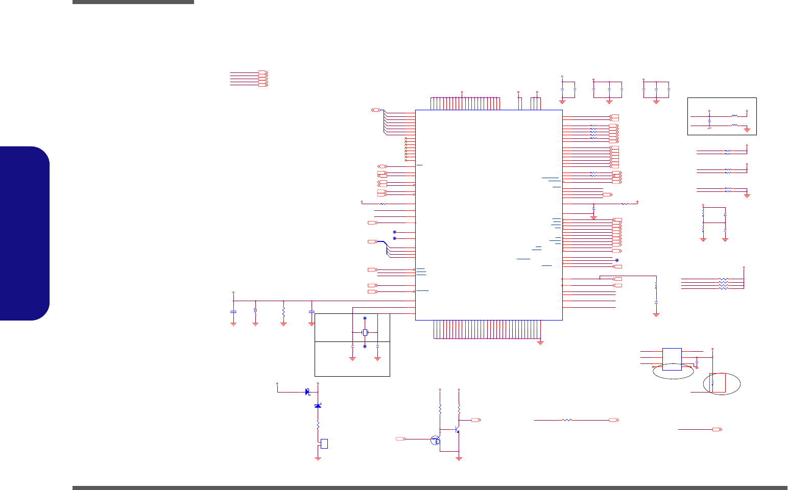
Schematic Diagrams
B - 14 VT8237-3
B.Schematic Diagrams
VT8237-3
Sheet 13 of 34
VT8237-3
H_PWRGD 3
R103
665_1%
SPCLK
SEEDI 12
APICCLK1
APICD0
VGATE
SATA_LED
APICD1
2.5VSBPLL
SPCLK 2
DPRSLPVR
GND_SBPLL
H_FERR# 3
H_INIT# 3
H_IGNNE# 3
H_A20M# 3
APICCLK1 2
H_SMI# 3
H_NMI 3
H_INTR 3
DPRSLPVR
H_DPSLP# 3
H_CPUSLP# 3
H_STPCLK# 3
Z1307
1
1
2
2
JBAT1
CON 2_BAT
VAD00
H25
VAD01
G26
VAD02
K26
VAD03
J23
VAD04
F26
VAD05
G25
VAD06
K22
VAD07
K24
MCRS A11
MCOL B11
MTXD2 B9
MTXD1 B10
MTXD0 A10
MTXENA C11
MTXCLK C10
MTXD3 A9
MDCK A7
MDIO B7
MRXD3 C7
MRXD1 B8
MRXDV D8
MRXCLK C9
MRXERR D10
MRXD2 A8
EECS D11
EEDO B12
EEDI/EEDI* A12
EECK C12
LANVCC E7
PLLVCC T22
PLLGND U22
VAD08
E24
VAD09
G23
VAD10
L26
VAD11
L25
VAD12
E26
VAD13
E25
VAD14
L24
VAD15
M26
VLVREF
H22
UPCMD
K23
DNCMD
K25
UPSTB+
J26
UPSTB-
J24
DNSTB+
H26
DNSTB-
H24
VLCOMP
J22 LANGND E6
MIIVCC4 E11
MIIVCC2 E9
MIIVCC3 E10
VBAT
AF4
VCLK
L22
MIIVCC1 D9
GND
P11
GND
P12
GND
P13
GND
P14
GND
P15
GND
P16
GND
R11
GND
R15 GND
R14 GND
R13 GND
R12
GND
R16
GND
R21
GND
T11
GND
T12
GND
T16 GND
T15 GND
T14 GND
T13
VCCVK18 M24
VCC VK4 N21
VCCVK5 N22
VCCVK6 N23
VCC VK7 N24
VCCVK8 N25
VCCVK9 N26
VCCVK10 P22
VCC VK11 P23
VCCVK12 P24
VCCVK13 P25
VCC VK14 P26
VCCVK15 M21
VCCVK16 M22
VCCVK17 M23
RTCX1
AE4
RTCX2
AF3
LREQ0
AE6 LFRM
AF6
MRXD0 C8
MIIVCC25-1 D12
MIIVCC25-2 E12
VCCVK3 L21
VCCVK2 K21
LAD0
AD8
LAD1
AF7
LAD2
AE7
LAD3
AD7
VBE
G24
VPAR
F24
LREQ1
AE8
PHYRST D7
PWR GD
AC5
RSMRST
AD4
FERR U24
A20M U26
IGNNE T24
INIT R26
INTR T25
NMI T26
SMI U25
STPCLK R24
SLP V26
GHI/GPI22/GPO22 R22
DPSLP/GPI23/GPO23 P21
PCICLK R23
APICCLK,GPI19 U23
APICD0/GPIO10 R25
APICD1/GPIO11 T23
VGATE/GPIO8 AC9
GPI28/GPO28/VIDSEL/SATALED,GPI28/GPO28/VIDSEL AC8
VRDPSLP/GPI29/GPO29 AB9
AGPBZ/GPI06 AD10
VCCVK19 M25
VCCVK1 L23
VCCVK20 L19
VCC VK21 M19
VCCVK22 N19
VCCVK23 P19
GND
AA21
GND
AB19
GND
AB22
GND
AB25
GND
AC18
GND
AE17
GND
W22
GND
W25
GND
AE19
GND
AE22
GND
AE25
GND
AA9
GND
T21
GND
AA10
GND
AB18
GND
K19
NC1
F23
NC2
G22
NC,PHYPWRDN F8
U27C
VT8237R plus/VT8237A-BGA541
1.05VS 3, 4,5,28,29
C523
1UF
2.5V
C524
0.1U F
3V 11,12,17,19,24,25,26,29,30
SEECS
SEEDO
SEECLK
SEEDI
PM_DPRSLPVR
AGP_BU SY # AGP_BUSY # 7
C157
0.1UF
C131
4.7uF
R424 33_1%
C86
4.7uF
C168
0.1UF
FB10
HCB2012KF-121T30
R97
4.7K
C193
0.1UF
R418 10K
R428 33_1%
R500
1.5K_04
LPC_AD[3:0]19,22
R437 33_1%
R426 33_1%
C208
1UF
R100 360_1%
C130
0.1UF
R420 33_1%
AGP_BU SY #
R422 33_1%
C216
0.1UF
C165
0.1uF_04
LPC_AD2
LPC_AD1
LPC_AD0
R141 4.7K
LPC_AD3
FB9
HCB2012KF-121T30
C87
1UF
R101 1K
R136 2.2_08R109 4.7K VPAR
2.5VS
R139 33_1%
C132
0.1UF
2.5VS
2.5VSBPLL
2.5VS 2.5V
3VS
2.5VS
2.5VS
3V
GND_SBPLL
2.5VS 3V
950314
VLAD4
VLAD1
VLAD0
VLAD7
VLAD3
VLAD2
VLAD[0..7]7
VLAD5
VLAD6
VBE#7
GND_SBPLL
2.5VSBPLL
3VS 2,7,8,9,10,11,12,14,15,16,19,20,22,23,24,26,28,30
BOM?
C950719
DEL GHL P ULL UP RESISTER
LVREF_SB= 0.3V FOR VT8237R plus
LVREF_SB=0.45V FOR VT8237A
R393 360_1%
R106 360_1%
APICD0
APICD1
R102
*33
C126
*10PF
PM_DPRSLPVR 3,28
VCLK_SB2
CE
B
Q32
DTC114EUA
Z1317
LPC_DRQ#0
DPRSLPVR
VGATE
LPC_DRQ#1
GHI
ADD GND SHIELD
3VS
VT8237R plus=> 10PF
VT8237A => 12PF
AP339A
Z1301
VCOMPP
LVREF_SB
3VS
Z1303
Z1304
Z1302
Z1308
Z1309
2.5VS 2,3,11,12,20,26
LVREF_SB
Z1310
Z1311
Z1312
VDD 3 3,19,22,25,26,27
Z1313
TXEN 17
TXD2 1 7
TXD1 1 7
TXD0 1 7
TXD3 1 7
C288
10UF/10V_08
ALL_PWROK11,20
TXCL K 1 7
MCOL 17
MC R S 1 7
40mil
40mil
R88
10K_06
R515
10K_06
1.05VS
A C
D13
RB751V
A C
D14
RB751V
C246
10pF
RXER 17
RXD0 17
RXDV 17
RXCLK 17
RXD3 17
RXD2 17
RXD1 17
32KHZX1
32KHZX2
R211
*100K_04
Z1314
R151 4.7K_04
MDIO
1
3
2
4
Y1
32.768KHZ
C468
10UF/10V_08
Z1315
R198
1K
R144 4.7K_04
R444 4.7K_04
21
J1
JOPEN
VCCRTC
VCCRTC
R442 *4.7K_04
VDD3
MDIO MDIO 17
MDC 17
B
E C
Q33
3904
-PHYRST 17
-PHYPWRDN 17
C247
10pF
F070395
DI
3
SK
2
CS
1
DO 4
VCC 8
GND 5
NC1
6NC2 7
U3
CAT93C46S-26490T
DNSTB#7DNSTB7
UPCMD7
UPSTB#7U PSTB7
DNCMD7
EEPROM
Must use +3.3VSUS if it want to wake
on LAN from resume function well.
Near to
South
Bridge
LPC_FRAME#19,22 LPC _DRQ#0
LPC_FRAME#
LPC_D RQ#1
ALL_PWROK
ALL_PWROK11,20
RSMRST#12,19
GHI
VCCRTC 12
R548
0_04
2.5VS
SEEDO
Z1316
SPCLK
SEECS
SEEDI
SEECLK
3V
TXEN
VCOMPP
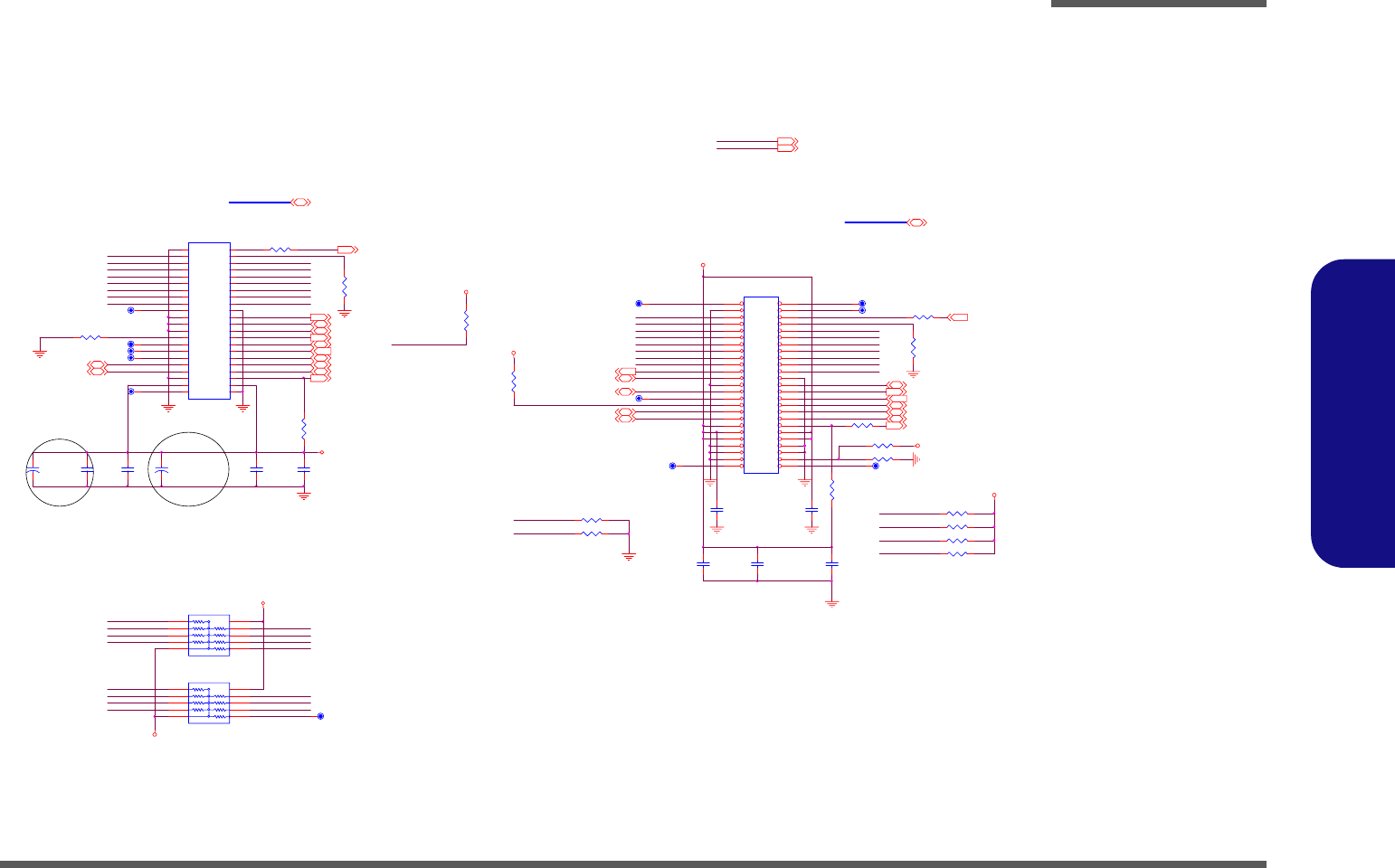
Schematic Diagrams
HDD & CDROM B - 15
B.Schematic Diagrams
HDD & CDROM
Sheet 14 of 34
HDD & CDROM
+
C539
100U_6.3V_B
+
C364
100U_6.3V_B
IDE_SDD [0:15] IDE_SDD[0:15] 12
PDLED# 23
5VS
3VS
IDE_PDDREQ
R555 4.7K
R553 4.7K
IDE_SDDREQ
R557 4.7K
IDE_PIORDY
IDE_SIORDY
R556 4.7K
PIN 51~52=GND
IDE_SDDREQ
IDERST#
PDLED#
R251
10K
C342
0.1UF
950314
TO CD ROM
IDE_SDCS1# 12
5VS 12,16,18,19,20, 23, 24, 26, 30
3VS 2,7,8,9,10,11,12,13,15,16,19,20,22,23,24,26,28,30
IDE_PDD8
IDE_PDD4
Z1411
IDE_PDD3
IDE_PDD15 IDE_PDD12
IDE_PDD9
IDE_PDD11
5VS
IDE_PDD14
5VS
10
9
8
7
6
1
2
3
4
5
RP13
*10P8RX10K
IDE_PDD13
IDE_PDD0
IDE_PDD2
IDE_PDD1
IDE_PDD6
IDE_SDCS3#12
10
9
8
7
6
1
2
3
4
5
RP12
*10P8RX10K
IDE_PDD5 IDE_PDD10
IDE_SDA0 12IDE_SDA212 IDE_SDA1 12
IDE_PDIOW#
IDE_PDIOR#
R552 4.7K
941202
R554 4.7K
R23 0
3VS
IDE_PDD11
IDE_PDD10
IDE_PDD13
IDE_PDD9
IDE_PDD8
IDE_PDD12
IDE_PDD15
IDE_PDD14
R32 *4.7K
Z1408 5VS
IDE_PDA0 12
IDE_PDCS1#
IDE_PDIOW# 12
IDE_PDDREQ12
IDE_PDA1 12
IDE_PDDREQ
IDE_PIORDY 12
IDE_PDDACK#12 INT_IRQ14
IDE_PDCS1# 12
INT_IRQ14 12
IDE_PDDACK# IDE_PIORDY
IDE_PDIOW#
IDE_PDA1
IDE_PDA0
IDE_PDIOR#
IDE_PDIOR#12
C369
0.1UF
C374
0.1UF
IDE_PDA2
IDE_SDIOW# 12
IDE_SDDACK# 12
IDE_SDIOR# 12
R537
10K
11
33
55
77
99
11 11
13 13
15 15
17 17
19 19
21 21
23 23
25 25
27 27
29 29
31 31
33 33
35 35
37 37
39 39
41 41
43 43
2
2
4
4
6
6
8
8
10
10
12
12
14
14
16
16
18
18
20
20
22
22
24
24
26
26
28
28
30
30
32
32
34
34
36
36
38
38
40
40
42
42
44
44
JHDD1
CON44
C354
0.1UF
INT_IRQ15
IDE_SDIOW#
IDE_SDCS1#
IDE_SDDACK#
IDE_SDCS3#
IDE_SDA1
IDE_SDA0
IDE_SIORDY
IDE_SDA2
IDE_PDD[0:15]
IDE_PDD5
IDE_PDD1
INT_CD_L
CRESETN
Z1407
IDE_PDD0
IDE_PDD3
IDE_PDCS3#
Z1406
Z1405
IDE_SDD7
R360
10K
R24
4.7K
R359 0
C408
220uF/10V
C20
0.1UF
C25
0.1UF
C400
10UF/10V_12
12 34 56 78 910 1112 1314 1516 1718 1920 2122 2324 2526 2728 2930 3132 3334 3536 3738 3940 4142 4344 4546 4748 4950
JCD1
JAE_KX15-50K5
C23
0.1UF
R29 0
5VS
SDACT# 23
IDE_PDA212 IDE_PDCS3#12
IDE_PDD[0:15] 12
IDERST# 11
INT_IRQ15 12
Z1415
Z1416
Z1412
Z1414
Z1413
IDE_SDD8
IDE_SDD9 IDE_SDD6
IDE_SIORDY 12
IDE_SDD3
IDE_SDD13
IDE_SDD11
IDE_SDD12
IDE_SDD5
IDE_SDD4
IDE_SDD2
IDE_SDD10
IDE_SDD0
IDE_SDD1IDE_SDD14
IDE_SDIOR#
IDE_SDD15
IDE_SDDR EQ 12
3VS
R565
10K
IDE_PDD6
CD_GND
IDE_PDD7
IDE_PDD4
IDE_PDD2
INT_CD_R
M950626M950626
Z1409
R239 33
Z1410
Z1401
470
R534
R533
*10K
INT_IRQ15
IDERST# 11
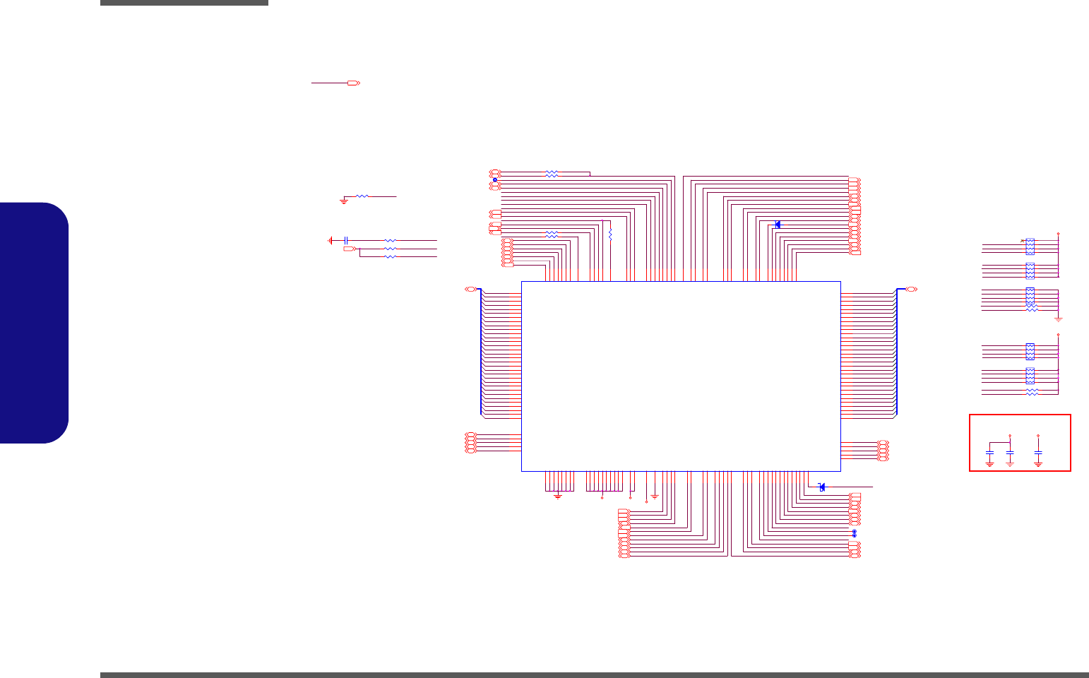
Schematic Diagrams
B - 16 CARDBUS / CARD READER
B.Schematic Diagrams
CARDBUS / CARD READER
Z1502
SD_D1
A_CAD31
A_CAD30
A_CAD29
C304 *10PF
A_CAD28
MS_BS
A_CAD27
MS_C L K
CARD_PWREN#
MS_D 3
MS_D 0
MS_D 1
MS_D 2
MS _I N S#
SD_CD #
A_CAD26
PCM_MF1
A_CAD25
SD_WP
A_CAD24
A_CAD23
3VS
SD_D3
A_CAD22
MS_D0
MS_BS
1
2
3
4 5
6
7
8
RN10 8P4RX47K
SD_D2
A_CAD21
PCMSPK
SD_CD#
R310 47K_04
A_CAD20
R298 47K_04
A_CAUDIO
A_CAD19
PCM_SUSPEN D#
A_CAD18
C327
0.1UF_04
A_CAD17
A_CAD16
A_CAD15
PCLKPCM2
PCI_AD11
PCI_AD6
PCI_AD15
PCI_AD20
PCI_AD29
PCI_AD23
PCI_AD17
PCI_AD8
PCI_AD30
PCI_AD0
PCI_AD25
PCI_AD13
PCI_AD27
PCI_AD7
MS _I NS #
CARD_PWREN#
A_CAD14
PCI_AD14
PCI_AD3
PCI_AD28
PCI_AD22
PCI_AD19
PCI_AD18
PCI_AD16
PCI_AD5
PCI_AD24
PCI_AD21
PCI_AD4
PCI_AD2
PCI_AD12
PCI_AD10
PCI_AD26
PCI_AD1
PCI_AD31
PCI_AD9
A_CAD13
A_CAD12
A_CAD11
A_CAD10
A_CAD9
MS_D1
A_CAD8
MS_D2
A_CAD7
Z1501
PCM_IDSEL
3VS 2,7,8,9,10,11,12,13,14,16,19,20,22,23,24,26,28,30
A_CAD6
Z1504
SD_CLK
PCLKPCM
A_CAD5
A_CAD4
A_CAD3
1
2
3
4 5
6
7
8
RN30 8P4RX47K
SD_D0
A_CCLK
SD_CLK
A_CAD2
R273 0_04
SD_WP
A_CAD1
CB714F
169BGA
PCI-to-CardBus/MS/xD/MMC/SD
PCLKPCM
C497
0.1UF_04
VCC D1# 16
A_CCLKRUN#
A_CRST#
VCC D0# 16
VPPD 1 16
VPPD 0 16
A_CAD0
SD_D3 16
SD_D1 16
SD_D2 16
SD_D0 16
SD_CLK 16
SD_CMD 16
MS_D3
PME#12,19,24
A_CFR AME#
AVCC VCC_CARD
R148 47K_04
SD_CLKIN
CLOSE TO CARD SOCKET
SD_D3
C325
0.1UF_04
xD_CD# R303 47K_04
CLOSE TO CHIP
PCI_INTB#11,24
PCI_INTA#8,11,24 PCI_INTC#11,24
R308 0
R309 0
A_CCLKRU N# 16
A_CPERR#16
A_CCBE3# 16
A_CCBE2# 16
A_CCBE0# 16
A_CFRAME# 16
A_CTRDY#16
A_CSTOP#16
A_CIRDY#16
A_CPAR 16
A_CVS1 16
A_CDEVSEL#16
A_CCBE1# 16
A_CBLOC K#16
A_CVS2 16
T
A_CD2 16
A_CAD[31:0] 16
A_CD14 16
A_CVS2
A_CVS1
A_CCD 2#
G_RST#
A_CSTSCHG
A_CINT#
PCM_MF7
A_CGNT#
A_CBLOCK#
PCM_MF6
PCM_MF5
Z1505
A_CREQ#
SD_CMD
A_CSERR#
SD_D1
SD_D2
SD_D0
xD_BSY#
xD_BSY#
xD_CD#
PCM_MF4
A_A1 8
A_CCD 1#
MS_D1 16
MS_D2 16
MS_BS 16
MS_D0 16
MS_CLK 16
MS_D3 16
MS_ IN S # 1 6
A_CPERR#
A_CSTOP#
A_CDEVSEL#
Z1503
A_CD14
A_CD2
PCM_RST#
A_CTRDY#
VPPD0
A_CIRDY#
AC
D42 SCS751V-40
AC
D43 SCS751V-40
VPPD1
VCCD0#
SD_CLKIN
VCCD1#
A_CSERR#16
A_CSTSCHG16 A_CINT#16
A_CREQ#16
A_CCD2# 16
A_CAU DI O16
A_CCD1# 16
A_CRST# 16
A_CGNT#16
A_CCLK 16
A_A18 16
A_CCBE0#
AD0
N8
AD1
K7
AD2
L7
AD3
N7
AD4
M7
AD5
N6
AD6
M6
AD7
K6
AD8
M5
AD9
L5
AD10
K5
AD11
M4
AD12
K4
AD13
N3
AD14
M3
AD15
N2
AD16
J2
AD17
J1
AD18
H4
AD19
H3
AD20
G3
AD21
G2
AD22
F1
AD23
F2
AD24
E2
AD25
E3
AD26
E4
AD27
D1
AD28
D2
AD29
D4
AD30
C1
AD31
C2
CBE0#
N5
CBE1#
N1
CBE2#
J3
CBE3#
E1
PAR
M2
DEVSEL# L1
FRAME# J4
PCIGNT# B1
PCIREQ# A1
IDSEL F4
IRDY# K1
TRDY# K3
PERR# L3
SERR# M1
STOP# L2
PCICLK H1
PCIRST# G4
MFUNC0 K8
RI_OUT#/PME# L8
VCCD1# M13
VCCD0# N13
VCC1
F3
VCC2
G1
VCC3
K2
VCC4
N4
VCC5
L6
VCC6
L9
VCC7
H11
VCCA1
G13
VCCA2
A7
VCC8
D12
VCC9
C8
VCC10
B4
GND1
D3
GND2
H2
GND3
L4
GND4
M8
GND5
K11
GND6
F12
GND7
C10
GND8
B6
SPKROUT M9
SUSPEND# L1 1
CAUDIO/BVD2/SPKR#
B5
CBLOCK#/A19
D11
CCD1#/CD1# L12
CCD2#/CD2# A4
CDEVSEL#/ A21
B13
CFRAME#/A23
B11
CGNT#/WE#
C11
CINT#/READY/IREQ#
D6
CIRDY#/A15
A12
CPERR#/A14
C13
CREQ#/INPACK#
B8
CSERR#/WAI T#
A5
CSTOP#/A20
C12
CSTSCHG/BVD1/STSCHG#
C5
CTRDY#/A22
A13
CVS1/VS1 C6
CVS2/VS2 D9
CCLK/A16
B12
CCLKRUN#/ WP/IOIS16#
D5
CRST#/RESET
B9
CAD0/D3 L13
CAD1/D4 K12
CAD2/D11 K10
CAD3/D5 J10
CAD4/D12 K13
CAD5/D6 J12
CAD6/D13 J11
CAD7/D7 H10
CAD8/D15 H12
CAD9/A10 G12
CAD10/CE2# G11
CAD11/OE# G10
CAD12/A11 F11
CAD13/IORD# F13
CAD14/A9 E13
CAD15/IOWR# F10
CAD16/A17 E12
CAD17/A24 D10
CAD18/A7 B10
CAD19/A25 A10
CAD20/A6 C9
CAD21/A5 A9
CAD22/A4 D8
CAD23/A3 A8
CAD24/A2 C7
CAD25/A1 D7
CAD26/A0 A6
CAD27/D0 C4
CAD28/D8 A3
CAD29/D1 B3
CAD30/D9 C3
CAD31/D10 B2
CCBE0#/CE1# H13
CCBE1#/A8 E11
CCBE2#/A12 A11
CCBE3#/REG# B7
CPAR/A13 D13
RSVD/D2 A2
RSVD/A18 E10
RSVD/D14 J13
MFUNC1 N9
MFUNC2 K9
MFUNC3 N10
MFUNC4 L10
MFUNC5 N11
MFUNC6 M11
G_RST# M10
VPPD 1 M12
VPPD 0 N12
SMC E#
J5
SMWP#
J6
SMCD #
J7
SMCL E/SD DAT 2
F5
SMALE/SDCMD
E5
SMDATA7/ SDD AT0
E6
SMWE#/SDCLK
F6
SMDATA4/ SDD AT3
G6
SMBSY#
H6
SMDATA0/ SDD AT1
F7
SMWPD#/SDWP
F8
SDCD#
E8
SDPWREN33#
G7
SMPWREN#/MSPWREN J8
SMDATA1/ MSBS H8
SMD ATA5/ MSDATA2 G8
SMD ATA6/ MSDATA1 H9
SMD ATA2/ MSDATA0 G9
SMD ATA3/ MSDATA3 F9
SMRE#/MSCLK E9
MSINX# H7
MFUNC7 J9
SDCLKI H5
VCC_SD
E7
GND_SD
G5
U12
CB714F
1
2
3
4 5
6
7
8
RN29 8P4RX47K
1
2
3
4 5
6
7
8
RN28
8P4R X47K
1
2
3
4 5
6
7
8
RN4 8P4RX47K
A_CCBE1#
R269 *0
R138 47K_04
PCM_MF6
PCM_MF4
PCM_MF5
PCM_MF7
MS _C LK
PCM_SUSPEND#
A_CCBE2#
VCC_CARD
AVCC3VS
SERIRQ12,19
VCC_CARD
PCI _STOP#11, 24
A_CCBE3#
PCI_C/BE1#11,24
PCI _GNT#011
PCI _TRDY#11,24
PCI_REQ#011
PCI_AD25
PCI _PAR11,24
PCMSPK
PCM_RST#
R296 0_04
PCI_AD[31:0]11,2 4
SD_CMD
R528 100_04
PCI_C/BE3#11,24
R294 *0_04
PCI_C/BE2#11,24
PCI_FRAME#11,24
PCMSPK30 G_RST#
R306
0_04
SD_CD# 16
PCI_IRDY#11,24
CARD_PWREN# 16
PCI _SERR#11,24
PCI_DEVSEL#11,24
SD_WP 16
PCI_C/BE0#11,24
PCI _PERR#11,24
PCIRSTC#11,24
Sheet 15 of 34
CARDBUS / CARD
READER
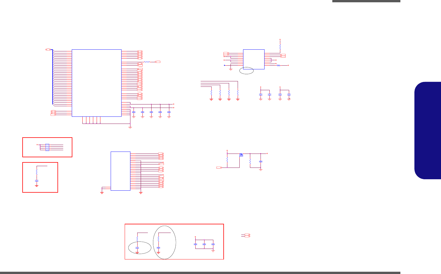
Schematic Diagrams
CARD SOCKET B - 17
B.Schematic Diagrams
CARD SOCKET
Sheet 16 of 34
CARD SOCKET
SD_WP 15
SD_WP
1
2
3
4 5
6
7
8
RN11
*8P4RX47K
R339
1K_04
CAD26/A0
29
CAD25/A1
28
CAD24/A2
27
CAD23/A3
26
CAD22/A4
25
CAD21/A5
24
CAD20/A6
23
CAD18/A7
22
CCBE1#/A8 12
CAD14/A9
11
CAD9/A10
8
CAD12/A11
10
CPAR/A13 13
CPERR#/A14 14
CIRDY#/A15 20
CCLK/A16 19
CAD16/A17
46
RFU/A18
47
CBLOCK#/A19 48
CSTOP#/A20 49
CDEVSEL#/A21 50
CTRDY#/A22 53
CFRAME#/A23 54
CAD17/A24
55
CAD19/A25
56
VCC 51
VCC 17
GND 68
GND 35
GND 34
GND 1
CAD27/D0
30
CAD29/D1
31
RFU/D2
32
CAD0/D3
2CAD1/D4
3
CAD3/D5
4
CAD5/D6
5
CAD7/D7
6
CAD28/D8
64
CAD30/D9
65 CAD31/D10
66
CAD2/D11
37
CAD4/D12
38
CAD6/D13
39
RFU/D14
40
CAD8/D15
41
CCBE0#/CE1# 7
CAD10/CE2#
42
CAD15/IOWR#
45
CAD13/IORD#
44
CAD11/OE#
9
CCBE3#/REG# 61
CRST#/RESET 58
CCLKRUN#/IOIS16# 33
CGNT#/WE# 15
CVS1/VS1# 43
CVS2/VS2# 57
CCD1#/CD1# 36
CCD2#/CD2# 67
CAUDIO/SPKR# 62
CSTSCHG/STSCHG# 63
CSERR#/WAIT# 59
CINT#/IREQ# 16
CREQ#/INPACK# 60
CCBE2#/A12 21
VPP 52
VPP 18
GND1
GND 1
GND2
GND 2
GND3
GND 3
GND4
GND 4
GND5
GND 5
GND6
GND 6
JPCMCIA1
20216-0021
PCB F ootprint = ICMB-A68LMYG-AS1-R
R292 10
VCCD0#
1
VCCD1#
2
3.3V
3
3.3V
4
5V
5
5V
6
GND
7
OC#
812V 9
AVPP 10
AVCC 11
AVCC 12
AVCC 13
VPPD1 14
VPPD0 15
SHDN# 16
U19
CP-2211F
AVCC5VS
AVPP
5VS
3VS
3VS
3VS
AVCC
AVPP
AVCC
VCCD0#15 VPPD0 15
VPPD1 15
VCCD1#15
A_CTRDY# 15
A_CVS1 15
A_CCBE1# 15
A_CINT# 15
A_CSERR# 15
A_CRST# 15
A_CVS2 15
A_CFRAME# 15
A_CPAR 15
A_CD215
A_A1815
A_CSTOP# 15
A_CBLOCK# 15
A_CCBE3# 15
A_CAUDIO 15
A_CCLKRUN# 15
A_CPERR# 15
A_CD1415
A_CCD2# 15
A_CCBE2# 15
A_CCD1# 15
A_CREQ# 15
A_CDEVSEL# 15
A_CAD[31:0]15 A_CCBE0# 15
A_CCLK 15
A_CIR DY # 15
A_CSTSCHG 15
A_CGNT# 15
A_CCBE0#
A_CRST#
SD_CLK 15
SD_CLK
SD_CD# 15
SD_CD#
A_CAD10
A_CCBE0#
A_CRST#
A_CAD11
C368
0.1UF_04
C339
0.1UF _04
G
DS
Q16
AO3409
VCCD1# VPPD0
VPPD1
Z1603
VCCD 0#
VCCD 1#
VPPD0
VPPD1
C361
0.1UF_04
A_CAD31
C352
0.1UF_04
Reserved layout for debug used
A_CAD30
5VS 12,14,18,19,20,23,24,26,30
C365
0.1UF_04
3VS 2,7,8,9,10,11,12,13,14,15,19,20,22,23,24,26,28,30
A_CAD28
Close to cardbus socket
R340 1k
R333
*0_04
Z1605
MS_CLK
C344
*10PF_04
A_CAD29
A_CAD24
C950719
BOM ?
A_CAD25
A_CAD26
A_CAD27
A_CAD20
CARDBUS SOCKET
A_CAD21
A_CAD22
A_CAD17
A_CAD16
A_CAD23
A_CAD19
A_CAD18
A_CAD12
A_CAD2
A_CAD3
A_CAD15
A_CAD7
A_CAD13
A_CAD0
A_CAD8
A_CAD4
A_CAD14
A_CAD1
A_CAD10
A_CAD11
A_CAD9
A_CAD6
A_CAD5
DAT2_SD 2
VSS_MS 21
CD/DAT3_SD 3
CMD_SD 4
VSS_SD 5
VDD_SD 6
CLK_SD 7
VSS_SD 8
DAT0_SD 9
DAT1_SD 10
WP_SD 11
VSS_MS 12
VCC_MS 13
SCLK_MS 14
DAT3_MS 15
INS_MS 16
DAT2_MS 17
SDIO/DAT0_MS 18
DAT1_MS 19
BS_MS 20
CD_SD 1
GND
23 GND
22
JREADER1
MDR0 19-X0-0 X10(R ev erse)
R321
47K_04
Close to socket
R322
47K_04
R320
47K_04
R319
47K_04
C231
33PF_04
R473
0_04
SD_CLK
C314
10PF
R323
10K_04
3 IN 1 SOCKET SD/MMC/MS(Pro)
MS_BS 15
MS_D2
MS_D3 15
MS_BS
MS_D1 15
MS_D0 15
MS_D1
MS_D0 MS_D 2 15
MS_D3
Z1602
F042795
VCCD0# SH DN#
MS_ IN S# 1 5
SD_CMD 15
SD_D3 15
SD_D0 15
SD_CMD
SD_D2
SD_D0
SD_D2 15
MS_IN S#
SD_D1 SD_D1 15
SD_D3
CCLK/A16
C363
10u_08
C323
0.1UF
C349
10u_08
C372
0.1UF
M950627
Card Reader Power
MS_CL K
Z1601
R285
0
MS_CLK 15
CCLK/A16
C496
0.1UF_04
C373
10u_08
VCC_CARD
C494
0.1UF_04
VCC_CARD
5VS
CARD_PWREN#15
C495
0.1UF_04
3VS
R324
100K_04
VCC_CARD
VCC_CARD
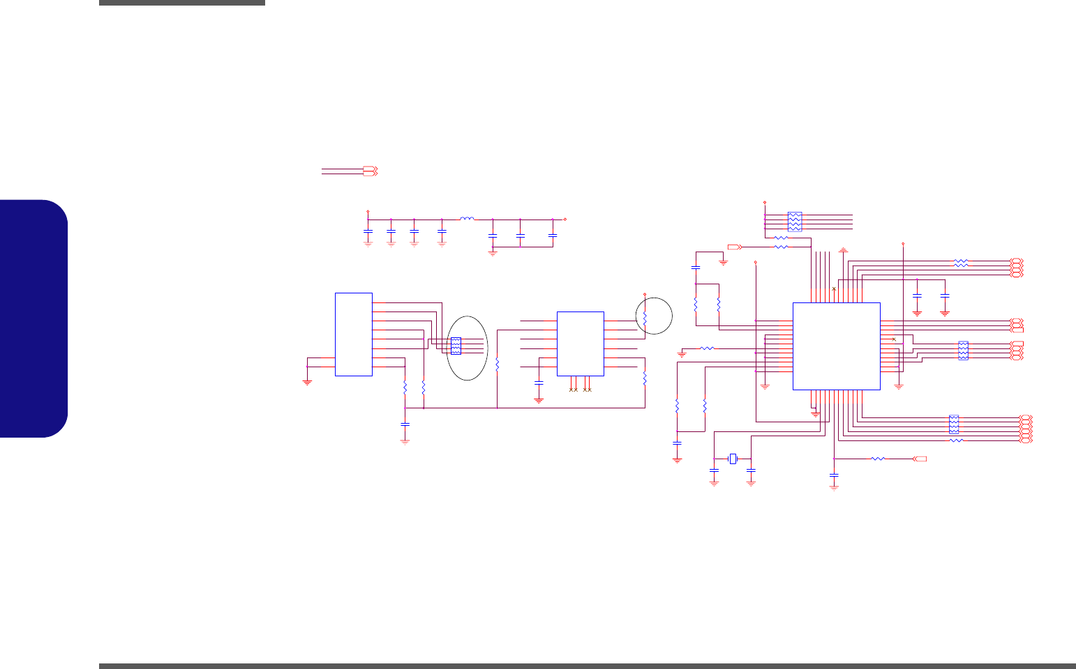
Schematic Diagrams
B - 18 LAN
B.Schematic Diagrams
LAN
Sheet 17 of 34
LAN
Z1708
C474
0.1UF_04
RXD2
RXD1
RXD0
RXCLK
RXD3
Z1710
RXER
RXDV
MCOL
Z1714
R204 *0_04 -PHYRST 13
6-19-91001-001
950314
C286
10u_08
TXC LK P
LINK
SPEED
LAN_CLKI
TD-
RD-
RD+
TD+
R560
75_1%
Z1707
Z1706
Z1703
RX+
R558
0
C525
0.1UF_04
R559
75_1%
3VLANPH
3VS 2,7,8,9,10,11,12,13,14,15,16,19,20,22,23,24,26,28,30
TXCLK
DA+ 1
DA- 2
DB+ 3
DC+ 4
DC- 5
DB- 6
DD+ 7
DD- 8
GND
GND1
GND
GND2
JLAN1
PJS-28VL3
R169
49.9_1%
C280
0.1UF_04
R210 33_04
R42
75_1%
C290
10PF
C252
0.1UF_04
F950323
12
X1 25MHz
1
2
3
4 5
6
7
8RN24
8P4RX33_04
R485 6.49K_1%
R171
49.9_1%
C56
1000p/2KV_12
R43
75_1%
Z1704
R491 33_04
C263
0.1UF_04
C264
0.1UF_04
R487 33_04
R172
49.9_1%
C469
0.01u_04
1
2
3
46
5
7
8
LP2
YCM1012V4SF-181T04
C251
0.1UF_04
C285
10PF
C274
0.1UF_04
VDDRX
25
RX-
26
RX+
27
FXSD
28
GNDRX
29
GNDPLL
30
REXT
31
VDDPLL
32
GNDTXC
33
TX-
34
TX+
35
VDDTX
36
GNDTX
37
GND OSC
38
XO
39
XI
40
VDDOSC
41
RST
42
MDIO
43
MDC
44
RXD3
45
RXD2
46
RXD1
47
RXD0
48
VDD1 1
GND1 2
RXDV 3
RXC 4
RXER 5
GNDC 6
VDDC 7
TXER 8
TXC 9
TXEN 10
TXD 0 11
TXD 1 12
TXD2 13
TXD3 14
COL 15
CRS 16
GND2 17
VDD2 18
INT 19
LED0 20
LED 1 21
LED2 22
LED3 23
PD 24
VT6103L
U6
VT6103L-G
C291
2.2UF
R170
49.9_1%
1
2
3
4 5
6
7
8
RN8
8P4RX33_04
L16 0_08
C276
0.01u_04 3VLANPH
3V
3VLANPH
3VLANPH
3VLANPH
RXD1 13
RXD0 13
MCRS 13
RXD3 13
RXD2 13
TXD3 13
MCOL 13
TXD2 13
TXCLK 13
TXD0 13
TXD1 13
RXER 13
TXEN 13
RXCLK 13
RXDV 13
MDC 13
MDIO 13
LAN_CLKO
NWAY
DUPLEX
SPEED
LINK
MC R S
MD I O
RX+
RX-
TD-
TD+
Z1701
Z1702
MDC
CRS
RXERP
COL
RXDVP
RXCLKP
RXD1P
RXD2P
RXD3P
RXD0P
TXD 1
TXD 0
TXEN
TXD 2
REXT
TD+ 7
TD- 8
TD C 6
RX- 15
RXC 14
RX+ 16
TX+
10
TXC
11
TX-
9
RD-
2
RDC
3
RD+
1
NC
4NC
5
NC
12 NC
13
U4
LF-H80P-1
TXD 3
Z1711
Z1712
Z1713
C473
0.01u_04
3V 11,12,13,19,24,25,26,29,30
M950626
MD I O#
81 72 6
5
3
4
RN6
8P4RX10K_04
RX-
TX-
TX+
RD+
Z1709
RD-
TX-
TX+
R475 33_04
R483 10K_04
-PHYPWRDN13
C950719 BOM?
NWAY
DUPLEX
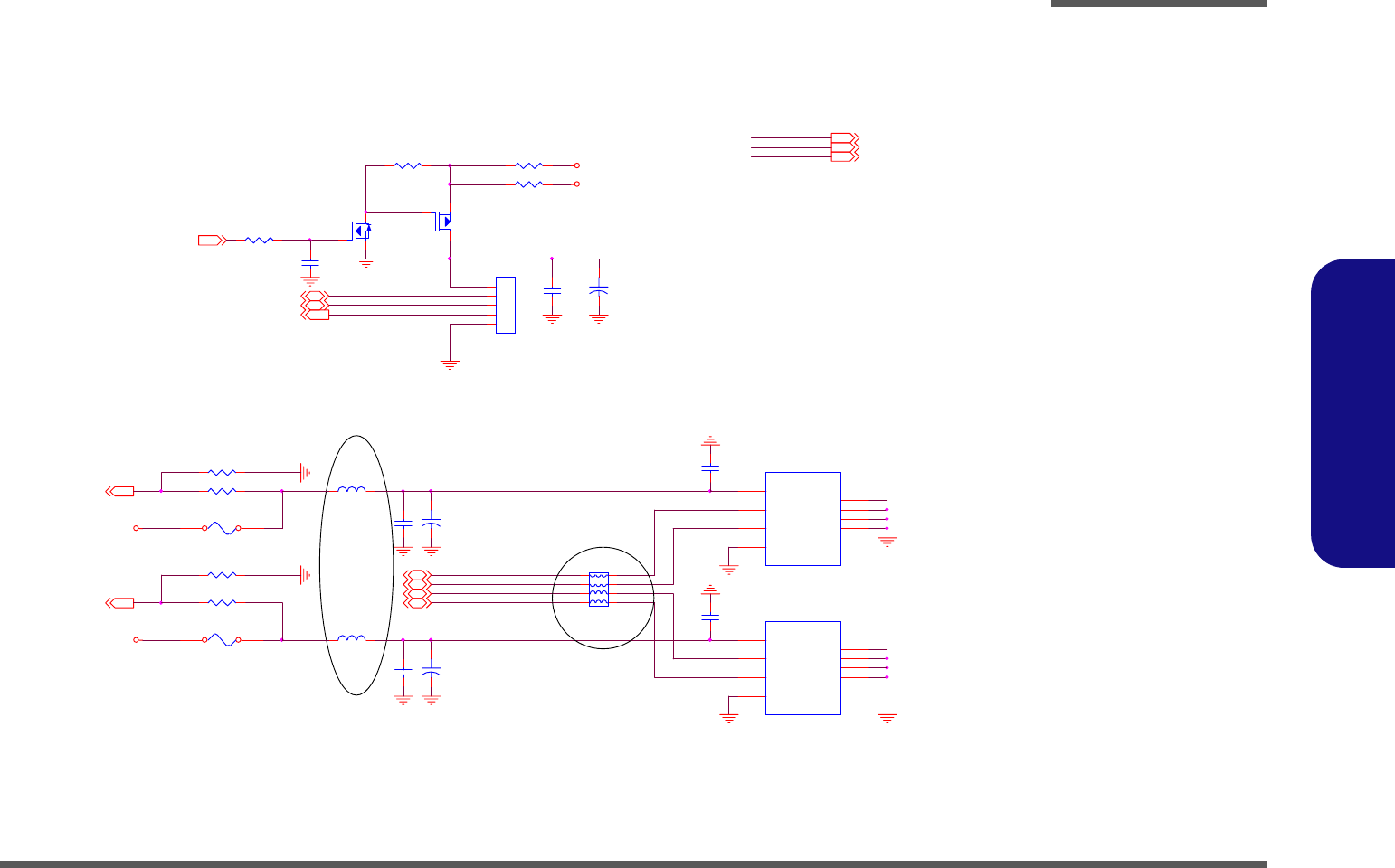
Schematic Diagrams
USB & CCD B - 19
B.Schematic Diagrams
USB & CCD
Sheet 18 of 34
USB & CCD
Z1812
CCD_EN19
6-19-91001-001
USB_PN0
CCD_DET#
USB_PP0
Z1803
Z1804
Z1802 G
D S
Q4
NDS352AP_NL
G
DS
Q3
2N7002
R6 100K
1
2
3
4
5
JCCD1
CON5_M
+
C12
10UF/10V_12
R7 0
R8 *0
C397
0.1UF
5VS
C17
0.1UF
5V
CCD_DET#19 USB_PP011 USB_PN011
R22 100K Z1801
1
2
3
46
5
7
8
LP3
YCM1012V4SF-181T04
F070395
Z1810
Z1807
R99 560K
R91 470K
1 2
F1 1.1A
C94
0.1UF
C92
0.1UF
L15
HCB3216KF-800T30
R130 560K
VCC
1
DATA-
2
DATA+
3
GND
4
SGND1
SGND2
SGND3
SGND4
JUSB3
USB_4P
+
C108
100uF/10V
L14
HCB3216KF-800T30
R131 470K
1 2
F2 1.1A C141
0.1UF
+
C175
100uF/10V
VCC
1
DATA-
2
DATA+
3
GND
4
SGND1
SGND2
SGND3
SGND4
JUSB2
USB_4P
C146
0.1UF
5V
5V
USB_PP311
USB_PP511 USB_PN511
USB_OC3#11 USB_PN311
USB_OC5#11
5VS 12,14,16,19,20,23,24,26,30
5V 19,20,24,25,26,27,28
3VH8 19,24,27,30
Z1805
Z1806
Z1809
Z1811
Z1808
C950719 BOM?
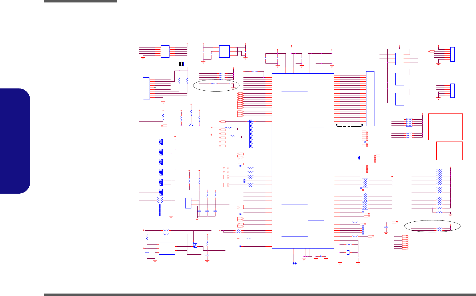
Schematic Diagrams
B - 20 HITACHI H8
B.Schematic Diagrams
HITACHI H8
Sheet 19 of 34
HITACHI H8
SUSC#12
WEB0#
R561 10K_04
WEB1#
WEB2#
WEB3#
WEB4#
5VS
SUSB#
C526
0.1U_04
SUSC#
LPC_FRAME#13,22
BRIGHTNESS 20
FOR H8 ID
PM_CLKRUN#
BRIGHTNESS
VDD3
CPU_FANSEN
R267
10K
R263
1K
80CLK
R282
10K
H8_P74
H8_P75
H8_P71
SMI#
VDD5 22,23,26,29,30
WEB0#
1
2
3
4
5
6
JHOTKEY1
CON6A_R
WEB3#
AUX_CLK
KBD_CLK
KBD_DATA
AUX_DATA
RSMRST#12,13 RSMRST#
80PORT_DET#
3IN 1
MD0_BOOT_FLASH
MD0_BOOT_FLASH
KBC_RXD1
R268 10K_04
21 S2
S1
R265 10K_04
Z1908
CHG_EN27
Z1913
3IN1
KBC_AGND
KBC_AGND
KBC_MD1
MD0_BOOT_FLASH
80POR T_DE T#
80CLK3IN1
KBC_TXD1 KBC_RXD1PWR_SW#
WLAN_DET# 24
80PORT_DET#
M950627
Z1907
80PORT_DET#
WEB3#
Z1904
H8_53
VDD3 3,13,22,25,26,27
SYS_FAN
H8_47
H8_46
H8_51
H8_109
H8_107
H8_108
SCROLL/BlueTooth
NUM/SRS
CAP/CCD
PWR/SUS
BAT_CHG/EMAIL
3VS
81 72 6
5
3
4
RP7 8P4RX10K_04
1
2
3
4
5
6
7
8
9
10
JDEBUG1
HEADER 10_R
24
B
EC
Q14
2N3904
KBC_PCLK2BUF_PLT_RST#7,11
VDD3
SERIRQ12,15
81 72 6
5
3
4RP8 8P4RX10K_04
MD0_BOOT_FLASH
JH8DBG
KBC_TXD1
H_A20GATE11
M_B TN #25
WEB5#
WEB4#
H8_48
2
H8_106
1
Z1912
Z1911
J_KB1
Z1910
R283
10K
1
LPC_AD0
H8 DEBUG PORT
CHG_EN
Z1909 5V 18,20,24,25,26,27, 28
3VS 2,7,8,9,10,11,12,13,14, 15,16,20,22,23,24,26,28,30
CCD_DET#
R252
10K
LPC_AD1
3VH8
H8_15
3VS
LPC_AD3
KBC_PCLK
DD_ON26
LPC_AD2
WEB2-->APPLICATION
WEB1-->E-MAIL
WEB0-->WWW
SCI#
9
LPC_FRAME#
3V 11,12, 13,17,24,25,26,29,30
Hot Key Pin Define
WEB0-->WWW
WEB1-->E-MAIL
WEB2-->APPLICATION
WEB3-->REC
WEB4-->ZOOM IN
WEB5-->ZOOM OUT
G
DS
Q15
2N7002W
Z1902
WEB5#
THERM_ALE RT#3
H8_RCIN#
SMD_THER M3SMC_THER M3
H8_P71
R523 100_04
H8_P75
PWR_BTN#
H8_P74
WEB1#
WEB2#
R524 100_04
R506 100_04
H8_RRST#
R496 100_04
Z1903
R493 100_04
10
AUX_CLK
AUX_DATA
KBD_CLK
H8_RRST#
H8_PME#
H8_SWI#
H8_SCI#
H8_GA20
H8_PB#
H8_RCIN#
H8_SMI#
WLAN _DET#
CCD_DET#
BT_DET#
KBD_DATA KBC_RXD1
SMC_BAT1
SMD_BAT1 80CLK
KBC_TXD1
80PORT_DET#
BAT1_DET
Z1901
TP_CLK
H8_SMI#
TP_DATA
PM_CLKRUN#11,12
H8_SCI#
VCORE_ON
KBC_RESET#
SUSB#12,20,25,26, 29
KBC_MD1
H8_GA20
H8_SWI#
KBC_PWRGD
5VS 12,14,16, 18,20,23,24,26,30
Z1906
KBC_RESET#
RESET_OUT#
H8_PB#
CHG_CUR 27
PWR_SW#
C294
0.1UF/10V_04
C137
47PF_04
C311
1U_06
R516 10K_04
R104
10K_04
R520 10K_04
AC
D39 SCS751
AC_IN#
C476
10UF/10V_08
LED_SCROLL 23
LED_NUM 23
LED_CAP 23
LED_PWR 23
LED_BAT_CHG 23
LED_ACIN 23
A C
D18 SCS751V-40
WLAN_EN 23,24
CCD_EN 18
BT_EN 23,24
LED_BAT_FULL 23
BLK_EN 20
R281
150K
C310
10UF/ 10V_08
R284 10K_04
MODEL_ID
R512
0_04
C489 1U_06
R276 10K_04
MR#
3
VCC
5
GND
2
RESET# 1
WDI 4
U9
AAT3510IGV
R527 10K_04
R287 10K_04
R264 100K_04
C477 1U_06
R510 4.7K_04
A C
D15 SCS751V-40
C487 1U_06
LID_SW#
11
22
33
44
JTP1
CON4
1
2
3
4
5
6
JHOTKEY2
CON6A_L
A
C
AC
D35
BAV99
A
C
AC
D40
BAV99
R498 10K_04
KBC_LPCPD#
LPC_AD013,22
LPC_AD313,22
LPC_AD113,22 LPC_AD213,22
KBC_STBY#
VCORE_ON28
R108
10K_04
R278 150K
A C
D21 SCS751V-40
MODEL_ID
1
1
2
2
3
3
4
4
5
5
10 10
99
88
77
66
RN27
10K_12_10P8R
A
C
AC
D37
BAV99
R569
10K
24
23
22
14
12
11
21
8
20
19
6
5
18
4
17
10
9
7
3
2
1
16
15
13
J_KB1
85201-24X5
80CLK
1
1
2
2
3
3
4
4
5
5
10 10
99
88
77
66
RN25
10K_12_10P8R
VDD3
VIN 1
GND 2
SD 3
BP
4
VO
5
U10
CM2838SIM25
R270
10M
CIR_EN
R511 4.7K_04
C313
0.1UF/10V_04
A C
D17 SCS751V-40
3IN 1
R275 10K_04
C316
0.01U/16V_04
KBC_RST#11
C312
10UF/10V_08
950525
SMI#12
C303
22PF
SWI #12
SCI#12
PWR_BTN#12
R505 10K_04
H_A20GATE
R513 10K_04
H8_56
R514 10K_04
R280 100K_04
DD_ON
R272 10K_04
C133
47PF_04
C492
68P_04
A C
D20 SCS751V-40
R274
10K_04
GA20
R519 10K_04
R503 120K_04
C317
0.1UF/10V_04
SWI #
R521 10K_04
R219 120K_04
H8_P70
R501 10K_04
PWR_SW#25
C122
0.1UF/10V_04
3V
R522 10K_04
C305
22PF
H8_58
C307
0.1U_06
H8_57
H8_55
C293
0.1UF/10V_04
R502 100_04
3VH8 24,27,30
A C
D16 SCS751V-40
CCD_DET# 18
R508 10K_04
R277 10K_04
NMI
KB-SI7 KB-SI3
A C
D19 SCS751V-40
KB-SI1
KB-SI5 KB-SI2
KB-SI4
KB-SI6
KB-SI0
A
C
AC
D41
BAV99
WEB4#
R525 *10K_04
R526 10K_04
KB-SO2
KB-SO7
KB-SO4
C306
0.1U F/ 10V_04
KB-SO0
KB-SO5
KB-SO8
KB-SO1
KB-SO3
KB-SO15
KB-SO9 KB-SO13
KB-SO6
A
C
AC
D38
BAV99
KB-SO10 KB-SO14
KB-SO12
12 34 56 78 910
JH8DBG1
SPUFZ-10S3-B-0-B
Z1905
PME# 12,15,24
R517 10K_04
A
C
AC
D36
BAV99
R507 10K_04
X2
10MHz
C309
0.1UF/10V_04
WLAN_DET#
1
1
2
2
3
3
4
4
5
5
10 10
99
88
77
66
RN26
10K_12_10P8R
R518 10K_04
R499 10K_04
BAT2_DET
R271 10K_04
R504 10K
R226 10K
CPU_FANSEN 22
KBC_BEEP 30
PWR_BTN#
VOL_MUTE 30
SUSC#
CPU_FAN 22
BAT2_VOLT
8 1
7 2
6
53
4
RN9
8P4RX10K_04
950310
LED_EMAIL
LID_SW#20,27
R230 100K_04
VDD 3
WEB5#
VDD3
VDD3
VDD3
SYS_FANSEN
VDD3
VDD3
VDD3
VDD3
5VS
VDD5
3VH8
VDD53VH8VDD3
VDD5
VDD3
CHG_CURSEN27
H8_54
CHG_CURSEN
KBC_RST#
TERM_REST#3
KBC_MD1
WEB0#
R350
*0_04
R351
0_04
BAT1_VOLT
5V SMC_BAT1
BAT1_DET
SMD_BAT1
KBC_PWRGD11
SMC_BAT127
BAT1_VOLT27
SMD_BAT127
BAT1_DET27
WEB1#
R358 10K_04
VDD3
3V
H8_PME#
TP_ CLK
TP_ DATA
WEB2#
81 72 6
5
3
4
RP14 8P4RX10K_04
3V
PME#
VDD3
BT_EN
KBC_TXD1
TOTAL_CUR27
KB-SO11
CCD_EN
BT_DET#
SRS_EN#
TER M_R EST#
TOTAL_CU R
WLAN_EN
H8_52
AC_IN#27
BLK_EN
KB-SI1
KB-SO5
KB-SO9
KB-SO0
C950718
KB-SI3
KB-SO3
KB-SI5
KB-SO7
KB-SO15
KB-SO1
KB-SI2
BT_DET# 24
KB-SO10
KB-SI6
KB-SO2
KB-SO8
KB-SO6
KB-SI4
KB-SO14
KB-SO12
KB-SI0
KB-SO13
KB-SO4
KB-SI7
KB-SO11
KBC_RXD1
BUF_PLT_RST#
MD1
9MD0
10
P50/ExTxD1*
16
P51/ExRxD1*
15
PD0 66
P70/AN0
68
P71/AN1
69
P72/AN2
70
P73/AN3
71
P74/AN4
72
P75/AN5
73
P76
74 P77
75
P43/TMC11
2P44/TMO1
3
P45/TMR11 4
P80/PME#
129
P81//CS2#/GA20
130
P82/CLKRUN#/HIFSD
131
P83/LPCPD#
132
P84/IRQ3#/TxD1
133
P85/IRQ4#/RxD1
134
P86/IRQ5#/SCK1/SCL1
135
P30/D8/HDB0/LAD0
121
P31/D9/HDB1/LAD1
122
P32/D10/HDB2/LAD2
123
P33/D11/HDB3/LAD3
124
P34/D12/HDB4/LFRAME#
125
P35/D13/HDB5/LRESET#
126
P36/D14/HDB6/LCLK
127
P37/D15/HDB7/SERIRQ
128
RESET#
8
RESET_OUT#
142
NMI
11
STBY#
12
PB0/D0/WUE0#/LSMI#
120
PB1/D1/WUE1#/LSCI
119
PB2/WUE2# 118
PB3/WUE3# 117
PB4/WUE4# 116
PB5/WUE5#
115
PB6/WUE6#
114
PB7/WUE7#
113
AVSS
67
VSS
111 VSS
95 VSS
42 VSS
7
AVCC 76
AVref 77
VCCB 36
VCC 1
VCL 13
PG0 58
PG1 57
PG2 56
PG3 55
PG4/ExSDAA* 54
PG5/ExSCLA* 53
PG6/ExSDAB* 52
PG7/ExSCLB* 51
P60/FTCI/KIN0#/TMIX 78
P61/FTOA/KIN1# 79
P62/FTIA/KIN2#/TMIY 80
P63/FTIB/KI N3# 81
P64/FTIC/KIN4# 82
P65/FTID/KIN5# 83
P66/FTOB/KIN6#/IRQ6# 84
P67/TMOX/KIN7#/IR Q7# 85
PF7/ TMOY* 43
PF6/ ExTMOX* 44
PF5/ExTMIY* 45
PF4/ ExTMIX* 46
PF3/ TMOB 47
PF2/ TMOA 48
PF1/TMIB 49
PF0/TMIA 50
P90/IRQ2#/ADTRG#
24
P91/IRQ1#
23
P92/IRQ0#
22
P93
21
P94
20
P95
19
P96/EXCL
18
P97SDA0
17
P40/TMCI0 136
P41/TMO0 137
P42/TMRI0/SDA1
138
P46 5
P47
6
XTA L 143
PA0/KIN8#
41
PA1/KIN9#
40
PA2/KIN10#/PS2AC
39
PA3/KIN11#/PS2AD
38
PA4/KIN12#/PS2BC
37
PA5/KIN13#/PS2BD
35
PA6/KIN14#/PS2CC
34
PA7/KIN15#/PS2CD
33
P52/ExSCK1*/SCL0
14
PE7 25
PE6 26
PE5
27
PE4 28
PE3 29
PE2 30
PE1 31
PE0 32
VSS
139 VCC 86
PD1 65
PD2 64
PD3 63
PD4 62
PD5 61
PD6 60
PD7 59
PC7 87
PC6 88
PC5 89
PC4 90
PC3 91
PC2 92
PC1 93
PC0 94
P27 96
P26 97
P25 98
P24 99
P23 100
P22 101
P21 102
P20 103
EXTAL 144
P17/PW7 104
P16/PW6 105
P15/PW5 106
P14/PW4 107
P13/PW3 108
P12/PW2 109
P11/PW1 110
P10/PW0 112
X1
140 X2
141
INT. K/B
Debug Port
South
Bridge
Theraml
Battery
PS2
Power
Management
Consumer IR
LED
Indicator
PWM
output
Clock
GPIO
U8
H8S/2111 BV
CHG_CUR
KBC_PCLK
SMC_BAT1
TOTAL_C UR
BAT1_DET
CHG_CURSEN
SMD_BAT1
BAT1_VOLT
SERIRQ
M_BTN#
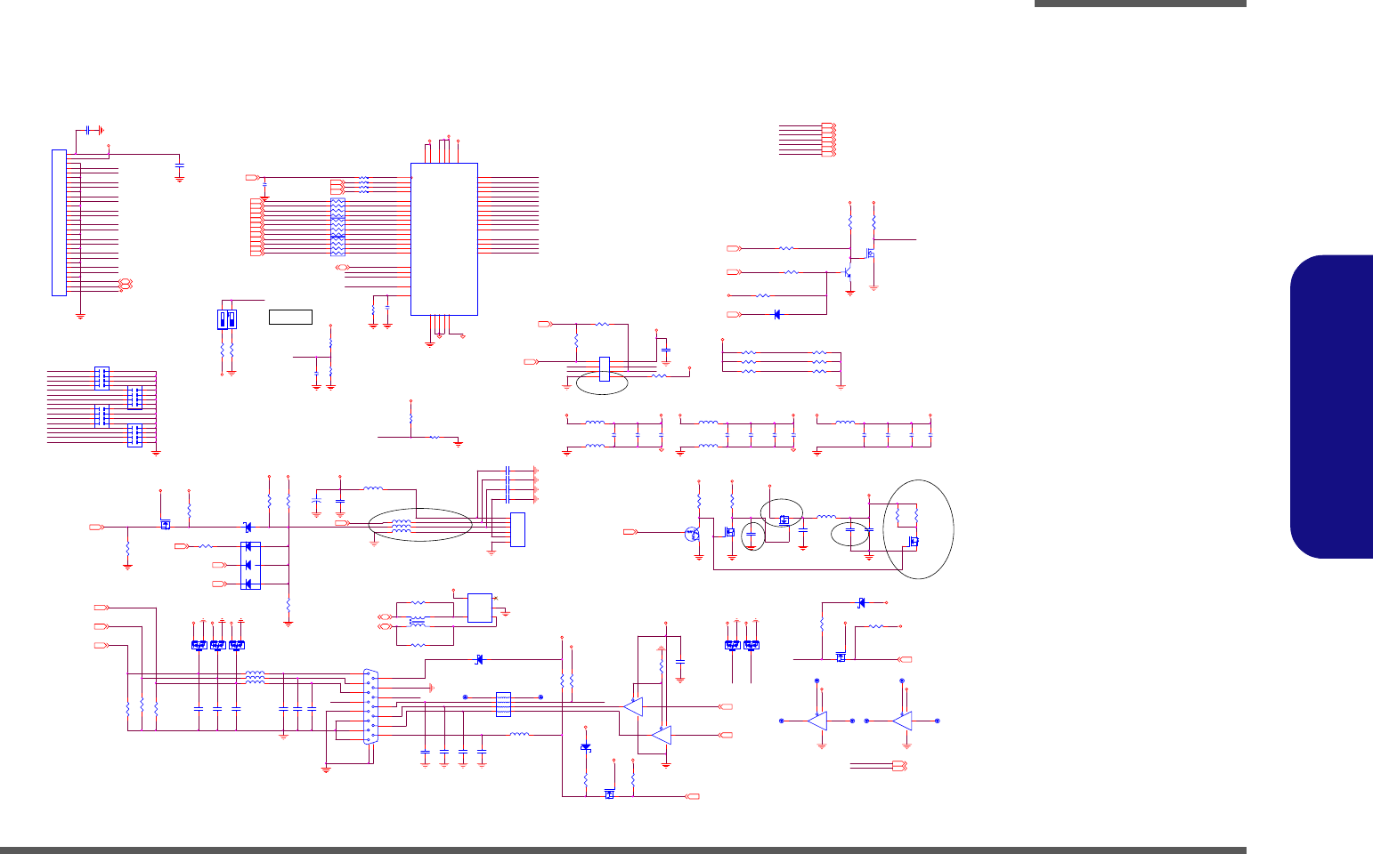
Schematic Diagrams
CRT & LVDS B - 21
B.Schematic Diagrams
CRT & LVDS
Sheet 20 of 34
CRT & LVDS
VSYNC
HSYNC
R31 22
Z2023
R364 22
Z2026
R363 22
R27 22
Z2001
F070395
R39
100K
Z2002
LVREF
Z2003
Z2004
PDVP1CLK
R33
100_08
BRIGH TNESS
Z2025
VGADATA
VGADATA
Z2040
Z2046
Z2042
Z2043 Z2045Z2044
Z2041
G
D S
Q26
AO340
1
2
3
45
6
7
8
LP1
FCA3216KF4-121T3
R361
4.7K
3VS 2,7,8,9,10,11,12,13,14,15,16,19,22,23,24,26,28,30
3V 11,12,13,17,19,24,25,26,29,30
LA_DATAN1
1 2
L22
HCB3216KF-800T30
R19
75_1%
AC
D30 R B751V
C3
10PF
1 2
L11 HCB2012KF-121T30
1 2L1 H CB1608KF-121T25
NC 1
VN 2
CH1 3
CH2
4
VP
5U21
CM1213-02SO
81 72 6
5
3
4
RP9 8P4RX22_04
AC
D31 RB751V
81 72 6
5
3
4
RP10 8P4RX22_04
C404
4.7UF/10V_08
C46
0.1UF
R2
*15K
R15
75_1%
R1
*15K
R365
10K
81 72 6
5
3
4
RP11 8P4RX22_04
PLVDD
R3
4.7K
1 2L3 H CB1608KF-121T25
1 2
L10 HCB1608KF-121T25
LA_DATAP0
A
C
AC
D4
BAV99
1 2
L20
FCB1608KF-121T25
C396
0.1UF
LB_DATAP0
C1
10PF
+
C45
10UF /25V_1206
R20 2.2K
A
C
AC
D8
BAV99
1
2
3
4
5
6
JINV1
CON6
A
C
AC
D3
BAV99
C6
22PF
C29
0.1UF
C391
220PF
C27
0.1UF
C31 * 0.1UF
1211
14
13
7
U22D
74HCT125PW
C4
1000PF
R37
4.7K
A
C
AC
D7
BAV99
C28
4.7U F/10V_08
2.5VS 2,3, 11,12,13,26
Z2048
56
14
4
7
U22B
74HC T125PW
C5
22PF
1 2L2 H CB1608KF-121T25
C33 0.1UF
98
14
10
7
U22C
74HCT125PW
LA_DATAN0
1 2
L9 HCB1608KF-121T25
C7
22PF
C390
220PF
G
D S
Q5
2N7002
C30 * 0.1UF
C2
10PF
Z2005
AC
D9
RB751V
C403
0.1UF
5VS
Z2006
23
14
1
7
U22A
74HCT125PW
R38
2.2K
LA_CLKP
C32 * 0.1UF
1 2
L12
HCB2012KF-121T30
Z2007
8
7
6
5
4
3
2
19
10
11
12
13
14
15
GND2
GND1
JVGA1
VGA DSUB
G
D S
Q2
2N7002
LB_DATAN0
R17
75_1%
A
C
AC
D5
BAV99
CE
B
Q8
DTC114EUA
LID_SW#19,27
C389
1000PF
PLVDD
Z2008
5VS
5VS 5VS
3VS
5VS
5VS
5VS
5VS
5VS 5VS
3VS
Z2009
LB_CLKN
VIN
3VS
3VS
5VS
Z2010
R369
10K
Z2011
1
2
3
4
5
6
7
8
9
10
11
12
13
14
15
16
17
18
19
20
21
22
23
24
25
26
27
28
29
30
JLCD1
CON30
L_BKLTEN7
Z2012
LA_DATAP1
Z2013
USB_4+
MI D 1
MI D 3
Z2014
G
DS
Q10
2N7002
LB_DATAN2
R74
100K
Z2015
ENAVEE1
R58
2.2K
Z2016
G
DSQ12
BSS138_NL
LA_CLKN
LB_DATAP2
LA_DATAN2
C405
0.1UF
PIN GND1,2,3,4=GND
VS
VC
LB_CLKP
LB_DATAP1
5V 18,19,24,25,26,27,28
G
DS
Q9
2N7002
LA_DATAP2
FBLU
C398
10PF
R25
2.4K_1%
Z2017
R570
100_08
LB_DATAN1
DUAL
C26
*0.1UF
1-4 ON;
2-3 OFF
1.5V 7, 26,29
R370
*10K
5VS
3VS
5V5V
CLKINP
C950719
L_DDC_DATA 8
L_DDC_CLK 8
C950719
3VS
5VS
CRT_RED8
CRT_BLUE8
CRT_GREEN8
5VS
Z2034
BRIGHTNESS19
R368
82K
AC
D11 RB751V
R60 0
+
1
+
2
+
3-4
-5
-6
D3P
D12 RB731U
CRT_HSYNC 8
VDD 5 19,22,23,26,29,30
CRT_DDC_DATA 8
CRT_DDC_CLK 8
CRT_VSYNC 8
2.5VS
3VS
3VS
BLK_EN19
1 2
L8
HC B2012KF-121T30
VIN 25,26, 27,28,29
2.5VS
ENAVDD7
2.5VS
VSY N C
HSYNC
1 2
L7
HC B2012KF-121T30
ACD10 *1SS355
USB_4-
1.5VS
2.5VS
1 2
L4
HCB2012KF-121T30
Z2027 Z2029
ALL_PWR OK11,13
1 2
L6
HC B2012KF-121T30
ALL_PWROK11,13
ENAVDD
PDVP1CLK7
DUAL8
1 2
L5
HCB2012KF-121T30
VCC25 1
VCC25 29
VCCLVDS 5
VCCLVDS 13
VCCLVDS 22
VCCPLL 27
GND
35
GNDLVDS
10
GNDLVDS
14
GNDLVDS
19
GNDPLL
26
D[0]
36
D[1]
37
D[2]
38
D[3]
39
D[4]
40
D[5]
41
D[6]
43
D[7]
44
D[8]
45
D[9]
46
D[10]
47
D[11]
48
DE
33
DUAL
2
HSYNC
31
PDB
34 R_FB
28
VSWING
25
VREF
32
VSYNG
30
XC L K
42 A0- 24
A0+ 23
A1- 21
A1+ 20
A2- 18
A2+ 17
A3- 12
A3+ 11
A4- 9
A4+ 8
A5- 7
A5+ 6
CLK1- 16
CLK1+ 15
CLK2- 4
CLK2+ 3
U23
VT1637
DVDD
Z2028
LVDSVCCPLLVC C
LVDSGNDPLLGND
R356 0
R357 0
FRED
FPD00
FPD10
FPD08
FPD03
FPD01
FPD05
FPD07
FPD06
FPD09
FPD02
FPD11
FPD04
LA_DATAP2
LA_DATAP0
LB_CLKN
LB_CLKP
LA_DATAN0
LB_DATAP2
LA_CLKP
LB_DATAN1
LA_CLKN
LB_DATAN0
LA_DATAP1
LB_DATAP1
LB_DATAN2
LA_DATAN2
LB_DATAP0
LA_DATAN1
LVDS_PD#
PDVP1VS7PDVP1HS7
Z2035
Z2020
1.5VS 2,4, 7,24,26
LVDSGND PLLGND
DVDD
Z2030
1
2
4
3
SW2
SW-4X2_4
DUAL
G
S D
Q7
2N7002
R35
2.2K_04
EDGE
R26 *4.7K
R261 *0_04
R362
4.7K
SR1
MR A
SR0
R242 *0_04
EDGE
R225 * 0_04
LA_DATAP2
LA_DATAN1
USB_PN411
USB_PP411
F070395
LB_DATAN1
LB_DATAP2
2.5VS
R241 *0_04
LVDS_PD#
1
4
2
3
L21
*PWC1206ST161T
R34 *0_04
LB_CLKP
C302
0.1u/16V_04
LA_DATAP0
1
2
3
4 5
6
7
8
CP2
*8P4CX10PF
1
2
3
4 5
6
7
8
CP4
*8P4CX10PF
R224
*0_04
LA_DATAP1
R40 1K_04
LB_CLKN
LA_DATAN2
B
E
C
Q6
2N3904
R41 *1K_04
1
2
3
4 5
6
7
8
CP1
*8P4CX10PF
1
2
3
4 5
6
7
8
CP3
*8P4CX10PF
1
2
3
4 5
6
7
8
U33
*P2040C
LA_CLKP
LB_DATAN0
R240 *0_04
LA_CLKN
R36
1K_04
R260 *0_04
LB_DATAP0
LB_DATAP1
LA_DATAN0
LB_DATAN2
R243 *0_04
2.5VS3VS
3VS
3VS
3VS
CRT
SUSB#12,19,25,26,29
ENAVEE7
C950719
LVDSVCC
PLLVCC
C406
.01U_06
C407
.01U_06
DISPCLKI8
DISPCLKO8
C21
.1U_06
C402
1UF
C395
.01U_06
USB_4-
C13
.01U_06
R262 *10K_04
C399
1UF
C394
.1U_06
USB_4+
MRA SR0
C19
.1U_06
C22
.01U_06
SR1
C24
1UF
FGRN
HS
Z2019
Z2021
Z2022
Z2024
Z2037
Z2036
INVERTER
FPD007
FPD037FPD027FPD017
FPD067FPD057FPD047
FPD097FPD087FPD077
FPD117FPD107
PDVP1DE7
R380
4.7K_04 R568
4.7K_04
LVREF
5VS 12,14,16,18,19, 23,24,26,30
R28
1K_1%
R30
1K_1%
2.5VS
1.5VS
F070395
WAITTING FOR EMI
SOLUTION
C401
0.1UF
Z2018
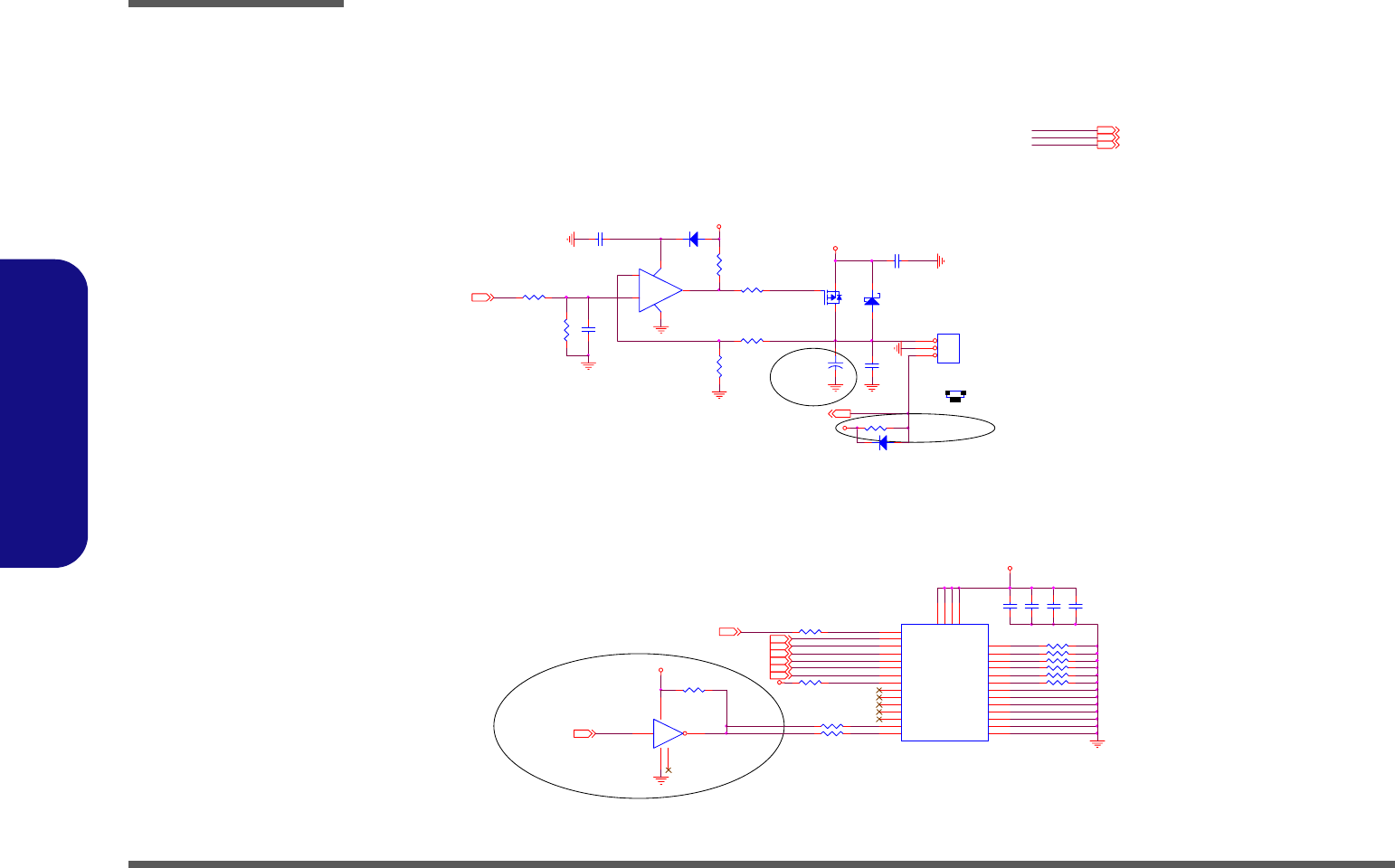
Schematic Diagrams
B - 22 CPU FAN, ROM
B.Schematic Diagrams
CPU FAN, ROM
Sheet 21 of 34
CPU FAN, ROM
Z2207
Z2208
JFAN1
1
R11
*2.2M_04
CPU_FANSEN
3
R12 120K_04
M950626
SOCKET PLCC32
Z2209
ROM
SOCKET PLCC32
FWH_INIT#
FANON
R301 8.2K_04
C8 0. 1UF/10V_04
C351
0.1UF/10V_04
R5 2.2K_1%_04
A C
D6
SCS751V-40
R10
10K_1%_04
R327 100_04
VPP 1
RST#
2
FGPI3 3
FGPI2 4
FGPI1 5
FGPI0 6
WP#
7
TBL#
8
ID3 9
ID2 10
ID1 11
ID0 12
FWH0
13
FWH1
14
FWH2
15
GND 16
FWH3
17
RFU
18
RFU
19
RFU
20
RFU
21
RFU
22
FWH4
23
INIT#
24
VCC 25
GND 26
VCCA 27
GNDA 28
IC 29
FGPI4 30
CLK
31
VCC 32
U18
FWH32
AC D21SS355
R4 10K_04
R336 8.2K_04
R300 100_04
R13 4.99K_1%_04
VDD3 3,13,19,25,26,27
C381
0.1UF/10V_04
R325 8.2K_04
R9
100K_1%_04
R299 100_04
Z2201
R316 8.2K_04
C382
0.1UF/10V_04
R302 8.2K_04
+
1
-
3O4
V5
G
2
U1
LMV331
+
C392
100U /10V
C10 0.1UF/10V_04
AC D11SS355
G
D S
Q1
NDS352AP_NL
C341
0.1UF/10V_04
R341 0_04
C11
0.1UF/10V_04
Z2202
VDD5
VDD3
CPU_FAN
VDD5
3VS
VDD5 19,23,26,29,30
C393
10UF/10V_08
2 4
53
1
U36
MCH74VHC1G14DFT2G
R342 10K
3VS
Z2206
3VS 2,7,8,9,10,11,12,13,14,15,16,19,20,23,24,26,28,30
Z2203
LPC_FRAME#
Z2204
M950626
Z2212
Z2211
Z2214
Z2213
Z2210
FLASH#11
1
2
3
JFAN1
FI-S03P-HF
C950719
LPC_AD013,19
LPC_AD213,19 LPC_AD313,19
PCLK_FWH2
CPU_FANSEN19
LPC_AD113,19
LPC_FRAME#13,19
CPU_FAN19
Z2205
R562 10K_04
3VS
PCIRSTX#11 PCIRSTX#
CPU FAN
LPC_AD1
PCLK_FWH
LPC_AD3
LPC_AD0
LPC_AD2
Schematic Diagrams
LED B - 23
B.Schematic Diagrams
LED
Sheet 22 of 34
LED
Z2314
Z2318
Z2310
Z2309
CHANGE LED
3VS
VDD5
WLAN_EN19,24
WIRELESS LAN /BT
LED
C
B
E
10K
10K
Q23
DTC114EUA
Z2317
3VH8 19,24,27,30
SCR LOCKNUM LOCK LED
GREEN LED GREEN LED
B
EC
Q25
2N3906
GREEN LED
CAPS LOCK LED
34
12
GREEN
ORANGE
D24
DLED
PDLED#14
C950719C950719
Z2301
Z2304
Z2303
Z2302
C950720
VDD5 19,22,26,29,30
AC
D29
LED
R354
100
C
B
E
47K
47K
MQ1
DTA114EUA
C
B
E
10K
10K
Q24
DTC114EUA
AC
MD1
LED
MR1
100
3VS
ACIN
PWR/SUS
BT_EN19, 24
CE
B
Q17
DTC114EUA
CE
B
Q18
DTC114EUA
CE
B
Q21
DTC114EUA
3VS
BATT/E mail
CHARGE FULL
R345 200
R346 200
VDD5
A C
D23
LED
Z2315
R355
100
CE
B
Q19
DTC114EUA
CE
B
Q20
DTC114EUA
R347 200
R348 20034
12
GREEN
ORANGE
D25
DLED
Z2308
Z2307Z2305
Z2306
+
1
+
2
+
3-4
-5
-6
D3P
D22
IMN10
R349
4.7K
950317
5VS
SDACT#14 SDACT#
PDLED#
PD_LED#
LED_ACIN19 LED_BAT_FULL19
LED_BAT_CHG19
LED_PWR19
LED_SCROLL19
LED_CAP19
LED_NUM19
R352
100
C
B
E
10K
10K
Q22
DTC114EUA
AC
D27
LED
Z2316
Z2312
3VS 2,7,8,9,10,11,12,13,14,15,16,19,20,22,24,26,28,30
5VS 12,14,16,18,19,20,24,26,30
AC
D28
LED
Z2313
R353
100
GREEN LED
HDD/PD LED
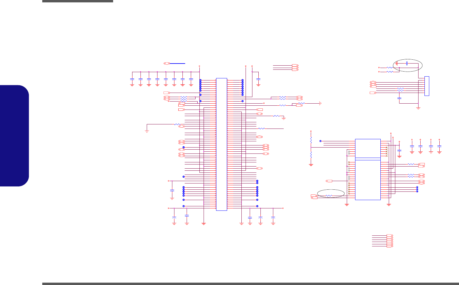
Schematic Diagrams
B - 24 MINI-PCI & BLUETOOTH
B.Schematic Diagrams
MINI-PCI & BLUETOOTH
Sheet 23 of 34
MINI-PCI &
BLUETOOTH
BT_DATA
BT_CHCLK
5VS 12,14,16,18,19,20,23,26,30
3V 11,12,13,17,19,25,26,29,30
3VS 2,7,8,9,10,11,12,13,14,15,16,19,20,22,23,26,28,30
C242
0.1UF
3V
C176
0.1UF
3VS
1.5VS 2,4,7,20,26
5V 18,19,20,25,26,27,28
PCI_AD24
3VH8 19,27,30
3V
CDL
CCL
PCI_AD[31:0]
Z2405
Z2406
Z2407
WLAN _DET#
M950626
Z2402
R529 *10K
3VS 2,7,8,9,10,11,12,13,14,15,16,19,20,22,23,26,28,30
3VH8
R162 0
R166 0
Z2403
Z2404
BT_EN
Z2409BT_DATA R142 0
C203
0.1UF
3VS
BT_DET#
1
2
3
4
5
6
7
8
JBLUETOOTH1
CON8
BT_CHCLK R140 0
USB_PP6
Z2410
Z2408
C467 0.01UF
BT_DET#19
USB_PN611
R163 *0
USB_PN6
USB_PP611
BT_EN19,23
3V R164 0
USB_PN7 11
USB_PP7 11
PCIRSTC# 11,15
PCI_INTA# 8,11,15
PCI_INTC#11,15 PCI_INTD# 11
PCI_INTB#11,15
PCI_AD16
PCI_AD1
Z2437
PCI_AD5
PCI_AD11
PCI_AD2
PCI_AD28
PCI_AD20
PCI_AD4
PCI_AD22
PCI_AD15
PCI_AD30
PCI_AD19
PCI_AD3
PCI_AD7
PCI_AD14
PCI_PAR
PCI_FR AME#
PCI_IRDY #
PCI_AD0
PCI_AD12
PCI_AD27
PCI_AD29
PCI_AD26
IDSEL
PCI_AD21
PCI_AD8
PCLKMPCI
PME#
PCI_AD17
Z2411
PCI_AD25
PCI_AD18
PCI_AD9
Z2414
Z2416
PCI_AD23
Z2412
Z2413
PCI_SERR#
Z2417
Z2419
PCI_AD31
Z2432
Z2415 Z2434
Z2433
PCI_DEVSEL#
Z2431
Z2429
PCI_STOP#
Z2430
PCI_PERR #
PCI_AD6
PCI_AD13
PCI_AD10
PCI_TRDY#
Z2439
Z2435
Z2438
Z2436
Z2421
Z2420
Z2422
Z2425
Z2423
Z2424
Z2426
Z2441
Z2440
Z2427
Z2428
Z2443
Z2444
Z2445
Z2442
Z2448
Z2447
Z2446 R175 *0_04 Z2401
WAKE#
1+3V_1 2
RSVD1
3GND7 4
RSVD2
5+1.5V_1 6
CLKREQ#
7RSVD13 8
GND1
9RSVD14 10
REFCLK-
11 RSVD15 12
REFCLK+
13 RSVD16 14
GND2
15 RSVD17 16
RSVD3
17 GND8 18
RSVD4
19 RSVD18 20
GND3
21 PERST# 22
PER_N0
23 +3V_AUX 24
PER_P0
25 GND9 26
GND4
27 +1.5V_2 28
GND5
29 SMB_CLK 30
PET_N0
31 SMB_DATA 32
PET_P0
33 GND10 34
GND6
35 USB_D- 36
RSVD5
37 USB_D+ 38
RSVD6
39 GND11 40
RSVD7
41 LED_WWAN# 42
RSVD8
43 LED_WLAN# 44
RSVD9
45 LED_WPAN# 46
RSVD10
47 +1.5V_3 48
RSVD11
49 GND12 50
RSVD12
51 +3V_2 52
KEY
U29
PCI-e MINI_CAR D
BT_DET#19 BT_EN19,23
WLAN_CLKREQ#
R414
10K
R412
*0
SMB_SBCLK 2,9,10,12
SMB_SBDATA 2,9,10,12
F070395
3V 11,12,13,17,19,25,26,29,30
3VS
1.5VS 2,4,7,20,26
WLAN_DET#19
C180
0.1UF
1.5VS
R149 0 WLAN_EN 19,23
WLAN_EN
3V
T
T
T
T
C510
*0.1U
T
C501
*0.1U
C502
*0.1U
T
T
T
T
R541
*33
R547 *4.7K
R545 33
R546 *10
T
Z2418
C511
*0.1U
R531 *10
T
T
C512
*0.1U
T
R543 *10
C509
*0.1U
C520
*220uF(D) C515
*220uF(D)
T
T
T
R532 *10
T
T1 2
3 4
5 6
7 8
910
11 12
13 14
15 16
17 18
19 20
21 22
23 24
25 26
27 28
29 30
31 32
33 34
35 36
37 38
39 40
41
43
45
47
49
42
44
46
48
50
51 52
53 54
55 56
57 58
59 60
61 62
63 64
65 66
67 68
69 70
71 72
73 74
75 76
77 78
79 80
81 82
83 84
85 86
87 88
89 90
91 92
93 94
95 96
97 98
99 100
101 102
103 104
105 106
107 108
109 110
111 112
113 114
115 116
117 118
119 120
121 122
123 124
JMINIPCI1
Mini-PCI CON.
T
T
C504
*0.1U
C500
*0.1U
C505
*0.1U
R530 *0
TT
T
T
T
C513
*0.1U
T
T
C503
*0.1U
C499
*220uF(D)
T
T
T
T
C514
*0.1U
T
R542 *0
T
T
T
3VS 5VS
5VS
3V
5V
3VS
PCI_DEVSEL# 11,15
3V
PCI_R EQ#311
PCI_PAR 11,15
PCI_STOP# 11,15
PCI_FRAME# 11,15
PCI_C/BE0# 11,15
PCI_SERR #11,15
PCI_C /BE2#11,15
PCI_AD[31:0]11,15
PCIRSTC# 11,15PCLKMPCI2
PCI_PERR #11,15
PCI _TR DY # 11, 15
PCI_C /BE1#11,15
PME# 12,15,19
WLAN_DET#19
PCI_C /BE3#11,15
PCI _IR DY #11,15
PCI_GNT#3 11
WLAN_EN19,23
C277
0.1UF
3VS
C237
0.1UF
PCI_AD19
3VS
PCIE_WAKE#
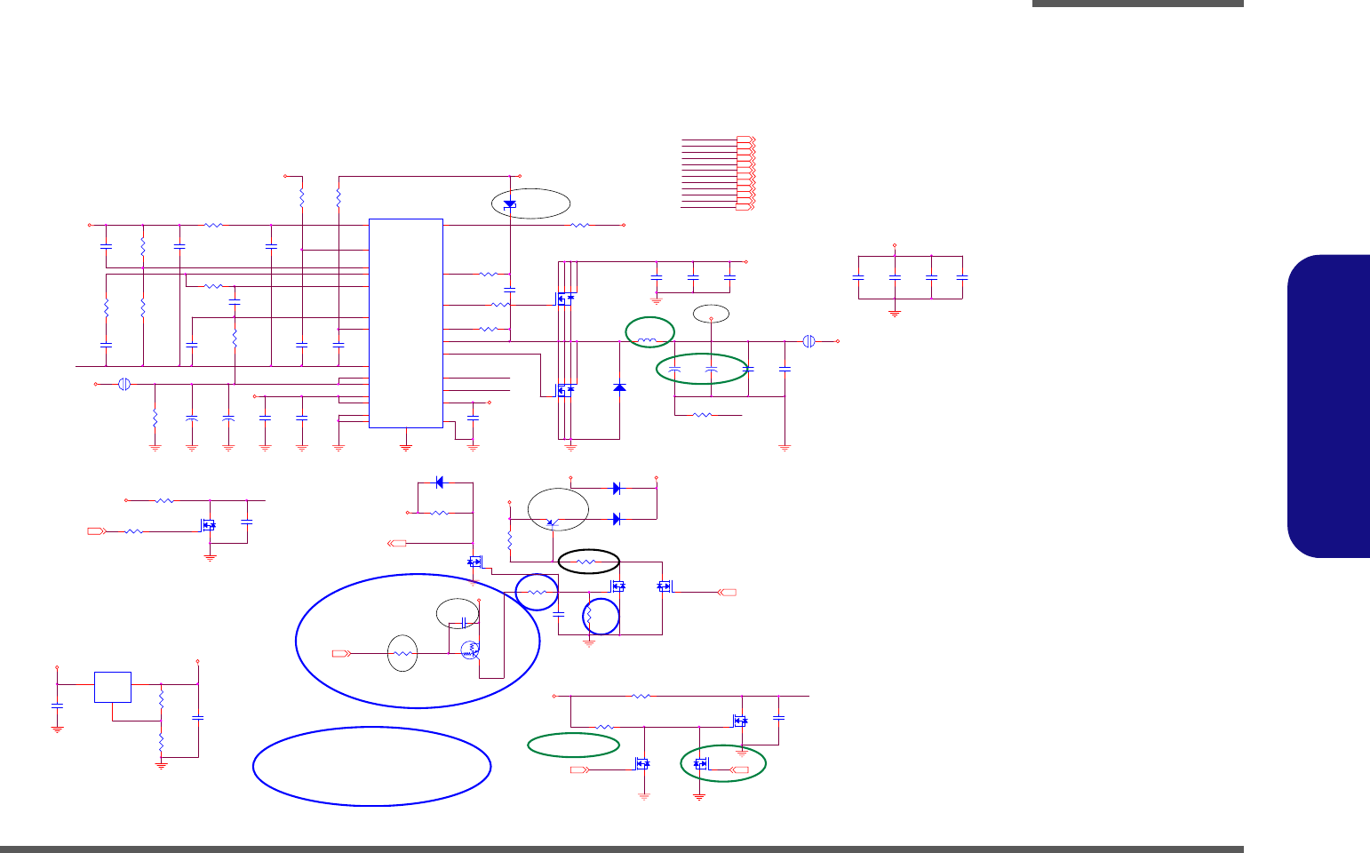
Schematic Diagrams
1.8V, 0.9VS, 2.5VS B - 25
B.Schematic Diagrams
1.8V, 0.9VS, 2.5VS
Sheet 24 of 34
1.8V, 0.9VS, 2.5VS
VDD 5 19,22,23,26,29,30
DD_ONH 26
PWR_SW#19
7/5
Z2510
Z2505
Z2509
Z2511
Z2504
Z2508
VSSA
VSSA
G
DS
PQ9
2N7002W
Z2515
Z2502
VIN
Z2501
Z2516
Z2524
3/13
PIN 4=FL OATI NG
1A
Z2503
3/13
Z2513
Z2512
VTTEN
PC 11 9
*10U_10V_08
PC 11 8
*10U_10V_08
5A
Z2506
3A
C E
B
PQ2
DTA114EUA
PR21
10K_06
Z2523
PC10
0.1U_50V_06
5V 18,19,20,24,26,27,28
VIN 1 26
3/16
VA 27
4
62 5
73
1
8
PQ35
RSS090N03
Vin
3
Gnd/Adj
1
Out 2
PU6 CM1117
4
62 5
73
1
8
PQ28
RSS090N03
PC 14 0
10U_25V_12
PR151
100_1%_04
PR148
100_1%_04
3/7
DEL
+
PC33
220U_4V_V
PC141
4.7U_10V_08
3/7
+
PC32
*220U_4V_V
PL3
2.5U_7*7*3.5
3/7
5VS 12,14,16, 18,19,20, 23,24,26,30
5V
Z2525
PC36
0.1U_06
TEST 26,28,29
Z2518
PC37
0.1U_06
PC38
0.1U_06
EN_1.8V
PC35
0.1U_06
Z2507
0.9VS
M_BTN#19
VDD 3 3,13,19,22,26,27
1.8V 2,6,7,9,10
VIN 20,26,27,28, 29
0.9VS 10
2.5VS 2,3,11,12,13,20,26
3VS 2,7,8,9,10,11,12,13,14,15,16,19,20,22,23,24,26,28,30
DD_ON#26,29
F042795
Z2514
Z2522
Z2520
Z2519
M_BTN#
DD_ONH
Z2521
PWR_SW#
AC
PD1
SCS551V-30
SUSB#
VTTEN
Z2526
Z2517
EN_1.8V
PC34
1U_06
PC116
*0.1U_04
PR 48
1.5M_06
PC110
1U_06
PC 27
1000P_06
PC111
.1U_04
PC39
.01U_04
950525
PC80
10U_25V_12
PR61 10_06
PR62
7.15K_1%_06
A C
PD10 SCS140P
PR118
10K_04
PC106
1U_06
PC31
.068U_06
G
DS
PQ20
2N7002W
A C
PD17
SM340A
+
PC41
150U_4V_B
PR138
10_06
PC 11 2
.1U_04
G
DS
PQ31
2N7002W
PR57 *100K_04
PR110
100K_04
PC40
.1U_04
PR105 20K_04
A C
PD12 SCS140P
PC30
.1U_04
1 2
PJ5
OPEN_8A
PR139
20K_1%_06
PR55 0_06
G
DS
PQ36
2N7002W
PC103
0.1U_50V_06
PR58
0_06
PR60
10_06
PC115
1U_06
PR19
4.7K_04
+
PC 11 7
*150U_4V_B
PR63 100K_04
12 PJ2
OPEN_3A
PC114
100P_50V_04
AC
PD11
SCS140P
PC9
.1U_04
PR56 47K_04
PR137 47K_04
G
DS
PQ6
2N7002W
B
E C
PQ25
2SB1198KR
VTTEN 11
TON
2
VDDQS
3
VSSA
4
VCCA
5
FB
6
PGD 7
REF
8
COMP
9
VTTS
10
EN/PSV 1
VDDP2
12
VDDP2
13
VTT
14
VTT
15
PGND1
16
PGND2
17 PGND1 18
DL 19
VDDP1 20
ILIM 21
LX 22
DH 23
BST 24
GND
25
PU2
SC486
PR127
10_06
PC113
1U_06
G
DS
PQ22
2N7002W
G
DS
PQ21
2N7002W
PC81
10U_25V_12
PR52
10K_1%_06
PR18
4.7K_04
PR134 10_06
PR59 100K_04
PR140 0_06
PR133
2.2K_1%_06
VIN
VIN1
VDD3
VA
V1.8
VIN
V1.8
V1. 8
5V
5V
VIN
1.8V
5V
0.9VS
5V
3V
SUSB#12,19, 20,26,29
2.5V
3V 11,12,13,17,19,24,26,29,30
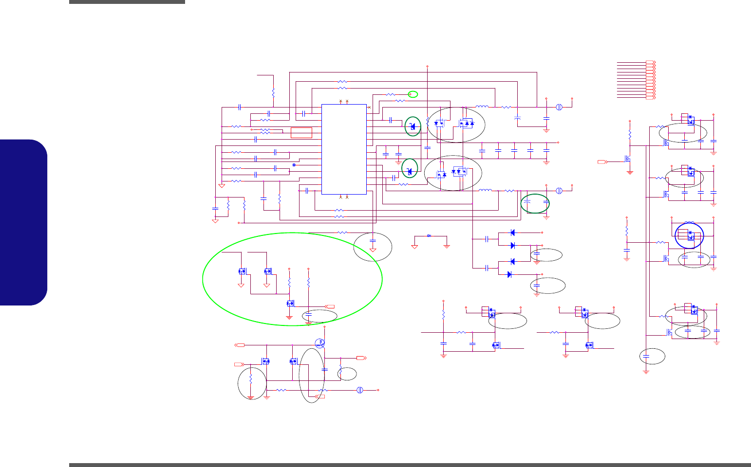
Schematic Diagrams
B - 26 VDD3, VDD5
B.Schematic Diagrams
VDD3, VDD5
Sheet 25 of 34
VDD3, VDD5
PC122
0.1U_10V_04
PR114 10_04
PC92
0.01U_06
3
2 4
1
5
6
PQ39
NTGS4141NT1G
PC44
0.1U_04
PC89 220P_04
1 2
PL4
4.7U_7*7*3.5
PR141
10m_25
SYS5V
VIN1
VDD5
VIN
SYS3V VDD3
SYS5V
SYS10V
SYS15V
SYS15V
3V VDD5
SYS5V
SYS5V
DD_ON19
5V
INTVCC2
VDD3
5VS
SYS15V
VDD5
F042795
3VS
1.5V
VDD3
1.5VS
VDD5
SGND4
SGND4 SGND4
INTVCC2
SGND4
TEST
DD_ON#
1.5V 7,29
F042795
F042795
6/22
G
DS
PQ53
2N7002W
6/22
RUN_SS1
VIN 20,25,27,28,29
VIN1 25
VDD3 3,13,19,22,25,27
3V 11,12,13,17,19,24,25,29,30
VDD5 19,22,23,29,30
5V 18,19,20,24,25,27,28
3VS 2,7,8, 9,10,11,12,13,14,15,16,19,20,22,23,24,28,30
5VS 12,14,16,18,19,20,23,24,30
3VH8 19,24,27,30
SGND4
Z2611 AC
PD14
SCS551V-30
AC PD16
SCS551V-30
R69
100K_04
F042795
DD_ON
F042795
F950503
F950503
F950503
F950503
Z2613
7
8
1
2
PQ29A
SP8K10SFD5TB
3A 5A3A 5A
3/13
3/13
F042795
F042795
4
3
5
6
PQ29B
SP8K1 0SFD5TB
Z2610
7
8
1
2
PQ30A
SP8K10SFD5TB
INTVCC2
PR162
10K_04
PR161
10K_04
+
PC125
150U_6.3V_V
INTVCC2
G
DS
PQ55
2N7002W
G
DS
PQ54
2N7002W
1.5VS 2,4,7,20,24
RUN_SS2
SGND4
RUN_SS2
F042695
950519
RUN/SS2
SUSB#
Z2638Z2633
2.5VS 2,3,11,12,13,20
PR128 0_06
Z2604
Z2622
Z2614
Z2616
DD_ON#
Z2617
Z2627
TEST 25, 28,29
Z2632
DD_ON#
Z2612
Z2601
Z2615
Z2602
1 2
PL5
4.7U_7*7*3. 5
Z2607
Z2623
RUN/SS2
Z2628
4
3
5
6
PQ30B
SP8K1 0SFD5TB
DD_ONH
Z2621
RUN/SS2
Z2609
Z2619RUN_SS1
Z2626
Z2618 Z2620
PR115 0_06 Z2625
Z2606
Z2608
5V
950310
C378
2.2UF _12_X7R
C950719
SUSB#12,19,20,25,29
DD_ON#25,29
DD_ONH 25
Z2630
3/7
EN_15V
PR124 *0_04
3/7
Z2631
EN_15V
PC77
2200P_50V_06
PL1
*HCB3216K-800T30
PR145
0_04
AC
PD9 SCS355V
PR143
100K_04
PR150
10K_04
THERMTRIP# 3
PC127
10U_10V_08
PR123 1M_04
PR126 0_04
PR119
*0_04
1 2
PJ6
OPEN_5A
5/15
PC19
0.1U_50V_06
PC93
0.01U_06
PC123
0.1U_10V_04
G
DS
PQ43
2N7002W
PR106 20K_1%_04
PR142
10m_25
PR130 20K_1%_04
PR135
10_04
PC109 0.01U_06
PC133
0.1U_10V_04
PC131
*.01U_04
PC134
*0.1U_06
PC107 0.1U_06
PC88
1U_10V_06
1 2
PJ7
OPEN_5A
PR73
0_04
PR144
0_04
PC82
10U_25V_12
PR129 105K_1%_04
G
DS
PQ37
2N7002W
PC129
10U_10V_08
PC47
0.1U_04
PC130
0.1U_04
PC79
*1000P_04
4
6 2
5
7 3
1
8PQ48
RSS090N03
PR116 15K_04
G
S D
PQ42
2N7002W
RUN/SS1
28
SENSE1+
30
SENSE1-
31
VOSENSE1
1
PLLFLTR
2
PLLIN
3
FCB
4
ITH1
5
SGND
6
SW2 15
BOOST2 17
TG2 14
PGND 19
INTVCC 20
EXTVCC 21
BG1 22
VIN 23
BOOST1 24
PGOOD 27
BG2 18
3.3VOUT
7
ITH2
8
VOSENSE2
9
SENSE2-
11
SENSE2+
12 RUN/SS2 13
SW1 25
TG1 26
NC 32
NC 29
NC
10
NC
16
PU5
LTC3728LXCUH
PC100
0.1U_06
PC99 0.01U _16V_ 04
G
S D
PQ13
2N7002W
Z2636
PR68
100K_04
Z2637
3
2 4
1
5
6
PQ38
NTGS4141NT1G
PC87
22n_06
Z2634
PC51
10U_10V_08
PC132
*.01U_04
C E
B
PQ10
DTA114EUA
PC97 220P_04
PC94 *30P_04
PC136
2200PF_04 G
DS
PQ44
2N7002W
G
S D
PQ45
2N7002W
PC96 *30P_04
PR146
1M_04
PR67 100K_04
Z2635
PR66 1M_04
PR147
1M_04
PR117 15K_04
EN_15VS
PC48
0.1U_10V_04
7/19
5A
PC128
0.1U_10V_04
7/19
7/19
PC84
10U_25V_12
Z2605
PC86 0.1U_06
PR113 10_04
PC98
0.01U_16V_04
G
S D
PQ12
2N7002W
PC137
0.1U_04
2.5VS2.5V
PR136
1M_04
PC139
10U_10V_08
PR149
0_04
PC42
0.1U_10V_04
PC108 *180P_04
Z2634
21 PJ4 JUMP
12
PJ3 2mm
PC138
0.1U_10V_04
PC105
1000P_04
G
S D
PQ46
2N7002W
PR131 10_04
3
2 4
1
5
6
PQ47
NTGS4141NT1G
A C
PD8 SCS355V
PC95
2200P_50V_06
0V:220KHz
5V:640KHz
+
PC126
150U_6.3V_V
3
2 4
1
5
6
PQ41
NTGS4141NT1G
PC85
10U_25V_12
A C
PD6 SCS355V
PR125 *0_04
Z2624
PR120
0_04
PC135
2200PF_04
5/11
PC29
4.7U_10V_08
G
DS
PQ11
2N7002W
PC83
10U _25V_12
PC90
1000P_04
PR132 10_04
AC
PD7 SCS355V
3A
3
2 4
1
5
6
PQ40
NTGS4141NT1G
PR111
63.4K_1%_04
PR65
4.7K_04
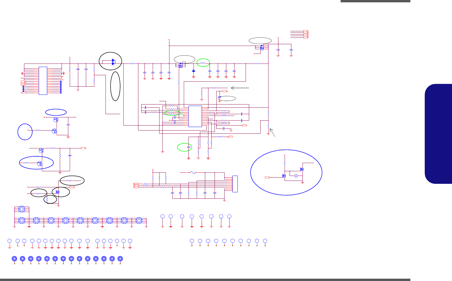
Schematic Diagrams
CHARGER, DC IN B - 27
B.Schematic Diagrams
CHARGER, DC IN
CHG_EN
PR109 0_06
H41
C256D107
LID_SW#
H42
C315D146 H43
C315D146
Z2734
H44
H5_5D2_7 H45
C256D107 H46
H5_5D2_7
# CHG_CUR :
V=1.25V=2.5A
Z2709
3S/4S_SEL H:16.8V ; L: 12.6V
# TOTAL_CUR :
V=0.020 X 20 X Ichg
Z2737
Z2738
ADJ C.V POINT
# CURSEN :
V=0.025 X 20 X Ichg
# BAT_SEL H: CHARGE BAT_A
PR107 10K_04
CTL
RINGO#
DTRO#
PR101 *1M_04
CTSO#
ACIN
TXD O
RTSO#
RXDO
# TOTAL POWER 60W
BATTERY MAX
CHARGE 2.50A
DSRO#
DCDO#
H8 X 2.5 =
Actually
current
G
DS
PQ23
*2N7002W
PC78
0.1U_10V_04
2
3
4
5 6
7
8
9
1
H16
MTH 8 _0D 2 _ 8
H22
H6_5D4_2
PC3 .22U_10V_06
PC4
0.1U_06
H5
C158D158
PR104
10K_04
H12
C158
G
DS
PQ4
2N7002W
PR85
*2.2M_06
H7
H6_0D2_3
PC65
30P_06
H13
C158
PC76
10U_25V_12
2
3
4
5 6
7
8
9
1
H17
MTH 8_0D2_8
PC12
10U _ 25V_12
H23
H6_5D4_2
PR91
10K_06
CE
B
PQ19
DTA114EUA
PR86
0_06
PC8 6800P_50V_06
PR96 25m_25
PR13 *0_06
H32
C79D79 H33
C158D158
PC73
.1U_50V_08
M4
M-MARK1
PR97
10K_06
H26
C158
PC66
30P_06
PR6
10K_1%_06
H14
C158
C388
0.1U_50V_06
M3
M-MAR K1
PR4
0_06
H15
C158
A C
PD 5
SM340A
M5
M- MAR K1
H27
C158
PC71
10U_25V_12
Low:12.6V
PR16 100_06
H25
C158
PR37
100K_04
H28
C158
M8
M-MARK1
H8
C79D79
2
3
4
5 6
7
8
9
1
H30
MTH8_0D2_8
PL2
10U_10*10*4
H24
C158
M12
M-MARK1
PR87
220K_1%_04
H20
H6_5D4_2
PC68
10U_25V_12
M1
M- MAR K1
PR7 10K_06
PC63
10U_25V_12
-IN C2 1
OUTC 2 2
+IN E2 3
-INE2 4
ACOK 5
VREF 6
ACIN 7
-INE1 8
+IN E1 9
OUTC1 10
OUTD/SEL 11
-IN C1 12
+IN C2
24
+IN C1
13
CTL
14
FB123
15
-INE3
16
RT
17
XACOK
18
VH
19
OUT
20
VCC
21
CS
22
GND
23
MB39A126
PU3
MB3 9A126
CE
BPQ24
DTC114EUA
PR12 100K_06
PR8 100K_06
PR2
10K_1%_06
PC 69
*10U_25V_12
M11
M-MAR K1
2
3
4
5 6
7
8
9
1
H31
MTH8_0D2_8
M10
M-MARK1
PR3 30K_06
2
3
4
5 6
7
8
9
1
H21
MTH8_0D2_8
PR17 100_06
PR14
*10K_06
2
3
4
5 6
7
8
9
1
H9
MTH8_0D2_8
H1
C158D158
PC59
10U_25V_12
CE
BPQ16
DTC114EUA
PC64
*10U_25V_12
1 2
3 4
5 6
7 8
910
11 12
13 14
15 16
17 18
19 20
21 22
23 24
25 26
27 28
29 30
31 32
JUSB1
CON32AF
PR84 0_06
PC 70
10U_25V_12
PR83
10K_04
2.5A
PR1 *0_06
PC60
.1U_50V_08
PR89 *100K_06
M2
M-MARK1
PR82
0_06
M14
M-MARK1
PR95 20m_25
PR88
20K_1%_04
M7
M-MAR K1
PR10 33K_06
PC67
10U_25V_12
M6
M- MAR K1
G
DS
PQ3
2N7002W
4
62 5
73
1
8
PQ17
SI4835BD Y -T1-E3
4
62 5
73
1
8
PQ18
SI4835BDY-T1-E3
PR5
30K_1%_06
1
2
3
4
5
6
7
8
9
JBATTA1
BAT CON
PR11 10K_06
H34
C158D 158
PR108
6.8K_1%_04
CE
B
PQ1
DTA114EUA
PR 98
10K_06
M9
M-MARK1
H11
C158
M13
M-MARK1
H2
C158D158
H18
C158
2
3
4
5 6
7
8
9
1
H10
MTH8_0D2_8
PR93
0_06
H4
C158D158 H37
C158D158
2
3
4
5 6
7
8
9
1
H29
MTH 8_0D2_8
PR103
30K_1%_04
H19
H6_5D 4_2
PC6
2200P_50V_06
H6
C158D158
PC7 6800P_50V_06
Z2735
PR94
0_06
2
3
4
5 6
7
8
9
1
H35
MTH8_0D2_8
12 PJ1
2mm
H38
C158D 158
PC5
.1U_50V_06
H3
C158D158
PC61
.01U_50V_06
PR90
10K_08
2
3
4
5 6
7
8
9
1
H36
MTH8_0D2_8
PF1
7A
PR92 100_06
PC2
1nF_10V_06
PC62 22P_50V_06
PC1 .01U_50V_06
PR15 0_06
PR9
28K_1%_06
PC72
10U_25V_12
VDD3
VIN
VB
VIN ACOK
PR102
*200K_04
SYS5V
VIN
5V
VB
SYS5V
5V
3VH8
SYS5V
VA
Hi:16.8V
CHG_CUR 19
CHG_EN19
TOTAL_CUR 19
3VH8 19,24,30
CHG_CURSEN 19
5V 18,19,20,24,25,26,28
VDD3 3,13,19,22, 25,26
USB_OC2#11
VIN 20,25,26,28, 29
SMC_BAT119 SMD_BAT119
USB_PP211
VA 25
USB_PN211
CUR_CONT
LID_SW#19,20
BAT1_DET19VDD3
VA
3/13
Z2729VB
Z2732
ACIN
3/13
AC_IN #
Z2731
3/13
ACOK
H8 X 2 =
Actually
current
Z2736
Z2718
Z2739
TPA 0P
TPA 0N TP B0P
TPB 0N
USB_PN2
USB_PP2
USB_OC2#
BAT1_VOLT
VA
Z2707
Z2706
Z2722
Z2708
BAT1_VOLT 19
3/17
3/17
DEL
Z2715
3/17
3/17 3/17
Z2703
3/17
Z2741
Z2702
Z2723
A1
A2
C
PD3
SBM1040
AC_IN# 19
Z2705
Z2733
Z2721
Z2711
Z2704
Z2712
Z2713Z2714
VREF
F042795
Z2710
VREF
Z2740
Z2716
CTL Z2717
Z2730
6/22
H39
H7_7D4_5
CUR_CONT
5/11
5/11
5/11
H40
H6_0D3_7
F042795
Sheet 26 of 34
CHARGER, DC IN
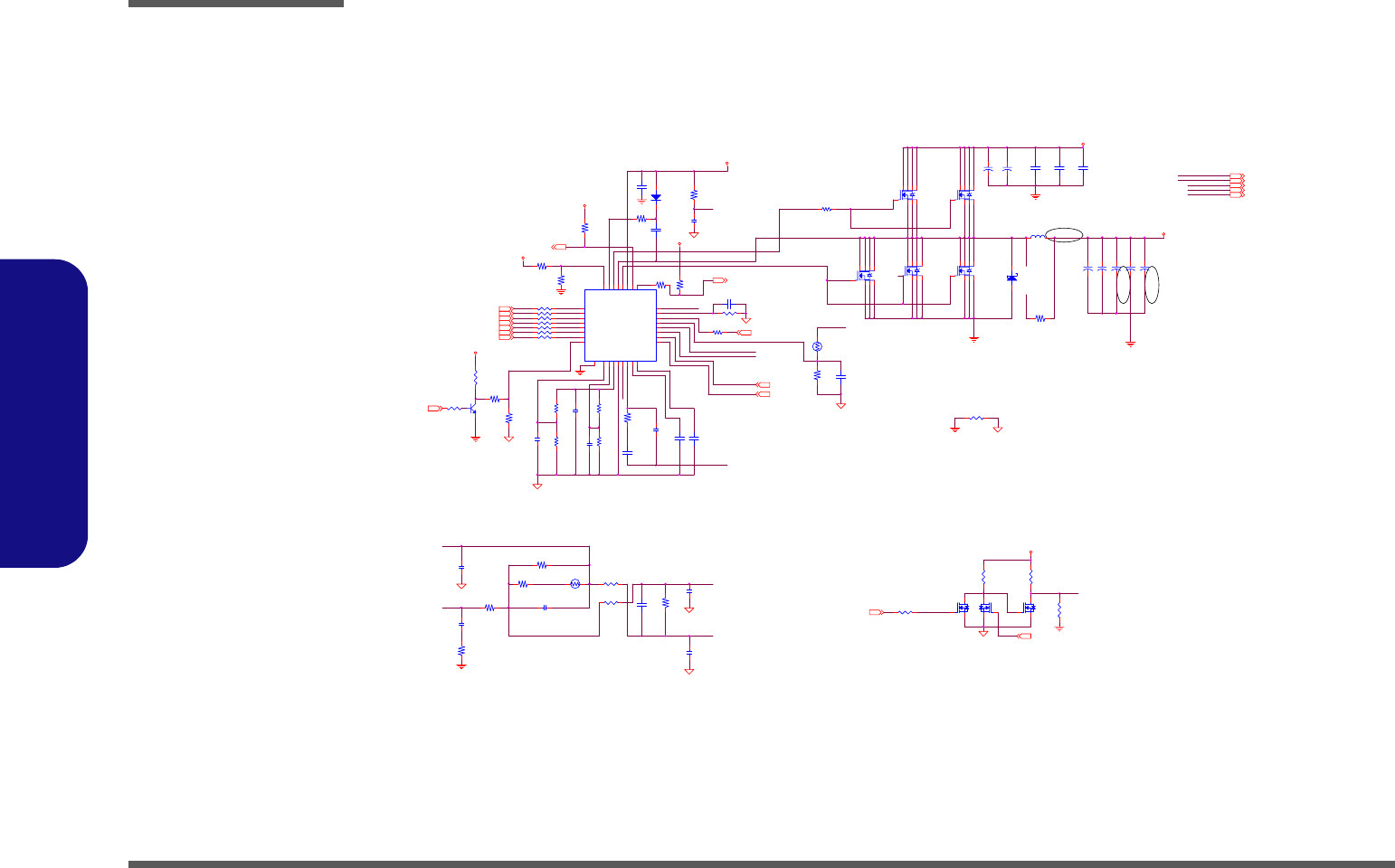
Schematic Diagrams
B - 28 VCORE
B.Schematic Diagrams
VCORE
1 2
PR174 0_06
PR160 1K_04
VCORE 3,4
7/24
7/24
5V 18,19,20,24,25,26,27
1. 05V S 3, 4,5 ,1 3,2 9
VIN 20,25,26,27,29
3VS 2,7,8,9,10,11,12,13,14,15,16,19,20,22,23,24,26,30
+
PC174
*15u/25V_D
PR 33 0_04
PR 34 0_04
PR 38 0_04
PR 40 0_04
PR 42 0_04
PR 45 0_04
7/24
SGND 3
SGND3
SGND3
SGND 3
1
2
PC172
*3.3n/50V_08
SGND 3
SGND 3
SGND3
R564
10K_06
1.05VS
B
E C
Q34
3904
SGND 3
DRN PR183
100_ 04
1
2
PR184
12.4K_1%_06
DRP_L1
1 2
PC171 33n/50V_06
PR182
100_ 04
1
2
PC173
* 100p/ 50 V_06
CS-
12
RTH2
100K
1
2
PC169
* 100p/ 50 V_06
CS1N
1 2
PR180
*0_06
1 2
PR185
27.4K_1%_06
1 2
PR181
28K_1%_06
1
2
PC168
*100p/50V_06
1
2
PC1 70
*68p/50V_06
CS+
PR 32 0_04
PR43 0_06
H_VID04
H_VID64
H_VID24
H_VID44H_VID54
H_VID14
H_VID34
SGND3
1
2
PR186
*0_06
Z2839 EN_VCORE
VR_ON
PWRGD_VCORE 11
PR64 0_04
PR53
10K_04 PR49
10K_04
G
DS
PQ8
2N7002W
G
DS
PQ5
2N7002W
G
DS
PQ7
2N7002W
1
2
PC161
1000p/ 50V_06
EN_VCOR E
4
62 73 8
5
1
PQ34
IR F7831TRPB F
VCCA
VIN
CS1N
PR50
*10K_04
SS
1
2
PC1 62
*100P_06
1 2
PR165 0_06
4
62 73 8
5
1
PQ26
I RF 782 1TRPB F
VCORE_ON19
1 2
PR173
0_06
TG
PR1 76
130K_1%_06
3VS
HYS
CS-
CLKEN#
1
2
PR167
680_06
5V
SGND 3
CS+
BG
1
2
PR178
887_1%_06
TEST 25,26,29
DRN
+
PC124
470u_2.5V_D
1
2
PC163
1000 p/ 50V_06
VCC A
VSSSENSE 4
1 2
PR166
0_06
RP15
100K _06
25A
DAC
VCCSENSE 4
PR179
130K_1%_06
+
PC102
15u/25V_D
+
PC45
470u_2.5V_D
1
2
PC1 65
*100p/50V_06
VREF
PM_DPRSLPVR3,13
TTR I P
1 2
PC159 1000p/50V_06
VSSS ENSE
SS
12
PR27
0_04
VREFVREF
CLKEN#2
DRN
12
RTH1
*100K
5V
PM_DPRSLPVR 3,13
1
2
PC164
10n/50V_06
4
62 73 8
5
1
PQ33
IRF7831TRPBF
1
2
PC160
*10p/50V_06
3VS
1 2
PR168
*10K_06
CLSET
VCCSENSE
1
2
PR169
*0_06
1
2
PR1 71
1K_0 4
VRE F
1
2
PR164
10_06
3VS
A C
PD15
SM340A
VID6
1
VID5
2
VID4
3
VID3
4
VID2
5
VID1
6
VID0
7
DPRSTP#
8
HYS
9
CLSET
10
VREF
11
DAC
15
SS
16
FB- 17
FB+ 18
CS- 19
CS+ 20
TTRIP 21
DPRSL 22
RAMP 23
EN 24
PWRGD 25
CLKEN# 26
V5 27
BG 28
DRN 29
TG 30
BST 31
VRTT # 32
ERROUT
14 VCCA
13 AGND
12
GND
33
PU1
SC454
+
PC121
*470u_2.5V_D
PR17210K_06
1
2
PC166
100p/5 0V_0 6
VCC A
1
2
PR31
*0_04
AC
PD4
SCS5 51V
1
2
PC18
10u/25V_12
1
2
PC1 7
10u/25V_12
PR177
130K _1%_06
4
62 73 8
5
1
PQ32
IRF7831TRPBF
1
2
PC155
1u/10V_06
PL6 0.6uH 13*13*4
+
PC157
470u_2.5V_D
4
62 73 8
5
1
PQ27
IRF7821TRPBF
1
2
PR175
0_06
1
2
PC75
1u/10V_06
BST
1
2
PC167
1800p/50V_06
VCORE
1
2
PC156
1u/10V_ 06
12
PR1 70
0_06
1
2
PC16
10u/25V_12
E_OUT
DRN
+
PC43
470u_2.5V_D
Sheet 27 of 34
VCORE
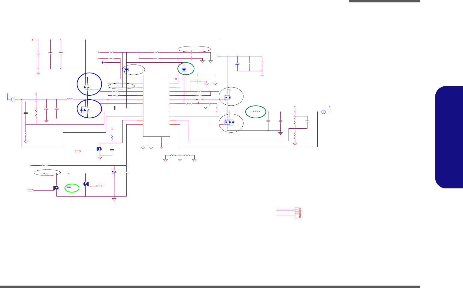
Schematic Diagrams
1.05VS, 1.5V B - 29
B.Schematic Diagrams
1.05VS, 1.5V
Sheet 28 of 34
1.05VS, 1.5V
6/22
AC
PD2
SCS551V-30
AC
PD18
SCS551V-30
G
DS
PQ15
2N7002W
4
3
5
6
PQ51B
SP8K10SFD5TB
Z2916 Z 2920
PR71 0_06
VIN
Z2902
PR157 0_06
Z2911
3V 11,12,13,17,19,24,25,26, 30
5/11
PC49
0.1U_06
Z2923
Z2921
6/22
2A
1.5V 7,26
2.5A
4
3
5
6
PQ52B
SP8K10SFD5TB
Z2918
G
DS
PQ14
2N7002W
PC151
10U_25V_12
PC58
0.1U_50V_06
1 2
PJ8
OPEN_3A
PC57
10U_25V_12
PR155 10K_1%_04
PR78 10K_1%_04
PR72 1M_04
1 2
PL8
2.5U_7*7*3.5
PR159
20K_1%_04
PC46 1U_10V_06
1 2
PJ9
OPEN_3A
PR81 0_06
PR69 10K_04
PR153
10K_1%_04
G
DS
PQ50
2N7002W
PC147 0.1U_06
PR74 10_04
PC144
0.1U_10V_04
PC154
0.1U_50V_06
PC143 1000P_04
PC148 1U_16V_06
PC54
10U_25V_12
PC149
100P_50V_04
PC53 0.1U_06
G
DS
PQ49
2N7002W
PR80
10K_1%_04
PGND1
1
DL1
2
VDDP1
3
ILIM1
4
LX1
5
DH1
6
BST1
7
EN/PSV2
8
TON 2 9
VOUT2 10
VCCA2 11
FBK2 12
PGOOD2 13
AGND2
14
PGND2
15
DL2 16
VDDP2
17
ILIM2 18
LX2 19
DH2 20
BST2 21
EN/PSV1
22
TON 1 23
VOUT1
24
VCCA1 25
FBK1
26
PGOOD1
27
AGND1
28
SC1485
PU7
PR156 0_04
PL7
1.5U_7*7*3. 5
PC153
10U_25V_12
PC145 1000P_04
PR77 47K_04
PR154 10K_04
Z2901
PR75
10K_04
PR79 10_04
Z2917
PR158
0_06
PR152
0_06
PC142
100P_50V_04
Z2905
PC50 1U_10V_06
7
8
1
2
PQ52A
SP8K10SFD5TB
PC52
0.1U_10V_04
PR76 750K_04
PR70
11K_1%_04
PC146 1U_16V_06
SUSB#12, 20,25,26
Z2908
DD_ON#25,26
SGND2
V1.051.05VS
VDD5
3V
SYS5V
SYS5V
Z2914
V1.5 1.5V
SGND1 SGND2
SGND2SGND1
SGND2
SGND2
SGND2SGND1
SGND1
SGND1
SGND1
Z2907
Z2909
VIN 20,25, 26,27,28
VCCPGD
DD_ON#
Z2922
Z2903
Z2904
Z2910
Z2919
VDD5 19,22,23,26,30
TEST 25,26,28
SUSB#
3/7
3/7 3/7
Z2906
F950503
7/19
Z2915
Z2913
Z2912
+
PC56
*150U_4V_B
+
PC55
150U_4V_B
1.05VS 3,4,5,13,28
F042795
F042795
F042795
F042795
+
PC152
*150U_4V_B
+
PC150
150U_4V_B
F042795
7
8
1
2
PQ51A
SP8K10SFD 5TB
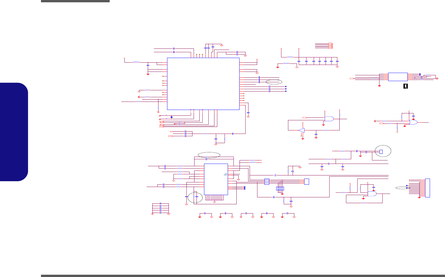
Schematic Diagrams
B - 30 AUDIO VT1613
B.Schematic Diagrams
AUDIO VT1613
C330
0.1U F_0 4
C334
2.2UF/16V_08
1
2
3
45
6
7
8
L13
FC A3216KF 4-121
MDC
2
R279
4.7K_04
TJMDC3
1
2
3
45
6
7
8
CP5
8P4CX180PF
1
11
MUTE
C329
0.1UF _04
12
LO-
C384 0. 1UF_04
AUD_AGND
Z3026
R295
*7.5K_04
ACZ_SDATAOUT
C345
6PF_ 04
AUD_AGND
R305
100K_04
AUD_AGND
C332
0.1UF _04
24
53
1
U16
MCH 74VHC 1G14DF T2G
Z3033
Z3034
C340 6PF_04
SPKOUTR
C386 0. 1UF_04
SEL
1 2
+
C326 47uF/6.3V_D
5VS 12, 14, 16,18 ,19, 20, 23,2 4,26
3VS 2,7,8,9,10,11,12,13,14,15,16,19,20,22,23,24,26,28
R311 0
3V 11,12, 13,17,1 9,24,25, 26,29
AUD_AGND
Z3014
C347
10UF/ 10V_12
C508
0.1U F_0 4
C518
0.1U F_04
PLEASE PLACE CLOSE CODEC &
AMP THE POWER I NPUT PINS
C335
10UF /1 0V_12
C336
0. 1UF_04
C507
0.1UF_04
LOUT_R
C517
0.1UF _04
1 2
L19
HCB 3216KF-800 T30
1 2
L17
HCB 3216KF -800T3 0
AUD_AGND
AUD_AGND
MDC MODEM
AUD_VDD5VS
R331
10.2K_04
Z303 0
Z3024
Z3023
SPKL1
C321
330PF_04
C322
*10uF/10V_12
R343 0
SPDIF O
1 2
+
C319 47uF/6.3V_D
ACZ_BITCLK
C506 1 UF_ 04
Z302 8
Z3008
C385
0.1UF_04
C318 1UF_04
SEL
21 S1 SHORT
AUD_AGND
AUD_AGND
C498 3 30PF_ 04
SPDIFO
AC_SPKR12
LOU T_L
Z3025
3VS
AUD_AGND
C358 1UF
C357 1UF
MIC 1 -L
C359 1UF
R536 10.2K_04
C376 0. 1UF_04
Z3035
RVdd 18
RLINEI N
21
LVdd 7
ROUT+ 22
RHPIN
20 ROUT- 15
RBYPASS
19
LOU T+ 3
LOUT- 10
MUTE IN
11 SE/BTL 14
GND/ HS
1
HP/LINE 16
MU TE OU T
9
SHUTDOWN
8
LBYPASS
6
LHPIN
5
LLIN EIN
4TJ 2
NC 17
NC 23
GND/HS
12 GND/HS
13 GND / HS
24
THREM/GND
25
THREM/ GND
26
THREM/GND
27
THREM/ GND
28
THREM/GND
29
THREM/GND
30
THREM/ GND
31
THREM/GND
32
THREM/GND
33
U15 APA2020ARL
C324
680PF _04
Z303 1
C360
1UF
R539 0
CT1 10U F/ 10V_08
PLEASE PLACE CLOSE CODEC &
AMP THE POWER INPUT PINS
Z3038
C337 *1UF_04
R313 * 2M_04
2
14
3
5
U11
*TC7SZ08
C370
0.1UF _04
3VS
RO-
1110
3VS
C353
2200PF _04
R535 1 0K_04
3VH8
AUD_AGND
KBC_BEEP
AUD_VD D
Z3037
R291 *7.5K_04
R338
10K_04
C346 1UF_04
AUD_AG ND
R293 2. 2K_04
SPKL2
C516 22PF
R332 10K_04
3V
LIN E1-L
MIC
SPD_I FO
SPKOUTL
HPSEL
LIN E1-R
SSurr-R
INTMICSEL
AUD_AGND
SPKOUTR
FRONT-R
FRONT-L
3VS
AUD_AGND
MIC 1 _VR E F O_L
MIC 1- L
AUD_AGND
R312
*10K _04
VDD5
R307
1K_04
C371 0.1u /16V_04
AUD_AGND
ASD_IN0
EAPD_MUTE
C338 *1UF _04
C950718
TC2 0.1 UF/10V_0 4
GND
1
Azalia_SDO
3
GND
5
Azalia_SYNC
7
Azalia_SDI
9
Azalia_RST#
11 Azal ia_ BC LK 12
GND 10
GND 8
3.3V Main/aux 6
RESERVED 4
RESERVED 2
JMDC1
AMP/CON12
1 2L24 FCB1608KF-121T25
Z3005
C377
270p/50V_04
AUD_AGND
R337 10K_04
C375
270p/50V_04
R334
2.7K_04
Z3013BEEP
Z3006
C348
100PF /50V _04
PCMSPK15
Z3012 C366 1U F
AUD_AGND
INTMICSEL
Z3002
Z3003
C379
*1u
Z3011
AUD_AGND
MIC1-L
1109
Z3004
C356 1UF
C355 1UF LINE1-R
LINE1-L
MI C
LOUT_R
LOUT_L
2
14
3
5
U17
74AHC1G08GW
Z3001
1108
1107
ACZ_SDATAIN112
INCD_R
SPDIF _O
HPSEL
Z3007
SPD_IFO
R21 * 220_04
3VH8 19, 24,27
M950704
M950704
LIN E_L
LIN E_R
C350 1UF
XTL_I N / MCLK
2
XTL_OUT / NC
3
SDATA_OUT
5
BI T_CLK / SCLK
6
SDATA_I N
8
SYNC / LRCLK
10
RESET#
11
PC_BEEP / N C 12
PHONE / N C 13
AUX_L 14
AUX_R 15
NC6 16
NC5 17
CD_L 18
CD_GND 19
CD_R 20
MIC1 21
MIC2 / NC 22
LINE_IN_L 23
LIN E_IN_R 24
AGND2 42
AGND1 26
AVCC2 38
AVCC1 25
VMID 27
VREFOUT1 28
AFI LT1 29
AFI LT2 30
NC8 31
NC7 32
NC / I 2SEN 33
VAUX / NC 34
LIN E_OUT_L 35
LIN E_OUT_R 36
DVCC1
1
DVCC2
9
DGND1
4
DGND2
7
NC1
37
HP_OUT_L / NC
39
NC2
40
HP_OUT_R / NC
41
NC3
43
NC4
44
GPIO0 / SDATA_OUT1
45
XTL_SEL / SDA
46
EAPD / SPDIF_IN / SCL
47
SPDIF_OUT
48
U20
VT1613
C367 1UF
C362 1UF
1
1
2
2
3
3
4
4
JSPK1
CON4_SPK
1
2
3
4
5
6
7
8
9
10
11
12
13
14
15
JAUDIO1
CON15
AUD_AGND
C333 1UF
C343 1UF
C950720
C95071 9
LO+
VDD5 19, 22,23, 26,29
Z3032
SPKR1
C519
0.1u /16V_04
CODEC_XIN
ACZ_SY NC12
ACZ_SDATAIN012
ACZ_RST#12
ACZ_SDATAOUT12
AUD_VDD
ACZ_ BITCLK12
R544 *10K_04
CODEC_XOUT
Z3010
Z3009
H8_BEEP
AUD_AGND
ABITCLK
C320 1UF
Z3036
R538 22
5VS
Z302 9
Z3027
AUD_AGND
AUD_AGND
R344 *0_04
Z3019
ACZ_SY NC
ACZ_SDATAIN1
R335 1 M_04
R540 22
C383 15PF
C380 15PF
1 2
X3
24.5 76MHZ
R314 0 _04
Z3015
C387 0.1UF_0 4
Z3016
1
12
2
JINTMIC1
ACES/C ON2
INCD_L
C308
0. 1UF _04
VOL_MUTE19
INCD_GND
EAPD_MUTE 2
14
3
5
U13
SN74AHC1G32DCKR
H8_BEEP
SPKOUTL
MUTE
R318
10K_04
C331
0.1U F_0 4
R330 0_04
R297
1K_04
R315 *0_04
R286 0_04
3V
Z3020
KBC_BEEP19
R326
10K_04
3VH8
R317 * 0_04
R328 * 10K_04
Z3021
Z3022
1 2L18
*HC B3216K-800T30
RO+
ACZ_RST# R266 0
C315
0.1 UF_ 04
3V
AUD_VDD
R304
100K_0 4
SPKR2
C328
680PF_04
Z3018
R329 *10K_04
MIC 1_V R EF O_L
AUD_VDD
Z3017
Sheet 29 of 34
AUDIO VT1613
Schematic Diagrams
PWR HOT BOARD B - 31
B.Schematic Diagrams
PWR HOT BOARD
1
2
3
4
5
6
PPJHOTKEY1
CON6A_HOTKEY
PPGND PPGNDPPGND PPGND
314 2
PPSW2
HCH STS-05
314 2
PPSW3
HCH STS-05
314 2
PPSW4
HCH STS-05
PPGND
PPGNDPPGND
PPWEB3#
PPM_BTN#
PPWEB4#
PPWEB5#
314 2
PPSW1
HCH STS-05
PPR1
221
AC
PPD1
LED_1206
PP+5VS
PP+5VS
PPGND
PWR LED
PIN5,6=PPGND
PIN5,6=PPGNDPIN5,6=PPGND
PIN5,6=PPGND
M950704
Z3101
PPGND
PPH1
C67D67 PPH6
C237D91
PPH5
C67D67 PPH4
C237D91 PPH2
C237D91
PPH3
C237D91
PPWEB5#
PPWEB3#
PPWEB4#
PPGND
PPM_BTN#
Sheet 30 of 34
PWR HOT BOARD
Schematic Diagrams
B - 32 HOTKEY LT BOARD
B.Schematic Diagrams
HOTKEY LT BOARD
HWEB2#
HWEB2# HWEB0# HWEB1#
HH4
C237D91
HH2
C67D67 HH3
C237D91
HH1
C67D67 HH5
C237D91
HGNDHGNDHGND
HWEB0#
HWEB1#
HWEB1#-->WEB2-->APPLICATION
HWEB2#-->WEB1-->E-MAIL
HWEB0#-->WEB0-->WWW
1
2
3
4
5
6
HJHOTKEY1
CON6A
314 2
HSW1
HCH STS-05
HGND
APE-MAIL WWW
PIN5,6=HGND PIN5,6=HGNDPIN5,6=HGND
314 2
HSW2
HCH STS-05
314 2
HSW3
HCH STS-05
HGNDHGND
HGND
Sheet 31 of 34
HOTKEY LT
BOARD
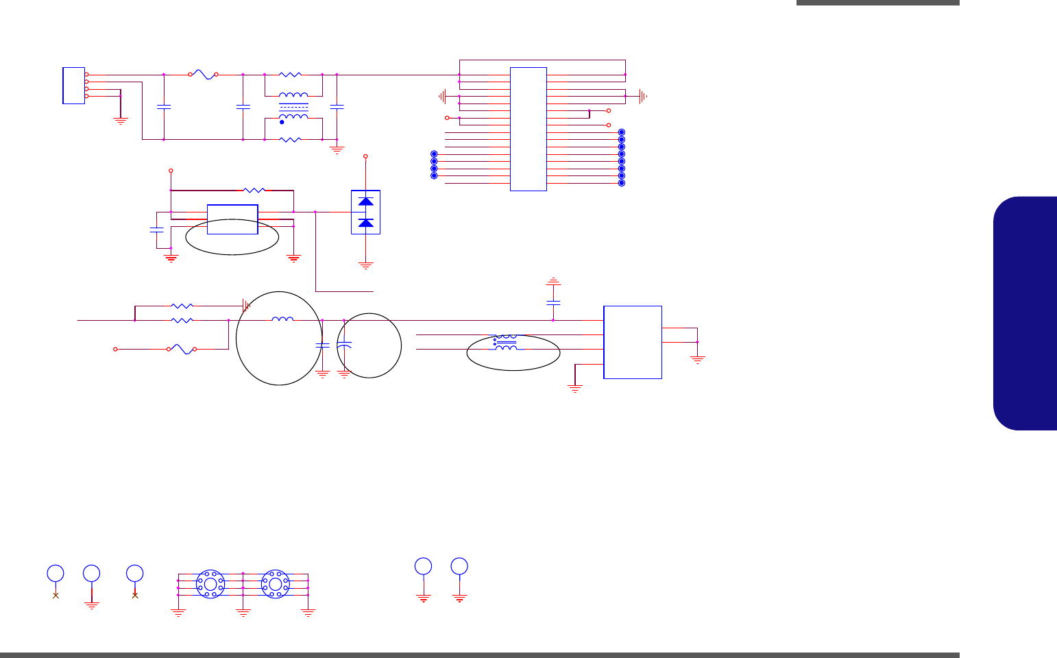
Schematic Diagrams
USB BOARD B - 33
B.Schematic Diagrams
USB BOARD
7343->3528
C950724 F042895
PIN GND3~4 =UGND
UUSB_OC2# Z3804
Z3802
Z3801UVA+ UVA++
UGND
UGND
UGND
UGND
UGND
UR3 *2.7K
32
1 4
UPL1
*EMI_CHOKE
UL2
HCB1608KF-121T25
950525? ?
VCC
1
DATA-
2
DATA+
3
GND
4
SGND1
SGND2
UJUSB1
USB_1
UPR2 0(1206)
UR1 470K
UR2 560K UC2
0.1UF
UPC1
0.1UF/50V_0805
UPC3
0.1UF/50V_0805
1 2
UF1 1.1A
1 2
3 4
5 6
7 8
910
11 12
13 14
15 16
17 18
19 20
21 22
23 24
25 26
27 28
29 30
31 32
UJUSB2
CON32A
C
AC
A
UD1
*BAV99
1
4
2
3UL3
PLW3216S161Q2
UC3
0.1UF
11
22
3GND1
4GND2
UJAC1
ACIN_CON
UC4
0.01UF
UPF1
5A
+
UC1
100U_6.3V_B
UPC2
0.1UF/50V_0805
VS
1
GND
2
Q3
GND 4
PRG
6
GND 5
UU1
TLE4917DS
U+5V
UPR1 0(1206)
U+5V
U+3VH8
U+3VH8
U+3VH8
U+5V
UTPB0P
UTPB0N
URXD
UTXD
URTS#
UCTS#
UTPA0N
UTPA0P
ULID_RSUM#
URING#
UDTR#
UUSB_PP2
UUSB_PN2
UH2
C237D91
UH1
C79D79
2
3
4
5 6
7
8
9
1
UH4
MTH8_0D2_8
ULID_RSUM#
LID SWITCH
UGNDUGNDUGND
UGND
UGND
UGND
UGND UGND
UH3
C79D79
UGND
UGND
Z3803
UUSB_PP2
UUSB_PN2
UUSB_OC2#
2
3
4
5 6
7
8
9
1
UH5
MTH8_0D2_8
UGND
Z3806
UDCD#
UDSR#
Z3805
F042895
UH6
H6_0D2_3 UH7
H6_0D2_3
UGND UGND
Sheet 32 of 34
USB BOARD
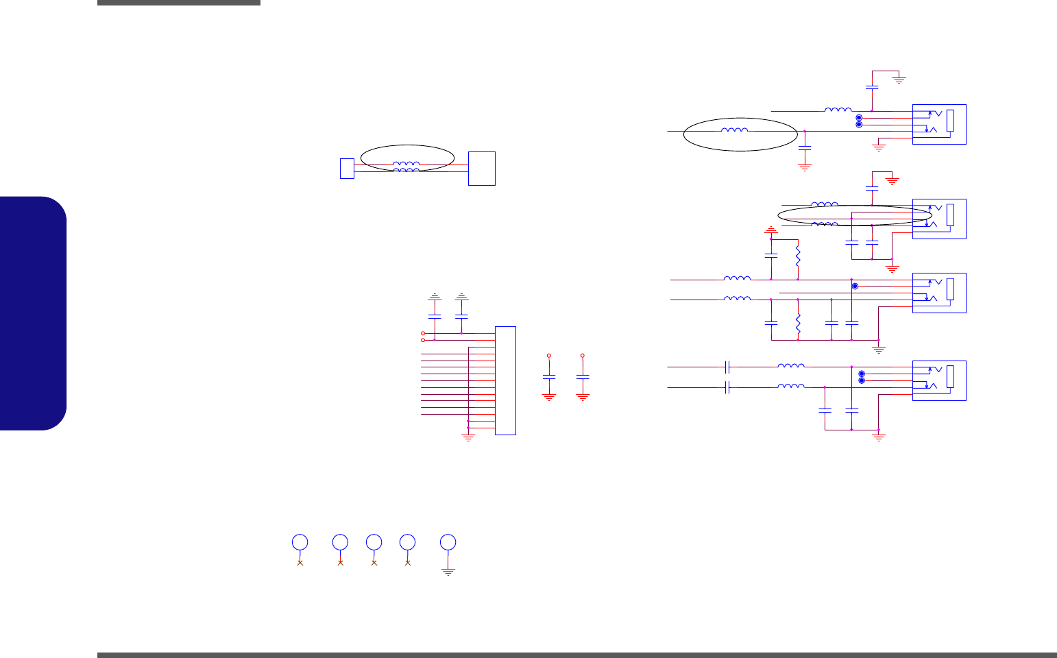
Schematic Diagrams
B - 34 AUDIO & MODEM BOARD
B.Schematic Diagrams
AUDIO & MODEM BOARD
ASPD_IFO
Z3413ASPKOUTL
ASPDIF
AC16
0.1UF
A+3V
AGND
AC17
0.1UF
AGND
A+3V
ALINE1-L
ALINE1-R
ASPKOUTR
Z3414
Z3417
AGND
AGND
AGND
AGND
Z3406
Z3407
AGND
AGND
AGND
AGND
F070395
AGND
PIN GND1=AGND
Z3401
Z3402 Z3404
Z3403
Mic In
/Cen/LEF Out
SPK OUT
/Front Out
Line In
/REAL
Surround Out
SPDIF OUT
/Side Surronnd
OUT
AMIC
ALINE1-L
ASSURR-R
ALINE1-R
ALFE
AINTMICSEL AC13 1UF
AC8
2200P
1 2
AL3 HCB1608KF-121T25
ASPKOUTR
ASPKOUTL
AHPSEL
ASPD_IFO
3
3
5
5
4
4
2
2
1
1
AJSPKOUT1
AUDIO JACK_SPKOUT
11
22
AJMODEM1
85204-2
AC1
680PF
AC4
330PF
AC11 1UF
1 2
AL5
HCB1608KF-121T25
AC14
0.1UF
3
3
5
5
4
4
2
2
1
1
AJSPDIF1
AUDIO JACK_SPDIF
1 2
AL4 HCB1608KF-121T25
AL10
HK2125 R10J-T
AC5
1000PF
AL9
HK2125 R10J-T
AC6
2200P
1 2
AL1
HCB1608KF-121T25
AC7
0.1UF
AC9
680PF
1 2
AL2
FCM1608K-121T06
1
2
3
4
5
6
7
8
9
10
11
12
13
14
15
AJAUDIO1
CON15_R
AC3
680PF
3
3
5
5
4
4
2
2
1
1
AJMIC1
AUDIO JACK_MIC
AL7 HCB1608KF-121T25
AC10
2200P
AC12
2200P
AC2
1000PF
1 2
AL6
HCB1608KF-121T25
AC15
0.1UF AR2
1K
AL8 HCB1608KF-121T25
3
3
5
5
4
4
2
2
1
1
AJLINE1
AUDIO JACK_LINEIN
TIP
1
RING
2
AHMDCC1
PJS
AR1
1K
AGND
A+3VS
A+3V
ASSURR-R
AH3
C256D256 AH2
C111D111
AMIC
AH1
C79D79
AH5
C79D79 AH4
C315D110
AGND
Z3418
Z3419
F042895
Z3412
AHPSEL
Z3411
ALFE
AINTMICSEL
Z3408
Z3410
Z3415
Z3416
AGND
950510
Z3405
Sheet 33 of 34
AUDIO & MODEM
BOARD
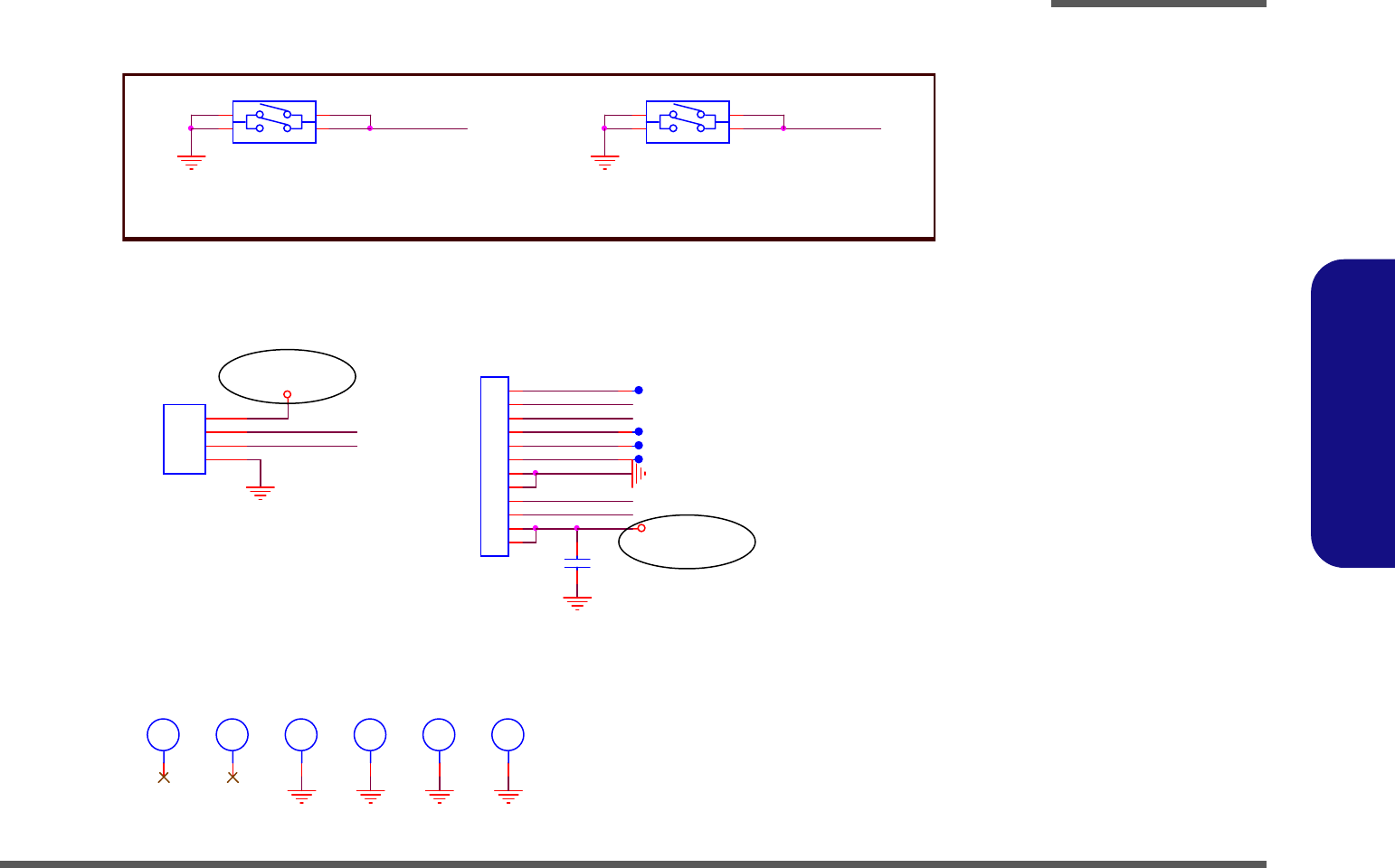
Schematic Diagrams
CLICK BOARD B - 35
B.Schematic Diagrams
CLICK BOARD
TPBUTTON_L
Z3502
TPBUTTON_R
Z3504
TTP_DATA
TTP_CLK
Z3503
Z3501
TH3
C237D91 TH1
C237D91 TH 4
C237D91
TH5
C67D67
TH2
C67D67
TGNDTGND
TH6
C237D91
TGND TGND
TPBUTTON_R
TTP_DATA
TTP_CLK
11
22
33
44
TJTP2
CON4
TC1
0.1UF_04
1
2
3
4
5
6
7
8
9
10
11
12
TJTP1
87151-1207G
314 2
TSW 2
HCH STS-05
TGN D TGN D
T+5V
TGND
TGND
T+5V
TGND
PIN5,6=TGND PIN5,6=TGND
C950719
TPBUTTON_L 314 2
TSW 1
HCH STS-05
C950720
Sheet 34 of 34
CLICK BOARD

Schematic Diagrams
B - 36
B.Schematic Diagrams