Clevo M710L Service Manual. Www.s Manuals.com. Manual
User Manual: Notebook Clevo M710L - Service manuals and Schematics, Disassembly / Assembly. Free.
Open the PDF directly: View PDF ![]() .
.
Page Count: 83
- Manual
- Preface
- Introduction 1-1
- Disassembly 2-1
- Chapter 1: Introduction
- Overview
- System Specifications
- External Locator - Top View with LCD Panel Open
- External Locator - Front & Rear Views
- External Locator - Left & Right Side Views
- External Locator - Bottom View
- Mainboard Overview - Top (Key Parts)
- Mainboard Overview - Bottom (Key Parts)
- Mainboard Overview - Top (Connectors)
- Mainboard Overview - Bottom (Connectors)
- Chapter 2: Disassembly
- Overview
- Maintenance Tools
- Connections
- Maintenance Precautions
- Removing the Battery
- Removing the Hard Disk Drive
- Removing the System Memory (RAM)
- Removing the Heat Sink
- Removing the Wireless LAN Module
- Removing the Bluetooth Module
- Removing the Optical (CD/DVD) Device
- Removing the Keyboard
- Removing the Modem Module
- Appendix A: Part Lists
- Appendix B: Schematic Diagrams
- SYSTEM BLOCK DIAGRAM
- Diamondville SC 1/2
- Diamondville SC 2/2
- 945GSE 1/5, HOST
- 945GSE 2/5
- 945GSE 3/5, DDR
- 945GSE 4/5
- 945GSE 5/5
- DDRII SO-DIMM 0
- DDRII SO- DIMM 1
- PANEL, INVERTER, CRT
- CLOCK GENERATOR
- CH7-M 1/4, SATA
- ICH7-M 2/4, PCI, USB, SPI
- ICH7-M 3/4
- ICH7-M 4/4
- MULTI I/O, ODD, CCD BT
- NEW CARD, USB
- CARD READER JMB385
- LED, FAN, PC BEEP, TP, FP
- PCI-E LAN RTL8102E
- AUDIO CODEC ALC269 QFN
- KBC-ITE IT8502E
- 3VS, 5VS
- VDD3, VDD5
- POWER 1.8V/ 0.9V
- POWER 1.5VS/ 1.05VS
- VCORE
- AC IN, CHARGE
- CLICK BOARD
- Multi B’d, LID, LED, SW, USB
- Multi B’d, Mini Card, MDC, RJ11


Preface
I
Preface
Notebook Computer
M710L
Service Manual

Preface
II
Preface
Notice
The company reserves the right to revise this publication or to change its contents without notice. Information contained
herein is for reference only and does not constitute a commitment on the part of the manufacturer or any subsequent ven-
dor. They assume no responsibility or liability for any errors or inaccuracies that may appear in this publication nor are
they in anyway responsible for any loss or damage resulting from the use (or misuse) of this publication.
This publication and any accompanying software may not, in whole or in part, be reproduced, translated, transmitted or
reduced to any machine readable form without prior consent from the vendor, manufacturer or creators of this publica-
tion, except for copies kept by the user for backup purposes.
Brand and product names mentioned in this publication may or may not be copyrights and/or registered trademarks of
their respective companies. They are mentioned for identification purposes only and are not intended as an endorsement
of that product or its manufacturer.
Version 1.0
October 2008
Trademarks
Intel and Atom are trademarks/registered trademarks of Intel Corporation.
Windows® is a registered trademark of Microsoft Corporation.
Other brand and product names are trademarks and./or registered trademarks of their respective companies.

Preface
III
Preface
About this Manual
This manual is intended for service personnel who have completed sufficient training to undertake the maintenance and
inspection of personal computers.
It is organized to allow you to look up basic information for servicing and/or upgrading components of the M710L series
notebook PC.
The following information is included:
Chapter 1, Introduction, provides general information about the location of system elements and their specifications.
Chapter 2, Disassembly, provides step-by-step instructions for disassembling parts and subsystems and how to upgrade
elements of the system.
Appendix A, Part Lists
Appendix B, Schematic Diagrams

Preface
IV
Preface
FCC Statement
(Federal Communications Commission)
You are cautioned that changes or modifications not expressly approved by the party responsible for compliance could
void the user's authority to operate the equipment.
This equipment has been tested and found to comply with the limits for a Class B digital device, pursuant to Part 15 of
the FCC Rules. These limits are designed to provide reasonable protection against harmful interference in a residential
installation. This equipment generates, uses and can radiate radio frequency energy and, if not installed and used in ac-
cordance with the instructions, may cause harmful interference to radio communications. However, there is no guarantee
that interference will not occur in a particular installation. If this equipment does cause harmful interference to radio or
television reception, which can be determined by turning the equipment off and on, the user is encouraged to try to correct
the interference by one or more of the following measures:
• Re orient or relocate the receiving antenna.
• Increase the separation between the equipment and receiver.
• Connect the equipment into an outlet on a circuit different from that to which the receiver is connected.
• Consult the service representative or an experienced radio/TV technician for help.
Operation is subject to the following two conditions:
1. This device may not cause interference.
And
2. This device must accept any interference, including interference that may cause undesired operation of the device.
FCC RF Radiation Exposure Statement:
1. This Transmitter must not be co-located or operating in conjunction with any other antenna or transmitter.
2. This equipment complies with FCC RF radiation exposure limits set forth for an uncontrolled environment. This equipment
should be installed and operated with a minimum distance of 20 centimeters between the radiator and you body.
Warning
Use only shielded ca-
bles to connect I/O de-
vices to this
equipment. You are
cautioned that chang-
es or modifications not
expressly approved by
the manufacturer for
compliance with the
above standards could
void your authority to
operate the equip-
ment.
If your purchase option
includes both Wire-
less LAN and 3.5G
modules, then the ap-
propriate antennas will
be installed. Note that
In order to comply with
FCC RF exposure
compliance require-
ments, the antenna
must not be co-located
or operate in conjunc-
tion with any other an-
tenna or transmitter.

Preface
V
Preface
IMPORTANT SAFETY INSTRUCTIONS
Follow basic safety precautions, including those listed below, to reduce the risk of fire, electric shock and injury to per-
sons when using any electrical equipment:
1. Do not use this product near water, for example near a bath tub, wash bowl, kitchen sink or laundry tub, in a wet
basement or near a swimming pool.
2. Avoid using a telephone (other than a cordless type) during an electrical storm. There may be a remote risk of elec-
trical shock from lightning.
3. Do not use the telephone to report a gas leak in the vicinity of the leak.
4. Use only the power cord and batteries indicated in this manual. Do not dispose of batteries in a fire. They may
explode. Check with local codes for possible special disposal instructions.
5. This product is intended to be supplied by a Listed Power Unit (DC Output 19V, 3.42A or 18.5V, 3.5A (65W) AC/DC Adapter).
CAUTION
Always disconnect all telephone lines from the wall outlet before servicing or disassembling this equipment.
TO REDUCE THE RISK OF FIRE, USE ONLY NO. 26 AWG OR LARGER,
TELECOMMUNICATION LINE CORD
This Computer’s Optical Device is a Laser Class 1 Product
Preface
VI
Preface
Instructions for Care and Operation
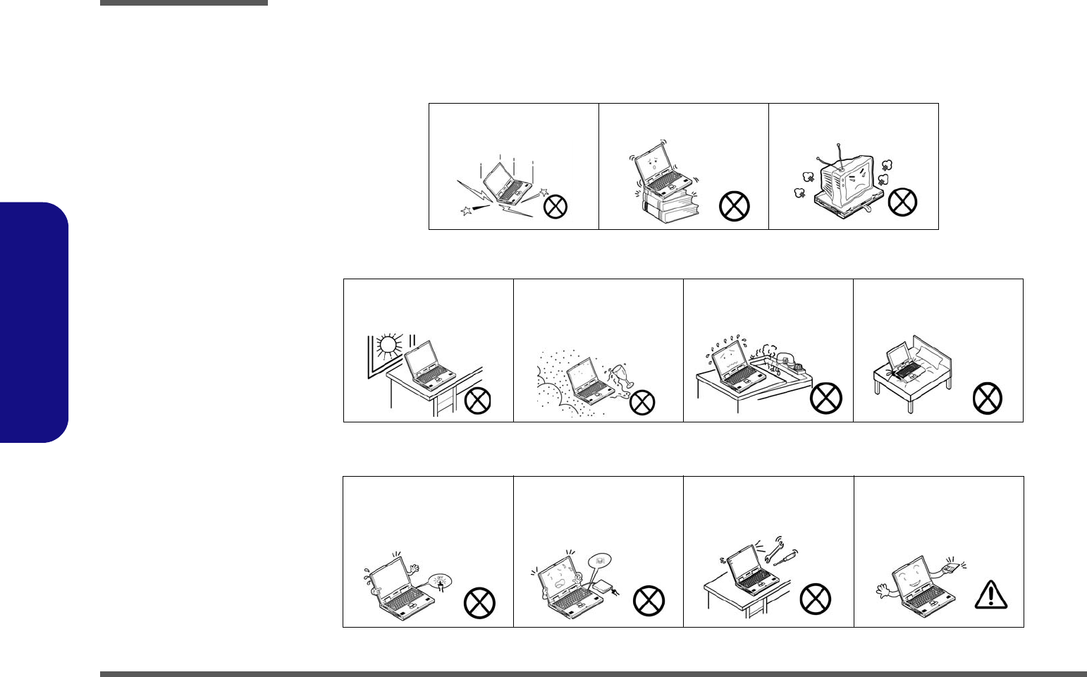
The notebook computer is quite rugged, but it can be damaged. To prevent this, follow these suggestions:
1. Don’t drop it, or expose it to shock. If the computer falls, the case and the components could be damaged.
2. Keep it dry, and don’t overheat it. Keep the computer and power supply away from any kind of heating element. This
is an electrical appliance. If water or any other liquid gets into it, the computer could be badly damaged.
3. Follow the proper working procedures for the computer. Shut the computer down properly and don’t forget to save
your work. Remember to periodically save your data as data may be lost if the battery is depleted.
Do not expose the computer
to any shock or vibration. Do not place it on an unstable
surface. Do not place anything heavy
on the computer.
Do not expose it to excessive
heat or direct sunlight. Do not leave it in a place
where foreign matter or mois-
ture may affect the system.
Don’t use or store the com-
puter in a humid environment. Do not place the computer on
any surface which will block
the vents.
Do not turn off the power
until you properly shut down
all programs.
Do not turn off any peripheral
devices when the computer is
on.
Do not disassemble the com-
puter by yourself. Perform routine maintenance
on your computer.
Preface
VII
Preface
4. Avoid interference. Keep the computer away from high capacity transformers, electric motors, and other strong mag-
netic fields. These can hinder proper performance and damage your data.
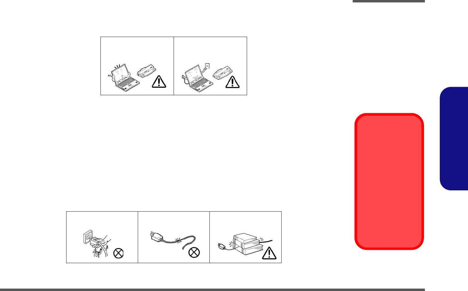
5. Take care when using peripheral devices.
Power Safety
The computer has specific power requirements:
• Only use a power adapter approved for use with this computer.
• Your AC adapter may be designed for international travel but it still requires a steady, uninterrupted power supply. If you are
unsure of your local power specifications, consult your service representative or local power company.
• The power adapter may have either a 2-prong or a 3-prong grounded plug. The third prong is an important safety feature; do
not defeat its purpose. If you do not have access to a compatible outlet, have a qualified electrician install one.
• When you want to unplug the power cord, be sure to disconnect it by the plug head, not by its wire.
• Make sure the socket and any extension cord(s) you use can support the total current load of all the connected devices.
• Before cleaning the computer, make sure it is disconnected from any external power supplies.
Use only approved brands of
peripherals. Unplug the power cord before
attaching peripheral devices.
Do not plug in the power
cord if you are wet. Do not use the power cord if
it is broken. Do not place heavy objects
on the power cord.
Power Safety
Warning
Before you undertake
any upgrade proce-
dures, make sure that
you have turned off the
power, and discon-
nected all peripherals
and cables (including
telephone lines). It is
advisable to also re-
move your battery in
order to prevent acci-
dentally turning the
machine on.

Preface
VIII
Preface
Battery Precautions
• Only use batteries designed for this computer. The wrong battery type may explode, leak or damage the computer.
• Do not continue to use a battery that has been dropped, or that appears damaged (e.g. bent or twisted) in any way. Even if the
computer continues to work with a damaged battery in place, it may cause circuit damage, which may possibly result in fire.
• Recharge the batteries using the notebook’s system. Incorrect recharging may make the battery explode.
• Do not try to repair a battery pack. Refer any battery pack repair or replacement to your service representative or qualified service
personnel.
• Keep children away from, and promptly dispose of a damaged battery. Always dispose of batteries carefully. Batteries may explode
or leak if exposed to fire, or improperly handled or discarded.
• Keep the battery away from metal appliances.
• Affix tape to the battery contacts before disposing of the battery.
• Do not touch the battery contacts with your hands or metal objects.
Related Documents
You may also need to consult the following manual for additional information:
User’s Manual on CD
This describes the notebook PC’s features and the procedures for operating the computer and its ROM-based setup pro-
gram. It also describes the installation and operation of the utility programs provided with the notebook PC.
Battery Disposal
The product that you have purchased contains a rechargeable battery. The battery is recyclable. At the end of
its useful life, under various state and local laws, it may be illegal to dispose of this battery into the municipal
waste stream. Check with your local solid waste officials for details in your area for recycling options or proper
disposal.
Caution
Danger of explosion if battery is incorrectly replaced. Replace only with the same or equivalent type recommend-
ed by the manufacturer. Discard used battery according to the manufacturer’s instructions.

Preface
IX
Preface
Contents
Introduction ..............................................1-1
Overview .........................................................................................1-1
System Specifications .....................................................................1-2
External Locator - Top View with LCD Panel Open ......................1-5
External Locator - Front & Rear Views ..........................................1-6
External Locator - Left & Right Side Views ...................................1-7
External Locator - Bottom View .....................................................1-8
Mainboard Overview - Top (Key Parts) .........................................1-9
Mainboard Overview - Bottom (Key Parts) ..................................1-10
Mainboard Overview - Top (Connectors) .....................................1-11
Mainboard Overview - Bottom (Connectors) ...............................1-12
Disassembly ...............................................2-1
Overview .........................................................................................2-1
Maintenance Tools ..........................................................................2-2
Connections .....................................................................................2-2
Maintenance Precautions .................................................................2-3
Removing the Battery ......................................................................2-5
Removing the Hard Disk Drive .......................................................2-6
Removing the System Memory (RAM) ..........................................2-8
Removing the Heat Sink ...............................................................2-10
Removing the Wireless LAN Module ...........................................2-11
Removing the Bluetooth Module ..................................................2-12
Removing the Optical (CD/DVD) Device ....................................2-13
Removing the Keyboard ................................................................2-14
Removing the Modem Module .....................................................2-15
Part Lists ..................................................A-1
Part List Illustration Location ........................................................A-2
Top .................................................................................................A-3
Bottom ............................................................................................A-4
LCD ............................................................................................... A-5
HDD ............................................................................................... A-6
Combo ............................................................................................ A-7
DVD-COMBO ............................................................................... A-8
Schematic Diagrams.................................B-1
SYSTEM BLOCK DIAGRAM ......................................................B-2
Diamondville SC 1/2 ......................................................................B-3
Diamondville SC 2/2 ......................................................................B-4
945GSE 1/5, HOST ........................................................................B-5
945GSE 2/5 .....................................................................................B-6
945GSE 3/5, DDR ..........................................................................B-7
945GSE 4/5 .....................................................................................B-8
945GSE 5/5 .....................................................................................B-9
DDRII SO-DIMM 0 .....................................................................B-10
DDRII SO- DIMM 1 ....................................................................B-11
PANEL, INVERTER, CRT ..........................................................B-12
CLOCK GENERATOR ................................................................B-13
CH7-M 1/4, SATA .......................................................................B-14
ICH7-M 2/4, PCI, USB, SPI .........................................................B-15
ICH7-M 3/4 ..................................................................................B-16
ICH7-M 4/4 .................................................................................B-17
MULTI I/O, ODD, CCD BT ........................................................B-18
NEW CARD, USB .......................................................................B-19
CARD READER JMB385 ...........................................................B-20
LED, FAN, PC BEEP, TP, FP ......................................................B-21
PCI-E LAN RTL8102E ................................................................B-22
AUDIO CODEC ALC269 QFN ...................................................B-23
KBC-ITE IT8502E .......................................................................B-24
3VS, 5VS ......................................................................................B-25
VDD3, VDD5 ...............................................................................B-26

Preface
X
Preface
POWER 1.8V/ 0.9V .....................................................................B-27
POWER 1.5VS/ 1.05VS .............................................................. B-28
VCORE ........................................................................................ B-29
AC IN, CHARGE ......................................................................... B-30
CLICK BOARD ........................................................................... B-31
Multi B’d, LID, LED, SW, USB .................................................. B-32
Multi B’d, Mini Card, MDC, RJ11 .............................................. B-33

Introduction
Overview 1 - 1
1.Introduction
Chapter 1: Introduction
Overview
This manual covers the information you need to service or upgrade the M710L series notebook computer. Information
about operating the computer (e.g. getting started, and the Setup utility) is in the User’s Manual. Information about driv-
ers (e.g. VGA & audio) is also found in User’s Manual. That manual is shipped with the computer.
Operating systems (e.g. Windows XP, Windows Vista, etc.) have their own manuals as do application software (e.g. word
processing and database programs). If you have questions about those programs, you should consult those manuals.
The M710L series notebook is designed to be upgradeable. See “Disassembly” on page 2 - 1 for a detailed description
of the upgrade procedures for each specific component. Please note the warning and safety information indicated by the
“” symbol.
The balance of this chapter reviews the computer’s technical specifications and features.

Introduction
1 - 2 System Specifications
1.Introduction
System Specifications
Feature Specification
Processor Intel® Atom™
N270
BGA Package
45nm (45 Nanometer) Process Technology
512 KB L2 Cache & 533 MHz FSB
1.60GHz
Core Logic Intel® 82945GSE + 82801GBM Chipset
LCD 10.2" WSVGA (1024 * 600) TFT LCD
Memory 64-bit Wide DDRII (DDR2) Data Channel
One 200 Pin SO-DIMM Socket Supporting DDRII (DDR2) 533MHz RAM Modules
Memory Expandable up to 2GB (1024/2048 MB DDR2 Modules)
Video Adapter Intel 945GSE Integrated Video
Shared Memory Architecture (up to 128MB dynamically allocated from system memory where needed)
Supports DirectX9.0
BIOS One 8Mb SPI Flash ROM Phoenix™ BIOS
Security Security (Kensington® Type) Lock Slot BIOS Password
Storage One Changeable 12.7mm(h) SATA (Serial) Optical Device (CD/DVD) Type Drive (see “Optional” on page 1 - 4)
Easy Changeable 2.5" 9.5 mm (h) SATA (Serial) HDD
Audio High Definition Audio (HDA)
Compliant with Microsoft UAA (Universal Audio
Architecture)
Direct Sound 3D™ Compatible
2 * Built-In Speakers
Built-In Microphone
Latest Specification Information
The specifications listed in this Appendix are correct at the time of going to press. Certain items (particularly processor types/speeds and
CD/DVD device types) may be changed, delayed or updated due to the manufacturer's release schedule. Check with your service center
for details.

Introduction
System Specifications 1 - 3
1.Introduction
Keyboard &
Pointing Device Winkey Keyboard Built-In TouchPad with Scrolling Function
Interface Two USB 2.0 Ports (Left Side of Computer)
One Headphone-Out Jack
One Microphone-In Jack
One Internal Microphone
One RJ-11 Modem Jack
One RJ-45 LAN Jack
One DC-In Jack
One External Monitor Port
Card Reader Embedded 7-in-1 Card Reader (MS/ MS Pro/ SD/ Mini SD/ MMC/ RS MMC/ MS Duo)
Note: MS Duo/ Mini SD/ RS MMC Cards require a PC adapter
Mini-Card Slots
One Mini-Card Slot for
Wireless LAN Module
Communication 10/100Mb Base-T Ethernet LAN
56K Fax Modem
802.11b/g Wireless LAN Mini-Card Module with USB interface (Option)
Bluetooth 2.0 + EDR (Enhanced Data Rate) Module (Factory Option)
1.3M or 2.0M Pixel PC Camera Module with USB interface (Factory Option)
Power
Management Supports ACPI 3.0 Supports Wake on LAN (From Sleep)
Supports Resume from Modem Ring (From Sleep)
Power
Full Range AC/DC Adapter AC Input 100 - 240V, DC Output 50 - 60Hz, 19V, 3.42A or 18.5V, 3.5A (
65
Watts)
Battery 4 Cell Smart Lithium-Ion Battery Pack, 2400mAH
2 Cell Smart Lithium-Ion Battery Pack, 2200mAH (Option)
8 Cell Smart Lithium-Ion Battery Pack, 4400mAH (Option)
Battery Life 4 Hours with 4 Cell Battery ( Without ODD Use)
Environmental
Spec Temperature
Operating: 5°C - 35°C
Non-Operating: -20°C - 60°C
Relative Humidity
Operating: 20% - 80%
Non-Operating: 10% - 90%
Dimensions
& Weight 299mm (w) * 219mm (d) * 26.5-35.7mm (h) Around1.6 kg With 2 Cell Battery and Without ODD
Feature Specification
Introduction
1 - 4 System Specifications
1.Introduction
Optional Optical Drive Module Options:
SATA DVD/CD-RW Combo Drive Module
SATA DVD Super Multi Drive Module
8 Cell Smart Lithium-Ion Battery Pack
2 Cell Smart Lithium-Ion Battery Pack
1.3M or 2.0M Pixel USB PC Camera Module (Factory
Option)
802.11b/g Wireless LAN Mini-Card Module with USB
interface
Bluetooth 2.0 + EDR (Enhanced Data Rate) Module
(Factory Option)
Feature Specification

Introduction
External Locator - Top View with LCD Panel Open 1 - 5
1.Introduction
External Locator - Top View with LCD Panel Open Figure 1
Top View
1. Built-In PC
Camera
(Optional)
2. LCD
3. Speaker
4. Power Button
5. Hot-Key Buttons
6. LED Status
Indicators
7. Keyboard
8. Touchpad &
Buttons
9. LED Power &
Communication
Indicators
10. Built-in
Microphone
2
5
1
7
8
4
6
9
3
3
10

Introduction
1 - 6 External Locator - Front & Rear Views
1.Introduction
External Locator - Front & Rear Views
Figure 2
Front View
1. LED Power &
Communication
Indicators
2. 7-in-1 Card Reader
3. Microphone-In Jack
4. Headphone-Out
Jack
Figure 3
Rear View
1. Battery
Front
1
4
3
2
Rear
1
Introduction
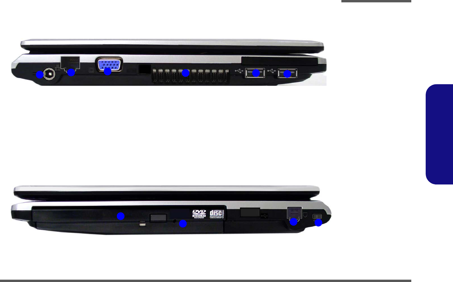
External Locator - Left & Right Side Views 1 - 7
1.Introduction
External Locator - Left & Right Side Views
4
123
Left
55
Figure 4
Left Side View
1. DC-In Jack
2. RJ-45 LAN Jack
3. External Monitor
Port
4. Vent
5. 2 * USB 2.0 Ports
Figure 5
Right Side View
1. Optical Device
Drive Bay
2. Emergency Eject
Hole
3. RJ-11 Phone Jack
4. Security Lock Slot
234
Right
1
Introduction
1 - 8 External Locator - Bottom View
1.Introduction
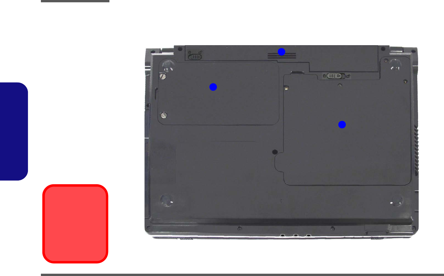
External Locator - Bottom View
Figure 6
Bottom View
1. Battery
2. Hard Disk Bay
Cover
3. RAM & CPU Bay
Cover
Overheating
To prevent your com-
puter from overheating
make sure nothing
blocks the vent/fan in-
takes while the com-
puter is in use.
2
3
1
Introduction
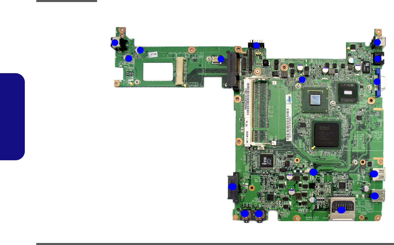
Mainboard Overview - Top (Key Parts) 1 - 9
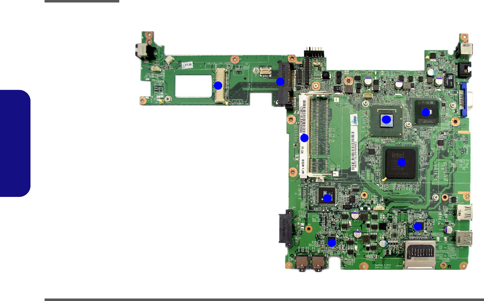
1.Introduction
Mainboard Overview - Top (Key Parts) Figure 7
Mainboard Top
Key Parts
1. CLOCK
GENERATOR
2. RTL8102E
3. SC413
2
1
3
Introduction
1 - 10 Mainboard Overview - Bottom (Key Parts)
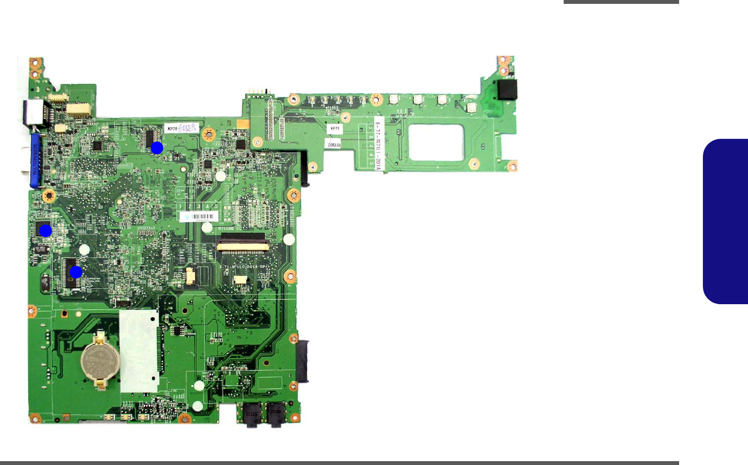
1.Introduction
Mainboard Overview - Bottom (Key Parts)
Figure 8
Mainboard Bottom
Key Parts
1. North Bridge
2. Intel Diamondville
Processor
3. South Bridge
4. Card Reader
Controller
JM8385
5. Realtek ALC269
6. ITE
7. Memory Slot
DDRII So-DIMM
8. HDD Connector
9. WLAN
Connector
2
3
1
4
5
6
8
7
9
Introduction
Mainboard Overview - Top (Connectors) 1 - 11
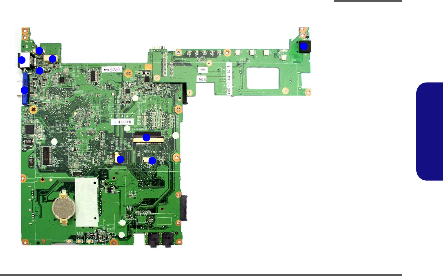
1.Introduction
Mainboard Overview - Top (Connectors) Figure 9
Mainboard Top
Connectors
1. Keyboard Cable
Connector
2. Internal
Microphone Cable
Connector
3. Touch Pad Cable
Connector
4. External Monitor
Port
5. RJ-45 LAN Jack
6. Speaker Cable
Connector
7. LCD Cable
Connector
8. CCD Cable
Connector
9. RJ-11 Phone Jack
89
3
1
2
4
5
6
7
Introduction
1 - 12 Mainboard Overview - Bottom (Connectors)
1.Introduction
Mainboard Overview - Bottom (Connectors)
Figure 10
Mainboard Bottom
Connectors
1. RJ-11 Phone
Jack
2. Modem Cable
Connector
3. Speaker Cable
Connector
4. Modem
Connector
5. Battery
Connector
6. Bluetooth Cable
Connector
7. DC-In Jack
8. RJ-45 LAN Jack
9. External Monitor
Port
10. USB Ports
11. Card Reader
12. Fan Cable
Connector
13. Microphone-In
Jack
14. Headphone-Out
Jack
15. Optical Device
Drive Connector
2
3
15
4
7
6
8
10
12
11
9
13
14
15
10

Disassembly
Overview 2 - 1
2.Disassembly
Chapter 2: Disassembly
Overview
This chapter provides step-by-step instructions for disassembling the M710L series notebook’s parts and subsystems.
When it comes to reassembly, reverse the procedures (unless otherwise indicated).
We suggest you completely review any procedure before you take the computer apart.
Procedures such as upgrading/replacing the RAM, CD device and hard disk are included in the User’s Manual but are
repeated here for your convenience.
To make the disassembly process easier each section may have a box in the page margin. Information contained under
the figure # will give a synopsis of the sequence of procedures involved in the disassembly procedure. A box with a
lists the relevant parts you will have after the disassembly process is complete. Note: The parts listed will be for the dis-
assembly procedure listed ONLY, and not any previous disassembly step(s) required. Refer to the part list for the previ-
ous disassembly procedure. The amount of screws you should be left with will be listed here also.
A box with a will also provide any possible helpful information. A box with a contains warnings.
An example of these types of boxes are shown in the sidebar.
Information
Warning

Disassembly
2 - 2 Overview
2.Disassembly
NOTE: All disassembly procedures assume that the system is turned OFF, and disconnected from any power supply (the
battery is removed too).
Maintenance Tools
The following tools are recommended when working on the notebook PC:
• M3 Philips-head screwdriver
• M2.5 Philips-head screwdriver (magnetized)
• M2 Philips-head screwdriver
• Small flat-head screwdriver
• Pair of needle-nose pliers
• Anti-static wrist-strap
Connections
Connections within the computer are one of four types:
Locking collar sockets for ribbon connectors To release these connectors, use a small flat-head screwdriver to
gently pry the locking collar away from its base. When replac-
ing the connection, make sure the connector is oriented in the
same way. The pin1 side is usually not indicated.
Pressure sockets for multi-wire connectors To release this connector type, grasp it at its head and gently
rock it from side to side as you pull it out. Do not pull on the
wires themselves. When replacing the connection, do not try to
force it. The socket only fits one way.
Pressure sockets for ribbon connectors To release these connectors, use a small pair of needle-nose pli-
ers to gently lift the connector away from its socket. When re-
placing the connection, make sure the connector is oriented in
the same way. The pin1 side is usually not indicated.
Board-to-board or multi-pin sockets To separate the boards, gently rock them from side to side as
you pull them apart. If the connection is very tight, use a small
flat-head screwdriver - use just enough force to start.

Disassembly
Overview 2 - 3
2.Disassembly
Maintenance Precautions
The following precautions are a reminder. To avoid personal injury or damage to the computer while performing a re-
moval and/or replacement job, take the following precautions:
1. Don't drop it. Perform your repairs and/or upgrades on a stable surface. If the computer falls, the case and other
components could be damaged.
2. Don't overheat it. Note the proximity of any heating elements. Keep the computer out of direct sunlight.
3. Avoid interference. Note the proximity of any high capacity transformers, electric motors, and other strong mag-
netic fields. These can hinder proper performance and damage components and/or data. You should also monitor
the position of magnetized tools (i.e. screwdrivers).
4. Keep it dry. This is an electrical appliance. If water or any other liquid gets into it, the computer could be badly
damaged.
5. Be careful with power. Avoid accidental shocks, discharges or explosions.
•Before removing or servicing any part from the computer, turn the computer off and detach any power supplies.
•When you want to unplug the power cord or any cable/wire, be sure to disconnect it by the plug head. Do not pull on the wire.
6. Peripherals – Turn off and detach any peripherals.
7. Beware of static discharge. ICs, such as the CPU and main support chips, are vulnerable to static electricity.
Before handling any part in the computer, discharge any static electricity inside the computer. When handling a
printed circuit board, do not use gloves or other materials which allow static electricity buildup. We suggest that
you use an anti-static wrist strap instead.
8. Beware of corrosion. As you perform your job, avoid touching any connector leads. Even the cleanest hands pro-
duce oils which can attract corrosive elements.
9. Keep your work environment clean. Tobacco smoke, dust or other air-born particulate matter is often attracted
to charged surfaces, reducing performance.
10. Keep track of the components. When removing or replacing any part, be careful not to leave small parts, such as
screws, loose inside the computer.
Cleaning
Do not apply cleaner directly to the computer, use a soft clean cloth.
Do not use volatile (petroleum distillates) or abrasive cleaners on any part of the computer.
Power Safety
Warning
Before you undertake
any upgrade proce-
dures, make sure that
you have turned off the
power, and discon-
nected all peripherals
and cables (including
telephone lines). It is
advisable to also re-
move your battery in
order to prevent acci-
dentally turning the
machine on.

Disassembly
2 - 4 Overview
2.Disassembly
Disassembly Steps
The following table lists the disassembly steps, and on which page to find the related information. PLEASE PERFORM
THE DISASSEMBLY STEPS IN THE ORDER INDICATED.
To remove the Battery:
1. Remove the battery page 2 - 5
To remove the HDD:
1. Remove the battery page 2 - 5
2. Remove the HDD page 2 - 6
To remove the System Memory:
1. Remove the battery page 2 - 5
2. Remove the system memory page 2 - 8
To remove the Heat Sink:
1. Remove the battery page 2 - 5
2. Remove the heat sink page 2 - 10
To remove the Wireless LAN Module:
1. Remove the battery page 2 - 5
2. Remove the Wireless LAN page 2 - 11
To remove the Bluetooth:
1. Remove the battery page 2 - 5
2. Remove the bluetooth page 2 - 12
To remove the Optical Device:
1. Remove the battery page 2 - 5
2. Remove the Optical device page 2 - 13
To remove the Keyboard:
1. Remove the battery page 2 - 5
2. Remove the keyboard page 2 - 14
To remove the Modem :
1. Remove the battery page 2 - 5
2. Remove the HDD page 2 - 6
3. Remove the heat sink page 2 - 10
4. Remove the Wireless LAN page 2 - 11
5. Remove the bluetooth page 2 - 12
6. Remove the Optical device page 2 - 13
7. Remove the keyboard page 2 - 14
8. Remove the modem page 2 - 15
Disassembly
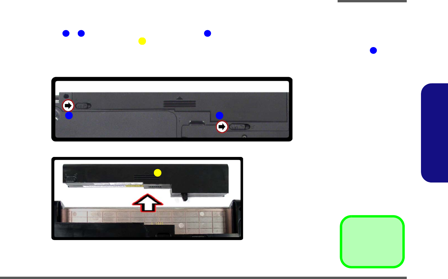
Removing the Battery 2 - 5
2.Disassembly
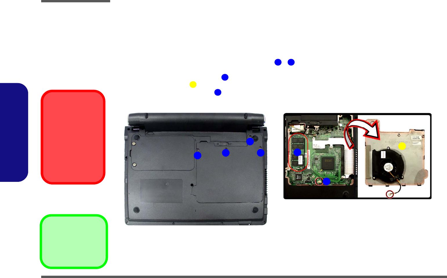
Removing the Battery
1. Turn the computer off, and turn it over.
2. Slide the latches ( & ) the direction of the arrow, and hold latch in place.
3. Slide the battery in the direction of the arrow .
3. Battery
1 2 2
6
3
1
a.
b.
2
3
Figure 1
Battery Removal
a. Slide the 2 latches and
hold latch in place.
b. Slide the battery in the di-
rection of the arrow.
2
Disassembly
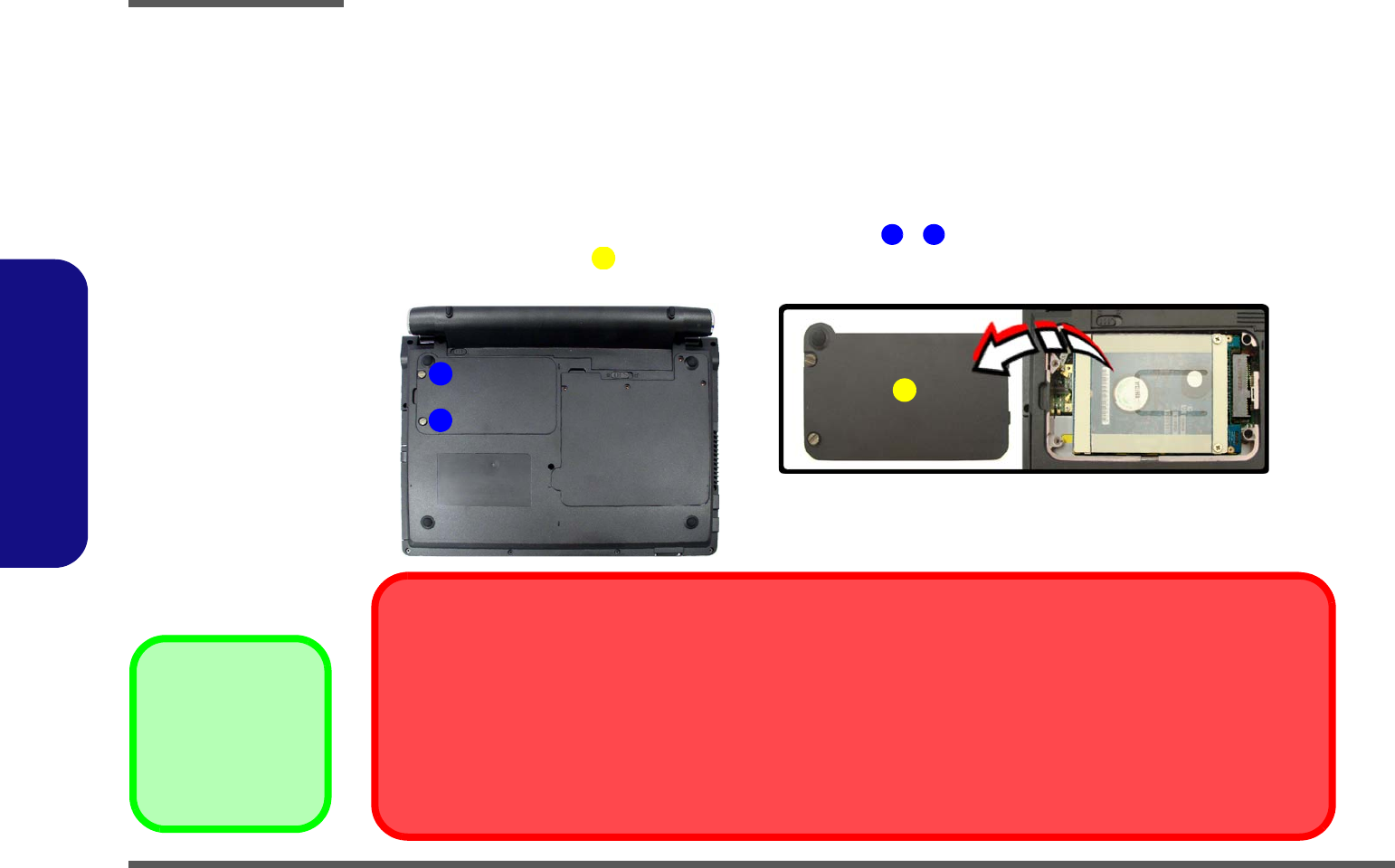
2 - 6 Removing the Hard Disk Drive
2.Disassembly
Removing the Hard Disk Drive
The hard disk drive can be taken out to accommodate other 2.5" serial (SATA) hard disk drives with a height of 9.5mm
(h). Follow your operating system’s installation instructions, and install all necessary drivers and utilities (as outlined in
Chapter 4 of the User’s Manual) when setting up a new hard disk.
Hard Disk Upgrade Processl
1. Turn off the computer, and remove the battery (page 2 - 5).
2. Locate the hard disk bay cover and remove the screws ( - ).
3. Remove the bay cover .
Figure 2
HDD Assembly
Removal
a. Locate the HDD bay cov-
er and remove the
screws.
b. Remove the bay cover.
3. HDD Bay Cover
•2 Screws
1 2
6
3
a.
1
2
HDD System Warning
New HDD’s are blank. Before you begin make sure:
You have backed up any data you want to keep from your old HDD.
You have all the CD-ROMs and FDDs required to install your operating system and programs.
If you have access to the internet, download the latest application and hardware driver updates for the operating system you plan
to install. Copy these to a removable medium.
3
b.
Disassembly
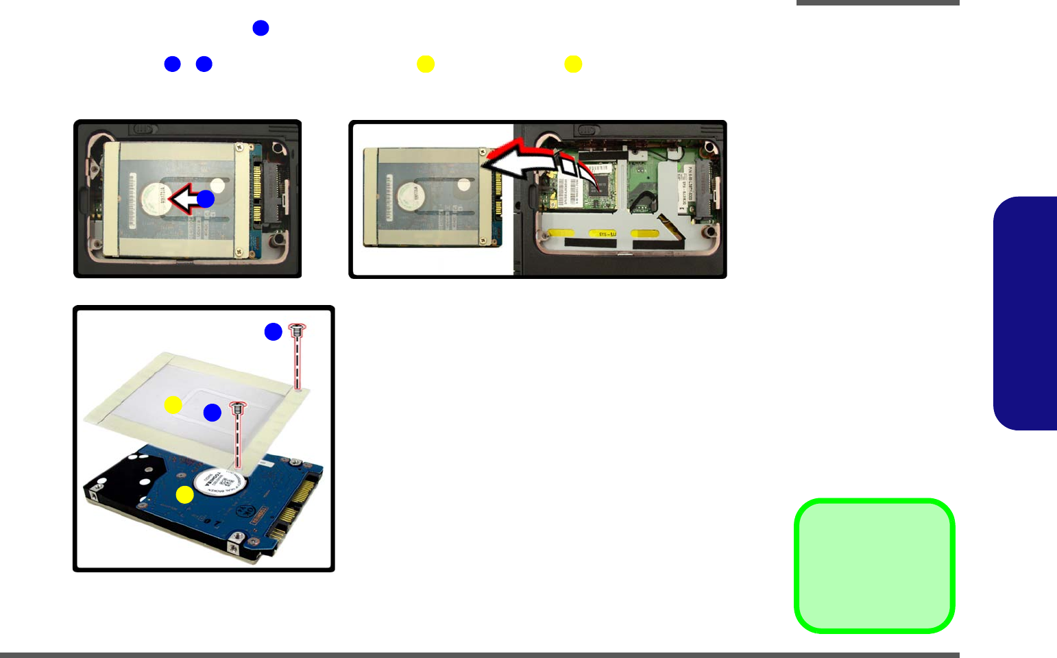
Removing the Hard Disk Drive 2 - 7
2.Disassembly
4. Carefully grip the mylar cover tab and slide the hard disk in the direction of arrow.
5. Lift the hard disk up (Figure d) in the direction of arrow.
6. Remove the screws - and separate the mylar cover from the hard disk .
7. Reverse the process to install any new hard disk.
4Figure 3
HDD Assembly
Removal Sequence
c. Slide the HDD in the di-
rection of the arrow.
d. Lift the HDD out of the
bay.
e. Remove the screws and
separate the mylar cover
from the HDD.
5 6 6
76
8
7. Mylar Cover
8. HDD
•2 Screws
c. d.
4
e.
6
5
8
7
Disassembly
2 - 8 Removing the System Memory (RAM)
2.Disassembly
Removing the System Memory (RAM)
The computer has one memory socket for 200 pin Small Outline Dual In-line (SO-DIMM) DDRII (DDR2) type memory
modules. The total memory size is automatically detected by the POST routine once you turn on your computer.
Memory Upgrade Process
1. Turn off the computer, remove the battery (page 2 - 5).
2. Locate the CPU/RAM bay cover, and remove screws - .
3. Carefully (a fan and cable are attached to the under side of the cover) lift up the bay cover.
4. Carefully disconnect the fan cable .
5. Remove the bay cover .
6. The RAM will be visible at point on the mainboard.
Figure 4
RAM Module
Removal
a. Remove the screws.
b. Disconnect the fan
cable and remove
the cover.
Contact Warning
Be careful not to touch
the metal pins on the
module’s connecting
edge. Even the clean-
est hands have oils
which can attract parti-
cles, and degrade the
module’s perfor-
mance.
1 4
5
6
6. CPU/RAM Bay Cover
•4 Screws
7
a.
3
4
1
6
b.
2
5
7
Disassembly
Removing the System Memory (RAM) 2 - 9
2.Disassembly
7. Gently push the two release latches ( & ) on the sides of the memory socket in the direction indicated by the
arrows (Figure d).
8. The RAM module(s) will pop-up (Figure d), and you can then remove it.
9. Insert a new module holding it at about a 30° angle and fit the connectors firmly into the memory slot.
10. The module will only fit one way as defined by its pin alignment. Make sure the module is seated as far into the slot
as it will go. DO NOT FORCE IT; it should fit without much pressure.
11. Press the module down towards the mainboard until the slot levers click into place to secure the module.
12. Replace the bay cover and the screws (make sure you reconnect the fan cable before screwing down the bay cover
- Figure b).
13. Restart the computer to allow the BIOS to register the new memory configuration as it starts up.
8 9
10
Figure 5
Memory Removal
Sequence
c. Push the release
latch(es).
d. Remove the module(s).
c. d.
10
8
9
10 RAM Module(s)
Disassembly
2 - 10 Removing the Heat Sink
2.Disassembly
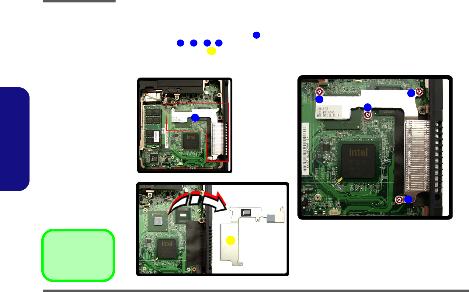
Removing the Heat Sink
1. Turn off the computer, turn it over and remove the battery (page 2 - 5) and the component bay cover (page 2 - 8).
2. The CPU heat sink will be visible at point on the mainboard.
3. Loosen screws , , ,(Figure 6b) the reverse order as indicated on the label.
4. Carefully lift the heat sink (Figure 6c) up and off the computer.
5. Reverse the process to install the heat sink .
A
4 3 2 1
B
Figure 6
Processor Removal
a. Locate the heat sink.
b. Loosen the screws in the
reverse order indicated.
c. Remove the heat sink.
B. Heat Sink
•4 Screws
b.
B
4
a.
c.
3
2
A
1
Disassembly
Removing the Wireless LAN Module 2 - 11
2.Disassembly
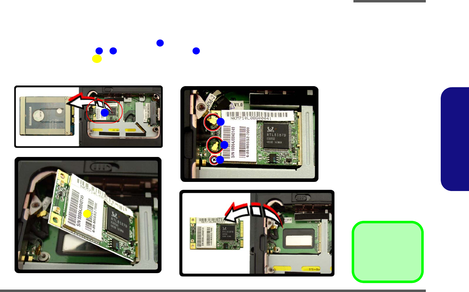
Removing the Wireless LAN Module
1. Turn off the computer, remove the battery (page 2 - 5) and the HDD bay cover(page 2 - 8).
2. Remove the HDD module.
3. The Wireless LAN module will be visible at point on the mainboard.
4. Carefully disconnect cables - , and then remove screw from the module socket.
5. The Wireless LAN module will pop-up.
6. Lift the Wireless LAN module (Figure d) up and off the computer.
Figure 7
Wireless LAN
Module Removal
a. Remove the HDD mod-
ule and Iocate the WLAN
module.
b. Disconnect the cables
and remove the screw.
c. The WLAN module will
pop up.
d. Remove the WLAN
module.
Note: Make sure you
reconnect the antenna
cable to “1” + “2”
socket (Figure 7b).
1
2 3 4
5
1
2
c.
a.
5
3
b.
d.
4
5. WLAN Module
•1 Screw
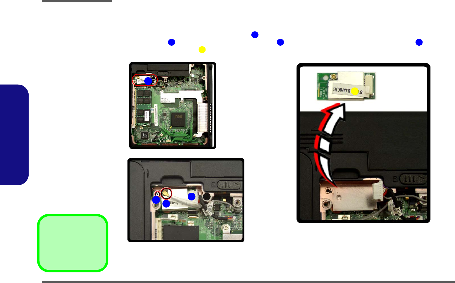
Disassembly
2 - 12 Removing the Bluetooth Module
2.Disassembly
Removing the Bluetooth Module
1. Turn off the computer, remove the battery (page 2 - 5), and the CPU/RAM bay cover (page 2 - 8).
2. The Bluetooth module will be visible at point on the mainboard.
3. Remove screw and carefully disconnect the cable and separate the module from the connector .
4. Lift the Bluetooth module up and off the computer.
1
2 3 4
5
Figure 8
Bluetooth Removal
a. Remove the cover and
locate the Bluetooth
module.
b. Remove the screw and
disconnect the cable and
seperate the connector.
c. Lift the Bluetooth module
out.
a.
c.
b.
34
1
2
c.
5
5. Bluetooth Module
•1 Screw
Disassembly
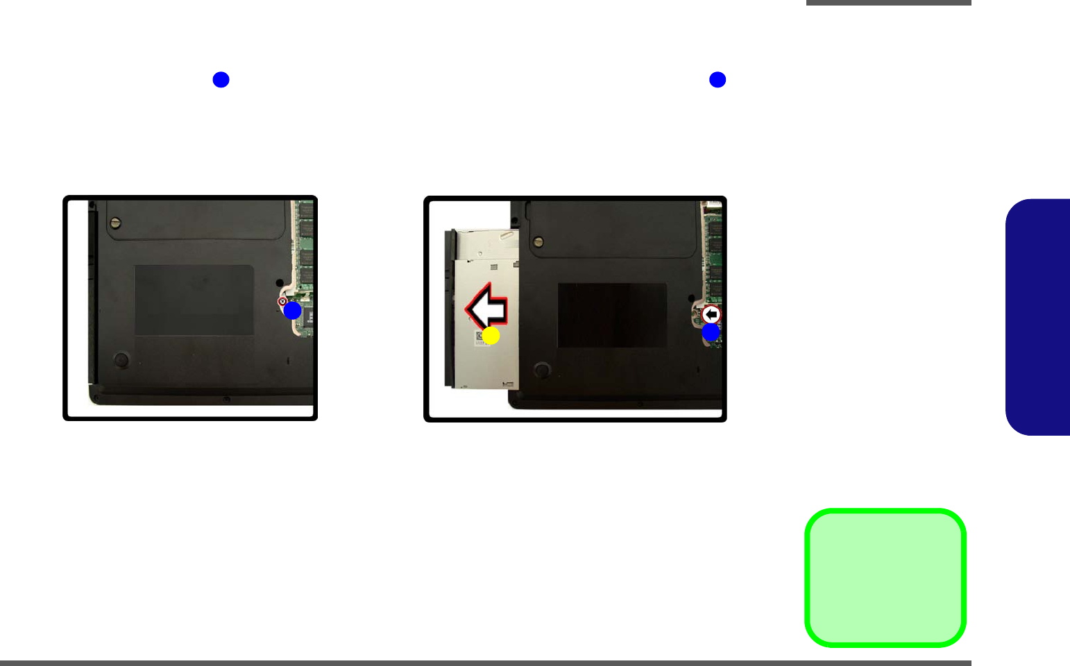
Removing the Optical (CD/DVD) Device 2 - 13
2.Disassembly
Removing the Optical (CD/DVD) Device
1. Turn off the computer, remove the battery (page 2 - 5), and the CPU/RAM bay cover (page 2 - 8).
2. Remove the screw at point , and use a screwdriver to carefully push out the optical device at point .
3. Insert the new device and carefully slide it into the computer (the device only fits one way. DO NOT FORCE IT; The
screw holes should line up.
4. Restart the computer to allow it to automatically detect the new device.
Figure 9
Optical Device
Removal
a. Remove the cover and
locate the screw.
b. Remove the screw and
push the optical device
out off the computer at
point 2 and remove the
optical device.
1 2
3. Optical Device
•1 Screw
2
1
a.
3
b.
Disassembly
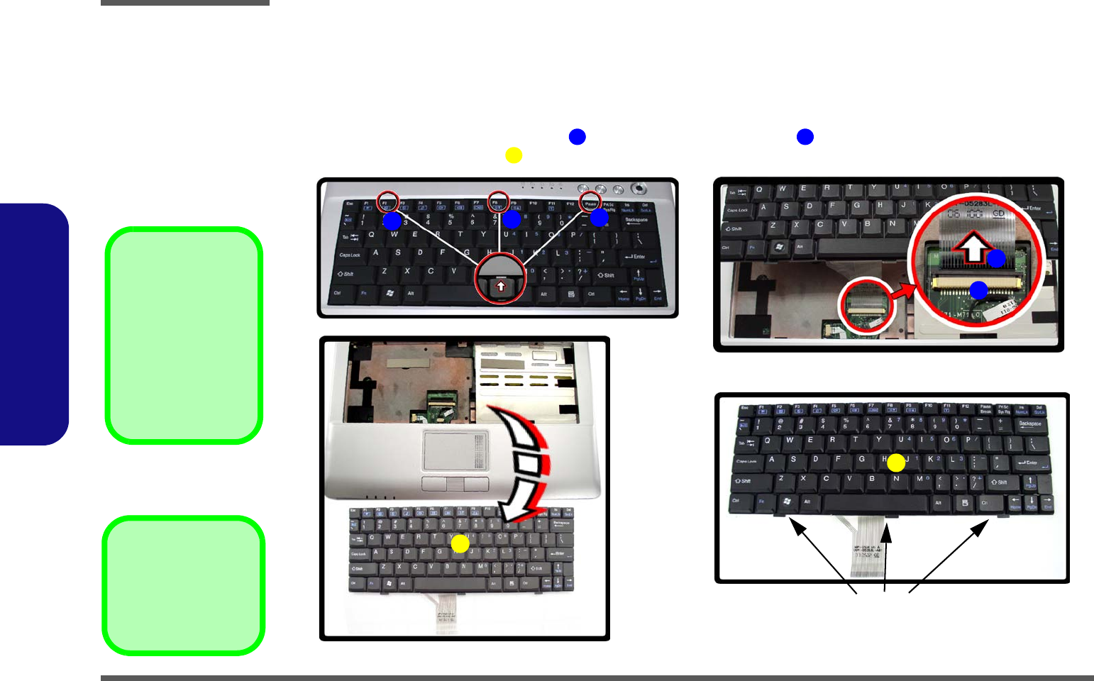
2 - 14 Removing the Keyboard
2.Disassembly
Removing the Keyboard
1. Turn off the computer, and remove the battery (page 2 - 5).
2. Press the three keyboard latches at the top of the keyboard to elevate the keyboard from its normal position (you
may need to use a small screwdriver to do this).
3. Carefully lift the keyboard up, being careful not to bend the keyboard ribbon cable (Figure b).
4. Disconnect the keyboard ribbon cable from the locking collar socket .
5. Carefully lift up the keyboard (Figure c) off the computer.
4 5
Figure 10
Keyboard Removal
a. Press the three latches
to release the keyboard.
b. Lift the keyboard up and
disconnect the cable
from the locking collar.
c. Remove the keyboard.
Re-Inserting the Key-
board
When re-inserting the
keyboard firstly align
the three keyboard
tabs at the bottom of
the keyboard with the
slots in the case.
6. Keyboard Module.
6
a. b.
5
4
6
Keyboard Tabs
c.
13
2
6
Disassembly
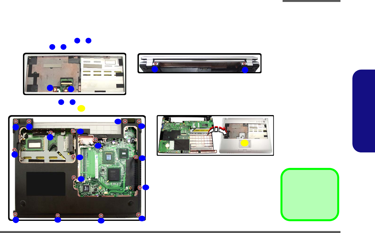
Removing the Modem Module 2 - 15
2.Disassembly
Removing the Modem Module
1. Turn off the computer, remove the battery (page 2 - 5) and the CPU/RAM bay cover (page 2 - 8) and the heat sink
(page 2 - 10) and the Wireless LAN (page 2 - 11) and the optical device (page 2 - 13) and the keyboard (page 2 -
14).
2. Disconnect the connectors - from under the keyboard and turn it over.
3. Remove screws - from the rear of the computer.
4. Remove the screws - from the bottom case.
5. Carefully lift up the top case off the computer.
Figure 11
Modem Removal
a. Disconnect the connec-
tors from under the key-
board.
b. Remove the screws.
c. Remove the screws.
d. Remove the top case.
21. Top Case
•18 Screws
1 2
3 4
a. b.
12
4
3
520
21
c.
9
76
8
10 11
13
12
14
15
16
17
20
18
19
d.
21
5
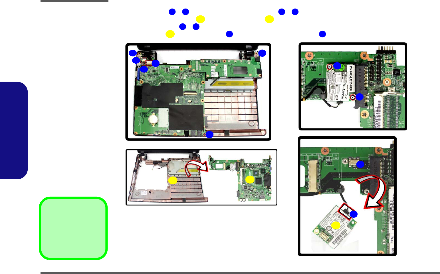
Disassembly
2 - 16 Removing the Modem Module
2.Disassembly
6. Remove screws - and disconnect the connectors - from the mainboard.
7. Separate the bottom case from the mainboard and turn it over.
8. Remove the screws - .
9. Lift the modem up off the socket and disconnect the connector from the modem.
22 24 26 27
Figure 12
Modem Removal
Sequence
e. Remove the screws and
and disconnect the con-
nectors.
f. Separate the bottom
case from the main-
board.
g. Remove the screws
h. Lift the modem up off
the socket and discon-
nect the connector.
28. Bottom Case
29. Main Board
32. Modem
•5 Screws
28 29
30 31
32 33 34
e.
h.
g.
29
28
26
25
24
27
23
22
30
31
32
34
f.
33

Part Lists
A-1
A.Part Lists
Appendix A:Part Lists
This appendix breaks down the M710L series notebook’s construction into a series of illustrations. The component part
numbers are indicated in the tables opposite the drawings.
Note: This section indicates the manufacturer’s part numbers. Your organization may use a different system, so be sure
to cross-check any relevant documentation.
Note: Some assemblies may have parts in common (especially screws). However, the part lists DO NOT indicate the
total number of duplicated parts used.
Note: Be sure to check any update notices. The parts shown in these illustrations are appropriate for the system at the
time of publication. Over the product life, some parts may be improved or re-configured, resulting in new part numbers.
Part Lists
A - 2 Part List Illustration Location
A.Part Lists
Part List Illustration Location
The following table indicates where to find the appropriate part list illustration.
Table A - 1
Part List Illustration
Location Part Pages#
Top page A - 3
Bottom page A - 4
LCD page A - 5
HDD page A - 6
Combo page A - 7
DVD-Combo page A - 8
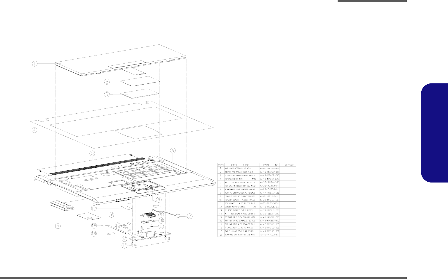
Part Lists
Top A - 3
A.Part Lists
Top
Figure A - 1
Top
黑色 無鉛
無鉛
無鉛
無鉛
無鉛
無鉛
無鉛
無鉛
無鉛
非耐落 無鉛
無鉛
無鉛
無鉛
無鉛
無鉛
無鉛
無鉛
設變材質 無鉛
材質變更 無鉛
非耐落 無鉛
Part Lists
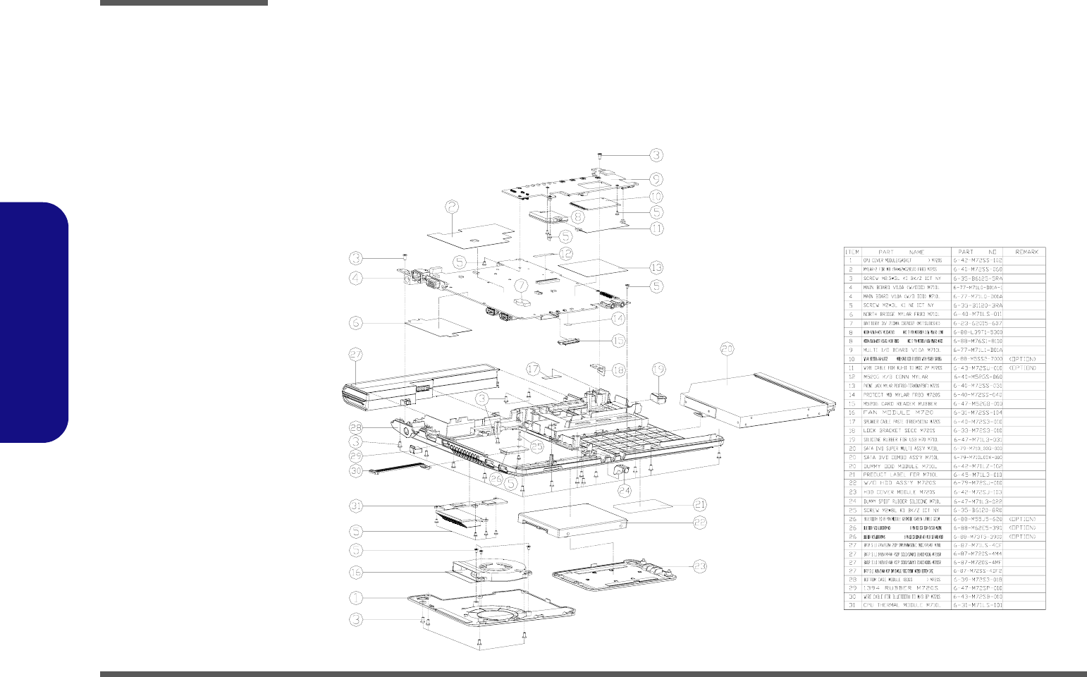
A - 4 Bottom
A.Part Lists
Bottom
Figure A - 2
Bottom 厚度變更 無鉛
無鉛
無鉛
凱碩 無鉛
無鉛
無鉛
無鉛
無鉛
海華 無鉛
無鉛
側壁加肉 無鉛
無鉛
無鉛
無鉛
無鉛
無鉛
無鉛
無鉛
無鉛
亞旭 無鉛
無鉛
無鉛
無鉛
無鉛
無鉛
無鉛
無鉛
無鉛
藍天2 互億 無鉛
無鉛
無鉛
無鉛
無鉛
無鉛
無鉛
無鉛
修模無鉛
無鉛
無鉛
藍天7 互億 無鉛
Part Lists
LCD A - 5
A.Part Lists
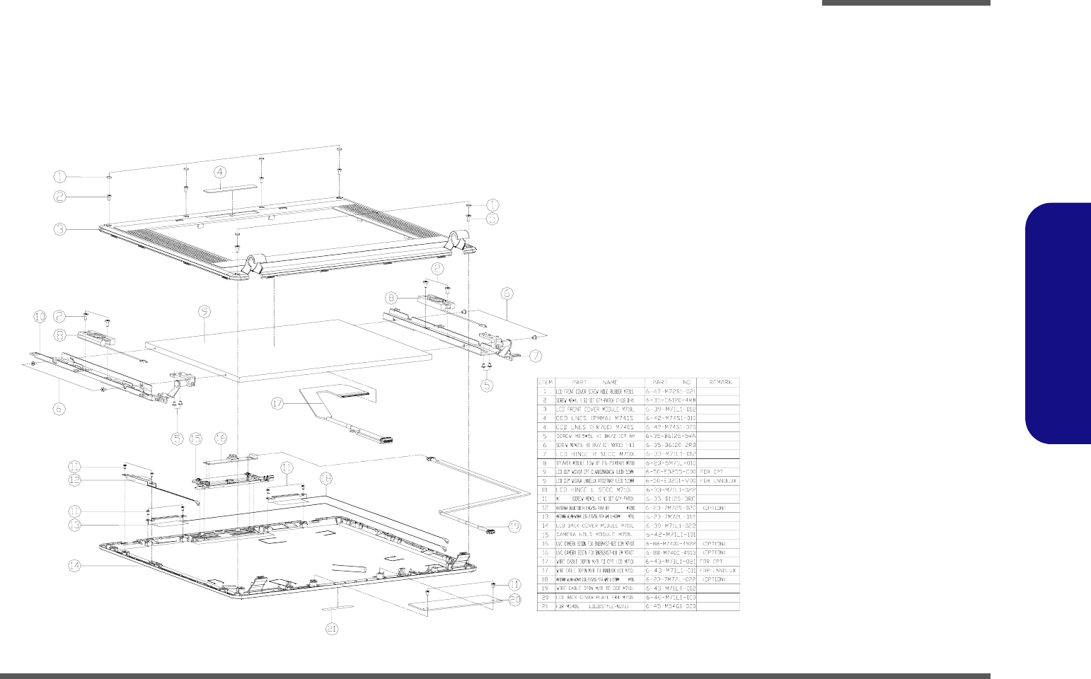
LCD
Figure A - 3
LCD
無鉛
無鉛
無鉛
無鉛
無鉛
無鉛
無鉛
無鉛
無鉛
非耐落 無鉛
無鉛
無鉛
無鉛
灰色 精乘 無鉛
精乘 無鉛
精乘 無鉛
無鉛
中性 無鉛
無鉛
無鉛
無鉛
無鉛
無鉛
無鉛
無鉛
Part Lists
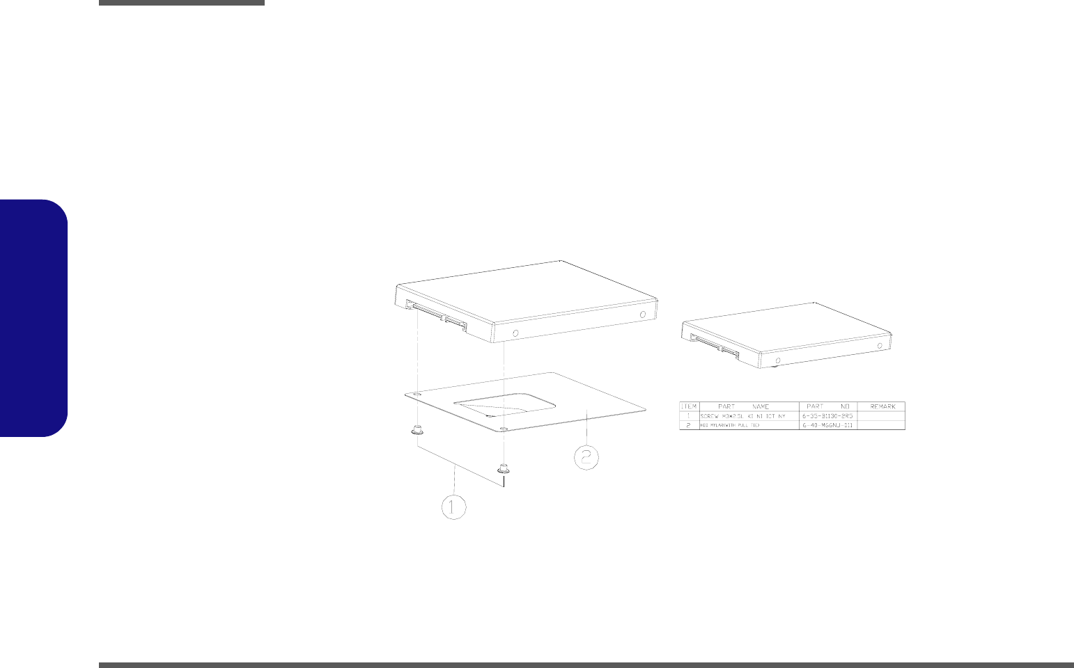
A - 6 HDD
A.Part Lists
HDD
Figure A - 4
HDD
無鉛
無折切痕(設變)(無鉛)

Part Lists
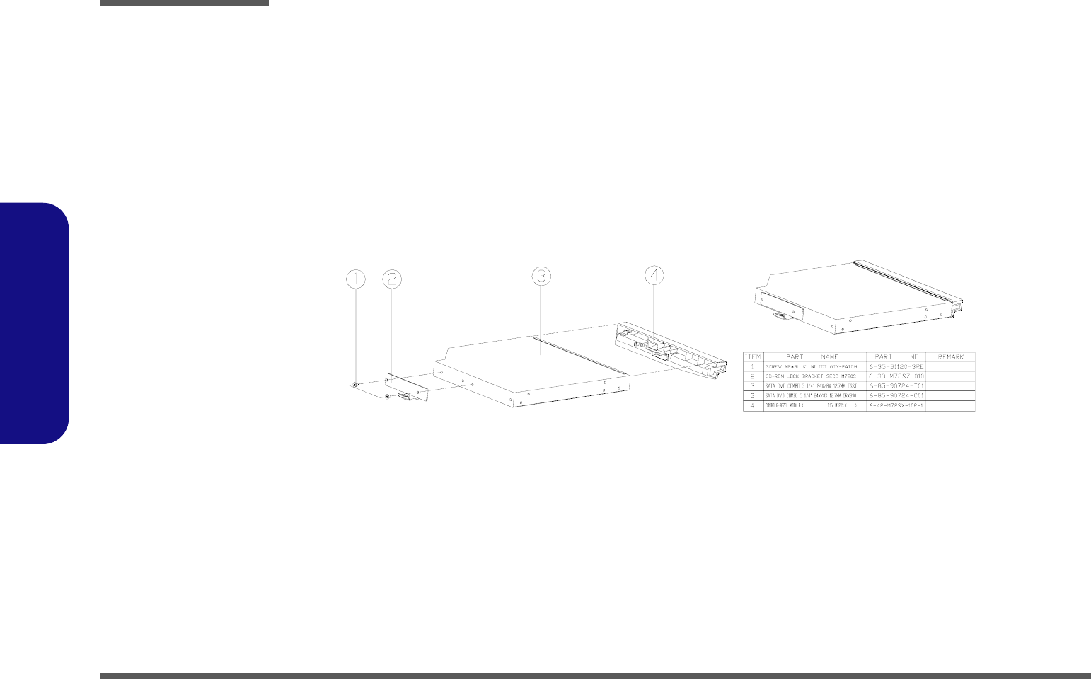
Combo A - 7
A.Part Lists
Combo
Figure A - 5
Combo
無鉛
無鉛
觸點高度降低 世華 無鉛
無鉛
無鉛
Part Lists
A - 8 DVD-COMBO
A.Part Lists
DVD-COMBO
Figure A - 6
DVD-COMBO
無鉛
無鉛
觸點高度降低 世華 無鉛
無鉛
無鉛
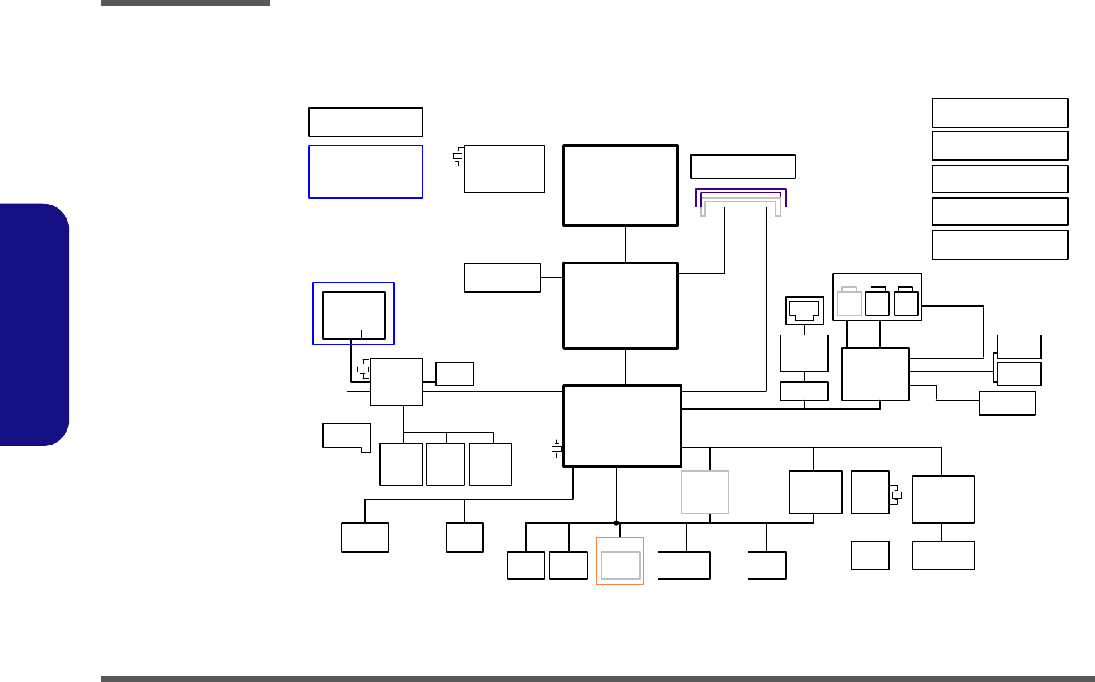
Schematic Diagrams
B-1
B.Schematic Diagrams
Appendix B:Schematic Diagrams
This appendix has circuit diagrams of the M710L notebook’s PCB’s. The following table indicates where to find the ap-
propriate schematic diagram.
Diagram - Page Diagram - Page Diagram - Page
SYSTEM BLOCK DIAGRAM - Page B - 2 CLOCK GENERATOR - Page B - 13 KBC-ITE IT8502E - Page B - 24
Diamondville SC 1/2 - Page B - 3 CH7-M 1/4, SATA - Page B - 14 3VS, 5VS - Page B - 25
Diamondville SC 2/2 - Page B - 4 ICH7-M 2/4, PCI, USB, SPI - Page B - 15 VDD3, VDD5 - Page B - 26
945GSE 1/5, HOST - Page B - 5 ICH7-M 3/4 - Page B - 16 POWER 1.8V/ 0.9V - Page B - 27
945GSE 2/5 - Page B - 6 ICH7-M 4/4 - Page B - 17 POWER 1.5VS/ 1.05VS - Page B - 28
945GSE 3/5, DDR - Page B - 7 MULTI I/O, ODD, CCD BT - Page B - 18 VCORE - Page B - 29
945GSE 4/5 - Page B - 8 NEW CARD, USB - Page B - 19 AC IN, CHARGE - Page B - 30
945GSE 5/5 - Page B - 9 CARD READER JMB385 - Page B - 20 CLICK BOARD - Page B - 31
DDRII SO-DIMM 0 - Page B - 10 LED, FAN, PC BEEP, TP, FP - Page B - 21 Multi B’d, LID, LED, SW, USB - Page B - 32
DDRII SO- DIMM 1 - Page B - 11 PCI-E LAN RTL8102E - Page B - 22 Multi B’d, Mini Card, MDC, RJ11 - Page B - 33
PANEL, INVERTER, CRT - Page B - 12 AUDIO CODEC ALC269 QFN - Page B - 23
Table B - 1
Schematic
Diagrams
Version Note
The schematic dia-
grams in this chapter
are based upon ver-
sion 6-7P-M71L3-003.
If your mainboard (or
other boards) are a lat-
er version, please
check with the Service
Center for updated di-
agrams (if required).
Schematic Diagrams
B - 2 SYSTEM BLOCK DIAGRAM
B.Schematic Diagrams
SYSTEM BLOCK DIAGRAM
Sheet 1 of 32
SYSTEM BLOCK
DIAGRAM
ICH7-M
PROCESSOR
CLEVO M710L System Block Diagram
BGA 437 pin
652 BGA
Intel
Diamondville
SOUTH BRIDGE
FSB
Intel 945 GSE
998 FCBGA
NORTH BRIDGE
AZALIA LINK
1.8V,0.9VS(VTT_MEM)
DDRII
IC S 9L P R3 65
Co lc k G e ne ra t or
1.05VS,1.5VS
RJ-11
Azalia Codec
MD C C ON
AZALIA
MDC
MODULE
INT SPK L
Memory Termination
SO-DIMM0
533 MHz
400 / 533 MHz
JMB385
SOCKET
7IN1
CARD READER
PCIE
USB2.0
480 Mbps
33 MHz
EC
I T E 85 0 2E
32.768 KHz
LPC
TH ER M AL
SE NS O R SMART
BATTERY
TOUCH PAD
SMART
FAN
EM C1 4 02
EC SMBUS
INT. K/B
INT MIC
9*9*1.6mm
14*14*1.6mm
AC-IN,CHARGER
32.768KHz
14.318 MHz
DDRII
SO-DIMM1
SATA I/II 3.0Gb/s
100 MHz
48pins LQFP
128pins LQFP
Re al t ek
AL C2 6 9
SPDIF
OUT HP
OUT
SHEET22
MIC
IN
3VS, 5V S
VDD3,VDD5,3.3V,5V
MULTI I/O BOARD
SPK_R, RJ-11, LED
LID, HOT KEY, USB,
SP I
CLICK BOARD
LCD CONNECTOR,
IVERTER
RJ-45
LA N
RTL8102E
REALTEK
25
MH z
SYSTEM SMBUS
DMI
X2
SOCKET
Mini PCIE
(USB3)
New Card
SOCKET
(USB4)
INT SPK R
VCORE
CCD
( U SB 7)
<12"
<12"
1"~16"
<8"
0.5"~11" 0.1"~13
24 MHz
0.5"~5.5"
<=8"
27mm*27mm*2.4mm
31mm*31mm*2.28mm
17.1mm*8.1mm*1.2mm
TSSOP 64PIN
(Optional)
22mm*22mm
Bluetooth
(USB5)US B 0 USB2
Multi
fuction B'd
USB1
ODDSA T A HD D
(Optional)
Schematic Diagrams
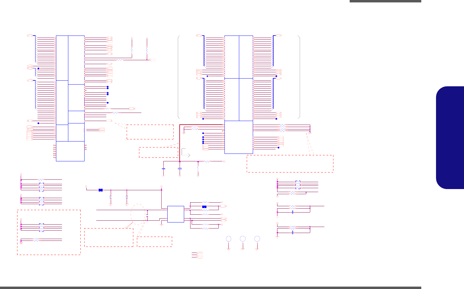
Diamondville SC 1/2 B - 3
B.Schematic Diagrams
Diamondville SC 1/2
Sheet 2 of 32
Diamondville SC 1/2
1. 05 V S
1.05V S 1.05VS
1.05VS
1.05VS
1.05VS
1. 05 V S
VD D3
V_THE RM
3.3V
VD D3
V_TH ERM
1.05VS
1.05VS
H_REQ#[4:0]4
H _AD STB# 04
H_ A# [3 1 :3 ]4
H_ A# [3 1 :3 ]4
H _D#[63:0]4
H_DSTBN#04
H _D#[63:0]4
H_DINV#04
H_ D S T BP# 04
H_DSTBN#14H_ D S T BP# 14
H_DINV#14
PM _TH RM TRI P# 5,13
C PU_BS EL 04
C PU_BS EL 14
C PU_BS EL 24
H_ T R DY # 4
H_ B PRI# 4
H_DEFER# 4
H_ R S #2 4
H_ R S #0 4
H_CPURST# 4
H_ R S #1 4
H_ H IT # 4
H_LO CK# 4
H_ B R0# 4
H_DRDY# 4
H_ H IT M# 4
H_ D B SY # 4
H_ B NR # 4
H_ A DS# 4
H_DSTBP#2 4
H_D#[63:0] 4
H_D#[63:0] 4
H_DSTBN#2 4
H_DINV#2 4
H_DINV#3 4
H_DSTBN#3 4
H_DSTBP#3 4
CLK_CPU_BCLK 12
CLK_CPU_BCLK# 12
1.05VS 3,4,6,7,12,13,16,27
3.3V 11,14.. 18,21,25..27
VD D 3 13,20,23..25,29
H _AD STB# 14
H_FERR#13
H_ A2 0 M #13
H_ IG NN E#13 H _STPC LK #13
H_NMI13
H_INTR13
H_SMI#13
H_INIT# 13
PM_SY SRS T# 15
H_DPRSTP# 13,28
H_DPSLP# 13
H_DPWR# 4
H_CPUSLP# 4,13
H_PWRGD 13
SMC_CPU_THERM 23
SMD_CPU_THERM 23
TH ERM _AL ER T# 23
H_ D # 3 6
H_ D # 3 2
H_ D # 6 2
H _D#31
H _D#16
H _D#15
H_ D # 4 1
H_ D # 5 6
H _D#21
H _D#17 H_ D # 4 9
H _D#29
H_ D # 3 9
H_GTLREF
H_ D # 4 7
H_ D # 3 4
H_ D # 5 3
H _D#27
H_D#3
H_ D # 3 7
H _D#26
H _D#22
H_D#8
H_D#5
H _D#30
H_ D # 4 6
H _D#28
H_D#1 H_ D # 3 3
H_ D # 6 0
H_ D # 5 9
H _D#11
H_D#7
H_D#4
H_ D # 5 0H _D#18
H_D#6
H _D#19
H _D#13 H_ D # 4 5
H_ D # 4 3
H _D#24
H_ D # 4 4
H_ D # 5 4
AC LKPH
H _D#25
H _D#12
H_ D # 4 2
H_ D # 6 1
H_ D # 4 8
H _D#23
H _D#10
H_D#0
H_ D # 3 8
H_ D # 5 7
H_ D # 5 5
H_ D # 5 1
H _D#20
H _D#14
H_ D # 3 5
H_ D # 6 3
H_ D # 5 2
H_D#9
H_D#2
H_ D # 4 0
H_ D # 5 8
Z0202
H_BPM 4#
H_REQ#1
H_A#10
Z0215
H_A#22
H_REQ#2
H_T RS T#
H_T DO
H_A20M#
H_A#27
H_A#15
H_A#21
H_A#11
H_BPM 1#
H_REQ#3
H_A#13
H_A#4
H_IER R#
H_A#14
H_A#16
H_T MS
H_T CK
H_A#30
H_A#28
H_A#18
H_A#17
H_A#9
H_A#7
H_A#5
H_A#3
H_T HE RM DC
H_A#19
H_A#12
H_A#34
H_A#32
H_ ST PC L K #
H_A#23
H_A#8
H_T DI
H_A#33
H_ SM I#
H_ R EQ# 4
H_BPM 0#
H_ IG NN E#
H_A#31
Z0201
Z0216
H_ NM I
H_A#26
H_A#35
H_ BR 1 #
H_BPM 5#H_A#24
H_REQ#0
H_A#6
H_ IN TR
H_A#29
H_A#20
H_T HE RM DA
H_A#25
H_IGNNE#
H_A#32
H_A#34
H_A#35
H_A#33
H_DP#0
H_DP#1
DCLKPH
H_ M CE RR
H_ ED M
H_EXTG BRE F
H_ F O R CEP R#
H_ H F PL L
H_ R S P#
H_DPSLP#
H_PWRGD
H_INTR
H_ PW RG D
H_D PSLP#
H_ D PW R #
H_ D PR ST P#
CO M P0
CO M P1
CO M P2
CO M P3
H_ D P# 2
H_ D P# 3
H_CPU_CMREF
H_ C OR E _ D E T
H_ EX TGB RE F
H_DPW R#
H_THERMDC
H_THERMDA
Z0213
Z0214
H_CPU_CMREF
H_ B P M5 #
H_ PR O CH OT#
H_ T M S
H_TCK
H_TRST#
H_ T D I
H_PROCHOT#
H_A20M#
H _STPCLK#
H_NMI
H_DPRSTP#
H_SMI#
H_BPM 3#
R186 27.4_1%_04
R39 56_04
C298 1U _6.3V_04
R159 *1K_04
R158 *1K_04
C3 7
0.1U_10V_X7R _04
R38 22_04
RN 2 2
* 8 P 4 R X 1K _0 4
1
2
3
4 5
6
7
8
R17 1K_1%_04
RN 2 0
8P4RX1K_04
1
2
3
4 5
6
7
8
R15 2K_1%_04
C3 0 2
10 U _ 6. 3V _0 6
C18
*0.1U _16V_04
C4 3 0 .1U_ 1 0 V _ X7R _ 0 4
NC
AD DR GR OU P 0
CONTROL
XDP/ITP SIGNALS
TH ER MH CL K
AD DR GR OU P 1
U10A
INTEL AT O M
P21
H20
N20
R20
J19
N19
G2 0
M1 9
H21
L20
M2 0
K19
J20
K20
N21
J21
G1 9
P20
R19
C19
F19
E21
A16
D19
C14
C18
C20
E20
D20
B18
C15
B16
B17
C16
B19
U18
T16
J4
R16
T15
R15
U17
D6
G6
H6
K4
K5
M1 5
L16
C21
C1
A3
V11
V12
G17
E4
E5
H17
K17
J18
H15
J15
K18
J16
M17
N16
M16
L17
K16
V15
AA17
V20
D15
W18
Y17
U20
W19
F16
V16
W20
T20
T21
T19
Y18
V19
Y19
U21
L21
D17
M1 8
A17
B14
B15
A14
A[3]#
A[4]#
A[5]#
A[6]#
A[7]#
A[8]#
A[9]#
A[10]#
A[11]#
A[12]#
A[13]#
A[14]#
A[15]#
ADSTB[0]#
REQ[0]#
REQ[1]#
REQ[2]#
REQ[3]#
REQ[4]#
A[17]#
A[18]#
A[19]#
A[20]#
A[21]#
A[22]#
A[23]#
A[24]#
A[25]#
A[26]#
A[27]#
A[28]#
A[29]#
A[30]#
A[31]#
ADSTB[1]#
A20M#
FERR#
IG N NE#
STPCLK#
LIN T0
LIN T1
SMI#
NC1
NC2
NC3
NC4
NC5
NC6
NC7
RSV D3
RSV D2
RSV D1
BC LK[0]
BC LK[1]
PROCHOT
TH E R M D A
TH ERM DC
THER MTR IP#
BP M[0]#
BP M[1]#
BP M[2]#
BP M[3]#
PRDY#
PRE Q#
TC K
TD I
TDO
TM S
TRST#
BR1#
HIT#
HITM#
R ESET#
R S [0 ]#
R S [1 ]#
R S [2 ]#
TRDY#
IER R#
INIT#
LOC K#
BR0#
DEFER#
DRDY#
DBS Y#
AD S#
BN R#
BP RI#
A[16]#
AP0
AP1
A[32]#
A[33]#
A[34]#
A[35]#
DATA GRP 3
DATA GRP 0 DATA GRP 1
MISC
DATA GRP 2
U 10B
IN TE L ATOM
Y11
W10
Y12
AA 14
AA 11
W12
AA 16
Y10
Y9
Y13
W15
AA 13
Y16
W13
AA9
W9
Y14
Y15
W16
AA5
Y8
W3
U1
W7
W6
Y7
AA6
Y3
W2
V3
U2
T3
AA8
V2
W4
Y4
Y5
Y6
A7
T17
R6
J6
H5
G5
T1
T2
F20
F21
R18
R17
U4
V17
N18
B7
C2
G2
F1
D3
B4
E1
A5
C3
A6
F2
C6
B6
B3
C4
C7
D2
E2
F3
C5
R3
R2
P1
N1
M2
P2
J3
N3
G3
H2
N2
L2
M3
J2
H1
J1
K2
K3
L1
V9
R4
M4
D4
A13
U5
V5
M6
N15
N6
P17
T6
D[0 ]#
D[1 ]#
D[2 ]#
D[3 ]#
D[4 ]#
D[5 ]#
D[6 ]#
D[7 ]#
D[8 ]#
D[9 ]#
D[10]#
D[11]#
D[12]#
D[13]#
D[14]#
D[15]#
DST B N[0 ]#
DST B P [0 ]#
DIN V[0 ]#
D[16]#
D[17]#
D[18]#
D[19]#
D[20]#
D[21]#
D[22]#
D[23]#
D[24]#
D[25]#
D[26]#
D[27]#
D[28]#
D[29]#
D[30]#
D[31]#
DST B N[1 ]#
DST B P [1 ]#
DIN V[1 ]#
GT L R E F
BIN IT#
EDM
BSEL[0]
BSEL[1]
BSEL[2]
COMP[0]
COMP[1]
COMP[2]
COMP[3]
DPRSTP#
DPSLP#
DP W R #
PW RG OO D
SLP#
CMREF[1]
D[48]#
D[49]#
D[50]#
D[51]#
D[52]#
D[53]#
D[54]#
D[55]#
D[56]#
D[57]#
D[58]#
D[59]#
D[60]#
D[61]#
D[62]#
D[63]#
DSTBN[3]#
DSTBP [3] #
DINV[3]#
D[32]#
D[33]#
D[34]#
D[35]#
D[36]#
D[37]#
D[38]#
D[39]#
D[40]#
D[41]#
D[42]#
D[43]#
D[44]#
D[45]#
D[46]#
D[47]#
DSTBN[2]#
DSTBP [2] #
DINV[2]#
DP# 0
DP# 1
DP#2
DP#3
CORE_DET
ACLK PH
DC L KP H
EXTBGR EF
FOR C EPR #
HFP L L
MC E R R #
RSP #
R10 *15m il_short
R 42 * 0_04
R2 0 1 K_ 1 % _0 4
R187 54.9_1%_04
R161 54.9_1%_04
RN 1
8P4RX56_04
1
2
3
4 5
6
7
8
R 1 78 4. 7 K _0 4
R 177 *10K_04
C30
* 1U_6.3V_04
H2 3
C237B128D 107
H2 2
C237B128D107
R12 10K_04
RN 2 4
*8 P 4 R X 1K _ 04
1
2
3
4 5
6
7
8
C303
1000p_50V_04
U9
EM C 1402
1
2
3
4
5
6
7
8
VD D
D+
D-
THE RM
GND
ALER T
SDA TA
SC LK
R 1 79 4. 7 K _0 4
R 16 *0_04
R160 *1K_1%_04
R 14 *10m il_shor t
R 192 1K_1%_04
R 191
330_04
R24 *1K_1%_04
R32 56_04
R30
56_04
R163 1K_1%_04
R2 3
2K_1%_04
R164 2K_1%_04
R25 *1K_04
R162 27.4_1%_04
H24
C 237B128D 107
PM_THRMTRIP# should connect to
ICH7 and GMCH without T-ing
Layout note:
FROM IMVP6
Voltage
COMP0, COMP2: 0.5" Max, Zo=27.4 Ohms
COMP1, COMP3: 0.5" Max, Zo=55 Ohms
Best estimate is 18 mils wide trace for outer layers and 14
mils wide trace if on internal layers.
translation
La yo ut n o te:
Zo=60 Ohm
Zo=55 Ohm
Zo=55 Ohm
Close to Thermal IC
Layout Note:
Layout Note:
Route H_THERMDA and
H_THERMDC on same layer.
10 mil trace on 10 mil
spacing.
Thermal IC
Within 2.0" of the CPU
Layout Note:
6-02-01402-LD0
6-02-83771-LL0
Layout Note:
H_GTLREF
0.5" max, Zo= 55 Ohms
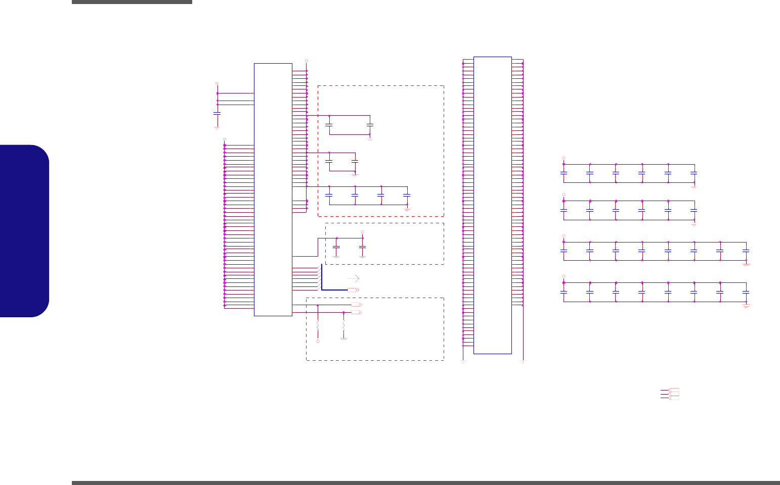
Schematic Diagrams
B - 4 Diamondville SC 2/2
B.Schematic Diagrams
Diamondville SC 2/2
VC O RE
1.05VS
VC ORE
VC O RE
VC O RE
1.05VS
VC O RE
VC O RE
1.5VS
H_VID[6:0] 28
VC C SE NSE 28
VS SSE NSE 28
1.05VS 2, 4,6,7,12,13,16,27
1.5VS 5. .7,14,16..18,22,27
VC O RE28
VC C SEN SE
VSS SEN SE
H_VI D1
H_VI D4
H_VI D3
H_VI D2
H_VI D6H_VID[6:0]
H_VI D5
H_VI D0
C323
*10U_6. 3V_06
C46
*10U_6.3V _06
C72
10U_6.3V_06
C317
*10U_6.3V _06
C320
*10U_6.3V_06
C70
10U_6.3V_06
C48
* 10U_6. 3V_06
C44
* 10U_6. 3V _06
C42
0.1U_10V_X7R_04
U10C
INTEL ATOM
A10
A11
A12
B10
B11
B12
C10
C11
C12
D10
D11
D12
E10
E11
E12
F10
F11
F12
G10
G11
G12
H10
H11
H12
J10
J11
J12
K10
K11
K12
L10
L11
L12
M10
M11
M12
N10
N11
N12
P10
P11
P12
R10
R11
R12
D9
E9
F8
F9
G8
G14
H8
H14
J8
J14
K8
K14
L8
L14
M8
M14
N8
N14
P8
P14
R8
R14
T8
T14
U8
U9
U10
U11
U12
U13
F14
F13
E14
E13
D7
F15
D16
E18
G15
G16
E17
G18
C13
D13
C9
U14
V10
A9
B9
VCCP1
VCCP2
VCCP3
VCCP4
VCCP5
VCCP6
VCCP7
VCCP8
VCCP9
VCCP10
VCCP11
VCCP12
VCCP13
VCCP14
VCCP15
VCCP16
VCCP17
VCCP18
VCCP19
VCCP20
VCCP21
VCCP22
VCCP23
VCCP24
VCCP25
VCCP26
VCCP27
VCCP28
VCCP29
VCCP30
VCCP31
VCCP32
VCCP33
VCCP34
VCCP35
VCCP36
VCCP37
VCCP38
VCCP39
VCCP40
VCCP41
VCCP42
VCCP43
VCCP44
VCCP45
VTT2
VTT3
VTT4
VTT5
VTT6
VTT7
VTT8
VTT9
VTT10
VTT11
VTT12
VTT13
VTT14
VTT15
VTT16
VTT17
VTT18
VTT19
VTT20
VTT21
VTT22
VTT23
VTT24
VTT25
VTT26
VTT27
VTT28
VTT29
VTT30
VTT31
VCCPC64
VCCPC63
VCCPC62
VCCPC61
VC C A
VID[0]
VID[1]
VID[2]
VID[3]
VID[4]
VID[5]
VID[6]
VCCSENSE
VS SSE NSE
VTT1
VTT32
VCCF
VCCQ1
VCCQ2
C54
1U_6.3V _04
C63
1U_6.3V_04
C36
10U_6.3V_06
C325
10U_6.3V_06
C324
10U_6.3V_06
C68
*1U_6.3V_04
C67
1U_6.3V_04
C55
*1U_6.3V_04
C65
*1U_6.3V_04
C52
*1U_6.3V_04
C40
0.1U_10V_X7R_04
C51
*1U_6. 3V_04
C69
*1U_6. 3V_04
C62
*1U_6.3V_04
U10D
INTE L ATO M
A2
A4
A8
A15
A18
A19
A20
B1
B2
B5
B8
B13
B20
B21
C8
C17
D1
D5
D8
D14
D18
D21
E3
E6
E7
E8
E15
E16
E19
F4
F5
F6
F7
F17
F18
G1
G4
G7
G9
G21
H3
H4
H7
H9
H13
H16
H18
H19
J5
J7
J9
J13
J17
K1
K6
K7
K9
K13
K15
K21
L3
L4
L5
L6
L7
L9
L13
L15
L18
L19
M1
M5
M7
M9
M13
M21
N4
AA20
AA19
AA18
AA15
AA12
AA10
AA7
AA4
AA3
AA2
Y21
Y20
Y2
Y1
W21
W17
W14
W11
W8
W5
W1
V21
V18
V14
V13
V8
V7
V6
V4
V1
U19
U16
U15
U7
U6
U3
T18
T13
T12
T11
T10
T9
T7
T5
T4
R21
R13
R9
R7
R5
R1
P19
P18
P16
P15
P13
P9
P7
P6
P5
P4
P3
N17
N13
N9
N7
N5
G13
V SS1
V SS2
V SS4
V SS5
V SS6
V SS7
V SS8
V SS9
V SS10
V SS11
V SS12
V SS13
V SS14
V SS15
V SS16
V SS17
V SS18
V SS19
V SS20
V SS21
V SS22
V SS23
V SS24
V SS25
V SS26
V SS27
V SS28
V SS29
V SS30
V SS31
V SS32
V SS33
V SS34
V SS35
V SS36
V SS37
V SS38
V SS39
V SS41
V SS45
V SS46
V SS48
V SS49
V SS51
V SS52
V SS53
V SS54
V SS55
V SS56
V SS57
V SS58
V SS59
V SS60
V SS61
V SS62
V SS63
V SS64
V SS65
V SS66
V SS67
V SS68
V SS69
V SS70
V SS71
V SS72
V SS73
V SS74
V SS75
V SS76
V SS77
V SS78
V SS79
V SS80
V SS81
V SS82
V SS83
V SS84
VSS95
VSS96
VSS97
VSS98
VSS99
V SS100
V SS101
V SS102
V SS103
V SS104
V SS105
V SS106
V SS107
V SS108
V SS109
V SS110
V SS111
V SS112
V SS113
V SS114
V SS115
V SS116
V SS117
V SS118
V SS119
V SS120
V SS121
V SS122
V SS123
V SS124
V SS125
V SS126
V SS127
V SS128
V SS129
V SS130
V SS131
V SS132
V SS133
V SS134
V SS135
V SS136
V SS137
V SS138
V SS139
V SS140
V SS141
V SS142
V SS143
V SS144
V SS145
V SS146
V SS147
V SS148
V SS149
V SS151
V SS152
V SS153
V SS154
V SS155
V SS156
V SS157
V SS158
V SS159
V SS160
V SS161
V SS162
V SS42
C50
* 1U_6. 3V_04
R31
100_1%_04
C56
1U_6.3V_04
C41
*22U_6.3V_08
R29
100_1%_04
C58
1U_6.3V_04
C71
10U_6.3V_06
C66
1U_6.3V_04
C39
*10U_6.3V _06C64
1U_6.3V_04
C57
1U_6.3V_04
C73
1U_6.3V_04
C76
1U_6.3V_04
C47
*1U_6.3V_04
C45
*1U_6.3V_04
C60
10U_6.3V_06
C53
0.1U_10V_X7R_04
C74
10U_6.3V_06
Route VCCSENSE and
VSSSENSE traces at 27.4Ohm
with 50 mil spacing.
Place PU and PD within 1
i n ch of CP U .
Layou t note:
Near pin D7
Layout note:
20mils
+VCCP = 1.05V (0.997V~1.102V)
PLACE NEAR CPU
Zo=55 Oh m 1/2 spac ing
2A
Sheet 3 of 32
Diamondville SC 2/2
Schematic Diagrams
945GSE 1/5, HOST B - 5
B.Schematic Diagrams
945GSE 1/5, HOST
Sheet 4 of 32
945GSE 1/5, HOST
1.05VS
1.05VS
1.05V S 1.05VS
1.05VS
1.05VS
1.05VS
H _D #[63:0]2
1.05V S 2,3,6,7,12,13,16, 27
H_A#[31:3] 2
H_ADS# 2
H_REQ#[4:0] 2
CL K _M C H_ B C L K # 1 2
H_DINV#1 2
H _ DE F ER# 2
H_DINV#3 2
H_DINV#2 2
CL K _M C H_ B C L K 1 2
H_DINV#0 2
H_ADSTB#1 2
H_ADSTB#0 2
H_BNR# 2
H _BPR I# 2
H_BR0# 2
H_CPURST# 2
CLK_ BS EL 0 1 2C PU _B SEL02
C PU _B SEL22
MC H_B SEL1 5
CLK_ BS EL2 12
CLK_ BS EL1 12
MC H_B SEL2 5
MC H_B SEL0 5
C PU _B SEL12
H_DBSY# 2
H_DSTBN#2 2
H_DSTBN#3 2
H_TRDY# 2
H_RS#0 2
H_DSTBP#2 2
H_RS#2 2
H_HITM# 2
H_DSTBN#0 2
H _ DR DY # 2
H_DSTBP#0 2
H_LOCK# 2
H_DSTBP#1 2
H_DSTBP#3 2
H_DPW R# 2
H_HIT# 2
H_DSTBN#1 2
H_CPUSLP# 2,13
H_RS#1 2
MCH_HXRCOMP
MCH _HY R COMP
MCH _HY SC OMP
M CH _HXSC O MP
H_REQ#3
H_REQ#1
H _A#19
H_A#7
H _D#63
H _D#57
H _D#32
H _D#31
H _D#26
H_D#3
M CH _ HV REF 0
H _A#27
H _D#60
H _D#18
H _D#17
H_D#6
H _A#17
H _D#50
H _D#37
H _D#36
H _D#21
H _A#28
H _A#21
H _A#14
H _D#62
H _D#54
H_D#8
H_D#0
H _D#19
H _D#11
MC H _H Y S W IN G
H _A#30
H_A#8
H _D#46
H _D#28
H _D#27
H_REQ#2
H_REQ#0
H_A#6
H _D#58
H _D#35
H _D#34
H _D#33
MC H _H XSW IN G
MC H _H X RC O MP
H _A#16
H _A#15
H _D#53
H _D#23 H _A#25
H _A#10
H _D#44
H _D#39
H _D#14
H _A#20
H _A#12
H_A#4
H_A#3
H _D#47
H _D#30
H _D#24
H_D#7
H _A#24
H _D#48
H _D#41
H _D#29
H _D#20
H _A#31
H _A#29
H _A#18
H _D#45
H _D#25
H_D#2
MC H _H Y S C O M P
H _A#11
H_A#5
H _D#51
H _D#38
H _D#12
MC H _H Y R C OM P
H _A#26
H _A#13
H _D#59
H _D#16
H _D#13
H_D#5
MC H _H XSC OM P
H _D#22
H _D#10
H_D#9
H_A#9
H _D#55
H _D#52
H _D#40
H _D#15
H_REQ#4
H _A#23
H _A#22
H _D#61
H _D#56
H _D#49
H _D#43
H _D#42
H_D#4
H_D#1
C329
*1U _6.3V_04
C 305
* 1U_ 6.3V_04
R 206 * 10mil_short
R172 24.9_1%_04
R 200 * 10mil_short
C35
0.1U_10V_X7R_04
R 183
221_1%_04
R 193 * 10mil_short
R174
100_1%_04
C327
0.1U _10V_X7R_04
R176
200_1%_04
R181 24.9_1%_04
R171
221_1%_04
R173
100_1%_04
R196
1K_04
R 205 1K_04
R 184
100_1%_04
R202
56_04
R198
1K_04
R194
1K_04
R175 54.9_1%_04
R180 54.9_1%_04
C315
0.1U_10V_X7R _04
R 199 *0_04
R201
1K_04
R 197 *0_04
R195
1K_04
HOST
945G SE
U11A
A10
A6
C1 5
J1
K1
H1
C4
F6
H9
H6
F7
E3
C2
C3
K9
F5
J7
K7
H8
E5
K8
J8
J2
J3
N1
M5
K5
J5
H3
J4
N3
M4
M3
N8
N6
K3
N9
M1
V8
V9
R6
T8
R2
N5
N2
R5
U7
R8
T4
T7
R3
T5
V6
V3
W2
W1
V2
W4
W7
W5
V5
AB4
AB8
W8
AA9
AA8
AB1
AB7
AA2
AB5
F8
D12
C13
A8
E13
E12
J12
B13
A13
G13
A12
D14
F14
J13
E17
H15
G15
G14
A15
B18
B15
E14
H13
C14
A17
E15
H17
D17
G17
F10
C12
H16
E2
B9
C7
G8
B10
AA6
AA5
C10
C6
H5
J6
T9
U6
G7
E6
F3
M8
T1
AA3
F4
M7
T2
AB3
C8
B4
C5
G9
E9
G12
B8
F12
A5
B6
G10
E8
E10
E1
H_ XRC O MP
H_XSC OM P
H_XSW IN G
H_ Y RC OM P
H_ Y SCO M P
H_ Y SW IN G
H_ D #_ 0
H_ D #_ 1
H_ D #_ 2
H_ D #_ 3
H_ D #_ 4
H_ D #_ 5
H_ D #_ 6
H_ D #_ 7
H_ D #_ 8
H_ D #_ 9
H_D #_10
H_D #_11
H_D #_12
H_D #_13
H_D #_14
H_D #_15
H_D #_16
H_D #_17
H_D #_18
H_D #_19
H_D #_20
H_D #_21
H_D #_22
H_D #_23
H_D #_24
H_D #_25
H_D #_26
H_D #_27
H_D #_28
H_D #_29
H_D #_30
H_D #_31
H_D #_32
H_D #_33
H_D #_34
H_D #_35
H_D #_36
H_D #_37
H_D #_38
H_D #_39
H_D #_40
H_D #_41
H_D #_42
H_D #_43
H_D #_44
H_D #_45
H_D #_46
H_D #_47
H_D #_48
H_D #_49
H_D #_50
H_D #_51
H_D #_52
H_D #_53
H_D #_54
H_D #_55
H_D #_56
H_D #_57
H_D #_58
H_D #_59
H_D #_60
H_D #_61
H_D #_62
H_D #_63
H_A#_3
H_A#_4
H_A#_5
H_A#_6
H_A#_7
H_A#_8
H_A#_9
H _A #_10
H _A #_11
H _A #_12
H _A #_13
H _A #_14
H _A #_15
H _A #_16
H _A #_17
H _A #_18
H _A #_19
H _A #_20
H _A #_21
H _A #_22
H _A #_23
H _A #_24
H _A #_25
H _A #_26
H _A #_27
H _A #_28
H _A #_29
H _A #_30
H _A #_31
H_AD S#
H _A DSTB# _ 0
H _A DSTB# _ 1
H _VR EF0
H_BNR#
H_BPR I#
H_BREQ0#
H_ C P UR S T#
HCLKN
HC L K P
H_DBSY#
H_ D E FE R#
H_ D INV # _ 0
H_ D INV # _ 1
H_ D INV # _ 2
H_ D INV # _ 3
H_DPW R#
H_DRDY#
H_ D S TB N# _ 0
H_ D S TB N# _ 1
H_ D S TB N# _ 2
H_ D S TB N# _ 3
H_DSTBP#_0
H_DSTBP#_1
H_DSTBP#_2
H_DSTBP#_3
H_HIT#
H_ H IT M#
H _LOC K#
H_R EQ#_0
H_R EQ#_1
H_R EQ#_2
H_R EQ#_3
H_R EQ#_4
H _RS#_0
H _RS#_1
H _RS#_2
H_SLPCPU#
H_TRDY#
H _VR EF1
C25
* 0.1U _10V _X7R _04
10 mils wide, 20 mils spacing
Layout Notice:
MCH_HXSWING and MCH_HYSWING
should be 10 mils traces
and 20 mils spacing
Layout Notice:
Layout Notice:
0.1uF should be placed
100mils or less from GMCH
pin.
B SE L 2 B SE L0 Fr eq ue n cy FSB
Ho st C l oc k
BS EL 1
FS B5 3 3100 1 33 MH z
FS B4 0 0101 1 00 MH z
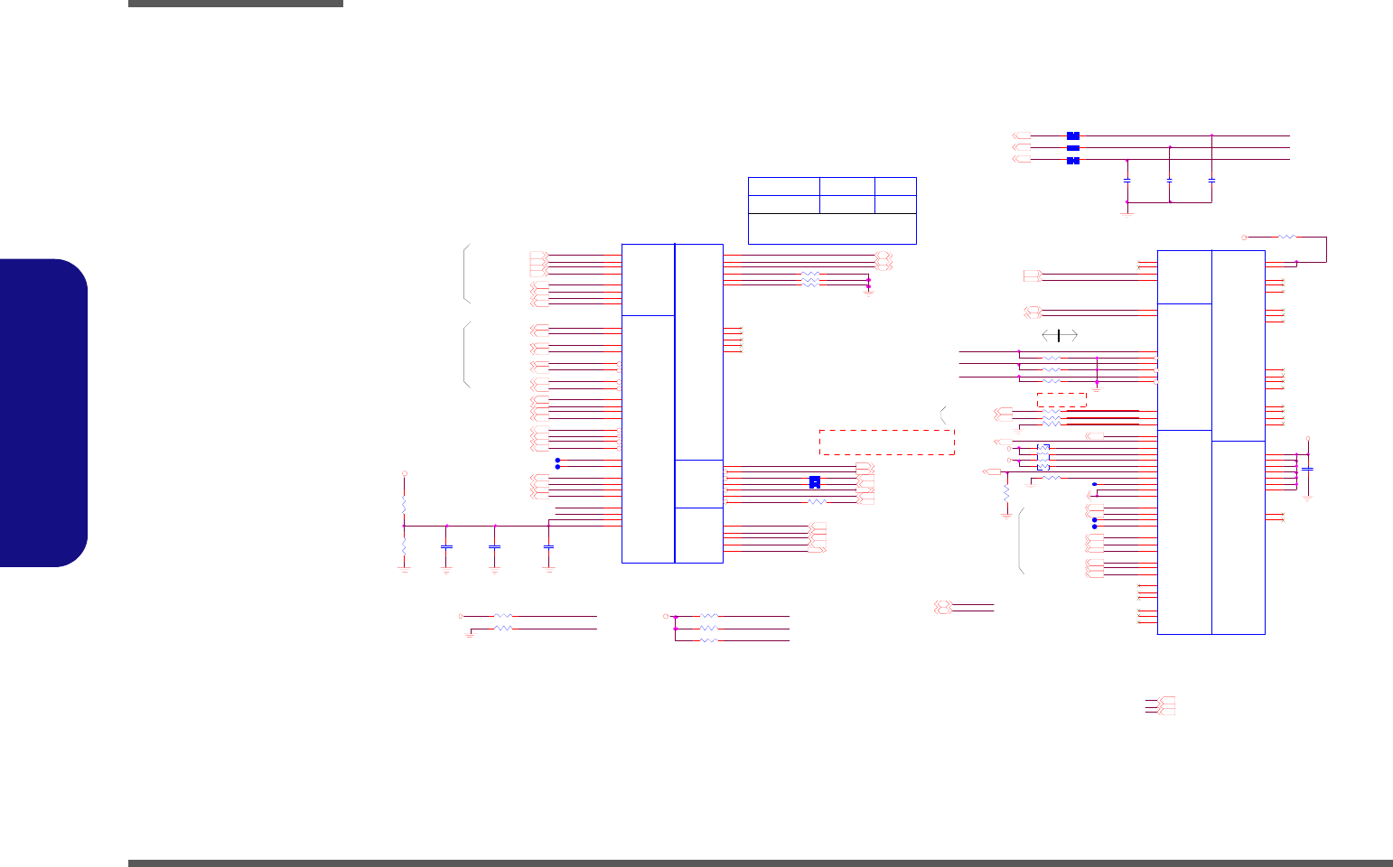
Schematic Diagrams
B - 6 945GSE 2/5
B.Schematic Diagrams
945GSE 2/5
Sheet 5 of 32
945GSE 2/5
1.8V
3.3VS
1.8V 3.3VS
1.5VS
1.5VS
3.3VS
1 . 5V S 3 , 6 , 7 , 1 4, 16 . . 1 8 , 2 2 , 2 7
3 .3V S 6 ,7 ,9 .. 2 4 ,27 ,2 8
1.8V 7,9,10,26
M_C LK_DDR09M_C LK_DDR19
M_C LK_DDR210 M_C LK_DDR310
M_C LK_DDR0#9M_C LK_DDR1#9
M_C LK_DDR2#10
M_C LK_DDR3#10
M CH _BSEL1 4
M CH _BSEL0 4
M CH _BSEL2 4
M_C KE09
M_C KE210
M_C KE310
M_C S3#10
M_C S0#9
M_C S2#10
M_ODT310 M_ODT210
M_ODT09PM _BMB USY # 15
IMVP 6_ PW RG D 15,28
MC H_ IC H_ S Y NC # 1 4
PM_EXTTS0# 9,10
MC H_ C LK RE Q # 1 2
CLK_DR EF 12
CLK_DR EF# 12
CLK_DR EFSS # 12
CLK_DR EFSS 12
PM_ D PRS LP VR 15,28
PM_THR MTR IP# 2,13
PLT_RST# 14 ,1 5
CL K_ PC IE_ 3G P LL12
C LK _P CIE_3G PLL#12
DAC_DDCACLK11
LVDS -L1N11
LVDS -L0N11
BLO N11
LVDS -L1P11
LVDS -L2N11
LVDS -L2P11
LVDS -L0P11
LVDS -LC LKN11
LV D S -L C L K P11
EN AVDD11
DAC_DDCADATA11
M_C KE19
M_C S1#9
M_ODT19
L_DD C_C LK11
L_DDC_DATA11
DM I _ TXP 114
DM I _ TXN 014
DM I _ TXP 014
DM I _ TXN 114
DMI_RXN014
DMI_RXP114
DMI_RXN114
DMI_RXP014
DAC _ RE D11
D AC _G R EEN11
DAC_BLUE11
L_ B K LT C T L11,23
DAC _VSYN C11
DA C_HS YN C11
PEG _CO MP
DAC _ B L UE_ 9 4 5
L_CTLBDATA
Z0513
L_ D D C _ D A T A
L_ D D C _ C L K
L_ C LK C T L A
Z0512
DAC_GREEN_945
DAC _ RE D _ 94 5
L_ I B G
Z0511
M_ R CO MP N
M_ R CO MP P PM _EXTTS #_ 1
PM _EXTTS #_ 0
MCH _CLKR EQ#
N_ C R T_ V SY NC
N_C RT_RE FSET
N_ C RT_ HS YN C
M_CLK_DDR2
NB_ R S TIN#
M_CLK_DDR2#
M_CLK_DDR3
MC H_ C F G3
M_CLK_DDR1#
M_RCOMPN
Z0502
M_CLK_DDR0#
M_RCOMPP
Z0501
M_CLK_DDR0
MC H_ C F G6
M_CLK_DDR3#
PM_ EXTTS#_1
M_CLK_DDR1
MCH_CFG5
L_DDC_CLK
L_DDC_DATA
M_VRE F_MCH
DMI_TXP0
DMI_TXN0
DMI_TXP1
DMI_TXN1DMI_TXN1
DMI_RXN1
DMI_RXP0
DMI_RXN0
DMI_RXP1
DAC_RED_945
DAC_GREEN_945
DAC_BLUE_945
PM_ EXTTS#_0
R40 150_1%_04
R210 24.9_1%_04
R46 150_1%_04
R1 6 8
10K_1%_04
R5 7 *1 0 m il _ s h or t
C304
2.2U_6.3V_06
R5 6 1 0 0 _ 04
R185 80.6_1%_04
R44 150_1%_04
R182 80.6_1%_04
R167
10K_1%_04
CFG/RSVD
DMI
PM
DDR2 MUXING
CLK
94 5 G S E
U1 1 B
Y29
Y32
Y28
Y31
V28
V31
V29
V32
AF33
AG1
AJ 1
AM30
AG33
AF1
AK1
AN30
AN21
AN22
AF26
AF25
AG14
AF12
AK14
AH12
AJ21
AF11
AE12
AF14
AJ14
AJ12
AN12
AN14
AA33
AE1 A27
A26
J33
H33
J15
AB29
W27
G2 1
F26
C18
E18
G2 0
J20
J18
H26
F18
J22
G1 8
E31
A3
C17
K32
K31
DMI_RXN_0
DMI_RXN_1
DMI_RXP_0
DMI_RXP_1
DMI_TXN_0
DMI_TXN_1
D MI _TXP_0
D MI _TXP_1
SM_CK_0
SM_CK_1
SM_CK_2
SM_CK_3
SM_CK#_0
SM_CK#_1
SM_CK#_2
SM_CK#_3
S M_CK E_0
S M_CK E_1
S M_CK E_2
S M_CK E_3
SM_CS#_0
SM_CS#_1
SM_CS#_2
SM_CS#_3
SM_OCDCOMP_0
SM_OCDCOMP_1
S M_OD T_0
S M_OD T_1
S M_OD T_2
S M_OD T_3
SM_RCOMPN
SM_RCOMPP
SM_VREF_0
SM_VREF_1 D_REFCLKN
D_REFCLKP
D_ R EF SS C L KN
D_REFSSCLKP
TH R M T R I P #
PW R OK
RSTIN#
PM _B MBU SY #
PM_EXTTS#_0
CFG_0
CFG_1
CFG_2
CFG_5
CFG_6
PM_EXTTS#_1
RESERVED8
CL KR E Q #
CFG_3
PM_ICHSYNC#
RESERVED9
RESERVED7
RESERVED1
RESERVED2
C86
0.1U _10V_X7R_04
R45 255_1%_04
R5 9 1 0 K_ 0 4
R5 8 1 0 K_ 0 4
R51 39_04
R50 39_04
C309
0.1U_10V_X7R _04
R48 1.5K_04
R4 3 *1 0 m il_ s h ort
R4 7 *1 0 m il_ s h ort
R4 1 *1 0 m il_ s h ort
R188 10K_04
R55
100K _04
RN 2 1
8P4RX10K_04
1
2
3
45
6
7
8
SDVO
LVDS VGA
TV
MISC
945G SE
U11F
J27
Y26
AA26
H27
A21
C2 0
E20
G2 3
B21
C2 1
D2 1
H20
H22
A24
A23
E25
F25
C25
D25
F27
D27
H25
H30
G29
F28
E28
G28
H28
K30
K27
J29
J30
K29
D30
C30
G31
F32
D31
H31
G32
C31
N2 8
M3 2
P33
R3 2
P28
N3 2
P32
T32
M3 0
P30
T30
N3 0
R3 0
T29
R2 8
M2 8
F33
D33
F30
E33
D32
F29
A30
A29
G2 6
J26
SD VO_C TRLCLK
G_ C L KN
G_ C L KP
SD VO_C TRLDA TA
TV_D ACA
TV_D ACB
TV_DAC C
TV_IREF
TV _I RTNA
TV _I RTNB
TV_IRTNC
CR T_ DD C_ C LK
CR T_ DD C_ D AT A
CR T _ BL UE
CR T _ BL UE#
CR T_ GR EEN
CR T_ GR EEN #
CR T_ RED
CR T_ RED #
CR T_VSY NC
CR T_ HSY NC
RE FSET
L_BKLTCTL
L_BKLTEN
L_CLKC TLA
L_CTLBDA TA
L_DD C_C LK
L_DD C_D ATA
L_VDD EN
L_IBG
L_VBG
L_VREF H
L_VREF L
LA_CLKN
LA_CLKP
LA_DATAN _0
LA_DATAN _1
LA_DATAN _2
LA_DATAP _0
LA_DATAP _1
LA_DATAP _2
SD VO _R ED
SDVO_GREEN
SDV O_BLUE
SDV O_CLKP
SD VO _RED #
SDVO _GR EEN #
SD VO_BL U E#
SD VO _CLKN
SD VO _TVC LKIN
SD VO_IN T
SD VO_FL D STALL
SDVO_TVCLKIN#
SD VO _IN T#
SD VO _F LD STALL#
EXP_A_ CO MPI
EXP_A_ IC OM PO
LB_DATAN _0
LB_DATAN _1
LB_DATAN _2
LB_DATAP _0
LB_DATAP _1
LB_DATAP _2
LB_CLKN
LB_CLKP
TV_DCONSEL0
TV_DCONSEL1
R 3 4 * 2. 2K _ 0 4
R 3 7 * 2. 2K _ 0 4
R 190 2.2K_04
C1 1 7
22P_50V_04
C108
22P_50V_04
C102
22P_50V_04
R6 0 *1 0 m il _ s h or t
C3 1 4
0. 1U _ 1 0V _X 7 R _0 4
SL Z di f f= 10 0 Oh m
MS Zdiff=95 Ohm
Zdiff=70 Ohm
Zo=100 Ohm
Zo=50 Ohm Zo=37.5 Ohm
Zo=55 Ohm
Minimize REFSET routing
length and shield with VSS
DMIx2 Defalt
Calistoga Strapping
MCH_CFG5
LOW HIGH
RSVD.
MCH _C FG3 Res erve
MCH _C FG6 Res erve
MAX=0.5"
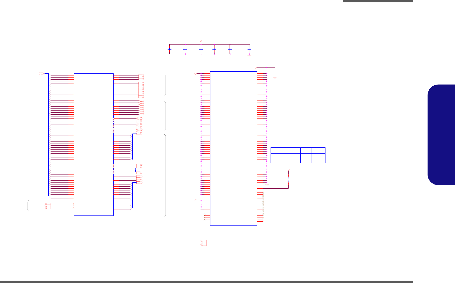
Schematic Diagrams
945GSE 3/5, DDR B - 7
B.Schematic Diagrams
945GSE 3/5, DDR
Sheet 6 of 32
945GSE 3/5, DDR
1. 05 V S
1. 05 V S
3.3VS
1.05VS
1. 5 V S
M_A_DQ[63:0]9, 1 0
M_ B _ W E#10
M_ B_RA S#10 M_B_CA S#10
M_ B_ A[1 3 :0 ] 1 0
M_ B_ BS2 # 10
M_ B_ BS1 # 10
M_ B_ BS0 # 10
M_ A _ W E # 9
M_ A_ RA S# 9
M_ A_ CA S# 9
M_A_BS0# 9
M_A_BS1# 9
M_A_BS2# 9
M_A_DM6 9,10
M_A_DM1 9,10
M_A_DM7 9,10
M_A_DM0 9,10
M_A_DM3 9,10
M_A_DM4 9,10
M_A_DM2 9,10
M_A_DM5 9,10
M _A_ DQ S3 9 ,10
M _A_ DQ S0 9 ,10
M _A_ DQ S6 9 ,10
M _A_ DQ S7 9 ,10
M _A_ DQ S4 9 ,10
M _A_ DQ S1 9 ,10
M _A_ DQ S2 9 ,10
M _A_ DQ S5 9 ,10
M_ A_ DQ S7 # 9,10
M_ A_ DQ S4 # 9,10
M_ A_ DQ S5 # 9,10
M_ A_ DQ S3 # 9,10
M_ A_ DQ S0 # 9,10
M_ A_ DQ S2 # 9,10
M_ A_ DQ S6 # 9,10
M_ A_ DQ S1 # 9,10
M_ A_ A[1 3 :0 ] 9
1.05VS 2..4,7,12,13,16,27
1 .5 VS 3,5 ,7 , 1 4, 16 ..1 8 ,2 2 ,2 7
3 .3 VS 5,7 ,9 . .2 4 ,27 ,2 8
M_A_DQ26
M_A_DQ62
M_A_DQ27
M_A_DQ63
M_A_DQ53
M_A_DQ28
M_A_DQ23
M_A_DQ59
M_A_DQ43
M_A_DQ18
M_A_DQ40
M_A_DQ8
M_A_DQ1
M_A_DQ32
M_A_DQ51
M_A_DQ58
M_A_DQ17
M_A_DQ38
M_A_DQ57
M_A_DQ31
M_A_DQ12
M_A_DQ50
M_A_DQ37
M_A_DQ4
M_A_DQ44
M_A_DQ13
M_A_DQ42
M_A_DQ61
M_A_DQ10
M_A_DQ30
M_A_DQ60
M_A_DQ46
M_A_DQ2
M_A_DQ41
M_A_DQ11
M_A_DQ52
M_A_DQ0
M_A_DQ7
M_A_DQ25
M_A_DQ45
M_A_DQ20
M_A_DQ3
M_A_DQ19
M_A_DQ33
M_A_DQ47
M_A_DQ15
M_A_DQ35
M_A_DQ49
M_A_DQ5
M_A_DQ9
M_A_DQ34
M_A_DQ39
M_A_DQ16
M_A_DQ22
M_A_DQ54
M_A_DQ6
M_A_DQ55
M_A_DQ29
M_A_DQ48
M_A_DQ14
M_A_DQ36
M_A_DQ24
M_A_DQ56
M_A_DQ21
M_B_A1
M_B_A3
M_B_A12
M_B_A13
M_B_A7
M_B_A6
M_B_A11
M_B_A9
M_B_A2
M_B_A5
M_B_A10
M_B_A8
M_B_A0
M_B_A4
Z0601
Z0602
MCH _CFG19
M_A_A5
M_A_A11
M_A_A13
M_A_A12
M_A_A1
M_A_A3
M_A_A8
M_A_A10
M_A_A9
M_A_A4
M_A_A6
M_A_A0
M_A_A2
M_A_A7
C90
*0.1U_10V_X7R_04
DDR2 SYSTEM MEMORY
945GS E
U11C
AC31
AB28
AE33
AF32
AC33
AB32
AB31
AE31
AH31
AK31
AL2 8
AK27
AH30
AL3 2
AJ2 8
AJ2 7
AH32
AF31
AH27
AF28
AJ3 2
AG31
AG28
AG27
AN27
AM2 6
AJ2 6
AJ2 5
AL2 7
AN26
AH25
AG26
AM1 2
AL1 1
AH9
AK9
AM1 1
AK11
AM8
AK8
AG9
AF9
AF8
AK6
AF7
AG11
AJ 6
AH6
AN6
AM6
AK3
AL2
AM5
AL5
AJ 3
AJ 2
AG2
AF3
AE7
AF6
AH5
AG3
AG5
AF5
AG19
AG21
AG20
AN 20
AL2 1
AK 21
AK 22
AL2 2
AH 22
AG 22
AF 21
AM 21
AE 21
AL2 0
AE 22
AE 26
AE 20
AJ 1 7
AK 18
AN 28
AM 28
AH 17
AJ 1 5
AM 17
AM 15
AH 15
AK 15
AN 15
AJ 1 8
AF 19
AN 17
AL1 7
AG 16
AL1 8
AG 18
AL1 4
AC 29
AK 30
AJ 3 3
AM 25
AN 8
AJ 8
AM 3
AE 2
AC 28
AJ 3 0
AK 33
AL2 5
AN 9
AH 8
AM 2
AE 3
AB 30
AL3 1
AF 30
AK 26
AL9
AG 7
AK 5
AH 3
AK 12
AH 11
AG 17
AH 21
AJ 2 0
AE 27
SA _D Q_0
SA _D Q_1
SA _D Q_2
SA _D Q_3
SA _D Q_4
SA _D Q_5
SA _D Q_6
SA _D Q_7
SA _D Q_8
SA _D Q_9
SA _D Q_10
SA _D Q_11
SA _D Q_12
SA _D Q_13
SA _D Q_14
SA _D Q_15
SA _D Q_16
SA _D Q_17
SA _D Q_18
SA _D Q_19
SA _D Q_20
SA _D Q_21
SA _D Q_22
SA _D Q_23
SA _D Q_24
SA _D Q_25
SA _D Q_26
SA _D Q_27
SA _D Q_28
SA _D Q_29
SA _D Q_30
SA _D Q_31
SA _D Q_32
SA _D Q_33
SA _D Q_34
SA _D Q_35
SA _D Q_36
SA _D Q_37
SA _D Q_38
SA _D Q_39
SA _D Q_40
SA _D Q_41
SA _D Q_42
SA _D Q_43
SA _D Q_44
SA _D Q_45
SA _D Q_46
SA _D Q_47
SA _D Q_48
SA _D Q_49
SA _D Q_50
SA _D Q_51
SA _D Q_52
SA _D Q_53
SA _D Q_54
SA _D Q_55
SA _D Q_56
SA _D Q_57
SA _D Q_58
SA _D Q_59
SA _D Q_60
SA _D Q_61
SA _D Q_62
SA _D Q_63
SB _C AS#
SB _R AS#
SB _W E#
SB_MA_0
SB_MA_1
SB_MA_2
SB_MA_3
SB_MA_4
SB_MA_5
SB_MA_6
SB_MA_7
SB_MA_8
SB_MA_9
SB_MA_1 0
SB_MA_1 1
SB_MA_1 2
SB_MA_1 3
SA_C AS#
SA_R AS#
SA_RCVENIN#
SA_R CVE NO UT#
SA_WE#
SA_MA_0
SA_MA_1
SA_MA_2
SA_MA_3
SA_MA_4
SA_MA_5
SA_MA_6
SA_MA_7
SA_MA_8
SA_MA_9
SA_MA_1 0
SA_MA_1 1
SA_MA_1 2
SA_MA_1 3
SA_D QS#_0
SA_D QS#_1
SA_D QS#_2
SA_D QS#_3
SA_D QS#_4
SA_D QS#_5
SA_D QS#_6
SA_D QS#_7
SA_D QS_0
SA_D QS_1
SA_D QS_2
SA_D QS_3
SA_D QS_4
SA_D QS_5
SA_D QS_6
SA_D QS_7
SA_D M_0
SA_D M_1
SA_D M_2
SA_D M_3
SA_D M_4
SA_D M_5
SA_D M_6
SA_D M_7
SA_BS_ 0
SA_BS_ 1
SA_BS_ 2
SB_BS_ 0
SB_BS_ 1
SB_BS_ 2
C84
0.1U_10V_X7R _04
C59
10U_6.3V_06
C79
*0. 1U_10V_X7R_04
C88
4.7U_6.3V_06
C3 1
10U _6.3V_06
C87
10U_6.3V_06
NCTF
945GSE
U11H
T25
R25
P25
N25
M2 5
P24
N24
M2 4
Y22
W22
V22
U22
T22
R22
P22
N22
M2 2
Y21
W21
V21
U21
T21
R21
P21
N21
M2 1
Y20
W20
V20
U20
T20
R20
P20
N20
M2 0
Y19
P19
N19
M1 9
Y18
P18
N18
M1 8
Y17
P17
N17
M1 7
Y16
P16
N16
M1 6
Y15
P15
N15
M1 5
Y14
AD25
AC25
AB25
AD24
AC24
AD22
AD21
AD20
AD19
AD18
AD17
AD16
AD15
AD14
K14
AD13
Y13
W13
V13
U1 3
T1 3
R1 3
P13
N1 3
M1 3
AD12
Y12
W12
AN33
AA25
V25
U2 5
AA22
AA21
AA20
AA19
AA18
AA17
AA16
AA15
AA14
T10
R10
P10
N10
L10
W14
V14
U14
T14
R14
V12
U1 2
T1 2
R1 2
P12
N1 2
M1 2
AD11
AD10
K10
P14
N14
M1 4
D1
AA13
A4
A33
B2
AN1
C1
M1 0
A18
AB10
AA10
K28
K25
K26
R2 4
T2 4
K21
K19
K20
K24
K22
J1 7
K23
K17
K12
K13
K16
K15
VC C_N CTF1
VC C_N CTF2
VC C_N CTF3
VC C_N CTF4
VC C_N CTF5
VC C_N CTF6
VC C_N CTF7
VC C_N CTF8
VC C_N CTF9
VC C_N CTF10
VC C_N CTF11
VC C_N CTF12
VC C_N CTF13
VC C_N CTF14
VC C_N CTF15
VC C_N CTF16
VC C_N CTF17
VC C_N CTF18
VC C_N CTF19
VC C_N CTF20
VC C_N CTF21
VC C_N CTF22
VC C_N CTF23
VC C_N CTF24
VC C_N CTF25
VC C_N CTF26
VC C_N CTF27
VC C_N CTF28
VC C_N CTF29
VC C_N CTF30
VC C_N CTF31
VC C_N CTF32
VC C_N CTF33
VC C_N CTF34
VC C_N CTF35
VC C_N CTF36
VC C_N CTF37
VC C_N CTF38
VC C_N CTF39
VC C_N CTF40
VC C_N CTF41
VC C_N CTF42
VC C_N CTF43
VC C_N CTF44
VC C_N CTF45
VC C_N CTF46
VC C_N CTF47
VC C_N CTF48
VC C_N CTF49
VC C_N CTF50
VC C_N CTF51
VC C_N CTF52
VC C_N CTF53
VC C_N CTF54
VC C_N CTF55
VC C_N CTF56
VC CAU X_N CTF1
VC CAU X_N CTF2
VC CAU X_N CTF3
VC CAU X_N CTF4
VC CAU X_N CTF5
VC CAU X_N CTF6
VC CAU X_N CTF7
VC CAU X_N CTF8
VC CAU X_N CTF9
VCCAUX_NCTF10
VCCAUX_NCTF11
VCCAUX_NCTF12
VCCAUX_NCTF13
VCCAUX_NCTF14
VCCAUX_NCTF15
VCCAUX_NCTF16
VCCAUX_NCTF17
VCCAUX_NCTF18
VCCAUX_NCTF19
VCCAUX_NCTF20
VCCAUX_NCTF21
VCCAUX_NCTF22
VCCAUX_NCTF23
VCCAUX_NCTF24
VCCAUX_NCTF25
VCCAUX_NCTF26
VCCAUX_NCTF27
VCCAUX_NCTF28
VSS _N CTF1
VSS _N CTF2
VSS _N CTF3
VSS _N CTF4
VSS _N CTF5
VSS _N CTF6
VSS _N CTF7
VSS _N CTF8
VSS _N CTF9
VS S_ NC TF 10
VS S_ NC TF 11
VS S_ NC TF 12
VS S_ NC TF 13
VTT_ NC TF1
VTT_ NC TF2
VTT_ NC TF3
VTT_ NC TF4
VTT_ NC TF5
VC C_N CTF57
VC C_N CTF58
VC C_N CTF59
VC C_N CTF60
VC C_N CTF61
VCCAUX_NCTF29
VCCAUX_NCTF30
VCCAUX_NCTF31
VCCAUX_NCTF32
VCCAUX_NCTF33
VCCAUX_NCTF34
VCCAUX_NCTF35
VCCAUX_NCTF36
VCCAUX_NCTF37
VCCAUX_NCTF38
VC C_N CTF62
VC C_N CTF63
VC C_N CTF64
VTT_ NC TF6
VS S_ NC TF 14
VS S_ NC TF 15
VS S_ NC TF 16
VS S_ NC TF 17
VS S_ NC TF 18
VS S_ NC TF 19
RSVD_3
RSVD_4
RSVD_5
RSVD_6
CF G _ 19
R ESER VED 10
R ESER VED 11
R ESER VED 12
R ESER VED 13
R ESER VED 14
R ESER VED 15
R ESER VED 16
R ESER VED 17
R ESER VED 18
R ESER VED 19
R ESER VED 20
R ESER VED 21
R ESER VED 22
R ESER VED 23
R ESER VED 24
R ESER VED 25
R61
*1 K _ 0 4
Zdiff=85 Ohm
Zo=55 Ohm
Zo=55 Ohm
Zo=55 Ohm
Zo=55 Ohm
MCH_ CF G19
(DM I LA NE
REVERSAL)
HIGHLOWCalistoga Strapping
No rma l La ne s
Re versed
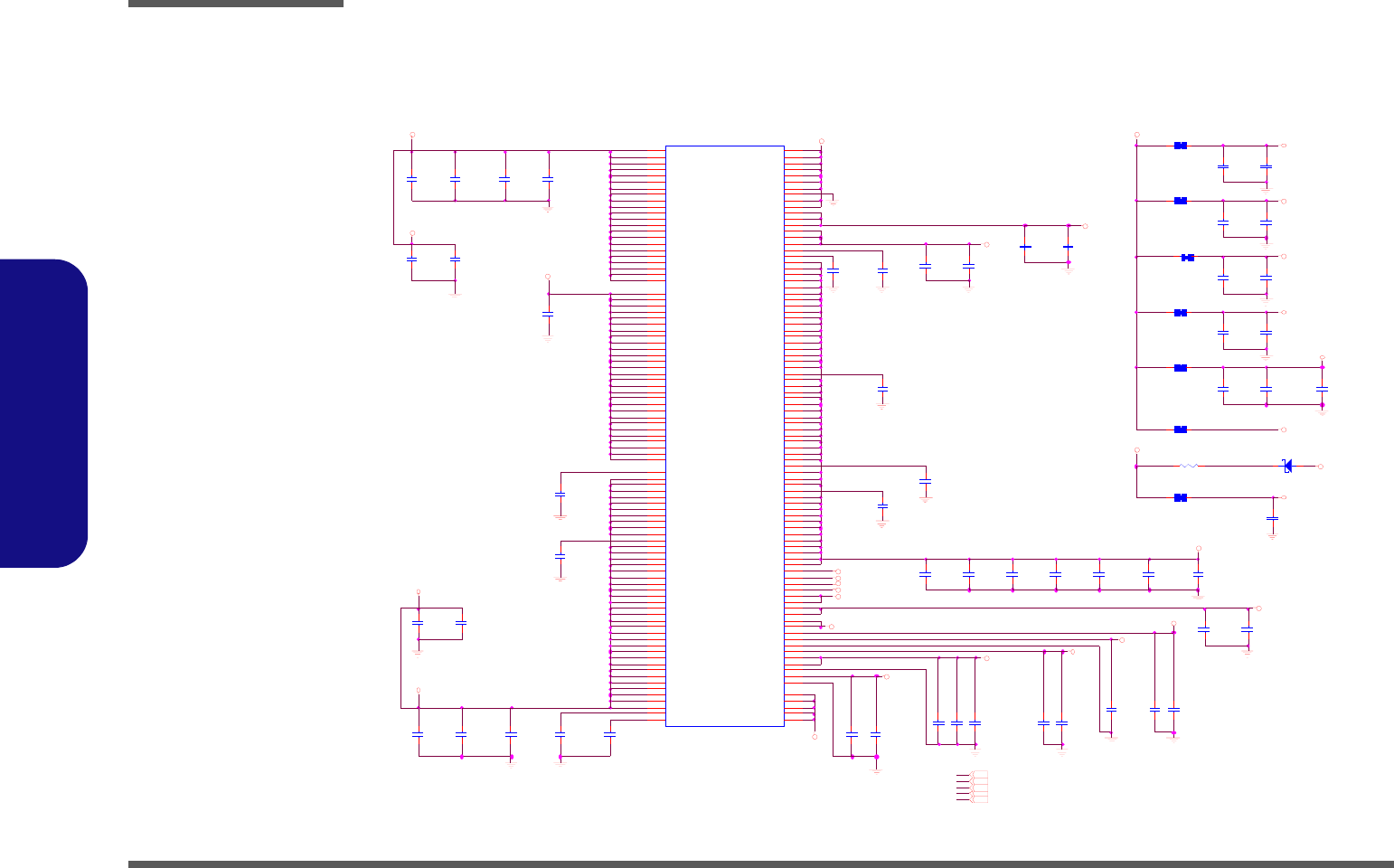
Schematic Diagrams
B - 8 945GSE 4/5
B.Schematic Diagrams
945GSE 4/5
Sheet 7 of 32
945GSE 4/5
1.05VS
2.5VS
2.5VS_ C RTD AC
2.5VS
2. 5V S
1.5VS _P CIE
1.5VS
1.5VS_D PLLB
1.5VS_D PLLA
1.5VS_H PLL
1.5VS_M PLL
1.5VS_3G PLL
1.8V
3.3VS
1.5VS
2.5VS
1. 5 V S
1.5VS_ PC IE
1.5VS_M PLL
1.5VS_H PLL
1.5VS_D PLLA
1.5VS_ D PL L B
1.5VS_3GP LL
1.05VS
2.5VS
2.5VS_ C RTD AC
1.05VS
1.5VS
1. 05 V S 1.5VS
1. 05 V S
1.05VS
1 .5V S 3 ,5 ,6 ,1 4 ,1 6 ..1 8 ,2 2 ,2 7
1.05VS 2..4,6,12,13,16,27
1.8V 5,9,10,26
2.5V S 11,27
3 .3V S 5 ,6 ,9 ..2 4 ,2 7 ,2 8
Z0707
Z0706
Z0705
Z 0710
Z0703
Z0704
Z0701
Z0702
Z0708
Z0709
C96 0. 1U _10V_X7R_04
C95 0.01U _50V _04
C85 0.01U _50V_04
C32
0.47U _10V_04
C3 1 0
0.47U _10V_04
C 116
0.1U _10V _X7R _04
C97
4.7U _6. 3V _06
C334
10U _6. 3V _06
C 322
10U _6.3V _06
C61
1 0 U _ 6. 3V _0 6
C3 1 8
0.47U _10V_04
C1 5 8
0.1U _10V_X7R _04
C307
10U _10V_08
C109
*4.7U _6.3V_06
C 113 10U _6.3V _06
C77
4.7U _6. 3V _06
C80
0.1U _10V_X7R _04
C133
10U _6. 3V _06
D1 2 S CS5 5 1 V
AC
C328
* 4. 7U _6.3V_06
C3 4 2
0.1U_10V_X7R_04
C3 1 9
10U _6.3V_06
C7 5
10U _6.3V_06
C3 8
10U _6.3V_06
C3 3 0
1U_6.3V_04
C316
10U _6.3V_06
C154 0. 1U _10V_X7R_04
C 153 0.01U _50V _04
C 105 0.1U _10V _X7R_04
L15
* HC B1005KF-121T20_10m il_s hort
L3
*H CB 1005KF- 121T20_10m il_short
L16
* HC B1005K F-121T20_10m il_s hort
C3 2 6
0.47U _10V_04
L7
* HC B1005KF-121T20_10m il_s hort
L6
* HC B1005KF-121T20_10m il_s hort
L17
* HC B1005K F-121T20_10m il_s hort
L5
* HC B1005K F-121T20_10m il_s hort
C312
10U _6.3V_06
C26
10U _6.3V_06
C308
1 0 U _ 6. 3V _0 6
C93 0.1U_10V_X7R_04
C98 10U _6.3V_06
C 354 0.1U _10V _X 7R_04
R 189 10_04
C83
0.1U _10V_X7R _04
C3 1 3
1U _ 6 . 3 V _ 0 4
C141
0.1U _10V _X7R _04
C1 2 4
10U _6.3V_06
C3 4 3
10U_6.3V_06
C3 0 1
0.1U _10V_X7R _04
C4 9
1U _6.3V_04
C3 5 6
10U _6.3V_06
C81
10U _6.3V_06
C3 5 7
10U _6.3V_06
C1 6 0
10U _6.3V_06
C3 3 8
10U _6.3V_06
C1 7
10U _6.3V_06
C2 9 9
10U _6.3V_06
C349
1U_6.3V_04
C3 5 3
1U _ 6 . 3 V _ 0 4
C1 9
0.1U _10V_X7R _04
C359
*10U _10V_08
C3 3 1
1U _ 6 . 3 V _ 0 4
C3 3 6
0.1U _10V_X7R _04
POWER
945GSE
U11D
T26
R26
P26
N26
M26
V19
U19
T19
W18
V18
T18
R18
AE 5
AD 5
B26
J32
AD 2
AD 1
C24
B24
B25
J23
A14
D10
P9
L9
D9
P8
L8
D8
P7
L7
D7
A7
P6
L6
G6
D6
U5
P5
L5
G5
D5
N33
M33
V26
U33
T33
C29
AB 33
AM 32
AN 29
AM 29
AL29
AK 29
AJ 2 9
AH 29
AG 29
AF 29
AE 29
AN 24
AM 24
AL24
AK 24
AJ 2 4
AH 24
AG 24
AF 24
AE 24
AN 18
AN 16
E26
D26
C26
B31
C28
B28
A28
F20
F22
D23
E23
B20
A20
B22
A22
D22
C22
W17
U17
R17
W16
V16
T16
R16
V15
U15
T15
AD 33
AD 32
AD 31
AD 30
AD 29
AD 28
AD 27
AC 27
AD 26
AC 26
AB26
AE19
AE18
AF17
AE17
AF16
AE16
AF15
AE15
J14
J10
AD 8
AD 7
AD 6
D29
AM 16
AL16
AK 16
AJ 1 6
AN 13
AM 13
AL13
AK 13
AJ 1 3
AH 13
AG 13
AF 13
AE 13
AN 4
AM 10
AL10
AK 10
AH 1
AH 10
AG 10
AF 10
AE 10
AN 7
U4
P4
AM 7
L4
G4
D4
Y3
U3
P3
L3
G3
D3
Y2
U2
L2
P2
G2
D2
AA 1 Y1
H10
AE 9
AD 9
U9
B32
U1
P1
L1
G1
F1
AL7
AK 7
AJ 7
AH 7
AN 10
AJ 1 0
Y4
VC C0
VC C1
VC C2
VC C3
VC C4
VC C5
VC C6
VC C7
VC C8
VC C9
VC C10
VC C11
VCC D HM PLL 1
VCC D HM PLL 2
VCCADPLLA
VCCADPLLB
VCCAHPLL
VCCAMPLL
VC CAC R TD AC 0
VC CAC R TD AC 1
V SSAC RTD AC
VC C SYN C
VTT0
VTT1
VTT2
VTT3
VTT4
VTT5
VTT6
VTT7
VTT8
VTT9
VTT1 0
VTT1 1
VTT1 2
VTT1 3
VTT1 4
VTT1 5
VTT1 6
VTT1 7
VTT1 8
VTT1 9
VTT2 0
VC CA3G BG
V SSA3 G BG
VCC A3G PLL
VC C3G 0
VC C3G 1
VC CTXLVD S1
VCC SM 0
VCC SM 1
VCC SM 2
VCC SM 3
VCC SM 4
VCC SM 5
VCC SM 6
VCC SM 7
VCC SM 8
VCC SM 9
VC CSM 1 0
VC CSM 1 1
VC CSM 1 2
VC CSM 1 3
VC CSM 1 4
VC CSM 1 5
VC CSM 1 6
VC CSM 1 7
VC CSM 1 8
VC CSM 1 9
VC CSM 2 0
VC CSM 2 1
VCCHV0
VCCHV1
VCCHV2
VC C ALVDS
VC CD LVD S0
VC CD LVD S1
VC CD LVD S2
VCCDTVDAC
VCCDQTVDAC
VC C ATVBG
VSS ATVBG
VCCATVDACA0
VCCATVDACA1
VCCATVDACB0
VCCATVDACB1
VC CA TVDA CC 0
VC CA TVDA CC 1
VC C12
VC C13
VC C14
VC C15
VC C16
VC C17
VC C18
VC C19
VC C20
VC C21
VC CA UX1
VC CA UX2
VC CA UX3
VC CA UX4
VC CA UX5
VC CA UX6
VC CA UX7
VC CA UX8
VC CA UX9
VC CA UX1 0
VC CA UX1 1
VC CA UX1 2
VC CA UX1 3
VC CA UX1 4
VC CA UX1 5
VC CA UX1 6
VC CA UX1 7
VC CA UX1 8
VC CA UX1 9
VC CA UX2 0
VC CA UX2 1
VC CA UX2 6
VC CA UX2 7
VC CA UX2 8
VC CTXLVD S0
VC CSM 2 2
VC CSM 2 3
VC CSM 2 4
VC CSM 2 5
VC CSM 2 6
VC CSM 2 7
VC CSM 2 8
VC CSM 2 9
VC CSM 3 0
VC CSM 3 1
VC CSM 3 2
VC CSM 3 3
VC CSM 3 4
VC CSM 3 5
VC CSM 3 6
VC CSM 3 7
VC CSM 3 8
VC CSM 3 9
VC CSM 4 0
VC CSM 4 1
VC CSM 4 2
VC CSM 4 3
VC CSM 4 4
VTT2 2
VTT2 3
VC CSM 4 5
VTT2 4
VTT2 5
VTT2 6
VTT2 7
VTT2 8
VTT2 9
VTT3 0
VTT3 1
VTT3 2
VTT3 3
VTT3 4
VTT3 5
VTT3 6
VTT3 7
VTT3 8
VTT3 9 VTT45
VC CA UX2 2
VC CA UX2 3
VC CA UX2 4
VC CA UX2 5
VSS ALVDS
VTT4 4
VTT4 1
VTT4 2
VTT4 3
VTT4 0
VC CSM 4 6
VC CSM 4 7
VC CSM 4 8
VC CSM 4 9
VC CSM 5 0
VC CSM 5 1
VTT2 1
C341
4.7U _6.3V _06
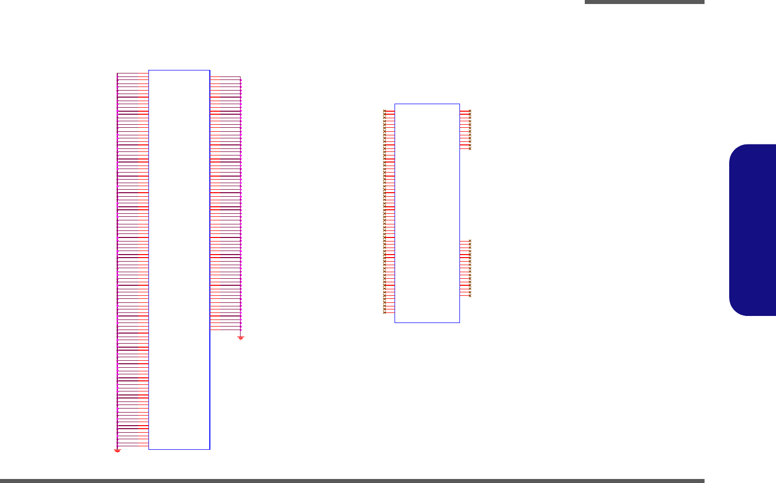
Schematic Diagrams
945GSE 5/5 B - 9
B.Schematic Diagrams
945GSE 5/5
Sheet 8 of 32
945GSE 5/5
VSS
94 5 G S E
U11E
AH3 3
Y33
V33
R33
AK32
AG32
AE32
AC3 2
AA32
U32
H32
E32
C32
AM31
AJ3 1
AA31
U31
T31
R31
P31
N31
M31
J31
F31
AL30
AG30
AE30
AC3 0
AA30
Y30
V30
U30
G30
E30
B30
AA29
U29
R29
P29
N29
M29
H29
E29
B29
AK28
AH2 8
AE28
AA28
U28
T28
J28
D28
AM27
AF27
AB27
AA27
Y27
U27
T27
R27
P27
N27
M27
G27
C27
B27
AL26
W26
U26
AN2 5
AK25
J25
G25
A25
H23
F23
J16
AL1 5
AG1 5
W15
R15
F15
D15
AM1 4
AH 1 4
AE 14
H14
B14
F13
D13
AL1 2
AG1 2
H12
B12
AN 1 1
AJ 1 1
AE 11
AM9
AB 9
W9
R9
M9
J9
F9
C9
A9
AL8
AG8
AE 8
U8
AA 7
V7
R7
N7
H7
E7
B7
AL6
AG6
AE 6
AB 6
W6
T6
M6
K6
AN 5
AJ 5
B5
AA 4
V4
R4
N4
K4
H4
E4
AL3
AD 3
W3
T3
G33
AJ 9
B3
AK 2
AH 2
AF 2
AB 2
M2
K2
H2
F2
V1
R1
E27
AH2 6
AG25
AE25
B23
AJ2 2
AF22
G22
AM22
E22
J21
H21
F21
AM20
AF18
AH1 8
AM18
W19
D20
AF20
AK20
AH2 0
R19
U18
H18
D18
AK17
V17
T17
F17
B17
AH1 6
U16
VSS_1
VSS_2
VSS_3
VSS_4
VSS_6
VSS_7
VSS_8
VSS_9
VSS_10
VSS_11
VSS_12
VSS_13
VSS_14
VSS_15
VSS_16
VSS_17
VSS_18
VSS_19
VSS_20
VSS_21
VSS_22
VSS_23
VSS_24
VSS_25
VSS_26
VSS_27
VSS_28
VSS_29
VSS_30
VSS_31
VSS_32
VSS_33
VSS_34
VSS_35
VSS_36
VSS_37
VSS_38
VSS_39
VSS_40
VSS_41
VSS_42
VSS_43
VSS_44
VSS_45
VSS_46
VSS_47
VSS_48
VSS_49
VSS_50
VSS_51
VSS_52
VSS_53
VSS_54
VSS_55
VSS_56
VSS_57
VSS_58
VSS_59
VSS_60
VSS_61
VSS_62
VSS_63
VSS_64
VSS_65
VSS_67
VSS_68
VSS_69
VSS_71
VSS_72
VSS_73
VSS_74
VSS_77
VSS_78
VSS_79
VSS_80
VSS_81
VSS_111
VSS_112
VSS_113
VSS_114
VSS_115
VSS_116
VSS_117
VSS_118
VSS_119
VSS_120
VSS_121
VSS_122
VSS_123
VSS_124
VSS_125
VSS_126
VSS_127
VSS_128
VSS_129
VSS_130
VSS_131
VSS_132
VSS_134
VSS_135
VSS_136
VSS_137
VSS_138
VSS_139
VSS_140
VSS_141
VSS_142
VSS_143
VSS_144
VSS_145
VSS_146
VSS_147
VSS_148
VSS_149
VSS_150
VSS_151
VSS_152
VSS_153
VSS_154
VSS_155
VSS_156
VSS_157
VSS_158
VSS_159
VSS_160
VSS_161
VSS_162
VSS_163
VSS_164
VSS_165
VSS_166
VSS_167
VSS_168
VSS_169
VSS_170
VSS_171
VSS_172
VSS_173
VSS_174
VSS_5
VSS_133
VSS_175
VSS_176
VSS_177
VSS_178
VSS_179
VSS_180
VSS_181
VSS_182
VSS_183
VSS_184
VSS_185
VSS_66
VSS_70
VSS_75
VSS_76
VSS_82
VSS_84
VSS_85
VSS_86
VSS_83
VSS_87
VSS_88
VSS_89
VSS_90
VSS_91
VSS_100
VSS_99
VSS_98
VSS_96
VSS_95
VSS_94
VSS_92
VSS_93
VSS_97
VSS_101
VSS_102
VSS_103
VSS_104
VSS_105
VSS_106
VSS_107
VSS_108
VSS_109
VSS_110
NC
945GSE
U11G
W33
AM3 3
AL33
C33
B33
AN 3 2
A32
AN 3 1
W28
V27
W29
J24
H24
W32
G24
F24
E24
D24
K33
A31
E21
C23
AN 1 9
AM1 9
AL19
AN3
Y9
J19
H19
G19
F19
E19
D19
C19
B19
G16
F16
E16
D16
C16
B16
AN2
Y7
AM4
AF4
AD4
AL4
AK4
AH4
AG4
AE4
AM1
Y5
AL1
Y6
W30
Y25
Y24
AB 22
AB 21
AB 19
AB 16
AB 14
AA 12
W24
AA 24
AB 24
AB 20
AB 18
AB 15
AB 13
AB 12
AH 1 9
AK19
AJ19
A19
Y8
A16
W31
AJ4 AB 17
Y10
W10
W25
V24
U24
V10
U10
K18
NC 1
NC 2
NC 3
NC 4
NC 5
NC 6
NC 7
NC 8
NC 9
NC 1 0
NC 1 1
NC 1 2
NC 1 3
NC 1 4
NC 1 5
NC 1 6
NC 1 7
NC 1 8
NC 1 9
NC 2 0
NC 2 1
NC 2 2
NC 2 3
NC 2 4
NC 2 5
NC 2 9
NC 3 0
NC 3 1
NC 3 2
NC 3 3
NC 3 4
NC 3 5
NC 3 6
NC 3 7
NC 3 8
NC 4 1
NC 4 2
NC 4 3
NC 4 4
NC 4 5
NC 4 6
NC 4 7
NC 4 9
NC 5 0
NC 5 1
NC 5 2
NC 5 3
NC 5 4
NC 5 7
NC 5 8
NC 5 9
NC 6 0
NC64
NC63
NC62
NC61
RESERVED26
RESERVED27
RESERVED28
RESERVED29
RESERVED30
RESERVED31
RESERVED32
RESERVED33
RESERVED34
RESERVED35
RESERVED36
RESERVED37
RESERVED38
RESERVED39
RESERVED40
RESERVED41
NC 2 8
NC 2 6
NC 2 7
NC 3 9
NC 4 0
NC 4 8
NC 5 5
NC 5 6 RESERVED42
NC65
NC66
NC67
NC68
NC69
NC70
NC71
NC72
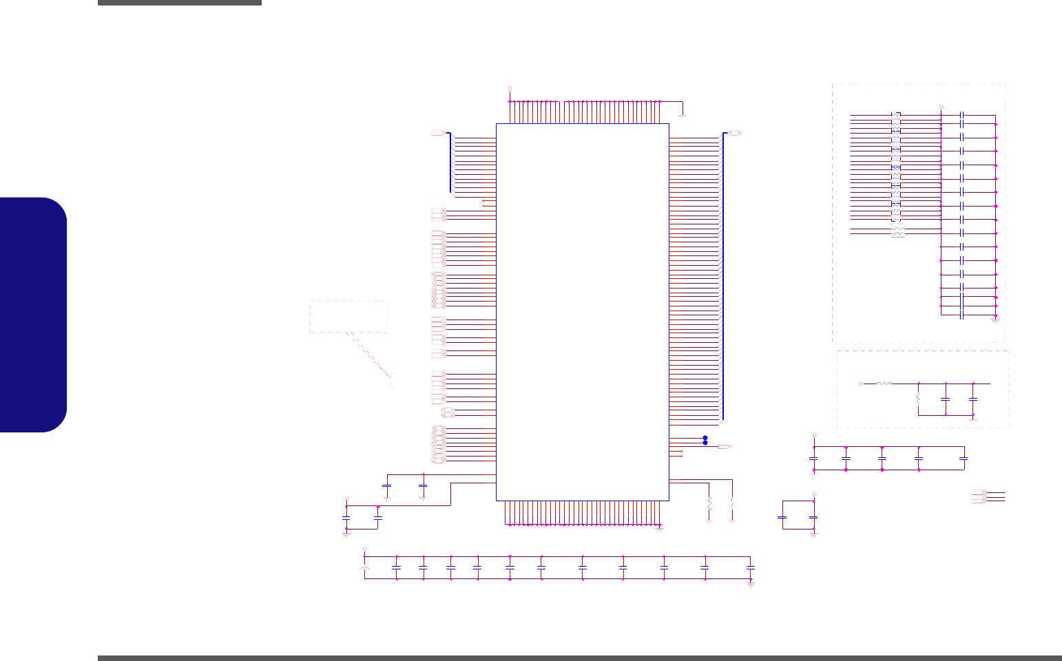
Schematic Diagrams
B - 10 DDRII SO-DIMM 0
B.Schematic Diagrams
DDRII SO-DIMM 0
Sheet 9 of 32
DDRII SO-DIMM 0
1.8V
VTT_MEM
1.8V
3.3V S
1.8V
VTT_MEM
1.8V
M_A_D QS4#6,10
M_A_D QS2#6,10
M_A_D QS7#6,10
M_A_D QS1#6,10
M_A_D QS3#6,10
M_A_D QS5#6,10
M_A_D QS6#6,10
M_A_D QS0#6,10
M_ODT05
M_ODT15
M_A_DQS16,10
M_A_DQS56,10
M_A_DQS66,10
M_A_DQS26,10
M_A_DQS46,10
M_A_DQS76,10
M_A_DQS36,10
M_A_DQS06,10
M_A_DM66,10
M_A_DM16,10
M_A_DM06,10
M_A_DM36,10
M_A_DM56,10
M_A_DM26,10
M_A_DM76,10
M_A_DM46,10
M_ A_ A[ 1 3: 0 ]6
M_ A_ BS2#6
M_ A_ BS0#6
M_ A_ BS1#6
M_CS0#5
M_CS1#5
M_A_WE#6
M_A_RAS#6
M_A_CAS#6
M_CLK_DDR1#5
M_CLK_DDR0#5
M_CLK_DDR15
M_CLK_DDR05
M_CKE 15M_CKE 05
M_A_DQ[63:0] 6,10
PM_EXTTS0# 5,10
3.3VS5.. 7,10.. 24,27,28
1.8V5,7,10,26
VTT_MEM10,26
ICH_SMBDAT010,12,15
ICH_SMBCLK010, 12,15
M_A_A6
M_CS1#
M_A_A7
M_A_BS2#
M_A_A12
M_A_A11
M_A_A13
M_ C KE1
M_A_WE#
M_A_A10
M_A_A0
M_A_A5
M_A_A4
M_A_CAS#
M_A_A1
M_A_BS0#
M_A_A2
M_A_A8
M_ C KE0
M_ODT1
M_A_A9
SA1_DIM0
M_A_DQ55
M_A_DQ53
M_A_DQ42
M_ODT0
Z0901
M_A_DQ50
M_A_DQ35
M_A_DQ28
M_A_DQ20
M_A_DQ14
Z0902
M_A_DQ62
M_A_DQ8
M_A_DQ60
M_A_DQ58
M_A_DQ56
M_A_DQ54
M_A_DQ51
M
_A_DQ33
M_A_DQ27
M_A_DQ21
M_A_DQ19
M_A_WE#
SA0_DIM0
M_A_DQ37
M_A_DQ59
M_A_DQ49
M_A_DQ39
M_CS0#
M_A_DQ57
M_A_DQ18
M_A_DQ5
MVREF_DIM0
MVREF _DIM0
M_A_DQ7
M_A_DQ3
M_A_DQ36
M_A_DQ24
M_A_DQ2
M_ODT1
M_A_DQ48
M_A_DQ43
M_A_DQ29
M_A_DQ23
M_A_DQ6
M_ A_ BS1#
M_A_DQ41
M_A_DQ26
M_A_DQ25
M_A_DQ1
M_CKE1
M_A_DQ63
M_A_DQ32
M_CS1#
M_A_DQ61
M_A_DQ46
M_A_DQ2
2
M_A_DQ10
M_A_DQ4
M_CKE0
M_A_DQ52
M_A_DQ17
M_A_DQ16
M_ A_ BS0#
M_ A_ C AS#
M_ A_ R AS#
M_A_DQ47
M_A_DQ34
M_A_DQ31
M_A_DQ15
M_A_DQ13
M_A_DQ11
M_A_DQ45
M_A_DQ9
M_ A_ BS2#
M_A_DQ44
M_A_DQ40
M_A_DQ38
M_A_DQ30
M_A_DQ12
M_A_DQ0
M_A_RAS#
M_A_BS1#
M_ODT0
M_CS0#
M_A_A3
M_A_A2
M_A_A3
M_A_A13
M_A_A11
M_A_A5
M_A_A1
M_A_A4
M_A_A6
M_A_A7
M_A_
A8
M_A_A0
M_A_A12
M_A_A9
M_A_A10
RN10
8P4RX56_04
1
2
3
45
6
7
8
C128 0.01U_50V_04
C148 0.1U_10V_X7R_04
C159 0.1U_10V_X7R_04
C82
10U_10V_08
R100 10K_1%_04
C344
0.1U_10V_X7R_04
C104 *0.1U_1 0 V_ X7R _ 04
C335
*0. 1U_10V_X7 R _ 04
C23
0.1U_10V_X7R_04
C155 0.1U_10V_X7R_04
C351
0.1U_10V_X7R_04
C173
4.7U_6.3V_06
C174
*0.22U_10V_04
R22
10K_04
C143 *0.1U_1 0 V_ X7R _ 04
C245
0.1U_10V_X7R_04
C131
*4. 7U_6.3V_06
C140 0.1U_10V_X7R_04
C340
0.1U_10V_X7R_04
R19
10K_04
C147 *0.1U_1 0 V_ X7R _ 04
C107 *0.1U_1 0 V_ X7R _ 04
C365
10U_10V_08
C127
0.1U_10V_X7R_04
C347
*0. 1U_10V_X7 R _0 4
C129 0.1U_10V_X7R_04
C114 0.1U_10V_X7R_04
C78
*10U_10V _08
C332
22U_6.3V_08
RN2
8P4RX56_04
1
2
3
45
6
7
8
C123 *0.1U_1 0 V_ X7R _ 04
C252
0.1U_10V _X7R_04
C240
1U_6.3V_04
C175 *0.1U_1 0 V_ X7R _ 04
C166 *0.1U_1 0 V_ X7R _ 04
C164 0.1U_10V_X7R_04
+
C321
* 150U _4V_B
C162
*0 . 1 U _ 10 V_ X7R_04
RN4
8P4RX56_04
1
2
3
45
6
7
8
C122 0.01U_50V_04
C171 0.1U_10V_X7R_04
C22
2.2U_6.3V_06
RN8
8P4RX56_04
1
2
3
45
6
7
8
C249
2. 2U_6.3V_06
C142
*0. 1U _10V_X7R_04
C360
0.22U_10V_04
R102
10K_1%_04
RN14
4P2RX56_04
14
23
C112
10U_10V_08
C94
22U_6.3V_08
RN12
8P4RX56_04
1
2
3
45
6
7
8
JDIMM1
2-1734073-1
102
101
100
99
98
97
94
92
93
91
105
90
89
107
106
5
7
17
19
4
6
14
16
23
25
35
37
20
22
36
38
43
45
55
57
44
46
56
58
61
63
73
75
62
64
74
76
123
125
135
137
124
126
134
136
141
143
151
153
140
142
152
154
157
159
173
175
158
160
174
176
179
181
189
191
180
182
192
194
112
111
117
96
95
118
81
82
87
103
88
104
149
47
133
183
77
12
48
184
78
71
72
121
122
196
193
8
162
150
138
40
28
18
24
41
53
42
54
59
65
60
66
127
139
128
145
165
171
172
187
178
190
9
21
33
155
34
132
144
156
168
2
3
15
27
83
120
50
69
163
86
39
198
200
161
1
177
199
116
11
29
49
68
129
146
167
186
10
26
52
67
130
147
170
185
84
13
31
51
70
131
148
169
188
85
108
109
113
110
115
79
80
30
164
114
32
166
119
195
197
A0
A1
A2
A3
A4
A5
A6
A7
A8
A9
A1 0/ AP
A11
A12
BA0
BA1
DQ0
DQ1
DQ2
DQ3
DQ4
DQ5
DQ6
DQ7
DQ8
DQ9
DQ10
DQ11
DQ12
DQ13
DQ14
DQ15
DQ16
DQ17
DQ18
DQ19
DQ20
DQ21
DQ22
DQ23
DQ24
DQ25
DQ26
DQ27
DQ28
DQ29
DQ30
DQ31
DQ32
DQ33
DQ34
DQ35
DQ36
DQ37
DQ38
DQ39
DQ40
DQ41
DQ42
DQ43
DQ44
DQ45
DQ46
DQ47
DQ48
DQ49
DQ50
DQ51
DQ52
DQ53
DQ54
DQ55
DQ56
DQ57
DQ58
DQ59
DQ60
DQ61
DQ62
DQ63
VD D
VDD
VD D
VD D
VD D
VDD
VD D
VD D
VD D
VDD
VD D
VD D
VSS
VSS
VSS
VSS
VS S
VSS
VSS
VSS
VS S
VSS
VSS
VSS
VS S
VSS
VSS
VSS
VS S
VSS
VSS
VSS
VS S
VSS
VSS
VSS
VS S
VSS
VSS
VSS
VS S
VSS
VSS
VSS
VS S
VSS
VSS
VSS
VSS
VS S
VSS
VSS
VS S
VSS
VSS
VSS
VS S
VSS
VSS
VSS
VS S
VSS
VSS
VSS
VS S
VSS
NC1
NC2
NC3
NC4
NCTEST
A14
VSS
SA0
SA1
VSS
VR EF
VSS
VD DSPD
A13
DQS#0
DQS#1
DQS#2
DQS#3
DQS#4
DQS#5
DQS#6
DQS#7
DM0
DM1
DM2
DM3
DM4
DM5
DM6
DM7
A15
DQS0
DQS1
DQS2
DQS3
DQS4
DQS5
DQS6
DQS7
A1 6/ BA2
RAS#
WE#
CAS#
S0#
S1#
CKE0
CKE1
CK0
CK1
ODT0
CK0#
CK1#
ODT1
SD A
SC L
RN6
8P4RX56_04
1
2
3
45
6
7
8
+VTT_MEM RESISTORS
CLOSE TO SO-DIMM_0
16-56034-45A
Place one cap close to every 2 pull-up resistors
terminated to +VTT_MEM
Layout note:
SO-DIMM 0
20mils
20mils
signal/space/signal:
7 / 4 / 7
Layout Note:
3/20
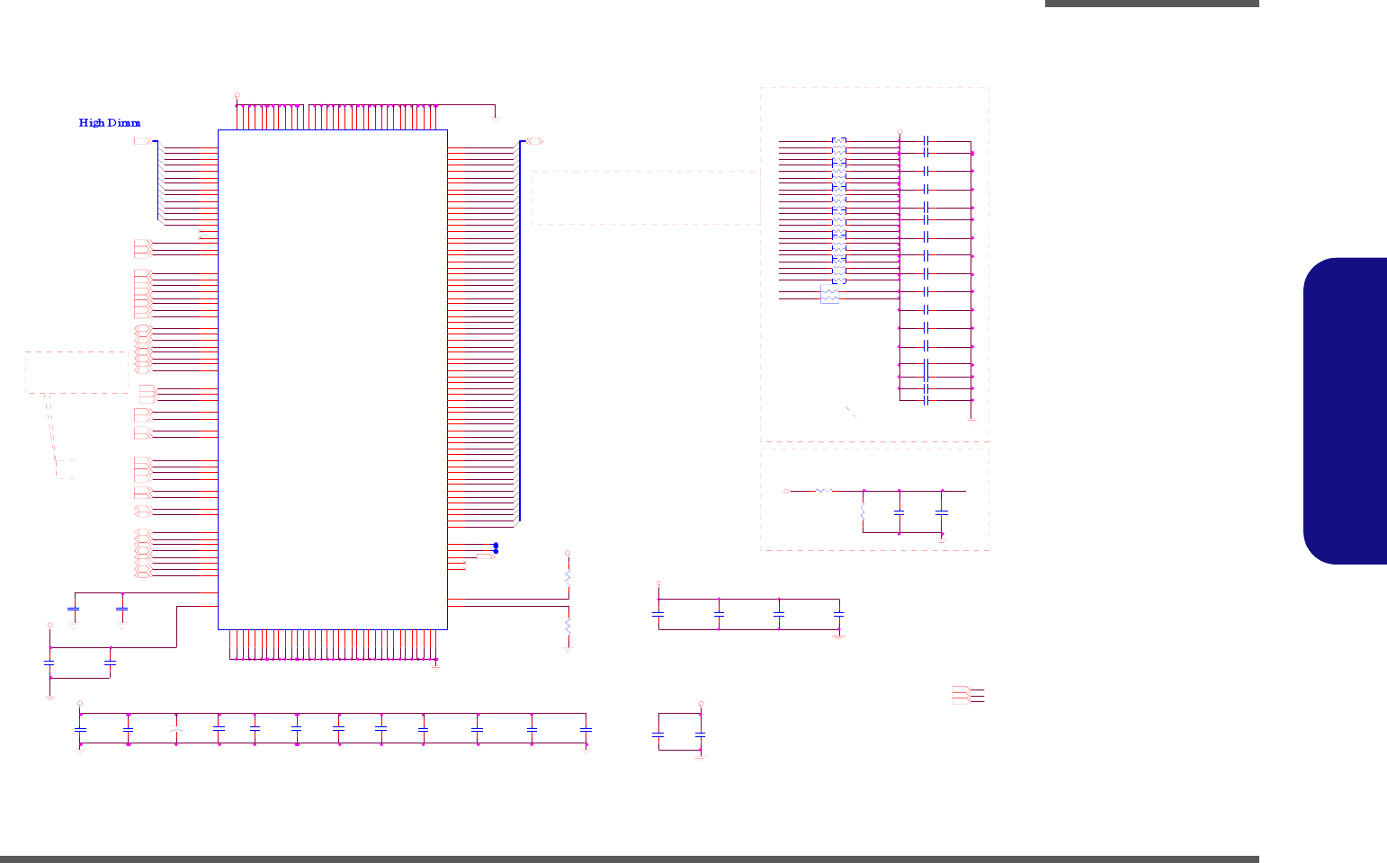
Schematic Diagrams
DDRII SO- DIMM 1 B - 11
B.Schematic Diagrams
DDRII SO- DIMM 1
VTT_M EM
1.8V
3.3VS
1.8V
1. 8V VTT_ M EM
1.8V
3.3VS
VTT_M EM9, 26 1. 8V5,7,9,26
3. 3V S5..7,9,11..24,27,28
P M_EXTTS 0# 5,9
M_ B_ A[13 :0]6
M_ A_ DQ S0#6,9
M_ A_ DQ S4#6,9
M_ A_ DQ S3#6,9 M_A_DQ S2#6,9
M_ A_ DQ S5#6,9
M_ A_ DQ S6#6,9
M_ A_ DQ S1#6,9
M_ A_ DQ S7#6,9
M_ODT25
M_ODT35
M_ B _ W E #6M _B_ CAS#6
M _B_RAS#6
M _C KE35
M _C KE25
M _B_BS2#6
M_CS3#5
M_CS2#5
M _B_BS0#6
M _B_BS1#6
M_ A _ D M36,9 M_ A_ D M26,9
M_ A _ D M46,9 M_ A_ D M56,9
M_ A _ D M66,9
M_ A _ D M06,9
M_ A _ D M76,9
M_ A _ D M16,9
M_ A_ D QS76,9
M_ A_ D QS16,9
M_ A_ D QS36,9
M_ A_ D QS56,9
M_ A_ D QS06,9
M_ A_ D QS46,9
M_ A_ D QS26,9
M_ A_ D QS66,9
M_A_D Q[63:0] 6,9
ICH _SMB CLK09,12,15
ICH _SMB DAT09,12,15
M _ CL K _ DD R3 #5
M_CLK_DDR35
M_CLK_DDR25
M _ CL K _ DD R2 #5
M _B_A5
M _B_A9
M _B_A8
M _B_A1
M _B_A2
M_CS2#
M _B_A12
M _B_BS0#
M_OD T2
M _B_A10
M _B_A13
M_B_RAS #
M _B_A3
M _B_A4
M_CKE 3
M _B_A11
M_B_WE#
M _B_A0
M_OD T3
M _B_A7
M _B_A6
M _B_BS1#
M_B_CAS #
M_CS3#
MVREF _D IM1M_OD T2
M_OD T3
SA0_DIM1
SA1_DIM1
Z1001
Z1002
M_ B _ W E #
M_ B_ C AS#
M_ B_ R AS#
M _CKE3
M _CKE2
M_B_B S2#
M_CS2#
M_CS3#
M_B_B S1#
M_B_B S0#
MVREF_DIM1
M_ A _ D Q5 1
M_ A _ D Q1 1
M_ A _ D Q5
M_ A _ D Q7
M_ A _ D Q5 7
M_ A _ D Q6
M_ A _ D Q5 3
M_ A _ D Q2 8
M_ A _ D Q1 4
M_ A _ D Q0
M_ A _ D Q5 9
M_ A _ D Q1 9
M_ A _ D Q5 4
M_ A _ D Q9
M_ A _ D Q2 5
M_ A _ D Q2 4
M_ A _ D Q1 0
M_ A _ D Q4 6
M_ A _ D Q1 6
M_ A _ D Q5 5
M_ A _ D Q4 5
M_ A _ D Q3 7
M_ A _ D Q1 8
M_ A _ D Q5 8
M_ A _ D Q2 7
M_ A _ D Q3 0
M_ A _ D Q2 1
M_ A _ D Q5 0
M_ A _ D Q4 3
M_ A _ D Q3 2
M_ A _ D Q4 1
M_ A _ D Q1 5
M_ A _ D Q1 2
M_ A _ D Q6 2
M_ A _ D Q3 8
M_ A _ D Q6 1
M_ A _ D Q1 7
M_ A _ D Q3 3
M_ A _ D Q1
M_ A _ D Q6 3
M_ A _ D Q3 1
M_ A _ D Q5 2
M_ A _ D Q4 4
M_ A _ D Q4 2
M_ A _ D Q4 9
M_ A _ D Q3 4
M_ A _ D Q2 3
M_ A _ D Q3 9
M_ A _ D Q2 9
M_ A _ D Q4 7
M_ A _ D Q6 0
M_ A _ D Q3
M_ A _ D Q2 6
M_ A _ D Q8
M_ A _ D Q4
M_ A _ D Q4 8
M_ A _ D Q2 2
M_ A _ D Q2 0
M_ A _ D Q1 3
M_ A _ D Q4 0
M_ A _ D Q3 6
M_ A _ D Q5 6
M_ A _ D Q3 5
M_ A _ D Q2
M_B_A6
M_B_A3
M_B_A2
M_B_A11
M_B_A4
M _B_BS2#
M_B_A9
M_CKE 2
M_B_A8
M_B_A1
M_B_A13
M_B_A10
M_B_A5
M_B_A7
M_B_A12
M_B_A0
C150
*0.1U_10V_X7R_04
C126 *0.01U_50V_04
RN15
* 4P 2R X56_04
14
23
+
C366
*150U _4V_B
R18
* 10K_04
R245
*10K_1%_04
C157 *0.1U_10V_X7R _04
C119 *0.1U_10V_X7R _04
C337
*0.1U _10V_X7R_04
C165 *0.1U_10V_X7R _04
C339
*0 .1U _10 V_ X7 R_0 4
C2 4
*0.1U _16V_04
C130 *0.1U_10V_X7R _04
C9 1
*10U_10V_08
C 121
* 0.1U_10V_X7R _04
C115
* 10U _10V_08
RN11
* 8P4RX56_04
1
2
3
45
6
7
8
JDIMM2
* 1734075- 2
102
101
100
99
98
97
94
92
93
91
105
90
89
107
106
5
7
17
19
4
6
14
16
23
25
35
37
20
22
36
38
43
45
55
57
44
46
56
58
61
63
73
75
62
64
74
76
123
125
135
137
124
126
134
136
141
143
151
153
140
142
152
154
157
159
173
175
158
160
174
176
179
181
189
191
180
182
192
194
112
111
117
96
95
11 8
81
82
87
103
88
104
14 9
47
133
183
77
12
48
184
78
71
72
121
122
196
193
8
162
15 0
138
40
28
18
24
41
53
42
54
59
65
60
66
127
13 9
128
145
165
171
17 2
187
178
190
9
21
33
155
34
132
144
156
16 8
2
3
15
27
83
120
50
69
163
86
39
198
200
161
1
177
199
116
11
29
49
68
129
146
167
186
10
26
52
67
130
147
170
185
84
13
31
51
70
131
148
169
188
85
108
109
113
110
115
79
80
30
164
114
32
166
119
195
197
A0
A1
A2
A3
A4
A5
A6
A7
A8
A9
A10/AP
A11
A12
BA0
BA1
DQ 0
DQ 1
DQ 2
DQ 3
DQ 4
DQ 5
DQ 6
DQ 7
DQ 8
DQ 9
DQ 1 0
DQ 1 1
DQ 1 2
DQ 1 3
DQ 1 4
DQ 1 5
DQ 1 6
DQ 1 7
DQ 1 8
DQ 1 9
DQ 2 0
DQ 2 1
DQ 2 2
DQ 2 3
DQ 2 4
DQ 2 5
DQ 2 6
DQ 2 7
DQ 2 8
DQ 2 9
DQ 3 0
DQ 3 1
DQ 3 2
DQ 3 3
DQ 3 4
DQ 3 5
DQ 3 6
DQ 3 7
DQ 3 8
DQ 3 9
DQ 4 0
DQ 4 1
DQ 4 2
DQ 4 3
DQ 4 4
DQ 4 5
DQ 4 6
DQ 4 7
DQ 4 8
DQ 4 9
DQ 5 0
DQ 5 1
DQ 5 2
DQ 5 3
DQ 5 4
DQ 5 5
DQ 5 6
DQ 5 7
DQ 5 8
DQ 5 9
DQ 6 0
DQ 6 1
DQ 6 2
DQ 6 3
VDD
VD D
VD D
VDD
VD D
VDD
VD D
VD D
VDD
VD D
VDD
VDD
VSS
VSS
VSS
VS S
VSS
VSS
VSS
VSS
VS S
VSS
VSS
VSS
VSS
VS S
VSS
VSS
VSS
VSS
VS S
VSS
VSS
VSS
VSS
VS S
VSS
VSS
VSS
VSS
VS S
VSS
VSS
VSS
VSS
VSS
VSS
VSS
VS S
VSS
VSS
VSS
VS S
VSS
VSS
VSS
VSS
VS S
VSS
VSS
VSS
VSS
VS S
VSS
VSS
VSS
NC 1
NC 2
NC 3
NC 4
NC TE ST
A14
VSS
SA0
SA1
VSS
VR EF
VSS
VD DSP D
A13
DQS#0
DQS#1
DQS#2
DQS#3
DQS#4
DQS#5
DQS#6
DQS#7
DM0
DM1
DM2
DM3
DM4
DM5
DM6
DM7
A15
DQS0
DQS1
DQS2
DQS3
DQS4
DQS5
DQS6
DQS7
A16/BA2
R AS#
WE#
C AS#
S0#
S1#
C KE0
C KE1
CK0
CK1
ODT0
CK0#
CK1#
ODT1
SD A
SC L
C144 *0.01U_50V_04
C375
*0.1U _10V_X7R_04
C333
*4.7U _6.3V_06
RN5
* 8P4RX56_04
1
2
3
45
6
7
8
C103
* 4. 7U _ 6. 3V _0 6
C156
*10U _10V_08
C172 *0.1U_10V_X7R _04
C161 *0.1U_10V_X7R _04
C146 *0.1U_10V_X7R _04
R246 *10K_1%_04
C345
*0.1U_10V_X7R _04
C111 *0.1U_10V_X7R _04
RN7
* 8P4RX56_04
1
2
3
45
6
7
8
C9 9
*10U_10V_08
C125 *0.1U_10V_X7R _04
C169
* 0.1U _10V _X7R_04
C132 *0.1U_10V_X7R _04
RN9
* 8P4RX56_04
1
2
3
45
6
7
8
C361
*0.22U_10V_04
RN13
* 8P4RX56_04
1
2
3
45
6
7
8
C101
* 22U _6. 3V _08
C376
*1U_6.3V_04
C151 *0.1U_10V_X7R _04
C168 *0.1U_10V_X7R _04
C149 *0.1U_10V_X7R _04
C120 *0.1U_10V_X7R _04
R21
* 10K_04
C3 3
*2.2U _6.3V_06
C 348
* 0.1U_10V _X7R _04
C229
* 2.2U _6.3V _06
RN3
* 8P4RX56_04
1
2
3
45
6
7
8
C110
*0.22U_10V_04
C358
*0.1U_10V_X7R _04
C377
*0.1U _16V_04
C118 *0.1U_10V_X7R _04
+VTT_MEM RESISTORS
CLOSE TO SO-DIMM_1
Place one cap close to every 2 pull-up resistors
terminated to +VTT_MEM
16 -5 60 34 -4 5A
SO-DIMM 1
Layout note:
7 / 4 / 7
signal/space/signal:
Layout Note:
20mils
20mils
Layout note:
SO-DIMM_1 is placed farther from
the GMCH than SO-DIMM_0
Sheet 10 of 32
DDRII SO-DIMM 1
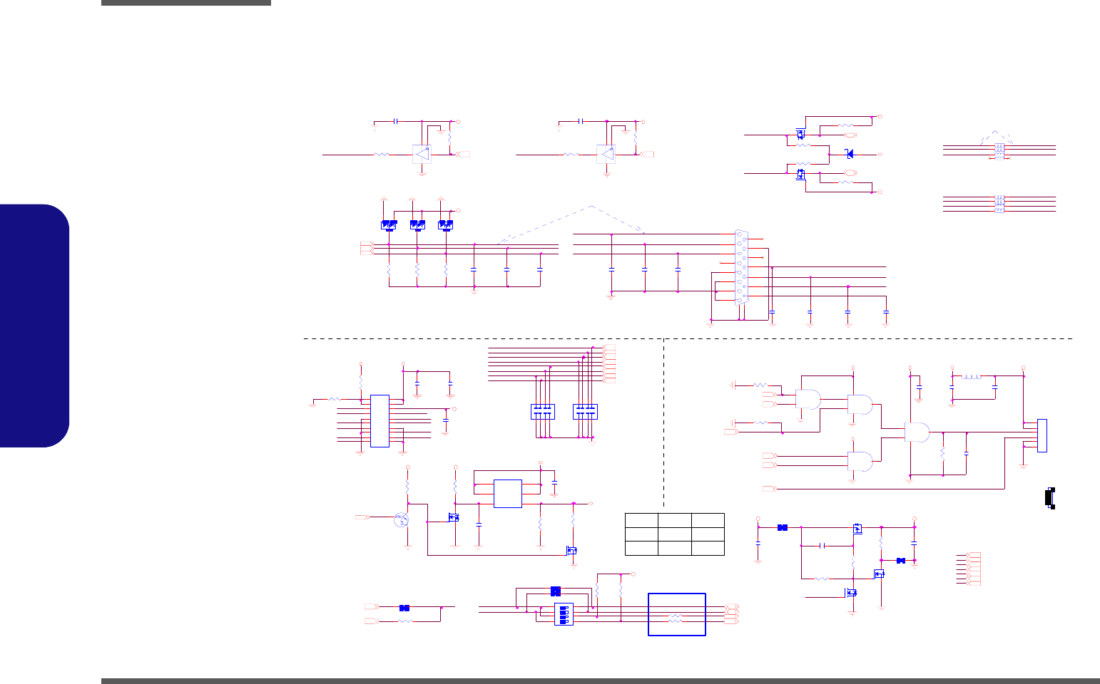
Schematic Diagrams
B - 12 PANEL, INVERTER, CRT
B.Schematic Diagrams
PANEL, INVERTER, CRT
Sheet 11 of 32
PANEL, INVERTER,
CRT
3.3V 3.3V VIN VIN_INV
3.3V
5VS
3.3VS
3.3VS
3.3VS3.3VS
SY S15 V SYS15 V
3. 3V
PLVD D
PLVD D
3. 3V S
2.5VS
5V 5V_LED
5V_LED
3.3V S
D AC _VS YN C 5 DAC _ HSY NC 5
EN AVDD5
LVDS -L0N 5
LVDS -L0P 5
LVDS -LC LKN 5
LVDS -LC LKP 5
SB _BLO N15
BKL_EN23
LID_SW#17,23
LCD_BRIGHTNESS23
3.3V 2,14.. 18,21,25.. 27
3.3V S 5..7,9,10,12..24,27,28
5VS 13,16,17,20, 22,24
SYS 15V 24,25
VIN 24..29
D A C_ DD CA DAT A 5
D A C_ DD CA CL K 5
LVDS -L2N 5
LVDS -L2P 5
LVDS -L1N 5
LVDS -L1P 5
DAC_RED5
D A C_ BL UE5
DAC_GREEN5
BLO N5
PM_ PW R OK15,28
2.5V S 7,27
L C D_ B R IGH T NES S23
L_BKLTCTL5,23
5V 16..18,20,25..28
LCD ID0 15
LCD ID1 15
L_DDC_CLK 5
L_DD C_D ATA 5
Z1102
Z1104
Z1103
CR T_ H S YN C_ R
DAC _GR EEN_R
DAC _ RED _ R
CR T_ D DC ACL K_ R
CR T_ VS YN C_ R
Z1106Z1105
LV D S - L C L K N
LVD S-L0P
LV D S - L C L K P
Z1101
CR T_ D DC ADA T_ R
DAC _ BL UE_ R
ED ID _C LK
Z1108
LVD S-LCLKN
LVD S-LCLKP
LVDS-L0P
ED ID _D AT
LVDS-L0N
D A C_ BL UE
CRT_HSYNC
C RT_ DD CAD AT
C RT _ DD CAC L K
DAC_GREEN
DAC_RED
C RT_ DD CAC L K
C RT_VSYN C
C RT_ DD CAD AT
LVDS-L2N
LVDS-L2P
LVDS-L1P
LVDS-L1N
LVD S-L2N
LVD S-L0N
LVD S-L2P
IN V_BL ON
LVD S-L1P
CR T_D DC ADA T_ R
DAC_RED
D A C_ R E D_ R
CR T _D DC ACL K_ R
DAC_GREEN
D A C_ BL UE
DAC_GREEN_R
DAC_BLUE_R
CR T _VS YN C_ R
CR T_H SYN C_ R
CR T _ HSY NCCR T_ VSY NC
LVD S-L1N
Z 1111
IN V_BLO N
Z1109 Z 1110
Z1108 E DID _D AT
EDID_CLK
Q1 9
*2N7002W
G
DS
Q1 1
SI3456BD V-T1-E 3
3
2
1
4
5
6
G
D
D
S
D
D
R 146
* 1 0K _0 4
R140
*100K_04
CP2
* 1 0P _8 P 4 C _0 4
1
2
3
4 5
6
7
8
R 3 2.2K_04
J_INV1
* 87212-06G 0
1
2
3
4
5
6
CP 1
* 10P_8P4C_04
1
2
3
45
6
7
8
C14
220P_50V_04
C516
0.1U _50V_06
R145
*10K_04
L34
*15mil_short
D 1 SCS 751V-40
AC
J_LC D1
88107-20001
12
34
56
78
910
11 12
13 14
15 16
17 18
19 20
C 16 0.1U_16V _04
C2 8
22P _50V_04
R153
1M_04
C11
1000P _50V_04
U13B
74LVC 08P W
4
5
6
147
LP2
FCA 3216KF4-121T03
1
2
3
4
6
5
7
8
12
ON
43
SW1
*N HD S-04-T
3
4
1
2
5
6
7
8
C1 3
220P_50V_04
R 222 1M _04
C15
* 22P_50V_04
R9
*390_04
Q5
2N 7002W G
D S
R349
0_06
R8 39_04
R354
* 10mil_s hort
R344
100K_04
R 7 39_04
R345
0_04
R 346 330K_04
C514
10U_10V _08
Q1 8
AO3415
G
DS
C515 * 0.1U _16V_04
Q17
2N 7002W
G
DS
R 348 *0_04
R 350 * 0_06
R 221 100K_04
R 5 4.7K_04
C291
0.1U_50V_06
Q3
2N7002W
G
DS
U13D
74LVC 08P W
12
13
11
147
C283
*10U_10V_08
U2
SN74AH C1G125DC KR
1
2
5
4
3
C279
0.1U_16V _04
D3
BAV99
A
C
AC
C1
0.022U _25V_06
U1
SN74AHC 1G125DC KR
1
2
5
4
3
C1 0
1000P_50V_04
C21
* 22P_50V_04
R 351 *10mil_shor t
U13C
74LVC 08PW
9
10 8
147
R 352 *10mil_shor t
R149 *100_04
R13
* 390_04
U13A
74LVC 08PW
1
23
147
LP1
FCA3216KF4-121T03
1
2
3
4
6
5
7
8
R27
150_1%_04
R152
1M _ 04
C346
*100P_50V_04
R 4 2.2K_04
R203
1M_04
R150 *100_04
C20
* 22P_50V_04
C2 9
22P _50V_04
C 285
* 0.1U_16V _04
C278
0.1U _16V_04
C290
* 0.1U _50V_06
R 347 *10m il_s hort
D1 1
B AV99
A
C
AC
Q12
2N7002W
G
DS
C2 7
22P _50V_04
R28
150_1% _04
R2 6
150_1%_04
D2
BAV99
A
C
AC
Q6
2N 7002W G
D S
C350
* 0.1U _16V_04
C12 0.1U _16V_04
R147
75_1% _06
Q4
D TC114E UA C
E
B
R 6 4.7K_04
J_ C R T 1
C 10509-91505-L
8
7
6
5
4
3
2
19
10
11
12
13
14
15
GND2
GN D1
L14
* HC B1608KF-121T25
12
INVERTER CONNECTOR
PANEL
2A
CRT
2A
For Panel ID
40 mil
6
J_INV1
1
6- 20 -4 1A 10 -1 06
Zo=75 Ohm
Zo=75 Ohm
7/1 3
Modify C4 from 0.1uF change to
0.01uF for LVDS power time.
40 mil
EDID Panel
SW
EDID
Panel ID
5,4 / 6,3 7,2 / 8,1
ON
ON
OFF
OFF
7/30
Schematic Diagrams
CLOCK GENERATOR B - 13
B.Schematic Diagrams
CLOCK GENERATOR
Sheet 12 of 32
CLOCK
GENERATOR
3. 3VS
3.3VS
3.3VS
3. 3VS
1.05VS
3. 3VS_G
3.3VS 3.3VS_G
3. 3VS
3. 3VS 5..7,9. .11,13.. 24,27,28
CLK_BSEL24CLK_ICH1415
CLK_MCH_BCLK 4
CLK_CPU_BCLK# 2
CLK_MCH_BCLK# 4
CLK_CPU_BCLK 2
CLK_ICH4815
CLK_BSEL04
PM_ STP CPU#15 PM_STPP CI#15
VRM_PWRGD15
I C H _ SMBD A T09,10,15 I C H _ SMBC LK 09,10,15
PC L K_I C H14
KBC_PCLK23
CLKEN#28
1. 05VS 2..4,6, 7,13,16,27
CLK_PCIE_ICH# 14
CLK_PCIE_ICH 14
CLK_PCIE_LAN# 21
CLK_PCIE_LAN 21
CLK_DREF 5
CLK_DREF# 5
CLK_BSEL14
CLK_SATA 13
CLK_SATA# 13
MCH_CLKREQ# 5
WLAN_CLK REQ# 17
CLK_PCIE_MINI# 17
CLK_PCIE_MINI 17
NEWCARD_CLK REQ# 18
C L K_PC I E _ N EW _C AR D # 1 8
CLK_PCIE_JM380 19
CLK_PCIE_JM380# 19
C L K_PC I E _ N EW _C AR D 18
CLK_DREFSS 5
CLK_DREFSS# 5
CLK_PCIE_3GPLL# 5
C L K_PC I E _ 3G PL L 5
XTAL _I N CLK_CPU_BCLK#
CLK_MCH_BCLK
CLK_CPU_BCLK
CLK_MCH_BCLK#
Z 1204
CLK_ICH48
FSLA
XTAL_ OU T
Z 1205
PC L K_I CH
KBC _ P C L K
FSLC
Z 1202
Z 1206
VR M_ PW R GD
CLK_PCIE_ICH#
CLK_PCIE_ICH
CLK_PCIE_LAN#
CLK_PCIE_LAN
Z 1220
Z 1203
Z 1207
CLK_DREF
CLK_DREF#
Z 1234
CLK_SA TA#
CLK_SA TA
CLK_PCIE_MINI#
CLK_PCIE_MINI
CLK_PCIE_NEW_CARD#
CLK_PCIE_NEW_CARD
CLK_PCIE_JM380
CLK_PCIE_JM380#
Z1221
CLK_DREFSS#
CLK_DREFSS
CLK_PCIE_3GPLL#
CLK_PCIE_3GPLL
WLAN_CLK REQ#
R243 470_04
C368
1U_6.3V_04
R248 10K_04
L19 * HCB1005KF-121T20_10m il _short
C378
1U_6.3V _04
C384
0.1U_16V_04
R114 33_04
X2
14. 318MHz
1 2
R108 33_04
Q13
2N7002W
G
DS
L9
*HCB 1005KF -121T20_10mil _short
R122 10K_04
C369
1U_6.3V_04
T152
C372
10U_6.3V_06
C371
0.1U_16V_04
R112 * 10K_04
R116 10K_04
T153
R118 * 10K_04
R104 2.2K _04
T147
U6
SLG8SP510T
5
9
61
37
51
53
43
50
54
8
11
7
63
49
62
10
26
48
60
59
42
44
39
3
4
20
55
64
6
1
15
16
23
52
45
46
22
21
30
31
35
34
33
32
18
17
13
14
56
36
12
2
19
29
41
40
27
28
24
25
58
38
47
57
PCI3
VDD48
VDDREF
CPU_STOP#
CPU1
CPU0#
SRC7#/CR#_E
CPU1#
CPU0
GNDPCI
GND48
PCIF5/I TP_EN
SDATA
VD D C PU _ I O
REF0/FSLC/EST_SEL
US B_48MHz/FSLA
VDDSRC_IO1
NC
X1
X2
GNDSRC3
SR C 7 / C R # _F
VDDSRC
PCI1/CR#_B
PCI2/TME
VDDPLL3_I O
VDDCPU
SCLK
PCI4/27_Select
PCI0/CR#_A
GND
VDDPLL3
GNDSRC1
GNDCPU
VDDSRC_IO3
SR C 8 #/ I TP#
SRC2#/SATA#
SRC2/SATA
SR C 9
SR C 9#
SR C 1 0#
SR C 10
SRC11/ CR#_H
SRC11#/ CR#_G
27MHz_SS/SRC1#/SE2
27MHz_NonSS/SRC1/S E1
SRC 0/DOTT_96
SRC0#/DOTC_96
CK_PWRGD/P D#
VDDSRC_IO2
VD D _ I O
VDDPCI
GND
GNDSRC2
SR C 6
SR C 6#
SR C 4
SR C 4#
SRC3/ CR#_C
SRC3#/ CR#_D
GNDREF
PCI_STOP#
SRC8/I TP
FSLB/TEST_MODE
T146
C247
27P_50V_04
R228
10K_04
R107 * 10K_04
C262
1U_6.3V_04
C385
0.1U_16V_04
R103 33_04
R90 1 0K_04
C266
10U_6.3V_06
R92 470_04
C253
27P_50V_04
R119 33_04
R93 470_04
C381
0. 1U_16V_04
C379
0.1U_16V_04
C370
0. 1U_16V_04
C380
0.1U_16V_04
C374
0.1U_16V_04
PL ACE CRYST AL
WI THIN 500 MILS
OF CK4 10M
CLOCK GENERATOR
FS L A
133 MHz0
Frequency
Host Clock
BSEL2
FSLC
01
BSEL1
FSLB
010200 MHz
BS E L 0
10m il
Zo= 55 O hm
Z o=55 Ohm
533 MHz
800 MHz
SL Zdiff=100 Ohm
MS Zdiff=95 Ohm
MC H PCI CLK: SRC1 0 / SRC10 #
SR C11/C R#H MCHCL KREQ #
MI NI PC IECL K: SR C9 / SRC9 #
SR C11#/ CR#G MINI CLKR EQ#
NE WCARD PCI ECLK: SRC 8/ITP / S RC8#/ ITP#
SR C7#/C R#F
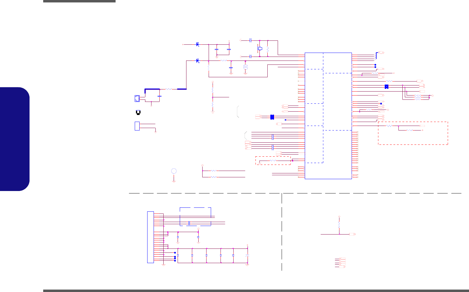
Schematic Diagrams
B - 14 CH7-M 1/4, SATA
B.Schematic Diagrams
CH7-M 1/4, SATA
Sheet 13 of 32
CH7-M 1/4, SATA
1.05VS
1.05VS
RTCVC C
3.3V S
3.3VS
5VS
3.3VS
3.3VS
RTCVCC
3.3VS
VD D3
C LK_ SATA#12
CLK_ SATA12
SB_KBCR ST# 23
PM _TH RM TR IP# 2,5
GA2 0 # 2 3
H_ F E RR # 2
H_SM I# 2
LP C _ F R A M E # 2 3
H_INTR 2
H_INI T# 2
H_IGN NE # 2
H_NM I 2
H_ST PCL K# 2
H_ A2 0 M# 2
H_ D P RS TP# 2 ,2 8
H_D PSL P# 2
H_ PW R GD 2
AZ_ SD IN117
AZ_RST#17, 22
AZ_ SD IN022
AZ_SDOUT17,22
LP C _ A D [ 3: 0 ] 2 3
SATA_LE D# 17
1.05VS 2..4,6, 7,12,16,27
5VS 11, 16,17,20,22,24
VDD 3 2,20,23..25,29
3 .3V S 5 ..7 ,9. .12 ,1 4 ..24 ,27 ,2 8
RT C VCC 1 6
SATAR XN117
SATAR XP117
SATAT XP117
SATATXN 117
AZ_ SY NC17, 22
AZ_BITCLK17 , 2 2
H_CPUSLP# 2,4
RTC_X1
IN TR UD ER#
RTCRST#
Z1324
SATA_LED# PM _TH RM TR IP#
Z1326
SB_TH RM TRIP#
LPC_DRQ0#
LP C _ F R A M E #
ICH_DPSLP#
ICH_DPRSTP#
H_ CP USL P _ SB #
IC H_INTVR MEN Z1325
Z1319
SATAR XP 0
Z1302 Z1303
Z1317
Z1318
LP C _ A D 2
LP C _ A D 0
LP C _ A D 3
LP C _ A D 1
Z1327
Z1328
Z1329
SATAT XN0
SATAT XP0
SATAR XP0_R SATAR XP0
Z1330
SATAR XN0
SATAR XN0 _ R
SATATXP0
Z1320SATATXN0
Z1321
SATA_ L ED#
ICH_INTVRMEN
ID E_ IRQ
ID E_ P DIO RD Y
SATARXN0
RTC_X2
Z1322
Z1323
ID E _ IRQ
ID E_ PDIO RD Y
Z1302
C3
*0 .1 U _1 6 V _ 0 4
C306 3900P_X7R _04
J_HDD1
C 16623-122A4
S1
S2
S3
S4
S5
S6
S7
P1
P2
P3
P4
P5
P6
P7
P8
P9
P10
P11
P12
P13
P14
P15
C311 3900P_X7R _04
C9
*0 .1 U _1 6 V _ 0 4
C292
10U_10V_08
C2 6 4
1U_10V _06
C4 0 4
1U_10V _06
C4
1U_6.3V_04
R213 *0_04
+
C293
100U_6.3V_B2
C8
0.1U_16V _04
H27
C 237B128D107
R236
10K_04
C295
0.01U _50V_04
C383 3900P_X7R _04
JCBAT1
*85205-02001
2
1
C2 9 6
10U _10V_08
C382 3900P_X7R _04
R1 1 7
332K_1% _06
C390 3900P_X7R _04
R241 10K _04
R125
10M_06
C389 3900P_X7R _04
X3
32.768KH z
14
3
2
RT CLA N
AC -9 7/ AZ AL IA
SA TA
ID E
LP CCP U
U1 6 A
ICH 7 -M
AB1
AB2
W4
Y5
W1
Y1
Y2
W3
V3
U3
U5
V4
T5
U7
V6
V7
U1
R6
R5
T2
T3
T1
T4
AF 18
AF3
AE3
AG2
AH2
AF7
AE7
AG6
AH6
AF1
AE1
AH 10
AG 10
AH 17
AE 17
AF 17
AE 16
AD 16
AB 15
AE 14
AG 13
AF 13
AD 14
AC 13
AD 12
AC 12
AE 12
AF 12
AB 13
AC 14
AF 14
AH 13
AH 14
AC 15
AE 15
AG 16
AH 16
AF 16
AH 15
AF 15
AA 6
AB 5
AC 4
Y6
AC 3
AA 5
AB 3
AE 22
AH 28
AG 27
AF 24
AH 25
AG 26
AG 24
AG 22
AG 21
AF 22
AF 25
AG 23
AF 23
AH 24
AH 22
AF 26
AA3
RTXC1
RTCX2
INTVRMEN
INTRUDER#
EE_CS
EE_SHCLK
EE_DOUT
EE_DIN
LAN _CLK
LAN _RSTSY NC
LAN _RXD0
LAN _RXD1
LAN _RXD2
LAN _TXD 0
LAN _TXD 1
LAN _TXD 2
A CZ_BIT_CLK
ACZ_SYNC
ACZ_RST#
ACZ_SDIN0
ACZ_SDIN1
ACZ_SDIN2
ACZ_SDOUT
SATALED#
SATA0RXN
SATA0RXP
SATA0TXN
SATA0TXP
SATA2RXN
SATA2RXP
SATA2TXN
SATA2TXP
SATA_CLKN
SATA_CLKP
SATARBIASN
SATARBIASP
DA0
DA1
DA2
DCS1#
DCS3#
DD0
DD1
DD2
DD3
DD4
DD5
DD6
DD7
DD8
DD9
DD10
DD11
DD12
DD13
DD14
DD15
DDREQ
IORDY
IDEIRQ
DDACK#
DIOW#
DIOR#
LAD0
LAD1
LAD2
LAD3
LDR Q0#
LD RQ 1#/G PIO23
LFRA ME#
A20G ATE
A20 M#
CPUSLP#
TP1/D PRSTP#
TP2/ DPSLP#
FER R#
G PIO4 9 /C PUPW RGD
IGN NE#
IN IT 3 _3 V#
INIT#
IN TR
RC IN#
SMI#
NM I
STPCL K#
TH ERM TRIP#
RTCRST#
R1 1 5
*0 _ 04 R 223 10K_04
R211 *56_04
C268 15P_50V_06
D22 SCS751V-40
A C
JO PEN1
* OPE N_10m il-1MM
12
C267 15P_50V_06
R65 56_04
R219 *56_04
JC BAT2
AAA-B AT- 022 -K01
1
2
R214 *10mil_short
R242 4.7K _04
R220 *10mil_short
C412
0.1U_16V _04
D20 SCS751V-40
A C
C406
*4.7U_6.3V_06
R 244 24.9_1%_04
R209 56_04
R2 5 1
1M _ 04
R2 1 2
24.9_1% _04
R8 3 1 0K_ 0 4
R124 20K_1% _04
R284 1K_04
R255 *10m il_short
R256 *10m il_short
RTC CLEAR
Within 500mil
24 .9 _1 % ne ed s to p la ce d wi th in 2 " of I CH 7,
56 Ohm must be placed within 2" of 24.9_1%
w/ o st ub .
Layout note:
(+ 3VS )
Trace >12mil
SL Zdiff=100 Ohm
MS Zdiff=95 Ohm
Zo=55 Ohm
Zo=55 Ohm
near
Connector
PIN GND1~2=GND
SATA HDD SATA HDD & ODD LED
JCBAT
12
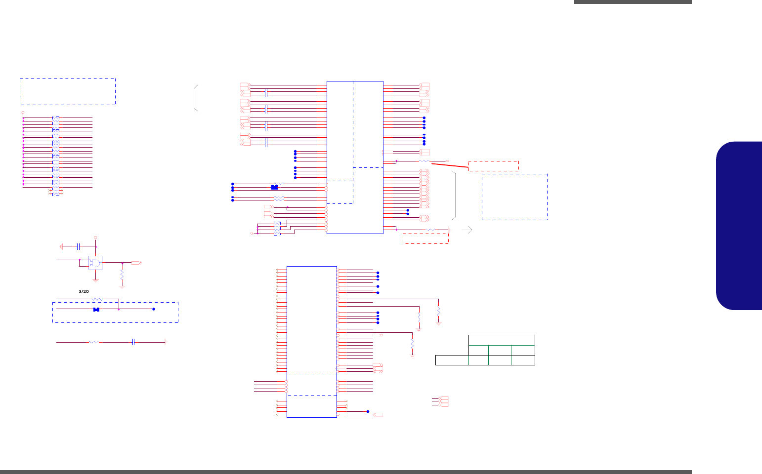
Schematic Diagrams
ICH7-M 2/4, PCI, USB, SPI B - 15
B.Schematic Diagrams
ICH7-M 2/4, PCI, USB, SPI
Sheet 14 of 32
ICH7-M 2/4, PCI,
USB, SPI
1.5VS
3.3VS
3. 3 V 3.3V
U SB_PP0 1 8
U SB_PN 3 18
U SB_PN 2 17
U SB_PP3 1 8
U SB_PP5 1 7
U SB_PN 7 17
U SB_PN 0 18
U SB_PN 5 17
U SB_PP1 1 8
U SB_PP2 1 7
U SB_PP7 1 7
U SB_PN 1 18
PC IE_RXN 1_W LAN17
PC IE_ RXP1_ W L AN17 DMI_RXP0 5
DMI_RXP1 5
DMI_RXN1 5
DMI_RXN0 5
C LK_PCIE _I CH # 12
C LK_PCIE _I CH 12
PC IE_TXN 1 _W L AN17 PC IE_TXP1_WLAN17 DMI_TXN0 5
D MI_TXP0 5
D MI_TXP1 5
DMI_TXN1 5
BU F_PLT_R ST# 1 7,18,21,23
3.3VS 5.. 7,9..13,15..24,27,28
1 .5 VS 3,5 ..7 ,1 6 ..1 8 ,2 2 ,27
M C H_ IC H_ SY NC # 5
P LT _ R S T # 5, 15
PCLK_ICH 12
PME# 23
3.3V 2,11,15..18,21,25..27
PC IE_TXN3_LAN21
PC IE_TXP3_LA N21
PCIE _R XP3_LA N21 PCIE _R XN3_LAN21
PC IE_TXN 2_ NEW _C AR D18 PCIE _T XP2_ NE W _ CAR D18
PCIE _R XP2 _ NEW _C AR D18
PCIE_RXN2_NEW_CARD18
PC IE_TXN 5_ CAR D19
PCIE_RXN5_CARD19
PCIE _TXP5_ CA RD19
PCIE _R XP5 _ CAR D19
USB _O C0 #18
USB _O C2 #17
PCI_RST# 19
USB _O C3 #18
U SB_PN 4 17
U SB_PP4 1 7
DMI_RXN2
DMI_TXP2
DMI_RXP3
DMI_RXP2
DMI_TXN2
DMI_TXN3
DMI_TXP3
DMI_RXN3
Z1410
Z1411
Z1430
Z1431
Z1429
Z1428
Z1404
Z1401
Z1402
Z1403
P LT_R ST#
PC IE_TXN1_C
PC IE_TXP1_C
P CI_ IN TF #
P CI_ IR DY #
PCI_REQ1#
PCI_REQ0#
PCI_TRDY#
PCI_SERR#
P CI_ IN TB #
P CI_ IN TE #
PCI_REQ5#
PCI_FRAME#
P CI_ IN TH #
P CI_ IN TD #
PCI_LOCK#
P CI_ IN TC #
PCI_REQ3#
PCI_REQ2#
PCI_STOP#
P CI_ IN TG #
PCLK_ICH Z1425
PCI_PERR#
P CI_ IN TA #
PCLK_ICH
P CI_ IN TG #
PCI_IN TD#
P CI_ IR DY #
PCI_REQ1#
P CI_ IN TF #
PCI_FRAME#
PCI_IN TC#
PCI_C/BE2#
PCI_REQ2#
P CI_D EVSEL#
PLT_RST#
PCI_PAR
P CI_ IN TE #
Z1418
PCI_C/BE3#
PCI_LOCK#
Z1419
Z1420
PCI_TRDY#
PCI_PERR#
PCI_RST#
PC I_GN T5#
Z1417
PCI_C/BE0#
PCI_STOP#
P CI_ IN TH #
PCI_REQ0#
PCI_C/BE1#
Z1424
PCI_SERR#
PCI_REQ4#
PCI_IN TB#
PCI_REQ3#
PCI_REQ5#
PCI_IN TA#
Z1409
Z1406
Z1408
PC IE_TXN3_C
PC IE_TXP3_C
PC IE_TXN2_C
PC IE_TXP2_C
PC IE_TXN4_C
PCI_REQ4#
P LT_R ST#
PCI _R ST#
PCIRST#
PC IE_TXP4_C
PC I_GN T4#
S_SPI_SI
SPI_SC L KS_SPI_SCLK
SPI_SI
SPI_SOS_SPI_S0
S_SPI_CS# SPI_CS#
Z1405
Z1426
Z1427
P CI_D EVSEL#
Z1407
T42
T145
T43
R97
1K_04
T44
U4
74LV C1G 08G W
1
2
5
4
3
R8 9 *1 0 m il_ s h or t
R2 3 2 *0 _ 0 4
R98 *10mil_short
R253 *47_04
R215
100K_04
RN26
8P4RX10K_04
1
2
3
45
6
7
8
C184 0.1U_10V_X7R _04
RN19
8P4RX10K_04
1
2
3
45
6
7
8
C236 *10P_50V _04
R258
22.6_1%_06
R254 *47_04RN17
8P4RX10K_04 1
2
3
4 5
6
7
8
RN28
8P4RX10K_04
1
2
3
45
6
7
8
R247
*1K_04
RN18
8P4RX10K_04
1
2
3
45
6
7
8
C 364 * 0.1U _16V _04
C187 0.1U_10V_X7R _04
C185 0.1U_10V_X7R _04
R7 4
24. 9_1%_04
C186 0.1U_10V_X7R _04
RN 2 9
8P4RX10K_04
1
2
3
45
6
7
8
R105 *47_04
R94
*1K _04
C181 0.1U_10V_X7R _04
C182 0.1U_10V_X7R _04
C188 0.1U_10V_X7R _04
RN27
8P4RX10K_04
1
2
3
45
6
7
8
R 96 *0_04
PCI-Express
Direct Media Interface
USB
SP I
U16D
IC H 7 -M
F26
F25
E28
E27
H26
H25
G28
G27
K26
K25
J28
J27
M26
M25
L28
L27
P26
P25
N28
N27
T25
T24
R28
R27
V26
V25
U28
U27
Y26
Y25
W28
W27
AB 26
AB 25
AA 28
AA 27
AD 25
AD 24
AC 28
AC 27
AE 28
AE 27
C25
D25
D3
C4
D5
D4
E5
C3
A2
B3
F1
F2
G4
G3
H1
H2
J4
J3
K1
K2
L4
L5
M1
M2
N4
N3
D2
D1
R2
P6
P1
P5
P2
PER n1
PER p1
PETn1
PETp1
PER n2
PER p2
PETn2
PETp2
PER n3
PER p3
PETn3
PETp3
PER n4
PER p4
PETn4
PETp4
PER n5
PER p5
PETn5
PETp5
PER n6
PER p6
PETn6
PETp6
DMI0RXN
DMI0RXP
DM I 0 TXN
DMI0TXP
DMI1RXN
DMI1RXP
DM I 1 TXN
DMI1TXP
DMI2RXN
DMI2RXP
DM I 2 TXN
DMI2TXP
DMI3RXN
DMI3RXP
DM I 3 TXN
DMI3TXP
DM I_ CL KN
DMI_CLKP
DM I_ZC OM P
DMI_IRCOMP
OC 0 #
OC 1 #
OC 2 #
OC 3 #
OC 4 #
OC 5 #/ GP IO 2 9
OC 6 #/ GP IO 3 0
OC 7 #/ GP IO 3 1
USBP0N
US BP0 P
USBP1N
US BP1 P
USBP2N
US BP2 P
USBP3N
US BP3 P
USBP4N
US BP4 P
USBP5N
US BP5 P
USBP6N
US BP6 P
USBP7N
US BP7 P
U SBRB IAS#
US BRBI AS
SPI_C LK
SPI_C S#
SPI_AR B
SPI_M OSI
SPI_M ISO
C183 0.1U_10V_X7R _04
PCI
Interrupt I/F
MISC
U16B
IC H 7 -M
E18
C1 8
A16
F18
E16
A18
E17
A17
A15
C1 4
E14
D1 4
B12
C1 3
G1 5
G1 3
E12
C1 1
D1 1
A11
A10
F11
F10
E9
D9
B9
A8
A6
C7
B6
E6
D6
D7
E7
C16
D16
C17
D17
E13
F13
A13
A14
C8
D8
B15
C12
D12
C15
A7
E10
B18
A12
C9
E11
B10
F15
F14
F16
C26
A9
B19
A3
B4
C5
B5 G7
F8
F7
G8
AE5
AD 5
AG 4
AH 4
AD 9 AH20
F21
AH8
AG8
AE9
AD 0
AD 1
AD 2
AD 3
AD 4
AD 5
AD 6
AD 7
AD 8
AD 9
AD 10
AD 11
AD 12
AD 13
AD 14
AD 15
AD 16
AD 17
AD 18
AD 19
AD 20
AD 21
AD 22
AD 23
AD 24
AD 25
AD 26
AD 27
AD 28
AD 29
AD 30
AD 31
REQ0#
GNT0#
REQ1#
GNT1#
REQ2#
GNT2#
REQ3#
GNT3#
REQ4#/GPIO22
GNT4#/GPIO48
RE Q5 # /GP IO1
GNT5#/GPIO17
C/BE0#
C/BE1#
C/BE2#
C/BE3#
IRDY#
PAR
PC IRST#
D EVSEL#
PER R#
PLOC K#
SER R#
STOP#
TRD Y#
FRAM E#
PLTRST#
PCIC LK
PM E#
PIR QA #
PIR QB #
PIRQC#
PIRQD# GPIO5/PIRQH#
GPIO4/PIRQG#
GPIO3/PIRQF#
GPIO2/PIRQE#
RSVD[1]
RSVD[2]
RSVD[3]
RSVD[4]
RSVD[5] MCH_SYNC#
TP3
RSVD [8 ]
RSVD [7 ]
RSVD [6 ]
Place within 500
mils of ICH
Place within 500
mils of ICH
(+ 3 V )
(+ 3 V )
(+ 3 V )
PLT_RST#:
BUF_PLT_RST#:
N/B,IDE,KBC,LAN
MINI CARD
(+3 V S )
(+3 V S )
(+ 5 V S)
(+ 5 V S)
RA
(+3 V S )
(+ 5 V S)
(+ 5 V S)
RB
(+5 V S )
on board
on daughter board
on daughter board
USB0: PORT0
USB1: PORT1
USB2: PORT2
USB3: NEW CARD
USB4: Mini PCIE
USB5: Bluetooth
USB6: X
USB7: CCD
Zo=90 Ohm
Zo=60 Ohm
SL Zdiff=100 Ohm
MS Zdiff=95 Ohm
Intel ? ? ? ?
GN T5 #
11
RB
GNT 4 #
Un st af f
RA
St ra p
ICH7 Bo ot BIOS selec t
UnStuffLPC(default)
Layout Guide:
Near ICH7M
100mil
3/20
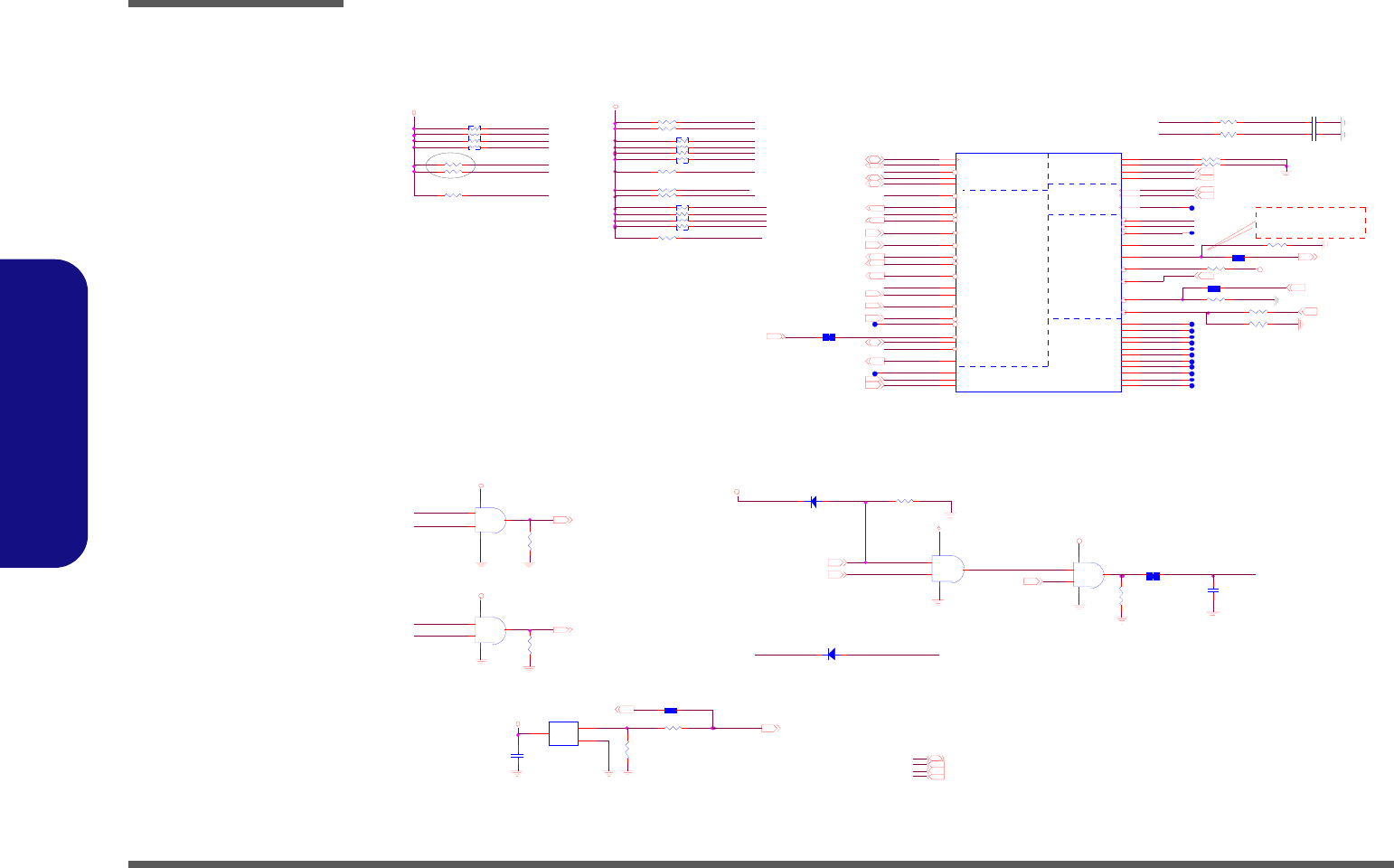
Schematic Diagrams
B - 16 ICH7-M 3/4
B.Schematic Diagrams
ICH7-M 3/4
3.3V
3.3V
3. 3V S
3.3VS
3.3V
3.3V
3.3V
3.3V
3.3VS
ICH _S MBC L K09,10,12
ICH _S MBD AT09,10,12
LPC_SIR Q23
SW I#23
SC I#23 SM I#23
PM_BM BU SY#5
PM _S TP PCI#12
PM_ STPC PU#12
SB_RSM RST# 2 3
SB_ PW R _B TN # 2 3
CL K_ I CH 4 8 12
PM_PWR OK 11,28
PM_DP RSLPVR 5 ,28
IC H_SPKR22
PC IE_W AKE #1 7 , 1 8, 21
PM_SY SR ST#2
SB_BL ON11
LC D I D 0 1 1
LC D I D 1 1 1ICH _S MBC L K118 ICH _S MBD AT118
SB_MU TE#22
SUSB # 18,23 ,2 4
SUSC # 23
IM VP 6 _ PW RG D5, 2 8
3.3V 2,11,14,16..18,21,25..27
VD D3 2,13,20,23..25,29
PM_C L KRU N#23
3.3VS 5..7,9..14,16..24,27,28
5VS 11,13, 16,17,20, 22,24
CL K_ I CH 1 4 12
PLT_RST# 5,14
OD D_ D E T E CT #17
VRM _ PW RG D12
1.8V_PWR GD26
VCC P_PWR GD27
EC_PM _PWRO K23
IC H_SM BDAT0
IC H_ SM B CL K0
SLP _S 5#
SB_BATLO W#
IC H_SM BDAT1
Z1510
ICH _S USC #
LINK ALERT#
ICH _S USB#
PM _RI#
CL K_ ICH 1 4
Z1508
CL K_ ICH 4 8
Z1506
Z1507
LC D I D 0
PCIE_W A KE#_N
LPC _SI RQ
PM _TH RM #
SB_PW RO K
PM _STP PCI#
PM _STP CPU #
LPC _PD #
PM _SYSR ST#
PM_CLKRU N #
ODD_DETECT#
Z1503
Z1511
Z1512
Z1513
Z1514
Z1519
VR M_PW R GD
Z1509
Z1520
Z1502
PC IE_ W AKE #_ N
INS TAN T _ ON
P M_CLKR UN #
LINKALER T#
ICH _SMBD AT1
LPC_PD #
LC D I D 1
SC I#
SB_M UTE#
IN S TANT _ ON
SB_MU TE#
PM _STPP CI#
PM_STPCPU#
Z1521
CLK_ICH48
CLK_ICH14
Z1505
Z1504
IC H_ SM B CL K1
ICH _SMBC LK0
ICH _SMBD AT0
SCI#
PM_THRM#
LPC _SIRQ
ICH _S USB#
SB _R SM RST#
Z1524 SB_ PW R OK
Z1525
PM_PW R O KSU SB#
PM_PW RO K
Z1515
Z1516
Z1517
Z1518
SB _R SM RST#
ICH _S USC #
LA N _ R S T #
OD D_ D E T EC T #
PM _PW RO K
PM _S YSR ST#
SW I#
SMI#
IC H_SU SB#
PM_R I#
ICH _SMBC LK1
R 79 100K_04
R84 * 1 0m il_sho rt
R2 26 * 1 0m il_sho rt
SATA
SM B
SYS
GPIO
GPIO
GPIO
Clocks
Power MGT
U16C
ICH7-M
AF1 9
AH18
AH19
AE19
C22
B22
A26
B25
A25
A19
A27
A22
AB18
AC21
AC18
E21
E20
A20
B23
F19
E19
R4
E22
AC20
AF2 1
R3
D2 0
AG18
AC19
U2
AD21
AD20
AE20
F20
AH21
AF2 0
AD22
AC1
B2
C2 0
B24
D2 3
F22
AA4
AC22
C2 1
C2 3
C1 9
Y4
A28
A21
B21
E23
GPI O21 /SATA0 GP
GPI O19 /SATA1 GP
GPI O36 /SATA2 GP
GPI O37 /SATA3 GP
SM BC LK
SM BD ATA
LIN KAL ERT#
SM LINK0
SM LINK1
SP KR
SU S_STAT#
SY S_RS T#
GPIO0/BM_BUSY#
GPIO6
GPIO7
GPIO8
GPIO9
GPIO 1 0
G P IO 11 /S M B AL E R T#
GPIO 1 2
GPIO 1 3
GPIO 1 4
GPIO 1 5
G PIO 18 /ST PPC I#
G PIO 20 /ST PC PU#
GPIO 2 4
GPIO 2 5
G P IO 32 /C LK RU N#
G P IO 33 /A Z_ D OC K_ EN#
G P IO 34 /A Z_ D OC K_ RST #
GPIO 3 5
GPIO 3 8
GPIO 3 9
WAKE#
SE RIR Q
TH RM #
VR MP W RG D
CLK14
CLK48
SU SCLK
SLP_ S3#
SLP_ S4#
SLP_ S5#
PW R OK
GPIO 1 6/D PR SL PVR
TP0/BATLOW #
PW RBTN #
LAN_R ST#
RSMRST#
RI#
GPIO26
GPIO27
GPIO28
R86 *10mil_short
R 217 * 10m il_short
C3 6 3
*0 . 1 U _ 1 6V _0 4
R2 1 8
10K _04
R235 1M_04
RN16
8P4RX10K_04
1
2
3
4 5
6
7
8
R231
1M _04
R81 1K_04
R230 *100_04
R88 10K_04
R87 100K_04
R 237 10K_04
D1 3 S C S 3 55 V
AC
R 2 34 * 1 0m i l _s h o r t
RN23
8P4RX10K_04
1
2
3
4 5
6
7
8
U14B
74LVC08PW
4
5
6
147
R2 3 3
*100K _04
R216
1M _04
C 391 * C_04
U14C
74LVC08PW
9
10 8
147
R257 *R _04
R 225 *100K_04
R1 2 3
100_04
D16 SCS355V
AC
U15
*G690L293T73
1
2
3
GND
RST#
VC C
R8 5 *1 0 K_ 04
R252 *R _04R 77 2.2K_04
U1 4 D
74LVC 08PW
12
13
11
147
C373
* 0.1U _10V_X7R_04
RN25
8P4R X10K_04
1
2
3
4 5
6
7
8
R 67 * 10K_04
C 394 * C_04
R229 *10K_04
R 80 2.2K_04
U14A
74LVC08PW
1
23
147
R224 8. 2K_1% _04
R 227 100K_04
R1 1 1 1 0K _ 0 4
R7 8 1 0 K_0 4 (+3VS)
(+3VS)
(+3VS)
(+3VS)
(+ 3 V S)
(+ 3 V S)
(+ 3 V S)
(+ 3V S )
(+ 3V S )
(+ 3 V S)
(+ 3 V S)
(+ 3 V S)
(+ 3V S )
(+ 3 V S)
(+ 3 V S)
(+ 3 V S)
(+ 3V )
(+ 3 V )
(+ 3 V )
(+ 3 V )
(+ 3 V )
(+ 3 V )
(+ 3 V )
(+ 3 V )
(+ 3 V )
(+ 3 V )
(+ 3 V)
(+ 3 V)
(+ 3 V)
(IMP809)
POWER OK
It"s for internal testing
pu rp os es o nl y
Layout note:
/LPCPD#
POWER GOOD
6/18
Sheet 15 of 32
ICH7-M 3/4
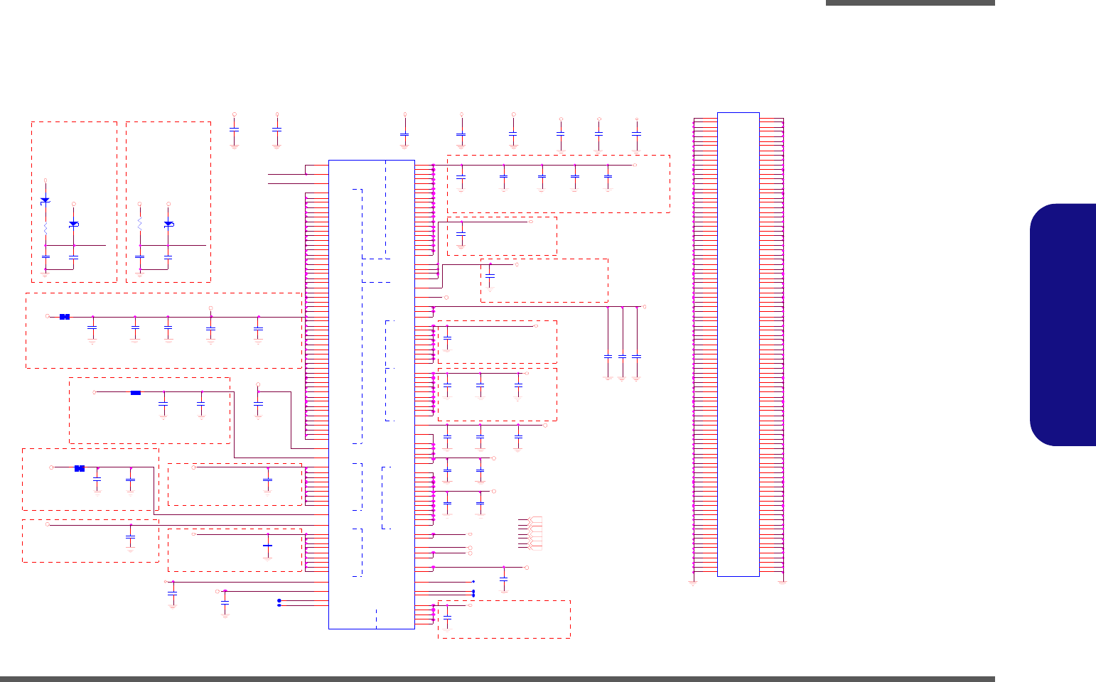
Schematic Diagrams
ICH7-M 4/4 B - 17
B.Schematic Diagrams
ICH7-M 4/4
Sheet 16 of 32
ICH7-M 4/4
1.5VS
1.5VS_ PCI E_ICH
3.3VS
1.5VS
1. 5 V S1.5VS
3.3VS
1. 5 V S
3.3V
1. 5 V S
1. 5 V S
1.5V S
1. 5 V S
1. 5 V S
1. 5 V S
3. 3 V
3. 3 V
RTCVCC
3.3V S
3.3VS
1.05VS
3.3VS
1.05VS
3. 3 V S
3. 3V
3.3VS
5VS
5VS
5V 3.3V
3.3V3.3V3.3V
5VS 1.05VS 1.05VS 1.05VS
3.3VS 5..7, 9..15,17..24, 27,28
5VS 11,13,17,20,22,24
1.05VS 2..4, 6,7,12,13,27
RTCVCC 13
1.5VS 3,5.. 7,14,17,18,22,27
3.3V 2,11,14,15,17,18,21,25..27
5V 11,17,18,20,25..28
Z1601
VCC5REF
VC C5R EF
Z1603
Z1608
Z1605
Z1604
V5R EF_ SUS
Z1607
Z1602
V5R EF_ SU S
Z1606
C258
0.1U _10V _X7R_04
C 226 * 0.1U_10V _X 7R _04
U1 6 E
ICH 7 -M
A4
A23
B1
B8
B11
B14
B17
B20
B26
B28
C2
C6
C27
D10
D13
D18
D21
D24
E1
E2
E4
E8
E15
F3
F4
F5
F12
F27
F28
G1
G2
G5
G6
G9
G14
G18
G21
G24
G25
G26
H3
H4
H5
H24
H27
H28
J1
J2
J5
J24
J25
J26
K24
K27
K28
L13
L15
L24
L25
L26
M3
M4
M5
M12
M13
M14
M15
M16
M17
M24
M27
M28
N1
N2
N5
N6
N11
N12
N13
N14
N15
N16
N17
N18
N24
N25
N26
P3
P4
P12
P13
P14
P15
P16
P17
P24
P27
P28
R1
R11
R12
R13
R14
R15
R16
R17
R18
T6
T12
T13
T14
T15
T16
T17
U4
U12
U13
U14
U15
U16
U17
U24
U25
U26
V2
V13
V15
V24
V27
V28
W6
W24
W25
W26
Y3
Y24
Y27
Y28
AA1
AA24
AA25
AA26
AB4
AB6
AB11
AB14
AB16
AB19
AB21
AB24
AB27
AB28
AC2
AC5
AC9
AC11
AD1
AD3
AD4
AD7
AD8
AD11
AD15
AD19
AD23
AE2
AE4
AE8
AE11
AE13
AE18
AE21
AE24
AE25
AF2
AF4
AF8
AF11
AF27
AF28
AG1
AG3
AG7
AG11
AG14
AG17
AG20
AG25
AH1
AH3
AH7
AH12
AH23
AH27
V SS[1]
V SS[2]
V SS[3]
V SS[4]
V SS[5]
V SS[6]
V SS[7]
V SS[8]
V SS[9]
V SS[10 ]
V SS[11 ]
V SS[12 ]
V SS[13 ]
V SS[14 ]
V SS[15 ]
V SS[16 ]
V SS[17 ]
V SS[18 ]
V SS[19 ]
V SS[20 ]
V SS[21 ]
V SS[22 ]
V SS[23 ]
V SS[24 ]
V SS[25 ]
V SS[26 ]
V SS[27 ]
V SS[28 ]
V SS[29 ]
V SS[30 ]
V SS[31 ]
V SS[32 ]
V SS[33 ]
V SS[34 ]
V SS[35 ]
V SS[36 ]
V SS[37 ]
V SS[38 ]
V SS[39 ]
V SS[40 ]
V SS[41 ]
V SS[42 ]
V SS[43 ]
V SS[44 ]
V SS[45 ]
V SS[46 ]
V SS[47 ]
V SS[48 ]
V SS[49 ]
V SS[50 ]
V SS[51 ]
V SS[52 ]
V SS[53 ]
V SS[54 ]
V SS[55 ]
V SS[56 ]
V SS[57 ]
V SS[58 ]
V SS[59 ]
V SS[60 ]
V SS[61 ]
V SS[62 ]
V SS[63 ]
V SS[64 ]
V SS[65 ]
V SS[66 ]
V SS[67 ]
V SS[68 ]
V SS[69 ]
V SS[70 ]
V SS[71 ]
V SS[72 ]
V SS[73 ]
V SS[74 ]
V SS[75 ]
V SS[76 ]
V SS[77 ]
V SS[78 ]
V SS[79 ]
V SS[80 ]
V SS[81 ]
V SS[82 ]
V SS[83 ]
V SS[84 ]
V SS[85 ]
V SS[86 ]
V SS[87 ]
V SS[88 ]
V SS[89 ]
V SS[90 ]
V SS[91 ]
V SS[92 ]
V SS[93 ]
V SS[94 ]
V SS[95 ]
V SS[96 ]
V SS[97 ]
VSS[98 ]
VSS[99 ]
VSS [100 ]
VSS [101 ]
VSS [102 ]
VSS [103 ]
VSS [104 ]
VSS [105 ]
VSS [106 ]
VSS [107 ]
VSS [108 ]
VSS [109 ]
VSS [110 ]
VSS [111 ]
VSS [112 ]
VSS [113 ]
VSS [114 ]
VSS [115 ]
VSS [116 ]
VSS [117 ]
VSS [118 ]
VSS [119 ]
VSS [120 ]
VSS [121 ]
VSS [122 ]
VSS [123 ]
VSS [124 ]
VSS [125 ]
VSS [126 ]
VSS [127 ]
VSS [128 ]
VSS [129 ]
VSS [130 ]
VSS [131 ]
VSS [132 ]
VSS [133 ]
VSS [134 ]
VSS [135 ]
VSS [136 ]
VSS [137 ]
VSS [138 ]
VSS [139 ]
VSS [140 ]
VSS [141 ]
VSS [142 ]
VSS [143 ]
VSS [144 ]
VSS [145 ]
VSS [146 ]
VSS [147 ]
VSS [148 ]
VSS [149 ]
VSS [150 ]
VSS [151 ]
VSS [152 ]
VSS [153 ]
VSS [154 ]
VSS [155 ]
VSS [156 ]
VSS [157 ]
VSS [158 ]
VSS [159 ]
VSS [160 ]
VSS [161 ]
VSS [162 ]
VSS [163 ]
VSS [164 ]
VSS [165 ]
VSS [166 ]
VSS [167 ]
VSS [168 ]
VSS [169 ]
VSS [170 ]
VSS [171 ]
VSS [172 ]
VSS [173 ]
VSS [174 ]
VSS [175 ]
VSS [176 ]
VSS [177 ]
VSS [178 ]
VSS [179 ]
VSS [180 ]
VSS [181 ]
VSS [182 ]
VSS [183 ]
VSS [184 ]
VSS [185 ]
VSS [186 ]
VSS [187 ]
VSS [188 ]
VSS [189 ]
VSS [190 ]
VSS [191 ]
VSS [192 ]
VSS [193 ]
VSS [194 ]
C206
0.1U_10V _X7R _04
C218
0.1U_16V_04
D6
SCS 751V-40
AC
C2 2 4
0.1U _16V_04
C 214
0.1U _16V_04
C2 3 2
0.1U _16V_04
C2 3 4
0.1U _16V_04
C3 8 7
*0.1U_16V_04
C261
0.1U_16V_04
C230
1U _6.3V_04
C212
*1U _6.3V_04
C246
1U_6.3V_04
C2 1 1
1U _ 6 . 3V _0 4
C 222 1U_6.3V_04
C225
1U _6.3V_04
C2 3 8
0. 1U _16V_04
C216
1U_6.3V_04
R95
100_04
C2 0 1
10U _6.3V_06
CORE
VCCA3GP
VCC PAUX
USB
ATXARX
IDE
USB CORE
PCI
U16F
IC H7-M
G1 0
AD17
F6
AA22
AA23
AB22
AB23
AC23
AC24
AC25
AC26
AD26
AD27
AD28
D2 6
D2 7
D2 8
E24
E25
E26
F23
F24
G2 2
G2 3
H2 2
H2 3
J22
J23
K22
K23
L22
L23
M2 2
M2 3
N2 2
N2 3
P22
P23
R2 2
R2 3
R2 4
R2 5
R2 6
T22
T23
T26
T27
T28
U2 2
U2 3
V22
V23
W22
W23
Y22
Y23
B27
AG28
AB7
AC 6
AC 7
AD 6
AE6
AF5
AF6
AG 5
AH 5
AD 2
AH11
AB10
AB9
AC10
AD10
AE10
AF10
AF9
AG 9
AH 9
C1
AA2
Y7
L11
L12
L14
L16
L17
L18
M11
M18
P11
P18
T11
T18
U11
U18
V11
V12
V14
V16
V17
V18
V5
V1
W2
W7
U6
R7
AE 23
AE 26
AH 26
AA 7
AB 12
AB 20
AC 16
AD 13
AD 18
AG 12
AG 15
AG 19
A5
B13
B16
B7
C10
D15
F9
G11
G12
G16
W5
P7
A24
C24
D19
D22
G19
K3
K4
K5
K6
L1
L2
L3
L6
L7
M6
M7
N7
AB 17
AC 17
T7
F17
G17
AB 8
AC 8
K7
C28
G20
A1
H6
H7
J6
J7
E3
V5RE F[1]
V5RE F[2]
V5RE F_Sus
Vcc1_5_B[1]
Vcc1_5_B[2]
Vcc1_5_B[3]
Vcc1_5_B[4]
Vcc1_5_B[5]
Vcc1_5_B[6]
Vcc1_5_B[7]
Vcc1_5_B[8]
Vcc1_5_B[9]
Vcc1_5_B[10]
Vcc1_5_B[11]
Vcc1_5_B[12]
Vcc1_5_B[13]
Vcc1_5_B[14]
Vcc1_5_B[15]
Vcc1_5_B[16]
Vcc1_5_B[17]
Vcc1_5_B[18]
Vcc1_5_B[19]
Vcc1_5_B[20]
Vcc1_5_B[21]
Vcc1_5_B[22]
Vcc1_5_B[23]
Vcc1_5_B[24]
Vcc1_5_B[25]
Vcc1_5_B[26]
Vcc1_5_B[27]
Vcc1_5_B[28]
Vcc1_5_B[29]
Vcc1_5_B[30]
Vcc1_5_B[31]
Vcc1_5_B[32]
Vcc1_5_B[33]
Vcc1_5_B[34]
Vcc1_5_B[35]
Vcc1_5_B[36]
Vcc1_5_B[37]
Vcc1_5_B[38]
Vcc1_5_B[39]
Vcc1_5_B[40]
Vcc1_5_B[41]
Vcc1_5_B[42]
Vcc1_5_B[43]
Vcc1_5_B[44]
Vcc1_5_B[45]
Vcc1_5_B[46]
Vcc1_5_B[47]
Vcc1_5_B[48]
Vcc1_5_B[49]
Vcc1_5_B[50]
Vcc1_5_B[51]
Vcc1_5_B[52]
Vcc1_5_B[53]
Vcc3_3[1]
VccDM IPLL
Vcc1_5_A[1]
Vcc1_5_A[2]
Vcc1_5_A[3]
Vcc1_5_A[4]
Vcc1_5_A[5]
Vcc1_5_A[6]
Vcc1_5_A[7]
Vcc1_5_A[8]
Vcc1_5_A[9]
Vc c SATAPL L
Vcc3_3[2]
Vcc1_5_A[10]
Vcc1_5_A[11]
Vcc1_5_A[12]
Vcc1_5_A[13]
Vcc1_5_A[14]
Vcc1_5_A[15]
Vcc1_5_A[16]
Vcc1_5_A[17]
Vcc1_5_A[18]
VccUSB PLL
VccSus1_05/VccLAN 1_05[1]
VccSus1_05/VccLAN 1_05[2]
Vcc1_05[1]
Vcc1_05[2]
Vcc1_05[3]
Vcc1_05[4]
Vcc1_05[5]
Vcc1_05[6]
Vcc1_05[7]
Vcc1_05[8]
Vcc1_05[9]
V cc1_05[10]
V cc1_05[11]
V cc1_05[12]
V cc1_05[13]
V cc1_05[14]
V cc1_05[15]
V cc1_05[16]
V cc1_05[17]
V cc1_05[18]
V cc1_05[19]
V cc1_05[20]
VccSus3_3/V ccLAN 3_3[1]
VccSus3_3/V ccLAN 3_3[2]
VccSus3_3/V ccLAN 3_3[3]
VccSus3_3/V ccLAN 3_3[4]
Vcc3_3/VccHD A
V ccSus3_3/V ccSusHD A
V_CPU _I O[1]
V_CPU _I O[2]
V_CPU _I O[3]
Vcc3_3[3]
Vcc3_3[4]
Vcc3_3[5]
Vcc3_3[6]
Vcc3_3[7]
Vcc3_3[8]
Vcc3_3[9]
Vcc3_3[10]
Vcc3_3[11]
Vcc3_3[12]
Vcc3_3[13]
Vcc3_3[14]
Vcc3_3[15]
Vcc3_3[16]
Vcc3_3[17]
Vcc3_3[18]
Vcc3_3[19]
Vcc3_3[20]
Vcc3_3[21]
VccRTC
VccSus3_3[1]
VccSus3_3[2]
VccSus3_3[3]
VccSus3_3[4]
VccSus3_3[5]
VccSus3_3[6]
VccSus3_3[7]
VccSus3_3[8]
VccSus3_3[9]
V ccSus3_3[10]
V ccSus3_3[11]
V ccSus3_3[12]
V ccSus3_3[13]
V ccSus3_3[14]
V ccSus3_3[15]
V ccSus3_3[16]
V ccSus3_3[17]
V ccSus3_3[18]
Vcc1_5_A[19]
Vcc1_5_A[20]
Vcc1_5_A[21]
Vcc1_5_A[22]
Vcc1_5_A[23]
Vcc1_5_A[24]
Vcc1_5_A[25]
V ccSus1_05[1]
V ccSus1_05[2]
V ccSus1_05[3]
Vcc1_5_A[26]
Vcc1_5_A[27]
Vcc1_5_A[28]
Vcc1_5_A[29]
Vcc1_5_A[30]
VccSus3_3[19]
C233
0.1U_16V _04
D4
SC S751V-40
AC
C2 4 2
*0.1U_16V_04
C213
0.1U_16V _04
C192
10U _6.3V_06
C228
0.1U_10V _X7R _04
C2 3 5
0.1U _16V_04
C243
0. 1U _10V_X7R_04
C227
0.1U_16V_04
C248
0.1U_16V_04
C 256
10U _6.3V_06
C220
0.1U _10V_X7R_04
C207
0.1U_10V_X7R _04
C2 5 1
0. 1U _16V_04
C2 5 0
0.1U _16V_04
R109
10_04
C255
0.1U_16V_04
C2 4 1
0.1U _16V_04
C3 8 8
*0.1U_16V_04
C257
0.1U_16V_04
C210
* 0.1U _10V_ X7 R_04
C259
* 0.1U _16V_04
C362
0.01U _50V_04
L8
*H CB1005K F-121T20_10mil_short
L10
*H CB 1005KF-121T20_10m il_s hort
L18
*H CB 1005KF-121T20_10m il_s hort
C231
10U _6.3V_06
C 263
* 0.1U_16V _04
C265
10U _6.3V _06
C190
10U_6.3V_06
C355
10U_6.3V_06
C217
* 0. 1U _10 V_ X7 R_0 4
C2 2 3
0. 1U _16V_04
D5
SC S751V-40
AC
C2 0 9
10U _6.3V_06
C 219 0.1U_10V_X7R_04
C221
10U_6.3V_06
Place above Caps within 100 mils of ICH on the bottom
s id e or 1 40 m il s o n th e to p ne ar D 28 , T2 8, A D2 8
Layout note:
Layout note:
Pl ac e wi t hi n 10 0m il s of I CH o n th e
bo tt om s i de o r 14 0 mi ls o n th e to p
Pl ac e wi th in 1 00 mi ls o f I CH
on the bottom side or 140
mi ls o n th e to p ne ar p i n AG 5
Place within 100mils
o f IC H on th e bo tt om
s id e or 1 4 0 mi ls o n
the top
Place within 100mils of
ICH on the bottom side or
140 mils on the top Pl ac e wi th in 1 00 mi ls o f I CH
on the bottom side or 140
mi ls o n th e to p ne ar p i n AG 9
Place within 100 mils
o f IC H7 o n th e bo tt om
side of 140mils on
the top
Distribute in PCI section
Pl ac e at M CH e dg e
Pl ac e wi th in 1 00 m il s
of ICH7 on the bottom
si de o f 14 0m il s on
th e to p
Pl ac e on s e co nd ar y
si de u nd er MC H
Pl ac e wi th i n 10 0 mi ls
of I CH 7 on th e bo tt om
side of 140mils on
th e to p
Layout note:
Place within 100 mils
o f pi n F6 of I CH 7 on
the bottom side of
140mils on the top
Layout note:
Pl ac e wi th in 1 00 m il s
of pin AD17 of ICH7
on the bottom side or
14 0 mi ls o n th e to p
si de
Layout note: Layout note:
Layout note:
Layout note:
Layout note:
Layout note:
Layout note:
Layout note:
Layout note:
Layout note:
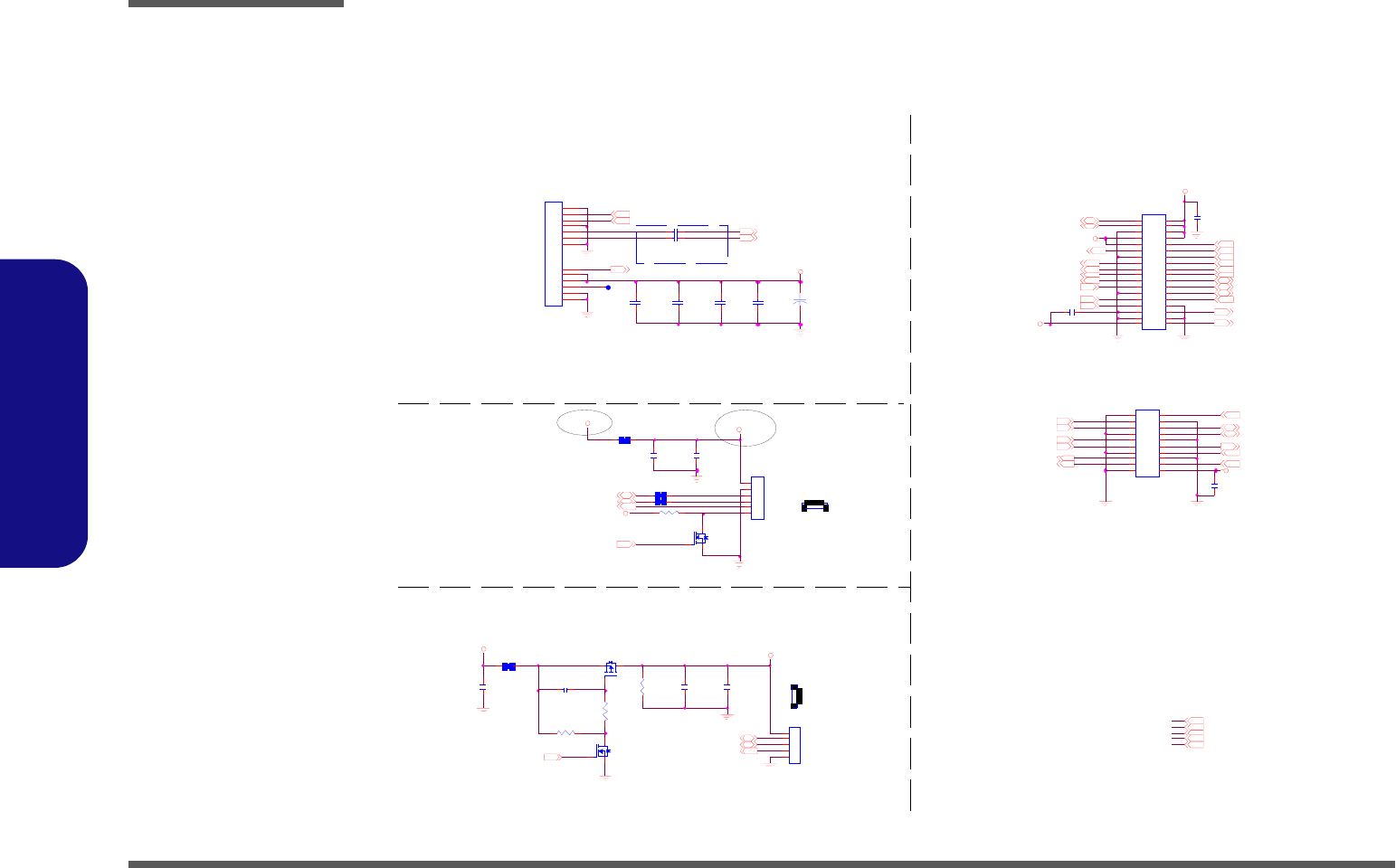
Schematic Diagrams
B - 18 MULTI I/O, ODD, CCD BT
B.Schematic Diagrams
MULTI I/O, ODD, CCD BT
Sheet 17 of 32
MULTI I/O, ODD,
CCD BT
5V_CCD
3.3V_BT
3.3V S
3.3V
3.3V
3. 3VS
5V
1.5VS
5VS
5V
CCD_DET#23
CCD_EN23
BT_ EN20,23
BT_ D ET#23
LED_SCROLL# 23
LED_NUM# 23
LED_CAP# 23
3.3V 2,11,14..16,18,21,25.. 27
3.3V S 5..7, 9.. 16, 18. .24,27,28
5V 11,16,18,20,25..28
5VS 11,13,16,20,22,24
USB_PP514
USB_PN514
USB_PN714
US B_PP714
LED_THR OTTLE# 23
SP KOUTR-22
SP KOUTR+22
WLAN_EN 20,23
AZ _ BI T C LK13,22
AZ _RST#13,22
AZ_SYNC13,22
AZ_ S DIN113 SATA _ LED#13
1.5V S 3,5..7,14,16,18,22,27
WLAN _ C L KR EQ# 1 2
USB_PN4 14
US B_PP4 1 4
PC I E_ WAKE# 15,18,21
BUF_PLT_RST# 14,18,21,23
PCIE_TXP1_WLA N14
PC I E_ R XN 1_WLAN14
C L K_PC I E _MIN I12
CLK_PCIE_MINI#12
PCIE_RXP1_WLA N14
PC I E_ TXN 1_WLAN14
LID_SW# 11,23
WEB0# 24
WLAN_DET# 23
WEB2# 23
WEB1# 23
M_BTN#24
USB_PN214
USB_PP214
ODD_DETECT# 15
SA T AR XP1 13
SA TA TXP1 13
SA TATXN113
SA T AR XN113
3G_EN 20,23
AZ _ SD OUT13,22
USB_OC2#14
Z1707
Z1709
Z1708
BT_EN#
USB_PN6_R
U SB _ PP6 _R
Z1799
SATA RXP 1 _R
SATA RXN1_R
L4
*HCB 1608KF-121T25_15mil_short
C284
0.1U_16V_04
L12
*HC B1608KF -121T25_15mil _short
Q1
NDS352AP_NL
G
DS
Q7
2N7002W
G
DS
J_BT1
87212-06G0
1
2
3
4
5
6
C300
10U_10V_08
R11 10K_04
C443
0.1U_10V _04
C432
1U_10V _06
C275
10U_10V _08
J_MFB2
5F 1. 233A 1-A2000.210
12
34
56 78
910
1112
1314
16
18
20
15
17
19
C297
0.1U_16V_04
C277
0.1U_16V_04
C281 0.1U_16V_04
R169 * 10mil _short
J_CCD1
85204-05001
1
2
3
4
5
C431
0.1U_10V _04
C280
0.1U_16V_04
C276
10U_10V_08
R170 * 10mil _short
R143
100K_04
Q2
2N7002W
G
DS
C287
0.1U_16V_04
+
C446
*100U_6.3V_B2
J_MFB1
5F1- 233A1-A2000-218
12
34
56
78
910 1112
1314
1516
1718
1920
2122
2324 2526
2728
2930
3132
3334
3536
R144
100K _04
C444
10U_10V_08
R139 330K_04
C473 3900P_X7R_04
C461 3900P_X7R_04
J_ODD1
C18535-11305-L
S1
S2
S3
S4
S5
S6
S7
P1
P2
P3
P4
P5
P6
Bluetooth
CCD
48 mi l
MULTI I/O CONN
J_CCD1
5
1
50mil
From H8 default HI
61
J_BT1
3.3VS=4A
Port 5
6-20-41A10-106
PIN GND1~4=GND
SATA ODD
near
Connector
OPTION
7/21
8/27
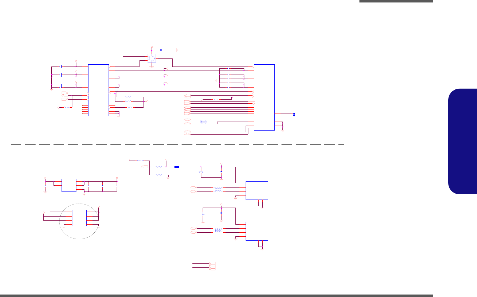
Schematic Diagrams
NEW CARD, USB B - 19
B.Schematic Diagrams
NEW CARD, USB
Sheet 18 of 32
NEW CARD, USB
5V
3.3V
3.3VS
1.5VS
3.3VS
3. 3 V
N C_3.3V
N C_3.3VS
N C_1.5VS
3.3V
3. 3V S
5V
U SBVC C01
USB _VC C01_0
U SBVC C01
USB _VC C01_0
USBVCC01
3.3V
USB_OC3#14
SUSB #15,23,24
U SB_PN 314
U SB_PP314
PC IE_W AKE#15,17,21
N EW C ARD _CLKR EQ#12
C LK_PCIE_N EW _CAR D12
PCIE_TXP2_NEW_CARD14
PC IE_RXP2 _NEW _ C ARD14
PC IE_RXN2_NEW _C AR D14
PC IE_TXN 2_N EW_C ARD14
IC H_ SMB CL K115
IC H_ SMB DAT115
BU F_PLT_R ST#14,17,21,23
C LK _P CIE_N EW_CAR D#12
USB_PN014
USB_PN114
USB_O C0#14
U SB_PP014
U SB_PP114
1.5VS 3,5..7,14,16,17,22,27
5V 11,16,17,20,25..28
3.3VS 5..7,9..17,19.. 24,27,28
3.3V 2,11,14..17,21,25..27
NC _C PPE#
BUF_PLT_RST#
NC _PE RST #
BU F_PL T_R ST#
NC _ RS T#
Z1801
NC _C PUS B#
PCIE_ W AK E#
Z1802
Z1803
U SB_PP0_R
U SB_PN1_ R
U SB_PP1_R
U SB_PN0_ R
USB_O C0#
L11
* WCM 2012F2S-161T03-short
1
4
2
3
U2 8
UP7534DSA8-20
6
83
2 7
14
5VO UT1
VO UT3VIN2
VIN1 VO UT2
GN DEN#
FLG#
L22
* WCM 2012F2S-161T03-short
1
4
2
3
L24
* WCM 2012F2S-161T03-short
1
4
2
3
+
C524
220U _6.3V_6*5.9
C425 *0.1U_16V _04
R303 10K_04
C454
0.1U_16V _04
C440
10U _10V_08
R295 *100K_04
J_N EW1
* 130801-1
17
1
10
26
20
23
4
19
18
22
21
25
24
14
15
12
9
13
11
8
7
16
5
6
3
2
CPPE#
GN D
+1.5V
GN D
GN D
GN D
CPUSB#
REFCLK+
REFCLK-
PE Tp0
PE Tn0
PE Rp0
PE Rn0
+3.3V
+3.3V
+3 .3VAUX
+1.5V
PE RST#
W A KE#
SM B_DATA
SM B_CLK
CLKREQ#
R ESER VED
R ESER VED
USB_D+
USB_D-
U21
* P2231THLFC 1
2
3
4
6
5 8
7
9
1
11
14
15
16
17
18
19
20
21
22
23
10
12
13
24 25
SY SRS T#
SH DN #
STBY #
3.3VIN
3.3VIN 3.3V OU T
3.3V OU T
PER ST#
NC
GN D
CPUSB#
CPPE #
1.5V OU T
1.5V OU T
1.5VIN
1.5VIN
AU XOU T
AU XIN
RC LKEN
OC#
NC
NC
NC
NC GND
U22
*R T9701-CP L
1
2
3
4
5
VO UT
GN D
VIN
VIN
VO UT
C416
0.1U_16V _04
C419 *0.1U_16V _04
J_USB 1
SK10713
1
5
2
3
4
6
V+
GND1
DA TA _L
DA TA _H
GN D
GND2
C 4 20 * 0. 1 U _ 16 V _ 0 4
+
C415
* 100U _10V_D
C427 *0.1U_16V _04
C428 * 0.1U_16V _04
R292
15K_04
C441
10U_10V _08
J_USB 2
SK10713
1
5
2
3
4
6
V+
GND1
DA TA _L
DA TA _H
GN D
GND2
C 4 29 * 0. 1 U _ 16 V _ 0 4
R294 *100K_04
C433 *0.1U_16V _04
R301 *10K_04
R293
10K_04
C 4 21 * 0. 1 U _ 16 V _ 0 4
C439
0.1U_16V _04
R 304 10K _04
C426 *0.1U_16V _04
C 4 35 * 0. 1 U _ 16 V _ 0 4
C438
0.1U_16V _04
C 4 22 * 0. 1 U _ 16 V _ 0 4
U20
* 74LVC 1G 08G W
1
2
5
4
3
L21
* HC B1608KF-121T25_15m il_s hort
R353
*10K_04
NEW CARD
100 MIL
20 mil
40 mil
EN E P2 23 1 pi n3 ,4 ,1 4, 15 ,2 2
ha s in te rn al ly p ul le d hi gh
( 17 0K o hm S )
40 mil
6-01-74108-Q61
GND1~ 4=GND
Port 3
Port 0
Port 1
USB PORT
60 mil
60 mil
100 MIL
6-02-75348-920
Schematic Diagrams
B - 20 CARD READER JMB385
B.Schematic Diagrams
CARD READER JMB385
VCC_CARD
3.3VS
VC C_CARD
VCC_CARD
3.3VS
DV1 . 8 V
DV1.8V
DV1.8V
3.3VS
3.3VS
DV1.8V
VC C_CARD
DV1.8V
3.3VS
VCC_CARD
VCC_CARD
3.3VS5..7,9. .18,20..24,27,28
C L K_PC I E_ J M 380#12
PC I E_ TXP5 _C AR D 1 4
CLK_PCIE_JM38012
PC I E_ TXN 5 _CARD 14
PC I E_ R XP5_CARD 14
PC I E_ R XN5_CARD14
PC I _ R ST#14
1.8V5,7,9,10,26
JMB_D3D 23
SD _ CLK
MDIO7
MDIO12
MDIO13
MS_INS#
MDIO14
SD _WP
SD _CD#
SD_CLK
MDIO9
Z1903
Z1901
SD _ C D#
SD_D2 MS_INS#
MDIO10
Z1902
Z1909
SD_D0
SD_D1
Z1906
MDIO12
MDIO8
MDIO11
SD_D3
MDI O14
Z1908
CR1_LEDN
Z1904
CR1_PCTLN
SD_BS
Z1907
MDIO7
Z1905
SD_WP
MDI O13
CR1_PCTLN
MS_IN S#
SD _ D3
SD _ D3
SD _ D1
SD _ BS
SD _ D1
SD _ CD#
SD _ WP
SD _ D0
SD _ D0
SD _ D2
SD _ CLK
SD _ BS
SD _ CLK
SD _ D2
SD _ CD#
C430 0.1U_10V_X7R_04
C434 0.1U_10V_X7R_04
D25 *SCS751V-40A C
C472
0.1U_16V_04
J_CARD-REV1
MDR019-C0-0010(Reverse)
P2
P21
P3
P4
P5
P6
P7
P8
P9
P10
P11
P12
P13
P14
P15
P16
P17
P18
P19
P20
P1
P23
P22
DAT2_SD
V SS_MS
CD/DAT3_SD
CMD_SD
V SS_SD
VDD_SD
C L K_SD
V SS_SD
DAT0_SD
DAT1_SD
WP_SD
V SS_MS
VCC_MS
SCLK_MS
DAT3_MS
INS_ MS
DAT2_MS
SDIO/DAT0_MS
DAT1_MS
BS_MS
CD_SD
GND
GND
C468
0.1U_16V_04
R300 200K_04
C469
*10P_50V_04
R305 8.2K_1%_04
C436
0.1U_16V_04
R302 200K_04
R299 10K_04
C449
0.1U_16V_04
C442
0.1U_16V_04
C466
0.1U_16V_04
C423
0.1U_16V_04
C470
0.1U_16V_04
R298 4.7K_04
C424
0.1U_16V_04
R320 10K_04
C471
0.1U_16V_04
R297 4.7K_04
C445
1000P_50V_04
R319 10K_04
C453
0.1U_16V_04
C437
10U_10V_08
C462
10U_10V_08
R318 75_06
C467
0.1U_16V_04
JMB38 5
U23
JMB385
1
2
3
4
5
6
7
8
9
10
11
12
14
15
16
17
18
19
20
21
22
23
24
13
37
38
39
40
41
42
43
44
45
46
47
48
36
35
34
33
32
31
30
29
28
27
26
25
XR ST N
XTE ST
APC L KN
APCLKP
AP VD D
APG N D
APR EXT
APRXP
AP RXN
APV 18
APTX N
APTXP
SEEC L K
CR1_CD1N
CR1_CD0N
CR1_PCTLN
DV18
REG_CTRL
DV33
CR_LEDN
MDIO14
MDIO13
GND
SEED AT
DV1 8
PCI ES_EN
PCIES
MDIO7
MDIO6
MDIO5
MDIO4
DV3 3
MDIO3
MDIO2
MDIO1
MDIO0
NC
NC
NC
GND
GND
GND
TAV3 3
MDIO8
MDIO9
MDIO10
MDIO11
MDIO12
R296 * s hort_08
C465
0.1U_16V_04
4 IN 1 SOCKE T SD/MM C/MS/MS Pro
Near Cardreader CONN
Card Reader Power
MDIO7
HIGH
CR1_LEDN
High
Active
On Borad
LO W
Add-in Card
CR1_PCTLN
High
Active
M DI O12
CR1_PCTLN
Low
Active
M DI O14
CR1_LEDN
Low
Active
Layout note:
Layout note:
Very closed to pin 5 Very closed between
pi n 5 an d p in 10
C472 Near to Pin30
MP version IC will provide card reader power by Pin17
Be c au s e M P ve r si on JMB3 8 5 w ill pr o vid e 1. 8V by IC se lf , be a d re s er v e f o r de bu g
D03 -0221
Sheet 19 of 32
CARD READER
JMB385
Schematic Diagrams
LED, FAN, PC BEEP, TP, FP B - 21
B.Schematic Diagrams
LED, FAN, PC BEEP, TP, FP
Sheet 20 of 32
LED, FAN, PC
BEEP, TP, FP
5VS
3.3VS
VD D3 VDD3
VDD3 3.3VS3.3VSVD D3
5VS
5VS_TP
5VS_FAN
5VS5V S _ F A N
3.3VS
5VS 11,13, 16,17,22,24
VD D3 2,13,23..25,29
3.3VS 5..7,9..19,21..24,27,28
C PU_FA NSEN23
LED_BAT_FU LL# 23LED_BAT_ CH G#23
WLAN _EN 17,23L ED_ PW R# 2 3 BT_EN17 , 2 3LED_AC IN#23
TP_DATA 23
TP_CLK 23
CP U_ FA N23
3G_EN 17,23
Z2003 Z2004
Z2008Z2007
Z2005Z2001 Z2002 Z2006
Z2022
Z2023
FO N#
FO N#
H2 1
C158D158
H2 0
C1 5 8 D1 5 8
H1 9
C1 5 8 D1 5 8
H18
C158D158 M4
M-M A RK 1
M3
M-M A RK 1
M2
M- MA R K 1
M1
M-MAR K1
1
H1
M T H3 1 5 D1 1 1
2
3
4
5 6
7
8
9
M6
M-MA RK1
M5
M-MARK1 M8
M-MAR K1
1
H8
M TH315D 111
2
3
4
5 6
7
8
9
M7
M-MARK1
1
H11
MTH315D111_N 56
2
3
4 7
8
9
U7
APE 8872
35
2
1
46
7
8
VO UT GND
VIN
FO N
VSET GND
GND
GND
1
H9
M TH315D111
2
3
4
5 6
7
8
9
C269
10U_10V_08
R3 4 2
*0 _ 0 4
1
H1 0
MTH 315D 111_N56
2
3
4 7
8
9
H17
C237D91 M1 0
M-M A RK 1
M12
M-MA RK1
M14
M-MAR K1
M11
M-MARK1
M9
M-M A R K 1
M13
M-MAR K1
SG
Y
D1 0
KPB-3025Y SGC
1
3
2
4
SG
Y
D9
KP B-3025YS GC
1
3
2
4
C2 4 4
1 U _ 6 . 3V _0 4
C2 3 9
22P_5 0V_ 04
C237
22 P _ 5 0 V _ 04
D 21 SCS 355V
AC
Q8
DT C11 4 E UA
C
E
B
C270
0.1U_16V_04
H1 3
O59X44D 59X44
1
H12
O 59X44D59X44
1
C254
*10U _10V_08
R9 9
10 K _ 0 4
R135
220_04
R133
220_04
J_FAN1
85 2 0 5- 03 0 0 1
1
2
3
SG
Y
D8
KP B-3025YS GC
1
3
2
4
Q9
DTC114EUA
C
E
B
D7
* RY -SP172YG 34
AC
J_TP1
85201-04051
1
2
3
4
R1 0 1
10 K _ 0 4
R 283 4.7K_04R134
22 0 _ 0 4
R132
22 0 _ 0 4
R136
220_04
R 1 1 0 * 1 5m i l _s h o r t
H15
C 2 3 7 B 1 28 D 1 07
H1 6
*C 23 7 B 12 8D 1 07
1
H2
MT H2 37 D1 1 1
2
3
4
5 6
7
8
9
1
H3
MTH 315D111
2
3
4
5 6
7
8
9
1
H4
MTH 315D111
2
3
4
5 6
7
8
9
Q10
* DTC 114EU A
C
E
B
R1 3 7
220_04
R1 3 8
*2 2 0 _0 4
1
H5
MTH315D111
2
3
4
5 6
7
8
9
1
H6
MTH 315D 111
2
3
4
5 6
7
8
9
S1
SMD 80X80
11
1
H7
M TH 315D 111
2
3
4
5 6
7
8
9
FAN CONTROL
CLICK CONN
3
1
J_FAN1
BAT LED
WLAN/BT LED
LED
POWER ON LED
13
42
J_TP1
41
3
42
1
3
42
1
3G LED
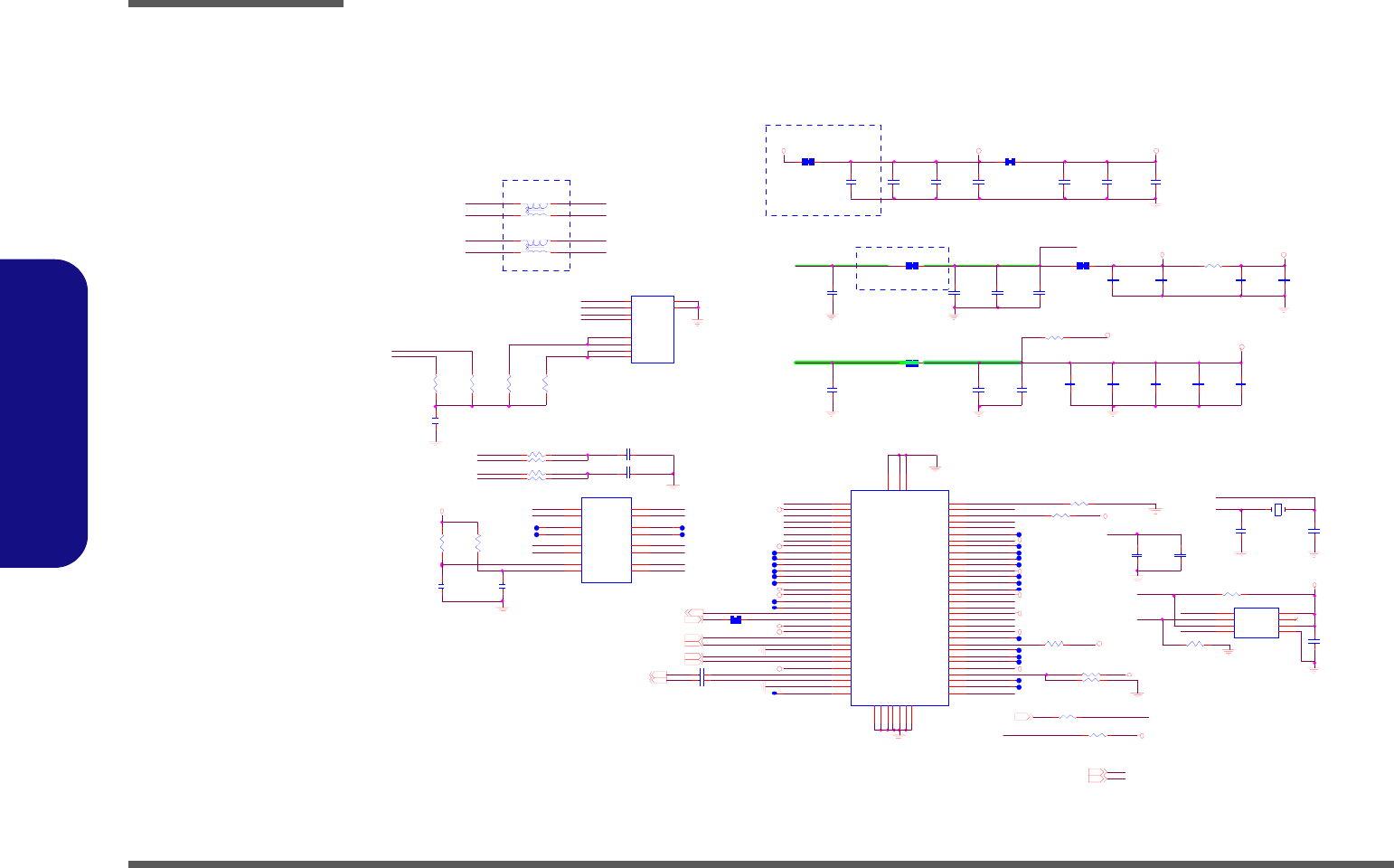
Schematic Diagrams
B - 22 PCI-E LAN RTL8102E
B.Schematic Diagrams
PCI-E LAN RTL8102E
Sheet 21 of 32
PCI-E LAN
RTL8102E
L AN_ V D D3
LAN_VDD3
LAN_VDD3
LAN_VDD3
LAN_VDD3
LAN_VDD3
3. 3V S
LAN DV DD 12
LA N _ V D D 33.3V AVD D3
AV DD 3
LAN AVD D12
LAN AVD D12
EVDD12
EVDD12
EVDD12
LA NAVD D 12
LAN DVD D12
LAND VD D12
LAND VD D12
LAN DVD D12
LAN DVD D12
LAN DVD D12
LAN D VDD 12
LAND VD D12
3.3V S5..7 ,9 ..20, 22 ..24 ,2 7 ,28
3.3V2,11,14..18,25..27
PCIE _TXN 3_LAN14
PCIE _R XP3_LAN14
CLK_PCIE_LAN12
PC IE_RXN 3_LAN14
LAN _OG PIO23
PC IE_TXP3_LA N14
PC IE_W AK E#15, 17,18
BU F_PL T_R ST#14, 17,18,23
CLK_PC IE_LAN#12
XTAL 1
XTAL 2
M A2/EESK
MA 0 / E E D O
EEC S
M A1/EED I
M A2/EESK
RS TB
Z2124
81 10 2 R EST
Z2135
XTAL 2
I SOLATEB
PCI E_TXP3_LAN
PCI E_ W AKE#
EEC S
M A1/EED I
Z2116
PCI E_TXN 3_LAN
DVDD12/CLKREQB
MDIO 0+
XTAL 1
MDIO 1+
CL K_ P C IE_ L A N#
Z2115
MDIO 1-
M A0/EED O
Z2113
GVDD
Z2118
ISO LATEB
Z2114
Z2117
CTRL12D
MDIO 0-
TMS
FB12
PCI E_RXN2_G LA N_C
PCI E_RXP2_GLAN _C
CTRL12A
CLK_PC IE_LAN
MLMX1+
MLMX0-
MLMX0+
TX_CT
Z 2112
DD _ NP
DC _ NP
RX_CT
MLMX1-
TX_C T
MD I O 1+
RD _ CT
MLMX1+_R
MD I O 0+ M LMX0-_R
TD_C T
MDIO0-
Z2111
Z2110
MDIO0+
MDIO1+
M LMX1-_R
RX_ C T
MDIO1-
Z2107
Z2109
MLMX0+_R
Z2106
Z2108
MD I O 0-
MD I O 1-
GVDD
FB12
CTRL12D
CTRL12A
M LMX0-_R M LMX0-
MLMX1+_R MLMX1+
MLMX0+_R
M LMX1-_R
MLMX0+
MLMX1-
Z2119
Z2120
Z2121
Z2122
Z2123
Z2125
Z2126
Z2127
Z2128
Z2129
Z2131
Z2132
Z2133
Z2134
Z2130
DV DD 12/C LKR EQB
R154
*0_04
C191
0.01U_50V_04
R155
*0 _ 0 4 C204
* 0.1U _16V _04
U5
*AT93C46DN-SHT
1
2
3
4
7
6
5
8
CS
SK
DI
DO
NC
ORG
GND
VC C
R9 1 3 .6 K_ 0 6
C215
0.1U_16V_04
C176
0.1U_16V_04
C1 9 9
*1U _6.3V_04
R82 *15m il_s hort
R69 10K_04
R 73 *0_04
C1 9 5
*22U _6. 3V _08
C1 6 3
0.1U_16V_04
C196
0. 1U _ 1 6V _0 4
C134
0. 1U _ 1 6V _0 4
C135 0.1U _10V_X7R_04
C1 9 7
0.1U_16V_04
C198
*0 .1 U_ 1 6 V _ 0 4
C136 0.1U _10V_X7R_04
R6 3 *1 5 m i l_ s h o rtR72 *15m il_s hort
R54 *10K_04
R204 1K_04
C1 8 9
0.1U _16V_04
C178
*22U _6.3V_08
U3
RTL81102E
18
19
20
21
22
23
24
25
26
27
28
29
30
31
32
1
2
3
4
5
6
7
8
9
10
11
12
13
14
15
16 48
47
46
45
44
43
42
41
40
39
38
37
36
35
34
33
64
63
62
61
60
59
58
57
56
55
54
53
52
51
50
49
17
GN D1
GND2
GND3
GN D4
GND5
GN D 6
GN D7
GN D 9
GND8
65
NC
LA NW A KEB
PER STB
DVD D1 2
EVD D12
HSIP
HSIN
EGN D
REF CL K _ P
REF CL K _ N
EVD D12
HSO P
HSO N
EGN D
NC
VCTR L12A
AVD D33
MD IP 0
MD IN0
AVD D12
MD IP 1
MD IN1
AVD D12
NC
NC
NC
NC
NC
NC
DVD D1 2
VDD 33
EESK
EED I/AUX
VDD33
EED O
EE CS
DV DD 12
TRSTB
TMS
TSTCK
NC
NC
VDD33
IS OL ATEB
NC
NC
CLKREQB
RSET
VC TRL12D
NC
CK TA L2
CK TA L1
NC
DV DD 12
LED0
LED1
LED2
LED3
VDD33
NC
GPO
GPI
DV DD 12
NC
GN D 1
GN D2
GND3
GN D4
GND5
GND6
GN D7
GND9
GND8
GGND
R207 15K _04
C170
*22U_6.3V_08
C352
0.1U_16V_04
R75 *0_04
C139
*22U _6.3V_08
R208 * 1K_04
C1 3 8
0.1U _16V_04
C2 0 8
*22U _6. 3V _08
C137
1U _6.3V_04
C 193
0.1U _16V_04
C 282
1000p_2KV_12
C167
0.1U_16V_04
LP 3
*WC M 2012F2S-161T03-s hort
1
4
2
3
R 52 *0_04
R2
75_1%_04
C1 7 9
0.1U_16V_04
C 152
0.1U _16V_04
PINP JS -A8J D3G
RJ_45
8
7
6
5
4
3
2
1GN D1
GN D2
DD-
DD+
DB-
DC-
DC+
DB+
DA-
D A+ shield
sh i e ld
C200
0.1U_16V_04
R1
75_1%_04
C194
0. 1U _ 1 6V _0 4
R 53 *10m il_short
R148
75_1%_04
R151
75_1%_04
R49 *10mil_short
LP 4
*WC M 2012F2S-161T03-s hort
1
4
2
3
R62 *1K_04
R 71 2.49K_1%_04
R 6 4 * 49 . 9 _ 1 % _ 04
R 6 6 * 49 . 9 _ 1 % _ 04
R 7 0 * 49 . 9 _ 1 % _ 04
L13
N S0013LF
1
216
15
314
412
5
6
7
13
98
11
10
RD+
RD- RX+
RX-
RD_CT RX_CT
NC NC
NC
TD _C T
TD +
NC
TX-TD -
TX_C T
TX+
R76 *10m il_short
C 177 *0.01U_50V_04
C203
22P_50V_04
C 180 *0.01U_50V_04
C205
*22U_6.3V_08
C286
0.01U_50V_04
C202
22P _50V_04
X1 25M H z12
R 6 8 * 49 . 9 _ 1 % _ 04
C288
0.01U _50V_04
LAN (RTL8102E)
1A
40 mil
40 mil
must be
within 0.5cm
mu st be wi t hi n
0.5cm (to pin 1)
>4 0M IL S
60 mil
ne ar 8 1 02 E pi n 6 3
near 8102E
NE A R PI N 28
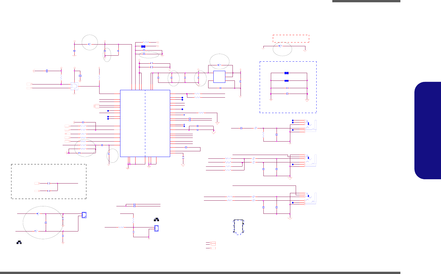
Schematic Diagrams
AUDIO CODEC ALC269 QFN B - 23
B.Schematic Diagrams
AUDIO CODEC ALC269 QFN
Sheet 22 of 32
AUDIO CODEC
ALC269 QFN
AUD G
1. 5 V S
AGND
AG ND
AG ND
5VS_AU D 5VS
3.3VS3.3VS
5V S
AU DG
3.3VS_ AU D
AUD G
3.3VS_ AU D
3.3VS
AUD G
AU DG
AUDG
3.3VS_ AU D
5V S 11, 13,16,17, 20,24
3.3VS 5..7,9. .21,23,24,27,28
1. 5 V S 3 , 5 . . 7, 14 , 1 6 . . 1 8 , 27
SB_M UTE#15
KBC_MUTE#23
AZ _B ITC LK13, 17
A Z_ SYN C13,17
AZ_ SD IN013
AZ_ R ST#13,17
AZ _S DO UT13, 17
KBC_BEE P23
IC H_SP KR15
SPKO UTR-17 SPKO UTR+17
M IC_SEN SE
Z2237
Z2235
SPDI FO
Z2229
Z2234
Z2230
Z2232
Z2228
Z2236
Z2227
Z2231
Z2233
HP_SEN SE
HE ADPH ON E-R
HE ADPH ON E-L
PHO NE- R
PHO NE- L
INT_MIC
MIC2-VREFO
MU TEAPM #
MIC 2 _RIN T_ M IC MIC 2 _L
SP DIFO Z2201
Z2202
Z2203
AZ_SDOUT_R
AZ_ R ST#_ R
AZ_ SY NC _R
AZ_SD IN0_R
AZ_ BITC L K_ R
Z2204BEEP
SPK OU TL-
SPKO UTL+
MI C 1 - V RE F O -L
MI C 1 - V RE F O -R
MI C 2 - V RE F O
HEAD PH ON E-L
HEAD PH ON E-R
Z 2207
Z 2206
Z 2209 MI C1 -R
MI C1 -LZ 2208
MIC 1 -L
MIC 1 -R
MI C 1 - V R E F O- R
MI C 1 - V R E F O- L
Z 2211
Z 2210
Z 2212
M IC2_L
M IC2_R
Z 2213
Z 2214
M IC_ S E NS EJD _SENS E
H P_SEN SE
SP KOU TL+_L
SP KOU TL-_L
BEEP
SP KOU TR-
SP KOU TR+
SP KOU TL-
SP KOU TL+
Z 2205
C520 2.2U _6.3V_06
R 330 4.7K_04
C495
22U_10V_08
C 455 100P_50V_04
R 332 4.7K_04
L2
FCM 1608K-121T06
L1
FC M 1608K-121T06
R
L
J_H P1
C 12103-10609-L
2
6
5
3
1
4
R327 20K_1% _04
C459
0.1U_16V_04
DI GI T AL
ANALOG
U24
ALC 269 Q FN
1
2
3
4
5
6
7
8
9
10
11
12
13
14
15
16
17
18
19
20
21
22
23
24
26
27
28
29
30
31
32
37
34
35
36
33
39
40
41
42
43
45
44
46
47
48
38
25
49
DVDD1
GPIO0
GPIO1
PD #
SD ATA-OU T
BIT-C LK
DVSS 2
SD ATA-IN
DVD D-IO
SY NC
R ESET#
PC BEEP
Sens e A
LI N E 2 - L
LINE2-R
MIC2-L
MIC2-R
Se ns e -B
JDR EF
MO NO -O UT
MIC1-L
MIC1-R
LI N E 1 - L
LINE1-R
AVSS1
VR EF
M IC 1-V REF O -L
MIC2-V REFO
MI C 1 - V R E F O -R
C RVR EF
HP-OUT-L
AV SS2
OPV E E
CBN
CBP
HP-O UT-R
PVD D1
SPK- L+
SPK- L-
PVS S1
PVSS2
SPK- R+
SPK- R-
PV DD 2
SPD IFC 2/E APD
SPD IFO
AVD D2
AV DD 1
GN D
C4 6 0
0.1U _16V_04
C456
1U_6.3V_04
L28
FCM 1608K-121T06
R127 22_04
U30
*G 92 4
1
23
4 5
SHD N#
GN DBY P
OUT VIN
C526
0.1U_16V_04
C496
0. 1U _16V_04
C489 4.7U _6.3V _06
C448
1U _6.3V_04
R
L
J_S PDIF1
* C12103-10609-L
2
6
5
3
1
4
R309 10K_04
L33
* FCM 1005KF-102T02
1 2
L32 FCM 1005KF-121T031 2
L31 FCM 1005KF-121T031 2
C503
* 0.1U _10V _X7R_04
U2 9
74 A H C 1 G 08 G W
1
2
5
4
3
R328
*100K_04
C458 0.1U _16V_04
C517 22U _10V_08
C491
*0.1U _10V_X7R_04
R314 22_04
R317 22_04
R313 22_04
L29
F CM 1005KF-121T03
1 2
C522
*1U_16V_06
L30
F CM 1005KF-121T03
1 2
C 511 0. 1U _16V_04
L23
F CM 1608K-121T06
C525 *0.1U_16V_04 C 512 0. 1U _16V_04
C 513 0.1U_16V_04
R 12 8 1K _0 4
R 33 1 1K _0 4
R334
100K_04
C7
180P _50V_04
R310 * 0_04
R 336 100_1%_04
L26
FCM 1608K-121T06
R315 *10m il_s hor t
R 335 100_1%_04
C272 4.7U _6.3V_06
C485 4.7U _6.3V_06
C 508
100P_50V _04
R340 20K_1% _04
C6
180P _50V_04
C260
680P _50V_04
R312 1K_04
C482
* 0.01U _50V_04
R 121 75_1%_04
C 510
* 100P_50V_04
C 494 10U_10V_08
R
L
J_MIC1
C 12103-10609-L
2
6
5
3
1
4
C505
100P_50V_04
R120
4.7K_04
C507
100P_50V_04
C488
0.1U_16V_04
R316 22_04
JP2 * 10m il_short
J _ SPK1
88266-02001_R
PCB Footprint = 88266-2R
2
1
R341
* 220_04
C 521
2.2U _6.3V_06
C447
1U _6.3V_04
JP1 * 10m il_short
C493
22U _10V_08
C271
22U_10V_08
C509
1U _6.3V_04
R339 39.2K_1%_04
C518 0.1U_16V _04
C 506
100P_50V _04
C457 22P_50V_04
C486 4.7U _6.3V _06
C519 10U _10V _08
J_INTM IC1
88266-02001
PCB Footprint = 88266-2L
2
1
1
J_INTMIC1
2
4
6
3
HE ADPH ONE
BLACK
MIC IN
BLACK
BLACK
SP DIF OUT
5
2
1
Layout Note:
V er y cl os e to Au di o Co de c
Low mute!
2
J_SPK1
1
PC BEEP
8/20
7/31
8/20
8/20
8/20
8/28
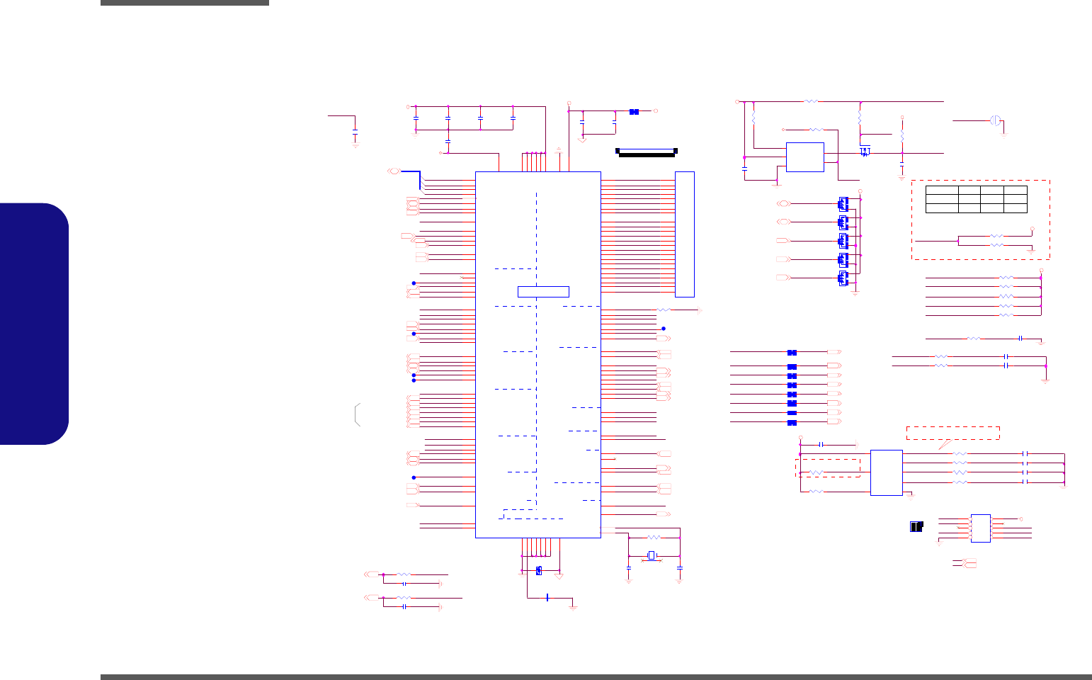
Schematic Diagrams
B - 24 KBC-ITE IT8502E
B.Schematic Diagrams
KBC-ITE IT8502E
Sheet 23 of 32
KBC-ITE IT8502E
K BC_AG ND
KB C_AG ND
KBC _AVDD
VDD 3
VD D3
3. 3 V S
VDD 3
VDD 3
VD D3
VDD 3
VDD3
VD D3
VDD 3
VDD3
VDD 3 2,13,20,24,25,29
3.3 V S 5 ..7 ,9.. 22 ,2 4 ,2 7,2 8
SMI # 15
SW I# 1 5
SB_KBC RST# 13
SB_ PW R _ BTN # 1 5
SCI # 15
GA 2 0 # 1 3
BUF _P LT_RS T#14,17,18,21 LP C _ S I R Q15
LPC _FRAM E#13 KBC _P CL K12
LC D_ BR IGH TNES S11
CPU_FA NSEN 20
KBC_M UTE#22
LED_CAP#17
L ED_ SC RO LL#17
KBC_BE EP22
LE D _ N U M #17
TP _C L K20
TP _ D A T A20
TH ERM _ALE RT#2
SMC_CPU_THERM2
SMD_CPU_THERM2
LED_PWR #20
LED_BAT_FU LL#20 LE D_ BA T_ CH G#20
LED _TH RO TTLE#17
PW R _S W #24
LI D _ S W #11,17
CCD_EN 17
SU SB# 15,18,24
SU SC # 15
D D_O N 24,25
BK L_ EN 11
WLAN_DET# 17
BT_ D ET# 17
VC O RE_ON 28
PM E# 14
CHG_EN 29
SB_R SMR ST# 15
AC _IN29
LED _ACIN #20
L PC _A D[3 :0 ]13
PM_C LKRU N# 15
BT_EN 17,20
WEB1#17 APKE Y#24
WEB2#17
WLAN_EN17,20
CH G_ C UR29
SM C_BAT29
BAT_VOLT29
BAT_ DET29
SM D_BAT29
CC D_D ET#17
LA N _ O G P I O21
JMB _D 3D19
CP U_F AN20
EC _ PM_PW RO K 1 5
SMC _BAT29
SM D_BAT29
3G _E N 17,20
CELL_CONTROL29
L_BKLTCTL 5,11
KBC _FLA SH
Z2407
Z2405
Z2404
3IN1
KBC_SPI_CE#
KBC _S PI_SI_R
KBC_SPI_SCLK
KBC _S PI_SO_R
KBC _S PI_CE#_ R
KBC_SPI_SO
KBC _S PI_SCLK_R
KBC_SPI_SI
KBC _ TXD
KBC _ RXD
KB -SI3
KB -SI2
KB -SO5
KB -SI1
KB -SO3
KB -SO4
KB -SO11
KB -SI6
KB -SI4
KB -SO8
KB -SO7
KB -SO6
KB -SO14
KB -SO2
KB -SO15
KB -SI0
KB -SI5
KB -SO12
KB -SO1
KB -SO10
KB -SO0
KB -SI7
KB -SO9
KB -SO13
Z240 2
Z240 3
BRIG HTN ESS
KB C_ SPI_SC LK
KB C_SPI_C E#
Z2401
KB C_SPI_SI
KB C_SPI_SO
3G_EN
CIR_IN
KB C_GA 20 #
KBC _ W RES ET#
CP U_ FA N _R
SM D_VG A_TH ERM
SM C_VG A_TH ERM
BRIGHTNESS
KBC _PW R BTN#
KBC _SW I#
KBC _GA20#
KBC _RST#
KBC _SMI#
KBC _SCI#
WLAN _P WR
80C LK
3IN 1
THE RM _R ST#
80POR T_D ET#
FLFR AM #
KB C_ CL KR UN #
KB C_ PW R BT N#
WD _DISAB LE
KB C_ SW I#
KB C_ RS T#
KB C_SC I#
KB C_SM I#
WD T_EN
WD _DISAB LE
KBC _W R ESET#
KB C_ RS MR ST#
AC _IN
KBC _CLKR UN #
BA T1 _VO LT
SM D_BA T
CHG_CUR
BA T_ D ET
SM C_BA T
BAT_ VO LT _ R
JM B _ D 3 D
BAT_D ET
CHG_CUR
SMC _B AT
BAT1_VOLT
Z2406KBC_PC LK
SMD _B AT
CHG_CUR_R
CC D_ DET #
MOD EL_ID
BAT_ DET
BAT_VOLT_R
CH G_ C UR
3G_D ET#
MO DE L_ ID
LPC _AD0
LPC _AD1
LPC _AD2
LPC _AD3
C P U_ FA N_ R
KBC _ RSM RS T#
WD T_EN
80PO RT_DET#
3IN1
KBC _TXD
WD T_EN
K BC_ RXD
80CLK
AC _IN
R 290 4.7K_04
R2 6 8
10 K _ 0 4
R2 7 1
1 0 0K _0 4
R273 15_1%_04
D1 7
BAV99 A
C
AC
C5 2 3
0.1U _50V_06
R265 10K_04
R269
100K_04
C410
0.1U _16V_04
C417
0.1U _16V_04
J_H8D BG1
SPU FZ-10S3-VB-0-B
12 34
56
78 910
C4 0 1
0.1U_16V_04
C392 1U _6.3V_04
R260 100_04
R 2 72 1 2 0 K _0 4
R285 47_04
R 261 *10K_04
C397 *0.1U_16V_04
D2 3
BAV99
A
C
AC
C418
15P_50V_06
J_KB1
85202-24051
24
23
22
14
12
11
21
8
20
19
6
5
18
4
17
10
9
7
3
2
1
16
15
13
D1 9
*B A V 99
A
C
AC
R 282 1K_04
D1 8
BAV99 A
C
AC
R280 47_04R 275 4.7K_04
C411
10U_10V_08
X4
32.768KHz
1 4
32
R 250 10K_04
R277 15_1%_04
R286 *10mil_short
K/B MATRIX
FLASH
LPC
SMBUS
PS/2
PWM
UART
DAC
CLOCK
IT8502E
CIR
ADC
WAKE UP
PWM/COUNTER
LPC/WAKE UP
EXT GPIO
GP INTERRUPT
WAKE UP
GPIO
U18
IT8502E
14
13
10
9
8
7
6
17
5
15
23
126
4
58
59
60
61
62
63
64
65
36
37
38
39
40
41
42
43
44
45
46
51
52
53
54
55
11
26
50
92
114
127
121
3
74
85
86
87
120
124
22
35
125
18
21
112
109
108
123
88
89
90
47
48
24
25
28
29
30
31
32
34
66
67
68
69
70
71
72
73
1
12
27
49
122
113
75
2
128
79
78
77
76
83
84
82
33
20
91
81
80
16
119
56
57
93
94
95
96
97
98
99
107
110
111
115
116
117
118
100
101
102
103
104
105
106
19
WR ST#
LPC CLK
LAD 0
LAD 1
LAD 2
LAD 3
LFR AME#
( PD )L P CP D# /W U I6/ GPE 6
SER IRQ
EC SMI# /G PD4( P U )
EC SCI# /G PD3( P U )
GA20/GPB5
KBR ST# /GPB6( P U )
KSI0/STB#
KS I1/ AFD#
KS I2 /INI T#
KS I3 /SL IN#
KSI4
KSI5
KSI6
KSI7
KSO 0/PD0
KSO 1/PD1
KSO 2/PD2
KSO 3/PD3
KSO 4/PD4
KSO 5/PD5
KSO 6/PD6
KSO 7/PD7
KSO 8/ ACK#
KSO 9 /BUS Y
KSO10/PE
KSO 11 /ER R#
KSO12/SLCT
KSO 13
KSO 14
KSO 15
VCC
VSTBY
VS TBY
VSTBY
VSTBY
VSTBY
VSTB Y
VB AT
AVCC
P S 2 C LK 0/ G P F 0 ( P U )
PS2D AT0/G PF1( PU )
P S 2 C LK 1/ G P F 2 ( P U )
( PD )TMR I0/ W UI2 /G PC4
( PD )TMR I1/ W UI3 /G PC6
LPC RST#/WU I4/G PD 2( PU )
( PD )W U I 5/ GPE 5
PW R SW/G PE4( PU )
RI1#/WUI0/GPD0( PU )
RI2#/WUI1/GPD1( PU )
( PD )R IN G#/PW R FAIL # /LPCR ST#/ GPB7
TXD/G PB1 ( PU )
RXD/GPB0( PU )
( PD )C TX/ GPB2
PS2D AT1/G PF3( PU )
P S 2 C LK 2/ G P F 4 ( P U )
PS2D AT2/G PF5( PU )
( PD )TAC H0/G PD6
( PD )TAC H1/G PD7
PW M 0/GPA 0( PU )
PW M 1/GPA 1( PU )
PW M 2/GPA 2( PU )
PW M 3/GPA 3( PU )
PW M 4/GPA 4( PU )
PW M 5/GPA 5( PU )
PW M 6/GPA 6( PU )
PW M 7/GPA 7( PU )
AD C0/G PI0
AD C1/G PI1
AD C2/G PI2
AD C3/G PI3
AD C4/G PI4
AD C5/G PI5
AD C6/G PI6
AD C7/G PI7
VSS
VS S
VSS
VSS
VSS
VSS
AV SS
CK3 2 KE
CK3 2 K
DAC3/GPJ3
DAC2/GPJ2
DAC1/GPJ1
DAC0/GPJ0
( PD )E GC S#/ GPE2
( PD )E GC LK/ GPE3
( P D )EG AD/ GP E 1
G INT/G PD5 ( PU )
L80LLAT/G PE7( PU )
VSS
DAC5/GPJ5
DAC4/GPJ4
PW U RE Q# /GP C7( PU )
( PD )C RX/G PC 0
( PD )KSO 16/G PC3
( PD )KSO 17/G PC5
( PD )GPH 0/ID0
( PD )GPH 1/ID1
( PD )GPH 2/ID2
( PD )GPH 3/ID3
( PD )GPH 4/ID4
( PD )GPH 5/ID5
( PD )GPH 6/ID6
( PD )GPG 1/ID7
SM CLK0 /G PB3
SM DAT0 /G PB4
SM CLK1 /G PC1
SM DAT1 /G PC2
SM CLK2/G PF 6 ( PU )
SM DAT2 /G PF7( PU )
FL FR AME# /G PG2
FLAD 0/ SCE#
FLAD1/SI
FLAD 2/S O
FLAD3/G PG6
FLCLK/SC K
( PD )FL RS T# /W U I7 /GPG 0/T M
( PD )L 80 H L AT/ GP E0
R276 *10_04
R259 100_04
R266 *10mil_short
R287 *10M_06
C407 *33P_50V _04
R291 *10mil_short
R279 *10mil_short
C 409 *10P_50V_04
R274 *10mil_short
R267 *10mil_short
R249 *10mil_short
L20
*H CB10 05K F-121T20_10m il_sh ort
R278 *10mil_short
R 281 *10K_04
C408
0. 1U _10V_X7R_04
C398
0.1U_16V_04
C396
0.1U _16V_04
R 264 10K_04
PJ 8
20 m i l
1 2
C403 *33P_50V _04
R 288 4.7K_04
R 2 6 3 * 1 0K _0 4
C402
0.1U_16V_04
U1 9
SST25VF 080B SO 8
1
2
3
4
5
6
7
8
CE#
SO
WP#
VSS
SI
SC K
HOLD#
VDD
R 262 100_04
C3 8 6
0.1U _16V_04
R 289 100K_04
C405 *33P_50V _04
D2 4
BAV99
A
C
AC
Q15
2N 7002W
G
DS
C414
15P_50V _06
C3 9 3 *1 U_ 6.3 V_ 04
C395
0.1U _16V_04
C399
0.1U_16V_04
C 400 0.1U_16V_04
R270 10K_04
C413 *33P_50V _04
NC 1 N C_ 0 4
U17
AAT3510IGV -2.93-C -C-T1
3
5
2
1
4
MR #
VC C
GN D
RESET#
WD I
???
8Mbit
KBC_SPI_*_R = 0.1"~0.5"
J_KB1
124
LOW ACTIVE
WEB0--->AP KEY
WEB1--->EMAILKEY
WEB2--->WWW KEY
U32 from S ST25VF080B SO8
change to EN25F80 SO8.
RA
RB
RA
MODEL_ID
V1 .0 X10K
RB
M7 10 L
2
10 9
J_H8DBG1
1
6-21-C2A00-210
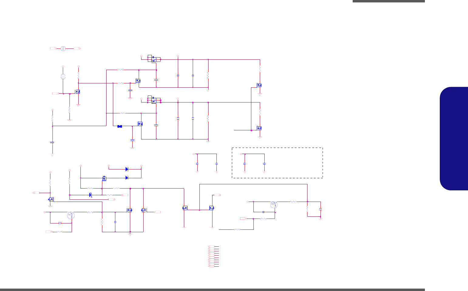
Schematic Diagrams
3VS, 5VS B - 25
B.Schematic Diagrams
3VS, 5VS
Sheet 24 of 32
3VS, 5VS
3.3VS
5VS
5VSVD D 5
SYS3V VD D 5
SY S15V
VI N
VD D 3
VI N VA VI N 1
VD D 3
VIN
VD D 3
3.3V S
VI N 125
1.05VS2.. 4, 6,7,12,13,16,27
5VS11,13,16,17,20,22 3.3VS5.. 7,9..23,27,28
1.5VS3,5.. 7, 14,16..18,22,27
VI N11,25..29
VD D32,13,20,23,25,29 VD D525,27,28
VA29
SYS15V11,25
SUSBL26,27
DD_ON 23,25
M_BTN#17
PW R_SW#23
SUSB#15,18, 23 SUSBL 26, 27
AP KEY # 2 3
WEB 0#17
WEB0# 17
APKEY# 23
Z2503
EN_15VS
Z 2502
Z2504
Z2501
Z2505
Z2506
DI S_5VS_3V S
DI S_5VS_3VS
Z2512
Z2511
Z2507
Z2509
Z2510
A PKE Y#
PJ10
20m il
1 2
PR155 *0_04
PQ47
*2N7002W
G
DS
PQ46
* 2N7002W
G
DS
PQ3 6
2N7002W
G
DS
PQ17
2N7002W
G
DS
PR 1 33
10_06
PQ1 4
2N7002W
G
DS
PD 4 * SC S7 51 V
A C
PR 5 8
100K_04
PR131
10K_04
PQ3 5
2N7002W
G
DS
PQ3 0
AO4468
4
6 2
5
7 3
1
8
PC122
0.1U_16V_04
PR54
100K_04
PR57 100K_04
PR 1 20
10_06
PJ9
20mil
12
PQ16
2N7002W
G
DS
PD 1 9 S CS140P
A C
PR59 100K_04
PC155
3900P_50V_04
PR130
47K_04
R126
330K_04
PC156
0. 1U_16V_04
PQ40
2N7002W
G
DS
PR122
100K_04 PC48
0. 1U_16V_04
PC121
*0. 1U_50V_06
PQ1 5
DTA114EUA
CE
B
PQ34
*DTA114EUA
CE
B
PQ3 3
2N7002W
G
DS
PR51
* 100K_04
PQ4 5
AO4468
4
6 2
5
7 3
1
8
PR152
* 100K_04
PC157
0.1U_16V_04
PR154
* 100K_04
PR119 *10K_04
PQ13
N D S3 52 AP _ NL
G
DS
PD 1 8 S CS140P
A C
R326
330K_04
PC53
0.1U_50V _06
PC154
*0.1U_50V_06
PQ3 7
2N7002W
G
DS
PC49
0.01U_50V_04
PC 5 0
10U_10V_08
PR151 *100K_04
PC 1 27
*0.1U_16V_04
PR 5 6 20K _1%_04
PC 1 59
10U_10V_08
PC 5 2
0.1U_50V_06
PR 6 1
100K_04
PR60 10K_04
PC 1 58
0.1U_16V_04
PC142
2200P_50V_06
PR 1 56 0 _04
PC166
0.1U_16V_04
PC167
0.1U_16V _04
PR153
* 10K_04
PR 1 23 * 10mi l_short
Power Plane
Power Plane
Near LAN
Transformer
FOR EMI
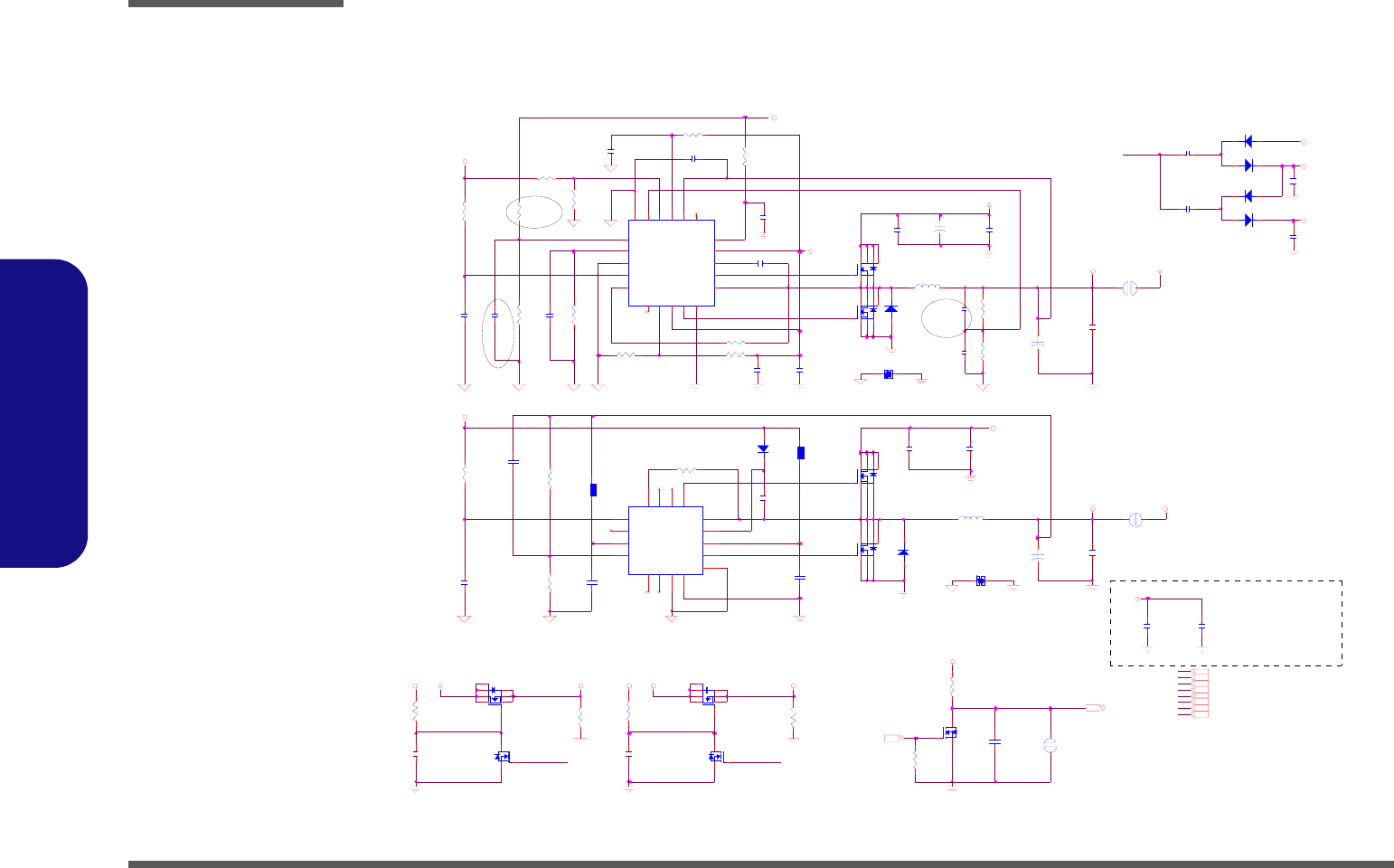
Schematic Diagrams
B - 26 VDD3, VDD5
B.Schematic Diagrams
VDD3, VDD5
Sheet 25 of 32
VDD3, VDD5
VD D3SY S15 V 5VVDD53.3V SYS15V
SYS15V
SG N D4
SYS10V
SYS5V
SY S5V
SGND4
SG N D4
SGND4
INTVCC2
SGND4
VI N
SYS5V
VI N 1
VD D5
SGND4
SG N D4SGN D4
VD D3
SG N D6SGN D6
SYS3V
SG N D6
VIN
SGND6
INTVCC2
INTVCC2
SGND4
5V
3.3V 2,11,14..18,21,26,27
VD D3 2,13,20,23,24,29
5V 11,16..18,20,26..28
VD D524,27,28
SY S5V 2 9
VIN 11,24,26..29
SY S1 5V 1 1, 2 4
VI N 1 2 4
DD_ON23,24
DD_ON# 26
Z2625Z2624
DD_ON#DD_ON#
Z 2627
LGATE 1 Z 2626
DD_ON
DD_ON#
Z2603
Z2610
Z2618
Z2611
LGATE1
Z2602
Z2608
Z2601
Z2614
Z2612
Z2621 Z2615
Z2613
PC164
1000P_50V_X7R_04
PC 1 69
0.1U_16V_04
PC 1 68
0.1U_16V_04
PC150
0.1U_16V_04
PR 1 64
15mil_short
PR 1 58
12K_04
PC 161
2.2U_6.3V_06
PC163
*30P_50V_04
PR161 10K_1%_04
PU5
SC418
1
2
3
4
5
6
7
8
9
10
11
12
13
14
15
16
17
18
19
20
21
FB
FBL
VD D A
VOUT
NC
VIN
VL D O
BST
DH
LX
PGND
DL
VD D P
RPSV
PGOOD
ILIM
EN / PS V
AG N D
RTON
EN L
PAD
PD 1 5 F M0540-N
A C
PC 1 47
2200P_50V_06
PC 1 53
0.1U_16V_04
PC 138
1000P _50V_04
PR 1 59
10K_04
PR 1 48
10K_04
PJ 1 1
5mm
1 2
PJ12
20mil
12
PQ39
AO4468
4
62
5
73
1
8
PD 1 7 F M0540-N
A C
PC 1 62
*0. 1U_25V_04
+
PC 1 46
15U_25V _4. 5* 6
PR 1 34
10K_1%_04
PQ38
AO4468
4
6 2
5
7 3
1
8
PC 137
1U_25V_06
PN C1NC_06
PC 1 31
1U_10V_06
PD10
FM0540-N
AC
PC151
*4.7U_25V_X5R_08
PC 1 43
*2200P_50V_06
PR 1 47
75K_06
PD 1 3
FM5822
A C
PR 1 36
2.94K_1%_04
PR165
10K_04
PC 1 44
0.01U_50V_04
PR 1 42422K_06
PR 138
91K_1%_06
PQ32
2N7002W
G
DS
PC51
1000P_50V_04
PN C2NC_06
PR162 113K_04
PQ44
2N7002W
G
DS
PR163 *100K_04
PQ31
AO4468
4
62
5
73
1
8
PR 1 49
100K_04
PD11
FM5822
A C
PJ 1 3
5mm
1 2
PC134
1U_25V_08
PQ42
AO4468
4
6 2
5
7 3
1
8
PC135
1000P_50V_04
PC128
0.1U_25V_X7R_06
PR 1 60
137K_1%_04
PQ12
2N7002W
G
DS
PC 1 32
1000P_50V_04
PR52
1M_04
PR166 10K_1%_06
PC141
1U_25V_X5R_08
PR 157
10K_04
PR 1 67
*10mil_short
PC165
1U_10V_06
PC 1 33
1U_10V_06
PR140
*100K_04
PQ4 1
AO4468
4
62
5
73
1
8
PC 130
0.01U_50V_04
PU 6
SC412A
1
2
3
4
5
6
7
8
9
10
11
12
13
14
15
16
17
LX
BST
VC C
DL
GND
RTN
N.C
N.C
FB
VO U T
PGD
EN
ILIM
N.C
N.C
DH
PAD
PC 152
0.1U_50V_06
PC 1 45
0.01U_50V_04
PR 53
*100K_04
PR 137
10K_1%_04
PC118
*4.7U_25V_X5R_08
PC 1 49
2200P_50V_06
PD 1 6 F M0540-N
AC
PC 1 23
0.01U_50V_04
PR 1 39
10_06
PC125
0.1U_16V_04
PL7
4.7uH_7* 7*3.5
1 2
PR 5 5
1M_04
PD 1 4 F M0540-N
AC
PL8
4.7uH_7*7*3.5
1 2
PQ4 3
AO4468
4
62
5
73
1
8
PC 1 19
*4.7U_25V_X5R_08
PR 1 25 10_06
+
PC 1 48
220U_6.3V_6*5. 9
+
PC 1 20
220U_6.3V_6*5. 9
3A3A 3A
Power Plane
3A
Power Plane
4A
5A
Ra
Rb
Near LAN
Transformer
FOR EMI
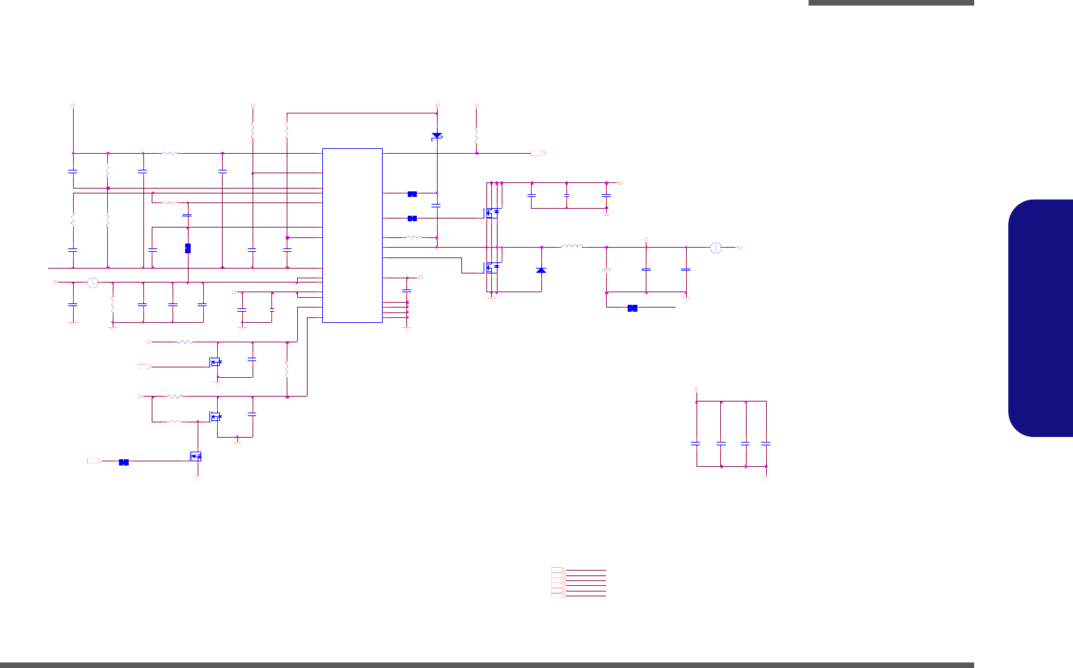
Schematic Diagrams
POWER 1.8V/ 0.9V B - 27
B.Schematic Diagrams
POWER 1.8V/ 0.9V
Sheet 26 of 32
POWER 1.8V/ 0.9V
VI N
5V
5V
5V
VDDQ
5V
1.8V
VTT_MEM
3.3VVI N
1.8V
VD D Q
VD D Q
VTT_MEM9,10 1. 8V5,7,9,10
5V11,16. .18,20,25,27,28 3. 3V2,11, 14..18,21,25,27
VIN11,24,25,27..29
1.8V_PWRGD 15
DD_ON#25
SU SB L24,27
SYS15V11,24,25
DD_ON#
1. 8VEN
Z2712
Z2713
VSSA
Z2715
Z2716
Z2718
Z2717
Z2709
Z2708
Z2701
VS SA
Z2706
Z2703
Z2704
Z2705
Z2707
Z2702
VTTEN
1.8V_PWRGD
Z2714
Z2710
Z2711
PC38
10U_6.3V_06
PC36
10U_6.3V_06
PC41
*10U_6.3V_06
PC 3 7
10U_6.3V_06
PC 1 17
1000p_50V_04
PR 4 8
100K_04
PC 7 7
*4.7U_25V_X5R_08
PC 2 6
0.1U_25V_X7R_06
PR112
10_06
PC 6 9
0.1U_50V_06
PC 2 9 0.01U_50V _04
PC 3 2
0.1U_16V_04
PR43 *15mil _short
PC115
0. 1U_16V_04
PR 1 14
10K_1%_04
PR109
* 15mil_short
PQ2 2
AO4468
4
62 5
73
1
8
PR 1 13
2K_1%_04
PD2
FM0540-N
AC
PC40
100P_50V_04
PC 2 8 0. 01U_50V_04
PC 4 2
10U_6.3V_06
PR111 10_06
+
PC104
220U_4V_D
PC94
0.01U_50V_04
PC 4 3
*0.1U_16V_04
PC116
1U_10V_06
PR41
100K_04
PC44
1U_10V_06
PC45
*0.068U_50V_06
PR36
15K_1%_04
PQ10
2N7002W
G
DS
PR 4 9
47K_04
PC35
1U_10V_06
PC31
1U_10V_06
PC46
1U_10V_06
PR50 *10mil_short
PC 4 7
0.1U_16V_04
PJ2
OPEN_2A
12
PC39
1U_10V_06 PQ2 6
AO4468
4
62 5
73
1
8
PL6
4. 7uH _6.5* 6.9*3
1 2
PR44
10_06
PQ9
2N7002W
G
DS
PD 9
FM5822
A C
PC30 0.01U_50V_04
PR 1 10
1.5M_04
PR 4 5
*15mil _short
PC 6 1
0.1U_50V_06
PR47
*0_04
PC27 0.01U_50V_04
PR 4 0
* 20K_1%_06
PR35
* 15mil_short
PQ8
2N7002W
G
DS
PR42
10_04
PU4
SC486
11
2
3
4
5
6
7
8
9
10
1
12
13
14
15
16
17
18
19
20
21
22
23
24
25
VTTEN
TON
VD DQS
VSS A
VC CA
FB
PGD
REF
COMP
VTTS
EN / PS V
VD DP2
VD DP2
VTT
VTT
PGND1
PGND2
PGND1
DL
VDDP1
ILIM
LX
DH
BS T
PGND2
PR46 47K_04
PJ6
8m m
1 2
3A
6A
Ra
Rb
0403
0614
6/18
7/30
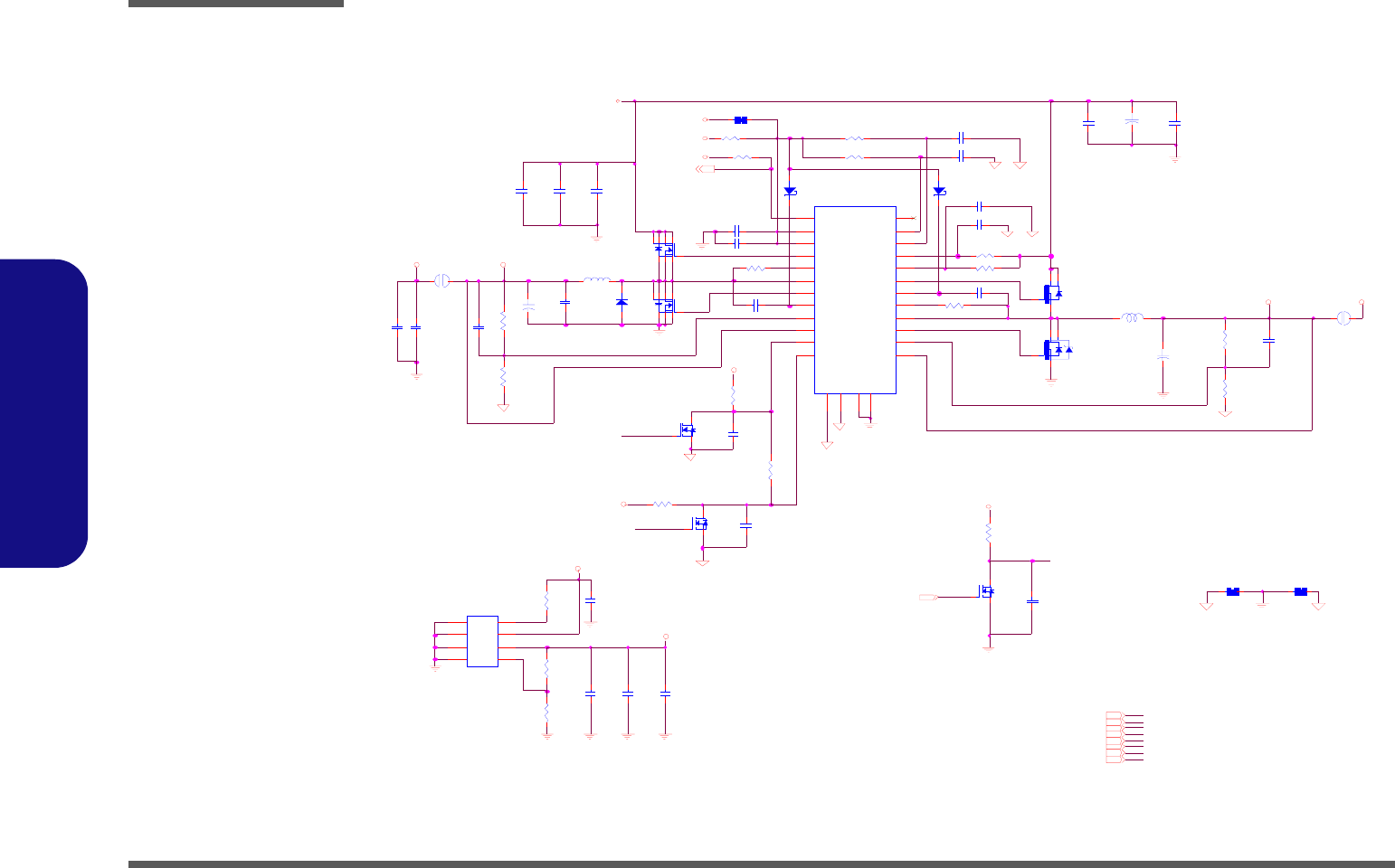
Schematic Diagrams
B - 28 POWER 1.5VS/ 1.05VS
B.Schematic Diagrams
POWER 1.5VS/ 1.05VS
SG ND 2SG ND 1
3.3VS
2.5VS
SGND1
SGND1
VIN
VDD 5
SG ND 2SGND1
1.5VS
SGND2
5V
1.05V S
SG ND 2
SG N D2 SGND1
V1.05
V1.5
3.3V
SGN D 2
SG ND 1
5V
5V
5V
VIN11,24..26,28,29 VD D524,25,28
5V11,16..18,20,25,26,28
1.05V S2. .4 ,6, 7,1 2 ,1 3 ,1 6
3.3V2,11,14..18,21,25,26 1.5VS3,5. .7,14,16..18,22
VCC P_PW R G D15
2.5VS7,11
3.3VS5 ..7 ,9 ..2 4,2 8
SU SBL24,26
Z2818
Z2819
Z2807
Z2813
Z2814
Z2816
Z2812
Z2810
EN _1 .5VS
Z2815
Z2808
Z2805
Z2802
VC CP_PW RG D
Z2806
SU SBL#
Z2811
Z2817
Z2804
Z2803
Z2801
Z2809
EN _1.05V S
SUSBL#
SU SBL#
PR 74
10K_1%_04
PD 5
FM 0540-N
AC
PC 16 1000p_50V_04
PR86
20K_1% _04
C8 9
10 U _ 10 V _ 0 8
PR87 10_04
C100
0.1U _16V _04
PR 22
*1 5m il_s hort
PC 99
0.1U _16V_04
PC 86
*0.1U_50V_06
PR93
10K_1% _04
C1 0 6
1U _ 6 . 3 V _ 04
PJ 5
7m m
1 2
PQ 20
AO 4468
4
62
5
73
1
8
PR 24
* 15m il_short
PQ 25B
SP8K10SFD 5TB
4
3
5
6
PR83 750K_04
PL5
1.5uH _4.7* 5 .2*3
1 2
PQ 27
*2N 7002W
G
DS
PC 73
0.1U_50V_06
SC413
PU 1
1
2
3
4
5
6
7
8
9
10
11
12
13
14
15
16
17
18
19
20
21
22
23
24
25
26
27
28
PG ND 1
DL 1
VDD P1
IL IM1
LX1
DH 1
BST1
EN/ PSV2
TON 2
VOU T2
VCCA2
FB K2
PGOOD2
AG ND 2
PGND2
DL2
VDD P2
IL IM 2
LX2
DH 2
BST2
EN/ PSV1
TON 1
VOU T1
VCCA1
FBK1
PGOOD1
AG ND 1
PR 75
11K _1% _04
PR 1 10K_04
PR 77
0_04
PC6 1U_10V_06
R3 6
51K_1% _04
PR 89 4.3K_1%_06
PC 10 1U _10V _06
PR 76
15K_1%_04
PD 6
FM 0540-N
AC
PR2 10_04
R3 3
47K_1% _04
P Q25A
S P 8K 10 S F D 5 T B
7
8
1
2
PR 96
*10K_04
PC 81 100P_50V _04
PR72 1M _04
R3 5
10K_04
PJ 4
3m m
1 2
PC 114 0.01U _50V_04
PQ 21
AO 4468
4
62
5
73
1
8
U12
SC1565
1
2
3
45
6
7
8EN
VIN
VO
ADJGND
GND
GND
GND
PC 89
20P_50V_04
PQ 28
2N7002W
G
DS
PR 71 *15m il_short
PC 113 0.01U _50V_04
C9 2
10 U _ 10 V _ 0 8
PR 97
100K_04
PC 62
0.1U_50V_06
PC 107
*0.1U _16V_04
PR 172 *0_06
PC 63
0.1U_50V_06
PC 19 1U _10V_06
PL4
2.5uH_7*7* 3. 5
1 2
PC 18 1U _10V _06
PR 21
10K_04
PC 64
0.1U_50V_06
PQ1
2N 7002W
G
DS
PD7
FM5822
A C
PC 72
0.1U_50V_06
PC 14 1000p_50V_04
PC 108
10U_10V_08 PC 85 0.1U_25V_X7R _06
PC 92 0.1U_25V_X7R _06
+
PC 95
220U _6.3V_6* 5.9
+
PC76
*15U_25V_4.5*6
+
PC 83
220U _6.3V_6* 5.9
2.5VS
1A
2A
Power Plane
Rb
Power Plane
7A
2.5A
1A
Rb
Ra
1.05VS UP TO 1.1VS
Ra
7/23
Sheet 27 of 32
POWER 1.5VS/
1.05VS
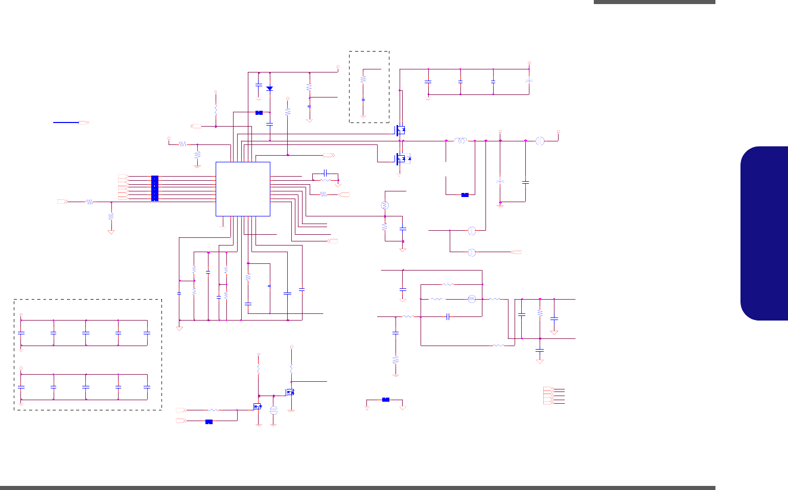
Schematic Diagrams
VCORE B - 29
B.Schematic Diagrams
VCORE
Sheet 28 of 32
VCORE
3.3V S
5V
3.3V S
3.3VS
VDD5
VD D5
V_CO R E VCORE
VIN
SG ND 3
SGND3
SG ND 3
SGND3
SG ND 3
SG ND 3
SGND3
SG ND 3
SGND3
VIN
VIN
PM_DPRSLPVR 5,15
VS SSEN SE 3
H_DPRSTP#2,13
C LKEN #12
VC OR E_O N23
PM _ PW R O K11,15
IM VP 6_P W R GD 5,1 5
H _V ID[6:0] 3
VC O RE3
3.3VS5..7,9..24,27
5V11,16.. 18,20,25..27
VI N11,24..27,29
VD D 524,25,27
VC C SEN SE 3
VC C A
EN _V CO R E
SS
Z2916
BST
VR EFVC
CLSET
Z2911
Z2909
HYS
TTR IP
VR EFV C
CS+
DAC
VSS SEN SE
ERR O UT
VC CA
CS-
VCC A
Z2917
CS 1 N
Z2913
CS-
CS+Z2912
Z2914
EN _VCO R E
TG
Z2901
Z2903
Z2907
Z2902
Z2906
Z2905
Z2904
Z2908
DRN
DR N
DRN CS1N
BG
Z2915
IM VP6_PW RG D
H_ VID [6 :0 ]
VC CS ENS E
V CO R ESEN SE
VCO R ESEN SE
DRN
Z2910
P R25 *10mil_short
PC84
<VALUE>
1
2
PTH2
100K_5%_06 NTC
12
PC88 <V A LUE >
1 2
P R15 *10mil_short
P C87 0.1U _10V_X7R_04
PR 95
<VALU E>
1
2
PQ11
2N7002W
G
DS
PR 115
100K_04
PR116 *10m il_short
PR 10 *0 _04
PR117
10K _04
PC 10 1
180P_50V_04
PC 105
1000P_50V_04
1
2
PR102
<VA LU E>
1
2
PC106
1U _10V _06
1
2
PC90
<VALU E>
1
2
PR 12
100_04
PC 21
<VALU E>
1
2
PQ29
2N7002W
G
DS
PD 8
FM 0540-N
AC
PJ 3
OPEN-5mm
1 2
P R19 *10mil_short
PR 105
<VA LU E>
1
2
PL3
1.5uH _4.7*5.2* 3
1 2
PR 10 4
150K_04
P R18 *10mil_short
PR 94 *15m il_short
PTH 1
100K _5%_06 N TC
12
PU2
SC454
1
2
3
4
5
6
7
8
9
10
11
15
16
17
18
19
20
21
22
23
24
25
26
27
28
29
30
31
32
14
13
12
33
VID6
VID5
VID4
VID3
VID2
VID1
VID0
DPRSTP#
HYS
CL SE T
VRE F
DAC
SS
FB -
FB+
CS -
CS+
TTRIP
DPRSL
RAMP
EN
PW RG D
CLKEN#
V5
BG
DRN
TG
BST
VR TT#
ER RO UT
VC CA
AG N D
GN D
PC 22
<VALU E>
1
2
PC 109
<VALU E>
1
2
PC 13
*3.3nF_16V_04
PR 10 0
130K_1%_04
PC 11 0
0.01U_50V_04
PR 106
30.1K_1%_04
PC8
* 4.7U_2 5V_X5R_08
PC96
<V ALUE >
1
2
P R17 *10mil_short
P R16 *10mil_short
PC93
22nF _16V_04
PQ 23 A
SP8K 10SF D5TB
7
8
1
2
PQ 23 B
SP8K 10SF D5TB
4
3
5
6
PJ 1 5
20 m i l
1 2
PC 17 6
0.1U _50V_06
PJ 1 4
20 m i l
1 2
PC17 7
0. 1U _50V_06
PC 17 8
0.1U _50V_06
PC18 0
0. 1U _50V_06
PR 3
*10mil_short
PC 17 9
0.1U_50V_06
+
PC 82 220U _6.3V_6*5.9
PR81
*1 5 m il_s h ort
PC17 2
0. 1U _50V_06
PC 17 3
0.1U _50V_06
PC17 5
0. 1U _50V_06
PC 17 4
0.1U_50V_06
PC 17 1
0.1U _50V_06
+
PC 71
15U _25V_4.5*6
PR78
680_04
PR 7
<VALU E>
1
2
PR 28 <V A L U E >
12
PC 97<VA LU E>
1
2
PR 11
<VALU E>
1
2
PC70
0.1U _50V _06
PR 88
<VALU E>
1
2
PJ 7
20m il
12
PR 80
10K _04
PC 11 1
*100P_50V_04
1
2
PR14 <VALU E>
12
PR 1 18 * 0_ 04
PC 7
*4.7U _25V _X5R _08
PC100
* 100P _50V_04
1
2
PR9
<VALU E>
1 2
PC 17
100P_50V_04
PR 99
130K_1%_04
PR 13
100_04
PR5
<VALU E>
1
2
PC 17 0
*2200P_06
1
2
P R23 *10mil_short
PR 16 8
<VA LU E>
1
2
PC 112
100P_50V_04
1
2
P R 4 1 7. 4K _1 % _ 0 4
PR 91
<V ALUE >
1
2
PR82
28K _1%_04
H_ VID 03
H_ VID 13
H_ VID 63
H_ VID 23H_ V ID 33
H_ VID 43
H_ VID 53
4A
FOR EMI
FOR EMI
7/23
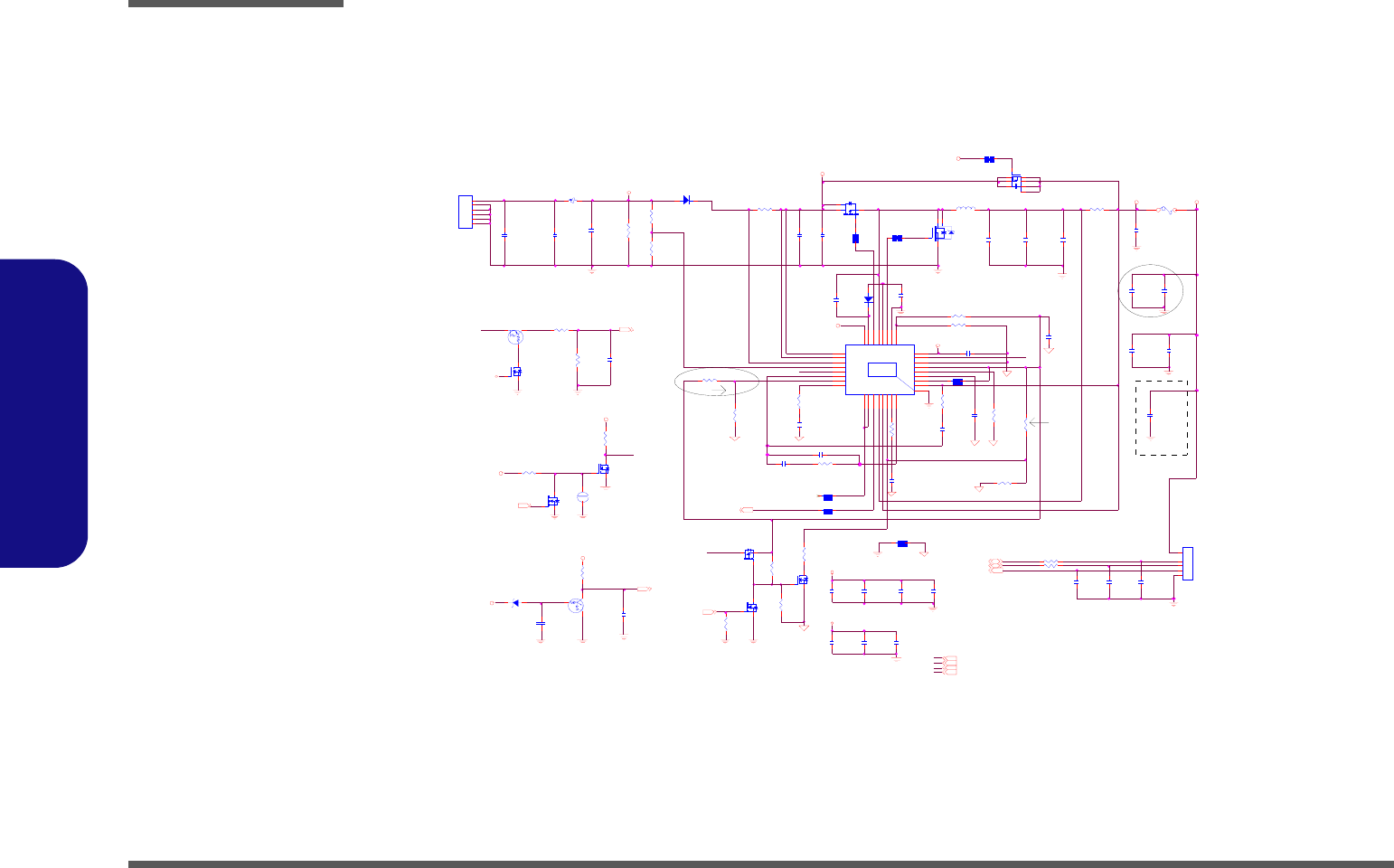
Schematic Diagrams
B - 30 AC IN, CHARGE
B.Schematic Diagrams
AC IN, CHARGE
SY S5V
VA
BAT
VIN
VDD3
SG ND 5
SG ND 5 SG ND 5
VA
SGN D 5
SG ND 5
SG ND 5
VA
VA
SG ND 5
VIN
VA
V_BATBA T
SG ND 5
SGND5
SYS 5V
SYS 5V
SGND5
B AT_VO LT 23
VIN 1 1, 24 ..2 8
SYS5V 2 5
VDD 3 2,13,20,23..25
VA 24
CH G_C UR23
SM D_BAT23 BAT _DET23
SM C_BAT23
CH G_ EN23
CELL_CONTROL23
AC _IN 23
B AT Z 3034
Z303 5
Z3001
Z3030Z 3010
Z3005
Z3029
Z3023
Z3031
Z301 9
Z3028
Z3022
CT L 1
Z3020
Z3007
Z3026
Z3032
Z3018
Z301 5
Z3027
Z3012
Z3004
Z3025
Z3009
AC_IN
Z3013
Z3016
Z3014
Z3017
Z3039
Z3003
Z3038
Z3037
Z3008
Z303 6
CTL1
CH_VREF
Z3024
AC_IN
Z3018
CECLM
PC58
4.7U _25V_X5R_08
PD20
FM10 40-T1
A C
PR169
100K_04
PC 23
2200P_50V_X7R _04
TRERMAL PAD
PU 3
M B39A 132
1
2
3
4
5
6
7
9
10
11
12
13
14
15
17
18
19
20
21
22
23
25
26
27
28
29
30
31
8
16
24
32
33
VC C
-IN C1
+IN C1
AC IN
AC OK
-IN E 3
AD J 1
-I NE 1
OU T C 1
OU T C 2
+IN C2
-INC 2
ADJ 2
COMP 2
BATT
ADJ3
CS
RT
VREF
GND
CTL 1
CEL L S
PG ND
OUT-2
VB
LX
OU T -1
CB
COMP1
CO M P3
VIN
CTL2
SG ND
PR20
10K_1%_04
PC 102 1000P_50V _X7R_04
PD3
*U DZ16B
AC
PMBAT1
BTD-05 TI1G
1
2
3
4
5
PC57
4.7U _25V_X5R_08
P R67 10_04
PQ 19B
SP8K10SFD 5TB
4
3
5
6
PC181
0.1U _50V _06
PQ3
2N 7 0 02 W
G
DS
PC1
0.1U _50V_06
PR37
10 K _ 0 4
P R68 10_04
PC 11
1U_25V_08
PC4
100P_50V_04
PC15 0.1U_50V_06
PR32
10 K _ 1 % _ 04
P C24 0.1U _16V_04
PR90
1K _ 1 % _ 0 4
PD 1
FM0540-N
AC
PQ4
2N7002W
G
DS
PQ24
AM4835P
4
62
5
73
1
8
PC 66
0.1U_50V_06
PR64
10K_1% _04
PR 103 22K_1% _04
PC 54
0.1U_50V _06
PL1
H CB4532K F-800T60
PC 78
4.7U _25V_X5R _08
PC 160
0 . 1U _ 5 0V _0 6
PQ 5
* DTC 114EU A
C
E
B
PR33
100K_04
PC80
4.7U _25V_X5R_08
PC79
4. 7U _25V_X5R_08
PQ 48
AO 341 5
G
D S
PR38
30K_1%_04
PR 79 * 15mil_short
PR 31 * 10mil_short
PR 84 20K_04
PC 34
*0. 1U _25V_06
PR63
10 K _ 0 6
PF1
5A
PC59
0.1U _50V_06
PR34
100K_04
PQ49
2N 7 0 02 W
G
DS
PC56
0.1U _50V_06
PC 103 *22P_50V_04
PC12
0.1U _50V_06
J _D C- JAC K1
2DC -G213-B200
GND2
GND1
2
1
GND4
GND3
PR8 *15m il_s ho rt
PR 70 20m _20
PC 74
*4 .7 U _2 5 V_ X 5 R _ 0 8
PC91
0.1U _25V_X7R_06
PR 27
*10mil_short
PC 60
0.1U_50V_06
PR 26
10K_1%_04
PC 25
10 00P_5 0 V_X7R _ 04
PC 65
0.1U_50V_06
PQ7
D TA1 14EU A
CE
B
P R29 100K_04 PR 10 7
13 . 7 K _ 1 % _ 06
PC68
0.1U _50V_06
PC 2
100P_50V_04
PC 3
100P_50V_04
PL2
10U H 2.0A 6.7*6.3*3.5
1 2
PR 98 21K_1%_04
PR 92 39. 2K _1%_04
PC 5
0.1U _50V_06
PC67
0.1U _50V_06
PR 73
* 10m il_short
PR 39
6.04K_1% _04
PR 85 *0_0 4
PJ1
20mil
1 2
PQ 2
2N7002W
G
DS
PC98
100P_50V_04
PQ19A
SP 8K10SFD 5TB
7
8
1
2PR69 20m _20
PC 33
0.1U_16V_04
PR 101
49.9K_1%_04
PC 75
*4 .7 U _2 5 V_ X 5 R _ 0 8
PC20
0.1U _50V_06
PC 55
0.1U_50V_06
PR171
1. 5 M _ 04
PQ 6
2N 7002W
G
DS
PR6
*10m il_short
PC 9
0.1U_50V_06
PR62
130K_1% _04
PR 30 * 10mil_short
PR170
36K_1%_06
TO T A L
PO W E R
AD J
CHARGE
CURRENT
ADJ
0.5V/1A
Bttery Voltage:
6V~16.8V
1.7A
3.6A
3.6A
3.6A
3.6A
3.6A
FOR EMI
7/23
Sheet 29 of 32
AC IN, CHARGE
Schematic Diagrams
CLICK BOARD B - 31
B.Schematic Diagrams
CLICK BOARD
Sheet 30 of 32
CLICK BOARD
CGND
CGND
CGND
CG N D
CGND
C5V
CG N D CGND CGNDCGND CGND CGND
CGND
C5V
CTPBUTTON_L
CTPBU TT O N_ L
CTP_ CL K
CTPBUTTON_R
CTP_DA TA
CTPBUTTON_R
CTP_CLK
CTP_DATA
CJ_TP1
8 71 5 1- 12 0 7G
1
2
3
4
5
6
7
8
9
10
11
12
CSW1
TJG-533-S-T/R
3
14
2
5
6
CC1
0.1U_10V_04
1
CH4
MTH237D91
2
3
4
5 6
7
8
9
1
CH2
MTH237D91
2
3
4
5 6
7
8
9
CJ_TP2
85201-04051
1
2
3
4
1
CH3
MTH237D91
2
3
4
5 6
7
8
9
CC2
0.1U_10V_04
1
CH1
MTH237D91
2
3
4
5 6
7
8
9
CS W2
TJ G -5 3 3- S -T / R
3
14
2
5
6
6-20-94A20-112
CSW1~2
4
1
12
CJ_TP1
2
13
LIFT
KEY
RIGH T
KEY
CJ_TP2
1
4
CLICK BOARD
6-20-94A50-104
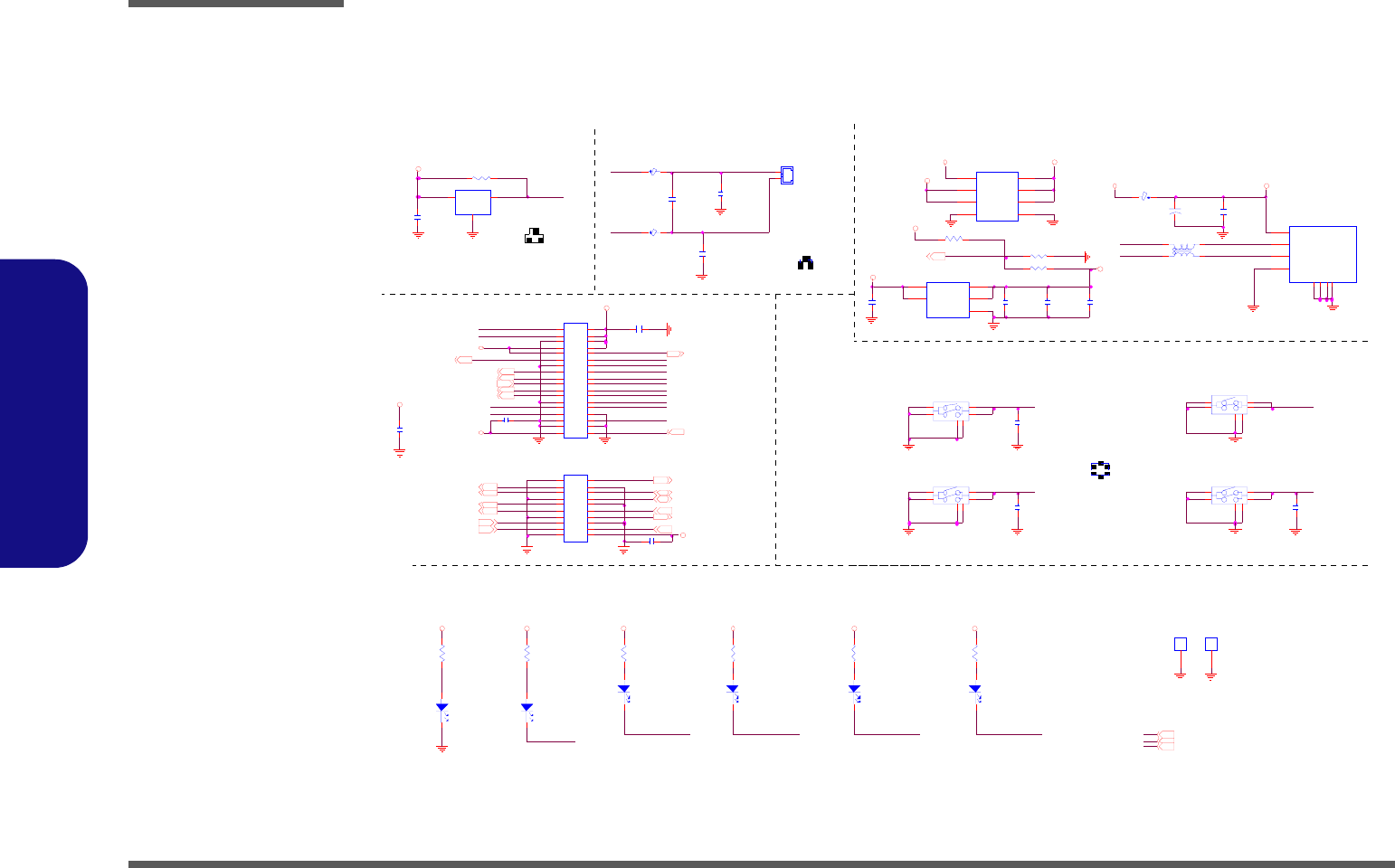
Schematic Diagrams
B - 32 Multi B’d, LID, LED, SW, USB
B.Schematic Diagrams
Multi B’d, LID, LED, SW, USB
M_USBVCC22
MGND
MG ND MG ND
MG ND
MG NDMGND
MGND MG N D
MGND
MGND
MG ND
M _3.3V
MGND
MG NDMG ND
M_3.3V
M_ 5 V
MG ND
M _3.3VSM_3.3VS M_3.3VS M_3.3VS M_3.3VS
MGND MGND
M _3.3VS
MGND
M_1.5VS
MG ND
M_3.3V S
MG ND
MG ND
MGND
M_5V
M_5V
M_5V
M_ U S B V C C 2 M_ U SBVC C2
M _U SBVC C2
M _ US BV CC 2
M_3.3V
MG ND
MGND
MGND MG N D
MG ND
MG ND
M_3.3VS 32
MAZ_SDIN132
MA Z _S DO UT32
MA Z _R S T #32 MA Z _B ITC L K32
MAZ_SY NC32
MW LA N _ E N 32
MW LA N _ D ET # 3 2
M_3.3V 32
MU SB_PP4 32
MU SB_PN 4 32
MC L K _P CIE _ M INI#32
MCLK_PC IE_MINI32
M_1.5VS 32
MPC IE_TXP 1_WLAN32
M PCIE_TXN1_WLAN32
M PC IE_RXP1_WLAN32 MPCIE_RXN1_WLAN32
MB U F _ P L T _R ST # 32
MP C IE_ W AKE # 3 2
MW LAN _CL KR EQ# 32
M3 G _E N 3 2
MU S B_ OC 2 #
MUSB _O C2#
MW E B 0#
Z3202
MH D_ L ED#
Z 3201
Z3205Z3204
MWEB1#
MWEB2#
MU SB_ PP2 _ R
MU SB_ PN 2_ R
MM _B T N #
MN UM _L ED # M SCR OLL_LED#
MUSB_PN 2
MUSB_PP 2
Z3206
MW E B 2 #
MC AP_L ED#
MW E B 0 #
MW LA N _ DE T#
MT H RO T TL E _ L E D #
ML ID _ SW #
MN UM _ L E D#
MDD-SPKR+
MDD-SPKR-
MS CR OL L _L ED #
MM _ B T N#
MU S B_ OC 2 #
MH D_LED #
MW E B 1 #
MLID_SW#
Z3203
MCA P_LED# MTHROTTLE_LED#
MW LA N _ E N
MU S B _ P N 2
MU SB_PP2
M DD -SPKR -
M DD -SPKR +
M DD -SPKR -_ R
M DD -SPKR +_R
MUSB _O C2#
MC 3 5
*0.1U_16V_04
ML4
* WCM 2012F2S-161T03
1
4
2
3
MU 3
*R T9701-CP L
1
2
3
4
5
VO UT
GN D
VIN
VIN
VO UT MC 3 6
*10U_10V_08
MR 22 *15K_04
MC33
* 10U _10V_08
MC 11 0.1U _16V_04
MC18
180P_50V_04
MR 24 10K_04
MR7
220_04
ML7
FC M1608K -121T06
MR 23 *10K_04
MR8
220_04
MD 4
KP-2012S GC
AC
MS1
SM D80X80
11
MC 3 4
*0 .1 U _1 6 V _ 0 4
MC19
*0.1U_16V_04
MS W 4
TJ G - 53 3 - S - T / R
3
14
2
5
6
MD 1
H T -1 5 0N B-D T
AC
+
MC 1 5
*100U_6.3V_B 2 MJ_USB1
* C10 7B3- 10403- Y
1
GN D1
2
3
4
GND2
GN D3
GN D4
V+
shield
DA TA_ L
DA TA_ H
GN D
sh i e ld
shield
sh i e ld
MR 5
220_04
MJ_S PK1
88266-02001
PC B Footprint = 88266-2L
2
1
MC 31
* 0.1U _16V_04
ML 6
FC M1608K -121T06
MR2
220_04
MJ _ MF B 1
5P1-251A4-13V00-218
12 34
56 78
910 1112
1314
1516 1718
1920 2122
2324 2526
2728
2930 3132
3334 3536
MS W 1
TJ G - 5 33 - S - T / R
3
1
4
2
5
6
MC20
* 0.1U _16V_04
MU 1
EC 2648-B3-F
1
2
3
VCC
GN D
OUT
MJ _ MF B 2
5P1.251A4-13V00.210
12 34
56 78
910
1112 1314
16
18
20
15
17
19
MR4
220_04
MC12
0.1U _16V_04
MC17
180P_50V_04
MR6
220_04
MD 2
KP-2012SG C
AC
MC 3 0
*0.1U_16V_04
MR 1 10K_04
MC14
* 0.1U _16V_04
ML 5
*H CB3216KF -800T30
MC 1
0.1U _16V_04
MC23
* 0.1U _16V_04
MD 6
KP-2012SG C
AC
MS W 2
TJ G - 5 33 - S - T / R
3
14
2
5
6
MS W 3
TJ G - 53 3 - S - T / R
3
14
2
5
6
MD 5
KP-2012SG C
AC
MS2
SMD80X80
11
MD3
KP -2012SGC
AC
MC 32
*1 U_ 1 6 V _ 06
MU 2
*UP 7534BS8
6
83
2 7
14
5VO UT1
VO UT3VI N2
VI N1 VO UT2
GNDEN #
FLG #
SW 6
SW 4 S W2
3
42
PSW1~8
SW8
1
HOT KEY & POWER SW
LED
HDD/CD-ROM
LED
POWER
SWITCH
LED
NUM LOCK
LED SCROLL
LOCK
LED
CAPS LOCK
LE D
60 mil
USB PORT
THROTTLE
LED
PSU1, PSU2
1
LID SWITCH IC
SPEAKER CONNECTOR
3
2
PJMODEM
1
2
M _3 .3 V S NE ED 4 A
6 - 21 -C 17 0 0- 21 8
6 -2 1 -C 17 00 -2 1 0
50 mil
100 MIL
50 mil
7/16
Sheet 31 of 32
Multi B’d, LID, LED,
SW, USB
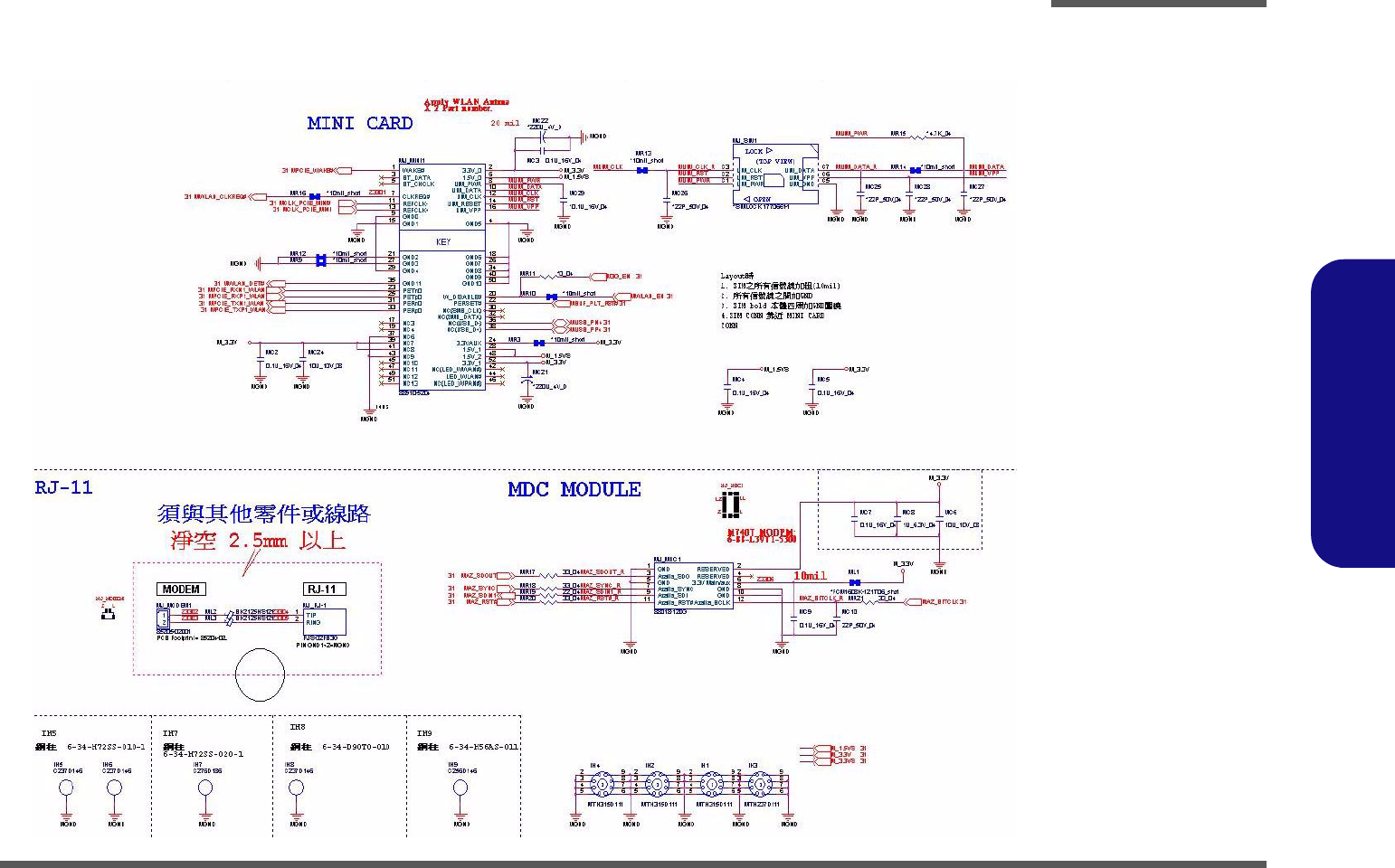
Schematic Diagrams
Multi B’d, Mini Card, MDC, RJ11 B - 33
B.Schematic Diagrams
Multi B’d, Mini Card, MDC, RJ11
Sheet 32 of 32
Multi B’d, Mini
Card, MDC, RJ11

Schematic Diagrams
B - 34
B.Schematic Diagrams